
Digitized Speech Transmission at VHF Using Existing FM Mobile Radios
Upload
khangminh22Category
view
1download
0
J20419F
A PUBLICATION FOR THE RADIO AMATEURESPECIAllY COVERING VHF, UHF AND MICROWAVES
VOLUME NO.8 AUTUMN 3/1976 DM 4.50
-
COpIUfl' retrectcr
Mom reuec tc
••, •
I" •
•~
•
" ~ ID . ) '0 •j
.... 100 _...

VHFCOMMUNICATIONS
PubU,h" by :Verlag UKW·BEAICHTE Han. J Dohlu. oHO Jannw.fIe \-4 0 -8523 BAIEASOOAfFed Aep of Germany Telephones (091 9119157 I (0 9133) 855, 856
PubUlher , :T, Billan. H Dahlu.
Editor. :Terry 0 a,UlIn , G 3 JVO I OJ 0 eo, responSible 10' the 'tiKI and '.youlRobert f Lentz . OL 3 WR. responSible lor the technical co nllnt,
Ad"l rl il lng mln.v, r:T. B,tta"
VHF COMMUNICATIONS,11'11 In ternational ed iti on 01 Ihe Gorman pubhc.hon UKW·BEAICHTE . II .. quarter ly amaleu r
radIO magazine especially cat,m' \l 10' Ii'll VHF/UHF"tSHF 'ec hnolooy It " published In
Spring. Summer, Autumn. lind W,nter The l ubel;:np llon pm;:e " OM 16 00 or "Il,onll equ lva"len l per y".r Individual co p,es Ir, ava,lable al OM .. 50, Of eqUlvllent. each Subscflphonl .order, 01 tntlovKlulI1 coc.ee, purchase 01 P C board. lin<! adve,t,!MICI &peel.' com po nents,adv.rhsements and con tribut ions to lhe magllintl shou ld be addr• • Hd to the na',onal rep re eemauve
• V.rllg UKW·BERICHTE 1916Ait figh t. r_ rved Reprin t•. ',. n. tallon. or e~l'lc l ' OnlV With lhe wri ll en approval o t thepubli.her
Pfinle(l In the Fed Rep 01 Germanv bV R Reichenbach KG Krehngllr39 8500 Nuernberg
VERTRETUNGEN :
~jl,u ......._.C. n...._.,~
'r."".' ...,.....O_uy
HoIllnd,....,11. 1,~u .__.... , ....nd-.._ "'Mel_.-.-Y--......
R E PR ESE N T A r iv E 5 :
_J DoNuo c....._lIn ""._n ....It '" ,,'" 1'·110_ P1c ••"' W'E," I let'OlIWlA~ 80. 1:100 T(l(lf\Aol. VIC"~1 f ll l~.tlIN_ o.m.- P1c.~10 ~~_ .. ..._,
-",E ......... . OZ1~. """",0<1(11 50.... [lIl-4'001l'OlQsrED P....,"01,.800C."OI'_ "'''' .... ~ ,sa.o ~...PAA~Y. l" I'>INoIl-,-V... , UIIW-IIERICHTE H Donlu. oHQ JI .I<II' , ~ a -1m eAIERSOORf , ., 01':13·'" '"I(on Pooloe.... . ......'" ,"u' n_, )')01 " -Mol eon......_ n. l"._ 120-" ""o.u.oe"' llon. E,"_ 1t - ~lI:l eo_ 0.'_ """'oe_.. .....oNu,,,,,, )001~' I!lt
Z "-,, ~ .~ ~f PO 110. 212 . " MOl"'N 21'00 , , .. '''·~ ,1'4Qll
aTE., I 112OMI VII .,., " . 1·20 '30' "" LANO , .. 10212" '"' .Conto CO" ""'" 31014_P W. n" . U I CW f_, OUDElAtroE """'oe_.......o 110~E '" '''........'' ..... I I I ,0.00 "0 80. fill WE ~ ~ a~ORO 'Il &024......."" r""lT LA ~ YO """'_. 10 "' -'J2~ n .......£R _,,,......."" 3 "00011SAl'utIIoc.o_ P080'21J2 ~f1llUllD2'OOOf~n·.~.
.....10,0. "'__ EA ~c.. MADRID·" oew-ConMfIII$ II '01 1QU"s...._ 5 MfO" 0-.--....,..- ...·11601 V£ ~~ INGE '''~XI
"",",," 0 QOIIM ·~
_J~ SC....... "__ 'UIIOCH """_l'U-~' P1c""""lUfUCHIO-"" .........600 20 f-..toft C_ OI.D CO!AIoD()Io CIl J I ~HVHF ~1CA'IQI<lSR_"""""'" ~ "'f1 1 G.o<y__ W2 1.lCl
." ........ _,. JAUl: S'QWl< NY '~ I'O' 'Il 111" f3.0 $f,1O C•• • ....c YU-MOOO V"'''<NCI ~ ...~_ .
A PUBLICATION FOR THE RADIO AMATEURESPECIAL LY COVERING VHF. UHF AND MICROWAVESVOLUME NO.8 AUTUMN EDITION 3/ 1976
H, Berner
VOEINTG
F Wein gartnerOJ ell
DrJng , H scmerrenOL3ZU
The MOIl Importan l Features andCharaCle nSI!CI 0 1 GHz Ante nna s
A TransmI t Converte r lor 432 MHIwith SChOl!ky Rin g M,xer
Des.gn 01 TranSistor Frequency Multipliers
130 · 14 1
142 ·150
151 • 1504
R LentzDL3 WA
AM SAT
Newsletter t 176
J. Kestl erOK 1 OF
DE. Schmi tzerOJ 4 BG
J , KesUer
OK 1 OF
E51lma hng the S,gnal-to-Noise Raho 01an ATV-Llnk 155 ·157
Mod ll!cal lon al tha STE Receiver ARAC t o:<, lor Recep tion 15801 ' he OSCAR Satellites In th e 10 m and 2 m Band
A Unive rsal Converter lor HF and VHF 159 - 174
A Second Version 01 the Mod ular AF·Amphl ,er 175 · 180and Volta ge Stabilizer
A Preci Sion Digital Mulhmeler 181 • 191Part 2, Input Ampll l 18t and Power Supply
~ VHF CO MMUNICATIONS 3/1976 . 129 -

THE MOST IMPORTANT FEATURES AND CHARACTERISTICSOF GHz ANTENNAS
by H. Berner , VDE/NTG
Mor e and more telecommunications Bctl Vlty is moving 10 the micr owave bands, main ly due tothe o var load lng 01 the frequency range under 1 GHz . but also due to the high dlt&Cllvlly andgain tnet can be obtai ned using relall vily co mpac t arrays. Beamwldths 01 t and less caneasily be realized . It is known tha I the lower the beamwidth, the higher the gain 01 thean tenna Thi s mean s tha low output power levels will be able to provide sc tuoent signalstreng th over greater di stan ces Further ceraue regard ing propa gahon al frequen c ies ine..cess 01 1 GHz are 10 be dealt With sepa rately
1. MICROWAVE ANTENNAS
This arti cle is 10 be limi ted 10 antenna deSigns lo r the freq uency range 01 3 GHI to 30 GHI ,mainly be cau se it is in ex cess o f 3 GHl where the an lennas diller Irom those known in
VHF/ UHF techno logy. and sin ce very little activity is actually bein g mad e at trequencses mexcess 01 30 GHl. The range 01 frequenc ies between 3 and 30 GHl IS also call ed th e cenumetric w ave range. It is in thi s range where there are suc h a large number of different typeso f antennas, especially in th e sphere o f ape rture antennas.
Horn An tennas
Pyramidal ho rns
Secto ral ho rnsCorr ugated hornsConical horns
Double con ical horns
Ap e rlur e Anl enn ••
Reflector An tennas
Parabolic anlennasShell -shaped antennas
Hog ·horn antennasCassegraln anTennas
Cylindrical pere bchca
Discrete Antennas
srct ted-une radl al orsMult iple-element arr aysPnnted cncurt antennas
Pnase-ccntrcued arrays
Log arit hmi c
periodic Antennas
LP v -AntennasLP Dipole Antennas
Sp iral Antennas End -on Arr ays Focu ssed Arrays
D,p' lng HtIHmut Ber..... " 11 I t. lt-member ot St. nd. rd Eleklrok Lo'en, AG
- 130 - A VHF COMMUNICATIONS 3/19 76

2. SPECIFIC CHARACTERISTICS
2.1. Microwave antennas are large with raspeclto Ihe wavelength . Thi' means thai gene rallygeOmelric and optical laws must be used 10 describe the radiation mechanics.
2.2. Linear bodies such as dipoles are no longer used lor reo-encn . bUI reuecnve surfaces orspecially shaped waveguides (horns).
2.3. Lo w beamwid lhs can be aChieved with handy dimensions, Th is means a high di rec!lvl tyin both planes. which ensures that lh e inlarference to other services on the same Irequency and ground reuecuon are kep i 10 a minimum ,
We are to drtterentiate between ~ga l n. and ~d l rec t l v l ty., Both 01 these designahons are usedin the NTG recommendations 1301 01 1969. The main dnterence is that the same po wer is tedto the test antenna and reference antenna in the gain measurement. whereas II is memeasurement 01 the ettecnve rad iated power that is cetmeo in the directivity measurementThe relationship between gain G and directivity 0 is'
Where th e anten na etlicien cy is: '1 :ii I .
The ga in meretore in cludes the losses in the antenna and any reqUIred mat chmg networks,
The di rec tivity can be obtained trom the measured radia llon diagram by means 01 integrahon .and does not inc lude the losses.
A hatlwave dipole or isotropi c radiator are o tten given as relerence antenna , All gain anddi rec tiVi ty values given in this article are ret eeree to an isotrop ic radia lor and are given in alogarithmic scale (dB ),
3. MAIN TYPES OF ANTENNAS AND THEIR CHARACTERISTICS
3.1.1. Horn Antenn . ,
The aperture Of the horn can be ctessec as radiating surf ace and the main rad iahng characteris tics can be cal culated trcm true. The surf ace shou ld be assumed to be covered With anmll nl te nu mber 01 inlinitely small elementary rad ial ors, The rad iallon diagram results I rom themterterence ol lhe ma ny mdividual radia lions, Directivity 01 a pyramidal hor n (see Fig. 1) canbe calcu laled approximately as tcuows:
0.10 10gCO :,x b) dB
Where - a.. and .b~ are the lengths 01the aperture sur taces.
A VHF COMMUNICATIONS 3/ 1976 • 131 •

In pract ice, a value 01 between 15 dB and 25 dB result s, Horn antennas 01 th is size ellh,bltlow atdelobes. However. i f the horn and thu s the direc tivit y are Incr eased, this will also Increase the aroe scbes. II th e beamwid ths 01 the horn are sulllcienUy small . e g HI' . ,I ISpossible to match a horn antenna in a frequency range 01 I : 1.5 , Speci al types 01 horn s allowa frequency range 01 1 : 10 w,th a VSWR 01 2.5 : 1
In addi tion to the previously men tioned pyram idal horn . one also uses comcet, sec to ral,corrugated and double-conical horns. Sin ce horn antennas are relat tvely easy to manu facture, th ey are very popular as ind ividual anlennas, standard-g ain antennas, as driVin gelements 01 reflector an tennas. or as Ind iVidual elements In phased arrays (see 3 13)
3.1.2. Rell. etor Antenn"
Reflector type an tennas represent the largest group of aperture antennas (see Table 2).
Ope ratio n can be co mpared With thaI 01 an automobile headli ght and need not be discussedin de tai l here, Smce the reflec ting surface must be large With respect to the wavelength , as Inoptics. these antennas are usually only used in the cenllmeter and mil lim eter wave ranges
U..T y p e Prlnc:lple S'''Il'' '.- ... wl " .......".,.,- - -1.4",.,.,... ,.,.. Sa,."". .........
FRONT -FED PARABOLIC~
sa,."". ......... Sa,.M.AN TENNA
,~. ~.. on,.......HI'......... ,-,,~..
SHELL-SHAPED ANTENNA r ...,.,_... I..... -/~
HOG-HORN ANTENNA b ...,.,.,.,... ..",.50'..""' . _
-CYLI NDRICAL PARABOLIC ~ Ro<Io' - -
CASS EGRAIN ANTENNA "....,_.........!I.t,..,., • • """'" ,-,
\ ,~.
GREGORIAN ANTENNA 'J ..,'.........
Rellecto r type an tennas ellhlbil a Simple ..nd robu st construc tion, allow Simple leed systemsand provide a good trent-to-ceca reno. The s,mplest and most popu lar type is there fore thelront-Ied parabo lic (see Fig . 2).
The parabolic reflector is energize d by a horn mount ed at the local polnl The microw aveenergy is fed to the horn via a ben t wavegUide . The directiv ity IS dependent on the 'oll OWlngrelat ionshi p and is usually in the order 01 10 dB to 60 dB :
- 132 - ). VHF COMMUNICATIONS 311976

•
Ag
.<I:
Rec
tefM
iule
.h
otn
,.d
'.lo
'!O
f'<I
GH
z
•••
I.
",-
--
" .f--
4--+
-
•
IJ
.,.l 1-/
......
•ID
~....
-·~
IL
_.I
'D•.
-j~
/I~
~--,
•~
---
•D
IA-
• •
"
....,<.
....-
-
Fig
.I:
L.b
ofel
ory~
of
eeo
.del
mul
timod
oe.!
tdle
lor
Fig
.3:
Gel
"01
ep
efe
bo
ke"l.-
wit
hde.~I~
fro
mth
ekM
elpe
..bo
llc:
ahep
e
Ag.S
:R
ed/.
lio
np
en..
..of
•tq
Ue,.~
.ed
ielo
r

With. g,yen wavelength. the d"echy ,ly will ,nc rease on Increasmg the dlilmelel Ho wl:tVer. ,nprecuce tnere are l lmrlrng laclor s smee tnaVOIdable lolerances 01 the reflec ting surfacereduce l he directiVIty . as can be seen ,n Fig . 3 The gain relened 10 an ISOIIOPIC ,adl alor GIwas calcu lated according 10 the tollowlng equatlorr-
01 - ll(lt ~' e '1 59(:1~'t),-) D /..' I
1••( ~)'Where: 'I • scrtece area used
.\ _ Square mean value 01 the dimenSional de ... iatlons
o • geueetcr diameteri • Wavelength
II is mamly horn ant ennas With a square , rect ang ular o r cncuter crOSS-!le'Cl lon thaI ate usuall y
used 10 feed the anlenna (Fig. 4)
In spi te 01 the aqUIre aperture. the radiation Charac teristics In the E· and H·planes ared lllereni d ue 10 the dillereol cu rrent ratlol in each cten (see Fig. 5).
Sin ce the erceicoe suppression and the dm,chvl ty .re mamly dependent on the dllUrtbutlon 01' he ene rgy Irom the horn 'Athe reflec 'mg surlace. melhod ' o f optlmllmg th iS energy dl,'n ·bullon were sought. The cenlral laboratonM oj the German PTI therelore developed a so called coaxial rad ialo r (Fig. II). wh ich excIIM several wave modes Within I" aperture planeand thus obtains an app,oxlmate'y symmetric al energy d istribution on tee reuectcr .
A cOH ugated horn (see Fig.' and ' l also prOVide' a vlttuaUy symmetrical ene rgy d.,'rlbuhonIn all plane,
How ever, there are other methods o f obtamlOg I lavourable energy dl slrlbutlon .
She ll ·shaped (Fig. 10) and hog -horn an 'ennas (Fig. 11 Ind 12) are construc ted 10 a slm,larmanner '0I ron t· fed pa rabolics , The di llerence IS 'hat no Circular parabolic reflector IS usedbUl only a section o f such a rellec 'or ,
These an 'ennas exhlbll a Iar better sldelobe supp reSSion than In 'he case WIth Iront-Iedparabollcs However, 'he vert ica l and hor llontal d iagr ams are d llle'en, du e to the ir no n symmetr ical cons,ruchon , The en clO&eCl constrUC'lon ma"es such anl enna s msens"lve toenvironmental mlluences
The casS8'graln antenna is onc e again I " uely para bo hc antenna In which the wave s areceuectec tw ice (see Fig. 13 Ind 141.
Th iS type 01 anlenna has the advanlage thaI 'he long ben l leeder 01 Ihe parabo li c IS repla cedby • sho rl waveguide , This is espec ially 01 Inleresl lo r antennas used In radl o as'on omywhere ' he waVill;lUlde loss betwee n an'anna and receiver should be as Iowa. pOSSible,
• 13-4 • A VHF COMMUNICATIONS 3/1976

fig
.7:
eo..
......
......
......
,...
...
1FT
Z.
W.G
_..
"
e ". • •
, ,.-F
ig.I
:L
ab
ofa
tory
onod
e<l0
1a
c:o
nvg
ate
dh
om
_.-
uF
ig,
11:
Pri
ncl
pte
ofa
1'Io
m
,.
,ab
ollc
lho
g-1
'Iom
1

A l ruely parabolic construc tio n also has the advanlage tha i two waves can be transml1led andreceived when using cross pctenseucn. It may be a di sadvantage met the aob-reuectcrcovers a part 01 the reuector surface. whi ch means that the Ilrst sidelobe s are only suppre ssed by 13 dB 10 17 dB (see Fig . 15) co mpared 10 18 dB 10 23 dB with other lype s.
The previ ously mentioned reuect c r antennas with directiv ity tactors from 20 dB to 60 dB areused lor microwave links, space communications, radio astronomy. satell ite ground stations(Fig. 17), and lo r radar eccuceucne.
The cylindrical parabolic anten na should also be mentioned whose reuecuve surface is onlyparabolic In one plane (see Fig , 17),
This type of antenna posse sses antlrely dillerent beamwidlhs In the hOrizontal and verti calplanes , as is olten required lor radar app licationsExample : 2.4· horizontal and 6.S· vert ica l beamw idth .
A elctted wavegu ide (Fig. 18} is normally used lor energizing such ant ennas . This is a slraighlpiece of waveguide Into whi Ch slots have been cut on the side laCing the refl ecting eurtace.These slOIS radial e energy towards the reuect cr . II is possible by alteflng the geometry 01 thestore to vary the energy dl slribulion alOng lhe leng lh of lhe wavegu ide 80 a8 to achieve aside lo be attenueuon of 20 dB and more .
3.1.3. Antenn.. with Discr et e Elemenl,
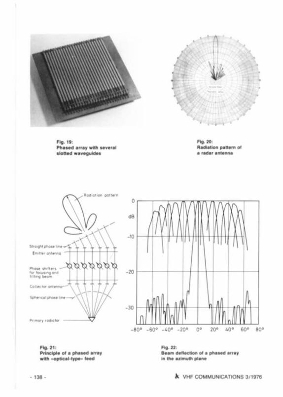
As in tne lower frequency ranges such as VHF, It is also poSSible In the micr owa ve range 10combine a large number of ind ividual elements to te rm phased arrays. Virtually any radlallonpatt ern can be co temec in thi s manner. One of me horn types, or slotled line s are ette n usedas indlvlduel elements, Fig. 19 shows suc h a phased array comprising several erctree waveguides,
The di rectivity and etoeroee ertenueucn il dependent on lhe lil e ot lhe array and on thedistribution 01 the energy . The array shown In the photograph is approximately sao mm bySOO mm and the · 3 dB beam wid ths in the H- and E·planes amounts to about S·, The eroetoeealtenua tion is al least 20 dB (see FIg. 20).
II is possible by alte ring the phase relationships between the individual element s to chang ethe direct ion 01 lh e radiation pat tern A very special, but interesting example is given InFig. 21.
The energy distr ibution 10 the indi vidual rad iating e'em ents i8 1'101 made With the aid 01 linesbut in free apace by radiation between the primary radiat or and a number 0 ' co llec to rantennas. A phase-stutter is provided between each 01 these couec tc r antennas and theradia ting emitter antennas. II is eose.ore 10 shll t the beam In both plan es by co rrect adju stment 01 th e phase relationships (Fig, 22).
• 136 • ~ VHF COMMUNICATIONS 3/1976

- - - - Fi9-
13:~
...e-.,
.-
---
....
'1:
---..
1III
_.-..
9"0
.11
8,_
....
....
.
.......
......
1SR
.do.
ta..
."..
....
ea-.
-.,...~_J
ItG
M.r
• •
, I
•
fig. It"".Mel ...., ...........1-"oft.cl • • • ...,..
f • . 2'0:R...__ p.n. ... of.......-.-
-" I-P'-t-i-Y-H t IIl1t+1
I \/11/
II
~,
-201--+---+- +-1- - \-'---I- -+--j
-JO f-
In
fig . 21:Priftc... CIt • ,... ,..... ~.HJp8-0....
fig . n :..__fIectoooI of ,
.. ."......,..~
. 138 • ~ Vtif COMMUNICATK>NS 3/1918

A comi ng trend is the use 01 pr inted strlpllnes In phased arrays In thiS case , the individualrad lahng elements are repla ced by a com ple te phased array In the form 01 a prlnl ed cncuuboard The advanlage 01 Ih lS IS Ihat the man ulactu re ct targe numbers 01 these antennas isSimp le and Inexpens ive. and th e anlennas are very I lat and lightweig ht. The disadv antage ISIhat the losses are retatlvely high . When uling a PTFE base material . a 10SI 01 app roximalely2 dB per meier wil l present at X-band IrequenCles. whereas With wavegUides only approxImately 0 ,1 dB /m Will be exhibited A line length 01 1 m IS nOI sulllClent even lor smallan lennas, which means th at losses In the order 01 3 dB 10 9 dB are exhlbl led by pri nted.phased arr ays.
Fig , 23 shows the prlOciple 01 a pnnled slo t an lenna as an example, Siois are etched «uc thelro nl 01 the board , and lorm Ihe rad iatlOg elemen ts The alots are coupled to a srnprmeteedee, wh ich IS li lted to ensure a sllg hll y d illerent coupling to the slOIS accord lOg to the required energy d istr ibution , The base mal erial is glassllbre remtcrced PTFE (Tetlon). Due tothe Ina voldable tcre reoces 01 the elc hlng process . printed antennas are only used uptoapproximately 35 GHz.
Spi ral antennas are In a cl ass 01 thei r own . and are usually also manu lac lured In prin tedc irCUit techf'lO!ogy , In the case 01 Fig. 24. two !plrals are wound on a I lat eurtece The twoInner ends are led symmetrica lly . and th l' Iype can be compared With a bent crocre conllguration , Due to the varying spacing between the two spi rals a resonance condlhon lor anyIr equency w ill appea r at venous polnll on the spiral . wh ich means that l he anlenna can beused over a very Wide Irequency range ( I : 10 to 1 ; 40). Thl! pol arisation IS linear at low Irequencies and becom es mor e and more Circular lowards higher Ir equenCles The recrenen isperpendicular 10 the pla ne o f the spi ral. and the - 3 dB beamwid lh 01 the antenne shown inF~. 25 IS In lhe order 01 90". Such antennas are used nearly exclUSively l or aeronauticalappuc atm ns. where i ls extreme wldeband cha racterlshcs can be uhhzed to the l ull
The sp ira l can also be wound on a cone so that a semH:lrcular radiation pattern resu lts.
FIg. 2$:Splrl l Inl.nn. wllhdl .s-c:l lo nl l Chl . acl• •1111C1
3.3. Log Periodic Ant enn a'•
Finally ICHOl penodrc antennas are to be dlSCuued In thiS type 01 antenna. leve.al led dipolesare mounted in either one plane (Fig. 2e l Similar 10 Vagi -antennas. or In a . V _ arrangemen twhere th e two front -ends meet (Fig. 27)
A VHF COMMUNICATIONS 3/ 1976 • 139 ·

" ·'c
c::::::
:Jc c
7"'"
;
r~
r,r.."
F..
n:
5104
....
.-.
...p
nn
iIe
dcO
f'CUO
tM
hft
Ok
l9Y
rog_
2.,P
nn
c:ip
eo
r.89
"'''
....
....
.......
......,,.
....~
-.-
o • -

The le nglhs and the spacings 01 th. d lpol••lemenlS a re r.lated by the valu. 'T
,. . I In + t ) . h In + l ' < t
In " n
li the operallng trequency II yarled conllnuously. I~. ....111 always be dlpol" thaI are appro. 'mlle ly rMOnll'lI a t lhe lelual ' req uency M*led The electrical chirlele" l ltCI lhere lor.cNinge per~lCIlly ....,th the Iogantl'wn Of the 'requency. ....I'''c " led to the dnIlOlnallon Ollhneanlennal that al$O posaess a Wide 'requency range 01 (1 '0 10 1 20 ) T.... dlfllCtlvlly IIlimIted ll nee ont)' a porhon 0' the anlenna II reIOrnlnl al any on. Irequency The a_ageg.aln II In Itle order 0 ' 7 dB Ttle d Ipoledl~ lor the P"gher trequenc:... ...."1 be veryImIn. ...."te" II Itle re.uon why SUCh antenn.. are only many'aClured 'or I r eq~,," uploabOut 12GHz
Log pertOOIC antennas I r••Ither used on Ihtllr own as anlennl or II • •CII.r 'or paraboliCan le nnas
In addlilon 10 lhe types 01 a nlen nal desc"bed Iher e a re o lhe r lyPft l uch a, locused an de nd -o n antenna arrays However . Ihey a re very lew and are not 01 gre at impol1ance he'e
Your source for RF-coaxlal connectors:OF 5 OW, Wollram W. Franke, Phlllpplslr.13, 0 ·4400 Munster
W, d o not ont)' hand le the I tandard ~f\llCIOfI. but also lhe lpeclal ..,.pea auch 115 cornerConneclo rs . .....ltChlng connectors wher . I 250 VIS A Con lK t II actualed . plugl lor cables 01uplO 23 mm dlAlTlll ler and a special servlC. ....'th respect to rnounlln9 ""I lructions. tec hnicaldala a nd spec..1 loot . Please ....,.1. tor fUl1her det.... o r VISit ou r showroom, al
Elchenweg 13 B [)..«OO MUNSTER-Ro." (W Ge rmany) T.lephone 1025CJ.41 7«9
T ,,l . 0- .. •• "', c ...
~...._--Iy ... , , , ," .... "'.1-;;:; """PIuo lot AQ 11. M ,,~ ,,- ... - "" -'.o.
Pluo!of AG Y .. ,.I~ I,' · ,. .- '" ,,~ ,,~ - , -" ".......... • 0' " •• ,. '.. I' · o~ •• ..~ ". - ,
~-" "......- •• o. ti! ,.I~ "" 1-"" -" o.,-- .", 1,. l~
".OM .. "", -- ""' .... Ia- "
,. ,.I.!!'~o ,~ o. "" I~ I~"...
Ior'9'" - Ia· " ,.I ~· ••j!!' , - -" ".-",. '" I- "" ". ". " If
,~ -- ,.-",. ,..."
I ", "" ... ".". ,I ~
_." C
AdApIoor , . Ia- ",. •• o• ". c
I~ -"~-- » •• 0~ ~
, I ':"_.
1'1.10- c -.- '- M 0" ". ,, - •• ."- ".""- 7. Il'U9 " •• •• ". ". ""
;;-,;;; -.0 ".Inl er c o nn echon cable wllh UHF·BNC con nec lor, I re avaIlable 'Ilher ml.ed or WIth the sameco n nec lo r, OM 990 plu. OM 1,- PIIr me ier 01 ca ble len9 lh Alao Ivillable w,lh ere endIr.... o r WIth N. C or banana plug
A VHF COMMUNICATIONS 311918 - t41 •

A TRANSMIT CONVERTER FOR 432 MHzWITH SCHOTTKY RING MIXER
by F. Weingartner, OJ 6 zz
A teensven er is 10 be desc ribed that converts 10 m SSB l ignals to the 10 em band In aSimilar manner 10 liS 2 m brother rn. lhe 2 m transverte r OJ6 ZZ 005. the eecenent charac teri stics 01 this transvarta r are mainly dependent on the use 01 the InelpenSlve Schottky ' Ingm ill er IE-500 , An output power 01 2 W il provided a' .(32 MHz when uSing an operallngvoltage 01 12V, Th!s meal'll that IhiS module I' SUitable lor bo lh portable and homeopereuon .
1.THE RING MIXER
Accord ing 10 the data sheela, a converSion lou 01 7.dB II presen t when converting to afrequency 01432 MHz in the case cllhe SRA·l . and 9 dB In the caM ollhe IE-5OClFo r price reasons. me ' Irst prototypes used lhe (2 dB tnferlor) ring mi ller IE·SOI)
Wh ereas the usability 01 the stan dard verercn 01 Ihls f1ng ml~er seems 10 be lavorable ett50 MHz , It seemed , at I lrsl , quest ionable whel her !h IS mixer could be ui lli zed In me plannedtraneve rter The requi red signal 01 432 MHz II relatively near 10 the uppe r Ir equency IImll .where Ihe COflverlion 1055 increases rapid ly, However, Ihe mal ching 10 4().t MHz oscillalormodule and lhe linea r ampll iler chain lor 432 MHz Wllh the aid 01 tuneable PI·lInks ensuredtne usab ili ty 01 Ihe flng ml~er IE-SOO. As can be seen In the measu red values . spu riOussig nals are well suppressed 0 1 course. the band pass II Iter co upling and the screened con" ruction also p lay an important part . Fig , t shows me author's third prolotype.
~ VHF COMMUNICATIONS 3/ 1976

,•L -<!. r 1':
T
.=r
,---,---------.:~
rr~ :: :t
- , ~-e~ ~!
c ,•- I ~
" =e
= -~ . =•.
" --B =.=E .• -.=.
~ VHF COMMUNICATIONS 3/ 1976 . '''3 ·

2. CIRCUIT DESCRIPTION
The CirCUlI dIagram glVtJn In Fig , 2 sho ws that lhe described transrmt conver ler does notpossess lis own local oscillator chain, The reql.m OO local escutatcr l requency 01 404 MHz ISob lamed more favorably Irom a separale module, e 0 usmo the local oscilla tor moduleOJ 4 LB 003 (2) , Th l' can also be used lor me 10Cil1 oscillalo r Irequency 01 the rece ive converter In order 10 ensure co mprete transcetve opera tIon A local oscillalor sll~nal 01apprOlll ma tely 700 mW 11'110 SOU (.Q 10 dB m) IS requIred lo r Ihe lransm,l converterOJ 6 ZZ OO6.
The 28 MHz Signal to be converle d is fed to connecnon Pt 3 and should 1'101 ellceed 100 mVunder Imear condi tions. The signal IS amphhed. I llt ared to remove any harmon ics and led 10me rm g miller . The reqUired ccnverercn produc t IS I lIlered ou t With tne aid 01 a PHilter ,co rrec tly matched , and red to the I lrs t linear ampli ller stage eqUIP~ Wllh tranSlslor T 2,Since thIS stage Just compensaTes lor the converlllon loss, three rurther linear am pli llerslages eQUIPpect With tranSistors T 3 to T 5 are requIred '1'1 orde r 10 obtain Ihe ou tpu t power012 W , Ellper lmen ts have sho wn thai tranSlslors are reql,llred lor T 2 and T 3 that possess avery h igh gain at a power level tn the order 0 1 several lens 0 1 mW TranSistors BF 224 andSF); 62 were not suffic iently good lor these slages, The teenerstcr BFX 59 used ill a low-powertransistor used lo r UHF mas thead ampli ller. The stages eqUIP~ With T 2. T 3 and T 4 arecoup led logether With the aid 0 1 bandpass hlters. In order to ensu re that all unwan ted conversion pr od uc ts are 1'101 passed 10 the power tranSIstors T 4 and T 5
An inlegrated 5 V vcrtaqe stabi lizer whi ch teeds the ease voltage diViders is used lor stablliz·Ing the operating poi n ts 0 1driver and outpu t tran SIStors (T 4, T 5) ,
The ccnec tere 01 T 4 and T 5 are alw ays con nected to the operatmg voltage, They are blockedin the receive mode With the aid 01 the base resistors In the transmll mode. an ope rahngvo il age 01 + 12 II is con nec ted 10 Pt 2 ThiS ensu res that the 5\1 , tablllzer and the o therstages are prOVided With the reqUired ope rating voltages
T 1:T 2. T 3T 4:T 5:
1 1:12 :
L 1:
L 2:L 3:
BF 224BF); 59 (Siemens)C 1·12 (CTC)C 3- 12 (e TC)
LM 309 (Natio nal Semiconductor) . SG 309 T (Silicon General)Rmg miller IE·5QO
18 turns of enamelled copper WIre wound on 0,3 mm dlacoiflormer With green co re3 turns of wire as lor Li on the co re side above L 1121ums of enam elled co pper wIre wound on a 3 mm larmer, ..II ·l upporllng
AU other COlli from Itlver-plated copper wire 1 mm dla
L 4.L 5:L 6, L 8:L 7:
- 144 -
1 5 turns Inner dl a 5 mm25 turns Inner dl a 4 mm15 lu rn , Inner d la 4 mm1.5 turn, Inner d ia 4 mmcall lap apprOll. 6 mm Irom COld end
" VHF COMMUNICATIONS 3/ 1976

L 9 .
l10:L l1:L 12:
AU cho kes:
1.5 mm turns inner dll 4 mmcoil tap eoorox . O,S turn 'r om cold end4 5 turns inne r d is. 5 mm2.5 lu rns inne r d is. 6 mmwir e 0137 mm in leng th . bend accor dtng to Fig , 4b
Femte beads With several turns 010,3 mm dis enamelled coppe r wIre
L14 L 17: S lurnsL 18 L 20: 6 turnsL21; 7 turn s
C 8. C 11: 12 pf ptastrc lo il capacito rs 7 mm d iS . (Valvo. CaulC 9, C 15. C 17, C 21, C 23: 6 pF plashc lo i l capaci to rs 7 mm dis ,C 10 : 22 pF plastic 1011capaci to rs 7 mm d18 ,C 29, C 30. C 35: 13 pf air spaced trimm er (Tronsef) With 2 connec tionsC 36 : 34 pF air spaced tri mmer (Tronser) With 2 connections
II
0+DJ 6ZZ 0068 OJ ,,,
I
l"r-r-
IG " TT
" : "~~'X0 ' JI
/ 0 Il;Jl U ] . '1~" r 0 ~ } f5 ~ Y~~ ~ J..~1- I ' ,_N -, s Iv ~ J::l : =-:' I ~):,;; ~l~ Y :- j:Se'''' ........ ~1~
u 1~~ I I ...........-... __ _ u
1, ~r "~1 ~~ gl~~ ~~~~ iS i}~ rzkj,,,,,•,
I '"' .....t- I ~ o-C:J-o o-c=>-o ). ~~lf:,__ _ v_ _ -'~ _l _ :..!.. __~____ ~80_ _ _ ; _C~~I-oOT 2 Hc,,:>
e -!} ~ ,I) C' ' 7 I !>O~~1M l Qll H 1-CI .-.4~ o-C:J-o 0 0 e1' .-.4~"0 ,,.. ~ *o-<~" ;;~" . , CO ' " , ' 10• 0 ~ , o~o 'M7__
, .. o-C::I--<> ' .., • ""-C:::)-<I
o .... -=-'" i ~ , ~ }," ],f.! o ~o ~,f ~~1: .-.4+-«:2 c e r- 1 • - I ~~ e nu ~ :; v ~o 0 CII
Ptlo Pl2 0 ! OPll ' SI p , ~ o I '6 4 '
120mm ,
3. CONSTRUCTION
All co mponents are accommodated on the double -coa led PC-board OJ6 ZZ 006 whosedi me nsions are 123 mm )(73 mm . The component loca tio ns and the conduc to r lanes on thelower side 01 this board are shown in Flg. 3 Screeni ng pane ls 01 25 mm in height arerequired which are I lrsll y solde red together according to the dashed lines and are sold ered tothe g ro und surface 01 the boa rd alter all componen ts have been mounted into place. /It. smallcu tou t sho uld be provIded on the small screening plate lor the base le&dthrough (Fig. 4_),
A VHF COMMUNICATIONS 3/ 1976 - 145 •

r
,l.!-T
j1'0- 11 _.-- ..
.-tt/
l.. .... __
Flg ,4 : ., Sc;,..n.ng p. n, I. ; bl lnd ut;l. nc:. ll2
Alter dri lling Ihe hOles from tne conduc to r side. the copper coating is drilled out using alarger drill 10 approximately 2 to J rnm dis around Ihe component co nnec tions,
The Scho ttky ring mixer is placed onto the board and the two ends 01 the case soldered 10th e ground surface. Attenhon should be paid thai the ring millor is correc Uy rneenee into thePC-board , A holler soldering iron (approximately 60 W) should be used lor soldering the rmgmixer in to p lace, in order to ensure Ihal a Quick , clean solder ing process takes pla ce
All components thai are connected to ground are direc tly SOlde red to the ground surface. Allsell-supporting coils should be spaced at least 1 mm Ir om Ihe ground surface . The cases 01T 2 and T 3 should be spaced app rOllimately 2 mm Irom lhe -ground surface. The gro undedco nnections o f trimmer C 8 and C 9 should be cut o l t to a leng th 01 1 mm . and bent so thatth e tr immers are rcceree di rectly on the PC-boa rd , The connections 01 trimmer ceoecnorsC 11, C 15, C 17, C 21, and C 23 are only bent on one side since one connection is located ina hol e. wi thout conductor lane , to the gro und surface,
All tr imm er cepecuo rs With the excecnce 01 C 29. C 30. C 35. and C 36 (air spaced) are plastiClo il trim mers wh ich guarantee a good freq uency stability 01 the resonan t circu its. All capaci tors are di sk types and should be soldered int o place With lhe shortest poSSibleconnections. but without causing a short-c ircui t. The number o f turns in the case o f thechokes is no t cnncet.
4. COOLING OF THE POWER TRAN SISTORS
The dr iver tran Sistor T 4 (C 1-12) 15 SOldered to a cylinder-headed. 4 mm dlameler bra ssscrew, After this . T 4 and the outcuttrensutoe T 5 are screwed to a common alumini um heatsink. An aluminium bloc k With the dim ensions 01 25 mm II 85 mm II 5 mm has been foun dsullic ient in continuous operation , This heat Sink can be seen on the lower side 01 thePC-board in Fig. 5
5. CA SE
The trrs t pr ototypes were tested Without case and were lound 10 be sensiti ve 10 surro undmgin fluences, For th is reason . me descrIbed prototype was enclosed In a 35 mm high case madetrom double-coated PC-boa rd maleria l. However. thi s did not completely cure all meee neigh-
- 146 - ~ VHF COMMUNICATIONS 3/1976
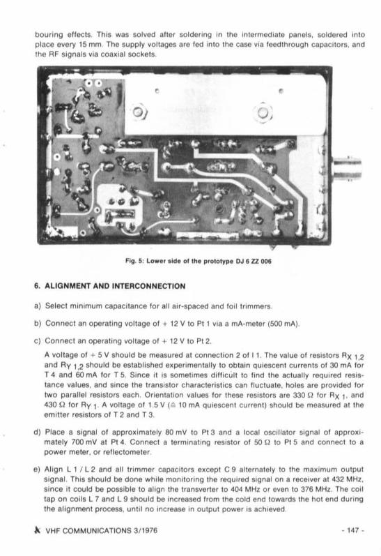
bouring euecte nus was solved after so ldering in the mlerm edla te panels, soldered Intopla ce every lS mm . The supply voltages are led mto lhe case via teedlhrough cecec .tc rs. andIhe RF signals via coaxial soc kets
,OJ
,
u,•
(
Fig. 5: low. , s id. ol lh. prololyp. OJ e zz ooe
8. ALIGNMENT AND INTERCONN ECTION
a) Select minimum capacitance lor all air -spaced and ton tnmmers
b) Connec t an operallng voltage 01 + 12 V 10 Pt 1 via a mA-meter (500 mAl .
cJ Connec t an operalmg voltage 01 + 12 V to PI 2.
A voltage 01 + 5 V shou ld be measured al connec tion 2 0111, The value 01 resistors AX 1,2and Ry 1.2 should be eslablished expe rimentally to ob tain qureaeent currents o f 30 mA lorT 4 and 60 mA lor T 5. Sin ce It IS ecmeumee dlllicult 10 hnd the actually reQuired resistan ce values . and emce the tranSistor charactensucs can uuctuete . ho les are provrcec fortwo paranel resist or s each . Onentancn values lor Ihese rnislors are 330 U lor AX 1. and430 U lor Ry I . A voueqe 01 1.5 V (Q 10 mA quiescent cun ent) should be measured at theemitt er resisto rs 01 T 2 and T 3.
d) Place a signal 01 approximately 80 mv to Pt 3 and a loca l oecmeto r sig nal ot approxtma le ly 700 mV at Pt 4. Co nnect a terminal lng resi stor 01 50 U to PI 5 and connect to apower meter. or reuectometer.
eJ Align I I I l 2 and all trimmer capaci to rs except C 9 allerna lely 10 the max imum outputsignal. This should be done wh ile mOnltormg the required Sig nal on a receiv er at 432 MHz.since it could be poSSible to align the Iransverter to 404 MHz or even to 376 MHz . The co iltap on co ils L 7 and 19 should be inc reased Irom the Cold end towero e the ho t end dUringthe alignment process , until no increa se in c utout power is achieved.
~ VHF COMMUNICATIONS 311976 - 147 _

I ) If a receiver is available wh ich allows the local OSCIllalo r trequencv to be monnored at l ulloutput power , II is possIble lor trimmer ceoacncr C 9 to be ahgned lor rmmmum localc ecluatce Signal. Th is pcsrtron should be In the vlClnlly 01 minimum ceoacueoce . II th is ISnot possibl e, C 9 should remain al ItSpomt 01min imum capacitance
7. MEASURED VALUES
Alter correc t alignment. the tran sverter modu le provides an ou tput power 01 2 W on 432 MHzwith an in pul power 01 100 mV ,
Fig . &; Outpul 1pec;I, urn of Ihe I, e nn efl e r OJ e Zl DOe be twe en 330 a nd 530 MHIIVerlical 10 d B I dly.; horll onlal ; 2Il MHI I dlY.1
II w ill be seen in FI<iJ.6 Iha l tne local OSCillator signa l (seco nd sign al trcm lel t) is suppressedby mor e tha n 55 dB With respect to Ihe peak outc ut 01 Ihe requ ired Signal. The Imagerejection (376 MHz) is in lhe same order. The co nversion prod ucl wllh the f.rsl narmc mc 01the ca rrier (second signal Irom the rlghl) IS also suppressed by SS dB as is Ihe seco ndharmonic of lha carr ier (right -hand signal).
Wher eas all co nversion prod ucls are reduced together With the dri ve Signal, the localcectue tc r signal wlU mcrease slig hlty .
The supp ression c rtne I lf sl harmon ic 01 rne outpul Signal 01 an average 013S dB IS relall velypoor. Th is means tha I a bandpass 1IIIer should be used, especiall y when th e oulpu t Signal isto be led 10 a linear ernphtrer .
This was tcuowec by a two-tone lest in order to estab li sh the Intermodula tlon cnerec tensncs .These two camera were led 10 me transverter al a Ireq uency spacing 01 1.6 kHz and at apower level o f 30 mV . The resul t can be seen in FIg. 7. The SIgnal fall s 0 11 by more than55 dB et a frequency spacing 01 S kHz from the earne r. In pract ical ope rati on , il was fou ndth at no sig nal co uld be establ ished mor e than 6 kHz from lhe nom mal frequ ency even when
. 148 · ~ VHF COMMUNICATIONS 3 /1976

fig . 7; Inl. rmO(lul. lIon IpKllum of Ihe Ir. n, wel1" wIth Iwo -Ion e " ",n. ll(30 mY 1 1.1 kHz .p•.c:lnll: nl1.: 10 dB /d ., ho,lz.: 2 kHz/d .)
Fig . 8: Inl e rmO(lul. lfon IpKtrum 0 1 OJ IIU 0011 wllh two·Ion • • llIn.l.(15 mY 1 1.1 kHz . p.clng ; wel1.: 10 dB I dlw., hori Z.: 2 kHzld iw ,)
the requ ired signal was mor e lha n 60 dB over the norse Of course, the signal Improves stilimore et lower drive levels (15 mV each) : the lh ird order intermOdulation product s are morethan 26 dB weaker tha n each of the two-l one signals (Fig . 8)
A VHf COMMUNICATIONS 3/ 1976 • 149 ·

fig . , ;Outpu t po. , ' t • • funellofto l th. opera ting \loll.g• .
B " C~'1 Wllu. t :LO Ilgn l ' ("04 MHl i in mV
'"'"'I'
' OUI
~1 'OOI
aol
k( IDJ 6!1
~~
~,,I
II! - -IIUt - ...
o'"
"
"
11
•
Fig. II shows the dependance 01 Ihe clean output power Irom me operating vo ll age. The drIVelel/el during this measur ement was kept cons la nt at 100 mV (sing le lone). The ope,allngvo Uage 01 lhe toeal OSCilla tor module OJ" LB 003 WI ' 1\01 cha nged The ou tpu t \l0111g8value, in mV are given in brackets
II . grea ler d rive Sign31 Iha n 90 10 100 mV is led 10 Ihe Iransverte, . the out put sIgna' Will bedi storted , and WIll become wid er . ThiS ShOWS thai Ih a r ing mt~8 ' II bemg O\l.,d rlven .
I . REFERENCES
(1) WeingArtner. F.: A Transm ll Con verter lor 144 MHz wll h SChoUky Ring Mlke rVHF COMMUNICATIONS 7, Edi tion " '1975. Pages 194 · 199
(2) Saltier, G.: A Modular ATV TransmitterVHF COMMUNICATIONS 5. Edlhon 2/ 1973. Pages 66· eo
• 150 • ~ VHF COMMUNICATIONS 3 /1976

DESIGN OF TRANSISTOR FREQUENCY MULTIPLIERS
b~ 0,,1"9_H. $chl . rholl , DL 3 ZU
The described design mrc rrnencn was obtai ned du ring expenrnents on low -power transis tormultipliers. Of course , the infor mation gi ven cannot be generalized . but should provide someuseful information when working in c!:m juncl ion with Ir equency mul tiplier. in the frequencyrange between 10 MHz and app ro ximately 1SO MHz.
1. EXPERIMENTAL CIRCUIT
The circ ui t d iagram 01 a frequency mu lti plier with the associated measuring equi pment isgiven in Fig . 1. The test equipmen t comprises a l ube vottmete r URI (Rhode & Schwarz) withAF probe, a measur ing receiver and transm itte r ASV (Rhode & Schwarz) lor 30 ·300 MHz, aswell as 8 calibrated ertenueto r lor Z • 60 Q of up to 10 dB. A l ast swi tching transistor (ITapprox. 400 MHz) With large reactive capaci tance (simi lar to BSY 18 or 2 N 708) was used onpu rpose since an expenmeotat c ircui t that is able to operate using such a transistor wou ldalso be uncritical with respect to mod ifications 01 the mechanical construction and transistortype, However, th is does not mean that suc h transistor types should be used lor frequencymultipliers ins tead 01 true RF types such as the 2 N 918.
All resonant circuits were accommcc eteo in screening cans (coi l sets type 0 3 wilh core andtwo caps) . However, it was lound that me design ru les were also valid for simple scree nedco ils w ith core but withou t caps.
In order to make it suitab le l or various types 01 drive. Inducta nce L 2 (40'" 01 the turns onl l ) wes pr ovided with e center lap and bu ilt up in a stric tly , eerencee manner. Th is allowed apush -pull doubler to be obtained . In add i tio n to this, drive via a capacifi ve tap was also tried .
ASV
Dl3 ZU
6O U'+ H
u
URItV)
IUIiI
ss ,.......J.......,,
56 1.4Hl
55p L ~11"l8 MHl .1
II11
68p J l 2
u,,- - -.--.--,- IV
~ VHF COMMUNICATIONS 3 / 1976 • t51 •

The dr ive ci rcUli nol shown here was conslrucled Irom a 9 MHz crystal-co ntro lled osc illalo rwllh buller, a phase modulalor (wilhout AF· aignal j , and a doubler Irom 9 10 18 MHz. Thi sdoobler was no t l ull y driven at Ihe collector Irom Ihe somewhal weak SIgnal 01 Ihe phasemodulalor. wh ich means Iha l Ihe lormal lon 01higher harmonics is very low and will nol inler·lere WIth the measurement, as will be explained laler, AI Ihe 36 MHz OOlpul 01 &uch a eucuu.virtuall y all harmonics 01 18 MHz can be expecled, as well as harmoniCS 01 9 MHz al a lowerlevel.
2. THE MEASUREMENTS
A convenllonal doobler stage was lt rst ly construc led The base was provided wllh 0 V biasvoltage and was driven by tne whole winding L 2 140 % 01 the turns 01 L 1). The emItterresi stor RE that was aelecled (68 Q ) was bypassed as Ulual ullng a eececuce. The value wasCe - 680 pF (senes resonance alapprOll. 18 MHz).
This c irc ui t seemed to be slable, but Ihe hm lng 01 Ihe ccnectcr circuit comprIsing L 3 lorma llimum volta~ on the VTVM reeuttec In a dl llerent adJuslmenl lhan when aUgning lormaJlim um outpu l at 36 MHz on the meas uring receiver . This indicaled 81rong harmon ica andspurious signals. The measu ring receiver ind lca led mainly Ihat non -harmonic spurioussignals ccc urec. although the RF drive voltage in conjunc tion wll h Ihe Ihreshold voltage 01me transistor should have resul led in a suitable cur,enl I low angle lor slable Irequencydoobhng , Di fferent values 01 the RF drive venece. dil lerent taps. and dlllerttnt base bia s'IOltages d id not imp rovelhe inllable operation ,
However . operation wal "lIslac tory as soon as Ihe em iller capacllor CE was removed. II wasnow poSSible by sUllable selec llon 01 an emilie r relillor 10 c etem a lavorable current Ilowangle and a favorable collecto r dri .... wilh oui lormal ion 01non ·harmonlc spurU, The harmonicreJechon COuld also be classed as being good.
Various o ther types 01 drive .....ere used : capacil lve coupling 10 Ihe 18 MHz cirCUit comprisingL 1. various base bias voltages (even wilh diode atabi llza lion). aa .....ell as a push -pull doubler .However , none 01 them represenl ed any particular advanlaoes over Ihe Simple CirCUli given inFig , 1. tha t r&qulres a ....ry 10..... number 01componenls ,
3. RESULTS
As has been preViously menlioned , no emn ter cepecrtor shou ld be provided , It .....as thenfound that lhe output malching ma inly delermines Ihe suppression 01harmonic and spunousaignals. as well as Ihe elliclency 01 the doubler, Th iS meana Iha t lhe load reSISlance 01 Ihecollector cncou . Inc lud ing lis loading by Ihe subsequenl I lage mu st be designed 10 Ihal Iheco llector vollage is driven Just up to lhe limIt characle rls llcs bul nol overdrlven
In Ihe de SCribed case , the RF voltage at tne ccnectcr should no t e..ceee .. 10 ma.. 5 11(measured wllh lhe URI). ol herwise stro ng harmoniCS co uld be measured up to 300 MHz.
• 152 · A VHF COMMUNICATIONS 3/ 1976
3.1. Me..ured Value.
The CIrcUIt given In FIg t with l 2 40 % 01 L I , wI thout bias vorteqe. and without emit tercececuce provIded the following measured value s '
(All values re ferred to the level o f Ihe reqUired Irequency 36 MHz)
27 MH z'45 MH z.54 MH z:72 MH z.90 MHz.
108 MHz:
not measurablenet measu rable·34 dB- 36dB· 39 dB- 39 dB
Measuring conomcns :
Ie - 2 3 mAUHF - 1 15 V (aI 350 U jue .. 5 V (ettecnve vetue)RE . 150U
Higher harmonics co uld not be de termined
4_ REALIZATION
The requned optimum outpu t mat ching canno l always be achieved In c.ecuce. Sin ce theloading o f the COllec to r CIrCUlI by the ne~ l slage IS ("'I,cull 10 calc ulate. It IS assumed to begiven and the emi tter resistor is changed so that the optimum cnve 01 'he ccuector vcnece ISobtained For example. an emnter resistor 01 150 U was lound 10 be tavcu eaore In 'he experi mental cucurt fOI Ihe 350 U load resistor . On reducmg the load resistance to 110 U . It waspossible to redu ce (he emitter resistor to 68 U ,
The mea surement 01 the RF voltage at the couecro- causes a cenem problem II this successlui me tn oc IS to be used t fus must be made Wllh a row -cepecmve OSCilloscope or VTVMprobe When measuflng In comu ncnon With a vcnmeter the RMS value 01 Uc should besomewhal less Ihan 0 7 ~ Ub In the case 0 1 an osc i lloscope . the peek -to-pees value 01 thecouector vollage should be eomewnet less Ihan 2 x Ub ' The resonan t CIfCUII shou ld be tuned101 maximum vcttaqe With the aid 01the probe
Durmg Hie experimen ts (36 MHz). the 2 pF probe 01 the URI Wdll used II was even possi ble totune In a 7 pF osc i lloscope probe. bu t a 10 pF probe cau:;ad dlf f lcutlu'ls
If the above meaSUflng equipment IS no ' available, the follOWing meth od can be usedThe co llec to r cun em 01 the subseq uent cl ass B or cl ass C stage represents a reliable RF \1011 meter . wh ich although It Cann ot indicate dny absol ute value s. wdl nol lalslly the measuringset-up sin ce the or ig inal load concnucns are prevalen t. II IS ad\l lsable to dampen lhe ccuectoecucurt of lh ls . indlcatlng CirCUit .. wllh approximately 100 U so Ihat no Inlernal cnarac tenencs(e ,g, ins tab il Ity) of this stage IS able to lalslly the measur emen t
). VHF COMMUNICATIONS 3/ 1976 • 153 •
•IIe
Dl3 ZU
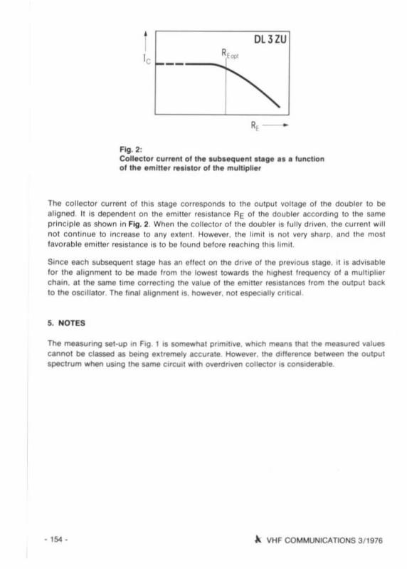
Fig. 2;CoIiK IO' current o l lh" l ubseq ue nt I llg. I" 'unct ion0' Ih. eminer ""Ilor 01 Ih" mu ltiplie'
The collec to r current 01 this stage corresponds to the outpu t voltage o f the doubler 10 bealigned . II is dependent on the eeuner resistance RE 01 the doubler acco rding to the sameprinciple as shown In Fig . 2. When the ecnectcr 01 l h8 doubler il l ull y driven. th e current Will
no t contin ue to mcrea se to any extent. Howe ver, the limit is not very sharp, and the mostfavor abl e emi ller resistance is to be found betc re reach ing th" limit
s.oce each subsequent stage has an ettec t on the drive 01 the preVIOuS stage . It III adVIsabl elor the ahg nmeo l 10 be made Irom the lowest toward s the tugh" sl frequency 01 I mutl,phercham . I I the same time correc lmg the ...alue 01 the emuter resli la nces I rom the ou tp ut back10 th e OSCill ator , The hnal ahgn meotlS. however . 001 especially Clll,ca l
5. HOTES
The measurtng set-up In FIg 1 IS somewhat primitive. wh ich means Ihat the measured val ueseeoect be c lassed as bltlng • • I reme!y accu rate How ever, lhe dlll.rertee be lwMn the outputspectrum when USIng the same CirCUli With overdrlven collecto r II considerable
• 1504 • .. VHF COMMUNICATIONS 3/1 976
ESTIMATING THE SIGNAl·TO·NOISE RATIOOF AN ATV·lINK
by R. Len tz, DL 3 WR
The lollowing short article allows the si. ret- to-norse reuc 01 an amateur TV link 10 beestimat ed based on the signal strength 01 a SSB signal. A comparison bet ween SSB and ATV
signal strength allows a more accurate eshma tion 01 whet her such communications would bepossible , and w ith which sig nal·to-noise r8110 Ihan when calculating Ihe signal -lo-nOlse eeuclrom Ihe path loss.
The pat h loss calcula tion under non-hne-ot -stqh t conditions, which are usually prevalent inamateur radio, can on ly estab lish the order 01 magnitude On Ihe o ther hand. the comparisonto a kn own sse signal sl reng th on the same freQuency band also includes both the speci ficconditions at bo lh locations, and also the ec tuer ccncmcns at that momenl .
1. PREREOUISITES
SSB, and TV commumcatrons (CCIR/BI are to la ke place in me same IreQuency band
The same anten na and eeteoee cables should be used . or the euterence in gai n o r losssho uld be taken inlo consi de ra tion during tne carcureucn.
The transmit po.....er (pEP In the sse mode, o r synchronizing level in lhe ATV mod e) sho uldbe app rOlll mately eq ual Larger variations Should be taken into ecneroe reucn du ring cercurauoo.
The noise hgures 0 1 the receivers should be app rOllimately equal. Large r venencoe shouldabo be taken Into constoe -eucn .
2. FUNDAMENTAL DIFFERENCE DUE TO THE INCREASE OF THE BANDWIDTH
The sensllivi ty l imits 01 a receive system (1) can be determined according to the lollowmgeq uation when the same an tenna and cables are used
Pn -Fllkll TollB
..... ith : Pn - noise po.....er 0 1 the receiver (WIF • no ise teeter (no l in dB)k • Bo llzmanns co nslanl _ 1.38 II 10' 1) Wsl KTo • ambient tempererure e 290 K
B • band.....«nn ct tne IF modu le
II the noi se lacto r F is the same lor bo th modes, It is the band..... ,dth B that is the determiningteeter .
A VHF COMMUNICATIONS 3/ 1976 · 155·

A bandwidth 015,75 MHz (2} has boon established lor ATV, and 2,4 kHz (cryst al t ill er) lor SSBThe lollowlng. higher power requ-rements tor ATV can be calcula ted as tcucwe.
..!!art . 5750 kHz . 2396 Q, 33 8 eaBSSB 2,4 kHz
Th is mea ns lhat an ATY Slgnal· to ·nOlso eeuc 01 OdB IS 10 be e~ pected when the SSB 5uj~ na l
streng l h is apprO_lmately 34 dB over the nOI56. At a SSB SI N rati o 01 mor e than 60 dB , theATY sig nal· to ·noise ratio w ill be app rox 30 dB A norse-tree ATV Signal IS obtamoo at apprca .40 d B, wh ich can be expected when a SSB SIN rene ot appro~ , 75 dB IS avail able
2.1. DiffIcult condll lon s
Whereas the previous calcu latio n only co nsiders me bandwidth dillefence and thus onl y themajor dI sadvantage 01 ATY, lurther dlrtl cultle5 mu st be taken Into co nSideration In crecnce.
II an o ld . mochlled tuner with a nOise Ilgure 01 10 dB 15 usee lor recept ion, wh ereas a goodcon vene r wilh apprcx. 4 dB is used In the SSB mode. the ATV li nk Will have a tenn er c.sadvantage 016 dB bnnglng the to tal up to 40 dB
II the SSB Imk is made w llh a peak power of 400 W, and only 10 W are avail abl e lor the ATVtransm ission , a furt her 16 d8 dlsadvanlage Will be present to r the ATV link
Wher eas a low-noise voice link IS available at a signaH o- nOlse rene 01 20 dB . a norse-tree TVpicture wi ll net be available un ti l the Slgnal- to· nOlse ratio is in the order 01 40 dB (3), (4)
The se cons iderations sho w that all POSSibIli ties should be used to the lull lor long d istance(w ideband) television l inks.
co20l. 567 8910fl O'"'9· ---- -
70cm ATV
12
- 156 - A VHF COMMUNICATIONS 3/ 1976

3. RANGE UNDER L1NE.()F-SIGHT CONDITIONS
For compiehon. a (hagram la ...." trom (3) has been IncluOt<l 10 .nd,cale lhe rlnge ot In A TVSII I'On IS I tunct ,on ol ltle Iransmll po ....e r under lhe lo llowlng cond,hon,
llne.-ot ·,.ghl or v.rtual Ime-o l-Slghl COn(hIlOn,ove r hilly COUnl"y..de and .uburban I rel• . bulnol over' lhe-horlzon commun'CITlOn.
The lol low lng condll~ I r. anumed 10 be presenl I I bOlh lIahons tS dB Inlenna gl .n.25 dB cable IoU. 7.8 dB no'N hgur• . frllq\l8OC)' rl nge 70 em band TI'le ra rtQe Of a to Wtran~l lIer """,ttl varIOUS nDI.. 'alICe as PIIramel., ., g'ven ,n 1!'Ie tOl'm 01 d.~ I,nes It .... ,Itbit seen tnet tO W .... .11 only ha". a rangot of 2O "'m In'p'I. of lhe rllgh 10111 anl."na gl ,n 01
JO dB. even when a sllgh lly no',y poclur. (SIN JO dBI IS accaplable
C. REFERENCES
(1l R Lentz : Noise in ReceIve System,VHF COMMUNICATIONS 7, Edit ion 4"915. Pages 217 ·235
(2 ) J GrImm ATV InlormihonVHF COMMUNICATIONS 8, Ed,l,on 111916, Piges 19 · 23
(3 ) J Grimm . Influences on a ATV-Transm lSSlonManUSCrlpllrom aleclure a l ltle ATV·convenhon 1914 rn Krumb.tchlWe,1 Germlny
(4) Teletun "'en·Labol'buch II, Page 69
AMERICA'SLeading technical Journal
for amateurs-__ Th., monlhly magaz.ne h&1 let I ....hole new lIandarel
lor s lal.-.ol· lhe-art conll ructlOl'l and teehnlC4!' 1r1IC!ft,ElIlen..". CCMtI'&ge 01 YHF/l.tiF, ATTY, FM. ICI, andmuch , much me,.
1 year US S 12,003 .,.ar, US S 2400
lflcludmg b Ulk a.rt, ••ghIIO EuropeEUROPE : ESKILL PERSSON 8 M5 CJp
FrOlunaorand I19400 Upplllndl Vallby. S'NlIden
00-.10 M,"-pey.ollo "'~_oI \'W'~
A VH F COMMU NICATIONS 3/1916 - t51 -

Modilicatlon 01the STE Rece iver ARAC 102lor Reception 01 the OSCAR Satellites
In the 10 m and 2 m Band
by AMSAT Newsle«e' 1/ 1976
The receiver ARAC 102 manufactured by STE in Milan is I small. complete receiver withbuil l -in loudspeaker. The receiver IS designed to operate Irom a voltage 01 12 V and ISdesigned lor AM, FM, and SSBfCW recept ion In the frequency range s Irom 28 to 30 MHz,and 144 to 146 MHz. The receiver is further eql,lIPped with an aut omatic noi se lim iter . andsquelch .
The tuning range 01 2 MHz is somewhat 100 wide. when the receiver is on ly to be used lorreception 01 the satelli tes OSCAR 6 and OSCAR 7. However , the 28· 30 MHz receive module(AR 10) can be easily modi/ jed so that the luning r8nge 18 limited to 29.38 to 29.55 MHz. or145,8 MHz 10 14600 MHz. The fo llow ing modi fica tion s are requ ired:
Three wire bridges designated WIth A, B, and C are loc ated on the lelthand side 01 the tr iplevariable capacitor 01 mooure AA 10. These bridges should be disconnected and a 5 pFce cecncr so ldered into these posit Ions, Thi s can usually be achie~ed Without remo~ ing theboard . The three capacito rs should be ceramic disk types ,
Trimmer capacitors C 3, C 8, and C 9 located adjacent to these br idges, and inductance L 6(be tween C 9 and the crys tal ) are aligned lor maximum gain across the new luning range 0129.38 10 29.55 MHz.
The 38 ,6667 MHz crystal pro~ided in the 2 m converter mod ule AC 2 should be el(chs nged tora HC·25/U, series resonance crystal o f 38.833 MHz. Th iS ensures th at a freque ncy 01145.9 MHz is converted to 29-'1 MHz.
LINEAR AMPLIFIERS lor 2 m and 70 cm
Clean linear operation due 10ophmum biasing and use 01CTC transistors BM 70- 12 orCM 40· 12 rasp.
Band 145 MHz 432 MHzOutput BO W 40 WInput t o W 10 WCurr ent 10 A 6 ASize (mm) 130 l( 58 l( 200
Deale rs enquiries welcome toUKW·TECHNtK Jahnsl r,140 -8523 Ba iersd orf(W,Germany )
• 158 · A. VHF COMMUNICATIONS 3/ t976

A UNIVERSAL CONVERTER FOR HF AND VHFby J . K. ltle " DK 1 OF
A large number 0' ama leurs only hcenced lor operahon on the VHF band. and up posIeS'high Quality transceIVers or receivers lor lhe frequency range 01 ..... 10 '''6 MHz, whIch areusually eqUipped lor several modes (A.M, FM , s se. and CW). The lollowing artIc le ia 10describe a receive converter which allows complete coverage 01 the frequency rang e 0150 kHz 10 30 MHz in sections 01 2 MHz in bandwid lh and convert ing them 10 the 2 m bandThis allows the esceuent cha rac le riahc I 01 modern VHF equipment su ch 8' high s.elecllvlly.good la rge -aignal handling capab ili tIes and high l iab ili ty . as well as ollen digital readout 10be used to cover the large, con tinuous range trom longwaves to the high est shortw ave Ire quaney. The quality of reception 'a main ly dependenl on the VHF equipment . and 01 co urseon the antenna used .
1. CONCEPT
In order to redu ce Ihe mechanical work 10 • min imum. no tuned Input Circu its .re used . ThiSsolves. large number 01 probleml thl t wou ld be encountered With respecl 10 r80Q8 I WIICh·ing , AI can be Men in the block diagram shown in Fig. 1. the Input signel lro m the entenne IIled via 8 lowpess tnter (cu t-crt Irequency : 32 MHZ), end led dl f&Ctly to lhe mber whIch ISequipped with 8 SChoMky ring mi ller. The outpul ltequency is passed via the aubl&quenlbandpasl Itlter and is ted to the 2 m recei ver. Thil hlter also ensures thaI the mIller il loadedwith lIs nom inal impedance . This II very Importanl With respec t to op tImiZing the large-lignalhandling capabihlles (1), (5).
50 kHz· )Q Io4Hz
VHF r"'. .....r144· 146 104Hz
vcoI_ _______ .J
OK10F 030
RF modul e
.IIIIIL. •
l'~ - - - - - - - - - - - - - - - - - - ~I
,.. - - -- - -- - _. - -- - -----_. _- ,I
I SynthesizerI moduleI OK1QF OJl
II rplol otClt1al
5 104 Hz ...I I 0~ .J
Fig . I : Block dlli'I'" 01 1"1 I'll' ' I e l l.. eon • • n.,lo, 2 '" l.e. I••,.
~ VHF COMMUNICATIONS 3/ 1976 • 159 -

The sensi tivity th reshold 01 Ihe receive system is thus mainly dependent on the norse I lgure01 th e VHF receiver (usually in the order 01 3 dB) . and Irom the cc nverstcn loss 01 the ringmixer incl ud ing match ing losses which amo un t to a totat 01 appr ox imately 8 dB This resultsin a tot at no ise I lgure 01 approximately lt dB . This value is co mpletely satisfactory for theshor1 wave range. since an tenna norse, atmos pheric and erectncat mterterence are usuall yhigher (2).
In order to inc rease sensihvity (at the cost 01 redUCing me large-Ill gnal handling capabili ties ).it would be possi ble to use a tuned pream phher lor Ihe upper frequency range (20 to 30 MHz).
The lo cal osc ill ator of the converter must be variable in steps 01 2 MHz In the range 01 144 to116 MHz , If a conveouonar crystal oscilla tor were to be used. a total 01 15 crysl als wou ld berequired With the aid 01 me Pll-Iechnology used here (3). (4). It is poSSible for only onesing le crystal to be used . The main oscillator (VeO) OSCillates di rec lly at the final frequencyrequired lor the mixer , The osci lla to r signal is then div ided by lour and !Inally led to anadjustable frequency divi der which divides It by lactor N The frequency range selec tion Ismade in th is manner. The output signat 01 the N-dlvider is led to the phase detector where ilis compared to a frequency Of exactly 500 kHz (crystal-controlled frequency o f 5 MHz dividedby 10), The output DC voltage 01 the pha se compara to r is used to tune the veo With the aid01 its ve-ectcr diode to the exec t frequency required (selec ted by N)
2. CIRCUIT DESCRIPTION
2.1. RF ci rc ui t
A detailed crecvrt di agram of the RF ctrc uu is given in Flg. 2 A series CIfCUlt 01 two RFchokes is co nnec ted across the antenna input (Pt301) to protec t the input cucurt Irom stallccha rges (thunderstor m). This is touowec by a l our-stage lowpass hlter (:r-circuil) comprisingind uc tances L 301 to L 304. ThiS I llIer has a cutolf freq uency of 32 MHz In order to gua ranteegood fi ller cherectensncs up in 10 the UHF-range. the capaci tan ces are divided over twocapaci tors 01 100 pF each In this manner. the unwanted euec t 01 the connection Inductanceis kept as small as possi b le, Ceramic disk capaci to rs should be used here which should besolde red Into place With the sho rtest possib le connections, The measu red attenuation curve01 the lowpass filter is given In Fill. 3
The in pu t IIIter is followed by a match ing link comprising L 305. R 301 and C 301. ThIS linkhas the lask 01 term inating the in pu t o f the Schollky ring mlKer lor frequencies in excesa 01the passban d range 01 the inpul lo wpass h lter .
II sho uld also be menncned Ihat the RF sillnal to be rflce lved is not l ed to the RF inp ut of themixer, bu l to the IF co nnec tio n. since it is only this input that can be used dow n to very lowtreooeoces. The two other con nec tions POSse5S a lower frequency lim It of 5 MHz due to thebuilt -in lransl ormers.
The resu lti ng sum IreQuency Is led Irom the RF ccnnecncn et tue Schollky mixer via a bandpass filler (L 306, C 302, and R 302, L 307, C 303) to the outpu t 01 P1 302 The compone'l tvalues for the match ing lin ks were calculated accor ding to the ecoencoe given in (5).
• 160 · ~ VHF COMMUNICATIONS 3/ 1976

•
M .
g 'CH.-- .....~"C'-" --'-<H
0 "M •- .,.. ,
). VHF COMMUN!CAliONS 311916
!,•..ItI•I
• 161 •

' _ _ ::\ III, I •.• /11. I. ... Ij' ."I,I T I OM lOFolO
!.. ",h . . . \~ . T + .
..... /r .' ,_\\ ,1 ... ~ .
,: ;to:• ttl "h -;',-rttHH
t:rrrli~'j f liijjjf\}j ~
...• ••
r~tj: :• 1 i + ..• -< .~ . + ••• jl
I .. . I'tll· . · 1... •
.,
~H:r-++IJfIl+Pq:g;p::::::TfTlliI~•••••••••~
The veo is eqUIpped wllh Iran l illo r T 301, and is varIable with Ihe aid 01 varaclot diodee 302 in tne range 01 116 to , .... MHz Soma ollhe Rf output power is lapped Ot! al lhe d rainci rc ui t and led via PI 304 10 Ihe .ynilleaizer ci rCUl i The lunl~ voUa"e led 10 PI 303 . mual be
pa ssed yie a mu lt iple stage h lle, link (L 309. L 3010. l 301 II. 10 ensure that no residual phaseco mparator frequency is present The butler I tage T 302 ill connected \/1' Iha vol lage d iVide rC 304 I C 305 . The gain 01 th l' MOSFET Itage can be varied wllh the I.d 01 the controlvoltage led \/1. PI 306. which enll ures • IImple au tomatic level ce m rcr 01 Ihe osc illator power
Tran slormer Tr JOI IS provided in Ihe drain ci rCUli of Ihe buller slage . The primary of l hlltran atc rmer Illuned to resonan ce With me aid o f l rlmmer C 106. ThIS Is foHowed by tne driverequ ipped wilh Iransislor T 303, and a funher Iransfo rmer (Tr 302) lor coupling to tne outputI tage of the loca l oscillalo r (T 3(4).
The oulput I lage T 304 operates in class A (colleclor DC currenl approx 100 rnA) , ThIS slageis ab le to provide an ou tpul power o f 10 mW allow d,s torllon to Ihe ring ml.er. The malchlnglink co mpriling R 303. lJ012 and C 307 wllh a cu lo ll frequency in excess of 500 MHz.ensures the requi red SOU terminatIon . DIode 0301 generates a OC-yoUage proportIonal 10lhe ampil iude of Ihe cscmetor SIgnal. whIch II fed vIa PI 308 to the coo ucr amplifIer to
module OK 1 OF 002 (Fig. 71
The power l upply lor the OSCIlla tor amp ll ller II connected Yla PI 307, The VCO is prOYldedwith an exi ra carefu lly fi ltered ope ratIng yollage Yla eceeecuen Pt 305
2.2. Synth.alJ:.r
Flgur•• " to e show the cirCUi t diag ram of tne synt hesizer . ConnectIon PI 3 11 IS prOYldedwllh m e osc ill ator signal lak en from Pl 304 of the RF·module, This IS followed by a buttersl age (T 311) eqUIpped with . MOSFET. Thll I lage II prOYlde<! to Isolate the dlgtlal CirCUI tryIrom the VCO. Due to the rel atIvely large bandwidt h reqUire<! lor tbe OSCIlla tor frequency (11610 144 MHz). the bufter il cormecled yia a transl ormer (Tr 311) to Ihe amphller I lage T 312.The primary wind Ing for ms a resonance cirCUli al apprOlumalely 130 MHz togeTher wll h Iheoutpu t capacitance of the MOSFET. Due to the loadIng ol lhe inpul Impedance of T 312, Ihereq uired bandw idTh 01 yirtually 30 MHz il ob tained WIthout dl lhcuillel
- 162 • '" VHF COMMUNICATIONS 3 /1976

•
,OK10F o310
tn,• ••.......'
••
Pl)l2 _t.
r----- n~r,~------------ - --~"- ---- - - ----- - - -- - - - - -: ,I 1 1 - - - ,I I .. . r .... 1--lI I , . , ~ :: .,. ~
I I 1m ,I ~ T)I ' . :.,,,.,
Pl3nl ~ h
i;~ ' -rr' , ;I' ,*' H ,,* I~--- - - + - - -- -- -- - - - -- -- - ---- -- - -- - ----- - ------- -
FIg. 4: Circu it dl . ",. , m 0 ' th . HF·con.." .,(Butler, pr . -dl v lder, In el con.... ,.,• •)
'" ,T ' "I m d . ,
"'.,... . t;; l ,, ,, .
, ---r T.l -"----;---1-- -
1312DKIOF Q)'~
I )1'.. ...... I ns... .....
..... ....z
• 'i:!-I',•,
" --•, 1 • •, ; ,
•m .,
,"
" " ' , ' .
......... -'
..,,,
....",... ", .."...I . ' : /
, "., .: , ..1
r- :.,t-c-; "1
! ~ ( {. it ••••••.• -'
un." " ~ '
Fig _5;Clrc: ull dl' Il'lm of the HF-convel1.,V, ••• bl. divide , with dlll" e 'I.I' e" ..)
). VHF COMMUNICATIONS 3/ 1976 • 163 •

The subaequf>fll ci rcul i comprlsmg T 313 as phase reversal CIrCUli , 1311 (Eel-divide by 41,and Iransistors T 314 and T 3 15 (level conversion ECl/nl) was des<:r'bed m detai l m (41 An l -compat lble Signal of one fourth o f lhe cscurarcr freQuency IS available at polnl Y It IS led10 the var iabl e frequency divider, whose CirCUli dUlgram is given in Fig. S ThIS comproses aTwo-stage decade coun ter (1314 and 1315) whIch IS adluslable uSing the d.gltal I w.tches viaInputs A 1 to A 4 and B When the tens-posit ion (1315) has reached 'he value 8 and ' he urutapoSl lton (1314) has altlllned the value 9. The J ' lnput 01 the fllpl lop 1312 Will be released , Thene_1 Input pu lse Will place II mlo .Is work ing poSillon and reset mptrop 1313 AI the sameltme. Ihe decade counter w.1I be SWitched a ll and ch.rll'fld again w,th "S commencementvalue The fol low ing clock pulse SWitc hes 1313 80 thaT the l( ' lnput 01 1312 IS released Thenext Inpu t pu lse SWitches 1312 back 10 lis rHI poIITlon wh,ch sw,'ches the eeun ter on agamSO that a new cycle can commence, The diVided OSCillator Irequency IS la ken from the output
01 1312 and fed to the phase comparator crrcun via pOinT Z
The lo llow lng tab le sho ws the relat ionsh ip betwee n channel setecuon and 'he 0Ic,118'or . 01receive Irequ ency of the converter
seiecnce B A.. A) A, A, OSCillator ReceIve frequencyfreQuency With IF •
(MHz) 144 ·146 MHz
00 L L L L L ,.. O· 20' L L L L H ,,, 2 - 402 L L L H L 140 4 · e03 L L L H H ' 38 ,. ,04 L L H L L .36 8 ·10
OS L L H L H ra 10 - 1206 L L H H L ' 32 12 - 1407 L L H H H '30 14 - 16DB L H L L L 12' 16 - 1809 L H L L H '26 18 - 20
'0 H L L L L ,,, 20 ·2211 H L L L H ,,, 22·2412 H L L H L ' 20 24·26
' 3 H L L H H . 18 26 - 2814 H L H L L "' 28 ·30
Fig. e sho ws the remamlng 11ages o f th e syntheSizer, A 5 MHz crystal cont rolled oscilla torcomprisi ng T 316 With l ubl8Quen t pulse shape r (T 317) p rOVides the relerence signal , wh ich" di vided by 10 In 1317 and compared 10 the d iVided osc il lato r 'requency In the phasedetec to r 1316 . Transistor T 318 then ampll iles the DC-vollag e proportional 10 the phasedi llerence between the two treqceoc.es. alter which It is lltd 10 the VCO a8 tun mg vollaQe vial 3 11 and Pt 315. The follow 'ng opera ting vol tages are reQui red '" 13,5 V (3 mAl, and + 5 V(appro• . 250 mAl.
• 1601 • A VHF COMMUNICATIONS 3/1976

..
, ..
------------------------- ---------------------,____-==-_-==-_--"::., ~.i:- :.t. 313
•_.~-~-~ r. .•..,,'L"'---':; -G!}-r~.-,~-" '", Tj16 ~ 0' -'''--':' " ,,.t<. r- r.,. T''' : " u ,
· ·~·;Il-"'-g~fg[©~l; 11'Z;-~:T-~C311 r~ . 1'·.·· ,... I ......"",{ I"" I
I,- ,, ~
-----------------------------------------------~
Fig. I : Clrtul, d. ' g rl m 011,.. HF·conul1. ,(RI I.,.ne. o.eill.lol, ph• • • COmp.,.to,)
2.3. Pow., . upply
The c irc u it diagram ot the power supply IS g l ~en In Fig . 7 The power tran sformer possessestwo 12 V windings. and such transformer s are easily available on the market TwoDC-vo nages are ob tained with the aid 01 the bridge rectruer G321' one is led via Pt 324 tothe voltage stabilizer 1322 and IS stabrltzed 10 + 15 V; the Oth6' vcnece IS lak en trom theceo ter tap 01 the trans former and roods the stabil izer 1323 which is prOVided 10f the ~ Vsupply 01 the TIL·ClrCUIts. The suppl~ vollage for the VCO and the aC·amplilier Cion be takenvia a I iIte r lin k 01 160 U 1 3 3 l.F subsequent to the phase competatcr CIfCUII (pt 326).
However, since this voltage shou ld be well tntere o. the 3 3l.F ceoecuor Should nOI be anelectrclync tvpe. but have a ctesuc dielectr ic.
The rest 0 ' the ctrc un Shown in Fig , 7 co mprises a cc nrrcr amp lltler lor the cscutator ou tputpower . The OC·volldge prOVided b~ di ode a 301 (F'Ig, 2). wh ich IS proporlfonalto the x c -vcn age 01 the osc ill ator et connectio n 8 01 the Schotlk~ miller, IS fed via connections Pt 308 andPt 329 to the gale 01 T 321. The ac -cc mume ncn 01 t M ~~ I 15 kU I I IIF ensures the stablll t~
o f Ihe co ntrol cnc uu r eanerstcr T 321 .s prOVided as source tcuc wer and ensures tha I theDC-voltage po tential IS Increased to appr ollimately -+- 5 V 80 that the follOWing operatro natampunar 1321 can be dri ven co rrectly The nom inal value of lh e c.o ce voltage can beadjusted with the aid 01 mmmer resistor R 321, wh ich also allows any vanaucn 01 the pmc h011 vo llage 01 T 32 1 to be adjusted Inlegraled ctrcurt 1321 IS not providod With fOOdback viaresistor s, but oce-etee at tul! gain to r the control loo p. The satufaled output voltage 01 t J21IS In the order 01 2 V, and is compensated Wllh the aid o f the lhfeshold voltage 01 the threediodes in series It lhe output. so tnet 0 V ClIO be obtained at PI 327. c cnnectron Pt327 ISco nnected to PI 306 which ensur es that the ga te bia s Voltage 01 the MOSFET of the T 302 ISco n trolled so that the rectl l,ed oscillator voltage at Pt 308 always possesses us most la ~otable
vlllue.
'" VHF COMMUNICATIONS 311976 - 165 -

T2
31
R2
31
···
12
31
•
•
PllIJ7P
lll1
...,..
..
o.
>,>
... H.1).5'
DK
10F
.32
132
2
Pill'
-,
1m
Ii.
f-<I
221101'".
PI326L
._
r---
-----
IG
321!PUZ3
UG
CU
Oll
.'"1
323
l"In
"P
llll."
I..·1
>-t

3. CONSTRUCTION
PC·boards OK 1 OF 030.031 . and 032 have been design ed lor construction 01 the co nvener.Boards 030 and 032 are single-coated . whereas 031 IS e cuere-coaree and provrceo withth ro ugh-contacts . Flgur•• 8, 9 end 10 give the component rcceucne on the PC-bo ards .Figure. 11 end 12 show photographs 01 the author's prot otype. The RF and synthesi zermodules are provided with approximately 30 mm high screening panels made Irom 0,5 mmth ick brass or lin plate . The leedt hrough capac ito rs and coaxial SOCkets lor Pt 301 r.nd Pt 302are so ldered into place. The spacing belween the lower side of the board and the lower edge01 the screening panel should amount to epprox 5 mm .
It is most tavotatse lor the RF module (030) to be mounted on one side 01 the metal chassis.and the synthesizer modu le (031) on the other Side, II is also advi sabl e lor Pt 304 and Pt 311to be located virtually adja cent to another. The Interconnec tion betwoon tnese two po int s caneither be made using a th in coaxial cable (approx , 5 cm long ) or USing an Insulated wir e.wh ich musl be wi thin the screening In thi s case. a capaci to r 01 approx . 5 pF should beconnec ted in parallel to PI 311.
3.1. Special component.
RF-module OK 1 OF 030
M 300:
T301:1 302:T 303 :T 304
0 301:0 302:
Tr301 , Tr302:
Schollky ring mixer IE-500
BF 245 A (TI) or W 245 A (Sil iconix)40841 or 40673 (RCA)2 N 5179 (RCA). also BF 224 (TI) applicabl e2 N 3866 (dillerent producers) with coo lmg Iin s
AA 116 or similar Ge-diodeBB 104 G (green). dillerent producer s
pr imary 3 turns. secondary 1 turn 010,4 mm enamelled coppe r wirein po lled co re. 9 dra . x 7 or 11 d la x 7. mat eri al K 12, AL • 16;(B 65531 - L 0016 - A 012): direclly g lued to the PC·board : ccrucrmer With2 chambers. or use insulated wire lor the secondary:
l 301 2:
L 30 13:
L 3014. l3015:
C 306. C 308 :
l 309 , l3010, L 3011: IF circu it s 455 kHz, ceoecno e rem oved . yell ow marking :l 30 1 - l 304 : 15 turns 01 1 mm silver-plated coppe r wi re. sell -supporlmg. 6 mm inne r d ial 305: 6 tu rns. other ce reue as l 301l 306 , l 307; 3 turns. other de lai ls as l301l 308 : 4 turns 01 1 mm silver-plated coppe r wire. turns spaced 2 mm. tap 0.75 1urns
Irom the ground end ; Tro li tul lorm er 6 mm dla, with VHF core (brown)1.5 tu rns , other de tails as L 301
app rox . 1 mHo100 turns of 0 ,15 mm enamelled copper wire in po tted core14 d ia , x 8 mm , mater ial M 25, Al value 100 (B 65541 • K 0100· A 025)or 79 turns lo r mate rial N 22, AL-value 160 (B 65541 - K 0160 - A 022 )
rernte choke , 22 " H. spacing 10 mm
plastiC lo il o r ceramic disk l r immer. 10 mm cre., 310 12 pF
~ VHF COM MUNtCATIONS 3/1976 - 167 •

-- - - -- - " -~
I
L eo __J
-- ~ - - ---- - - ~ - - - - - - - - - - -
Fig . I , Co mpo".nt loe.llont III' PC·bo.,d 01( 1 OF 030
Fig. II: Compo nenl loc:. llon. on PC·bu .d OK 1 OF 031
. 168 · A VHF COMMUNICATIONS 3/ 1976

fig I' : Author'. prototype ot Ih. SW-conw."., (Af·rnodu~ DI( I Of 0301
toJ
A. VHF COMMUNICATIONS 311976 • 169 ·

Feed -through cepe cuor s: approx . 2 ,2 nF / 30 V, for so lder mountingAll o fhe r capacitors: ceramic di sk typeA spa ci ng 01 at least 10 mm is available lor the resist ors .
Synthe.lzer OK 1 OF 03t
T311:T 3 12, T 3 13:T314:T315:T316, T 317:T 318 :
40841 or 40673 (RCA)2 N 5179 (RCA)SF 272 or B5X 29 (5GS)2 N 709 (di fleren t manufactu rers)2 N 9 14 or other silicon NPN transislorsBC 413, BC 109 (Siemens) or similar Si·NPN tran sist ors
1311 : SP 8601 BT (fo rmer ly 5P 601 5 ) Plessey1312,1 313: 5N 74 H 102 (TI)t 314, 1315: 5N 74196 N (TI) o r FW ,.. (Siemens)1317: SN 7490 N (TI) o r FW 161 (Siemens)1316: MC 4044 P (Moto rola)
AU 15 except t 311 with 14 pin connectors
aL 311:
Tr 311;
C 311:
crys tal 5 MHz 1 2 x 10⁻¹ , para llel resonance, load apprOJ( ,30 pF , holder HC-6/U
like L 309
like Tr 301, excep t pnmary 4 windings
loi l trimmer or ceramic di sk tr immer 10 mm di a" 10 to 60 pF
Feed ·through capacitors: apprcx . 2.2 nF/3O V, lor so lder mountingAll bypass and coupling capacitors: cerermc di sk typesFor the resisto rs a spacing ofl0 mm is available,
'~il ·U~~ ~i) -l.JltI '!.!l"0 OK1QF012 0
o 8',5 ~ ' V'f~ 5 5 r - -- ,
~~{ ',
• ,+ ,
• a,,5_"
§ 8,5t• ,• - I
*- , •II·l f ~ ' ':'' ' lJJ • ,
5~- I
~HH~i!
,• ,@&- ,,,
-- --'•o ~ L7" G l2 1 0
110 -I- -
Fig . 10 : Componenlloc.tlona on PC_board OK 1 OF D32
J•
• 170 - ~ VHF COMMUNICATIONS 3/ 1976

Pow er l upp l, OK 1 OF G32
T 321:
1321:1322:1323:
0321:
SF 245 C (TI) or W 245 C (Sdlconllq
TBA 221 B (Siemenl) or 741 CM (dlflerenl manulaclure~l
l M 340 K · 15 (NS) or SO 8715 e (Sil icon General llM 309 K (NS). also other manu lactu rer l
Sili con -bridge recliliers B 40 C 2200 or B 80 C 2200
$elect Ihe sUllable translormer available on the market
4. ALIGNMENT
It Is advlSlble lor the power l uppt, to be checked belore connecting it to the other modules,
This is fOllOWed b)' connecllng the RF-module. Pt 306 is temporari ly connec ted via a reSil tor01 150 kU 10 PI 307 where It II con nec ted to the operating vollage 01 + 15 V Pt 305 ISprovided with a filtered operating voltage from Pt 326 A vanable DC-vollage of 0 V to appro ..,+ 13 V is connected to Pt 303 wh ich can be made With lhe aid 01 a varisbt e r8$lsl or 01appro.. 10 kU connecfed between PI 305 and ground , II a Irequency counter II available. Itcsn be connec ted to Pt 305 . Wllh the aid 01 the po tentiometer connected to PI 303. a vollage01 12 V should be selec ted and the VCO frequency should be aligned to appr oximately144 MHz with the aid 01 the cere 01 l 308, Thl 10wI .t VeO -lrequency 01 116 MHz ahould be
ob tain ed with the aid of a tun ing voltaoe 01 approximately 3 V. Value s 01betwven 2.5 and 4 Vare per miSSible. Fig. 13 shows th e tuning curve measure d on the autho,.s prototype .
• '"- .",,,... ,./ '" , c,,,en•• '.• '.• '.• ••• ••.. '.• ••.. '." "." '"" ••" .".. ..,,- , , , , • • • •
.........,...I 'II " " ,
Fig. 13:Fr~u.ftey ol In. veo • •• luftetlonolin. l uning Yol!.~
~ VHF COMMUNICATIONS 3/1976 • 111 •

This is fo llowed by aligning the tocet osci lla to r ampli fier. It IS advisable to I lrstly check theDC-o pe rating po ints 01 the transistors T 302, T 303, and T 304 with the VCO inoperative (diS'co nnec t PI 305). A vollage dr op 01 eoo rce 1.5 to 2.5 V must be present across the sourceresistor 01 T 302. The emi tte r voltage values 01 T 303 and T 304 are given in Fl 2, The VCO isconnected again and the tuning voltage (Pt303) adjusted to 12 V so that th e oscillator frequency is in Ihe order 01 144 MHz. A hig h impedance vol tmeter (range approx . 3 V.
A i: 100 kU) is connected between PI 308 and ground, and capaci tors C 306 and C 308 arealigned lor maximum reading, A value 01 apprOlllma tely 0.9 to 1,4 V should be avansbe . Ifreq uired . it is possible to alter the volt age divider C 304 I C 305. The indi ca ted voltage shouldbe WIth in the given range also at the lower Irequency limit l lo .. t 16 MHz),
The digI tal part 01 the Circuit IS now broug hl into ccereucn. Connec tion PI 311 IS connectedto PI 304. as well as PI 312 to Pt 314 With the cor respo nding con nections on the powersupply . Alter SWitchi ng on. the crys tal osc illa tor (counter to the collector 01 T 317) and Ihesubsequent dlv ide ·by· ten diViders are chec ked (counter or osciuoeccpe to pi n 11 01 I 3 17),The co res 01 inductances L 311, L 309. and L 3011 are inserted comple tely , alter wh ich anin terconn ectio n is made bet ween Pt 315 and Pt303 and a voltmeter (range i: 15 V)co nnec ted between Pt 315 and grou nd The phase control ci rcuit should now lock in . Thevo ltage read ing should change to that give n in Fig. 13 when altering the poainon of Ihedig i tal swi tches,
Finally, the opera tio nal amp li fier is alig ned , The resistor temp orari ly connected to Pt 306 ISremoved and th is poi nt co nnected to Pt 327, Pt 308 is connected to Pt 329, Connect the vol t·meter be tween PI 308 and gro und, A voltage o f 0.7 V is adjus ted wit h the aid 01 R 321. Thisvalue mu st be constant over the whole tun ing rang e trom channel 00 to channel 14
The 2 m receiver is now co nnec ted to Pt 302. and PI 301 terminat ed With 50 n , Select chan nel00 and tune the receive r to 144 MHz in the sse or CW mode, A clean heterodyne should beheard II the accuracy 01 the 2 m receiver is sullicient (e.g, d igital eeed-oun. it is possible to rthe crysta l osci lla to r to be aligned to zero beat With the aid 01 C 311
The receiver is now tun ed to 144,5 MHz. The spurious oscilla tion present at th is po int can bealigned l or mi nimum by adjust ing the co re 01 L 3010. In the case of the author s prototype ,Ih is spurious sig nal cou ld be reduced to appro » 10 dB over the noise level. 01 course. th isw ill on ly be the case II the harmonics of the 500 kHz signal (I rom the phase co mpa rator) arene t induc ed into the 2 m receiver via a dlllerent path . " is advisable to use a well -screenedeonetrucucn for the converter .
5. FURTHER INFORMA TION
Especially the large signal handling capabilities 0 1 sho rtwave receivers can be easily checkedduring th e evening hours on the 40 m band . Atthough the desc ribed converter does notpossess any creseiecnvuv. It was lou nd to be conside rably better than several shortwavereceivers including a tubed dcubse-ccnvereron supe rhet With th ree tuned input cncurts Theau thor's 2 m statio n descnbed partially in (6) and (7) was used as 2 m receiver, and a W 3 DZZan tenna was used . Experiments made with o ther 2 m transceivers were also posi tive Unde rthese co nditions, a 10 dB attenuated connector bet ween the conver ter and the receiverbroughl a ncucrtne improvement 01 the signal · to-noise reno .
- 172 - A VHF COMMUNICATIONS 3 /1976

Since ttns converter comprises a passive mtxer crrcu.t . It IS cess.ere 'or rne signal path to bereversed so Ihat a 2 m signal Injected to PI 302 Will be co nverled 10 the shortwave range,How ever . the e-we pow er shou ld not be hi gher Ihan 1 mW In order to ensure Ihal the uneerrange 0 ' tne ring mixer IS no r exceede d. In this case . an output po wer 01 app roximalely0.2 mW will be available at P1301. A wldeband ampll 'ler can be used 10 increase tms 10 therequu eo ou tpu t po wer since the Image trequencv IS cc mpretery supp ressed with the aid o tthe inpu l lowpass Iiller. The editors would be Inte res ted to receive lurthe r Into rma tlonregardmg a sUilable power ampll 'ler when the conve rter IS used In thiS mode .
II a 10 m receiver (28 10 30 MHz) IS available, II IS also possrbre to r Ihe cescneec mcdule tobe also used as VHF receive converter in the Irequency range o f 86 10 116 MHz and trc m 144to 174 MH z, The associated channels and receive uequencres are given en tabl e 2
Adj us tment 10 (MHz) 10 · IF {MHZ) 10 + IF (MHz)
00 14' 116 · 114 172 ·17401 142 114. 112 170 · 17202 140 112 - 110 168· 17003 I,. 110 · 108 166 · 1680' ,,. 108 · 106 164 · 166
05 '34 106 · 104 162 · 16406 132 104· t02 160 · 16207 130 102· 100 t 58 · 16008 128 100 · 98 156 ·1 58O. 126 '8 · 96 154 ·1 56
10 12' 96· .' 152 · 154
" 122 94 · .2 150 ·1 52
' 2 120 '2 · 90 148 · 15013 "8 90 · 68 146 · 14814 '" 68 · 66 144 · 146
Image rejec tion is bes t made using a tuned VHF preamplifier . which is also adVisable lo rimproving the senSll ivi ty at VHF. The author has also tested the large-sIgnal handling cecemlIlies 01 the cooverter when converlmg Irom 145 MHz to 29 MHz. When not uSing a HF preamp li fie r , i t is poSSible 10 transm it 600 kHz from the receive frequency w llh an ou tpu t po wero f 400 W and to mon.tcr one 's own transm iSSion via a repeater USing a second antenn a. Thetwo antennas are decoup led by approximately 60 dB. and the FM repealer signal was onlyapprmdmate ly 30 dB over the norse.
Of cou rse . it is also poSSible 'or the desc nbed converter to be used as transmit converterfrom sho rtwave to the 2 m band , The malt imum drive level lor AM or SSB should nOI exceee1 mW PEP. The convereic n foss is also in Ihe order 01 7 10 8 dB .
The various opera ting modes 01 the converter are to be given mor e clearly In the lo llo wln gtable 3
~ VHF COMMUNICATIONS 311976 • 173 •

Tabl e 3 Receive converter Transmit co nverter
Input frequency SO kHZ · 30 MHz 144 - 146 MHzOutput trequencv 144 · 146 MHz SO kHz · 30 MHz
Input frequency 86 ·116 MHz .Output frequency 28 · 30 MHz .
lnputlrequency 144 · 114 MHz 28 · 30 MHzOutput frequency 2• . 30 MHz 144 · 114 MHz
6, REFERENCES
(1) Martin, M ,: Empfangerelngangsteil mil gr oBem Dynamlk beretchund senr genngen IntermodulahonsverzerrungenCQ- DL 1975, Heft 6, seue 326 · 3J6
(2) Lentz, R.: NOise in Receive SystemsVHF COMMUNICATIONS 7, Edllion 1975, Pages 211 ·235
(3) Kestler, J.: An FM I ranscerver With Multi -Channel Synthe SizerVHF COMMUNICATIONS 5, Edihon 211973. Pages 130 - 145
(4) Kestler, J .: A Stereo VHF-FM Receiver With Frequency Synthe sizerVHF COMMUNICATIONS 7, Editi on 4/197 5. Pages 200 - 202
(5) Kestler, J .: MatChi ng Circu its lor Schollky Ring MUtersVHF COMMUNICATIONS 8, Editi on 1/ 1976, Pages 13 · 18
(6) KesUer, J .: A phase-locked Osc illa tor l or 144 MHzVHF COMMUNICATIONS 6, Edilion 2/ 1974, Pages 216 - 227
(7) Kestler, J .: A Receive Converter lor 114 MHz / 9 MHz With Schollky Ring MUterVHF COMMUNICATIONS 6, Editi on 411 974, Pages 204 ·214
NEW ! NEW IPOLARISATIONS SWITCHING UNIT for 2m CROSSED VAGIS
Reauy-to-cperate as cescnoec In VHF COMMUNICATIONS Complete in cabmet with th reeBNC connec tors Especially designed l or use With crossed yagls mounted as an . X., and fedwi th equal-length feeder s FollOWing S IX pol ansatlons can be selec ted : Vertica l. hor izontal.c lockwise circular. ant lcl ockwise ci rcul ar, slant 45" and slant 135",
VSWR. max 1 2Power : 100 W carrierOrmen srcns: 216 by 132 by 80 mm .
Insert ion loss: 0,1 to 0.3 dBPhase error : apprux. 1·
- 174 •
Verlag UKW-BERICHTE, H. Dohlus oHGJahnslraBe 14 - 0 -8523 BAIERSDORF
A VHF COMMUNICATIONS 3/ 1976

A SECOND VERSION OF THE MODULAR AF·AMPLIFIERAND VOLTAGE STABILIZER
by D.E. Schmltz.f, OJ 4 90
The fir st version 01 the AF and voltage stabilizer module OJ 4 BG 007 ceec an integ ratedci rc uit type PA237, wh ich Is no longer manufactured . An Interchangeable replacementmodule has now boon devetcoed , and experi men ts were made in order to reduce Ihe lowintrinsic noi se 01 the previou s module The vol tage stabilizer circuit used in the OJ 4 80 007modu le has not been changed,
1. DEVELOPMENT
An Int egrated crreuu was requ ired to recrece the PA 237 that was also able to work over awi de voltage fange. Furt hermor e. II shOuld be manufactured by several muerent compamesso lhat de liveries could be gua ranteed IOf a considerable lime. These demands wers mel byth e TBA 800 . Th is Ie also o ilers lhe additiOnal advan tage 01 a sell -balanCing ctrcuu so thatexactly hall 01 the voltage Will appear al the ou tput . Independent 01 Ihe opera lmg voltageTh is ensures tha i the drive range remains at ccnmum .
Althou gh th e dala shee ts lor th e TaA 800 li sted better intrinsic noise characteris tics than IhePA 237, the author was surprised to fmd that Virtua lly the same norse was present as wllh theori gi nal modu le (Ihe origi nal ci rcui t had only been modi lled where absolutety necessary)Since Ih e cause 0 1 th is could not be Ihe act ual in tegrated cecun. the laull had to lay With theexte rnal components.
Alt er consi deration , the cause could only be the reSlslors 01 the AF·Il ller at the input 01 thein tegra ted clrcuu . ThiS was 'ound to be true by measuring the intrinsic norse level 0' thec irc ui l as a function 0 1 the source Imped ance 01 the mtegrated eueuu. The resu lts 01 th iSmeasurements are give n in Flgur. 1, curve a, AU noise measur ements were made WIth thew ideband AF·Mlllivo llmel er typ e hp 403 B. wh ich pcsseseee a measunng range 01 1 Hz 101 MHz.
OJ4OO
- -,.. '" ,..,,,..,,..FI9· 1:Noi.. '1oll_g e I l ltle oUIput ol lhe TBA aoo " I function olth. 10U~1 Imp,d,ne. ZCu,.... I : TBA aoo ,Ion , _ eu,..... b · ' : wilh 1.,n,l " o, T 1
). VHF COMMUNICATIONS 3/ 1976 • 175 ·

" --'' 0]k,
•
• •-e"
".•DJLBG017
ci e-, R2• 10-fl- · Cl
Th. larO. Inc r.ase 01 the int rmsl C nOlle when ."ceedInO a sourc. Impedanc. ot apprO"I 'ma tely 3 kU was very surpriSing . 'IOC. th. IC poss.sses a r.lallvety very high ,"put Impedanc. (1 MUI by usi ng a Darling ton CirCUlI. When USing tne Orlg,nal Circuli possessing asou rce Impedance In lhe order 01 70 kU (OJ 4 BG 007 ). lhe InlrmSlC nolle will be appro.I ·ma lel y 8 dB worse Ihan wh4:tn directly drlvII'lO lhe tC al low Impedance Due 10 the Af ·II II. , .modute OJ 4 BG 017 possea.ses a ~hal Iow.r nOise levet Ihan II IndlCaled '" f igure 1The noIse IevttI 01 lhe complete modul. I' also Indlcaled '" figure 1 The nolle level 01 l heCompl.te module IS Indlcaled by lhe value A With a short-CIrcuit al lhe Input. and by valu. Bon the open CltCUIt con(lIhon. The reason l or IhlS Impl'ovement II capacl ior C 4. wh iCh keepsme base 0 1 T I at low Impedance 'or me higher Ireq ueoc...
~ r' .C7
" -OR1
'0_
2. MODIFIED CIRCUIT
Aller so me ."penments. the clfcuII gi ven In Figur. 2 was I inalty found II o ll.red a v.ry lowIn lr lnSIC nOise level InspI 'e 0 1 the prOVISIon 0' 'he AF-Ill ter A low-nOise tranSlstor ISconnected in Ironl 01 lhe TBA 800 ThIS aUOWl lhe use 01 a r.lallvely h'Oh-Imped~ "Flilter .wh Ich does no l locrease ,he In lrlnSIC nolle 10 any greal degree . and IS able 10 dr..... r BA 800et such a low Imped ance thai tC hardly IncrllNl!i18S t he In trlnalc noise""'" The nolM characlenshCs ar. In fluenced by r8l1110r R S Ihat de lermlnes lhe operahl'lO currenl 0 1 tr ansistor T 1II lhe valu. 0 1 R 5 IS high. or no t prOVided . the lource Impedance prQVIl:led 10 Ih. TBA 800win no t be of very low Impedance and win conSiderably mcr• .,e the tOlat noise levelHowever . the Inc rease 0 ' the nolN lowards highe r source Impedances IS low (FIgure 1.Curve el . II . on lhe Ol her hand . the velue of R S " relallv. 1y low . Ihe IC Will be provided w,lh alow source Impedanc. AI low source Impedances . Ihe Iota' intrinSIC noise IS hardly higherth an wh.n usil'lO the T8o\ 8OO di rectly connected 10 a very low source resistor. however. theImprovement 01 the nOlle cha rac tenstlCS at hlgh.r sourc. Impedances II no longer so pre valant. Th is ettect Illhown by curv. b -. In Figur. I.
A di sad vantage ot me prOVIsion o t T 1 i. the Shill 0 1 the output DC vollage at cc nnec ncn 12011 1. Th is IS due 10 Ihe teet Ihal the dr ive range has been decreased ,
How ever. tms can be compensa ted lo r In a Simple manner : the In'ernal CirCUli 01 the TBA 800(Flgur. 31 is prov ided With two d iode pa lhl betw een connections 1 and 3 thai are usuall yshort-Ci rc ui ted lor meet dpp li calions II connectIOn 3 remalnl vnconeectec . these IwO diodesWItt compensate lor the vollage Shill at connection 12 lhal IS caused by ,ranSlslor T 1. andwoll ensu re th at the dnve range II optimum again ,
- 176 • ~ VHF CO l,Al,AUNlCAn ON S 311976

-,.
..
r- ISA I!lOO----
: r--f..+=,,,",,••,q
•,•,,,
""1:':":
1Q..,,
3. FREQUENCY RESPONSE
" lg. 3:Inle.nel circuit 01the TSA 100
The freQuency respOnse o flhe modlhed AF'Clr CUIl (Flg ur. 4) d08$ not diller greally Irom thaIo f module OJ4 BG 007 . The lower cul·o ll freQuency IS mainly dete.mlne<! by R 1 and C I ,whereas R 6 and C 5 elthlbl l a far lCM'er CUI-o il IreQuency 10 the $eltl<:tfl'd Circu lI When theAF·ll lter IS on ly 10 be used in the SSB·mode, II would be possible lor Ihe value C 5 10 bedecreased enu furth er (down 10 22 14F), which would ,esull In a bell., suppressIOn 0 1 humvol tages. Howeve" Ihis wou ld make II dl llicult to zero In the Signal In the CW-mode: II thelowe r cut- 011 freQuency o f the modu le IS 10 be reduced SlllI lurt her lor Ihls reason , II ISpOSSib le fo r C l IO be Inc reased 10 0 47 141'.
-...
• \f II
1I. ~
j-i- IIIIII'" BG...•
•• .. ..
•
Fig. • :Frequency ' ..pon.. ol l"e A" ·empllf l.r
The tar h lghe. galO 01 Ihe TBA 800 wll h resoect tc the PA 231, and tne po SSlblll ly 01 uSing ahigher feedback resu lts tn a more lavorable operahon 0 1 the AF·ltiter. ThiS means thaI thehlghesl pOulble skirt slope 01 Ihe ICM'-pass hiler IS reall y obtained which mean s tha I a higherallenuallon 0 1 hlQher I r&Quencies IS obtained With Ihl S module al Ihe same cut-oil IreQuen cyas wllh module OJ4 BG 001 . The di llerence amounts 10 appro lt 7 dB al 10 kHz
Capacl to , C 6 IS ImpOrtan t lo r suppressing low Irequency (hum) voltage co mponents . e .gIrom me operatlOg vol tage 01 lhe module II reqUI,ed , lhe capaCitance value s can be mcreased II eutucrent room IS al/al fable .
A VHF COMMUNICATIONS 3/ 1916 · 117·

4. OUTPUT POWER
Sinc e the integ rated circ urt TeA 800 possess es co nSldl:lrably more el hcl&nl cutputt rans tetorsth an was the case wllh the PA 237, n is possible 10 directly cnve I loudspeaker If tn e Irnped ance is no l 100 low 0 1 course, thi s depends on the operallng vol lage and required out putpower , With higher ope ral lng voltagl:ls. low impedance lOUdspeakers and low output power s,i l will be necessa ry to use the given output lransl orm er as was the case With OJ 4 BG 007
The ou tput power levels c rovrcec by the crrcun lor lo w level appllca l lons are 10 be given mtwo dil lerent ways '
Flguf. 5 shows the ou tput power at var ious operating voltages as a luncl lon 01 the loadimpedance, whereas Flgu r. 6 gives tne output power at variou s load Impedances as atunctron 01 the Operalmg voltage The give n curves are somewhat lower than l he values gi venin the data sneers 01 Ihe TBA 800, wh ich are gi ven lor a d istorlio n lacl or 01 10 %
f Ig. 5:Output pow.r ... tunetlo n ol lh. lo.d ,• • I.,orPl rl met e r; oper.tlng volt.ge (II • 24 VI
e
OJt.BG 011"'r--~~--,--r--r-r--
, j-- -r--;-- f-+-A- ,'hf..
o
FIg. II:Output po w.r .1 • lunellon ol the oper.tlng voll'geP. fl meter ; lOld ... I.tor (3.' - 41 Uj
••,,1
i ,22 27 41n
P, ---47 82 12 I!>
•OJt. BG011
\ 1\ \
1\-, "-r-,, r-,
1"- r--. r-, i'-~ ,,~
,~
,
,,
o
1J
P ,
smce Ihe auth or was no t able to carry out a narm omc enetc rucn measurement, rne slightIiml tmg 01 the output signal when observed on an OSCilloscope was used as cri terium lo r tnema _imum cnve level. The harmo n iCdlSl orl lon al lh ls level is la r lower Ihan the 10 "to .
Since the available heal Slnk area provided in modu le OJ 4 BG 017 IS not reall y larga and amcethe mod ules are encrosec in an aluminium eox. the heal diSSipation is flOt very lavorable Fortms reason,lhe Clrcu ll Shoutd not be used et an c ut out power m exce ss 012, 5 W. 0 1 course.the peovrston 01 addit ional cooling 01 the TBA 800. as well as beller alt new (ho les in thealummium 00_) co uld provide a beller neat di SSipatIon . but It 15 ten thlt thIS shou ld not benecessa ry since the outpu t power 01 Ihe new module IS already more than twice Ihal 01module OJ 4 BG 007
Finally . the curves given In Figu re 5 and 6 gi ve some tunner measuring values regard ing thecurren t gain at lu ll dnve. and the etll ciency It several vo ltages and impedances 01Interest l orp ract ical Operation ,
• 178 · A VHF COMMUNICATIONS 3 /1976

A) w unour oulpul Iranslormer B) wun oulpullranslormer (SM 1)
U. RL Ima• p n U. RL Ima• p"
V II mA W " V II rnA W "12 • 2 192 •• 77 .2 4 93 085 1512 15 122 1.1 7. •• 4 145 ,. 7012 27 7. 07 7' 12 .2 52 0,44 70I. 15 180 2,44 15 I. .2 7. 1,02 73I. 27 11 2 1,45 72I. 47 72 O. 70
• 3. 250 i s 70
• . 2 148 U18 7.
• 15 90 0.2 7'
5. TENDENCY TO SElF-QSCILLATION AT RF FREOUENCIES
A slig ht lendency 10 RF,oscIUal lon was observed du ring Ihe power measuremenlslo eslabhshrne values given In Figures 5 and 6, These measuremenl s were made with I pure cnnu c loadand operating voltages in e.cess 0 1 12 V. ThiS tendency to OSCillation did nOI appear evenwh en uSing relahvely low mductlve loads (such as loudspeaker or loudspeaker and ou tputtransformer ), wh ich means Ihal when uSing I loudspeaker . no neutrlhzatlon win be reqUiredHowever . II such osci llahon shoul d occ ur in some tases. tl wil l only be neeenary to prOVide Ilew -impedance COil between Ihe modu le and load II was found dUring th e power meaevremente using a purely resistive load met 10 tur ns 01 0 5 mm dla enamelled copper wire woundon a 100 U reSlSlor wil l be sullicienl
Allem pts maoe 10 nautraltle Ih tt TBA 800 so Ihal no tendency 10 Osclllilion was e.hlblled alpure ly resenve. or evan slightly capacilive IOlds were unl orlunatety wll hout success, How ·ever, thi S 15 not tmpo rtanl smce I slightly Inductive load (loudspea ker) 15 IlwlyS cconecteeunder normal pract icil co ndi tio ns
6. VOLTAGE STABILIZER CIRCUIT
As It has been previou sly menncnec . It was 1'10 1 necessary 10 mak e any modll lCltlons 10 thevo ltage etatntuer Circ uit. For Ihll reason. Ihe ong,"al cucurt wal used , bu t tne locations ontne PC· board are slighlly di llerenl In orde r 10 IVOld repel ling Ilreldy pubilihed mlormahon.In le res ted reaoer. can hnd lu rther details In Ihedlagrams gIVen in (1)
7. PC·BOARD OJ 4 BG 017
" was poSSible lor Ihe new AF·amphher Ind ...ol lage slablhzftf CirCUlI to be IccolTVTlodaled ona PC·board 01 65 mm . 90 mm , ThiS bolrd has been deslgnaled OJ 4 BG 017 The module IS
co mpletel y Interchangeable wll h the prev ious AF· modu le OJ 4 BG 007 , The PC-board Indco mponen t roceucns are gIVen In Flgur. 7. and a pho tograph o f tne aulhor 'S prOIOlype IIg iven 10 Flgur. 6
A VHF COMMUNICATIONS 3/1976 • 179 •

90 mm
'')O il 15v - ,
~-'I' I-'
~.,•
0'0
e s e•., e0 ~
~.,0
."0 ."
9
c IOO ~
0- --'l' 1- -
=o~og-o'" * ".!' 11 t ru
' - -10' • ol io . ~ ~I·1O~ 12V OJ 4 eo 11
101p 017 100=0 •O- - - IJI'-'----0
c 10 1010)1
Fill. 7: Co mpo neniioulion. on PC-bo.rd OJ" SO 017
8. COMPONENT DETAILS
I 1 TSA 800 (PhIlips. In . 50S. Telelunken. EPC)C 2. C 3. C " plasl lC 10 11 cec aeue -e. low torereoce (5 '" 0 ' less)Oul pu t tra nsforme r. Type EK 25 as lor OJ .. SO 007 t1)T , . low neree s,lIcon PNP WIth II h Igh currenl gaIn . e g BC 179 C. BC 415 B
9. REFERENCES
(11 0 E. Schmuzer: An Int&gra ted AF amphller and voltage stabIli zerVHF COMMUNICATIONS 4 , EdItIon 1/1 972. PAge. 3" ·39
Data sheels lor lhe Inlegrated cucurt TBA 800
• 180 • "" VHF COMMUNICATIONS 3/ 1976
A PRECISION DIGITAL MULTIMETERPart 2: Input amplllier and power supply
by J . K. ltler , OK 1 OF
fl. INPUT MODULE
The cirCUli diagram 01 the ,npu t mod ule " shown In Fig . II. The Ilgnal to be mellsured 15 ledI rom the mpul socket ctme un ll ( _IN_) VIII the mcce SWitch S 18 10 the Inpu t 'I01l8g8 diVider
that is equrpped with pre craron r8SlSl0 r5, lind 15 freq uency compensa lud uSing parallel
cececncrs. In order nc r 10 leed the high mpu! vol tage In the 2 kV range along the PC-bo ard ,th iS voltage d!'Ildaf (1 MU I 1 kU ) " mOunted sepa rately The ou tpu t 01 'h e range SWitch S 211
is connec ted 10 II second waler 01 the mode SWitc h S l b . Th iS IS p rOVided 10 pass the Inputsignal 10 the amphller lor AC vol tage and DC voUage messu remen ls
The DC -voltage to be measured IS passed VIII II crctecnve resllllor 01 100 kU 10 me ' ,fsl
IIrnpliller slage eqUiPped With the Integrate<! operational amphller 127 1 A sou rce loll owerusmg th e two syslems 01 the double FET T 271 IS connected be lo'e each mpul 01 the arnph
trer. The mpul Impedance 01 this stage amounts to several hundred MU .....hlch means tnet tnemput voltage d iVider .s pr acl lcall y not loaded The IWO. anll·phase lener diodes al Ihe Inp ul01 the FET protect It agalnlt high vol tag8$ The 011$81 voltage o f the operahonal amph l ler can
be zeroec With the aid 01 the trimmer res.stor A 271 The gain teeter or the amphlle, IS de ter mined by theleedback reSlltOIl (10 kU / 500 klll to a value 0151
smce the A/D-converter requi res a nega tive mpu t vo llage. a rever"'1 I lage equipped ..... Ith theamplifier 1272 has been provroed The gain teete r 01 lhiS stdge amounts 10 - 1. and the exactvalue can be ad,us led ..... Ith the atd 0 1 A 272, A 273 II used lo r ahgmnenl 0 1 ' he ct tset vertage
The reve rsal slage IS bypassed .....hen me relay IS energlled (shown 10 Ill:! r8st poSlllon) ThiS ISme case w hen a neqanve Input vo ltage IS 10 be measured In order to ensure mat the rtl laydoes not sWllc h bac k and lorlh al an Inpu t vollage corresporu"jmg to aero. 'h e comparalof
(1273) is pr ovrded wllh a lo w bias vonaq e at l is non -m ver! lng mpu t whIch enswes tnat l hednvar transislor lor the rel ay (T 272) remains blocked
The ou lput 0 1 the DC preampll fle ' II fed via r8$lsl o, R 277 and a ttmd .....al e' on the modeSWitc h (S Ic) 10 lhe A/D-converl er The cahbratron 0 1 the Unit 10 the pc-mooc IS made ..... Iththe aid 01 reststor A 277
6.2. Pr• • mpUf"r lor AC m• • , ur.mo nt.
TI'I8 mput stage (T 273 , 127., IS bUil l up In a simi la' manner to that 01 the DC-p 'lIamphher
sta ge , In th IS caM. be.....ever. the ampl "ler uses an mt&gra ted CirCUI t type LM 30 1 A, .....hlchpo~ses a conSlde,abl y hIgher bandWidth lhan the Internall y lr8Quency-compens.atedTBA 221 The voltage gain 01 IhlS stage amounts 10 25 (1 • 24 k I 1 kl
~ VHF COMMUNICATIONS 3/ 1976 • 18t -

..... ~."I
~•.
"..."••••
D'
'.. .'" H04'".~"".
R21!l Co ~, 211~!
~..
~AC c .~ _.., I'·
~'" I ' J " ",1276 "'1101 q r-o-,. .. } . £ 121& ,,. I • ." ,
.·H , ,• ,,., •
~ ,"If'i,~..r~·"w
lol t..~I ' L..... .•"
,m
r , -r ,
"'1 "1"1 "I
....M . . ...._ .t . IlI......_ .... 0_"
,..,.,.. ,
,.
2• , •DC •• l
",•,~..
".
• 182 •
'Iog, t , Cln:ult dIeg'_ ot th<t Iftpulcircultol 1tI_ digit.' ... ultll"~.'
~ VHF COMMUNICATIONS 3/1978

The ne~t slage eqUIPpeod with Ihe Inlegraled amplltlers .275 Bnd 1276 lor ms a l u llwa~e
recl l l,er w ith subseq uent I IUenng or the oc-vcnece. and tbe operatio n IS to be e _plalned withIhe aid 0 1 Ihe baSIC Circui t given in Fig . 10.
p
2R C.r---=---r--- l~---,,
U R•
IAC,n
R
•
RD,
•
R,
1 2u, DC
oul
Fig , 10; Pr ln clpl. 01tt•• ree'lIl1e ,
The caoecno- CM given In dashed lines IS I lrsl ly allumed ec t 10 be presenl /It. equarewaveAC-vo l tage is aSlllmed to be presenl at Ihe Inpu l cr Ihe CIrCUli DUring the POSlllve hallwavectme Inpu t s'Onal . amphher I, rece ives lun leedbaCk vIa dIOde 0 , Th" means that l is gain ISzero and Its oulpul voltage corresponds to the Ihresho ld vollage 01 0 , Thl' thresho ld voltageIS COmpensa ied lor in diode 0, 10 Ihat 0 V can be measured at POint P, The out pul vollage 01I, tn eeetor e amounts to
R,Ua - 2 R It Ue (posi live halfwave)
u me input voltage is negal lve, diode 0 , Will be blocked. Bnd the Inverted m put Signal wtll bec reseor at potnl P . The outp ut vctteae 01 the second ampliller In thll case II
R, R, R,Ua -A ~ Ue • 2R ~ ue - +"fA It ue (negative hallwave)
It Will be seen thai the resulling gain teeter II equal In bo th cases b-ul Ihe Sign IS dl tfer enl
POSi tive mput VOltages Will be Inverted. bul not negallve ThiS mean s thaI thiS IS a true lull waVfl re<: ltiIClIIOfl. The advanlage 01 Ih,s CirCUit IS Iha l lhe th,eshold vollages 01 diodes 0 ,and 0 , Will have no alleet on the resu llmg DC-vollage as long as Ihey have Iden tica l cnareclerls t,cs, The Circui t operlles pracllcally linearly do wn 10 input volt<lges in the order 0 1
several mV.
CapaCl lor C M has lhe lask 0 1 redUCIng the gain laCIor I, In Ihe use 01 AC-vollages. In o the rwords to lo rm a mean value 0 1 lhe ou lpul voltage Thi S mean. Ihal Ihe digi tal mul tlmellHdeSCribed here Indicates the mea n value (In a mathemat ica l Mnse), Howeve r. II Will be call braled In RMS values . as I' usually Ihe case.
A VHF COMMUNICATIONS 3/197 6 - 163 •

Tt'Ie tas k 01 the lollOWing ClrCUl' IS 10 lorm a DC·voUage 'hat IS proportional 10 the reeuteeee10 be measu red ThiS IS made In tee mOSI Simple man ner by allOWing a know n current to /lo wvia a resisto r and 10 measure the vollage drop across It The currenl source IS termed by I 277and T 274 (Fig 9) The Int egrated CirCUit 1278 rep resents m e preamph lulIr wh ose inputImped ance must be large wl lh respec t to the highest resisl ance value 10 be measured (2 M ~l )
For Ihl s reason. a preampli lie r sl age eqUiPped With a double FET (T 275111 also used he re
R R
~ --c:::J--() - U~£~
I u, / 1-. " 12 tu.
- U.
FIg. 11:Prlncipl . olth.r••ist.nc. m • • • urement
A c irCUit shOWing the prl nClpte 01 operation 01 the resistance measu flng CIfCI.llt IS given InFig . 11. The measu ring cu rren t I /low s via resls'ors AN and All and causes a vo ltage drop U.across the resistan ce to be measur ed A. ThiS vonage IS amplified In I, amd led to Ihe ou tpulThe ou tpu t voltage o f 'he cucurt Ihu s corresponds '0
R,Ua .. I • All • ( 1 .. If, 1
The voltage di vider ( A~!R.) IS deSigned so Ihat e.aclly hall Ihe measur ing vo llage (U. '2)result s at the nOn-inverting inpu t o f I,. ThiS IS Ihe case when .
Al 2 A- • I .~ IsvalldA. A,
Since the measuring cu rrent I also flows via AN , tha ou lput voltage 01 If Will amount to
ThiS voltage ISalso equa l 10'
UN •U.
2 . - ' UAEF2
The follOWing therefore resu ll s lor the measu ring eurren t I •
ThIS means fhal Ihe cu-rent rs Independent 0 1 A• . thu l constanl and wholy de termined by there ference 'Iol lage UAEF and the nominal reSlSlance AN
• 184 • ~ VHF COMMUNICATIONS 3/ 1976
The fo llow ing results for the oUlput voltage o f the encou:
Ua • • Ax x UAEF x ( 1 t !!L )AN A,
The various measuring ranges can be easily obtained by SWitching tne value 01 AN
The last wate r 01 the range SWitch (5 2c) is used lor SWitching the deCimal pomts (seesection 3.)
6.4. Construc l lon
The PC-board OK 1 OF 027 has been designed lor accommodation 01 the input CirCUIt. Thedimensions 01 the bOard are 100 mm x 120 mm It 15 double-coa led and possesses lh roughccntects. The connections can be made w ith me aid 01 a 31·pin connec tor The numbersgi ven in the c ircuit diagram (Fig, 1) co rrespond to the pm numbers, The component locationsare given in Fig. 12. and Fig. 13 shows a photograph 01 lhe autho r"s prot otype.
6.5. Compon ent s
1271, 1272,1273.1277. 1278 :1274. I 275. 1276:
T 271, T 273. T 275:T 272. T 274:
Aelay:Trim mer potentiometer :
TBA 221 B (Siemens) or LM 741 CM (NS)LM 301 A INS)
2 N 3958 dual-FET (Sil icon lx)BSX 46. 2 N 2219 or Similar NPN tranSistor
AH-12 or ASO·12 (nalional)spacing 511 0 mm
CM . plastic loil capacitor 4,7 flF / 25 V (Sie mens B 32110 - 0 3475 · M 000)S 1: multi-pos it ion switch 3 x 3 co ntacts (mod e)S 2: mu lt i-posit ion SWitch 3 x 5 cont acts (measuri ng range)
&.& Interconnect ion and allgnmenl
The oc-vonece amphtier is aligned fi rstly. Alter connecling the supply voltages (± 15V,+ 12 V). a warm up perfcd o f approx. 15 min , shou ld be allowed unti l lhe ope rational ampll hers have obtained lhelr ope rating lemperature, The inpul (conn ection 8) sho uld then beccnnecrec to ground and a sensi tive voumeter (app rox. 100 mY) connec ted betw een TP 1 andg round. Th is vo ltage is now alig ned to 18 ro with lhe aid 01 A 271. Alter this. Ihe same shouldbe ca rrie d ou t w ilh respect to TP 2 and A 273.
A voltage of approximately + ISO mV is no w connec ted to the inpul which can be taken withtne aid o f a voltage d ivider I rom a small batt ery. Aller th is. the output voltage (connection 3)is measured. The rel ay should act uate on reversmg the polarity 01 the input voltage, and thepreviou sly ind icated voltage value is aligned wi th the aid o f A 272.
A. VHF COMMUNICATIONS 311976 • 185 •
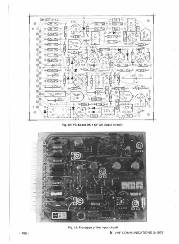
• 186 •
'Ig U : ~ototype of 11\<1 Iof\CIoUI ~1tC..1I
~ VHF COMMUNICATIONS 3/1976

Afte r grounding the Input 01 the AC amptrtrer (connec tion 16) the vonaqe at TP 3 is zeroedw ith the aid 01 R 274 A DC-vollage is no w connec ted to the Input that result s In a voltage 0 'approx . - 10 V at the ou tpu t [connectron 22), R 275 is now aligned so that th,s value remainsconstan t o n reversing the polarity ct me Input vol tage .
The resistance measu ring cncun IS ahgned Ilnally , The ou tp ul voltage (connectlon3 1) ISzeroed w ilh the aid 01 R 276 w il h the inpul (ccnnecucn 30) grounded
Resist or s R 2n, R 278 and R 279 de termine the -ten scale - 0 1 the measu ring system in eachmode , These are adjusted al ter completing the umt wllh the aid 01 a standa rd vol tagegenera to r or already calibra ted d ig ital mcueneter. Il lS advisable 'or Ihese tr imm er resis to rs tobe access.tne Irom cu te.ce Ihe case . e,g lor them to be mounted on the rear panel
The capacitance values shown In pa ralle l With lhe resist or s 01 the Input vcnage diVider InFig , 9 are only give n lo r orientation , These values can di ller according to the wiring 01 themeasuring range SWitch . II the highesl posebre accura cy of the described multi meter IS to be
u sed to the lull , it wi ll oe necessary for an individual alignment 01 these cececnore to be
made. This is made in Ihe most simple manner With the aid 01 an oscilloscope connected toTP 3, Alter com pletion , a c lean squarewave signal 01 epprcx . 2 kHZ which can be taken Iroma TIL l lipllop, is teo to the input. The values 01 the parallel cececnc rs are Ihen varied in allmeasur ing ranges In order to cetetn a clean squarewave signal at TP 3
7, POWER SUPPLY
The c irc ui t d iag ram 01 the po war sup ply Is given in Fig . 14 A voltage 01 ... 15 V reqUired lo rthe operational ampli fie rs is oblai ned Ir om the uppe r tr ansto rmer w ind ing, is rectified Withthe aid 0 1 G 1 and slabi lized in the l ilted -vo ltage stabilizer 128L The same Wind ing alsogener ate s a voltage 01 ... 12 V, which IS taken Irom the center lap . This is use d l or o peratrcn
0 1 the relay and the control lamps. and tneretc re does nOI r&qui re any stabilization. The+ 5 V req uired lo r supplying the TTL-integrated cirCUlls IS also obtained Irom thi S voltageWith Ihe aid 01slabi lize r I 291.
A vo ltage 01 · 15 V is gene rated ' rom the center transl or mer Wind ing using a seco nd l i~ed ·
voltage stabi li zer. This voltage is also used lor ccerencn o t the ope rational ampll ile rs. Thevo ltage doubler ci rcui t comp risi ng diodes D281 and 0.282 supplies a nega ll ve vo ltage ofapp rc x. • 40 V, wh ich IS eteotneee 10 - 20 V WIth Ihe aid 01 transis tor T 281, This vcttage isrequ ired for the AID conve rter,
The lo we r w inding 0 1 the tra nslorme r provides Ihe plal e vo llag e lo r the motcetcr tu bes al terrect ifi cat ion With the aid 01 D 291. The approp ria te charge capacitor is to ce found onPC-bo ard DK 1 OF 02£.
Con nection 10 01 mod ule 029 is connected to the mput of the AID converter. If the vol tagelevel co nnec ted at this POint IS less than - 10 V (adjustable With A 291). the outpct of theco mpara to r 1292 is released (open collec tor), 10 Ihat Ihe mu!livlbra tor equipped Withampli fie r I 293 can oectnete and the pilo t lamp ccnoectec to connection 26 will bli nk penorncenv. This is the out-ol- range indicatio n mentioned in the mrrcc ucuce 01 Ihis article
A. VHF COMMUNICATIONS 3/ 1976 • 187 ·

'"
'"121. 1lj l,l
III
""tsv
1
1
,1 281
",
",
Gl
1 262D281 JlN 4001 l M 320 K- IS
I 0" 0282 :1 "" II ~5V 1N4oo1 63 \1
~f-+-=)----J-=~~100", I5k8 6k8 10k I
L 53V T 281'-__--"""'....., .J'--<--<) (311 · 201,1__ _ _ _ _ _ _ _ _ _ ---J
!l81 1 84 0 C1000
'"a.SAtava. SA
Tr 1."
Si 1 O.4 A
. 15 1,1
IIr--<l-- 0..",0v
I
UOl
R291I10' I
1221
".,
6801 1W
1292,
DK10 F 029
".
100
'",
"'1I '" 0291
14 1 1N4007
OVER I
• 188 . A. VHF CO MMUNICATIONS 3 / 1976

1~T,
r---------------,~1 , _ _ I
I " ""' - - _ _ IIf ' ... II \ ' j ... I 1I \.... \ I
I 1! o ' ' T1 \ \ t ~ •I \ \ l"rl \ 0 \ I ::;, \ \ ' ~I '-, ' .1I ... I • I I Tt ...._- ' - / . :;,I - ..._ _ ... I ~, ,L J
r------------------,,,,I
-e
r---------------,,,,----- , ~,,-, -.... ', ',\"'./ "\ '!: \ I ,..\ 0 \ Ii'\ \ . -\ 0 \: ~.l\ \ ,
... ...... \ I ~Tv-, _ { _) ) I "
-"' ... I, ,L J
...---..." ....., ,... ... 0 -,, -
I r r ' \\ I \ I, "\ .. ... -" ,
I'" 0 _.. ... .,I .............. ...' ~ II , , '" , +: :~, ,,I ,I ,I ,, I, I, II I
i :L J~
@(~~j@ +f i-aID- <
--1 no!,wr0 211'
----:0 1-;00:;35Vo
t;+ ~l'r,, ,
...'i ! ~" "I ' I ~ ~L-' •u•r--',
",,I ',,I ',I... ,,L __ J
"
"
o"-
LI
L
-•
."
A VHF COMMUNICATIONS 3/ 1976 • 189 ·

·•
I•ii
I!!
I
• 190 · ~ VHF COMMUNICATIONS 3/ 1976

7.2. Con l truct lon
Pc-ec eree OK 1 OF 028 and 029 have been destgned l or acccmmcceucn 0 1 the power supplyBoth are 100 mm II 120 mm. smgle-coated and can also be p-ovroed With 3 1 pm connec to rsThe com ponent locations are given in Fig. 15 end 16. end Fill. 17 end 18 sho w phOlographs01 the cr otctvpe boards
Since suc h measurmg equipment tS o ften 10 continuous operation, a co re type M 74 shouldbe used lor the po wer transl ormer , although size M 64 would be sul hc lenl lor in termed iateoperationThe followmg table giv es the number 0 1 tu rns and lhe wtre d,amelers In lh e case 01 a M 74transformer core:
Primary w ind ing :Sc reen ing :Secondary Wind ing I:Secondary w ind ing II:Secondary w ind ing III:
7.3. Compon entl
1210 turns 01 032 mm dia ,1 II copper 10 11 0 ,05 mm2 II 66 turns o f 0 55 mm ere112 turns 010.32 mm d ,a1020 turns 0 1 0.15 mm d,a
128 1.1282:t 291:t 292 , I 293
T 28 1:
Gl :G 2:
0281 ,0282:0291 :
R 291 :
Voltage stabi lizer LM 340 K · 15 (NS)Vo ltage stabilizer LM 320 K • 15 (NS)Vol tage stabilizer LM 309 K (NS)Operaucnat amphuer TAA 86 1 or TAA 761 (Stemens)
2 N 2905 or similar PNP·sili con transistor
Br idge rec trtrer B 40 C 2200 1S.emens)Br idge recnuer B 40 C 1000 (Siemens)
Sili con recnuer diode 1 N 4001 or sumterSili con recuher d iode 1 N 4007 or Slmtlar
Trimm er resistor , SpilClng lOt5 mm
8. FINAL NOTES
No curr ent measuri ng range s were p rOVided on the eescnbee mullt meter In order no t tocomp lic ate the range sWitchi ng Expenence has shown that 95 % 01 practical measurementsare concerned With vo ltage and resIStance. In add it ion to this. any current can be measuredwi th th e aid 01 a SUitab le resistor In the lorm of a vol tage drop,
Although th ree-and-a· hall di g,t dig llal multlmeters are available In lhe range 0 1 600 to1000 OM on the markel , It can slltl be worthwh ile construc ting the described mult lmeter . Oncompar ing the described un it With the vari ous soecrnc eucns 01 the available equipm ent WIthrespect to measuring accur acy and lowe st measuring ranges . II Will be seen Ihat the OK 1 OFmulti meter is virt ually one orde r 01 magn itude better than tnose whose data Sheets areavailab le 10 the ed llor lal stall. Prereqursrte is, however, Ihalthe deSCribed mel al-f llm resistors ,of which lour pieces should have a torere nce 0 1 0,1 %, are used, and lhal l he compteree uni tis aligned wrth the aid 0 1 a very good digi tal vonmerer alt er construc tion
~ VHF COMMUNICATIONS 3/19 76 • 191 •

MATERIAL PRICE LIST OF EaUIPMENTdescribed In Edition 3/1976 01 VHF COMMUNICATIONS
OJ" BO 017 NEW AF AMPLIFIER and VOLTAGE STABILIZE R
PC·bOard OJ 4 SG 0 17 (w ith printed plan)Semicondu cto rs A OJ 4 SO 0 17 (AF·amphl ,er I IC , 1 tr anSist Or)Semicondu cto r. B OJ 4 SO 0 17 (Vol tage stablhzer: 1 IC. 1 Ir8nSlslor)
Tran sl ormer EK 25 - as long 85 stoc k lasts - specia l redu ced pri ce :
Ed. 3/ 1978
OM 12.OM 23.OM 19 ,OM 4,SO
28 MHz 1432 MHz TRAN SMIT CO NVERTERwl1h SCHOTIKY RIN G MIXER
OJ ell 006
PC·boardSemiconductorsM,n lk fl
""
OJ 6 ZZ 006OJ 6lZ006DJ 6 ZZ 006
OJ ezz 006
(double-coaled . w ithout through conlacls)(S lranlll la r• . 1 IC. 1 ring ml ler)(12 tr immer . 2 leed thrOugh capacitor • .1 COII$81 wllh co r.., 10 temte beads)
with above part s
Ed . 3/ 1978
OM 19,OM ISO-
OM 26 0 M 190.-
OK 1 0 F O:ZS · 02t DI G I T A L M ULTIM f T ER
OK 1 OF 025
PC·bOardM lnlkll
""01<10F026
PC-boardInd icato r lubesSemico nductors
""OK 1 OF027
PC-boa rdSemiconduclorsMmik l'
"It
OK 1 OF 028
PC-boa rdSemiconducto rs
."OK 1 OF029
PC-boardSermccnductcrs
""All PC-bo lrd.All kltl
A /D.(:ONVERTER
OK 1 OF 025 (double-coa led . lh rough-conlacl s)OK 1 OF 025 (I t le s. 9 tranSIslors, 2 dIodes . 3 reS1Slors 1% )OK 1 OF 025 with I bo v. pI'"
DECODER Ind INDICATOR MODULE
OK t OF 026 (doub le coated. through conlac ls )OK t OF 026 (4 Nix ie lu bet ZM 1330)OK t OF 026 (5 ICs. t transistor )OK 1 OF 026 wllh lbove plrt,
INPUT MODULE
OK I OF 027 (double coa led , Ihr ough contacts)OK t OF 027 (8 tes . 5 tranSlS1or• . 12 dIodes)OK 1 OF 027 ( t relay, 27 r8llslors 1%. .. resistors 0,1 % )OK 1 OF 027 with lbov. pa rt.
POWER SUPPLY 1
OK 1 OF 028 (With pr inted plan)OK 1 OF 028 (2 ICs. 2 rect . 1 lr anSlslor, .. dIodes)OK 1 OF 028 with I bove pI'"
POWER SUPPLY 2
OK 1 OF 029 (wl lh pr inted plan)OK 1 OF 029 (3 IC• . 2 d lodfts)OK 1 OF 029 with l bove pI'"
OK 1 OF 25-29 DIGITAL MULTIM ETEROK 1 OF 25-29 DIGITAL MULTIM ETER
Ed. 311978
OM 30.OM 89SOOM 115.-
Ed. 311978
OM 17.OM 70.OM 31,OM 115.-
Ed. 3" 878
OM 30,OM ~
OM 58 OM 175.-
Ed.3/Ht76
OM 15,OM 65 OM 79.-
Ed. 311976
OM 15 0 M 32.OM 4e.-OM 100.OM 500.-
• t92 • ~ VHF COMMUNICATIONS 3" 976

OK 1 OF 030 - 032 HF end VHF UNIVER SAL CONVERTER
OK 1 OF 030OK 1 OF 030
OK 1 OF 030oOK 1 OF 030
5000 MHzOK 1 OF 031DK10F031
OK 1 OF 030
PC-boa rd
Sem ico nducto rsMln lk,lt 1
. It
OK 1 OF03TOK 1 OF031
PC-boa rdSem ico nductorsMln lk",
Crys talThu mbwheel sw.It
OK 1 OF 032
PC-boardSemiconducto rsM ln lk, lt
.It
KIt.
RF INPUT MODULE
OK 1OF 030 (double-coated, no Ihrough·contaC" .with printed plan)(1 rmg ml~er . 4 transisl ors. 2 diodes)(2 chokes. 3 polled co res. 3 COIIsels .\ ccinoemer with co re)(5 leedlhrough . 2 trim mer . 34 cerarmc ceoe..16 resisl or s. 1coo ting l lns, 2 m sflver-pl wfre)complete with ebove perts
SYNTHESIZER MODULE
OK 1OF 031 (dou ble co ated. th rough con tac ls)OK 1OF 03 \ (7 ICs. 8 tranSIstor s)OK t OF 031 (9 leedl hrough. 1 tfl mmer . 22 cerermc, and
I lanl ahum capaCIIo r. 38 feSlslor• . I cOIIMI.6 rc lOCkets. 1 polled core)HC-6/U(2 SWitches With accessories)compt.'e wllh abov e perts
POWER SUPPLY
OK \ OF 032 (With prin ted plan)OK \ OF 032 (3 ICs. 1 tranarator. 4 diodes. 1 rect if ier)OK t OF 032 (4 elec trolytlCs, \ cresuc 10 11. 1 ceramic
cececrtc e. 9 resIstor s. 1 tnm rner pot )OK 1 OF 032 complele with ebove pert s
OK 1 OF 30·32 50 kHI to 30 MHI / 145 MHz. comple te
Ed. 3/ HI76
OM 16 -0M 64-
OM 34-
0M 34 -
DM 145.-
Ed. 31HI76
OM 20,OM 98 -
OM 54 OM 26 0 M 48 OM 240.-
Ed. 3/HI76
OM 12,OM 52.-
OM 18 0 M 80.
OM 460.-
Verlag UKW-BERICHTE, H. Dohlus oHGJahnstraBe 14 - 0 ·8523 BAIERSOORF
Wes l -Germany ' Telephone (0 9191 ) 91 57 or (0 9 133) 855. 856

r f.,@CRY STAL FILTER S OSCILLATOR CRYSTAL S
6~1ll SYNONYMOUS FOR QUALITYAND ADVANCED TECHNOLOGY
NEW STANDARD FILTERS
CW-FILTER XE-9NB see table
SWITCHABLE SSB FILTERSfor a fixed carri er frequency of 9.000 MH z
XF-9B 01 XF·9B 028998.5 kHz for LSB 9001 .5 kHz for USB
See XF-98 for all other specificationsThe carrie r crystal XF 900 is provided
Filler Type I XF·9A " .go ,,<>C ,,-90 " -se I XF-9NB
App llca llon SSB sse AM AM FM ewTransml '
Numbur 01crys tall s • • • • •3 ee bandwl(llh 2 " kHz 23 kHz 3 8 kHz .. 8 kHZ 11.5 kHz 0 4 kHz
6 dB bandwidth 25 kHz 2 4 kHz 3.75 kHz 50 kHz 12.0 kHz 0 5 kHz
Ripple < IdB < 2 dB < 2 dB < 2 dB < 2 dB < Q,S dB
Insertion lou < 3 dB < 3SdB < 3 5dB < 35 dB < 3 5 dB < 6 5dB
Z 500 0 500 0 500 0 500 0 '200 0 500 0Term maloon
C, 30 pF 30pF 30pF 30pF 30 pF 30 "(6 SOdS ) 1 7 (B80dS) \8 (660 dBl lB (6 6OdB) 18 (6 60dBli 8 (660 dBJ22
Sha pe ,"clo r(6 80dB)22 (680dBI22 (SaD dB122 (660dB)22 (680 dB) 4 0
Ulhmll le reJecl lon > 45 dB I > 1ClOdB I > lOO dB > rocca > 90 dB > 90 dB
XF·9A and XF·98 compl ete With XF 901, XF 902XF·9NB comple te woth XF 903
KRISTALLVERARBEITUNG NECKARBISCHOFSHEIM GMBH ~0692.. N",ckarbllchof.h",im Po.tf",ch 7
Copyright © 2022 FDOKUMEN


![[2021] JMCC COMM.27 - Supreme Court of Jamaica](https://static.fdokumen.com/doc/165x107/631905dcc51d6b41aa043d49/2021-jmcc-comm27-supreme-court-of-jamaica.jpg)
