Granulomatous Interstitial Nephritis in Children Resulting from ...
Upload
independentCategory
view
4download
0
VARIUS: A Model of Process Variation and Resulting Timing Errors for
Microarchitects∗
Smruti R. Sarangi, Brian Greskamp, Radu Teodorescu, Jun Nakano, Abhishek Tiwari, and Josep Torrellas
University of Illinois at Urbana-Champaign
http://iacoma.cs.uiuc.edu
September 2007
To Appear in IEEE Transactions on Semiconductor Manufacturing, 2007
Abstract
Within-die parameter variation poses a major challenge to high-performance microprocessor design, negatively impacting
a processor’s frequency and leakage power. Addressing this problem, this paper proposes a microarchitecture-aware model for
process variation — including both random and systematic effects. The model is specified using a small number of highly-intuitive
parameters. Using the variation model, this paper also proposes a framework to model timing errors caused by parameter variation.
The model yields the failure rate of microarchitectural blocks as a function of clock frequency and the amount of variation. With
the combination of the variation model and the error model, we haveVARIUS, a comprehensive model that is capable of producing
detailed statistics of timing errors as a function of different process parameters and operating conditions. We propose possible
applications of VARIUS to microarchitectural research.
1 Introduction
As high-performance processors move into 32 nm technologies and below, designers face the major roadblock of parameter
variation — the deviation of process, voltage, and temperature (PVT [1]) values from nominal specifications. Variation makes
designing processors harder because they have to work under a range of parameter values.
Variation is induced by several fundamental effects. Process variation is caused by the inability to precisely control the fabri-
cation process at small-feature technologies. It is a combination of systematic effects [2, 3, 4] (e.g., lithographic lens aberrations)
and random effects [5] (e.g., dopant density fluctuations). Voltage variations can be caused byIR drops in the supply distribution
∗This work was supported in part by the National Science Foundation under grants EIA-0072102, EIA-0103610, CHE-0121357, and CCR-0325603; DARPAunder grant NBCH30390004; DOE under grant B347886; and gifts from IBM and Intel.
network or byL dI/dt noise under changing load. Temperature variation is caused by spatially- and temporally-varying factors.
All of these variations are becoming more severe and harder to tolerate as technology scales to minute feature sizes.
Two key process parameters subject to variation are the transistor threshold voltage,Vth, and the effective length,Leff. Vth
is especially important because its variation has a substantial impact on two major properties of the processor, namely the fre-
quency it attains and the leakage power it dissipates. Moreover,Vth is also a strong function of temperature, which increases its
variability [6].
One of the most harmful effects of variation is that some sections of the chip are slower than others — either because their
transistors are intrinsically slower or because high temperature or low supply voltage renders them so. As a result, circuits in
these sections may be unable to propagate signals fast enough and may suffer timing errors. To avoid these errors, designers in
upcoming technology generations may slow down the frequency of the processor or create overly conservative designs. It has
been suggested that parameter variation may wipe out most of the potential gains provided by one technology generation [7].
An important first step to redress this trend is to understand how parameter variation affects timing errors in high-performance
processors. Based on this, we could devise techniques to cope with the problem — hopefully recouping the gains offered by
every technology generation. To address these problems, this paper proposesVARIUS, a novel microarchitecture-aware model for
process variation and for variation-induced timing errors. VARIUS can be used by microarchitects in a variety of studies.
The contribution of this paper is two-fold:
A model for process variation. We propose a novel model for process variation. Its component for systematic variation uses
a multivariate normal distribution with a spherical correlation structure. This matches empirical data obtained by Friedberget
al. [2]. The model has only three parameters — all highly intuitive — and is easy to use. Moreover, we also model temperature
variation.
A model for timing errors due to parameter variation. We propose a novel, comprehensive timing error model for microarchi-
tectural structures in dies that suffer from parameter variation. This model is calledVATS. It takes into account process parameters,
the floorplan, and operating conditions like temperature. We model the error rate in logic structures, SRAM structures and com-
binations of both, and consider both systematic and random variation. Moreover, our model matches empirical data and can be
simulated at high speed.
This paper is organized as follows. Section 2 introduces background material and provides mathematical preliminaries; Sec-
tion 3 presents the process variation model; Section 4 presents the model of timing errors for logic and SRAM under parameter
variation; Section 5 shows a model validation and evaluation; Section 6 presents related work and Section 7 concludes.
2
2 Background
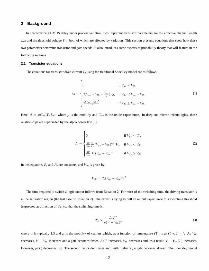
In characterizing CMOS delay under process variation, two important transistor parameters are the effective channel length
Leff and the threshold voltageVth, both of which are affected by variation. This section presents equations that show how these
two parameters determine transistor and gate speeds. It also introduces some aspects of probability theory that will feature in the
following sections.
2.1 Transistor equations
The equations for transistor drain currentId using the traditional Shockley model are as follows:
Id =
0 if Vgs ≤ Vth
β(Vgs − Vth − Vds
2 )Vds if Vds < Vgs − Vth
β(Vgs−Vth)2
2 if Vds ≥ Vgs − Vth
(1)
Here,β = µCoxW/Leff, whereµ is the mobility andCox is the oxide capacitance. In deep sub-micron technologies, these
relationships are superseded by the alpha power law [8]:
Id =
0 if Vgs ≤ Vth
WLeff
Pc
Pv(Vgs − Vth)α/2Vds if Vds < Vd0
WLeff
Pc(Vgs − Vth)α if Vds ≥ Vd0
(2)
In this equation,Pc andPv are constants, andVd0 is given by:
Vd0 = Pv(Vgs − Vth)α/2
The time required to switch a logic output follows from Equation 2. For most of the switching time, the driving transistor is
in the saturation region (the last case of Equation 2). The driver is trying to pull an output capacitance to a switching threshold
(expressed as a fraction ofVdd) so that the switching time is:
Tg ∝LeffV
µ(V − Vth)α(3)
whereα is typically 1.3 andµ is the mobility of carriers which, as a function of temperature (T), isµ(T ) ∝ T−1.5. As Vth
decreases,V − Vth increases and a gate becomes faster. AsT increases,Vth decreases and, as a result,V − Vth(T ) increases.
However,µ(T ) decreases [9]. The second factor dominates and, with higherT , a gate becomes slower. The Shockley model
3
occurs as a special case of the alpha-power model withα = 2.
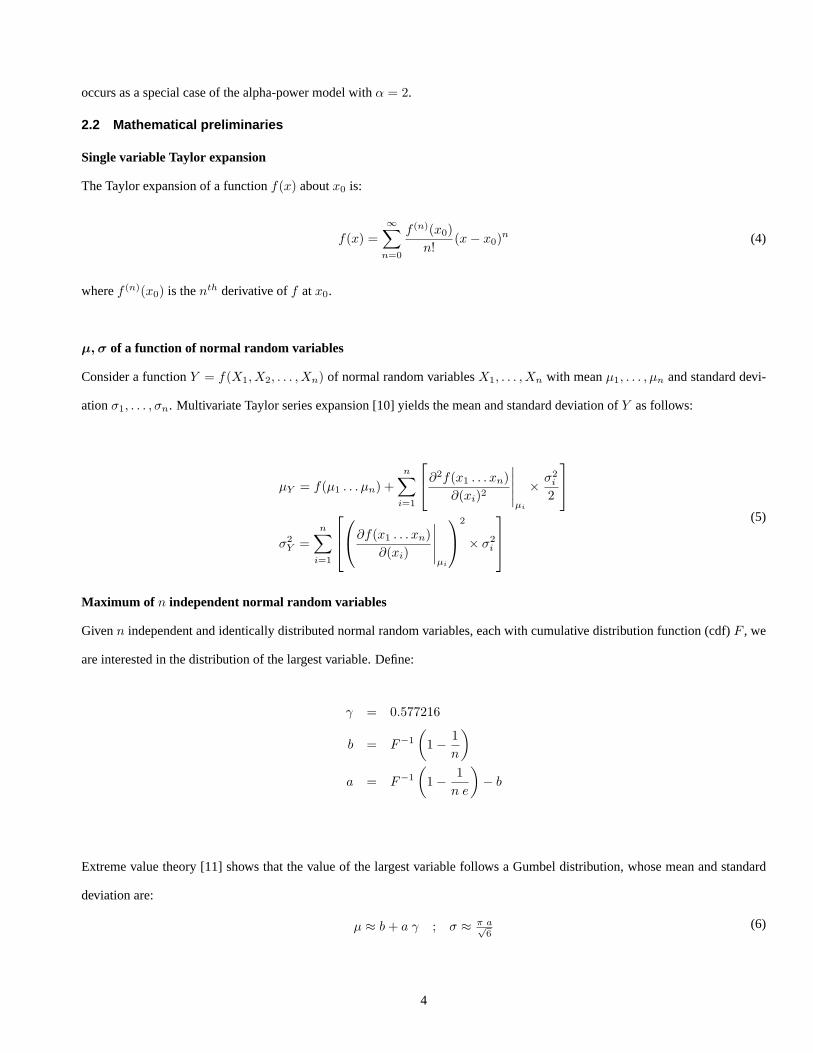
2.2 Mathematical preliminaries
Single variable Taylor expansion
The Taylor expansion of a functionf(x) aboutx0 is:
f(x) =∞∑
n=0
f (n)(x0)n!
(x− x0)n (4)
wheref (n)(x0) is thenth derivative off atx0.
µ, σ of a function of normal random variables
Consider a functionY = f(X1, X2, . . . , Xn) of normal random variablesX1, . . . , Xn with meanµ1, . . . , µn and standard devi-
ationσ1, . . . , σn. Multivariate Taylor series expansion [10] yields the mean and standard deviation ofY as follows:
µY = f(µ1 . . . µn) +n∑
i=1
∂2f(x1 . . . xn)∂(xi)2
∣∣∣∣∣µi
× σ2i
2
σ2
Y =n∑
i=1
∂f(x1 . . . xn)
∂(xi)
∣∣∣∣∣µi
2
× σ2i
(5)
Maximum of n independent normal random variables
Givenn independent and identically distributed normal random variables, each with cumulative distribution function (cdf)F , we
are interested in the distribution of the largest variable. Define:
γ = 0.577216
b = F−1
(1− 1
n
)a = F−1
(1− 1
n e
)− b
Extreme value theory [11] shows that the value of the largest variable follows a Gumbel distribution, whose mean and standard
deviation are:
µ ≈ b + a γ ; σ ≈ π a√6
(6)
4
3 Process variation model
Process variation has die-to-die (D2D) and within-die (WID) components, with the WID component further subdividing into
randomand systematiccomponents. Lithographic aberrations introduce systematic variations, while dopant fluctuations and
line edge roughness generate random variations. By definition, systematic variations exhibit spatial correlation and, therefore,
nearby transistors share similar systematic parameter values [2, 3, 4]. In contrast, random variation has no spatial correlation and,
therefore, a transistor’s randomly-varying parameters differ from those of its immediate neighbors. Most generally, variation in
any parameterP can be represented as follows:
∆P = ∆PD2D + ∆PWID = ∆PD2D + ∆Prand + ∆Psys
In this work, we focus on WID variation. For simplicity, we model the random and systematic components of WID variation as
normal distributions [12]. We treat random and systematic variation separately, since they arise from different physical phenomena.
As described in [12], we assume that their effects are additive. If required, D2D variation can be modeled as an independent
additive variable by adding a chip-wide offset to the parameters of every transistor on the die. This approach does sacrifice some
fidelity since, in reality, WID and D2D variations may not be statistically independent.
3.1 Systematic variation
We model systematic variation using a multivariate normal distribution [10] with a spherical spatial correlation structure [13].
For that, we divide a chip inton small, equally-sized rectangular sections. Each section has a single value of the systematic
component ofVth (and Leff) that is distributed normally with zero mean and standard deviationσsys — where the latter is
different forVth andLeff. This is a general approach that has been used elsewhere [12]. For simplicity, we assume that the spatial
correlation is homogeneous (position-independent) and isotropic (not depending on the direction). This means that, given two
points~x and~y on the chip, the correlation of their systematic variation values depends only on the distance between~x and~y.
These assumptions have been used by other authors such a Xionget al. [14].
Assuming position independence and isotropy, the correlation function of a systematically-varying parameterP is:
corr(P~x, P~y) = ρ(r) ; r = |~x− ~y|
By definition, ρ(0) = 1 (i.e., totally correlated). Intuitively,ρ(∞) = 0 (i.e., totally uncorrelated) if we only consider WID
variation. To specify the behavior ofρ(r) between the limits, we choose the spherical model [13] for its good agreement with
Friedberg’s [2] measurements. Although the correlation function Friedberg reports is not isotropic, the shape of the function (as
opposed to the scale) is the same on the horizontal and vertical die axes. In both cases, the shape closely matches that of the
5
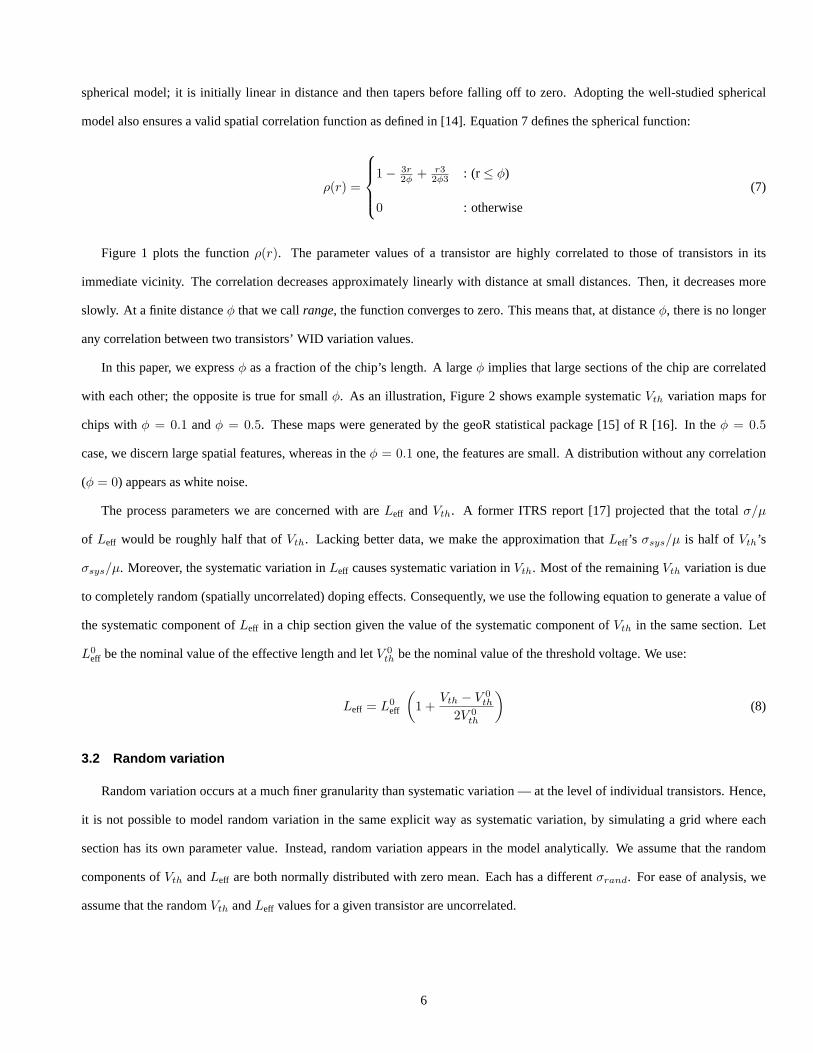
spherical model; it is initially linear in distance and then tapers before falling off to zero. Adopting the well-studied spherical
model also ensures a valid spatial correlation function as defined in [14]. Equation 7 defines the spherical function:
ρ(r) =
1− 3r
2φ + r32φ3 : (r ≤ φ)
0 : otherwise
(7)
Figure 1 plots the functionρ(r). The parameter values of a transistor are highly correlated to those of transistors in its
immediate vicinity. The correlation decreases approximately linearly with distance at small distances. Then, it decreases more
slowly. At a finite distanceφ that we callrange, the function converges to zero. This means that, at distanceφ, there is no longer
any correlation between two transistors’ WID variation values.
In this paper, we expressφ as a fraction of the chip’s length. A largeφ implies that large sections of the chip are correlated
with each other; the opposite is true for smallφ. As an illustration, Figure 2 shows example systematicVth variation maps for
chips withφ = 0.1 andφ = 0.5. These maps were generated by the geoR statistical package [15] of R [16]. In theφ = 0.5
case, we discern large spatial features, whereas in theφ = 0.1 one, the features are small. A distribution without any correlation
(φ = 0) appears as white noise.
The process parameters we are concerned with areLeff andVth. A former ITRS report [17] projected that the totalσ/µ
of Leff would be roughly half that ofVth. Lacking better data, we make the approximation thatLeff’s σsys/µ is half of Vth’s
σsys/µ. Moreover, the systematic variation inLeff causes systematic variation inVth. Most of the remainingVth variation is due
to completely random (spatially uncorrelated) doping effects. Consequently, we use the following equation to generate a value of
the systematic component ofLeff in a chip section given the value of the systematic component ofVth in the same section. Let
L0eff be the nominal value of the effective length and letV 0
th be the nominal value of the threshold voltage. We use:
Leff = L0eff
(1 +
Vth − V 0th
2V 0th
)(8)
3.2 Random variation
Random variation occurs at a much finer granularity than systematic variation — at the level of individual transistors. Hence,
it is not possible to model random variation in the same explicit way as systematic variation, by simulating a grid where each
section has its own parameter value. Instead, random variation appears in the model analytically. We assume that the random
components ofVth andLeff are both normally distributed with zero mean. Each has a differentσrand. For ease of analysis, we
assume that the randomVth andLeff values for a given transistor are uncorrelated.
6
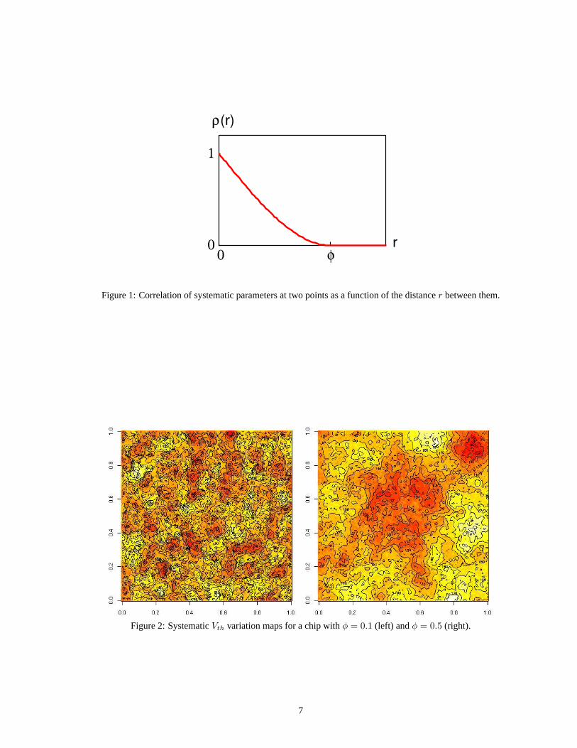
0
1
0 φr
(r)ρ
Figure 1: Correlation of systematic parameters at two points as a function of the distancer between them.
Figure 2: SystematicVth variation maps for a chip withφ = 0.1 (left) andφ = 0.5 (right).
7
3.3 Values for σ and φ
Since the random and systematic components ofVth andLeff are normally distributed and independent, the total WID variation
is also normally distributed with zero mean. The standard deviation is as follows:
σtotal =√
σ2rand + σ2
sys(9)
For Vth, the 1999 ITRS [17] gave a design target ofσtotal/µ=0.06 for year 2005 (although no solution existed); however,
the projection has been discontinued since 1999. On the other hand, it is known that ITRS variability projections were too
optimistic [18, 19]. Consequently, forVth, we useσtotal/µ=0.09. Moreover, according to empirical data from [20], the random
and systematic components are approximately equal in 32 nm technology. Hence, we assume that they have equal variances.
Since both components are modeled as normal distributions, Equation 9 tells us that their standard deviationsσrand andσsys are
equal to9%/√
2 = 6.3% of the mean. This value for the random component matches the empirical data of Keshavarziet al. [21].
As explained before, we setLeff’s σtotal/µ to be half ofVth’s. Consequently, it is 4.5%. Furthermore, assuming again that the
two components of variation are more or less equal, we have thatσrand andσsys for Leff are equal to4.5%/√
2 = 3.2% of the
mean.
To estimateφ, we note that Friedberget al. [2] experimentally measured the gate-length parameter to have a range close to
half of the chip length. Hence, we setφ = 0.5. Through Equation 8, the sameφ applies to bothLeff andVth.
3.4 Impact on chip frequency
Through Equation 3, process variation inVth andLeff induces variation in the delay of gates — and, therefore, variation in the
delay of critical paths. Unfortunately, a processor structure cannot cycle any faster than its slowest critical path can. As a result,
processors are typically slowed down by process variation. To motivate the rest of the paper, this section gives a rough estimation
of the impact of process variation on processor frequency.
Equation 3 approximately describes the delay of an inverter. Substituting Equation 8 into Equation 3 and factoring out con-
stants with respect toVth produces:
Tg ∝V (1 + Vth/V 0
th)(V − Vth)α
(10)
Empirically, we find that Equation 10 is nearly linear with respect toVth for the parameter range of interest. BecauseVth is
normally distributed and a linear function of a normal variable is itself normal,Tg is approximately normal.
Assuming that every critical path in a processor consists ofncp gates, and that a modern processor chip has thousands of
8
critical paths, Bowmanet al. [7] compute the probability distribution of the longest critical path delay in the chip (max{Tcp}).
Then, the processor frequency can be estimated to be the inverse of the longest path delay (1/ max{Tcp}).
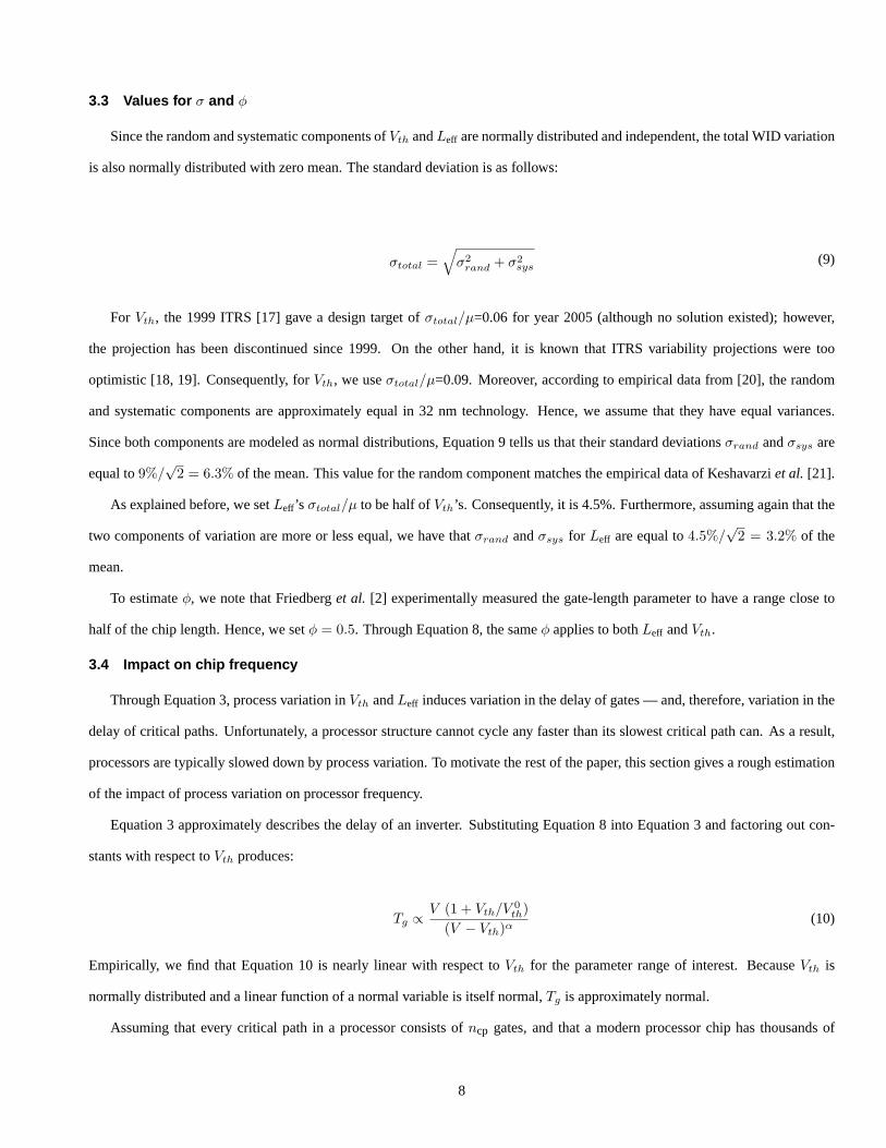
Figure 3 shows the probability distribution of the chip frequency for different values ofVth’s σtotal/µ. The frequency is given
relative to a processor withoutVth variation (F/F0). The figure shows that, asσtotal/µ increases, (i) the mean chip frequency
decreases and (ii) the chip frequency distribution gets more spread out. In other words, given a batch of chips, asVth’s σtotal/µ
increases, the mean frequency of the batch decreases and, at the same time, an individual chip’s frequency deviates more from the
mean.
Such frequency loses may be reduced if the processor is equipped with ways of tolerating some variation-induced timing
errors. As a possible first step in this direction, the rest of the paper presents a model of variation-induced timing errors in a
processor. In future work, we will examine how such errors can be tolerated. In the rest of the paper, we do not use Bowmanet
al.’s [7] critical path model any more.
4 Timing error model
This section presents VATS, a novel model of variation-induced timing errors in processor pipelines. In the following, we first
model errors in logic and then in SRAM memory.
4.1 General approach
A pipeline stage typically has a multitude of paths, each one with its own time slack — possibly dependent on the input data
values. This work makes two simplifying assumptions about the failure model.
Assumption 1: A path causes a timing fault if and only if it is exercised and its delay exceeds the clock period. Note that this fault
definition does not account for any architectural masking effects. However, architectural vulnerability factors (AVFs) [22] could
be applied to model these masking effects if desired.
Assumption 2: Each stage is tightly designed so that, in the absence of process variation, at least one path has a delay equal to
the clock periodt0. This provides a pre-variation base case against which to make delay comparisons.
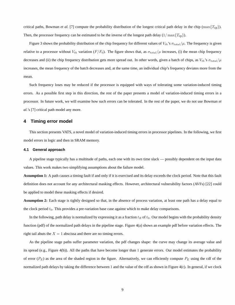
In the following, path delay is normalized by expressing it as a fractiontR of t0. Our model begins with the probability density
function (pdf) of the normalized path delays in the pipeline stage. Figure 4(a) shows an example pdf before variation effects. The
right tail abuts theX = 1 abscissa and there are no timing errors.
As the pipeline stage paths suffer parameter variation, the pdf changes shape: the curve may change its average value and
its spread (e.g., Figure 4(b)). All the paths that have become longer than1 generate errors. Our model estimates the probability
of error (PE) as the area of the shaded region in the figure. Alternatively, we can efficiently computePE using the cdf of the
normalized path delays by taking the difference between1 and the value of the cdf as shown in Figure 4(c). In general, if we clock
9
0.86 0.88 0.9 0.92 0.94 0.96 0.98 10
50
100
150
200
250
F/F0
Pro
babi
lity
Den
sity
Fun
ctio
n
σ / µ = 0.03σ / µ = 0.06σ / µ = 0.09σ / µ = 0.12
Figure 3: Probability distribution of the relative chip frequency as a function ofVth’s σtotal/µ. We useV 0th=0.150V at 100oC, 12
FO4s in the critical path, and 10,000 critical paths in the chip.
tR
tR
tR
1
(a)
(b)
(c)
1
1
1
Dva
rlog
iccd
fD
varl
ogic
Dlo
gic
PE
PE
Figure 4: Example critical path delay distributions before variation in pdf form (a) and after variation in pdf (b) and cdf (c) form.The dark parts show the error rate.
10
the processor with periodtR, the probability of error is:
PE(tR) = 1− cdf(tR)
In the event that race-through errors are also a concern,cdf(th) gives the probability of violating the minimum hold timeth.
However, we will not consider hold-time violations in the rest of the paper.
4.2 Timing errors in logic
We start by considering a pipeline stage of only logic. We represent the logic critical path delay in the absence of variation as a
random variableDlogic, which is distributed in a way similar to Figure 4(a). Such delay is composed of both wire and gate delay.
For simplicity, we assume that wire accounts for a fixed fractionkw of total delay. This assumption has been made elsewhere [23].
Consequently, we can write:
Dlogic = Dwire + Dgates
Dwire = kw Dlogic
Dgates = (1− kw) Dlogic
(11)
We now consider the effects of variation. Since variation typically has a very small effect on wires, we only consider the
variation ofDgates, which has a random and a systematic component. For each path, we divide the systematic variation component
(∆Dgates sys) into two terms: (i) the average value of it for all the pathsin the stage(∆Dgates sys) — which we call the stage
systematic mean — and (ii) the rest of the systematic variation component (∆Dgates sys −∆Dgates sys) — which we call intra-
stage systematic deviation.
Given the high degree of spatial correlation in process (P) and temperature (T) variation, and the small size of a pipeline stage,
the intra-stage systematic deviation is small. Indeed, in Section 3.3, we suggested a value ofφ equal to 0.5 (half of the chip length).
On the other hand, the length of a pipeline stage is less than, say, 0.1 of the length of a typical 4-core chip. Therefore, given that
the stage dimensions are significantly smaller thanφ, the transistors in a pipeline stage have highly-correlated systematicVth and
systematicLeff values. Using Monte Carlo simulations with the parameters of Section 3.3, we find that the intra-stage systematic
deviation ofDgates has aσintrasys ≈ 0.004 × µ, while the variation of∆Dgates sys across the pipeline stages of the processor
has aσintersys ≈ 0.05× µ. Similarly,T varies much more across stages than within them.
The random component ofDgates’s variation is estimated from the fact that we model a path asn FO4 gates connected
with short wires. Each gate’s random component is independent. Consequently, for a whole n-gate path,Dgates’s σrand is
√n × σrand DF04 , whereσrand DF04 is the standard deviation of the delay of one FO4 gate. If we taken = 12 as representative
of high-end processors, the overall variation is small. It can be shown thatDgates’s σrand ≈ 0.01× µ. Finally, T has no random
11
component.
We can now generate the distribution ofDlogic with variation (which we callDvarlogic and show in Figure 4(b)) as follows.
We model the contribution of∆Dgates sys in the stage as a factorη that multipliesDgates. This factor is the average increase in
gate delay across all the paths in the stage due to systematic variation. Without variation,η = 1.
We model the contribution of the intra-stage systematic deviation and of the random variation asDextra, a
small additive normal delay perturbation. SinceDextra combinesDgates’s intra-stage systematic and random effects,
σextra =√
σ2intrasys + σ2
rand. For our parameters,σextra ≈ 0.011 × µ. Like η, Dextra should multiplyDgates as shown in
Equation 12. However, to simplify the computation and becauseDlogic is clustered at values close to one, we prefer to approxi-
mateDextra as an additive term as in Equation 13:
Dvarlogic = (η + Dextra) Dgates + Dwire (12)
= (1− kw) (η + Dextra) Dlogic + kw Dlogic
≈ (1− kw) (η Dlogic + Dextra) + kw Dlogic (13)
Once we have theDvarlogic distribution, we numerically integrate it to obtain itscdfDvarlogic(Figure 4(c)). Then, the estimated
error ratePE of the stage cycling with a relative clock periodtR is:
PE(tR) = 1− cdfDvarlogic(tR) (14)
4.2.1 How to use the model
To apply Equation 13, we must calculatekw, η, Dextra, andDlogic for the prevailing variation conditions. To do this, we
produce a gridded spatial map of process variation using the model in Section 3.1 and superimpose it on a high-performance
processor floorplan. For each pipeline stage, we computeη from the pipeline stage’s temperature and the systematicLeff andVth
maps. Moreover, by subtracting the resulting mean delay of the stage from the individual delays in the grid points inside the stage,
we produce the intra-stage systematic deviation. We combine the latter distribution with the effect of the random process variation
to obtain theDextra distribution.Dextra is assumed normal.
Ideally, we would obtain a per-stagekw andDlogic through timing analysis of each stage. For our general evaluation, we
assume that the LF adder in [24] is representative of processor logic stages, and setkw = 0.35 [23]. Additionally, we derive
pdfDlogicusing experimental data from Ernstet al. [25]. They measure the error ratePE of a multiplier unit as they reduce its
supply voltageV . By reducingV , they lengthen path delays. Those paths with delays longer than the cycle time cause an error.
12
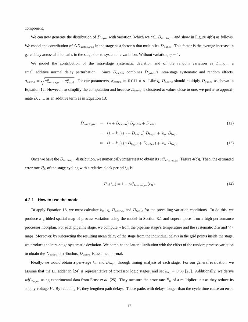
Our aim is to find thepdfDlogiccurve from their plot ofPE(V ) (a curve similar to that shown in Figure 5(a)).
Focusing on Equation 13, Ernst’s experiment corresponds to an environment with no parameter variation, soDextra = 0.
EachV corresponds to a new averageη(V ) and, therefore, a newDvarlogic(V ) distribution. We compute eachη(V ) using the
alpha-power model (Equation 3) as the ratio of gate delay atV and gate delay at the minimum voltage in [25] for which no errors
were detected.
At a voltageV , the probability of error is equal to the probability of exercising a path with a delay longer than 1 clock cycle.
Hence,PE(V ) = P (Dvarlogic(V ) > 1). If we use Equation 13 and defineg(V ) = 1/(kw + η(V ) × (1 − kw)), we have
Dvarlogic(V ) = Dlogic/g(V ). Therefore:
PE(V ) = P (Dvarlogic(V ) > 1)
= P (Dlogic/g(V ) > 1)
= P (Dlogic > g(V ))
= 1− cdfDlogic(g(V ))
(15)
Lettingy = g(V ), we havecdfDlogic(y) = 1−PE(V ). Therefore, we can generatecdfDlogic
numerically by taking successive
values ofVi, measuringPE(Vi) from Figure 5(a), computingyi = g(Vi), and plotting (yi,1-PE(Vi)) — which is (yi,cdfDlogic(yi)).
After that, we smooth and numerically differentiate the resulting curve to find the sought functionpdfDlogic. Finally, we approx-
imate thepdfDlogiccurve with a normal distribution, which we find hasµ = 0.849 andσ = 0.019 (a curve similar to that shown
in Figure 5(b)).
Strictly speaking, thispdfDlogiccurve only applies to the circuit and conditions measured in [25]. To generatepdfDlogic
for
a different stage with a different technology and workload characteristics, one would need to use timing analysis tools on that
particular stage. In practice, Section 5.1 shows empirical evidence that this method producespdfDlogiccurves that are usable
under a range of conditions, not just those under which they were measured.
Finally, sinceDlogic andDextra are normally distributed,Dvarlogic in Equation 13 is also normally distributed.
4.3 Timing errors in SRAM memory
To model variation-induced timing errors in SRAM memory, we build on the work of Mukhopadhyayet al. [26]. They
considerrandomVth variation only and use the Shockley current model. We extend their work to account for random and
systematic variation of bothLeff andVth and use the more accurate alpha-power current model. Additionally, we describe the
access time distribution for an entire multi-line SRAM array rather than for a singe cell.
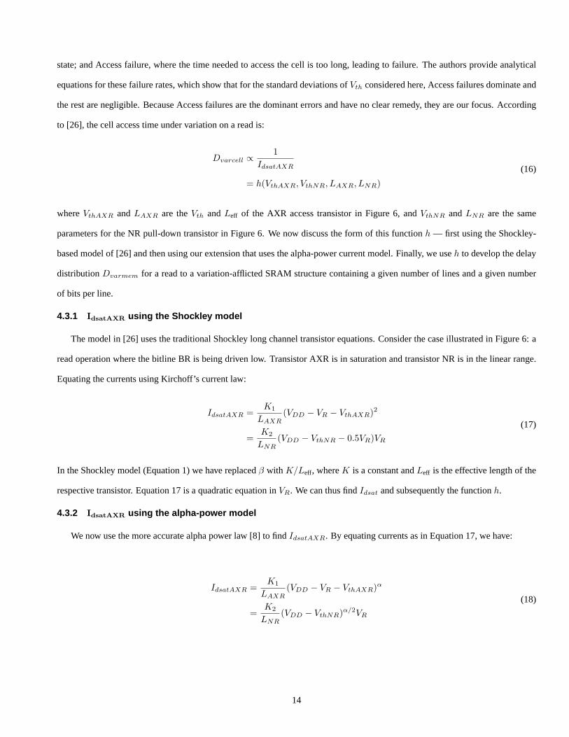
Mukhopadhyayet al. [26] describe four failure modes in the SRAM cell of Figure 6: Read failure, where the contents of a
cell are destroyed when the cell is read; Write failure, where a write is unable to flip the cell; Hold failure, where a cell loses its
13
state; and Access failure, where the time needed to access the cell is too long, leading to failure. The authors provide analytical
equations for these failure rates, which show that for the standard deviations ofVth considered here, Access failures dominate and
the rest are negligible. Because Access failures are the dominant errors and have no clear remedy, they are our focus. According
to [26], the cell access time under variation on a read is:
Dvarcell ∝1
IdsatAXR
= h(VthAXR, VthNR, LAXR, LNR)
(16)
whereVthAXR andLAXR are theVth andLeff of the AXR access transistor in Figure 6, andVthNR andLNR are the same
parameters for the NR pull-down transistor in Figure 6. We now discuss the form of this functionh — first using the Shockley-
based model of [26] and then using our extension that uses the alpha-power current model. Finally, we useh to develop the delay
distributionDvarmem for a read to a variation-afflicted SRAM structure containing a given number of lines and a given number
of bits per line.
4.3.1 IdsatAXR using the Shockley model
The model in [26] uses the traditional Shockley long channel transistor equations. Consider the case illustrated in Figure 6: a
read operation where the bitline BR is being driven low. Transistor AXR is in saturation and transistor NR is in the linear range.
Equating the currents using Kirchoff’s current law:
IdsatAXR =K1
LAXR(VDD − VR − VthAXR)2
=K2
LNR(VDD − VthNR − 0.5VR)VR
(17)
In the Shockley model (Equation 1) we have replacedβ with K/Leff, whereK is a constant andLeff is the effective length of the
respective transistor. Equation 17 is a quadratic equation inVR. We can thus findIdsat and subsequently the functionh.
4.3.2 IdsatAXR using the alpha-power model
We now use the more accurate alpha power law [8] to findIdsatAXR. By equating currents as in Equation 17, we have:
IdsatAXR =K1
LAXR(VDD − VR − VthAXR)α
=K2
LNR(VDD − VthNR)α/2VR
(18)
14
E)
Log(
P
t 0
D log
icpd
f()
1.54 1.34(a) (b)
V
Figure 5: Error rate versus voltage curve from [25] (a) and correspondingpdfDlogic (b).
WL
BRBL
IdsatAXR
VR AXR
NR
VDD
Figure 6: A read from a 6T SRAM cell, pulling the right bitline low.
●
●
● ● ● ● ● ● ● ●
2 4 6 8 10
0.00
00.
004
0.00
80.
012
Degree
Err
or
Figure 7: Error versus degree of expansion ofz.
15
As in Equation 17, constants have been folded intoK1 andK2. To solve forVR, perform the following transformation:
(VDD − VR − VthAXR)α = (VDD − VthAXR)α ×(
1− VR
VDD − VthAXR
)α
(19)
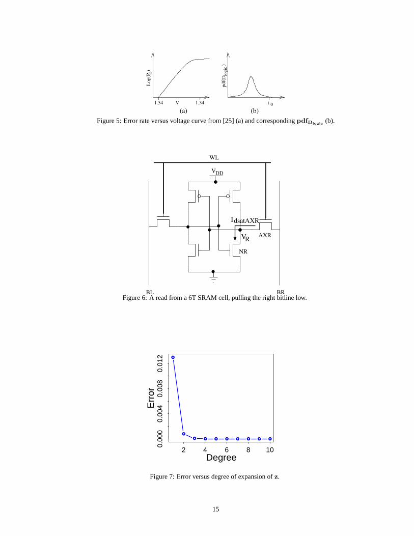
Let z = VR
VDD−VthAXRand expand(1− z)α using the Taylor series (Equation 4). Typical values ofz are near 0.25, so we compute
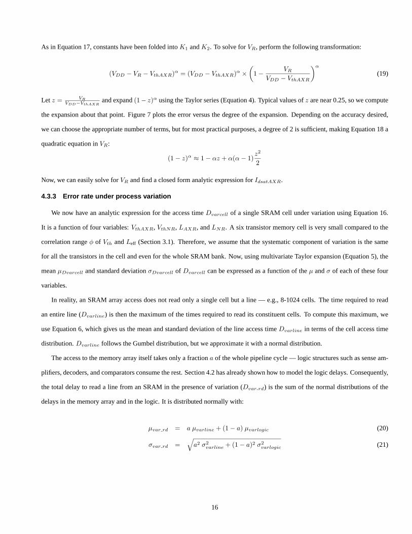
the expansion about that point. Figure 7 plots the error versus the degree of the expansion. Depending on the accuracy desired,
we can choose the appropriate number of terms, but for most practical purposes, a degree of 2 is sufficient, making Equation 18 a
quadratic equation inVR:
(1− z)α ≈ 1− αz + α(α− 1)z2
2
Now, we can easily solve forVR and find a closed form analytic expression forIdsatAXR.
4.3.3 Error rate under process variation
We now have an analytic expression for the access timeDvarcell of a single SRAM cell under variation using Equation 16.
It is a function of four variables:VthAXR, VthNR, LAXR, andLNR. A six transistor memory cell is very small compared to the
correlation rangeφ of Vth andLeff (Section 3.1). Therefore, we assume that the systematic component of variation is the same
for all the transistors in the cell and even for the whole SRAM bank. Now, using multivariate Taylor expansion (Equation 5), the
meanµDvarcell and standard deviationσDvarcell of Dvarcell can be expressed as a function of theµ andσ of each of these four
variables.
In reality, an SRAM array access does not read only a single cell but a line — e.g., 8-1024 cells. The time required to read
an entire line (Dvarline) is then the maximum of the times required to read its constituent cells. To compute this maximum, we
use Equation 6, which gives us the mean and standard deviation of the line access timeDvarline in terms of the cell access time
distribution.Dvarline follows the Gumbel distribution, but we approximate it with a normal distribution.
The access to the memory array itself takes only a fractiona of the whole pipeline cycle — logic structures such as sense am-
plifiers, decoders, and comparators consume the rest. Section 4.2 has already shown how to model the logic delays. Consequently,
the total delay to read a line from an SRAM in the presence of variation (Dvar rd) is the sum of the normal distributions of the
delays in the memory array and in the logic. It is distributed normally with:
µvar rd = a µvarline + (1− a) µvarlogic (20)
σvar rd =√
a2 σ2varline + (1− a)2 σ2
varlogic (21)
16
Then, the estimated error rate of a memory stage cycling with a relative clock periodtR is:
PE(tR) = 1− cdfDvar rd(tR) (22)
Note that this model is only an approximation, since it provides a curve forPE(tR) that is continuous. In reality, an SRAM
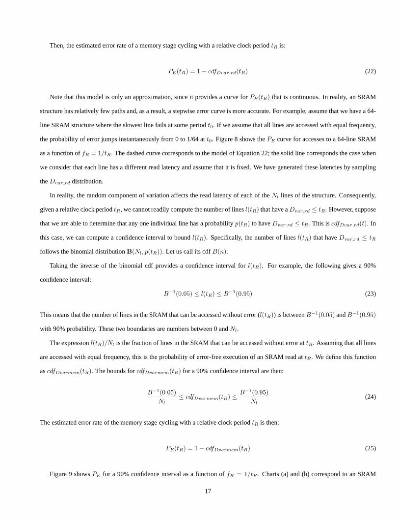
structure has relatively few paths and, as a result, a stepwise error curve is more accurate. For example, assume that we have a 64-
line SRAM structure where the slowest line fails at some periodt0. If we assume that all lines are accessed with equal frequency,
the probability of error jumps instantaneously from 0 to 1/64 att0. Figure 8 shows thePE curve for accesses to a 64-line SRAM
as a function offR = 1/tR. The dashed curve corresponds to the model of Equation 22; the solid line corresponds the case when
we consider that each line has a different read latency and assume that it is fixed. We have generated these latencies by sampling
theDvar rd distribution.
In reality, the random component of variation affects the read latency of each of theNl lines of the structure. Consequently,
given a relative clock periodtR, we cannot readily compute the number of linesl(tR) that have aDvar rd ≤ tR. However, suppose
that we are able to determine that any one individual line has a probabilityp(tR) to haveDvar rd ≤ tR. This iscdfDvar rd(t). In
this case, we can compute a confidence interval to boundl(tR). Specifically, the number of linesl(tR) that haveDvar rd ≤ tR
follows the binomial distributionB(Nl, p(tR)). Let us call its cdfB(n).
Taking the inverse of the binomial cdf provides a confidence interval forl(tR). For example, the following gives a 90%
confidence interval:
B−1(0.05) ≤ l(tR) ≤ B−1(0.95) (23)
This means that the number of lines in the SRAM that can be accessed without error (l(tR)) is betweenB−1(0.05) andB−1(0.95)
with 90% probability. These two boundaries are numbers between 0 andNl.
The expressionl(tR)/Nl is the fraction of lines in the SRAM that can be accessed without error attR. Assuming that all lines
are accessed with equal frequency, this is the probability of error-free execution of an SRAM read attR. We define this function
ascdfDvarmem(tR). The bounds forcdfDvarmem(tR) for a 90% confidence interval are then:
B−1(0.05)Nl
≤ cdfDvarmem(tR) ≤ B−1(0.95)Nl
(24)
The estimated error rate of the memory stage cycling with a relative clock periodtR is then:
PE(tR) = 1− cdfDvarmem(tR) (25)
Figure 9 showsPE for a 90% confidence interval as a function offR = 1/tR. Charts (a) and (b) correspond to an SRAM
17
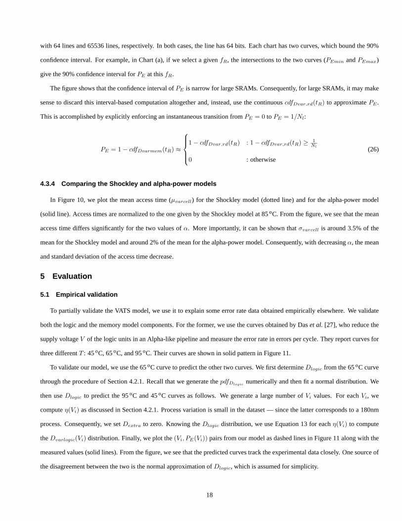
with 64 lines and 65536 lines, respectively. In both cases, the line has 64 bits. Each chart has two curves, which bound the 90%
confidence interval. For example, in Chart (a), if we select a givenfR, the intersections to the two curves (PEmin andPEmax)
give the 90% confidence interval forPE at thisfR.
The figure shows that the confidence interval ofPE is narrow for large SRAMs. Consequently, for large SRAMs, it may make
sense to discard this interval-based computation altogether and, instead, use the continuouscdfDvar rd(tR) to approximatePE .
This is accomplished by explicitly enforcing an instantaneous transition fromPE = 0 to PE = 1/Nl:
PE = 1− cdfDvarmem(tR) ≈
1− cdfDvar rd(tR) : 1− cdfDvar rd(tR) ≥ 1
Nl
0 : otherwise
(26)
4.3.4 Comparing the Shockley and alpha-power models
In Figure 10, we plot the mean access time (µvarcell) for the Shockley model (dotted line) and for the alpha-power model
(solid line). Access times are normalized to the one given by the Shockley model at 85oC. From the figure, we see that the mean
access time differs significantly for the two values ofα. More importantly, it can be shown thatσvarcell is around 3.5% of the
mean for the Shockley model and around 2% of the mean for the alpha-power model. Consequently, with decreasingα, the mean
and standard deviation of the access time decrease.
5 Evaluation
5.1 Empirical validation
To partially validate the VATS model, we use it to explain some error rate data obtained empirically elsewhere. We validate
both the logic and the memory model components. For the former, we use the curves obtained by Daset al. [27], who reduce the
supply voltageV of the logic units in an Alpha-like pipeline and measure the error rate in errors per cycle. They report curves for
three differentT : 45oC, 65oC, and 95oC. Their curves are shown in solid pattern in Figure 11.
To validate our model, we use the 65oC curve to predict the other two curves. We first determineDlogic from the 65oC curve
through the procedure of Section 4.2.1. Recall that we generate thepdfDlogicnumerically and then fit a normal distribution. We
then useDlogic to predict the 95oC and 45oC curves as follows. We generate a large number ofVi values. For eachVi, we
computeη(Vi) as discussed in Section 4.2.1. Process variation is small in the dataset — since the latter corresponds to a 180nm
process. Consequently, we setDextra to zero. Knowing theDlogic distribution, we use Equation 13 for eachη(Vi) to compute
theDvarlogic(Vi) distribution. Finally, we plot the(Vi, PE(Vi)) pairs from our model as dashed lines in Figure 11 along with the
measured values (solid lines). From the figure, we see that the predicted curves track the experimental data closely. One source of
the disagreement between the two is the normal approximation ofDlogic, which is assumed for simplicity.
18

0.94 0.96 0.98 1.00 1.021e−0
81e−0
41e
+00
Relative Frequency fR
Erro
r Rat
e (e
rrors
/acc
ess) naive−predactual
fR
Figure 8: Error-rate for an example 64-line SRAM structure assuming a continuous model (dashed line) or a discrete one withfixed read latencies (solid line).
0.94 0.96 0.98 1.00 1.021e−0
81e−0
41e
+00
Relative Frequency fR
Erro
r Rat
e (e
rrors
/acc
ess)
0.94 0.96 0.98 1.00 1.021e−0
81e−0
41e
+00
Relative Frequency fR
Erro
r Rat
e (e
rrors
/acc
ess)
PEmin
EmaxPRf
(a) (b)fR fR
Figure 9: 90% confidence intervals forPE in a 64-line SRAM (a) and in a 64K-line SRAM (b) as a function of the relativefrequencyfR.
19

140 160 180 200 220 240
0.6
0.8
1.0
1.2
Threshold Voltage (mV)
Acce
ss T
ime
alpha=2.0alpha=1.3
Norm
alize
d Ce
ll Acc
ess
Tim
e
Figure 10: Relative mean access time (µvarcell) for α equal to 1.3 and 2.0. The latter corresponds to the Shockley model.
●
●
●
●
●
●
●
1.35 1.40 1.45 1.50 1.55
1e−1
01e−0
81e−0
61e−0
41e−0
2
Supply Voltage(V)
Erro
r Rat
e
● 45C65C95CModel
Erro
r Rat
e (E
rrors
/ cy
cle)
Figure 11: Validating the logic model by comparing the measured and predicted number of errors per cycle.
20
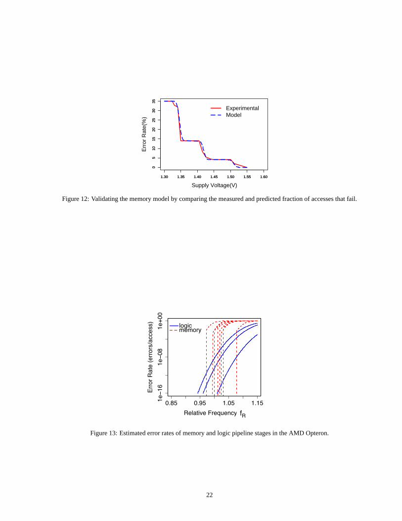
To validate the memory model, we use experimental data from Karlet al. [28]. They examine a 64KB SRAM with 32-bit lines
comprising four different-latency banks, and measure the error rate as the supply voltageV changes. We assume that all cells
have the same value of the systematic process variation. Using the measuredPE(V ) for each bank, we findDvar rd(tR) using
the method of Equations 20 and 21 in Section 4.3.3. The original data is shown in solid pattern in Figure 12, and the prediction is
displayed as a dashed line. From the figure, we see that the predicted and measured error rate are close.
5.2 Example error curves
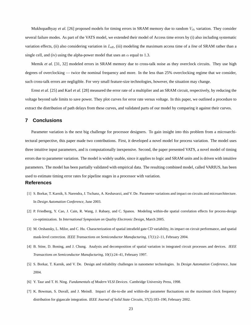
As one example of the uses of our model, we apply it to estimate the error rate of the logic and memory stages of an AMD
Opteron processor as we increase the frequency. After generating aVth andLeff variation map according to our variation model,
we apply the timing error model to compute the error rate versus frequency for each pipeline stage. A stage is classified as either
memory-dominated or logic-dominated. For the logic-dominated stages (e.g., the decoder and functional units), we use the error
model of Section 4.2. For the memory-dominated stages (e.g., the caches), we use Equation 26 of the non-continuous model in
Section 4.3.3. Because we do not have actual net-level data for the microprocessor, the critical path distribution of each logic stage
is assumed to match that of the multiplier in [25]. Figure 13 shows the results, where the frequency is normalized to the one that
the processor without process variation can deliver.
In the figure, each line corresponds to one pipeline stage. We see that memory stages have steeper error curves than the logic
ones. This is due to the small number of lines in the structures; when the clock frequency exceeds the speed of the slowest line, the
error rate undergoes a step change from zero to a relatively high number. On the other hand, logic error onset is more gradual. We
envision a situation where architects and circuit designers will use such error curves to design processors that can tolerate timing
errors.
5.3 Tradeoffs in the model
Perhaps the main shortcoming of VATS is the loss of precision due to two main simplifications: (1) the use of normal approx-
imations and (2) the assumption that wire delay is not affected by variation and accounts for a fixed fractionkw of logic delay.
Section 5.1 has argued that the loss of accuracy is small in practice. The approximations in VATS make it easier to apply it in the
early stages of design, when architects must estimate variation effects at a high level.
6 Related work
Agarwalet al. [29] proposed a simple correlation model for systematic variation based on quad-tree partitioning. The model is
widely used [30, 12]. It is computationally efficient, but no analytical form for the correlation structure is given, and it is not clear
how well the model matches measured correlation data. The spherical correlation function used in this paper has been chosen to
match empirical measurements, but has the disadvantage that generating random instances for Monte Carlo simulation is more
computationally intensive.
21
1.30 1.35 1.40 1.45 1.50 1.55 1.60
05
1015
2025
3035
1.30 1.35 1.40 1.45 1.50 1.55 1.60
05
1015
2025
3035
Supply Voltage(V)
Err
or R
ate(
%)
ExperimentalModel
Figure 12: Validating the memory model by comparing the measured and predicted fraction of accesses that fail.
0.85 0.95 1.05 1.151e−1
61e−0
81e
+00
Relative Frequency fR
Erro
r Rat
e (e
rrors
/acc
ess) logicmemory
fR
Figure 13: Estimated error rates of memory and logic pipeline stages in the AMD Opteron.
22
Mukhopadhyayet al. [26] proposed models for timing errors in SRAM memory due to randomVth variation. They consider
several failure modes. As part of the VATS model, we extended their model of Access time errors by (i) also including systematic
variation effects, (ii) also considering variation inLeff, (iii) modeling the maximum access time of aline of SRAM rather than a
single cell, and (iv) using the alpha-power model that uses anα equal to 1.3.
Memik et al. [31, 32] modeled errors in SRAM memory due to cross-talk noise as they overclock circuits. They use high
degrees of overclocking — twice the nominal frequency and more. In the less than 25% overclocking regime that we consider,
such cross-talk errors are negligible. For very small feature-size technologies, however, the situation may change.
Ernstet al. [25] and Karlet al. [28] measured the error rate of a multiplier and an SRAM circuit, respectively, by reducing the
voltage beyond safe limits to save power. They plot curves for error rate versus voltage. In this paper, we outlined a procedure to
extract the distribution of path delays from these curves, and validated parts of our model by comparing it against their curves.
7 Conclusions
Parameter variation is the next big challenge for processor designers. To gain insight into this problem from a microarchi-
tectural perspective, this paper made two contributions. First, it developed a novel model for process variation. The model uses
three intuitive input parameters, and is computationally inexpensive. Second, the paper presented VATS, a novel model of timing
errors due to parameter variation. The model is widely usable, since it applies to logic and SRAM units and is driven with intuitive
parameters. The model has been partially validated with empirical data. The resulting combined model, called VARIUS, has been
used to estimate timing error rates for pipeline stages in a processor with variation.
References
[1] S. Borkar, T. Karnik, S. Narendra, J. Tschanz, A. Keshavarzi, and V. De. Parameter variations and impact on circuits and microarchitecture.
In Design Automation Conference, June 2003.
[2] P. Friedberg, Y. Cao, J. Cain, R. Wang, J. Rabaey, and C. Spanos. Modeling within-die spatial correlation effects for process-design
co-optimization. InInternational Symposium on Quality Electronic Design, March 2005.
[3] M. Orshansky, L. Milor, and C. Hu. Characterization of spatial intrafield gate CD variability, its impact on circuit performance, and spatial
mask-level correction.IEEE Transactions on Semiconductor Manufacturing, 17(1):2–11, February 2004.
[4] B. Stine, D. Boning, and J. Chung. Analysis and decomposition of spatial variation in integrated circuit processes and devices.IEEE
Transactions on Semiconductor Manufacturing, 10(1):24–41, February 1997.
[5] S. Borkar, T. Karnik, and V. De. Design and reliability challenges in nanometer technologies. InDesign Automation Conference, June
2004.
[6] Y. Taur and T. H. Ning.Fundamentals of Modern VLSI Devices. Cambridge University Press, 1998.
[7] K. Bowman, S. Duvall, and J. Meindl. Impact of die-to-die and within-die parameter fluctuations on the maximum clock frequency
distribution for gigascale integration.IEEE Journal of Solid State Circuits, 37(2):183–190, February 2002.
23
[8] T. Sakurai and R. Newton. Alpha-power law MOSFET model and its applications to CMOS inverter delay and other formulas.IEEE
Journal of Solid-State Circuits, 25(2):584–594, April 1990.
[9] K. Kanda, K. Nose, H. Kawaguchi, and T. Sakurai. Design impact of positive temperature dependence on drain current in sub-1-V CMOS
VLSIs. IEEE Journal of Solid-State Circuits, 36(10):1559–1564, October 2001.
[10] A. Papoulis.Probability, Random Variables and Stochastic Processes. McGrawHill, 2002.
[11] E. Castillo.Extreme Value and Related Models with Applications in Engineering and Science. John Wiley & Sons, 2004.
[12] A. Srivastava, D. Sylvester, and D. Blaauw.Statistical Analysis and Optimization for VLSI: Timing and Power. Springer, 2005.
[13] N. Cressie.Statistics for Spatial Data. John Wiley & Sons, 1993.
[14] J. Xiong, V. Zolotov, and L. He. Robust extraction of spatial correlation. InInternation Symposium on Physical Design, April 2006.
[15] P. Ribeiro and P. Diggle. The geoR package. http://www.est.ufpr.br/geoR.
[16] The R project for statistical computing. http://www.r-project.org.
[17] International Technology Roadmap for Semiconductors (1999).
[18] A. Kahng. The road ahead: Variability.IEEE Design & Test of Computers, 19(3):116–120, May-June 2002.
[19] A. Kahng. How much variability can designers tolerate?IEEE Design & Test of Computers, 20(6):96–97, November-December 2003.
[20] T. Karnik, S. Borkar, and V. De. Probabilistic and variation-tolerant design: Key to continued Moore’s Law. InWorkshop on Timing Issues
in the Specification and Synthesis of Digital Systems, February 2004.
[21] A. Keshavarzi et al. Measurements and modeling of intrinsic fluctuations in MOSFET threshold voltage. InInternational Symposium on
Low Power Electronics and Design, August 2005.
[22] S. Mukherjee, C. Weaver, J. Emer, S. Reinhardt, and T. Austin. A systematic methodology to compute the architectural vulnerability
factors for a high-performance microprocessor. InInternational Symposium on Microarchitecture, December 2003.
[23] E. Humenay, D. Tarjan, and K. Skadron. Impact of parameter variations on multicore chips. InWorkshop on Architectural Support for
Gigascale Integration, June 2006.
[24] Z. Huang and M. D. Ercegovac. Effect of wire delay on the design of prefix adders in deep-submicron technology. InAsilomar Conference
on Signals and Systems, October 2000.
[25] D. Ernst, N. S. Kim, S. Das, S. Pant, R. Rao, T. Pham, C. Zeisler, D. Blaauw, T. Austin, K. Flautner, and T. Mudge. Razor: A low-power
pipeline based on circuit-level timing speculation. InInternational Symposium on Microarchitecture, December 2003.
[26] S. Mukhopadhyay, H. Mahmoodi, and K. Roy. Modeling of failure probability and statistical design of SRAM array for yield enhancement
in nanoscaled CMOS.IEEE Transactions on Computer Aided Design, 24(12):1859–1880, December 2005.
[27] S. Das, S. Pant, D. Roberts, S. Lee, D. Blaauw, T. Austin, T. Mudge, and K. Flautner. A self-tuning DVS processor using delay-error
detection and correction. InIEEE Symposium on VLSI Circuits, June 2005.
24
[28] E. Karl, D. Sylvester, and D. Blaauw. Timing error correction techniques for voltage-scalable on-chip memories. InInternational Sympo-
sium on Circuits and Systems, May 2005.
[29] A. Agarwal et al. Path-based statistical timing analysis considering inter- and intra-die correlations. InInternational Workshop on Timing
Issues in the Specification and Synthesis of Digital Systems, June 2002.
[30] X. Liang and D. Brooks. Mitigating the impact of process variations on CPU register file and execution units. InInternational Symposium
on Microarchitecture, December 2006.
[31] A. Mallik and G. Memik. A case for clumsy packet processors. InInternational Symposium on Microarchitecture, December 2004.
[32] G. Memik, M. H. Chowdhury, A. Mallik, and Y. I. Ismail. Engineering over-clocking: Reliability-performance trade-offs for high-
performance register files. InInternational Conference on Dependable Systems and Networks, June 2005.
25
Copyright © 2022 FDOKUMEN