UsersManual_23xx - SPJ Embedded Technologies Pvt. Ltd.
33
UsersManual_23xx © SPJETPL All Rights Reserved. (http://www.spjsystems.com/ ) Page 1 of 33
-
Upload
khangminh22 -
Category
Documents
-
view
12 -
download
0
Transcript of UsersManual_23xx - SPJ Embedded Technologies Pvt. Ltd.

UsersManual_23xx
© SPJETPL All Rights Reserved. (http://www.spjsystems.com/) Page 1 of 33

UsersManual_23xx
© SPJETPL All Rights Reserved. (http://www.spjsystems.com/) Page 2 of 33
Revision History Date Version Description Author
16 July 2007 1.0 Initial version. SRT
26 July, 2007 1.1 Formatting changes, changed board drawings
PVR
27 May, 2007 1.2 Re-structured manual SRT
2 August, 2007 1.3 Corrected jumper descriptions PVR, SRT
9 August 2007 1.4 Corrected flash programming description.
PVR, SRT
16 October, 2007 1.5 Changes for PCB versions, Chip revisions
SRT

UsersManual_23xx
© SPJETPL All Rights Reserved. (http://www.spjsystems.com/) Page 3 of 33
DISCLAIMER User’s Manual and other documentation: This user’s manual and the accompanying documentation such as schematic diagrams – in soft or hard form - contains descriptions of copyrighted products, which are not explicitly indicated as such. The absence of the trademark symbol does not infer that a Product is not protected. Additionally, registered patents and trademarks are similarly not expressly indicated in these documents. The information in these documents has been carefully checked and is believed to be entirely reliable. However, SPJ Embedded Technologies Pvt. Ltd. (henceforth “Company”) assumes no responsibility for any inaccuracies. The Company, neither gives any guarantee nor accepts any liability whatsoever for consequential damages resulting from the use of these documents or associated product. The Company reserves the right to alter the information contained herein without prior notification and accepts no responsibility for any damages that might result. Additionally, The Company offers no guarantee nor accepts any liability for damages arising from the improper usage or improper installation of the hardware or software. The Company further reserves the right to alter the layout and/or design of the hardware without prior notification and accepts no liability for doing so. SPJ Embedded Technologies Pvt. Ltd. 101, Beaver Grandeur, Baner Road, Baner, Pune 411045. INDIA Phone : +91 (20) 27293002 Fax : +91 (20) 27293003 Email : [email protected] Web Site: http://www.spjsystems.com/

UsersManual_23xx
© SPJETPL All Rights Reserved. (http://www.spjsystems.com/) Page 4 of 33
Table of Contents
1. INTRODUCTION ...................................................................................................................................................6 2. GETTING STARTED.............................................................................................................................................7
2.1 UNPACKING:.........................................................................................................................................................7 2.2 POWER SUPPLY REQUIREMENTS: .........................................................................................................................7 2.3 CONNECTING THE SYSTEM: ..................................................................................................................................7
Powering ON:........................................................................................................................................................7 3. HARDWARE DESCRIPTION ..............................................................................................................................8
SPECIFICATIONS OF MINIARM-2368 AND MINIARM-2378 BOARDS:........................................................................8 4. CONNECTORS, JUMPERS, SWITCHES, POTS AND LEDS..........................................................................9
CONNECTOR LOCATIONS: ...........................................................................................................................................9 CONNECTOR DETAILS: .............................................................................................................................................10
PWR JACK (Power Jack):...................................................................................................................................10 UART0 Connector: ..............................................................................................................................................10 UART1 Connector: ..............................................................................................................................................10 CAN1 Connector: ................................................................................................................................................11 CAN2 Connector: ................................................................................................................................................11 LCDCON Connector: ..........................................................................................................................................11 Ethernet RJ45 Connector: ...................................................................................................................................12 USBCON Connector: ..........................................................................................................................................12 SDCON Connector:.............................................................................................................................................12 JTAG Connector:.................................................................................................................................................12 IO_A, IO_B Connectors: .....................................................................................................................................13 IO_C, IO_D Connectors: ....................................................................................................................................15
JUMPERS, SWITCHES AND POT LOCATIONS: .............................................................................................................18 JUMPER DESCRIPTIONS:............................................................................................................................................19
Jumper “PWRMODE” (Power Source Selection): ............................................................................................19 Jumper “PGM”:.................................................................................................................................................20 Jumper “RST”:...................................................................................................................................................20 Jumpers “BKLT1” and “BKLT2” (LCD Backlight Control):............................................................................20 Jumper “UMODE” (USB device mode Selection):............................................................................................20 Jumpers “D-” and “D+” (D- and D+ USB Lines, respectively):......................................................................21 Jumper “AD0.0” (Connect potentiometer to AD0.0):........................................................................................21 Jumper “RTCK” (for JTAG Interface):..............................................................................................................21 Jumper “SDPWR” (SD card Power Selection):.................................................................................................21
SWITCHES DESCRIPTIONS: ........................................................................................................................................22 Switch “RESET” (Reset Push Button): ..............................................................................................................22
POT DESCRIPTIONS: ................................................................................................................................................22 “POT1” (LCD Contrast Adjustment):.................................................................................................................22 “POT2” (Simulate ADC input): ..........................................................................................................................22
LED LOCATIONS: .....................................................................................................................................................23 LEDS DESCRIPTION: ................................................................................................................................................24
PWR: ...................................................................................................................................................................24 P1...P8:................................................................................................................................................................24 SD:.......................................................................................................................................................................24 UGL1:..................................................................................................................................................................24 USC1: ..................................................................................................................................................................24 100MBPS:............................................................................................................................................................24 ACT: ....................................................................................................................................................................24 LINK:...................................................................................................................................................................24

UsersManual_23xx
© SPJETPL All Rights Reserved. (http://www.spjsystems.com/) Page 5 of 33
5. RUNNING USER PROGRAMS ON MINIARM ...............................................................................................25 TO PROGRAM THE FLASH: .........................................................................................................................................25 PROGRAM THE MINIARM-23XX BOARD AND RUN PROGRAM:..................................................................................25 DESCRIPTION OF EXAMPLE PROGRAMS:....................................................................................................................28
Hello:...................................................................................................................................................................28 Hello1:.................................................................................................................................................................28 HelloLCD: ...........................................................................................................................................................29 SquareWave:........................................................................................................................................................29 FastSquareWave:.................................................................................................................................................29 LEDRing:.............................................................................................................................................................29 Clock: ..................................................................................................................................................................29 USB: ....................................................................................................................................................................29 ADC:....................................................................................................................................................................29 DAC:....................................................................................................................................................................30 CAN: ....................................................................................................................................................................30 EMAC:.................................................................................................................................................................30 MCI: ....................................................................................................................................................................30
6. OPTIONAL ACCESSORIES OF MINIARM ....................................................................................................31 LCD MODULE: .........................................................................................................................................................31 SGL-ARM BOARD: ..................................................................................................................................................31
7. MINIARM APPLICATIONS...............................................................................................................................32

UsersManual_23xx
© SPJETPL All Rights Reserved. (http://www.spjsystems.com/) Page 6 of 33
1. Introduction This is user’s manual for MiniARM-2368 and MiniARM-2378 Evaluation Boards (MiniARM-23xx) based on LPC2368 and LPC2378 micro-controllers, respectively. This is a general-purpose board designed as a development tool; this board has a facility to download user programs into the on-chip flash memory of the micro-controller. It is strongly recommended to read this manual carefully before you start using the MiniARM-23xx board. CAUTION: This board contains components that are sensitive to Electro-Static Discharge (ESD). The board must be handled carefully, so as not to subject it to ESD. As far as possible, do not touch any conducting part on the board – including any component or connector pins – as this may damage parts of the board permanently. While handling the board, hold it only by it’s edges. If you must touch any of the parts, make sure to discharge yourself to earth. Parts damaged due to ESD are not covered by the limited warranty.

UsersManual_23xx
© SPJETPL All Rights Reserved. (http://www.spjsystems.com/) Page 7 of 33
2. Getting Started
2.1 Unpacking: You will find following items in the package:
• MiniARM-23xx board • Serial communication cable • Power adaptor* • CD-ROM • USB Cable
* Power adaptor is included only if the board is shipped in India. If the board is shipped to any country other than India, only a power jack with a pair of red and black wires is supplied. The user is required to provide nominal +8VDC supply across the 2 wires: Red=positive, Black=negative. This supply voltage maybe in the range 8 to 9 VDC only. Higher voltage may cause excessive heating and may cause permanent damage to the board.
2.2 Power Supply Requirements: The power adaptor works with 230Volts AC. It produces approximately 8 Volts DC, and the MiniARM uses on-board regulators to provide 5 Volts and 3.3Volts DC to all components on the board.
2.3 Connecting the system: The serial communication cable supplied with the board should be used to connect the board to a PC running Windows2000/XP Operating System. This cable uses all 9 wires and connections are “one-to-one”. If you must use another cable, be sure that it has all 9 wires in it. Further, it must have DB9 female connector on one end (PC end) and DB9 male connector on another end (MiniARM end). The 9 wires in the straight cable must be connected as:
DB9Female.Pin1 ßà DB9Male.Pin1 DB9Female.Pin2 ßà DB9Male.Pin2 DB9Female.Pin3 ßà DB9Male.Pin3 .
. . DB9Female.Pin9 ßà DB9Male.Pin9
Powering ON: After connecting the serial communication cable as described above, you may insert the power adaptor output jack into the on-board power socket. Plug the power adaptor into 230VAC mains outlet and turn it on. The power-on indication Red LED will turn on. CAUTION: Please do not connect or disconnect the serial communication cable while the board is powered ON. Doing so can damage the serial port of the MiniARM board and/or PC.

UsersManual_23xx
© SPJETPL All Rights Reserved. (http://www.spjsystems.com/) Page 8 of 33
3. Hardware Description
Specifications of MiniARM-2368 and MiniARM-2378 boards: 1) LPC2368 / LPC2378 * with 12 MHz main crystal. 2) Operating speed up to 72 MHz using on-chip PLL. 3) Ethernet Interface Standards support:
a. 10/100 Mbps Ethernet (10 Base-T, 100 Base-TX, 100 Base-FX and 100 Base-T4). b. Fully compliant with IEEE standard 802.3.
4) USB2.0 device interface standard support. 5) Includes one SD memory card connector that allows you to connect a wide range of memory
cards. 6) LCD interface circuit with 16-pin connector for directly connecting text LCD module. 7) Four UARTs. Two of them (UART0 and UART1) available as RS232 (3 wire) on 2 separate
DB9 female connectors. Remaining two (UART2 and UART3) are available as low-voltage TTL (3.3V) on connectors.
8) On-board regulators to supply 5V, 3.3V to the board. 9) Includes AC adaptor (230 VAC input, 8 VDC output, 500 mA). 10) CD-ROM containing:
a) Evaluation version of SCARM – C Compiler for ARM – a product of SPJ Embedded Technologies Pvt. Ltd.
b) Sample programs to access LCD, serial port, RTC and most other peripherals etc. c) Flash Magic ISP utility program, courtesy of http://www.flashmagictool.com/ .
11) Unused / optionally used port pins are available on convenient connectors. 12) Push-button to reset the micro-controller. 13) Jumpers to select between Program (ISP) mode and RUN mode. 14) MiniARM-2368 and MiniARM-2378 boards include Real Time Clock (RTC) with battery.
Please note, it can maintain date and time even when power is switched off only if the RTC is initialized to correct mode of operation by software.
15) The same battery will also power 2KB NVRAM. Please note, LCD is NOT supplied with the MiniARM. It may be purchased separately and connected to MiniARM. * LPC2368/LPC2378 chip soldered on MiniARM board may have different revisions – indicated by one of the suffix (-, A, B). NXP Semiconductors may have published errata corresponding to various chip revisions. Please refer to appropriate errata sheet form NXP Semiconductors website (http://www.nxp.com/).

UsersManual_23xx
© SPJETPL All Rights Reserved. (http://www.spjsystems.com/) Page 9 of 33
4. Connectors, Jumpers, Switches, POTs and LEDs
Connector locations: Figure 1 shows the locations of all connectors on the board. USB Connector LCD Connector Ethernet Connector (RJ45)
UART1 Power Jack
Figure 1: Connector locations
JTAG Connector on bottom side
SD-Card Connector on bottom side
IO_A
IO_C
IO_D
IO_B
UART0
CAN2
CAN1

UsersManual_23xx
© SPJETPL All Rights Reserved. (http://www.spjsystems.com/) Page 10 of 33
Connector Details:
PWR JACK (Power Jack): This is power input connector. The supplied power adaptor (if board is shipped in India) has power jack compatible with this connector.
UART0 Connector: This is a DB9 female connector, used for RS232 serial communication with the PC: Pin 2 = TxD0 – RS232 level output from MiniARM23xx Board. Corresponding 3.3V pin (P0.2/TXD0) is also available on Pin27 of IO_C connector. Pin 3 = RxD0 – RS232 level input to MiniARM23xx Board. Corresponding 3.3V pin (P0.3/RXD0) is also available on Pin28 of IO_C connector. Pin 4 = ISP_RESET – RS232 level input to MiniARM23xx Board. Used to (optionally) reset the board under control of ISP utility software. Pin 5 = GND – Ground. Pin 7 = ISP_MODE – RS232 level input to MiniARM23xx Board. Used to (optionally) control the mode of processor (ISP mode or RUN mode). All other pins of UART0 are unused. This UART0 connector is also used for ISP (In-system Programming). Note: UART0 is available as 3 wires RS232 only. The signals at pin 4 and 7 of UART0 connector are not used as RS232 handshake signals. Rather, these 2 signals are only used for controlling operating mode of the micro-controller (normal “run” mode or ISP mode) and to reset the micro-controller. This feature is useful while programming the board using FlashMagic. If you wish, appropriate jumper setting can disable this feature, as described later.
UART1 Connector: This is a DB9 female connector, used for RS232 serial communication with the PC: Pin 2 = TxD1 – RS232 level output from MiniARM23xx Board. Corresponding 3.3V pin (P0.15/TXD1/SCK0/SCK) is also available on Pin35 of IO_C connector. Pin 3 = RxD1 – RS232 level input to MiniARM23xx Board. Corresponding 3.3V pin (P0.16/RXD1/SSEL0/SSEL) is also available on Pin33 of IO_C connector. Pin 5 = GND – Ground. All other pins of UART1 are unused.

UsersManual_23xx
© SPJETPL All Rights Reserved. (http://www.spjsystems.com/) Page 11 of 33
CAN1 Connector: This is DB9 male connector, used for CAN High-speed communication: Pin 2 = CANL Pin 7 = CANH The CANL output drives the low side of the CAN differential bus. The CANH output drives the high side of the CAN differential bus. All other pins of CAN1 are unused. CAN serial Input to MiniARM23xx board P0.0/RD1/TXD3/SDA1, which is also available on Pin 27 of IO_B connector. CAN serial Output from MiniARM23xx board P0.1/TD1/RXD3/SCL1, which is also available on Pin 29 of IO_B connector. User may not connect anything to these pins as these are used on-board for CAN.
CAN2 Connector: This is DB9 male connector, used for CAN High-speed communication: Pin 2 = CANL Pin 7 = CANH The CANL output drives the low side of the CAN differential bus. The CANH output drives the high side of the CAN differential bus. All other pins of CAN2 are unused. CAN serial Input to MiniARM23xx board P0.4/I2SRX_CLK/RD2/CAP2.0, which is also available on Pin 23 of IO_B connector. CAN serial Output from MiniARM23xx board P0.5/I2SRX_WS/TD2/CAP2.1, which is also available on Pin 25 of IO_B connector. User may not connect anything to these pins as these are used on-board for CAN.
LCDCON Connector: This is a 16 pin, single line connector, designed for connection to standard, text LCD modules. The pin/signal correspondence is designed to be matching with that required by such LCD modules. Pin 1 = GND Pin 2 = +5V Pin 3 = Vlcd (Contrast control Voltage) Pin 4 = P1.31 (Used as RS of LCD)

UsersManual_23xx
© SPJETPL All Rights Reserved. (http://www.spjsystems.com/) Page 12 of 33
Pin 5 = GND Pin 6 = P1.29 (Used as EN of LCD) Pin 7 to 10 = No Connection Pin 11 to 14 = P1.19 to P1.22 (Used as D4-D7 of LCD, respectively) Pin 15 = Backlighting Pin 16 = GND
Ethernet RJ45 Connector: The Ethernet Interface on the MiniARM23xx board is available via this connector. It can be used to connect the board to LAN.
USBCON Connector: The USB device Interface on the MiniARM23xx board uses this connector. This is female B type connector. It can be typically connected to USB port of your PC through the supplied USB cable.
SDCON Connector: This is mounted on the bottom side of the PCB. Standard SD memory card can be inserted in it. Once a valid card is inserted, it can be accessed through software.
JTAG Connector: This standard 20 pin JTAG connector provides debugging support for the LPC23xx. This is connector is mounted bottom side of the board as shown in figure1. JTAG cables like SJT-S or SJT-U can be connected to this connector, while other end of the cable can be connected to PC COM port or USB port, respectively. Debugger software (like the debugger built into SCARM) allows JTAG based debugging. It is also possible to use third party JTAG based emulators / debuggers. The pin-out of JTAG Connector is given below: Pin Signal name. 1 3.3V 3 nTRST 5 TDI 7 TMS 9 TCK 11 RTCK 13 TDO 15 nRST 17 GND 19 GND 2 3.3V 4 GND

UsersManual_23xx
© SPJETPL All Rights Reserved. (http://www.spjsystems.com/) Page 13 of 33
6 GND 8 GND 10 GND 12 GND 14 GND 16 GND 18 GND 20 GND
IO_A, IO_B Connectors: These are 32 pin dual line headers. These connectors bring out I/O and most of the pins of the LPC23xx micro-controller. Further, 5V and 3.3V are also made available on these connectors. These female headers are intended for use to connect external peripherals. The pin/signal details of IO_A and IO_B are as below: IO_A: Pin Signal name. 1 P0.24/AD0.1/I2SRX_WS/CAP3.1 3 P2.10/EINT0 5 P0.21/RI1/MCIPWR/RD1 7 P1.26/PWM1.6/CAP0.0 9 P1.25/MAT1.1 11 P1.23/PWM1.4/MISO0 13 P0.10/TXD2/SDA2/MAT3.0 15 USB-B 17 P1.19/CAP1.1 19 P0.20/DTR1/MCICMD/SCL1 21 P1.22/MAT1.0 23 P1.29/PCAP1.1/MAT0.1 25 P2.11/EINT1/MCIDAT1/I2STX_CLK 27 P0.17/CTS1/MISO0/MISO 29 P0.22/RTS1/MCIDAT0/TD1 31 P0.19/DSR1/MCICLK/SDA1 2 GND 4 GND 6 5V 8 P2.8/TD2/TXD2/TRACEPKT3 10 P1.24/PWM1.5/MOSI0 12 P0.9/I2STX_SDA/MOSI1/MAT2.3 14 P2.13/EINT3/MCIDAT3/I2STX_SDA 16 P1.31/SCK1/AD0.5 18 P1.20/PWM1.2/SCK0

UsersManual_23xx
© SPJETPL All Rights Reserved. (http://www.spjsystems.com/) Page 14 of 33
20 P1.21/PWM1.3/SSEL0 22 P1.28/PCAP1.0/MAT0.0 24 P2.12/EINT2/MCIDAT2/I2STX_WS 26 3.3V 28 P0.7/I2STX_CLK/SCK1/MAT2.1 30 GND 32 GND IO_B: Pin Signal name. 1 P0.6/I2SRX_SDA/SSEL1/MAT2.0 3 P1.15/ENET_REF_CLK 5 P1.14/ENET_RX_ER 7 P1.0/ENET_TXD0 9 P1.9/ENET_RXD0 11 P1.8/ENET_CRS 13 P1.4/ENET_TX_EN 15 P1.1/ENET_TXD1 17 P0.25/AD0.2/I2SRX_SDA/TXD3 19 P0.8/I2STX_WS/MISO1/MAT2.2 21 P1.27/CAP0.1 23 P0.4/I2SRX_CLK/RD2/CAP2.0 25 P0.5/I2SRX_WS/TD2/CAP2.1 27 P0.0/RD1/TXD3/SDA1 29 P0.1/TD1/RXD3/SCL1 31 P1.10/ENET_RXD1 2 GND 4 GND 6 5V 8 5V 10 GND 12 GND 14 GND 16 3.3V 18 3.3V 20 GND 22 GND 24 GND 26 5V (NC) 3
28 5V (NC) 3 30 GND 32 GND

UsersManual_23xx
© SPJETPL All Rights Reserved. (http://www.spjsystems.com/) Page 15 of 33
IO_C, IO_D Connectors: These are 36 pin dual line headers. These connectors bring out I/O and most of the pins of the LPC23xx micro-controller. Further, 5V and 3.3V are also made available on these connectors. These female headers are intended for use to connect external peripherals. The pin/signal details of IO_C and IO_D are as below: IO_C: Pin Signal name. 1 P0.29/U1D+ 3 P1.18/U1UP_LED/PWM1.1/CAP1.0 5 P2.9/U1CONNECT/RXD2/EXTIN0 7 P3.25/MAT0.0/PWM1.2 9 {P3.23/CAP0.0/PCAP1.0} 11 P0.27/SDA0 13 P0.28/SCL0 15 {P0.31/U2D+} 17 {P4.1/A1} 19 {P4.3/A3} 21 {P4.5/A5} 23 {P4.7/A7} 25 {P4.9/A9} 27 P0.2/TXD0 29 P0.18/DCD1/MOSI0/MOSI 31 5V 33 P0.16/RXD1/SSEL0/SSEL 35 P0.15/TXD1/SCK0/SCK 2 P0.30/U1D- 4 P1.30/VBUS/AD0.4 6 P3.26/MAT0.1/PWM1.3 8 {P3.24/CAP0.1/PWM1.1} 10 {P0.13/U2UP_LED/MOSI1/AD0.7} 12 {P0.14/U2CONNECT/SSEL1} 14 {P0.12/MISO1/AD0.6} 16 {P4.0/A0} 18 {P4.2/A2} 20 {P4.4/A4} 22 {P4.6/A6} 24 {P4.8/A8} 26 {P4.10/A9} 28 P0.3/RXD0 30 GND 32 5V 34 3.3V 36 GND

UsersManual_23xx
© SPJETPL All Rights Reserved. (http://www.spjsystems.com/) Page 16 of 33
IO_D: Pin Signal name. 1 P1.16/ENET_MDC 3 P0.26/AD0.3/AOUT/RXD3 5 {P3.7/D7} 7 {P3.5/D5} 9 {P3.3/D3} 11 {P3.1/D1} 13 {P4.24/OE} 15 P4.28/MAT2.0/TXD3 17 {P4.30/CS0} 19 P0.11/RXD2/SCL2/MAT3.1 21 {P4.15/A15} 23 {P4.13/A13} 25 {P4.11/A11} 27 P2.0/PWM1.1/TXD1/TRACECLK 29 P2.2/PWM1.3/CTS1/PIPESTAT1 31 P2.4/PWM1.5/DSR1/TRACESYNC 33 P2.6/PCAP1.0/RI1/TRACEPKT1 35 3.3V 2 P1.17/ENET_MDIO 4 P0.23/AD0.0/I2SRX_CLK/CAP3.0 6 {P3.6/D6} 8 {P3.4/D4} 10 {P3.2/D2} 12 {P3.0/D0} 14 {P4.25/WE} 16 P4.29/MAT2.1/RXD3 18 {P4.31/CS1} 20 P2.7/RD2/RTS1/TRACEPKT2 22 {P4.14/A14} 24 {P4.12/A12} 26 P2.1/PWM1.2/RXD1/PIPESTAT0 28 P2.3/PWM1.4/DCD1/PIPESTAT2 30 P2.5/PWM1.6/DTR1/TRACEPKT0 32 5V 34 GND 36 GND Note1: Many pins have multiple functions, hence the signal names include many options separated by ‘/’. For details, please refer to LPC23xx data-sheets.

UsersManual_23xx
© SPJETPL All Rights Reserved. (http://www.spjsystems.com/) Page 17 of 33
Note2: Signal names enclosed in curly braces {} are available only in MiniARM-2378. In case of MiniARM2368, these pins of connectors IO_A, IO_B, IO_C and IO_D have no connection.
3Note3: Pin numbers 26 and 28 of IO_B connector have no connection (NC) in PCB revision V2.1. Pin numbers 26 and 28 of IO_B connector bring out 5V in PCB revisions higher than V2.1.

UsersManual_23xx
© SPJETPL All Rights Reserved. (http://www.spjsystems.com/) Page 18 of 33
Jumpers, switches and POT locations: Figure 2 shows locations of all jumpers, switches and potentiometers on the board: POT1 (LCD Contrast Adjustment) POT2 (Simulate input to ADC)
RESET push-button
Figure 2: Jumpers, switches and POT locations
SDPWR
PGM
RST
BKLT2
D+
UMODE D-
BKLT1 RTCK
AD0.0
PWRMODE

UsersManual_23xx
© SPJETPL All Rights Reserved. (http://www.spjsystems.com/) Page 19 of 33
Jumper Descriptions: Viewpoint Reference: Look at the MiniARmM23xx board from front side. The LCD connector should be near the upper edge. Two CAN connectors should be near the right edge. Two RS232 connectors should be near the left edge. Conventions used:
• 2 pin jumpers: These can be shorted or open. These 2 conditions are noted as Short or Open, respectively.
• 3 pin jumpers: 3 conditions are possible in this case: middle and rightmost pin shorted, middle and leftmost pin shorted, or open (no pins shorted). These 3 conditions are noted as Right, Left or Open, respectively.
“Don’t care” condition of a jumper is noted as X. The jumper setting is clearly described in the table. Row marked with asterisk (*) indicates factory setting.
Jumper “PWRMODE” (Power Source Selection): Power to the board can be supplied by one of the 2 sources: The power adaptor or 5VDC available from PC through USB connector. This 3-pin jumper lets you select one of these 2 sources. Right jumper position selects Adaptor as power source. Left jumper position selects PC (through USB port) as power source. The jumper setting is clearly described in the table below: PWRMODE
jumper position Board will be powered from:
* Right Adaptor Left USB port (i.e. power from PC) Open No power CAUTION: When powering the board from USB, there is a restriction on current. So user may not connect additional peripherals likes LCD, LAN cable etc. so as to stay within current limit. This may harm your PC! Power consumption of the board varies depending on what peripherals are connected and what is the operating speed. The table below indicates typical power consumption under various conditions: Test Condition Supply current
(milli-amp) Board without any peripherals connected, operating at 12 MHz. 100 Board + LCD with backlighting ON, operating at 12 MHz. 130 Board + LCD with backlighting ON, operating at 72 MHz and LAN cable not inserted.
210
Board + LCD with backlighting ON, operating at 72 MHz and LAN cable inserted.
300
ALL Port Pins ON + USB Cable + LCD with backlighting ON, operating at 72 MHz and LAN cable inserted.
710

UsersManual_23xx
© SPJETPL All Rights Reserved. (http://www.spjsystems.com/) Page 20 of 33
Jumper “PGM”: PGM jumper
position Description
* Right Mode (ISP mode or RUN mode) will be controlled by FlashMagic. Left ISP mode selected manually. (FlashMagic can not control mode). Open RUN mode selected manually. (FlashMagic can not control mode).
Jumper “RST”: RST jumper
position Description
* Short Allow FlashMagic to automatically reset the board. Open Do not allow FlashMagic to automatically reset the
board. Note: In either case, user can always manually reset the board by momentarily pressing the RESET push-button.
Jumpers “BKLT1” and “BKLT2” (LCD Backlight Control): BKLT1
position BKLT2 position
Description
Open Open LCD Backlight always OFF. Open Short LCD Backlight controlled by software. * Short X LCD Backlight always ON.
Jumper “UMODE” (USB device mode Selection): Positioning this jumper on right side allows soft-connect of the USB device by P2.9. Positioning this jumper on left side gives a power-up sequence for the USB detection. P2.9/U1CONNECT/RXD2/EXTIN0 is also available on Pin5 of IO_C connector. UMODE
jumper position
Description
* Right USB device Connect is controlled by Soft-connect port pin P2.9. Left USB device Connect is controlled by hardware. Open USB device will not work; port pin P2.9 can be used for other purpose.
UsersManual_23xx
© SPJETPL All Rights Reserved. (http://www.spjsystems.com/) Page 21 of 33
Jumpers “D-” and “D+” (D- and D+ USB Lines, respectively): These Connect the USB Lines P0.30/U1D- and P0.29/U1D+ to the USB connector. P0.30/U1D- is also available on Pin2 of IO_C connector. P0.29/U1D+ is also available on Pin1 of IO_C connector. If you wish to use P0.29 and P0.30 as GPIO pins, then you must leave both these jumpers open. If you wish to use them as USB pins, then you must short both these jumpers. D- position D+ Position Description Open Open USB device will not work; port pins P0.30 and P0.29 can be
used as GPIO. * Short Short USB device interface will work. Port pins P0.30 and P0.29 can
not be used for any other purpose, even though those are available on IO_C connector.
Note: Any other combination of these jumpers is invalid and will cause malfunctioning of USB interface.
Jumper “AD0.0” (Connect potentiometer to AD0.0): Connects the POT2 potentiometer to Port pin P0.23/AD0.0/I2SRX_CLK/CAP3.0 for simulating analog input (AD0.0). P0.23/AD0.0/I2SRX_CLK/CAP3.0 is also available on Pin4 of IO_D connector. AD0.0
position Description
Open POT2 will not be connected to AD0.0. External input maybe connected to AD0.0.
* Short Connects the port pin P0.23 to POT2 for ADC simulation. You may not connect external input to AD0.0 even though this pin is available on IO_D connector.
Jumper “RTCK” (for JTAG Interface): When shorted, this jumper connects pull-down resistor to RTCK signal of JTAG interface. RTCK
position Description
* Open No pull-down to RTCK. Short 10K pull-down to RTCK.
Jumper “SDPWR” (SD card Power Selection): This jumper provides 3 options for SD-Card power: always ON, software controlled or always OFF.

UsersManual_23xx
© SPJETPL All Rights Reserved. (http://www.spjsystems.com/) Page 22 of 33
SDPWR jumper
position Board will be powered from:
* Right SD Power is software controlled by port pin P0.21. Note that this pin is also available on pin5 of IO_A.
Left SD Power is always ON. Open No SD power.
Switches Descriptions:
Switch “RESET” (Reset Push Button): This is Reset push button switch is used to give hardware reset pulse to RST pin of micro-controller.
POT Descriptions:
“POT1” (LCD Contrast Adjustment): This potentiometer is used to adjust the contrast of 16x2 LCD module.
“POT2” (Simulate ADC input): This potentiometer is used to for analog input simulation of ADC channel AD0.0 i.e. pin P0.23/AD0.0/I2SRX_CLK/CAP3.0. This pin is also available on Pin4 of IO_D connector.
UsersManual_23xx
© SPJETPL All Rights Reserved. (http://www.spjsystems.com/) Page 23 of 33
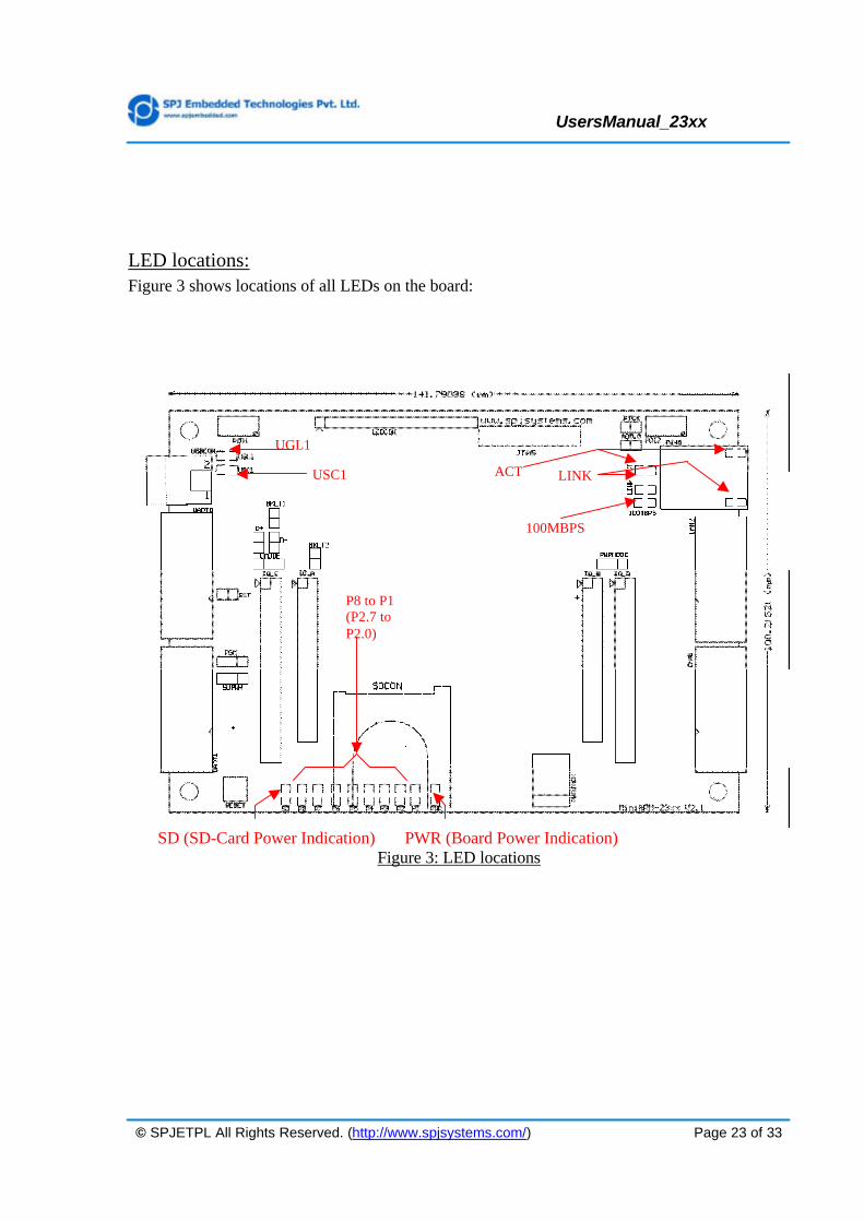
LED locations: Figure 3 shows locations of all LEDs on the board:
SD (SD-Card Power Indication) PWR (Board Power Indication)
Figure 3: LED locations
P8 to P1 (P2.7 to P2.0)
UGL1
USC1 ACT LINK
100MBPS

UsersManual_23xx
© SPJETPL All Rights Reserved. (http://www.spjsystems.com/) Page 24 of 33
LEDs Description:
PWR: PWR is a red LED that indicates power ON.
P1...P8: P1 to P8 are yellow LEDs that indicate status of port pins P2.0 to P2.7, respectively. If port pin output is HIGH, the corresponding LED will glow. These LEDs can be used for testing purpose. Note that the port pins P2.0 to P2.7 are also available on IO_D connector. Please refer to connector details for pin numbers.
SD: SD is a blue LED that indicates power to SD-card.
UGL1: UGL1 is a blue LED that indicates good USB link.
USC1: USC1 is a red LED that indicates a USB soft connect from P0.14 or by hardware.
100MBPS: 100MBPS is a red LED that indicates a 100Mbit Speed Ethernet LAN connection. If it is OFF, that indicates a 10Mbit Speed Ethernet LAN connection.
ACT: ACT is a yellow LED that indicates LAN traffic. I.e. when Ethernet packets are sent or received, this LED will blink. This LED maybe present in the RUMODE5 connector itself or on the PCB, as shown in Figure3.
LINK: LINK is a green LED that indicates good LAN link. I.e. it will normally glow when LAN cable is plugged in the connector. This LED maybe present in the RUMODE5 connector itself or on the PCB, as shown in Figure3.

UsersManual_23xx
© SPJETPL All Rights Reserved. (http://www.spjsystems.com/) Page 25 of 33
5. Running user programs on MiniARM The LPC23xx micro-controllers include on-chip flash for storing user program and non-volatile data. The LPC2368 / LPC2378 on MiniARM-2368 / MiniARM-2378 have 512KBytes flash. This flash is In-System-Programmable (ISP). The LPC23xx micro-controllers have a built-in boot-load program. Upon power-on, this boot-load program takes control; it passes control to the user program if pin P2.10 is HIGH and some other conditions are satisfied. Please refer to the LPC23xx data-sheet for further details. On the MiniARM board, the P2.10 pin is made available on a jumper marked PGM, just above the jumper SD-PWR (please refer to Figure2).
To program the flash: There are 2 ways to put the LPC23xx in ISP mode: You may do it manually, by placing a jumper. Alternatively, you may set the jumpers in such a way that the ISP software running on PC will automatically put the LPC2378 in ISP or RUN mode. Please refer to setting of related jumpers for more details. Then run Flash Magic (Version 3.71.245 or above). The CD you received with MiniARM board contains evaluation version of SCARM C Compiler for ARM. When you install it, you will see the folder SCARM\Utilities. This folder contains FlashMagic3.71.zip.
NOTE: Flash Magic is not an SPJ product. It has been downloaded from FlashMagic web site.
To install the ISP software, you may extract the appropriate zip file and then run SETUP.EXE from the extracted files.
Program the MiniARM-23xx board and run program: 1) Start Flash Magic (using Start — Programs — Flash Magic) and configure the COM Port interface as illustrated.
• From the device list, select appropriate device (LPC2378 or LPC2368). • Enter crystal frequency correctly (12.0 MHz). • Select COM port. • Select Baud Rate. Usually it works fine at 115200 baudrate. If you face problems at this
baudrate, you may try a lower baudrate. These setting are shown below.

UsersManual_23xx
© SPJETPL All Rights Reserved. (http://www.spjsystems.com/) Page 26 of 33
2) You may have to check or un-check the High Speed Communications option, depending on your jumper setting. If jumper PGM is RIGHT and RST is SHORT, then you must check this option; otherwise you must un-check it. To check or un-check this option, select Options/Advanced Options from menu and then select the Communications tab, as shown below.
UsersManual_23xx
© SPJETPL All Rights Reserved. (http://www.spjsystems.com/) Page 27 of 33
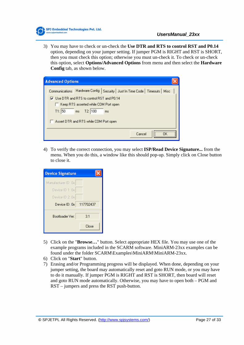
3) You may have to check or un-check the Use DTR and RTS to control RST and P0.14 option, depending on your jumper setting. If jumper PGM is RIGHT and RST is SHORT, then you must check this option; otherwise you must un-check it. To check or un-check this option, select Options/Advanced Options from menu and then select the Hardware Config tab, as shown below.
4) To verify the correct connection, you may select ISP/Read Device Signature... from the menu. When you do this, a window like this should pop-up. Simply click on Close button to close it.
5) Click on the "Browse…" button. Select appropriate HEX file. You may use one of the example programs included in the SCARM software. MiniARM-23xx examples can be found under the folder SCARM\Examples\MiniARM\MiniARM-23xx.
6) Click on "Start" button. 7) Erasing and/or Programming progress will be displayed. When done, depending on your
jumper setting, the board may automatically reset and goto RUN mode, or you may have to do it manually. If jumper PGM is RIGHT and RST is SHORT, then board will reset and goto RUN mode automatically. Otherwise, you may have to open both – PGM and RST – jumpers and press the RST push-button.

UsersManual_23xx
© SPJETPL All Rights Reserved. (http://www.spjsystems.com/) Page 28 of 33
CAUTION: Pin P2.10 is also available in the connector IO_B. If you have connected an external device to this connector, ensure that P2.10 is not pulled low during reset. If it is pulled low during reset, the LPC23xx may enter ISP mode and may not run user program.
Description of example programs: As mentioned above, the SCARM software includes a set of examples programs for MiniARM-23xx. All these example programs are written in C and their pre-compiled HEX files also exist in each example’s folder. However, some of these example programs are fairly complex and the evaluation version of SCARM C Compiler (which is included with the board) may not allow you to compile such big programs. You may need the full commercial version of SCARM to be able to change and re-compile such big programs. However, many small example programs can be compiled using evaluation version of SCARM. You may try to modify some such example programs and experiment with the MiniARM-23xx board. This section provides a brief description of these example programs. Before that, it describes an important software tool – SPJTerminal - that is part of SCARM. SPJTerminal: Terminal Emulation utility: When you run the SCARM main program (SIDE_ARM), you will see a “Tools” menu. Under this menu, there is an option “SPJTerminal”. When you click on this option, the SPJTerminal program opens. It is a simple terminal emulation program. Select Port/Settings from it’s menu to set the COM port setting appropriately (19200 baud, 8 data bits, 1 stop bit, echo OFF, no parity). Then select Port/Open from menu to open the COM port. Now any characters received by the computer over the selected COM port will be displayed in the main window of SPJTerminal program. Also, any characters you type will be transmitted by the PC over the same COM port. NOTE: The ISP flash utility and SPJTerminal program – both use COM port of PC. However, Windows does not allow more than one programs to use the same COM port at the same time. As a result, these 2 programs can’t run simultaneously. You must close port of SPJTerminal before you start ISP utility.
Hello: Transmit "Hello" to UART0 and then echo characters. Before running this program, connect the MiniARM board to PC COM port and have SPJTerminal running with appropriate setting (19200 baud, 8 Data Bits, 1 Stop Bits, Echo Off, Parity None). When you switch on power to the board, you should see "Hello" appearing in the main SPJTerminal window. Then if you type any key, you should see the same character appearing in SPJTerminal window (because the board echoes it).
Hello1: This is same as Hello, except that it uses UART1 (instead of UART0). Hence, to test this program, you will need to Connect UART1 of board to COM port of PC.

UsersManual_23xx
© SPJETPL All Rights Reserved. (http://www.spjsystems.com/) Page 29 of 33
HelloLCD: This similar to Hello, but it additionally displays the “Hello” string on LCD and also echoes characters to LCD.
SquareWave: Produces a squarewave at P0.24 (i.e. pin 1 of connector IO_A).
FastSquareWave: Produces a squarewave at P0.24 (i.e. pin 1 of connector IO_A). This is much faster squarewave because it uses PLL multiplier and MAM.
LEDRing: Turns on the P1…P8 LEDs (connected to P2.0…P2.7 pins), one after the other cyclically.
Clock: Uses on-chip RTC (battery powered) and displays date/time on LCD as well on UART0 serial port (i.e. can be seen in SPJTerminal window, if board is connected to PC). However, at power-on, it waits maximum 5 seconds to check reception of any character from serial port. If a character is received within 5 seconds and if it is 'S', then it will allow user to set the clock (via serial port). If no character received within 5 seconds or of some other character is received, it simply starts displaying the time (updates every second). Battery backed-up RAM (2 KB) Test: Also this example verifies the Battery backed-up RAM. It checks the signature string in first locations of Battery backed-up RAM. If it finds ok it will show message "Bat RAM is Ok..." on serial window, otherwise it will write the signature string into RAM locations and shows message "Bat RAM is not Ok... " on serial window.
USB: USB Test demonstrates the Mass Storage Example. User can see "README.txt" file on PC having contents: “This is a USB Memory Device demonstration for the MINIARM 23XX Board with Philips LPC23XX." User can copy this file to local hard-disk of PC. Also user can delete/modify this file. However, such modifications are saved in RAM. I.e. after switching OFF and ON, it will once again show the original README.txt file.
ADC: Analog input simulation is facilitated for AD0.0 channel with on-board potentiometer (POT2). This program displays ADC reading on LCD as well on UART0 serial port (i.e. can be seen in SPJTerminal window, if board is connected to PC). It simply starts displaying the ADC reading (updates every second). User may turn POT2 to change analog input voltage connected to AD0.0; accordingly updated reading is displayed on LCD. ADC reading is the range (0x000 to 0x3FF).

UsersManual_23xx
© SPJETPL All Rights Reserved. (http://www.spjsystems.com/) Page 30 of 33
DAC: This example program generates a ramp wave on DAC port pin P0.26, which is available on Pin3 of IO_D connector.
CAN: This example program attempts to test communication between CAN1 and CAN2 ports, by sending messages from both ports and checking their reception on the other port. Result of the test is indicated by LEDs P1 and P2. P1 indicates that message sent by CAN2 is received by CAN1. P2 indicates that message sent by CAN1 is received by CAN2. Please note, this program will work correctly only if a straight cable is connected between CAN1 and CAN2 connectors. Note that such a cable is not supplied with the board.
EMAC: This example tests the TX and RX of Ethernet port. Note that the board does not include or provide a unique MAC address. You may need to obtain or purchase it separately. Since this is only a test program, it hard-codes 0x010203040506 as it’s own MAC address. When this program is run, it will wait until it receives an Ethernet packet with destination address matching with it’s own MAC address. When such a packet is received, it simply sends it back to the source.
MCI: This example program tests SD-Card. It checks for presence of SD-Card and then writes data into SD card and read it back. After reading, the data is compared with what was written, and result (matching or not) is displayed on serial window.

UsersManual_23xx
© SPJETPL All Rights Reserved. (http://www.spjsystems.com/) Page 31 of 33
6. Optional Accessories of MiniARM This chapter describes optional accessories of the MiniARM evaluation board:
LCD module: The MiniARM board has been specially engineered for easy LCD connection. 16 char X 2 rows, text LCD module can be mounted directly on the MiniARM board. The board also provides appropriate mounting holes, so the LCD can be fixed to the MiniARM board with simple screw arrangement. Due to the direct connection, no cable is required.
SGL-ARM board: This board provides Graphics LCD interface to the MiniARM boards. This board can be mounted right on top of the MiniARM board. It provides 2 different types of connectors – these are directly matching with some of the popular Graphics LCD module. Supported resolutions are 128 X 64, 240 X 64, 240 X 128, 320 X 240 and so on. Note that graphics LCDs with T6963 and SEDxxx controllers are supported. Further, it also provides 2 PS/2 ports. You may connect a PS/2 keyboard and a PS/2 mouse to these. Optionally, touch-screen interface is also offered with a 4-pin connector (for 4 wire touch screen). The SL-ARM-GL, SL-ARMPS, SL-ARM-TS libraries (fully compatible with SCARM C Compiler) provide interface functions for graphics LCD, PS/2 keyboard, PS/2 mouse and Touch-screen. Thus you can develop GUI applications using MiniARM board, SGL-ARM add-on board, SL-ARM-XX libraries and SCARM C Compiler.

UsersManual_23xx
© SPJETPL All Rights Reserved. (http://www.spjsystems.com/) Page 32 of 33
7. MiniARM Applications The MiniARM evaluation board is designed to be used in many different configurations. Some of them are described here: 1. As a test platform for your ARM applications. Using the default configuration, you can
download your program (HEX file) into the on-chip flash memory of the µC and run it. 2. Since the board provides standard 20-pin JTAG pins on a connector, debugging is easily
possible with the help of debugger software (on PC). JTAG cable maybe needed for such debugging.
3. The sample programs provided with the MiniARM evaluation board include programs to interface with LCD, USB, CAN, and Ethernet etc. Thus, you can connect the required peripherals externally and have your application ready in a short time.
4. As an experimenting platform for self-learning or for training. Students may find it especially useful for implementing their projects.

UsersManual_23xx
© SPJETPL All Rights Reserved. (http://www.spjsystems.com/) Page 33 of 33