User Guide - BL654 Development Kit
38
User Guide BL654 Development Kit Part # 455-00001 & 455-00002 Version 0.1
-
Upload
khangminh22 -
Category
Documents
-
view
0 -
download
0
Transcript of User Guide - BL654 Development Kit
User Guide BL654 Development Kit Part # 455-00001 & 455-00002
Version 0.1
BL654 Development Kit User Guide
Embedded Wireless Solutions Support Center:
http://ews-support.lairdtech.com
www.lairdtech.com/bluetooth
2
© Copyright 2018 Laird. All Rights Reserved
Americas: +1-800-492-2320
Europe: +44-1628-858-940
Hong Kong: +852 2923 0610
REVISION HISTORY
Version Date Notes Contributor(s) Approver
0.1 19 Feb 2018 Initial PRELIMINARY version Raj Khatri Jonathan Kaye
BL654 Development Kit User Guide
Embedded Wireless Solutions Support Center:
http://ews-support.lairdtech.com
www.lairdtech.com/bluetooth
3
© Copyright 2018 Laird. All Rights Reserved
Americas: +1-800-492-2320
Europe: +44-1628-858-940
Hong Kong: +852 2923 0610
CONTENTS
Overview .................................................................................................................................................................... 4
Laird BL654 Development Kit Part Numbers ............................................................................................................. 4
Package Contents ...................................................................................................................................................... 4
BL654 Development Kit – Main Development Board ............................................................................................... 5
Understanding the Development Board ................................................................................................................... 7
Functional Blocks ....................................................................................................................................................... 8
Power Supply ..................................................................................................................................................... 9
Reset Button .................................................................................................................................................... 12
SWD (JTAG) Interface ...................................................................................................................................... 13
Four-wire UART Serial Interface ...................................................................................................................... 16
UART Mapping ................................................................................................................................................. 16
nAutoRUN Pin and Operating Modes ............................................................................................................. 18
vSP (Virtual Serial Port) Modes and OTA (Over the Air) smart BASIC App Download .................................... 19
Software .................................................................................................................................................................. 21
Breakout Connector Pinouts ................................................................................................................................... 22
SIO (Special Input/Output Sockets) Breakout Connectors .............................................................................. 22
Additional Peripherals/Sensors ....................................................................................................................... 26
Temperature Sensor ......................................................................................................................... 27
I2C Sensor (RTC Chip) ....................................................................................................................... 28
SPI Device EEPROM .......................................................................................................................... 29
Push Button and LED Connected to BL654 ....................................................................................... 30
NFC External Antenna Connector and NFC Antenna RF Matching Circuit ....................................... 32
Optional External Serial QSPI Flash IC .............................................................................................. 33
Optional 32.76 kHz Crystal ............................................................................................................... 34
Other Features......................................................................................................................................................... 35
Current Consumption Measurement .............................................................................................................. 35
Appendix .................................................................................................................................................................. 37
Coin Cell Insertion ........................................................................................................................................... 37
Coin Cell Removal ............................................................................................................................................ 38
Additional Documentation ...................................................................................................................................... 38
BL654 Development Kit User Guide
Embedded Wireless Solutions Support Center:
http://ews-support.lairdtech.com
www.lairdtech.com/bluetooth
4
© Copyright 2018 Laird. All Rights Reserved
Americas: +1-800-492-2320
Europe: +44-1628-858-940
Hong Kong: +852 2923 0610
OVERVIEW
The Laird BL654 Development Kit provides a platform for rapid wireless connectivity prototyping, providing multiple options for the development of Bluetooth Low Energy (BLE) plus Near Field Communication (NFC) applications.
The Laird BLE development kit is designed to support the rapid development of applications and software for the BL654 series of BLE modules featuring Laird’s innovative event driven programming language – smartBASIC or for use with the Nordic SDK for C development. More information regarding this product series including a detailed module user’s guide and smartBASIC user guides are available on Laird’s BL654 product page: http://www.lairdtech.com/products/bl654-ble-thread-nfc-modules
LAIRD BL654 DEVELOPMENT KIT PART NUMBERS
Part Number Product Description
455-00001 Development Kit for 451-00001 module – Integrated antenna
455-00002 Development Kit for the 451-00002 module – External antenna
Applicable to the following BL654 module part numbers:
Part Number Product Description
451-00001 Bluetooth v5/802.15.4/NFC module – Integrated antenna
451-00002 Bluetooth v5 / 802.15.4 / NFC module – External antenna
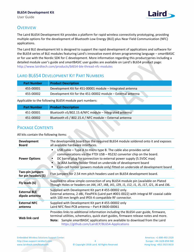
PACKAGE CONTENTS
All kits contain the following items:
Development Board
The development board has the required BL654 module soldered onto it and exposes all available hardware interfaces.
Power Options
▪ USB cable – Type A to micro type B. The cable also provides serial communications via the FTDI USB – RS232 converter chip on the board.
▪ DC barrel plug for connection to external power supply (5.5VDC max) ▪ 3x AAA battery holder fitted on underside of development board ▪ Coin-cell holder (powers module only) fitted on underside of development board
Two-pin jumpers for pin headers (5)
Five jumpers for 2.54 mm pitch headers used on BL654 development board.
Fly leads (6) Supplied to allow simple connection of any BL654 module pin (available on Plated Though Holes or headers on J44, J47, J48, J41, J29, J1, J12, J1, J5, J17, J21, J6 and J36.
External BLE dipole antenna
Supplied with Development Kit part # 455-00002 only. External antenna, 2 dBi, FlexPIFA (Laird part #001-0022) with integral RF coaxial cable with 100 mm length and IPEX-4 compatible RF connector.
External NFC antenna
Supplied with Development Kit part # 455-00002 only Laird NFC flexi-PCB antenna – Part # 0600-00061
Web link card
Provides links to additional information including the BL654 user guide, firmware, terminal utilities, schematics, quick start guides, firmware release notes and more.
Note: Sample smartBASIC applications are available to download from the Laird https://github.com/LairdCP/BL654-Applications

BL654 Development Kit User Guide
Embedded Wireless Solutions Support Center:
http://ews-support.lairdtech.com
www.lairdtech.com/bluetooth
5
© Copyright 2018 Laird. All Rights Reserved
Americas: +1-800-492-2320
Europe: +44-1628-858-940
Hong Kong: +852 2923 0610
BL654 DEVELOPMENT KIT – MAIN DEVELOPMENT BOARD
This section describes the BL654 development board hardware. The BL654 development board is delivered with the BL654 series module loaded with integrated smartBASIC runtime engine firmware but no onboard smartBASIC; because of this it starts up in AT command mode by default.
Applications in smartBASIC are simple and easy to develop for any BLE application. Sample smartBASIC applications scripts are available to download from the Laird GitHub repository on the BL654 product page at https://github.com/LairdCP/BL654-Applications. The development board also can be used with Nordic SDK.
The BL654 development board is a universal development tool that highlights the capabilities of the BL654 module. The development kit is supplied in a default configuration which should be suitable for multiple experimentation options. It also offers several header connectors that help isolate on-board sensors and UART from the BL654 module to create different configurations. This allows you to test different operating scenarios.
The board allows the BL654 series module to physically connect to a PC via the supplied USB cable for development purposes. The development board provides USB-to-Virtual COM port conversion through a FTDI chip – part number FT232R. Any Windows PC (XP or later) should auto-install the necessary drivers; if your PC cannot locate the drivers, you can download them from http://www.ftdichip.com/Drivers/VCP.htm
Key Features
The BL654 development board has the following features:
▪ BL654 series module soldered onto the development board ▪ The following power supply options for powering the development board:
– USB (micro-USB, type B) – External DC supply (2.5-5.5V) – AAA batteries (three AAA battery holder fitted on underside of development board) – USB (micro-USB, type B) –for direct use of BL654 USB interface as well
▪ Powering the BL654 module in Normal Voltage mode (OPTION1) via selection switch (SW7). Regulated 3.3V or Regulated 1.8V via selection switch.
▪ Powering the BL654 module in High Voltage mode (OPTION2) via selection switch (SW7). Regulated 2.5V or 4.5V (from 3xAAA battery (4.5V)) via selection switch. Option to inject external voltage anywhere between 2.5V to 5.5V for the High Voltage mode (via J28).
▪ Power supply option for coin-cell (CR2032) operation of the BL654 module ONLY (not development board) ▪ USB to UART bridge (FTDI chip) ▪ BL654 UART can be interfaced to:
– USB (PC) using the USB-UART bridge (FTDI chip) – External UART source (using IO break-out connectors J1 when the development board is powered
from a DC jack or AAA batteries) – Atmel MCU by use of an analog switch to route the BL654 UART (for those customers working with
Nordic SDK) ▪ Current measuring options (BL654 module only):
– Pin header (Ammeter) – 10R Series resistor for differential measurement (oscilloscope)
▪ IO break-out 2.54 mm pitch pin header connectors (plated through-holes) that bring out all interfaces of the BL654 module – UART, SPI, QSPI, I2C, SIO [DIO or AIN (ADCs)], PWM, FREQ, NFC – and allow for plugging in external modules/sensors.
▪ Pin headers jumpers that allow the on-board sensors (I2C sensor, LEDs, SPI interface, etc.; and the USB UART FTDI bridge) to be disconnected from BL654 module (by removing jumpers).
BL654 Development Kit User Guide
Embedded Wireless Solutions Support Center:
http://ews-support.lairdtech.com
www.lairdtech.com/bluetooth
6
© Copyright 2018 Laird. All Rights Reserved
Americas: +1-800-492-2320
Europe: +44-1628-858-940
Hong Kong: +852 2923 0610
▪ Four on-board sensors: – Analog output temperature sensor – I2C device (RTC chip) – SPI device (EEPROM) – QSPI device (Flash IC)
▪ Four buttons and Four LEDs for user interaction ▪ One reset button (via an analog switch) ▪ NFC antenna connector on-board development board for use with supplied flexi-PCB NFC antenna ▪ Optional external 32.768 kHz crystal oscillator and associated load capacitors. Not required for operation of
the BL654; is disconnected by open solder bridges by default. ▪ Optional external serial (SPI) flash IC. Not required for operation of the BL654; is disconnected by open
solder bridges by default. ▪ Optional external serial (QSPI) flash IC. Not required for operation of the BL654; is disconnected by open
solder bridges by default. ▪ Access to BL654 JTAG – also known as Serial Wire Debug (SWD) Interface ▪ On-board SWD (JTAG) programmer circuitry ▪ smartBASIC runtime engine FW upgrade capability:
– Via UART (using the FTDI USB-UART) – Via SWD (JTAG) using on-board JTAG programmer circuitry on the BL654 Development Kit
▪ smartBASIC application upgrade capability: – Via UART (using the FTDI USB-UART) – Via OTA (Over-the-Air)
BL654 Development Kit User Guide
Embedded Wireless Solutions Support Center:
http://ews-support.lairdtech.com
www.lairdtech.com/bluetooth
7
© Copyright 2018 Laird. All Rights Reserved
Americas: +1-800-492-2320
Europe: +44-1628-858-940
Hong Kong: +852 2923 0610
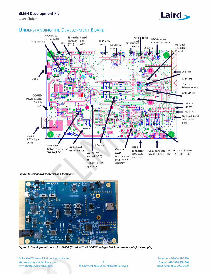
UNDERSTANDING THE DEVELOPMENT BOARD
Figure 1: Dev board contents and locations
Figure 2: Development board for BL654 (fitted with 451-00001 Integrated Antenna module for example)
DC Jack 7-12V Input CON1
SW8 Select between 2.5V or 3xAAA(4.5V)
On-board SWD interface and programmer circuitry
NFC Antenna Connector CON2
USB2 connector USB-SWD interface
USB3 connector BL654 nR SPI EEPROM device
Optional Serial QSPI or SPI flash
I2C device U16
J48 PTH
FTDI-FT232R
DC/USB Power Source
Switch SW4
Header J12 for nAutoRUN
J35
J1 Header Plated Through Holes (PTH) for UART Temperature
Sensor
TP14 GND Hook
LED2 LED1 LED3 LED 4 J37 J26 J45 J39
J5 (VSP) Optional 32.768 kHz Crystal
SW3 nReset /BOOT Button
SPI EEPROM device
SW7 select Normal (VDD) or High (VDD_HV) operation
J7 (VDD)
Current Measurement
J9 (VDD_HV)
J41 PTH
J47 PTH
USB1
J29 PTH
4 Buttons
BL654 Development Kit User Guide
Embedded Wireless Solutions Support Center:
http://ews-support.lairdtech.com
www.lairdtech.com/bluetooth
8
© Copyright 2018 Laird. All Rights Reserved
Americas: +1-800-492-2320
Europe: +44-1628-858-940
Hong Kong: +852 2923 0610
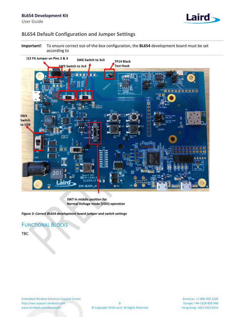
BL654 Default Configuration and Jumper Settings
Important! To ensure correct out-of-the-box configuration, the BL654 development board must be set according to
Figure 3: Correct BL654 development board jumper and switch settings
FUNCTIONAL BLOCKS
TBC
J12 Fit Jumper on Pins 2 & 3
SW5 Switch to 3v3
SW6 Switch to 3v3 TP14 Black Test Hook
SW7 in middle position for Normal Voltage mode (VDD) operation
SW4 Switch to USB
BL654 Development Kit User Guide
Embedded Wireless Solutions Support Center:
http://ews-support.lairdtech.com
www.lairdtech.com/bluetooth
9
© Copyright 2018 Laird. All Rights Reserved
Americas: +1-800-492-2320
Europe: +44-1628-858-940
Hong Kong: +852 2923 0610
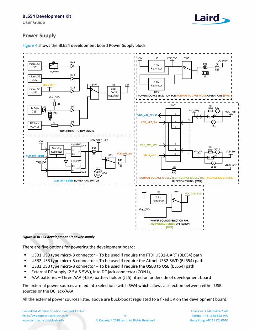
Power Supply
Figure 4 shows the BL654 development board Power Supply block.
Figure 4: BL654 development Kit power supply
There are five options for powering the development board:
▪ USB1 USB type micro-B connector – To be used if require the FTDI USB1-UART (BL654) path ▪ USB2 USB type micro-B connector – To be used if require the Atmel USB2-SWD (BL654) path ▪ USB3 USB type micro-B connector – To be used if require the USB3 to USB (BL654) path ▪ External DC supply (2.5V-5.5VV), into DC jack connector (CON1), ▪ AAA batteries – Three AAA (4.5V) battery holder (J25) fitted on underside of development board
The external power sources are fed into selection switch SW4 which allows a selection between either USB sources or the DC jack/AAA.
All the external power sources listed above are buck-boost regulated to a fixed 5V on the development board.

BL654 Development Kit User Guide
Embedded Wireless Solutions Support Center:
http://ews-support.lairdtech.com
www.lairdtech.com/bluetooth
10
© Copyright 2018 Laird. All Rights Reserved
Americas: +1-800-492-2320
Europe: +44-1628-858-940
Hong Kong: +852 2923 0610
The BL654 module has the following power supply pins:
▪ VDD pin (operating range of 1.7V to 3.6V) – Used for Normal Voltage mode ▪ VDD_HV pin (operating range of 2.5V to 5.5V) – Used for High Voltage mode ▪ VBUS pin (operating range of 4.35V to 5.5V) – Used for BL654 USB mode
It can be powered in the following ways:
▪ Normal Voltage mode operation
Option 1 – Normal voltage power supply mode entered when the external supply voltage is connected to both the VDD and VDD_HV pins (so that VDD equals VDD_HV). Connect external supply within a 1.7V to 3.6V range to the BL654 VDD and VDD_HV pins.
For Normal Voltage mode operation, the BL654 Development Board power supply section generates the following:
– Regulated 3.3V – Regulated 1.8V
and then via selection switch SW5 (default is 3.3V position), you can select whether to use 3.3V or 1.8V.
▪ High Voltage mode operation
Option 2 – High voltage mode power supply mode (using BL654 VDD_HV pin) entered when the external supply voltage in ONLY connected to the VDD_HV pin and the VDD pin is not connected to any external voltage supply. Connect external supply within a 2.5V to 5.5V range to the BL654 VDD_HV pin. Leave the BL654 VDD pin unconnected.
For High Voltage mode operation, the BL654 Development Board power supply section generates the following:
– Regulated 2.5V – 3 x AAA generated 4.5V (or inject external voltage into J28pin1 up to 5.5V)
and then via selection switch SW8 (default is 2.5V position), you can select whether to use 2.5V or 4.5V.
Option 3 – High voltage mode with voltage via USB3
– For either option, if you use the BL654 USB interface, the BL654 VBUS pin must be connected to and external supply within the range of 4.35V to 5.5V.
The BL654 development board power supply section is designed to cater to the above and you should follow these two steps:
1. Set SW7 – Select one of the following three positions:
▪ High Voltage mode operation and BL654 USB (connect USB cable to USB3 connector) – Top position. Source from USB3.
▪ Normal Voltage mode operation – Middle position (default). Source from SW5.
▪ High Voltage mode operation – Bottom position (default). Source from SW8.
2. Depending on chosen SW7 position, select one of the following three positions:
▪ Plug in USB cable into USB3 – If SW7 is set to Top position.
▪ SW5 (either 3.3V or 1.8V) – Default SW5 on 3.3V position. If SW7 set to Middle position.
▪ SW8 (either 2.5V or 4.5V (3xAAA) – Default SW5 on 2.5V position. If SW7 set to Bottom position.
Table 1 summarises the dev-board on-board power sources and switch positions.
BL654 Development Kit User Guide
Embedded Wireless Solutions Support Center:
http://ews-support.lairdtech.com
www.lairdtech.com/bluetooth
11
© Copyright 2018 Laird. All Rights Reserved
Americas: +1-800-492-2320
Europe: +44-1628-858-940
Hong Kong: +852 2923 0610
Table 1: Dev board power sources and switch positions
Selection Switch SW7 positions (silk screen)
Source
Voltage Operating mode
Dev Board Power Supply Switch Positions
SW5 Selects between
1.8V or 3.3V
SW8 Selects between
2.5V or 4.5V (3xAAA)
Connect USB cable into
USB3
Present selected voltage to the BL654 pin
BL654 VDD pin BL654 VDD_HV pin BL654 VBUS pin
SW7 Top position – Silkscreen: USB3
(Source from USB3)
High Voltage Mode with BL654 USB used (USB3)
Note 1 USB3 voltage USB3 voltage
SW7 Middle position – Silkscreen: SW5 SW6
(Source from SW5, Note 2)
Normal Voltage Mode
Decided by SW5
(default SW5 on 3.3V position)
N/A N/A
SW7 Bottom position – Silkscreen: AAA (SW8)
(Source from SW8)
High Voltage Mode
Note 1
Decided by SW8
(default SW8 on 2.5V position)
N/A
Power Source and Switch Location Notes:
Note 1: No voltage is presented to VDD pin, as in High voltage mode, the VDD pin becomes an output voltage pin. It can be used to supply external circuitry from the VDD pin. Before any current can be taken from the BL654 VDD pin, this feature must be enabled in the BL654. Additionally, the VDD output voltage is configurable from 1.8V to 3.3V with possible settings of 1.8V, 2.1V, 2.4V, 2.7V, 3.0V, and 3.3V. The default voltage is 1.8V.
Note 2: When SW6 is set to position “coin-cell,” then the voltage selected with SW5 (default position 3V3) does not get presented to the BL654. The CR2032 coin cell (in J34) voltage is not regulated but is fed directly to the BL654 module supply pin. Switch SW6 selects between the regulated 3V3V/1V8 and coin cell. The coin cell powers only the BL654 module directly (on the development board); this is power domain VDD_nRF_SW through R46 0R.
Note: The development board for BL654 has on-board circuitry to allow access to BL654 SWD interface (via USB connector USB2). Use USB2 only to power the development board when BL654 SWD interface is needed. Refer to SWD Interface. When USB2 is used, USB1 does not need to be used for DC power.
The development board power supply circuitry special feature is it resolves whether the BL654 VDD pin is an input supply pin (in Normal Voltage mode) or becomes an output supply voltage pin (in High Voltage mode).
On the development board, the power circuity net names are as follows:
▪ VCC_3V3 – Supplies regulated 3.3V power to the FTDI chip as well as temperature sensor (U1). ▪ VSUPPLY – Supplies regulated 3.3V or 1.8V via selection switch SW5 to net VSUPPLY which is connected to
input of Load switch U21. ▪ VCC_2V5_5V5 – Selection switch SW8 supplies either regulated 2.5V or 3x AAA battery voltage (4.5V) can
be used for when BL654 is powered in High Voltage mode (using the VDD_HV pin). ▪ V5V – The main development board power supply’s buck-boosted output (that is 5V) supplies a discrete
regulator made up of Q3 and U19. U19 OpAmp drives Q3 to generate regulated voltage (that then is connected to input of load switch U20) that tracks control signal VDD_nRF_SENSE.
BL654 Development Kit User Guide
Embedded Wireless Solutions Support Center:
http://ews-support.lairdtech.com
www.lairdtech.com/bluetooth
12
© Copyright 2018 Laird. All Rights Reserved
Americas: +1-800-492-2320
Europe: +44-1628-858-940
Hong Kong: +852 2923 0610
▪ VDD_VSRC_nRF – Supplies the FTDI chip IO and all other sensors and circuitry. VDD_VSRC_nRF is generated from load switches U20 or U19.
▪ VDD_nRF_SENSE – Used as control signal to drive control pin of load switches U20 and U19. The source of VDD_nRF_SENSE is the BL654 VDD pin. When BL654 is powered in High Voltage mode (using the VDD_HV pin), the BL654 VDD pin becomes an output.
▪ VDD_nRF_SW – Selection switch SW6 supplies either VDD_SRC_nRF or coin-cell (J34). When the BL654 operated in Normal Voltage mode (SW7 in middle position and voltage source is either 1.8V or 3.3V selected by SW5). Also supplies the I2C RTC chip (U16). The use case for powering this is that the RTC chip can be configured so that, after the pre-determined time, the RTC chip outputs (via RTC_ALARM pin) a transition level that can be used to wake up the BL654 module up from deep sleep.
▪ VDD_nRFp – Supplies the BL654 series module only. Current measuring block on the development board only measures the current into power domain VDD_nRFp (that is current going into header J7 pin1).
▪ VDD_nRF – Supplies the BL654 series module only and is to the current that has come out of the current measuring block on the development board on header connector J7pin2.
▪ VDD_HVp – Supplies the BL654 series module only. Current measuring block on the development board only measures the current into power domain VDD_nRFp (that is current going into header J9 pin1).
▪ VDD_HV – Supplies the BL654 series module only and is to the current that has come out of the current measuring block on the development board on header connector J9pin2.
▪ VBUS_nRFp – This voltage from USB cable plugged into connector USB3, that is directly fed to BL654 VBUS pin (via 0R resistor R50) on net VBUS_nRF.
Additional Power Option (for BL654 module only –not development board) – Coin Cell
The coin cell powers only the BL654 module directly via SW6 (on the development board – power domain VDD_nRF_SW) and through R46 provides power to the I2C RTC chip (U16).
Refer to the Appendix for the correct method of coin cell insertion and removal.
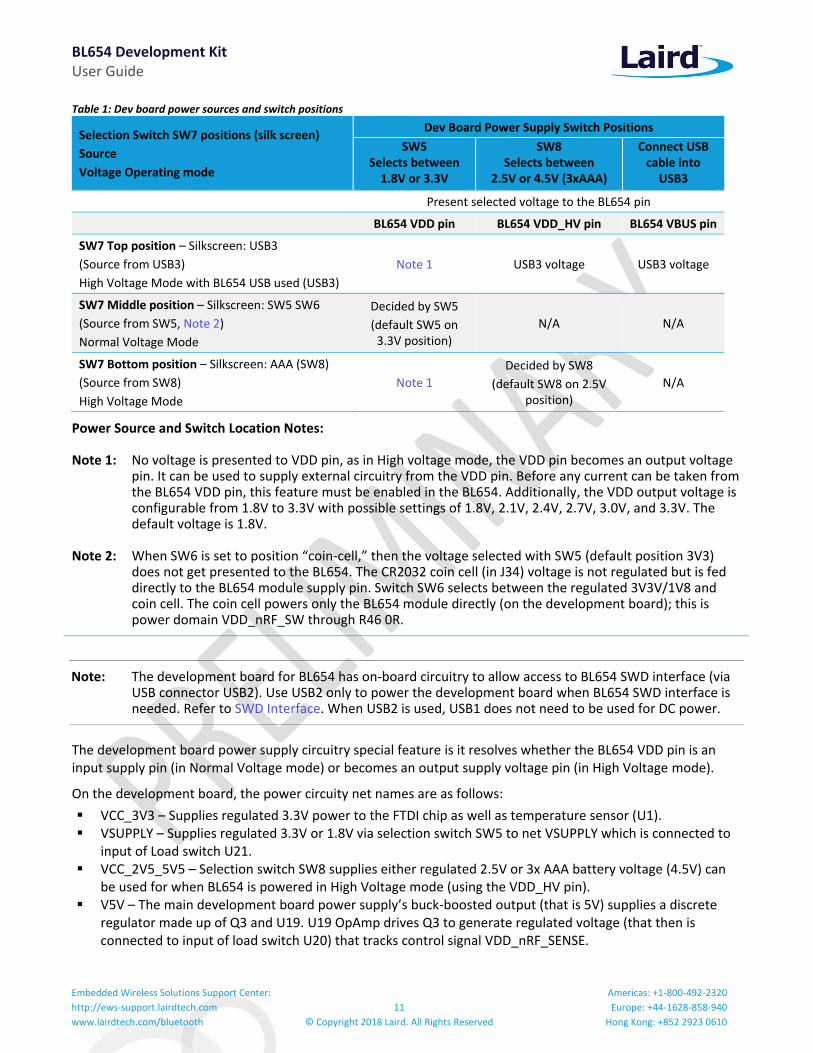
Reset Button
The development board has a reset button (SW3). The nReset is active low (SW3 pushed down) that is routed to the BL654 module nReset pin via an analog switch U25. The placement of the Reset button is shown in Figure 5.
Figure 5: Reset button placement
C63NOPOP (0.01uF,16V)
GND
NOPOP (PIN HEADER,2.54mm 1X2P)J42
11
22
GND
R34150RR
eset
SW3TACT SW,SMD/180d
11
22
33
44
BOOT_RESET_BLE
GND

BL654 Development Kit User Guide
Embedded Wireless Solutions Support Center:
http://ews-support.lairdtech.com
www.lairdtech.com/bluetooth
13
© Copyright 2018 Laird. All Rights Reserved
Americas: +1-800-492-2320
Europe: +44-1628-858-940
Hong Kong: +852 2923 0610
Figure 6: Reset button schematic and routing through analog switch and location diagram
By default, the analog switch (U25) control line (USB_DETECT) is low and therefore nReset button (SW3) is routed via the analog switch (U25) to BL654 nReset pin (nRESET_BLE).
The development board has USB2 cable detection circuit that generates the USB_DETECT signal on its output, so if a USB cable is plugged into connector USB2, then USB2 cable detection circuit generates a HIGH on USB_DETECT and routes nReset button (SW3) to the Atmel MCU. This is useful for those customers working with the Nordic SDK.
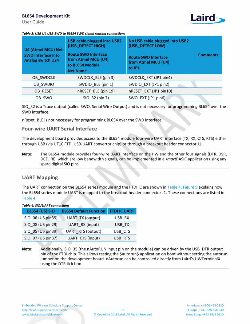
Table 3 displays the routing of SW3 reset button via analog switch U25 to either the BL654 reset pin or Atmel MCU depending on state of the USB_DETECT control line (which is HIGH on USB cable being plugged into USB2).
Table 2: USB U4 USB-SWD to BL654 SWD signal routing connections
SW3 reset button into Analog switch U25 (net name)
USB cable plugged into USB2 (USB_DETECT HIGH)
No USB cable plugged into USB2 (USB_DETECT LOW)
Comments Route SW3 reset button to Atmel MCU (U4)
via analog switch U25
Net name
Route SW3 reset button to BL654 reset pin to JP1
via analog switch U25
BOOT_RESET_BLE IMCU_BOOTBLE (pin 6) nRESET_BLE
SWD (JTAG) Interface
The development board provides access to the BL654 module two-wire SWD interface on JP1 via analog switch U24. This is REQUIRED for customer use, since the BL654 module supports smartBASIC runtime engine firmware over JTAG (as well as over UART).
Laird recommends you use JTAG (2-wire interface) to handle future BL654 module firmware upgrades. You MUST wire out the JTAG (2-wire interface) on your host design (four lines should be wired out, namely SWDIO, SWDCLK, GND and VCC). Firmware upgrades can still be performed over the BL654 UART interface, but this is slower (60 seconds using UART vs. 10 seconds when using JTAG) than using the BL654 JTAG (2-wire interface).
Upgrading smartBASIC runtime engine firmware or loading smartBASIC applications also can be done using the UART interface.
BOOT_RESET_BLEIMCU_BOOT
USB_DETECT
VDD_VSRC_nRF
U25
Dual DPDT,1.65V~4.45V
1B01
1B115
2B05
2B13
1A16
2A4
1S2
3B09
3B17
4B013
4B111
3A8
4A12
2S10
GND6
VCC14
GND
nRESET_BLE
C790.1uF,16V
GND

BL654 Development Kit User Guide
Embedded Wireless Solutions Support Center:
http://ews-support.lairdtech.com
www.lairdtech.com/bluetooth
14
© Copyright 2018 Laird. All Rights Reserved
Americas: +1-800-492-2320
Europe: +44-1628-858-940
Hong Kong: +852 2923 0610
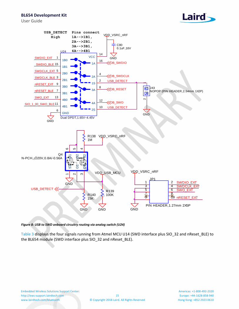
For those customers (using Nordic SDK) that require access to BL654 SWD (JTAG) interface, the BL654 development board (see Figure 1) has on-board circuitry to allow access to BL654 module SWD interface (via USB connector USB2).
Figure 8 shows the SWD on-board circuitry routing via analog switch U24. When USB cable is plugged into connector USB2 (then the USB cable detection output generates a HIGH for USB_DETECT) and Atmel MCU SWD (JTAG) signals are routed to the BL654 SWD interface. This is required to connect the two-wire SWD (JTAG) interface from U14 to the BL654 SWD (JTAG) interface.
When no USB cable is plugged into connector USB2, the USB cable detection output generates a LOW for USB_DETECT and the Atmel MCU SWD (JTAG) signals are routed to connector JP1 so an external BL654 module can be programmed over the SWD interface.
Figure 7: JP1 on development board
BL654 Development Kit User Guide
Embedded Wireless Solutions Support Center:
http://ews-support.lairdtech.com
www.lairdtech.com/bluetooth
15
© Copyright 2018 Laird. All Rights Reserved
Americas: +1-800-492-2320
Europe: +44-1628-858-940
Hong Kong: +852 2923 0610
Figure 8: USB to SWD onboard circuitry routing via analog switch (U24)
Table 3 displays the four signals running from Atmel MCU U14 (SWD interface plus SIO_32 and nReset_BLE) to the BL654 module (SWD interface plus SIO_32 and nReset_BLE).
OB_SWDIO
C800.1uF,16V
GND
OB_SWDCLK
USB_DETECT
NOPOP (PIN HEADER,2.54mm 1X2P)J431
12
2
GND
VDD_VSRC_nRF
SWDIO_EXT
USB_DETECT Pins connect
High 1A-->1B1,
2A-->2B1,
3A-->3B1,
4A-->4B1
SWDIO_BLE
SIO_1_00_SWO_BLE
nRESET_EXT
U24
Dual DPDT,1.65V~4.45V
1B01
1B115
2B05
2B13
1A16
2A4
1S2
3B09
3B17
4B013
4B111
3A8
4A12
2S10
GND6
VCC14
OB_RESET
SWDCLK_BLE
SWDCLK_EXT
OB_SWO
USB_DETECT
SWO_EXT
nRESET_BLE
GND
GND GND
R1381M
Q4N-PCH,¡Ó20V,0.8A/-0.56A
S1
1
G1
2
D2
3S
24
G2
5
D1
6
R139100KR140
15K
GND
VDD_VSRC_nRF
VDD_USB_MCU
USB_DETECT
GND
SWDIO_EXTSWDCLK_EXT
JP1
PIN HEADER,1.27mm 2X5P
1 23 45 67 89 10 nRESET_EXT
SWO_EXT
VDD_VSRC_nRF
BL654 Development Kit User Guide
Embedded Wireless Solutions Support Center:
http://ews-support.lairdtech.com
www.lairdtech.com/bluetooth
16
© Copyright 2018 Laird. All Rights Reserved
Americas: +1-800-492-2320
Europe: +44-1628-858-940
Hong Kong: +852 2923 0610
Table 3: USB U4 USB-SWD to BL654 SWD signal routing connections
U4 (Atmel MCU) Net
SWD Interface into Analog switch U24
USB cable plugged into USB2 (USB_DETECT HIGH)
No USB cable plugged into USB2 (USB_DETECT LOW)
Comments Route SWD Interface from Atmel MCU (U4)
to BL654 Module
Net Name
Route SWD Interface from Atmel MCU (U4)
to JP1
OB_SWDCLK SWDCLK_BLE (pin 3) SWDCLK_EXT (JP1 pin4)
OB_SWDIO SWDIO_BLE (pin 1) SWDIO_EXT (JP1 pin2)
OB_RESET nRESET_BLE (pin 19) nRESET_EXT (JP1 pin10)
OB_SWO SIO_32 (pin 7) SWO_EXT (JP1 pin6)
SIO_32 is a Trace output (called SWO, Serial Wire Output) and is not necessary for programming BL654 over the SWD interface.
nReset_BLE is not necessary for programming BL654 over the SWD interface.
Four-wire UART Serial Interface
The development board provides access to the BL654 module four-wire UART interface (TX, RX, CTS, RTS) either through USB (via UT10 FTDI USB-UART convertor chip) or through a breakout header connector J1.
Note: The BL654 module provides four-wire UART interface on the HW and the other four signals (DTR, DSR, DCD, RI), which are low bandwidth signals, can be implemented in a smartBASIC application using any spare digital SIO pins.
UART Mapping
The UART connection on the BL654 series module and the FTDI IC are shown in Table 4. Figure 9 explains how the BL654 series module UART is mapped to the breakout header connector J1. These connections are listed in Table 4.
Table 4: SIO/UART connections
BL654 (U5) SIO BL654 Default Function FTDI IC UART
SIO_06 (U5 pin35) UART_TX (output) USB_RX
SIO_08 (U5 pin29) UART_RX (input) USB_TX
SIO_05 (U5 pin39) UART_RTS (output) USB_CTS
SIO_07 (U5 pin37) UART_CTS (input) USB_RTS
Note: Additionally, SIO_35 (the nAutoRUN input pin on the module) can be driven by the USB_DTR output pin of the FTDI chip. This allows testing the $autorun$ application on boot without setting the autorun jumper on the development board. nAutorun can be controlled directly from Laird’s UWTerminalX using the DTR tick box.
BL654 Development Kit User Guide
Embedded Wireless Solutions Support Center:
http://ews-support.lairdtech.com
www.lairdtech.com/bluetooth
17
© Copyright 2018 Laird. All Rights Reserved
Americas: +1-800-492-2320
Europe: +44-1628-858-940
Hong Kong: +852 2923 0610
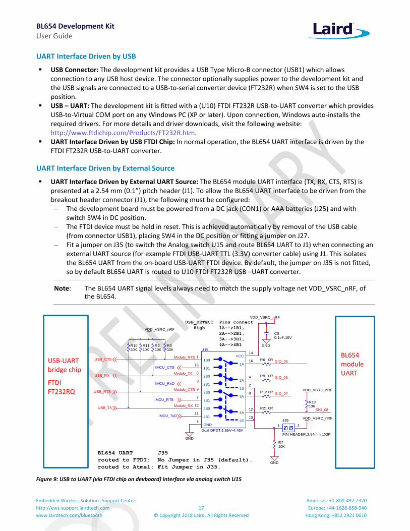
UART Interface Driven by USB
▪ USB Connector: The development kit provides a USB Type Micro-B connector (USB1) which allows connection to any USB host device. The connector optionally supplies power to the development kit and the USB signals are connected to a USB-to-serial converter device (FT232R) when SW4 is set to the USB position.
▪ USB – UART: The development kit is fitted with a (U10) FTDI FT232R USB-to-UART converter which provides USB-to-Virtual COM port on any Windows PC (XP or later). Upon connection, Windows auto-installs the required drivers. For more details and driver downloads, visit the following website: http://www.ftdichip.com/Products/FT232R.htm.
▪ UART Interface Driven by USB FTDI Chip: In normal operation, the BL654 UART interface is driven by the FTDI FT232R USB-to-UART converter.
UART Interface Driven by External Source
▪ UART Interface Driven by External UART Source: The BL654 module UART interface (TX, RX, CTS, RTS) is presented at a 2.54 mm (0.1”) pitch header (J1). To allow the BL654 UART interface to be driven from the breakout header connector (J1), the following must be configured: – The development board must be powered from a DC jack (CON1) or AAA batteries (J25) and with
switch SW4 in DC position. – The FTDI device must be held in reset. This is achieved automatically by removal of the USB cable
(from connector USB1), placing SW4 in the DC position or fitting a jumper on J27. – Fit a jumper on J35 (to switch the Analog switch U15 and route BL654 UART to J1) when connecting an
external UART source (for example FTDI USB-UART TTL (3.3V) converter cable) using J1. This isolates the BL654 UART from the on-board USB-UART FTDI device. By default, the jumper on J35 is not fitted, so by default BL654 UART is routed to U10 FTDI FT232R USB –UART converter.
Note: The BL654 UART signal levels always need to match the supply voltage net VDD_VSRC_nRF, of the BL654.
Figure 9: USB to UART (via FTDI chip on devboard) interface via analog switch U15
IMCU_CTS
IMCU_RxD
C80.1uF,16V
GND
IMCU_RTS
IMCU_TxD
USB_CTS
Module_CTS
VDD_VSRC_nRF
R710K
R6 0R
R9 0R
R12 0R
R21 0R
USB_RX
R1910K
PIN HEADER,2.54mm 1X2P
J35
11
22
USB_DETECT Pins connect
High 1A-->1B1,
2A-->2B1,
3A-->3B1,
4A-->4B1
Module_RX
GND
SIO_08
VDD_VSRC_nRF
SIO_05
SIO_06
SIO_07VDD_VSRC_nRF
USB_TX
USB_RTS
VDD_VSRC_nRF
U15
Dual DPDT,1.65V~4.45V
1B01
1B115
2B05
2B13
1A16
2A4
1S2
3B09
3B17
4B013
4B111
3A8
4A12
2S10
GND6
VCC14
Module_RTS
Module_TX
R210K
GND
R310K
R1010K
R1110K
USB-UART bridge chip
FTDI FT232RQ
BL654 module UART
BL654 UART J35
routed to FTDI: No Jumper in J35 (default).
routed to Atmel: Fit Jumper in J35.
BL654 Development Kit User Guide
Embedded Wireless Solutions Support Center:
http://ews-support.lairdtech.com
www.lairdtech.com/bluetooth
18
© Copyright 2018 Laird. All Rights Reserved
Americas: +1-800-492-2320
Europe: +44-1628-858-940
Hong Kong: +852 2923 0610
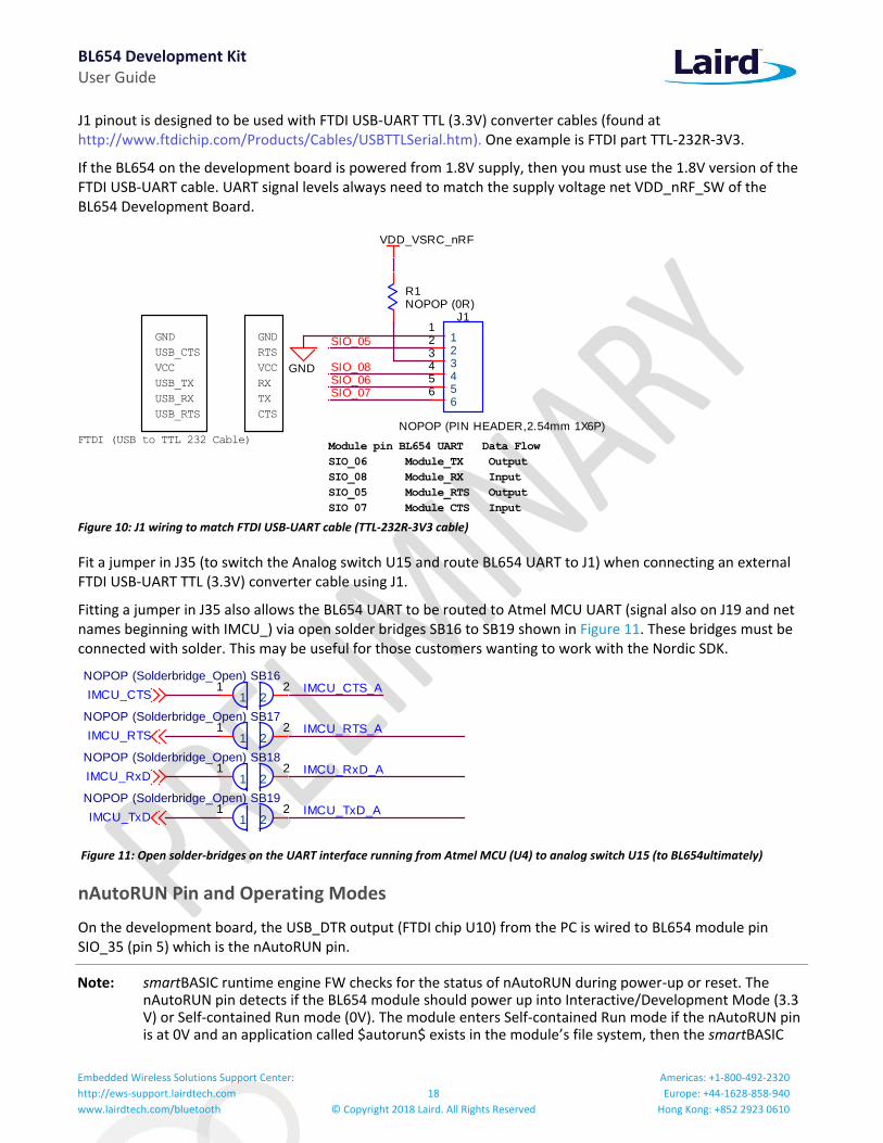
J1 pinout is designed to be used with FTDI USB-UART TTL (3.3V) converter cables (found at http://www.ftdichip.com/Products/Cables/USBTTLSerial.htm). One example is FTDI part TTL-232R-3V3.
If the BL654 on the development board is powered from 1.8V supply, then you must use the 1.8V version of the FTDI USB-UART cable. UART signal levels always need to match the supply voltage net VDD_nRF_SW of the BL654 Development Board.
Figure 10: J1 wiring to match FTDI USB-UART cable (TTL-232R-3V3 cable)
Fit a jumper in J35 (to switch the Analog switch U15 and route BL654 UART to J1) when connecting an external FTDI USB-UART TTL (3.3V) converter cable using J1.
Fitting a jumper in J35 also allows the BL654 UART to be routed to Atmel MCU UART (signal also on J19 and net names beginning with IMCU_) via open solder bridges SB16 to SB19 shown in Figure 11. These bridges must be connected with solder. This may be useful for those customers wanting to work with the Nordic SDK.
Figure 11: Open solder-bridges on the UART interface running from Atmel MCU (U4) to analog switch U15 (to BL654ultimately)
nAutoRUN Pin and Operating Modes
On the development board, the USB_DTR output (FTDI chip U10) from the PC is wired to BL654 module pin SIO_35 (pin 5) which is the nAutoRUN pin.
Note: smartBASIC runtime engine FW checks for the status of nAutoRUN during power-up or reset. The nAutoRUN pin detects if the BL654 module should power up into Interactive/Development Mode (3.3 V) or Self-contained Run mode (0V). The module enters Self-contained Run mode if the nAutoRUN pin is at 0V and an application called $autorun$ exists in the module’s file system, then the smartBASIC
SIO_06
R1NOPOP (0R)
Module pin BL654 UART Data Flow
SIO_06 Module_TX Output
SIO_08 Module_RX Input
SIO_05 Module_RTS Output
SIO_07 Module_CTS Input
SIO_07
SIO_08
VDD_VSRC_nRF
SIO_05
FTDI (USB to TTL 232 Cable)
GND
USB_CTS
VCC
USB_TX
USB_RX
USB_RTS
GND
RTS
VCC
RX
TX
CTS
J1
NOPOP (PIN HEADER,2.54mm 1X6P)
11
22
33
44
55
66
GND
IMCU_RTS_A
IMCU_RxD_A
SB19NOPOP (Solderbridge_Open)
11
22 IMCU_TxD_A
IMCU_RTS
IMCU_CTS
IMCU_TxD
IMCU_RxD
SB16NOPOP (Solderbridge_Open)
11
22 IMCU_CTS_A
SB17NOPOP (Solderbridge_Open)
11
22
SB18NOPOP (Solderbridge_Open)
11
22

BL654 Development Kit User Guide
Embedded Wireless Solutions Support Center:
http://ews-support.lairdtech.com
www.lairdtech.com/bluetooth
19
© Copyright 2018 Laird. All Rights Reserved
Americas: +1-800-492-2320
Europe: +44-1628-858-940
Hong Kong: +852 2923 0610
runtime engine FW executes the smartBASIC application script automatically; hence the name Self-contained Run mode.
Tying nAutoRUN HIGH (to net name on devboard VDD_VSRC_nRF) inhibits the $autorun$ application from running. As an alternative to using USB_DTR, the J12 three-pin header allows a jumper to be fitted to select between the two operating modes.
Table 5: BL654 nAutoRUN header
nAutoRUN Pin
BL654 Operating Mode (pin28, nAutoRUN Mode/SIO_35)
Interactive/ Development Mode
(SIO_35 set High Externally)
Self-contained Run Mode (nAutoRUN
mode)
(SIO_35 Low Internally)
Circuit
J12 Jumper Position
Develop
Jumper on J12 pins 2-1
nAutoRUN (default)
Jumper on J12 pins 2-3
BL654 has internal pull-down enabled, jumper in J12 in 2-3 can also be left off
The J12 header connector allows the USB_DTR signal from the FTDI chip to be disconnected from the BL654.
To connect the BL654 nAutoRUN pin SIO_35 (pin 5) to PC FTDI USB_DTR line via the J12 header connector, do the following:
▪ Fit the jumper into the J12 (pin 2-1) header connector to allow the PC (using UwTerminal) to control nAutoRUN pin (SIO_35).
To disconnect the BL654 nAutoRUN SIO_35 (pin 5) from the PC FTDI USB_DTR line, do the following:
▪ Remove the jumper on header connector J12 pin 2-1. Then nAutoRUN can be controlled by inserting the jumper onto J12 (pin 2-3) as shown in Table 5 (this is the default). The BL654 by default has pull-down enabled on the SIO_35 (nAutoRUN) pin, so the jumper into J12 (pin 2-3) is optional.
vSP (Virtual Serial Port) Modes and OTA (Over the Air) smart BASIC App Download
The OTA feature makes it possible to download smart BASIC applications over the air to the BL654. To enable this feature, SIO_02 must be pulled high externally.
On the development board, header connector J5-pin1 brings out the BL654 SIO_02; J5-pin 2 brings out VCC_nRF_SW. To pull BL654 SIO_02 high (to net name VCC_nRF_SW on devboard), fit jumper into header J5.
Note: When SIO_02 is high, ensure that SIO_35 (nAutoRun) is NOT high at same time, otherwise you cannot load the smartBASIC application script.
R25NOPOP (10K)
USB_DTR
GND
VDD_VSRC_nRF
PIN HEADER,2.54mm 1X3PJ12
11
22
33
n_Autorun /
module_DSR
Module_DSR
Develop: Jumper J12 pin2-1
nAUTORUN: Jumper J12 pin2-3 (default)
SIO_35
BL654 Development Kit User Guide
Embedded Wireless Solutions Support Center:
http://ews-support.lairdtech.com
www.lairdtech.com/bluetooth
20
© Copyright 2018 Laird. All Rights Reserved
Americas: +1-800-492-2320
Europe: +44-1628-858-940
Hong Kong: +852 2923 0610
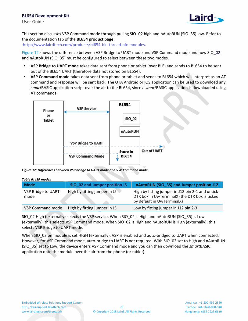
This section discusses VSP Command mode through pulling SIO_02 high and nAutoRUN (SIO_35) low. Refer to the documentation tab of the BL654 product page: http://www.lairdtech.com/products/bl654-ble-thread-nfc-modules.
Figure 12 shows the difference between VSP Bridge to UART mode and VSP Command mode and how SIO_02 and nAutoRUN (SIO_35) must be configured to select between these two modes.
▪ VSP Bridge to UART mode takes data sent from phone or tablet (over BLE) and sends to BL654 to be sent out of the BL654 UART (therefore data not stored on BL654).
▪ VSP Command mode takes data sent from phone or tablet and sends to BL654 which will interpret as an AT command and response will be sent back. The OTA Android or iOS application can be used to download any smartBASIC application script over the air to the BL654, since a smartBASIC application is downloaded using AT commands.
Figure 12: Differences between VSP bridge to UART mode and VSP Command mode
Table 6: vSP modes
Mode SIO_02 and Jumper position J5 nAutoRUN (SIO_35) and Jumper position J12
VSP Bridge to UART mode
High by fitting jumper in J5 High by fitting jumper in J12 pin 2-1 and untick DTR box in UwTerminalX (the DTR box is ticked by default in UwTerminalX)
VSP Command mode High by fitting jumper in J5 Low by fitting jumper in J12 pin 2-3
SIO_02 High (externally) selects the VSP service. When SIO_02 is High and nAutoRUN (SIO_35) is Low (externally), this selects VSP Command mode. When SIO_02 is High and nAutoRUN is High (externally), this selects VSP Bridge to UART mode.
When SIO_02 on module is set HIGH (externally), VSP is enabled and auto-bridged to UART when connected. However, for VSP Command mode, auto-bridge to UART is not required. With SIO_02 set to High and nAutoRUN (SIO_35) set to Low, the device enters VSP Command mode and you can then download the smartBASIC application onto the module over the air from the phone (or tablet).
BL654 Development Kit User Guide
Embedded Wireless Solutions Support Center:
http://ews-support.lairdtech.com
www.lairdtech.com/bluetooth
21
© Copyright 2018 Laird. All Rights Reserved
Americas: +1-800-492-2320
Europe: +44-1628-858-940
Hong Kong: +852 2923 0610
SOFTWARE
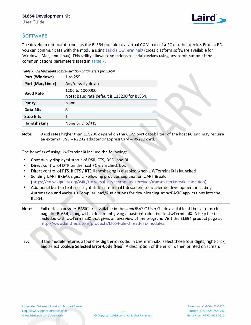
The development board connects the BL654 module to a virtual COM port of a PC or other device. From a PC, you can communicate with the module using Laird’s UwTerminalX (cross platform software available for Windows, Mac, and Linux). This utility allows connections to serial devices using any combination of the communications parameters listed in Table 7.
Table 7: UwTerminalX communication parameters for BL654
Port (Windows) 1 to 255
Port (Mac/Linux) Any/dev/tty device
Baud Rate 1200 to 1000000
Note: Baud rate default is 115200 for BL654.
Parity None
Data Bits 8
Stop Bits 1
Handshaking None or CTS/RTS
Note: Baud rates higher than 115200 depend on the COM port capabilities of the host PC and may require an external USB – RS232 adapter or ExpressCard – RS232 card.
The benefits of using UwTerminalX include the following:
▪ Continually displayed status of DSR, CTS, DCD, and RI ▪ Direct control of DTR on the host PC via a check box ▪ Direct control of RTS, if CTS / RTS Handshaking is disabled when UWTerminalX is launched ▪ Sending UART BREAK signals. Following provides explanation UART Break.
(https://en.wikipedia.org/wiki/Universal_asynchronous_receiver/transmitter#Break_condition) ▪ Additional built-in features (right click in Terminal tab screen) to accelerate development including
Automation and various XCompile/Load/Run options for downloading smartBASIC applications into the BL654.
Note: Full details on smartBASIC are available in the smartBASIC User Guide available at the Laird product page for BL654, along with a document giving a basic introduction to UwTerminalX. A help file is included with UwTerminalX that gives an overview of the program. Visit the BL654 product page at http://www.lairdtech.com/products/bl654-ble-thread-nfc-modules.
Tip: If the module returns a four-hex digit error code: In UwTerminalX, select those four digits, right-click, and select Lookup Selected Error-Code (Hex). A description of the error is then printed on screen.
BL654 Development Kit User Guide
Embedded Wireless Solutions Support Center:
http://ews-support.lairdtech.com
www.lairdtech.com/bluetooth
22
© Copyright 2018 Laird. All Rights Reserved
Americas: +1-800-492-2320
Europe: +44-1628-858-940
Hong Kong: +852 2923 0610
BREAKOUT CONNECTOR PINOUTS
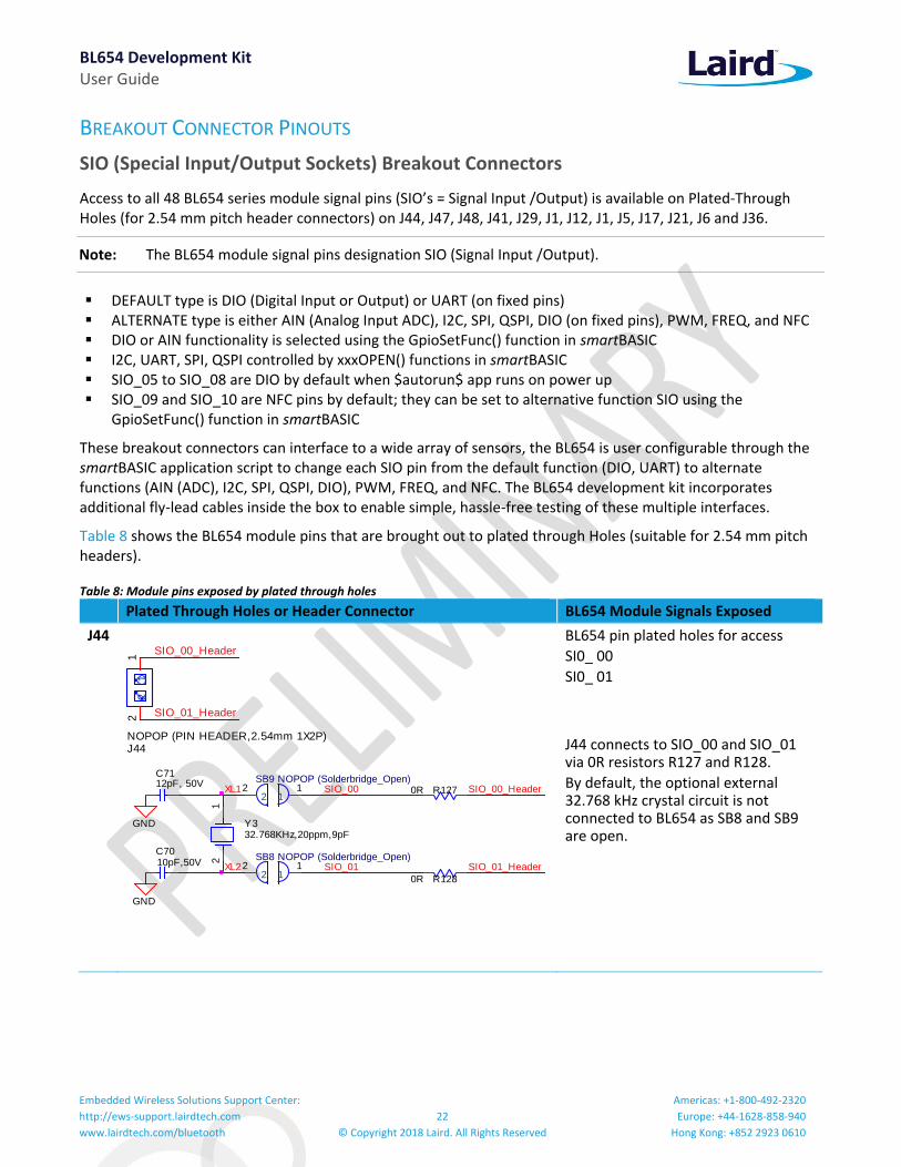
SIO (Special Input/Output Sockets) Breakout Connectors
Access to all 48 BL654 series module signal pins (SIO’s = Signal Input /Output) is available on Plated-Through Holes (for 2.54 mm pitch header connectors) on J44, J47, J48, J41, J29, J1, J12, J1, J5, J17, J21, J6 and J36.
Note: The BL654 module signal pins designation SIO (Signal Input /Output).
▪ DEFAULT type is DIO (Digital Input or Output) or UART (on fixed pins) ▪ ALTERNATE type is either AIN (Analog Input ADC), I2C, SPI, QSPI, DIO (on fixed pins), PWM, FREQ, and NFC ▪ DIO or AIN functionality is selected using the GpioSetFunc() function in smartBASIC ▪ I2C, UART, SPI, QSPI controlled by xxxOPEN() functions in smartBASIC ▪ SIO_05 to SIO_08 are DIO by default when $autorun$ app runs on power up ▪ SIO_09 and SIO_10 are NFC pins by default; they can be set to alternative function SIO using the
GpioSetFunc() function in smartBASIC
These breakout connectors can interface to a wide array of sensors, the BL654 is user configurable through the smartBASIC application script to change each SIO pin from the default function (DIO, UART) to alternate functions (AIN (ADC), I2C, SPI, QSPI, DIO), PWM, FREQ, and NFC. The BL654 development kit incorporates additional fly-lead cables inside the box to enable simple, hassle-free testing of these multiple interfaces.
Table 8 shows the BL654 module pins that are brought out to plated through Holes (suitable for 2.54 mm pitch headers).
Table 8: Module pins exposed by plated through holes
Plated Through Holes or Header Connector BL654 Module Signals Exposed
J44
BL654 pin plated holes for access
SI0_ 00
SI0_ 01
J44 connects to SIO_00 and SIO_01 via 0R resistors R127 and R128.
By default, the optional external 32.768 kHz crystal circuit is not connected to BL654 as SB8 and SB9 are open.
NOPOP (PIN HEADER,2.54mm 1X2P)J44
11
22
SIO_00_Header
SIO_01_Header
GND
R1270R
R1280R
SIO_00_Header
GND Y332.768KHz,20ppm,9pF
12
SIO_00XL1
SIO_01
C7010pF,50V
C7112pF, 50V
XL2 SIO_01_HeaderSB8 NOPOP (Solderbridge_Open)
11
22
SB9 NOPOP (Solderbridge_Open)
11
22
BL654 Development Kit User Guide
Embedded Wireless Solutions Support Center:
http://ews-support.lairdtech.com
www.lairdtech.com/bluetooth
23
© Copyright 2018 Laird. All Rights Reserved
Americas: +1-800-492-2320
Europe: +44-1628-858-940
Hong Kong: +852 2923 0610
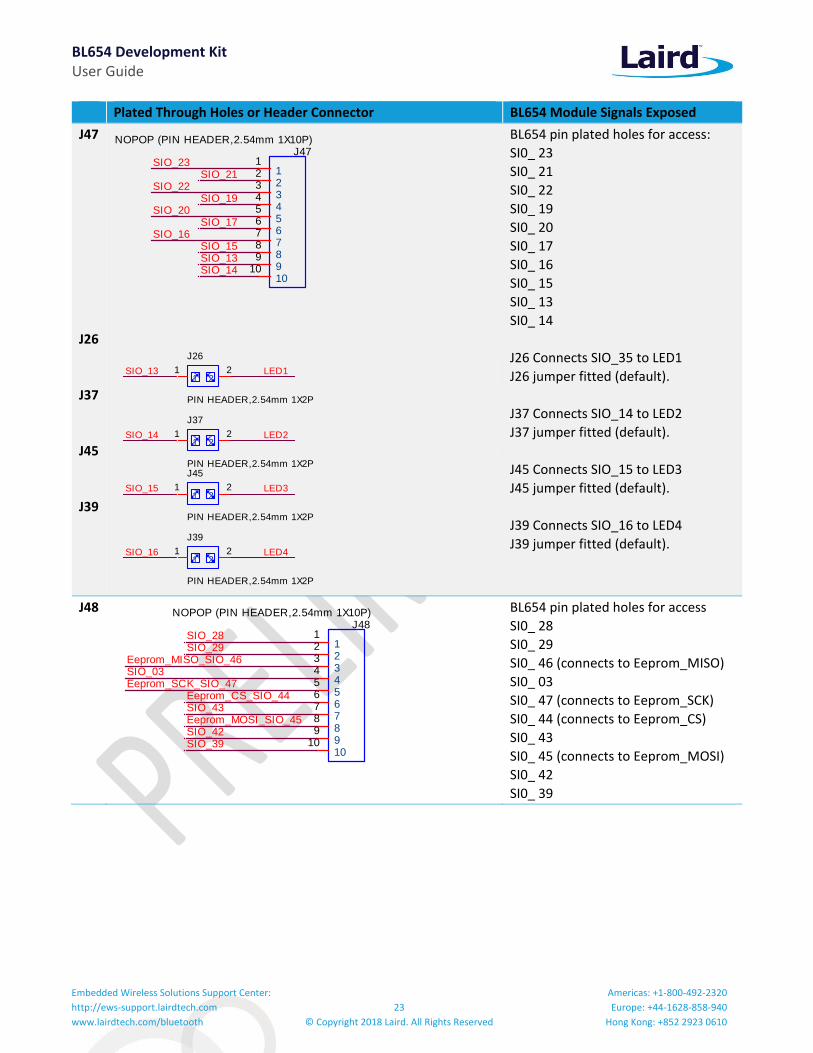
Plated Through Holes or Header Connector BL654 Module Signals Exposed
J47
J26
J37
J45
J39
BL654 pin plated holes for access:
SI0_ 23
SI0_ 21
SI0_ 22
SI0_ 19
SI0_ 20
SI0_ 17
SI0_ 16
SI0_ 15
SI0_ 13
SI0_ 14
J26 Connects SIO_35 to LED1
J26 jumper fitted (default).
J37 Connects SIO_14 to LED2
J37 jumper fitted (default).
J45 Connects SIO_15 to LED3
J45 jumper fitted (default).
J39 Connects SIO_16 to LED4
J39 jumper fitted (default).
J48
BL654 pin plated holes for access
SI0_ 28
SI0_ 29
SI0_ 46 (connects to Eeprom_MISO)
SI0_ 03
SI0_ 47 (connects to Eeprom_SCK)
SI0_ 44 (connects to Eeprom_CS)
SI0_ 43
SI0_ 45 (connects to Eeprom_MOSI)
SI0_ 42
SI0_ 39
SIO_23
SIO_14
SIO_15SIO_13
SIO_16
SIO_22
SIO_17
SIO_21
SIO_19SIO_20
J47NOPOP (PIN HEADER,2.54mm 1X10P)
11
22
33
44
55
66
77
88
99
1010
SIO_15
SIO_14
SIO_13
SIO_16
PIN HEADER,2.54mm 1X2P
J37
11
22 LED2
LED4
PIN HEADER,2.54mm 1X2P
J39
11
22
PIN HEADER,2.54mm 1X2P
J45
11
22 LED3
LED1
PIN HEADER,2.54mm 1X2P
J26
11
22
J48NOPOP (PIN HEADER,2.54mm 1X10P)
11
22
33
44
55
66
77
88
99
1010
SIO_03
SIO_29
Eeprom_MOSI_SIO_45
Eeprom_CS_SIO_44Eeprom_SCK_SIO_47
Eeprom_MISO_SIO_46
SIO_39SIO_42
SIO_43
SIO_28
BL654 Development Kit User Guide
Embedded Wireless Solutions Support Center:
http://ews-support.lairdtech.com
www.lairdtech.com/bluetooth
24
© Copyright 2018 Laird. All Rights Reserved
Americas: +1-800-492-2320
Europe: +44-1628-858-940
Hong Kong: +852 2923 0610
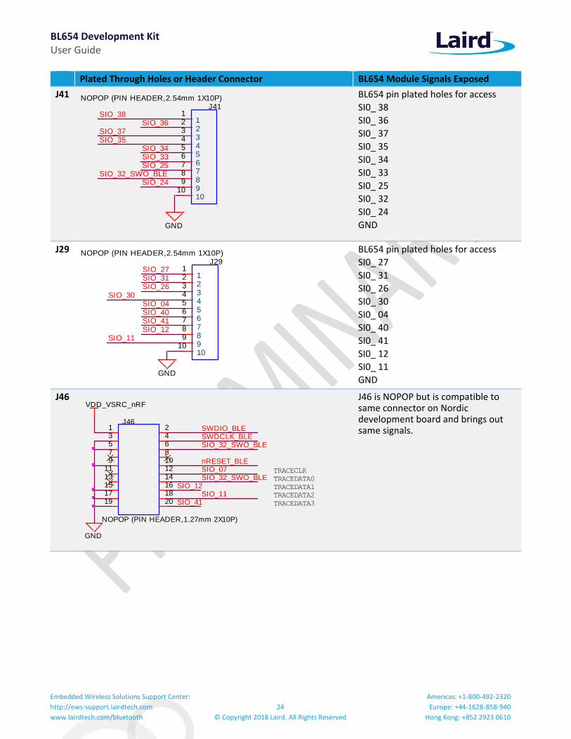
Plated Through Holes or Header Connector BL654 Module Signals Exposed
J41
BL654 pin plated holes for access
SI0_ 38
SI0_ 36
SI0_ 37
SI0_ 35
SI0_ 34
SI0_ 33
SI0_ 25
SI0_ 32
SI0_ 24
GND
J29
BL654 pin plated holes for access
SI0_ 27
SI0_ 31
SI0_ 26
SI0_ 30
SI0_ 04
SI0_ 40
SI0_ 41
SI0_ 12
SI0_ 11
GND
J46
J46 is NOPOP but is compatible to same connector on Nordic development board and brings out same signals.
SIO_38SIO_36
SIO_37
SIO_32_SWO_BLESIO_25SIO_33SIO_34
SIO_35
SIO_24
GND
J41NOPOP (PIN HEADER,2.54mm 1X10P)
11
22
33
44
55
66
77
88
99
1010
SIO_30SIO_04
GND
SIO_40SIO_41SIO_12
SIO_11
SIO_27
SIO_26
J29NOPOP (PIN HEADER,2.54mm 1X10P)
11
22
33
44
55
66
77
88
99
1010
SIO_31
VDD_VSRC_nRF
TRACEDATA3
TRACEDATA2
TRACEDATA1
TRACEDATA0
TRACECLK
GND
SWDCLK_BLESIO_32_SWO_BLE
SWDIO_BLE
SIO_11SIO_41
nRESET_BLESIO_07
SIO_12
J46
NOPOP (PIN HEADER,1.27mm 2X10P)
1 23 45 67 89 10
1113151719
1214161820
SIO_32_SWO_BLE
BL654 Development Kit User Guide
Embedded Wireless Solutions Support Center:
http://ews-support.lairdtech.com
www.lairdtech.com/bluetooth
25
© Copyright 2018 Laird. All Rights Reserved
Americas: +1-800-492-2320
Europe: +44-1628-858-940
Hong Kong: +852 2923 0610
Plated Through Holes or Header Connector BL654 Module Signals Exposed
J1
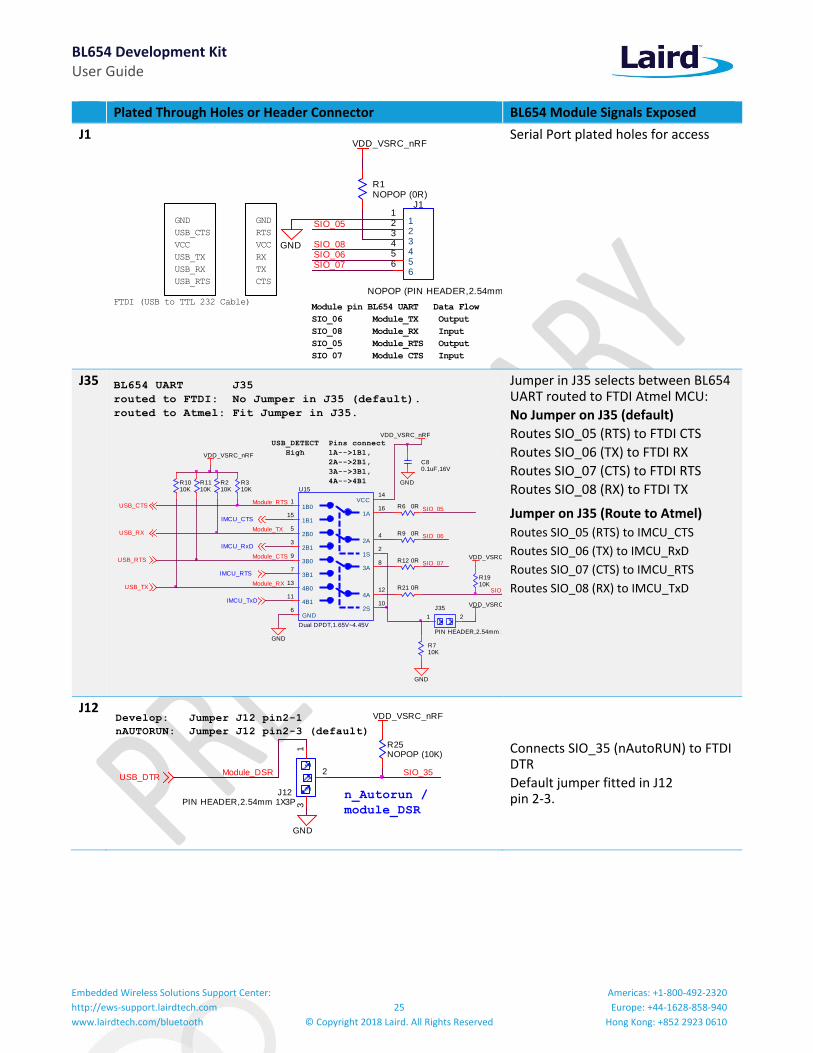
Serial Port plated holes for access
J35
Jumper in J35 selects between BL654 UART routed to FTDI Atmel MCU:
No Jumper on J35 (default)
Routes SIO_05 (RTS) to FTDI CTS
Routes SIO_06 (TX) to FTDI RX
Routes SIO_07 (CTS) to FTDI RTS
Routes SIO_08 (RX) to FTDI TX
Jumper on J35 (Route to Atmel)
Routes SIO_05 (RTS) to IMCU_CTS
Routes SIO_06 (TX) to IMCU_RxD
Routes SIO_07 (CTS) to IMCU_RTS
Routes SIO_08 (RX) to IMCU_TxD
J12
Connects SIO_35 (nAutoRUN) to FTDI DTR
Default jumper fitted in J12 pin 2-3.
SIO_06
R1NOPOP (0R)
Module pin BL654 UART Data Flow
SIO_06 Module_TX Output
SIO_08 Module_RX Input
SIO_05 Module_RTS Output
SIO_07 Module_CTS Input
SIO_07
SIO_08
VDD_VSRC_nRF
SIO_05
FTDI (USB to TTL 232 Cable)
GND
USB_CTS
VCC
USB_TX
USB_RX
USB_RTS
GND
RTS
VCC
RX
TX
CTS
J1
NOPOP (PIN HEADER,2.54mm 1X6P)
11
22
33
44
55
66
GND
BL654 UART J35
routed to FTDI: No Jumper in J35 (default).
routed to Atmel: Fit Jumper in J35.
IMCU_CTS
IMCU_RxD
C80.1uF,16V
GND
IMCU_RTS
IMCU_TxD
USB_CTS
Module_CTS
VDD_VSRC_nRF
R710K
R6 0R
R9 0R
R12 0R
R21 0R
USB_RX
R1910K
PIN HEADER,2.54mm 1X2P
J35
11
22
USB_DETECT Pins connect
High 1A-->1B1,
2A-->2B1,
3A-->3B1,
4A-->4B1
Module_RX
GND
SIO_08
VDD_VSRC_nRF
SIO_05
SIO_06
SIO_07VDD_VSRC_nRF
USB_TX
USB_RTS
VDD_VSRC_nRF
U15
Dual DPDT,1.65V~4.45V
1B01
1B115
2B05
2B13
1A16
2A4
1S2
3B09
3B17
4B013
4B111
3A8
4A12
2S10
GND6
VCC14
Module_RTS
Module_TX
R210K
GND
R310K
R1010K
R1110K
R25NOPOP (10K)
USB_DTR
GND
VDD_VSRC_nRF
PIN HEADER,2.54mm 1X3PJ12
11
22
33
n_Autorun /
module_DSR
Module_DSR
Develop: Jumper J12 pin2-1
nAUTORUN: Jumper J12 pin2-3 (default)
SIO_35
BL654 Development Kit User Guide
Embedded Wireless Solutions Support Center:
http://ews-support.lairdtech.com
www.lairdtech.com/bluetooth
26
© Copyright 2018 Laird. All Rights Reserved
Americas: +1-800-492-2320
Europe: +44-1628-858-940
Hong Kong: +852 2923 0610
Plated Through Holes or Header Connector BL654 Module Signals Exposed
J5
SIO_ 02 (for VSP capability)
Can be used to pull-up SIO_02 to VDD_nRF_SW
Default No Jumper fitted on J5 SIO_02
J17
J21
J17 Routes SIO_27 (I2C SCL) to RTC_SCL device
J17 pin 2-1 jumper NOT fitted (default).
J21 Routes SIO_26 (I2C_SDA) to RTC_SDA device
J21 pin 2-1 jumper NOT fitted (default).
J6
J6 routes SIO_03 to Temp Sensor
J6 pin 2-1 jumper NOT fitted (default)
J36
BL654 pin plated holes for access
SI0_ 09 via R100 0R (default NOPOP)
SI0_ 10 via R101 0R (default NOPOP)
To use NFC1 pin as SIO_09 fit R100 0R and NOPOP R98.
To use NFC1 pin as SIO_09 fit R101 0R and NOPOP R99.
Additional Peripherals/Sensors
The BL654 development board provides for simple and hassle-free connectivity to a wide range of sensors, but also includes several on-board sensors and options to enable a developer to test functionality straight out of the box.
In the smartBASIC application code written to use sensors on the development board, including the Temperature sensor (U1) – analog output, SPI EEPROM (U2), I2C RTC chip (U16), LED1(D1), LED2(D2), LED3(D3), LED4(D4) Button1(SW1), Button2(SW2), Button3(SW9) and Button4(SW10) the SIO pins direction and type must be set in the smartBASIC application to override the defaults in the BL654 firmware.
For more information on these sample applications, see GitHub smartBASIC sample applications repository on the BL654 product page at https://github.com/LairdCP/BL654-Applications.
VDD_nRF_SW
PIN HEADER,2.54mm 1X2P
J5
11
22
VSP on SIO_02
SIO_02
R14560R
R1080R
PIN HEADER,2.54mm 1X2PJ21
11
22
SIO_27
PIN HEADER,2.54mm 1X2PJ17
11
22
SIO_26
R1070R
RTC_SDARTC_SCL
SIO_03
PIN HEADER,2.54mm 1X2P
J6
11
22Temp_Sens
C53300pF,50VR100NOPOP (0R)
R101NOPOP (0R)C54300pF,50V
GND
PIN HEADER,2.54mm 1X2PJ36
11
22
GND
R98
0R
CON2
FFC/FPC,SMD/90d
11 22 33 44 55
GND6
GND7
NFC1_SIO_09
R99
0R
NFC2_SIO_10

BL654 Development Kit User Guide
Embedded Wireless Solutions Support Center:
http://ews-support.lairdtech.com
www.lairdtech.com/bluetooth
27
© Copyright 2018 Laird. All Rights Reserved
Americas: +1-800-492-2320
Europe: +44-1628-858-940
Hong Kong: +852 2923 0610
Temperature Sensor
The temperature sensor (U1) by default is connected to the BL654 module as jumper on J6 pin bridges TEMP_SENS and SIO_03.
Figure 13: Temperature sensor schematic and PCB
The on-board temperature sensor (TI LM20BIM7 - www.ti.com/lit/ds/symlink/lm20.pdf) has an analogue output that can be connected to BL654 module pin SIO_03; but since the LM20BIM7 has an analogue output, the BL654 module SIO_03 digital pin (DIO) must be configured as AIN analogue input (ADC). To configure the SIO_03 pin from DIO pin to Alternate function AIN, see the example file “ts.temperature.sensor.sb” in the GitHub smartBASIC sample applications repository on the BL654 product page at https://github.com/LairdCP/BL654-Applications
Key specifications of the LM20BIM7 are as follows in Table 9.
Table 9: LM20BIM7 Specifications
Output type Analogue output
Accuracy at 30ºC ±1.5ºC ±4ºC (max)
Accuracy at 40ºC to +85ºC approx. ±2.5ºC ±5ºC (max)
Power supply voltage range +2.4 V to 5.5 V
Current Drain 10 uA (max)
Output impedance 160 Ohms (max)
SIO_03
C20.1uF,16V
Analog output temp sensor
V+ 2.4V-3.6V
C30.1uF,16V
PIN HEADER,2.54mm 1X2P
J6
11
22
VCC_3V3
Temp_Sens
GND GNDGNDGND
R5NOPOP (4.7K)
U1
2.4V,10uA,-55dC~+130dC
V+4
GND5
Vo3
GND2
NC1
R4
470R,1%
BL654 Development Kit User Guide
Embedded Wireless Solutions Support Center:
http://ews-support.lairdtech.com
www.lairdtech.com/bluetooth
28
© Copyright 2018 Laird. All Rights Reserved
Americas: +1-800-492-2320
Europe: +44-1628-858-940
Hong Kong: +852 2923 0610
The LM20BIM7 datasheet states the relationship of Temperature (T) to Voltage output (Vo) can be approximated as a linear equation (for temperature range of -40ºC to +85ºC):
Vo(mV) = -11.67mV/ºC x T + 1858.3
gives the following calculated Vo versus temperature:
Table 10: LM20BIM7 Temperature to Voltage Output relationship
Temperature (T) Typical Voltage
+80ºC +924.7mV
+70ºC +1041.4mV
+60ºC +1158.1mV
+50ºC +1274.8mV
+40ºC +1391.5mV
+30ºC +1508.2mV
+20ºC +1624.9mV
+10ºC +1741.6mV
+0ºC +1858.2mV
-10ºC +1975.0mV
-20ºC +2091.7mV
-30ºC +2208.4mV
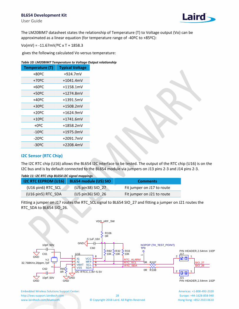
I2C Sensor (RTC Chip)
The I2C RTC chip (U16) allows the BL654 I2C interface to be tested. The output of the RTC chip (U16) is on the I2C bus and is by default connected to the BL654 module via jumpers on J13 pins 2-3 and J14 pins 2-3.
Table 11: I2C RTC chip BL654 I2C signal mappings
I2C RTC EEPROM (U16) BL654 module (U5) SIO Comments
(U16 pin6) RTC_SCL (U5 pin38) SIO_27 Fit jumper on J17 to route
(U16 pin5) RTC_SDA (U5 pin36) SIO_26 Fit jumper on J21 to route
Fitting a jumper on J17 routes the RTC_SCL signal to BL654 SIO_27 and fitting a jumper on J21 routes the RTC_SDA to BL654 SIO_26.
R810R
R3210K
VDD_nRF_SW
R3310K
R1080R
PIN HEADER,2.54mm 1X2PJ21
11
22
C61
10pF,50VTP9NOPOP (TH_TEST_POINT)
1
Y232.768KHz,20ppm,7pF
12
R1060R
R8210K
SIO_27
U16
I2C RTCC,1.8V~5.5V
X11
X22
VBAT3
VSS4
SDA5SCL6MFP7VCC8
PIN HEADER,2.54mm 1X2PJ17
11
22
C62
10pF,50V
C60
0.1uF,16V
SIO_26
R1070R
GNDGND
GND
GNDRTC_ALARM
GND
RTC_SDARTC_SCL
BL654 Development Kit User Guide
Embedded Wireless Solutions Support Center:
http://ews-support.lairdtech.com
www.lairdtech.com/bluetooth
29
© Copyright 2018 Laird. All Rights Reserved
Americas: +1-800-492-2320
Europe: +44-1628-858-940
Hong Kong: +852 2923 0610
Figure 14: I2C device RTC chip schematic and PCB
To test the BL654 I2C interface, use smartBASIC application rtcs.erver.sb in the GitHub smartBASIC sample application repository on the BL654 product page at https://github.com/LairdCP/BL654-Applications. This application runs on the BL654 and can be used with an Android phone (requires an app such as nRF connect, https://play.google.com/store/apps/details?id=no.nordicsemi.android.mcp&hl=en_GB) or another BT900/BL620/BL652/BL654 loaded with “rtcc.lient.sb”.
The smartBASIC application “rtcs.erver.sb” is a BLE RTC server, and it advertises the current time (which it gets from the I2C RTC chip (U4)).
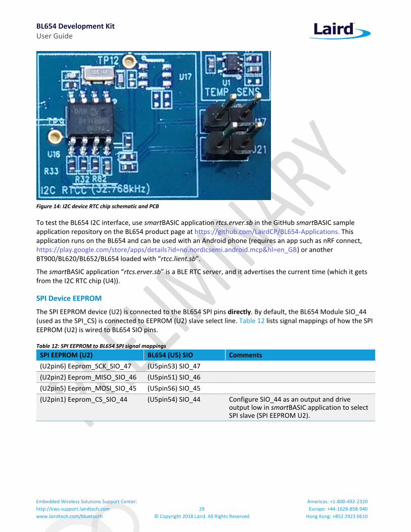
SPI Device EEPROM
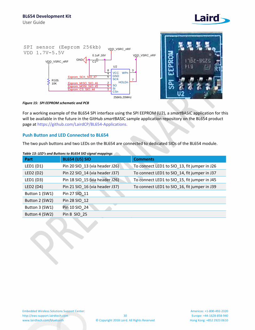
The SPI EEPROM device (U2) is connected to the BL654 SPI pins directly. By default, the BL654 Module SIO_44 (used as the SPI_CS) is connected to EEPROM (U2) slave select line. Table 12 lists signal mappings of how the SPI EEPROM (U2) is wired to BL654 SIO pins.
Table 12: SPI EEPROM to BL654 SPI signal mappings
SPI EEPROM (U2) BL654 (U5) SIO Comments
(U2pin6) Eeprom_SCK_SIO_47 (U5pin53) SIO_47
(U2pin2) Eeprom_MISO_SIO_46 (U5pin51) SIO_46
(U2pin5) Eeprom_MOSI_SIO_45 (U5pin56) SIO_45
(U2pin1) Eeprom_CS_SIO_44 (U5pin54) SIO_44 Configure SIO_44 as an output and drive output low in smartBASIC application to select SPI slave (SPI EEPROM U2).
BL654 Development Kit User Guide
Embedded Wireless Solutions Support Center:
http://ews-support.lairdtech.com
www.lairdtech.com/bluetooth
30
© Copyright 2018 Laird. All Rights Reserved
Americas: +1-800-492-2320
Europe: +44-1628-858-940
Hong Kong: +852 2923 0610
Figure 15: SPI EEPROM schematic and PCB
For a working example of the BL654 SPI interface using the SPI EEPROM (U2), a smartBASIC application for this will be available in the future in the GitHub smartBASIC sample application repository on the BL654 product page at https://github.com/LairdCP/BL654-Applications.
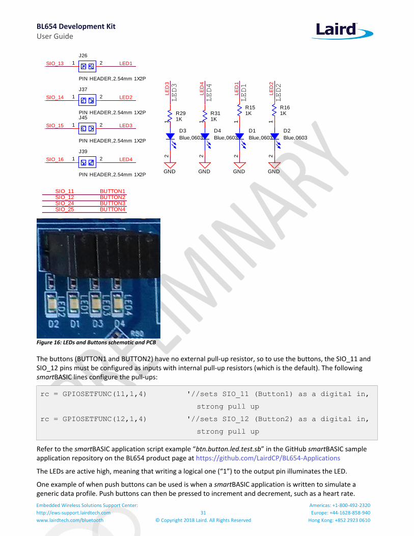
Push Button and LED Connected to BL654
The two push buttons and two LEDs on the BL654 are connected to dedicated SIOs of the BL654 module.
Table 13: LED’s and Buttons to BL654 SIO signal mappings
Part BL654 (U5) SIO Comments
LED1 (D1) Pin 20 SIO_13 (via header J26) To connect LED1 to SIO_13, fit jumper in J26
LED2 (D2) Pin 22 SIO_14 (via header J37) To connect LED1 to SIO_14, fit jumper in J37
LED1 (D3) Pin 18 SIO_15 (via header J26) To connect LED1 to SIO_15, fit jumper in J45
LED2 (D4) Pin 21 SIO_16 (via header J37) To connect LED1 to SIO_16, fit jumper in J39
Button 1 (SW1) Pin 27 SIO_11
Button 2 (SW2) Pin 28 SIO_12
Button 3 (SW1) Pin 10 SIO_24
Button 4 (SW2) Pin 8 SIO_25
Eeprom_MISO_SIO_46
VDD_VSRC_nRF
R10510K
U2
256Kb,20MHz
CSn1
SO2
WPn3
GND4
SI5
SCK6
HOLDn7
VCC8
Eeprom_MOSI_SIO_45Eeprom_CS_SIO_44
C1
0.1uF,16V
VDD_VSRC_nRF
VDD_VSRC_nRF
Eeprom_SCK_SIO_47
GND
SPI sensor (Eeprom 256kb)
VDD 1.7V-5.5V
BL654 Development Kit User Guide
Embedded Wireless Solutions Support Center:
http://ews-support.lairdtech.com
www.lairdtech.com/bluetooth
31
© Copyright 2018 Laird. All Rights Reserved
Americas: +1-800-492-2320
Europe: +44-1628-858-940
Hong Kong: +852 2923 0610
Figure 16: LEDs and Buttons schematic and PCB
The buttons (BUTTON1 and BUTTON2) have no external pull-up resistor, so to use the buttons, the SIO_11 and SIO_12 pins must be configured as inputs with internal pull-up resistors (which is the default). The following smartBASIC lines configure the pull-ups:
rc = GPIOSETFUNC(11,1,4) '//sets SIO_11 (Button1) as a digital in,
strong pull up
rc = GPIOSETFUNC(12,1,4) '//sets SIO_12 (Button2) as a digital in,
strong pull up
Refer to the smartBASIC application script example “btn.button.led.test.sb” in the GitHub smartBASIC sample application repository on the BL654 product page at https://github.com/LairdCP/BL654-Applications
The LEDs are active high, meaning that writing a logical one (“1”) to the output pin illuminates the LED.
One example of when push buttons can be used is when a smartBASIC application is written to simulate a generic data profile. Push buttons can then be pressed to increment and decrement, such as a heart rate.
SIO_15
SIO_14
SIO_13
SIO_16
PIN HEADER,2.54mm 1X2P
J37
11
22 LED2
LED4
PIN HEADER,2.54mm 1X2P
J39
11
22
PIN HEADER,2.54mm 1X2P
J45
11
22 LED3
LED1
PIN HEADER,2.54mm 1X2P
J26
11
22
LED3
GNDL
ED
3
R291K
D3
Blue,0603
12
LED4
GND
LE
D4
D4
Blue,0603
12
R311K
GND
LE
D1
R151K
LED1
D1
Blue,0603
12
GND
LE
D2
R161K
LED2
D2
Blue,0603
12
BUTTON4SIO_25BUTTON3SIO_24
SIO_11 BUTTON1SIO_12 BUTTON2
BL654 Development Kit User Guide
Embedded Wireless Solutions Support Center:
http://ews-support.lairdtech.com
www.lairdtech.com/bluetooth
32
© Copyright 2018 Laird. All Rights Reserved
Americas: +1-800-492-2320
Europe: +44-1628-858-940
Hong Kong: +852 2923 0610
NFC External Antenna Connector and NFC Antenna RF Matching Circuit
The NFC antenna input connector (CON2) allows the Laird supplied flex-PCB NFC antenna to be plugged in. The BL654 module NFC circuit uses two pins, pin 59 (NFC1/SIO_9) and pin 57 (NFC2/SIO_10) to connect the antenna. These pins are shared with GPIOs (SIO.09 and SIO.10). BL654 NFC pins are enabled by default. NFC can be disabled via smartBASIC application. Pin 59 (NFC1/SIO_9) and pin 57 (NFC2/SIO_10) are configured by default on the development board schematic to use NFC antenna, but if pin 59 (NFC1/SIO_9) and pin 57 (NFC2/SIO_10) are needed as normal GPIOs, R98 and R99 must be removed and R100 and R101 must be shorted by 0R.
C53 (300pF) and C54 (300pF) are RF tuning elements for the flexi-PCB NFC antenna.
Table 14: NFC input BL654 SIO signal mappings
BL654 (U5) SIO Bring out SIO_9 and SIO_10 to NFC antenna connector (CON2)
Bring out SIO_9 and SIO_10
to Header connector (J36)
pin 59 (NFC1/SIO_9) Fit R98 0R (default)
Remove R100 0R (default)
Remove R98 0R
Fit R100 0R
pin 57 (NFC2/SIO_10) Fit R99 0R (default)
Remove R101 0R (default)
Remove R99 0R
Fit R101 with 0R
Figure 17: NFC antenna RF matching circuit, NFC antenna connector schematic and NFC plugged in to connector CON2
C53300pF,50VR100NOPOP (0R)
R101NOPOP (0R)C54300pF,50V
GND
PIN HEADER,2.54mm 1X2PJ36
11
22
GND
R98
0R
CON2
FFC/FPC,SMD/90d
11 22 33 44 55
GND6
GND7
NFC1_SIO_09
R99
0R
NFC2_SIO_10

BL654 Development Kit User Guide
Embedded Wireless Solutions Support Center:
http://ews-support.lairdtech.com
www.lairdtech.com/bluetooth
33
© Copyright 2018 Laird. All Rights Reserved
Americas: +1-800-492-2320
Europe: +44-1628-858-940
Hong Kong: +852 2923 0610
The smartBASIC application nfc.all.launch.sb in the GitHub smartBASIC sample application repository on the BL654 product page at https://github.com/LairdCP/BL654-Applications exercises the following over the BL654 NFC:
▪ On Android NFC enabled devices – Opens the Laird toolkit application or shows it in the Google Play store if it's not installed
▪ On Windows NFC enabled devices – Opens the calculator ▪ On other NFC enabled devices – Shows the Laird website or text saying this is a BL654
Optional External Serial QSPI Flash IC
There is an optional external serial QSPI flash IC (U18) that may be used, for example, for data logging purposes. U18 can also capable of SPI mode.
Solder bridges SB4, SB5, SB6, SB7, SB10 and SB11 must individually be shorted to connect this optional external serial (QSPI) flash (U18 to the BL654 module).
By default, these BL644 pins are GPIO pins.
Figure 18: Optional external serial SPI flash IC (U18) schematic and PCB
Table 15 shows the U18 pin mapping to BL654 SIO pin mapping (via open solder bridges).
Table 15: U18 SPI or QSPI flashc IC pin mapping to BL654 GPIO mappings
BL654 Pin (Pin Name) U18 Pin (QSPI flash IC)
and Pin Name Via Open Solder bridge
Pin 16 (SIO_17/QSPI_CS) Pin 1 CS#
SB7 BL654 Dev board R126 10K pull-up on,
therefore by default, device not selected. Drive from BL654 line low to select.
Pin 14 (SIO_19/QSPI_CLK) Pin 6 SCLK SB4
Pin 13 (SIO_20/QSPI_DIO0) Pin 5 SIO_0/SI SB5
SB5 NOPOP (Solderbridge_Open)
11
22
SB11NOPOP (Solderbridge_Open)
11
22
GND
QSPI_CLKSB4 NOPOP (Solderbridge_Open)
11
22
SB10 NOPOP (Solderbridge_Open)
11
22
QSPI_DIO3
SIO_22SIO_20
SIO_19
SIO_23
GND
QSPI_DIO2
VDD_VSRC_nRF VDD_VSRC_nRF
QSPI_DIO0
R12610K
QSPI_CS#QSPI_DIO1
U184Mx1,SPI,1.65~3.6V
CS#1
SO/SIO12
WP#3
GND4
SI/SIO05CLK6HOLD#7VCC8
GN
D9
SB6NOPOP (Solderbridge_Open)
11
22
SB7NOPOP (Solderbridge_Open)
11
22SIO_17
SIO_21
C50.1uF,16V
GND
BL654 Development Kit User Guide
Embedded Wireless Solutions Support Center:
http://ews-support.lairdtech.com
www.lairdtech.com/bluetooth
34
© Copyright 2018 Laird. All Rights Reserved
Americas: +1-800-492-2320
Europe: +44-1628-858-940
Hong Kong: +852 2923 0610
BL654 Pin (Pin Name) U18 Pin (QSPI flash IC)
and Pin Name Via Open Solder bridge
Pin 12 (SIO_21/QSPI_DIO1) Pin 2 SIO_1/SO SB6
Pin 11 (SIO_22/QSPI_DIO2) Pin 3 SIO_2/WP# SB11
Pin 9 (SIO_23/QSPI_DIO3) Pin 7 SIO_3/HOLD# SB10
The smartBASIC application for this external optional serial QSPI flash IC will be available in the future in the GitHub smartBASIC sample application repository on the BL654 product page at https://github.com/LairdCP/BL654-Applications
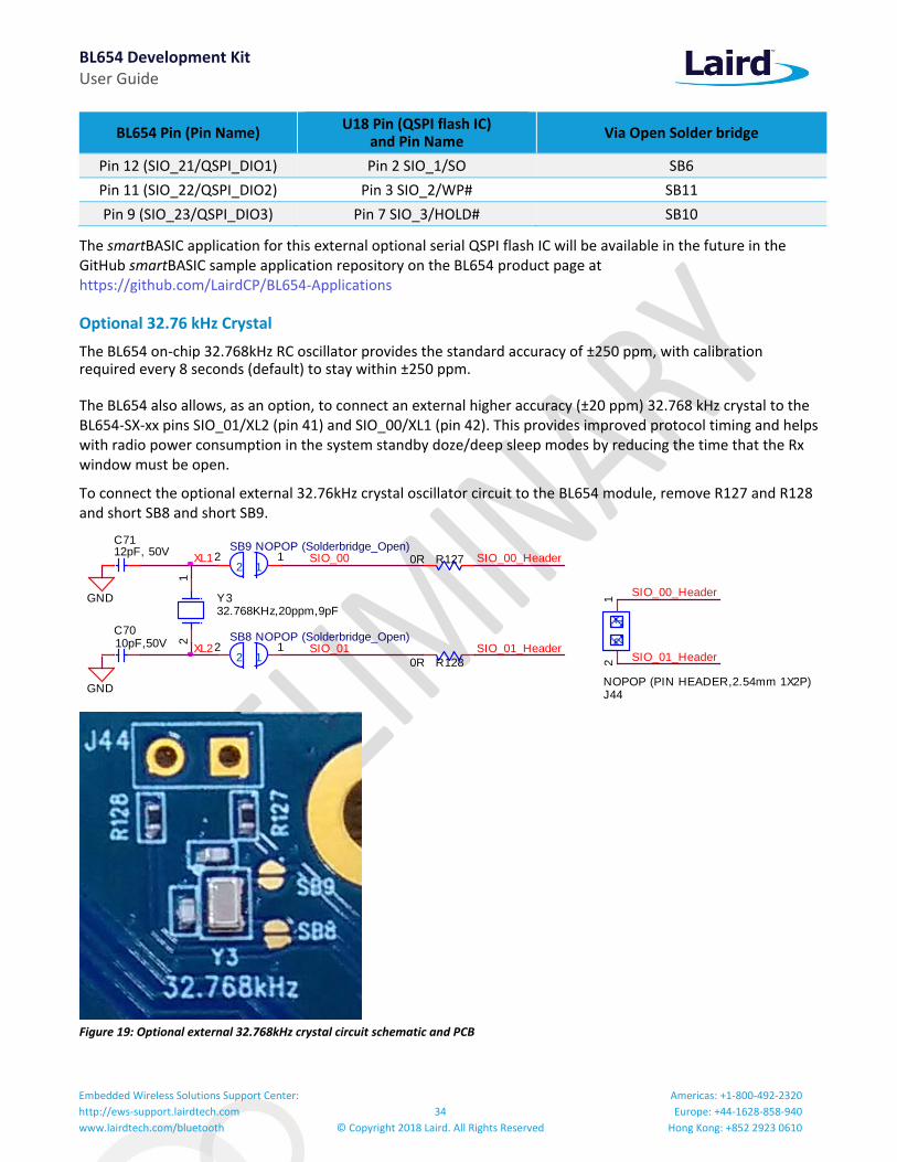
Optional 32.76 kHz Crystal
The BL654 on-chip 32.768kHz RC oscillator provides the standard accuracy of ±250 ppm, with calibration required every 8 seconds (default) to stay within ±250 ppm.
The BL654 also allows, as an option, to connect an external higher accuracy (±20 ppm) 32.768 kHz crystal to the BL654-SX-xx pins SIO_01/XL2 (pin 41) and SIO_00/XL1 (pin 42). This provides improved protocol timing and helps with radio power consumption in the system standby doze/deep sleep modes by reducing the time that the Rx window must be open.
To connect the optional external 32.76kHz crystal oscillator circuit to the BL654 module, remove R127 and R128 and short SB8 and short SB9.
Figure 19: Optional external 32.768kHz crystal circuit schematic and PCB
GND
R1270R
R1280R
SIO_00_Header
GND Y332.768KHz,20ppm,9pF
12
SIO_00XL1
SIO_01
C7010pF,50V
C7112pF, 50V
XL2 SIO_01_HeaderSB8 NOPOP (Solderbridge_Open)
11
22
SB9 NOPOP (Solderbridge_Open)
11
22
NOPOP (PIN HEADER,2.54mm 1X2P)J44
11
22
SIO_00_Header
SIO_01_Header
BL654 Development Kit User Guide
Embedded Wireless Solutions Support Center:
http://ews-support.lairdtech.com
www.lairdtech.com/bluetooth
35
© Copyright 2018 Laird. All Rights Reserved
Americas: +1-800-492-2320
Europe: +44-1628-858-940
Hong Kong: +852 2923 0610
A smartBASIC application will be available in the future in the GitHub smartBASIC sample application repository on the BL654 product page at http://www.lairdtech.com/products/bl654-ble-thread-nfc-modules.
OTHER FEATURES
Current Consumption Measurement
A removable jumper (on J7 and J9) is provided to break the power supply line directly to the module, allowing you to measure current consumption. For normal operation, the jumper on J7 (and J9) between pin1 and pin2 must be fitted (and is fitted by default).
IMPORTANT: To achieve the optimal power consumption of the BL654 series module on the development board, see the “lp.low.power.deep.sleep.sb” file in the GitHub smartBASIC sample application repository on the BL654 product page at https://github.com/LairdCP/BL654-Applications
Note: This measures the current consumption of the BL654 series module ONLY.
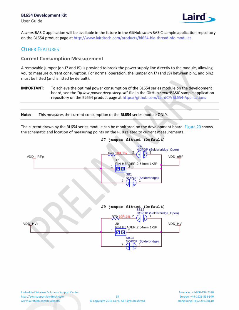
The current drawn by the BL654 series module can be monitored on the development board. Figure 20 shows the schematic and location of measuring points on the PCB related to current measurements.
R79 10R,1%
SB13NOPOP (Solderbridge)
11
22
PIN HEADER,2.54mm 1X2PJ9
11
22
VDD_HV
SB1NOPOP (Solderbridge)
11
22
VDD_HVp
VDD_nRFp
SB2NOPOP (Solderbridge_Open)
11
22
J7 jumper fitted (Default)
R76 10R,1%
PIN HEADER,2.54mm 1X2PJ7
11
22
VDD_nRF
J9 jumper fitted (Default)SB12NOPOP (Solderbridge_Open)
11
22
BL654 Development Kit User Guide
Embedded Wireless Solutions Support Center:
http://ews-support.lairdtech.com
www.lairdtech.com/bluetooth
36
© Copyright 2018 Laird. All Rights Reserved
Americas: +1-800-492-2320
Europe: +44-1628-858-940
Hong Kong: +852 2923 0610
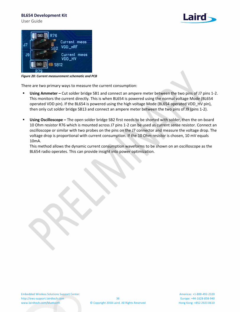
Figure 20: Current measurement schematic and PCB
There are two primary ways to measure the current consumption:
▪ Using Ammeter – Cut solder bridge SB1 and connect an ampere meter between the two pins of J7 pins 1-2. This monitors the current directly. This is when BL654 is powered using the normal voltage Mode (BL654 operated VDD pin). If the BL654 is powered using the high voltage Mode (BL654 operated VDD_HV pin), then only cut solder bridge SB13 and connect an ampere meter between the two pins of J9 (pins 1-2).
▪ Using Oscilloscope – The open solder bridge SB2 first needs to be shorted with solder, then the on-board 10 Ohm resistor R76 which is mounted across J7 pins 1-2 can be used as current sense resistor. Connect an oscilloscope or similar with two probes on the pins on the J7 connector and measure the voltage drop. The voltage drop is proportional with current consumption. If the 10 Ohm resistor is chosen, 10 mV equals 10mA. This method allows the dynamic current consumption waveforms to be shown on an oscilloscope as the BL654 radio operates. This can provide insight into power optimization.
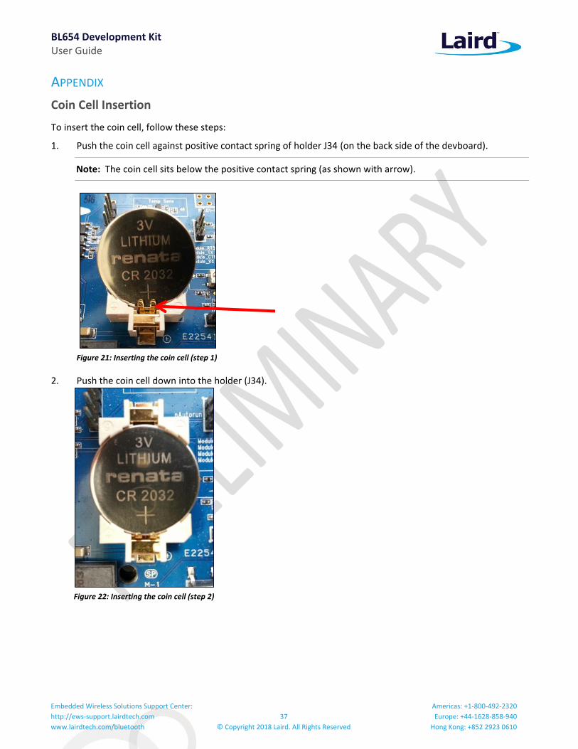
BL654 Development Kit User Guide
Embedded Wireless Solutions Support Center:
http://ews-support.lairdtech.com
www.lairdtech.com/bluetooth
37
© Copyright 2018 Laird. All Rights Reserved
Americas: +1-800-492-2320
Europe: +44-1628-858-940
Hong Kong: +852 2923 0610
APPENDIX
Coin Cell Insertion
To insert the coin cell, follow these steps:
1. Push the coin cell against positive contact spring of holder J34 (on the back side of the devboard).
Note: The coin cell sits below the positive contact spring (as shown with arrow).
Figure 21: Inserting the coin cell (step 1)
2. Push the coin cell down into the holder (J34).
Figure 22: Inserting the coin cell (step 2)
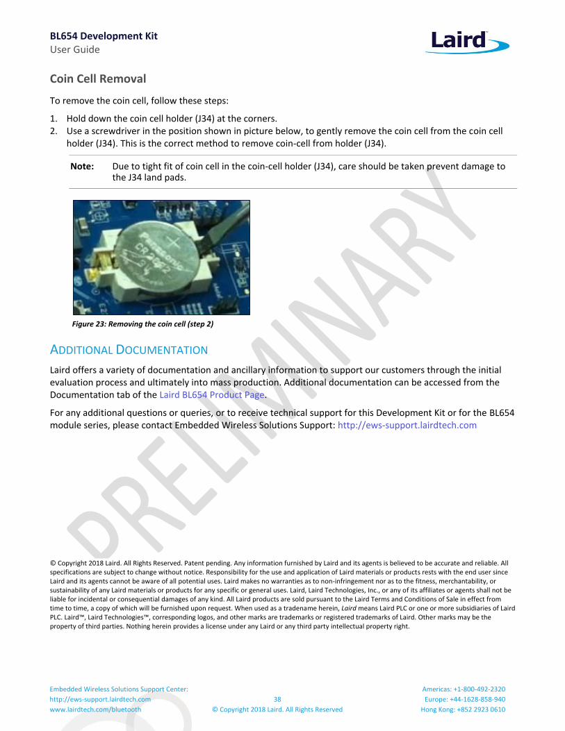
BL654 Development Kit User Guide
Embedded Wireless Solutions Support Center:
http://ews-support.lairdtech.com
www.lairdtech.com/bluetooth
38
© Copyright 2018 Laird. All Rights Reserved
Americas: +1-800-492-2320
Europe: +44-1628-858-940
Hong Kong: +852 2923 0610
Coin Cell Removal
To remove the coin cell, follow these steps:
1. Hold down the coin cell holder (J34) at the corners. 2. Use a screwdriver in the position shown in picture below, to gently remove the coin cell from the coin cell
holder (J34). This is the correct method to remove coin-cell from holder (J34).
Note: Due to tight fit of coin cell in the coin-cell holder (J34), care should be taken prevent damage to the J34 land pads.
Figure 23: Removing the coin cell (step 2)
ADDITIONAL DOCUMENTATION
Laird offers a variety of documentation and ancillary information to support our customers through the initial evaluation process and ultimately into mass production. Additional documentation can be accessed from the Documentation tab of the Laird BL654 Product Page.
For any additional questions or queries, or to receive technical support for this Development Kit or for the BL654 module series, please contact Embedded Wireless Solutions Support: http://ews-support.lairdtech.com
© Copyright 2018 Laird. All Rights Reserved. Patent pending. Any information furnished by Laird and its agents is believed to be accurate and reliable. All specifications are subject to change without notice. Responsibility for the use and application of Laird materials or products rests with the end user since Laird and its agents cannot be aware of all potential uses. Laird makes no warranties as to non-infringement nor as to the fitness, merchantability, or sustainability of any Laird materials or products for any specific or general uses. Laird, Laird Technologies, Inc., or any of its affiliates or agents shall not be liable for incidental or consequential damages of any kind. All Laird products are sold pursuant to the Laird Terms and Conditions of Sale in effect from time to time, a copy of which will be furnished upon request. When used as a tradename herein, Laird means Laird PLC or one or more subsidiaries of Laird PLC. Laird™, Laird Technologies™, corresponding logos, and other marks are trademarks or registered trademarks of Laird. Other marks may be the property of third parties. Nothing herein provides a license under any Laird or any third party intellectual property right.