Uncovering Thermal and Electrical Properties of Sb2Te3 ...
23
1 Uncovering Thermal and Electrical Properties of Sb2Te3/GeTe Superlattice Films Heungdong Kwon 1 , Asir Intisar Khan 2 , Christopher Perez 1 , Mehdi Asheghi 1 , Eric Pop 2,3 , Kenneth E. Goodson 1,3,* 1 Dept. of Mechanical Eng., Stanford University, Stanford, CA 94305, U.S.A. 2 Dept. of Electrical Eng., Stanford University, Stanford, CA 94305, U.S.A. 3 Dept. of Materials Science & Eng., Stanford University, Stanford, CA 94305, U.S.A. * E-mail: [email protected] ABSTRACT: Superlattice-like phase change memory (SL-PCM) promises lower switching current than conventional PCM based on Ge2Sb2Te5 (GST). However, a fundamental understanding of SL-PCM requires detailed characterization of the interfaces within such a SL. Here, we explore the electrical and thermal transport of SLs with deposited Sb2Te3 and GeTe alternating layers of various thicknesses. We find up to ~4× reduction of the effective cross-plane thermal conductivity of the SL stack (as-deposited polycrystalline) compared to polycrystalline GST (as-deposited amorphous and later annealed) due to the thermal interface resistances within the SL. Thermal measurements with varying periods of our SLs show a signature of phonon coherence with a transition from wave-like to particle-like phonon transport, further described by our modeling. Electrical resistivity measurements of such SLs reveal strong anisotropy (~2000×) between the in-plane and cross-plane directions due to the weakly interacting van der Waals gaps. This work uncovers electro-thermal transport in SLs based on Sb2Te3 and GeTe, for improved design of low-power PCM. KEYWORDS: Sb2Te3/GeTe superlattice, time-domain thermoreflectance, thermal conductivity, electrical resistivity, anisotropy In recent years, there has been a large and growing interest in new materials for new data storage opportunities. These opportunities are driven in equal parts by growing memory demands of artificial intelligence applications, and by shortcomings of existing memory technologies such as flash (non-volatile, but relatively slow) and DRAM (fast, but volatile). 1,2 In this context, phase change memory (PCM) has become a key emerging technology, 3 with Intel and Micron jointly introducing a commercial PCM-based product called 3D X-point in 2017. However, PCM improvements remain necessary, including reduction of resistance drift, higher endurance, and lower switching current density, ideally < 1 MA cm -2 . Several recent studies have suggested that replacing the phase-change material (conventionally Ge2Sb2Te5, i.e. GST) with a superlattice (SL) of alternating thin chalcogenide films (e.g., Sb2Te3 and GeTe) could offer lower switching power, faster switching speed, and higher endurance. 4,5 Interestingly, the fundamental operation of SL- PCM is not well understood. It was initially proposed that its memory states are controlled at the internal interfaces by subtle changes in the position of Ge atoms in multi-layered Sb2Te3/GeTe films. 6 However, the broader influence
-
Upload
khangminh22 -
Category
Documents
-
view
1 -
download
0
Transcript of Uncovering Thermal and Electrical Properties of Sb2Te3 ...

1
Uncovering Thermal and Electrical Properties of Sb2Te3/GeTe Superlattice Films
Heungdong Kwon1, Asir Intisar Khan2, Christopher Perez1, Mehdi Asheghi1, Eric Pop2,3, Kenneth E. Goodson1,3,* 1Dept. of Mechanical Eng., Stanford University, Stanford, CA 94305, U.S.A. 2Dept. of Electrical Eng., Stanford University, Stanford, CA 94305, U.S.A. 3Dept. of Materials Science & Eng., Stanford University, Stanford, CA 94305, U.S.A.
*E-mail: [email protected]
ABSTRACT: Superlattice-like phase change memory (SL-PCM) promises lower switching current than
conventional PCM based on Ge2Sb2Te5 (GST). However, a fundamental understanding of SL-PCM requires
detailed characterization of the interfaces within such a SL. Here, we explore the electrical and thermal
transport of SLs with deposited Sb2Te3 and GeTe alternating layers of various thicknesses. We find up to ~4×
reduction of the effective cross-plane thermal conductivity of the SL stack (as-deposited polycrystalline)
compared to polycrystalline GST (as-deposited amorphous and later annealed) due to the thermal interface
resistances within the SL. Thermal measurements with varying periods of our SLs show a signature of
phonon coherence with a transition from wave-like to particle-like phonon transport, further described by
our modeling. Electrical resistivity measurements of such SLs reveal strong anisotropy (~2000×) between the
in-plane and cross-plane directions due to the weakly interacting van der Waals gaps. This work uncovers
electro-thermal transport in SLs based on Sb2Te3 and GeTe, for improved design of low-power PCM.
KEYWORDS: Sb2Te3/GeTe superlattice, time-domain thermoreflectance, thermal conductivity, electrical
resistivity, anisotropy
In recent years, there has been a large and growing interest in new materials for new data storage opportunities.
These opportunities are driven in equal parts by growing memory demands of artificial intelligence applications,
and by shortcomings of existing memory technologies such as flash (non-volatile, but relatively slow) and DRAM
(fast, but volatile).1,2 In this context, phase change memory (PCM) has become a key emerging technology,3 with
Intel and Micron jointly introducing a commercial PCM-based product called 3D X-point in 2017. However, PCM
improvements remain necessary, including reduction of resistance drift, higher endurance, and lower switching
current density, ideally < 1 MA cm-2.
Several recent studies have suggested that replacing the phase-change material (conventionally Ge2Sb2Te5, i.e.
GST) with a superlattice (SL) of alternating thin chalcogenide films (e.g., Sb2Te3 and GeTe) could offer lower
switching power, faster switching speed, and higher endurance.4,5 Interestingly, the fundamental operation of SL-
PCM is not well understood. It was initially proposed that its memory states are controlled at the internal interfaces
by subtle changes in the position of Ge atoms in multi-layered Sb2Te3/GeTe films.6 However, the broader influence
2
of internal interfaces on electrical and thermal transport in SL-PCM remains poorly understood, especially when
considering that conventional PCM is driven by a thermally-induced phase change mechanism. In addition, the
complex physics of energy and charge transport at these interfaces also presents an opportunity to better understand
the mechanism of SL-PCM device switching.
In the past, both our groups and others have demonstrated the benefits of thermal engineering of PCMs (e.g. by
increasing their thermal resistance) by introducing multi-layer dielectric insulation,7-9 graphene,10 MoS2,11 and other
interface layers12,13 to reduce the switching current and power density. The influence of PCM interfaces and of
ballistic heat flow14 are only expected to become magnified in ultrathin nanoscale films and devices, and particularly
in SL structures which have numerous internal interfaces.15 In fact, recent results suggest that the low switching
current in SL-PCM could be thermally driven due to the thermal resistance of interfaces within the PCM stack.14,16
Motivated by the need for a deeper understanding of SL-PCM materials, here we report the thermal and electrical
transport characterization of Sb2Te3/GeTe SLs by measuring their temperature- and period-dependent cross-plane
thermal conductivity. These measurements uncover a minimum thermal conductivity and a transition from coherent,
wave-like phonon transport to quasi-ballistic phonon transport around the 3/1 nm/nm period. Thickness-dependent
measurements also reveal the thermal boundary resistance between SL-PCM and TiN, a typical PCM electrode
material. Finally, we report electrical resistivity measurements of 4/1 nm/nm Sb2Te3/GeTe SLs, revealing a strong,
nearly 2000-fold anisotropy between the cross-plane and in-plane directions.
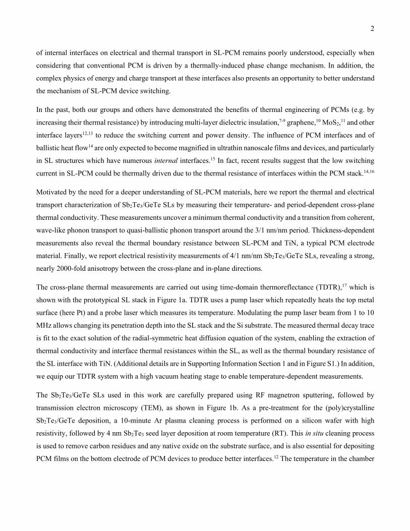
The cross-plane thermal measurements are carried out using time-domain thermoreflectance (TDTR),17 which is
shown with the prototypical SL stack in Figure 1a. TDTR uses a pump laser which repeatedly heats the top metal
surface (here Pt) and a probe laser which measures its temperature. Modulating the pump laser beam from 1 to 10
MHz allows changing its penetration depth into the SL stack and the Si substrate. The measured thermal decay trace
is fit to the exact solution of the radial-symmetric heat diffusion equation of the system, enabling the extraction of
thermal conductivity and interface thermal resistances within the SL, as well as the thermal boundary resistance of
the SL interface with TiN. (Additional details are in Supporting Information Section 1 and in Figure S1.) In addition,
we equip our TDTR system with a high vacuum heating stage to enable temperature-dependent measurements.
The Sb2Te3/GeTe SLs used in this work are carefully prepared using RF magnetron sputtering, followed by
transmission electron microscopy (TEM), as shown in Figure 1b. As a pre-treatment for the (poly)crystalline
Sb2Te3/GeTe deposition, a 10-minute Ar plasma cleaning process is performed on a silicon wafer with high
resistivity, followed by 4 nm Sb2Te3 seed layer deposition at room temperature (RT). This in situ cleaning process
is used to remove carbon residues and any native oxide on the substrate surface, and is also essential for depositing
PCM films on the bottom electrode of PCM devices to produce better interfaces.12 The temperature in the chamber
3
is then elevated to 180 °C without breaking vacuum and the alternating multilayers of GeTe and Sb2Te3 are
deposited at a pressure of 4 mTorr.
The cross-sectional high-angle annular dark field (HAADF) scanning transmission electron microscope (STEM)
images of the resulting SL (Figure 1b) reveal sharp interfaces with clear van der Waals gaps. Although alternating
thin layers of Sb2Te3 and GeTe were deposited, the STEM images show a reconfiguration of the superlattice into
5-atom layers of Sb2Te3 and odd-numbered (7-, 9-, or 11-atom) layers of GexSbyTez during the sputter deposition
at elevated temperature.18,19,20 However, nearly perfect alignment of all vdW gaps parallel to the substrate is
maintained, as evident from the STEM. We also note the presence of (some) stacking faults and other interfacial
defects.21 These unique structural attributes are expected to play a role in cross-plane electrical and thermal
transport, as described below. We cap the SL stacks in situ with 10 nm of TiN, the same material used for PCM
electrodes, followed by a layer of 70 nm Pt, which is used for the TDTR measurement.
Figure 1c displays our measured effective cross-plane thermal conductivity of a ~60 nm SL with 12 deposited
periods of 4 nm Sb2Te3 and 1 nm GeTe, with a 10 nm TiN capping layer, from RT to 400 °C. This effective thermal
conductivity includes the contribution from the thermal resistances of the SL layers as well as the thermal boundary
resistance at the SL/TiN and SL/Si interface. The SL is polycrystalline as-deposited at 180 °C and the overall SL
stack has larger effective thermal conductivity (0.29 ± 0.02 W m-1 K-1) at RT. As a baseline, we also depict the
thermal conductivity of as-deposited amorphous 60 nm thick Ge2Sb2Te5 (a-GST, including a similar capping layer)
~0.17 W m-1 K-1 at RT.22 The thermal conductivity of GST sharply increases at ~150 °C during the transition to its
face-centered cubic phase and continues to increase up to ~1.05 W m-1 K-1 at the onset of transition to its hexagonal
crystalline phase at 200 oC. 22 The thermal conductivity of hexagonal-GST slightly increases to ~1.24 W m-1 K-1 at
350 oC. The reported experimental data for 350 nm thick hexagonal-GST film indicates that the thermal conductivity
decreases with decreasing temperature from ~2.2 W m-1 K-1 at ~350 oC to ~1.7 W m-1 K-1 at RT.22 The linear but
gradual increase in the thermal conductivity of the hexagonal-GST from RT to 350 oC is attributed to the
contribution of electrons to the energy transport in the hexagonal-GST films.22,23 This weak temperature dependency
is also observed in our SL film where the effective thermal conductivity of the SL increases only slightly with
temperature, from 0.29 W m-1 K-1 at RT to a maximum of 0.47 ± 0.05 W m-1
K-1 at ~400 °C. The effective cross-
plane thermal conductivity of the SL stack is 5× lower than the crystalline GST phases at high temperature, which
is primarily attributed to the strong role of the interfaces and vdW gaps within the SL. In addition, the as-deposited
polycrystalline SL films may have smaller grain size than the annealed GST (as-deposited amorphous), which could
also contribute to the measured thermal conductivity difference above.
Next, we wish to quantify the thermal conductivity of the Sb2Te3/GeTe SL itself, and the thermal boundary
resistance (TBR) between the SL and the TiN electrode, 𝑅SL/TiN. These thermal resistances can have a large impact
4
on the temperature rise within SL-PCMs and may in part shed light on the underlying switching mechanism in these
memory devices. For this purpose, we design a set of ~14 nm, 29 nm, 59 nm, and 89 nm thick samples comprised
of repeating 1/4 nm/nm GeTe/Sb2Te3 layers on top of the 4 nm Sb2Te3 seed layer. The top TiN/Pt capping and
bottom 4 nm Sb2Te3 seed layers on the silicon wafer are identical for all samples. The total thermal resistances of
these SL films, 𝑅tot, is measured using TDTR at RT and plotted vs. the film thickness in Figure 1d. The slope of
the linear regression for 𝑅tot can be used to estimate the intrinsic cross-plane thermal conductivity of the SL, 𝑘SL ≈
0.41 ± 0.04 W m-1 K-1, at room temperature.
On the other hand, the vertical intercept as the number of film interfaces approaches zero yields the TBR between
the TiN capping layer and SL-PCM film including a smaller contribution from the SL/Si interface, 𝑅SL/TiN+SL/Si ≈
52.4 m2 K GW-1, because the TDTR signal is more sensitive to the top interface with TiN rather than that the bottom
interface with the Si substrate. To confirm this, we conducted the exact fitting process to separately estimate 𝑅SL/TiN
= 41.7 ± 10.8 m2 K GW-1 (see Supporting Information Section 2, Figure S2, and Table S1). This result is ~47%
larger than what has been reported between TiN and fcc-GST 𝑅GST/TiN ~28 m2 K GW-1.24 More detailed interface
characterization would be needed to explain this difference, but this could be partially attributed to the different
deposition temperature of our SL-PCM films (~180 oC), while the fcc-crystalline interface could form a rougher
interface compared to an amorphous Ge2Sb2Te5 film. In the Supporting Information Section 3, we have also detailed
a theoretical analysis that indicates the acoustic velocity of the SL film could be suppressed by ~10% due to the
creation of minibands and a flattened phonon dispersion spectrum in SLs.25 This alone could account for about 27%
larger thermal resistance between the SL film and TiN, compared to GST and TiN.
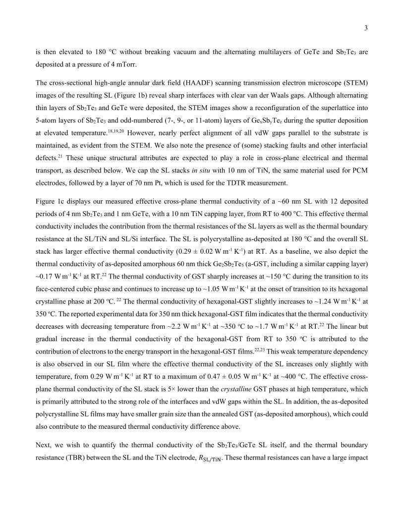
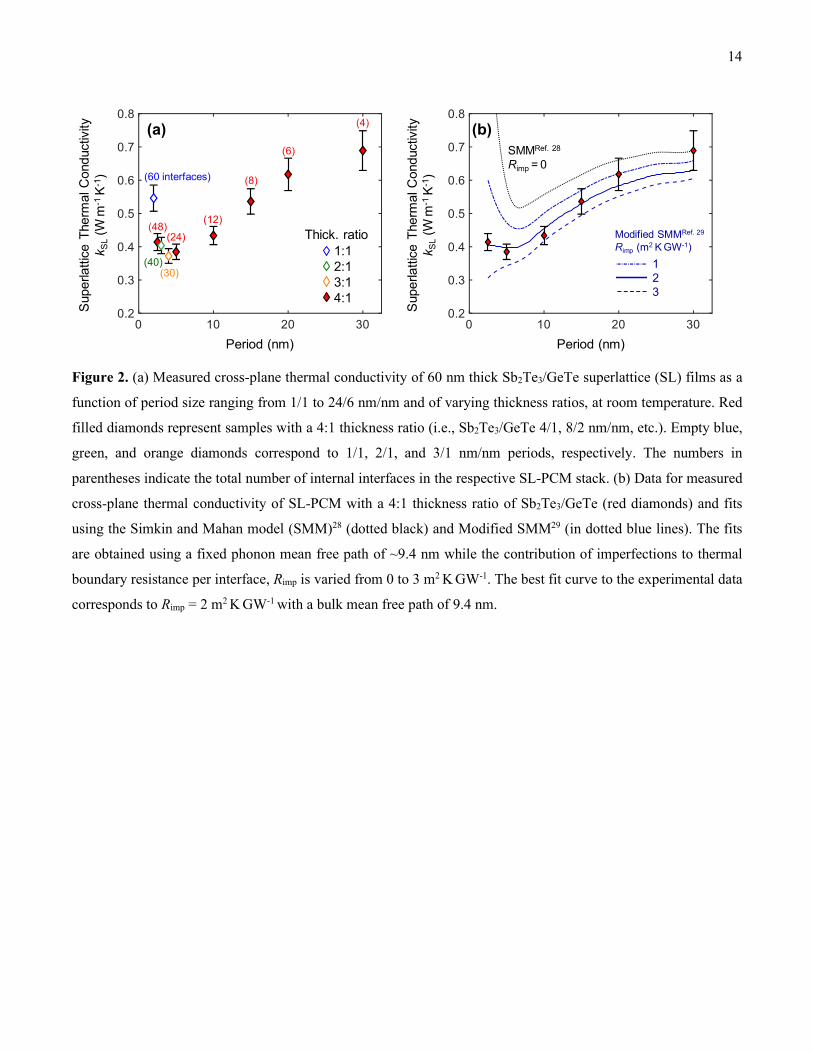
To assist with a better understanding of the switching mechanisms and complex physics of energy transport at the
interfaces of SL-PCM, we have conducted systematic thermal characterization of ~60 nm thick films with different
size periods and thickness ratios (t.r.) of Sb2Te3/GeTe (Figure 2). All the films were capped in situ with 10 nm thick
TiN layers. The SL-PCM period sizes of Sb2Te3/GeTe are 24/6, 16/4, 12/3, 8/2, 4/1, and 2/0.5 nm/nm (all with t.r.
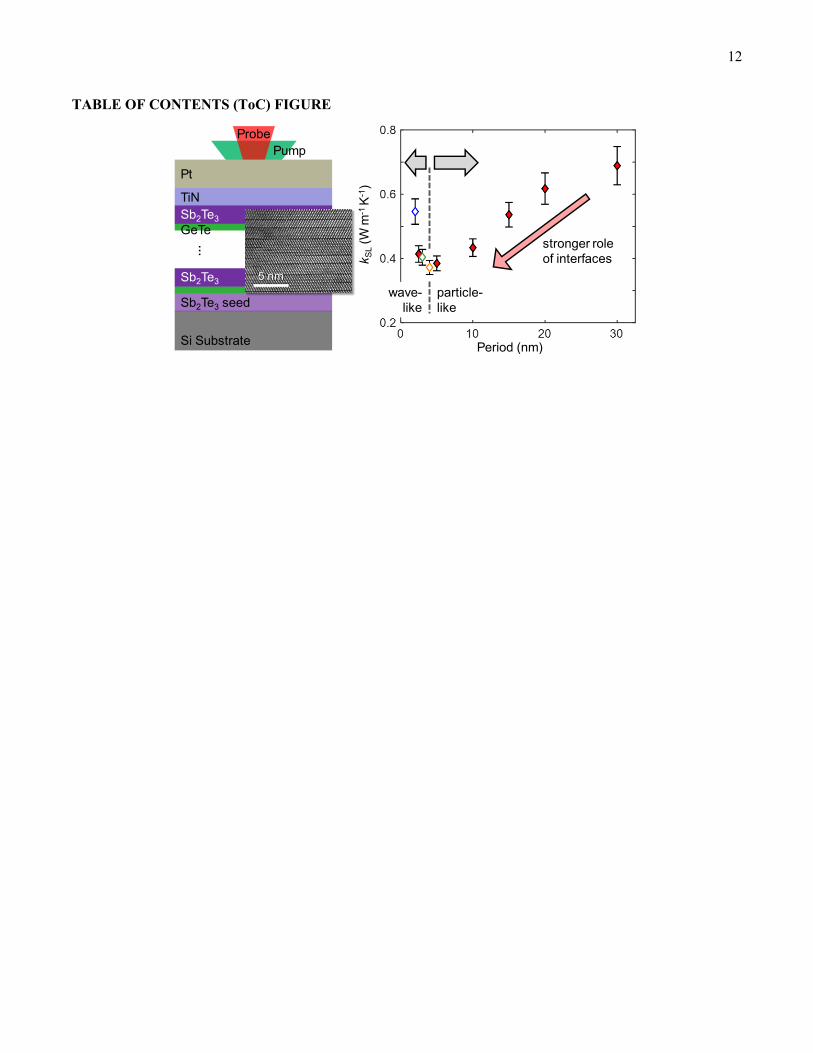
of 4:1), 3/1 nm/nm (t.r. 3:1), 2/1 nm/nm (t.r. 2:1), and 1/1 nm/nm (t.r. 1:1). As shown in Figure 2a, the cross-plane
thermal conductivity of SL-PCM films decreases from 0.69 ± 0.06 W m-1 K-1 for a 24/6 nm/nm period (4 interfaces)
to 0.37 ± 0.03 W m-1 K-1 for a 3/1 nm/nm period (30 interfaces). We note that the thermal conductivity of the SLs
shown in Figure 2a excludes the contribution of the TiN capping layer and Si substrate (see Supporting Information
Section 2), and thus exclusively represents the thermal transport in SL-PCM films. It is notable that the theoretical
minimum lattice thermal conductivity for these materials,26 kmin ≈ 0.31 W m-1 K-1 (see Supporting Information
Section 4) is only ~18% smaller than the minimum thermal conductivity of the 3/1 nm/nm period (30 interfaces)
SL film. Interestingly, the measured thermal conductivity of our SLs increases again for shorter periods of 3/1
nm/nm, 2/1 nm/nm, and 1/1 nm/nm, corresponding to 40, 48 and 60 interfaces, respectively. This counterintuitive
5
trend suggests a transition of phonon transport behavior from the quasi-ballistic regime (> 4 nm periods) to a wave-
like, quasi-coherent regime (2, 2.5, and 3 nm periods), a phenomenon usually observed in high-quality SL films.27
To model this observed thermal conductivity behavior of our Sb2Te3/GeTe SLs, we use the Simkin-Mahan Model
(SMM)28 with a correction for imperfections at the interfaces29 as detailed below (also see Supporting Information
Section 5). The main input parameters to the SMM are the mass ratio of lattice units, the number of lattices
consisting of the one period of Sb2Te3/GeTe, and the bulk phonon mean free path scaled by the lattice size. We first
estimate the bulk phonon mean free path λ in the SL from conventional kinetic theory λ ≈ 3k/(Cvv), where k is the
phonon thermal conductivity obtained by averaging the bulk thermal conductivity of Sb2Te3 and GeTe (with 4:1
thickness ratio) in the cross-plane direction, Cv is the volumetric specific heat, and v is the average sound velocity
(See Supporting Information Section 3 for detailed calculation), yielding 𝜆 ≈ 1 nm. However, this mean free path
is shorter than our considered SL periods, and thus the kinetic theory estimate cannot be applied to understand the
wave-like phonon behavior shown in Figure 2a.
To go a step further, we recall that layered materials are strongly anisotropic, which could lead to a significant
underestimation of the phonon mean free path by kinetic theory,15,30 due to the change in the phonon density of
states in the different directions of the lattice. In addition, time-resolved measurements have suggested that phonons
could have relatively longer lifetimes in Sb2Te3/GeTe SL films.31 Therefore, to model the experimentally observed
thermal conductivity trend (Figure 2a), we use the “modified” SMM29 (M-SMM) in Figure 2b by employing two
free parameters, the bulk phonon mean free path of the SL and the TBR originating from imperfections at SL
interfaces. Using the M-SMM, we first determine the best fit (blue solid line) to our experimental data (red filled
diamonds representing 24/6, 16/4, 12/3, 8/2, 4/1, and 2/0.5 nm/nm; t.r. 4:1 for Sb2Te3/GeTe) with 𝜆 = 9.4 nm and
the thermal boundary resistance per interface due to the inelastic scattering caused by imperfections alone, Rimp. =
2 m2 K GW-1. Thus, the M-SMM with a longer mean free path compared to kinetic theory estimates better predicts
the behavior of the thermal conductivity of our SL-PCM films. This suggests that the mean free path along the
cross-plane (c-axis) is larger than the one obtained from the simple kinetic theory, which has also been observed
before in similar layered materials such as MoS2 and graphite.15,30
Next, we model the thermal conductivities with a fixed 𝜆 = 9.4 nm while varying Rimp from 0 to 3 m2 K GW-1. We
note that for the fits in Figure 2b we only use the SLs with t.r. 4:1 of Sb2Te3/GeTe, where the data for the SL with
largest size period 24/6 nm/nm is available; this is to minimize the impact of the TBR between SL interfaces. The
fit for Rimp= 0 (using SMM) in Figure 2b represents perfect internal interfaces of Sb2Te3/GeTe and captures the
trend in the experimental thermal conductivity data of SLs in Figure 2a. However, this fit clearly overestimates the
thermal conductivity for smaller SL periods. Considering Rimp =1-2 m2 K GW-1, our model closely captures the
experimental thermal conductivity data. Such low Rimp. values indicate overall high-quality interfaces of our SLs
(further detailed in Supporting Information Section 5 and in Figure S3), with any contributions most likely arising
6
from the stacking faults18,32 which are apparent in Figure 1b. We further note that the fitted Rimp values agree well
with the molecular dynamics simulation results33 for the thermal boundary resistances per interface (1 to 2 m2 K
GW-1) originating from imperfections at the three different atomic layers (Te1, Bi, and Te2) of Bi2Te3.
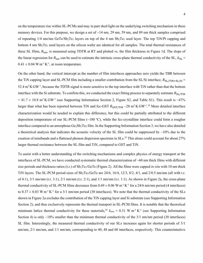
We now turn to electrical resistivity characterization of our SL films, which may also impact their programming in
SL-PCM data storage devices. For the in-plane electrical resistivity measurements of thin films, the standard transfer
length method (TLM) is usually employed,34 as shown in Figure 3a. This measurement is sensitive to the in-plane
electrical resistivity, ρ||, and the electrical contact resistivity with the metal pads, ρC. For cross-plane electrical
resistivity measurements, we utilize a modified TLM (M-TLM), which uses mesa structures to determine the cross-
plane electrical resistivity simultaneously.35 To fabricate the M-TLM structure, we etch into the SL film between
the two metal contacts (here Pt) as shown in Figure 3b (also see Supporting Information Section 6). This will
increase the contribution of the cross-plane electrical resistance, Re⊥, that is proportional to the etched depth, tetch.
The contact and cross-plane resistivities of the SL film can be estimated from simultaneously fitting the measured
electrical resistance as a function of contact spacing and etch depth, in the modified TLM devices. Figure 3c shows
the fitting line of the electrical resistance in each M-TLM device with a SL formed by 4 nm Sb2Te3 and 1 nm GeTe
deposition, and Figure 3d shows the total area-specific resistance, ρetch (including the SL/metal contact resistance),
corresponding to the amount of the etched depth. The slope in Figure 3d represents the cross-plane electrical
resistivity of these SLs, ρ⊥ ≈ 1.1 ± 0.35 Ω cm at room temperature. The in-plane electrical resistivity is estimated as
ρ|| ≈ 5.8 ± 0.3 × 10⁻⁴ Ω cm from the lateral TLM. The error bars of ρ|| and ρ⊥ are calculated using a Monte Carlo
approach,36 propagated from the uncertainties in the metal contact width and spacing (± 0.5 μm), as well as the etch
depth (± 2 nm). We note that the measured electrical resistances for different etched depths of SL films show
linearity (Figure 3c) across large distances of neighboring contact spacing (up to 20 µm), indicating good uniformity
of our sputtered SLs over a large area.
Our measured in-plane electrical resistivity is similar to that previously reported in-plane for such SLs37 and to
crystalline GeTe,38 but smaller than crystalline Sb2Te3,39 and nearly 2000-fold smaller than the SL cross-plane
resistivity. This strong anisotropy in the electrical transport is in close agreement with previously reported data40
for such SL films. The large anisotropy is not surprising in these layered SL materials (see Supplementary Table
S2), with covalent bonds in-plane and numerous weak van der Waals bonds and some stacking disorder in the cross-
plane direction.40-42 Some charge accumulation or depletion in adjacent SL layers (with smaller and larger band
gaps, respectively)43 could also contribute to the anisotropy of electrical resistivity in these films, and could be the
subject of future exploration.
We also note how these SL resistivity values compare to those in a-GST (> 102 Ω cm), fcc-GST (~0.1 Ω cm), and
hexagonal-GST (~10-3 Ω cm) near room temperature (RT).44 In other words, the cross-plane resistivity of the SL is
7
larger than for the crystalline phases of GST while the in-plane resistivity of the SL is slightly smaller than
hexagonal-GST. The in-plane SL resistivity can also be used to estimate the electronic contribution to the in-plane
thermal conductivity with the Wiedemann-Franz law, ke,|| ≈ 1.24 W m-1 K-1, which represents a lower bound. The
total in-plane thermal conductivity of the SL could be up to ~5 W m-1 K-1 at RT including the phonon component,
based on the in-plane thermal conductivity of both crystalline GeTe38 and Sb2Te339 (but likely to be somewhat
smaller for the SL due to finite size effects in our ultrathin films). This means that our SLs with 4/1 nm/nm periods
have greater than 4-fold (and possibly up to 16-fold) thermal anisotropy between the in-plane and cross-plane
directions.
In summary, we reported the electrical and thermal transport characterization of SL-PCMs with Sb2Te3/GeTe
alternating layers. The measured in-plane and cross-plane electrical resistivities of the SLs indicate a very
anisotropic structure, which can largely impact the electric field and resulting heat generation in SL-based phase
change memory (PCM) devices. We also observe up to ~4× lower effective cross-plane thermal conductivity of
(poly)crystalline Sb2Te3/GeTe SLs compared to crystalline GST, due to the presence of SL interfaces. These could
play a strong role in the reduction of SL-PCM programing current compared to conventional PCM based on GST.
We also observed a transition from quasi-coherent to quasi-ballistic phonon transport as we varied the period of
Sb2Te3/GeTe films (from 1/1 to 24/6 nm/nm), with a minimum thermal conductivity observed around the 3/1 nm/nm
period. Future work could provide additional in-plane and cross-plane thermal and electrical measurements of SLs
at cryogenic and high temperatures, to further our understanding of transport physics in such materials.

8
REFERENCES
1. Raoux, S.; Xiong, F.; Wuttig, M.; Pop, E. Phase Change Materials and Phase Change Memory. MRS Bull. 2014,
39 (8), 703–710.
2. Sebastian, A.; Le Gallo, M.; Burr, G. W.; Kim, S.; BrightSky, M.; Eleftheriou, E. Tutorial: Brain-Inspired
Computing Using Phase-Change Memory Devices. J. Appl. Phys. 2018, 124 (11), 111101.
3. Wong, H.-S. P.; Raoux, S.; Kim, S.; Liang, J.; Reifenberg, J. P.; Rajendran, B.; Asheghi, M.; Goodson, K. E.
Phase Change Memory. Proc. IEEE 2010, 98 (12), 2201–2227.
4. Egami, T.; Johguchi, K.; Yamazaki, S.; Takeuchi, K. Investigation of Multi-Level-Cell and SET Operations on
Super-Lattice Phase Change Memories. Jpn. J. Appl. Phys. 2014, 53 (4S), 04ED02.
5. Tominaga, J.; Fons, P.; Kolobov, A.; Shima, T.; Chong, T. C.; Zhao, R.; Lee, H. K.; Shi, L. Role of Ge Switch
in Phase Transition: Approach Using Atomically Controlled Sb2Te3/GeTe Superlattice. Jpn. J. Appl. Phys. 2008,
47 (7), 5763–5766.
6. Simpson, R. E.; Fons, P.; Kolobov, A. V.; Fukaya, T.; Krbal, M.; Yagi, T.; Tominaga, J. Interfacial Phase-Change
Memory. Nat. Nanotechnol. 2011, 6 (8), 501–505.
7. Kim, W.; BrightSky, M.; Masuda, T.; Sosa, N.; Kim, S.; Bruce, R.; Carta, F.; Fraczak, G.; Cheng, H. Y.; Ray,
A.; Zhu, Y.; Lung, H. L.; Suu, K.; Lam, C. ALD-Based Confined PCM with a Metallic Liner toward Unlimited
Endurance. 2016 IEEE International Electron Devices Meeting (IEDM) 2016, 4.2.1–4.2.4.
8. Fong, S. W.; Sood, A.; Chen, L.; Kumari, N.; Asheghi, M.; Goodson, K. E.; Gibson, G. A.; Wong, H.-S. P.
Thermal Conductivity Measurement of Amorphous Dielectric Multilayers for Phase-Change Memory Power
Reduction. J. Appl. Phys. 2016, 120 (1), 015103.
9. Fong, S. W.; Neumann, C. M.; Yalon, E.; Rojo, M. M.; Pop, E.; Wong, H.-S. P. Dual-Layer Dielectric Stack for
Thermally Isolated Low-Energy Phase-Change Memory. IEEE Trans. Electron Devices 2017, 64 (11), 4496–4502.
10. Ahn, C.; Fong, S. W.; Kim, Y.; Lee, S.; Sood, A.; Neumann, C. M.; Asheghi, M.; Goodson, K. E.; Pop, E.;
Wong, H.-S. P. Energy-Efficient Phase-Change Memory with Graphene as a Thermal Barrier. Nano Lett. 2015, 15
(10), 6809–6814.
11. Neumann, C. M.; Okabe, K. L.; Yalon, E.; Grady, R. W.; Wong, H.-S. P.; Pop, E. Engineering Thermal and
Electrical Interface Properties of Phase Change Memory with Monolayer MoS2. Appl. Phys. Lett. 2019, 114 (8),
082103.
12. Khan, A. I.; Kwon, H.; Islam, R.; Perez, C.; Chen, M. E.; Asheghi, M.; Goodson, K. E.; Wong, H.-S. P.; Pop,
E. Two-Fold Reduction of Switching Current Density in Phase Change Memory Using Bi₂Te₃ Thermoelectric
Interfacial Layer. IEEE Electron Device Lett. 2020, 41 (11), 1657–1660.
13. Ren, K.; Cheng, Y.; Chen, X.; Ding, K.; Lv, S.; Yin, W.; Guo, X.; Ji, Z.; Song, Z. Carbon Layer Application in
Phase Change Memory to Reduce Power Consumption and Atomic Migration. Mater. Lett. 2017, 206, 52–55.
9
14. Aryana, K.; Gaskins, J. T.; Nag, J.; Stewart, D. A.; Bai, Z.; Mukhopadhyay, S.; Read, J. C.; Olson, D. H.;
Hoglund, E. R.; Howe, J. M.; Giri, A.; Grobis, M. K.; Hopkins, P. E. Interface Controlled Thermal Resistances of
Ultra-Thin Chalcogenide-Based Phase Change Memory Devices. Nat. Commun. 2021, 12 (1), 774.
15. Sood, A.; Xiong, F.; Chen, S.; Cheaito, R.; Lian, F.; Asheghi, M.; Cui, Y.; Donadio, D.; Goodson, K. E.; Pop,
E. Quasi-Ballistic Thermal Transport Across MoS2 Thin Films. Nano Lett. 2019, 19 (4), 2434–2442.
16. Boniardi, M.; Boschker, J. E.; Momand, J.; Kooi, B. J.; Redaelli, A.; Calarco, R. Evidence for Thermal‐Based
Transition in Super‐Lattice Phase Change Memory. Phys. status solidi – Rapid Res. Lett. 2019, 13 (4), 1800634.
17. Jiang, P.; Qian, X.; Yang, R. Tutorial: Time-Domain Thermoreflectance (TDTR) for Thermal Property
Characterization of Bulk and Thin Film Materials. J. Appl. Phys. 2018, 124 (16), 161103.
18. Momand, J.; Wang, R.; Boschker, J. E.; Verheijen, M. A.; Calarco, R.; Kooi, B. J. Dynamic Reconfiguration
of van Der Waals Gaps within GeTe-Sb2Te3 Based Superlattices. Nanoscale 2017, 9 (25), 8774–8780.
19. Lotnyk, A.; Hilmi, I.; Ross, U.; Rauschenbach, B. Van Der Waals Interfacial Bonding and Intermixing in
GeTe-Sb2Te3-Based Superlattices. Nano Res. 2018, 11 (3), 1676–1686.
20. Kowalczyk, P.; Hippert, F.; Bernier, N.; Mocuta, C.; Sabbione, C.; Batista-Pessoa, W.; Noé, P. Impact of
Stoichiometry on the Structure of van Der Waals Layered GeTe/Sb2Te3 Superlattices Used in Interfacial Phase-
Change Memory (IPCM) Devices. Small 2018, 14 (24), 1704514.
21. Wang, R.; Bragaglia, V.; Boschker, J. E.; Calarco, R. Intermixing during Epitaxial Growth of van Der Waals
Bonded Nominal GeTe/Sb2Te3 Superlattices. Cryst. Growth Des. 2016, 16 (7), 3596–3601.
22. Reifenberg, J. P.; Panzer, M. A.; Kim, S.; Gibby, A. M.; Zhang, Y.; Wong, S.; Wong, H. S. P.; Pop, E.; Goodson,
K. E. Thickness and Stoichiometry Dependence of the Thermal Conductivity of GeSbTe Films. Appl. Phys. Lett.
2007, 91 (11), 111904.
23. Yang, Y.; Hamann, H. F.; Asheghi, M. Thermal Conductivity Measurements and Modeling of Phase-Change
Ge2Sb2Te5 Materials. Nanoscale Microscale Thermophys. Eng. 2009, 13 (2), 88–98.
24. Lee, J.; Bozorg-Grayeli, E.; Kim, S.; Asheghi, M.; Philip Wong, H. S.; Goodson, K. E. Phonon and Electron
Transport through Ge2Sb2Te5 Films and Interfaces Bounded by Metals. Appl. Phys. Lett. 2013, 102 (19), 191911.
25. Maris, H.; Tanaka, Y. Phonon Group Velocity and Thermal Conduction in Superlattices. Phys. Rev. B. 1999,
60 (4), 2627–2630.
26. Cahill, D. G.; Watson, S. K.; Pohl, R. O. Lower Limit to the Thermal Conductivity of Disordered Crystals.
Phys. Rev. B. 1992, 46 (10), 6131–6140.
27. Ravichandran, J.; Yadav, A. K.; Cheaito, R.; Rossen, P. B.; Soukiassian, A.; Suresha, S. J.; Duda, J. C.; Foley,
B. M.; Lee, C. H.; Zhu, Y.; Lichtenberger, A. W.; Moore, J. E.; Muller, D. A.; Schlom, D. G.; Hopkins, P. E.;
Majumdar, A.; Ramesh, R.; Zurbuchen, M. A. Crossover from Incoherent to Coherent Phonon Scattering in
Epitaxial Oxide Superlattices. Nat. Mater. 2014, 13 (2), 168–172.
10
28. Simkin, M. V.; Mahan, G. D. Minimum Thermal Conductivity of Superlattices. Phys. Rev. Lett. 2000, 84 (5),
927–930.
29. Yang, B.; Chen, G. Partially Coherent Phonon Heat Conduction in Superlattices. Phys. Rev. B. 2003, 67 (19),
195311.
30. Zhang, H.; Chen, X.; Jho, Y. D.; Minnich, A. J. Temperature-Dependent Mean Free Path Spectra of Thermal
Phonons Along the c-Axis of Graphite. Nano Lett. 2016, 16 (3), 1643–1649.
31. Makino, K.; Saito, Y.; Fons, P.; Kolobov, A. V.; Nakano, T.; Tominaga, J.; Hase, M. Coherent Phonon Study
of (GeTe)l(Sb2Te3)m Interfacial Phase Change Memory Materials. Appl. Phys. Lett. 2014, 105 (15), 151902.
32. P. E. Hopkins, Thermal Transport across Solid Interfaces with Nanoscale Imperfections: Effects of Roughness,
Disorder, Dislocations, and Bonding on Thermal Boundary Conductance, ISRN Mech. Eng. 2013, 2013, 682586.
33. Hsieh, I. T.; Huang, M. J. An Investigation into the Thermal Boundary Resistance Associated with the Twin
Boundary in Bismuth Telluride. Nanoscale Microscale Thermophys. Eng. 2019, 23 (1), 36–47.
34. Berger, H. H. Contact Resistance and Contact Resistivity. J. Electrochem. Soc. 1972, 119 (4), 507.
35. Yang, B.; Liu, W. L.; Liu, J. L.; Wang, K. L.; Chen, G. Measurements of Anisotropic Thermoelectric Properties
in Superlattices. Appl. Phys. Lett. 2002, 81 (19), 3588–3590.
36. Cox, M.; Harris, P.; Siebert, B. R. L. Evaluation of Measurement Uncertainty Based on the Propagation of
Distributions Using Monte Carlo Simulation. Meas. Tech. 2003, 46 (9), 824–833.
37. Cecchi, S.; Zallo, E.; Momand, J.; Wang, R.; Kooi, B. J.; Verheijen, M. A.; Calarco, R. Improved Structural
and Electrical Properties in Native Sb2Te3/GexSb2Te3+x van Der Waals Superlattices Due to Intermixing Mitigation.
APL Mater. 2017, 5 (2), 026107.
38. Nath, P.; Chopra, K. L. Thermal Conductivity of Amorphous and Crystalline Ge and GeTe Films. Phys. Rev. B
1974, 10 (8), 3412–3418.
39. Das, V. D.; Soundararajan, N. Thermoelectric Power and Electrical Resistivity of Crystalline Antimony
Telluride (Sb2Te3) Thin Films: Temperature and Size Effects. J. Appl. Phys. 1989, 65 (6), 2332–2341.
40. Yang, Z.; Xu, M.; Cheng, X.; Tong, H.; Miao, X. Manipulation of Dangling Bonds of Interfacial States Coupled
in GeTe-Rich GeTe/Sb2Te3 Superlattices. Sci. Rep. 2017, 7 (1), 17353.
41. Liu, J.; Okamoto, S.; Van Veenendaal, M.; Kareev, M.; Gray, B.; Ryan, P.; Freeland, J. W.; Chakhalian, J.
Quantum Confinement of Mott Electrons in Ultrathin LaNiO3/LaAlO3 Superlattices. Phys. Rev. B. Phys. 2011, 83
(17), 161102.
42. Peng, H.; Xie, C.; Schoen, D. T.; Cui, Y. Large Anisotropy of Electrical Properties in Layer-Structured In2Se3
Nanowires. Nano Lett. 2008, 8 (5), 1511–1516.
43. Yu, R.H. Tamm states in finite semiconductor superlattices: Influence of accumulation and depletion layers.
Phys. Rev. B 1993, 47 (3), 1379–1382.
11
44. Deshmukh, S.; Yalon, E.; Lian, F.; Schauble, K. E.; Xiong, F.; Karpov, I. V.; Pop, E. Temperature-Dependent
Contact Resistance to Nonvolatile Memory Materials. IEEE Trans. Electron Devices 2019, 66 (9), 3816–3821.
ASSOCIATED CONTENT
Supporting Information
The Supporting Information is available free of charge on the ACS Publications website at DOI: XXXX
Additional details on the time domain thermoreflectance measurement method, sensitivity analysis, theoretical
calculation of thermal boundary resistance, theoretical estimation of minimum thermal conductivity, additional
details on the thermal modeling, additional details and benchmarking of the electrical resistivity measurement
ACKNOWLEDGMENTS
We acknowledge the financial support from the Semiconductor Research Corporation, SRC (task 2826.001),
Kwanjeong Educational Foundation Fellowship, and Stanford Graduate Fellowship. H.K and A.I.K are thankful to
Dr. James McVittie for lab assistance and useful discussion. Authors are grateful to Kazuhiko Yamamoto, Shosuke
Fujii and Kazunari Ishimaru from Kioxia Corporation, Japan for obtaining the high-quality scanning transmission
electron microscopy images and management support. Part of this work was performed at the Stanford
Nanofabrication Facility (SNF) and Stanford Nanofabrication Shared Facilities (SNSF), supported by the National
Science Foundation under award ECCS-2026822.
AUTHOR CONTRIBUTION
H. K. and A.I.K. conducted the thermal and electrical measurements. A.I.K. and H.K. performed the film
depositions. All the authors contributed to the discussion of the experimental results and the writing of the
manuscript.
COMPETING INTERESTS
The authors declare no competing interests.
12
TABLE OF CONTENTS (ToC) FIGURE
k
SL
(Wm
-1 K
-1)
Period (nm)
wave-
like
particle-
like
stronger role
of interfaces
TiN
Pt
Si Substrate
Sb2Te3 seed
Pump
Probe
···
Sb2Te3
Sb2Te3
GeTe
5 nm
13
Figures
Figure 1. Cross-plane thermal characterization of Sb2Te3/GeTe superlattices (SLs). (a) Measurement setup
showing, from bottom to top: silicon (Si) substrate, 4 nm Sb2Te3 seed layer, deposited alternating GeTe and Sb2Te3
layers, TiN/Pt capping layers, and pump/probe lasers. (b) High-resolution scanning transmission electron
microscopy (STEM) cross-sections of resulting superlattice on a 100 mm diameter Si wafer, revealing sharp
interfaces and clear van der Waals gaps. The resulting superlattice is somewhat different from the as-deposited
layers, due to interfacial reconstruction which is known to occur during deposition kinetics.18-20 (c) Measured
effective thermal conductivity of 60 nm thick as-deposited SL including the TiN capping layer (red filled triangles)
from room temperature to 400 ºC, and the temperature-dependent effective thermal conductivity of Ge2Sb2Te5
(GST) (including similar capping layer) from Ref. 22 (filled circles). The measurement laser spot size is ~10 μm,
and the SL measurements are averaged from three locations on the same sample. (d) Measured total thermal
resistance of 4/1 nm/nm superlattice with increasing number of periods, from 2 to 17 at room temperature (2 periods
= 4 internal interfaces including the bottom Sb2Te3 seed layer = 14 nm thick, etc.). The inverse of the slope of the
linear fit estimates the intrinsic thermal conductivity of the SL, and the y-intercept yields the sum of thermal
boundary resistance between SL/TiN at the top and SL/Si at the bottom.
Pump
Probe
TiN (10 nm)
Pt (70 nm)
Si Substrate
···
4 nm Sb2Te3 seed layer
RSL/TiN + RSL/Si ≈ 52.4 m2 K GW-1
Rto
t(m
2 K
GW
-1)
Thickness (nm)
(d)
···
GeTe
Sb2Te3
Sb2Te3
GeTe
(a) (b)
1/slope = kSL ≈ 0.41 W m-1 K-1
5 nm10 nm
4/1 nm/nm
Sb2Te3/GeTe SL stack
fcc-GST
hexagonal-GST
a-GST stack
T (K)
Effe
ctive th
erm
al co
ndu
ctivity
keff
(Wm
-1 K
-1)
(c)
14
Figure 2. (a) Measured cross-plane thermal conductivity of 60 nm thick Sb2Te3/GeTe superlattice (SL) films as a
function of period size ranging from 1/1 to 24/6 nm/nm and of varying thickness ratios, at room temperature. Red
filled diamonds represent samples with a 4:1 thickness ratio (i.e., Sb2Te3/GeTe 4/1, 8/2 nm/nm, etc.). Empty blue,
green, and orange diamonds correspond to 1/1, 2/1, and 3/1 nm/nm periods, respectively. The numbers in
parentheses indicate the total number of internal interfaces in the respective SL-PCM stack. (b) Data for measured
cross-plane thermal conductivity of SL-PCM with a 4:1 thickness ratio of Sb2Te3/GeTe (red diamonds) and fits
using the Simkin and Mahan model (SMM)28 (dotted black) and Modified SMM29 (in dotted blue lines). The fits
are obtained using a fixed phonon mean free path of ~9.4 nm while the contribution of imperfections to thermal
boundary resistance per interface, Rimp is varied from 0 to 3 m2 K GW-1. The best fit curve to the experimental data
corresponds to Rimp = 2 m2 K GW-1 with a bulk mean free path of 9.4 nm.
Superlattic
e T
herm
al C
onductivity
kS
L(W
m-1
K-1
)
Superlattic
e T
herm
al C
onductivity
kS
L(W
m-1
K-1
)
Period (nm) Period (nm)
1
2
3
(a) (b)
(30)
(24)
(8)
(6)
(4)
(40)
(60 interfaces)
(12)(48)
1:1
2:1
3:1
4:1
Thick. ratio Modified SMMRef. 29
Rimp (m2 K GW-1)
SMMRef. 28
Rimp = 0

15
Figure 3. Electrical characterization of Sb2Te3/GeTe superlattices with 4/1 nm/nm period. (a) Top view optical
image of transfer length method (TLM) structure, where L is the distance between the Pt contact pads and W is the
width of each contact pad. (b) Schematic cross-section of the modified TLM (M-TLM) along the dashed line in (a),
with ~82 nm thick Pt contact pads and a 90 nm thick Sb2Te3/GeTe film with a 4/1 nm/nm period on thermally grown
SiO2 (~110 nm). (c) Measured electrical resistance Re,tot = 2Re,C + 2Re,⊥ + Re, vs. distance L between neighboring
contact pads for varying SL film etched depths, at room temperature. (d) Calculated total area-specific resistance
(including the Pt/SL contact resistance), ρetch as a function of the etched depth. Each data point is averaged from the
contact resistivities of five M-TLM devices with the same etch depth. The errors due to the fabrication uncertainties
are calculated using a Monte Carlo method.33
Si
SiO2
(a) (b)
(c)
ρe
tch
(Ωcm
2)
(d)W
= 8
00
m
L~102 nm(20 periods)
tetch
L
Re,||
Re,
tfilm
Re,C
Re
⊥,to
t(Ω
μm
)
L (μm) tetch (nm)
Pt Pt
16
Supporting Information
Uncovering Thermal and Electrical Properties of Sb2Te3/GeTe Superlattice Films
Heungdong Kwon1, Asir Intisar Khan2, Christopher Perez1, Mehdi Asheghi1, Eric Pop2,3, Kenneth E. Goodson1,3,*
1Dept. of Mechanical Eng., Stanford University, Stanford, CA 94305, U.S.A.
2Dept. of Electrical Eng., Stanford University, Stanford, CA 94305, U.S.A.
3Dept. of Materials Science & Eng., Stanford University, Stanford, CA 94305, U.S.A.
*E-mail: [email protected]
1. Time Domain Thermoreflectance (TDTR)
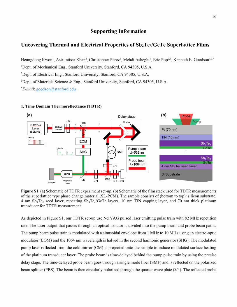
Figure S1. (a) Schematic of TDTR experiment set-up. (b) Schematic of the film stack used for TDTR measurements
of the superlattice type phase change material (SL-PCM). The sample consists of (bottom to top): silicon substrate,
4 nm Sb2Te3 seed layer, repeating Sb2Te3/GeTe layers, 10 nm TiN capping layer, and 70 nm thick platinum
transducer for TDTR measurement.
As depicted in Figure S1, our TDTR set-up use Nd:YAG pulsed laser emitting pulse train with 82 MHz repetition
rate. The laser output that passes through an optical isolator is divided into the pump beam and probe beam paths.
The pump beam pulse train is modulated with a sinusoidal envelope from 1 MHz to 10 MHz using an electro-optic
modulator (EOM) and the 1064 nm wavelength is halved in the second harmonic generator (SHG). The modulated
pump laser reflected from the cold mirror (CM) is projected onto the sample to induce modulated surface heating
of the platinum transducer layer. The probe beam is time-delayed behind the pump pulse train by using the precise
delay stage. The time-delayed probe beam goes through a single mode fiber (SMF) and is reflected on the polarized
beam splitter (PBS). The beam is then circularly polarized through the quarter wave plate (λ/4). The reflected probe
(a) (b)
TiN (10 nm)
Pt (70 nm)
Si Substrate
···
4 nm Sb2Te3 seed layer
Pump
Probe
···
GeTe
Sb2Te3
Sb2Te3
GeTe
17
laser is detected by a high-speed photodetector (PD). The optical signal is measured by the lock-in amplifier wired
to the PD. We monitor the ratio between in- and out-of-phase voltage signals from the lock-in amplifier as a function
of the time delay between the pump and probe beams. This ratio signal is fitted with a multilayer heat diffusion
model1 to extract the unknown parameters.
2. Sensitivity Analysis
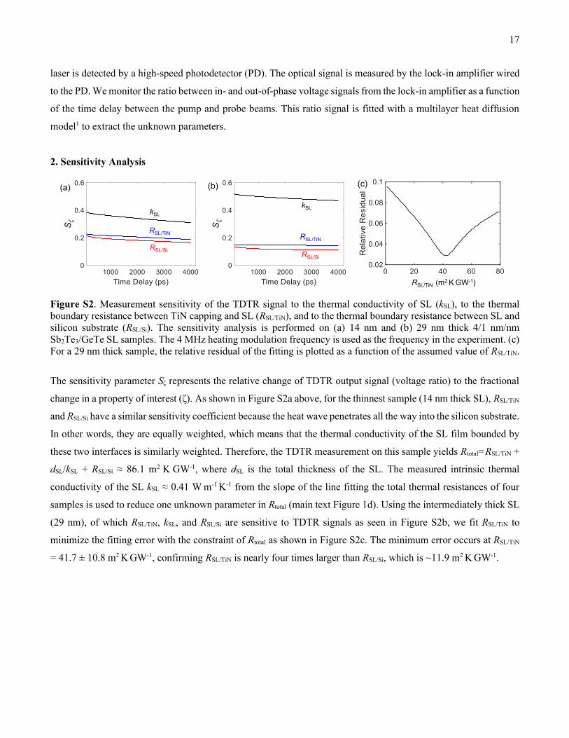
Figure S2. Measurement sensitivity of the TDTR signal to the thermal conductivity of SL (kSL), to the thermal
boundary resistance between TiN capping and SL (RSL/TiN), and to the thermal boundary resistance between SL and
silicon substrate (RSL/Si). The sensitivity analysis is performed on (a) 14 nm and (b) 29 nm thick 4/1 nm/nm
Sb2Te3/GeTe SL samples. The 4 MHz heating modulation frequency is used as the frequency in the experiment. (c)
For a 29 nm thick sample, the relative residual of the fitting is plotted as a function of the assumed value of RSL/TiN.
The sensitivity parameter Sζ represents the relative change of TDTR output signal (voltage ratio) to the fractional
change in a property of interest (ζ). As shown in Figure S2a above, for the thinnest sample (14 nm thick SL), RSL/TiN
and RSL/Si have a similar sensitivity coefficient because the heat wave penetrates all the way into the silicon substrate.
In other words, they are equally weighted, which means that the thermal conductivity of the SL film bounded by
these two interfaces is similarly weighted. Therefore, the TDTR measurement on this sample yields Rtotal=RSL/TiN +
dSL/kSL + RSL/Si ≈ 86.1 m2 K GW-1, where dSL is the total thickness of the SL. The measured intrinsic thermal
conductivity of the SL kSL ≈ 0.41 W m-1 K-1 from the slope of the line fitting the total thermal resistances of four
samples is used to reduce one unknown parameter in Rtotal (main text Figure 1d). Using the intermediately thick SL
(29 nm), of which RSL/TiN, kSL, and RSL/Si are sensitive to TDTR signals as seen in Figure S2b, we fit RSL/TiN to
minimize the fitting error with the constraint of Rtotal as shown in Figure S2c. The minimum error occurs at RSL/TiN
= 41.7 ± 10.8 m2 K GW-1, confirming RSL/TiN is nearly four times larger than RSL/Si, which is ~11.9 m2 K GW-1.
kSL
RSL/Si
RSL/TiN
kSL
RSL/Si
RSL/TiN
(a) (b) (c)
RSL/TiN (m2 K GW-1)
Sζ
Sζ
18
Materials
Properties TiN fcc-Ge2Sb2Te5 Sb2Te3 GeTe
𝝆 [g cm-3] 5.40 6.30 6.51 6.18
Cv [MJ m-3 K-1] 3.14 (Ref. 7) 1.34 (Ref. 8) 1.29 (Ref. 9) 1.53 (Ref. 10)
vs,L [m/s] 9638 (Ref. 11) 3190 (Ref. 12) 2757 (c-axis)Ref. 13 2670 (c-axis)Ref. 14
kbulk,lattice [W m-1 K-1] - - 0.8 (c-axis)Ref. 15 2 (c-axis)Ref. 15
Table S1. Summary of the reported values for the density, volumetric specific heat, and longitudinal sound velocity
for TiN, fcc-Ge2Sb2Te5, crystalline Sb2Te3, and crystalline GeTe. For Sb2Te3 and GeTe, the cross-plane (c-axis)
longitudinal sound velocity and thermal conductivity data are referred to estimate the phonon mean free path in
SLs.
3. Theoretical Calculation of Thermal Boundary Resistance (TBR)
The result shows ~47 % larger thermal boundary resistance than the reported data2 between TiN and fcc-Ge2Sb2Te5
(GST), RGST/TiN ≈ 28 m2 K GW-1. Several studies have indicated that the cross-plane acoustic velocity of the SL film
could be suppressed significantly due to the creation of minibands and flattened phonon dispersion spectra in SLs.3,4
To explain the larger RSL/TiN compared to RGST/TiN, we calculate the theoretical TBR using the Diffuse Mismatch
Model (DMM) with a gray approximation.5
𝑅 =𝐶v,1
4𝜋(
𝑣2𝐶v,2
𝑣1𝐶v,1 + 𝑣2𝐶v,2)
−1
where Cv is the volumetric specific heat, v is the sound velocity, and the subscripts indicate the material on either
side of the interface. The material properties used in the TBR calculation are presented in Table S1. The volumetric
specific heat in Table S1 is calculated from the density in the table and the molecular specific heat given by the
corresponding references. For the sound velocity in the model, we use the values of longitudinal sound velocity.
Although this simplified model cannot predict an accurate TBR compared to the DMM using a full phonon
dispersion, the approximation can provide insight into the trend of TBRs. For the cross-plane sound velocity of the
SL film, we use the following equation given in Ref 6.
𝑣𝑆𝐿 =𝑑
√𝑑1
2
𝑣12 +
𝑑22
𝑣22 + (
𝑍1𝑍2
+𝑍1𝑍2
)𝑑1𝑑2𝑣1𝑣2
where 𝑍 = 𝜌𝑣 is the acoustic impedance, d is the period of the SL, and the subscripts indicate the materials on either
side of the interface (i.e. Sb2Te3 and GeTe). The estimated effective velocity across the SL is used as the parameter
to calculate the thermal boundary resistance between TiN and SL-PCM with the DMM. As expected, the averaged
volumetric specific heat (1.32 MJ m-3 K-1) and longitudinal acoustic velocity (2739 m/s) of 4/1 nm/nm Sb2Te3/GeTe
are not noticeably different from those of fcc-Ge2Sb2Te5 (shown in Table S1), owing to their similar molecular
composition. It was observed that the measured longitudinal sound velocity across a Sb2Te3/Bi2Te3 SL is ~10%
19
reduced from its effective sound velocity.6 In this study, we use the same scaling factor to estimate the decreased
cross-plane longitudinal sound velocity of the 4/1 nm/nm Sb2Te3/GeTe film from the effective velocity. The ratio
between RSL/TiN and RGST/TiN is then calculated to be ~1.27. Though the ratio of TBRs calculated using the simple
DMM model underestimates the experimental values of TBR between SL/TiN relative to the reported data of TBR
of fcc-GST/TiN film, we attribute the higher TBR of SL-PCM to the decreased sound velocity in SL film.
4. Minimum Thermal Conductivity
The minimum thermal conductivity model proposed by Cahill et al.16 describes the thermal conductivity of a highly
disordered crystal with a random walk motion of vibrational modes, as:
𝑘𝑚𝑖𝑛 =1
2(
𝜋
6)
13
𝑘𝐵𝑛𝑎
23(𝑣𝑙 + 2𝑣𝑡)
where kB is the Boltzmann constant, na is the atomic number density, vl is the longitudinal speed of sound, and vt is
the transverse speed of sound. Using this model, the theoretical lower bound of thermal conductivity for
superlattices can be estimated.17 To estimate the minimum thermal conductivity of SL explored in this study, first,
we calculate the individual minimum thermal conductivities of Sb2Te3 and GeTe respectively, and then the
minimum thermal conductivity of SL is estimated with their thickness ratio in the SL period unit. The atomic density
is derived using the mass density and molar mass of each material and the sound velocity data of Sb2Te3 and GeTe
are taken from Ref. 13 and Ref. 14, respectively.
5. Simkin and Mahan model (SMM)
To analyze our experimental data of the cross-plane thermal conductivity of superlattice (SL) films, we employ the
Simkin and Mahan model (SMM),18 which describes thermal transport in the SL films with SL period smaller than
the coherence length of phonon. This approach reduces the SL system into a periodic one-dimensional mass-spring
chain system where molecular mass of a molecule (e.g. Sb2Te3 or GeTe) that comprises the SL is considered. From
the calculated band structure determined from the characteristic matrix, we estimate the thermal conductivities of
SLs. The input parameters for SMM are the bulk phonon mean free path and the molecular mass ratio between the
two materials in the SL. We consider the 4:1 thickness ratio of Sb2Te3 and GeTe in one period of SL for our case.
However, this model assumes elastic scattering processes at the interface, which cannot account for imperfections
or disorder at the interfaces present in our SL films, some of which can be seen in Figure 1b of the main text.
Therefore, we modify the SMM as described in Ref. 19 to incorporate the impact of these imperfections. In addition,
using the conventional kinetic theory, the estimated phonon mean free path across the SL films is ~1 nm (as
explained in the main text), which is shorter than the period of the SL. In this case, SMM cannot predict the
experimentally observed thermal conductivity in such SL. Therefore, to obtain a better estimate of phonon mean
free path across our SLs, we fit the experimental thermal conductivity data using a modified SMM (M-SMM). The

20
bulk phonon mean free path across the SL (λ), and the thermal boundary resistances per interface due to
imperfections acting alone (Rimp) are used as the two unknown free parameters, see Figure 2b in the main text.
To obtain further insight, we plot (Figure S3) various thermal resistances of Sb2Te3/GeTe SL films (total thickness
60 nm) with varying period thicknesses for a fixed mean free path of 9.4 nm and four different values of Rimp = 0,
1, 2, and 3 m2 K GW-1 (TBR per interface due to imperfections, acting alone). As the TBR due to the imperfection
at the interface increases, the total thermal resistance calculated using the modified SMM (RM-SMM) in the SL
becomes larger than the thermal resistance estimated by SMM. For Rimp ~3 m2 K GW-1 (Figure S3d), a minimum
thermal conductivity of SL (a maximum thermal resistance) cannot be observed, because of the dominance of the
thermal resistance due to the imperfections in the overall resistance of SL film. This indicates that the phonon
coherence phenomena may not be observed in SL films with lower quality interfaces (i.e., higher Rimp). At the same
time, this further points to the good quality interfaces in our studied SLs.
Figure S3. The calculated total thermal resistance of Sb2Te3/GeTe SL using modified SMM RM-SMM (black), the
thermal resistance of SL estimated by SMM RSMM (red), and the total thermal resistance due to imperfections at the
interfaces in the SL Rtot,imp (blue) as a function of the period thicknesses for varying Rimp = (a) 0 m2 K GW-1, (b) 1
m2 K GW-1, (c) 2 m2 K GW-1, and (d) 3 m2 K GW-1. Here, Rimp is the thermal boundary resistance per interface in
Period (nm)
R(m
2 K
GW
-1)
R(m
2 K
GW
-1)
Period (nm)
R(m
2 K
GW
-1)
Period (nm)
(b)
(c) (d)
(a)
R(m
2 K
GW
-1)
Period (nm)
RM-SMM
RSMM
Rtot,imp
RM-SMM
RSMM
Rtot,imp
RM-SMM
RSMM
Rtot,imp
RM-SMM
RSMM
Rtot,imp
Rimp = 0 m2KGW-1 Rimp = 1 m2KGW-1
Rimp = 2 m2KGW-1 Rimp = 3 m2KGW-1
21
SL due to imperfections acting alone. RM-SMM = RSMM + Rtot,imp where, Rtot,imp = nRimp and n is the total number of the
interfaces in SL.
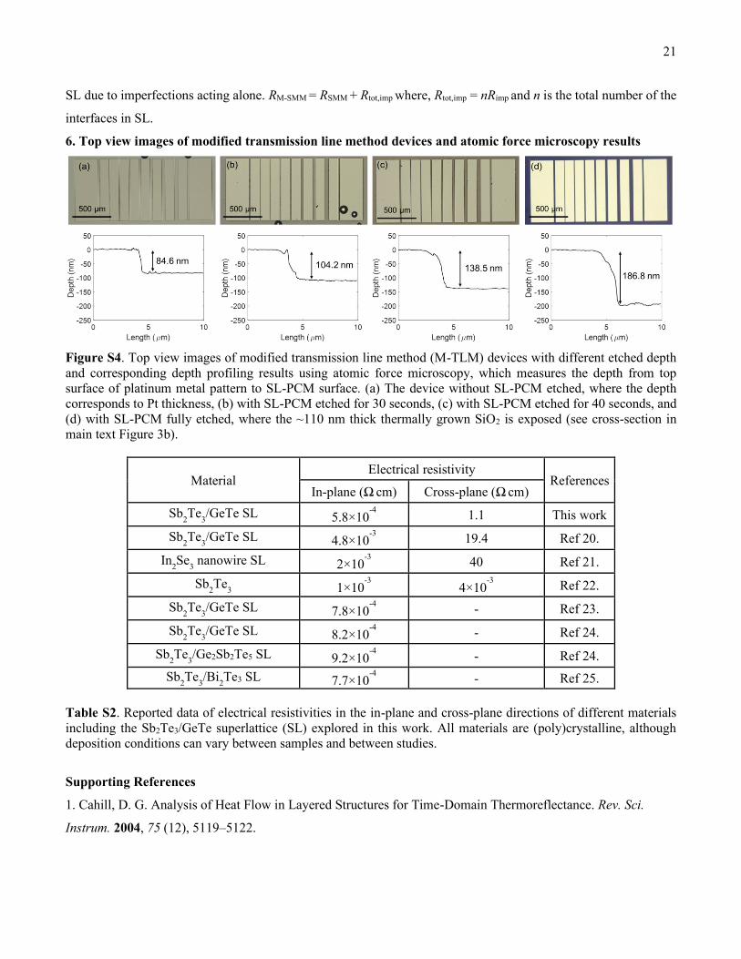
6. Top view images of modified transmission line method devices and atomic force microscopy results
Figure S4. Top view images of modified transmission line method (M-TLM) devices with different etched depth
and corresponding depth profiling results using atomic force microscopy, which measures the depth from top
surface of platinum metal pattern to SL-PCM surface. (a) The device without SL-PCM etched, where the depth
corresponds to Pt thickness, (b) with SL-PCM etched for 30 seconds, (c) with SL-PCM etched for 40 seconds, and
(d) with SL-PCM fully etched, where the ~110 nm thick thermally grown SiO2 is exposed (see cross-section in
main text Figure 3b).
Material Electrical resistivity
References In-plane (Ω
cm) Cross-plane (Ω
cm)
Sb2Te
3/GeTe SL 5.8×10
-4 1.1 This work Sb
2Te
3/GeTe SL 4.8×10
-3 19.4 Ref 20. In
2Se
3 nanowire SL 2×10
-3 40 Ref 21. Sb
2Te
3 1×10
-3 4×10⁻³ Ref 22.
Sb2Te
3/GeTe SL 7.8×10
-4 - Ref 23. Sb
2Te
3/GeTe SL 8.2×10
-4 - Ref 24. Sb
2Te
3/Ge2Sb2Te5 SL
9.2×10
-4 - Ref 24. Sb
2Te
3/Bi
2Te3 SL 7.7×10
-4 - Ref 25.
Table S2. Reported data of electrical resistivities in the in-plane and cross-plane directions of different materials
including the Sb2Te3/GeTe superlattice (SL) explored in this work. All materials are (poly)crystalline, although
deposition conditions can vary between samples and between studies.
Supporting References
1. Cahill, D. G. Analysis of Heat Flow in Layered Structures for Time-Domain Thermoreflectance. Rev. Sci.
Instrum. 2004, 75 (12), 5119–5122.
22
2. Lee, J.; Bozorg-Grayeli, E.; Kim, S.; Asheghi, M.; Philip Wong, H. S.; Goodson, K. E. Phonon and Electron
Transport through Ge2Sb2Te5 Films and Interfaces Bounded by Metals. Appl. Phys. Lett. 2013, 102 (19), 191911.
3. Maris, H.; Tanaka, Y. Phonon Group Velocity and Thermal Conduction in Superlattices. Phys. Rev. B. 1999, 60
(4), 2627–2630.
4. Bies, W. E.; Radtke, R. J.; Ehrenreich, H. Phonon Dispersion Effects and the Thermal Conductivity Reduction
in GaAs/AlAs Superlattices. J. Appl. Phys. 2000, 88 (3), 1498–1503.
5. Chen, G. Size and Interface Effects on Thermal Conductivity of Superlattices and Periodic Thin-Film
Structures. J. Heat Transfer 1997, 119 (2), 220–229.
6. Wang, Y.; Liebig, C.; Xu, X.; Venkatasubramanian, R. Acoustic Phonon Scattering in Bi2Te3/Sb2Te3
Superlattices. Appl. Phys. Lett. 2010, 97 (8), 083103.
7. Barsoum, M. W.; Rawn, C. J.; El-Raghy, T.; Procopio, A. T.; Porter, W. D.; Wang, H.; Hubbard, C. R.
Thermal Properties of Ti4AlN3. J. Appl. Phys. 2000, 87 (12), 8407–8414.
8. Battaglia, J. L.; Kusiak, A.; Schick, V.; Cappella, A.; Wiemer, C.; Longo, M.; Varesi, E. Thermal
Characterization of the SiO2-Ge2Sb2Te5 Interface from Room Temperature up to 400 °C. J. Appl. Phys. 2010, 107
(4), 044314.
9. Dutta, P.; Bhoi, D.; Midya, A.; Khan, N.; Mandal, P.; Shanmukharao Samatham, S.; Ganesan, V. Anomalous
Thermal Expansion of Sb2Te3 Topological Insulator. Appl. Phys. Lett. 2012, 100 (25), 251912.
10. Shaltaf, R.; Gonze, X.; Cardona, M.; Kremer, R. K.; Siegle, G. Lattice Dynamics and Specific Heat of α-
GeTe: Theoretical and Experimental Study. Phys. Rev. B. 2009, 79 (7), 075204.
11. Meng, W. J.; Eesley, G. L. Growth and Mechanical Anisotropy of TiN Thin Films. Thin Solid Films 1995,
271 (1–2), 108–116.
12. Lyeo, H. K.; Cahill, D. G.; Lee, B. S.; Abelson, J. R.; Kwon, M. H.; Kim, K. B.; Bishop, S. G.; Cheong, B. K.
Thermal Conductivity of Phase-Change Material Ge2Sb2Te5. Appl. Phys. Lett. 2006, 89 (15), 151904.
13. Yang, F.; Ikeda, T.; Snyder, G. J.; Dames, C. Effective Thermal Conductivity of Polycrystalline Materials
with Randomly Oriented Superlattice Grains. J. Appl. Phys. 2010, 108 (3), 034310.
14. Askarpour, V.; Maassen, J. Unusual Thermoelectric Transport Anisotropy in Quasi-Two-Dimensional
Rhombohedral GeTe. Phys. Rev. B 2019, 100 (7), 75201.
15. Campi, D.; Paulatto, L.; Fugallo, G.; Mauri, F.; Bernasconi, M. First-Principles Calculation of Lattice
Thermal Conductivity in Crystalline Phase Change Materials: GeTe, Sb2Te3, and Ge2Sb2Te5. Phys. Rev. B 2017,
95 (2), 024311.
16. Cahill, D. G.; Watson, S. K.; Pohl, R. O. Lower Limit to the Thermal Conductivity of Disordered Crystals.
Phys. Rev. B 1992, 46 (10), 6131–6140.
17. Venkatasubramanian, R.; Siivola, E.; Colpitts, T.; O’Quinn, B. Thin-Film Thermoelectric Devices with High
Room-Temperature Figures of Merit. Nature 2001, 413 (6856), 597–602.
23
18. Simkin, M. V.; Mahan, G. D. Minimum Thermal Conductivity of Superlattices. Phys. Rev. Lett. 2000, 84 (5),
927–930.
19. Yang, B.; Chen, G. Partially Coherent Phonon Heat Conduction in Superlattices. Phys. Rev. B. 2003, 67 (19),
195311.
20. Yang, Z.; Xu, M.; Cheng, X.; Tong, H.; Miao, X. Manipulation of Dangling Bonds of Interfacial States Coupled
in GeTe-Rich GeTe/Sb2Te3 Superlattices. Sci. Rep. 2017, 7 (1), 17353.
21. Peng, H.; Xie, C.; Schoen, D. T.; Cui, Y. Large Anisotropy of Electrical Properties in Layer-Structured In2Se3
Nanowires. Nano Lett. 2008, 8 (5), 1511–1516.
22. Hinsche, N. F.; Yavorsky, B. Y.; Mertig, I.; Zahn, P. Influence of Strain on Anisotropic Thermoelectric
Transport in Bi2Te3 and Sb2Te3. Phys. Rev. B - Condens. Matter Mater. Phys. 2011, 84 (16), 165214.
23. Tominaga, J.; Kolobov, A. V.; Fons, P. J.; Wang, X.; Saito, Y.; Nakano, T.; Hase, M.; Murakami, S.; Herfort,
J.; Takagaki, Y. Giant Multiferroic Effects in Topological GeTe-Sb2Te3 Superlattices. Sci. Technol. Adv. Mater.
2015, 16 (1), 14402.
24. Cecchi, S.; Zallo, E.; Momand, J.; Wang, R.; Kooi, B. J.; Verheijen, M. A.; Calarco, R. Improved Structural
and Electrical Properties in Native Sb2Te3/GexSb2Te3+x van Der Waals Superlattices Due to Intermixing Mitigation.
APL Mater. 2017, 5 (2), 026107.
25. Hinsche, N. F.; Yavorsky, B. Y.; Gradhand, M.; Czerner, M.; Winkler, M.; König, J.; Böttner, H.; Mertig, I.;
Zahn, P. Thermoelectric Transport in Bi2Te3/Sb2Te3 Superlattices. Phys. Rev. B 2012, 86 (8), 085323.