Two problems in spin-dependent transport in metallic magnetic multilayers
150
arXiv:cond-mat/0401613v1 [cond-mat.mtrl-sci] 29 Jan 2004 TWO PROBLEMS IN SPIN-DEPENDENT TRANSPORT IN METALLIC MAGNETIC MULTILAYERS by Asya Shpiro A dissertation submitted in partial fulfillment of the requirements for the degree of Doctor of Philosophy Department of Physics New York University January, 2004 Thesis Adviser Peter M. Levy
-
Upload
independent -
Category
Documents
-
view
1 -
download
0
Transcript of Two problems in spin-dependent transport in metallic magnetic multilayers

arX
iv:c
ond-
mat
/040
1613
v1 [
cond
-mat
.mtr
l-sci
] 29
Jan
200
4
TWO PROBLEMS IN SPIN-DEPENDENT TRANSPORT IN METALLIC
MAGNETIC MULTILAYERS
by
Asya Shpiro
A dissertation submitted in partial fulfillment
of the requirements for the degree of
Doctor of Philosophy
Department of Physics
New York University
January, 2004
Thesis Adviser Peter M. Levy

c© Asya Shpiro
All Rights Reserved, 2004

To my parents
iii

Acknowledgements
I would like to express my deepest gratitude to my thesis adviser, Professor Peter M.Levy, for his constant support and guidance, patience and encouragement. I appreciatean opportunity to learn from his expertise, dedication to physics and to the people underhis supervision.
Almost all my research was done in a close collaboration withProfessor ShufengZhang. I am grateful to him for his explanations, suggestions, and constant interest inmy work.
I would also like to acknowledge the hospitality of the Laboratoire de Physique desSolides at the Universite Paris-Sud in Orsay, France, wherepart of my research wasdone, in particular, Professor Albert Fert and Charles Sommers.
I am thankful to many graduate students, current and former,at Physics Department.Their attitude toward knowledge sharing and supporting each other was a great help.Many of them became good friends of mine.
I am in a great debt to my parents, Polina and Vladimir Shpiro,who first introducedme to the world of science and the world of scientists, who influenced my choice ofcareer, and made me realize that physicists are the best people on Earth. My PhD istheir big achievement.
Finally, I would like to thank the people who were next to me during the last stagesof my work on the dissertation, my husband Lazar Fleysher andour daughter Sonya, fortheir love and understanding.
iv

Abstract
Transport properties of magnetic multilayers in current perpendicular to the plane of thelayers geometry are defined by diffusive scattering in the bulk of the layers, and diffu-sive and ballistic scattering across the interfaces. Due tothe short screening length inmetals, layer by layer treatment of the multilayers is possible, when the macroscopictransport equation (Boltzmann equation or diffusion equation) is solved in each layer,while the details of the interface scattering are taken intoaccount via the boundary con-ditions. Embedding the ballistic and diffusive interface scattering in the framework ofthe diffusive scattering in the bulk of the layers is the unifying idea behind the problemsaddressed in this work: the problem of finding the interface resistance in the multilay-ered structures and the problem of current-induced magnetization switching.
In order to find the interface resistance, the method of solving the semiclassicallinearized Boltzmann equation in CPP geometry is developed, allowing one to obtainthe equations for the chemical potential everywhere in the multilayers in the presenceof specular and diffuse scattering at the interfaces, and diffuse scattering in the bulkof the layers. The variation of the chemical potential within a mean-free path of theinterfaces leads to a breakdown of the resistors-in-seriesmodel which is currently usedto analyze experimental data. While the resistance of the whole system is found byadding resistances due to the bulk of the layers and resistances due to the interfaces,the interface resistances are not independent of the properties of the bulk of the layers,particularly, of the ratio of the layer thickness to the mean-free path in this layer.
A mechanism of the magnetization switching that is driven byspin-polarized cur-rent is studied in noncollinear magnetic multilayers. Eventhough the transfer of thespin angular momentum between current carriers and local moments occurs near theinterface of the magnetic layers, in order to determine the magnitude of the transfer oneshould calculate the spin transport properties far beyond the interfacial regions. Dueto the presence of long longitudinal spin-diffusion lengths, the longitudinal and trans-verse components of the spin accumulations become intertwined from one layer to the
v

next, leading to a significant amplification of the spin-torque with respect to the treat-ments that concentrate on the transport at the interface only, i.e., those that only considerthe contribution to the torque from the bare current and neglect that arising from spinaccumulation.
vi

Contents
iii
Acknowledgements iv
Abstract v
List of Figures ix
List of Appendices xii
1 Introduction 11.1 Magnetoresistive effects . . . . . . . . . . . . . . . . . . . . . . . . .11.2 Spin-dependent transport in metallic magnetic multilayers and the GMR 61.3 Current-induced switching . . . . . . . . . . . . . . . . . . . . . . . .111.4 Problems to be solved . . . . . . . . . . . . . . . . . . . . . . . . . . . 13
1.4.1 Interface resistance . . . . . . . . . . . . . . . . . . . . . . . . 131.4.2 Current-induced magnetization switching . . . . . . . . .. . . 15
2 Description of transport in multilayers 192.1 Boltzmann equation . . . . . . . . . . . . . . . . . . . . . . . . . . . 202.2 Landauer approach - interface resistance. . . . . . . . . . . .. . . . . 28
3 Interface resistance in multilayers - theory 323.1 General solution of the Boltzmann equation . . . . . . . . . . .. . . . 333.2 Boundary conditions at the interface between two layers. . . . . . . . 343.3 Equations for chemical potential profile in a multilayer. . . . . . . . . 363.4 Special forms of diffuse scattering . . . . . . . . . . . . . . . . .. . . 40
vii

4 Interface resistance in multilayers - results 434.1 Two layers . . . . . . . . . . . . . . . . . . . . . . . . . . . . . . . . . 45
4.1.1 Same metals . . . . . . . . . . . . . . . . . . . . . . . . . . . 454.1.2 Different metals . . . . . . . . . . . . . . . . . . . . . . . . . 454.1.3 Anticipation of the breakdown of the resistors-in-series model . 49
4.2 Three and five layers . . . . . . . . . . . . . . . . . . . . . . . . . . . 514.3 Co-Cu and Fe-Cr systems . . . . . . . . . . . . . . . . . . . . . . . . . 56
5 Spin-torques - theory 655.1 Review of formalism . . . . . . . . . . . . . . . . . . . . . . . . . . . 655.2 Two ferromagnetic layers . . . . . . . . . . . . . . . . . . . . . . . . . 715.3 Correction to CPP resistance . . . . . . . . . . . . . . . . . . . . . . .795.4 Permalloy . . . . . . . . . . . . . . . . . . . . . . . . . . . . . . . . . 80
6 Spin-torques in the thin FM - thick FM - NM structure 836.1 Numerical results . . . . . . . . . . . . . . . . . . . . . . . . . . . . . 846.2 Spin current at the interface between ferromagnetic layers . . . . . . . 966.3 Resistance . . . . . . . . . . . . . . . . . . . . . . . . . . . . . . . . 98
7 Conclusion 100
Appendices 103
Bibliography 135
viii

List of Figures
1.1 Anisotropic magnetoresistance . . . . . . . . . . . . . . . . . . . .. . 21.2 Magnetoresistance of Fe/Cr superlattices . . . . . . . . . . .. . . . . . 31.3 Ferromagnetic and antiferromagnetic configuration of amultilayered
magnetic metallic structure . . . . . . . . . . . . . . . . . . . . . . . . 41.4 Current In Plane of the layers and Current Perpendicularto the Plane of
the layers geometries . . . . . . . . . . . . . . . . . . . . . . . . . . . 41.5 Density of states for up and down electrons for cobalt . . .. . . . . . . 71.6 Spin-dependent scattering . . . . . . . . . . . . . . . . . . . . . . . .. 81.7 Two current model: resistor network analogy . . . . . . . . . .. . . . 101.8 Current-induced magnetization switching . . . . . . . . . . .. . . . . 121.9 Resistors-in-series model . . . . . . . . . . . . . . . . . . . . . . . .. 141.10 Chemical potential profile in two semi-infinite metallic layers . . . . . . 151.11 Multilayered pillar-like structure used for current induced reversal of a
magnetic layer . . . . . . . . . . . . . . . . . . . . . . . . . . . . . . . 171.12 Exchange splitting . . . . . . . . . . . . . . . . . . . . . . . . . . . . 17
2.1 Displacement of the Fermi surface in the momentum space under theinfluence of the electric field . . . . . . . . . . . . . . . . . . . . . . . 24
2.2 One-dimensional barrier with the transition coefficient T and reflectioncoefficientR = 1 − T , connected to an external source . . . . . . . . . 29
3.1 Scattering at an interface . . . . . . . . . . . . . . . . . . . . . . . . .343.2 System consisting of two layers . . . . . . . . . . . . . . . . . . . . .373.3 Diffuse scatteringS(θ) . . . . . . . . . . . . . . . . . . . . . . . . . . 42
4.1 Chemical potential and interface resistance in two layers of identicalmetals . . . . . . . . . . . . . . . . . . . . . . . . . . . . . . . . . . . 46
ix
4.2 Step-like potential experienced by electrons at an interface between twometals . . . . . . . . . . . . . . . . . . . . . . . . . . . . . . . . . . . 46
4.3 Chemical potential profile in two-layered system withV2/V1 = 2 fordifferent amount of diffuse scattering at the interface . . .. . . . . . . 47
4.4 Effect of the diffuse scattering in the bulk of the layerson the interfaceresistance in two-layered system . . . . . . . . . . . . . . . . . . . . . 48
4.5 Summary of the results for the two-layered system . . . . . .. . . . . 504.6 Step-like potential experienced by electrons in a multilayered system . . 524.7 Chemical potential profiles in the multilayered systems. . . . . . . . . 534.8 Summary of results for the three-layered and five-layered systems . . . 554.9 FM-N structures . . . . . . . . . . . . . . . . . . . . . . . . . . . . . . 574.10 Step-like potentials experienced by up and down electrons in the Co-Cu
and Fe-Cr multilayered structures . . . . . . . . . . . . . . . . . . . . 584.11 Resistances due to the interfaces in the Co-Cu systems .. . . . . . . . 614.12 Deviations from the resistors-in-series model in the Co-Cu systems . . . 624.13 Resistances due to the interfaces in the Fe-Cr systems .. . . . . . . . . 634.14 Deviations from the resistors-in-series model in the Fe-Cr systems . . . 64
5.1 Direction of the effective field and spin-torque acting on a thin FM layerbackground magnetization . . . . . . . . . . . . . . . . . . . . . . . . 71
5.2 System of two thick ferromagnetic layers . . . . . . . . . . . . .. . . 725.3 Spin accumulation and spin current distribution in two-layered system . 775.4 Spin-torque and effective field acting on the FM layer in FM-Sp-FM
system as a function of the layer thickness . . . . . . . . . . . . . . .. 78
6.1 Multilayered pillar-like structure used for current induced reversal of amagnetic layer . . . . . . . . . . . . . . . . . . . . . . . . . . . . . . . 84
6.2 Total torque acting on the thin FM layer in the FM-Sp-FM-NM systemas a function of the layer thickness for differentλJ andλF
sdl and zerointerface resistance . . . . . . . . . . . . . . . . . . . . . . . . . . . . 87
6.3 Total torque acting on the thin FM layer in the FM-Sp-FM-NM systemas a function of the layer thickness for differentλJ andλF
sdl and non-zerointerface resistance . . . . . . . . . . . . . . . . . . . . . . . . . . . . 88
6.4 Total effective field acting on the thin FM layer in the FM-Sp-FM-NMsystem as a function of the layer thickness for differentλJ andλF
sdl andzero interface resistance . . . . . . . . . . . . . . . . . . . . . . . . . . 89
x

6.5 Total effective field acting on the thin FM layer in the FM-Sp-FM-NMsystem as a function of the layer thickness for differentλJ andλF
sdl andnon-zero interface resistance . . . . . . . . . . . . . . . . . . . . . . . 90
6.6 Spin-accumulation and spin-current distribution in the FM-Sp-FM-NMsystem with the thin FM layer thicknesstF = 3 nm and zero interfaceresistance . . . . . . . . . . . . . . . . . . . . . . . . . . . . . . . . . 92
6.7 Spin-accumulation and spin-current distribution in the FM-Sp-FM-NMsystem wight the thin FM layer thicknesstF = 15 nm and zero interfaceresistance . . . . . . . . . . . . . . . . . . . . . . . . . . . . . . . . . 93
6.8 Spin-accumulation and spin-current distribution in the FM-Sp-FM-NMsystem whit the thin FM layer thicknesstF = 3 nm and non-zero inter-face resistance . . . . . . . . . . . . . . . . . . . . . . . . . . . . . . . 94
6.9 Spin-accumulation and spin-current distribution in the FM-Sp-FM-NMsystem Whit the thin FM layer thicknesstF = 15 nm and non-zerointerface resistance . . . . . . . . . . . . . . . . . . . . . . . . . . . . 95
6.10 True spin current at the interface between the thin and the thick fer-romagnetic layers in comparison with the bare transverse current as afunction of the angle between the magnetization directionsin the layers 97
6.11 Normalized resistance of the thick FM-Sp-thin FM-NM structure as afunction of the angle between the magnetization directionsin the layers 99
A.1 Specular scattering at the potential barrier . . . . . . . . .. . . . . . . 108A.2 Reflection coefficient at the potential barrier as a function of the angle
of incidence . . . . . . . . . . . . . . . . . . . . . . . . . . . . . . . . 111A.3 System consisting of three layers . . . . . . . . . . . . . . . . . . .. . 111A.4 System consisting of five layers . . . . . . . . . . . . . . . . . . . . .. 115
B.1 Structure of the interface between the ferromagnetic and non-magneticlayers . . . . . . . . . . . . . . . . . . . . . . . . . . . . . . . . . . . 123
B.2 Three-layered structure used for current induced reversal of a magneticlayer . . . . . . . . . . . . . . . . . . . . . . . . . . . . . . . . . . . . 131
xi

List of Appendices
A Appendices for interface resistance chapters 103
A.1 Calculus related to the problem . . . . . . . . . . . . . . . . . . . . .103A.1.1 Dirac delta function inǫ and andv space . . . . . . . . . . . . 103A.1.2 Angular averaging . . . . . . . . . . . . . . . . . . . . . . . . 104A.1.3 Diffuse scattering termF (g) in the boundary conditions . . . . 105
A.2 Current conservation across an interface . . . . . . . . . . . .. . . . . 105A.3 Specular reflection and transmission at the potential step . . . . . . . . 107A.4 Equations for chemical potential for three-layered system . . . . . . . 110A.5 Equations for chemical potential for five-layered system . . . . . . . . 114A.6 Numerical procedure of solving the Fredholm equation ofthe second
kind . . . . . . . . . . . . . . . . . . . . . . . . . . . . . . . . . . . . 118A.7 Parameters entering the equations for the chemical potentials for Co-Cu
and Fe-Cr systems . . . . . . . . . . . . . . . . . . . . . . . . . . . . . 119A.7.1 Electrons Fermi velocities ratios for Co-Cu system . .. . . . . 119A.7.2 The summary of the Fermi velocities ratios entering the equa-
tions for the chemical potentials . . . . . . . . . . . . . . . . . 120
B Appendices for torques chapters 122
B.1 Derivation of the boundary conditions for spin-accumulation and spin-current between the layers . . . . . . . . . . . . . . . . . . . . . . . . 122
B.2 Solution of the diffusion equation for spin-accumulation . . . . . . . . 131
xii

Chapter 1
Introduction
1.1 Magnetoresistive effects
During the last decade, attention has been focused on a question of magnetically con-trolled electrical transport. Materials can change their resistance in response to a mag-netic field. This phenomena is called magnetoresistance (MR). All metals have an inher-ent, though small, MR owing to the Lorentz force that a magnetic field exerts on movingelectrons. Metallic alloys containing magnetic atoms can have an enhanced MR. For ex-ample, an anisotropic magnetoresistance (AMR) measures the change in resistance asthe direction of the magnetization changes relative to the direction of the electric cur-rent. (Fig. 1.1) Ifθ is the angle between the magnetization and the current direction,(Fig. 1.1b)), the resistance is the following function ofθ:
R = R0 + ∆RAMR cos2 θ, (1.1)
whereR0 is the resistance atθ = π/2, and∆RAMR/R0 is the AMR ratio. The resistivityis typically smaller if the current direction is perpendicular to the direction of magne-tization than in the condition that those are parallel due tothe scattering anisotropy ofelectrons. The AMR ratio is fairly small: a few percent for Ni0.8Fe0.2 alloy (permal-loy) at room temperature, and somewhat larger at lower temperatures. Nevertheless, thephenomenon of anisotropic magnetoresistance has a significant importance for techni-cal applications, such as magnetic sensors. As illustratedin Fig. 1.1c), if a magnet isattached on a rotating disk, an MR sensor can detect the number of rotations or the speedof motion from the resistance change of the MR sensor. It has also been attempted to
1

M
IM
I
M
I
I
M H
IM
H
Low resistivity
MR sensor
High resistivityRotating disk
Magnet
a) b)
c)
R
0 H
1 2
V V
Figure 1.1: Anisotropic magnetoresistance (AMR): a) Resistance as a function of ap-plied field. b) Measurement. V, I, M, H andθ are voltage, current, magnetization,applied field, and the angle between the current and the magnetization. c) Applicationof AMR sensor. Adapted from Ref. [1]
apply an AMR sensor for a magnetic recording technology, butfor ultra-high densityrecording, a very high sensitivity of reading head is necessary, and thus the high MRratio is required, which can’t be provided by the AMR effect.
Magnetoresistive effects are more pronounced in magnetic layered structures, ormagnetic superlattices. They are formed artificially by alternately depositing on a sub-strate several atomic layers of one element, say, iron, followed by layers of another el-ement, such as chromium. A term Giant Magnetoresistance (GMR) is used to describethe behavior of materials consisting of alternating layersof ferromagnetic and nonmag-netic metals deposited on an insulating substrate. The GMR effect has been observed in1988 in the resistivity measurements on Fe/Cr multilayers,[2] as shown in Fig. 1.2. At4.2 K the resistivity of the Fe/Cr multilayer was decreased by almost 50% by applyingan external field. At 300 K, the decrease of resistivity reaches 17%, which is signifi-cantly larger than MR changes caused by the AMR effect. Ifθ is the angle between themagnetization directions of the neighboring ferromagnetic layers, the resistance of thesystem takes the following form:
R = RP +∆RGMR
2(1 − cos θ), (1.2)
whereRP is the resistance of the system when the magnetic moments in the alternatinglayers are aligned in the same direction, or parallel (θ = 0), and∆RGMR = RAP −RP ,
2

Figure 1.2: Magnetoresistance of three Fe/Cr superlattices at 4.2 K. The current and theapplied field are along the same [110] axis in the plane of the layers. Adapted fromRef. [2]
whereRAP is the resistance of the system when the magnetic moments of the neighbor-ing layers are oppositely aligned, or antiparallel (θ = π). Resistance is the greatest forthe antiparallel (AP) configuration of the magnetizations,and smallest for the parallel(P) one (Fig. 1.3). The GMR ratio is defined as(RAP − RP )/RAP ∗ 100% or, alterna-tively, as(RAP − RP )/RP ∗ 100%. GMR effects has been obtained in two geometries(Fig. 1.4). In the first one the current is applied in the planeof the layer (Current InPlane, or CIP geometry), while in the second one the current flows perpendicular to theplane of the layers (Current Perpendicular to the Plane, or CPP geometry). The CPP-MR is larger than the CIP-MR, and it exists at much larger thicknesses of the samples.
The mechanism of GMR is attributed to the change of the magnetic structure in-duced by an external field. The role of external magnetic fieldis to change the internalmagnetic configuration; in cases when it is not possible, theGMR does not appear. Itis necessary to separate magnetic regions from one another so as to be able to reorienttheir magnetization, otherwise layers are too strongly coupled and ordinary fields can
3

CoFe
CoFe
CoFe
CuCr
CuCr
CuCr
P AP
N F N F NF
Figure 1.3: Ferromagnetic and antiferromagnetic configuration of a multilayered mag-netic metallic structure
Current In the Plane (CIP)
Current Perpendicular
to the Plane (CPP)
Figure 1.4: Current In Plane of the layers and Current Perpendicular to the Plane of thelayers geometries. Adapted from Ref [3]
4

not rotate magnetic moments in one layer relative to momentsin the neighboring layer.The multilayers are designed so that at zero external field the magnetizations of thealternating magnetic layers are aligned opposite to each other. The external magneticfield rotates the magnetization, so that all ferromagnetic layers become aligned in thesame direction, and resistance changes. There are several ways to provide the originalantiparallel alignment of the neighboring FM layers. The first one involves choosing themetallic interlayer thickness (≈ 1 nm) such that the Ruderman-Kittel-Kasuya-Yoshida(RKKY) coupling between localized moments via the conduction electrons forces themagnetic layers to be antiferromagnetically coupled. The other is to make the succes-sive magnetic layers with different coercivities. Smallerfield may switch a layer with thesmaller coercivity, while the layer with a bigger one remains in the previous direction;it will rotate at larger field, and there is a range of externalfields when the alignmentis antiparallel. Finally, a phenomena known as ”exchange bias” may be used, when anAF metal in a contact with FM metal pins the magnetization of the later in the directionopposite to the magnetization of the last layer of AF so as to produce zero net magneti-zation. The second FM layer, separated from the pinned one bythe nonmagnetic layerremains free to rotate its magnetization under the influenceof the external field.
The primary source of GMR is spin-dependent scattering of conducting electrons, or,more precisely, change in the scattering rate as the magnetic configuration changes by anexternal magnetic field. In the antiparallel magnetic structure, conduction electrons aremuch more scattered that in the parallel magnetic structure. Spin-dependent scatteringcan make a large contribution to the resistivity. In the following section, I will discuss aphenomenon of spin-dependent scattering and its effect on the electron transport.
Similarly to AMR sensors, GMR sensors can also be used to detect rotations and tomeasure the speed of motion. They have an advantage of the full angular dependence.Whereas for an AMR-type sensor opposite field directions produce the same signal, fora GMR-type sensor parallel and antiparallel magnetizationalignments yield differentresistivities. High sensitivity of GMR sensors make them attractive as the sensors formagnetic fields, particularly, as read-out heads in hard disk drives in computers. Thefact that GMR is mainly an interface effect (see below) allows the sensor to be madethinner, which leads to the improvement of the spatial resolution in read-out. GMR-based hard drives are already being used in computer industry. The magnetic randomaccess memories (MRAMs) based on GMR effect have also been realized, but they arenot favorable because of the relatively small resistance ofthe GMR memory elementcompared with the current leads connecting it with the processing unit.
Besides metallic multilayer systems, similar phenomena are found in granular sys-
5

tems where small ferromagnetic clusters are dispersed in non-magnetic matrices. Ex-tremely large MR effect has been found in manganese perovskite oxides and is calledthe colossal MR (CMR) effect. Another class of structures where high MR ratios hasbeen obtained is the tunneling junctions, where the layers of ferromagnetic metal areseparated by a thin insulating barrier; the MR effect in these structures is called tunnelmagnetoresistance (TMR).
1.2 Spin-dependent transport in metallic magnetic mul-tilayers and the GMR
The transport in the GMR devices studied to date isdiffusive. In a macroscopic sample,electron undergoes scattering off a large number of impurities. One is in the regime ofdiffusive transport when the concentration of impurities requires the averaging of thescattering potential. The averaging leads to the loss of thememory of the electron mo-mentum direction and, hence, to a resistance. The characteristic lengthscale over whichelectrons retain a memory of their momentum is called the mean free path,λmfp. Dueto the large transverse size of the layered systems, the macroscopic transport equations,such as the Boltzmann equation or diffusion equation, see Sec. 2, can be applied inorder to describe electron transport in multilayers, even if the thickness of the layersis of the order or smaller than the mean free path. In the multilayers, the presence ofinterfaces leads to additional scattering. At the interface between layers of differentmetals, electrons experiencespecularscattering due to the band mismatch. The direc-tion of the electron momentum changes, but it does so in a predictable and reproduciblefashion. Specular scattering at the interface between two metals is treated in detail inAppendix A.3. Roughness of the interfaces leads to an additional,diffusivescattering,when the incoming electron unpredictably changes the direction of its momentum, andthe information about the electron momentum is lost. Due to the short screening lengthin metals (typically about 1-3 A, which is at least an order ofmagnitude smaller than thelayer thicknesses in the structures currently being investigated), a layer by layer treat-ment of the multilayers is possible, where the macroscopic transport equation is solvedin each layer, while the details of the interface scatteringare taken into account via theboundary conditions.
In ferromagnetic metals, the transport properties of electrons arespin-dependent.This dependency arises from the unbalance of the spin populations at the Fermi level dueto the splitting between the up and down spin states (exchange splitting). As illustrated
6

N (E)
F
E
s
dε
Figure 1.5: Density of statesN(E) for up and down s and p electrons for cobalt.ǫF isthe Fermi energy.
in Fig. 1.5 for cobalt, the majority (spin parallel to the magnetization, or spin-up) d-statesare all filled, and the d-electron states at the Fermi level contain entirely minority (spinanti-parallel to the magnetization, or spin-down) electrons. Although there are also s andp electrons at the Fermi level, a significant number of the carriers are the more highlypolarized d electrons, which produces a current which is partially spin-polarized. Theimbalance of spin-up and spin-down electrons also results in the different probabilitiesof the s→d transition for majority and minority electrons and consequently in differentresistivities.
Spin-dependent scattering occurs both in the bulk of the layers and at the interfaces.In a multilayer, electrons move in the potential which reflects the band mismatch atthe interfaces between the magnetic and nonmagnetic layers. The exchange splitting ofthe up- and down d-bands in the ferromagnetic layers resultsin different heights of thesteps seen by up- and down- conduction electrons (Fig. 1.6a)). In the P configuration,the height of the steps is the same in all layers but differentfor majority and minorityspins. In the AP state, small and large steps alternate for each spin direction. Anothercontribution to the scattering is due to the presence of impurities in the layers, and due tothe roughness at the interfaces. This scattering is also spin-dependent in ferromagneticmetals, and it is stronger for minority electrons (Fig. 1.6b)), resulting in the differentresistance in P and AP states and the GMR effect.
A remarkable property of the electron transport in magneticmultilayers is that atlow temperatures most of the scattering encountered by the electrons does not flip their
7

a)
b)
Antiparallel Parallel
Figure 1.6: a) Spin dependent potentials in a magnetic multilayer for the AP and P con-figurations for majority and minority electrons. Adapted from Ref. [3]. b) Illustrationof spin-dependent electron scattering in GMR multilayers.Adapted from Ref. [4].
8

spin, as it costs energy. Even though the carrier may undergomany scattering events,the orientation of its spin can be very long-lived. The characteristic time when the elec-tron remembers its spin is the spin-flip timeτsf , and the characteristic length scale isthe spin-diffusion lengthλsdl =
√
Dτsf , whereD is the diffusion constant. The spin-diffusion length is usually of the order of ten times larger then the electron mean-freepath. The slow spin relaxation leads to a formation of a steady-state non-equilibriumbuild-up of magnetic moments, or spin-accumulation, extending over a lengthλsdl fromthe interface between the layers with antiparallel magnetization directions. This magne-tization acts as a bottleneck for spin transport across the interface, which in turn hindersthe flow of charge and results in the higher resistance in the antiparallel configurationcompared with the parallel configuration. [5]
The large spin-diffusion length in ferromagnetic metals means that the current can beconsidered to be carried by two independent channels of carriers, one for spin-up elec-trons with a resistivityρ↑, and the other made of spin-down electrons with a resistivityρ↓; this is commonly referred to as thetwo current model. This model allows a simpleillustration of how the GMR effect works in CPP structures. If the thickness of the lay-ers is larger then the electron mean free path in the layers, aresistor network analogyis appropriate (Fig. 1.7a)), when the resistivities of eachlayer for each spin directionare added in series, while those for two channels are added inparallel. Since the resis-tances of the majority (RM ) and minority (Rm) electrons are different, andRM < Rm,there is a ”short-circuit” effect in the parallel configuration, and resistance is smaller inP state than in the AP state, and the GMR effect exists. In the CIP geometry, a simpleresistor network analogy yields the same resistances in both P and AP configurations(Fig. 1.7b)), and the absence of the GMR effect. For the CIP-MR to exist, the mean-free-path has to be larger than the thickness of a layer. In this case, electrons, whichtravel parallel to the interfaces, sample the scattering from different layers, and the cur-rent is sensitive to the change of the magnetic configurationof the system. The electronmean-free path is the characteristic length scale for spin-dependent transport in the CIPgeometry. In the CPP geometry, where the electric current samples scattering in all lay-ers, the GMR does not depend onλmfp. The characteristic length scale for the transportin the CPP geometry is the spin-diffusion lengthλsdl. Spin-flips limit the distance overwhich the two spin currents are independent. If the size of a sample is larger thanλsdl,spin-up and spin-down currents are mixed, and the CPP-MR is decreased. In this work,I will only consider the current perpendicular to the plane of the layers geometry.
A CPP-MR model that provides a significant insight into the problem was developedby Valet and Fert. [6] Within this model, the Boltzmann equation, with an additional
9

a)
b)
RM RnmRm
AP P
Current Perpendicular to Plane
Current In Plane
Figure 1.7: Two-current model: resistor network analogy for the CIP and CPP resis-tances of the ferromagnetic (P) and antiferromagnetic (AP)configurations of the mag-netic moments in a multilayer.RM (red),Rm (green), andRnm (blue) stand for theresistances of the magnetic layers for spin parallel and antiparallel to the local magneti-zation, and of the non-magnetic layers. Adapted from Ref. [3]
10

term to account for spin accumulation, is solved at zero temperature. In the case whenthe mean free path is much smaller then the spin diffusion length, the macroscopic trans-port equations are obtained that relate the current and the electrochemical potential, sothat the resistance of the system can be found. The Valet-Fert model correctly describesthe main features of magnetoresistive multilayers, i.e., increase in MR with decreas-ing temperature, increase with decreasing film thickness and increase with increasingnumber of layers.
1.3 Current-induced switching
It has been seen from the discussion of the GMR effect that therelative orientation of themagnetic moments of the layers affects the electric current, causing different resistancesfor different magnetic configurations. The reverse effect,that a spin-polarized currentcould affect the magnetic moment of a layer, has also been predicted, [7, 8, 9, 10, 11]and experimentally demonstrated. [12, 13, 14] In the perpendicular transport geometry,the spin-polarized currents may transfer angular momentumbetween the layers, result-ing in the current-driven excitations in magnetic multilayers: either reversal of layermagnetization, or generation of spin-waves. [15]
Spin-polarized current exerts a torque on a ferromagnetic layer if that layer’s mo-ment is not collinear with the direction of current polarization. The reversal of themagnetization is due to the interaction between the magnetization and the spin accumu-lation in a direction perpendicular to the magnetization. Fig. 1.8 shows schematicallythe five-layered structure used to measure current-inducedswitching, and the directionsof the torque acting on the magnetic moment of the thin ferromagnetic layer due to thespin transfer by the current, polarized in the direction of the magnetization of the thickferromagnetic layer. [12]
The great interest in the phenomenon of the current-driven excitations in magneticmultilayers lies both in trying to understand the underlying physics and in its poten-tial for device use: magnetization reversal for magnetic media and magnetic memories,and spin-wave generation for production of high frequency radiation. In present mag-netic devices the moments are reversed via externally generated magnetic fields. Thereading/writing processes would be simplified by applying apolarized current throughthe magnetic layer itself. Practically, though, the magnetization reversal by spin transferrequires high current densities, around 107 A/cm2, in order to overcome magnetic damp-ing. The current density should be reduced by approximatelyan order of magnitude so
11

S2
S2 S2
S1 S1
S1S1
#2#1
Cu Co Cu CoSi N3 4a)
b) c)
d) e)
Electron flow
(Positive current)
(Positive current)
(Negative current)
(Negative current)
Electron flow
Electron flow
Electron flow
Figure 1.8: a) Schematic representation of the five-layeredstructure used to measurecurrent-induced switching. The system consists of the thinCo layer of the variablethickness (#1), separated by the 4 nm Cu layer from the the thick (100 nm) Colayer(#2). Another Cu layer contacts the thin Co layer via an opening5 to 10 nm in diameterin an insulating silicon nitride membrane. b)-e) Directions of torque (red arrows) on themagnetic moments in the thin FM layer due to the spin-polarized current. Adapted fromRef. [12]
12

that this effect could be considered for applications. [16]
1.4 Problems to be solved
Transport properties of magnetic multilayers in current perpendicular to the plane of thelayers geometry are defined by diffusive scattering in the bulk of the layers, and diffusiveand ballistic scattering across the interfaces. Electronsscattered at the interfaces maybe scattered again in the bulk of the layers, and, in order to better describe transportin the entire structure, the transport in the bulk of the layers and the transport throughthe interfaces should be treated self-consistently. Embedding the ballistic and diffusiveinterface scattering in the framework of the diffusive scattering in the bulk of the layers isthe unifying idea behind the problems that I address in my work: the problem of findingthe interface resistance and the problem of current-induced magnetization switching.
1.4.1 Interface resistance
Chapters 3 and 4 of this work are devoted to the problem of finding resistance due to theinterfaces in metallic multilayered structures. The presence of the specular and diffusescattering at interfaces leads to a finite voltage drop across them, [17, 6, 18, 19] and,hence, to a resistance. An origin of interface resistance, and the procedure of finding aresistance of an interface between two ballistic conductors is discussed in Chap. 2. Inthe realistic multilayered structure, where transport in the bulk of the layers is diffusive,resistance of the interfaces has to be incorporated into theresistance of the whole system.In order to do that, the resistors-in-series model was developed, and is currently used toanalyze experimental data. [20, 21, 22, 23] Within this model, resistance of an interfaceis treated independently of the resistance of the bulk of thelayers, and total resistanceof a multilayered system is a sum of the bulk and interface contributions.(Fig. 1.9)
But the assumption that the resistance of the interface and resistance of the bulk areindependent is not correct. An electron reflected from the interface can be scattered inthe bulk and go back to the interface, not to the reservoir, hence changing the currentthrough the interface. In terms of chemical potentials it means that in addition to anabrupt drop at an interface, there is a gradual change in the chemical potential within amean-free-path from the interface. [24, 25, 26, 27, 28, 29] Fig. 1.10 shows schematicallya chemical potential profile at an interface between two semi-infinite metallic layers.In Fig. 1.10, as well as in the all following pictures of chemical potentials, only the
13

d1 d2R= + d d21 1 2+ Rint + +
1 M 2 M 1 M 2 1MM
... ...ρ ρ
Figure 1.9: Resistors-in-series model.ρ1 andρ2 are resistivities of the metallic layersM1 and M2, d1 andd2 are thicknesses of M1 and M2,Rint is a resistance of the interfacebetween M1 and M2.
potential drop due to the scattering from the interface is shown; the drop due to theresistivity of the adjacent layers is not shown. The resistance measured far from theinterface,R1, is different from the one that would be measured in its immediate vicinity,R0. In the multilayers with layer thicknesses of the order of electron mean-free path,the chemical potential doesn’t reach its asymptotic value within a layer. This leads to abreakdown of the resistors-in-series model. While the resistance of the whole system isstill found by adding resistances due to the bulk of the layers and resistances due to theinterfaces, interface resistances are not independent of the properties of the bulk of thelayers, in particular, of the ratio of the layer thickness tothe electron mean-free path inthis layer.
In order to determine the contribution of the interfaces to the resistance of the wholemultilayered structure with layer thicknesses of the orderor less the electron mean-freepath, the form of chemical potential everywhere in the system has to be considered,and there was no such study for the systems with both specularand diffuse scatteringat interfaces. In Ref.[25] the variation of the chemical potential was studied, howeverwithout examining how diffuse scattering at the interface altered its pattern, while inRef. [30] the interface resistanceR1 (theirRA/B) coming from the specular reflectionat the interface together with diffuse scattering in the bulk of the layers is calculated farfrom the interface. More recently the change of interface resistanceRA/B with diffusescattering at the interface was calculated in Ref. [31], however only far from the inter-face. Contrary to the works [25, 30, 31], where ab-initio calculations of the interface
14

~R0~R1
z
µ
Figure 1.10: Chemical potential profile in two semi-infinitemetallic layers. Only thepotential drop due to the scattering from the interface is shown; the drop due to theresistivity of the adjacent layers is not shown.R0 is the resistance measured directly atthe interface;R1 is the resistance measured far from the interface.
resistance due to specular reflections at interfaces are performed, simple free-electronmodel for reflections at the interfaces is used in this work. In Chap. 3, a procedure allow-ing one to find a chemical potential profile everywhere in the multilayered structure inCPP geometry, including the close vicinity of the interfaces, and take into account bothspecular and diffuse scattering at the interfaces will be developed. [32] Results of thecalculation of the resistances due to the interfaces in various systems will be presentedin Chap. 4.
1.4.2 Current-induced magnetization switching
Chapters 5 and 6 of this work are devoted to the problem of the magnetization switchingthat is driven by spin-polarized current in noncollinear magnetic multilayers. It is knownthat the transfer of spin angular momenta between current carriers and local momentsoccurs near the interface of magnetic layers when their moments are non-collinear. Thespecular scattering of the current at interfaces between magnetic and nonmagnetic lay-ers that is attendant to ballistic transmission can create spin torque. [7, 8, 9, 10, 11, 33,34, 35] However, to determine the magnitude of the transfer,one should calculate thespin transport properties far beyond the interface regions. [36] In this work, I considerthe effect that the diffuse scattering in the bulk of the magnetic layers and the diffusescattering at interfaces have on the spin-torque; the spin transfer that occurs at interfaces
15

is self-consistently determined by embedding it in the globally diffusive transport cal-culations. [37] The ballistic component of transport can beaccommodated within theformalism described below, but this requires the knowledgeof the band structure in thelayers and is outside the scope of this study. [38]
A model system to calculate the spin torque is a magnetic multilayer whose essentialelements consist of a thick magnetic layer, whose primary role is to polarize the current,a thin magnetic layer that is to be switched, a nonmagnetic spacer layer so that there is nointerlayer exchange coupling between the thick and thin layers, and a nonmagnetic layeror lead on back of the thin magnetic layer; see Fig. 1.11. The transport in the multilayeris considered as a diffusive process, and the interfaces aretaken into account via theboundary conditions. In order to discuss the angular momentum transfer between thespin-polarized current and the magnetic background, one has to consider the exchangeinteraction between the accumulation and the background, or ”sd” interaction, describedby the Hamiltonian operatorHint = −Jm ·Md. The term(J/h)m×Md can be shownto exist in the equation of motion of the spin-accumulation by considering the quantumBoltzmann equation for the distribution function which takes the spin of an electron intoaccount.[39] It describes a deterministic or ballistic precession of the accumulation dueto the ”sd” interaction when the magnetization directions of the spin-accumulation andthe local moments are not parallel. The exchange coupling parameterJ is the differencebetween the energies of the spin-up and spin-down electronsfor each particular value ofthe electron momentum,J(k) = ǫ↑(k) − ǫ↓(k) (see Fig. 1.12), averaged over the Fermisurface. The value ofJ can be obtained from the band structure calculations. For cobalt,I use the value ofJ =0.3 eV. [40] For permalloy,J has been directly measured to beabout 0.1 eV. [41]
The exchange interaction leads to the appearance of the component of the spin ac-cumulation transverse to the local magnetization direction. The transverse spin accu-mulation produces two effects simultaneously: one is to create a magnetic ”effectivefield” acting on a local magnetization in the layer, and the other, the ”spin torque”, is toincrease or decrease the angle between the magnetizations in the ferromagnetic layers.Contrary to the previous treatments, [7, 8, 9, 10, 11] both these effects enter the equationof motion for the local magnetization (the Landau-Lifshitz-Gilbert equation, Eq. (5.8))on an equal footing.
One of the consequences of the global approach to evaluate the effect the polarizedcurrent has on the background magnetization is that due to the presence of the longlongitudinal spin diffusion length, longitudinal and transverse components (to the localmagnetization direction) of spin accumulations are intertwined from one layer to the
16

θ
M M(2) (1)
0 t F
z
FM2 Sp FM1 NMy
x
d d
j e
Figure 1.11: Multilayered pillar-like structure used for current induced reversal of amagnetic layer. FM2 is a thick ferromagnetic layer with the thickness exceedingλF
sdl
and local magnetizationM(2)d = cos θez−sin θey, Sp is a thin nonmagnetic spacer, FM1
is a thin ferromagnetic layer with the thicknesstF and local magnetizationM(1)d = ez,
and NM is a nonmagnetic back layer.
ε
εF
J
k
Figure 1.12: Exchange splitting
17

next. As will be shown in Chap. 6, this leads to a large amplification of the spin torqueacting on the free ferromagnetic layer. The angular momentum transferred to a thinlayer far exceedsthe transverse component (to the orientation of the magnetization ofthe free layer) of the bare portion of the incoming spin polarized current, i.e., the partproportional to the electric field. This, in turn, may lead tothe reduction of the criticalcurrent necessary to switch spintronics devices (see Sec. 1.3).[16]
The transfer of angular momentum from the polarized currenthas an effect on thevoltage drop across the multilayer being studied. [7] The experimental data on severalmultilayered structures has confirmed that there are corrections to the simplecos2(θ/2)dependence of the CPP resistance, whereθ is the angle between the magnetization di-rections in the magnetic layers. [42, 43] The formalism described in this work allows toevaluate these corrections.
In Chap. 5, I will present a spin transfer model in which the equation of motion of thespin accumulation (essentially a spin-diffusion equation) is solved in order to describethe effect of the spin-polarized current on the background magnetization. Based on thisequation, a simplified system of two thick magnetic layers separated by a non-magneticspacer, and, in Chap. 6, a realistic multilayered structuredepicted in Fig. 1.11 will bestudied.
18
Chapter 2
Description of transport in multilayers
In this chapter, the different formalisms for calculating electrical transport in solids willbe reviewed. There are three most widely used ways to describe transport - semiclassicalBoltzmann equation approach, Landauer formalism, and Kuboapproach.
The semi-classical Boltzmann equation approach combines Newton’s law with aprobabilistic description of random scattering forces. Itcan be used to describe transportin the systems where the quantum interference effects do notplay a significant role, i.e.,the electron mean-free path is large compared to the latticeconstant, and small relativeto the macroscopic dimensions of the system. The Boltzmann equation approach givesconductivity in terms of classical parameters of electrons- velocity, mean-free path,density. This formalism will be discussed in Sec. 2.1 below in detail as it is the maintool used to obtain results in the present work.
In the Landauer approach, [44, 45] current flow can be viewed as a consequenceof the injection of carriers at contacts of a sample, and their probability of reachingthe other end. In this approach, a current through a conductor, and conductivity, areexpressed in terms of scattering properties of the system, or in terms of the probabilitythat an electron can transmit through a conductor. [46, 47] The Landauer formula forthe conductance of a localized scatterer (an interface between two metallic layers, forexample) will be derived and discussed below in Sec. 2.2.
The Kubo formalism is a method of calculating the response ofa many-particlesystem to an external potential, for instance, the electrical current in response to anelectric field. The external field is treated as a small perturbation on the equilibrium stateof the system, eliciting a linear response, whose magnitudemeasures the correspondingtransport coefficient, which is given in terms of the equilibrium properties of the system,
19

i.e., in zero field. The electrical conductivity tensor for example, may be expressedabstractly by the Kubo formula:[48]
σµν =1
kT
∫ ∞
0< jµ(t)jν(0) > dt.
The conductivity depends on the time correlation between a component of the currentoperatorjν(0) at time zero and the componentjµ(t) at some later timet, integratedover all time and evaluated as the average of the expectationvalue of the product overthe equilibrium ensemble. The direct application of the Kubo formulas can be cum-bersome, but they provide an exact basis for various theorems involving the transportcoefficients. Fortunately, all three approaches - Boltzmann equation, Kubo, and Lan-dauer (for electrical conductivity) - can be shown to be equivalent, and yield the sameresults for transport coefficients in some limits. [47]
2.1 Boltzmann equation
The Boltzmann approach assumes the existence of a distribution functionf(k, r), whichis a local concentration of carriers in the statek in the neighborhoodd3r of the pointrin space. The total number of the carriers in the small volumed3rdk of the phase spaceis
2 × (# of the allowed k states per unit volume in the momentum space)
× dk × f(k, r)d3r,
where the factor of2 enters because of the spin degeneracy. The number of allowedstates per unit volumedk is inverse of the volume occupied by one state in the momen-tum space. As follows from the Schrodinger equation for a free electron with periodicboundary conditions in theLx × Ly × Lz box, the allowedk-states are spaced within2π/Li in each direction, so that the volume in thek-state per one state is(2π)3/V . Thetotal number of carriers in the phase volumed3rdk is
dN = 2f(k, r)d3r
(2π)3dk. (2.1)
The distribution function can change due to the diffusion ofthe carriers, under theinfluence of the external fields, and due to scattering. The Boltzmann equation states
20

that in a steady state at any point, and for any value ofk, the net rate of change off(k, r) is zero, i.e.
(
∂f(k, r)
∂t
)
scatt
+
(
∂f(k, r)
∂t
)
field
+
(
∂f(k, r)
∂t
)
diff
= 0.
The rate of the change of the distribution function due to diffusion (the motion of thecarriers in and out of the regionr) can be found as follows. Suppose thatvk is thevelocity of a carrier in statek. Then, in an intervalt, the carriers in this state move adistancevkt. Since the volume occupied by particles in phase space remains invariant(Liouville’s theorem), the number of carriers in the neighborhood ofr at timet is equalto the number of carriers in the neighborhood ofr − vkt at time0:
f(k, r, t) = f(k, r− vkt, 0).
This means that the rate of the change of the distribution function due to diffusion is(
∂f(k, r)
∂t
)
diff
= −vk · ∂f(k, r)
∂r= −vk · ∇rf(k, r). (2.2)
External fields change thek-vector of each carrier, according to Newton’s law, at therate
k =F
h,
whereF is the force acting on the carriers due to, for example, an electric field E, sothatF = eE. According to Liouville’s theorem ink-space, one can write
f(k, r, t) = f(k − kt, r, 0),
so that the rate of the distribution function change due to the external fields is(
∂f(k, r)
∂t
)
field
= −k · ∂f(k, r)
∂k= − e
hE · ∇kf(k, r). (2.3)
The rate of change of f(k,r ) due to scattering is(
∂f(k, r)
∂t
)
scatt
=∫
[f(k′, r)(1−f(k, r))Pk′,k−f(k, r)(1−f(k′, r))Pk,k′]dk′. (2.4)
21

The process of scattering fromk to k′ decreasesf(k, r). The probability of this processis proportional to the number of carriers in the initial statek, f(k, r), and to the numberof vacancies in the final statek′, 1 − f(k′, r). It is also proportional to the scatteringprobabilityPk,k′, which measures the rate of transition between the statesk andk′ if thestatek is known to be occupied and the statek′ is known to be empty. There is also theinverse process, the scattering fromk′ into k, which increasesf(k, r). It’s probabilityis proportional tof(k′, r)(1 − f(k, r)). The transition rate fromk′ into k is Pk′,k. Thesummation over all possiblek′ states has to be performed.
Combining the equations (2.2), (2.3), and (2.4), one obtains the Boltzmann equationfor the distribution function:
vk · ∇rf(k, r) +e
hE · ∇kf(k, r) =
∫
[f(k′, r)(1 − f(k, r))Pk′,k (2.5)
− f(k, r)(1 − f(k′, r))Pk,k′]dk′.
In this form, the Boltzmann equation is a nonlinear integrodifferential equation. In gen-eral,Pk,k′ may depend on the distribution functionf(k, r), and on the distribution of thescatterers. The nonlinearity may be removed provided that the principle of microscopicreversibility is valid, or the symmetryPk,k′ = Pk′,k exist. This is usually the case ifthe crystal and scattering potentials are real and invariant under spatial inversion. [49] Ifthe scatterers are sufficiently dilute and the potential describing the interaction betweena carrier and a scatterer is sufficiently weak,Pk,k′ is independent of the distributionfunctionf(k, r).
The Boltzmann equation may be simplified to a linear partial differential equationby the relaxation-time approximation. This approximationassumes that there exist arelaxation timeτ such that an electron experiences a collision in an infinitesimal timeintervaldt with probabilitydt/τ . In general, the collision rate1/τ may depend on theposition and the momentum of the electron:τ = τ(k, r). The additional assumptionsare necessary to express the fact that collisions drive the electronic system toward localequilibrium. First, the distribution of electrons emerging from collisions at any timeis assumed not to depend on the structure of the nonequilibrium distribution functionf(r,k, t) just prior to collision. Second, if the electrons in a regionaboutr have theequilibrium distribution function
f(r,k, t) = f 0(r, ǫ) =1
eǫ(k)−µ(r)kBT (r) + 1
, (2.6)
22
where both the chemical potentialµ and the temperatureT may depend on the coordi-nate, the collisions will not alter the form of the distribution function. [50] Assuminga uniform temperature distribution in space, the equilibrium distribution function takesthe following form:
f(r,k, t) = f 0(ǫ) =1
eǫ−ǫFkBT + 1
, (2.7)
whereǫF is an electron Fermi energy.
It can be shown [49] that in the relaxation-time approximation the collision term inthe Boltzmann equation simplifies to
(
∂f(k, r)
∂t
)
scatt
= −f(k, r) − f 0(ǫ)
τ(k, r).
This form of the scattering term reflects the fact that the role of the collisions is tobring the system to an equilibrium. The Boltzmann equation in the relaxation-timeapproximation takes the form
vk · ∇rf(k, r) +e
hE · ∇kf(k, r) = −f(k, r) − f 0(ǫ)
τ(k, r). (2.8)
The relaxation-time approximation provides the same description as the full Boltzmannequation if it is applied to spatially homogeneous disturbances in an isotropic metal withisotropic elastic scattering. [49] In this case, the relaxation time is defined as
1
τ(k)=∫
Pk,k′(1 − k · k′)dk′.
This relaxation time is called the transport relaxation time.
Within the relaxation-time approximation, the Boltzmann equation (2.8) may besolved, and the electrical conductivity, which is the proportionality constant betweenthe electrical current and the field,j = σE, may be found. In the homogeneous mediumkept at constant temperature, the terms proportional to thespacial gradient∇ are equalto zero, and the distribution functionf(r,k) turns out to be
f(k) = f 0(ǫ(k)) − ∂f 0(ǫ)
∂ǫτ(k)vk · eE. (2.9)
23

v
eτ E/ h
Figure 2.1: Displacement of the Fermi surface in the momentum space under the influ-ence of the electric field
This equation may be written as
f(k, r) = f 0(ǫ(k)) − ∂f 0(k)
∂ǫ(k)
∂ǫ(k)
∂k· eτ(k)
hE = f 0(ǫ(k − eτ(k)
hE)).
Assuming that the electron relaxation time does not depend on it’s momentum,τ(k) =τ , it looks as if the whole Fermi surface had been shifted by theamount(eτ/h)E in k-space (Fig 2.1). But, in fact, only the electrons close to thesurface of the Fermi spherehave moved, the ones near the bottom of the conductivity band, deep within the Fermisphere, are not really affected by the field. One can say that only the electrons withenergies close to the Fermi energy, and, hence, the velocities close to the Fermi velocityparticipate in transport. The conductivity of a metal depends only on the properties ofthe electrons at the Fermi level, not on the properties of allelectrons in the metal.
The electrical current densityj is defined as
j = e∫
vf(v, r)dv, (2.10)
wheref(v, r) is the density of the carriers in the(r,v) space, so that the number ofelectrons in the volumed3rdv is
dN = f(v, r)d3rdv.
Comparing this expression with the equation (2.1), the following relationship between
24

f(v, r) andf(k, r) may be obtained:
f(v, r) =1
4π3
(
m
h
)3
f(k, r), (2.11)
wherem is the electron mass, and the relationmv = hk is used. Considering the casewhere bothj andE are in thex-direction, the relaxation timeτ is independent of themomentum, and substitutingf(k, r) from the equation (2.9), one obtains the followingexpression for the conductivity:
σ =1
4π3
e2τ
3
(
m
h
)3 ∫(
−∂f(ǫ)
∂ǫ
)
v2d3v, (2.12)
where the fact that∫
vkf0(ǫ(k))dv = 0 is used, sincef 0(ǫ(k)) is isotropic ink. The
factor1/3 appears in the expression sincev2x has been averaged over the Fermi surface,
so thatv2x = 1
3v2. In a metal for the temperature close to 0K, the function(−∂f 0(ǫ)/∂ǫ)
behaves like a delta-function at the Fermi level,δ(ǫ − ǫF ), and the expression for theconductivity (2.12) reduces to
σ =k3
F
3π2
e2τ
m=ne2τ
m, (2.13)
wheren = k3F/3π
2 is the electron density, andm is the electron mass. Strictly speak-ing, the above expression for the electrical conductivity is only valid for free electrons.The free-electron description of a metal will be used throughout this work, so the equa-tion (2.13) will be used to calculate the conductivity.
An alternative form of the scattering term in the Boltzmann equation may be ob-tained as follows. Assuming the rate of transition between the statesk andk′ to beindependent ofk andk′, Pk,k′ = P0, the scattering term Eq. (2.4) may be written as
(
∂f
∂t
)
scatt
= −f(r,k) − f(r)
τ,
where1
τ=∫
P0dk,
f(r) =1
4π
∫
FSf(r,k)dk. (2.14)
25

The linearized Boltzmann equation then takes the form
evk · E∂f0
∂ǫ+ vk · ∇f(r,k) = −f(r,k) − f(r)
τ. (2.15)
Introducingg(r,k) such thatf(r,k) = f 0(ǫ(k))− ∂f0
∂ǫg(r,k), the functionf(r) may be
written as
f(r) = f 0(ǫ(k)) − ∂f 0
∂ǫ
1
4π
∫
FSg(r,k)dk, (2.16)
and the equation for the functiong(r,k) takes the form
vk · ∇g(r,k) +g(r,k)
τ= evk · E +
µ(r)
τ, (2.17)
whereµ(r) is defined as
µ(r) =1
4π
∫
FSg(r,k)dk, (2.18)
so thatg(r,k) may be written as
g(r,k) = µ(r) + g(r,k),
where∫
FSg(r,k)dk = 0. (2.19)
The functionµ(r) defined in Eq. (2.18) is the non-equilibrium part of the chemicalpotential, since the distribution functionf(r,k) may be written as
f(r,k) = f 0(ǫ(k)) − ∂f 0
∂ǫµ(r,k) − ∂f 0
∂ǫg(r,k) ≈ 1
eǫ(k)−(ǫF +µ(r))
kBT (r) + 1− ∂f 0
∂ǫg(r,k)
(2.20)Equations (2.17) and (2.18) are the starting point of Chap. 3, where the equations for thechemical potential profile in the multilayered metallic structures are derived.
To conclude the discussion of the Boltzmann approach to the electrical transport insolids, the diffusion equation on the concentration of carriers will be derived below. Thenon-stationarylinearized Boltzmann equation takes the following form:
∂f(x,k, t)
∂t+ vx
∂f(x,k, t)
∂x− e
∂f 0(x, ǫ)
∂ǫExvx = −f(x,k, t) − f(x)
τ, (2.21)
26

where, for simplicity, electrical field is assumed to have only one component,Ex, andspacial gradient inx-direction only is considered. Integrating Eq. (2.21) overall v-space, and using the definitions of the concentration and current density
n(r, t) =∫
f(r,v, t)dv, (2.22)
andj = e
∫
vf(r,v, t)dv, (2.23)
wherem is the electron mass, the continuity equation
∂n(x, t)
∂t+
1
e
∂jx(x, t)
∂x= 0 (2.24)
may be obtained. The term proportional to∫
vx(∂f/∂ǫ)dv can be shown to be zero, andthe term proportional to
∫
(f − f)dv is zero due to the condition (2.19). Multiplying theBoltzmann equation (2.21) byvx and integrating over allv-space again, the followingequation is obtained:
1
e
∂jx(x, t)
∂t+∫
v2x
∂f(x,v, t)
∂xdv − 1
4π3
(
m
h
)3
eEx
∫
v2x
∂f 0(x, ǫ)
∂ǫdv
= −1
e
jx(x, t)
τ. (2.25)
The term proportional to∫
vxf0dv can be shown to be zero. Assuming the electrical
current to be independent of time, and writing the second term,∫
v2x(∂f/∂x)dv, as
< v2x >
∂∂x
∫
fdv = 13v2
F∂∂x
∫
fdv, the following expression for the current is obtained:
jx(x) = σEx − eD∂n(x)
∂x, (2.26)
whereD = 13v2
F τ is the diffusion constant,σ =k3
F
3π2e2τm
is the electrical conductivity.Equation (2.26) states that within a linear response model,the current is proportionalto the electrical field and the gradient of the carriers concentration with the negativesign. Substituting the equation (2.26) into the continuityequation (2.24), the diffusionequation is obtained:
∂n(x, t)
∂t= D
∂2n(x, t)
∂x2. (2.27)
27
Equations (2.24) and (2.26), generalized to the spinor form, are the starting point ofChap. 6, where the equations for the spin-accumulation are obtained.
2.2 Landauer approach - interface resistance.
The conductanceG due to elastic scattering of an obstacle, characterized by transmis-sion and reflection coefficientsT andR, is given by
G =e2
πh
T
R, (2.28)
wheree is electron charge, andh is Plank’s constant. At zero temperatureT andR areevaluated at the Fermi energy. Equation (2.28) applies to samples of arbitrary shape andstructural complexity, and may be used, for example, to calculate the conductance of aplanar barrier, such as an interface between two metals. Below, equation (2.28) will bederived within an approximation of a single conductivity channel, [47, 51, 46, 52] whichmakes a system effectively one-dimensional. Expression (2.28) can be generalized forthe case of many independent conducting channels, and for nonzero temperature, [51,47] but these generalizations won’t be covered here.
Consider a barrier connected through ideal 1D wires to some external source (apair of reservoirs with different chemical potentialsµ1 andµ2) which drives a currentI through the system. The barrier is characterized by its transition coefficientT andreflection coefficientR = 1 − T . (Fig. 2.2)
Consider first two reservoirs without a barrier. Left reservoir emits electrons withenergiesE up to a quasi-Fermi energy (chemical potential)µ1, Right reservoir emitselectrons with energiesE up to the chemical potentialµ2. Energies are measured relativeto equilibrium chemical potential (common for both reservoirs). Current emitted by theleft reservoir and going to the right is
I+ = −evn(E − µ1) ≈ −evn0(E) + ev∂n
∂Eµ1,
wheren(E) is electron density per unit length.v is the velocity component along thewire at the Fermi surface. Current emitted by the right reservoir to the left is
I− = evn(E − µ2) ≈ evn0(E) − ev∂n
∂Eµ2.
28

µ1
µ1
µ2
µ2
V
TReservoir 1 Reservoir 2
R=1−T
1T
I
Figure 2.2: One-dimensional barrier with the transition coefficientT and reflection co-efficientR = 1 − T , connected to an external source (a pair of reservoirs with differentchemical potentialsµ1 andµ2.)
Then, total current is given by the sum ofI+ andI− and is equal to
I = ev∂n
∂E(µ1 − µ2).
∂n/∂E is the density of states for two spin directions and for carriers with positivevelocity. In one-dimensional case,∂n/∂E = 1/πhv [53] and
I =e
πh(µ1 − µ2).
This is the total current emitted by the left reservoir due tothe difference in the quasi-Fermi levels. Carriers have a probabilityT for traversal of the sample and a probabilityR of being reflected back. Assuming thatT andR don’t depend on the electron energyin the energy rangeµ1 > E > µ2, the net current flow may be written as
I =e
πhT (µ1 − µ2).
The difference in chemical potentials of the two reservoirsµ1−µ2 can be identified with
29

the drop of electron potentialeV across the source. Conductance, given byG = I/V is
G =I
(µ1 − µ2)/e=
e2
πhT,
and resistance of the system is
G−1 =πh
e21
T. (2.29)
Expression (2.29) gives a non-zero resistance in the case ofcompletely transparent bar-rier, T = 1. The resistance in a system consisting only of the ideal wires and reservoirsis a finite quantity
G−1C =
πh
e2= 12.9 kΩ. (2.30)
This quantity is called the contact resistance. It occurs between a large reservoir withthe infinite number of states that an electron can have, and a narrow wire with onlyone conductivity channel in the same way as traffic jam occurswhen 4-lane highwaytransforms into 2-lane street. If a larger numberM of the conductivity channels isallowed to exist in a wire (when the wire is three-dimensional but still very thin, sothat the perpendicular motion of an electron is quantized),the contact resistance can beshown to have the form [47]
G−1c =
πh
e21
M.
The wider the wire, the larger the number of transverse modesM can propagate in itand the smaller the contact resistance is, and it is negligible for thick contacts.
The resistance of the barrier alone can be calculated by subtracting the contact re-sistance (equation (2.30)) from the total resistance of the”barrier-contacts-reservoirs”system (equation (2.29)), and is equal to
G−1 =πh
e2R
T; (2.31)
this is equivalent to the expression (2.2) for the conductivity when one uses1− T = R.
Resistance is usually associated with energy loss. In the considered model, scatteringboth at the barrier and in the wires is perfectly elastic (R + T = 1), so that there seemsto be no energy loss in this system. Nevertheless, resistance exists. The resistance of thebarrier can’t be considered without connecting the barrierto the reservoirs. Electronsreflected from the barrier go back to the reservoir. Instead of reissuing the electron that
30

entered the reservoir, a new one comes out, so that information about the momentum ofthe electron is lost in a large reservoir, the outcoming electron does not have the samedirection of the momentum as the incoming one had. This loss of information is theorigin of the resistance of the barrier. [54] The existence of resistance in the Landauerapproach requires the presence of the reservoirs, but its magnitude depends only on theelastic events at the barrier.
31

Chapter 3
Interface resistance in multilayers -theory
The Landauer formula (2.29) is derived for an obstacle connected to the source via idealscattering-free wires. The purpose of this work, though, isto find a resistance due tointerfaces in a realistic multilayered structure consisting of several diffusive metalliclayers and interfaces between them. As discussed in Chap. 1,scattering at the inter-faces is affected by the presence of the diffuse scattering in the bulk of the layers, andcontributions from the bulk of the layers and the interfacesto the total resistance of thestructure can’t simply be added. In this section, the procedure allowing one to find achemical potential profile and resistance due to the interfaces in a multilayered metal-lic structure in CPP geometry that takes into account an interaction of the scattering atthe interfaces and scattering in the bulk of that layers willbe developed. Transport inthe bulk of the layers will be described by semiclassical Boltzmann equation, and in-terfaces will be taken into account via boundary conditions. Both specular and diffusescattering at the interfaces will be considered. While Landauer’s result for the interfaceresistance won’t be explicitly used in this work, only scattering properties of the inter-faces, their reflection and transmission coefficients will be used, which is a signature ofthe Landauer approach.
First, a general solution of the semiclassical linearized Boltzmann equation in CPPgeometry is presented. Next, boundary conditions at an interface between two layers inthe presence of both specular and diffuse scattering at the interface will be discussed.Then, a system of integral equations describing a chemical potential profile in two semi-infinite metallic layers will be derived. [32] Integral equations on the chemical poten-
32
tials in the systems consisting of three and five layers are presented in Appendices A.4and A.5. This chapter is completed with determining the special form of diffuse scat-tering such that resistances measured at the interface and far from it are the same fora system consisting of two semi-infinite layers of identicalmetals and an interface be-tween them. The forms of diffuse scattering for which a prediction can be made as towhether the potential drop at the interface is bigger or smaller than that measured farfrom it will be indicated.
3.1 General solution of the Boltzmann equation
In the relaxation-time approximation the linearized Boltzmann equation in CPP geom-etry takes the form (see Eq. (2.17) andµ(z) denoting the non-equilibrium part of thechemical potential):
∂g(θ, z)
∂z+g(θ, z)
vzτ= eEz +
µ(z)
vzτ, (3.1)
wheree is an electron charge,τ is an electron relaxation rate,vz andEz are an electronvelocity and an electric field in the directionz perpendicular to the plane of the layers,andθ is the angle that the electron momentumk makes withz axis which takes valuesfrom 0 to π. Chemical potentialµ(z) is the average ofg(θ, z) in momentum space (seeEq. (2.18)):
µ(z) =1
2
∫ π
0g(θ, z) sin θdθ. (3.2)
Equation (3.1) is an ordinary first-order differential equation. Since the chemicalpotentialµ(z) enters the right hand side of this equation, its solutiong(θ, z) in the regionbetweenz1 andz2 of z axis will depend onµ(z) via an integral:
g(θ, z) =∫ z2
z1
dz′k(θ, z, z′)µ(z′) + y(θ, z), (3.3)
wherek(θ, z, z′) andy(θ, z) are functions defined by the geometry of the problem andthe boundary conditions. By using the definition of the chemical potential (3.2), anequation forµ(z) can be obtained by integrating equation (3.3) overθ:
µ(z) =∫ z2
z1
dz′K(z, z′)µ(z′) + Y (z), (3.4)
whereK(z, z′) = 12
∫ π0 k(θ, z, z
′) sin θdθ, Y (z) = 12
∫ π0 y(θ, z) sin θdθ.[55]
33

a) b)
1
STSR
1−S
f ( v <1 )
f ( v >1 ) f ( v <
2 )
f ( v >2 )
z = 0
Figure 3.1: Scattering at an interface: a) schematic representation of electron scattering,b) direction of electron fluxes at an interface.
In the structure consisting of several layers (N), boundaryconditions connect distri-bution function in a layer (Li) with the distribution functions in the adjacent layers (Lj).Equation (3.4) can then be generalized to describe the chemical potential everywhere inthe system:
µi(z) =N∑
j=1
∫
Lj
dz′Kij(z, z′)µj(z
′) + Yi(z). (3.5)
The integral equation (3.5) is a system of Fredholm equations of the second kind,which can be numerically solved to obtain the chemical potential profile everywherein the layered structure. [32, 56] The functionsKij(z, z
′) andYi(z) are defined by theboundary conditions at the interfaces. Numerical procedure of solving the Fredholmequation of the second kind is presented in the Appendix A.6.
3.2 Boundary conditions at the interface between twolayers
At the interface between two layers, an incoming electron isscattered via reflection andtransmission. There is also diffuse scattering in all directions. In the present work, asimple model for the diffuse scattering will be used, where asingle parameterS rep-resents an amount of electrons which arenot scattered diffusely, so that the specularlyreflected and transmitted electron fluxes are scaled byS. 1−S is the amount of electronsscattered diffusely. Figure 3.1a) represents schematically how an electron is scattered atan interface.
34

The boundary conditions for the distribution functionf at the interfacez = 0 be-tween two semi-infinite layers in the presence of diffuse andspecular scattering take thefollowing form: [24, 57]
f(v>2 , 0) = S(v1, v2)R21(v1, v2)f(v<
2 , 0) + S(v1, v2)T12(v1, v2)f(v>1 , 0)
+[1 − S(v1, v2)]F (f),
f(v<1 , 0) = S(v1, v2)R12(v1, v2)f(v>
1 , 0) + S(v1, v2)T21(v1, v2)f(v<2 , 0)
+[1 − S(v1, v2)]F (f),
(3.6)
where
F (f) =1
Ω
∫
FSdk[|v<
2z|f(v<2 , 0) + |v>
1z|f(v>1 , 0)], (3.7)
Ω =∫
FSdkδ(ǫ− ǫF )|vz|,
ǫF is the electron Fermi energy,v1 (v2) is the electron velocity in the layer 1(2), andv>
(v<) refer tovz > 0 (vz < 0). Rij(v1, v2) (Tij(v1, v2)) is the reflection (transmission)coefficient at an interface for an electron travelling from the layeri to the layerj,and1 − S(v1, v2) describes the diffuse scattering. As shown at the Fig. 3.1b), an outgo-ing particle fluxf(v>
2 ) (f(v<1 )) comes from the specularly reflected particle flux (first
term), the specularly transmitted particle flux (second term), and the particle flux fromall directions diffusely scattered in the direction ofv>
2 (v<1 ) (last term).
Similar boundary conditions, but without the last term, were investigated by Hoodand Falicov for currents in plane of the layers geometry. [57] In CPP geometry, cur-rent conservation requires the presence of the term responsible for the diffuse scatteringat an interface in the boundary conditions. The proof of the fact that the boundaryconditions (3.6)-(3.7) indeed conserve the current acrossan interface is presented inAppendix A.2.
At the interface between two metals, reflection and transmission coefficientsRij
andTij have to be found from quantum mechanical considerations, asreflection andtransmission coefficients for the quantum mechanical flux. In general,Rij , Tij andSdepend on both variablesv1 andv2. In the quasi-one-dimensional layered structures,where the component of electron velocity parallel to an interface in conserved, onlyzcomponent of velocity enters reflection and transmission coefficients. Furthermore, inthe case of specular scattering, angle of reflection and angle of transmission are uniquelydefined by the angle of incidence, so thatRij andTij are the functions of the cosine of an
35

angle that an electron velocity makes with an interface only,Rij(cos θi) andTij(cos θi),whereθi is the angle of incidence of an electron at the interface ini-th layer. Specularscattering at an interface between two metals is consideredin detail in Appendix A.3.In order to simplify the discussion of the effects of the diffuse scattering at an interfaceon the electron transport in multilayers, diffuse scattering parameterS is assumed to beconstant, independent of the electron direction, with one exception, in Sec. 3.4, wherethe special forms of the diffuse scattering coefficient for which a shape of the chemicalpotential profile can be predicted analytically are considered. With these simplifications,the boundary conditions on the functiong take the following form:
g(v>2 , 0) = SR21(θ2)g(v
<2 , 0) + ST12(θ1)g(v
>1 , 0) + (1 − S)F (g),
g(v<1 , 0) = SR12(θ1)g(v
>1 , 0) + ST21(θ2)g(v
<2 , 0) + (1 − S)F (g),
(3.8)
whereF (g) can be shown (Appendix A.1.3) to have the form:
F (g) =2v2
F1
v2F2 + v2
F1
∫ π/2
0g(v>
1 , 0) cos θ sin θdθ (3.9)
+2v2
F2
v2F2 + v2
F1
∫ π/2
0g(v<
2 , 0) cos θ sin θdθ,
wherevF1 andvF2 are the electron Fermi velocities in the first and the second layercorrespondingly.
3.3 Equations for chemical potential profile in a multi-layer
In this section, solution of the Boltzmann equation in the system consisting of two semi-infinite metallic layers and interface between them (Fig. 3.2) is presented, and equationson the chemical potential profile are derived. For simplicity, the same electron relax-ation timeτ is assumed in both layers. Solution of the Boltzmann equation (3.1) forcorrections to the distribution function of the electrons moving to the rightg(v>
1 , z) andto the leftg(v<
1 , z) in the first layer, and electrons moving to the rightg(v>2 , z) and to
36

zz=0
j
M M1 2
Figure 3.2: System consisting of two layers.
the leftg(v<2 , z) in the second layer take the following form:
g(v>1 , z) =
∫ z−∞ dz′ exp
(
− z−z′
|vz1|τ
) (
eEz1 + µ1(z′)|vz1|τ
)
g(v<1 , z) = A exp
(
z|vz1|τ
)
+∫ z0 dz
′ exp(
z−z′
|vz1|τ
) (
eEz1 − µ1(z′)|vz1|τ
)
g(v>2 , z) = B exp
(
− z|vz2|τ
)
+∫ z0 dz
′ exp(
− z−z′
|vz2|τ
) (
eEz2 + µ2(z′)|vz2|τ
)
g(v<2 , z) = − ∫∞z dz′ exp
(
z−z′
|vz2|τ
) (
eEz2 − µ2(z′)|vz2|τ
)
,
(3.10)
whereµ1(z) (µ2(z)) is the chemical potential in the left (right) layer,Ez1 (Ez2) is anelectric field in the left (right) layer, andvz1 (vz2) is a component of an electron velocityin the directionz in the left (right) layer. Since only thez component of an electric fieldis present in CPP geometry, the subscriptz will be omitted fromEz1 andEz2 everywherebelow. A, B are constants of integration, independent ofz. They are defined by theboundary conditions (3.8), and equal to
A = SR12(θ1)eE1l1| cos θ1| − ST21(θ2)eE2l2| cos θ2|
+ SR12(θ1)∫ 0
−∞exp
(
ξ′
cos θ1
)
µ1(ξ′)
cos θ1dξ′ (3.11)
37

+ ST21(θ2)∫ ∞
0exp
(
−ξ′cos θ1
)
µ2(ξ′)
cos θ2dξ′ + (1 − S)F (g)
B = −SR21(θ2)eE2l2| cos θ2| + ST12(θ1)eE1l1| cos θ1|
+ SR21(θ2)∫ ∞
0exp
(
−ξ′cos θ2
)
µ2(ξ′)
cos θ2dξ′ (3.12)
+ ST12(θ1)∫ 0
−∞exp
(
ξ′
cos θ2
)
µ1(ξ′)
cos θ1dξ′ + (1 − S)F (g),
where li = vF iτ is the electron mean free path ini-th layer, θi is an angle that anelectron velocity makes withz axis ini-th layer, and a dimensionless variableξ = z/li,wherei = 1 or 2 depending on in which layer the chemical potential is considered,is introduced. Since the boundary conditions connect the distribution functions at bothsides of the interface, both anglesθ1 andθ2 enter the expressions forA andB. From thedefinition of the chemical potential (3.2) it follows (see Appendix A.1.2) that
2µ1(z) =∫ π/20 (g(v>
1 , z) + g(v<1 , z)) sin θ1dθ1
2µ2(z) =∫ π/20 (g(v>
2 , z) + g(v<2 , z)) sin θ2dθ2,
(3.13)
where the averaging is performed over the electron momentumdirectionθ1 andθ2 in thefirst or the second layer correspondingly. Hence, the constants of integrationA has tobe expressed in terms of the angleθ1 only,A(θ1), andB in terms of the angleθ2 only,B(θ2). It can be shown (see Appendix A.3) that anglesθ1 andθ2 are related;θ1 can beexpressed as a function ofθ2, θ1(θ2), and vice versa,θ2(θ1). It follows from this relationthatT12(θ1) = T21(θ2) andR12(θ1) = R21(θ2). Note that when calculating the functionF (g), change of angles is not required, which reflect the fact thatin the process of diffusescattering angles of incidence, reflection and transmission are not related, so a variableθwill enter the expression forF (g) without the subscript. The electrical fieldsE1 andE2
in the layers are related due to the current conservation, sothatσiEi = const throughoutthe system, whereσi is the conductivity of the layeri. Since electron relaxation timeτis assumed to be the same in all layers, and the conductivity is inversely proportional tov3
F , [53] electrical fieldsE1 andE2 are related viav2F1E1l1 = v2
F2E2l2.
The following equations on the chemical potentials in the left and right layers are
38

obtained from equations (3.10)-(3.13):
2µ1(ξ) = eE1l1
∫ π/2
0
[
(1 + SR12(θ1)) cos θ1 −v2
F1
v2F2
ST12(θ1) cos θ2(θ1)
]
× exp
(
ξ
cos θ1
)
sin θ1dθ1
+∫ 0
−∞µ1(ξ
′)dξ′
×∫ π/2
0
[
exp
(
−|ξ − ξ′|cos θ1
)
+ SR12(θ1) exp
(
ξ + ξ′
cos θ1
)]
tan θ1dθ1
+∫ ∞
0µ2(ξ
′)dξ′∫ π/2
0ST12(θ1) exp
(
−ξ′cos θ2(θ1)
)
exp
(
ξ
cos θ1
)
sin θ1cos θ2(θ1)
dθ1
+2(1 − S)
1 + v2F2/v
2F1
∫ 0
−∞µ1(ξ
′)dξ′
×∫ π/2
0exp
(
ξ′
cos θ
)
sin θdθ∫ π/2
0exp
(
ξ
cos θ
)
sin θdθ
+2(1 − S)
1 + v2F1/v
2F2
∫ ∞
0µ2(ξ
′)dξ′
×∫ π/2
0exp
(
−ξ′cos θ
)
sin θdθ∫ π/2
0exp
(
ξ
cos θ
)
sin θdθ (3.14)
2µ2(ξ) = −eE2l2
∫ π/2
0
[
(1 + SR21(θ2)) cos θ2 −v2
F2
v2F1
ST21(θ2) cos θ1(θ2)
]
× exp
(
−ξcos θ2
)
sin θ2dθ2
+∫ ∞
0µ2(ξ
′)dξ′
×∫ π/2
0
[
exp
(
−|ξ − ξ′|cos θ2
)
+ SR21(θ2) exp
(
−ξ − ξ′
cos θ2
)]
tan θ2dθ2
+∫ 0
−∞µ1(ξ
′)dξ′∫ π/2
0ST21(θ1) exp
(
ξ′
cos θ1(θ2)
)
exp
(
−ξcos θ2
)
sin θ2cos θ1(θ2)
dθ2
39

+2(1 − S)
1 + v2F2/v
2F1
∫ 0
−∞µ1(ξ
′)dξ′
×∫ π/2
0exp
(
ξ′
cos θ
)
sin θdθ∫ π/2
0exp
(
− ξ
cos θ
)
sin θdθ
+2(1 − S)
1 + v2F1/v
2F2
∫ ∞
0µ2(ξ
′)dξ′
×∫ π/2
0exp
(
−ξ′cos θ
)
sin θdθ∫ π/2
0exp
(
−ξcos θ
)
sin θdθ (3.15)
These equations describe the chemical potential profile everywhere in the systemconsisting of two semi-infinite metallic layers in the presence of both specular and dif-fuse scattering at the interface between them. In a similar fashion, equations describingthe chemical potential profiles in three- and five-layered systems can be obtained. Be-cause of the tedious calculations required for the derivation, only the final equations arepresented in Appendices A.4 and A.5. Even in the simplest structure consisting of twolayers of identical metals divided by an interface, the formof the chemical potentialcan’t be found analytically, though is this case a certain prediction can be made. Resultsof the numerical solution of the equations on the chemical potential in various systemsare presented in Chap. 4.
3.4 Special forms of diffuse scattering
In the simple case of identical metals at both sides of an interface, special forms of dif-fuse scatteringS(cos θ) can be found, for which the chemical potential remains constantoutside the interfacial region, so that the resistance measured at the interface is the sameas the resistance measured far from it. In the identical layers, vF1 = vF2, θ1 = θ2, andchemical potential is antisymmetrical aroundz = 0:
µ2(ξ) = −µ1(−ξ) (3.16)
Then, equation 3.14 for the chemical potential in the left layer,µ1(ξ) for example, takesthe form
2µ1(ξ) = eE1l1
∫ π/2
0(1 − S(θ1) + 2S(θ1)R12(θ1)) exp
(
ξ
cos θ1
)
sin θ1 cos θ1dθ
40

+∫ 0
−∞µ1(ξ
′)dξ′ (3.17)
×∫ π/2
0
(
exp
(
−|ξ − ξ′|cos θ1
)
+ S(θ1) (2R12(θ1) − 1) exp
(
ξ + ξ′
cos θ1
))
tan θ1dθ1.
The derivative of the chemical potentialµ1(ξ) takes the form
2µ′1(ξ) = eE1l1
∫ π/2
0(1 − S(θ1) + 2S(θ1)R12(θ1)) exp
(
ξ
cos θ1
)
sin θ1dθ1
+∫ 0
−∞µ1(ξ
′)dξ′ (3.18)
×∫ π/2
0S(θ1) (2R12(θ1) − 1) exp
(
ξ + ξ′
cos θ1
)
tan θ1cos θ1
dθ1
−∫ ξ
−∞µ1(ξ
′)dξ′∫ π/2
0exp
(
−ξ + ξ′
cos θ1
)
tan θ1cos θ1
dθ1
+∫ 0
ξµ1(ξ
′)dξ′∫ π/2
0exp
(
ξ − ξ′
cos θ1
)
tan θ1cos θ1
dθ1.
The conditionµ′1(ξ) = 0, so that the chemical potential in the left layerµ1(ξ) is constant,
can be satisfied when the reflection coefficientR12(θ) and diffuse scattering parameterS(θ) are related via
S⋆(θ) =cos θ − β
(cos θ + β)(1 − 2R(θ)), (3.19)
whereβ is a constant. Then the chemical potential in the left layer is equal toµ1(z) =βeE1l1 = const, and in the right layerµ2(z) = −βeE2l2 = const, where electricalfieldsE1 andE2, and electron mean-free pathsl1 andl2 are the same in both layers. Thesheet resistance across the interfaceAR0 and measured far from itAR1 (Fig. 1.10) are
AR0 = AR1 =µ1(z) − µ2z
ej= β
6π2h3
e2m2v2F
,
wherem is an electron mass,vF is an electron Fermi velocity, same in both layers.
The special form of diffuse scattering (Eq. (3.19)) which makesµ(z) constant forz 6= 0 can be found for any reflection coefficient. In particular, ifan interface betweenmetals is modeled as a sheet delta function potential, so that the reflection coefficient
41

0.2 0.4 0.6 0.8 1cos
cos
cos
0.2
0.4
0.6
0.8
1S A
BC
θ
θS*( , β = 1 )
θS*( , )β = α
Figure 3.3: Diffuse scatteringS(θ). Region A: potential drop at the interface is biggerthen potential drop far from the interface. Region B: potential drop at the interface issmaller then potential drop far from the interface. Region C: region of special forms ofdiffuse scattering.
takes the formR(θ) = α/(α+cos2θ), [58] it exists foranyβ from 1 toα. These specialforms ofS occupy region C in Fig. 3.3. If the functionS(θ) stays above this regionfor all θ (region A in Fig. 3.3) then the resistance across the interfaceR0 is larger thanresistanceRs measured far from it. WhenS(θ) stays below this region for allθ (regionB in Fig. 3.3) thenR0 is smaller thenR1. ForS(θ) occupying both regions C and A or(and) B, no prediction for the chemical potential shape can be made.
42

Chapter 4
Interface resistance in multilayers -results
In this chapter, the numerical results for the chemical potential profile and resistancedue to the interfaces in the multilayered systems are presented.
The systems consisting of two, three, or five metallic layers, i.e., with 1, 2, or 4interfaces, in which I consider electrons move across a step-like potential. Energies arereferenced to the Fermi level so thatǫF = 0, and the effective mass of the electronis assumed to be independent of the material and spin-orientation. In thei-th layer,electrons move in a constant potentialVi = −mv2
iF /2, whereviF is the electron Fermivelocity in thei-th layer. The same electron relaxation timeτ is assumed in all layers,and an electron mean-free pathli = vF iτ is introduced. Current conservation requireselectric fieldsEi in the layers to be related byv2
F iEili = const (see Sec. 3.3). Thereflection coefficient at the interface between two metals takes the following form (seeAppendix A.3):
Rij(θi) =
∣
∣
∣
∣
∣
∣
∣
∣
1 −√
1 − 1cos2 θi
+v2
F j
v2F i
1cos2 θi
1 +
√
1 − 1cos2 θi
+v2
F j
v2F i
1cos2 θi
∣
∣
∣
∣
∣
∣
∣
∣
2
. (4.1)
Besides the specular scattering at the interfaces, diffusescattering is present, such thatthe diffuse scattering parameterS (see Chap. 3) is assumed to be independent of theangle of incidence, and the same for all interfaces.
Equations (3.14)-(3.15), (A.15)-(A.19) and (A.20)-(A.28) yield the chemical poten-tials in each layer of the multilayered system, normalized to the voltage drop within a
43

mean-free path in this layerµi(z)/eEili. Resistance due to the interfaces is proportionalto the drop of the chemical potential:
AR =∆µ
ej, (4.2)
whereAR is the sheet resistance due to an interface,e is the electron charge andj is theelectric current. In terms of the chemical potential drop normalized to the voltage dropwithin a mean-free path in the layer∆µ/eEl, the interface resistance may be written as
AR =∆µ
eσE=
∆µ
eEl
l
σ=
∆µ
eEl
6π2h
e2k2F
. (4.3)
The factor6π2h/e2k2F , different for each material and each spin-orientation, has to be
taken into account when deducing the resistance due to the interfaces from the chemicalpotential drops obtained by solving the equations for the chemical potential profiles.
RN , whereN is the number of interfaces in the system,N = 1, 2, 4, denotes theresistance due to the interfaces, measured far from the interfaces:
RN = [µ(−∞) − µ(+∞)]/ej.
For the two-layered systems, resistanceR0 measured directly at the interface atz = 0(Fig. 1.10) is introduced:
R0 = [µ(0−) − µ(0+)]/ej.
In this chapter, the systems consisting of two semi-infinitemetallic layers are con-sidered. The influence of the diffuse scattering at the interface on the chemical potentialprofile, and the influence of the diffuse scattering in the bulk of the layers on the in-terface resistance are investigated. The breakdown of the resistors-in-series model isanticipated. Next, the prediction about the resistors-in-series model breakdown is testedin the systems consisting of three and five layers. The interface resistance dependenceon the layers thicknesses relative to the electron mean-free path is obtained for differentparametersS of diffuse scattering at the interfaces. Finally, realistic multilayers con-sisting of two, three and five layers of ferromagnetic and non-magnetic metals (Co-Cuand Fe-Cr systems) are considered. Resistances due to the interfacesRN are obtainedas a function of the layer thicknesses and the amount of the diffuse scattering at theinterfaces. I investigate the deviation of the resistanceRN in the three- and five-layered
44

systems with the layer thicknesses less than the electron mean-free path in the layersfrom the resistanceNR1 that such systems would have if the interfaces were far enoughfrom each other so that the scattering from the neighboring interfaces would not inter-fere.
The numerical procedure of solving the integral equations for the chemical potentialprofile (3.14)-(3.15), (A.15)-(A.19) and (A.20)-(A.28) isdiscussed in the appendix A.6.
4.1 Two layers
4.1.1 Same metals
Equations (3.16) and (3.17) are solved numerically [32] to obtain the chemical po-tential profile in the system consisting of two identical metallic layers separated bya delta function potential, so that the reflection coefficient takes the formR(θ) =α/(α + cos2 θ). [58] Fig. 4.1a) shows how the chemical potential profile changes withthe amount of diffuse scattering whenS is a constant between0 (only diffuse scat-tering is present at an interface) and1 (only specular scattering is present). Interfaceresistance grows as the amount of diffuse scattering decreases, [24] and the chemicalpotential varies within a mean-free path of the boundary. The resistanceR1 measuredfar from the interface can be larger or smaller then that measured at the interface,R0,(see Fig. 1.10), depending on the value ofS. Fig. 4.1b) shows the difference betweenR0 andR1 relative toR1. This difference can be as large as 18-19%. When there is nodiffuse scattering at the interface,S = 1, the difference between the resistanceR1 andR0, agrees with the results obtained by Penn and Stiles [26].
4.1.2 Different metals
Next, a system consisting of two different metallic layers and an interface between themis considered. [32] Figure 4.2 shows the step-like potential experienced by electrons insuch a system. Forz < 0, electrons move in a constant potentialV1 = −mv2
F1/2, andV2 = −mv2
F2/2) for z > 0.Equations (3.14) and (3.15) with the reflection coefficients(4.1) are solved in order
to investigate how the chemical potential profile and interface resistance change as thefunctions of the potential barrier heightV2/V1, and the amount of diffuse scattering at theinterface. In Fig. 4.3, the forms of the chemical potential for V2/V1 = 2, and differentvalues of the diffuse scattering parameterS are shown. As in the case of the same metal
45

Figure 4.1: Chemical potential and interface resistance intwo layers of identical metals:a) chemical potential profile forS = 0, 0.1, . . ., 1, normalized with respect to potentialdropeEl within a mean-free pathl of the metal, b) the difference betweenR0 andR1
relative toR1.
j, E
1V
V2
zz=0
ε = 0F
Figure 4.2: Step-like potential experienced by electrons at an interface between twometals.
46

−4 −2 0 2 4
0.0
0.2
−0.2
0.4
−0.4
0.6
−0.6
0.8
−0.8
1.0
−1.0
1.2
−1.2
S=1
S=0
S=1
l l
z/l z/l
eEeE1 1 2 2
1 2
1 2µ µ
Figure 4.3: Chemical potential profile in two-layered system for different values ofdiffuse scatteringS = 0, 0.1, . . ., 1 at the interface, normalized with respect to potentialdropeEili within a mean-free pathli of each metal, so that the plots are anti-symmetricalaroundz = 0.
on both sides of the boundary, the chemical potential varieswithin several mean-freepaths of the interface. Resistance measured far from the interface,R1, is bigger then thatmeasured right at the interface,R0, for interfaces where diffuse scattering dominates(S is close to0). R1 is smaller thenR0 for the interfaces where specular scatteringdominates (S is close to1). Unlike the case of two identical layers, the resistance ofthestep-like barrier decreases as the amount of diffuse scattering decreases. [24]
Figure 4.4 demonstrates the effect of diffuse scattering inthe bulk of the layers on theinterface resistance. In the case of a completely specular interface,S = 1, the variationof interface resistance as the function of the barrier height V2/V1 is shown in comparisonwith that obtained by Barnas and Fert in the system of ballistic layers. [18, 19] In thepresence of diffuse scattering in the bulk of the layers, both R0 andR1 are less thanthe interface resistance obtained for purely ballistic transport. In the diffusive layer,electrons reflected off the barrier can be scattered back on the barrier, and again have achance to be transmitted through, making the interface resistance smaller.
Figure 4.5 summarizes the behavior of the interface resistance as the amount ofdiffuse scattering at the interface, and the height of the potential barrier experienced by
47

1.00.0 1.20.2 1.40.4 1.60.6 1.80.8 2.01.00.00
0.25
0.410
0.615
0.8
20
1.0
25
1.2
30
35b)a)
AR 01AR
BFAR
BFAR
AR 0
1AR
V1V2 V2 V1/ /
AR
, fO
m x
m
AR
, fO
m x
m2
2
Figure 4.4: Effect of the diffuse scattering in the bulk of the layers on the interfaceresistance in two-layered system. Red line is the Barnas andFert result for the sheetinterface resistance,ARBF , adapted from Refs. [18, 19], for the ballistic transport inthe bulk of the layers and specular scattering at the interface; blue and green lines areresistancesAR0 andAR1 for diffuse transport in the bulk of the layers and specularscattering at the interface,S = 1, as the functions of the electron potentials ratio a)V2/V1 < 1, b)V2/V1 > 1.
48
the electrons at the interface change. Arbitrary units for the resistance are used, sincethe calculations are performed irrespective of the particular metals. Note that the ratioof the electron Fermi velocities in the layersvF2/vF1 is used as a variable, not the ratioof the electron potentialsV2/V1, as in the Fig. 4.4. In Figs. 4.5a)-b), the variation of theinterface resistance as the function of the amount of diffuse scattering at the interfacefor the system withvF2/vF1 = 2 is shown. The resistanceR0 measured directly atthe interface is larger than the resistanceR1 measured far from it, andR0 grows as theinterface becomes less diffusive (S approaches1), whileR1 decreases slightly, so thatthe absolute value of the differenceR1 − R0 grows, reaching about 70% if calculatedrelative toR0, and 120% if calculated relative toR1 for a completely specular interface.In Figs. 4.5c)-f), the variation of the interface resistance as the function ofvF2/vF1 fordifferent values ofS is shown. In the absence of the potential barrier (vF2/vF1 = 1),bothR0 andR1 increase as the amount of diffuse scattering at the interface increase (Sapproaches0), since only diffuse scattering is responsible for the resistance in this case.As the height of the barrier grows (vF2/vF1 becoming> 1 or< 1), specular reflectionstarts to influence the interface resistance, and the valuesof bothR0 andR1 are closerto each other for different values ofS than they were in the absence of the potentialbarrier. Values of the potential barrier heights exist where the interface resistance isalmost independent of the amount of diffuse scattering at the interface. These valuesare different forR0 andR1. The percentage difference betweenR1 andR0 shows novariation with the barrier height in the case of completely diffuse interface (S = 0), sincevF2/vF1 only defines the scale of the interface resistance in this case. As the amount ofdiffuse scattering at the interface decreases, both(R1−R0)/R0 and(R1−R0)/R1 showa strong dependence on the potential barrier height, reaching maximum values of severaltens percent for small barriers. This fact is of particular interest, because small barrierheights are realized in Fe-Cr multilayers for minority electrons and Co-Cu multilayersfor majority electrons. These systems will be discussed further below.
4.1.3 Anticipation of the breakdown of the resistors-in-series model
The results of the previous section show that the resistanceof the interface deduced fromthe voltage drop measured far from the interface (R1) should not be interpreted as theinterface resistance that would be obtained by measuring the voltage drop directly at theinterface (R0), as they may differ significantly. As seen from Figs. 4.1a) and 4.3, thechemical potential varies within the electron mean-free path from the interface. Hence,in the multilayered system with layers thicknesses of the order or less than the mean-free
49

Figure 4.5: Summary of the results for the two-layered system: a) resistancesR0, R1,and the differenceR1−R0 as the functions of the diffuse scatteringS at the interface forvF2/vF1 = 2, b) percentage differencesR1−R0 relative toR0 andR1 as the functions ofS for vF2/vF1 = 2, c)-d) resistancesR0 andR1 as the functions of the electrons Fermivelocities ratiovF2/vF1 for different values of the diffuse scatteringS at the interface.In the plots a)-d), arbitrary units for the resistance are used. e)-f) percentage differencesR1 − R0 relative toR0 andR1 as the functions of the electrons Fermi velocities fordifferent values ofS.
50
path, the chemical potential can be expected not to reach itsasymptotic value within alayer. The breakdown of the resistors-in-series model can be anticipated, which meansthat while the resistance of the whole structure still can befound by adding the resis-tances due to the bulk of the layers and due to the interfaces,neither the resistanceR1
norR0 of the interface between the semi-infinite layers should be considered as the re-sistance of the interface between the layers which are thinner than the mean free pathdue to the scattering indigenous to them. In other words, even if one maintains the sameinterface between layers, its contribution to the resistance of a multilayered structureswill depend on the thickness of the adjacent layers, or, moreprecisely, on the ratio ofthe thickness to the mean-free path. Its contribution will be constant,R1, only if theinterfaces are far enough from each other for the chemical potential to level off.
In the following section, the prediction about the resistors-in-series model break-down and interface resistance dependence on the ratio of thelayer thickness to the elec-tron mean-free path in this layer will be tested in the systems consisting of three and fivelayers.
4.2 Three and five layers
In this section, systems consisting of three and five layers of different metals are con-sidered. [56] Figure 4.6 shows the step-like potentials experienced by electrons in suchsystems. In the three-layered system (Fig. 4.6a)), electrons move in a constant potentialV1 = −mv2
F1/2 at z < −d andz > d, andV2 = −mv2F2/2 at −d < z < d. In the
five-layered system (Fig. 4.6b)), electrons move in a constant potentialV1 = −mv2F1/2
at z < −3d, −d < z < d, andz > 3d, andV2 = −mv2F2/2 at −3d < z < −d and
d < z < 3d. The structures with only two possible values of the electron Fermi velocityare chosen for simplicity; further below, when the realistic Fe-Cr and Co-Cu systemswill be considered,this restriction will be removed, and the electron Fermi velocity willdepend not only on the material but on the magnetization direction in the magnetic layer.
Equations (A.15)-(A.19) and (A.20)-(A.28) with the reflection coefficients (4.1) aresolved in order to investigate how the chemical potential profile changes when the thick-ness of the layers changes and becomes less than the electronmean-free path in thelayers. I find the resistance due to the interfaces as the function of the layers thicknessrelative to the electron mean-free path, for different values of diffuse scatteringS at theinterfaces, and investigate the deviation from the resistors-in-series model as the barrier
51
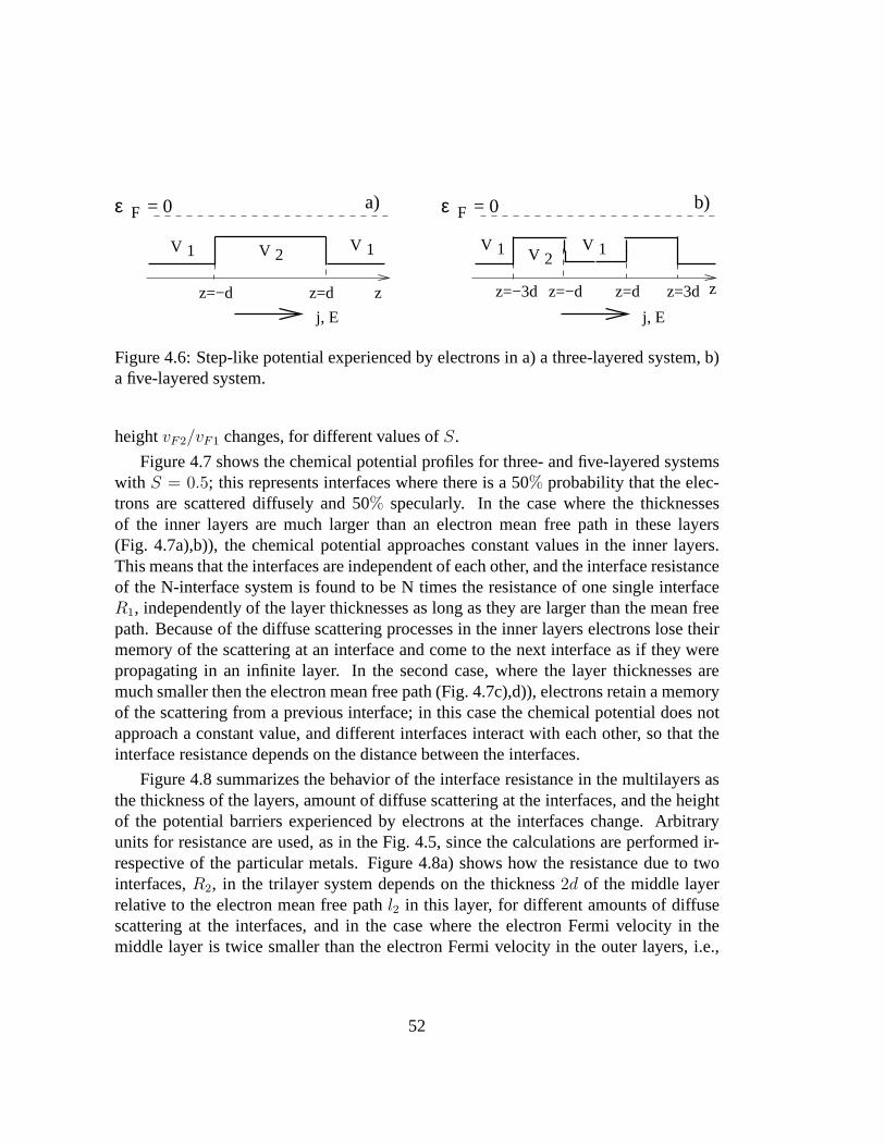
j, E
ε = 0F
V 2
j, E
ε = 0F
V 2V 11V V 11V
z=−d z=dz=−3d z=3d z
b)a)
zz=−d z=d
Figure 4.6: Step-like potential experienced by electrons in a) a three-layered system, b)a five-layered system.
heightvF2/vF1 changes, for different values ofS.
Figure 4.7 shows the chemical potential profiles for three- and five-layered systemswith S = 0.5; this represents interfaces where there is a 50% probability that the elec-trons are scattered diffusely and 50% specularly. In the case where the thicknessesof the inner layers are much larger than an electron mean freepath in these layers(Fig. 4.7a),b)), the chemical potential approaches constant values in the inner layers.This means that the interfaces are independent of each other, and the interface resistanceof the N-interface system is found to be N times the resistance of one single interfaceR1, independently of the layer thicknesses as long as they are larger than the mean freepath. Because of the diffuse scattering processes in the inner layers electrons lose theirmemory of the scattering at an interface and come to the next interface as if they werepropagating in an infinite layer. In the second case, where the layer thicknesses aremuch smaller then the electron mean free path (Fig. 4.7c),d)), electrons retain a memoryof the scattering from a previous interface; in this case thechemical potential does notapproach a constant value, and different interfaces interact with each other, so that theinterface resistance depends on the distance between the interfaces.
Figure 4.8 summarizes the behavior of the interface resistance in the multilayers asthe thickness of the layers, amount of diffuse scattering atthe interfaces, and the heightof the potential barriers experienced by electrons at the interfaces change. Arbitraryunits for resistance are used, as in the Fig. 4.5, since the calculations are performed ir-respective of the particular metals. Figure 4.8a) shows howthe resistance due to twointerfaces,R2, in the trilayer system depends on the thickness2d of the middle layerrelative to the electron mean free pathl2 in this layer, for different amounts of diffusescattering at the interfaces, and in the case where the electron Fermi velocity in themiddle layer is twice smaller than the electron Fermi velocity in the outer layers, i.e.,
52

−500
−1.0−1.0
−200 0
−0.5−0.5
−100 500
0.00.0
0
0.50.5
100
1.01.0
200−2.0
−1.5
−1.0
−0.5
0.0
0.5
1.0
−2.0−1.0
−1.0
1.5
−1.5
−0.5
−0.5
2.0
−1.0
0.0
0.0
−0.5
0.5
0.5
0.0
1.0
1.0
0.5
1.0
1.5
2.0
z/l z/l
z/l
µ
µµ
µ
z/l
a) b)
d)c)
eEl
eEleEl
eEl
Figure 4.7: Chemical potential profiles forS = 0.5, normalized with respect to potentialdropeEl within eachlayer: a) in the three-layered system with the middle layer thick-ness much larger than the electron mean-free path in the layer, b) in the five-layeredsystem with the middle layers thicknesses much larger than the electron mean-free pathin the layers, c) in the three-layered system with the middlelayer thickness much smallerthan the electron mean-free path in the layer, d) in the five-layered system with the mid-dle layers thicknesses much smaller than the electron mean-free path in the layers.
53

vF1 = 2vF2. When the thickness of the middle layer is large (2d/l2 ≫ 1),R2 is indepen-dent of2d, and it is twice the resistance of one single interfaceR1. As the ratio2d/l2decreases, interface resistance in the trilayer system changes. For completely diffuseinterfaces (S = 0) interface resistance decreases as2d/l2 decreases. If a small amountof specular scattering is present at the interfaces, interface resistance at first increasessignificantly as2d/l2 decreases, and then decreases abruptly when2d/l2 becomes lessthan 0.2. As the amount of specular scattering at the interfaces grows (S reaches 1), thechange in the interface resistance as2d/l2 decreases becomes smaller.
In the Fig. 4.8b), the difference between the resistance dueto the interfaces in thethree-layered systemR2 and twice the resistance of the single interface between twosemi-infinite layers2R1 relative to2R1 as a function of the electron Fermi velocitiesratio vF2/vF1 for different values ofS at the interfaces and for2d/l2 = 0.4 is shown.This difference represents the deviation from the resistors-in-series model. In the ab-sence of the barrier (vF2/vF1 = 1), resistance exists due to diffuse scattering, and(R2 − 2R1)/2R1 = 0 for completely specular interfaces only. The deviation fromthe resistors-in-series model is the largest for the completely specular interfaces (S = 1)andvF2/vF1 = 1.4. The shape of the potential barrier (whether the electrons expe-rience a step up or step down at the interface between the firstand the second layers)strongly influences the(R2−2R1)/2R1 difference, as the plots are asymmetrical aroundvF2/vF1 = 1, the ratio of the electron Fermi velocities that representsthe absence of thebarrier.
Similarly, Fig. 4.8c) shows the resistance due to four interfaces in a five-layeredsystem as a function of the layers thickness2d relative to the electron mean-free pathin the second layerl2. Unlike in the three-layered system, the variation of the interfaceresistance with2d/l2 is less pronounced for diffusive interfaces (S approaching0), andmore pronounced for specular interfaces (S approaching1). Figure 4.8d) shows thedeviation from the resistors-in-series model in the five-layered system, the differencebetweenR4 and4R1 relative to4R1 for differentS and2d/l2 = 0.4. As the numberof steps experienced by the electrons grows from2 in the three-layered system to4 inthe five-layered system, the actual shape of the barrier seems to play less important rolein defining the(RN − NR1)/NR1 difference as a function ofvF2/vF1, as the plots for(R4−4R1)/4R1 look symmetrical aroundvF2/vF1 = 1. As in the three-layered system,the maximum deviation from the resistors-in-series model is obtained for completelyspecular interfaces; it reaches 15% forvF2/vF1 = 1.6 andvF2/vF1 = 0.6.
54

2
2
0.5
0.5
4
4
1
1
6
6
1.5
1.5
8
8
2
2
2.5
2.5
2.6
1.5
2.8
3
1.6
3.2
1.7
3.4
10
1.8
3.6
20
1.9
302
5
0
0
R
R
2
4
b)
S=0
S=1
a)
S=0
S=1
c)
−
−
v v
R 2R2R
4R4R
R
v v
F2 F1
2 1
1
1
1
4
F2 F1
,
,
%
%
=0.4
=0.4
S=0
S=0
S=0.1
S=0.1
S=0.2
S=0.2
S=0.3
S=0.3
S=0.4
S=0.4
S=0.5
S=0.5
S=0.6
S=0.6
S=0.7
S=0.7
S=0.8
S=0.8
S=0.9
S=0.9
S=1
S=1
2d/l 2
2d/l 2
/
2d/l 2
2d/l 2
/
d)
2.5
−2.5
−5
−7.5
−10
−12.5
−15
Figure 4.8: Summary of results for the three-layered and five-layered systems: a) resis-tance due to the interfacesR2 of the three-layered system as a function of the middlelayer thickness to the electron mean-free path in this layerratio 2d/l2 for different val-ues of diffuse scatteringS at the interfaces and for the electron Fermi velocities ratiovF2/vF1 = 0.5, b) percentage difference betweenR2 and twice the resistance of thesingle interface between two semi-infinite layers2R1 relative to2R1 as a function ofthe electron Fermi velocities ratiovF2/vF1 for different values ofS at the interfaces andfor 2d/l2 = 0.4, c) resistance due to the interfacesR4 of the five-layered system as afunction of2d/l2 for different values ofS at the interfaces and forvF2/vF1 = 0.5, d)percentage difference betweenR4 and four times the resistance of the single interfacebetween two semi-infinite layers4R1 relative to4R1 as a function ofvF2/vF1 for dif-ferent values ofS at the interfaces and for2d/l2 = 0.4, In the plots a) and c), arbitraryunits for the resistance are used.
55

4.3 Co-Cu and Fe-Cr systems
In this section the resistance due to the interfaces in the realistic two-, three-, and five-layered Fe-Cr and Co-Cu systems is studied. The following cases are considered: 1) aFM↑-N single interface, 2) FM↑-N-FM↑(↓)- a trilayer with parallel (anti-parallel) mag-netization directions in the ferromagnetic layers, and 3) FM↑-N-FM↑(↓)-N-FM↑ - a five-layered system with parallel (anti-parallel) magnetization directions in the ferromagneticlayers (see Fig. 4.9). In the case of the five-layered system the thicknesses of the innerlayers are taken to be the same, and the magnetization of the middle ferromagnetic layeronly is changed. Majority and minority electrons experience different potential steps atthe interfaces between magnetic and non-magnetic metals (see Fig. 4.10a)). The ratio ofthe electron Fermi velocities in the Fe-Cr systemsvF (Cr)/vF (Fe) is taken to be 0.837for majority electrons, and 1.003 for minority electrons. [57] In the Co-Cu systems theratio vF (Cu)/vF (Co) is calculated to be 1.05 for majority electrons, and 1.18 formi-nority electrons (see appendix A.7.1). Interface resistances are calculated by assumingmajority and minority channels to be independent, [3] so that the total resistance is theparallel combination of the resistances of up electronsR↑ and down electronsR↓:
R =R↑R↓R↑ +R↓
. (4.4)
The step-like potentials experienced by electrons in the two-, three-, and five-layeredCo-Cu and Fe-Cr structures are shown schematically in the Fig. 4.10. In order to findthe resistances of up and down electronsR↑ andR↓ in each case a) through j) (seeFig. 4.10), equations (3.14)-(3.15), (A.15)-(A.19), and (A.20)-(A.28) were numericallysolved with the reflection coefficients (4.1) and the appropriate parametersvF1, vF2,andvF3. I present the correspondence betweenR↑, R↓, type of the structure, equationsthat need to be solved, and parametersvF1, vF2, andvF3 entering these equations inthe Appendix A.7.2. In order to deduce the interface resistance from the jump of thechemical potential (Eq. (4.3)), the values of the electronsFermi momentum in the non-magnetic layers are taken to bekFCu = 1.36A−1 for copper, andkFCr = 3.8A−1 forchromium. [57]
Figures 4.11 and 4.12 summarize the behavior of the resistance due to the interfacesin the Co-Cu multilayers with different magnetization configurations as I change theamount of the diffuse scatteringS at the interfaces and the thickness of the layers2drelative to the electron mean-free pathlmfp. Figure 4.11a) shows the resistanceR1
measured far from the interface between two semi-infinite layers of Co and Cu, and that
56

FM
FM FM
FM FM FM
N
N N
N
a)
b)
c)
Figure 4.9: a) FM↑-N single interface, b) FM↑-N-FM↑(↓) three-layered system, c) FM↑-N-FM↑(↓)-N-FM↑ five-layered system.
57
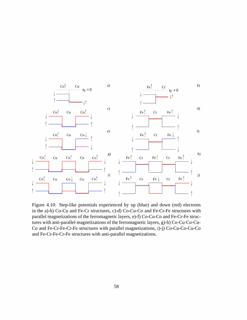
Fe
CuCo Co CrFe Fe
CuCo CoCu Co CrFe FeCr Fe
Cu CuCo Co Co Cr CrFe Fe Fe
Co Cr Fe
ε = 0F ε = 0F
Co Cu Fe Cr
e)
g)
i)
f)
h)
j)
d)c)
a) b)
Cu Co
Figure 4.10: Step-like potentials experienced by up (blue)and down (red) electronsin the a)-b) Co-Cu and Fe-Cr structures, c)-d) Co-Cu-Co and Fe-Cr-Fe structures withparallel magnetizations of the ferromagnetic layers, e)-f) Co-Cu-Co and Fe-Cr-Fe struc-tures with anti-parallel magnetizations of the ferromagnetic layers, g)-h) Co-Cu-Co-Cu-Co and Fe-Cr-Fe-Cr-Fe structures with parallel magnetizations, i)-j) Co-Cu-Co-Cu-Coand Fe-Cr-Fe-Cr-Fe structures with anti-parallel magnetizations.
58

measured right at the interface,R0, as the functions ofS. For diffuse interfaces (S isclose to zero),R1 is larger thanR0. BothR1 andR0 decrease as the amount of diffusescattering at the interface decreases (S increases), butR1 decreases faster, and thereexists a value of parameterS whenR1 = R0. The resistanceR0 becomes larger thanR1 for a specular interface. The relative difference betweenR1 andR0 (Fig. 4.11b)) isabout 20% for completely diffuse interfaces; as the resistances decrease, this differencemay reach more than 100%.
Figures 4.11c)-f) show the resistances due to the interfaces in the multilayersR2
for three-layered systems andR4 for five-layered systems as the functions of the layerthicknesses relative to the electron mean-free path for different amounts of diffuse scat-tering at the interfaces and different magnetization configurations (see Fig. 4.10). Inall four geometries, resistance due to the interfaces decreases as the amount of diffusescattering decreases (S changes from0 to 1). Interface resistance is very small for com-pletely specular interfaces, due to the very small potential barrier height that the majorityelectrons experience at the interface between Co and Cu, so that the majority channelshunts the current. As seen from the Figs. 4.11c)-f), resistance due to the interfaces inthe multilayers do not depend on the thickness of the layers2d relative to the electronmean-free pathlmfp when2d/lmfp is greater than1, and they are found to be equal tothe sum of resistancesR1 of the corresponding number of the independent interfaces,2R1 or 4R1. As the thickness of the layers becomes much smaller than themean-freepath,2d/lmfp ≪ 1, resistancesR2 andR4 start to deviate from2R1 or 4R1, as predicted,indicating the breakdown of the resistors-in-series model.
Figures 4.12a)-d) show the deviations of the actual resistancesR2 andR4 from theresistors-in-series model results,2R1 or 4R1, relative to2R1 or 4R1, as the functions of2d/lmfp for different amounts of diffuse scattering at the interfaces and different mag-netization configurations. These deviations are not monotonic with 2d/lmfp. The differ-ence betweenRN andNR1 is especially large for extreme interfaces, almost completelyspecular,S close to1, or completely diffuse,S close to0. (In the three-layered systemsthe plot forS = 1 is not shown, as it has a much larger scale than other plots.) It reaches10-15% in the three-layered systems, 20% in the five-layeredsystems with the paral-lel magnetization directions, and 30% in the five-layered systems with the anti-parallelmagnetization directions for completely specular interfaces.
Finally, Figs. 4.12e)-f) show the difference between actual resistance due to inter-facesRN (N =1, 2, and 4) and the resistance that would be obtained assuming interfacesto be independent of each other as a function of the amount of diffuse scatteringS atthe interfaces. The thickness2d of the non-magnetic layers is taken to be small com-
59

pared to the electron mean free path in the layers (2d/lmfp=0.4). The actual resistanceis compared with both the resistance of an independent interface measured right at theinterface,NR0, and that measured far from the interface,NR1. In all geometries, both(RN −NR1)/NR1 and(RN −NR0)/NR0 are significant for either completely diffuseor completely specular interfaces. For the realistic interfaces where an equal amountof specular and diffuse scattering is present,S = 0.5, the difference between the inter-face resistance one could measure and the resistance of independent interfaces measuredright at the interfaces,NR0, reaches 10%, which is comparable with the experimentalerror for the interface resistance. [23]
Figures 4.13 and 4.14 show the same information as the figures4.11 and 4.12 forFe-Cr systems. Similarly to the resistances in the Co-Cu systems,R1 is larger thanR0 atsmallS, bothR0 andR1 decrease as the interface becomes more specular (S approach-ing 1), R1 decreasing faster (see Fig. 4.13a)). The difference with Co-Cu systems isthatR1 becomes equal toR0 for S closer to1. The relative difference betweenR0 andR1 is between 12 and 18% forS up to0.9,(Fig. 4.13b)), after that the difference growssignificantly (not shown). ResistancesR2 andR4 for different magnetization configura-tions decrease as the amount of diffuse scattering at the interfaces decreases. In the caseof the parallel magnetization directions both in the three-and five-layered structures,resistances of the completely specular interfaces are not shown, because they are smallcompared to the resistances forS 6= 1, due to the very small potential barrier experi-enced by minority electrons at the interface between Fe and Cr (smaller than that formajority electrons at the interface between Co and Cu). Resistance due to the interfacesdepend on the thickness of the layers relative to the electron mean-free path,2d/lmfp,as it becomes of the order or less then1 (Fig. 4.13c)-f)). As it is for the Co-Cu sys-tems, the deviation from the resistors-in-series model forFe-Cr structures is substantialfor extreme interfaces, withS close to0 or 1 (Fig. 4.14a)-d)), but for the interfaces withS = 0.5, the difference betweenRN andNR0 reaches 20% for the systems with parallelmagnetic configuration and more then 15% for the systems with anti-parallel magneticconfiguration (Fig. 4.13e)). This exceeds experimental error, which is about 10% for theinterface resistance and about 15% for the bulk resistance [23].
60
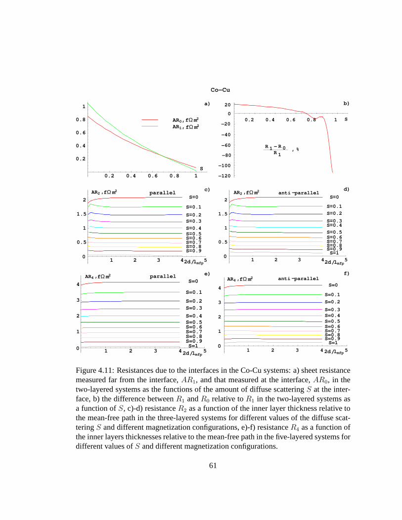
0.2
1
0.4
2
0.6
3
0.8
4 4
1
5 5
0.2
0.4
0.5
0.6
1
0.8
1.5
1
2
S
AR0 , ff
f f
f f
ΩΩ
Ω Ω
Ω Ω
mm
m m
m m
2
2
2 2
22
AR1 ,
AR AR
AR AR
2 2
44
, ,
, ,
S=0.1
mfp mfp
mfp mfp
anti
anti
parallel −
−
Sparallel
parallel
= S0
S
=
=
0
S0.1
S
=
=
0.1
S0.2S
=
=
0.2
S0.3
S
==
0.3S
0.4S
=
=
0.4
S0.5S
==
0.5S0.6
S=
=0.6
S0.7S
==
0.7S0.8
S=
=0.8
S0.9 =0.9S=1
%,R1
2d l/ 2d l/
2d l/ 2d l/
R1
a) b)
c) d)
e) f)
10.80.60.40.2
20
0
−20
−40
−60
−80
−100
−120
− R
2 3
1.5
0.5
2
1
0 0
4
3
2
1 2 3 4 5
S=0
S=0.2S=0.3
S=0.4S=0.5S=0.6S=0.7S=0.8S=0.9S=1
1
0
parallel
4
3
2
1
1 2 3 4 5
S=0
S=0.1
S=0.2
S=0.3S=0.4S=0.5S=0.6S=0.7S=0.8S=0.9
S=10
0
1
S
Co−Cu
Figure 4.11: Resistances due to the interfaces in the Co-Cu systems: a) sheet resistancemeasured far from the interface,AR1, and that measured at the interface,AR0, in thetwo-layered systems as the functions of the amount of diffuse scatteringS at the inter-face, b) the difference betweenR1 andR0 relative toR1 in the two-layered systems asa function ofS, c)-d) resistanceR2 as a function of the inner layer thickness relative tothe mean-free path in the three-layered systems for different values of the diffuse scat-teringS and different magnetization configurations, e)-f) resistanceR4 as a function ofthe inner layers thicknesses relative to the mean-free pathin the five-layered systems fordifferent values ofS and different magnetization configurations.
61
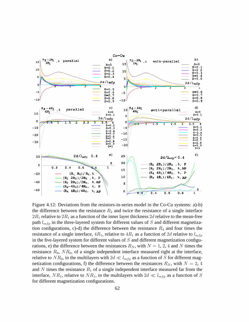
Figure 4.12: Deviations from the resistors-in-series model in the Co-Cu systems: a)-b)the difference between the resistanceR2 and twice the resistance of a single interface2R1 relative to2R1 as a function of the inner layer thickness2d relative to the mean-freepathlmfp in the three-layered system for different values ofS and different magnetiza-tion configurations, c)-d) the difference between the resistanceR4 and four times theresistance of a single interface,4R1, relative to4R1 as a function of2d relative tolmfp
in the five-layered system for different values ofS and different magnetization configu-rations, e) the difference between the resistancesRN , withN = 1, 2, 4 andN times theresistanceR0, NR0, of a single independent interface measured right at the interface,relative toNR0, in the multilayers with2d≪ lmfp as a function ofS for different mag-netization configurations, f) the difference between the resistancesRN , with N = 2, 4andN times the resistanceR1 of a single independent interface measured far from theinterface,NR1, relative toNR1, in the multilayers with2d ≪ lmfp as a function ofSfor different magnetization configurations.
62

1
0.2
1
11
2
0.4
2
22
3
0.6
3
33
4
0.8
4
44
5
1
5
55
0.1
0.2
0.2
0.2
0.5
0.25
0.4
0.3
0.4
1
0.5
0.6
0
0.6
1.5
0.75
0
0.80.8
1
1.25
1.5
S
AR0, f
f
f
f f
f
ΩΩ
Ω
Ω Ω
Ω
m
m
m
m m
m
2
2
2
2 2
2
AR1,
R1
R
R R
R
−
2
4 4
2
R
,
, ,
,
0R1
2
2 2
2
anti
,
d
d d
d
−
%
parallel
l
l l
l
S
mfp
mfp mfp
mfp
=
parallel
0
S
S
anti
=
=
−
0
0.1
S
S
parallel
S
=
=
=
0.1
0.2
S
S
0
S=
=
=0.2
0.3
S
S
parallel
0.1S
=
=
S
=0.3
0.4
=
S
S
0.2
0
S=
=
S
=0.4
0.5
=
S
S
0.3
0.1
S=
=
S
=0.5
0.6
=
S
S
0.4
0.2
S=
=
S
=0.6
0.7
=
S
S
0.5
0.3
S=
=
S
=0.7
0.8
=
S
S
0.6
0.4
S=
=
S
=0.8
0.9
=
S
0.7
S
0.5
S=
S
=
=0.9
=
1
0.8
0.6
S
S
=
=
0.9
0.7S
S
=
=
0.8
1
S=0.9
/
/ /
c) d)
e) f)
/
Fe−Cr
a) b)20
17.5
15
12.5
10
7.5
5
2.50
0.2 0.4 0.6 0.8S0
Figure 4.13: Resistances due to the interfaces in the Fe-Cr systems: a) sheet resistancemeasured far from the interface,AR1, and that measured at the interface,AR0, in thetwo-layered systems as the functions of the amount of diffuse scatteringS at the in-terface, b) the difference betweenR1 andR0 relative toR0 in the two-layered systemsas a function ofS (note the differentS-axis limit), c)-d) resistanceR2 as a function ofthe inner layer thickness relative to the mean-free path in the three-layered systems fordifferent values of the diffuse scatteringS and different magnetization configurations,e)-f) resistanceR4 as a function of the inner layers thicknesses relative to themean-freepath in the five-layered systems for different values ofS and different magnetizationconfigurations.
63

Figure 4.14: Deviations from the resistors-in-series model in the Fe-Cr systems: a)-b)the difference between the resistanceR2 and twice the resistance of a single interface2R1 relative to2R1 as a function of the inner layer thickness2d relative to the mean-freepathlmfp in the three-layered system for different values ofS and different magnetiza-tion configurations, c)-d) the difference between the resistanceR4 and four times theresistance of a single interface,4R1, relative to4R1 as a function of2d relative tolmfp
in the five-layered system for different values ofS and different magnetization config-urations, e) the difference between the resistancesRN , with N = 1, 2, 4 andN timesthe resistanceR0 of a single independent interface measured right at the interface,NR0,relative toNR0, in the multilayers with2d≪ lmfp as a function ofS for different mag-netization configurations, f) the difference between the resistancesRN , with N = 2, 4andN times the resistanceR1 of a single independent interface measured far from theinterface,NR1, relative toNR1, in the multilayers with2d ≪ lmfp as a function ofSfor different magnetization configurations.
64

Chapter 5
Spin-torques - theory
In the following two chapters, a mechanism of the magnetization switching of magneticmultilayers driven by a spin-polarized current is studied.First, I present a spin trans-fer model in which the equation of motion of the spin accumulation is solved in orderto derive the torque acting on the background magnetization. Next, a system of twothick magnetic layers separated by a non-magnetic spacer isconsidered. The analyticalexpressions for the spin-current and spin-accumulation distributions in the system, andspin-torque and effective field acting on the local magnetization in the ferromagneticlayers are obtained, and I discuss the significance of the result for the spin-current atthe interface between layers in the system with magnetization directions close to anti-parallel. Finally, the correction to the CPP magnetoresistance due to the interaction ofthe electron spins and background magnetization is calculated. In the next chapter, Ipresent the results for a realistic multilayered structure.
5.1 Review of formalism
The linear response of the current to the electric field in thex-direction for diffusivetransport, Eq. (2.26), can be written in a spinor form as [36]
(x) = CE(x) − D∂n
∂x, (5.1)
whereE(x) is the electric field,j, C, D, andn are the2 × 2 matrices representing thecurrent, the conductivity, the diffusion constant, and thecharge and spin accumulations
65

at a given position. The diffusion constant and the conductivity are related via the Ein-stein relationC = e2N(ǫF )D for a degenerate metal, whereN(ǫF ) is the density ofstates at the Fermi level. In general, these matrices can be expressed in terms of thePauli spin matrixσ as
C = C0I + σ · C,D = D0I + σ · D,N = N0I + σ · N,n = n0I + σ · m,
j = jeI + σ · jm,
(5.2)
where2n0 is the charge accumulation,2n0 = n↑ + n↓, andm is the spin-accumulation,2|m| = n↑ − n↓, n↑ is the number of electrons with the spins parallel to the princi-pal quantization axis,n↓ is the number of electrons with the spins anti-parallel to theprincipal quantization axis, and, similarly, electric current2je = j↑ + j↓, magnetizationcurrent2|jm| = j↑ − j↓. Inserting Eqs. (5.2) in Eq. (5.1), the electric currentje andmagnetization currentjm can be written as
je ≡ Re(Trj) = 2C0E(x) − 2D0∂n0
∂x− 2D · ∂m
∂x, (5.3)
jm ≡ ReTr(σj) = 2CE(x) − 2D∂n0
∂x− 2D0
∂m
∂x, (5.4)
where the unitse = µB = 1 are chosen for the notation convenience. The first termon the right hand side of Eq. (5.4) is the contribution to the spin polarized current fromthe electric field, the third term is the contribution from the spin accumulation, which ispresent in a magnetically inhomogeneous structure. The second term, the contributioncoming from the charge accumulation, will be neglected, since its characteristic length-scale, of the order of several angstroms, is of the order of magnitude smaller than otherrelevant lengthscales. As will be shown below, in magnetic multilayers the contributionof the third term to the spin current can dominate over the first. Comparing Eq. (5.3)with the expression (2.26) for the electric current, the parametersC0 andD0 can be
identified withC0 = 12σ =
k3F
6π2e2τm
, D0 = 12D = 1
6v2
F τ = 16vFλmfp, whereλmfp ≡ vF τ
is the electron mean-free path.For a transition metal ferromagnet, the spin-polarizationparameter for the conduc-
tivity β, the diffusion constantβ ′, and for the density of statesβ ′′ can be defined asC = βC0Md, D = β ′D0Md, andN = β ′′N0Md, whereMd is the unit vector torepresent the direction of the local (background) magnetization. Similarly to the spin-
66

polarization parameters for the interface,γ, γ′, andγ′′, introduced in the Appendix B.1,spin-polarization parameters for the bulk are related asβ ′ = (β − β ′′)/(1− ββ ′′) (com-pare with Eq. (B.34)). The experimental value forβ can be found in the Ref. [23], andthe value ofβ ′′ can be found from the bulk densities of states of up and down electrons,N↑ andN↓, asβ ′′ = (N↑ − N↓)/(N↑ + N↓). Inserting the expressions forC andD inEqs. (5.3) and (5.4), and eliminating the electric field and charge density, the followingexpression for the spin-current is obtained:
jm = βjeMd − 2D0
[
∂m
∂x− ββ ′Md(Md ·
∂m
∂x)
]
. (5.5)
The equation of motion for the spin accumulation may be obtained by generalizingthe continuity equation (2.24) to the systems with both spin-up and spin-down electrons,and including the possibility of spin-flip scattering. The continuity equation for the spin-up electrons densityn↑ (spin-down electrons densityn↓) has the form
∂n↑(↓)∂t
+∂j↑(↓)∂x
= −n↑(↓) − n↓(↑)τsf
,
whereτsf is the spin-flip relaxation time of the conduction electrons, and, for the spin-accumulation,
∂|m|∂t
+∂|jm|∂x
= −2|m|τsf
.
Introducing the termJ/hm × Md (see Chap. 1), the equation of motion form may bewritten as
∂m
∂t+∂jm∂x
+J
hm× Md = −2m
τsf. (5.6)
Upon placing the expression for the magnetization current Eq. (5.5) in Eq. (5.6) onefinds the following equation of motion for the spin-accumulation vector:
1
2D0
∂m
∂t− ∂2m
∂x2+ ββ ′Md
(
Md ·∂2m
∂x2
)
+m
λ2sf
+m ×Md
λ2J
= − 1
2D0
∂
∂x(βjeMd), (5.7)
whereλsf ≡√
D0τsf andλJ ≡√
2hD0/J . The term on the right hand side of the
67

time dependent diffusion equation Eq. (5.7) for the spin accumulation is the sourceterm; it is this term that drives the accumulation. [59] Following the conventional treat-ment of magnetic multilayers for current perpendicular to the plane of the layers, onecan assume that the magnetization is uniform throughout a layer, and changes discon-tinuously between the layers. [60, 6] If one looks for the steady-state solutions of theequation (5.7), the first term on the left-hand side is zero, and the electric currentje isconstant throughout the multilayer; therefore one can see that the source term is confinedto interfaces between the layers, and can be taken into account by appropriate bound-ary conditions. The boundary conditions at the diffusive interfaces between two layerswith noncollinear magnetizations are addressed in detail in Appendix B.1. It is shownthat while the spin-accumulation experiences a jump at the interfaces, proportional tothe interface resistance, the spin-current is continuous across the diffusive interface, andno spin-torque is created at the interface. The specular scattering at the interfaces canalso be taken into account within the semiclassical framework presented in this work,as it is done, for example, in Chap. 3; this involves considering eachk vector sepa-rately which for a noncollinear multilayer is a cumbersome problem, and it will not beaddressed here. Below, the equations for the spin-accumulation and the effect of thespin-accumulation on the local magnetization in the bulk ofthe layers are discussed.
The equation of motion for the local magnetizationMd is the Landau-Lifshitz-Gilbert equation
dMd
dt= −γ0Md × (He + Jm) + αMd ×
dMd
dt, (5.8)
whereγ0 is the gyromagnetic ratio,He is the magnetic field including the contributionsfrom the external field, anisotropy and magnetostatic field,the additional effective fieldJm is due to coupling between the local moments and the spin accumulation, and thelast term is the Gilbert damping term. Note that the characteristic time scale for the localmoment isγ−1
0 He, of the order of nanoseconds for a magnetic field of 0.1 T, while thetime scale of the spin accumulation is of the order ofτsf andh/J , i.e., of the order ofpicoseconds. Therefore, the background magnetization canbe assumed to be fixed onthe time scale of the spin accumulation, and the steady statesolution of the equation (5.7)can be considered.
By separating the spin accumulation into longitudinal (parallel to thelocal moment)and transverse (perpendicular to thelocal moment) modes,m|| andm⊥, and looking for
68

the steady state solutions, equation (5.7) can be written as
∂2m||∂x2
− m||λ2
sdl
= 0, (5.9)
whereλsdl =√
1 − ββ ′λsf , and
∂2m⊥∂x2
− m⊥λ2
sf
− m⊥ ×Md
λ2J
= 0. (5.10)
Note that the terms longitudinal and transverse refer to themagnetization in the indi-vidual layers, i.e., they arelocally defined and have no global meaning throughout anoncollinear multilayer.
The longitudinal accumulationm|| decays at the length scale of the spin diffusionlengthλsdl, while the transverse spin accumulationm⊥ decays asλJ if one assumesλJ ≪ λsf . This assumption is valid for cobalt, for example. where thespin-diffusionlengthλsdl has been measured to be about 60 nm,β is 0.5,λmfp is about 6 nm, [23]vF = 0.6 · 106 m/s,J = 0.3 eV.[40] I estimateβ ′ to be about 0.9 using the bulk densi-ties of states for up and down electrons of 2.42 states/(atomRy) and 13.42 states/(atomRy) [61], so thatλsf = 80 nm,λJ = 2 nm,λJ ≪ λsf , and the transverse spin accumu-lation has a much shorter length scale compared to the longitudinal one. However, forpermalloy,λsdl has been measured to be about 5 nm,β is 0.7, [23]β ′ is estimated to beabout 0.95 using the bulk densities of states for up and down electrons of 2.4 states/Ryand 15 states/Ry [62, 63], so thatλsf is about 9 nm. Taking the typical diffusion constantof a metal to beD0 = 10−3m2/s, andJ = 0.1 eV, [41],λJ can be estimated to be 4 nm,comparable withλsf . The majority of the results presented in this work are obtained inthe limitλJ ≪ λsf , so that they are applicable to cobalt. The structure consisting of twosemi-infinite permalloy layers divided by a nonmagnetic spacer is considered separatelybelow.
As seen from Eq. (5.8), the longitudinal spin accumulation has no effect on the localmoment; therefore, one can re-write Eq. (5.8) in terms of thetransverse spin accumula-tion only by replacingm by m⊥:
dMd
dt= −γ0Md × (He + Jm⊥) + αMd ×
dMd
dt. (5.11)
In order to describe the transverse accumulation, it is convenient to introduce an aux-
69

iliary vectorA such thatJm⊥ = A × Md. [36] If one considers a system with twononcollinear ferromagnetic layers, the spin accumulationin one layer depends on theorientation of the other. Supposing that the above equationis used for the layer F1 (seeFig. 1.11), the local magnetization of this layer is labeledasM
(1)d , and the magnetiza-
tion of the other layer is labeled asM(2)d . Without loss of generality, the vectorA can
be written as a linear combination of the vectorM(2)d , and the vector perpendicular to
M(2)d , for example,A = aM
(2)d − bM
(2)d × M
(1)d , so that the two components of the
accumulation in the plane perpendicular toM(1)d are written as
Jm⊥ = aM(2)d × M
(1)d + bM
(1)d × (M
(2)d × M
(1)d ), (5.12)
wherea andb are determined by geometric details of the multilayer. By placing thisform of the accumulation in the equation of motion for the background magnetization,Eq. (5.11), one finds the following equation of motion forM
(1)d
:
dM(1)d
dt= −γ0M
(1)d ×(He+bM
(2)d )−γ0aM
(1)d ×(M
(2)d ×M
(1)d )+αMd×
dMd
dt. (5.13)
Thus the transverse spin accumulation produces two effectssimultaneously: the termbM
(1)d × M
(2)d is the torque due to an ”effective field”bM(2)
d , and the other isaM(1)d ×
(M(2)d × M
(1)d ) is called the ”spin torque” predicted in the Refs. [7, 8, 9, 10, 11]. The
first term produces a precessional motion aboutM(1)d
; in this sense it actsas if the spincurrent creates a magnetic field onM(1)
d(see Fig. 5.1). The second term acts so as
to increase or decrease the angle betweenM(1)d
andM(2)d
; also, it acts so as to assistor oppose the damping term in Eq. (5.8). Note that both the spin-torque and effectivefield terms appear on an equal footing in the equation (5.13),as both are related to thetransverse spin accumulation.
The torque transmitted by the current to the background may also be determinedfrom the following considerations. The torqueτ acting on the background angular mo-mentumMd is the time derivative ofMd, τ = dMd/dt. Thetotalangular momentum ofthe system, which is the sum of the electron angular momentumm and the backgroundangular momentumMd is conserved, so thatm + Md = const. The torque acting onthe background magnetization can be written in terms of the electron spin accumulationand spin current as
τ = −dmdt
= −∂m∂t
− ∂jm∂x
,
70

θ
M M(2) (1)
0 tF
z
FM2 FM1 NMy
y
x
d d
j e
effective field, −x−direction
spin−torque, −y−direction
Figure 5.1: Direction of the effective field (red vector) andspin-torque (blue vector)acting on a thin FM layer background magnetizationM
(1)d = ez, if the magnetization of
the thick layer isM(2)d = cos θez − sin θey.
so that the torque transmitted by a steady-state current is given by thegradientof the spincurrent. Integrating this over a layer with the thicknessd which absorbs the momentum,one finds
∆τ = −∫ d
0
∂jm∂x
dx = jm(0) − jm(d). (5.14)
The total torque absorbed by the layer is the difference between the spin current valuesat the boundaries of the layer.
5.2 Two ferromagnetic layers
In order to illustrate the method developed in Sec. 5.1 to determine the effective field andspin-torque acting on the ferromagnetic layer, I choose a simplified system where I cananalytically derive the spin accumulation, spin-current,effective field, and spin-torque.I consider a system consisting of two thick ferromagnetic layers with the magnetizationsM
(1)d = cos θez + sin θey andM
(2)d = cos θez − sin θey, wherex is the direction of the
electric current (see Fig. 5.2), separated by a nonmagneticspacer layer so that there isno exchange coupling between ferromagnetic layers, and backed by nonmagnetic layers,or leads. The nonmagnetic spacer layer thickness is considered to be small comparedto the spin-diffusion length in the nonmagnetic metal (λN
sdl ∼ 600 nm), so that bothspin accumulation and spin current are constant in the spacer, and I will use both terms”spacer” and ”interface between magnetic layers” interchangeably. The thickness of
71

Ftx, x, x
z
y
z
z θ
θM
M (1)
(2)
je
0−tF
d
d
Figure 5.2: System of two thick ferromagnetic layers separated by a spacer layerand backed by nonmagnetic layers, or leads. Magnetization of the first (right) layeris M
(1)d = cos θez + sin θey, magnetization of the left (second) layer isM(2)
d =cos θez − sin θey. (x, y, z) is the global coordinate system, (x, y, z) and (x, ¯y, ¯z) are thelocal coordinate systems connected to the local magnetizations in the first and secondlayers.
the ferromagnetic layerstF is large enough so that one can neglect the reflections fromthe outer boundaries of the layers. The difference between this system and the systemconsidered in the Ref. [36] is that in the latter, the second layer is assumed to be halfmetallic, so that the current is fully spin-polarized, while here this approximation isabandoned.
I solve Eqs. (5.9) and (5.10) to find the longitudinal and transverse spin accumulationin both ferromagnetic layers, and use Eq. (5.5) to find the spin-current. In the localcoordinate system (x, y, z) connected to the local magnetization of the right layer, thespin-accumulation and spin current take the following form:
m(1)z = G1 exp(−x/λsdl)
m(1)x = 2Re(G2 exp(−x/l+))
m(1)y = 2Im(G2 exp(−x/l+)),
(5.15)
72

j(1)m,z = βje + 2D0(1−ββ′)
λsdlG1 exp(−x/λsdl)
j(1)m,x = 4D0Re
(
G2exp(−x/l+)
l+
)
j(1)m,y = 4D0Im
(
G2exp(−x/l+)
l+
)
,
(5.16)
whereG1 andG2 are constants of integration, and
1
l+=
√
√
√
√
1
λ2sf
− i
λ2J
≈ 1 − i√2λJ
(5.17)
whenλJ ≪ λsf . Similar expressions for the local spin-accumulation and spin-currentare written for the second layer.
To determine the constants of integration, the boundary conditions at the interfacebetween two ferromagnetic layers have to be invoked. The boundary conditions are dis-cussed in detail in Appendix B.1. At a diffusive interface, the spin-current is conserved,and the spin-accumulations to the left and to the right of theinterface in the global(x, y, z) coordinate system are related as follows:
mx(0−) −mx(0+) = 2jm,x(0)r λJ√2D0
my(0−) −my(0+) = 2jm,x(0)(
cos2 θ + sin2 θ(1−γγ′)
)
r λJ√2D0
mz(0−) −mz(0+) = −γje cos θr λJ√2(1−γγ′)D0
+ 2jm,x(0)(
sin2 θ + cos2 θ(1−γγ′)
)
r λJ√2D0
,
wherer is proportional to the interface resistanceARI (see Eq. (B.35)),γ andγ′ are thespin polarization parameters for the conductivity and the diffusion constant at the inter-face (see Eq. (B.5)). Note that the spin-accumulation is conserved across the interface ifthere is no diffuse scattering at the interface (ARI = 0). Vectors in the local and globalcoordinate systems are related via the rotation matrix (seeEq.(B.20)), and the constantsof integration are
G1 = − βje√2λJJ
ha30
eµB×
sin2 θ(1 + r) + r(1−γ/β)1−γγ′ cos2 θ
cos2 θ(1 + rλ1−γγ′ ) + λ sin2 θ(1 + r)
(5.18)
73

G2 =βje
2√
2λJJ
ha30
eµB× (1 + rtλ) sin 2θ
cos2 θ(1 + rλ1−γγ′ ) + λ sin2 θ(1 + r)
(1 − i), (5.19)
whereλ = (1 − ββ ′)λJ/√
2λsdl, t = γ/β(1 − γγ′), r =√
2ARIe2N I
0 (ǫF )D0(1 −γ′′2)/λJ(1 − γγ′), ARI is the resistance of the interface between two ferromagneticlayers,β, β ′ are spin-polarization parameters for conductivity and diffusion constantin the bulk of the layers,γ, γ′, γ′′ are spin-polarization parameters for conductivity,diffusion constant, and electron density of states at the interface;N I
0 (ǫF ) is the densityof states at the interface at Fermi energy (see Appendix B.1). The expressions for thespin-accumulation in the right layer are
m(1)x = 2e
− x√2λJ ReG2[cos x√
2λJ+ sin x√
2λJ]
m(1)y = −2e
− x√2λJ ReG2[cos x√
2λJ− sin x√
2λJ] cos θ +G1e
− xλsdl sin θ
m(1)z = 2e
− x√2λJ ReG2[cos x√
2λJ− sin x√
2λJ] sin θ +G1e
− xλsdl cos θ.
(5.20)
In the left layer they are
m(2)x (x) = m(1)
x (−x)m(2)
y (x) = m(1)y (−x)
m(2)z (x) = −m(1)
z (−x).
The spin-current in the layers can be found from Eq. (5.5). The expressions for thecomponents ofjm are complicated, and I will only present the values of thex−, y−,andz−components ofjm at x = 0, in the nonmagnetic spacer, in the absence of thescattering at the interface. Due to the symmetry of the problem, only thez-componentis non zero, so that
jm(x = 0) =βje cos θ
cos2 θ + λ sin2 θez, (5.21)
whereλ =√
1 − ββ ′λJ/√
2λsf , and it is of the order of 0.02 for cobalt. The spincurrent at the interface reaches its maximum value of
jm,max(x = 0) =βje cos θ⋆
2λ(5.22)
74

when the angle between the local magnetizations is2θ⋆, where
cos 2θ⋆ = −1 − 3λ
1 − λ, (5.23)
and2θ⋆ is close toπ whenλ ≪ 1. The magnitude of the spin-current is enhanced by alarge factor ofλ−1 compared to the bare spin-currentβje cos θ. This enhancement comesfrom the interplay between longitudinal and transverse accumulations; it is the result ofthe global nature of the spin-current even though the transverse components of the spincurrent and accumulation are absorbed within a region of severalλJ of the interface.While the total spin torque acting on a symmetric two-layered structure is zero, theresult of Eq. (5.21) can serve as an indication that in the non-symmetric structure whenone layer is pinned and the other free; the spin-torque acting on the free layer, and,hence, the angular momentum transferred to it, exceeds the transverse component of thebare portion of the incoming spin-current by1/2λ. This prediction will be tested in thenext chapter, where the non-symmetric three-layered system is discussed.
The spin-torquea1 and the effective fieldb1 acting on the ferromagnetic layer canbe found from the following considerations. From Eq. (5.15), the transverse spin-accumulation in the right layer can we written as
m(1)⊥ = m
(1)x ex+m
(1)y ey = 2Re(G2 exp(−x/l+))ex+2Im(G2 exp(−x/l+))ey, (5.24)
whereex andey are unit vectors in thelocal coordinate system. By noticing thatG2 canbe written asG2 sin 2θ, M(2)
d ×M(1)d = − sin 2θex, M(1)
d ×(M(2)d ×M
(1)d ) = − sin 2θey,
one can writem(1)⊥ as
m(1)⊥ = −2Re(G2 exp(−x/l+))M
(2)d ×M
(1)d
− 2Im(G2 exp(−x/l+))M(1)d × (M
(2)d × M
(1)d ). (5.25)
One can see that the form of the transverse spin-accumulation given by Eq. (5.25) isexactly the form used in the definition ofa andb (Eq.(5.12)):
Jm⊥ = aM(2)d × M
(1)d + bM
(1)d × (M
(2)d × M
(1)d ). (5.26)
To obtain the coefficientsa andb, one averages the spin-accumulation (5.25) over thethicknesstF of the right layer. The spin-torque and effective fieldper unit lengthacting
75

on the ferromagnetic layer take the form
a1 = − βje
2√
2λJ
ha30
eµB×
1 − cos( tF√2λJ
)e− tF√
2λJ
tF/(√
2λJ)× (1 + rtλ)
cos2 θ(1 + rλ1−γγ′ ) + λ sin2 θ(1 + r)
,
(5.27)
b1 =βje
2√
2λJ
ha30
eµB×
sin( tF√2λJ
)e− tF√
2λJ
tF/(√
2λJ)× (1 + rtλ)
cos2 θ(1 + rλ1−γγ′ ) + λ sin2 θ(1 + r)
. (5.28)
Note that in order to get the true torque and field acting on theferromagnetic layers, thecoefficientsa andb has to be multiplied bysin 2θ (see Eq. (5.26)).
Both spin-torquea sin 2θ and effective fieldb sin 2θ reach their maximum valuewhenθ = θ⋆⋆ where
cos 2θ⋆⋆ = −1 − λ
1 + λ(5.29)
in the absence of the interface resistance; we see thatθ⋆⋆ is close to90.
In the second layer, the spin-torquea2 is equal to−a1, and the effective fieldb2 isequal to−b1 due to the symmetry of the problem.
In Fig. 5.3 I present the spin accumulation and spin current distribution in the FM-Sp-FM structure withλJ = 4 nm,λsdl = 60 nm in the presence of the interface resis-tanceARI = 0.5 fΩ·m2; [23] the diffusion constant is taken to be 10−3 m2/s. Bothm
andjm are constant in the spacer, so I don’t show the spacer in theseplots. As followsfrom Eq. (5.20), the characteristic length scale of the x-component of the accumula-tion, perpendicular to the plane of the layer magnetizations, isλJ . Global y- and z-components of spin accumulation are defined by both transverse and longitudinallocalcomponents of the accumulation, so for them, two length scales may be distinguished:one of the order ofλJ for a more rapid change of the spin accumulation, and the longerone, of the order of the spin-diffusion lengthλsdl. Only the z-component of the spinaccumulation is discontinuous in the presence of the interface resistance due to the sym-metry of the problem. Far from the interfaces,x ≫ λJ andx ≪ −λJ , the spin currentis collinear with background magnetizationM(1)
d or M(2)d , approaching its bare values
jm = βjeM(1)d or jm = βjeM
(2)d . As follows from the equation (5.21), a large ampli-
fication of z-component of the spin-current occurs within a distance of severalλJ fromthe interface.
In Fig. 5.4 I show the spin-torque and effective field per unitlength acting on thefirst ferromagnetic layer as a function of the thickness of the layerstF relative to
√2λJ .
76

Figure 5.3: x-, y-, and z-components of the spin-accumulationm/(βje/
√2λJJ)(ha3
0/eµB) (a-c) and spin-currentjm/βje (d-f) distribution inFM-Sp-FM system in the presence of interface resistance forλJ = 4 nm,λsdl = 60 nmand different anglesθ.
77

3
3
4
4
5
5
=0o
=15o
=30o
=45o
=60o
=75o
=90o
θθθθθ
0.5
2
1
1
1
4
2
2
θ
1.5
6
3
3
2
8
4
4
10
5
5
λ JtF / \/ 2
λ JtF / \/ 2
λ JtF / \/ 2
λ JtF / \/ 2
θ−2
−4
−6
−8
−1
−2
0
0
−10
−0.5
−1.5
0
0
1 2
1 2a b
a sin 2 b sin 2θ θ
a)
b)
c)
d)
Figure 5.4: Spin-torquea/βje(ha30/eµB) and (b)a sin 2θ/βje(ha
30/eµB), (c) effective
field b/βje(ha30/eµB) and (d)b sin 2θ/βje(ha
30/eµB) acting on the FM layer in FM-Sp-
FM system as a function oftF/√
2λJ in the presence of interface resistance forλJ = 4nm,λsdl = 60 nm and different anglesθ.
One can see that while the torque and field termsa andb (Fig. 5.4a) and c)) are largestfor θ = 90, they don’t act on the background magnetization, sincesin 2θ = 0. The truetorque and fielda sin 2θ andb sin 2θ (Fig. 5.4b) and d)) are largest forθ close to90 (seeEq. (5.29)). It is worth noting that while the effective fielddecreases much faster thenthe spin torque as the thickness of the layers increases, at their maximum, they have thesame magnitude, so they indeed have to appear on an equal footing in the equation ofmotion for the local magnetization.
78

5.3 Correction to CPP resistance
The normalized angular dependence of the resistance can be defined as [43]
Rnorm =R(2θ) − R(0)
R(2π) − R(0), (5.30)
and the data was fit to
Rnorm =1 − cos2(θ)
1 + χ cos2(θ). (5.31)
I calculate the angular dependence of the CPP resistance based on the spin currentsthat are found using the diffusion equation for the spin accumulation in noncollinearstructures as follows.
The resistivity of a system is a proportionality coefficientbetween electric field andelectric current,E = ρje. From Eq. (5.3), electric current can be written in terms of thelongitudinal spin accumulationm|| as
je = 2C0E − 2D0β′∂m||∂x
, (5.32)
where in the right layerm|| ≡ mz = G1 exp (−x/λsdl), in the left layerm|| ≡ m¯z =−G1 exp (x/λsdl) (see Eq. (5.15)),G1 is defined by Eq. (5.18). The resistivity of thefirst (right) and the second (left) layers then takes the form:
ρ1,2 =1 − 2D0β′
λsdl
G1
jeexp (∓x/λsdl)
2C0. (5.33)
The sheet resistance of the whole system can be found by integrating the resistivity overthex-coordinate from−tF to tF , and adding the interface resistanceARI ; I find
AR(θ) =tFC0
(
1 +ββ ′λ
(1 − ββ ′)
(1 + r)(1 − γγ′) sin2 θ + r(1 − γ/β) cos2 θ
(1 − γγ′ + rλ) cos2 θ + λ(1 + r)(1 − γγ′) sin2 θ
)
+ARI ,
(5.34)whereθ is half of the angle between magnetizations. The parameterχ then takes thefollowing form:
χ = −1 +1
λ(1 + r)+
r
(1 + r)(1 − γγ′), (5.35)
79

whereλ = (1 − ββ ′)λJ/(√
2λsdl), r =√
2ARIe2N I
0 (ǫF )D0(1 − γ′′2)/λJ(1 − γγ′), eis the electron charge,N I
0 is the density of states at the interface,D0 is the diffusionconstant in the bulk,γ, γ′, γ′′ are the spin-polarization parameters for the conductivity,diffusion constant, and density of states at the interface (see Appendix B.1). For cobalt,I estimateχ to be about 60 if I takeλJ = 2 nm,λsdl = 60 nm,D0 = 10−3m2/s,β = 0.5,γ = 0.75, N↑ = 2.42 states/(atom Ry),N↓ = 13.42 states/(atom Ry) for the bulk,N↑ =1.83 states/(atom Ry),N↓ = 17.75 states/(atom Ry) for the interface (with Cu),so thatβ ′ = 0.9, γ′ = 0.97, N I
0 (ǫF ) = 6.5·1028 states/m3eV. To my knowledge, thereis no experimental data for the value ofχ for cobalt, so my result can not be comparedwith the experimental one. Below, I present a calculation for permalloy, for which anexperimental value ofχ exists.[43]
5.4 Permalloy
For permalloy, the approximationλJ ≪ λsf is not valid, so one has to use the exactexpression forl+ (see Eq. (5.17)),
1
l+=
√
√
√
√
1
λ2sf
− i
λ2J
=c− id√
2λJ
(5.36)
where c =
√
(λJ/λsf)2 +√
(λJ/λsf)4 + 1, d =
√
−(λJ/λsf)2 +√
(λJ/λsf)4 + 1.
Note that for cobaltc ≈ d ≈ 1. In the absence of the interface resistance, I obtainthe following analytical expressions for spin-accumulation distribution, spin-torque, andeffective field:
m(1)x = 2e
− cx√2λJ [ReG2 cos dx√
2λJ− ImG2 sin dx√
2λJ]
m(1)y = −2e
− cx√2λJ [ReG2 cos dx√
2λJ+ ImG2 sin dx√
2λJ] cos θ +G1e
− xλsdl sin θ
m(1)z = 2e
− cx√2λJ [ReG2 cos dx√
2λJ+ ImG2 sin dx√
2λJ] sin θ +G1e
− xλsdl cos θ,
a = − J
c2 + d2
1 − cos( dtF√2λJ
)e− ctF√
2λJ
tF/(√
2λJ)(cReG2 − dImG2)
80

− J
c2 + d2
sin( dtF√2λJ
)e− ctF√
2λJ
tF/(√
2λJ)(dReG2 + cImG2), (5.37)
b =J
c2 + d2(cReG2 − dImG2)
sin( tF√2λJ
)e− tF√
2λJ
tF/(√
2λJ)
− J
c2 + d2(dReG2 + cImG2)
1 − cos( dtF√2λJ
)e− ctF√
2λJ
tF/(√
2λJ), (5.38)
where
G1 = −βje√
2
λJJ
ha30
eµB× c sin2 θ
(c2 + d2) cos2 θ + 2cλ sin2 θ(5.39)
G2 = G2 sin 2θ = − βje√2λJJ
ha30
eµB× (d− ic) sin 2θ
(c2 + d2) cos2 θ + 2cλ sin2 θ. (5.40)
The parameterχ (Eq. 5.31) for permalloy takes the form
χ = −1 +c2 + d2
2cλ, (5.41)
where
c =
√
(λJ/λsf)2 +√
(λJ/λsf)4 + 1
=
√
(1 − ββ ′)(λJ/λsdl)2 +√
(1 − ββ ′)2(λJ/λsdl)4 + 1,
c2 + d2 = 2√
(λJ/λsf)4 + 1 = 2√
(1 − ββ ′)2(λJ/λsdl)4 + 1,
λ =(1 − ββ ′)√
2
λJ
λsdl
.
TakingλJ to be 4 nm,λsdl to be 5 nm,β = 0.7, β ′ = 0.95 (see Sec. 5.1), I estimateχ to be about 3.8. This number has to be compared with the experimentally obtainedχ = 1.17. [43] While the theoretical value ofχ is more than three times larger thanthe experimental one, it is calculated without taking into account the resistance of theinterface between permalloy layers; the presence of he interface resistance leads to a
81

smaller value ofχ (see Eq. (5.35)).
82

Chapter 6
Spin-torques in the thin FM - thick FM- NM structure
In this chapter, I consider a realistic pillar-like multilayered structure used for current in-duced reversal of a magnetic layer [64, 65, 66] consisting ofa thick ferromagnetic layer,whose primary role is to polarize the current, and whose magnetization is pinned, a thinferromagnetic layer that is to be switched, a nonmagnetic spacer layer so that there is nointerlayer exchange coupling between the thick and thin layers, and nonmagnetic layeror lead in the back of the thin magnetic layer, Fig. 6.1. The lead in the back of the thickmagnetic layer does not have to be considered, because the thickness of the left ferro-magnetic layer is taken to exceed the spin diffusion lengthλsdl in this layer; the spinpolarization of the current is dictated by the thick magnetic layer. As in the symmetricalstructure considered in the previous chapter, the thickness of the nonmagnetic spacerlayertSp is taken to be small compared to the spin-diffusion length inthe nonmagneticmetal (λN
sdl ∼ 600 nm), so that both spin accumulation and spin current are constant inthe spacer, and all the results are obtained in the approximation thattSp = 0. The major-ity of the results for the spin-current, spin-accumulation, spin-torque, and effective fieldacting on the local magnetization in the thin magnetic layerare obtained numericallyusing the MathematicaTM software, [67] and presented in Sec. 6.1. Next, I derive ananalytical expression for the transverse spin-current at the interface between two ferro-magnetic layers within an approximation that the thicknessof the thin FM layertF ismuch smaller than the spin-flip lengthλsf , but much larger than the characteristic lengthscale of the transverse spin accumulationλJ . Finally, I study the angular dependence ofthe resistance of the structure described above.
83

θ
M M(2) (1)
0 t F
z
FM2 Sp FM1 NMy
x
d d
j e
Figure 6.1: Multilayered pillar-like structure used for current induced reversal of a mag-netic layer. FM2 is a thick ferromagnetic layer with the thickness exceedingλF
sdl andlocal magnetizationM(2)
d = cos θez − sin θey, Sp is a thin nonmagnetic spacer, FM1 isa thin ferromagnetic layer with the thicknesstF and local magnetizationM(1)
d = ez, andNM is a nonmagnetic back layer.
6.1 Numerical results
In order to find the spin accumulation and spin current distributions in the structure de-picted in Fig 6.1, I solve Eqs. (5.9) and (5.10) in the thick ferromagnetic layer, thin fer-romagnetic layer, and nonmagnetic back layer, and find the spin current using Eq. (5.5)(see appendix B.2). In Appendices B.1 and B.2 I derive the boundary conditions on theaccumulation and current at the interface between the thickand thin ferromagnetic lay-ers, and at the interface between the thin magnetic layer andthe nonmagnetic layer; withthese one can determine the spin current across the entire structure, and consequentlythe spin torque and effective field acting on the thin magnetic layer. In the absence ofspecular scattering at the interfaces, spin current is continuous across the whole system;the spin accumulation is discontinuous across the diffusive interfaces, the discontinuitybeing proportional to the interface resistance, and continuous across the interface withzero resistance. I assume that there is neither specular nordiffuse scattering at the in-terface between the thin ferromagnetic layer and nonmagnetic layer, and that there is nospecular scattering at the interface between ferromagnetic layers. I obtain all the resultsboth in the absence and in the presence of the diffuse scattering at this interface. With-out further simplifications I am unable to give analytic expressions for the accumulationand current across the multilayer, and I present the numerical results for these quantities
84

as well as the torque and field they create. In all the plots below, the diffusion constantis taken to be 10−3 m2/s in the magnetic layers, and 5·10−3 m2/s in the nonmagneticlayers, and the spin diffusion length in the nonmagnetic layersλN
sdl is taken to be 600nm. The amount of diffuse scattering at the interfaceARI , the spin polarization param-eters for the conductivityγ at the interface andβ in the bulk of magnetic layersβ aretaken from the experimental data on CPP-MR,ARI(1 − γ2) = 0.5 fOm·m2, γ = 0.75,β = 0.5. [23] Other spin polarization parameters are obtained using the results of theab-initio calculations of the density of states for up and down electrons. [61]
In Figs. 6.2-6.5 I show thetotal (not per unit length as in the previous chapter fora symmetrical structure) spin torquea sin θtF and effective fieldb sin θtF as a functionof the thickness of the thin magnetic layertF which is being switched for differentcombinations ofλJ , λsdl, ARI , and for different anglesθ between the magnetizationdirections in the layers. Two values ofλJ are chosen for illustration,λJ = 4 nm, whichis comparable to the mean free pathλmfp = 6 nm, and a smaller value ofλJ = 1 nm;λsdl is taken to be 60 nm and 30 nm. One can see that while the spin torque rapidlyincreases for small but finitetF ≈ λJ and then gradually levels off (Figs. 6.2-6.3),the effective field is largest abouttF ≈ 0.5λJ and then decreases toward zero withtF(Figs. 6.4-6.5); this can be understood as follows. When thethickness of the thin layertF is much smaller thanλJ , the spin accumulation in the thin layer is the same as that ofthe thick layer at the interface, and its direction is parallel to that of the magnetization ofthe thick layerM(2)
d (note that I do not consider torques created directly at the interfacebetween the ferromagnetic layers); therefore, as follows from the definition ofa andb,Jm⊥ = aM
(2)d × M
(1)d + bM
(1)d × (M
(2)d × M
(1)d ) (Eq. (5.12)), only the effective field
b can exist, since only the second term has a component alongM(2)d . As tF increases,
the spin accumulation in the thin magnetic layer rotates away from M(2)d and develops
a transverse component, parallel toM(2)d × M
(1)d , i.e., a spin torquea develops. When
tF becomes larger thanλJ , the spin accumulation is further rotated in the thin layer,out of the plane ofM(2)
d andM(1)d , and thus the component of the spin accumulation
in the plane of the magnetizations decreases rapidly, i.e.,the effective field diminishesfaster than the torque. AstF increases further there are no additional contributions toeither the field and torque because they represent effects that are centered at the interfacewith the spacer layer and averaged over the entire thicknessof the thin magnetic layer.Although the effective field is negligible compared to the torque in the limit of largetF , it is noteworthy that at its maximum the fieldb is at least as large asa, so that bothspin torque and effective field should enter the equation of motion of the background
85

magnetization, Eq. (5.8). One also notes that while the torque and field termsa andbare largest forθ = 180 and0, they do not act on the background magnetization becausesin θ = 0. The largest effects are found forθ close to180 (see below). Comparing thefigures 6.2 and 6.3, 6.4 and 6.5, one can see that interface resistance decreases both spintorque and effective field, and causes the spin torque to achieve saturation for slightlysmallertF . Comparing the diagrams a) and c), b) and d) at each of the Figs. 6.2-6.5, onenotices that when the spin diffusion length is reduced fromλsdl = 60 nm toλsdl = 30nm, the spin torque and effective field are reduced. Comparing the diagrams a) and b),c) and d) at each of the Figs. 6.2-6.5, one can see that when thespin transfer length isreduced fromλJ = 4 nm toλJ = 1 nm, the spin torque achieves saturation for smallertF and the effective field is increased and peaks for lowertF .
In Figs. 6.6-6.9 I show the spin accumulation and spin current distribution in thethick FM-thin FM-NM system both in the absence and in the presence of the interfaceresistance forλJ = 4 nm,λsdl = 60 nm, for different anglesθ between magnetizationdirections in the layers, and for two different thicknessestF of the thin ferromagneticlayer. I choosetF = 3 nm, smaller thanλJ , but where the spin torquea sin θtF starts tosaturate, andtF = 15 nm, much larger thanλJ , but smaller thanλsdl. The magnetizationin the thin layerM(1)
d is taken as the globalz axis; the current is along thex axis whichis along the growth direction of the multilayer, and they direction is perpendicular to theother two. In these global axes, longitudinal and transverse in the thin magnetic layerrefers to the directionsz andx − y; however for the thick layer, whose magnetizationM
(2)d is at an angleθ relative toM(1)
d , the globaly andz axes do not define what is meantby longitudinal and transverse in this layer.
Comparing the figures 6.6 and 6.8, 6.7 and 6.9, one notices that the diffuse scatteringat the interface between the ferromagnetic layers producessizable discontinuities in theaccumulation at the interface (see Appendices B.1 and B.2),but it does not lead to anincreased spin torque (see Figs. 6.2-6.5); this result is different from the ones obtainedwithin other models.
One can see that far from the interfacex ≪ −λJ the accumulation and current inthe thick layer are collinear with background magnetization M
(2)d , i.e., referred to its
local axes they are longitudinal with no transverse components, and the spin currentapproaches its bare valuejm → βjeM
(2)d (see Eq. (5.5)), as one expects in the bulk of
a ferromagnet. Even though one still has a longitudinal spinaccumulation in the region−λsdl ≪ x≪ −λJ its gradient is small compared to that of the transverse accumulationwhich makes large contributions to the spin current in the regionx > −λJ . This is clearfrom the plots formx andjm,x which go to zero, whilemy → m sin θ, jm,y → βje sin θ,
86

θ = 0o
θ = 30o
θ = 60o
θ = 90o
θ = 120o
θ = 150o
θ = 180o
−0.5
−1
−1.5
−2
−0.25
−0.5
−0.75
−1
1.25
1.5
−1.75
108642 2 4 6 8 10
2 4 6 8 10 2 4 6 8 10
t F nm,t F nm,
t F nm, t F nm,
θa sin Ftθa sin Ft
θa sin Ft θa sin Ft
λ λJ sdl= 4 nm, = 30 nm
AR = 0Iλ λJ sdl= 4 nm, = 60 nm
AR = 0I
AR = 0Iλ λJ sdl= 1 nm, = 30 nm
AR = 0Iλ λJ sdl= 1 nm, = 60 nm
a)
b)
c)
d)
0
−0.2
−0.4
−0.6
−0.8−1
−1.4
−1.2
0
0
0
−0.5
−1
−1.5
−2
Figure 6.2: Total torquea sin θtF/βje(ha30/eµB) acting on the thin FM layer in the FM-
Sp-FM-NM system as a function of the layer thickness for differentλJ andλsdl and zerointerface resistance.
87

θ = 0o
θ = 30o
θ = 60o
θ = 90o
θ = 120o
θ = 150o
θ = 180o
−1.4
−1.2
−1.5
−1.5
−1−1.25
−1
−0.8
−0.5
−1
2 2
2 2
−0.6 −0.75
4 4
4 4
6 6
6 6
−0.4 −0.5
8 8
8 8−0.25
−0.5
−0.75
−1
−1.25
−1.5
−1.75
−0.2510 10
t F nm, t F nm,
t F nm, t F nm,
a sinθ t F a sinθ t F
a sinθ t Fa sinθ t F
10 10
λ λJ sdl= 4 nm, = 30 nm
AR > 0I
AR > 0Iλ λJ sdl= 1 nm, = 30 nm
AR > 0Iλ λJ sdl= 1 nm, = 60 nm
AR > 0Iλ λJ sdl= 4 nm, = 60 nm
a)
b)
c)
d)
−0.2
0
0
0
0
Figure 6.3: Total torquea sin θtF/βje(ha30/eµB) acting on the thin FM layer in the FM-
Sp-FM-NM system as a function of the layer thickness for differentλJ andλsdl andnon-zero interface resistance.
88

θ = 0o
θ = 30o
θ = 60o
θ = 90o
θ = 120o
θ = 150o
θ = 180o
0.5
0.25
1
0.5
1.5
0.75
2 2
22
2
1
1
0.5
4 4
44
2.5
1.25
2
1
6 6
66
3
1.5
3
1.5
8 8
88
3.54
2
10 10
1010
t Fb sinθ t Fb sinθ
t Fb sinθt Fb sinθt F nm, t F nm,
t F nm,t F nm,
λ λJ sdl= 4 nm, = 30 nm
AR = 0I AR = 0Iλ λJ sdl= 4 nm, = 60 nm
AR = 0Iλ λJ sdl= 1 nm, = 30 nm
AR = 0Iλ λJ sdl= 1 nm, = 60 nm
b) d)
0
0
0
0
a) c)
Figure 6.4: Total effective fieldb sin θtF/βje(ha30/eµB) acting on the thin FM layer in
the FM-Sp-FM-NM system as a function of the layer thickness for differentλJ andλsdl
and zero interface resistance.
89

θ = 0o
θ = 30o
θ = 60o
θ = 90o
θ = 120o
θ = 150o
θ = 180o
0.2
0.2 0.2
0.25
0.4
0.40.4
0.5
0.6
0.60.6
0.75
22
2 2
0.8
0.8
1
4 4
4 4
1
1
1
1.25
6 6
6 6
1.2
1.2
1.2
1.5
8 8
8 8
1.4
1.4
1.75
0.8
10 10
10 10t F nm,
t F nm,
t F nm,
t F nm,
t Fb sinθ t Fb sinθ
t Fb sinθt Fb sinθ
AR > 0Iλ λJ sdl= 1 nm, = 30 nm
AR > 0I
AR > 0Iλ λJ sdl= 4 nm, = 30 nm
AR > 0Iλ λJ sdl= 4 nm, = 60 nm
a)
b)
c)
d)
λ λJ sdl= 1 nm, = 60 nm
0
0
0
0
Figure 6.5: Total effective fieldb sin θtF/βje(ha30/eµB) acting on the thin FM layer in
the FM-Sp-FM-NM system as a function of the layer thickness for differentλJ andλsdl
and non-zero interface resistance.
90

mz → m cos θ, andjm,z → βje cos θ. For example, forθ = 90, jm,y → 1, in unitsof βje, while jm,z → 0 in the thick ferromagnetic layer far from the interface. Inthe nonmagnetic layer to the right,x > tF , the spin current is polarized along themagnetization direction in the thin magnetic layerM
(1)d , and there is no, or very little,
spin current in thex− y direction.Surprisingly, there is a huge enhancement of the transverse(x − y) components of
the spin current in the region aboutx = 0 (diagrams d) and e) in Figs. 6.6-6.9). Sincethe torque transmitted to the thin magnetic layer is the difference between the transversecomponent of the spin current at the boundaries of this layer(see Eq. (5.14)), it is greatlyamplified compared to what one would find neglecting the spin accumulation. The thickmagnetic layer to the leftx < 0 is pinned so that the enhanced torques acting in theregion of the interface do not produce any rotation. Thez or longitudinal component ofthe incoming spin current is not absorbed by the thin magnetic layer as there is no trans-fer of spin angular momentum along this direction (tF ≪ λsdl), see the diagram f) inFigs. 6.6-6.9. The slight decrease injm,z is due to the spin flip scattering in the magneticlayer which is characterized byλsdl = 60 nm. The much slower decrease injm,z in thenonmagnetic layer,x > tF , comes from the spin flip scattering in the nonmagnetic layerwhoseλN
sdl = 600 nm.The large enhancement of the transverse spin currents can beunderstood as follows.
At the interface between the thick and thin ferromagnetic layers, the spin accumulationhas to adjust to the new magnetization direction. Both the longitudinal and transversecomponents ofm have to experience the change of the same order, but the distance overwhich the transverse component is absorbed,λJ , is much smaller than that for the longi-tudinal accumulation,λsdl. Therefore the gradient of the transverse accumulation aboutx = 0 is large and as it is the gradient that contributes to the spincurrent, Eq. (5.5), onefinds an amplification of the transverse components of the spin current at the interface.In the next section I present a quantitative estimate for theenhancement.
It is worth noting that since the transport in the spin transfer region is assumed tobe diffusive (see Chap. 1), so that the length scale ofm⊥ andjm⊥ is λJ , the transversecomponent of the spin current is absorbed over theentire thin layer, if its thickness iscomparable withλJ (diagrams d) and e) in Figs. 6.6 and 6.8). For larger thicknessestF(Figs. 6.7 and 6.9), the transverse spin current in the thin magnetic layer indeed goes tozero before reaching the interface with the nonmagnetic back layerx = tF .The reasonfor the different behavior in the thin layer arises from its confined geometry, i.e., thereflections from the thin magnetic/nonmagnetic back layer interface create the patternsobserved for the transverse spin currents.
91

Figure 6.6: x-, y-, and z-components of the spin-accumulationm/(βje/
√2λJJ)(ha3
0/eµB) (a-c) and spin-currentjm/βje (d-f) distribution inthe FM-Sp-FM-NM system withλJ = 4 nm,λsdl = 60 nm, the thin FM layer thicknesstF = 3 nm and zero interface resistance.
92

Figure 6.7: x-, y-, and z-components of the spin-accumulationm/(βje/
√2λJJ)(ha3
0/eµB) (a-c) and spin-currentjm/βje (d-f) distribution inthe FM-Sp-FM-NM system withλJ = 4 nm,λsdl = 60 nm, the thin FM layer thicknesstF = 15 nm and zero interface resistance.
93

Figure 6.8: x-, y-, and z-components of the spin-accumulationm/(βje/
√2λJJ)(ha3
0/eµB) (a-c) and spin-currentjm/βje (d-f) distribution inthe FM-Sp-FM-NM system withλJ = 4 nm,λsdl = 60 nm, the thin FM layer thicknesstF = 3 nm and non-zero interface resistance.
94

Figure 6.9: x-, y-, and z-components of the spin-accumulationm/(βje/
√2λJJ)(ha3
0/eµB) (a-c) and spin-currentjm/βje (d-f) distribution inthe FM-Sp-FM-NM system withλJ = 4 nm,λsdl = 60 nm, the thin FM layer thicknesstF = 15 nm and non-zero interface resistance.
95

6.2 Spin current at the interface between ferromagneticlayers
As seen from Figs. 6.6-6.9, the spin current at the interfacebetween the ferromagneticlayers is significantly amplified compared with its bare valueβjeMd for large anglesθbetween the magnetization directions in the layers. In thissection, I derive an analyticalexpression for the amplification within a simplifying approximationλJ ≪ tF ≪ λsf .
The spin accumulation distribution in the thin layer takes the form (see appendix B.2):
m(1)x = 2 sin θe−x[ReG5 cos x− ImG5 sin x]
+ 2 sin θex−2ξ[(ReG6 cos ξ − ImG6 sin ξ) cos(x− ξ) (6.1)
+ (ImG6 cos ξ + ReG6 sin ξ) sin(x− ξ)],
m(1)y = 2 sin θe−x[ImG5 cos x+ ReG5 sin x]
+ 2 sin θex−2ξ[(ImG6 cos ξ + ReG6 sin ξ) cos(x− ξ) (6.2)
− (ReG6 cos ξ − ImG6 sin ξ) sin(x− ξ)],
m(1)z = G3e
−x/λsdl +G4e(x−tF )/λsdl , (6.3)
wherex = x/√
2λJ , ξ = tF/√
2λJ , G3, G4, G5 andG6 are constants of integrationfound via the boundary conditions (see Appendix B.1). The spin current is calculated as(see Eq. (5.5))
j(1)m,x = −1
2
∂m(1)x (x)
∂x,
j(1)m,y = −1
2
∂m(1)y (x)
∂x, (6.4)
j(1)m,z = βje −
1
2(1 − ββ ′)
∂m(1)z (x)
∂x.
Using the approximationλJ ≪ tF ≪ λsf , the transverse spin-current at the interfacebetween ferromagnetic layersx = 0 in the absence of the interface resistance may be
96

0.5
1
1.5
2
2.5
β ej(x = 0) /
λ J= 4 nm
π/ 2π/ 4 π/ 4
mj
bare current, sin θ
true current
λ sdl = 60 nm
θπ3
Figure 6.10: True spin current at the interface between the thin and the thick ferromag-netic layers (red line) in comparison with the bare transverse current (blue line) as afunction of the angle between the magnetization directionsin the layers forλJ = 4 nm,λsdl = 60 nm.
written as
j(1)m,x(x = 0) = (ReG5 + ImG5) sin θ/
√2λJ , (6.5)
j(1)m,y(x = 0) = −(ReG5 − ImG5) sin θ/
√2λJ , (6.6)
or, after substitutingG5,
j(1)m,⊥(x = 0) = − βje sin θ
2(cos2 θ/2 + λ sin2 θ/2)ey, (6.7)
whereλ =√
1 − ββ ′λJ/√
2λsf . Up to the difference in notation, this expression isthe same as the one obtained in the previous chapter for the spin current at the interfacebetween two infinite ferromagnetic layers, Eq. (5.21). The magnitude of the spin currentat the interface is shown in the Fig. 6.10 (red line) in comparison with the bare value ofthe transverse current,βje sin θ (blue line). One can see that for the anglesθ close toπ,the magnitude of the transverse spin current, and, hence, the spin torque acting on thethin layer is enhanced compared to its bare value ofβje sin θ, reaching its largest valueof
j(1)m,⊥max(x = 0) =
βje sin θ(1 + λ)
4λ(6.8)
97

for the angleθ⋆ such that
cos θ⋆ = −1 − λ
1 + λ. (6.9)
This huge enhancement, by a factor of1/4λ, whereλ is of the order of 0.03 for cobalt,comes from the interplay between longitudinal and transverse accumulation; it is theresult of the global nature of the spin current even though the transverse components ofthe spin current and accumulation are absorbed within a regionλJ of the interface.
6.3 Resistance
I calculate the resistance of the structure depicted on Fig.6.1 using the expression forthe resistivity in each layer which follows from Eq (5.32) for the electric current:
ρ =1
2C0
+D0β
′
jeC0
∂m||∂x
(6.10)
The sheet resistance of the systemAR takes the following form:
AR = ARI +L
2C0+
ββ ′
2√
2jeC0
[G1 + (G4 −G3)(1 − e−tF /λsdl)], (6.11)
whereARI is the resistance due to the interfaces,L is the total length of the system,G1,G3, andG4 are the constants of integration, defined in the appendix B.2. Figure 6.11shows the normalized resistanceRnorm = (R(θ) − R(0))/(R(π) − R(0)) as a func-tion of the angleθ between the magnetization directions in the layers forλJ = 4 nm,λsdl = 60 nm, and several values of the thin layer thicknesstF . One can see that the nor-malized resistance is a non-monotonic function of the anglebetween the magnetizationdirections in the layers (compare with the reference [68]).This is a consequence of theangular momentum transfer from the polarized current to thebackground magnetization,and the effect it has on the voltage drop across the multilayer.
98

−20
−15
−10
−5
Rnorm
t = 3 nmF
t = 15 nmF
t = 60 nmF
θπ/4 π /2 3 π/4 π
J
sdlλ = 60λ = 4 nm
nm
Figure 6.11: Normalized resistanceRnorm as a function of the angleθ between themagnetization directions in the layers in the absence of theinterface resistance forλJ =4 nm,λsdl = 60 nm, and several values of the thin layer thicknesstF .
99

Chapter 7
Conclusion
Chapters 3 and 4 address the problem of finding the resistancedue to the interfaces inthe multilayered metallic structures. In Chap. 3, the general method of solving the semi-classical linearized Boltzmann equation in CPP geometry isdeveloped, allowing oneto obtain the integral equations for the chemical potentials everywhere in the multilay-ers in the presence of both specular and diffuse scattering at the interfaces, and diffusescattering in the bulk of the layers. In Chap. 4, the numerical results for the chemical po-tential and interface resistance in the multilayered metallic systems are presented. Thevariation of the chemical potential within a mean-free pathof the interface between twosemi-infinite metallic layers is investigated. The difference between the potential dropassociated with the interfacefar from it and thatat the interface depends on the amountof diffuse scattering at the interface and can change sign. In the case of the same metalat both sides of the boundary, the different forms of diffusescattering are classifiedaccording to whether the measured resistance is bigger or smaller than that across theinterface. For certain forms of diffuse scattering, the chemical potential remains con-stant outside the immediate interfacial region. Interfaceresistance in the presence ofthe diffuse scattering in the bulk of the layers is less than that calculated in the ballistictransport regime. The resistance due to interfaces in the metallic structures consisting ofthree and five layers is calculated. If one maintains the sameinterface between layers,its contribution to the total resistance of the system depends on the thickness of the adja-cent layers. This contribution is constant only if the distance between interfaces is largerthan the electron mean free path. As the thickness of the layers becomes smaller thanthe electron mean free path in these layers, scattering frominterfaces start to interactwith each other. The error incurred by neglecting the dependence of the interface resis-
100

tance on layer thickness depends on the amount of diffuse scattering at interfaces andthe height of the potential step at the interface. It reaches15-20% in Fe-Cr and Co-Cusystems with equal amounts of specular and diffuse scattering at interfaces. In order toobserve this effect one should investigate systems where interface resistance dominatestotal resistance. Hence, the thickness of the layers shouldbe small. Also, by introducingadditional scatterers, one should be able to change the ratio of thickness to mean freepath without changing the thickness of the layers.
In Chaps. 5 and 6 a mechanism for the magnetization switchingthat is driven byspin-polarized current in noncollinear magnetic multilayers is studied. I find the spin-torque due to the bulk of the magnetic layers and the diffuse scattering at interfacesfor a number of layered structures; the spin transfer that occurs at interfaces is self-consistently determined by embedding it in globally diffusive transport calculations. InChap. 5 a system consisting of two thick ferromagnetic layers divided by a nonmag-netic spacer is considered. The spin accumulation and the spin current distributions,as well as the spin torques acting on the magnetic layers are found analytically. I ob-tain an analytical expression for the CPP magnetoresistance that takes into account theeffect of the transfer of the spin angular momentum from the polarized current on thevoltage drop across the multilayer, and estimate a parameter of the angular dependenceof the CPP-MR that gives a correction to the simplecos2(θ/2) dependence of the re-sistance for cobalt and permalloy. For the latter, this parameter can be compared withthe experimental value. While there is a difference betweenthe theoretical and experi-mental values, the theoretical value is obtained without taking into account the interfaceresistance, which presence leads to a smaller discrepancy.In Chap. 6 a realistic mag-netic multilayer consisting of a thick magnetic layer, a thin magnetic layer that is to beswitched, a nonmagnetic spacer layer, and nonmagnetic layers or leads on the backs ofthe magnetic layers; the current is perpendicular to the plane of the layers. I find thespin-torques acting on the thin magnetic layer, spin accumulation and current profiles inthe whole structure for different angles between the magnetization directions in the lay-ers and different thicknesses of the thin layer. The spin angular momentum transferredfrom the polarized current to the background magnetizationof the thin magnetic layerfar exceeds the transverse component (to the orientation ofthe magnetization of the thinlayer) of the bare portion of the incoming spin-polarized current (the part proportionalto the electric field). Due to the presence of long longitudinal spin-diffusion lengths, thelongitudinal and transverse components of the spin accumulations become intertwinedfrom one layer to the next, leading to a significant amplification of the spin torque withrespect to the treatments that neglect spin accumulation about the interfaces. I estimate
101

the scale of the amplification asλsdl/λJ , the ratio of the spin-diffusion length to thecharacteristic length scale of the transverse component ofthe spin accumulation. Thelarge enhancment of the spin current in the free ferromagnetic layer may lead to thereduction of the critical current necessary to switch spintronics devices.
102

Appendix A
Appendices for interface resistancechapters
A.1 Calculus related to the problem
In this appendix, several auxiliary equations are obtained, which are used in Chap. 3 toderive the equations for the chemical potential profile in multilayers.
A.1.1 Dirac delta function in ǫ and and v space
The Fermi-Dirac equilibrium distribution function has theform
f 0(ǫ) =1
exp( ǫ−ǫF
kBT) + 1
,
whereǫ is an electron energy,ǫF is Fermi energy,kB is Boltzmann constant, andT istemperature. AtT → 0, the derivative of the distribution function over the energy canbe approximated by the delta function:
∂f(ǫ)
∂ǫ∼ δ(ǫ− ǫF ).
103

The electron’s energy is a function of its velocity, so deltafunctions inǫ space andvspace are related via
δ(ǫ− ǫF ) =δ(v − vF )
∂ǫ/∂v,
and, in a free electron model,
δ(ǫ− ǫF ) =1
mvδ(v − vF ), (A.1)
wherem is the electron’s mass.
A.1.2 Angular averaging
For an arbitrary functiony(| cos θ|), y(| cos θ|) sin θ is symmetric aroundθ = π/2, and
∫ π/2
0y(| cos θ|) sin θdθ =
∫ π
π/2y(| cos θ|) sin θdθ. (A.2)
For example, since a correction to the equilibrium distribution functiong(v, z) can bewritten as a function ofz and| cos θ| only, whereθ is an angle that an electron momen-tum makes withz axis (Eq. (3.1)), the chemical potentialµ(z) can be written as
2µ(z) =∫ π
0g(θ, z) sin θdθ
=∫ π/2
0(g(| cos θ|, cos θ > 0, z) + g(| cos θ|, cos θ < 0, z)) sin θdθ
For an arbitrary functiony(v), if it can be written as a function of| cos θ| only, it followsfrom Eq. (A.1) and Eq. (A.2) that
∫
FSdv|vz|δ(ǫ− ǫF )y(v) ∼
∫ ∞
0
∫ π
0v2dv v| cos θ|1
vδ(v − vF )y(|cosθ|) sin θdθ
= v2F
∫ π/2
0y(|cosθ|) cos θ sin θdθ (A.3)
104
A.1.3 Diffuse scattering termF (g) in the boundary conditions
By using the definition of the correction to the equilibrium distribution functiong(v, z)(Eq. (3.1)), the term in the boundary conditions responsible for the diffuse scattering atan interfaceF (g) (Eq. (3.7)) can be written as
F (g) =1
Ω
(∫
dv2|v<2z|δ(ǫ− ǫF )g(v<
2 , 0) +∫
dv1|v>1z|δ(ǫ− ǫF )g(v>
1 , 0))
,
wherevi is an electron velocity ini-th layer, and
Ω =∫
dv2|v<2z|δ(ǫ− ǫF ) +
∫
dv1|v>1z|δ(ǫ− ǫF ).
Then, with the help of Eq. (A.3),
F (g) =2v2
F1
v2F1 + v2
F2
∫ π/2
0g(v>
1 , 0) cos θ sin θdθ
+2v2
F2
v2F1 + v2
F2
∫ π/2
0g(v<
2 , 0) cos θ sin θdθ (A.4)
is obtained.
A.2 Current conservation across an interface
Electrical currentj(z) is defined in terms of the distribution function as
j1(z) =∫
FSdv1|v1z|(f(v>
1 , z) − f(v<1 , z))
in the left layer, and
j2(z) =∫
FSdv1|v2z|(f(v>
2 , z) − f(v<2 , z))
in the right layer. At an interface, the electron distribution functionsf(v>1 , 0), f(v<
1 , 0),f(v>
2 , 0), andf(v<2 , 0) are related via boundary conditions (3.6)-(3.7). Since thebound-
ary condition is a linear combination of the specular (S = 1) and diffuse (S = 0)scattering terms, it is enough to consider current conservation separately forS = 1 and
105

S = 0.
If only specular scattering is present at an interface, current to the left of the interface,j1(z = 0−, S = 1), may be written as
j1(z = 0−, S = 1) = v2F1
∫ π/2
0cos θ1 sin θ1dθ1(g(v
>1 , 0)(1−R12(θ1))−T21(θ2)g(v
<2 , 0)),
and current to the right of the interface,j2(z = 0+), as
j2(z = 0+, S = 1) = v2F2
∫ π/2
0cos θ2 sin θ2dθ2(g(v
>1 , 0)T12(θ1)−(1−R21(θ2))g(v
<2 , 0)),
whereθ1 (θ2) is the angle of incidence (transmission) to the left (right) of the interface.In the process of specular scattering, transmission and reflection coefficients are definedso thatTij(θi) = 1 − Rij(θi), and anglesθ1 andθ2 are related (Appendix A.3), so that
v2F1 cos θ1 sin θ1dθ1 = v2
F2 cos θ2 sin θ2dθ2,
and electrical current is conserved at the interface:
j1(z = 0−, S = 1) = j2(z = 0+, S = 1).
If only diffuse scattering is present at an interface, current to the left of the interface,j1(z = 0−, S = 0), may be written as
j1(z = 0−, S = 0) = v2F1
∫ π/2
0cos θ1 sin θ1dθ1(g(v
>1 , 0) − F (g))
= v2F1
∫ π/2
0cos θ1 sin θ1dθ1g(v
>1 , 0) − 1
2v2
F1F (g)
whereF (g) is given by Eq. (A.4). Then, expression forj1(z = 0−, S = 0) takes theform
j1(z = 0−, S = 0) =v2
F1v2F2
v2F1 + v2
F2
∫ π/2
0cos θ1 sin θ1dθ1(g(v
>1 , 0) − g(v<
2 , 0)).
106

Similarly, current to the right of the interface,j2(z = 0+, S = 0), is
j2(z = 0+, S = 0) =v2
F1v2F2
v2F1 + v2
F2
∫ π/2
0cos θ2 sin θ2dθ2(g(v
>1 , 0) − g(v<
2 , 0)).
Since anglesθ1 andθ2 are not related in the process of diffuse scattering, it follows that
j1(z = 0−, S = 0) = j2(z = 0+, S = 0).
If both specular and diffuse scattering are present at an interface, so thatS 6= 0 andS 6= 1, the total electrical currentj1(2)(z = 0) can be written as a linear combination ofj1(2)(z = 0, S = 1) andj1(2)(z = 0, S = 0):
j1(z = 0−) = Sj1(z = 0−, S = 1) + (1 − S)j1(z = 0−, S = 0)
j2(z = 0+) = Sj2(z = 0+, S = 1) + (1 − S)j2(z = 0+, S = 0)
Hence, total electrical current at the interface is conserved by the boundary condi-tions (3.6)-(3.7):
j1(z = 0−) = j2(z = 0+) (A.5)
A.3 Specular reflection and transmission at the poten-tial step
Consider an electron with the Fermi energyǫF moving in a one-dimensional step-likepotentialV (z) = V1 if z < 0, V (z) = V2 if z > 0. (Fig. A.1a)) For example, thiscorresponds to a free electron motion across an interface between two layers of differentmetals, or layers of the same magnetic metals with antiparallel magnetization directions.
If electron energy is referenced fromǫF , so thatǫF = 0, energy conservation lawtakes the following form:
V1 +mv2
F1
2= V2 +
mv2F2
2= ǫF = 0, (A.6)
where an effective electron massm is assumed to be the same in both materials. ElectronFermi velocitiesvF1 to the left of the step (z < 0) andvF2 to the right of the step (z > 0)
107

V1 ~ v2F1
V2 ~ v2F2
z=0 z z=0 z
θ 1
θ 2
T 21 (θ2)
R21 (θ2)
T 12 (θ1)
R12 (θ1)b)
V
Fεa)
Figure A.1: Specular scattering at the potential barrier: a) Motion in a step-like potential,b) reflection and transmission at an interface.
are related viavF1
vF2=
√
√
√
√
|V1||V2|
.
Electron velocityv and momentumk are related asmv = hk. From the one-dimensional geometry of the problem it follows that the component of an electronmomentum parallel toz = 0 plane is conserved, so that the energy conservation law(Eq. (A.6)) can be written in terms ofz-component of the momentumkz = kF cos θonly:
− 2m|V1|h2 + k2
F1 cos2 θ1 = −2m|V2|h2 + k2
F2 cos2 θ2, (A.7)
whereθ1 (θ2) is the angle that an electron momentum makes withz axis in the left (right)layer.
Condition (A.7) means that at an interface, the angle of incidence of an electrontraveling from left to rightθ1 and its angle of transmittanceθ2, or, vice versa, the angleof incidence of an electron traveling from right to leftθ2 and its angle of transmittanceθ1 are related as follows (Fig. A.1b)):
cos θ2 = cos θ1vF1
vF2Re
√
1 − 1cos2 θ1
+v2
F2
v2F1
1cos2 θ1
sin θ2dθ2 = sin θ1dθ1vF1
vF2
1
Re
√
1− 1cos2 θ1
+v2F2
v2F1
1cos2 θ1
,(A.8)
108

or
cos θ1 = cos θ2vF2
vF1Re
√
1 − 1cos2 θ2
+v2
F1
v2F2
1cos2 θ2
sin θ1dθ1 = sin θ2dθ2vF2
vF1
1
Re
√
1− 1cos2 θ2
+v2F1
v2F2
1cos2 θ2
.(A.9)
Quantum mechanically, an electron is described by the wave functionψ, which, inthe case of the electron moving in a constant potential, has the form of a plane wave,ψ = eikr. At the potential barrier alongz direction, an electron experiences scattering,so that its wave function is only partially transmitted across the barrier, and partiallyreflected. For an electron moving from left to right, two plane waves, incident andreflected, are present in the left layer, and transmitted plane wave is present in the rightlayer: (Fig. A.1b))
ψ1 ∼ eik1zz + re−ik1zz
ψ2 ∼ teik2zz,(A.10)
wherer (t) is the reflection (transmission) coefficient for the wave functionψ. At aninterface between layers, both electrical charge density,proportional to|ψ|2, and quan-tum mechanical flux density, proportional toψψ⋆′ − ψ⋆ψ′, have to be conserved, whichrequires continuity of bothψ andψ′ atz = 0:
ψ1(z = 0) = ψ2(z = 0), ψ′1(z = 0) = ψ′
2(z = 0).
These continuity conditions, together with the expressions for the wave function in theleft and right layers (A.10) lead to the following expressions for the reflection and trans-mission coefficients for the wave function:
1 + r = tk1z(1 − r) = k2zt
⇒
r = k1z−k2z
k1z+k2z
t = 2k1z
k1z+k2z
(A.11)
In the boundary conditions (3.6) for the semiclassical Boltzmann equation, reflectionand transmission coefficients for an electronfluxare required. It follows from the quan-tum mechanical flux conservation condition thatr andt are related via
1 = |r|2 +k2z
k1z|t|2,
109

so it is convenient to define the reflection (transmission) coefficient for the flux in termsof the reflection (transmission) coefficient for the wave function as
R = |r|2, T =k2z
k1z|t|2,
so that the conditionT = 1 − R is satisfied. Reflection coefficient for the electron fluxgoing from left to right takes the following form:
R12(θ1) = |r12(θ1)|2 =
∣
∣
∣
∣
∣
∣
∣
∣
1 −√
1 − 1cos2 θ1
+v2
F2
v2F1
1cos2 θ1
1 +
√
1 − 1cos2 θ1
+v2
F2
v2F1
1cos2 θ1
∣
∣
∣
∣
∣
∣
∣
∣
2
. (A.12)
In a similar fashion, reflection coefficient for the electronflux going from the rightto the left layer can be obtained:
R21(θ2) = |r21(θ2)|2 =
∣
∣
∣
∣
∣
∣
∣
∣
1 −√
1 − 1cos2 θ2
+v2
F1
v2F2
1cos2 θ2
1 +
√
1 − 1cos2 θ2
+v2
F1
v2F2
1cos2 θ2
∣
∣
∣
∣
∣
∣
∣
∣
2
. (A.13)
Expressions (A.12)-(A.13) together with the relations on the anglesθ1 andθ2 (A.9)-(A.8) lead to the microscopic reversibility condition
Rij(θi) = Rji(θj). (A.14)
Figure A.2 shows schematically how the reflection coefficientsR12 andR21 depend onthe cosine of the angle of incidenceθ1 or θ2 for two different geometries of the potentialbarrier,V2 > V1 andV2 < V1.
A.4 Equations for chemical potential for three-layeredsystem
In this appendix, equations for the chemical potential profile in the system consistingof three metallic layers (Fig. A.3) are presented without derivation. The same electronrelaxation timeτ is assumed in all three metals, and a dimensionless variableξ = z/li
110

V 1
V 21 − −−−
V2 V1>
1
1 cosθ
R
2
21
V 2
V 1
V2 V1< 1
1 cosθ
R 12
11 − −−−
1
1 cosθ
R 12
1
1
1 cosθ
R 21
2
Figure A.2: Reflection coefficient at the potential barrier as a function of the angle ofincidence
is introduced, whereli = vF iτ is an electron’s mean free path in thei-th layer, so thatµi = µi(ξ = z/li), anddi = d/li, where2d is the thickness of the middle layer.
2µ1(ξ) = eE1l1
∫ π/2
0
[
(1 + SR12(θ1)) cos θ1 −v2
F1
v2F2
ST12(θ1) cos θ2(θ1)
]
× exp
(
ξ + d1
cos θ1
)
sin θ1dθ1 (A.15)
2M 3MM 1
z=dz=−d z
j, E
Figure A.3: System consisting of three layers.
111

+∫ −d1
−∞µ1(ξ
′)dξ′
×∫ π/2
0
(
exp
(
−|ξ − ξ′|cos θ1
)
+ SR12(θ1) exp
(
ξ + ξ′ + 2d1
cos θ1
))
tan θ1dθ1
+∫ d2
−d2
µ2(ξ′)dξ′
×∫ π/2
0ST12(θ1) exp
(
−ξ′ − d2
cos θ2(θ1)
)
exp
(
−ξ + d1
cos θ1
)
sin θ1cos θ2(θ1)
dθ1
+2(1 − S)v2
F1
v2F1 + v2
F2
∫ −d1
−∞µ1(ξ
′)dξ′∫ π/2
0exp
(
ξ′ + d1
cos θ
)
sin θ
×∫ π/2
0exp
(
ξ + d1
cos θ
)
sin θ
+2(1 − S)v2
F2
v2F1 + v2
F2
∫ d2
−d2
µ2(ξ′)dξ′
∫ π/2
0exp
(
−ξ′ − d2
cos θ
)
sin θ
×∫ π/2
0exp
(
ξ + d1
cos θ
)
sin θ
+∫ π/2
0ST21(θ2)A(θ2) exp
(
−2d2
cos θ2
)
exp
(
ξ + d1
cos θ1(θ2)
)
sin θ1(θ2)dθ1(θ2)
+2(1 − S)v2
F2
v2F1 + v2
F2
∫ π/2
0A(θ2) exp
(
−2d2
cos θ
)
sin θdθ∫ π/2
0exp
(
ξ + d1
cos θ
)
sin θdθ
2µ2(ξ) =∫ d2
−d2
µ2(ξ′)dξ′
∫ π/2
0exp
(
−|ξ − ξ′|cos θ2
)
tan θ2dθ2
+∫ π/2
0A(θ2) exp
(
ξ − d2
cos θ2
)
sin θ2dθ2 (A.16)
+∫ π/2
0B(θ2) exp
(
−ξ − d2
cos θ2
)
sin θ2dθ2
2µ3(ξ) = −eE3l3
∫ π/2
0
[
(1 + SR32(θ3)) cos θ3 −v2
F3
v2F2
ST32(θ3) cos θ2(θ3)
]
112

× exp
(
−ξ + d3
cos θ3
)
sin θ3dθ3 (A.17)
+∫ ∞
d3
µ3(ξ′)dξ′
×∫ π/2
0
(
exp
(
−|ξ − ξ′|cos θ3
)
+ SR32(θ3) exp
(
−ξ − ξ′ + 2d3
cos θ3
))
tan θ3dθ3
+∫ d2
−d2
µ2(ξ′)dξ′
×∫ π/2
0ST32(θ3) exp
(
ξ′ − d2
cos θ2(θ3)
)
exp
(
−ξ + d3
cos θ3
)
sin θ3cos θ2(θ3)
dθ3
+2(1 − S)v2
F3
v2F3 + v2
F2
∫ ∞
d3
µ3(ξ′)dξ′
∫ π/2
0exp
(
−ξ′ + d3
cos θ
)
sin θ
×∫ π/2
0exp
(
−ξ + d3
cos θ
)
sin θ
+2(1 − S)v2
F2
v2F3 + v2
F2
∫ d2
−d2
µ2(ξ′)dξ′
∫ π/2
0exp
(
ξ′ − d2
cos θ
)
sin θ
×∫ π/2
0exp
(
−ξ + d3
cos θ
)
sin θ
+∫ π/2
0ST23(θ2)B(θ2) exp
(
−2d2
cos θ2
)
exp
(
−ξ + d3
cos θ3(θ2)
)
sin θ3(θ2)dθ3(θ2)
+2(1 − S)v2
F2
v2F3 + v2
F2
∫ π/2
0B(θ2) exp
(
−2d2
cos θ
)
sin θdθ∫ π/2
0exp
(
−ξ + d3
cos θ
)
sin θdθ
where
A(θ2) = eE2l2| cos θ2|(1 + SR23(θ2)) − ST23(θ2)eE3l3| cos θ3(θ2)|
+ SR23(θ2)B(θ2) exp
(
−2d2
cos θ2
)
+2(1 − S)v2
F2
v2F3 + v2
F2
∫ π/2
0B(θ) exp
(
−2d2
cos θ
)
sin θdθ
+ SR23(θ2)∫ d2
−d2
exp
(
ξ′ − d2
cos θ2
)
µ2(ξ′)
cos θ2dξ′ (A.18)
+ ST23(θ2)∫ ∞
d3
exp
(
−ξ′ + d3
cos θ3(θ2)
)
µ3(ξ′)
cos θ3(θ2)dξ′
113

+2(1 − S)v2
F2
v2F3 + v2
F2
∫ d2
−d2
µ2(ξ′)dξ′
∫ π/2
0exp
(
ξ′ − d2
cos θ
)
sin θdθ
+2(1 − S)v2
F3
v2F3 + v2
F2
∫ ∞
d3
µ3(ξ′)dξ′
∫ π/2
0exp
(
−ξ′ + d3
cos θ
)
sin θdθ
B(θ2) = −eE2l2| cos θ2|(1 + SR21(θ2)) + ST21(θ2)eE1l1| cos θ1(θ2)|
+ SR21(θ2)A(θ2) exp
(
−2d2
cos θ2
)
+2(1 − S)v2
F2
v2F1 + v2
F2
∫ π/2
0A(θ) exp
(
−2d2
cos θ
)
sin θdθ
+ SR21(θ2)∫ d2
−d2
exp
(
−ξ′ − d2
cos θ2
)
µ2(ξ′)
cos θ2dξ′ (A.19)
+ ST21(θ2)∫ −d1
−∞exp
(
ξ′ + d1
cos θ1(θ2)
)
µ1(ξ′)
cos θ1(θ2)dξ′
+2(1 − S)v2
F2
v2F1 + v2
F2
∫ d2
−d2
µ2(ξ′)dξ′
∫ π/2
0exp
(
−ξ′ − d2
cos θ
)
sin θdθ
+2(1 − S)v2
F1
v2F1 + v2
F2
∫ −d1
−∞µ1(ξ
′)dξ′∫ π/2
0exp
(
ξ′ + d1
cos θ
)
sin θdθ
A.5 Equations for chemical potential for five-layeredsystem
In this appendix, equations for the chemical potential profile in the system consistingof five metallic layers (Fig. A.4) are presented without derivation. For simplicity, onlysymmetrical structuresM1-M2-M3-M2-M1 are considered. The same electron relax-ation timeτ is assumed in all three metals, and a dimensionless variableξ = z/li isintroduced, whereli = vF iτ is an electron mean free path in thei-th layer, so thatµi = µi(ξ = z/li), anddi = d/li, bi = b/li, where2d is the thickness of the middlelayer,2b is the thickness of the second and fourth layers.
2µ1(ξ) =∫ −d1−2b1
−∞µ1(ξ
′)dξ′∫ π/2
0exp
(
−|ξ − ξ′|cos θ1
)
tan θ1dθ1 (A.20)
114

2MM 1 M 12M3M
z=−d zz=d z=d+2bz=−d−2b
j, E
Figure A.4: System consisting of five layers.
+∫ π/2
0A(θ1) exp
(
ξ + d1 + 2b1cos θ1
)
sin θ1dθ1
2µ2(ξ) =∫ −d2
−d2−2b2µ2(ξ
′)dξ′∫ π/2
0exp
(
−|ξ − ξ′|cos θ2
)
tan θ2dθ2 (A.21)
+∫ π/2
0B1(θ2) exp
(
−ξ + d2 + 2b2cos θ2
)
sin θ2dθ2
+∫ π/2
0B2(θ2) exp
(
ξ + d2
cos θ2
)
sin θ2dθ2
2µ3(ξ) =∫ d3
−d3
µ3(ξ′)dξ′
∫ π/2
0exp
(
−|ξ − ξ′|cos θ3
)
tan θ3dθ3 (A.22)
+∫ π/2
0C(θ3)
(
exp
(
−ξ − d3
cos θ3
)
− exp
(
ξ − d3
cos θ3
))
sin θ3dθ3
µ4(ξ) = −µ2(−ξ) (A.23)
µ5(ξ) = −µ1(−ξ) (A.24)
115

where
A(θ1) = eE1l1(1 + SR12(θ1)) cos θ1 − eE2l2ST12(θ1) cos θ2(θ1)
+ SR12(θ1)∫ −d1−2b1
−∞exp
(
ξ′ + d1 + 2b1cos θ1
)
µ1(ξ′)
cos θ1dξ′ (A.25)
+2(1 − S)v2
F1
v2F1 + v2
F2
∫ −d1−2b1
−∞µ1(ξ
′)dξ′∫ π/2
0exp
(
ξ′ + d1 + 2b1cos θ
)
sin θdθ
+ ST12(θ1)∫ −d2
−d2−2b2exp
(
−ξ′ − d2 − 2b2cos θ2(θ1)
)
µ2(ξ′)
cos θ2(θ1)dξ′
+2(1 − S)v2
F2
v2F1 + v2
F2
∫ −d2
−d2−2b2µ2(ξ
′)dξ′∫ π/2
0exp
(
−ξ′ − d2 − 2b2cos θ
)
sin θdθ
+ ST12(θ1)B2(θ2(θ1)) exp
(
−2b2cos θ2(θ1)
)
+2(1 − S)v2
F2
v2F1 + v2
F2
∫ π/2
0B2(θ) exp
(
−2b2cos θ
)
cos θ sin θdθ
B1(θ1) = −eE2l2(1 + SR21(θ2)) cos θ2 + eE1l1ST21(θ2) cos θ1(θ2)
+ ST21(θ2)∫ −d1−2b1
−∞exp
(
ξ′ + d1 + 2b1cos θ1(θ2)
)
µ1(ξ′)
cos θ1(θ2)dξ′ (A.26)
+2(1 − S)v2
F1
v2F1 + v2
F2
∫ −d1−2b1
−∞µ1(ξ
′)dξ′∫ π/2
0exp
(
ξ′ + d1 + 2b1cos θ
)
sin θdθ
+ SR21(θ2)∫ −d2
−d2−2b2exp
(
−ξ′ − d2 − 2b2cos θ2
)
µ2(ξ′)
cos θ2dξ′
+2(1 − S)v2
F2
v2F1 + v2
F2
∫ −d2
−d2−2b2µ2(ξ
′)dξ′∫ π/2
0exp
(
−ξ′ − d2 − 2b2cos θ
)
sin θdθ
+ SR21(θ2)B2(θ2) exp
(
−2b2cos θ2
)
+2(1 − S)v2
F2
v2F1 + v2
F2
∫ π/2
0B2(θ) exp
(
−2b2cos θ
)
cos θ sin θdθ
116
B2(θ2) = eE2l2(1 + SR23(θ2)) cos θ2 − eE3l3ST23(θ2) cos θ3(θ2)
+ SR23(θ2)∫ −d2
−d2−2b2exp
(
ξ′ + d2
cos θ2
)
µ2(ξ′)
cos θ2dξ′ (A.27)
+2(1 − S)v2
F2
v2F3 + v2
F2
∫ −d2
−d2−2b2µ2(ξ
′)dξ′∫ π/2
0exp
(
ξ′ + d2
cos θ
)
sin θdθ
+ ST23(θ2)∫ d3
−d3
exp
(
−ξ′ − d3
cos θ3(θ2)
)
µ3(ξ′)
cos θ3(θ2)dξ′
+2(1 − S)v2
F3
v2F3 + v2
F2
∫ d3
−d3
µ3(ξ′)dξ′
∫ π/2
0exp
(
−ξ′ − d3
cos θ
)
sin θdθ
+ SR23(θ2)B1(θ2) exp
(
−2b2cos θ2
)
+2(1 − S)v2
F2
v2F3 + v2
F2
∫ π/2
0B1(θ) exp
(
−2b2cos θ
)
cos θ sin θdθ
− ST23(θ2)C(θ2) exp
(
−2d3
cos θ3(θ2)
)
− 2(1 − S)v2F3
v2F3 + v2
F2
∫ π/2
0C(θ) exp
(
−2d3
cos θ
)
cos θ sin θdθ
C(θ3(1 + SR32(θ3)) exp
(
2d3
cos θ3
)
)
= −eE3l3(1 + SR32(θ3)) cos θ3 + eE2l2ST32(θ3) cos θ2(θ3)
+ ST32(θ3)∫ −d2
−d2−2b2exp
(
ξ′ + d2
cos θ2(θ3)
)
µ2(ξ′)
cos θ2(θ3)dξ′ (A.28)
+2(1 − S)v2
F2
v2F3 + v2
F2
∫ −d2
−d2−2b2µ2(ξ
′)dξ′∫ π/2
0exp
(
ξ′ + d2
cos θ
)
sin θdθ
+ SR32(θ3)∫ d3
−d3
exp
(
−ξ′ − d3
cos θ3
)
µ3(ξ′)
cos θ3dξ′
+2(1 − S)v2
F3
v2F3 + v2
F2
∫ d3
−d3
µ3(ξ′)dξ′
∫ π/2
0exp
(
−ξ′ − d3
cos θ
)
sin θdθ
117

+ ST32(θ2)C(θ2(θ3)) exp
(
−2b2cos θ2(θ3)
)
+2(1 − S)v2
F2
v2F3 + v2
F2
∫ π/2
0B1(θ) exp
(
−2b2cos θ
)
cos θ sin θdθ
− 2(1 − S)v2F3
v2F3 + v2
F2
∫ π/2
0C(θ) exp
(
−2d3
cos θ
)
cos θ sin θdθ
A.6 Numerical procedure of solving the Fredholm equa-tion of the second kind
In this Appendix, the numerical procedure of solving the Fredholm equation of the sec-ond kind, Eq. (3.4), will be briefly discussed. The general form of the Fredholm equationof the second kind is the following:
f(x) =∫ b
aK(x, y)f(y)dy + g(x), (A.29)
wheref(x) is an unknown function defined on the interval[a, b] of the real axis,K(x, y)is the kernel of the integral, andg(x) is the source.
The Nystrom routine is used in to solve the equation (A.29). [69] It transforms theintegral equation into the system ofN linear equations for the unknown vectorf(xi),wherexi are the points of the mesh at the interval[a, b], given by theN-point Gauss-Legendre rule. This standard rule [69] gives the points of the mesh with weights:
gauleg(a, b,x,w, N),
wherea andb are the boundaries of the interval of interest,x is the vector of the pointsof the mesh,w is the vector of the weights, andN is the number of points in the mesh.The equation for the vectorf(xi) takes the following form:
f(xi) =N∑
j=1
K(xi, yj)f(yj)wj + g(xi), (A.30)
or
fi =N∑
j=1
Kijfj + gi, (A.31)
118

whereKij = wjK(xi, yj), or, in the matrix form,
(1 − ˆK)f = g. (A.32)
In the case of a singularity in the kernel, for instance ifK(x, y) → ∞ whenx = y,this singularity is removed from the integral by writing
∫ b
aK(x, y)f(y)dy =
∫ b
aK(x, y)(f(y)− f(x))dy + r(x)f(x),
wherer(x) =∫ ba K(x, y)dy. Instead of the Eq. (A.31), the following system of equa-
tions is obtained:
fi(1 − ri +N∑
j=1,j 6=i
Kij) =N∑
j=1,j 6=i
Kijfj + gi. (A.33)
The systems of linear equations (A.31) or (A.33) are solved using theludcmpandlubksbroutines. [69] In order to work with the vectors and matrices, the standard NR.hpackage is used, which contains also the standard numericalroutinesgauleg, ludcmp,andlubksb.
The numerical procedure for solving the system of the Fredholm equations of thesecond kind, Eq. (3.5), is identical to the one for solving a single equation, and will notbe covered here.
A.7 Parameters entering the equations for the chemicalpotentials for Co-Cu and Fe-Cr systems
A.7.1 Electrons Fermi velocities ratios for Co-Cu system
In this appendix, the ratio of the electrons Fermi velocities in the Co-Cu structurevFCu/vFCo for majority and minority electrons is obtained using the results presented inRef. [70] for the transmission probabilities averaged overthe Fermi surface. The proba-bility for an electron to be transmitted through an interface between metalsi andj as a
119

function of the angle of incidence takes the following form (see Appendix A.3):
Tij(cos θ) =4√
1 + (v2Fj/v
2F i − 1)/ cos2 θ
1 +√
1 + (v2Fj/v
2F i − 1)/ cos2 θ
, (A.34)
wherev2F i andv2
Fj are the electron Fermi velocities in the metalsi andj. After aver-aging over the Fermi surface, the expression for the transmission probability takes thefollowing form:
T (A) =1
2
∫ π
0Tij(cos θ, A) sin θdθ = 4A
∫ 1/A
0
√
1 + 1/x2
1 +√
1 + 1/x2, (A.35)
whereA = v2Fj/v
2F i − 1. The equationT (A) = T ⋆ is solved numerically, withT ⋆
equal to 0.44 for the minority electrons, and 0.66 for the majority electrons. [70] Inthis illustration, a (110) interface has been chosen, and the electrons were assumed togo from Cu into Co. The ratiovFCu/vFCo is found to be 1.05 for majority electrons,and 1.18 for minority electrons. If the motion from Co into Cuis considered, the sameratio of vFCu/vFCo is obtained for majority electrons, but different ratio is obtained forminority electrons; this suggests that the free electron approximation used to obtain thetransmission probability expression (A.34) is reasonablefor majority states, but not forminority states. Within the free electron model, the averaging over the Fermi surface isperformed, and the information about the true electron momenta is lost, which leads todifferent values ofvFCu/vFCo for different directions of motion.
A.7.2 The summary of the Fermi velocities ratios entering the equa-tions for the chemical potentials
The following table summarizes the correspondence betweenthe equations that haveto be solved in order to find the resistances of up and down electronsR ↑ andR ↓ indifferent geometries and magnetization configurations (Fig. 4.9) and the electron Fermivelocities ratios entering these equations:
120

Two layers Three or five layersEqs.(3.14)-(3.15) Eqs.(A.15)-(A.19) or (A.20)-(A.28)
parallel anti-parallelCoCu R ↑ vF2
vF1= 1.05 vF2
vF1= vF2
vF3= 1.05 vF2
vF1= 1.05; vF2
vF3= 1.18
R ↓ vF2
vF1= 1.18 vF2
vF1= vF2
vF3= 1.18 vF2
vF1= 1.18; vF2
vF3= 1.05
FeCr R ↑ vF2
vF1= 0.837 vF2
vF1= vF2
vF3= 0.837 vF2
vF1= 0.837; vF2
vF3= 1.003
R ↓ vF2
vF1= 1.003 vF2
vF1= vF2
vF3= 1.003 vF2
vF1= 1.003; vF2
vF3= 0.837
121

Appendix B
Appendices for torques chapters
B.1 Derivation of the boundary conditions for spin-ac-cumulation and spin-current between the layers
In this appendix, the boundary conditions at the interfacesbetween the layers in Fig. 1.11are derived. To achieve this goal, I consider a sub-system shown in Fig. B.1 whichconsists of a semi-infinite FM layer withx < 0 with the local magnetizationM =cos θez − sin θey, a diffuse interfacial layer I between0 < x < dI with the same localmagnetization as in the FM layer, and a semi-infinite NM layerfor x > dI . WhendI is infinitesimally small, this sub-system represents the three FM-NM interfaces inFig. 1.11, i.e., between the thick FM and spacer layers, between the spacer and thinFM layers (when spatially inverted), and between the thin FMand back NM layers.Both spin accumulation and current are assumed to be continuous at the FM-I and I-NM interfaces, and one can derive the relation between spin accumulation and currentat x = 0 with the same quantities atx = dI as the thickness of the interfacial layerdI
goes to zero. In this limit the parameters of the interfaciallayer, such asλImfp, τ
Isf , JI ,
λIJ , and, most important, its resistanceARI remain constant; the latter condition implies
that the diffusion constant of the interfacial layerDI0 ∼ dI asdI → 0.
Equations (5.9), (5.10) for the spin accumulation are solved, and the Eq. (5.5) is usedto find spin current in the ferromagnetic and interfacial layers. By adopting a set of localcoordinates(x, y, z) such that thelocalmagnetization isMz = ez the spin accumulation
122

M M z
NMy
xFM I
0
θ θ
d
j e
I
Figure B.1: Structure of the interface between the layers atFig.1.11. FM is a semi-infinite ferromagnetic layer with the local magnetizationM
(2)d = cos θez − sin θey, I is
a diffuse interfacial layer with the same local magnetization as in FM layer, and NM isa semi-infinite nonmagnetic layer.
and current in the FM layer take the form:
mFx = 2Re
(
G2 exp( xlF+
))
mFy = 2Im
(
G2 exp( xlF+
))
mFz = G1 exp( x
λFsdl
),
(B.1)
and
jFm,x = −4DF
0 Re(
G2
lF+exp( x
lF+))
jFm,y = −4DF
0 Im(
G2
lF+exp( x
lF+))
jFm,z = βje − 2DF
0 (1−ββ′)
λFsdl
G1 exp( xλF
sdl
).
(B.2)
123

In the interfacial layer, spin accumulation and spin current take the form:
mIx = 2Re
(
G5 exp( xlI+
))
+ 2Re(
G6 exp(− xlI+
))
mIy = 2Im
(
G5 exp( xlI+
))
+ 2Im(
G6 exp(− xlI+
))
mIz = G3 exp( x
λIsdl
) +G4 exp(− xλI
sdl
),
(B.3)
and
jIm,x = −4DI
0
[
Re(
G5
lI+exp( x
lI+))
− Re(
G6
lI+exp(− x
lI+))]
jIm,y = −4DI
0
[
Im(
G5
lI+exp( x
lI+))
− Im(
G6
lI+exp(− x
lI+))]
jIm,z = γje − 2DI
0(1−γγ′)
λIsdl
[
G3 exp( xλI
sdl
) −G4 exp(− xλI
sdl
)]
.
(B.4)
Hereβ, β ′ are spin-polarization parameters for the conductivity anddiffusion constantin the bulk of the ferromagnetic layer, defined in Chap. 5;γ, γ′ are similar parametersfor the conductivity and diffusion constant in the interfacial layer, defined as
CI = γCI0Md,
DI = γ′DI0Md. (B.5)
and
(lF,I+ )−1 =
√
√
√
√
1
(λF,Isf )2
− i
(λF,IJ )2
≈ 1 − i√2λF,I
J
, (B.6)
whenλF,IJ ≪ λF,I
sf .
The boundary conditions for the continuity of the spin accumulation and current at
124
the interface between ferromagnetic and interfacial layerx = 0 take the form:
2ReG2 = 2ReG5 + 2ReG6
2ImG2 = 2ImG5 + 2ImG6
G1 = G3 +G4,
(B.7)
and
−4DF0 Re(
G2
lF+) = −4DI
0Re(G5−G6
lI+)
−4DF0 Im(G2
lF+) = −4DI
0Im(G5−G6
lI+)
βje − 2DF0 (1−ββ′)
λFsdl
G1 = γje − 2DI0(1−γγ′)
λIsdl
(G3 −G4).
(B.8)
To relatemF (0) to mI(dI), andjFm(0) to jIm(dI), one can use the assumption thatas the thickness of the interfacial layer goes to zero, otherparameters of the interfaciallayer, such asλI
sdl, JI , andλI
J remain constant, but the diffusion constantDI0 goes to
zero with the same rate asdI , so thatdI/DI0 = const. Then, for example, for small
dI ≪ λIJ thex-component of the spin-accumulation atx = dI may be written as
mIx(d
I → 0) ≈ 2Re(G5 +G6) + 2Re
(
(G5 −G6)dI
lI+
)
. (B.9)
By comparing this expression with Eqs. (B.7) and (B.8), the following relation be-tween thex-components of spin accumulation and current atx = 0 andx = dI isobtained:
mIx(d
I → 0) = mFx (0) − jF
m,x(0)dI
2DI0
, (B.10)
and similarly,
mIy(d
I → 0) = mFy (0) − jF
m,y(0)dI
2DI0
, (B.11)
mIz(d
I → 0) = mFz (0) + je
γ
2(1 − γγ′)
dI
DI0
− jFm,z(0)
1
2(1 − γγ′)
dI
DI0
. (B.12)
In a manner similar to Eq. (B.9) thex-component of spin current atx = dI may be
125

written as
jIm,x(d
I → 0) ≈ −4DI0Re
(
G5 −G6
lI+
)
− 2Re (i(G5 +G6))dIJI
h.
By comparing this expression with Eqs. (B.7) and (B.8), one finds the continuity condi-tion for thex-component of spin current:
jIm,x(d
I → 0) = jFm,x(0) −mF
y (0)dIJI
h, (B.13)
and, similarly,
jIm,y(d
I → 0) = jFm,y(0) +mF
x (0)dIJI
h, (B.14)
and
jIm,z(d
I → 0) = jFm,z(0) −mF
z (0)dI
τ Isf
. (B.15)
With these relations, the boundary conditions at the three interfaces in the multilayeredstructure depicted in Fig. 1.11 can now be obtained.
By using the conditions Eqs. (B.10)-(B.15), the boundary conditions at the inter-face between the thin (first) ferromagnetic and non-magnetic (N) layers of the structureshown in Fig. 1.11 atx = tF may be written immediately, since in the thin FM layer thelocal coordinate system(x, y, z) coincides with the global axes(x, y, z); one finds
mNx (tF ) −m(1)
x (tF ) = −rj(1)m,x(tF )
mNy (tF ) −m(1)
y (tF ) = −rj(1)m,y(tF )
mNz (tF ) −m(1)
z (tF ) = rjeγ
1−γγ′ − rj(1)m,z(tF ) 1
1−γγ′ ,
(B.16)
and
jNm,x(tF ) − j(1)
m,x(tF ) = −m(1)y (tF )dIJI
h
jNm,y(tF ) − j(1)
m,y(tF ) = m(1)x (tF )dIJI
h
jNm,z(tF ) − j(1)
m,z(tF ) = −m(1)z (tF ) dI
τIsf
,
(B.17)
126

wherer = dI/2DI0. Similarly, the boundary conditions at the interface between the
non-magnetic spacer (S) and the thin (first) FM layer atx = 0 take the form:
mSx(0) −m(1)
x (0) = rj(1)m,x(0)
mSy (0) −m(1)
y (0) = rj(1)m,y(0)
mSz (0) −m(1)
z (0) = −rje γ1−γγ′ + rj(1)
m,z(0) 11−γγ′ ,
(B.18)
and
jSm,x(0) − j(1)
m,x(0) = m(1)y (0)dIJI
h
jSm,y(0) − j(1)
m,y(0) = −m(1)x (0)dIJI
h
jSm,z(0) − j(1)
m,z(0) = m(1)z (0) dI
τIsf
,
(B.19)
Note that spin-current conservation condition at the interfaces, which means thatthere are no torques acting at the interfaces, is due to the infinitely small thickness of theinterfacial layersdI → 0. To write the boundary conditions at the interface between thethick FM and NM spacer layers atx = 0, one have to change from the local coordinatesystem(x, y, z), related to the magnetization direction in the thick FM layer, to theglobal (x, y, z) system. Any vectora will be transformed according to the followingrule:
ax = ax
ay = ay cos θ + az sin θ
az = −ay sin θ + az cos θ.
(B.20)
By applying this transformation to the conditions, Eqs. (B.10)-(B.15), one obtain thefollowing boundary conditions at the interface between thethick (second) FM and non-
127

magnetic spacer (S) layers:
mSx(0) −m(2)
x (0) = −rj(2)m,x(0)
mSy (0) −m(2)
y (0) = −rje γ1−γγ′ sin θ − rj(2)
m,y(0)1−γγ′ cos2 θ1−γγ′
+rj(2)m,z(0) sin θ cos θ γγ′
1−γγ′
mSz (0) −m(2)
z (0) = rjeγ
1−γγ′ cos θ + rj(2)m,y(0) sin θ cos θ γγ′
1−γγ′
+rj(2)m,z(0)1−γγ′ sin2 θ
1−γγ′ ,
(B.21)
and
jSm,x(0) − j(2)
m,x(0) = −m(2)y (0) cos θ dIJI
h−m(2)
z (0) sin θ dIJI
h
jSm,y(0) − jS
m,y(0) = m(2)x (0) cos θ dIJI
h−m(2)
y (0) sin2 θ dI
τIsf
+m(2)z (0) sin θ cos θ dI
τIsf
jSm,z(0) − j(2)
m,z(0) = m(2)x (0) sin θ dIJI
h+m2y(0) sin θ cos θ dI
τIsf
−m(2)z (0) cos2 θ dI
τIsf
,
(B.22)
Note that as the thickness of the interfacial layerdI goes to zero, for diffuse scatter-ing considered here, large discontinuities in the spin-accumulation (Eqs. (B.16), (B.18),(B.21)) are produced, proportional to finiter = dI/2DI
0, but small discontinuities inthe spin-currents (Eqs. (B.17), (B.19), (B.22)) proportional todI , becauseJI does notincrease andτ I
sf does not decrease asdI → 0. Since the torque acting at the interfaceis proportional to the discontinuity of the spin-current atthe interface (see Eq. (5.14)),the finite thickness of the interfacial layer is essential for torque production at the inter-face. As the infinitely small interfacial thicknessesdI → 0 are considered, one obtainsspin-current conservation conditions at each interface:
jNm(tF ) = j(1)m (tF ), (B.23)
128

jSm(0) = j(1)m (0), (B.24)
andj(2)m (0) = jSm(0). (B.25)
By eliminatingmS(0) andjSm(0) from Eqs. (B.18), (B.21), (B.24), and (B.25), one
obtains the boundary conditions at the interface between thick (second) and thin (first)FM layers atx = 0 (of course there is the NM spacer in-between, however its thicknesstN is irrelevant for these boundary conditions as long astN ≪ λN
sdl):
m(1)x (0) −m(2)
x (0) = −2rj(1)m,x(0)
m(1)y (0) −m(2)
y (0) = −rje γ1−γγ′ sin θ − rj(1)
m,y(0)2−γγ′(1+cos2 θ)1−γγ′
+rj(1)m,z(0) sin θ cos θ γγ′
1−γγ′
m(1)z (0) −m(2)
z (0) = rjeγ
1−γγ′ (1 + cos θ) + rj(1)m,y(0) sin θ cos θ γγ′
1−γγ′
−rj(1)m,z(0)2−γγ′ sin2 θ
1−γγ′ ,
(B.26)
andj(1)m (0) = j(2)m (0) (B.27)
Finally, I show that parameterr = dI/2DI0 is proportional to the interface resistance
ARI found from CPP transport measurements [23]. By consideringthe expression(5.3) for the electrical current in the interfacial layer, and the assumptions thatDI
0 ∼ dI
andλIsdl remains constant as the thickness of the interfacial layerdI → 0, one finds
ARI = dI/2CI0 , or r = dI
2DI0
= ARICI
0
DI0. ParametersCI
0 andDI0 may be related via
Einstein’s relationCI = e2NI(ǫF )DI , (B.28)
where
C = C0I + σ · CD = D0I + σ · DN = N0I + σ · N,
(B.29)
σ is the Pauli matrix. In Eqs. (B.29), as well as in the equations below, the subscriptIis omitted for simplisity, as only the parameters of the interfacial layer are considered.
129

Using the definitions ofγ andγ′, Eqs. (B.5), and introducing a spin-polarizationparameter for the density of statesγ′′, such that
N = γ′′N0Md (B.30)
equations (B.29) may be written as
C = C0(I + γσz)
D = D0(I + γ′σz)
N = N0(I + γ′′σz).
(B.31)
The product ofN andD then takes the form
ND = N0D0((1 + γ′γ′′)I + (γ′ + γ′′)σz),
and from the Einstein’s relation (B.28) it follows that
C0 = e2N0D0(1 + γ′γ′′)γC0 = e2N0D0(γ
′ + γ′′).(B.32)
The experimental value ofγ may be found in the Ref. [23], the value ofγ′′ may be foundfrom the density of states of up and down electrons,N↑ andN↓ correspondingly, sinceN may be written as
N =
(
N↑ 00 N↓
)
,
and comparing this matrix with the expression forN in (B.31), one obtains
γ′′ =N↑−N↓N↑+N↓
N0 =N↑+N↓
2.
(B.33)
From the equation (B.32) the spin-polarization parameterγ′ can be expressed in termsof γ andγ′′ as
γ′ =γ − γ′′
1 − γγ′′, (B.34)
130

θ
M M(2) (1)
0 t F
z
FM2 FM1 NMy
x
d d
j e
Figure B.2: Three-layered structure used for current induced reversal of a magneticlayer. FM2 is a thick ferromagnetic layer with the thicknessexceedingλF
sdl and localmagnetizationM(2)
d = cos θez − sin θey, FM1 is a thin ferromagnetic layer with thethicknesstF and local magnetizationM(1)
d = ez, and NM is a nonmagnetic back layer.
so that the parameterr takes the form:
r = ARIe2N I
0 (ǫF )1 − γ′′2
1 − γγ′, (B.35)
wheree is the electron charge ,N I0 (ǫF ) is the density of states at the interface at Fermi
energy.
B.2 Solution of the diffusion equation for spin-accumu-lation
In this appendix, I present the expressions for the spin-accumulation and spin-current inthe multilayered system shown on the Fig. B.2.
Equations. (5.9), (5.10) for the spin accumulation in each of three layers are solved,and the spin currents are found using Eq. (5.5). In the thick ferromagnetic layer, spin
131

accumulation and current take the form
m(2)x = 2Re
(
G2 exp( xl+
))
m(2)y = 2Im
(
G2 exp( xl+
))
cos θ −G1 exp( xλF
sdl
) sin θ
m(2)z = 2Im
(
G2 exp( xl+
))
sin θ + G1 exp( xλF
sdl
) cos θ,
(B.36)
and
j(2)m,x = −4D0Re
(
G2
l+exp( x
l+))
j(2)m,y = −βje sin θ − 4D0Im
(
G2
l+exp( x
l+))
cos θ
+2D0(1−ββ′)λsdl
G1 exp( xλF
sdl
) sin θ
j(2)m,z = βje cos θ − 4D0Im
(
G2
l+exp( x
l+))
sin θ − 2D0(1−ββ′)λF
sdl
G1 exp( xλF
sdl
) cos θ.
(B.37)In the thin ferromagnetic layer
m(1)x = 2Re
(
G5 exp(− xl+
))
+ 2Re(
G6 exp(x−tFl+
))
m(1)y = 2Im
(
G5 exp(− xl+
))
+ 2Im(
G6 exp(x−tFl+
))
m(1)z = G3 exp(− x
λFsdl
) +G4 exp(x−tFλF
sdl
),
(B.38)
and
j(1)m,x = 4D0
[
Re(
G5
l+exp(− x
l+))
−Re(
G6
l+exp(x−tF
l+))]
j(1)m,y = 4D0
[
Im(
G5
l+exp(− x
l+))
− Im(
G6
l+exp(x−tF
l+))]
j(1)m,z = βje + 2D0(1−ββ′)
λFsdl
[
G3 exp(− xλF
sdl
) −G4 exp(x−tFλF
sdl
)]
.
(B.39)
132

wherel−1+ =
√
1λ2
sf
− iλ2
J
≈ 1−i√2λJ
, andλFsdl is spin-diffusion length in FM layer. In the
non-magnetic layer,
mN = A exp(−x− tFλN
sdl
), (B.40)
and
jNm =2DN
0
λNsdl
A exp(−x− tFλN
sdl
). (B.41)
To obtain the 12 unknown constantsAx, Ay, Az, G1, ReG2, ImG2, G3, G4, ReG5,ImG5,ReG6, ImG6, one can use the boundary conditions (see Appendix B.1, Eqs.(B.16),(B.26), (B.23), and (B.27)):
mNx (tF ) −m(1)
x (tF ) = −rj(1)m,x(tF )
mNy (tF ) −m(1)
y (tF ) = −rj(1)m,y(tF )
mNz (tF ) −m(1)
z (tF ) = rjeγ
1−γγ′ − rj(1)m,z(tF ) 1
1−γγ′ ,
(B.42)
and
m(1)x (0) −m(2)
x (0) = −2rj(1)m,x(0)
m(1)y (0) −m(2)
y (0) = −rje γ1−γγ′ sin θ − rj(1)
m,y(0)2−γγ′(1+cos2 θ)1−γγ′
+rj(1)m,z(0) sin θ cos θ γγ′
1−γγ′
m(1)z (0) −m(2)
z (0) = rjeγ
1−γγ′ (1 + cos θ) + rj(1)m,y(0) sin θ cos θ γγ′
1−γγ′
−rj(1)m,z(0)2−γγ′ sin2 θ
1−γγ′ ,
(B.43)
where the parameterr is proportional to the interface resistanceARI , r = ARIe2N0(1−
γ′′2)/(1 − γγ′), e is the electron charge,N0 is the density of states at the interface,γ,γ′, γ′′ are the spin polarization parameters for the conductivity,diffusion constant, anddensity of states at the interfaces (see Appendix B.1). The other six boundary conditions
133
come from the conservation of spin current at the interfaces:
jNm(tF ) = j(1)m (tF ), (B.44)
j(1)m (0) = j(2)m (0). (B.45)
In order to find the torquea and effective fieldb acting on the thin ferromagneticlayer, one can use the definition ofa andb (Eq. (5.12)):
Jm(1)⊥ = aM
(2)d ×M
(1)d + bM
(1)d × (M
(2)d ×M
(1)d ) = −a sin θex − b sin θey. (B.46)
From the other hand,Jm
(1)⊥ = Jm(1)
x ex + Jm(1)y ey. (B.47)
Comparing these expressions, one can see that the torquea and effective fieldb per unitlength can be obtained by averaging thex- andy- components of the spin accumulationover the thicknesstF of the thin layer.
134
Bibliography
[1] S. Maekawa and T. Shinjo, inElectronic Transport in Mesoscopic Systems(Taylorand Francis, London and New York, 2002), Chap. 1.
[2] M. N. Baibichet al., Physical Review Letters61, 2472 (1988).
[3] S. Maekawa and T. Shinjo, inElectronic Transport in Mesoscopic Systems(Taylorand Francis, London and New York, 2002), Chap. 2.
[4] K.-M. H. Lenssenet al., Sensors and Actuators85, 1 (2000).
[5] M. Johnson, Physical Review Letters67, 3594 (1991).
[6] T. Valet and A. Fert, Physical Review B48, 7009 (1993).
[7] J. C. Slonczewski, Journal of Magnetizm and Magnetic Materials159, L1 (1996).
[8] J. C. Slonczewski, Journal of Magnetizm and Magnetic Materials 195, L261(1999).
[9] J. C. Slonczewski, Journal of Magnetizm and Magnetic Materials247, 324 (2002).
[10] L. Berger, Physical Review B54, 9353 (1996).
[11] L. Berger, Journal of Applied Physics89, 5521 (2001).
[12] E. B. Myerset al., Science285, 867 (1999).
[13] M. Tsoi et al., Physical Review Letters80, 4281 (1998).
[14] B. Ozyilmazet al., Physical Review Letters61, 067203 (2003).
[15] J. Basset al., cond-mat/0310467 (unpublished).
135

[16] A. Fertet al., cond-mat/0310737 (unpublished).
[17] T. Valet and A. Fert, Journal of Magnetism and Magnetic Materials121, 378(1993).
[18] J. Barnas and A. Fert, Physical Review B49, 12835 (1994).
[19] J. Barnas and A. Fert, Journal of Magnetism and MagneticMaterials136, 260(1994).
[20] S. Zhang and P. M. Levy, Journal of Applied Physics69, 4786 (1991).
[21] W. P. P. Jr.et al., Journal of Magnetism and Magnetic Materials126, 406 (1993).
[22] J. Basset al., Comments on Condensed Matter Physics18, 223 (1998).
[23] J. Bass and W. P. P. Jr., Journal of Magnetism and Magnetic Materials200, 274(1999).
[24] S. Zhang and P. M. Levy, Physical Review B57, 5336 (1998).
[25] W. H. Butleret al., Journal of Applied Physics87, 5173 (2000).
[26] D. R. Penn and M. D. Stiles, Physical Review B59, 13338 (1999).
[27] B. Laikhtman and S. Luryi, Physical Review B49, 17177 (1994).
[28] C. Kunze, Physical Review B51, 14085 (1995).
[29] R. Landauer, Physical Review B52, 11225 (1995).
[30] K. M. Schepet al., Physical Review B56, 10805 (1997).
[31] K. Xia et al., cond-mat/0005314 (unpublished).
[32] A. Shpiro and P. M. Levy, Physical Review B63, 014419 (2000).
[33] X. Waintalet al., Physical Review B62, 12317 (2000).
[34] A. Brataaset al., Physical Review Letters84, 2481 (2000).
[35] D. H. Hernandoet al., Physical Review B62, 5700 (2000).
136

[36] S. Zhanget al., Physical Review Letters88, 236601 (2002).
[37] A. Shpiroet al., Physical Review B67, 104430 (2003).
[38] J. Zhang and P. M. Levy, unpublished .
[39] J. Zhang, P. M. Levy, and V. P. Antropov, unpublished .
[40] V. P. Antropov, unpublished (unpublished).
[41] R. L. Cooper and E. A. Uehling, Physical Review164, 662 (1967).
[42] P. Dauguetet al., Physical Review B54, 1083 (1996).
[43] J. W. P. Pratt, private communication (unpublished).
[44] R. Landauer, IBM Journal of Research and Development1, 223 (1957).
[45] R. Landauer, Journal of Mathematical Physics37, 5259 (1996).
[46] R. Landauer, Zeitschrift fur Physik B - Condensed Matter68, 217 (1987).
[47] S. Datta, inElectronic Transport in Mesoscopic Systems(Cambridge UniversityPress, New York, 1995), Chap. 2.
[48] J. M. Ziman, inPrinciples of the Theory of Solids(Cambridge University Press,New York, 1972), Chap. 7.
[49] N. W. Ashcroft and N. D. Mermin, inSolid State Physics(Saunders College Pub-lishing, Fort Worth, 1976), Chap. 16.
[50] N. W. Ashcroft and N. D. Mermin, inSolid State Physics(Saunders College Pub-lishing, Fort Worth, 1976), Chap. 13.
[51] M. Buttiker et al., Physical Review B31, 6207 (1985).
[52] Y. Imry et al., Review of Modern Physics71, S306 (1999).
[53] N. W. Ashcroft and N. D. Mermin, inSolid State Physics(Saunders College Pub-lishing, Fort Worth, 1976), Chap. 2.
137

[54] S. Doniach and E. H. Sondheimer, inGreen’s Functions for Solid State Physisists(W.A.Benjamin, New York, 1974), Chap. 5.
[55] B. Laikhtman and S. Luryi, Physical Review B49, 17177 (1994).
[56] A. Shpiroet al., in Proceedings of the Fall 2001 Materials Research Society Meet-ing (Materials Research Society, Pittsburgh, Pennsylvania, 2001).
[57] R. Q. Hood and L. M. Falicov, Physical Review B46, 8287 (1992).
[58] G. Baym, inLectures on Quantum Mechanics(W.A.Benjamin, New York, 1969).
[59] S. Zhang and P. M. Levy, Physical review B65, 052409 (2002).
[60] H. E. Camblonget al., Physical review B47, 4735 (1993).
[61] K. Wanget al., Philosophical Magazine83, 1255 (2003).
[62] I. I. Mazin, Physical Review Letters83, 1427 (1999).
[63] B. Nadgornyet al., Physical Review B61, R3788 (2000).
[64] J. A. Katineet al., Physical Review Letters84, 3149 (2000).
[65] F. J. Albertet al., Applied Physics Letter77, 3809 (2000).
[66] J. Grollieret al., Applied Physics Letter78, 3663 (2001).
[67] S. Wolfram, in Mathematica. A System for Doing Mathematics by Computer(Addison-Wesley Publishing Company, Redwood City, Calif., 1988).
[68] J. Manschotet al., cond-mat/0309252 (unpublished).
[69] W. H. Presset al., in Numerical Recipes in C. The Art of Scientic Computing(Cambridge University Press, New York, 1992), Chap. 2,18.
[70] M. D. Stiles, Journal of Applied Physics79, 5805 (1996).
138