
Transparent Reconfigurable Acceleration for Heterogeneous Embedded Applications
6
Transparent Reconfigurable Acceleration for Heterogeneous Embedded Applications Antonio Carlos S. Beck 1,2 , Mateus B. Rutzig 1 , Georgi Gaydadjiev 2 , Luigi Carro 1 1 Universidade Federal do Rio Grande do Sul, Instituto de Informática – Porto Alegre/Brazil 2 Delft University of Technology, Computer Engineering – Delft/The Netherlands [email protected], [email protected], [email protected], [email protected] Abstract Embedded systems are becoming increasingly complex. Besides the additional processing capabilities, they are characterized by high diversity of computational models coexisting in a single device. Although reconfigurable architectures have already shown to be a potential solution for such systems, they just present significant speedups of very specific dataflow oriented kernels. Furthermore, reconfigurable fabric is still withheld by the need of special tools and compilers, clearly not sustaining backward software compatibility. In this paper, we propose a new technique to optimize both dataflow and control-flow oriented code in a totally transparent process, without the need of any modification in the source or binary codes. For that, we have developed a Binary Translation algorithm implemented in hardware, which works in parallel to a MIPS processor. The proposed mechanism is responsible for transforming sequences of instructions at run- time to be executed on a dynamic coarse-grain reconfigurable array, supporting speculative execution. Executing the MIBench suite, we show performance improvements of up to 2.5 times, while reducing 1.7 times the required energy, using trivial hardware resources. 1. Introduction While the number of embedded systems is growing, a new trend can be observed: the presence of multi-functional devices, which perform a wide range of different applications with diverse behaviors, e.g. present day portable phones or PDAs. As a consequence, simple processors are not enough to handle the computational requirements of these new systems anymore, thus forcing designers to create novel solutions to increase their performance, while maintaining power dissipation as low as possible. Approaches like superscalar processors are readily present in the market, but the limited and time-varying instruction level parallelism (ILP) available in applications [1][2], combined with the area and power costs for the search of the parallelism itself, preclude the employment of these processors as an effective organization to be used in low-energy devices. Thanks to the advance of the manufacturing technologies, the availability of silicon area for new designs is increasing. In this scenario, reconfigurable architectures appear to be an attractive solution. By translating a sequence of code into combinational logic, one can have huge performance gains with energy savings, at the price of extra area [3][4]. At the same time that reconfigurable computing can explore the ILP of the applications, it can also speed up sequences of data dependent instructions, which is its main advantage when comparing to traditional architectures. Furthermore, as reconfigurable architectures are highly based on regular circuits, another advantage emerges: it is common sense that as the more the technology shrinks to 65 nanometers and below, the harder it will be to print the geometries employed today, directly affecting the yield [5]. Moreover, because circuit customization is a very expensive process, regular circuits customized in the field are also considered as the new low cost solution. However, reconfigurable systems have two main drawbacks. The first one is that they are designed to handle very data intensive or streaming workloads. This means that the main design strategy is to consider the target applications as having very distinct kernels for optimization. By speeding up small parts of the software, huge gains would be achieved. In contrast, as commented before, the number of applications that a single embedded device must handle is growing. Nowadays, it is very common to find embedded systems with ten or more functions with radically different behaviors. The second problem is that the process of mapping pieces of code to reconfigurable logic usually involves some kind of transformation, manual or using special languages or tool chains. These transformations modify somehow the source or the binary code, precluding the wide spread usage of reconfigurable systems. As the old X86 ISA has been showing, sustaining binary compatibility, allowing legacy code reuse and traditional programming paradigms are key factors to reduce the design cycle and maintain backward compatibility. Based on these two main concerns discussed above, our work proposes the use of a technique called Dynamic Instruction Merging (DIM), which is a Binary Translation (BT) method implemented in hardware. It is used to detect and transform sequences of instructions at run time to be executed in a reconfigurable array. DIM is a totally transparent process: there is no need for changing the code before its execution at all, allowing full binary code reuse. Moreover, the employed reconfigurable unit is a coarse-grained array, composed of simple functional units and multiplexers. Being not limited to the complexity of fine- grain configurations and using the special BT mechanism, the proposed system can also speeds up control-flow oriented software, without any distinct kernel subject of optimization. In this work we show why our approach is suitable for this new class of heterogeneous embedded systems, demonstrating the BT implementation, the structure of the reconfigurable hardware and how they interact with each other. This paper is organized as follows. Section 2 shows a review of the existing reconfigurable processors and some other approaches regarding dynamic translation of instructions. Section 3 discusses what our contribution is considering the whole context. Section 4 demonstrates the system, looking at the structure of the 978-3-9810801-3-1/DATE08 © 2008 EDAA
Transcript of Transparent Reconfigurable Acceleration for Heterogeneous Embedded Applications
Transparent Reconfigurable Acceleration for Heterogeneous Embedded Applications
Antonio Carlos S. Beck1,2, Mateus B. Rutzig1, Georgi Gaydadjiev2, Luigi Carro1 1 Universidade Federal do Rio Grande do Sul, Instituto de Informática – Porto Alegre/Brazil
2 Delft University of Technology, Computer Engineering – Delft/The Netherlands [email protected], [email protected], [email protected], [email protected]
Abstract Embedded systems are becoming increasingly complex. Besides the additional processing capabilities, they are characterized by high diversity of computational models coexisting in a single device. Although reconfigurable architectures have already shown to be a potential solution for such systems, they just present significant speedups of very specific dataflow oriented kernels. Furthermore, reconfigurable fabric is still withheld by the need of special tools and compilers, clearly not sustaining backward software compatibility. In this paper, we propose a new technique to optimize both dataflow and control-flow oriented code in a totally transparent process, without the need of any modification in the source or binary codes. For that, we have developed a Binary Translation algorithm implemented in hardware, which works in parallel to a MIPS processor. The proposed mechanism is responsible for transforming sequences of instructions at run-time to be executed on a dynamic coarse-grain reconfigurable array, supporting speculative execution. Executing the MIBench suite, we show performance improvements of up to 2.5 times, while reducing 1.7 times the required energy, using trivial hardware resources. 1. Introduction
While the number of embedded systems is growing, a new trend can be observed: the presence of multi-functional devices, which perform a wide range of different applications with diverse behaviors, e.g. present day portable phones or PDAs. As a consequence, simple processors are not enough to handle the computational requirements of these new systems anymore, thus forcing designers to create novel solutions to increase their performance, while maintaining power dissipation as low as possible. Approaches like superscalar processors are readily present in the market, but the limited and time-varying instruction level parallelism (ILP) available in applications [1][2], combined with the area and power costs for the search of the parallelism itself, preclude the employment of these processors as an effective organization to be used in low-energy devices.
Thanks to the advance of the manufacturing technologies, the availability of silicon area for new designs is increasing. In this scenario, reconfigurable architectures appear to be an attractive solution. By translating a sequence of code into combinational logic, one can have huge performance gains with energy savings, at the price of extra area [3][4]. At the same time that reconfigurable computing can explore the ILP of the applications, it can also speed up sequences of data dependent instructions, which is its main advantage when comparing to traditional architectures. Furthermore, as reconfigurable architectures are
highly based on regular circuits, another advantage emerges: it is common sense that as the more the technology shrinks to 65 nanometers and below, the harder it will be to print the geometries employed today, directly affecting the yield [5]. Moreover, because circuit customization is a very expensive process, regular circuits customized in the field are also considered as the new low cost solution.
However, reconfigurable systems have two main drawbacks. The first one is that they are designed to handle very data intensive or streaming workloads. This means that the main design strategy is to consider the target applications as having very distinct kernels for optimization. By speeding up small parts of the software, huge gains would be achieved. In contrast, as commented before, the number of applications that a single embedded device must handle is growing. Nowadays, it is very common to find embedded systems with ten or more functions with radically different behaviors.
The second problem is that the process of mapping pieces of code to reconfigurable logic usually involves some kind of transformation, manual or using special languages or tool chains. These transformations modify somehow the source or the binary code, precluding the wide spread usage of reconfigurable systems. As the old X86 ISA has been showing, sustaining binary compatibility, allowing legacy code reuse and traditional programming paradigms are key factors to reduce the design cycle and maintain backward compatibility.
Based on these two main concerns discussed above, our work proposes the use of a technique called Dynamic Instruction Merging (DIM), which is a Binary Translation (BT) method implemented in hardware. It is used to detect and transform sequences of instructions at run time to be executed in a reconfigurable array. DIM is a totally transparent process: there is no need for changing the code before its execution at all, allowing full binary code reuse. Moreover, the employed reconfigurable unit is a coarse-grained array, composed of simple functional units and multiplexers. Being not limited to the complexity of fine-grain configurations and using the special BT mechanism, the proposed system can also speeds up control-flow oriented software, without any distinct kernel subject of optimization.
In this work we show why our approach is suitable for this new class of heterogeneous embedded systems, demonstrating the BT implementation, the structure of the reconfigurable hardware and how they interact with each other. This paper is organized as follows. Section 2 shows a review of the existing reconfigurable processors and some other approaches regarding dynamic translation of instructions. Section 3 discusses what our contribution is considering the whole context. Section 4 demonstrates the system, looking at the structure of the
978-3-9810801-3-1/DATE08 © 2008 EDAA

reconfigurable array and the algorithm itself. Section 5 presents the simulation environment and results. Finally, the last section draws conclusions and introduces future work.
2. Related work 2.1 Reconfigurable architectures
Careful classification study in respect to coupling, granularity and instructions type is presented in [6]. In accordance with this study, in this section we discuss only the most relevant work. For instance, processors like Chimaera [7] have tightly coupled reconfigurable array in the processor core, limited to combinational logic only. The array is, in fact, an additional functional unit (FU) in the processor pipeline, sharing the resources with all normal FUs. This simplifies the control logic and diminishes the communication overhead between the reconfigurable array and the rest of the system. The GARP machine [8] is a MIPS compatible processor with a loosely coupled reconfigurable array. The communication is done using dedicated move instructions.
More recently, new reconfigurable architectures, very similar to the dataflow approaches, were proposed. For instance, TRIPS is based on a hybrid von-Neumann/dataflow architecture that combines an instance of coarse-grained, polymorphous grid processor core with an adaptive on-chip memory system [9]. TRIPS uses three different execution modes, focusing on instruction-, data- or thread- level parallelism. Wavescalar [10], on the other hand, totally abandons the program counter and the linear von-Neumann execution model that is limiting the amount of exploited parallelism. In agreement with the previous examples, Piperench [11] and Molen [12] are also reconfigurable machines relying on compiler driven resource allocation. 2.2 Dynamic detection and reconfiguration
In order to avoid recompilation, recent work proposed a reconfigurable system unifying two ideas: Binary Translation (BT) [15], where a system (implemented in hardware or software) is responsible for monitoring, analyzing and transforming parts of the binary code of a running program to provide means to enhance the performance; and Trace Reuse [16], which relies on the idea that sequences of instructions with the same operands will be repeated a large number of times during program execution. As a result, the reconfigurable process is transparent, since there is no need for any modifications in the program binary code. Consequently, such approach does not require extra designer effort and causes no disruption to the standard tool flow used during the software development.
Stitt et al. [4] [13] presented the first studies about the benefits and feasibility of dynamic partitioning using reconfigurable logic, showing good results for a number of popular embedded system benchmarks. This approach, called warp processing, is based on a complex SoC. It is composed by a microprocessor to execute the application software, another microprocessor where a simplified CAD algorithm runs, local memory and a dedicated FPGA array. Firstly, the microprocessor executes the original binary code while a profiler monitors the instructions in order to detect critical regions. Next, the CAD software decompiles the application to a control flow graph, synthesizes it and maps the circuit onto a simplified FPGA structure. At last the binary code is modified to use the generated hardware blocks. However, even if the CAD system used is very simplified, it requires significant resources: up to 8 MB of memory are necessary for its execution. Another
deficiency is related to the FPGA: besides the long latency and consumed area, it is also power inefficient due to the excessive switches and the considerable amount of static power. Moreover, because of the memory footprint required for keeping configurations, this technique is just limited to critical parts of the software, working at its best just in very particular programs, such as the filters based ones.
In [14] a coarse-grain array, composed by simple functional units and tightly coupled to an ARM processor, is presented. This array is called Configurable Compute Array (CCA). Feeding the CCA involves two steps: the discovery of which subgraphs are suitable for running on the CCA, and their replacement by microops in the instruction stream. Two alternative approaches are presented: static and dynamic. Static discovery finds subgraphs for the CCA at compile time. Those are marked in the machine code by using two additional instructions, so that a replacement mechanism can insert the appropriate CCA microops dynamically. In this case, as the code is changed, the backward compatibility is lost. Dynamic discovery, in turn, assumes the use of a trace cache to perform sub-graph discovery on the retiring instruction stream. This technique uses a very complex graph analysis, based on RePlay [20], leading to a huge memory overhead. Because of that, just high-level simulations using the Simplescalar Toolset are reported. No measurements are given in terms of area overhead, power consumption and timing and there are no details about how a CGF is transformed to an array’s configuration. The overheads, the detection and reconfiguration delays are not discussed at all. Moreover, the CCA does not support memory operations or shifts, limiting its field of application and, as a consequence, it supports only limited number of inputs and outputs.
Despite all the aforementioned drawbacks, works in [4] and [20] show the potential of dynamically transforming parts of the software to reconfigurable logic execution. 3. Proposed approach
Our work is based on a special BT hardware called Dynamic Instruction Merging (DIM). DIM is designed to detect and transform instruction groups for reconfigurable hardware execution. As can be observed in Figure 1, this is done concurrently while the main processor fetches other instructions. When a sequence of instructions is found, following given policies that will be explained later, a binary translation is applied to it. Thereafter, this configuration is saved in a special cache, and indexed by the program counter (PC).
The next time the saved sequence is found, the dependence analysis is no longer necessary: the processor loads the previously stored configuration from the special cache, the operands from the register bank, and activate the reconfigurable hardware as functional unit. Then, the array executes that configuration in hardware (including write back of the results), instead of normal processor instructions. Finally, the PC is updated, in order to continue with the execution of the normal (not translated) instructions. This way, repetitive dependence analysis for the same sequence of instructions is avoided. Depending on the size of the special cache used to store the configurations, the optimization can be extended to the entire application, not being limited to very few hot spots. Moreover, both the DIM engine and the reconfigurable array are designed to work in parallel to the processor and do not introduce any delay overhead or penalties for critical path of the pipeline structure.

Comparing to the techniques cited in section 2, our approach makes use of a coarse grain reconfigurable unit allowing implementation in any technology, not being limited to FPGAs only. In addition, we use binary translation to avoid source code recompilation or the utilization of extra tools, making the optimization process totally transparent to the programmer. Adding to the fact that our array is not limited to the complexity of fine-grain configurations, the binary code detection and translation algorithm is very simple. It can be implemented using trivial hardware resources, in contrast to the complex on-chip CAD software or graph analyzers used in the related work.
4. Description of the system 4.1 Architecture of the array
The reconfigurable unit is a dynamic coarse-grain array tightly coupled to the processor. It works as an additional functional unit in the execution stage of the pipeline, using similar approach as Chimaera [7]. This way, no external accesses (in respect to the processor) to the array are necessary.
An overview of its general organization is shown in Figure 2. The array is two dimensional, and each instruction is allocated in an intersection between one row and one column. If two instructions do not have data dependences, they can be executed in parallel, in the same row. Each column is homogeneous, containing a determined number of ordinary functional units of a particular type, e.g. ALUs, shifters, multipliers etc. Depending on the delay of each functional unit, more than one operation can be executed within one processor equivalent cycle. It is the case of the simple arithmetic ones. On the other hand, more complex operations, such as multiplications, usually take longer to be finished. The delay is dependent of the technology and the way the functional unit was implemented. Load/store (LD/ST) units remain in a different group of the array. The number of parallel units in this group depends on the amount of ports available in the memory. The current version of the reconfigurable array does not support floating point operations.
For the input operands, there is a set of buses that receive the values from the registers. These buses will be connected to each functional unit, and a multiplexer is responsible for choosing the correct value (Figure 2a). As can be observed, there are two multiplexers that will make the selection of which operand will be issued to the functional unit. We call them input multiplexers. After the operation is completed, there is a multiplexer for each bus line that will choose what result will continue through that line. These are the output multiplexers (Figure 2b). As some of the values of the input context or old results generated by previous operations can be reused by other functional units, the first input of each output multiplexer always holds the previous result of the same bus line. Furthermore, note that in the example used in
Figure 2, the first group supports up to two loads to be executed in parallel, while in the second group four simple logic/arithmetic operations are allowed.
Figure 2 – An example of an array’s configuration
4.2 The binary translation algorithm The binary translation hardware starts working on the first
instruction found after a branch execution, and stops the translation when it detects an unsupported instruction or another branch (when no speculative execution is supported). If more than three instructions were found, a new entry in the cache (based on FIFO) is created and the data of a special buffer, used to keep the temporary translation, is saved. This translation relies on a set of tables, used to keep the information about the sequence of instructions that is being processed, e.g. the routing of the operands as well as the configuration of the functional units. Other intermediate tables are also needed; however, they are used only in the detection phase. This information is not saved in the cache since it is not needed during the reconfiguration phase.
The BT algorithm takes advantage of the hierarchal structure of the reconfigurable array: for each incoming instruction, the first task is the verification of RAW (read after write) dependences. The source operands are compared to a bitmap of target registers of each line (which compose the dependence table). If the current line and all above do not have that target register equal to one of the source operands of the current instruction, it can be allocated in that line, in a column at the first available position from the left, depending on the group (using the resource table). When this instruction is allocated, the dependence table is updated in the correspondent line. Summarizing the dependence information for each line, our technique increases the size of the window of instructions, which is one of the major limiting factors of ILP in superscalar processors, exactly due to the number of comparators necessary [17]. Finally, the source/target operands from/to the context bus (the input/output tables) are configured for that instruction.
For each line there is also the information about what registers can be written back or saved to the memory (context table). Hence, it is possible to write results back in parallel to the execution of other operations. Figure 2c shows an example of how a sequence of instructions would be allocated in array after detection and translation.
The algorithm supports functional units with different delays and functionalities. Moreover, it handles false data dependencies, and it also performs speculative execution. In this case, each operand that will be written back has an additional flag indicating its depth concerning speculation. When the branch relative to that basic block is taken, it triggers the writes of these correspondent operands. The speculative policy is based on bimodal branch
Figure 1 – The proposed approach
1st time Next times
Rec. Cache
Processor
Execute
Load configuration
BT
ReconfigurableArray
Save
Load operands
PC = 0x50 PC = 0x50 PC = 0x50
Translate
Execute Write Back
1
3 2 5
8
7 6
4
(a)
(b)
(c)
predictor [21]. For each level of the tree of basic blocks, the counter must achieve the maximum or minimum value (indicating the way of the branch). When the counter reaches this value, the instructions corresponding to this basic block are added to that configuration of the array. The configuration is always indexed by the first PC address of the whole tree. If a miss speculation happens a predefined number of times for a given sequence, achieving the opposite value of the respective counter, that entire configuration is flushed out and the process is repeated. 4.3 Reconfiguration and execution
The reconfiguration phase involves: the loading of the configuration bits for the multiplexers, functional units and immediate values, from the special cache; and fetching of the operands that will be used by that configuration from the register bank. A given configuration is indexed in the cache using the PC of its first instruction, and this address is obtained in the first stage of the pipeline (through the PC register). This way, since the array is supposed to start execution in the fourth stage (the execution stage in our case), there are three cycles available for the array reconfiguration. In cases three cycles are not enough (for example, there is a great number of operands to be fetched from the register bank) the processor will be stalled and wait for the end of the reconfiguration process.
After the reconfiguration is finished, execution begins. Memory accesses are done by the LD/ST units, and their access addresses can be calculated by ALUs located in previous lines, during execution, allowing memory operations even with those addresses that are not known at compile time. The operations that depend on the result of a load are allocated considering a cache hit as the total load delay. Then, if a miss occurs, the whole array operation stops until the miss is resolved. Finally, when the operands are not used anymore for that configuration, they are written back either in the memory or in the local registers. For instance, if there are two writes to the same register in a given configuration, just the last one will be performed, since the first one was already consumed inside the array by other instructions.
5. Results In our study we are using an improved VHDL version of the
Minimips processor [26], which is based on the R3000 version. For area evaluation, we are using the Mentor Leonardo Spectrum [19] and, for power estimations, Synopsis PowerCompiler [25], both with the TSMC 0.18u library. The system was evaluated with the Mibench Benchmark Suite [18]. This suite has been chosen because it has a larger range of different application behaviors when compared against other benchmark sets, such as SPEC2000 [18]. We are using all benchmarks with no representative floating point computations and that could be compiled successfully to the target architecture. 5.1 Benchmarks evaluation
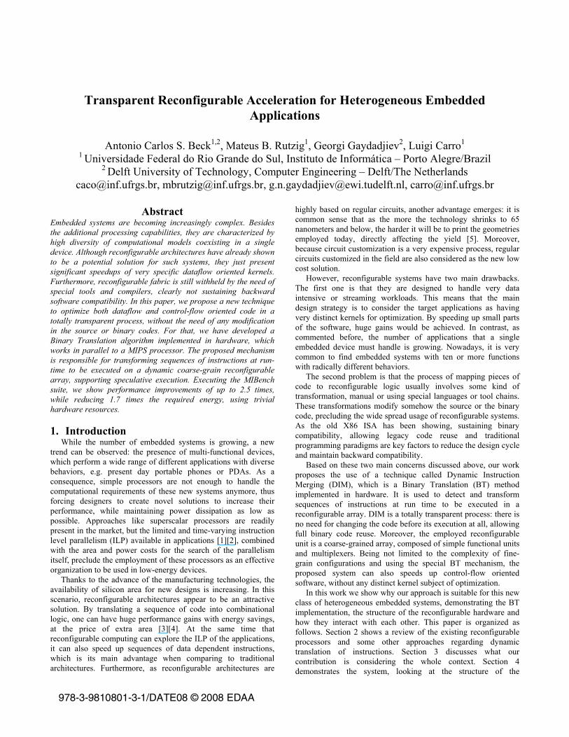
First, we characterize the algorithms regarding the number of instructions executed per branch (classifying them as control or dataflow oriented). As it can be observed in Figure 3b, the RawAudio (decoding) algorithm is the most control flow oriented one (a small number of instructions executed per branch) while the Rijndael (encoding) is the quite opposite. For reconfigurable architectures in general, the more instructions a basic block (BB) has, the better, since there is more room for exploiting parallelism. Furthermore, more branches mean additional paths that can be
taken, increasing the execution time and the area consumed by a given configuration, when implemented in reconfigurable logic.
Figure 3 – (a) How many BBs are necessary to cover a certain execution rate considering total execution time
(b) Average size of the Basic Block Figure 3a shows the results of our investigation on the number
of BBs responsible for a certain percentage of the total number of basic block execution figures. For instance, in the CRC32 algorithm, just 3 basic blocks are responsible for almost 100% of all the program execution time. Again, for typical reconfigurable systems, this type of algorithm suits best: one just needs to concentrate the design effort on that specific group of basic blocks, implementing them to reconfigurable logic.
However, other algorithms, such as the widely used JPEG decoder, have no distinct execution kernels at all. In this algorithm, to achieve an execution rate of 50% of the total number of BBs, 20 different BBs are necessary. Hence, if one wished to have a JPEG speedup of two times, considering ideal assumptions, all those basic blocks should be implemented into reconfigurable logic. This situation becomes even more evident if one considers the wide range of applications embedded processors are involved nowadays. In a scenario when an embedded system runs RawAudio decoder, JPEG encoder and decoder, and the StringSearch, the designer would have to transform approximately 45 different BBs into the reconfigurable logic to achieve 2x performance improvement. This is why a system with adaptive characteristics that can explore smaller granularities in a large number of basic blocks is envisioned as important. 5.2 Performance
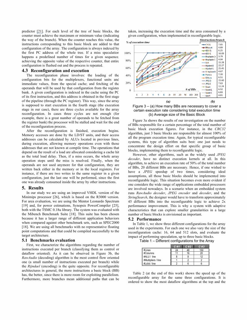
In Table 1, we show three different configurations for the array used in the experiments. For each one we also vary the size of the reconfiguration cache: 16, 64 and 512 slots, and evaluate the impact of performing speculation, up to three basic blocks.
Table 1 – Different configurations for the Array
Table 2 (at the end of this work) shows the speed up of the
reconfigurable array for the same three configurations. It is ordered to show the most dataflow algorithms at the top and the
7.65 4.89 6.25 16.09 3.79 4.04 15.28 22.27 25.45 4.67 7.20 6.51 15.60 7.63 11.24 6.52 6.83 4.81
# of BBs
100%
80%
60%
40%
20%
0
% of execution time #instructions/branch
(a) (b)
C #1 C #2 C #3#Lines 24 48 150 #Columns 11 16 20 #ALU / line 8 8 12 #Multipliers / line 1 2 2 #Ld/st / line 2 6 6
most control flow ones at the bottom. In Configuration #3 with speculation, an average performance improvement of more than 2.5 times is demonstrated. Moreover, gains are shown regardless of the instruction/branch rate, even for very control oriented algorithms such as RawAudio Decoder and Quicksort, as well as those which do not have distinct kernels, such as Susan Corners. Together with these results, we show an extra table at the right, demonstrating the overall optimization assuming infinite hardware resources for the array. As it can be observed, with the best configuration it is possible to get very close to this theoretical speedup. In fact, the algorithms that can most benefit from hardware infinite resources are exactly the dataflow ones, since they demand more lines in the array. They have as most executed kernels basic blocks with a huge number of instructions, mainly when speculation is used. On the other hand, in algorithms which have no distinct kernels, the most important resource to be increased is the number of slots available in the cache memory. Figure 4 summarizes the results of Table 2.
Figure 4 – Speed up presented with different configurations
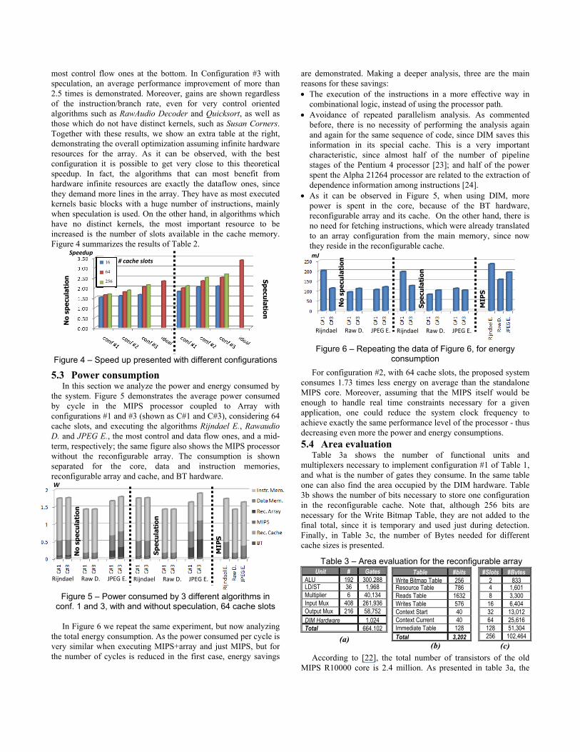
5.3 Power consumption In this section we analyze the power and energy consumed by
the system. Figure 5 demonstrates the average power consumed by cycle in the MIPS processor coupled to Array with configurations #1 and #3 (shown as C#1 and C#3), considering 64 cache slots, and executing the algorithms Rijndael E., Rawaudio D. and JPEG E., the most control and data flow ones, and a mid-term, respectively; the same figure also shows the MIPS processor without the reconfigurable array. The consumption is shown separated for the core, data and instruction memories, reconfigurable array and cache, and BT hardware.
Figure 5 – Power consumed by 3 different algorithms in conf. 1 and 3, with and without speculation, 64 cache slots
In Figure 6 we repeat the same experiment, but now analyzing
the total energy consumption. As the power consumed per cycle is very similar when executing MIPS+array and just MIPS, but for the number of cycles is reduced in the first case, energy savings
are demonstrated. Making a deeper analysis, three are the main reasons for these savings: • The execution of the instructions in a more effective way in
combinational logic, instead of using the processor path. • Avoidance of repeated parallelism analysis. As commented
before, there is no necessity of performing the analysis again and again for the same sequence of code, since DIM saves this information in its special cache. This is a very important characteristic, since almost half of the number of pipeline stages of the Pentium 4 processor [23]; and half of the power spent the Alpha 21264 processor are related to the extraction of dependence information among instructions [24].
• As it can be observed in Figure 5, when using DIM, more power is spent in the core, because of the BT hardware, reconfigurable array and its cache. On the other hand, there is no need for fetching instructions, which were already translated to an array configuration from the main memory, since now they reside in the reconfigurable cache.
Figure 6 – Repeating the data of Figure 6, for energy consumption
For configuration #2, with 64 cache slots, the proposed system consumes 1.73 times less energy on average than the standalone MIPS core. Moreover, assuming that the MIPS itself would be enough to handle real time constraints necessary for a given application, one could reduce the system clock frequency to achieve exactly the same performance level of the processor - thus decreasing even more the power and energy consumptions. 5.4 Area evaluation
Table 3a shows the number of functional units and multiplexers necessary to implement configuration #1 of Table 1, and what is the number of gates they consume. In the same table one can also find the area occupied by the DIM hardware. Table 3b shows the number of bits necessary to store one configuration in the reconfigurable cache. Note that, although 256 bits are necessary for the Write Bitmap Table, they are not added to the final total, since it is temporary and used just during detection. Finally, in Table 3c, the number of Bytes needed for different cache sizes is presented.
According to [22], the total number of transistors of the old
MIPS R10000 core is 2.4 million. As presented in table 3a, the
No
spec
ula
tion
Speculation
16
64
256
# cache slots
Speedup
Rijndael Raw D. JPEG E. Rijndael Raw D. JPEG E.
No
spec
ula
tion
Spec
ula
tion
MIP
S
mJ
Unit # Gates ALU 192 300,288 LD/ST 36 1,968 Multiplier 6 40,134 Input Mux 408 261,936 Output Mux 216 58,752 DIM Hardware 1,024 Total 664,102
Table 3 – Area evaluation for the reconfigurable array
(c) (a)
(b)
Table #bits Write Bitmap Table 256 Resource Table 786 Reads Table 1632 Writes Table 576 Context Start 40 Context Current 40 Immediate Table 128 Total 3,202
#Slots #Bytes 2 833 4 1,601 8 3,300 16 6,404 32 13,012 64 25,616
128 51,304 256 102,464
W
Rijndael Raw D. JPEG E. Rijndael Raw D. JPEG E.
No
spec
ula
tion
Spec
ula
tion
MIP
S

array together with the hardware detection occupies 664,102 gates. Considering that one gate is equivalent to 4 transistors, which would be the amount necessary to implement a NAND or NOR gates, the whole system would take nearly 2.66 million transistors to be implemented.
6. Conclusions and future work This work demonstrated that it is possible to use a
reconfigurable architecture to improve system performance with a wide range of distinct applications, in a totally transparent process and with trivial hardware resources. Using speculation, we have obtained energy savings of up 55% on average and a mean speedup of more than 2.5 times in the most aggressive configuration. Currently, we are working on finding the ideal shape for the reconfigurable array and techniques to switch off functional units when they are being not used.
7. References [1] Wall, D. “Limits of instruction-level parallelism”. In Proceedings of
the 4th international conference on Architectural support for programming languages and operating systems, p.176-188, 1991
[2] Xu, B. Albonesi, D.H. “Methodology for the analysis of dynamic application parallelism and its application to reconfigurable computing”. In Proceedings of SPIE, Vol. 3844, p. 78-86, 1999
[3] Venkataramani. G.. Najjar. W.. Kurdahi. F.. Bagherzadeh. N.. Bohm W.. “A Compiler Framework for Mapping Applications to a Coarse grained Reconfigurable Computer Architecture”. In Conf. on Compilers, Architecture and Synthesis for Embedded Systems (CASES). 2001
[4] Lysecky, R., Stitt, G., Vahid, F., "Warp Processors". In ACM Transactions on Design Automation of Electronic Systems (TODAES), pp. 659-681, July 2006
[5] Or-Bach, Z. “Panel: (when) will FPGAs kill ASICs?”. In 38th Design Automation Conference (DAC), 2001.
[6] Compton K., Hauck, S., “Reconfigurable computing: A survey of systems and software”. In ACM Computing Surveys, vol. 34, no. 2, pp. 171-210, June 2002.
[7] Hauck, S., Fry, T., Hosler, M., Kao, J., “The Chimaera reconfigurable functional unit”. In Proc. IEEE Symp. FPGAs for Custom Computing Machines, Napa Valley, CA, pp. 87–96, 1997.
[8] Hauser, J. R., Wawrzynek, J., “Garp: a MIPS processor with a reconfigurable coprocessor”. In Proc. 1997 IEEE Symp. Field Programmable Custom Computing Machines, pp. 12–21, 1997.
[9] Sankaralingam, k., Nagarajan, R., Liu, H., Kim, C. , Huh, J. , Burger, D. , Keckler, S. W., Moore C. R., “Exploiting ILP, TLP and DLP with the Polymorphous TRIPS Architecture”. In Proc. of the 30th Int. Symp. on Computer Architecture, pp. 422-433, June 2003.
[10] Swanson, S., Michelson, K., Schwerin, A., Oskin. M. “WaveScalar”. In MICRO-36, Dec. 2003
[11] Goldstein, S. C., Schmit, H., Budiu, M., Cadambi, S., Moe, M., Taylor, R.R., "PipeRench: A Reconfigurable Architecture and Compiler". In IEEE Computer, pp. 70-77, April, 2000
[12] Vassiliadis, S., Gaydadjiev, G. N., Bertels, K.L.M., Panainte, E. M., “The Molen Programming Paradigm”. In Proceedings of the Third International Workshop on Systems, Architectures, Modeling, and Simulation, pp. 1-10, Greece, July 2003
[13] Lysecky, R., Vahid F., Tan, S., A Study of the Scalability of On-Chip Routing for Just-in-Time FPGA Compilation"". In IEEE Symposium on Field-Programmable Custom Computing Machines (FCCM), pp. 57-62, 2005
[14] Clark, N., Kudlur, M., Park, H. Mahlke, S., Flautner, K., "Application-Specific Processing on a General-Purpose Core via Transparent Instruction Set Customization". In International Symposium on Microarchitecture (MICRO-37), pp. 30-40, Dec. 2004
[15] Gschwind, M., Altman, E., Sathaye, P., Ledak, Appenzeller, D. “Dynamic and Transparent Binary Translation”. In IEEE Computer, vol. 3 n. 33, (2000) 54-59
[16] González, A., Tubella, J., Molina, C., “Trace-Level Reuse”. In Int’l Conf. on Parallel Processing, Sep. 1999
[17] Burns, J.; Gaudiot, J.-L, “SMT layout overhead and scalability”. In Parallel and Distributed Systems, IEEE Transactions on On page(s): 142-155, Volume: 13, Issue: 2, Feb 2002
[18] Guthaus, M.R., Ringenberg, J.S., Ernst, D., Austin, T.M., Mudge T., Brown, R.B., “MiBench: A Free, Commercially Representative Embedded Benchmark Suite. 4th Workshop on Workload Characterization”, Austin, TX, Dec. 2001
[19] Leonardo Spectrum, available at homepage: http://www.mentor.com [20] Patel S. J., Lumetta, S. S. “rePLay: A Hardware Framework for
Dynamic Optimization”. In IEEE Trans. Comput., vol. 50, no. 6, pp. 590–608, 2001
[21] Smith, J. E. “A study of branch prediction strategies”. In Proceedings of the 8th annual symposium on Computer Architecture, p.135-148, May 12-14, 1981
[22] Yeager, K.C. “The Mips R10000 Superscalar Microprocessor,”; IEEE Micro, pp. 28-40, Apr. 1996
[23] Intel Pentium 4 Homepage - http://www.intel.com/products/processor/pentium4/index.htm
[24] Wilcox K., Manne, S. "Alpha processors: A history of power issues and a look to the future". CoolChips Tutorial An Industrial Perspective on Low Power Processor Design in conjunction with Micro-33, 1999.
[25] Synopsis PowerCompiler, datasheet available at homepage: http://www.synopsys.com/products/power/power_ds.pdf
[26] Minimips VHDL available at http://www.opencores.org
Dat
a Fl
ow
Con
trol
Flo
w
Algorithm Speed Up – Configuration #1 Speed Up – Configuration #2 Speed Up – Configuration #3
No Speculation Speculation No Speculation Speculation No Speculation Speculation 16 64 256 16 64 256 16 64 256 16 64 256 16 64 256 16 64 256
Rijindael E. 1.05 1.20 1.21 1.05 1.24 1.24 1.05 1.71 1.73 1.06 1.55 1.55 1.05 3.46 3.60 1.06 2.68 2.68 Rijindael D. 1.07 1.21 1.21 1.07 1.25 1.25 1.07 1.63 1.64 1.07 1.55 1.55 1.07 3.32 3.33 1.07 2.32 2.32
GSM E. 1.63 1.65 1.68 2.01 2.05 2.13 1.63 1.65 1.68 2.03 2.07 2.17 1.63 1.65 1.69 2.03 2.07 2.19 JPEG E. 1.95 2.04 2.07 1.79 1.88 1.89 2.50 2.72 2.77 3.55 4.27 4.37 2.50 2.72 2.77 3.55 4.27 4.37
SHA 1.90 1.90 1.90 3.81 3.84 3.84 1.90 1.91 1.91 4.80 4.84 4.84 1.90 1.91 1.91 4.80 4.84 4.84 Susan Smothing 1.49 1.60 1.65 2.70 2.99 3.31 1.49 1.61 1.65 2.83 3.14 3.52 1.49 1.61 1.65 2.83 3.14 3.52
CRC 1.53 1.53 1.53 1.92 1.92 1.92 1.53 1.53 1.53 1.92 1.92 1.92 1.53 1.53 1.53 1.92 1.92 1.92 JPEG D. 1.92 2.03 2.04 1.64 1.78 1.78 2.05 2.21 2.22 2.02 2.54 2.55 2.05 2.21 2.22 2.03 2.62 2.63 Patricia 1.49 1.84 1.93 1.58 2.05 2.23 1.49 1.86 1.95 1.64 2.17 2.37 1.49 1.86 1.95 1.64 2.17 2.37
Susan Corners 1.22 1.49 1.72 1.31 1.47 1.91 1.38 1.79 2.17 1.56 1.79 2.64 1.38 1.79 2.17 1.56 1.79 2.64 Susan Edges 1.23 1.42 1.64 1.29 1.48 1.83 1.43 1.70 2.20 1.47 1.74 2.43 1.43 1.70 2.20 1.53 1.81 2.58
Dijkstra 1.59 1.71 1.71 2.03 2.21 2.22 1.59 1.72 1.72 2.04 2.24 2.24 1.59 1.72 1.72 2.04 2.24 2.24 GSM D. 1.28 1.28 1.29 1.27 1.28 1.29 1.62 1.62 1.65 1.48 1.50 1.52 2.79 2.79 2.93 2.37 2.49 2.58 Bitcount 1.76 1.76 1.76 1.83 1.83 1.83 1.76 1.76 1.76 1.83 1.83 1.83 1.76 1.76 1.76 1.83 1.83 1.83
Stringsearch 1.38 1.61 1.86 1.56 2.22 2.77 1.38 1.62 1.89 1.57 2.30 2.96 1.38 1.62 1.89 1.57 2.30 2.96 Quicksort 1.37 1.74 1.74 1.69 2.32 2.33 1.37 1.77 1.77 1.80 2.66 2.67 1.37 1.77 1.77 1.80 2.66 2.67
RawAudio E. 1.60 1.61 1.61 1.98 1.99 2.00 1.60 1.61 1.61 1.98 1.99 2.00 1.60 1.61 1.61 1.98 1.99 2.00 RawAudio D. 1.64 1.64 1.64 1.79 1.79 1.79 1.64 1.64 1.64 1.79 1.79 1.79 1.64 1.64 1.64 1.79 1.79 1.79
Average 1.51 1.63 1.68 1.80 1.98 2.09 1.58 1.78 1.86 2.03 2.33 2.49 1.65 2.04 2.13 2.08 2.50 2.67
Table 2 – Speedups using the reconfigurable array coupled to the MIPS processor
Ideal No
Spec Spec
5.10 8.05 4.68 7.42 1.70 2.19 2.22 2.64 1.91 4.87 1.65 3.52 1.53 1.92 2.77 4.39 2.19 3.07 2.17 2.66 2.21 2.60 1.72 2.25 3.31 3.68 1.76 1.83 1.89 2.97 1.77 2.67 1.61 2.00 1.64 1.79 2.32 3.36