Bioinformatics analysis of disordered proteins in prokaryotes
Upload
independentCategory
view
0download
0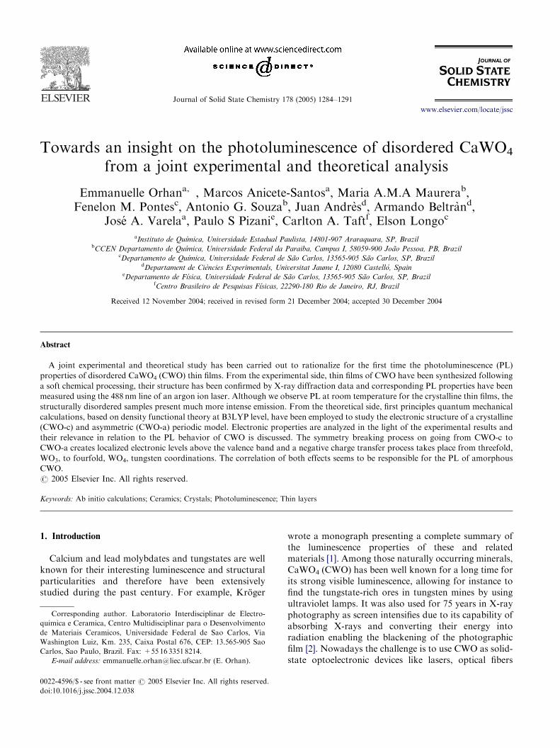
ARTICLE IN PRESS
0022-4596/$ - se
doi:10.1016/j.jss
�Correspondquimica e Cera
de Materiais C
Washington Lu
Carlos, Sao Pau
E-mail addr
Journal of Solid State Chemistry 178 (2005) 1284–1291
www.elsevier.com/locate/jssc
Towards an insight on the photoluminescence of disordered CaWO4
from a joint experimental and theoretical analysis
Emmanuelle Orhana,�, Marcos Anicete-Santosa, Maria A.M.A Maurerab,Fenelon M. Pontesc, Antonio G. Souzab, Juan Andresd, Armando Beltrand,
Jose A. Varelaa, Paulo S Pizanie, Carlton A. Taftf, Elson Longoc
aInstituto de Quımica, Universidade Estadual Paulista, 14801-907 Araraquara, SP, BrazilbCCEN Departamento de Quımica, Universidade Federal da Paraiba, Campus I, 58059-900 Joao Pessoa, PB, Brazil
cDepartamento de Quımica, Universidade Federal de Sao Carlos, 13565-905 Sao Carlos, SP, BrazildDepartament de Ciencies Experimentals, Universitat Jaume I, 12080 Castello, Spain
eDepartamento de Fısica, Universidade Federal de Sao Carlos, 13565-905 Sao Carlos, SP, BrazilfCentro Brasileiro de Pesquisas Fısicas, 22290-180 Rio de Janeiro, RJ, Brazil
Received 12 November 2004; received in revised form 21 December 2004; accepted 30 December 2004
Abstract
A joint experimental and theoretical study has been carried out to rationalize for the first time the photoluminescence (PL)
properties of disordered CaWO4 (CWO) thin films. From the experimental side, thin films of CWO have been synthesized following
a soft chemical processing, their structure has been confirmed by X-ray diffraction data and corresponding PL properties have been
measured using the 488 nm line of an argon ion laser. Although we observe PL at room temperature for the crystalline thin films, the
structurally disordered samples present much more intense emission. From the theoretical side, first principles quantum mechanical
calculations, based on density functional theory at B3LYP level, have been employed to study the electronic structure of a crystalline
(CWO-c) and asymmetric (CWO-a) periodic model. Electronic properties are analyzed in the light of the experimental results and
their relevance in relation to the PL behavior of CWO is discussed. The symmetry breaking process on going from CWO-c to
CWO-a creates localized electronic levels above the valence band and a negative charge transfer process takes place from threefold,
WO3, to fourfold, WO4, tungsten coordinations. The correlation of both effects seems to be responsible for the PL of amorphous
CWO.
r 2005 Elsevier Inc. All rights reserved.
Keywords: Ab initio calculations; Ceramics; Crystals; Photoluminescence; Thin layers
1. Introduction
Calcium and lead molybdates and tungstates are wellknown for their interesting luminescence and structuralparticularities and therefore have been extensivelystudied during the past century. For example, Kroger
e front matter r 2005 Elsevier Inc. All rights reserved.
c.2004.12.038
ing author. Laboratorio Interdisciplinar de Electro-
mica, Centro Multidisciplinar para o Desenvolvimento
eramicos, Universidade Federal de Sao Carlos, Via
iz, Km. 235, Caixa Postal 676, CEP: 13.565-905 Sao
lo, Brazil. Fax: +55 16 3351 8214.
ess: [email protected] (E. Orhan).
wrote a monograph presenting a complete summary ofthe luminescence properties of these and relatedmaterials [1]. Among those naturally occurring minerals,CaWO4 (CWO) has been well known for a long time forits strong visible luminescence, allowing for instance tofind the tungstate-rich ores in tungsten mines by usingultraviolet lamps. It was also used for 75 years in X-rayphotography as screen intensifies due to its capability ofabsorbing X-rays and converting their energy intoradiation enabling the blackening of the photographicfilm [2]. Nowadays the challenge is to use CWO as solid-state optoelectronic devices like lasers, optical fibers
ARTICLE IN PRESSE. Orhan et al. / Journal of Solid State Chemistry 178 (2005) 1284–1291 1285
components or scintillators [3–6]. CWO is also theobject of interesting structural studies because itpresents a great variety of phases depending on thepreparation conditions [7,8].
Numerous papers report the photoluminescence (PL)behavior of crystalline CaWO4. When excited by short-wavelength ultraviolet radiations (around 250 nm) atroom temperature, it mainly presents a blue emissionband at around 420 nm, which is commonly attributedto the WO4 tetrahedra [9], or to self-trapped electronstates [10]. A green emission band also exists at around490 nm, whose origin is a bit controversial. It alreadyhas been attributed to WO3 defect centers associatedwith oxygen vacancies [11,12] or to intrinsic transitionsin the WO4
2� complex [13,14]. Very little information isavailable on the luminescence spectra under longerwavelength excitations.
In the present paper, the PL of non-crystallineCaWO4 is investigated for the first time. Visible PL atroom temperature in disordered materials was firstobserved by Canham in porous silicon [15] and sincethen the study of PL in disordered or nanostructuredmaterials has been the focus of numerous studies,mainly on titanate compounds [16–22]. We are combin-ing laboratory experiments and high-level calculationsinto a synergetic strategy for understanding the PLorigin in disordered CaWO4. The experimental workpresents measurements of broad, intense PL at roomtemperature in structurally disordered CWO thin filmsprepared by the polymeric precursor method. Thisprocess offers advantages over other synthesis techni-ques such as low cost, good compositional homogeneity,high purity, low processing temperatures and ability tocoat large substrate areas.
The aim of the theoretical part is to investigate theelectronic structure of CWO by using models represent-ing its crystalline and disordered structures and to givean interpretation in terms of density of states (DOS) andband structure diagrams of the conditions allowing PLto occur at room temperature. This approach renders aplausible quantitative description of the behavior ofCWO under laser excitation and an interesting correla-tion between the theoretical and experimental results.We do not aim to explain the mechanisms of PL in theCWO system but to explain why the intensity is muchhigher in the disordered films than in the crystalline one.The achievement of strong PL at room temperaturefrom a compound processed by a low-cost method isindeed of primary interest for eventual application insolid-state optoelectronic devices.
2. Experimental
The CaWO4 thin films studied in the present workwere synthesized following a soft chemical method, the
so-called polymeric precursor method [23]. Details ofthe processing have already been published [24]. Thepolymeric precursor solution was spin coated onsubstrates by a spinner operating at 7000 rev/min for40 s (spin-coater KW-4B, Chemat Technology) via asyringe filter to avoid particulate contamination. Thesubstrates were silicon-coated platinum and quartz.After spinning, the films were kept in ambient air at423K on a hot plate for 20min to remove residualsolvents. They were then annealed at different tempera-tures from 573 to 873K for 4 h in air atmosphere.
The CWO thin films were structurally characterizedby X-ray diffraction (XRD) using CuKa radiationsource. The diffraction patterns were recorded on aSiemens D5000 machine in a y� 2y configuration usinga graphite monochromator. The spectral dependence ofoptical absorbance for the crystalline and amorphousCWO thin films was measured in the wavelength rangefrom 200 to 800 nm, using a Cary 5G spectrophot-ometer. The PL spectra of the CWO thin films wererecorded with a U1000 Jobin–Yvon double monochro-mator coupled to a cooled GaAs photomultiplier and aconventional photon counting system. The 488 nmexciting wavelength of an argon ion laser was used,with the laser’s maximum output power kept at 60mW.A cylindrical lens was used to prevent the samplefrom overheating. The slit width used was 100 mm. Allmeasurements were taken at room temperature. Atomicforce microscopy (AFM) was used to obtain a 3D imagereconstruction of the sample surface. These imagesallow for an accurate analysis of the sample surface andquantification of highly relevant parameters such asroughness and grain size. A Digital Instruments Multi-Mode Nanoscope IIIa was used.
3. Computational methods
Calculations have been carried out with the CRYS-TAL98 package [25], which is based on both DensityFunctional (DFT) and Hartree–Fock theories. Thegradient-corrected correlation functional by Lee, Yangand Parr was used, combined with the Becke 3 exchangefunctional, B3LYP [26,27], which has been demon-strated by Muscat et al. [28] to be suitable for calculatingstructural parameters and band structures for a widevariety of solid-state compounds. The basis sets used fordescribing O and Ca atomic centers can be found inRef. [29] and for W in the paper by Cora et al. [30]. Thek-points sampling was chosen to be 40 points withinthe irreducible part of the Brillouin zone. For simulatingthe displacement of the W2 and W4 atom (as defined inFig. 1), we have used the atom displacement optionprovided with the CRYSTAL program. The XCrysDenprogram was used to design the DOS and the bandstructure diagrams [31].
ARTICLE IN PRESS
Fig. 1. CWO-c periodic model: 1� 1� 2 supercell of the CaWO4
primitive unit cell (top). CWO-a periodic model: W2 and W4 are
shifted in the direction opposite to the starred oxygen atoms (bottom).
Fig. 2. XRD patterns for the thin films annealed at (a) 573K, (b)
673K, (c) 773K and (d) 873K for 4 h.
E. Orhan et al. / Journal of Solid State Chemistry 178 (2005) 1284–12911286
4. Crystal structure and periodic models
The scheelite CaWO4 crystallizes in a tetragonalstructure (space group I41=a; C4h symmetry). Tungstenatoms are surrounded by four oxygen atoms in atetrahedral configuration and calcium atoms are sur-rounded by eight oxygen atoms in a pseudo-cubicconfiguration. The experimental a and c parameters are,respectively, 5.2429 and 11.3737 A [32]. The optimiza-tion of the cell parameters was not necessary as thepreliminary results obtained with the experimentalparameters gave an energy gap value equal to theexperimental one (see Section 5). The Crystal98 codetransforms the conventional cell into the primitive cellfor simplifying the calculations. In this case, theprimitive cell parameters are a ¼ b ¼ c ¼ 6:7885 (A; a ¼
b ¼ 134:56871 and g ¼ 66:20111: We have used a1� 1� 2 supercell of the primitive cell as a periodicmodel for representing the crystalline CWO (CWO-c). Itresults in 24 atoms in the supercell, see top part of Fig. 1.
Various authors attribute the green PL component ofCaWO4 (around 490 nm) to the existence of some WO3
truncated tetrahedra in the crystalline scheelite[11,13,33,34]. We assume that before the completecrystallization of the film, i.e., before the heat treatmentreaches 873K, the structure is composed of a randommixture of WO4 and WO3 tetrahedra linked by the Caions. This assumption is based on our experience withtitanates: XANES experimental results on the crystal-lization process of SrTiO3 and PbTiO3 [17,35] pointedout the coexistence of two types of environments for thetitanium, namely, fivefold titanium coordination ([TiO5]square-base pyramid) and sixfold titanium coordination([TiO6] octahedron), from the citrate solution to thedisordered powder, when synthesized by the polymeric
precursor method. This certain degree of order instructurally disordered materials was to be expected,since two or more atoms arranged close to each other ina stable configuration must necessarily have some degreeof order because there always are minima of thepotential energy. Furthermore, as it is well known, thedetails of the band structure for a periodic system aremainly determined by the potential within the unit cellrather than by the long-range periodicity. This meansthat any symmetry perturbation in the unit cell will haveconsequences on the electronic structure.
We thus created a 1� 1� 2 supercell that will standfor the non-crystalline phases. Starting from theprevious CWO-c model, the W2 and W4 atoms wereshifted by 0.3 A in the direction opposite to the starredoxygen atoms as to break the bonds (see bottom part ofFig. 1). This 0.3 A value was chosen after tests at 0.1,0.2, 0.4 and 0.5 A because it was the first value allowingto see clearly the effects of bond deformation on theelectronic structure and that reproduces quite well theexperimental value of the band gap energy. This newperiodic model will be called CWO-a, for beingasymmetric. W2 and W4 are now surrounded by threeoxygen atoms in their first coordination sphere.
Our aim with the use of this CWO-a model is to offera simple scheme allowing to understand the effects of astructural deformation on the electronic structure with-out completely suppressing the geometry of the cell thatis useful for the periodic calculations. Using the samekind of distorted model, we have successfully explainedthe PL of various perovskite titanates [18,19,36,37].
5. Results and discussion
Fig. 2 shows the XRD patterns of CWO thin filmsdeposited on silicon substrate after different annealing
ARTICLE IN PRESSE. Orhan et al. / Journal of Solid State Chemistry 178 (2005) 1284–1291 1287
temperatures: 573, 673, 773 and 873K. A diffuse patternis observed for the films treated at 573 and 673K,indicating the formation of an inorganic disorderedphase after the pyrolysis process. The crystallization ofthe CWO scheelite phase starts at 773K but all peaksare visible and well-defined only at 873K. All peaks areascribed to the tetragonal structure, matching with theJCPDS 41-1431 card.
A closer observation of the structure of two filmsannealed at 473 and 873K made by AFM shows thedifference between them in terms of surface morphology(see Fig. 3). The CWO thin film annealed at 423Kpossesses a homogeneous surface morphology with verylow roughness. There was no evidence of a granularstructure. The surface morphology of the CWO changesdramatically at 873K. At this stage of growth,coalescence of nuclei occurs, with formation of granularstructures resulting in a significant increase in rough-ness. This result is in agreement with the XRD analysis,where at 873K a high crystallization can be observed.
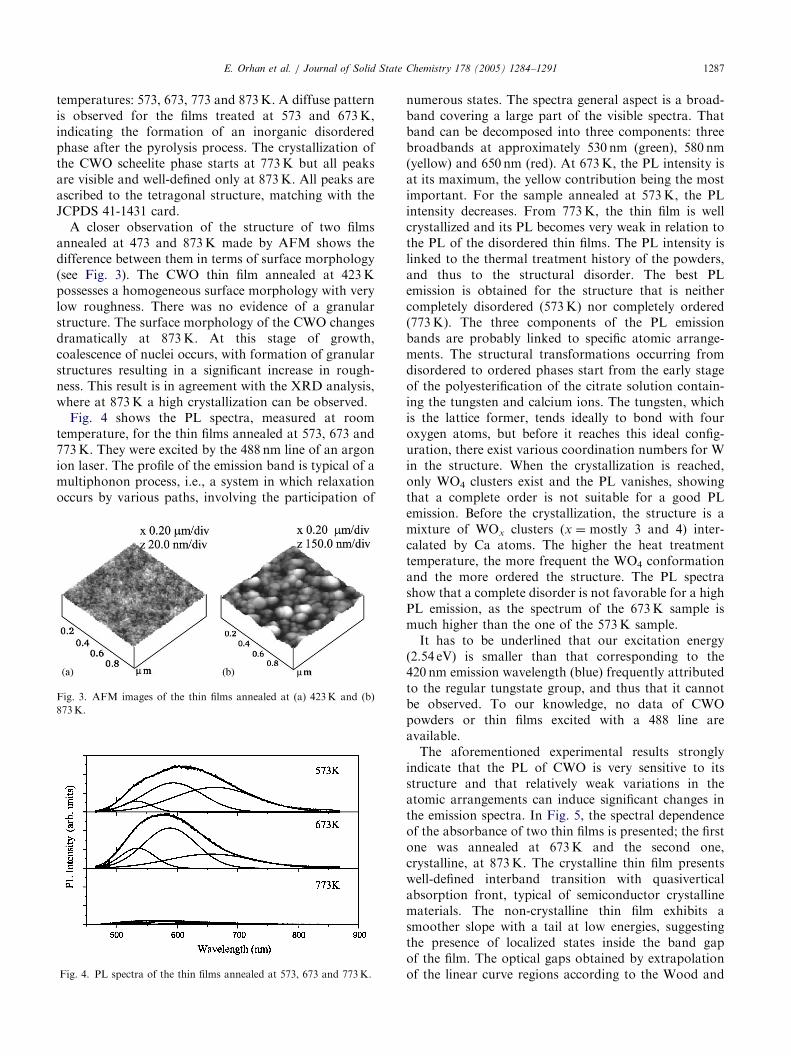
Fig. 4 shows the PL spectra, measured at roomtemperature, for the thin films annealed at 573, 673 and773K. They were excited by the 488 nm line of an argonion laser. The profile of the emission band is typical of amultiphonon process, i.e., a system in which relaxationoccurs by various paths, involving the participation of
Fig. 3. AFM images of the thin films annealed at (a) 423K and (b)
873K.
Fig. 4. PL spectra of the thin films annealed at 573, 673 and 773K.
numerous states. The spectra general aspect is a broad-band covering a large part of the visible spectra. Thatband can be decomposed into three components: threebroadbands at approximately 530 nm (green), 580 nm(yellow) and 650 nm (red). At 673K, the PL intensity isat its maximum, the yellow contribution being the mostimportant. For the sample annealed at 573K, the PLintensity decreases. From 773K, the thin film is wellcrystallized and its PL becomes very weak in relation tothe PL of the disordered thin films. The PL intensity islinked to the thermal treatment history of the powders,and thus to the structural disorder. The best PLemission is obtained for the structure that is neithercompletely disordered (573K) nor completely ordered(773K). The three components of the PL emissionbands are probably linked to specific atomic arrange-ments. The structural transformations occurring fromdisordered to ordered phases start from the early stageof the polyesterification of the citrate solution contain-ing the tungsten and calcium ions. The tungsten, whichis the lattice former, tends ideally to bond with fouroxygen atoms, but before it reaches this ideal config-uration, there exist various coordination numbers for Win the structure. When the crystallization is reached,only WO4 clusters exist and the PL vanishes, showingthat a complete order is not suitable for a good PLemission. Before the crystallization, the structure is amixture of WOx clusters (x ¼ mostly 3 and 4) inter-calated by Ca atoms. The higher the heat treatmenttemperature, the more frequent the WO4 conformationand the more ordered the structure. The PL spectrashow that a complete disorder is not favorable for a highPL emission, as the spectrum of the 673K sample ismuch higher than the one of the 573K sample.
It has to be underlined that our excitation energy(2.54 eV) is smaller than that corresponding to the420 nm emission wavelength (blue) frequently attributedto the regular tungstate group, and thus that it cannotbe observed. To our knowledge, no data of CWOpowders or thin films excited with a 488 line areavailable.
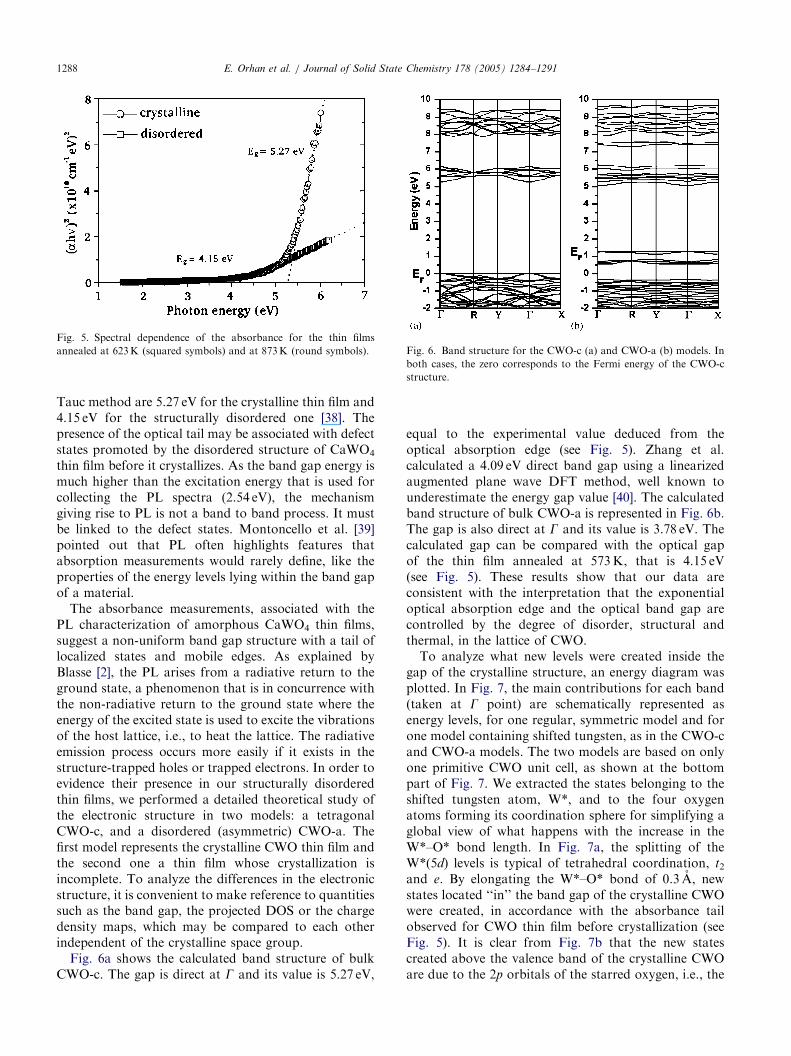
The aforementioned experimental results stronglyindicate that the PL of CWO is very sensitive to itsstructure and that relatively weak variations in theatomic arrangements can induce significant changes inthe emission spectra. In Fig. 5, the spectral dependenceof the absorbance of two thin films is presented; the firstone was annealed at 673K and the second one,crystalline, at 873K. The crystalline thin film presentswell-defined interband transition with quasiverticalabsorption front, typical of semiconductor crystallinematerials. The non-crystalline thin film exhibits asmoother slope with a tail at low energies, suggestingthe presence of localized states inside the band gapof the film. The optical gaps obtained by extrapolationof the linear curve regions according to the Wood and
ARTICLE IN PRESS
Fig. 5. Spectral dependence of the absorbance for the thin films
annealed at 623K (squared symbols) and at 873K (round symbols). Fig. 6. Band structure for the CWO-c (a) and CWO-a (b) models. In
both cases, the zero corresponds to the Fermi energy of the CWO-c
structure.
E. Orhan et al. / Journal of Solid State Chemistry 178 (2005) 1284–12911288
Tauc method are 5.27 eV for the crystalline thin film and4.15 eV for the structurally disordered one [38]. Thepresence of the optical tail may be associated with defectstates promoted by the disordered structure of CaWO4
thin film before it crystallizes. As the band gap energy ismuch higher than the excitation energy that is used forcollecting the PL spectra (2.54 eV), the mechanismgiving rise to PL is not a band to band process. It mustbe linked to the defect states. Montoncello et al. [39]pointed out that PL often highlights features thatabsorption measurements would rarely define, like theproperties of the energy levels lying within the band gapof a material.
The absorbance measurements, associated with thePL characterization of amorphous CaWO4 thin films,suggest a non-uniform band gap structure with a tail oflocalized states and mobile edges. As explained byBlasse [2], the PL arises from a radiative return to theground state, a phenomenon that is in concurrence withthe non-radiative return to the ground state where theenergy of the excited state is used to excite the vibrationsof the host lattice, i.e., to heat the lattice. The radiativeemission process occurs more easily if it exists in thestructure-trapped holes or trapped electrons. In order toevidence their presence in our structurally disorderedthin films, we performed a detailed theoretical study ofthe electronic structure in two models: a tetragonalCWO-c, and a disordered (asymmetric) CWO-a. Thefirst model represents the crystalline CWO thin film andthe second one a thin film whose crystallization isincomplete. To analyze the differences in the electronicstructure, it is convenient to make reference to quantitiessuch as the band gap, the projected DOS or the chargedensity maps, which may be compared to each otherindependent of the crystalline space group.
Fig. 6a shows the calculated band structure of bulkCWO-c. The gap is direct at G and its value is 5.27 eV,
equal to the experimental value deduced from theoptical absorption edge (see Fig. 5). Zhang et al.calculated a 4.09 eV direct band gap using a linearizedaugmented plane wave DFT method, well known tounderestimate the energy gap value [40]. The calculatedband structure of bulk CWO-a is represented in Fig. 6b.The gap is also direct at G and its value is 3.78 eV. Thecalculated gap can be compared with the optical gapof the thin film annealed at 573K, that is 4.15 eV(see Fig. 5). These results show that our data areconsistent with the interpretation that the exponentialoptical absorption edge and the optical band gap arecontrolled by the degree of disorder, structural andthermal, in the lattice of CWO.
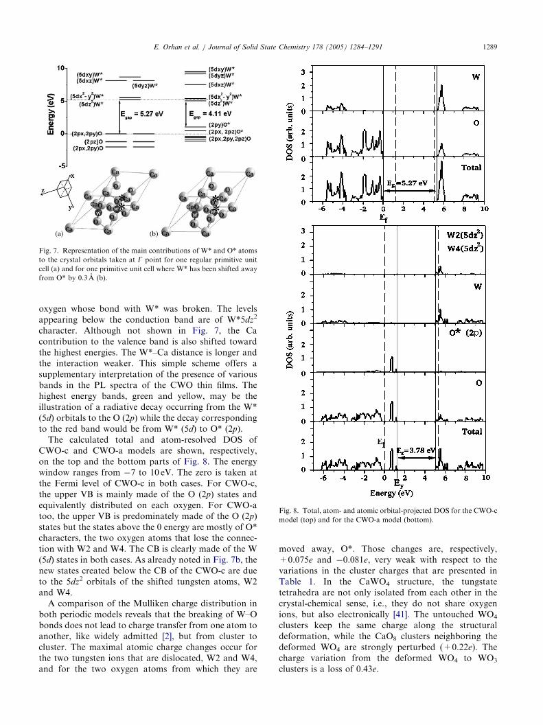
To analyze what new levels were created inside thegap of the crystalline structure, an energy diagram wasplotted. In Fig. 7, the main contributions for each band(taken at G point) are schematically represented asenergy levels, for one regular, symmetric model and forone model containing shifted tungsten, as in the CWO-cand CWO-a models. The two models are based on onlyone primitive CWO unit cell, as shown at the bottompart of Fig. 7. We extracted the states belonging to theshifted tungsten atom, W*, and to the four oxygenatoms forming its coordination sphere for simplifying aglobal view of what happens with the increase in theW*–O* bond length. In Fig. 7a, the splitting of theW*(5d) levels is typical of tetrahedral coordination, t2and e. By elongating the W*–O* bond of 0.3 A, newstates located ‘‘in’’ the band gap of the crystalline CWOwere created, in accordance with the absorbance tailobserved for CWO thin film before crystallization (seeFig. 5). It is clear from Fig. 7b that the new statescreated above the valence band of the crystalline CWOare due to the 2p orbitals of the starred oxygen, i.e., the
ARTICLE IN PRESS
Fig. 8. Total, atom- and atomic orbital-projected DOS for the CWO-c
model (top) and for the CWO-a model (bottom).
Fig. 7. Representation of the main contributions of W* and O* atoms
to the crystal orbitals taken at G point for one regular primitive unit
cell (a) and for one primitive unit cell where W* has been shifted away
from O* by 0.3 A (b).
E. Orhan et al. / Journal of Solid State Chemistry 178 (2005) 1284–1291 1289
oxygen whose bond with W* was broken. The levelsappearing below the conduction band are of W*5dz2
character. Although not shown in Fig. 7, the Cacontribution to the valence band is also shifted towardthe highest energies. The W*–Ca distance is longer andthe interaction weaker. This simple scheme offers asupplementary interpretation of the presence of variousbands in the PL spectra of the CWO thin films. Thehighest energy bands, green and yellow, may be theillustration of a radiative decay occurring from the W*(5d) orbitals to the O (2p) while the decay correspondingto the red band would be from W* (5d) to O* (2p).
The calculated total and atom-resolved DOS ofCWO-c and CWO-a models are shown, respectively,on the top and the bottom parts of Fig. 8. The energywindow ranges from �7 to 10 eV. The zero is taken atthe Fermi level of CWO-c in both cases. For CWO-c,the upper VB is mainly made of the O (2p) states andequivalently distributed on each oxygen. For CWO-atoo, the upper VB is predominately made of the O (2p)states but the states above the 0 energy are mostly of O*characters, the two oxygen atoms that lose the connec-tion with W2 and W4. The CB is clearly made of the W(5d) states in both cases. As already noted in Fig. 7b, thenew states created below the CB of the CWO-c are dueto the 5dz2 orbitals of the shifted tungsten atoms, W2and W4.
A comparison of the Mulliken charge distribution inboth periodic models reveals that the breaking of W–Obonds does not lead to charge transfer from one atom toanother, like widely admitted [2], but from cluster tocluster. The maximal atomic charge changes occur forthe two tungsten ions that are dislocated, W2 and W4,and for the two oxygen atoms from which they are
moved away, O*. Those changes are, respectively,+0.075e and �0.081e, very weak with respect to thevariations in the cluster charges that are presented inTable 1. In the CaWO4 structure, the tungstatetetrahedra are not only isolated from each other in thecrystal-chemical sense, i.e., they do not share oxygenions, but also electronically [41]. The untouched WO4
clusters keep the same charge along the structuraldeformation, while the CaO8 clusters neighboring thedeformed WO4 are strongly perturbed (+0.22e). Thecharge variation from the deformed WO4 to WO3
clusters is a loss of 0.43e.
ARTICLE IN PRESS
Table 1
Charge variations for each individual cluster of the structure before
and after deformation
Cluster
designation
Charge of the
CWO-c clusters
(e)
Charge of the
CWO-a clusters
(e)
Charge
difference (e)
Ca1O8 �1.64 �2.04 +0.40
Ca2O8 �1.64 �1.68 +0.02
Ca3O8 �1.64 �1.86 +0.22
Ca4O8 �1.64 �1.86 +0.22
W3O4 1.64 1.65 �0.01
W1O4 1.64 1.65 �0.01
W2Oxa 1.64 2.07 �0.43
W4Oxa 1.64 2.07 �0.43
ax¼ 4 for CWO-c and x ¼ 3 for CWO-a.
E. Orhan et al. / Journal of Solid State Chemistry 178 (2005) 1284–12911290
A charge gradient thus exists in the structure beforeexcitation. This gradient, together with the localizedstates appearing in the band gap, allows the electrons toself-trap, in accordance with the study of Zhang et al.[40] who reported that excitons self-trap before emittingluminescence photons in CWO. Because of the signifi-cant local lattice distortion that accompanies self-trapping, the states giving rise to luminescence can bedescribed as molecular orbitals of the single distortedatomic group on which the extra charge localizes, that isto say WO3 clusters. This phenomenon episodicallyoccurs in the crystalline structure, leading to the well-known visible PL of CWO, but is far more frequent inthe disordered thin film, because all the conditionsfavorable to self-trapping are present.
6. Conclusions
Thin films of CWO have been synthesized following asoft chemical low-cost processing and new PL behaviorhas been evidenced. For the first time, the intense room-temperature visible PL of non-crystalline CWO thinfilms is discussed. In accordance with the measuredoptical tails, the existence of localized levels in the bandgap of the crystalline compound when it is deformed hasbeen proven. The main character of those localizedlevels is 2p of the oxygen atoms losing the connectionwith the tungsten for the states appearing above thevalence band and 5dz2 of these particular tungsten forthe states appearing below the conduction band. Theseresults show that the chosen theoretical models areconsistent with the experimental data and with theinterpretation that the exponential optical absorptionedge and the optical band gap are controlled by thedegree of disorder, structural and thermal, in the latticeof CWO system. Moreover, a charge gradient has beenobserved in the deformed structure, due to the chargedifferences between the clusters. The coexistence of
localized levels and of a charge gradient createsfavorable conditions for the self-trapping of excitonsbefore emitting luminescence photons.
Acknowledgment
This work was partially supported by the Brazilianresearch-financing institutions: Fundac- ao de Amparo aPesquisa do Estado de Sao Paulo—FAPESP/CEPID,by the Conselho Nacional de Desenvolvimento Cientı-fico e Tecnologico—CNPq/PRONEX and by thePrograma de colaboracion hispano brasileno no.PHB2001-0040.
References
[1] F.A. Kroger, Some Aspects of the Luminescence of Solids,
Elsevier, Amsterdam, 1948.
[2] G. Blasse, B.C. Grabmaier, Luminescent Materials, Springer,
Berlin, Heildelberg, 1994.
[3] M. Nikl, P. Bohacek, N. Mihokova, N. Solovieva, A. Vedda,
M. Martini, G.P. Pazzi, P. Fabeni, M. Kobayashi, M. Ishii,
J. Appl. Phys. 91 (2002) 5041.
[4] M. Nikl, P. Bohacek, E. Mihokova, M. Kobayashi, M. Ishii,
Y. Usuki, V. Babin, A. Stolovich, S. Zazubovich, M. Bacci,
J. Lumin. 87 (9) (2000) 1136.
[5] M. Kobayashi, M. Ishii, Y. Usuki, H. Yahagi, Nucl. Instrum.
Methods Phys. Res. A 333 (1993) 429.
[6] M. Nikl, Phys. Stat. Sol. (a) 178 (2000) 595.
[7] D. Errandonea, M. Somayazulu, D. Hausermann, Phys. Stat. Sol.
(b) 235 (2003) 162.
[8] D. Errandonea, F.J. Manjon, M. Somayazulu, D. Hausermann,
J. Solid State Chem. 177 (2004) 1087.
[9] W. Van Loo, Phys Stat. Sol. (a) 28 (1975) 227.
[10] V. Pankratov, D. Millers, L. Grigorjeva, S. Chernov, Phys. Stat.
Sol. (b) 225 (2) (1980) 9.
[11] J.A. Groenink, G. Blasse, J. Solid State Chem. 32 (1) (1980) 9.
[12] B.M. Sinel’nikov, E.V. Sokolenko, E.G. Zvekova, Inorg. Mater.
32 (1996) 6.
[13] Z. Lou, M. Cocivera, Mater. Res. Bull. 37 (2002) 1573.
[14] M.J. Treadaway, R.C. Powell, J. Chem. Phys. 61 (10) (1974) 4003.
[15] L.T. Canham, Appl. Phys. Lett. 57 (1990) 1046.
[16] F.M. Pontes, C.D. Pinheiro, E. Longo, E.R. Leite, S.R. de
Lazaro, J.A. Varela, P.S. Pizani, T.M. Boschi, F. Lanciotti Jr.,
Mater. Chem. Phys. 78 (1) (2003) 227.
[17] F.M. Pontes, E. Longo, E.R. Leite, E.J.H. Lee, J.A. Varela, P.S.
Pizani, C.E. M Campos, F. Lanciotti Jr, V. Mastellaro, C.D.
Pinheiro, Mater. Chem. Phys. 77 (2) (2003) 598.
[18] E. Longo, E. Orhan, F.M. Pontes, C.D. Pinheiro, E.R. Leite, J.A.
Varela, P.S. Pizani, T.M. Boschi, F. Lanciotti Jr, A. Beltran,
J. Andres, Phys. Rev. B 69 (2004) 125115.
[19] E. Orhan, F.M. Pontes, M.A. Santos, E.R. Leite, A. Beltran,
J. Andres, T.M. Boschi, P.S. Pizani, J.A. Varela, C.A. Taft,
E. Longo, J. Phys. Chem. B 108 (2004) 9221.
[20] H. Pinto, A. Stashans, Phys. Rev. B 65 (2002) 134304.
[21] E. Heifets, R.I. Eglitis, E.A. Kotomin, J. Maier, G. Borstel, Phys.
Rev. B 64 (2001) 235417.
[22] Ph. Ghosez, J.-P. Michenaud, X. Gonze, Phys. Rev. B 58 (1998)
6224.
[23] F.M. Pontes, E.R. Leite, D.S.L. Pontes, E. Longo, E.M.S. Santos,
S. Mergulhao, P. Pizani, F. Lanciotti, T.M. Boschi, J.A. Varela,
J. Appl. Phys. 91 (2002) 5972.
ARTICLE IN PRESSE. Orhan et al. / Journal of Solid State Chemistry 178 (2005) 1284–1291 1291
[24] F.M. Pontes, M.A.M.A. Maurera, A.G. Souza, E. Longo, E.R.
Leite, R. Magnani, M.A.C. Machado, P.S. Pizani, J.A. Varela,
J. Eur. Ceram. Soc. 23 (2002) 3001.
[25] V.R. Saunders, R. Dovesi, C. Roetti, M. Causa, N.M. Harrison,
R. Orlando, C.M. Zircovich-Wilson, CRYSTAL98 User’s Man-
ual, University of Torino, Torino, Italy, 1998.
[26] C. Lee, W. Yang, R.G. Parr, Phys. Rev. B 37 (1988) 785.
[27] A.D. Becke, J. Chem. Phys. 98 (1993) 5648.
[28] J. Muscat, A. Wander, N.M. Harrison, Chem. Phys. Lett. 42
(2001) 397.
[29] available at http://www.chimifm.unito.it/teorica/crystal/crys-
tal.html.
[30] F. Cora, A. Patel, N.M. Harrison, R. Dovesi, C.R.A. Catlow,
J. Am. Chem. Soc. 118 (1996) 12174.
[31] A. Kokalj, J. Mol. Graph. 17 (1999) 176.
[32] R.M. Hazen, L.M. Finger, J.W.E. Mariathasan, J. Phys. Chem.
Solids 46 (1985) 253.
[33] M. Nikl, P. Strakova, K. Nitsch, V. Petricek, V. Mucka,
O. Jarolimek, J. Novak, P. Fabeni, Chem. Phys. Lett. 291
(1998) 300.
[34] M. Martini, G. Spinolo, A. Vedda, M. Nikl, K. Nitsch, V.
Hamplova, P. Fabeni, G.P. Pazzi, I. Dafinei, P. Lecoq, Chem.
Phys. Lett. 260 (1996) 418.
[35] E.R. Leite, F.M. Pontes, E.C. Paris, C.A. Paskocimas, E.J.H. Lee,
E. Longo, P.S. Pizani, J.A. Varela, V. Mastelaro, Adv. Mater.
Opt. Electron. 10 (6) (2000) 235.
[36] E. Orhan, F.M. Pontes, C.D. Pinheiro, E.R. Leite, T.M. Boschi,
P.S. Pizani, A. Beltran, J. Andres, J.A. Varela, E. Longo, J. Solid
State Chem. 177 (2004) 3979.
[37] M.S. Silva, M. Cilence, E. Orhan, M.S. Goes, M.A.C. Machado,
L.P.S. Santos, C.O. Paiva-Santos, E. Longo, J.A. Varela,
M.A. Zaghete, P.S. Pizani, J. Lumin., 2004, in press.
[38] D.L. Wood, J. Tauc, Phys. Rev. B 5 (1972) 3144.
[39] F. Montoncello, M.C. Carotta, B. Cavicchi, M. Ferroni,
A. Giberti, V. Guidi, C. Malagu, G. Martinelli, F. Meinardi,
J. Appl. Phys. 94 (3) (2003) 1501.
[40] Y. Zhang, N.A.W. Holzwarth, R.T. Williams, Phys. Rev. B 57
(1998) 12738.
[41] A.M. Van de Craats, G.J. Dirksen, G. Blasse, J. Solid State
Chem. 118 (1995) 337.
Copyright © 2022 FDOKUMEN