TMS570LS 系列 16/32 位精简指令集计算机 (RISC) 闪存微控制器
107
TMS570LS20206-EP, TMS570LS20216-EP www.ti.com.cn ZHCS983A – JUNE 2012 – REVISED AUGUST 2012 TMS570LS 系列 16/32 位精简指令集计算机 (RISC) 闪存微控制器 查询样品: TMS570LS20206-EP, TMS570LS20216-EP 1 TMS570LS 系列 16/32 位 RISC 闪存微控制器 1.1 特性 1 • 虽然 TMS570LS20206-EP 和 TMS570LS20216- • 基于调频零引脚锁相环 (FMzPLL) 的时钟模块 EP 使用与经 IEC 61508 SIL3 认证的 TMS – 振荡器和 PLL 时钟监视器 TMS570LS 微控制器系列产品一样的芯片,但这两 • 高达 115 个外设 IO 引脚 个器件是经认证符合 GEIA-STD-00021-1 标准的航 – 16 个专用 GIO - 其中 8 个有外部中断 空航天级别电子元件,并且经测试可在军用温度范 – 可编程外部时钟 (ECLK) 围内运行。 • 通信接口 • 高性能微控制器 – 三个多缓冲串行外设接口 (MibSPI),每个接口具 – 运行在锁步中的双中央处理单元 (CPU) 有: – 闪存和 SRAM 上的错误校正码 (ECC) • 四个芯片选择和一个使能引脚 – CPU 和内存 BIST(内置自检) • 128 个支持奇偶校验的缓冲器 – 带有错误引脚的错误信令模块 (ESM) • 一个具有并行模式 • ARM® Cortex™-R4F 32 位 RISC CPU – 两个带有本地互连网络接口 (LIN 2.0) 的通用异步 – 具有 8 级管线的高效 1.6 每兆赫每秒百万次整数 收发器 (SCI) 接口 运算指令 (DMIPS/MHz) – 三个 CAN (DCAN) 控制器 – 带有单精度/双精度的浮点单元 • 其中两个带有 64 个邮箱,另外一个有 32 个 – 内存保护单元 (MPU) 邮箱 – 带有第三方支持的开放式架构 • 邮箱 RAM 上的奇偶校验 • 运行特性 – 双通道 FlexRay™ 控制器 – 高达 160MHz 系统时钟 • 支持奇偶校验的 8K 字节消息 RAM – 内核电源电压 (V CC ):1.5V • 带有 MPU 和奇偶校验的传输单元 – I/O 电源电压 (V CCIO ):3.3V • 高端定时器 (NHET) • 集成内存 – 32 个可编程 I/O 通道 – 支持 ECC 的 2M 字节闪存 – 支持奇偶校验的 128 字高端定时器 RAM – 支持 ECC 的 60K 字节 RAM – 带有 MPU 和奇偶校验的传输单元 • 包括 FlexRay,控制器局域网 (CAN),和本地互联 • 两个 12 位多缓冲 ADC (MibADC) 网路 (LIN) 在内的多种通信接口 – 总共 24 个 ADC 输入通道 • NHET 定时器和 2x 12 位模数转换器 (ADC) – 每个通道有 64 个支持奇偶校验的缓冲器 • 外部存储器接口 (EMIF) • 跟踪和校准接口 – 16 位数据、22 位地址、4 芯片选择 – 嵌入式跟踪模块 (ETMR4) • 公共 TMS570 平台架构 – 数据修改模块 (DMM) – 系列产品上的一致内存映射 – RAM 跟踪端口 (RTP) – 实时中断 (RTI) 操作系统 (OS) 定时器 – 参数覆盖模块 (POM) – 矢量中断模块 (VIM) • 包括 IEEE 1149.1 JTAG,边界扫描和 ARM – 循环冗余校验器(CRC, Coresight 组件的片载仿真逻辑 2 通道) • 提供完整的开发工具包 • 直接内存访问 (DMA) 控制器 – 开发板 – 32 DMA 请求和 16 通道/控制数据包 – Code Composer Studio 集成开发环境 (IDE) – 控制数据包内存上的奇偶校验 – HaLCoGen 代码生成工具 – 专用内存保护单元 (MPU) – 高端定时器 (HET) 汇编程序和模拟器 – nowFlash 闪存编辑工具 1 Please be aware that an important notice concerning availability, standard warranty, and use in critical applications of Texas Instruments semiconductor products and disclaimers thereto appears at the end of this data sheet. PRODUCTION DATA information is current as of publication date. Products conform to 版权 © 2012, Texas Instruments Incorporated specifications per the terms of the Texas Instruments standard warranty. Production processing does not necessarily include testing of all parameters. English Data Sheet: SPNS209
-
Upload
khangminh22 -
Category
Documents
-
view
0 -
download
0
Transcript of TMS570LS 系列 16/32 位精简指令集计算机 (RISC) 闪存微控制器

TMS570LS20206-EP, TMS570LS20216-EP
www.ti.com.cn ZHCS983A –JUNE 2012–REVISED AUGUST 2012
TMS570LS 系系列列 16/32 位位精精简简指指令令集集计计算算机机 (RISC) 闪闪存存微微控控制制器器查查询询样样品品: TMS570LS20206-EP, TMS570LS20216-EP
1 TMS570LS 系系列列 16/32 位位 RISC 闪闪存存微微控控制制器器
1.1 特特性性1
• 虽虽然然 TMS570LS20206-EP 和和 TMS570LS20216- • 基基于于调调频频零零引引脚脚锁锁相相环环 (FMzPLL) 的的时时钟钟模模块块EP 使使用用与与经经 IEC 61508 SIL3 认认证证的的 TMS – 振振荡荡器器和和 PLL 时时钟钟监监视视器器TMS570LS 微微控控制制器器系系列列产产品品一一样样的的芯芯片片,,但但这这两两 • 高高达达 115 个个外外设设 IO 引引脚脚个个器器件件是是经经认认证证符符合合 GEIA-STD-00021-1 标标准准的的航航 – 16 个个专专用用 GIO - 其其中中 8 个个有有外外部部中中断断空空航航天天级级别别电电子子元元件件,,并并且且经经测测试试可可在在军军用用温温度度范范
– 可可编编程程外外部部时时钟钟 (ECLK)围围内内运运行行。。• 通通信信接接口口• 高高性性能能微微控控制制器器
– 三三个个多多缓缓冲冲串串行行外外设设接接口口 (MibSPI),,每每个个接接口口具具– 运运行行在在锁锁步步中中的的双双中中央央处处理理单单元元 (CPU)有有::– 闪闪存存和和 SRAM 上上的的错错误误校校正正码码 (ECC)• 四四个个芯芯片片选选择择和和一一个个使使能能引引脚脚– CPU 和和内内存存 BIST((内内置置自自检检))• 128 个个支支持持奇奇偶偶校校验验的的缓缓冲冲器器– 带带有有错错误误引引脚脚的的错错误误信信令令模模块块 (ESM)• 一一个个具具有有并并行行模模式式• ARM® Cortex™-R4F 32 位位 RISC CPU
– 两两个个带带有有本本地地互互连连网网络络接接口口 (LIN 2.0) 的的通通用用异异步步– 具具有有 8 级级管管线线的的高高效效 1.6 每每兆兆赫赫每每秒秒百百万万次次整整数数收收发发器器 (SCI) 接接口口
运运算算指指令令 (DMIPS/MHz)– 三三个个 CAN (DCAN) 控控制制器器– 带带有有单单精精度度/双双精精度度的的浮浮点点单单元元
• 其其中中两两个个带带有有 64 个个邮邮箱箱,,另另外外一一个个有有 32 个个– 内内存存保保护护单单元元 (MPU)邮邮箱箱
– 带带有有第第三三方方支支持持的的开开放放式式架架构构 • 邮邮箱箱 RAM 上上的的奇奇偶偶校校验验• 运运行行特特性性 – 双双通通道道 FlexRay™ 控控制制器器
– 高高达达 160MHz 系系统统时时钟钟 • 支支持持奇奇偶偶校校验验的的 8K 字字节节消消息息 RAM– 内内核核电电源源电电压压 (VCC)::1.5V • 带带有有 MPU 和和奇奇偶偶校校验验的的传传输输单单元元– I/O 电电源源电电压压 (VCCIO)::3.3V • 高高端端定定时时器器 (NHET)
• 集集成成内内存存 – 32 个个可可编编程程 I/O 通通道道– 支支持持 ECC 的的 2M 字字节节闪闪存存 – 支支持持奇奇偶偶校校验验的的 128 字字高高端端定定时时器器 RAM– 支支持持 ECC 的的 60K 字字节节 RAM – 带带有有 MPU 和和奇奇偶偶校校验验的的传传输输单单元元
• 包包括括 FlexRay,,控控制制器器局局域域网网 (CAN),,和和本本地地互互联联 • 两两个个 12 位位多多缓缓冲冲 ADC (MibADC)网网路路 (LIN) 在在内内的的多多种种通通信信接接口口
– 总总共共 24 个个 ADC 输输入入通通道道• NHET 定定时时器器和和 2x 12 位位模模数数转转换换器器 (ADC)– 每每个个通通道道有有 64 个个支支持持奇奇偶偶校校验验的的缓缓冲冲器器• 外外部部存存储储器器接接口口 (EMIF)
• 跟跟踪踪和和校校准准接接口口– 16 位位数数据据、、22 位位地地址址、、4 芯芯片片选选择择– 嵌嵌入入式式跟跟踪踪模模块块 (ETMR4)• 公公共共 TMS570 平平台台架架构构– 数数据据修修改改模模块块 (DMM)– 系系列列产产品品上上的的一一致致内内存存映映射射– RAM 跟跟踪踪端端口口 (RTP)– 实实时时中中断断 (RTI) 操操作作系系统统 (OS) 定定时时器器– 参参数数覆覆盖盖模模块块 (POM)– 矢矢量量中中断断模模块块 (VIM)
• 包包括括 IEEE 1149.1 JTAG,,边边界界扫扫描描和和 ARM– 循循环环冗冗余余校校验验器器((CRC,, Coresight 组组件件的的片片载载仿仿真真逻逻辑辑2 通通道道))• 提提供供完完整整的的开开发发工工具具包包• 直直接接内内存存访访问问 (DMA) 控控制制器器
– 开开发发板板– 32 DMA 请请求求和和 16 通通道道/控控制制数数据据包包– Code Composer Studio 集集成成开开发发环环境境 (IDE)– 控控制制数数据据包包内内存存上上的的奇奇偶偶校校验验– HaLCoGen 代代码码生生成成工工具具– 专专用用内内存存保保护护单单元元 (MPU)– 高高端端定定时时器器 (HET) 汇汇编编程程序序和和模模拟拟器器
– nowFlash 闪闪存存编编辑辑工工具具
1
Please be aware that an important notice concerning availability, standard warranty, and use in critical applications ofTexas Instruments semiconductor products and disclaimers thereto appears at the end of this data sheet.
PRODUCTION DATA information is current as of publication date. Products conform to 版权 © 2012, Texas Instruments Incorporatedspecifications per the terms of the Texas Instruments standard warranty. Productionprocessing does not necessarily include testing of all parameters. English Data Sheet: SPNS209

TMS570LS20206-EP, TMS570LS20216-EP
ZHCS983A –JUNE 2012–REVISED AUGUST 2012 www.ti.com.cn
• 支支持持的的封封装装 • 社社区区资资源源
– 337 引引脚脚球球状状栅栅格格阵阵列列封封装装 (GWT) – TI E2E 社社区区
– 144 引引脚脚有有盖盖四四方方扁扁平平 (PGE) 封封装装
1.2 支支持持国国防防和和航航空空航航天天应应用用
• 受受控控基基线线
• 一一个个组组装装/测测试试场场所所
• 一一个个制制造造场场所所
• 额额定定温温度度为为 -55°C 至至 125°C• 延延长长的的产产品品生生命命周周期期
• 延延长长的的产产品品变变更更通通知知
• 产产品品可可追追溯溯性性
2 TMS570LS 系列 16/32 位 RISC 闪存微控制器 版权 © 2012, Texas Instruments Incorporated

TMS570LS20206-EP, TMS570LS20216-EP
www.ti.com.cn ZHCS983A –JUNE 2012–REVISED AUGUST 2012
1.3 说说明明
TMS570LS 是一款高性能微控制器系列产品。 此架构包括锁步中的双 CPU,CPU 和内存内置自检 (BIST)逻辑,闪存和数据 RAM 上的 ECC,外设内存上的奇偶校验,和外设 IO 上的回路功能。
TMS570LS 系列集成了 ARM® Cortex™-R4F 浮点 CPU,该 CPU 提供了高效的 1.6 DMIPS/MHz,并且具有可运行至高达 160MHz 的配置,从而提供大于 250 DMIPS 的指令执行速度。 TMS570LS 系列还提供具有单一位错误校正和双位错误检测的闪存 (2MB) 和数据 SRAM (160KB) 选项。
TMS570LS 特有用于基于实时控制应用的外设,其中包括高达 32 nHET 的定时器通道和两个支持高达 24个输入的 12 位模数转换器。 有多个通信接口,其中包括一个 2 通道 FlexRay,3 个 CAN 控制器,每个控制器支持 64 个邮箱,和 2 个 LIN/UART 控制器。
借助于多个可选的通信和控制外设,TMS570LS 系列是一个针对高性能实时控制应用的理想解决方案。
包括在 TMS570LS 系列并在本文档中进行说明的器件有:
• TMS570LS20206• TMS570LS20216
TMS570LS 系列微控制器包含下列组件:
• 锁步中的双 TMS570 16/32 位 RISC (ARM Cortex™-R4F)• 支持 ECC 的高达 2M 字节 的程序闪存
• 支持 ECC 的高达 160K 字节的静态 RAM (SRAM)• 实时中断 (RTI) 操作系统定时器
• 矢量中断模块 (VIM)• 循环冗余校验器 (CRC)支持并行特征值分析 (PSA)• 直接内存访问 (DMA) 控制器
• 带前置分频器的基于调频锁相环 (FMzPLL) 的时钟模块
• 三个多缓冲串行外设接口 (MibSPI)• 两个具有本地互连网络接口 (LIN) 的 UART (SCI)• 三个 CAN 控制器 (DCAN)• 带有专用传输单元 (HTU) 的高端定时器 (NHET)• 提供带有专用 PLL 和传输单元 (FTU) 的 FlexRay 控制器
• 外部时钟前置分频 (ECP) 模块
• 两个 16 通道 12 位多缓冲 ADC (MibADC) - 其中 8 个通道由两个 ADC 共用
• 支持故障检测的地址总线奇偶校验
• 带有外部错误引脚的错误信令模块 (ESM)• 支持超范围复位置位的电压监控器 (VMON)• 嵌入式跟踪模块 (ETMR4)• 数据修正模块 (DMM)• RAM 跟踪端口 (RTP)• 参数覆盖模块 (POM)• 对于 GWT 封装,有 16 个专用通用 I/O (GIO) 引脚;对于 PGE 封装,有 8 个专用 GIO 引脚
• 对于 GWT 封装,总共 115 个外设 I/O;对于 PGE 封装,总共 68 个外设 I/O• 16 位外部存储器接口 (EMIF)
此器件运用大端序 (big-endian) 格式,在该格式中,一个字的最高有效字节被存储于编号最小的字节中,而最低有效字节则存储在编号最大的字节中。
器件内存包括通用 SRAM,此 SRAM 支持字节模式、半字模式及字模式的单周期读/写访问。 这个器件上的闪存存储器是一个由 64 位宽数据总线接口实现的非易失性、电可擦除并且可编程的存储器。 为了实现所有读取、编程和擦除操作,此闪存运行在一个 3.3V 电源输入上(与 I/O 电源一样的电平)。 当处于管线模式中时,闪存可在高达 160MHz 的系统时钟频率下运行。
版权 © 2012, Texas Instruments Incorporated TMS570LS 系列 16/32 位 RISC 闪存微控制器 3

TMS570LS20206-EP, TMS570LS20216-EP
ZHCS983A –JUNE 2012–REVISED AUGUST 2012 www.ti.com.cn
此器件有 9 个通信接口:3 个 MibSPI,2 个 LIN/SCI,3 个 DCAN 和 1 个 FlexRay™ 控制器(可选。)SPI 为相似的移位寄存器类型器件之间的高速通信提供了一种便捷的串行交互方法。 LIN 支持本地互联标准2.0 并可被用作一个使用标准不归零码 (NRZ) 格式的全双工模式 UART。 DCAN 支持 CAN 2.0B 协议标准并使用一个串行、多主机通信协议,此协议有效支持对速率高达 1 兆位每秒 (Mbps) 的稳健通信的分布式实时控制, DCAN 是要求可靠串行通信或者多路复用布线并在嘈杂和恶劣环境中运行的应用的理想选择。FlexRay 使用一个双通道串行、固定时基多主机通信协议,在此协议下,每通道的通信速率为 10 兆位每秒(Mbps)。 一个 FlexRay 传输单元 (FTU) 可实现 FlexRay 数据到主 CPU 内存的匿名传输和读取。 数据传输受到一个专用、内置内存保护单元 (MPU) 的保护。
NHET 是一款先进的智能定时器,此定时器可为实时应用提供精密的定时功能。 该定时器为软件控制型,采用一个精简指令集,并具有一个专用的定时器微级机和一个连接的 I/O 端口。 NHET 可被用于脉宽调制输出、捕捉或者比较输入,或者通用 I/O。它特别适合于那些需要多种传感器信息和驱动传动器并具有复杂和准确的时间脉冲的应用。 一个高端定时器传输单元 (HET-TU) 提供了将 NHET 数据存入主内存或者从主内存读出 NHET 数据的特性。 为了防止错误传输,在 HET-TU 内部有一个内存保护单元 (MPU)。
此器件具有 2 个 12 位分辨率 MibADC,每个 MibADC 具有总共 24 个通道和受 64 字奇偶校验保护的缓冲器 RAM。 MibADC 通道可被独立转换或者可针对顺序转换序列由软件成组。 2 个 ADC 共用 8 个通道。 有3 个独立分组,其中的 2 个分组由一个外部事件触发。 每个序列可在被触发时执行一次转换,或者被配置成连续转换模式。
调频锁相环 (FMzPLL) 时钟模块包含一个锁相环、一个时钟监视器电路、一个时钟启用电路,和一个前置分频器。 FMzPLL 的功能是将外部频率基准倍频至一个供内部使用的较高频率。 FMzPLL 为全局时钟模块(GCM) 提供 6 个可能时钟源输入中的一个。 GCM 模块向所有其它的外设模块提供系统时钟 (HCLK),实时中断时钟 (RTICLK1),CPU 时钟 (GCLK),NHET 时钟 (VCLK2),DCAN 时钟 (AVCLK1),以及外设接口时钟 (VCLK)。
此器件还有一个外部时钟前置分频器 (ECP) 模块,当被启用时,此模块在 ECLK 引脚上输出一个连续外部时钟。 ECLK 频率是一个外设接口时钟 (VCLK) 频率的用户可编程比例。
直接内存访问控制器 (DMA) 有 32 个 DMA 请求,16 个通道/控制数据包和对其内存的奇偶校验保护。 无需CPU 配合,DMA 即可提供内存到内存传输功能。 为了防止内存发生错误传输,DMA 内置了一个内存保护单元 (MPU)。
错误信令模块 (ESM) 监控所有器件错误并在检测到一个故障时确定是触发一个中断还是触发一个外部错误引脚。
外部内存接口 (EMIF) 提供到异步内存或者其它从器件的内存扩展。
提供几个接口来提高应用代码的调试能力。 除了内置了 ARM Cortex™-R4F CoreSight™ 调试接口,一个外部跟踪宏单元 (ETM) 提供程序执行的指令和数据跟踪。 为了实现仪器测量的目的,执行了一个 RAM 跟踪端口模块 (RTP) 来支持 CPU 或者任何其它主机执行的 RAM 访问的高速输出。 一个直接内存模块 (DMM)提供向器件内存写入外部数据的功能。 RTP 和 DMM 对于应用代码的程序执行时间没有影响或者只有很小的影响。 一个参数覆盖模块 (POM) 可将闪存访问重新路由至 EMIF,从而避免了闪存内参数更新所需的重编程步骤。
1.4 订订购购信信息息 (1)
可可订订购购 正正面面TA 封封装装 VID 号号部部件件号号 标标记记
S5LS20206ASGWTMEP S20206ASGWTMEP V62/12622-01YENFBGA (GWT)
S5LS20216ASGWTMEP S20216ASGWTMEP V62/12622-02YE-55°C 至 125°C
S5LS20206ASPGEMEP S20206ASPGEMEP V62/12622-01XE薄型四方扁平 (LQFP) (PGE) 封装
S5LS20216ASPGEMEP S20216ASPGEMEP V62/12622-02XE
(1) 要获得最新的封装和订购信息,请参见本文档末尾的封装选项附录,或者浏览 TI 网站www.ti.com。
4 TMS570LS 系列 16/32 位 RISC 闪存微控制器 版权 © 2012, Texas Instruments Incorporated

Flash2.0MBwith ECC
CRC
OSC
NHET
SYS
LIN2
MiBSPI1
DCAN1OSCIN
OSCOUT
TRSTTMSTCK
TDITDO
RST
PORRST
TEST
NHET[31:0]
LIN2RXLIN2TX
MIBSPI1SIMOMIBSPI1SOMIMIBSPI1CLK
MIBSPI1SCS[3:0]
CAN1RXCAN1TX
FLTP1
ECLK
MIBSPI3SIMOMIBSPI3SOMIMIBSPI3CLK
DCAN2 CAN2RXCAN2TX
128 Words
128 Buffers
MIBSPI3SCS[3:0]
VIM
HET TU8 DCP
64 Messages
64 Messages
DMA
16 Channels
Primary SCR
ETMETMTRACECTL
ETMTRACECLKOUT CCM-R4
RTP
DMM
RTCK
RT
PD
ATA
[15
:0]
RT
PS
YN
C
RT
PC
LK
1 Port
MIBSPI1ENA
with Parity
with Parity
with Parity
with Parity
VCCP1
with Parity
with MPU
ETMDATA[31:0]
MIBSPI3ENA
FLTP2
with MPU
RT
PE
NA
8 TransferGroups
64 Channel
with Parity
2 Channel
ClockMonitor
MiBSPI3
128 Bufferswith Parity
8 TransferGroups
FlexRay8k Byte
with Parity
FRAYRX1
FRAYTX1
FRAYTXEN1FRAYRX2FRAYTX2FRAYTXEN2
DCAN3 CAN3RXCAN3TX32 Messages
with Parity
RAM
160kB
with ECC
FMzPLL
Kelvin_GND
DAP
DMMENADMMSYNC
DMMCLKDMMDATA[1:0] with Parity
Periph Bridge
Cortex-R4F
Msg RAM
FlexRay
with MPUwith Parity
RTI
SCR2
TU
SCR1
Note:Priorities
SCR2 : round robin
SCR : round robinSCR1 : 1=DMA, 2=DMM, 3=DAP
DMMDATA[15:2]*
MiBADC2
64 Wordswith Parity
AD
2IN
[7:0
]
AD
2E
VT
MiBSPIP5 MIBSPI5SIMO[3:0]*MIBSPI5SOMI[3:0]*MIBSPI5CLK*
MIBSPI5SCS[3:0]*
MIBSPI5ENA*
128 Bufferswith Parity
8 TransferGroups
32 Regions
with DMMDATA[15:2] pins
64 Words
with
ICEPick
2 RAM blocks
ESMERROR
MiBADC164 Words
with Parity
AD
1IN
[7:0
]
VS
SA
D
AD
RE
FH
IA
DR
EF
LO
AD
1E
VT
12Bit 12Bit
with MPU
Cortex-R4F
with MPU
GIOGIOA[7:0]/INT[7:0]
GIOB[7:0]
LIN1LIN1RXLIN1TX
STCLBIST
EMIFADD[21:0]EMIFDATA[15:0]
EMIFCS[3:0]
EMIFWE
EMIFOE
EMIFEMIFBADD[1:0]
VC
CA
D
AD
SIN
[15
:8]
POM
* MIBSPIP5 pins are multiplexed
ETMTRACECLKIN
EMIFDQM[1:0]
SCR
PCR
FPLLfor FlexRay
VMONVccIO
Vcc
TMS570LS20206-EP, TMS570LS20216-EP
www.ti.com.cn ZHCS983A –JUNE 2012–REVISED AUGUST 2012
1.5 功功能能方方框框图图
版权 © 2012, Texas Instruments Incorporated TMS570LS 系列 16/32 位 RISC 闪存微控制器 5

TMS570LS20206-EP, TMS570LS20216-EP
ZHCS983A –JUNE 2012–REVISED AUGUST 2012 www.ti.com.cn
1 TMS570LS 系系列列 16/32 位位 RISC 闪闪存存微微控控制制器器 ....... 1 5.1 Device Identification Code Register ................ 57
1.1 特性 .................................................. 1 5.2 Die-ID Registers .................................... 59
1.2 支持国防和航空航天应用 ............................ 2 5.3 PLL Registers ...................................... 60
1.3 说明 .................................................. 3 6 Device Electrical Specifications .................... 611.4 订购信息 ............................................. 4 6.1 Operating Conditions ............................... 61
6.2 Absolute Maximum Ratings Over Operating Free-1.5 功能方框图 ........................................... 5Air Temperature Range (unless otherwise noted) . 612 Device Overview ........................................ 7
6.3 Device Recommended Operating Conditions ...... 612.1 Terms and Acronyms ................................ 76.4 Thermal Information ................................ 622.2 Device Characteristics ............................... 86.5 Electrical Characteristics Over Operating Free-Air2.3 Memory .............................................. 9
Temperature Range ................................ 632.4 Pin Assignments .................................... 17
7 Peripheral and Electrical Specifications .......... 672.5 Terminal Functions ................................. 22
7.1 Clocks .............................................. 672.6 Device Support ..................................... 35
7.2 ECLK Specification ................................. 713 Reset / Abort Sources ................................ 37
7.3 RST And PORRST Timings ........................ 723.1 Reset / Abort Sources .............................. 37
7.4 TEST Pin Timing ................................... 744 Peripherals .............................................. 40
7.5 DAP - JTAG Scan Interface Timing ................ 754.1 Error Signaling Module (ESM) ..................... 40
7.6 Output Timings ..................................... 764.2 Direct Memory Access (DMA) ...................... 43
7.7 Input Timings ....................................... 774.3 High End Timer Transfer Unit (HET-TU) ........... 44
7.8 Flash Timings ...................................... 784.4 Vectored Interrupt Manager (VIM) ................. 45
7.9 SPI Master Mode Timing Parameters .............. 794.5 MIBADC Event Trigger Sources ................... 47
7.10 SPI Slave Mode Timing Parameters ............... 834.6 MIBSPI .............................................. 48
7.11 CAN Controller Mode Timings ...................... 874.7 ETM ................................................ 50
7.12 SCI/LIN Mode Timings ............................. 874.8 Debug Scan Chains ................................ 51
7.13 FlexRay Controller Mode Timings .................. 874.9 CCM ................................................ 52
7.14 EMIF Timings ....................................... 884.10 LPM ................................................. 53
7.15 ETM Timings ....................................... 904.11 Voltage Monitor ..................................... 53
7.16 RTP Timings ........................................ 924.12 CRC ................................................ 53
7.17 DMM Timings ....................................... 944.13 System Module Access ............................ 53
7.18 MibADC ............................................. 954.14 Debug ROM ........................................ 54
8 Mechanical Packaging and Orderable4.15 CPU Self Test Controller: STC / LBIST ............ 55 Information ............................................ 101
5 Device Registers ....................................... 57 8.1 Packaging Information ............................ 101
6 内容 Copyright © 2012, Texas Instruments Incorporated
Submit Documentation FeedbackProduct Folder Links: TMS570LS20206-EP TMS570LS20216-EP
TMS570LS20206-EP, TMS570LS20216-EP
www.ti.com.cn ZHCS983A –JUNE 2012–REVISED AUGUST 2012
2 Device Overview
2.1 Terms and Acronyms
Table 2-1. Terms and Acronyms
Terms and Acronyms Description Comments
ADC Analog To Digital Converter
AHB Advanced High-performance Bus Part of the R4 core
CCM-R4 CPU Compare Module for CortexTM-R4F
CRC Cyclic Redundancy Check Controller
DAP Debug Access Port DAP is an implementation of an ARM Debug Interface.
DCAN Controller Area Network
DMA Direct Memory Access
DMM Data Modification Module
ECC Error Correction Code
EMIF External Memory Interface
ESM Error Signaling Module
ETM Embedded Trace Module
FMzPLL Frequency-Modulated Zero-Pin Phase-LockedLoop
FPLL FlexRay Phase-Locked Loop
GIO General-Purpose Input/Output
HET High-End Timer
ICEPICK In Circuit Emulation TAP (Test Access Port) ICEPick can connect or isolate a module level TAP to or from aSelection Module higher level chip TAP. ICEPick was designed with both
emulation and test requirements in mind.
JTAG Joint Test Access Group IEEE Committee responsible for Test Access Ports
LBIST Logic Built-In Self Test Test the integrity of R4 CPU
LIN Local Interconnect Network
VIM Vectored Interrupt Manager
MibSPI Multi-Buffered Serial Peripheral Interface
MPU Memory Protection Unit
OSC Oscillator
PBIST Programmable Built-In Self Test Test the integrity of SRAM
PCR Peripheral Central Resource
POM Parameter Overlay Module The POM provides a mechanism to redirect accesses to non-volatile memory into a volatile memory external to the device.
PSA Parallel Signature Analysis
RTI Real-Time Interrupt
RTP RAM Trace Port
SCR Switch Central Resource
SCI Serial Communication Interface
SECDED Single Error Correction and Double ErrorDetection
STC Self Test Controller
SYS System Module
TU Transfer Unit
VBUS Virtual Bus One of the protocols that comprises CBA (Common BusArchitecture)
VBUSP Virtual Bus-Pipelined One of the protocols that comprises CBA (Common BusArchitecture)
VMON Voltage Monitor
Copyright © 2012, Texas Instruments Incorporated Device Overview 7Submit Documentation Feedback
Product Folder Links: TMS570LS20206-EP TMS570LS20216-EP

TMS570LS20206-EP, TMS570LS20216-EP
ZHCS983A –JUNE 2012–REVISED AUGUST 2012 www.ti.com.cn
2.2 Device Characteristics
The table below shows the different configurations options offered in the TMS570LS series of devices:
Table 2-2. Characteristics of the TMS570LS Series Devices
Feature TMS570LS20216 TMS570LS20206
Package 337 BGA 144 QFP 337 BGA 144 QFP
Type (GWT) (PGE) (GWT) (PGE)
Speed 160MHz 140MHz 160MHz 140MHz
Flash Size 2MB 2MB 2MB 2MB
RAM Size 160KB 160kB 160KB 160kB
FlexRay 2ch 2ch - -
CAN 3 2 3 2
MibSPI 3 3 3 3
UART / LIN 2 2 2 2
NHET Channels 32 25 32 25
12-Bit ADC Channels 24 20 24 20
EMIF 16-bit - 16-bit -
GIO 16 8 16 8
ETM 32-bit - 32-bit -
RTP 16-bit - 16-bit -
DMM 16-bit - 16-bit -
8 Device Overview Copyright © 2012, Texas Instruments Incorporated
Submit Documentation FeedbackProduct Folder Links: TMS570LS20206-EP TMS570LS20216-EP

Flash (2MB)
RAM (160kB)
CRC
Peripherals
SYSTEM Modules
Flash - ECC
RAM - ECC
EMIF (256MB)CS1
CS0
CS2
CS3
POM (4MB)
Flash (2MB)
Flash - ECC
RESERVED
RESERVED
RESERVED
RESERVED
RESERVED
RESERVED
RESERVED
(2MB)
(160kB)
(Mirrored Image)
(2MB Mirrored Image)
0x00000000
0x001FFFFF
0x08000000
0x08027FFF
0xFE000000
0xFF000000
0xFFF7FFFF
0xFFF80000
0xFFFFFFFF
0x08427FFF
0x20400000
0x6FFFFFFF
0x60000000
0x204FFFFF
0x201FFFFF
0x20000000
0x08400000
0x004FFFFF
0x00400000
0xFEFFFFFF
0x603FFFFF
0x00000000
0x001FFFFF
0x08000000
0x08027FFF
0x08427FFF
0x20400000
0x60000000
0x204FFFFF
0x201FFFFF
0x20000000
0x08400000
0x004FFFFF
0x00400000
0x00000000
0x001FFFFF
0x08000000
0x08027FFF
0x08427FFF
0x20400000
0x60000000
0x204FFFFF
0x201FFFFF
0x20000000
0x08400000
0x004FFFFF
0x00400000
0x00000000
0x001FFFFF
0x08000000
0x08027FFF
0x08427FFF
0x20400000
0x60000000
0x204FFFFF
0x201FFFFF
0x20000000
0x08400000
0x004FFFFF
0x00400000
TMS570LS20206-EP, TMS570LS20216-EP
www.ti.com.cn ZHCS983A –JUNE 2012–REVISED AUGUST 2012
2.3 Memory
2.3.1 Memory Map
The memory map, including all available Flash and RAM memory configurations for the device family, isshown below.
Figure 2-1. Memory Map of TMS570LS20216 and TMS570LS20206
Copyright © 2012, Texas Instruments Incorporated Device Overview 9Submit Documentation Feedback
Product Folder Links: TMS570LS20206-EP TMS570LS20216-EP

TMS570LS20206-EP, TMS570LS20216-EP
ZHCS983A –JUNE 2012–REVISED AUGUST 2012 www.ti.com.cn
The Parameter Overlay memory space maps to the lower 4MB of the EMIF CS0 memory space. ECCmust be disabled by software via the CPU CP15 register if POM is used to overlay the program memoryto the EMIF space; otherwise ECC errors will be generated. The contents of memory connected to theEMIF are not guaranteed after a power on reset. The addressable EMIF memory range is limited to thelower 32MB of each EMIF chip select for 16bit memories, and to the lower 16MB of each EMIF chip selectfor 8bit memories. The default EMIF data width is 16bit. The EMIF pins do not have GIO functionality.
10 Device Overview Copyright © 2012, Texas Instruments Incorporated
Submit Documentation FeedbackProduct Folder Links: TMS570LS20206-EP TMS570LS20216-EP

TMS570LS20206-EP, TMS570LS20216-EP
www.ti.com.cn ZHCS983A –JUNE 2012–REVISED AUGUST 2012
2.3.2 Flash Memory
The F035 (130nm Flash Process) Flash memory is a nonvolatile electrically erasable and programmablememory. The Flash has a state machine for simplifying the program and erase functions.
This device’s 2M-Byte flash memory contains four 512K-Byte memory arrays (or banks) consisting of 22total sectors. 1M-Byte versions of the device contain only the first two 512K-Byte banks (Bank 0 and Bank1) and have a total of 14 sectors. The bank and sector configurations are shown in Flash Memory Banksand Sectors . When in pipeline mode, the Flash operates with a system clock frequency of up to 160MHz(versus a system clock in non-pipeline mode of up to 36MHz). The flash in pipeline mode is capable ofaccessing 128 bits at a time and provides two 64-bit pipelined words to the CPU. The minimum size for anerase operation is one sector. A single program operation can program either one 32-bit word or one 16-bit half word at a time.
Table 2-3. Flash Memory Banks and Sectors
MEMORY ARRAYS (ORSector NO. Segment Low Address High address BANKS)
Bank 0: 512K Bytes
0 32K Bytes 0x0000_0000 0x0000_7FFF
1 32K Bytes 0x0000_8000 0x0000_FFFF
2 32K Bytes 0x0001_0000 0x0001_7FFF
3 8K Bytes 0x0001_8000 0x0001_9FFF
4 8K Bytes 0x0001_A000 0x0001_BFFFBANK0 (512K Bytes)
5 16K Bytes 0x0001_C000 0x0001_FFFF
6 64K Bytes 0x0002_0000 0x0002_FFFF
7 64K Bytes 0x0003_0000 0x0003_FFFF
8 128K Bytes 0x0004_0000 0x0005_FFFF
9 128K Bytes 0x0006_0000 0x0007_FFFF
Bank 1: 512K Bytes
0 128K Bytes 0x0008_0000 0x0009_FFFF
1 128K Bytes 0x000A_0000 0x000B_FFFFBANK1 (512K Bytes)
2 128K Bytes 0x000C_0000 0x000D_FFFF
3 128K Bytes 0x000E_0000 0x000F_FFFF
Bank 2: 512K Bytes
0 128K Bytes 0x0010_0000 0x0011_FFFF
1 128K Bytes 0x0012_0000 0x0013_FFFFBANK2 (512K Bytes)
2 128K Bytes 0x0014_0000 0x0015_FFFF
3 128K Bytes 0x0016_0000 0x0017_FFFF
Bank 3: 512K Bytes
0 128K Bytes 0x0018_0000 0x0019_FFFF
1 128K Bytes 0x001A_0000 0x001B_FFFFBANK3 (512k Bytes)
2 128K Bytes 0x001C_0000 0x001D_FFFF
3 128K Bytes 0x001E_0000 0x001F_FFFF
Copyright © 2012, Texas Instruments Incorporated Device Overview 11Submit Documentation Feedback
Product Folder Links: TMS570LS20206-EP TMS570LS20216-EP

TMS570LS20206-EP, TMS570LS20216-EP
ZHCS983A –JUNE 2012–REVISED AUGUST 2012 www.ti.com.cn
NOTE• The external flash pump voltage (VccP) is required for all flash operations (program,
erase, and read). After a system reset, pipeline mode is disabled (FRDCNTL[2:0] is a"000"). In other words, the device powers up and comes out of reset in non-pipelinemode.
• The user must program proper ECC bits throughout the entire flash memory to avoidECC errors due to Cortex R4 speculative fetches if flash ECC is enabled.
• The flash on this device does not support EEPROM emulation.
12 Device Overview Copyright © 2012, Texas Instruments Incorporated
Submit Documentation FeedbackProduct Folder Links: TMS570LS20206-EP TMS570LS20216-EP

TMS570LS20206-EP, TMS570LS20216-EP
www.ti.com.cn ZHCS983A –JUNE 2012–REVISED AUGUST 2012
2.3.3 System Modules Assignment
This table shows the memory map for the Cyclic Redundancy Check (CRC) module, the Cortex™-R4FCoreSight™ debug module, and the System modules.
Table 2-4. System Modules Assignment
Frame Name Address Range
Frame Start Address Frame Ending Address
CRC 0xFE00_0000 0xFEFF_FFFF
CoreSight Debug ROM Register 0xFFA0_0000 0xFFA0_0FFF
Cortex-R4F Debug Register 0xFFA0_1000 0xFFA0_1FFF
ETM-R4 Register 0xFFA0_2000 0xFFA0_2FFF
CoreSight TPIU Register 0xFFA0_3000 0xFFA0_3FFF
POM Register 0xFFA0_4000 0xFFA0_4FFF
DMA RAM 0xFFF8_0000 0xFFF8_0FFF
VIM RAM 0xFFF8_2000 0xFFF8_2FFF
RTP RAM 0xFFF8_3000 0xFFF8_3FFF
Flash Wrapper Register 0xFFF8_7000 0xFFF8_7FFF
PCR Register 0xFFFF_E000 0xFFFF_E0FF
FlexRay PLL/STC CLK Register 0xFFFF_E100 0xFFFF_E1FF
PBIST Register 0xFFFF_E400 0xFFFF_E5FF
STC Register 0xFFFF_E600 0xFFFF_E6FF
EMIF Register 0xFFFF_E800 0xFFFF_E8FF
DMA Register 0xFFFF_F000 0xFFFF_F3FF
ESM Register 0xFFFF_F500 0xFFFF_F5FF
CCMR4 Register 0xFFFF_F600 0xFFFF_F6FF
DMM Register 0xFFFF_F700 0xFFFF_F7FF
RAM ECC even Register 0xFFFF_F800 0xFFFF_F8FF
RAM ECC odd Register 0xFFFF_F900 0xFFFF_F9FF
RTP Register 0xFFFF_FA00 0xFFFF_FAFF
RTI Register 0xFFFF_FC00 0xFFFF_FCFF
VIM Parity Register 0xFFFF_FD00 0xFFFF_FDFF
VIM Register 0xFFFF_FE00 0xFFFF_FEFF
System Register 0xFFFF_FF00 0xFFFF_FFFF
Copyright © 2012, Texas Instruments Incorporated Device Overview 13Submit Documentation Feedback
Product Folder Links: TMS570LS20206-EP TMS570LS20216-EP

TMS570LS20206-EP, TMS570LS20216-EP
ZHCS983A –JUNE 2012–REVISED AUGUST 2012 www.ti.com.cn
2.3.4 Peripheral Selects
The peripheral frame contains the memory map for the peripheral registers as well as the peripheralmemories. The first table shows the memory map for the peripheral module registers and following tableshows the memory map for the peripheral module memories.
Table 2-5. Peripheral Select Assignment
Peripheral Module Address Range Peripheral Selects
Base Address Ending Address
MIBSPIP5 0xFFF7_FC00 0xFFF7_FDFF PS[0]
MIBSPI3 0xFFF7_F800 0xFFF7_F9FF PS[1]
MIBSPI1 0xFFF7_F400 0xFFF7_F5FF PS[2]
LIN2 0xFFF7_E500 0xFFF7_E5FF PS[6]
LIN1 0xFFF7_E400 0xFFF7_E4FF
DCAN3 0xFFF7_E000 0xFFF7_E1FF PS[7]
DCAN2 0xFFF7_DE00 0xFFF7_DFFF PS[8]
DCAN1 0xFFF7_DC00 0xFFF7_DDFF
FlexRay 0xFFF7_C800 0xFFF7_CFFF PS[12]+PS[13]
MIBADC2 0xFFF7_C200 0xFFF7_C3FF PS[15]
MIBADC1 0xFFF7_C000 0xFFF7_C1FF
GIO 0xFFF7_BC00 0xFFF7_BCFF PS[16]
NHET 0xFFF7_B800 0xFFF7_B8FF PS[17]
HET TU 0xFFF7_A400 0xFFF7_A4FF PS[22]
FlexRay TU 0xFFF7_A000 0xFFF7_A1FF PS[23]
Table 2-6. Peripheral Memory Selects
Peripheral Module Memory Address Range Peripheral Selects
Base Address Ending Address
MIBSPIP5 RAM 0xFF0A0000 0xFF0BFFFF PCS[5]
MIBSPI3 RAM 0xFF0C0000 0xFF0DFFFF PCS[6]
MIBSPI1 RAM 0xFF0E0000 0xFF0FFFFF PCS[7]
DCAN3 RAM 0xFF1A0000 0xFF1BFFFF PCS[13]
DCAN2 RAM 0xFF1C0000 0xFF1DFFFF PCS[14]
DCAN1 RAM 0xFF1E0000 0xFF1FFFFF PCS[15]
MIBADC2 RAM 0xFF3A0000 0xFF3BFFFF PCS[29]
MIBADC1 RAM 0xFF3E0000 0xFF3FFFFF PCS[31]
NHET RAM 0xFF460000 0xFF47FFFF PCS[35]
HET TU RAM 0xFF4E0000 0xFF4FFFFF PCS[39]
FlexRay TU RAM 0xFF500000 0xFF51FFFF PCS[40]
14 Device Overview Copyright © 2012, Texas Instruments Incorporated
Submit Documentation FeedbackProduct Folder Links: TMS570LS20206-EP TMS570LS20216-EP

TMS570LS20206-EP, TMS570LS20216-EP
www.ti.com.cn ZHCS983A –JUNE 2012–REVISED AUGUST 2012
2.3.5 Memory Auto-Initialization
This device allows some of the on-chip memories to be initialized via the memory hardware initializationcontrol registers in the System module. The purpose of having the hardware initialization is to program thememory arrays with error detection capability to a known state based on their error detection scheme(odd/even parity or ECC). The MINITGCR register enables the memory initialization sequence, and theMSINENA register selects the memories that are to be initialized. Please refer to the Architecture chapterof the Technical Reference Manual (TRM) for more information.
The mapping of the different memories to the specific bits in the MSINENA register is shown in thefollowing table.
Table 2-7. Memory Initialization
Connecting Module Address Range RAM Select
Base Address Ending Address
RAM 0x08000000 0x0801FFFF 0
MIBSPIP5 RAM 0xFF0A0000 0xF0BFFFFF 12
MIBSPI3 RAM 0xFF0C0000 0xFF0DFFFF 11
MIBSPI1 RAM 0xFF0E0000 0xFF0FFFFF 7
DCAN3 RAM 0xFF1A0000 0xFF1BFFFF 10
DCAN2 RAM 0xFF1C0000 0xFF1DFFFF 6
DCAN1 RAM 0xFF1E0000 0xFF1FFFFF 5
FlexRay RAM RAM is not visible 9 (1)
MIBADC2 RAM 0xFF3A0000 0xFF3BFFFF 14
MIBADC1 RAM 0xFF3E0000 0xFF3FFFFF 8
NHET RAM 0xFF460000 0xFF47FFFF 3
HET TU RAM 0xFF4E0000 0xFF4FFFFF 4
DMA RAM 0xFFF80000 0xFFF80FFF 1
VIM RAM 0xFFF82000 0xFFF82FFF 2
FlexRay TU RAM 0xFF500000 0xFF51FFFF 13
(1) reserved only; the FlexRay RAM has its own Initialization mechanism.
The associated ECC RAM will get initialized as well, if the ECC functionality is enabled.
The associated Parity RAM will get initialized as well, if the Parity functionality is enabled.
NOTEThe user must initialize entire SRAM with ECC bits to avoid ECC errors due to Cortex R4speculative fetches if SRAM ECC is enabled.
Copyright © 2012, Texas Instruments Incorporated Device Overview 15Submit Documentation Feedback
Product Folder Links: TMS570LS20206-EP TMS570LS20216-EP

TMS570LS20206-EP, TMS570LS20216-EP
ZHCS983A –JUNE 2012–REVISED AUGUST 2012 www.ti.com.cn
2.3.6 PBIST RAM Self Test
The PBIST (Programmable Built-In Self Test) architecture provides a run-time-programmable memoryBIST engine for varying levels of test coverage across the device’s embedded RAM memory. The PBISTarchitecture consists of a small CPU with an instruction set targeted specifically towards testing RAMmemories. This CPU includes both control and instruction registers necessary to execute the individualmemory algorithms. In order to minimize test load overhead, once an algorithm is loaded into theinstruction registers, it can be run on multiple memories of different sizes or types. The memoryconfiguration information and test algorithm code is stored in an on-chip ROM. The PBIST RAM groupsimplemented on this device are shown in the following table. More information about memory self test canbe found in the PBIST chapter of the device TRM.
Table 2-8. PBIST RAM Grouping
RAM Module Memory Type RGS Test Pattern (Algorithm)Group /RDS (1)
Triple Triple March Down 1A Pre- Map DTXN 2A PMOSslow fast read 13N [HCLK/ charge column [HCLK/ openread [ROM [HCLK/ VCLK (2) [HCLK/ [HCLK/ VCLK (2) [HCLK/[ROM clock VCLK (2) cycles] VCLK (2) VCLK (2) cycles] VCLK (2)
clock cycles] cycles] cycles] cycles] cycles]cycles]
1 PBIST ROM 0/1 12290 4098ROM
2 STC ROM 13/1 24578 8194ROM
3 DCAN1 SP 1/0..2 12600 2637 2064 1914 5490 11544
4 DCAN2 SP 2/0..2 12600 2637 2064 1914 5490 11544
5 DCAN3 SP 3/0..2 6360 1341 1104 1146 2754 5016
6 ESRAM SP, multi-strobe 4/21..22 266320 52254 41120 33212 181260 409616w/page mode
7 MibSPI SP 5/0..5 50160 10458 7968 6900 21924 52272
8 VIM SP 6/0 4200 879 688 638 1830 3848
9 MibADC 2P, sync write 7/0..1 8400 1758 1376 1276 3660 7696async read
10 DMA 2P, sync write 8/0..5 18960 4410 3072 2772 6084 Notasync read Available
11 NHET 2P, sync write 9/0..11 25440 5940 4224 4008 8136 20064async read
12 HET TU 2P, sync write 10/0..5 6480 1530 1152 1236 2052 4272async read
13 RTP 2P, sync write 11/0..8 37800 8775 6048 5310 12150 34632async read
14 FlexRay SP 12/0..7 175040 34872 27296 22608 108912 246336
15 ESRAM SP, multi-strobe 4/20 133160 26127 20560 16606 90630 204808w/ page mode
SP = Single Port RAM; 2P = Two Port RAM
(1) RGS (RAM group select) and RDS (return data select) stand for an unique RAM select id. More information about the RGS and theRDS can be found in the technical reference manual (TRM)
(2) The test clock for ESRAM, DMA and RTP is HCLK; the test clock for other modules is VCLK.
NOTE• The March13N test algorithm is recommended for application testing.
• The maximum PBIST test execution speed is limited to 100MHz.
• The supply current while performing PBIST self test is different than the device operatingmode current. These values can be found in the Icc section of the device electricalspecifications.
16 Device Overview Copyright © 2012, Texas Instruments Incorporated
Submit Documentation FeedbackProduct Folder Links: TMS570LS20206-EP TMS570LS20216-EP

18
17
16
15
14
13
12
11
10
19 VSS VSS
MIBSPI5SIMO[1]
ETMDATA[06]
VCCIO VCC VCC
VSS
VCC
EMIF_ADDR[19]
EMIF_ADDR[13]
EMIF_ADDR[12]
EMIF_ADDR[18]
EMIF_ADDR[16]
EMIF_BA[0]
EMIF_OE
EMIF_DQM[1]
EMIF_DQM[0]
ETMDATA[07]
ETMDATA[12]
ETMDATA[13]
ETMDATA[14]
ETMDATA[15]
DMMENA
ETMDATA[05]
VCCIO
VCCIO
VCCIO
VCCIO VCCIO VCCIO
ETMDATA[04]
ETMDATA[03]
MIBSPI5
SOMI[2]
MIBSPI5
SOMI[3]
VSS
VCC
VSS
VSS
VSS
VCC
VSS
VSS
VSS
VSS
VSS
JHGFEDCA B LK
18
17
16
15
14
13
12
11
10
19
JHGFEDCA B LK
TMSNHET[10]
MIBSPI5CS[0]
MIBSPI1SIMO
MIBSPI1ENA
MIBSPI5CLK
MIBSPI5SIMO[0]
NHET[28]
DMMDATA[0]
VSS TCK TDO TRSTNHET[08]
MIBSPI1CLK
MIBSPI1SOMI
MIBSPI5ENA
MIBSPI5SOMI[0]
NHET[0]
DMMDATA[1]
TDI RSTEMIF_
ADDR[21]EMIF_WE
MIBSPI5SOM[1]
DMMCLK
MIBSPI5SIMO[3]
MIBSPI5SIMO[2]
NHET[31]
EMIF_CS[1]
EMIF_CS[0]
RTCKFRAY
TXEN1
EMIF_ADDR[20]
EMIF_BA[1]
EMIF_DATA[1]
ETMDATA[17]
EMIF_DATA[0]
ETMDATA[16]
DMMSYNC
ETMDATA[02]
FRAYRX1
FRAYTX1
ERRORNHET[26]
NHET[17]
ECLK
NHET[14]
CAN1TX
CAN1RX
NHET[30]
NHET[04]
NHET[19]
EMIF_ADDR[17]
EMIF_ADDR[15]
EMIF_ADDR[14]
TMS570LS20206-EP, TMS570LS20216-EP
www.ti.com.cn ZHCS983A –JUNE 2012–REVISED AUGUST 2012
2.4 Pin Assignments
2.4.1 GWT BGA Package Pinout (337 ball)
Figure 2-2. GWT Package Pinout Top Left Quadrant (337 ball) [Top View]
Copyright © 2012, Texas Instruments Incorporated Device Overview 17Submit Documentation Feedback
Product Folder Links: TMS570LS20206-EP TMS570LS20216-EP

18
17
16
15
14
13
12
11
10
19
VCCIO
VCC
VCCIO
VCCIO
NC
VCC
18
17
16
15
14
13
12
11
10
19
VUTRPNMK L W
VCCVSS
VSS
VSS
VSS
VSS
VSS
VSS
VCC GIOB[3]
VUTRPNMK L W
VCCIOVCCIOVCCIOVCC
NHET[28]
DMMDATA[0]
CAN3RX
AD1EVT
ADSIN[15]
AD2IN[6]
AD1IN[6]
ADSIN[11]
VSSAD VSSAD
VSSADAD1IN[2]
NHET[0]
DMMDATA[1]
CAN3TX
NCADSIN[8]
ADSIN[14]
EMIF_CS[1]
EMIF_DATA[0]
ETMDATA[16]
EMIF_CS[0]
EMIF_DATA[1]
ETMDATA [17]
EMIF_CS[2]
EMIF_DATA[2]
ETMDATA[18]
EMIF_CS[3]
EMIF_DATA[3]
ETMDATA[19]
ADSIN[13]
AD1IN[4]
ADSIN[9]
VSSAD
VCCAD
AD1IN[0]
AD2EVT
LIN1RX
RTPCLK
AD1IN[1]
ADREFHI
AD1IN[7]
NC
NC
NC
AD1IN[5]
AD2IN[7]
NC
NC
AD1IN[3]
ADSIN[10]
AD2IN[3]
AD2IN[2]
ADREFLO
AD2IN[4]
ADSIN[12]
MIBSPI3CS[0]
RTPDATA[3]
RTPDATA[2]
ETMTRACE
CLKOUT
RTPDATA[0]
RTPDATA[1]
RTPSYNC
ETMTRACE
CTL
LIN1TX
RTPENA
MIBSPI5CS[3]
ETMDATA[0]
AD2IN[0]
AD2IN[1]NC
ETMDATA[1]
AD2IN[5]
TMS570LS20206-EP, TMS570LS20216-EP
ZHCS983A –JUNE 2012–REVISED AUGUST 2012 www.ti.com.cn
Figure 2-3. GWT Package Pinout Top Right Quadrant (337 ball) [Top View]
18 Device Overview Copyright © 2012, Texas Instruments Incorporated
Submit Documentation FeedbackProduct Folder Links: TMS570LS20206-EP TMS570LS20216-EP

9
8
7
6
5
4
3
2
1
10 CAN1TX CAN1RXEMIF_
ADDR[12]EMIF_DQM[0]
ETM_DATA[15] VCC VCC VSS VSS VSS
VSSVSSVSSVSS
VSSVCCVSSVSS
VCC
VCCP
VCCIO
VCCIO
NHET
[27]
FRAY
TXEN2
EMIF_ADDR[11]
EMIF_ADDR[5]
FRAY
RX2FRAY
TX2
EMIF_ADDR[10]
EMIF_ADDR[4]
LIN2
RX
LIN2
TX
EMIF_ADDR[9]
EMIF_ADDR[3]
ETMDATA[8]
ETMDATA[9]
ETMDATA[10]
ETMDATA[11]
EMIF_ADDR[2]
EMIF_ADDR[8]
MIBSPI5
CS[1]
GIOA
[4]
GIOA
[0]
NHET
[16]
NHET
[29]
VSS
VSS VSS
MIBSPI3
CS[2]
NHET
[22]
NHET
[12]
GIOA
[5]
GIOA
[2]
GIOA
[1]
MIBSPI3
CS[3]
EMIF_
ADDR[6]
EMIF_
ADDR[7]
EMIF_
ADDR[1]
EMIF_
ADDR[0]
NC
NC
NC GIOA
[3]
NC
NHET
[11]
EMIF_
DATA[4]
ETM
DATA[20]
GIOB
[7]
GIOB
[2]
MIBSPI1
CS[1]
EMIF_
DATA[5]
ETM
DATA[21]
GIOB
[4]
GIOB
[5]
MIBSPI1
CS[2]
EMIF_
DATA[6]
ETM
DATA[22]
VCCIO VCCIO VCCIO VCC VCC
FLTP2 FLTP1ETM
DATA[23]
ETM
DATA[24]
NHET
[21]
NHET
[23]
EMIF_
DATA[7]
EMIF_
DATA[8]
GIOA
[6]
MIBSPI1
CS[3]NC NC
CAN2
TX
GIOB
[6]
GIOB
[1]
KELVIN
GND
CAN2
RX
NHET
[18]OSCIN OSCOUT
9
8
7
6
5
4
3
2
1
10
JHGFEDCA B LK
JHGFEDCA B LK
TMS570LS20206-EP, TMS570LS20216-EP
www.ti.com.cn ZHCS983A –JUNE 2012–REVISED AUGUST 2012
Figure 2-4. GWT Package Pinout Bottom Left Quadrant (337 ball) [Top View]
Copyright © 2012, Texas Instruments Incorporated Device Overview 19Submit Documentation Feedback
Product Folder Links: TMS570LS20206-EP TMS570LS20216-EP

9
8
7
6
5
4
3
2
1
10
9
8
7
6
5
4
3
2
1
10
VUTRPNMK L W
NC
OSCIN
VCC VCC
OSCOUT
NC NC
VCCIO
VCCIO
VCCIO
VCC
VSS VSS
VSS
VSS
VCCIO VCCIO VCCIO
ETMDATA[23]
EMIF_DATA[7]
GIOB[1]
ETMDATA[24]
EMIF_DATA[8]
KELVINGND
GIOA[7]
GIOB[0]
NHET[25]
EMIF_DATA[9]
ETMDATA[25]
ETMDATA[26]
EMIF_DATA[10]
NC NC
NHET[13]
NHET[15]
NHET[24]
NHET[20]
EMIF_DATA[11]
ETMDATA[27]
NC
MIBSPI1CS[0]
NC
NC
ETMDATA[28]
ETMDATA[29]
NHET[7]
NHET[3]
TEST
RTPDATA[13]
RTPDATA[15]
NHET[1]
RTPDATA[12]
NHET[6]
RTPDATA[14]
VSS VSS VCC
VSS VSS VSS
VCC VSS VSS
VUTRPNMK L W
RTPDATA[11]
EMIF_DATA[12]
EMIF_DATA[13]
RTPDATA[10]
RTPDATA[9]
MIBSPI3CS[1]
NHET[2]
MIBSPI5CS[2]
ETMDATA[30]
NHET[5]
RTPDATA[8]
PORRSTNHET
[9]RTP
DATA[7]EMIF_
DATA[14]
MIBSPI3SIMO
MIBSPI3SOMI
RTPDATA[6]
EMIF_DATA[15]
ETMDATA[31]
MIBSPI3ENA
MIBSPI3CLK
RTPDATA[5]
RTPDATA[4]
ETMTRACECLKIN
ETMTRACE
CLKOUT
RTPDATA[2]
RTPDATA[3]
MIBSPI3CS[0]
GIOB[3]
TMS570LS20206-EP, TMS570LS20216-EP
ZHCS983A –JUNE 2012–REVISED AUGUST 2012 www.ti.com.cn
Figure 2-5. GWT Package Pinout Bottom Right Quadrant (337 ball) [Top View]
20 Device Overview Copyright © 2012, Texas Instruments Incorporated
Submit Documentation FeedbackProduct Folder Links: TMS570LS20206-EP TMS570LS20216-EP

(TOP VIEW)
FRAYTXEN2
GIOA[3]/INT[3] 144
143
141
140
139
138
137
136
135
134GIOA[1]/INT[1]
133VSSIO
132
131FRAYRX2
130
129
128
127
126
125
124
123
122
121
VSSIO 120
VCCIO 119
GIOA[0]/INT[0] 118
117
116
115
114
NHET[15] 113
112
37
38
39
40
41
42
43
44
45
46
47
48
49
50
51
52
53
54
55
56
57
58
59
60
61
62
63
64
65
66
67
68
69
VCC
VSS
VSSIO
VCCIO
NHET[3]
NHET[1]
NHET[24]
NHET[5]
NHET[20]
VSS
VCC
NHET[6]
CAN1RX
VCCAD
111
110
109
70
71
72
NHET[8]
LIN1TXLIN1RX
CAN2TX
CAN2RX
NHET[2]
TEST
AD2EVT
AD2IN[0]
AD2IN[1]
AD2IN[2]
AD2IN[3]
VSSAD
ADREFLO
ADREFHI
ADSIN[15]
ADSIN[13]
ADSIN[14]
ADSIN[12]
ADSIN[11]
nERROR
NHET[16]
GIOA[2]/INT[2]
LIN2RX
LIN2TX
NHET[14]
NHET[30]
VSS
FRAYTX2
VCCPVSS
FRAYRX1
FRAYTXEN1
FRAYTX1
FLTP2
FLTP1
NHET[11]
NHET[10]
VSS
GIOA[5]/INT[5]
GIOA[4]/INT[4]
NHET[7]
NHET[4]
VCCIO
VCC
GIOA[7]/INT[7]
NHET[9]
CAN1TX
142
AD
SIN
[10]
AD
SIN
[9]
AD
SIN
[8]
AD
1IN
[7]
AD
1IN
[6]
AD
1IN
[5]
AD
1IN
[4]
AD
1IN
[3]
AD
1IN
[2]
AD
1IN
[1]
AD
1IN
[0]
AD
1E
VT
nR
ST
VS
S
EC
LK
VS
SIO
VC
CIO
DM
MD
ATA
[4]/
MIB
SP
I5C
LK
DM
MD
ATA
[5]/n
MIB
SP
I5C
S[0
]
DM
MD
ATA
[7]/
nM
IBS
PI5
EN
A
DM
MD
ATA
[8]/
MIB
SP
I5S
IMO
[0]
DM
MD
ATA
[9]/
MIB
SP
I5S
IMO
[1]
DM
MD
ATA
[10]/
MIB
SP
I5S
IMO
[2]
DM
MD
ATA
[11
]/M
IBS
PI5
SIM
O[3
]
DM
MD
ATA
[12]/M
IBS
PI5
SO
MI[0
]
DM
MD
ATA
[13]/M
IBS
PI5
SO
MI[1
]
DM
MD
ATA
[14]/M
IBS
PI5
SO
MI[2
]
DM
MD
ATA
[15]/M
IBS
PI5
SO
MI[3
]
VC
C
NH
ET
[28]
NH
ET
[0]
VS
SIO
VC
CIO
VC
C
DM
MD
ATA
[6]/
nM
IBS
PI5
CS
[1]
VS
S
36
35
34
33
32
31
30
29
28
27
26
25
24
23
22
21
20
19
18
17
16
15
14
13
12
11
10
987654321
73
74
76
77
78
79
80
81
82
83
84
85
86
87
88
89
90
91
92
93
94
95
96
97
98
99
100
101
102
103
10
4
105
10
6
107
108
75
TM
S
NH
ET
[13]
nM
IBS
PI1
CS
[2]
nM
IBS
PI1
CS
[0]
NH
ET
[23]
NH
ET
[21]
NH
ET
[18]
MIB
SP
I3S
OM
I
MIB
SP
I3S
IMO
RT
CK
TD
I
TD
O
VS
S
VC
C
TC
K
nT
RS
T
nP
OR
RS
T
VS
S
OS
CO
UT
VC
C
nM
IBS
PI1
EN
A
MIB
SP
I1C
LK
VS
SIO
VC
CIO
MIB
SP
I1S
IMO
NH
ET
[22]
NH
ET
[12]
NM
IBS
PI3
CS
[0]
nM
IBS
PI3
EN
A
MIB
SP
I3C
LK
VS
SIO
VC
CIO
MIB
SP
I1S
OM
I
nM
IBS
PI1
CS
[1]
GIO
A[6
]/IN
T[6
]
OS
CIN
VCC
TMS570LS20206-EP, TMS570LS20216-EP
www.ti.com.cn ZHCS983A –JUNE 2012–REVISED AUGUST 2012
2.4.2 PGE QFP Package Pinout (144 pin)
Figure 2-6. PGE Pinout (144 pin) [Top View]
Copyright © 2012, Texas Instruments Incorporated Device Overview 21Submit Documentation Feedback
Product Folder Links: TMS570LS20206-EP TMS570LS20216-EP

TMS570LS20206-EP, TMS570LS20216-EP
ZHCS983A –JUNE 2012–REVISED AUGUST 2012 www.ti.com.cn
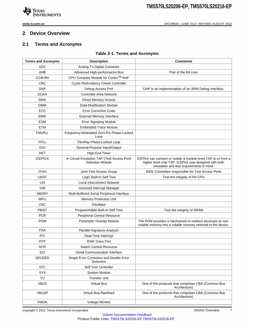
2.5 Terminal Functions
This following table describes the pins on the device.
NOTETable Abbreviations: PWR = power, GND = ground, REF = reference voltage, NC = noconnect, IPD = Internal Pull Down, IPU = Internal Pull Up, I/O = Input/Output, I = Input, O =Output
Table 2-9. Terminal Functions
Terminal InternalTMS570LS20216 TMS570LS20206 Type pullup/p Description
Name ulldown337 144 337 144
HIGH-END TIMER (NHET)
NHET[0] K18 105 K18 105 Timer input capture or output compare.The applicable NHET pins can beNHET[1] V2 42 V2 42programmed as general-purpose
NHET[2] W5 56 W5 56 input/output (GIO) pins. NHET pins arehigh-resolution.NHET[3] U1 41 U1 41The high-resolution (HR) SHARE feature
NHET[4] B12 121 B12 121 allows even HR pins to share the nexthigher odd HR pin structures. The nextNHET[5] V6 44 V6 44higher odd HR pin structure is always
NHET[6] W3 48 W3 48 implemented, even if the next higher oddHR pad and/or pin itself is not. The HRNHET[7] T1 109 T1 109sharing is independent of whether or not
NHET[8] E18 112 E18 112 the odd pin is available externally. If anodd pin is available externally andNHET[9] V7 57 V7 57shared, then the odd pin can only be
NHET[10] D19 116 D19 116 used as a general-purpose I/O.NHET[0] provides SPI clock when usedNHET[11] E3 117 E3 117for SPI emulation.
NHET[12] B4 8 B4 8 Each NHET pin is equipped with an inputsuppression filter that can be used toNHET[13] N2 26 N2 26eliminate the sampling of pulses that are
NHET[14] A11 138 A11 138 smaller than a programmable durationprogramNHET[15] N1 113 N1 113 GIOA[0]/INT[0] is also connected to themable3.3V I/O 2mA - z NHET Pin Disable input of the NHETIPDNHET[16] A4 142 A4 142
module.(20uA)NHET[17] A13 A13 NHET pins can be programmed as a
GIO pins when not used as NHETNHET[18] J1 10 J1 10functional pins.
NHET[19] B13 B13
NHET[20] P2 45 P2 45
NHET[21] H4 11 H4 11
NHET[22] B3 9 B3 9
NHET[23] J4 12 J4 12
NHET[24] P1 43 P1 43
NHET[25] M3 M3
NHET[26] A14 A14
NHET[27] A9 A9
NHET[28] K19 106 K19 106
NHET[29] A3 A3
NHET[30] B11 137 B11 137
NHET[31] J17 J17
22 Device Overview Copyright © 2012, Texas Instruments Incorporated
Submit Documentation FeedbackProduct Folder Links: TMS570LS20206-EP TMS570LS20216-EP
TMS570LS20206-EP, TMS570LS20216-EP
www.ti.com.cn ZHCS983A –JUNE 2012–REVISED AUGUST 2012
Table 2-9. Terminal Functions (continued)
Terminal InternalTMS570LS20216 TMS570LS20206 Type pullup/p Description
Name ulldown337 144 337 144
GENERAL-PURPOSE I/O (GIO)
General-purpose input/output pin.GIOA[0]/INT[0] is an interrupt-capable
GIOA[0]/INT0 A5 118 A5 118 pin. GIOA[0]/INT[0] is also connected tothe NHET Pin Disable input of the NHETmodule.
GIOA[1]/INT1 C2 134 C2 134
GIOA[2]/INT2 C1 141 C1 141
GIOA[3]/INT3 E1 144 E1 144 General-purpose input/outputGIOA[4]/INT4 A6 110 A6 110 pins.GIOA[7:1]/INT[7:1] are interrupt-
capable pins.GIOA[5]/INT5 B5 111 B5 111 ProgrammableGIOA[6]/INT6 H3 27 H3 27 3.3V I/O 2mA - z IPD
GIOA[7]/INT7 M1 51 M1 51 (20uA)GIOB[0] M2 M2
GIOB[1] K2 K2
GIOB[2] F2 F2
GIOB[3] W10 W10General-purpose input/output pins.
GIOB[4] G1 G1
GIOB[5] G2 G2
GIOB[6] J2 J2
GIOB[7] F1 F1
FlexRay Controller (FLEXRAY)
NOTE: Devices with out the FlexRay option should leave all FlexRay pins unconnected (NC)
ProgrammableFRAYRX1 A15 126 3.3V I FlexRay data receive (channel 1) pinIPD(20uA)
FRAYTX1 B15 124 8mA FlexRay data transmit (channel 1) pin3.3V O
FRAYTXEN1 B16 125 8mA FlexRay transmit enable (channel 1) pin
ProgrammableFRAYRX2 A8 131 3.3V I FlexRay data receive (channel 2) pinIPD(20u
A)
FRAYTX2 B8 129 8mA FlexRay data transmit (channel 2) pin3.3V O
FRAYTXEN2 B9 130 8mA FlexRay transmit enable (channel 2) pin
CAN Controller (DCAN1)
CAN1TX A10 50 A10 50 Program CAN1 transmit pin or GIO pinmable3.3V I/O 2mA - z IPUCAN1RX B10 49 B10 49 CAN1 receive pin or GIO pin(20uA)
CAN Controller (DCAN2)
CAN2TX H2 54 H2 54 Program CAN2 transmit pin or GIO pinmable3.3V I/O 2mA - z IPUCAN2RX H1 55 H1 55 CAN2 receive pin or GIO pin(20uA)
CAN Controller (DCAN3)
CAN3TX M18 M18 program CAN3 transmit pin or GIO pinmable3.3V I/O 2mA - z IPUCAN3RX M19 M19 CAN3 receive pin or GIO pin(20uA)
Copyright © 2012, Texas Instruments Incorporated Device Overview 23Submit Documentation Feedback
Product Folder Links: TMS570LS20206-EP TMS570LS20216-EP

TMS570LS20206-EP, TMS570LS20216-EP
ZHCS983A –JUNE 2012–REVISED AUGUST 2012 www.ti.com.cn
Table 2-9. Terminal Functions (continued)
Terminal InternalTMS570LS20216 TMS570LS20206 Type pullup/p Description
Name ulldown337 144 337 144
Serial Communications Interface (SCI)/Local Interconnect Network (LIN1)
LIN1RX W12 53 W12 53 Program LIN1 data receive pin or GIO pinmable3.3V I/O 2mA - z IPULIN1TX V12 52 V12 52 LIN1 data transmit pin or GIO pin(20uA)
Serial Communications Interface (SCI)/Local Interconnect Network (LIN2)
LIN2RX A7 140 A7 140 Program LIN2 data receive pin or GIO pinmable3.3V I/O 2mA - z IPULIN2TX B7 139 B7 139 LIN2 data transmit pin or GIO pin(20uA)
Multibuffered Serial Peripheral Interface (MIBSPI1)
MIBSPI1CLK F18 17 F18 17 4mA MIBSPI1 clock pin or GIO pin
MIBSPI1CS[0] R2 23 R2 23
MIBSPI1CS[1] F3 24 F3 24 MIBSPI1 slave chip select pins or GIO2mA - z pinsMIBSPI1CS[2] G3 25 G3 25 ProgrammableMIBSPI1CS[3] J3 J3 3.3V I/O IPU
MIBSPI1ENA G19 18 G19 18 2mA - z MIBSPI1 enable pin or GIO pin(20uA)MIBSPI1 data stream - Slave in/masterMIBSPI1SIMO F19 14 F19 14 out pin or GIO pin
4mAMIBSPI1 data stream - Slave out/masterMIBSPI1SOMI G18 13 G18 13 in pin or GIO pin
Multibuffered Serial Peripheral Interface (MIBSPI3)
MIBSPI3CLK V9 3 V9 3 4mA MIBSPI3 clock pin or GIO pin
MIBSPI3CS[0] V10 7 V10 7
MIBSPI3CS[1] V5 V5 MIBSPI3 slave chip select pins or GIO2mA - z pinsMIBSPI3CS[2] B2 B2 ProgrammableMIBSPI3CS[3] C3 C3 3.3V I/O IPU
MIBSPI3ENA W9 6 W9 6 2mA - z MIBSPI3 enable pin or GIO pin(20uA)MIBSPI3 data stream - Slave in/masterMIBSPI3SIMO W8 4 W8 4 out pin or GIO pin
4mAMIBSPI3 data stream - Slave out/masterMIBSPI3SOMI V8 5 V8 5 in pin or GIO pin
24 Device Overview Copyright © 2012, Texas Instruments Incorporated
Submit Documentation FeedbackProduct Folder Links: TMS570LS20206-EP TMS570LS20216-EP

TMS570LS20206-EP, TMS570LS20216-EP
www.ti.com.cn ZHCS983A –JUNE 2012–REVISED AUGUST 2012
Table 2-9. Terminal Functions (continued)
Terminal InternalTMS570LS20216 TMS570LS20206 Type pullup/p Description
Name ulldown337 144 337 144
Multibuffered Serial Peripheral Interface - Parallel (MIBSPIP5)
MIBSPI5CLK/DM MIBSPI5 clock pin or GIO pin;H19 91 H19 91 4mAMDATA[4] multiplexed with DMMDATA[4] pin
MIBSPI5CS[0]/DM E19 92 E19 92MDATA[5]
MIBSPI5CS[1]/DM B6 93 B6 93MDATA[6] MIBSPI5 slave chip select pins or GIOpins; multiplexed with DMMDATA pinsMIBSPI5CS[2]/DM W6 W6 2mA - zMDATA[2]
MIBSPI5CS[3]/DM T12 T12MDATA[3]
MIBSPI5ENA/DM MIBSPI5 enable pin or GIO pin;H18 94 H18 94MDATA[7] multiplexed with DMMDATA[7] pin
MIBSPI5SIMO[0]/ ProgramJ19 95 J19 95DMMDATA[8] mable3.3V I/O IPUDMMDATA[9]/MIB E16 96 E16 96 MIBSPI5 data stream - Slave in/master(20uA)SPI5SIMO[1]out pins or GIO pins; multiplexed with
MIBSPI5SIMO[2]/ DMMDATA pinsH17 97 H17 97DMMDATA[10]
MIBSPI5SIMO[3]/ G17 98 G17 98DMMDATA[11]4mA
MIBSPI5SOMI[0]/ J18 99 J18 99DMMDATA[12]
MIBSPI5SOMI[1]/ E17 100 E17 100 MIBSPI5 data stream - Slave out/masterDMMDATA[13]in pins or GIO pins; multiplexed with
MIBSPI5SOMI[2]/ DMMDATA pinsH16 101 H16 101DMMDATA[14]
MIBSPI5SOMI[3]/ G16 102 G16 102DMMDATA[15]/
Multibuffered Analog-To-Digital Converter (MIBADC1)
ProgrammableAD1EVT N19 84 N19 84 3.3V I/O 2 mA - z MibADC1 event input pin or GIO pinIPD(20uA)
AD1IN[0] W14 83 W14 83
AD1IN[1] V17 82 V17 82
AD1IN[2] V18 81 V18 81
AD1IN[3] T17 80 T17 803.3V I MibADC1 analog input pins
AD1IN[4] U18 79 U18 79
AD1IN[5] R17 78 R17 78
AD1IN[6] T19 77 T19 77
AD1IN[7] V14 76 V14 76
Copyright © 2012, Texas Instruments Incorporated Device Overview 25Submit Documentation Feedback
Product Folder Links: TMS570LS20206-EP TMS570LS20216-EP

TMS570LS20206-EP, TMS570LS20216-EP
ZHCS983A –JUNE 2012–REVISED AUGUST 2012 www.ti.com.cn
Table 2-9. Terminal Functions (continued)
Terminal InternalTMS570LS20216 TMS570LS20206 Type pullup/p Description
Name ulldown337 144 337 144
Multibuffered Analog-To-Digital Converter (MIBADC2)
ProgrammableAD2EVT W13 59 W13 59 3.3V I/O 2 mA - z MibADC2 event input pin or GIO pinIPD(20uA)
AD2IN[0] V13 60 V13 60
AD2IN[1] U13 61 U13 61
AD2IN[2] U14 62 U14 62
AD2IN[3] U16 63 U16 633.3 V I MibADC2 analog input pins
AD2IN[4] U15 U15
AD2IN[5] T15 T15
AD2IN[6] R19 R19
AD2IN[7] R16 R16
Multibuffered Analog-To-Digital Converter - shared signals (MIBADC1, MIBADC2)
ADSIN[8] P18 75 P18 75
ADSIN[9] W17 74 W17 74
ADSIN[10] U17 73 U17 73
ADSIN[11] U19 72 U19 72 MibADC1, MibADC2 shared analog input3.3 V I pinsADSIN[12] T16 71 T16 71
ADSIN[13] T18 70 T18 70
ADSIN[14] R18 69 R18 69
ADSIN[15] P19 68 P19 68
3.3-V MibADC1, MibADC2 module high-ADREFHI V15 66 V15 66 REF voltage reference input
GND MibADC1, MibADC2 module low-voltageADREFLO V16 65 V16 65 REF reference input
3.3-V MibADC1, MibADC2 analog supplyVCCAD W15 67 W15 67 PWR voltage
VSSAD V19 64 V19 64
VSSAD W16 W16 MibADC1, MibADC2 analog groundGND referenceVSSAD W18 W18
VSSAD W19 W19
Oscillator (OSC)
Oscillator input connection pin orOSCIN K1 20 K1 20 1.5V I external clock input pin
OSCOUT L1 21 L1 21 1.5V O Oscillator ouptut connection pin
Kelvin_GND L2 L2 GND Kelvin_GND for oscillator
26 Device Overview Copyright © 2012, Texas Instruments Incorporated
Submit Documentation FeedbackProduct Folder Links: TMS570LS20206-EP TMS570LS20216-EP

TMS570LS20206-EP, TMS570LS20216-EP
www.ti.com.cn ZHCS983A –JUNE 2012–REVISED AUGUST 2012
Table 2-9. Terminal Functions (continued)
Terminal InternalTMS570LS20216 TMS570LS20206 Type pullup/p Description
Name ulldown337 144 337 144
System Module (SYS)
Power on Reset Pin. External powerIPDPORRST W7 28 W7 28 3.3V I supply monitor circuitry must assert a(100µA) power-on reset on this pin.
Active Low Bidirectional Reset pin. Anexternal device can assert a device reseton this pin.The output buffer on this pin is
IPU implemented as an open drain (drivesRST B17 85 B17 85 4mA (100µA) low only).3.3V I/O To ensure an external reset is not
arbitrarily generated, TI recommendsthat an external pullup resistor isconnected to this pin.
IPD External Clock Prescaler module outputECLK A12 88 A12 88 8mA (20µA) pin or GIO pin
Tset/Debug (T/D)
IPD JTAG test clock pin. Clocks the JTAGTCK B18 30 B18 30 3.3V I (100uA) debug logic.
RTCK A16 35 A16 35 3.3V O JTAG return test clock pin. (JTAG)
IPUTDI A17 34 A17 34 JTAG test data in pin.(100uA)
IPD8 mATDO C18 33 C18 33 JTAG test data out pin.3.3V I/O (100uA)
JTAG serial input pin for controlling theIPUTMS C19 36 C19 36 state of the CPU test access port (TAP)(100uA) controller.
JTAG test hardware reset to TAP. IEEEIPDTRST D18 29 D18 29 Standard 1149-1 (JTAG) Boundary-Scan(100uA) Logic3.3V I Test enable pin. Reserved for internal TI
IPD use only. For proper operation, this pinTEST U2 58 U2 58 (100uA) must be connected to ground, e.g. usinga external resistor.
Error Signaling Module (ESM)
IPDERROR B14 143 B14 143 3.3V I/O 8mA Error Signaling pin(20uA)
Flash
Flash Test Pad 1 pin. For properoperation this pin must connect only to atest pad or not be connected at all [noFLTP1 J5 122 J5 122 connect (NC)]. The test pad must not beexposed in the final product where itmight be subjected to an ESD event.
Flash Test Pad 2 pin. For properoperation this pin must connect only to atest pad or not be connected at all [noFLTP2 H5 123 H5 123 connect (NC)]. The test pad must not beexposed in the final product where itmight be subjected to an ESD event.
Flash pump voltage supply (3.3 V). This3.3VVCCP F8 128 F8 128 pin is required for Flash read, programPWR and erase operations.
Copyright © 2012, Texas Instruments Incorporated Device Overview 27Submit Documentation Feedback
Product Folder Links: TMS570LS20206-EP TMS570LS20216-EP

TMS570LS20206-EP, TMS570LS20216-EP
ZHCS983A –JUNE 2012–REVISED AUGUST 2012 www.ti.com.cn
Table 2-9. Terminal Functions (continued)
Terminal InternalTMS570LS20216 TMS570LS20206 Type pullup/p Description
Name ulldown337 144 337 144
RAM Trace Port Module (RTP)
RTPDATA[0] V11 V11
RTPDATA[1] U11 U11
RTPDATA[2] T10 T10
RTPDATA[3] U10 U10
RTPDATA[4] T9 T9
RTPDATA[5] U9 U9
RTPDATA[6] U8 U8
RTPDATA[7] U7 U7 RAM Trace Port Output Data Signal pins8mA or GIO pinsRTPDATA[8] U6 U6 ProgramRTPDATA[9] U5 U5 mable3.3V I/O IPURTPDATA[10] U4 U4
(20uA)RTPDATA[11] T4 T4
RTPDATA[12] V3 V3
RTPDATA[13] U3 U3
RTPDATA[14] T3 T3
RTPDATA[15] T2 T2
RTPENA U12 U12 2mA - z Packet Handshake Signal pin or GIO pin
Packet Synchronization Signal pin orRTPSYNC T11 T11 GIO pin8mARTPCLK W11 W11 Packet Clock Signal pin or GIO pin
28 Device Overview Copyright © 2012, Texas Instruments Incorporated
Submit Documentation FeedbackProduct Folder Links: TMS570LS20206-EP TMS570LS20216-EP

TMS570LS20206-EP, TMS570LS20216-EP
www.ti.com.cn ZHCS983A –JUNE 2012–REVISED AUGUST 2012
Table 2-9. Terminal Functions (continued)
Terminal InternalTMS570LS20216 TMS570LS20206 Type pullup/p Description
Name ulldown337 144 337 144
Data Modification Module (DMM)
DMMDATA[0] L19 L19DMM Data pins or GIO pins
DMMDATA[1] L18 L18
DMMDATA[2]/MIB 2mA - zW6 W6SPI5CS[2]
DMMDATA[3]/MIB T12 T12SPI5CS[3]
DMMDATA[4]/MIB H19 H19 4mASPI5CLK
DMMDATA[5]/MIB E19 E19SPI5CS[0]
DMMDATA[6]/MIB B6 B6 2mA - zSPI5CS[1]
DMMDATA[7]/MIB H18 H18SPI5ENA
DMMDATA[8]/MIB J19 J19 ProgramSPI5SIMO[0] DMM Data pins or GIO pins; multiplexedmable with MIBSPI5 pinsDMMDATA[9]/MIB 3.3V I/OE16 E16 IPUSPI5SIMO[1] (20uA)
DMMDATA[10]/MI H17 H17BSPI5SIMO[2]
DMMDATA[11]/MI G17 G17BSPI5SIMO[3]4mA
DMMDATA[12]/MI J18 J18BSPI5SOMI[0]
DMMDATA[13]/MI E17 E17BSPI5SOMI[1]
DMMDATA[14]/MI H16 H16BSPI5SOMI[2]
DMMDATA[15]/MI G16 G16BSPI5SOMI[3]
DMMENA F16 F16 8mA DMM Handshake pin or GIO pin
DMMSYNC J16 J16 DMM Synchronization pin or GIO pin2mA - z
DMMCLK F17 F17 DMM Clock input pin or GIO pin
Copyright © 2012, Texas Instruments Incorporated Device Overview 29Submit Documentation Feedback
Product Folder Links: TMS570LS20206-EP TMS570LS20216-EP

TMS570LS20206-EP, TMS570LS20216-EP
ZHCS983A –JUNE 2012–REVISED AUGUST 2012 www.ti.com.cn
Table 2-9. Terminal Functions (continued)
Terminal InternalTMS570LS20216 TMS570LS20206 Type pullup/p Description
Name ulldown337 144 337 144
External Memory Interface Module (EMIF)
EMIFBADD[0] D13 D133.3V I/O 8mA EMIF Byte Address pins
EMIFBADD[1] D16 D16
EMIFDATA[0] K16 K16
EMIFDATA[1] L16 L16
EMIFDATA[2] M16 M16
EMIFDATA[3] N16 N16
EMIFDATA[4] E4 E4
EMIFDATA[5] F4 F4
EMIFDATA[6] G4 G4Program
EMIFDATA[7] K4 K4 mable3.3V I/O 8mA EMIF Data pinsIPUEMIFDATA[8] L4 L4(20uA)
EMIFDATA[9] M4 M4
EMIFDATA[10] N4 N4
EMIFDATA[11] P4 P4
EMIFDATA[12] T5 T5
EMIFDATA[13] T6 T6
EMIFDATA[14] T7 T7
EMIFDATA[15] T8 T8
EMIFADD[0] D4 D4
EMIFADD[1] D5 D5
EMIFADD[2] D6 D6
EMIFADD[3] D7 D7
EMIFADD[4] D8 D8
EMIFADD[5] D9 D9
EMIFADD[6] C4 C4
EMIFADD[7] C5 C5
EMIFADD[8] C6 C6
EMIFADD[9] C7 C7
EMIFADD[10] C8 C83.3V I/O 8mA EMIF Address pins
EMIFADD[11] C9 C9
EMIFADD[12] C10 C10
EMIFADD[13] C11 C11
EMIFADD[14] C12 C12
EMIFADD[15] C13 C13
EMIFADD[16] D14 D14
EMIFADD[17] C14 C14
EMIFADD[18] D15 D15
EMIFADD[19] C15 C15
EMIFADD[20] C16 C16
EMIFADD[21] C17 C17
EMIFCS[0] L17 L17
EMIFCS[1] K17 K173.3V I/O 8mA EMIF Chip Select pins
EMIFCS[2] M17 M17
EMIFCS[3] N17 N17
30 Device Overview Copyright © 2012, Texas Instruments Incorporated
Submit Documentation FeedbackProduct Folder Links: TMS570LS20206-EP TMS570LS20216-EP

TMS570LS20206-EP, TMS570LS20216-EP
www.ti.com.cn ZHCS983A –JUNE 2012–REVISED AUGUST 2012
Table 2-9. Terminal Functions (continued)
Terminal InternalTMS570LS20216 TMS570LS20206 Type pullup/p Description
Name ulldown337 144 337 144
EMIFWE D17 D17 3.3V I/O 8mA EMIF Write Enable pin
EMIFOE D12 D12 3.3V I/O 8mA EMIF Output Enable pin
EMIFDQM[0] D10 D103.3V I/O 8mA EMIF Byte Enable pins
EMIFDQM[1] D11 D11
Copyright © 2012, Texas Instruments Incorporated Device Overview 31Submit Documentation Feedback
Product Folder Links: TMS570LS20206-EP TMS570LS20216-EP

TMS570LS20206-EP, TMS570LS20216-EP
ZHCS983A –JUNE 2012–REVISED AUGUST 2012 www.ti.com.cn
Table 2-9. Terminal Functions (continued)
Terminal InternalTMS570LS20216 TMS570LS20206 Type pullup/p Description
Name ulldown337 144 337 144
Embedded Trace Module (ETM)
ETMDATA[0] R12 R12
ETMDATA[1] R13 R13
ETMDATA[2] J15 J15
ETMDATA[3] H15 H15
ETMDATA[4] G15 G15
ETMDATA[5] F15 F15
ETMDATA[6] E15 E15
ETMDATA[7] E14 E14
ETMDATA[8] E9 E9
ETMDATA[9] E8 E8
ETMDATA[10] E7 E7
ETMDATA[11] E6 E6
ETMDATA[12] E13 E13
ETMDATA[13] E12 E12
ETMDATA[14] E11 E11
ETMDATA[15] E10 E103.3V O 8mA ETM Trace Data output pins
ETMDATA[16] K15 K15
ETMDATA[17] L15 L15
ETMDATA[18] M15 M15
ETMDATA[19] N15 N15
ETMDATA[20] E5 E5
ETMDATA[21] F5 F5
ETMDATA[22] G5 G5
ETMDATA[23] K5 K5
ETMDATA[24] L5 L5
ETMDATA[25] M5 M5
ETMDATA[26] N5 N5
ETMDATA[27] P5 P5
ETMDATA[28] R5 R5
ETMDATA[29] R6 R6
ETMDATA[30] R7 R7
ETMDATA[31] R8 R8
ETMTRACECTL R11 R11 ETM Control pin3.3V O 8mAETMTRACECLKO R10 R10 ETM Clock output pinUT
IPUETMTRACECLKIN R9 R9 3.3V I ETM Clock input pin(20uA)
32 Device Overview Copyright © 2012, Texas Instruments Incorporated
Submit Documentation FeedbackProduct Folder Links: TMS570LS20206-EP TMS570LS20216-EP

TMS570LS20206-EP, TMS570LS20216-EP
www.ti.com.cn ZHCS983A –JUNE 2012–REVISED AUGUST 2012
Table 2-9. Terminal Functions (continued)
Terminal InternalTMS570LS20216 TMS570LS20206 Type pullup/p Description
Name ulldown337 144 337 144
Supply Voltage Digital I/O (3.3V) and Core (1.5V)
VCCIO F6 1 F6 1
VCCIO F7 15 F7 15
VCCIO F11 40 F11 40
VCCIO F12 90 F12 90
VCCIO F13 108 F13 108
VCCIO F14 119 F14 119
VCCIO G6 132 G6 132
VCCIO G14 G14
VCCIO H6 H6
VCCIO H14 H14
VCCIO J6 J6 Digital I/O supply pinsNote: All VccIO pads are connected toVCCIO L14 L14 3.3V the BGA packages through the packagePWRVCCIO M6 M6 substrate. There is not a direct ball tobond pad connection for this supply.VCCIO M14 M14
VCCIO N6 N6
VCCIO N14 N14
VCCIO P6 P6
VCCIO P7 P7
VCCIO P8 P8
VCCIO P9 P9
VCCIO P12 P12
VCCIO P13 P13
VCCIO P14 P14
VCCIO
VCC F9 19 F9 19
VCC F10 31 F10 31
VCC H10 37 H10 37
VCC J14 47 J14 47
VCC K6 87 K6 87Digital Core supply pins
VCC K8 104 K8 104 Note: All Vcc pads are connected to the1.5VVCC K12 114 K12 114 BGA packages through the packagePWR substrate. There is not a direct ball toVCC K14 135 K14 135bond pad connection for this supply.
VCC L6 L6
VCC M10 M10
VCC P10 P10
VCC P11 P11
VCC
Copyright © 2012, Texas Instruments Incorporated Device Overview 33Submit Documentation Feedback
Product Folder Links: TMS570LS20206-EP TMS570LS20216-EP

TMS570LS20206-EP, TMS570LS20216-EP
ZHCS983A –JUNE 2012–REVISED AUGUST 2012 www.ti.com.cn
Table 2-9. Terminal Functions (continued)
Terminal InternalTMS570LS20216 TMS570LS20206 Type pullup/p Description
Name ulldown337 144 337 144
Supply Ground
VSS A1 2 A1 2
VSS A2 16 A2 16
VSS A18 22 A18 22
VSS A19 32 A19 32
VSS B1 38 B1 38
VSS B19 39 B19 39
VSS H8 46 H8 46
VSS H9 86 H9 86
VSS H11 89 H11 89
VSS H12 103 H12 103
VSS J8 107 J8 107
VSS J9 115 J9 115
VSS J10 120 J10 120
VSS J11 127 J11 127
VSS J12 133 J12 133
VSS K9 136 K9 136
VSS K10 K10Digital supply ground reference pins
VSS K11 K11 Note: All Vss pads are connected to theGND BGA packages through the packageVSS L8 L8substrate.
VSS L9 L9
VSS L10 L10
VSS L11 L11
VSS L12 L12
VSS M8 M8
VSS M9 M9
VSS M11 M11
VSS M12 M12
VSS V1 V1
VSS W1 W1
VSS W2 W2
VSS V4 V4
VSS
VSS
VSS
VSS
VSS
34 Device Overview Copyright © 2012, Texas Instruments Incorporated
Submit Documentation FeedbackProduct Folder Links: TMS570LS20206-EP TMS570LS20216-EP

TMS570LS20206-EP, TMS570LS20216-EP
www.ti.com.cn ZHCS983A –JUNE 2012–REVISED AUGUST 2012
2.6 Device Support
2.6.1 Device and Development-Support Tool Nomenclature
To designate the stages in the product development cycle, TI assigns prefixes to the part numbers of alldevices and support tools. Each commercial family member has one of three prefixes: TMX, TMP, or TMS(e.g.,TMS570LS20216ASGWTMEP). Texas Instruments recommends two of three possible prefixdesignators for its support tools: TMDX and TMDS. These prefixes represent evolutionary stages ofproduct development from engineering prototypes (TMX/TMDX) through fully qualified productiondevices/tools (TMS/TMDS).
Device development evolutionary flow:
TMX Experimental device that is not necessarily representative of the final device's electricalspecifications.
TMP Final silicon die that conforms to the device's electrical specifications but has not completedquality and reliability verification.
TMS Fully-qualified production device.
Support tool development evolutionary flow:
TMDX Development-support product that has not yet completed Texas Instruments internalqualification testing.
TMDS Fully qualified development-support product.
TMX and TMP devices and TMDX development-support tools are shipped against the followingdisclaimer:
"Developmental product is intended for internal evaluation purposes."
TMS devices and TMDS development-support tools have been characterized fully, and the quality andreliability of the device have been demonstrated fully. TI's standard warranty applies.
Predictions show that prototype devices (TMX or TMP) have a greater failure rate than the standardproduction devices. Texas Instruments recommends that these devices not be used in any productionsystem because their expected end-use failure rate still is undefined. Only qualified production devices areto be used.
TI device nomenclature also includes a suffix with the device family name. This suffix indicates thepackage type (for example, GWT), the temperature range (for example, "Blank" is the commercialtemperature range), and the device speed range in Mega Hertz.
Copyright © 2012, Texas Instruments Incorporated Device Overview 35Submit Documentation Feedback
Product Folder Links: TMS570LS20206-EP TMS570LS20216-EP

Prefix: TMS = Fully TMS QualifiedP = TMP PrototypeX = TMX Samples
Core Technology:5 = 570 Cortex R4
Architecture:LS = Lockstep CPUs
Flash Memory Size:20 = 2MB
RAM Memory Size:2 = 160kB
Peripheral Set:16 = FlexRay06 = No FlexRay
Die Revision:A = 1st Die Revision
Technology/Core Voltage:S = F035 (130nm), 1.5 V nominal core voltage
Package Type:
PGE = 144p QFP Package [Green]
Temperature Range:M = -55...+125 C
o
Quality Designator:EP = Enhanced Product
Full Part # TMS 570 LS 20 2 16 A S GWT M EP
Orderable Part # S 5 LS 20 2 16 A S GWT M EP
GWT = 337p BGA Package
TMS570LS20206-EP, TMS570LS20216-EP
ZHCS983A –JUNE 2012–REVISED AUGUST 2012 www.ti.com.cn
A. For actual device part numbers (P/Ns) and ordering information, see the TI website (http://www.ti.com).
Figure 2-7. Device Numbering Conventions(A)
36 Device Overview Copyright © 2012, Texas Instruments Incorporated
Submit Documentation FeedbackProduct Folder Links: TMS570LS20206-EP TMS570LS20216-EP

TMS570LS20206-EP, TMS570LS20216-EP
www.ti.com.cn ZHCS983A –JUNE 2012–REVISED AUGUST 2012
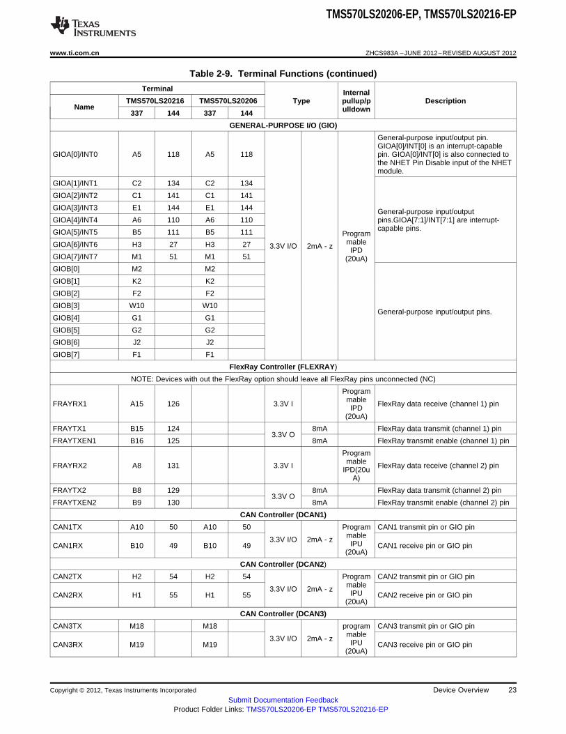
3 Reset / Abort Sources
3.1 Reset / Abort Sources
The device Resets and Aborts are handled as shown in the following table. The table shows the source ofthe error, the system mode, the type of error response and the corresponding Error Signaling Module(ESM) channel. Only standard ARM exception handlers and ESM errors are used.
Table 3-1. Reset / Abort Sources
Error Source System Mode Error Response ESM Hookup group channel
1) CPU transactions
Precise write error (Strongly User/Privilege Precise Abort (CPU) n/aOrdered)
Precise read error (Device or User/Privilege Precise Abort (CPU) n/aNormal)
Imprecise write error (Device or User/Privilege Imprecise Abort (CPU) n/aNormal)
Illegal instruction User/Privilege Undefined Instruction Trap n/a(CPU) (1)
MPU access violation User/Privilege Abort (CPU) n/a
2) SRAM
B0 Tightly Coupled Memory User/Privilege ESM 1.26(TCM) (even) ECC single error(correctable)
B0 TCM (even) ECC double error User/Privilege Abort (CPU), ESM => nERROR 3.3(non-correctable)
B0 TCM (even) uncorrectable User/Privilege ESM => NMI 2.6error (i.e. redundant addressdecode)
B0 TCM (even) address bus User/Privilege ESM => NMI 2.10parity error
B1 TCM (odd) ECC single error User/Privilege ESM 1.28(correctable)
B1 TCM (odd) ECC double error User/Privilege Abort (CPU), ESM => nERROR 3.5(non-correctable)
B1 TCM (odd) uncorrectable User/Privilege ESM => NMI 2.8error (i.e. redundant addressdecode)
B1 TCM (odd) address bus parity User/Privilege ESM => NMI 2.12error
3) Flash with ECC INTEGRATED INTO CPU
ECC single error (correctable) User/Privilege ESM 1.6
ECC double error (non- User/Privilege Abort (CPU), ESM => nERROR 3.7correctable)
Uncorrectable error (i.e. User/Privilege ESM => NMI 2.4redundant address tag,redundant syndrome compare,address bus parity, etc.)
4) DMA transactions
External imprecise error on read User/Privilege ESM 1.5(Illegal transaction with okresponse)
External imprecise error on write User/Privilege ESM 1.13(Illegal transaction with okresponse)
(1) The Undefined Instruction TRAP is NOT detectable outside the CPU. The trap is taken only if the Code reaches the execute stage ofthe CPU.
Copyright © 2012, Texas Instruments Incorporated Reset / Abort Sources 37Submit Documentation Feedback
Product Folder Links: TMS570LS20206-EP TMS570LS20216-EP
TMS570LS20206-EP, TMS570LS20216-EP
ZHCS983A –JUNE 2012–REVISED AUGUST 2012 www.ti.com.cn
Table 3-1. Reset / Abort Sources (continued)
Error Source System Mode Error Response ESM Hookup group channel
Memory access permission User/Privilege ESM 1.2violation
Memory parity error User/Privilege ESM 1.3
5) DMM transactions
External imprecise error on read User/Privilege ESM 1.5(Illegal transaction with okresponse)
External imprecise error on write User/Privilege ESM 1.13(Illegal transaction with okresponse)
6) AHB-AP transactions
External imprecise error on read User/Privilege ESM 1.5(Illegal transaction with okresponse)
External imprecise error on write User/Privilege ESM 1.13(Illegal transaction with okresponse)
7) HET TU
NCNB (Strongly Ordered) User/Privilege Interrupt => VIM n/atransaction with slave errorresponse
External imprecise error (Illegal User/Privilege Interrupt => VIM n/atransaction with ok response)
Memory access permission User/Privilege ESM 1.9violation
Memory parity error User/Privilege ESM 1.8
8) NHET
Memory parity error User/Privilege ESM 1.7
9) MibSPI
MibSPI1 memory parity error User/Privilege ESM 1.17
MibSPI3 memory parity error User/Privilege ESM 1.18
MibSPIP5 memory parity error User/Privilege ESM 1.24
10) MibADC
MibADC1 memory parity error User/Privilege ESM 1.19
MibADC2 memory parity error User/Privilege ESM 1.1
11) DCAN
DCAN1 memory parity error User/Privilege ESM 1.21
DCAN2 memory parity error User/Privilege ESM 1.23
DCAN3 memory parity error User/Privilege ESM 1.22
12) PLL
PLL slip error User/Privilege ESM 1.10
13) Clock monitor
Clock monitor interrupt User/Privilege ESM 1.11
14) CCM
Self test failure User/Privilege ESM 1.31
Compare failure User/Privilege ESM => NMI 2.2
15) FlexRay
Memory parity error User/Privilege ESM 1.12
16) FlexRay TU
NCNB (Strongly Ordered) User/Privilege Interrupt => VIM n/atransaction with slave errorresponse
38 Reset / Abort Sources Copyright © 2012, Texas Instruments Incorporated
Submit Documentation FeedbackProduct Folder Links: TMS570LS20206-EP TMS570LS20216-EP

TMS570LS20206-EP, TMS570LS20216-EP
www.ti.com.cn ZHCS983A –JUNE 2012–REVISED AUGUST 2012
Table 3-1. Reset / Abort Sources (continued)
Error Source System Mode Error Response ESM Hookup group channel
External imprecise error (Illegal User/Privilege Interrupt => VIM n/atransaction with ok response)
Memory access permission User/Privilege ESM 1.16violation
Memory parity error User/Privilege ESM 1.14
17) VIM
Memory parity error User/Privilege ESM 1.15
18) voltage monitor
VMON out of voltage range n/a Reset n/a
19) CPU Selftest (LBIST)
CPU Selftest (LBIST) error User/Privilege ESM 1.27
20) errors reflected in the SYSESR register
Power-Up Reset; VCC out of n/a Reset n/avoltage range
Oscillator fail / PLL slip (2) n/a Reset n/a
Watchdog time limit exceeded n/a Reset n/a
CPU Reset n/a Reset n/a
Software Reset n/a Reset n/a
External Reset n/a Reset n/a
(2) Oscillator fail/PLL slip can be configured in the system register PLLCTL1 to generate a reset.
Copyright © 2012, Texas Instruments Incorporated Reset / Abort Sources 39Submit Documentation Feedback
Product Folder Links: TMS570LS20206-EP TMS570LS20216-EP

TMS570LS20206-EP, TMS570LS20216-EP
ZHCS983A –JUNE 2012–REVISED AUGUST 2012 www.ti.com.cn
4 Peripherals
4.1 Error Signaling Module (ESM)
The Error Signaling Module (ESM) is used to indicate a severe device failure via interrupts and theexternal ERROR pin. The error pin is normally used by an external device to either reset the controllerand/or keep the system in a fail safe state.
The ESM module consists of three error groups with 32 inputs each. The generation of the interrupts andthe activation of the ERROR Pin is shown in the following table. The next table shows the ESM errorsources and their corresponding group and channel numbers.
Table 4-1. ESM Groups
Error Group Interrupt, Level Influence on ERROR pin
Group1 maskable, low/high configurable
Group2 non-maskable, high fixed
Group3 none, none fixed
Table 4-2. ESM Assignments
ERROR Sources Group Channels
Reserved Group1 0
MibADC2 - parity Group1 1
DMA - MPU Group1 2
DMA - parity Group1 3
Reserved Group1 4
DMA/DMM/AHB-AP - imprecise read error Group1 5
Flash (ATCM) - correctable error Group1 6
NHET - parity Group1 7
HET TU - parity Group1 8
HET TU - MPU Group1 9
PLL - slip Group1 10
Clock Monitor - interrupt Group1 11
FlexRay - parity Group1 12
DMA/DMM/AHB-AP - imprecise write error Group1 13
FlexRay TU - parity Group1 14
VIM RAM - parity Group1 15
FlexRay TU - MPU Group1 16
MibSPI1 - parity Group1 17
MibSPI3 - parity Group1 18
MibADC1 - parity Group1 19
Reserved Group1 20
DCAN1 - parity Group1 21
DCAN3 - parity Group1 22
DCAN2 - parity Group1 23
MibSPIP5 - parity Group1 24
Reserved Group1 25
RAM even bank (B0TCM) - correctable error Group1 26
CPU - selftest Group1 27
RAM odd bank (B1TCM) - correctable error Group1 28
Reserved Group1 29
Reserved Group1 30
40 Peripherals Copyright © 2012, Texas Instruments Incorporated
Submit Documentation FeedbackProduct Folder Links: TMS570LS20206-EP TMS570LS20216-EP

TMS570LS20206-EP, TMS570LS20216-EP
www.ti.com.cn ZHCS983A –JUNE 2012–REVISED AUGUST 2012
Table 4-2. ESM Assignments (continued)
ERROR Sources Group Channels
CCM-R4 - selftest Group1 31
Reserved Group2 0
Reserved Group2 1
CCM-R4 - compare Group2 2
Reserved Group2 3
Flash (ATCM) - uncorrectable error Group2 4
Reserved Group2 5
RAM even bank (B0TCM) - uncorrectable error Group2 6
Reserved Group2 7
RAM odd bank (B1TCM) - uncorrectable error Group2 8
Reserved Group2 9
RAM even bank (B0TCM) - address bus parity error Group2 10
Reserved Group2 11
RAM odd bank (B1TCM) - address bus parity error Group2 12
Reserved Group2 13
Reserved Group2 14
Reserved Group2 15
Flash (ATCM) - ECC live lock detect Group2 16
Reserved Group2 17
Reserved Group2 18
Reserved Group2 19
Reserved Group2 20
Reserved Group2 21
Reserved Group2 22
Reserved Group2 23
Reserved Group2 24
Reserved Group2 25
Reserved Group2 26
Reserved Group2 27
Reserved Group2 28
Reserved Group2 29
Reserved Group2 30
Reserved Group2 31
Reserved Group3 0
Reserved Group3 1
Reserved Group3 2
RAM even bank (B0TCM) - ECC uncorrectable error Group3 3
Reserved Group3 4
RAM odd bank (B1TCM) - ECC uncorrectable error Group3 5
Reserved Group3 6
Flash (ATCM) - ECC uncorrectable error Group3 7
Reserved Group3 8
Reserved Group3 9
Reserved Group3 10
Reserved Group3 11
Reserved Group3 12
Reserved Group3 13
Copyright © 2012, Texas Instruments Incorporated Peripherals 41Submit Documentation Feedback
Product Folder Links: TMS570LS20206-EP TMS570LS20216-EP

TMS570LS20206-EP, TMS570LS20216-EP
ZHCS983A –JUNE 2012–REVISED AUGUST 2012 www.ti.com.cn
Table 4-2. ESM Assignments (continued)
ERROR Sources Group Channels
Reserved Group3 14
Reserved Group3 15
Reserved Group3 16
Reserved Group3 17
Reserved Group3 18
Reserved Group3 19
Reserved Group3 20
Reserved Group3 21
Reserved Group3 22
Reserved Group3 23
Reserved Group3 24
Reserved Group3 25
Reserved Group3 26
Reserved Group3 27
Reserved Group3 28
Reserved Group3 29
Reserved Group3 30
Reserved Group3 31
42 Peripherals Copyright © 2012, Texas Instruments Incorporated
Submit Documentation FeedbackProduct Folder Links: TMS570LS20206-EP TMS570LS20216-EP

TMS570LS20206-EP, TMS570LS20216-EP
www.ti.com.cn ZHCS983A –JUNE 2012–REVISED AUGUST 2012
4.2 Direct Memory Access (DMA)
The direct-memory access (DMA) controller transfers data to and from any specified location in the devicememory map. The DMA supports data transfer for both on-chip memories and peripherals.
The DMA controller on this device supports 16 channels and 32 request lines. Each of the 32 DMArequests are assigned by default to one of the 16 available channels. For DMA requests multiplexedbetween multiple sources, the DMA controller cannot differentiate between the multiple sources and theuser has to ensure that multiple sources are not enabled at the same time. Please refer to the DMASpecification in the TRM for more details.
The DMA request configuration is shown in the following table.
Table 4-3. DMA Request Line Connection
Modules DMA Request Sources DMA Request
MIBSPI1 MIBSPI1[1] (1) DMAREQ[0]
MIBSPI1 MIBSPI1[0] (2) DMAREQ[1]
Reserved Reserved DMAREQ[2]
Reserved Reserved DMAREQ[3]
MIBSPI1 / MIBSPI3 / DCAN2 MIBSPI1[2] / MIBSPI3[2] / DCAN2 IF3 DMAREQ[4]
MIBSPI1 / MIBSPI3 / DCAN2 MIBSPI1[3] / MIBSPI3[3] / DCAN2 IF2 DMAREQ[5]
MIBSPIP5 / DCAN1 MIBSPIP5[2] / DCAN1 IF2 DMAREQ[6]
MIBADC1 / MIBSPIP5 MIBADC1 event / MIBSPIP5[3] DMAREQ[7]
MIBSPI1 / MIBSPI3 / DCAN1 MIBSPI1[4] / MIBSPI3[4] / DCAN1 IF1 DMAREQ[8]
MIBSPI1 / MIBSPI3 / DCAN2 MIBSPI1[5] / MIBSPI3[5] / DCAN2 IF1 DMAREQ[9]
MIBADC1 / MIBSPIP5 MIBADC1 G1 / MIBSPIP5[4] DMAREQ[10]
MIBADC1 / MIBSPIP5 MIBADC1 G2 / MIBSPIP5[5] DMAREQ[11]
RTI / MIBSPI1 / MIBSPI3 RTI DMAREQ0 / MIBSPI1[6] / MIBSPI3[6] DMAREQ[12]
RTI / MIBSPI1 / MIBSPI3 RTI DMAREQ1 / MIBSPI1[7] / MIBSPI3[7] DMAREQ[13]
MIBADC2 / MIBSPI3 / MIBSPIP5 MIBADC2 event / MIBSPI3[1] (1) / MIBSPIP5[6] DMAREQ[14]
MIBSPI3 / MIBSPIP5 MIBSPI3[0]† / MIBSPIP5[7] DMAREQ[15]
MIBADC2 / MIBSPI1 / MIBSPI3 / DCAN1 MIBADC2 G1 / MIBSPI1[8] / MIBSPI3[8] / DCAN1 DMAREQ[16]IF3
MIBADC2 / MIBSPI1 / MIBSPI3 / DCAN3 MIBADC2 G2 / MIBSPI1[9] / MIBSPI3[9] / DCAN3 DMAREQ[17]IF1
RTI / MIBSPIP5 RTI DMAREQ2 / MIBSPIP5[8] DMAREQ[18]
RTI / MIBSPIP5 RTI DMAREQ3 / MIBSPIP5[9] DMAREQ[19]
LIN2 / NHET / DCAN3 LIN2 receive / NHET DMAREQ[4] / DCAN3 IF2 DMAREQ[20]
LIN2 / NHET / DCAN3 LIN2 transmit / NHET DMAREQ[5] / DCAN3 IF3 DMAREQ[21]
MIBSPI1 / MIBSPI3 / MIBSPIP5 MIBSPI1[10] / MIBSPI3[10] / MIBSPIP5[10] DMAREQ[22]
MIBSPI1 / MIBSPI3 / MIBSPIP5 MIBSPI1[11] / MIBSPI3[11] / MIBSPIP5[11] DMAREQ[23]
NHET / MIBSPIP5 NHET DMAREQ[6] / MIBSPIP5[12] DMAREQ[24]
NHET / MIBSPIP5 NHET DMAREQ[7] / MIBSPIP5[13] DMAREQ[25]
CRC / MIBSPI1 / MIBSPI3 CRC DMAREQ[0] / MIBSPI1[12] / MIBSPI3[12] DMAREQ[26]
CRC / MIBSPI1 / MIBSPI3 CRC DMAREQ[1] / MIBSPI1[13] / MIBSPI3[13] DMAREQ[27]
LIN1 / MIBSPIP5 LIN1 receive / MIBSPIP5[14] DMAREQ[28]
LIN1 / MIBSPIP5 LIN1 transmit / MIBSPIP5[15] DMAREQ[29]
MIBSPI1 / MIBSPI3 / MIBSPIP5 MIBSPI1[14] / MIBSPI3[14] / MIBSPIP5[1] (1) DMAREQ[30]
MIBSPI1 / MIBSPI3 / MIBSPIP5 MIBSPI1[15] / MIBSPI3[15] / MIBSPIP5[0] (2) DMAREQ[31]
(1) SPI1, SPI3, SPI5 receive in standard SPI/compatibility mode(2) SPI1, SPI3, SPI5 transmit in standard SPI/compatibility mode
Copyright © 2012, Texas Instruments Incorporated Peripherals 43Submit Documentation Feedback
Product Folder Links: TMS570LS20206-EP TMS570LS20216-EP

TMS570LS20206-EP, TMS570LS20216-EP
ZHCS983A –JUNE 2012–REVISED AUGUST 2012 www.ti.com.cn
4.3 High End Timer Transfer Unit (HET-TU)
The High End Timer Transfer Unit (HET-TU) is a local Direct Memory Access (DMA) module. It isspecifically designed to transfer High End Timer (NHET) data to (or from) the CPU data SRAM . The HETsoftware controls which HET instructions generate transfer requests to the transfer unit. More informationabout the NHET and the HET-TU can be found in the technical reference manual (TRM). The HET-TUsupports 8 channels.
The HET-TU request assignment is shown in the following table.
Table 4-4. NHET Request Line Connection
Modules Request Source HET TRANSFER UNIT Request
NHET HTUREQ[0] HET TU DCP[0]
NHET HTUREQ[1] HET TU DCP[1]
NHET HTUREQ[2] HET TU DCP[2]
NHET HTUREQ[3] HET TU DCP[3]
NHET HTUREQ[4] HET TU DCP[4]
NHET HTUREQ[5] HET TU DCP[5]
NHET HTUREQ[6] HET TU DCP[6]
NHET HTUREQ[7] HET TU DCP[7]
44 Peripherals Copyright © 2012, Texas Instruments Incorporated
Submit Documentation FeedbackProduct Folder Links: TMS570LS20206-EP TMS570LS20216-EP

TMS570LS20206-EP, TMS570LS20216-EP
www.ti.com.cn ZHCS983A –JUNE 2012–REVISED AUGUST 2012
4.4 Vectored Interrupt Manager (VIM)
The Vectored Interrupt Manager (VIM) provides hardware assistance for prioritizing and controlling themany interrupt sources present on the device. Interrupt requests originating from the device modules (i.e.,SPI, LIN, SCI, etc.) are assigned to channels within the 64-channel VIM. Programming multiple interruptsources to the same VIM channel effectively shares the VIM channel between sources. The VIM requestchannels are maskable so that individual channels can be selectively disabled. All interrupt requests canbe programmed in the VIM to be of either type:• Fast interrupt request (FIQ)- The FIQ implemented in Cortex-R4F is Non-Maskable Fast Interrupts
(NMFI).• Normal interrupt request (IRQ)
The VIM prioritizes interrupts, whose precedence of request channels decrease with ascending channelorder in the VIM (0 [highest] and 64[lowest] priority). For VIM default mapping, channel priorities, and theirassociated modules see the table below. More information on the VIM can be found in the technicalreference manual (TRM).
Table 4-5. Interrupt Request Assignments
Modules Interrupt Sources Default VIM Interrupt Request
ESM ESM High level interrupt (NMI) 0
Reserved (NMI) 1
RTI RTI compare interrupt 0 2
RTI RTI compare interrupt 1 3
RTI RTI compare interrupt 2 4
RTI RTI compare interrupt 3 5
RTI RTI overflow interrupt 0 6
RTI RTI overflow interrupt 1 7
RTI RTI timebase 8
GIO GIO interrupt A 9
NHET NHET level 1 interrupt 10
HET TU HET TU level 1 interrupt 11
MIBSPI1 MIBSPI1 level 0 interrupt 12
LIN1 (incl. SCI) LIN1 level 0 interrupt 13
MIBADC1 MIBADC1 event group interrupt 14
MIBADC1 MIBADC1 sw group 1 interrupt 15
DCAN1 DCAN1 level 0 interrupt 16
Reserved Reserved 17
FlexRay FlexRay level 0 interrupt 18
CRC CRC Interrupt 19
ESM ESM Low level interrupt 20
SYSTEM Software interrupt (SSI) 21
CPU PMU Interrupt 22
GIO GIO interrupt B 23
NHET NHET level 2 interrupt 24
HET TU HET TU level 2 interrupt 25
MIBSPI1 MIBSPI1 level 1 interrupt 26
LIN1 (incl. SCI) LIN1 level 1 interrupt 27
MIBADC1 MIBADC1 sw group 2 interrupt 28
DCAN1 DCAN1 level 1 interrupt 29
Reserved Reserved 30
MIBADC1 MIBADC1 magnitude interrupt 31
Copyright © 2012, Texas Instruments Incorporated Peripherals 45Submit Documentation Feedback
Product Folder Links: TMS570LS20206-EP TMS570LS20216-EP

TMS570LS20206-EP, TMS570LS20216-EP
ZHCS983A –JUNE 2012–REVISED AUGUST 2012 www.ti.com.cn
Table 4-5. Interrupt Request Assignments (continued)
Modules Interrupt Sources Default VIM Interrupt Request
FlexRay FlexRay level 1 interrupt 32
DMA FTCA interrupt 33
DMA LFSA interrupt 34
DCAN2 DCAN2 level 0 interrupt 35
DMM DMM level 0 interrupt 36
MIBSPI3 MIBSPI3 level 0 interrupt 37
MIBSPI3 MIBSPI3 level 1 interrupt 38
DMA HBCA interrupt 39
DMA BTCA interrupt 40
Reserved Reserved 41
DCAN2 DCAN2 level 1 interrupt 42
DMM DMM level 1 interrupt 43
DCAN1 DCAN1 IF3 interrupt 44
DCAN3 DCAN3 level 0 interrupt 45
DCAN2 DCAN2 IF3 interrupt 46
FPU FPU interrupt 47
FlexRay TU FlexRay TU Transfer Status interrupt 48
LIN2 (incl. SCI) LIN2 level 0 interrupt 49
MIBADC2 MIBADC2 event group interrupt 50
MIBADC2 MIBADC2 sw group 1 interrupt 51
FlexRay FlexRay T0C interrupt 52
MIBSPIP5 MIBSPIP5 level 0 interrupt 53
LIN2 (incl. SCI) LIN2 level 1 interrupt 54
DCAN3 DCAN3 level 1 interrupt 55
MIBSPIP5 MIBSPIP5 level 1 interrupt 56
MIBADC2 MIBADC2 sw group 2 interrupt 57
FlexRay TU FlexRay TU Error interrupt 58
MIBADC2 MIBADC2 magnitude interrupt 59
DCAN3 DCAN3 IF3 interrupt 60
Reserved Reserved 61
FlexRay FlexRay T1C interrupt 62
Reserved Reserved 63
Note: Address location 0x00000000 in the VIM RAM is reserved for the phantom interrupt ISR entry.
46 Peripherals Copyright © 2012, Texas Instruments Incorporated
Submit Documentation FeedbackProduct Folder Links: TMS570LS20206-EP TMS570LS20216-EP

TMS570LS20206-EP, TMS570LS20216-EP
www.ti.com.cn ZHCS983A –JUNE 2012–REVISED AUGUST 2012
4.5 MIBADC Event Trigger Sources
All three conversion groups can be configured for event-triggered operation, providing up to three eventtriggered groups.
The trigger source and polarity can be selected individually for group 1, group 2 and the event group fromthe options identified in the first table following for MibADC1 and in the second table following forMibADC2.
Table 4-6. MIBADC1 Event Trigger Sources
Event # SOURCE SELECT BITS for G1, G2 or HookupEVENT (G1SRC[2:0], G2SRC[2:0] or
EVSRC[2:0])
1 000 AD1EVT
2 001 NHET[8]
3 010 NHET[10]
4 011 RTI compare 0
5 100 NHET[17]
6 101 NHET[19]
7 110 GIOB[0]
8 111 GIOB[1]
NOTEThe Trigger is present, even if the pin is not available.
Table 4-7. MIBADC2 Event Trigger Sources
Event # SOURCE SELECT BITS for G1, G2 or HookupEVENT (G1SRC[2:0], G2SRC[2:0] or
EVSRC[2:0])
1 000 AD2EVT
2 001 NHET[8]
3 010 NHET[10]
4 011 RTI compare 0
5 100 NHET[17]
6 101 NHET[19]
7 110 GIOB[0]
8 111 GIOB[1]
NOTEThe Trigger is present, even if the pin is not available.
The application can generate the trigger condition using these signals by configuring the correspondingdevice pins as input pins and driving them from an external source, or by configuring them as output pinsand driving them by software. The pin doesn't have to be present on the package to be able to be used asa trigger.
The interrupt request signals (RTI compare 0) are driven HIGH when the interrupt condition occurs. So ifthe ADC is required to be triggered on the interrupt being asserted, select the rising edge for this triggersource. The ADC can be still triggered using the falling edge on the interrupt line. In this case, the fallingedge occurs when the interrupt line is deasserted.
Copyright © 2012, Texas Instruments Incorporated Peripherals 47Submit Documentation Feedback
Product Folder Links: TMS570LS20206-EP TMS570LS20216-EP

TMS570LS20206-EP, TMS570LS20216-EP
ZHCS983A –JUNE 2012–REVISED AUGUST 2012 www.ti.com.cn
4.6 MIBSPI
4.6.1 MIBSPI Event Trigger Sources
The Multi-buffered Serial Peripheral Interfaces (MIBSPIs) have a programmable buffer memory thatenables data transmission to be completed without CPU intervention. The buffers are combined indifferent Transfer Groups (TGs) that can be triggered by external events such as I/O activity, timers or bythe internal tick counter. The internal tick counter supports the periodic trigger of events. Each buffer of theMibSPI can be associated with different DMA channels in different TGs, allowing the user to move databetween internal memory and an external slave with minimal CPU interaction.
Table 4-8. MIBSPI1 Event Trigger Sources
Event TGxCTRL TRIGSRC[3:0] Hookup
Disabled 0000 No trigger source
EVENT0 0001 GIOA[0]
EVENT1 0010 GIOA[1]
EVENT2 0011 GIOA[2]
EVENT3 0100 GIOA[3]
EVENT4 0101 GIOA[4]
EVENT5 0110 GIOA[5]
EVENT6 0111 GIOA[6]
EVENT7 1000 GIOA[7]
EVENT8 1001 NHET[8]
EVENT9 1010 NHET[10]
EVENT10 1011 NHET[12]
EVENT11 1100 NHET[14]
EVENT12 1101 NHET[16]
EVENT13 1110 NHET[18]
EVENT14 1111 Internal Tick counter
Table 4-9. MIBSPI3 Event Trigger Sources
Event TGxCTRL TRIGSRC[3:0] Hookup
Disabled 0000 No trigger source
EVENT0 0001 GIOA[0]
EVENT1 0010 GIOA[1]
EVENT2 0011 GIOA[2]
EVENT3 0100 GIOA[3]
EVENT4 0101 GIOA[4]
EVENT5 0110 GIOA[5]
EVENT6 0111 GIOA[6]
EVENT7 1000 GIOA[7]
EVENT8 1001 NHET[8]
EVENT9 1010 NHET[10]
EVENT10 1011 NHET[12]
EVENT11 1100 NHET[14]
EVENT12 1101 NHET[16]
EVENT13 1110 NHET[18]
EVENT14 1111 Internal Tick counter
48 Peripherals Copyright © 2012, Texas Instruments Incorporated
Submit Documentation FeedbackProduct Folder Links: TMS570LS20206-EP TMS570LS20216-EP

TMS570LS20206-EP, TMS570LS20216-EP
www.ti.com.cn ZHCS983A –JUNE 2012–REVISED AUGUST 2012
Table 4-10. MIBSPI5 Event Trigger Sources
Event TGxCTRL TRIGSRC[3:0] Hookup
Disabled 0000 No trigger source
EVENT0 0001 GIOA[0]
EVENT1 0010 GIOA[1]
EVENT2 0011 GIOA[2]
EVENT3 0100 GIOA[3]
EVENT4 0101 GIOA[4]
EVENT5 0110 GIOA[5]
EVENT6 0111 GIOA[6]
EVENT7 1000 GIOA[7]
EVENT8 1001 NHET[8]
EVENT9 1010 NHET[10]
EVENT10 1011 NHET[12]
EVENT11 1100 NHET[14]
EVENT12 1101 NHET[16]
EVENT13 1110 NHET[18]
EVENT14 1111 Internal Tick counter
4.6.2 MIBSPIP5/DMM Pin Multiplexing
The multiplexing of MIBSPIP5 and DMM pins are controlled by the status of the MIBSPIP5 module andthe DMM module. The pins will have DMM functionality if the DMM module is enabled and the MIBSPIP5module is disabled; if the MIBSPIP5 is enabled the pins will have MIBSPI functionality, regardless of theDMM module status. DMMCLK, DMMSYNC, DMMENA and DMMDATA[1:0] are always functionalindependent of the MIBSPIP5 configuration because they are not multiplexed. The related pin numberscan be found in the MIBSPI5 and the DMM section of the Terminal Functions chapter. The following tableshows the MIBSPI5 and DMM Data pin multiplexing.
Table 4-11. MIBSPIP5 Pin Multiplexing
MIBSPIP5 enabled DMM enabled &MIBSPIP5 disabled
MIBSPI5CLK DMMDATA[4]
MIBSPI5CS[0] DMMDATA[5]
MIBSPI5CS[1] DMMDATA[6]
MIBSPI5CS[2] DMMDATA[2]
MIBSPI5CS[3] DMMDATA[3]
MIBSPI5ENA DMMDATA[7]
MIBSPI5SIMO[0] DMMDATA[8]
MIBSPI5SIMO[1] DMMDATA[9]
MIBSPI5SIMO[2] DMMDATA[10]
MIBSPI5SIMO[3] DMMDATA[11]
MIBSPI5SOMI[0] DMMDATA[12]
MIBSPI5SOMI[1] DMMDATA[13]
MIBSPI5SOMI[2] DMMDATA[14]
MIBSPI5SOMI[3] DMMDATA[15]
Copyright © 2012, Texas Instruments Incorporated Peripherals 49Submit Documentation Feedback
Product Folder Links: TMS570LS20206-EP TMS570LS20216-EP

TMS570LS20206-EP, TMS570LS20216-EP
ZHCS983A –JUNE 2012–REVISED AUGUST 2012 www.ti.com.cn
4.7 ETM
The device contains an ARM Cortex™-R4F External Trace Macrocell (ETM-R4) with a 32bit data port. TheETM-R4 module is connected to a Test Port Interface Unit (TPIU) with a 32bit data bus. The ETM-R4 isCoreSight compliant and follows the ARM ETM v3 specification; for more details see ARM CoreSight™ETM-R4 TRM specification Revr0p0. The ETM-R4 supports "half rate clocking" only.
The ETM clock source can be selected as either VCLK or the external ETMTRACECLKIN pin. Theselection is done by the EXTCTRLOUT[1:0] control bits of the TPIU; the default is '00'.
Table 4-12. ETMTRACECLKIN Selection
EXTCTRLOUT[1:0] TPIU/TRACECLKIN
00 tied-zero
01 VCLK
10 ETMTRACECLKIN
11 tied-zero
50 Peripherals Copyright © 2012, Texas Instruments Incorporated
Submit Documentation FeedbackProduct Folder Links: TMS570LS20206-EP TMS570LS20216-EP
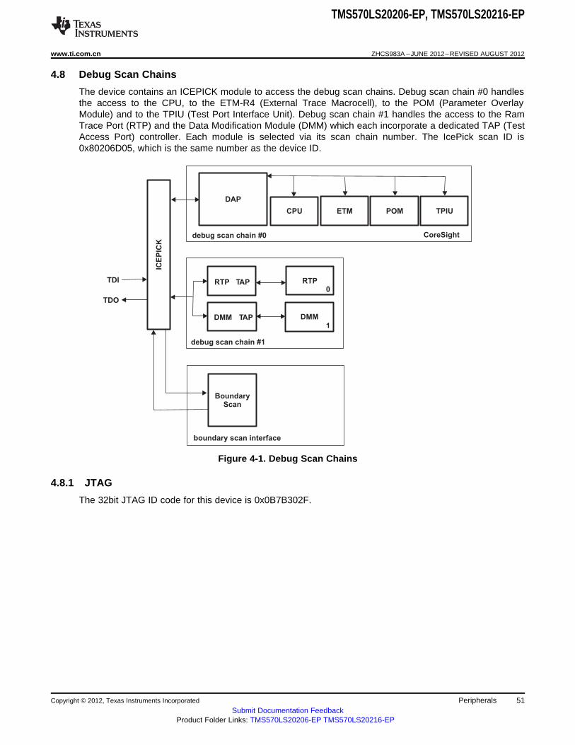
ETM
DMM TAP
RTP TAPTDI
TDO
DAP
TPIU
debug scan chain #0
debug scan chain #1
CPU POM
DMM
RTP
boundary scan interface
0
1
CoreSight
ICE
PIC
K
BoundaryScan
TMS570LS20206-EP, TMS570LS20216-EP
www.ti.com.cn ZHCS983A –JUNE 2012–REVISED AUGUST 2012
4.8 Debug Scan Chains
The device contains an ICEPICK module to access the debug scan chains. Debug scan chain #0 handlesthe access to the CPU, to the ETM-R4 (External Trace Macrocell), to the POM (Parameter OverlayModule) and to the TPIU (Test Port Interface Unit). Debug scan chain #1 handles the access to the RamTrace Port (RTP) and the Data Modification Module (DMM) which each incorporate a dedicated TAP (TestAccess Port) controller. Each module is selected via its scan chain number. The IcePick scan ID is0x80206D05, which is the same number as the device ID.
Figure 4-1. Debug Scan Chains
4.8.1 JTAG
The 32bit JTAG ID code for this device is 0x0B7B302F.
Copyright © 2012, Texas Instruments Incorporated Peripherals 51Submit Documentation Feedback
Product Folder Links: TMS570LS20206-EP TMS570LS20216-EP
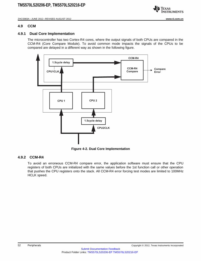
CPU 1 CPU 2
1.5cycle delay
1.5cycle delay
CCM-R4
CPU1CLK
CPU2CLK
CompareError
CCM-R4Compare
TMS570LS20206-EP, TMS570LS20216-EP
ZHCS983A –JUNE 2012–REVISED AUGUST 2012 www.ti.com.cn
4.9 CCM
4.9.1 Dual Core Implementation
The microcontroller has two Cortex-R4 cores, where the output signals of both CPUs are compared in theCCM-R4 (Core Compare Module). To avoid common mode impacts the signals of the CPUs to becompared are delayed in a different way as shown in the following figure.
Figure 4-2. Dual Core Implementation
4.9.2 CCM-R4
To avoid an erroneous CCM-R4 compare error, the application software must ensure that the CPUregisters of both CPUs are initialized with the same values before the 1st function call or other operationthat pushes the CPU registers onto the stack. All CCM-R4 error forcing test modes are limited to 100MHzHCLK speed.
52 Peripherals Copyright © 2012, Texas Instruments Incorporated
Submit Documentation FeedbackProduct Folder Links: TMS570LS20206-EP TMS570LS20216-EP

TMS570LS20206-EP, TMS570LS20216-EP
www.ti.com.cn ZHCS983A –JUNE 2012–REVISED AUGUST 2012
4.10 LPM
TMS570 Platform devices support multiple low power modes. These different modes allow the user totrade-off the amount of current consumption during low power mode versus functionality and wake-uptime.
Supported Low Power modes on this devices are Doze, Snooze and Sleep; for detailed description pleaserefer to the Architecture section of the Technical Reference Manual.
4.11 Voltage Monitor
A voltage monitor has been implemented on this device. The purpose of this voltage monitor is toeliminate the requirement for a specific sequence when powering up the core and I/O voltage supplies. Italso reduces the risk of corrupting memory or glitches on I/O pins during power-up, power-down or brownouts. The voltage monitor does not eliminate the need of a voltage supervisor circuit to guarantee that thedevice is held in reset when the voltage supplies are out of range. The voltage monitor thresholds can befound in the Vmon section of the device electrical specifications.
When the voltage monitor detects a low voltage on the I/O supply, it will assert a reset. When the voltagemonitor detects a low voltage on the core supply, it asynchronously makes all output pins high impedance,and asserts a reset. The voltage monitor is disabled when the device is in halt mode.
The voltage monitor has three filter functions:• It rejects short low-going glitches on the PORRST pin• It rejects noise on the VCCIO supply• It rejects noise on the VCC supplyPlease note that such glitches on VCC and VCCIO could still corrupt the system depending on manyfactors. The width of noise that can be filtered by the voltage monitor on the VCC and VCCIO supplies isshown in the table below. Glitches less than MIN will be filtered out, glitches greater than MAX areguaranteed to generate a reset. The duration of glitches that will be filtered on the PORRST pin can befound in Table 7-6, Timing Requirements for PORRST.
Table 4-13. VMON Supply Glitch Filter Capability
Parameter Min Max
Width of glitch on VCC that can be filtered out 300ns 1us
Width of glitch on VCCIO that can be filtered out 300ns 1us
4.12 CRC
MCRC Controller is a module which is used to perform CRC (Cyclic Redundancy Check) to verify theintegrity of memory system. A signature representing the contents of the memory is obtained when thecontents of the memory are read into MCRC Controller. The responsibility of MCRC controller is tocalculate the signature for a set of data and then compare the calculated signature value against a pre-determined good signature value. MCRC controller provides up to four channels to perform CRCcalculation on multiple memories in parallel and can be used on any memory system. Channel 1 can alsobe put into data trace mode. In data trace mode, MCRC controller compresses each data being readthrough the CPU read data bus.
When using the MCRC module in PSA mode while ECC is enabled, bus masters (e.g. FTU, HTU, DMA orCPU) should not write to the data RAM (TCRAM) to avoid corrupting the PSA value.
4.13 System Module Access
The system module access modes and access rights are shown in the following table.
Copyright © 2012, Texas Instruments Incorporated Peripherals 53Submit Documentation Feedback
Product Folder Links: TMS570LS20206-EP TMS570LS20216-EP

TMS570LS20206-EP, TMS570LS20216-EP
ZHCS983A –JUNE 2012–REVISED AUGUST 2012 www.ti.com.cn
Table 4-14. System Module Access
Domain Module Access Mode Used by Module Access Rights Required toAccess the Module RAMS
System VIM n/a privilege mode (RWP)
System RTP n/a privilege mode (RWP)
System DMA user mode privilege mode (RWP)
Peripheral HTU privilege mode privilege mode (RWP)
Peripheral FTU user & privilege mode user & privilege mode (RW)
4.14 Debug ROM
The Debug ROM stores the location of the components on the Debug APB bus.
Table 4-15. Debug ROM Table
Address Description Value
Components Table
0x000 pointer to Cortex-R4 0x00001003
0x000 ETM 0x00002003
0x000 TPIU 0x00003003
0x000 POM 0x00004003
0x001 end of table 0x00000000
54 Peripherals Copyright © 2012, Texas Instruments Incorporated
Submit Documentation FeedbackProduct Folder Links: TMS570LS20206-EP TMS570LS20216-EP

TMS570LS20206-EP, TMS570LS20216-EP
www.ti.com.cn ZHCS983A –JUNE 2012–REVISED AUGUST 2012
4.15 CPU Self Test Controller: STC / LBIST
The CPU Self Test Controller (STC) is used to test the ARM CPU core using a Deterministic Logic BIST(LBIST) Controller as the test engine. The STC has the capability of dividing the complete test run intosmaller independent test sets (intervals). The test coverage and number of test execution cycles for eachtest interval is shown in the table below.
The maximum clock rate for the STC / LBIST is:• 53.333MHz when HCLK = 160MHz / VCLK = 80MHz on BGA package• 50MHz when HCLK = 100MHz / VCLK = 100MHz on QFP and BGA packages• 46.666MHz when HCLK = 140MHz / VCLK = 70MHz on QFP and BGA packages
In order to achieve the proper clock rate during CPU self test a STC clock divider has been implemented.The clock divider is set by the CLKDIV bits in STCCLKDIV register in the secondary system module frameat location 0xFFFF E108. The default value of the CPU Self Test LBIST clock divider is set to 'divide-by-1’.
NOTEThe supply current while performing CPU self test is different than the device operatingmode current. These values can be found in the Icc section of Section 6.5.
Table 4-16. STC/LBIST Test Coverage and Duration
Intervals Test Coverage Test Cycles (STC Clock Cycles)
0 0% 0
1 57.14% 1,555
2 65.82% 3,108
3 70.56% 4,661
4 73.56% 6,214
5 76.06% 7,767
6 78.07% 9,320
7 79.62% 10,873
8 80.92% 12,426
9 82.1% 13,979
10 82.94% 15,532
11 83.76% 17,085
12 84.51% 18,638
13 85.12% 20,191
14 85.62% 21,744
15 86.19% 23,297
16 86.56% 24,850
17 86.97% 26,403
18 87.33% 27,956
19 87.67% 29,509
20 88.01% 31,062
21 88.31% 32,615
22 88.58% 34,168
23 88.87% 35,721
24 89.11% 37,274
25 89.34% 38,827
26 89.59% 40,380
27 89.82% 41,933
28 90.05% 43,486
Copyright © 2012, Texas Instruments Incorporated Peripherals 55Submit Documentation Feedback
Product Folder Links: TMS570LS20206-EP TMS570LS20216-EP

TMS570LS20206-EP, TMS570LS20216-EP
ZHCS983A –JUNE 2012–REVISED AUGUST 2012 www.ti.com.cn
Table 4-16. STC/LBIST Test Coverage and Duration (continued)
Intervals Test Coverage Test Cycles (STC Clock Cycles)
29 90.26% 45,039
30 90.46% 46,592
31 90.64% 48,145
32 90.84% 49,698
56 Peripherals Copyright © 2012, Texas Instruments Incorporated
Submit Documentation FeedbackProduct Folder Links: TMS570LS20206-EP TMS570LS20216-EP

TMS570LS20206-EP, TMS570LS20216-EP
www.ti.com.cn ZHCS983A –JUNE 2012–REVISED AUGUST 2012
5 Device Registers
5.1 Device Identification Code Register
The device identification code register identifies several aspects of the device including the silicon version.The details of the device identification code register are shown in Figure 5-1. The device identificationcode register value for this device is:• Rev 0 = 0x80206D05• Rev A = 0x80206D0D
Figure 5-1. Device ID Bit Allocation Register
31 30 29 28 27 26 25 24 23 22 21 20 19 18 17 16
CP-15 UNIQUE ID 16
R-1 R-00000 0000 10000 R-0
15 14 13 12 11 10 9 8 7 6 5 4 3 2 1 0
TECH I/O PERIP FLASH ECC RAM VERSION 1 0 1VOLT HERA ECCAGE L
PARITY
R-011 R-0 R-1 R-10 R-1 R-1 R-1 R-0 R-1
LEGEND: R/W = Read/Write; R = Read only; -n = value after reset; D= device dependent
Table 5-1. Device ID Bit Allocation Register Field Descriptions
Bit Field Value Description
31 CP15 Indicates the presence of coprocessor 15
0 CP15 not present
1 CP15 present
30-17 UNIQUE ID 1 Silicon version (revision) bits This bitfield holds a unique number for a dedicated device configuration(die).
16-13 TECH Process technology on which the device is manufactured.
0000 C05
0001 F05
0010 C035
0011 F035
Others Reserved
12 I/O I/O voltage of the device.VOLTAGE 0 I/O are 3.3v
1 I/O are 5v
11 PERIPHERA Peripheral ParityL PARITY
0 No parity on peripherals
1 Parity on peripherals
10-9 FLASH ECC Flash ECC
00 No error detection/correction
01 Program memory with parity
10 Program memory with ECC
11 Reserved
8 RAM ECC Indicates if RAM memory ECC is present.
0 No ECC implemented
1 ECC implemented
7-3 REVISION Revision of the Device.
Copyright © 2012, Texas Instruments Incorporated Device Registers 57Submit Documentation Feedback
Product Folder Links: TMS570LS20206-EP TMS570LS20216-EP

TMS570LS20206-EP, TMS570LS20216-EP
ZHCS983A –JUNE 2012–REVISED AUGUST 2012 www.ti.com.cn
Table 5-1. Device ID Bit Allocation Register Field Descriptions (continued)
Bit Field Value Description
2-0 101 The platform family ID is always 0b101
58 Device Registers Copyright © 2012, Texas Instruments Incorporated
Submit Documentation FeedbackProduct Folder Links: TMS570LS20206-EP TMS570LS20216-EP

TMS570LS20206-EP, TMS570LS20216-EP
www.ti.com.cn ZHCS983A –JUNE 2012–REVISED AUGUST 2012
5.2 Die-ID Registers
The two registers (DIEIDL and DIEIDH) form a 64-bit number that contains information about the device’sdie lot number, wafer number and X, Y wafer coordinates. The die identification information will vary fromunit to unit. This information is programmed by TI as part of the initial device test procedure. The dataformat of the Die-ID registers is shown here.
Figure 5-2. DIEIDL Register (Location: 0xFFFF FF7C)
31 30 29 28 27 26 25 24 23 22 21 20 19 18 17 16
LOT (LOWER 10 BITS) WAFER #
R-D R-D
15 14 13 12 11 10 9 8 7 6 5 4 3 2 1 0
Y WAFER COORDINATES X WAFER COORDINATES
R-D R-D
LEGEND: R/W = Read/Write; R = Read only; -n = value after reset; D= device dependent
Figure 5-3. DIEIDH Register (Location: 0xFFFF FF80)
31 30 29 28 27 26 25 24 23 22 21 20 19 18 17 16
RESERVED
R-D
15 14 13 12 11 10 9 8 7 6 5 4 3 2 1 0
RESERVED LOT # (UPPER 14 BITS)
R-D
LEGEND: R/W = Read/Write; R = Read only; -n = value after reset; D= device dependent
Copyright © 2012, Texas Instruments Incorporated Device Registers 59Submit Documentation Feedback
Product Folder Links: TMS570LS20206-EP TMS570LS20216-EP

TMS570LS20206-EP, TMS570LS20216-EP
ZHCS983A –JUNE 2012–REVISED AUGUST 2012 www.ti.com.cn
5.3 PLL Registers
The default values for the PLL (Phase Locked Loop) control registers are shown in this section. PLLCTL1and PLLCTL2 are used to configure PLL1 (F035 FMzPLL) and PLLCTL3 is used to configure PLL2 (F035FPLL).
Figure 5-4. PLLCTL1 Register (Location: 0xFFFF FF70)
31 30 29 28 27 26 25 24 23 22 21 20 19 18 17 16
ROS BPOS[1:0] PLLDIV[4:0] ROF RESV REFCLKDIV[5:0]
R/WP- R/WP-01 R/WP-01111 R/WP- R-0 R/WP-0000100 0
15 14 13 12 11 10 9 8 7 6 5 4 3 2 1 0
PLLMUL[15:0]
R/WP-0101111100000000
LEGEND: R/W = Read/Write; R = Read only; -n = value after reset; D= device specific
PLLCTL1 Default = 0x2F025F00
Figure 5-5. PLLCTL2 Register (Location: 0xFFFF FF74)
31 30 29 28 27 26 25 24 23 22 21 20 19 18 17 16
FMEN SPREADINGRATE[8:0] RESV EWADJ[8:4]A
R/WP- R/WP-111111111 R-0 R/WP-000000
15 14 13 12 11 10 9 8 7 6 5 4 3 2 1 0
BWADJ[3:0] ODPLL SPR_AMOUNT[8:0]
R/WP-0111 R/WP-001 R/WP-000000000
LEGEND: R/W = Read/Write; R = Read only; -n = value after reset; D = device specific
PLLCTL2 Default = 0x7FC07200
NOTEThere are several combinations of the modulation depth and modulation frequency that arenot allowed. Valid settings for this device include the list in Table 7-2.
Figure 5-6. PLLCTL3 Register (Location: 0xFFFF E100)
31 30 29 28 27 26 25 24 23 22 21 20 19 18 17 16
RESERVED OSC RESERVEDDIV
R/W-000000000 R/WP- R/W-0000000
15 14 13 12 11 10 9 8 7 6 5 4 3 2 1 0
RESERVED PLL_MUL[3:0] RESERVED PLL_DIV [2:0]
R/W-000000 R/WP-011 R/W-00000 R/WP 111
LEGEND: R/W = Read/Write; R = Read only; -n = value after reset; D= device specific
PLLCTL3 Default = 0x00000307
60 Device Registers Copyright © 2012, Texas Instruments Incorporated
Submit Documentation FeedbackProduct Folder Links: TMS570LS20206-EP TMS570LS20216-EP

TMS570LS20206-EP, TMS570LS20216-EP
www.ti.com.cn ZHCS983A –JUNE 2012–REVISED AUGUST 2012
6 Device Electrical Specifications
6.1 Operating Conditions
6.2 Absolute Maximum Ratings Over Operating Free-Air Temperature Range (unlessotherwise noted) (1)
Supply voltage ranges VCC(2) - 0.3 V to 2.1V
VCCIO, VCCAD, VCCP (Flash pump) (2) - 0.3 V to 4.1V
Input voltage range All input pins - 0.3 V to 4.1 V
Input clamp current IIK(VI<0 or VI> VCCIO) ±20 mA
All pins except AD1IN[7:0], AD2IN[7:0], ADSIN[15:8]
IIK (VI<0 or VI>VCCAD)
AD1IN[7:0], AD2IN[7:0], ADSIN[15:8] ±10 mA
total ±40 mA
Operating free-air temperature ranges, TA -55°C to 125°C
Storage temperature range, Tstg -65°C to 150°C
(1) Stresses beyond those listed under “absolute maximum ratings” may cause permanent damage to the device. These are stress ratingsonly, and functional operation of the device at these or any other conditions beyond those indicated under “recommended operatingconditions” is not implied. Exposure to absolute-maximum-rated conditions for extended periods may affect device reliability
(2) All voltage values are with respect to their associated grounds.
6.3 Device Recommended Operating Conditions (1)
MIN NOM MAX Unit
VCC Digital logic supply voltage (Core) 1.35 1.5 1.65 V
VCCIO Digital logic supply voltage (I/O) 3 3.3 3.6 V
VCCAD MibADC supply voltage 3 3.3 3.6 V
VCCP Flash pump supply voltage 3 3.3 3.6 V
VSS Digital logic supply ground 0 V
VSSAD MibADC supply ground -0.1 0.1 V
TA Operating free-air temperature -55 125 °C
(1) All voltages are with respect to VSS except VCCAD is with respect to VSSAD.
Copyright © 2012, Texas Instruments Incorporated Device Electrical Specifications 61Submit Documentation Feedback
Product Folder Links: TMS570LS20206-EP TMS570LS20216-EP

TMS570LS20206-EP, TMS570LS20216-EP
ZHCS983A –JUNE 2012–REVISED AUGUST 2012 www.ti.com.cn
6.4 Thermal InformationTMS570LS20206TMS570LS20216
THERMAL METRIC UNITSGWT PGE
337 BALL 144 PINS
θJA Junction-to-ambient thermal resistance (1) 30.7 32.1
θJCtop Junction-to-case (top) thermal resistance (2) 4.7 3.3
θJB Junction-to-board thermal resistance (3) 15 13.7°C/W
ψJT Junction-to-top characterization parameter (4) 0.1 0.1
ψJB Junction-to-board characterization parameter (5) 15 13.3
θJCbot Junction-to-case (bottom) thermal resistance (6) N/A N/A
(1) 在 JESD51-2a 描述的环境中,按照 JESD51-7 的规定,在一个 JEDEC 标准高 K 电路板上进行仿真,从而获得自然对流条件下的结至环境热阻抗。
(2) 通过在封装顶部模拟一个冷板测试来获得结至芯片外壳(顶部)的热阻。 不存在特定的 JEDEC 标准测试,但可在 ANSI SEMI 标准 G30-88 中找到内容接近的说明。
(3) 按照 JESD51-8 中的说明,通过在配有用于控制 PCB 温度的环形冷板夹具的环境中进行仿真,以获得结至电路板的热阻。(4) 结至顶部的特征参数,( ψJT),估算真实系统中器件的结温,并使用 JESD51-2a(第 6 章和第 7 章)中描述的程序从仿真数据中提取出该
参数以便获得 θJA。(5) 结至电路板的特征参数,(ψJB),估算真实系统中器件的结温,并使用 JESD51-2a(第 6 章和第7 章)中描述的程序从仿真数据中提取出该
参数以便获得 θJA 。(6) 通过在外露(电源)焊盘上进行冷板测试仿真来获得结至芯片外壳(底部)热阻。 不存在特定的 JEDEC 标准测试,但可在 ANSI SEMI
标准 G30-88 中找到了内容接近的说明。
62 Device Electrical Specifications Copyright © 2012, Texas Instruments Incorporated
Submit Documentation FeedbackProduct Folder Links: TMS570LS20206-EP TMS570LS20216-EP

TMS570LS20206-EP, TMS570LS20216-EP
www.ti.com.cn ZHCS983A –JUNE 2012–REVISED AUGUST 2012
6.5 Electrical Characteristics Over Operating Free-Air Temperature Range (1)
Parameter Test Conditions MIN TYP MAX Unit
Vhys Input hysteresis 0.15 V
VIL Low-level input voltage All inputs (2) -0.3 0.8 V
VIH High-level input voltage All inputs 2 VCCIO + 0.3 V
VOL Low-level output voltage IOL = IOL MAX 0.2 VCCIO V
IOL = 50 µA 0.2
VOH High-level output voltage IOH = IOH MAX 0.8 VCCIO V
IOH = 50 µA VCCIO - 0.2
VILoscin Low-level input voltage OSCIN -0.3 0.2 VCC V
VIHoscin High-level input voltage OSCIN 0.8 VCC VCC + 0.3 V
VMON Voltage monitoring VCC low 1.0 1.2 1.35 Vthreshold
VCC high 1.7 2 2.38
VCCIO low 2.0 2.4 3.0
IIC Input clamp current VI < VSSIO - 0.3 or VI > VCCIO + 0.3 -2 2 mA
II Input current (I/O pins) IIL Pulldown VI = VSS -1 1 µA
IIH Pulldown 20 uA VI = VCCIO 5 40
IIH Pulldown 100 uA VI = VCCIO 40 195
IIL Pullup 20 uA VI = VSS -40 -3.6
IIL Pullup 100 uA VI = VSS -195 -40
IIH Pullup VI = VCCIO -1 1
All other pins No pullup or pulldown -1 1
IOL Low-level output current TDO VOL = VOL MAX 8 mA
TDI
TMS
RTCK
ECLK
FRAYTX1
FRAYTXEN1
FRAYTX2
FRAYTXEN2
DMMENA
ETMTRACECTL
ETMTRACECLKOUT
ETMDATA[31:0]
RTPSYNC
RTPCLK
RTPDATA[15:0]
EMIFWE
EMIFOE
EMIFCS[3:0]
EMIFDATA[15:0]
EMIFADD[21:0]
EMIFBADD[1:0]
EMIFDQM[1:0]
ERROR
(1) Source currents (out of the device) are negative while sink currents (into the device) are positive.(2) This does not apply to PORRST pin.
Copyright © 2012, Texas Instruments Incorporated Device Electrical Specifications 63Submit Documentation Feedback
Product Folder Links: TMS570LS20206-EP TMS570LS20216-EP

TMS570LS20206-EP, TMS570LS20216-EP
ZHCS983A –JUNE 2012–REVISED AUGUST 2012 www.ti.com.cn
Electrical Characteristics Over Operating Free-Air Temperature Range(1) (continued)Parameter Test Conditions MIN TYP MAX Unit
IOL Low-level output current RST VOL = VOL MAX 4 mA
MIBSPI1CLK
MIBSPI1SIMO
MIBSPI1SOMI
MIBSPI3CLK
MIBSPI3SIMO
MIBSPI3SOMI
MIBSPI5CLK
MIBSPI5SIMO[3:0]
MIBSPI5SOMI[3:0]
DMMDATA[15:8]
DMMDATA[4]
All other output pins 2
IOH High-level output current TDO VOH = VOH MIN -8 mA
TDI
TMS
RTCK
ECLK
FRAYRX1
FRAYTX1
FRAYTXEN1
FRAYRX2
FRAYTX2
FRAYTXEN2
ETMTRACECTL
ETMTRACECLKOUT
ETMDATA[31:0]
RTPSYNC
RTPCLK
RTPDATA[15:0]
DMMENA
EMIFWE
EMIFOE
EMIFCS[3:0]
EMIFDATA[15:0]
EMIFADD[21:0]
EMIFBADD[1:0]
EMIFDQM[1:0]
ERROR
64 Device Electrical Specifications Copyright © 2012, Texas Instruments Incorporated
Submit Documentation FeedbackProduct Folder Links: TMS570LS20206-EP TMS570LS20216-EP

TMS570LS20206-EP, TMS570LS20216-EP
www.ti.com.cn ZHCS983A –JUNE 2012–REVISED AUGUST 2012
Electrical Characteristics Over Operating Free-Air Temperature Range(1) (continued)Parameter Test Conditions MIN TYP MAX Unit
IOH High-level output current RST VOH = VOH MIN -4 mA
MIBSPI1CLK
MIBSPI1SIMO
MIBSPI1SOMI
MIBSPI3CLK
MIBSPI3SIMO
MIBSPI3SOMI
MIBSPI5CLK
MIBSPI5SIMO[3:0]
MIBSPI5SOMI[3:0]
DMMDATA[15:8]
DMMDATA[4]
All other output pins -2
ICC(1) VCC Digital supply All packages HCLK = 100MHz, VCLK = 100MHz 350 mA
current (OperatingHCLK = 140MHz, VCLK= 70MHz 390 mAmode)
BGA packages HCLK = 160MHz, VCLK = 80MHz 430 mA
VCC Digital supply All packages STCCLK = 46.666MHz Peak 510 mAcurrent (CPU selftest
STCCLK = 50.0MHz Peak 540 mAmode: LBIST) (2) (3)
BGA packages STCCLK = 53.333MHz Peak 580 mA
VCC Digital supply All packages HCLK=80MHz, Peak 340 mAcurrent (Mem selftest VCLK=40MHzmode: PBIST) (2) (4)
HCLK=100MHz, Peak 430 mAVLCK=100MHz
VCC Digital supply current (doze mode) OSCIN = 6 MHz, VCC = 1.65 V (5) 35 mA
VCC Digital supply current (snooze mode) All frequencies, VCC = 1.65 V (5) 30 mA
VCC Digital supply current (sleep mode) All frequencies, VCC = 1.65 V (5) 25 mA
ICCIO VCCIO Digital supply current (operating mode) No DC load, VCCIO = 3.6 V (6) 15 mA
VCCIO Digital supply current (doze mode) No DC load, VCCIO = 3.6 V (6) 700 µA
VCCIO Digital supply current (snooze mode) No DC load, VCCIO = 3.6 V (6) 100 µA
VCCIO Digital supply current (sleep mode) No DC load, VCCIO = 3.6 V (6) 100 µA
ICCAD VCCAD supply current (operating mode) All frequencies, VCCAD = 3.6 V 30 mA
VCCAD supply current (doze mode) All frequencies, VCCAD = 3.6 V (5) 200 µA
VCCAD supply current (snooze mode) All frequencies, VCCAD = 3.6 V (5) 200 µA
VCCAD supply current (sleep mode) All frequencies, VCCAD = 3.6 V (5) 200 µA
ICCP VCCP pump supply current VCCP = 3.6 V read operation 25 mA
VCCP = 3.6 V program (7) 90 mA
VCCP = 3.6 V erase 90 mA
VCCP = 3.6 V doze mode (5) 5 µA
VCCP = 3.6 V snooze mode (5) 5 µA
VCCP = 3.6 V sleep mode (5) 5 µA
CI Input capacitance (8) 2 pF
CO Output capacitance 3 pF
(1) Typical values are at Vcc=1.5V and maximum values are at Vcc=1.65V(2) The peak current is measured on the TI EVM board with two 10µF and thirteen 100nF capacitors on VCC domain. Running at a lower
frequency consumes less current.(3) LBIST currents specified are for execution of LBIST with a certain STC clock. Lower current consumption can be achieved by
configuring a slower STC Clock frequency. The current peak duration can last for the duration of 1 LBIST test interval.(4) PBIST currents specified are for execution of PBIST on all RAMs(Group 1- 14) and all the algrithms. Lower current consumption can be
achieved by configuring a slower HCLK frequency. Different algorithms consume different current. For more information, please refer toBasic PBIST Configuration and influence on current consumption (SPNA128).
(5) For Flash banks/pumps in sleep mode.(6) I/O pins configured as inputs or outputs with no load. All pulldown inputs ≤ 0.2 V. All pullup inputs ≥ VCCIO - 0.2 V.(7) This assumes reading from one bank while programming a different bank.(8) The maximum input capacitance CI of the FlexRay RX pin(s) is 10pF.
Copyright © 2012, Texas Instruments Incorporated Device Electrical Specifications 65Submit Documentation Feedback
Product Folder Links: TMS570LS20206-EP TMS570LS20216-EP

1000.00
10000.00
100000.00
1000000.00
10000000.00
100000000.00
80 90 100 110 120 130 140 150 160 170
Ye
ars
Es
tim
ate
d (
Ho
urs
)
Continuous TJ (°C)
`
Wirebond Voiding Fail Mode
GWT
PGE
1000
10000
100000
1000000
80 90 100 110 120 130 140 150 160
Continuous Junction Temperature (°C)
Years
Estim
ate
d (
Hours
)
G001
Electromigration Fail Mode
TMS570LS20206-EP, TMS570LS20216-EP
ZHCS983A –JUNE 2012–REVISED AUGUST 2012 www.ti.com.cn
(1) See the absolute maximum ratings and the recommended operating conditions.(2) Silicon operating life design goal is 10 years at 105°C junction temperature (does not include package interconnect life).(3) The predicted operating lifetime vs junction temperature is based on reliability modeling using electromigration as the dominant
failure mechanism affecting device wearout for the specific device process and design characteristics.
Figure 6-1. TMS570LS20206-EP and TMS570LS20216-EP Operating Life Derating Chart
Figure 6-2. TMS570LS20206-EP and TMS570LS20216-EP Wirebond Voiding Fail Mode
66 Device Electrical Specifications Copyright © 2012, Texas Instruments Incorporated
Submit Documentation FeedbackProduct Folder Links: TMS570LS20206-EP TMS570LS20216-EP

OSCIN OSCOUT
C1
(see Note A)
C2
Crystal
(a) (b)
External
(toggling 0-1.5V)Clock Signal
Kelvin_GND
(see Note B)
OSCOUTOSCIN
TMS570LS20206-EP, TMS570LS20216-EP
www.ti.com.cn ZHCS983A –JUNE 2012–REVISED AUGUST 2012
7 Peripheral and Electrical Specifications
7.1 Clocks
7.1.1 PLL And Clock Specifications
Table 7-1. Timing Requirements For PLL Circuits Enabled Or Disabled
MIN MAX Unit
f(OSC)(1) Input clock frequency 5 MHz
f(OSC) Input clock frequency 20 MHz
tc(OSC) Cycle time, OSCIN 50 ns
tw(OSCIL) Pulse duration, OSCIN low 15 ns
tw(OSCIH) Pulse duration, OSCIN high 15 ns
f(OSCRST)(1) OSC FAIL frequency - upper level 20 50 MHz
f(OSCRST)(1) OSC FAIL frequency - lower level 1.5 5 MHz
(1) This parameter is characterized from -40°C to 125°C only.
7.1.2 External Reference Resonator/Crystal Oscillator Clock Option
The oscillator is enabled by connecting the appropriate fundamental 5–20 MHz resonator/crystal and loadcapacitors across the external OSCIN and OSCOUT pins as shown in section (a) of the figure below. Theoscillator is a single stage inverter held in bias by an integrated bias resistor. This resistor is disabledduring leakage test measurement and HALT mode.
NOTETI strongly encourages each customer to submit samples of the device to theresonator/crystal vendors for validation. The vendors are equipped to determine what loadcapacitors will best tune their resonator/crystal to the microcontroller device for optimumstart-up and operation over temperature/voltage extremes.
An external oscillator source can be used by connecting a 1.5V clock signal to the OSCIN pin and leavingthe OSCOUT pin unconnected (open) as shown in section (b) of the figure below.
Figure 7-1. Recommended Crystal/Clock Connection
NOTEIn figure (a), The values of C1 and C2 should be provided by the resonator/crystal vendor.
In figure (b), Kelvin_GND should not be connected to any other GND.
Copyright © 2012, Texas Instruments Incorporated Peripheral and Electrical Specifications 67Submit Documentation Feedback
Product Folder Links: TMS570LS20206-EP TMS570LS20216-EP

TMS570LS20206-EP, TMS570LS20216-EP
ZHCS983A –JUNE 2012–REVISED AUGUST 2012 www.ti.com.cn
7.1.3 Validated FMPLL Setting
The following table includes the validated FMPLL settings.
Table 7-2. Validated FMPLL Settings
OSC_IN Frequency FMPLL Output ModulationPLLCTL1 PLLCTL2 Modulation Depth(MHz) Frequency(MHz) Bandwidth (KHz)
10 0x20049500 0x82409253 150 100 0.5%
10 0x20049500 0x8300B240 150 77 0.5%
10 0x20048600 0x8240925C 135 100 0.5%
10 0x20048600 0x8300B247 135 77 0.5%
10 0x20048600 0x824092B9 135 100 1.0%
10 0x20048D80 0x8300B443 95 77 0.5%
10 0x20048D80 0x824094AF 95 100 1.0%
16 0x20079500 0x82409253 150 100 0.5%
16 0x20079500 0x8300B240 150 77 0.5%
16 0x20078600 0x8240925C 135 100 0.5%
16 0x20078600 0x8300B247 135 77 0.5%
16 0x20078600 0x824092B9 135 100 1.0%
16 0x20078D80 0x8300B443 95 77 0.5%
16 0x20078D80 0x824094AF 95 100 1.0%
20 0x20099500 0x82409253 150 100 0.5%
20 0x20099500 0x8300B240 150 77 0.5%
20 0x20098600 0x8240925C 135 100 0.5%
20 0x20098600 0x8300B247 135 77 0.5%
20 0x20098600 0x824092B9 135 100 1.0%
20 0x20098D80 0x8300B443 95 77 0.5%
20 0x20098D80 0x824094AF 95 100 1.0%
68 Peripheral and Electrical Specifications Copyright © 2012, Texas Instruments Incorporated
Submit Documentation FeedbackProduct Folder Links: TMS570LS20206-EP TMS570LS20216-EP

guaranteed faillower-
thresholdguaranteed pass
upper-
thresholdguaranteed fail
f[MHz]1.5 5.0 20.0 50.0
TMS570LS20206-EP, TMS570LS20216-EP
www.ti.com.cn ZHCS983A –JUNE 2012–REVISED AUGUST 2012
7.1.4 LPO And Clock Detection
The LPOCLKDET module consists of a clock monitor (CLKDET) and 2 low power oscillators (LPO) - a lowfrequency (LF) and a high frequency (HF) oscillator. The CLKDET is a supervisor circuit for an externallysupplied clock signal. In case the externally supplied clock frequency falls out of a frequency window, theclock detector flags this condition and switches to the HF LPO clock (limp mode). The OSCFAIL flag andclock switch-over remain, regardless of the behavior of the oscillator clock signal. The only way OSCFAILcan be cleared (and re-enable OSCIN as the clock source) is a power-on-reset.
Table 7-3. LPO And Clock Detection
Parameter MIN Type MAX Unit
Invalid frequency lower threshold 1.5 5 MHz
upper threshold 20 50 MHz
Limp mode frequency (HFosc) 7.9 10 14.4 MHz
HFosc frequency 7.9 10 14.4 MHz
LFosc frequency 62 80 113 kHz
Figure 7-2. LPO And Clock Detection
Copyright © 2012, Texas Instruments Incorporated Peripheral and Electrical Specifications 69Submit Documentation Feedback
Product Folder Links: TMS570LS20206-EP TMS570LS20216-EP

Address Waitstates
Data Waitstates
RAM
Address Waitstates
Data Waitstates
Flash
0MHz
0MHz
0MHz
0MHz
f(HCLK)
f(HCLK)
f(HCLK)
f(HCLK)
100MHz
108MHz72MHz36MHz
0 1 2 3
0 1
0
0
TMS570LS20206-EP, TMS570LS20216-EP
ZHCS983A –JUNE 2012–REVISED AUGUST 2012 www.ti.com.cn
7.1.5 Switching Characteristics Over Recommended Operating Conditions For Clocks
Table 7-4. Switching Characteristics Over Recommended Operating Conditions For Clocks
Parameter Test Conditions MIN MAX Unit
f(HCLK) HCLK - System clock frequency (337 BGA Pipeline mode enabled 160 MHzpackages) Pipeline mode disabled 36 MHz
f(HCLK) HCLK - System clock frequency (144pin QFP Pipeline mode enabled 140 MHzpackage) Pipeline mode disabled 36 MHz
f(GCLK) GCLK - CPU clock frequency (ratio GCLK : f(HCLK) MHzHCLK = 1:1)
f(RCLK) RCLK - Frequency out of PLL macro into R- 160 MHzdivider
f(RTICLK)(1) RTICLK - clock frequency f(VCLK) MHz
f(VCLK) VCLK - Primary peripheral clock frequency f(VCLK2) MHz
f(VCLK2) VCLK2 - Secondary peripheral clock frequency 100 MHz
f(AVCLK1) AVCLK1 - Primary asynchronous peripheral clock f(VCLK) MHzfrequency
f(AVCLK2) AVCLK2 - Secondary asynchronous peripheral f(VCLK) MHzclock frequency
f(ECLK)(2) ECLK - External clock output frequency for ECP 80 MHz
Module
f(PROG/ERASE) System clock frequency - Flash f(HCLK) MHzprogramming/erase
(1) If the RTIx clock source is chosen to be anything other than the default VCLK, then the RTI clock needs to be at least three times slowerthan the VCLK.
(2) (ECLK) = f(VCLK) / N, where N = {1 to 65536}. N is the ECP prescale value defined by the ECPCNTL.[15:0] register bits in the Systemmodule. Pipeline mode enabled or disabled is determined by the FRDCNTL[2:0].
7.1.5.1 Timing - Wait States
Figure 7-3. Wait States
NOTEIf FMzPLL frequency modulation is enabled, special care must be taken to ensure that themaximum system clock frequency f(HCLK) and peripheral clock frequency f(VCLK) are notexceeded. The speed of the device clocks may need be derated to accommodate themodulation depth when FMzPLL frequency modulation is enabled.
70 Peripheral and Electrical Specifications Copyright © 2012, Texas Instruments Incorporated
Submit Documentation FeedbackProduct Folder Links: TMS570LS20206-EP TMS570LS20216-EP

ECLK
3
4
TMS570LS20206-EP, TMS570LS20216-EP
www.ti.com.cn ZHCS983A –JUNE 2012–REVISED AUGUST 2012
7.2 ECLK Specification
7.2.1 Switching Characteristics Over Recommended Operating Conditions For ExternalClocks
Table 7-5. Switching Characteristics Over Recommended Operating Conditions For External Clocks (1) (2)
NO. Parameter Test Conditions MIN MAX Unit
3 tw(EOL) Pulse duration, ECLK low under all prescale factor 0.5tc(ECLK) – tf nscombinations (X and N)
4 tw(EOH) Pulse duration, ECLK high under all prescale factor 0.5tc(ECLK) – tr nscombinations (X and N)
(1) X = {1,2,3,4,5,6,7,8,9,10,11,12,13,14,15,16}. X is the VBUS interface clock divider ratio determined by the CLKCNTL.[19:16] bits in theSYS module.
(2) N = {1 to 65536}. N is the ECP prescale value defined by the ECPCNTL.[15:0] register bits in the System module.
Figure 7-4. ECLK Timing Diagram
Copyright © 2012, Texas Instruments Incorporated Peripheral and Electrical Specifications 71Submit Documentation Feedback
Product Folder Links: TMS570LS20206-EP TMS570LS20216-EP

3.3 V
1.5 V
CCIOPORL
PORRST
VCC (1.5 V)
6
VCCPORH
V
VIL(PORRST)
VCCIOPORHVCCIOPORH
VCCIOPORLVCCPORL
VCC
VCCIO / VCCP
VCCPORH
VCCPORL
VILVIL VILVILVIL(PORRST)
8
7
6
3
7
9
TMS570LS20206-EP, TMS570LS20216-EP
ZHCS983A –JUNE 2012–REVISED AUGUST 2012 www.ti.com.cn
7.3 RST And PORRST Timings
7.3.1 Timing Requirements For PORRST
Table 7-6. Timing Requirements For PORRST
NO. MIN MAX Unit
VCCPORL(1) VCC low supply level when PORRST must be active during power up 0.5 V
VCCPORH(1) VCC high supply level when PORRST must remain active during power up 1.35 V
and become active during power down
VCCIOPORL(1) VCCIO / VCCP low supply level when PORRST must be active during 1.1 V
power up
VCCIOPORH(1) VCCIO / VCCP high supply level when PORRST must remain active during 3 V
power up and become active during power down
VIL(PORRST)(1) Low-level input voltage of PORRST VCCIO > 2.5V 0.2 VCCIO V
Low-level input voltage of PORRST VCCIO< 2.5V 0.5 V
3 tsu(PORRST)(1) Setup time, PORRST active before VCCIO and VCCP > VCCIOPORL during 0 ms
power up
6 th(PORRST)(1) Hold time, PORRST active after VCC > VCCPORH 1 ms
7 tsu(PORRST)(1) Setup time, PORRST active before VCC <= VCCPORH during power down 8 µs
8 th(PORRST)(1) Hold time, PORRST active after VCCIO and VCCP > VCCIOPORH 1 ms
9 th(PORRST)(1) Hold time, PORRST active after VCC < VCCPORL 0 ms
tf(PORRST)(1) Filter time PORRST, pulses less than MIN will be filtered out, pulses 20 150 ns
greater than MAX are guaranteed to generate a reset (2)
tf(RST) Filter time RST, pulses less than MIN will be filtered out, pulses greater 20 150 nsthan MAX are guaranteed to generate a reset
(1) This parameter is characterized from -40°C to 125°C only.(2) A low pulse on the nPORRST pin which is just barely longer than the glitch filter implemented on this pin will result in a very short
internal reset. This may result in unpredictable behavior as some parts of the device may be reset while other parts of the device arenot.
Figure 7-5. PORRST Timing Diagram
NOTEThere is no timing dependency between the ramp of the VCCIO and the VCC supply voltage;this is just an exemplary drawing. All requirements are to ensure PORRST is active whenVCCIO or VCC is out of the normal operating range.
72 Peripheral and Electrical Specifications Copyright © 2012, Texas Instruments Incorporated
Submit Documentation FeedbackProduct Folder Links: TMS570LS20206-EP TMS570LS20216-EP

TMS570LS20206-EP, TMS570LS20216-EP
www.ti.com.cn ZHCS983A –JUNE 2012–REVISED AUGUST 2012
7.3.2 Switching Characteristics Over Recommended Operating Conditions For RST
Table 7-7. Switching Characteristics Over Recommended Operating Conditions For RST (1) (2)
Parameter MIN MAX Unit
tv(RST) Valid time, RST active after PORRST inactive 1048c(OSC) ns
Valid time, RST active (all others) 8tc(VCLK)
(1) Specified values do NOT include rise/fall times. For rise and fall timings, see the switching characteristics for output timings versus loadcapacitance table.
(2) This parameter is characterized from -40°C to 125°C only.
7.3.3 IO Status During PORRST
IO buffer condition during power-on-reset (nPORRST is low): All I/O pins, except nRST, are configured asHigh-impedance while nPORRST is low and immediately after nPORRST goes high. The FlexRayFRAYTX1 and FRAYTX2 pins are high impedance (high-Z) while nPORRST is low, and are output high atlatest 1024 oscillator cycles after nPORRST goes high; the FlexRay FRAYTXEN1 and FRAYTXEN2 pinsare high impedance (high-Z) while nPORRST is low, and output high immediately after nPORRST goeshigh.
IO pullup/pulldown condition during power-on-reset: all internal pullups and pulldowns on input pins aredisabled when nPORRST is low, and become active immediately after nPORRST goes high. Pins that arelisted with "programmable" have programmable pullups or pulldowns. The default value after reset is listedunderneath "programmable" in the following table. The exceptions are nPORRST, nRST, nTRST andTEST pins. The pulls on these pins will be active during power-on-reset.
Copyright © 2012, Texas Instruments Incorporated Peripheral and Electrical Specifications 73Submit Documentation Feedback
Product Folder Links: TMS570LS20206-EP TMS570LS20216-EP

TMS570LS20206-EP, TMS570LS20216-EP
ZHCS983A –JUNE 2012–REVISED AUGUST 2012 www.ti.com.cn
7.4 TEST Pin Timing
Table 7-8. TEST Pin Timing (1)
NO. Description MIN MAX Unit
tf(TEST) Filter time TEST, pulses less than MIN will be filtered out, pulses 10 80 nsgreater than MAX are guaranteed to enter TEST mode
(1) This parameter is characterized from -40°C to 125°C only.
74 Peripheral and Electrical Specifications Copyright © 2012, Texas Instruments Incorporated
Submit Documentation FeedbackProduct Folder Links: TMS570LS20206-EP TMS570LS20216-EP

1 1
2
3
5
TMS
TDI
TDO
RTCK
TCK
4
TMS570LS20206-EP, TMS570LS20216-EP
www.ti.com.cn ZHCS983A –JUNE 2012–REVISED AUGUST 2012
7.5 DAP - JTAG Scan Interface Timing
7.5.1 JTAG clock specification 12-MHz and 50-pF load on TDO output
Table 7-9. JTAG Scan Interface Timing
NO. MIN MAX Unit
f(TCK) TCK frequency (at HCLKmax) 12 MHz
f(RTCK) RTCK frequency (at TCKmax and HCLKmax) 10 MHz
1 td(TCK -RTCK) Delay time, TCK to RTCK 20 ns
2 tsu(TDI/TMS - RTCKr) Setup time, TDI, TMS before RTCK rise (RTCKr) 15 ns
3 th(RTCKr -TDI/TMS) Hold time, TDI, TMS after RTCKr 0 ns
4 th(RTCKf -TDO) Hold time, TDO after RTCKf 0 ns
5 td(RTCKf -TDO) Delay time, TDO valid after RTCK fall (RTCKf) 10 ns
Note: The timings in this table are measured with a 50pF and 50µA load. And they are measured at the 50% point, not 20% or 80% point.
Figure 7-6. JTAG timing
Copyright © 2012, Texas Instruments Incorporated Peripheral and Electrical Specifications 75Submit Documentation Feedback
Product Folder Links: TMS570LS20206-EP TMS570LS20216-EP

80% 80%
20% 20%0
Output
tr tf
VCCIO
TMS570LS20206-EP, TMS570LS20216-EP
ZHCS983A –JUNE 2012–REVISED AUGUST 2012 www.ti.com.cn
7.6 Output Timings
7.6.1 Switching Characteristics For Output Timings Versus Load Capacitance (CL)
Table 7-10. Switching Characteristics For Output Timings Versus Load Capacitance (CL)
Parameter MIN TYP MAX Unit
tr 8mA pins CL = 15 pF 2.5 ns
CL = 50 pF 5
CL = 100 pF 9
CL = 150 pF 12
tf 8mA pins CL = 15 pF 2.5 ns
CL = 50 pF 5
CL = 100 pF 9
CL = 150 pF 12
tr 4mA pins CL = 15 pF 7 ns
CL = 50 pF 13
CL = 100 pF 21
CL = 150 pF 29
tf 4mA pins CL = 15 pF 7 ns
CL = 50 pF 13
CL = 100 pF 21
CL = 150 pF 29
tr 2mA-z pins CL = 15 pF 10 ns
CL = 50 pF 17
CL = 100 pF 25
CL = 150 pF 35
tf 2mA-z pins CL = 15 pF 10 ns
CL = 50 pF 17
CL = 100 pF 25
CL = 150 pF 35
Figure 7-7. CMOS-Level Outputs
76 Peripheral and Electrical Specifications Copyright © 2012, Texas Instruments Incorporated
Submit Documentation FeedbackProduct Folder Links: TMS570LS20206-EP TMS570LS20216-EP

VCCIO80% 80%
20% 20%0
Input
tpw
TMS570LS20206-EP, TMS570LS20216-EP
www.ti.com.cn ZHCS983A –JUNE 2012–REVISED AUGUST 2012
7.7 Input Timings
7.7.1 Timing Requirements For Input Timings
Table 7-11. Timing Requirements For Input Timings (1)
MIN MAX Unit
tpw Input minimum pulse width tc(VCLK) + 10 (2) ns
(1) tc(VCLK) = peripheral VBUS clock cycle time = 1 / f(VCLK)(2) The timing shown above is only valid for pin used in GIO mode
Figure 7-8. CMOS-Level Inputs
Copyright © 2012, Texas Instruments Incorporated Peripheral and Electrical Specifications 77Submit Documentation Feedback
Product Folder Links: TMS570LS20206-EP TMS570LS20216-EP

TMS570LS20206-EP, TMS570LS20216-EP
ZHCS983A –JUNE 2012–REVISED AUGUST 2012 www.ti.com.cn
7.8 Flash Timings
Table 7-12. Timing Requirements For Program Flash
MIN NOM MAX Unit
tprog(32-bit) Full word (32-bit) programming time 33 300 µs
tprog(Total) 2M-byte programming -40°C to 125°C 17 74 stime (1)
0°C to 60°C, for first 25 17 25 scycles
tprog ECC(16-bit) ECC programming time 33 300 µs
tprog ECC(total) Total ECC bit -40°C to 125°C 4.3 15 sprogramming time (256k- 0°C to 60°C, for first 25 4.3 7 sbyte) cycles
terase(sector) Sector erase time -40°C to 125°C 2 15 s(including compaction) 0°C to 60°C, for first 25 1.5 10 s
cycles
terase(bank) Bank erase time (including Bank 0 7.5 20 scompaction),0°C to 60°C, Bank 1 5.5 12 sfor first 25 cycles
Bank 2 5.5 12 s
Bank 3 5.5 12 s
twec Write/erase cycles at TA = -40 to 125°C (2) 1000 cycles
tret Data Retention with continuous 150°C (2) 1000 hours
(1) This programming time includes overhead of state machine, but does not include data transfer time.(2) Flash write/erase cycles and data retention specifications are based on a validated implementation of the TI flash API. Non-TI flash API
implementation is not supported. For detailed description see the F035 Flash Validation Procedure (SPNA127). The flash memory cellsare qualified for data retention greater than 1000 hours at 150°C. Data retention at reduced temperatures can be estimated based on anArrhenius model with activation energy of 1 eV.
78 Peripheral and Electrical Specifications Copyright © 2012, Texas Instruments Incorporated
Submit Documentation FeedbackProduct Folder Links: TMS570LS20206-EP TMS570LS20216-EP

TMS570LS20206-EP, TMS570LS20216-EP
www.ti.com.cn ZHCS983A –JUNE 2012–REVISED AUGUST 2012
7.9 SPI Master Mode Timing Parameters
7.9.1 SPI Master Mode External Timing Parameters (CLOCK PHASE = 0, SPICLK = output,SPISIMO = output, and SPISOMI = input)
Table 7-13. SPI Master Mode External Timing Parameters (1) (2) (3)
NO. MIN MAX Unit
1 tc(SPC)M Cycle time, SPICLK (4) 50 256tc(VCLK) ns
2 (5) tw(SPCH)M Pulse duration, SPICLK high (clock polarity = 0) 0.5tc(SPC)M – 3 – tr 0.5tc(SPC)M + 5 ns
tw(SPCL)M Pulse duration, SPICLK low (clock polarity = 1) 0.5tc(SPC)M – 3 – tf 0.5tc(SPC)M + 5
3 (5) tw(SPCL)M Pulse duration, SPICLK low (clock polarity = 0) 0.5tc(SPC)M – 3 – tf 0.5tc(SPC)M + 5 ns
tw(SPCH)M Pulse duration, SPICLK high (clock polarity = 1) 0.5tc(SPC)M – 3 – tr 0.5tc(SPC)M + 5
4 (5) td(SIMO-SPCL)M Delay time, SPISIMO valid before SPICLK low 0.5tc(SPC)M – 10 ns(clock polarity = 0)
td(SIMO-SPCH)M Delay time, SPISIMO valid before SPICLK high 0.5tc(SPC)M – 10(clock polarity = 1)
5 (5) tv(SPCL-SIMO)M Valid time, SPISIMO data valid after SPICLK low 0.5tc(SPC)M – tf(SPC) -7 ns(clock polarity = 0)
tv(SPCH-SIMO)M Valid time, SPISIMO data valid after SPICLK high 0.5tc(SPC)M – tr(SPC) -7(clock polarity = 1)
6 (5) tsu(SOMI-SPCL)M Setup time, SPISOMI before SPICLK low (clock tf(SPC) nspolarity = 0)
tsu(SOMI-SPCH)M Setup time, SPISOMI before SPICLK high (clock tr(SPC) + 4polarity = 1)
7 (5) th(SPCL-SOMI)M Hold time, SPISOMI data valid after SPICLK low 10 ns(clock polarity = 0)
th(SPCH-SOMI)M Hold time, SPISOMI data valid after SPICLK high 10(clock polarity = 1)
8 (6) tC2TDELAY Setup time CS active until SPICLK high, assumes (C2TDELAY+CSHOLD+ (C2TDELAY+CSHOLD+ nsthat SPInENA is low at tSPIENA (clock polarity = 0) 2)*tc(VCLK) - tf(SPICS) + 2)*tc(VCLK) - tf(SPICS) +
tr(SPC)- 9 tr(SPC)+ 5
Setup time CS active until SPICLK low, assumes (C2TDELAY+CSHOLD+ (C2TDELAY+CSHOLD+ nsthat SPInENA is low at tSPIENA (clock polarity = 1) 2)*tc(VCLK) - tf(SPICS) + 2)*tc(VCLK) - tf(SPICS) +
tf(SPC) - 9 tf(SPC) + 5
9 (6) tT2CDELAY Hold time SPICLK low until CS inactive (clock 0.5*tc(SPC)M + 0.5*tc(SPC)M + nspolarity = 0) T2CDELAY*tc(VCLK) + T2CDELAY*tc(VCLK) +
tc(VCLK) - tc(VCLK) -tf(SPC) + tr(SPICS) - 5 tf(SPC) + tr(SPICS) + 10
Hold time SPICLK high until CS inactive (clock 0.5*tc(SPC)M + 0.5*tc(SPC)M + nspolarity = 1) T2CDELAY*tc(VCLK) + T2CDELAY*tc(VCLK) +
tc(VCLK) - tc(VCLK) -tr(SPC) + tr(SPICS) - 5 tr(SPC) + tr(SPICS) + 10
10 tSPIENA SPIENAn Sample point C2TDELAY * tc(VCLK) - C2TDELAY * tc(VCLK) nstf(SPICS) - 20
11 tSPIENAW(7) SPIENAn Sample point from write to buffer (C2TDELAY+2)*tc(VCLK) ns
(1) The MASTER bit (SPIGCR1.0) is set and the CLOCK PHASE bit (SPIFMTx.16) is set.(2) tc(VCLK) = interface clock cycle time = 1 / f(VCLK)(3) For rise and fall timings, see the "switching characteristics for output timings versus load capacitance" table.(4) When the SPI is in Master mode, the following must be true:
For PS values from 1 to 255: tc(SPC)M ≥ (PS +1)tc(VCLK) ≥ 50 ns, where PS is the prescale value set in the SPIFMTx.[15:8] register bits.For PS values of 0: tc(SPC)M = 2tc(VCLK) ≥ 50 ns. The external load on the SPICLK pin must be less than 60pF.
(5) The active edge of the SPICLK signal referenced is controlled by the CLOCK POLARITY bit (SPIFMTx.17).(6) C2TDELAY and T2CDELAY are programmed in the SPIDELAY register(7) Parameters characterized from -40°C to 125°C only.
Copyright © 2012, Texas Instruments Incorporated Peripheral and Electrical Specifications 79Submit Documentation Feedback
Product Folder Links: TMS570LS20206-EP TMS570LS20216-EP

SPICLK(clock polarity = 0)
SPISIMO
SPICSn
Master Out Data Is Valid
SPICLK(clock polarity = 1)
SPIENAn
10
Write to buffer
11
8 9
SPISOMI
SPISIMO
SPICLK
(clock polarity = 1)
SPICLK
(clock polarity = 0)
7
Master In DataMust Be Valid
Master Out Data Is Valid
2
1
3
54
6
TMS570LS20206-EP, TMS570LS20216-EP
ZHCS983A –JUNE 2012–REVISED AUGUST 2012 www.ti.com.cn
Figure 7-9. SPI Master Mode External Timing (CLOCK PHASE = 0)
Figure 7-10. SPI Master Mode Chip Select timing (CLOCK PHASE = 0)
80 Peripheral and Electrical Specifications Copyright © 2012, Texas Instruments Incorporated
Submit Documentation FeedbackProduct Folder Links: TMS570LS20206-EP TMS570LS20216-EP

TMS570LS20206-EP, TMS570LS20216-EP
www.ti.com.cn ZHCS983A –JUNE 2012–REVISED AUGUST 2012
7.9.2 SPI Master Mode External Timing Parameters (CLOCK PHASE = 1, SPICLK = output,SPISIMO = output, and SPISOMI = input)
Table 7-14. SPI Master Mode External Timing Parameters (1) (2) (3)
NO. MIN MAX Unit
1 tc(SPC)M Cycle time, SPICLK (4) 50 256tc(VCLK) ns
2 (5) tw(SPCH)M Pulse duration, SPICLK high (clock polarity = 0) 0.5tc(SPC)M – 3 – tr 0.5tc(SPC)M + 5 ns
tw(SPCL)M Pulse duration, SPICLK low (clock polarity = 1) 0.5tc(SPC)M – 3 – tf 0.5tc(SPC)M + 5
3 (5) tw(SPCL)M Pulse duration, SPICLK low (clock polarity = 0) 0.5tc(SPC)M – 3 – tr 0.5tc(SPC)M + 5 ns
tw(SPCH)M Pulse duration, SPICLK high (clock polarity = 1) 0.5tc(SPC)M – 3 – tf 0.5tc(SPC)M + 5
4 (5) td(SIMO-SPCH)M Delay time, SPICLK high after SPISIMO data 0.5tc(SPC)M – 10 nsvalid(clock polarity = 0)
td(SIMO-SPCL)M Delay time, SPICLK low after SPISIMO data valid 0.5tc(SPC)M – 10(clock polarity = 1)
5 (5) tv(SPCH-SIMO)M Valid time, SPISIMO data valid after SPICLK 0.5tc(SPC)M – tr(SPC) – 7 nshigh(clock polarity = 0)
tv(SPCL-SIMO)M Valid time, SPISIMO data valid after SPICLK 0.5tc(SPC)M – tf(SPC) – 7low(clock polarity = 1)
6 (5) tsu(SOMI-SPCH)M Setup time, SPISOMI before SPICLK high (clock tr(SPC)+4 nspolarity = 0)
tsu(SOMI-SPCL)M Setup time, SPISOMI before SPICLK low (clock tf(SPC)polarity = 1)
7 (5) tv(SPCH-SOMI)M Valid time, SPISOMI data valid after SPICLK high 10 ns(clock polarity = 0)
tv(SPCL-SOMI)M Valid time, SPISOMI data valid after SPICLK low 10(clock polarity = 1)
8 (6) tC2TDELAY Setup time CS active until SPICLK high, assumes (C2TDELAY+CSHOLD+ (C2TDELAY+CSHOLD+ nsthat SPInENA is low at tSPIENA (clock polarity = 0) 2)*tc(VCLK) +0.5*tc(SPC)M - 2)*tc(VCLK) +0.5*tc(SPC)M -
tf(SPICS) + tr(SPC) - 9 tf(SPICS) + tr(SPC) + 5
Setup time CS active until SPICLK low, assumes (C2TDELAY+CSHOLD+ (C2TDELAY+CSHOLD+ nsthat SPInENA is low at tSPIENA (clock polarity = 1) 2)*tc(VCLK) + 0.5*tc(SPC)M 2)*tc(VCLK) + 0.5*tc(SPC)M
- tf(SPICS) + tf(SPC) - 9 - tf(SPICS) + tf(SPC) + 5
9 (6) tT2CDELAY Hold time SPICLK low until CS inactive (clock T2CDELAY*tc(VCLK) + T2CDELAY*tc(VCLK) + nspolarity = 0) tc(VCLK) - tf(SPC) + tr(SPICS) tc(VCLK) - tf(SPC) + tr(SPICS)
- 5 + 10
Hold time SPICLK high until CS inactive (clock T2CDELAY*tc(VCLK) + T2CDELAY*tc(VCLK) + nspolarity = 1) tc(VCLK) - tr(SPC) + tc(VCLK) - tr(SPC) +
tr(SPICS)- 5 tr(SPICS)+ 10
10 tSPIENA SPIENAn Sample Point C2TDELAY * tc(VCLK) - C2TDELAY * tc(VCLK) nstf(SPICS)- 20
11 tSPIENAW SPIENAn Sample point from write to buffer (C2TDELAY+2)*tc(VCLK) ns
(1) The MASTER bit (SPIGCR1.0) is set and the CLOCK PHASE bit (SPIFMTx.16) is set.(2) tc(VCLK) = interface clock cycle time = 1 / f(VCLK)(3) For rise and fall timings, see the "switching characteristics for output timings versus load capacitance" table.(4) When the SPI is in Master mode, the following must be true:
For PS values from 1 to 255: tc(SPC)M ≥ (PS +1)tc(VCLK) ≥ 50 ns, where PS is the prescale value set in the SPIFMTx.[15:8] register bits.For PS values of 0: tc(SPC)M = 2tc(VCLK) ≥ 50 ns. The external load on the SPICLK pin must be less than 60pF.
(5) The active edge of the SPICLK signal referenced is controlled by the CLOCK POLARITY bit (SPIFMTx.17).(6) C2TDELAY and T2CDELAY are programmed in the SPIDELAY register
Copyright © 2012, Texas Instruments Incorporated Peripheral and Electrical Specifications 81Submit Documentation Feedback
Product Folder Links: TMS570LS20206-EP TMS570LS20216-EP

SPICLK(clock polarity = 0)
SPISIMO
SPICS
Master Out Data Is Valid
SPICLK(clock polarity = 1)
SPIENA
10
Write to buffer
11
8 9
Master In DataMust Be Valid
Master Out Data Is Valid Data Valid
SPISOMI
SPISIMO
SPICLK
(clock polarity = 1)
SPICLK
(clock polarity = 0)
2
1
3
6
7
5
4
TMS570LS20206-EP, TMS570LS20216-EP
ZHCS983A –JUNE 2012–REVISED AUGUST 2012 www.ti.com.cn
Figure 7-11. SPI Master Mode External Timing (CLOCK PHASE = 1)
Figure 7-12. SPI Master Mode Chip Select timing (CLOCK PHASE = 1)
82 Peripheral and Electrical Specifications Copyright © 2012, Texas Instruments Incorporated
Submit Documentation FeedbackProduct Folder Links: TMS570LS20206-EP TMS570LS20216-EP

TMS570LS20206-EP, TMS570LS20216-EP
www.ti.com.cn ZHCS983A –JUNE 2012–REVISED AUGUST 2012
7.10 SPI Slave Mode Timing Parameters
7.10.1 SPI Slave Mode External Timing Parameters (CLOCK PHASE = 0, SPICLK = input,SPISIMO = input, and SPISOMI = output)
Table 7-15. SPI Slave Mode External Timing Parameters (1) (2) (3)
NO. MIN MAX Unit
1 tc(SPC)S Cycle time, SPICLK (4) 90 ns
2 (5) tw(SPCH)S Pulse duration, SPICLK high(clock polarity = 0) 30 ns
tw(SPCL)S Pulse duration, SPICLK low(clock polarity = 1) 30
3 (5) tw(SPCL)S Pulse duration, SPICLK low(clock polarity = 0) 30 ns
tw(SPCH)S Pulse duration, SPICLK high(clock polarity = 1) 30
4 (5) td(SPCH-SOMI)S Delay time, SPISOMI valid after SPICLK high trf(SOMI) + 15 ns(clock polarity = 0)
td(SPCL-SOMI)S Delay time, SPISOMI valid after SPICLK low (clock trf(SOMI) + 15polarity = 1)
5 (5) tV(SPCH-SOMI)S Valid time, SPISOMI data valid after SPICLK high 0 ns(clock polarity =0)
tV(SPCL-SOMI)S Valid time, SPISOMI data valid after SPICLK low 0(clock polarity =1)
6 (5) tsu(SIMO-SPCL)S Setup time, SPISIMO before SPICLK low(clock 4 nspolarity = 0)
tsu(SIMO-SPCH)S Setup time, SPISIMO before SPICLK high(clock 4polarity = 1)
7 (5) th(SPCL-SIMO)S Hold time, SPISIMO data valid after SPICLK low 6 ns(clock polarity = 0)
th(SPCH-SIMO)S Hold time, SPISIMO data valid after S PICLK high 6(clock polarity = 1)
8 td(SPCL-SENAH)S Delay time, SPIENAn high after last SPICLK low 1.5tc(VCLK) 2.5tc(VCLK)+tr(ENAn)+ 26 ns(clock polarity = 0)
td(SPCH-SENAH)S Delay time, SPIENAn high after last SPICLK high 1.5tc(VCLK) 2.5tc(VCLK)+tr(ENAn)+ 26(clock polarity = 1)
9 td(SCSL-SENAL)S Delay time, SPIENAn low after SPICSn low (if new tf(ENAn) tc(VCLK) + tf(ENAn)+ 18 nsdata has been written to the SPI buffer)
(1) The MASTER bit (SPIGCR1.0) is set and the CLOCK PHASE bit (SPIFMTx.16) is set.(2) tc(VCLK) = interface clock cycle time = 1 /f(VCLK)(3) For rise and fall timings, see the "switching characteristics for output timings versus load capacitance" table.(4) When the SPI is in Slave mode, the following must be true:
tc(SPC)S > 2tc(VCLK) and tc(SPC)S>= 90 ns.tw(SPCH)S > tc(VCLK) and tw(SPCL)S > tc(VCLK).
(5) The active edge of the SPICLK signal referenced is controlled by the CLOCK POLARITY bit (SPIFMTx.17).
Copyright © 2012, Texas Instruments Incorporated Peripheral and Electrical Specifications 83Submit Documentation Feedback
Product Folder Links: TMS570LS20206-EP TMS570LS20216-EP

SPICLK(clock polarity = 0)
SPICSn
SPICLK(clock polarity = 1)
SPIENAn
8
9
SPISIMO DataMust Be Valid
SPISOMI Data Is ValidSPISOMI
SPISIMO
SPICLK
(clock polarity = 1)
SPICLK
(clock polarity = 0)
7
2
1
3
54
6
TMS570LS20206-EP, TMS570LS20216-EP
ZHCS983A –JUNE 2012–REVISED AUGUST 2012 www.ti.com.cn
Figure 7-13. SPI Slave Mode External Timing (CLOCK PHASE = 0)
Figure 7-14. SPI Slave Mode Enable Timing (CLOCK PHASE = 0)
84 Peripheral and Electrical Specifications Copyright © 2012, Texas Instruments Incorporated
Submit Documentation FeedbackProduct Folder Links: TMS570LS20206-EP TMS570LS20216-EP

TMS570LS20206-EP, TMS570LS20216-EP
www.ti.com.cn ZHCS983A –JUNE 2012–REVISED AUGUST 2012
7.10.2 SPI Slave Mode External Timing Parameters (CLOCK PHASE = 1, SPICLK = input,SPISIMO = input, and SPISOMI = output)
Table 7-16. SPI Slave Mode External Timing Parameters (1) (2) (3)
NO. MIN MAX Unit
1 tc(SPC)S Cycle time, SPICLK (4) 90 ns
2 (5) tw(SPCH)S Pulse duration, SPICLK high (clock polarity = 0) 30 ns
tw(SPCL)S Pulse duration, SPICLK low (clock polarity = 1) 30
3 (5) tw(SPCL)S Pulse duration, SPICLK low (clock polarity = 0) 30 ns
tw(SPCH)S Pulse duration, SPICLK high (clock polarity = 1) 30
4 (5) td(SOMI- Delay time, SPISOMI data valid after SPICLK low trf(SOMI)+15 nsSPCL)S (clock polarity = 0)
td(SOMI- Delay time, SPISOMI data valid after SPICLK high trf(SOMI)+15SPCH)S (clock polarity = 1)
5 (5) tV(SPCL- Valid time, SPISOMI data valid after SPICLK high 0 nsSOMI)S (clock polarity =0)
tV(SPCH- Valid time, SPISOMI data valid after SPICLK low 0SOMI)S (clock polarity =1)
6 (5) tsu(SIMO- Setup time, SPISIMO before SPICLK high (clock 4 nsSPCH)S polarity = 0)
tsu(SIMO- Setup time, SPISIMO before SPICLK low (clock 4SPCL)S polarity = 1)
7 (5) th(SPCH- Hold time, SPISIMO data valid after SPICLK high 6 nsSIMO)S (clock polarity = 0)
th(SPCL- Hold time, SPISIMO data valid after SPICLK low 6SIMO)S (clock polarity = 1)
8 td(SPCH- Delay time, SPIENAn high after last SPICLK high 1.5tc(VCLK) 2.5tc(VCLK)+tr(ENAn)+ 26 nsSENAH)S (clock polarity = 0)
td(SPCL- Delay time, SPIENAn high after last SPICLK low 1.5tc(VCLK) 2.5tc(VCLK)+tr(ENAn)+ 26SENAH)S (clock polarity = 1)
9 td(SCSL- Delay time, SPIENAn low after SPICSn low (if new tf(ENAn) tc(VCLK) + tf(ENAn)+ 18 nsSENAL)S data has been written to the SPI buffer)
10 td(SCSL- Delay time, SOMI valid after SPICSn low (if new data tc(VCLK) 2tc(VCLK) + trf(SOMI)+ 20 nsSOMI)S has been written to the SPI buffer)
(1) The MASTER bit (SPIGCR1.0) is set and the CLOCK PHASE bit (SPIFMTx.16) is set.(2) tc(VCLK) = interface clock cycle time = 1 /f(VCLK)(3) For rise and fall timings, see the "switching characteristics for output timings versus load capacitance" table.(4) When the SPI is in Slave mode, the following must be true:
tc(SPC)S > 2tc(VCLK) and tc(SPC)S>= 90 ns.tw(SPCH)S > tc(VCLK) and tw(SPCL)S > tc(VCLK).
(5) The active edge of the SPICLK signal referenced is controlled by the CLOCK POLARITY bit (SPIFMTx.17).
Copyright © 2012, Texas Instruments Incorporated Peripheral and Electrical Specifications 85Submit Documentation Feedback
Product Folder Links: TMS570LS20206-EP TMS570LS20216-EP

SPICLK(clock polarity = 0)
SPISOMI
SPICSn
Slave Out Data Is Valid
SPICLK(clock polarity = 1)
SPIENAn
10
8
9
Data Valid
SPISIMO DataMust Be Valid
SPISOMI Data Is ValidSPISOMI
SPISIMO
SPICLK
(clock polarity = 1)
SPICLK
(clock polarity = 0)
2
1
3
5
4
6
7
TMS570LS20206-EP, TMS570LS20216-EP
ZHCS983A –JUNE 2012–REVISED AUGUST 2012 www.ti.com.cn
Figure 7-15. SPI Slave Mode External Timing (CLOCK PHASE = 1)
Figure 7-16. SPI Slave Mode Enable Timing (CLOCK PHASE = 1)
86 Peripheral and Electrical Specifications Copyright © 2012, Texas Instruments Incorporated
Submit Documentation FeedbackProduct Folder Links: TMS570LS20206-EP TMS570LS20216-EP
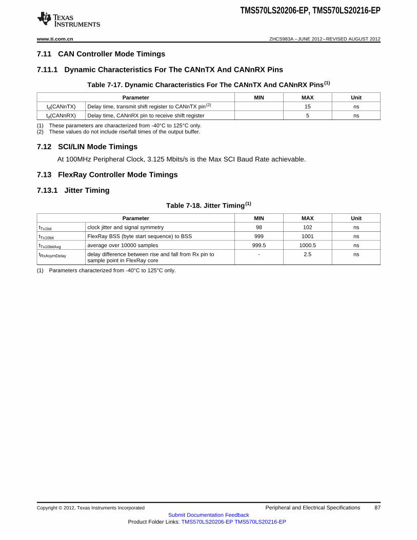
TMS570LS20206-EP, TMS570LS20216-EP
www.ti.com.cn ZHCS983A –JUNE 2012–REVISED AUGUST 2012
7.11 CAN Controller Mode Timings
7.11.1 Dynamic Characteristics For The CANnTX And CANnRX Pins
Table 7-17. Dynamic Characteristics For The CANnTX And CANnRX Pins (1)
Parameter MIN MAX Unit
td(CANnTX) Delay time, transmit shift register to CANnTX pin (2) 15 ns
td(CANnRX) Delay time, CANnRX pin to receive shift register 5 ns
(1) These parameters are characterized from -40°C to 125°C only.(2) These values do not include rise/fall times of the output buffer.
7.12 SCI/LIN Mode Timings
At 100MHz Peripheral Clock, 3.125 Mbits/s is the Max SCI Baud Rate achievable.
7.13 FlexRay Controller Mode Timings
7.13.1 Jitter Timing
Table 7-18. Jitter Timing (1)
Parameter MIN MAX Unit
tTx1bit clock jitter and signal symmetry 98 102 ns
tTx10bit FlexRay BSS (byte start sequence) to BSS 999 1001 ns
tTx10bitAvg average over 10000 samples 999.5 1000.5 ns
tRxAsymDelay delay difference between rise and fall from Rx pin to - 2.5 nssample point in FlexRay core
(1) Parameters characterized from -40°C to 125°C only.
Copyright © 2012, Texas Instruments Incorporated Peripheral and Electrical Specifications 87Submit Documentation Feedback
Product Folder Links: TMS570LS20206-EP TMS570LS20216-EP

TMS570LS20206-EP, TMS570LS20216-EP
ZHCS983A –JUNE 2012–REVISED AUGUST 2012 www.ti.com.cn
7.14 EMIF Timings
Table 7-19. EMIF Read/Write Mode Switching Characteristics (1) (2)
NO Parameter Description MIN MAX Unit
Reads and Writes
1 td(TURNAROUND)( Turn around time (TA + 1) * E - (TA + 1) * E - ns
3) tr(CS) - 2 tr(CS) + 3
Reads
2 tc(EMRCYCLE) EMIF read cycle time (RS + RST + (RS + RST + nsRH + TA +4) * RH + TA +4) *
E - tf(CS) - 3 E - tf(CS) + 3
3 tsu(EMCSL-EMOEL) Output setup time, EMIFCS[3:0] low to EMIFOE (RS +1) * E - (RS +1) * E - nslow (SS=0) tf(CS) + tf(OE) - 5 tf(CS) + tf(OE) + 5
Output setup time, EMIFCS[3:0] low to EMIFOE - tf(CS) + tf(OE) - - tf(CS) + tf(OE) + nslow (SS=1) 5 5
4 th(EMOEH-EMCSH) Output hold time, EMIFOE high to EMIFCS[3:0] (RH +1) * E - (RH +1) * E - nshigh (SS=0) tr(OE) + tr(CS) - 4 tr(OE) + tr(CS) + 6
Output hold time, EMIFOE high to EMIFCS[3:0] - tr(OE) + tr(CS) - - tr(OE) + tr(CS) + nshigh (SS=1) 4 6
5 tsu(EMBAV-EMOEL) Output setup time, EMIFBADD[1:0] valid to (RS +1) * E - (RS +1) * E - nsEMIFOE low trf(AD) + tf(OE) - 5 trf(AD) + tf(OE) +
5
6 th(EMOEH-EMBAIV) Output hold time, EMIFOE high to (RH +1) * E - (RH +1) * E - nsEMIFBADD[1:0] invalid tr(OE) - 5 tr(OE) + 5
7 tsu(EMAV-EMOEL) Output setup time, EMIFADD[21:0] valid to (RS +1) * E - (RS +1) * E - nsEMIFOE low trf(AD) + tf(OE) - 6 trf(AD) + tf(OE) +
6
8 th(EMOEH-EMAIV) Output hold time, EMIFOE high to EMIFADD[21:0] (RH +1) * E - (RH +1) * E - nsinvalid tr(OE) - 5 tr(OE) + 6
9 tw(EMOEL)(3) EMIFOE active low width (RST +1) * E - (RST +1) * E - ns
tf(OE) - 1 tf(OE) + 0
10 tsu(EMDV-EMOEH) Setup time, EMIFD[15:0] valid before EMIFOE tr(OE) + 9 nshigh
11 th(EMOEH-EMDV) Hold time, EMIFD[15:0] valid after EMIFOE high - tr(OE) - 3
Writes
12 tc(EMWCYCLE) EMIF write cycle time (WS + WST + (WS + WST + nsWH + TA +4) * WH + TA +4) *
E - tf(CS) - 3 E - tf(CS) + 2
13 tsu(EMCSL-EMWEL) Output setup time, EMIFCS[3:0] low to EMIFWE (WS +1) * E - (WS +1) * E - nslow (SS=0) tf(CS) + tf(WE) - 5 tf(CS) + tf(WE) + 5
Output setup time, EMIFCS[3:0] low to EMIFWE - tf(CS) + tf(WE) - - tf(CS) + tf(WE) + nslow (SS=1) 5 5
14 th(EMWEH-EMCSH) Output hold time, EMIFWE high to EMIFCS[3:0] (WH +1) * E - (WH +1) * E - nshigh (SS=0) tr(WE) + tr(CS) - 4 tr(WE) + tr(CS) +
5
Output hold time, EMIFWE high to EMIFCS[3:0] - tr(WE) + tr(CS) - - tr(WE) + tr(CS) + nshigh (SS=1 4 5
15 tsu(EMBAV-EMWEL) Output setup time, EMIFBADD[1:0] valid to (WS +1) * E - (WS +1) * E - nsEMIFWE low trf(AD) + tf(WE) - 5 trf(AD) + tf(WE) +
5
16 th(EMWEH-EMBAIV) Output hold time, EMIFWE high to EMBADD[1:0] (WH +1) * E - (WH +1) * E - nsinvalid tr(WE) - 5 tr(WE) + 5
17 tsu(EMAV-EMWEL) Output setup time, EMIFADD[21:0] valid to (WS +1) * E - (WS +1) * E - nsEMIFWE low trf(AD) + tf(WE) - 6 trf(AD) + tf(WE) +
6
(1) RS = Read setup, RST = Read Strobe, RH = Read Hold, WS = Write Setup, WST = Write Strobe, WH = Write Hold, TA = Turn Around,SS= Strobe Select Mode
(2) E = VCLK period in ns.(3) Parameters characterized from -40°C to 125°C only.
88 Peripheral and Electrical Specifications Copyright © 2012, Texas Instruments Incorporated
Submit Documentation FeedbackProduct Folder Links: TMS570LS20206-EP TMS570LS20216-EP

EMIFCS[3:0]
EMIFBADD[1:0]
EMIFR/W
EMIFADD[21:0]
EMIFOE
EMIFD[15:0]
EMIFWE
2
1
3
5
7
9
8
6
4
11
10
TMS570LS20206-EP, TMS570LS20216-EP
www.ti.com.cn ZHCS983A –JUNE 2012–REVISED AUGUST 2012
Table 7-19. EMIF Read/Write Mode Switching Characteristics(1)(2) (continued)
NO Parameter Description MIN MAX Unit
18 th(EMWEH-EMAIV) Output hold time, EMIFWE high to (WH +1) * E - (WH +1) * E - nsEMIFADD[21:0] invalid tr(WE) - 5 tr(WE) + 6
19 tw(EMWEL)(1) EMIFWE active low width (WST +1) * E - (WST +1) * E -
tf(WE) - 1 tf(WE) + 1
20 tsu(EMDV-ENWEL) Output setup time, EMIFD[15:0] valid to EMIFWE (WS +1) * E - (WS +1) * E - nslow trf(DA) + tf(WE) - 6 trf(DA) + tf(WE) +
5
21 th(EMWEH-EMDIV) Output hold time, EMIFD[15:0] valid after (WH +1) * E - (WH +1) * E - nsEMIFWE high tr(WE) - 5 tr(WE) + 5
(1) Parameters characterized from -40°C to 125°C only.
7.14.1 Read Timing (Asynchronous RAM)
Figure 7-17. Asynchronous Memory Read Timing for EMIF
Copyright © 2012, Texas Instruments Incorporated Peripheral and Electrical Specifications 89Submit Documentation Feedback
Product Folder Links: TMS570LS20206-EP TMS570LS20216-EP

t(ETM)cyc
t(ETM)r t(ETM)ft(ETM)h
t(ETM)l
EMIFCS[3:0]
EMIFBADD[1:0]
EMIFADD[21:0]
EMIFWE
EMIFD[15:0]
EMIFOE
12
1
13
15
17
19
18
16
14
2120
TMS570LS20206-EP, TMS570LS20216-EP
ZHCS983A –JUNE 2012–REVISED AUGUST 2012 www.ti.com.cn
7.14.2 Write Timing (Asynchronous RAM)
Figure 7-18. Asynchronous Memory Write Timing for EMIF
7.15 ETM Timings
7.15.1 ETMTRACECLK Timing
Figure 7-19. ETMTRACECLK Timing
Table 7-20. ETMTRACECLK Timing
Parameter Minimum Maximum Description
f(ETM)cyc 40MHz Clock frequency
t(ETM)cyc 25ns Clock period
t(ETM)l 2ns Low pulse width
t(ETM)h 2ns High pulse width
t(ETM)r 3ns Clock and data rise time
t(ETM)f 3ns Clock and data fall time
90 Peripheral and Electrical Specifications Copyright © 2012, Texas Instruments Incorporated
Submit Documentation FeedbackProduct Folder Links: TMS570LS20206-EP TMS570LS20216-EP

t(ETM)su t(ETM)ho
ETMTRACECLK
ETMDATA
t(ETM)su t(ETM)ho
TMS570LS20206-EP, TMS570LS20216-EP
www.ti.com.cn ZHCS983A –JUNE 2012–REVISED AUGUST 2012
7.15.2 ETMDATA Timing
Figure 7-20. ETMDATA Timing
Table 7-21. ETMDATA Timing
Parameter Typical Description
t(ETM)su 2.5ns Data setup time
t(ETM)ho 1.5ns Data hold time
Note: The timings in this table are measured with a 50pF and 50µA load. And they are measured at the 50% point, not 20% or 80% point.'Typical' means 25°C and nominal voltage.
Copyright © 2012, Texas Instruments Incorporated Peripheral and Electrical Specifications 91Submit Documentation Feedback
Product Folder Links: TMS570LS20206-EP TMS570LS20216-EP

t(RTP)dsu t(RTP)dho
RTPSYNC
RTPCLK
RTPDATA
t(RTP)shot(RTP)ssu
t(RTP)cyc
tr tft(RTP)h
t(RTP)l
TMS570LS20206-EP, TMS570LS20216-EP
ZHCS983A –JUNE 2012–REVISED AUGUST 2012 www.ti.com.cn
7.16 RTP Timings
7.16.1 RTPCLK Timing
Figure 7-21. RTPCLK Timing
Table 7-22. RTPCLK Timing
Parameter Minimum Description
t(RTP)cyc 10 ns Clock period (depending on HCLK divideratio)
t(RTP)h (t(RTP)cyc/2) - ((tr+tf)/2) -1.5 High pulse width (depending on HCLK divideratio and load on pin)
t(RTP)l (t(RTP)cyc/2) - ((tr+tf)/2) -1.5 Low pulse width (depending on HCLK divideratio and load on pin)
7.16.2 RTPDATA Timing
Figure 7-22. RTPDATA Timing
Table 7-23. RTPDATA Timing
Parameter Minimum Description
t(RTP)dsu 0.5 t(RTP)cyc-3ns Data setup time
t(RTP)dho 0.5 t(RTP)cyc-2ns Data hold time
t(RTP)ssu 0.5 t(RTP)cyc-3ns SYNC setup time
t(RTP)sho 0.5 t(RTP)cyc-2ns SYNC hold time
Note: The timings in this table are measured with a 50pF and 50µA load. And they are measured at the 50% point, not 20% or 80% point.
92 Peripheral and Electrical Specifications Copyright © 2012, Texas Instruments Incorporated
Submit Documentation FeedbackProduct Folder Links: TMS570LS20206-EP TMS570LS20216-EP

t(RTP)disable t(RTP)enable
HCLK
RTPCLK
RTPENA
RTPSYNC
RTPDATA
t(RTP)disable t(RTP)enable
HCLK
RTPCLK
RTPENA
RTPSYNC
RTPDATA
t(RTP)enablet(RTP)disable
HCLK
RTPCLK
RTPENA
RTPSYNC
RTPDATA d1 d2 d3 d4 d5 d6 d7 d8
Divide by 1
1 2 3 4 5 6 7 8 9 10 11 12 13 14 15 16
TMS570LS20206-EP, TMS570LS20216-EP
www.ti.com.cn ZHCS983A –JUNE 2012–REVISED AUGUST 2012
7.16.3 RTPENABLE Timing
Figure 7-23. RTPENABLE Timing
Table 7-24. RTPENABLE Timing
Parameter Minimum Maximum Description
t(RTP)disable 1.5tc(HCLK) + tr(RTPSYNC) + 12ns Time that RTPENA must go highbefore the next scheduled
RTPSYNC in order to suspendtransmission for the packet
following the scheduledRTPSYNC.
t(RTP)enable 4.5tc(HCLK) + tr(RTPSYNC) 5.5tc(HCLK) + tr(RTPSYNC) + 12ns Time after RTPENA goes lowbefore a packet that has been
halted, resumes.
Copyright © 2012, Texas Instruments Incorporated Peripheral and Electrical Specifications 93Submit Documentation Feedback
Product Folder Links: TMS570LS20206-EP TMS570LS20216-EP

t(DMM)dsu t(DMM)dho
DMMSYNC
DMMCLK
DMMDATA
t(DMM)shot(DMM)ssu
t(DMM)cyc
tr tft(DMM)h
t(DMM)l
TMS570LS20206-EP, TMS570LS20216-EP
ZHCS983A –JUNE 2012–REVISED AUGUST 2012 www.ti.com.cn
7.17 DMM Timings
7.17.1 DMMCLK Timing
Figure 7-24. DMMCLK Timing
Table 7-25. DMMCLK Timing
Parameter Minimum Description
t(DMM)cyc tc(HCLK) * 2 Clock period
t(DMM)h t(DMM)cyc/2-(tr+tf)/2 High pulse width
t(DMM)l t(DMM)cyc/2-(tr+tf)/2 Low pulse width
7.17.2 DMMDATA Timing
Figure 7-25. DMMDATA Timing
Table 7-26. DMMDATA Timing
Parameter Minimum Description
t(DMM)ssu 2ns SYNC active to clk falling edge setup time
t(DMM)sho 3ns clk falling edge to SYNC deactive hold time
t(DMM)dsu 2ns DATA to clk falling edge setup time
t(DMM)dho 3ns clk falling edge to DATA hold time
94 Peripheral and Electrical Specifications Copyright © 2012, Texas Instruments Incorporated
Submit Documentation FeedbackProduct Folder Links: TMS570LS20206-EP TMS570LS20216-EP

HCLK
DMMCLK
DMMSYNC
DMMDATA
DMMENA
D00 D01 D10 D11 D20 D21 D30 D31 D40 D41 D50
TMS570LS20206-EP, TMS570LS20216-EP
www.ti.com.cn ZHCS983A –JUNE 2012–REVISED AUGUST 2012
7.17.3 DMMENA Timing
Figure 7-26. DMMENA Timing
The above figure shows a case with 1 DMM packet per 2 DMMCLK cycles (Mode = Direct Data Mode,data width = 8, portwidth = 4) where none of the packets received by the DMM are sent out, leading tofilling up of the internal buffers. The DMMENA signal is shown asserted, after the first two packets havebeen received and synchronized to the HCLK domain. Here, the DMM has the capacity to accept packetsD4, D5, D6, D7. Packet D8 would result in an overflow. Once DMMENA is asserted, the DMM expects tostop receiving packets after 4 HCLK cycles; once DMMENA is de-asserted, the DMM can handle packetsimmediately (after 0 HCLK cycles).
7.18 MibADC
7.18.1 MibADC
The multibuffered A-to-D converter (MibADC) has a separate power bus for its analog circuitry thatenhances the A-to-D performance by preventing digital switching noise on the logic circuitry which couldbe present on VSS and VCC from coupling into the A-to-D analog stage. All A-to-D specifications aregiven with respect to ADREFLO unless otherwise noted.
Table 7-27. MibADC
Resolution 12 bits (4096 values)
Monotonic Assured
Output conversion φcode 00h to FFFh [00 for VAI ≤ADREFLO; FFF for VAI ≥ ADREFHI]
7.18.2 MibADC Recommended Operating Conditions
Table 7-28. MibADC Recommended Operating Conditions (1)
MIN MAX UNIT
ADREFHI A-to-D high-voltage reference source 3 3.6 V
ADREFLO A-to-D low-voltage reference source 0 0.3 V
VAI Analog input voltage ADREFLO ADREFHI V
IAIC Analog input clamp current (2) -2 2 mA(VAI < VSSAD – 0.3 or VAI > VCCAD +0.3)
(1) For VCCAD and VSSAD recommended operating conditions, see the "device recommended operating conditions" table.(2) Input currents into any ADC input channel outside the specified limits could affect conversion results of other channels.
Copyright © 2012, Texas Instruments Incorporated Peripheral and Electrical Specifications 95Submit Documentation Feedback
Product Folder Links: TMS570LS20206-EP TMS570LS20216-EP

TMS570LS20206-EP, TMS570LS20216-EP
ZHCS983A –JUNE 2012–REVISED AUGUST 2012 www.ti.com.cn
7.18.3 Operating Characteristics Over Full Ranges Of Recommended Operating Conditions
Table 7-29. Operating Characteristics Over Full Ranges Of Recommended Operating Conditions (1)
Parameter Description/Conditions Min TYP Max Unit
Rmux(2) Analog input mux on- 250 Ω
resistance
Rsamp(2) ADC sample switch on- 150 250 Ω
resistance
Cmux Input mux capacitance 16 pF
Csamp ADC sample capacitance 11 12 13 pF
IAIL Analog input leakage Input leakage per ADC input pin –200 200 nAcurrent
IADREFHI(2) ADREFHI input current ADREFHI = 3.6 V, ADREFLO = VSSAD 5 mA
CR Conversion range over ADREFHI - ADREFLO 3 3.6 Vwhich specified accuracyis maintained
EDNL Differential nonlinearity Difference between the actual step width and the ideal value. ±3.8 LSBerror
EINL Integral nonlinearity error Maximum deviation from the best straight line through the MibADC. ±3.7 LSBMibADC transfer characteristics, excluding the quantization error.
ETOT Total error/Absolute Maximum value of the difference Executing periodic ±8 (3) LSBaccuracy between an analog value and the ideal internal calibration
midstep value. No calibration ±15 LSB
(1) 1 LSB = (ADREFHI – ADREFLO)/ 212 for the MibADC(2) This parameter is characterized from -40°C to 125°C only.(3) An periodic internal offset calibration is required to achieve the absolute accuracy. Please refer to the Analog To Digital Converter (ADC)
Module chapter of the TMS570LS Series Microcontroller Technical Reference Manual (SPNU489) and Interfacing the Embedded 12-bitADC (SPNA129) for more information.
96 Peripheral and Electrical Specifications Copyright © 2012, Texas Instruments Incorporated
Submit Documentation FeedbackProduct Folder Links: TMS570LS20206-EP TMS570LS20216-EP

Rmux
Rsamp
CsampCmux
Pin
RmuxSmux
Smux
Pin
IAIL
Ssamp
IAIL
RmuxSmuxPin
IAIL IAIL
TMS570LS20206-EP, TMS570LS20216-EP
www.ti.com.cn ZHCS983A –JUNE 2012–REVISED AUGUST 2012
7.18.4 MibADC Input Model
Figure 7-27. MibADC Input Equivalent Circuit
Copyright © 2012, Texas Instruments Incorporated Peripheral and Electrical Specifications 97Submit Documentation Feedback
Product Folder Links: TMS570LS20206-EP TMS570LS20216-EP

TMS570LS20206-EP, TMS570LS20216-EP
ZHCS983A –JUNE 2012–REVISED AUGUST 2012 www.ti.com.cn
7.18.5 MibADC Timings
Table 7-30. MibADC Timings (1)
Min NOm MAX Unit
tc(ADCLK) Cycle time, MibADC clock 33 ns
td(SH) Delay time, sample and hold time 200 ns
td(C) Delay time, conversion time 400 ns
td(SHC)(2) Delay time, total sample/hold and conversion time 600 ns
(1) These parameters are characterized from -40°C to 125°C only.(2) This is the minimum sample/hold and conversion time that can be achieved. These parameters are dependent on many factors, e.g the
prescale settings.
98 Peripheral and Electrical Specifications Copyright © 2012, Texas Instruments Incorporated
Submit Documentation FeedbackProduct Folder Links: TMS570LS20206-EP TMS570LS20216-EP

0 1 2 3 4 5 6 7
Analog Input Value (LSB)
At Transition
011/100
(– 1/2 LSB)
End-Point Lin. Error
At Transition
001/010 (– 1/4 LSB)
IdealTransition
ActualTransition
0 ... 101
0 ... 100
0 ... 011
0 ... 010
0 ... 001
0 ... 111
0 ... 110
Dig
ita
lO
utp
ut
Co
de
0 ... 000
0 1 2 3 4 5
0 ... 101
0 ... 100
0 ... 011
0 ... 010
0 ... 001
0 ... 000
0 ... 110
Analog Input Value (LSB)
Dig
ita
lO
utp
ut
Co
de
Differential
Linearity Error (1/2 LSB)1 LSB
Differential Linearity
Error (–1/2 LSB)1 LSB
0 1 2 3 4 5
0 ... 101
0 ... 100
0 ... 011
0 ... 010
0 ... 001
0 ... 000
0 ... 110
1 LSB
1 LSB
TMS570LS20206-EP, TMS570LS20216-EP
www.ti.com.cn ZHCS983A –JUNE 2012–REVISED AUGUST 2012
7.18.6 MibADC Nonlinearity Error
The differential nonlinearity error shown in the figure below (sometimes referred to as differential linearity)is the difference between an actual step width and the ideal value of 1 LSB.
Figure 7-28. Differential Nonlinearity (DNL)
The integral nonlinearity error shown in the figure below (sometimes referred to as linearity error) is thedeviation of the values on the actual transfer function from a straight line.
Figure 7-29. Integral Nonlinearity (INL) Error
Copyright © 2012, Texas Instruments Incorporated Peripheral and Electrical Specifications 99Submit Documentation Feedback
Product Folder Links: TMS570LS20206-EP TMS570LS20216-EP

0 1 2 3 4 5 6 7
0 ... 101
0 ... 100
0 ... 011
0 ... 010
0 ... 001
0 ... 000
0 ... 111
0 ... 110
Analog Input Value (LSB)
Dig
ita
lO
utp
ut
Co
de
Total Error
At Step
0 ... 001 (1/2 LSB)
Total Error
At Step 0 ... 101
( 1 1/4 LSB)–
TMS570LS20206-EP, TMS570LS20216-EP
ZHCS983A –JUNE 2012–REVISED AUGUST 2012 www.ti.com.cn
7.18.7 MibADC Total Error
The absolute accuracy or total error of an MibADC as shown in the figure below is the maximum value ofthe difference between an analog value and the ideal midstep value.
Figure 7-30. Absolute Accuracy (Total) Error
100 Peripheral and Electrical Specifications Copyright © 2012, Texas Instruments Incorporated
Submit Documentation FeedbackProduct Folder Links: TMS570LS20206-EP TMS570LS20216-EP

TMS570LS20206-EP, TMS570LS20216-EP
www.ti.com.cn ZHCS983A –JUNE 2012–REVISED AUGUST 2012
8 Mechanical Packaging and Orderable Information
8.1 Packaging Information
The following packaging information and addendum reflect the most current data available for thedesignated device(s). The data is subject to change without notice and without revision of this document.
Copyright © 2012, Texas Instruments Incorporated Mechanical Packaging and Orderable Information 101Submit Documentation Feedback
Product Folder Links: TMS570LS20206-EP TMS570LS20216-EP

PACKAGE OPTION ADDENDUM
www.ti.com 10-Dec-2020
Addendum-Page 1
PACKAGING INFORMATION
Orderable Device Status(1)
Package Type PackageDrawing
Pins PackageQty
Eco Plan(2)
Lead finish/Ball material
(6)
MSL Peak Temp(3)
Op Temp (°C) Device Marking(4/5)
Samples
S5LS20206ASGWTMEP ACTIVE NFBGA GWT 337 90 Non-RoHS &Non-Green
SNPB Level-3-220C-168 HR -55 to 125 TMS570S20206ASGWTMEP
S5LS20206ASPGEMEP ACTIVE LQFP PGE 144 60 RoHS & Green NIPDAU Level-3-260C-168 HR -55 to 125 S20206ASPGEMEPTMS570LS
S5LS20216ASGWTMEP ACTIVE NFBGA GWT 337 90 Non-RoHS &Non-Green
SNPB Level-3-220C-168 HR -55 to 125 TMS570S20216ASGWTMEP
S5LS20216ASPGEMEP ACTIVE LQFP PGE 144 60 RoHS & Green NIPDAU Level-3-260C-168 HR -55 to 125 S20216ASPGEMEPTMS570LS
V62/12622-01XE ACTIVE LQFP PGE 144 60 RoHS & Green NIPDAU Level-3-260C-168 HR -55 to 125 S20206ASPGEMEPTMS570LS
V62/12622-01YE ACTIVE NFBGA GWT 337 90 Non-RoHS &Non-Green
SNPB Level-3-220C-168 HR -55 to 125 TMS570S20206ASGWTMEP
V62/12622-02XE ACTIVE LQFP PGE 144 60 RoHS & Green NIPDAU Level-3-260C-168 HR -55 to 125 S20216ASPGEMEPTMS570LS
V62/12622-02YE ACTIVE NFBGA GWT 337 90 Non-RoHS &Non-Green
SNPB Level-3-220C-168 HR -55 to 125 TMS570S20216ASGWTMEP
(1) The marketing status values are defined as follows:ACTIVE: Product device recommended for new designs.LIFEBUY: TI has announced that the device will be discontinued, and a lifetime-buy period is in effect.NRND: Not recommended for new designs. Device is in production to support existing customers, but TI does not recommend using this part in a new design.PREVIEW: Device has been announced but is not in production. Samples may or may not be available.OBSOLETE: TI has discontinued the production of the device.
(2) RoHS: TI defines "RoHS" to mean semiconductor products that are compliant with the current EU RoHS requirements for all 10 RoHS substances, including the requirement that RoHS substancedo not exceed 0.1% by weight in homogeneous materials. Where designed to be soldered at high temperatures, "RoHS" products are suitable for use in specified lead-free processes. TI mayreference these types of products as "Pb-Free".RoHS Exempt: TI defines "RoHS Exempt" to mean products that contain lead but are compliant with EU RoHS pursuant to a specific EU RoHS exemption.Green: TI defines "Green" to mean the content of Chlorine (Cl) and Bromine (Br) based flame retardants meet JS709B low halogen requirements of <=1000ppm threshold. Antimony trioxide basedflame retardants must also meet the <=1000ppm threshold requirement.
(3) MSL, Peak Temp. - The Moisture Sensitivity Level rating according to the JEDEC industry standard classifications, and peak solder temperature.
(4) There may be additional marking, which relates to the logo, the lot trace code information, or the environmental category on the device.

PACKAGE OPTION ADDENDUM
www.ti.com 10-Dec-2020
Addendum-Page 2
(5) Multiple Device Markings will be inside parentheses. Only one Device Marking contained in parentheses and separated by a "~" will appear on a device. If a line is indented then it is a continuationof the previous line and the two combined represent the entire Device Marking for that device.
(6) Lead finish/Ball material - Orderable Devices may have multiple material finish options. Finish options are separated by a vertical ruled line. Lead finish/Ball material values may wrap to twolines if the finish value exceeds the maximum column width.
Important Information and Disclaimer:The information provided on this page represents TI's knowledge and belief as of the date that it is provided. TI bases its knowledge and belief on informationprovided by third parties, and makes no representation or warranty as to the accuracy of such information. Efforts are underway to better integrate information from third parties. TI has taken andcontinues to take reasonable steps to provide representative and accurate information but may not have conducted destructive testing or chemical analysis on incoming materials and chemicals.TI and TI suppliers consider certain information to be proprietary, and thus CAS numbers and other limited information may not be available for release.
In no event shall TI's liability arising out of such information exceed the total purchase price of the TI part(s) at issue in this document sold by TI to Customer on an annual basis.
OTHER QUALIFIED VERSIONS OF TMS570LS20206-EP, TMS570LS20216-EP :
• Catalog: TMS570LS20206, TMS570LS20216
NOTE: Qualified Version Definitions:
• Catalog - TI's standard catalog product

TRAY
Chamfer on Tray corner indicates Pin 1 orientation of packed units.
*All dimensions are nominal
Device PackageName
PackageType
Pins SPQ Unit arraymatrix
Maxtemperature
(°C)
L (mm) W(mm)
K0(µm)
P1(mm)
CL(mm)
CW(mm)
S5LS20206ASPGEMEP PGE LQFP 144 60 5X12 150 315 135.9 7620 25.4 17.8 17.55
S5LS20216ASGWTMEP GWT NFBGA 337 90 6 X 15 150 315 135.9 7620 20 17.5 15.45
S5LS20216ASPGEMEP PGE LQFP 144 60 5X12 150 315 135.9 7620 25.4 17.8 17.55
V62/12622-01XE PGE LQFP 144 60 5X12 150 315 135.9 7620 25.4 17.8 17.55
V62/12622-02XE PGE LQFP 144 60 5X12 150 315 135.9 7620 25.4 17.8 17.55
V62/12622-02YE GWT NFBGA 337 90 6 X 15 150 315 135.9 7620 20 17.5 15.45
PACKAGE MATERIALS INFORMATION
www.ti.com 5-Jan-2022
Pack Materials-Page 1


MECHANICAL DATA
MTQF017A – OCTOBER 1994 – REVISED DECEMBER 1996
1POST OFFICE BOX 655303 • DALLAS, TEXAS 75265
PGE (S-PQFP-G144) PLASTIC QUAD FLATPACK
4040147/C 10/96
0,27
72
0,17
37
73
0,13 NOM
0,25
0,750,45
0,05 MIN
36
Seating Plane
Gage Plane
108
109
144
SQ
SQ22,2021,80
1
19,80
17,50 TYP
20,20
1,351,45
1,60 MAX
M0,08
0°–7°
0,08
0,50
NOTES: A. All linear dimensions are in millimeters.B. This drawing is subject to change without notice.C. Falls within JEDEC MS-026

重要声明和免责声明TI“按原样”提供技术和可靠性数据(包括数据表)、设计资源(包括参考设计)、应用或其他设计建议、网络工具、安全信息和其他资源,不保证没有瑕疵且不做出任何明示或暗示的担保,包括但不限于对适销性、某特定用途方面的适用性或不侵犯任何第三方知识产权的暗示担保。这些资源可供使用 TI 产品进行设计的熟练开发人员使用。您将自行承担以下全部责任:(1) 针对您的应用选择合适的 TI 产品,(2) 设计、验证并测试您的应用,(3) 确保您的应用满足相应标准以及任何其他功能安全、信息安全、监管或其他要求。这些资源如有变更,恕不另行通知。TI 授权您仅可将这些资源用于研发本资源所述的 TI 产品的应用。严禁对这些资源进行其他复制或展示。您无权使用任何其他 TI 知识产权或任何第三方知识产权。您应全额赔偿因在这些资源的使用中对 TI 及其代表造成的任何索赔、损害、成本、损失和债务,TI 对此概不负责。TI 提供的产品受 TI 的销售条款或 ti.com 上其他适用条款/TI 产品随附的其他适用条款的约束。TI 提供这些资源并不会扩展或以其他方式更改 TI 针对 TI 产品发布的适用的担保或担保免责声明。TI 反对并拒绝您可能提出的任何其他或不同的条款。IMPORTANT NOTICE
邮寄地址:Texas Instruments, Post Office Box 655303, Dallas, Texas 75265Copyright © 2022,德州仪器 (TI) 公司


![第1章CATIA简介.ppt [只读]](https://static.fdokumen.com/doc/165x107/6318668f1a1adcf65a0e3cb1/1catiappt-.jpg)