Electrooxidation of primary alcohols on smooth and electrodeposited platinum in acidic solution
Upload
khangminh22Category
view
0download
0
Thin film solar cells using all-electrodeposited ZnS, CdS and CdTe materials.
ECHENDU, Obi Kingsley.
Available from Sheffield Hallam University Research Archive (SHURA) at:
http://shura.shu.ac.uk/19597/
This document is the author deposited version. You are advised to consult the publisher's version if you wish to cite from it.
Published version
ECHENDU, Obi Kingsley. (2014). Thin film solar cells using all-electrodeposited ZnS, CdS and CdTe materials. Doctoral, Sheffield Hallam University (United Kingdom)..
Copyright and re-use policy
See http://shura.shu.ac.uk/information.html
Sheffield Hallam University Research Archivehttp://shura.shu.ac.uk

Sheffield Hallam University Learning and Information Services
Adseits Centre, City Campus Shaffieid Si 1WD
REFERENCE
ProQuest Number: 10694478
All rights reserved
INFORMATION TO ALL USERS The quality of this reproduction is d e p e n d e n t upon the quality of the copy subm itted.
In the unlikely e v e n t that the author did not send a c o m p le te manuscript and there are missing p a g e s , these will be n oted . Also, if material had to be rem oved,
a n o te will ind icate the deletion .
uestProQuest 10694478
Published by ProQuest LLC(2017). Copyright of the Dissertation is held by the Author.
All rights reserved.This work is protected against unauthorized copying under Title 17, United States C o d e
Microform Edition © ProQuest LLC.
ProQuest LLC.789 East Eisenhower Parkway
P.O. Box 1346 Ann Arbor, Ml 4 8 1 0 6 - 1346
Thin film solar cells using all-electrodeposited
ZnS, CdS and CdTe materials
Obi Kingsley Echendu
A thesis submitted in partial fulfilment o f the requirements of
Sheffield Hallam University for the degree of
Doctor of Philosophy
April 2014

Declaration
I hereby declare that the work described in this thesis is my own work, done by me and has not been submitted for any other degree anywhere.
Obi Kingsley Echendu
Acknowledgement
To the glory of God the Father, Son and Holy Spirit, I wish to express my profound
thanks and gratitude to all who were instrumental to my completion o f the research that
resulted to this thesis. I sincerely thank the former Vice-Chancellor of the Federal
University o f Technology Owerri, (FUTO) Nigeria, late Prof. C. O. E. Onwuliri, for
nominating me for this programme. May his gentle soul, rest in peace. I also thank the
present Vice-Chancellor o f FUTO, Nigeria, Prof. C. C. Asiabaka, for upholding my
nomination. I thank the Deputy Vice-Chancellors of FUTO, Prof. B. N. Onwuagba and
Prof. F. C. Eze, for their role in my nomination for this programme. In a special way, I
thank the Tertiary Education Trust Fund (TETFUND) Nigeria, for actually funding this
programme.
My profound gratitude and thanks go to my director o f studies and principal
supervisor, Prof. I. M. Dharmadasa for exposing me to the science of photovoltaic solar
cells and semiconductor devices in general through this research. I remain indebted to
him for training and mentoring me in this field. I also thank my 2nd supervisor, Dr.
Andrew Young for his assistance. I appreciate the encouragement and useful
discussions o f my colleagues in the Electrodeposition group of MERI, Dr. D. G. Diso,
Dr. A. R. Weerasinghe, F. Fauzi, H. I. Salim, N. A. Abdulmanaf, O. I. Olusola and M.
L. Madugu. L. Bowen of Physics department, Durham University, R. Burton, S. Creasy
and V. Patel o f MERI, Sheffield Hallam University, are thanked for assisting with SEM
and XRD measurements. Prof. D. J. Cleaver is thanked for his useful discussion on the
writing o f this thesis. Dr. K. B. Okeoma is also thanked for his immense help and useful
discussions.
My family is not left out. I thank in most special way, my lovely wife, Olivia C.
Echendu for helping me in typesetting this thesis and for always encouraging me,
especially when I felt overwhelmed by the weight of this research. I thank my lovely
sons, Benedict and Francis Obi-Echendu, for being patient with me during the course of
this research and for always waiting to help me put off my shoes and cloths whenever I
returned home from the laboratory. I appreciate the encouragement I received from all
my relatives and friends. In a special way, I remember my dearest mother, late Mrs
Beatrice I. Echendu, who saw me begin this programme but did not live to see me finish
it. May Almighty God grant her eternal rest in Christ Jesus. Finally, to all who assisted
me in one way or the other, I say, thank you and God bless.
ii

Dedication
To God the Father, Son and Holy Spirit, who sees me through in all things, I dedicate this work.
Obi Kingsley Echendu
List of Publications
Journal publications
1 D. G. Diso, F. Fauzi, O. K. Echendu, A. R. Weerasinghe and I. M.Dharmadasa, Electrodeposition and characterisation of ZnTe layers for application in CdTe based multi-laver graded bandgap solar cells. Journal o f Physics: Conference Series 286: (2011) 012040. (doi:10.1088/1742-6596/286/1/012040).
2 I. M. Dharmadasa and Obi Kingsley Echendu, Electrodeposition o f Electronic Materials for Applications in Macroelectronic and Nanotechnology-Based Devices. Encyclopaedia o f Applied Electrochemistry, Springer Reference (2012). (http://www.springerreference.com/index/chapterdbid/303488y
3 O. K. Echendu, A. R. Weerasinghe, D. G. Diso, F. Fauzi and I. M. Dharmadasa, Characterization o f n-type and p-type ZnS thin layers grown by electrochemical method, J. Elect. Materi. 42(4) (2013) 692-700. doi: 10.1007/s i 1664-012-2393-y.
4 F. Fauzi, D. G. Diso, O. K. Echendu, V. Patel, Y. Purandare, R. Burton and I. M. Dharmadasa, Development of ZnTe layers using electrochemical technique for applications in thin film solar cells. Semicond. Sci. Technol. 28: (2013) 045005 (lOpp). doi:10.1088/0268-1242/28/4/045005.
5 R. Dharmadasa, O. K. Echendu, I. M. Dharmadasa and T. Druffel,Rapid Thermal Processing in CdS/CdTe Thin Film Solar Cells bv Intense Pulsed Light Sintering. Photovoltaics fo r the 21st Century: Electrochemical Society Transactions, 58(11) (2013) 67-75.
6 O. K. Echendu and I. M. Dharmadasa,Effects o f thickness and annealing on optoelectronic properties of electrodeposited ZnS thin films for photonic device applications. J. Elect. Materi. 43(3) (2014) 791-801 . doi: 10.1007/sll664-013-2943-y.
1 O. K. Echendu, F. Fauzi, A. R. Weerasinghe and I. M. Dharmadasa,High short-circuit current density CdTe solar cells using all-electrodeposited semiconductors. Thin Solid Films, 556 (2014) 529 - 534 .
Conference publications
1 A. R. Weerasinghe, O. K. Echendu, D. G. Diso and I. M. Dharmadasa, Study ofelectrodeposited ZnS thin films grown with ZnSOa and fffl-LiyS^Ch precursors for use in solar cells. Proceedings o f International Conference on Solar Energy
i v
Materials, Solar Cells and Solar Energy Applications (SOLAR ASIA), Kandy, Sri Lanka, (2011) 120-125.
2 IM Dharmadasa, Obi Kingsley Echendu, Ruvini Dharmadasa and Fijay Fauzi, Distortions observed in cuirent-voltage characteristics o f photovoltaic solar cells. Proceedings o f the 27th European Photovoltaic Solar Energy Conference and Exhibition, Frankfurt, Germany, (2012)2308 - 2313.
3 O. K. Echendu, F. Fauzi, L. Bowen and I. M. Dharmadasa, n-CdTe - Based Multilayer Graded Bandgap Solar Cell Using All - electrodeposited Semiconductors, Proceedings o f the 9th Photovoltaic Science, Applications and Technology Conference C95, Swansea, United Kingdom, (2013) 147-150.
4 I. M. Dharmadasa, D. G. Diso, O. K. Echendu, H. I. Salim, N. A. Abdul-Manaf, M. B. Dergacheva, K. A. Mit and K. A. Urazov, Thin film photovoltaic solar cells with nano- and micro-rod type II-VI semiconducting materials grown by electroplating. Proceedings o f the 9th Photovoltaic Science, Applications and Technology Conference C95, Swansea, United Kingdom, (2013) 79-82.
5 Heather M. Yates, David W. Sheel, I. M. Dharmadasa, O. K. Echendu and F. Fauzi, The effects of TCP properties on CdS/CdTe PV solar cells. Proceedings o f the 9th Photovoltaic Science, Applications and Technology Conference C95, Swansea, United Kingdom, (2013) 211-214.
6 I. M. Dharmadasa, O. K. Echendu, N. A. Abdul-Manaf, M. B. Dergacheva, K. A. Mit and K. A. Urazov, Next generation solar cells using graded bandgap structures utilising nano- and micro-rod type semiconductors. Proceedings o f the 2nd International Conference on Solar Energy Materials, Solar Cells and Solar Energy Applications (SOLAR ASIA), Willayah Persekutuan, Malaysia, (2013) 17-22.
7 F. Fauzi, N. A. Abdul-Manaf, O. K. Echendu, and I. M. Dharmadasa, Electrochemical deposition o f organic and inorganic pin-hole plugging layers for CdS/CdTe solar cells, 2nd International Conference on Solar Energy Materials, Solar Cells and Solar Energy Applications (SOLAR ASIA), Willayah Persekutuan, Malaysia, (2013) 47-54.
8 N. A. Abdul-manaf, O. K. Echendu, H. I. Salim, L. Bowen and I. M. Dharmadasa. Electrodeposition and characterization o f polvaniline for development of organic/inorganic hybrid solar cells, 2nd International Conference on Solar Energy Materials, Solar Cells and Solar Energy Applications (SOLAR ASIA), Willayah Persekutuan, Malaysia, (2013) 105-110.
9 Echendu. O. K., Fauzi. F., Bowen. L. and Dharmadasa. I. M.
v
All electrodeposited multilayer graded bandgap solar cells using II-VI semiconductors. Proceedings o f the 28th European Photovoltaic Solar Energy Conference and Exhibition, Paris, France, (2013)2409 - 2413.
10 Abdul-Manaf N. A., Echendu O. K., Fauzi F., Bowen L. and Dharmadasa I. M.Electrodeposition and characterization of polvaniline to develop organic/inorganic hybrid solar cells based on cadmium telluride, Proceedings o f the 28th European Photovoltaic Solar Energy Conference and Exhibition, Paris, France, (2013)2327-2332.
Conference presentations
1 D. G. Diso, F. Fauzi, O. K. Echendu, A. R. Weerasinghe and I. M. Dharmadasa, Electrodeposition and characterisation o f ZnTe layers for multilayer graded bandgap solar cell application. Condensed matter and Materials Physics Conference (CMMP 10), 14-16 December 2010, Warwick, United Kingdom,. (Poster).
2 O. K. Echendu, A. R. Weerasinghe, D. G. Diso, F. Fauzi and I. M. Dharmadasa, Concentration dependence of the electrical conductivity type of electrodeposited ZnS thin films. Condensed matter and Materials Physics Conference (CMMP 11), 13-15 December 2011, Manchester, United Kingdom. (Oral Presentation).
3 O. K. Echendu , D. G. Diso, A.R. Weerasinghe, F. Fauzi, I. M. Dharmadasa,Electrodeposited II-VI semiconductor window materials for solar cells. 12th European Conference on Organized Films (ECOF 12), 17-20 July 2011, Sheffield, United Kingdom. (Poster P53).
4 A. R. Weerasinghe, O. K. Echendu, D. G. Diso and I. M. Dharmadasa, Study ofelectrodeposited ZnS thin films grown with ZnSOa and precursorsfor use in solar cells. International Conference on Solar Energy Materials, Solar Cells and Solar Energy Applications (SOLAR ASIA), 28-30 July 2011, Kandy, Sri Lanka. (Oral Presentation).
5 O. K. Echendu, A. R. Weerasinghe, D. G. Diso, F. Fauzi and I. M.Dharmadasa.Electrodeposition of ZnS thin films for use in graded bandgap solar cell devices. 7th Photovoltaic Science, Applications and Technology Conference C93 (PVSAT-7), 6-8 April 2011, Edinburgh, United Kingdom. (Poster D2-1).
6 O. K. Echendu, A. R. Weerasinghe, F. Fauzi and I. M. Dharmadasa,94-Electrodeposition of n-type and p-type ZnS thin films from two different Zn
precursors. UK Semiconductors & UK Nitrides Consortium Summer Meeting, 4- 5 July 2012, Sheffield, United Kingdom. (Poster D-P-l).
vi
7 F. Fauzi, D. G. Diso, A. R. Weerasinghe, O. K. Echendu, R. Burton and I. M. Dharmadasa, Development of ZnTe layers using electrochemical technique for applications in thin film solar cells. UK Semiconductors & UK Nitrides Consortium Summer Meeting, 4-5 July 2012, Sheffield, United Kingdom. (Poster D-P-3).
8 A. R. Weerasinghe, O. K. Echendu, F. Fauzi and I. M. Dharmadasa, Electrodeposition of n-type CdSfi.ASeY to use as an intermediate layer in thin film solar cells. UK Semiconductors & UK Nitrides Consortium Summer Meeting, 4-5 July 2012, Sheffield, United Kingdom. (Poster B-P-7).
9 I. M. Dharmadasa, Obi Kingsley Echendu, Ruvini Dharmadasa and Fijay Fauzi, Distortions observed in current-voltage characteristics o f photovoltaic solar cells, 27th European Photovoltaic Solar Energy Conference and Exhibition (27th EUPVSEC), 24-28 September 2012, Franhfurt, Germany. (Poster 3CV.1).
10 O. K. Echendu, F. Fauzi, L. Bowen and I. M. Dharmadasa, n-CdTe - Based Multilayer Graded Bandgap Solar Cell Using All - electrodeposited Semiconductors, 9th Photovoltaic Science, Applications and Technology Conference C95, 10-12 April 2013, Swansea, United Kingdom. (Poster D l-8).
11 F. Fauzi, O. K. Echendu, L. Bowen and I. M. Dharmadasa, Development of ZnTe layers using electrochemical technique for applications in thin film solar cells, 9th Photovoltaic Science, Applications and Technology Conference C95, 10-12 April 2013, Swansea, United Kingdom. (Poster D2-13).
12 Heather M. Yates, David W. Sheel, I. M. Dharmadasa, O. K. Echendu and F. Fauzi, The effects of TCP properties on CdS/CdTe PV solar cells. 9th Photovoltaic Science, Applications and Technology Conference C95, 10-12 April 2013, Swansea, United Kingdom. (Poster D2-11).
13 I. M. Dharmadasa, D. G. Diso, O. K. Echendu, H. I. Salim, N. A. Abdul Manaf, M. B. Dergacheva, K. A. Mit and K. A. Urazov, Thin film photovoltaic solar cells with nano- and micro-rod type II-VI semiconducting materials grown by electroplating, 9th Photovoltaic Science, Applications and Technology Conference C95, 10-12 April 2013, Swansea, United Kingdom. (Oral Presentation).
14 O. K. Echendu, A. R. Weerasinghe, F. Fauzi, H. I. Salim, N. A. Abdul Manaf and I. M. Dharmadasa, Electroplating of semiconductor materials for photovoltaic and optoelectronic device applications. 4th Association o f Professional Sri Lankans Convention, APSL - Research Symposium (APSL-RS), 17 November 2012, Sheffield, United Kingdom. (Oral Presentation).
vii
15 I. M. Dharmadasa, O. K. Echendu, N. A. Abdul Manaf, M. B. Dergacheva, K. A. Mit and K. A. Urazov, Next generation solar cells using graded bandgap structures utilising nano- and micro-rod type semiconductors, 2nd International Conference on Solar Energy Materials, Solar Cells and Solar Energy Applications (SOLAR ASIA), 22-24 August 2013, Willayah Persekutuan, Malaysia. (Oral Presentation).
16 I. M. Dharmadasa, D. G. Diso, O. K. Echendu, H. I. Salim, N. A. Abdul Manaf, M. B. Dergacheva, K. A. Mit and K. A. Urazov, Thin film photovoltaic solar cells with nano- and micro-rod type II-VI semiconducting materials grown by electroplating, 39th IEEE Photovoltaic Specialist Conference, 16-21 June 2013, Florida, United States. (Poster).
17 F. Fauzi, N. A. Abdul Manaf, O. K. Echendu, and I. M. Dharmadasa, Electrochemical deposition o f organic and inorganic pin-hole plugging layers for CdS/CdTe solar cells, 2nd International Conference on Solar Energy Materials, Solar Cells and Solar Energy Applications (SOLAR ASIA), 22-24 August 2013, Willayah Persekutuan, Malaysia. (Oral Presentation).
18 N. A. Abdul-manaf, O. K. Echendu, H. I. Salim, L. Bowen and I. M. Dharmadasa. Electrodeposition and characterization of polvaniline for development of organic/inorganic hybrid solar cells, 2nd International Conference on Solar Energy Materials, Solar Cells and Solar Energy Applications (SOLAR ASIA), 22-24 August 2013, Willayah Persekutuan, Malaysia. (Oral Presentation).
19 O. K. Echendu, F. Fauzi, and I. M. Dharmadasa, High short-circuit current density CdTe solar cells using all-electrodeposited semiconductors, UK Semiconductors & UK Nitrides Consortium Summer Meeting, 3-4 July 2013, Sheffield, United Kingdom. (Poster P-B-2).
20 N. A. Abdul-Manaf, O. K. Echendu, F. Fauzi, H. I. Salim, I. M. Dharmadasa, Development o f Polvaniline as a pinhole plugging layer in CdS/CdTe solar cells, UK Semiconductors & UK Nitrides Consortium Summer Meeting, 3-4 July, 2013, Sheffield, United Kingdom. (Poster P-B-l).
21 R. Dharmadasa, O. K. Echendu, I. M. Dharmadasa and T. Druffel,Rapid Thermal Processing in CdS/CdTe Thin Film Solar Cells by Intense Pulsed Light Sintering, Electrochemical Society Conference, 28th October — 1st November, 2013, San Francisco, United States. (Oral Presentation).
22 Echendu. O. K., Fauzi. F., Bowen L. and Dharmadasa. I. M,All electrodeposited, multilayer graded bandgap solar cells using II-VI semiconductors. 28th European Photovoltaic Solar Energy Conference and
viii
Exhibition (28lh EU PVSEC), 3 tfh September - 4,h October, 2013, Paris, France. (Poster 3BV.6.37).
23 Abdul-Manaf N. A., Echendu O. K., Fauzi F., Bowen L. and Dharmadasa I. M., Electrodeposition and characterization of polvaniline to develop organic/inorganic hybrid solar cells based on CdTe. 28th European Photovoltaic Solar Energy Conference and Exhibition (28th E U PVSEC), 3(fh September - 4th October, 2013, Paris, France. (Poster 3BV.5.53).
Submitted papers
1 O. K. Echendu and I. M. Dharmadasa,Graded-bandgap solar cells using all-electrodeposited ZnS, CdS and CdTe thin- films (Submitted to Solid-State Electronics on 1 March, 2014).
2 N. A. Abdul-Manaf, O. K. Echendu, F. Fauzi, L. Bowen and I. M. Dharmadasa, Development of polvaniline using electrochemical technique for plugging pinholes in cadmium sulphide/cadmium telluride solar cells (Submited to Journal o f Electronic Materials on 17 February, 2014).
3 D. G. Diso, F. Fauzi, O. K. Echendu and I. M. Dharmadasa,Optimisation of CdTe electrodeposition voltage for development o f CdS/CdTe solar cells (Submitted to Thin Solid Films on 28 March, 2014).
4 I. M. Dharmadasa, P. A. Bingham, O. K. Echendu, H. I. Salim, T. Druffel, R. Dharmadasa, G. U. Sumanasekera, R. R. Dharmasena, M. B. Dregacheva, K. A. Mit, K. A. Urazov, L. Bowen, M. Walls and A. Abbas,Fabrication of CdS/CdTe-based thin film solar cells using an electrochemical technique (Submitted to Coatings on 9 April, 2014).
5 I. O. Olusola, O. K. Echendu and I. M. Dharmadasa,Electrodeposition and optimisation of n-CdSe thin films for photovoltaic solar cells application (Submitted to Journal o f Electronic Materials on 10 April, 2014).
6 O. K. Echendu, F. Fauzi and I. M. Dharmadasa,Effect o f (GdCL+CdFA treatment on the conversion efficiency o f CdS/CdTe solar cells (Submitted to P VS AT-10 Conference C90, Loughborough, April 2014).
7 M. L. Madugu, L. Bowen, O. K. Echendu and I. M. Dharmadasa, Characterisation of electrodeposited InYSey layers for thin film solar cell application (Submitted to PVSAT-10 Conference C90, Loughborough, April 2014).
Abstract
The urgent global need for affordable alternative and clean energy supply has triggered extensive research on the development of thin-film solar cells since the past few decades. This has necessitated the search for low-cost, scalable and manufacturable thin-film semiconductor deposition techniques which in turn has led to the research on electrodeposition technique as a possible candidate for the deposition of semiconductor materials and the fabrication of thin-film solar cells using these materials.
Electronic quality ZnS, CdS, and CdTe thin layers have been successfully electrodeposited from aqueous solutions on glass/fluorine-doped tin oxide (FTO) substrates, using simplified two-electrode system instead of the conventional three- electrode system. This process was also carried out in a normal physical chemistry laboratory instead o f the conventional cleanroom that is very expensive to maintain. The electrodeposited materials were characterised for their structural, optical, electrical, morphological and compositional properties using x-ray diffraction, optical absorption, photoelectrochemical cell, current-voltage, scanning electron microscopy and energy dispersive x-ray techniques respectively. The results show that amorphous n-type and p- type ZnS layers were deposited by varying the concentrations o f Zn2+ and S2' in the deposition electrolyte. The CdS layers show hexagonal structure with n-type electrical conduction while CdTe layers show cubic structure with n-type electrical conduction, in the cathodic deposition potential range explored.
Using CdTe as the main absorber material, fully fabricated solar cell structures of the n-n hetero-junction + large Schottky barrier type were fabricated instead o f the conventional p-n junction type structure. Conventional post-deposition CdCL treatment of CdTe rather carried out with a mixture of CdCl2 and CdF2 , resulted in pronounced improvement of all the device parameters. Characterisation of the fully fabricated solar cells was done using current-voltage and capacitance-voltage techniques. Promising device parameters were obtained for the best devices, with barrier heights greater than (1.00 - 1.13) eV, short-circuit current densities of (20 - 48) mAcrn’2, open-circuit voltages of (500 - 670) mV, fill factors o f (0.33 - 0.47) and overall conversion efficiencies o f (5.0 - 12.0)%. Remarkably, the two highest efficiency figures o f 10.4% and 12.0% came up for solar cells involving ZnS as buffer layer and window layer with the structures, glass/FTO/n-ZnS/n-CdS/n-CdTe/Au and glass/FTO/n-ZnS/n-CdTe/Au, respectively. At present, the reproducibility and consistency o f these devices is poor, but these results demonstrate that these devices structures have the potential to achieve efficiency values over 20% when fully optimised.
Table of content
Chapter 1 Introduction................................................................................................1
1.1 Global energy supply and consumption.......................................................................1
1.2 Non-renewable and renewable energy sources.......................................................... 3
1.2.1 Wind energy...................................................................................................... 3
1.2.2 Geothermal energy........................................................................................... 5
1.2.3 Hydropower.......................................................................................................5
1.2.4 Biomass..............................................................................................................6
1.2.5 Solar energy....................................................................................................... 7
1.3 Solar radiation and air mass coefficients......................................................................8
1.4 Solar energy conversion and technologies................................................................ 10
1.4.1 Photo-thermal solar energy conversion.......................................................11
1.4.2 Thermo-photovoltaic solar energy conversion........................................... 12
1.4.3 Photo-chemical solar energy conversion.....................................................15
1.4.4 Photovoltaic solar energy conversion.......................................................... 15
1.5 Aims and motivation for this work............................................................................. 18
1.6 Conclusion..................................................................................................................... 20
Chapter 2 Photovoltaic solar cells............................................................................26
2.0 Introduction................................................................................................................... 26
2.1 Inorganic solar cells......................................................................................................28
2.1.1 Silicon solar cells and silicon technology................................................... 27
2.1.2 III-V compound-based solar cells................................................................ 30
2.1.3 Chalcogenide solar cells................................................................................31
2.2 Organic solar cells........................................................................................................ 32
2.3 Dye-sensitised solar cells............................................................................................. 35xi
2.4 Hybrid solar cells........................................................................................................... 37
2.5 Conclusion...................................................................................................................... 38
Chapter 3 Materials characterisation techniques..................................................43
3.0 Introduction....................................................................................................................43
3.1 Structural characterisation............................................................................................43
3.1.1 X-ray diffraction (XRD)................................................................................ 44
3.2 Morphological characterisation...................................................................................47
3.2.1 Scanning Electron microscopy (SEM)........................................................ 48
3.2.2 Transmission electron microscopy (TEM)................................................. 50 -
3.2.3 Atomic force microscopy (AFM).................................................................51
3.3 Compositional characterisation................................................................................... 52
3.3.1 X-ray fluorescence (XRF).............................................................................53
3.3.2 Energy dispersive x-ray (EDX)................................................................... 54
3.3.3 Auger electron spectroscopy (AES)............................................................ 55
3.3.4 X-ray photoemission spectroscopy (XPS). .............................................. 55
3.3.5 Rutherford back scattering (RBS)................................................................56
3.3.6 Secondary ion mass spectroscopy (SIMS)..................................................56
3.4 Electrical characterisation.............................................................................................57
3.4.1 Direct current conductivity measurement....................................................57
3.4.2 Hall Effect measurements..............................................................................58
3.4.3 Photoelectrochemical (PEC) cell characterisation.................................... 60
3.5 Optical characterisation................................................................................................ 62
3.5.1 Spectrophotometry.......................................................................................... 62
3.5.2 Raman spectroscopy.......................................................................................65
3.6 Defects characterisation............................................................................................... 65
3.6.1 Photoluminescence (PL) .................................................................. 66
3.6.2 Cathodoluminescence (CL).......................................................................... 67
3.6.3 Admittance spectroscopy (AS).....................................................................67
3.6.4 Deep level transient spectroscopy (DLTS).................................................68
3.7 Conclusion....................................................................................................................68
Chapter 4 Device characterisation techniques.................................................... ..74
4.0 Introduction............................. 74
4.1 Current-Voltage (I-V) characterisation.....................................................................74
4.1.1 I-V characterisation under dark condition..................................................75
4.1.2 I-V characterisation under illumination...................................................... 79
4.2 Capacitance-Voltage (C-V) characterisation............................................................ 81
4.3 Spectral response (SR) characterisation....................................................................84
4.4 Conclusion..................................................................................
Chapter 5 ZnS deposition and characterisation.....................
5.0 Introduction................................ ...............................................
5.1 Preparation of n-ZnS deposition electrolyte...........................
5.2 Preparation of p-ZnS deposition electrolyte...........................
5.3 Substrate preparation..................................................................
5.4 Electrodeposition of n-ZnS window/buffer layers.................
5.5 Electrodeposition of p-ZnS window/buffer layers.................
5.6 Characterisation of electrodeposited ZnS layers...................
5.6.1 X-ray diffraction (XRD) of n-ZnS and p-ZnS layers
5.6.2 Photoelectrochemical (PEC) cell study......................
..89
..89
..90
..92
..92
..93
..95
..97
..97
1 0 0
5.6.3 Current-Voltage measurements.............................................. ................... 102
5.6.4 Spectrophotometry : .................................................................... 106
5.6.4.1 Comparison of absorbance and energy bandgaps of n-ZnS and p-
ZnS layers......................................................................................... 106
5.6.4.2 Full optical characterisation o f n-ZnS layers of different
thicknesses........................................................................................ 110
5.6.5 Scanning electron microscopy (SEM) and energy dispersive X-ray
(ED X ).................................................................................................... 118
5.7 Conclusion....................................................................................................................122
Chapter 6 CdS deposition and characterisation .126 ‘
6.0 Introduction............................... 126
6.1 Preparation of CdS deposition electrolyte............................................................... 127
6.2 Substrate preparation..................................................... ..127
6.3 Electrodeposition of CdS window/intermediate material....................; . .. .. .. 128C
6.4 Characterisation of electrodeposited CdS layers.............................................. 129
6.4.1 X-ray diffraction (XRD) of CdS layers.........................................................129
6.4.1.1 Effect o f growth temperature on the XRD of CdS layers........... 132
6.4.1.2 Effect o f growth time on electrodeposited CdS layers............... 133
6.4.2 Photoelectrochemical (PEC) cell study.........................................................135
6.4.3 Current-voltage measurements.......................................................................136
6.4.4 Spectrophotometry............................................................................................139
6.4.4.1 Effect o f growth voltage on optical absorption o f CdS layers .139
6.4.4.2 Effect o f annealing on absorption properties of CdS layers...... 140
6.4.4.3 Effect o f growth temperature on absorption properties of CdS. 142
6.4.4.4 Effect of thickness on the full optical properties of CdSxiv
layers.................................................................................................. 143
6.4.5 Scanning electron microscopy (SEM) and energy dispersive x-ray
(EDX)........................................................... 147
6.5 Conclusion.......................................................................................................................155
Chapter 7 CdTe deposition and characterisation................................................160
7.0 Introduction..................................................................................................................160
7.1 Preparation o f CdTe deposition electrolyte............................................................. 162
7.2 Substrate preparation...................................................................................................163
7.3 Electrodeposition of CdTe absorber layers................................................... . ...164
7.4 Characterisation of electrodeposited CdTe layers grown using two- and three-
electrode systems with carbon anodes.....................................................................166
7.4.1 X-ray diffraction (X R D ).................................................................................166
7.4.2 Photoelectrochemical (PEC) cell study.........................................................169
7.4.3 Spectrophotometry............................................................................................173
7.5 Characterisation of electrodeposited CdTe layers grown using two-electrode
system with platinum anode..................................................................................... 175
7.5.1 X-ray diffraction (XRD)..............................................................................175
7.5.1.1 Effect o f deposition time on XRD of CdTe layers from two-
electrode system using platinum anode........................................ 176
7.5.1.2 Effect o f different annealing conditions on XRD of CdTe layers
from two-electrode system using platinum anode.......................181
7.5.2 Photoelectrochemical (PEC) cell study.....................................................190
7.5.3 Spectrophotometry........................................................................................193
7.5.4 Scanning electron microscopy (SEM) and energy dispersive x-ray
(EDX).............................................................................................................204
xv
7.6 Conclusion....................................................................................................................208
C hapter 8 Solar cell fabrication and characterisation........................................... 213
8.0 Introduction.................................................................................................................. 213
8.1 Solar cell fabrication................................................................................................... 213
8.2 Characterisation o f n-CdTe/Au solar cells...............................................................215
8.3 Characterisation o f n-CdS/n-CdTe solar cells.........................................................216
8.3.1 n-CdS/n-CdTe solar cells using CdTe from two-electrode system with
platinum anode ............................................................................................216
8.3.2 n-CdS/n-CdTe solar cells using CdTe from two-electrode system with
carbon anode..................................................................................................227
8.3.3 n-CdS/n-CdTe solar cells using CdTe from three-electrode system with
carbon anode..................................................................................................230
8.4 Characterisation of n-ZnS/n-CdTe solar cells...................................... 232
8.5 Characterisation of n-ZnS/n-CdS/n-CdTe multi-layer graded bandgap solar
cells.............................................................................................................................. 236
8.6 optimisation o f CdTe annealing conditions for solar cell fabrication..................242
8.7 Comment on the possible reasons for the observation of high Jsc values............245
8.8 Conclusion....................................................................................................................250
C hapter 9 Challenges encountered and future w ork ...................................................255
9.0 Introduction.................................................................................................................. 255
9.1 Challenges encountered in the course of this research...........................................255
9.1.1 Control of electrodeposition p rocess.........................................................255
9.1.2 Control of ion balance in the electrolyte during deposition....................257
9.1.3 Purity of starting materials, deposition environment and materials
handling.......................................................................................................... 258
xvi
9.1.4 Annealing of Z nS .........................................................................................259
9.2 Future work..................................................................................................................260
9.2.1 Implementation of p-n junction solar cell structure using p-ZnS window
material and n-CdTe absorber material................................................... 260
9.2.2 Application of automated pumping system for replenishing Te and S ions
in the deposition electrolytes.....................................................................261
9.2.3 Implementation of two- and three-junction device structures using p-ZnS
as window material..................................................................................... 262
9.2.4 Application o f pin-hole plugging layers and MIS structures.................263
9.2.5 Detailed study o f the effect of fluorine on solar cell performance........263
9.2.6 Further work on the resistivity of CdS and CdTe layers........................ 264
Chapter 10 The future of solar cells.........................................................................267
10.0 Introduction................................................................................................................267
10.1 Existing proposals for next generation solar c e lls ........................................... . . .261
10.1.1 Intermediate band (IB) solar cells..............................................................267
10.1.2 Plasmonic solar cells........................................... 268
10.1.3 Hot-carrier solar cells...................................................................................269
10.1.4 Solar cells with down conversion...............................................................269
10.1.5 Solar cells with up conversion.................................................................... 270
10.1.6 Concentrator solar cells............................................................................... 271
10.1.7 Quantum dot/quantum well solar cells......................................................271
10.1.8 Graded bandgap solar cells......................................................................... 272
10.2 Conclusion..................................................................................................................273
Appendix 1...................................................................................................................... 278
Appendix II.....................................................................................................................308xvii

C hapter 1: Introduction
1.1 Global energy supply and consumption
The global need for sustainable energy supply has necessitated serious research,
development and monitoring o f various global energy supplies and consumption in
recent years. The energy crisis of the 1970s really taught the world serious lessens on
the need for sustainable global energy supplies [1, 2]. The BP's annual 'Statistical
Review o f World Energy 2013' for the year 2012, indicates that oil still remains the
dominant fuel for energy generation with 33.1% of the global total energy consumption
as at 2012, although this value stands as the lowest share on record for oil for 13 years
running [3]. Oil is followed in sequence by coal, natural gas, hydroelectricity, nuclear
energy and finally renewable energy [3], as shown in figure 1.1.
World consumptionlAT«s« < e f» « £<* tttij;
U Ntxtear energy I Natural g ssIS 03
ICGG0
87 88 89 9Q 91 W S3 35 95 96 §7 33 » CO 0t W 03 0.1 05 06 07 08 C9 50 1! 57 0
World primary consumption grew by a below-average 1.8% in 2012. Growth was below average in all regions except Africa. Oil remains the world’s leading fuel, accounting for 33.1% of global energy consumption, but this figure is the lowest share on record and oil has lost market share for 13 years in a row. Hydroelectric output and other renewables in power generation both reached record shares of global primary energy consumption (16.7% and 1.9% respectively).
Figure 1.1: BP Statistical Review of World Energy 2013 [3].
Be it as it may, these major global energy sources are not without serious
environmental concerns ranging from CO2 emission to oil spillage on land and water as
well as nuclear waste contamination, all of which eventually contribute to the big issues
of environmental degradation and global warming making big news headlines today.
The 2013 climate change report released in September, 2013 by the Inter-governmental
1
Panel on Climate Change (DPCC) blames this on the activities of humans which have
eventually resulted to increase in the greenhouse gas content of the atmosphere [4].
These human activities eventually boil down to heavy dependence on energy source
which produce these greenhouse gases in both our industrial and domestic activities
without adequate consideration o f the accompanying adverse environmental effects
such as global warming and pollution.
Nevertheless, BP’s 2013 annual Statistical Review o f world energy indicates that
renewable energy sources (which more or less produce less adverse environmental
effects) grew by about 15.2%. in power generation, accounting for a record 4.7% of
global power generation [3]. This is encouraging news for the pursuit o f renewable
energy sources. Renewable energy is so important because it is apparently infinite, clean
and at least less toxic. For example the estimated life span o f the sun is another 7 billion97years, while generating energy at the rate of about 4x10 W [5]. The primary
renewable energy sources include the sun, wind, biomass, tide, wave and the earth's heat
[6]. With renewable energy taking last position in the rank of global energy sources
according to the BP’s Statistical Review o f world energy and the detrimental climate
change issues, there is a serious campaign for massive research and development
activities in search of alternative, renewable and clean energy supplies for a more
conducive environment and survival o f man and other living things on earth.
The major conventional energy sources in the world today include oil, natural
gas, hydroelectricity, coal and nuclear. Among these, oil, coal and natural gas generally
come from fossil and are therefore collectively called fossil fuel. They are derived from
deposits of dead organic matter that have existed over millions o f years. The major
characteristic of this energy source is the production o f large amounts of carbon dioxide
and other greenhouse gas emissions which play very prominent role in global warming
[7, 8]. For this reason, there have been efforts over the years to find alternative energy
sources which produce minimal carbon and other greenhouse emission. Hydroelectricity
and nuclear energy belong to this class o f energy sources, although nuclear energy
production has its own problems of nuclear contamination. It is therefore clear that the
word “alternative” in energy terms does not necessarily imply “safe” or “sustainable”.
For example nuclear energy is not as safe as hydroelectricity given its inherent nuclear
radiation issue, such as in the present case o f the Fukushima nuclear power station
radioactive contamination in Japan, triggered by the 2011 earthquake and tsunami. This
in fact creates confusion sometimes when classifying energy sources in terms o f their

level of safety. For this reason, the classification o f energy sources in this thesis will be
based on renewable and non-renewable sources.
1.2 Non-renewable and renewable energy sources
Energy sources that cannot be replenished once they are used are said to be non
renewable [9, 10]. This replenishment is actually done naturally. Based on this, most of
the major conventional energy sources are non-renewable and therefore stand a chance
o f running out in future. All energy sources derived from fossil fuel belong to this class
including oil, coal and natural gas [9, 10]. As mentioned earlier these energy sources
take thousands and millions o f years to form and therefore they are not easily
replenished. Added to this group also is nuclear energy [9, 10]. Nuclear energy
generation requires a radioactive element (uranium) which is obtained from its ore in
the ground. The quantity of this uranium present in the ground is limited and only found
in limited locations around the globe. For this reason, nuclear energy is non-renewable.
On the other hand, energy sources that are easily replenished in nature once they are
used are called renewable energy sources [9, 10]. These renewable energy sources
include solar, wind, geothermal, hydropower (which includes tide and water wave) and
biomass [9, 10]. These sources are practically infinite and can be used again and again
without fear of exhaustion. The sun for instance has been estimated to continue to
produce solar radiation for another 7 billion years to come [5]. Water, wind and
geothermal energies are naturally occurring and continue in endless cycles without
interruption. Also biomass which is mostly derived from plants continues to be
available as long as there are plants. Biomass can be converted into biofuel using
different methods. In fact, in some developing countries today, biomass remains the
major source of fuel for domestic use. A typical example of this kind o f fuel is
firewood. Because the project described in this thesis is based on the conversion of the
sun’s energy into electricity, and the sun being a renewable energy source, a brief
description of the above mentioned renewable energy sources will be presented in the
following sub-sections.
1.2.1 Wind Energy
Wind energy is a source of clean energy which can be harnessed directly in form
of mechanical power or in form of electricity. In any case, wind turbines are used to
convert the kinetic energy of the wind into mechanical power. In the case o f electricity
3
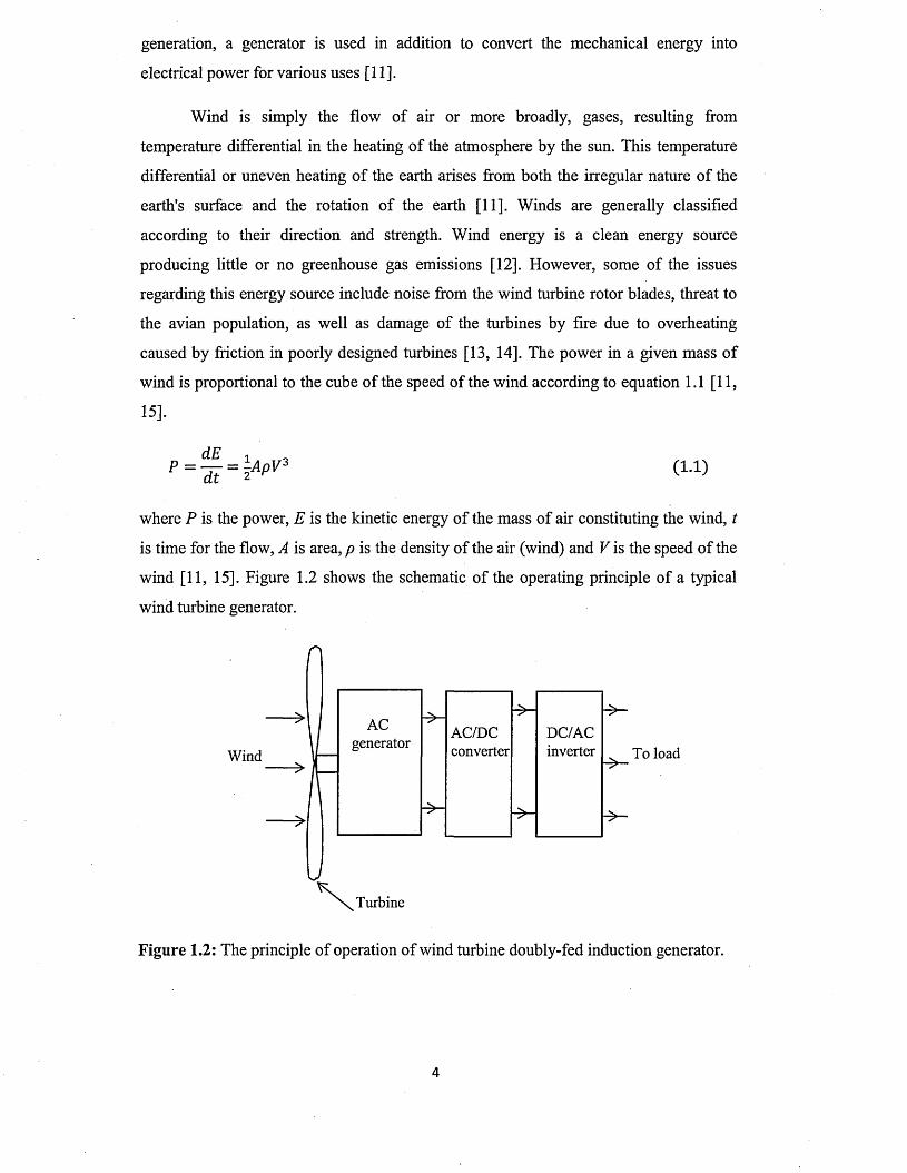
generation, a generator is used in addition to convert the mechanical energy into
electrical power for various uses [11].
Wind is simply the flow of air or more broadly, gases, resulting from
temperature differential in the heating of the atmosphere by the sun. This temperature
differential or uneven heating of the earth arises from both the irregular nature of the
earth's surface and the rotation of the earth [11]. Winds are generally classified
according to their direction and strength. Wind energy is a clean energy source
producing little or no greenhouse gas emissions [12]. However, some of the issues
regarding this energy source include noise from the wind turbine rotor blades, threat to
the avian population, as well as damage of the turbines by fire due to overheating
caused by friction in poorly designed turbines [13, 14]. The power in a given mass of
wind is proportional to the cube of the speed of the wind according to equation 1.1 [11,
15].
dE i ’p = ^ = V 3 ( i .i)
where P is the power, E is the kinetic energy of the mass of air constituting the wind, t
is time for the flow, A is area, p is the density of the air (wind) and V is the speed o f the
wind [11, 15]. Figure 1.2 shows the schematic of the operating principle of a typical
wind turbine generator.
r
— >
Wind ■ > .
>
Turbine
Figure 1.2: The principle of operation of wind turbine doubly-fed induction generator.
DC/ACinverter
AC/DCconverter
ACgenerator
4
1.2.2 Geotherm al Energy
Enormous heat is produced at the core of the Earth by the radioactive decay of
some naturally occurring minerals [16]. The temperature due to this heat reaches few
thousands of degrees Celsius. This high temperature and the accompanying pressure
cause rocks to melt, forming molten magma. The heat from the magma creates upward
convection current that heats up the rocks and water above it up to temperatures above
300°C [16]. This heat energy generated and stored in the Earth is called geothermal
energy and can be harnessed in order to heat water and produce steam to turn turbines
for electricity generation. Geothermal energy has been in use from ancient times for
bathing and space heating [16, 17].
Although geothermal energy is abundant in the Earth, greenhouse gases trapped
in the Earth can be released when this energy is tapped. However, the amount of these
greenhouse gases is relatively low compared to that generated from fossil fuels. As a
result, wide deployment of geothermal energy as an alternative to fossil fuel can help
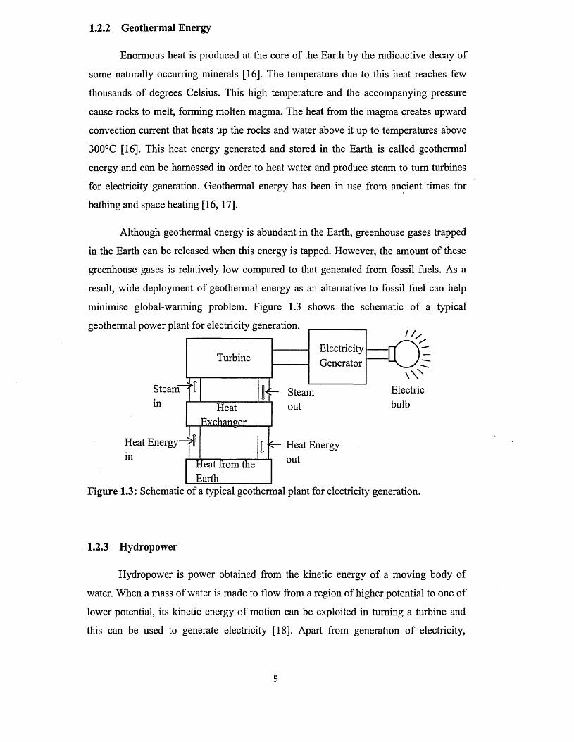
minimise global-warming problem. Figure 1.3 shows the schematic o f a typical
geothermal power plant for electricity generation.
Steamin
Heat Energy in
Turbine
ifHeat
Exchanger
f I*Heat from theEarth
ElectricityGenerator
/ /
Steamout
Heat Energy out
o =wNElectricbulb
Figure 1.3: Schematic of a typical geothermal plant for electricity generation.
1.2.3 Hydropower
Hydropower is power obtained from the kinetic energy o f a moving body of
water. When a mass of water is made to flow from a region of higher potential to one of
lower potential, its kinetic energy o f motion can be exploited in turning a turbine and
this can be used to generate electricity [18]. Apart from generation o f electricity,
5
hydropower has been in use since ancient times for purposes such as irrigation and
operation of mills for various applications [19].
Hydropower naturally originates from wave power and tidal power. Water
waves are generated by wind flowing over the surface o f the ocean or sea [20]. This
flow transfers energy from the wind to the wave. As a result of uneven surface o f the
see water, the wind flow creates pressure differences between different levels on the sea
surface which in turn cause the water wave to grow in strength. Tidal power is created
by the gravitational attraction between the Earth and the moon as well as between the
earth and the sun. This attraction brings about distortion in the water level o f oceans
which consequently raises the sea level. This causes water from the middle of the ocean
to move towards the sea shore resulting in tide.
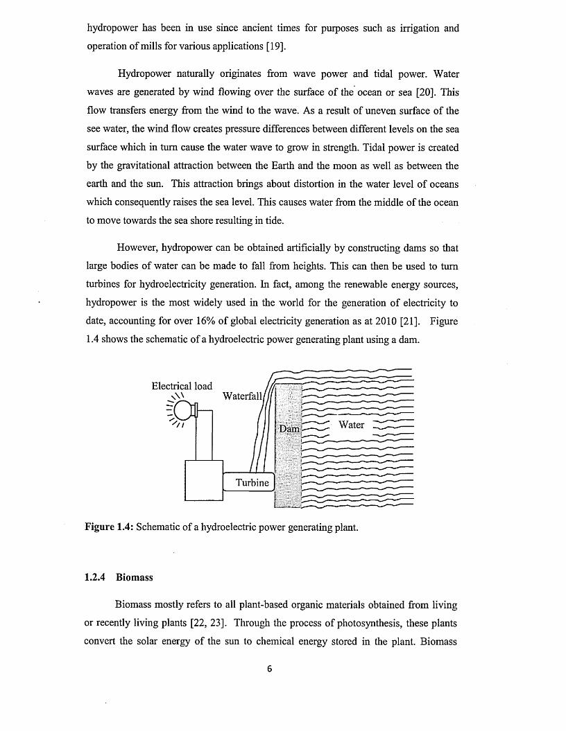
However, hydropower can be obtained artificially by constructing dams so that
large bodies of water can be made to fall from heights. This can then be used to turn
turbines for hydroelectricity generation. In fact, among the renewable energy sources,
hydropower is the most widely used in the world for the generation of electricity to
date, accounting for over 16% of global electricity generation as at 2010 [21]. Figure
1.4 shows the schematic of a hydroelectric power generating plant using a dam.
Electrical loadWaterfall
WaterDam
Turbine
Figure 1.4: Schematic of a hydroelectric power generating plant.
1.2.4 Biomass
Biomass mostly refers to all plant-based organic materials obtained from living
or recently living plants [22, 23]. Through the process o f photosynthesis, these plants
convert the solar energy of the sun to chemical energy stored in the plant. Biomass
6
energy is therefore energy derived from biomass. The conversion of biomass into
energy can be done in different ways giving rise to the different biomass energy
technology applications. These involve converting biomass into solid, liquid or gaseous
fuels called biofuels, principally used for transportation [24, 25]. This can be done
through thermal, chemical or biochemical means. Examples of such biofuels include
bio-ethanol, methanol, ethylene (or ethylene glycol) and propylene (or propylene
glycol) [24 - 27]. Another method of bioenergy production is by direct combustion or
burning of biomass such as wood to produce heat energy for direct application such as
cooking and space heating and for indirect generation of electricity by heating water to
produce steam for operating turbines [24, 28].
In a broader sense, biomass includes both plant and animal materials that can be
converted into industrial chemicals for the production of bioenergy. In recent times,
biomass has been extended to sources such as waste from industrial and agricultural
activities. These are called lignocellulosic biomass. Biomass has always been a major
energy source for humans right from ancient times and has been projected to contribute
up to 15% of the global primary energy supply by 2050 [29].
1.2.5 Solar Energy
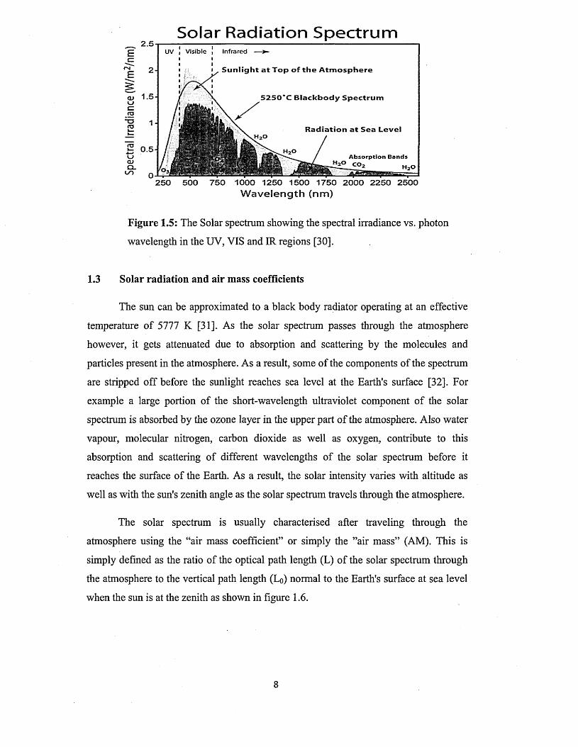
Solar energy is simply energy based on the sun's electromagnetic radiation.
Figure 1.5 shows the solar spectrum comprising electromagnetic radiation of various
wavelengths or frequencies [30]. This spectrum covers the ultraviolet (UV) radiation
(100 - 400) nm, the visible (VIS) radiation (400 - 700) nm and the infrared (IR)
radiation (700 nm and above). This covers most of the important spectrum for terrestrial
solar energy application especially through solar thermal and photovoltaic technologies.
Further discussion on solar energy conversion through various technologies is presented
in the following sections.
7
Solar Radiation SpectrumVisible In fra red
Sunlight at Top o f the Atmosphere
5250 C Blackbody Spectrum
Radiation at Sea Level
A b s o rp t io n B an d s h 2 ° C 0 2
m£250 500 750 1000 1250 1500 1750 2000 2250 2500
W a v e l e n g t h (n m )
Figure 1.5: The Solar spectrum showing the spectral irradiance vs. photon
wavelength in the UV, VIS and IR regions [30].
1.3 Solar radiation and air mass coefficients
The sun can be approximated to a black body radiator operating at an effective
temperature of 5777 K [31]. As the solar spectrum passes through the atmosphere
however, it gets attenuated due to absorption and scattering by the molecules and
particles present in the atmosphere. As a result, some of the components of the spectrum
are stripped off before the sunlight reaches sea level at the Earth’s surface [32]. For
example a large portion of the short-wavelength ultraviolet component o f the solar
spectrum is absorbed by the ozone layer in the upper part o f the atmosphere. Also water
vapour, molecular nitrogen, carbon dioxide as well as oxygen, contribute to this
absorption and scattering of different wavelengths o f the solar spectrum before it
reaches the surface of the Earth. As a result, the solar intensity varies with altitude as
well as with the sun's zenith angle as the solar spectrum travels through the atmosphere.
The solar spectrum is usually characterised after traveling through the
atmosphere using the “air mass coefficient” or simply the ”air mass” (AM). This is
simply defined as the ratio of the optical path length (L) o f the solar spectrum through
the atmosphere to the vertical path length (Lo) normal to the Earth's surface at sea level
when the sun is at the zenith as shown in figure 1.6.
8
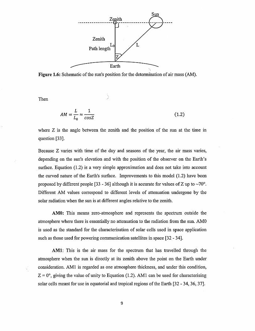
Sun
Path lengtl:
Zenith
Earth
Figure 1.6: Schematic o f the sun's position for the determination o f air mass (AM).
Then
(1.2)
where Z is the angle between the zenith and the position of the sun at the time in
question [33].
Because Z varies with time of the day and seasons of the year, the air mass varies,
surface. Equation (1.2) is a very simple approximation and does not take into account
the curved nature o f the Earth's surface. Improvements to this model (1.2) have been
proposed by different people [33 - 36] although it is accurate for values o f Z up to -70°.
Different AM values correspond to different levels of attenuation undergone by the
solar radiation when the sun is at different angles relative to the zenith.
AMO: This means zero-atmosphere and represents the spectrum outside the
atmosphere where there is essentially no attenuation to the radiation from the sun. AMO
is used as the standard for the characterisation of solar cells used in space application
such as those used for powering communication satellites in space [32 - 34].
AM I: This is the air mass for the spectrum that has travelled through the
atmosphere when the sun is directly at its zenith above the point on the Earth under
consideration. AMI is regarded as one atmosphere thickness, and under this condition,
Z = 0°, giving the value of unity to Equation (1.2). AMI can be used for characterising
solar cells meant for use in equatorial and tropical regions of the Earth [32 - 34, 36, 37].
depending on the sun's elevation and with the position of the observer on the Earth’s
9
AM1.5: This is the solar spectrum that has passed through 1.5 atmosphere
thickness. It represents the air mass when the sun is at an angle of Z= 48.2° to the
Earth's surface. In fact, A M I.5 is used as the average air mass o f the solar spectrum at
mid-latitudes. This is because the air mass of the spectrum in the region actually
fluctuates roughly about this value within the day. This is the air mass generally adopted
by the global solar energy industry as a standard for the characterisation o f solar cells
and solar panels for all terrestrial applications [32 - 34, 36 - 41].
AM2 and AM3: The AM2 corresponds to the spectrum when the sun is at an
angle Z = 60° relative to the zenith and AM3 corresponds to the situation with Z = 70°.
These two cover the range for characterising the average performance o f solar cells in
regions o f high latitudes such as northern Europe as well as in temperate zones where
winter, for instance, affects the spectra irradiance [32 - 34, 36, 37].
Solar intensity or solar irradiance (I) is the power per unit area of solar radiation.
The value of /varies as the solar radiation reaches the Earth’s surface as a result o f the
aforementioned attenuation that takes place in the atmosphere [32]. When the radiation
is released from the sun before any attenuation, the maximum solar irradiance Io is
obtained. This value is also called the total solar irradiance. It is also called the total
solar constant with an average value of about 1367 Wm ' 2 [42, 43]. The solar intensity is
related to the air mass according to Equation (1.3) [33].
/ = 1.1 x /„ x o.7C'4M>(“ 78) (1.3)
Therefore, for AM 1.5 condition, the average value of irradiance is about 1000 W m' .
This is the value used in different research laboratories for the purpose of comparing
performance o f solar cells.
1.4 Solar energy conversion and technologies
The conversion of solar radiation or solar energy into other useful energy forms
and sources takes different routes. In all cases, the primary components are photons
which come from solar radiation. These conversion routes and the corresponding
technologies involve the conversion of photon energy directly into heat energy,
chemical energy or electrical energy as well as conversion into electricity through
intermediate stages such as conversion into heat and then to electrical energy. The
various modes of solar energy conversion and the associated technologies are discussed
in the following sub-sections.10
1.4.1 Photo-therm al solar energy conversion
This involves the direct conversion o f photon energy (solar energy) into heat
energy through the use of solar collectors and absorbers. The resulting thermal (heat)
energy can then be used directly for example, for drying (as in solar dryers) [44] and
water heating (as in solar water heaters) [45] etc. In general, materials employed as
absorbers and concentrators for the above class of photo-thermal energy conversion
should have desirable properties such as high absorption coefficient over the entire solar
spectrum and low thermal emissivity in the infrared region o f the solar spectrum [46] as
well as excellent resistance to atmospheric and environmental corrosion. The optical
property o f the materials should also be very stable at high operating temperatures.
Materials such as silicon [47], black cobalt [48], Aluminium [49], stainless steel [50],
chromium [51], molybdenum [52] etc. are typical materials employed in photo-thermal
conversion of solar energy.
Depending on the energy (thermal) need, photo-thermal converters can be
classified in terms of their temperatures o f operation [53] as follows:
(a) Low tem perature photo-therm al converters; which can operate at temperatures
below 100°C. These are used in applications such as water heating in homes and for
heating o f swimming pools etc.
(b) M edium tem perature photo-therm al converters; which can operate at
temperatures between 60°C and 150°C. They are used for water desalination,
refrigeration cooling, space heating and for mechanical energy production such as for
generating steam for turning turbines.
(c) High tem perature photo-therm al converters; which can operate at temperatures
in the range 150°C to 800°C. These can be used in catalytic dissociation o f water for the
generation of hydrogen and oxygen as well as for production of steam for the operation
of turbines for electricity generation and other mechanical applications.
(d) Very high tem perature photo-therm al converters; which can operate at
temperatures above 800°C. They can be employed in thermoelectricity generation,
magneto-hydrodynamics as well as thermal dissociation of water for the production of
hydrogen as another source of fuel.
11
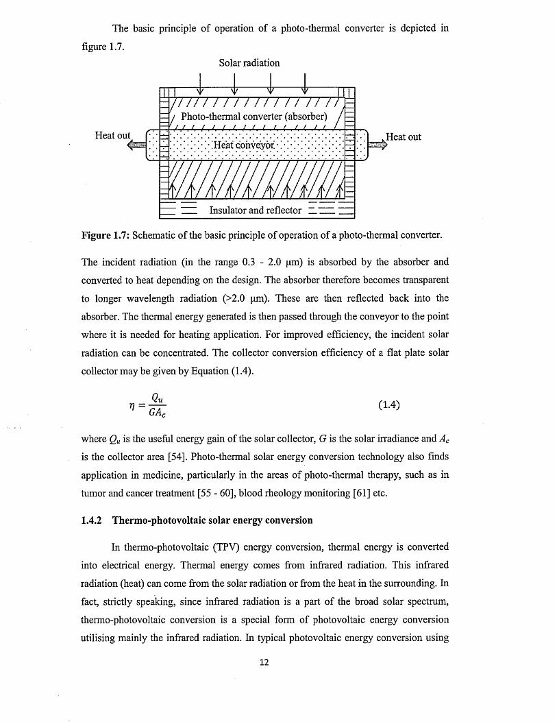
The basic principle of operation of a photo-thermal converter is depicted in
figure 1.7.
Solar radiation
Photo-thermal converter (absorber)
Heat out Heat outHeat cohveyor!
Insulator and reflector
Figure 1.7: Schematic of the basic principle of operation o f a photo-thermal converter.
The incident radiation (in the range 0.3 - 2.0 pm) is absorbed by the absorber and
converted to heat depending on the design. The absorber therefore becomes transparent
to longer wavelength radiation (>2.0 pm). These are then reflected back into the
absorber. The thermal energy generated is then passed through the conveyor to the point
where it is needed for heating application. For improved efficiency, the incident solar
radiation can be concentrated. The collector conversion efficiency of a flat plate solar
collector may be given by Equation (1.4).
where Qu is the useful energy gain of the solar collector, G is the solar irradiance and Ac
is the collector area [54]. Photo-thermal solar energy conversion technology also finds
application in medicine, particularly in the areas of photo-thermal therapy, such as in
tumor and cancer treatment [55 - 60], blood rheology monitoring [61] etc.
1.4.2 Thermo-photovoltaic solar energy conversion
In thermo-photovoltaic (TPV) energy conversion, thermal energy is converted
into electrical energy. Thermal energy comes from infrared radiation. This infrared
radiation (heat) can come from the solar radiation or from the heat in the surrounding. In
fact, strictly speaking, since infrared radiation is a part o f the broad solar spectrum,
thermo-photovoltaic conversion is a special form of photovoltaic energy conversion
utilising mainly the infrared radiation. In typical photovoltaic energy conversion using
solar cells, the ultraviolet visible and near infrared parts o f the solar spectrum are mostly
converted into electricity. Conventional solar cells normally contain semiconductors
with bandgaps between 1.0 eV and 4.0 eV [62]. This automatically makes them
transparent to the infrared radiation corresponding to photons with energies below their
bandgaps. In thermo-photovoltaic energy conversion therefore, very narrow bandgap
semiconductors are used in the photovoltaic part of the entire process in order to
effectively absorb longer wavelength infrared radiation from heat energy generated by
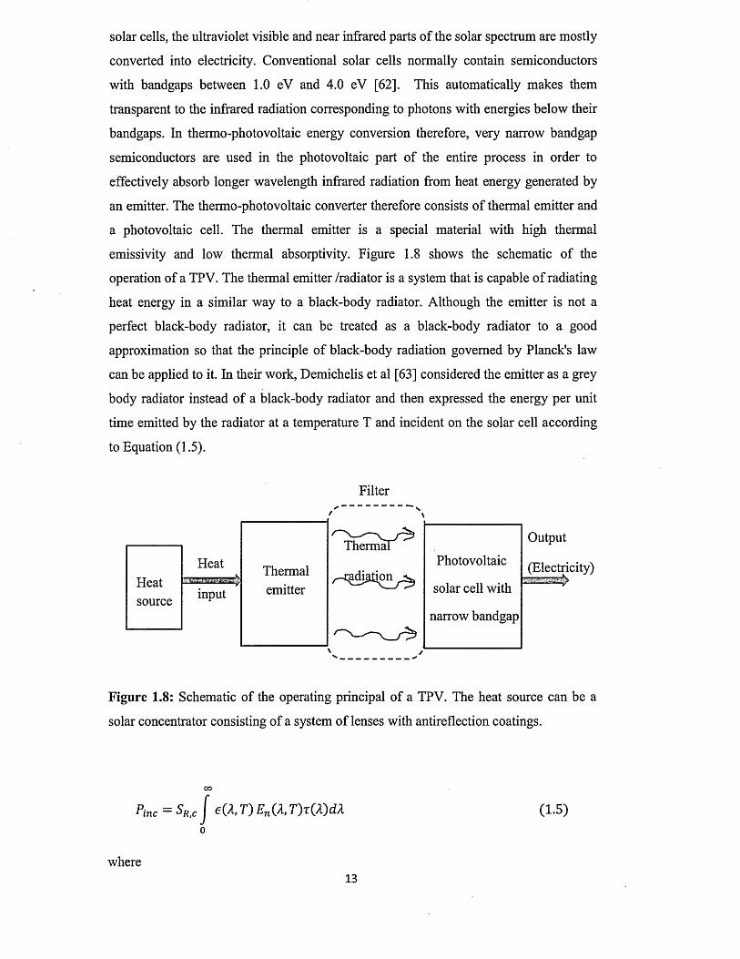
an emitter. The thermo-photovoltaic converter therefore consists o f thermal emitter and
a photovoltaic cell. The thermal emitter is a special material with high thermal
emissivity and low thermal absorptivity. Figure 1.8 shows the schematic of the
operation of a TPV. The thermal emitter /radiator is a system that is capable of radiating
heat energy in a similar way to a black-body radiator. Although the emitter is not a
perfect black-body radiator, it can be treated as a black-body radiator to a good
approximation so that the principle o f black-body radiation governed by Planck's law
can be applied to it. In their work, Demichelis et al [63] considered the emitter as a grey
body radiator instead o f a black-body radiator and then expressed the energy per unit
time emitted by the radiator at a temperature T and incident on the solar cell according
to Equation (1.5).
source
Filter
\
/~ThOTnaT>r^Photovoltaic
Thermalemitter
/ - tg d ia l jo n ^solar cell with
\ *
narrow bandgap
Output
(Electricity)
Figure 1.8: Schematic of the operating principal of a TPV. The heat source can be a
solar concentrator consisting of a system of lenses with antireflection coatings.
uu
Pine = Sr.c J e d T) En (A, T)x{X)dX (1.5)
where13
Pinc = Energy per unit time emitted by the radiator,
S r , c = geometric factor o f the radiator cell,
c (h,T) — spectral emittance at wavelength, X and temperature, T,
En(X,T) = emissive power of a black-body at wavelength, X and temperature, T,
r(X) = transmittance o f the filter between the emitter and the solar cell.
The energy absorbed by the solar cell per unit time ( P a b s ) is then given by
o
where A (X) = absorbance of the cell.
The efficiency o f the solar cell is given by
where
t j c e i i = efficiency of the solar cell,
Jmp = current density at maximum power point,
Vmp = voltage at maximum power point,
Jph = total photo-generated current density,
Vg = Eg/e is the bandgap voltage,
Eg = bandgap energy of the solar cell, and
e = electron charge.
The conversion efficiency r]TPV o f the thermo-photovoltaic converter then becomes
00
J A(X)e(.A,T)En (.lT )T (X )< t t (1.6)
(1.8)
where Aceu = area of the solar cell.
14
Equations (1.5) - (1.8) show that the efficiency o f a TPV depends strongly on the
temperature of the emitter and the wavelength of the photons radiated by the emitter.
Thermo-photovoltaic energy conversion is therefore a process based on
heat/temperature differential between the emitter and the solar cell. Materials that have
been used in TPV systems as emitters include erbium oxide (E1O 3) [64], ytterbium
oxide (Yb2 0 3 ) [64, 65], molybdenum [63, 64], tungsten [63, 65], tantalum [63] and
polycrystalline graphite [63]. Semiconductor solar cells that have been used in TPV
systems include germanium solar cells [64], silicon solar cells [64], InGaAsSb/GaSb
solar cells [6 6 ], InGaAs/InP solar cells [67], InGaAsP/InP solar cells [67] and
InGaAs/InGaAs/InP solar cells [67]. Dasheill et al have obtained a TPV conversion
efficiency o f 19.7% using InGaAsSb/GaSb solar cell at temperature of ~30°C with an
emitter temperature of 950°C [6 6 ].
1.4.3 Photo-chemical solar energy conversion
Photochemical solar energy conversion deals with the conversion of radiant
energy o f the sun into chemical energy which can further be converted directly into
electricity (photo-electrochemical conversion) or stored in the form of hydrogen
(through water splitting) [6 8 , 69] or in other forms such as methanol and other
hydrocarbons. Photosynthesis is one such way of converting the sun's radiant energy
into chemical energy which can be found in nature. The photo-chemical converter is
therefore an energy generator as well as an energy storage system. In the case of serving
as a storage system, the stored chemical energy can be converted into other desired
forms of energy such as heat and electricity for utilisation. For example ethanol or
hydrogen produced from a photo-chemical converter can be burnt as fuel in order to
generate electricity or mechanical energy for transportation [70]. Among the various
photo-chemical energy conversion routes, the photo-catalytic water splitting for
hydrogen production has been researched more in recent times [6 8 , 69]. In general, the
work by Ross and Hsiao indicates that photo-chemical solar energy conversion system
has higher thermodynamic efficiency limit compared to a corresponding photovoltaic
solar energy conversion system employing a p-n junction solar cell [71].
1.4.4 Photovoltaic solar energy conversion
Photovoltaic (PV) solar energy conversion is the direct conversion of solar
energy of the sun into electricity using a photovoltaic solar cell. Among all the above
discussed solar energy conversion technologies, the photovoltaic technology is the most
15
famous as well as most widely researched and commercialised to date. Unlike the other
solar energy conversion technologies, PV technology has provided power for various
levels o f application ranging from low power applications in the order o f 1.0 W as in
calculators and wrist watches, to Megawatt applications such as in power stations [72 -
74]. The basic principle of operation of PV solar energy conversion is based on the
ability of photons from the solar radiation to break bonds in a photovoltaic (photo
active) material in order to create electron-hole pairs which can then be separated by a
built-in electric field (in a fully fabricated photovoltaic device) and collected in an
external circuit (before they are recombined) to produce electricity [74]. The fully
fabricated photovoltaic device is a solar cell. The photovoltaic solar cell will be
discussed in full in chapter 2. Nevertheless, various techniques have been employed to
increase the conversion efficiency o f PV solar cells. These include the use o f solar
concentrators [75] and multi-junction tandem approach [76]. Various photovoltaic
materials used to date in the fabrication of solar cells include organic (such as
semiconducting polymers) and inorganic semiconductor materials. The conversion
efficiency o f a photovoltaic solar cell depends on a number o f factors ranging from the
device architecture to the energy bandgaps of the semiconducting materials used as well
as the chemical nature of these materials. Further details on the efficiencies o f different
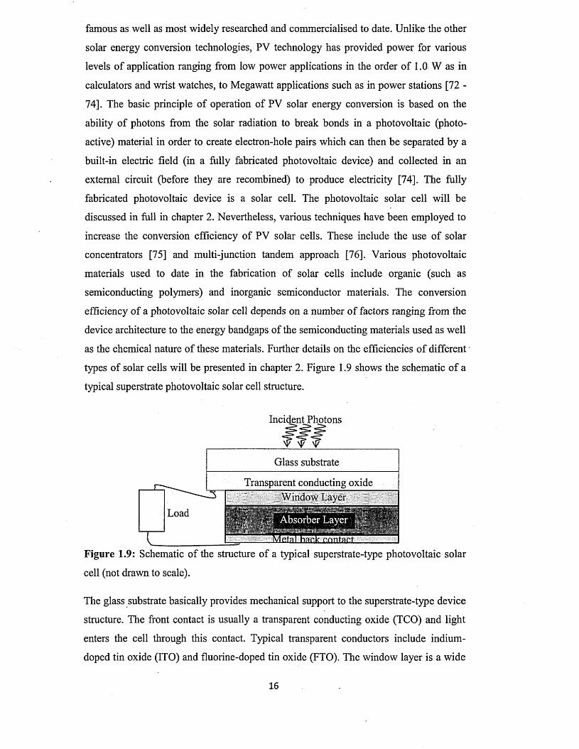
types of solar cells will be presented in chapter 2. Figure 1.9 shows the schematic of a
typical superstrate photovoltaic solar cell structure.
Incident Photons
Glass substrate
Transparent conducting oxide
LoadWindow Layer
"onTnrT""
Figure 1.9: Schematic of the structure of a typical superstrate-type photovoltaic solar
cell (not drawn to scale).
The glass substrate basically provides mechanical support to the superstrate-type device
structure. The front contact is usually a transparent conducting oxide (TCO) and light
enters the cell through this contact. Typical transparent conductors include indium-
doped tin oxide (ITO) and fluorine-doped tin oxide (FTO). The window layer is a wide
16
bandgap semiconductor such as CdS or ZnS to allow enough light (mostly in the near
UV, visible and IR) to reach the absorber layer. The absorber layer is the main
photoactive material where most of the electron-hole pairs are generated. In fact, in a
well-designed graded bandgap solar cell, all the layers take part in absorption of
photons in order to generate electron-hole pairs. Typical absorber layers include CdTe,
Si, GaAs, CuInGaSe2 (CIGS) etc. The metal back contact is very crucial to the
operation o f the solar cell. The type o f metal used here affects the electrical behaviour
of the metal/semiconductor interface. This contact can have either ohmic behaviour or a
rectifying (Schottky barrier) behaviour. The particular behaviour chosen depends on
where the major depletion region in the device is located. If the contact is ohmic, there
is no depletion region existing at that interface. In general, if a p-n junction type device
is intended, then the depletion region is made to exist at the interface between the
window layer and the absorber layer. One of these two layers is then a p-type
semiconductor and the other is an n-type semiconductor. In this case, the metal back
contact should make an ohmic contact with the absorber layer. If a Schottky barrier-type
device is intended, then the interface between the metal back contact and the absorber
layer is a Schottky (rectifying) interface. In this case, the major depletion region in the
device is located at this interface. There may or may not be a depletion region at the
interface between the window layer and the absorber layer but the major depletion
region is at the Schottky contact. The nature o f this metal back contact is therefore
crucial in the operation o f a photovoltaic solar cell.
It is important to remark at this point that the contact between the TCO and the
window layer is usually ohmic. By definition an ohmic contact is one that obeys Ohm’s
law such that similar electrical current passes through it in both directions. On the other
hand, a Schottky contact is a rectifying contact which allows electrical current to pass
through it in one direction only. In practical devices, there is a very small current that
flows in the reverse direction. Because o f the large differences (of several orders o f
magnitude) between the currents in these two directions, the current in the preferred
direction is dominant so that the infinitesimal current in the opposite direction is
neglected. A p-n junction is also a good rectifying junction.
For completeness as well as for brevity, the reviews of various thin film
semiconductor deposition techniques and the physics of these semiconductors and their
devices are presented in Appendices I and II respectively.
17
1.5 Aims and motivation of this work
The work reported in this thesis was actually inspired by the previous work by
Dharmadasa et al in 2002 in which an unconfirmed conversion efficiency of -18.0%
was reported for a glass/FTO/CBD-CdS/ED-CdTe/Au solar cell by using n-CdTe as
absorber material [5]. This work exposed a possible confusion which may have been
responsible for the stagnation in the efficiency o f CdS/CdTe-based solar cells for
decades. This concerns the existence of simple n-CdS/p-CdTe p-n junction as well as n-
CdS/n-CdTe hetero-junction + large Schottky barrier height at the n-CdTe/metal
interface, which results in the existence of a depletion region at different locations in the
two device structures.
The main aim of the present work therefore involves further investigation o f the
later device structure with well-established n-CdTe material using possible low-cost and
further simplified processes, and the extension o f this approach to devices involving
ZnS as window/buffer material. There are therefore major differences and modifications
both in materials growth and device processing in the present work. The major
highlights of the procedure employed by Dharmadasa et al include:
i. Use of CBD-grown CdS as the only window material.
ii. Use of three-electrode system in the growth of CdTe layers.
iii. Use of non-aqueous electrolyte for the deposition o f CdTe with ethylene glycol
as the non-aqueous solvent.
iv. Use of CdCb and TeCU as sources o f Cd and Te ions in the deposition of CdTe.
v. Deposition o f CdTe at a relatively high temperature of 160°C due to the use of
non-aqueous solution.
vi. Use of CdU as source of iodine for n-type doping of CdTe.
vii. Etching of CdS layers in dilute Na0 H+Na2 S2 0 3 solution prior to the deposition
of CdTe.
viii. Post-deposition annealing of CdTe layers at 400°C for 20 minutes using the
conventional CdCl2 treatment with CdCk dissolved in methanol.
18
ix. Etching of CdTe layers in Na0 H+Na2S2 0 3 solution only before metallisation
with Au.
x. Fabrication of only glass/FTO/n-CdS/n-CdTe/Au solar cells o f smaller cross-
sectional area (with 1 mm diameter).
The approach used in the present work has the following differences from and
modifications to the work reported in the past:
i. Use of all-electrodeposited semiconductors (ZnS, CdS, CdTe) thereby
eliminating the CBD process for process simplification and cost reduction.
ii. - Use of both two-electrode and three-electrode systems for the electrodeposition
of CdTe for comparison with the aim of eliminating the use of the reference
electrode in order to simplify the deposition process.
iii. Use o f all-aqueous electrolytes (with de-ionised water as solvent) for the
electrodeposition of all materials thereby eliminating the use o f expensive and
toxic non-aqueous ethylene glycol.
iv. Use of CdSC>4 and Te0 2 as sources o f Cd and Te ions in the electrodeposition of
CdTe.
v. Electrodepostion of CdTe and in fact, all the materials, at relatively low
temperature generally <90°C due to the use of aqueous solutions.
vi. Use of Cdl2 as well as CdCl2 and CdF2 as sources of halogens for n-type doping
of CdTe.
vii. Cleaning of ZnS and CdS layers with methanol and de-ionised water instead of
etching with Na0 H+Na2S2 0 3 solution before depositing CdTe.
Viii Post-deposition annealing of CdTe at 450°C for 15 minutes with CdCl2+CdF2
treatment. The CdCl2 and CdF2 were also dissolved in de-ionised water instead
of methanol. The temperature of 450°C was used since the CdTe layers were
grown at relatively low temperature <90°C.
ix. Etching of CdTe layers in acidified K^C^C^ solution as well as in dilute
Na0 H+Na2 S2 0 3 solution prior to metallisation.
19
x. Fabrication of solar cells of relatively larger cross-sectional areas with 2 mm and
3 mm diameters.
xi. Fabrication o f different solar cell structures including glass/FTO/n-CdS/n-
CdTe/Au, glass/FTO/n-ZnS/n-CdTe/Au and multi-layer graded-bandgap
glass/FTO/n-ZnS/n-CdS/n-CdT e/Au structures.
1.6 Conclusion
This chapter presented the current issues on energy supply and consumption.
The need for alternative sustainable, renewable as well as affordable clean energy
supply for various applications was also presented. Reduction of greenhouse gases that
largely contribute to the current issue of global warming was identified as the ultimate
benefit of renewable and alternative clean energy supply. Various renewable energy
sources and the corresponding technologies to meet this need were reviewed with
special emphasis on photovoltaic solar energy conversion for the purpose o f this thesis.
The last section presented the aims and motivation for the work presented-in this thesis.
2 0
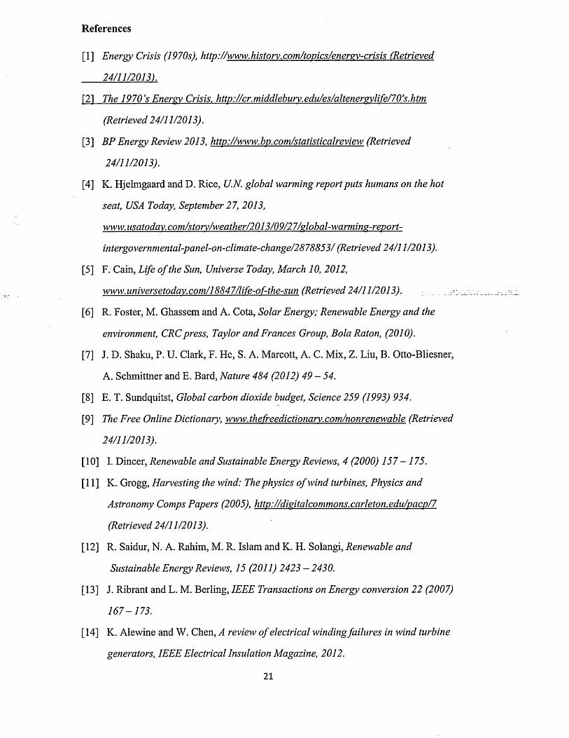
References
[I] Energy Crisis (1970s), http://www.historv.com/tovics/enersv-crisis (Retrieved
24/11/2013).
IZL The 1970’sE nersv Crisis. http://cr.middleburv.edu/es/altenersvlife/70's.htm
(Retrieved 24/11/2013).
[3] BP Energy Review 2013, httv://www.by.com/statisticalreview (Retrieved
24/11/2013).
[4] K. Hjelmgaard and D. Rice, U.N. global wanning report puts humans on the hot
seat, USA Today, September 27, 2013,
www.usatodav.com/storv/weather/2013/09/27/slobal-warmins-revort-
intergovernmental-panel-on-climate-change/2878853/ (Retrieved 24/11/2013).
[5] F. Cain, Life o f the Sun, Universe Today, March 10, 2012,
www. universetodav. com/18847/life-of-the-sun (Retrieved 24/11/2013). .......
[6 ] R. Foster, M. Ghassem and A. Cota, Solar Energy; Renewable Energy and the
environment, CRCpress, Taylor and Frances Group, Bola Raton, (2010).
[7] J. D. Shaku, P. U. Clark, F. He, S. A. Marcott, A. C. Mix, Z. Liu, B. Otto-Bliesner,
A. Schmittner and E. Bard, Nature 484 (2012) 49 - 54.
[8 ] E. T. Sundquitst, Global carbon dioxide budget, Science 259 (1993) 934.
[9] The Free Online Dictionary, www. thefreedictionarv. com/nonrenewable (Retrieved
24/11/2013).
[10] I. Dincer, Renewable and Sustainable Energy Reviews, 4 (2000) 157 -1 7 5 .
[II] K. Grogg, Harvesting the wind: The physics o f wind turbines, Physics and
Astronomy Comps Papers (2005), httv://disitalcommons.carleton.edu/vacv/7
(Retrieved 24/11/2013).
[12] R. Saidur, N. A. Rahim, M. R. Islam and K. H. Solangi, Renewable and
Sustainable Energy Reviews, 15 (2011) 2423-2430.
[13] J. Ribrant and L. M. Berling, IEEE Transactions on Energy conversion 22 (2007)
167-173 .
[14] K. Alewine and W. Chen, A review o f electrical winding failures in wind turbine
generators, IEEE Electrical Insulation Magazine, 2012.
21
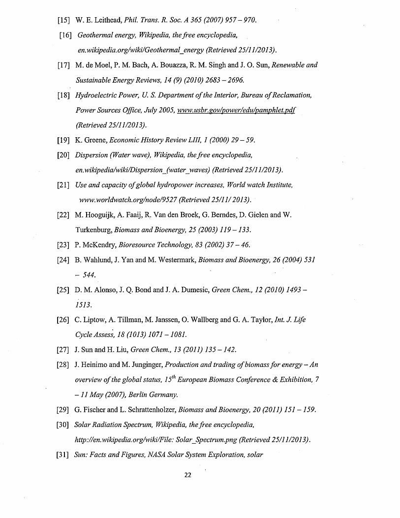
[15] W. E. Leithead, Phil. Trans. R. Soc. A 365 (2007) 957 - 970.
[16] Geothermal energy, Wikipedia, the free encyclopedia,
en.wikipedia.org/wiki/Geothermal_energy (Retrieved 25/11/2013).
[17] M. de Moel, P. M. Bach, A. Bouazza, R. M. Singh and J. O. Sun, Renewable and
Sustainable Energy Reviews, 14 (9) (2010) 2683-2696.
[18] Hydroelectric Power, U. S. Department o f the Interior, Bureau ofReclamation,
Power Sources Office, July 2005, www. usbr. sov/power/edu/pamph let, p d f
(Retrieved 25/11/2013).
[19] K. Greene, Economic History Review LIH, 1 (2000) 29 - 59.
[20] Dispersion (Water wave), Wikipedia, the free encyclopedia,
en.wikipedia/wiki/Dispersion_(water_waves) (Retrieved 25/11/2013).
[2 1 ] Use and capacity o f global hydropower increases, World watch Institute,
www.worldwatch.org/node/9527 (Retrieved 25/11/2013).
[22] M. Hooguijk, A. Faaij, R. Van den Broek, G. Bemdes, D. Gielen and W.
Turkenburg, Biomass and Bioenergy, 25 (2003) 119 -1 3 3 .
[23] P. McKendry, Bioresource Technology, 83 (2002) 37 - 46.
[24] B. Wahlund, J. Yan and M. Westermark, Biomass and Bioenergy, 26 (2004) 531
- 544.
[25] D. M. Alonso, J. Q. Bond and J. A. Dumesic, Green Chem., 12 (2010) 1493 -
1513.
[26] C. Liptow, A. Tillman, M. Janssen, O. Wallberg and G. A. Taylor, Int. J. Life
Cycle Assess, 18 (1013) 1071 -1081.
[27] J. Sun and H. Liu, Green Chem., 13 (2011) 135 -1 4 2 .
[28] J. Heinimo and M. Junginger, Production and trading o f biomass fo r energy - An
overview o f the global status, 15th European Biomass Conference & Exhibition, 7
- 1 1 May (2007), Berlin Germany.
[29] G. Fischer and L. Schrattenholzer, Biomass and Bioenergy, 20 (2011) 151 -1 5 9 .
[30] Solar Radiation Spectrum, Wikipedia, the free encyclopedia,
http://en.wikipedia.org/wiki/File: Solar_Spectrum.png (Retrieved 25/11/2013).
[31] Sun: Facts and Figures, NASA Solar System Exploration, solar
22
system.nasa.gov/planets/profile. cfm ?Display =Facts&Object=Sun (Retrieved
10/10/2013).
[32] C. J. Riordan, Solar Cells, 18 (1986) 223 - 232.
[33] Air Mass (Solar energy), Wikipedia the free encyclopedia,
en.wikipedia.org/wiki/Air_mass_(solar_energy) (Retrieved 25/11/2013).
[34] R. J. Matson, K. A. Emery and R. E. Bird, Solar Cells, 11 (1984) 105 -1 4 5 .
[35] F. Kasten, Lighting Res. Technol., 25 (3) (1993) 129 -1 3 0 .
[36] R. E. Bird, Solar Cells, 7 (1982 -19 8 3 ) 107 -1 1 8 .
[37] R. Bird, R. Hulstrom and and C. Riorda, Solar Cells, 14 (1985) 193 -1 9 5 .
[38] C. A. Gueymard, D Myers and K. Emery, Solar Cells, 73 (6) (2002) 443 - 467.
[39] R. Hulstrom, R. Bird and C. Riordan, Solar Cells, 15 (1985) 365 - 391.
[40] rredc.nrel.gov/solar/spectra/aml. 5/(Retrieved 25/11/2013).
[41] rredc.nrel.gov/solar/spectra/aml.5/ASTMG173/ASTMG173.html (Retrieved
25/11/2013).
[42] C. A. Gueymard, Solar Energy, 76 (2004) 423 - 453.
[43] B. Mendoza, Advances in Space Research, 35 (2005) 882 - 890.
[44] S. VijayaVenkataRaman, S. Iniyan and R. Goic, Renewable and Sustainable
Energy Reviews, 16 (2012) 2652 - 2670.
[45] S. E. Frid, A. V. Mordynskii and A. V. Arsatov, Thermal Engineering 59 (2012)
874-880 .
[46] C. C. Uhuegbu, Journal o f Emerging Trends in Engineering and Applied Sciences
(JETEAS), 2 (1) (2011) 9 6 -1 0 1 .
[47] D. C. Booth, D. D. Allred and B. O. Seraphin, Solar Energy Materials, 2 (1979)
107-124 .
[48] Z. Abdel Hamid, A. Abdel Aal and P. Schmuki, Surf. Interface Anal, 40 (2008)
1493 -1499.
[49] J. Salmi, J-P. Bonino and R. S. Bes, J. Mater. Sci., 35 (2000) 1347 -1 3 5 1 .
[50] A. Avila-Garcia and U. Morales-Ortiz, Sol. Energ. Mater. Sol. Cell 90 (2006)
2556 - 2568.
[51] K. D. Masterson, Journal o f Solid State Chemistry, 22 (1977) 41 - 49.
23
[52] B. O. Seraphin, Thin Solid Films, 90 (1982) 395 - 403.
[53] J. Spitz, Thin Solid Films 45 (1977) 31 - 41.
[54] M. G. Hutchins, Surface Technology 20 (1983) 301 - 320.
[55] K. Dong, Z. Liu, Z. Li, J. Ren and X. Qu, Adv. Mater. 25 (2013) 4452 - 4458.
[56] H. Kang, B. Jia, J. Li, D. Morrish and M. Gu, Appl. Phys. Lett. 96 (2010) 063702-
1 - 063702-3.
[57] X. Huang, P. K. Jain, I. H. El-Sayed and M. A. El-Sayed, Laser Med. Sci. 23
(2008)217-228.
[58] K. T. Nguyen, J. Bioengineer & Biomed. Sci., 2 (4) (2012) 1 - 2 .
[59] L. G. Gutwein, A. K. Singh, M. A. Hahn, M. C. Rule, J. A. Knapik, B. M.
Moudgil, S. C. Brown and S. R. Grobmyer, Int. J. Nanomedicine 7 (2012) 351 -
357.
[60] W. I. Choi, A. Sahu, Y. H. Kim and G. Tae, Annals o f Biomedical Engineering 40
(2) (2012) 534 - 546.
[61] E. I. Galanzha and V. P. Zharov, Cytometry PartA 79A (2011) 746 - 757.
[62] W. H. Strehlow and E. L. Cook, J. Phys. Chem. Ref. Data 2 (1) (1973).163-199.
[63] F. Demichelis, E. MinettiMezzetti, M. Agnello and E. Tresso, J. Appl. Phys. 53
(1982)9098-9104.
[64] H. Hofler, P. Wurfel and W. Ruppel, Solar Cells 10 (1983) 2 5 7 -2 7 1 .
[65] F. Demichelis and E. MinettiMezzetti, Solar Cells 1 (1979/1980) 395 - 403.
[6 6 ] M. W. Dashiell, J. F. Beausang, H. Ehsani, G. J. Nichols, D. M. Depoy, L. R.
Danielson, P. Talamo, K. D. Rahner, E. J. Brown, S. R. Burger, P. M. Fourspring,
W. F. Topper Jr and G. W. Turner, IEEE Transactions on Electron Devices 53
(12) (2006) 2879-2891.
[67] C. M. Waits, Thermophotovoltaic energy conversion fo r personal power sources,
Army Research Laboratory, Adelphi, MD 20783 -1197 , ARL-TR-5942, February
(2012).
[6 8 ] H. Berberoglu and L. Pilon, International Journal o f Hydrogen Energy 35 (2010)
500-510 .
[69] V. J. Babu, M. K. Kumar, A. S. Nair, T. L. Kheng, S. I. Anakhverdiev and S.
24
Ramakrishna, International Journal o f Hydrogen Energy 37 (2012) 8897 - 8904.
[70] L. Su and Y. X. Gan, Nano Energy 1 (2012) 159 -1 6 3 .
[71] R. T. Ross and T. Hsiao, J. Appl. Phys. 48 (1977) 4783 - 4785.
[72] H. J. Wenger, J. Schaefer, A. Rosenthal, B. Hammond and L. Schlueter, IEEE
(1991) CH2953-8/91/0000-0586 $1.00©1991 IEEE.
[73] http://topaz.firstsolar.com/nroiects/Tovaz-Solar-Farm7(Retrieved 25/11/2013).
[74] I. M. Dharmadasa, Advances in Thin-Film Solar Cells (Boulevard, Singapore,
Pan Stanford Publishing Pte. Ltd) (2012).
[75] Y. Yang, W. Yang, W. Tang and C. Sun, Appl. Phys. Lett. 103 (2013) 083902-1 -
083902-5.
[76] H. Keppner, J. Meier, P. Torres, D. Fischer and A. Shah, Appl. Phys. A 69 (1999)
169-177 .
25
2.0 Introduction
Chapter 2: Photovoltaic solar cells
Solar cells constitute the heart of photovoltaic technology. The solar cells used
for photovoltaic energy conversion are basically made of semiconductors. These
semiconducting materials can have n-type, p-type or i-type electrical conductivity as
mentioned in Appendix II. When used in solar cells, they are combined in various
junction configurations such as p-n junction, p-i-n junction, n-n hetero-junction, p-p
hetero-junction, metal-semiconductor junction and metal-insulator-semiconductor
junction. Two or more of these junction types must be present in a solar cell device
before it can function.
The basic principle o f operation o f a solar cell involves the following steps [1]:
(i) Absorption o f photons from incident solar radiation as well as heat from the
surroundings (for solar cells incorporating impurity photovoltaic effect).
(ii) Breaking of bonds in the solar cell materials by these incident photons and the
consequent generation of electron-hole (e-h) pairs.
(iii) Separation o f these photo-generated e-h pairs (to avoid their recombination) by
means of the built-in electric field within the solar cell device. This also depends on
the lifetime and diffusion lengths of these electrons and holes in the solar cell
materials.
(iv) Transportation of these separated photo-generated electrons and holes towards the
two terminals (the electrical contacts) o f the solar cell. This depends both on the
gradient of the slope of the energy band edges and on the mobility o f both electrons
and holes in the semiconductor materials making up the solar cell.
(v) Final collection of these electrons and holes into an external circuit in the form of
electric current. This depends on the nature o f contacts between the semiconductors
and the contacting materials. Low resistance contacts are very important in this
case.
The above mentioned processes depend on a number of factors which include:
(i) availability o f energetic photons in the incident radiation,
(ii) the nature or type of semiconducting materials involved in the solar cell device
fabrication, and
(iii) the type and nature of active junctions existing within the device.
26
The solar energy materials (semiconductors) used in solar cell fabrication range
from inorganic to organic materials. Different types of solar cells have been fabricated
based on each of these two groups or even a combination o f the two. One can therefore
broadly classify solar cells based on these two groups o f materials (organic and
inorganic materials) as well as on their combination in what is known today as hybrid
solar cells.
The time line of photovoltaic solar cells starts with the discovery of the
“photovoltaic effect” by Edmund Becquerel in 1839 while working with an electrolytic
cell using two metal electrodes [2, 3]. Afterwards, Adams and Day observed PV effect
in solid selenium in 1877 [3]. In fact, following this work, Charles Fritts developed the
first selenium solar cell using gold contact. This produced less than 1% conversion
efficiency in 1883 [3]. In 1887, James Moser discovered dye-sensitised solar cell using
photoelectrochemical (PEC) cell. This continued until 1904 when the first
semiconductor junction solar cell was produced by Wilhelm Hallwachs using copper
and copper oxide [3]. In 1905, Albert Einstein explained the photoelectric effect for
which he later won Noble price. In 1918, the Czochralski method of silicon crystal
growth was introduced. In 1932, PV effect was discovered in CdSe by Audobert and
Stora. Following these developments, silicon solar cell with 4.5% efficiency was
produced for space applications in the 1950s. Between 1959 and 1960, Hoffman
Electronics produced 10-14% efficient commercial solar cells. The first high efficiency
GaAs hetero-structure solar cell was produced in 1970. In 1977, the world's PV
production exceeded 500 kW. The energy crisis o f 1970s triggered extensive research
and development activities in the PV area. In 1994, National Renewable Energy
Laboratory (NREL) in United States produced concentrated solar cell exceeding 30%
efficiency using GalnP/GaAs. In 1996, Michael Gratzel's group in Switzerland
produced 11% dye-sensitised solar cell. In 2000s, organic solar cells came into the PV
field and today hybrid solar cells combining organic and inorganic semiconductors are
being researched extensively.
2.1 Inorganic solar cells
Inorganic solar cells utilise inorganic semiconductor materials. To date the
highest efficiency solar cells in general are those using inorganic materials [4]. Major
inorganic semiconductors involved in this category of solar cells include Si, Ge, GaAs,
InP, Gap, GaSb, CIGS, CIS, Cu2 S, CdS, CdTe, ZnS, ZnTe, ZnSe, CdSe , PbSe, CZTS,
27
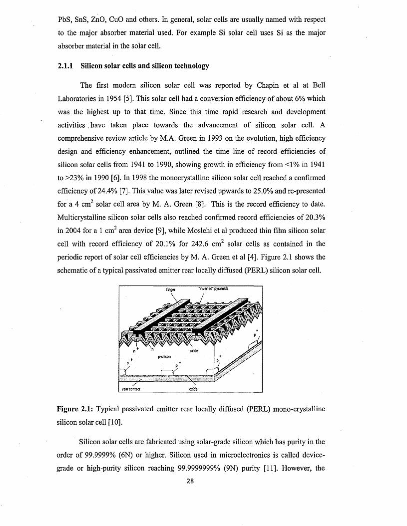
PbS, SnS, ZnO, CuO and others. In general, solar cells are usually named with respect
to the major absorber material used. For example Si solar cell uses Si as the major
absorber material in the solar cell.
2.1.1 Silicon solar cells and silicon technology
The first modem silicon solar cell was reported by Chapin et al at Bell
Laboratories in 1954 [5]. This solar cell had a conversion efficiency o f about 6 % which
was the highest up to that time. Since this time rapid research and development
activities have taken place towards the advancement of silicon solar cell. A
comprehensive review article by M.A. Green in 1993 on the evolution, high efficiency
design and efficiency enhancement, outlined the time line of record efficiencies of
silicon solar cells from 1941 to 1990, showing growth in efficiency from <1% in 1941
to >23% in 1990 [6 ]. In 1998 the monocrystalline silicon solar cell reached a confirmed
efficiency of 24.4% [7]. This value was later revised upwards to 25.0% and re-presented
for a 4 cm2 solar cell area by M. A. Green [8 ]. This is the record efficiency to date.
Multicrystalline silicon solar cells also reached confirmed record efficiencies of 20.3%
in 2004 for a 1 cm2 area device [9], while Moslehi et al produced thin film silicon solar
cell with record efficiency of 20.1% for 242.6 cm2 solar cells as contained in the
periodic report o f solar cell efficiencies by M. A. Green et al [4]. Figure 2.1 shows the
schematic of a typical passivated emitter rear locally diffused (PERL) silicon solar cell.
’inverted* pyramidsfinger
oxide
oxiderear contact
Figure 2.1: Typical passivated emitter rear locally diffused (PERL) mono-crystalline
silicon solar cell [1 0 ].
Silicon solar cells are fabricated using solar-grade silicon which has purity in the
order of 99.9999% (6 N) or higher. Silicon used in microelectronics is called device
grade or high-purity silicon reaching 99.9999999% (9N) purity [11]. However, the
28
production of these grades of silicon is capital intensive, requiring huge amount of
electrical and thermal energy as well as advanced chemical processing steps.
The production of Si starts with the carbon reduction of silicates (SiCb) at high
temperatures to produce metallurgical grade silicon (MG-Si) with purity o f about
98.5%. This is then reacted with HC1 to form chlorosilanes such as tri-chlorosilane,
distilled for purification and then pyrolysed in a Bell reactor by passing it over a high-
purity silicon rod called seed crystal at temperatures of about 1150°C. In this process,
high purity polycrystalline silicon for solar cell application is produced. The chemical
reaction for this process is shown in Equation (2.1).
2H SiCl3 + H e a t -> Si + 2HCl + S iC l4 (2 .1 )
The heat for this reaction is produced by electrical resistive heating requiring huge
amount o f electrical energy.
In order to produce silicon wafers which are typically 200 - 350 pm thick, with
low resistivity o f ~ 1 Q cm, the already made polysilicon is melted at high temperatures
and then re-solidified into monocrystalline silicon ingots by the Czochralski method
[11]. These ingots are then cut into wafers for microelectronics or solar cell
applications. The Czochralski process involves slowly pulling out a silicon seed crystal
from a bath of high purity molten silicon while the seed is rotated. These processes
require high degree of precision. The very high temperature and high input energy
requirements, coupled with the high degree of precision involved in the production of
high purity silicon make this technology an expensive one for solar cell production.
According to the review article by Ranjan et al, the cost of polycrystalline silicon and
silicon wafer as at 2010 is of the order o f US$60 - 70 per kg for polycrystalline silicon
and $ 3 - 4 per 156 mm2 wafer [11].
Another method for producing silicon ingots is the Bridgeman method. This
involves making a cast of silicon ingot in a quartz crucible in the re-crystallisation
process [11]. This method is relatively cheaper but the major shortcoming is that it ends
up producing multi-crystalline silicon instead of single crystal silicon. These multi
crystalline silicon ingots therefore contain grain boundaries that constitute
recombination or scattering centres for charge carriers in devices fabricated using them
[12]. The crucible can also introduce impurities in the ingot formed. In any case, the
29
production of solar cell-grade silicon is very expensive thus driving the cost o f solar
cells made with it high.
An alternative form o f silicon is the amorphous silicon (a-Si), which basically
contains large numbers of imperfections resulting in the presence of dangling
(unsatisfied) bonds. It has therefore lost the long range order that characterises
crystalline silicon [13]. The presence o f dangling bonds creates large density of states of
the order o f 1019 - 1020 cm ' 3 which poses a problem to the movement o f the Fermi level
necessary in device fabrication [14]. The problem is solved by adding Hydrogen to the
a-Si in a process of hydrogenation. This has the advantage o f passivating the dangling
bonds and significantly reducing the density of states in the bandgap o f a-Si [15]. The
resulting material is therefore hydrogenated amorphous silicon (a-Si:H). One major
advantage of the amorphous silicon technology is that it can be grown and dop ed ea s ily ;
by some o f the conventional semiconductor growth techniques such as reactive
evaporation [16], sputtering, glow discharge plasma process [17] PECVD [18] etc. With
a-Si technology, relatively low cost thin-film Si-solar cells can now be produced
compared to those produced using single crystal or polycrystalline silicon with hundreds
of microns thickness and expensive starting high-purity materials. For example one
major source of a-Si:H is silane (SiH4), which is a gas. The energy bandgap of a-Si:H
ranges from about 1.70 eV to values > 2.0 eV [19]. Silicon is an indirect bandgap
semiconductor with an energy bandgap of 1.12 eV at room temperature [20] and typical
absorption coefficient (a) < 50 cm ' 1 near its bandgap [21]. However, hydrogenated
amorphous silicon has a direct bandgap with improved absorption coefficient of about
104 cm ' 1 near its bandgap [22]. Amorphous silicon solar cell has reached record
efficiency o f 10.1% in 2009 [23].
2.1.2 III-V compound-based solar cells
III-V compound-based solar cells are solar cells that have the group III-V
semiconductors as their main absorber materials. The most prominent o f these are GaAs
and InP. These have direct bandgaps of 1.42 eV for GaAs [24] and 1.35 eV for InP [25].
Both of these also have high carrier mobility [26, 27]. Other III-V semiconductors that
feature in solar cell fabrication include GaP (direct Eg = 2.78 eV; indirect Eg = 2.40 eV)
[28], GaSb (Eg = 0.74 eV) [29], InAs (Eg = 0.36 eV) [30], and InSb (Eg = 0.17 eV) [31].
Sometimes their ternary compound semiconductor variants can be used for the purpose
o f tailoring the bandgaps. Examples of these ternary III-V compound semiconductors
3 0

include InGaP, InGaAs, AlGaAs, InAIP etc. Sometimes quartenary semiconductors of
the III-V compounds can be formed such as GalnNAs, GaNPAs.
The III-V semiconductor-based solar cells are the best option for tandem (multi
junction) and concentrated solar cells [32, 33]. Figure 2.2 shows the schematic of device
structure o f a typical III-V tandem solar cell.'Metal contact
-Reflection coating
TCO
Glass substrate
Top cell
~~j— Tunnel junction
Bottom cell
Figure 2.2: Schematic of a tandem solar cell structure based on III-V semiconductors.
O f all the III-V based solar cells structures, the best record efficiencies for this group of
solar cells have come from GaAs and InP-based solar cells. These include GaAs thin
film solar cell with efficiency of 27.6% (for cell area o f -0.99 cm2) [34]; GaAs
concentrator solar cell with 29.1% efficiency (for cell area of -0.05 cm2) as reported in
[4] and GaAs thin film module with efficiency o f 23.5% (for module area o f 858.5 cm2]
[35], crystalline InP solar cell with efficiency o f 19.1% (for cell area o f 4.02 cm2) [36],
InGaP/GaAs/InGaAs multi-junction solar cell with efficiency of 37.9% (for cell area of
-1.05 cm2) [37], and GaInP/GaAs:GaInAsP/GaInAs concentrator solar cell with
efficiency of 38.5% (for cell area o f -0.20 cm2) [38]. Sharp Corporation has also
reported record efficiency of 44.4% for a GaAs-based concentrator solar cell [39].
2.1.3 Chalcogenide solar cells
Chalcogenides are compounds that principally contain group VI elements
(chalcogens). Chalcogenide semiconductors generally contain at least one metallic
element and one chalcogen. The four main chalcogens that normally feature in
semiconductors are oxygen, sulphur, selemium and tellurium. The major groups o f
chalcogenide semiconductors include I-VI semiconductors (eg. Q 12S and CuO), II-VI
semiconductors (e.g. CdTe and CdS), III-VI (e.g. InSe and In2S3), IV-VI (e.g. SnS), I-
31
Ill-VI (e.g. CuInSe2 and CuInGaS2) and I-II-IV-VI (e.g. Cu2ZnSnS4). In this category of
semiconductors, the major ones usually employed as absorber materials in solar cells
include Cu2S, CdTe, CIS, CIGS and CZTS.
Presently however, only three of these solar cells are being researched and
developed and therefore are in the efficiency table o f chalcogenide solar cells. These
include CdTe solar cells, CIGS (or CIGSS) and CZTS (or CZTSS) with CZTS (or
CZTSS) being the most recent. CdTe-based thin-film solar cells have recently reached
confirmed record efficiencies of 19.6% for a cell area of -1.01 cm2 and module
efficiency of 16.1% for a module area of 7200 cm2 as reported in ref [4]. On the part of
CIGS family, CIGS has reached a cell efficiency o f 19.9% for a cell o f area -1 cm2 [40]
and a module efficiency of 15.5% for a module area of 9703 cm2 [41] while CIGSS
reached confirmed module efficiency o f 13.0% for a module area of 1.68 m 2 as reported
in [4]. For the CZTS family, the available record efficiencies are only for laboratory
scale solar cells. For this, CZTS has researched 8.4% efficiency for a cell area o f -0.45
cm2 [42], while CZTSS has reached efficiency o f 11.1% for a cell area of -0.45 cm2
[43].
It is important to note that conventional solar cell structures usually fabricated
using the above mentioned absorber semiconductors are of the p-n junction type with
the absorber materials preferably being the p-type semiconductors even though some of
them can be grown with n-type conductivity. Some of the basic device structures
reported in the literature include; n-CdS/p-CdTe [44], n-CdS/p-CIGS [45] and n-CdS/p-
CZTS [42]. In this thesis, the solar cell structures reported are o f the n-n hetero-
junction+large Schottky barrier type involving n-type CdTe absorber material instead of
the conventional p-type CdTe.
2.2 O rganic solar cells
Organic solar cells are the type o f solar cells made from organic compounds,
usually polymers. They are also called polymer solar cells or plastic solar cells [46].
The search for suitable organic materials for photovoltaic application dates back to the
1950s when Keam and Calvin reported photovoltaic effect at Magnesium
phthalocyanine-oxidized TM $D junction in 1958 [47]. Kallmann and Pope also
reported photovoltaic effect in organic crystals of antracence in 1959 [48]. In general,
organic photovoltaics (OPVs) use organic molecules or organic polymers to absorb light
and subsequently produce electricity. The mechanism of OPVs however differs from
32
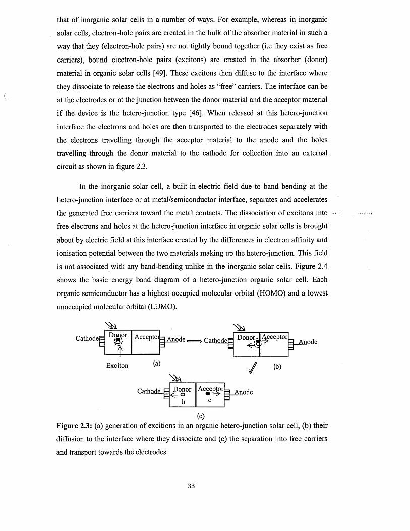
that o f inorganic solar cells in a number of ways. For example, whereas in inorganic
solar cells, electron-hole pairs are created in the bulk o f the absorber material in such a
way that they (electron-hole pairs) are not tightly bound together (i.e they exist as free
carriers), bound electron-hole pairs (excitons) are created in the absorber (donor)
material in organic solar cells [49]. These excitons then diffuse to the interface where
they dissociate to release the electrons and holes as “free” carriers. The interface can be
at the electrodes or at the junction between the donor material and the acceptor material
if the device is the hetero-junction type [46]. When released at this hetero-junction
interface the electrons and holes are then transported to the electrodes separately with
the electrons travelling through the acceptor material to the anode and the holes
travelling through the donor material to the cathode for collection into an external
circuit as shown in figure 2.3.
In the inorganic solar cell, a built-in-electric field due to band bending at the
hetero-junction interface or at metal/semiconductor interface, separates and accelerates
the generated free carriers toward the metal contacts. The dissociation o f excitons into
free electrons and holes at the hetero-junction interface in organic solar cells is brought
about by electric field at this interface created by the differences in electron affinity and
ionisation potential between the two materials making up the hetero-junction. This field
is not associated with any band-bending unlike in the inorganic solar cells. Figure 2.4
shows the basic energy band diagram of a hetero-junction organic solar cell. Each
organic semiconductor has a highest occupied molecular orbital (HOMO) and a lowest
unoccupied molecular orbital (LUMO).
Acceptor Anode Donor-,
Exciton (a) /Cathode F D onor
< - oh
Acceptor
e3 Anode
b
(b)
(c)Figure 2.3: (a) generation of excitions in an organic hetero-junction solar cell, (b) their
diffusion to the interface where they dissociate and (c) the separation into free carriers
and transport towards the electrodes.
33
These are analogous to the valence band and conduction band respectively in the
inorganic counterpart. The energy bandgap of the organic solar cell is also defined as
the differences in energy between the HOMO and LUMO. The energies corresponding
to the HOMO and LUMO levels are the ionisation potential and electron affinity as
shown in figure 2.4. The open-circuit voltage of the organic hetero-junction solar cell is
then defined by the differences between the HOMO of the donor material and the
LUMO of the acceptor material. The two metal contacts consist o f a high work function
metal as the cathode and a low work function metal as the anode.
Typical cathode material is indium-doped tin oxide (ITO) while typical anode
material is Al. A number of active layers (donors and acceptors) are used in organic
solar cells. These include donor materials such as chloroaluminium phthalocyanine
(ClAlPc), Poly [2-methoxy-5-(2'-ethyl-hexyloxy)-1,4-phenyleneVinylene](MEHPPV),
Poly (3-hexylthiophene) (1TP3HT), copper phthalocyanine (CuPc), poly [2-methoxy-5-
(3'7'-dimethyloctyloxy)-l, 4-phenylene vinylene] (MDMO-PPV) and poly (3-
octylthiophene) (P3OT) as well as acceptor materials such as Fullerene- (C60), Cyano-
PPV (CNPPV), Poly (perylene diimide acrylate (PPDA), (6 ,6 )-phenyl-C6 i-butyric-acid
methyl ester (PCBM) and Perylene tetracarboxylic derivative (PV).
Vacuum level
LUM O
D onormaterial A cceptor
material
HOM O
HOM O
Figure 2.4: Energy band diagram showing the features o f a hetero-junction organic
solar cell. IP is ionisation potential and other symbols have their usual meanings.
Major issues with organic solar cells include very low efficiencies [50], and cell
degradation due to the reaction of the polymers with oxygen, water and the metallic
electrodes [51]. Nevertheless, the major drive in the pursuit o f organic solar cells is the
low-cost organic materials and the processing steps involved as well as flexibility in the
3 4
range of substrates that can be used including plastic substrates. The variability in the
type o f substrates used in OPVs gives them a wide range of (low-power) applications.
All these advantages help to drive down the cost o f OPVs compared to inorganic solar
cells. The confirmed efficiencies o f OPVs have reached 11.1% for cell areas of ~1.01
cm2 and 8.2% for sub-modules area of 24.99 cm2 as reported in solar cell efficiencies
tables (version 42) by Green et al [4].
2.3 Dye-Sensitised solar cells (DSSC)
The dye-sensitised solar cell (DSSC) is a type o f photoelectrochemical (PEC)
cell. It is so-called because the absorption of photons from incident sunlight is
undertaken by a dye. The modem DSSC is also called Gratzel cell although it was said
to have been co-invented by Gratzel and O'Regan in 1988 [52]. In any case, the history
of the invention o f DSSC written by Brian O'Regan suggests that the hue inventor of
the cell is contestable [52].
The working principle of the DSSC differs from those of inorganic and organic
solar cells in as number of ways [53]. In the traditional DSSC, the main components
include, a wide bandgap mesoporous n-type semiconductor which serves as electron
transport medium, a dye (sensitiser) which is the main light absorbing material, a liquid
organic electrolyte which contains the redox couple necessary for the regeneration of
the dye (sensitiser). All these components are sandwiched between two electrodes, one
of which is a transparent conducting glass serving as the anode while the cathode is a
metallic conductor [53]. Figure 2.5 shows the schematic of the energy band diagram and
operating principle of the DSSC. The involvement of a liquid electrolyte in the dye-
sensitised solar cell typically makes it a solid/liquid junction photoelectrochemical cell.
35
C ountet electrodeSemiconductor
Conductingglass
Redox s/s+ couple
Figure 2.5: Schematic of energy band diagram and operating principle o f dye-sensitised
solar cell.
The common mesoporous semiconductor used in the DSSC is titanium dioxide
(Ti0 2 ). The required dye material is deposited on the TiC>2 so that it fills the pores in
TiC>2 in order to facilitate intimate contact between the two materials. When light hits
the dye, the light is absorbed by the dye and free electrons are generated in the dye.
These are then injected into the conduction band of the TiC>2 from where they are
transported to the TCO front electrical contact for passage into an external load. The
photo-excitation process takes the dye from its original (ground) state S to an excited
state S*. Injection of electrons to the semiconductor leaves the dye in an oxidised state
S+. The redox system (usually iodine/ triiodide couple) [53] in the electrolyte
immediately donates electrons to the oxidised dye to return it to its original state, at the
same time, leaving the iodide oxidised to triiodide. This also triggers the recapture of
the electrons initially released in the conduction band of the semiconductor by the
triiodide in the redox couple through the counter electrode in order to regenerate the
iodide by the reduction of this triiodide at the cathode. The cycle therefore continues.
The open-circuit voltage of the DSSC is the differences between the redox potential of
the electrolyte and the Fermi level o f the semiconductor as shown in figure 2.5.
As mentioned earlier, common oxide semiconductor used as photoanodes in
DSSC is TiC>2 [53]. Other wide bandgap oxide semiconductors such as ZnO,
Sn0 2 have also been used. Typical counter electrodes (cathode) used in DSSC include
platinum, carbon and others. Common dye materials include ruthenium (ii) polypyridine
complexes, Triphenylamine-based dyes and many others as reported in the mini review
article by Robertson [54].
3 6
The major advantage of DSSCs lies in their low cost production [53]. Major
difficulties include very low conversion efficiencies compared to conventional
inorganic solar cells [53], poor stability as well as leakage due to the liquid electrolyte
involved [55] and effect o f temperature, since the cell’s operation is based on chemical
reaction cycles. In the bid to tackle the leakage and corrosion due to the liquid
electrolyte content of DSSC, research on solid-state DSSC is in progress [53]. To do
this, the redox electrolyte is usually replaced with a solid state p-type semiconductor
which interpenetrates the mesoporous nanocrystalline TiC>2 [53]. Examples of p-type
semiconductors that have been used include CsSnl3 , 2,2',7,7'-Tetrakis-(N,N-di-4-
methoxyphenylamino)-9,9'-spirobifluorene (Spiro-OMeTAD), Cul, CuSCN and CuBr.
In general, DSSCs have reached confirmed conversion efficiencies of up to 11.9% for
cell area of -1.01 cm2 and 9.9% for sub-module area of 17.11 cm2 as reported in the
solar cell efficiencies table (version 42) by Green et al [4].
2.4 Hybrid solar cells
The general idea behind hybrid solar cells is to combine the advantages of
organic and inorganic semiconductors to achieve balanced results. For example the low
cost and easy proccessability of organic semiconductor materials are combined with
high absorption coefficient of inorganic semiconductors and their ability to be produced
in nanoparticulate form in order to produce organic/inorganic hybrid solar cells with
improved properties [56, 57]. In fact solid-state dye-sensitised solar cells discussed in
the previous section are typically hybrid cells. Some hybrid solar cells are based on
nanoparticles or quantum dots. Examples include photoelectrochemical cells using
nanoporous TiC>2 electrodes sensitised with InP quantum dots [58], hybrid solar cells
using nanoporous TiC>2 sensitised with HgTe nanocrystals, hybrid solar cells involving
CdSe nanorods and polymer [59], hybrid solar cells combing conjugated polymer and
TiC>2 , ZnO and CdSe, hybrid solar cells involving polymer and silicon nanocrystals
[60]. Others include hybrid solar cells based on CuInS2 in organic matrices [57] and
many others. However, the hybrid solar cell approach has not yet been able to compete
favourably with conventional inorganic solar cell architectures as their conversion
efficiencies are still below those o f conventional inorganic solar cells. For example, one
o f the best devices based on c-Si/PEDOT:PSS produces an efficiency of 11.3% in 2012
[61].
37
J
2.5 Conclusion
A review of different types of PV solar cells was presented in this chapter. The
major classes of solar cells discussed include; inorganic solar cells, organic solar cells,
dye sensitised solar cells arid hybrid solar cells based on the nature of the semiconductor
materials used in making them. The merits and shortcomings o f each group of these
solar cells were also highlighted based on their performances and cost o f manufacturing
techniques. Inorganic solar cells currently dominate the solar cell efficiency table. In
this group, GaAs-based multi-junction solar cells have reached laboratory-scale
efficiencies o f 44.4% under concentrated sunlight and 29.1% without concentrated
sunlight, with module efficiency of up to 23.5% for GaAs solar cell. Silicon solar cells
follow in this group with laboratory-scale efficiency of 25.0% for monocrystalline Si
and module efficiency of 20.1% for multicrystalline Si. CdTe and CIGS solar cells have
reached laboratory-scale efficiencies of 19.6% and 19.9% respectively with module
efficiencies of 16.1% and 15.5% respectively. Organic solar cells are also coming up
with advantages such as low production cost and flexible manufacturing techniques,
although the power outputs remain low.
3 8

References
[1] I. M. Dharmadasa, Advances in Thin-Film Solar Cells, Pan Stanford Publishing
Pte. Ltd, Boulevard, Singapore, (2012).
[2] http://encyclobeamia.solarbotics.net/articles/photovoltaic.html (retrieved
27/10/2013).
[3] http://en.wikivedia.ors/wiki/Timeline o f solar cells (retrieved 27/10/2013).
[4] M. A. Green, K. Emery, Y. Hishikawa, W. Warta and E. D. Dunlop, Prog.
Photovolt: Res. Appl, 21 (2013) 827 -837 .
[5] D. M. Chapin, C. S. Fuller and G. L. Pearson, J. Appl. Phys. 25 (1954) 676 - 677.
[6] M. A. Green, Semicond. Sci. Technol., 8 (1993) 1 -1 2 .
[7] J. Zhao, A. Wang, and M. A. Green, Appl. Phys. Lett., 73 (14) (1998) 1991 -1 9 9 3 .
[8] M. A. Green, Prog. Photovolt: Res. Appl. 17 (2009) 183 -1 8 9 .
[9] O. Schultz, S. W. Glunz and G. P. Willeke, Prog. Photovolt: Res. Appl., 12 (2004)
5 5 3 -558 .
[10] J. Zhao, A. Wang, P. Altermatt, and M. A. Green, Appl. Phys. Lett., 66 (26)
(1995) 3636-3638.
[11] S. Ranjan, S. Balaji, R. A. Panella and B. E. Ydstie, Computers and Chemical
Engineering, 35 (2011) 1439-1453.
[12] I. Sanyal, K. K. Chattopadhyay, S. Chaudhuri, and A. K. Pal, J. Appl. Phys. 70 (2)
(1991)841-845.
[13] F. Cramarossa and P. Capezzuto, Mater. Chem. Phys., 9 (1983) 213-233.
[14] D. E. Carlson, Prog. Crystal Growth Charact., 4(3) (1981) 173 - 193.
[15] G. A. N. Connell and J. R. Pawlik, Physical Review B, 13 (2) (1976) 787 - 804.
[16] J. C. Anderson and S. Biwas, J. Non-Cryst. Solids, 77&78 (1985) 817 - 820.
[17] B. G. Budagyan, A. A. Sherchenkov, A. E. Berdnikov, and V. D. Chemomordik,
Russian Microelectronics, 29 (6) (2000) 391 — 396.
[18] C. Koch, M. Ito and M. Schubert, Sol. Ener. Mat. Sol. Cells, 68 (2001) 227 - 236.
[19] P. Gogoi, H. S. Jha and P. Agarwal, Thin Solid Films, 518 (2010) 6818 - 6828.
[20] S. M. Sze and K. K. Ng, Physics o f Semiconductor Devices, 3rd edition, John
Wiley & Sons, Inc., New Jersey, United States o f America (2007).
[21] H. A. Weakliem and D. Redfield, J. Appl. Phys., 50 (3) (1979) 1491 -1493 .
[22] A. V. Shah, H. Schade, M. Vanecek, J. Meier, E. Vallat-Sauvain, N. Wyrsch, U.
Kroll, C. Droz and J. Bailat, Prog. Photovolt: Res. Appl, 12 (2004) 1 1 3 -1 4 2 .
[23] S. Benagli, D. Borrello, E. Vallat-Sauvain, J. Meier, U. Kroll, J. Hoetzel, J. Bailat,i
3 9
J. Steinhauser, M. Marmelo, G. Monteduro and L. Castens, Preprint o f the 24th
European Photovoltaic Solar Energy Conference & Exhibition, Hamburg, 21-25
September (2009).
[24] R. Gurwitz, A. Tavor, L. Karpeles, I. Shalish, W. Yi, G. Seryogin and V.
Narayanamurti, Appl. Phys. Lett. 100 (2012) 191602-1 -191602-3.
[25] R. Ahuja, S. Auluck, O. Eriksson, J. M. Wills and B. Johansson, Solid State
Communications., 104 (5) (1997) 249-252.
[26] GaAs-Gallium Arsenide: Electrical Properties,
httv://www.ioffe.ru/SVA/NSM/Semicond/GaAs/electric.html.
[27] InP-Indium Phosphide: Electrical Properties,
httv://www.ioffe.ru/SVA/NSM/Semicond/InP/electric.html.
[28] B. Wang, Z. Zhang and N. Zhang, Solid State Sciences 12 (2010) 1188 -1 1 9 1 .
[29] V. W. L. Chin, Solid-State Electronics, 38 (1) (1995) 59 - 67.
[30] R. Bhat, P.S. Dutta and S. Guha, J. Cryst. Growth, 310 (2008) 1910 -1 9 1 6 .
[31] Y. Yang, L. Li, X. Huang, G. Li and L. Zhang, J. Mater Sci, 42 (2007) 2753 -
2757.
[32] K. Araki, M. Kondo, H. Uozumi, N.J. Ekins-Daukes, T. Egami, M. Hiramatsu, Y.
Miyazaki and M. Yamaguchi, Sol. Ener. Mat. Sol. Cells, 90 (2006) 3320 - 3326.
[33] M. Yamaguch, T. Takamoto and K. Araki, Sol. Ener. Mat. Sol. Cells, 90 (2006)
3068-3077.
[34] B. M. Kayes, H. Nie, R. Twist, S. G. Spruytte, F. Reinhardt, I. C. Kizilyalli and
G. S. Higashi, 27.6% conversion efficiency, a new record fo r single-junction
solar cells under 1 sun illumination, 978-1-4244-9965-6/11/$26.00 ©2011 IEEE.
[35] L. S. Mattos, S. R. Scully, M. Syfu, E. Olson, L. Yang, C. Ling, B. M. Kayes and
G. He, New module efficiency record: 23.5% under 1-sun illumination using thin-
film single-junction GaAs solar cells, 978-l-4673-0066-7/12/$26.00 ©2011
IEEE.
[36] C. J. Keavney, V. E. Haven and S. M. Vernon, Emitter structures in MOCVD InP
solar cells, 0160-8371/90/0000-0141©$1.00 1990 IEEE.
[37] K. Sasaki, T. Agui, K. Nakaido, N. Takahashi, R. Onitsuka, and T. Takamoto,
AIP Conference Proceedings 1556, 22 (2013); doi: 10.1063/1.4822190.
[38] J. D. McCambridge, M. A. Steiner, B. L. Unger, K. A. Emery et al, Prog.
Photovolt: Res. Appl. 19 (2011) 352 -3 6 0 .
[39] Sharp Corporation, Concentrator solar cell with world's highest conversion
efficiency o f 44.4%>,
4 0

h tip://phys. ore/news/2013-06-solar-cell-world-h ishest-conversion. html
(retrieved 30/12/2013).
[40] I. Repins, M. A. Contreras, B. Egaas, C. DeHart, J. Scharf, C. L. Perkins, B. To
and R. Noufi, Prog. Photovolt: Res. Appl. 16 (2008) 235 - 239.
[41] MiaSole Sets Flexible PVEfficiency World Record at 15.5 Percent
http://www.MiaSole.com (May 24. 2012). (retrieved 08/12/2013).
[42] B. Shin, O. Gunawan, Y. Zhu, N. A. Bojarczuk, S. J. Chey and S. Guha, Prog.
Photovolt: Res. Appl. 21 (2013) 72 - 76.
[43] T. K. Todorov, J. Tang, S. Bag, O. Gunawan, T. Gokmen, Y. Zhu and D. B.
Mitzi, Adv. Energy Mater., 3 (2013) 34 - 38.
[44] B. M. Basol, Solar Cells, 23 (1988) 69 - 88.
[45] S. Ishizuka, A. Yamada, H. Shibata, P. Fons and S. Niki, Thin Solid Films, 519
(2011) 7216- 7220.
[46] N. Yeh and P. Yeh, Renewable and Sustainable Energy Reviews, 21 (2013) 421 -
431.
[47] D. Kearns and M. Calvin, J. Chem. Phys. 29 (1958) 950 - 951.
[48] H. Kallmann, and M. Pope, The Journal o f Chemical Physics 30 (2) (1959) 585 -
586.
[49] B. A. Gregg, J. Phys. Chem. B, 107 (2003) 4688 - 4698.
[50] Y. Liang, Z. Xu, J. Xia, S. Tsai, Y. Wu, G. Li, C. Ray and L. Yu, Adv. Mater. 22
(2010) E 135-E 138.
[51] M. Jorgensen, K. Norrman and F. C. Krebs, Sol. Ener. Mat. Sol. Cells, 92 (2008)
686 - 714.
[52] httyJ/workspace.imoerial.ac.uk/oeoDle/Dublic/chemistrv/Brian%200Re2an
/EarlvHistorv.html (retrieved 03/11/2013).
[53] M. Gratzel, Journal o f Photochemistry and Photobiology C: Photochemistry
Reviews, 4 (2003) 145 -1 5 3 .
[54] N. Robertson, Angew. Chem. Int. Ed. 45 (2006) 2338 - 2345. doi:
10.1002/anie.200503083.
[55] M. Toivola, L. Peltokorpi, J. Halme and P. Lund, Sol. Ener. Mat. Sol. Cells, 91
(2007) 1733-1742.
[56] S. Gunes and N. S. Sariciftci, Inorganica Chimica Acta. 361 (2008) 581 - 588.
[57] E. Arici, D. Meissner, F. Schaffler and N. S. Sariciftci, International Journal o f
Photoenergy, 5 (2003) 199 - 208.
[58] A. Zaban, O. I. Micic, B. A. Gregg and A. J. Nozik, Langmuir, 14 (1998) 3153 -
41

3156.
[59] J. Lee, S. Mubeen, G. Hemandez-Sosa, Y. Sun, F. M. Toma, G. D. Stucky and M.
Moskovits, Adv. Mater., 25 (2013) 2 5 6 -2 6 0 .
[60] C. Liu, Z. C. Holman and U. R. Kortshagen, Nano Lett., 9 (1) (2009) 449 - 452.
[61] Q. Liu, M. Ono, Z. Tang, R. Ishikawa, K. Ueno, and H. Shira, Appl. Phys. Lett.,
100 (2012) 183901-1 -183901-4.
4 2
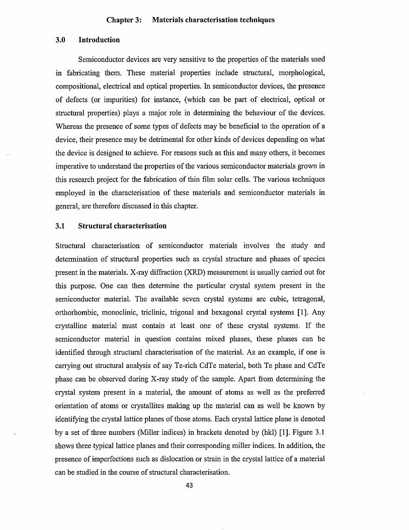
Chapter 3: Materials characterisation techniques
3.0 Introduction
Semiconductor devices are very sensitive to the properties of the materials used
in fabricating them. These material properties include structural, morphological,
compositional, electrical and optical properties. In semiconductor devices, the presence
of defects (or impurities) for instance, (which can be part o f electrical, optical or
structural properties) plays a major role in determining the behaviour of the devices.
Whereas the presence of some types o f defects may be beneficial to the operation of a
device, their presence may be detrimental for other kinds o f devices depending on what
the device is designed to achieve. For reasons such as this and many others, it becomes
imperative to understand the properties of the various semiconductor materials grown in
this research project for the fabrication of thin film solar cells. The various techniques
employed in the characterisation of these materials and semiconductor materials in
general, are therefore discussed in this chapter.
3.1 Structural characterisation
Structural characterisation of semiconductor materials involves the study and
determination of structural properties such as crystal structure and phases o f species
present in the materials. X-ray diffraction (XRD) measurement is usually carried out for
this purpose. One can then determine the particular crystal system present in the
semiconductor material. The available seven crystal systems are cubic, tetragonal,
orthorhombic, monoclinic, triclinic, trigonal and hexagonal crystal systems [1]. Any
crystalline material must contain at least one of these crystal systems. If the
semiconductor material in question contains mixed phases, these phases can be
identified through structural characterisation of the material. As an example, if one is
carrying out structural analysis of say Te-rich CdTe material, both Te phase and CdTe
phase can be observed during X-ray study of the sample. Apart from determining the
crystal system present in a material, the amount of atoms as well as the preferred
orientation of atoms or crystallites making up the material can as well be known by
identifying the crystal lattice planes of those atoms. Each crystal lattice plane is denoted
by a set of three numbers (Miller indices) in brackets denoted by (hkl) [1]. Figure 3.1
shows three typical lattice planes and their corresponding miller indices. In addition, the
presence of imperfections such as dislocation or strain in the crystal lattice of a material
can be studied in the course of structural characterisation.
43
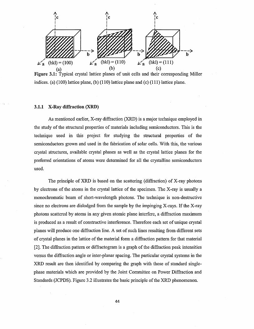
4 8
(hkl) = (100) (hkl) = (110) (hkl) = (111)(a) O’) (c)
Figure 3.1: Typical crystal lattice planes o f unit cells and their corresponding Miller
indices, (a) (100) lattice plane, (b) (110) lattice plane and (c) (111) lattice plane.
3.1.1 X-Ray diffraction (XRD)
As mentioned earlier, X-ray diffraction (XRD) is a major technique employed in
the study o f the structural properties o f materials including semiconductors. This is the
technique used in this project for studying the structural properties of the
semiconductors grown and used in the fabrication o f solar cells. With this, the various
crystal structures, available crystal phases as well as the crystal lattice planes for the
preferred orientations of atoms were determined for all the crystalline semiconductors
used.
The principle o f XRD is based on the scattering (diffraction) of X-ray photons
by electrons o f the atoms in the crystal lattice of the specimen. The X-ray is usually a
monochromatic beam of short-wavelength photons. The technique is non-destructive
since no electrons are dislodged from the sample by the impinging X-rays. If the X-ray
photons scattered by atoms in any given atomic plane interfere, a diffraction maximum
is produced as a result o f constructive interference. Therefore each set o f unique crystal
planes will produce one diffraction line. A set of such lines resulting from different sets
of crystal planes in the lattice of the material form a diffraction pattern for that material
[2]. The diffraction pattern or diffractogram is a graph of the diffraction peak intensities
versus the diffraction angle or inter-planar spacing. The particular crystal systems in the
XRD result are then identified by comparing the graph with those of standard single
phase materials which are provided by the Joint Committee on Power Diffraction and
Standards (JCPDS). Figure 3.2 illustrates the basic principle of the XRD phenomenon.
4 4
x = d sin 6Incident Scattered
X-ray X-ray_
/ 810 \
Figure 3.2: The basic principle o f X-ray diffraction from atoms in different lattice
planes of a crystal.
As the beam of monochromatic X-ray photons of wavelength, X falls on the set
of lattice planes A and B, they are scattered (diffracted) as shown. The condition for
constructive interference of these scattered rays in order to produce the needed
diffraction pattern is governed by Bragg’s law [1]. The Bragg's law states that, for
constructive interference to occur, the path difference between the two interfering waves
(which is equal to 2dsin0 from figure 3.2) must be equal to a whole number, n o f the
wavelength, thus giving rise to Equation (3.1).
nX = 2 d s \n 6 (3.1)
where 6 is the angle between the X-ray beam and the atomic plane .
Since the X-ray wavelength, X is constant, determination o f the diffraction angle (26)
will help to determine the d-spacing (inter-planar spacing) o f the lattice planes using
Equation (3.1), where n is unity for successive lattice planes.
From the resulting peaks of the X-ray diffractogram, some other crystalline
properties of the material can be determined. These include finding the Miller indices o f
the various crystal planes (orientations) in the sample, obtaining the lattice constants of
the crystal structures present in the material and estimating the sizes of the crystallites in
the material. Equations (3.2) - (3.4) [1, 3] with Equation (3.1) are the relevant equations
employed in the analysis of XRD results of crystalline materials such as
semiconductors.
a = d j h 2 + k 2 + I2
kXD =
P cos9
(3.2)
(3.3)
4 5
/? = 4 £ ta n 0 (3 .4 )
where a is the lattice constant, D is crystallite size, k is Scherer constant, /? is full width
at half maximum (FWHM) of the particular XRD peak (usually the most intense peak)
under consideration and s is strain in the crystal lattice. The FWHM is the width of the
XRD peak (in radians) at half the peak intensity as shown in figure 3.3.
p
20 (°)
Figure 3.3: XRD peak showing FWHM.
The XRD equipment used in the project reported in this thesis was the Philips X'Pert
Pro diffractometer (Philips Analytical, Almelo, the Netherlands) with Cu-Ka and
excitation wavelength o f 1.5406 A at source tension and current o f 40 kV and 40 mA
respectively. However, another technique that is used for studying the structure of
materials (crystalline and non-crystalline) is the transmission electron microscopy. In
this case, the transmission electron microscope (TEM) is used in the diffraction mode
instead of the image mode. In the image mode, it is used to obtain morphological
information about the sample. A major requirement in the use of the TEM for obtaining
diffraction patterns of atomic arrangement in a material is that the sample has to be very
thin (typically of the order of 100 nm). This restriction in sample thickness is not
encountered when using X-ray diffractometer. An example of electron diffraction
patterns of a material obtained with TEM is shown in figure 3.4.
4 6
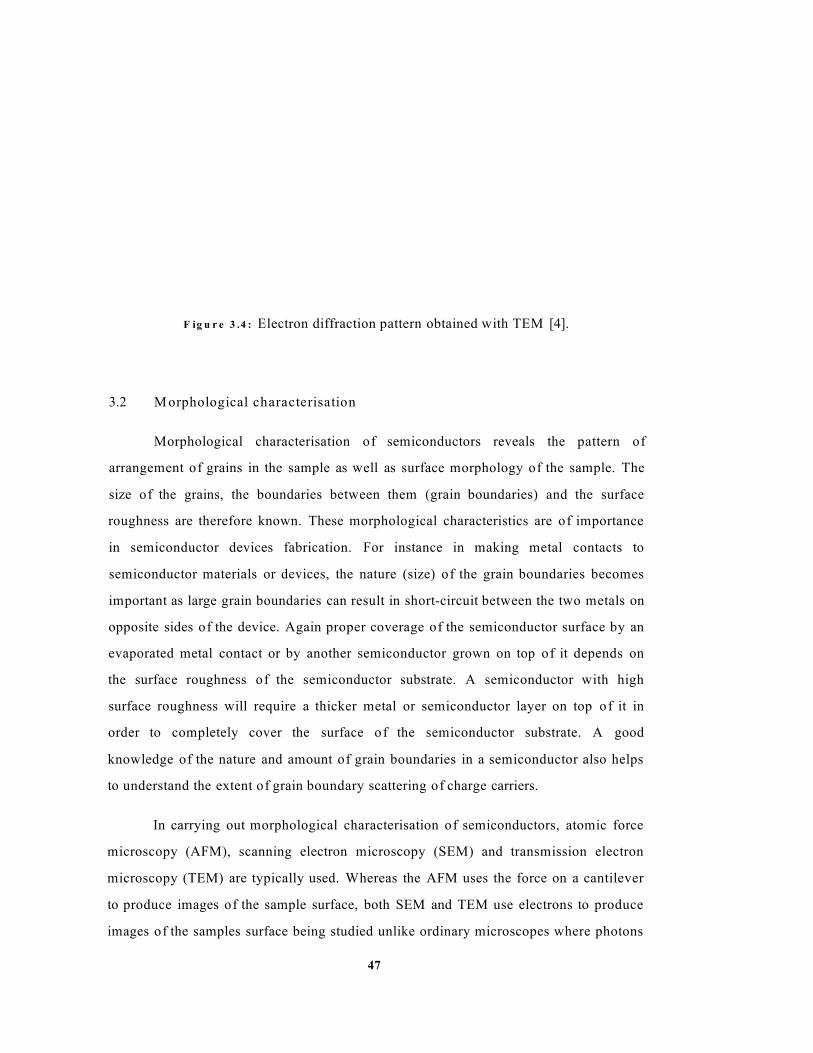
F ig u r e 3 .4 : Electron diffraction pattern obtained with TEM [4].
3.2 M orphological characterisation
Morphological characterisation of semiconductors reveals the pattern of
arrangement of grains in the sample as well as surface morphology of the sample. The
size of the grains, the boundaries between them (grain boundaries) and the surface
roughness are therefore known. These morphological characteristics are of importance
in semiconductor devices fabrication. For instance in making metal contacts to
semiconductor materials or devices, the nature (size) of the grain boundaries becomes
important as large grain boundaries can result in short-circuit between the two metals on
opposite sides of the device. Again proper coverage of the semiconductor surface by an
evaporated metal contact or by another semiconductor grown on top of it depends on
the surface roughness of the semiconductor substrate. A semiconductor with high
surface roughness will require a thicker metal or semiconductor layer on top of it in
order to completely cover the surface of the semiconductor substrate. A good
knowledge of the nature and amount of grain boundaries in a semiconductor also helps
to understand the extent of grain boundary scattering of charge carriers.
In carrying out morphological characterisation of semiconductors, atomic force
microscopy (AFM), scanning electron microscopy (SEM) and transmission electron
microscopy (TEM) are typically used. Whereas the AFM uses the force on a cantilever
to produce images of the sample surface, both SEM and TEM use electrons to produce
images of the samples surface being studied unlike ordinary microscopes where photons
47

(light) are rather used to form the images of the sample surface. All three microscopes
however, have differences in their principles o f operation as well as in versatility. For
example, whereas the SEM is limited in resolution and versatility, the TEM is more
versatile in both resolution and application [5]. These similarities and differences are
highlighted in the next sub-sections.
3.2.1 Scanning electron microscopy (SEM)
Figure 3.5 illustrates the principle of operation o f the SEM. The electron gun
produces a beam of electrons (at voltages o f 2 - 25 kV) which is focused on to the
sample by means o f magnetic lenses.
momtor
i l l
Electron gun
^ Electron beam< Anode
< Magnetic lens
Scan coils
Secondary electron detector
Back-scattered electron detector
Sample
Sample stageFigure 3.5: Schematic o f the components and operating principle of scanning electron
microscope.
The scanning coils help to deflect the electron beam in such a way that a raster scanning
of the specimen is done across a rectangular area to produce an image o f the sample
surface on a screen. As the focused electron beam impinges on the specimen, a number
of interactions take place between the incident electron beam and the specimen. These
interactions result in the back scattering o f some o f the incident electrons as well as in
the production of secondary electrons or even photons. These emitted electrons and
photons are collected by various detectors and used to produce useful information about
the material of the specimen. Among the information produced in this scanning process
is an image of the sample surface. The level o f interaction between the incident
electrons and the sample material depends on the energy of the incident electrons [6].
4 8
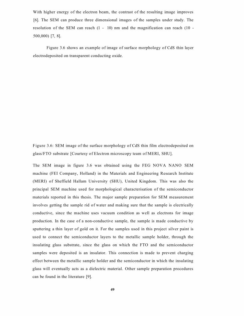
With higher energy of the electron beam, the contrast of the resulting image improves
[6]. The SEM can produce three dimensional images of the samples under study. The
resolution of the SEM can reach (1 - 10) nm and the magnification can reach (10 -
500,000) [7, 8].
Figure 3.6 shows an example of image of surface morphology of CdS thin layer
electrodeposited on transparent conducting oxide.
Figure 3.6: SEM image of the surface morphology of CdS thin film electrodeposited on
glass/FTO substrate [Courtesy of Electron microscopy team of MERI, SHU].
The SEM image in figure 3.6 was obtained using the FEG NOVA NANO SEM
machine (FEI Company, Holland) in the Materials and Engineering Research Institute
(MERI) of Sheffield Hallam University (SHU), United Kingdom. This was also the
principal SEM machine used for morphological characterisation of the semiconductor
materials reported in this thesis. The major sample preparation for SEM measurement
involves getting the sample rid of water and making sure that the sample is electrically
conductive, since the machine uses vacuum condition as well as electrons for image
production. In the case of a non-conductive sample, the sample is made conductive by
sputtering a thin layer of gold on it. For the samples used in this project silver paint is
used to connect the semiconductor layers to the metallic sample holder, through the
insulating glass substrate, since the glass on which the FTO and the semiconductor
samples were deposited is an insulator. This connection is made to prevent charging
effect between the metallic sample holder and the semiconductor in which the insulating
glass will eventually acts as a dielectric material. Other sample preparation procedures
can be found in the literature [9].
49
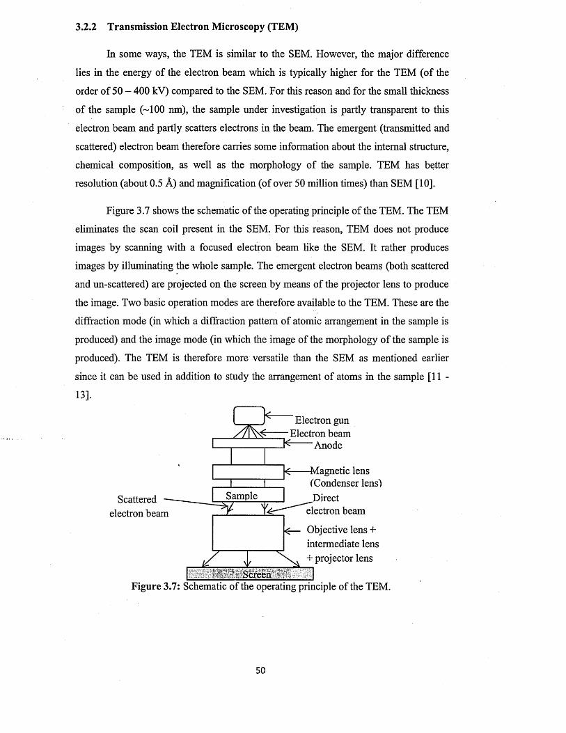
3.2.2 Transmission Electron Microscopy (TEM)
In some ways, the TEM is similar to the SEM. However, the major difference
lies in the energy of the electron beam which is typically higher for the TEM (of the
order o f 50 - 400 kV) compared to the SEM. For this reason and for the small thickness
of the sample (-100 nm), the sample under investigation is partly transparent to this
electron beam and partly scatters electrons in the beam. The emergent (transmitted and
scattered) electron beam therefore carries some information about the internal structure,
chemical composition, as well as the morphology of the sample. TEM has better
resolution (about 0.5 A) and magnification (of over 50 million times) than SEM [10].
Figure 3.7 shows the schematic o f the operating principle o f the TEM. The TEM
eliminates the scan coil present in the SEM. For this reason, TEM does not produce
images by scanning with a focused electron beam like the SEM. It rather produces
images by illuminating the whole sample. The emergent electron beams (both scattered
and un-scattered) are projected on the screen by means of the projector lens to produce
the image. Two basic operation modes are therefore available to the TEM. These are the
diffraction mode (in which a diffraction pattern o f atomic arrangement in the sample is
produced) and the image mode (in which the image o f the morphology o f the sample is
produced). The TEM is therefore more versatile than the SEM as mentioned earlier
since it can be used in addition to study the arrangement of atoms in the sample [11 -
13].r
£ — — Electron beamElectron gunElectron gun
Anode
< Magnetic lens
Scattered electron beam
Sample(Condenser lens)
^.Direct electron beam
<— Objective lens + intermediate lens
\ + projector lens
Figure 3.7: Schematic of the operating principle of the TEM.
50
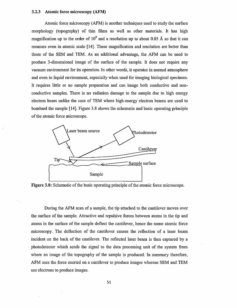
3.2.3 Atomic force microscopy (AFM)
Atomic force microscopy (AFM) is another techniques used to study the surface
morphology (topography) o f thin films as well as other materials. It has high
magnification up to the order o f 108 and a resolution up to about 0.05 A so that it can
measure even in atomic scale [14]. These magnification and resolution are better than
those of the SEM and TEM. As an additional advantage, the AFM can be used to
produce 3-dimensional image o f the surface o f the sample. It does not require any
vacuum environment for its operation. In other words, it operates in normal atmosphere
and even in liquid environment, especially when used for imaging biological specimen.
It requires little or no sample preparation and can image both conductive and non-
conductive samples. There is no radiation damage to the sample due to high energy
electron beam unlike the case of TEM where high-energy electron beams are used to
bombard the sample [14]. Figure 3.8 shows the schematic and basic operating principle
o f the atomic force microscope.
,aser beam source 'hotodetector
Cantilever
Sample surface
Sample
Figure 3.8: Schematic of the basic operating principle o f the atomic force microscope.
During the AFM scan of a sample, the tip attached to the cantilever moves over
the surface of the sample. Attractive and repulsive forces between atoms in the tip and
atoms in the surface o f the sample deflect the cantilever, hence the name atomic force
microscopy. The deflection o f the cantilever causes the reflection of a laser beam
incident on the back of the cantilever. The reflected laser beam is then captured by a
photodetector which sends the signal to the data processing unit o f the system from
where an image of the topography of the sample is produced. In summary therefore,
AFM uses the force exerted on a cantilever to produce images whereas SEM and TEM
use electrons to produce images.
5 1
The AFM has three different modes of operation. These modes are; contact
mode, non-contact mode and tapping mode [14]. In the contact mode, the cantilever tip
(probe) makes direct and steady contact with the surface of the sample being scanned.
As the scanning proceeds, the cantilever deflection is maintained at constant level by a
feedback loop resulting in the scanner moving vertically in order to maintain a constant
force on the sample surface. The vertical movement o f the scanner is then converted to a
signal from which the image of the topography of the sample is produced [14]. The
contact mode is most appropriately used for hard surface.
In the non-contact mode, the cantilever is vibrated vertically at a frequency
slightly higher than its resonant frequency. The amplitude of the vibration however, is
within few nanometres. The amplitude of vibration or the phase shift between the
resonance frequency o f the cantilever and its actual frequency of vibration is maintained
at a constant value by the feedback mechanism while scanning the sample surface. The
force that maintains this constancy is used to produce the topographic image of the
sample surface [14].
In the tapping mode, the cantilever is oscillated at its resonance frequency and
at the same time the tip gently taps the surface of the sample during the scanning
process. As the cantilever tip moves up and down over the sample surface, the
electrostatic force between the tip and the sample surface fluctuates to and fro, resulting
to fluctuation in the amplitude of the oscillation of the cantilever. The feedback loop
tends to keep this fluctuation in amplitude constant by moving the scanner up and down,
and this is used to produce the image o f the sample topography [14]. The vibration
modes (non-contact mode and tapping mode) normally produce the highest AFM image
resolutions [14]. With the AFM image, the grain sizes as well as the surface roughness
of a sample can be determined. Other images that can be obtained with the AFM include
phase images, electrical potential images, electrical conductivity mapping, ferroelectric
and piezoelectric responses [14].
3.3 Compositional characterisation
Some properties of many compound semiconductors depend largely on the
elemental (or atomic) composition of those semiconductors. As an example, the
electrical conductivity type of CdTe is seriously affected by the amounts Cd and Te
atoms in the material. A CdTe sample with higher Te content than Cd (Te-rich CdTe)
naturally exhibits p-type electrical conductivity whereas a CdTe material with higher Cd
52
content than Te (Cd-rich CdTe) exhibits n-type electrical conductivity. A stoichiometric
CdTe with equal amounts of Cd and Te shows intrinsic (i-type) conductivity. On the
other hand a semiconductor like CdS has no such composition-dependence o f electrical
conductivity type. As a result, CdS always naturally has n-type conductivity no matter
the amounts of Cd and S in it. For reasons such as this, it becomes important to know
the exact or at least, the approximate atomic composition of these semiconductor
materials in order to use them properly for specific applications. In carrying out
compositional analysis of semiconductors, a number of techniques are used. These
mainly include X-ray fluorescence (XRF) [15, 16], energy dispersive X-rays (EDX)
[17], X-ray photoelectron spectroscopy (XPS) [18], secondary ion mass spectroscopy
(SIMS) [19], Rutherford back scattering spectroscopy (RBS) [16, 17] and Auger
electron spectroscopy (AES) [17, 18]. In this research project however, only EDX was
used for compositional characterisation of the electrodeposited semiconductors due to
unavailability and lack o f easy access to other techniques.
3.3.1 X-ray fluorescence (XRF)
When a high-energy X-ray is incident on the atom of an element, an electron can
be ejected from an inner shell o f this atom thus rendering the atom unstable. In order to
return to stability, an electron from an outer energy shell can fall into this lower energy
level electron vacancy to occupy it, thereby losing the excess energy in form o f X-ray
photon. This manner o f production of radiation (light) is called X-ray fluorescence. The
XRF technique is based on this principle. The wavelength of this emitted radiation is
characteristic of the atoms of the particular element involved and is related to the atomic
number, Z o f the element according to Equation (3.5) [2].
i = K ( Z - f f ) 2 (3.5)
where K is a constant depending on the spectral series and a is a shielding constant
whose value is < 1.
The emitted wavelengths therefore indicate the elements present. The XRF system uses
computer programs to plot the wavelength dispersion of these emitted radiations and
therefore identify the various elements in the sample being studied. The intensity of the
spectral lines actually shows the amount (concentration) o f atoms of each element
present. In this way, a quantitative mapping of the atomic composition of the elements
making up a test sample is obtained. Figure 3.9 illustrates the basic principles o f X-ray53
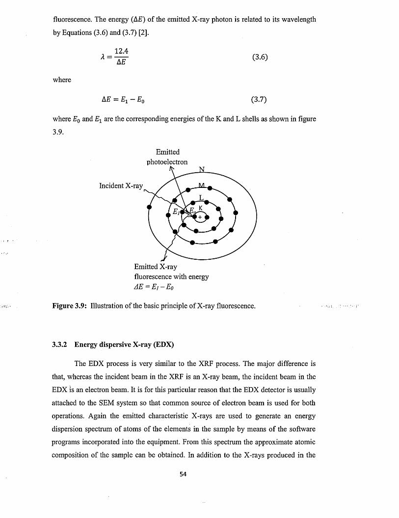
fluorescence. The energy (AE) of the emitted X-ray photon is related to its wavelength
by Equations (3.6) and (3.7) [2].
12.4/ = -AT ( 3 ' 6 )
where
AE = E1 - E0 (3.7)
where E0 and E± are the corresponding energies o f the K and L shells as shown in figure
3.9.
Emittedphotoelectron
Incident X-ray
Emitted X-rayfluorescence with energy AE — Ej — E q
Figure 3.9: Illustration of the basic principle of X-ray fluorescence.
3.3.2 Energy dispersive X -ray (EDX)
The EDX process is very similar to the XRF process. The major difference is
that, whereas the incident beam in the XRF is an X-ray beam, the incident beam in the
EDX is an electron beam. It is for this particular reason that the EDX detector is usually
attached to the SEM system so that common source o f electron beam is used for both
operations. Again the emitted characteristic X-rays are used to generate an energy
dispersion spectrum of atoms of the elements in the sample by means of the software
programs incorporated into the equipment. From this spectrum the approximate atomic
composition of the sample can be obtained. In addition to the X-rays produced in the
54
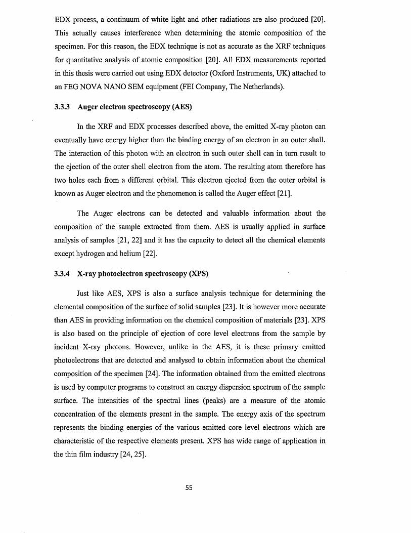
EDX process, a continuum of white light and other radiations are also produced [20].
This actually causes interference when determining the atomic composition of the
specimen. For this reason, the EDX technique is not as accurate as the XRF techniques
for quantitative analysis of atomic composition [20]. All EDX measurements reported
in this thesis were carried out using EDX detector (Oxford Instruments, UK) attached to
an FEG NOVA NANO SEM equipment (FEI Company, The Netherlands).
3.3.3 Auger electron spectroscopy (AES)
In the XRF and EDX processes described above, the emitted X-ray photon can
eventually have energy higher than the binding energy of an electron in an outer shall.
The interaction of this photon with an electron in such outer shell can in turn result to
the ejection of the outer shell electron from the atom. The resulting atom therefore has
two holes each from a different orbital. This electron ejected from the outer orbital is
known as Auger electron and the phenomenon is called the Auger effect [21].
The Auger electrons can be detected and valuable information about the
composition of the sample extracted from them. AES is usually applied in surface
analysis o f samples [21, 22] and it has the capacity to detect all the chemical elements
except hydrogen and helium [22].
3.3.4 X-ray photoelectron spectroscopy (XPS)
Just like AES, XPS is also a surface analysis technique for determining the
elemental composition o f the surface of solid samples [23]. It is however more accurate
than AES in providing information on the chemical composition o f materials [23]. XPS
is also based on the principle of ejection of core level electrons from the sample by
incident X-ray photons. However, unlike in the AES, it is these primary emitted
photoelectrons that are detected and analysed to obtain information about the chemical
composition of the specimen [24]. The information obtained from the emitted electrons
is used by computer programs to construct an energy dispersion spectrum o f the sample
surface. The intensities of the spectral lines (peaks) are a measure o f the atomic
concentration of the elements present in the sample. The energy axis of the spectrum
represents the binding energies o f the various emitted core level electrons which are
characteristic of the respective elements present. XPS has wide range of application in
the thin film industry [24, 25].
55
3.3.5 R utherford back scattering spectroscopy (RBS)
Rutherford back scattering involves the bombardment of a sample with a beam
of energetic ions (usually He2+ or H*), some of which get scattered back by atoms in the
sample [26]. Energies o f the backscattered ions are used to obtain information about the
chemical composition of the sample. Just as in the XPS and AES, an energy dispersion
of the backscattered ions can be constructed from which specific chemical elements
making up the sample can be identified using the positions of the peaks on the energy
axis. The peak intensities again give the relative concentration o f the atoms of each
element. The RBS can reach depth resolution o f about one monolayer [26]. Figure 3.10
illustrates the basic principle of Rutherford back scattering.
Incident high energy ion beam
Detector
Back-scattered ion beam
Sample
Figure 3.10: Illustration of the basic principle of the RBS technique.
3.3.6 Secondary ions mass spectroscopy (SIMS)
In SIMS technique, a focused ion beam is used to sputter the surface of the
sample. In the process, secondary ions are ejected. These secondary ions are then
collected and analysed using a mass spectrometer in order to obtain useful information
about the elemental composition of the sample [27, 28]. As the sputtering o f the sample
proceeds, a depth profile is obtained. Information can then be obtained about the
elemental composition of the sample as a function of the sputtered depth. This is
particularly useful in the study of intermixing/inter-diffusion of atoms in multilayer thin
film structures [29].
It is important at this point to mention that, the probing depth of each of the
above discussed techniques in sections 3.3.1 to 3.3.6 depends on factors such as the
energy of the probing electrons or ions, and the nature of the material under study.
56
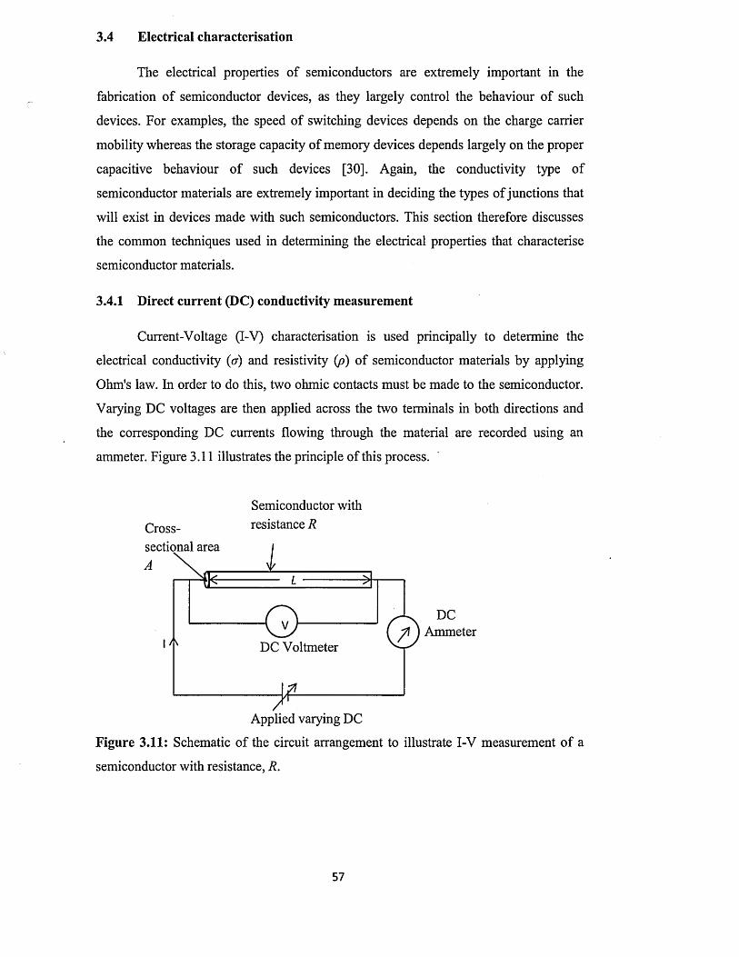
3.4 Electrical characterisation
The electrical properties of semiconductors are extremely important in the
fabrication o f semiconductor devices, as they largely control the behaviour of such
devices. For examples, the speed o f switching devices depends on the charge carrier
mobility whereas the storage capacity of memory devices depends largely on the proper
capacitive behaviour of such devices [30]. Again, the conductivity type o f
semiconductor materials are extremely important in deciding the types o f junctions that
will exist in devices made with such semiconductors. This section therefore discusses
the common techniques used in determining the electrical properties that characterise
semiconductor materials.
3.4.1 Direct cu rren t (DC) conductivity measurem ent
Current-Voltage (I-V) characterisation is used principally to determine the
electrical conductivity (<r) and resistivity (p) o f semiconductor materials by applying
Ohm's law. In order to do this, two ohmic contacts must be made to the semiconductor.
Varying DC voltages are then applied across the two terminals in both directions and
the corresponding DC currents flowing through the material are recorded using an
ammeter. Figure 3.11 illustrates the principle of this process.
Semiconductor with Cross- resistance Rsectional area
DCAmmeter
DC Voltmeter
Applied varying DC
Figure 3.11: Schematic of the circuit arrangement to illustrate I-V measurement o f a
semiconductor with resistance, R.
57
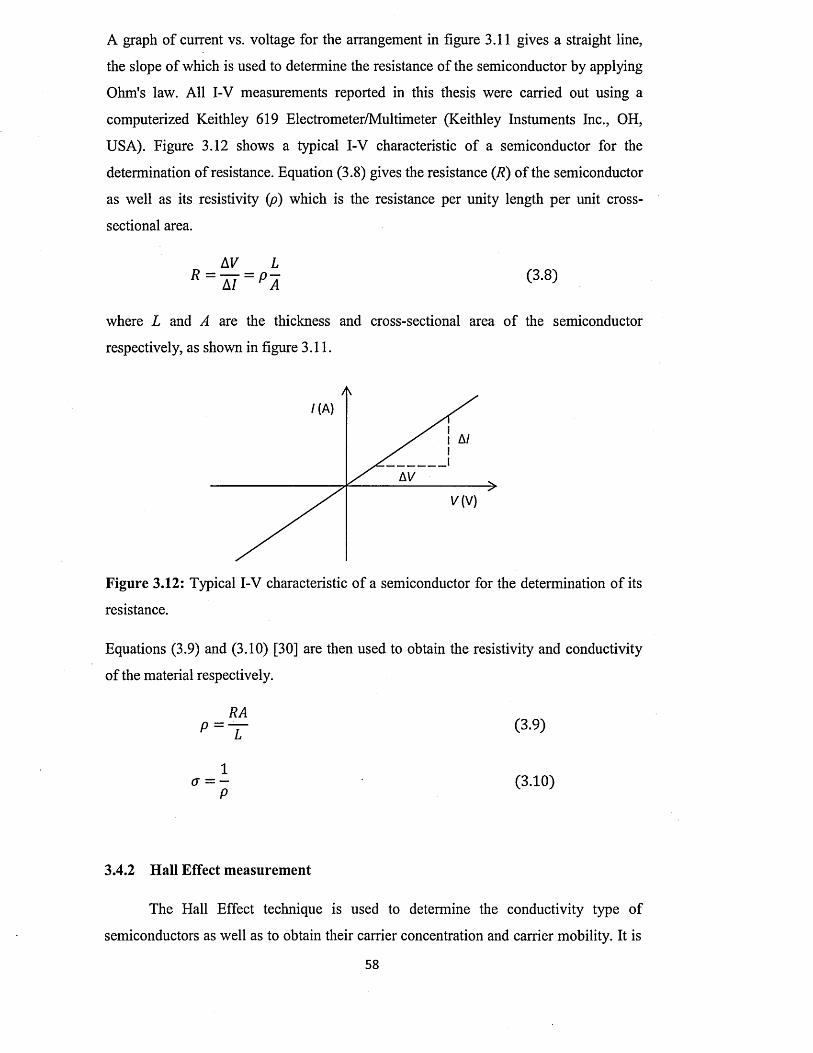
A graph of current vs. voltage for the arrangement in figure 3.11 gives a straight line,
the slope o f which is used to determine the resistance of the semiconductor by applying
Ohm's law. All I-V measurements reported in this thesis were carried out using a
computerized Keithley 619 Electrometer/Multimeter (Keithley Instuments Inc., OH,
USA). Figure 3.12 shows a typical I-V characteristic o f a semiconductor for the
determination of resistance. Equation (3.8) gives the resistance (.R) o f the semiconductor
as well as its resistivity (p) which is the resistance per unity length per unit cross-
sectional area.
where L and A are the thickness and cross-sectional area o f the semiconductor
respectively, as shown in figure 3.11.
Figure 3.12: Typical I-V characteristic o f a semiconductor for the determination o f its
resistance.
Equations (3.9) and (3.10) [30] are then used to obtain the resistivity and conductivity
of the material respectively.
AV L(3 .8 )
(3 .9 )
1G
P(3 .1 0 )
3.4.2 Hall Effect measurem ent
The Hall Effect technique is used to determine the conductivity type of
semiconductors as well as to obtain their carrier concentration and carrier mobility. It is
58

principally based on the Lorentzian force on a charge carrier flowing in a semiconductor
confined in a magnetic field [30].
Consider a piece o f semiconductor with a current (I) flowing along it in the x-direction
(from left to right). If an external magnetic field vector B is applied perpendicular to the
direction o f current flow in the z-direction (upward) as shown in figure 3.13, then a Hall
voltage will develop along the y-axis. Now if an n-type semiconductor is used, the
electrons are pushed towards the end o f the semiconductor (towards the reader) setting
up an electric field Ey also towards the reader. A Hall voltage Vh therefor develops in
the direction perpendicular to / and B. If a p-type semiconductor is used, the holes are
still pushed towards the end of the semiconductor (towards the reader) but an electric
field Ey is set up into the paper which in turn sets up Hall voltage with an opposite sign
to that due to the n-type semiconductor. From the Hall voltage data obtained and the
known values o f the magnetic field intensity and the applied current, the Hall mobility,
carrier concentration and conductivity type of the particular semiconductor involved can
be obtained using Equations (3.11) - (3.17) [30].
J - ± [■* - ± - ± --t A - ± _-fc _-h _-h
Figure 3.13: Illustration of Hall Effect in a semiconductor carrying a current I in a
magnetic field B perpendicular to the direction o f current flow. A Hall voltage Vh is
developed perpendicular to / and B.
n = rHRhV
(3 .1 1 )
P = JjL. (3 .1 2 )
where Rh is the Hall coefficient (which is positive for p-type material and negative for
n-type material) and q is electronic charge. The constant rH is the Hall factor given by
Equation (3.13).
59
<T2)
Th ~ w(3.13)
where r is the mean free time between collisions.
The Hall coefficient can be obtained from the measured Hall voltage, applied current,
applied magnetic field and thickness of the semiconductor used according to Equation
(3.14).
( 3 ' 1 4 )
where ]x is the magnitude o f x-component of the applied current density, Bz is the z-
component of the applied magnetic field and t is the thickness of the sample.
The conductivity (a) is obtained from the applied current density and electric field by
Equation (3.15).
<x = ^ (3.15)
Then the Hall mobility QuH) is obtained from Equation (3.16).
n„ = \Rh \c (3.16)
The drift mobility (fi) is related to the Hall mobility by Equation (3.17).
R h = r H n (3.17)
By combining Equations (3.10) and (3.16), the resistivity can be obtained. An
alternative method for measuring the resistivity is the four- point probe or Van der pauw
technique as described elsewhere [31, 32].
3.4.3 Photoelectrochemical (PEC) cell measurem ent
The Hall Effect technique discussed above for determining the conductivity type
o f semiconductors requires that the semiconductor specimen be alone or, if a
mechanical support is needed, the semiconductor be deposited on a non-conducting
substrate. In the fabrication of thin film solar cells using electrodeposition technique,
the semiconductor layers are usually grown on a transparent conducting oxide (TCO)
substrate which serves both as a front ohmic contact and a window for light to pass into
the cell. In most cases, it is extremely difficult to detach the semiconductor layer from
60
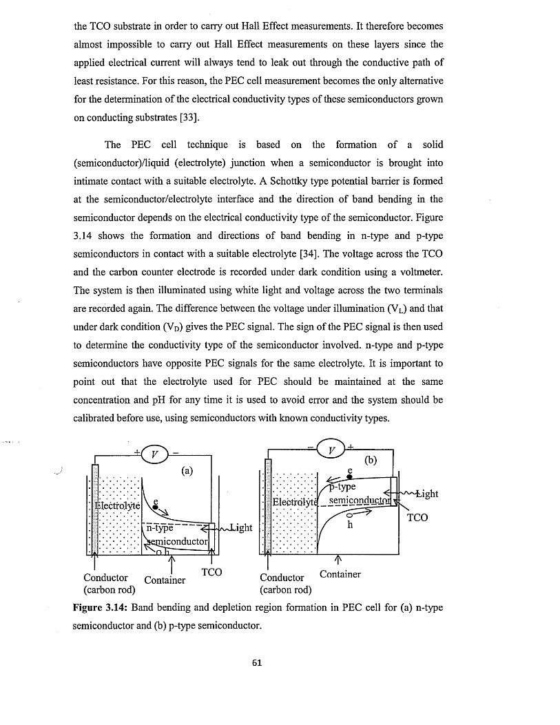
the TCO substrate in order to carry out Hall Effect measurements. It therefore becomes
almost impossible to carry out Hall Effect measurements on these layers since the
applied electrical current will always tend to leak out through the conductive path of
least resistance. For this reason, the PEC cell measurement becomes the only alternative
for the determination o f the electrical conductivity types of these semiconductors grown
on conducting substrates [33].
The PEC cell technique is based on the formation o f a solid
(semiconductor)/liquid (electrolyte) junction when a semiconductor is brought into
intimate contact with a suitable electrolyte. A Schottky type potential barrier is formed
at the semiconductor/electrolyte interface and the direction of band bending in the
semiconductor depends on the electrical conductivity type of the semiconductor. Figure
3.14 shows the formation and directions of band bending in n-type and p-type
semiconductors in contact with a suitable electrolyte [34]. The voltage across the TCO
and the carbon counter electrode is recorded under dark condition using a voltmeter.
The system is then illuminated using white light and voltage across the two terminals
are recorded again. The difference between the voltage under illumination (Vl) and that
under dark condition (Vd) gives the PEC signal. The sign of the PEC signal is then used
to determine the conductivity type of the semiconductor involved, n-type and p-type
semiconductors have opposite PEC signals for the same electrolyte. It is important to
point out that the electrolyte used for PEC should be maintained at the same
concentration and pH for any time it is used to avoid error and the system should be
calibrated before use, using semiconductors with known conductivity types.
-ight
n-Type ^ Semiconductor
TCOight
TCO Conductor Container (carbon rod)
Conductor Container (carbon rod)
Figure 3.14: Band bending and depletion region formation in PEC cell for (a) n-type
semiconductor and (b) p-type semiconductor.
61

If an n-type semiconductor has a negative PEC signal for any given electrolyte, then a
p-type semiconductor will have a positive PEC signal for the same electrolyte. This is
because these two semiconductors have band bending in opposite directions when in
contact with the electrolyte as illustrated in figure (3.14). The magnitude o f the PEC
signal gives an indication of the suitability of the doping concentration o f the
semiconductor. Large PEC signals indicate doping concentration that is moderate [33].
A highly doped semiconductor will have low PEC signal. If a metal or an insulator is
used in place of the semiconductor, zero PEC will be registered in both cases as there is
no band bending associated with these types o f materials. The PEC measurements
reported in this thesis were carried out using aqueous solution of 0.1M Na2 S2C>3 as an
electrolyte and a digital voltmeter.
3.5 Optical characterisation
A good knowledge of the optical properties of the semiconductors used in solar
cell fabrication is o f paramount importance as a solar cell is essentially an
optoelectronic device. Two major semiconductor layers employed in the fabrication of
thin film solar cells are the window layer and the absorber layer. These are so-called
because of the part they play in the solar cell when light is incident on it. The window
layer basically acts as a “window” through which light (photons) enters the active
junction or junctions of the solar cell. Its optical properties should therefore reflect this
function namely; it should have high transparency (transmittance), low absorbance and
low reflectance. On the other hand, very high absorbance and nil transmittance are
desirable in the absorber layer whose function is mainly to absorb the incident light and
create electron-hole pairs. In fact the amount of photocurrent produced by a solar cell is
a strong function of these parameters. It therefore becomes imperative that these
semiconductors are properly characterised for their optical properties [35].
3.5.1 Spectrophotometry
When light is incident on a semiconductor, part of the light is absorbed by the
semiconductor, while the remaining portion is either reflected (scattered) at the
semiconductor surface or transmitted through the semiconductor and emerges on the
opposite side. In any case, the processes involved (absorption, reflection and
62
transmission) depend on the optical properties of the semiconductor material under
study.
In determining the absorbance o f a semiconductor material using a
spectrophotometer, a light of known intensity (Jo) is directed onto the semiconductor
and a detector behind it records the intensity (7) o f the transmitted light. From these two
intensities, the fraction of the incident light absorbed by the material as well as the
amount reflected back at the surface are determined using appropriate equations [1, 36 -
38]. The transmitted intensity is related to the incident intensity according to Equation
(3.18).
7(d) = 70 exp (—ad) (3.18)
where d is distance into the semiconductor layer to which the light travels. This
represents the thickness of the semiconductor. The constant, a is the absorption
coefficient o f the material and determines the rate at which the semiconductor absorbs
light as it travels through it.
The ratio o f the transmitted intensity to the incident intensity defines the transmittance
(7) of the material according to Equation (3.19).
/- = T (3.19)1o
The transmittance is then related to the absorbance by Equation (3.20).
A = logio ( y ) = logio (^) (3.20)
The reflectance R of the material is obtained from Equation (3.21).
(n — l ) 2R = 7-------- t t t (3.21)(n + 1)2 v J
where n is the real part of the complex refractive index (TV) of semiconductor material. N
is also given by Equation (3.22)
N = n + i K (3.22)
where K is the imaginary part o f the refractive index known as the extinction
coefficient. K actually determines the absorption coefficient according to Equation
(3.23)63
4 nKa = —— (3.23)
where X is the wavelength of the incident light.
The complex dielectric constant (<r) of the semiconductor is related to the extinction
coefficient by Equation (3.24).
e = (n + iK)2 = er + €i (3.24)
where er and e* are the real and imaginary parts of the dielectric constant.
The absorption coefficient is also related to the transmittance o f the material and
thickness according to Equation (3.25).
InTa = — — (3.25)
a is also related to the energy (hv) o f the incident light (photons) as well as to the
energy bandgap of the semiconductor according to Tauc's equations given by Equations
(3.26) and (3.27) for direct and indirect bandgap semiconductors respectively.
C (h v - Eg ) l hcc — -------- ;---------- (3.26)
hv
C ( k v - E g ) 2a = ------- (3.27)
hv
where C is a constant, Eg is the energy bandgap of the semiconductor, h is Planck's
constant and v is the frequency of the incident light.
In general, T, R and A are related by Equation (3.28).
T + R + A = 1 (3.28)
The graph of (ahv)2 vs. hv for equation (3.26) or the graph of (ahv)m vs. hv for equation
(3.27) is used to obtain Eg by extrapolating the straight-line portion o f the graph to the
hv axis. This optical characterisation technique was used in this research project for all
the semiconductor layers grown and reported in this thesis. The equipment used for this
was a Cary 50 Scan UV-Vis Spectrophotometer (Varian Australia, Pty. Ltd).
64
3.5.2 Raman spectroscopy
Raman spectroscopy is another optical analytical technique used in
characterising semiconductors and materials in general [41, 39,40]. It is used to identify
the various vibrational modes of the molecules in a material by directing a strong beam
of light (usually a laser) onto the sample.
In raman spectroscopy, the incident radiation creates a distortion in the electrons
around the bonds in the molecules making up the sample. This creates a temporary
polarisation o f the molecules therefore inducing an instantaneous dipole moment in the
molecules. As the bonds relax back to their normal states, the incident radiation is re
emitted by scattering, at different wavelengths from that of the incident radiation. This
is known as raman shift and it depends on the structure (or chemical bonding) of the
molecules producing it. This scattered radiation is therefore polarised with the degree of
polarisation depending on the type o f vibration of the molecule producing it. From the
raman scattering therefore, information is obtained about the type o f molecules (or
bonds) present in the sample. The resulting raman spectrum is therefore used as a
fingerprint for identifying materials [39]. The raman peak intensity mainly depends on
the polarisability of the active species (molecules) in the sample. However, raman
spectroscopy was not used in the research work reported in this thesis.
3.6 Defects characterisation
The presence and effects of defects in semiconductors cannot be over
emphasised. This is because, defects play active role in carrier transport in
semiconductor devices [42]. The presence of defect levels in the bandgap of
semiconductors can be beneficial as well as detrimental in semiconductor devices [43].
For example, the presence of defect levels in some semiconductor materials helps in
obtaining photoluminescence used in light emitting diodes [42, 44]. Also, the presence
of defects (impurities) can be helpful in some photovoltaic devices [45, 46] contributing
to impurity PV effect. On the other hand, the presence of certain defects in some
semiconductors, have detrimental effects on the devices made with these materials. This
is because these defect levels constitute trap centers for charge carriers in these devices
[47].
Defect levels can be created in a semiconductor either by introducing impurities
into the semiconductor [48] or as a result of native defects such as structural defects
65
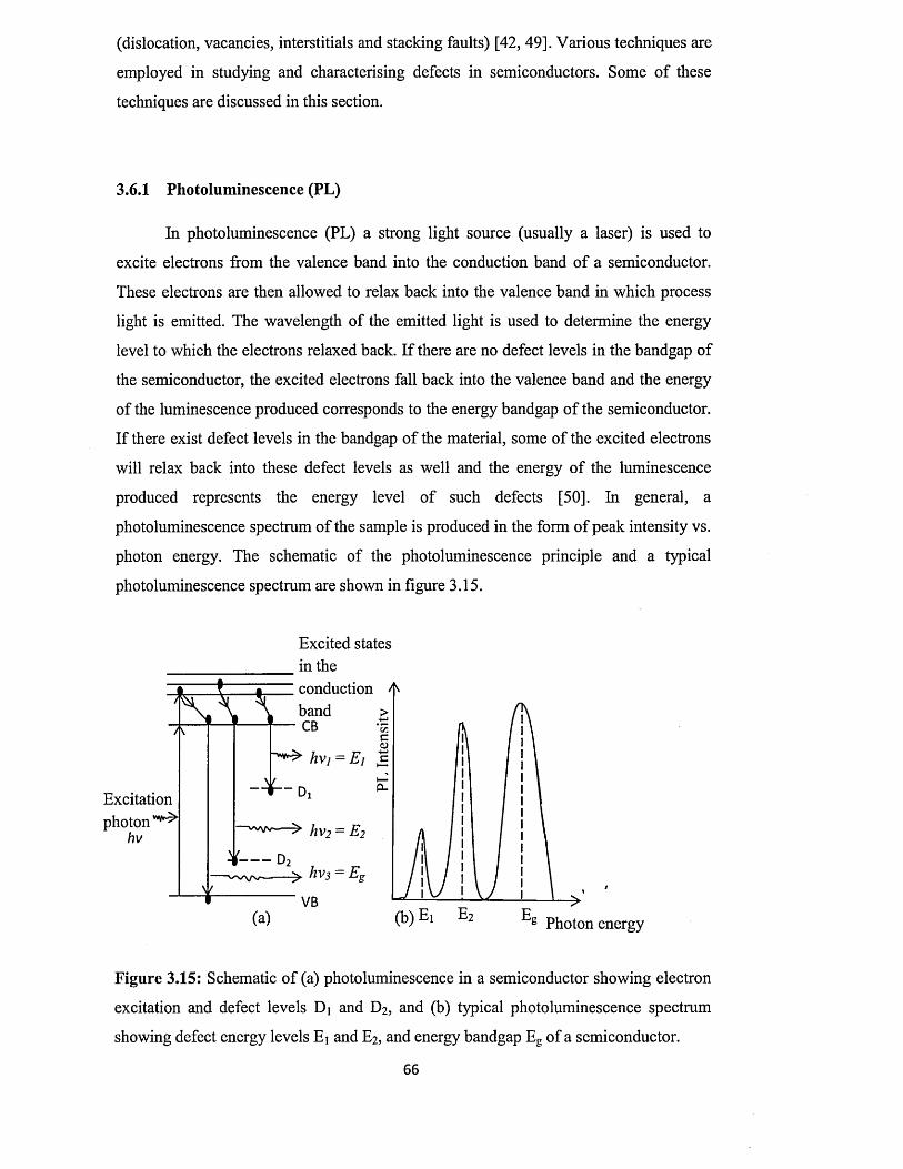
(dislocation, vacancies, interstitials and stacking faults) [42, 49]. Various techniques are
employed in studying and characterising defects in semiconductors. Some of these
techniques are discussed in this section.
3.6.1 Photoluminescence (PL)
In photoluminescence (PL) a strong light source (usually a laser) is used to
excite electrons from the valence band into the conduction band o f a semiconductor.
These electrons are then allowed to relax back into the valence band in which process
light is emitted. The wavelength of the emitted light is used to determine the energy
level to which the electrons relaxed back. If there are no defect levels in the bandgap of
the semiconductor, the excited electrons fall back into the valence band and the energy
of the luminescence produced corresponds to the energy bandgap of the semiconductor.
If there exist defect levels in the bandgap of the material, some of the excited electrons
will relax back into these defect levels as well and the energy o f the luminescence
produced represents the energy level o f such defects [50]. In general, a
photoluminescence spectrum of the sample is produced in the form of peak intensity vs.
photon energy. The schematic of the photoluminescence principle and a typical
photoluminescence spectrum are shown in figure 3.15.
Excited states in theconduction Aband > CB
Excitationn h n tn n
05) ^ Photon energy
Figure 3.15: Schematic of (a) photoluminescence in a semiconductor showing electron
excitation and defect levels Dj and D2 , and (b) typical photoluminescence spectrum
showing defect energy levels Ej and E2, and energy bandgap Eg of a semiconductor.
66

The PL peak intensity indicates the density o f electrons that fall into the various levels,
therefore indicating the density o f the various defect levels in the semiconductor. In
order to determine defect levels in semiconductors however, the photoluminescence
spectroscopy is carried out at low temperatures [50] so that the defect levels are not
saturated in order to be able to trap electrons.
3.6.2 Cathodoluminescence (CL)
Cathodoluminescence (CL) is similar to PL in its principle of operation in the
sense that electrons are excited from the valence band into the conduction band of a
semiconductor, and these electrons relax back to the valence band or defect levels to
produce photons. However, the major difference lies in the way these electrons are
excited. Whereas high-energy photons are used to excite these electrons in the PL
process, high-energy electrons are used in the case of CL [51]. The CL detector is
usually attached to SEM system which is the source of electron beam for the excitation
[51]. One major advantage of CL over PL is that, in CL the incident electron beam
penetrates deeper into the sample than does the photons in PL thus allowing for a more
in-depth study of the luminescence properties of the sample [52]. The CL spectrum is
constructed in the same way as the PL spectrum and defect analysis is carried out in a
similar way [52].
3.6.3 Admittance spectroscopy (AS)
In admittance spectroscopy (AS), a Schottky barrier contact is normally made on
one side o f the semiconductor in order to make a diode with a depletion region. Then
the complex admittance of the junction is measured as a function o f various impurity
levels in the bandgap o f the semiconductor material [53]. The basic principle behind
admittance spectroscopy recognises that,, for a diode with healthy depletion regioni
without impurity (defect levels), the capacitance o f the junction depends on the dc bias
voltage but is not affected by the frequency at which the measurement is made (even in
the frequency ranges from below, 1 kHz to over 1 MHz) [54]. However, if impurity
levels exist in the junction, these substantially affect the capacitance-frequency (C-F)
response. This is because the impurities (traps) cause the movement of the Fermi level
as they trap and un-trap charge carriers causing a fluctuation in the distribution of
charges in the junction which in turn causes a variation in the capacitance and
conductance of the junction as it returns to thermal equilibrium [53]. This is used to
67
produce peaks which can be associated with defect (impurity) levels in the material
making up the Schottky junction.
In thermal admittance spectroscopy (TAS) which is a variant of AS, the
capacitance and conductance of the junction are measured as functions of both
frequency and temperature and these results are also used to observe the effects o f both
frequency and temperature on the capacitance and conductance. The results also show
peaks which represent the various defect levels present in the material [55].
3.6.4 Deep level transient spectroscopy (DLTS)
Deep level transient spectroscopy (DLTS) is similar to admittance spectroscopy.
The major difference however is that, whereas small ac-signal is used in AS
measurements, voltage pulse is normally used while carrying out DLTS measurement
[54]. However, DLTS is a high-frequency capacitance transient measurement technique.
It produces a spectrum of a wide variety o f trap centers in a semiconductor [56]. The
spectrum produced in DLTS can have both positive and negative peaks thus indicating
whether the defect (trap) level is closer to the valence band or to the conduction band.
The peak intensity reflects the concentration or density of the defect level present [56].
In addition to the above defect characterization techniques, there are other
techniques such as photo acoustic spectroscopy (PAS) and Schottky barrier
measurements at metal/semiconductor interfaces. All these techniques detect very many
defect levels in semiconductors, but only a few defects will dominate in controlling the
final I-V characteristics o f devices based on a particular semiconductor. Therefore,
Schottky barrier measurements are the most appropriate for semiconductor devices, and
this thesis discusses the Fermi level pinning situation detected in CdTe earlier in this
programme [18, 33].
3.7 Conclusion
Various thin film semiconductor characterisation techniques are presented and
discussed in this chapter. These techniques vary in their fundamental principles and in
the particular properties or characteristics of the materials they are used to study. They
generally range from structural characterisation to morphological, compositional,
electrical, optical, as well as defect characterisation techniques. The importance o f each
technique in understanding the nature of semiconductor materials before fabricating
devices with them were pointed out. Although many characterisation techniques are
68

available and were discussed, only a selected few were employed in characterising the
semiconductor materials grown in the course of this research for obvious reasons such
as availability, cost and time scale.
69
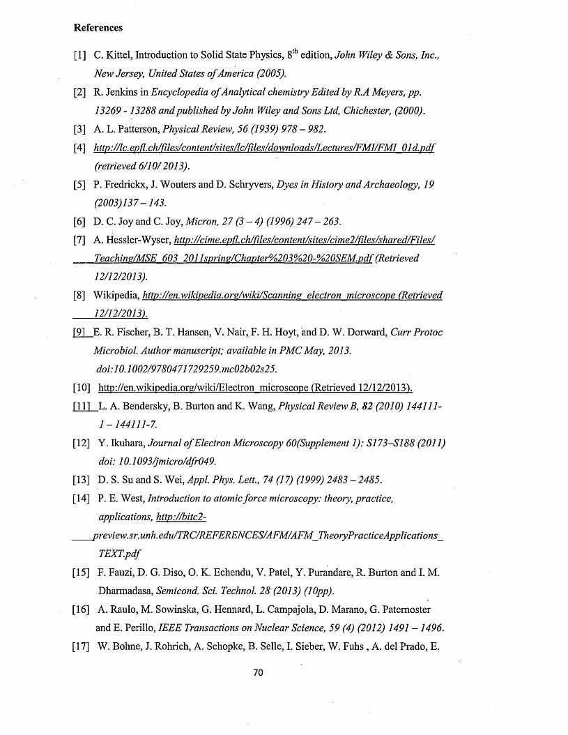
References
[1] C. Kittel, Introduction to Solid State Physics, 8 th edition, John Wiley & Sons, Inc.,
New Jersey, United States o f America (2005).
[2] R. Jenkins in Encyclopedia o f Analytical chemistry Edited by R.A Meyers, pp.
13269 - 13288 and published by John Wiley and Sons Ltd, Chichester, (2000).
[3] A. L. Patterson, Physical Review, 56 (1939) 978 - 982.
[4] http://lc. evfl. ch/files/content/sites/lc/files/downloads/Lectures/FMI/FMI Old.pdf
(retrieved 6/10/2013).
[5] P. Fredrickx, J. Wouters and D. Schryvers, Dyes in History and Archaeology, 19
(2003)137-143.
[6 ] D. C. Joy and C. Joy, Micron, 27 (3 - 4) (1996) 247 - 263.
[7] A. Hessler-Wyser, http://cime.epfl.ch/files/content/sites/cime2/files/shared/Files/
Teachins/MSE 603 2011sprins/Chapter%203%20-%20SEM.pdf (Retrieved
12/12/2013).
[8 ] Wikipedia, http://en.wikipedia.0 rs/wiki/Scannin2 electron microscope (Retrieved
12/12/2013).
I~91 E . R. Fischer, B. T. Hansen, V. Nair, F. H. Hoyt, and D. W. Dorward, Curr Protoc
Microbiol. Author manuscript; available in PMC May, 2013.
doi:10.1002/9780471729259.mc02b02s25.
[10] http://en.wikipedia.org/wiki/Electron microscope (Retrieved 12/12/2013).
r i l l L. A. Bendersky, B. Burton and K. Wang, Physical Review B, 82 (2010) 144111-
1 -144111-7.
[12] Y. Ikuhara, Journal o f Electron Microscopy 60(Supplement 1): S I 73-S188 (2011)
doi: 10.1093/jmicro/dfr049.
[13] D. S. Su and S. Wei, Appl. Phys. Lett., 74 (17) (1999) 2483 - 2485.
[14] P. E. West, Introduction to atomic force microscopy: theory, practice,
applications, http://bitc2-
preview.sr.unh.edu/TRC/REFERENCES/AFM/AFM_TheoryPracticeApplications_
TEXT.pdf
[15] F. Fauzi, D. G. Diso, O. K. Echendu, V. Patel, Y. Purandare, R. Burton and I. M.
Dharmadasa, Semicond. Sci. Technol. 28 (2013) (lOpp).
[16] A. Raulo, M. Sowinska, G. Hennard, L. Campajola, D. Marano, G. Paternoster
and E. Perillo, IEEE Transactions on Nuclear Science, 59 (4) (2012) 1491 -1 4 9 6 .
[17] W. Bohne, J. Rohrich, A. Schopke, B. Selle, I. Sieber, W. Fuhs , A. del Prado, E.
7 0
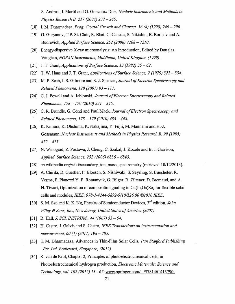
S. Andres , I. Martil and G. Gonzalez-Diaz, Nuclear Instruments and Methods in
Physics Research B, 217 (2004) 237 — 245.
I. M. Dharmadasa, Prog. Crystal Growth and Charact. 36 (4) (1998) 249 — 290.
G. Guryanov, T.P. St. Clair, R. Bhat, C. Caneau, S. Nikishin, B. Borisov and A.
Budrevich, Applied Surface Science, 252 (2006) 7 208 - 7210.
Energy-dispersive X-ray microanalysis: An Introduction, Edited by Douglas
Vaughan, NORAN Instruments, Middleton, United Kingdom (1999).
J. T. Grant, Applications o f Surface Science, 13 (1982) 35 - 62.
T. W. Haas and J. T. Grant, Applications o f Surface Science, 2 (1979) 322 - 334.
M. P. Seah, I. S. Gilmore and S. J. Spencer, Journal o f Electron Spectroscopy and
Related Phenomena, 120 (2001) 93 — 111.
C. J. Powell and A. Jablonski, Journal o f Electron Spectroscopy and Related
Phenomena, 1 7 8 -1 7 9 (2 0 1 0 )3 3 1 -3 4 6 .
C. R. Brundle, G. Conti and Paul Mack, Journal o f Electron Spectroscopy and
Related Phenomena, 1 7 8 -1 7 9 (2010) 433 - 448.
K. Kimura, K. Ohshima, K. Nakajima, Y. Fujii, M. Mannami and H.-J.
Gossmann, Nuclear Instruments and Methods in Physics Research B, 99 (1995)
4 7 2 -4 7 5 .
N. Winograd, Z. Postawa, J. Cheng, C. Szakal, J. Kozole and B. J. Garrison,
Applied Surface Science, 252 (2006) 6836 - 6843.
en.wikipedia.org/wiki/secondary_ion_mass_spectrometry (retrieved 10/12/2013).
A. Chirila, D. Guettler, P. Bloesch, S. Nishiwaki, S. Seyrling, S. Buecheler, R.
Verma, F. Pianezzi,Y. E. Romanyuk, G. Bilger, R. Ziltener, D. Bremaud, and A.
N. Tiwari, Optimization o f composition grading in Cu(In,Ga)Se2 for flexible solar
cells and modules, IEEE, 978-1-4244-5892-9/10/S26.00 ©2010 IEEE.
S. M. Sze and K. K. Ng, Physics of Semiconductor Devices, 3rd edition, John
Wiley & Sons, Inc., New Jersey, United States o f America (2007).
R. Hall, J. SCI. INSTRUM., 44 (1967) 53 - 54.
H. Castro, J. Galvis and S. Castro, IEEE Transactions on instrumentation and
measurement, 60 (1) (2011) 198 - 205.
I. M. Dharmadasa, Advances in Thin-Film Solar Cells, Pan Stanford Publishing
Pte. Ltd, Boulevard, Singapore, (2012).
R. van de Krol, Chapter 2, Principles of photoelectrochemical cells, in
Photoelectrochemical hydrogen production, Electronic Materials: Science and
Technology, vol. 102 (2012) 13 - 67, www.springer.com/.../9781461413790-
71
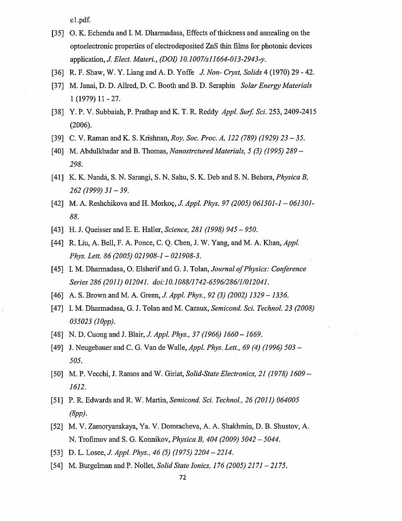
cl.pdf.
[35] O. K. Echendu and I. M. Dharmadasa, Effects of thickness and annealing on the
optoelectronic properties of electrodeposited ZnS thin films for photonic devices
application,/. Elect. Materi., (DOI) 10.1007/sll664-013-2943-y.
[36] R. F. Shaw, W. Y. Liang and A. D. Yoffe J. Non- Cryst, Solids 4 (1970) 29 - 42.
[37] M. Janai, D. D. Allred, D. C. Booth and B. D. Seraphin Solar Energy Materials
1 (1979) 11 -27.
[38] Y. P. V. Subbaiah, P. Prathap and K. T. R. Reddy Appl. Surf. Sci. 253, 2409-2415
(2006).
[39] C. V. Raman and K. S. Krishnan, Roy. Soc. Proc. A, 122 (789) (1929) 23 - 35.
[40] M. Abdulkbadar and B. Thomas, Nanostrctured Materials, 5 (3) (1995) 289 -
298.
[41] K. K. Nanda, S. N. Sarangi, S. N. Sahu, S. K. Deb and S. N. Behera, Physica B,
2 6 2 (1 9 9 9 )3 1 -3 9 .
[42] M. A. Reshchikova and H. Morkog, J. Appl. Phys. 97 (2005) 061301-1 - 061301-
88.[43] H. J. Queisser and E. E. Haller, Science, 281 (1998) 945 - 950.
[44] R. Liu, A. Bell, F. A. Ponce, C. Q. Chen, J. W. Yang, and M. A. Khan, Appl.
Phys. Lett. 86 (2005) 021908-1 - 021908-3.
[45] I. M. Dharmadasa, O. Elsherif and G. J. Tolan, Journal o f Physics: Conference
Series 286 (2011) 012041. doi:10.1088/1742-6596/286/1/012041.
[46] A. S. Brown and M. A. Green, J. Appl. Phys., 92 (3) (2002) 1329 -1 3 3 6 .
[47] I. M. Dharmadasa, G. J. Tolan and M. Cazaux, Semicond. Sci. Technol. 23 (2008)
035023 (lOpp).
[48] N. D. Cuong and J. Blair, J. Appl. Phys., 37 (1966) 1660 -1669 .
[49] J. Neugebauer and C. G. Van de Walle, Appl. Phys. Lett., 69 (4) (1996) 503 -
505.
[50] M. P. Vecchi, J. Ramos and W. Giriat, Solid-State Electronics, 21 (1978) 1609 -
1612.
[51] P. R. Edwards and R. W. Martin, Semicond. Sci. Technol., 26 (2011) 064005
(8pp).
[52] M. V. Zamoryanskaya, Ya. V. Domracheva, A. A. Shakhmin, D. B. Shustov, A.
N. Trofimov and S. G. Konnikov, Physica B, 404 (2009) 5042 - 5044.
[53] D. L. Losee, J. Appl. Phys., 46 (5) (1975) 2204 - 2214.
[54] M. Burgelman and P. Nollet, Solid State Ionics, 176 (2005) 2171 - 2175.
72

[55] R. A. Enzenroth, K. L. Barth and W. S. Sampath, J. Phys. Chem. Solids, 66
(2005) 1883 - 1886.
[56] D. V. Lang, J. Appl. Phys., 45 (7) (1974) 3023 - 3032.
73
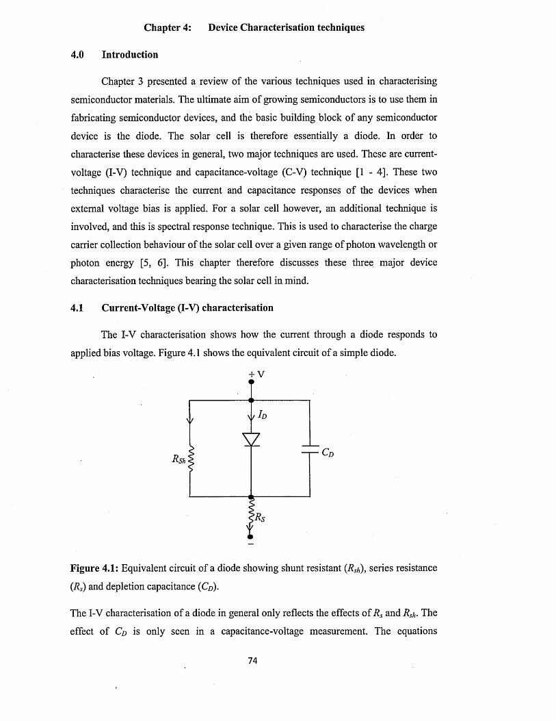
C hapter 4: Device C haracterisation techniques
4.0 Introduction
Chapter 3 presented a review of the various techniques used in characterising
semiconductor materials. The ultimate aim of growing semiconductors is to use them in
fabricating semiconductor devices, and the basic building block o f any semiconductor
device is the diode. The solar cell is therefore essentially a diode. In order to
characterise these devices in general, two major techniques are used. These are current-
voltage (I-V) technique and capacitance-voltage (C-V) technique [1 - 4]. These two
techniques characterise the current and capacitance responses o f the devices when
external voltage bias is applied. For a solar cell however, an additional technique is
involved, and this is spectral response technique. This is used to characterise the charge
carrier collection behaviour of the solar cell over a given range of photon wavelength or
photon energy [5, 6 ]. This chapter therefore discusses these three major device
characterisation techniques bearing the solar cell in mind.
4.1 Current-Voltage (I-V) characterisation
The I-V characterisation shows how the current through a diode responds to
applied bias voltage. Figure 4.1 shows the equivalent circuit of a simple diode.
+ V
Figure 4.1: Equivalent circuit o f a diode showing shunt resistant ( R s h ) , series resistance
(Rs) and depletion capacitance (Co).
The I-V characterisation of a diode in general only reflects the effects o f Rs and Rsi,. The
effect of Cd is only seen in a capacitance-voltage measurement. The equations
74
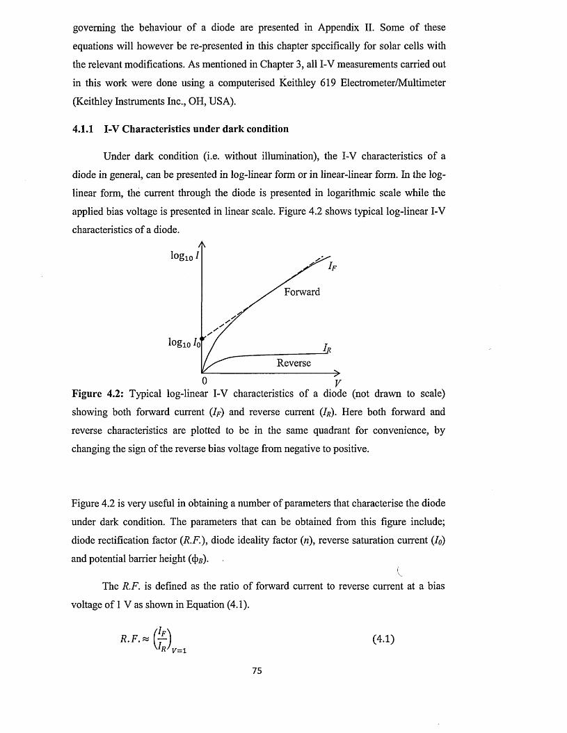
governing the behaviour of a diode are presented in Appendix II. Some o f these
equations will however be re-presented in this chapter specifically for solar cells with
the relevant modifications. As mentioned in Chapter 3, all I-V measurements carried out
in this work were done using a computerised Keithley 619 Electrometer/Multimeter
(Keithley Instruments Inc., OH, USA).
4.1.1 I-V Characteristics under dark condition
Under dark condition (i.e. without illumination), the I-V characteristics of a
diode in general, can be presented in log-linear form or in linear-linear form. In the log-
linear form, the current through the diode is presented in logarithmic scale while the
applied bias voltage is presented in linear scale. Figure 4.2 shows typical log-linear I-V
characteristics of a diode.
logio I
Forward
logio h
Reverse
Figure 4.2: Typical log-linear I-V characteristics of a diode (not drawn to scale)
showing both forward current (Ip) and reverse current ( I r ) . Here both forward and
reverse characteristics are plotted to be in the same quadrant for convenience, by
changing the sign of the reverse bias voltage from negative to positive.
Figure 4.2 is very useful in obtaining a number of parameters that characterise the diode
under dark condition. The parameters that can be obtained from this figure include;
diode rectification factor (R.F.), diode ideality factor (n), reverse saturation current (Jo)
and potential barrier height ((J)#).
The R.F. is defined as the ratio of forward current to reverse current at a bias
voltage o f 1 V as shown in Equation (4.1).
The R.F. is a measure o f the rectifying quality of the diode. A rectification factor of
about three orders of magnitude (R.F.~103) is enough to make a good diode [7]. In order
to obtain the diode ideality factor from figure 4.2, Equation (11.25) is used and is re
presented here as Equation (4.2) for convenience.
For an applied bias of V > 0.75 V, the exponential term in Equation (4.2) becomes
sufficiently large [7] so that
Taking the natural logarithm o f both sides of Equation (4.4), and rearranging, yields
Equation (4.5).
Re-writing Equation (4.5) in common logarithmic form for convenience then gives
Equation (4.7) shows that the graph of log1 0 / vs. V gives a straight line, the slope of
which is q/2 .303nkT . Therefore from the slope o f the forward current in figure (4.2),
the value of n can be obtained since q, k and T are all known. The value o f n is very
useful in understanding the current transport mechanism in a diode. In an ideal diode
where current transport takes place over the potential barrier only through thermionic
emission, the value of n is unity. If current transport is dominated by recombination and
generation (R & G) mechanism, then n = 2.00. If both mechanisms are present as is the
case in a practical diode, n takes a value between 1.00 and 2.00. In a practical diode,
(4.2)
(4.3)
Then Equation (4.2) simplifies to Equation (4.4), thus
(4.4)
(4.5)
0.434 log101 = — + 0.434 log1 0 I0 (4.6)
Dividing Equation (4.6) by 0.434 gives
logio I = (■2.303nkT;)l7 + log1 0 / 0 (4.7)
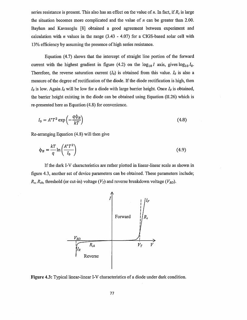
series resistance is present. This also has an effect on the value of n. In fact, if Rs is large
the situation becomes more complicated and the value o f n can be greater than 2 .0 0 .
Bayhan and Kavasoglu [8 ] obtained a good agreement between experiment and
calculation with n values in the range (3.43 - 4.07) for a CIGS-based solar cell with
13% efficiency by assuming the presence of high series resistance.
Equation (4.7) shows that the intercept of straight line portion o f the forward
current with the highest gradient in figure (4.2) on the log10/ axis, gives log10/0.
Therefore, the reverse saturation current (7o) is obtained from this value. Io is also a
measure o f the degree o f rectification of the diode. If the diode rectification is high, then
Io is low. Again Io will be low for a diode with large barrier height. Once I0 is obtained,
the barrier height existing in the diode can be obtained using Equation (11.26) which is
re-presented here as Equation (4.8) for convenience.
If the dark I-V characteristics are rather plotted in linear-linear scale as shown in
figure 4.3, another set of device parameters can be obtained. These parameters include;
Rs, Rsh, threshold (or cut-in) voltage ( F t) and reverse breakdown voltage ( V b d ) .
A
(4.8)
Re-arranging Equation (4.8) will then give
(4.9)
I
Forward
V b d
Reverse
VT V
Figure 4.3: Typical linear-linear I-V characteristics of a diode under dark condition.
77
The series resistance is obtained by finding the slope (A //A 7) of the straight line
portion of the high forward current and applying Ohm's law, so that Rs is obtained from
Equation (4.10).
r-(Z77aF) (4’10)
A low value o f Rs is desirable for a good device in which case the forward current has
highest possible slope (A I/A V ) [9]. In a practical diode however, a high value of Rs can
arise due to two major reasons. One o f these is the presence o f resistive oxide layer
between the semiconductor and the metal contact (forming an MIS structure). This
resistive interfacial layer can arise due to oxidation caused by the etching process
preceding the metal contact formation, or due to high density o f surface states and
therefore high surface recombination velocity [1, 10]. Another reason for high series
resistance is the use of semiconductor materials with high bulk resistivity [1, 10]. This
is because, at sufficiently high forward bias, the current through the diode increases
rapidly so that the series resistance o f the diode is controlled by both bulk resistance of
the semiconductor material used, and the contact resistance at the two
metal/semiconductor interfaces [11]. At such high series resistance, the slope of the
forward I-V curve decreases substantially. For an ideal diode Rs = 0, so that the slope of
the forward current (A //AF) -» oo.
From the reverse I-V curve, the shunt resistance Rsh is obtained by determining
the slope (A I/A V ) as in the case of Rs. The value of Rsi, is indicative o f the presence of
current leakage paths in the diode. For a good diode, a high value of Rsh is desirable [7,
9, 11]. For an ideal diode, Rsh -> oo. With low Rsh value, substantial leakage current (Io)
flows in the diode under reverse bias. During the forward biasing of a diode, very small
current flows through the diode as bias voltage increase gradually from 0 V up to a
certain minimum voltage. Beyond this voltage, the current through the diode rises
rapidly. This minimum voltage is known as the threshold voltage ( F t ) or cut-in voltage
or turn on voltage of the particular diode involved [9, 11 - 13] as shown in figure 4.3.
Ge and Si diodes have typical threshold voltages o f about 0.2 V and 0.7 V respectively
[11]. In order for a diode to operate, a forward bias > VT must be applied. The threshold
voltage also represents the built-in potential of a diode.
Under reserve bias, a negligible current flows through the diode. However, at a
certain high reserve bias, a large reverse current suddenly begins to flow through the
7 8
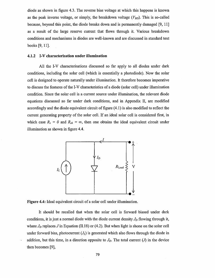
diode as shown in figure 4.3. The reverse bias voltage at which this happens is known
as the peak inverse voltage, or simply, the breakdown voltage ( V b d )- This is so-called
because, beyond this point, the diode breaks down and is permanently damaged [9, 11]
as a result o f the large reserve current that flows through it. Various breakdown
conditions and mechanisms in diodes are well-known and are discussed in standard text
books [9, 11].
4.1.2 I-V characterisation under illumination
All the I-V characterisations discussed so far apply to all diodes under dark
conditions, including the solar cell (which is essentially a photodiode). Now the solar
cell is designed to operate naturally under illumination. It therefore becomes imperative
to discuss the features of the I-V characteristics o f a diode (solar cell) under illumination
condition. Since the solar cell is a current source under illumination, the relevant diode
equations discussed so far under dark conditions, and in Appendix II, are modified
accordingly and the diode equivalent circuit o f figure (4.1) is also modified to reflect the
current generating property of the solar cell. If an ideal solar cell is considered first, in
which case Rs = 0 and Rsh - °o, then one obtains the ideal equivalent circuit under
illumination as shown in figure 4.4.
h
Figure 4.4: Ideal equivalent circuit of a solar cell under illumination.
It should be recalled that when the solar cell is forward biased under dark
conditions, it is just a normal diode with the diode current density Jo flowing through it,
where Jd replaces J in Equation (11.18) or (4.2). But when light is shone on the solar cell
under forward bias, photocurrent (J£) is generated which also flows through the diode in
addition, but this time, in a direction opposite to Jd- The total current (J) in the device
then becomes [9],
7 9
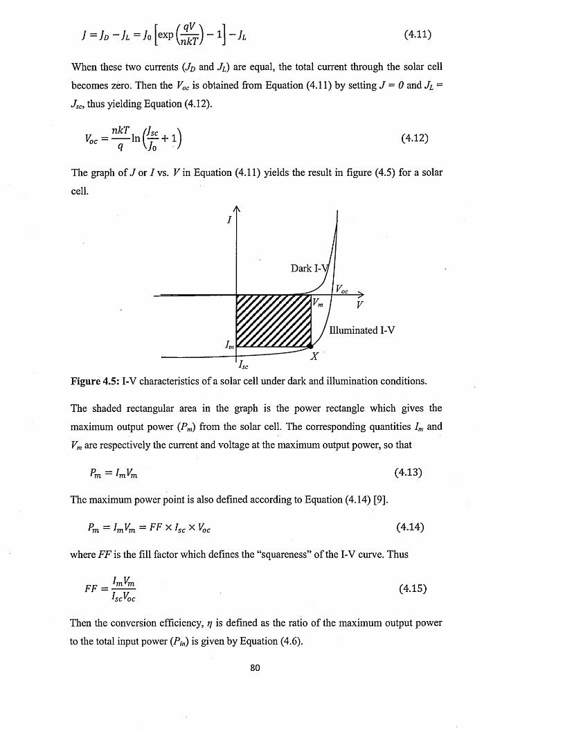
J = J d - h = J o [exp(^f) - l] - h (4.11)
When these two currents {Jd and J£) are equal, the total current through the solar cell
becomes zero. Then the Voc is obtained from Equation (4.11) by setting J = 0 and Jl =
Jsc, thus yielding Equation (4.12).
Voc =nkT
l n l7q \Jo(4.12)
The graph o f J or I vs. V in Equation (4.11) yields the result in figure (4.5) for a solar
cell.
A
PIlluminated I-V
Figure 4.5: I-V characteristics of a solar cell under dark and illumination conditions.
The shaded rectangular area in the graph is the power rectangle which gives the
maximum output power (Pm) from the solar cell. The corresponding quantities Im and
Vm are respectively the current and voltage at the maximum output power, so that
P = I Vrm 1m vm
The maximum power point is also defined according to Equation (4.14) [9].
Pm l-mYm ~~ P P * h e * ^oc
(4.13)
(4.14)
where FF is the fill factor which defines the “squareness” o f the I-V curve. Thus
FF =Irr,\L 1m ym
hcVoc(4.15)
Then the conversion efficiency, rj is defined as the ratio of the maximum output power
to the total input power (P,„) is given by Equation (4.6).
80

where P in is the solar power density of the incident light, which for the AM 1.5, is 100
Wcm'2.
For a practical solar cell, the effects of R s and R s h are brought into Equation (4.11)\
accordingly by replacing V wtihiV-IRs). Rs is more influential than R s ft since it directly
affects the fill factor. The equivalent circuit o f a real practical solar cell is then given in
figure 4.6.
■* +
h
% -
Figure 4.6: Equivalent circuit of a practical solar cell showing the presence of R s and
R s h -
From figure 4.5 therefore, the solar cell parameters under illumination can be obtained.
The J s c (or I s c ) and V o c can be read directly from the graph. The F F can be obtained by
drawing the largest possible rectangle through the maximum power point (X), and
reading directly, I m and V m as shown, and then applying Equation (4.15). Using
Equation (4.16) the conversion efficiency, t j is then obtained by substitution. R s and R s h
under illumination are also obtained just in the same way as in the dark I-V graph
described previously.
4.2 Capacitance-Voltage (C-V) characterisation
Every diode has a depletion region of a certain width, w. This depletion region is
the heart of the diode and where all the major activities in the diode take place. All the
equations describing the behaviour of a diode under various conditions actually show
what happens in the depletion region. The description of the formation o f a rectifying
junction given in Appendix II simply shows that the depletion region of a diode can be81
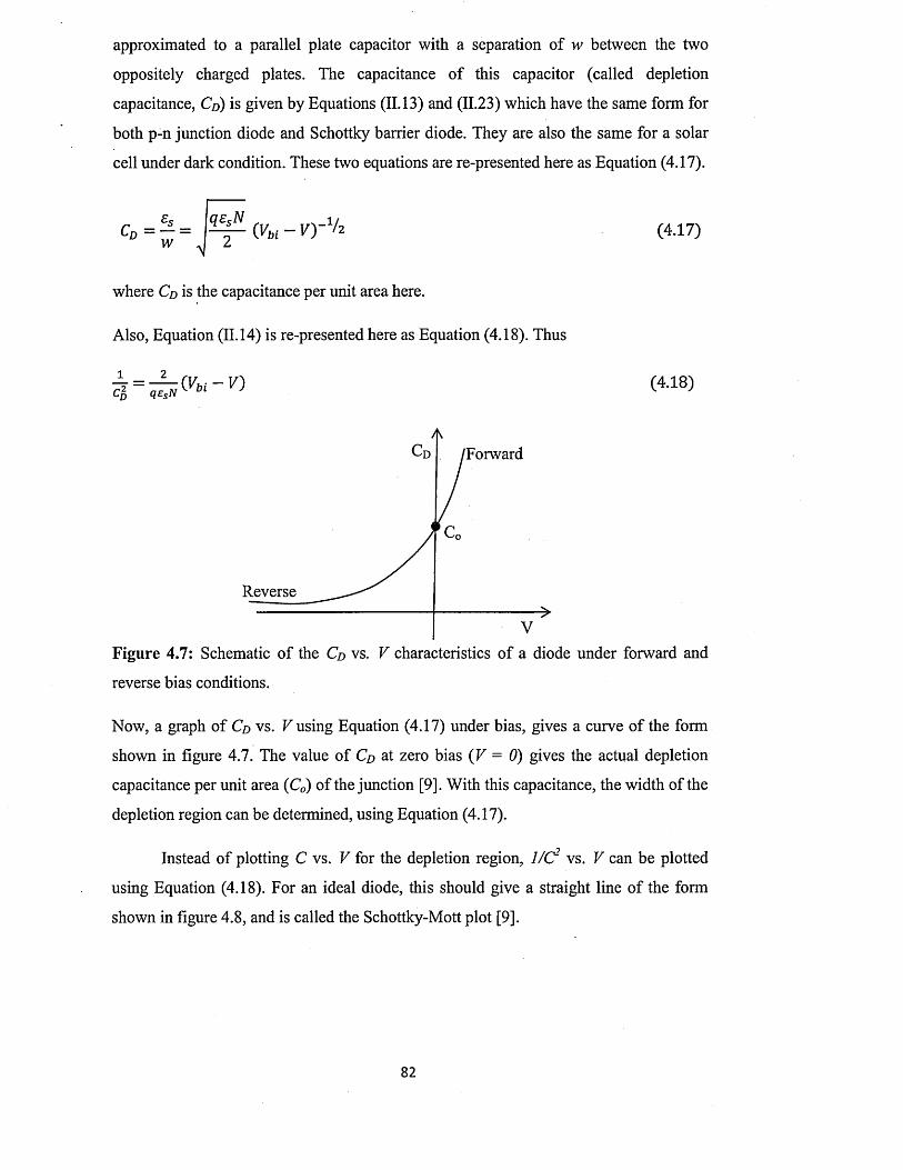
approximated to a parallel plate capacitor with a separation of w between the two
oppositely charged plates. The capacitance of this capacitor (called depletion
capacitance, C d ) is given by Equations (11.13) and (11.23) which have the same form for
both p-n junction diode and Schottky barrier diode. They are also the same for a solar
cell under dark condition. These two equations are re-presented here as Equation (4.17).
reverse bias conditions.
Now, a graph o f Cd v s . V using Equation (4.17) under bias, gives a curve o f the form
shown in figure 4.7. The value o f Cd at zero bias (V = 0) gives the actual depletion
capacitance per unit area (C0) of the junction [9]. With this capacitance, the width of the
depletion region can be determined, using Equation (4.17).
Instead of plotting C vs. V for the depletion region, 1/C2 vs. V can be plotted
using Equation (4.18). For an ideal diode, this should give a straight line of the form
shown in figure 4.8, and is called the Schottky-Mott plot [9].
(4 .1 7 )
where Cd is the capacitance per unit area here.
Also, Equation (11.14) is re-presented here as Equation (4.18). Thus
(4 .1 8 )
Reverse
'Forward
>V
Figure 4.7: Schematic of the Cd v s . V characteristics o f a diode under forward and
82
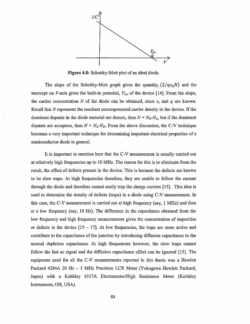
Figure 4.8: Schottky-Mott plot of an ideal diode.
The slope of the Schottky-Mott graph gives the quantity, (2 / q s 0N ) and the
intercept on F-axis gives the built-in potential, Fj,;, o f the device [14]. From the slope,
the carrier concentration N o f the diode can be obtained, since es and q are known.
Recall that N represents the resultant uncompensated carrier density in the device. If the
dominant dopants in the diode material are donors, then N = Nd-Na, but if the dominant
dopants are acceptors, then N = Na-Nd. From the above discussion, the C-V technique
becomes a very important technique for determining important electrical properties o f a
semiconductor diode in general.
It is important to mention here that the C-V measurement is usually carried out
at relatively high frequencies up to 10 MHz. The reason for this is to eliminate from the
result, the effect of defects present in the device. This is because the defects are known
to be slow traps. At high frequencies therefore, they are unable to follow the current
through the diode and therefore cannot easily trap the charge carriers [15]. This idea is
used to determine the density of defects (traps) in a diode using C-V measurement. In
this case, the C-V measurement is carried out at high frequency (say, 1 MHz) and then
at a low frequency (say, 10 Hz). The difference in the capacitance obtained from the
low frequency and high frequency measurements gives the concentration o f impurities
or defects in the device [15 - 17]. At low frequencies, the traps are more active and
contribute to the capacitance of the junction by introducing diffusion capacitance to the
normal depletion capacitance. At high frequencies however, the slow traps cannot
follow the fast ac signal and the diffusion capacitance effect can be ignored [15]. The
equipment used for all the C-V measurements reported in this thesis was a Hewlett
Packard 4284A 20 Hz - 1 MHz Precision LCR Meter (Yokogawa Hewlett Packard,
Japan) with a Keithley 6517A Electrometer/High Resistance Meter (Keithley
Instruments, OH, USA).
83
4.3 Spectral response (SR) characterisation
Spectral response (SR) characterisation is very important for solar cells since
light of certain wavelengths must be absorbed by the solar cell in order to create
electron-hole pairs and subsequently produce photocurrent. The spectral response is
therefore useful in determining the total current deliverable by a solar cell [9, 18, 19]
and the range o f wavelengths of photons that are absorbed and are converted to current
by the solar cell.
There are three types o f spectral response used in characterising solar cells.
These include; spectral responsivity (S) external quantum efficiency (EQE) and internal
quantum efficiency (IQE) [18]. All of these are also related and are wavelength
dependent.
Spectral responsivity is the amount of current that is delivered by a solar cell per unit
incident photon power. The unit is therefore given as amperes per watt (AAV) [5].
External quantum efficiency is defined as the ratio of the number of charge carriers in
the current delivered by a solar cell to the number of incident photons of a given energy.
The EQE is actually derived from the spectral responsivity [9, 18] so that
where X is incident photon wavelength, J(X) is the photocurrent at a given wavelength,
q is electronic charge and <ft(X) is the number of photons per unit area per unit time per
unit bandwidth of wavelengths.
Since EQE is derived from spectral responsivity, the equation for EQE can alternatively
by written as
to ta l inpu t p ho ton p o w e r /(en erg y p er pho ton )outnut current/(char ae ner electron)
(4.19)
or
EQE(X) (4.20)
EQE{X) (4.21)
EQE is usually expressed in percentage.
84
In ternal quantum efficiency is a more complicated spectral response since it involves
the actual number of photons absorbed by the solar cell in order to produce
photocurrent. It is clear that not all the incident photons are absorbed by the solar cell.
Some of these photons are reflected at the point o f incidence on the solar cell. Some are
transmitted through the solar cell while the rest are absorbed. In determining the IQE
using the total incident photon flux therefore, the amount of photons reflected and those
transmitted should be put into consideration. This is the major point of difference
between IQE and EQE. I f one assumes zero transmission for a solar cell with sufficient
thickness and high absorption coefficient, then IQE can be written as in Equation (4.22)
[9, 20] by modifying Equation (4.20).
I Q E W = q W ) [ l - R { X ) ] (4'22)
where R(X) is the fraction of the photons reflected by the solar cell at the point of
incidence.
Comparing Equations (4.20) and (4.22), one therefore sees that for any given solar cell,
IQE is higher than EQE. The IQE result can give information on the loss mechanisms in
the solar cell for absorbed photons with energies higher than the bandgap of the solar
cell material [18]. From the foregoing, it is also obvious that once the spectral response
is known, the current deliverable by a solar cell can be obtained by integrating over all
wavelengths from zero to the bandgap wavelength, as can be inferred from Equations
(4.20) and (4.22).
4.4 Conclusion
The characterisation of semiconductor devices (including solar cells) was
presented in this chapter. The various characterisation techniques employed for this
purpose, were discussed to include, I-V, C-V and spectral response techniques. Each
technique is seen to be unique in nature and in the manner they are carried out yielding
different results that help to understand the behaviour of the devices under study. I-V
characterisation is seen to reveal the behaviour of the electrical current through the
diode (device) under external bias. C-V characterisation reveals the response o f the
depletion region capacitance of diodes under different bias conditions. Both I-V and C-
V characterisation techniques also help to understand the nature of defects (impurities)
present in the device. Spectral response measurements are particularly useful for
characterising solar cells. Since the solar cell must absorb incident light (photons), the85

particular useful range o f wavelengths o f the incident photons is known through these
measurements. In addition, the result of the spectral response measurement can help to
obtain the total current deliverable from the solar cell as well as help to understand the
possible loss mechanisms that come into play in the solar cell.
8 6
References
[1] M. Siad, A. Keffous, S. Mamma, Y. Belkacem and H. Menari, Applied Surface
Science, 236 (2004) 366 - 376.
[2] Y. Li, W. Huang, H. Huang, C. Hewitt, Y. Chen, G. Fang and D. L. Carroll, Solar
Energy, 90 (2013) 5 1 -5 7 .
[3] N. Christoforou, J. D. Leslie and S. Mamaskinos, Solar Cells, 26 (1989) 215 -
225.
[4] J. Singh and M. H. Cohen, J. Appl. Phys., 51(1) (1980) 413 - 418.
[5] H. Field, AIP Conference Proceedings 462, (1999) 629 - 635; doi:
10.1063/1.58006
[6 ] B. L. Sopori, Solar Cells, 22 (1987) 287 - 294.
[7] I. M. Dharmadasa, Advances in Thin-Film Solar Cells, Pan Stanford Publishing
Pte. Ltd, Boulevard, Singapore, (2012).
[8 ] H. Bayhan and A. S. Kavasoglu., Turk J Phys. 31 (2007) 7.
[9] S. M. Sze and K. K. Ng, Physics of Semiconductor Devices, 3rd edition, John
Wiley & Sons, Inc., New Jersey, United States o f America (2007).
[10] A. Keffous, M. Siad, S. Mamma, Y. Belkacem, C. L. Chaouch, H. Menari, A.
Dahmani and W. Chergui, Applied Surface Science, 218 (2003) 336 - 342.
[11] A. K. Sharma, Semiconductor Electronics, New Age International (P) Ltd, New
Delhi, India (1996).
[12] T. F. Kent, S. D. Camevale and R. C. Myers, Appl. Phys. Lett., 102 (2013)
201114-1-201114-4.
[13] I. W. Wu, Y. H. Chen, P. S. Wang, C. G. Wang, S. H. Hsu and C. I. Wu, Appl.
Phys. Lett., 96 (2010) 013301-1 - 013301-3.
[14] P. E. Bagnoli and A. Nannini, Solid-State Electronics, 30 (10) (1987) 1005 -
1012 .
[15] S. N. Sarangi, P. K. Adhikari, D. Pandey and S. N. Sahu, J. Nanopart. Res., 12
(2010)2277-2286.
[16] S. K. Das and G. C. Morris, J. Appl. Phys. 73 (2) (1993) 782 - 786.
[17] S. Altindal, A. Tataroglu and I. Dokme, Sol. Ener. Mat. Sol. Cell, 85 (2005) 345 -
358.
[18] J. S. Hartman and M. A. Lind, Solar Cells, 7 (1982 - 1983) 147 -1 5 7 .
[19] H. K. Gummel and F. M. Smits, The Bell System Technical Journal, (1964) 1103
- 1121 .
87

[20] W. J. Yang, Z. Q. Ma, X. Tang, C. B. Feng, W. G. Zhao and P. P. Shi, Solar
Energy, 82 (2008) 106—110.
88
Chapter 5: ZnS deposition and characterisation
5.0 Introduction
ZnS is a direct bandgap semiconductor belonging to the II-VI compound
semiconductor family. It is non-toxic and has a wide bandgap of about 3.68 eV for the
bulk material [1]. Being a non-toxic material and having wide bandgap, it can
potentially replace the CdS usually used as a window material in CdS/CdTe and
CdS/CIGS solar cells. The success of ZnS in this regard will therefore bring about cost
reduction and provide more environmentally friendly applications. Cost reduction will
be achieved because it will reduce the cost of handling o f Cd-containing wastes
generated during the CdS production process. Environmental friendliness is achieved
because it will reduce the amount of Cd-containing waste generated during the
processes of fabrication of CdS/CdTe and CdS/CIGS solar cells.
Because o f its wider bandgap compared to CdS, the use of ZnS as a window
layer in the fabrication o f CdTe- and CIGS-based solar cells has the potential of
reducing window absorption losses associated with CdS due to the relatively narrow
bandgap of CdS of 2.42 eV [2, 3], therefore producing devices with improved short-
circuit current. This is because the presence of ZnS in this case will allow more higher-
energy photons to reach the CdTe or CIGS absorber layer in order to create more photo
generated charge carriers. It can also be used as a window layer in graded bandgap solar
cells such as ZnS/CdS/CdTe multi-layer graded bandgap solar cell. This device
structure, under optimum design and operation, will benefit from reduced
thermallisation effect by absorbing photons from different regions o f the solar spectrum
at different regions in the device. Apart from its possible application in solar cells, ZnS
has other optoelectronic properties making it suitable for use in devices such as sensors,
lasers, thermoelectric coolers and thin film polarisers [4]. It is also applicable in
electroluminescence devices [5], light-emitting diodes and phosphorescence devices [6 ].
The deposition of ZnS over the years has been done using various growth
techniques. Such techniques include thermal evaporation [7], spray pyrolysis [8 ],
electrochemical atomic layer deposition (ECALE) [9], chemical bath deposition (CBD)
[10], metal-organic chemical vapour deposition (MOCVD) [11], molecular beam
epitaxy (MBE) [12] as well as electrodeposition (ED) [4, 13]. However, the report on
electrodeposition of ZnS is scarce in the literature. One major reason for this is the fact
89

that the electrodeposition o f chalcogenides of Zn from standard aqueous solutions is a
difficult task [14].
It is possible to dope ZnS in order to obtain n-type ZnS (n-ZnS) and p-type ZnS
(p-ZnS) using extrinsic doping. This has mostly been reported by researchers using
mainly vapour techniques such as MBE [12] and vapour phase epitaxy (VPE) [15]. The
extrinsic dopants that have been used include Cl and ethylchloride for n-type doping
[12, 15] as well as N, P, In, Al, Ga, Ag and NH3 for p-type doping [16 - 19]. The use of
elements like In, Al and Ga in p-type doping o f ZnS rather sounds incredible since they
are ordinarily known as n-type dopants for II-VI semiconductors. Nevertheless, these
elements are not actually used individually to achieve p-type doping in ZnS. They are
rather used in conjunction with p-type dopant elements like N in a method known as co
doping in order to achieve effective p-type doping in ZnS [18, 19]. However, the
intrinsic n-type and p-type doping of ZnS has not been reported in the literature. The
achievement of this intrinsic n-type and p-type doping o f ZnS thin-film layers using
electrodeposition technique has been achieved and is presented in this chapter.
A range of characterisation techniques was used in studying the properties of
these layers deposited. Conductivity types of the layers were established using photo
electrochemical (PEC) cell measurements. Structural characterisation of the layers was
carried out using XRD. Optical characterisation was done using optical absorption,
transmittance and reflectance spectrophotometry. Scanning electron microscopy (SEM)
and energy dispersive X-ray (EDX) were used to study the morphology and atomic
composition of the layers.
5.1 Preparation of n-ZnS deposition electrolyte
The deposition electrolyte for n-ZnS thin-film layers was made up o f 0.3M of
ZnCL (98% purity) and 0.03M of (NH4)2S2C>3 (laboratory reagent grade) in 800 ml o f
de-ionised water and contained in 1000 ml plastic beaker. Both chemicals were bought
from Sigma-Aldrich, United Kingdom. The plastic beaker was in turn contained in 1800
ml glass beaker as a water bath. The reason for using plastic beaker as the main
container for the electrolyte is to avoid ions such as Na+ used in making some glasses
from leaching into the electrolyte and poison the electrolyte. This precaution is taken
because atoms of groups 1A and IB elements are known to act as acceptor dopants in
II-VI semiconductor [20, 21]. It is also for this same reason that (1^ 4 ) 2 8 2 0 3 was used
as sulphur precursor instead of Na2S2C>3 commonly used in the electrodeposition o f ZnS
90
[13,22] and CdS [23-25]. The reason also for using a water bath instead o f directly
heating the electrolyte, is that, more uniform heating o f the electrolyte is obtained when
a water bath is used than when direct heating is done. Thus the heating from the
hotplate is transferred to the electrolyte indirectly through the water bath.
Before the addition of (NH4)2S2C>3 , cyclic voltammetry (CV) was carried out on
the aqueous solution containing only Z11CI2 at the initial pH o f the solution which was
~5.4+0.02. In carrying out a CV, varying direct current voltages from +100 mV to -
2000 mV were applied across the electrolyte through cathode and anode electrodes. The
cathode (working electrode) was a fluorine-doped tin oxide on glass (glass/FTO)
cleaned with methanol, acetone and de-ionised water. The anode (counter electrode)
was a high-purity carbon rod. The CV is normally used in electrochemistry to study
reaction mechanisms of electrolytes such as during an electrodeposition process [26].
During the CV process, the change in current in response to the applied potential across
the working electrode is recorded. A graph of current vs. applied potential, usually
called a voltammogram, gives information on the deposition mechanism during the
electrodeposition process for the particular electrolyte involved. Most importantly, the
possible range of deposition potentials for the electrolyte system in question can be
deduced. When the electrolyte contains only one precursor such as Z 11CI2 , the
voltammogram is simpler in features showing more clearly the particular applied
potential at which deposition of the metallic atoms (Zn atoms) sets in. With this, a
slightly lower potential than that was applied to the Z 11CI2 solution for electro
purification which lasted for 48 hours. This purification process is very important since
the ZnCl2 precursor was of low purity (98%). During this process, any metallic ions
present in the chemical which would have otherwise deposited along with Zn during the
formation of ZnS, is eliminated from the solution without removing Zn. This is the
reason why the electro-purification process was done at a potential just slightly below
the deposition potential of Zn. It is important to note that the electro-purification
process was only carried for ZnCb solution because o f its low purity compared to
(NH4)2 S2 0 3 . This electro-purification and self-purification capabilities are part o f the
advantages of the electrodeposition technique. Self-purification is the continuous
removal o f impurities from the deposition electrolytes during the actual
electrodeposition process. This is possible since the deposition electrolyte is used for a
long time before replacement. It can however be topped-up from time to time by adding
the appropriate amounts of the right chemicals.
91
After the purification process, (NH4)2S2 0 3 was added to the solution to form the
ZnS deposition electrolyte. The pH of the resulting electrolyte was then adjusted to
3.00±0.02 using dilute HC1 and NH4OH. It is also important to note the ratio of Zn2+ to
S2' concentrations which is [Zn2+]/[S2'] = 10. This electrolyte will be referred to in this
thesis as the higher Zn2+ concentration bath.
5.2 Preparation of p-ZnS deposition electrolyte
The electrolyte for the deposition of p-ZnS was also made with the same ZnCl2
(98% purity) and (NH4 )2 S2 0 3 chemicals as in the case of n-ZnS. However, their
concentrations were 0.015M and 0.15M respectively. This brings the ratio o f
concentration o f Zn2+ to the concentration of S2‘ to 1:10, so that [Zn2+]/[S2’] = 0.1. The
electrolyte was also made up to the same volume as in the n-ZnS case. Similar steps
were also taken for electro-purification and the pH was finally adjusted to 4.00±0.02
after the addition of (> ^ 4)2 8 2 0 3 . The pH was maintained at this level as sulphur
precipitation was observed at lower pH making the electrolyte look very cloudy. This
was attributed to the higher concentration of S2' relative to Zn2+ which eventually
altered the chemistry of the electrolyte in comparison with the n-ZnS electrolyte. This
electrolyte will be referred to in this report as the lower Zn2+ concentration bath.
5.3 Substrate preparation
The principal substrate used for the electrodeposition of both n-ZnS and p-ZnS
thin-film layers was TEC-7 glass/FTO with sheet resistance of 7 O/square, obtained
from Pilkington Group, United Kingdom. The 30.0 cm><30.0 cm*3.0 mm plates were
cut into smaller sizes of ~3.0 cm><2.0 cmx3.0 mm using diamond glass cutter. These
therefore produced substrates of surface area ~6.0 cm2. These were washed with soap
solution in an ultrasonic bath for 15 minutes. After this, they were cleaned with cotton
buds using soap solution and then rinsed with de-ionised water. Using cotton buds,
soaked in acetone, they were again cleaned for about 5 minutes and rinsed with de
ionised water. This was repeated using methanol followed again by rinsing with de
ionised water and then drying in a flow o f nitrogen gas. Using insulating
Polytetrafluoroethylene (PTFE) tape, each glass/FTO substrate was attached to a high-
purity carbon electrode (cathode). The glass/FTO (now working electrode), was cleaned
again with methanol using cotton buds, then rinsed with de-ionised water, dried with
nitrogen gas and finally inserted into the appropriate electrolyte for electrodeposition of
the desired material.
92
It is imperative here to stress the importance of surface preparation prior to
deposition o f any semiconductor layer. The FTO surface o f the glass/FTO substrate
serves as an ohmic electrical contact to the semiconductor material deposited on it when
devices are made. One of the well-known issues in semiconductor device fabrication
lies with the interfaces [27, 28]. This can be interface between a metal and a
semiconductor, between semiconductors, between a semiconductor and an insulator or
between a metal and an insulator. The metal/semiconductor contact can either be an
ohmic contact or a rectifying contact depending on the type o f device being fabricated.
Since the device performance essentially depends on the contacts, they must be as
intimate (clean) as possible. Greasy substances or dust particles on the glass/FTO
surface for instance, will result in the formation o f poor electrical contact between FTO
and the semiconductor deposited on it. This can lead to peeling off o f the semiconductor
layer during post-deposition heat treatment. In the event that the layer does not peel off,
it can create voids at the interface between FTO and the semiconductor resulting to poor
transport of charge carriers in a fabricated device, giving rise to very poor device
performance. Again the presence o f such voids can lead to creation o f pinholes in the
semiconductor which in turn results to short-circuiting effects when devices are
fabricated with two electrical contacts.
For the above reasons, substrate preparation becomes a very crucial step in
semiconductor growth and ultimately in semiconductor devices fabrication such as in
solar cell production. The use of organic solvents such as acetone and methanol in
cleaning of substrates for semiconductor deposition is therefore very important and
therefore cannot be over-emphasized.
5.4 Electrodeposition of n-ZnS window/buffer layers
In order to proceed with the electrodeposition of a semiconductor, the right
deposition potential (or growth voltage) should be established and applied. The
determination of this potential is not very simple by just using the Nemst equation of
electrochemistry. This is because Nemst equation is concerned with a case o f a single
component of a half-cell whereas in electrodeposition of compound semiconductor
materials more than one component are involved making the system a bit complex and
the required stoichiometry of the deposited material involved is very crucial for example
in device fabrication. The single deposition potential provided by the Nemst equation is
therefore not sufficient as most semiconductors can be deposited in a wide range of
93
potentials. This is in addition to other limitations of the equation [29 - 31]. It is for this
reason that the cyclic voltammetry is very important.
A cyclic voltammetry o f n-ZnS deposition electrolyte was carried out in
cathodic mode over a range o f potentials (from +100 mV to -2000 mV) in order to
cover a wide range o f cathodic potentials since the actual deposition o f all the materials
in this thesis is based on cathodic electrodeposition. To do this, the electrolyte was
heated to a temperature o f ~30°C using a hotplate. The stirring rate was maintained at
400 rotations per minute (rpm). At higher temperatures, the electrolyte turned cloudy
due to sulphur precipitation. In fact, the electrolyte was relatively clear at temperatures
ranging from room temperature to ~60°C and very cloudy beyond 60°C. The source of
electrical power for this process and the actual deposition was a computerised Gill AC
potentiostat. The forward and reverse cycles of the voltammetry were run at a rate o f 5
mVmin'1. Figure 5.1 shows the resulting cyclic voltammogram for the n-ZnS
electrolyte. In the forward cycle, as shown by the arrows in figure 5.1 (a), the formation
of S atoms on the substrate starts gradually as soon as a cathodic potential is applied and
the formation of Zn atoms on the substrate starts from a cathodic voltage around 1000
mV (point A). The formation of ZnS is expected between points B and C. In the reverse
cycle, figure 5.1(b) shows that the dissolution of Zn starts from cathodic potential
around 1300 mV to cathodic potential around 1080 mV. Between cathodic potentials of
1050 mV and 730 mV, S is still depositing as indicated by the positive deposition
current density. The dissolution of S starts just below the cathodic potential o f 730 mV
as shown by the negative deposition current density in this region. A combination of
both cycles therefore, shows that the formation of ZnS can actually start from a cathodic
potential around 1300 mV upwards. In fact the hump appearing between points B and C
in figure 5.1 (a) indicates that the actual cathodic deposition potential range for ZnS is
defined in the range 1400 - 1650 mV for n-ZnS.
A number of samples were therefore test-deposited in this cathodic voltage
range and characterised in order to determine the best potential for depositing ZnS with
the right stoichiometry for solar cell fabrication. This cathodic deposition potential was
finally chosen to be 1550 mV from the results of this experiment. In order to establish
the best growth temperature, samples were also grown at the above chosen potential for
a fixed period of time of 30 minutes at different temperatures ranging from 30°C to
60°C and characterised. To determine the best growth time at the fixed cathodic
94
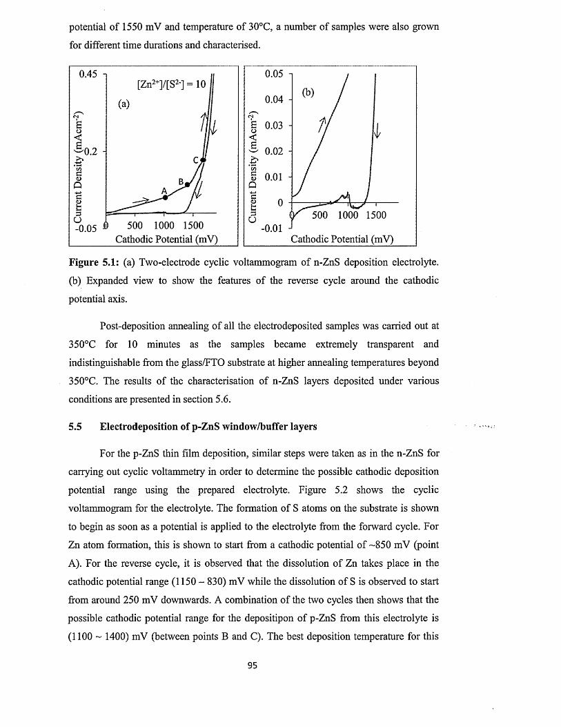
potential of 1550 mV and temperature of 30°C, a number of samples were also grown
for different time durations and characterised.
0.05
0.04
0.03
0.02
0.01
500 1000 1500- 0.01
Cathodic Potential (mV)
0.45
0.2
Cathodic Potential (mV)
Figure 5.1: (a) Two-electrode cyclic voltammogram of n-ZnS deposition electrolyte,
(b) Expanded view to show the features of the reverse cycle around the cathodic
potential axis.
Post-deposition annealing o f all the electrodeposited samples was carried out at
350°C for 10 minutes as the samples became extremely transparent and
indistinguishable from the glass/FTO substrate at higher annealing temperatures beyond
350°C. The results of the characterisation of n-ZnS layers deposited under various
conditions are presented in section 5.6.
5.5 Electrodeposition of p-ZnS window/buffer layers
For the p-ZnS thin film deposition, similar steps were taken as in the n-ZnS for
carrying out cyclic voltammetry in order to determine the possible cathodic deposition
potential range using the prepared electrolyte. Figure 5.2 shows the cyclic
voltammogram for the electrolyte. The formation of S atoms on the substrate is shown
to begin as soon as a potential is applied to the electrolyte from the forward cycle. For
Zn atom formation, this is shown to start from a cathodic potential of -850 mV (point
A). For the reverse cycle, it is observed that the dissolution of Zn takes place in the
cathodic potential range (1150 - 830) mV while the dissolution of S is observed to start
from around 250 mV downwards. A combination of the two cycles then shows that the
possible cathodic potential range for the depositipon of p-ZnS from this electrolyte is
(1100 ~ 1400) mV (between points B and C). The best deposition temperature for this
95

material was also taken as 30°C for the same reason given in the case of n-ZnS. This
was also the temperature at which the cyclic voltammetry was carried out. The best
cathodic deposition potential was established as 1365 mV after deposition and
characterisation of a number of samples. The deposited p-ZnS layers were annealed at
350°C for 10 minutes as in the case of n-ZnS layers and the results obtained are
presented in section 5.6.
- 1 0 C 300 700 1100 1500
Cathodic potential (mV)
Figure 5.2: Two-electrode cyclic voltammogram of p-ZnS deposition electrolyte.
It is noted that S atoms were the first to deposit before Zn atoms in the
electrodeposition process described above. This follows from the fact that S has a lower
standard reduction potential o f E° = -0.476 V than Zn with E° value o f -0.762 V [32].
This is in agreement with the fact that in a cathodic deposition process* the species with
the lowest E° value (or more electropositive species) deposit first followed by the
species with the next higher E° value (or less electropositive species) [26]. Thus the
reaction
S + 2e~ <-» S 2~ (E° = -0 .4 7 6 V) (5.1)
will proceed at a lower cathodic potential than the reaction
Z n2+ + 2e~ <-» Zn (E° = -0 .7 6 2 V) (5.2)
Thus the reaction resulting in the formation of S atoms on the cathode (substrate) takes
place first. This then encourages the co-deposition of Zn atoms to form ZnS on the
cathode. The proposed equations of reaction leading to the formation of ZnS on the
substrate are then given as
9 6

S20 l~ + 6 H+ ~ 2 S + 3 H20 + 4 e “ (5.3)
and
Z n2+ + 2e «-» Zn (5.2)
Equation (5.3) shows that 4 moles of electrons are required to form 2 moles of S
atoms. This then means that only 2 moles o f electrons are required to form 1 mole of S
atoms. From equation (5.2), only 2 moles of electrons are required to form 1 mole o f Zn
atoms. On the whole therefore, a total of 4 moles of electrons are involved in the
formation of 1 mole of ZnS so that
5.6 Characterisation of electrodeposited ZnS layers
A range of techniques available within the Materials and Engineering Research
Institute (MERI) were used in characterising the electrodeposited n-ZnS and p-ZnS
thin-film layers. These techniques include X-ray diffraction for structural
characterisation, photoelectrochemical (PEC) cell for determination o f electrical
conductivity type, current-voltage measurement for determination of electrical
resistivity/conductivity, spectrophotometry for optical characterisation, scanning
electron microscopy for surface morphological studies and energy dispersive X-ray for
determination of atomic composition of the various layers.
5.6.1 X-ray diffraction of n-ZnS and p-ZnS layers
Figures 5.3 (a) and (b) show the X-ray diffractograms of ZnS layers grown from
the higher Zn2+ and lower Zn2+ baths. The figures show clearly that the ZnS layers from
both baths had no XRD peaks. All the XRD peaks present in the figures are those o f the
underlying FTO substrate. These ZnS layers are therefore amorphous in nature. After
annealing at 350°C for 10 minutes, the layers still showed no XRD peaks, confirming
their amorphous nature as shown in figure 5.4.
Zn + S «-> ZnS (5.4)
97
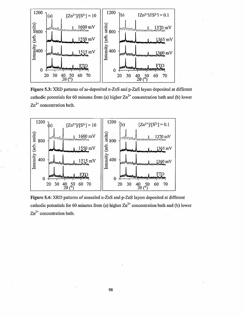
1200[Zn2+]/[S2i = 10
£400 - 1515 mV
T “120 30 40 50 60 70
20 (°)
1200 i
§ 800 Hi-iG3*
400
rzn2+i/rs2-i = o .i
L .„ m 0 m V
» 1365 mV
360 mV
20 30 40 50 60 70 20 (°)
Figure 5.3: XRD patterns of as-deposited n-ZnS and p-ZnS layers deposited at different
cathodic potentials for 60 minutes from (a) higher Zn2+ concentration bath and (b) lower^ I
Zn concentration bath.
1200 i1200 i
1600 mV 1370mV3 800 -3 800 -
x>155.0 mV 365 mV
400 -400 - 151.5 mV
F.T]
Figure 5.4: XRD patterns of annealed n-ZnS and p-ZnS layers deposited at different
cathodic potentials for 60 minutes from (a) higher Zn2+ concentration bath and (b) lower
Zn2+ concentration bath.
98
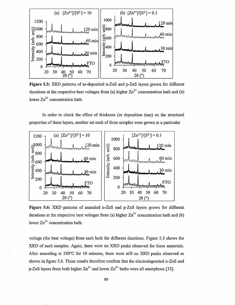
1200 i
SI 000
| 800
'2-600 -
400(L)M 200 -
0
(a) [Zn2+]/[S2_] = 10
J j ^ j 20 min
60 min
0 min
- J s ^ TQ
20 30 40 50 60 70 20 (°)
(b) [Zn2+]/[S2_] = 0.1
1000 -
2 0 mm5800 -3 I 60 mm
30 mm
200 -
20 30 40 50 60 7020 (°)
Figure 5.5: XRD patterns of as-deposited n-ZnS and p-ZnS layers grown for different^ I
durations at the respective best voltages from (a) higher Zn concentration bath and (b)
lower Zn2+ concentration bath.
In order to check the effect of thickness (or deposition time) on the structural
properties of these layers, another set each of three samples were grown at a particular
1200 n (a) [Zn2+]/[S2‘] = 10
^ 0 0 0 . { , 4 I ( 120 min
i f f ™ ”
0 min
200 -
20 30 40 50 60 70 20 (°)
[Zn2+]/[S2*] = 0.1
1 2 0 ming 800
i 60 mm
co 400 -U 30 mm
200 -
20 30 40 50 60 70 20 (°)
Figure 5.6: XRD patterns of annealed n-ZnS and p-ZnS layers grown for different
durations at the respective best voltages from (a) higher Zn2+ concentration bath and (b)
lower Zn2+ concentration bath.
voltage (the best voltage) from each bath for different durations. Figure 5.5 shows the
XRD of such samples. Again, there were no XRD peaks observed for these materials.
After annealing at 350°C for 10 minutes, there were still no XRD peaks observed as
shown in figure 5.6. These results therefore confirm that the electrodeposited n-ZnS and
p-ZnS layers from both higher Zn2+ and lower Zn2+ baths were all amorphous [33].
99
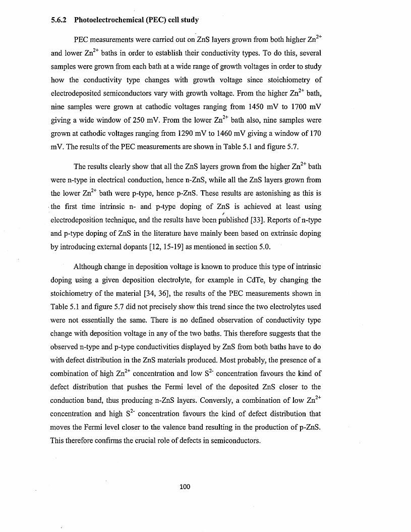
5.6.2 Photoelectrochemical (PEC) cell study
PEC measurements were carried out on ZnS layers grown from both higher Zn2+
and lower Zn2+ baths in order to establish their conductivity types. To do this, several
samples were grown from each bath at a wide range of growth voltages in order to study
how the conductivity type changes with growth voltage since stoichiometry of
electrodeposited semiconductors vary with growth voltage. From the higher Zn2+ bath,
nine samples were grown at cathodic voltages ranging from 1450 mV to 1700 mV94-giving a wide window o f 250 mV. From the lower Zn bath also, nine samples were
grown at cathodic voltages ranging from 1290 mV to 1460 mV giving a window of 170
mV. The results of the PEC measurements are shown in Table 5.1 and figure 5.7.
The results clearly show that all the ZnS layers grown from the higher Zn2+ bath
were n-type in electrical conduction, hence n-ZnS, while all the ZnS layers grown from
the lower Zn2+ bath were p-type, hence p-ZnS. These results are astonishing as this is
the first time intrinsic n- and p-type doping of ZnS is achieved at least using/
electrodeposition technique, and the results have been published [33]. Reports o f n-type
and p-type doping of ZnS in the literature have mainly been based on extrinsic doping
by introducing external dopants [12, 15-19] as mentioned in section 5.0.
Although change in deposition voltage is known to produce this type o f intrinsic
doping using a given deposition electrolyte, for example in CdTe, by changing the
stoichiometry o f the material [34, 36], the results of the PEC measurements shown in
Table 5.1 and figure 5.7 did not precisely show this trend since the two electrolytes used
were not essentially the same. There is no defined observation of conductivity type
change with deposition voltage in any of the two baths. This therefore suggests that the
observed n-type and p-type conductivities displayed by ZnS from both baths have to do
with defect distribution in the ZnS materials produced. Most probably, the presence of a
combination of high Zn2+ concentration and low S2' concentration favours the kind of
defect distribution that pushes the Fermi level o f the deposited ZnS closer to the
conduction band, thus producing n-ZnS layers. Conversly, a combination o f low Zn2+
concentration and high S2‘ concentration favours the kind o f defect distribution that
moves the Fermi level closer to the valence band resulting in the production o f p-ZnS.
This therefore confirms the crucial role of defects in semiconductors.
100
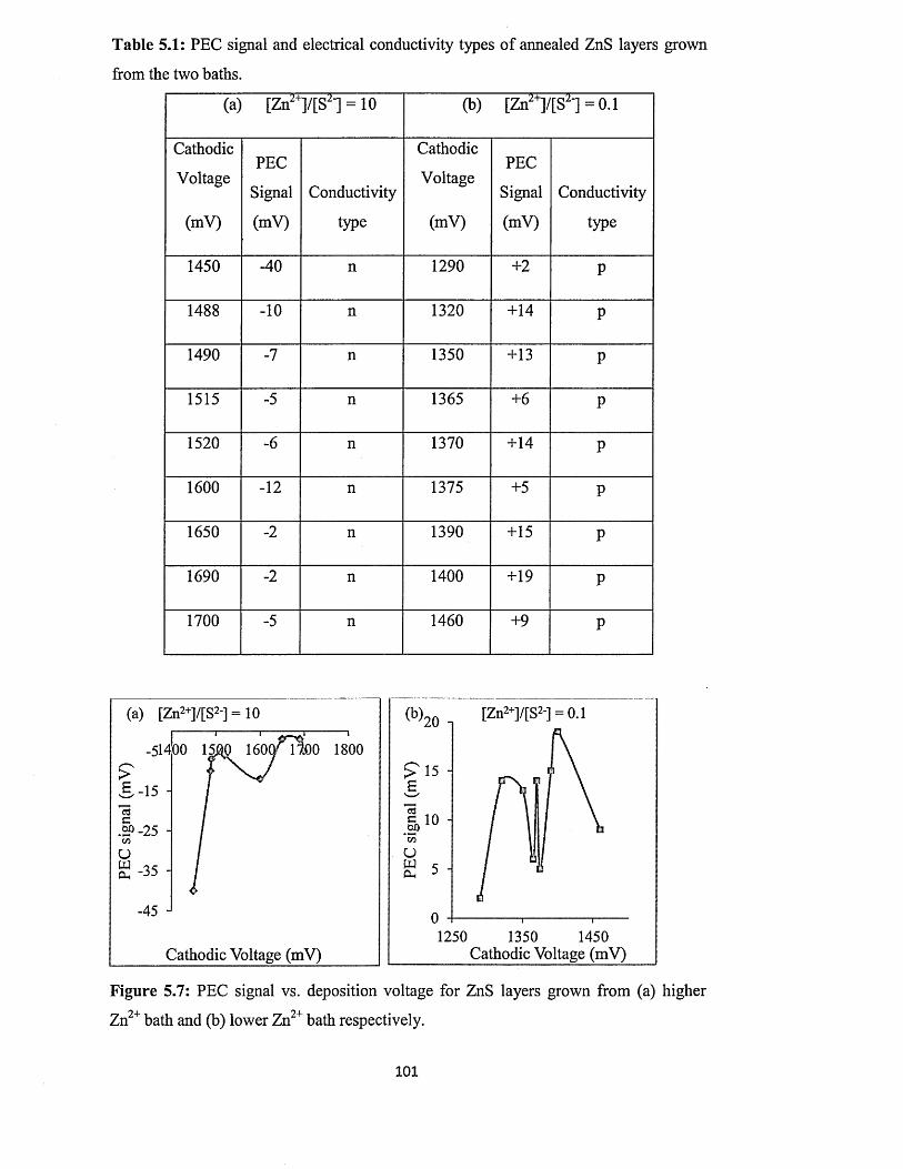
Table 5.1: PEC signal and electrical conductivity types o f annealed ZnS layers grown
from the two baths.
(a) [Zn2+]/[S2-] = 10 (b) [Zn2+]/[S2*] = 0.1
Cathodic
Voltage
(mV)
PEC
Signal
(mV)
Conductivity
type
Cathodic
Voltage
(mV)
PEC
Signal
(mV)
Conductivity
type
1450 -40 n 1290 + 2 P
1488 - 1 0 n 1320 +14 P
1490 -7 n 1350 +13 P
1515 -5 n 1365 + 6 P
1520 - 6 n 1370 +14 P
1600 - 1 2 n 1375 +5 P
1650 - 2 n 1390 +15 P
1690 - 2 n 1400 +19 P
1700 -5 n 1460 +9 P
(a) [Zn2+]/[S2‘] = 10
-51400 1500 160 Of 1700 1800
-35 -
-45 J
Cathodic Voltage (mV)
(b)20 i
> 15 g
c 10too
OWCL. 5 -
0
[Zn2+]/[S2*] = 0.1
1250 1350 1450Cathodic Voltage (mV)
Figure 5.7: PEC signal vs. deposition voltage for ZnS layers grown from (a) higher
Zn2+ bath and (b) lower Zn2+ bath respectively.
101
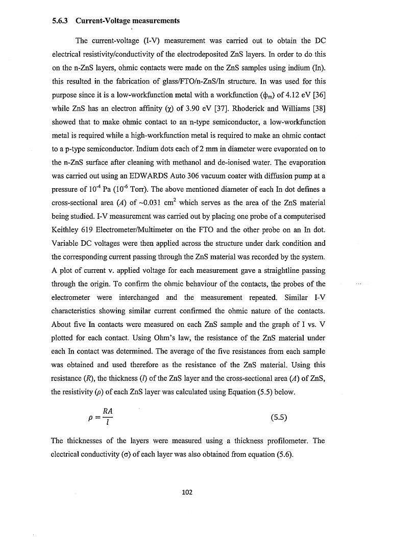
5.6.3 Current-Voltage measurements
The current-voltage (I-V) measurement was carried out to obtain the DC
electrical resistivity/conductivity of the electrodeposited ZnS layers. In order to do this
on the n-ZnS layers, ohmic contacts were made on the ZnS samples using indium (In),
this resulted in the fabrication o f glass/FTO/n-ZnS/In structure. In was used for this
purpose since it is a low-workfunction metal with a workfimction ((j)m) of 4.12 eV [36]
while ZnS has an electron affinity (x) of 3.90 eV [37]. Rhoderick and Williams [38]
showed that to make ohmic contact to an n-type semiconductor, a low-workfunction
metal is required while a high-workfunction metal is required to make an ohmic contact
to a p-type semiconductor. Indium dots each of 2 mm in diameter were evaporated on to
the n-ZnS surface after cleaning with methanol and de-ionised water. The evaporation
was carried out using an EDWARDS Auto 306 vacuum coater with diffusion pump at a
pressure of 10*4 Pa (10‘6 Torr). The above mentioned diameter of each In dot defines a
cross-sectional area (A) of -0.031 cm2 which serves as the area o f the ZnS material
being studied. I-V measurement was carried out by placing one probe o f a computerised
Keithley 619 Electrometer/Multimeter on the FTO and the other probe on an In dot.
Variable DC voltages were then applied across the structure under dark condition and
the corresponding current passing through the ZnS material was recorded by the system.
A plot of current v. applied voltage for each measurement gave a straightline passing
through the origin. To confirm the ohmic behaviour o f the contacts, the probes o f the
electrometer were interchanged and the measurement repeated. Similar I-V
characteristics showing similar current confirmed the ohmic nature o f the contacts.
About five In contacts were measured on each ZnS sample and the graph of I vs. V
plotted for each contact. Using Ohm’s law, the resistance of the ZnS material under
each In contact was determined. The average of the five resistances from each sample
was obtained and used therefore as the resistance o f the ZnS material. Using this
resistance (R), the thickness (/) o f the ZnS layer and the cross-sectional area (A) o f ZnS,
the resistivity (p) of each ZnS layer was calculated using Equation (5.5) below.
RAP = — (5.5)
The thicknesses of the layers were measured using a thickness profilometer. The
electrical conductivity (o) o f each layer was also obtained from equation (5.6).
102
1o = —
p(5.6)
Table 5.2 and figure 5.8 show the resistivity and conductivity values obtained
for as-deposited and annealed n-ZnS o f different thicknesses grown at a cathodic
voltage of 1550 mV.
Table 5.2: Electrical resistivity of as-deposited and annealed n-ZnS layers o f different
thicknesses.
Serial
NO
Sample
ID
Growth
Time (min)
Thickness
(nm)
AD-ZnS
pxlO4
(Ocm)
HT-ZnS
p x io 4
(Ocm)
1 K405 60 281 3.9 4.8
2 K407 1 2 0 352 3.6 3.3
3 K408 150 448 2.5 3.1
4 K406 180 462 2.3 2.7
5 K410 2 0 0 569 2 . 2 2 . 6
6 K409 180 755 1.4 2.5
7 K411 240 785 1.9 1.9
Note: AD = as-deposited, HT = heat-treated.
103
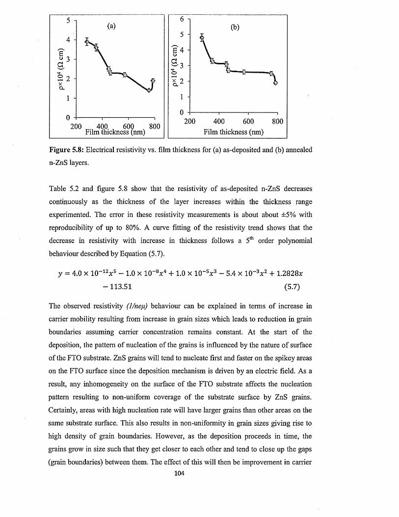
200 400 600 800Film thickness (nm) Film thickness (nm)
Figure 5.8: Electrical resistivity vs. film thickness for (a) as-deposited and (b) annealed
n-ZnS layers.
Table 5.2 and figure 5.8 show that the resistivity of as-deposited n-ZnS decreases
continuously as the thickness of the layer increases within the thickness range
experimented. The error in these resistivity measurements is about about ±5% with
reproducibility of up to 80%. A curve fitting of the resistivity trend shows that the
decrease in resistivity with increase in thickness follows a 5th order polynomial
behaviour described by Equation (5.7).
y = 4.0 x 10 " 1 2 * 5 - 1.0 x 10~8 x 4 + 1.0 x 10 - 5 * 3 - 5.4 x 10 " 3 * 2 + 1.2828*
-1 1 3 .5 1 (5.7)
The observed resistivity (l/ne[i) behaviour can be explained in terms of increase in
carrier mobility resulting from increase in grain sizes which leads to reduction in grain
boundaries assuming carrier concentration remains constant. At the start of the
deposition, the pattern of nucleation of the grains is influenced by the nature o f surface
of the FTO substrate. ZnS grains will tend to nucleate first and faster on the spikey areas
on the FTO surface since the deposition mechanism is driven by an electric field. As a
result, any inhomogeneity on the surface of the FTO substrate affects the nucleation
pattern resulting to non-uniform coverage o f the substrate surface by ZnS grains.
Certainly, areas with high nucleation rate will have larger grains than other areas on the
same substrate surface. This also results in non-uniformity in grain sizes giving rise to
high density o f grain boundaries. However, as the deposition proceeds in time, the
grains grow in size such that they get closer to each other and tend to close up the gaps
(grain boundaries) between them. The effect of this will then be improvement in carrier104
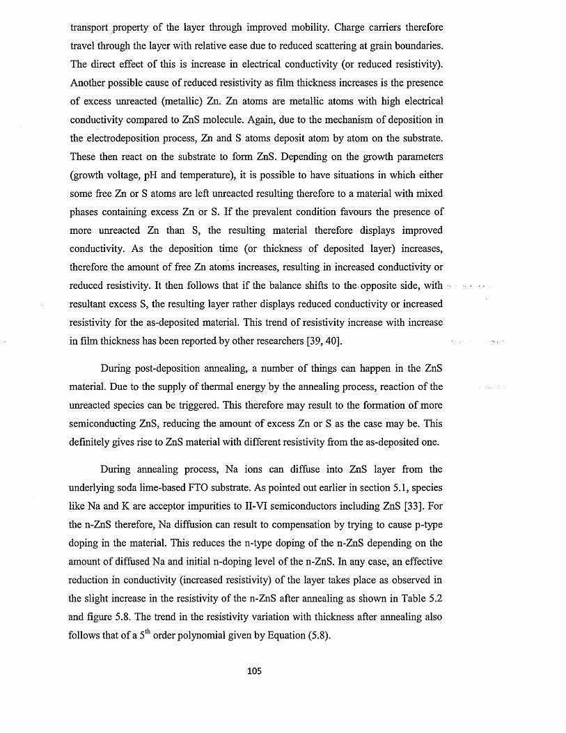
transport property of the layer through improved mobility. Charge carriers therefore
travel through the layer with relative ease due to reduced scattering at grain boundaries.
The direct effect of this is increase in electrical conductivity (or reduced resistivity).
Another possible cause o f reduced resistivity as film thickness increases is the presence
o f excess unreacted (metallic) Zn. Zn atoms are metallic atoms with high electrical
conductivity compared to ZnS molecule. Again, due to the mechanism of deposition in
the electrodeposition process, Zn and S atoms deposit atom by atom on the substrate.
These then react on the substrate to form ZnS. Depending on the growth parameters
(growth voltage, pH and temperature), it is possible to have situations in which either
some free Zn or S atoms are left unreacted resulting therefore to a material with mixed
phases containing excess Zn or S. If the prevalent condition favours the presence of
more unreacted Zn than S, the resulting material therefore displays improved
conductivity. As the deposition time (or thickness of deposited layer) increases,
therefore the amount of free Zn atoms increases, resulting in increased conductivity or
reduced resistivity. It then follows that if the balance shifts to the opposite side, with
resultant excess S, the resulting layer rather displays reduced conductivity or increased
resistivity for the as-deposited material. This trend of resistivity increase with increase
in film thickness has been reported by other researchers [39,40].
During post-deposition annealing, a number of things can happen in the ZnS
material. Due to the supply of thermal energy by the annealing process, reaction of the
unreacted species can be triggered. This therefore may result to the formation o f more
semiconducting ZnS, reducing the amount of excess Zn or S as the case may be. This
definitely gives rise to ZnS material with different resistivity from the as-deposited one.
During annealing process, Na ions can diffuse into ZnS layer from the
underlying soda lime-based FTO substrate. As pointed out earlier in section 5.1, species
like Na and K are acceptor impurities to II-VI semiconductors including ZnS [33]. For
the n-ZnS therefore, Na diffusion can result to compensation by trying to cause p-type
doping in the material. This reduces the n-type doping of the n-ZnS depending on the
amount of diffused Na and initial n-doping level of the n-ZnS. In any case, an effective
reduction in conductivity (increased resistivity) of the layer takes place as observed in
the slight increase in the resistivity of the n-ZnS after annealing as shown in Table 5.2
and figure 5.8. The trend in the resistivity variation with thickness after annealing also
follows that of a 5th order polynomial given by Equation (5.8).
105
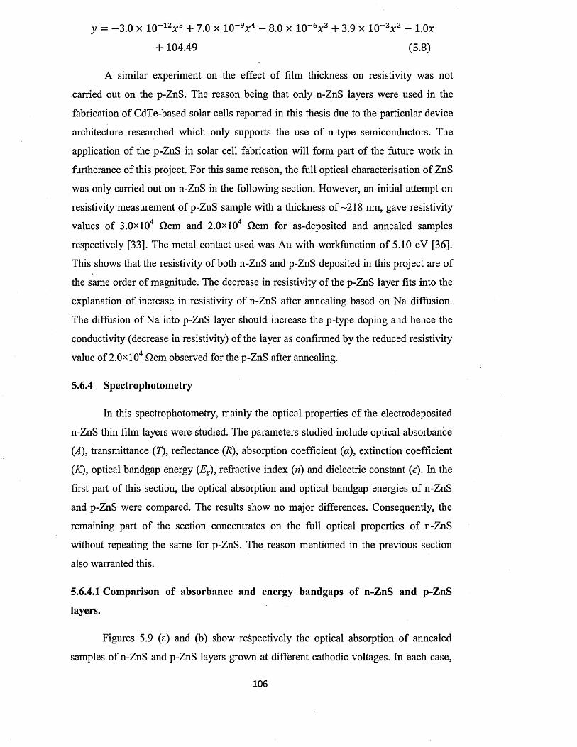
y = -3 .0 x 10~12x 5 + 7.0 x 10" V - 8.0 x 10~6x 3 + 3.9 x 10~3x 2 - l.Ox
+ 1 0 4 .4 9 (5.8)
A similar experiment on the effect of film thickness on resistivity was not
carried out on the p-ZnS. The reason being that only n-ZnS layers were used in the
fabrication of CdTe-based solar cells reported in this thesis due to the particular device
architecture researched which only supports the use o f n-type semiconductors. The
application of the p-ZnS in solar cell fabrication will form part of the future work in
furtherance of this project. For this same reason, the full optical characterisation of ZnS
was only carried out on n-ZnS in the following section. However, an initial attempt on
resistivity measurement o f p-ZnS sample with a thickness of -218 nm, gave resistivity
values of 3.0x10⁴ Qcm and 2.0xlO4 flcm for as-deposited and annealed samples
respectively [33]. The metal contact used was Au with workfunction of 5.10 eV [36].
This shows that the resistivity o f both n-ZnS and p-ZnS deposited in this project are o f
the same order o f magnitude. The decrease in resistivity of the p-ZnS layer fits into the
explanation of increase in resistivity of n-ZnS after annealing based on Na diffusion.
The diffusion of Na into p-ZnS layer should increase the p-type doping and hence the
conductivity (decrease in resistivity) of the layer as confirmed by the reduced resistivity
value of 2.0x10⁴ Hem observed for the p-ZnS after annealing.
5.6.4 Spectrophotometry
In this spectrophotometry, mainly the optical properties of the electrodeposited
n-ZnS thin film layers were studied. The parameters studied include optical absorbance
(A), transmittance (7), reflectance (R), absorption coefficient (a), extinction coefficient
(K), optical bandgap energy (Eg), refractive index (n) and dielectric constant (e). In the
first part of this section, the optical absorption and optical bandgap energies o f n-ZnS
and p-ZnS were compared. The results show no major differences. Consequently, the
remaining part of the section concentrates on the full optical properties o f n-ZnS
without repeating the same for p-ZnS. The reason mentioned in the previous section
also warranted this.
5.6.4.1 Comparison of absorbance and energy bandgaps of n-ZnS and p-ZnS
layers.
Figures 5.9 (a) and (b) show respectively the optical absorption of annealed
samples of n-ZnS and p-ZnS layers grown at different cathodic voltages. In each case,
106
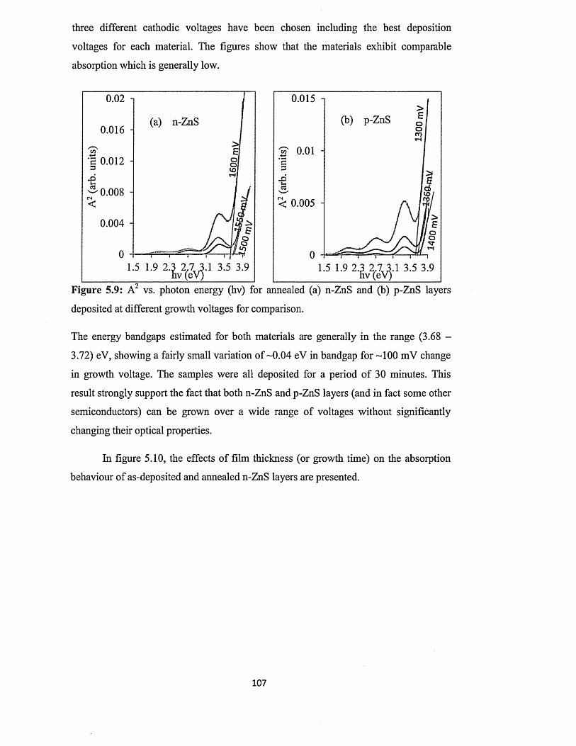
three different cathodic voltages have been chosen including the best deposition
voltages for each material. The figures show that the materials exhibit comparable
absorption which is generally low.
0.02 i
(a) n-ZnS0.016 -
c 0.012 - o]
0.008 -
0.004 -
0 .015 i
(b) p-ZnS oono0.01 -
< 0.005 -
Figure 5.9: A2 vs. photon energy (hv) for annealed (a) n-ZnS and (b) p-ZnS layers
deposited at different growth voltages for comparison.
The energy bandgaps estimated for both materials are generally in the range (3.68 -
3.72) eV, showing a fairly small variation o f -0.04 eV in bandgap for -100 mV change
in growth voltage. The samples were all deposited for a period o f 30 minutes. This
result strongly support the fact that both n-ZnS and p-ZnS layers (and in fact some other
semiconductors) can be grown over a wide range of voltages without significantly
changing their optical properties.
In figure 5.10, the effects of film thickness (or growth time) on the absorption
behaviour of as-deposited and annealed n-ZnS layers are presented.
107
0.06
0.012
0.04§0.008
0.004
hv (eV) hv (eV)
Figure 5.10: A2 vs. hv for (a) as-deposited and (b) annealed n-ZnS layers grown
at cathodic voltage o f 1550 mV for different times.
The graphs show that n-ZnS exhibits low absorption property and the absorbance
becomes even lower after annealing. However, as the deposition time (or thickness)
increases, the absorbance increases, and energy bandgap decreases. This behaviour
suggests that as the thickness increases, smaller grains in the material tend to coalesce to
form larger grains. The result o f this is that the optical property of the material tends
towards that o f the bulk material with the bandgap approaching that o f the bulk
material. After post-deposition annealing, the bandgaps were observed to increase
slightly. This may be as a result o f loss o f excess S or Zn or rather as a result of
complete reaction between excess S and Zn forming more ZnS material. The energy
bandgap values estimated for the various layers from figure 5.10 are in the range (3.58 -
3.72) eV for as-deposited samples and (3.66 - 3.78) eV after annealing. These values
are in very good agreement with literature values for ZnS [1, 9, 41]. The thicknesses of
the layers used were -284 nm, 361 nm and 526 nm for growth times of 30, 45 and 60
minutes respectively. It is important to point out that the use of A2 vs. hv, instead of
(ahv) 2 vs. hv, to estimate energy bandgap of a semiconductor is a very quick way of
estimating the energy bandgap and gives result similar to that obtained using (ahv) 2 vs.
hv.
Figure 5.11 shows similar absorption results for as-deposited and annealed p-
ZnS layers grown for different time durations.
108
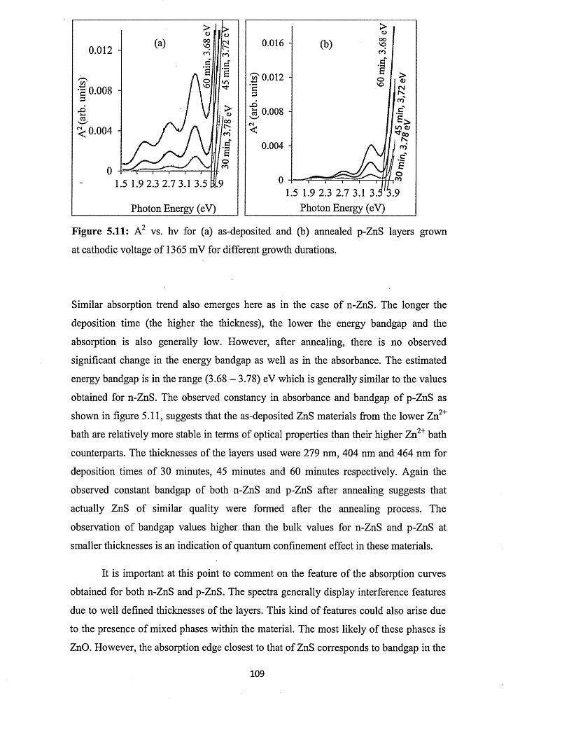
1.5 1.9 2.3 2.7 3.1 3.3' Photon Energy (eV)Photon Energy (eV)
Figure 5.11: A2 vs. hv for (a) as-deposited and (b) annealed p-ZnS layers grown
at cathodic voltage of 1365 mV for different growth durations.
Similar absorption trend also emerges here as in the case of n-ZnS. The longer the
deposition time (the higher the thickness), the lower the energy bandgap and the
absorption is also generally low. However, after annealing, there is no observed
significant change in the energy bandgap as well as in the absorbance. The estimated
energy bandgap is in the range (3.68 - 3.78) eV which is generally similar to the values
obtained for n-ZnS. The observed constancy in absorbance and bandgap o f p-ZnS as
shown in figure 5.11, suggests that the as-deposited ZnS materials from the lower Zn2+
bath are relatively more stable in terms of optical properties than their higher Zn2+ bath
counterparts. The thicknesses of the layers used were 279 nm, 404 nm and 464 nm for
deposition times of 30 minutes, 45 minutes and 60 minutes respectively. Again the
observed constant bandgap of both n-ZnS and p-ZnS after annealing suggests that
actually ZnS of similar quality were formed after the annealing process. The
observation of bandgap values higher than the bulk values for n-ZnS and p-ZnS at
smaller thicknesses is an indication of quantum confinement effect in these materials.
It is important at this point to comment on the feature o f the absorption curves
obtained for both n-ZnS and p-ZnS. The spectra generally display interference features
due to well defined thicknesses of the layers. This kind of features could also arise due
to the presence of mixed phases within the material. The most likely of these phases is
ZnO. However, the absorption edge closest to that of ZnS corresponds to bandgap in the
range (2.70 - 3.10) eV which is actually less than the optical bandgap o f bulk ZnO
which is 3.37 eV [40]. The lack of any XRD peak really makes it difficult to confirm
the presence o f ZnO. But if there is amorphous ZnO present in these layers, the
observed bandgap is expected to be higher than 3.37 eV, due to quantum confinement
effects which also has been observed for ZnS with small thicknesses. This therefore
makes it difficult to conclude the presence of mixed phases such as ZnO and these
observed three peaks separated by equal distances must be arising due to interference of
light. Whatever the case is, this feature is very typical o f the electrodeposited ZnS layers
produced in this project.
5.6.4.2 Full optical characterisation of n-ZnS layers of different thicknesses
This sub-section presents the full optical characterisation of three n-ZnS layers
of different thicknesses before and after annealing. The thicknesses of the layers were
400 nm, 500 nm and 700 nm measured using a UBM Microfocus Optical Measuring
System. Normal incidence transmittance o f the layers was measured using a Carry 50
UV-VIS spectrophotometer in the wavelength range (315 - 800) nm. Before the
transmittance of the glass/FTO/ZnS layers was measured, the transmittance of
glass/FTO was measured in baseline mode as the reference. This serves to automatically
cancel the effect o f glass/FTO in the measured transmittance of glass/FTO/ZnS so that
the result obtained is only the transmittance of ZnS. Using the equations in section 3.5,
and the transmittance spectra measured, the absorbance, reflectance, absorption
coefficient, extinction coefficient, energy bandgap, refractive index and dielectric
constant of each ZnS layers were obtained.
Figures 5.12 (a) and (b) show the transmittance spectra o f the three n-ZnS
layers. The figures show that the transmittance of the layers decreases as the film
thickness increases both before and after annealing. However, after annealing, the
transmittance generally increases. The transmittance of the as-deposited layers in the
visible region of the electromagnetic spectrum (A. = 400 - 700) nm is in the range o f (69
- 75)%, (55 - 62)% and (45 - 52)% for the samples with thickness of 400 nm, 500 nm
and 700 nm respectively.
110

100 1
40 i ; " ' ’••“700nm— 500 nm— 400 nm
20 -
315 412 509 606 703 800 Wavelength (nm)
p\ 70p 60
700 nm 500 nm -400 nm
1-------1-------1-------1-------r315 412 509 606 703 800
Wavelength (nm)
Figure 5.12: Transmittance spectra o f (a) as-deposited and (b) annealed ZnS layers of
different thicknesses.
The corresponding transmittance after annealing is in the range (83 - 92)%, (76 -
87)% and (67 - 78)% respectively. Post-deposition annealing therefore improves the
transmittance of the layers. Again, it shows that the transmittance o f the layers has
strong thickness dependence. The transmittance also increases as the wavelength of
incident light increases.
The absorbance spectra of the layers are shown in figures 5.13 (a) and (b).
Again, the figures show that absorbance of the layers is thickness dependent with the
thickest layer (700 nm) showing the highest absorbance and the thinnest layer (400 nm)
showing the lowest absorbance in the wavelength range explored. The absorbance also
decreases as the wavelength of incident light increases.
I ll

(a)
•g 0 . 8C3
I 0.6<u01 0.4Oco< 0.2 -|
■ • -700 nm- -500 nm
— 400 nm
S . ..•*siV N
315 412 509 606 703 800 Wavelength (nm)
C3
1
0.8
0.6
(b) 700 nm 500 nm
400 nm
**“ «<«•>»!
315 412 509 606 703 800 Wavelength (nm)
Figure 5.13: Absorbance spectra of (a) as-deposited and (b) annealed ZnS layers of
different thicknesses.
Figure 5.13 (b) shows that annealing reduces the absorbance generally. The
implication of figures 5.12 and 5.13 is that, depending on the required application, the
transmittance and absorbance of these ZnS layers can be tuned to the desired levels by
simply varying the thickness. Thus for application as window material in solar cells, the
thickness should be kept as low as possible in order to allow enough photons to pass
through to the absorber layer in order to create more charge carriers.
Figure 5.14 presents the reflectance o f the three ZnS layers as a function of
wavelength of incident light. The reflectance is generally having a maximum value of
~20% for all three layers at a wavelength of 315 nm for both as-deposited and annealed
samples. Again the reflectance depends on the film thickness, increasing with thickness
across the entire wavelength range under consideration. The as-deposited samples
nevertheless, exhibit a week dependence on the incident light wavelength in comparison
with the annealed samples which show relatively drastic decrease with increase in
wavelength of incident light. Annealing generally reduces the reflectance especially
towards longer wavelengths.
112

100 1 100 -]
700 nm 700 nm 500 nm
500 nm400 nm
400 nm
Wavelength (nm)Wavelength (nm)
Figure 5.14: Reflectance spectra o f (a) as-deposited and (b) annealed ZnS layers of
different thicknesses.
Figures 5.15 (a) and (b) show the dependence o f absorption coefficient
(a) on incident photon energy for ZnS layers before and after annealing respectively, a
increases as photon energy increases and as film thickness increases. For as-deposited
samples, there is a sharp rise in a at a photon energy o f -3.60 eV.
2.0E+04 n 2.0E+04 -i
.i/
700 nm
500 nm »/i
400 njn
700 nm
500 nm
400 nm1.5E+04 -1.5E+04 -
*v1.0E+04 -:1.0E+04 -
5.0E+03 -5.0E+03 -
0.0E+000.0E+00 —i3.9
Photon Energy (eV)Photon Energy (eV)
Figure 5.15: Graphs of absorption coefficient vs. photon energy for (a) as-deposited
and (b) annealed ZnS layers of different thicknesses.
In the annealed samples, this occurs at a photon energy of -3.68 eV. It is
observed from both figures that the absorption coefficients of the thicker samples (with
thicknesses of 500 nm and 700 nm) tend to come to the same value. This suggests that
in this thickness range, the ZnS material properties are tending towards those of the bulk
material. In the visible region of the spectrum, the value of a for the as-deposited113
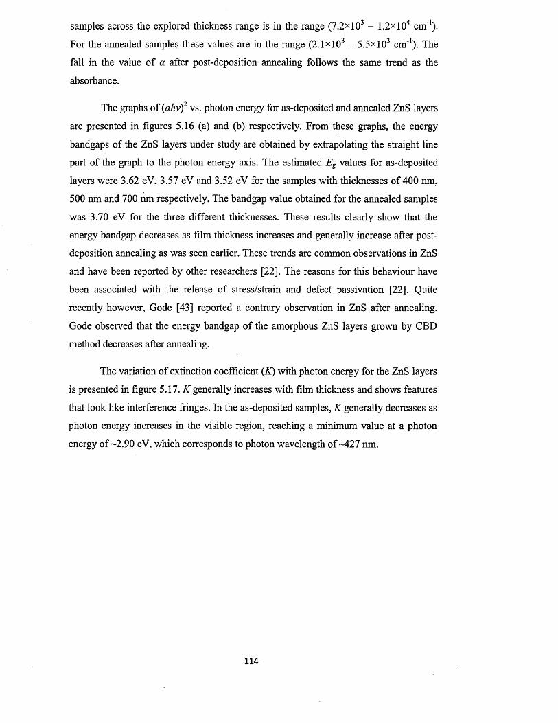
samples across the explored thickness range is in the range (7.2x10³ - 1.2xl04 cm '1).
For the annealed samples these values are in the range (2.1 xlO3 - 5 .5xl03 cm '1). The
fall in the value of a after post-deposition annealing follows the same trend as the
absorbance.
"yThe graphs o f {ahv) vs. photon energy for as-deposited and annealed ZnS layers
are presented in figures 5.16 (a) and (b) respectively. From these graphs, the energy
bandgaps of the ZnS layers under study are obtained by extrapolating the straight line
part of the graph to the photon energy axis. The estimated Eg values for as-deposited
layers were 3.62 eV, 3.57 eV and 3.52 eV for the samples with thicknesses o f 400 nm,
500 nm and 700 nm respectively. The bandgap value obtained for the annealed samples
was 3.70 eV for the three different thicknesses. These results clearly show that the
energy bandgap decreases as film thickness increases and generally increase after post
deposition annealing as was seen earlier. These trends are common observations in ZnS
and have been reported by other researchers [22]. The reasons for this behaviour have
been associated with the release of stress/strain and defect passivation [22]. Quite
recently however, Gode [43] reported a contrary observation in ZnS after annealing.
Gode observed that the energy bandgap of the amorphous ZnS layers grown by CBD
method decreases after annealing.
The variation of extinction coefficient (K) with photon energy for the ZnS layers
is presented in figure 5.17. K generally increases with film thickness and shows features
that look like interference fringes. In the as-deposited samples, K generally decreases as
photon energy increases in the visible region, reaching a minimum value at a photon
energy of -2.90 eV, which corresponds to photon wavelength of -427 nm.
114
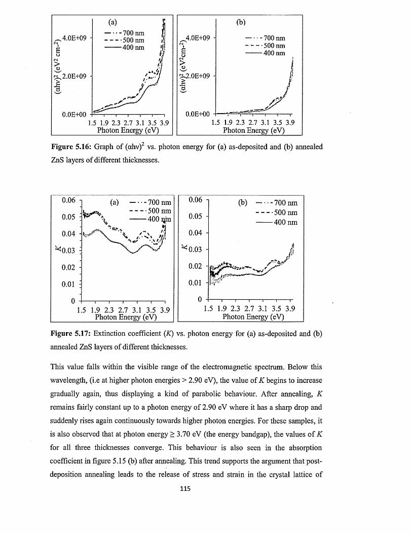
700 nm 500 nm 400 nm
4.0E+09 - • - 700 nm -*500 nm — 400 nm
4.0E+09 -
2.0E+09 -
0.0E+000.0E+00.9
Photon Energy (eV) Photon Energy (eV)
Figure 5.16: Graph of (ahv)2 vs. photon energy for (a) as-deposited and (b) annealed
ZnS layers of different thicknesses.
0.06 700 nm 500 nm 400 qjn0.05
0.02
0.01
Photon Energy (eV)
0.06 -I
0.05 -
0.04
^ 0 .0 3
0.02 -
0.01 -
0
(b) 700 nm 500 nm 400 nm
JrVr*
1.5 1.9 2.3 2.7 3.1 3.5 3.9 Photon Energy (eV)
Figure 5.17: Extinction coefficient (K) vs. photon energy for (a) as-deposited and (b)
annealed ZnS layers of different thicknesses.
This value falls within the visible range o f the electromagnetic spectrum. Below this
wavelength, (i.e at higher photon energies > 2.90 eV), the value of K begins to increase
gradually again, thus displaying a kind of parabolic behaviour. After annealing, K
remains fairly constant up to a photon energy of 2.90 eV where it has a sharp drop and
suddenly rises again continuously towards higher photon energies. For these samples, it
is also observed that at photon energy > 3.70 eV (the energy bandgap), the values o f K
for all three thicknesses converge. This behaviour is also seen in the absorption
coefficient in figure 5.15 (b) after annealing. This trend supports the argument that post
deposition annealing leads to the release of stress and strain in the crystal lattice of
115

materials as well as helps in the passivation of defects. The introduction of stress/strain
most likely results from the presence o f unintended inclusions like ZnO and Zn(OH )2 or
even due to the presence of excess unreacted Zn and S in the as-deposited samples as
has been mentioned in earlier section. In the annealing process, these inclusions like
Zn(OH )2 can decompose in the presence o f heat energy in addition to further reaction of
the excess Zn and S resulting to purer and more stable ZnS with improved quality
especially since these materials were grown at low temperatures.
The dependence of refractive index on photon energy for the ZnS layers is
presented in figure 5.18. Figures 5.18 (a) and (b) generally show that refractive index
(n) increases as film thickness increases. They also show that n increases as the incident
photon energy increases, although this increase is more rapid in the annealed samples
than in the as-deposited samples. However, in both cases, n gets closer to each other in
the ultraviolet region with higher photon energy. The refractive index is related to the
propagation velocity (v) o f light in the material and the speed of light in vacuum (c)
according to n = c/v [44]. The implication o f this equation is that as the refractive index
increases towards-higher photon energy region, the corresponding incident light travel
more slowly through the layers with reduced velocity o f propagation. This implies in
turn that these photons get mostly absorbed in the material. However, photons o f lower
energy tend to travel through the layer with higher propagation velocity without
absorption leading to transmission of these photons through the material layer.
For as-deposited samples, the value o f n falls in the range (2.00 - 2.60) while for
the annealed samples n is in the range (1.50 - 2.59). The fall in the value o f n after
annealing implies that light will propagate faster through the annealed samples than in
the as-deposited ones. This result also supports the fact that annealing improves the
materials by removing stress/strain and passivating defects which act as scattering
centres in the as-deposited materials.
116
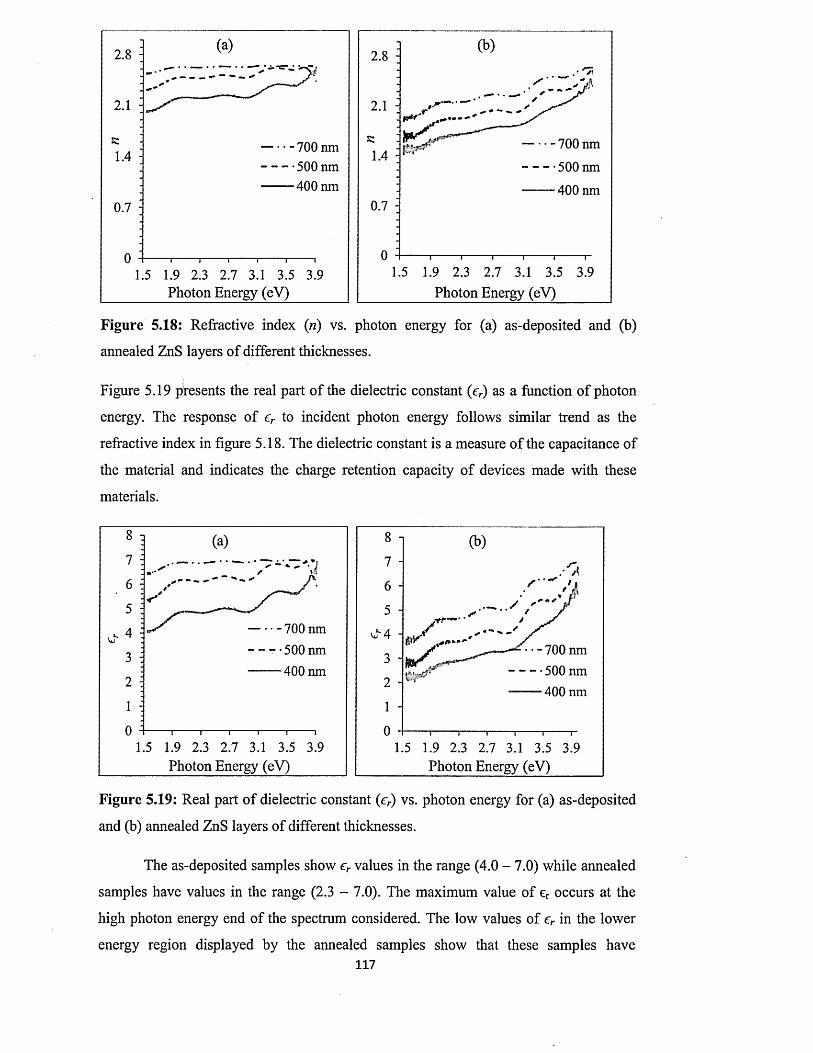
700 nm
500 nm 700 nm 500 nm 400 nm
1.4
400 nm0.7
Photon Energy (eV) Photon Energy (eV)
Figure 5.18: Refractive index (ri) vs. photon energy for (a) as-deposited and (b)
annealed ZnS layers of different thicknesses.
Figure 5.19 presents the real part o f the dielectric constant (er) as a function of photon
energy. The response o f cr to incident photon energy follows similar trend as the
refractive index in figure 5.18. The dielectric constant is a measure o f the capacitance of
the material and indicates the charge retention capacity o f devices made with these
materials.
700 nm— - -500 nm ----- 400 nm
Photon Energy (eV)
ftr'
- • • -700 nm 500 nm- — 400 nm
Photon Energy (eV)
Figure 5.19: Real part o f dielectric constant (er) vs. photon energy for (a) as-deposited
and (b) annealed ZnS layers of different thicknesses.
The as-deposited samples show er values in the range (4.0 - 7.0) while annealed
samples have values in the range (2.3 - 7.0). The maximum value of cr occurs at the
high photon energy end of the spectrum considered. The low values of er in the lower
energy region displayed by the annealed samples show that these samples have117
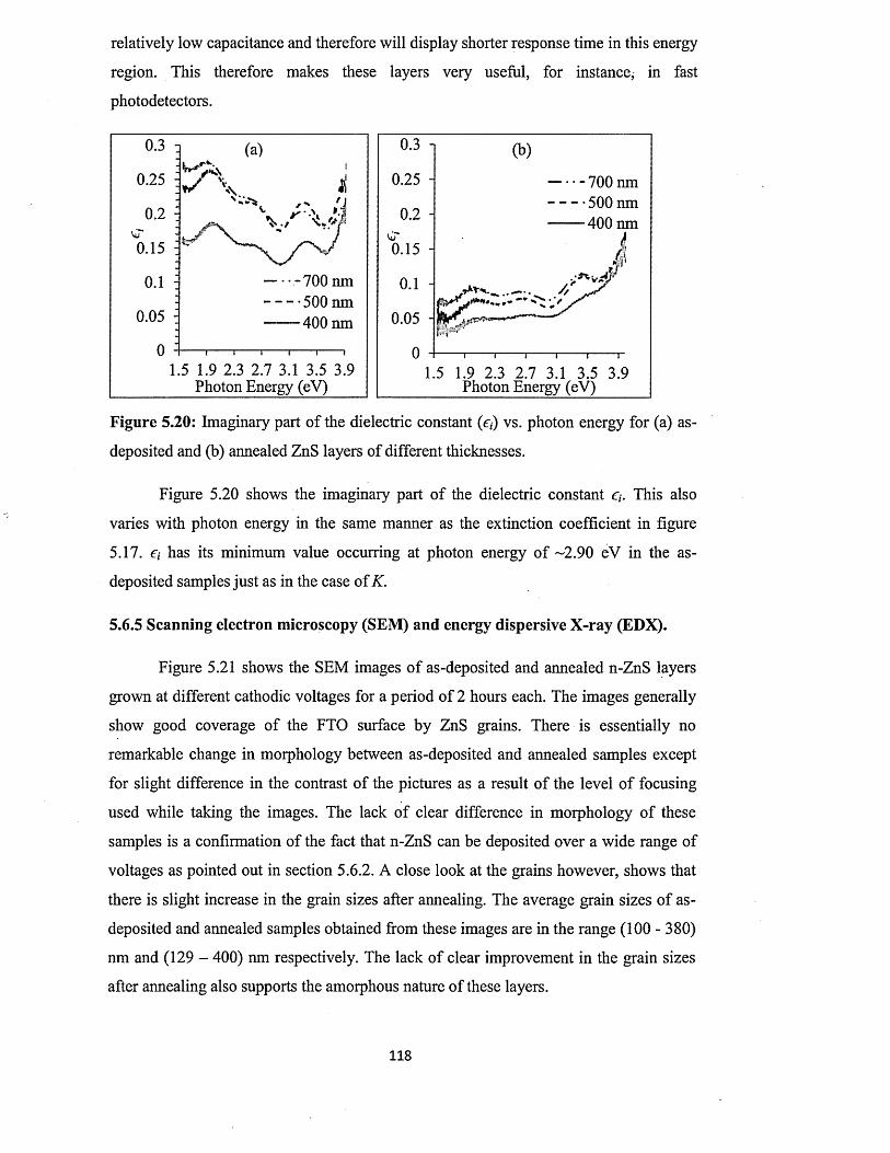
relatively low capacitance and therefore will display shorter response time in this energy
region. This therefore makes these layers very useful, for instance, in fast
photodetectors.
0.25 700 nm 500 nm 400 nm0.2
0.15 0.15
• • - 700 nm— 500 nm— 400 nm0.05 0.05 -
,9Photon Energy (eV) Photon Energy (eV)
Figure 5.20: Imaginary part of the dielectric constant (e,) vs. photon energy for (a) as-
deposited and (b) annealed ZnS layers of different thicknesses.
Figure 5.20 shows the imaginary part o f the dielectric constant £/. This also
varies with photon energy in the same manner as the extinction coefficient in figure
5.17. has its minimum value occurring at photon energy o f -2.90 eV in the as-
deposited samples just as in the case of K.
5.6.5 Scanning electron microscopy (SEM) and energy dispersive X -ray (EDX).
Figure 5.21 shows the SEM images o f as-deposited and annealed n-ZnS layers
grown at different cathodic voltages for a period of 2 hours each. The images generally
show good coverage of the FTO surface by ZnS grains. There is essentially no
remarkable change in morphology between as-deposited and annealed samples except
for slight difference in the contrast o f the pictures as a result o f the level o f focusing
used while taking the images. The lack of clear difference in morphology of these
samples is a confirmation o f the fact that n-ZnS can be deposited over a wide range of
voltages as pointed out in section 5.6.2. A close look at the grains however, shows that
there is slight increase in the grain sizes after annealing. The average grain sizes o f as-
deposited and annealed samples obtained from these images are in the range (100 - 380)
nm and (129 - 400) nm respectively. The lack o f clear improvement in the grain sizes
after annealing also supports the amorphous nature of these layers.
118
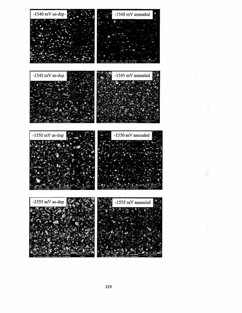
1540 mV annealed
1545 mV annealed
-1550 mV as-dep' V-% T *r -
,* t < • / * . <
*-t j - '* i %■
«* * /"*" i»t *#> "** * »A- w yf .*>*
’*. * 4-'»‘ *< v ; - * /
** * ' • f ^^ * j A w *•" ' » ' f ** ’* * % k
' *• ‘ v' ! , * * * * I• -H* " * *
I, ^ ' •*k. ; .L** *& & *** * .„w ' J Jk<M **, spot i WD m ag HV I de t I Lens M cce -
* 4 O ' 4 9 mm 6C 200 * 15 CO kV- TLO i immersion •
- *> V **:ft ^ ' * ■ "'$&■*' ‘ <k *
1550 mV annealed
1555 mV annealed
s i ■ ..tf.vMML ..*• i •••. i j - . . .»sc o ! : WD mag I HV : dot : Lens Mode a 0 4 & mm 60 000 * 15 00 fcV: T IP Immersion
spot WD m ag h v : de t Lens Mooe4 0 4 8 m m (5C 000x 1 5 0CkV : TIP >rrnefS»on
119
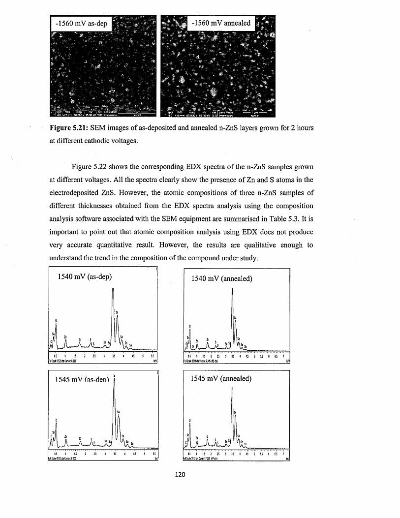
Figure 5.21: SEM images of as-deposited and annealed n-ZnS layers grown for 2 hours
at different cathodic voltages.
Figure 5.22 shows the corresponding EDX spectra of the n-ZnS samples grown
at different voltages. All the spectra clearly show the presence of Zn and S atoms in the
electrodeposited ZnS. However, the atomic compositions of three n-ZnS samples of
different thicknesses obtained from the EDX spectra analysis using the composition
analysis software associated with the SEM equipment are summarised in Table 5.3. It is
important to point out that atomic composition analysis using EDX does not produce
very accurate quantitative result. However, the results are qualitative enough to
understand the trend in the composition o f the compound under study.
1540 mV (as-dep) 1540 mV (annealed)
1545 mV fas-den^
Ffl Sale SSS da O n e r t.SM
1545 mV (annealed)
j U U t J J X x# i 1 IS 2 2 ! J
:ulScaleI313cfa Curccr: F.3561<7 ds}55 5 S5 2
120
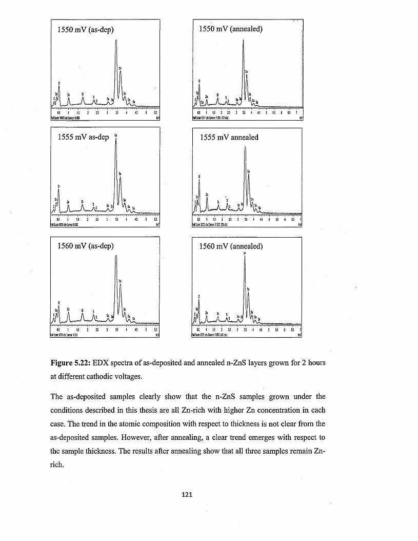
1550 mV (as-dep)
0
d a a
Sn
Sj
1.5 1 IS 2 2.5 J 15 4 xi S 5i ilSfflkHSfc&rerUCJ to
1550 mV (annealed)
1555 mV as-dep
IsV
1560 mV (as-dep)
1555 mV annealed
1560 mV (annealed)
Figure 5.22: EDX spectra of as-deposited and annealed n-ZnS layers grown for 2 hours
at different cathodic voltages.
The as-deposited samples clearly show that the n-ZnS samples grown under the
conditions described in this thesis are all Zn-rich with higher Zn concentration in each
case. The trend in the atomic composition with respect to thickness is not clear from the
as-deposited samples. However, after annealing, a clear trend emerges with respect to
the sample thickness. The results after annealing show that all three samples remain Zn-
rich.
12 1
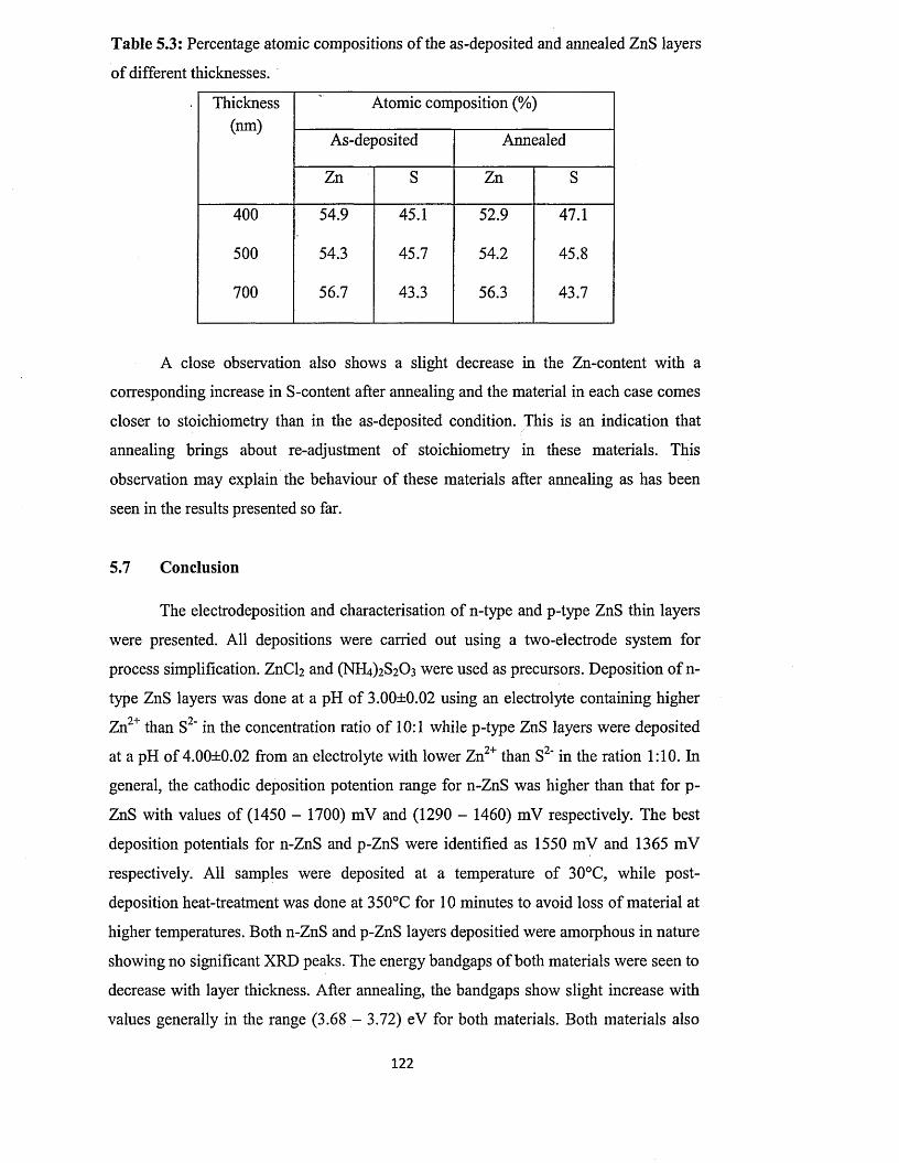
Table 5.3: Percentage atomic compositions of the as-deposited and annealed ZnS layers
of different thicknesses.
Thickness(nm)
Atomic composition (%)
As-deposited Annealed
Zn S Zn S
400 54.9 45.1 52.9 47.1
500 54.3 45.7 54.2 45.8
700 56.7 43.3 56.3 43.7
A close observation also shows a slight decrease in the Zn-content with a
corresponding increase in S-content after annealing and the material in each case comes
closer to stoichiometry than in the as-deposited condition. This is an indication that
annealing brings about re-adjustment of stoichiometry in these materials. This
observation may explain the behaviour of these materials after annealing as has been
seen in the results presented so far.
5.7 Conclusion
The electrodeposition and characterisation of n-type and p-type ZnS thin layers
were presented. All depositions were carried out using a two-electrode system for
process simplification. ZnCl2 and (NH4)2S2 0 3 were used as precursors. Deposition of n-
type ZnS layers was done at a pH of 3.00±0.02 using an electrolyte containing higher
Zn2+ than S2" in the concentration ratio o f 10:1 while p-type ZnS layers were deposited
at a pH of 4.00±0.02 from an electrolyte with lower Zn2+ than S2* in the ration 1:10. In
general, the cathodic deposition potention range for n-ZnS was higher than that for p-
ZnS with values of (1450 - 1700) mV and (1290 - 1460) mV respectively. The best
deposition potentials for n-ZnS and p-ZnS were identified as 1550 mV and 1365 mV
respectively. All samples were deposited at a temperature of 30°C, while post
deposition heat-treatment was done at 350°C for 10 minutes to avoid loss of material at
higher temperatures. Both n-ZnS and p-ZnS layers depositied were amorphous in nature
showing no significant XRD peaks. The energy bandgaps of both materials were seen to
decrease with layer thickness. After annealing, the bandgaps show slight increase with
values generally in the range (3.68 - 3.72) eV for both materials. Both materials also
122
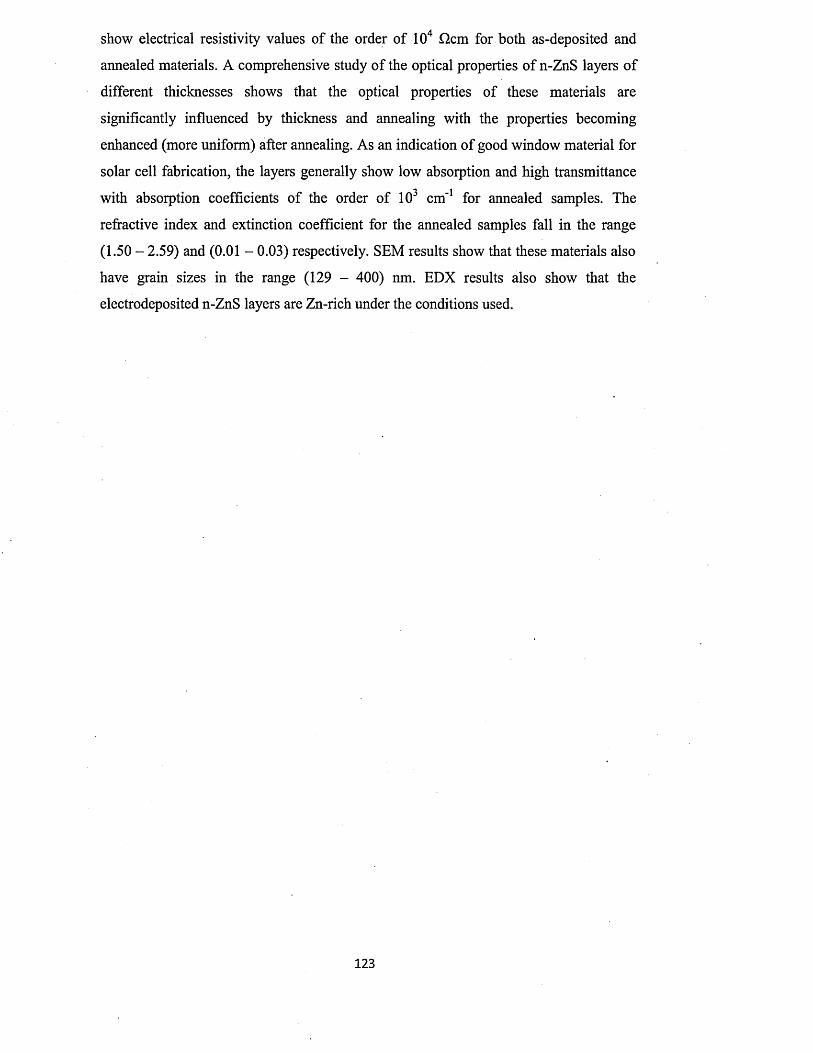
show electrical resistivity values of the order of 104 Qcm for both as-deposited and
annealed materials. A comprehensive study o f the optical properties of n-ZnS layers o f
different thicknesses shows that the optical properties o f these materials are
significantly influenced by thickness and annealing with the properties becoming
enhanced (more uniform) after annealing. As an indication o f good window material for
solar cell fabrication, the layers generally show low absorption and high transmittance
with absorption coefficients o f the order o f 103 cm '1 for annealed samples. The
refractive index and extinction coefficient for the annealed samples fall in the range
(1.50 - 2.59) and (0.01 - 0.03) respectively. SEM results show that these materials also
have grain sizes in the range (129 - 400) nm. EDX results also show that the
electrodeposited n-ZnS layers are Zn-rich under the conditions used.
123
References
[1] R. John and S. S. Florence, Chalcog. Lett. 7(4) (2010) 269 - 273.
[2] I. O. Oladeji, L. Chow, C. S. Ferekides, V. Viswanathan and Z. Zhao, Sol. Ener.
Mat. Sol. Cell 61 (2000) 203 - 211.
[3] D. S. Albin, Y. Yan and M. M. Al-Jassim, Progress in photovoltaics: Research
and applications (2002) 309-322 (DOI: 10.1002/pip.426).
[4] K. Anuar, Z. Zainal, N. Saravanan, and N. Asikin, Mater. Sci. 44(2), (2008).
[5] W. Tong, B. K. Wagner, T. K. Tran, W.Ogle, W. Park and C.J. Summer, J.Cryst.
Growth 164(1996)202-207.
[6] S. H. Deulkara, C. H. Bhosalea and M. Sharonb, J. Phys. Solids, 65(11) (2004)
1879-1885.
[7] Z. Porada and E. Schabowska, Thin Solid Films 145 (1986) 75.
[8] A. N. Yazici, M. Oztas and M. Bedir, J. Lumin. 104 (2003) 115 - 122.
[9] T. Ozniiluer, I. Erdogan and U. Demir, Langmuir 22 (2006) 4415 - 4419.
[10] G. Nabiyouni, R. Sahrael, M. Toghiany, M. H. M. Ara and K. Hedayati, Rev. Adv.
Mater.Sci. 27 52-57.
[11] H. Kashani, Thin Solid Films 288 (1996) 50 - 56.
[12] T. Yasuda, B. Zhang and Y. Segawa, J. Cryst. Growth 175/176 (1997) 583 - 586.
[13] A. Kassim, S. Nagalingam, H.S. Min and N. Karrim, Arabian Journal o f
Chemistry 3 (2010) 243 - 249.
[14] D. Lincot, Thin Solid Films 487 (2005) 40 - 48.
[15] S. Zhang, H. Kinto, T. Yatabe and S. Iida, J. Cryst. Growth 86 (1988) 372 - 376,.
[16] Y. Yu, J. Jie, P. Jiang, L. Wang, C. Wu, Q. Peng, X. Zhang, Z. Wang, C. Xie, D.
Wu and Y. Jiang, J. Mater. Chem. 21 (2011) 12632.
[17] S. Iida, T. Yatabe, H. Kinto and M. Shinohara, J. Cryst. Growth, 101 (1990) 141-
146,
[18] S. Kishimoto, T. Yamamoto and S. Iida, Materials Research Society, Spring
Meeting, San Francisco (2002).
[19] X. Ma, Hindawi Publishing Corporation, Journal o f Nanomaterials (2011), doi:
10.1155/2011/952616.
[20] K. Zanio, Semiconductors and semimetals, Vol. 13 “Cadmium Telluride”
Academic press (1978).
[21] S. Dennison, J.Mater. Chem. 41 (1994) 4.
[22] B. W. Sanders and A. H. Kitai J. Cryst. Growth, 100 (1990) 405 - 410.
[23] D. G. Diso, G. E. A. Muftah, V. Patel and I. M. Dharmadasa, J. Electrochem. Soc.
124

157(6) (2010) H647 - H651.
[24] F. Kadirgan, D. Mao, W. Song, T. Ohno and B. McCandless, Turk. J. Chem., 24
(2000) 21 - 33.
[25] H. Karami and A. Kaboli, Int. J. Electrochem. Sci, 5 (2010) 706 - 719.
[26] I. M. Dharmadasa and O. K. Echendu, Electrodeposition o f Electronic Materials
for Applications in Macroelectronic and Nanotechnology-Based Devices,
Encyclopaedia o f Applied Electrochemistry, Springer Reference (2012).
(http://www.sprinaerreference.com/index/chopterdbid/303488).
[27] I. M. Dharmadasa, Prog. Crystal Growth and Charact. 36, (4) (2998) 249 - 290
[28] I. M. Dharmadasa, C. J. Blomfield, C. G. Scott, R. Coratger, F. Ajustron and J.
Beauvillian, Solid-State Electronics, 42,(4) (1998) 595 - 604.
[29] D. A. Vermilyea, J. Chem. Phys. 27 (1957)822.
[30] A. S. Feiner and A. J. McEvoy, Journal o f Chemical Education, 71,(6)
(1994) 493 - 494.
[31] Nemst Equation. http://www.wikiuedia.ors/wiki/Nernst equation, (accessed
2/11/2013).
[32] P. Vanysek, Electrochemical Series table 1 Alphabetical, CRCpress LLC (2000).
[33] O. K. Echendu, A. R. Weerasinghe, D. G. Diso, F. Fauzi and I. M. Dharmadasa,
Journal ofElec. Materi., 42,(4) (2013) 692 - 700.
[34] M. Takahashi, K. Uosaki and H. Kita, J. Appl. Phys. 60 (6) (1986) 2046.
[35] V. B. Patil, D. S. Sutrave, G. S. Shahane and L. P. Deshmukh, Thin Solid Films
401 (2001) 35.
[36] S. Halas, Materials Science-Polland, 24, (4) (2006).
[37] Y. Yi, X. Shanhua, L. Shiyong, H. Jinman and S. Jiacong, Appl. Phys. Lett. 69, (3)
(1996)377-379.
[38] E. H. Rhoderick and R. H. Williams, Metal-Semiconductor contacts, 2nd ed.,
Clarendon press (1988).
[39] L. J. Eriksson and W. T. Peria, Thin Solid Films, 5 (1970) 303 - 311.
[40] H. Murray and A. Tosser, Thin Solid Films, 22 (1974) 37-44.
[41] J. Liao and K. Ho, Solar Energy materials and Solar Cell 86 (2005) 229 - 241,.
[42] S. Senthilkumaar, R. Thami and Z. Selvi, Appl. Phys. A, 94 (2009) 123 - 129.
[43] F. Gode, Physica B 406 (2011) 1653 - 1659.
[44] S. M. Sze and K. K. Ng, Physics o f Semiconductor Devices, 3rd ed., John Wiley
Sons, Inc, New Jersey (2007).125
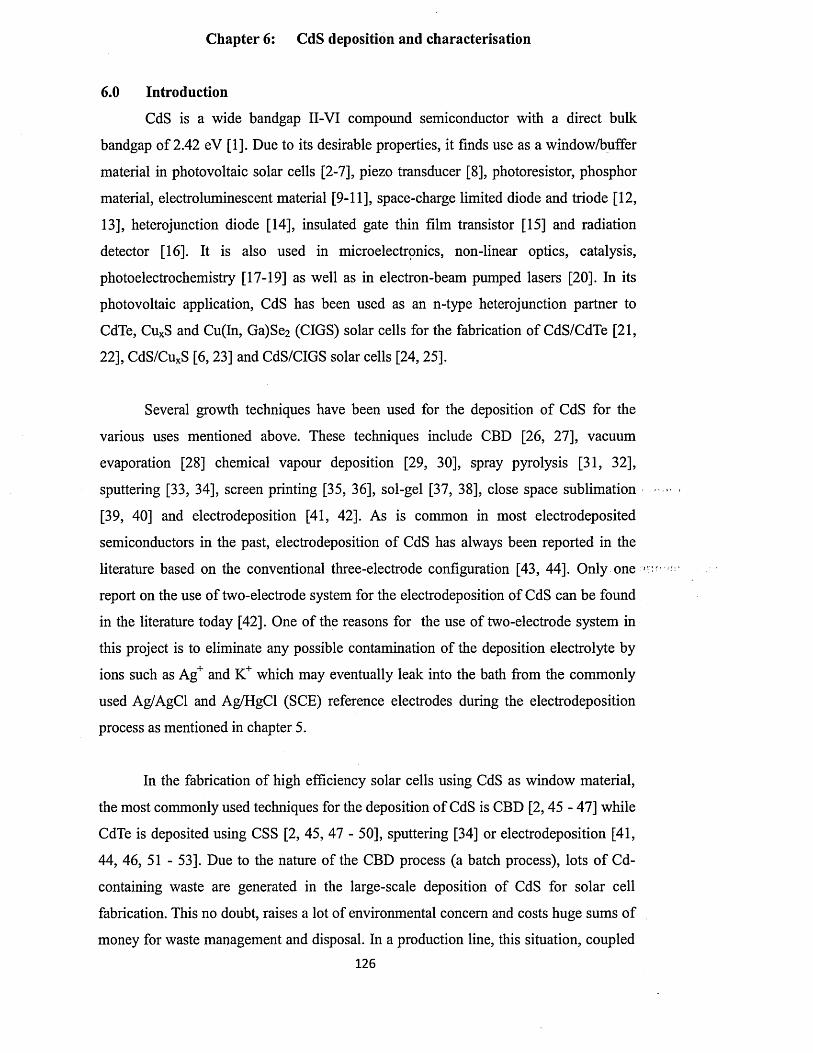
Chapter 6: CdS deposition and characterisation
6.0 Introduction
CdS is a wide bandgap II-VI compound semiconductor with a direct bulk
bandgap o f 2.42 eV [1]. Due to its desirable properties, it finds use as a window/buffer
material in photovoltaic solar cells [2-7], piezo transducer [8], photoresistor, phosphor
material, electroluminescent material [9-11], space-charge limited diode and triode [12,
13], heterojunction diode [14], insulated gate thin film transistor [15] and radiation
detector [16]. It is also used in microelectronics, non-linear optics, catalysis,
photoelectrochemistry [17-19] as well as in electron-beam pumped lasers [20]. In its
photovoltaic application, CdS has been used as an n-type heterojunction partner to
CdTe, CuxS and Cu(In, Ga)Se2 (CIGS) solar cells for the fabrication of CdS/CdTe [21,
22], CdS/CuxS [6, 23] and CdS/CIGS solar cells [24, 25].
Several growth techniques have been used for the deposition of CdS for the
various uses mentioned above. These techniques include CBD [26, 27], vacuum
evaporation [28] chemical vapour deposition [29, 30], spray pyrolysis [31, 32],
sputtering [33, 34], screen printing [35, 36], sol-gel [37, 38], close space sublimation
[39, 40] and electrodeposition [41, 42]. As is common in most electrodeposited
semiconductors in the past, electrodeposition of CdS has always been reported in the
literature based on the conventional three-electrode configuration [43, 44]. Only one ,v
report on the use of two-electrode system for the electrodeposition of CdS can be found
in the literature today [42]. One of the reasons for the use of two-electrode system in
this project is to eliminate any possible contamination of the deposition electrolyte by
ions such as Ag+ and K+ which may eventually leak into the bath from the commonly
used Ag/AgCl and Ag/HgCl (SCE) reference electrodes during the electrodeposition
process as mentioned in chapter 5.
In the fabrication of high efficiency solar cells using CdS as window material,
the most commonly used techniques for the deposition o f CdS is CBD [2,45 - 47] while
CdTe is deposited using CSS [2, 45, 47 - 50], sputtering [34] or electrodeposition [41,
44, 46, 51 - 53]. Due to the nature of the CBD process (a batch process), lots o f Cd-
containing waste are generated in the large-scale deposition of CdS for solar cell
fabrication. This no doubt, raises a lot of environmental concern and costs huge sums o f
money for waste management and disposal. In a production line, this situation, coupled
126

with the use of at least two different deposition techniques, presents real issues and
leads to the production of expensive solar panels. It is preferable in such an industrial
process to have only one production line by using only one technique to deposit both
CdS and CdTe. A continuous process such as electrodeposition fits into this one
production line that can be used for the production of less expensive solar panels. It is
for this reason that the electrodeposition of CdS thin-films using two-electrode system
has been researched and reported in this chapter.
6.1 Preparation of CdS deposition electrolyte
In order to carry out the electrodeposition of CdS thin-films for use in CdTe-
based solar cells, the deposition electrolyte was prepared using 0.3M CdCh.HbO (molar
mass = 215.31 g) and 0.03M Na2S2 0 3 .5H20 (molar mass = 248.18 g) in 800 ml of de
ionised water. Both CdCfe-^O and Na2S2 0 3 .5H20 were laboratory reagent grade,
purchased from Fisher Scientific United Kingdom. The resulting solution is contained in
a 1000 ml plastic beaker. Because o f the purity grade o f the CdC^.IUO, the solution
containing only CdC^.fbO was first prepared. The pH was adjusted to 1.80±0.02 using
HC1 and NH4OH. The 1000 ml plastic beaker containing this solution was put inside a
2000 ml glass beaker containing some de-ionised water. This serves as a water bath to
ensure uniform heating o f the electrolyte. The entire container was placed on a hot plate
with a magnetic stirrer. After stirring the C d C ^ .^ O solution at 400 r.p.m. for 24 hrs, it
was heated to a temperature of (80±2)°C and a cyclic voltammetry was carried out
using two-electrode configuration as was done in the case o f ZnS deposition electrolyte
in section 5.1 using glass/FTO as the cathode and high-purity carbon rod as the anode.
The CdCl2.H20 solution was then subjected to electro-purification for 48 hrs before the
addition o f Na2S2 0 3 .5H20. The pH o f the resulting electrolyte was then adjusted again
to 1.80± 0.02 at room temperature.
6.2 Substrate preparation
Two different types of substrate were used for the electrodeposition o f CdS in
this project. These were glass/FTO and glass/FTO/ZnS. The same steps detailed in
section 5.2 were taken to prepare the glass/FTO substrates by cleaning with soap
solution, acetone, methanol, de-ionised water and drying in a stream of N 2 . Similar sizes
(3.0 cm x 2.0 cm x 3.0 mm) of glass/FTO were also used. The glass/FTO/ZnS
substrates were obtained from the previously electrodeposited n-ZnS layers. Prior to the
deposition of CdS however, the ZnS layers o f the glass/FTO/ZnS substrates were rinsed
127
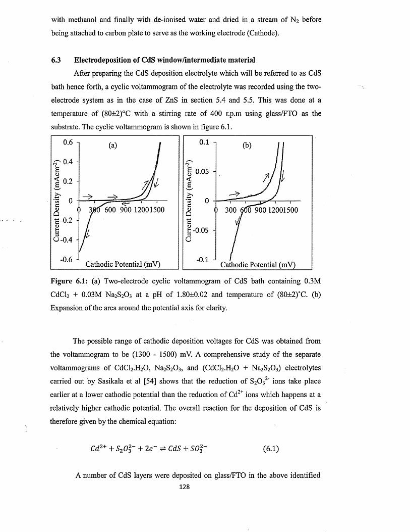
with methanol and finally with de-ionised water and dried in a stream of N 2 before
being attached to carbon plate to serve as the working electrode (Cathode).
6.3 Electrodeposition of CdS window/intermediate m aterial
After preparing the CdS deposition electrolyte which will be referred to as CdS
bath hence forth, a cyclic voltammogram of the electrolyte was recorded using the two-
electrode system as in the case of ZnS in section 5.4 and 5.5. This was done at a
temperature of (80±2)°C with a stirring rate of 400 r.p.m using glass/FTO as the
substrate. The cyclic voltammogram is shown in figure 6.1.
I 0-2
600 900 12001500- 0.2 -
O-0.4 -
-0 .6 JCathodic Potential (mV)
0 300 600 90012001500
-0.05 -
-0 .1 JCathodic Potential (mV)
Figure 6.1: (a) Two-electrode cyclic voltammogram of CdS bath containing 0.3M
CdCl2 + 0.03M Na2S2C>3 at a pH of 1.80±0.02 and temperature of (80±2)°C. (b)
Expansion of the area around the potential axis for clarity.
The possible range of cathodic deposition voltages for CdS was obtained from
the voltammogram to be (1300 - 1500) mV. A comprehensive study of the separate
voltammograms of CdCl2 .H2 0 , Na2S2C>3 , and (CdCl2 .H2 0 + Na2S2C>3) electrolytes
carried out by Sasikala et al [54] shows that the reduction of S2O 32' ions take place
earlier at a lower cathodic potential than the reduction of Cd2+ ions which happens at a
relatively higher cathodic potential. The overall reaction for the deposition o f CdS is
therefore given by the chemical equation:
C d 2+ + S2Ol~ + 2e~ ^ CdS + SO f" (6 .1 )
A number of CdS layers were deposited on glass/FTO in the above identified128
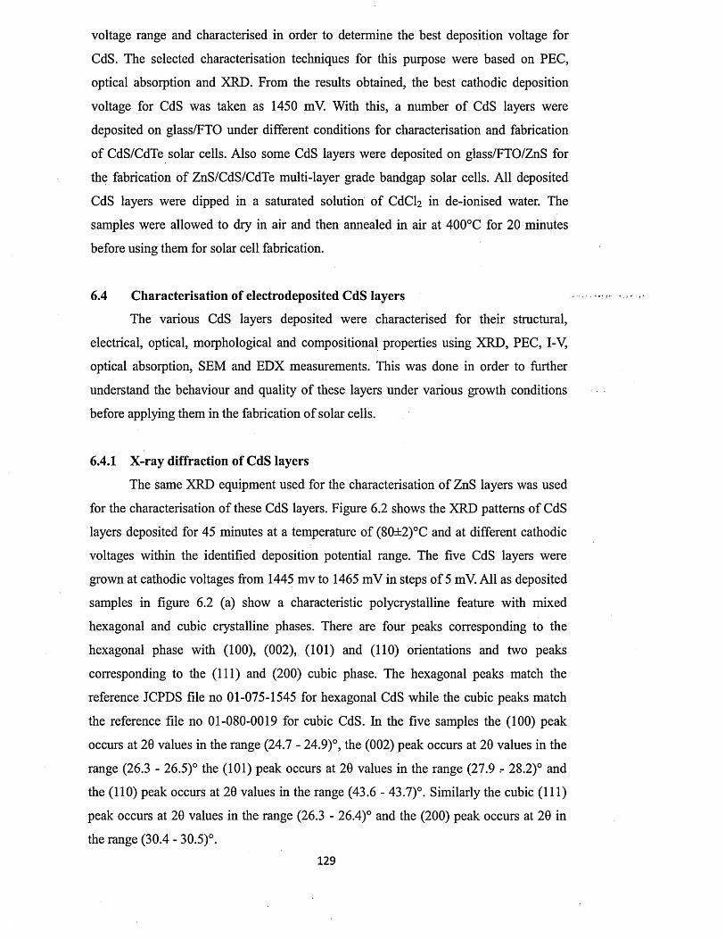
voltage range and characterised in order to determine the best deposition voltage for
CdS. The selected characterisation techniques for this purpose were based on PEC,
optical absorption and XRD. From the results obtained, the best cathodic deposition
voltage for CdS was taken as 1450 mV. With this, a number o f CdS layers were
deposited on glass/FTO under different conditions for characterisation and fabrication
of CdS/CdTe solar cells. Also some CdS layers were deposited on glass/FTO/ZnS for
the fabrication of ZnS/CdS/CdTe multi-layer grade bandgap solar cells. All deposited
CdS layers were dipped in a saturated solution o f CdCb in de-ionised water. The
samples were allowed to dry in air and then annealed in air at 400°C for 20 minutes
before using them for solar cell fabrication.
6.4 Characterisation of electrodeposited CdS layers
The various CdS layers deposited were characterised for their structural,
electrical, optical, morphological and compositional properties using XRD, PEC, I-V,
optical absorption, SEM and EDX measurements. This was done in order to further
understand the behaviour and quality of these layers under various growth conditions
before applying them in the fabrication of solar cells.
6.4.1 X-ray diffraction of CdS layers
The same XRD equipment used for the characterisation of ZnS layers was used
for the characterisation of these CdS layers. Figure 6.2 shows the XRD patterns of CdS
layers deposited for 45 minutes at a temperature of (80±2)°C and at different cathodic
voltages within the identified deposition potential range. The five CdS layers were
grown at cathodic voltages from 1445 mv to 1465 mV in steps o f 5 mV. All as deposited
samples in figure 6.2 (a) show a characteristic polycrystalline feature with mixed
hexagonal and cubic crystalline phases. There are four peaks corresponding to the
hexagonal phase with (100), (002), (101) and (110) orientations and two peaks
corresponding to the (111) and (200) cubic phase. The hexagonal peaks match the
reference JCPDS file no 01-075-1545 for hexagonal CdS while the cubic peaks match
the reference file no 01-080-0019 for cubic CdS. In the five samples the (100) peak
occurs at 20 values in the range (24.7 - 24.9)°, the (002) peak occurs at 20 values in the
range (26.3 - 26.5)° the (101) peak occurs at 20 values in the range (27.9 .- 28.2)° and
the (110) peak occurs at 20 values in the range (43.6 - 43.7)°. Similarly the cubic (111)
peak occurs at 20 values in the range (26.3 - 26.4)° and the (200) peak occurs at 20 in
the range (30.4 - 30.5)°.
129

1600 (a) as-deposited
1465 mV
. 1455 mV
. 1450 mV
800
c 400
1600 (b) annealed
1465 mV
1460 mV
800 1455 mV
mV
400 1445 mV
FT<
Figure 6.2: XRD patterns o f (a) as-deposited and (b) annealed CdS layers deposited for 45 minutes at different cathodic growth voltages.
After CdCl2 treatment and annealing in air at 400°C for 20 minutes, a startling
observation was made. This was the disappearance of the peaks representing the cubic
phase o f CdS. Figure 6.2 (b) shows the XRD patterns of the annealed CdS layers with
only peaks representing the hexagonal phase. Metin et al [55] reported a similar
scenario of mixed cubic and hexagonal phases in CBD-CdS in which the cubic phase
disappeared after annealing. A slight narrowing of the range of 20 values for the four
peaks was also observed with all the (100) peaks occurring at a 20 value o f 24.7°, all the
(002) peaks occurring at a 20 value of 26.4°, the (101) peaks occurring at 20 range of
(28.0 - 28.1)° and the (110) peaks occurring at 20 range of (43.5 - 43.6)°.
Figure 6.2 (b) shows that the preferred orientation of the crystallites in the
hexagonal CdS phase is in the (002) crystal plane. The disappearance of the peaks
corresponding to the cubic phase after annealing suggests that the cubic phase of CdS is
not stable, at least, at the annealing temperature used in this project. The essence o f this
particular experiment is to determine the best deposition voltage for CdS. For this
reason an estimation of the crystallite sizes was done and the effect of annealing on
them was investigated for the five samples grown at different voltages. To do this only
the hexagonal phase is considered since the cubic phase is not stable on annealing. The
(002) peak was considered as the preferred orientation for these samples. Although the
(002) peak coincides with FTO peak, close look at this peak in comparison with the
highest FTO peak (at 20 -37°) in the XRD patterns of the five samples shows that the
(002) peak actually represents the preferred orientation of CdS crystallites in the layers.
However, for crystallite size analysis, the (101) peaks were used for two reasons. First,130
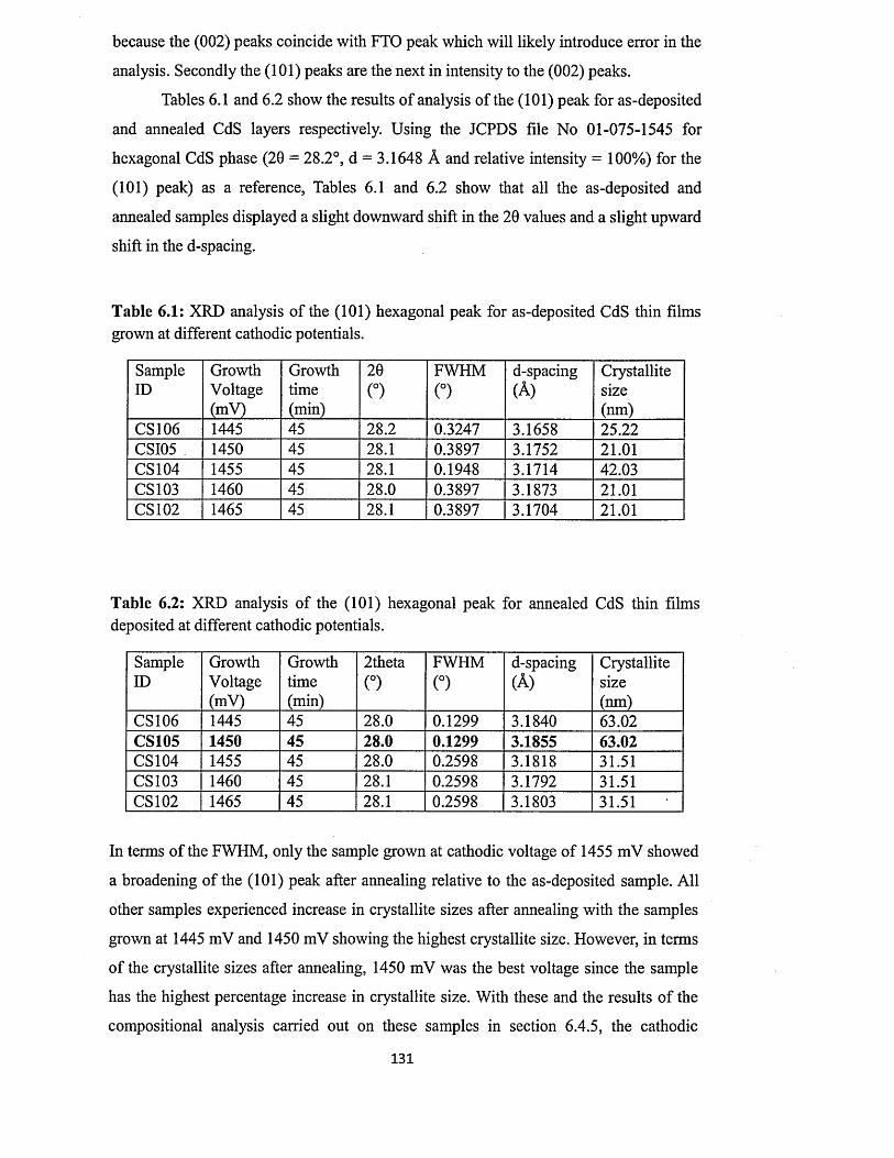
because the (002) peaks coincide with FTO peak which will likely introduce error in the
analysis. Secondly the (101) peaks are the next in intensity to the (002) peaks.
Tables 6.1 and 6.2 show the results o f analysis of the (101) peak for as-deposited
and annealed CdS layers respectively. Using the JCPDS file No 01-075-1545 for
hexagonal CdS phase (20 = 28.2°, d = 3.1648 A and relative intensity = 100%) for the
(101) peak) as a reference, Tables 6.1 and 6.2 show that all the as-deposited and
annealed samples displayed a slight downward shift in the 20 values and a slight upward
shift in the d-spacing.
Table 6.1: XRD analysis of the (101) hexagonal peak for as-deposited CdS thin films grown at different cathodic potentials.
SampleID
GrowthVoltage(mV)
Growthtime(min)
20(°)
FWHM(°)
d-spacing(A)
Crystallitesize(nm)
CS106 1445 45 28.2 0.3247 3.1658 25.22CSI05 1450 45 28.1 0.3897 3.1752 21.01CS104 1455 45 28.1 0.1948 3.1714 42.03CS103 1460 45 28.0 0.3897 3.1873 21.01CS102 1465 45 28.1 0.3897 3.1704 21.01
Table 6.2: XRD analysis of the (101) hexagonal peak for annealed CdS thin films deposited at different cathodic potentials.
SampleID
GrowthVoltage(mV)
Growthtime(min)
2theta(°)
FWHM(°)
d-spacing(A)
Crystallitesize(nm)
CS106 1445 45 28.0 0.1299 3.1840 63.02CS105 1450 45 28.0 0.1299 3.1855 63.02CS104 1455 45 28.0 0.2598 3.1818 31.51CS103 1460 45 28.1 0.2598 3.1792 31.51CS102 1465 45 28.1 0.2598 3.1803 31.51
In terms o f the FWHM, only the sample grown at cathodic voltage of 1455 mV showed
a broadening of the (101) peak after annealing relative to the as-deposited sample. All
other samples experienced increase in crystallite sizes after annealing with the samples
grown at 1445 mV and 1450 mV showing the highest crystallite size. However, in terms
o f the crystallite sizes after annealing, 1450 mV was the best voltage since the sample
has the highest percentage increase in crystallite size. With these and the results o f the
compositional analysis carried out on these samples in section 6.4.5, the cathodic
131
voltage of 1450 mV was chosen as the best voltage for the electrodeposition o f CdS in
this project. An experiment carried out on solar cell fabrication and assessment across
these voltages also supported this choice.
6.4.1.1 Effect of growth tem perature on the XRD of CdS layers
Here, five different CdS layers were grown at a cathodic voltage of 1450 mV for
30 minutes and at five different temperatures. This is to study the effect o f growth
temperature on the XRD results of these CdS layers. Figures 6.3 (a) and (b) show the
XRD results of these layers, grown at temperatures o f 30°C, 40°C, 50°C, 60°C and
70°C, before and after annealing respectively.
2000(a) as-deposited g (b) annealed2000
1500
50°C ^1000
40°C
500 30°.C30°C
FT]
Figure 6.3: XRD patterns of (a) as-deposited and (b) annealed CdS samples grown for 30 minutes at different growth temperatures.
Both figures show that the deposition temperatures from 30°C to 50°C for 30
minutes did not produce any noticeable XRD peaks for CdS. At a temperature o f 60°C,
the clear XRD peaks began to emerge at the usual 20 positions. At a temperature of
70°C, the peaks become clearer. Physically, the samples grown from 30°C to 50°C
looked very transparent and yellow showing that the layers were very thin. Again it
shows that at the initial nucleation stage, the deposited CdS has an amorphous nature.
At higher temperatures of 60°C and above, the as-deposited samples grown for 30
minutes looked dark yellow and as the temperature and growth time increased, they
turned greenish-yellow. At this stage, the growth rate increased substantially as seen
from rapid increase in deposition current density, and the samples always showed very
clear XRD features. After annealing in air, the greenish-yellow samples turned orange
132

yellow to orange depending on the thickness. The thicker the samples, the more they
tend towards orange colour. These results and many other experiments done during this
project, show that growth temperature and time have very strong influence on the nature
of CdS layers deposited.
6.4.1.2 Effect of growth time on electrodeposited CdS layers
In order to investigate the effect of growth time on the nature of CdS samples
grown, another set of five samples were grown at a temperature of 80°C, cathodic
voltage of 1450 mV and for different times from 5 minutes to 25 minutes. Figures 6.4(a)
and (b) show the XRD patterns of the samples grown, before and after annealing
respectively. In this case, up to a time of 10 minutes, the XRD features did not show up
clearly, suggesting that the materials at this early formation stage are amorphous. From
15 minutes of growth and above, the materials begin to crystallise and the XRD peaks
begin to show up.
2000 i
57 nm (25min1600
nm mm
mm
S 800 - 201 nm (1 0 min)
§400 -
FTP
20 (°)
- (b)c, 557 nm (25
1600 -
03
• t 800ca>
ill 4 ft 1 317 npm (20 min
I l l 2^5 mil (15 min)
201 nm (1 0 min
1 - 1 . 1 |27nm (ftm iri
20 30 0 60 70
Figure 6.4 : XRD patterns of (a) as-deposited and (b) annealed CdS layers grown at
cathode voltage of 1450 mV and temperature of 80°C for different durations producing
different thicknesses.
A possible reason for this observed amorphous nature of CdS at the initial nucleation
and formation stages is the fact that the formation of sulphur atoms is the one to take
place at the cathode before the formation of Cd atoms. This prior formation o f sulphur
then helps to drive the deposition of Cd. At the initial stage therefore more sulphur gets
deposited on the cathode with only very little amount of Cd. As the deposition
progresses in time, more and more Cd is attracted to and deposited on the cathode133
leading to the formation of CdS with increased Cd-content as the two species react
together at the cathode. As a result, CdS peaks begin to show up in the XRD at this
growth time. Also with increase in growth temperature as shown in figure 6.3, the rateI
of attraction and discharge of Cd and the resulting reaction between S and Cd at the
cathode increases and the CdS crystals begin to form and grow.
Tables 6.3 and 6.4 show the variation o f CdS thickness with growth time for two
sets of samples grown at 1450 mV, but at different temperatures. Each set o f samples
was grown at a particular temperature.
Table 6.3: Variation of film thickness with growth time for samples grown at 80°C.
Sample ID Growth time (min)
Film thickness (nm)
CS170 12 172CS171 15 239CS172 19 317CS173 24 374CS174 28 452CS175 34 466
Table 6.4: Variation of film thickness with growth time for samples grown at 85°C.
Sample ID Growth time (min)
Film thickness (nm)
CS144A 5 127CS145 10 201CS146 15 295CS147 20 377CS148 25 557
Figures 6.5 and 6.6 also show the graphs of thickness vs. growth time for the CdS data
given in Tables 6.3 and 6.4. Both tables and figures show that the thickness o f deposited
CdS layers increases as deposition time increases. This relationship is however not
linear but rather appears as a fourth order polynomial. The error in the measurements is
about ±50 nm and the reproducibility is up to 90%. The reason for this nonlinearity is
not far-fetched. The condition of the deposition bath at the time of growth o f each
sample plays a significant part. Experience acquired during the project shows that
because of the problem of sulphur precipitation, especially at elevated temperatures like
the ones used in this experiment the concentration of sulphur in the bath runs low very
easily. This usually manifests in the rapid fall in the deposition current density. To try to
restore the concentration of sulphur in the bath, a calculated amount of the sulphur134
source (Na2S2 0 3 ) is usually added to the bath from time to time. The same thing
happens with Cd2+ but to bring this situation under control, the initial concentration of
Cd2+ is made higher (10 times higher in this case) than that o f S2* in the bath. This is
another reason why the ratio o f the concentration o f these two ions in the bath is [Cd2+] /
[S2'] = 10 / 1. As a result of the above issues, there is a fluctuation in the thickness of the
samples obtained under constant temperature following the fluctuation in the
concentration of the ions in the bath.
500 -i
400 -
£ 3 0 0 -
2 200 - £I 100 -
Growth time (min)
Figure 6.5: Variation of film thickness with growth time for the set of samples grown at
80°C.
800 n
200 -
(jrowth time
Figure 6.6: Variation of film thickness with growth time for the set o f samples grown at
85°C.
6.4.2 Photoelectrochemical (PEC) cell study
The PEC results of the electrodeposited CdS layers are shown in Table 6.5 and
figure 6.7. The measurements were done with CdS layers grown at cathodic voltages
ranging from 1300 mV to 1480 mV covering the range of deposition potentials
identified earlier from previous experiments.
135
Table 6.5: PEC signal of n-type CdS deposited at different cathodic potentials.
Cathodic Voltage (mV)
PEC Signal (mV)
1300 -1581350 -1071380 -1031400 -991450 -971480 -110
The PEC signals of all the samples have negative value indicating that the samples all
have n-type electrical conductivity. This result is in perfect agreement with the fact that
CdS occurs naturally as an n-type semiconductor. It is a difficult task to obtain intrinsic
p-type doping o f CdS. However, some researchers have achieved extrinsic p-doping of
CdS by mainly using Cu as a dopant [56 - 59]. Bi has also been used to achieve p-type
doping in CdS through ion implantation [60]. The results in Table 6.5 and figure 6.7 are
for annealed CdS layers. The as-deposited layers also displayed n-type PEC signals
although the results are not shown in this report.
1300 1350 1400 1450 1500-30 -
-80 -
130 -
-180 JCathodic Voltage (mV)
Figure 6.7: PEC signal of n-type CdS deposited at different cathodic potentials.
6.4.3 Current-voltage m easurement
The purpose of this I-V measurement is to determine the resistivity o f CdS layer
deposited at the cathodic voltage of 1450 mV for different time duration as wells as to
determine the effect of CdC^ and CdCl2+CdF2 treatments on the resistivity/conductivity
of the electrodeposited CdS layers. Six CdS samples were grown with different
thickness. Each sample was divided into four pieces. One piece of each sample was left
as-deposited. The second piece was annealed at 400°C for 20 minutes without any prior
chemical treatment. This sample was designated annealed without CdC^. The third
136
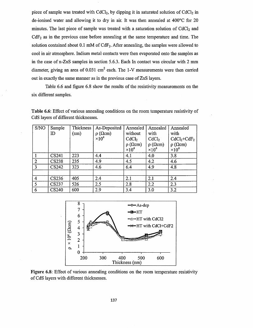
piece of sample was treated with CdC^, by dipping it in saturated solution of CdCh in
de-ionised water and allowing it to dry in air. It was then annealed at 400°C for 20
minutes. The last piece o f sample was treated with a saturation solution o f CdC^ and
CdF2 as in the previous case before annealing at the same temperature and time. The
solution contained about 0.1 mM of CdF2 . After annealing, the samples were allowed to
cool in air atmosphere. Indium metal contacts were then evaporated onto the samples as
in the case of n-ZnS samples in section 5.6.3. Each In contact was circular with 2 mm
diameter, giving an area o f 0.031 cm each. The 1-V measurements were then carried
out in exactly the same manner as in the previous case o f ZnS layers.
Table 6.6 and figure 6.8 show the results of the resistivity measurements on the
six different samples.
Table 6.6: Effect o f various annealing conditions on the room temperature resistivity of CdS layers of different thicknesses.
S/NO SampleID
Thickness(nm)
As-Deposited p (Ocm) xlO4
Annealed without CdCl2 p (Qcm) xlO4
Annealed with CdCl2 p (Hem) xlO4
AnnealedwithCdCl2+CdF2 p (£2cm) xlO4
1 CS241 223 4.4 4.1 4.0 3.82 CS238 235 4.9 4.5 4.2 4.63 CS242 323 4.6 6.4 4.9 4.8
4 CS236 405 2.4 2.1 2.1 2.45 CS237 526 2.5 2.8 2.2 2.36 CS240 600 2.9 3.4 3.0 3.2
-“4—As-dep —a —HT-& -H T with CdC12 -* -H T with CdCl+CdF2
200 300 400 500 600______________ Thickness (nm)__________
Figure 6.8: Effect of various annealing conditions on the room temperature resistivity of CdS layers with different thicknesses.
137

From Table 6.6 the trend of the resistivity dependence on film thickness does not seem
to be clear. However, if the samples are separated into the upper three and the lower
three, then a sensible trend is observed. For each group o f three samples, the resistivity
increases as thickness increases for all the samples. In each condition, the three samples
in the lower group have lower resistivity values than the other three samples in the
upper group. From figure 6.8, one sees a clearer picture of the resistivity variation with
film thickness. It can be seen that the resistivity o f CdS increases with thickness up to a
thickness of -323 nm. It then falls rapidly as the thickness increases up to a thickness of
-405 nm. Then the resistivity increases again slowly as the thickness o f the layers
increases. The error in the resistivity measurement is about within 5% with
reproducibility of up to 80%. The most significant trend in this whole result is that the
resistivity values are high for small thicknesses up to 323 nm and are lower for large
thickness >323 nm. There are two possible reasons for this observed trend in the
resistivity of CdS with respect to material thickness. One is to do with excess S-content
especially at the early stages of nucleation and formation as explained previously in
section 6.4.1.2. In this situation, the CdS with thickness up to 323 nm are still
amorphous with a lot of S and only very little amount of Cd, therefore producing S-rich
CdS. As the deposition progresses and the film thickness builds up, more and more Cd
is incorporated in the CdS formed resulting to the formation of CdS material with
improved stoichiometry and crystallinity. This resulting crystalline CdS certainly has
more improved qualities compared to the amorphous and S-rich CdS. Consequently the
resistivity values of the CdS materials with higher thicknesses (>323 nm) are lower than
those of samples with lower thicknesses. This explanation correlates with the observed
XRD results for samples grown for different durations having different thicknesses.
Annealing with or without CdCl2 and CdCl2+CdF2 treatment does not seem to
have any pronounced effect on the resistivity of these materials. It is very difficult to
figure out any existing trend in the resistivity of both annealed and as-deposited CdS
materials in this experiment. Liu et al [61] reported similar behaviour for CBD-CdS
with no clear trend in resistivity with respect to film thickness. They however, only
observed significant reduction in resistivity by about two orders of magnitude (from 105
£2cm to 103 Qcm) with increased growth temperature of 80°C. The most important
observation in this regard however, is that the resistivity of both as-deposited and
annealed CdS layers are of the same order o f magnitude. The values are also in good
agreement with literature values [61 - 63]. A good number of papers however, have
reported drastic reduction in resistivity o f CdS after annealing with or without CdCL
138
treatment [54, 55, 64 - 66] and some have reported decrease in resistivity with
increasing film thickness [28, 67]. Preusser and Cocivera reported increase in resistivity
after annealing [63]. For the present samples in the annealed form, the resistivity
decreased slightly with CdCl2 treatment compared to the samples annealed without
CdCl2 treatment. With CdCl2+CdF2 treatment the resistivity went up slightly again. This
suggests that there is compensation effect in the materials when they are annealed with
CdCl2+CdF2 treatment. However, the two samples exempted from this group (ie CS241
and CS242) rather displayed continuous slight decrease in resistivity with CdCk and
CdCl2+CdF2 treatment suggesting no such compensation effect.
6.4.4 Spectrophotometry
In this section the results of optical characterisation of electrodeposited CdS
layers are presented. Different experiments ranging from effects o f growth voltage to
effects of growth time/thickness, annealing and temperature on the optical properties of
CdS layers were carried out and the results are presented.
6.4.4.1 Effect of growth voltage on the optical absorption of CdS layers
Figures 6.9 (a) and (b) show respectively the graphs o f absorbance vs.
wavelength and square of absorbance vs. photon energy for CdS samples grown at
different cathodic voltages for 45 minutes. Figure 6.9 (a) shows that the five samples
have similar absorbance patterns showing absorption edge at the same photon
wavelength of 512 nm. Figure 6.9 (b) shows the different layers displaying
approximately the same energy bandgap of 2.42 eV again with similar absorbance
edges. These results simply show that CdS of similar quality can be deposited in this
range of growth voltage.
139
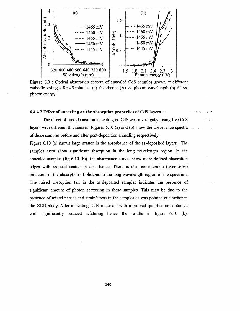
320 400 480 560 640 720 800 Wavelength (nm)
1.5 1.8 2.1 2.4 2.7 3 Photon energy (eV)
Figure 6.9 : Optical absorption spectra of annealed CdS samples grown at different cathodic voltages for 45 minutes, (a) absorbance (A) vs. photon wavelength (b) A2 vs. photon energy.
6.4.4.2 Effect of annealing on the absorption properties of CdS layers ^
The effect of post-deposition annealing on CdS was investigated using five CdS
layers with different thicknesses. Figures 6.10 (a) and (b) show the absorbance spectra
of those samples before and after post-deposition annealing respectively.
Figure 6.10 (a) shows large scatter in the absorbance of the as-deposited layers. The
samples even show significant absorption in the long wavelength region. In the
annealed samples (fig 6.10 (b)), the absorbance curves show more defined absorption
edges with reduced scatter in absorbance. There is also considerable (over 50%)
reduction in the absorption o f photons in the long wavelength region o f the spectrum.
The raised absorption tail in the as-deposited samples indicates the presence of
significant amount of photon scattering in these samples. This may be due to the
presence of mixed phases and strain/stress in the samples as was pointed out earlier in
the XRD study. After annealing, CdS materials with improved qualities are obtained
with significantly reduced scattering hence the results in figure 6.10 (b).
140
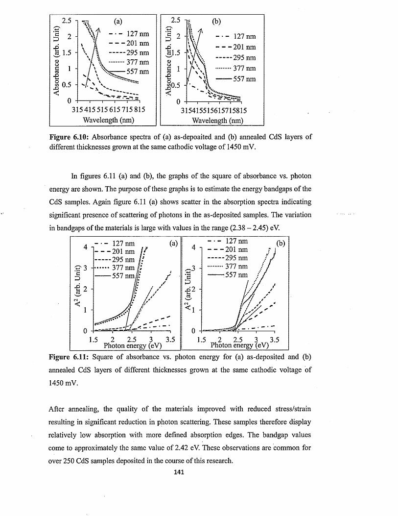
2.5 -
e!D 2 -Xt-4cS 1.5 -<DccS
f>1 -
Oco 0.5 -<
0
127 nm 201 nm
295 nm377 nm557 nm
315415515615715815 Wavelength (nm)
2.5 tp
cZ)x>->1kjI<do§
J o<
.5
1
5 H
0
127 nm 201 nm 295 nm
377 nm 557 nm
~T------------1---------------1-----”T~ — T
315415515615715815 Wavelength (nm)
Figure 6.10: Absorbance spectra of (a) as-depoaited and (b) annealed CdS layers of different thicknesses grown at the same cathodic voltage o f 1450 mV.
In figures 6.11 (a) and (b), the graphs of the square o f absorbance vs. photon
energy are shown. The purpose of these graphs is to estimate the energy bandgaps o f the
CdS samples. Again figure 6.11 (a) shows scatter in the absorption spectra indicating
significant presence of scattering of photons in the as-deposited samples. The variation
in bandgaps of the materials is large with values in the range (2.38 - 2.45) eV.
127 nm127 nm
1
01.5 2 2.5 3 3.5
Photon energy (eV)2 2.5 3 3.5
Photon energy (eV)
Figure 6.11: Square o f absorbance vs. photon energy for (a) as-deposited and (b)
annealed CdS layers of different thicknesses grown at the same cathodic voltage of
1450 mV.
After annealing, the quality of the materials improved with reduced stress/strain
resulting in significant reduction in photon scattering. These samples therefore display
relatively low absorption with more defined absorption edges. The bandgap values
come to approximately the same value of 2.42 eV. These observations are common for
over 250 CdS samples deposited in the course of this research.141
6.4.4.3 Effect of growth tem perature on the absorption properties of CdS layers
Figure 6.12 shows the effect o f growth temperature on the optical absorption of
CdS layers grown at five different temperatures at the same voltage and for growth time
of 30 minutes. In figure 6.12 (a), the absorption curves show large scatter with the
curves showing high absorption with very weak absorption edges. This results in energy
bandgap values in a wide range (2.39-2.56) eV with values of 2.56 eV, 2.50 eV, 2.40 eV
and 2.39 eV corresponding to samples grown at 43°C, 50°C, 60°C and 70°C
respectively. The absorption increases as the growth temperature increases, while the
energy bandgap decreases as the growth temperature increases. The samples grown at
33°C did not show any absorption, indicating that no significant deposition o f CdS
actually took place at this temperature at the chosen growth time of 30 minutes. In fact
the curve corresponding to this temperature is not visible in the two figures.
33°C• - • 43°C 50°C 60°C 70°C
e0.5 -
-fiO.4 - 33°C• - • 43 °C 50°C 60°C 70°C
Photon energy (eV) Photon energy (eV)
Figure 6 .12: Effect of growth temperature on the optical absorption o f (a) as-deposited
and (b) annealed CdS layers grown at 1450 mV for 30 minutes.
After annealing, figure 6.12 (b) shows that significant changes took place in
these samples during the annealing process. The absorbance of all the samples got
drastically reduced. The high absorption tails due to photon scattering lowered
considerably indicating the presence of little or no scattering centres resulting from the
release of stress/strain in the crystal lattices of the samples. Significant improvement of
the absorption edges become evident and the bandgaps o f the samples came to the same
value of -2.42 eV except for the sample grown at 33°C whose absorption curve did not
appear in the figure just like in figure 6.12 (a). Generally again, the absorbance
increases as the growth temperature increases indicating that more CdS materials were
142
deposited at higher temperatures than at lower temperatures.
6.4.4.4 Effect of thickness on the full optical properties of CdS layers
In this particular experiment, the full optical characterisation o f CdS samples o f
different thickness was undertaken. This involved determining the absorbance,
transmittance, reflectance, absorption coefficients extinction coefficients, refractive
indices and dielectric constants o f these materials with different thicknesses. Since the
preceding sections have covered the effects o f various growth parameters on the
absorption properties of CdS layers and since better CdS materials are obtained after
annealing, only the annealed samples grown at the cathodic voltage o f 1450 mV were
used in this characterisation.
Figures 6.13 (a) and (b) show the absorbance vs. wavelength and square of
absorbance vs. photon energy o f the five different layers respectively. The figures
generally show that absorption increases as film thickness increase and the gradient of
the absorption curve also increases with film thickness.
e3Xui
<Uo§•eocn X <
2.5 -|
2 -
1.5 -
1 -
0.5
0
127 nm 201 nm 295 nm 377 nm 557 nm
315 415 515 615 715 815 Wavelength (nm)
3 -
2 -
1 -
0
(b) 127 nm 201 nm ------295 nm 377 nm 557 nm'
1.5 2 2.5 3 3.5Photon energy (eV)
Figure 6.13: (a) Absorbance vs. Wavelength and (b) A2 vs. Photon energy for annealed
CdS layers of different thicknesses.
Figures 6.14 (a) and (b) show the transmittance and reflectance spectra o f CdS
layers of different thicknesses respectively. In figure 6.14 (a), one observes that
transmittance decrease as film thickness increases.
143
100 1 (a)
80 - * '
Co"oN 60 -/ S '
• ' s
/ I f /
i f<L>oacd 40 -
scnCC320 - ' , J f
£ 0 - juaaHzp-----,....—,
127 nm 201 nm 295 nm 377 nm—----- 557 nm
315 415 515 615 715 Wavelength (nm)
ox'w 'oocc3-*->ou
53D&
30
20 -
10 -
0
(b) - • - 127 nm 201 nm 295 nm 377 nm
-557 nm
315 415 515 615 715 815 Wavelength (nm)
Figure 6.14: (a) Transmittance vs. Wavelength and (b) Reflectance vs. Wavelength for
annealed CdS layers of different thicknesses.
Also transmittance increases as incident photon wavelength increases. For
samples with thickness >201 nm, there is no significant transmission of light in the
lower wavelengths up to 480 nm. However, for the sample with thickness o f 127 nm,
there is relatively significant transmission o f photons in this wavelength range with up
to 50% transmittance. This shows and explains the reason why it is generally accepted
that for solar cell application as window material, CdS needs to have very small
thickness, even as small as (10 - 50) nm [68]. The problem however in this situation, is
the issue of good coverage o f the underlying TCO layer. If the thickness o f CdS is too
low, it may not properly cover the TCO surface and this leads to short-circuiting when
CdTe is deposited on CdS for solar cell fabrication. But if the particular CdS used is
highly photovoltaic, then very thin layer is not necessary as absorption o f photons by
the CdS layer helps to create more photo-generated charge carriers. Figure 6.14 (b)
shows that the reflectance of all the layers have a maximum value of 20%. However, the
photon wavelength at which this maximum occurs is strongly thickness dependent. As
the thickness of the layer increases, this reflectance maximum as well as the onset of
reflectance shift towards longer wavelengths. Towards the longer wavelengths from the
point of maximum reflectance, the reflectance falls rapidly below the bandgap o f CdS.
This results shows that it is not very helpful to use extremely thin CdS as a window
layer for example in CdS/CdTe solar cell since there will be significant reflectance o f
the incident light in the short wavelength regions as some photons in this wavelength
region (high energy photons) will be reflected back into the atmosphere by very thin
CdS. Using very thick CdS layer again will result in the reflection of significant amount
o f photons in the visible region. There should therefore be a balance somewhere in-
144
between, requiring an optimum thickness of CdS for this kind of application.
Figures 6.15 (a) and (b) show the graphs of absorption coefficient vs. photon
energy (hv) and (ahv)2 vs. photon energy respectively. Both figures show similar trend
in the dependence o f absorption on incident photon energy. Unlike in figure 6.13 (b),
the absorption edges shift towards shorter wavelength as film thickness increases; this is
surprising as the opposite trend is expected. From figure 6.15 (a) the absorption
coefficients of these layers around the bandgap of CdS lie in the range (4.3 *104 -
7 .2xl04) cm"1 which is in agreement with literature values [62, 65]. From figure 6.15
(b), the bandgaps of the various layer come to the same value o f -2.42 eV as seen
earlier in figure 6.13 (b).
1.5E+05 n
B&1.g
.w'o<L> ■ O ' oGO
oO.OE+OOCOpO <
0E+05
.0E+04 -
127 nm 201 nm
295 nm377 nm557 nm
1.5 2 2.5 3 3.5Photon energy (eV)
1.0E+11 i “
So>5.0E+10<D
a
0.0E+00
• - 127 nm
1.5 2 2.5 3Photon energy (eV)
Figure 6.15: (a) Absorption coefficient vs. Photon energy and (b) (ahv)2 vs. Photon
energy for annealed CdS layers with different thicknesses.
Figure 6.16 (a) and (b) show the dependence of extinction coefficient and
refractive index on photon energy respectively.
0.4 i
^4^0 .3G.a>
S0.2<DooI 0-1%->oG■£ 0W
(a)
- 127 nm -201 nm
— 295 nm 377 nm 557 nm
1.5 2 2.5 3 3.5 Photon energy (eV)
x 2<D■a.G<D > 1 -
(b)
• - 127 nm — 201 nm
295 nm 377 nm 557 nm
1.5 2 2.5 3 3.5 Photon energy (eV)
Figure 6.16: (a) Extinction coefficient vs. Photon energy and (b) Refractive index vs.
Photon energy for annealed CdS layers of different thicknesses.145
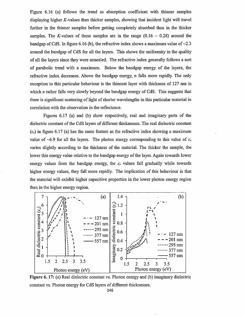
Figure 6.16 (a) follows the trend as absorption coefficient with thinner samples
displaying higher if-values than thicker samples, showing that incident light will travel
further in the thinner samples before getting completely absorbed than in the thicker
samples. The ^-values of these samples are in the range (0.16 - 0.28) around the
bandgap of CdS. In figure 6.16 (b), the refractive index shows a maximum value o f ~2.3
around the bandgap of CdS for all the layers. This shows the uniformity in the quality
o f all the layers since they were annealed. The refractive index generally follows a sort
o f parabolic trend with a maximum. Below the bandgap energy o f the layers, the
refractive index decreases. Above the bandgap energy, n falls more rapidly. The only
exception to this particular behaviour is the thinnest layer with thickness of 127 nm in
which n rather falls very slowly beyond the bandgap energy of CdS. This suggests that
there is significant scattering o f light o f shorter wavelengths in this particular material in
correlation with the observation in the reflectance.
Figures 6.17 (a) and (b) show respectively, real and imaginary parts o f the
dielectric constant of the CdS layers of different thicknesses. The real dielectric constant
(£>) in figure 6.17 (a) has the same feature as the refractive index showing a maximum
value o f -6 .9 for all the layers. The photon energy corresponding to this value of er
varies slightly according to the thickness of the material. The thicker the sample, the
lower this energy value relative to the bandgap energy of the layer. Again towards lower
energy values from the bandgap energy, the e> values fall gradually while towards
higher energy values, they fall more rapidly. The implication of this behaviour is that
the material will exhibit higher capacitive properties in the lower photon energy region
than in the higher energy region.
ccd-t-j .w A C H o o a
*C-4- >o
*3
& 0
- • **
/ ' { / / ' }
1k
/ / ' s s,ti * * 7f / ' /
\x5li * • ft ✓
il‘ I
/ / 1 »/ 1 '/ i \t
(a)
- 127 nm -201 nm
--295 nm ••• 377 nm— 557 nm
1.5 2 2.5 3 3.5
Photon energy (eV)
1.4 -i
Vu* 1s ✓ 1
<D
*5 0
| 0tocd£
2
1
8
6
4
2 H
0
(b)
127 nm 201 nm
~ 295 nm 377 nm———557 nm
1.5 2 2.5 3 3.5Photon energy (eV)
Figure 6.17: (a) Real dielectric constant vs. Photon energy and (b) imaginary dielectric
constant vs. Photon energy for CdS layers of different thicknesses.146
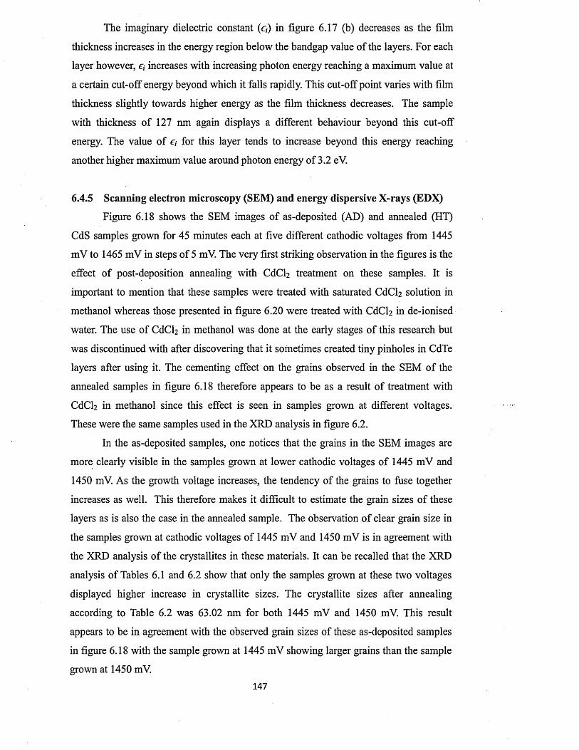
The imaginary dielectric constant (£,) in figure 6.17 (b) decreases as the film
thickness increases in the energy region below the bandgap value of the layers. For each
layer however, ey increases with increasing photon energy reaching a maximum value at
a certain cut-off energy beyond which it falls rapidly. This cut-off point varies with film
thickness slightly towards higher energy as the film thickness decreases. The sample
with thickness of 127 nm again displays a different behaviour beyond this cut-off
energy. The value of e,- for this layer tends to increase beyond this energy reaching
another higher maximum value around photon energy of 3.2 eV.
6.4.5 Scanning electron microscopy (SEM) and energy dispersive X-rays (EDX)
Figure 6.18 shows the SEM images o f as-deposited (AD) and annealed (HT)
CdS samples grown for 45 minutes each at five different cathodic voltages from 1445
mV to 1465 mV in steps of 5 mV. The very first striking observation in the figures is the
effect of post-deposition annealing with CdCl2 treatment on these samples. It is
important to mention that these samples were treated with saturated CdCl2 solution in
methanol whereas those presented in figure 6.20 were treated with CdCb in de-ionised
water. The use of CdCh in methanol was done at the early stages of this research but
was discontinued with after discovering that it sometimes created tiny pinholes in CdTe
layers after using it. The cementing effect on the grains observed in the SEM of the
annealed samples in figure 6.18 therefore appears to be as a result of treatment with
CdCl2 in methanol since this effect is seen in samples grown at different voltages.
These were the same samples used in the XRD analysis in figure 6.2.
In the as-deposited samples, one notices that the grains in the SEM images are
more clearly visible in the samples grown at lower cathodic voltages o f 1445 mV and
1450 mV. As the growth voltage increases, the tendency of the grains to fuse together
increases as well. This therefore makes it difficult to estimate the grain sizes o f these
layers as is also the case in the annealed sample. The observation of clear grain size in
the samples grown at cathodic voltages o f 1445 mV and 1450 mV is in agreement with
the XRD analysis of the crystallites in these materials. It can be recalled that the XRD
analysis of Tables 6.1 and 6.2 show that only the samples grown at these two voltages
displayed higher increase in crystallite sizes. The crystallite sizes after annealing
according to Table 6.2 was 63.02 nm for both 1445 mV and 1450 mV. This result
appears to be in agreement with the observed grain sizes of these as-deposited samples
in figure 6.18 with the sample grown at 1445 mV showing larger grains than the sample
grown at 1450 mV.
147
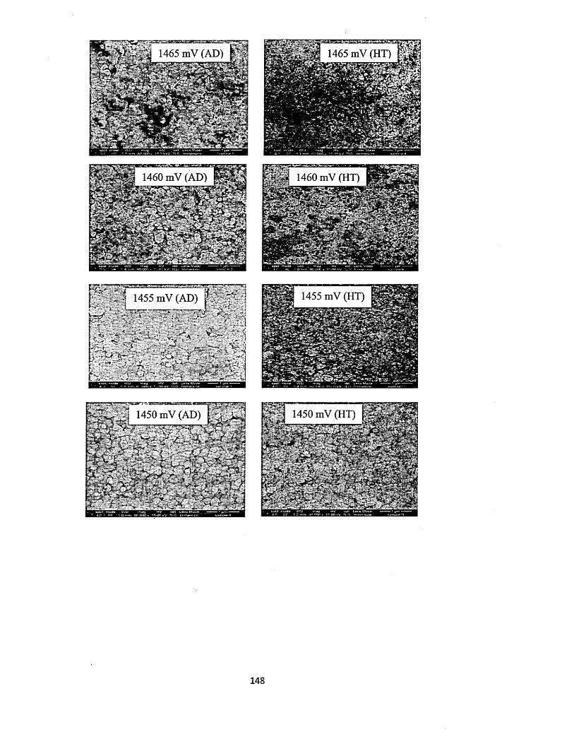
* 1465 mV
/** - \ : */
K / f*V. >«Sgk^ v *'%*%>« ■* »c •?!£**. .‘O-
*>*'. >*
F'i S"! 1460 mV (HT)' S i C ^ m 1460 mV (AD) ^ . vO
m&& Wh*> <
1455 mV (HT)1455 mV (AD) f . l
i
( i* x 'y^':'4^f% ? i*s'. l&££
148

Figure 6.18: SEM images of as-deposited (AD) and annealed (HT) CdS samples grown
at different cathodic voltages for 45 minutes. CdCh treatment was done with saturated
CdCb in methanol.
Figure 6.19 shows the EDX spectra o f the same samples before and after post
deposition annealing indicating the presence of both Cd and S atoms in these materials.
The peaks showing C, N, O and Si must have come from the underlying glass/FTO
substrate on which these CdS layers were grown. The percentage atomic concentrations
of Cd and S in these samples, obtained from analysis of the EDX are presented in figure
6.21 and Table 6.7.
1465 mV (AD) 1465 mV (HT)
:ut Scale ffld sC m sor. 6.850Scale cts Cursor 7.M7 d s |
1460 mV (HT)
65 1 keV :uB Scala 403 d s Cursor 6 S5Q:i l Scale 205 els Cursor 7.035 (4 d sj
149
1455 mV (HT)1455 mV (AD) s*
'■111 (.5
:ul Scale 2893 d s C m 5.003 (51 d s)i i i S d e W c t s Cursor 6 850 (17 cts)
1450 mV (HT)1450 mV (AD)
keV :ufl S d a 1071 d s Cursor. 5015 (28 ds):u> Scale 1036 cts Cursor. 6.850 (13 ctsj
1445 mV (HT)1445
:uB Scab 1159 els Cursor 6.015 (23 ctsj:uB Scale 450 cts Cursor 6.850 (13 ds)
Figure 6.19: EDX spectra of as-deposited (AD) and annealed (HT) CdS samples grown
at different cathodic voltages for 45 minutes. Annealing was preceded by CdCl2
treatment.
Figure 6.20 shows the SEM images o f CdS samples grown at a cathodic voltage
of 1450 mV with different thicknesses. It can be seen that as the thickness of the layers
increase, the grains become clearer and more closely packed. At thicknesses o f (127 and
201) nm however, the amount of deposited CdS material could not completely cover
these particular FTO substrates. These two samples therefore show significant amount
150
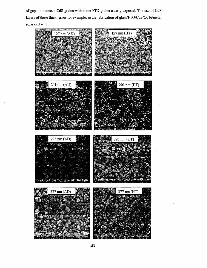
of gaps in-between CdS grains with some FTO grains clearly exposed. The use o f CdS
layers of these thicknesses for example, in the fabrication of glass/FTO/CdS/CdTe/metal
Figure 6.20: SEM images of as-deposited (AD) and annealed (HT) CdS samples grown at cathodic voltage o f 1450 mV with different thicknesses. CdCl2 treatment was done with saturated CdCl2 in de-ionised water.
definitely be a failure as a result of shunting o f both CdTe and the metal contact with the
FTO which will result in loss of fill factor and open-circuit voltage. Apart from the 377
nm sample (corresponding to a growth time of 20 minutes), the other samples did not
show any significant increase in grain size after post-deposition annealing. This
suggests that this thickness may be the approximate optimum thickness for CdS based
on grain size improvement after annealing for this particular glass/FTO substrates used
in this research.
The cementing effect after annealing observed in the samples o f figure 6.18 is
not visible in the samples o f figure 6.20. As mentioned earlier, this may be because
these samples (in figure 6.20) were treated with CdCh dissolved in de-ionised water as
against CdCl2 dissolved in methanol used in the samples o f figure 6.18.
Table 6.7 and figure 6.21 show the percentage S and Cd compositions o f the
CdS layers grown at different cathodic voltages for 45 minutes.
Table 6.7: Percentage S and Cd atomic compositions of as-deposited and annealed CdS
samples growm for 45 minutes at different cathodic voltages.
Cathodicvoltage(mV)
SampleID
Growthtime(min)
Atomic composition (%) As-depositedCd/S
AnnealedCd/SAs-
depositedAnnealed
Cd S Cd S1445 5 45 46.6 53.4 46.7 53.3 0.87 0.881450 4 45 46.6 53.4 47.8 52.2 0.87 0.921455 59 45 50.4 49.6 49.1 50.9 1.02 0.961460 2 45 45.1 54.9 45.7 54.3 0.82 0.841465 1 45 42.1 57.9 44.2 55.8 0.73 0.79
152
100 1100 1(a) As-deposited-®—s
■"■Hi Cd(b) Annealed
£ 60 -
5 40 -
1445 1450 1455 1460 1465 Cathodic voltage (mV)_____
1445 1450 1455 1460 1465Cathodic voltage (mV)______
Figure 6.21: Percentage S and Cd atomic compositions of (a) as-deposited and (b) annealed CdS samples grown for 45 minutes at different cathodic voltages.
These atomic concentrations were obtained from the EDX using EDX analysis software
of the SEM equipment. Both Table 6.7 and figure 6.21 (a) show that all the as-deposited
samples were S-rich, except for the sample grown at cathodic voltage o f 1455 mV
which rather showed Cd-richness. With the exception o f this particular sample, it is also
observed in the as-deposited samples that the concentration of S in the layers increases
as the growth voltage increases while the concentration of Cd decreases accordingly.
After annealing, both Table 6.7 and figure 6.21 (b) reveal all the samples to be
clearly S-rich. A very close observation also shows that the samples become more
stoichiometric after annealing. The only exception to this is only the sample grown at
1455 mV. These results and others seen previously demonstrate also that the best
electrodeposited CdS material from this experiment comes after post-deposition
annealing. The sample with the best stoichiometry before and after annealing (with the
exception of the sample grown at cathodic voltage 1455 mV sample) is the sample
grown at the cathodic voltage of 1450 mV with Cd/S = 0.92 after annealing. All other
samples have Cd/S < 0.92 after annealing.
Table 6.8 and figure 6.22 show the percentage S and Cd composition o f the
samples grown at cathodic voltage of 1450 mV for different times with different
thicknesses.
153
Table 6.8: Percentage S and Cd atomic compositions of CdS layers grown at cathodic
voltage o f 1450 mV for different durations.
Vg(mV)
SampleID
Growthtime(min)
Thickness(nm)
Atomic composition (%) As-deposite
dCd/S
AnnealedCd/SAs-
depositedAnnealed
Cd S Cd S1450 CS148 5 127 42.2 57.8 30.9 60.1 0.73 0.511450 CS147 10 201 44.7 55.3 47.9 52.1 0.81 0.921450 CS146 15 295 48.1 51.9 48.8 51.2 0.93 0.951450 CS145 20 377 51.4 48.6 48.7 51.3 1.06 0.951450 CS144 25 557 48.5 51.5 48.6 51.4 0.94 0.951450 CS4-D 45 700 46.6 53.4 47.8 52.2 0.87 0.92
100
(a) As-deposited (b) Annealed
- f l
45Growth time (min) Growth time (min)
Figure 6.22: Percentage S and Cd atomic compositions of CdS layers grown at cathodic voltage o f 1450 mV for different durations.
The results show generally again that as-deposited samples are S-rich except for the
sample grown for 20 minutes with thickness o f 377 nm. The trend in S-content o f these
samples is that, as the deposition time (thickness) increases the S-content decreases up
to the thickness of about 377 nm and then begins to increase as thickness increases
beyond this point. After annealing, all the samples emerged S-rich. The best
stoichiometry after annealing comes for thickness in the range (295 - 557) nm
corresponding to growth time in the range (15 - 25) minutes according to Table 6.8 and
figure 6.22 (b).
It is also important to point out here that EDX technique is not an accurate
technique for precise determination of atomic composition as mentioned in section 3.3.2
of chapter 3. The results presented in this chapter may therefore be taken as qualitative
and not quantitative.
154
6.5 Conclusion
Electrodeposition and characterisation of CdS layers have been presented in this
chapter. The electrodeposition of these layers was carried out using two-electrode
system for process simplification. The precursors used were CdCfeJHkO and
Na2S203.5H20 while the pH and deposition temperature were 1.8±0.02 and 85±2°C
respectively. All deposited samples showed n-type electrical conductivity over a wide
range of cathodic deposition potentials with the best cathodic deposition potential
identified as 1450 mV. XRD results show that as-deposited samples were
polycrystalline in nature with mixed phases of cubic and hexagonal structures. After
annealing however, the XRD peaks representing cubic phase disappear completely
while the peaks of the hexagonal phase are enhanced with preferred orientation in the
(002) plane. Also, the bandgap of all the layers come to 2.42 eV after annealing,
indicating improvement in the quality o f the materials after this process. Results of
optical characterisation show that absorption increases with sample thickness with a in
the order of 104 cm"1 around the bandgap. Refractive index also increases with thickness
showing a maximum value of 2.3 around the bandgap and extinction coefficient
decreases with increasing thickness with values in the range (0.16 - 0.28) around the
bandgap. The resistivity o f the layers also increases with thickness with values generally
in the range (2.1 - 6.4)xl04 Hem. CdCk treatment with CdCk dissolved in methanol
results in cementing together of the grains unlike in the case of CdCk dissolved in de
ionised water. Crystallite sizes of annealed samples were observed to be in the range (31
- 63) nm while EDX analysis shows that the samples are S-rich under the conditions
described.
155

References
[1] T. L. Chu and S. S. Chu, Solid-State Electronics, 38 (3) (1995) 533 - 549.
[2] J. Britt and C. Ferekides, Appl. Phys. Lett. 62, (1993) 2851.
[3] K. Matsune, H. Oda, T. Toyama, H. Okamoto, Y. Kudriavysevand and R.
Asomoza, Solar Energy Materials & Solar Cells, 90 (2006) 3108 - 3114.
[4] H. Miyazaki, R. Mikami, A. Yamada and M. Konagai, Journal o f Physics and
Chemistry o f Solids, 64 (2003) 2055 - 2058.
[5] W. K. Metzger, J. Appl. Phys., 103 (2008) 094515.
[6 ] R. Hill, Solid-State and Electron Devices, (Special Issue), 2 (1978) S49 - S54.
[7] S. Martinuzzi, Solar Cells, 5 (1982) 234 - 268.
[8 ] S. B. Hussain, J. Sound Vib., 12 (2) (1970) 177 - 180.
[9] Y. Kraftmankher, Eur. J. Phys. 33 (2012) 503 - 511.
[10] V. Ceric, J. Phys. D: Appl. Phys., 5 (1972) 1168 - 1172.
[11] B. Kramer, S. Gelfman and K. Kalikstein, Physical Review B, 6 (2) (1972) 556 -
564.
[12] R. Zuleeg and R. S. Muller, Solid-State Electronics, 7 (1964) 575 - 582.
[13] R. Zuleeg, Solid-State Electronics, 6 (1963)193 - 196.
[14] W. Duncan and A. R. Smellie, J. Appl. Phys. 49, 4098 (1978).
[15] J. Conragan and R. S. Muller, Solid-State Electronics, 9 (2) (1966) 182.
[16] R. P. Parker, Phys. Med. Biol., 5 (4) (1970) 605 - 620.
[17] E. S. Yousef, M. Hotzel and C. Russel, J. Non-crystalline Solids, 354 (2008) 4675
- 4680.
[18] I. A. Kirovskaya, O. T. Timoshenko and E. O. Karpova, Russian Journal o f
Physical Chemisty A, 85 (4) (2011) 557 - 560.
[19] L. Sheeney-Hai-Ichia, S. Pogorelova, Y. Gofer and I. Willner, Advanced
Functional Materials, 4 (5) (2004) 416 - 424.
[20] C. B. Roxlo and M. M. Salour, Appl. Phys. Lett. 38 (1981) 738.
[21] A. Bosio, N. Romeo, S. Mazzamuto and V. Canevari, Prog. Cryst. Growth &
Charact. Mater., 52 (2006) 247-279.
[22] I. M. Dharmadasa, A. P. Samantilleke, N. B. Chaure, and J. Young, Semicond.
Sci. Technol, 17 (2002) 1238 -1248.
[23] R. B. Hall and J. D. Meakin, Thin Solid Films, 63 (1979) 203 - 211.
[24] N. B. Chaure, A. P. Samantilleke, R. P. Burton, J. Young and I. M. Dharmadasa,
Thin Solid Films, 472 (2005) 212 - 216.
[25] N. Naghavi, G. Renou, V. Bockelee, F. Donsanti, P. Genevee, M. Jubault, J. F.
156
Guillemoles and D. Lincot, Thin Solid Films, 519 (21) (2011) 7600 - 7605.
[26] C. D. Lokhande, Materials Chemistry and Physics, 26 (1990) 405 - 409.
[27] P. K. Nair, J. Campos and M. T. S. Nair, Semicond. Sci. Technol., 3 (1988) 134 -
145.
[28] J. I. B. Wilson and J. Woods, J. Phys. Chem. Solids, 34 (1973) 171 - 181.
[29] N. Lovergine, R. Cingolani, and A. M. Mancini, J. Cryst. Growth, 118 (1992) 304
- 308.
[30] X. Shen, A. Yuan, F. Wang, J. Hong and Z. Xu, Solid State Communications, 133
(1) (2005) 19 - 22.
[31] J. W. Orton, B. J. Goldsmith, J. A. Chapmann and M. J. Powell, J. Appl. Phys. 53,
(1982) 1602 -1614.
[32] M. Krunks, E. Mellikov and E. Sork, Thin Solid Films, 145 (1) (1986) 105 - 109.
[33] N. Remeo, A. Bosio, V. Canevari and D. Seuret, Solar Cells, 22 (1) (1987) 23 -
27.
[34] N. R. Paudel, K. A. Wieland and A. D. Compaan, Solar Energy Materials &
Solar Cells, 105 (2012) 109 -112.
[35] P. J. Sebastian and M. Ocampo, Solar Energy Materials & Solar Cells, 44 (1)
(1996) 1 -10.
[36] P. J. Sebastian and M. E. Calixto, Thin Solid Films, 360 (1-2) (2000) 128 - 132.
[37] J. Butty, Y. Z. Hu, N. Peyghambarian, Y. H. Kao and J. D. Mackenzie, Appl.
Phys. Lett. 67 (1995) 2672 - 2674.
[38] A. A. Ziabari and F. E. Ghodsi, Solar Energy Materials & Solar Cells, 105 (2012)
249 - 262.
[39] J. Schaffner, E. Feldmeier, A. Swirschuk, H. J. Schimper, A. Klein and W.
Jaegermann, Thin Solid Films, 519 (21) (2011) 7556 - 7559.
[40] H. R. Moutinho, D. Albin, Y. Yan, R. G. Dhere, X. Li, C. Perkins, C. S. Jiang, B.
To and M. M. Al-Jassim, Thin Solid Films, 436 (2) (2003) 175 - 180.
[41] B. M. Basol, Solar Cells, 23 (1988) 69 - 88.
[42] D. G. Diso, G. E. A. Muftah, V. Patel and I. M. Dharmadasa, J. Electrochemical
Society, 157 (6) (2010) H647 - H651.
[43] M. Rami, E. Benamar, M. Fahoume, F. Chraibi and A. Ennaoui, M. J. Condensed
Matter, 3 (1) (2000) 66 - 70.
[44] G. C. Morris, P. E. Tanner and A. Tottszer, Photovoltaic Specialists Conference
1990, Conference Record o f the twenty first IEEE, 21 - 25 May, 1990,
Kissimmee, Florida, USA, Vol.l Pg. 575-580 .
157
http.V/ieeexplore. ieee. org/stamp/stamp.jsp?tp=&arnumber=l11685.
[45] R. G. Dhere, M. Bonnet-Wymard, E. Charlet, E. Peter, J. N. Duenow, J. V. Li, D.
Kuciauskas and T. A. Gessert, Thin Solid Films, 519 (2011) 7142 - 7145.
[46] J. M. Woodcock, A. K. Turner, M. E. Ozsan and J. G. Summers, Photovoltaic
Specialists Conference 1991, Conference Record o f the twenty second IEEE, 7 -
11 October, 1991, Las Vegas, Nevada, USA, Vol.2 Pg. 842 - 847.
http://ieeexplore.ieee.org/xpls/abs_all.jsp?arnumber=l69328.
[47] X. Wu, Solar Energy, 77 (2004) 803 - 814.
[48] N. Romeo, A. Bosio, R. Tedeschi, A. Romeo and V. Canevari, Solar Energy
Materials & Solar Cells, 58 (1999) 209 - 218.
[49] X. Wu, J. C. Keane, R. G. Dhere, C. DeHart, D. S. Albin, A. Duda, T. A. Gessert,
S. Ashar, D. H. Levi and P. Sheldon, Proceedings o f 17th European PVSEC,
(2001) 995 -1000.
[50] C. S. Ferekides, D. Marinskiy, V. Viswanathan, B. Tetali, V. Palekis, P. Selvaraj
and D. L. Morel, Thin Solid Films, 361-361 (2000) 520 - 526.
[51] S. Dennison, J. Mater. Chem., 4(1) (1994) 41 - 46.
[52] S. K. Das and G. C. Morris, Solar Energy Materials & Solar Cells, 28 (1993) 305
-316.
[53] A. K. Turner, J. M. Woodcock, M. E. Ozsan, J. G. Summers, J. Barker et al, Solar
Energy Materials, 23 (1991) 388 - 393.
[54] G. Sasikala, P. Thilakan and C. Subramanian, Solar Energy Materials & Solar
Cells, 62(2000)275-293.
[55] H. Metin, S. Erat, F. M. Emen, V. Kafadar, A. N. Yazici, M. Ari and N. Kulcu,
Journal o f Luminescence, 130 (2010) 1531 - 1538.
[56] T. Abe, Y. Kashiwaba, M. Baba, J. Imai and H. Sasaki, Applied Surface Science,
175-176(2001) 149-1554.
[57] T. D. Dzhafarov, M. Altunbas, A. I. Kopya, V. Novruzov and E. Bacaksiz, J.
Phys.D: Appl. Phys., 32 (1999) L I25 - L I28.
[58] P. J. Sebastian, Appl. Phys. Lett. 62 (1993) 29656 - 29658.
[59] B. Ullrich, H. Ezumi, S. Keitoku and T. Kobayashi, Materials Science and
Engineering, B35 (1995) 117-159.
[60] F. Chemow, G. Eldridge, G. Ruse and L. Wahlin, Appl. Phys. Lett. 12 (1968) 339
-341.
[61] F. Liu, Y. Lai, J. Liu, B. Wang, S. Kuang, Z. Zhang, J. Li and Y. Liu, Journal o f
Alloys and Compounds, 493 (2010) 305 - 308.
158 ^
[62] N. B. Chaure, S. Bordas, A. P. Samantilleke, S. N. Chaure, J. Haigh and I. M.
Dharmadasa, Thin Solid Films, 437 (2003) 10 -17 .
[63] S. Preusser and M. Cocivera, Solar Energy Materials 20 (1990) 1 -1 4 .
[64] J. Kokaj and A. E. Rakhshani, J. Phys.D: Appl. Phys., 37 (2004) 1970 -1975.
[65] W. J. Danaher, L. E. Lyons and G. C. Morris, Solar Energy Materials, 2 (1985)
137 -148.
[6 6 ] S. Kolhe, S. K. Kulkami, A. S. Nigavekar and S. K. Sharma, Solar Energy
Materials 10 (1984) 47 - 54.
[67] K. S. Balakrishnan and A. C. Rastogi, Solar Energy Materials, 20 (1990) 417 -
434.
[6 8 ] T. M. Razykov, C. S. Ferekides, D. Morel, E. Stefanakos, H. S. Ullal and H. M.
Upadhyaya, Solar Energy, 85 (2011) 1580 - 1608.
159
Chapter 7: CdTe deposition and characterisation
7.0 Introduction
The electrodeposition o f CdTe for the fabrication o f CdS/CdTe solar cells has
received research attention for quite some time now [1 - 9]. The manufacturability and
scalability o f this simple but powerful process has been undoubtedly demonstrated by
British Petroleum (BP Solar) company in the late 1990s by the production o f over 10%
efficiency solar panels o f ~1 m2 [3]. The conventional electrodeposition set-up usually
involves three electrodes (working electrode or cathode, counter electrode or anode and
reference electrode) and most of the work reported so far on the electrodeposition of
CdTe and other semiconductors in general, have been based on the three-electrode
system [1, 9 - 15]. The use of simple two-electrode system for electrodeposition of
semiconductors is uncommon as the conventional electrochemical deposition process is
traditionally based on the principle o f three-electrode system [16]. As a result, only very
few reports can be found in the literature involving the use of two-electrode systems for
the electrodeposition of semiconductors [17-19].
In the whole history of electrodeposition of CdTe thin films however, it is
difficult to find any documented report on the use of two-electrode systems in the
literature. This situation therefore prompted the use o f two-electrode system in the
electrodeposition of CdTe as well as other thin film semiconductors for the fabrication
o f CdTe-based solar cells in this thesis. In addition, the suspicion that possible leakage
o f unwanted groups 1A and IB ions like K+ and Ag+ from saturated calomel electrode
(SCE) and Ag/AgCl reference electrode [20] could deteriorate the efficiency of CdTe
solar cells (since n-type CdTe is the preferred species in this work instead of p-type
CdTe), gave strong impetus to the investigation o f the use of the two-electrode system
in the electrodeposition of CdTe and other semiconductors. These ions are known to
have detrimental effects on CdTe-based solar cells [6 , 21]. This approach therefore
serves to eliminate one possible impurity source (the reference electrode) for the
development of n-CdTe-based solar cells as well as to simplify the electrodeposition
process and reduce cost at the same time. Again, the deposition temperature can be
raised without the fear of exceeding the operating temperature limit of the reference
electrode usually specified by the manufacturers (~70°C for SCE and ~100°C for
Ag/AgCl electrode) [22]. This will have the benefit of improving the crystallinity of the
semiconductors deposited. Along the line, a brief comparative study of the possible
160
effects of the two-electrode and three-electrode systems was carried out to study the
effects of these different electrode systems on the quality of CdTe layers produced. This
study however, showed no particular difference in the quality of CdTe layers deposited
using both electrode systems.
The fact that CdTe can be grown with n-type or p-type electrical conductivity
without extrinsic doping is well known [23, 24] and this is particularly achieved by
changing the stoichiometry of the material. A Cd-rich CdTe results in n-type
conductivity (n-CdTe) while a Te-rich CdTe results in p-type conductivity (p-CdTe)
[24]. In electrodeposition, this stoichiometry change is simply achieved by varying the
deposition potential. At lower cathodic deposition potentials within the possible
deposition potential range of CdTe, p-CdTe is obtained. At higher deposition potentials
n-CdTe is obtained [23], and at a potential somewhere in-between, intrinsic CdTe (i-
CdTe) is obtained. This shows that such a material can be deposited in a certain range o f
deposition potential depending on which conductivity type one wants. This same
situation has also been reported for electrodeposited p-, i- and n-type copper indium
diselenide (CIS) within a cathodic deposition potential range of (2.20 - 2.80) V in two-
electrode system [17] and p+-, p-, i-, n-, and n+-type copper indium gallium diselenide
(CIGS), within a cathodic deposition potential range of (0.40 - 1.35) V in three-
electrode system [25] as well as for p- and n-type ZnSe, within a cathodic deposition
potential range of (0.50 - 0.60) V in three-electrode system [26], though the doping in
this case o f ZnSe was by addition of extrinsic dopants (As and Ga). In all these
examples, it becomes very clear that the electrodeposition of any particular
semiconductor can actually be carried out over a certain wide range o f deposition
potentials. As another example, the work by Diso et al. [19], on two-electrode
deposition of CdS layers, shows that good quality CdS layers can be obtained in a
cathodic deposition range of (1300 - 1500) mV under the conditions they used. In the
work by Takahashi et al in ref [23], p-type and n-type CdTe were electrodeposited in a
cathodic potential from 300 mV to 600 mV vs. Ag/AgCl which is actually a potential
range of 300 mV.
One of the issues usually raised about the two-electrode system in favour o f the
three-electrode system is that of fluctuation in the deposition potential and current
density over the surface of the working electrode due to the measurement o f the applied
potential with respect to the anode unlike in the three-electrode system where the
applied potential is measured with respect to the reference electrode. The three-
161
electrode system is known to provide a stable deposition potential and current density at
the working electrode/electrolyte interface during an electrodeposition process by
measuring the deposition potential relative to the reference electrode instead o f the
counter electrode (anode) [27]. The above cited examples in the literature therefore
show that such a small fluctuation in the deposition potential (of few millivolts of
course), does not necessarily have any adverse effect on the semiconductor material
deposited considering the wide range of potentials over which this material can
normally be deposited, whether with three-electrode system or with two-electrode
system. This therefore helps to clear the suspicion and fear that two-electrode deposition
does not produce good quality materials (at least in semiconductors) due to fluctuations
in the deposition potential and current density over the surface of the working electrode.
The comparison of some properties o f electrodeposited CdTe layers and
glass/FTO/CdS/CdTe/metal thin film solar cells fabricated using both two-electrode and
three-electrode systems in this thesis, shows that both systems can produce CdTe layers
of similar qualities for thin-film solar cell applications.
7.1 Preparation of CdTe deposition electrolyte
Two similar deposition electrolytes were used in the electrodeposition of CdTe
layers in both two-electrode and three-electrode configurations. Both electrolytes
contain aqueous solutions of 1M CdS0 4 of 99.0% purity and Te0 2 of 99.999% purity
dissolved in H2 SO4 of 98% purity all in 800 ml of de-ionised water. A major issue
worthy of note here is the problem of TeC>2 dissolution. Te0 2 is practically insoluble in
water [28]. It is however soluble in sulphuric acid [29] although the solubility is not
hundred per-cent. About 30 mM of Te0 2 solution was prepared by dissolving in
concentrated H2 SO4 for about 1 hour as much as possible and then diluting with de
ionised water in 250 ml plastic round-bottom flask ready for addition into CdSC>4
solution. Before the addition of TeC>2 solution, the CdSC>4 solution was stirred for 24
hours and then electro-purified for 48 hours following the steps outlined earlier in
chapters 5 and 6 . Then about 4 ml of TeC>2 solution was added into the CdS0 4 solution
and stirred for 24 hours before taking a cyclic voltammogram of the resulting electrolyte
to identify the possible deposition potential range for CdTe. All voltammetry and
electrodeposition processes were carried out using two-electrode system for the main
deposition electrolyte to which 1000 parts per million (1000 ppm) each of 99.999%
CdCl2 and CdF2 were added for n-type doping. The counter electrode in the case of
two-electrode system was high-purity platinum plate or carbon rod. For the second
162
electrolyte, the voltammetry and deposition were done in three-electrode configuration
for comparison with the two-electrode system. The counter electrode was high-purity
carbon rod and the reference electrode was saturated calomel electrode. It also
contained 1000 parts per million of 99.999% Cdl2 for n-type doping. The pH of both
electrolytes was maintained at 2.00±0.02 with moderate stirring rate o f 300 rpm. The
deposition temperature for the two-electrode bath was maintained at (85±2)°C while
that for the three-electrode system was maintained at a (68±2)°C since it had saturated
calomel reference electrode whose manufacturer-specified maximum operating
temperature is 70°C. All the cyclic voltammetry were also taken under similar
conditions for uniformity. It is important to mention that the main aim o f the use of
these two systems is to show that CdTe of similar qualities can equally be produced
using either electrode systems. The aim is not strictly to compare the qualities o f the
CdTe produced from the two electrolytes that have slightly different compositions in
terms of the dopants used and with different counter electrodes. It is rather to show that
the two-electrode system is as good as the three electrode system and therefore can be
used even at better advantage in terms of its simplicity (reducing cost), minimised
contamination of the bath and higher deposition temperature for better crystallinity
when compared to the three-electrode system. For this reason major work carried out on
CdTe was with two-electrode system. In fact the SCE used in this project was a
modified one. Because of the observation of gradual leakage of the 3M KCI2 solution in
the outer jacket, the electrode was modified by replacing the solution with exactly 3M
CdCb with purity of 99.999% to avoid getting K+ into the deposition bath. It is
important to remark that for the comparative study of CdTe obtained from two-electrode
and three-electrode systems using carbon anode in both cases, the two-electrode bath
contained only 1000 ppm of CdCk as an n-type dopant. The main two-electrode bath
used for the rest o f the project contained 1 0 0 0 ppm each of CdCh and CdF2 using
platinum anode. The reasons for these variations will be seen in the course o f this
chapter.
7.2 Substrate preparation
For establishment o f the right deposition conditions for these baths, glass/FTO
substrates were used. After the optimisation, glass/FTO/ZnS and glass/FTO/CdS as well
as glass/FTO/ZnS/CdS were then used as substrates to deposit CdTe for solar cell
fabrication. However, to prepare the glass/FTO substrates, the same procedure used in
electrodeposition of ZnS and CdS, in chapters 5 and 6 , was also used in the case of
163

CdTe. Soap solution, acetone, methanol and de-ionised water were used as solvents for
cleaning the glass/FTO substrates while only methanol and de-ionised water were used
for cleaning glass/FTO/ZnS, glasss/FTO/CdS and glass/FTO/ZnS/CdS substrates.
7.3 Electrodeposition of CdTe absorber layers
The voltammograms obtained from the cyclic voltammetry o f the two deposition
baths using the three different electrode configurations are shown in figures 7.1 (a), (b)
and (c) and were used to determine the possible deposition potentials for CdTe using the
different electrode configurations.
*(a) 2-E with .carbon anode (b) 2-E with platinum abode
Cathodic potential (mV)
Cathodic potential (mV) / ^
H =V ^wW>\ 1 / / 1 r~10J) 400 v 98€r^ 1400 1900
Cathodic potential (mV)
0 600 1200 1800 2400
Cathodic potential (mV)
(b) 3-E with carbon anode
-100 800 1 1 0 0
"O
- 1 0
-15Cathodic potential (mV)
Figure 7.1: Cyclic voltammograms of CdTe deposition electrolytes containing the
respective precursors and dopants for (a) two-electrode system with carbon anode (inset
is expansion of the region around the horizontal axis), (b) two-electrode system with
platinum anode (inset is expansion of the region around the horizontal axis) and (c)164

three-electrode system with carbon anode. The points marked A and B indicate the
possible deposition potential ranges for CdTe.
The two-electrode systems used were o f two types. One has carbon anode and the other
has platinum anode as shown in the figures. The essence of using platinum anode is to
observe/eliminate any possible contamination from the carbon anode. Since platinum is
an inert metal, it is believed that it will bring about little or no contamination compared
to carbon. Afterwards, the bulk of the work done on CdTe deposition in this project was
with the two-electrode system using platinum anode.
After determining the deposition potentials of Cd in each case as was done for
ZnS and CdS, electro-purification o f the CdSC>4 solutions was carried out at a
temperature of (85.0±0.2)°C for the two-electrode systems and (68.0±0.2)°C for the
three-electrode system for 48 hours. The temperature of 68.0°C was used for the three-
electrode system to avoid damaging the reference electrode since its maximum
operating temperature is 70.0°C according to the manufacturer’s specifications. TeC>2
was added afterwards and the pH of both electrolytes adjusted to 2.00+0.02 at room
temperature. After stirring for 24 hours, the set of voltammograms in figure 7.1 was
recorded to identify the possible range of deposition potentials for CdTe in each case.
The various dopants were then added accordingly as mentioned in section 7.1. Few
samples were then deposited on cleaned glass/FTO from each electrolyte using the
various electrode configurations across the identified deposition potential ranges for
characterisation using XRD, PEC cell and optical absorption to find out the best
deposition potential for n-CdTe from each electrolyte and each electrode configuration.
The baths were continuously stirred moderately at 300 rpm during the deposition and
the plating current density in all cases was maintained in the range (150 - 180) pAcm'2.
The layers were deposited on glass/FTO as well as on annealed glass/FTO/ZnS,
glass/FTO/CdS and glass/FTO/ZnS/CdS substrates at the respective best cathodic
potentials for device fabrication.
Generally, in CdTe deposition, Te (with standard reduction potential E° =
+0.593 V) deposits first since it has a more positive standard reduction potential than Cd
(E° = -0.403 V). The chemical reactions for the reduction o f Te and Cd from HTe0 2 +
and Cd2+ leading to the formation of CdTe on the cathode are given by [2]:
H TeO l + 3H+ + 4 e" Te + 2H20 ( 1 )
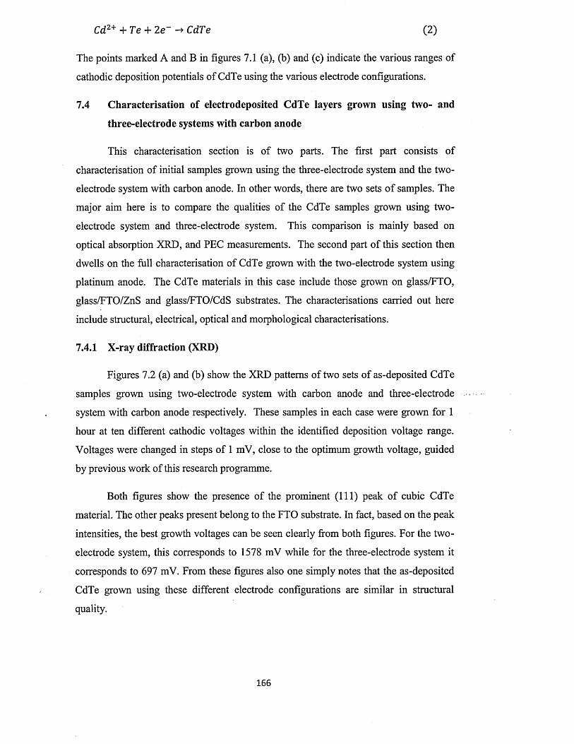
Cd2+ + Te + 2e~ -* CdTe (2)
The points marked A and B in figures 7.1 (a), (b) and (c) indicate the various ranges of
cathodic deposition potentials of CdTe using the various electrode configurations.
7.4 Characterisation of electrodeposited CdTe layers grown using two- and
three-electrode systems with carbon anode
This characterisation section is of two parts. The first part consists of
characterisation of initial samples grown using the three-electrode system and the two-
electrode system with carbon anode. In other words, there are two sets o f samples. The
major aim here is to compare the qualities of the CdTe samples grown using two-
electrode system and three-electrode system. This comparison is mainly based on
optical absorption XRD, and PEC measurements. The second part o f this section then
dwells on the full characterisation of CdTe grown with the two-electrode system using
platinum anode. The CdTe materials in this case include those grown on glass/FTO,
glass/FTO/ZnS and glass/FTO/CdS substrates. The characterisations carried out here
include structural, electrical, optical and morphological characterisations.
7.4.1 X-ray diffraction (XRD)
Figures 7.2 (a) and (b) show the XRD patterns of two sets of as-deposited CdTe
samples grown using two-electrode system with carbon anode and three-electrode
system with carbon anode respectively. These samples in each case were grown for 1
hour at ten different cathodic voltages within the identified deposition voltage range.
Voltages were changed in steps o f 1 mV, close to the optimum growth voltage, guided
by previous work of this research programme.
Both figures show the presence of the prominent (111) peak of cubic CdTe
material. The other peaks present belong to the FTO substrate. In fact, based on the peak
intensities, the best growth voltages can be seen clearly from both figures. For the two-
electrode system, this corresponds to 1578 mV while for the three-electrode system it
corresponds to 697 mV. From these figures also one simply notes that the as-deposited
CdTe grown using these different electrode configurations are similar in structural
quality.
166
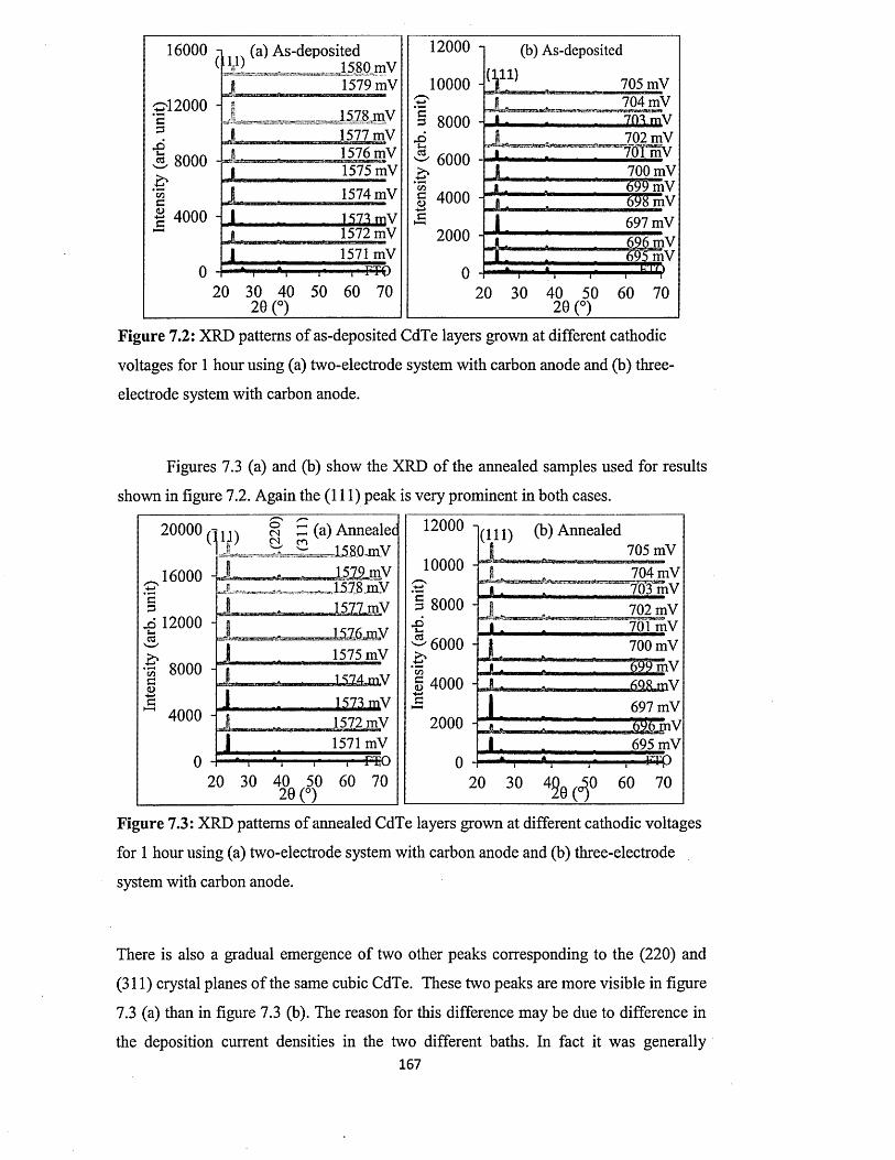
16000
xJ-iC3
(a) As-deposited (' U) 1580 mV
ri2000 -
8000 4
4000 -
1
1578 mV 1577 mV1576 mV 1575 mV1574 mV
J573_mV1572 mV1571 mV
2 0 30 40 2 0 (°)
*i"* - '- t- F T P
50 60 70
12000 n
1 0 0 0 0 -
XS-tcd
8000 -
6000
4000
2000 -
(b) As-deposited
{\ 11]
20 30■■t r
40 502 0 (°)
705 mV704 mV JQim V702 mV
700 mV699 mV
W m V697 mV
Figure 7.2: XRD patterns of as-deposited CdTe layers grown at different cathodic
voltages for 1 hour using (a) two-electrode system with carbon anode and (b) three-
electrode system with carbon anode.
Figures 7.3 (a) and (b) show the XRD of the annealed samples used for results
shown in figure 7.2. Again the (111) peak is very prominent in both cases.
20000 q
16000S '* 1
jd 12000cd
■f 8000Go
4000 -
(a) Annealec 1580,mV
1578,mV
1516j n y
1575 mV
1572 mV1571 mV
| j , » n o20 30 40 50 60 70
2 0 (°)
12000 -i
1 0 0 0 0 -
GG
Xc3
8000 -
§ 4000
6000 -
2000 -
( I l l ) (b) Annealed
20 304§e
705 mV704 mV
W m V702 mV 70fmV 700 mV
T25mV
697 mV
695 mV
0 60 70
Figure 7.3: XRD patterns of annealed CdTe layers grown at different cathodic voltages
for 1 hour using (a) two-electrode system with carbon anode and (b) three-electrode
system with carbon anode.
There is also a gradual emergence of two other peaks corresponding to the (220) and
(311) crystal planes o f the same cubic CdTe. These two peaks are more visible in figure
7.3 (a) than in figure 7.3 (b). The reason for this difference may be due to difference in
the deposition current densities in the two different baths. In fact it was generally167
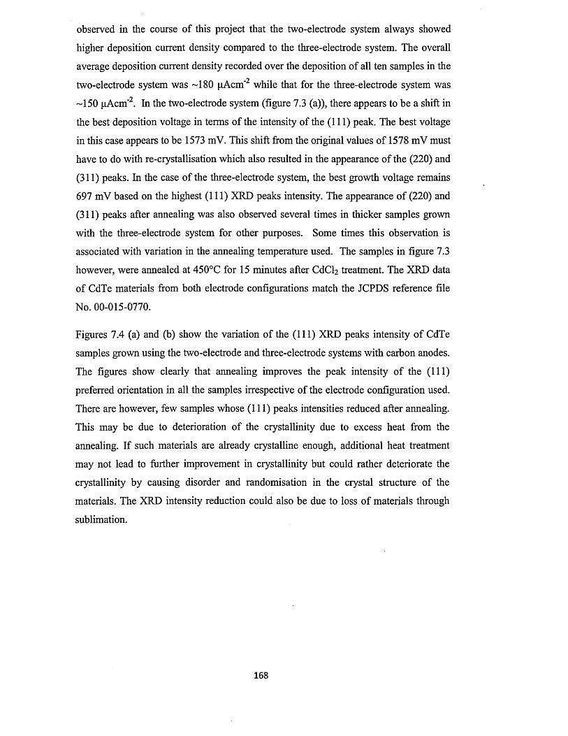
observed in the course of this project that the two-electrode system always showed
higher deposition current density compared to the three-electrode system. The overall
average deposition current density recorded over the deposition of all ten samples in the
two-electrode system was -180 pAcm ' 2 while that for the three-electrode system was
-150 pAcm"2. In the two-electrode system (figure 7.3 (a)), there appears to be a shift in
the best deposition voltage in terms o f the intensity of the (111) peak. The best voltage
in this case appears to be 1573 mV. This shift from the original values of 1578 mV must
have to do with re-crystallisation which also resulted in the appearance o f the (2 2 0 ) and
(311) peaks. In the case of the three-electrode system, the best growth voltage remains
697 mV based on the highest (111) XRD peaks intensity. The appearance o f (220) and
(311) peaks after annealing was also observed several times in thicker samples grown
with the three-electrode system for other purposes. Some times this observation is
associated with variation in the annealing temperature used. The samples in figure 7.3
however, were annealed at 450°C for 15 minutes after CdCk treatment. The XRD data
of CdTe materials from both electrode configurations match the JCPDS reference file
No. 00-015-0770.
Figures 7.4 (a) and (b) show the variation o f the (111) XRD peaks intensity o f CdTe
samples grown using the two-electrode and three-electrode systems with carbon anodes.
The figures show clearly that annealing improves the peak intensity o f the (111)
preferred orientation in all the samples irrespective of the electrode configuration used.
There are however, few samples whose (111) peaks intensities reduced after annealing.
This may be due to deterioration o f the crystallinity due to excess heat from the
annealing. If such materials are already crystalline enough, additional heat treatment
may not lead to further improvement in crystallinity but could rather deteriorate the
crystallinity by causing disorder and randomisation in the crystal structure of the
materials. The XRD intensity reduction could also be due to loss o f materials through
sublimation.
168
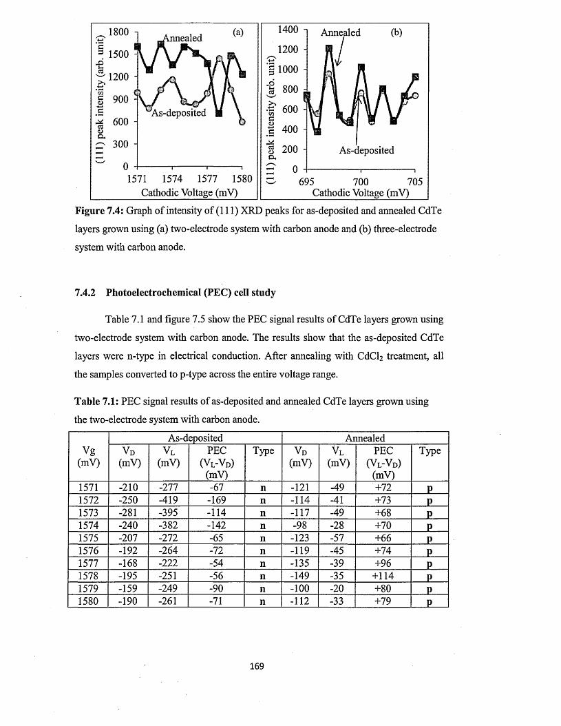
nnealed
As-deposited
1571 1574 1577 1580Cathodic Voltage (mV)
1400 i Annealed
1200 H
g 1 0 0 0 1
800 .
g 200 - As-deposited
695 700 705Cathodic Voltage (mV)
Figure 7.4: Graph of intensity of (111) XRD peaks for as-deposited and annealed CdTe
layers grown using (a) two-electrode system with carbon anode and (b) three-electrode
system with carbon anode.
7.4.2 Photo electro chemical (PEC) cell study
Table 7.1 and figure 7.5 show the PEC signal results of CdTe layers grown using
two-electrode system with carbon anode. The results show that the as-deposited CdTe
layers were n-type in electrical conduction. After annealing with CdCl2 treatment, all
the samples converted to p-type across the entire voltage range.
Table 7.1: PEC signal results o f as-deposited and annealed CdTe layers grown using
the two-electrode system with carbon anode.
Vg(mV)
As-deposited Annealedv D
(mV)VL
(mV)PEC
(V l-V d)(mV)
Type
>! VL
(mV)PEC
(V l-V d )(mV)
Type
1571 - 2 1 0 -277 -67 n - 1 2 1 -49 +72 P1572 -250 -419 -169 n -114 -41 +73 P1573 -281 -395 -114 n -117 -49 + 6 8 P1574 -240 -382 -142 n -98 -28 +70 P1575 -207 -272 -65 n -123 -57 + 6 6 P1576 -192 -264 -72 n -119 -45 +74 P1577 -168 - 2 2 2 -54 n -135 -39 +96 P1578 -195 -251 -56 n -149 -35 +114 P1579 -159 -249 -90 n - 1 0 0 - 2 0 +80 P1580 -190 -261 -71 n - 1 1 2 -33 +79 P
169
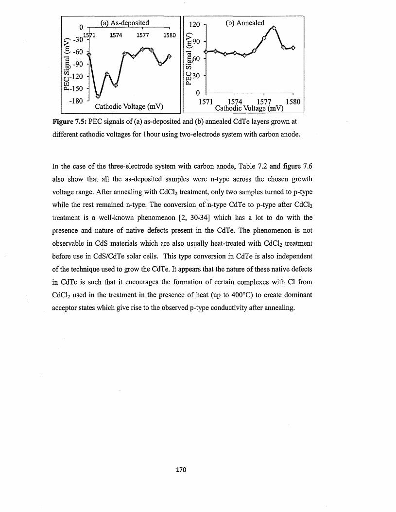
(a) As-deposited (b) Annealed120 i1577 15801574
-30 - £90 -
- 1 2 0
-180 J 1574 1577 1580Cathodic Voltage (mV)
1571Cathodic Voltage (mV)
Figure 7.5: PEC signals o f (a) as-deposited and (b) annealed CdTe layers grown at
different cathodic voltages for lhour using two-electrode system with carbon anode.
In the case of the three-electrode system with carbon anode, Table 7.2 and figure 7.6
also show that all the as-deposited samples were n-type across the chosen growth
voltage range. After annealing with CdCl2 treatment, only two samples turned to p-type\
while the rest remained n-type. The conversion of n-type CdTe to p-type after CdCl2
treatment is a well-known phenomenon [2, 30-34] which has a lot to do with the
presence and nature of native defects present in the CdTe. The phenomenon is not
observable in CdS materials which are also usually heat-treated with CdCl2 treatment
before use in CdS/CdTe solar cells. This type conversion in CdTe is also independent
of the technique used to grow the CdTe. It appears that the nature o f these native defects
in CdTe is such that it encourages the formation of certain complexes with Cl from
CdCl2 used in the treatment in the presence of heat (up to 400°C) to create dominant
acceptor states which give rise to the observed p-type conductivity after annealing.
17 0
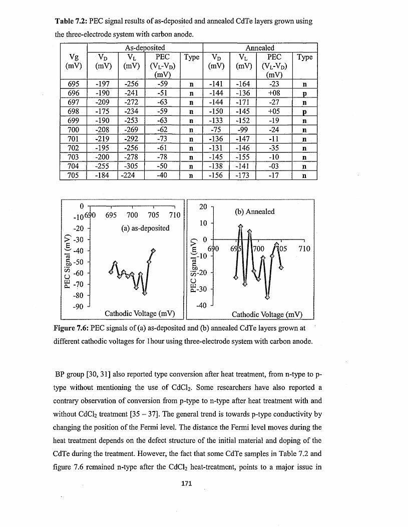
Table 7.2: PEC signal results of as-deposited and annealed CdTe layers grown using
the three-electrode system with carbon anode.
Vg(mV)
As-deposited Annealedv D
(mV)VL
(mV)PEC
(VL-VD)(mV)
Type VD(mV)
VL(mV)
PEC( V l-V d )
(mV)
Type
695 -197 -256 -59 n -141 -164 -23 n
696 -190 -241 -51 n -144 -136 +08 P697 -209 -272 -63 n -144 -171 -27 n
698 -175 -234 -59 n -150 -145 +05 P699 -190 -253 -63 n -133 -152 -19 n
700 -208 -269 -62 n -75 -99 -24 n
701 -219 -292 -73 n -136 -147 - 1 1 n
702 -195 -256 -61 n -131 -146 -35 n
703 - 2 0 0 -278 -78 n -145 -155 - 1 0 n
704 -255 -305 -50 n -138 -141 -03 n
705 -184 -224 -40 n -156 -173 -17 n
2 0 nI
710 (b) Annealed- 1 0 6 i> 0
- 2 0 - > - 3 0 - ^ -40 -KJa - 5 0 -
O -6 ° -S -70 -
-80 - -90 -
(a) as-deposited
690 7101700^ - 1 0 - cd Cc/5-20 -
Cathodic Voltage (mV) Cathodic Voltage (mV)
Figure 7.6: PEC signals of (a) as-deposited and (b) annealed CdTe layers grown at
different cathodic voltages for 1 hour using three-electrode system with carbon anode.
BP group [30, 31] also reported type conversion after heat treatment, from n-type to p-
type without mentioning the use of CdC^. Some researchers have also reported a
contrary observation of conversion from p-type to n-type after heat treatment with and
without CdCl2 treatment [35 -3 7 ] . The general trend is towards p-type conductivity by
changing the position o f the Fermi level. The distance the Fermi level moves during the
heat treatment depends on the defect structure of the initial material and doping o f the
CdTe during the treatment. However, the fact that some CdTe samples in Table 7.2 and
figure 7.6 remained n-type after the CdCl2 heat-treatment, points to a major issue in
171
CdTe. This kind of inconsistency in the conductivity type behaviour of CdTe due to the
nature o f native defects present in it may explain the strong Fermi level pinning
behaviour in CdTe [38 - 40]. For instance, Dharmadasa [38, 39] studied Metal/n-CdTe
interfaces and identified five distinct Fermi level pining positions at this interface. The
implication o f this is that the same CdTe sample can display very different device
behaviours even when the same metal is used to form metal/CdTe at different times
under similar conditions or even at the same time under similar conditions [40]. This
may also explain the prolonged dead-lock in the improvement of the conversion
efficiencies of CdS/CdTe solar cells. Almost all CdS/CdTe solar cells reported in the
literature are regarded as n-CdS/p-CdTe p-n junction solar cells. The general impression
and the generally accepted idea as literature reveals is that CdTe is always converted to
p-type after CdCb heat-treatment even if the initial sample is n-type and even if n-type
dopants such as Cl, F and I were introduced during the growth [1, 6 , 30 - 34, 41]. It is
important at this point to recall that B. M. Basol who pioneered the type-conversion
junction formation in CdTe-based solar cells also reported that n-CdTe thin films
electrodeposited from an electrolyte containing over 500 ppm of Br‘ (a known donor in
CdTe) did not type-convert to p-CdTe after CdCb heat treatment even at 400°C for 10
minutes. As a result, he added that annealing time, in addition to native impurities, plays
a strong role in the type conversion mechanism [1, 2]. The results o f Table 7.2 and in
fact several other observations during this project show that the conversion o f n-CdTe to
p-CdTe after CdCh heat treatment is not always achieved especially when sufficient
source o f halogens (CdCl2 , Cdl2 , CdF2 etc) is contained in the deposition environment.
The disappointing implication therefore is that sometimes one ends up fabricating n-
CdS/n-CdTe solar cell and still thinks it is n-CdS/p-CdTe device and o f course goes
ahead to analyse and assess it as such when in reality it is not. This can really create
huge confusion in the literature. It was also observed during this research project that
even among CdTe samples grown at a particular voltage at different times, some may
change from n-type to p-type after CdCb treatment and others may not. The
observation also was that increasing the halogen concentration in the deposition bath
helps to retain the n-type nature of the electrodeposited CdTe samples. Also treatment
with a mixture of CdCl2 and CdF2 instead of CdCl2 alone before annealing, also helps to
retain the n-type behaviour of CdTe. These two approaches were used for the
subsequent deposition of n-CdTe samples for solar cell fabrication as will be seen in the
following sections and chapters.
172
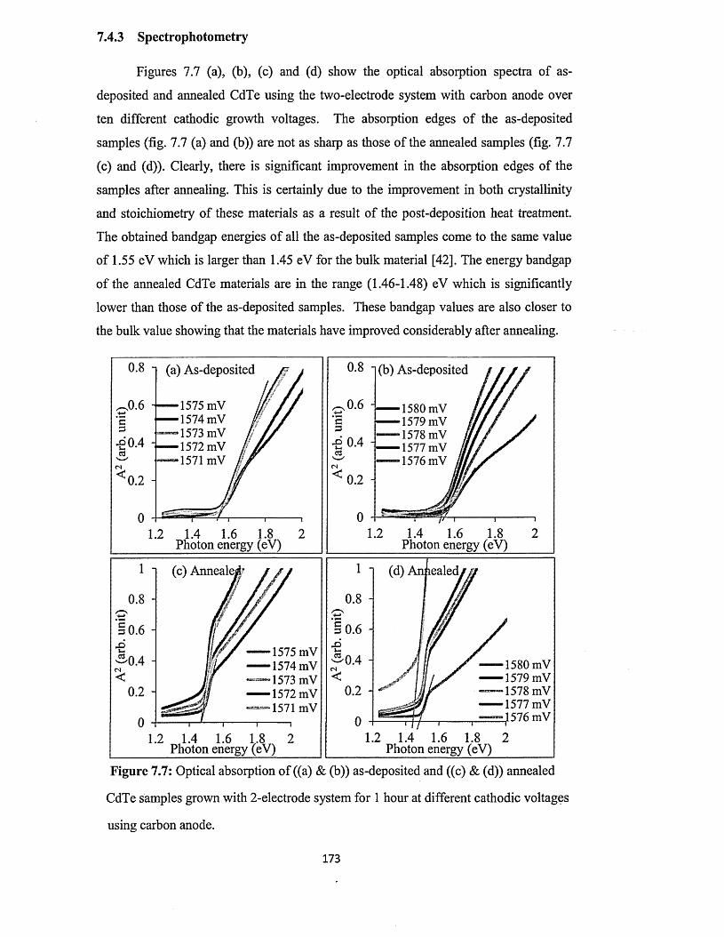
7.4.3 Spectrophotometry
Figures 7.7 (a), (b), (c) and (d) show the optical absorption spectra of as-
deposited and annealed CdTe using the two-electrode system with carbon anode over
ten different cathodic growth voltages. The absorption edges o f the as-deposited
samples (fig. 7.7 (a) and (b)) are not as sharp as those of the annealed samples (fig. 7.7
(c) and (d)). Clearly, there is significant improvement in the absorption edges of the
samples after annealing. This is certainly due to the improvement in both crystallinity
and stoichiometry o f these materials as a result o f the post-deposition heat treatment.
The obtained bandgap energies o f all the as-deposited samples come to the same value
of 1.55 eV which is larger than 1.45 eV for the bulk material [42]. The energy bandgap
o f the annealed CdTe materials are in the range (1.46-1.48) eV which is significantly
lower than those of the as-deposited samples. These bandgap values are also closer to
the bulk value showing that the materials have improved considerably after annealing.
(a) As-deposited (b) As-deposited
1575 mV 1574 mV 1573 mV 1572 mV 1571 mV
•P 0.4
1.4 1.6 1.8Photon energy (eV)
1.2 1.4 1.6 1.8Photon energy (eV)
(c) Anneale
1575 mV 1574 mV 1573 mV 1572 mV 1571 mV
1580 mV 1579 mV 1578 mV 1577 mV 1576 mV
1.2 1.4 1.6 1Photon energy (eV)
1.2 1.4 1.6 1.8Photon energy (eV)
Figure 7.7: Optical absorption of ((a) & (b)) as-deposited and ((c) & (d)) annealed
CdTe samples grown with 2-electrode system for 1 hour at different cathodic voltages
using carbon anode.
173
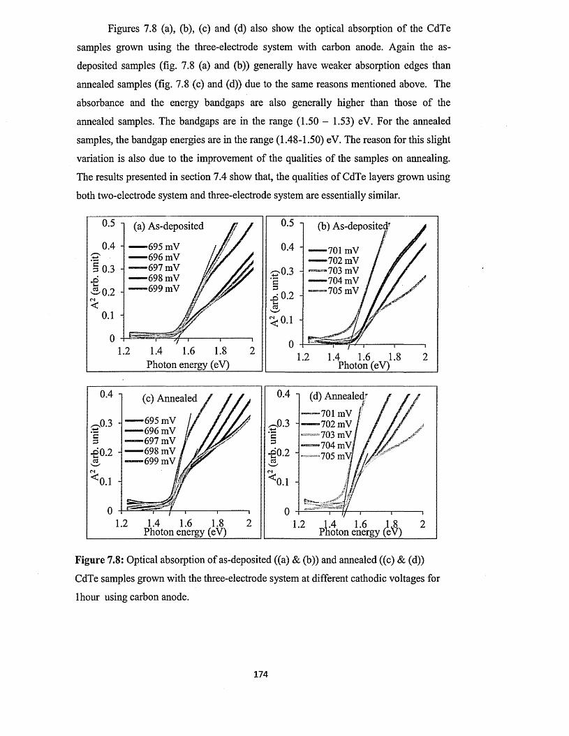
Figures 7.8 (a), (b), (c) and (d) also show the optical absorption o f the CdTe
samples grown using the three-electrode system with carbon anode. Again the as-
deposited samples (fig. 7.8 (a) and (b)) generally have weaker absorption edges than
annealed samples (fig. 7.8 (c) and (d)) due to the same reasons mentioned above. The
absorbance and the energy bandgaps are also generally higher than those of the
annealed samples. The bandgaps are in the range (1.50 - 1.53) eV. For the annealed
samples, the bandgap energies are in the range (1.48-1.50) eV. The reason for this slight
variation is also due to the improvement of the qualities of the samples on annealing.
The results presented in section 7.4 show that, the qualities of CdTe layers grown using
both two-electrode system and three-electrode system are essentially similar.
0.5
0.4
§ 0.3
(a) As-deposited
*695 mV *696 mV *697 mV *698 mV *699 mV
0 . 1 -
1.4 1.6 1.8Photon energy (eV)
0.5 i (b) As-deposited?
701 mV702 mV703 mV704 mV
1.4 1.6 1.1Photon (eV)
0.4 i (c) Annealed
695 mV696 mV697 mV698 mV699 mV
1.4 1.6 1.8Photon energy (eV)
0.4
^0 .3
I ,cC
^ 0 . 1
0
(d) AnnealedmmKm&tHmm |— 702 mV- 703 mVcsEsm y 04 mV- 705 mV/
1 . 2 1 . 6oton energy
Figure 7.8: Optical absorption of as-deposited ((a) & (b)) and annealed ((c) & (d))
CdTe samples grown with the three-electrode system at different cathodic voltages for
lhour using carbon anode.
174
7.5 Characterisation of CdTe layers grown using two-electrode system with
platinum anode
The results and discussion in section 7.4 highlighted the similarity of the CdTe
layers grown using both two-electrode and three-electrode systems with carbon anode.
The essence is to show that instead o f the three-electrode system, one can also use the
two-electrode system without compromising the quality of the materials deposited. Cost
is reduced by saving the cost o f reference electrode. The risk o f poisoning o f the
deposited semiconductor due to possible leakage of unwanted ions from the reference
electrode into the deposition bath can be avoided. Deposition of materials at relatively
higher temperature is taken to advantage and the deposition process is made simpler.
These are the potential advantages of using two-electrode system over three-electrode
system. For these reasons, the main electrodeposition of CdTe materials for solar cell
fabrication in this research was carried out using the two-electrode system with
platinum anode. The results of the characterisation o f the CdTe layers deposited using
this electrode system are presented and discussed in this section.
7.5.1 X-ray diffraction (XRD
Table 7.3 and figure 7.9 present the XRD results of as-deposited and annealed
CdTe layers deposited across a range o f ten cathodic voltages in the vicinity o f the
optimum growth voltage. Figure 7.9 (a) shows the presence o f the cubic CdTe (111) and
(2 2 0 ) peaks for samples grown at all the voltages with the ( 1 1 1 ) crystal plane as the
preferred orientation. Table 7.3 shows that the highest (111) peak intensity occurs at a
cathodic voltage of 2038 mV followed by 2037 mV. After annealing in air at 450°C for
15 minutes with CdCb + CdF2 treatment, figure 7.9 (b) shows the emergence o f weak
(311) peak in addition to the existing (111) and (220) peaks. This time around, Table
7.3 shows that the highest (111) peak intensity shifts to a cathodic voltage o f 2039 mV
followed by 2041 mV. The three XRD peaks also match those of the JCPDS reference
file no.00-015-0770 of cubic CdTe. Based on the combination o f XRD, optical
absorption, PEC and initial solar cell device results, 2038 mV was used in the rest o f the
CdTe deposition as the best deposition voltage.
175
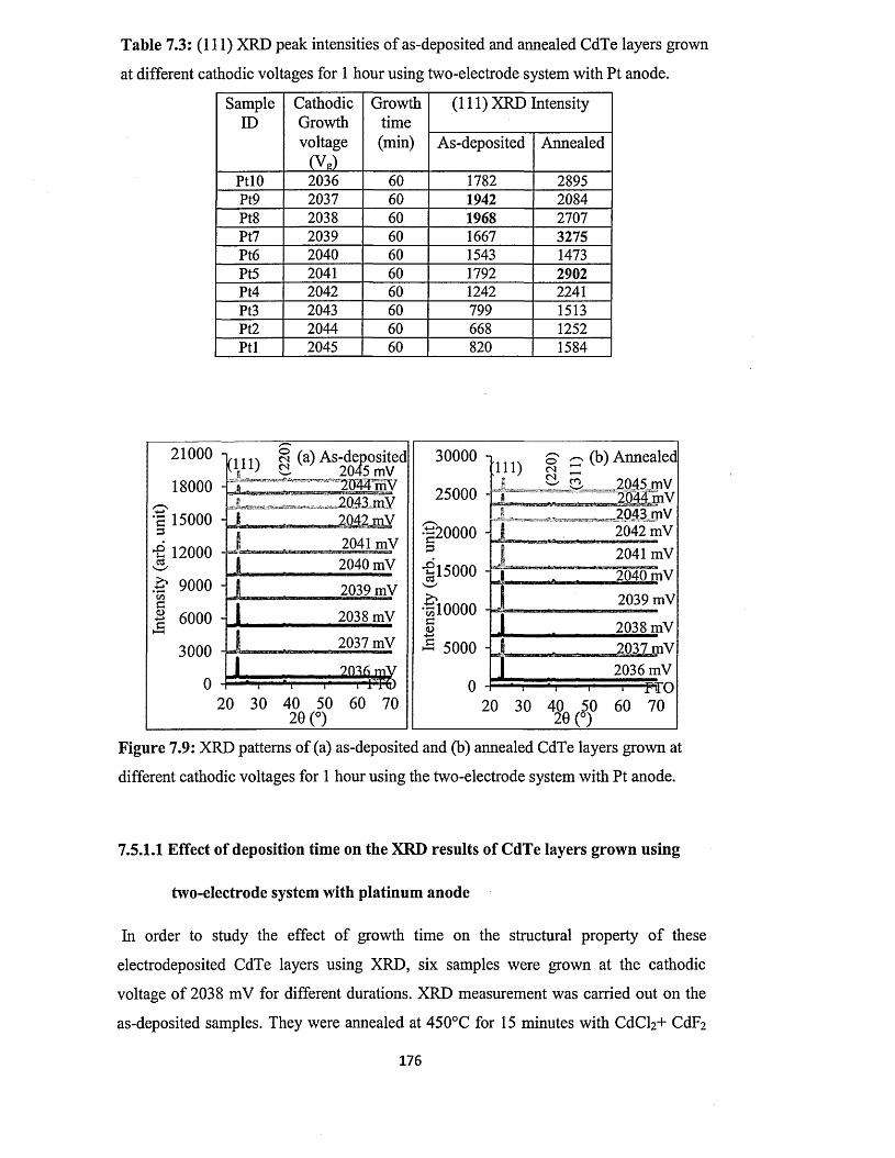
Table 7.3: (111) XRD peak intensities of as-deposited and annealed CdTe layers grown
at different cathodic voltages for 1 hour using two-electrode system with Pt anode.
SampleID
CathodicGrowthvoltage
(Vg)
Growthtime(min)
(111) XRD Intensity
As-deposited Annealed
PtlO 2036 60 1782 2895Pt9 2037 60 1942 2084Pt8 2038 60 1968 2707Pt7 2039 60 1667 3275Pt6 2040 60 1543 1473Pt5 2041 60 1792 2902Pt4 2042 60 1242 2241Pt3 2043 60 799 1513Pt2 2044 60 6 6 8 1252Ptl 2045 60 820 1584
s -cS
21000
18000
15000
12000
9000
6000
3000
0
h m ® (a) As-deposited 2045 mV 20441nV 2043mV
2041 mV
JL____ 2040 mV
-J_____ 2039 mV
1 2038 mV
! . 2037 mV
- 1 ..........................20 30 40 50 60 70
2 0 (°)
30000
25000
•*200003
03
2043 mV 2042 mV
15000 -
•sslOOOO 4*4 e<L>
£ 5000
1 1 1 )(b) Annealed
2045 mV
2041 mV2040 mV2039 mV
2038 mV2037 mV2036 mV
- i— fTO20 30 40 50 60
2 0 (°)70
Figure 7.9: XRD patterns of (a) as-deposited and (b) annealed CdTe layers grown at
different cathodic voltages for 1 hour using the two-electrode system with Pt anode.
7.5.1.1 Effect of deposition time on the XRD results of CdTe layers grown using
two-electrode system with platinum anode
In order to study the effect of growth time on the structural property o f these
electrodeposited CdTe layers using XRD, six samples were grown at the cathodic
voltage o f 2038 mV for different durations. XRD measurement was carried out on the
as-deposited samples. They were annealed at 450°C for 15 minutes with CdCl2+ CdF2
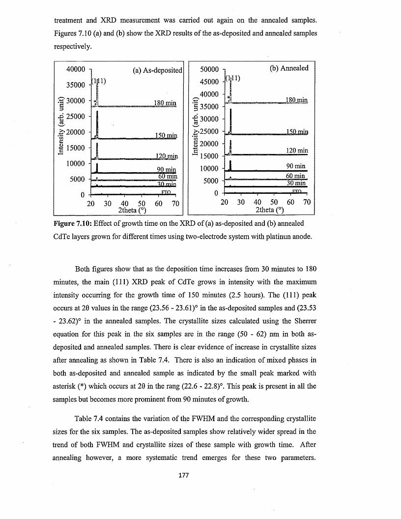
treatment and XRD measurement was carried out again on the annealed samples.
Figures 7.10 (a) and (b) show the XRD results o f the as-deposited and annealed samples
respectively.
40000
35000
S '30000 e3x> 25000
£*20000
15000 -\
10000
5000
0
( W
(a) As-deposited
180 min
u u mm
1 2 0 min
J 90 min- t ■ . -. 60 min
30 minFTO
20 30 40 50 60 702 theta (°)
50000
45000
^ 4 0 0 0 0 H
§ 35000
'B 3000003
^ 2 5 0 0 0 J
(b) Annealed
_1.80_min
JJJUm§ 2 0 0 0 0 -
~ 15000 -
1 0 0 0 0 -
J1 2 0 min
J 90 min
5000 -.* . . . .. 60 min
30 min0 -
20 30 40 50 60 702 theta (°)
Figure 7.10: Effect o f growth time on the XRD of (a) as-deposited and (b) annealed
CdTe layers grown for different times using two-electrode system with platinun anode.
Both figures show that as the deposition time increases from 30 minutes to 180
minutes, the main (111) XRD peak of CdTe grows in intensity with the maximum
intensity occurring for the growth time of 150 minutes (2.5 hours). The (111) peak
occurs at 20 values in the range (23.56 - 23.61)° in the as-deposited samples and (23.53
- 23.62)° in the annealed samples. The crystallite sizes calculated using the Sherrer
equation for this peak in the six samples are in the range (50 - 62) nm in both as-
deposited and annealed samples. There is clear evidence of increase in crystallite sizes
after annealing as shown in Table 7.4. There is also an indication of mixed phases in
both as-deposited and annealed sample as indicated by the small peak marked with
asterisk (*) which occurs at 20 in the rang (22.6 - 22.8)°. This peak is present in all the
samples but becomes more prominent from 90 minutes of growth.
Table 7.4 contains the variation of the FWHM and the corresponding crystallite
sizes for the six samples. The as-deposited samples show relatively wider spread in the
trend of both FWHM and crystallite sizes o f these sample with growth time. After
annealing however, a more systematic trend emerges for these two parameters.
177
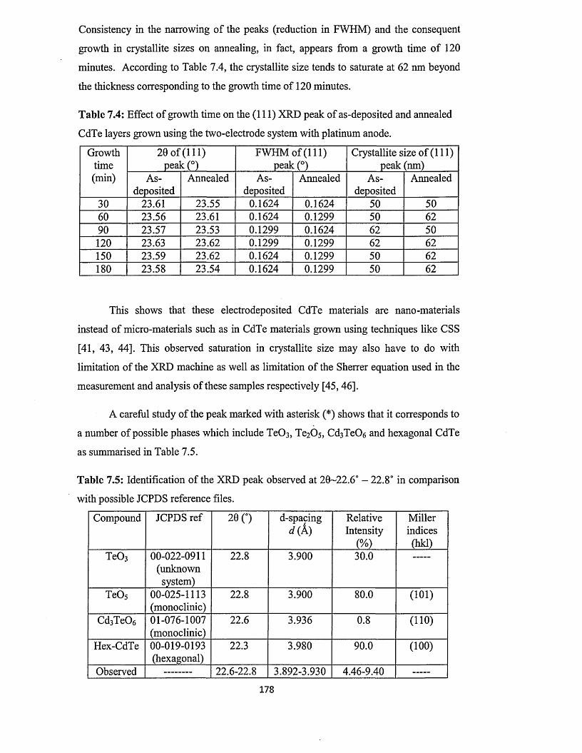
Consistency in the narrowing o f the peaks (reduction in FWHM) and the consequent
growth in crystallite sizes on annealing, in fact, appears from a growth time o f 1 2 0
minutes. According to Table 7.4, the crystallite size tends to saturate at 62 nm beyond
the thickness corresponding to the growth time of 1 2 0 minutes.
Table 7.4: Effect o f growth time on the (111) XRD peak of as-deposited and annealed
CdTe layers grown using the two-electrode system with platinum anode.
Growthtime(min)
2 0 of pea
a n )k(°)
FWHM of (111) peak (°)
Crystallite size of (111) peak (nm)
As-deposited
Annealed As-deposited
Annealed As-deposited
Annealed
30 23.61 23.55 0.1624 0.1624 50 5060 23.56 23.61 0.1624 0.1299 50 6290 23.57 23.53 0.1299 0.1624 62 50
1 2 0 23.63 23.62 0.1299 0.1299 62 62150 23.59 23.62 0.1624 0.1299 50 62180 23.58 23.54 0.1624 0.1299 50 62
This shows that these electrodeposited CdTe materials are nano-materials
instead of micro-materials such as in CdTe materials grown using techniques like CSS
[41, 43, 44]. This observed saturation in crystallite size may also have to do with
limitation of the XRD machine as well as limitation of the Sherrer equation used in the
measurement and analysis of these samples respectively [45,46].
A careful study of the peak marked with asterisk (*) shows that it corresponds to
a number of possible phases which include Te0 3 , Te2 0 s, CdsTeOe and hexagonal CdTe
as summarised in Table 7.5.
Table 7.5: Identification of the XRD peak observed at 20-22.6° - 22.8° in comparison
with possible JCPDS reference files.
Compound JCPDS ref 2 0 (°) d-spacingd ( A)
RelativeIntensity
(%)
Millerindices
(hkl)T e0 3 00-022-0911
(unknownsystem)
2 2 . 8 3.900 30.0
TeOs 00-025-1113(monoclinic)
2 2 . 8 3.900 80.0 ( 1 0 1 )
Cd3T e0 6 01-076-1007(monoclinic)
2 2 . 6 3.936 0 . 8 ( 1 1 0 )
Hex-CdTe 00-019-0193(hexagonal)
22.3 3.980 90.0 ( 1 0 0 )
Observed 2 2 .6 -2 2 . 8 3.892-3.930 4.46-9.40
178
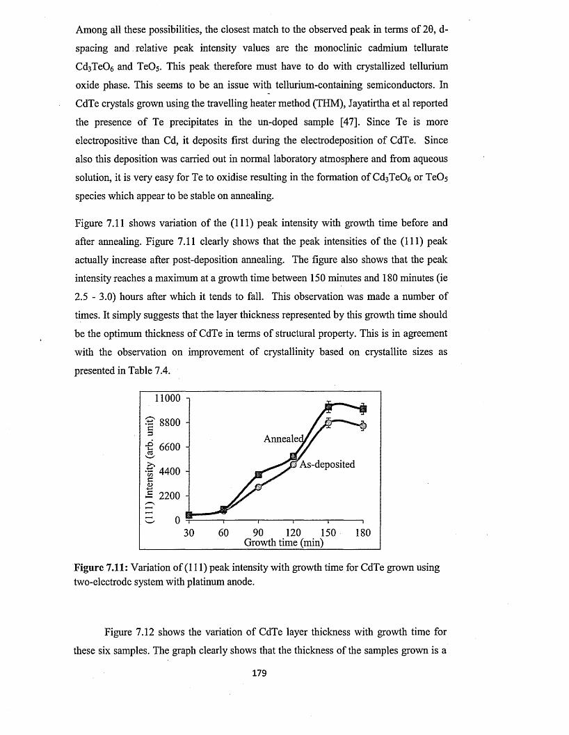
Among all these possibilities, the closest match to the observed peak in terms of 20, d-
spacing and relative peak intensity values are the monoclinic cadmium tellurate
Cd3Te0 6 and TeOs. This peak therefore must have to do with crystallized tellurium
oxide phase. This seems to be an issue with tellurium-containing semiconductors. In
CdTe crystals grown using the travelling heater method (THM), Jayatirtha et al reported
the presence o f Te precipitates in the un-doped sample [47]. Since Te is more
electropositive than Cd, it deposits first during the electrodeposition of CdTe. Since
also this deposition was carried out in normal laboratory atmosphere and from aqueous
solution, it is very easy for Te to oxidise resulting in the formation o f Cd3TeC>6 or TeOs
species which appear to be stable on annealing.
Figure 7.11 shows variation of the (111) peak intensity with growth time before and
after annealing. Figure 7.11 clearly shows that the peak intensities of the (111) peak
actually increase after post-deposition annealing. The figure also shows that the peak
intensity reaches a maximum at a growth time between 150 minutes and 180 minutes (ie
2.5 - 3.0) hours after which it tends to fall. This observation was made a number of
times. It simply suggests that the layer thickness represented by this growth time should
be the optimum thickness of CdTe in terms of structural property. This is in agreement
with the observation on improvement of crystallinity based on crystallite sizes as
presented in Table 7.4.
1 1 0 0 0 n
S? 8800 -Annealei
6600 -
As-depositedg 4400 -
2 2 0 0 -
90 120 1Growth time (min)
Figure 7.11: Variation o f (111) peak intensity with growth time for CdTe grown using two-electrode system with platinum anode.
Figure 7.12 shows the variation of CdTe layer thickness with growth time for
these six samples. The graph clearly shows that the thickness of the samples grown is a
179
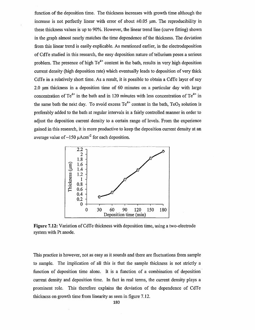
function of the deposition time. The thickness increases with growth time although the
increase is not perfectly linear with error of about ±0.05 pm. The reproducibility in
these thickness values is up to 90%. However, the linear trend line (curve fitting) shown
in the graph almost nearly matches the time dependence o f the thickness. The deviation
from this linear trend is easily explicable. As mentioned earlier, in the electrodeposition
o f CdTe studied in this research, the easy deposition nature o f tellurium poses a serious
problem. The presence o f high Te4+ content in the bath, results in very high deposition
current density (high deposition rate) which eventually leads to deposition of very thick
CdTe in a relatively short time. As a result, it is possible to obtain a CdTe layer of say
2 . 0 pm thickness in a deposition time of 60 minutes on a particular day with large
concentration of Te4+ in the bath and in 120 minutes with less concentration o f Te4+ in
the same bath the next day. To avoid excess Te4+ content in the bath, TeC>2 solution is
preferably added to the bath at regular intervals in a fairly controlled manner in order to
adjust the deposition current density to a certain range o f levels. From the experience
gained in this research, it is more productive to keep the deposition current density at an
average value of -150 pAcm ' 2 for each deposition.
2 . 2
C/5
0 . 6
0.40 . 2
Deposition time (min)
Figure 7.12: Variation o f CdTe thickness with deposition time, using a two-electrode system with Pt anode.
This practice is however, not as easy as it sounds and there are fluctuations from sample
to sample. The implication o f all this is that the sample thickness is not strictly a
function of deposition time alone. It is a function of a combination of deposition
current density and deposition time. In fact in real terms, the current density plays a
prominent role. This therefore explains the deviation of the dependence o f CdTe
thickness on growth time from linearity as seen in figure 7.12.180
In the light of the discussion on effect of Te4+-containing bath on the deposited
CdTe material, it is important to note that high Te4+ content in the deposition bath
results in the deposition o f Te-rich CdTe. From experience and from literature, Te-rich
CdTe does not produce good solar cell devices [36, 38]. Cd-rich CdTe is preferable for
good devices.
7.5.1.2 Effect of different annealing conditions on XRD of CdTe layers grown
using two-electrode system with platinum anode
In this particular experiment, four different CdTe layers with different
thicknesses were deposited on glass/FTO substrates. Each sample was then divided into
four parts. One set of four samples was left as-deposited. Another set of four samples
was annealed but without prior CdC^ or CdCl2+CdF2 treatment. Another set of four
samples was annealed with prior CdCl2 treatment. The last set o f four samples was
annealed with prior CdCl2+ CdF2 treatment. All annealing was done at 450°C for 15
minutes. The aim here is to see how the various annealing conditions affect the XRD
results o f these samples. This will help to understand the reason why the well-known
CdCl2 treatment is important.
Figure 7.13 shows XRD patterns of the CdTe sample with thickness o f 1.1 pm
and different annealing conditions. The figure shows the clear difference in the intensity
of the (111) peak for the various conditions. Treatment with CdCh and CdCl2+CdF2
clearly improved the intensity of the (111) peak. Treatment with CdCl2+CdF2 appears
to be better than treatment with only CdCh based on these peak intensities.
181
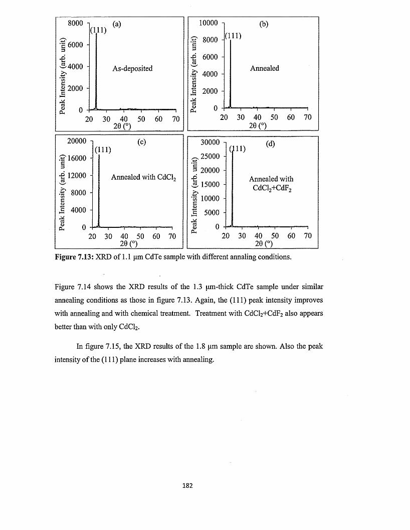
8000
c 60003
4000
C/3
I 2000 H
(111) (a)
As-deposited
cd<d
20 30 40 50 60 7020 (°)
20000 i
.* 16000 c3•S 12000 -cd
.{? 8000 HC/3e1 4000cd<u n
O h 0
( 1 1 1 )(c)
Annealed with CdCh
20 30 40 50 60 70 20 (°)
1 0 0 0 0 -i
8000 -
6000 -Annealed
2000 -
20 30 40 50 60 7020 (°)
c3
•sed
cd<DPLh
30000 i
25000
20000 -
15000 -
1 0 0 0 0 -
5000 -
0
O H )(d)
Annealed with CdCl2+CdF2
1..... T20 30 40 50 60 70
20 (°)
Figure 7.13: XRD of 1.1 pm CdTe sample with different annaling conditions.
Figure 7.14 shows the XRD results of the 1.3 pm-thick CdTe sample under similar
annealing conditions as those in figure 7.13. Again, the (111) peak intensity improves
with annealing and with chemical treatment. Treatment with CdCl2+CdF2 also appears
better than with only CdCl2 .
In figure 7.15, the XRD results of the 1.8 pm sample are shown. Also the peak
intensity o f the ( 1 1 1 ) plane increases with annealing.
182
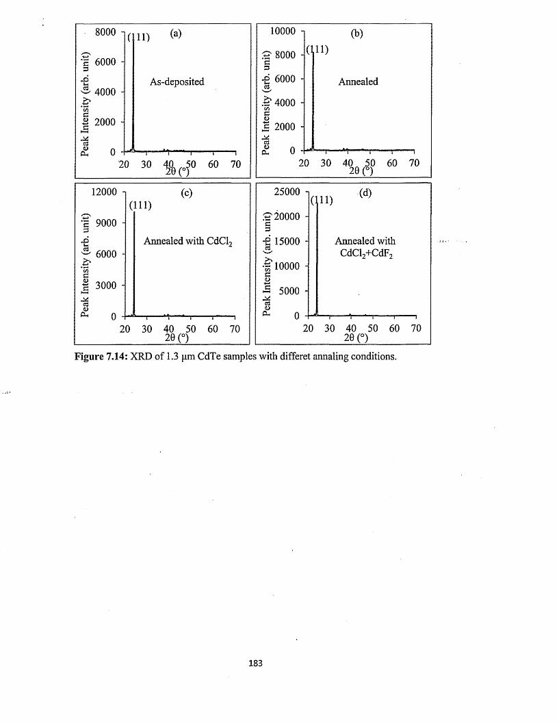
8000 -i
c 6000=5-dcd 4000
C/5
I 2000ci—h
CdU n(in 0
11) (a)
As-deposited
20 30 0 60 70
12000
c 9000 3
cd'w '
coca>
cd<DOh
6000
3000 -
(HI)(c)
Annealed with CdCL
20 30 40 5020 (°)
60 70
•P 6000 Annealed
£ 4000
€ 2000 -
20 30 40 50 60 7020 (°)
c3S-ccd
cd<uPLh
25000 -I
20000 -
15000
1 0 0 0 0 -
5000 -
11)■(d)
Annealed with CdCl2+CdF2
20- i------*1----—r-30 40 50
20 (°)60 70
Figure 7.14: XRD of 1.3 pm CdTe samples with differet annaling conditions.
183
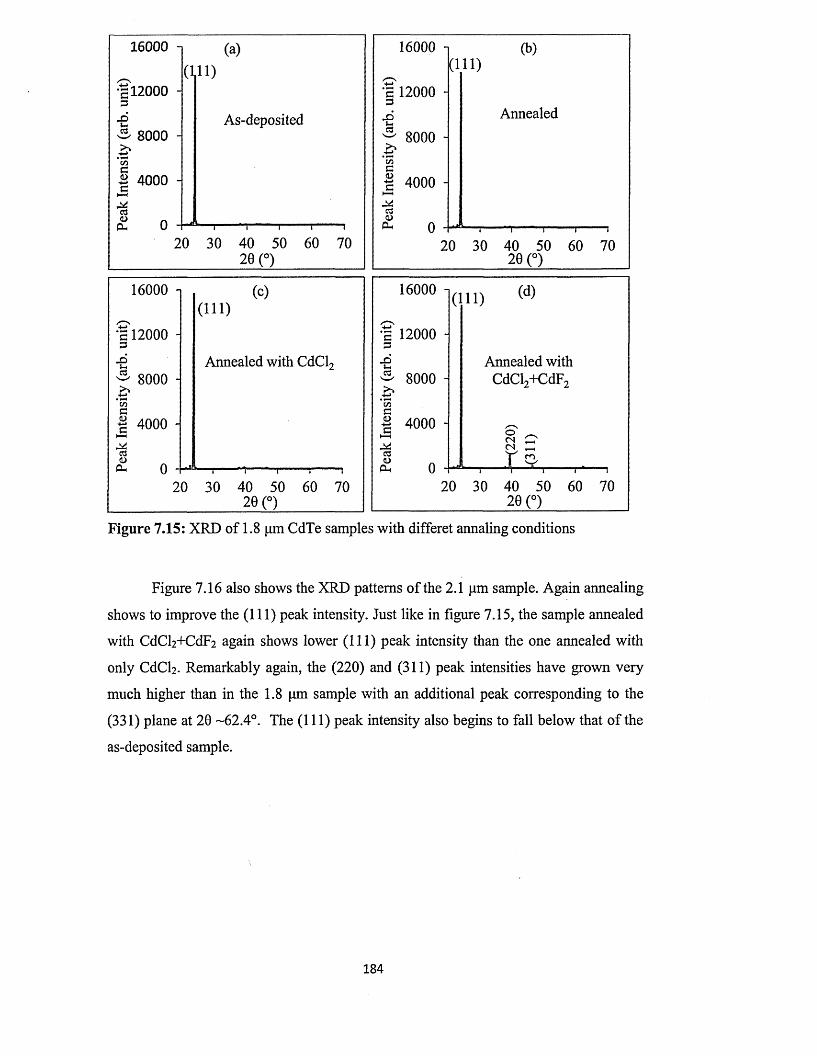
16000
•£120003
& 8000
cn| 4000 ci—i
ci<U neu 0
a n )
(a)
As-deposited
20 30 40 50 60 7020 (°)
16000 i
•g 12000 H3
a<uPin
8000 -
4000 -
0 oL
(111)(c)
Annealed with CdCL
20 30 40 50 60 70 20 (°)
16000 -
12000Annealed
t 1------ 120 30 40 50 60 70
20 (°)
03
<n<uP-i
16000 i
12000 -
8000 -
4000 -
(111) (d)
Annealed with CdCl2+CdF2
o _(Nr ci— r—"—i
20 30 40 50 60 70 20 (°)
Figure 7.15: XRD of 1.8 pm CdTe samples with differet annaling conditions
Figure 7.16 also shows the XRD patterns o f the 2.1 pm sample. Again annealing
shows to improve the (111) peak intensity. Just like in figure 7.15, the sample annealed
with CdCl2+CdF2 again shows lower (111) peak intensity than the one annealed with
only CdCl2 . Remarkably again, the (220) and (311) peak intensities have grown very
much higher than in the 1.8 pm sample with an additional peak corresponding to the
(331) plane at 20 -62.4°. The (111) peak intensity also begins to fall below that o f the
as-deposited sample.
184
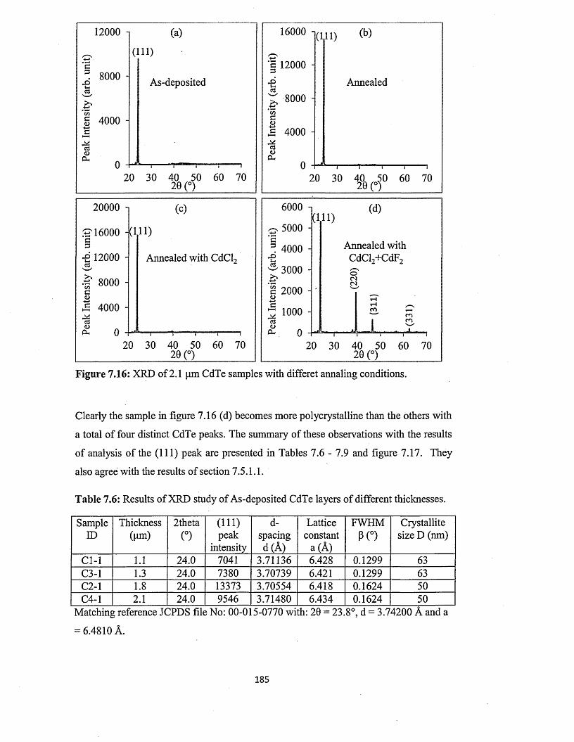
JDs-03
12000 i
8000 -
g 4000 - c
c3<L>Plh0
(a)
(111)
As-deposited
ua.
20 30 40 50 60 70 20 (°)
20000 n (c)
S '16000 -1(111) a
•S 12000 -J Annealed with CdCl2
• f 8000a<D
*6c3<DPh
4000
0 I.. -T I--------- f------ 1
20 30 40 50 60 70 20 (°)
16000 i
S 12000
^ 8000 -
§3 4000a<Dcu
(HI) (b)
Annealed
20 30 44 J ° 60 70 20 (
x>Vic3
a<u
6000 -1
5000 -
4000
3000 -
2000 -
1000 -
0
(111)(d)
Annealed with CdCl2+CdF2o<NCN
CO mm
20 30 40 5020 (°)
60 70
Figure 7.16: XRD of 2.1 pm CdTe samples with differet annaling conditions.
Clearly the sample in figure 7.16 (d) becomes more polycrystalline than the others with
a total o f four distinct CdTe peaks. The summary of these observations with the results
of analysis of the (111) peak are presented in Tables 7.6 - 7.9 and figure 7.17. They
also agree with the results of section 7.5.1.1.
Table 7.6: Results of XRD study of As-deposited CdTe layers of different thicknesses.
SampleID
Thickness(pm)
2theta(°)
(111)peak
intensity
d-spacingd (A)
Lattice constant
a (A)
FWHMP(°)
Crystallite size D (nm)
Cl-1 1.1 24.0 7041 3.71136 6.428 0.1299 63C3-1 1.3 24.0 7380 3.70739 6.421 0.1299 63C2-1 1.8 24.0 13373 3.70554 6.418 0.1624 50C4-1 2.1 24.0 9546 3.71480 6.434 0.1624 50
Matching reference JCPDS file No: 00-015-0770 with: 20 = 23.8°, d = 3.74200 A and a
= 6.4810 A.
185

Table 7.7: Results of XRD study of CdTe layers of different thicknesses annealed at
450°C for 15 minutes.
SampleID
Thickness(pm)
2theta(°)
(111)peak
intensity
d-spacingd(A)
Lattice constant
a (A)
FWHMP(°)
Crystallite size D (nm)
C l-2 1.1 23.8 7949 3.74607 6.488 0.1299 63C3-2 1.3 24.1 8171 3.69754 6.404 0.1299 63
C2-2 1.8 24.0 13681 3.71247 6.430 0.1299 63
C4-2 2.1 24.0 15066 3.70878 6.424 0.1299 63Matching reference JCPDS file No: 00-015-0770 with: 20 = 23.8°, d = 3.74200 A and a
= 6.4810 A.
Table 7.8: Results of XRD study o f CdTe layers o f different thicknesses annealed with
CdCb at 450°C for 15 minutes.
SampleID
Thickness(pm)
2theta(°)
(111)peak
intensity
d-spacingd(A)
Lattice constant
a (A)
FWHMP(°)
Crystallite size D (nm)
Cl-3 1.1 24.0 16668 3.70767 6.422 0.1299 63C3-3 1.3 24.1 10055 3.69664 6.403 0.1299 63C2-3 1.8 24.1 15605 3.69672 6.403 0.1299 63C4-3 2.1 24.0 15528 3.71501 6.434 0.1299 63
Matching reference JC PDS file No: 00-015-0770 with: 20 = 23.8°, d = 3.7^ 200 A and a
= 6.4810 A.
Table 7.9: Results o f XRD study of CdTe layers o f different thicknesses annealed with
CdCl2+CdF2 at 450°C for 15 minutes.
SampleID
Thickness(pm)
2theta(°)
(111)peak
intensity
d-spacingd (A)
Lattice constant
a (A)
FWHM :P(°)
Crystallite size D (nm)
C l-4 1.1 24.0 26855 3.71505 6.434 0.1299 63C3-4 1.3 24.0 22606 3.71491 6.434 0.1299 63C2-4 1.8 24.0 14557 3.71443 6.433 0.1624 50C4-4 2.1 24.0 5311 3.72640 6.454 0.1299 63
Matching reference JC PDS file NO: 00-015-0770 witih: 20 = 23.8°, d = 3.7^ 200 A and a
= 6.4810 A.
18 6

30000 (a) 1.1 jim
3 24000
18000 -
c 12000 -OJ
~ 6000 -
& Cr ^&^ XV"
* d>°
Anneafnng condition
(b)1.3 jim
x>u>a
ccsvCLh
25000
20000
15000 -
10000 -
5000 -
($y/ / / /
Annealing condition
cp
jS
iCOC<u
03<DpH
20000 n (c) 1.8 pm 16000 -12000 -
8000 -4000 -
Annealing condition
20000 -j
3 16000 -
•s 12000 -e3&
8000 -4000 -
+->ch—1 0 -
MccS<DPh &
(d) 2.1 jim
& # c r ^
Annealing condition
Figure 7.17: Bar chart of the effect of different annealing conditions on the (111) peak intensity o f CdTe of different thicknesses. 1
In order to shed more light on the effects of CdCl2 or CdCl2+CdF2 treatment on the
structural properties of CdTe, a sample of CdTe was deliberately grown for four hours
with Te-richness by adding a lot of TeC>2 solution into the deposition bath. The sample
was then divided into three pieces. One of the pieces was just annealed without CdCl2
treatment and one was annealed with CdCh treatment. The last piece was left as-
deposited. All the annealing again was done at 450°C for 15 minutes and the results of
the XRD on these samples are shown in figures 7.18 (a), (b) and (c). Figure 7.18 (a)
shows clear Te-richness o f this as-deposited sample with a mixture o f peaks belonging
to cubic CdTe (JCPDS No. 00-015-0770) and hexagonal Tellurium (JCPDS No. 00-
036-1452). The three main CdTe peaks; (111), (220) and (311), are all visible here with
broad widths showing that only small amount of CdTe is present in this sample. The
187
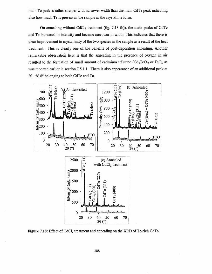
main Te peak is rather sharper with narrower width than the main CdTe peak indicating
also how much Te is present in the sample in the crystalline form.
On annealing without CdCh treatment (fig. 7.18 (b)), the main peaks of CdTe
and Te increased in intensity and became narrower in width. This indicates that there is
clear improvement in crystallinity o f the two species in the sample as a result of the heat
treatment. This is clearly one o f the benefits of post-deposition annealing. Another
remarkable observation here is that the annealing in the presence o f oxygen in air
resulted to the formation of small amount o f cadmium tellurate (Cd3Te06) or TeOs as
was reported earlier in section 7.5.1.1. There is also appearance of an additional peak at
20 -56.8° belonging to both CdTe and Te.
A s-denosited 8 (b) AnnealedX
600 -
§500 -
*400 -* 600
£ 400 -*200 -
200 -100 -
*»40 5020 (°)
20 30 40 50 60 7020 (°) ____
2500 i (c) Annealed with CdCl2 treatment
<- 2000
-£1500 *
551000
20 30 40 50 60 7020 (°)
Figure 7.18: Effect of CdC^ treatment and annealing on the XRD of Te-rich CdTe.
188
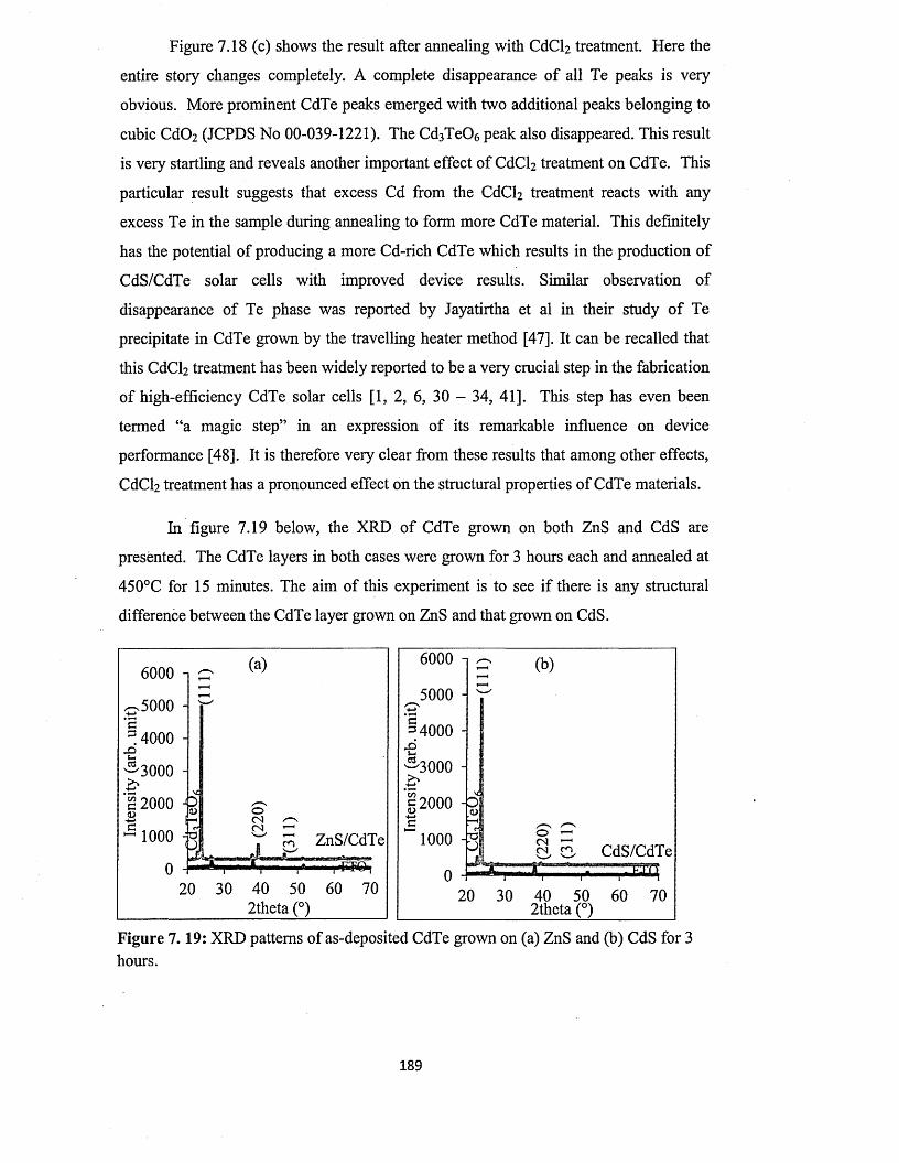
Figure 7.18 (c) shows the result after annealing with CdCl2 treatment. Here the
entire story changes completely. A complete disappearance o f all Te peaks is very
obvious. More prominent CdTe peaks emerged with two additional peaks belonging to
cubic CdC>2 (JCPDS No 00-039-1221). The Cd3TeC>6 peak also disappeared. This result
is very startling and reveals another important effect of CdCh treatment on CdTe. This
particular result suggests that excess Cd from the CdCh treatment reacts with any
excess Te in the sample during annealing to form more CdTe material. This definitely
has the potential of producing a more Cd-rich CdTe which results in the production of
CdS/CdTe solar cells with improved device results. Similar observation of
disappearance of Te phase was reported by Jayatirtha et al in their study o f Te
precipitate in CdTe grown by the travelling heater method [47]. It can be recalled that
this CdCl2 treatment has been widely reported to be a very crucial step in the fabrication
of high-efficiency CdTe solar cells [1, 2, 6, 30 - 34, 41]. This step has even been
termed “a magic step” in an expression of its remarkable influence on device
performance [48]. It is therefore very clear from these results that among other effects,
CdCl2 treatment has a pronounced effect on the structural properties of CdTe materials.
In figure 7.19 below, the XRD of CdTe grown on both ZnS and CdS are
presented. The CdTe layers in both cases were grown for 3 hours each and annealed at
450°C for 15 minutes. The aim of this experiment is to see if there is any structural
difference between the CdTe layer grown on ZnS and that grown on CdS.
6000
5000 -
.4000 -
3000 -
2000 O
1000 -Jo ZnS/CdTem
2theta (°)
5000 -
=» 4000 -
£2000
CdS/CdTe
20 30 40 50 60 702theta (°)
Figure 7.19: XRD patterns of as-deposited CdTe grown on (a) ZnS and (b) CdS for 3 hours.
189

The results in figures 7.19 (a) and (b) show that CdTe grown on both substrates have
similar structural quality.
7.5.2 Photoelectrochemical (PEC) cell study
The aim o f this experiment is to establish the electrical conductivity types of the
CdTe materials before fabricating solar cells with them. The solar cell device structures
targeted in this research are glass/FTO/n-CdTe/Au, glass/FTO/n-ZnS/n-CdTe/Au,
glass/FTO/n-CdS/n-CdTe/Au and glass/FTO/n-ZnS/n-CdS/n-CdTe/Au. All the
structures involve the use o f all n-type semiconductors in order to fabricate n-n
heterojunction/Schottky barrier solar cells.
In the previous chapters the conditions for the growth of n-ZnS and n-CdS layers
have been established. In this chapter and particularly in this section, the aim is to
establish the conditions for the growth of good quality n-CdTe layers. Hall Effect
measurement could not be carried out on the electrodeposited semiconductors in this
project due to the fact that they were all grown on conducting glass/FTO substrates
which definitely will interfere with the results if Hall Effect measurements were to be
done on these samples. As a result, PEC cell measurement becomes the only alternative _
for the determination o f the conductivity types o f these materials as was mentioned
earlier.
To carry out PEC measurements on CdTe, only CdTe materials grown on
glass/FTO were used. Table 7.10 and Figure 7.20 show the PEC results of CdTe layers
grown on glass/FTO using two-electrode system with platinum anode and description of
how the Fermi level moves towards p-type conductivity during annealing. Both Table
7.10 and the figure 7.20 (a) show that the as-deposited samples were all n-type at all the
growth voltages. After annealing with CdCl2 treatment however, only three samples
remained n-type while the rest converted to p-type (including the one grown at -2038
mV). This shows the tendency of conductivity type of CdTe to move from n-type to p-
type on annealing, with CdCh treatment as shown in figure 7.20 (b). The distribution of
the n-and p-type follows no definite order relative to the growth potential. This bath at
the time of growth o f these samples contained only 1000 ppm of CdCH as the n-type
dopant. To improve the n-type doping, additional 1000 ppm of CdF2 was also added to
the bath.
190
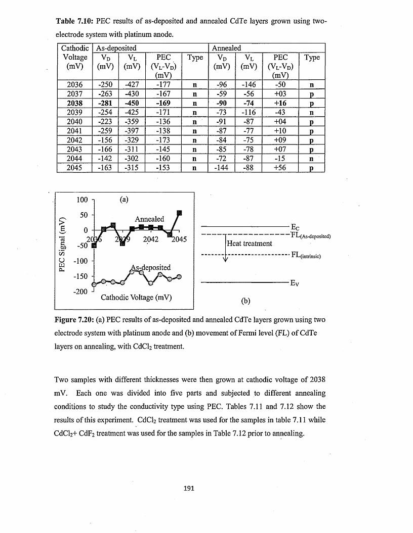
Table 7.10: PEC results of as-deposited and annealed CdTe layers grown using two-
electrode system with platinum anode.
CathodicVoltage
(mV)
As-deposited AnnealedVD
(mV)VL
(mV)PEC
(Vl-Vd)(mV)
Type VD(mV)
VL(mV)
PEC(Vl-Vd)
(mV)
Type
2036 -250 -427 -177 n -96 -146 -50 n2037 -263 -430 i o\ n -59 -56 +03 P2038 -281 -450 -169 n -90 -74 +16 P2039 -254 -425 -171 n -73 -116 -43 n2040 -223 -359 -136 n -91 -87 +04 P2041 -259 -397 -138 n -87 -77 +10 P2042 -156 -329 -173 n -84 -75 +09 P2043 -166 -311 -145 n -85 -78 +07 P2044 -142 -302 -160 n -72 -87 -15 n2045 -163 -315 -153 n -144 -88 +56 P
---------------------------------------- E cE L ( As-deposited)
Heat treatment
• FL(intrinsic)
--------------------------------E v
(b)
Figure 7.20: (a) PEC results of as-deposited and annealed CdTe layers grown using two
electrode system with platinum anode and (b) movement of Fermi level (FL) o f CdTe
layers on annealing, with CdC^ treatment.
Two samples with different thicknesses were then grown at cathodic voltage o f 2038
mV. Each one was divided into five parts and subjected to different annealing
conditions to study the conductivity type using PEC. Tables 7.11 and 7.12 show the
results o f this experiment. CdCh treatment was used for the samples in table 7.11 while
CdCl2+ CdF2 treatment was used for the samples in Table 7.12 prior to annealing.
100 i
Annealed
2042 :045-50
-150 -
-200Cathodic Voltage (mV)
191
Table 7.11: Conductivity type confirmation o f CdTe layers (grown at cathodic voltage of 2038 mV) under different annealing conditions with CdCl2 treatment.
SampleID
Thickness(pm)
CdCl2treatment
Annealing temp (°C)
Annealingtime(min)
v D(mV)
> | PEC
signalVl-Vd(mV)
type
FNl-a 1.8 None None none -114 -194 -80 nFNl-b 1.8 none 450 15 -166 -267 -101 nFNl-c 1.8 Yes 350 15 -97 -141 -44 nFNl-d 1.8 Yes 400 15 -132 -202 -65 nFNl-e 1.8 Yes 450 15 -96 -138 -42 n
Table 7.12: Conductivity type confirmation of CdTe layers (grown at cathodic voltage
of 2038 mV) under different annealing conditions with CdCl2+CdF2 treatment.
SampleID
Thickness(pm)
CdCl2+CdF 2 treatment
Annealingtemp(°C)
Annealingtime(min)
v D(mV)
v L(mV)
PECsignalVl-Vd(mV)
type
FN-a 2.6 None None none -196 -339 -143 nFN-b 2.6 none 450 15 -140 -250 -110 nFN-c 2.6 Yes 350 15 -251 -344 -93 nFN-d 2.6 Yes 400 15 -125 -218 -93 nFN-e 2.6 Yes 450 15 -49 -100 -51 n
All the samples, both before and after various chemical and heat treatments, remained
n-type. Another set of four samples were grown with four different thickness at the
same cathodic voltage of 2038 mV and the experiment repeated with annealing, this
time at 415°C for 15 minutes, but different CdCl2 and CdCl2+CdF2 treatments. Tables
7.13 - 7.16 show the results. Again all samples remained n-type under all annealing
conditions confirming that the CdTe material grown from this bath were all n-type for
solar cell fabrication.
Table 7.13: PEC measurements of as-deposited CdTe layers with different thicknesses.Sample
IDGrowth
time(min)
Thickness(pm)
VL(mV)
VD(mV)
PECsignal(mV)
Conductivitytype
Cl-1 156 1.1 -312 -158 -154 nC3-1 187 1.3 -109 -67 -42 nC2-1 240 1.8 -39 -03 -36 nC4-1 300 2.1 -313 -197 -116 n
192
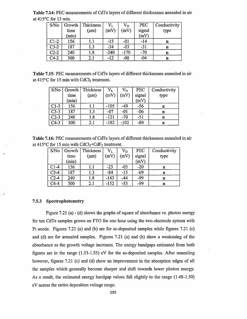
Table 7.14: PEC measurements of CdTe layers of different thicknesses annealed in airat 415°C for 15 min.
S/No Growthtime(min)
Thickness(pm)
VL(mV)
vD(mV)
PECsignal(mV)
Conductivitytype
Cl-2 156 1.1 -15 -01 -14 nC3-2 187 1.3 -34 -03 -31 nC2-2 240 1.8 -240 -170 -70 nC4-2 300 2.1 -12 -08 -04 n
Table 7.15: PEC measurements of CdTe layers of different thicknesses annealed in air at 415°C for 15 min with CdCl2 treatment.
S/No Growthtime(min)
Thickness(pm)
VL(mV)
vD(mV)
PECsignal(mV)
Conductivitytype
Cl-3 156 1.1 -105 -49 -56 nC3-3 187 1.3 -07 -01 -06 nC2-3 240 1.8 -121 -70 -51 nC4-3 300 2.1 -182 -102 -80 n
Table 7.16: PEC measurements of CdTe layers of different thicknesses annealed in air at 415°C for 15 min with CdCl2+CdF2 treatment.
S/No Growthtime(min)
Thickness(pm)
V l
(mV)VD
(mV)PECsignal(mV)
Conductivitytype
C l-4 156 1.1 -23 -03 -20 nC3-4 187 1.3 -84 -15 -69 nC2-4 240 1.8 -143 -44 -99 nC4-4 300 2.1 -152 -53 -99 n
7.5.3 Spectrophotometry
Figure 7.21 (a) - (d) shows the graphs of square of absorbance vs. photon energy
for ten CdTe samples grown on FTO for one hour using the two-electrode system with
Pt anode. Figures 7.21 (a) and (b) are for as-deposited samples while figures 7.21 (c)
and (d) are for annealed samples. Figures 7.21 (a) and (b) show a weakening of the
absorbance as the growth voltage increases. The energy bandgaps estimated from both
figures are in the range (1.53-1.55) eV for the as-deposited samples. After annealing
however, figures 7.21 (c) and (d) show an improvement in the absorption edges of all
the samples which generally become sharper and shift towards lower photon energy.
As a result, the estimated energy bandgap values fall slightly to the range (1.48-1.50)
eV across the entire deposition voltage range.
193
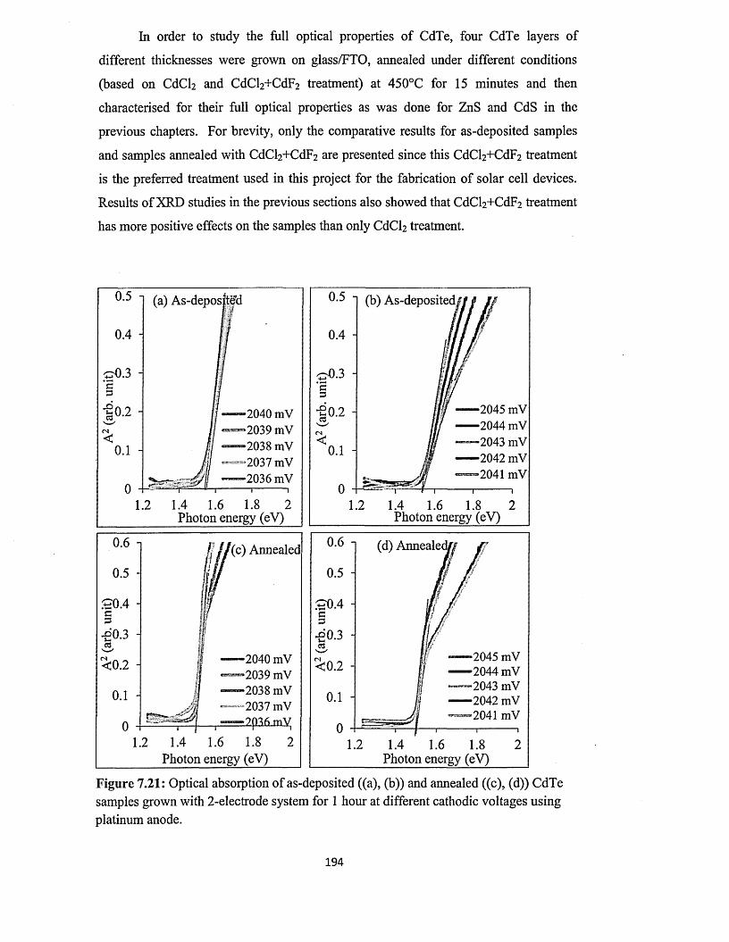
In order to study the full optical properties of CdTe, four CdTe layers of
different thicknesses were grown on glass/FTO, annealed under different conditions
(based on CdCl2 and CdCl2+CdF2 treatment) at 450°C for 15 minutes and then
characterised for their full optical properties as was done for ZnS and CdS in the
previous chapters. For brevity, only the comparative results for as-deposited samples
and samples annealed with CdCl2+CdF2 are presented since this CdCl2+CdF2 treatment
is the preferred treatment used in this project for the fabrication of solar cell devices.
Results of XRD studies in the previous sections also showed that CdCl2+CdF2 treatment
has more positive effects on the samples than only CdCl2 treatment.
0.5 i (a) As-deposited
2040 mV 2039 mV 2038 mV 2037 mV 2036 mV
1.4 1.6 1.8 2Photon energy (eV)
0.6
0.5
:~o.4 -
cS
< 0.2
0.1 H
0
/ / / ( c ) Annealed
2040 mV esss!!!Bi2039 mV
2038 mV 2037 mV
-2p36 mV
1.2 1.4 1.6 1.8 2Photon energy (eV)
0.5 n (b) As-depositedj
2045 mV 2044 mV 2043 mV 2042 mV 2041 mV
1.4 1.6 1.8 2Photon energy (eV)
(d) Anneale
2045 mV 2044 mV 2043 mV 2042 mV 2041 mV
1.4 1.6 1.8Photon energy (eV)
Figure 7.21: Optical absorption of as-deposited ((a), (b)) and annealed ((c), (d)) CdTe samples grown with 2-electrode system for 1 hour at different cathodic voltages using platinum anode.
194
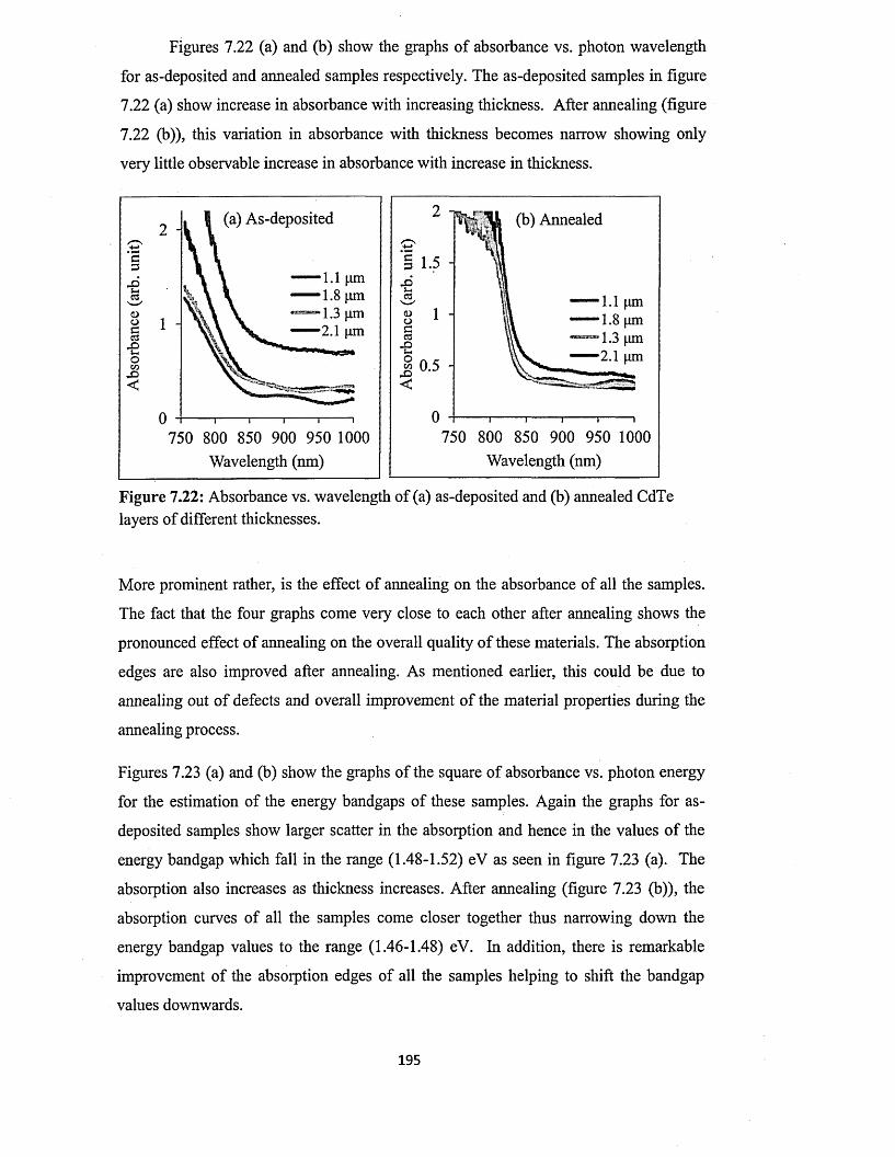
Figures 7.22 (a) and (b) show the graphs of absorbance vs. photon wavelength
for as-deposited and annealed samples respectively. The as-deposited samples in figure
7.22 (a) show increase in absorbance with increasing thickness. After annealing (figure
7.22 (b)), this variation in absorbance with thickness becomes narrow showing only
very little observable increase in absorbance with increase in thickness.
(a) As-deposited (b) Annealed
750 800 850 900 950 1000 Wavelength (nm)
750 800 850 900 950 1000 Wavelength (nm)
Figure 7.22: Absorbance vs. wavelength of (a) as-deposited and (b) annealed CdTe layers of different thicknesses.
More prominent rather, is the effect of annealing on the absorbance of all the samples.
The fact that the four graphs come very close to each other after annealing shows the
pronounced effect of annealing on the overall quality o f these materials. The absorption
edges are also improved after annealing. As mentioned earlier, this could be due to
annealing out o f defects and overall improvement of the material properties during the
annealing process.
Figures 7.23 (a) and (b) show the graphs of the square of absorbance vs. photon energy
for the estimation of the energy bandgaps of these samples. Again the graphs for as-
deposited samples show larger scatter in the absorption and hence in the values o f the
energy bandgap which fall in the range (1.48-1.52) eV as seen in figure 7.23 (a). The
absorption also increases as thickness increases. After annealing (figure 7.23 (b)), the
absorption curves of all the samples come closer together thus narrowing down the
energy bandgap values to the range (1.46-1.48) eV. In addition, there is remarkable
improvement of the absorption edges of all the samples helping to shift the bandgap
values downwards.
195
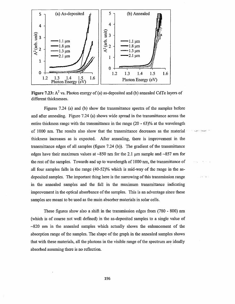
(a) As-deposited
1.1 pm
1.3 1.4 1.5Photon Energy (eV)
(b) Annealed
1.2 1.3 1.4 1.5 1.6Photon Energy (eV)
Figure 7.23: A vs. Photon energy o f (a) as-deposited and (b) annealed CdTe layers of different thicknesses.
Figures 7.24 (a) and (b) show the transmittance spectra of the samples before
and after annealing. Figure 7.24 (a) shows wide spread in the transmittance across the
entire thickness range with the transmittance in the range (20 - 63)% at the wavelength
of 1000 nm. The results also show that the transmittance decreases as the material
thickness increases as is expected. After annealing, there is improvement in the
transmittance edges of all samples (figure 7.24 (b)). The gradient of the transmittance
edges have their maximum values at -850 nm for the 2.1 pm sample and -857 nm for
the rest of the samples. Towards and up to wavelength o f 1000 nm, the transmittance of
all four samples falls in the range (40-52)% which is mid-way of the range in the as-
deposited samples. The important thing here is the narrowing o f this transmission range
in the annealed samples and the fall in the maximum transmittance indicating
improvement in the optical absorbance of the samples. This is an advantage since these
samples are meant to be used as the main absorber materials in solar cells.
These figures show also a shift in the transmission edges from (780 - 800) nm
(which is o f course not well defined) in the as-deposited samples to a single value of
-820 nm in the annealed samples which actually shows the enhancement o f the
absorption range of the samples. The shape o f the graph in the annealed samples shows
that with these materials, all the photons in the visible range o f the spectrum are ideally
absorbed assuming there is no reflection.
19 6
(a) As-deposited
750 800 850 900 950 1000 Wavelength (nm)
80 - —— 1.1 pm
70 - ■——1.8 pm
Co 60 -ox — 2.1 pm
^ 5 0 -o3 40 -
f f
Tra
nsm
ibO
U>o
o...
.1....
..1
I f10 -
0 - ---- --------- p-
(b) Annealed
750 800 850 900 950 1000 Wavelength (nm)
Figure 7.24: Transmittance vs. wavelength o f (a) as-deposited and (b) annealed CdTe layers of different thicknesses.
In figures 7.25 (a) and (b), one sees the reflectance spectra of these materials before and
after annealing. The figures also show relatively wide spread in the reflectance spectra
of the as-deposited samples across the entire thickness especially at the wavelengths
where the reflectance sets in. This cut off wavelength also increases as the thickness of
the samples increases. In the annealed samples, the cut off wavelength tend to converge
to a narrow range with samples of thicknesses <2.1 pm having their cut-off wavelength
come to the same value. Towards higher wavelengths up to 1000 nm, all the curves also
converge to a reflectance of -20% in the annealed samples. In the as-deposited samples
the reflectance in this wavelength range falls within (11 - 20)% across the sample
thicknesses.
197
100 - (b) Annealed
80 -
b 60 H— 1.1 pm
Qo — 1.8 pm
1 40 -_ i 3
<D ----- 2.1 pm<D_ot 20 - (rillu 1 * 1 i i »
750 800 850 900 950 1000Wavelength (nm)
100 ! (a) As-deposited
1.1 pm
1.3 pm 2.1 pm
750 800 850 900 950 1000 Wavelength (nm)
Figure 7.25: Reflectance vs. wavelength of (a) as-deposited and (b) annealed CdTe layers of different thicknesses.
Figure 7.26 shows the graphs of absorption coefficient (a) vs. photon energy for
the as-deposited and annealed CdTe layers of different thicknesses. Figure 7.26 (a)
shows that the absorption coefficient increases with film thickness and is in the range
(2.0 - 3.0)xl04 cm '1 across the thicknesses explored in this experiment.
4.0E+04 -] (b) Annealed5.0E+04 (a) As-deposited
o 3.0E+04 -1 .1 pm
3.0E+04 -1.3 pm 2.1 pm$5 2.0E+04 -
1.0E+04 -g 1.0E+04 -
0.0E+00g 0.0E+00 11.6
Photon energy (eV) Photon energy (eV)
Figure 7.26: Absorption coefficient vs. photon energy of (a) as-deposited and (b) annealed CdTe layers o f different thicknesses.
After annealing, there is general increase in a with the values coming in the range (2.6 -
4.0) x io 4 cm '1 towards the visible region of the spectrum. This is an improvement
resulting from the annealing. Strikingly too, there appears to be a reverse trend here in
the variation of a with thickness compared to that in the as-deposited samples. The
absorption coefficient in the annealed samples rather increases as the sample thickness
decreases. This result suggests that as the sample thickness increases in the micro-meter
range, to certain extent, the room for improvement in the qualities of the samples on
annealing seems to decrease. It can be recalled that similar observation was made in the
XRD study o f these same samples annealed with CdCl2+ CdF2 in figures 7.13 - 7.16
where the (111) peak intensity reaches its maximum for thicknesses of 1.8 pm and 2.1
pm. These results tend to suggest that there should be an optimum thickness o f the
material for optimum structural and optical qualities of these samples.
The graphs o f (ahv)2 vs. photon energy (hv) are shown in figure 7.27. In both
as-deposited samples (figure 7.27 (a)) and annealed samples ( figure 7.27 (b)), one
observes that the absorption (ahv)2 beyond the bandgap energy, decreases as the sample
thickness increases similar to the case of figure 7.26.
1.0E+09 -i (a) As-deposited 4.0E+09 (b) Annealed
.0E+08 3.0E+09
S 6.0E+082.0E+09
4.0E+081.3 pm 2.1 pm
•— 2.1 pm j= 1.0E+09£ 2.0E+08
0.0E+000.0E+00 I1.6
Photon energy (eV)Photon energy (eV)
Figure 7.27: (ahv)2 vs. photon energy o f (a) as-deposited and (b) annealed CdTe layers of different thicknesses.
In the annealed samples there is a clear improvement in the absorption edge o f all the
samples. The energy bandgap values estimated from these figures for the as-deposited
samples are in the range (1.47 - 1.52) eV. For the annealed samples, the bandgap values
are in the range (1.47-1.49) eV showing a contraction of this range and overall shift
towards lower energy values. These ranges of bandgap values are similar to those
obtained from figures 7.23 (a) and (b).
199
Figure 7.28 presents the dependence of extinction coefficient on photon energy for these
samples before and after annealing. Again the extinction coefficient follows similar
trend as the absorption coefficient and absorption (ahv)2 in figures 7.26 and 7.27. The
extinction coefficient values are higher in the annealed samples compared to the as-
deposited samples owing to improvement by post-deposition annealing.
The dependence of refractive index on photon energy is shown in figure 7.29.
Figure 7.29 (a) shows how relatively widespread the refractive index is over the entire
sample thickness range compared to the values in the annealed samples where they
converge, to the same values towards the longer wavelength (lower photon energy). In
this lower energy region (near 1.20 eV), the spread in the value of n in the as-deposited
samples is (2.00 - 2.63) whereas in the annealed sample only one value of n -2.63 is
observed. The fall in the refractive index in the higher energy region (form the bandgap
energy) is more rapid in the annealed samples than in the as-deposited samples. These
results show that the refractive indexes of these materials are more stable after
annealing indicating improvement in the optical properties o f the materials than in the
as-deposited samples.
(a) As-deposited0.3
0.25
1.1 pm0.2
0.151.3 pm 2.1 pm
0.05
1.2
Photon energy (eV)
(b) Annealed
0.25 -
5 0.15
2 0-1 '
1.2 1.3 1.4 1.5
Photon energy (eV)
Figure 7.28: Extinction coefficient vs. photon energy of (a) as-deposited and (b) annealed CdTe layers of different thicknesses.
200
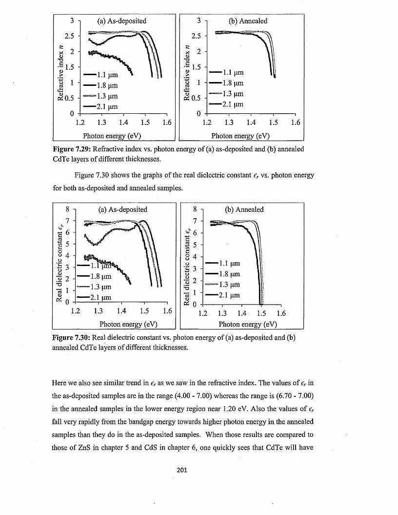
(a) As-deposited (b) Annealed
2.1 urn2.1 urn
1.2 1.3 1.4 1.5
Photon energy (eV)
1.2 1.3 1.4
Photon energy (eV)
Figure 7.29: Refractive index vs. photon energy o f (a) as-deposited and (b) annealed CdTe layers of different thicknesses.
Figure 7.30 shows the graphs of the real dielectric constant er vs. photon energy
for both as-deposited and annealed samples.
(a) As-deposited (b) Annealed
Photon energy (eV) Photon energy (eV)
Figure 7.30: Real dielectric constant vs. photon energy of (a) as-deposited and (b) annealed CdTe layers of different thicknesses.
Here we also see similar trend in er as we saw in the refractive index. The values o f er in
the as-deposited samples are in the range (4.00 - 7.00) whereas the range is (6.70 - 7.00)
in the annealed samples in the lower energy region near 1.20 eV. Also the values o f er
fall very rapidly from the bandgap energy towards higher photon energy in the annealed
samples than they do in the as-deposited samples. When those results are compared to
those of ZnS in chapter 5 and CdS in chapter 6, one quickly sees that CdTe will have
201
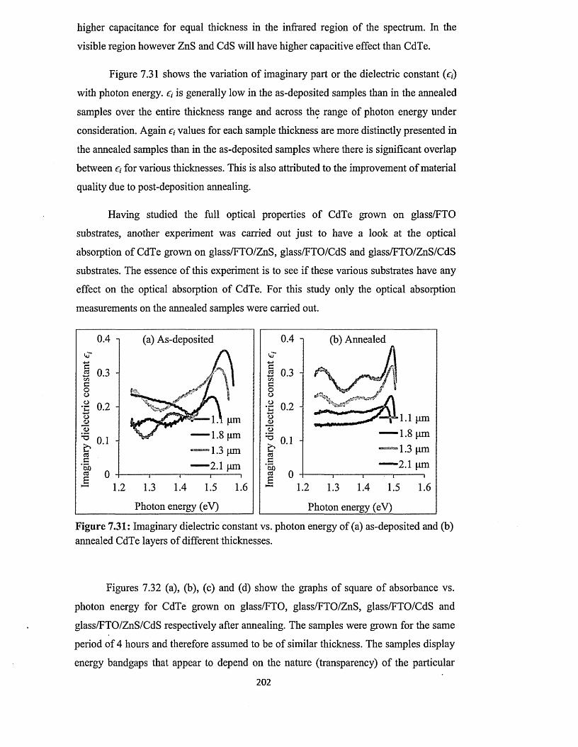
higher capacitance for equal thickness in the infrared region of the spectrum. In the
visible region however ZnS and CdS will have higher capacitive effect than CdTe.
Figure 7.31 shows the variation of imaginary part or the dielectric constant (cy)
with photon energy. £y is generally low in the as-deposited samples than in the annealed
samples over the entire thickness range and across the range of photon energy under
consideration. Again £, values for each sample thickness are more distinctly presented in
the annealed samples than in the as-deposited samples where there is significant overlap
between ey for various thicknesses. This is also attributed to the improvement o f material
quality due to post-deposition annealing.
Having studied the full optical properties o f CdTe grown on glass/FTO
substrates, another experiment was carried out just to have a look at the optical
absorption of CdTe grown on glass/FTO/ZnS, glass/FTO/CdS and glass/FTO/ZnS/CdS
substrates. The essence o f this experiment is to see if these various substrates have any
effect on the optical absorption of CdTe. For this study only the optical absorption
measurements on the annealed samples were carried out.
(a) As-deposited (b) Annealed
1.1 pm1.1 pm 1.8 pm 1.3 pm2.1 pm
1.3 pm 2.1 pm
i1.6 > 1.3 1.4 1,
Photon energy (eV)Photon energy (eV)
Figure 7.31: Imaginary dielectric constant vs. photon energy of (a) as-deposited and (b) annealed CdTe layers of different thicknesses.
Figures 7.32 (a), (b), (c) and (d) show the graphs o f square o f absorbance vs.
photon energy for CdTe grown on glass/FTO, glass/FTO/ZnS, glass/FTO/CdS and
glass/FTO/ZnS/CdS respectively after annealing. The samples were grown for the same
period of 4 hours and therefore assumed to be of similar thickness. The samples display
energy bandgaps that appear to depend on the nature (transparency) of the particular
202
material upon which the CdTe layer is directly grown which is also an indication of the
bandgap o f these materials. Since the bandgap values of these substrates are of the
order Eg (FTO) > Eg (ZnS) > Eg (CdS), the bandgap of the CdTe on these substrates also
appears in the order 1.50 eV > 1.48 eV > 1.46 eV > 1.45 eV for the samples in (a), (b),
(c) and (d) respectively. These bandgap values however do not vary that much and
observations during this project show that if the thickness of CdTe or any other material
(especially, CdS) is sufficiently large, the bandgap measured for these layers remain the
same irrespective of the nature of the underlying substrates. Thus one can conclude that
for sufficiently thick CdTe layer, the optical absorption behaviour is similar for CdTe
grown on the different substrates used in this project.
glass/FTO/CdTe (b) dassfFTO/ZnS/CdTe
E = 1.50 eV E = 1.48 eV
0.4
1.4 1.6 1.8Photon energy (eV)
21.4 1.6 1.8Photon energy (eV)
glass/FTO/CdS/CdTe
E = 1 .46eV
(d) glass/FTO/ZnS/CdS/CdTe
E =1.45 eV
' | 0.8-oJ3 0.40.4
1.4 1.6Photon energyPhoton energy (eV)
Figure 7.32: Optical absorption of CdTe grown on different substrates.
203
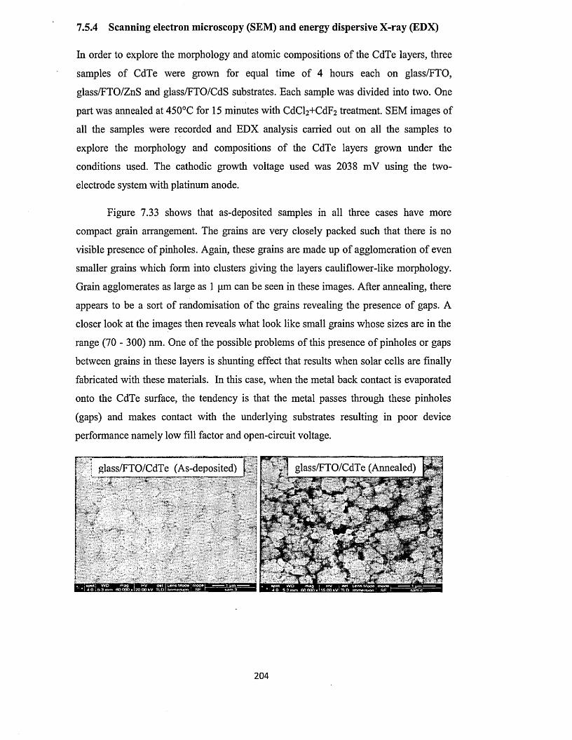
7.5.4 Scanning electron microscopy (SEM) and energy dispersive X-ray (EDX)
In order to explore the morphology and atomic compositions of the CdTe layers, three
samples of CdTe were grown for equal time of 4 hours each on glass/FTO,
glass/FTO/ZnS and glass/FTO/CdS substrates. Each sample was divided into two. One
part was annealed at 450°C for 15 minutes with CdCl2+CdF2 treatment. SEM images of
all the samples were recorded and EDX analysis carried out on all the samples to
explore the morphology and compositions of the CdTe layers grown under the
conditions used. The cathodic growth voltage used was 2038 mV using the two-
electrode system with platinum anode.
Figure 7.33 shows that as-deposited samples in all three cases have more
compact grain arrangement. The grains are very closely packed such that there is no
visible presence o f pinholes. Again, these grains are made up of agglomeration of even
smaller grains which form into clusters giving the layers cauliflower-like morphology.
Grain agglomerates as large as 1 pm can be seen in these images. After annealing, there
appears to be a sort of randomisation of the grains revealing the presence of gaps. A
closer look at the images then reveals what look like small grains whose sizes are in the
range (70 - 300) nm. One of the possible problems of this presence o f pinholes or gaps
between grains in these layers is shunting effect that results when solar cells are finally
fabricated with these materials. In this case, when the metal back contact is evaporated
onto the CdTe surface, the tendency is that the metal passes through these pinholes
(gaps) and makes contact with the underlying substrates resulting in poor device
performance namely low fill factor and open-circuit voltage.
-Vvl glass/FTO/CdTe (Annealed)glass/FTO/CdTe (As-deposited)
20 4
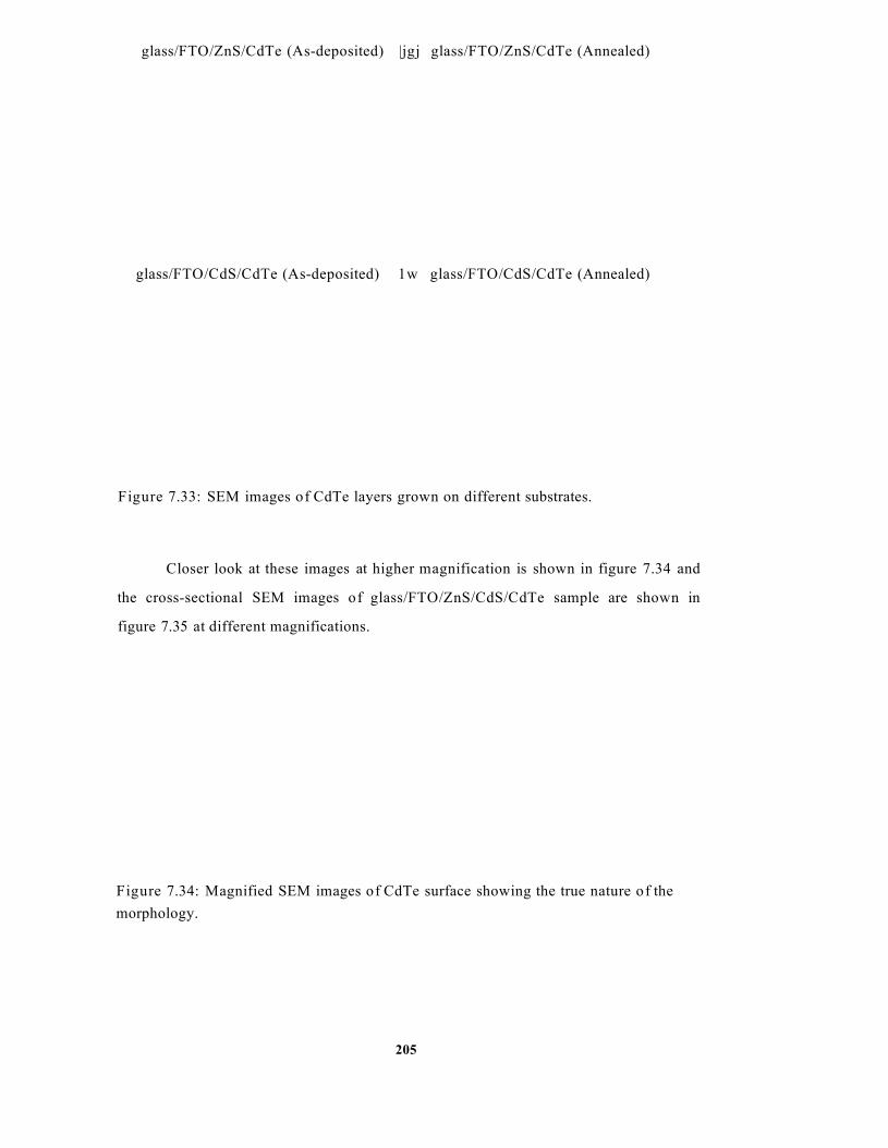
glass/FTO/ZnS/CdTe (As-deposited) |jgj glass/FTO/ZnS/CdTe (Annealed)
glass/FTO/CdS/CdTe (As-deposited) 1w glass/FTO/CdS/CdTe (Annealed)
Figure 7.33: SEM images of CdTe layers grown on different substrates.
Closer look at these images at higher magnification is shown in figure 7.34 and
the cross-sectional SEM images of glass/FTO/ZnS/CdS/CdTe sample are shown in
figure 7.35 at different magnifications.
Figure 7.34: Magnified SEM images of CdTe surface showing the true nature of the morphology.
205
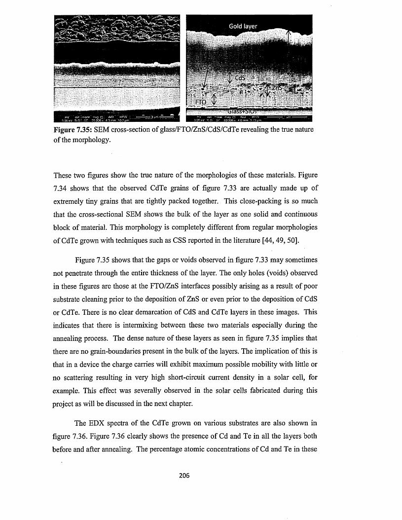
Figure 7.35: SEM cross-section o f glass/FTO/ZnS/CdS/CdTe revealing the true nature of the morphology.
These two figures show the true nature o f the morphologies of these materials. Figure
7.34 shows that the observed CdTe grains of figure 7.33 are actually made up of
extremely tiny grains that are tightly packed together. This close-packing is so much
that the cross-sectional SEM shows the bulk of the layer as one solid and continuous
block of material. This morphology is completely different from regular morphologies
of CdTe grown with techniques such as CSS reported in the literature [44, 49, 50].
Figure 7.35 shows that the gaps or voids observed in figure 7.33 may sometimes
not penetrate through the entire thickness of the layer. The only holes (voids) observed
in these figures are those at the FTO/ZnS interfaces possibly arising as a result o f poor
substrate cleaning prior to the deposition o f ZnS or even prior to the deposition of CdS
or CdTe. There is no clear demarcation of CdS and CdTe layers in these images. This
indicates that there is intermixing between these two materials especially during the
annealing process. The dense nature of these layers as seen in figure 7.35 implies that
there are no grain-boundaries present in the bulk of the layers. The implication o f this is
that in a device the charge carries will exhibit maximum possible mobility with little or
no scattering resulting in very high short-circuit current density in a solar cell, for
example. This effect was severally observed in the solar cells fabricated during this
project as will be discussed in the next chapter.
The EDX spectra of the CdTe grown on various substrates are also shown in
figure 7.36. Figure 7.36 clearly shows the presence of Cd and Te in all the layers both
before and after annealing. The percentage atomic concentrations of Cd and Te in these
2 0 6
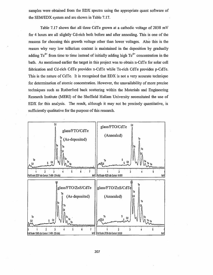
samples were obtained from the EDX spectra using the appropriate quant software of
the SEM/EDX system and are shown in Table 7.17.
Table 7.17 shows that all three CdTe grown at a cathodic voltage o f 2038 mV
for 4 hours are all slightly Cd-rich both before and after annealing. This is one o f the
reasons for choosing this growth voltage other than lower voltages. Also this is the
reason why very low tellurium content is maintained in the deposition by gradually
adding Te4+ from time to time instead of initially adding high Te4+ concentration in the
bath. As mentioned earlier the target in this project was to obtain n-CdTe for solar cell
fabrication and Cd-rich CdTe provides n-CdTe while Te-rich CdTe provides p-CdTe.
This is the nature o f CdTe. It is recognised that EDX is not a very accurate technique
for determination o f atomic concentration. However, the unavailability of more precise
techniques such as Rutherford back scattering within the Materials and Engineering
Research Institute (MERI) of the Sheffield Hallam University necessitated the use of
EDX for this analysis. The result, although it may not be precisely quantitative, is
sufficiently qualitative for the purpose of this research.
glass/FTO/CdTeglass/FTO/CdTe
(Annealed)(As-deposited)
Full Scale 4525 cts Cursor 0.000FulScale2237ctsC ursor7.409 (39 cts)
glass/FTO/ZnS/CdTe glass/FTO/ZnS/CdTe
(As-deposited) (Annealed)
Cd s m
' Ml I l | I M II ■ M I | l I II I II II 111 I I I I
keV Ful Scale 273S cts Cursor 0.000Ful Scale 1S60 cts Cursor 7.409 (33 cts)
207
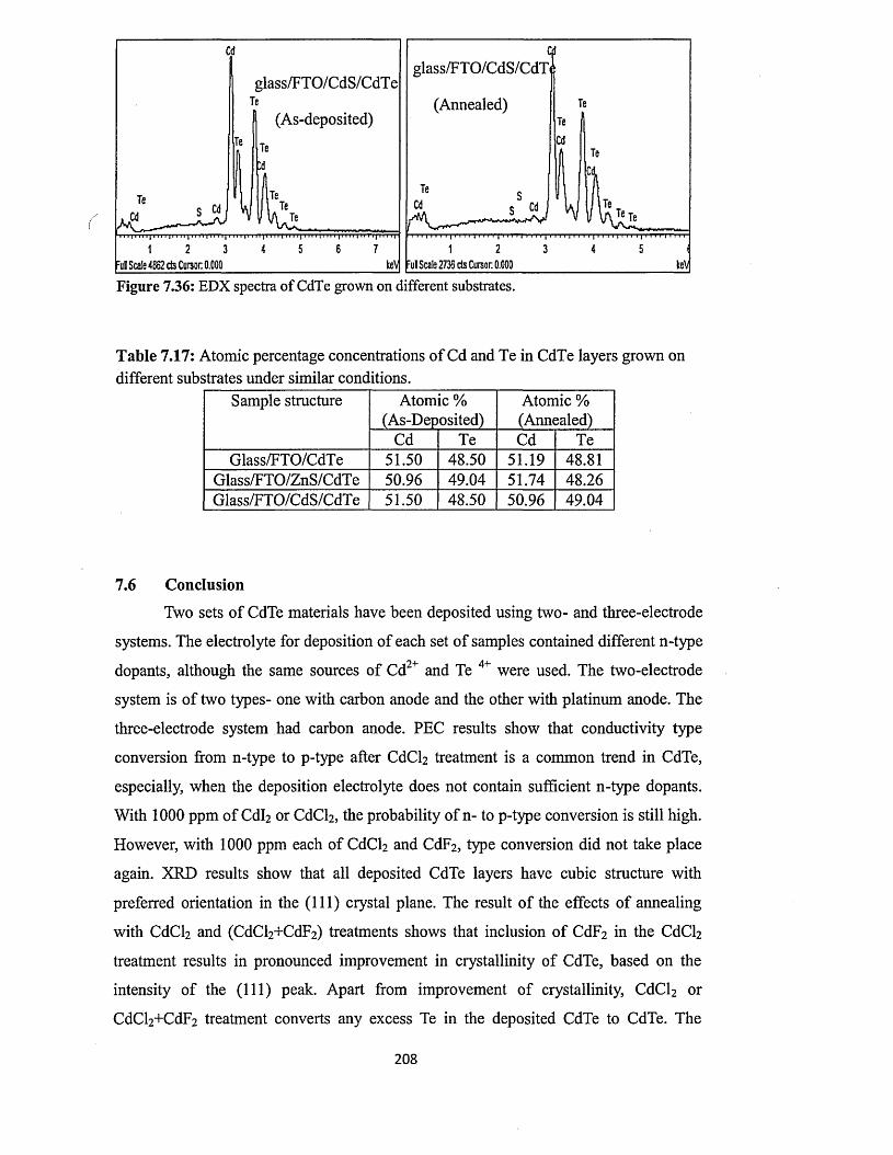
glass/FTO/CdS/CdT iglass/FTO/CdS/CdT e'e
(As-deposited)(Annealed)
c
:ul Scale 4862 cts Cursor 0.000 Ful Seals 2736 cts Cursor. 0.000
Figure 7.36: EDX spectra of CdTe grown on different substrates.
Table 7.17: Atomic percentage concentrations o f Cd and Te in CdTe layers grown on different substrates under similar conditions.
Sample structure Atomic % (As-Deposited)
Atomic % (Annealed)
Cd Te Cd TeGlass/FTO/CdTe 51.50 48.50 51.19 48.81
Glass/FTO/ZnS/CdTe 50.96 49.04 51.74 48.26Glass/FTO/CdS/CdTe 51.50 48.50 50.96 49.04
7.6 Conclusion
Two sets o f CdTe materials have been deposited using two- and three-electrode
systems. The electrolyte for deposition of each set o f samples contained different n-type
dopants, although the same sources of Cd2+ and Te 4+ were used. The two-electrode
system is o f two types- one with carbon anode and the other with platinum anode. The
three-electrode system had carbon anode. PEC results show that conductivity type
conversion from n-type to p-type after CdCh treatment is a common trend in CdTe,
especially, when the deposition electrolyte does not contain sufficient n-type dopants.
With 1000 ppm of Cdl2 or CdCl2 , the probability of n- to p-type conversion is still high.
However, with 1000 ppm each of CdCl2 and CdF2 , type conversion did not take place
again. XRD results show that all deposited CdTe layers have cubic structure with
preferred orientation in the (111) crystal plane. The result o f the effects o f annealing
with CdCl2 and (CdCl2+CdF2) treatments shows that inclusion o f CdF2 in the CdCl2
treatment results in pronounced improvement in crystallinity of CdTe, based on the
intensity of the (111) peak. Apart from improvement of crystallinity, CdCl2 or
CdCl2+CdF2 treatment converts any excess Te in the deposited CdTe to CdTe. The
20 8
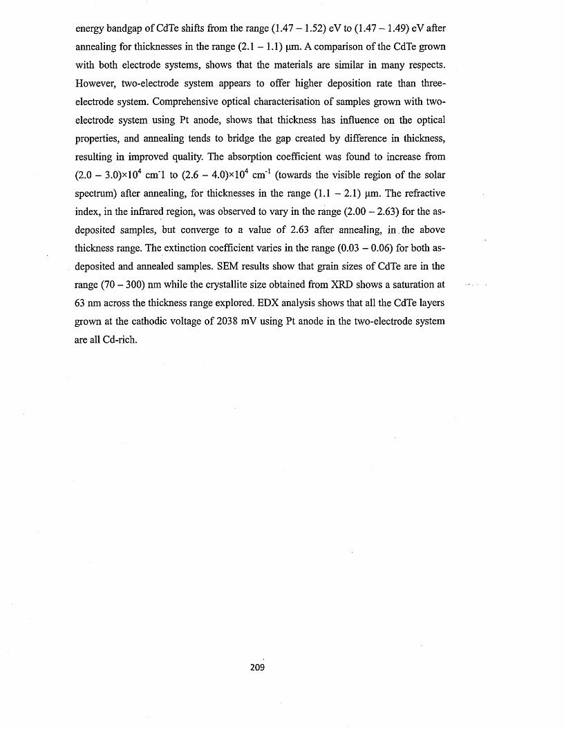
energy bandgap o f CdTe shifts from the range (1.47 - 1.52) eV to (1.47 - 1.49) eV after
annealing for thicknesses in the range (2.1 - 1.1) pm. A comparison of the CdTe grown
with both electrode systems, shows that the materials are similar in many respects.
However, two-electrode system appears to offer higher deposition rate than three-
electrode system. Comprehensive optical characterisation of samples grown with two-
electrode system using Pt anode, shows that thickness has influence on the optical
properties, and annealing tends to bridge the gap created by difference in thickness,
resulting in improved quality. The absorption coefficient was found to increase from
(2.0 - 3.0)xl04 cm 'l to (2.6 - 4.0)* 104 cm '1 (towards the visible region o f the solar
spectrum) after annealing, for thicknesses in the range (1.1 - 2.1) pm. The refractive
index, in the infrared region, was observed to vary in the range (2.00 - 2.63) for the as-
deposited samples, but converge to a value of 2.63 after annealing, in .the above
thickness range. The extinction coefficient varies in the range (0.03 - 0.06) for both as-
deposited and annealed samples. SEM results show that grain sizes of CdTe are in the
range (70 - 300) nm while the crystallite size obtained from XRD shows a saturation at
63 nm across the thickness range explored. EDX analysis shows that all the CdTe layers
grown at the cathodic voltage o f 2038 mV using Pt anode in the two-electrode system
are all Cd-rich.
209
References
1] B. M. Basol, J. Appl. Phys. 55 (1984) 601.
2] B .M . Basol, Solar Cells 23 (1988) 69.
3] D. Cunningham, M. Rubcich and D. Skinner, Prog. Photovolt: Res. App. 10 (2002)
159.
4] R. N. Bhattacharya and K. Rajeshwar, J. Appl. Phys. 58 (9) (1985) 3590.
5] S. K. Das, Sol. Energy Mat. Sol. Cells 29 (1993) 277.
6] S. Dennison, J. Mater. Chem. 4 (1) (1994) 41.
7] L. M. Peter and R. L. Wang, Electrochem. Commun. 1 (1999) 554.
8] I. M. Dharmadasa, A. P. Samantilleke, N. B. Chaure and J. Young, Semicond. Sci.
Technol. 17 (2002) 1238.
9] N. W. Duffy, L. M. Peter and R. L. Wang, J. Electroanal.
Chem. 532 (2002) 207.
10] C. Natarajan, M. Sharon, C. Levy-Clement and M. Neumann-Spallart, Thin Solid
Films 237 (1994) 118.
11] T. Pauport and D. Lincot, Electrochim. Acta 45 (2000) 3345.
12] H. Chen, P. N. Kalu and E. E. Kalu, J. Solid State Electrochem. 14 (2010) 1013.
13] S. M. Pawar, B. S. Pawar, A. V. M oholkar, D. S. Choi, J. H. Yun, J. H. Moon, S.
S. Kolekar and J. H. Kim, Electrochim. Acta 55 (2010) 4057.
14] X. Donglin, X. Man, L. Jianzhuang and Z. Xiujian, J. Mater. Sci. 41 (2006) 1875.
15] T. Mahalingam, V. Dhanasekarau, K. Sundaram, A. Kathalingam and J. Rhee,
Ionics 18 (2012) 299.
16] F. A. Kroger, J. Electrochem. Soc. 124 (1978) 2038.
17] I. M. Dharmadasa, R. P. Burton and M. Simmond, Sol. Energ. Mat. Sol. Cells 90
(2006) 2191.
18] A. Bouraiou, M. S. Aida, E. Tomasella and N. Attaf, J. Mater. Sci. 44 (2009)
1241.
19] D. G. Diso, G. E. A. Muftah, V. Patel and I. M. Dharmadasa, J. Electrochem. Soc.
157 (2010) (6) H647.
20] http://www. consultrsr. com/resources/ref/refpostls.htm
21] K. Zanio, Semiconductors and Semimetals, vol. 13 “Cadmium Telluride”, (New
York: Academic Press) (1978).
22] http://www.consultrsr.com/resources/ref/select.htm
23] M. Takahashi, K. Uosaki and H. Kita, J. Appl. Phys. 60 (6) (1986) 2046.
24] V. B. Patil, D. S. Sutrave, G. S. Shahane and L. P. Deshmukh, Thin Solid Films
210
401 (2001) 35.
[25] I. M. Dharmadasa, N. B. Chaure, G. J. Tolan and A. P. Samantilleke, J.
Electrochem. Soc. 154 (6) (2007) H466.
[26] I. M. Dharmadasa, A. P. Samantilleke, J. Young, M. H. Boyle, R. Bacewicz and
A. Wolska, J. Mater. Sci - Mater. El. 10 (1999) 441.
[27] R. K. Pandey, S. N. Sahu and S. Chandra, Handbook o f Semiconductor
Electrodeposition, (New York: Marcel Dekker) (1996).
[28] www.almazovtic.com/Ts02.htm
[29] http://tellurium.atomistrv.com/tellurium dioxide.html
[30] J. M. Woodcock, A. K. Turner, M. E. Ozsan and J. G. Summers, Photovoltaic
Specialists Conference 1991, Conference Record o f the twenty second IEEE, 7 -
11 October, 1991, Las Vegas, Nevada, USA, Vol.2 Pg. 842 - 847.
http.V/ieeexplore. ieee. org/xpls/abs_all.jsp?arnumber=l69328.
[31] A. K. Turner, J. M. Woodcock, M. E. Ozsan, J. G. Summers and J. Barker et al,
Solar Energy Materials, 23, ((1991)) 388-393.
[32] C. J. Bridge, P. Dawson, P. D. Buckle and M. E. Ozsan, Semicond. Sci. Technol.,
15, (2000)975-979.
[33] N. W. Duffy, L. M. Peter, R. L. Wang, D. W. Lane and K. D. Rogers,
Electrochimica Acta, 45, (2000) 3355 - 3365.
[34] V. Valdna, F. Buschmann and E. Mellikov, J. Cryst. Growth, 161, (1996) 164 -
167.
[35] E. Belas, J. France, R. Drill, A. L. Toth, P. Horodysky, P. Moravec and P. Hoschl,
J. Elect. Materi., Vol.34, No.6, (2005) 957 - 962.
[36] T. Schulmeyer, J. Fritsche, A. ThiBen, A. Klein, W. Taegermann, M. Campo and
J. Beier, Thin Solid Films, 431 — 432, (2003) 84 — 89.
[37] S. Yang, J. Chou and H. Ueng, Thin Solid Films, 518, (2010) 4197 - 4202.
[38] I. M. Dharmadasa, Prog. Crystal Growth and Charact., Vol.36, No.4, (1998) 249
-2 9 0 .
[39] I. M. Dharmadasa, C. J. Blomfield, C. G. Scott, R. Coratger, F. Ajuston and J.
Beauvillain, Solid-State Electronics, Vol.42, No.4, (1998) 595 - 604.
[40] R. H. Williams, N. Forsyth, I. M. Dharmadasa and Z. Sobiesierski, Applied
Surface Science 41/42, (1989) 189 -1 9 4 .
[41] S. Mazzamuto, L. Vaillant, A. Bosio, N. Romeo, N. Armani and G. Salviati, Thin
Solid Films, 516, (2008) 7079 - 7083.
[42] T. L. Chu and S. S. Chu, Solid-State Electronics, Vol.38, No.3, (1995) 533-549.
211
[43] A. Bosio, N. Romeo, S. Mazzamuto and V. Canevari, Prog. Cryst. Growth &
Charact. Mater., 52, (2006) 247-279.
[44] C. S. Ferekides, D. Marinskiy, V. Viswanathan, B. Tetali, V. Palekis, P. Selvaraj
and D. L. Morel, Thin Solid Films, 361-361, (2000) 520-526.
[45] A. Bouraiou, M. S. Aida, E. Tomasella and N. Attaf, J. Mater. Sci. 44,
(2009) 1241 -1244.
[46] A. W. Burton, K. Ong, T. Rea and I. Y. Chen, Microporous and Mesoporous
Materials, 117, (2009) 7 5 -9 0 .
[47] H. N. Jayatirtha, D. O. Henderson, A. Burger and M. P. Volz, Appl. Phys. Lett.
62, (1993)573-575.
[48] J. Fritsche, S. Gunst, E. Golusda, M. C. Lejard, A. ThiOen, T. Mayer, A. Klein, R.
Wendt, R. Gegenwart, D. Bonnet and W. Jaegermann, Thin Solid Films, 387,
(2001)161-164.
[49] P. Liu, V. P. Singh, C. A. Jarro and S. Rajaputra, Nanotechnology, 22, (2011)
145304 (9pp). Doi:10.1088/0957-4484/22/14/145304.
[50] Z. Fang, X. C. Wang, H. C. Wu and C. Z. Zhao, International Journal o f
Photoenergy, Article ID 297350 (2011). Doi: 10.1155/2011/297350.
212
Chapter 8 Solar cell fabrication and characterisation
8.0 Introduction
In this chapter the fabrication of different solar cells under different conditions
and their assessment are presented. These cells were fabricated using the three main
materials deposited and characterised as presented in Chapters 5 - 7 . The different solar
cell device architectures implemented basically include glass/FTO/n-CdTe/Au,
glass/FTO/n-ZnS/n-CdTe/Au, glass/FTO/n-CdS/n-CdTe/Au and glass/FTO/n-ZnS/n-
CdS/n-CdTe/Au (multilayer graded bandgap solar cell). Other device structures
involving i-ZnO and Al-ZnO buffer layers grown on FTO were also fabricated.
The device processing steps used in this research include post-deposition
annealing of the various device structures (before making the Au back contacts) with
prior CdCl2 and CdCl2+CdF2 treatment, chemical etching and back contact
metallisation. The main etchants used were dilute acidified K^C^O? aqueous solution
(oxidising etch) and aqueous solution of NaOH+Na2 S2C>3 (reducing etch). An attempt
was also made to see the effect o f replacing K^C^C^+F^SCU mixture with a mixture of
K^C^Cb+HNC^+FkPCU on device performance. The main device assessment tool used
was current-voltage characteristics. An attempt was also made to carry out capacitance-
voltage measurement o f few solar cells with good rectifying properties. The fabrication
and assessment results of all these solar cells are presented in this chapter.
8.1 Solar cell fabrication
Similar steps were involved in the fabrication of all the solar cells reported in
this thesis. The general procedure after the deposition of the absorber layer (CdTe)
involved CdCl2 or CdCl2+CdF2 treatment by dipping in a saturated solution o f CdCl2 or
CdCl2+CdF2 in water or in methanol. Alternatively some CdCh or CdCl2+CdF2 solution
could be spread on the CdTe surface using a pipette. The samples were then allowed to
dry in air inside a fume cupboard. To facilitate the drying a warm air blower was used
to blow warm air over the samples in order to dry the CdCb or CdCl2+CdF2 solution on
it. After the drying, the samples were then annealed in a carbolite furnace at the desired
temperature generally in the range (350 - 450)°C for the time period in the range (15 -
60) minutes depending on the particular need. The samples were then allowed to cool
in air. The white CdCl2 and CdCl2+CdF2 powder on the samples were then washed off
213
with de-ionised water and the samples dried using the warm air blower or in a stream of
N2.
The next stage in the processing is the chemical etching. For this process, two
solutions were used. One of the etchants was the acid (oxidising) etchant containing
about lg o fK 2Cr20 7, 20 ml o f de-ionised water and two drops of concentrated sulphuric
acid all in a 50 ml beaker. This solution actually provides a dilute acidic aqueous
solution o f K2Cr20 7. The second etchant was the basic (reducing) etchant. This etchant
contains about 0.5g each o f NaOH and Na2S2C>3 in 50 ml of de-ionised watgr all
contained in a 100 ml glass beaker. This solution is then heated over a hot plate with a
stirrer to about 60°C ready for use. The already annealed samples were then etched in
the acid etchant by dipping them in the oxidising etchant for about 5 seconds and then
rinsed in de-ionised water. Again they were etched in the reducing etchant by dipping
them in the basic etchant for about 2 minutes while the solution is continuously stirred
moderately. They were then rinsed again in de-ionised water and dried in a stream of
nitrogen gas. All the etched samples were then transferred immediately to a metallic
mask with circular holes. The choice of these etchants followed the work by
Dharmadasa, Dharmadasa et al and Das and Morris [1 - 3]. Two different masks were
used. The main one used for most of the devices was one with 2 mm-diameter circular
holes. The other used had 3 mm-diameter circular holes. The mask containing the
etched samples was then placed in the EDWARDS 306 vacuum coater (metalliser) with
an FTM7 Film Thickness Monitor. A piece o f gold wire o f 99.999% purity was then cut
and placed in the tungsten filament for evaporation o f Au. The evaporation chamber of
the metalliser was then closed and evacuated to a pressure of 10-4 Pa (10*6 Torr). When
this pressure was attained, about 100 nm-thick Au layer was evaporated onto the
samples. The thickness o f the evaporated Au was controlled using the thickness monitor
and shutter accompanying the metalliser. The whole system was allowed for about 30
minutes to cool and the completed solar cell devices were removed and then
characterised using current-voltage and capacitance-voltage measurements. The I-V
system used was a Kiethley 619 Electrometer/multimeter using a solar simulator with
light intensity of 1000 Wm'2. The C-V system used was a Kiethley 6517A
Electrometer/High resistance Meter with Hewlett Packard 4284A (20 Hz - 1 MHz)
Precision LCR Meter. The results of the characterisation of the various solar cell
structures fabricated are presented in the following sections.
21 4

8.2 Characterisation of n-CdTe/Au solar cells
Figure 8.1 shows the graphs o f I-V characteristics o f four different glass/FTO/n-
CdTe/Au solar cells with CdTe grown at cathodic voltage o f 2038 mV for different
times. One major observation in these graphs is the very poor device characteristics of
all the cells. Again the reproducibility of the devices reported in this thesis is still poor
at present (especially for the best devices) and is generally around 40%.
(b) 3.0 hr8 -
*•g 4 -<D
D O l 1 U! 1= -1 -0.6 -0.2O £ .-4-> -4 ^
-8 J
Light Vo
i i i i 0 / 0.6 1
ltage (V)
(a) 2.5 hr
0.6
Light Voltage (V)
(d) 5.0 hr(c) 4.0 hr
— i------------- 1
0.6 1u <
-30 JLight Voltage (V)Light Voltage (V)
Figure 8.1: I-V characteristics of glass/FTO/n-CdTe/Au solar cells with CdTe grown for (a) 2.5 hr, (b) 3.0 hr, (c) 4.0 hr and (d) 5.0 hr.
This is a common observation during the course of this research. The best device
obtained using this device structure was the one involving CdTe grown for 5 hours with
Voc = 170 mV, Jsc = 12.8 mAcm'2, FF = 0.31 and r| = 0.7%. The summary o f all the
device results is given in Table 8.1 below and these measurements have error of about
±5%.
215
Table 8.1: Summary o f device results for glass/FTO/n-CdTe/Au solar cells. The error in these measurements is within ±5%.
Sample ID CdTe Growth time (hr)
V o c
(mV)Jsc
(mAcnf2)FF il
(%)C l-4 2.5 330 3.5 0.48 0.55C3-4 3.0 400 3.8 0.41 0.62C4-4 4.0 350 4.0 0.33 0.46
F 5.0 170 12.8 0.31 0.70
With the exception of the device with CdTe grown for 4 hours the results show that the
overall device efficiency increases as growth time (thickness) of CdTe increases. Again
the short-circuit current density increases as the growth time (thickness) o f CdTe
increases. The FF generally decreases as CdTe growth time increases. The Voc does not
show any consistent trend with respect to CdTe growth time. The reason for the very
poor results may have to do with the large lattice mismatch between CdTe and Sn02
(FTO). Cubic CdTe has lattice constant a = 6.4810 A according to the JCPDS file No.
00-015-0770 while tetragonal SnC>2 has lattice constant a = 4.7200 A according to
JCPDS file No. 00-001-0625. This amounts to lattice mismatch of 27% relative to CdTe
and 37% relative to Sn02.
8.3 Characterisation of n-CdS/n-CdTe/Au solar cells
Different structures of n-CdS/n-CdTe/Au solar cells were fabricated using both
two-electrode system and three-electrode system. Even in two-electrode configuration,
CdS/CdTe solar cells were fabricated using both carbon anode and platinum anode.
Another set o f cells were also fabricated incorporating i-ZnO as a buffer layer resulting
to the fabrication of glass/FTO/i-ZnO/n-CdS/n-CdTe/Au solar cells in addition to the
glass/FTO/n-CdS/n-CdTe/Au solar cells. The i-ZnO used also came from Pilkington
Group United Kingdom in the form of glass/FTO/i-ZnO substrates. All these devices
and the results of their characterisation are presented in this section.
8.3.1 n-CdS/n-CdTe solar cells using CdTe from two-electrode system with
platinum anode
Figures 8.2 (a) - (f) show the I-V characteristics of glass/FTO/n-CdS/n-CdTe/Au solar
cells fabricated using CdS grown for different durations representing different
thicknesses in order to determine the best growth time (thickness) of CdS for making
CdS/CdTe solar cells. All the CdS samples were grown at a cathodic voltage o f 1450
mV while the CdTe layers were grown at a cathodic voltage of 2038 mV for 4.5 hours216
and annealed at 450°C for 18 minutes after CdCl2+CdF2 treatment. Figure 8.2 shows
that these devices have high series resistances and low shunt resistances. The sample in
figure 8.2 (a) however, shows relatively higher shunt resistance and actually has lowest
series resistance. This is reflected in its highest fill factor among other devices.
Table 8.2 shows the summary of the device parameters of these devices under A.M 1.5
illumination. From Table 8.2, it is clear that none o f the device parameters in general
has any clear dependence on the growth time (or thickness) of CdS. However, the best
device in terms o f Voc, JSc and r\ is the device with CdS grown for 28 minutes showing
an efficiency o f 4.9%.
(a) CS170-A (12 m in)/
(b) CS171-B (15 m in /
45 -
0.6 -15 -
-35 J Light Voltage (V)
-35 J Light Voltage (V)
(c) CS172-C (19 m in/
(d) CS173-D (24 minV
oneCD
C j= g oI <
3 &0.6
-35 JLight Voltage (V)
-33 J Light Voltage (V)
217
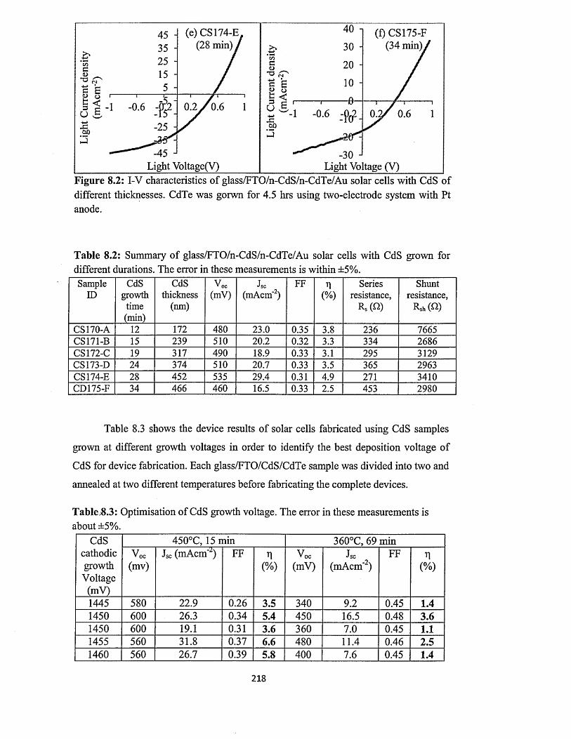
45 -
* 35 ‘?5 -C/5C 1 C ■8 — 15 'c £ 5 -
(e) CS174-E (28 min) j
40 -
£ 30 " 'tn§ 20 J
CNe g 10 1 2 0§ < n
(f) CS175-F (34 m in)/
o 1 1 i_= | - 1 -0.6 -<&' O £ . -15 -
t -25 .
^ -45 J Light \
1 I * *
O.2 / 0 . 6 1
foltage(V)
S ' 1-°-6 --P02-
-30 - Light Vo
i...."j" 1.......... 1
0 2 / 0.6 1
Itage (V)! figure 8.2: I-V characteristics of glass/FTO/n-CdS/n-CdTe/Au solar cells with CdS ofdifferent thicknesses. CdTe was gorwn for 4.5 hrs using two-electrode system with Pt anode.
Table 8.2: Summary of glass/FTO/n-CdS/n-CdTe/Au solar cells with CdS grown for different durations. The error in these measurements is within ±5%.Sample
IDCdS
growthtime(min)
CdSthickness
(nm)
V oc(mV)
Jsc(mAcm'2)
FF n(%)
Seriesresistance,
R .( « )
Shuntresistance,
R sh (^)
CS170-A 12 172 480 23.0 0.35 3.8 236 7665CS171-B 15 239 510 2 0 .2 0.32 3.3 334 2686CS172-C 19 317 490 18.9 0.33 3.1 295 3129CS173-D 24 374 510 20.7 0.33 3.5 365 2963CS174-E 28 452 535 29.4 0.31 4.9 271 3410CD175-F 34 466 460 16.5 0.33 2.5 453 2980
Table 8.3 shows the device results o f solar cells fabricated using CdS samples
grown at different growth voltages in order to identify the best deposition voltage of
CdS for device fabrication. Each glass/FTO/CdS/CdTe sample was divided into two and
annealed at two different temperatures before fabricating the complete devices.
Table ,8.3: Optimisation of CdS growth voltage. The error in these measurements is about ±5%.
CdScathodicgrowthVoltage
(mV)
450°C, 15 min 360°C, 69 minV o c
(mv)Jsc (mAcm'2) FF h
(%)V o c
(mV)Jsc
(mAcm'2)FF if
(%)
1445 580 22.9 0.26 3.5 340 9.2 0.45 1.41450 600 26.3 0.34 5.4 450 16.5 0.48 3.61450 600 19.1 0.31 3.6 360 7.0 0.45 1.11455 560 31.8 0.37 6.6 480 11.4 0.46 2.51460 560 26.7 0.39 5.8 400 7.6 0.45 1.4
2 1 8
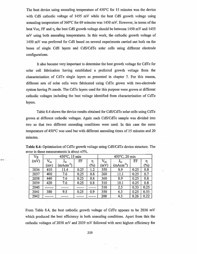
The best device using annealing temperature o f 450°C for 15 minutes was the device
with CdS cathodic voltage of 1455 mV while the best CdS growth voltage using
annealing temperature of 360°C for 69 minutes was 1450 mV. However, in terms of the
best Voc, FF and r|, the best CdS growth voltage should be between 1450 mV and 1455
mV using both annealing temperatures. In this work, the cathodic growth voltage of
1450 mV was preferred for CdS based on several experiments carried out both on the
bases o f single CdS layers and CdS/CdTe solar cells using different electrode
configurations.
It also became very important to determine the best growth voltage for CdTe for
solar cell fabrication having established a preferred growth voltage from the
characterisation o f CdTe single layers as presented in chapter 7. For this reason,
different sets o f solar cells were fabricated using CdTe grown with two-electrode
system having Pt anode. The CdTe layers used for this purpose were grown at different
cathodic voltages including the best voltage identified from characterisation o f CdTe
layers.
Table 8.4 shows the device results obtained for CdS/CdTe solar cells using CdTe
grown at different cathodic voltages. Again each CdS/CdTe sample was divided into
two so that two different annealing conditions were used. In this case the same
temperature of 450°C was used but with different annealing times o f 15 minutes and 20
minutes.
Table 8.4: Optimisation o f CdTe growth voltage using CdS/CdTe device structure. The error in these measurements is about ±5%.
Vg(mV)
450°C, 15 min 450°C, 20 minV o c
(mv)Jsc
(mAcm'2)FF 0
(%)V o c
(mV)Jsc
(mAcm'2)FF
(%)2036 410 11.4 0.25 1.2 350 8.9 0.25 0.82037 400 7.6 0.25 0.8 260 11.1 0.25 0.72038 440 7.6 0.25 0.8 360 8.9 0.25 0.82039 420 7.6 0.25 0.8 310 10.1 0.25 0.82040 ------ ------ 310 2.5 0.33 0.252041 380 9.5 0.25 0.9 350 6.3 0.25 0.552042 ------ ------ 200 4.3 0.26 0.22
From Table 8.4, the best cathodic growth voltage of CdTe appears to be 2036 mV
which produced the best efficiency in both annealing conditions. Apart from this the
cathodic voltages of 2038 mV and 2039 mV followed with next highest efficiency for
21 9
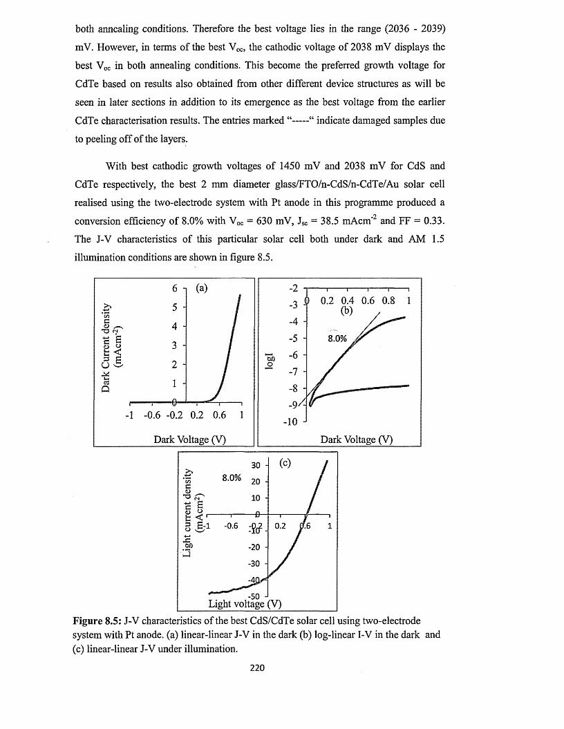
both annealing conditions. Therefore the best voltage lies in the range (2036 - 2039)
mV. However, in terms of the best Voc, the cathodic voltage of 2038 mV displays the
best Voc in both annealing conditions. This become the preferred growth voltage for
CdTe based on results also obtained from other different device structures as will be
seen in later sections in addition to its emergence as the best voltage from the earlier
CdTe characterisation results. The entries marked “-----“ indicate damaged samples due
to peeling off of the layers.
With best cathodic growth voltages o f 1450 mV and 2038 mV for CdS and
CdTe respectively, the best 2 mm diameter glass/FTO/n-CdS/n-CdTe/Au solar cell
realised using the two-electrode system with Pt anode in this programme produced a
conversion efficiency of 8.0% with Voc = 630 mV, Jsc = 38.5 mAcm'2 and FF = 0.33.
The J-V characteristics of this particular solar cell both under dark and AM 1.5
illumination conditions are shown in figure 8.5.
8.0%
fc <
j 9/ -10 -
1
Dark Voltage (V) Dark Voltage (V)
(c)308.0%
VL/a <
0.2
-20 -
-30 -
-50 J Light voltage (V)
Figure 8.5: J-V characteristics of the best CdS/CdTe solar cell using two-electrode system with Pt anode, (a) linear-linear J-V in the dark (b) log-linear I-V in the dark and (c) linear-linear J-V under illumination.
220
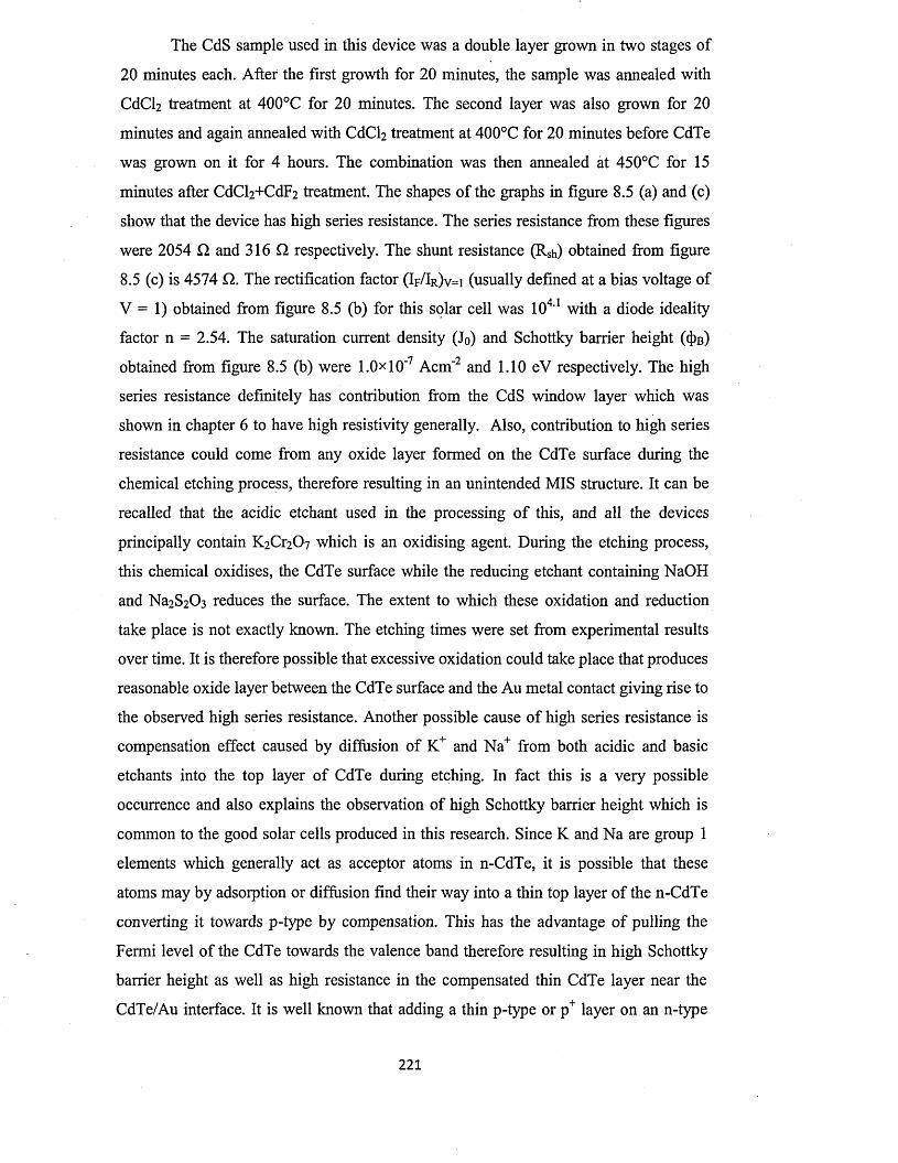
The CdS sample used in this device was a double layer grown in two stages of
20 minutes each. After the first growth for 20 minutes, the sample was annealed with
CdCb treatment at 400°C for 20 minutes. The second layer was also grown for 20
minutes and again annealed with CdCb treatment at 400°C for 20 minutes before CdTe
was grown on it for 4 hours. The combination was then annealed at 450°C for 15
minutes after CdCl2+CdF2 treatment. The shapes of the graphs in figure 8.5 (a) and (c)
show that the device has high series resistance. The series resistance from these figures
were 2054 Q. and 316 Q respectively. The shunt resistance ( R Sh ) obtained from figure
8.5 (c) is 4574 £ 1 The rectification factor ( I f / I r ) v = i (usually defined at a bias voltage of
V = 1) obtained from figure 8.5 (b) for this solar cell was 104'1 with a diode ideality
factor n = 2.54. The saturation current density (J0) and Schottky barrier height (4>b )
obtained from figure 8.5 (b) were 1.0x1 O'7 Acm'2 and 1.10 eV respectively. The high
series resistance definitely has contribution from the CdS window layer which was
shown in chapter 6 to have high resistivity generally. Also, contribution to high series
resistance could come from any oxide layer formed on the CdTe surface during the
chemical etching process, therefore resulting in an unintended MIS structure. It can be
recalled that the acidic etchant used in the processing o f this, and all the devices
principally contain K.2Cr2 0 7 which is an oxidising agent. During the etching process,
this chemical oxidises, the CdTe surface while the reducing etchant containing NaOH
and Na2 S2C>3 reduces the surface. The extent to which these oxidation and reduction
take place is not exactly known. The etching times were set from experimental results
over time. It is therefore possible that excessive oxidation could take place that produces
reasonable oxide layer between the CdTe surface and the Au metal contact giving rise to
the observed high series resistance. Another possible cause of high series resistance is
compensation effect caused by diffusion o f K+ and Na+ from both acidic and basic
etchants into the top layer o f CdTe during etching. In fact this is a very possible
occurrence and also explains the observation of high Schottky barrier height which is
common to the good solar cells produced in this research. Since K and Na are group 1
elements which generally act as acceptor atoms in n-CdTe, it is possible that these
atoms may by adsorption or diffusion find their way into a thin top layer o f the n-CdTe
converting it towards p-type by compensation. This has the advantage o f pulling the
Fermi level of the CdTe towards the valence band therefore resulting in high Schottky
barrier height as well as high resistance in the compensated thin CdTe layer near the
CdTe/Au interface. It is well known that adding a thin p-type or p+ layer on an n-type
221
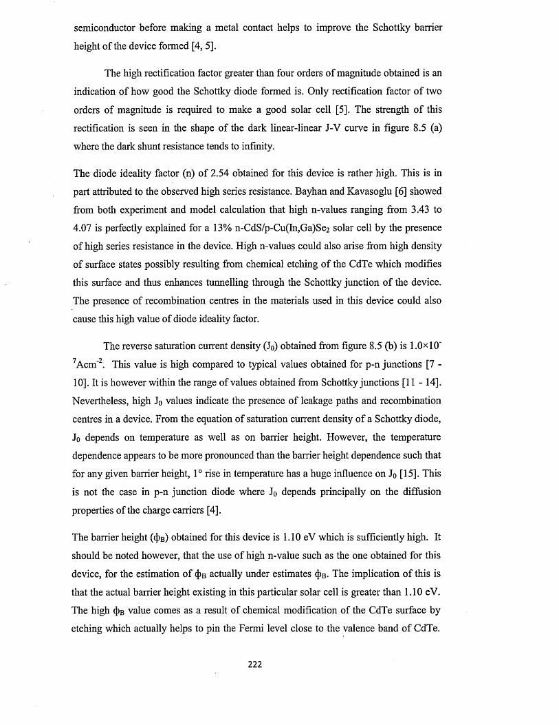
semiconductor before making a metal contact helps to improve the Schottky barrier
height o f the device formed [4, 5].
The high rectification factor greater than four orders of magnitude obtained is an
indication o f how good the Schottky diode formed is. Only rectification factor o f two
orders of magnitude is required to make a good solar cell [5]. The strength o f this
rectification is seen in the shape o f the dark linear-linear J-V curve in figure 8.5 (a)
where the dark shunt resistance tends to infinity.
The diode ideality factor (n) o f 2.54 obtained for this device is rather high. This is in
part attributed to the observed high series resistance. Bayhan and Kavasoglu [6] showed
from both experiment and model calculation that high n-values ranging from 3.43 to
4.07 is perfectly explained for a 13% n-CdS/p-Cu(In,Ga)Se2 solar cell by the presence
of high series resistance in the device. High n-values could also arise from high density
of surface states possibly resulting from chemical etching o f the CdTe which modifies
this surface and thus enhances tunnelling through the Schottky junction of the device.
The presence of recombination centres in the materials used in this device could also
cause this high value of diode ideality factor.
The reverse saturation current density (Jo) obtained from figure 8.5 (b) is 1.0x10'
?Acm'2. This value is high compared to typical values obtained for p-n junctions [7 -
10]. It is however within the range of values obtained from Schottky junctions [11 - 14].
Nevertheless, high Jo values indicate the presence of leakage paths and recombination
centres in a device. From the equation of saturation current density o f a Schottky diode,
Jo depends on temperature as well as on barrier height. However, the temperature
dependence appears to be more pronounced than the barrier height dependence such that
for any given barrier height, 1° rise in temperature has a huge influence on Jo [15]. This
is not the case in p-n junction diode where Jo depends principally on the diffusion
properties of the charge carriers [4].
The barrier height (4>b ) obtained for this device is 1.10 eV which is sufficiently high. It
should be noted however, that the use o f high n-value such as the one obtained for this
device, for the estimation o f $ b actually under estimates <])b . The implication o f this is
that the actual barrier height existing in this particular solar cell is greater than 1.10 eV.
The high (])b value comes as a result of chemical modification of the CdTe surface by
etching which actually helps to pin the Fermi level close to the valence band o f CdTe.
222
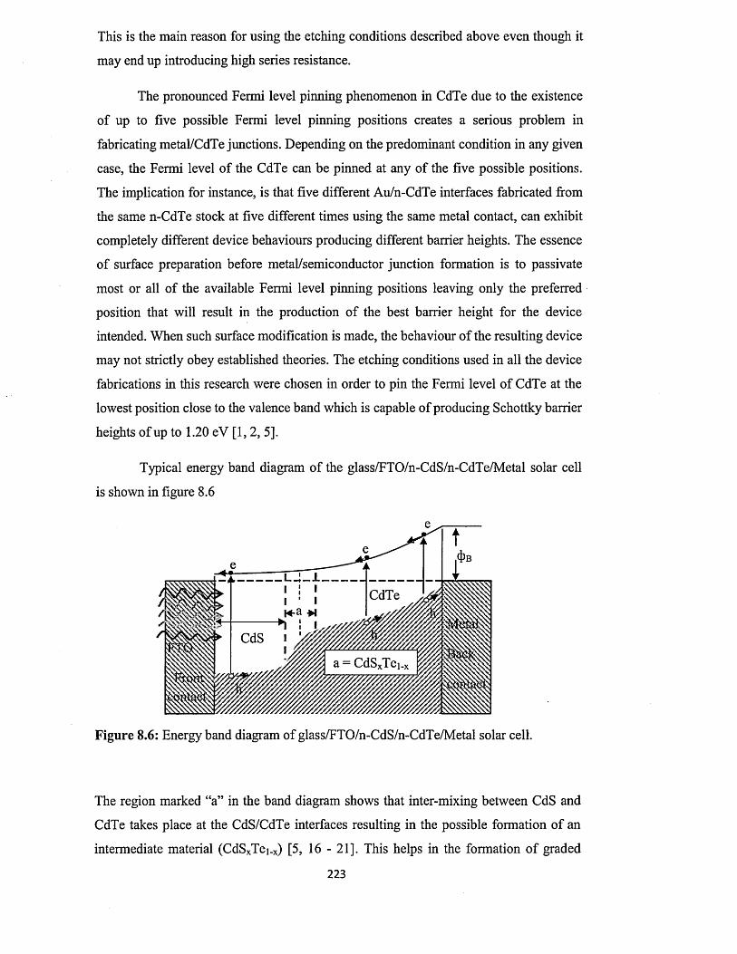
This is the main reason for using the etching conditions described above even though it
may end up introducing high series resistance.
The pronounced Fermi level pinning phenomenon in CdTe due to the existence
of up to five possible Fermi level pinning positions creates a serious problem in
fabricating metal/CdTe junctions. Depending on the predominant condition in any given
case, the Fermi level of the CdTe can be pinned at any of the five possible positions.
The implication for instance, is that five different Au/n-CdTe interfaces fabricated from
the same n-CdTe stock at five different times using the same metal contact, can exhibit
completely different device behaviours producing different barrier heights. The essence
o f surface preparation before metal/semiconductor junction formation is to passivate
most or all o f the available Fermi level pinning positions leaving only the preferred
position that will result in the production o f the best barrier height for the device
intended. When such surface modification is made, the behaviour o f the resulting device
may not strictly obey established theories. The etching conditions used in all the device
fabrications in this research were chosen in order to pin the Fermi level of CdTe at the
lowest position close to the valence band which is capable of producing Schottky barrier
heights o f up to 1.20 eV [1, 2, 5].
Typical energy band diagram of the glass/FTO/n-CdS/n-CdTe/Metal solar cell
is shown in figure 8.6
Figure 8.6: Energy band diagram of glass/FTO/n-CdS/n-CdTe/Metal solar cell.
The region marked “a” in the band diagram shows that inter-mixing between CdS and
CdTe takes place at the CdS/CdTe interfaces resulting in the possible formation o f an
intermediate material (CdSxTei_x) [5, 16 - 21]. This helps in the formation o f graded

bandgap across the entire device. This situation is encouraged by the post-deposition
CdCl2 or CdCl2+CdF2 heat treatment o f the CdS/CdTe bi-layer during device
processing. As a result, the CdS/CdTe junction is not an abrupt junction but a graded
one with the bandgap gradually varying from 2.42 eV (bandgap o f CdS) to 1.45 eV
(bandgap of CdTe). This bandgap grading helps in the absorption o f photons from
different regions o f the solar spectrum at different regions of the bandgap. This helps to
reduce thermalisation effect in the device [5, 22 - 26]. In a solar cell, incident photons
interact with the covalent bonds in the solar cell materials to break the bonds and release
electron-hole (e-h) pairs which results in the generation of electricity when these photo
generated charge carriers are collected to an external circuit. However, not all incident
photons can break the bonds and create e-h pairs. In principle, only photons with energy
(hv) equal to or greater than the energy bandgap of the solar cell materials can create
such e-h pairs. When the energy of the incident photon is very much higher than the
energy bandgap o f the solar cell material, the excess energy of this photon is transferred
to the crystal lattice o f the solar cell material and causes heating effect in the lattice of
the material. In addition, the photo-generated charge carriers created by these high-
energy photons quickly lose their extra energy (in excess of the bandgap energy) to the
lattice of the semiconductor material in order to return to thermal equilibrium with the
semiconductor. This results in increased lattice vibrations (phonons). Subsequently, this
causes increased scattering of the photo-generated charge carriers and results in losses
in the photo-generated current. This phenomenon is called thermalisation and the
associated loss is called thermalisation loss [27 - 30]. This effect is more pronounced in
single junction solar cells with low energy bandgap absorber materials. This can as well
damage the solar cells due to the heat produced in the process. With bandgap grading,
the burden of absorption of high-energy photons is shared across the entire bandgap of
the solar cell. Apart from reducing thermalisation effect, the graded bandgap structure
helps in the effective collection and acceleration of photo-generated charge carriers
towards the metal contacts by providing gradually varying electric field across the
device length. It can therefore result in increased current output of the solar cell since
current is not only a function of the number o f charge carriers involved but also a
function of the mobility; rate at which these charge carriers are transported from one
point to another under an applied electric field.
The device structure shown in figure 8.6 is therefore a combination of n-n
hetero-junction and a large Schottky barrier resulting in the enhancement of the slope o f
224
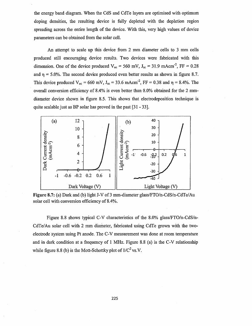
the energy band diagram. When the CdS and CdTe layers are optimised with optimum
doping densities, the resulting device is fully depleted with the depletion region
spreading across the entire length of the device. With this, very high values of device
parameters can be obtained from the solar cell.
An attempt to scale up this device from 2 mm diameter cells to 3 mm cells
produced still encouraging device results. Two devices were fabricated with this
dimension. One of the device produced Voc = 560 mV, Jsc = 31.9 mAcm'2, FF = 0.28
and rj = 5.0%. The second device produced even better results as shown in figure 8.7.
This device produced Voc = 660 mV, Jsc = 33.6 mAcm'2, FF = 0.38 and r) = 8.4%. The
overall conversion efficiency o f 8.4% is even better than 8.0% obtained for the 2 mm-
diameter device shown in figure 8.5. This shows that electrodeposition technique is
quite scalable just as BP solar has proved in the past [31 - 33].
40
0.2
-20 - /-30 /
" ^ 4 0 -
Light Voltage (V)Dark Voltage (V)
Figure 8.7: (a) Dark and (b) light J-V of 3 mm-diameter glass/FTO/n-CdS/n-CdTe/Au solar cell with conversion efficiency of 8.4%.
Figure 8.8 shows typical C-V characteristics of the 8.0% glass/FTO/n-CdS/n-
CdTe/Au solar cell with 2 mm diameter, fabricated using CdTe grown with the two-
electrode system using Pt anode. The C-V measurement was done at room temperature
and in dark condition at a frequency of 1 MHz. Figure 8.8 (a) is the C-V relationship
while figure 8.8 (b) is the Mott-Schottky plot o f 1/C2 vs.V.
225
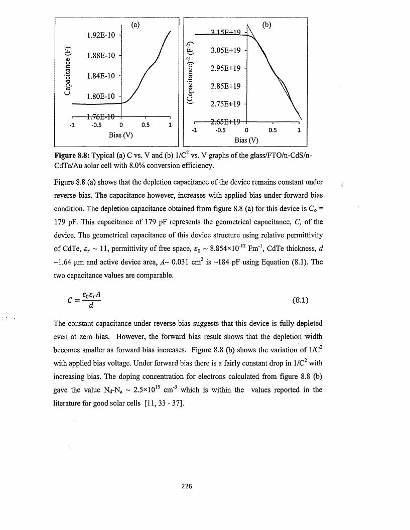
1.92E-10 -
3.05E+19 -1.88E-10 -
2.95E+19 -1.84E-10 -
2.85E+19 -a,
1.80E-10 -2.75E+19 -
H76E-4fr-0.5 10.5
0.5Bias (V)
Bias (V)
Figure 8.8: Typical (a) C vs. V and (b) 1/C vs. V graphs of the glass/FTO/n-CdS/n- CdTe/Au solar cell with 8.0% conversion efficiency.
Figure 8.8 (a) shows that the depletion capacitance o f the device remains constant under
reverse bias. The capacitance however, increases with applied bias under forward bias
condition. The depletion capacitance obtained from figure 8.8 (a) for this device is C0 =
179 pF. This capacitance of 179 pF represents the geometrical capacitance, C, o f the
device. The geometrical capacitance of this device structure using relative permittivity
of CdTe, sr - 11, permittivity of free space, £ 0 ~ 8.854xl0'12 Fm '1, CdTe thickness, d
-1.64 pm and active device area, A~ 0.031 cm2 is -184 pF using Equation (8.1). The
two capacitance values are comparable.
C =£0£rA
(8.1)
The constant capacitance under reverse bias suggests that this device is fully depleted
even at zero bias. However, the forward bias result shows that the depletion width
becomes smaller as forward bias increases. Figure 8.8 (b) shows the variation o f 1/C2
with applied bias voltage. Under forward bias there is a fairly constant drop in 1/C2 with
increasing bias. The doping concentration for electrons calculated from figure 8.8 (b)
gave the value Nd-Na - 2.5* 1015 cm-3 which is within the values reported in the
literature for good solar cells [11 ,33-37].
22 6
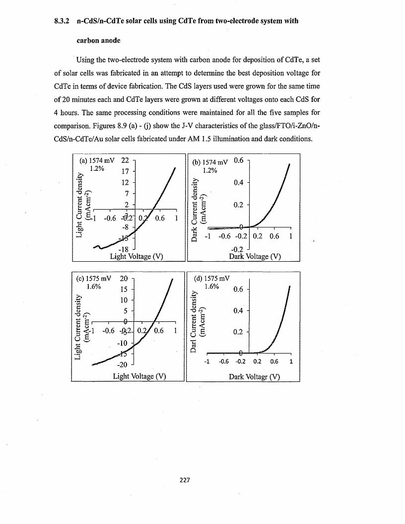
8.3.2 n-CdS/n-CdTe solar cells using CdTe from two-electrode system with
carbon anode
Using the two-electrode system with carbon anode for deposition of CdTe, a set
o f solar cells was fabricated in an attempt to determine the best deposition voltage for
CdTe in terms o f device fabrication. The CdS layers used were grown for the same time
o f 20 minutes each and CdTe layers were grown at different voltages onto each CdS for
4 hours. The same processing conditions were maintained for all the five samples for
comparison. Figures 8.9 (a) - (j) show the J-V characteristics of the glass/FTO/i-ZnO/n-
CdS/n-CdTe/Au solar cells fabricated under AM 1.5 illumination and dark conditions.
(b) 1574 mV °-6 1.2%
£ 0.4
(a) 1574 mV 22 -j 1.2% 17 -
T3T3
0.2
-18 J Light Voltage (V)
-0 .2 JDark Voltage (V)
(c) 1575 mV 20 -| 1.6% .
(d) 1575 mV 1.6% a 6
0.4
0.6 0.2-10 :
0.6-20 J Light Voltage (V) Dark Voltagr (V)
227

(e) 1576 mV „ 3.0%
* 22 'g 1 2 - 0>1=* n 2 -
(f) 1576 mV 2 -1
3.0%£ L5 ' c<L> _ .T3 1 -c S<u 0
1 1 0 . 5 -O vS
A
C c 1 < T
| | - 1 - 0 . 6 -Ifc2 - O &£ -1 8 ^3 ------ -28 J
Lights
1 y i 1
0 . 2 / 0 . 6 1
/oltage (V)
^ f--------------j--------- ------------ T..- "T----------- --\
Q - 1 -0 . 6 -0 . 2 0 . 2 0 . 6 1
Dark Voltage (V)
(g) 1577 mV 6 0 - 4.5%
40 -
(h) 1577 mV 4.5%
-20 -
-40 J Light Voltage (V) Dark Voltage (V)
(i) 1578 mV 7 5 - . 4.5%
§ < 5 £ — 1-------------- 1
0.6 1-25 -
-45 J Light Voltage (V) Dark Voltage (V)
Figure 8.9: (a) - (j) Light and dark J-V characteristics of glass/FTO/i-ZnO/n-CdS/n- CdTe/Au solar cells fabricated with CdTe grown at different cathodic voltages from two-electrode system with carbon anode.
The summary of the device parameters obtained for these devices are presented in Table
8.5 and figures 8.10 (a) - (e).
22 8
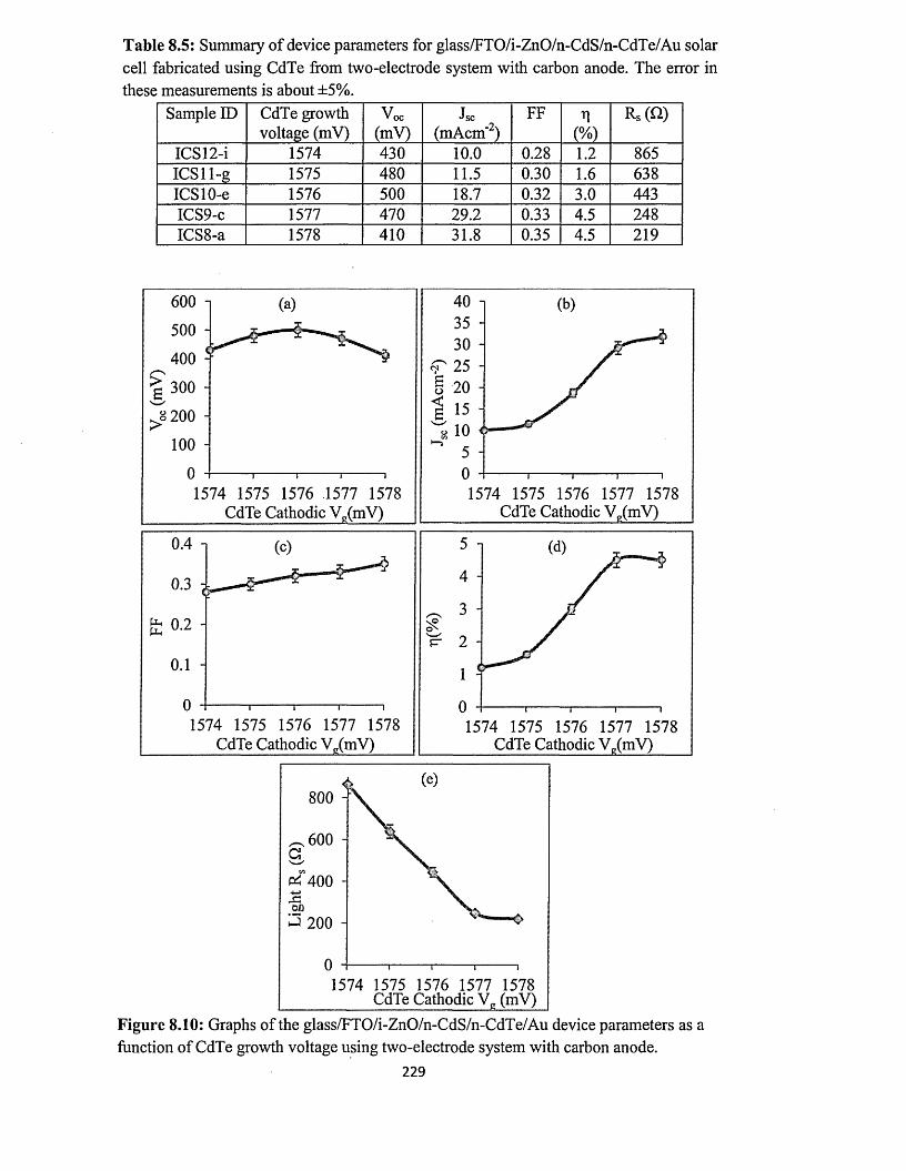
Table 8.5: Summary of device parameters for glass/FTO/i-ZnO/n-CdS/n-CdTe/Au solar cell fabricated using CdTe from two-electrode system with carbon anode. The error in these measurements is about ±5%.
Sample ID CdTe growth voltage (mV)
Voc(mV)
Jsc(mAcm'2)
FF h(%)
Rs(fJ)
ICS12-i 1574 430 10.0 0.28 1.2 865IC S ll-g 1575 480 11.5 0.30 1.6 638ICSlO-e 1576 500 18.7 0.32 3.0 443ICS9-c 1577 470 29.2 0.33 4.5 248ICS8-a 1578 410 31.8 0.35 4.5 219
600 n 40 i
500 -
400 i 25 -I 20 -300 -
200 -
100 -
1574 1575 1576 1577 1578 CdTe Cathodic Vg(mV)
1574 1575 1576 1577 1578 CdTe Cathodic Vg(mV)
0.4 i 5
40.3 A3
2
1
01574 1575 1576 1577 1578
CdTe Cathodic Vg(mV)1574 1575 1576 1577 1578
CdTe Cathodic Vg(mV)
800 -
600 -
W)J 200 -
1574 1575 1576 1577 1578 CdTe Cathodic Vg (mV)
Figure 8.10: Graphs of the glass/FTO/i-ZnO/n-CdS/n-CdTe/Au device parameters as a function of CdTe growth voltage using two-electrode system with carbon anode.
229
A close observation of figure 8.9, figure 8.10 and Table 8.5 shows there is a
clear trend in the performance of the devices with respect to the CdTe growth voltage.
The overall efficiency o f the devices increases as the CdTe growth voltage increases.
The short-circuit current density and fill factor values also increase as the CdTe growth
voltage increases. There is however, inconsistency in the Voc values but the series
resistance values obtained from the light J-V curves show a consistent decrease as CdTe
growth voltage increases.
The implication of this consistency in the device parameters show that better solar cells
are obtained using Cd-rich CdTe which are obtained at relatively higher cathodic
growth voltages. The series resistances of these devices under illumination are very high
and are attributed to the additional resistance of the i-ZnO layer used. The results show
generally that the best cathodic growth voltage for CdTe using this electrode
configuration is between 1577 mV and 1578 mV.
8.3.3 n-CdS/n-CdTe solar cells using CdTe from three-electrode system with
carbon anode
In this experiment, two different sets o f solar cells were fabricated using CdTe
grown from the three-electrode system with carbon anode. The deposition voltages of
CdTe were taken in the cathodic voltage range (697-700) mV since the best cathodic
growth voltage established from XRD results was 697 mV and since Cd-rich CdTe
obtained from higher cathodic voltages produce better solar cells as seen from the
previous section. In the end the best solar cells obtained with this system also came with
CdTe grown at the cathodic voltage of 697 mV. One set of the devices had the structure
o f glass/FTO/n-CdS/n-CdTe/Au and the other set had the structure o f glass/FTO/i-
ZnO/ri-CdS/n-CdT e/Au.
Tables 8.6 and 8.7 show the summaries of the parameters obtained for these two
sets of devices. The results in the two tables show that CdTe grown at 700 mV in some
cases produced solar cells with impressive Jsc values. However, in terms of the best Voc,
FF and ri values, the best CdTe cathodic growth voltage was 697 mV.
23 0
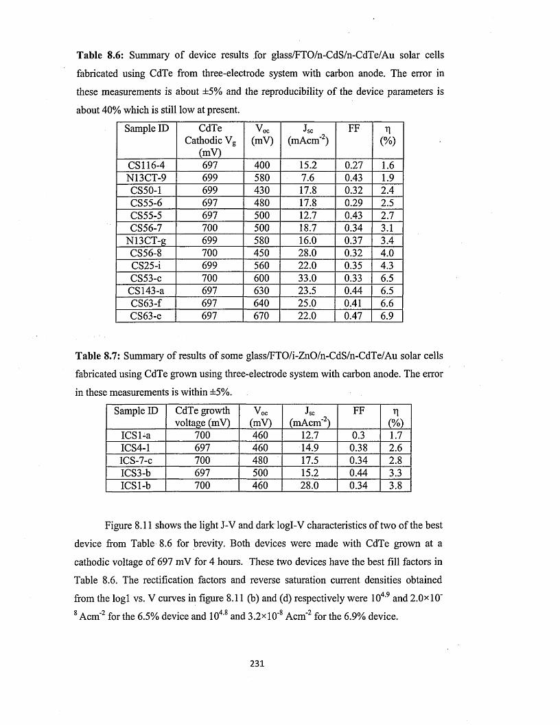
Table 8.6: Summary of device results for glass/FTO/n-CdS/n-CdTe/Au solar cells
fabricated using CdTe from three-electrode system with carbon anode. The error in
these measurements is about ±5% and the reproducibility o f the device parameters is
about 40% which is still low at present.
Sample ID CdTe Cathodic Vg
(mV)
Voc(mV)
Jsc(mAcm*2)
FF(%)
CS116-4 697 400 15.2 0.27 1.6N13CT-9 699 580 7.6 0.43 1.9CS50-1 699 430 17.8 0.32 2.4CS55-6 697 480 17.8 0.29 2.5CS55-5 697 500 12.7 0.43 2.7CS56-7 700 500 18.7 0.34 3.1
N13CT-g 699 580 16.0 0.37 3.4CS56-8 700 450 28.0 0.32 4.0CS25-i 699 560 22.0 0.35 4.3CS53-c 700 600 33.0 0.33 6.5
CS143-a 697 630 23.5 0.44 6.5CS63-f 697 640 25.0 0.41 6.6CS63-e 697 670 22.0 0.47 6.9
Table 8.7: Summary of results of some glass/FTO/i-ZnO/n-CdS/n-CdTe/Au solar cells
fabricated using CdTe grown using three-electrode system with carbon anode. The error
in these measurements is within ±5%.
Sample ID CdTe growth voltage (mV)
V o c
(mV)Jsc
(mAcm*2)FF
(%)ICSl-a 700 460 12.7 0.3 1.7ICS4-1 697 460 14.9 0.38 2.6ICS-7-c 700 480 17.5 0.34 2.8ICS3-b 697 500 15.2 0.44 3.3ICSl-b 700 460 28.0 0.34 3.8
Figure 8.11 shows the light J-V and dark logl-V characteristics of two of the best
device from Table 8.6 for brevity. Both devices were made with CdTe grown at a
cathodic voltage of 697 mV for 4 hours. These two devices have the best fill factors in
Table 8.6. The rectification factors and reverse saturation current densities obtained
from the logl vs. V curves in figure 8.11 (b) and (d) respectively were 104'9 and 2.0x10*
8 Acm"2 for the 6.5% device and 104'8 and 3.2xl0"8 Acm'2 for the 6.9% device.
231
(a) CS143-a 40 - 6.5%
30 -
•3 20 - c<D _■OfT 10 -is s<D oc <C ' 1 ......o' S -1 -0.6 -0.2 -a -10 -bX)
3 -20 -
~ " ^ ^ 3 0 -
Light Vc
i $ *0.2 y.6 1
J )
)ltage (V)
(c) CS63-e 30 -i £> 6.9%8 20 -
c S io -<u o AUB <
, ot _, i i u
•§> -1 -0.6 -0.2 -10 -
-20 .;
-30 -
Light Volte
.... i i / ......i0.2 o k 1
ige(V)
0.2 0.4 0.6 0.8
(b) CS143-a 6.5%
-10 J
Dark Voltage (V)
0.2 0.4 0.6 0.8
(d) CS63-e 6.9%
-10 J
Dark Voltage (V)
Figure 8.11: Current-voltage characteristics of two best solar cells fabricated using
CdTe grown at a cathodic voltage o f 697 mV from the three-electrode system with
carbon anode ((a) and (c)) under illumination and ((b) and (d)) under dark conditions.
8.4 C haracterisation of n-ZnS/n-CdTe solar cells
In this section glass/FTO/n-ZnS/n-CdTe/Au solar cells were fabricated. As
mentioned earlier, the aim of using ZnS as a window layer instead o f CdS is to see if it
is possible to replace CdS with ZnS in CdTe-based solar cells and by extension to other
solar cell structures using CdS as a window material such as CIGS. There are two major
reasons for this targeted replacement. First is that ZnS has higher energy bandgap than
CdS and therefore can give rise to solar cells with improved short-circuit current
densities. Second is that ZnS is non-toxic, containing no Cd and therefore will bring
about a reduction in Cd-containing toxic waste generated during the CdS deposition
process especially using wet chemistry routes.
232

Different sets o f glass/FTO/n-ZnS/n-CdTe/Au solar cells were fabricated using
CdTe from the three different electrode configurations namely two-electrode with
carbon anode, two-electrode with platinum anode and three-electrode with carbon
anode. Table 8.8 summarises the device results o f the solar cells made using these three
electrode systems.
Table 8.8: Summary o f glass/FTO/n-ZnS/n-CdTe/Au solar cells fabricated using CdTe from both two-electrode and three-electrode systems. The error in these measurements is about ±5% with reproducibility o f about 40% for the device parameters.
SampleID
V o c
(mV)Jsc
(mAcm*2)FF *1
(%)CdTe electrode system
K207-k 400 6.3 0.25 0.6 3-electrode with carbon anodeK243 260 12.0 0.25 0.8 3-electrode with carbon anodeK265 280 22.9 0.27 1.7 3-electrode with carbon anodeK262 500 11.4 0.48 2.7 3-electrode with carbon anode
K317-C 390 19.7 0.36 2.8 2-electrode with carbon anodeK321-a 500 21.8 0.40 4.4 2-electrode with carbon anode
K326-b 620 22.5 0.38 5.3 2-electrode with Pt anodeK326-2 646 47.8 0.39 12.0 2-electrode w ith P t anode
The results in Table '8.8 clearly show that the best two devices came from those
involving CdTe grown using two-electrode system with Pt anode. Figure 8.12 shows the
J-V characteristics of some of these devices each representing a particular electrode
system. The overall best glass/FTO/n-ZnS/n-CdTe/Au device fabricated in this research
produced a conversion efficiency o f 12.0%. This is the best solar cell produced in this
research in terms of the overall conversion efficiency. It also produced the highest
short-circuit current density among all other devices fabricated. The success in
fabricating this particular solar cell demonstrates the possibility of replacing CdS with
ZnS in all the solar cells where CdS is involved as a window material.
233
(e) K321-a 4.4 % 4
c 2-E with C anode(c) K321-a
^ 4.4% 202-E with C anode
-10 -
-20 -
0.6-30 J Light Voltage (V) Dark Voltage (V)
(f) K326-2 12.0% 40 ‘
£ 2-E with Pt anode < 20 -£'w/'
,n
(g) K326-2 60 " cjT' 12% - Q
| 2-E with Pt anode
1 40 ■
t 3 0 - c<D
20 -c<ug 10 - o r\
1
i i iUg -1 -0.6 -0.2T3* -20 -<D
5 -40 -
23 -60
Light Volt
1 i k *
0 . 2 m i
age (V)
Q -1 -0.6 -0.2 0.2 0.6 1
Darv Voltage (V)
Figure 8.12: Ligth and dark J-V curves o f some glass/FTO/n-ZnS/n-CdTe/Au solar cells.
Figures 8.13 (a) and (b) show the graph of logl vs. V for this particular device
and the typical energy band diagram for glass/FTO/n-ZnS/n-CdTe/Au solar cell
respectively.23 4
K326-2, n y 2-E with Bf anode
H b = ZnCdSxTei-x
Bias Voltage (V)
Figure 8.13: (a) LogI vs. V of the 12.0% glass/FTO/n-ZnS/n-CdTe/Au solar cell and
(b) Typical energy band diagram for glass/FTO/n-ZnS/n-CdTe/Metal solar cell.
The region marked “b” in figure 8.13 (b) shows the result of inter-diffusion of atoms at
the ZnS/CdTe interface producing an intermediate material, ZnCdxTei.x. This
intermixing, as in the case of CdS/CdTe devices, is enhanced by the annealing process
after the CdCl2+CdF2 treatment of the top CdTe layer [5, 16-21] . The presence of this
intermediate material serves to facilitate band gap grading and minimising any lattice
mismatch between ZnS and CdTe. Just like in the case of CdS/CdTe devices discussed
previously, the bandgap of the resulting ZnS/CdTe structure is effectively graded from
the bandgap of ZnS (Eg = 3.70 eV) to the bandgap of CdTe (Eg = 1.45 eV). This will
result in a relatively continuous slope in the bandgap which helps to minimise
thermalisation and facilitate acceleration o f photo-generated charge carriers towards the
metal contacts giving rise to improvement in short-circuit current density from the solar
cell. Again the use of ZnS window material helps to allow higher energy photons into
the CdTe absorber layer for generation of more electron-hole pairs compared to when
CdS is used as a window material. These advantages have actually come into play in
this particular device which produced the highest short-circuit current density among all
solar cell structures fabricated in this research project.
The series resistance obtained for this device from figure 8.12 (f) under
illumination was 112 Q and that from figure 8.12 (g) under dark condition was 126 Q.
The relatively reduced series resistance of this device compared to that o f the 8.0%
CdS/CdTe solar cell is attributed to the formation of relatively thinner oxide layer on
the CdTe layer as a result of chemical etching as has been explained earlier in the case
235
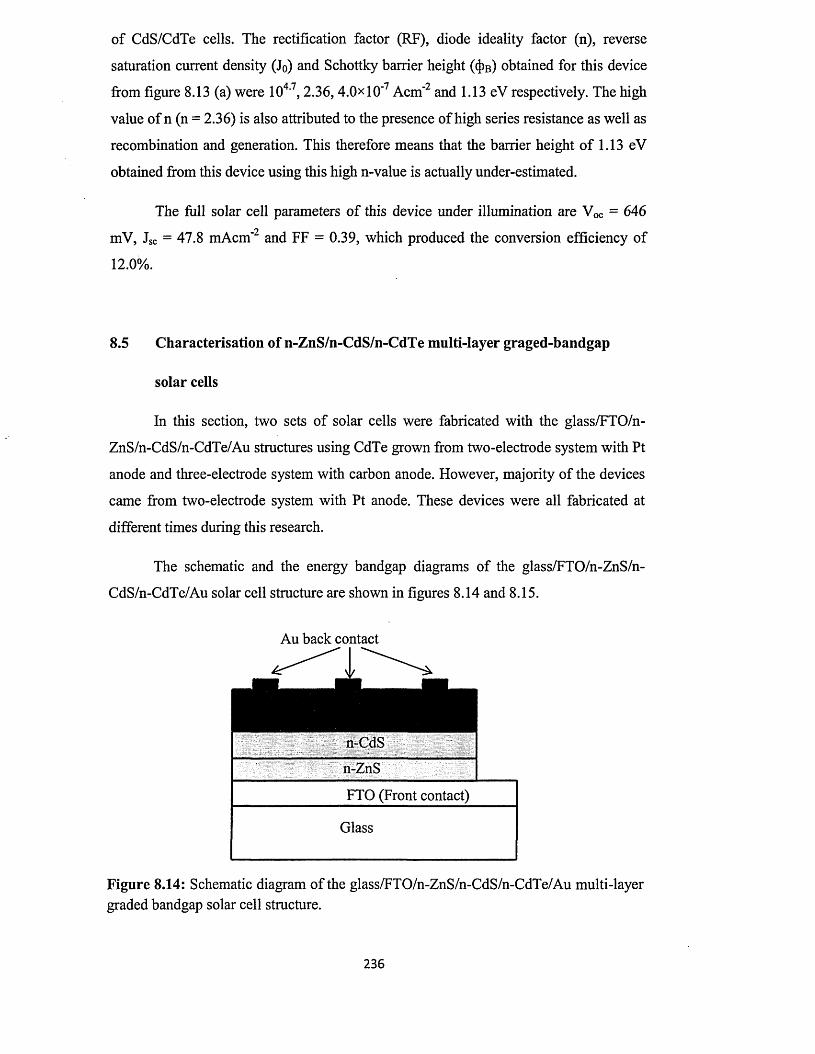
of CdS/CdTe cells. The rectification factor (RF), diode ideality factor (n), reverse
saturation current density (Jo) and Schottky barrier height (4>b ) obtained for this device
from figure 8.13 (a) were 104'7, 2.36,4.0x1 O'7 Acm'2 and 1.13 eV respectively. The high
value o f n (n = 2.36) is also attributed to the presence of high series resistance as well as
recombination and generation. This therefore means that the barrier height o f 1.13 eV
obtained from this device using this high n-value is actually under-estimated.
The full solar cell parameters o f this device under illumination are Voc = 646
mV, Jsc = 47.8 mAcm'2 and FF = 0.39, which produced the conversion efficiency of
12.0%.
8.5 Characterisation of n-ZnS/n-CdS/n-CdTe multi-layer graged-bandgap
solar cells
In this section, two sets o f solar cells were fabricated with the glass/FTO/n-
ZnS/n-CdS/n-CdTe/Au structures using CdTe grown from two-electrode system with Pt
anode and three-electrode system with carbon anode. However, majority of the devices
came from two-electrode system with Pt anode. These devices were all fabricated at
different times during this research.
The schematic and the energy bandgap diagrams of the glass/FTO/n-ZnS/n-
CdS/n-CdTe/Au solar cell structure are shown in figures 8.14 and 8.15.
Au back contact
- v
n-CdS
n-ZnS____________
FTO (Front contact)
Glass
Figure 8.14: Schematic diagram of the glass/FTO/n-ZnS/n-CdS/n-CdTe/Au multi-layer graded bandgap solar cell structure.
23 6
One way of reducing or preventing the loss o f photo-generated current and
prevent damage due to thermalisation effect in a solar cell, as mentioned earlier, is to
grade the bandgap of the solar cell so that photons of varying energies can be absorbed
at different regions o f the solar cell [22 - 26, 38 - 40]. In this way high-energy photons
are absorbed by wider bandgap regions of the solar cell and lower energy photons
absorbed by narrower bandgap regions of the solar cell.
# x l-X
Figure 8.15: Typical energy band diagram of glass/FTO/n-ZnS/n-CdS/n-CdTe/Au multi-layer graded-bandgap solar cell.
Electron-hole pairs are therefore created in different regions of the cell without
heating up of the crystal lattice. One of the ways o f bringing about grading in the
bandgap of the solar cell is to use different semiconductor materials with different
bandgaps and arranging them in such a way that the resultant energy bandgap o f the
solar cell is graded in a descending order from the window material to the main
absorber material. This type of device therefore is a multi-layer graded bandgap device.
Another way of achieving bandgap grading is by gradually changing the composition of
the solar cell material during the growth process. This method however holds only for
materials whose bandgaps change with change in composition such as in AlGaAs/GaAs
solar cell where the bandgap o f GaAs increases as the A1 content increases [25, 26, 38 -
40].
In the graded bandgap solar cells fabricated in this research, the multi-layer
graded bandgap approach was used in which the wider bandgap material used was ZnS
and the narrow bandgap absorber material was CdTe. The intermediate bandgap
material used was CdS. Figure 8.14 shows the schematic o f this device structure while
237
figure 8.15 shows the energy bandgap diagram. During the post-deposition heat
treatment, inter-diffusion o f atoms o f the various constituent materials takes place at the
interfaces. This facilitates the formation o f intermediate materials at these interfaces. In
the ZnS/CdS and CdS/CdTe interfaces, materials such as ZnxCdi.xS and CdSxTei.x are
possibly formed respectively. This further helps the bandgap grading as well as
minimises possible lattice mismatch and therefore surface states at these interfaces.
With this kind of device structure, impurity photovoltaic effect and impact ionisation
can combine in one device and help in the possible creation o f more than one e-h pairs
by one photon, hence resulting in increased short-circuit current density. Impurity
photovoltaic effect takes place through existing impurity or defect levels in the bandgap
of the solar cell. In this situation, heat energy from the surrounding and infrared
radiation, from the sun can promote electrons from the valence band to an impurity
level. Now because of the shape o f the bandgap, the accompanying hole is quickly taken
towards the back contact as in figure 8.15. The electron promoted to the impurity level
in the bandgap has little or no chance of recombining again with the accompanying
hole. Electron accelerating from a higher energy level towards the front contact can
knock out this “suspended” electron from the impurity level towards the front contact in
a form of impact ionisation. The result is that one photon can effectively create two e-h
pairs and eventually resulting in increase in Jsc. The shape of the graded bandgap helps
in effective collection of all photo-generated e-h pairs without allowing room for
recombination. All these advantages o f course will become evident only in optimised
device structure.
In figures 8.14 and 8.15, one can also look at the device structure as a CdS/CdTe
solar cell with ZnS as a buffer layer. Buffer layers can be used in this way especially
when very thin CdS window layer is used in order to minimise window absorption loss.
In this case the thin CdS layer may not be able to cover the FTO surface properly thus
resulting is shunting effect between FTO and CdTe. To prevent this shunting effect
which results in loss o f fill factor and V0c, a wide bandgap buffer layer is used. The use
of buffer layers such as ZnO [17], aluminium-doped ZnO (Al- ZnO) [35], Sn02 [18],
and zinc stannate (ZTO) [41] have been reported in the literature. This has resulted to
improved FF and Voc but at the same time has led to reduced Jsc due to the relatively
high resistivity of these buffer layers. In the present work, ZnS with relatively lower
resistivity than the above mentioned buffer layers, has been used. This has also resulted
in improved Jsc as well as FF and Voc compared to simple CdS/CdTe device, for the best
2 3 8
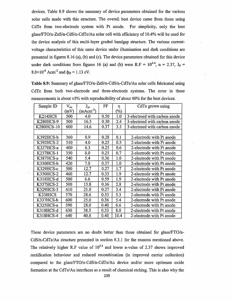
devices. Table 8 . 9 shows the summary o f device parameters obtained for the various
solar cells made with this structure. The overall best device came from those using
CdTe from two-electrode system with Pt anode. For simplicity, only the best
glass/FTO/n-ZnS/n-CdS/n-CdTe/Au solar cell with efficiency of 1 0 . 4 % will be used for
the device analysis of this multi-layer graded bandgap structure. The various current-
voltage characteristics o f this same device under illumination and dark conditions are
presented in figures 8 . 1 6 (a), (b) and (c). The device parameters obtained for this device
under dark conditions from figures 1 6 (a) and (b) were R.F = 1 0 4 '4, n = 2 . 3 7 , Jo =
8 .0 > < 1 0 * 8 Acm'2 and 4>b = 1 .1 3 eV.
Table 8.9: Summary of glass/FTO/n-ZnS/n-CdS/n-CdTe/Au solar cells fabricated using
CdTe from both two-electrode and three-electrode systems. The error in these
measurements is about ±5% with reproducibility o f about 40% for the best devices.
Sample ID V o c
(mV)Jsc
(mAcm'2)FF T]
(%)CdTe grown using
K214HCS 500 4.0 0.50 1.0 3-electroed with carbon anodeK280HCS-9 500 16.5 0.30 2.4 3-electroed with carbon anode
K280HCS-10 600 14.6 0.37 3.3 3-electroed with carbon anode
K392HCS-b 360 0.9 0.28 0.1 2-electrode with Pt anodeK392HCS-2 510 4.0 0.25 0.5 2-electrode with Pt anodeK327HCS-a 400 6.3 0.25 0.6 2-electrode with Pt anodeK237HCS-1 350 8.0 0.25 0.7 2-electrode with Pt anodeK387HCS-a 540 5.4 0.36 1.0 2-electrode with Pt anodeK330HCS-b 420 7.0 0.37 1.0 2-electrode with Pt anodeK329HCS-C 500 12.7 0.27 1.7 2-electrode with Pt anodeK330HCS-2 460 12.7 0.33 1.9 2-electrode with Pt anodeK 318HCS-d 500 6.6 0.59 1.9 2-electrode with Pt anodeK337HCS-2 500 15.8 0.36 2.8 2-electrode with Pt anodeK329HCS-3 610 21.0 0.27 3.4 2-electrode with Pt anodeK338HCS 570 28.6 0.33 5.3 2-electrode with Pt anode
K337HCS-b 600 25.0 0.36 5.4 2-electrode with Pt anodeK325HCS-a 590 28.0 0.40 6.6 2-electrode with Pt anodeK318HCS-d 630 38.5 0.33 8.0 2-electrode with Pt anodeK318HCS-4 640 40.8 0.40 10.4 2-electrode with Pt anode
These device parameters are no doubt better than those obtained for glass/FTO/n-
CdS/n-CdTe/Au structure presented in section 8.3.1 for the reasons mentioned above.
The relatively higher R.F value of 104'4 and lower n-value of 2.37 shows improved
rectification behaviour and reduced recombination (ie improved carrier collection)
compared to the glass/FTO/n-CdS/n-CdTe/Au device and/or more optimum oxide
formation at the CdTe/Au interfaces as a result of chemical etching. This is also why the239
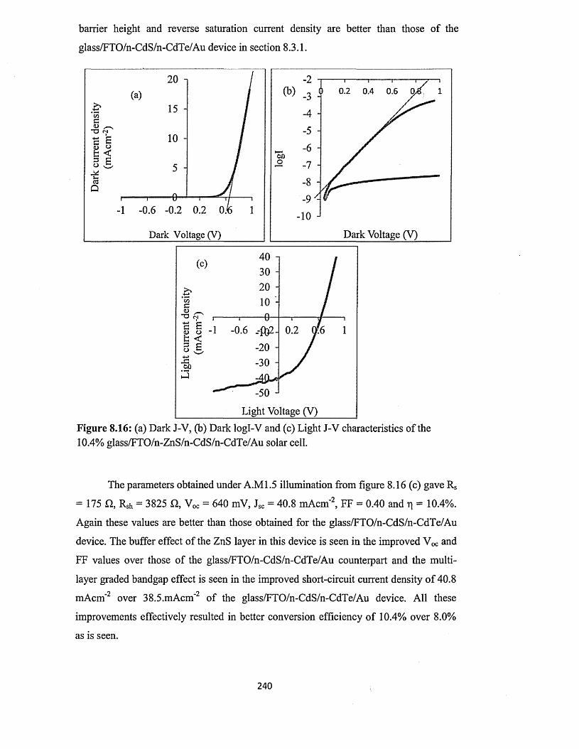
barrier height and reverse saturation current density are better than those of the
glass/FTO/n-CdS/n-CdTe/Au device in section 8.3.1.
20 i0.2 0.4 0.6
fa <
11 -10 J
Dark Voltage (V)Dark Voltage (V)
40 n
20 -
0.2u < -20 -
-30 -
-50 J
Light Voltage (V)
Figure 8.16: (a) Dark J-V, (b) Dark logl-V and (c) Light J-V characteristics of the 10.4% glass/FTO/n-ZnS/n-CdS/n-CdTe/Au solar cell.
The parameters obtained under A.M1.5 illumination from figure 8.16 (c) gave Rs
= 175 n, Rsh = 3825 £2, V„c = 640 mV, Jsc = 40.8 mAcm'2, FF = 0.40 and ri = 10.4%.
Again these values are better than those obtained for the glass/FTO/n-CdS/n-CdTe/Au
device. The buffer effect o f the ZnS layer in this device is seen in the improved Voc and
FF values over those o f the glass/FTO/n-CdS/n-CdTe/Au counterpart and the multi
layer graded bandgap effect is seen in the improved short-circuit current density o f 40.8
mAcm'2 over 38.5.mAcm'2 o f the glass/FTO/n-CdS/n-CdTe/Au device. All these
improvements effectively resulted in better conversion efficiency of 10.4% over 8.0%
as is seen.
2 4 0
It is important now to point out that the observed high short-circuit current
densities reported for the different devices reported in this thesis were remarkable and
not observed all the time. The reason for this is the instability problem associated with
these devices that makes them deteriorate after few months or even weeks. For this
reason, part o f the future work should be focused on reproducibility and improvement
of the stability o f these promising device structures. However, in order to ensure that the
observed high short-circuit current densities were genuine, the particular diodes
producing them were isolated by carefully removing the CdTe material around the Au
back contact and the measurements repeated.
Figure 8.17 (a) and (b) show the C vs. V and Mott-Schottky plots o f the solar
cell o f figure 8.16 under discussion. The C-V measurement was carried out at room
temperature and a frequency o f 1MHz with applied bias voltages from -1.0 V to +1.0 V.
Figure 8.17 (a) shows a gradual increase in the depletion capacitance as bias increases
from reverse to forward bias. The measured depletion capacitance at zero bias gave the
value C0 = 151 pF. This capacitance value suggests that this device has a reasonably
wide depletion region comparable to the device thickness.
1.65E-10 i
4.00E+19 -1.60E-10 -
3.00E+19 -1.55E-10 -
2.00E+19Cu
1.00E+191.45E-10 -
1 0.50.5Bias (V)Bias (V)
Figure 8.17: Typical (a) C vs. V and (b) 1/C2 vs. V graphs o f the glass/FTO/n-ZnS/n-
CdS/n-CdTe/Au multi-layer graded bandgap solar cell with 10.4% conversion
efficiency.
Figure 8.17, (b) shows the response of 1/C2 to applied reverse bias. As forward
bias increases, the drop in the value of 1/C2 is more rapid up to a forward bias o f 0.35
V. At forward bias voltages >0.35 V, 1/C2 remains fairly constant. The doping
concentration of electrons (Nd-Na) estimated from figure 8.17 (b) is approximately
2 4 1
8 .1 x l 0 14 cm3. This is a relatively moderate doping density supporting the presence of
wide depletion region in this device. The diffusion voltage of this device could not be
estimated since the slope line of the 1/C2 vs. V graph falls well outside the bias voltage
range within which the C-V measurement was made.
8.6 Optimisation of CdTe annealing conditions for solar cell fabrication
In this section, the choice of CdCl2 or CdCl2+CdF2 treatment prior to annealing
and the choice o f annealing temperature and annealing time after the best chemical
(CdCl2+CdF2) treatment were experimented. The decision to consider the use o f
CdCl2+CdF2 in addition to CdCl2 in this treatment came from the work o f Mazzumuto
et al [42] in which they maintained a flow o f Freon gas (CHF2CI) in their CSS chamber
during the post-deposition heat treatment o f CdS/CdTe as a form of CdCl2 treatment
and produced solar cells with efficiency close to 16.0% [42]. Also the choice of the
range o f annealing temperature and time came from the range reported in the literature
[31,37,43].
In order to choose between CdCl2 and CdCl2+CdF2 treatment, a set of five
glass/FTO/n-CdS/n-CdTe samples was used for this experiment. Each sample was
divided into two pieces. One set of these pieces was treated with CdCb and the other
treated with CdCl2+CdF2 . Both sets of treated samples were then annealed at the same
temperature of 450°C for 15 minutes and the device fabrication completed by
evaporation o f Au contacts on the CdTe surfaces after chemical etching. All the samples
were etched under similar conditions and the metallisation with gold done under similar
conditions as well.
Table 8.10 shows the summary of the device results obtained from this
experiment. The results show very clear difference in the device parameters obtained for
the two different treatments. All device parameters (Voc, Jsc, FF and rj) are clearly higher
for the devices with CdCl2+CdF2 treatment than those with only CdCl2 treatment. The
increase in Jsc for the CdCl2+CdF2-treated devices is massive and remarkable. It is
because of this result that CdCl2+CdF2 treatment was preferred to the conventional
CdCl2 treatment in this research.
242
Table 8.10: Results of comparative study of CdCk and CdCl2+CdF2 treatment for glass/FTO/n-CdS/n-CdTe/Au solar cell structure. The reproducibility o f these device parameters is about 40% with measurement error o f about ±5%.DeviceS/No
CdCb treatment CdCl2+CdF2 treatmentV o c
(mv)Jsc (mAcm'2) FF ft(% ) V o c
(mV)Jsc (mAcm-2) FF ft (%)
1 550 11.4 0.31 1.9 630 23.5 0.44 6.52 600 19.7 0.42 5.03 430 9.9 0.28 1 .1 610 23.9 0.42 5.84 500 16.8 0.37 3.1 500 19.1 0.45 4.25 380 1 0 . 1 0.25 0.9 620 38.2 0.33 8 . 0
In order to determine the best annealing temperature and annealing time after
CdCl2+CdF2 treatment, several samples corresponding to different solar cell structures
were used. Each sample was also divided into parts. Both parts were given the same
CdCl2+CdF2 treatment but each part was afterwards annealed at different temperatures
and annealing times
Tables 8.11 (a) - (e) show the device results of different device structures under
different annealing temperatures and times. From all the results, it is clear that annealing
at 450°C for 15 minutes always produced the best device results and especially
producing the highest Voc and Jsc values. The FF values are generally low under this
annealing condition. A close look at Tables 8.11 (a) and (b) show strikingly that at the
particular annealing temperature o f 360°C, the FF values are generally higher than
those obtained at other temperatures. This improved FF values however come at the
expense of Voc and Jsc.
Table 8.11 (a): Optimisation of annealing conditions using glass/FTO/n-CdS/n- CdTe/Au and glass/FTO/n-ZnS/n-CdS/n-CdTe/Au device structures. The reproducibility o f these device parameters is about 40% with measurement error of about ±5%.DeviceS/No
450°C, 15min 360°C, 20minV o c
(mv)Jsc (mAcm'2) FF ft(% ) V o c
(mV)Jsc (mAcm'2) FF ft(% )
1 510 24.2 0.30 3.7 500 7.6 0.60 2.32 600 30.5 0.34 6 . 2 440 6.3 0.52 1.43 610 24.8 0.43 6.5 490 1.9 0.50 0.5
4* 640 40.8 0.40 10.4 500 6 . 6 0.59 1.9*Device 4 is glass/FTO/n-ZnS/n-CdS/n-CdTe/Au structure.
243
Table 8.11 (b): Optimisation of annealing conditions using glass/FTO/n-CdS/n- CdTe/Au device structure. The reproducibility o f these device parameters is about 40% with measurement error o f about ±5%.DeviceS/No
450°C, 15min 360°C, 69minV o c
(mv)Jsc (mAcm'"1) FF T ! ( % ) V o c
(mV)Jsc (mAcm'7) FF T | ( % )
1 600 26.3 0.34 5.4 450 16.5 0.48 3.62 560 31.8 0.37 6 . 6 480 11.4 0.46 2.53 560 26.7 0.39 5.8 400 7.6 0.45 1.44 580 22.9 0.26 3.5 340 9.2 0.45 1.45 600 19.1 0.31 3.6 360 7.0 0.45 1 . 1
Table 8.11 (c): Optimisation o f annealing temperature and time using different device structures. The reproducibility o f these device parameters is about 40% with measurement error o f about ±5%.
DeviceS/No
450°C, 15min 380°C, 30minV o c
(mv)Jsc
(mAcm'2)FF T1
(%)V o c
(mV)Jsc
(mAcm'2)FF il
(%)1 * 500 1.9 0.28 0.3 350 0.45 0.26 0.04
2 ** 500 4.0 0.25 0.5 360 0.9 0.28 0 . 1
400 8 . 2 0.28 0.9 450 2 . 0 0.26 0 . 24 ** 350 4.5 0.26 0.4 300 1.7 0.25 0 . 1
is glass/FTO/n-Cc S/n-CdSe/n-CdTe/Au, ** is glass/Fr ’O/n-ZnS/n-CdS/n-CdT e/Au
*** is glass/FTO/n-CdSe/n-CdS/n-CdTe/Au.
Table 8.11 (d): Optimisation of CdTe annealing time at 450°C using
glass/FTO/n-CdS/n-CdTe/Au device structure with CdTe grown at different voltages. The reproducibility o f these device parameters is about 40% with measurement error o f about ±5%.
CdTecathodicgrowthvoltage(mV)
450°C, 15min 450°C, 20minV o c
(mv)Jsc
(mAcm'2)FF Tl
(%)V o c
(mV)Jsc
(mAcm'2)FF il
(%)
2036 410 11.4 0.25 1 . 2 350 8.9 0.25 0 . 8
2037 400 7.6 0.25 0 . 8 260 1 1 . 1 0.25 0.72038 440 7.6 0.25 0 . 8 360 8.9 0.25 0 . 8
2039 420 7.6 0.25 0 . 8 310 1 0 . 1 0.25 0 . 8
2040 ----- ------ 310 2.5 0.33 0.25
2041 380 9.5 0.25 0.9 350 6.3 0.25 0.552042
T------ 2 0 0 4.3 0.26 0 . 2 2
2 4 4
/■v
Table 8.11 (e): Optimisation of CdTe annealing conditions using
glass/FTO/n-ZnS/n-CdS/n-CdTe/Au device structure with CdTe grown at different voltages. The reproducibility of these device parameters is about 40% with measurement error o f about ±5%.
CdTecathodicgrowthVoltage
(mV)
400°C, 20min 450°C, 15minV o c
(mv)Jsc
(mAcm'2)FF i)
(%)V o c
(mV)Jsc
(mAcm'2)FF
(%)
2036 ----- -----2037 420 7.0 0.37 1 . 0 460 12.7 0.33 1.92038 500 12.7 0.27 1.7 610 2 1 . 0 0.27 3.42039 400 6.3 0.25 0 . 6 350 8 . 0 0.25 0.7
8.7 Comment on the possible reasons for the observation of high J sc values - - r t
Some o f the device results presented in this chapter showed very high Jsc values
which are rather remarkable. These levels of Jsc values are completely outside the range
o f values reported to date in the literature for CdTe-based solar cells. The main stream
CdTe-based solar cells reported in the literature are mostly p-n junction type structures
whereas the devices reported in this thesis are n-n+large Schottky barrier type
structures. These two device structures are different although there are few similarities.
The major similarities lie in the fact that the basic CdS/CdTe device structures in both
cases consist o f the same semiconductors namely; CdS and CdTe, irrespective o f the
conductivity type of CdTe. Again in both device structures, photo-generated electrons
move towards the TCO front contact (i.e towards the CdS side) while the photo
generated holes move towards the metal back contact (i.e towards the CdTe side).
Figure 8.18 shows the energy band diagrams of the p-n junction type and n-n+Schottky
junction type glass/TCO/CdS/CdTe/Metal solar cells for comparison.
The main differences in these two device structures are as follows:
(i) Conductivity type of the CdTe layer
This is the fundamental difference between these two device structures in figure 8.18.
Whereas p-CdTe is used in figure 8.18 (a), n-CdTe is used in figure 8.18 (b). This
difference is fundamental in the sense that it gives rise to the two different energy band
diagrams.
245
(ii) Position of the depletion region
For any semiconductor solar cell, and in general any semiconductor device to function,
there must be an active depletion region within the device. This depletion region arises
as a result o f an energy band bending created within the device. In the p-n junction type
device, this band bending is created by metallurgically joining a p-type semiconductor
and an n-type semiconductor as in the case of figure 8.18 (a). This region is also called
space-charge region because it does not contain any charge carriers and does not allow
any to stay within it due to the existing electric field within it which is created by the
band bending. The extent to which this electric field (or the depletion region) spreads in
the device defines the depletion width (w) of the device as shown in figure 8.18.
i p -
w
n-CdS
wn-Cd
n-CdS
Figure 8.18: Energy band diagrams of p-n and n-n+Schottky junction for
glass/TCO/n-CdS/p-CdTe/Metal and glass/TCO/n-CdS/n-CdTe/Metal solar cells.
246
In the Schottky barrier-type device, the depletion region is formed within the
device very close to the metal back contact as shown in figure 8.18 (b). If the device is
the n-n+Schottky barrier type as in the case of the devices reported in this thesis, there
may or may not be an additional but weak depletion region (x) at the n-n heterojunction
[44 - 46]. If this region exists eventually, it becomes complimentary to the main
depletion region due to the Schottky barrier at the n-CdTe/Metal interface. Depending
on the extent o f both regions, they may eventually merge into one wider depletion
region in the device which helps in easily driving the device to full depletion.
The implications of the position of the main depletion region will be different in
both device structures in figure 8.18. Consider a case of equal but definite depletion
regions of width, w, in both device structures. When a photon of sufficient energy hits
the depletion region, an electron-hole pair is created. Due to the existing electric field in
the depletion region (in the same direction in both device structures), the electron moves
to the left towards the TCO while the hole moves to the right towards the metal contact.
Now there are extra bulk o f semiconductor materials to the left and right o f the
depletion width in figure 8.18 (a) whereas the extra material only exists to the left o f the
depletion width in figure 8.18 (b). In figure 8.18 (a) both photo-generated electron and
hole have to overcome the resistance of these extra materials before reaching the
respective electrical contacts. In figure 8.18 (b) only the electron moving towards the
TCO will encounter this resistance o f the extra material. The hole encounters virtually
no resistance before reaching the metal back contact because of the position o f the
depletion region. The implication is that the photo-generated electron and hole may
have a chance of recombining in the bulk of the materials before reaching the electrical
contacts in the case of figure 8.18 (a). In the case of figure 8.18 (b), the hole almost
instantly reaches the metal back contact as soon as it is created, leaving the electron
with little or no option o f recombining with a hole before reaching the TCO front
contact. As a result, more photo-generated charge carriers are effectively collected in
the device of figure 8.18 (b) compared to that o f figure 8.18 (a). This definitely leads to
higher output Jsc from the device in figure 8.18 (b) compared to that in figure 8.18 (a).
This is one of the possible reasons for the very high Jsc values observed in the devices
reported in this project using the device structure o f figure 8.18 (b).
247
(iii) Quality of electrodeposited m aterials and the mobility of charge carriers
Another possible reason for the observed high Jsc values has to do with the quality o f the
electrodeposited semiconductor materials in general. After studying the quality of
different CdTe samples based on the presence of detrimental impurities present in them,
Lyons et al concluded that electrodeposited CdTe was o f best quality among the others
which were obtained from different growth techniques [47]. This conclusion is very
important to note. In figure 7.35 in section 7.5.4 o f chapter 7, we see the cross-sectional
SEM images of the electrodeposited materials used in this research which indicate that
the bulk of these materials grow as continuous block of materials showing no visible
sign o f grain boundaries unlike materials grown by other techniques like CSS. The
implication of the reported high quality of electrodeposited CdTe by Lyons et al and the
result of the SEM cross-section reported earlier in chapter 7 will be the improvement in
the mobility o f charge carriers in these materials. The presence of little or no grain
boundaries in these materials will mean little scattering of photo-generated charge
carriers. This will culminate in enhanced Jsc values in solar cells made with these
materials. Charge carrier mobility is known to be higher in n-type CdTe than in p-type
CdTe [48 - 50]. The use of n-CdTe in this project therefore supports the enhancement of
mobility of photo-generated electrons and holes which leads to increase in Jsc since
current density in a semiconductor is a direct function of both carrier density and carrier
mobility. Cd-rich CdTe without extrinsic doping ensures n-type conductivity and the
CdTe materials used in this research were all deliberately grown with Cd-richness by
virtue of the deposition potential chosen in addition to the n-type doping by halogens as
shown in Table 7.17. In fact in figure 8.18, the photo-generated electrons moving
towards the TCO will move more easily and faster in the device in figure 8.18 (b) with
n-CdTe than that in figure 8.18 (a) with p-CdTe thereby minimising the chances of
recombination o f these electrons in figure 8.18 (b) before reaching the TCO front
contact. This enhances the Jsc in this type o f solar cell.
(iv) Possibility of im purity photovoltaic effect and im pact ionisation
It is possible in these devices for photons with energy lower than the bandgap
energy of CdTe to create useful electron-hole pairs through the impurity photovoltaic
effect and for impact ionisation to take place as well, resulting in one photon possibly
creating two electron-hole pairs in order to enhance Jsc. [51, 25]. This is possible
because of the shape of the energy band diagram of the device structure used in these
solar cells. Although the author has not carried out measurements such as quantum
248

efficiency (QE) and responsivity on these devices to confirm the existence o f impurity
photovoltaic effect and impact ionisation, previous work published in the literature
based on AlGaAs/GaAs system has shown experimental evidence o f impurity
photovoltaic effect using responsivity measurements. The full account of this work is
contained in ref [52] in which evidence o f photocurrent generation by photons with
energy lower than the bandgap energy of GaAs was experimentally observed. This
current collection in the longer wavelength region o f the spectrum could not however be
detected by conventional QE measurement indicating also a fundamental deficiency of
QE measurement in this regard. Again recent unpublished work by the Solar Energy
group o f Sheffield Hallam University, on the the above mentioned AlGaAs/GaAs solar
cells has shown an internal photon to current conversion efficiency (IPCE) of up to
140%.
The major reasons these measurements were not carried out on the devices
reported in this thesis are the instability and reproducibility issues associated with these
device. This is because at present these devices degrade easily within weeks and even
days of their fabrication and reproduction of the devices with the high Jsc values is not
easy at present. In general, the reproducibility o f the device parameters (especislly for
the best devices) is only about 40% at present which is still low for commercialisation
purpose. This issue is attributed to the complex nature o f this subject. For these reasons
the author has not been able to arrange for these measurement of spectral response to be
made in laboratories where the equipment are available since these equipment are not in
the Solar Energy Research laboratory o f Sheffield Hallam University at present.
However, the existence o f several native defect/impurity levels in the bandgap o f
CdTe that causes strong Fermi level pinning effect at the CdTe/metal interface in CdTe
[1, 51] is taken to advantage in the solar cells reported in this thesis. As shown in
figures 8.15 and 8.18 (b), electrons can be promoted to these defect levels by photons
with energy lower than the bandgap energy of CdTe. These photons can come from the
incident radiation from the sun or from the heat energy in the surroundings o f the solar
cell. Because of the position of the depletion region and the shape of the band diagram
of these devices, the holes associated with the electrons promoted to the defect levels,
are immediately drifted towards the metal back contact leaving these electrons little or
no room for recombining with the holes. From these defect/impurity levels, these
electrons can easily be promoted to the conduction band by other lower-energy photons
giving rise to impurity photovoltaic effect. Alternatively, electrons accelerating from the
249
higher potential barrier existing in the device can knock out these “suspended” electrons
from the impurity levels into the conduction band of CdTe in a form o f impact
ionisation. In this way the combination of these two processes can result to one photon
effectively creating two electron-hole pairs bringing about improvement of photocurrent
of the solar cell. This impurity photovoltaic effect may not be as easy in a p-n junction
type CdS/CdTe or ZnS/CdTe solar cell due principally to the position of the depletion
region as shown in figure 8.18 (a). In the p-n junction type device, electrons can as well
be promoted to impurity levels near the p-CdTe/metal interface but because of the
position of the depletion region, there will be no available electric field near this
interface to immediately drift the holes towards the metal back contact (unless in the
case of frilly depleted device which o f course is not needed for the n-n+large Schottky
junction device) due to the presence of bulk region o f CdTe materials between the
depletion region and the metal back contact. The result is that these photo-generated
electron-hole pairs are still within each other’s reach for easy recombination. In
addition, the fact that charge carriers generally have higher mobility in n-CdTe than in
p-CdTe facilitates the easy transport of these photo-generated electrons and holes
towards the respective electrical contacts [48]. The overall shape of the device structure
therefore, plays important role in ensuring effective collection of photo-generated
electrons and holes resulting in improved Jsc such as are seen in the devices reported in
this thesis and published recently [53].
8 . 8 Conclusion
Fabrication and assessment of different solar cell structures have been presented.
The main features o f these devices include: the use of n-CdTe as main absorber material
instead of the conventional p-CdTe; the implementation of device structures of n-n
hetero-junction + large Schottky barrier height type, as against the conventional p-n
junction type, and the use of (CdCl2+CdF2) treatment instead of the conventional CdCl2
treatment. The processing steps used resulted in the fabrication of (best) devices with
large Schottky barrier heights of ~1.2 eV at the n-CdTe/metal interface. The four device
structures fabricated include glass/FTO/n-CdTe/Au, glass/FTO/n-ZnS/n-CdTe/Au,
glass/FTO/n-CdS/n-CdTe/Au and glass/FTO/n-ZnS/n-CdS/n-CdTe/Au. Two best
devices with efficiencies of 10.4% and 12.0% came from those involving n-ZnS as
window/buffer material, thus underlining the advantage of these ZnS layers in CdTe-
2 5 0
based solar cell development. The advantage of (CdCl2+CdF2) treatment over
conventional CdCb treatment, is seen in the pronounced and consistent improvement of
the device parameters, especially Jsc, in all the cases. Annealing of CdTe at 450°C for
15 minutes was observed to produce the best devices although this process can be
improved further. Device results show that the best cathodic growth voltages for n-ZnS,
n-CdS and n-CdTe using two-electrode system are around the values of 1550 mV, 1450
mV and 2038 mV respectively. The best devices displayed unusual high Jsc values,
suggesting the existence of impurity photovoltaic effect, impact ionisation as well as the
advantage o f device structures involving the use o f n-CdTe in these devices. However,
the devices generally suffer from low FF, possibly due to high series resistance and/or
presence of shunting paths. Preliminary results o f C-V measurements indicate that the
best devices have doping densities o f the order of 1014 - 1015 cm'3. The device results
also show that two-electrode system produces materials and devices with qualities
similar to and even better than those produced from three-electrode system. Although
solar cells with efficiencies up to 1 2 .0 % were produced, the reproducibility and stability
of these devices still remain issues needing serious attention.
25 1

References
[1] I. M. Dharmadasa, Prog. Crystal Growth and Charact.,36,(4), (1998) 249 - 290.
[2] I. M. Dharmadasa, C. J. Blomfield, C. G. Scott, R. Coratger, F. Ajuston and J.
Beauvillain, Solid-State Electronics, 42, (4), (1998) 595 - 604.
[3] S. K. Das and G. C. Morris, Sol. Energ. Mater. Sol. Cells, (1993) 305 - 316.
[4] S. M Sze and K. K. Ng, Physics o f Semiconductor Devices, 3rd Ed, John Wiley
& Sons, Inc, New Jersey, (2007) p. 150.
[5] I. M. Dharmadasa, A. P. Samantilleke, N. B. Chaure and J. Young, Semicond. Sci.
Technol. 17, (2002) 1238-1248.
[6] H. Bayhan, A. S. Kavasoglu., TurkJPhys. 31, 7 (2007).
[7] L. A. Kosyachenko, and E. V. Grushko, Semiconductors, 44, (10), (2010) 1375 -
1382.
[8] S. Vatavu and P. Gasin, Thin Solid Films 515, (2007) 6179 - 6183.
[9] G. S. Khrypunov, V. R. Kopach, A. V. Meriuts, R. V. Zaitsev, M. V. Kirichenko
andN . V. Deyneko, Semiconductors, 45, (11), (2011) 1505 -1 511 .
[10] H. Uda, H. Sonomura and S. Ikegami, Meas. Sci. Technol 8 , (1997) 8 6 -9 1 .
[11] K. M. Al-Shibani, Physica B 322, (2002) 390 - 396.
[12] B. M. Basol and O. M. Stafsudd, Solid-State Electronics, 24, (1981) 121 -1 2 5 .
[13] A. Bezryadina, C. France, R. Graham, L. Yang, S. A. Carter and G. B. Alers,
Appl. Phys. Lett. 100, (2012) 013508.
[14] L. A. Kosyachenko, V. M. Sklyarchuk, O'. F. Sklyarchuk, O. L. Maslyanchuk, V.
A. Gnatyuk and T. Aoki, IEEE Transactions on Nuclear Science, 56, (4), (2009)
1827-1834.
[15] H. G. Cetinkaya, H. Tacimer, H. Uslu and S. Altindal, Curr. Appl.Phys. 13,
(2013) 1150-1156.
[16] K. Nakamura, M. Gotoh, T. Fujihara, T. Toyama and H. Okamoto, Sol. Energ.
Mater. Sol. Cells 75, (2003) 185-192 .
[17] A. Rios-Flores, O. Ares, J. M. Camacho, V. Rejon and J. L. Pena, Solar Energy
8 6 , (2012) 780 - 785.
[18] N. R. Paudel, K. A. Wieland and A. D. Campaan, Sol. Energ. Mater. Sol.
Cells 105, (2012)109-112.
[19] D. S. Albin, Y. Yan and M. M. Al-Jassim, Prog. Photovolt:Res. Appl. 10: (2002)
3 0 9 -3 2 2 (DOI: 10.1002/pip.426).
[20] U. Jahn, T. Okamoto, A. Yamada and M. Konagi, J. Appl. Phys. 90, (2001) 2553.
252
[21] X. Wu, Solar Energy 77, (2004) 803 - 814.
[22] I. M. Dharmadasa, R. P. Burton and M. Simmonds, Sol Energ. Mater. Sol.
Cells 90, (2006) 2191 - 2200.
[23] I. M. Dharmadasa, N. B. Chaure, G. J. Tolan and A. P. Samantilleke, J.
Electrochem. Soc. 154(6), (2007) H 446-H 471.
[24] I. M. Dharmadasa, J. S. Roberts and G. Hill, Sol. Energ. Mater. Sol. Cells 8 8 ,
(2005)413-422.
[25] I. M. Dharmadasa, G. J. Tolan, J. S. Roberts, G. Hill, S. Ito, P. Liska and M.
Gratzel, Proc. O f 21st European Photovoltaic Solar Energy Conference, 4 — 8
September, Dresden, Germany, (2006) 257 - 262.
[26] I. M. Dharmadasa, O. Elsherif and G. J. Tolan, Journal o f Physics: Conference
Series 286 (2011) 012041. doi:10.1088/1742-6596/286/1/012041.
[27] G. Conibeer, M. Green, R. Corkish, Y. Cho, E. Cho, C. Jiang, T.
Fangsuwannarak, E. Pink, Y. Huang, T. Puzzer, T. Trupke, B. Richards, A.
Shalav and K. Lin, Thin Solid Films 511 - 512, (2006) 654 - 662.
[28] B. S. Richards, Sol. Energ. Mater. Sol. Cells 90, (2006) 2329 - 2337.
[29] M. A. Green, Physica E 14, (2002) 65 - 70.
[30] F. Dimroth, Phys. Stat. Sol. (C) 3, (2006) 373 - 379.
[31] D. Cunningham, M. Rubcich and D. Skinner, Prog. Photovolt. Res. Appl. 10:
(2002) 159-168.
[32] A. K. Turner, J. M. Woodcock, M. E. Ozsan, J. G. Summers, J. Barker, S. Binns,
K. Buchanan, C. Chai, S. Dennison, R. Hart, D. Johnson, R. Marshall, S. Oktik,
M. Patterson, R. Perks, S. Roberts, M. Sadeghi, J. Sherborne, J. Szubert and S.
Webster, Solar Energy Materials 23, (1991) 388-393.
[33] J. M. Woodcock, A. K. Turner, M. E. Ozsan and J. G. Summers, Photovoltaic
Specialists Conference 1991, Conference Record o f the twenty second IEEE, 7 -
11 October, 1991, Las Vegas, Nevada, USA, Vol.2 Pg. 842 - 847.
http://ieeexplore.ieee.org/xpls/abs_all.jsp?arnumber=169328.
[34] G. Friesen, E. D. Dunlop and R. Wendt, Thin Solid Films 387, (2001) 239 - 242.
[35] R. G. Dhere, M. Bonnet-Eymard, E. Charlet, E. Peter, J. N. Duenow, J. V. Li, D.
Kuciauska and T. A. Gessert, Thin Solid Films 519 (2011) 7142-7145.
[36] J. Britt and C. Ferekides, Appl. Phys. Lett. 62, (1993) 2851.
[37] B. M. Basol Solar Cells 23 (1988) 69.
[38] G. F. Virshup, C. W. Ford and J. G. Werthen, Appl. Phys. Lett. 47 (12), (1985)
1 3 1 9 -1 3 2 1 .
253
[39] D. K. Wagner and J. R. Shealy, Appl. Phys. Lett. 45, (1984) 162 -1 6 4 .
[40] R. J. Schuelke, C. M. Maziar and M. S. Lundstrom, Solar Cells, 15, (1985) 73 -
86.
[41] X. Wu, J. C. Keane, R. G. Dhere, C. DeHart, D. S. Albin, A. Duda, T. A. Gessert,
S. Ashar, D. H. Levi and P. Sheldon, In: Proceedings o f 17th European PVSEC,
(2001) 995 -1000.
[42] S. Mazzamuto, L. Vaillant, A. Bosio, N. Romeo, N. Armani and G. Salviati, Thin
Solid Films, 516, (2008) 7079 - 7083.
[43] T. M. Razykov, C. S. Ferekides, D. Morel, E. Stefanakos, H. S. Ullal and H. M.
Upadhyaya, Solar photovoltaic electricity: Current status and future prospects,
Solar Energy 85 (2011) 1580-1608.
[44] S. C. Lee and G. L. Pearson, Solid-State Electronics 24, (1981) 563 - 568.
[45] W. G. Oldham and A. G. Milnes, Solid-State Electronics 6 , (1963) 121 -1 3 2 .
[46] W. G. Oldham and A. G. Milnes, Solid-State Electronics 7, (1964) 153 -1 6 5 .
[47] L. E. Lyons, G. C. Morris and R. K. Tandon, Solar Energy Materials 18, (1989)
3 15-331 .
[48] A. L. Fahrenbruch, J. Cryst. Growth 39, (1977) 73 - 91.
[49] G. Ottaviani, C. Canali and A. Quaranta, IEEE Transactions on Nuclear Science,
Vol. NS-22, (1975) 192 - 204.
[50] I. Turkevych, R. Grill, J. France, E. Belas, P. Hoschl and P. Moravec, Semicond.
Sci. Technol. 17, (2002) 1064-1066.
[51] I. M. Dharmadasa, J. D. Bunning, A. P. Samantilleke and T. Shen, Sol. Energ.
Mat. Sol. C.8 6 , (2005) 373.
[52] I. M. Dharmadasa, Advances in Thin-Film Solar Cells (Boulevard, Singapore,
Pan Stanford Publishing Pte. Ltd) (2012) 46.
[53] O. K. Echendu, A. R. Weerasinghe, F. Fauzi and I. M. Dharmadasa, Thin Solid
Films 556 (2014) 529 - 534.
2 5 4
Chapter 9: Challenges encountered and Future work
9.0 Introduction
The growth and handling of semiconductor materials for device fabrication has
always been a serious business, demanding the highest level o f discipline and hard
work. More demanding yet is the fabrication of microelectronic semiconductor devices.
This is because, semiconductors are very sensitive to “foreign” atoms and ions as these
atoms and ions (even in parts per million levels) seriously interfere with their properties
and therefore the behaviour of the devices which are fabricated with them. For this
reason the entire semiconductor growth and fabrication processes are conventionally
carried out in “clean rooms.” and with clean equipment and materials [1]. Again, high
degree of precision is required in handling the concentrations of atomic species (such as
in the doping process) in order to ensure reproducibility. Carrying out semiconductor
growth and device fabrication in an environment other than a clean room is therefore a
very difficult task. This chapter highlights the challenges encountered during the growth
of semiconductors and fabrication o f the solar cells reported in this thesis. The
corresponding measures taken to overcome these difficulties are also presented.
Because the business of semiconductor growth and device fabrication is not an easy;
one, not all the desired work and results with respect to fabrication of different device
structures were achieved within the time available for this research work. The remaining
work required in order to achieve these targets are also presented in this chapter as part
o f future work.
9.1 Challenges encountered in the course of this research
This section discourses the various levels of challenges encountered at different
levels of the research work that resulted to this thesis.
9.1.1 Control of electrodeposition process
Trying to carry out electrodeposition of semiconductors for the first time was a
huge challenge. The process is relatively simple compared to many other deposition
techniques, but not just to a beginner. The preparation of the right deposition
electrolytes was not something that goes very easily. Solution chemistry comes into
play. For somebody who does not have adequate chemistry background, this can indeed
be an additional problem. A difficult but important decision had to be taken about the
initial concentrations of the various precursors that will make up the deposition
255
electrolytes. For electrolytes such as those for the deposition of CdS and ZnS, this was
very difficult as the concentration o f the S precursor is crucial. Excess S2' in the
electrolyte results in lots of precipitation even as soon as the electrolyte is prepared. One
of the major problems in a solution growth technique, such as chemical bath deposition,
is that o f precipitation which results in the generation o f lots o f chemical waste, such as
Cd-containing waste, in the case of CdS deposition. This same issue is one of the major
reasons for choosing electrodeposition as an alternative growth technique with the
lowest possible waste generation since the deposition electrolyte is re-used for a long
time. Therefore one has to deal with the issue of precipitation. Deep literature search on
the electrodeposition of compound semiconductors containing sulphur component was
very useful in this regard. This revealed that the concentration of S precursors need not
be high in order to minimise or eliminate unwanted precipitation.
In addition to the concentration o f these precursors, the pH of the electrolyte is
in fact a major key player in arresting precipitation. High pH values (in the basic range)
tend to encourage precipitation while low pH values (in the acidic range) tend to
discourage precipitation. This is evident in the CBD process where the solutions are
usually maintained at pH values in the basic region [2, 3].
Similar situation is seen in the preparation of CdTe deposition electrolyte,
although this is more tricky compared to the S-containing cases in a sense. This is
because excess Te-content does not manifest in visible precipitation but rather manifests
in Te precipitation in the deposited CdTe sample [4, 5] because Te tends to deposit very
rapidly on application of voltage [6 ]. This is a very serious situation because such Te-
rich CdTe layers do not produce good solar cells in the end [7]. Te-rich CdTe layers
also tend to develop lots of pinholes or even peel off during post-deposition heat
treatment. Te concentration therefore needs to be kept as low as possible to avoid
depositing CdTe containing excess Te.
In both cases of S and Te, the remedy used was to make low-concentration
solutions of S and Te precursors and to gradually add small quantities of these solutions
into the deposition electrolytes carefully and gradually at regular intervals during
electrodeposition process. This approach really helped to deposit layers with good
quality and reasonable reproducibility for solar cell fabrication.
2 5 6

9.1.2 Control of ion balance in the electrolyte during deposition
When a deposition electrolyte is freshly made, the amounts of the constituent
ions are exactly known. However, as deposition proceeds, these ions get depleted
gradually in the electrolyte. The stoichiometry of the layers deposited subsequently,
therefore differ from those deposited initially when the electrolyte was made. This
situation seriously affects the reproducibility of the layers and the subsequent devices
fabricated with them, since the electrolyte used in electrodeposition is targeted to last
for a long time before replacement. There is therefore need to restore the initial
concentration o f the ionic species in the electrolyte as deposition continues, in order to
ensure good degree of reproducibility in the layers deposited, as well as in the solar
cells produced at last. This restoration o f the concentration of ions in the deposition
electrolyte was a very big challenge during the course of this research as there was no
available equipment or system to achieve this. Nevertheless, the technique used to
achieve this was the systematic addition of these ionic species from prepared feedstock
at regular intervals during the deposition process. After preparing the electrolytes,
separate solutions of the precursors were prepared with the same concentrations as those
in the deposition electrolytes. From these separate solutions therefore, the deposition
electrolytes were fed from time to time. In order to minimise the variations, the metallic
ions (Cd2+ and Zn2+) in the electrolytes are made to have much higher concentrations
than the non-metallic ions o f S2' and Te4+. This way, only the S2+ and Te4+ are fed into
the deposition electrolytes regularly while Cd2+ and Zn2+ are fed once in a while. This
helps to reduce the difficulty in trying to control the balance of all the ions in the
electrolyte at the same time.
In the case of CdTe deposition, about 2 ml of Te0 2 solution is fed into the
deposition electrolyte after each round of CdTe deposition, which takes 4 to 5 hours.
This is also done immediately after the deposition while the electrolyte is still hot, in
order to facilitate the dissolution of Te0 2 from the top-up solution. It can be recalled
that Te0 2 has very low solubility in water, and even in dilute H2SO4 as mentioned
earlier. As a result, the TeC>2 solution always has undissolved white power o f TeC>2 in
the solution. The added TeC>2 solution is then left to stir for about 2 hours before another
sample is grown. In this way, an approximately constant amount of Te4+ is maintained
in the electrolyte for each CdTe deposition, hence ensuring consistency and
reproducibility to a reasonable extent. In the case o f CdS and ZnS deposition, similar
steps were taken in maintaining the concentration of S2'in the deposition electrolytes.
257
9.1.3 Purity of starting materials, deposition environment and materials handling
Another major challenge during the course o f this project was the issue o f purity
o f the electrodeposited semiconductor layers grown in a normal physical chemistry
laboratory environment instead o f in a clean room. As mentioned earlier, the ideal
environment for the growth of semiconductors and fabrication of semiconductor devices
is the cleanroom environment, which is actually expensive to maintain. Because the
major target in this project is to produce low-cost thin film solar cells using low-cost
techniques, the use of cleanroom with its associated cost o f maintenance is eliminated.
The consequence o f this is therefore additional discipline and care in preparing the
electrolytes, carrying out the deposition, processing the samples and fabricating the
solar cells. This no doubt demands a lot from the researcher in terms of high degree of
responsibility needed. This situation can be aggravated by having more than two
researchers in the same laboratory working on different materials, which can create
serious cross-contamination problem. In any case, certain measures were taken to
minimise this problem of contamination at various stages during this programme in
order to produce functional solar cells. -
The three semiconductors grown and used in the fabrication of solar cells in this
research are all II-VI semiconductors. For this group of semiconductors, atoms o f group
LA and IB elements (such as Na, K, Ag and Cu) are known to be detrimental impurities
in them and in the devices made with them, as they introduce acceptor levels in these
materials [8 , 9]. For this reason, effort was made to avoid the leaching o f ions like Na+
from glass beakers used as containers for the deposition electrolytes by replacing these
glass beakers with plastic beakers. Again to avoid possible leakage of Ag+ and K+ ions
from Ag/AgCl and Hg/HgCl2 reference electrodes into the deposition electrolytes, the
use o f reference electrodes was completely eliminated in most of the deposition
processes reported in this thesis. The only place a reference electrode was used was in
the initial CdTe deposition where the KC1 solution in the outer jacket of the Hg/HgCl2
reference electrode was replaced with a CdCl2 solution.
In order to ensure that good quality semiconductors were grown with minimum
possible impurities, the starting chemicals were electro-purified before the growth o f the
semiconductors as stated in the experimental sections of chapters 5, 6 and 7. The
handling of materials in the laboratory was done with great care, ensuring that clean
hand gloves and laboratory coats were worn while in the laboratory. All
2 5 8
electrodeposition exercises, chemical treatments and heat treatments were done inside
fume cupboards to minimise contamination. The entire laboratory environment was kept
as clean as possible and activities of other researchers working in the laboratory were
monitored with care to ensure high degree of discipline in order to further minimise
contamination. Only de-ionised water was used for all washings and rinsing involving
the semiconductors and materials used in handling the chemicals and the
semiconductors as well. By doing all this, huge effort was made to ensure the highest
possible purity in an ordinary physical chemistry laboratory environment such as the
one in which the semiconductors and solar cells reported in this thesis were produced.
9.1.4 Annealing of ZnS
In chapter 5, the annealing condition of the ZnS layers grown in this project was
given as 350°C for 10 minutes. It was observed that, at higher annealing temperatures,
the ZnS materials tend to sublime, leaving pinholes in the remaining layer. This
situation posed a great challenge for solar cell fabrication using these ZnS layers as
window layers. This is because the CdTe absorber layer has to be annealed at up to
450°C for 15 minutes in order to achieve good solar cell device parameters as was
reported in chapter 8 . It therefore became very difficult to make good solar cells
involving ZnS as the 450°C annealing temperature tends to affect ZnS. This issue
became of great concern because the use of ZnS as a window or buffer layer in CdTe-
based solar cell is expected to produce solar cells with better conversion efficiencies
compared to those involving CdS as window layer. This is due to the higher bandgap of
ZnS compared to CdS as also explained in chapter 8 . As a result o f this difficulty, only
one solar cell with glass/FTO/ZnS/CdTe/Au structure produced an efficiency o f 12%,
which was the highest efficiency achieved in this project. Many others could not survive
annealing at 450°C. The few surviving ones incurred pinholes resulting in poor
conversion efficiencies as reported also in chapter 8 . The next good solar cell involving
ZnS was the graded bandgap structure o f glass/FTO/ZnS/CdS/CdTe/Au which also
produced the second highest efficiency of 10.4%. In fact these two solar cells with the
best efficiencies actually used double layers of ZnS and CdS as a step taken to solve the
problem of annealing temperatures of ZnS. This idea however came as the last resort.
Part of the future work will therefore consider the use o f double layers for the window
and buffer materials, as well as growing ZnS using other possible precursors to see if
stronger ZnS can be obtained that can easily stand heat treatment at up to 450°C.
25 9
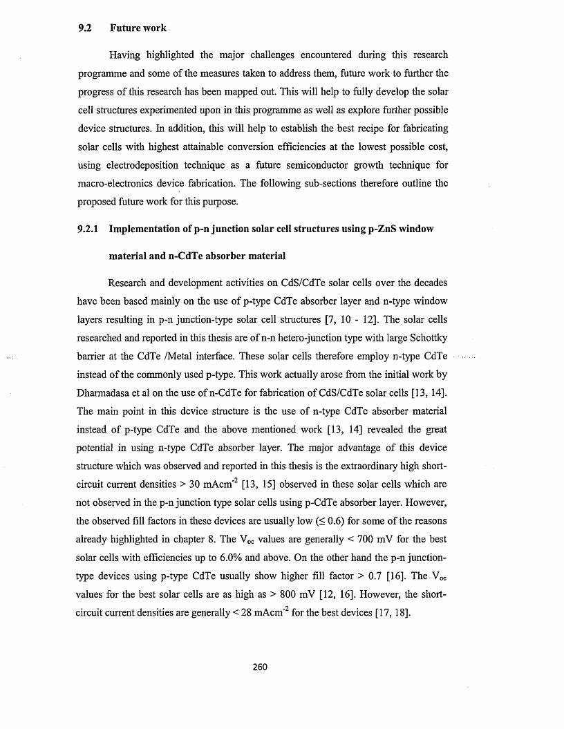
9.2 Future work
Having highlighted the major challenges encountered during this research
programme and some of the measures taken to address them, future work to further the
progress o f this research has been mapped out. This will help to fully develop the solar
cell structures experimented upon in this programme as well as explore further possible
device structures. In addition, this will help to establish the best recipe for fabricating
solar cells with highest attainable conversion efficiencies at the lowest possible cost,
using electrodeposition technique as a future semiconductor growth technique for
macro-electronics device fabrication. The following sub-sections therefore outline the
proposed future work for this purpose.
9.2.1 Implementation of p-n junction solar cell structures using p-ZnS window
material and n-CdTe absorber material
Research and development activities on CdS/CdTe solar cells over the decades
have been based mainly on the use o f p-type CdTe absorber layer and n-type window
layers resulting in p-n junction-type solar cell structures [7, 10 - 12]. The solar cells
researched and reported in this thesis are of n-n hetero-junction type with large Schottky
barrier at the CdTe /Metal interface. These solar cells therefore employ n-type CdTe .
instead o f the commonly used p-type. This work actually arose from the initial work by
Dharmadasa et al on the use of n-CdTe for fabrication of CdS/CdTe solar cells [13, 14].
The main point in this device structure is the use of n-type CdTe absorber material
instead of p-type CdTe and the above mentioned work [13, 14] revealed the great
potential in using n-type CdTe absorber layer. The major advantage o f this device
structure which was observed and reported in this thesis is the extraordinary high short-
circuit current densities > 30 mAcm ' 2 [13, 15] observed in these solar cells which are
not observed in the p-n junction type solar cells using p-CdTe absorber layer. However,
the observed fill factors in these devices are usually low (< 0 .6 ) for some of the reasons
already highlighted in chapter 8 . The Voc values are generally < 700 mV for the best
solar cells with efficiencies up to 6.0% and above. On the other hand the p-n junction-
type devices using p-type CdTe usually show higher fill factor > 0.7 [16]. The Voc
values for the best solar cells are as high as > 800 mV [12, 16]. However, the short-
circuit current densities are generally < 28 mAcm ’2 for the best devices [17, 18].
26 0
As part o f the future work in furtherance of the research work reported in this
thesis, a combination of the use o f p-n junction structure and n-type CdTe absorber
material for CdTe-based solar cells, will be pursued. In doing this, the aim will be to
combine the high Jsc values coming from the use o f n-type CdTe absorber material and
the high Voc and FF values coming from the use o f p-n junction structures. The window
material in this resultant device will therefore be a p-type wide bandgap material. P-type
ZnS will be used for this. It can be recalled that the electrodeposition and
characterisation of p-type ZnS layers were reported in chapter 5. However, these layers
were not used in solar cell fabrication yet for some reasons. One o f the reasons is to
avoid handling too many materials and projects at the same time. Three materials were
used so far (n-CdS, n-ZnS and n-CdTe). The electrodeposition and characterisation of
these three materials as well as their use in solar cell fabrication were not easy tasks.
Again, the etching process and metal back contact already in use in the group are for
making Schottky contacts on n-type CdTe. In order to fabricate glass/FTO/p-ZnS/n-
CdTe/Metal solar cell structure, the right recipe for etching of n-CdTe has to be
established for making suitable ohmic contact to n-CdTe. The successful
implementation and optimisation of this device structure is expected to yield solar cells
with the highest possible device parameters.
9.2.2 Application of automated pumping system for replenishing Te and S ions in
the deposition electrolytes
One major difficulty in the electrodeposition process is the replenishing of the
ions in the deposition electrolyte as electrodeposition proceeds. At the moment, there is
not a precise way of doing this. In chapters 5, 6 , 7 and early parts o f this chapter, the
method used for the addition of ions into the deposition electrolytes was stated. This
method was helpful to some extent but was not very accurate given that one is dealing
with semiconductors. A more precise and consistent way of doing this will involve
automation, by means o f a pumping system which systematically, precisely and
consistently injects the solution containing the required ions into the deposition
electrolyte as the deposition process goes on. Addition of Te into CdTe deposition
electrolyte will be the first to be experimented in this way. This is because Te
concentration in CdTe is the most influential in CdTe-based solar cell performance than
the atoms of the other chalcogens such as sulphur. This procedure will help to establish
26 1
high degree of reproducibility in the material layers deposited which in turn will ensure
good reproducibility and consistency in the solar cells fabricated using these materials.
An alternative approach to this will be the application o f ion selective electrodes
(ISE) also called specific ion electrodes (SIE) [19] which can be used to monitor the
concentration of ions in solution. To use this, the concentration o f the ions of interest is
measured as soon as the deposition electrolyte is prepared. This concentration is then
used as a benchmark. After each round o f deposition the ion concentration is measured
again. With few initial monitoring experiments, the required exact amount o f solution
containing the ions can then be added to the electrolyte manually to restore the
concentration of ions in the electrolyte.
9.2.3 Im plementation of the two- and three-junction device structures using p-
ZnS as window m aterial
Apart from the single p-n junction structure using p-ZnS as mentioned in
section 9.2.1, other two-junction and three-junction structures using p-ZnS will be
pursued. These include glass/FTO/p-ZnS/p-CdTe/n-CdTe/ohmic metal contact
structure, and glass/FTO/p-ZnS/p-CdTe/i-CdTe/n-CdTe/ohmic metal contact structure.
Figure 9.1: Schematic o f proposed energy band diagrams for the device structures of
(a) glass/FTO/p-ZnS/p-CdTe/n-CdTe/ohmic metal contact and (b) glass/FTO/p-ZnS/p-
CdTe/i-CdTe/n-CdTe/ohmic metal contact. (Figures are not drawn to scale).
262
The aim of all this is to search for the best possible device structure for next-generation
solar cells. In addition, the already experimented glass/FTO/n-ZnS/n-CdTe/Schottky
contact graded bandgap device structure will be pursued further and developed having
produced encouraging device result already. Proposed energy band diagrams o f some of
the device structures mentioned above, to be pursued, are shown in figure 9.1.
9.2.4 Application of pinhole plugging layers and MIS structures
It is suspected that possible pinholes exist in the electrodeposited material layers
that may lead to short-circuit especially between the evaporated back metal contact and
the front contact or the window layer. A possible cause o f such pinholes will be the
pattern of nucleation in electrodeposition. This involves initial nucleation at sharp
points on the FTO substrate as a result o f concentration of electric field at such points
when a potential is applied across the FTO surface. Some o f these pinholes are
sometimes observed physically on the samples especially after post-deposition heat
treatment. In order to ensure that these pinholes do not create short-circuit problem, it is
necessary that a semiconducting or very thin insulating layer is deposited on the last
layer before the application of back metal contact. At the moment the best available
material for this purpose is polyaniline which is a semiconducting polymer. This
material is being researched and developed at present in the author's research group.
This approach, if successful, will result in hybrid solar cells combining organic and
inorganic semiconducting materials. The feasibility o f this approach has also been
demonstrated recently [2 0 ].
Apart from plugging the pinholes, the organic material layer or thin insulating
layer as the case may be, serves as an insulating layer, resulting in MIS-type device
structure, which also helps to improve barrier height and hence the solar cell Voc-
Roberts et al have also demonstrated this using C4-anthracene as the organic thin
insulating layer [2 1 ].
9.2.5 Detailed study of the effect of fluorine on solar cell performance
In chapter 7, it was mentioned that fluorine, in the form o f CdF2 , was
incorporated into CdTe layers in two ways. One way was by adding CdF2 into the CdTe
deposition electrolyte. The second way was by using a mixture of CdCl2 and small
amount of CdF2 to do post-deposition heat treatment o f CdTe layers prior to etching and
back metal contact formation. In chapter 8 , the result of this experiment was presented
263
in comparison with the use of only CdC^ in the post-deposition heat treatment. The
results showed that using (CdCl2+CdF2) mixture in the post-deposition heat treatment
consistently resulted to drastic improvement in all the device parameters.
Now only a certain amount of CdF2 (about 0.1 g) was used in this experiment
together with about 50 ml o f saturated CdCk in aqueous solution. As part of the future
work, this particular experiment will be re-visited and different combinations of both
CdCl2 and CdF2 experimented in order to establish the optimum combination that
produces the best device result. In addition to this will also be the determination of the
optimum CdCl2/CdF2 combination in the CdTe deposition electrolyte.
9.2.6 Further work on the resistivity of CdS and CdTe layers
In chapter 6 , the electrodeposition and characterisation of CdS layers were
presented. The resistivity values obtained for these electrodeposited CdS layers were
rather high (in the range of 1 0 4 flcm to 1 0 5 Hem) and this is suspected to contribute to
the high series resistance of the solar cells which ultimately affected the fill factor
values adversely. As part of the future work, attempt will be made to reduce the
resistivity values of these CdS layers. To do this, fluorine, bromine and iodine doping
will be attempted by adding appropriate sources of these atoms into the deposition
electrolyte. The major sources in mind at present are CdF2 , CdBr2 and Cdl2 .
Again, the results o f characterisation o f CdTe layers presented in chapter 7 did
not include the resistivity measurements on CdTe layers. The reason for this was that
the attempt made (within the available time for this programme) to make ohmic contact
to the electrodeposited n-CdTe layers using In-Ga eutectic, as well as In metal was not
successful. The resulting contacts displayed very resistive behaviour that was not
reliable for determining the resistivity o f the layers. Further work on ohmic contact
formation on the electrodeposited n-CdTe layers will be pursued in order to determine
the resistivity range of these layers and to see how this affects the performance o f solar
cells made with these layers. In order to do this, doping with other possible n-type
dopants will be attempted in addition to Cl and F doping already in place.
More accurate quantitative determination of the atomic concentrations o f all the
three semiconductor layers (ZnS, CdS and CdTe) will be embarked upon using
techniques such as XRF, SIMS and XPS. This will help to understand the stoichiometry
of these layers and the best stoichiometry of each material for making the best devices.
264

References
[1] Research and Markets: Microelectronics & semiconductor device/wafer cleaning
equipment market-Forecast (2012 -20 1 7 ) published October 2012
httv://www.researchandmarkets.com/research/5xdbtl/microelectronics (Retrieved
17/12/2013).
[2] X. Y. Peng, H. W. Gu, T. Zhang, F. Qu, F. Z. Ding and H. Y. Wang, Rare Met., 32
(4) (2013) 3 80 -389 .
[3] N. K. Allouche, T. B. Nasr, N. T. Kamoun and C. Guasch, Materials Chemistry
and Physics, 123 (2010) 620 — 624.
[4] S. H. Shin, J. Bajaj, L. A. Moudy and D. T. Cheung, Appl. Phys. Lett., 43 (1)
(1983) 66 - 70.
[5] S. Hu and C. H. Henager Jr., J. Cryst. Growth, 311 (2009) 3184 - 3194.
[6 ] A. P. Samantilleke, M. F. Cerqueira and B. Mari, J. Cryst. Growth 320 (2011) 13 -
17.
[7] C. Heisler, M. Bruckner, F. Lind, C. Kraft, U. Reislohner, C. Ronning, and W.
Wesch, J. Appl. Phys., 113 (2013) 224504-1 - 224504-6.
[8 ] S. Dennison J. Mater. Chem. 4 (1) (1994) 41- 46.
[9] K. Zanio, Semiconductors and Semimetals, vol. 13 “Cadmium Telluride ”, New
York: Academic Press (1978).
[10] B. M. Basol, O. M. Stafsudd and A. Bindal, Solar Cells, 15 (1985) 279 - 284.
[11] G.C. Morris and S.K. Das, Influence o f CdCL treatment of CdS on the properties
o f electrodeposited CdS/CdTe thin film solar cells, Photovoltaic Specialists
Conference, 1993, Conference Record o f the twenty third IEEE, Louisville,
Kenturky, USA, 1 0 -1 4 May 1993, pg. 469 - 474.
http://ieeexplore. ieee. org/xpl/login.jsp?tp=&arnumber=347136&url=http%3A %2F%2
Fieeexplore.ieee.org%2Fxpls%2Fabs_all.jsp%3Famumber%3D347136
[12] D. Cunningham, M. Rubcich and D. Skinner, Prog. Photovolt. Res. Appl. 10:
(2002) 159-168.
[13] I. M. Dharmadasa, A. P. Samantilleke, N. B. Chaure and J. Young, Semicond. Sci.
Technol. 17, (2002) 1238 - 1248.
[14] N. B. Chaure, A. P. Samantilleke and I. M. Dharmadasa, Sol. Energ. Mater. Sol.
Cells, 77(2003)303-317 .
[15] O. K. Echendu, F. Fauzi, L. Bowen and I. M. Dharmadasa, Proceedings o f the 9th
Photovoltaic Science, Applications and Technology Conference C95, Swansea,
2 6 5
United Kingdom, (2013) 147-150.
[16] J. Britt and C. Ferekides, Appl. Phys. Lett., 62 (1993) 2851 - 2852.
[17] G. C. Morris, P. E. Tanner and A. Tottszer, Photovoltaic Specialists Conference
1990, Conference Record o f the twenty first IEEE, 21 - 25 May, 1990,
Kissimmee, Florida, USA, Vol.l Pg. 575 -580 .
http’J/ieeexplore. ieee. org/stamp/stamp.jsp?tp=&arnumber=l11685.
[18] X. Wu, S. Asher, D. H. Levi, D. E. King, Y. Yan, T. A. Gessert, and P. Sheldon,
J. Appl. Phys., 89 (8) (2001) 4564 - 4569.
[19] Ion selective electrodes, en.wikipedia.org/wiki/Ion-selective_electrode (Retrieved
22/12/2013).
[20] M. M. Tessema and D. M. Giolando, Sol. Energ. Mater. Sol. Cells 107 (2012)
9 -1 2 .
[21] G.G. Roberts, M.C. Petty and I.M. Dharmadasa, IEE PROC, Vol. 128, Pt. I, No.
6, DECEMBER 1981, 0143-7100/81/060197 + 05 $01.50/0.
26 6
Chapter 10 The future of solar cells
10.0 Introduction
In chapter 2, different types of solar cells were discussed. The major solar cell
classification discussed was based on the main absorber material used in the different
types of solar cells. Those cells were also either organic, inorganic or hybrid devices
and they all have different operating principles as well as different levels of
performance. In any case however, the efficiencies of the solar cells in general are still
below the theoretical limits (in view of the Shockley-Queisser limit) and require further
improvements in order to reach and exceed these limits, so as to bring down the cost of
solar panels. In the light of this, several approaches have been proposed over the last
two decades for the next generation solar cells with potential for possible improvement
of the solar cell efficiencies beyond the Shockley-Queisser limit. These proposed ideas
include; intermediate band solar cells, plasmonic solar cells, hot-carrier solar cells, solar
cells with up-conversion, solar cells with down-conversion, concentrator solar cells,
quantum dot/quantum well solar cells and graded bandgap solar cells. This chapter
briefly discusses the basic ideas behind these proposed solar cell designs and the extent
they have gone in producing solar cells with improved performance over the traditional
designs. Based on the results achieved so far, and the possibility o f further progress, the
way forward for next generation solar cells with improved performance is suggested.
10.1 Existing proposals for next generation solar cells
This section briefly reviews the above named proposed solar cell models with
possible potentials to serve as the next generation solar cells. This short review includes
the main ideas behind each model, the extent of research work carried out and still
going on so far on them, the results obtained to date and the prospect of each of these
models.
10.1.1 Intermediate band (IB) solar cells
In any given solar cell with an absorber material of energy bandgap Eg, incident
photons with energy > Eg are absorbed while photons with energy < Eg are transmitted.
These transmitted sub-bandgap energy photons do not therefore contribute to creation of
electron-hole pairs in the solar cell. They are therefore lost. If these photons can be
captured in the solar cell, so that, they can effectively participate in promoting electrons
from the valence band of the absorber material to the conduction band, it is believed that
267
the efficiency of the solar cell can be improved mainly through the improvement of
photo-generated current. This is the idea behind the intermediate band (IB) solar cell
[1]. Here, energy levels, called intermediate bands, are created within the bandgap of
the solar cell by deliberately introducing appropriate atoms. Photons with energy < Eg
can then promote electrons from the valence band to the intermediate band and then
from the intermediate band to the conduction band [1]. A major assumption in this
approach is that null density o f states exists between the valence band and the IB, and
between the IB and the conduction band. The maximum theoretical efficiency for a
single junction IB solar cell has been calculated to be up to 63% [2]. The IB solar cell
idea is just similar to the impurity photovoltaic effect originally proposed by W olf in
1960 [3].
The practical efficiency values achieved to date by IB solar cells have not
exceeded those of the conventional solar cells without intermediate bands. In fact
disappointingly, the efficiencies have not yet competed with those of conventional solar
cells according to Luque et al [2]. The idea has not worked yet and majority o f the work
done so far are theoretical calculations. A possible reason for this could be the fact that
the behaviour of these intermediate band states as recombination centres has been
grossly neglected. Another possibility is that, the right device structure may not have
been used, in which case, both the shape of the energy band diagram and the existing
built-in electric field do not facilitate rapid separation and collection o f the photo
generated charge carriers before they recombine.
10.1.2 Plasmonic solar cells *
Plasmonic solar cells tend to employ the quantised oscillation o f free electron
gas in certain metals to facilitate light trapping in the solar cell leading to improved
absorption of photons with energy lower than the bandgap energy o f the solar cell
absorber material. These quanta of plasma oscillations are called plasmons [4]. The
application of plasmonic oscillation in solar cells is usually done by applying thin
coatings of plasmonic metals (such as gold and silver) on the back of the solar cell
absorber layer [5]. This is expected to enhance the trapping of longer wavelength
photons and scatter them back into the solar cell for absorption. This principle is
expected to enhance the photo-generated current density and therefore improve the
efficiency of solar cells [6 ].
26 8
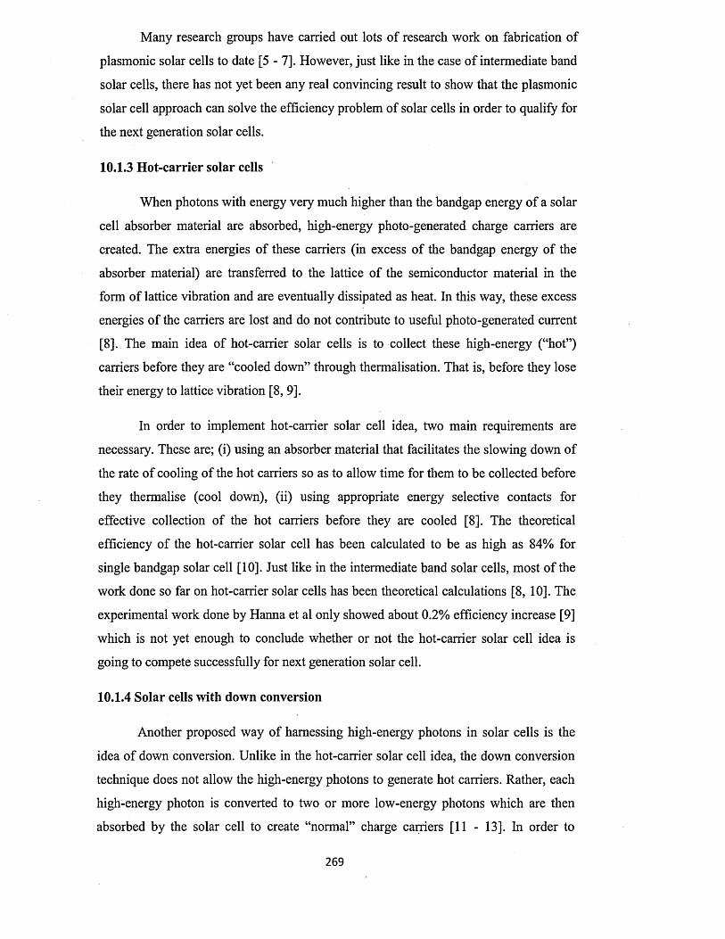
Many research groups have carried out lots of research work on fabrication of
plasmonic solar cells to date [5 - 7]. However, just like in the case o f intermediate band
solar cells, there has not yet been any real convincing result to show that the plasmonic
solar cell approach can solve the efficiency problem of solar cells in order to qualify for
the next generation solar cells.
10.1.3 Hot-carrier solar cells
When photons with energy very much higher than the bandgap energy of a solar
cell absorber material are absorbed, high-energy photo-generated charge carriers are
created. The extra energies of these carriers (in excess of the bandgap energy of the
absorber material) are transferred to the lattice of the semiconductor material in the
form of lattice vibration and are eventually dissipated as heat. In this way, these excess
energies of the carriers are lost and do not contribute to useful photo-generated current
[8]. The main idea of hot-carrier solar cells is to collect these high-energy (“hot”)
carriers before they are “cooled down” through thermalisation. That is, before they lose
their energy to lattice vibration [8, 9].
In order to implement hot-carrier solar cell idea, two main requirements are
necessary. These are; (i) using an absorber material that facilitates the slowing down of
the rate of cooling of the hot carriers so as to allow time for them to be collected before
they thermalise (cool down), (ii) using appropriate energy selective contacts for
effective collection of the hot carriers before they are cooled [8]. The theoretical
efficiency of the hot-carrier solar cell has been calculated to be as high as 84% for
single bandgap solar cell [10]. Just like in the intermediate band solar cells, most o f the
work done so far on hot-carrier solar cells has been theoretical calculations [8, 10]. The
experimental work done by Hanna et al only showed about 0.2% efficiency increase [9]
which is not yet enough to conclude whether or not the hot-carrier solar cell idea is
going to compete successfully for next generation solar cell.
10.1.4 Solar cells with down conversion
Another proposed way of harnessing high-energy photons in solar cells is the
idea of down conversion. Unlike in the hot-carrier solar cell idea, the down conversion
technique does not allow the high-energy photons to generate hot carriers. Rather, each
high-energy photon is converted to two or more low-energy photons which are then
absorbed by the solar cell to create “normal” charge earners [11 - 13]. In order to
269
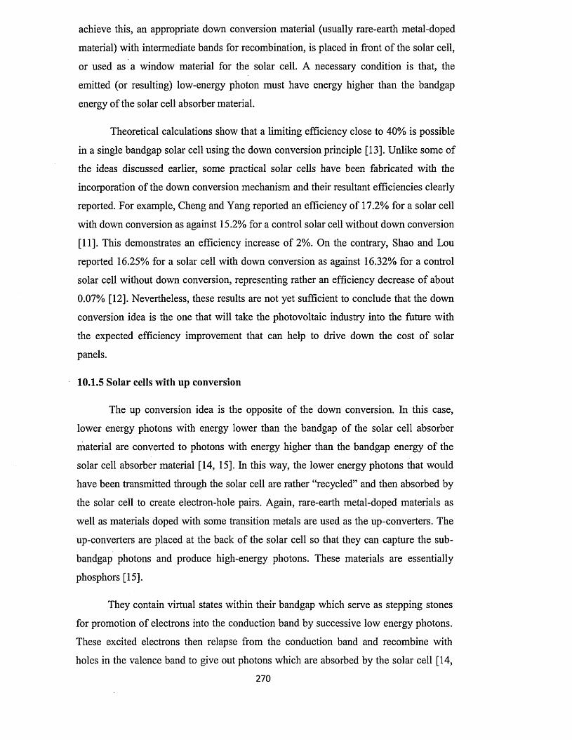
achieve this, an appropriate down conversion material (usually rare-earth metal-doped
material) with intermediate bands for recombination, is placed in front of the solar cell,
or used as a window material for the solar cell. A necessary condition is that, the
emitted (or resulting) low-energy photon must have energy higher than the bandgap
energy o f the solar cell absorber material.
Theoretical calculations show that a limiting efficiency close to 40% is possible
in a single bandgap solar cell using the down conversion principle [13]. Unlike some of
the ideas discussed earlier, some practical solar cells have been fabricated with the
incorporation of the down conversion mechanism and their resultant efficiencies clearly
reported. For example, Cheng and Yang reported an efficiency of 17.2% for a solar cell
with down conversion as against 15.2% for a control solar cell without down conversion
[11]. This demonstrates an efficiency increase of 2%. On the contrary, Shao and Lou
reported 16.25% for a solar cell with down conversion as against 16.32% for a control
solar cell without down conversion, representing rather an efficiency decrease o f about
0.07% [12]. Nevertheless, these results are not yet sufficient to conclude that the down
conversion idea is the one that will take the photovoltaic industry into the future with
the expected efficiency improvement that can help to drive down the cost of solar
panels.
10.1.5 Solar cells with up conversion
The up conversion idea is the opposite of the down conversion. In this case,
lower energy photons with energy lower than the bandgap of the solar cell absorber
material are converted to photons with energy higher than the bandgap energy o f the
solar cell absorber material [14, 15]. In this way, the lower energy photons that would
have been transmitted through the solar cell are rather “recycled” and then absorbed by
the solar cell to create electron-hole pairs. Again, rare-earth metal-doped materials as
well as materials doped with some transition metals are used as the up-converters. The
up-converters are placed at the back o f the solar cell so that they can capture the sub-
bandgap photons and produce high-energy photons. These materials are essentially
phosphors [15].
They contain virtual states within their bandgap which serve as stepping stones
for promotion of electrons into the conduction band by successive low energy photons.
These excited electrons then relapse from the conduction band and recombine with
holes in the valence band to give out photons which are absorbed by the solar cell [14,
270
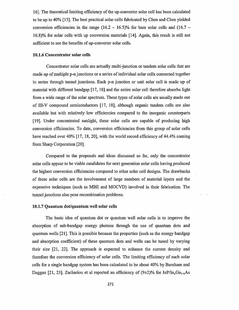
16]. The theoretical limiting efficiency of the up-converter solar cell has been calculated
to be up to 40% [15]. The best practical solar cells fabricated by Chen and Chen yielded
conversion efficiencies in the range (16.2 - 16.5)% for bare solar cells and (16.7 -
16.8)% for solar cells with up conversion materials [14]. Again, this result is still not
sufficient to see the benefits of up-converter solar cells.
10.1.6 Concentrator solar cells
Concentrator solar cells are actually multi-junction or tandem solar cells that are
made up of multiple p-n junctions or a series o f individual solar cells connected together
in series through tunnel junctions. Each p-n junction or unit solar cell is made up of
material with different bandgap [17, 18] and the entire solar cell therefore absorbs light
from a wide range o f the solar spectrum. These types o f solar cells are usually made out
of III-V compound semiconductors [17, 18], although organic tandem cells are also
available but with relatively low efficiencies compared to the inorganic counterparts
[19]. Under concentrated sunlight, these solar cells are capable of producing high
conversion efficiencies. To date, conversion efficiencies from this group of solar cells
have reached over 40% [17, 18, 20], with the world record efficiency of 44.4% coming
from Sharp Corporation [20].
Compared to the proposals and ideas discussed so far, only the concentrator
solar cells appear to be viable candidates for next generation solar cells having produced
the highest conversion efficiencies compared to other solar cell designs. The drawbacks
of these solar cells are the involvement of large numbers o f material layers and the
expensive techniques (such as MBE and MOCVD) involved in their fabrication. The
tunnel junctions also pose recombination problems.
10.1.7 Quantum dot/quantum well solar cells
The basic idea o f quantum dot or quantum well solar cells is to improve the
absorption of sub-bandgap energy photons through the use o f quantum dots and
quantum wells [21]. This is possible because the properties (such as the energy bandgap
and absorption coefficient) of these quantum dots and wells can be tuned by varying
their size [21, 22]. The approach is expected to enhance the current density and
therefore the conversion efficiency of solar cells. The limiting efficiency o f such solar
cells for a single bandgap system has been calculated to be about 40% by Bamham and
Duggan [21, 23]. Zachariou et al reported an efficiency of (9±2)% for InP/InxGai.xAs
27 1
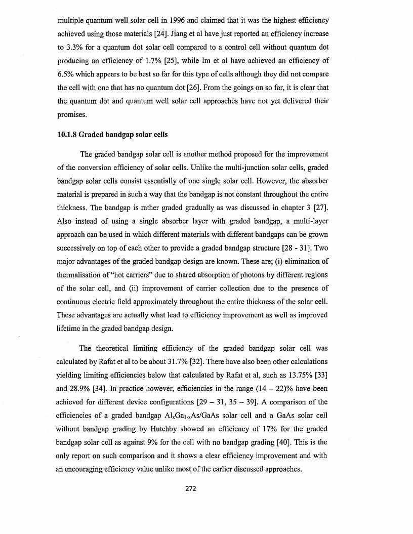
multiple quantum well solar cell in 1996 and claimed that it was the highest efficiency
achieved using those materials [24]. Jiang et al have just reported an efficiency increase
to 3.3% for a quantum dot solar cell compared to a control cell without quantum dot
producing an efficiency o f 1.7% [25], while Im et al have achieved an efficiency of
6.5% which appears to be best so far for this type of cells although they did not compare
the cell with one that has no quantum dot [26]. From the goings on so far, it is clear that
the quantum dot and quantum well solar cell approaches have not yet delivered their
promises.
10.1.8 Graded bandgap solar cells
The graded bandgap solar cell is another method proposed for the improvement
of the conversion efficiency of solar cells. Unlike the multi-junction solar cells, graded
bandgap solar cells consist essentially o f one single solar cell. However, the absorber
material is prepared in such a way that the bandgap is not constant throughout the entire
thickness. The bandgap is rather graded gradually as was discussed in chapter 3 [27].
Also instead of using a single absorber layer with graded bandgap, a multi-layer
approach can be used in which different materials with different bandgaps can be grown
successively on top of each other to provide a graded bandgap structure [28 - 31]. Two
major advantages of the graded bandgap design are known. These are; (i) elimination of
thermalisation of “hot carriers” due to shared absorption of photons by different regions
of the solar cell, and (ii) improvement o f carrier collection due to the presence of
continuous electric field approximately throughout the entire thickness o f the solar cell.
These advantages are actually what lead to efficiency improvement as well as improved
lifetime in the graded bandgap design.
The theoretical limiting efficiency of the graded bandgap solar cell was
calculated by Rafat et al to be about 31.7% [32]. There have also been other calculations
yielding limiting efficiencies below that calculated by Rafat et al, such as 13.75% [33]
and 28.9% [34]. In practice however, efficiencies in the range (14 - 22)% have been
achieved for different device configurations [29 - 31, 35 - 39]. A comparison o f the
efficiencies of a graded bandgap AlxGai_xAs/GaAs solar cell and a GaAs solar cell
without bandgap grading by Hutchby showed an efficiency of 17% for the graded
bandgap solar cell as against 9% for the cell with no bandgap grading [40]. This is the
only report on such comparison and it shows a clear efficiency improvement and with
an encouraging efficiency value unlike most o f the earlier discussed approaches.
27 2
The results of the graded bandgap AlxGa(i.X)As/GaAs solar cell reported by
Dharmadasa et al is worth commenting on at this point [39, 41]. This device structure
has produced the highest reported Voc of 1.175 V for a single device without light
concentration in addition to maximum possible fill factor of -0.85. The efficiency of
this solar cell has increased from 12% to 20% in just two attempts. Most strikingly yet,
this solar cell has been reported to be active in complete darkness, producing Voc of
-800 mV in complete darkness, as an evidence o f the incorporation of impurity
photovoltaic effect in the device [42]. In fact, following this idea, an attempt on multi
layer graded bandgap solar cell during the research work reported in this thesis, using
glass/FTO/ZnS/CdS/CdTe/Au device structure, produced an efficiency of 10.4% with a
high Jsc of 40.8 mAcm ' 2 as reported in chapter 8 [30, 31]. Based on these results, one
can say that the graded bandgap approach has future prospect for possible application in
next generation solar cells. In comparison with the concentrator solar cell approach, the
graded bandgap solar cells offer more cost-effective option, considering that the
concentrator solar cells involve large numbers o f material layers and expensive
techniques.
10.2 Conclusion
A brief review o f various proposed approaches for improvement of solar cell
conversion efficiencies has been presented in this chapter. Most o f the proposed ideas
have not yielded convincing results to substantiate their future prospect in the PV
industry. Most of the claimed efficiency improvements reported in the literature for
many of these proposals are not clearly presented with the major solar cell efficiency
comparison between the proposed and the control device structures missing. In most
cases, authors present quantum efficiencies in place o f the actual power conversion
efficiency which involves Jsc, Voc and FF. Other authors either present only Jsc or Voc
enhancement, saying nothing about the overall conversion efficiency, but rather use the
single Jsc or Voc or FF improvement to represent the efficiency improvement. Yet other
authors present the percentage increase in either Jsc or Voc and leave out the rest o f the
device parameters together with the overall conversion efficiency. The clear observation
from literature is that most of these ideas and proposals have not yet produced
meaningful convincing results to prove their strengths. In some of the places the actual
efficiency was mentioned, the values were so low to be taken seriously.
273

Only two ideas appear to have produced reasonable efficiency results that can be
seen as real and encouraging. These two ideas are the concentrator solar cell approach
(which involves multi-junction and tandem solar cell structures) and the graded bandgap
approach. These two approaches have one thing in common. That is ability to absorb
photons from a broad range o f the solar spectrum due to the presence of different
bandgaps. These two approaches at present appear to be the ones that can provide the
results expected from next generation solar cells.
27 4
References
[1] A. Luque and A. Marti, Phys. Rev. Lett., 78 (26) (1997) 5014 - 5017.
[2] A. Luque, P. G. Linares, E. Antolin, E. Canovas, C. D. Farmer, C. R. Stanley, and
A. Marti, Appl. Phys. Lett. 96 (2010) 013501-1 - 013501-3.
[3] M. Wolf, Limitations and Possibilities for Improvement of Photovoltaic Solar
Energy Converters, Part I: Considerations for Earth's Surface Operation, Proc. o f
IRE, July (1960) 1246-1263.
[4] H. Haug and S. W. Koch, Quantum theory o f the optical and electronic propertiestVi • •of semiconductors, 4 edition, World Scientific Publishing Co. Pte. Ltd, Toh Tuck
Link, Singapore (2004).
[5] P. R. Pudasaini and A. A. Ayon, Microelectronic Engineering, 110 (2013) 126 -
131.
[6 ] M. Yang, J. Li, F. Lin and X. Zhu, Plasmonics, 8 (2013) 877-883.
[7] D. Derkacs, S. H. Lim, P. Matheu, W. Mar and E. T. Yu, Appl. Phys. Lett. 89
(2006) 093103-1 - 093103-3.
[8 ] G. Conibeer, N. Ekins-Daukes, J. Guillemoles, D. Konig, E. Cho, C. Jiang, S.
Shrestha and M. Green, Sol. Energ. Mater. Sol. Cells, 93 (2009) 713 - 719.
[9] M. C. Hanna, Z. Lu, and A. J. Nozik, Hot carrier solar cells, AIP Conference
Proceedings 404, 309 (1997); doi: 10.1063/1.53477.
[10] D. J. Farrell, Y. Takeda, K. Nishikawa, T. Nagashima, T. Motohiro, and N. J.
Ekins-Daukes, Appl. Phys. Lett. 99 (2011) 111102-1 -111102-3.
[11] C. Cheng and J. Yang, IEEE Electron Device Letters, 33 (5) (2012) 697 - 699.
[12] G. Shao and C. Lou, The effects of down-conversion materials on solar cells,
Photovoltaic Specialists Conference (PVSC), 2012 38th IEEE, 3 - 8 June 2012, pg.
002596-002600,
http://ieeexplore.ieee.org/xpl/login.jsp?tp=&amumber=6318126&url=http%3A%2F%
2Fieeexplore. ieee. org%2Fiel5 %2F6304846%2F6317554 %2F06318126.pdf%3Famum
ber%3D6318126.
[13] T. Trupke, M. A. Green, and P. Wiirfel, J. Appl. Phys., 92, (3) (2002) 1668-1674 .
[14] Y. Chen and T. Chen, Journal o f Rare Earths, 29, (8) (2011) 723 - 726.
[15] C. M. Johnson and G. J. Conibeer, J. Appl. Phys. 112 (2012) 103108-1 -103108-
9.
[16] N. Bloembergen, Phys. Rev. Lett. 2 (3) (1959) 84 - 85.
[17] J. F. Geisz, D. J. Friedman, J. S. Ward, A. Duda, W. J. Olavarria, T. E. Moriarty, J.
T. Kiehl, M. J. Romero, A. G. Norman, and K. M. Jones, Appl. Phys. Lett., 93
275
(2008) 123505-1 -123505-3.
[18] R. R. King, D. C. Law, K. M. Edmondson, C. M. Fetzer, G. S. Kinsey, H. Yoon,
R. A. Sherif, andN . H. Karam ,Appl. Phys. Lett., 90 (2007) 183516-1 -183516-3.
[19] T. Ameri, N. Lia and C. J. Brabec, Energy Environ. Sci., 6 (2013) 2390 - 2413.
[20] Sharp Corporation, Concentrator solar cell with world's highest conversion
efficiency of 44.4%, http://phys.org/news/2013-06-solar-cell-world-highest-
conversion.html (retrieved 30/12/2013).
[21] K. W. J. Bamham and G. Duggan, J. Appl. Phys., 67 (7) (1990) 3490 - 3493.
[22] Wikipedia, Quantum dot, http://en.wikipedia.org/wiki/Quantum_dot (retrieved
30/12/2013).
[23] G. L. Araujo and A. Marti, Sol. Energ. Mater. Sol. Cells, 33 (1994) 213 - 240.
[24] A. Zachariou, K.W.J. Bamham, P. Griffin, J. Nelson, C. Button, M. Hopkinson,
M. Pate and J. Epler, A new approach to p-doping and the observation of
efficiency enhancement in InP/InGaAs quantum well solar cells, Photovoltaic
Specialists Conference, 1996, Conference Record o f the Twenty Fifth IEEE, May
13-17, 1996; Washington, D.C., USA, http://ieeexplore.ieee.org/xpl/login.jsp?tp=&arnumber=563960&url=http%3A%2F%2 Fieeexplore.ieee.org%2Fiel3%2F4263%2F12206%2F00563960.pdf%3Famumber%3 D563960.
[25] L. Jiang, T. You and W. Deng, Nanotechnology, 24 (2013) 415401 (6pp).
[26] J. Im, C. Lee, J. Lee, S. Park and N. Park, Nanoscale, 3 (2011) 4088 - 4093.
[27] I. M. Dharmadasaa, J. S. Roberts and G. Hill, Sol. Energ. Mater. Sol. Cells, 88
(2005)413-422.
[28] I. M. Dharmadasa, Advances in Thin-Film Solar Cells, Pan Stanford Publishing
Pte. Ltd, Boulevard, Singapore, (2012).
[29] T. Dullweber, G. Hanna, U. Rau and H. W. Schock, Sol. Energ. Mater. Sol. Cells
67(2001)145-150.
[30] O. K. Echendu, F. Fauzi, L. Bowen and I. M. Dharmadasa, n-CdTe - Based
Multilayer Graded Bandgap Solar Cell Using All - electrodeposited
Semiconductors, Proc. o f 9th Photovoltaic Science, Applications and Technology
Conference C95, Swansea, United Kingdom, (2013) 147-150.
[31] O. K. Echendu, F. Fauzi, L. Bowen and I. M. Dharmadasa, All electrodeposited
multilayer graded bandgap solar cells using II-VI semiconductors, Proc. o f 28th
European Photovoltaic Solar Energy Conference and Exhibition, Paris, France,
2 7 6

(2013)2409 - 2413.
[32] N. H. Rafat, A. M. A. Haleem and S. E. D. Habib, Renewable Energy, 32 (2007)
2 1 -3 4 .
[33] A. Dhingra and A. Rothwarf, IEEE Transaction on Electron Devices, 43 (4)
(1996) 613.
[34] G. F. Brown, J. W. Ager III, W.Walukiewicz and J.Wua, Sol. Energ. Mater. Sol.
Cells 94 (2010) 478 - 483.
[35] M. S. Leite, R. L. Woo, W. D. Hong, D. C. Law, and H. A. Atwater, Appl. Phys.
Lett. 98, (2011) 093502-1 - 093502-3.
[36] M. A. Contreras, J. Tuttle, A. Gabor, A. Tennant, K. Ramanathan, S. Asher, A.
Franz, J. Keane, L. Wang and R. Noufi, Sol. Energ. Mater. Sol. Cells, 41/42
(1996)231-246.
[37] M. L. Timmons, R. Venkatasubramanian, T. S. Colpitts, J. S. Hills, J. A. Hutchby,
P. A. lies and C.L. Chu, Graded-band-gap AlGaAs solar cells for AlGaAs/Ge
cascade cells, Photovoltaic Specialists Conference 1990, Conference Record o f
the twenthy first IEEE, 21 - 2 5 May 1990, vol.l, pg. 68 - 72,
http.V/ieeexplore. ieee. org/xpl/login.jsp?tp=&amumber=l11593&url=http %3A %2F%2
Fieeexplore. ieee. org%2Fxpls%2Fabs_all.jsp%3Famumber%3Dl 11593
[38] L. C. Olsen et al 1988, Graded bandgap solar cells
http://www.dtic.mil/dtic/tr/fulltext/u2/a211537.pdf ('retrieved 30/12/2013).
[39] I.M. Dharmadasa, N.D.P.S.R. Kalyanaratne and R. Dharmadasa,
J.Natn.Sci.Foundation Sri Lanka, 41(2) (2013) 73-80.
[40] J. A. Hutchby, Appl. Phys. Lett., 26 (8) (1975) 457 - 459.
[41] I.M. Dharmadasa, G.J. Tolan, J.S. Roberts, G. Hill, S. Ito, P. Liska and M. Gratzel,
Proc. o f 21st European Photovoltaic Solar Energy Conference, 4 - 8 September,
Dresden, Germany, (2006) 257 - 262.
[42] I. M. Dharmadasa, O. Elsherif and G. J. Tolan, Journal o f Physics: Conference
Series 286 (2011) 012041. doi:10.1088/1742 6596/286/1/012041.
277
Appendix I: Thin film semiconductor deposition techniques
1.0 Introduction
The semiconductor materials used for device fabrication in the past were mainly
o f the bulk type with thickness of the order of few hundred micrometres [1 - 3]. Silicon
(Si), germanium (Ge) and gallium arsenide (GaAs) are examples o f this kind o f
semiconductors that have found use in microelectronics. In recent times, with the advent
o f nanotechnology, the thicknesses of semiconductors used in device fabrication have
been drastically reduced by some orders of magnitude such that,, semiconductor devices
can now be fabricated using materials with thicknesses in the nanometre range without
really compromising device performance. This thin film technology has one major
advantage of reducing the amount of materials used in device fabrication thus driving
down the cost o f such devices [4, 5]. To date, different types o f thin-film semiconductor
devices have been produced ranging from thin-film diodes and transistors [4] to thin
film lasers [6 ] as well as thin film solar cells [5]. Different techniques have been used
over the decades for the deposition of thin film semiconductors. These techniques can
broadly be classified into vapour phase techniques and liquid phase deposition
techniques. The survey o f these various techniques is the subject o f this appendix I.
1.1 Vapour phase deposition techniques •
Vapour phase semiconductor deposition techniques cover a wide range o f thin
film deposition methods in which semiconductor films are deposited on a solid substrate
using source material usually in the vapour phase. Insulating and conducting films can
as well be deposited. Depending on the nature of the source materials, these techniques
can also be divided into physical vapour phase (involving purely physical process such
as vacuum evaporation at high temperature followed by condensation) and chemical
vapour phase (involving a chemical reaction at the surface of the substrate to form the
desired material). In general, vapour phase deposition techniques require vacuum
systems. This usually makes the techniques expensive. Different types o f vapour phase
deposition methods include molecular beam epitaxy (MBE), metal organic vapour
phase epitaxy (MOVPE), chemical vapour deposition (CVD), metal organic chemical
vapour deposition (MOCVD), sputtering and close space sublimation (CSS) [7].
1.1.1 Molecular beam epitaxy (MBE)
MBE is one of the physical vapour evaporative deposition techniques used for
278vy
depositing single crystal semiconductors. As the name implies, it encourages the layer-
by layer (epitaxial) growth o f semiconductors. In a typical MBE growth, the precursor
material which can be in solid or gaseous form [8 ] is placed in a Knudsen effusion cell
from which it is evaporated in the form o f a beam of atoms, ions or molecules onto a
heated substrate which is usually a clean semiconductor (usually Si or GaAs). In order
to achieve good uniformity of the deposit, the hot substrate is continuously rotated.
Another essential requirement for the growth of high quality materials is ultra-high
vacuum (UHV) condition, involving pressure as low as 10' 11 Torr (~1.3xl O' 9 Pa) as well
as ultra-pure source materials [7]. Because o f the evaporation process for generating the
molecular beam of material being deposited, the evaporation Knudsen effusion cell
(crucible) is usually made of high refractory materials that can withstand such high
temperatures. Materials like pyrolytic boron nitride are used as crucibles because they
have good chemical stability at high temperatures up to 1400°C as well as low gas
emission [9]. High refractory tantalum is also used as a good heating element.
The MBE system also has adequate facilities for precise control of uniformity, lattice
match, composition, doping level and thickness of the growing sample. In addition, it
also has the capability of allowing in situ characterisation of the growing sample
through the use of tools like the reflection high energy electron diffraction (RHEED)
and mass spectrometer [7, 9] as shown in figure 1.1.
Vacuum pump
^ Mass spectrometerRHEED
detector
RHEEDgunHeating
coil
Knudsen effusion cells containing precursors
Figure 1.1: Schematic of a typical MBE system.
The system has different Knudsen effusion cells making it possible to contain different
types of precursors at the same time for multicomponent (such as ternary and
quartenary) semiconductor deposition. Each effusion cell has its independent heating
coil for heating the precursor since different precursors have different evaporation
279
temperatures. Because each effusion cell is at a certain angle to the substrate, the MBE
technique has relatively poor throwing power which is affected by the line of sight for
substrates with complex shape as well as blind holes. Nevertheless, the technique has
high deposition rate of up to 75 pm per minute [7, 9]. The scalability is only up to large
wafer size of -450 mm diameter.
Some o f the limitations o f the MBE technique include low throughput due to the
requirement o f high vacuum condition, complicated system operation requiring high
level of training and expertise coupled with the fact that the equipment is very
expensive to procure and maintain.
Thin-film semiconductor materials that have been grown using MBE technique include
ZnS on sapphire [10], Cdi_x ZnxS on GaAs [11], ZnSe on GaAs [12], CdSe on GaAs
[12], Si on Si [13], GaN on GaAs [14], Ge on Ge [15] etc.
1.1.2 Sputtering
The sputtering technique involves the bombardment of a target (precursor) with
high energy ions in order to eject surface atoms which eventually deposit on a substrate
placed at a close distance from the target [7]. It is therefore an etching process. It is
based on the principle of momentum transfer from the bombarding ions to the atoms of
the bombarded substrate.
The basic operating principle of sputtering deposition is depicted in figure 1.2.
The material to be sputtered (for example CdTe crystal or gold metal) is used as the
target. The bombarding ions usually come from the plasma of an inert gas source such
as Argon. When the target is bombarded by ions with sufficient energy and momentum,
atoms o f the target are dislodged from the target material and then travel to the substrate
and get deposited to form the desired thin film deposit. The entire process takes place in
a vacuum chamber. Different types o f sputter deposition exist, and these include the
following
28 0
Deposited Substratefilm
Depositi]atoms
] Togassupply
Sputtering ions
TargetFigure 1.2: Basic operating principle o f sputtering deposition technique.
1.1.2.1 DC Sputtering
In DC sputtering, the target and substrate are biased with direct current (DC)
voltage such that the target is used as the cathode and the substrate as the anode [7].
This applied bias (-1000V) helps to accelerate the plasma ions towards the cathode. On
hitting the target they transfer their high energy to the target thus sputtering it out and
depositing onto the surface of the substrate. For this reason the target must be a
conducting material (such as semiconductor and metal). Insulator cannot be used as
targets in DC sputtering due to their very high resistance which otherwise will require
extremely high bias voltages to sputter [7, 16]. DC sputtering technique has been used
to deposit thin film materials like indium tin oxide (ITO) [17], ZnO [18], CdS [19], NiO
[2 0 ] etc.
1.1.2.2 R F sputtering
In order to achieve the sputtering o f non-conducting (insulating) materials, a
voltage oscillating at radio frequency (RF) can be applied to the cathode o f the
sputtering system instead of a DC voltage in the case o f DC sputtering. The frequency
of the applied RF power is typically o f the order o f 13.5 MHz [16]. The effect o f the RF
voltage is to prevent the accumulation of positively charged ions (from the bombarding
ions) on the insulating target which ordinarily will require a very high DC bias of up to
1012 V to sputter in a DC sputtering arrangement. On one cycle (say the positive cycle),
electrons are attracted towards the target (cathode). This then creates a negative bias on
the target. On the reverse cycle, the ion bombardment of the target continues. In this
way the insulating target is effectively sputtered. Typical applied RF peak voltage used
in this operation is about 1000 V at a frequency of about 13.5 MHz [7, 16].
28 1
Semiconductor materials that have been grown by RF sputtering include CdTe [21],
CdS [22], ZnS [23], ZnO [24], ZnTe [25], ZnSe [26] etc.
1.1.2.3 Magnetron Sputtering
In magnetron sputtering, a magnetic field is applied between the anode and the
cathode o f the sputtering system. The magnetic field is arranged to be closer to the
surface of the target with the effect that secondary electrons generated by the target
during bombardment do not travel straight to the anode to bombard the substrate. These
electrons are rather confined in a kind o f cycloidal trajectory near the surface of the
target. As a result, their high density increases the plasma density and helps in achieving
more efficient sputtering result [27]. Again this helps to reduce the heat generated in the
substrate by otherwise higher momentum electrons, therefore reducing radiation damage
as well as allowing for the use of temperature-sensitive and surface-sensitive substrates
such as plastics and metal oxide semiconductors. As a result o f the modification by
magnetic field, magnetron sputtering yields higher deposition rate than the traditional
DC sputtering and allows for large area industrial application [28]. A recent variety of
magnetron sputtering known as high power impulse magnetron sputtering (HIPIMS) is
mostly applied in the sputtering of metallic coatings. In this system, very high target
power pulses of density up to 2800 - 3000 Wcm ' 2 are achieved [29, 30] whereas in a
conventional magnetron sputtering power densities of 20 - 50 Wcm ' 2 are usual [27].
Magnetron sputtering can be done in form of DC or RF magnetron sputtering depending
on the target material. Several semiconductor materials have been deposited by
magnetron sputtering method according to literature, which include CdTe [31], ZnS
[32], CdS [33], ZnO [34], GaAs [35] etc.
1.1.2.4 Reactive sputtering
Reactive sputtering combines physical and chemical deposition processes in one
deposition run. To do this, a reactive gas such as oxygen or nitrogen is added to the inert
gas flow that is traditionally part of the sputtering process [7]. This helps to synthesize
compounds such as oxides and nitrides on a wide variety of substrates [7]. During the
sputtering process, the reactive gas reacts chemically with the sputtered atoms, thus
producing the needed compound on the substrate. If the sputtering rate is higher than the
chemical reaction rate for example, the reaction will then take place on the substrate,
and if the reaction rate is faster than the sputtering rate, then the reaction will take place
on target. The control o f these two processes therefore affects the stoichiometry o f the
282
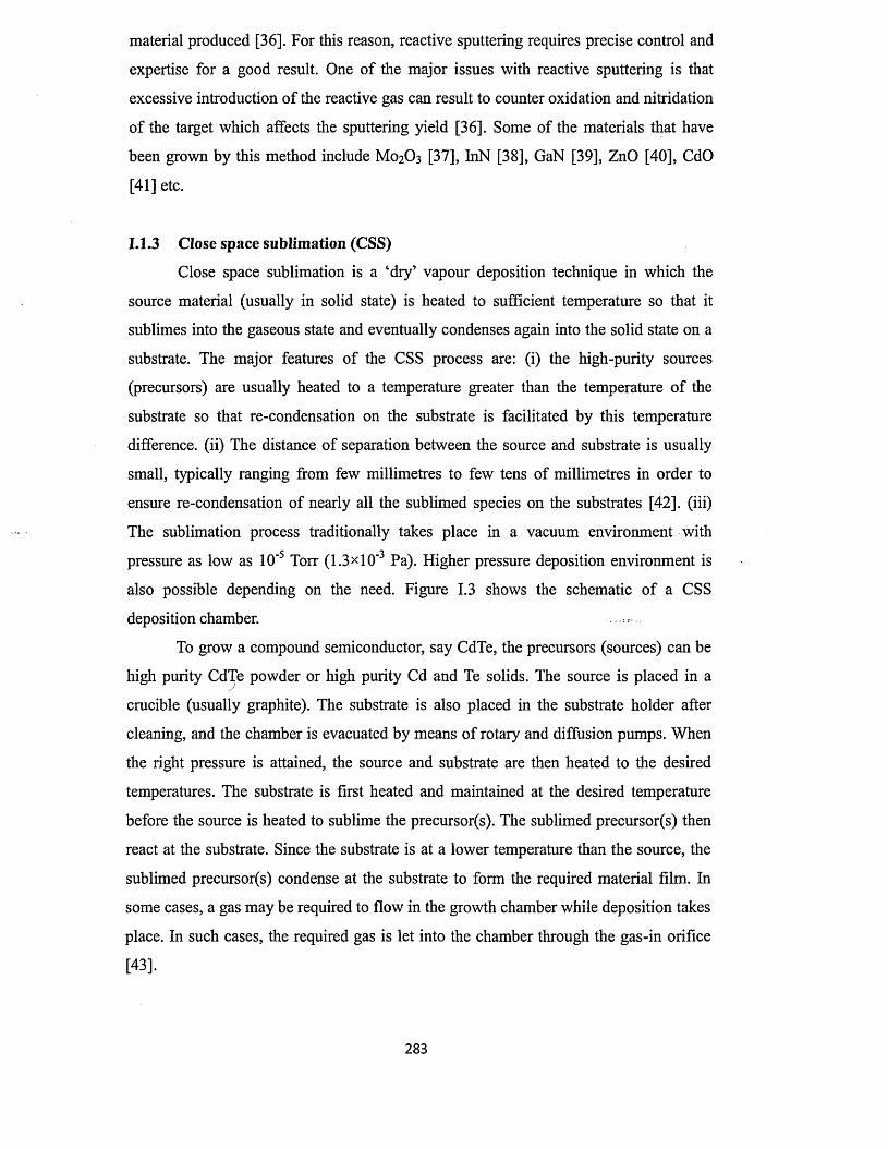
material produced [36]. For this reason, reactive sputtering requires precise control and
expertise for a good result. One of the major issues with reactive sputtering is that
excessive introduction of the reactive gas can result to counter oxidation and nitridation
o f the target which affects the sputtering yield [36]. Some of the materials that have
been grown by this method include M 0 2 O3 [37], InN [38], GaN [39], ZnO [40], CdO
[41] etc.
1.1.3 Close space sublimation (CSS)
Close space sublimation is a ‘dry’ vapour deposition technique in which the
source material (usually in solid state) is heated to sufficient temperature so that it
sublimes into the gaseous state and eventually condenses again into the solid state on a
substrate. The major features of the CSS process are: (i) the high-purity sources
(precursors) are usually heated to a temperature greater than the temperature o f the
substrate so that re-condensation on the substrate is facilitated by this temperature
difference, (ii) The distance of separation between the source and substrate is usually
small, typically ranging from few millimetres to few tens of millimetres in order to
ensure re-condensation of nearly all the sublimed species on the substrates [42]. (iii)
The sublimation process traditionally takes place in a vacuum environment with
pressure as low as 10' Torr (1.3x10' Pa). Higher pressure deposition environment is
also possible depending on the need. Figure 1.3 shows the schematic of a CSS
deposition chamber.
To grow a compound semiconductor, say CdTe, the precursors (sources) can be
high purity CdTe powder or high purity Cd and Te solids. The source is placed in a
crucible (usually graphite). The substrate is also placed in the substrate holder after
cleaning, and the chamber is evacuated by means of rotary and diffusion pumps. When
the right pressure is attained, the source and substrate are then heated to the desired
temperatures. The substrate is first heated and maintained at the desired temperature
before the source is heated to sublime the precursor(s). The sublimed precursor(s) then
react at the substrate. Since the substrate is at a lower temperature than the source, the
sublimed precursor(s) condense at the substrate to form the required material film. In
some cases, a gas may be required to flow in the growth chamber while deposition takes
place. In such cases, the required gas is let into the chamber through the gas-in orifice
[43].
283
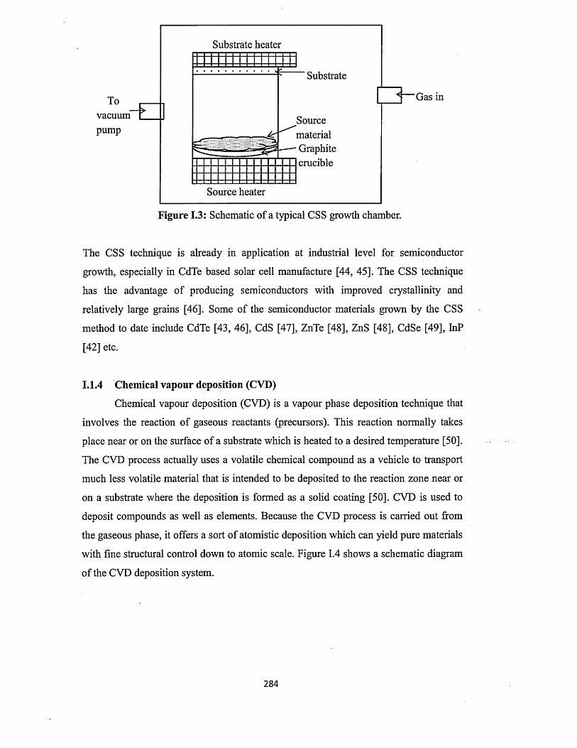
Substrate heater
Tovacuum"pump
Substrate
SourcematerialGraphitecrucible
Source heater
< Gas in
Figure 1.3: Schematic of a typical CSS growth chamber.
The CSS technique is already in application at industrial level for semiconductor
growth, especially in CdTe based solar cell manufacture [44, 45]. The CSS technique
has the advantage o f producing semiconductors with improved crystallinity and
relatively large grains [46]. Some of the semiconductor materials grown by the CSS
method to date include CdTe [43, 46], CdS [47], ZnTe [48], ZnS [48], CdSe [49], InP
[42] etc.
1.1.4 Chemical vapour deposition (CVD)
Chemical vapour deposition (CVD) is a vapour phase deposition technique that
involves the reaction of gaseous reactants (precursors). This reaction normally takes
place near or on the surface of a substrate which is heated to a desired temperature [50].
The CVD process actually uses a volatile chemical compound as a vehicle to transport
much less volatile material that is intended to be deposited to the reaction zone near or
on a substrate where the deposition is formed as a solid coating [50]. CVD is used to
deposit compounds as well as elements. Because the CVD process is carried out from
the gaseous phase, it offers a sort of atomistic deposition which can yield pure materials
with fine structural control down to atomic scale. Figure 1.4 shows a schematic diagram
o f the CVD deposition system.
2 8 4
Heater
Carrier gas. source
SubstrateDepositedfilm Substrate
holderHeater
Figure 1.4: Schematic o f a CVD deposition system.
The CVD process is typically carried out inside a vacuum since gaseous precursors are
involved. The pressure in the chamber varies depending on the material to be deposited
and the particular modification made to the basic CVD system. The technique generally
has moderate deposition rates up to 250 nm per minute with good throwing power on
substrates with complex shape. It can as well be scaled up to the large wafer size. There
are several variations of the CVD technique depending on the particular modification
made to the standard CVD process. These variations include the following:
1.1.4.1 Plasma enhanced CVD (PECVD)
In PECVD, the precursor gases are subjected to time varying electric fields with
frequencies of 50 kHz to 13.5 MHz or even microwave frequencies. This eventually
causes partial ionisation of the gas atoms and creates plasma o f the precursor gases [51].
DC power can also be used to create the plasma [52]. The presence of this plasma
enhances the reaction of the carrier gases at the substrate to produce thin film coatings.
The deposition rate in this case is higher. The deposition process takes place at
temperatures up to 700°C [51, 52]. A range o f thin film coatings that have been
produced with the PECVD technique include ZnO [51, 53], ZnS [52], CdS [54], HgTe-
CdTe [55], Ge [56], InP [57] etc.
1.1.4.2 Low pressure CVD (LPCVD)
This is done under vacuum condition because of the low pressure involved. The
pressure can be as low as 17 mTorr (2.3 Pa) [58]. The growth temperatures are as high
285
as 900°C, helping to obtain dense and stable deposits [59]. Some of the materials
deposited by LPCVD include Cr0 2 [60], Si [61], graphene [58], ZnO [62] etc.
1.1.4.3 Atomic layer deposition (ALD)
This is a variant of CVD technique involving pressure typically in the range 0.1
- 10 mbar (i.e 170 - 17000 Pa) or even atmospheric pressure and temperature in the
range 50 - 500°C [63]. It allows fine control of the deposited film thickness down to
atomic levels with the ability o f allowing deposition on large, as well as complex
shaped surfaces [64]. As an industrial technique, ALD is commonly used for the
deposition of thin films for electroluminescent flat-panel displays.
The basic feature of ALD is that deposition of films proceeds in cycles with a
definite film thickness deposited in each reaction cycle. The total thickness of the film
produced is therefore directly proportional to the number of cycles involved [64]. Each
cycle typically takes place within seconds with about 0.1 A to 3 A thickness of film
deposited [64]. This process however depends on the reaction rate of the precursors in
the reactor as well as on the type o f reactor used and the amount o f available adsorption
sites on the substrate. The average deposition rate is low and in the range 100 - 300 nm
per hour and the range o f materials that can be grown by this method is limited due to
cost [64]. Some of the semiconductor materials grown by this technique include ZnO
[65], ZnS [6 6 ], In2 S3 [67], ZnTe [6 8 ], CdTe [6 8 ], PbS [69], GaAs [70] etc.
1.1.4.4 Atmospheric pressure CVD (APCVD)
The APCVD process is carried out under normal atmospheric pressure as the
name suggests. It is suitable for the deposition of oxides [71, 72]. High-temperature
APCVD is usually used for the deposition of epitaxial layers such as SiGe [73] as well
as hard compound metallurgical coatings like TiN [74]. Low temperature APCVD is
best suitable for the deposition o f many insulating oxides [71, 72]. The deposition rate is
generally low giving rise to low throughput. Good uniformity o f the deposited films is
not always ensured in this technique and the incidence o f pinholes is highly probable.
APCVD is not common for growing other semiconductors. One can however find a
publication involving the use of APCVD-grown CdTe in solar cell fabrication [75].
1.1.4.5 Photo-enhanced CVD (PHCVD)
In photo-enhanced CVD (PHCVD), electromagnetic radiation (photons) is used
to activate the vapour-phase reactants. Short-wavelength (UV) radiation is normally286

used in this process in order to create reactive free-radicals that react to the films [76].
Unlike APCVD, PHCVD has a more wide range o f application in thin film growth. The
range of materials grown with this technique to date include S i0 2 [77], a-Si:H [78],
SiNx, T i02, Ta2 0 5 , H f0 2 [79], ZnSe [80], ZnO [81] etc. A variant of PHCVD is Laser-
induced CVD (LCVD), which employs laser as a source o f photons.
1.1.5 Metalorganic chemical vapour deposition (MOCVD)
Metalorganic chemical vapour deposition (MOCVD) is also known as
metalorganic vapour phase epitaxy (MOVPE). This is a type o f CVD technique in
which the precursors are usually metalorganic vapour rather than inorganic vapour used
in the conventional CVD process. Metalorganic compounds are essentially metal atoms
with some alkyl radicals attached to them. Such alkyl radicals include methyl, ethyl and
isopropyl [82]. This technique offers the growth of epitaxial layers o f doped and
undoped compound semiconductors. It has the advantage o f being used to grow most
semiconductors that prove difficult to grow using other high-quality epitaxial growth
techniques such as MBE [83].
The MOCVD technique involves very complex processes but can be used to
grow semiconductors with complex multilayers. The growth chamber does not actually
involve a vacuum condition but deposition pressure in the growth chamber can be in the
range o f 10 to 760 Torr (~1333 to 101325 Pa). This is one of the reasons it can be used
to grow a very wide variety of semiconductors with high quality. The precursor gases
must be o f ultra-high purity as a requirement for growing high-quality semiconductors.
The substrate must also be a lattice-matched semiconductor such as GaAs. In any case,
MOCVD does not have the type of fine precision found in MBE technique, such as in
the control o f thickness as well as doping density [83].
MOCVD is in active application in the fabrication of semiconductor devices
such as multi-junction solar cells with high efficiencies, light emitting diodes as well as
laser diodes [82]. Many semiconductors have been grown using the MOCVD technique
to date. These include ZnSe, ZnMgSSe, ZnSSe [84], GaAs [85], AlGaAs [8 6 ], InGaAs
[87], InP [8 8 ], InAs [89], InSb [90], GaSb [91], CdTe [92], CdS, CdSe [93], ZnS [94],
GaN [95], ZnO [96] and so on.
1.2 Liquid phase deposition (LPD) techniques
In liquid phase deposition of thin films the precursors consist o f ions, atoms or
molecules in liquid solutions. The solution can either be aqueous or non-aqueous
287
depending on the need. The LPD techniques in general do not require any vacuum
system. The reagents are more or less easily available, thus solving the problem o f
acquiring expensive and sometimes, very sensitive metal-organic precursors as used in
chemical vapour deposition. As a result, LPD techniques provide cheaper and more
environmentally friendly growth techniques unlike in vapour-phase techniques. Some
temperature-sensitive substrates can be used in LPD. In other words, a wide range of
substrates can be used. Also large area deposition is very easy in liquid phase deposition
since there are no vacuum chambers to restrict the size o f the substrates that can be
used. Below are some o f the liquid phase (or wet chemical) deposition techniques
available for thin film deposition.
1.2.1 Spray pyrolysis
In spray pyrolysis, a liquid solution of the compound to be deposited is made.
This solution is then pulverised by means o f a neutral gas and atomised by an atomiser
to form an aerosol. This aerosol is sprayed by the atomiser on a heated substrate so that
the solvent evaporates, and the solute precipitates on the substrate. Due to the
temperature of the substrate, the precipitate dries thermally onto the substrate and
solidifies into a thin film with crystallites. This process of adhesion and solidification
into crystallites is called sintering.
Figure 1.5 shows the schematic of the spray pyrolysis technique. The properties
of the deposited film are controlled by a set of variables including temperature,
concentration of precursors in the solution, the type of solvent used to dissolve the
precursors, the atomisation method etc. [97]. Among all these however, temperature ■
appears to be the most influential.
Spray pyrolysis is mostly used to deposit oxides although other semiconductor
films can be grown using it [97, 98]. Some of the thin films grown by the spray
pyrolysis techniques include SnC>2 [99], Sn0 2 :F [100], In:Sn0 2 [101], ZnO [102],
Al:ZnO [103], ZnS [104], CdTe [105], CdS [106], CdSe [107] and others.
28 8
Atomiser containing precursor solution
Spray(aerosol)
Heater
Figure 1.5: Schematic o f the spray pyrolysis deposition technique.
1.2.2 Sol-gel deposition technique
Sol-gel technique involves initially making a suspension o f precursors for the
compound to be deposited in a colloidal form [108]. In general, these precursors are
usually metals or metalloids that are surrounded by different ligands [108] such as the
alcohol groups. During the sol-gel process, two major reactions take place. These are
hydrolysis o f the ligands to form hydroxyl groups, and the subsequent condensation of
these hydroxyl groups. Four major steps are then involved in sol-gel deposition of thin
or thick coatings as depicted in figure 1 .6 .
lllllllllllllllllSubstrate ----- >| Substrate 1----- > Substrate
Sol-gelformation
Sol-gel application on
substrate
Polymerisation and formation of continuous
network
Heat treatment and pyrolysis
to form coating
Figure 1.6: Schematic of the sol-gel deposition process.
Application of the sol-gel on the substrates can be either by dipping the substrate in the
sol-gel solution, or by dropping the sol-gel on the substrates and spinning to spread it, or
by painting it on the substrate, or by spraying. Then the particles o f the compound being
deposited polymerise from the solution forming a continuous network. During this
stage, the compound which serves as the vehicle for carrying the precursor particles is
removed from the sol-gel solution. On heat-treating the resulting network o f particles,
pyrolysis of the remaining components takes place forming the desired coating. The sol-
289

gel deposited coating (film) can be amorphous or crystalline in nature.
The sol-gel technique is a cost-effective technique used for the production of
organic and inorganic industrial coatings such as anti-corrosion coatings as well as for
the deposition of semiconductor thin films [109, 110]. Some o f the materials that are
produced by sol-gel technique include TiC>2 [111], ZnO [112], Cdln2 0 4 [113], CdO
[114], ZnS [115], CdSe [116], ZnSe [117] and others. Substrates for sol-gel coating can
be conducting or non-conducting materials.
1.2.3 Spin coating technique
Spin coating is another type of wet chemical deposition technique used for
making different types of coatings. Similar to the sol-gel process, the material to be
spin-coated is prepared as a solution in a solvent that evaporates easily. In order to carry
out the coating process a puddle of the solution is dispensed at the centre o f the
substrate which is attached to a spinner. The substrate with the fluid is then spun at a
high speed o f 1000 - 6000 rpm. The centripetal force on the fluid causes it to spread
over the entire surface o f the substrate while the solvent evaporates simultaneously. The
deposited material then dries in the process to form a film. Depending on the need, this
deposited film can be given heat treatment in other to enhance its quality. Film thickness
from few nanometres up to few micrometres, can be deposited using this technique. The
thickness and other properties of the deposited film depend on a number o f parameters
ranging from the spin speed to the rate of drying of the solvent (which also depends on
the nature o f the solvent), surface tension, spin time, concentration of the solution and
volume o f the solution dispensed at a time. Figure 1.7 illustrates the processes involved
in a spin coating process as explained above. Spin coating can be used for depositing a
thin film on both conducting and non-conducting substrates.
The spin coating process is applied extensively in the industry such as in the
production of optical mirrors, photolithography [118] etc. The technique produces films
with good uniformity at a relatively low cost compared to some other techniques. Some
of the thin film semiconductors deposited using spin coating include TiC>2 [119], ZnO
[120], Sn02 [121], organic semiconductors [122 - 124], single wall carbon nanotubes
(SWCNT) [125] etc.
2 9 0
FilmSolution formation Thin film
SubstrateDryingPuddle of
solution dispensed
Solution
Substrate Substrate
on Spinner
substrate
Figure 1.7: Schematic of the spin coating process.
1.2.4 Screen printing
In screen printing technique, a paste of the material (compound) to be screen-
printed is prepared and used as the ink for printing. A mesh is used to precisely define
the area o f the substrate that is to be printed upon. A screen printer is then used to apply
the paste evenly to the mask [126]. The paste application process involves rubbing the
paste on the mask with a roller called squeegee, thus pushing the paste through the
openings in the mask in order to deposit it on the underlying substrate [126]. Figure 1.8
shows the schematic of the screen printing process.
Squeegee
siPrint
\
ed area
t
Massten
\
k o rcil
r-- I IT.:™! 1n-.-.-i | . . .
Substrate
Figure 1.8: Schematic o f the screen printing process.
After the printing, the printed sample is left to dry. Annealing of the sample can as well
be done. The annealing condition depends on the nature of the substrate and the
thickness of the printed film depends on the thickness of the mask used [126]. The
quality of the printed film depends on a number of factors which include, the viscosity
of the paste used, the rate of drying o f the printed paste, the pressure o f the squeegee on
the paste during the printing process and so on [127, 128].
The screen printing technique finds application in the semiconductor inductry
such as in fabrication of biosensors [129], solar cells [130], light-emitting diodes [131]
291
etc. Some other materials produced by screen printing including organic and inorganic
semiconductor materials as well as ceramic materials are T1O2 [132],
(Nao.5Bio.5)o.94Bao.o6Ti03[133], CdSe [134], ZnO, poly (3,4-ethylenedioxythiopene) poly
(styrene-Sulfonate)(PEDOT:PSS), Poly-(3-(2-methylhexan-2-yl) oxy-carbonyl
dithiophene) (P3MHOCT) [130] etc.
1.2.6 Successive ionic layer adsorption and reaction (SIL AR)
The SILAR technique is a low-cost solution-based technique for the deposition
of a wide range o f thin film compound materials. It is a convenient technique for large
area thin film deposition. It is based on the adsorption o f ions of the different precursor
species on a substrate in a successive fashion and the consequent reaction o f these ions
on the substrates to form the required compound [135,136].
In order to deposit a given compound, separate solutions o f the various
precursors are prepared in separate beakers to provide anions and cations. The substrate
(after cleaning) is then dipped in the solutions separately in succession with rinsing in
de-ionised water in-between dips. When the substrate is dipped in all the precursors, a
cycle is completed. The thickness of the film produced depends directly on the number
of cycles performed [137]. During the dipping process, ions of the precursors adsorb (at
nucleation sites) on the surface of the substrate. These anions and cations then react on
the substrate to form atoms of the thin film being deposited. The rinsing process helps to
prevent precipitation in the solutions. Figure 1.9 illustrates the SILAR process. SILAR
method is a modification of the chemical bath deposition (CBD) where precipitation
causes a lot of material waste. Several compound semiconductor and composite thin
films have been deposited using the SILAR method. These include (NiS)x(CdS)(i.X)
composite [138], ZnS [139], M 0 S2 , Bi2Se3 , SbSe3 , Bi2Se3-Sb2-Se3 [137], CdS, LaS,
MnS, ZnSe [137], CdO [140], Cu2ZnSnS4 [141], ZnTe [142], In2S3 [143], CuInSe2,
CuInSeNxSx [144], SnS [145], T i02 [146] etc
292
Substrate Thin film
W i W I WJ_p
Precursor with cations
De-ionisedwater
Precursor with anions
De-ionisedwater
Figure 1.9: Schematic o f the SILAR deposition process.
1.2.5 Chemical bath deposition (CBD)
The chemical bath deposition (CBD) technique is one o f the low-cost and
widely researched thin film deposition techniques since 1919. It is scalable and used as
a batch process. The major challenge in CBD process is the generation of large volumes
of chemical waste after each round of deposition. This is because it is difficult to re-use
the solution once the reaction is completed during any deposition process as a result of
large amount of precipitation generated in most cases. The thickness and quality o f the
deposited films in CBD depend on a number of parameters including temperature,
stirring rate, deposition time, nature of substrate and concentration of the precursors in
solution [147, 148].
In the CBD technique, the deposition of the required compound, say XY,jffom a
solution containing ions of XY, say X+ and Y,' depends on the solubility product (Ksp)
of the compound XY and the ionic product (K ip) of X+ and Y." If the ionic product (Kn>)
exceeds the solubility product (Ksp), then, the excess ions precipitate to form XY [147,
148]. In order to control the rate of the release o f these ions (especially the metallic ion
X*), a complexing agent (or chelating agent) is added to the solution. One example o f a
complexing agent usually employed in the CBD process is ammonia. The complexing
agent helps to form a complex of the metallic ion species, making the ion soluble in the
solution which is most favoured by an alkaline environment [147, 148]. CBD technique
has been used for the deposition of semiconductor thin films for various applications.
Some of the semiconductors include ZnSe [148], CdS [149], ZnS [150], PbS [151], ZnO
[152], SnS-CuS [153], CuO [154], CdTe [155], Sn02, Cd2Sn04 [156], CdO [157] and
others.
293
1.2.6 Electrochemical deposition (ED)
Electrochemical deposition or simply, Electrodeposition (ED) is the deposition
of dissolved or suspended materials on a substrate (electrode) by means of applied
electric field [158]. In other words, the chemical reaction resulting in the deposition of
the solid material does not proceed on its own as is the case with CBD. The reaction is
thus thermodynamically unfavourable because the overall change in free energy (G) for
the reaction is positive. Therefore, the applied electrical field supplies the energy needed
to drive the reaction [159]. Electrodeposition, otherwise known as electroplating is a
well-known industrial process traditionally used to deposit coatings o f noble metals on
conducting substrates for protection of the substrates which are usually metals. It is also
used over the centuries for extracting and purifying metals.
The application of electrodeposition as a semiconductor deposition technique
became known mainly in the 1970's [160 - 164]. However, in the case of deposition of
compound semiconductors, the deposition reaction becomes more complicated than the
deposition of single metals or elemental semiconductor materials such as Si and Ge. The
reason for this complexity is because two or more elements must be co-deposited at the
substrate with one o f the elements being a non-metal. In order to electrodeposit a
semiconductor (elemental or compound semiconductor), a liquid electrolyte containing
the ions of the elements o f the semiconductor is prepared in a beaker or tank. This
solution can either be aqueous or non-aqueous provided the precursors are very soluble
in whichever solvent used [165 - 167]. Through a working electrode (usually the
cathode) and a counter electrode (usually the anode) a DC current is passed through the
electrolyte by means of a potentiostat in order to drive the deposition process: The>
deposition takes place cathodically so that the applied potential (cathodic voltage) can
be maintained constant. In a conventional electrodeposition process, a third electrode
(the reference electrode) is required which helps to stabilize the applied voltage and
current. Two major reference electrodes used in this case are Ag/AgCl electrode and
Hg/HgCl2 (saturated calomel) electrode. The use of reference electrode in the
electrodeposition of semiconductors can sometimes pose a contamination problem. This
is because the electrical properties of semiconductors can drastically be affected by the
presence of unwanted ions even in parts per billion levels [168]. Hg/HgCl2 and
Ag/AgCl reference electrodes contain K+ and Ag+ which are ions o f groups LA and IB
elements that are p-type dopants for II-VI semiconductors [169, 170]. These ions are
known to be detrimental to CdTe-based solar cells [168, 171]. Possible leakage o f these
ions from the reference electrode into the deposition electrolyte can cause serious
294
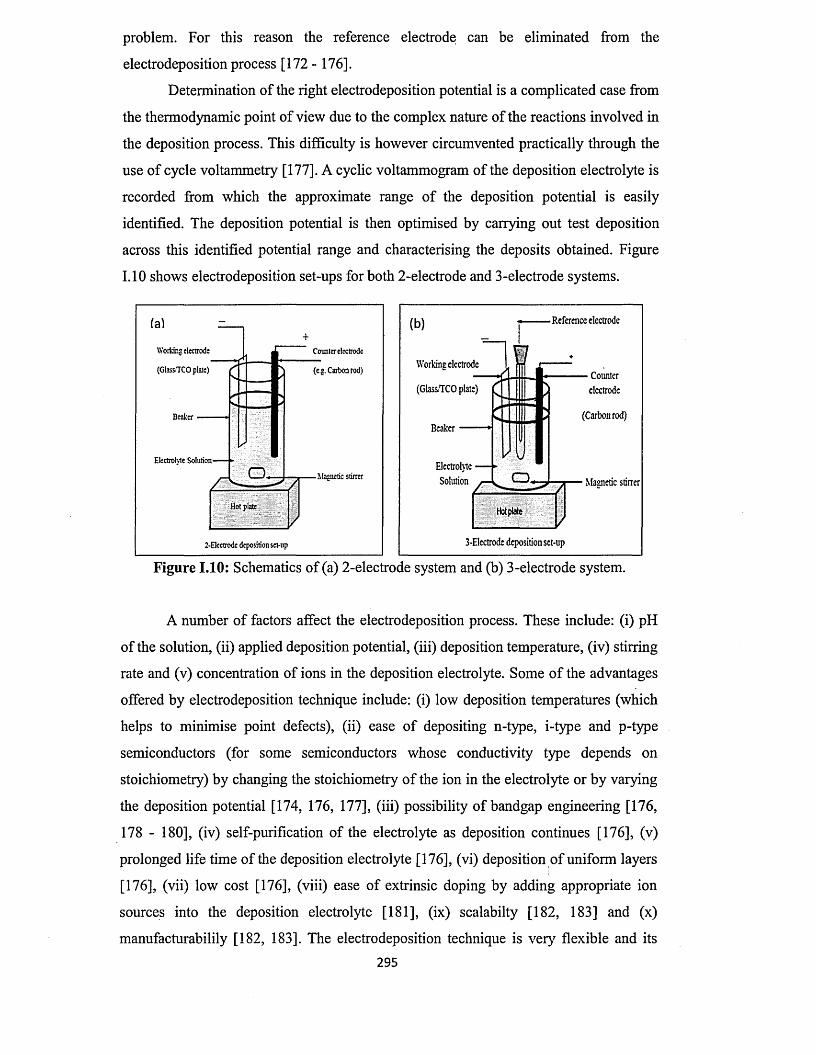
problem. For this reason the reference electrode can be eliminated from the
electrodeposition process [172- 176].
Determination of the right electrodeposition potential is a complicated case from
the thermodynamic point of view due to the complex nature of the reactions involved in
the deposition process. This difficulty is however circumvented practically through the
use of cycle voltammetry [177]. A cyclic voltammogram of the deposition electrolyte is
recorded from which the approximate range o f the deposition potential is easily
identified. The deposition potential is then optimised by carrying out test deposition
across this identified potential range and characterising the deposits obtained. Figure
1.10 shows electrodeposition set-ups for both 2-electrode and 3-electrode systems.
fa)Working electrodi
(GlassTCO plate)
Beaker
Electrolyte Solution-
Counter electrode
O .
(e.g.Cartx>arod)
Hot plate
-Magnetic stirrer
/2-Electrode deposition set-up
(b)
Working electrode
(GlassTCO plate)
•Reference electrode
Beaker
ElectrolyteSolution
Hotplate
3-Electrode deposition set-up
— Counter electrode
(Carbon rod)
■ Magnetic stirrer
Figure 1.10: Schematics of (a) 2-electrode system and (b) 3-electrode system.
A number of factors affect the electrodeposition process. These include: (i) pH
of the solution, (ii) applied deposition potential, (iii) deposition temperature, (iv) stirring
rate and (v) concentration of ions in the deposition electrolyte. Some o f the advantages
offered by electrodeposition technique include: (i) low deposition temperatures (which
helps to minimise point defects), (ii) ease o f depositing n-type, i-type and p-type
semiconductors (for some semiconductors whose conductivity type depends on
stoichiometry) by changing the stoichiometry o f the ion in the electrolyte or by varying
the deposition potential [174, 176, 177], (iii) possibility of bandgap engineering [176,
178 - 180], (iv) self-purification of the electrolyte as deposition continues [176], (v)
prolonged life time of the deposition electrolyte [176], (vi) deposition o f uniform layers
[176], (vii) low cost [176], (viii) ease of extrinsic doping by adding appropriate ion
sources into the deposition electrolyte [181], (ix) scalabilty [182, 183] and (x)
manufacturabilily [182, 183]. The electrodeposition technique is very flexible and its
295
manufacturability has already been demonstrated by BP producing solar panels of ~1 m 2
with -10% efficiency in the recent past [182]. It can be used to grow both single crystal
and polycrystalline materials [176, 184]. This is the deposition technique employed in
the research project reported in this thesis. Many semiconductors, conducting polymers,
as well as different solar cell structures and other devices have been produced using
electrodeposition technique. These include CdTe [185], CdS [173], ZnS [172], ZnSe
[167,181], ZnTe [186,187], GaP [187], GaAs [161], InP [188], Polyaniline [189 -191],
Polymer-semiconductor composites [192], CuInSe2 [167, 174, 175], CIGS [178], Si
[193], Ge [194], InSb [195], InAs [196] and many others.
2 9 6
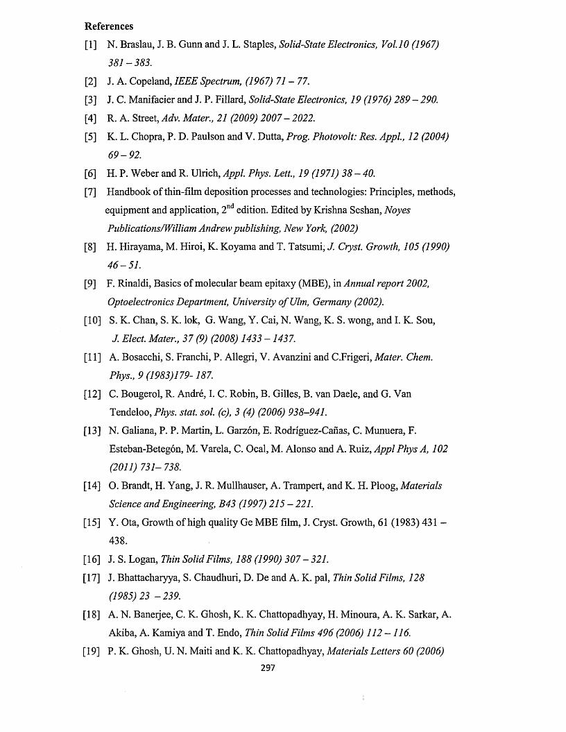
References
[1] N. Braslau, J. B. Gunn and J. L. Staples, Solid-State Electronics, Vol. 10 (1967)
381-383 .
[2] J. A. Copeland, IEEE Spectrum, (1967) 7 1 -7 7 .
[3] J. C. Manifacier and J. P. Fillard, Solid-State Electronics, 19 (1976) 289 - 290.
[4] R. A. Street, Adv. Mater., 21 (2009) 2007 - 2022.
[5] K. L. Chopra, P. D. Paulson and V. Dutta, Prog. Photovolt: Res. Appl., 12 (2004)
6 9 -9 2 .
[6] H. P. Weber and R. Ulrich, Appl. Phys. Lett., 19 (1971) 38 - 40.
[7] Handbook of thin-film deposition processes and technologies: Principles, methods,
equipment and application, 2nd edition. Edited by Krishna Seshan, Noyes
Publications/William Andrew publishing, New York, (2002)
[8] H. Hirayama, M. Hiroi, K. Koyama and T. Tatsumi, J. Cryst. Growth, 105 (1990)
4 6 -5 1 .
[9] F. Rinaldi, Basics of molecular beam epitaxy (MBE), in Annual report 2002,
Optoelectronics Department, University o f Ulm, Germany (2002).
[10] S. K. Chan, S. K. lok, G. Wang, Y. Cai, N. Wang, K. S. wong, and I. K. Sou,
J. Elect. Mater., 37 (9) (2008) 1433 -1437 .
[11] A. Bosacchi, S. Franchi, P. Allegri, V. Avanzini and C.Frigeri, Mater. Chem.
Phys., 9 (1983)179-187.
[12] C. Bougerol, R. Andre, I. C. Robin, B. Gilles, B. van Daele, and G. Van
Tendeloo, Phys. stat. sol. (c), 3 (4) (2006) 938-941.
[13] N. Galiana, P. P. Martin, L. Garzon, E. Rodriguez-Canas, C. Munuera, F.
Esteban-Betegon, M. Varela, C. Ocal, M. Alonso and A. Ruiz, Appl Phys A, 102
(2011) 731- 738.
[14] O. Brandt, H. Yang, J. R. Mullhauser, A. Trampert, and K. H. Ploog, Materials
Science and Engineering, B43 (1997) 215 - 221.
[15] Y. Ota, Growth of high quality Ge MBE film, J. Cryst. Growth, 61 (1983) 431 -
438.
[16] J. S. Logan, Thin Solid Films, 188 (1990) 307 - 321.
[17] J. Bhattacharyya, S. Chaudhuri, D. De and A. K. pal, Thin Solid Films, 128
(1985)23 -2 3 9 .
[18] A. N. Baneijee, C. K. Ghosh, K. K. Chattopadhyay, H. Minoura, A. K. Sarkar, A.
Akiba, A. Kamiya and T. Endo, Thin Solid Films 496 (2006) 1 12 -116 .
[19] P. K. Ghosh, U. N. Maiti and K. K. Chattopadhyay, Materials Letters 60 (2006)
297
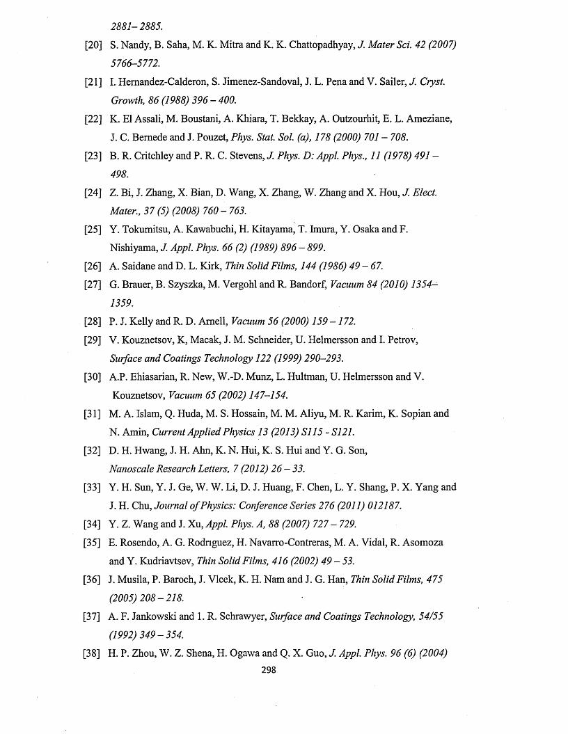
[20] S. Nandy, B. Saha, M. K. Mitra and K. K. Chattopadhyay, J. Mater Sci. 42 (2007)
5766-5772.
[21] I. Hemandez-Calderon, S. Jimenez-Sandoval, J. L. Pena and V. Sailer, J. Cryst.
Growth, 86 (1988) 396 - 400.
[22] K. El Assali, M. Boustani, A. Khiara, T. Bekkay, A. Outzourhit, E. L. Ameziane,
J. C. Bemede and J. Pouzet, Phys. Stat. Sol. (a), 178 (2000) 701 - 708.
[23] B. R. Critchley and P. R. C. Stevens, J. Phys. D: Appl. Phys., 11 (1978) 491 -
498.
[24] Z. Bi, J. Zhang, X. Bian, D. Wang, X. Zhang, W. Zhang and X. Hou, J. Elect.
Mater., 37 (5) (2008) 760 - 763.
[25] Y. Tokumitsu, A. Kawabuchi, H. Kitayama, T. Imura, Y. Osaka and F.
Nishiyama, J. Appl. Phys. 66 (2) (1989) 8 9 6 -8 9 9 .
[26] A. Saidane and D. L. Kirk, Thin Solid Films, 144 (1986) 49 - 67.
[27] G. Brauer, B. Szyszka, M. Vergohl and R. Bandorf, Vacuum 84 (2010) 1354-
1359.
[28] P. J. Kelly and R. D. Amell, Vacuum 56 (2000) 159 -1 7 2 .
[29] V. Kouznetsov, K, Macak, J. M. Schneider, U. Helmersson and I. Petrov,
Surface and Coatings Technology 122 (1999) 290-293.
[30] A.P. Ehiasarian, R. New, W.-D. Munz, L. Hultman, U. Helmersson and V.
Kouznetsov, Vacuum 65 (2002) 147-154.
[31] M. A. Islam, Q. Huda, M. S. Hossain, M. M. Aliyu, M. R. Karim, K. Sopian and
N. Amin, Current Applied Physics 13 (2013) S I 15 - S121.
[32] D. H. Hwang, J. H. Ahn, K. N. Hui, K. S. Hui and Y. G. Son,
Nanoscale Research Letters, 7 (2012) 26 — 33.
[33] Y. H. Sun, Y. J. Ge, W. W. Li, D. J. Huang, F. Chen, L. Y. Shang, P. X. Yang and
J. H. Chu, Journal o f Physics: Conference Series 276 (2011) 012187.
[34] Y. Z. Wang and J. Xu, Appl. Phys. A, 88 (2007) 727 - 729.
[35] E. Rosendo, A. G. Rodriguez, H. Navarro-Contreras, M. A. Vidal, R. Asomoza
and Y. Kudriavtsev, Thin Solid Films, 416 (2002) 49 - 53.
[36] J. Musila, P. Baroch, J. Vlcek, K. H. Nam and J. G. Han, Thin Solid Films, 475
(2005)208-218.
[37] A. F. Jankowski and 1. R. Schrawyer, Surface and Coatings Technology, 54/55
(1992)349-354.
[38] H. P. Zhou, W. Z. Shena, H. Ogawa and Q. X. Guo, J. Appl. Phys. 96 (6) (2004)
298

3199 -3205 .
[39] J. Ross and M. Rubin, Materials Letters, 12 (1991) 215 - 218.
[40] C. W. Hsu, T. C. Cheng, C. H. Yang, Y. L. Shen, J. S. Wu and S. Y. Wu, Journal
o f Alloys and Compounds, 509 (2011) 1774 -1776.
[41] P. M. Babu, G. V. Rao, P. S. Reddy and S. Uthanna, J. Mater. Sci: Materials in
Electronics, 15 (2004) 389 - 394.
[42] D. Kiriya, M. Zheng, R. Kapadia, J. Zhang, M. Hettick, Z. Yu, K. Takei, H. H.
Wang, P. Lobaccaro and A. Javey, J. Appl. Phys. 112 (2012) 123102-1 -123102-
6.
[43] S. Mazzamuto, L. Vaillant, A. Bosio, N. Romeo, N. Armani and G. Salviati,
Thin Solid Films, 516 (2008) 7079 - 7083.
[44] htto://www.2 reentechmedia.com/articles/read/GE-Research-Beats-First-S0 lars-
CdTe-P V-Efficiencv-Record
[45] D. Bonnet, Thin Solid Films, 361-362 (2000) 547 - 552.
[46] C.S. Ferekides, D. Marinskiy, V. Viswanathan, B. Tetali, V. Palekis, P. Selvaraj
and D. L. Morel, Thin Solid Films 361 - 362 (2000) 520 - 526.
[47] J. Schaffner, E. Feldmeier, A. Swirschuk, H.-J. Schimper, A. Klein and W.
Jaegermann, Thin Solid Films, 519 (2011) 7556 - 7559.
[48] D. Kurbatov, V. Kosyak, M. Kolesnyk, A. Opanasyuk, and S. Danilchenko,
Integrated Ferroelectrics, 103 (2009) 32-40.
[49] O. de Melo, E. SaAnchez, H. RodroAguez, S. De Roux, F. RaAbago-Bemal and
J. Ruiz-Garcia, Mater. Chem. Phys. 59 (1999) 120 -1 2 4 .
[50] N. J. Archer, Phys. Technol. 10 (1979) 152 -1 6 1 .
[51] X. Liu, X. Wu, H. Cao, and R. P. H. Chang, J. Appl. Phys. 95 (6) (2004) 3141 -
3147.
[52] J. S. Jie, W. J. Zhang, Y. Jiang, X. M. Meng, J. A. Zapien, M. W. Shao and S. T.
Lee, Nanotechnology, 17 (2006) 2913 -2917 .
[53] P.K. Shishodia, H.J. Kim, A. Wakahara, A. Yoshida, G. Shishodia and R. M.
Mehra, Journal o f Non-Crystalline Solids, 352 (2006) 2343 - 2346.
[54] N. I . Fainer, M. L. Kosinova, Y. M. Rumyantsev, E. G. Salman and F. A.
Kuznetsov, Thin Solid Films, 280 (1996) 1 6 -1 9 .
[55] L. M. Williams, P.-Y. Lu, and S. N. G. Chu, A ppl Phys. lett., 54 (14) (1989) 1329
-1331 .
[56] R. A. Rudder, G. G. Fountain, and R. J. Markunas, J. Appl. Phys. 60 (10) (1986)
3519 - 3522.
29 9
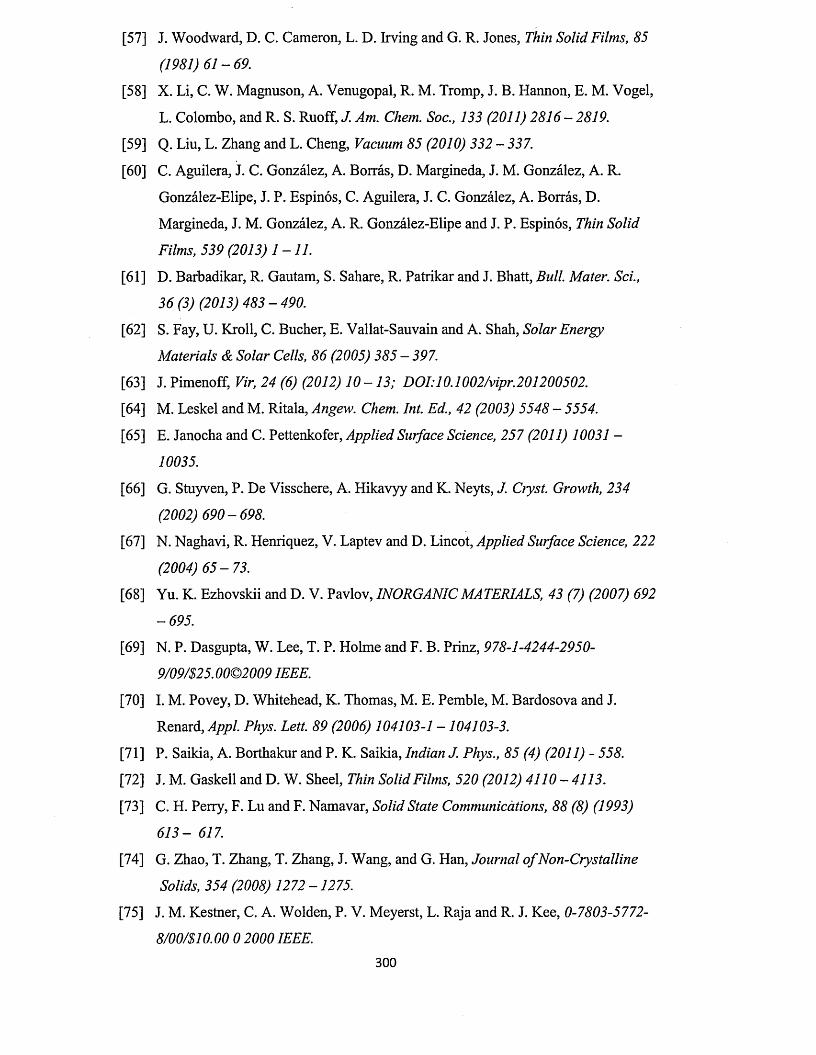
[57] J. Woodward, D. C. Cameron, L. D. Irving and G. R. Jones, Thin Solid Films, 85
(1981) 61 - 69.
[58] X. Li, C. W. Magnuson, A. Venugopal, R. M. Tromp, J. B. Hannon, E. M. Vogel,
L. Colombo, and R. S. Ruoff, J. Am. Chem. Soc., 133 (2011) 2816 - 2819.
[59] Q. Liu, L. Zhang and L. Cheng, Vacuum 85 (2010) 332 - 337.
[60] C. Aguilera, J. C. Gonzalez, A. Borras, D. Margineda, J. M. Gonzalez, A. R.
Gonzalez-Elipe, J. P. Espinos, C. Aguilera, J. C. Gonzalez, A. Borras, D.
Margineda, J. M. Gonzalez, A. R. Gonzalez-Elipe and J. P. Espinos, Thin Solid
Films, 539 (2013) 1 -1 1 .
[61] D. Barbadikar, R. Gautam, S. Sahare, R. Patrikar and J. Bhatt, Bull. Mater. Sci.,
36 (3) (2013) 4 8 3 -4 9 0 .
[62] S. Fay, U. Kroll, C. Bucher, E. Vallat-Sauvain and A. Shah, Solar Energy
Materials & Solar Cells, 86 (2005) 385 - 397.
[63] J. Pimenoff, Vir, 24 (6) (2012) 1 0 -1 3 ; D01:10.1002/vipr.201200502.
[64] M. Leskel and M. Ritala, Angew. Chem. Int. Ed., 42 (2003) 5548 - 5554.
[65] E. Janocha and C. Pettenkofer, Applied Surface Science, 257 (2011) 10031 -
10035.
[66] G. Stuyven, P. De Visschere, A. Hikavyy and K. Neyts, J. Cryst. Growth, 234
(2002)690 - 698.
[67] N. Naghavi, R. Henriquez, V. Laptev and D. Lincot, Applied Surface Science, 222
(2004)65-73 .
[68] Yu. K. Ezhovskii and D. V. Pavlov, INORGANIC MATERIALS, 43 (7) (2007) 692
-6 9 5 .
[69] N. P. Dasgupta, W. Lee, T. P. Holme and F. B. Prinz, 978-1-4244-2950-
9/09/S25.0002009 IEEE.
[70] I. M. Povey, D. Whitehead, K. Thomas, M. E. Pemble, M. Bardosova and J.
Renard, Appl. Phys. Lett. 89 (2006) 104103-1 -104103-3.
[71] P. Saikia, A. Borthakur and P. K. Saikia, Indian J. Phys., 85 (4) (2011) - 558.
[72] J. M. Gaskell and D. W. Sheel, Thin Solid Films, 520 (2012) 4110 - 4113.
[73] C. H. Perry, F. Lu and F. Namavar, Solid State Communications, 88 (8) (1993)
6 1 3 - 617.
[74] G. Zhao, T. Zhang, T. Zhang, J. Wang, and G. Han, Journal o f Non-Crystalline
Solids, 354 (2008) 1272 -1275.
[75] J. M. Kestner, C. A. Wolden, P. V. Meyerst, L. Raja and R. J. Kee, 0-7803-5772-
8/00/$10.00 0 2000 IEEE.
3 0 0
[76] H. Sankur, Thin Solid Films, 218 (1992) 161 —169.
[77] V. Sanchez, J. Mungu and M. Estrada, Microelectronics Reliability, 44 (2004)
8 8 5 - 888.
[78] W. I. Milne, F. J. Clough, S. C. Deane, S. D. Baker and P. A. Robertson, Applied
Surface Science, 43 (1989) 277 — 284.
[79] Q. Fang, J. Y. Zhang, Z. M. Wang, G. He, J. Yu and I. W. Boyd, Microelectronic
Engineering, 66 (2003) 621 - 630.
[80] W. E. Johnson and L. A. Schlie, Appl. Phys. Lett, 40 (9) (1982 ) 798 - 801.
[81] R. Solanki and G. J. Collins, Appl. Phys. Lett., 42 (8) (1983) 662 - 663.
[82] A. G. Thompson, Materials Letters, 30 (1997) 255 - 263.
[83] J. L. Zilko, Metal organic chemical vapour deposition: Technology and
equipment,
http.7/www. elsevierdirect. com/companions/978143 777873l/past_edition_
chapters/Metal_Organic_Chemical_Vapor.pdf (Retrieved 15/10/2013).
[84] J. Sollner, M. Deschler, H. Jiirgenserf, H. Kalisch, W. Taudt, H. Hamadeh, M.
Heuken, U. Blieske, M. Saad, A. Bauknecht, T. Kampschulte, J. Albert and M.
Ch. Lux-Steiner, J. Cryst. Growth 184/185 (1998) 158 -1 6 2 .
[85] R. Pena-Sierra, J. G. Castro-Zavala and A. Escobosa, J. Cryst. Growth, 107
(1991)337-341.
[86] T. Soga, Y. Takahash, S. Sakai and M. Umeno, J. Cryst. Growth, 68 (1984) 1 6 9 -
175.
[87] A. Jasik, A. Wnuk, J. Gaca, M. Wojcik, A. Wojcik-Jedlinska, J. Muszalski and
W. Strupinski, J. Cryst. Growth, 311 (2009) 4423-4432.
[88] J. Haigh and S. O’Brien, J. Cryst. Growth, 68 (1984) 550 - 556.
[89] T. I. Voronina, T. S. Lagunova, S. S. Kizhayev, S. S. Molchanov, B. V. Pushnyi
and Yu. P. Yakovlev, SEMICONDUCTORS, 38 (5) (2004) 5 3 7 -5 4 2 .
[90] R. J. Egan, V. W. L. Chin and T. L. Tansley, Semicond. Sci. Technol. 9 (1994)
1591 -1597.
[91] L. M.uller-Kirsch, R. Heitz, U.W. Pohl, D. Bimberg, I. H.ausler, H. Kirmse and
W. Neumann, Physica E, 13 (2002) 1181 -1184 .
[92] I. Mora-Sero, R. Tena-Zaera, J. Gonzalez and V. Munoz-Sanjose, J. Cryst.
Growth, 262 (2004) 1 9 -2 7 .
[93] A. C. Jones, S. A. Rushworth, P. J. Wright, B. Cockayne, P. O ’Brien and J. R.
Walsh, J. Cryst. Growth 97 (1989) 537 - 541.
[94] J. Fang, P. H. Holloway, J. E. Yu, K. S. Jones, B. Pathangey, E. Brettschneider
301
and T. J. Anderson, Applied Surface Science 70/71 (1993) 701 - 706.
[95] K. Choi, M. Arita and Y. Arakawa, J. Cryst. Growth, 357 (2012) 58 - 61.
[96] C. Y. Liu, B.P. Zhang, N. T. Binh, K. Wakatsuki and Y. Segawa, J. Cryst.
Growth, 290 (2006) 314 - 318.
[97] P. S. Patil, Versatility o f chemical spray pyrolysis technique, Mater. Chem. Phys.,
59(1999) 185-198 .
[98] R. Krishnakumar, V. Subramanian, Y. Ramprakash and A. S. Lakshmanan, Thin
film preparation by spray pyrolysis for solar cells, Mater. Chem. Phys., 15 (1987)
38 5 -3 9 5 .
[99] G. Gordillo, L. C. Moreno, W. de la Cruz and P. Teheran, Thin Solid Films, 252
(1996) 61 - 66.
[100] P. S. Shewale, K. U. Sim, Y. Kim, J. H. Kim, A. V. Moholkar and M. D.
Uplane, Journal o f Luminescence, 139 (2013) 113 -1 1 8 .
[101] C. E. Benouis, M. Benhaliliba, F. Yakuphanoglu, A. T. Silver, M. S. Aida and
A. S. Juarez, Synthetic Metals, 161 (2011) 1509-1516.
[102] A. Ashour, M. A. Kaid, N. Z. El-Sayed and A. A. Ibrahim, Applied Surface
Science, 252 (2006) 7844 - 7848.
[103] M. A. Kaid and A. Ashour, Applied Surface Science, 253 (2007) 3029 - 3033.
[104] T. Dedova, M. Krunks, O. Volobujeva, and I. Oja, Phys. Stat. Sol. (c), 2 (3)
(2005) 1161-1166.
[105] V. V. Ison, A. R. Rao and V. Dutta, Solid State Sciences, 11 (2009) 2003 - 2007.
[106] A. A. Yadav, M. A. Barote and E. U. Masumdar, Solid State Sciences, 12 (2010)
1173-1177.
[107] A. A. Yadav, M. A. Barote and E. U. Masumdar, Mater. Chem. Phys., 121
(2010)53-57.
[108] C. J. Brinker and G. W. Scherer, Sol-gel Science: The physics and chemistry of
sol-gel processing, Academic Press, Inc, An Imprint o f Elsevier, London (1990).
[109] M. L. Zheludkevich, I. M. Salvado and M. G. S. Ferreira, J. Mater. Chem., 15
(2005)5099-5111.
[110] L. Malfatti and P. Innocenzi, J Sol-Gel Sci Technol, 60 (2011) 226 - 235.
[111] M. Kumar, M. Kumar and D. Kumar, Microelectronic Engineering, 87 (2010)
447-450 .
[112] M. N. Kamalasanan and S. Chandra, Thin Solid Films, 288 (1996) 112 -1 1 5 .
[113] M. A. F. Mendoza, R. C. Perez G. T. Delgado and O. Z. Angel, Solar Energy
Materials & Solar Cells, 94 (2010) 80 — 84.
302
[114] J. S. Cruz, G. T. Delgado, R. C. Perez, S. J. Sandoval, O. J. Sandoval, C. I. Z.
Romero, J. M. M ann and O. Z. Angel, Thin Solid Films, 493 (2005) 83 - 87.
[115] A. Goktas, F. Aslan, E. Yasar and I. H. Mutlu, J. Mater. Sci: Mater. Electron, 23
(2012) 1361 -1366 .
[116] C. H. Lu, B. Bhattachaijee, C. H. Hsu, S. Y. Chen, R. C. Ruaan and W. H.
Chang, J. Electroceram., 17 (2006) 21 - 29.
[117] S. D. Hutagalung and S. C. Loo, Proceedings o f the 7th IEEE International
Conference on Nanotechnology August 2 -5 , Hong Kong (2007), 1-4244-0608-
0/07/$20.00 © 2007IEEE.
[118] N. Sahu, B. Parija and S. Panigrahi, Indian J. Phys., 83 (4) (2009) 493 - 502.
[119] C. Y. W. Lin, D. Channei, P. Koshy, A. Nakaruk and C. C. Sorrell, Ceramics
International, 38 (2012) 3943 - 3946.
[120] A. Nalbant, O. Ertek and I. Okur, Arab J. Sci. Eng., 38 (2013) 1909 -1915 .
[121] F. Gu, S. F. Wang, M. K. L.u, X. F. Cheng, S. W. Liu, G. J. Zhou, D. Xu and D.
R. Yuan, J. Cryst. Growth, 262 (2004) 182 -1 8 5 .
[122] D. M. DeLongchamp, B. M. Vogel, Y. Jung, M. C. Gurau, C. A. Richter, O. A:
Kirillov, J. Obrzut, D. A. Fischer, S. Sambasivan, L. J. Richter, and E. K. Lin,
Chem. Mater., 17 (2005) 5610 - 5612.
[123] F. Zhang, C. Di, N. Berdunov, Y. Hu, Y. Hu, X. Gao, Q. Meng, H. Sirringhaus
and D. Zhu, Adv. Mater., 25 (2013) 1401 -1407 .
[124] K. Oku, S. Inasawa, Y. Tsuji and Y. Yamaguchi, Drying Technology, 30 (2012)
832-838 .
[125] J. Huang, S. Somu and A. Busnaina, Electronic Materials Letters, 9 (2013) 505
-5 0 7 .
[126] H. D. Goldberg, R. B. Brown, D. P. Liu and M. E. Meyerhoff, Sensors and
Actuators B, 21 (1994) 171-183 .
[127] K. Cao, K. Cheng and Z. Wang, 7th International Conference on Electronics
Packaging Technology, (2006): 1-4244-0620-X/06/$20.00 C 2006IEEE.
[128] F. C. Krebs, Solar Energy Materials & Solar Cells, 93 (2009) 394 - 412.
[129] M. Tudorache and C. Bala, Anal Bioanal Chem, 388 (2007) 565 - 578.
[130] F. C. Krebs, M. Jorgensen, K. Norrman, O. Hagemann, J. Alstrup, T. D. Nielsen,
J. Fyenbo, K. Larsen and J. Kristensen, Solar Energy Materials & Solar Cells,
93 (2009)422-441.
[131] D. A. Pardo, G. E. Jabbour, and N. Peyghambarian, Adv. Mater., 12 (17) (2000)
1249-1252.
303
132] S. Ito, P. Chen, P. Comte, M. K. Nazeeruddin, P. Liska, P. Pechy and M.
Gratzel, Prog. Photovolt: Res. Appl., 15 (2007) 603 - 612.
133] M. Wu, Y. Wang, D. Wang, and Y. Li, IEEE Transactions on Ultrasonics,
Ferroelectrics, and Fr 2036 equency Control, 58 (10) (2011) 2036 - 2041.
134] O. Gomez-Daza, V. M. Garcia, M. T. S. Nair, and P. K. Nair, Appl. Phys. Lett.,
68 (14) (1996) 1987 -1989 .
135] Y. F. Nicolau, Applications o f surface Science 22/23 (1985) 1061 -1074 .
136] Y. F. Nicolau and J. C. Menard, J. Cryst. Growth 92 (1988) 128 -1 4 2 .
137] H. M. Pathan and C. D. Lokhande, Bull. Mater. Sci., 27 (2) (2004) 85 - 111.
138] A. U. Ubale and A. N. Bargal, Materials Research Bulletin, 46 (2011) 1000 -
1010.139] A. Ates, B. Guzeldir and M. Saglam, Materials Science in Semiconductor
Processing, 14 (2011) 2 8 -3 6 .
140] M. M. Beevi, M. Anusuya and V. Saravanan, International Journal o f Chemical
Engineering and Applications, 1 (2) (2010) 151 —154.
141] S. S. Mali, P. S. Shinde, C. A. Betty, P. N. Bhosale, Y. W. Oh and P. S. Patil,
Journal o f Physics and Chemistry o f Solids, 73 (2012) 735 - 740.
142] S. S. Kale, R. S. Mane, H. M. Pathan, A.V. Shaikh, O. S. Joo and S. H. Han,
Applied Surface Science, 253 (2007) 4335-4337.
143] R. Ranjith, T. T. John, C. S. Kartha, K. P. Vijayakumar, T. Abe and Y.
Kashiwaba, Materials Science in Semiconductor Processing, 10 (2007) 49 - 55.
144] M. Berruet, M. Valdes, S. Cere and M. Vazquez, J. Mater Sci, 47 (2012) 2454 -
2460.
145] B. Ghosh, M. Das, P. Baneijee and S. Das, Applied Surface Science, 254 (2008)
6436 - 6440.
146] U. M. Patil, K. V. Gurav, O. S. Joo and C. D. Lokhande, Journal o f Alloys and
Compounds, 478 (2009) 711 - 715.
147] P. K. Nair, M. T. S. Nair, V. M. Garcia, O. L. Arenas, Y. Pena, A. Castillo, I. T.
Ayala, O. Gomezdaza, A. Sachez, J. Campos, H. Hu, R. Suarez and M. E.
Rincon, Solar Energy Materials and Solar Cells, 52 (1998) 313 - 344.
148] C. D. Lokhande, P .S. Patil, H. Tributsch and A. Ennaoui, Solar Energy
Materials & Solar Cells, 55 (1998) 379-393.
149] X. Y. Peng, H. W. Gu, T. Zhang, F. Qu, F. Z. Ding and H. Y. Wang, Rare Met.,
32 (4) (2013) 380-389 .
150] N. K. Allouche, T. B. Nasr, N. T. Kamoun and C. Guasch, Materials Chemistry
304

and Physics, 123 (2010) 620 - 624.
[151] D. Kumar, G. Agarwal, B. Tripathi, D. Vyas and V. Kulshrestha, Journal o f
Alloys and Compounds, 484 (2009) 463 - 466.
[152] S. H. Chiu and J. C .A. Huang, Journal o f Non-Crystalline Solids, 358 (2012)
2453-2457.
[153] M. T. S. Nair, C. Lopez-Mata, O. GomezDaza and P. K. Nair, Semicond. Sci.
Technol., 18 (2003) 755 - 759.
[154] S. Cetinkaya, H. A. £etinkara, F. Bayansal, and S. Kahraman, The Scientific
World Journal Volume 2013, Article ID 126982, 6 pages,
http://dx.doi.org/10.1155/2013/126982.
[155] K. M. Garadkara, S. J. Pawar, P. P. Hankare and A. A. Patil, Journal o f Alloys
and Compounds, 491 (2010) 77 — 80.
[156] H. Khallaf, C. Chen, L. Chang, O. Lupan, A. Dutta, H. Heinrich, F. Haque, E.
del Barco and L. Chow, Applied Surface Science, 258 (2012) 6069 - 6074.
[157] H. Khallaf, C. Chen, L. Chang, O. Lupan, A. Dutta, H. Heinrich, A. Shenouda
and L. Chow, Applied Surface Science, 257 (2011) 9237-9242. - -'
[158] D. H. Everett, Pure Appl. Chem., 31(4) (1972) 577- 638.
[159] R. C. DeMattei and R. S. Feigelson, Electrochemical deposition of
semiconductors in '‘Electrochemistry o f semiconductors and Electronics
Processes and Devices ’ edited by J. McHardy and F. Ludwig, NOYES
Publication, New Jersey, USA, 1992.
[160] R. C. De Mattei, D. Elwell and R. S. Feigelson, J. Cryst. Growth 44 (1978) 545
-5 5 2 .
[161] R. C. De Mattei, D. Elwell and R. S. Feigelson, J. Cryst. Growth 43 (1978) 643
- 644.
[162] F. A. Kroger, J. Electrochem. Soc.,125 (1978) 2082.
[163] M. P. R. Panicker, M. Knaster, and F. A. Kroger, J. Electrochem. Soc., 125
(1978) 566.
[164] W. J. Danaher and L. E. Lyons, Nature, 271 (1978) 139.
[165] I. M. Dharmadasa, A. P. Samantilleke, N. B. Chaure and J. Young, Semicond.
Sci. Technol., 17 (2002) 1238 -1248.
[166] P. Heo, R. Ichino and M. Okido, Electrochimica Acta, 51 (2006) 6325 - 6330.
[167] D. Lincot, Thin Solid Films, 487 (2005) 40 - 48.
[168] S. Dennison, J. Mater. Chem., 4(1) (1994) 41.
[ 169] http://www.consultrsr.com/resources/ref/select.htm (Retrieved 20/10/2013).
305
[170] www.gamry.com/products/accessories/reference-electrodes/ (Retrieved
20/10/2013).
[171] K. Zanio, Semiconductors and Semimetals, vol. 13 “Cadmium Telluride”,
Academic Press (1978).
[172] O. K. Echendu, A. R. Weerasinghe, D. G. Diso, F. Fauzi, and I. M. Dharmadasa,
J. Elect. Mater., 42 (4) (2013) 692 - 700.
[173] D. G. Diso, G. E. A. Muftah, V. Patel and I. M. Dharmadasa, J. Electrochem.
Soc., 157 (6) (2010) H647-H651.
[174] I. M. Dharmadasa, R. P. Burton and M. Simmonds, Solar Energy Materials &
Solar Cells, 90 (2006) 2191-2200.
[175] A. Bouraiou, M. S. Aida, E. Tomasella and N. Attaf, J. Mater. Sci., 44 (2009)
1241.
[176] I.M. Dharmadasa and Obi Kingsley Echendu, Encyclopaedia o f Applied
Electrochemistry, Springer Reference (2012).
(http://www.springerreference. com/index/chapterdbid/303488).
[177] D. G. Diso, Research and development o f CdTe based thin film PV solar cells,
Doctoral thesis, Sheffield Hallam University, United Kingdom (2011).
http://shura.shu.ac.uk/id/eprint/4941.
[178] I. M. Dharmadasa, N. B. Chaure, G. J. Tolan, and A. P. Samantilleke, Journal o f
The Electrochemical Society, 154 (6) (2007) H466 - H471.
[179] O. K. Echendu, F. Fauzi, L. Bowen and I. M. Dharmadasa, Proceedings o f the
9th Photovoltaic Science, Applications and Technology Conference C95,
Swansea, United Kingdom, (2013) 147-150.
[180] 0 . K. Echendu, F. Fauzi, L. Bowen and I. M. Dharmadasa,
Proceedings o f the 28th European Photovoltaic Solar Energy Conference and
Exhibition, Paris, France, (2013)2409 - 2413.
[181] I. M. Dharmadasa, A. P. Samantilleke, J. Young, M. H. Boyle, R. Bacewicz and
A. Wolska, J. Mater. Sci: Mater. Electron, 10 (1999) 441- 445.
[182] D. Cunningham, M. Rubcich and D. Skinner, Prog. Photovolt: Res. Appl. 10
(2002) 159-168.
[183] J. M. Woodcock, A. K. Turner, M. E. Ozsan and J. G. Summers, Photovoltaic
Specialists Conference 1991, Conference Record o f the twenty second IEEE, 7 —
11 October, 1991, Las Vegas, Nevada, USA, Vol.2 Pg. 842 - 847.
http://ieeexplore. ieee. org/xpls/abs_all.jsp?arnumber=169328.
3 0 6
[184] I. V. Zubeck, R. S. Feigelson, R. A. Huggins and P. A. Pettit, J. Cryst. Growth,
34(1976)85 - 91.
[185] B. M. Basol, Solar Cells, 23 (1988) 69 - 88.
[186] D. G. Diso, F. Fauzi, O. K. Echendu, A. R. Weerasinghe and I. M. Dharmadasa,
Journal o f Physics: Conference Series 286: (2011) 012040.
[187] F. Fauzi, D.G. Diso, O.K. Echendu, V. Patel, Y. Purandare, R. Burton and I.M.
Dharmadasa, Semicond. Sci. Technol. 28: (2013) 045005 (10pp).
[188] D. Elwell, J. Cryst. Growth 52 (1981) 741 - 752.
[189] A. A. Ganash, F. M. Al-Nowaiser, S. A. Al-Thabaiti and A. A. Hermas, J. Solid
State Electrochem., 17 (2013) 849 - 860.
[190] H. Zhang, J. Wang, Z. Wang, F. Zhang and S. Wang, Synthetic Metals, 159
(2009) 2 7 7 -281 .
[191] A. Aykanat and J. O. Iroh, The Journal o f Adhesion, 78 (2002) 629 - 643.
[192] I. Gorelikov and E. Kumacheva, Chem. Mater., 16 (2004) 4122 - 4127.
[193] T. Munisamy and A. J. Bard, Electrochimica Acta, 55 (2010) 3797 - 3803.
[194] X. Liang, Y. Kim, D. K. Gebergziabiher and J. L. Stickney, Langmuir, 26 (4)
(2010)2877-2884.
[195] T. Fulop, C. Bekele, U .Landau, J. Angus and K. Kash, 77zm Solid Films, 449
(2 0 0 4 )1 -5 .
[196] M. Lajnefl, H. Ezzaouia and R. Chtourou, J. Phys. D: Appl. Phys. 41 (2008)
125302 (5pp)
3 0 7

Appendix II: Review of physics of semiconductors and semiconductor devices
11.0 Introduction
In this appendix II, the physics o f semiconductors and semiconductor devices is
reviewed. This review is necessary since “solar cells”, which are the main focus of this
thesis, involve semiconductors in their fabrication as devices. The sections of the
appendix will discuss briefly the band theory of solids as the basis for discussion on
semiconductors. The various types o f semiconductors based on the position of the Fermi
level will be discussed. Further from this, junctions involving semiconductors will be
discussed to include semiconductor-semiconductor junctions and metal-semiconductor
junctions. The last section will focus on metal-insulator-semiconductor junctions
followed by concluding remark.
11.1 Band theory of solids
According to the Bohr model of the atom, an atom consists o f a positively
charged nucleus surrounded by negatively charged electrons moving in circular orbits
with electrostatic force of attraction between them and the nucleus sustaining the
motion. These electrons are contained in different orbits which represent different
energy levels [1]. Electrons in the outer most shells (orbits) are more loosely bound to
the nucleus and are relatively free to move about in the orbits. An electron can only
move from one energy level (orbit) to the next higher level only if it has or loses as the
case may be, additional energy equal to the energy difference between these two energy
levels. When two or more atoms combine to form a substance, the outermost shells
(with their various subshells) merge together to make available more energy levels
where the electrons can move about. As the number of atoms increases, these available
energy levels form into continuous energy bands available for occupation by electrons.
The width of these bands and the separation between them characterise the material
formed and determines the ease with which electrons can move from one band to the
other under the influence of an electric field or supply of any other form of energy. In
some substances (we consider solid substances now) the empty energy bands (higher
energy bands) overlap with electron-filled bands so that electrons need little or no
additional energy in order to move into these higher levels. The outer electrons in the
atoms of such solids are then said to be “free” and easily move in the solid as soon as an
electric field is applied across the solid. Solids of this nature are called conductors [2].
In other substances, these energy bands do not overlap but are separated by a definite
308
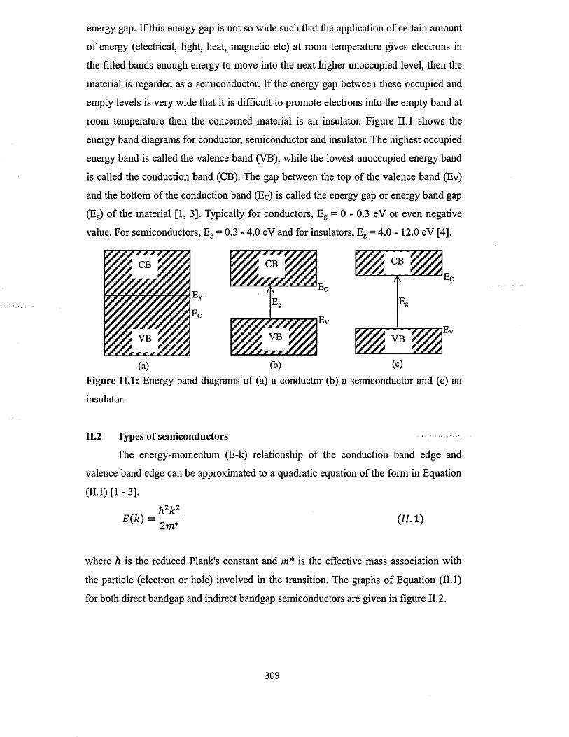
energy gap. If this energy gap is not so wide such that the application of certain amount
of energy (electrical, light, heat, magnetic etc) at room temperature gives electrons in
the filled bands enough energy to move into the next higher unoccupied level, then the
material is regarded as a semiconductor. If the energy gap between these occupied and
empty levels is very wide that it is difficult to promote electrons into the empty band at
room temperature then the concerned material is an insulator. Figure II.l shows the
energy band diagrams for conductor, semiconductor and insulator. The highest occupied
energy band is called the valence band (VB), while the lowest unoccupied energy band
is called the conduction band (CB). The gap between the top of the valence band (Ey)
and the bottom of the conduction band (Ec) is called the energy gap or energy band gap
(Eg) of the material [1, 3]. Typically for conductors, Eg = 0 - 0.3 eV or even negative
value. For semiconductors, Eg = 0.3 - 4.0 eV and for insulators, Eg = 4.0 -12.0 eV [4].
CB
/N
E
VB
Ec
(a) (b) (c)Figure I I .l : Energy band diagrams o f (a) a conductor (b) a semiconductor and (c) an
insulator.
II.2 Types of semiconductors
The energy-momentum (E-k) relationship o f the conduction band edge and
valence band edge can be approximated to a quadratic equation of the form in Equation
(II. 1) [1 - 3].
h2k 2E(k) =
2 m *(II.l)
where h is the reduced Plank's constant and m * is the effective mass association with
the particle (electron or hole) involved in the transition. The graphs of Equation (II.l)
for both direct bandgap and indirect bandgap semiconductors are given in figure II.2.
3 0 9

A Symmetry a x i s ^ .
Symmetry axis
Figure II.2: Schematic o f the E-k plot for (a) direct bandgap semiconductor and (b)
indirect bandgap semiconductor.
The alignment of the valence band maximum and the conduction band minimum plays a
crucial role in the transition o f an electron from the valence band to the conduction
band. When both points align at the same momentum (k), as in figure II.2 (a),
momentum is conserved and the bandgap of the semiconductor is regarded as direct.
The implication o f this is that an electron at the top of the valence band can move to the
bottom of the conduction band if it has sufficient energy, without changing its
momentum vector. Such electron therefore moves with a single effective mass (m*) -
along the symmetry axis. This type of transition is a direct transition. Examples of
semiconductors with direct bandgap include GaAs, CdTe, CdS, ZnS etc. On the other
hand, figure II.2 (b) shows a case for an indirect bandgap transition in which there is a
misalignment between the conduction band minimum and valence band maximum,
resulting in a change in momentum of an electron moving from the top o f the valence
band to the bottom of the conduction band. Momentum is therefore not conserved for
such transition as the electron involved will have two effective masses (one (mt*)
transverse to the symmetry axes and another {m f) along these axes). The bandgap, Eg,
involved in this case is therefore an indirect bandgap [2, 3]. Examples o f indirect
bandgap semiconductors include Si, Ge, GaP etc.
The nature of transition from valence band to conduction band in a semiconductor has a
consequence on the absorption property o f the semiconductor. In indirect transition,
phonons are involved in addition to change in energy. The phonons (a quantum of
lattice vibration) have large amount of momentum and a small amount of energy so as
to make up for the discrepancy in momentum that is the origin o f the indirect bandgap.
This participation of phonons is necessary since both energy and momentum must be
conserved in order for a fundamental transition to be effected. In direct transition,
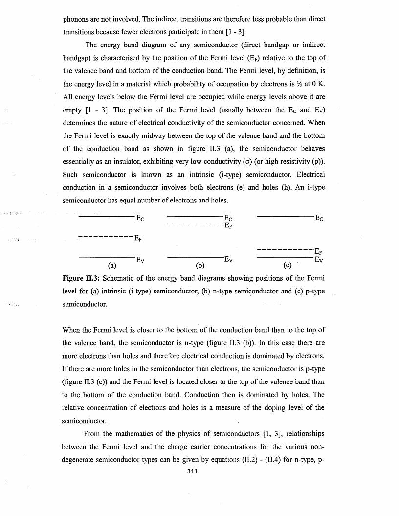
phonons are not involved. The indirect transitions are therefore less probable than direct
transitions because fewer electrons participate in them [1 - 3].
The energy band diagram of any semiconductor (direct bandgap or indirect
bandgap) is characterised by the position o f the Fermi level (Ep) relative to the top of
the valence band and bottom of the conduction band. The Fermi level, by definition, is
the energy level in a material which probability o f occupation by electrons is V2 at 0 K.
All energy levels below the Fermi level are occupied while energy levels above it are
empty [1 - 3]. The position of the Fermi level (usually between the Ec and Ey)
determines the nature o f electrical conductivity o f the semiconductor concerned. When
the Fermi level is exactly midway between the top o f the valence band and the bottom
of the conduction band as shown in figure II.3 (a), the semiconductor behaves
essentially as an insulator, exhibiting very low conductivity (o) (or high resistivity (p)).
Such semiconductor is known as an intrinsic (i-type) semiconductor. Electrical
conduction in a semiconductor involves both electrons (e) and holes (h). An i-type
semiconductor has equal number of electrons and holes.
Ec Ec Ec------------------------- Ef
---------------------- Ef
---------------------- - E pEy Ey Ey
(a) (b) (c)
Figure II.3: Schematic o f the energy band diagrams showing positions o f the Fermi
level for (a) intrinsic (i-type) semiconductor, (b) n-type semiconductor and (c) p-type
semiconductor.
When the Fermi level is closer to the bottom of the conduction band than to the top o f
the valence band, the semiconductor is n-type (figure II.3 (b)). In this case there are
more electrons than holes and therefore electrical conduction is dominated by electrons.
If there are more holes in the semiconductor than electrons, the semiconductor is p-type
(figure II.3 (c)) and the Fermi level is located closer to the top o f the valence band than
to the bottom of the conduction band. Conduction then is dominated by holes. The
relative concentration of electrons and holes is a measure o f the doping level o f the
semiconductor.
From the mathematics of the physics of semiconductors [1, 3], relationships
between the Fermi level and the charge carrier concentrations for the various non
degenerate semiconductor types can be given by equations (II.2) - (II.4) for n-type, p-
311
type and i-type semiconductors respectively.
nr ( EC — EF\ n = Nc exp {— — )
p = Nv exp ^Ep Ey
kT(II. 3)
n = p = ni = Nc exp ( — C~ j ^ ) = Nv 6Xp (Ec Ej
kTE j ~ E v
kT .)(I I A )
where N c and Ny are the effective densities o f states in the conduction band and valence
band respectively, k is Boltzmann constant, T is absolute temperature, is intrinsic
carrier concentration, Ei is the Fermi level in the intrinsic semiconductor and Eg is the
energy bandgap of the semiconductor.
For any given semiconductor, the product o f the majority and minority carrier
concentrations is a constant so that equations (II. 2) and (II. 3) yield
Equation (II.5) is the law of mass action. If the intrinsic properties are used as reference,
then n andp can be obtained alternatively as
II.3 Interfaces in semiconductor devices
The fabrication of semiconductor devices requires the formation of junctions or
interfaces. These interfaces can be between two semiconductors as well as between a
semiconductor and suitable metal or insulator. Depending on the need, as well as the
processes and the type of materials and semiconductors involved, these interfaces or
junctions can have rectifying property (in which case the flow of electrical current is
preferred only in one direction) or ohmic property (in which case current flow across the
junction can go in both directions, obeying Ohm’s law). Sometimes also, a
31 2
(11.S)
(II. 6)
( I I .7)

metal/semiconductor interface may require a thin insulating material between the metal
and semiconductor to form a metal/insulator/semiconductor junction for certain reasons
and applications.
11.3.1 Semiconductor/semiconductor interfaces
In device fabrication, a rectifying junction can be formed between two different
semiconductors o f similar or different conductivity types. Such junction involving
dissimilar semiconductors is known as hetero-junction [2, 5 - 14]. Instead o f using
dissimilar semiconductors, the same semiconductor in its different conductivity types
(n-type and p-type) can be used to form a rectifying junction in which case the junction
is known as a homo-junction [15 - 18]. The main purpose of forming these junctions is
to create a built-in electrical potential (or electric field) at these junctions for effective
carrier separation and transport in a semiconductor device.
11.3.1.1 Hetero-junctions
A semiconductor hetero-junction can either be an n-n, p-p or p-n junction,
depending on the conductivity types o f the two dissimilar semiconductors involved [5 -
14]. In any case, it is necessary that the bandgaps of the two semiconductors are
generally not the same. Another major requirement for a good and healthy hetero
junction formation is that, the two semiconductors involved are lattice matched. This
means that they have similar lattice constants [3]. If the lattice constants are not
matched, the semiconductors are strained at the junction creating dislocations that act as
charge carrier trap centres. As a result, the properties of the hetero-junction formed
deviate from the ideal behaviour. However, it is difficult to obtain perfect hetero
junction properties in practice and therefore practical hetero-junctions are not ideal [3 -
14].
Figure II.4 shows the formation o f an n-n hetero-junction using two different
semiconductors. Different rectifying n-n hetero-junctions have been reported in the
literature. These include AlGaAs/GaAs n-n hetero-junction [5], Si/Si n-n hetero
junction [19], GaSb/GalnAsSb n-n hetero-junction [20], InP/GaAs n-n hetero-junction
[6], Ge/Si n-n hetero-junction [7], InP/InSb n-n hetero-junction [9], InAsSb/GaSb n-n
hetero-junction [8] etc. Similarly, rectifying p-p hetero-junctions have been reported, for
example, for GalnSbAs/GaSb p-p hetero-junction [20] and Ge/Si p-p hetero-junction
[7]. The physics o f these hetero-junctions are also well documented in the literature [6,
7 ,2 1 -2 3 ].
31 3
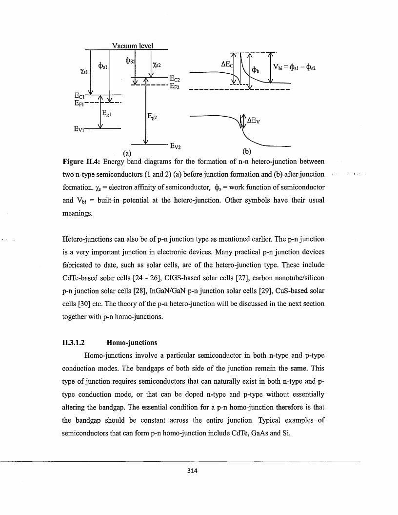
Vacuum level
Xsl
Eci'Efi'
va
Evr
A
v
jgi>/
Xs2
Ec2■*Ef2
V b i - (Psl - 4>s2<Pb
(a)Ev2
Figure II.4: Energy band diagrams for the formation of n-n hetero-junction between
two n-type semiconductors (1 and 2) (a) before junction formation and (b) after-junction
formation. & = electron affinity o f semiconductor, (j)s = work function of semiconductor
and Vbi = built-in potential at the hetero-junction. Other symbols have their usual
meanings.
Hetero-junctions can also be of p-n junction type as mentioned earlier. The p-n junction
is a very important junction in electronic devices. Many practical p-n junction devices
fabricated to date, such as solar cells, are of the hetero-junction type. These include
CdTe-based solar cells [24 - 26], CIGS-based solar cells [27], carbon nanotube/silicon
p-n junction solar cells [28], InGaN/GaN p-n junction solar cells [29], CuS-based solar
cells [30] etc. The theory of the p-n hetero-junction will be discussed in the next section
together with p-n homo-junctions.
II.3.1.2 Homo-junctions
Homo-junctions involve a particular semiconductor in both n-type and p-type
conduction modes. The bandgaps o f both side o f the junction remain the same. This
type of junction requires semiconductors that can naturally exist in both n-type and p-
type conduction mode, or that can be doped n-type and p-type without essentially
altering the bandgap. The essential condition for a p-n homo-junction therefore is that
the bandgap should be constant across the entire junction. Typical examples of
semiconductors that can form p-n homo-junction include CdTe, GaAs and Si.
3 1 4
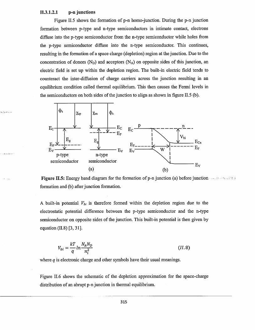
II.3.1.2.1 p-n junctions
Figure II.5 shows the formation of p-n homo-junction. During the p-n junction
formation between p-type and n-type semiconductors in intimate contact, electrons
diffuse into the p-type semiconductor from the n-type semiconductor while holes from
the p-type semiconductor diffuse into the n-type semiconductor. This continues,
resulting in the formation of a space charge (depletion) region at the junction. Due to the
concentration of donors (No) and acceptors (Na) on opposite sides o f this junction, an
electric field is set up within the depletion region. The built-in electric field tends to
counteract the inter-diffusion of charge carriers across the junction resulting in an
equilibrium condition called thermal equilibrium. This then causes the Fermi levels in
the semiconductors on both sides of the junction to align as shown in figure II.5 (b).
Xsn
V b i
E v E vp-type n-type
(b)
Figure II.5: Energy band diagram for the formation o f p-n junction (a) before junction
formation and (b) after junction formation.
A built-in potential Vbi is therefore formed within the depletion region due to the
electrostatic potential difference between the p-type semiconductor and the n-type
semiconductor on opposite sides of the junction. This built-in potential is then given by
equation (II.8) [3, 31].
kT NaMVb i= - l n - i4iVD
n?(//. 8)
where q is electronic charge and other symbols have their usual meanings.
Figure II.6 shows the schematic of the depletion approximation for the space-charge
distribution of an abrupt p-n junction in thermal equilibrium.
31 5

/
-X p
N d (density o f ion ised donors)
+ + + + +
+ + + + +
+ + + + + 4- 4- 4-4-4-
---------------------
* n X
Na (density of ionised acceptors)
Figure II.6: Schematic o f the space-charge distribution of an abrupt p-n junction in
thermal equilibrium.
From the well-established theory o f p-n junction [3, 31], the maximum built-in electric
field (Em) existing at x = 0 in the depletion region is given by Equation (II. 9).
\Em \ =q N Ax p q N Dx n
(11. 9)£s £s
where xp and xn are the distances by which the depletion region extends into the p-type
semiconductor and n-type semiconductor respectively. £s is the dielectric constant o f the
semiconductor material.
The maximum electric field in the depletion region is related to the built-in potential
according to Equation (11.10).
Vb l = j \ E m \ W ( 1 1 . 1 0 )
where W = xp + x„ is the width of the depletion region given by Equation (II. 11).
W =
N
2 £s
<7Vbi (77.11)
Equation (11.11) shows that reducing either the donor concentration or acceptor
concentration or both, increases the depletion width of the junction. In a one-sided
3 1 6
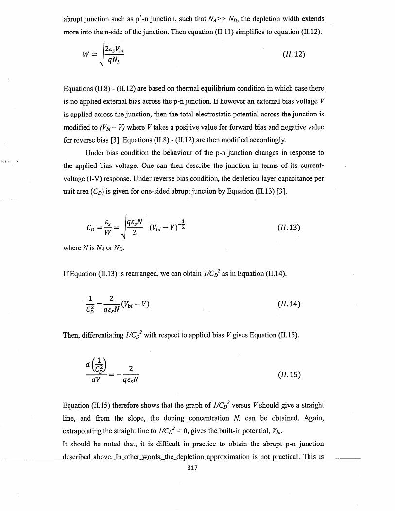
abrupt junction such as p+-n junction, such that N a » N d , the depletion width extends
more into the n-side of the junction. Then equation (11.11) simplifies to equation (11.12).
2£sVbiW = — ^ (II. 12)
a) <In d
Equations (II.8) - (11.12) are based on thermal equilibrium condition in which case there
is no applied external bias across the p-n junction. If however an external bias voltage V
is applied across the junction, then the total electrostatic potential across the junction is
modified to (Vbi ~ V) where V takes a positive value for forward bias and negative value
for reverse bias [3]. Equations (II.8) - (11.12) are then modified accordingly.
Under bias condition the behaviour of the p-n junction changes in response to
the applied bias voltage. One can then describe the junction in terms o f its current-
voltage (I-V) response. Under reverse bias condition, the depletion layer capacitance per
unit area (Q>) is given for one-sided abrupt junction by Equation (11.13) [3].
qesN i^ 4 - (Vb l - \ 0 2 (//. 13)
£sc° = w ,
where N is Na or Nd.
If Equation (11.13) is rearranged, we can obtain 1 /C d2 as in Equation (11.14).
1 2(Vb i- V ) (77.14)
Q) q£sN
Then, differentiating 1 /C d with respect to applied bias V gives Equation (11.15).
( £ ) 2D - (77.15)dV qesN
Equation (11.15) therefore shows that the graph of 1/C d2 versus V should give a straight
line, and from the slope, the doping concentration N, can be obtained. Again,
extrapolating the straight line to 1 /C d2 - 0, gives the built-in potential, Vbi.
It should be noted that, it is difficult in practice to obtain the abrupt p-n junction
jdescribed_aboYe._Injother_words,_the_depletion_approximationJs_not_practical._IhisJs_
317
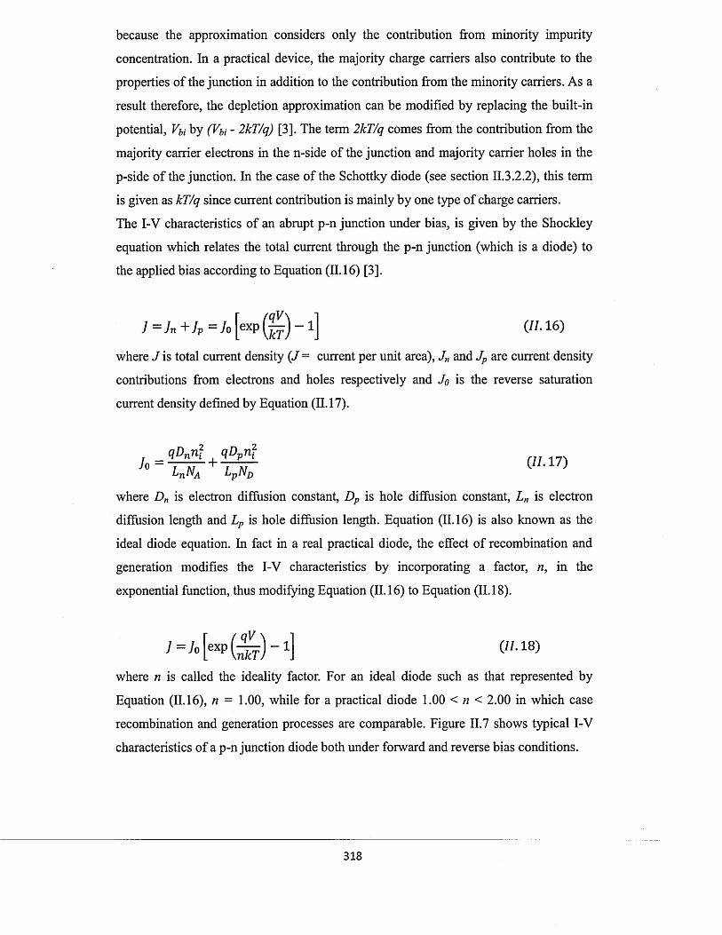
because the approximation considers only the contribution from minority impurity
concentration. In a practical device, the majority charge carriers also contribute to the
properties of the junction in addition to the contribution from the minority carriers. As a
result therefore, the depletion approximation can be modified by replacing the built-in
potential, by (V^ - 2kT/q) [3]. The term 2kT/q comes from the contribution from the
majority carrier electrons in the n-side of the junction and majority carrier holes in the
p-side o f the junction. In the case of the Schottky diode (see section H.3.2.2), this term
is given as kT/q since current contribution is mainly by one type o f charge carriers.
The I-V characteristics of an abrupt p-n junction under bias, is given by the Shockley
equation which relates the total current through the p-n junction (which is a diode) to
the applied bias according to Equation (11.16) [3].
7 = / n + / p = y o [ e x p ( | ^ ) - l ] (.11- 16)
where J is total current density ( / = current per unit area), Jn and Jp are current density
contributions from electrons and holes respectively and Jo is the reverse saturation
current density defined by Equation (11.17).
qDnri? qDvn}Jo = + 2-J^-L ( // . 1 7 )Jo LnNA LpND K J
where Dn is electron diffusion constant, Dp is hole diffusion constant, Ln is electron
diffusion length and Lp is hole diffusion length. Equation (11.16) is also known as the
ideal diode equation. In fact in a real practical diode, the effect o f recombination and
generation modifies the I-V characteristics by incorporating a factor, n, in the
exponential function, thus modifying Equation (11.16) to Equation (11.18).
/ = / o exp (— ) - l \nkT J
(II. 18)
where n is called the ideality factor. For an ideal diode such as that represented by
Equation (11.16), n = 1.00, while for a practical diode 1.00 < n < 2.00 in which case
recombination and generation processes are comparable. Figure II.7 shows typical I-V
characteristics of a p-n junction diode both under forward and reverse bias conditions.
3 1 8
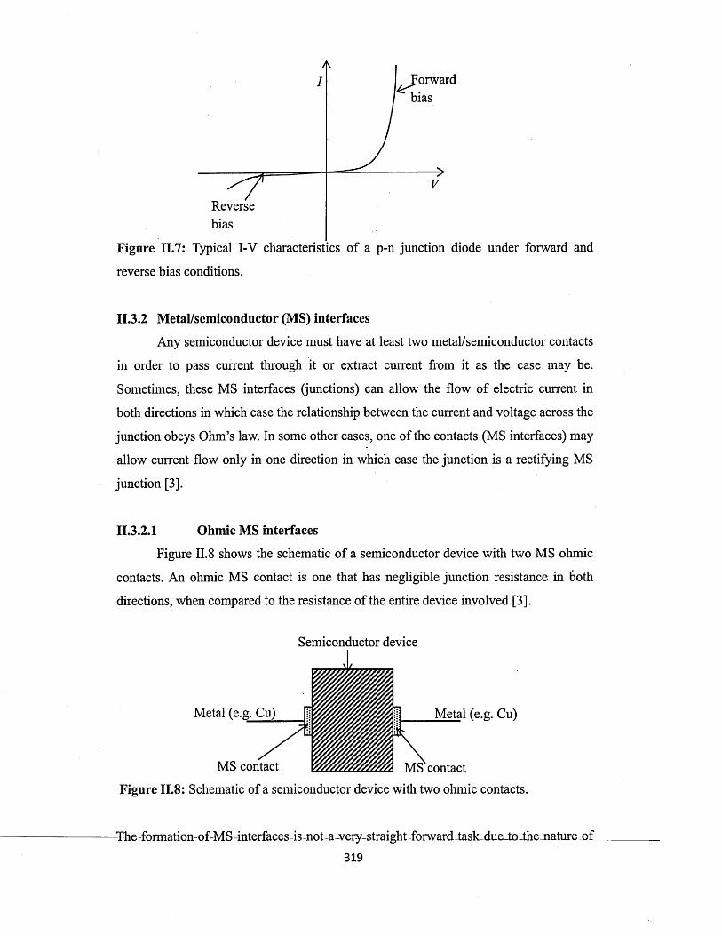
Reversebias
Figure II.7: Typical I-V characteristics o f a p-n junction diode under forward and
reverse bias conditions.
II.3.2 M etal/semiconductor (MS) interfaces
Any semiconductor device must have at least two metal/semiconductor contacts
in order to pass current through it or extract current from it as the case may be.
Sometimes, these MS interfaces (junctions) can allow the flow of electric current in
both directions in which case the relationship between the current and voltage across the
junction obeys Ohm’s law. In some other cases, one of the contacts (MS interfaces) may
allow current flow only in one direction in which case the junction is a rectifying MS
junction [3].
II.3.2.1 Ohmic MS interfaces
Figure II.8 shows the schematic o f a semiconductor device with two MS ohmic
contacts. An ohmic MS contact is one that has negligible junction resistance in both
directions, when compared to the resistance o f the entire device involved [3].
Semiconductor device
Metal (e.g. Cu) Metal (e.g. Cu)
MS contact MS contact
Figure II.8: Schematic of a semiconductor device with two ohmic contacts.
The-formationof-M Sinterfaces-is-nota w erystraightTbrw ard-taskduetothe mature J)f
319

interactions between the semiconductor and the contacting metal. A necessary
requirement for making ohmic contact on any semiconductor however is that work
functions of the semiconductor and the metal must be close enough so that band-
bending does not happen in the semiconductor due to substantial electrostatic potential
difference or barrier height between the positions of the Fermi level in the
semiconductor and the metal. An ohmic contact will result if the potential barrier height
is less than about 0.30 eV so that the depletion region formed in the semiconductor is
narrow [32]. Doping the semiconductor heavily, in excess of 1018 cm'3, helps to produce
very narrow depletion region in the semiconductor in order to facilitate ohmic behaviour
of the junction. Modification of the semiconductor surface is another way o f facilitating
ohmic contact fabrication. Surface states have pronounced effects on the electrical
properties of semiconductors. For example, Fermi level pinning in semiconductors is
encouraged by bulk defects and surface states [33 - 35]. Modification of these surfaces,
for example by mechanical polishing and chemical etching, can help to passivate these
defects and thus adjust the semiconductor work function by adjusting the Fermi level
for effective ohmic contact formation.
II.3.2.2 Rectifying MS interfaces (Schottky junctions)
In a rectifying MS or Schottky diode, substantial potential barrier (in excess of
0.40 eV) exists at the metal/semiconductor interface [32]. As a result, a depletion region
is formed at this junction, which extends reasonably into the semiconductor. A
necessary condition for the formation of a Schottky junction is that the metal and the
semiconductor should have work functions that differ substantially unlike in the case of
ohmic MS contact.
Consider a metal of work function, 4>m and an n-type semiconductor o f work
function <j)s and electron affinity Suppose also that the gap between the metal and the
semiconductor is 5, as shown in figure II.9 (figure II.9 (b)).
3 2 0
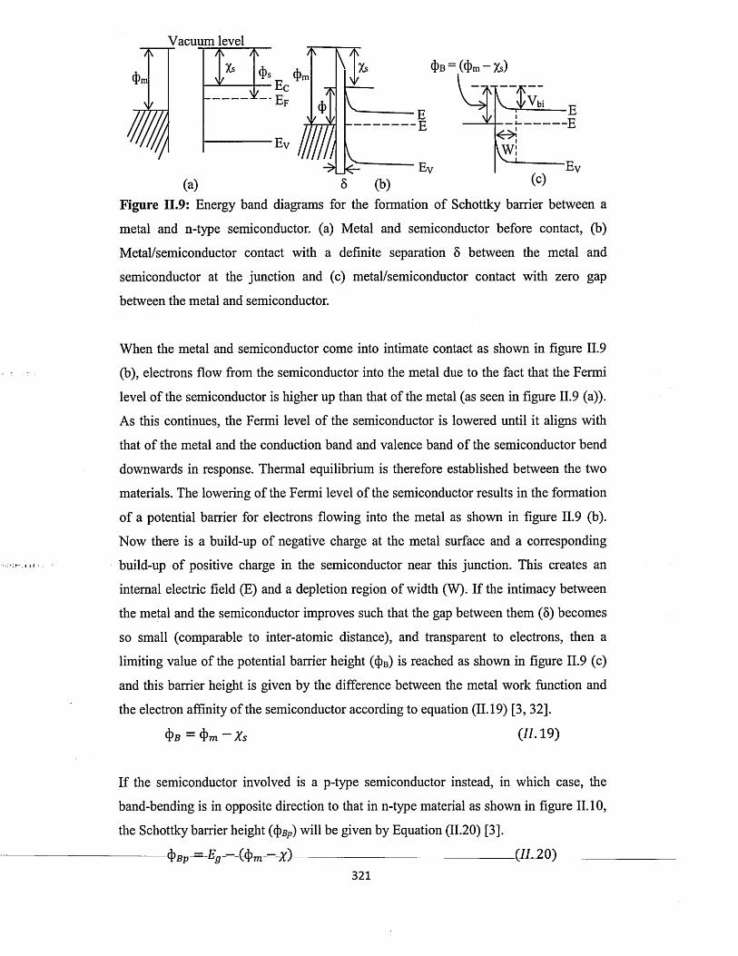
evelVacuum
'm'm
Ev
5 (b)
4>B=(4>m-Xs)
EE
A
V
Ev
r T ”Vv / Vb i
w :
■E-E
(C)' Ev
Figure II.9: Energy band diagrams for the formation o f Schottky barrier between a
metal and n-type semiconductor, (a) Metal and semiconductor before contact, (b)
Metal/semiconductor contact with a definite separation 8 between the metal and
semiconductor at the junction and (c) metal/semiconductor contact with zero gap
between the metal and semiconductor.
When the metal and semiconductor come into intimate contact as shown in figure II. 9
(b), electrons flow from the semiconductor into the metal due to the fact that the Fermi
level of the semiconductor is higher up than that of the metal (as seen in figure II.9 (a)).
As this continues, the Fermi level of the semiconductor is lowered until it aligns with
that of the metal and the conduction band and valence band o f the semiconductor bend
downwards in response. Thermal equilibrium is therefore established between the two
materials. The lowering of the Fermi level of the semiconductor results in the formation
of a potential barrier for electrons flowing into the metal as shown in figure II.9 (b).
Now there is a build-up of negative charge at the metal surface and a corresponding
build-up of positive charge in the semiconductor near this junction. This creates an
internal electric field (E) and a depletion region of width (W). If the intimacy between
the metal and the semiconductor improves such that the gap between them (8) becomes
so small (comparable to inter-atomic distance), and transparent to electrons, then a
limiting value of the potential barrier height (4>b) is reached as shown in figure II.9 (c)
and this barrier height is given by the difference between the metal work function and
the electron affinity of the semiconductor according to equation (11.19) [3, 32].
4>B = 4> m - X s ( / / . 1 9 )
If the semiconductor involved is a p-type semiconductor instead, in which case, the
band-bending is in opposite direction to that in n-type material as shown in figure 11.10,
the Schottky barrier height (4 ^ ) will be given by Equation (11.20) [3].
-------------------------------------------------------------------------------------------------------------- ( 7 7 . 2 0 ) -----
321
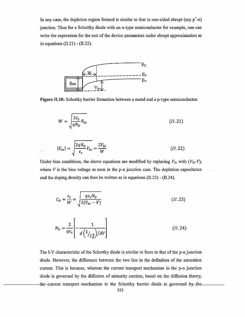
In any case, the depletion region formed is similar to that in one-sided abrupt (say p+-n)
junction. Thus for a Schottky diode with an n-type semiconductor for example, one can
write the expression for the rest o f the device parameters under abrupt approximation as
in equations (11.21) - (11.22).
4>b p
W ///M
' E c
•Ef
' E v
Figure 11.10: Schottky barrier formation between a metal and a p-type semiconductor.
W =2 £5
qNDVbi (77.21)
|Em| =2qND„ _ 2 V biT~Vbi~ir
Under bias conditions, the above equations are modified by replacing Vbi with (Vbi-V),
where V is the bias voltage as seen in the p-n junction case. The depletion capacitance
and the doping density can then be written as in equations (11.23) - (11.24).
r — —— —Cd ~ w ~
qssND2{Vb i- V )
(77.23)
(77.24)
The I-V characteristic of the Schottky diode is similar in form to that o f the p-n junction
diode. However, the difference between the two lies in the definition o f the saturation
current. This is because, whereas the current transport mechanism in the p-n junction
diode is governed by the diffusion of minority carriers, based on the diffusion theory,
the-current-transport-mechanism-in-the-Schottky-barrier-diode-is-govemed-by-the-322
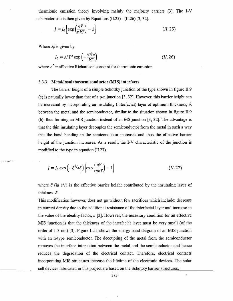
thermionic emission theory involving mainly the majority carriers [3]. The I-V
characteristic is then given by Equations (11.25) - (11.26) [3, 32].
Where Jo is given by
(77.26)
where A* = effective Richardson constant for thermionic emission.
3.3.3 Metal/insulator/semiconductor (MIS) interfaces
The barrier height of a simple Schottky junction o f the type shown in figure II.9
(c) is naturally lower than that o f a p-n junction [3, 32]. However, this barrier height can
be increased by incorporating an insulating (interfacial) layer o f optimum thickness, 5,
between the metal and the semiconductor, similar to the situation shown in figure II.9
(b), thus forming an MIS junction instead of an MS junction [3, 32]. The advantage is
that the thin insulating layer decouples the semiconductor from the metal in such a way
that the band bending in the semiconductor increases and thus the effective barrier
height of the junction increases. As a result, the I-V characteristic o f the junction is
modified to the type in equation (11.27).
where £ (in eV) is the effective barrier height contributed by the insulating layer of
thickness 8.
the value o f the ideality factor, n [3]. However, the necessary condition for an effective
MIS junction is that the thickness of the interfacial layer must be very small (of the
order of 1-3 nm) [3]. Figure 11.11 shows the energy band diagram of an MIS junction
with an n-type semiconductor. The decoupling of the metal from the semiconductor
removes the interface interaction between the metal and the semiconductor and hence
reduces the degradation of the electrical contact. Therefore, electrical contacts
incorporating MIS structures increase the lifetime of the electronic devices. The solar
..cell_deyjc.es fabricated in this project are based on the Schottky barrier structures.______
(77.27)
This modification however, does not go without few sacrifices which include; decrease
in current density due to the additional resistance of the interfacial layer and increase in
323
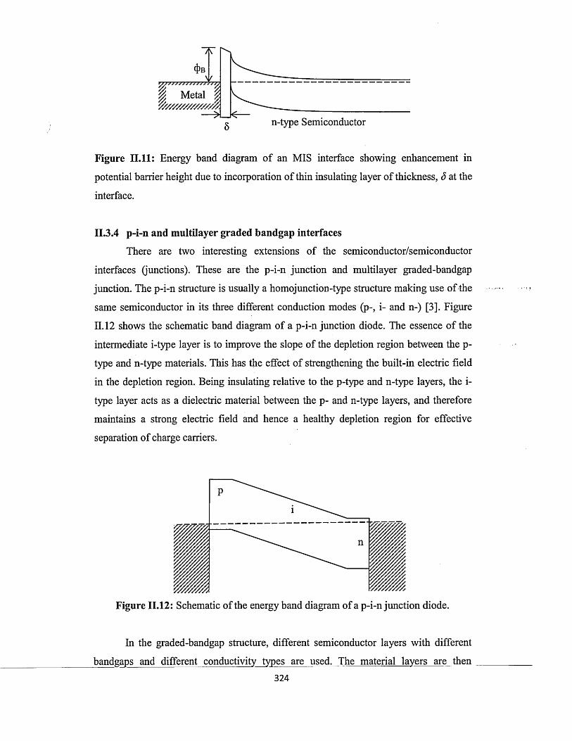
& Metal ^ V//////////////A
n-type Semiconductor
Figure 11.11: Energy band diagram of an MIS interface showing enhancement in
potential barrier height due to incorporation o f thin insulating layer o f thickness, S at the
interface.
II.3.4 p-i-n and m ultilayer graded bandgap interfaces
There are two interesting extensions o f the semiconductor/semiconductor
interfaces (junctions). These are the p-i-n junction and multilayer graded-bandgap
junction. The p-i-n structure is usually a homojunction-type structure making use o f the
same semiconductor in its three different conduction modes (p-, i- and n-) [3]. Figure
11.12 shows the schematic band diagram of a p-i-n junction diode. The essence o f the
intermediate i-type layer is to improve the slope of the depletion region between the p-
type and n-type materials. This has the effect of strengthening the built-in electric field
in the depletion region. Being insulating relative to the p-type and n-type layers, the i-
type layer acts as a dielectric material between the p- and n-type layers, and therefore
maintains a strong electric field and hence a healthy depletion region for effective
separation of charge carriers.
Figure 11.12: Schematic of the energy band diagram of a p-i-n junction diode.
In the graded-bandgap structure, different semiconductor layers with different
bandgaps and different conductivity types are used. The material layers are then
324
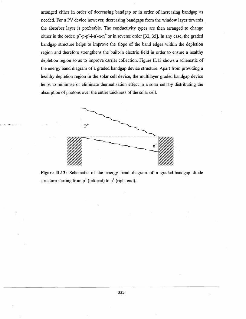
arranged either in order of decreasing bandgap or in order of increasing bandgap as
needed. For a PV device however, decreasing bandgaps from the window layer towards
the absorber layer is preferable. The conductivity types are then arranged to change
either in the order: p+-p-p'-i-n‘-n-n+ or in reverse order [32, 35]. In any case, the graded
bandgap structure helps to improve the slope of the band edges within the depletion
region and therefore strengthens the built-in electric field in order to ensure a healthy
depletion region so as to improve carrier collection. Figure 11.13 shows a schematic of
the energy band diagram of a graded bandgap device structure. Apart from providing a
healthy depletion region in the solar cell device, the multilayer graded bandgap device
helps to minimise or eliminate thermalisation effect in a solar cell by distributing the
absorption of photons over the entire thickness of the solar cell.
Figure 11.13: Schematic o f the energy band diagram of a graded-bandgap diode
structure starting from p+ (left end) to n+ (right end).
32 5
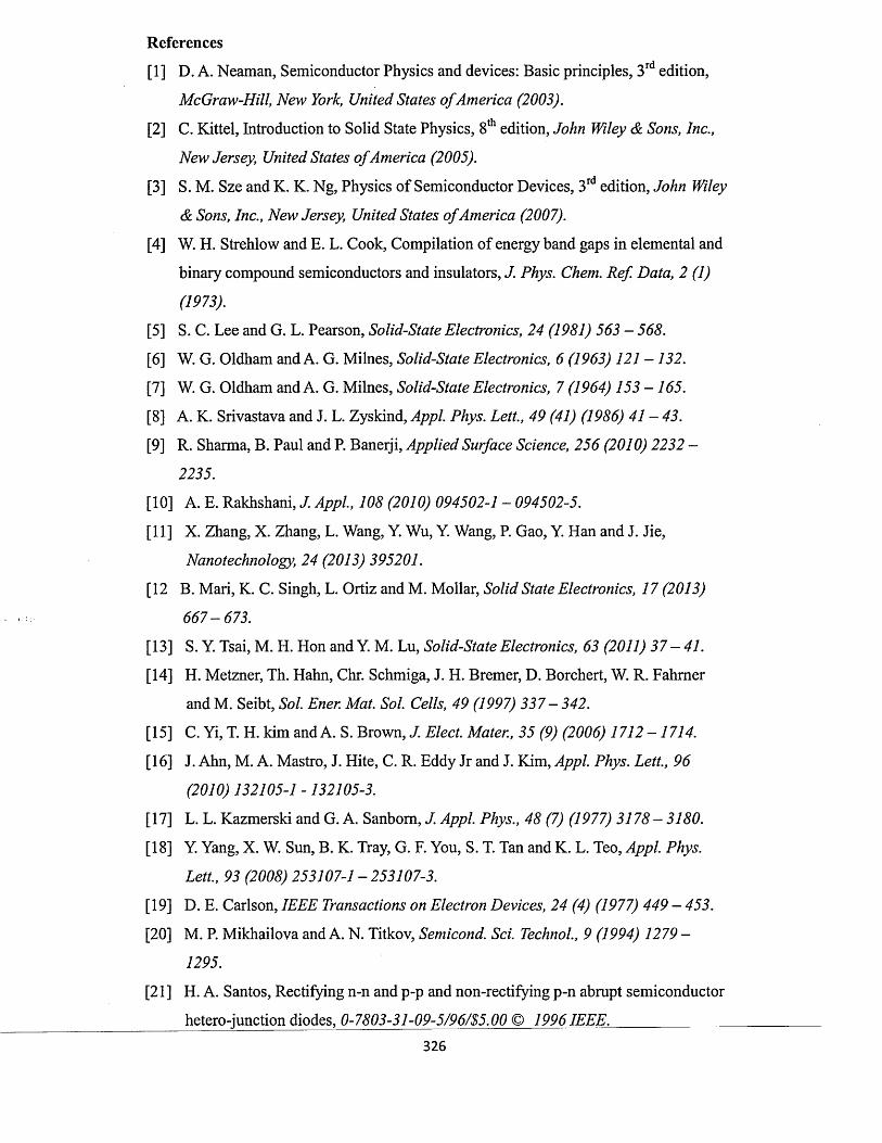
References
[1] D. A. teaman, Semiconductor Physics and devices: Basic principles, 3rd edition,
McGraw-Hill, New York, United States o f America (2003).
[2] C. Kittel, Introduction to Solid State Physics, 8th edition, John Wiley & Sons, Inc.,
New Jersey, United States o f America (2005).
[3] S. M. Sze and K. K. Ng, Physics of Semiconductor Devices, 3rd edition, John Wiley
& Sons, Inc., New Jersey, United States o f America (2007).
[4] W. H. Strehlow and E. L. Cook, Compilation of energy band gaps in elemental and
binary compound semiconductors and insulators, J. Phys. Chem. Ref. Data, 2 (1)
(1973).
[5] S. C. Lee and G. L. Pearson, Solid-State Electronics, 24 (1981) 563 - 568.
[6] W. G. Oldham and A. G. Milnes, Solid-State Electronics, 6 (1963) 121 -1 3 2 .
[7] W. G. Oldham and A. G. Milnes, Solid-State Electronics, 7 (1964) 153 -1 6 5 .
[8] A. K. Srivastava and J. L. Zyskind, Appl. Phys. Lett., 49 (41) (1986) 41 - 43.
[9] R. Sharma, B. Paul and P. Baneiji, Applied Surface Science, 256 (2010) 2232 -
2235.
[10] A. E. Rakhshani, J. Appl., 108 (2010) 094502-1 - 094502-5.
[11] X. Zhang, X. Zhang, L. Wang, Y. Wu, Y. Wang, P. Gao, Y. Han and J. Jie,
Nanotechnology, 24 (2013) 395201.
[12 B. Mari, K. C. Singh, L. Ortiz and M. Mollar, Solid State Electronics, 17 (2013)
667-673 .
[13] S. Y. Tsai, M. H. Hon and Y. M. Lu, Solid-State Electronics, 63 (2011) 3 7 - 41.
[14] H. Metzner, Th. Hahn, Chr. Schmiga, J. H. Bremer, D. Borchert, W. R. Fahmer
and M. Seibt, Sol. Ener. Mat. Sol. Cells, 49 (1997) 3 3 7 - 342.
[15] C. Yi, T. H. kim and A. S. Brown, J. Elect. Mater., 35 (9) (2006) 1712 -1714 .
[16] J. Ahn, M. A. Mastro, J. Hite, C. R. Eddy Jr and J. Kim, Appl. Phys. Lett., 96
(2010) 132105-1 -132105-3.
[17] L. L. Kazmerski and G. A. Sanborn, J. Appl. Phys., 48 (7) (1977) 3178 - 3180.
[18] Y. Yang, X. W. Sun, B. K. Tray, G. F. You, S. T. Tan and K. L. Teo, Appl. Phys.
Lett., 93 (2008) 253107-1-253107-3.
[19] D. E. Carlson, IEEE Transactions on Electron Devices, 24 (4) (1977) 449 - 453.
[20] M. P. Mikhailova and A. N. Titkov, Semicond. Sci. Technol., 9 (1994) 1279 -
1295.
[21] H. A. Santos, Rectifying n-n and p-p and non-rectifying p-n abrupt semiconductor
hetero-junction diodes, 0-7803-31-09-5/96/85.00 © 1996IEEE._______________
326
[22] R. J. Schuelke and M. S. Lundstrom, Solid-State Electronics, 27 (12) (1984) 1111
-1116.
[23] K. Yang, J. R. East and G. I. Haddad, Solid-State Electronics, 36 (3) (1993) 321 -
330.
[24] S. S. Ou, O. M. Stafsudd and B. M. Basol, Solid-State Electronics, 27 (1) (1984)
2 1 -2 5 .
[25] B. M. Basol, Solar Cells, 23 (1988) 69 - 88.
[26] G. C. Morris, P. G. Tanner and A. Tottszer, Towards high efficiency
electrodeposited CdS/CdTe thin film cells, 0160-8371/90/0000-0575©$1.001990
IEEE.
[27] T. Wada, Y. Hashimoto, S. Nishiwaki, T. Satoh, S. Hayashi, T. Negami and H.
Miyake, Sol. Ener. Mat. Sol. Cells, 67 (2001) 3 0 5 -3 1 0 .
[28] Y. Jung, X. Li, N. K. Rajan, A.D. Taylor and M. A. Reed, Nano Lett., 13 (2013) 95
-9 9 .
[29] B. R. Jampana, A. G. Melton, M. Jamil, N. N. Faleev, R. L. Opia, I. T. ferguson
and C. B. Honsberg, IEEE Electron Device Letters, 31 (1) (2010) 32 - 34.
[30] M. K. Mukheijee, F. Pfisterer, G. H. Hewig, H. W. Schock and W. H. Bloss, J.
Appl, Phys. 48 (4) (1977) 1538 -1542.
[31] T. Soga, Nanostructured materials for solar energy conversion, chapter 1, edited
by Tetsu Soga and published by Elsevier, (2006).
[32] I. M. Dharmadasa, Advances in Thin-Film Solar Cells, Pan Stanford Publishing
Pte. Ltd, Boulevard, Singapore, (2012).
[33] J. P. Ponpon, Solid State Electron. 28 (1985) 689.
[34] I. M. Dharmadasa, Prog. Cryst Growth Ch. 36 (1998) 249.
[35] I. M. Dharmadasa, J. D. Bunning, A. P. Samantilleke and T. Shen, Sol. Energ.
Mat. Sol. Cells.86 (2005) 373.
3 2 7
Copyright © 2022 FDOKUMEN


![Fluorescent cellulose aerogels containing covalently immobilized (ZnS) ₓ (CuInS ₂) ₁₋ ₓ/ZnS (core/shell) quantum dots [2013]](https://static.fdokumen.com/doc/165x107/63372dc94554fe9f0c05b209/fluorescent-cellulose-aerogels-containing-covalently-immobilized-zns-cuins.jpg)