The Way towards Amplifier Design Using CAD (ADS) Tool
6
The Way towards Amplifier Design Using CAD (ADS) Tool Zeeshan kaleem*, Chan killee*, Muhammad Saqib*, Sheikh Mohsin**,Farrukh Salim** * Department of electrical, electronic, control and instrumental engineering, Hanyang University, ERICA campus, South Korea ** Department of computer engineering, Hanyang University, ERICA campus, South Korea { Zeeshankaleem , saqib.uetl, mohsin.professional , engr.farrukhsaleem} @gmail.com, [email protected] Abstract-This paper mainly focuses on design arts and operational mechanism of ADS tool. ADS tool is characterized by reliable, efficient and controlled functioning as compare to conventional approaches. In this paper, we describe an ADS tool based interactive procedure that provides the students in electrical and computer engineering programs with an easy-to-use reference and overview of an amplifier design. This multimedia-based system covers topics that start with introductory basic concepts in amplifier design and conclude with advanced and detailed concepts using the ADS tool. Keywords- Amplifier, ADS tool, stability, gain, smith chart I. INTRODUCTION The Advancements in the electronics and computer industries, emerging newer technologies and the designer needs their product in a market fast and first and at a reduce cost [1]. This has significantly increased the scope of background, knowledge and technical skills required by the personal concerned with such type of issues. The step towards using a CAD tools is that since the mathematics of active circuit design are too complex for manual computations. The tutorial designed is targeted towards first-time users of ADS tool for designing an amplifier. The popularity of ADS tool has also resulted in a number of tutorial [2], [3].Since there are many tutorial available but presently there are no such complete tutorial which can explain learner the basics of amplifier and their CAD design steps in one tutorial. They are basically computer based textbooks, and lack significant student interaction or feedback. This paper describes a unique, interactive, Computer based named, the way towards amplifier design using CAD (ADS) tool, for independent learning of amplifier design. The amplifier is an integral part of any communication system. The purpose of having an amplifier in a system is to boost the signal to the desired level. It also helps to keep the signal well above noise so that it can be analyzed easily and accurately. Though many CAD tools are available which had made the designing and analyzing the system quite easy, Advanced Design System (ADS) is the world's leading electronic design automation (EDA) software for RF, microwave, and high-speed digital design and verification. Leading companies in the wireless communication, wireless networking, signal integrity and aerospace & defense industries rely upon ADS as their high-frequency design platform for WiMAX, LTE, radar and satellite communication systems. Agilent's Advanced Design System (ADS) offers a complete range of software design tools for microwave and RF communications system, product, and component design. Agilent ADS allows microwave engineers to analyze, design, and simulate active and passive microwave components and systems. Layout and powerful optimizers in ADS help increase productivity and efficiency, validating high-yield designs prior to manufacturing. Agilent offers design, simulation and test capability for all of your RF and microwave amplifier design and test needs. Designers of low-noise amplifiers and power amplifiers can use harmonic balance simulation in Advanced Design System (ADS) to characterize gain compression and noise. After designing your amplifier and building a prototype, you can utilize Agilent test equipment to verify your designs. Agilent products include Network Analyzers, Spectrum Analyzers, Signal Sources, Oscilloscopes and more, all for your amplifier test requirements [4]. The intent was to develop a practical guide for independent study by learners who had little or no exposure to amplifier design by using ADS tool. Some of the goals of this paper were to: 1. Engage students as active learners in exploring new concepts immediately with interactive exercises; 2. Allow students to proceed at their own pace and plan; 3. Permit the learning to take place off-campus. This paper has been divided into four sections, fIrst describes the introduction, second part describes the amplifier design mechanism, third part describes the details of the amplifier design mechanism, including gain; stability conditions etc. and then final part describes the amplifier design in ADS tool. II. AMPLIFIER DESIGN MECHANISM There are many references available on basic amplifier concept and design. The procedure ISBN 978-89-5519-146-2 - 962- Feb. 7-10, 2010 ICACT 2010
Transcript of The Way towards Amplifier Design Using CAD (ADS) Tool

The Way towards Amplifier Design UsingCAD (ADS) Tool
Zeeshan kaleem*, Chan killee*, Muhammad Saqib*, Sheikh Mohsin**,Farrukh Salim**
*Department ofelectrical, electronic, control and instrumental engineering, Hanyang University,ERICA campus, South Korea
**Department ofcomputer engineering, Hanyang University, ERICA campus, South Korea{ Zeeshankaleem , saqib.uetl, mohsin.professional , engr.farrukhsaleem} @gmail.com, [email protected]
Abstract-This paper mainly focuses on design arts andoperational mechanism of ADS tool. ADS tool ischaracterized by reliable, efficient and controlledfunctioning as compare to conventional approaches. In thispaper, we describe an ADS tool based interactive procedurethat provides the students in electrical and computerengineering programs with an easy-to-use reference andoverview of an amplifier design. This multimedia-basedsystem covers topics that start with introductory basicconcepts in amplifier design and conclude with advancedand detailed concepts using the ADS tool.
Keywords- Amplifier, ADS tool, stability, gain, smith chart
I. INTRODUCTION
The Advancements in the electronics and computerindustries, emerging newer technologies and the designerneeds their product in a market fast and first and at areduce cost [1]. This has significantly increased the scopeof background, knowledge and technical skills requiredby the personal concerned with such type of issues. Thestep towards using a CAD tools is that since themathematics of active circuit design are too complex formanual computations. The tutorial designed is targetedtowards first-time users of ADS tool for designing anamplifier.The popularity of ADS tool has also resulted in a numberof tutorial [2], [3].Since there are many tutorial availablebut presently there are no such complete tutorial whichcan explain learner the basics of amplifier and their CADdesign steps in one tutorial. They are basically computerbased textbooks, and lack significant student interactionor feedback. This paper describes a unique, interactive,
Computer based named, the way towards amplifierdesign using CAD (ADS) tool, for independent learningof amplifier design.The amplifier is an integral part of any communicationsystem. The purpose of having an amplifier in a system isto boost the signal to the desired level. It also helps tokeep the signal well above noise so that it can beanalyzed easily and accurately. Though many CAD toolsare available which had made the designing andanalyzing the system quite easy, Advanced DesignSystem (ADS) is the world's leading electronic designautomation (EDA) software for RF, microwave, and
high-speed digital design and verification. Leadingcompanies in the wireless communication, wirelessnetworking, signal integrity and aerospace & defenseindustries rely upon ADS as their high-frequency designplatform for WiMAX, LTE, radar and satellitecommunication systems. Agilent's Advanced DesignSystem (ADS) offers a complete range of software designtools for microwave and RF communications system,product, and component design.Agilent ADS allows microwave engineers to analyze,design, and simulate active and passive microwavecomponents and systems. Layout and powerfuloptimizers in ADS help increase productivity andefficiency, validating high-yield designs prior tomanufacturing.Agilent offers design, simulation and test capability forall of your RF and microwave amplifier design and testneeds. Designers of low-noise amplifiers and poweramplifiers can use harmonic balance simulation inAdvanced Design System (ADS) to characterize gaincompression and noise.After designing your amplifier and building a prototype,you can utilize Agilent test equipment to verify yourdesigns. Agilent products include Network Analyzers,Spectrum Analyzers, Signal Sources, Oscilloscopes andmore, all for your amplifier test requirements [4].
The intent was to develop a practical guide forindependent study by learners who had little or noexposure to amplifier design by using ADS tool.Some of the goals of this paper were to:1. Engage students as active learners in exploring newconcepts immediately with interactive exercises;2. Allow students to proceed at their own pace and plan;3. Permit the learning to take place off-campus.
This paper has been divided into four sections, fIrstdescribes the introduction, second part describes theamplifier design mechanism, third part describes thedetails of the amplifier design mechanism, includinggain; stability conditions etc. and then final partdescribes the amplifier design in ADS tool.
II. AMPLIFIER DESIGN MECHANISM
There are many references available on basicamplifier concept and design. The procedure
ISBN 978-89-5519-146-2 - 962- Feb. 7-10, 2010 ICACT 2010

presented in this paper is an easiest way for learningan amplifier design. Firstly we describe idealprocedural steps for designing an amplifier.
1) Check stability performance by calculatingRolette stability factor K, using the S-parametersof the transistor at a given frequency and plotrespective stability circles to determine unstableregion in the smith chart for Tsand TL.
2) If the transistor is potentially unstable then wehave to add some resistor but this will increasethe noise figure.
3) Calculate unilateral figure of merit to determinewhether to use Unilateral or bilateral design.
4) Calculate NF min and I'OPT of the transistor fromthe S-parameter. Plot the noise circle bychoosing appropriate NF min value
5) For unilateral case use the constant gain circlesfor the desired or maximum gain and forbilateral case use the available power gaincircles for the desired or maximum gain.
6) Choose a T, value in the stable region and aswell as within the noise circle and correspondinggain circle. We are not using operating powergain circle as it is to be plotted in I' out sodifficult to correlate with the noise circles in theI' in plane.
7) Calculate the corresponding I'L. From thecorresponding T calculate the Z; and ZL.
8) These are the impendence values for a givennoise figure, gain etc for the transistor. Nowthese have to be matched with theircorresponding source and load impendence Zoo
9) The impendence matching networks aredesigned using smith chart.
III. AMPLIFIER CHARACTERISTICS
A. Gain Performance
There is several power gain equations used in design ofamplifier. The transducer power gain GT, the operatingpower gain Gp , and the available power gain GA definedas follows.
GT = (power delivered to the load)/ (power availablefrom the source)GP = (power delivered to the load)/ (power input to thenetwork)GA= (power available from the network)/ (poweravailable from the source)The maximum available gain (sometimes called MAG,sometimes called GMAX) of a device is only definedwhere K is greater than one. This is because the termunder the square-root becomes negative for values of Kless than 1. And then gain is infmite. Infinite gain meansoscillator.The maximum stable gain (MSG) of a device is definedwhen maximum available gain is undefmed (K<I). It ismerely the ratio of mag (S21)/mag (S12)'
The maximum gain available (MAG) and can becalculated by using S-Parameter and k as expressed in(1).
MAG = I51 2 (k ± ..Jk2 - 1)1 (1)
52 1
1) Available Gain & Power Gain Circles (GA,Gp)
An available gain input network circle is a locus ofsource impedances for a given gain below the optimumgain. The center of the circle is the point of maximumgain. Similarly, the power gain output network circle is alocus of load impedances for a given gain below theoptimum gain. If the stability factor K is less than unity,then the 0 dB circle is at GMAX, and the inside of thiscircle is shaded as an unstable region.
2) Ga versus noise tradeoffWhen gain is not sufficient quantity to explain, then wecan plot constant available gain and constant-noise circlesto investigate possible trade-offs between gain and noise.So we have to take the point where we can compromisebetween the noise and Gain.
3) Gp versus POUT trade-offsJust as we face trade-offs between noise performance andgain at the input of low-noise circuits, similar trade-offsbetween the small-signal gain and maximum outputpower exist at the output of an active two-port. When theconstant-output-power contours and operating constantgain circles are superimposed on the Smith chart, we canchoose the load either for maximum gain or maximumoutput power, or for a compromise between these twoextremes.
B. Stability Conditions
Stability, in referring to amplifiers, refers to an amplifier'simmunity to causing spurious oscillations. There are twotraditional expressions used when speaking of stability:conditional and unconditional stability.A network is conditionally stable if the real part of Z in
and Z out is greater than zero for some positive real sourceand load impedances at a specific frequency [5].A network is unconditionally stable if the real part of Zin
and Zout is greater than zero for all positive real sourceand load impedances at a specific frequency. The stabilityof an amplifier is a very important consideration in adesign and can be determined from the S parameter, thematching networks, and the terminations. To stabilize thetwo-port, we need to know what type of terminations canlead to possible oscillation .There are three kinds ofterminations that is unfriendly source terminations,Friendly terminations and borderline terminations.When two-port is potentially unstable, then there areunfriendly source terminations for which IrOUTI > 1.0,Friendly source terminations, when [I'OUTI < 1.0 and forBorderline terminations [I'oUTI = 1.0. The same threepossibilities apply for the load terminations also.Virtually all commercially available RF/MW transistorsexhibit potential instability at some frequencies. In order
ISBN 978-89-5519-146-2 - 963- Feb. 7-10, 2010 ICACT 2010
to stabilize a device, we first need to identify theunfriendly terminations that may lead to oscillation, andthen stabilize the device by adding a protective circuitry,so that it cannot directly interface any unfriendlytermination [5].
1) Rollets stabilityfactorThis factor is used to tell us whether the device is stableor not. There are two possibilities either Rollets StabilityFactor, k> I or k < 1. When k > 1, the device isunconditionally stable and when k < I, the device isconditionally stable and potentially unstable.We can say that the network will be stable if the Stabilityor Rollett factor, k, is greater than one, a) k > 1 and b) I!J.I< 1.The stability factor is given by (2).
Unconditional stability of the circuit is the goal of theamplifier designer .
2) Stability circlesSince a picture is worth a thousand words, we again tumto a Smith chart-based graphical technique for help. Avisual illustration of RF stability is done through thestability circles , where the circumference of the circlesrepresents the locus of all borderline terminations.Accordingly, a stability circle is the border between allstable and unstable terminations. At each frequency wecan find two stability circles, one for the sourceterminations and another for the loads.The input and output reflection coefficients equations aregiven as in (3).
(3)
f - bzoul- az
When we set If inl in the equation (3) equal to one, aboundary would be established. On one side of theboundary, there would be If inl < I and on the other sidethere would be If inl > I.The boundary will be obtained by solving the expressionas in (4)
The radius and centre of the circle will be given by (5) asa function of S-parameters.
(5)
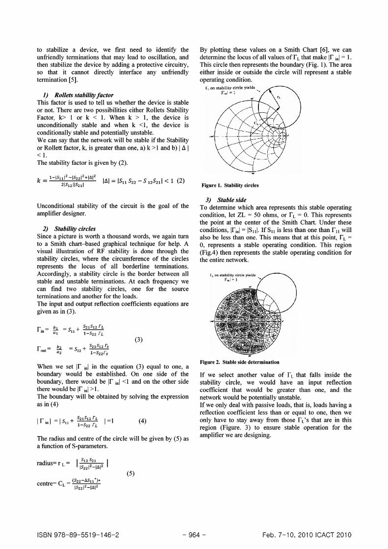
By plotting these values on a Smith Chart [6], we candetermine the locus ofall values of I'Lthat make If inl = I .This circle then represents the boundary (Fig. 1). The areaeither inside or outside the circle will represent a stableoperating condition.
rL on sta bility circle yields[F•• 1 = 1
Figure 1. Stability circles
3) Stable sideTo determine which area represents this stable operatingcondition, let ZL = 50 ohms, or I'L = O. This representsthe point at the center of the Smith Chart . Under theseconditions, If inl = ISIII . If SII is less than one than Fu willalso be less than one. This means that at this point, I'L =
0, represents a stable operating condition. This region(FigA) then represents the stable operating condition forthe entire network.
I'Lon stab ilit y circle yieldsIf " I - 1 '"
Figure 2. Stable side determination
If we select another value of I'L that falls inside thestability circle, we would have an input reflectioncoefficient that would be greater than one, and thenetwork would be potentially unstable .If we only deal with passive loads, that is, loads having areflection coefficient less than or equal to one, then weonly have to stay away from those fL's that are in thisregion (Figure . 3) to ensure stable operation for theamplifier we are designing.
ISBN 978-89-5519-146-2 - 964- Feb. 7-10, 2010 ICACT 2010

81.,-1 ' .~~...f~"o~. "~Proled ..•
~.P!OlII<I ...~1~f'ro'IMts._ .
1Irt.~~ .. ,~"'ol8Ct..•~~ ...,;e.wC'MQ\. ••
e"..n~"
ClClrDr""m..~.~.
~... •
Figure 3. Passive loads case Figure 6. Creating a new project
In the new schematic of the project , push the "Library"button to open a library lists to choose the suitabletransistor model to build the amplifier.After opened the Library List window, choose "RFTransistor Library ~ Packaged BJTs" to choose thetransistor and then you have to design suitable biasingcircuit for that purpose do the DC simulation to find outthe right bias points for the amplifier. After designing thesuitable biasing circuit of the chosen transistor, next stepin designing the amplifier with the S parameter method isto determine whether the amplifier is unconditionallystable or potentially unstable , SII position and gain circlesfor the bare transistor.The stability factors are easily calculated usingMeasurement Equations in the ADS schematic panel. K ispre-programmed in as stabjact which can be selectedfrom the S-parameter palette on the left. Delta can beprogrammed yourself using a blank MeasEqn . Themaximum available gain (MAG) and maximum stablegain (MSG) can also be calculated using the max_gainfunction .For the S-parameter, simulation, another suitable model isneeded to select from the Library List. While the"GaCircle" and "L_StabCircle" simulators can beobtained from the "Simulation-S_Param" tag.
Figure 7. ADS schematic and stability circle plot
...11
,,)1
~... :I. l_ol.b rt
131Crc1. l l SlabCrr.'GtC«lr'''Q a.CI'tlt(S.15,51) l )labC,tlel -1_"ab_rl't't tS,Sll
$P ISI~xn MH:
5lcr£OO M-IzSlep-50 MI1z
Figure 4.
Figure 5.
jIC.I- ',! > I
If, on the other hand, IS III >1, with ZL = 50 n, then thisarea would be the stable region and this region theunstable area. (Fig. 4)
To ensure that we have an unconditionally stablecondition at a given frequency in our amplifier design, wemust be able to place any passive load on the network anddrive it with any source impedance without moving intoan unstable condition.
From a graphical point of view, we want to be sure thatthe stability circle falls completely outside the SmithChart, and we want to make sure that the inside of thestability circle represents the unstable region (Figure . 5).The area outside the stability circle, including the SmithChart, would then represent the stable operating region[6].
IV. AMPLIFIER DESIGN USING ADS TOOL
A. Creating new project
The overview of designing any type of amplifier in ADStool has been presented in this tutorial.Firstly open ADS program. Choose "File ~ NewProject" to open a new project.
ISBN 978-89-5519-146-2 - 965- Feb. 7-10, 2010 ICACT 2010
Dr-~,,-
\ ~
r;--Stoof .... ~"""f.... m;;---~
-11- t
Figure 10. Smith chart utility
-I
~r11J~~
il! W-I
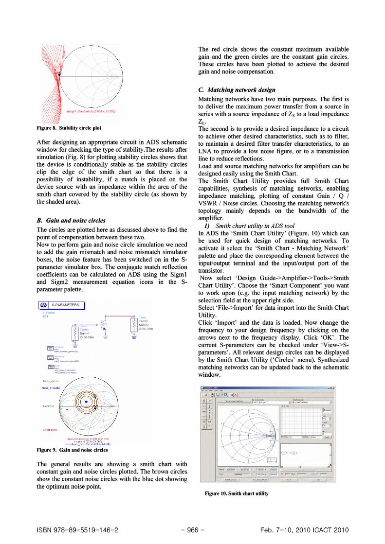
The red circle shows the constant maximum availablegain and the green circles are the constant gain circles.These circles have been plotted to achieve the desiredgain and noise compensation.
C. Matching network design
Matching networks have two main purposes. The first isto deliver the maximum power transfer from a source inseries with a source impedance of Zs to a load impedanceZL.The second is to provide a desired impedance to a circuitto achieve other desired characteristics, such as to filter,to maintain a desired filter transfer characteristics, to anLNA to provide a low noise figure , or to a transmissionline to reduce reflections.Load and source matching networks for amplifiers can bedesigned easily using the Smith Chart .The Smith Chart Utility provides full Smith Chartcapabilities, synthesis of matching networks, enablingimpedance matching, plotting of constant Gain / Q /VSWR / Noise circles. Choosing the matching network'stopology mainly depends on the bandwidth of theamplifier.
1) Smith chart utility in ADS toolIn ADS the ' Smith Chart Utility' (Figure. 10) which canbe used for quick design of matching networks. Toactivate it select the ' Smith Chart - Matching Network'palette and place the corresponding element between theinput/output terminal and the input/output port of thetransistor.Now select 'Design Guide ->Amplifier->Tools->SmithChart Utility' . Choose the 'Smart Component' you wantto work upon (e.g. the input matching network) by theselection field at the upper right side.Select ' File->Import ' for data import into the Smith ChartUtility.Click 'Import' and the data is loaded. Now change thefrequency to your design frequency by clicking on thearrows next to the frequency display. Click 'OK' . Thecurrent S-parameters can be checked under 'View->Sparameters'. All relevant design circles can be displayedby the Smith Chart Utility ('Circles' menu). Synthesizedmatching networks can be updated back to the schematicwindow.
' ...mY. ,m2Nl. n=2Z~50 ()Ivn
indep{GAcircleMax) (0000 to 51.000)cirJlls (0,000 to 51.000)
indep(Noise_t ircleMin) (0 000 1051.000)
rtB_.-.-"" .~""' I-.--....."-'"
~ ....-.-..-.as'
S.P8lfOYJ1
SP I
Figure 9. Gain and noise circles
The general results are showing a smith chart withconstant gain and noise circles plotted. The brown circlesshow the constant noise circles with the blue dot showingthe optimum noise point.
After designing an appropriate circuit in ADS schematicwindow for checking the type of stability.The results aftersimulation (Fig. 8) for plotting stability circles shows thatthe device is conditionally stable as the stability circlesclip the edge of the smith chart so that there is apossibility of instability, if a match is placed on thedevice source with an impedance within the area of thesmith chart covered by the stability circle (as shown bythe shaded area) .
B. Gain and noise circles
The circles are plotted here as discussed above to find thepoint of compensation between these two.Now to perform gain and noise circle simulation we needto add the gain mismatch and noise mismatch simulatorboxes, the noise feature has been switched on in the Sparameter simulator box. The conjugate match reflectioncoefficients can be calculated on ADS using the Sigmland Sigm2 measurement equation icons in the Sparameter palette.
ISBN 978-89-5519-146-2 - 966- Feb. 7-10, 2010 ICACT 2010
i NelworkResponse-------------,
Type
~Trace1
[511"3Trace2
[511"3Min
~ ~ISlarl Freq ro--- SlopFreq ~~
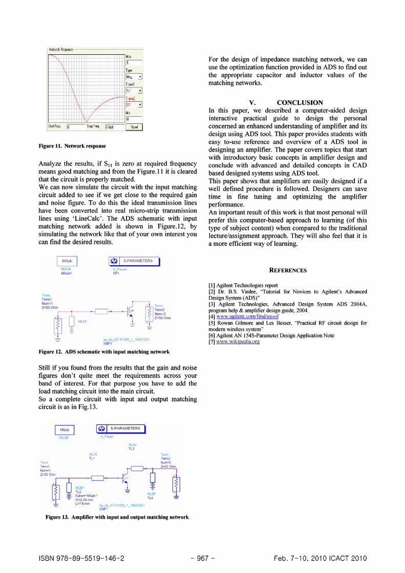
Figure 11. Network response
Analyze the results, if Sll is zero at required frequencymeans good matching and from the Figure. I I it is clearedthat the circuit is properly matched.We can now simulate the circuit with the input matchingcircuit added to see if we get close to the required gainand noise figure. To do this the ideal transmission lineshave been converted into real micro-strip transmissionlines using 'LineCalc' . The ADS schematic with inputmatching network added is shown in Figure.12, bysimulating the network like that of your own interest youcan find the desired results.
For the design of impedance matching network, we canuse the optimization function provided in ADS to fmd outthe appropriate capacitor and inductor values of thematching networks.
V. CONCLUSIONIn this paper, we described a computer-aided designinteractive practical guide to design the personalconcerned an enhanced understanding ofamplifier and itsdesign using ADS tool. This paper provides students witheasy to-use reference and overview of a ADS tool indesigning an amplifier. The paper covers topics that startwith introductory basic concepts in amplifier design andconclude with advanced and detailed concepts in CADbased designed systems using ADS tool.This paper shows that amplifiers are easily designed if awell defined procedure is followed. Designers can savetime in fine tuning and optimizing the amplifierperformance.An important result of this work is that most personal willprefer this computer-based approach to learning (of thistype of subject content) when compared to the traditionallecture/assignment approach. They will also feel that it isa more efficient way of learning.
8MSUBMSo bl
TennTenn 1Num=1Z=50 0 hm
S ParamSP I
Sl'_hp_AT-41435_1_19921201SNPI
TennTeml2Num:=2Z=50 0hm
REFERENCES
[1] Agilent Technologies report[2] Dr. B.S. Virdee, "Tutorial for Novices to Agilent's AdvancedDesign System (ADS)"[3] Agilent Technologies, Advanced Design System ADS 2004A,program help & amplifier design guide, 2004.[4] www.agilent.com/find/eesof[5] Rowan Gilmore and Les Besser, "Practical RF circuit design formodem wireless system"[6] Agilent AN 154S-Parameter Design Application Note[7] www.wikipedia.org
Figure 12. ADS schematic with input matching network
Still if you found from the results that the gain and noisefigures don't quite meet the requirements across yourband of interest. For that purpose you have to add theload matching circuit into the main circuit.So a complete circuit with input and output matchingcircuit is as in Fig.13.
aMSUB
",'NTLl
""NTLl
rermTermlNlII'I- 'Z· 500 twn
.----r---j
sp_Il;)_AT -J 10135_'_19921201SNPI
TennTerm2N<Jn·2Z- SOOhm
"-EFTLJ =-
Figure 13. Amplifier with input and output matching network
ISBN 978-89-5519-146-2 - 967- Feb. 7-10, 2010 ICACT 2010