The K2 parallel processor: architecture and hardware implementation
10
The K2 Parallel Processor: Architecture and Hardware Implementation MARCO ANNARATONE, MARCO FILLO, KIYOSHI NAKABAYASHIt AND MARC VIREDAZ Integrated Systems Laboratory, Swiss Federal Institute of Technology Gloriastrasse 95, 8092 Zurich, Switzerland an.d t NTT Communications and Information Processing Laboratories, Tokyo 180, Japan Abstract K2 is a distributed-memory parallel processor designed to support a multi-user, multi-tasking, time-sharing Operating system and an automatically paralleliting FORTRAN com- piler. This paper presents the architecture and the hardware implementation of K2, and focuses on the architectuml fea- tures required by the operating system and the compiler. A prototype machine with 24 processors is currently being de- veloped. 1 Introduction Distributed-memory parallel processors (DMPPs) feature different interconnection topologies (i.e., tori, hypercubes, linear arrays, just to mention DMPPs that were built and commercialized) and different parallelism grain-size, i.e., from the 64 vector processors of the MIMD iPSC/2[1] to the 65,536 simple processors of the SIMD Connection Machine CM-2[2]. Efficient interconnection topologies, communica- tion mechanisms, etc., have been researched and debated in recent years. Conversely, system software issues have not been as aggressively addressed. We believe this is one of the reasons why DMPPs have not achieved a significant commercial success so far. For this reason we have concen- trated our research on automatically parallelizing compilers (APCs), interactive symbolic debuggers, and multi-user op erating systems. Considering such features within the de- velopment of a DMPP modifies profoundly the design space and forces the architectural parameters mentioned above to be evaluated under a new perspective. This paper presents the architecture and the hardware implementation of K2, a DMPP designed to support a FOR- TRAN APC and a multi-user, multi-tasking, time-sharing operating system. In the paper we first critique current This research wan supported in part by ETH grant number 0.330.066.23/4, in part by the Mikrotechnik Kredit. Permission to copy without fee all or part of this material is granted provided that the copies are not made or distributed for di- rect commercial advantage, the ACM copyright notice and the title of the publication and its date appear, and notice is given that copying is by permission of the Association for Computing Machinery. To copy otherwise, or to republish, requires a fee and/or specific permission. CH2887-8/90/0000/0092$01 .OO Q 1990 IEEE DMPPs. Second, we present the architecture of K2. Then, we analyze the different design alternatives and justify our choices. The hardware implementation and the project st* tus are finally discussed. Throughout the paper we also refer to our ongoing research on the compiler and the operating system. 2 A Critique of DMPPs DMPPs such as the Connection Machine (CM) [2], NCUBE [3], Intel iPSC/2 [I], Warp [4] and iWarp [SI, and various Transputer-based computers like the Meiko M40 [6] are attachedprocessors: there is a host between the user and the DMPP. The host is a Symbolics or a Vax in the CM, a SUN in the NCUBE, a SUN with dedicated 1/0 processors in Warp, and a SUN (remote) and an 80386 (local) on the iPSC/2. Such approach dates back to the Solomon [7] and ILLIAC IV [8] DMPPs, and has also been used to connect array processors to mini or mainframe computers. These DMPPs run single-user or, at most, provide space sharing (iPSC, NCUBE, and CM): programmers can con- currently use non-overlapping sections of the DMPP topol- ogy. On these machines jobs may run on the attached pro- cessor in batch-mode, similarly to what was done on Cray computers running under COS. Batch processing makes it unrealistic to run interactive programs, and tends to favor post-mortem debugging. Interactive use and debugging is possible on some DMPPs only by locking the machine. This is not a practical solution since debugging sessions can last hours if not days, and running the application on a simu- lator to check the functional correctness of the code has a limited usefulness. As some experts have realized, a single-user, single-task DMPP is unlikely to fulfill the market requirements in the years to come. In a recent paper by Gordon Bell [9] one reads: , “The lack of multiprogramming ability today may dictate using these machines [i.e., high- performance DMPPs] on only one or a few very large jobs at the same time, and hence making 92
Transcript of The K2 parallel processor: architecture and hardware implementation

The K2 Parallel Processor: Architecture and Hardware Implementation
MARCO ANNARATONE, MARCO FILLO, KIYOSHI NAKABAYASHIt AND MARC VIREDAZ
Integrated Systems Laboratory, Swiss Federal Institute of Technology Gloriastrasse 95, 8092 Zurich, Switzerland
an.d
t NTT Communications and Information Processing Laboratories, Tokyo 180, Japan
Abstract K2 is a distributed-memory parallel processor designed to support a multi-user, multi-tasking, time-sharing Operating system and an automatically paralleliting FORTRAN com- piler. This paper presents the architecture and the hardware implementation of K2, and focuses on the architectuml fea- tures required by the operating system and the compiler. A prototype machine with 24 processors is currently being de- veloped.
1 Introduction Distributed-memory parallel processors (DMPPs) feature different interconnection topologies (i.e., tori, hypercubes, linear arrays, just to mention DMPPs that were built and commercialized) and different parallelism grain-size, i.e., from the 64 vector processors of the MIMD iPSC/2[1] to the 65,536 simple processors of the SIMD Connection Machine CM-2[2]. Efficient interconnection topologies, communica- tion mechanisms, etc., have been researched and debated in recent years. Conversely, system software issues have not been as aggressively addressed. We believe this is one of the reasons why DMPPs have not achieved a significant commercial success so far. For this reason we have concen- trated our research on automatically parallelizing compilers (APCs), interactive symbolic debuggers, and multi-user o p erating systems. Considering such features within the de- velopment of a DMPP modifies profoundly the design space and forces the architectural parameters mentioned above to be evaluated under a new perspective.
This paper presents the architecture and the hardware implementation of K2, a DMPP designed to support a FOR- TRAN APC and a multi-user, multi-tasking, time-sharing operating system. In the paper we first critique current
This research wan supported in part by ETH grant number 0.330.066.23/4, in part by the Mikrotechnik Kredit.
Permission to copy without fee all or part of this material is granted provided that the copies are not made or distributed for di- rect commercial advantage, the ACM copyright notice and the title of the publication and its date appear, and notice is given that copying is by permission of the Association for Computing Machinery. To copy otherwise, or to republish, requires a fee and/or specific permission.
CH2887-8/90/0000/0092$01 .OO Q 1990 IEEE
DMPPs. Second, we present the architecture of K2. Then, we analyze the different design alternatives and justify our choices. The hardware implementation and the project st* tus are finally discussed. Throughout the paper we also refer to our ongoing research on the compiler and the operating system.
2 A Critique of DMPPs DMPPs such as the Connection Machine (CM) [2], NCUBE [3], Intel iPSC/2 [I], Warp [4] and iWarp [SI, and various Transputer-based computers like the Meiko M40 [6] are attachedprocessors: there is a host between the user and the DMPP. The host is a Symbolics or a Vax in the CM, a SUN in the NCUBE, a SUN with dedicated 1/0 processors in Warp, and a SUN (remote) and an 80386 (local) on the iPSC/2. Such approach dates back to the Solomon [7] and ILLIAC IV [8] DMPPs, and has also been used to connect array processors to mini or mainframe computers.
These DMPPs run single-user or, at most, provide space sharing (iPSC, NCUBE, and CM): programmers can con- currently use non-overlapping sections of the DMPP topol- ogy.
On these machines jobs may run on the attached pro- cessor in batch-mode, similarly to what was done on Cray computers running under COS. Batch processing makes it unrealistic to run interactive programs, and tends to favor post-mortem debugging. Interactive use and debugging is possible on some DMPPs only by locking the machine. This is not a practical solution since debugging sessions can last hours if not days, and running the application on a simu- lator to check the functional correctness of the code has a limited usefulness.
As some experts have realized, a single-user, single-task DMPP is unlikely to fulfill the market requirements in the years to come. In a recent paper by Gordon Bell [9] one reads:
,
“The lack of multiprogramming ability today may dictate using these machines [i.e., high- performance DMPPs] on only one or a few very large jobs at the same time, and hence making
92

the cost per job quite high, thus diminishing the performance/price advantage.” [emphasis added]
In the above DMPPs the user interface and the software development environment reside on the host. The host runs the sequential part of the application; this may result in a communication bottleneck between the host and the at- tached processor that for the CM-1 or the iPSCI2, for in- stance, can be severe.
The above DMPPs do not have APCs. An APC takes as input, source code developed for uniprocessors and per- forms the following tasks: (1) domain decomposition on the DMPP topology, (2) code optimization and parallelization, and (3) code generation for all the nodes including interpro- cessor communication operations. APCs are already avail- able on shared-memory multiprocessors-the KAP FOR- TRAN compiler [lo] for the Sequent Symmetry or the Al- liant FORTRAN compiler [ l l ] are two examples. The major hurdle in the implementation of an APC for DMPPs is the domain decomposition. Nonetheless, the development of an APC is an essential step towards more usable DMPPs, since programmers should not be expected to manually decom- pose the data-structures (much like they are not expected to allocate registers in uniprocessors).
From the above considerations, we can derive the system features that should be supported by a new architecture:
e
e
e
3
A time-sharing, multi-user, multi-tasking operating system. This eases interactive debugging, and gener- ally decreases the cost per job. This implies:
- a disk subsystem with enough bandwidth to s u p port paging activities, process swapping, and large-files transfer (see also below).
- large local storage to decrease the load on the interprocessor communication channels [12], and to accommodate the working sets of sev- eral large-sized processes. For instance, finite- element analysis of three-dimensional semicon- ductor structures requires data sets in excess of 320 Mbyte [13]; trace-driven cache simuIations need data-sets of more than 150 Mbyte to be able to capture a few hundred milliseconds of RISC microprocessor activity [14].
- memory protection and virtual memory support on each node.
Efficient execution of APC-generated parallel pro- grams. Higher communication bandwidth between the serial part and the parallel part of the code by avoiding the attached processor design paradigm.
Overview of the K2 architec- ture
K2 has been designed to support the execution of applica- tion software and the execution of system software. While
/7
Figure 1: The K2 user-level machine abstraction.
much is known about efficient topologies and communica- tion mechanisms for parallel application code, the same can- not be said for parallel system software. Our decision was to design a topology well known to perform efficiently on a p plication code, and to enhance it to support system-related activities.
Figure 1 shows the K2 user-leuel machine abstraction, which consists of a torus of computation nodes (CNs). CNs are interconnected by point-to-point (32-bit wide) bidirec- tional channels, hereafter referred to as user channels. The advantages of this topology (when the DMPP has a lim- ited number of processors, as in our case) are well-known. By summarizing the results from the works of Dally [15], Vitilnyi [16], and Johnsson [17], a two-dimensional topology represents a natural choice when the processing elements are 256 or less (Dally), or 64 or less (Johnsson). This con- sensus can be found in the marketplace as well. In fact, the Warp machine (a linear array of processors) has evolved into iWarp (a two-dimensional torus); moreover, many hy- percube users “flatten” the topology and work on tori em- bedded in the hypercube [18, 19, 20, 21, 221.
The K2 eystem-level machine abstraction is shown in fig- ure 2. Each row (or column) of CNs is connected to an input/output node (ION) to which terminals and disks are attached. The connection between each ION and a row (or column) of CNs is a serial token-ring, referred to as sys- tem channel. An identical token-ring serves all IONs and connects them to an Ethernet gateway.
All nodes are intended to run both user and system pro- cesses. The CNs are dedicated to computation-intensive parallel jobs, while the IONs run light-weight jobs such as editing, mail, etc. In addition, although the OS activities are distributed over all CNs and IONs, the latter are pri- marily used as file servers and disk caches.
In the following sections we elaborate on the two ma- jor architectural features in the design of K2, i.e., the user channels and the system channels.
93

E”
I I I I I T E R M I N A L S
Figure 2: T h e K2 system-level machine abstraction.
3.1 The user channels CNs communicate with one another in two different do- mains: user and system. While the former is typical of all DMPPs available today, the latter is unique to K2. Commu- nication among processors in the user and system domains cannot be efficiently supported by a single interconnection paradigm. In fact, application-related information is highly deterministic, and its flow within the torus is mainly dic- tated by the programmer of the parallel task (or by the APC). This is not the case for system-related communi- cation, as we shall discuss in detail in section 3.2. Be- cause precise control over the interprocessor communica- tion and synchronization is generally possible in the user domain, processors can communicate without resorting to the asynchronous, interrupt-based policy which character- izes message-passing architectures. That is, neighboring processors can exchange data by simply copying them from their own local memory to dedicated hardware channels. This mechanism, also used in Warp and iWarp, has two major advantages:
1. The communication is totally supported in hardware. Hence, no kernel activity is required either to send or to receive data, unlike in message-passing architectures.
2. If queue channels are used, self-synchronizing commu- nication can efficiently be achieved through hardware blocking. Processors reading from an empty queue or writing to a full queue will stall until the queue status changes .
Such a mechanism, unlike message-passing, lacks automatic routing and transparent forwarding. However, the low- dimensionality of the topologies featuring it makes the man- ual routing of information manageable by the programmer. This consideration does not apply to higher-dimensionality
Figure 3: Four user channel architectures. (M: local memory; P: processor; Q: queue; S: shared-memory.)
topologies (e.g., hypercubes): in this case automatic routing and transparent forwarding must be provided. Moreover, this issue becomes less important with the availability of an APC.
3.1.1 Alternative user channel architectures
Before committing to a specific user channel architecture, we evaluated four different alternatives. They are shown in figure 3. Figure 3(a) shows the “Warp/iWarp” channel architecture; it provides a simple and clear programming model (based on send and receive) and automatic pro- cess synchronization through queue blockage. This model features the highest interprocessor bandwidth when send- ing and receiving raw data. However, sharing of readlwrite data structures can be done only by physically moving them from processor to processor. The shared-memory model in figure 3(b) is more efficient, as long as the sharing of data structures is limited to two neighboring processors, but it lacks the simple programming model of the previous one and an automatic process synchronization mechanism (locks must be checked before accessing writable shared resources).
The architecture in figure 3(c) merges the previous two together: shared data structures do not have to be physi- cally copied between neighboring processors, and automatic process synchronization is accomplished by enqueueing and dequeueing pointers to the shared structures. Two disad- vantages are higher costs and a clumsy programming model. In fact, variable definition would be similar to that found in shared-memory multiprocessors (e.g., SHARED and PRIVATE) but with access semantics similar to DMPPs (i.e., send and receive) . Neither architecture 3(b) nor 3(c) copes well with
94
variables that are normally local to processors and become occasionally shared; the data allocation strategy and the consistency mechanism would be difficult to implement ele- gantly.
The fourth architecture (figure 3(d)), although it solves the problems just mentioned, lacks a programming model and the automatic process synchronization mechanism pro- vided by the queues. Finally, it requires the processors to have a tight coupling of their logical-to-physical address mapping, something difficult to accomplish in practice.
3.1.2 User channel throughput and latency
Fast local communication throughput is essential to achieve good performance. We have quantified this parameter in one of our studies [23]: the time to send a double-precision number to a neighbor processor should be no greater than 16 times the time required for a local double-precision multipli- cation or addition. Decreasing the communication through- put penalizes performance, while increasing it does not re- sult in appreciable performance improvement. Note that this holds true in a single-task environment, which was the assumption in the study cited above. In our case, the multi- tasking requirements call for the fastest queue flush on pro- cess switch. In addition, fast channels are required by the APC under development. In fact, the APC avoids some deficiencies typical of current shared-memory APCs (no- tably KAP [lo]) by carrying out run-time data-dependency analysis and construction of interprocessor communications. This allows, for instance, to parallelize fast-Fourier t r ans form code, a task which KAP is unable to do because it limits its parallelization to a compile-time analysis of the code. Since the run-time portion of the compiler requires substantial amount of information exchange among proces sors, its efficiency depends heavily on the speed of the user channels. Even with the 0.5 communication/computation ratio of a CN, the average overhead introduced by the com- piler run-time activities on an 8 x 8 K2 is about 20%, with a best case of 2% (in a fluid-dynamics simulation) and a worst case of 30% (in a binary FFT program) [24].
Another justification for high-throughput, low-latency channels comes from the need to support fast communica- tion between the serial and parallel parts of an application. K2’s multi-tasking makes it possible to have a CN in charge of running the sequential part of the application, and switch back and forth between this task and the one belonging to the parallel part. In this way we have reached the goal of eliminating the “host-attached processor” structure and its inherent communication bottleneck. The serial part of the application now runs within the parallel part, and can there- fore communicate with it using the high bandwidth of the user channels. The resulting minimum bandwidth (i.e., that between the CN running the serial part and the surround- ing CNs) features 50 Mbyte/s throughput for outgoing data and 200 Mbyte/s for incoming data (limited to maximum 4 Kbyte bursts).
3.1.3 The K2 user channel architecture
Based on the above reasoning, we decided to implement the model shown in figure 3(a) with some extra features.
First, the status of a queue can be checked. That is, the hardware queues allow both blocking and non-blocking ac- cess. Second, queues are not strictly unidirectional; in fact, they can also be read (only in supervisor mode, however) by the processor writing into them. Whenever the current process context is saved, the queues will be flushed out and their contents saved as part of it. This feature is also use- ful in the implementation of a debugger for the machine. Without it, the implementation of the debugger would be rather complicated, as the experience with the Warp miG chine showed [25].
Third, we had to decide whether to implement several virtual queues (as in iWarp [5]) on top of the physical one or not. Support of multi-tasking on the machine can be ac- complished either by having virtual queues assigned to each process and mapped onto the physical one, or by having the physical queue assigned to a single process at any given time. In the first case, the total depth of the physical queue is subdivided into all processes active at a given time (i.e., those that are either running or in fast wait), and a pro- cess switch does not require flushing of the queues to local memory but simply performing a pointer exchange. In the second case the depth of the virtual queue is identical to that of the physical one, but queue flush is required at any process switch. Given the limited size of the queues and their fast access time, a complete flushing of the queues to local memory does not represent a significant overhead even when the quantum of the process switch is relatively small (e.g., every 20,000 instructions), and therefore the second solution has been implemented.
3.2 The system channels The design of the user channels has been tailored to the characteristics of the application software running on the CNs: strong locality, predefined occurrence of communication activities, and relatively high computa- tion/communication ratio. To define similar figures-even qualitatively-for the system domain one must resort to some educated guess. Research on multi-user, multi-tasking operating systems for DMPPs has just started, and hard facts are not yet available.
It is fair to assume, however, that the data locality will strongly depend on the design of the file system, that com- munication will be stochastic in nature and will largely pre- vail over computation. If even one of the above assumptions held true, the communication mechanism implemented in the user domain would be highly inadequate. Its synchrony, its assumption of local communication, and its inflexibd- ity cannot be used to support largely asynchronous activi- ties typical of file transfers, paging, and process swapping. Moreover, the transfer of system-related information has a granularity which may go from the size of a page to small parcels of information such as acknowledgements, requests for services, etc. Finally, system-related information may
95
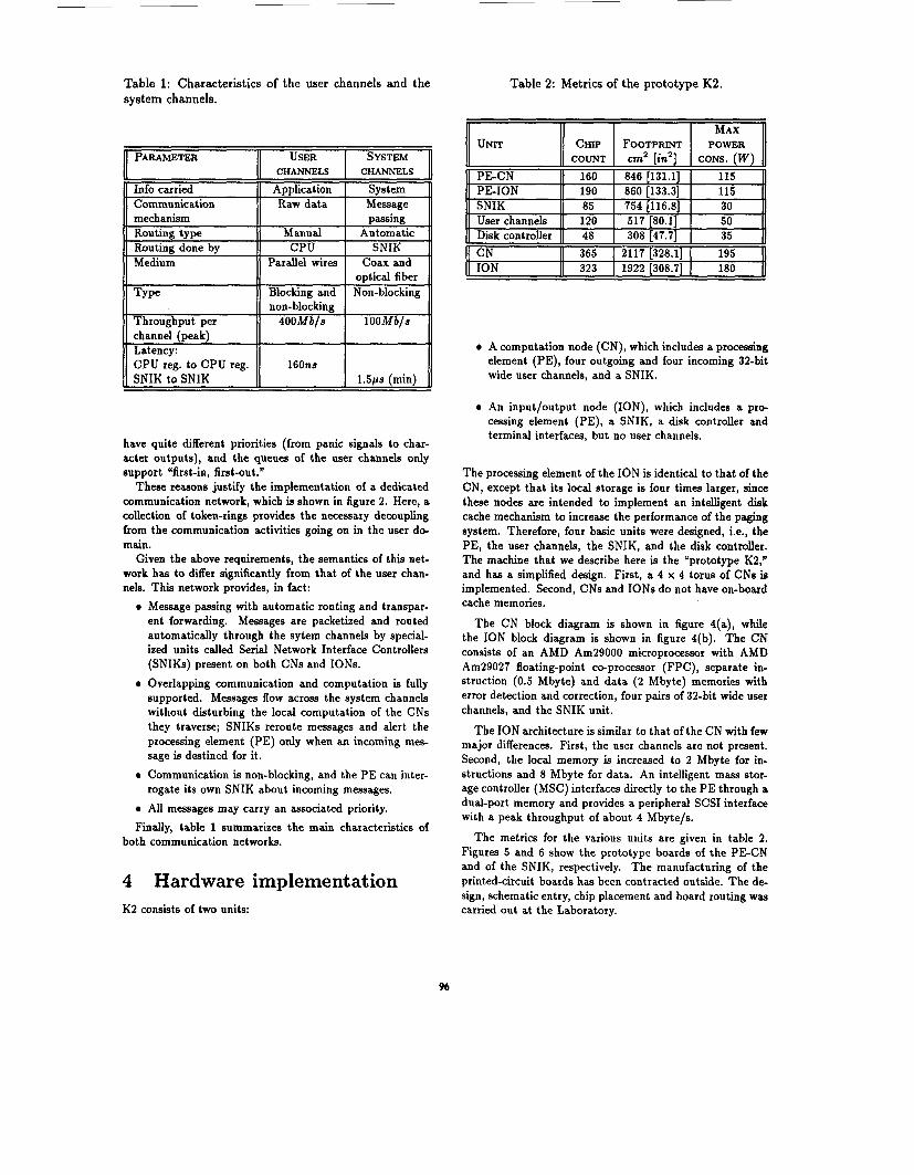
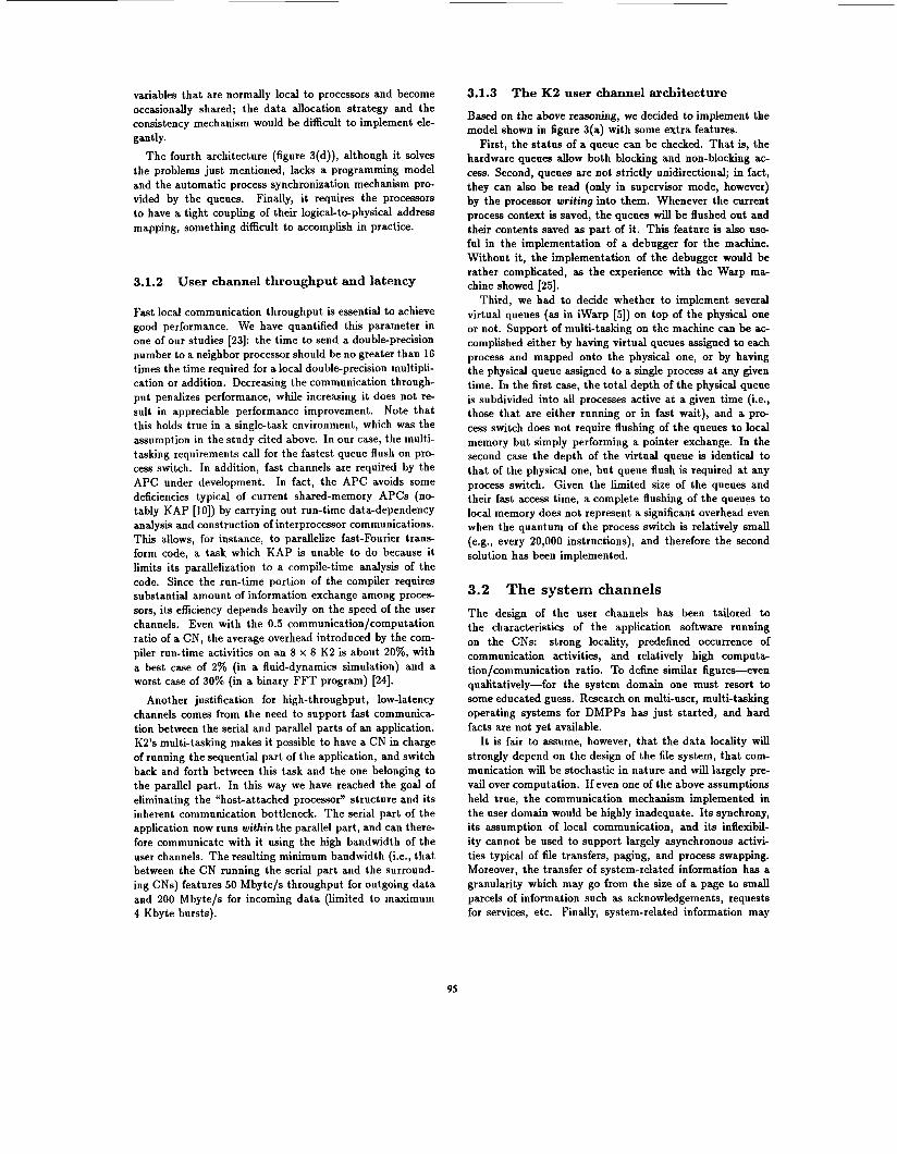
Table 1: Characteristics of the user channels and the system channels.
UNIT
P E C N PEION SNIK User channels
Table 2: Metrics of the prototype K2.
CHIP FOOTPRINT POWER COUNT cm’ [in’] CONS. ( W )
160 846 [131.1] 115 190 860 [133.3] 115 85 754 [116.8] 30 120 517 r80.11 50
PARAMETER
Info carried Communication
11 mechanism II I passinn II
USER SYSTEM
Application System Raw data Message
CHANNELS CHANNELS
3 Disk controller ii 48 i 308 i47.73 i 35 tl 1 CN 11 365 I 2117 1328.31 I 195
Routing type Routing done by Medium
Type
Throughput per channel (peak)
Manual Automatic CPU SNIK
Parallel wires Coax and optical fiber
Blocking and Non-blocking non- blocking
400Mbls 100Mbls
have quite different priorities (from panic signals to char- acter outputs), and the queues of the user channels only support “first-in, first-out.”
These reasons justify the implementation of a dedicated communication network, which is shown in figure 2. Here, a collection of token-rings provides the necessary decoupling from the communication activities going on in the user do- main.
Given the above requirements, the semantics of this net- work has to differ significantly from that of the user chan- nels. This network provides, in fact:
Latency: CPU reg. to CPU reg. SNIK to SNIK
Message passing with automatic routing and transpar- ent forwarding. Messages are packetized and routed automatically through the sytem channels by special- ized units called Serial Network Interface Controllers (SNIKs) present on both CNs and IONS.
Overlapping communication and computation is fully supported. Messages flow across the system channels without disturbing the local computation of the CNs they traverse; SNIKs reroute messages and alert the processing element (PE) only when an incoming mes- sage is destined for it.
Communication is non-blocking, and the PE can inter- rogate its own SNIK about incoming messages. All messages may carry an associated priority.
160ns 1 . 5 ~ s (min)
Finally, table 1 summarizes the main characteristics of both communication networks.
4 Hardware implementation K2 consists of two units:
n ION ii 323 i 1922 i308.7i i 180 n
0
0
The
A computation node (CN), which includes a processing element (PE), four outgoing and four incoming 32-bit wide user channels, and a SNIK.
An input/output node (ION), which includes a p r e cessing element (PE), a SNIK, a disk controller and terminal interfaces, but no user channels.
processing element of the ION is identical to that of the CN, except that its local storage is four times larger, since these nodes are intended to implement an intelligent disk cache mechanism to increase the performance of the paging system. Therefore, four basic units were designed, i.e., the PE, the user channels, the SNIK, and the disk controller. The machine that we describe here is the “prototype K2,” and has a simplified design. First, a 4 x 4 torus of CNs is implemented. Second, CNs and IONS do not have on-board cache memories.
The CN block diagram is shown in figure 4(a), while the ION block diagram is shown in figure 4(b). The CN consists of an AMD Am29000 microprocessor with AMD Am29027 floating-point ceprocessor (FPC), separate in- struction (0.5 Mbyte) and data (2 Mbyte) memories with error detection and correction, four pairs of 32-bit wide user channels, and the SNIK unit.
The ION architecture is similar to that of the CN with few major differences. First, the user channels are not present. Second, the local memory is increased to 2 Mbyte for in- structions and 8 Mbyte for data. An intelligent mass stor- age controller (MSC) interfaces directly to the PE through a dual-port memory and provides a peripheral SCSI interface with a peak throughput of about 4 Mbyte/s.
The metrics for the various units are given in table 2. Figures 5 and 6 show the prototype boards of the P E C N and of the SNIK, respectively. The manufacturing of the printed-circuit boards has been contracted outside. The de- sign, schematic entry, chip placement and board routing was carried out a t the Laboratory.
N S E W ...( .......................... : : ...... (..... H"TALRINO
- buffer FPU MMU
Figure 4: Block-diagram of CN (a) and ION (b).
on-chip
on-chip off-chip (88200) - ' off-chip (29027) on-chip
4.1 Processing element The choice of the CPU and the structure of the local mem- ory system were the fundamental issues in the design of the PE.
4.1.1
We decided to use a commercial CPU, rather than a custom processor, because of the obvious advantages both in hard- ware design (support chips and development tools), and in software development (availability of assemblers, compilers and debuggers).
When the CPU was chosen (May 1988), there were four high performance microprocessors in the market or about to enter it: the AMD Am29000, the Motorola MC88100, the SPARC, and the MIPS R2000. The last two were not con- sidered for other than technical reasons. The remaining two, i.e., the 29000 and 88100 CPUs, follow quite different design philosophies and a detailed analysis of both is outside the scope of this study. The CPUs' architectural characteristics which influenced the evaluation are shown in table 3.
Eventually, what tipped the scale in favor of the 29000 was the interface to the user channels. As already pointed out in section 3.1.2, the CPU architecture should allow a fast access mechanism to the user channels (whose references are non-cacheable), and their prompt blocking/unblocking.
With the 29000, mapping the channels onto the virtual address space does not cause any performance degradation since the on-chip TLB performs address translation as one of the pipeline stages. Instead, in the 88100 the mapping of the channels onto virtual space slows down their access since they must be addressed through the off-chip CMMU. More importantly, the 88000 CPU to CMMU handshake protocol introduces an access overhead for non-cacheable data of a t least 5 extra cycles.
A further consideration on this topic came from the effi- ciency in interrupt servicing during user channel blockage.
The choice of the CPU
Cache
...( .......................... : :...I.. ( ..... HORIZONMLIUNG
memories are not included in the prototype K2.
Table 3: Main characteristics of the AMD Am29000 and the Motorola MC88100 at the time of evaluation.
PARAMETER 11 A ~ 2 9 0 0 0 I MC88100
II I off-chip (88200) Data cache 11 8 Kbyte (casc.), I 16 +64 Kbyte,
II 11 2-way set-ass0c.t I 4-way set-assoc. 11 I off-chip (88200) Branch target II 128 entries, I N.A.
t Since then AMD decided to drop the development of the cache chips.
As we shall see later i n section 4.2, the 29000 provides a hardware mechanism to handle exception recovery, while the 88100 must resort to software emulation.
4.1.2 The design of the memory system
Four alternative structures of the local memory were con- sidered:
0 Instruction and data cache based system (I&D CACHE), with split caches and a two-way interleaved DRAM local memory.
97
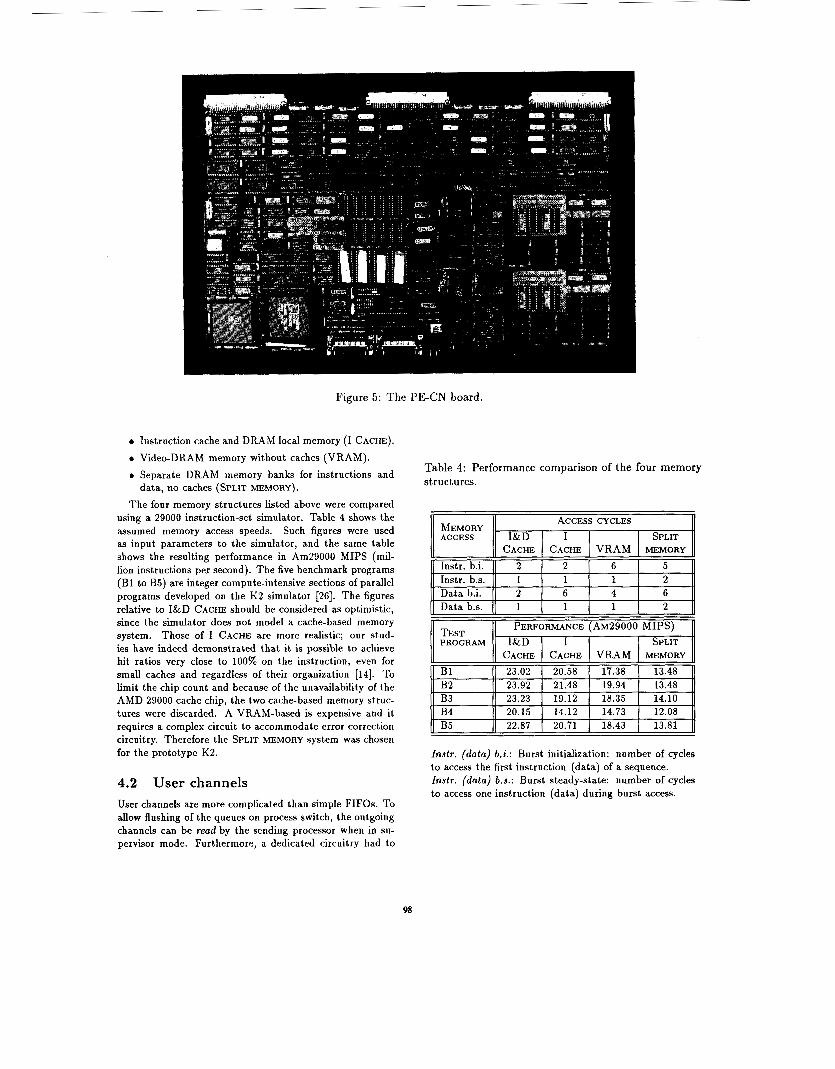
Figure 5: The PECN board.
0 Instruction cache and DRAM local memory (I CACHE). 0 Video-DRAM memory without caches (VRAM). 0 Separate DRAM memory banks for instructions and
The four memory structures listed above were compared using a 29000 instruction-set simulator. Table 4 shows the assumed memory access speeds. Such figures were used as input parameters to the simulator, and the same table shows the resulting performance in Am29000 MIPS (mil- lion instructions per second). The five benchmark programs (B1 to B5) are integer compute-intensive sections of parallel programs developed on the K2 simulator [26]. The figures relative to I&D CACHE should be considered as optimistic, since the simulator does not model a cache-based memory system. Those of I CACHE are more realistic; our stud- ies have indeed demonstrated that it is possible to achieve hit ratios very close to 100% on the instruction, even for small caches and regardless of their organization [14]. To limit the chip count and because of the unavailability of the AMD 29000 cache chip, the two cache-based memory struc- tures were discarded. A VRAM-based is expensive and it requires a complex circuit to accommodate error correction circuitry. Therefore the SPLIT MEMORY system was chosen for the prototype K2.
data, no caches (SPLIT MEMORY).
4.2 User channels User channels are more complicated than simple FIFOs. To allow flushing of the queues on process switch, the outgoing channels can be read by the sending processor when in su- pervisor mode. Furthermore, a dedicated circuitry had to
Table 4: Performance comparison of the four memory structures.
1) MEMORY I( ACCESS CYCLES
ACCESS I SPLIT
Instr. (data) h i . : Burst initialization: number of cycles to access the first instruction (data) of a sequence. Instr. (data) b.3.: Burst steady-state: number of cycles to access one instruction (data) during burst access.
98
be included to allow blocking without affecting kernel activ- ities. Our fast blocking scheme consists of not issuing the data transfer acknowledge to the processor whenever the queue is empty (on read) or full (on write). In this case the processor does not terminate the access and introduces wait-cycles indefinitely until the queue changes its state (to not-empty or to not-full, respectively).
A similar mechanism was implemented on Warp, which however had no interrupt-driven kernel activities running on top of the application. The presence of a multi-user, multi-tasking operating system kernel on K2 called for a special hardware solution to allow the processor to sense and serve interrupts while blocked on the queues. If an interrupt comes when the processor is blocked, the processor can leave its state by means of a trap, serve the interrupt, and come back to the channel access it could not complete.
This can be easily implemented on the 29000, because when a trap occurs the processor saves the current bus cycle information (necessary to resume the channel access) into special registers. The access to the blocked channel will be automatically resumed according to this information when the interrupt return is executed at the end of the trap han- dler.
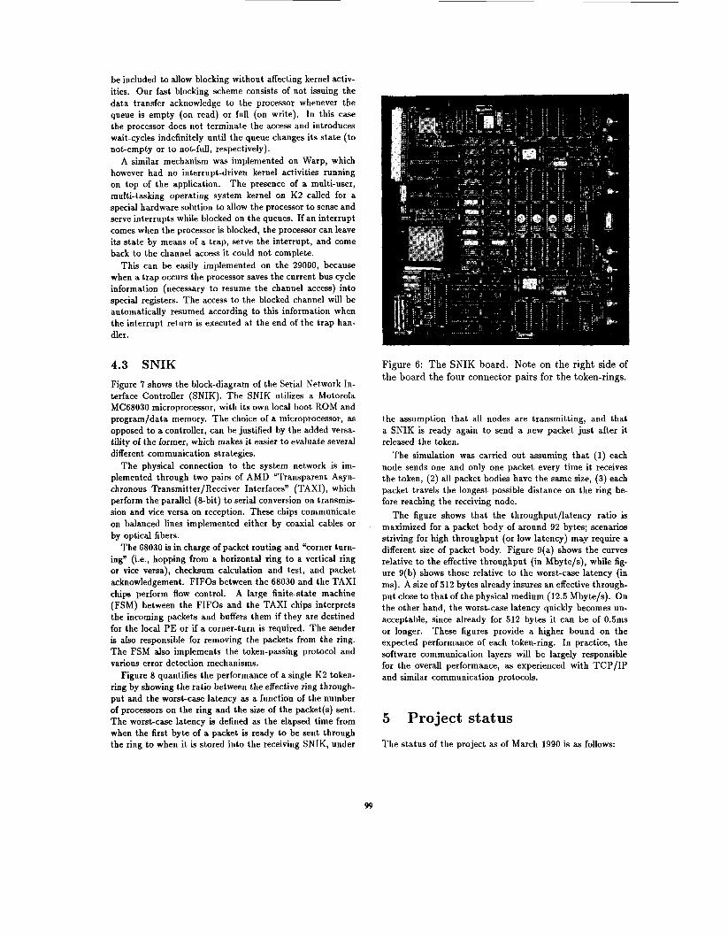
4.3 SNIK Figure 7 shows the block-diagram of the Serial Network In- terface Controller (SNIK). The SNIK utilizes a Motorola MC68030 microprocessor, with its own local boot ROM and program/data memory. The choice of a microprocessor, as opposed to a controller, can be justified by the added versa- tility of the former, which makes it easier to evaluate several different communication strategies.
The physical connection to the system network is im- plemented through two pairs of AMD uTransparent Asyn- chronous Transmitter/Receiver Interfaces” (TAXI), which perform the parallel (8-bit) to serial conversion on transmis- sion and vice versa on reception. These chips communicate on balanced lines implemented either by coaxial cables or by optical fibers.
The 68030 is in charge of packet routing and “corner turn- ing” (i.e., hopping from a horizontal ring t o a vertical ring or vice versa), checksum calculation and test, and packet acknowledgement. FIFOs between the 68030 and the TAXI chips perform flow control. A large finite-state machine (FSM) between the FIFOs and the TAXI chips interprets the incoming packets and buffers them if they are destined for the local P E or if a corner-turn is required. The sender is also responsible for removing the packets from the ring. The FSM also implements the token-passing protocol and various error detection mechanisms.
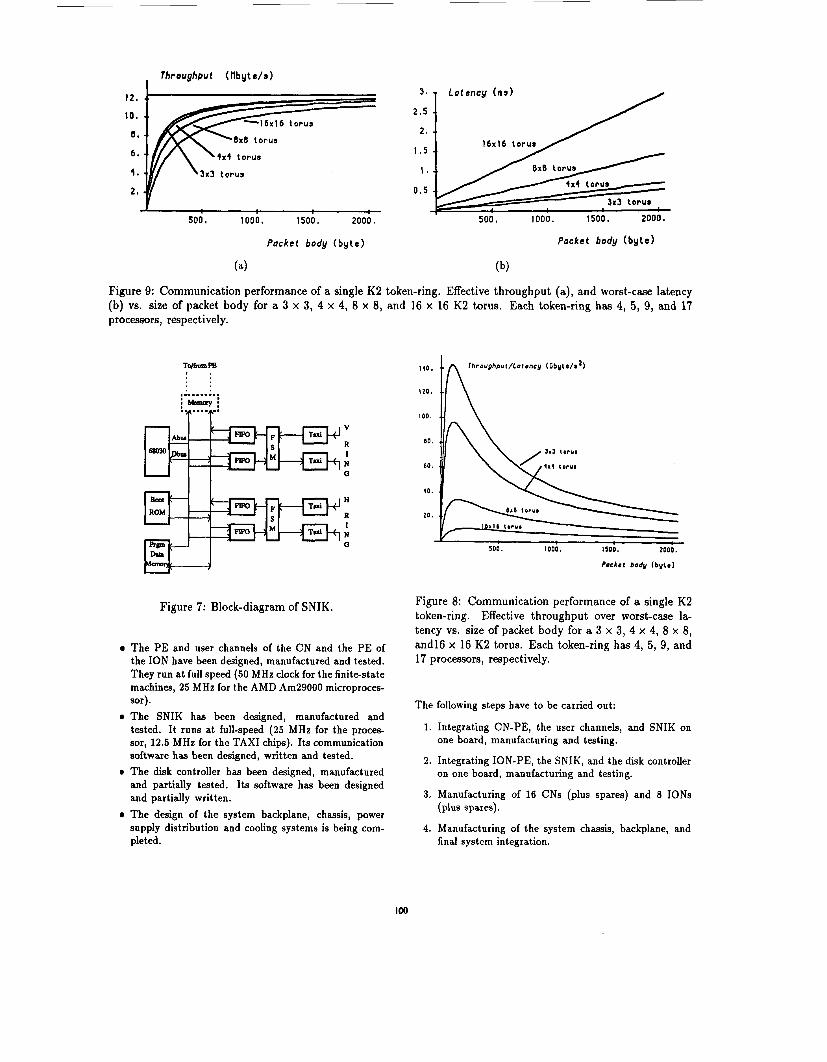
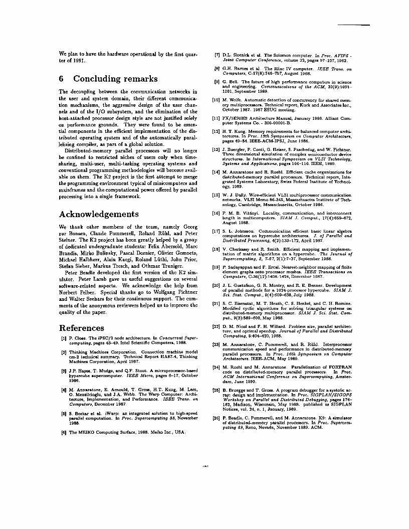
Figure 8 quantifies the performance of a single K2 token- ring by showing the ratio between the effective ring through- put and the worst-case latency as a function of the number of processors on the ring and the size of the packet(s) sent. The worst-case latency is defined as the elapsed time from when the first byte of a packet is ready to be sent through the ring to when it is stored into the receiving SNIK, under
Figure 6: The SNIK board. Note on the right side of the board the four connector pairs for the token-rings.
the assumption that all nodes are transmitting, and that a SNIK is ready again to send a new packet just after it released the token.
The simulation was carried out assuming that (1) each node sends one and only one packet every time it receives the token, (2) all packet bodies have the same size, (3) each packet travels the longest possible distance on the ring be- fore reaching the receiving node.
The figure shows that the throughput/latency ratio is maximized for a packet body of around 92 bytes; scenarios striving for high throughput (or low latency) may require a different size of packet body. Figure 9(a) shows the curves relative to the effective throughput (in Mbyte/s), while fig- ure 9(b) shows those relative to the worst-case latency (in ms). A size of 512 bytes already insures an effective through- put close to that of the physical medium (12.5 Mbyte/s). On the other hand, the worst-case latency quickly becomes un- acceptable, since already for 512 bytes it can be of 0.5ms or longer. These figures provide a higher bound on the expected performance of each token-ring. In practice, the software communication layers will be largely responsible for the overall performance, as experienced with TCP/IP and similar communication protocols.
5 Project status
The status of the project as of March 1990 is as follows:
99
Throughput ( flbyt e/, 1
12.
10.
I).
6 ,
1. 1 x 1 torus
3x3 t orus
500 a 1000. I 500 . 2000 8 500 I 1000 * 1500, 2000 I
Pocket body ( b y t e ) Pocket body (by te )
( 4 (b)
Figure 9: Communication performance of a single K 2 token-ring. Effective throughput (a) , and worst-case latency (b) vs. size of packet body for a 3 x 3, 4 x 4, 8 x 8, and 16 x 16 K 2 torus. Each token-ring has 4, 5 , 9, and 17 processors , respectively.
w Figure 7: Block-diagram of SNIK.
The PE and user channels of the CN and the PE of the ION have been designed, manufactured and tested. They run at full speed (50 MHz clock for the finite-state machines, 25 MHz for the AMD Am29000 microproces-
The SNIK has been designed, manufactured and tested. I t runs at full-speed (25 MHz for the proces- sor, 12.5 MHz for the TAXI chips). Its communication software has been designed, written and tested. The disk controller has been designed, manufactured and partially tested. Its software has been designed and partially written. The design of the system backplane, chassis, power supply distribution and cooling systems is being com- pleted.
sor).
500. I 000 , 1500.
Pocket body ( b y t e )
Figure 8: Communication performance of a single K2 token-ring. Effective throughput over worst-case la- tency vs. size of packet body for a 3 x 3, 4 x 4, 8 x 8, and16 x 16 K 2 torus. Each token-ring has 4, 5 , 9, and 17 processors, respectively.
The following steps have to be carried out:
1. Integrating CN-PE, the user channels, and SNIK on one board, manufacturing and testing.
2. Integrating ION-PE, the SNIK, and the disk controller on one board, manufacturing and testing.
3. Manufacturing of 16 CNs (plus spares) and 8 IONS (plus spares).
4. Manufacturing of the system chassis, backplane, and final system integration.
We plan to have the hardware operational by the first quar- ter of 1991.
6 Concluding remarks The decoupling between the communication networks in the user and system domain, their different communica- tion mechanisms, the aggressive design of the user chan- nels and of the 1/0 subsystem, and the elimination of the host-attached processor design style are not justified solely on performance grounds. They were found to be essen- tial components in the efficient implementation of the dis- tributed operating system and of the automatically paral- lelizing compiler, as part of a global solution.
Distributed-memory parallel processors will no longer be confined to restricted niches of users only when time- sharing, multi-user, multi-tasking operating systems and conventional programming methodologies will become avail- able on them. The K2 project is the first attempt to merge the programming environment typical of minicomputers and mainframes and the computational power offered by parallel processing into a single framework.
Acknowledgements We thank other members of the team, namely Georg zur Bonsen, Claude Pommerell, Roland Riihl, and Peter Steiner. The K2 project has been greatly helped by a group of dedicated undergraduate students: Felix Abersold, Marc Brandis, Mirko Bulinsky, Pascal Dornier, Olivier Gemoets, Michael Halbherr, Alain Kaegi, Roland Liithi, John Prior, Stefan Sieber, Markus Tresch, and Othmar Truniger.
Peter Beadle developed the first version of the K2 sim- ulator. Peter Lamb gave us useful suggestions on several software-related aspects. We acknowledge the help from Norbert Felber. Special thanks go to Wolfgang Fichtner and Walter Seehars for their continuous support. The com- ments of the anonymous reviewers helped us to improve the quality of the paper.
References P. Close. The iPSC/P node architecture. In Concurrent Super- computing, page8 43-49. Intel Scientific Computers, 1988.
Thinking Machines Corporation. Connection machine model cm-2 technical summary. Technical Report HA87-4, Thinking Machines Corporation, April 1987.
J.P. Hayes, T. Mudge, and Q.F. Stout. A microprocessor-based hypercube supercomputer. IEEE Micro, pages 6-17, October 1986.
M. Annaratone, E. Arnould, T. Gram, H.T. Kung, M. Lam, 0. Menzilcioglu, and J.A. Webb. The Warp Computer: Archi- tecture, Implementation, and Performance. IEEE "kana. on Computers, December 1987.
S. Borkar e t al. iWarp: an integrated solution t o high-speed parallel computation. In Proc. Supercomputing 88, November 1988.
The MEIKO Computing Surface, 1988. Meiko Inc., USA.
D.L. Slotnick e t al. The Solomon computer. In Proc. AFIPS - Joint Computer Conference, volume 22, pages 97-107, 1962.
G.H. Barnes e t al. The Illiac IV computer. IEEE mans. on Computers, C-17(8):746-757, August 1968.
G. Bell. The future of high performance computers in science and engineering. Communications of the ACM, 32(9):1091- 1101, September 1989.
M. Wolfe. Automatic detection of concurrency for shared mem- ory multiprocessors. Technical report, Kuck and Associates Inc., October 1987. 1987 ESUG meeting.
FX/SERIES Architecture Manual, January 1986. Alliant Com- puter Systems Co. - 300-00001-B.
H. T . Kung. Memory requirements for balanced computer archi- tectures. In Proc. 13th Symposium on Computer Architecture, pages 49-54. IEEEACM-IPSJ, June 1986.
J . Buergler, P. Conti, G. Heiser, S . Paschedag, and W. Fichtner. Three dimensional simulation of complex semiconductor device structures. In International Symposium on VLSI Technology, Systems and Applications, pages 106-110. IEEE, 1989.
M. Annaratone and R. Ruehl. Efficient cache organizations for distributed-memory parallel processors. Technical report, Inte- grated Systems Laboratory, Swiss Federal Institute of Technol- ogy, 1989.
W. J . Dally. Wire-efficient VLSI multiprocessor communication networks. VLSI Memo 86-345, Massachusetts Institute of Tech- nology, Cambridge, Massachusetts, October 1986.
P. M. B. Vi thyi . Locality, communication, and interconnect length in multicomputers. SIAM J . Comput., 17(4):659-672, August 1988.
S. L. Johnsson. Communication efficient basic linear algebra computations on hypercube architectures. J . of Parallel and Distributed Processing, 4(2):133-172, April 1987.
V. Cherkassy and R. Smith. Efficient mapping and implemen- tation of matrix algorithms on a hypercube. The Journal of Supercomputing, 2, 7-27, 2( 1):7-27, September 1988.
P. Sadayappan and F. Ercal. Nearest-neighbor mapping of finite element graphs onto processor meshes. IEEE !hnsactions on Computers, C-36( 12):1408-1424, December 1987.
J. L. Gustafson, G. R. Montry, and R. E. Benner. Development of parallel methods for a 1024-processor hypercube. SIAM J. Sci. Stat. Comput., 9(4):609-638, July 1988.
S. C. Eisenstat, M. T . Heath, C. S. Henkel, and C. H. Romine. Modified cyclic algorithms for solving triangular systems on distributed-memory multiprocessor. SIAM J . Sci. Stat. Com- put., 9(3):589-600, May 1988.
D. M. Nicol and F. H. Willard. Problem size, parallel architec- ture, and optimal speedup. Journal of Parallel and Distributed Computing, 5:404-420,1988,
M. Annaratone, C. Pommerell, and R. Ruhl. Interprocessor communication speed and performance in distributed-memory parallel processors. In Proc. 16th Symposium on Computer Architecture. IEEEACM, May 1989.
M. Ruehl and M. Annaratone. Parallelization of FORTRAN code on distributed-memory parallel processors. In Proc. A CM International Conference on Supercomputing, Amster- dam, June 1990.
B. Bruegge and T. Gross. A program debugger for a systolic ar- ray: design and implementation. In Proc. SIGPLAN/SIGOPS Workshop on Parallel and Distributed Debugging, pages 174- 182, Madison, Wisconsin, May 1988. published as SIGPLAN Notices, vol. 24, n. 1, January, 1989.
P. Beadle, C. Pommerell, and M. Annaratone. K9: A simulator of distributed-memory parallel processors. In Proc. Supercom- puting 89, Reno, Nevada, November 1989. ACM.