Low temperature epitaxial growth of Si and SiGe and their transfer to foreign substrate
Upload
independentCategory
view
3download
0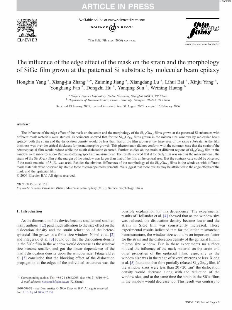
2006) xxx–xxx
+ MODEL
www.elsevier.com/locate/tsf
ARTICLE IN PRESS
Thin Solid Films xx (
The influence of the edge effect of the mask on the strain and the morphologyof SiGe film grown at the patterned Si substrate by molecular beam epitaxy
Hongbin Yang a, Xiang-jiu Zhang a,⁎, Zuiming Jiang a, Xiangdang Lu a, Lihui Bai a, Xinju Yang a,Yongliang Fan a, Dongzhi Hu a, Yanqing Sun a, Weining Huang b
a Surface Physics Laboratory, Fudan University, Shanghai 200433, PR Chinab Department of Microelectronics, Fudan University, Shanghai 200433, PR China
Received 19 January 2005; received in revised form 31 August 2005; accepted 16 February 2006
Abstract
The influence of the edge effect of the mask on the strain and the morphology of the Si0.8Ge0.2 films grown at the patterned Si substrates withdifferent mask materials were studied. Experiments showed that for the Si0.8Ge0.2 films grown in the micron size windows by molecular beamepitaxy, both the strain and the dislocation density would be less than that of the film grown at the large area of the same substrate, as the filmthickness was over the critical thickness for pesudomorphic growth. This phenomenon did not conform with the common case that the strain of theheteroepitaxial film would reduce while the misfit dislocation occurred. Further studies on the strain at different regions of Si0.8Ge0.2 film in thewindow were made by micro Raman scattering spectrum measurement. The results showed that if the SiO2 film was used as the mask material, thestrain of the Si0.8Ge0.2 film at the margin of the window was larger than that of the film at the central area. But the contrary case could be observedif the mask material of Si3N4 was used. Besides the obvious differences of the morphology of the Si0.8Ge0.2 films in the windows with differentmask materials were observed by atomic force microscope measurements. We suggest that these results may be attributed to the edge effects of themask and the epitaxial film.© 2006 Elsevier B.V. All rights reserved.
PACS: 68.35.Bs; 81.15.HiKeywords: Silicon-Germanium (SiGe); Molecular beam epitaxy (MBE); Surface morphology; Strain
1. Introduction
As the dimension of the device became smaller and smaller,many authors [1,2] paid much attention to the size effect on thedislocation density and the strain relaxation of the hetero-epitaxial film grown in a finite size window. Nobel et al. [2]and Fitagerald et al. [3] found out that the dislocation densityin the SiGe film in the window would decrease as the windowsize became smaller, and got the linear dependence of themisfit dislocation density upon the window size. Fitagerald etal. [3] concluded that the blocking effect of the dislocationpropagation at the edges of the individual structures was the
⁎ Corresponding author. Tel.: +86 21 65642965; fax: +86 21 65104949.E-mail address: [email protected] (X. Zhang).
0040-6090/$ - see front matter © 2006 Elsevier B.V. All rights reserved.doi:10.1016/j.tsf.2006.02.037
possible explanation for this dependence. The experimentalresults of Hollander et al. [4] showed that as the window sizewas reduced, the dislocation density became lower and thestrain in SiGe film was consistently increased. Theseexperimental results indicated that for the lattice mismatchedheterostructure, the window size would be an important factorfor the strain and the dislocation density of the epitaxial film inmicron size window. But in these experiments no authorsnoticed the influence of the mask material on the strain andother properties of the epitaxial films, especially as thewindow size was in the range of several microns or less. Xionget al. [5] found out that for a partially relaxed Si0.8Ge0.2 film, ifthe window sizes were less than 20×20 μm2 the dislocationdensity would decrease along with the reduction of thewindow size, and at the same time the strain in the SiGe filmsin the window would decrease too. This result was contrary to
TSF-21637; No of Pages 6
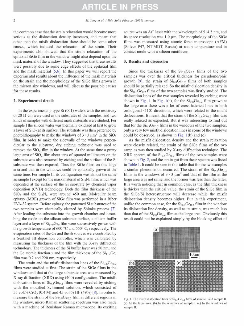
Fig. 1. The misfit dislocation lines of Si0.8Ge0.2 films of sample I and sample II.(a) At the large area. (b) In the windows of sample I. (c) In the windows ofsample II.
2 H. Yang et al. / Thin Solid Films xx (2006) xxx–xxx
ARTICLE IN PRESS
the common case that the strain relaxation would become moreserious as the dislocation density increases, and meant thatother than the misfit dislocation there should be some othercauses, which induced the relaxation of the strain. Theirexperiments also showed that the strain relaxation of theepitaxial SiGe film in the window might also depend upon themask material of the window. They suggested that these resultswere possibly due to some edge effects of the epitaxial filmand the mask material [5,6]. In this paper we will report theexperimental results about the influence of the mask materialson the strain and the morphology of the SiGe films grown inthe micron size windows, and will discuss the possible causesfor these results.
2. Experimental details
In the experiments p type Si (001) wafers with the resistivityof 20 Ω·cm were used as the substrates of the samples, and twokinds of samples with different mask materials were studied. Forsample I the silicon wafer was thermally oxidized at first to growa layer of SiO2 at its surface. The substrate was then patterned byphotolithography to make the windows of 3×3 μm2 in the SiO2
film. In order to make the sidewalls of the windows perpen-dicular to the substrate, dry etching technique was used toremove the SiO2 film in the window. At the same time a prettylarge area of SiO2 film about tens of squared millimeters on thesubstrate was also removed by etching and the surface of the Sisubstrate was then exposed. Thus the SiGe films on this largearea and that in the windows could be epitaxially grown at thesame time. For sample II, its configuration was almost the sameas sample I except for the maskmaterial of Si3N4 film, which wasdeposited at the surface of the Si substrate by chemical vapordeposition (CVD) technology. Both the film thickness of theSiO2 and the Si3N4 were around 450 nm. Molecular beamepitaxy (MBE) growth of SiGe film was performed in a RiberEVA-32 system. Before epitaxy, the patterned Si substrates of thetwo samples were chemically cleaned by Shirake process [7].After loading the substrate into the growth chamber and desor-bing the oxide on the silicon substrate surface, a silicon bufferlayer and a layer of Si1−xGex film were successively grown withthe growth temperature of 600 °C and 550° C, respectively. Theevaporation rates of the Ge and the Si sources were controlled bya Sentinel III deposition controller, which was calibrated bymeasuring the thickness of the film with the X-ray diffractiontechnology. The thickness of the Si buffer layer was 50 nm, andthe Ge atomic fraction x and the film thickness of the Si1−xGexfilm was 0.2 and 220 nm, respectively.
The strain and the misfit dislocation lines of the Si0.8Ge0.2films were studied at first. The strain of the SiGe films in thewindows and that at the large substrate area was measured byX-ray diffraction (XRD) using (400) configuration. The misfitdislocation lines of Si0.8Ge0.2 films were revealed by etchingwith the modified Schimmel solution, which consisted of55 vol.% CrO3 (0.4 M) and 45 vol.% HF (49%) [8]. In order tomeasure the strain of the Si0.8Ge0.2 film at different regions inthe window, micro Raman scattering spectrum was also madewith a machine of Renishaw Raman microscope. Its exciting
source was an Ar+ laser with the wavelength of 514.5 nm, andits space resolution was 1.0 μm. The morphology of the SiGefilms was measured using atomic force microscope (AFM)(Solver P47, NT-MDT, Russia) at room temperature and incontact mode with a silicon cantilever.
3. Results and discussion
Since the thickness of the Si0.8Ge0.2 films of the twosamples was over the critical thickness for pseudomorphicgrowth [9], the strain of Si0.8Ge0.2 films of both samplesshould be partially relaxed. So the misfit dislocation density inthe Si0.8Ge0.2 films of the two samples was firstly studied. Thedislocation lines of the two samples revealed by etching wereshown in Fig. 1. In Fig. 1(a), for the Si0.8Ge0.2 film grown atthe large area there was a lot of cross-hatched lines in bothorthogonal ⟨110⟩ directions, which were related to the misfitdislocations. It meant that the strain of the Si0.8Ge0.2 film wasreally relaxed as expected. But it was interesting to find outthat for the Si0.8Ge0.2 films in the windows of the two samples,only a very few misfit dislocation lines in some of the windowscould be observed, as shown in Fig. 1(b) and (c).
As the misfit dislocation density and the strain relaxationwere closely related, the strain of the SiGe films of the twosamples was then studied by X-ray diffraction technique. TheXRD spectra of the Si0.8Ge0.2 films of the two samples wereshown in Fig. 2, and the strain got from these spectra was listedin Table 1. It could be seen in this table that for the two samplesa similar phenomenon occurred. The strain of the Si0.8Ge0.2films in the windows of 3×3 μm2 and that of the film at thelarge area was not same, and the former was less than the latter.It is worth noticing that in common case, as the film thicknessis thicker than the critical value, the strain of the SiGe film inthe SiGe/Si heterostructure will decrease while the misfitdislocation density becomes higher. But in this experiment,unlike the common case, for the Si0.8Ge0.2 film in the windowits dislocation line density, as well as its strain, was much lessthan that of the Si0.8Ge0.2 film at the large area. Obviously thisresult could not be explained simply by the blocking effect of
Fig. 2. XRD spectra of Si0.8Ge0.2 films grown at the large area and in thewindows for sample I and sample II.
Fig. 3. Raman spectra of Si0.8Ge0.2 films in the windows at the margin and thecentral area for (a) sample I and (b) sample II. The insets are the amplified peaksof Si–Ge and Si–Si mode of the two samples at different regions.
3H. Yang et al. / Thin Solid Films xx (2006) xxx–xxx
ARTICLE IN PRESS
the dislocation propagation at the edges of the individualstructures suggested by Fitagerald et al. [3]. This experimentalphenomenon consisted with the results of Xiong et al. [5], butit showed further that the similar results could be obtained forthe Si0.8Ge0.2 film in the window with the different maskmaterial of Si3N4 (in which there was high tensile stress), andthat the strain of the Si0.8Ge0.2 film in the window with theSi3N4 mask was significantly less than that in the window withthe SiO2 mask.
In order to study the influence of the mask material on thestrain of the Si0.8Ge0.2 film in the window, Raman scatteringspectra of the Si0.8Ge0.2 films in the windows at the margin and atthe central area were measured by micro Raman scatteringspectrum technique. Fig. 3 showed all the spectra of the twosamples. In Fig. 3 three peaks located respectively near 288, 408,and 513 cm−1 were due to the nearest neighbor Ge–Ge, Si–Ge,and Si–Si atomic vibration of the Si0.8Ge0.2 film. The peaklocated at 520.5 cm−1 was due to the Si–Si atomic vibration ofthe Si substrate, and the peak near 435 cm−1 was attributed to thelocalized Si–Si vibration in the neighborhood of one or more Geatoms. The phonon frequencies ωSi–Si and ωSi–Ge of the Si–Siand Si–Gemode of the two samples were listed in Table 2. It wasobvious that for each sample there were differences in the phononfrequencies at different places. Since the phonon energies of SiGefilm depended on its Ge composition x and the strain, it meantthat for the two samples the strain and the Ge composition at themargin and at the center part were not same. For small values ofstrain the shift of the phonon frequency was linear with the strain
Table 1The strain of Si0.8Ge0.2 films of sample I and sample II from XRD spectra
Sample Peak position in XRDspectra
Strain ε$
Si(400) SiGe(400)
Si0.8Ge0.2 film at large area 69.120 68.079 −6.82E−03Si0.8Ge0.2 film in the window of
sample I (SiO2 mask)69.120 68.105 −6.23E−03
Si0.8Ge0.2 film in the window ofsample II (Si3N4 mask)
69.120 68.161 −5.26E−03
[10,11]. For xb0.5, the dependence of the phonon frequenciesωSi–Si and ωSi–Ge on the composition x and the in-plane strain ε$of Si1−xGex film could be written as:
xSi�Si ¼ 520:5−62x−DSie⫽ ð1Þ
xSi�Ge ¼ 400:5þ 14:2x−DGSe⫽ ð2Þ
e⫽ ¼ ða⫽−aSi1−xGexÞ=aSi1−xGex ð3Þ
Here, ΔSi=815 and ΔGS=575 were the strain-shift coeffi-cients for the Si–Si and the Si–Ge mode, a⫽ was the latticeconstant of the epitaxial Si1−xGex film parallel to the substratesurface and aSi1−xGex was the lattice constant of the unstrainedSi1−xGex film.
The Ge composition x and the strain ε⫽ at different placesof the two samples could be obtained from ωSi–Si and ωSi–Ge
with the Eqs. (1) and (2). The data of x and ε⫽ were listed in thelast two columns of Table 2. (It should be pointed out that therewas a little discrepancy between the strain got from the XRDmeasurement and Raman scattering spectra measurement. We
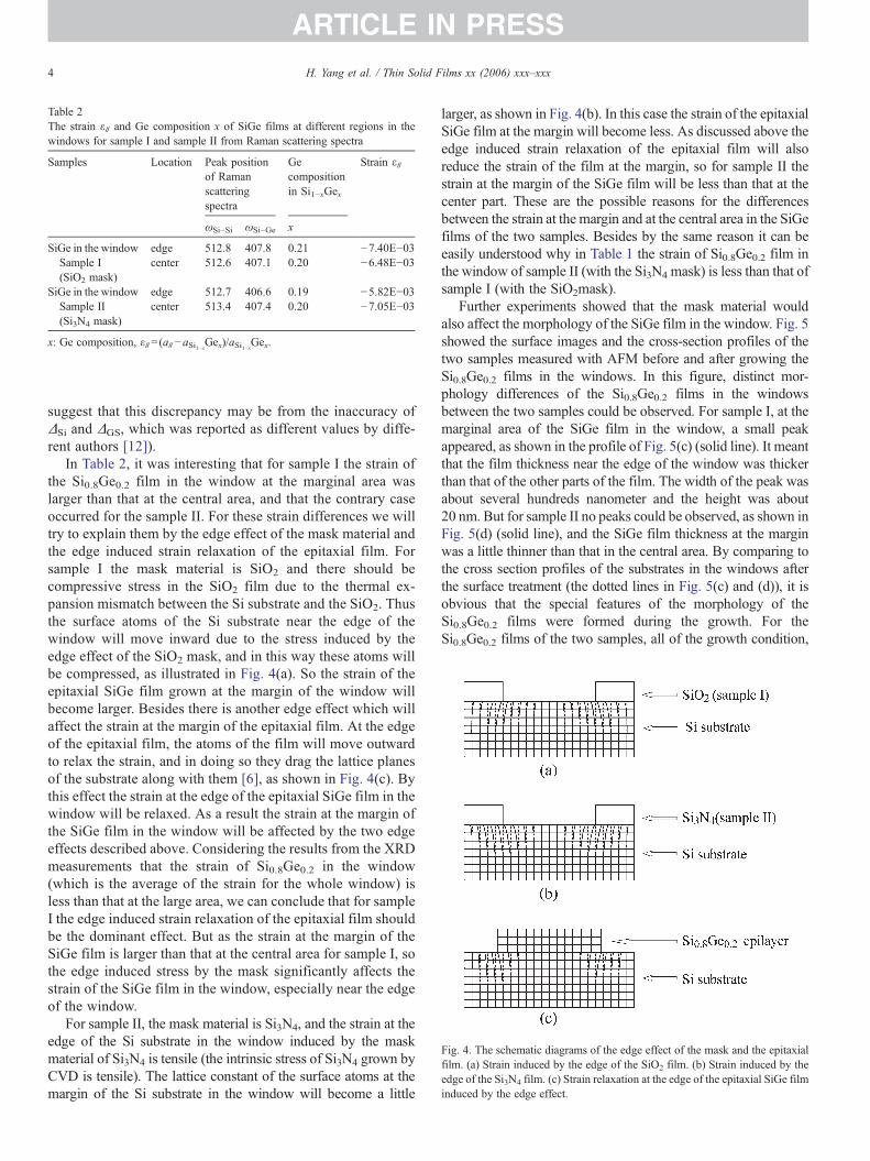
Fig. 4. The schematic diagrams of the edge effect of the mask and the epitaxialfilm. (a) Strain induced by the edge of the SiO2 film. (b) Strain induced by theedge of the Si3N4 film. (c) Strain relaxation at the edge of the epitaxial SiGe filminduced by the edge effect.
Table 2The strain ε$ and Ge composition x of SiGe films at different regions in thewindows for sample I and sample II from Raman scattering spectra
Samples Location Peak positionof Ramanscatteringspectra
Gecompositionin Si1−xGex
Strain ε$
ωSi–Si ωSi–Ge x
SiGe in the windowSample I(SiO2 mask)
edge 512.8 407.8 0.21 −7.40E−03center 512.6 407.1 0.20 −6.48E−03
SiGe in the windowSample II(Si3N4 mask)
edge 512.7 406.6 0.19 −5.82E−03center 513.4 407.4 0.20 −7.05E−03
x: Ge composition, ε$=(a$−aSi1−xGex)/aSi1−xGex.
4 H. Yang et al. / Thin Solid Films xx (2006) xxx–xxx
ARTICLE IN PRESS
suggest that this discrepancy may be from the inaccuracy ofΔSi and ΔGS, which was reported as different values by diffe-rent authors [12]).
In Table 2, it was interesting that for sample I the strain ofthe Si0.8Ge0.2 film in the window at the marginal area waslarger than that at the central area, and that the contrary caseoccurred for the sample II. For these strain differences we willtry to explain them by the edge effect of the mask material andthe edge induced strain relaxation of the epitaxial film. Forsample I the mask material is SiO2 and there should becompressive stress in the SiO2 film due to the thermal ex-pansion mismatch between the Si substrate and the SiO2. Thusthe surface atoms of the Si substrate near the edge of thewindow will move inward due to the stress induced by theedge effect of the SiO2 mask, and in this way these atoms willbe compressed, as illustrated in Fig. 4(a). So the strain of theepitaxial SiGe film grown at the margin of the window willbecome larger. Besides there is another edge effect which willaffect the strain at the margin of the epitaxial film. At the edgeof the epitaxial film, the atoms of the film will move outwardto relax the strain, and in doing so they drag the lattice planesof the substrate along with them [6], as shown in Fig. 4(c). Bythis effect the strain at the edge of the epitaxial SiGe film in thewindow will be relaxed. As a result the strain at the margin ofthe SiGe film in the window will be affected by the two edgeeffects described above. Considering the results from the XRDmeasurements that the strain of Si0.8Ge0.2 in the window(which is the average of the strain for the whole window) isless than that at the large area, we can conclude that for sampleI the edge induced strain relaxation of the epitaxial film shouldbe the dominant effect. But as the strain at the margin of theSiGe film is larger than that at the central area for sample I, sothe edge induced stress by the mask significantly affects thestrain of the SiGe film in the window, especially near the edgeof the window.
For sample II, the mask material is Si3N4, and the strain at theedge of the Si substrate in the window induced by the maskmaterial of Si3N4 is tensile (the intrinsic stress of Si3N4 grown byCVD is tensile). The lattice constant of the surface atoms at themargin of the Si substrate in the window will become a little
larger, as shown in Fig. 4(b). In this case the strain of the epitaxialSiGe film at the margin will become less. As discussed above theedge induced strain relaxation of the epitaxial film will alsoreduce the strain of the film at the margin, so for sample II thestrain at the margin of the SiGe film will be less than that at thecenter part. These are the possible reasons for the differencesbetween the strain at the margin and at the central area in the SiGefilms of the two samples. Besides by the same reason it can beeasily understood why in Table 1 the strain of Si0.8Ge0.2 film inthe window of sample II (with the Si3N4 mask) is less than that ofsample I (with the SiO2mask).
Further experiments showed that the mask material wouldalso affect the morphology of the SiGe film in the window. Fig. 5showed the surface images and the cross-section profiles of thetwo samples measured with AFM before and after growing theSi0.8Ge0.2 films in the windows. In this figure, distinct mor-phology differences of the Si0.8Ge0.2 films in the windowsbetween the two samples could be observed. For sample I, at themarginal area of the SiGe film in the window, a small peakappeared, as shown in the profile of Fig. 5(c) (solid line). It meantthat the film thickness near the edge of the window was thickerthan that of the other parts of the film. The width of the peak wasabout several hundreds nanometer and the height was about20 nm. But for sample II no peaks could be observed, as shown inFig. 5(d) (solid line), and the SiGe film thickness at the marginwas a little thinner than that in the central area. By comparing tothe cross section profiles of the substrates in the windows afterthe surface treatment (the dotted lines in Fig. 5(c) and (d)), it isobvious that the special features of the morphology of theSi0.8Ge0.2 films were formed during the growth. For theSi0.8Ge0.2 films of the two samples, all of the growth condition,

Fig. 5. The AFM images and the cross-sectional profiles of Si0.8Ge0.2 films of sample I and sample II. (a) The AFM image of sample I. (b) The AFM image of sampleII. (c) The profile of the Si0.8Ge0.2 films of sample I (solid line). (d) The profile of the Si0.8Ge0.2 film of sample II (solid line). The dotted lines in (c) and (d) are theprofiles of the substrates in the windows with the corresponding mask material after surface treatment. The lines A–A′, B–B′ show the places for measuring the cross-section profiles.
5H. Yang et al. / Thin Solid Films xx (2006) xxx–xxx
ARTICLE IN PRESS
the film thickness and the Ge composition x were same, asdescribed above, and the only difference between the twosamples was the mask material. So the difference of the surfacemorphology between the two samples had to originate from thedifferent materials of the masks.
For MBE growth, the surface morphology of the film isgoverned by the kinetics and the diffusion barrier of the adatoms isone of the important factors for determining the surface mor-phology of the film. Therefore to discuss the influence of the strainon the diffusion barrier of the adatoms and the strain disribution ofthe substrate surface are the keys for studying the special features ofthe film morphology in our experiment. We previously pointed outthat the strain at the marginal area of the epitaxial SiGe film in thewindow is affected by two edge effects, the edge induced stress bythe mask material and the edge induced strain relaxation of theepitaxial film. Obviously the influences of these edge effects on thestrain of SiGe film will decay along with the increasing of thedistance away from the edge of the window, and the straindistribution at the marginal area is determined by the influence ofthese edge effects. For sample I, the edge induced stress by the SiO2
mask will increase the strain of the SiGe film at the margin, and theedge induced strain relaxation of the epitaxial SiGe filmwill reduceit. In this case it is possible that a peak of compressive stress in theepitaxial SiGe film may appear somewhere near the edge of thewindow. But for sample II, both the edge effects will reduce thestrain at the margin of the epitaxial SiGe film, and therefore nopeaks of the strain may appear near the margin.
Many authors [13–15] studied the dependence of the strain onthe diffusion barrier for the Si and Ge adatoms on the Si substrate.Shu et al. [13] got the linear dependence of the diffusion barrier onthe external strain for the Si adatoms on Si (001) substrate in all
cases. Zoethout et al. [14] concluded by their experiment that theoverall effect of the tensile strain is a decrease in barrier height.From the results of these experimental and theoretical studies, wecan come to a conclusion for our experiments that the tensile strainwould enhance the diffusion rate, while the compressive strainwould lower the rate of diffusion. For sample I, itsmask ismade ofSiO2, so the adatoms at themargin of the windowwill diffusewiththe lower diffusion rate due to the compressive strain in thesubstrate. Usuallymore atomswill accumulate at the regionwherethe adatoms diffusion rate is lower, so a peak will form at theregion where the maximum compressive stress exists. As wediscussed above, for sample I a peak of compressive strainpossibly appears somewhere near the edge of the window,therefore a peak in the morphology may appear at the marginalarea of the SiGe film, as shown in Fig. 5(c). For sample II, there istensile stress at the margin of the Si substrate because of the maskof Si3N4. In this case the diffusion rate of the adatoms at the edgeof the window will be higher than that at the central area. So it isreasonable that the SiGe film near the edge of the window will bethinner than that at the central area, as shown in Fig. 5(d). Theseare the possible reasons for the formation of the special features ofthe morphology for sample I and sample II.
As the morphology of the SiGe film in the window is closelyrelated to the strain, the peak in Fig. 5(c) denotes the area, wherethe strain of the SiGe film is apparently influenced by the edgeeffect of the SiO2 mask. That is, the strain of the SiGe film in thewindow will be increased at the marginal area of severalhundreds of nanometer in width. Therefore if the epitaxial SiGefilm is grown in a submicron size window, more obviousinfluence on the strain of the epitaxial film by the edge effect ofthe mask will be expected.
6 H. Yang et al. / Thin Solid Films xx (2006) xxx–xxx
ARTICLE IN PRESS
4. Conclusion
For the lattice mismatched SiGe/Si heterostructure epitaxialygrown in the micron size window, the strain of the SiGe film inthe window is significantly influenced not only by the edgeeffect of the epitaxial film, but by the edge effect of the maskmaterial. The edge effect of the epitaxial film will induce thestrain relaxation of the SiGe film at the marginal area in thewindow, while the influence by the edge effect of the mask onthe strain of the epitaxial film will depend upon the differentkinds of stress induced by the mask. The compressive stress atthe marginal area of the window induced by the SiO2 mask willincrease the strain of the epitaxial SiGe film, while the tensilestress at the edge of the window induced by the Si3N4 mask willreduce its strain. If the strain relaxation of the SiGe film in thewindow is due to these kinds of edge effects, the misfit dis-location density of the SiGe film may decrease at the same time.Different influences on the morphology of the SiGe films in thewindows by the edge effects of the masks of SiO2 and Si3N4
have also been observed. We suggest that the difference of themorphology can possibly be explained by the different straindistribution in the Si substrate in the window and the depen-dence of the diffusion rate of the adatoms upon the strain.
Acknowledgement
This work is supported by the Natural Science Foundation ofChina, under Grant No. 60376012, the National AdvancedMate-
rials Committee of China, under Grant No. 2002AA313020 andthe State Key Laboratory of Functional Materials of Informatics,Chinese Academy of Science.
References
[1] A. Nishida, K. Nakagawa, E. Murakami, M. Miyao, J. Appl. Phys. 71(1992) 5913.
[2] D.B. Noble, J.L. Hoyt, C.A. King, J.F. Gibbons, T.I. Kamins, M.P. Scott,Appl. Phys. Lett. 56 (1990) 51.
[3] E.A. Fitzgerald, G.P. Watson, R.E. Proano, D.G. Ast, J. Appl. Phys. 65(1989) 2220.
[4] B. Holländer, L. Vescan, S. Mesters, S. Wickenh.auser, Thin Solid Films292 (1997) 213.
[5] H. Xiong, X.-J. Zhang, Z.M. Jiang, J.H. Hu, B. Shi, X.F. Zhou, W.R. Jiang,D.Z. Hu, Y.L. Fan, J. Cryst. Growth 233 (2001) 74.
[6] E. Murakami, A. Nishida, H. Etoh, K. Nakagawa, M. Miyao, Mater. Res.Soc. Symp. Proc. 198 (1990) 57.
[7] A. Ishizaka, Y. Shiraki, J. Electrochem. Soc. 133 (1986) 666.[8] J. Werner, K. Lyutovich, C.P. Parry, Eur. Phys. J., Appl. Phys. 27 (2004)
367.[9] R. People, J.C. Bean, Appl. Phys. Lett. 47 (1985) 322.[10] J.C. Tsang, P.M. Mooney, F. Dacol, J.O. Chu, J. Appl. Phys. 75 (1994)
8098.[11] J. Groenen, R. Carles, S. Christiansen, M. Albrecht, W. Dorsch, H.P.
Strunk, H. Wawra, G. Wagner, Appl. Phys. Lett. 71 (1997) 3856.[12] D.J. Lockwood, J.-M. Baribeau, Phys. Rev., B 45 (1992) 8565.[13] D.J. Shu, X.G. Feng Liu, Phys. Rev., B 64 (2001) 245410.[14] E. Zoethout, O. Grülü, H.J.W. Zandvliet, B. Poelsema, Surf. Sci. 452
(2000) 247.[15] H. Spjut, D.A. Faux, Surf. Sci. 306 (1994) 233.
Copyright © 2022 FDOKUMEN


![The formation, transport properties and microstructure of 45° [001] grain boundaries induced by epitaxy modification in YBa 2Cu 3O 7− x thin films](https://static.fdokumen.com/doc/165x107/6315b7dbc32ab5e46f0d6fce/the-formation-transport-properties-and-microstructure-of-45-001-grain-boundaries.jpg)