The influence of different electrodeposition E/t programs on the photoelectrochemical properties of...
9
The influence of different electrodeposition E/t programs on the photoelectrochemical properties of α-Fe 2 O 3 thin films Ricardo S. Schrebler a , Hernán Altamirano a , Paula Grez a , Francisco V. Herrera a , Eduardo C. Muñoz a , Luis A. Ballesteros a , Ricardo A. Córdova a , Humberto Gómez a , Enrique A. Dalchiele b, ⁎ a Instituto de Química, Facultad de Ciencias, Pontificia Universidad Católica de Valparaíso, Casilla 4059, Valparaíso, Chile b Instituto de Física, Facultad de Ingeniería, Herrera y Reissig 565, C.C. 30, 11000 Montevideo, Uruguay abstract article info Article history: Received 16 November 2009 Received in revised form 17 May 2010 Accepted 30 June 2010 Available online 8 July 2010 Keywords: Hematite Akaganeite Electrodeposition Photoelectrochemistry In this work morphological, structural and photoelectrochemical properties of n-type α-Fe 2 O 3 (hematite) thin films synthetized by means of two different electrochemical procedures: potential cycling electrodeposition (PC) and potential pulsed electrodeposition (PP) have been studied. The X-ray diffraction measurements showed that the films obtained after a thermal treatment at 520 °C present a nanocrystalline character. Scanning electron microscopy allowed finding that hematite films obtained by PP technique exhibit nanostructured morphology. The electrochemical and capacitance (Mott–Schottky and parallel capacitance) measurements showed that when in the PC and PP procedures the anodic limit E λ,A is being made more anodic, a decrease of the majority carriers concentration (N D ) and the surface states number has been observed. The photovoltammetry measurements indicated that the hematite films formed with the PP technique present a photocurrent one order of magnitude higher than the ones exhibited by the iron oxide films formed by PC. For instance, PP hematite films exhibit photovoltaic conversion efficiencies of 0.96% which are 2.5 times higher than the corresponding to the PC ones (0.38%). The maximum incident photon-to-current efficiency measured at λ = 370 and 600 nm was observed for hematite films grown by the PP procedure. By means of the photocurrent transient technique a decrease in the recombination process for those samples synthesized by PP was observed. The results obtained are discussed considering the influence of the anodic limit of the potential employed during the preparation of the iron oxyhydroxide (β-FeOOH) precursor film, all of this related to a decrease of the oxygen defects in this material and to a decrease of Fe(II) amount that is formed during the electrodeposition process. © 2010 Elsevier B.V. All rights reserved. 1. Introduction Investigations carried out with α-Fe 2 O 3 (hematite) have shown that it is a promising semiconductor material for photoelectrochem- ical and photocatalytic purposes due to its stability, abundance, environmental compatibility, as well as its suitable band gap and valence bandedge position [1–10]. Hematite iron oxide satisfies most of the requirements for an excellent solar energy conversion material because its band gap value allows utilization of ca. 40% of the incident solar radiation. However, in spite of the good properties presented by α-Fe 2 O 3 , some aspects must still be solved in order to attain an optimal behavior for certain photoelectrochemical applications. One of these aspects corre- sponds to the short diffusion length (L p ) presented by the photo- generated holes when this semiconductor is illuminated, reported values in the literature are L p = 20 nm [11] and L p =2–4 nm [12]. Indeed, the poor efficiency presented by α-Fe 2 O 3 photoanodes in water oxidation was attributed to this restriction [11]. In fact, because the absorbed light can reach a penetration depth near to 100 nm (α =1.6×10 7 m −1 at 500 nm) [13], most of the holes that are being generated in the material bulk will recombine with electrons before they have reached the surface. So, only those that are generated near the semiconductor/electrolyte interface will be able to oxidize the water molecules. In this way, it has been proposed that nanostructured thin films of α-Fe 2 O 3 could improve the performance of this semiconductor [14–18]. Recently, M. Grätzel et al. [10], found that those radiations presenting low penetration depth (b 370 nm) generate electron–hole pairs in the oxide surface. In these conditions the holes are able to reach the interface and to react with the reducing species present in the electrolyte. On the other hand, when working with radiations of longer wavelengths (until 570 nm), which present greater penetration depths and then more than 90% of the incident light is absorbed, generation of electron–hole pairs takes place inside the oxide and in this way, before the holes reach the surface the carrier recombination process takes place. In fact, M. Grätzel et al. [10] showed that in the fluoride-doped tin oxide (FTO)/SiO 2 /hematite–Co system, by using the semiconductor with a dendritic morphology with nanometric dimensions, incident Thin Solid Films 518 (2010) 6844–6852 ⁎ Corresponding author. Tel.: + 598 2 7110905; fax: + 598 2 7111630. E-mail address: dalchiel@fing.edu.uy (E.A. Dalchiele). 0040-6090/$ – see front matter © 2010 Elsevier B.V. All rights reserved. doi:10.1016/j.tsf.2010.06.065 Contents lists available at ScienceDirect Thin Solid Films journal homepage: www.elsevier.com/locate/tsf
Transcript of The influence of different electrodeposition E/t programs on the photoelectrochemical properties of...
Thin Solid Films 518 (2010) 6844–6852
Contents lists available at ScienceDirect
Thin Solid Films
j ourna l homepage: www.e lsev ie r.com/ locate / ts f
The influence of different electrodeposition E/t programs on thephotoelectrochemical properties of α-Fe2O3 thin films
Ricardo S. Schrebler a, Hernán Altamirano a, Paula Grez a, Francisco V. Herrera a, Eduardo C. Muñoz a,Luis A. Ballesteros a, Ricardo A. Córdova a, Humberto Gómez a, Enrique A. Dalchiele b,⁎a Instituto de Química, Facultad de Ciencias, Pontificia Universidad Católica de Valparaíso, Casilla 4059, Valparaíso, Chileb Instituto de Física, Facultad de Ingeniería, Herrera y Reissig 565, C.C. 30, 11000 Montevideo, Uruguay
⁎ Corresponding author. Tel.: +598 2 7110905; fax:E-mail address: [email protected] (E.A. Dalchiele
0040-6090/$ – see front matter © 2010 Elsevier B.V. Adoi:10.1016/j.tsf.2010.06.065
a b s t r a c t
a r t i c l e i n f oArticle history:Received 16 November 2009Received in revised form 17 May 2010Accepted 30 June 2010Available online 8 July 2010
Keywords:HematiteAkaganeiteElectrodepositionPhotoelectrochemistry
In this work morphological, structural and photoelectrochemical properties of n-type α-Fe2O3 (hematite) thinfilms synthetized bymeans of two different electrochemical procedures: potential cycling electrodeposition (PC)and potential pulsed electrodeposition (PP) have been studied. The X-ray diffractionmeasurements showed thatthe films obtained after a thermal treatment at 520 °C present a nanocrystalline character. Scanning electronmicroscopy allowed finding that hematite films obtained by PP technique exhibit nanostructured morphology.The electrochemical and capacitance (Mott–Schottky and parallel capacitance) measurements showed thatwhen in the PC and PP procedures the anodic limit Eλ,A is being made more anodic, a decrease of the majoritycarriers concentration (ND) and the surface states number has been observed. The photovoltammetrymeasurements indicated that the hematite films formed with the PP technique present a photocurrent oneorder ofmagnitudehigher than the ones exhibited by the iron oxidefilms formedbyPC. For instance, PPhematitefilms exhibit photovoltaic conversion efficiencies of 0.96% which are 2.5 times higher than the corresponding tothe PC ones (0.38%). Themaximum incident photon-to-current efficiencymeasured at λ=370 and 600 nmwasobserved for hematite films grown by the PP procedure. By means of the photocurrent transient technique adecrease in the recombination process for those samples synthesized by PP was observed. The results obtainedarediscussed considering the influence of theanodic limit of thepotential employedduring thepreparationof theironoxyhydroxide (β-FeOOH)precursorfilm, all of this related to a decreaseof the oxygendefects in thismaterialand to a decrease of Fe(II) amount that is formed during the electrodeposition process.
+598 2 7111630.).
ll rights reserved.
© 2010 Elsevier B.V. All rights reserved.
1. Introduction
Investigations carried out with α-Fe2O3 (hematite) have shownthat it is a promising semiconductor material for photoelectrochem-ical and photocatalytic purposes due to its stability, abundance,environmental compatibility, as well as its suitable band gap andvalence bandedge position [1–10]. Hematite iron oxide satisfies mostof the requirements for an excellent solar energy conversion materialbecause its band gap value allows utilization of ca. 40% of the incidentsolar radiation.
However, in spite of the goodproperties presentedbyα-Fe2O3, someaspects must still be solved in order to attain an optimal behavior forcertain photoelectrochemical applications. One of these aspects corre-sponds to the short diffusion length (Lp) presented by the photo-generated holes when this semiconductor is illuminated, reportedvalues in the literature are Lp=20 nm [11] and Lp=2–4 nm [12].Indeed, the poor efficiency presented byα-Fe2O3 photoanodes inwater
oxidation was attributed to this restriction [11]. In fact, because theabsorbed light can reach a penetration depth near to 100 nm(α=1.6×10⁷ m−1 at 500 nm) [13], most of the holes that are beinggenerated in the material bulk will recombine with electrons beforethey have reached the surface. So, only those that are generated near thesemiconductor/electrolyte interface will be able to oxidize the watermolecules. In this way, it has been proposed that nanostructured thinfilms of α-Fe2O3 could improve the performance of this semiconductor[14–18].
Recently,M.Grätzel et al. [10], found that those radiationspresentinglow penetration depth (b370 nm) generate electron–hole pairs in theoxide surface. In these conditions the holes are able to reach theinterface and to react with the reducing species present in theelectrolyte. On the other hand, when working with radiations of longerwavelengths (until 570 nm), which present greater penetration depthsand then more than 90% of the incident light is absorbed, generation ofelectron–hole pairs takes place inside the oxide and in this way, beforethe holes reach the surface the carrier recombination process takesplace. In fact, M. Grätzel et al. [10] showed that in the fluoride-doped tinoxide (FTO)/SiO2/hematite–Co system, by using the semiconductorwith a dendritic morphology with nanometric dimensions, incident
6845R.S. Schrebler et al. / Thin Solid Films 518 (2010) 6844–6852
photon to current efficiencies (IPCE) as high as IPCE=36% at 400 nmand 42% at 370 nm and 1.23 V vs. the reversible hydrogen electrode,have been obtained. Therefore, with this nanostructured morphology,light creates electron/hole pairs in the outer part of the hematite filmconstituted of nanoparticles with intimate contact to the electrolyte. So,the charge separation is efficient, since those holes need only to diffuseless than 10 nm to reach the Fe2O3 surface and react with watermolecules.
On the other hand, and independent of the preparation method,i.e.: chemical vapor deposition (CVD) [19], low-pressure metallor-ganic chemical vapor deposition (MOCVD) [20], plasma-enhancedchemical vapor deposition (PECVD) [21], atomic layer deposition [22],spray pyrolysis [23], ultrasonic spray pyrolysis [24], as well as, withthose prepared by other electrochemical methods [25–27], hematitealways exhibits a n-type character due to the tendency of α-Fe2O3 tobecome oxygen deficient. In addition, this semiconductor oxidepresents a high doping level with a concentration of majority carriers,ND, reaching values of 1019–1022 cm−3.
In previously published works we have described an electrochem-ical synthetic route for hematite (α-Fe2O3) thin film preparation[28,29]. This oxidewas obtained from the precursor iron oxyhydroxide(β-FeOOH) [30] electrochemically prepared as a thin film onto aconductor glass FTO (SnO2:F) substrate. In the synthesis of theprecursor film the potential cycling technique using the reductionreaction of H2O2 as OH− ion generator was employed, in a electrolyticsolution that contained Fe(III)–F complex species. Then, the α-Fe2O3
phasewas obtained upon heat treatment of this β-FeOOH precursor at520 °C [30]. The iron (III) oxide (hematite) films prepared in theseconditions presented a small band gap energy of 2.0 eV, which agreeswell with previously reported values of 1.9 to 2.2 eV for α-Fe2O3 thinfilms [23,31,32] depending on crystalline status and methods ofpreparation [32].
Furthermore, the semiconductor properties of the hematite filmsprepared by this method were very similar to those prepared by othertechniques. However, electrochemical quartz crystal microbalance(EQCM) measurements [29] carried out in-situ during the growth ofthe precursor oxy-hydroxide indicated that this compound undergoes apartial reduction during the successive potential cycles, which inducesan increase of the amount of Fe2+. The last is associatedwith thenumberof majority carriers that are present in the α-Fe2O3 material.
The present work reports a comparative study of the structural,morphological and photoelectrochemical properties of α-Fe2O3 thinfilms obtained after heat treatment of β-FeOOH precursor films grownby two different electrochemical procedures: potential cycling electro-deposition (PC) and potential pulsed electrodeposition (PP) (forshortness, further referred here as PC and PP hematite samples,respectively). Furthermore, with the scope to diminish the Fe(II)
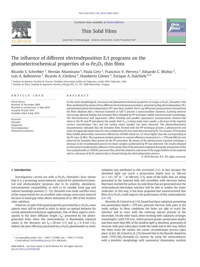
Fig. 1. Potential waveform perturbations (E–t) used during the electrodeposition of the βelectrodeposition (PP) (right).
amount that is formed during the electrodeposition process, a specialemphasis on the influence of the anodic limit of the potential employedduring the preparation of the iron oxyhydroxide (β-FeOOH) precursorfilm, was done.
2. Experimental
The β-FeOOH iron oxyhydroxide precursor thin films have beenelectrochemically grown onto transparent electrode substrates, con-sisting of glass plates with a conductive thin film of fluorine-doped tinoxide (SnO2:F, FTO) on one side (Nippon Sheets, sheet resistance ofabout 10–30Ω/□). A typical three electrode electrochemical cellgeometry has been used, comprising a FTO substrate (1.7 cm2), a Ptwire and a mercury/mercury sulfate (Hg/Hg2SO4, K2SO4 (sat'd)), SMSE,E=0.650 V vs. normal hydrogen electrode (NHE) as working, counterand reference electrodes, respectively. All the potentials reported in thisstudy refer to this reference electrode. The electrodeposition bathconsisted of an aqueous solution of 10 mM FeCl3+10 mM KF+1MH2O2+0.1 M KCl. All solutions were prepared from analytical gradereagents and 18.3 MΩ cm Millipore water. The electrodeposition wasperformed at 50 °C. Argon was flushed through the cell and theelectrolyte prior to the experiments, and an argon flowwasmaintainedover the solution during measurements and electrodeposition process.
Two types of E/t perturbation programs were applied to theinterface FTO/electrolyte solution, which are depicted in Fig. 1. In bothcases, the cathodic limit of potential (Eλ,C) wasmaintained constant at−0.9 V and the anodic limit of potential (Eλ,A) was varied from0.0 V to0.5 V. In the perturbation program of Fig. 1a (potential cycling), thepotential sweep rate was 0.020 V/s. On the other hand, theelectrodeposition by the potential pulse method involves theapplication of a periodic potential waveform to the working electrodeas shown in Fig. 1b. In this case, each pulse consisted of a cathodic-timeτC when a cathodic potential Eλ,C was applied, and an anodic-time τAwhen an anodic potential Eλ,A was applied. In this study, the cathodic-time and anodic-time have been fixed as 1.0 s and 2.5 s, respectively.The number of deposition cycles (PC procedure), and the number ofpulse cycles (PP procedure) applied to generate the hematiteprecursor films, corresponding to the same electrodeposition chargewere: 50 and 1300, respectively. The thickness of the obtainedoxyhydroxide films was of about ~1 μm for all the samples. Everyexperiment in this study was repeated at least five times and theresults obtained found to be very reproducible. The electrochemicalmeasurements were carried out using a Zanher IM6e potentiostat/galvanostat.
The iron oxyhydroxide thin films were then annealed in air for30 min at 500 °C in a Blue M model LINDBERG tube furnace.
-FeOOH precursor thin films. Potential cycling procedure (PC) (left). Potential pulse
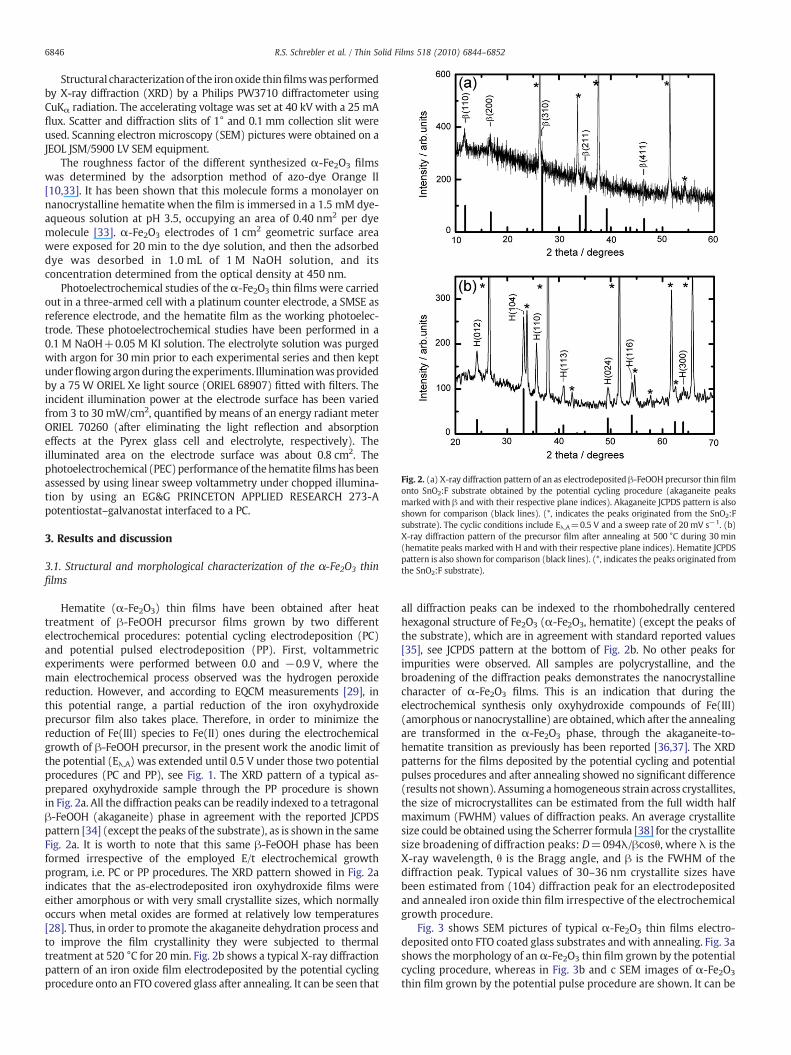
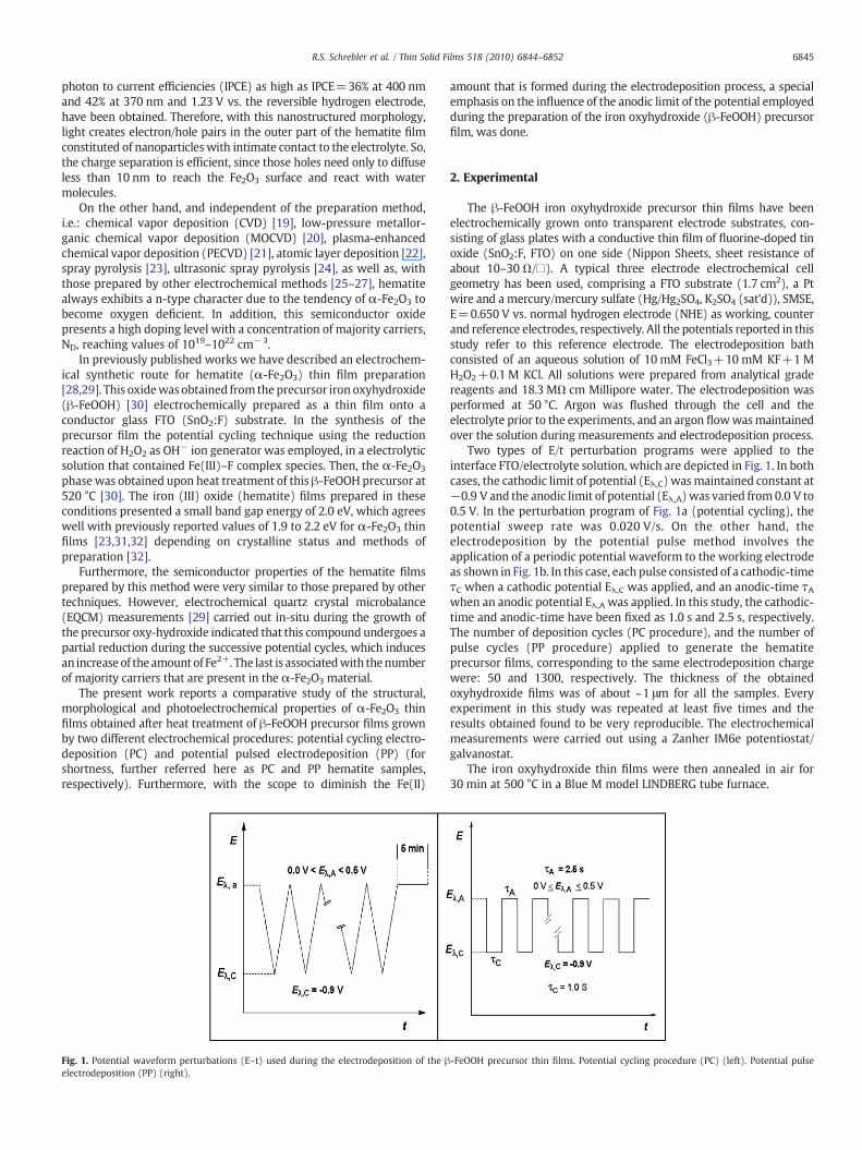
Fig. 2. (a) X-ray diffraction pattern of an as electrodeposited β-FeOOH precursor thin filmonto SnO2:F substrate obtained by the potential cycling procedure (akaganeite peaksmarked with β and with their respective plane indices). Akaganeite JCPDS pattern is alsoshown for comparison (black lines). (*, indicates the peaks originated from the SnO2:Fsubstrate). The cyclic conditions include Eλ,A=0.5 V and a sweep rate of 20 mV s−1. (b)X-ray diffraction pattern of the precursor film after annealing at 500 °C during 30 min(hematite peaks marked with H and with their respective plane indices). Hematite JCPDSpattern is also shown for comparison (black lines). (*, indicates the peaks originated fromthe SnO2:F substrate).
6846 R.S. Schrebler et al. / Thin Solid Films 518 (2010) 6844–6852
Structural characterizationof the ironoxide thinfilmswasperformedby X-ray diffraction (XRD) by a Philips PW3710 diffractometer usingCuKα radiation. The accelerating voltage was set at 40 kV with a 25 mAflux. Scatter and diffraction slits of 1° and 0.1 mm collection slit wereused. Scanning electron microscopy (SEM) pictures were obtained on aJEOL JSM/5900 LV SEM equipment.
The roughness factor of the different synthesized α-Fe2O3 filmswas determined by the adsorption method of azo-dye Orange II[10,33]. It has been shown that this molecule forms a monolayer onnanocrystalline hematite when the film is immersed in a 1.5 mM dye-aqueous solution at pH 3.5, occupying an area of 0.40 nm2 per dyemolecule [33]. α-Fe2O3 electrodes of 1 cm2 geometric surface areawere exposed for 20 min to the dye solution, and then the adsorbeddye was desorbed in 1.0 mL of 1 M NaOH solution, and itsconcentration determined from the optical density at 450 nm.
Photoelectrochemical studies of theα-Fe2O3 thin films were carriedout in a three-armed cell with a platinum counter electrode, a SMSE asreference electrode, and the hematite film as the working photoelec-trode. These photoelectrochemical studies have been performed in a0.1 M NaOH+0.05 M KI solution. The electrolyte solution was purgedwith argon for 30 min prior to each experimental series and then keptunderflowing argonduring the experiments. Illuminationwasprovidedby a 75W ORIEL Xe light source (ORIEL 68907) fitted with filters. Theincident illumination power at the electrode surface has been variedfrom 3 to 30 mW/cm2, quantified by means of an energy radiant meterORIEL 70260 (after eliminating the light reflection and absorptioneffects at the Pyrex glass cell and electrolyte, respectively). Theilluminated area on the electrode surface was about 0.8 cm2. Thephotoelectrochemical (PEC)performance of thehematitefilmshas beenassessed by using linear sweep voltammetry under chopped illumina-tion by using an EG&G PRINCETON APPLIED RESEARCH 273-Apotentiostat–galvanostat interfaced to a PC.
3. Results and discussion
3.1. Structural and morphological characterization of the α-Fe2O3 thinfilms
Hematite (α-Fe2O3) thin films have been obtained after heattreatment of β-FeOOH precursor films grown by two differentelectrochemical procedures: potential cycling electrodeposition (PC)and potential pulsed electrodeposition (PP). First, voltammetricexperiments were performed between 0.0 and −0.9 V, where themain electrochemical process observed was the hydrogen peroxidereduction. However, and according to EQCM measurements [29], inthis potential range, a partial reduction of the iron oxyhydroxideprecursor film also takes place. Therefore, in order to minimize thereduction of Fe(III) species to Fe(II) ones during the electrochemicalgrowth of β-FeOOH precursor, in the present work the anodic limit ofthe potential (Eλ,A) was extended until 0.5 V under those two potentialprocedures (PC and PP), see Fig. 1. The XRD pattern of a typical as-prepared oxyhydroxide sample through the PP procedure is shownin Fig. 2a. All the diffraction peaks can be readily indexed to a tetragonalβ-FeOOH (akaganeite) phase in agreement with the reported JCPDSpattern [34] (except the peaks of the substrate), as is shown in the sameFig. 2a. It is worth to note that this same β-FeOOH phase has beenformed irrespective of the employed E/t electrochemical growthprogram, i.e. PC or PP procedures. The XRD pattern showed in Fig. 2aindicates that the as-electrodeposited iron oxyhydroxide films wereeither amorphous or with very small crystallite sizes, which normallyoccurs when metal oxides are formed at relatively low temperatures[28]. Thus, in order to promote the akaganeite dehydration process andto improve the film crystallinity they were subjected to thermaltreatment at 520 °C for 20 min. Fig. 2b shows a typical X-ray diffractionpattern of an iron oxide film electrodeposited by the potential cyclingprocedure onto an FTO covered glass after annealing. It can be seen that
all diffraction peaks can be indexed to the rhombohedrally centeredhexagonal structure of Fe2O3 (α-Fe2O3, hematite) (except the peaks ofthe substrate), which are in agreement with standard reported values[35], see JCPDS pattern at the bottom of Fig. 2b. No other peaks forimpurities were observed. All samples are polycrystalline, and thebroadening of the diffraction peaks demonstrates the nanocrystallinecharacter of α-Fe2O3 films. This is an indication that during theelectrochemical synthesis only oxyhydroxide compounds of Fe(III)(amorphous or nanocrystalline) are obtained,which after the annealingare transformed in the α-Fe2O3 phase, through the akaganeite-to-hematite transition as previously has been reported [36,37]. The XRDpatterns for the films deposited by the potential cycling and potentialpulses procedures and after annealing showed no significant difference(results not shown). Assuming a homogeneous strain across crystallites,the size of microcrystallites can be estimated from the full width halfmaximum (FWHM) values of diffraction peaks. An average crystallitesize could be obtained using the Scherrer formula [38] for the crystallitesize broadening of diffraction peaks: D=094λ/βcosθ, where λ is theX-ray wavelength, θ is the Bragg angle, and β is the FWHM of thediffraction peak. Typical values of 30–36 nm crystallite sizes havebeen estimated from (104) diffraction peak for an electrodepositedand annealed iron oxide thin film irrespective of the electrochemicalgrowth procedure.
Fig. 3 shows SEM pictures of typical α-Fe2O3 thin films electro-deposited onto FTO coated glass substrates and with annealing. Fig. 3ashows the morphology of an α-Fe2O3 thin film grown by the potentialcycling procedure, whereas in Fig. 3b and c SEM images of α-Fe2O3
thin film grown by the potential pulse procedure are shown. It can be
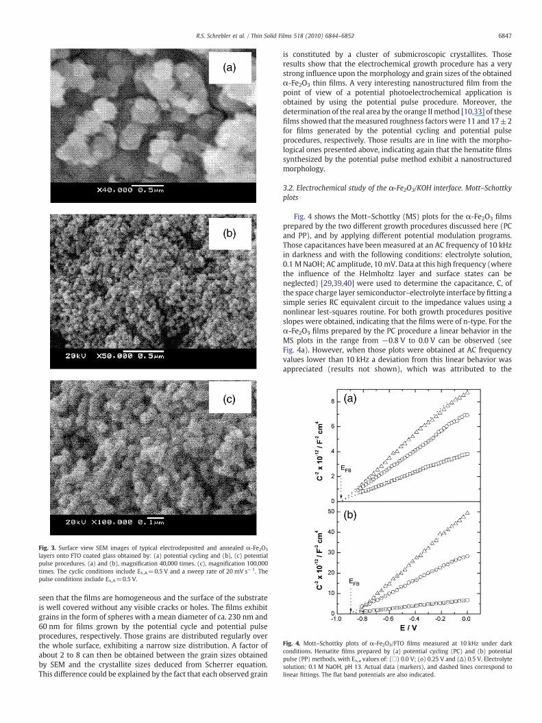
Fig. 3. Surface view SEM images of typical electrodeposited and annealed α-Fe2O3
layers onto FTO coated glass obtained by: (a) potential cycling and (b), (c) potentialpulse procedures. (a) and (b), magnification 40,000 times. (c), magnification 100,000times. The cyclic conditions include Eλ,A=0.5 V and a sweep rate of 20 mV s−1. Thepulse conditions include Eλ,A=0.5 V.
Fig. 4. Mott–Schottky plots of α-Fe2O3/FTO films measured at 10 kHz under darkconditions. Hematite films prepared by (a) potential cycling (PC) and (b) potentialpulse (PP) methods, with Eλ,a values of: (□) 0.0 V; (ο) 0.25 V and (Δ) 0.5 V. Electrolytesolution: 0.1 M NaOH, pH 13. Actual data (markers), and dashed lines correspond tolinear fittings. The flat band potentials are also indicated.
6847R.S. Schrebler et al. / Thin Solid Films 518 (2010) 6844–6852
seen that the films are homogeneous and the surface of the substrateis well covered without any visible cracks or holes. The films exhibitgrains in the form of spheres with a mean diameter of ca. 230 nm and60 nm for films grown by the potential cycle and potential pulseprocedures, respectively. Those grains are distributed regularly overthe whole surface, exhibiting a narrow size distribution. A factor ofabout 2 to 8 can then be obtained between the grain sizes obtainedby SEM and the crystallite sizes deduced from Scherrer equation.This difference could be explained by the fact that each observed grain
is constituted by a cluster of submicroscopic crystallites. Thoseresults show that the electrochemical growth procedure has a verystrong influence upon the morphology and grain sizes of the obtainedα-Fe2O3 thin films. A very interesting nanostructured film from thepoint of view of a potential photoelectrochemical application isobtained by using the potential pulse procedure. Moreover, thedetermination of the real area by the orange II method [10,33] of thesefilms showed that themeasured roughness factors were 11 and 17±2for films generated by the potential cycling and potential pulseprocedures, respectively. Those results are in line with the morpho-logical ones presented above, indicating again that the hematite filmssynthesized by the potential pulse method exhibit a nanostructuredmorphology.
3.2. Electrochemical study of the α-Fe2O3/KOH interface. Mott–Schottkyplots
Fig. 4 shows the Mott–Schottky (MS) plots for the α-Fe2O3 filmsprepared by the two different growth procedures discussed here (PCand PP), and by applying different potential modulation programs.Those capacitances have been measured at an AC frequency of 10 kHzin darkness and with the following conditions: electrolyte solution,0.1 MNaOH; AC amplitude, 10 mV. Data at this high frequency (wherethe influence of the Helmholtz layer and surface states can beneglected) [29,39,40] were used to determine the capacitance, C, ofthe space charge layer semiconductor–electrolyte interface by fitting asimple series RC equivalent circuit to the impedance values using anonlinear lest-squares routine. For both growth procedures positiveslopes were obtained, indicating that the films were of n-type. For theα-Fe2O3 films prepared by the PC procedure a linear behavior in theMS plots in the range from −0.8 V to 0.0 V can be observed (seeFig. 4a). However, when those plots were obtained at AC frequencyvalues lower than 10 kHz a deviation from this linear behavior wasappreciated (results not shown), which was attributed to the

6848 R.S. Schrebler et al. / Thin Solid Films 518 (2010) 6844–6852
presence of electronically active surface states in the semiconductorsubstrate, as it has been suggested in our previous work [29]. The flatband potential, VFB, for a given semiconductor can be calculated fromthe intercept of the MS plot formed from the following equation [41]:
1C 2 =
2eεεoND
V−VFBð Þ−kTe
� �ð1Þ
where C is the space charge capacitance, ε is the dielectric constant ofthe semiconductor, εo is the permittivity of the vacuum, ND is thedonor carrier concentration, V the applied potential, k Boltzmann'sconstant, and T the temperature. So, by extrapolating the lineal regionin these plots the flat band potential can be determined, and from theslope of the MS plots by using Eq. (1) the donor carrier concentrationwas calculated. Table 1 summarizes these photoelectrochemicalparameters (VFB and ND) for PC and PP hematite thin films. It can beappreciated that the experimentally measured flat band potentialmoves to the anodic direction when the anodic limit potential Eλ,a isbeing made more anodic. Furthermore, the donor carrier density ofthe α-Fe2O3 films decreases as the anodic limit potential Eλ,a is beingmade more anodic, for both PC and PP electrochemical grown films.Moreover, those films prepared by the PC procedure, present higherdonor carrier concentrations than those prepared by the PP method.
Thus, these results can be associated to the following facts describedbelow.
a) Like the othermetal oxide semiconductors (i.e.: ZnO, SnO2, In2O3)[42–44],α-Fe2O3 is anon-stoichiometric compound(presentingoxygendeficiency in their structure), showing in consequence an n-typecharacter [29]. Then, to maintain the electroneutrality of the system, itshould be necessary to reduce the metal ion, in this case Fe3+ to Fe2+.This electrochemical reduction can occur due to the electrons injectedby the external imposed potential. In our case, iron oxyhydroxide isformed on the electrode surface during the hydrogen peroxidereduction. This process occurs in the potential region where the partialreduction of Fe(III) to Fe(II) can take place. Therefore, it is possible thatthe initially formed iron oxyhydroxide will be structured with animportant number of non-stoichiometric sites. Then, if the potentialdoes not become sufficiently positive to oxidize part of the Fe(II) that isgenerated, an increase in the donor density will be verified. For thisreason, ND decreases when Eλ,A is made more positive. b) On the otherhand, it is well-known that hydroxides that are freshly formed inaqueousmedia contain in their structure an important amount of watermolecules. These water molecules can leave the hydroxide structureduring the anodization process, i.e.: known as the aging phenomenon[45,46]. This process promotes a more compact and stable oxidecompound according to the following reaction:
2FeðOHÞ3·nH2O→Fe2O3·ðn−xÞH2O þ ð3 þ xÞH2O: ð2ÞIn both cases, by the aging phenomena or oxidation of Fe2+ sites it
is taking place oxide dehydration process, which is achieved by theannealing to which the oxide is subjected after its synthesis.
In order to appreciate the possibility that Fe(II) and/or oxygenvacancy act as surface states and they diminish when the oxide filmwas prepared by means of potential pulse method, measurements ofthe parallel differential capacitance as a function of the potential in
Table 1Photoelectrochemical parameters (VFB and ND) for hematite thin films obtained by thePC and PP electrochemical methods at different anodic limit potentials Eλ,a.
Electrochemical method Eλ,a/V VFB/V ND/cm−3
Potential cycling (PC) 0.0 −1.01 1.0×10¹⁹
0.25 −0.98 5.4×10¹⁸
0.5 −0.95 4.2×10¹⁸
Potential pulse (PP) 0.0 −0.97 5.7×10¹⁸
0.25 −0.91 1.2×10¹⁸
0.5 −0.86 7.0×10¹⁷
0.1 MNaOH have been done. Just as was previously proposed [47–49],surface states density increases when the electroactive species arepresent on the semiconductor surface. In this case, they correspond toFe(II) species, which can act as electron donors or recombination sites.
The electrical nature of the semiconductor/electrolyte interfaceregion can be described by an equivalent circuit of an array of resistorsand capacitors arranged according to the physical structure of theregion. Fig. 5a illustrates a typical equivalent circuit of a semiconduc-tor/electrolyte interface [40,50,51]. The impedance due to trappingand detrapping of electrons at surfaces states corresponds to a circuitconsisting of a series resistance Rs and capacitance Cs, in parallel to thespace charge layer capacitance, Csc. To allow for dc current flow, aparallel resistance Rp, is included. The charge transfer impedance isdetermined by Rp and Zct, which is shown in parallel to the Helmholtzlayer capacitance CH. Circuit of Fig. 5a can be transformed into aparallel circuit (see Fig. 5b) of a frequency-dependent pseudoresis-tance, Rp(ω), and pseudocapacitance, Cp(ω) [40,50,51]. As a result thetotal measured parallel capacitance simply consists of the sum of thespace charge capacitance, CSC, and the pseudocapacitance due to thesurface states Cp(ω), as long as CH is larger than CSC+Cp(ω)[40,50,51]. To determine the surface states density, measurementsof the parallel capacitance (CP) at high and low frequencies werecarried out. At high frequencies the CP values are dominated by thespace charge capacitance CSC (CP≈CSC). Then, the surface statescapacitance (CSS) at different potentials was evaluated by subtractingthe high frequency response, CSC, from those CP values obtained at lowfrequencies [48], CSS=CP−CSC. Fig. 5 shows plots of CP (Fig. 5c and d)and CSS (Fig. 5e and f) vs. the applied potential for hematite filmsgrown by the PC and PP procedures, respectively. For the PC samplesfrom the CSS vs. E curves (Fig. 5e), it can be seen that when thefrequency decreases, a broad capacitance maximum develops and abroad frequency dependent peak is observed that is associated to thepresence of electrically active surface states [48]. The surface statesdensity, NSS, can be calculated through the following equation [48]:
NSS =CSS maxð Þ⋅4kT
e2ð3Þ
where CSS(max) corresponds to the maximum value attained by thesurface states capacitance (i.e. at low frequency), and the others havethey usual significance. Using Eq. (3), the calculated surface statesdensity for the hematite synthesized by the PC procedure is1.48×1014 cm−2. In the case of the oxide formed by PP technique,the frequency maximum in the interval studied was not observed(Fig. 5f), indicating that the energy level of the surface states shouldbe placed at higher energies, i.e. at more cathodic potentials.
3.3. Photoelectrochemical studies
The photoelectrochemical behavior of the electrochemically grownhematite thin films has been explored using a liquid-junction in a PECsystem under chopped white light. In this sense, these photoelec-trochemical experiments were performed in an electrolytic solutioncontaining 0.1 M NaOH+0.05 M KI, under 10 mW/cm2 chopped whitelight. Fig. 6 shows the j/E photoresponse for hematite thinfilmsobtainedby both electrochemical methods, i.e.: PC and PP, under chopped-illumination condition during an anodic potential scan. It can be seenthat in thewhole studied potential region the dark current is negligible.Moreover, thefilms showed photoactivitywith n-type behavior (anodicphotocurrent), in agreementwith thepreviously studiedMott–Schottkyplots (see above). So, the n-type behavior of the grown hematitefilms isagain unambiguously demonstrated. It can be observed that the PPhematite films (Fig. 6b), exhibit the best photovoltaic properties. In fact,the PP hematite films exhibit photocurrents that are ca. one order ofmagnitude higher than the ones exhibited by the iron oxide filmsformed by PC.
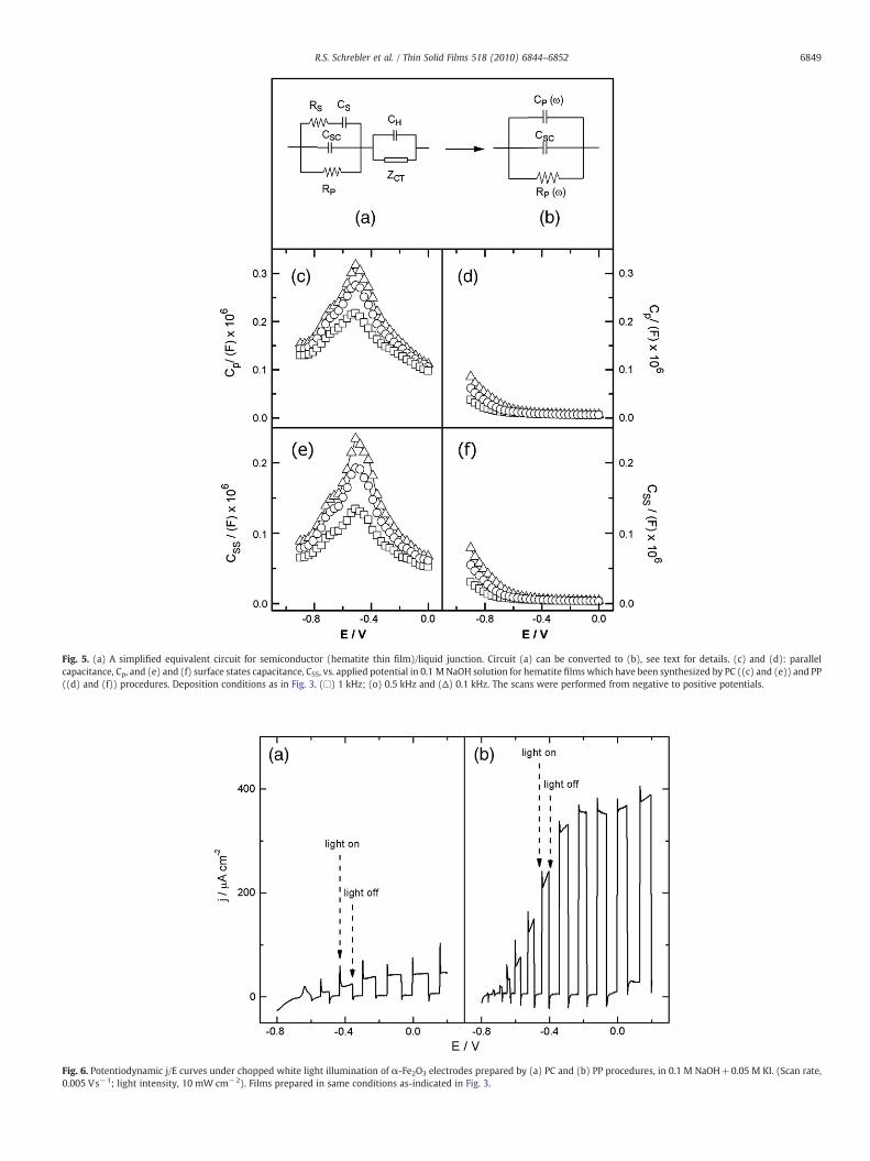
Fig. 6. Potentiodynamic j/E curves under chopped white light illumination of α-Fe2O3 electrodes prepared by (a) PC and (b) PP procedures, in 0.1 M NaOH+0.05 M KI. (Scan rate,0.005 Vs−1; light intensity, 10 mW cm−2). Films prepared in same conditions as-indicated in Fig. 3.
Fig. 5. (a) A simplified equivalent circuit for semiconductor (hematite thin film)/liquid junction. Circuit (a) can be converted to (b), see text for details. (c) and (d): parallelcapacitance, Cp, and (e) and (f) surface states capacitance, CSS, vs. applied potential in 0.1 MNaOH solution for hematite films which have been synthesized by PC ((c) and (e)) and PP((d) and (f)) procedures. Deposition conditions as in Fig. 3. (□) 1 kHz; (ο) 0.5 kHz and (Δ) 0.1 kHz. The scans were performed from negative to positive potentials.
6849R.S. Schrebler et al. / Thin Solid Films 518 (2010) 6844–6852
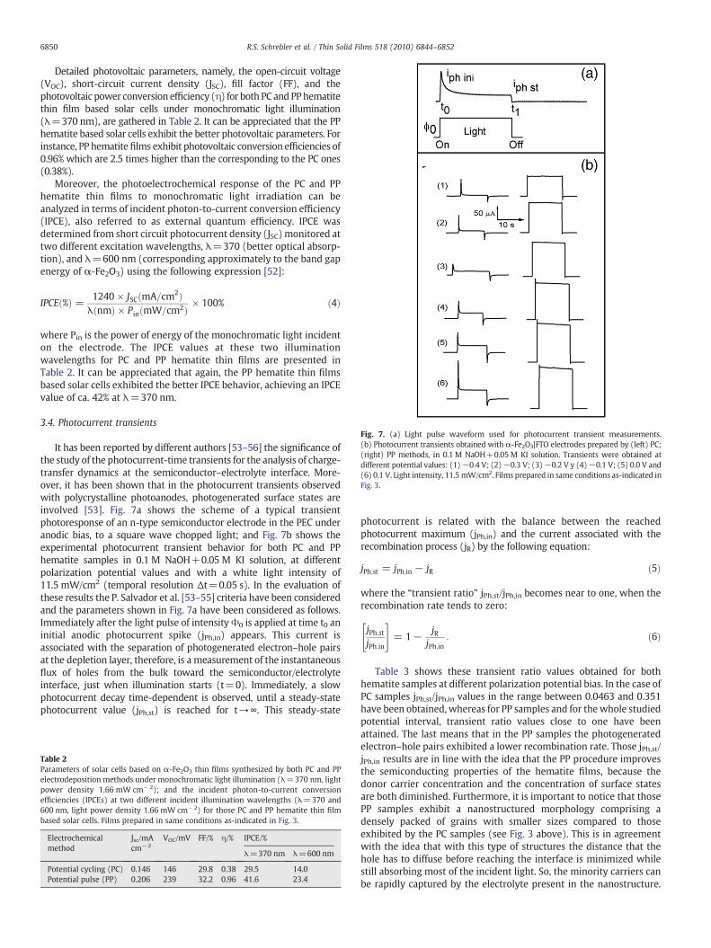
Fig. 7. (a) Light pulse waveform used for photocurrent transient measurements.(b) Photocurrent transients obtained with α-Fe2O3|FTO electrodes prepared by (left) PC;(right) PP methods, in 0.1 M NaOH+0.05 M KI solution. Transients were obtained atdifferent potential values: (1)−0.4 V; (2)−0.3 V; (3)−0.2 V y (4)−0.1 V; (5) 0.0 V and(6) 0.1 V. Light intensity, 11.5 mW/cm2. Films prepared in same conditions as-indicated inFig. 3.
6850 R.S. Schrebler et al. / Thin Solid Films 518 (2010) 6844–6852
Detailed photovoltaic parameters, namely, the open-circuit voltage(VOC), short-circuit current density (JSC), fill factor (FF), and thephotovoltaic power conversion efficiency (η) for both PC and PPhematitethin film based solar cells under monochromatic light illumination(λ=370 nm), are gathered in Table 2. It can be appreciated that the PPhematite based solar cells exhibit the better photovoltaic parameters. Forinstance, PP hematitefilms exhibit photovoltaic conversion efficiencies of0.96% which are 2.5 times higher than the corresponding to the PC ones(0.38%).
Moreover, the photoelectrochemical response of the PC and PPhematite thin films to monochromatic light irradiation can beanalyzed in terms of incident photon-to-current conversion efficiency(IPCE), also referred to as external quantum efficiency. IPCE wasdetermined from short circuit photocurrent density (JSC) monitored attwo different excitation wavelengths, λ=370 (better optical absorp-tion), and λ=600 nm (corresponding approximately to the band gapenergy of α-Fe2O3) using the following expression [52]:
IPCEð%Þ = 1240 × JSCðmA=cm2ÞλðnmÞ × PinðmW=cm2Þ × 100% ð4Þ
where Pin is the power of energy of the monochromatic light incidenton the electrode. The IPCE values at these two illuminationwavelengths for PC and PP hematite thin films are presented inTable 2. It can be appreciated that again, the PP hematite thin filmsbased solar cells exhibited the better IPCE behavior, achieving an IPCEvalue of ca. 42% at λ=370 nm.
3.4. Photocurrent transients
It has been reported by different authors [53–56] the significance ofthe study of the photocurrent-time transients for the analysis of charge-transfer dynamics at the semiconductor–electrolyte interface. More-over, it has been shown that in the photocurrent transients observedwith polycrystalline photoanodes, photogenerated surface states areinvolved [53]. Fig. 7a shows the scheme of a typical transientphotoresponse of an n-type semiconductor electrode in the PEC underanodic bias, to a square wave chopped light; and Fig. 7b shows theexperimental photocurrent transient behavior for both PC and PPhematite samples in 0.1 M NaOH+0.05 M KI solution, at differentpolarization potential values and with a white light intensity of11.5 mW/cm2 (temporal resolution Δt=0.05 s). In the evaluation ofthese results the P. Salvador et al. [53–55] criteria have been consideredand the parameters shown in Fig. 7a have been considered as follows.Immediately after the light pulse of intensityΦ0 is applied at time t0 aninitial anodic photocurrent spike (jPh,in) appears. This current isassociated with the separation of photogenerated electron–hole pairsat the depletion layer, therefore, is a measurement of the instantaneousflux of holes from the bulk toward the semiconductor/electrolyteinterface, just when illumination starts (t=0). Immediately, a slowphotocurrent decay time-dependent is observed, until a steady-statephotocurrent value (jPh,st) is reached for t→∞. This steady-state
Table 2Parameters of solar cells based on α-Fe2O3 thin films synthesized by both PC and PPelectrodeposition methods under monochromatic light illumination (λ=370 nm, lightpower density 1.66 mW cm−2); and the incident photon-to-current conversionefficiencies (IPCEs) at two different incident illumination wavelengths (λ=370 and600 nm, light power density 1.66 mW cm−2) for those PC and PP hematite thin filmbased solar cells. Films prepared in same conditions as-indicated in Fig. 3.
Electrochemicalmethod
Jsc/mAcm−2
VOC/mV FF/% η/% IPCE/%
λ=370 nm λ=600 nm
Potential cycling (PC) 0.146 146 29.8 0.38 29.5 14.0Potential pulse (PP) 0.206 239 32.2 0.96 41.6 23.4
photocurrent is related with the balance between the reachedphotocurrent maximum (jPh,in) and the current associated with therecombination process (jR) by the following equation:
jPh;st = jPh;in − jR ð5Þ
where the “transient ratio” jPh,st/jPh,in becomes near to one, when therecombination rate tends to zero:
jPh;stjPh;in
" #= 1− jR
jPh;in: ð6Þ
Table 3 shows these transient ratio values obtained for bothhematite samples at different polarization potential bias. In the case ofPC samples jPh,st/jPh,in values in the range between 0.0463 and 0.351have been obtained, whereas for PP samples and for thewhole studiedpotential interval, transient ratio values close to one have beenattained. The last means that in the PP samples the photogeneratedelectron–hole pairs exhibited a lower recombination rate. Those jPh,st/jPh,in results are in line with the idea that the PP procedure improvesthe semiconducting properties of the hematite films, because thedonor carrier concentration and the concentration of surface statesare both diminished. Furthermore, it is important to notice that thosePP samples exhibit a nanostructured morphology comprising adensely packed of grains with smaller sizes compared to thoseexhibited by the PC samples (see Fig. 3 above). This is in agreementwith the idea that with this type of structures the distance that thehole has to diffuse before reaching the interface is minimized whilestill absorbing most of the incident light. So, the minority carriers canbe rapidly captured by the electrolyte present in the nanostructure.
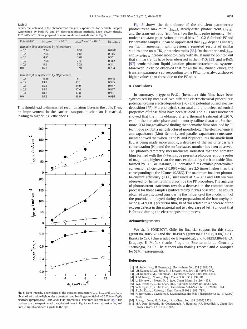
Table 3Parameters obtained in the photocurrent transient experiments for hematite samplessynthesized by both PC and PP electrodeposition methods. Light power density11.2 mW cm−2. Films prepared in same conditions as-indicated in Fig. 3.
Potential/V jPh, in/A cm−2×10⁻⁵ jPh,st/A cm−2×10⁻⁵ jPh,st/jPh,in
Hematite films synthesized by PC procedure−0.5 7.34 0.34 0.0463−0.4 7.66 0.88 0.115−0.3 4.81 1.69 0.351−0.2 7.56 2.36 0.312−0.1 9.4 3.21 0.3410.0 16.7 3.91 0.234
Hematite films synthesized by PP procedure−0.5 9.18 8.7 0.948−0.4 13.3 13.1 0.985−0.3 15.1 14.9 0.987−0.2 18.0 17.4 0.967−0.1 18.7 17.8 0.9510.0 19.2 18.9 0.984
6851R.S. Schrebler et al. / Thin Solid Films 518 (2010) 6844–6852
This should lead to diminished recombination losses in the bulk. Then,an improvement in the carrier transport mechanism is reached,leading to higher PEC efficiencies.
Fig. 8. Light intensity dependence of the transient parameters jPh,in, jPh,st, and jPh,st/jPh,in,obtained with white light under a constant band bending potential of−0.2 V for α-Fe2O3
electrodespreparedby: (○)PC and (●) PPprocedures. Experimental details as inFig. 7. Themarkers are the experimental data, dashed lines in Fig. 8a are linear regression fits, andlines in Fig. 8b and c are a guide to the eye.
Fig. 8 shows the dependence of the transient parameters:photocurrent maximum (jPh,in), steady-state photocurrent (jPh,st),and the transient ratio (jPh,st/jPh,in) on the light pulse intensity (Φ0),under a constant polarization potential bias of−0.2 V, for both PC andPP hematite samples. It can be appreciated that jPh,in depends linearlyon Φ0, in agreement with previously reported results of similarstudies done on n-TiO2 photoelectrodes [53]. On the other hand, jPh,stand jPh,st/jPh,in increase monotonically withΦ0. It must be pointed outthat similar trends have been observed in the n-TiO2 [53] and n-RuS2[57] semiconductor–liquid junction photoelectrochemical systems.Moreover, it can be observed that for all the Φ0 studied values, thetransient parameters corresponding to the PP samples always showedhigher values than those due to the PC ones.
4. Conclusions
In summary, n-type α-Fe2O3 (hematite) thin films have beensynthesized by means of two different electrochemical procedures:potential cycling electrodeposition (PC) and potential pulsed electro-deposition (PP). Morphological, structural and photoelectrochemicalproperties of those films have been studied. The XRD measurementsshowed that the films obtained after a thermal treatment at 520 °Cexhibit the hematite phase and a nanocrystalline character. Further-more, SEM images allowed finding that hematite films obtained by PPtechnique exhibit a nanostructured morphology. The electrochemicaland capacitance (Mott–Schottky and parallel capacitance) measure-ments showed that when in the PC and PP procedures the anodic limitEλ,A is being made more anodic, a decrease of the majority carriersconcentration (ND) and the surface states number has been observed.The photovoltammetry measurements indicated that the hematitefilms formed with the PP technique present a photocurrent one orderof magnitude higher than the ones exhibited by the iron oxide filmsformed by PC. For instance, PP hematite films exhibit photovoltaicconversion efficiencies of 0.96% which are 2.5 times higher than thecorresponding to the PC ones (0.38%). Themaximum incident photon-to-current efficiency (IPCE) measured at λ=370 and 600 nm wasobserved for hematite films grown by the PP procedure. The analysisof photocurrent transients reveals a decrease in the recombinationprocess for those samples synthesized by PPwas observed. The resultsobtained are discussed considering the influence of the anodic limit ofthe potential employed during the preparation of the iron oxyhydr-oxide (β-FeOOH) precursor film, all of this related to a decrease of theoxygen defects in this material and to a decrease of Fe(II) amount thatis formed during the electrodeposition process.
Acknowledgements
We thank FONDECYT, Chile, for financial support for this study(grant no. 1085176) and the DII-PUCV (grant no. 037.108/2008). E.A.D.thanks to CSIC (Universidad de la República), and to PEDECIBA-FISICA,Uruguay. E. Muñoz thanks Programa Bicentenario de Ciencia yTecnología, PSD82. The authors also thank J. Troccoli and A. Marquezfor SEM measurements.
References
[1] M. Anderman, J.H. Kennedy, J. Electrochem. Soc. 131 (1984) 21.[2] J.H. Kennedy, K.W. Frese Jr., J. Electrochem. Soc. 125 (1978) 709.[3] J.H. Kennedy, M.J. Anderman, J. Electrochem. Soc. 130 (1983) 848.[4] S. Mohanty, J. Ghose, J. Phys. Chem. Solids 53 (1992) 81.[5] U. Björkstén, J. Moser, M. Grätzel, Chem. Mater. 6 (1994) 858.[6] W.B. Ingler Jr., S.U.M. Khan, Int. J. Hydrogen Energy 30 (2005) 821.[7] W.B. Ingler Jr., S.U.M. Khan, Electrochem. Solid-State Lett. 9 (2006) G144.[8] S.U.M. Khan, J. Akikusa, J. Phys. Chem. B 103 (1999) 7184.[9] N. Beermann, L. Vayssieres, S.-E. Lindquist, A.Hagfeldt, J. Electrochem. Soc. 147 (2000)
2456.[10] A. Kay, I. Cesar, M. Grätzel, J. Am. Chem. Soc. 128 (2006) 15714.[11] M.P. Dare-Edwards, J.B. Goodenough, A. Hamnett, P.R. Trevellick, J. Chem. Soc.
Faraday Trans. I 79 (1983) 2027.

6852 R.S. Schrebler et al. / Thin Solid Films 518 (2010) 6844–6852
[12] J.H. Kennedy, K.W. Frese, J. Electrochem. Soc. 125 (1978) 709.[13] R.F.G. Gardner, F. Sweett, D.W. Tanner, J. Phys. Chem. Solids 24 (1963) 1183.[14] K. Itoh, J.O. Bockris, J. Appl. Phys. 56 (1984) 874.[15] K. Itoh, J.O. Bockris, J. Electrochem. Soc. 131 (1984) 1266.[16] C. Jorand Sartoretti, M. Ulmann, B.D. Alexander, J. Augustynski, A. Weidenkaff,
Chem. Phys. Lett. 376 (2003) 194.[17] G. Hodes, I.D.J. Howell, L.M. Peter, J. Electrochem. Soc. 139 (1992) 3136.[18] A. Hagfeldt, M. Grätzel, Chem. Rev. 95 (1995) 49.[19] T. Maruyama, T. Kanagawa, J. Electrochem. Soc. 143 (1996) 1675.[20] K. Shalini, G.N. Subbanna, S. Chandrasekaran, S.A. Shivashankar, Thin Solid Films
424 (2003) 568.[21] E.-T. Lee, B.-J. Kim, G.-E. Jang, Thin Solid Films 341 (1999) 73.[22] M. Lie, H. Fjellvåg, A. Kjekshus, Thin Solid Films 488 (2005) 74.[23] A.A. Akl, Appl. Surf. Sci. 233 (2004) 307.[24] A. Duret, M. Grätzel, J. Phys. Chem. B 109 (2005) 17184.[25] D. Lincot, Thin Solid Films 487 (2005) 40.[26] G. Zotti, G. Schiavon, S. Zecchin, U. Casellato, J. Electrochem. Soc. 145 (1998) 385.[27] S.S. Kulkarni, C.D. Lokhande, Mater. Chem. Phys. 82 (2003) 151.[28] R. Schrebler, K. Bello, F. Vera, P. Cury, E. Muñoz, R. del Río, H. Gómez, R. Córdova, E.A.
Dalchiele, Electrochem. Solid-State Lett. 9 (2006) C110.[29] R. Schrebler, K. Bello, F. Vera, P. Cury, E. Muñoz, R. del Río, H. Gómez, R. Córdova, E.A.
Dalchiele, Electrochem. Solid-State Lett. 10 (2007) D95.[30] S. Deki, Y. Aoi, J. Okibe, H. Yanagimoto, A. Kajinami, M. Mizuhata, J. Mater.
Chem. 7 (1997) 1769.[31] N. Beermann, L. Vayssieres, S.-E. Lindquist, A. Hagfeldt, J. Electrochem. Soc. 147 (2000)
2456.[32] L. Vayssieres, C. Sathe, S.M. Butorin, D.K. Shuh, J. Nordgren, J. Guo, Adv. Mater.
(Weinheim, Ger.) 17 (2005) 2320.[33] J. Bandara, J.A. Mielczarski, J. Kiwi, Langmuir 15 (1999) 7670.[34] Powder Diffraction File, Joint Committee for Powder Diffraction Studies (JCPDS)
File No. 34-1266 (β-FeOOH, akaganeite).[35] Powder Diffraction File, Joint Committee for Powder Diffraction Studies (JCPDS)
File No. 86-0550 (rhombohedrally centered hexagonal structure of Fe2O3,hematite).
[36] X. Wang, X. Chen, L. Gao, H. Zheng, M. Ji, C. Tang, T. Shen, Z. Zhang, J. Mater. Chem.14 (2004) 905.
[37] X. Wang, X. Chen, X. Ma, H. Zheng, M. Ji, Z. Zhang, Chem. Phys. Lett. 384 (2004)391.
[38] B.D. Cullity, Elements of X-ray Diffraction, second ed.Addison Wesley, Reading,MA, 1978.
[39] H.O. Finklea, Semiconductor Electrodes, Elsevier, Amsterdam, 1988.[40] X.G. Zhang, Electrochemistry of Silicon and Its Oxide, Kluwer Academic/Plenum
Publishers, New York, 2001.[41] A.J. Bard, L.R. Faulkner, Electrochemical methods, Fundamental and Applications,
first ed.John Wiley & Sons, Inc., New York, 1980.[42] C.G. Granqvist, Sol. Energy Mater. Sol. Cells 91 (2007) 1529.[43] D.P. Norton, Y.W. Heo, M.P. Ivill, K. Ip, S.J. Pearton, M.F. Chisholm, T. Steiner, Mater.
Today 7 (6) (2004) 34.[44] E.L. Miller, D. Paluselli, B. Marsen, R.E. Rocheleau, Thin Solid Films 466 (2004) 307.[45] R. Schrebler, J.R. Vilche, A.J. Arvía, Electrochim. Acta 21 (1979) 395.[46] R. Schrebler, J.R. Vilche, A.J. Arvía, Anal. Asoc. Quím. Argentina 70 (1982) 999.[47] J.N. Chazalviel, J. Electrochem. Soc. 129 (1982) 963.[48] G. Oskam, P.M. Hoffmann, J. Schmidt, P. Searson, J. Phys. Chem. 100 (1996) 1801.[49] A. Belaîdi, J.N. Chazalviel, F. Ozanam, O. Gorochov, A. Chari, B. Fotouchi, M. Etman,
J. Electroanal. Chem. 444 (1998) 35.[50] G. Oskam, P.M. Hoffmann, J.C. Schmidt, P.C. Searson, J. Phys. Chem. 100 (1996)
1801.[51] Ch. Ji, G. Oskam, P.C. Searson, J. Electrochem. Soc. 148 (2001) C746.[52] P.V. Kamat, J. Phys. Chem. C 112 (2008) 18737.[53] P. Salvador, J. Phys. Chem. 89 (1985) 3863.[54] D. Tafalla, P. Salvador, R.M. Benito, J. Electrochem. Soc. 137 (1990) 1810.[55] P. Salvador, M.L. García González, F. Muñoz, J. Phys. Chem. 96 (1992) 10349.[56] L.M. Peter, Chem. Rev. 90 (1990) 753.[57] P. Salvador, N. Alonso-Vante, H. Tribusch, J. Electrochem. Soc. 145 (1998) 216.