Electronic structure study of N, O related defects in GaP for photoelectrochemical applications
7
Electronic structure study of N, O related defects in GaP for photoelectrochemical applications Muhammad N. Huda, * a Todd G. Deutsch, b Pranab Sarker a and John A. Turner b It is known that the stability of GaP as a photocatalyst in electrolytes can be enhanced by nitrogen doping, GaP:N. However, both GaP (indirect gap) and GaP:N (direct gap) have poor optical absorption properties across their fundamental band gap. To enhance optical absorption as well as the photocurrent, we have examined by density functional theory the favorability of oxygen and hydrogen impurities in conjunction with N doping in bulk GaP. It has been found here that O-related defects are more favorable, whereas H with N substitution is not very favorable. These O–N related defects create a global effect in the GaP lattice by both volume and band gap reduction. Enhancement of optical absorption was also found due to these types of complex doping. Introduction The primary challenge for hydrogen production by photo-elec- trochemical (PEC) processes through water splitting by sunlight is to design and synthesize photo-catalyst materials with desired electronic properties. These materials must satisfy several criteria; for example, these photoelectrodes (i) must be highly stable in aqueous solution, (ii) must have band-edge positions that encompass the potentials for the water oxida- tion–reduction reactions, (iii) must absorb most of the photons from the solar spectrum, and (iv) must have good charge transport properties. 1–4 Unfortunately, current semiconductor materials cannot meet all these criteria simultaneously, so band engineering through doping or alloying is one of the best strategies to achieve the necessary material and electronic properties. TiO 2 , which is one of the most studied materials for PEC water splitting, 5 meets almost all the criteria, but its band gap is too large to absorb sunlight efficiently. Additionally, none of the transition metal based oxides that has been tried during the last four decades, especially the binary ones, has shown much improvement upon doping or alloying. Unwanted defect formation and strong band localization (such as at valence band maximum and conduction band minimum) due to an unlled d-band are the main reasons for the shortcomings of these metal oxides as photocatalysts. 6 In fact, the band properties near the band gap not only determine the effective mass of the charge carriers, but also determine the efficiency of optical absorption in the photo-electrodes. 7 Hence, the band positions, band gap and the characteristics of the band near the gap all need to be engineered concurrently to achieve an efficient photo-catalyst. In addition, behavior of such so called band- engineered materials in a given chemical environment may be altered due to the inner-diffusion of locally available atomic species into the semiconductor. The predictions and the effect of such “environmental” doping on the photocatalysts need to be understood at the fundamental level in order to have better control over the system. III–V based semiconductors have been studied for the PEC processes extensively. The lack of a prominent presence of d bands in the vicinity of the band gap, due to the d 10 electron conguration of the cation, facilitates the relatively lower effec- tive masses of the charge carriers in these semiconductors. For example, it is well known that GaN is stable in aqueous solution and has more delocalized bands than the 3d transition metal oxides. However, it has a large band gap, 3.4 eV, which makes it useful only in the ultraviolet regime of the spectra for PEC processes. InN has too low a band gap, around 0.7 eV, and In not being an earth abundant metal, it is not very suitable by itself as a PEC photocatalyst. GaP, on the other hand, is not as stable as GaN but the band gap is much lower, 2.26 eV, 8 with some reporting that the band edges barely straddle the water splitting potentials. 2,9 Moreover, the conduction band edge is at least as dispersive as GaN. However, despite the lower band gap of GaP, its optical response to photons near its band gap is not as good as GaN due to its indirect band gap and lower absorption proba- bility at the minimum direct gap, which will be discussed below. Previously it has been shown that doping/alloying with N atoms can change the indirect band gap of GaP to a direct electronic transition, and lower its band gap energy as well. 8 Given the fact that GaN is stable in solution, it is possible that alloying of GaP:N would provide a better solution for PEC photo- catalyst problems. However, even though P and N are from the same column of the periodic table and are isovalent, the lattice mismatch between GaP and GaN would create strain in the alloy a Department of Physics, University of Texas at Arlington, Arlington, TX 76019, USA. E-mail: [email protected] b National Renewable Energy Laboratory, Golden, CO 80401, USA Cite this: DOI: 10.1039/c3ta11475a Received 13th April 2013 Accepted 15th May 2013 DOI: 10.1039/c3ta11475a www.rsc.org/MaterialsA This journal is ª The Royal Society of Chemistry 2013 J. Mater. Chem. A Journal of Materials Chemistry A PAPER Published on 14 June 2013. Downloaded by University of Texas at Arlington on 14/06/2013 18:59:03. View Article Online View Journal
-
Upload
independent -
Category
Documents
-
view
3 -
download
0
Transcript of Electronic structure study of N, O related defects in GaP for photoelectrochemical applications
Journal ofMaterials Chemistry A
PAPER
Publ
ishe
d on
14
June
201
3. D
ownl
oade
d by
Uni
vers
ity o
f T
exas
at A
rlin
gton
on
14/0
6/20
13 1
8:59
:03.
View Article OnlineView Journal
aDepartment of Physics, University of Texas
E-mail: [email protected] Renewable Energy Laboratory, Go
Cite this: DOI: 10.1039/c3ta11475a
Received 13th April 2013Accepted 15th May 2013
DOI: 10.1039/c3ta11475a
www.rsc.org/MaterialsA
This journal is ª The Royal Society of
Electronic structure study of N, O related defects in GaPfor photoelectrochemical applications
Muhammad N. Huda,*a Todd G. Deutsch,b Pranab Sarkera and John A. Turnerb
It is known that the stability of GaP as a photocatalyst in electrolytes can be enhanced by nitrogen doping,
GaP:N. However, both GaP (indirect gap) and GaP:N (direct gap) have poor optical absorption properties
across their fundamental band gap. To enhance optical absorption as well as the photocurrent, we have
examined by density functional theory the favorability of oxygen and hydrogen impurities in
conjunction with N doping in bulk GaP. It has been found here that O-related defects are more
favorable, whereas H with N substitution is not very favorable. These O–N related defects create a
global effect in the GaP lattice by both volume and band gap reduction. Enhancement of optical
absorption was also found due to these types of complex doping.
Introduction
The primary challenge for hydrogen production by photo-elec-trochemical (PEC) processes through water splitting by sunlightis to design and synthesize photo-catalyst materials withdesired electronic properties. These materials must satisfyseveral criteria; for example, these photoelectrodes (i) must behighly stable in aqueous solution, (ii) must have band-edgepositions that encompass the potentials for the water oxida-tion–reduction reactions, (iii) must absorb most of the photonsfrom the solar spectrum, and (iv) must have good chargetransport properties.1–4 Unfortunately, current semiconductormaterials cannot meet all these criteria simultaneously, so bandengineering through doping or alloying is one of the beststrategies to achieve the necessary material and electronicproperties. TiO2, which is one of the most studied materials forPEC water splitting,5 meets almost all the criteria, but its bandgap is too large to absorb sunlight efficiently. Additionally, noneof the transition metal based oxides that has been tried duringthe last four decades, especially the binary ones, has shownmuch improvement upon doping or alloying. Unwanted defectformation and strong band localization (such as at valence bandmaximum and conduction band minimum) due to an unlledd-band are the main reasons for the shortcomings of thesemetal oxides as photocatalysts.6 In fact, the band propertiesnear the band gap not only determine the effective mass of thecharge carriers, but also determine the efficiency of opticalabsorption in the photo-electrodes.7 Hence, the band positions,band gap and the characteristics of the band near the gap allneed to be engineered concurrently to achieve an efficient
at Arlington, Arlington, TX 76019, USA.
lden, CO 80401, USA
Chemistry 2013
photo-catalyst. In addition, behavior of such so called band-engineered materials in a given chemical environment may bealtered due to the inner-diffusion of locally available atomicspecies into the semiconductor. The predictions and the effectof such “environmental” doping on the photocatalysts need tobe understood at the fundamental level in order to have bettercontrol over the system.
III–V based semiconductors have been studied for the PECprocesses extensively. The lack of a prominent presence of dbands in the vicinity of the band gap, due to the d10 electronconguration of the cation, facilitates the relatively lower effec-tive masses of the charge carriers in these semiconductors. Forexample, it is well known that GaN is stable in aqueous solutionand has more delocalized bands than the 3d transition metaloxides. However, it has a large band gap, 3.4 eV, which makes ituseful only in the ultraviolet regime of the spectra for PECprocesses. InN has too low a band gap, around 0.7 eV, and In notbeing an earth abundant metal, it is not very suitable by itself as aPEC photocatalyst. GaP, on the other hand, is not as stable asGaN but the band gap is much lower, 2.26 eV,8 with somereporting that the band edges barely straddle the water splittingpotentials.2,9 Moreover, the conduction band edge is at least asdispersive as GaN. However, despite the lower band gap of GaP,its optical response to photons near its band gap is not as good asGaN due to its indirect band gap and lower absorption proba-bility at the minimum direct gap, which will be discussed below.
Previously it has been shown that doping/alloying with Natoms can change the indirect band gap of GaP to a directelectronic transition, and lower its band gap energy as well.8
Given the fact that GaN is stable in solution, it is possible thatalloying of GaP:N would provide a better solution for PEC photo-catalyst problems. However, even though P and N are from thesame column of the periodic table and are isovalent, the latticemismatch between GaP and GaN would create strain in the alloy
J. Mater. Chem. A
Journal of Materials Chemistry A Paper
Publ
ishe
d on
14
June
201
3. D
ownl
oade
d by
Uni
vers
ity o
f T
exas
at A
rlin
gton
on
14/0
6/20
13 1
8:59
:03.
View Article Online
by decreasing the overall lattice constant. This is supposed tocreate a global effect on the GaP:N alloy. In addition, at a loweralloy limit, �1%, it has been shown by time-resolved photo-luminescence measurement that charge carrier lifetime isgoverned by non-radiative recombination processes.10 Henceonly N doping or alloying may not be sufficient to get a betterphoto-catalyst. Although there are several electronic structurestudies available in the literature on the GaP:N system,11–14 theformation of other related dopants/impurities in conjunctionwith N impurity, which is possible in an electrochemical cell,and their optical absorption properties have not been studied inthe literature extensively. For example, another related n-typealloy GaP:O shows promise in our theoretical study. Oxygendoping or alloying in GaP has been a subject of extensive studiesin the 70s and early 80s (for example, see ref. 15 and 16) mainlybecause of light emitting diode (LED) applications of GaP.However, as far as we know, no recently published paper hasbeen found on GaP:O.
It is mentioned earlier, the appropriate band gap is not theonly selection criterion for PEC photo-catalysts, the orbitalcomposition at the VBM (valence band maxima) and at the CBM(conduction band minima) is also important for enhancedoptical absorption. In the PEC processes, the GaP surface wouldcome into contact with several species of atoms, such as O, H, etc.We will examine the favorability of such impurities in the bulkstate in conjunction with N doping. It will be shown that O-related defects aremore favorable, whereas H with N substitutionis not very favorable. We have shown here that both GaP (indirectgap) and GaP:N (direct gap) have poor optical absorption prop-erties across their fundamental band gap. The strategy for theenhancement of optical absorption will also be discussed.
Computational methodology
For our calculation, the generalized gradient approximation(GGA)17 to density functional theory with the projectedaugmented wave (PAW) method18,19 has been used within theVienna ab initio simulation package (VASP 4.6.21).20,21 Spin-polarization has been considered in all our calculations. Allplane waves up to 400 eV were used and the Brillouin zoneintegrations were performed using the second orderMethfessel-Paxton method. However for the density of state (DOS) plottetrahedron methods have been used. A small value of U ¼ 4 eVhas been added to the Ga d-band for the DFT+U formalism. Thisopens up the band gap of GaP by 0.3 eV compared to that of theGGA-DFT formalism.22 The ion positions were always relaxeduntil the force on each of them is 0.01 eV or less. A 2 � 2 � 2zinc blend supercell has been used to calculate the electronicproperties of all the doped systems, such as GaP:N, GaP:O,GaP:NO, etc.
Results and discussioni Undoped GaP
First we start with the basic electronic structure of GaP briey.Unlike GaN which stabilizes in hexagonal symmetry, GaPprefers the cubic structure corresponding to the Td
2 – 3mF4 space
J. Mater. Chem. A
group of symmetry, and stabilizes in the zinc blende structure.Our calculated lattice constant was found to be 5.50 A, whichcompares well with the experimental lattice constant of 5.45 A.The Ga–P bond-length was found to be 2.39 A, where themeasured value is 2.36 A. We have also calculated the bulkmodulus (B0) of GaP and our calculated value was found to be76.1 GPa, compared to the experimental value of 88 GPa. Thisunder-estimation of B0 is a well known feature of the GGAfunctional, which is consistent with the fact that it slightlyoverestimates the lattice constants as well. Compared to GaN(calculated B0 is 170.4 GPa), GaP is a soer material which inturn reects the “soness” of the Ga–P bond in GaP. Given theatomic electronegativity difference between ‘Ga and P’ is lessthan that of between ‘Ga and N’, Ga–P bonds would have lessionic character than the Ga–N bonds. In fact, the strength ofhybridization of d–p bands in Ga–P is less than Ga–N as well.Hence, a substitution of a P atom by an N atom would have asignicant effect on the electronic properties of GaP supercells.
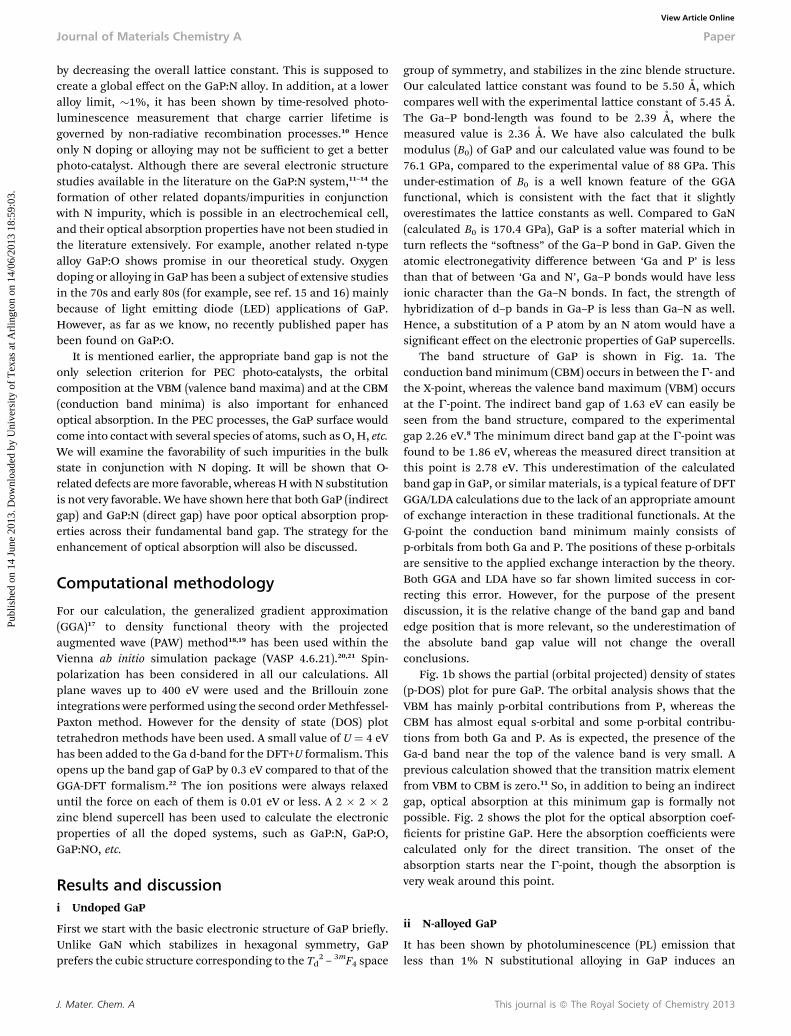
The band structure of GaP is shown in Fig. 1a. Theconduction bandminimum (CBM) occurs in between the G- andthe X-point, whereas the valence band maximum (VBM) occursat the G-point. The indirect band gap of 1.63 eV can easily beseen from the band structure, compared to the experimentalgap 2.26 eV.8 The minimum direct band gap at the G-point wasfound to be 1.86 eV, whereas the measured direct transition atthis point is 2.78 eV. This underestimation of the calculatedband gap in GaP, or similar materials, is a typical feature of DFTGGA/LDA calculations due to the lack of an appropriate amountof exchange interaction in these traditional functionals. At theG-point the conduction band minimum mainly consists ofp-orbitals from both Ga and P. The positions of these p-orbitalsare sensitive to the applied exchange interaction by the theory.Both GGA and LDA have so far shown limited success in cor-recting this error. However, for the purpose of the presentdiscussion, it is the relative change of the band gap and bandedge position that is more relevant, so the underestimation ofthe absolute band gap value will not change the overallconclusions.
Fig. 1b shows the partial (orbital projected) density of states(p-DOS) plot for pure GaP. The orbital analysis shows that theVBM has mainly p-orbital contributions from P, whereas theCBM has almost equal s-orbital and some p-orbital contribu-tions from both Ga and P. As is expected, the presence of theGa-d band near the top of the valence band is very small. Aprevious calculation showed that the transition matrix elementfrom VBM to CBM is zero.11 So, in addition to being an indirectgap, optical absorption at this minimum gap is formally notpossible. Fig. 2 shows the plot for the optical absorption coef-cients for pristine GaP. Here the absorption coefficients werecalculated only for the direct transition. The onset of theabsorption starts near the G-point, though the absorption isvery weak around this point.
ii N-alloyed GaP
It has been shown by photoluminescence (PL) emission thatless than 1% N substitutional alloying in GaP induces an
This journal is ª The Royal Society of Chemistry 2013
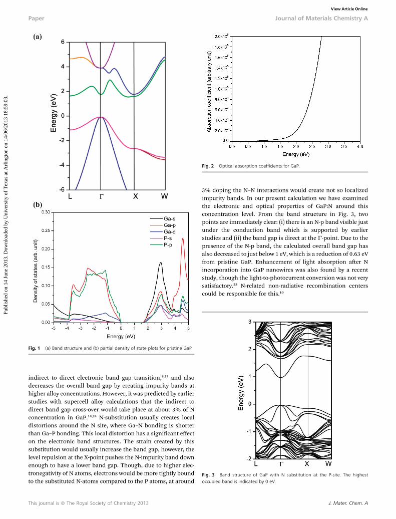
Fig. 2 Optical absorption coefficients for GaP.
Fig. 3 Band structure of GaP with N substitution at the P-site. The highestoccupied band is indicated by 0 eV.
Fig. 1 (a) Band structure and (b) partial density of state plots for pristine GaP.
Paper Journal of Materials Chemistry A
Publ
ishe
d on
14
June
201
3. D
ownl
oade
d by
Uni
vers
ity o
f T
exas
at A
rlin
gton
on
14/0
6/20
13 1
8:59
:03.
View Article Online
indirect to direct electronic band gap transition,8,23 and alsodecreases the overall band gap by creating impurity bands athigher alloy concentrations. However, it was predicted by earlierstudies with supercell alloy calculations that the indirect todirect band gap cross-over would take place at about 3% of Nconcentration in GaP.14,24 N-substitution usually creates localdistortions around the N site, where Ga–N bonding is shorterthan Ga–P bonding. This local distortion has a signicant effecton the electronic band structures. The strain created by thissubstitution would usually increase the band gap, however, thelevel repulsion at the X-point pushes the N-impurity band downenough to have a lower band gap. Though, due to higher elec-tronegativity of N atoms, electrons would be more tightly boundto the substituted N-atoms compared to the P atoms, at around
This journal is ª The Royal Society of Chemistry 2013
3% doping the N–N interactions would create not so localizedimpurity bands. In our present calculation we have examinedthe electronic and optical properties of GaP:N around thisconcentration level. From the band structure in Fig. 3, twopoints are immediately clear: (i) there is an N-p band visible justunder the conduction band which is supported by earlierstudies and (ii) the band gap is direct at the G-point. Due to thepresence of the N-p band, the calculated overall band gap hasalso decreased to just below 1 eV, which is a reduction of 0.63 eVfrom pristine GaP. Enhancement of light absorption aer Nincorporation into GaP nanowires was also found by a recentstudy, though the light-to-photocurrent conversion was not verysatisfactory.25 N-related non-radiative recombination centerscould be responsible for this.10
J. Mater. Chem. A
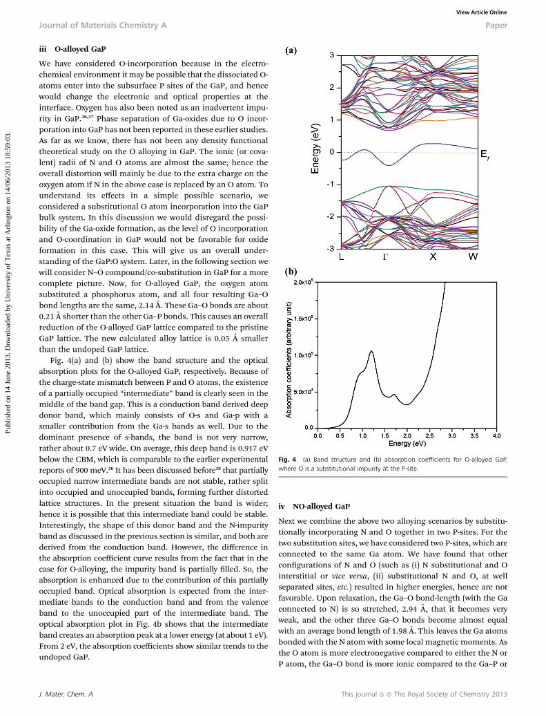
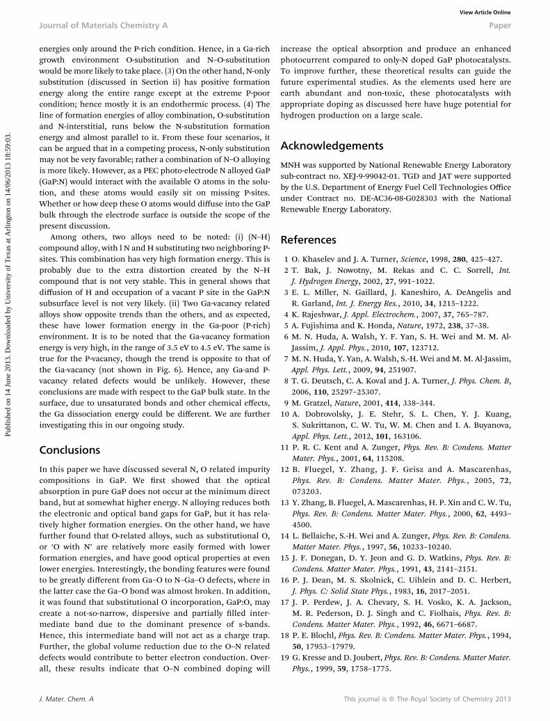
Fig. 4 (a) Band structure and (b) absorption coefficients for O-alloyed GaP,where O is a substitutional impurity at the P-site.
Journal of Materials Chemistry A Paper
Publ
ishe
d on
14
June
201
3. D
ownl
oade
d by
Uni
vers
ity o
f T
exas
at A
rlin
gton
on
14/0
6/20
13 1
8:59
:03.
View Article Online
iii O-alloyed GaP
We have considered O-incorporation because in the electro-chemical environment it may be possible that the dissociated O-atoms enter into the subsurface P sites of the GaP, and hencewould change the electronic and optical properties at theinterface. Oxygen has also been noted as an inadvertent impu-rity in GaP.26,27 Phase separation of Ga-oxides due to O incor-poration into GaP has not been reported in these earlier studies.As far as we know, there has not been any density functionaltheoretical study on the O alloying in GaP. The ionic (or cova-lent) radii of N and O atoms are almost the same; hence theoverall distortion will mainly be due to the extra charge on theoxygen atom if N in the above case is replaced by an O atom. Tounderstand its effects in a simple possible scenario, weconsidered a substitutional O atom incorporation into the GaPbulk system. In this discussion we would disregard the possi-bility of the Ga-oxide formation, as the level of O incorporationand O-coordination in GaP would not be favorable for oxideformation in this case. This will give us an overall under-standing of the GaP:O system. Later, in the following section wewill consider N–O compound/co-substitution in GaP for a morecomplete picture. Now, for O-alloyed GaP, the oxygen atomsubstituted a phosphorus atom, and all four resulting Ga–Obond lengths are the same, 2.14 A. These Ga–O bonds are about0.21 A shorter than the other Ga–P bonds. This causes an overallreduction of the O-alloyed GaP lattice compared to the pristineGaP lattice. The new calculated alloy lattice is 0.05 A smallerthan the undoped GaP lattice.
Fig. 4(a) and (b) show the band structure and the opticalabsorption plots for the O-alloyed GaP, respectively. Because ofthe charge-state mismatch between P and O atoms, the existenceof a partially occupied “intermediate” band is clearly seen in themiddle of the band gap. This is a conduction band derived deepdonor band, which mainly consists of O-s and Ga-p with asmaller contribution from the Ga-s bands as well. Due to thedominant presence of s-bands, the band is not very narrow,rather about 0.7 eV wide. On average, this deep band is 0.917 eVbelow the CBM, which is comparable to the earlier experimentalreports of 900 meV.26 It has been discussed before28 that partiallyoccupied narrow intermediate bands are not stable, rather splitinto occupied and unoccupied bands, forming further distortedlattice structures. In the present situation the band is wider;hence it is possible that this intermediate band could be stable.Interestingly, the shape of this donor band and the N-impurityband as discussed in the previous section is similar, and both arederived from the conduction band. However, the difference inthe absorption coefficient curve results from the fact that in thecase for O-alloying, the impurity band is partially lled. So, theabsorption is enhanced due to the contribution of this partiallyoccupied band. Optical absorption is expected from the inter-mediate bands to the conduction band and from the valenceband to the unoccupied part of the intermediate band. Theoptical absorption plot in Fig. 4b shows that the intermediateband creates an absorption peak at a lower energy (at about 1 eV).From 2 eV, the absorption coefficients show similar trends to theundoped GaP.
J. Mater. Chem. A
iv NO-alloyed GaP
Next we combine the above two alloying scenarios by substitu-tionally incorporating N and O together in two P-sites. For thetwo substitution sites, we have considered two P-sites, which areconnected to the same Ga atom. We have found that othercongurations of N and O (such as (i) N substitutional and Ointerstitial or vice versa, (ii) substitutional N and O, at wellseparated sites, etc.) resulted in higher energies, hence are notfavorable. Upon relaxation, the Ga–O bond-length (with the Gaconnected to N) is so stretched, 2.94 A, that it becomes veryweak, and the other three Ga–O bonds become almost equalwith an average bond length of 1.98 A. This leaves the Ga atomsbonded with the N atom with some local magnetic moments. Asthe O atom is more electronegative compared to either the N orP atom, the Ga–O bond is more ionic compared to the Ga–P or
This journal is ª The Royal Society of Chemistry 2013
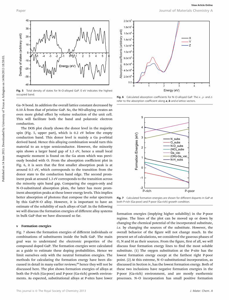
Fig. 5 Total density of states for N–O-alloyed GaP. 0 eV indicates the highestoccupied band.
Fig. 6 Calculated absorption coefficients for N–O-alloyed GaP. The x-, y- and z-refer to the absorption coefficient along a, b and c lattice vectors.
Fig. 7 Calculated formation energies are shown for different dopants in GaP atboth P-rich (Ga-poor) and P-poor (Ga-rich) growth condition.
Paper Journal of Materials Chemistry A
Publ
ishe
d on
14
June
201
3. D
ownl
oade
d by
Uni
vers
ity o
f T
exas
at A
rlin
gton
on
14/0
6/20
13 1
8:59
:03.
View Article Online
Ga–N bond. In addition the overall lattice constant decreased by0.10 A from that of pristine GaP. So, the NO-alloying creates aneven more global effect by volume reduction of the unit cell.This will facilitate both the band and polaronic electronconduction.
The DOS plot clearly shows the donor level in the majorityspin (Fig. 5, upper part), which is 0.2 eV below the emptyconduction band. This donor level is mainly a Ga p-orbitalderived band. Hence this alloying combination would turn thismaterial to an n-type semiconductor. However, the minorityspin shows a larger band gap of 1.3 eV, hence a small localmagnetic moment is found on the Ga atom which was previ-ously bonded with O. From the absorption coefficient plot inFig. 6, it is seen that the rst smaller absorption peak is ataround 0.5 eV, which corresponds to the transition from thedonor state to the conduction band edge. The second prom-inent peak at around 1.3 eV corresponds to the transition acrossthe minority spin band gap. Comparing the oxygen-only andN–O-substituted absorption plots, the latter has more prom-inent absorption peaks at these lower energy levels. This impliesbetter absorption of photons that compose the solar spectrumby this GaP:N–O alloy. However, it is important to have anestimate of the solubility of such alloys of GaP. In the followingwe will discuss the formation energies of different alloy systemsin bulk GaP that we have discussed so far.
v Formation energies
Fig. 7 shows the formation energies of different individuals orcombinations of substituents inside the bulk GaP. The maingoal was to understand the electronic properties of thecompound doped GaP. The formation energies were calculatedas a guide to estimate these doping probabilities. Hence welimit ourselves only with the neutral formation energies. Themethods for calculating the formation energy have been dis-cussed in detail in many earlier reviews;29 hence they will not bediscussed here. The plot shows formation energies of alloys atboth the P-rich (Ga-poor) and P-poor (Ga-rich) growth environ-ments. As expected, substitutional alloys at P-sites have lower
This journal is ª The Royal Society of Chemistry 2013
formation energies (implying higher solubility) in the P-poorregime. The lines of the plot can be moved up or down bychanging the chemical potential of the incorporated substitute,i.e. by changing the sources of the substitute. However, theoverall behavior of the gure will not change much. In thepresent set of calculations, we considered the gaseous phases ofO, N and H as their sources. From the gure, rst of all, we willdiscuss four formation energy lines to nd the most solublesubstitute. (1) The oxygen substitution at the P-site has thelowest formation energy except at the farthest right P-poorpoint. (2) At this extreme, N–O substitutional incorporation, asdiscussed in Section iv, has the lowest formation energy. Both ofthese two inclusions have negative formation energies in theP-poor (Ga-rich) environment, and are mostly exothermicprocesses. N–O incorporation has small positive formation
J. Mater. Chem. A
Journal of Materials Chemistry A Paper
Publ
ishe
d on
14
June
201
3. D
ownl
oade
d by
Uni
vers
ity o
f T
exas
at A
rlin
gton
on
14/0
6/20
13 1
8:59
:03.
View Article Online
energies only around the P-rich condition. Hence, in a Ga-richgrowth environment O-substitution and N–O-substitutionwould bemore likely to take place. (3) On the other hand, N-onlysubstitution (discussed in Section ii) has positive formationenergy along the entire range except at the extreme P-poorcondition; hence mostly it is an endothermic process. (4) Theline of formation energies of alloy combination, O-substitutionand N-interstitial, runs below the N-substitution formationenergy and almost parallel to it. From these four scenarios, itcan be argued that in a competing process, N-only substitutionmay not be very favorable; rather a combination of N–O alloyingis more likely. However, as a PEC photo-electrode N alloyed GaP(GaP:N) would interact with the available O atoms in the solu-tion, and these atoms would easily sit on missing P-sites.Whether or how deep these O atoms would diffuse into the GaPbulk through the electrode surface is outside the scope of thepresent discussion.
Among others, two alloys need to be noted: (i) (N–H)compound alloy, with l N and H substituting two neighboring P-sites. This combination has very high formation energy. This isprobably due to the extra distortion created by the N–Hcompound that is not very stable. This in general shows thatdiffusion of H and occupation of a vacant P site in the GaP:Nsubsurface level is not very likely. (ii) Two Ga-vacancy relatedalloys show opposite trends than the others, and as expected,these have lower formation energy in the Ga-poor (P-rich)environment. It is to be noted that the Ga-vacancy formationenergy is very high, in the range of 3.5 eV to 4.5 eV. The same istrue for the P-vacancy, though the trend is opposite to that ofthe Ga-vacancy (not shown in Fig. 6). Hence, any Ga-and P-vacancy related defects would be unlikely. However, theseconclusions are made with respect to the GaP bulk state. In thesurface, due to unsaturated bonds and other chemical effects,the Ga dissociation energy could be different. We are furtherinvestigating this in our ongoing study.
Conclusions
In this paper we have discussed several N, O related impuritycompositions in GaP. We rst showed that the opticalabsorption in pure GaP does not occur at the minimum directband, but at somewhat higher energy. N alloying reduces boththe electronic and optical band gaps for GaP, but it has rela-tively higher formation energies. On the other hand, we havefurther found that O-related alloys, such as substitutional O,or ‘O with N’ are relatively more easily formed with lowerformation energies, and have good optical properties at evenlower energies. Interestingly, the bonding features were foundto be greatly different from Ga–O to N–Ga–O defects, where inthe latter case the Ga–O bond was almost broken. In addition,it was found that substitutional O incorporation, GaP:O, maycreate a not-so-narrow, dispersive and partially lled inter-mediate band due to the dominant presence of s-bands.Hence, this intermediate band will not act as a charge trap.Further, the global volume reduction due to the O–N relateddefects would contribute to better electron conduction. Over-all, these results indicate that O–N combined doping will
J. Mater. Chem. A
increase the optical absorption and produce an enhancedphotocurrent compared to only-N doped GaP photocatalysts.To improve further, these theoretical results can guide thefuture experimental studies. As the elements used here areearth abundant and non-toxic, these photocatalysts withappropriate doping as discussed here have huge potential forhydrogen production on a large scale.
Acknowledgements
MNH was supported by National Renewable Energy Laboratorysub-contract no. XEJ-9-99042-01. TGD and JAT were supportedby the U.S. Department of Energy Fuel Cell Technologies Officeunder Contract no. DE-AC36-08-G028303 with the NationalRenewable Energy Laboratory.
References
1 O. Khaselev and J. A. Turner, Science, 1998, 280, 425–427.2 T. Bak, J. Nowotny, M. Rekas and C. C. Sorrell, Int.J. Hydrogen Energy, 2002, 27, 991–1022.
3 E. L. Miller, N. Gaillard, J. Kaneshiro, A. DeAngelis andR. Garland, Int. J. Energy Res., 2010, 34, 1215–1222.
4 K. Rajeshwar, J. Appl. Electrochem., 2007, 37, 765–787.5 A. Fujishima and K. Honda, Nature, 1972, 238, 37–38.6 M. N. Huda, A. Walsh, Y. F. Yan, S. H. Wei and M. M. Al-Jassim, J. Appl. Phys., 2010, 107, 123712.
7 M. N. Huda, Y. Yan, A. Walsh, S.-H. Wei andM. M. Al-Jassim,Appl. Phys. Lett., 2009, 94, 251907.
8 T. G. Deutsch, C. A. Koval and J. A. Turner, J. Phys. Chem. B,2006, 110, 25297–25307.
9 M. Gratzel, Nature, 2001, 414, 338–344.10 A. Dobrovolsky, J. E. Stehr, S. L. Chen, Y. J. Kuang,
S. Sukrittanon, C. W. Tu, W. M. Chen and I. A. Buyanova,Appl. Phys. Lett., 2012, 101, 163106.
11 P. R. C. Kent and A. Zunger, Phys. Rev. B: Condens. MatterMater. Phys., 2001, 64, 115208.
12 B. Fluegel, Y. Zhang, J. F. Geisz and A. Mascarenhas,Phys. Rev. B: Condens. Matter Mater. Phys., 2005, 72,073203.
13 Y. Zhang, B. Fluegel, A. Mascarenhas, H. P. Xin and C. W. Tu,Phys. Rev. B: Condens. Matter Mater. Phys., 2000, 62, 4493–4500.
14 L. Bellaiche, S.-H. Wei and A. Zunger, Phys. Rev. B: Condens.Matter Mater. Phys., 1997, 56, 10233–10240.
15 J. F. Donegan, D. Y. Jeon and G. D. Watkins, Phys. Rev. B:Condens. Matter Mater. Phys., 1991, 43, 2141–2151.
16 P. J. Dean, M. S. Skolnick, C. Uihlein and D. C. Herbert,J. Phys. C: Solid State Phys., 1983, 16, 2017–2051.
17 J. P. Perdew, J. A. Chevary, S. H. Vosko, K. A. Jackson,M. R. Pederson, D. J. Singh and C. Fiolhais, Phys. Rev. B:Condens. Matter Mater. Phys., 1992, 46, 6671–6687.
18 P. E. Blochl, Phys. Rev. B: Condens. Matter Mater. Phys., 1994,50, 17953–17979.
19 G. Kresse and D. Joubert, Phys. Rev. B: Condens. Matter Mater.Phys., 1999, 59, 1758–1775.
This journal is ª The Royal Society of Chemistry 2013
Paper Journal of Materials Chemistry A
Publ
ishe
d on
14
June
201
3. D
ownl
oade
d by
Uni
vers
ity o
f T
exas
at A
rlin
gton
on
14/0
6/20
13 1
8:59
:03.
View Article Online
20 G. Kresse and J. Furthmuumlller, Phys. Rev. B: Condens.Matter Mater. Phys., 1996, 54, 11169–11186.
21 G. Kresse and J. Furthmuller, Comput. Mater. Sci., 1996, 6,15–50.
22 S. L. Dudarev, G. A. Botton, S. Y. Savrasov, C. J. Humphreysand A. P. Sutton, Phys. Rev. B: Condens. Matter Mater. Phys.,1998, 57, 1505–1509.
23 H. P. Xin, C. W. Tu, Y. Zhang and A. Mascarenhas, Appl. Phys.Lett., 2000, 76, 1267–1269.
24 Y. Yan, Q. Wang, X. Zhang, W. Shu, J. Li, Y. Huang andX. Ren, Phys. B, 2012, 407, 112–115.
This journal is ª The Royal Society of Chemistry 2013
25 W. Wen, A. I. Carim, S. M. Collins, M. J. Price,S. L. Peczonczyk and S. Maldonado, J. Phys. Chem. C, 2011,115, 22652–22661.
26 M. Godlewski and B. Monemar, Phys. Rev. B: Condens. MatterMater. Phys., 1988, 37, 2752–2755.
27 C. K. Kim, J. Appl. Phys., 1974, 45, 243–245.28 M. N. Huda, Y. Yan, S.-H. Wei and M. M. Al-Jassim, Phys.
Rev. B: Condens. Matter Mater. Phys., 2009, 80,115118.
29 C. G. V. d. Walle and J. Neugebauer, J. Appl. Phys., 2004, 95,3851–3879.
J. Mater. Chem. A