The ATLAS semiconductor tracker end-cap module
37
Nuclear Instruments and Methods in Physics Research A 575 (2007) 353–389 The ATLAS semiconductor tracker end-cap module A. Abdesselam z , P.J. Adkin ae , P.P. Allport o , J. Alonso n , L. Andricek v , F. Anghinolfi e , A.A. Antonov t , R.J. Apsimon ae , T. Atkinson s , L.E. Batchelor ae , R.L. Bates j , G. Beck p , H. Becker v , P. Bell e , W. Bell j , P. Benesˇ ab , J. Bernabeu ak , S. Bethke v , J.P. Bizzell ae , J. Blocki g , Z. Broklova´ aa , J. Brozˇ aa , J. Bohm ac , P. Booker ae , G. Bright s , T.J. Brodbeck m , P. Bruckman z , C.M. Buttar j , J.M. Butterworth q , F. Campabadal a , D. Campbell m , C. Carpentieri h , J.L. Carroll o , A.A. Carter p , J.R. Carter d , G.L. Casse o , P. C ˇ erma´ k ab , M. Chamizo i , D.G. Charlton c , A. Cheplakov j , E. Chesi e , A. Chilingarov m , S. Chouridou ah , D. Chren ab , A. Christinet i , M.L. Chu ai , V. Cindro k , A. Ciocio n , J.V. Civera ak , A. Clark i , A.P. Colijn w , P.A. Cooke o , M.J. Costa ak , D. Costanzo af , W. Dabrowski f , K.M. Danielsen y , V.R. Davies ae , I. Dawson af , P. de Jong w , P. Dervan o , F. Doherty j , Z. Dolezˇal aa , M. Donega i , M. D’Onofrio i , O. Dorholt y , Z. Dra´sal aa , J.D. Dowell c , I.P. Duerdoth r , R. Duxfield af , M. Dwuznik f , J.M. Easton ae , S. Eckert h , L. Eklund e , C. Escobar ak , V. Fadeyev n , D. Fasching al , L. Feld h , D.P.S. Ferguson al , P. Ferrari e , D. Ferrere i , C. Fleta a , R. Fortin e , J.M. Foster r , C. Fowler ae , H. Fox h , J. Freestone r , R.S. French af , J. Fuster ak , S. Gadomski g , B.J. Gallop c , C. Garcı´a ak , J.E. Garcı´a-Navarro ak , S. Gibson z , M.G.D. Gilchriese n , F. Gonzalez ak , S. Gonzalez-Sevilla ak , M.J. Goodrick d , A. Gorisek e , E. Gornicki g , A. Greenall o , D. Greenfield ae , S. Gregory s , I.G. Grigorieva t , A.A. Grillo ah , J. Grosse-Knetter e , C. Gryska v , A. Guipet i , C. Haber n , K. Hara aj , F.G. Hartjes w , D. Hauff v , S.J. Haywood ae , S.J. Hegeman s , K. Heinzinger v , N.P. Hessey w , C. Heusch v , A. Hicheur ae , J.C. Hill d , M. Hodgkinson af , P. Hodgson af , T. Horazˇd ˇ ovsky´ ab , T.I. Hollins c , L.S. Hou ai , S. Hou ai , G. Hughes m , T. Huse y , M. Ibbotson r , M. Iglesias i , Y. Ikegami l , I. Ilyashenko ag , C. Issever z , J.N. Jackson o , K. Jakobs h , R.C. Jared al , P. Jarron e , P. Johansson af , R.W.L. Jones m , T.J. Jones o , D. Joos h , J. Joseph al , P. Jovanovic c , O. Jusko ab , V. Jusko ab , J. Kaplon e , S. Kazi s , Ch. Ketterer h , A.G. Kholodenko ad , B.T. King o , P. Kodysˇ aa , E. Koffeman w , Z. Kohout ab , T. Kohriki l , T. Kondo l , S. Koperny f , H. Koukol ab , V. Kra´l ab , G. Kramberger k , P. Kubı´k aa , J. Kudlaty v , C. Lacasta ak, , T. Lagouri aa , S.C. Lee ai , K. Leney o , S. Lenz v , C.G. Lester d , K. Liebicher v , M. Limper w , S. Lindsay o , V. Linhart ab , G. LLosa´ ak , F.K. Loebinger r , M. Lozano a , I. Ludwig h , J. Ludwig h , G. Lutz v , J. Lys n , M. Maassen h , D. Macina i , A. Macpherson e , C. MacWaters ae , C.A. Magrath w , P. Malecki g , I. Mandic´ k , M. Mangin-Brinet i , S. Martı´-Garcı´a ak , J.P. Matheson ae , R.M. Matson ae , S.J. McMahon ae , T.J. McMahon c , J. Meinhardt h , B. Mellado al , J.J. Melone j , I.J. Mercer m , I. Messmer h , B. Mikulec i , M. Mikuzˇ k , M. Min˜ano ak , V.A. Mitsou ak , P. Modesto ak , S. Moed i , B. Mohn a , S. Moncrieff s , G. Moorhead s , F.S. Morris ae , J. Morris p , M. Morrissey ae , H.G. Moser v , A. Moszczynski g , A.J.M. Muijs w , W.J. Murray ae , D. Muskett o , J. Nacher ak , K. Nagai p , I. Nakano x , R.B. Nickerson z , R. Nisius v , O.K. Oye a , V. O’Shea j , E. Paganis af , ARTICLE IN PRESS www.elsevier.com/locate/nima 0168-9002/$ - see front matter r 2007 Elsevier B.V. All rights reserved. doi:10.1016/j.nima.2007.02.019 Corresponding author. Tel.: +1 34 96 3543490; fax: +34 96 3543488. E-mail address: Carlos.Lacasta@ific.uv.es (C. Lacasta).
-
Upload
independent -
Category
Documents
-
view
4 -
download
0
Transcript of The ATLAS semiconductor tracker end-cap module

ARTICLE IN PRESS
0168-9002/$ - se
doi:10.1016/j.ni
�CorrespondE-mail addr
Nuclear Instruments and Methods in Physics Research A 575 (2007) 353–389
www.elsevier.com/locate/nima
The ATLAS semiconductor tracker end-cap module
A. Abdesselamz, P.J. Adkinae, P.P. Allporto, J. Alonson, L. Andricekv, F. Anghinolfie,A.A. Antonovt, R.J. Apsimonae, T. Atkinsons, L.E. Batchelorae, R.L. Batesj, G. Beckp,
H. Beckerv, P. Belle, W. Bellj, P. Benesab, J. Bernabeuak, S. Bethkev, J.P. Bizzellae, J. Blockig,Z. Broklovaaa, J. Brozaa, J. Bohmac, P. Bookerae, G. Brights, T.J. Brodbeckm, P. Bruckmanz,
C.M. Buttarj, J.M. Butterworthq, F. Campabadala, D. Campbellm, C. Carpentierih,J.L. Carrollo, A.A. Carterp, J.R. Carterd, G.L. Casseo, P. Cermakab, M. Chamizoi,
D.G. Charltonc, A. Cheplakovj, E. Chesie, A. Chilingarovm, S. Chouridouah, D. Chrenab,A. Christineti, M.L. Chuai, V. Cindrok, A. Ciocion, J.V. Civeraak, A. Clarki, A.P. Colijnw,
P.A. Cookeo, M.J. Costaak, D. Costanzoaf, W. Dabrowskif, K.M. Danielseny, V.R. Daviesae,I. Dawsonaf, P. de Jongw, P. Dervano, F. Dohertyj, Z. Dolezalaa, M. Donegai, M. D’Onofrioi,
O. Dorholty, Z. Drasalaa, J.D. Dowellc, I.P. Duerdothr, R. Duxfieldaf, M. Dwuznikf,J.M. Eastonae, S. Eckerth, L. Eklunde, C. Escobarak, V. Fadeyevn, D. Faschingal, L. Feldh,D.P.S. Fergusonal, P. Ferrarie, D. Ferrerei, C. Fletaa, R. Fortine, J.M. Fosterr, C. Fowlerae,H. Foxh, J. Freestoner, R.S. Frenchaf, J. Fusterak, S. Gadomskig, B.J. Gallopc, C. Garcıaak,J.E. Garcıa-Navarroak, S. Gibsonz, M.G.D. Gilchriesen, F. Gonzalezak, S. Gonzalez-Sevillaak,
M.J. Goodrickd, A. Goriseke, E. Gornickig, A. Greenallo, D. Greenfieldae, S. Gregorys,I.G. Grigorievat, A.A. Grilloah, J. Grosse-Knettere, C. Gryskav, A. Guipeti, C. Habern,K. Haraaj, F.G. Hartjesw, D. Hauffv, S.J. Haywoodae, S.J. Hegemans, K. Heinzingerv,N.P. Hesseyw, C. Heuschv, A. Hicheurae, J.C. Hilld, M. Hodgkinsonaf, P. Hodgsonaf,
T. Horazdovskyab, T.I. Hollinsc, L.S. Houai, S. Houai, G. Hughesm, T. Husey, M. Ibbotsonr,M. Iglesiasi, Y. Ikegamil, I. Ilyashenkoag, C. Isseverz, J.N. Jacksono, K. Jakobsh, R.C. Jaredal,P. Jarrone, P. Johanssonaf, R.W.L. Jonesm, T.J. Joneso, D. Joosh, J. Josephal, P. Jovanovicc,O. Juskoab, V. Juskoab, J. Kaplone, S. Kazis, Ch. Kettererh, A.G. Kholodenkoad, B.T. Kingo,P. Kodysaa, E. Koffemanw, Z. Kohoutab, T. Kohrikil, T. Kondol, S. Kopernyf, H. Koukolab,V. Kralab, G. Krambergerk, P. Kubıkaa, J. Kudlatyv, C. Lacastaak,�, T. Lagouriaa, S.C. Leeai,K. Leneyo, S. Lenzv, C.G. Lesterd, K. Liebicherv, M. Limperw, S. Lindsayo, V. Linhartab,G. LLosaak, F.K. Loebingerr, M. Lozanoa, I. Ludwigh, J. Ludwigh, G. Lutzv, J. Lysn,
M. Maassenh, D. Macinai, A. Macphersone, C. MacWatersae, C.A. Magrathw, P. Maleckig,I. Mandick, M. Mangin-Brineti, S. Martı-Garcıaak, J.P. Mathesonae, R.M. Matsonae,
S.J. McMahonae, T.J. McMahonc, J. Meinhardth, B. Melladoal, J.J. Melonej, I.J. Mercerm,I. Messmerh, B. Mikuleci, M. Mikuzk, M. Minanoak, V.A. Mitsouak, P. Modestoak, S. Moedi,
B. Mohna, S. Moncrieffs, G. Moorheads, F.S. Morrisae, J. Morrisp, M. Morrisseyae,H.G. Moserv, A. Moszczynskig, A.J.M. Muijsw, W.J. Murrayae, D. Musketto, J. Nacherak,K. Nagaip, I. Nakanox, R.B. Nickersonz, R. Nisiusv, O.K. Oyea, V. O’Sheaj, E. Paganisaf,
e front matter r 2007 Elsevier B.V. All rights reserved.
ma.2007.02.019
ing author. Tel.: +134 96 3543490; fax: +3496 3543488.
ess: [email protected] (C. Lacasta).

ARTICLE IN PRESSA. Abdesselam et al. / Nuclear Instruments and Methods in Physics Research A 575 (2007) 353–389354
M.A. Parkerd, U. Parzefallh, J.R. Paterr, S.J.M. Peetersw, G. Pellegrinia, G. Pelleritii,H. Perneggere, E. Perrini, P.W. Phillipsae, L.V. Pilavovau, K. Poltorakf, S. Pospısilab,M. Postraneckyq, T. Pritcharde, K. Prokofievaf, J.M. Rafıa, C. Rainej, P.N. Ratoffm,
P. Reznıcekaa, V.N. Riadovikovad, R.H. Richterv, A. Robichaud-Veronneaui, D. Robinsond,R. Rodriguez-Olieteak, S. Roee, A. Rudgee, K. Rungeh, A. Saavedras, H.F.W. Sadrozinskiah,F.J. Sanchezak, H. Sandakery, D.H. Saxonj, D. Scheirichaa, J. Schieckv, A. Seidenah, A. Sfyrlai,T. Slavıcekab, K.M. Smithj, N.A. Smitho, S.W. Snowr, M. Solarab, B. Sopkoab, V. Sopkoab,
L. Sospedraak, E. Spencerah, E. Staneckag, S. Stapnesy, J. Stastnyac, V. Strachkoak,A. Stradlingal, B. Stugua, D.S. Suai, P. Sutcliffeo, R. Szczygielg, R. Tanakax, G. Taylors,
P.K. Tengai, S. Teradal, R.J. Thompsonr, M. Titovh, B. Toczekf, D.R. Toveyaf, G. Tratzlv,V.L. Troitskyu, J. Tsengz, M. Turalag, P.R. Turnero, M. Tyndelae, M. Ullana, Y. Unnol,T. Vickeyal, E. Van der Kraaijw, G. Viehhauserz, E.G. Villaniae, T. Vitekab, T. Vu Anhi,
A.P. Vorobievad, J.H. Vossebeldo, M. Wachlerv, R. Wallnye, C.P. Wardd, M.R.M. Warrenq,M. Webelh, M. Weberi, M. Weberae, A.R. Weidbergz, P. Weilhammere, P.S. Wellse, P. Wetzelv,
M. Whitleyo, M. Wiesmannv, I. Wilhelmaa, M. Willenbrocki, I. Wilmutae, J.A. Wilsonc,J. Wintons, M. Wolterg, M.P. Wormaldo, S.L. Wual, X. Wui, H. Zhuaf, N. Bingeforsam,
R. Brenneram, T. Ekelofam
aCentro Nacional de Microelectronica de Barcelona, CNM-IMB, CSIC, Barcelona, SpainbDepartment of Physics and Technology, University of Bergen, N 5007 Bergen, Norway
cSchool of Physics and Astronomy, University of Birmingham, Birmingham B15 2TT, UKdCavendish Laboratory, Cambridge University, Cambridge, UK
eEuropean Laboratory for Particle Physics (CERN), Geneva, SwitzerlandfFaculty of Physics and Applied Computer Sciences, AGH University of Science and Technology, Cracow, Poland
gThe Henryk Niewodniczanski Institute of Nuclear Physics, Polish Academy of Sciences, Cracow, PolandhFakultat fur Physik, Albert-Ludwigs-Universitat, Freiburg, Germany
iSection de Physique, Universite de Geneve, SwitzerlandjDepartment of Physics and Astronomy, University of Glasgow, Glasgow, UK
kJozef Stefan Institute and Department of Physics, University of Ljubljana, Ljubljana, SlovenialKEK, High Energy Accelerator Research Organization, Oho 1-1, Tsukuba, Ibaraki 305-0801, Japan
mDepartment of Physics and Astronomy, University of Lancaster, Lancaster, UKnLawrence Berkeley National Laboratory, Berkeley, California, USA
oDepartment of Physics, Oliver Lodge Laboratory, University of Liverpool, Liverpool, UKpDepartment of Physics, Queen Mary and Westfield College, University of London, London, UK
qDepartment of Physics, University College, University of London, London, UKrSchool of Physics and Astronomy, University of Manchester, Manchester, UK
sUniversity of Melbourne, Parkville, Victoria 3052, AustraliatNIIGraphite, Moscow, Russia
uNIITAP, Zelenograd, Moscow, RussiavMax-Planck-Institut fur Physik, Munchen, Germany
wNIKHEF, Amsterdam, The NetherlandsxOkayama University, The Graduate School of Natural Science and Technology, Tsushima-naka 3-1-1, Okayama 700-8530, Japan
yThe University of Oslo, Department of Physics, Oslo, NorwayzDepartment of Physics, Oxford University, Oxford, UK
aaCharles University, Faculty of Mathematics and Physics, Prague, The Czech RepublicabCzech Technical University, Prague, The Czech Republic
acInstitute of Physics of the Academy of Sciences of the Czech Republic, Prague, The Czech RepublicadIHEP, Protvino, Russia
aeRutherford Appleton Laboratory, Chilton, Didcot, UKafDepartment of Physics and Astronomy, University of Sheffield, Sheffield, UK
agIoffe Physico-Technical Institute, St.Petersburg, RussiaahSanta Cruz Institute for Particle Physics, University of California, Santa Cruz, California, USA
aiInstitute of Physics, Academia Sinica, Taipei, TaiwanajUniversity of Tsukuba, Institute of Pure and Applied Sciences, 1-1-1 Tennodai, Tsukuba, Ibarai 305-8571, Japan
akInstituto de Fısica Corpuscular (IFIC), CSIC-Universidad de Valencia, Valencia, SpainalDepartment of Physics, University of Wisconsin, Madison, Wisconsin, USA
amUppsala University, Department of Nuclear and Particle Physics, P.O. Box 535, SE-75121 Uppsala, Sweden
Received 23 January 2007; accepted 7 February 2007
Available online 28 February 2007
ARTICLE IN PRESSA. Abdesselam et al. / Nuclear Instruments and Methods in Physics Research A 575 (2007) 353–389 355
Abstract
The challenges for the tracking detector systems at the LHC are unprecedented in terms of the number of channels, the required read-
out speed and the expected radiation levels. The ATLAS Semiconductor Tracker (SCT) end-caps have a total of about 3million
electronics channels each reading out every 25 ns into its own on-chip 3:3ms buffer. The highest anticipated dose after 10 years operation
is 1:4� 1014 cm�2 in units of 1MeV neutron equivalent (assuming the damage factors scale with the non-ionising energy loss). The
forward tracker has 1976 double-sided modules, mostly of area �70 cm2, each having 2� 768 strips read out by six ASICs per side. The
requirement to achieve an average perpendicular radiation length of 1.5% X 0, while coping with up to 7W dissipation per module (after
irradiation), leads to stringent constraints on the thermal design. The additional requirement of 1500e� equivalent noise charge (ENC)
rising to only 1800e� ENC after irradiation, provides stringent design constraints on both the high-density Cu/Polyimide flex read-out
circuit and the ABCD3TA read-out ASICs. Finally, the accuracy of module assembly must not compromise the 16mm ðrfÞ resolutionperpendicular to the strip directions or 580mm radial resolution coming from the 40mrad front-back stereo angle.
A total of 2210 modules were built to the tight tolerances and specifications required for the SCT. This was 234 more than the 1976 required
and represents a yield of 93%. The component flow was at times tight, but the module production rate of 40–50 per week was maintained
despite this. The distributed production was not found to be a major logistical problem and it allowed additional flexibility to take advantage
of where the effort was available, including any spare capacity, for building the end-cap modules. The collaboration that produced the ATLAS
SCT end-cap modules kept in close contact at all times so that the effects of shortages or stoppages at different sites could be rapidly resolved.
r 2007 Elsevier B.V. All rights reserved.
PACS: 29.40.Gx; 29.40.Wk
Keywords: Silicon; Module; Microstrip; ATLAS; SCT; LHC
1. Introduction
The ATLAS experiment [1] at the CERN Large HadronCollider (LHC) [2] is a general purpose detector, aiming ata TeV-scale reach for new physics. The LHC is expected tostart with luminosities ramping first to 1033 cm�2 s�1 in itsinitial running and gradually increasing up to 1034 cm�2 s�1
(corresponding to integrated luminosities of up to 105 pb�1
per year). The semiconductor tracker is required toreconstruct isolated leptons with a transverse momentumof pT45GeV with 95% efficiency out to jZjp2:5, tomeasure momentum even at pT ¼ 500GeV with betterthan 30% precision, to track back to the vertex z-coordinate with better than 1mm accuracy, achieve twotrack resolution of better than 200 mm at 30 cm radius andrepresent no more than 20% X 0 in total [3].
To achieve this, a design consisting of four barrels of2112 silicon modules in total and two sets of nine disks(each set comprising 988 end-cap modules) was adopted byATLAS. Roughly speaking, the barrel region covers jZjp1on its own, with the disks needed to extend the coverage tojZjp2:5 while minimising the material seen by the highlyinclined tracks in these directions.
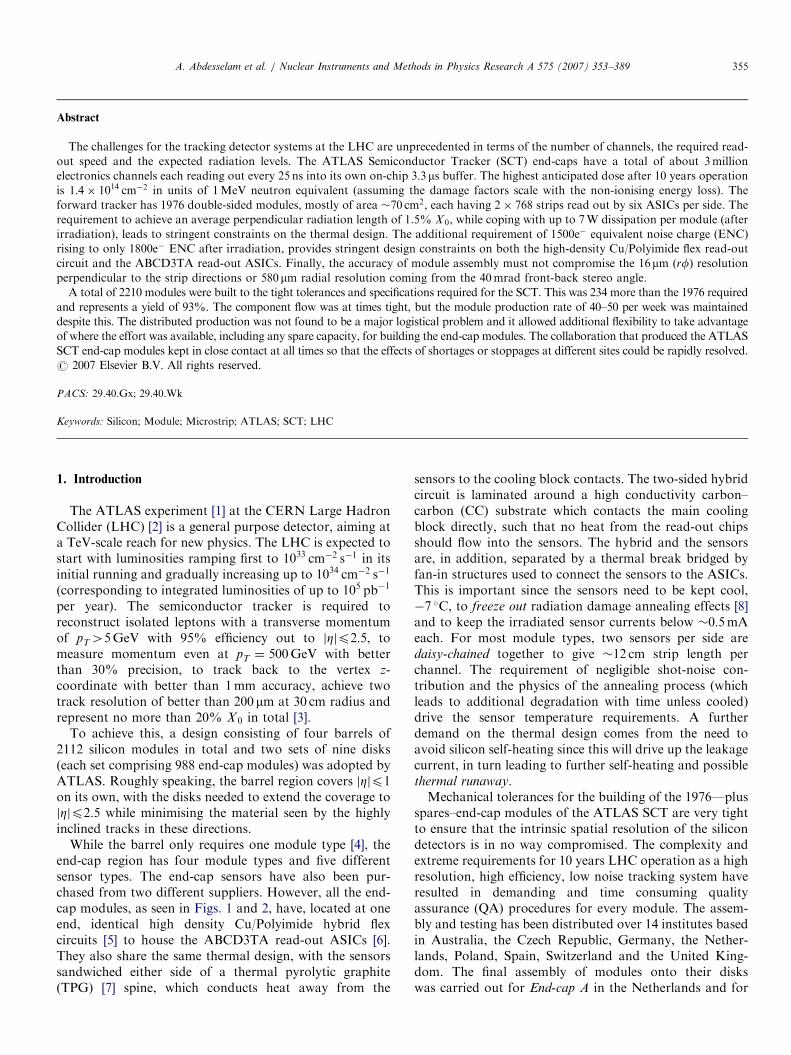
While the barrel only requires one module type [4], theend-cap region has four module types and five differentsensor types. The end-cap sensors have also been pur-chased from two different suppliers. However, all the end-cap modules, as seen in Figs. 1 and 2, have, located at oneend, identical high density Cu/Polyimide hybrid flexcircuits [5] to house the ABCD3TA read-out ASICs [6].They also share the same thermal design, with the sensorssandwiched either side of a thermal pyrolytic graphite(TPG) [7] spine, which conducts heat away from the
sensors to the cooling block contacts. The two-sided hybridcircuit is laminated around a high conductivity carbon–carbon (CC) substrate which contacts the main coolingblock directly, such that no heat from the read-out chipsshould flow into the sensors. The hybrid and the sensorsare, in addition, separated by a thermal break bridged byfan-in structures used to connect the sensors to the ASICs.This is important since the sensors need to be kept cool,�7 �C, to freeze out radiation damage annealing effects [8]and to keep the irradiated sensor currents below �0:5mAeach. For most module types, two sensors per side aredaisy-chained together to give �12 cm strip length perchannel. The requirement of negligible shot-noise con-tribution and the physics of the annealing process (whichleads to additional degradation with time unless cooled)drive the sensor temperature requirements. A furtherdemand on the thermal design comes from the need toavoid silicon self-heating since this will drive up the leakagecurrent, in turn leading to further self-heating and possiblethermal runaway.Mechanical tolerances for the building of the 1976—plus
spares–end-cap modules of the ATLAS SCT are very tightto ensure that the intrinsic spatial resolution of the silicondetectors is in no way compromised. The complexity andextreme requirements for 10 years LHC operation as a highresolution, high efficiency, low noise tracking system haveresulted in demanding and time consuming qualityassurance (QA) procedures for every module. The assem-bly and testing has been distributed over 14 institutes basedin Australia, the Czech Republic, Germany, the Nether-lands, Poland, Spain, Switzerland and the United King-dom. The final assembly of modules onto their diskswas carried out for End-cap A in the Netherlands and for

ARTICLE IN PRESS
Fig. 1. Exploded view of an SCT end-cap module showing the different components.
Fig. 2. ATLAS SCT end-cap modules. From left to right: outer, middle and inner. There is a fourth type, the short-middle, that follows the design of a
middle module with only one pair of silicon sensors.
A. Abdesselam et al. / Nuclear Instruments and Methods in Physics Research A 575 (2007) 353–389356
End-cap C in the UK, prior to both assemblies beingtransported to CERN for integration into the ATLASExperiment.
2. Layout of the ATLAS silicon tracker
This section describes the arrangement of tracking sub-detectors employed in ATLAS to measure charged particle3-momenta, determine their charge, reconstruct secondaryand tertiary vertexes, and identify interactions with thematerial in the tracking volume.
2.1. Physics goals of the ATLAS silicon tracker
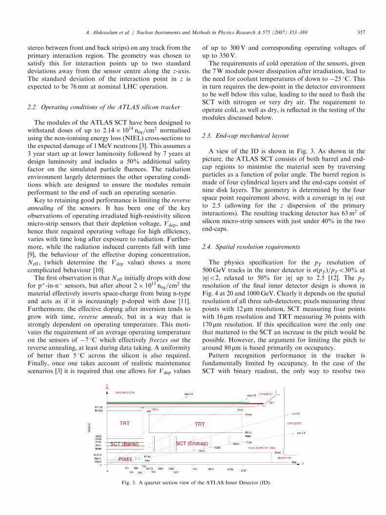
The ATLAS Inner Detector (ID) is 2.3m in diameter,7m in length and consists of the Semiconductor Tracker(SCT), with the Pixel detector within it and the gaseous/polypropylene foil Transition Radiation Tracker (TRT)surrounding it [3]. The ID sits within a 2T magnetic field,provided by the superconducting central solenoid, inte-grated inside the cryostat of the Liquid Argon electro-magnetic calorimeter.
The very high interaction rate at full luminosity and thehigh energy of jets, lead to requirements of both highgranularity and high spatial resolution. These effectivelydetermine the strip dimensions, given also that the ABCD3-TA [6] read-out chips give a binary read-out with a variablethreshold typically set to 1 fC for unirradiated operation. Theresolution requirements for isolated tracks are set by thetransverse momentum precision of p30% at 500GeVdiscussed above. In practice, this is readily achieved bymeasuring four space points along the track with the 16mmresolution in the f coordinate provided by the 80mm pitch(two sided with 40mrad stereo) of the SCT modules, evenwithout the charge interpolation possibilities which wouldcome from analogue read-out. More severe are the require-ments on the granularity to maintain typical hit occupanciesof order 1% or below, even within high pT jets. Also, becausethe capacitive load on the ABCD3TA chips cannot exceed18pF if noise of 1500e� ENC is to be achieved, the length ofthe strips cannot exceed 12cm for 1.2 pF/cm capacitance(when also allowing for fan-in and bonds).The layout described below was chosen to ensure at least
four space points in the SCT (where the orthogonalcoordinate to f measurement comes from the small angle
ARTICLE IN PRESSA. Abdesselam et al. / Nuclear Instruments and Methods in Physics Research A 575 (2007) 353–389 357
stereo between front and back strips) on any track from theprimary interaction region. The geometry was chosen tosatisfy this for interaction points up to two standarddeviations away from the sensor centre along the z-axis.The standard deviation of the interaction point in z isexpected to be 76mm at nominal LHC operation.
2.2. Operating conditions of the ATLAS silicon tracker
The modules of the ATLAS SCT have been designed towithstand doses of up to 2:14� 1014 neq=cm2 normalisedusing the non-ionising energy loss (NIEL) cross-sections tothe expected damage of 1MeV neutrons [3]. This assumes a3 year start up at lower luminosity followed by 7 years atdesign luminosity and includes a 50% additional safetyfactor on the simulated particle fluences. The radiationenvironment largely determines the other operating condi-tions which are designed to ensure the modules remainperformant to the end of such an operating scenario.
Key to retaining good performance is limiting the reverse
annealing of the sensors. It has been one of the keyobservations of operating irradiated high-resistivity siliconmicro-strip sensors that their depletion voltage, Vdep, andhence their required operating voltage for high efficiency,varies with time long after exposure to radiation. Further-more, while the radiation induced currents fall with time[9], the behaviour of the effective doping concentration,Neff , (which determine the Vdep value) shows a morecomplicated behaviour [10].
The first observation is that Neff initially drops with dosefor pþ-in-n� sensors, but after about 2� 1013 neq=cm2 thematerial effectively inverts space-charge from being n-typeand acts as if it is increasingly p-doped with dose [11].Furthermore, the effective doping after inversion tends togrow with time, reverse anneals, but in a way that isstrongly dependent on operating temperature. This moti-vates the requirement of an average operating temperatureon the sensors of �7 �C which effectively freezes out thereverse annealing, at least during data taking. A uniformityof better than 5 �C across the silicon is also required.Finally, once one takes account of realistic maintenancescenarios [3] it is required that one allows for Vdep values
Fig. 3. A quarter section view of th
of up to 300V and corresponding operating voltages ofup to 350V.The requirements of cold operation of the sensors, given
the 7W module power dissipation after irradiation, lead tothe need for coolant temperatures of down to �25 �C. Thisin turn requires the dew-point in the detector environmentto be well below this value, leading to the need to flush theSCT with nitrogen or very dry air. The requirement tooperate cold, as well as dry, is reflected in the testing of themodules discussed below.
2.3. End-cap mechanical layout
A view of the ID is shown in Fig. 3. As shown in thepicture, the ATLAS SCT consists of both barrel and end-cap regions to minimise the material seen by traversingparticles as a function of polar angle. The barrel region ismade of four cylindrical layers and the end-caps consist ofnine disk layers. The geometry is determined by the fourspace point requirement above, with a coverage in jZj outto 2.5 (allowing for the z dispersion of the primaryinteractions). The resulting tracking detector has 63m2 ofsilicon micro-strip sensors with just under 40% in the twoend-caps.
2.4. Spatial resolution requirements
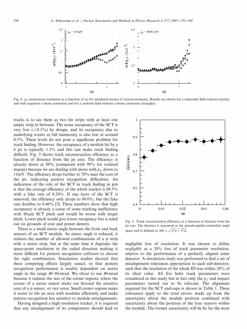
The physics specification for the pT resolution of500GeV tracks in the inner detector is sðpT Þ=pTo30% atjZjo2, relaxed to 50% for jZj up to 2.5 [12]. The pT
resolution of the final inner detector design is shown inFig. 4 at 20 and 1000GeV. Clearly it depends on the spatialresolution of all three sub-detectors; pixels measuring threepoints with 12mm resolution, SCT measuring four pointswith 16mm resolution and TRT measuring 36 points with170mm resolution. If this specification were the only onethat mattered to the SCT an increase in the pitch would bepossible. However, the argument for limiting the pitch toaround 80mm is based primarily on occupancy.Pattern recognition performance in the tracker is
fundamentally limited by occupancy. In the case of theSCT with binary readout, the only way to resolve two
e ATLAS Inner Detector (ID).
ARTICLE IN PRESS
Fig. 4. pT momentum resolution as a function of jZj for simulated muons of various momenta. Results are shown for a solenoidal field without (circles)
and with (squares) a beam constraint and for a uniform field without a beam constraint (triangles).
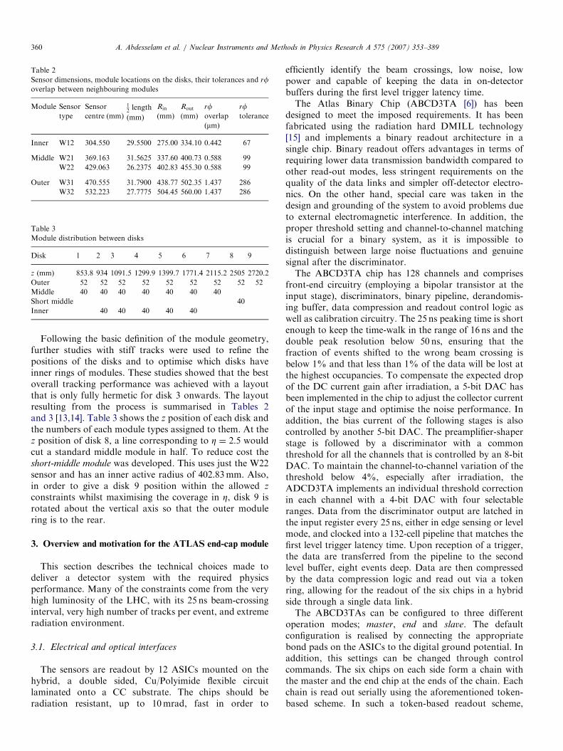
Fig. 5. Track reconstruction efficiency as a function of distance from the
jet axis. The distance is measured in the pseudorapidity-azimuthal angle
space and is defined as DR ¼ffiffiffiffiffiffiffiffiffiffiffiffiffiffiffiffiffiffiffiffiffiffiD2Zþ D2f
p.
A. Abdesselam et al. / Nuclear Instruments and Methods in Physics Research A 575 (2007) 353–389358
tracks is to see them as two hit strips with at least oneempty strip in between. The noise occupancy of the SCT isvery low ðo0:1%Þ by design, and its occupancy due tounderlying events at full luminosity is also low at around0.5%. These levels do not pose a significant problem fortrack finding. However, the occupancy of a module hit by ab jet is typically 1.5% and this can make track findingdifficult. Fig. 5 shows track reconstruction efficiency as afunction of distance from the jet axis. The efficiency isalready down at 89% (compared with 98% for isolatedmuons) because we are dealing with pions with pT down to1GeV. The efficiency drops further to 78% near the core ofthe jet, indicating pattern recognition difficulties. Anindication of the role of the SCT in track finding in jetsis that the average efficiency of the whole tracker is 89.5%with a fake rate of 0.24%. If one layer of the SCT isremoved, the efficiency only drops to 89.0%, but the fakerate doubles to 0.46% [3]. These numbers show that highoccupancy is already a cause of some tracking inefficiencywith 80mm SCT pitch and would be worse with largerpitch. Lower pitch would give lower occupancy but is ruledout on grounds of cost and power density.
There is a small stereo angle between the front and backsensors of an SCT module. As stereo angle is reduced, itreduces the number of allowed combinations of a f stripwith a stereo strip, but at the same time it degrades thespace-point resolution in the radial direction making itmore difficult for pattern recognition software to choosethe right combination. Simulation studies showed thatthese competing effects largely cancel, so that patternrecognition performance is weakly dependent on stereoangle in the range 40–80mrad. We chose to use 40mradbecause it reduces the size of the corner regions, where thecorner of a stereo sensor sticks out beyond the sensitivearea of a f sensor, or vice versa. Small corner regions makeit easier to tile an area with modules efficiently and makepattern recognition less sensitive to module misalignments.
Having designed a high resolution tracker, it is requiredthat any misalignment of its components should lead to
negligible loss of resolution. It was chosen to definenegligible as a 20% loss of track parameter resolution,relative to the performance of a perfectly aligned innerdetector. A simulation study was performed to find a set ofmisalignment tolerances appropriate to each sub-detector,such that the resolution of the whole ID was within 20% ofits ideal value. All five helix track parameters wereconsidered in this study but in fact only the pT and impactparameters turned out to be relevant. The alignmentrequired for the SCT end-caps is shown in Table 1. Thesetolerances apply to the total errors, made up from theuncertainty about the module position combined withuncertainty about the position of the four sensors withinthe module. The former uncertainty will be by far the most

ARTICLE IN PRESSA. Abdesselam et al. / Nuclear Instruments and Methods in Physics Research A 575 (2007) 353–389 359
difficult to control, so most of the error budget is assignedto it and one third of the budget is left for the tolerance onthe relative positions of sensors within the module.
2.5. Description of the module geometries
The geometries of the four types of end-cap module areclosely coupled to the constraints of processing on 4 in.wafers, the z-position of disks in the end-cap and theengineering design of the support disks.
The physics requirements of 4 rf=r hits up to jZj ¼ 2:5together with the overall detector active volume constraintson the radius 275mmoro 560mm and jzjo2800mm leadto a layout consisting of nine disks. Each disk has one, twoor three rings of modules, named Outer, Middle and Inner.All modules belonging to a particular ring type areidentical. The active length of the modules for the outerand middle rings is 120mm whilst that of the inner ring is55mm. Each module consists of two planes of sensorsglued back-to-back around a central spine. In the case ofOuter and Middle modules, each side contains two daisychained sensors to achieve the required active length. Thereis a relative angular rotation between the two planes ofsensors of 40mrad to give the required position resolutionsin rf ð16 mmÞ and r ð500mmÞ.
The coverage of each disk is required to be fully hermeticfor tracks above a transverse momentum of 1GeV, exceptfor the unavoidable dead area between the two sensors ineach plane for outer and middle modules. Moreover, thelayout allows sufficient overlapping active area betweenneighbouring modules for the module alignment para-meters to be efficiently determined. As a consequence, theshape of the modules is trapezoidal, resulting in a variablestrip pitch.
Table 1
Alignment accuracy required for the SCT (mm r.m.s.)
Total error budget Detector alignment within module
rf 12 4
z 200 67
Fig. 6. Modules mounted on the disk. The left picture (a) shows the outer and i
middle ring on the other side of the disk.
The number of modules in a given ring was determinedin the process of defining the module geometries byrequiring that the total number of modules, and thereforesilicon sensors and hence cost, was minimised. This isequivalent to using the largest sensor areas that could beaccommodated on a wafer.The active area overlap between neighbouring modules
in rf is achieved by staggering modules in z by �1.5mmabout the mean z of the ring, allowing to classify themodules in a ring as upper or lower. The design of the diskis such that the outer and inner rings are mounted on theside towards the interaction point (front) whilst the middlering modules are mounted on the side away from theinteraction point (rear), as seen in Fig. 6. The distance in z
between upper modules on either side of the disk is34.0mm.The final geometries for the five individual silicon
sensors needed were determined in an iterative fashionstarting with a nominal physics layout. The geometry of thetwo sensors making up the outer ring module wasdetermined using the outer active radius in ATLAS of560.0mm and the constraint that there must be no featureextending beyond a radius of 44.72mm from the centre ofthe undiced 4 in. wafer. The outermost sensor is denotedW32 and its partner is W31. The innermost edge of W31defines the limit of coverage of the outer module.The effective radius of the inner corners of W31 together
with the requirement of hermeticity defines the outer radiusof the middle ring. This is fixed by extrapolating a linecorresponding to an infinite momentum track, originatingfrom z ¼ �2sz (sz the beam spread in z) over the 34mmgap that separates the middle and outer rings at the z
position corresponding to disk 1. As above, the geometryof the two sensors was determined by the 44.72mmprocessing constraint. Here the sensors are denoted W21and W22. The inner edge of W21 defines the limit ofcoverage for the middle ring. Similarly, the geometry of theinner ring was determined from the inner active edge ofW21 and the 34mm front-to-back module separation. Thistime the limiting case is disk 6. Again, the limitingprocessing radius then defines the inner edge of the innersensor, denoted W11.
nner rings on one side of the disk and the picture on the right (b) shows the
ARTICLE IN PRESS
Table 2
Sensor dimensions, module locations on the disks, their tolerances and rfoverlap between neighbouring modules
Module Sensor
type
Sensor
centre (mm)
12length
(mm)
Rin
(mm)
Rout
(mm)
rfoverlap
ðmmÞ
rftolerance
Inner W12 304.550 29.5500 275.00 334.10 0.442 67
Middle W21 369.163 31.5625 337.60 400.73 0.588 99
W22 429.063 26.2375 402.83 455.30 0.588 99
Outer W31 470.555 31.7900 438.77 502.35 1.437 286
W32 532.223 27.7775 504.45 560.00 1.437 286
Table 3
Module distribution between disks
Disk 1 2 3 4 5 6 7 8 9
z (mm) 853.8 934 1091.5 1299.9 1399.7 1771.4 2115.2 2505 2720.2
Outer 52 52 52 52 52 52 52 52 52
Middle 40 40 40 40 40 40 40
Short middle 40
Inner 40 40 40 40 40
A. Abdesselam et al. / Nuclear Instruments and Methods in Physics Research A 575 (2007) 353–389360
Following the basic definition of the module geometry,further studies with stiff tracks were used to refine thepositions of the disks and to optimise which disks haveinner rings of modules. These studies showed that the bestoverall tracking performance was achieved with a layoutthat is only fully hermetic for disk 3 onwards. The layoutresulting from the process is summarised in Tables 2and 3 [13,14]. Table 3 shows the z position of each disk andthe numbers of each module types assigned to them. At thez position of disk 8, a line corresponding to Z ¼ 2:5 wouldcut a standard middle module in half. To reduce cost theshort-middle module was developed. This uses just the W22sensor and has an inner active radius of 402.83mm. Also,in order to give a disk 9 position within the allowed z
constraints whilst maximising the coverage in Z, disk 9 isrotated about the vertical axis so that the outer modulering is to the rear.
3. Overview and motivation for the ATLAS end-cap module
This section describes the technical choices made todeliver a detector system with the required physicsperformance. Many of the constraints come from the veryhigh luminosity of the LHC, with its 25 ns beam-crossinginterval, very high number of tracks per event, and extremeradiation environment.
3.1. Electrical and optical interfaces
The sensors are readout by 12 ASICs mounted on thehybrid, a double sided, Cu/Polyimide flexible circuitlaminated onto a CC substrate. The chips should beradiation resistant, up to 10mrad, fast in order to
efficiently identify the beam crossings, low noise, lowpower and capable of keeping the data in on-detectorbuffers during the first level trigger latency time.The Atlas Binary Chip (ABCD3TA [6]) has been
designed to meet the imposed requirements. It has beenfabricated using the radiation hard DMILL technology[15] and implements a binary readout architecture in asingle chip. Binary readout offers advantages in terms ofrequiring lower data transmission bandwidth compared toother read-out modes, less stringent requirements on thequality of the data links and simpler off-detector electro-nics. On the other hand, special care was taken in thedesign and grounding of the system to avoid problems dueto external electromagnetic interference. In addition, theproper threshold setting and channel-to-channel matchingis crucial for a binary system, as it is impossible todistinguish between large noise fluctuations and genuinesignal after the discriminator.The ABCD3TA chip has 128 channels and comprises
front-end circuitry (employing a bipolar transistor at theinput stage), discriminators, binary pipeline, derandomis-ing buffer, data compression and readout control logic aswell as calibration circuitry. The 25 ns peaking time is shortenough to keep the time-walk in the range of 16 ns and thedouble peak resolution below 50 ns, ensuring that thefraction of events shifted to the wrong beam crossing isbelow 1% and that less than 1% of the data will be lost atthe highest occupancies. To compensate the expected dropof the DC current gain after irradiation, a 5-bit DAC hasbeen implemented in the chip to adjust the collector currentof the input stage and optimise the noise performance. Inaddition, the bias current of the following stages is alsocontrolled by another 5-bit DAC. The preamplifier-shaperstage is followed by a discriminator with a commonthreshold for all the channels that is controlled by an 8-bitDAC. To maintain the channel-to-channel variation of thethreshold below 4%, especially after irradiation, theADCD3TA implements an individual threshold correctionin each channel with a 4-bit DAC with four selectableranges. Data from the discriminator output are latched inthe input register every 25 ns, either in edge sensing or levelmode, and clocked into a 132-cell pipeline that matches thefirst level trigger latency time. Upon reception of a trigger,the data are transferred from the pipeline to the secondlevel buffer, eight events deep. Data are then compressedby the data compression logic and read out via a tokenring, allowing for the readout of the six chips in a hybridside through a single data link.The ABCD3TAs can be configured to three different
operation modes; master, end and slave. The defaultconfiguration is realised by connecting the appropriatebond pads on the ASICs to the digital ground potential. Inaddition, this settings can be changed through controlcommands. The six chips on each side form a chain withthe master and the end chip at the ends of the chain. Eachchain is read out serially using the aforementioned token-based scheme. In such a token-based readout scheme,

ARTICLE IN PRESS
Fig. 8. Heat flow at the hybrid end of an outer module.
A. Abdesselam et al. / Nuclear Instruments and Methods in Physics Research A 575 (2007) 353–389 361
single chip failure can cause the loss of all data from thefollowing chips. To avoid this, a bypass scheme isimplemented in the hybrid to cope with single chip failureswithout loosing the data of the remaining chips. The onlylimitation is that the failing chips must not be immediateneighbours.
The sensor bias voltage is filtered in a dedicated networkat the hybrid as shown in Fig. 7. The high voltage is thensupplied by the hybrid at a pad in an extension of thehybrid flex (finger) that contacts a metal trace on one of theAlN cross pieces of the spine, onto which the sensorsare glued with a conductive epoxy. At the interface of thecooling block the hybrid implements a shielding schemethat will shunt any noise from the cooling block intothe main analogue ground. For the sensors a shunt shieldalso needs to be implemented. This is done using thespine TPG acting as a conductive layer between sensorsand cooling blocks. The TPG is electrically insulatedfrom both and, in order to behave as a shunt shield,connected to the analogue ground through a capacitor(see Fig. 7 at the top). In order to have the TPG and thesensors at the same DC level, the TPG is connected to thesensor bias through a 1MO resistor. This connection isdone with another finger similar to the one used for thesensor bias.
The electrical interface between the end-cap modules andthe disk services occurs mainly at the hybrid level. Powersupply currents and DC levels, needed to operate theASICs and to bias the sensors, are carried by power tapesthat connect the module to the periphery of the disk withminimal radiation length. As for the grounding, themodules’ power return is shorted to the cooling tubes atthe module mounting point. The connection is made bymeans of an additional small kapton finger with a coppertrace which is to be soldered to each module end of thepower tape.
The data transmission off detector is also an importantissue given the huge data rates expected. A system based onoptical fibres [16,17] has been designed because of its lowmass and the absence of electromagnetic interference.
Shunt Shield
47nF/630V
AGND
5.1kOhm 5.1kOhm
bias
biasreturn
Detector bias
1kOhm
10nF/630V
Fig. 7. Filter network implemented in th
Optical links are also used to distribute timing, trigger andcontrol (TTC) data from the counting room to the front-end electronics. There are two data fibres per module. Innormal operation each fibre reads out the data correspond-ing to one side of the module. The system containsimmunity to single point failure. The redundancy isimplemented in the module in two levels. For the datalinks, when one link fails, all the data from that module canbe routed through the other fibre. At the expected occu-pancies this will not lead to any loss of data. As for theTTC data, the redundant lines are distributed electricallyfrom one module to the neighbour.
3.2. Thermal design, simulation and prototyping
Outer and middle modules are supported and cooled bytheir contact with two cooling blocks; the main block (area230mm2) is shared between the hybrid and the spine, whilethe far block ð78mm2Þ cools only the spine. Inner modulesare cooled by the main block and in this case the far blockis only for mechanical support. Fig. 8 illustrates the heatpaths in an outer module.
AGND
AGND
1MOhm
spine TPG
sensor backplane
sensor bias rail
10nF/630V
e hybrid for the high voltage supply.
ARTICLE IN PRESSA. Abdesselam et al. / Nuclear Instruments and Methods in Physics Research A 575 (2007) 353–389362
3.2.1. Thermal loads and interfaces
The electrical power input to the whole hybrid istypically 5.4W but it can be as high as 7.5W in the worstcase, so the design was based on that value. The electricalpower input from the unirradiated sensor is negligible.Thereafter it depends on irradiation and annealing historyand temperature. After the fast components of annealingare complete, the leakage current is simply proportional toradiation dose and the constant of proportionality is takenfrom the tests on pre-production sensors. The voltageneeded to fully deplete the sensors also grows withradiation and is expected to be around 300V in the worstcase after 10 years. However, the design was made for themaximum voltage available from the power supply; 500Vminus a 40V drop in the filter. The outcome [18] is that themaximum sensor power, including safety factors to allowfor uncertainties, is predicted to be 185W=m2 at 0 �C. Thetemperature dependence of the sensor power is given by
PðTÞ ¼ PðT0ÞT
T0
� �2
exp �Eg
2k
1
T�
1
T0
� �� �(1)
where PðT0Þ is the power at T0 ¼ 273K, T is temperaturein Kelvin and k is the Boltzmann constant; for the energygap the value Eg ¼ 1:20 eV, based on measurements ofirradiated sensors, is taken.
There is a heat load on the sensor part of a module due toconvection from the surrounding gas. This load wassimulated with Computational Fluid Dynamics (CFD) andmeasured in a mock-up of a full disk [19]. Both approachespredict that the load is strongly dependent on position, beingmaximal for the outer modules at the top of a disk. Based onthese results an upper limit on the sensors convective loadwas estimated to be 0.8W for middle and outer modules and0.4W for inner modules. This heat is coming mainly fromthe hybrids and the rest is from the power tapes.
Evaporative C3F8 cooling has been chosen for the SCT.The coolant is injected through capillaries into the Ø3.6mm cooling pipes, where it arrives mainly in the liquidphase. Then it runs through the pipe on a wiggly circuit,passing through the cooling/mounting blocks of 10–13modules, before exiting the SCT mainly in the gaseousphase. By adjusting the pressure at the exhaust theoperating temperature can be tuned over the range�10–�30 �C, though it operates most efficiently near themiddle of this range. An important property of the coolantis the heat transfer coefficient (HTC) between the pipe walland the fluid which shows a strong rise with the powerdensity and is moderately dependent on several otherfactors. In this system we find that a conservativeparametrisation is to take HTC ¼ ð1800þ 330� rÞWm�2 K�1, where r is the power density in Wcm�2 [20].
3.2.2. Thermal specifications
The equivalent noise charge of the ABCD3TA readoutchip has a temperature dependence of six electrons perKelvin before irradiation and 24 electrons per Kelvin after
irradiation [21]. This temperature dependence is notnegligible compared with the design noise level of around1500e� ENC, so there is a motivation to keep the readoutchips reasonably cool.There is a shallow optimum between harmful and
beneficial annealing effects in the silicon sensors at atemperature of �7 �C. It is likely that there will be someaccidental or planned warm-ups of the SCT for main-tenance; therefore, we specify that the operating tempera-ture of the sensors at maximum power should be below�7 �C.A stronger constraint on sensor temperature comes from
the possibility of thermal runaway. Heat will be extractedfrom the sensors mainly by conduction, which is linear withtemperature. But the heat generated in the sensors growsexponentially with temperature, doubling every 7K. Thiscan lead to an unstable situation called thermal runaway inwhich the sensor temperature rises by positive feedbackuntil limited by some external factor, in this case the HVpower supply limit at about 2.5W. This is a hard failuremode, unlike the chip noise and sensor annealing, so weadd an extra 30% safety factor to the sensor power and wespecify that the module must not go into thermal runawaywhen the sensor power is 240W=m2 at 0 �C and the otherloads are as specified in Section 3.2.1.
3.2.3. Split module and split block design
Thus there is a strong specification on the temperature ofthe sensors, which generate around 2W, and a weakerspecification on the temperature of the chips, whichgenerate around 7W. So we can benefit by providingseparate heat paths to the coolant from the sensors andfrom the chips. This leads us to our design of a module thatis thermally split between the sensor part and the hybridpart. The glass substrate of the fan-ins and plastic base ofthe location washer provide mechanical connection com-bined with thermal isolation between the two halves of themodule. The TPG spine and the CC substrate of the hybridprovide low resistance heat paths to the cooling blockwithin their respective parts of the module. Having split themodule, we found that we could also benefit by introducinga thermal split into the main cooling block. This was doneby making the block from a CC-PEEK-CC sandwich,where the 1mm layer of PEEK is aligned with the thermalsplit in the module.The thermal performance of modules has been simulated
with FEA programmes and measured in several dummymodules and one real irradiated module.
3.2.4. Hybrid thermal performance
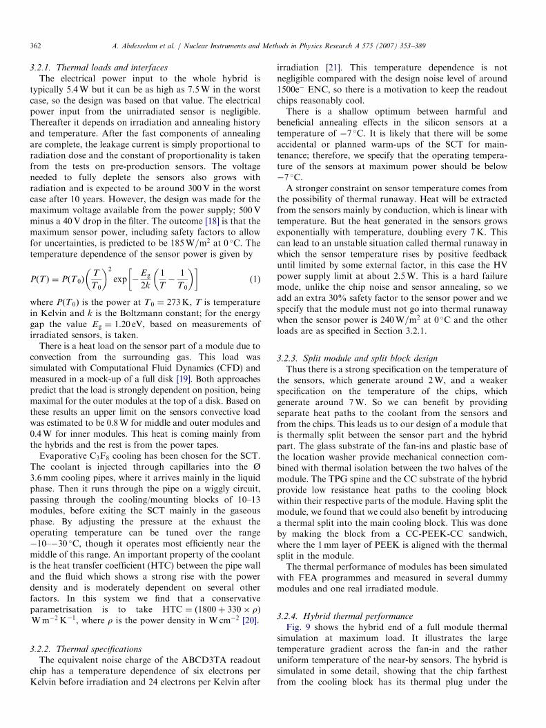
Fig. 9 shows the hybrid end of a full module thermalsimulation at maximum load. It illustrates the largetemperature gradient across the fan-in and the ratheruniform temperature of the near-by sensors. The hybrid issimulated in some detail, showing that the chip farthestfrom the cooling block has its thermal plug under the
ARTICLE IN PRESS
50.0
40.0
30.0
20.0
10.0
0.0
-20.0 -10.0 0.0 10.0 20.0 30.0
X
Y
Hybrid TemperatureZoom (-22,-2,-50,50)
12.011.010.09.008.007.006.005.004.003.002.001.000.00
-1.00-2.00-3.00-4.00-5.00-6.00-7.00-8.00-9.00-10.0-11.0-12.0
Fig. 9. The hybrid end of an outer module simulated at full power and with the coolant at �20 �C. The simulation has a 2-fold symmetry (zero stereo
angle) so only half of the module is shown.
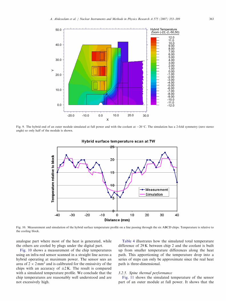
Fig. 10. Measurement and simulation of the hybrid surface temperature profile on a line passing through the six ABCD chips. Temperature is relative to
the cooling block.
A. Abdesselam et al. / Nuclear Instruments and Methods in Physics Research A 575 (2007) 353–389 363
analogue part where most of the heat is generated, whilethe others are cooled by plugs under the digital part.
Fig. 10 shows a measurement of the chip temperaturesusing an infra-red sensor scanned in a straight line across ahybrid operating at maximum power. The sensor sees anarea of 2� 2mm2 and is calibrated for the emissivity of thechips with an accuracy of �2K. The result is comparedwith a simulated temperature profile. We conclude that thechip temperatures are reasonably well understood and arenot excessively high.
Table 4 illustrates how the simulated total temperaturedifference of 29K between chip 2 and the coolant is builtup from smaller temperature differences along the heatpath. This apportioning of the temperature drop into aseries of steps can only be approximate since the real heatpath is three-dimensional.
3.2.5. Spine thermal performance
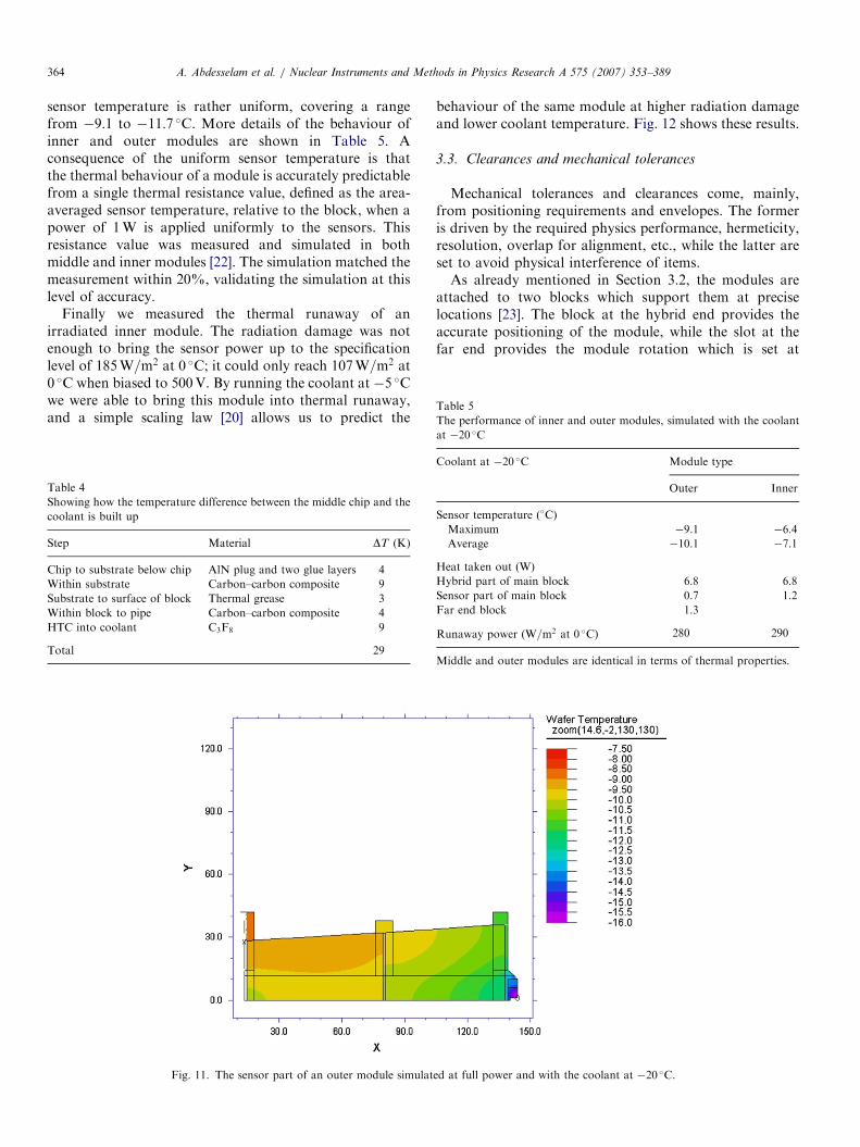
Fig. 11 shows the simulated temperature of the sensorpart of an outer module at full power. It shows that the
ARTICLE IN PRESS
Table 5
The performance of inner and outer modules, simulated with the coolant
A. Abdesselam et al. / Nuclear Instruments and Methods in Physics Research A 575 (2007) 353–389364
sensor temperature is rather uniform, covering a rangefrom �9:1 to �11:7 �C. More details of the behaviour ofinner and outer modules are shown in Table 5. Aconsequence of the uniform sensor temperature is thatthe thermal behaviour of a module is accurately predictablefrom a single thermal resistance value, defined as the area-averaged sensor temperature, relative to the block, when apower of 1W is applied uniformly to the sensors. Thisresistance value was measured and simulated in bothmiddle and inner modules [22]. The simulation matched themeasurement within 20%, validating the simulation at thislevel of accuracy.
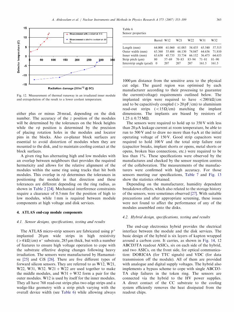
Finally we measured the thermal runaway of anirradiated inner module. The radiation damage was notenough to bring the sensor power up to the specificationlevel of 185W=m2 at 0 �C; it could only reach 107W=m2 at0 �C when biased to 500V. By running the coolant at �5 �Cwe were able to bring this module into thermal runaway,and a simple scaling law [20] allows us to predict the
Table 4
Showing how the temperature difference between the middle chip and the
coolant is built up
Step Material DT (K)
Chip to substrate below chip AlN plug and two glue layers 4
Within substrate Carbon–carbon composite 9
Substrate to surface of block Thermal grease 3
Within block to pipe Carbon–carbon composite 4
HTC into coolant C3F8 9
Total 29
Fig. 11. The sensor part of an outer module simulat
behaviour of the same module at higher radiation damageand lower coolant temperature. Fig. 12 shows these results.
3.3. Clearances and mechanical tolerances
Mechanical tolerances and clearances come, mainly,from positioning requirements and envelopes. The formeris driven by the required physics performance, hermeticity,resolution, overlap for alignment, etc., while the latter areset to avoid physical interference of items.As already mentioned in Section 3.2, the modules are
attached to two blocks which support them at preciselocations [23]. The block at the hybrid end provides theaccurate positioning of the module, while the slot at thefar end provides the module rotation which is set at
ed at full power and with the coolant at �20 �C.
at �20 �C
Coolant at �20 �C Module type
Outer Inner
Sensor temperature ð�CÞ
Maximum �9.1 �6.4
Average �10.1 �7.1
Heat taken out (W)
Hybrid part of main block 6.8 6.8
Sensor part of main block 0.7 1.2
Far end block 1.3
Runaway power ðW=m2 at 0 �C) 280 290
Middle and outer modules are identical in terms of thermal properties.
ARTICLE IN PRESS
Fig. 12. Measurement of thermal runaway in an irradiated inner module
and extrapolation of the result to a lower coolant temperature.
Table 6
Sensor properties
Barrel W12 W21 W22 W31 W32
Length (mm) 64.000 61.060 61.085 54.435 65.540 57.515
Outer width (mm) 63.360 55.488 66.130 74.847 64.636 71.810
Inner width (mm) 63.630 45.735 55.734 66.152 56.475 64.653
Strip pitch ðmmÞ 80 57–69 70–83 83–94 71–81 81–90
Interstrip angle ðmradÞ 0 207 207 207 161.5 161.5
A. Abdesselam et al. / Nuclear Instruments and Methods in Physics Research A 575 (2007) 353–389 365
either plus or minus 20mrad, depending on the disknumber. The accuracy of the z position of the moduleswill be determined by the tolerances on the block heightswhile the rf position is determined by the precisionof placing rotation holes in the modules and locatorpins in the blocks. Also co-planar block surfaces areessential to avoid distortion of modules when they aremounted to the disk, and to maintain cooling contact at theblock surfaces.
A given ring has alternating high and low modules withan overlap between neighbours that provides the requiredhermeticity and allows for the relative alignment of themodules within the same ring using tracks that hit bothmodules. This overlap in rf determines the tolerances inpositioning the module in that direction and thesetolerances are different depending on the ring radius, asshown in Table 2 [24]. Mechanical interference constraintsrequire a clearance of 0.5mm for the position of high tolow modules, while 1mm is required between modulecomponents at high voltage and disk services.
4. ATLAS end-cap module components
4.1. Sensor designs, specifications, testing and results
The ATLAS micro-strip sensors are fabricated using pþ
implanted 20mm wide strips in high resistivityð44 kO=cmÞ n� substrate, 285 mm thick, but with a numberof features to ensure high voltage operation to cope withthe substrate effective doping changes following heavyirradiation. The sensors were manufactured by Hamamat-su [25] and CiS [26]. There are five different types offorward silicon sensors. They are referred to as W12, W21,W22, W31, W32. W21þW22 are used together to makethe middle modules, and W31þW32 form a pair for theouter modules. W12 is used by itself for the inner modules.They all have 768 read-out strips plus two edge strips and awedge-like geometry with a strip pitch varying with theoverall device width (see Table 6) while allowing always
1000mm distance from the sensitive area to the physicalcut edge. The guard region was optimised by eachmanufacturer according to their processing to guaranteethe current(voltage) requirements outlined below. Theimplanted strips were required to have o200 kO=cmand to be capacitively coupled ð420 pF=cmÞ to aluminiumread-out strips ðo15O=cmÞ matching the implantdimensions. The implants are biased by resistors of1:25� 0:75MO.The sensors were required to hold up to 350V with less
than 20mA leakage current at room temperature, be able torun to 500V and to draw no more than 6mA at the initialoperating voltage of 150V. Good strip capacitors wererequired to hold 100V and the total strip failure rate(capacitor breaks, implant shorts or opens, metal shorts oropens, broken bias connections, etc.) were required to beless than 1%. These specifications were observed by themanufactures and checked by the sensor reception centresof the collaboration. The measurements of the manufac-turers were confirmed with high accuracy. For thosesensors meeting our specifications, Table 7 and Fig. 13show the statistics obtained.Depending on the manufacturer, humidity dependent
breakdown effects, which also related to the storage historyof the sensors, were sometimes observed [27]. With suitableprecautions and after appropriate screening, these issueswere not found to affect the performance of any of themodules assembled onto the disks.
4.2. Hybrid design, specifications, testing and results
The end-cap electronics hybrid provides the electricalinterface between the module and the disk services. Thebasic design of the hybrid is six layers of kapton wrappedaround a carbon core. It carries, as shown in Fig. 14, 12ABCD3TA readout ASICs, six on each side of the hybrid,and two ASICs, on the front side, for optical communica-tion: DORIC4A (for TTC signals) and VDC (for datatransmission off the module). All of them are providedwith analogue and digital supply voltages. The hybrid alsoimplements a bypass scheme to cope with single ABCD3-TA chip failures in the token ring. The sensors areconnected via the hybrid to the HV power supplies.A direct contact of the CC substrate to the coolingsystem efficiently removes the heat dissipated from thereadout chips.

ARTICLE IN PRESS
Fig. 13. Leakage current distribution of all the sensors when biased with
(a) 150 and (b) 350V.
Table 7
Statistics of the sensor characteristics, showing average values for the percentage of defective strips per sensor and measured currents at 150 and 350V for
the different manufactures: Hamamatsu and CiS
Number built Defective strip/sensor I ðmAÞ at 150V I ðmAÞ at 350V
CiS Ham. All CiS Ham. All CiS Ham. All CiS Ham. All
W12 776 692 1468 2.3 0.3 1.4 0.751 0.087 0.438 2.532 0.310 1.485
W21 860 757 1617 2.1 0.5 1.3 0.532 0.124 0.339 1.265 0.257 0.790
W22 1114 810 1924 2.2 0.4 1.4 0.689 0.166 0.443 2.176 0.699 1.480
W31 373 2645 3018 3.5 0.5 2.1 0.759 0.286 0.536 1.857 0.817 1.367
W32 363 2596 2959 4.1 0.4 2.3 0.838 0.255 0.563 1.255 0.692 0.990
A. Abdesselam et al. / Nuclear Instruments and Methods in Physics Research A 575 (2007) 353–389366
4.2.1. Design
To achieve the required specifications on electricalstability, mechanical rigidity and thermal performance,the hybrid was laid out as a flexible printed circuit board
folded around and glued onto a unidirectional CCsubstrate with high thermal conductivity. Details on thesubstrate properties are presented in Table 8.In the area where the substrate is mounted onto the
cooling block, the flex circuit is cut out to ensure aclose thermal contact between the cooling system andthe hybrid substrate. To compensate for this cut-outin the analogue ground plane the substrate in thecut-out region is plated with a 22mm copper layer in agalvanic process. This copper layer is soldered to theanalogue ground layer (layer six) at the backside ofthe flex circuit during the lamination of the flex to thesubstrate, effectively forming one continuous analogueground layer.It is vital to avoid any feedback from digital switching
into the analogue part of the ABCD3TA. This requiredvery stable supply voltages and led to a six layers designwith two solid planes for analogue ground and power. Tofurther improve the connection of analogue ground andpower between front- and back-side of the hybrid, there isnot only a connection across the wrap around, but also asolid solder connection between the tabs or fingers at theopposite side of the wrap around. Analogue and digitalpower are decoupled on both sides of each chip andadditionally on the front side as well as on the backside toimprove the electrical stability of the ABCD3TAs at lowthresholds.To improve the heat flow away from the chips, the flex
has small cutouts underneath each chip. These recesses arefilled with ceramic inlays made from aluminium nitride(AlN) with high thermal conductivity (150–180W/mK).The inlays are glued directly onto the CC substrate using acut-to-shape thermally conductive (3.7W/mK) boronnitride filled glue foil. These thermal plugs are staggeredso that the ABCD3TAs furthest from the cooling blockhave their thermal plugs underneath the analogue part ofthe chip, which dissipates more heat than the digitalpart. The other two chips share the same heat path withthermal plugs under the digital part of the chip. Thisensures that the outermost chips have their own heat pipealong the fibres of the substrate, resulting in a more eventemperature of all chips. Simulations of the thermalbehaviour and a comparison to measured data can befound in Section 3.2.4.
ARTICLE IN PRESS
Table 8
Properties of the carbon–carbon substrate
Thermal conductivity in fibre direction 600–650W/mK
Thermal conductivity perpendicular to fibre
direction
20–30W/mK
Density 1.9 g/cm3
Young’s modulus in fibre direction 300GPa
Tensile strength in fibre direction 300MPa
CTE in fibre direction (�1:0–�0:5) ppm/K
CTE perpendicular to fibre direction (10–20) ppm/K
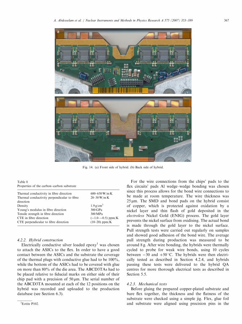
Fig. 14. (a) Front side of hybrid. (b) Back side of hybrid.
A. Abdesselam et al. / Nuclear Instruments and Methods in Physics Research A 575 (2007) 353–389 367
4.2.2. Hybrid construction
Electrically conductive silver loaded epoxy1 was chosento attach the ASICs to the flex. In order to have a goodcontact between the ASICs and the substrate the coverageof the thermal plugs with conductive glue had to be 100%,while the bottom of the ASICs had to be covered with glueon more than 80% of the die area. The ABCD3TAs had tobe placed relative to fiducial marks on either side of theirchip pad with a precision of 50mm. The serial number ofthe ABCD3TA mounted at each of the 12 positions on thehybrid was recorded and uploaded to the productiondatabase (see Section 6.3).
1Eotite P102.
For the wire connections from the chips’ pads to theflex circuits’ pads Al wedge–wedge bonding was chosensince this process allows for the bond wire connections tobe made at room temperature. The wire thickness was25mm. The SMD and bond pads on the hybrid consistof copper, which is protected against oxidation by anickel layer and thin flash of gold deposited in theelectroless Nickel Gold (ENIG) process. The gold layerprevents the nickel surface from oxidising. The actual bondis made through the gold layer to the nickel surface.Pull strength tests were carried out regularly on samplesand showed good adhesion of the bond wire. The averagepull strength during production was measured to bearound 8 g. After wire bonding, the hybrids were thermallycycled to probe for weak wire bonds, using 10 cyclesbetween �30 and þ50 �C. The hybrids were then electri-cally tested as described in Section 4.2.4, and hybridspassing these tests were delivered to the hybrid QAcentres for more thorough electrical tests as described inSection 5.5.
4.2.3. Mechanical tests
Before gluing the prepared copper-plated substrate andbare flex together, the thickness and the flatness of thesubstrate were checked using a simple jig. Flex, glue foiland substrate were aligned using precision pins in the
ARTICLE IN PRESS
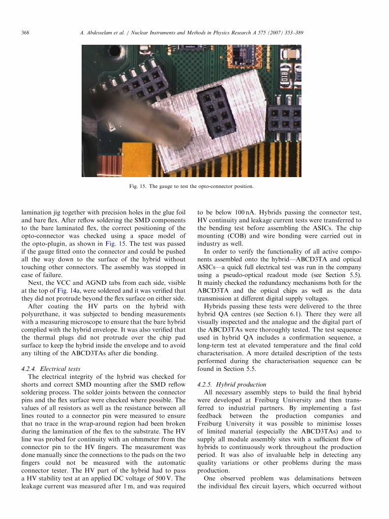
Fig. 15. The gauge to test the opto-connector position.
A. Abdesselam et al. / Nuclear Instruments and Methods in Physics Research A 575 (2007) 353–389368
lamination jig together with precision holes in the glue foiland bare flex. After reflow soldering the SMD componentsto the bare laminated flex, the correct positioning of theopto-connector was checked using a space model ofthe opto-plugin, as shown in Fig. 15. The test was passedif the gauge fitted onto the connector and could be pushedall the way down to the surface of the hybrid withouttouching other connectors. The assembly was stopped incase of failure.
Next, the VCC and AGND tabs from each side, visibleat the top of Fig. 14a, were soldered and it was verified thatthey did not protrude beyond the flex surface on either side.
After coating the HV parts on the hybrid withpolyurethane, it was subjected to bending measurementswith a measuring microscope to ensure that the bare hybridcomplied with the hybrid envelope. It was also verified thatthe thermal plugs did not protrude over the chip padsurface to keep the hybrid inside the envelope and to avoidany tilting of the ABCD3TAs after die bonding.
4.2.4. Electrical tests
The electrical integrity of the hybrid was checked forshorts and correct SMD mounting after the SMD reflowsoldering process. The solder joints between the connectorpins and the flex surface were checked where possible. Thevalues of all resistors as well as the resistance between alllines routed to a connector pin were measured to ensurethat no trace in the wrap-around region had been brokenduring the lamination of the flex to the substrate. The HVline was probed for continuity with an ohmmeter from theconnector pin to the HV fingers. The measurement wasdone manually since the connections to the pads on the twofingers could not be measured with the automaticconnector tester. The HV part of the hybrid had to passa HV stability test at an applied DC voltage of 500V. Theleakage current was measured after 1m, and was required
to be below 100 nA. Hybrids passing the connector test,HV continuity and leakage current tests were transferred tothe bending test before assembling the ASICs. The chipmounting (COB) and wire bonding were carried out inindustry as well.In order to verify the functionality of all active compo-
nents assembled onto the hybrid—ABCD3TA and opticalASICs—a quick full electrical test was run in the companyusing a pseudo-optical readout mode (see Section 5.5).It mainly checked the redundancy mechanisms both for theABCD3TA and the optical chips as well as the datatransmission at different digital supply voltages.Hybrids passing these tests were delivered to the three
hybrid QA centres (see Section 6.1). There they were allvisually inspected and the analogue and the digital part ofthe ABCD3TAs were thoroughly tested. The test sequenceused in hybrid QA includes a confirmation sequence, along-term test at elevated temperature and the final coldcharacterisation. A more detailed description of the testsperformed during the characterisation sequence can befound in Section 5.5.
4.2.5. Hybrid production
All necessary assembly steps to build the final hybridwere developed at Freiburg University and then trans-ferred to industrial partners. By implementing a fastfeedback between the production companies andFreiburg University it was possible to minimise lossesof limited material (especially the ABCD3TAs) and tosupply all module assembly sites with a sufficient flow ofhybrids to continuously work throughout the productionperiod. It was also of invaluable help in detecting anyquality variations or other problems during the massproduction.One observed problem was delaminations between
the individual flex circuit layers, which occurred without
ARTICLE IN PRESS
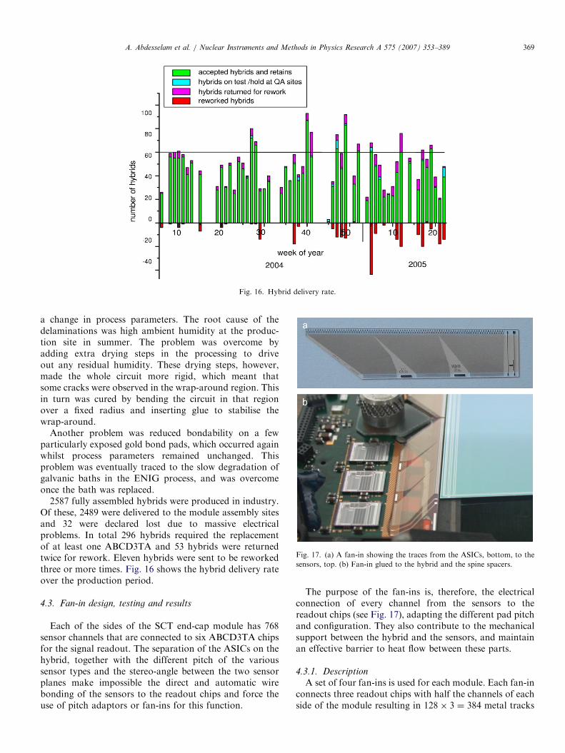
Fig. 16. Hybrid delivery rate.
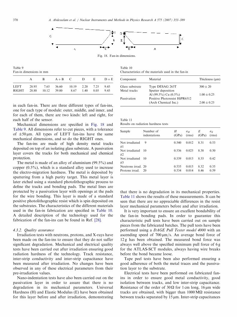
Fig. 17. (a) A fan-in showing the traces from the ASICs, bottom, to the
sensors, top. (b) Fan-in glued to the hybrid and the spine spacers.
A. Abdesselam et al. / Nuclear Instruments and Methods in Physics Research A 575 (2007) 353–389 369
a change in process parameters. The root cause of thedelaminations was high ambient humidity at the produc-tion site in summer. The problem was overcome byadding extra drying steps in the processing to driveout any residual humidity. These drying steps, however,made the whole circuit more rigid, which meant thatsome cracks were observed in the wrap-around region. Thisin turn was cured by bending the circuit in that regionover a fixed radius and inserting glue to stabilise thewrap-around.
Another problem was reduced bondability on a fewparticularly exposed gold bond pads, which occurred againwhilst process parameters remained unchanged. Thisproblem was eventually traced to the slow degradation ofgalvanic baths in the ENIG process, and was overcomeonce the bath was replaced.
2587 fully assembled hybrids were produced in industry.Of these, 2489 were delivered to the module assembly sitesand 32 were declared lost due to massive electricalproblems. In total 296 hybrids required the replacementof at least one ABCD3TA and 53 hybrids were returnedtwice for rework. Eleven hybrids were sent to be reworkedthree or more times. Fig. 16 shows the hybrid delivery rateover the production period.
4.3. Fan-in design, testing and results
Each of the sides of the SCT end-cap module has 768sensor channels that are connected to six ABCD3TA chipsfor the signal readout. The separation of the ASICs on thehybrid, together with the different pitch of the varioussensor types and the stereo-angle between the two sensorplanes make impossible the direct and automatic wirebonding of the sensors to the readout chips and force theuse of pitch adaptors or fan-ins for this function.
The purpose of the fan-ins is, therefore, the electricalconnection of every channel from the sensors to thereadout chips (see Fig. 17), adapting the different pad pitchand configuration. They also contribute to the mechanicalsupport between the hybrid and the sensors, and maintainan effective barrier to heat flow between these parts.
4.3.1. Description
A set of four fan-ins is used for each module. Each fan-inconnects three readout chips with half the channels of eachside of the module resulting in 128� 3 ¼ 384 metal tracks
ARTICLE IN PRESS
Fig. 18. Fan-in dimensions.
Table 9
Fan-in dimensions in mm
A B Aþ B C D E Dþ E
LEFT 28.95 7.65 36.60 10.19 2.20 7.25 9.45
RIGHT 28.88 10.12 39.00 8.67 1.40 8.05 9.45
Table 10
Characteristics of the materials used in the fan-in
Component Material Thickness (mm)
Glass substrate Type DESAG 263T 300� 20
Metal tracks Sputter deposition
Al (99.5%) Cu (0.5%) 1:00� 0:25Passivation Positive Photoresist HiPR6512
(Arch Chemical Inc.) 2:00� 0:25
Table 11
Results on radiation hardness tests
Sample Number of
indentations
H
(GPa)
sH
(rms)
E
(GPa)
sE
(rms)
Not irradiated
#1
9 0.540 0.012 8.31 0.53
Not irradiated
#2
10 0.536 0.025 8.38 0.50
Not irradiated
#3
10 0.539 0.013 8.55 0.42
Neutrons irrad. 20 0.535 0.015 8.32 0.35
Protons irrad. 20 0.534 0.014 8.46 0.59
A. Abdesselam et al. / Nuclear Instruments and Methods in Physics Research A 575 (2007) 353–389370
in each fan-in. There are three different types of fan-ins,one for each type of module: outer, middle, and inner, andfor each of them, there are two kinds: left and right, foreach half of the sensor.
Mechanical dimensions are specified in Fig. 18 andTable 9. All dimensions refer to cut pieces, with a toleranceof �50mm. All types of LEFT fan-ins have the samemechanical dimensions, and so do the RIGHT ones.
The fan-ins are made of high density metal tracksdeposited on top of an isolating glass substrate. A passivationlayer covers the tracks for both mechanical and chemicalprotection.
The metal is made of an alloy of aluminium (99.5%) andcopper (0.5%), which is a standard alloy used to increasethe electro-migration hardness. The metal is deposited bysputtering from a high purity target. This metal layer islater etched using a standard photolithographic process todefine the tracks and bonding pads. The metal lines areprotected by a passivation layer with openings at the padsfor the wire bonding. This layer is made of a standardpositive photolithographic resist which is spin deposited onthe substrates. The characteristics of the different materialsused in the fan-in fabrication are specified in Table 10.A detailed description of the technology used for thefabrication of the fan-ins can be found in Ref. [28].
4.3.2. Quality assurance
Irradiation tests with neutrons, protons, and X-rays havebeen made on the fan-ins to ensure that they do not suffersignificant degradation. Mechanical and electrical qualitytests have been carried out after irradiation ensuring goodradiation hardness of the technology. Track resistance,inter-strip conductivity and inter-strip capacitance havebeen measured after irradiation. No changes have beenobserved in any of these electrical parameters from theirpre-irradiation values.
Nano-indentation tests have also been carried out on thepassivation layer in order to assure that there is nodegradation in its mechanical parameters. UniversalHardness (H) and Elastic Modulus (E) have been obtainedfor this layer before and after irradiation, demonstrating
that there is no degradation in its mechanical properties.Table 11 shows the results of these measurements. It can beseen that there are no appreciable differences in the resistlayer mechanical parameters before and after irradiation.It is very important to ensure an excellent bondability of
the fan-in bonding pads. In order to guarantee thischaracteristic pull tests have been carried out on samplepieces from the fabricated batches. The pull tests have beenperformed using a DAGE Pull Tester model 4000 with anascending speed of 700 mm=s. An average bond force of12 g has been obtained. The measured bond force wasalways well above the specified minimum pull force of 6 gfor the ATLAS-SCT modules, always having wire breaksbefore the bond became loose.Tape peel tests have been also performed ensuring a
good adherence of both the metal traces and the passiva-tion layer to the substrate.Electrical tests have been performed on fabricated fan-
ins in order to ensure good metal conductivity, goodisolation between tracks, and low inter-strip capacitance.Resistance of the order of 30O for 1 cm long, 16mm widetracks are obtained, with bigger than 1000MO resistancebetween tracks separated by 15 mm. Inter-strip capacitances

ARTICLE IN PRESSA. Abdesselam et al. / Nuclear Instruments and Methods in Physics Research A 575 (2007) 353–389 371
are of the order of 0.8 pF for those geometries and areconstant for a wide frequency range. Metal sheet resistancehas been also routinely measured through specificallydesigned test structures obtaining values of 0:04O=sq.
All fan-ins were tested for defects before being supplied.A thorough visual inspection was performed in order toassure continuity in the lines and absence of short-circuits.The fan-ins supplied to the assembly centres had nomore than one shorted pair of neighbour strips or onebroken strip.
4.3.3. Production
The production of the fan-ins was carried out, after aselection process, in the Centro Nacional de Microelec-tronica (CNM-CSIC), Barcelona, Spain. The fabricationstarted early in September 2002 in order to assurethe availability of components for the assembly sitesqualification, and to allow a thorough evaluation by thecollaboration.
Fig. 19 shows the production progress during the wholeperiod including shipments and accumulated stock. Theproduction extended over 32 months, 1639 glasses wereprocessed resulting in 2642 fan-in sets shipped to themodule production sites, together with more than 600dummy fan-in sets.
The final average yield was 70% during the productionselection, and a further 3% of the fan-ins were rejected bythe assembly sites. An average production rate of 103 sets/month was achieved, reaching a rate of 120 sets/month inthe last period.
Fig. 20. Photograph of an end-cap module spine.
4.4. Spines design, testing and results
The silicon sensors are glued back to back onto asupport structure built from thermalised pyrolytic graphite(TPG) [29–31], with aluminium nitride (AlN), and alumi-nium oxide ðAl2O3Þ, ceramic parts required for mechanical
Fig. 19. Fan-in d
considerations. This structure is known as a spine and isshown in Fig. 20. To minimise the overall material within amodule the spine must have the lowest possible mass, itmust be mechanically rigid, and provide the interface forthe module cooling contacts. The TPG backbone of thespine transports the heat from the sensors, which produceup to 2W after the expected radiation dose from 10 yearsof ATLAS operation, to the module mounting/coolingblocks at each end which are held at around �15 �C. Thethermal performance of the TPG is vital to keep the sensorscold for the lifetime of the experiment. The thermalperformance of the spine has been simulated using finiteelement calculations [18] and compared with experimentaldata [22].To achieve precise tracking in the SCT the position and
orientation of the individual sensors relative to the modulemounting point have to be known with high accuracy andwithin a tight envelope, described in Section 3. The size andshape of the module in the perpendicular direction to thesensor plane is strongly dependent on the size and shape ofthe spine, most notably on any bow in the TPG, therefore
elivery rate.
ARTICLE IN PRESSA. Abdesselam et al. / Nuclear Instruments and Methods in Physics Research A 575 (2007) 353–389372
the TPG must be kept within a tight mechanical toleranceduring production.
4.4.1. Spine design
The design of the spine is detailed in Ref. [32]. The basicstructure is the 500� 25mm thick TPG heat spreader withthe AlN ceramic supports. The TPG functions as thethermal path between the sensors and cooling contact ateach end. In order to achieve electrical insulation andmechanical protection the TPG is coated with a 10mmlayer of Parylene-C. Parylene-C was chosen because it hasa low tendency to penetrate into the TPG layers duringdeposition. Such an effect was observed with Parylene-Nwhich leads to an increase of the TPG thickness at the cutedges. Since TPG is fragile and tends to delaminate thestructure of the spine has to be reinforced using AlNceramic sections. AlN has a rather high thermal con-ductivity, of 180W/mK at 20 �C, and a similar thermalexpansion coefficient to silicon, thus reducing mechanicalstress during any temperature changes. AlN plates ofthickness 225� 25mm cover the TPG at the coolingcontacts to ensure good thermal contact to the coolingpoints while protecting the soft TPG from mechanicaldamage. To maintain a spine of constant thickness theTPG is profiled at each end where the ceramic sections areglued; the glue is used to correct for any thicknessvariation. The hybrid end ceramic has a v-groove to enablemechanical assembly of the final module. The far-endcooling point has an oval slot to enable the sliding joint.The wings supporting the sensors and providing mechan-ical stiffness to the sensor-spine assembly have a thicknessof 500� 25mm. The AlN pieces at the hybrid end and thecentral wings contain metal traces to distribute the sensorbias voltage. The bias is supplied from the hybrid to oneside of the spine and therefore one of the AlN wings has ametallised through hole to electrically connect both sides ofthe spine.
Attached to the AlN wing at the hybrid end there is anAl2O3 spacer required to match the thickness of the spineto the hybrid for assembly. Al2O3 was chosen as it has alow thermal conductivity so as to maintain the thermalbreak between the hybrid and the sensors. Attached to thefar-end cooling point is a precision washer, constructedfrom FR4 and 0.5mm of aluminium, which defines the
Table 12
Properties of materials used in the spine
Property TPG
In plane thermal conductivity at 20 �C (W/mK) 1550�
Out of plane thermal conductivity at 20 �C (W/mK) 8:9� 0
Density ðg=cm3Þ 2:15�
Transverse pull strength ðN=cm2Þ 56:5�
Plane electrical conductivity ðO�1 cm�1Þ 1:63�
Thermal expansion coefficient at 20 �C ð�C�1Þ �1:17
Thermal expansion coefficient at 20 �C ð�C�1Þ 26:8�
precise oval slot. The distance between the v-groove andthe centre of the far-end washer’s slot defines the spinelength and ultimately the length of the module. The spinehas been designed for ease of construction as well as tosupply the required high thermal functionality.
4.4.2. Materials used in the spine
The TPG used in the spine is an anisotropic materialhaving both mechanical and thermal properties that, due tothe planar mosaic ordering of the carbon structures, arebasically constant within the plane of a substrate sheetand are significantly different in the orthogonal direction.Table 12 summarises the properties of the TPG, AlN andAl2O3 used in the construction of the spine. The ceramicdata are from CERAMTEC [33], unless noted otherwise.The TPG was glued to the thin AlN sheets at the cooling
block connections with ELASTOSIL 137-182 which waschosen as it has a thermal conductivity measured to be1:79� 0:1W=mK. Also, pull strengths exhibit no dete-rioration after an irradiation up to a fluence 2:7� 1015
24GeV=cprotons=cm2.
4.4.3. Construction process
The TPG for the spine was produced at NIIGraphite[34]. The TPG was delivered roughly cut into plates of145� 25� 0:7mm3 for outer and middle modules and80� 25� 0:7mm3 for inner modules. These plates weremechanically lapped and polished into the requiredthickness at NIITAP [35]. The TPG was cut to shape withlaser ablation, the end profiles of the TPG were thenfabricated via further grinding and polishing. The TPG washeated to 200 �C for 30min and kept for 45min undervacuum to avoid later out-gassing. Finally the TPG wascoated with a 10mm layer of Parylene-C. The bias contacthole in the Parylene-C was made using plasma etching.During the processing of the TPG, rolling was used tocorrect any mechanical deformation. The AlN ceramicparts were laser cut and profiled at NIITAP. ConductiveAl layers, which build up at the cut edge duringcutting, were removed using NaOH. Afterwards the pieceswere cleaned with distilled water. The metal traces werefabricated using vacuum evaporation of Ti–Cu–Ni. Thetotal thickness of the three layers is 2mm. The electricalresistivity was measured and kept lower than 20O between
AlN Al2O3
130 180 20
:4 n/a n/a
0:2 3.3 3.75
14:2
104 10�3–10�5
� 0:15� 10�6 3:1� 10�6 6:7� 10�6
0:4� 10�6 n/a n/a
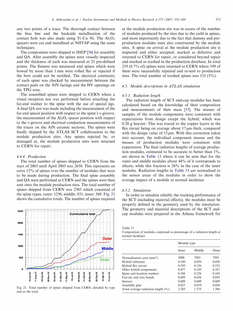
ARTICLE IN PRESSA. Abdesselam et al. / Nuclear Instruments and Methods in Physics Research A 575 (2007) 353–389 373
any two points of a trace. The thorough contact betweenthe bias line and the backside metallisation of thecontact hole was also made using Ti–Cu–Ni. The Al2O3
spacers were cut and metallised at NIITAP using the sametechniques.
The components were shipped to IHEP [36] for assemblyand QA. After assembly the spines were visually inspectedand the thickness of each was measured at 25 pre-definedpoints. The flatness was measured and spines which werebowed by more than 1mm were rolled flat or rejected ifthe bow could not be rectified. The electrical continuityof each spine was checked by measurement between thecontact pads on the AlN facings and the HV openings onthe TPG area.
The assembled spines were shipped to CERN where avisual reception test was performed before attaching thefar-end washer to the spine with the use of special jigs.A final QA test was made including the measurement of thefar-end spacer position with respect to the spine’s v-groove,the measurement of the Al2O3 spacer position with respectto the v-groove and electrical conduction measurements ofthe traces on the AlN ceramic sections. The spines werefinally shipped by the ATLAS SCT collaboration to themodule production sites. Any spines rejected by, ordamaged at, the module production sites were returnedto CERN for repair.
4.4.4. Production
The total number of spines shipped to CERN from thestart of 2003 until April 2005 was 2650. This represents anextra 12% of spines over the number of modules that wereto be made during production. The final spine assemblyand QA were performed at CERN and the spines were thensent onto the module production sites. The total number ofspines shipped from CERN was 2505 which consisted ofthe spine types; outer: 1250, middle: 831, inner: 569. Fig. 21shows the cumulative totals. The number of spines required
Fig. 21. Total number of spines shipped from CERN, detailed by type
and as the total.
at the module production site was in excess of the numberof modules produced by the sites due to the yield in spines,and more importantly due to the fact that dummy and pre-production modules were also constructed by the modulesites. A spine on arrival at the module production site isinspected and either accepted, marked as defective andreturned to CERN for repair, or considered beyond repairand marked as trashed in the production database. In total219 (8.7% of) spines were returned to CERN where 199 ofthem were successfully repaired and re-sent to productionsites. The total number of trashed spines was 135 (5%).
4.5. Module descriptions in ATLAS simulation
4.5.1. Radiation length
The radiation length of SCT end-cap modules has beencalculated based on the knowledge of their compositionand measurements of their mass [37]. The masses ofsamples of the module components were consistent withexpectations from design except the hybrid, which was0.28 g heavier. This was traced to the copper layers in theflex circuit being on average about 17mm thick, comparedwith the design value of 15mm. With this correction takeninto account, the individual component masses and themasses of production modules were consistent withexpectation. The final radiation lengths of average produc-tion modules, estimated to be accurate to better than 1%,are shown in Table 13 where it can be seen that for theouter and middle modules about 44% of it corresponds tosilicon, while this fraction is 26% in the case of the innermodules. Radiation lengths in Table 13 are normalised tothe sensor areas of the modules in order to show theaverage impact of a module at normal incidence.
4.5.2. Simulation
In order to simulate reliably the tracking performance ofthe SCT (including material effects), the modules must beproperly defined in the geometry used by the simulation.The geometry and material descriptions of the SCT end-cap modules were prepared in the Athena framework for
Table 13
Composition of modules, expressed as percentage of a radiation length at
normal incidence
Module type
Inner Middle Outer
Normalisation area ðmm2Þ 3090 7803 7893
Hybrid substrate 0.149 0.059 0.058
Hybrid flex circuit 0.595 0.236 0.233
Other hybrid components 0.477 0.189 0.187
Spine and location washers 0.388 0.226 0.243
Fan-ins and wire bonds 0.099 0.038 0.039
Sensors 0.609 0.609 0.609
Assembly glue 0.027 0.019 0.020
Total average radiation length (%) 2.345 1.375 1.388
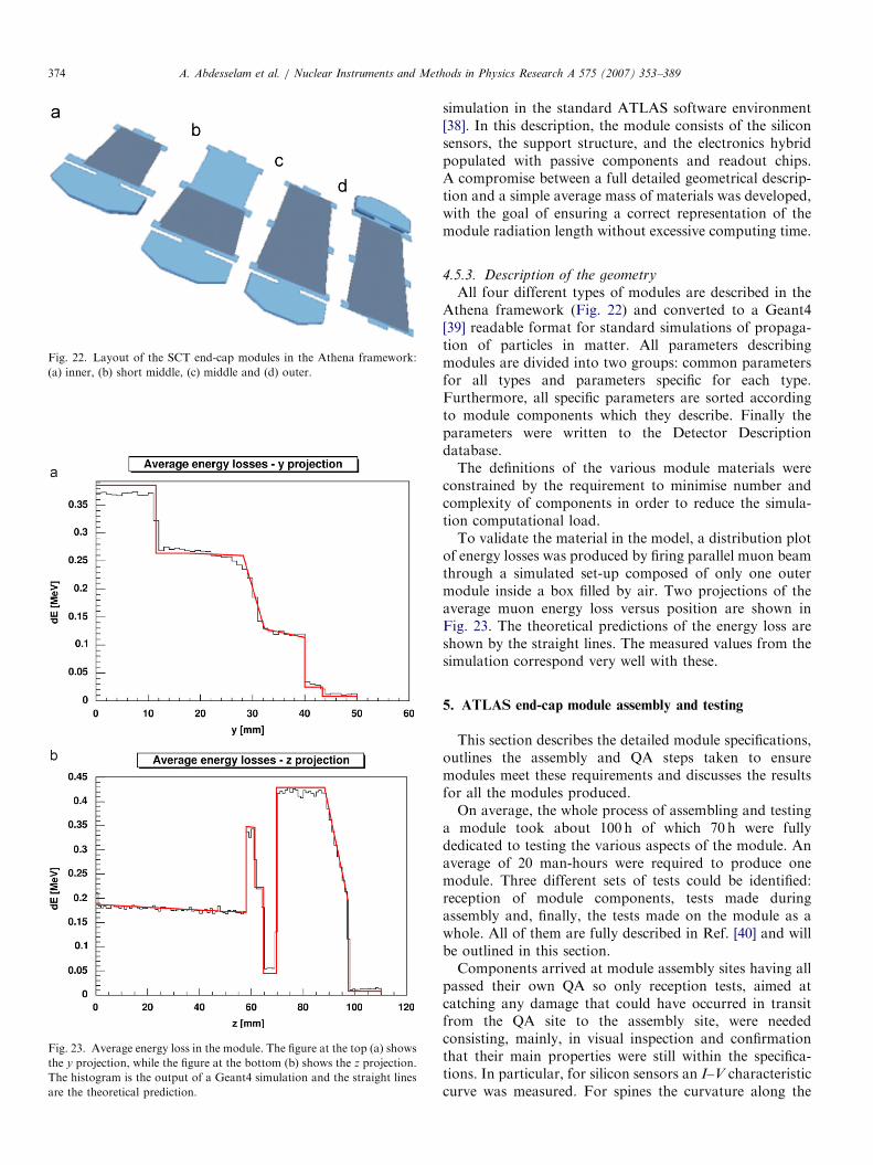
ARTICLE IN PRESS
Fig. 23. Average energy loss in the module. The figure at the top (a) shows
the y projection, while the figure at the bottom (b) shows the z projection.
The histogram is the output of a Geant4 simulation and the straight lines
are the theoretical prediction.
Fig. 22. Layout of the SCT end-cap modules in the Athena framework:
(a) inner, (b) short middle, (c) middle and (d) outer.
A. Abdesselam et al. / Nuclear Instruments and Methods in Physics Research A 575 (2007) 353–389374
simulation in the standard ATLAS software environment[38]. In this description, the module consists of the siliconsensors, the support structure, and the electronics hybridpopulated with passive components and readout chips.A compromise between a full detailed geometrical descrip-tion and a simple average mass of materials was developed,with the goal of ensuring a correct representation of themodule radiation length without excessive computing time.
4.5.3. Description of the geometry
All four different types of modules are described in theAthena framework (Fig. 22) and converted to a Geant4[39] readable format for standard simulations of propaga-tion of particles in matter. All parameters describingmodules are divided into two groups: common parametersfor all types and parameters specific for each type.Furthermore, all specific parameters are sorted accordingto module components which they describe. Finally theparameters were written to the Detector Descriptiondatabase.The definitions of the various module materials were
constrained by the requirement to minimise number andcomplexity of components in order to reduce the simula-tion computational load.To validate the material in the model, a distribution plot
of energy losses was produced by firing parallel muon beamthrough a simulated set-up composed of only one outermodule inside a box filled by air. Two projections of theaverage muon energy loss versus position are shown inFig. 23. The theoretical predictions of the energy loss areshown by the straight lines. The measured values from thesimulation correspond very well with these.
5. ATLAS end-cap module assembly and testing
This section describes the detailed module specifications,outlines the assembly and QA steps taken to ensuremodules meet these requirements and discusses the resultsfor all the modules produced.On average, the whole process of assembling and testing
a module took about 100 h of which 70 h were fullydedicated to testing the various aspects of the module. Anaverage of 20 man-hours were required to produce onemodule. Three different sets of tests could be identified:reception of module components, tests made duringassembly and, finally, the tests made on the module as awhole. All of them are fully described in Ref. [40] and willbe outlined in this section.Components arrived at module assembly sites having all
passed their own QA so only reception tests, aimed atcatching any damage that could have occurred in transitfrom the QA site to the assembly site, were neededconsisting, mainly, in visual inspection and confirmationthat their main properties were still within the specifica-tions. In particular, for silicon sensors an I–V characteristiccurve was measured. For spines the curvature along the
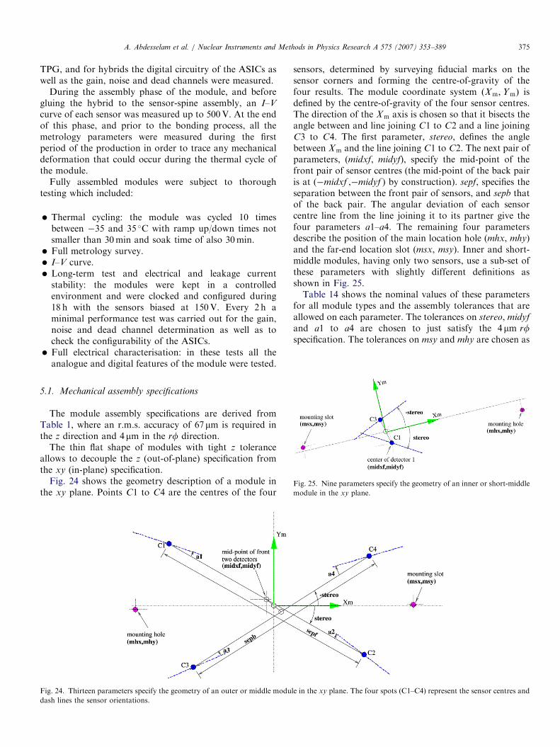
ARTICLE IN PRESSA. Abdesselam et al. / Nuclear Instruments and Methods in Physics Research A 575 (2007) 353–389 375
TPG, and for hybrids the digital circuitry of the ASICs aswell as the gain, noise and dead channels were measured.
During the assembly phase of the module, and beforegluing the hybrid to the sensor-spine assembly, an I–V
curve of each sensor was measured up to 500V. At the endof this phase, and prior to the bonding process, all themetrology parameters were measured during the firstperiod of the production in order to trace any mechanicaldeformation that could occur during the thermal cycle ofthe module.
Fully assembled modules were subject to thoroughtesting which included:
�
Fig
das
Thermal cycling: the module was cycled 10 timesbetween �35 and 35 �C with ramp up/down times notsmaller than 30min and soak time of also 30min.
� Full metrology survey. � I–V curve. � Long-term test and electrical and leakage currentstability: the modules were kept in a controlledenvironment and were clocked and configured during18 h with the sensors biased at 150V. Every 2 h aminimal performance test was carried out for the gain,noise and dead channel determination as well as tocheck the configurability of the ASICs.
�Fig. 25. Nine parameters specify the geometry of an inner or short-middle
module in the xy plane.
Full electrical characterisation: in these tests all theanalogue and digital features of the module were tested.
5.1. Mechanical assembly specifications
The module assembly specifications are derived fromTable 1, where an r.m.s. accuracy of 67mm is required inthe z direction and 4mm in the rf direction.
The thin flat shape of modules with tight z toleranceallows to decouple the z (out-of-plane) specification fromthe xy (in-plane) specification.
Fig. 24 shows the geometry description of a module inthe xy plane. Points C1 to C4 are the centres of the four
. 24. Thirteen parameters specify the geometry of an outer or middle modu
h lines the sensor orientations.
sensors, determined by surveying fiducial marks on thesensor corners and forming the centre-of-gravity of thefour results. The module coordinate system ðXm;YmÞ isdefined by the centre-of-gravity of the four sensor centres.The direction of the Xm axis is chosen so that it bisects theangle between and line joining C1 to C2 and a line joiningC3 to C4. The first parameter, stereo, defines the anglebetween Xm and the line joining C1 to C2. The next pair ofparameters, (midxf, midyf), specify the mid-point of thefront pair of sensor centres (the mid-point of the back pairis at (�midxf ,�midyf ) by construction). sepf, specifies theseparation between the front pair of sensors, and sepb thatof the back pair. The angular deviation of each sensorcentre line from the line joining it to its partner give thefour parameters a1–a4. The remaining four parametersdescribe the position of the main location hole (mhx, mhy)and the far-end location slot (msx, msy). Inner and short-middle modules, having only two sensors, use a sub-set ofthese parameters with slightly different definitions asshown in Fig. 25.Table 14 shows the nominal values of these parameters
for all module types and the assembly tolerances that areallowed on each parameter. The tolerances on stereo, midyf
and a1 to a4 are chosen to just satisfy the 4mm rfspecification. The tolerances on msy and mhy are chosen as
le in the xy plane. The four spots (C1–C4) represent the sensor centres and
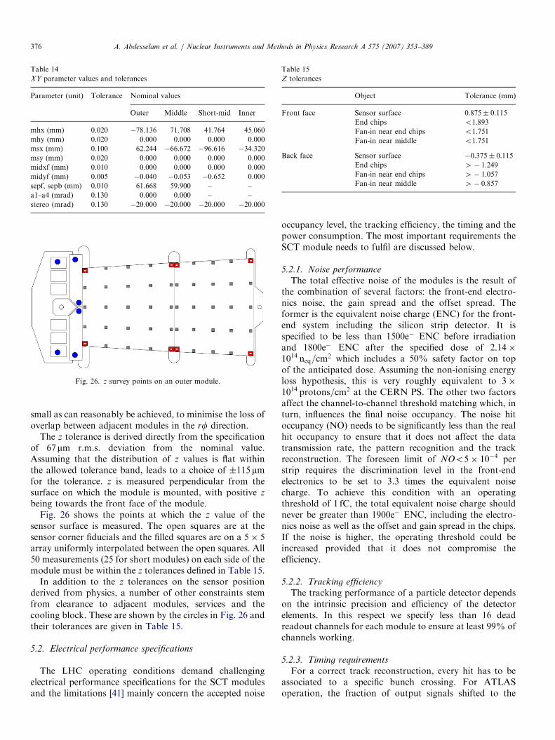
ARTICLE IN PRESS
Fig. 26. z survey points on an outer module.
Table 15
Z tolerances
Object Tolerance (mm)
Front face Sensor surface 0:875� 0:115End chips o1:893Fan-in near end chips o1:751Fan-in near middle o1:751
Back face Sensor surface �0:375� 0:115End chips 4� 1:249Fan-in near end chips 4� 1:057Fan-in near middle 4� 0:857
Table 14
XY parameter values and tolerances
Parameter (unit) Tolerance Nominal values
Outer Middle Short-mid Inner
mhx (mm) 0.020 �78.136 71.708 41.764 45.060
mhy (mm) 0.020 0.000 0.000 0.000 0.000
msx (mm) 0.100 62.244 �66.672 �96.616 �34.320
msy (mm) 0.020 0.000 0.000 0.000 0.000
midxf (mm) 0.010 0.000 0.000 0.000 0.000
midyf (mm) 0.005 �0.040 �0.053 �0.652 0.000
sepf, sepb (mm) 0.010 61.668 59.900 – –
a1–a4 (mrad) 0.130 0.000 0.000 – –
stereo (mrad) 0.130 �20.000 �20.000 �20.000 �20.000
A. Abdesselam et al. / Nuclear Instruments and Methods in Physics Research A 575 (2007) 353–389376
small as can reasonably be achieved, to minimise the loss ofoverlap between adjacent modules in the rf direction.
The z tolerance is derived directly from the specificationof 67mm r.m.s. deviation from the nominal value.Assuming that the distribution of z values is flat withinthe allowed tolerance band, leads to a choice of �115mmfor the tolerance. z is measured perpendicular from thesurface on which the module is mounted, with positive z
being towards the front face of the module.Fig. 26 shows the points at which the z value of the
sensor surface is measured. The open squares are at thesensor corner fiducials and the filled squares are on a 5� 5array uniformly interpolated between the open squares. All50 measurements (25 for short modules) on each side of themodule must be within the z tolerances defined in Table 15.
In addition to the z tolerances on the sensor positionderived from physics, a number of other constraints stemfrom clearance to adjacent modules, services and thecooling block. These are shown by the circles in Fig. 26 andtheir tolerances are given in Table 15.
5.2. Electrical performance specifications
The LHC operating conditions demand challengingelectrical performance specifications for the SCT modulesand the limitations [41] mainly concern the accepted noise
occupancy level, the tracking efficiency, the timing and thepower consumption. The most important requirements theSCT module needs to fulfil are discussed below.
5.2.1. Noise performance
The total effective noise of the modules is the result ofthe combination of several factors: the front-end electro-nics noise, the gain spread and the offset spread. Theformer is the equivalent noise charge (ENC) for the front-end system including the silicon strip detector. It isspecified to be less than 1500e� ENC before irradiationand 1800e� ENC after the specified dose of 2:14�1014 neq=cm2 which includes a 50% safety factor on topof the anticipated dose. Assuming the non-ionising energyloss hypothesis, this is very roughly equivalent to 3�1014 protons=cm2 at the CERN PS. The other two factorsaffect the channel-to-channel threshold matching which, inturn, influences the final noise occupancy. The noise hitoccupancy (NO) needs to be significantly less than the realhit occupancy to ensure that it does not affect the datatransmission rate, the pattern recognition and the trackreconstruction. The foreseen limit of NOo5� 10�4 perstrip requires the discrimination level in the front-endelectronics to be set to 3.3 times the equivalent noisecharge. To achieve this condition with an operatingthreshold of 1 fC, the total equivalent noise charge shouldnever be greater than 1900e� ENC, including the electro-nics noise as well as the offset and gain spread in the chips.If the noise is higher, the operating threshold could beincreased provided that it does not compromise theefficiency.
5.2.2. Tracking efficiency
The tracking performance of a particle detector dependson the intrinsic precision and efficiency of the detectorelements. In this respect we specify less than 16 deadreadout channels for each module to ensure at least 99% ofchannels working.
5.2.3. Timing requirements
For a correct track reconstruction, every hit has to beassociated to a specific bunch crossing. For ATLASoperation, the fraction of output signals shifted to the
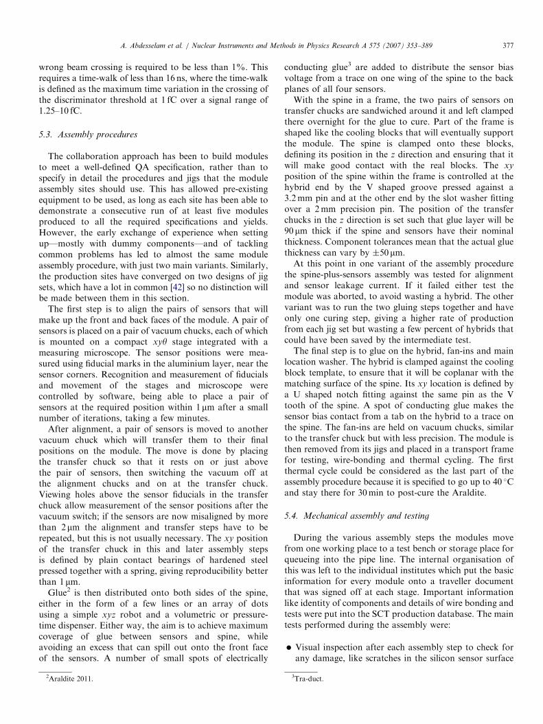
ARTICLE IN PRESSA. Abdesselam et al. / Nuclear Instruments and Methods in Physics Research A 575 (2007) 353–389 377
wrong beam crossing is required to be less than 1%. Thisrequires a time-walk of less than 16 ns, where the time-walkis defined as the maximum time variation in the crossing ofthe discriminator threshold at 1 fC over a signal range of1.25–10 fC.
5.3. Assembly procedures
The collaboration approach has been to build modulesto meet a well-defined QA specification, rather than tospecify in detail the procedures and jigs that the moduleassembly sites should use. This has allowed pre-existingequipment to be used, as long as each site has been able todemonstrate a consecutive run of at least five modulesproduced to all the required specifications and yields.However, the early exchange of experience when settingup—mostly with dummy components—and of tacklingcommon problems has led to almost the same moduleassembly procedure, with just two main variants. Similarly,the production sites have converged on two designs of jigsets, which have a lot in common [42] so no distinction willbe made between them in this section.
The first step is to align the pairs of sensors that willmake up the front and back faces of the module. A pair ofsensors is placed on a pair of vacuum chucks, each of whichis mounted on a compact xyy stage integrated with ameasuring microscope. The sensor positions were mea-sured using fiducial marks in the aluminium layer, near thesensor corners. Recognition and measurement of fiducialsand movement of the stages and microscope werecontrolled by software, being able to place a pair ofsensors at the required position within 1mm after a smallnumber of iterations, taking a few minutes.
After alignment, a pair of sensors is moved to anothervacuum chuck which will transfer them to their finalpositions on the module. The move is done by placingthe transfer chuck so that it rests on or just abovethe pair of sensors, then switching the vacuum off atthe alignment chucks and on at the transfer chuck.Viewing holes above the sensor fiducials in the transferchuck allow measurement of the sensor positions after thevacuum switch; if the sensors are now misaligned by morethan 2mm the alignment and transfer steps have to berepeated, but this is not usually necessary. The xy positionof the transfer chuck in this and later assembly stepsis defined by plain contact bearings of hardened steelpressed together with a spring, giving reproducibility betterthan 1mm.
Glue2 is then distributed onto both sides of the spine,either in the form of a few lines or an array of dotsusing a simple xyz robot and a volumetric or pressure-time dispenser. Either way, the aim is to achieve maximumcoverage of glue between sensors and spine, whileavoiding an excess that can spill out onto the front faceof the sensors. A number of small spots of electrically
2Araldite 2011.
conducting glue3 are added to distribute the sensor biasvoltage from a trace on one wing of the spine to the backplanes of all four sensors.With the spine in a frame, the two pairs of sensors on
transfer chucks are sandwiched around it and left clampedthere overnight for the glue to cure. Part of the frame isshaped like the cooling blocks that will eventually supportthe module. The spine is clamped onto these blocks,defining its position in the z direction and ensuring that itwill make good contact with the real blocks. The xy
position of the spine within the frame is controlled at thehybrid end by the V shaped groove pressed against a3.2mm pin and at the other end by the slot washer fittingover a 2mm precision pin. The position of the transferchucks in the z direction is set such that glue layer will be90mm thick if the spine and sensors have their nominalthickness. Component tolerances mean that the actual gluethickness can vary by �50mm.At this point in one variant of the assembly procedure
the spine-plus-sensors assembly was tested for alignmentand sensor leakage current. If it failed either test themodule was aborted, to avoid wasting a hybrid. The othervariant was to run the two gluing steps together and haveonly one curing step, giving a higher rate of productionfrom each jig set but wasting a few percent of hybrids thatcould have been saved by the intermediate test.The final step is to glue on the hybrid, fan-ins and main
location washer. The hybrid is clamped against the coolingblock template, to ensure that it will be coplanar with thematching surface of the spine. Its xy location is defined bya U shaped notch fitting against the same pin as the Vtooth of the spine. A spot of conducting glue makes thesensor bias contact from a tab on the hybrid to a trace onthe spine. The fan-ins are held on vacuum chucks, similarto the transfer chuck but with less precision. The module isthen removed from its jigs and placed in a transport framefor testing, wire-bonding and thermal cycling. The firstthermal cycle could be considered as the last part of theassembly procedure because it is specified to go up to 40 �Cand stay there for 30min to post-cure the Araldite.
5.4. Mechanical assembly and testing
During the various assembly steps the modules movefrom one working place to a test bench or storage place forqueueing into the pipe line. The internal organisation ofthis was left to the individual institutes which put the basicinformation for every module onto a traveller documentthat was signed off at each stage. Important informationlike identity of components and details of wire bonding andtests were put into the SCT production database. The maintests performed during the assembly were:
�
3
Visual inspection after each assembly step to check forany damage, like scratches in the silicon sensor surface
Tra-duct.
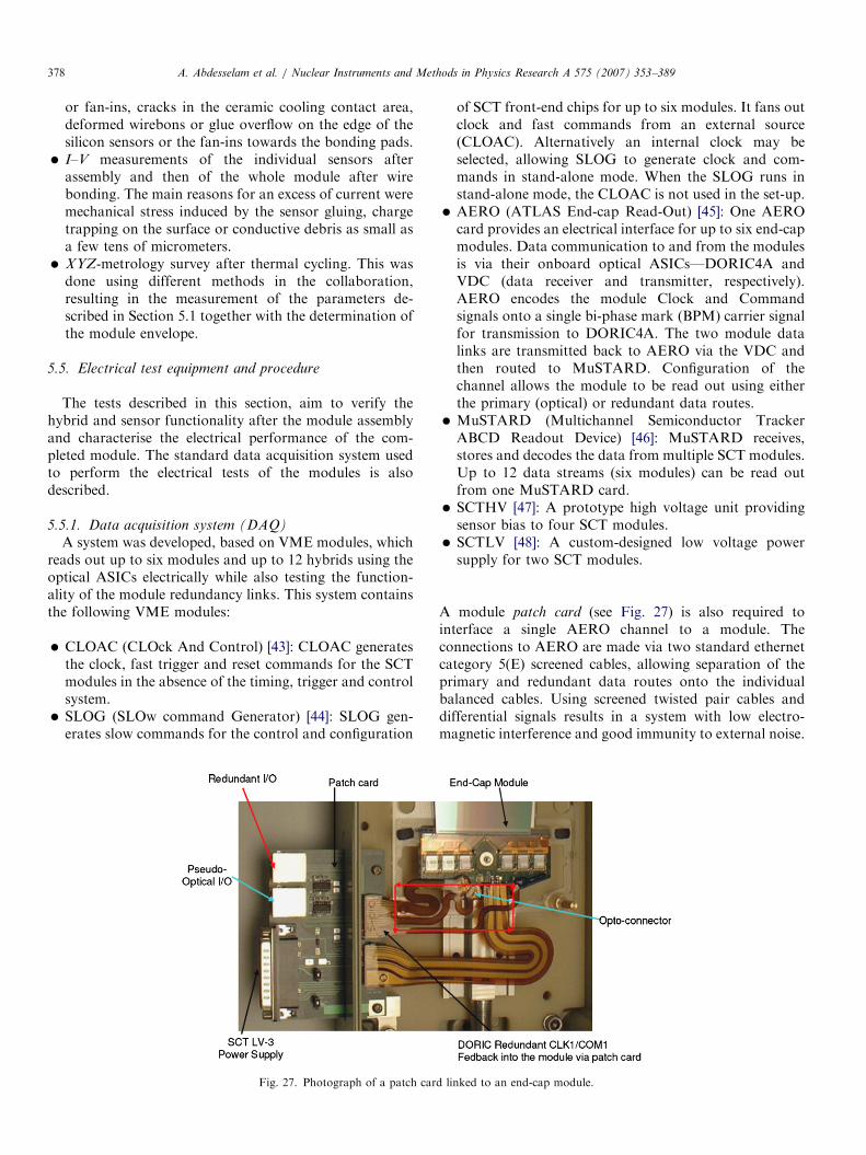
ARTICLE IN PRESSA. Abdesselam et al. / Nuclear Instruments and Methods in Physics Research A 575 (2007) 353–389378
or fan-ins, cracks in the ceramic cooling contact area,deformed wirebons or glue overflow on the edge of thesilicon sensors or the fan-ins towards the bonding pads.
� I–V measurements of the individual sensors afterassembly and then of the whole module after wirebonding. The main reasons for an excess of current weremechanical stress induced by the sensor gluing, chargetrapping on the surface or conductive debris as small asa few tens of micrometers.
� XYZ-metrology survey after thermal cycling. This wasdone using different methods in the collaboration,resulting in the measurement of the parameters de-scribed in Section 5.1 together with the determination ofthe module envelope.
5.5. Electrical test equipment and procedure
The tests described in this section, aim to verify thehybrid and sensor functionality after the module assemblyand characterise the electrical performance of the com-pleted module. The standard data acquisition system usedto perform the electrical tests of the modules is alsodescribed.
5.5.1. Data acquisition system (DAQ)
A system was developed, based on VME modules, whichreads out up to six modules and up to 12 hybrids using theoptical ASICs electrically while also testing the function-ality of the module redundancy links. This system containsthe following VME modules:
�
CLOAC (CLOck And Control) [43]: CLOAC generatesthe clock, fast trigger and reset commands for the SCTmodules in the absence of the timing, trigger and controlsystem. � SLOG (SLOw command Generator) [44]: SLOG gen-erates slow commands for the control and configuration
Fig. 27. Photograph of a patch card lin
of SCT front-end chips for up to six modules. It fans outclock and fast commands from an external source(CLOAC). Alternatively an internal clock may beselected, allowing SLOG to generate clock and com-mands in stand-alone mode. When the SLOG runs instand-alone mode, the CLOAC is not used in the set-up.
� AERO (ATLAS End-cap Read-Out) [45]: One AEROcard provides an electrical interface for up to six end-capmodules. Data communication to and from the modulesis via their onboard optical ASICs—DORIC4A andVDC (data receiver and transmitter, respectively).AERO encodes the module Clock and Commandsignals onto a single bi-phase mark (BPM) carrier signalfor transmission to DORIC4A. The two module datalinks are transmitted back to AERO via the VDC andthen routed to MuSTARD. Configuration of thechannel allows the module to be read out using eitherthe primary (optical) or redundant data routes.
� MuSTARD (Multichannel Semiconductor TrackerABCD Readout Device) [46]: MuSTARD receives,stores and decodes the data from multiple SCT modules.Up to 12 data streams (six modules) can be read outfrom one MuSTARD card.
� SCTHV [47]: A prototype high voltage unit providingsensor bias to four SCT modules.
� SCTLV [48]: A custom-designed low voltage powersupply for two SCT modules.
A module patch card (see Fig. 27) is also required tointerface a single AERO channel to a module. Theconnections to AERO are made via two standard ethernetcategory 5(E) screened cables, allowing separation of theprimary and redundant data routes onto the individualbalanced cables. Using screened twisted pair cables anddifferential signals results in a system with low electro-magnetic interference and good immunity to external noise.
ked to an end-cap module.
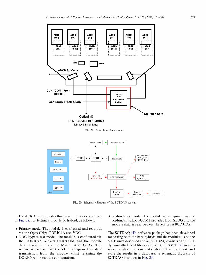
ARTICLE IN PRESS
Fig. 28. Module readout modes.
Fig. 29. Schematic diagram of the SCTDAQ system.
A. Abdesselam et al. / Nuclear Instruments and Methods in Physics Research A 575 (2007) 353–389 379
The AERO card provides three readout modes, sketchedin Fig. 28, for testing a module or hybrid, as follows:
�
Primary mode: The module is configured and read outvia the Opto Chips DORIC4A and VDC. � VDC Bypass test mode: The module is configured viathe DORIC4A outputs CLK/COM and the moduledata is read out via the Master ABCD3TAs. Thisscheme is used so that the VDC is bypassed for datatransmission from the module whilst retaining theDORIC4A for module configuration.
�
Redundancy mode: The module is configured via theRedundant CLK1/COM1 provided from SLOG and themodule data is read out via the Master ABCD3TAs.The SCTDAQ [49] software package has been developedfor testing both the bare hybrids and the modules using theVME units described above. SCTDAQ consists of a Cþþdynamically linked library and a set of ROOT [50] macroswhich analyse the raw data obtained in each test andstore the results in a database. A schematic diagram ofSCTDAQ is shown in Fig. 29.

ARTICLE IN PRESS
Fig. 30. Photo of an outer end-cap module supported by its transport
frame inside its aluminium test box. The dry-air and coolant inlets are
visible, as well as the support card.
Fig. 31. Typical set of plots obtained with the Response Curve procedure befo
From top to the bottom the vt50 value, the gain, the offset and the input noise
dead channels.
A. Abdesselam et al. / Nuclear Instruments and Methods in Physics Research A 575 (2007) 353–389380
5.5.2. Electrical tests
After the thermal cycling, the module was placed inside alight-tight aluminium test box where it was supported atthe two cooling blocks of the spine. The test box provideddry-air flow and cooling through a channel connected to anadjustable liquid coolant system (Fig. 30). Up to sixmodules in their test boxes could be placed inside acontrolled environment and tested simultaneously.Every module was electrically characterised with a
temperature of 10� 5 �C on the hybrid, as measured byan integrated thermistor. Front-end parameters such asgain, noise and channel-to-channel threshold spread weredetermined by using the internal calibration circuit of theABCD3TA chips to inject charge of adjustable amplitudein the preamplifier of each channel. The characterisationsequence [51] included the following steps:
�
re t
are
Digital tests were executed to identify chip or hybridmalfunction. These included tests of the redundancylinks, the chip by-pass functionality and the 128-cellpipeline circuit.
rimming for one data steam, corresponding to six chips (768 channels).
shown for each channel. The empty channels are the small number of
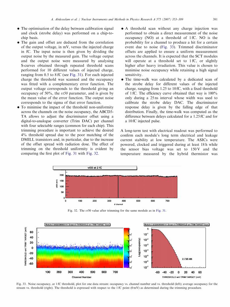
ARTICLE IN PRESSA. Abdesselam et al. / Nuclear Instruments and Methods in Physics Research A 575 (2007) 353–389 381
�
Fig
stre
The optimisation of the delay between calibration signaland clock (strobe delay) was performed on a chip-to-chip basis.
� The gain and offset are deduced from the correlationof the output voltage, in mV, versus the injected chargein fC. The input noise is then given by dividing theoutput noise by the measured gain. The voltage outputand the output noise were measured by analysingS-curves obtained through repeated threshold scansperformed for 10 different values of injected charge,ranging from 0.5 to 8 fC (see Fig. 31). For each injectedcharge the threshold was scanned and the occupancywas fitted with a complementary error function. Theoutput voltage corresponds to the threshold giving anoccupancy of 50%, the vt50 parameter, and is given bythe mean value of the error function. The output noisecorresponds to the sigma of that error function.
� To minimise the impact of the threshold non-uniformityacross the channels on the noise occupancy, the ABCD3-TA allows to adjust the discriminator offset using adigital-to-analogue converter (Trim DAC) per channelwith four selectable ranges (common for each chip). Thistrimming procedure is important to achieve the desired4% threshold spread due to the poor matching of theDMILL transistors and, in particular, due to the increaseof the offset spread with radiation dose. The effect oftrimming on the threshold uniformity is evident bycomparing the first plot of Fig. 31 with Fig. 32.
Fig. 32. The vt50 value after trimming
. 33. Noise occupancy, at 1 fC threshold, plot for one data stream: occupan
am vs. threshold (right). The threshold is expressed with respect to the 1 fC
�
for
cy
p
A threshold scan without any charge injection wasperformed to obtain a direct measurement of the noiseoccupancy (NO) at a threshold of 1 fC. NO is theprobability for a channel to produce a hit for a certainevent due to noise (Fig. 33). Trimmed discriminatoroffsets are applied to ensure a uniform measurementacross the channels. It is expected that the SCT moduleswill operate at a threshold set to 1 fC, or slightlyhigher after heavy irradiation. This value is chosen tominimise noise occupancy while retaining a high signalsensitivity.
� The time-walk was calculated by a dedicated scan ofthe strobe delay for different values of the injectedcharge, ranging from 1.25 to 10 fC, with a fixed thresholdof 1 fC. The efficiency curve obtained that way is 100%only during a 25ns interval whose width was used tocalibrate the strobe delay DAC. The discriminatorresponse delay is given by the falling edge of thatdistribution. Finally, the time-walk was computed as thedifference between delays calculated for a 1.25 fC and fora 10 fC injected pulse.
A long-term test with electrical readout was performed toconfirm each module’s long term electrical and leakagecurrent stability at low temperature. The ASICs werepowered, clocked and triggered during at least 18 h whilethe sensor bias voltage was set to 150V and thetemperature measured by the hybrid thermistor was
the same module as in Fig. 31.
vs. channel number and vs. threshold (left); average occupancy for the
oint (0mV) as determined during the trimming procedure.
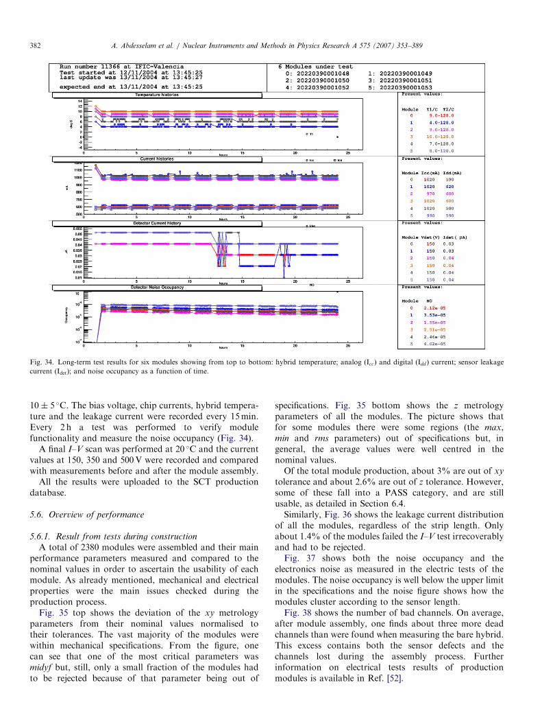
ARTICLE IN PRESS
Fig. 34. Long-term test results for six modules showing from top to bottom: hybrid temperature; analog ðIccÞ and digital ðIdd Þ current; sensor leakage
current (Idet); and noise occupancy as a function of time.
A. Abdesselam et al. / Nuclear Instruments and Methods in Physics Research A 575 (2007) 353–389382
10� 5 �C. The bias voltage, chip currents, hybrid tempera-ture and the leakage current were recorded every 15min.Every 2 h a test was performed to verify modulefunctionality and measure the noise occupancy (Fig. 34).
A final I–V scan was performed at 20 �C and the currentvalues at 150, 350 and 500V were recorded and comparedwith measurements before and after the module assembly.
All the results were uploaded to the SCT productiondatabase.
5.6. Overview of performance
5.6.1. Result from tests during construction
A total of 2380 modules were assembled and their mainperformance parameters measured and compared to thenominal values in order to ascertain the usability of eachmodule. As already mentioned, mechanical and electricalproperties were the main issues checked during theproduction process.
Fig. 35 top shows the deviation of the xy metrologyparameters from their nominal values normalised totheir tolerances. The vast majority of the modules werewithin mechanical specifications. From the figure, onecan see that one of the most critical parameters wasmidyf but, still, only a small fraction of the modules hadto be rejected because of that parameter being out of
specifications. Fig. 35 bottom shows the z metrologyparameters of all the modules. The picture shows thatfor some modules there were some regions (the max,min and rms parameters) out of specifications but, ingeneral, the average values were well centred in thenominal values.Of the total module production, about 3% are out of xy
tolerance and about 2.6% are out of z tolerance. However,some of these fall into a PASS category, and are stillusable, as detailed in Section 6.4.Similarly, Fig. 36 shows the leakage current distribution
of all the modules, regardless of the strip length. Onlyabout 1.4% of the modules failed the I–V test irrecoverablyand had to be rejected.Fig. 37 shows both the noise occupancy and the
electronics noise as measured in the electric tests of themodules. The noise occupancy is well below the upper limitin the specifications and the noise figure shows how themodules cluster according to the sensor length.Fig. 38 shows the number of bad channels. On average,
after module assembly, one finds about three more deadchannels than were found when measuring the bare hybrid.This excess contains both the sensor defects and thechannels lost during the assembly process. Furtherinformation on electrical tests results of productionmodules is available in Ref. [52].
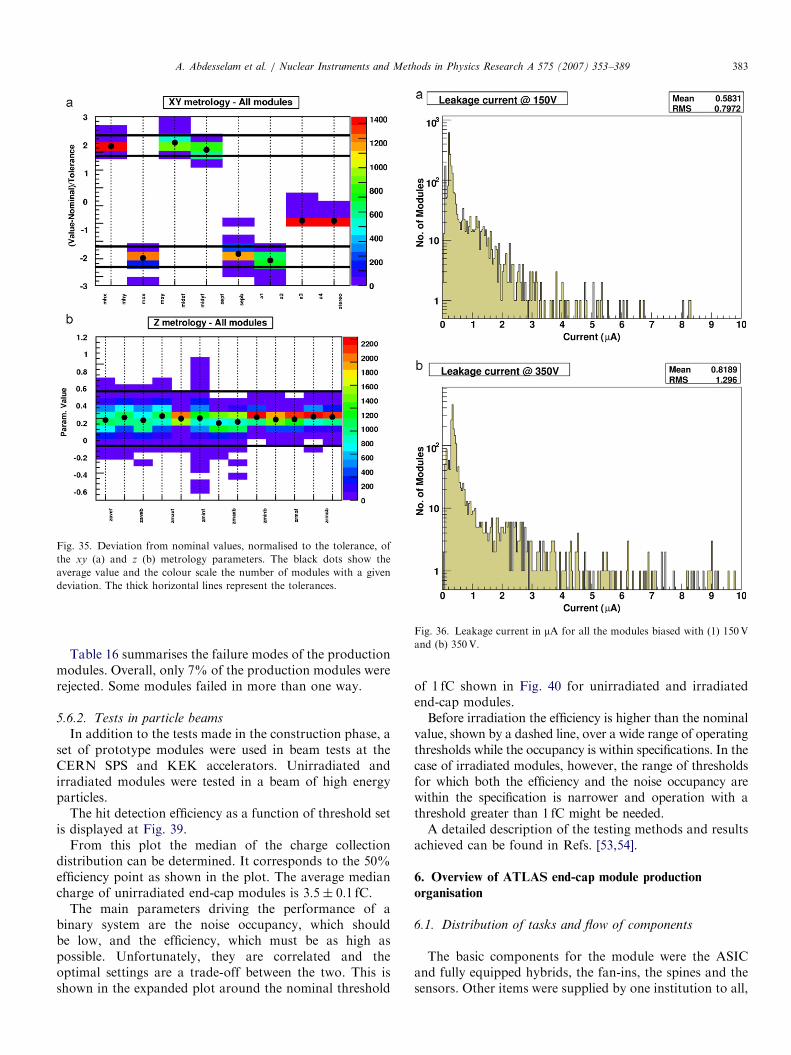
ARTICLE IN PRESS
Fig. 35. Deviation from nominal values, normalised to the tolerance, of
the xy (a) and z (b) metrology parameters. The black dots show the
average value and the colour scale the number of modules with a given
deviation. The thick horizontal lines represent the tolerances.
Fig. 36. Leakage current in mA for all the modules biased with (1) 150V
and (b) 350V.
A. Abdesselam et al. / Nuclear Instruments and Methods in Physics Research A 575 (2007) 353–389 383
Table 16 summarises the failure modes of the productionmodules. Overall, only 7% of the production modules wererejected. Some modules failed in more than one way.
5.6.2. Tests in particle beams
In addition to the tests made in the construction phase, aset of prototype modules were used in beam tests at theCERN SPS and KEK accelerators. Unirradiated andirradiated modules were tested in a beam of high energyparticles.
The hit detection efficiency as a function of threshold setis displayed at Fig. 39.
From this plot the median of the charge collectiondistribution can be determined. It corresponds to the 50%efficiency point as shown in the plot. The average mediancharge of unirradiated end-cap modules is 3:5� 0:1 fC.
The main parameters driving the performance of abinary system are the noise occupancy, which shouldbe low, and the efficiency, which must be as high aspossible. Unfortunately, they are correlated and theoptimal settings are a trade-off between the two. This isshown in the expanded plot around the nominal threshold
of 1 fC shown in Fig. 40 for unirradiated and irradiatedend-cap modules.Before irradiation the efficiency is higher than the nominal
value, shown by a dashed line, over a wide range of operatingthresholds while the occupancy is within specifications. In thecase of irradiated modules, however, the range of thresholdsfor which both the efficiency and the noise occupancy arewithin the specification is narrower and operation with athreshold greater than 1 fC might be needed.A detailed description of the testing methods and results
achieved can be found in Refs. [53,54].
6. Overview of ATLAS end-cap module production
organisation
6.1. Distribution of tasks and flow of components
The basic components for the module were the ASICand fully equipped hybrids, the fan-ins, the spines and thesensors. Other items were supplied by one institution to all,
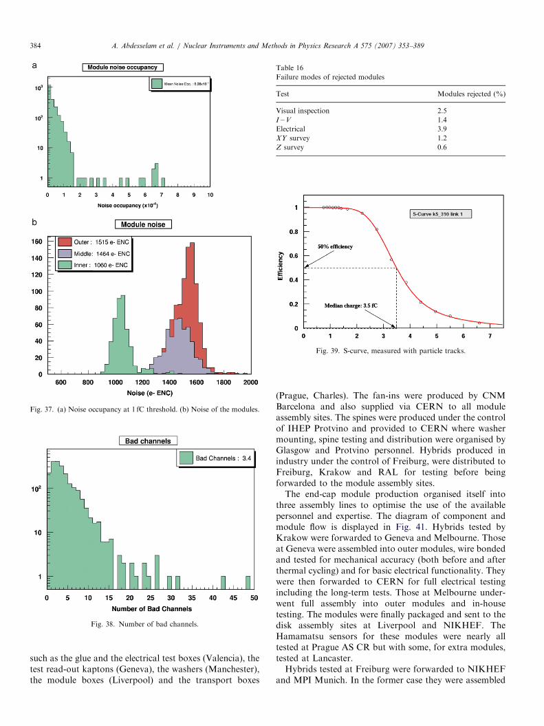
ARTICLE IN PRESS
Fig. 37. (a) Noise occupancy at 1 fC threshold. (b) Noise of the modules.
Fig. 38. Number of bad channels.
Table 16
Failure modes of rejected modules
Test Modules rejected (%)
Visual inspection 2.5
I2V 1.4
Electrical 3.9
XY survey 1.2
Z survey 0.6
Fig. 39. S-curve, measured with particle tracks.
A. Abdesselam et al. / Nuclear Instruments and Methods in Physics Research A 575 (2007) 353–389384
such as the glue and the electrical test boxes (Valencia), thetest read-out kaptons (Geneva), the washers (Manchester),the module boxes (Liverpool) and the transport boxes
(Prague, Charles). The fan-ins were produced by CNMBarcelona and also supplied via CERN to all moduleassembly sites. The spines were produced under the controlof IHEP Protvino and provided to CERN where washermounting, spine testing and distribution were organised byGlasgow and Protvino personnel. Hybrids produced inindustry under the control of Freiburg, were distributed toFreiburg, Krakow and RAL for testing before beingforwarded to the module assembly sites.The end-cap module production organised itself into
three assembly lines to optimise the use of the availablepersonnel and expertise. The diagram of component andmodule flow is displayed in Fig. 41. Hybrids tested byKrakow were forwarded to Geneva and Melbourne. Thoseat Geneva were assembled into outer modules, wire bondedand tested for mechanical accuracy (both before and afterthermal cycling) and for basic electrical functionality. Theywere then forwarded to CERN for full electrical testingincluding the long-term tests. Those at Melbourne under-went full assembly into outer modules and in-housetesting. The modules were finally packaged and sent to thedisk assembly sites at Liverpool and NIKHEF. TheHamamatsu sensors for these modules were nearly alltested at Prague AS CR but with some, for extra modules,tested at Lancaster.Hybrids tested at Freiburg were forwarded to NIKHEF
and MPI Munich. In the former case they were assembled
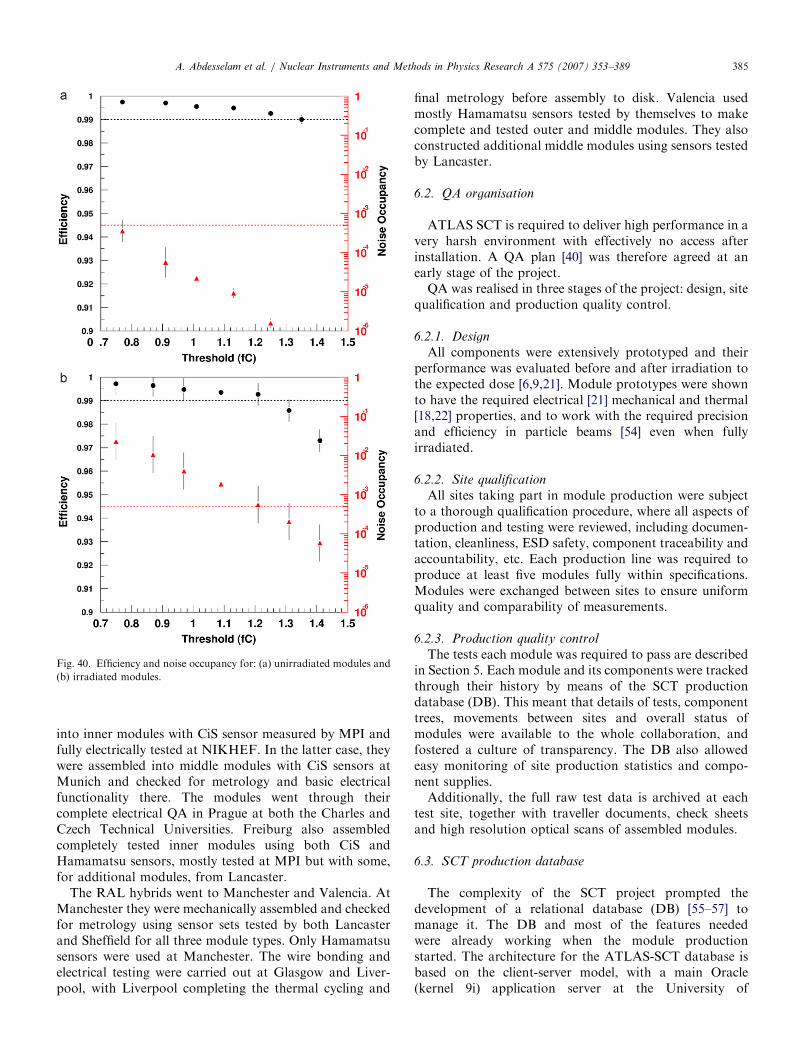
ARTICLE IN PRESS
Fig. 40. Efficiency and noise occupancy for: (a) unirradiated modules and
(b) irradiated modules.
A. Abdesselam et al. / Nuclear Instruments and Methods in Physics Research A 575 (2007) 353–389 385
into inner modules with CiS sensor measured by MPI andfully electrically tested at NIKHEF. In the latter case, theywere assembled into middle modules with CiS sensors atMunich and checked for metrology and basic electricalfunctionality there. The modules went through theircomplete electrical QA in Prague at both the Charles andCzech Technical Universities. Freiburg also assembledcompletely tested inner modules using both CiS andHamamatsu sensors, mostly tested at MPI but with some,for additional modules, from Lancaster.
The RAL hybrids went to Manchester and Valencia. AtManchester they were mechanically assembled and checkedfor metrology using sensor sets tested by both Lancasterand Sheffield for all three module types. Only Hamamatsusensors were used at Manchester. The wire bonding andelectrical testing were carried out at Glasgow and Liver-pool, with Liverpool completing the thermal cycling and
final metrology before assembly to disk. Valencia usedmostly Hamamatsu sensors tested by themselves to makecomplete and tested outer and middle modules. They alsoconstructed additional middle modules using sensors testedby Lancaster.
6.2. QA organisation
ATLAS SCT is required to deliver high performance in avery harsh environment with effectively no access afterinstallation. A QA plan [40] was therefore agreed at anearly stage of the project.QA was realised in three stages of the project: design, site
qualification and production quality control.
6.2.1. Design
All components were extensively prototyped and theirperformance was evaluated before and after irradiation tothe expected dose [6,9,21]. Module prototypes were shownto have the required electrical [21] mechanical and thermal[18,22] properties, and to work with the required precisionand efficiency in particle beams [54] even when fullyirradiated.
6.2.2. Site qualification
All sites taking part in module production were subjectto a thorough qualification procedure, where all aspects ofproduction and testing were reviewed, including documen-tation, cleanliness, ESD safety, component traceability andaccountability, etc. Each production line was required toproduce at least five modules fully within specifications.Modules were exchanged between sites to ensure uniformquality and comparability of measurements.
6.2.3. Production quality control
The tests each module was required to pass are describedin Section 5. Each module and its components were trackedthrough their history by means of the SCT productiondatabase (DB). This meant that details of tests, componenttrees, movements between sites and overall status ofmodules were available to the whole collaboration, andfostered a culture of transparency. The DB also allowedeasy monitoring of site production statistics and compo-nent supplies.Additionally, the full raw test data is archived at each
test site, together with traveller documents, check sheetsand high resolution optical scans of assembled modules.
6.3. SCT production database
The complexity of the SCT project prompted thedevelopment of a relational database (DB) [55–57] tomanage it. The DB and most of the features neededwere already working when the module productionstarted. The architecture for the ATLAS-SCT database isbased on the client-server model, with a main Oracle(kernel 9i) application server at the University of
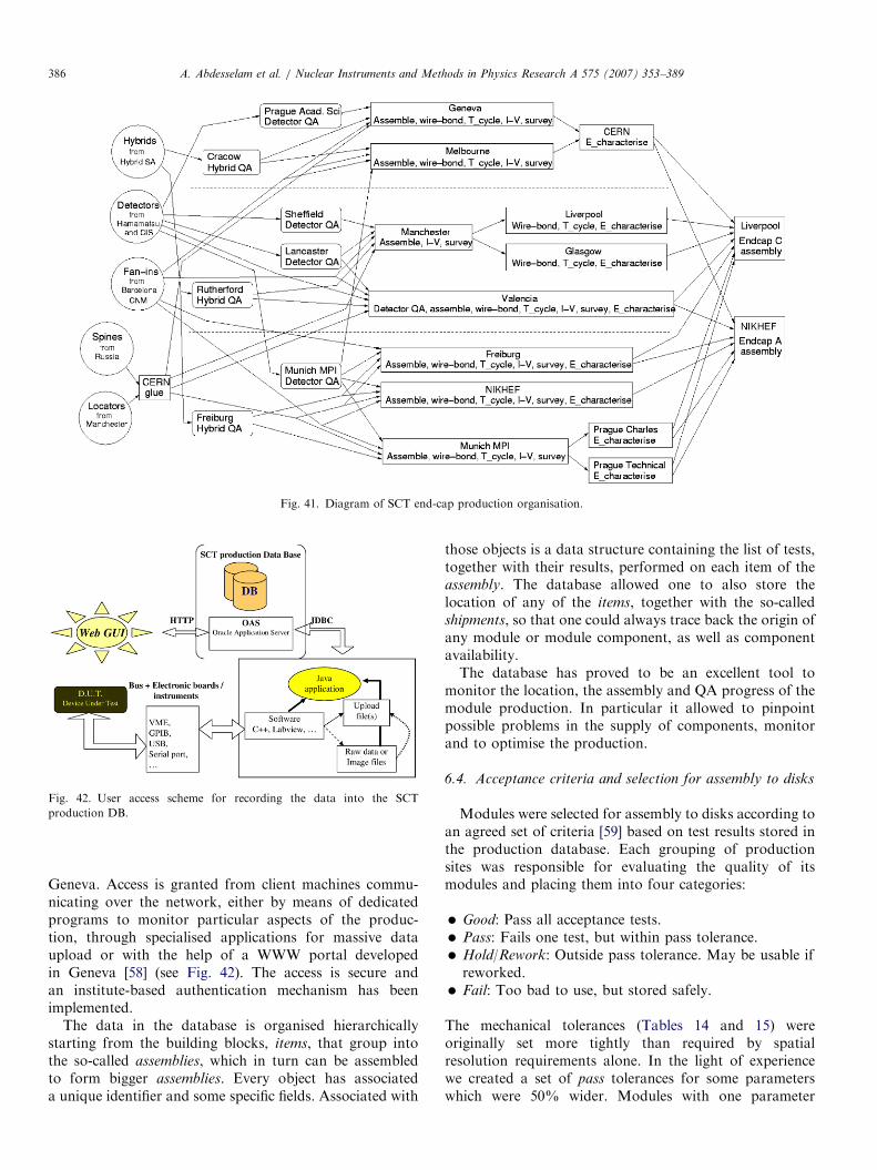
ARTICLE IN PRESS
Fig. 42. User access scheme for recording the data into the SCT
production DB.
Fig. 41. Diagram of SCT end-cap production organisation.
A. Abdesselam et al. / Nuclear Instruments and Methods in Physics Research A 575 (2007) 353–389386
Geneva. Access is granted from client machines commu-nicating over the network, either by means of dedicatedprograms to monitor particular aspects of the produc-tion, through specialised applications for massive dataupload or with the help of a WWW portal developedin Geneva [58] (see Fig. 42). The access is secure andan institute-based authentication mechanism has beenimplemented.
The data in the database is organised hierarchicallystarting from the building blocks, items, that group intothe so-called assemblies, which in turn can be assembledto form bigger assemblies. Every object has associateda unique identifier and some specific fields. Associated with
those objects is a data structure containing the list of tests,together with their results, performed on each item of theassembly. The database allowed one to also store thelocation of any of the items, together with the so-calledshipments, so that one could always trace back the origin ofany module or module component, as well as componentavailability.The database has proved to be an excellent tool to
monitor the location, the assembly and QA progress of themodule production. In particular it allowed to pinpointpossible problems in the supply of components, monitorand to optimise the production.
6.4. Acceptance criteria and selection for assembly to disks
Modules were selected for assembly to disks according toan agreed set of criteria [59] based on test results stored inthe production database. Each grouping of productionsites was responsible for evaluating the quality of itsmodules and placing them into four categories:
�
Good: Pass all acceptance tests. � Pass: Fails one test, but within pass tolerance. � Hold/Rework: Outside pass tolerance. May be usable ifreworked.
� Fail: Too bad to use, but stored safely.The mechanical tolerances (Tables 14 and 15) wereoriginally set more tightly than required by spatialresolution requirements alone. In the light of experiencewe created a set of pass tolerances for some parameterswhich were 50% wider. Modules with one parameter
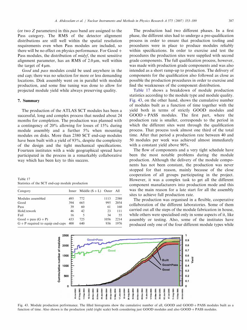
ARTICLE IN PRESSA. Abdesselam et al. / Nuclear Instruments and Methods in Physics Research A 575 (2007) 353–389 387
(or two Z parameters) in this pass band are assigned to thePass category. The RMS of the detector alignmentdistributions are still well within the spatial resolutionrequirements even when Pass modules are included, sothere will be no effect on physics performance. For GoodþPass modules, the distribution of midyf, the most sensitivealignment parameter, has an RMS of 2:0mm, well withinthe target of 4mm.
Good and pass modules could be used anywhere in theend cap; there was no selection for more or less demandinglocations. Disk assembly went on in parallel with moduleproduction, and some fine tuning was done to allow forprojected module yield while always preserving quality.
7. Summary
The production of the ATLAS SCT modules has been asuccessful, long and complex process that needed about 24months for completion. The production was planned witha contingency of 20% allowing for losses of 15% duringmodule assembly and a further 5% when mountingmodules on disks. More than 2380 SCT end-cap moduleshave been built with a yield of 93%, despite the complexityof the design and the tight mechanical specifications.Fourteen institutes with a wide geographical spread haveparticipated in the process in a remarkably collaborativeway which has been key to this success.
Fig. 43. Module production performance. The filled histograms show the cu
function of time. Also shown is the production yield (right scale) both consid
Table 17
Statistics of the SCT end-cap module production
Category Inner Middle ðSþ LÞ Outer All
Modules assembled 495 772 1113 2380
Good 394 665 995 2054
Pass 39 60 61 160
Hold/rework 46 42 23 111
Fail 16 5 34 55
Goodþ pass ðGþ PÞ 433 725 1056 2214
Gþ P required to equip end-caps 400 640 936 1976
The production had two different phases. In a firstphase, the different sites had to undergo a pre-qualificationprocess in order to ensure that production tooling andprocedures were in place to produce modules reliablywithin specifications. In order to exercise and test theprocedures the production sites were supplied with secondgrade components. The full qualification process, however,was made with production grade components and was alsointended as a short ramp-up to production. The delivery ofcomponents for the qualification also followed as close aspossible the production procedures in order to exercise andfind the weaknesses of the component distribution.Table 17 shows a breakdown of module production
statistics according to the module type and module quality.Fig. 43, on the other hand, shows the cumulative numberof modules built as a function of time together with theyield both in terms of strictly GOOD modules andGOODþ PASS modules. The first part, where theproduction rate is smaller, corresponds to the period inwhich the different sites went through the qualificationprocess. That process took almost one third of the totaltime. After that period a production rate between 40 and50 modules per week was achieved almost immediatelywith a constant yield above 90%.The flow of components and a very tight schedule have
been the most notable problems during the moduleproduction. Although the delivery of the module compo-nents has not been constant, the production was neverstopped for that reason, mainly because of the closecooperation of all groups participating in the project.However, it was a complex task to get all the differentcomponent manufacturers into production mode and thiswas the main reason for a late start for all the assemblysites to achieve full production rate.The production was organised in a flexible, cooperative
collaboration of the different laboratories. Some of themcarried out all the steps of the module fabrication in house,while others were specialised only in some aspects of it, likeassembly or testing. Also, some of the institutes haveproduced only one of the four different module types while
mulative number of all, GOOD and GOODþ PASS modules built as a
ering just GOOD modules and also GOODþ PASS modules.
ARTICLE IN PRESSA. Abdesselam et al. / Nuclear Instruments and Methods in Physics Research A 575 (2007) 353–389388
others were able to produce more than one type. Thisstructure allowed overcoming the problems that appearedduring the production.
Acknowledgements
We are greatly indebted to all the technical staff whoworked on the end-cap module project from the ATLASSCT Institutes. We acknowledge the support of the fundingauthorities of the collaborating institutes including theSpanish National Programme for Particle Physics; theResearch Council of Norway; the Particle Physics andAstronomy Research Council of the United Kingdom; thePolish Ministry of Education and Science; the GermanMinistry of Science; the Swiss National Science Founda-tion; the State Secretariat for Education and Research andthe Canton of Geneva; the Slovenian Research Agency andthe Ministry of Higher Education, Science and Technologyof the Republic of Slovenia; the Ministry of Education,Culture, Sports, Science and Technology of Japan; theJapan Society for the Promotion of Science; the Office ofHigh Energy Physics of the United States Department ofEnergy; the United States National Science Foundation;the Australian Department of Education, Science andTraining; Dutch Foundation for Fundamental Researchon Matter (FOM); the Ministry of Education, Youth andSports of the Czech Republic; the National ScienceCouncil, Taiwan; the Swedish Research Council.The Research was supported in part by the EU underRTN Contract HPRN-CT-2002-00292 Probe for NewPhysics within the Sixth European Community FrameworkProgramme.
References
[1] The ATLAS Technical Proposal for a General Purpose pp Experi-
ment at the Large Hadron Collider at CERN, CERN/LHCC/94–43,
1994.
[2] The LHC Conceptual Design Report—The Yellow Book, CERN/
AC/95–05 (LHC), 1995.
[3] ATLAS Inner Detector Technical Design Report, CERN/LHCC/
97–16, 1977.
[4] A. Abdesselam, et al., Nucl. Instr. and Meth. A 568 (2006) 642.
[5] L. Feld, Forward module components, ATL-IS-EN-0009.
[6] F. Campdabal, et al., Nucl. Instr. and Meth. A (552) (2005) 292.
[7] A.A. Carter, R. De Oliveira, A. Gandi, Comprehensively protected
by world-wide patents, including USA Patent US 6,514,616 B1,
February 4, 2003: A Thermal Management Device and Method of
making such a Device, and by further patents pending.
[8] Status Report of the RD20 Collaboration, CERN/DRDC 94–39,
1994.
[9] RD2 Status Report, CERN/DRDC/92–4, 1992.
[10] M. Moll, Radiation Damage in Silicon Particle Detectors, Disserta-
tion zur Erlangung des Doktorgrades des Fachbereichs Physik de
Universitat Hamburg, 1999.
[11] Third RD48 Status Report, CERN/LHCC 2000–009, 2000.
[12] ATLAS Detector and Physics Performance Technical Design Report,
CERN/LHCC 99–14, 1999.
[13] S. Haywood, Determination of SCT wheel positions, ATL-IS-ES-
0080.
[14] S. Haywood, Determination of SCT wheel positions, ATL-INDET-
2001–007.
[15] RD29 Status Report, DMILL, A Mixed Analogue-Digital Radiation
Hard Technology for High Energy Physics Electronics, CERN/
LHCC/97-15, 1996.
[16] A. Abdesselam, et al., The ATLAS SCT optoelectronics and the
associated electrical services, ATL-INDET-PUB-2007–001.
[17] D.J. White, et al., Nucl. Instr. and Meth. A 457 (2001) 369.
[18] S. Snow, Thermal and mechanical specifications and expected
performance of the forward SCT module, ATL-IS-EN-0007.
[19] I. Duerdoth, et al., Measurements of convection between the disks of
the SCT end-cap, ATL-IS-TR-0010.
[20] A. Clark, et al., Thermal performance of the ATLAS SCT forward
modules, ATL-INDET-2003-010.
[21] M. Mangin-Brinet, et al., Electrical test results from ATLAS-SCT
end-cap modules, ATL-INDET-2003-04.
[22] S. Snow, Thermal and mechanical performance results from forward
SCT modules, ATL-IS-TR-0002.
[23] S. Snow, S. Temple, SCT end-cap module/disk services mechanical
interface, ATL-IS-ER-0038.
[24] N. Hessey, Physics requirements for end-cap module placement
tolerances, ATL-IS-ER-0027.
[25] Hamamatsu Photonics Co. Ltd., Japan.
[26] CiS Institut fur Mikrosensorik gGmbH, Germany.
[27] F.G. Hartjes, Nucl. Instr. and Meth. A 552 (2005) 168.
[28] M. Ullan, M. Lozano, F. Campabadal, C. Fleta, C. Garcıa, F.
Gonzalez, J. Bernabeu, IEEE Trans. Nucl. Sci. NS-51 (3) (2004) 968.
[29] C.A. Heusch, H.G. Moser, A. Kholodenko, Nucl. Instr. and Meth. A
480 (2–3) (2002) 463.
[30] A. Kholodenko, et al., Comparison of the in-plane thermal
and electrical conductivities and transverse pull strengths of
various pyrolytic graphite materials, IHEP 2001–48, ATL-INDET-
2002-003.
[31] Kholodenko, H.G. Moser, Comparison of the thermal and mechan-
ical properties of TPG used for SCT ATLAS modules, ATL-INDET-
2000–007.
[32] ATLAS SCT end cap module—outer module spine assy., ATLISME-
0022.
[33] CeramTec AG, Germany.
[34] Scientific Research Institute of Carbon Based Materials, NIIGra-
phite, Moscow, Russia.
[35] Scientific Research Institute of Technology and Automation for
Industry, NIITAP, Russia.
[36] State Research Centre of Russia—Institute for High Energy, IHEP,
Moscow Region, Russia.
[37] S.W. Snow, C. Fracchiolla, The radiation length of SCT endcap
modules, ATL-INDET-PUB-2006-010.
[38] A. Rinoldi, et al., The simulation of the ATLAS experiment,
ATL-SOFT-2004-004.
[39] S. Agostinelli, et al., Nucl. Instr. and Meth. A 506 (2003) 250;
J. Allison, et al., IEEE Trans. Nucl. Sci. NS 53 (1) (2006) 270.
[40] The quality assurance of the ATLAS SCT end-cap detector modules,
ATL-IS-QA-0004.
[41] C. Lacasta, Electrical specifications and expected performance
of the end-cap module, ATLAS Project Document, ATL-IS-EN-
0008, 2002.
[42] D. Ferrere, Forward modules—assembly procedures, ATLAS Project
Document ATL-IS-AP-0049, 2002.
[43] J. Butterworth, D. Hayes, J. Lane, M. Postranecky, Timing, trigger
and control interface module for ATLAS SCT read out electronics,
Proceedings of the Fifth Workshop on Electronics for LHC
Experiments, Snowmass, Colorado, USA, 20–24 September 1999,
CERN 99-09, CERN/LHCC/99-33, pp. 336–340.
[44] M. Morrissey, SLOG, hhttp://hepwww.rl.ac.uk/atlas-sct/mm/Slogi.
[45] A. Greenall, ATLAS SCT AERO, hhttp://hep.ph.liv.ac.uk/�ashley/
ATLAS_AERO.htmli.
[46] M.J. Goodrick, M. Morrissey, MuSTARD, hhttp://sct-testdaq.
home.cern.ch/sct-testdaq/sctdaq/www/mustard.htmli.
ARTICLE IN PRESSA. Abdesselam et al. / Nuclear Instruments and Methods in Physics Research A 575 (2007) 353–389 389
[47] E. Gornicki, P. Malecki, S. Koperny, Multichannel system of
fully isolated HV power supplies for silicon strip detectors,
Proceedings of the Sixth Workshop on Electronic for LHC
Experiments, Cracow, Poland, 11–15 September 2000, (CERN-
2000-010), pp. 376–379.
[48] J. Bohm, et al., ATLAS-SCT Collaboration, Power supply and
power distribution system for the ATLAS silicon strip detectors,
Proceedings of the Seventh Workshop on Electronics for LHC
Experiments, Stockholm, September 2001, (CERN-2001-005),
pp. 363–367.
[49] L. Eklund, J. Hill, G. Moorhead, P.W. Phillips, Atlas SCT Test DAQ
Online Documentation, hhttp://sct-testdaq.home.cern.ch/sct-testdaq/
sctdaq/sctdaq.htmli; P.W. Phillips, ATLAS SCT Collaboration,
System performance of ATLAS SCT detector modules, Proceedings
of the Eighth Workshop on Electronics for LHC Experiments,
Colmar, France, 9–13 September 2002, (CERN-2002-003),
pp. 100–104.
[50] R. Brun, F. Rademakers, Nucl. Instr. and Meth. A 389 (1997) 81
hhttp://root.cern.chi.
[51] P.W. Phillips, L. Eklund, Electrical tests of SCT hybrids and modules,
hhttp://hepwww.rl.ac.uk/atlas-sct/documents/pro/Electrical_Tests_
338.pdfi.
[52] V.A. Mitsou, ATLAS-SCT Collaboration, IEEE Trans. Nucl. Sci.
NS-53 (2006) 729–734 [arXiv:physics/0606263].
[53] C. Lacasta, Electrical prototype module results, ATLAS Project
Document, ATL-IS-TN-0002, 2002.
[54] F. Campadabal, et al., Nucl. Instr. and Meth. A 538 (2005) 384–407.
[55] A. Clark, Ph. Demierre, J.M. Dubois, D. Ferrere, H. Nguyen 2 , F.
Serena, The ATLAS SCT production DB, ATL-INDET-2002-015.
[56] P. Demierre, D. Ferrere, A database for silicon microstrip detectors
in the SCT central cluster working group, ATL-INDET-98–219.
[57] J. Foster, S. Snow, Proposal for a database for the ATLAS SCT
construction, ATL-INDET-96–144.
[58] SCT production DB web page, hhttp://wacap.unige.ch:3146/
phyprdwww/sctprd/welcome.htmli.
[59] Z. Dolezal, J. Foster, SCT endcap module test data handling, 15 July
2004, hhttp://www-ucjf.troja.mff.cuni.cz/sct/QA/docs/UploadRules.
pdfi.