telecommunication engineering lab work - WordPress.com
90
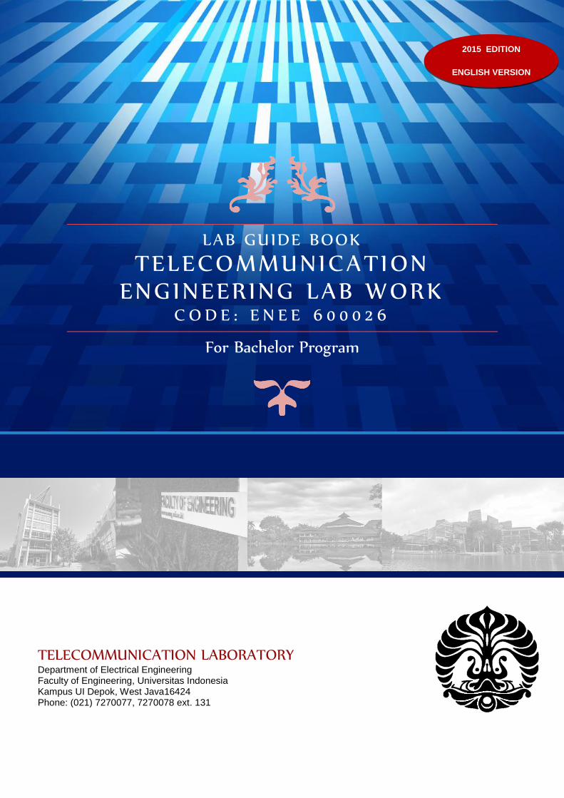
LAB GUIDE BOOK TELECOMMUNICATION ENGINEERING LAB WORK CODE: ENEE 600026 For Bachelor Program TELECOMMUNICATION LABORATORY Department of Electrical Engineering Faculty of Engineering, Universitas Indonesia Kampus UI Depok, West Java16424 Phone: (021) 7270077, 7270078 ext. 131 2015 EDITION ENGLISH VERSION
-
Upload
khangminh22 -
Category
Documents
-
view
1 -
download
0
Transcript of telecommunication engineering lab work - WordPress.com
LAB GUIDE BOOK
TELECOMMUNICATION ENGINEERING LAB WORK
C O D E : E N E E 6 0 0 0 2 6
For Bachelor Program
TELECOMMUNICATION LABORATORY Department of Electrical Engineering Faculty of Engineering, Universitas Indonesia Kampus UI Depok, West Java16424 Phone: (021) 7270077, 7270078 ext. 131
2015 EDITION
ENGLISH VERSION

LABORATORY MANUAL
TELECOMMUNICATION ENGINEERING (ENEE 610025) For International Class Student of Electrical Engineering
Published by Laboratory of Telecommunication Department of Electrical Engineering Faculty of Engineering Universitas Indonesia 2015
Supervisor : Dr. Fitri Yuli Zulkifli, S.T., M.Sc. As head of laboratory of Telecommunication DTE FTUI
Editor : Muhammad Erfinza Fariz Azhar Abdillah Author : Adhitya Satria Pratama Aisyah Ina Gustiana Budiman Budhiardianto Sayid Hasan Muhammad Haekal
Rifqi Ramadhan Angga Hilman Hizrian Ubay Muhammad Noor Mursid Abidiarso Yonathan Raka Pradana Irfan Kurniawan Rian Gilan Prabowo
For internal Universitas Indonesia use only! All rights is reserved. Reproduction and/or duplication of a part or entire of this document in any forms are prohibited.
Laboratory Manual Telecomunication Engineering 2015 2
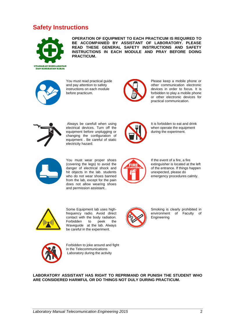
Safety Instructions
OPERATION OF EQUIPMENT TO EACH PRACTICUM IS REQUIRED TO BE ACCOMPANIED BY ASSISTANT OF LABORATORY. PLEASE READ THESE GENERAL SAFETY INSTRUCTIONS AND SAFETY INSTRUCTIONS IN EACH MODULE AND PRAY BEFORE DOING PRACTICUM.
You must read practical guide and pay attention to safety instructions on each module before practicum.
Please keep a mobile phone or other communication electronic devices in order to focus. It is forbidden to play a mobile phone or other electronic devices for practical communication.
Always be carefull when using electrical devices. Turn off the equipment before unplugging or changing the configuration of equipment . Be careful of static electricity hazard.
It is forbidden to eat and drink when operate the equipment during the experiment.
You must wear proper shoes (covering the legs) to avoid the danger of electrical shock and hit objects in the lab. students who do not wear shoes banned from the lab, except for the pain does not allow wearing shoes and permission assistant..
If the event of a fire, a fire extinguisher is located at the left of the entrance. If things happen unexpected, please do emergency procedures calmly.
Some Equipment lab uses high-frequency radio. Avoid direct contact with the body radiation. Forbidden to peek the Waveguide at the lab. Always be careful in the experiment.
Smoking is clearly prohibited in environment of Faculty of Engineering
Forbidden to joke around and fight in the Telecommunications Laboratory during the activity
LABORATORY ASSISTANT HAS RIGHT TO REPRIMAND OR PUNISH THE STUDENT WHO ARE CONSIDERED HARMFUL OR DO THINGS NOT DULY DURING PRACTICUM.
Laboratory Manual Telecomunication Engineering 2015 3
Preface
This lab guide book has been adapted over the years to meet
students‟ needs especially in the study of telecommunication
engineering at Electrical Engineering Dept. This guide book is
purposed to provide a user-friendly manual book to help students
understand practical aspects of telecommunication engineering
by doing experiments in the laboratory.
This book contains 10 modules to be done on Telecommunication Engineering Lab
Work. Each module on this book contains complete instructions on technical principles
and procedures in the lab consisting of the objectives, basic theory, equipment and
experimental procedures.
I would like to thank all those who have helped in this book preparation. I and all the
assistant team would be grateful for your suggestions to improve this book in the future.
I wish this book can be used well by the students and help you to understand the
telecommunication engineering clearly.
Depok, 23 September 2015
Head of Telecommunication
Laboratory
Electrical Engineering Dept., FTUI
Dr. Fitri Yuli Zulkifli, S.T., M.Sc.
NIP. 19740719 199802 2 001
Laboratory Manual Telecomunication Engineering 2015 4
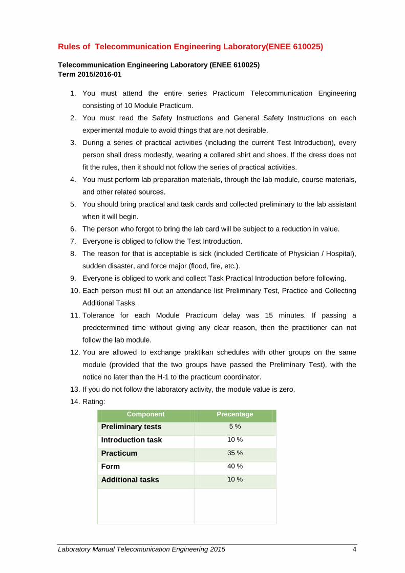
Rules of Telecommunication Engineering Laboratory(ENEE 610025)
Telecommunication Engineering Laboratory (ENEE 610025)
Term 2015/2016-01
1. You must attend the entire series Practicum Telecommunication Engineering
consisting of 10 Module Practicum.
2. You must read the Safety Instructions and General Safety Instructions on each
experimental module to avoid things that are not desirable.
3. During a series of practical activities (including the current Test Introduction), every
person shall dress modestly, wearing a collared shirt and shoes. If the dress does not
fit the rules, then it should not follow the series of practical activities.
4. You must perform lab preparation materials, through the lab module, course materials,
and other related sources.
5. You should bring practical and task cards and collected preliminary to the lab assistant
when it will begin.
6. The person who forgot to bring the lab card will be subject to a reduction in value.
7. Everyone is obliged to follow the Test Introduction.
8. The reason for that is acceptable is sick (included Certificate of Physician / Hospital),
sudden disaster, and force major (flood, fire, etc.).
9. Everyone is obliged to work and collect Task Practical Introduction before following.
10. Each person must fill out an attendance list Preliminary Test, Practice and Collecting
Additional Tasks.
11. Tolerance for each Module Practicum delay was 15 minutes. If passing a
predetermined time without giving any clear reason, then the practitioner can not
follow the lab module.
12. You are allowed to exchange praktikan schedules with other groups on the same
module (provided that the two groups have passed the Preliminary Test), with the
notice no later than the H-1 to the practicum coordinator.
13. If you do not follow the laboratory activity, the module value is zero.
14. Rating:
Component Precentage
Preliminary tests 5 %
Introduction task 10 %
Practicum 35 %
Form 40 %
Additional tasks 10 %
Laboratory Manual Telecomunication Engineering 2015 5
15. The practical value is determined by the behavior and activity of the practitioner during the
practicum, including during oral test before the lab begins.
16. Additional tasks performed in double folio striped paper and collected no later than 1 x 24
hours after the practicum ends.
17. All licensing and complaints please delivered to the Laboratory Coordinator
Head of Laboratory of Telecommunication
Dr. Fitri Yuli Zulkifli, S.T., M.Sc.
NIP. 197407191998022001
International Class Cordinator
Angga Hilman Hizrian
NPM 1206260860

Laboratory Manual Telecomunication Engineering 2015 6
Asistant of Laboratory
Telecommunication Engineering Laboratory (ENEE 610025)
Term 2015/2016-01
RIFQI RAMADHAN
Teknik Elektro 2012
Cordinator of Asistant
087781870722
UBAY MUHAMMAD NOOR
Teknik Elektro 2012
Cordinator of Telecommunication Engineering Laboratory for Reguler and Paralel Class
087788945594
ANGGA HILMAN HIZRIAN
Teknik Elektro 2012
Cordinator of Telecommunication Engineering Laboratory for International Class
085966116036
MURSID ABIDIARSO
Teknik Elektro 2013
085717108241
mursid.abidiarso @gmail.com
MUHAMMAD HAEKAL
Teknik Elektro 2012
081316106027
FARIZ AZHAR ABDILLAH
Teknik Elektro 2013
085692612648
MUHAMMAD ERFINZA
Teknik Elektro 2012
083898345760
RIAN GILANG PRABOWO
Teknik Elektro 2013
087808052796
IRFAN KURNIAWAN
Teknik Elektro 2013
085695133317
YONATHAN RAKA PRADANA
Teknik Elektro 2013
081329078777
Laboratory Manual Telecomunication Engineering 2015 7
Contents
Safety Instructions .................................................................................................................... 2 Preface ........................................................................................................................................ 3 Rules of Telecommunication Engineering Laboratory(ENEE 610025) ............................... 4 Asistant of Laboratory .............................................................................................................. 6 Contents ..................................................................................................................................... 7 Introduction of Telecommunications Engineering ................................................................ 9
Objectives ................................................................................................................................ 9
Classical Era: Wired Telecommunications Network ............................................................... 9
New Era: Wireless Telecommunications Networks .............................................................. 10
Explosions of Technology: Cellular Communications ........................................................... 12
New Needs: Multimedia Broadband Communication ........................................................... 15
Transmission Lines ................................................................................................................. 17
Objectives .............................................................................................................................. 17
Fundamental Theory ............................................................................................................. 17
Equipment .............................................................................................................................. 23
Procedure .............................................................................................................................. 27
Amplitude Modulation ............................................................................................................. 29
Objectives .............................................................................................................................. 29
Fundamental Theory ............................................................................................................. 29
Equipment .............................................................................................................................. 40
Procedure .............................................................................................................................. 40
Frequency Modulation ............................................................................................................ 43
Objectives .............................................................................................................................. 43
Fundamental Theory ............................................................................................................. 43
Equipment .............................................................................................................................. 49
Procedure .............................................................................................................................. 49
Telephony System ................................................................................................................... 51
Objectives .............................................................................................................................. 51
Fundamental Theory ............................................................................................................. 51
Laboratory Manual Telecomunication Engineering 2015 8
Equipment .............................................................................................................................. 55
Procedure .............................................................................................................................. 55
PULSE CODE MODULATION DAN TIME DIVISION MULTIPLEXING .................................. 57
Objectives .............................................................................................................................. 57
Fundamental Theory ............................................................................................................. 57
Equipment .............................................................................................................................. 62
Procedure .............................................................................................................................. 63
DIGITAL MODULATION ........................................................................................................... 66
Objectives .............................................................................................................................. 66
Fundamental Theory ............................................................................................................. 66
Equipment .............................................................................................................................. 69
Procedure .............................................................................................................................. 70
DIGITAL LINE CODING ........................................................................................................... 73
Objectives .............................................................................................................................. 73
Fundamental Theory ............................................................................................................. 73
Equipment Equipment ........................................................................................................... 76
Procedure .............................................................................................................................. 76
FILTER FINITE IMPULSE RESPONSE ................................................................................... 78
Objectives .............................................................................................................................. 78
Fundamental Theory ............................................................................................................. 78
Equipment .............................................................................................................................. 83
Procedure .............................................................................................................................. 83
RADIO LINES SIMULATION USING RADIOMOBILE SOFTWARE ...................................... 86
Objectives .............................................................................................................................. 86
Fundamental Theory ............................................................................................................. 86
Equipment .............................................................................................................................. 87
Procedure .............................................................................................................................. 87
REFERENCES .......................................................................................................................... 89

Laboratory Manual Telecomunication Engineering 2015 9
Module 1
Introduction of Telecommunications Engineering
Objectives
By studying this Introduction module, you are expected to know in general about
Telecommunication Engineering. Topics that will be introduced is about the development of the
Cellular Telecommunications Technology and its application in daily life.
Classical Era: Wired Telecommunications Network
Today we see how the development of mobile handsets are becoming one of the most
popular gadgets in the world. It is estimated that in 2008, there were 1.4 billion television sets in
the world and the number of mobile phones has reached three times that number. Institute of
Engineering and Technology estimates that by the end of 2012 there were more mobile phones
than the number of human population on earth.
Telecommunications means of distance communication using a specific medium.
Communication can be divided into three types, namely:
1. Communication One Direction (simplex). Examples: pagers, television, radio.
2. Two-Way Communication (duplex). For example: phone
3. Semi Two-Way Communication (Half Duplex). For example: walkie talkie
Telecommunications themselves began to grow since Alexander Graham Bell invented the
telephone. Telecommunications eventually evolving to enter the era of mobile telecommunications.
Mobile telephony or mobile telecommunications technology enabling wireless communication to
receive or make phone calls. Mobile telecommunications considers each geographical area made
up of small cells that can be interconnected. Each cell was covered by local radio transmitter and
receiver that is strong enough to deal with cellular phone itself, in this case by using a mobile
terminal. A collection of these cells form the radio access network and the radio frequency used for
transmitting calls and data used between the cells. Voice and data to be exchanged is transmitted
through the mobile network that consists of a radio access network and the core network of the
mobile operator.
Telephony system began to develop in 1838 when Samuel Morse invented the signaling
system of dots and dashes to the alphabet so complex messages can be sent and received more
easily. Just six years later, the system is backed up by the US Congress until the system is
Laboratory Manual Telecomunication Engineering 2015 10
installed the first telegraph line in the world with copper wires between Washington and Baltimore
as far as 40 miles.
At that point, the copper cables ranging connect various major cities in the United States
were built and operated by Western Union, which is still active today as an interstate money
transfer agent. Copper cabling system is also being developed in Europe and began the era of
information exchange via copper cable systems.
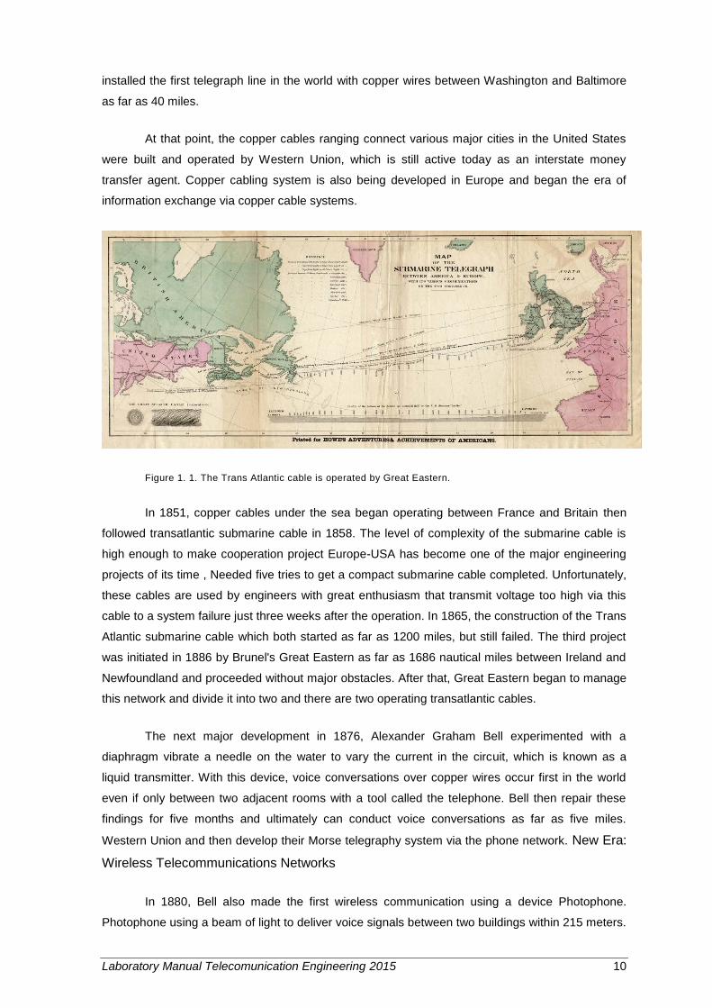
Figure 1. 1. The Trans Atlantic cable is operated by Great Eastern.
In 1851, copper cables under the sea began operating between France and Britain then
followed transatlantic submarine cable in 1858. The level of complexity of the submarine cable is
high enough to make cooperation project Europe-USA has become one of the major engineering
projects of its time , Needed five tries to get a compact submarine cable completed. Unfortunately,
these cables are used by engineers with great enthusiasm that transmit voltage too high via this
cable to a system failure just three weeks after the operation. In 1865, the construction of the Trans
Atlantic submarine cable which both started as far as 1200 miles, but still failed. The third project
was initiated in 1886 by Brunel's Great Eastern as far as 1686 nautical miles between Ireland and
Newfoundland and proceeded without major obstacles. After that, Great Eastern began to manage
this network and divide it into two and there are two operating transatlantic cables.
The next major development in 1876, Alexander Graham Bell experimented with a
diaphragm vibrate a needle on the water to vary the current in the circuit, which is known as a
liquid transmitter. With this device, voice conversations over copper wires occur first in the world
even if only between two adjacent rooms with a tool called the telephone. Bell then repair these
findings for five months and ultimately can conduct voice conversations as far as five miles.
Western Union and then develop their Morse telegraphy system via the phone network. New Era:
Wireless Telecommunications Networks
In 1880, Bell also made the first wireless communication using a device Photophone.
Photophone using a beam of light to deliver voice signals between two buildings within 215 meters.
Laboratory Manual Telecomunication Engineering 2015 11
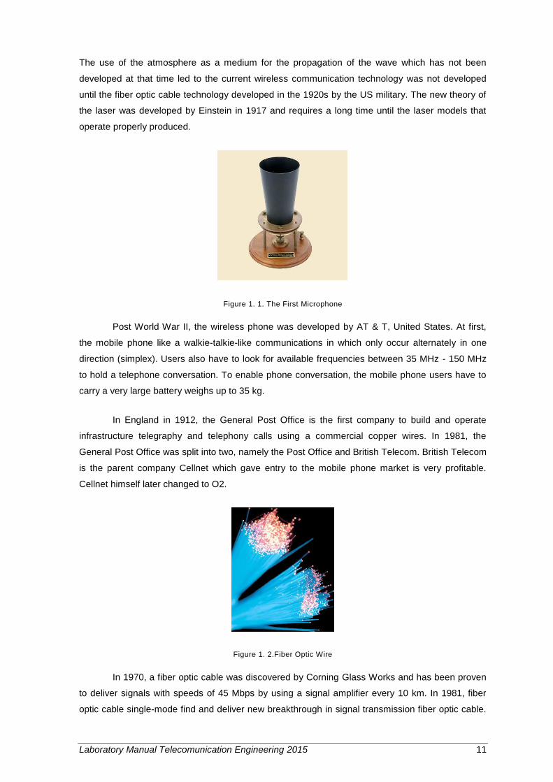
The use of the atmosphere as a medium for the propagation of the wave which has not been
developed at that time led to the current wireless communication technology was not developed
until the fiber optic cable technology developed in the 1920s by the US military. The new theory of
the laser was developed by Einstein in 1917 and requires a long time until the laser models that
operate properly produced.
Figure 1. 1. The First Microphone
Post World War II, the wireless phone was developed by AT & T, United States. At first,
the mobile phone like a walkie-talkie-like communications in which only occur alternately in one
direction (simplex). Users also have to look for available frequencies between 35 MHz - 150 MHz
to hold a telephone conversation. To enable phone conversation, the mobile phone users have to
carry a very large battery weighs up to 35 kg.
In England in 1912, the General Post Office is the first company to build and operate
infrastructure telegraphy and telephony calls using a commercial copper wires. In 1981, the
General Post Office was split into two, namely the Post Office and British Telecom. British Telecom
is the parent company Cellnet which gave entry to the mobile phone market is very profitable.
Cellnet himself later changed to O2.
Figure 1. 2.Fiber Optic Wire
In 1970, a fiber optic cable was discovered by Corning Glass Works and has been proven
to deliver signals with speeds of 45 Mbps by using a signal amplifier every 10 km. In 1981, fiber
optic cable single-mode find and deliver new breakthrough in signal transmission fiber optic cable.

Laboratory Manual Telecomunication Engineering 2015 12
In 1987, the second generation of fiber-optic cable operating at speeds of 1.5 Gbps with
reinforcement at every 50 km. In 1988, Trans Atlantic fiber optic cable was developed. The third
generation technology fiber optic cables capable of operating at a speed of about 2.5 Gbps with
reinforcement at every 100 km.
Explosions of Technology: Cellular Communications
Cell phone was first launched in 1985 in the UK by Vodaphone and Cellnet, which later the
two companies merged into O2. However, the mobile phone is not very practical because it weighs
20 kg with a very large battery systems. At that time, we could see the entrepreneurs carrying two
bags at once, namely file bag and telephone equipment.
In 1992, fourth-generation technology is developed with fiber optic cable Wavelength
Division Multiplexing principle which makes it able to double the speed twice every six months until
2006 has reached a speed of 14 Tbps with boosters every 160 km. This optical fiber cable
technology that allows us to enjoy the cable TV and broadband services (broadband) to various
regions. However, the cost to deploy broadband technology based on fiber optic cables is huge
and the risk is too high. This causes the need for broadband wireless communications is very high
until now.
Figure 1. 3. Development of Mobile Cellular Phone
In the previous description, we have discussed about the birth and development process in
brief communication with the wired network since the invention of Morse code in the 1800s to the
development of optical fiber communication system that began in the late 20th century. When the
fiber optic cable is able to conduct a conversation with a very large number of simultaneous, we
also need to look at the first steps of wireless personal communications that subsequently will be
an explosion of technology that is rapidly until now.
In principle, there is a very important difference between the first generation mobile
communication system with subsequent developments. In the first generation (1G), wireless
communications are still using analog systems. Sound transmitted directly as spoken by humans.
The development of 2G and next generation network transformation into a digital system, where
Laboratory Manual Telecomunication Engineering 2015 13
the voice is sampled and broken into data before it is transmitted. The sending side will then
reorder the data packets into voice intact that we can hear. This is the beginning of the era of
digital communication is growing very rapidly.
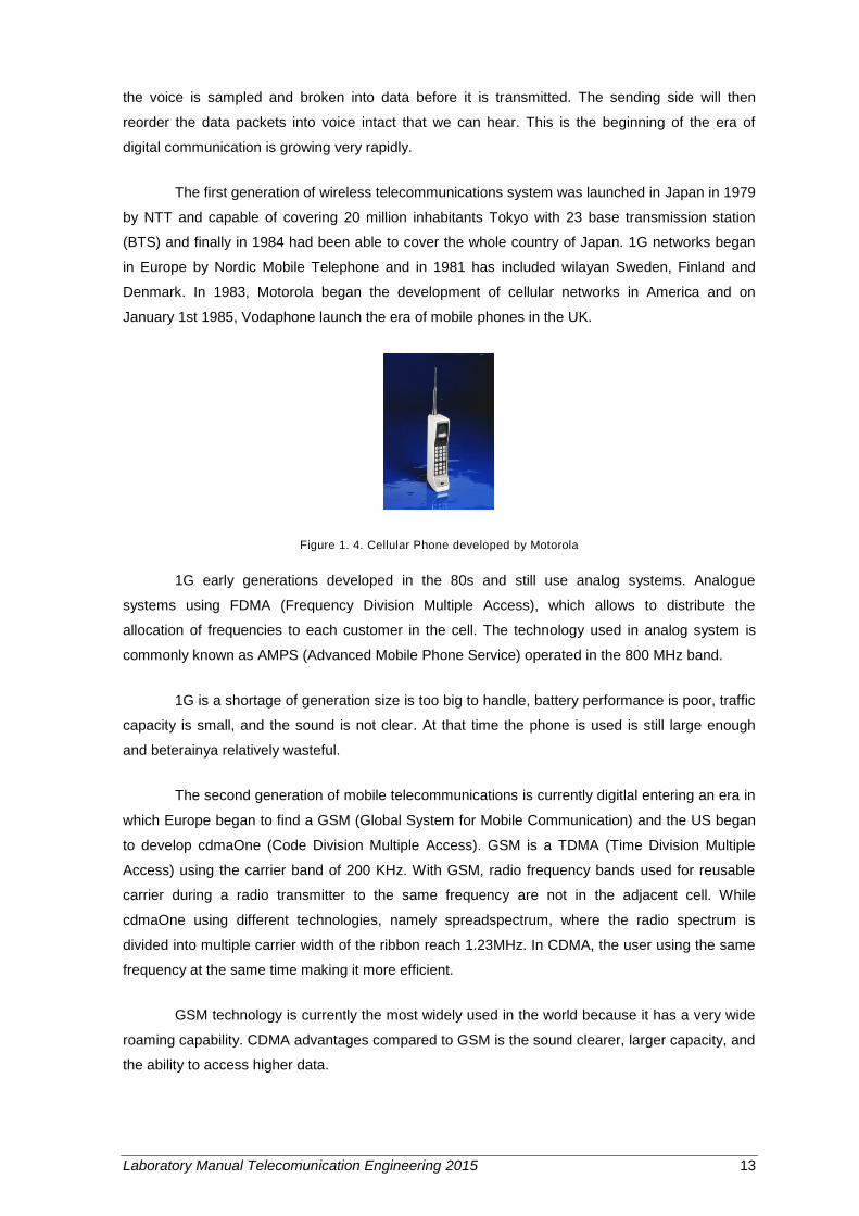
The first generation of wireless telecommunications system was launched in Japan in 1979
by NTT and capable of covering 20 million inhabitants Tokyo with 23 base transmission station
(BTS) and finally in 1984 had been able to cover the whole country of Japan. 1G networks began
in Europe by Nordic Mobile Telephone and in 1981 has included wilayan Sweden, Finland and
Denmark. In 1983, Motorola began the development of cellular networks in America and on
January 1st 1985, Vodaphone launch the era of mobile phones in the UK.
Figure 1. 4. Cellular Phone developed by Motorola
1G early generations developed in the 80s and still use analog systems. Analogue
systems using FDMA (Frequency Division Multiple Access), which allows to distribute the
allocation of frequencies to each customer in the cell. The technology used in analog system is
commonly known as AMPS (Advanced Mobile Phone Service) operated in the 800 MHz band.
1G is a shortage of generation size is too big to handle, battery performance is poor, traffic
capacity is small, and the sound is not clear. At that time the phone is used is still large enough
and beterainya relatively wasteful.
The second generation of mobile telecommunications is currently digitlal entering an era in
which Europe began to find a GSM (Global System for Mobile Communication) and the US began
to develop cdmaOne (Code Division Multiple Access). GSM is a TDMA (Time Division Multiple
Access) using the carrier band of 200 KHz. With GSM, radio frequency bands used for reusable
carrier during a radio transmitter to the same frequency are not in the adjacent cell. While
cdmaOne using different technologies, namely spreadspectrum, where the radio spectrum is
divided into multiple carrier width of the ribbon reach 1.23MHz. In CDMA, the user using the same
frequency at the same time making it more efficient.
GSM technology is currently the most widely used in the world because it has a very wide
roaming capability. CDMA advantages compared to GSM is the sound clearer, larger capacity, and
the ability to access higher data.

Laboratory Manual Telecomunication Engineering 2015 14
This 2G network SMS service start in 1993 and developed into a prepaid system began in
the late 1990s. Nordic Mobile Telephone begin introducing a system of payment by mobile phone
with the vehicle parking systems and vending machines Coca-Cola so the technology is a
promising new method of payment in 1998. The first commercial system that works like a credit
card began in 1999 in the Philippines by two operators , the Globe and Smart.
Advertising services on mobile phones first appeared in Finland in 2000 that allows mobile
phone users receive the latest news of a brand that wants to follow. This service is also open sales
opportunities ringtone to individual consumers. The ringtone was developed from monoponik to
become polyphonic. Polyphonic ringtone then began shifting with MP3 technology that developed
later. In 1999, NTT DoCoMo of Japan presenting the first mobile internet service in the world, but
the speed of service is still limited because of the technological limitations of 2G.
Since very little data access capabilities of GSM, reaching only 9.6 Kbps, began to develop
GPRS (General Packet Radio Data Services). Then the technology was introduced Wireless
Application Protocol (WAP), but the results are not so satisfactory. Until finally GPRS was
developed to be able to access data at speeds up to 115 Kbps and throughput only 20-30 Kbps.
GPRS also enables Internet access from anywhere and in real time. GPRS is less desirable
because the price is quite expensive at that time. Growing technology again is EDGE (Enhanced
Data for Global Evolusion) who only had implemented a minute, at speeds up to 3-4 times the
speed of GPRS.
The development of 3G services, initiated by NTT DoCoMo in early 2001 and the first
commercial 3G network was launched in October 2001 with WCDMA (Wideband Code Division
Multiple Access). In 2002, the 3G network was launched in South Korea and in the United States
named Monet. Both use a standard CDMA / EV-DO which is the Betamax of 3G and Monet also
had collapsed. The second network with WCDMA standard launched by Vodaphone KK (currently
known as Softbank) in Japan. At the same time in Europe, also developed by Three / Hutchison
Group in Italy and the UK.
The third generation is a continuation of GSM, GPRS, EDGE, and CDMA generations ever
before. This advanced technology called the Universal Mobile Telecommunications Service
(UMTS). The goal is to provide data access speed is higher achieve 385 kbps at a frequency of 5
KHz. The selected modulation technique is Wide-CDMA UMTS. Used on WCDMA radio frequency
of 5 MHz in the 1900 MHz band. HSDPA (High Speed Downlink Packet Access) is a continuation
of UMTS that uses radio frequency of 5 MHS by reaching a speed of 2 Mbps. To apply the
necessary UMTS greater costs due to pay a license to the government and the 3G vendor, adding
the base station, and the cost of capex (capital expenditure) and OPEX (operational expenditure)
others. Application of 3G among others for video calls, live streaming, and other broadband
multimedia services.
In 2003, 4 re-launched 3G services in Europe, two of which use WCDMA technology and
the other two use CDMA / EV-DO. WCDMA more developed than CDMA / EV-DO for nearly two-
Laboratory Manual Telecomunication Engineering 2015 15
thirds of the mobile telecommunications market and adopt this technology has become the industry
standard technology for 3G services. Discovery technology HSDPA (High Speed Downlink Packet
Access) enables mobile internet services faster with a speed of 1.8 Mbps to 14.4 Mbps. The
HSDPA service and then continue to grow until its own has become a lifestyle for some people.
Then the third generation is enriched again with the release of generation 3.5G. Speeds up to 3.6
Mbps so that it can serve faster multimedia communications, such as Internet access and video
sharing.
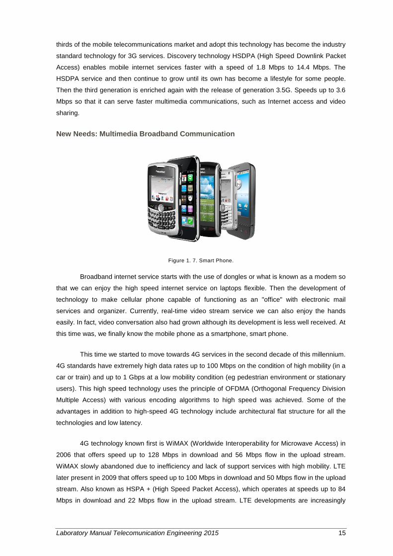
New Needs: Multimedia Broadband Communication
Figure 1. 7. Smart Phone.
Broadband internet service starts with the use of dongles or what is known as a modem so
that we can enjoy the high speed internet service on laptops flexible. Then the development of
technology to make cellular phone capable of functioning as an "office" with electronic mail
services and organizer. Currently, real-time video stream service we can also enjoy the hands
easily. In fact, video conversation also had grown although its development is less well received. At
this time was, we finally know the mobile phone as a smartphone, smart phone.
This time we started to move towards 4G services in the second decade of this millennium.
4G standards have extremely high data rates up to 100 Mbps on the condition of high mobility (in a
car or train) and up to 1 Gbps at a low mobility condition (eg pedestrian environment or stationary
users). This high speed technology uses the principle of OFDMA (Orthogonal Frequency Division
Multiple Access) with various encoding algorithms to high speed was achieved. Some of the
advantages in addition to high-speed 4G technology include architectural flat structure for all the
technologies and low latency.
4G technology known first is WiMAX (Worldwide Interoperability for Microwave Access) in
2006 that offers speed up to 128 Mbps in download and 56 Mbps flow in the upload stream.
WiMAX slowly abandoned due to inefficiency and lack of support services with high mobility. LTE
later present in 2009 that offers speed up to 100 Mbps in download and 50 Mbps flow in the upload
stream. Also known as HSPA + (High Speed Packet Access), which operates at speeds up to 84
Mbps in download and 22 Mbps flow in the upload stream. LTE developments are increasingly
Laboratory Manual Telecomunication Engineering 2015 16
supported by the development of MIMO antenna system (multi input multi output) and smart
antenna which can improve the performance of high-speed services.
In the United States, AT & T, Verizon, and Sprint has started a network based on LTE and
operate optimally in 2013. Then there were plans LightSquared will use satellites to reach 92% of
the US population with LTE service in 2015, although with this technology speed will be a separate
consideration.In Indonesia, commercial 4G service started in 2010 by PT. Firstmedia, Tbk with
trademark Sitra. Sitra WiMAX provides high-speed broadband services in Indonesia's first wireless
in congested areas such as Greater Jakarta, North Sumatra, and Aceh. Sitra itself is an expensive
BWA license holders in the Greater Jakarta area. But with the development of technology, WiMAX
is becoming obsolete because of the huge costs and other technology constraints to be replaced
by LTE. Telkomsel became the first operator to conduct trials of 4G LTE network at the APEC
conference in Bali in October 2013. The network is operated at a frequency of 1800 MHz with a
bandwidth of about 5 MHz.At the end of 2013, PT. Internux then launched the first commercial LTE
4G services since Nov. 14. 2013 at the Greater Jakarta area coverage. The market potential is
expected to reach 30 million people. 4G LTE technology used to use the principles of TDD-LTE
(Time Division Duplex-LTE) at a frequency of 2300 MHz.
4G development in Indonesia is still impressed road in places. The main issues that block
is the issue of government regulation that is not well finished. Besides placing the appropriate
frequency for 4G services is still unclear. In the frequency band above 1800 MHz is still necessary
to reset the frequency or frequency refarming, while the 700 MHz frequency band is still
constrained analog television system that has not been moved to digital television.Today also
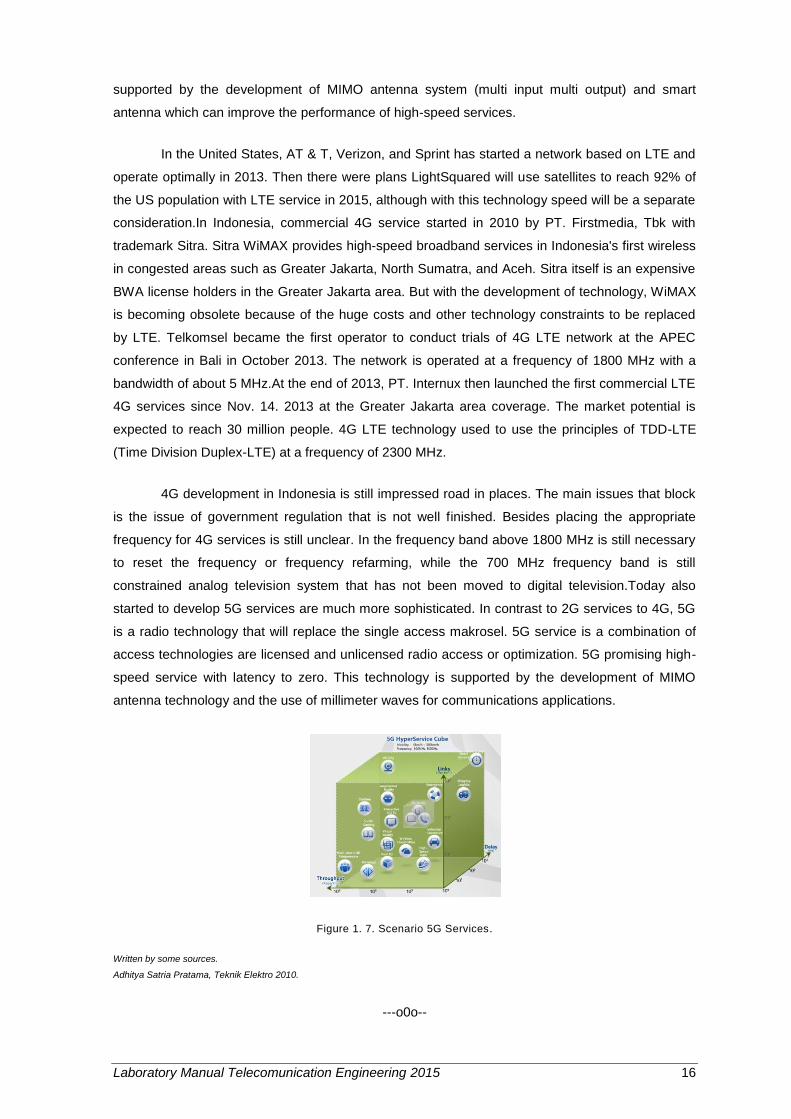
started to develop 5G services are much more sophisticated. In contrast to 2G services to 4G, 5G
is a radio technology that will replace the single access makrosel. 5G service is a combination of
access technologies are licensed and unlicensed radio access or optimization. 5G promising high-
speed service with latency to zero. This technology is supported by the development of MIMO
antenna technology and the use of millimeter waves for communications applications.
Figure 1. 7. Scenario 5G Services.
Written by some sources.
Adhitya Satria Pratama, Teknik Elektro 2010.
---o0o--

Laboratory Manual Telecomunication Engineering 2015 17
Module 2
Transmission Lines
In this assignment the measurement of voltage standing wave ratio (VSWR) of waveguide
components is undertaken using a waveguide slotted-line and probe detector. Voltage standing
wave ratio, invariably abbreviated to VSWR, is one of the fundamental parameters used in
specifying component performance. It quantifies the degree of mismatch a component presents to
the waveguide feed line.
The concept of impedance in waveguides and the use of the Smith Chart in impedance
and matching calculations are introduced. The measurement of impedance of a waveguide
component is carried out and the results used to determine the position of a capacitative probe to
effect matching.
Objectives
After following this lab, you are expected to:
Understand the concept of Voltage Standing Wave Ratio in the transmission line;
Understand the concept of impedance and admittance in the transmission line
Understand how to use Smith Chart to determine the value of impedance and
admittance in the transmission line.
Fundamental Theory
Fundamental of Transmission Lines
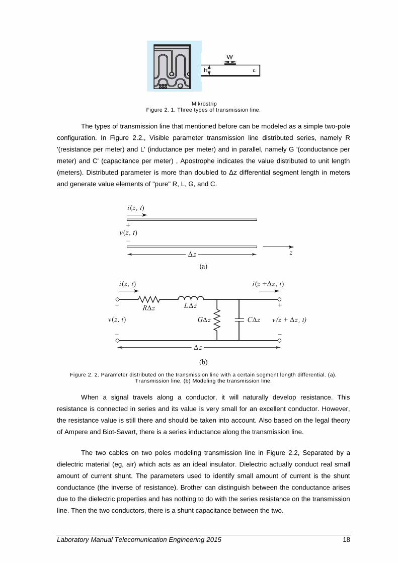
Three types of channels transmisidual plural-conductor encountered are twin lead, coaxial
and microstrip .The transmission line is quite familiar twin lead is used to connect the antenna to
the TV aerial, while the coaxial typically used to connect devices with high frequency. In the coaxial
line, cable consists of three layers: the innermost part jejari a conductor, dielectric layer berjejari b,
and the conductor layer on its outer part. Microstrip widely used in circuit board level. In Microstrip
line consists of copper that coats the substrate of alumina (Al2O3).
Twin Lead
Coaxial
Fundamentals of Electromagnetics With Engineering Applications by Stuart M. Wentworth
Copyright © 2005 by John Wiley & Sons. All rights reserved.
Transmission line examples along with schematic cross sections. A quarter is
shown for scale.
Fundamentals of Electromagnetics With Engineering Applications by Stuart M. Wentworth
Copyright © 2005 by John Wiley & Sons. All rights reserved.
Transmission line examples along with schematic cross sections. A quarter is
shown for scale.
Laboratory Manual Telecomunication Engineering 2015 18
Mikrostrip Figure 2. 1. Three types of transmission line.
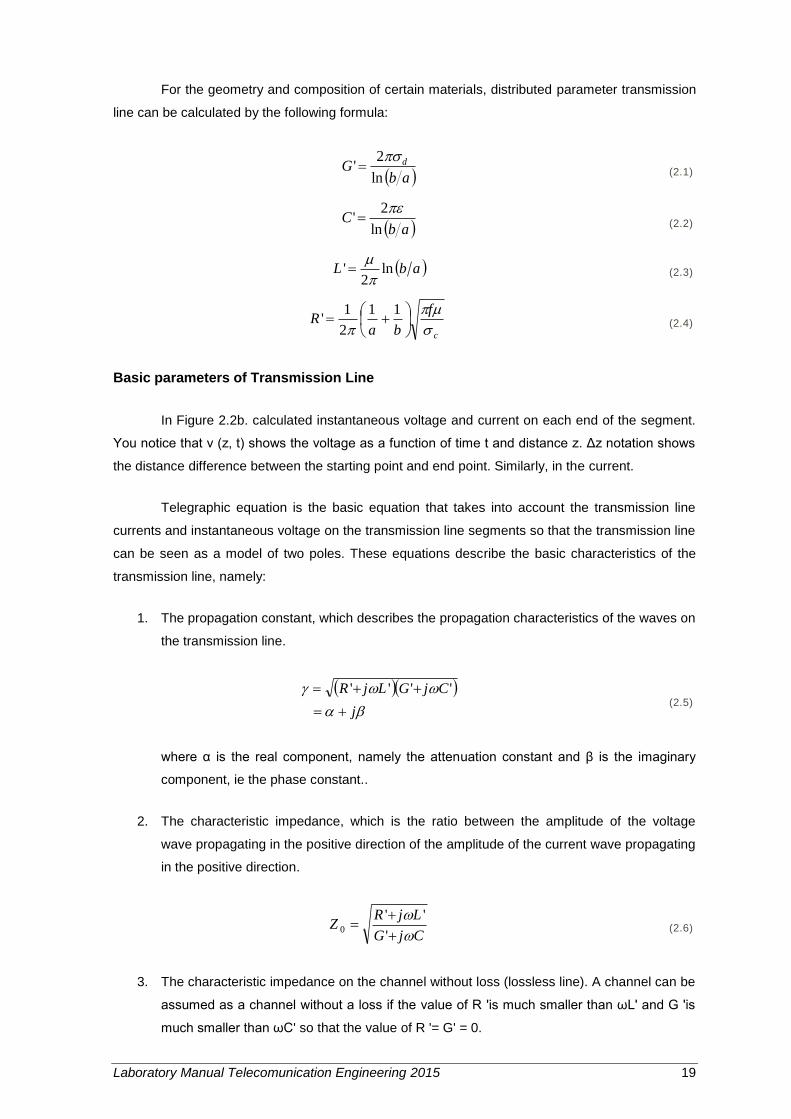
The types of transmission line that mentioned before can be modeled as a simple two-pole
configuration. In Figure 2.2., Visible parameter transmission line distributed series, namely R
'(resistance per meter) and L' (inductance per meter) and in parallel, namely G '(conductance per
meter) and C' (capacitance per meter) , Apostrophe indicates the value distributed to unit length
(meters). Distributed parameter is more than doubled to Δz differential segment length in meters
and generate value elements of "pure" R, L, G, and C.
Figure 2. 2. Parameter distributed on the transmission line with a certain segment length differential. (a). Transmission line, (b) Modeling the transmission line.
When a signal travels along a conductor, it will naturally develop resistance. This
resistance is connected in series and its value is very small for an excellent conductor. However,
the resistance value is still there and should be taken into account. Also based on the legal theory
of Ampere and Biot-Savart, there is a series inductance along the transmission line.
The two cables on two poles modeling transmission line in Figure 2.2, Separated by a
dielectric material (eg, air) which acts as an ideal insulator. Dielectric actually conduct real small
amount of current shunt. The parameters used to identify small amount of current is the shunt
conductance (the inverse of resistance). Brother can distinguish between the conductance arises
due to the dielectric properties and has nothing to do with the series resistance on the transmission
line. Then the two conductors, there is a shunt capacitance between the two.
Fundamentals of Electromagnetics With Engineering Applications by Stuart M. Wentworth
Copyright © 2005 by John Wiley & Sons. All rights reserved.
Transmission line examples along with schematic cross sections. A quarter is
shown for scale.
Fundamentals of Electromagnetics With Engineering Applications by Stuart M. Wentworth
Copyright © 2005 by John Wiley & Sons. All rights reserved.
Transmission line examples along with schematic cross sections. A quarter is
shown for scale.
Laboratory Manual Telecomunication Engineering 2015 19
For the geometry and composition of certain materials, distributed parameter transmission
line can be calculated by the following formula:
abG d
ln
2'
(2.1)
abC
ln
2'
(2.2)
abL ln2
'
(2.3)
c
f
baR
11
2
1' (2.4)
Basic parameters of Transmission Line
In Figure 2.2b. calculated instantaneous voltage and current on each end of the segment.
You notice that v (z, t) shows the voltage as a function of time t and distance z. Δz notation shows
the distance difference between the starting point and end point. Similarly, in the current.
Telegraphic equation is the basic equation that takes into account the transmission line
currents and instantaneous voltage on the transmission line segments so that the transmission line
can be seen as a model of two poles. These equations describe the basic characteristics of the
transmission line, namely:
1. The propagation constant, which describes the propagation characteristics of the waves on
the transmission line.
j
CjGLjR
'''' (2.5)
where α is the real component, namely the attenuation constant and β is the imaginary
component, ie the phase constant..
2. The characteristic impedance, which is the ratio between the amplitude of the voltage
wave propagating in the positive direction of the amplitude of the current wave propagating
in the positive direction.
CjG
LjRZ
'
''0 (2.6)
3. The characteristic impedance on the channel without loss (lossless line). A channel can be
assumed as a channel without a loss if the value of R 'is much smaller than ωL' and G 'is
much smaller than ωC' so that the value of R '= G' = 0.
Laboratory Manual Telecomunication Engineering 2015 20
'
'0
C
LZ (2.7)
Terminated Transmission Lines
Figure 2. 3. The transmission line that is terminated by a load. Positive direction indicates the direction
toward the load side, and negative indicates the opposite direction.
Some interesting phenomenon arises when a transmission line terminated with a load that
is placed at z = 0. The load impedance is the ratio between the voltage of the current on the load
side.
00
000
VV
VVZZ L
(2.8)
where Z0 is the characteristic impedance of the transmission line. Equation 2.8 can be rearranged
into:
0
0
0
0 VZZ
ZZV
L
L (2.9)
From equation 2.9. it appears that if the value of the load impedance ZL is equal to the
characteristic impedance Z0 channels, then no waves are reflected back to the source. This
condition is referred to as the state of the corresponding (matching).
In the case where the load impedance is not equal to or does not match line impedance
(mismatched), there is waves that bounce back toward the source and is considered harmful. The
level of impedance mismatch of the channel expressed in the reflection coefficient parameter
(refflection coefficient) on the load side, namely:
0
0
0
0
ZZ
ZZ
V
V
L
LL
(2.10)
In the short-circuit load (ZL = 0), the corresponding load (ZL = Z0), and load open circuit
(ZL = ∞) value of the reflection coefficient, respectively - 1, 0, and +1. Superposition of these
waves form a standing wave (standing wave), where the ratio between the value of the maximum
Laboratory Manual Telecomunication Engineering 2015 21
amplitude of the wave superposition minimum amplitude wave superposition expressed in
parameter VSWR (voltage standing wave ratio).
L
LVSWR
1
1
(2.11)
which ranges from 1 to infinity.
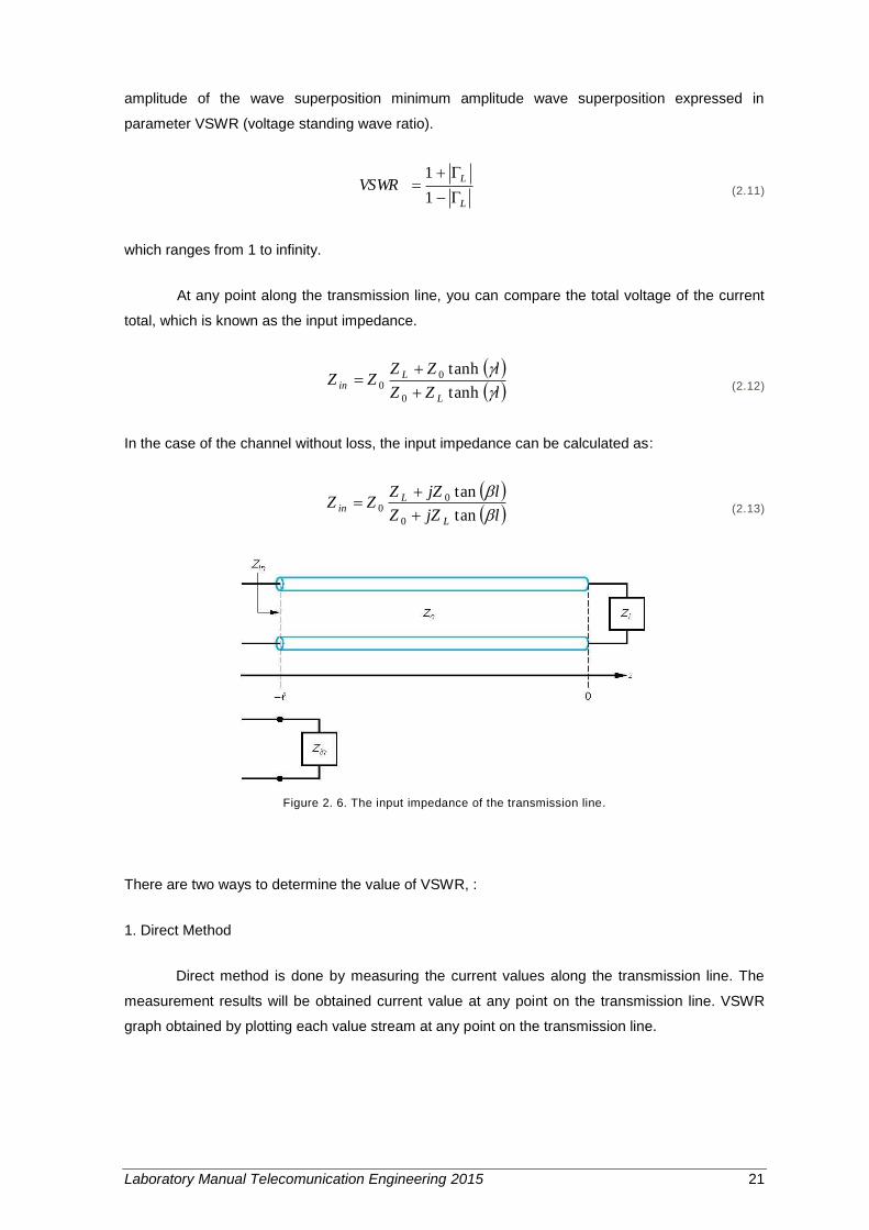
At any point along the transmission line, you can compare the total voltage of the current
total, which is known as the input impedance.
lZZ
lZZZZ
L
Lin
tanh
tanh
0
00
(2.12)
In the case of the channel without loss, the input impedance can be calculated as:
ljZZ
ljZZZZ
L
Lin
tan
tan
0
00
(2.13)
Figure 2. 6. The input impedance of the transmission line.
There are two ways to determine the value of VSWR, :
1. Direct Method
Direct method is done by measuring the current values along the transmission line. The
measurement results will be obtained current value at any point on the transmission line. VSWR
graph obtained by plotting each value stream at any point on the transmission line.
Fundamentals of Electromagnetics With Engineering Applications by Stuart M. Wentworth
Copyright © 2005 by John Wiley & Sons. All rights reserved.
The terminated T-line can be replaced by an equivalent lumped-element input
impedance.
Laboratory Manual Telecomunication Engineering 2015 22
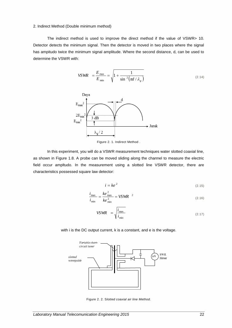
2. Indirect Method (Double minimum method)
The indirect method is used to improve the direct method if the value of VSWR> 10.
Detector detects the minimum signal. Then the detector is moved in two places where the signal
has ampitudo twice the minimum signal amplitude. Where the second distance, d, can be used to
determine the VSWR with:
gdE
EVSWR
/sin
11
2min
max (2.14)
Figure 2. 1. Indirect Method .
In this experiment, you will do a VSWR measurement techniques water slotted coaxial line,
as shown in Figure 1.8. A probe can be moved sliding along the channel to measure the electric
field occur ampltudo. In the measurement using a slotted line VSWR detector, there are
characteristics possessed square law detector:
2kei (2.15)
2
2min
2max
min
max VSWRke
ke
i
i (2.16)
min
max
i
iVSWR (2.17)
with i is the DC output current, k is a constant, and e is the voltage.
Figure 2. 2. Slotted coaxial air line Method.
Laboratory Manual Telecomunication Engineering 2015 23
A large electric field along the waveguide (waveguide) can be detected using a
slotted-line. The electric field is captured by the detector diodes in the probe. By sliding
the probe along the channel, the value of the electric field tercuplik. Depth probe on-line
slotted channels need to be considered, because the probe is inserted in the value of the
resulting output will be even greater. Good depth is not too deep or not too shallow, too
deep because otherwise it will cause a perturbation (disruption) which mengkopling field
in the channel so that its value will be getting bigger and inaccurate. In the detector also
given custody stub used to minimize the effects of loading (capacitance and resistance
shunt) on the transmission line.
Diagram Smith
Smith chart is a diagram which is used to understand the characteristics of the
transmission line and microwave circuit elements. This diagram consists of real and
imaginary numbers, where the real component is shown by a full circle, while the
imaginary component shown by a curved shape. Some characteristics of the transmission
line can be calculated with the Smith Chart include the VSWR, the load impedance,
admittance load, and the reflection coefficient. Based on the Smith chart can be
determined whether the conditions of the transmission line matching or not..
Equipment
This module uses lab equipment Microwave Trainer (MWT530) manufactured
Feedback Instruments Ltd. Equipment used in Table 1.1 below.
Table 2. 1. Equipment used in Transmission Line Module.
No Tool’s Name Quantity
1. Microwave Trainer Board 1
2. Variabel Attenuator 1
3. X-band CW Gunn Oscilator Source 1
4. Slotted line 1
5. Probe diode detector 1
6. Terminal hubung singkat 1
7. Terminal resistif 1
8. Waveguide Antena horn 1
9. H-plane tee 1
Laboratory Manual Telecomunication Engineering 2015 24
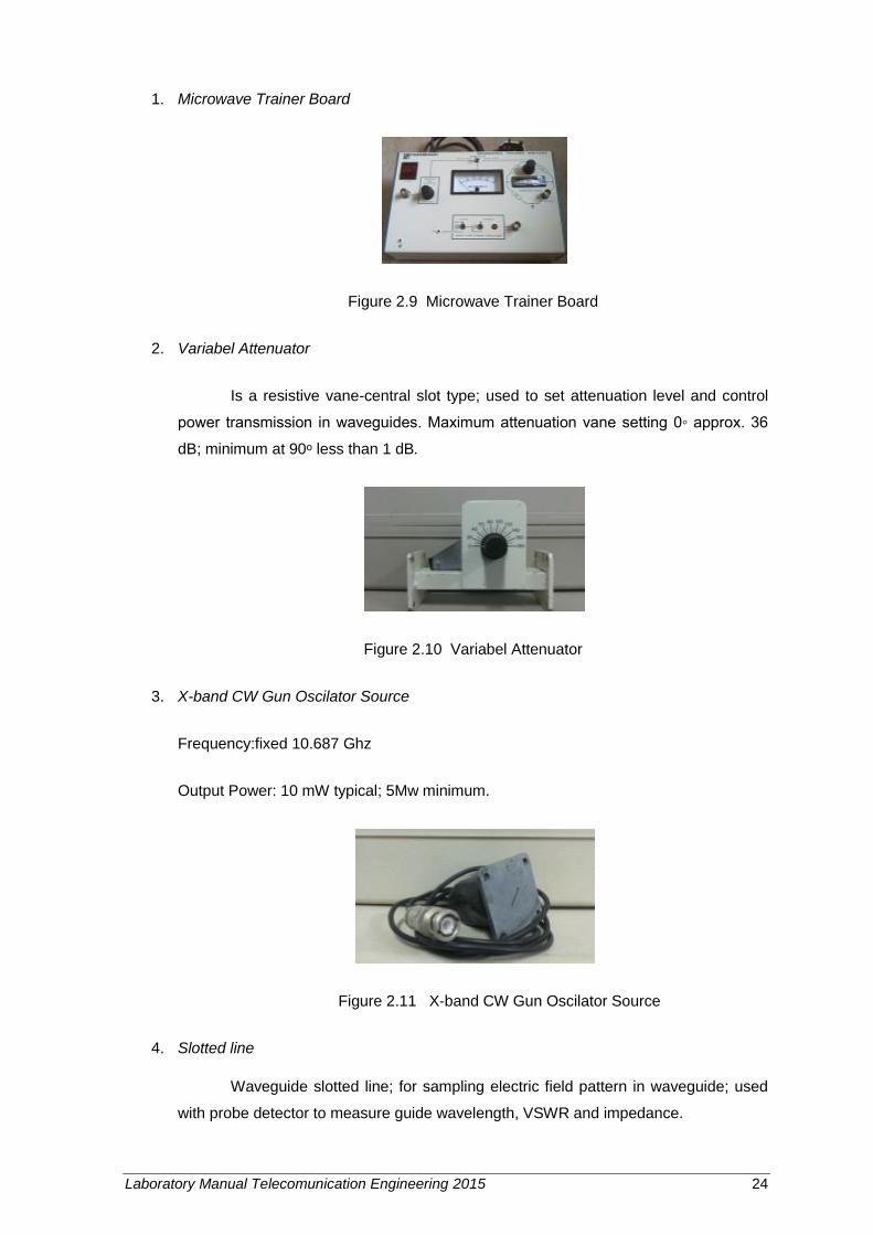
1. Microwave Trainer Board
Figure 2.9 Microwave Trainer Board
2. Variabel Attenuator
Is a resistive vane-central slot type; used to set attenuation level and control
power transmission in waveguides. Maximum attenuation vane setting 0◦ approx. 36
dB; minimum at 90ᵒ less than 1 dB.
Figure 2.10 Variabel Attenuator
3. X-band CW Gun Oscilator Source
Frequency:fixed 10.687 Ghz
Output Power: 10 mW typical; 5Mw minimum.
Figure 2.11 X-band CW Gun Oscilator Source
4. Slotted line
Waveguide slotted line; for sampling electric field pattern in waveguide; used
with probe detector to measure guide wavelength, VSWR and impedance.
Laboratory Manual Telecomunication Engineering 2015 25
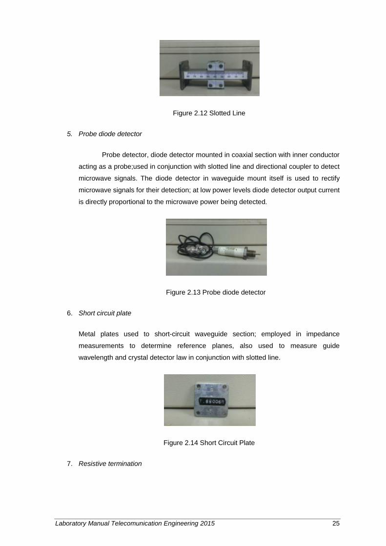
Figure 2.12 Slotted Line
5. Probe diode detector
Probe detector, diode detector mounted in coaxial section with inner conductor
acting as a probe;used in conjunction with slotted line and directional coupler to detect
microwave signals. The diode detector in waveguide mount itself is used to rectify
microwave signals for their detection; at low power levels diode detector output current
is directly proportional to the microwave power being detected.
Figure 2.13 Probe diode detector
6. Short circuit plate
Metal plates used to short-circuit waveguide section; employed in impedance
measurements to determine reference planes, also used to measure guide
wavelength and crystal detector law in conjunction with slotted line.
Figure 2.14 Short Circuit Plate
7. Resistive termination
Laboratory Manual Telecomunication Engineering 2015 26
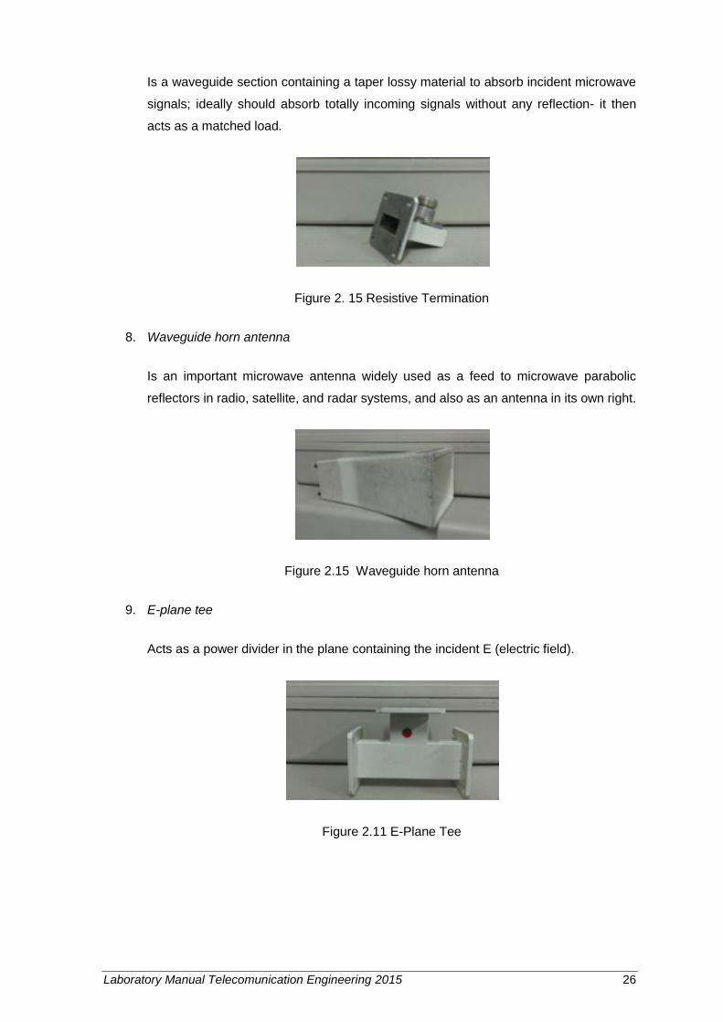
Is a waveguide section containing a taper lossy material to absorb incident microwave
signals; ideally should absorb totally incoming signals without any reflection- it then
acts as a matched load.
Figure 2. 15 Resistive Termination
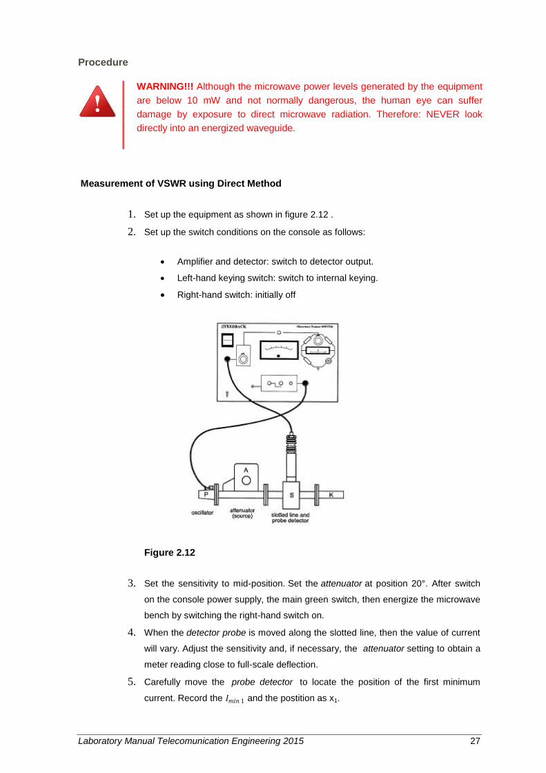
8. Waveguide horn antenna
Is an important microwave antenna widely used as a feed to microwave parabolic
reflectors in radio, satellite, and radar systems, and also as an antenna in its own right.
Figure 2.15 Waveguide horn antenna
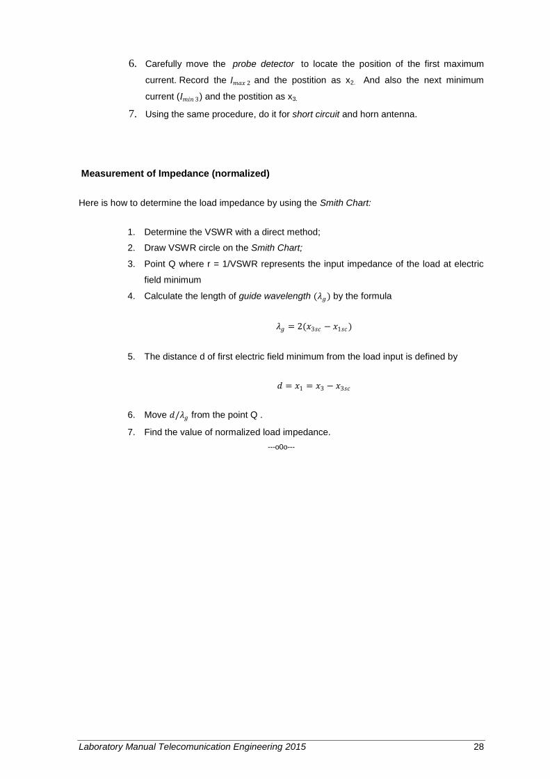
9. E-plane tee
Acts as a power divider in the plane containing the incident E (electric field).
Figure 2.11 E-Plane Tee
Laboratory Manual Telecomunication Engineering 2015 27
Procedure
WARNING!!! Although the microwave power levels generated by the equipment
are below 10 mW and not normally dangerous, the human eye can suffer
damage by exposure to direct microwave radiation. Therefore: NEVER look
directly into an energized waveguide.
Measurement of VSWR using Direct Method
1. Set up the equipment as shown in figure 2.12 .
2. Set up the switch conditions on the console as follows:
Amplifier and detector: switch to detector output.
Left-hand keying switch: switch to internal keying.
Right-hand switch: initially off
Figure 2.12
3. Set the sensitivity to mid-position. Set the attenuator at position 20°. After switch
on the console power supply, the main green switch, then energize the microwave
bench by switching the right-hand switch on.
4. When the detector probe is moved along the slotted line, then the value of current
will vary. Adjust the sensitivity and, if necessary, the attenuator setting to obtain a
meter reading close to full-scale deflection.
5. Carefully move the probe detector to locate the position of the first minimum
current. Record the 𝐼𝑚𝑖𝑛 1 and the postition as x1.
Laboratory Manual Telecomunication Engineering 2015 28
6. Carefully move the probe detector to locate the position of the first maximum
current. Record the 𝐼𝑚𝑎𝑥 2 and the postition as x2. And also the next minimum
current (𝐼𝑚𝑖𝑛 3) and the postition as x3.
7. Using the same procedure, do it for short circuit and horn antenna.
Measurement of Impedance (normalized)
Here is how to determine the load impedance by using the Smith Chart:
1. Determine the VSWR with a direct method;
2. Draw VSWR circle on the Smith Chart;
3. Point Q where r = 1/VSWR represents the input impedance of the load at electric
field minimum
4. Calculate the length of guide wavelength (𝜆𝑔) by the formula
𝜆𝑔 = 2(𝑥3𝑠𝑐 − 𝑥1𝑠𝑐)
5. The distance d of first electric field minimum from the load input is defined by
𝑑 = 𝑥1 = 𝑥3 − 𝑥3𝑠𝑐
6. Move 𝑑/𝜆𝑔 from the point Q .
7. Find the value of normalized load impedance.
---o0o---
Laboratory Manual Telecomunication Engineering 2015 29
Module 3
Amplitude Modulation
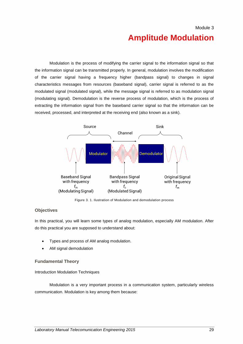
Modulation is the process of modifying the carrier signal to the information signal so that
the information signal can be transmitted properly. In general, modulation involves the modification
of the carrier signal having a frequency higher (bandpass signal) to changes in signal
characteristics messages from resources (baseband signal), carrier signal is referred to as the
modulated signal (modulated signal), while the message signal is referred to as modulation signal
(modulating signal). Demodulation is the reverse process of modulation, which is the process of
extracting the information signal from the baseband carrier signal so that the information can be
received, processed, and interpreted at the receiving end (also known as a sink).
Figure 3. 1. Ilustration of Modulation and demodulation process
Objectives
In this practical, you will learn some types of analog modulation, especially AM modulation. After
do this practical you are supposed to understand about:
Types and process of AM analog modulation.
AM signal demodulation
Fundamental Theory
Introduction Modulation Techniques
Modulation is a very important process in a communication system, particularly wireless
communication. Modulation is key among them because:

Laboratory Manual Telecomunication Engineering 2015 30
1. Modulation allows the antenna size becomes smaller, as the signal frequency becomes
higher. For an efficient radiation, measuring the size of the antenna should be λ / 10 or
more (ideally λ / 4), where λ is the wavelength of the signal to be radiated.
2. Modulation allows any technique or multiplex multiple paths so as to save resources
existing frequencies.
3. Modulation allows the channel assignment, for example in FM radio that separate radio
channels based on the frequency of the carrier signal. As an example for the RTC UI on
107.9 MHz, MBS at 102.2 MHz, 90.0 MHz Elshinta, and others.
A signal (carrier) can generally be expressed as:
tfAAtc ccc 2coscos)( (3.1)
where c (t) is the instantaneous wave function (instantaneous value), AC is the maximum
amplitude value [Volt], and cos θ is the angle that is divided into frequency components,
namely fc [Hertz] and phase components, namely φ [degrees ].
Based on the type of signal information, modulation is divided into analog
modulation in which a signal information in the form of analog signals and digital
modulation in which the information signal in the form of digital bits. The carrier signal is
always analog, because naturally a signal that can be transmitted in the air is an analog
signal. Based components of the equation, modulation is divided into amplitude
modulation (amplitude modulation, AM) and modulation angle (angle modulation). Angle
modulation itself subdivided based components, namely the frequency modulation
(frequency modulation, FM) and phase modulation (phase modulation, AM). AM
modulation AM then developed into a full carrier double side band (DSB-FC), double side
band suppressed carrier (DSB-SC), single side band (SSB), and vestigial side band
(VSB). Modulation FM and PM are divided by the width of the frequency spectrum owned
into a narrowband (NB) and wideband (WB).
Amplitude Modulation Process
At AM DSB-FC modulation, the carrier signal is :
tfVtv ccc 2cos)( (3.2)
While information signal is :

Laboratory Manual Telecomunication Engineering 2015 31
tfVtv mmm 2cos)( (3.3)
AM modulated signals generated by the equation:
tftfVVtV cmmcam 2cos2cos)( (3.4)
where tfVV mmc 2cos an envelope function equation and tfc2cos is a sinusoidal
wave equation. If the value of VC is issued, then the equation 2.4. can be written back
into:
v tftfmVtV cmAMcam 2cos2cos1)( (3.5)
where mAM is called as modulation index or mAM = Vm/VC. Modulation index determines the
quality of AM modulated signals. By using trigonometric identities:
v )cos(2
1)cos(
2
1))(cos(cos YXYXYX (3.6)
the AM modulated signal can be written as:
v tftfmVtfVtV mcAMcccam 2cos2cos2cos)( (3.7)
or if using the modulation index:
v tfftffmV
tfVtV mcmcAMc
ccam )(2cos)(2cos2
2cos)( (3.8)
Groove block diagram of AM modulated signal generation process shown in Figure 3.2.
Figure 3. 2. Block Diagram for AM Modulation
Laboratory Manual Telecomunication Engineering 2015 32
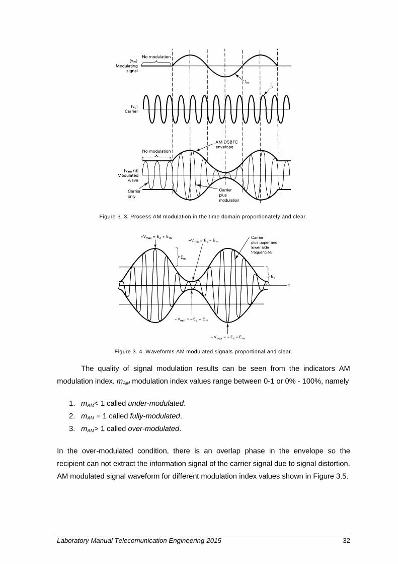
Figure 3. 3. Process AM modulation in the time domain proportionately and clear.
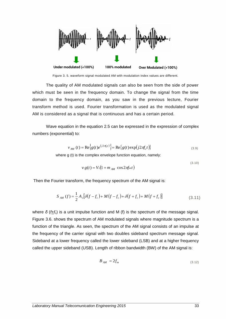
Figure 3. 4. Waveforms AM modulated signals proportional and clear.
The quality of signal modulation results can be seen from the indicators AM
modulation index. mAM modulation index values range between 0-1 or 0% - 100%, namely
1. mAM< 1 called under-modulated.
2. mAM = 1 called fully-modulated.
3. mAM> 1 called over-modulated.
In the over-modulated condition, there is an overlap phase in the envelope so the
recipient can not extract the information signal of the carrier signal due to signal distortion.
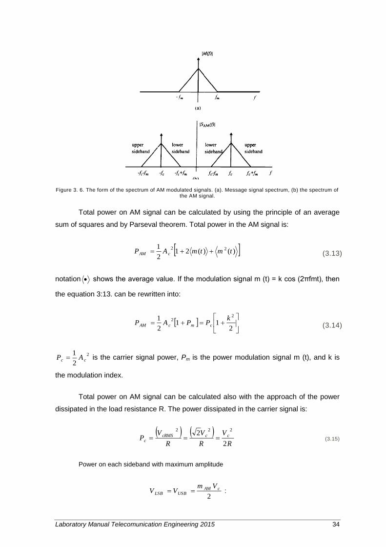
AM modulated signal waveform for different modulation index values shown in Figure 3.5.
Laboratory Manual Telecomunication Engineering 2015 33
Figure 3. 5. waveform signal modulated AM with modulation index values are different.
The quality of AM modulated signals can also be seen from the side of power
which must be seen in the frequency domain. To change the signal from the time
domain to the frequency domain, as you saw in the previous lecture, Fourier
transform method is used. Fourier transformation is used as the modulated signal
AM is considered as a signal that is continuous and has a certain period.
Wave equation in the equation 2.5 can be expressed in the expression of complex
numbers (exponential) to:
v tfjtgetgtv c
tfj
AMc
2exp)(Re)(Re)(2
(3.9)
where g (t) is the complex envelope function equation, namely:
v tfmVtg mAMc 2cos1)(
(3.10)
Then the Fourier transform, the frequency spectrum of the AM signal is:
v cccccAM ffMffffMffAfS 2
1)( (3.11)
where δ (f+fc) is a unit impulse function and M (f) is the spectrum of the message signal.
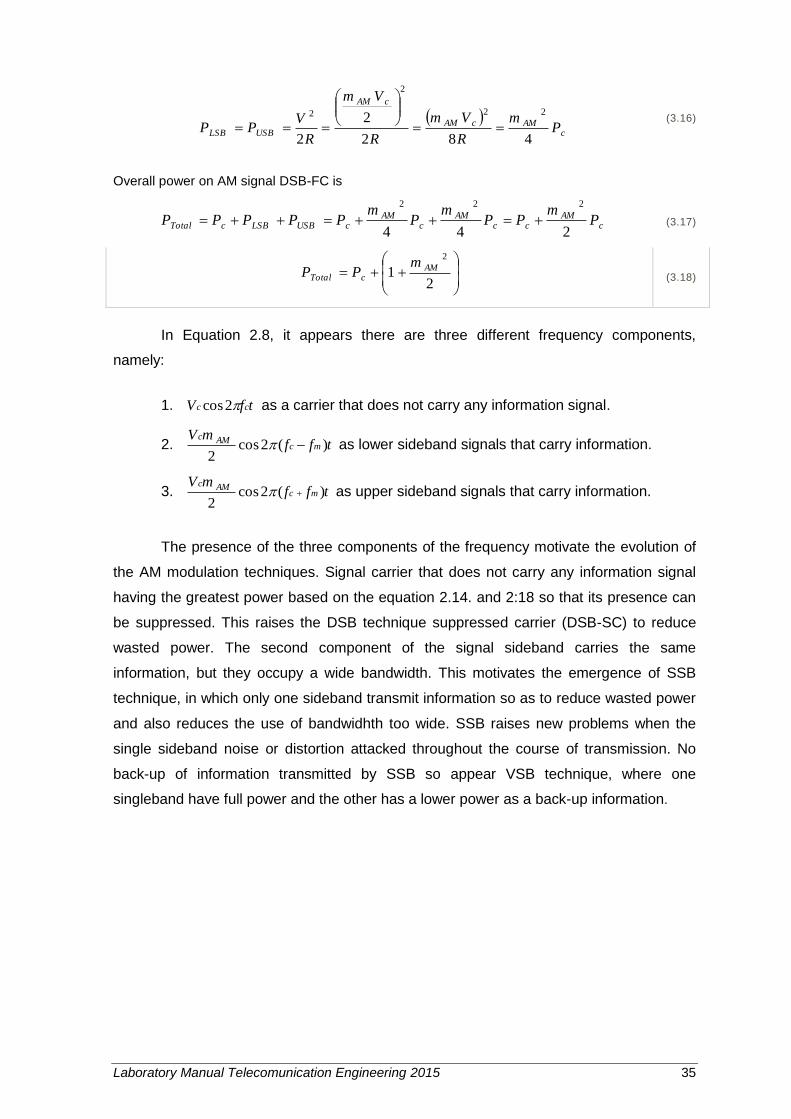
Figure 3.6. shows the spectrum of AM modulated signals where magnitude spectrum is a
function of the triangle. As seen, the spectrum of the AM signal consists of an impulse at
the frequency of the carrier signal with two doubles sideband spectrum message signal.
Sideband at a lower frequency called the lower sideband (LSB) and at a higher frequency
called the upper sideband (USB). Length of ribbon bandwidth (BW) of the AM signal is:
v mAM fB 2 (3.12)
Laboratory Manual Telecomunication Engineering 2015 34
Figure 3. 6. The form of the spectrum of AM modulated signals. (a). Message signal spectrum, (b) the spectrum of the AM signal.
Total power on AM signal can be calculated by using the principle of an average
sum of squares and by Parseval theorem. Total power in the AM signal is:
v )()(212
1 22tmtmAP cAM (3.13)
notation shows the average value. If the modulation signal m (t) = k cos (2πfmt), then
the equation 3:13. can be rewritten into:
v
211
2
1 22 k
PPAP cmcAM (3.14)
2
2
1cc AP is the carrier signal power, Pm is the power modulation signal m (t), and k is
the modulation index.
Total power on AM signal can be calculated also with the approach of the power
dissipated in the load resistance R. The power dissipated in the carrier signal is:
v
R
V
R
V
R
VP cccRMS
c2
2222
(3.15)
Power on each sideband with maximum amplitude
2
cAMUSBLSB
VmVV :
Laboratory Manual Telecomunication Engineering 2015 35
v
cAMcAM
cAM
USBLSB Pm
R
Vm
R
Vm
R
VPP
482
2
2
22
2
2
(3.16)
Overall power on AM signal DSB-FC is
v cAM
ccAM
cAM
cUSBLSBcTotal Pm
PPm
Pm
PPPPP244
222
(3.17)
21
2
AMcTotal
mPP (3.18)
In Equation 2.8, it appears there are three different frequency components,
namely:
1. tfV cc 2cos as a carrier that does not carry any information signal.
2. tffmV
mcAMc
)(2cos2
as lower sideband signals that carry information.
3. tffmV
mcAMc
)(2cos2
as upper sideband signals that carry information.
The presence of the three components of the frequency motivate the evolution of
the AM modulation techniques. Signal carrier that does not carry any information signal
having the greatest power based on the equation 2.14. and 2:18 so that its presence can
be suppressed. This raises the DSB technique suppressed carrier (DSB-SC) to reduce
wasted power. The second component of the signal sideband carries the same
information, but they occupy a wide bandwidth. This motivates the emergence of SSB
technique, in which only one sideband transmit information so as to reduce wasted power
and also reduces the use of bandwidhth too wide. SSB raises new problems when the
single sideband noise or distortion attacked throughout the course of transmission. No
back-up of information transmitted by SSB so appear VSB technique, where one
singleband have full power and the other has a lower power as a back-up information.
Laboratory Manual Telecomunication Engineering 2015 36
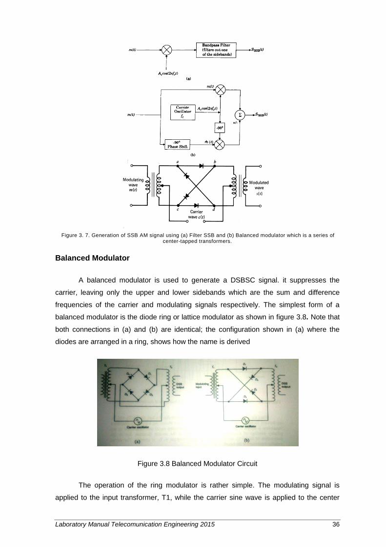
Figure 3. 7. Generation of SSB AM signal using (a) Filter SSB and (b) Balanced modulator which is a series of center-tapped transformers.
Balanced Modulator
A balanced modulator is used to generate a DSBSC signal. it suppresses the
carrier, leaving only the upper and lower sidebands which are the sum and difference
frequencies of the carrier and modulating signals respectively. The simplest form of a
balanced modulator is the diode ring or lattice modulator as shown in figure 3.8. Note that
both connections in (a) and (b) are identical; the configuration shown in (a) where the
diodes are arranged in a ring, shows how the name is derived
Figure 3.8 Balanced Modulator Circuit
The operation of the ring modulator is rather simple. The modulating signal is
applied to the input transformer, T1, while the carrier sine wave is applied to the center
Laboratory Manual Telecomunication Engineering 2015 37
taps of the input and output transformer. The carrier serves as a source of forward and
reverse bias for the diodes which function like swithces to conect the modulating signal to
the output transformer, T2. The result is that DSBSC signal will be generated at the output
transformer.
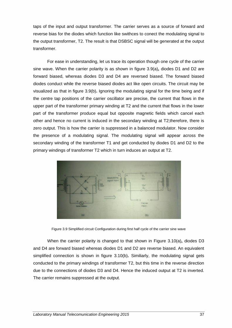
For ease in understanding, let us trace its operation though one cycle of the carrier
sine wave. When the carrier polarity is as shown in figure 3.9(a), diodes D1 and D2 are
forward biased, whereas diodes D3 and D4 are reversed biased. The forward biased
diodes conduct while the reverse biased diodes act like open circuits. The circuit may be
visualized as that in figure 3.9(b). Ignoring the modulating signal for the time being and if
the centre tap positions of the carrier oscillator are precise, the current that flows in the
upper part of the transformer primary winding at T2 and the current that flows in the lower
part of the transformer produce equal but opposite magnetic fields which cancel each
other and hence no current is induced in the secondary winding at T2;therefore, there is
zero output. This is how the carrier is suppressed in a balanced modulator. Now consider
the presence of a modulating signal. The modulating signal will appear across the
secondary winding of the transformer T1 and get conducted by diodes D1 and D2 to the
primary windings of transformer T2 which in turn induces an output at T2.
Figure 3.9 Simplified circuit Configuration during first half cycle of the carrier sine wave
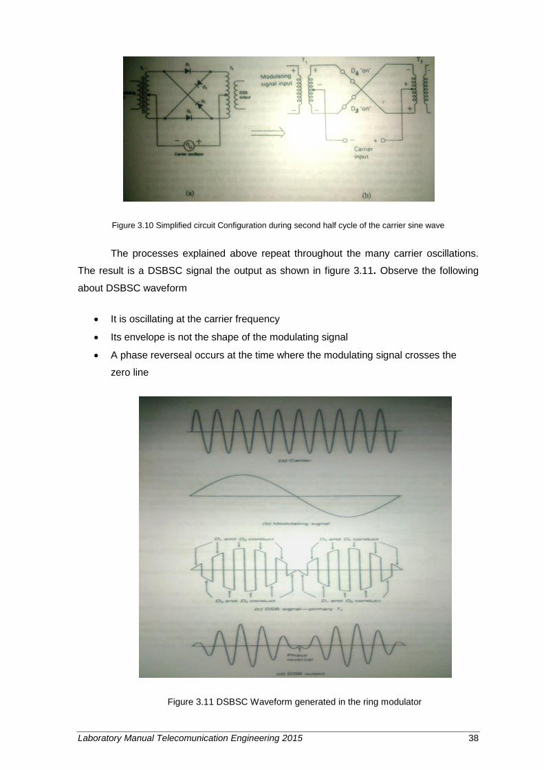
When the carrier polarity is changed to that shown in Figure 3.10(a), diodes D3
and D4 are forward biased whereas diodes D1 and D2 are reverse biased. An equivalent
simplified connection is shown in figure 3.10(b). Similiarly, the modulating signal gets
conducted to the primary windings of transformer T2, but this time in the reverse direction
due to the connections of diodes D3 and D4. Hence the induced output at T2 is inverted.
The carrier remains suppressed at the output.
Laboratory Manual Telecomunication Engineering 2015 38
Figure 3.10 Simplified circuit Configuration during second half cycle of the carrier sine wave
The processes explained above repeat throughout the many carrier oscillations.
The result is a DSBSC signal the output as shown in figure 3.11. Observe the following
about DSBSC waveform
It is oscillating at the carrier frequency
Its envelope is not the shape of the modulating signal
A phase reverseal occurs at the time where the modulating signal crosses the
zero line
Figure 3.11 DSBSC Waveform generated in the ring modulator
Laboratory Manual Telecomunication Engineering 2015 39
Demodulation Process
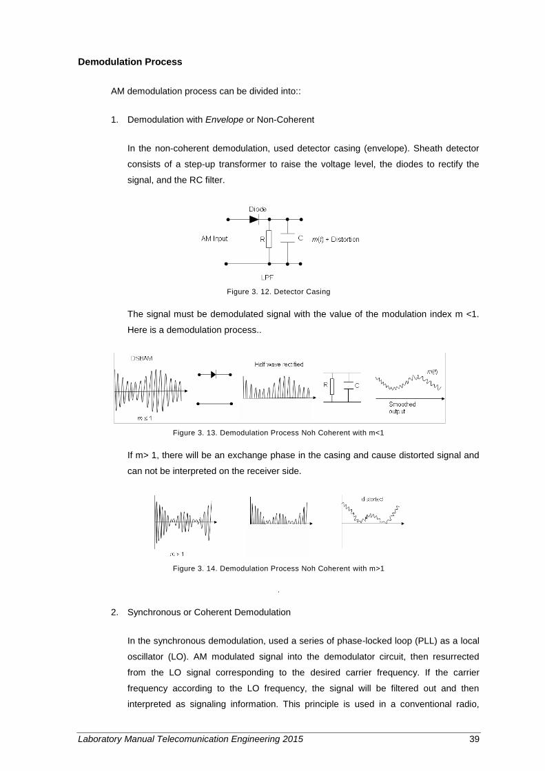
AM demodulation process can be divided into::
1. Demodulation with Envelope or Non-Coherent
In the non-coherent demodulation, used detector casing (envelope). Sheath detector
consists of a step-up transformer to raise the voltage level, the diodes to rectify the
signal, and the RC filter.
Figure 3. 12. Detector Casing
The signal must be demodulated signal with the value of the modulation index m <1.
Here is a demodulation process..
Figure 3. 13. Demodulation Process Noh Coherent with m<1
If m> 1, there will be an exchange phase in the casing and cause distorted signal and
can not be interpreted on the receiver side.
Figure 3. 14. Demodulation Process Noh Coherent with m>1
.
2. Synchronous or Coherent Demodulation
In the synchronous demodulation, used a series of phase-locked loop (PLL) as a local
oscillator (LO). AM modulated signal into the demodulator circuit, then resurrected
from the LO signal corresponding to the desired carrier frequency. If the carrier
frequency according to the LO frequency, the signal will be filtered out and then
interpreted as signaling information. This principle is used in a conventional radio,
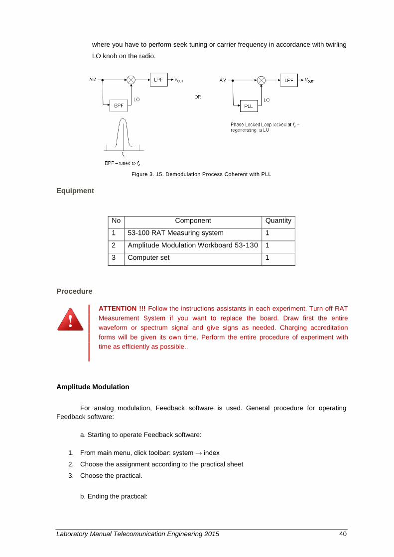
Laboratory Manual Telecomunication Engineering 2015 40
where you have to perform seek tuning or carrier frequency in accordance with twirling
LO knob on the radio.
Figure 3. 15. Demodulation Process Coherent with PLL
Equipment
No Component Quantity
1 53-100 RAT Measuring system 1
2 Amplitude Modulation Workboard 53-130 1
3 Computer set 1
Procedure
ATTENTION !!! Follow the instructions assistants in each experiment. Turn off RAT
Measurement System if you want to replace the board. Draw first the entire
waveform or spectrum signal and give signs as needed. Charging accreditation
forms will be given its own time. Perform the entire procedure of experiment with
time as efficiently as possible..
Amplitude Modulation
For analog modulation, Feedback software is used. General procedure for operating
Feedback software:
a. Starting to operate Feedback software:
1. From main menu, click toolbar: system → index
2. Choose the assignment according to the practical sheet
3. Choose the practical.
b. Ending the practical:

Laboratory Manual Telecomunication Engineering 2015 41
1. Click: System → end practical
2. If you want to end your practical in Feedback software, click: System → quit
ASSIGNMENT 1 PRACTICAL 1: Amplitude Modulation with Full Carrier
1. Set the <carrier level> to maximum
2. Set <modulation level> to zero
3. Note the signal at all monitoring points
4. Now increase the <modulation level> and observe at monitor point <6>
5. Increase the <modulation level> until the carrier amplitude just reaches zero on
negative modulation peak.
6. Observe the signals at all the monitoring points both with the oscilloscope and the
spectrum analyzer at various modulation levels.
Figure 3.16 Assignment 1 Practical 1 configurations
ASSIGNMENT 1 PRACTICAL 2: Demodulation using an Envelope Detector
Here the signal from the amplitude modulator from Assignment 1 Practical 1 is
demodulated using an envelope detector.
1. Select <Practical 2> from the <Practicals> menu in Assignment 1.
2. Set the <carrier level> to maximum.
3. Set the <modulation level>to about half scale.
4. Set the <time constant> to minimum.
5. Use the oscilloscope to monitor the detector output at monitor point <16> and adjust
the <time constant>.
6. Increase the time constant and note that the amplitude of the detected output.
7. Use the spectrum analyzer to observe the carrier component amplitude.
8. Compare the original modulating signal with the detector output in both shape and
phase at various time constants using the oscilloscope.
Laboratory Manual Telecomunication Engineering 2015 42
Figure 3.17 Assignment 1 Practical 2 configurations
ASSIGNMENT 2 PRACTICAL 1: Double Sideband with Suppressed Carrier
1. Use the oscilloscope and spectrum analyzer to examine the signals at monitor point
<4> and <5>.
2. Set the <carrier balance> to mid-scale.
3. Examine at <6> and note the wave shape.
4. Use the spectrum analyzer to observe that there are two sidebands but no carrier.
5. Adjust the <carrier balance>.
6. Note the effect on carrier amplitude.
7. Adjust <modulation level> and <carrier level> and no the effect.
8. Monitor at <13> and adjust the <BFO Frequency> for stable trace, so that the BFO is
in phase with the original carrier.
9. Observe that the product detector output is the same as the modulating signal.
Figure 3.18 Assignment 2 Practical 1 configurations
---o0o---

Laboratory Manual Telecomunication Engineering 2015 43
Module 4
Frequency Modulation
Objectives
In this practical, you will learn some types of analog modulation, especially FM modulation.
After do this practical you are supposed to understand about:
Types and process of FM analog modulation.
Differences between analog modulation of AM and FM
Fundamental Theory
Introduction
FM modulation is a modulation technique that is the most popular analog compared AM,
especially in the radio system applications. In the FM modulation, the amplitude of the carrier
signal is made constant, while the frequency of the carrier signal is varied to change the amplitude
of the information signal. Thus, the information on the FM modulation signal contained in the
component angle. This causes the FM has many advantages compared to AM, which are:
1. Immunity against noise on FM modulation is better than AM. It is caused by signals on the
information contained in the AM modulation amplitude and signal quality is strongly
influenced by the level of amplitude. Amplitude as known to be extremely susceptible to
noise, so we attacked signal noise and amplitude decreased, it is not impossible that the
transmitted information signal becomes distorted or lost altogether. FM signals are not
affected by variations in the amplitude of only using the amplitude threshold as a guide so
that FM is more resistant to atmospheric noise or impulses that can cause large
fluctuations in the amplitude of the signal. Threshold FM FM signal also causes more
resistant to noise burst.
2. FM allows the value of the quality of the measured signal as signal-to-noise ratio (SNR) for
the better, although FM occupies a wider bandwidth than AM.
3. The FM signal has a constant envelope so that the transmitted power more efficiently.
4. FM has a capture nature effect, whereby if there are two or more signals at the same
frequency into the FM receiver, then only the strongest signal to be received and other
signals will be rejected. This causes the FM is more resistant to co-channel interference
than AM will always receive all signals including the interference signal is weak.
Compared with AM, FM signal also has weakness include:
Laboratory Manual Telecomunication Engineering 2015 44
1. FM modulation require greater bandwidth than AM to generate capture effect and reduce
noise.
2. Equipment of FM transmitter and the receiver is far more complex than AM.
3. Reach FM signal closer than AM, because the frequencies used by FM higher so that the
wavelength is shorter than the AM signal which is longer so that it can be reflected through
the ionosphere to a more distant.
Modulation Process of FM
Suppose carrier signal is :
tωV=tv ccc cos (4.1)
FM signal basic equation is :
t+fπV=tv ccs frekuensideviasi 2cos (4.2)
wherein the frequency deviation depends on m (t). Frequency carrier signal will fluctuate, so that
the instantaneous carrier signal equation can be written as:
=tvs icicic φV=tπfV=tωV cos2coscos (4.3)
φi is the instantaneous angle tπf=tω ii 2 and fi is the instantaneous frequency.
Because tπf=φ ii 2 , then:
dt
dφ
π=fπf=
dt
dφ iii
i
2
1 atau 2 (4.4)
Based on the equation 4.4 it can be seen that the frequency is proportional to the rate of change
of the angle. If fc is carrier signal frequency and fm is message signal frequency, then:
dt
dφ
π=tωΔf+f=f i
mcci2
1cos (4.5)
cΔf is the peak frequency deviation of the carrier, ie mfc VkΔf with kf is a constant frequency
deviation sensitivity (Hz / volt) and Vm is the maximum amplitude of the message signal. Therefore,
obtained:
tωΔf+f=dt
dφ
πmcc
i cos2
1 (4.6)
then
tωπΔf+πf=dt
dφmcc
i cos22 (4.7)
To obtain the value of the angle, then the integration:

Laboratory Manual Telecomunication Engineering 2015 45
dttωπΔf+ω mcc cos2
(4.8)
We obtained:
m
mcci
ω
tωπΔf+tω=φ
sin2 (4.9)
tωf
Δf+tω=φ m
m
cci sin
(4.10)
Substituting equation 4.9. to equation 4.3., FM modulated signal obtained by the equation:
tω
f
Δf+tωV=tv m
m
cccs sincos
(4.11)
Comparison between m
c
f
Δf known as FM modulation index, namely:
m
c
f
Δf=β
pesansinyal frekuensi
pembawasinyal frekuensi puncakDeviasi (4.12)
FM modulated signal waveform can be seen in Figure 4.1.
Figure 4. 1. FM signal waveforms in the time domain..
Equation 4.11. can be expressed in a series of Bessel functions:
n=
mcncs tnω+ωβJV=tv cos
(4.13)

Laboratory Manual Telecomunication Engineering 2015 46
Figure 4. 2. Bessel functions for a particular order to the value of .
Jn()is a Bessel function of the first kind. With the expansion, is obtained
tJVtJV
tJVtJVtJVtv
mcmc
mcmcc
ff
mcc
ff
mcc
ff
mcc
ff
mcc
f
ccs
2Amp
2
2Amp
2
Amp
1
Amp
1
Amp
0
)2(cos)()2(cos)(
)(cos)()(cos)()(cos)()(
(4.14)
By using a Bessel function expansion, the frequency spectrum of the FM signal can be
obtained. In Figure 4.3. visible illustration of the frequency spectrum of the FM signal and shows
that the FM signal occupies a bandwidth wide enough compared with the AM signal.
Figure 4. 3. Illustration of the FM signal spectrum.
The value of each sideband magnitude can be seen in table Bessel functions for each
specific modulation index values as shown in Figure 4.4.
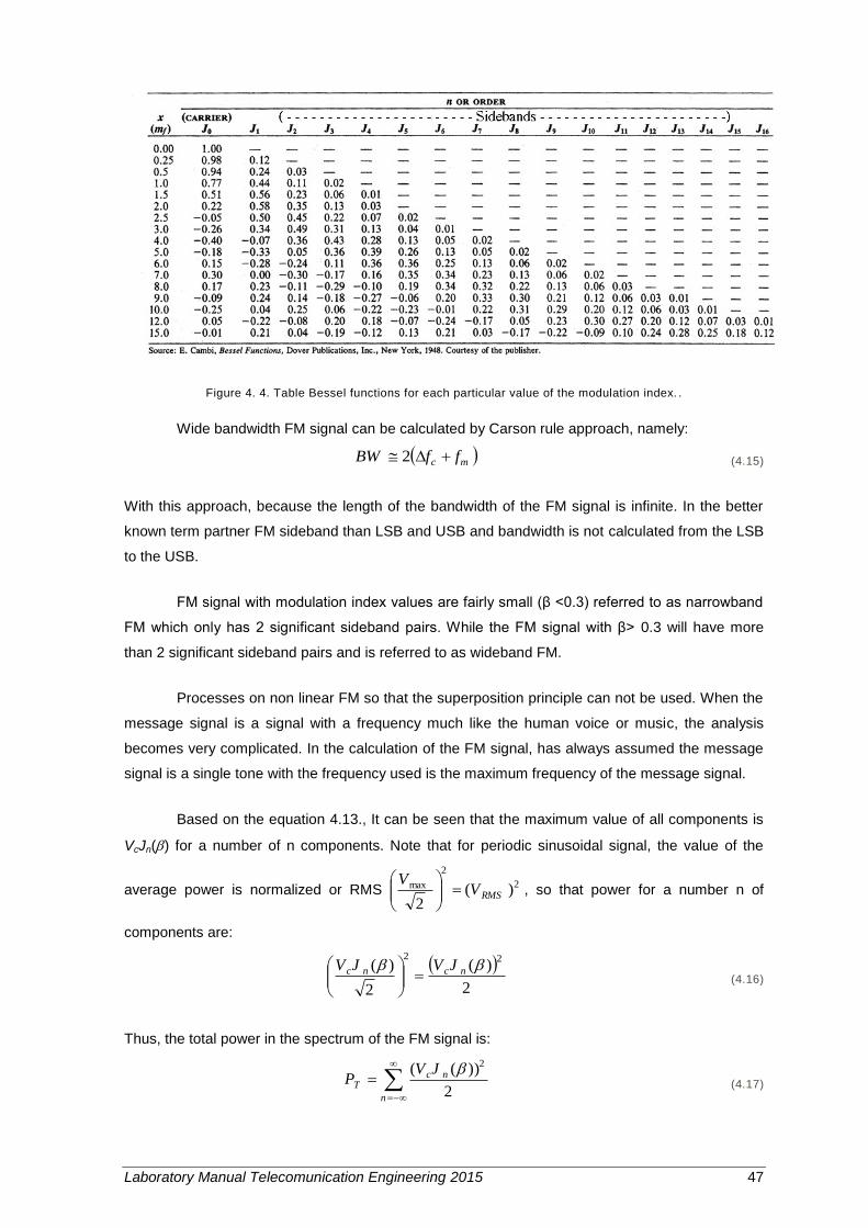
Laboratory Manual Telecomunication Engineering 2015 47
Figure 4. 4. Table Bessel functions for each particular value of the modulation index. .
Wide bandwidth FM signal can be calculated by Carson rule approach, namely:
mc ffBW 2 (4.15)
With this approach, because the length of the bandwidth of the FM signal is infinite. In the better
known term partner FM sideband than LSB and USB and bandwidth is not calculated from the LSB
to the USB.
FM signal with modulation index values are fairly small (β <0.3) referred to as narrowband
FM which only has 2 significant sideband pairs. While the FM signal with β> 0.3 will have more
than 2 significant sideband pairs and is referred to as wideband FM.
Processes on non linear FM so that the superposition principle can not be used. When the
message signal is a signal with a frequency much like the human voice or music, the analysis
becomes very complicated. In the calculation of the FM signal, has always assumed the message
signal is a single tone with the frequency used is the maximum frequency of the message signal.
Based on the equation 4.13., It can be seen that the maximum value of all components is
VcJn() for a number of n components. Note that for periodic sinusoidal signal, the value of the
average power is normalized or RMS 2
2
max )(2
RMSVV
, so that power for a number n of
components are:
2
)(
2
)(22
ncnc JVJV
(4.16)
Thus, the total power in the spectrum of the FM signal is:
n
ncT
JVP
2
))(( 2
(4.17)
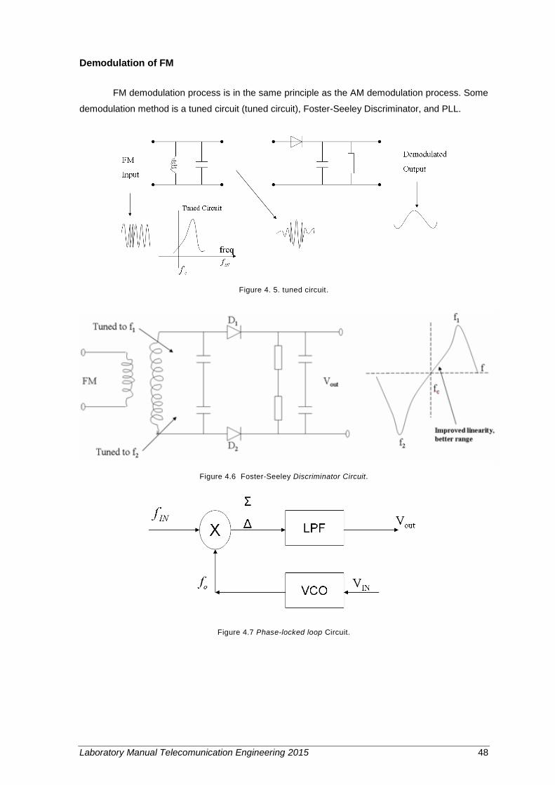
Laboratory Manual Telecomunication Engineering 2015 48
Demodulation of FM
FM demodulation process is in the same principle as the AM demodulation process. Some
demodulation method is a tuned circuit (tuned circuit), Foster-Seeley Discriminator, and PLL.
Figure 4. 5. tuned circuit.
Figure 4.6 Foster-Seeley Discriminator Circuit.
Figure 4.7 Phase-locked loop Circuit.
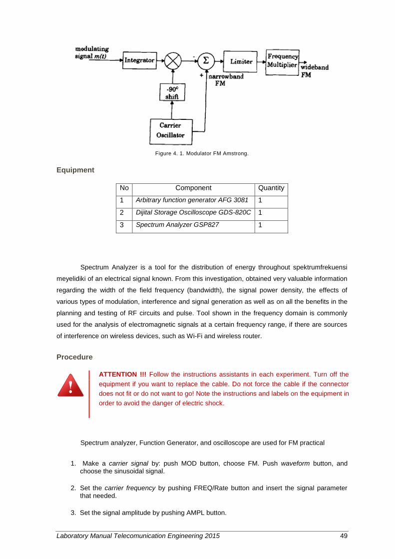
Laboratory Manual Telecomunication Engineering 2015 49
Figure 4. 1. Modulator FM Amstrong.
Equipment
No Component Quantity
1 Arbitrary function generator AFG 3081 1
2 Dijital Storage Oscilloscope GDS-820C 1
3 Spectrum Analyzer GSP827 1
Spectrum Analyzer is a tool for the distribution of energy throughout spektrumfrekuensi
meyelidiki of an electrical signal known. From this investigation, obtained very valuable information
regarding the width of the field frequency (bandwidth), the signal power density, the effects of
various types of modulation, interference and signal generation as well as on all the benefits in the
planning and testing of RF circuits and pulse. Tool shown in the frequency domain is commonly
used for the analysis of electromagnetic signals at a certain frequency range, if there are sources
of interference on wireless devices, such as Wi-Fi and wireless router.
Procedure
ATTENTION !!! Follow the instructions assistants in each experiment. Turn off the
equipment if you want to replace the cable. Do not force the cable if the connector
does not fit or do not want to go! Note the instructions and labels on the equipment in
order to avoid the danger of electric shock.
Spectrum analyzer, Function Generator, and oscilloscope are used for FM practical
1. Make a carrier signal by: push MOD button, choose FM. Push waveform button, and choose the sinusoidal signal.
2. Set the carrier frequency by pushing FREQ/Rate button and insert the signal parameter that needed.
3. Set the signal amplitude by pushing AMPL button.

Laboratory Manual Telecomunication Engineering 2015 50
4. Make the information signal by: push MOD button, then choose FM button, and choose FM freq and insert the information signal parameter that needed. Then click return. (Information signal frequency 2 mHz – 20 kHz, default: 100 Hz)
5. Set the deviation by: choose Freq Dev and insert the value. (default: 100 Hz). Deviation Frequency is the peak deviation of frequency from a carrier wave and modulatede wave.
6. Observe the display of information signal and modulation signal on oscilloscope by linking the MOD terminal and MAIN terminal to the oscilloscope.
7. Observe the display of the modulation signal result on spectrum analyzer by connecting MAIN terminal to the spectrum analyzer.
Time Domain Analysis
1. Switch on the function generator and oscilloscope.
2. Using coaxial cable, connect the output from the function generator with the channel
from oscilloscope.
3. Set the frequency value of the carrier signal in function generator.
4. Set the frequency deviation in function generator.
5. Push <autoset> at oscilloscope to ease the observation automatically.
6. Observe the message signal and the modulated signal at the oscilloscope‟s monitor.
Frequency Domain Analysis
1. Switch on the function generator and spectrum analyzer.
2. Using coaxial cable, connect the output from the function generator with the channel
from oscilloscope.
3. Set the frequency value of the carrier signal in function generator.
4. Set the frequency deviation in function generator.
5. Adjust the frequency range of view in spectrum analyzer
6. Observe the spectrum of the signal
7. Analyze by using Bessel function and Carson Rule
---o0o---
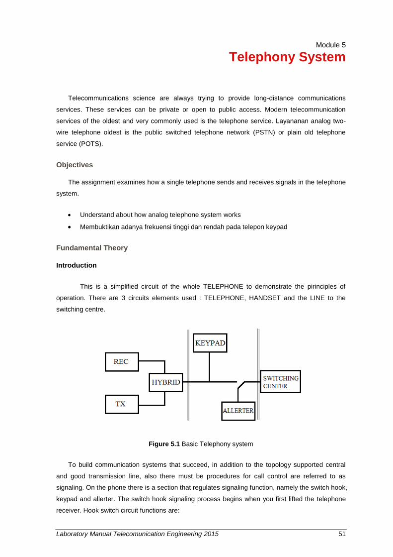
Laboratory Manual Telecomunication Engineering 2015 51
Module 5
Telephony System
Telecommunications science are always trying to provide long-distance communications
services. These services can be private or open to public access. Modern telecommunication
services of the oldest and very commonly used is the telephone service. Layananan analog two-
wire telephone oldest is the public switched telephone network (PSTN) or plain old telephone
service (POTS).
Objectives
The assignment examines how a single telephone sends and receives signals in the telephone
system.
Understand about how analog telephone system works
Membuktikan adanya frekuensi tinggi dan rendah pada telepon keypad
Fundamental Theory
Introduction
This is a simplified circuit of the whole TELEPHONE to demonstrate the pirinciples of
operation. There are 3 circuits elements used : TELEPHONE, HANDSET and the LINE to the
switching centre.
Figure 5.1 Basic Telephony system
To build communication systems that succeed, in addition to the topology supported central
and good transmission line, also there must be procedures for call control are referred to as
signaling. On the phone there is a section that regulates signaling function, namely the switch hook,
keypad and allerter. The switch hook signaling process begins when you first lifted the telephone
receiver. Hook switch circuit functions are:
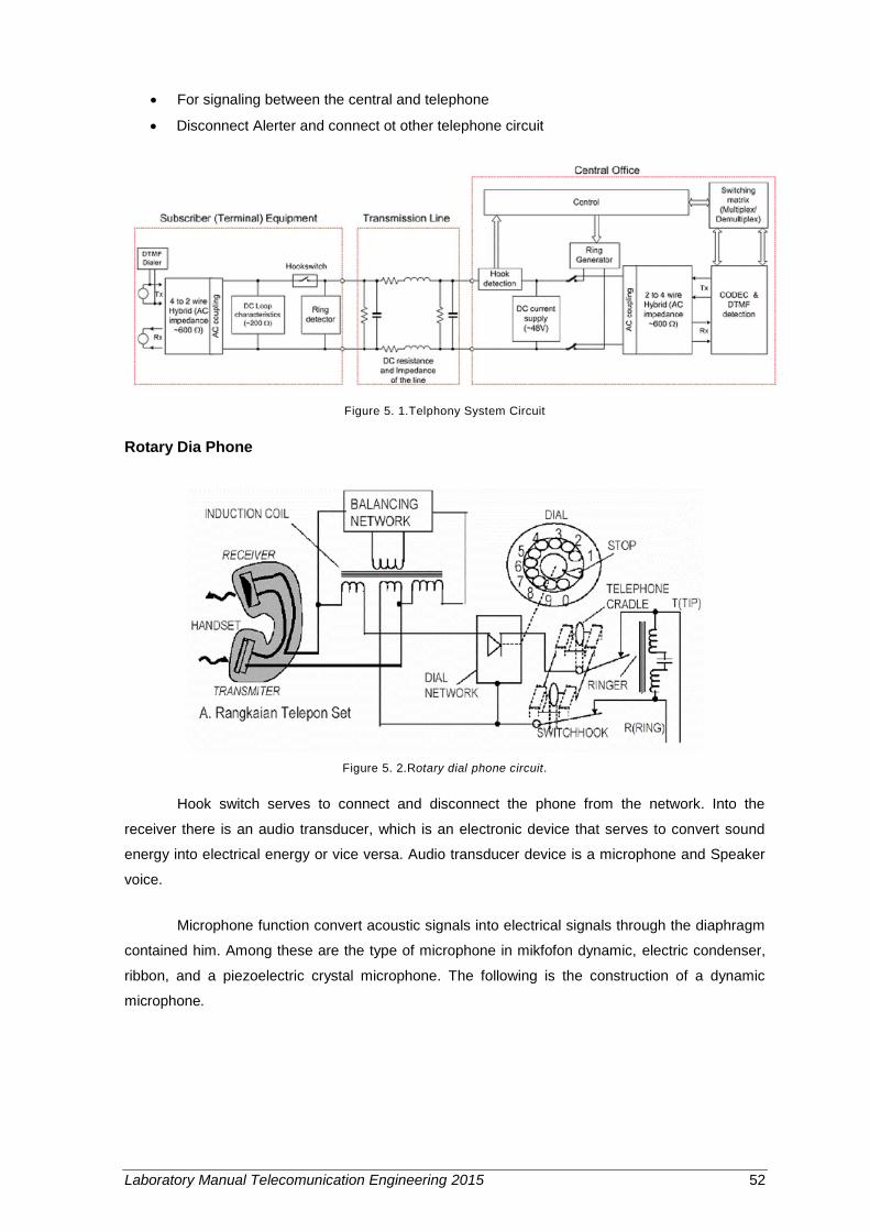
Laboratory Manual Telecomunication Engineering 2015 52
For signaling between the central and telephone
Disconnect Alerter and connect ot other telephone circuit
Figure 5. 1.Telphony System Circuit
Rotary Dia Phone
Figure 5. 2.Rotary dial phone circuit.
Hook switch serves to connect and disconnect the phone from the network. Into the
receiver there is an audio transducer, which is an electronic device that serves to convert sound
energy into electrical energy or vice versa. Audio transducer device is a microphone and Speaker
voice.
Microphone function convert acoustic signals into electrical signals through the diaphragm
contained him. Among these are the type of microphone in mikfofon dynamic, electric condenser,
ribbon, and a piezoelectric crystal microphone. The following is the construction of a dynamic
microphone.
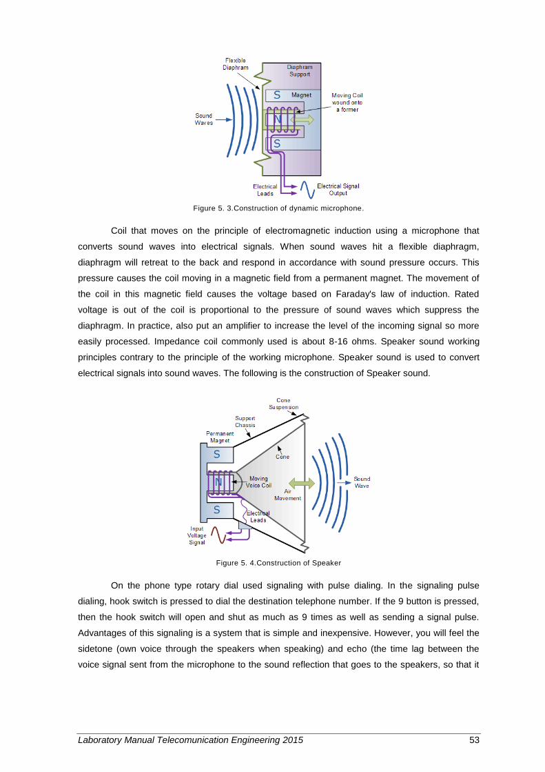
Laboratory Manual Telecomunication Engineering 2015 53
Figure 5. 3.Construction of dynamic microphone.
Coil that moves on the principle of electromagnetic induction using a microphone that
converts sound waves into electrical signals. When sound waves hit a flexible diaphragm,
diaphragm will retreat to the back and respond in accordance with sound pressure occurs. This
pressure causes the coil moving in a magnetic field from a permanent magnet. The movement of
the coil in this magnetic field causes the voltage based on Faraday's law of induction. Rated
voltage is out of the coil is proportional to the pressure of sound waves which suppress the
diaphragm. In practice, also put an amplifier to increase the level of the incoming signal so more
easily processed. Impedance coil commonly used is about 8-16 ohms. Speaker sound working
principles contrary to the principle of the working microphone. Speaker sound is used to convert
electrical signals into sound waves. The following is the construction of Speaker sound.
Figure 5. 4.Construction of Speaker
On the phone type rotary dial used signaling with pulse dialing. In the signaling pulse
dialing, hook switch is pressed to dial the destination telephone number. If the 9 button is pressed,
then the hook switch will open and shut as much as 9 times as well as sending a signal pulse.
Advantages of this signaling is a system that is simple and inexpensive. However, you will feel the
sidetone (own voice through the speakers when speaking) and echo (the time lag between the
voice signal sent from the microphone to the sound reflection that goes to the speakers, so that it
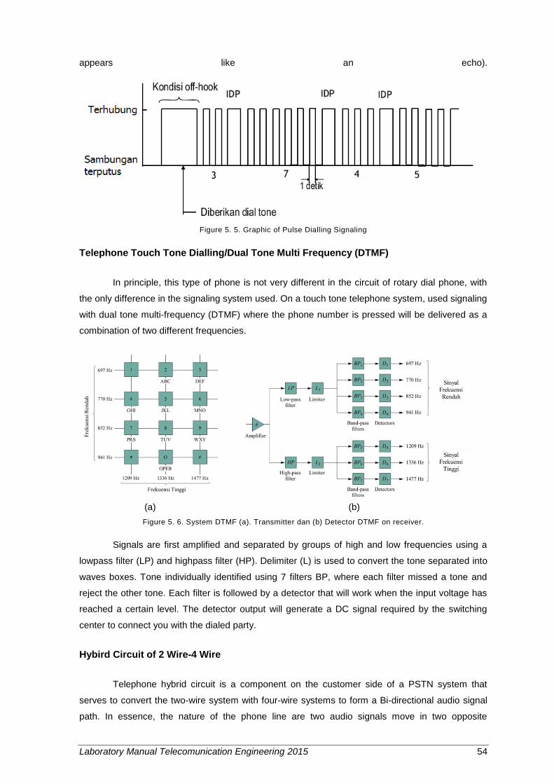
Laboratory Manual Telecomunication Engineering 2015 54
appears like an echo).
Figure 5. 5. Graphic of Pulse Dialling Signaling
Telephone Touch Tone Dialling/Dual Tone Multi Frequency (DTMF)
In principle, this type of phone is not very different in the circuit of rotary dial phone, with
the only difference in the signaling system used. On a touch tone telephone system, used signaling
with dual tone multi-frequency (DTMF) where the phone number is pressed will be delivered as a
combination of two different frequencies.
(a) (b)
Figure 5. 6. System DTMF (a). Transmitter dan (b) Detector DTMF on receiver.
Signals are first amplified and separated by groups of high and low frequencies using a
lowpass filter (LP) and highpass filter (HP). Delimiter (L) is used to convert the tone separated into
waves boxes. Tone individually identified using 7 filters BP, where each filter missed a tone and
reject the other tone. Each filter is followed by a detector that will work when the input voltage has
reached a certain level. The detector output will generate a DC signal required by the switching
center to connect you with the dialed party.
Hybird Circuit of 2 Wire-4 Wire
Telephone hybrid circuit is a component on the customer side of a PSTN system that
serves to convert the two-wire system with four-wire systems to form a Bi-directional audio signal
path. In essence, the nature of the phone line are two audio signals move in two opposite
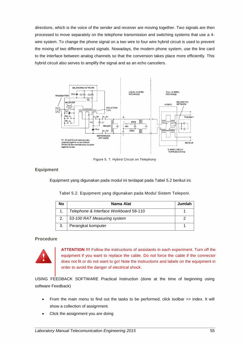
Laboratory Manual Telecomunication Engineering 2015 55
directions, which is the voice of the sender and receiver are moving together. Two signals are then
processed to move separately on the telephone transmission and switching systems that use a 4-
wire system. To change the phone signal on a two wire to four wire hybrid circuit is used to prevent
the mixing of two different sound signals. Nowadays, the modern phone system, use the line card
to the interface between analog channels so that the conversion takes place more efficiently. This
hybrid circuit also serves to amplify the signal and as an echo cancelers.
Figure 5. 7. Hybird Circuit on Telephony
Equipment
Equipment yang digunakan pada modul ini terdapat pada Tabel 5.2 berikut ini.
Tabel 5.2. Equipment yang digunakan pada Modul Sistem Teleponi.
No Nama Alat Jumlah
1. Telephone & Interface Workboard 58-110 1
2. 53-100 RAT Measuring system 2
3. Perangkat komputer 1
Procedure
ATTENTION !!! Follow the instructions of assistants in each experiment. Turn off the
equipment if you want to replace the cable. Do not force the cable if the connector
does not fit or do not want to go! Note the instructions and labels on the equipment in
order to avoid the danger of electrical shock.
USING FEEDBACK SOFTWARE Practical Instruction (done at the time of beginning using
software Feedback)
From the main menu to find out the tasks to be performed, click toolbar >> index. It will
show a collection of assignment.
Click the assignment you are doing
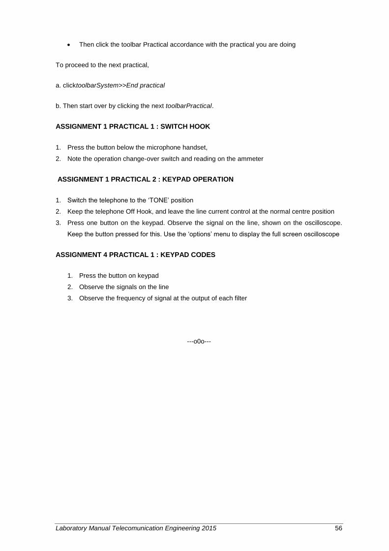
Laboratory Manual Telecomunication Engineering 2015 56
Then click the toolbar Practical accordance with the practical you are doing
To proceed to the next practical,
a. clicktoolbarSystem>>End practical
b. Then start over by clicking the next toolbarPractical.
ASSIGNMENT 1 PRACTICAL 1 : SWITCH HOOK
1. Press the button below the microphone handset,
2. Note the operation change-over switch and reading on the ammeter
ASSIGNMENT 1 PRACTICAL 2 : KEYPAD OPERATION
1. Switch the telephone to the „TONE‟ position
2. Keep the telephone Off Hook, and leave the line current control at the normal centre position
3. Press one button on the keypad. Observe the signal on the line, shown on the oscilloscope.
Keep the button pressed for this. Use the „options‟ menu to display the full screen oscilloscope
ASSIGNMENT 4 PRACTICAL 1 : KEYPAD CODES
1. Press the button on keypad
2. Observe the signals on the line
3. Observe the frequency of signal at the output of each filter
---o0o---
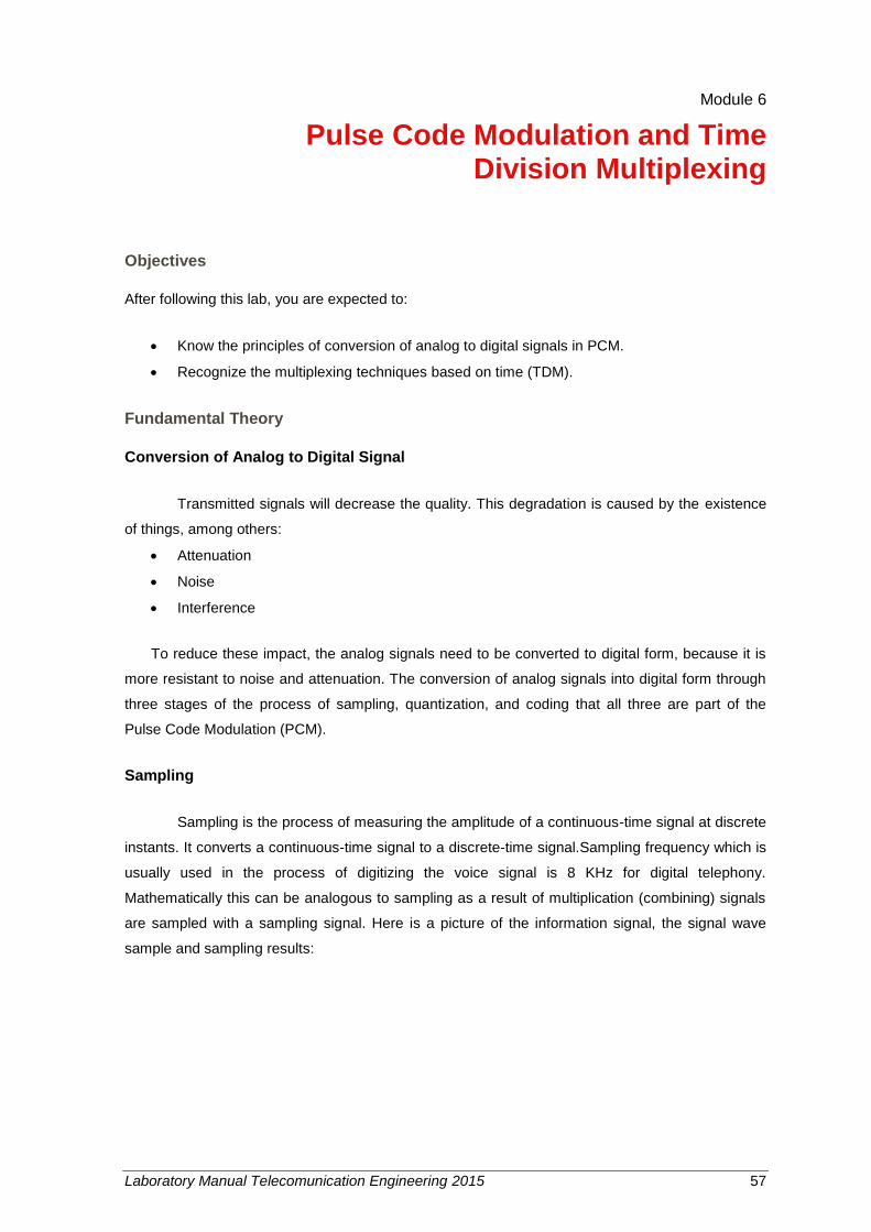
Laboratory Manual Telecomunication Engineering 2015 57
Module 6
Pulse Code Modulation and Time Division Multiplexing
Objectives
After following this lab, you are expected to:
Know the principles of conversion of analog to digital signals in PCM.
Recognize the multiplexing techniques based on time (TDM).
Fundamental Theory
Conversion of Analog to Digital Signal
Transmitted signals will decrease the quality. This degradation is caused by the existence
of things, among others:
Attenuation
Noise
Interference
To reduce these impact, the analog signals need to be converted to digital form, because it is
more resistant to noise and attenuation. The conversion of analog signals into digital form through
three stages of the process of sampling, quantization, and coding that all three are part of the
Pulse Code Modulation (PCM).
Sampling
Sampling is the process of measuring the amplitude of a continuous-time signal at discrete
instants. It converts a continuous-time signal to a discrete-time signal.Sampling frequency which is
usually used in the process of digitizing the voice signal is 8 KHz for digital telephony.
Mathematically this can be analogous to sampling as a result of multiplication (combining) signals
are sampled with a sampling signal. Here is a picture of the information signal, the signal wave
sample and sampling results:
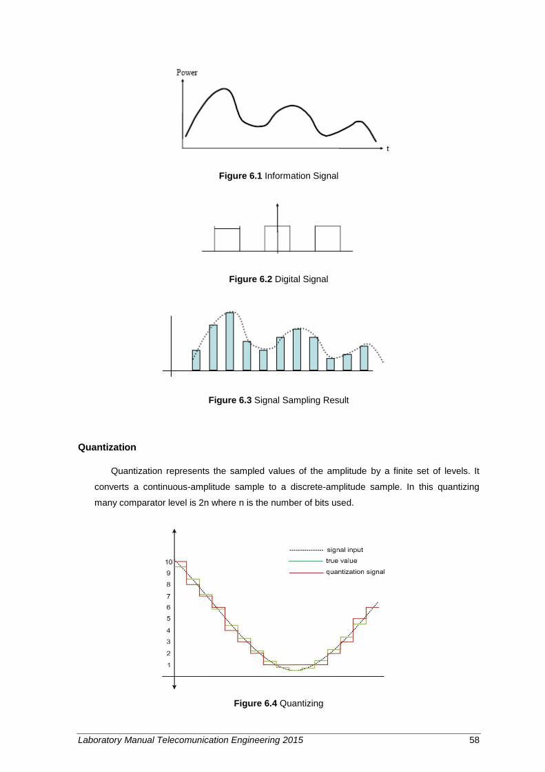
Laboratory Manual Telecomunication Engineering 2015 58
Figure 6.1 Information Signal
Figure 6.2 Digital Signal
Figure 6.3 Signal Sampling Result
Quantization
Quantization represents the sampled values of the amplitude by a finite set of levels. It
converts a continuous-amplitude sample to a discrete-amplitude sample. In this quantizing
many comparator level is 2n where n is the number of bits used.
Figure 6.4 Quantizing

Laboratory Manual Telecomunication Engineering 2015 59
Coding
Coding designates each quantized level by a (binary) code. Here is a picture of
quantization and coding process:
Figure 6.5 Coding
Figure 6.6 Coding Result
Multiplexing
Figure 6.7. Application of Multiplexing in Fiber Optic
Multiplexing is a method of using a channel of communication together. Multiplexing is
intended to save resources from the communications channel. One form of multiplexing is the Time
Division Multiplexing (TDM).TDM is the time interleaving of samples from several sources so that
the information from these sources can be transmitted serially over a single communication
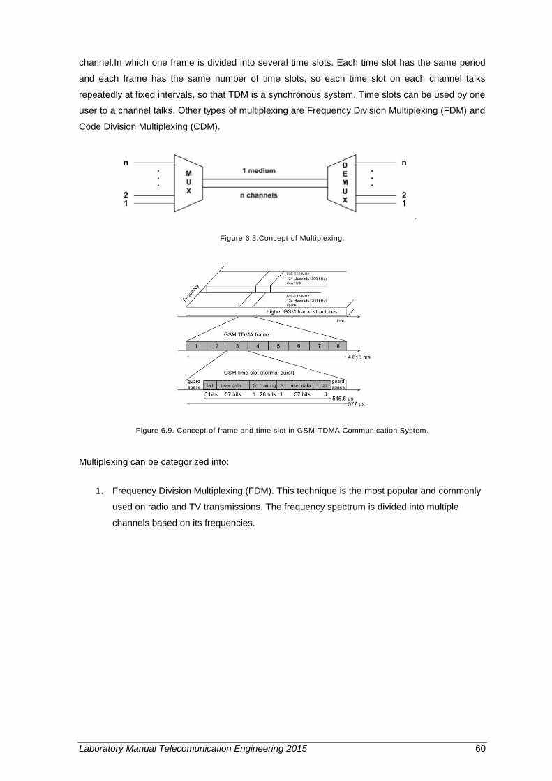
Laboratory Manual Telecomunication Engineering 2015 60
channel.In which one frame is divided into several time slots. Each time slot has the same period
and each frame has the same number of time slots, so each time slot on each channel talks
repeatedly at fixed intervals, so that TDM is a synchronous system. Time slots can be used by one
user to a channel talks. Other types of multiplexing are Frequency Division Multiplexing (FDM) and
Code Division Multiplexing (CDM).
.
Figure 6.8.Concept of Multiplexing.
Figure 6.9. Concept of frame and time slot in GSM-TDMA Communication System.
Multiplexing can be categorized into:
1. Frequency Division Multiplexing (FDM). This technique is the most popular and commonly
used on radio and TV transmissions. The frequency spectrum is divided into multiple
channels based on its frequencies.
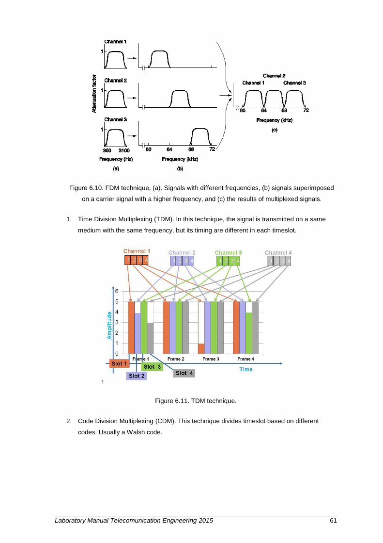
Laboratory Manual Telecomunication Engineering 2015 61
Figure 6.10. FDM technique, (a). Signals with different frequencies, (b) signals superimposed
on a carrier signal with a higher frequency, and (c) the results of multiplexed signals.
1. Time Division Multiplexing (TDM). In this technique, the signal is transmitted on a same
medium with the same frequency, but its timing are different in each timeslot.
Figure 6.11. TDM technique.
2. Code Division Multiplexing (CDM). This technique divides timeslot based on different
codes. Usually a Walsh code.
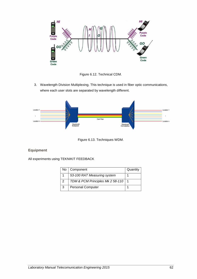
Laboratory Manual Telecomunication Engineering 2015 62
Figure 6.12. Technical CDM.
3. Wavelength Division Multiplexing. This technique is used in fiber optic communications,
where each user slots are separated by wavelength different.
Figure 6.13. Techniques WDM.
Equipment
All experiments using TEKNIKIT FEEDBACK
No Component Quantity
1 53-100 RAT Measuring system 1
2 TDM & PCM Principles Mk 2 58-110 1
3 Personal Computer 1
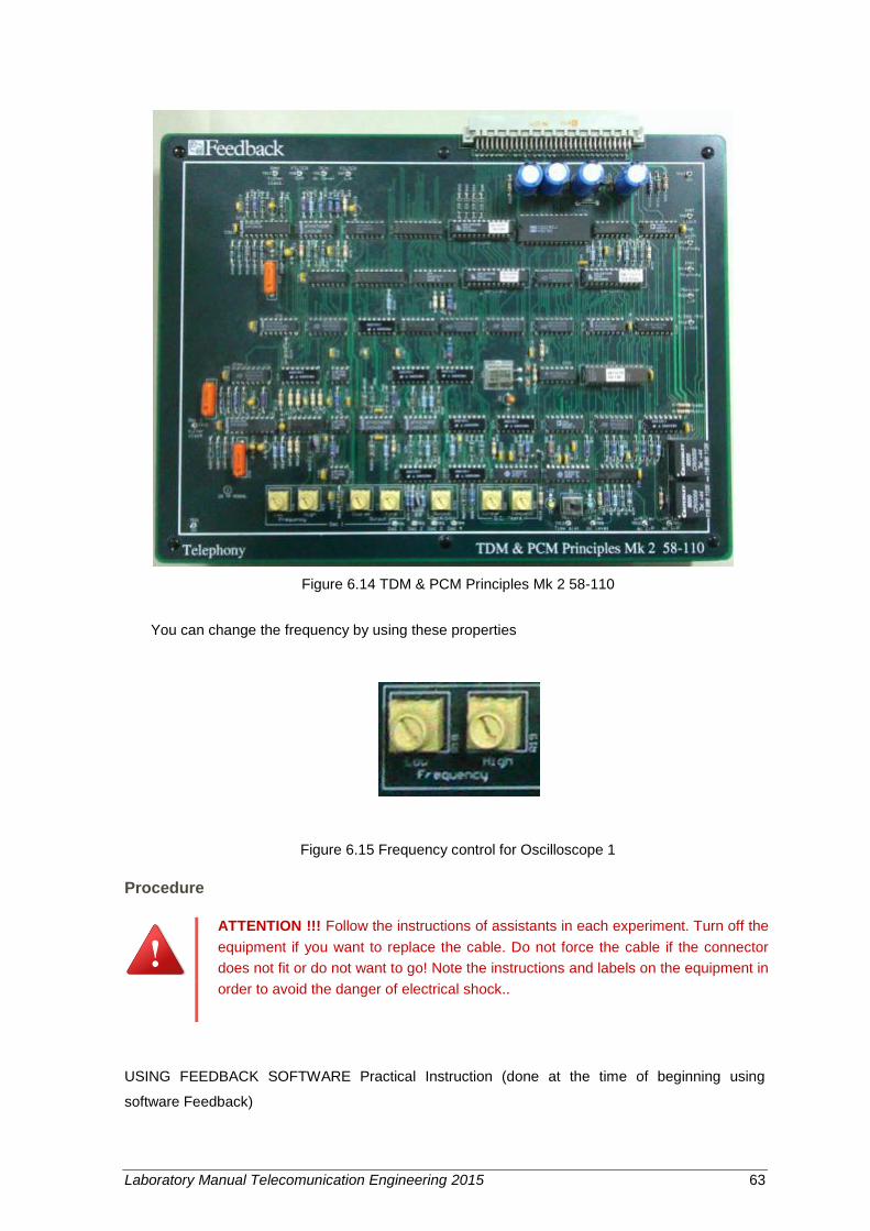
Laboratory Manual Telecomunication Engineering 2015 63
Figure 6.14 TDM & PCM Principles Mk 2 58-110
You can change the frequency by using these properties
Figure 6.15 Frequency control for Oscilloscope 1
Procedure
ATTENTION !!! Follow the instructions of assistants in each experiment. Turn off the
equipment if you want to replace the cable. Do not force the cable if the connector
does not fit or do not want to go! Note the instructions and labels on the equipment in
order to avoid the danger of electrical shock..
USING FEEDBACK SOFTWARE Practical Instruction (done at the time of beginning using
software Feedback)

Laboratory Manual Telecomunication Engineering 2015 64
From the main menu to find out the tasks to be performed, click toolbar >> index. It will
show a collection of assignment.
Click the assignment you are doing
Then click the toolbar Practical accordance with the practical you are doing
To proceed to the next practical,
a. ClicktoolbarSystem>>End practical
b. Then start over by clicking the next toolbarPractical.
ASSIGNMENT 7 PRACTICAL 1 and 4: Basic Sampling and Aliasing Error
1. Follow the general instructions. click toolbar practical → basic sampling
2. Set frequency of oscilloscope 1 to approximately 800 Hz and output Vpp 2 volt. (Change
display size with a `menu option ').
3. Observe the waveform on the oscilloscope 1, the clock, the sampling wave (at test point 7)
and the output on the low pass filter. Analysis it!
4. Change the sample time by using the menu 'option' to ¼. Observe the waveform occurs.
Analysis it!
5. Repeat step 3 by changing the sample time into 1 / 8.
6. Repeat steps 1-3 for 500 and 2 kHz frequency.
7. Analysis the result
ASSIGNMENT 9 PRACTICAL 1 : Quantizing
1. Follow the general instructions. click toolbar practical → quantization
2. Set the voltage to 0 (zero) volt, using `DC Test Linear controllers' and recalibration to get
accurate results.
3. Set the input voltage to 1 V, observe the digital output.
4. Repeat for 2 V and a maximum voltage untill the digital display does not change. Observe
the digital output.
5. Repeat to -1 V and -2 V and to a minimum. Observe the code changes' at zero voltage.
6. Analysis!
ASSIGNMENT 9 PRACTICAL2 : Quantizing Noise
1. Follow the general instructions. click toolbar practical → quantization noise
2. Set the frequency at 300 Hz and voltage amplitude (peak) at 0.2 volts by using the
controller `Fine control '.
3. Set the resolution to 4 bits, by using the menu 'Option ".
4. Observe the digital output (test point 7) and the results of the output filter (test point 8)
5. Repeat for different bits of resolution.
6. Use the 'spectrum analyzer' to see the output

Laboratory Manual Telecomunication Engineering 2015 65
7. Analysis!
ASSIGNMENT 9 PRACTICAL1 : Introduction of Multiplexing
1. Follow the general instructions. click toolbar practical→introduction to multiplexing
2. Observe the output on the oscillator 4 which is a result of demultiplexing (test point 7) and
output filters.
3. Compare the form of waves (test point 14) by using a large display. set oscillator 1 to 0
(zero) volt and varying the amplitude to determine the time slots used by each signal.
4. Increase the output value of oscillator 1.
5. Compare the input waveforms for each oscillator with output wave by using the menu
`option 'to choose a time slot.
---o0o---
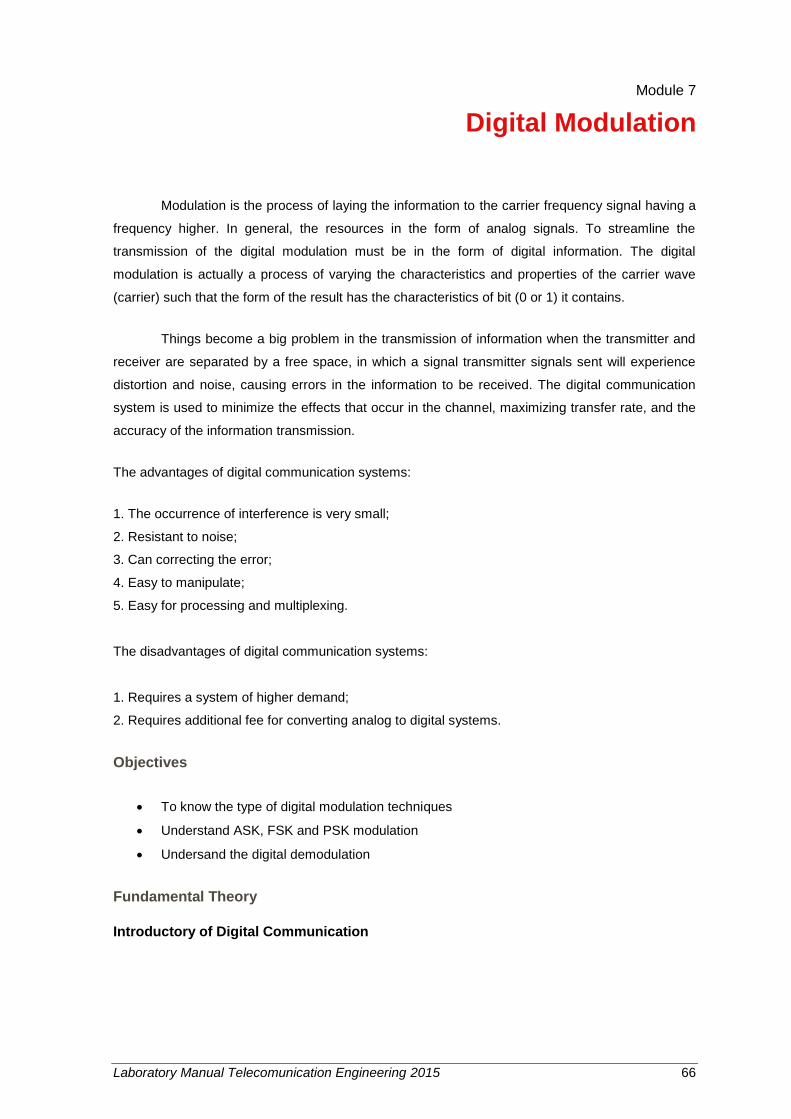
Laboratory Manual Telecomunication Engineering 2015 66
Module 7
Digital Modulation
Modulation is the process of laying the information to the carrier frequency signal having a
frequency higher. In general, the resources in the form of analog signals. To streamline the
transmission of the digital modulation must be in the form of digital information. The digital
modulation is actually a process of varying the characteristics and properties of the carrier wave
(carrier) such that the form of the result has the characteristics of bit (0 or 1) it contains.
Things become a big problem in the transmission of information when the transmitter and
receiver are separated by a free space, in which a signal transmitter signals sent will experience
distortion and noise, causing errors in the information to be received. The digital communication
system is used to minimize the effects that occur in the channel, maximizing transfer rate, and the
accuracy of the information transmission.
The advantages of digital communication systems:
1. The occurrence of interference is very small;
2. Resistant to noise;
3. Can correcting the error;
4. Easy to manipulate;
5. Easy for processing and multiplexing.
The disadvantages of digital communication systems:
1. Requires a system of higher demand;
2. Requires additional fee for converting analog to digital systems.
Objectives
To know the type of digital modulation techniques
Understand ASK, FSK and PSK modulation
Undersand the digital demodulation
Fundamental Theory
Introductory of Digital Communication

Laboratory Manual Telecomunication Engineering 2015 67
Analog-to-
Digital
Converter
Source
Encoder
Encryption
and
Scrambling
Channel
Encoder
Line
Coder
Digital
Modulation
DemodulatorChannel
Decoder
Baseband
Processing
Source
Decoder
Digital-to-
Analog
Converter
Line
Decoder
Signal
Regeneration
CH
AN
NE
L
SUMBER
SINYAL INFORMASI
(ANALOG)
PENERIMA
SINYAL INFORMASI
(ANALOG)
Baseband Transmission
Carrier TransmissionW
ireless
Wireline
Wire
less
Wireline
Analog
Waveform
Analog
Waveform
Digital Data
Digital Data
PENGIRIM
PENERIMA
Antena
Transmitter (Tx)
Antena
Receiver (Rx)
Figure 7.1. Block Diagram of Digital Communication.
a. Information Source
Information source can be a continuous signal or discrete signals. In digital communication,
analog signals should be converted into the digital one using Analog to Digital Converter (ADC).
b. Source Encoder and Decoder
Source coding is used to code information source in order to make information more suitable
for being transmitted. Source encoder will reduce the number of bit needed for transmitting
some kinds of information. This technique will reduce the bandwidth needed. Source decoder
is used to decode information after signals received in the receiver.
c. Line Coding and Decoding
Line coding applies digital data format without using modulation technique. The requirements
of line coding are spectrum at low frequency, transmission bandwidth required, timing content,
error monitoring, and code efficiency. The examples of line coding are Non Return to Zero
(NRZ), Return to Zero (RZ), Manchester, Alternate Mark Inversion (AMI), HDB3, etc.
d. Encryption and Scrambling
Two main reasons for using encryption and scrambling are confidentiality and authentication.
e. Channel Coding dan Decoding
In high speed data transmission, the „1‟ and „0‟ are usually of very short duration. Channel
coding and decoding is applied for reducing bit errors that are caused by the noisy channel.

Laboratory Manual Telecomunication Engineering 2015 68
Channel coding process data stream to make it compatible with channel characteristic. The
technique is applied by adding some parity bits to the digital word.
f. Digital Carrier Modulator and Demodulator
The main purpose of digital modulator is to map binary information into signal waveforms in
order to make the binary information capable to be transmitted over the channel.
g. Communication Channel
Communication channel is any medium that is used to transmit signals from transmitter to
receiver. In practice, the channel is noisy and will disturb signals.
Bandpass Transmission System
Bandpass transmission system is a transmission system that has undergone modulation,
ie the information signal (discrete) modulates the carrier signal (continuous). Before modulated
using a digital modulation technique, the signal must be in the form of digital data information.
Therefore, the information signal is still analog form must first be converted using an ADC (Analog
to Digital Converter). There are a wide variety of digital modulation techniques include ASK
(Amplitude shifted Keying), FSK (Frequency shifted Keying) and PSK (Phase shifted Keying). Also
known modulation techniques QAM (Quadrature Amplitude Modulation) which is a combination of
ASK and PSK.
Amplitude Shift Keying (ASK)
Amplitude Shift Keying (ASK) is digital modulation technique represented by amplitude level of the
information. In ASK, binary information, such as 0 and 1, will be stated as a different amplitude
level. In a band pass ASK, the signal is represented by:
(1)
Figure 7.2. ASK modulated Digital signal

Laboratory Manual Telecomunication Engineering 2015 69
There are two kinds of demodulation and detection schemes for ASK: no coherent (asynchronous)
and coherent (synchronous).
Frequency Shift Keying (FSK)
In frequency shift keying, the frequency of the carrier varies with the baseband information. For
example, binary 0 will have carrier frequency f1 while binary 1 will have carrier frequency f2. The
modulated signal for binary FSK is formulated by :
(2)
Figure 7.3. FSK modulated Digital signal
FSK signals can be demodulated and detected by using both non coherent technique and coherent
technique.
Phase Shift Keying
Phase Shift Keying (PSK) is digital modulation technique that using different phase carrier
according to the binary information.
Figure 7.4. PSK modulated Digital signal
Equipment
No Component Quantity

Laboratory Manual Telecomunication Engineering 2015 70
1. DCS-B VLSI Based Digital Communication Training
System
1
2. Oscilloscope 1
3. Passive Probe Detector 1
Procedure
ATTENTION !!! Follow the instructions of assistants in each experiment. Turn off the
equipment if you want to replace the cable. Do not force the cable if the connector
does not fit or do not want to go! Note the instructions and labels on the equipment in
order to avoid the danger of electrical shock.
General procedure for operating Feedback software:
Amplitude Shift Keying (ASK)
1. Select the group 4 (GP4) clock in the Clock Generation section with the help of switch
S1 and observe the corresponding LED indication.
2. Set the data pattern S4 using switch as per the given worksheet and observe the 8-bit
data pattern at SDATA post.
3. Connect SIN3 post to the IN2 post and IN3 post to the Ground in carrier modulation
section.
4. Connect SDATA to IN16 post and TXCLK to CLK2 post of the Encoded Data section.
5. Select NRZ-L data with the help of the switch S3 and observe the corresponding LED
indication in the Encoded Data section.
6. Connect OUT10 post of the Encoded Data section to IN4 post as a control input for the
carrier modulator section.
7. Observe the ASK modulated signal at the OUT2 post of the Carrier modulation section.
8. For the demodulation, connect the OUT2 post of the carrier modulator to the IN24 post
of the ASK demodulator section.
9. Observe the ASK demodulated data at the OUT20 post of the Carrier ASK
demodulator section.
10. Verify the recovered data with the SDATA.
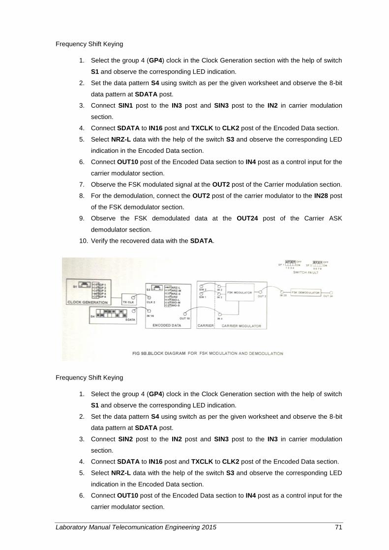
Laboratory Manual Telecomunication Engineering 2015 71
Frequency Shift Keying
1. Select the group 4 (GP4) clock in the Clock Generation section with the help of switch
S1 and observe the corresponding LED indication.
2. Set the data pattern S4 using switch as per the given worksheet and observe the 8-bit
data pattern at SDATA post.
3. Connect SIN1 post to the IN3 post and SIN3 post to the IN2 in carrier modulation
section.
4. Connect SDATA to IN16 post and TXCLK to CLK2 post of the Encoded Data section.
5. Select NRZ-L data with the help of the switch S3 and observe the corresponding LED
indication in the Encoded Data section.
6. Connect OUT10 post of the Encoded Data section to IN4 post as a control input for the
carrier modulator section.
7. Observe the FSK modulated signal at the OUT2 post of the Carrier modulation section.
8. For the demodulation, connect the OUT2 post of the carrier modulator to the IN28 post
of the FSK demodulator section.
9. Observe the FSK demodulated data at the OUT24 post of the Carrier ASK
demodulator section.
10. Verify the recovered data with the SDATA.
Frequency Shift Keying
1. Select the group 4 (GP4) clock in the Clock Generation section with the help of switch
S1 and observe the corresponding LED indication.
2. Set the data pattern S4 using switch as per the given worksheet and observe the 8-bit
data pattern at SDATA post.
3. Connect SIN2 post to the IN2 post and SIN3 post to the IN3 in carrier modulation
section.
4. Connect SDATA to IN16 post and TXCLK to CLK2 post of the Encoded Data section.
5. Select NRZ-L data with the help of the switch S3 and observe the corresponding LED
indication in the Encoded Data section.
6. Connect OUT10 post of the Encoded Data section to IN4 post as a control input for the
carrier modulator section.
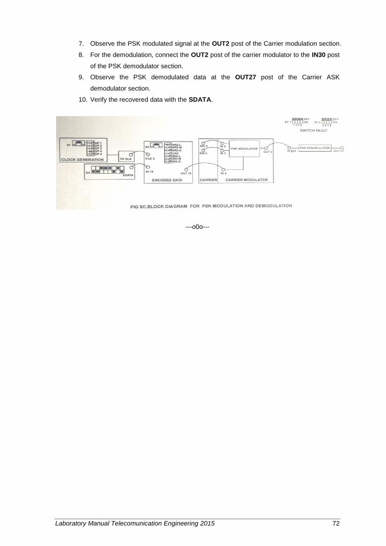
Laboratory Manual Telecomunication Engineering 2015 72
7. Observe the PSK modulated signal at the OUT2 post of the Carrier modulation section.
8. For the demodulation, connect the OUT2 post of the carrier modulator to the IN30 post
of the PSK demodulator section.
9. Observe the PSK demodulated data at the OUT27 post of the Carrier ASK
demodulator section.
10. Verify the recovered data with the SDATA.
---o0o---
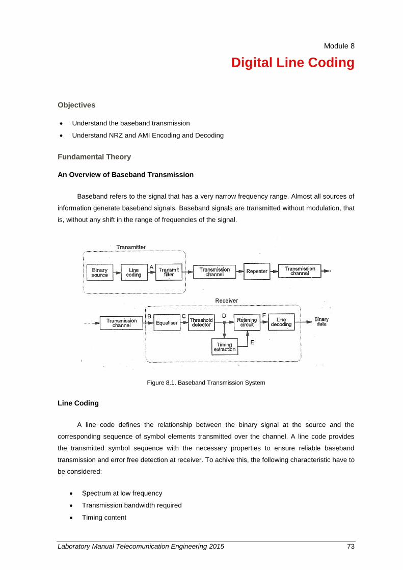
Laboratory Manual Telecomunication Engineering 2015 73
Module 8
Digital Line Coding
Objectives
Understand the baseband transmission
Understand NRZ and AMI Encoding and Decoding
Fundamental Theory
An Overview of Baseband Transmission
Baseband refers to the signal that has a very narrow frequency range. Almost all sources of
information generate baseband signals. Baseband signals are transmitted without modulation, that
is, without any shift in the range of frequencies of the signal.
Figure 8.1. Baseband Transmission System
Line Coding
A line code defines the relationship between the binary signal at the source and the
corresponding sequence of symbol elements transmitted over the channel. A line code provides
the transmitted symbol sequence with the necessary properties to ensure reliable baseband
transmission and error free detection at receiver. To achive this, the following characteristic have to
be considered:
Spectrum at low frequency
Transmission bandwidth required
Timing content
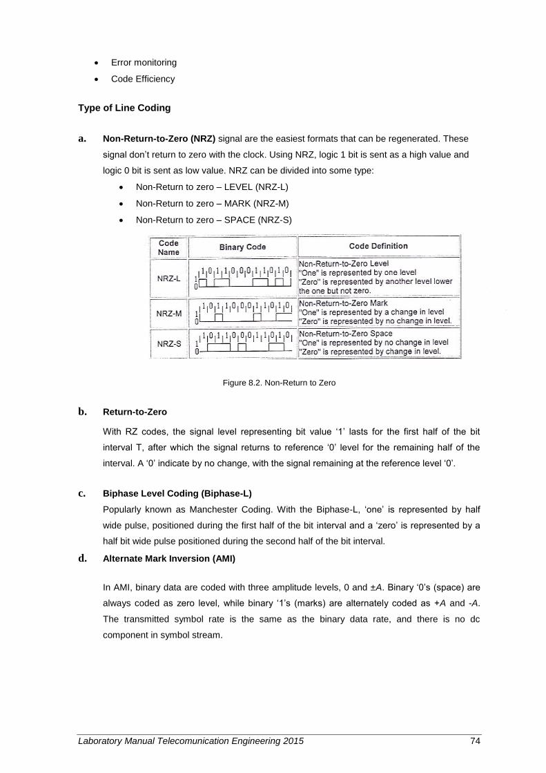
Laboratory Manual Telecomunication Engineering 2015 74
Error monitoring
Code Efficiency
Type of Line Coding
a. Non-Return-to-Zero (NRZ) signal are the easiest formats that can be regenerated. These
signal don‟t return to zero with the clock. Using NRZ, logic 1 bit is sent as a high value and
logic 0 bit is sent as low value. NRZ can be divided into some type:
Non-Return to zero – LEVEL (NRZ-L)
Non-Return to zero – MARK (NRZ-M)
Non-Return to zero – SPACE (NRZ-S)
Figure 8.2. Non-Return to Zero
b. Return-to-Zero
With RZ codes, the signal level representing bit value „1‟ lasts for the first half of the bit
interval T, after which the signal returns to reference „0‟ level for the remaining half of the
interval. A „0‟ indicate by no change, with the signal remaining at the reference level „0‟.
c. Biphase Level Coding (Biphase-L)
Popularly known as Manchester Coding. With the Biphase-L, „one‟ is represented by half
wide pulse, positioned during the first half of the bit interval and a „zero‟ is represented by a
half bit wide pulse positioned during the second half of the bit interval.
d. Alternate Mark Inversion (AMI)
In AMI, binary data are coded with three amplitude levels, 0 and ±A. Binary „0‟s (space) are
always coded as zero level, while binary „1‟s (marks) are alternately coded as +A and -A.
The transmitted symbol rate is the same as the binary data rate, and there is no dc
component in symbol stream.
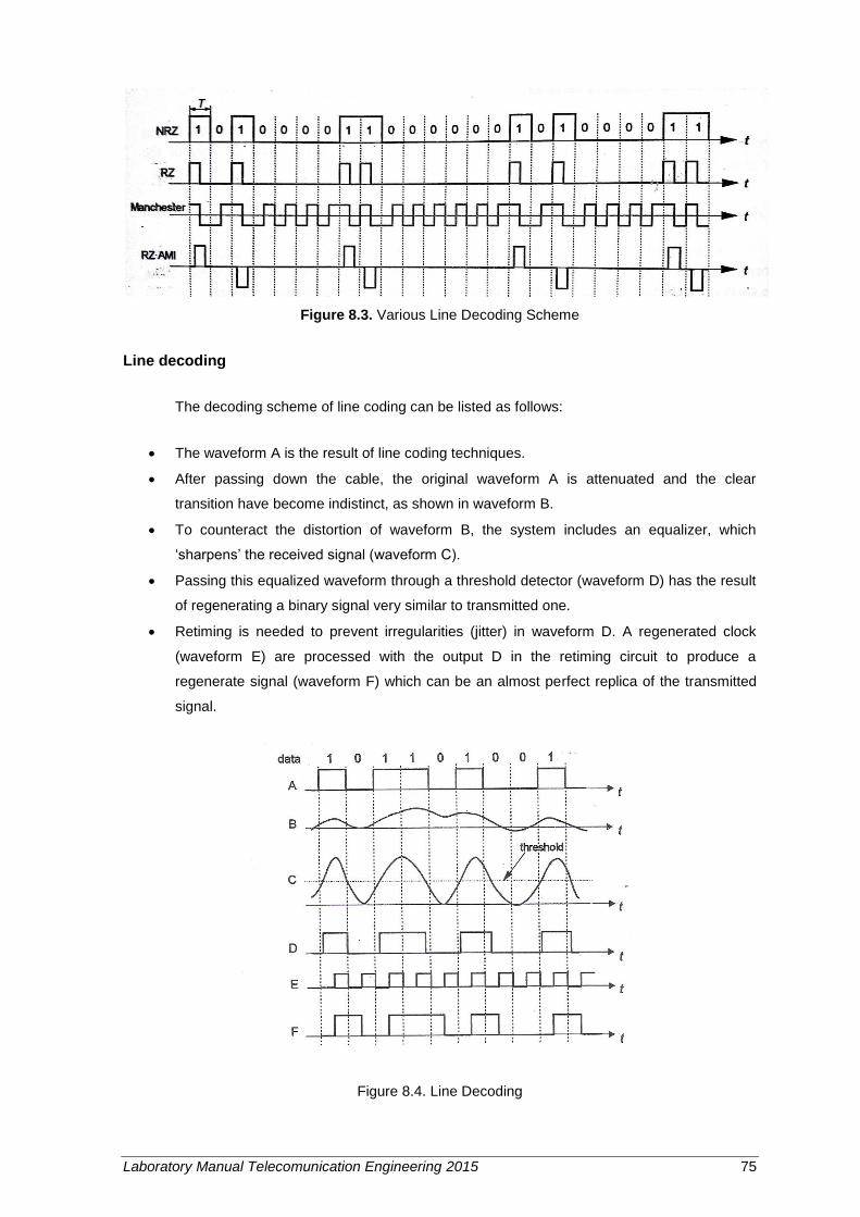
Laboratory Manual Telecomunication Engineering 2015 75
Figure 8.3. Various Line Decoding Scheme
Line decoding
The decoding scheme of line coding can be listed as follows:
The waveform A is the result of line coding techniques.
After passing down the cable, the original waveform A is attenuated and the clear
transition have become indistinct, as shown in waveform B.
To counteract the distortion of waveform B, the system includes an equalizer, which
„sharpens‟ the received signal (waveform C).
Passing this equalized waveform through a threshold detector (waveform D) has the result
of regenerating a binary signal very similar to transmitted one.
Retiming is needed to prevent irregularities (jitter) in waveform D. A regenerated clock
(waveform E) are processed with the output D in the retiming circuit to produce a
regenerate signal (waveform F) which can be an almost perfect replica of the transmitted
signal.
Figure 8.4. Line Decoding
Laboratory Manual Telecomunication Engineering 2015 76
Equipment Equipment
No Component Quantity
1. DCS-B VLSI Based Digital Communication Training
System
1
2. Oscilloscope 1
3. Passive Probe Detector 1
Procedure
ATTENTION !!! Follow the instructions of assistants in each experiment. Turn off the
equipment if you want to replace the cable. Do not force the cable if the connector
does not fit or do not want to go! Note the instructions and labels on the equipment in
order to avoid the danger of electrical shock.
Line Coding NRZ-L, NRZ-M, NRZ-S, BIO-M
1. Select the group 4 (GP4) clock in the Clock Generation section with the help of switch
S1 and observe the corresponding LED indication.
2. Set the data pattern S4 using switch as per the given worksheet and observe the 8-bit
data pattern at SDATA post.
3. Connect SDATA to IN16 post and TXCLK to CLK2 post of the Encoded Data section.
4. Selection of different encoded data‟s are done using switch S3 and observe the
corresponding LED indication.
5. Connect OUT10 post of the Encoded Data section to IN27 post of Decoded Data.
6. Observe the recovered clock at REC.CLK2 and decoded data at OUT24 post of
Decoded Data section
Laboratory Manual Telecomunication Engineering 2015 77
AMI Encoding and Decoding
1. Select the group 4 (GP4) clock in the Clock Generation section with the help of switch
S1 and observe the corresponding LED indication.
2. Set the data pattern S4 using switch as per the given worksheet and observe the 8-bit
data pattern at SDATA post.
3. Connect SDATA to IN7 post and TXCLK to CLK2 post of the Encoded Data section.
4. Observe the AMI encoded data at the OUT11 post of the Encoded Data section.
5. Connect OUT11 post of the Encoded Data section to IN26 post of Decoded Data and
OUT 10 post of Encoded Data to IN27 post of Decoded Data section.
6. Select BIO-M data using Switch S3 and observe the corresponding LED indication.
7. Observe the decoded AMI data at the OUT22 post od Decoded Data section
---o0o---

Laboratory Manual Telecomunication Engineering 2015 78
Module 9
Finite Impulse Response Filter
Objectives
Understand the DSP and its applications
Understand the concept of FIR filters and design FIR filter
Fundamental Theory
Overview of DSK
DSK TMS320C6713 is one of the types C6000 that can work on a fixed-point or floating-
point. However, DSP is still a starter kit, which is a platform that can simulate DSP C6713. This
type is intended for educational purposes, research, and evaluation. However, the results of the
application that we created in the DSK type is very likely to apply to the actual C6713 DSP.
Texas Instruments publish a series of DSP board for applications DSP processors with low
cost, one of which is a series of DSK TMS320C6713 DSP board. Basically, this board was
developed as a low-cost platform that has high performance to facilitate learning for all about digital
signal processing. On the DSP board is already integrated components that related with signal
processing using DSP (Digital Signal Processor). Components of board is hardware, but can be
programmed using Code Composer Studio software. In Figure 1 and Figure 2 respectively display
DSK TMS320C6713 and the block diagram of DSK TMS320C6713.
Figure 9.1. Display DSK TMS320C6713
Laboratory Manual Telecomunication Engineering 2015 79
Figure 9.2. Block diagram of DSK TMS320C6713
The main components as well as supporters of the DSK TMS320C6713 include:
Processor TMS320C6713
It is a processor with a clock speed of 225 Hz which support the operation of fixed-point
and floating-point. Operating speed can reach 1350 million floating-point operations per
second (Mflops) and 1800 million instructions per second (MIPS). In addition, the
processor is able to perform 450 million multiply-accumulate operations per second.
CPLD (Complex Programmable Logic Device)
CPLD contains registers that serves to regulate the features that exist on the board. On
the DSK C6713, there are 4 types of CPLD registers, namely:
1. USER_REG, Register to set switches and LEDs as desired by users.
2. DC_REG, Register to monitor and control the daughter card.
3. VERSION Register for indications that related to the version of the board and CPLD.
4. MISC Register to manage other functions on the board.
Flash memory
DSK uses flash memory to booting. In the flash contains a small program that called POST
(Power On Self Test). This program is run when DSK was first on. POST program will
examine the basic board functions as a USB connection, audio codec, LEDs, switches,
and so on.
SDRAM
The main memory that serves as a repository of instructions and data.
AIC23 Codec
Serves as ADC and DAC for the incoming signal to the board.
Daughter card interface
Additional connectors are useful for developing applications on board. There are three
connectors, namely memory expansion, peripheral expansion, and Host Port Interface.
LEDs and Switches
Laboratory Manual Telecomunication Engineering 2015 80
LEDs and switches is a feature that can help in building applications because can be
programmed as desired by the user.
JTAG (Joint Test Action Group)
Is a connector that can transfer data at very high speeds. This will be useful in real-time
applications.
DSK can be used for many things, ranging from communication simulation, control system
to image and sound processing. DSP commonly used in communications applications (mobile).
Embedded DSP can be found in cellular phones, fax / modems, disk drives, radios, printers,
hearing aids (hearing aids), MP3 player, high-definition television (HDTV), digital cameras and
others. The use of DSP in many tools can reduce the price of production, because the DSP can be
programmed according to the needs, the softaware is cheap and sufficient hardware support.
Digital Filters
The digital filter is a mathematical procedure or algorithm that processes the digital input
signal and generates a digital output signal that has certain properties in accordance with the
purpose of the filter. This filter can use in many applications. Most of the signal processing
applications using filters. In PSD, the filter that designed is digital filter. Digital filter can be divided
into two IIR Digital Filters (infinite impulse response) and FIR (finite impulse response). This
division is based on impulse response filter. FIR has a finite impulse response length, whereas IIR
infinite. FIR not has pole, then the stability can be guaranteed, while IIR has poles so more
unstable. In the high-order digital filter, error that happen because rounding the filter coefficients
can cause instability.
Some of the advantages of digital filter than analog filter is:
1. The digital filter has a linear phase response.
2. Because it was built based on a mathematical procedure using the software, the digital
filter performance is not easily affected by environmental conditions.
3. Response digital filter easily adapted to the needs by changing the mathematical
procedure only.
4. The digital filter can process many different signals with only one making it more efficient
algorithms.
5. The digital filter can be used for very low frequencies.
The digital filter weakness compared to the analog filter is:
1. Speed filter performance is highly dependent on the operating system and the processor
used and the level of difficulty of the algorithm.
Laboratory Manual Telecomunication Engineering 2015 81
2. In the application on the analog signal, before being put to the digital filter, the information
signal must be converted first into a digital signal that uses additional devices such as ADC
that will add to costs and affect the performance of the filter.
3. The design of the digital filter requires special skills in programming and others.
In general:
a. Finite Impulse Response (FIR)
Formula FIR can be seen as follows:
)()()(1
0
knxkhnyN
k
(1)
b. Infinite Impulse Response (IIR)
IIR formula can be seen as follows:
0
)()()(k
knxkhny (2)
The basic operation that used in signal processing just a simple multiplication and
summation. However, these two operations are performed is very numerous, so to implement in
the application is required a very fast processor to perform mathematical calculations. So,
designed a microprocessor that works specifically for digital signal processing called the Digital
Signal Processor (DSP).
Stage filter design can be seen in the following flow chart
Filter Specifications
Figure 9.3. Filter Specification.
Passband is an area where the desired frequency is passed, while the stopband is an area
where the undesired frequencies is attenuated (attenuated power to almost nothing magnitude). In
Laboratory Manual Telecomunication Engineering 2015 82
both these areas there is usually a ripple with the ripple deviation δp and δs deviation passband
ripple in the stopband. Transition region is an area where occurs a change between passband and
stopband. In the design of the filter is always used normalized frequency, thus facilitating the
design.
Calculation of filter coefficients can be done by several methods, namely windowing,
optimal method, and the method of counting frequency. In this module only discussed windowing
method for calculating the filter coefficients.
On the principle of windowing method, it is stated that if a function has limited functionality
(non-periodic) in the frequency domain, then the function will not be limited (periodic) in the time
domain and vice versa. Because the filter is limited to a certain frequency, then in the time domain
filter function is infinite. This is certainly contrary to our desire to design a filter with a length of h [n]
is limited. To limit the length of the filter in the time domain with a boundary called a window.
Nevertheless, the effect is to restrict the filter in the time domain, frequency domain then the length
of the filter becomes infinite.
FIR Filter
FIR filter serves to operate a real-time digital filter on a DSP. Named "finite" or limited
because there is no feedback on the type of filter. There is no feedback because the value of a
signal sample is limited to the value of (N-1) so that the number of samples depends on the
number of coefficients N. On the TMS320C6713 DSK, the use of FIR filters include the use of the
ADC and DAC are integrated with the DSP board. ADC serves to capture and transform the signal
into discrete form, whereas the DAC function transform back into an analog signal.
In general, an FIR is defined by the impulse responses, h(n), where h(n) is filter
coefficients as found in Figure 3. The value and number of filter coefficients are determined by the
desired filter specifications. Manually a value and the number of filter coefficients can be searched
using a variety of methods that exploit the concept of discrete Fourier transform and windowing
techniques.
Figure 9.4 FIR Filter
with bi is the value of filter coefficients and q is number of filter coefficients.
Laboratory Manual Telecomunication Engineering 2015 83
Equipment
In practical to this module used such tools in Table below.
Table Equipment used in Module Digital Modulation
No Component Quantity
1 DSK TMS320C6713 1
2 Software MATLAB 1
4 Software Code Composer Studio 1
5 Microphone 1
6 Audio Speaker 1
Procedure
ATTENTION !!! Always follow the instructions of lab assistant !! Do not store set-ups
because it will remove the default data !!! Be careful in doing targetting because if it
fails, it will undermine the entire system. Shrink speaker because the frequency used
is quite noisy. Be careful in operating equipment with a smooth board and press the
buttons if required.
In general, this experiment using MATLAB Simulink software and integrated with CCS
studio so it can be programmed on the TMS320C6713 DSK. The above process is called as the
targeting process. For digital filter design is done in Simulink with the help of FDA Tool.
Targetting Simulink in the DSK TMS320C6713
Simply, the targeting process used SIMULINK ® and CCS. To connect SIMULINK with
DSK needed ® Real Time Workshop, Embedded Target for TI C6000 DSP, and Link for CCS.
These three things can be found in SIMULINK ® and must be done configuration settings. The
third relationship that can be seen in the figure below.
In Figure 2 below show the process of debugging and verification conducted by the CCS
software. The use of CCS allows to generate codes that will be used in the DSP C6000 so that no
need programming manually because it was done by the CCS
Figure 9.5 Flowchart of targetting in DSK C6000
Design of Filters

Laboratory Manual Telecomunication Engineering 2015 84
Designing Filters use the help of Filter Design and Analysis (FDA) tool that found in
MATLAB software. The results from the use of this tool will be obtained FIR filter coefficients
required specifications. In this design, used methods Blackman.
Specification of Digital Filter design:
Low Pass Filter
Sampling Frequency (fs) = 16 000 Hz
Cut off Frequency (fs) = 3000 Hz
Transition Width = 1000
In this design method is used Blackman
f = transition width / sampling frequency
= 1000 Hz/16000Hz
= 0.0625
The number of coefficients
(N) = 3.3 / f
= 3.3 / 0.0625
= 53
Furthermore, the number of coefficients will be entered into the FDA tool.
Practical Procedures
By using the filter specifications such as the example above, then the steps to create a
filter is as follows: (Assistant MUST accompany)
1. Open the Simulink file FIR.mdl. Then, DSK connect with a computer, Perform diagnostics and
enable the studio CCS program when there is no alarm;
2. Then open the block FDA Tool in FIR.mdl (available 3 blocks FDA tool where each FDA tool will
be controlled by a single button on the DSK). In Figure 3 beside, display the simulation FIR filter

Laboratory Manual Telecomunication Engineering 2015 85
3. Fill in the desired filter specifications on the display are simulated as in below;
Figure 9.6 Input simulation parameters
4. Perform targetting from Simulink to DSK TMS320C6713 by pressing the incremental build as
contained in Figure 5 below. Remember DO NOT SAVE IN;
Figure 9.7 Display icon to perform targetting
5. Connect the Line in DSK with output on the computer, and Line Out DSK on the computer
microphone input. Connect the headphones on DSK with Loudspeaker;
6. Open the file 44100.wav that will serve as an input audio signal. This file is generated signal at a
frequency of 100-7000 Hz;
7. Open the file spectrumliat.mdl and run it;
8. Press the DIP switch on the DSK to see the results of the filters;
9. Fill borang observations and perform the above steps to design a filter with the specifications
given by the assistant then. In the process of targeting the experimentalist must be
accompanied by an assistant.
---o0o---
Laboratory Manual Telecomunication Engineering 2015 86
Module 10
Radio Lines Simulation Using Radiomobile Software
Objectives
To understand concept of wireless communication.
Learning to simulate one or more radio lines with modified parameters using Radio
Mobile software.
Fundamental Theory
Radio waves which propagating on the air will experience several different
physical phenomena, such as reflection, transmission, diffraction and scattering.
Propagation environment is the geographical environment in which radio waves
propagate from transmitter to receiver. Propagation environments strongly influenced by
the physical parameters such as pressure, temperature, humidity, refractive index,
topography, vegetation distribution, roads, and buildings. Radio wave propagation can be
determined by modeling the different physical mechanisms, such as damping vacuum,
atmospheric attenuation, attenuation due to vegetation, and others.
The simplest radio propagation is line-of-sight. Microwave signals can be blocked
by buildings or valleys. The waves must avoid any obstacles or tilt on the earth to make
transmission. If the position between the building is blocked, it is necessary to put an
antenna tower higher, in order to remain in a position to "see each other" (line of sight). In
general, the propagation is called line-of-sight if there are no waves diffraction effects, this
means that there is no obstacles in first Fresnel ellipsoid. In Figure 7.1 below shown a
simple model of radio propagation path analysis line-of-sight.
Figure 10.1 Simple Radio Line Propagation
Laboratory Manual Telecomunication Engineering 2015 87
In Figure 10.1, the power losses vacuum propagation (free space loss) can be calculated
by equation 1. below
v MHzkmdB FDFSPL log20log2045,32 (1)
If the loss of the transmission line, LT and LS, in Figure 9.1 is ignored, then the received
power receiver is:
vL
G
rGPP R
TTR
2
4
(2)
Radio Mobile Software
The first step to create a wireless system is to make a design and simulation of the
system. One of the tools to design and simulate a wireless system is the software Radio
Mobile. Radio Mobile is a software developed byRoger Coude for amateur radio users.
Radio Mobile using digital terrainelevation model for the calculation of the coverage
and signal strengthreceived at various points along the radio path. Radio Mobile
automaticallybuilds a profile between two points on a digital map showing the
coverage area and first Fresnel zone. During the simulation, the software will check the
line-of-sight and calculate the path loss. By using Radio Mobile, it is possible to make a
network of several different topologies, including network master/slave, point-to-multipoint.
This software can be used to calculate the coverage area of a base station in a point-to-
multipoint, working for a system that has frequency of 100 kHz to 200 GHz.
Equipment
No Component Quantity
1. Radio Mobile Software 1
2. Computer 1
Procedure
ATTENTION !!! Always follow the instructions of lab assistant !! Do not store set-ups
because it will remove the default data !!!!
Point-to-Point Radio System
1. Open Radio Mobile software (rmweng.exe);
2. Open the Folder Properties (F8), select the name of the city with. Select a city name or enter a position (lattitude and longitude) of the city and select the size of the image (Size height);
3. Open the Network properties (ctrl N), then open System. Make the desired system.
Set the parameters of the system;
Laboratory Manual Telecomunication Engineering 2015 88
4. Open unit properties (ctrl U), place the appropriate unit desired location; 5. Open the Network properties, and open membership, specify the system used for
each unit; 6. To display all units on the map, click View, then click Show network, and the click
All. 7. Calculate the link budget for the link by clicking Tools, then click the radio link (F2).
It can also display the details of the simulation output. (Tools → Radio → link →
view details) 8. Change parameters, such as antenna height, the unit being TX . RX. Give your
analysis! Repeater on Point-to-Multi Point Radio System
1. Open Radio Mobile software (rmweng.exe);
2. Open the Folder Properties (F8), select the name of the city with . Select a city name or enter a position (lattitude and longitude) of the city and select the size of the image (Size height);
3. Open the Network properties (ctrl N), and open the Parameters. Make the desired
parameters. Set the parameters of the parameter;
4. Select System. Create two systems (repeaters and hand held) is desired. Set the parameters of the parameter;
5. Select Membership. For repeater:
•Select Command on Role of Repeater table; •Repeater on System. For Hand held: •Select Subordinate on Role of Repeater table; •Hand held on System.
6. Click Tools, select Coverage, select Find best site 7. Give your analysis!
---o0o---
Laboratory Manual Telecomunication Engineering 2015 89
REFERENCES
Akademika Digital Communication Training System Experiment and Service
Manual
Christopher Haslett, Essentials of radio wave propagation, Cambridge University
Press, 2008 052187565X pages 119-120
Demetrius T Paris and F. Kenneth Hurd, Basic Electromagnetic Theory, McGraw
Hill, New York 1969 ISBN -0 048470-8, Chapter 8
George W. Hutchson, John K.H. Leong, Lim Choon Kwee, Nah Cherng Kai.
“Communication Principles and Systems”. School pof Engineering, Temasek
Polytechnic, Singapore.
H. P. Westman et al., (ed), Reference Data for Radio Engineers, Fifth Edition,
1968, Howard W. Sams and Co., no ISBN, Library of Congress Card No. 43-
14665 page 26-1
Manual Feedback Microwave Trainer MWT530
Shanmugam, Sam. “Digital Analog Communication Systems”. John Wiley & Sons,
Inc. Canada. 1979.
Stuart M. Wentworth. Fundamentals of Electromagnetics with Engineering
Aplications.Wiley.2005
TEKNIKIT Telephony Training System Student‟s Workbook 58-001WB
William H.Hyat and John A.Buck. Elektromagnetika, 7th ed. Erlangga. 2006