
Technische Universität Dresden Vereinfachte Methoden zur ...
279
Technische Universität Dresden Vereinfachte Methoden zur optimalen Regelung resonanter Leistungskonverter Sadachai Nittayarumphong der Fakultät Elektrotechnik und Informationstechnik der Technischen Universität Dresden Zur Erlangung des akademischen Grades eines Doktoringenieurs (Dr.-Ing.) vorgelegte Dissertation
-
Upload
khangminh22 -
Category
Documents
-
view
2 -
download
0
Transcript of Technische Universität Dresden Vereinfachte Methoden zur ...

Technische Universität Dresden
Vereinfachte Methoden zur optimalen Regelung resonanter Leistungskonverter
Sadachai Nittayarumphong
der Fakultät Elektrotechnik und Informationstechnik der Technischen Universität Dresden
Zur Erlangung des akademischen Grades eines
Doktoringenieurs
(Dr.-Ing.)
vorgelegte Dissertation

2

3
Technische Universität Dresden
Vereinfachte Methoden zur optimalen Regelung resonanter Leistungskonverter
Sadachai Nittayarumphong von der Fakultät Elektrotechnik und Informationstechnik der Technischen Universität
Dresden
zur Erlangung des akademischen Grades eines
Doktoringenieurs
(Dr.-Ing.)
genehmigte Dissertation
Vorsitzender: Prof. Dr.-Ing. habil. Gerald Gerlach Gutachter: Prof. Dr. -Ing. habil. Henry Güldner Tag der Einreichung: 11 Juli 2008 Prof. Dr. -Ing. Andreas Lindemann Tag der Verteidigung: 19 Dezember 2008 Dr. -Ing. Matthias Radecker

4
i
Abstract Nowadays the developments of power supplies in military, industrial or commercial applications are growing rapidly, not only to achieve the highest efficiency but also to focus on the size and weight minimization which are playing a major role in this area. Therefore, the research trends in dc-dc, ac-dc, dc-ac, ac-ac topologies are still continuously developing into the direction of new topologies, new control concepts, new materials and devices to achieve highest efficiency and smallest size. The cost per unit is also one of the most important points of power supplies. Also, with new control methods and new ways of manufacturing, for example, the cost per unit might be reduced. Also, a simplified control concept might help to avoid discrete circuits, especially, at low power levels. The last mentioned statement is demonstrated, for instance, by the concept of the Link-Switch of the company Power Integration where an extremely small number of components are necessary. With the target of minimization, this research work explores the possibility to replace conventional electromagnetic transformers considered as the most bulky devices in power supplies by piezoelectric transformers (PT) for innovative off-line power supplies. Several control methods for a load resonant converter focusing on class-E topology utilizing PT, were developed in order to investigate and to select an appropriate control method capable of improving the efficiency and reducing the size of the converter. Efficiency should be understood in this way as maximum reliability at minimum power losses. Different controllers were evaluated for optimizing the effect of disturbances of line and load variations. The ZVS condition for a wide input voltage range and a wide output load range can be achieved by a method called duty-cycle tracking. Further, with an improved design of the PT containing an auxiliary tap, the ZVS condition can be obtained by a method called turn-on synchronization. The controlled output voltage, current or power is achieved by a variable frequency control. Further, the dynamic modeling for open loop and closed loop of load resonant converters, focused on the class-E topology, was introduced. The transient behavior of the output voltage of the open loop against perturbations such as the input voltage change, the switching frequency change, and the output load change is treated by replacing the complete circuit of the class-E converter by simple equivalent circuit models. The results from the analysis of the open loop dynamic behavior are applied to modeling the closed loop class-E converter with several control methods. The methods of linearization for exact solution and heuristic approximation for the steady state analysis were purposed. These models of linearization were implemented with the controller in its topologies to investigate the sufficient accuracy of obtained results of the regulation. Besides, the linearization models were used to observe the stability condition of the proposed control loops. Finally, the evaluation of a well-known classical control such P, I, PI, PD, PID and a simplified controller for a fixed load application by matching an appropriate switching frequency according to the input voltage, into the load resonant converter, considering class-E topology, were presented. Also, the optimum design of the controller for a load resonant converter was discussed and derived.

ii

iii
Zusammenfassung
Die Entwicklung von Stromversorgungen in militärischen, industriellen und kommerziellen Anwendungen nimmt bis heute tendenziell stark zu. Nicht nur zur Erzielung höchster Wirkungsgrade, sondern auch im Hinblick auf Baugrößen- und Gewichtsminimierung, welche eine vorrangige Rolle spielen, ist diese Tendenz zu verzeichnen. Diesbezüglich gehen die Forschungstrends bei DC-DC, AC-DC, DC-AC und AC-AC Topologien in Richtung neuer Topologien, neuer Regelungskonzepte, sowie neuer Materialien und Bauelemente, um den höchsten Wirkungsgrad bei kleinster Baugröße zu erreichen. Die Gerätekosten sind ebenso ein sehr wichtiger Punkt bei Stromversorgungen. Auch durch neue Regelungsmethoden und durch neue Herstellungsverfahren können die Gerätekosten beispielsweise reduziert werden. Ebenso kann ein vereinfachtes Regelungskonzept dazu verhelfen, dass diskrete Schaltungen, speziell im unteren Leistungsbereich, vermieden werden. Letzteres wird beispielsweise beim Konzept des Link-Switch der Firma Power Integration verdeutlicht, indem extern wenige Bauelemente benötigt werden. Mit dem Ziel der Miniaturisierung wird in dieser Forschungsarbeit die Möglichkeit untersucht, konventionelle elektromagnetische Transformatoren, welche in Stromversorgungen als besonders voluminös gelten, durch piezoelektrische Transformatoren (PT) bei der Herstellung innovativer Netzstromversorgungen zu ersetzen. Verschiedene Regelungsmethoden für Lastresonanzkonverter, mit dem Fokus auf eine Klasse-E-Topologie mit PT, wurden hierzu entwickelt. Dies hatte zum Ziel, ein geeignetes Regelungsverfahren zu erarbeiten und auszuwählen, welches eine verbesserte Effizienz bei reduzierter Konverter-Baugröße aufzuweisen hat. Effizienz soll hierbei verstanden werden als maximale Zuverlässigkeit bei minimalen Leistungsverlusten. Verschiedene Reglertypen wurden entworfen um die Effekte der Störungen durch Netzspannungs-und Lastvariationen regelungstechnisch zu optimieren. Die Nullspannungsschaltungsbedingung (ZVS-Bedingung) über einen weiten Bereich der Eingangspannung und einen weiten Lastbereich kann durch einen sogenannte Duty-Cycle-Nachführung mit der Frequenz erreicht werden. Weiterhin kann durch eine verbesserte Ausführung des PT auf Basis einer Hilfsanzapfung die ZVS-Bedingung durch eine sogenannte Einschaltsynchronisation erreicht werden. Geregelte Ausgangsspannung, Ausgangsstrom oder Ausgangsleistung werden über eine Frequenzstellung erreicht. Die dynamische Modellierung der offenen und geschlossenen Regelschleife eines Lastresonanzkonverters, wieder im Hinblick auf die Klasse-E, wird im weiteren vorgestellt. Das transiente Verhalten der Ausgangsspannung der offenen Regelschleife gegenüber Störungen durch Eingangsspannungsänderung, durch Schaltfrequenzänderung oder durch Ausgangslaständerung, wird durch den Ersatz der Klasse-E-Schaltung durch einfache Äquivalenzmodelle behandelt. Die Ergebnisse der Analyse des Verhaltens des offenenen Regelkreises werden verwendet, um den Klasse-E-Konverter mit geschlossener Regelschleife unter Verwendung verschiedener vorgestellter Regelungsmethoden zu modellieren. Methoden der Linearisierung für die exakte Lösung und für eine heuristische Approximation der statischen Analyse des eingeschwungenen Zustands werden vorgeschlagen. Diese Methoden der Linearisierung werden zusammen mit den Reglermodellen in deren jeweilige Topologie implementiert um die ausreichende Genauigkeit der erhaltenen Resultate des Regelungsverhaltens zu beurteilen. Weiterhin werden diese Linearisierungsmodelle dazu verwendet, die Stabilitätskriterien der vorgeschlagenen Regelschleife zu überwachen.

iv
Schlussendlich wird die Bestimmung der bekannten klassischen Regler (P, I, PI, PD, PID), sowie eines vereinfachten Konstantlaststellers durch geeignete Anpassung der Schaltfrequenz an die Eingangsspannung, für Lastresonanzkonverter, wieder mit Blick auf die Klasse-E, vorgestellt. Außerdem wird der optimierte Reglerentwurf für Lastresonanzkonverter diskutiert und abgeleitet.

v
Acknowledgements This research work has been carried out between April 2004 and December 2007 at the Fraunhofer-Institut für Intelligente Analyse-und Informationssysteme IAIS in Birlinghoven, Germany. I have been able to finish this work within this time with the support of the following people and I would like to take this opportunity to express my gratitude to all of them. First, I am deeply grateful to Prof. Dr.-Ing. Henry Güldner for accepting me as a doctoral candidate, for giving me the opportunity to pursue a doctoral degree at the Technische Universität Dresden, for supporting and encouraging my work. I would like also to express my gratitude to Prof. Dr.-Ing. Andreas Lindemann for encouraging me in my study, supporting my work, and for being as a second evaluator. I would especially like to thank Dr. Matthias Radecker for offering me the opportunity to work at the IAIS Fraunhofer Institut during my doctoral work and being a great supervisor that I have had in my education carrier, for great suggestions, for continuous guidance, for valuable discussions and practical support during the last four years of my research work. Also, for reviewing, supporting German translation concerned to my work, and for being as a third evaluator. I also would like to take the opportunity to thank all my teachers since I was in the primary school in Thailand until my postgraduate education in Germany. Further, I would like to thank my colleagues, Fabio Bisogno for many valuable suggestions related to theoretical background of the class-E converter, Yuja Yang, Markus Nitschke, Prof. LydmiLa Zinchenko, Douglas Pappis and Rafael Eichelberger for theirs valuable discussions on related topics that helped me to improve my knowledge in the area of power electronics and microelectronics. I am also thankful to all of the members at the IAIS Fraunhofer Institut, especially, to Heidrun Szameit and Susanne Wandersee for any kinds of assistance during four years at IAIS. My thank goes out to my friends Chayakorn, Darunee, Parinya, Poramate, Pattama, Nada, Rossarin, Sombat, Supachalee, Suarpa, Sutthipong, Suparee, Seranee and Watchara for being good friend and providing a nice atmosphere during my stay in Germany. Most importantly, I am deepest grateful to all members of my family in Thailand, my uncles, my aunts and my cousins for their love, inspiration, encouragement and supporting of all time during my studies. Especially to my mother Jinda Nittayarumphong, my father Sangar Nittayarumphong, my brother Sadayut Nittayarumphong, and my grandmother Benja Lengsomboon. I will never thank enough for helping me realize this part of my life completing studies with a doctoral degree in Germany. A special thank also goes to Autchara Kayan, Worakamon Ngarmusawan for helping me to keep smiling and encouraging me during a difficult time. Finally, I am very much grateful to all of the people who have contributed their supporting to complete my work, even I did not mention their name.

vi

vii
Danksagung
Diese Forschungsarbeit entstand zwischen April 2004 und Dezember 2007 am Fraunhofer-Institut für Intelligente Analyse- und Informationssysteme IAIS in Birlinghoven, Deutschland. Ich konnte diese Arbeit in der genannten Zeit mit der Hilfe folgender Betreuer und Kollegen erfolgreich anfertigen, und möchte die Gelegenheit nutzen, meinen Dank zum Ausdruck zu bringen. Zurest bin ich Herrn Prof. Dr.-Ing. Hennry Güldner zu großem Dank verpflichtet, dass ich als Doktorand an der Technischen Universität Dresden akzeptiert wurde, und dass meine Arbeit Unterstützung und Motivierung fand. Ich möchte auch Herrn Prof. Dr.-Ing. Andreas Lindemann danken, dass er ebenso meine Arbeit unterstützte, und sich als zweiter Gutachter bereit erklärt hat. Ich möchte besonders Herrn Dr. Matthias Radecker danken, dass mir die Arbeitsmöglichkeit am Fraunhofer-Institut IAIS gegeben wurde, und dass ich in ihm einen besonders guten Vorgesetzten in meiner gesamten bisherigen Ausbildung hatte. Ich erhielt so besonders wichtige Hinweise, fortwährende Betreuung in wertvollen Diskussionen, und praktische Unterstützung in den zurückliegenden vier Jahren meiner Forschungstätigkeit. In diesem Sinne danke ich auch für die Hilfe bei der Übersetzung ins Deutsche und die Übernahme des dritten Gutachtens. Ich möchte ebenfalls die Gelegenheit wahrnehmen, meinen Lehrern in Thailand zur danken, angefangen von der Grundschule und dem College in Thailand, bis hin zu meinen Lehrern in Deutschland, wo ich eine Masterausbildung in Siegen absolvierte. Weiterhin möchte ich meinem Kollegen Fabio Bisogno für vielfältigen wertvollen Vorschläge danken, die sich auf den theoretischen Hintergrund der Klasse-E-Konverter beziehen, ebenso wie ich Yuja Yang, Markus Nitschke, Prof. Lyudmila Zinchenko, Douglas Pappis and Rafael Eichelberger für wichtige Diskussionen und diesbezüglichen Austausch zu Themen der Leistungselektronik und Mikroelektronik danken möchte. Mein Dank geht ebenso an meine Freunde Chayakorn, Darunee, Parinya, Poramate, Pattama, Nada, Rossarin, Sombat, Supachalee, Suarpa, Sutthipong, Suparee, Seranee und Watchara für ihre gute Freundschaft und eine angenehme Atmosphäre bei allem gemeinsam Erlebten in Deutschland in dieser zurückliegenden Zeit. Am wichtigsten ist es mir, meinem tiefsten Dank an meine Familie in Thailand Ausdruck zu verleihen, zunächst an meine Onkel, meine Tanten und meine Cousins, für deren Zuwendung und Ermutigung in dieser Zeit. Ganz besonders danke ich aber meiner Mutter Jinda Nittayarumphong meinem Vater Sangar Nittayarumphong, sowie meinem Bruder Sadayut Nittayarumphong und meiner Großmutter Benja Lengsomboon, wenngleich mein Dank nicht erschöpfend sein kann, was die Bewältigung dieses Lebensabschnittes mit ihrer Hilfe betrifft. Ein spezieller Dank geht auch an Autchara Kayan, Worakamonn Ngarmusawan, welche mir in schwieriger Zeit stets geholfen hat, meine Arbeit positiv zu sehen. Schlußendlich gilt meine Dankbarkeit all den Menschen, die außerdem mit ihrer Hilfe dazu beigetragen haben, dass ich meine Arbeit erfolgreich beenden konnte, auch wenn hier nicht all ihre Namen erwähnt sind.

viii

1
Contents Abstract Zusammenfassung Acknowledgement Danksagung Contents List of figures List of symbols List of acronyms Chapter 1 Introduction
1.1 Objective 1.2 Background 1.3 Outline of the thesis
Chapter 2 Control methods of hard switching converters 2.1 Introduction
2.2 Pulse width modulation switching mode power supplies (PWM controlled hard switching converters) 2.3 Closed loop control for hard-switching PWM converters
2.4 General control methods for PWM circuits 2.4.1 Direct output feed back 2.4.2 Voltage feed forward control 2.4.3 Current mode control 2.4.4 Hysteresis control 2.4.5 One-cycle control 2.4.6 Sliding mode control
2.4.7 Charge control 2.4.8 Flatness control 2.4.9 H-infinity control
2.5 Conclusion Chapter 3 Control concepts of resonant converters 3.1 Introduction 3.2 Literature review of class-E converter topology variation and control 3.2.1 Class-E converter with inductive impedance inverter 3.2.2 Class-E converter with switching controlled capacitor 3.2.3 Class-E combined converter
3.2.4 Half-wave controlled current rectifier method 3.2.5 Conventional regulation by frequency regulation 3.2.6 Analysis design with normalized parameters for class-E topology
i iii v vii 1 5 13 18 19 22 23 24 27 27 28 32 33 33 34 35 36 37 39 40 41 43 44 47 47 49 50 51 51 52 53 54

2
3.3 Normalized class-E analysis under suboptimum operation mode 3.4 Proposed control methods for class-E topology
3.4.1 Non-isolated output feed back closed-loop with PI control and duty cycle tracking
3.4.2 PT with auxiliary tap 3.4.2.1 Turn-on synchronization for duty cycle adjustment 3.4.3 Auxiliary tap regulation with synchronization for duty cycle
adjustment 3.4.4 Isolated output voltage feed back (with opto-coupler) 3.4.5 Multi loop regulation 3.4.6 Isolated PI control regulation with lag circuit 3.4.7 Burst mode control
3.4.8 Classification methods between heavy load and light load 3.4.8.1 Comparison of reverse and forward switch current time interval 3.4.8.2 Comparison of phase angle between auxiliary tap zero crossing and switch turn-off 3.4.8.3 Frequency consideration 3.4.8.4 Frequency consideration plus information of input voltage
3.4.9 Tap regulation using reference correction function 3.4.10 Power transfer capability
3.5 Conclusion Chapter 4 Modeling of load resonant converters 4.1 Introduction
4.2 Decomposition method for dynamic model of resonant converters by the class-E example
4.3 Open loop class-E dynamic model (Large signal model) 4.3.1 First order open loop dynamic model with two points
approximation 4.3.2 First order open loop dynamic model with two points plus exponential function 4.3.3 First order dynamic model with auxiliary resistor
4.4 Closed loop control modeling of load resonant converters (Small signal model)
4.4.1 Modeling of class-E closed loop control of non-isolated output voltage feed back with PI control and duty cycle tracking 4.4.2 Stability criterion of class-E with linearized modeling of the closed loop control of non-isolated output voltage feed back with PI control and duty cycle tracking 4.4.3 Modeling of class-E converter for PT with auxiliary tap 4.4.4 Modeling of class-E converter with auxiliary tap regulation using synchronization for duty cycle adjustment 4.4.5 Modeling of class-E converter with isolated output voltage feed back (with opto-coupler)
4.4.6 Modeling of class-E converter with multi loop regulation 4.4.7 Modeling of class-E converter with isolated PI control regulation plus lag circuit
4.4.8 Stability criterion with linearized modeling for class-E PI control plus lag circuit
4.5 Simplified Closed loop modeling of load resonant converters
56 65 68 72 75 77 80 81 82 83 86 86 89 92 97 98 104 105 107 107 109 110 112 121 123 128 130 133 135 136 141 143 144 147 147
3
4.6 Approximation of steady state behavior with an empirical heuristic method 4.6.1 Empirical heuristic method 4.6.2 Approximation of steady state behavior with empirical heuristic method 4.6.3 Approximation of '
maxI with an empirical heuristic method 4.7 Combination of large signal model and small signal model 4.8 Conclusion
Chapter 5 Controller design of resonant converters 5.1 Introduction 5.2 Controllers for load resonant converters
5.2.1 Optimal trajectory control of resonant converters 5.2.2 Fuzzy logic control of resonant converters 5.2.3 Neural network control of resonant converters 5.2.4 Adaptive control of resonant converters 5.2.5 Predictive control of resonant converters
5.3 Proposed controllers for fast inner-loop control 5.3.1 Proportional (P) control 5.3.2 Integral (I) control 5.3.3 Proportional and derivative (PD) control 5.3.4 Proportional and integral (PI) control 5.3.5 Proportional, integral and derivative (PID) control 5.3.6 Open loop input voltage feed forward control
5.4 Optimal controller design for resonant converters 5.5 Conclusion
Appendix A.1 The equivalent circuit assumption for resonant load circuit
with output rectifier (Full Bridge) Appendix A.2 The analyzed bandwidth of the switching frequency of
the class-E converter Appendix A.3 The steady state measurement results of output feed back
closed loop with PI control and duty cycle tracking method Appendix A.4 The transient response of the output voltage for the output
load jump for output feed back closed loop with PI control and duty cycle tracking
Appendix A.5 The transient response of the output voltage for the input
voltage jump for output feed back closed loop with PI control by duty cycle tracking
Appendix A.6 The difference of zero crossing phase angles of the motion current and the switch current of the class-E converter Appendix A.7 The transient response of the auxiliary tap regulation with duty cycle adjustment by synchronization method Appendix A.8 The results of output voltage for output voltage feed back
control method with opto-coupler
153 153 154
159
159
160 163 163 164 164 164 165 166 167 168 168 170 172 174176 178 184 188 189 191 207 208 209 210 218 219
4
Appendix A.9 The results of output voltage for multi loop regulation method Appendix A.10 The results of PI control regulation with lag circuit Appendix B.1 Comparison of the results of dynamic behavior for input
voltage jump between exact model and proposed first order dynamic model with two points approximation
Appendix B.2 Comparison of the results of dynamic behavior for frequency
jump between exact model and proposed first order dynamic model with two points approximation
Appendix B.3 Comparison of the results of dynamic behavior for output
load jump between exact model and proposed first order dynamic model with two points approximation
Appendix B.4 Comparison of the results of dynamic behavior for different
perturbation conditions between exact model and proposed first order dynamic model with auxiliary resistor
Appendix B.5 The phase margin of the open loop for isolated PI control regulation plus lag circuit Appendix B.6 Comparison of the results of simplified closed loop control
considering the output capacitor is being large value Appendix B.7 Comparison of the results of dynamic behavior for
different perturbation conditions between first order dynamic model with auxiliary resistor by approximation '
maxI with heuristic method and exact model Appendix B.8 The compared output voltage of 1V-step response between Fly-back and class-E converters Thesen Reference Curriculum vitae
220 221 223 229 235 241 243 244 246 247 249 257 267

5
List of Figures
Chapter 1 1.1 General families of converting power supplies 1.2 A classification of resonant converter types 1.3 Control scheme of resonant converters 1.4 Mason’s electrical equivalent circuit of the PT near its resonant frequency Chapter 2 2.1 Generalized switching mode power supplies 2.2 Example of different order PWM controlled hard switching converters 2.3 Voltage, current and power waveforms of the switching device in hard
switching the PWM converters 2.4 Control block diagram of PWM converters 2.5 Pulse width modulator signal 2.6 PWM converter with direct output feed back control circuit 2.7 PWM converter with voltage feed forward control circuit 2.8 Buck converter with current mode control circuit 2.9 The hysteresis control with boundary condition of the output voltage 2.10 Hysteresis control of PWM converters based on output voltage feed back 2.11 The product of signal )(ty from the input signal )(tx and
the switch signal )(tk 2.12 One cycle control for constant frequency switching 2.13 The sliding surface of the sliding mode control in PWM converters 2.14 The control schematic of the sliding mode controller for the buck
converter 2.15 Charge control for the buck converter and the steady state waveforms 2.16 Flatness control block diagram 2.17 H-infinity control scheme Chapter 3 3.1 a) Class-E converter 3.1 b) Waveforms of the class-E convert 3.2 Class-E converter with inductive impedance inverter 3.3 Class-E converter with switch controlled capacitor 3.4 Class-E combined converter 3.5 Class-E converter with half-wave controlled current rectifier 3.6 Class-E converter with full-wave controlled current rectifier 3.7 System equations of class-E converter 3.8 The normalized relation between the input voltage and the switching
frequency for a constant output voltage for different output loads 3.9 a) Characteristic of the output transfer ratio versus switching frequency
for a narrow band resonant converter 3.9 b) Class-E regulation method by turn-on adjustment 3.9 c) Class-E regulation method by frequency control 3.10 Generalized feed back control methods of the load resonant converter 3.11 Bandwidth and switching turn-on interval for the ZVS condition 3.12 Class-E converter with PI control and duty cycle tracking 3.13 Used PI controller
19 20 21 23 28 29 32 32 34 34 35 36 37 37 38
38
40 40 41 42 43 49 49 50 51 52 53 53 54 64 65 66 66 68 70 70 71
6
3.14 The class-E controller board with PT 3.15 Inductor-less half-bridge with PI control and duty cycle tracking 3.16 a) Class-E converter with auxiliary tapped PT 3.16 b) Inductor-less half-bridge with auxiliary tapped PT 3.17 a) The simulation results of the phase difference between motion current
and switching current with the varying switching frequency 3.17 b) The waveforms of motion current and switching current 3.18 The waveforms of motion current and output voltage at the tap at
the consideration of )...2/(1 3da CfR π>> 3.19 The waveforms of output voltage at the tap and the square wave signal
generated from comparator according to the zero crossing 3.20 The waveforms with the defined parameters T1 and T2 3.21 a) The turn on synchronization schematic 3.21 b) The steady state measurement of 12 Ω output load at 353 V/DC
input voltage for class-E turned on synchronization 3.21 c) The steady state measurement of 110 Ω output load at 8 V/DC input
voltage for inductor-less half-bridge turned on synchronization 3.22 Auxiliary tap regulation method 3.23 The steady state output voltages for the auxiliary tap regulation 3.24 Output voltage feed back with opto-coupler regulation method 3.25 Multi loop regulation method 3.26 a) Equivalent circuit of IC1 3.26 b) PI control regulation with lag circuit 3.27 Classification of control mode either continuous mode or burst
mode operation 3.28 The burst mode operation 3.29 The burst mode control 3.30 Time intervals of switch current 3.31 The simulation results of the ratio of the negative interval and the
positive interval of the switch current vs. modulated switching frequency for difference output loads
3.32 The measured of positive and negative intervals of the current at the switch
3.33 The results of burst mode control with the classification method of comparison of reverse and forward switch current time intervals for tap regulation control
3.34 The classification by the phase angle between auxiliary tap zero crossing and switch turn-off 3.35 The simulation results of the difference between the phase angle of the
auxiliary tap voltage at zero crossing and the end of the switch current across modulated frequency
3.36 The relation between )21( φφθ −= and the varying input voltages at different output loads during the regulation at constant output voltage
3.37 Calculation result of the relation between )21( φφθ −= and the varying input voltage at different loads during regulation after shifting at constant output voltage
3.38 The results of light load classification for burst mode control by the comparison of the phase angle between the auxiliary tap zero crossing and switch turn-off
3.39 The classification condition by frequency consideration
71 72 73 73 74 74
75
75 75 77 77 77 78 80 81 82 83
83 84 85 86 87 87 88 88 89 90 90 91 92 93
7
3.40 The classification method of burst mode control by frequency consideration for PI regulation with lag circuit 3.41 The results of burst mode control with difference output capacitors at
constant off/on time intervals 3.42 The condition for defining a constant ripple output voltage 3.43 Results of off-time interval control method 3.44 Results with constant of off-time and on-time intervals control 3.45 a) The characteristic of the switching frequencies vs. input voltage
at difference load conditions, and constant output voltage 3.45 b) The characteristic of frequency shifting over input voltage at different
load conditions to determine the border between heavy load and light load at constant output voltage
3.46 The results of burst mode control classification method with frequency consideration plus information of input voltage
3.47 Tap regulation using reference correction function 3.48 The relation parameters conxyθ vs. the voltage peak references at the tap to
achieve a constant designed output voltage for difference input voltages 3.49 The approximation of the reference values from 12 Ω until 1.2 kΩ for
different input voltages to achieve a designed constant output voltage 3.50 The approximation of the reference value from 12 Ω until 1.2 kΩ
for a constant input voltage to achieve a constant designed output voltage 3.51 The output voltages response at a load jump for tap regulation using
reference correction function 3.52 The compared output voltage response for the regulation with
correction function and without correction function Chapter 4 4.1 Decomposition class-E 4.2 The static result of the average output current depending on the input
voltage and the switching frequency used for the decomposition method 4.3 Simplified circuit of class-E converter 4.4 Dynamic behavior of class-E converter considering resonantoutput ττ >> 4.5 Dynamic behavior equivalent circuit of class-E converter considering
resonantoutput ττ >> 4.6 a) First order open loop dynamic model with two points approximation 4.6 b) The characteristic of )(tI 4.7 The perturbation conditions 4.8 Compared results of output voltage measurements and simulations
using exact models 4.9 a) The results from the static analysis for the average output current at
Vout = VoutA for input voltage jump 4.9 b) The results from the static analysis for the average output current at Vout = VoutB for input voltage jump 4.10 a) The results from the static analysis for the average output current at
Vout = VoutA for frequency jump 4.10 b) The results from the static analysis for the average output current at
Vout = VoutB for frequency jump 4.11 a) The results from the static analysis for the average output current at
Vout = VoutA for output load jump
94 95 96 96 97 97 97 98 99 100 100 101 102 103 109 110 111
112
112
113 113
114 115 116 116 117 117 118

8
4.11 b) The results from the static analysis for the average output current at Vout = VoutB for output load jump
4.12 The measured time constant again the step perturbations at difference output capacitors with varying output loads
4.13 The characteristic of )(tI including an exponential function 4.14 Compared results of output power at the output load between the two
points approximation model and the two points plus exponential function model
4.15 Assumption for first order dynamic model with auxiliary resistor 4.16 First order dynamic model with auxiliary resistor 4.17 a) Characteristic of input current supplied with '
maxI 4.17 b) Output voltage of circuit for input current supplied with '
maxI 4.18 a) The result from static analysis to determine the value of '
maxI in case of input voltage change
4.18 b) The result from static analysis to determine the value of 'maxI in case of
switching frequency change 4.19 The result from static analysis to determine the value of '
maxI in case of switching frequency and input voltage change
4.20 Class-E converter example feed back model of low frequency part 4.21 Laplace transformation of class-E output voltage feed back closed
loop with PI control 4.22 Linearized steady state class-E transfer function 4.23 Compared output voltages using 3rd order transfer function and 1st order
modeling by Mathmatica simulation for a load jump test 4.24 Compared output voltages for load jump using linearized function
modeling for simulation and measurement results 4.25 Laplace transformation of class-E with closed loop control using a linear
function applied for large output time constant 4.26 Laplace transformation of class-E with closed loop control using a linear
function applied for small output time constant 4.27 a) Class-E transfer function between avI and f 4.27 b) Class-E transfer function between tapV and f 4.28 The class-E modeling of auxiliary tap regulation with synchronization
duty cycle adjustment 4.29 The linearization transfer function of class-E for switching frequency vs.
average output current and amplitude of the sine wave of the auxiliary tap vs. switching frequency, applied to input voltage jump tests
4.30 Comparison of output voltage for an input voltage jump with modeling of auxiliary tap regulation between measurement and simulation results
4.31 Comparison of output voltage for an input voltage jump with modeling of auxiliary tap regulation eliminating the control delay time between measurement and simulation results
4.32 Linear transfer function of class-E between switching frequency vs. average output current
4.33 The class-E modeling of output voltage feed back with opto-coupler 4.34 Comparison of output voltage for a load jump with modeling of output
voltage feed back with opto-coupler between measurement and simulation results
4.35 The class-E modeling of multi loop regulation
118 120 121 122 123 123
124
124 127 127 128 128 130 132 132 133 134 134 136
136
137 138 139 140 141 142 142 143
9
4.36 The linearization transfer functions of the class-E applied to output load jump for switching frequency vs. average output current and switching
frequency vs. amplitude of the sine wave at the auxiliary tap 4.37 Comparison of output voltage for a load jump test with modeling of
multi loop between measurement and simulation results 4.38 a) The class-E modeling of PI control regulation plus lag circuit 4.38 b) The circuit diagram of the PI controller plus lag circuit 4.39 Comparison between measurement and simulation results of output voltage
for a load jump with modeling of PI control regulation plus lag circuit 4.40 Simplified dynamic model of class-E considering large output capacitor resonantoutput ττ >> 4.41 Simplified class-E modeling of PI control regulation plus lag circuit
considering large output capacitor resonantoutput ττ >> 4.42 Output voltage at the output load jump for large output capacitor of
simplified modeling 4.43 Output voltage against the output load jump for small output capacitor
of simplified modeling and the modeling with considering all of the ploes in high frequency part
4.44 The steady state results of the RMS output current vs. normalized switching frequency derived form heuristic method compared with exact solutions
4.45 a) The relation between 1Q and the logarithm LR 4.45 b) The tendency of outRMSI and EQRI ' 4.46 Output voltage response against output load jump from heuristic method
at 220 uF 4.47 Output voltage response against output load jump from heuristic method
at 47 uF Chapter 5 5.1 Closed loop control diagram with fuzzy logic control 5.2 Neural network 5.3 Adaptive controller 5.4 Closed loop control diagram 5.5 The output voltage and the maximum auxiliary tap voltage over the
variation of the input voltage at the different output loads for P control 5.6 The transient response of the output voltage and the auxiliary tap voltage
for an input voltage jump for P control 5.7 The output voltage and the maximum auxiliary tap voltage over the
variation of the input voltage at the different output loads for I control 5.8 The transient response of the output voltage and the auxiliary tap voltage
for an input voltage jump for I control 5.9 The output voltage and the maximum auxiliary tap voltage over the
variation of the input voltage at the different output loads for PD control 5.10 The transient response of the output voltage and the auxiliary tap voltage
for an input voltage jump for PD control 5.11 The output voltage and the maximum auxiliary tap voltage over the
variation of the input voltage at the different output loads for PI control 5.12 The transient response of the output voltage and the auxiliary tap voltage
for an input voltage jump for PI control 5.13 The output voltage and the maximum auxiliary tap voltage over the
variation of the input voltage at the different output loads for PID control
143 144 144 145 146 148 149 150 152 155 156
156 157 158 165 166 167 169 169 170 171 172 173 174 175 176 177
10
5.14 The transient response of the output voltage and the auxiliary tap voltage for an input voltage jump for PID control
5.15 The class-E control scheme for the feed forward open loop input voltage control
5.16 Approximation of control path with 1st order linear function 5.17 The steady state output voltage for the 1st order liner function
approximation of input voltage feed forward control 5.18 The transient response for input voltage jump for control 1st order liner
function approximation of input voltage feed forward 5.19 Approximation of control path with second order function 5.20 The steady state output voltage for the second order function
approximation of input voltage feed forward control 5.21 The transient response of the input voltage jump for second order
function approximation of input voltage feed forward control 5.22 Approximation of control path with logarithm function 5.23 The steady state output voltage for the logarithm function approximation
of input voltage feed forward control 5.24 Equivalent circuit of the tap voltage measurement 5.25 Frequency dependent gain response of the controller 5.26 The frequency dependent gain response (Bode plot) of the implemented
PI control plus lag circuit for continuous mode 5.27 The frequency response (Bode plot) of the implemented PI control plus
lag circuit for burst mode 5.28 The compared output voltage of input voltage of the closed loop of the
Class-E and Fly-back converter Appendix A.1 A.1.1 Output bridge equivalent resistance A.1.2 Waveform assumption A.1.3 Transformation of 2dC and EQR to primary side A.1.4 Series equivalent circuit of the parallel output circuit A.1.5 Equivalent circuit of the short circuit considering the resistance of diode bridge A.1.6 Equivalent circuit of the light load Appendix A.2 A.2.1-A.2.27 Bandwidth and switch turn-on interval for the ZVS condition at different
designed parameters of 1Q , 3A and duty cycle of class-E converter A.2.28 ZVS Band of switching frequency according to the parameters 3A at
different parameters 1Q at nominal duty cycle of 45% A.2.29 ZVS Band of switching frequency according to the parameters 1Q at
different parameters 3A at nominal duty cycle of 45% A.2.30-A.2.46 The relation between the input voltage and the switching frequency for a
constant output voltage for different output loads Appendix A.3 A.3.1-A.3.3 Compared steady state measurements of switching current, switching
voltage and output voltage of PI control by duty cycle tracking between measurement and PSPICE simulation
178 179 179 180 180 181 181 182 182 183 184 185 186 187 187 189 189 189
190 190 190 191 200 200 201 207
11
Appendix A.4 A.4.1 The output voltage response of output load jump of PI control by duty cycle tracking Appendix A.5 A.5.1 The output voltage response of input voltage jump of PI control by
duty cycle tracking Appendix A.6 A.6.1-A.6.21 The phase difference between of motion current and switching
current with the varying switching frequency at different designed parameters of 1Q , 3A and duty cycle of class-E converter
Appendix A.7 A.7.1 Transient response of input voltage jump for auxiliary tap regulation Appendix A.8 A.8.1 The steady state output voltages for output voltage feed back with
opto-coupler A.8.2 The output voltage for a load jump of output voltage feed back
control with opto-coupler Appendix A.9 A.9.1 The output voltage for multi loop regulation method A.9.2 The output voltage for a load jump of multi loop regulation method Appendix A.10 A.10.1 The output voltage of the PI control regulation with lag circuit A.10.2 Transient responses of input voltage jump of the PI control regulation
with lag circuit A.10.3 Transient responses of output load jump of the PI control regulation
with lag circuit Appendix B.1 B.1.1 Compared the output power for input voltage jump between exact
model and first order dynamic model with two points approximation for 220 uF output capacitor
B.1.2 The relative error for input voltage jump between exact model and first order dynamic model with two points approximation at 220 uF output capacitor
B.1.3 Compared the output power for input voltage jump between exact model and first order dynamic model with two points approximation at 1 uF output capacitor
B.1.4 Compared the output power for input voltage jump between exact model and first order dynamic model with two points approximation at 0.01 uF output capacitor
208 209 210 218 219 219 220 220 221 221 221 223 224 226 227
12
Appendix B.2 B.2.1 Compared the output power for switching frequency jump between exact
model and first order dynamic model with two points approximation at 220 uF output capacitor
B.2.2 The relative error for switching frequency jump between exact model and first order dynamic model with two points approximation at 220 uF output capacitor B.2.3 Compared the output power for switching frequency jump between
exact model and first order dynamic model with two points approximation at 1 uF output capacitor
B.2.4 Compared the output power for switching frequency jump between exact model and first order dynamic model with two points approximation at 0.01 uF output capacitor
Appendix B.3 B.3.1 Compared the output power for output load jump between exact model
and first order dynamic model with two points approximation at 220 uF output capacitor
B.3.2 The relative error for output load jump between exact model and first order dynamic model with two points approximation at 220 uF output capacitor
B.3.3 Compared the output power for output load jump between exact model and first order dynamic model with two points approximation at 1 uF output capacitor
B.3.4 Compared the output power for output load jump between exact model and first order dynamic model with two points approximation at 0.01 uF output capacitor
Appendix B.4 B.4.1 Compared the output power for different perturbation situations between
exact model and first order dynamic model with auxiliary resistor Appendix B.5 B.5.1 The phase margin of the open loop for isolated PI control regulation
plus lag circuit Appendix B.6 B.6.1 Output voltage response of the output load jump without considering
the class-E time constant B.6.2 Output voltage response of output load jump considering the
approximated class-E time constant Appendix B.7 B.7.1 Compared the output power for different perturbation situations
between exact model and first order dynamic model with auxiliary resistor by approximation of '
maxI with heuristic method Appendix B.8 B.8.1 The compared output voltage of 1V-step response of the closed loop of
the Fly-back and the class-E converter
229 230 231 233 235 236 237 239 241 243 244 245 246 247

13
List of Symbols
ia Coefficient of exponential function at index i A Coefficient of linear shifting function
iA Normalized parameter at index i initA3 Initialized 3A parameter where ZVS and ZCS is always acheived iA ' Normalized parameter at index i modulated with the switching frequency
1,1,1 CBA State-variable matrices at switch turn on 2,2,2 CBA State-Variable matrices at switch turn off
B Offset of linear shifting function C Capacitor
1dC Input equivalent capacitor of PT 2dC Output equivalent capacitor of PT at secondary side 2´dC Output equivalent capacitor of PT transferred to primary side
3dC Output equivalent capacitor of PT at secondary side for the auxiliary tap 3´dC Output equivalent capacitor of PT auxiliary tap transferred to primary side
fC Capacitor for duty cycle adjustment on the controller board
iC Capacitor for PI controller inC Input capacitor
Cout Output capacitor outC´ Equivalent output capacitor of dynamic model considering resonantoutput ττ >>
SEQC Series equivalent capacitor 'Cx Equivalent output capacitor for first order dynamic model with auxiliary
resistor Dc Duty cycle
initDc Initialized duty cycle where ZVS and ZCS is always achieved error Difference of output voltage and reference value f Switching frequency
0f Offset of the approximation linear transfer function of VCO nf Nominal frequency at ZVS/ZCS initial switching point
dynF Dynamic transfer function G CTR ratio of opto-coupler
cG Control gain LG Output impedance
avI Average output current 000 , avav II Offset of the approximation linear static transfer function of class-E
avI´ Average output current after a time constant 1Iav Average output current before the perturbation 2Iav Average output current after the perturbation 1CdI Current flow through the capacitor 1dC
ff iI , Current flow through the inductor fL
LL iI , Current flow through the inductor L shI Short circuit current

14
maxI Amplitude of the input current source applied into the two points plus exponential function dynamic model
'maxI Amplitude of the input current applied into dynamic model with auxiliary
resistor AVGI ,0 Equivalent DC output current source proportional to the output average current
of the high frequency part outRMSI RMS output current
ss iI , Current flow through the switching device )(tI Current source as a function of time
k Normalized load parameter )(tk Duty ratio of the switch operates as a switch function of time
030201 ,,, kkkk f Coefficient of the approximation linear static transfer function of class-E
pk Load factor K Constant
uK Coefficient of the approximation linear transfer function of VCO DK Gain for D control IK Gain for I control PK Gain for P control crK Critical gain of P control to obtain the first oscillation FBK Transfer function of the opto-coupler LCK Transfer function of the LC filter VDK Transfer function of the voltage divider
4,..1 KK Coefficients of approximation for parameter conθ used in tap regulation using reference correction function
L Inductor fL Input inductor for class-E
M Conversion ratio n Sweeping frequency variable N Transfer ratio of the transformer No Transfer ratio of the PT at the output voltage Nt Transfer ratio of the PT at the auxiliary tap
ip Pole of the system at index i crP Oscillation period
modelexactP _ Output power of the exact model
modellinearP _ Output power of proposed linear model
VBMP Losses in the burst mode VtotalP Losses without the burst mode
q Switching function of flatness control 1Q Q factor at optimum operation point 1'Q Q factor at suboptimum operation point 2Q Q factor defined in the parallel output circuit initQ1 Initialzed 1Q parameter where ZVS and ZCS is always acheived xxref Approximated reference value at the auxiliary tap to achieve a designed output
voltage at load index x

15
1xref Measured reference value at the auxiliary tap to achieve a designed output voltage at load index x
R Resistor ~R Estimated load for flatness control
aR Output impedance at the auxiliary tap of PT 'aR Output impedance at the auxiliary tap of PT transferred to the primary side
fR Resistor for frequency range adjustment on the controller board
LR Output load resistor LR' Equivalent output load resistor of dynamic model considering resonantoutput ττ >>
XR Auxiliary resistor 6,..1 RR Used resistors in the PI control plus lag circuit
LRx' Equivalent output load for first order dynamic model with auxiliary resistor eqR' Equivalent series impedance of SEQC and SEQR
diodeR Equivalent resistor of the output bridge rectifier EQR Equivalent output resistor combined of output bridge rectifier, output capacitor
and output load opR Equivalent resistor of opto-coupler 'EQR Equivalent EQR transfer to primary side
)(' opREQ Equivalent EQR transfer to primary side at optimum operation point
iR , 1iR Used resistors in the PI control SEQR Series equivalent resistor
)(opRSEQ Series equivalent resistor at optimum operation point s Laplace operator
21 , SS Switching devices rangeSat Saturation range
t Time 1t Time at the perturbation occur
1_t Negative interval of the switch current 2_t Positive interval of the switch current 3_t Measured time of phase angle offt _ Time-off interval for the burst mode calculating the output voltage ripple
onBMt Time-on interval for burst mode offBmt Time-off interval for burst mode
sTT , Period of switching frequency onT Switch turn-on time offT Switch turn-off time 1T Measured switching period 2T Measured period from rising edge of the comparator signal until the end of
switching period DU Output signal of D control IU Output signal of I control PU Output signal of P control 2U Voltage across capacitor 2dC

16
3U Voltage across capacitor 3dC max2U Maximum value of voltage across capacitor 2dC max3U Maximum value of voltage across capacitor 3dC 1Cdv Voltage across capacitor 1dC
cV Compared signal level control voltage dV Forward voltage drop across the diode iV Integrator input voltage of VCO sV Saw tooth waveform PV Switch operator 1'V Input signal at the PI control plus lag circuit 2'V Output signal at the PI control plus lag circuit
inV Input voltage V int Integrated value of )(tx
arxV Average output of the static transfer function inxarV _ Average input of the static transfer function
ccV DC input voltage source outV Output voltage outNV Nominal output voltage tapV Auxiliary tap output voltage
'tapV Auxiliary tap output voltage after a time constant
refV Voltage reference
taprefV Reference tap output voltage
maxVoutput Maximum output voltage minVoutput Minimum output voltage
outRMSV )( RMS output voltage RseqRMSV )( RMS output voltage across SEQR
CseqRMSV )( RMS output voltage across SEQC VFB Input voltage of VCO for PI control regulation with lag circuit VFBmax Maximum input voltage of VCO for PI control regulation with lag circuit VFBmin Minimum input voltage of VCO for PI control regulation with lag circuit
)(tx Input signal to the switch as a function of time y Flat control output 'y Derivative flat control output
z Substitute variable 'Z The weighted error signal
21 , zz State variable of flat control ~z State variable of flat control derived form auxiliary circuit
)(ty Output product signal of )(tx and )(tk iτ Time constant of integration part control dτ Time constant of differential part control
321 ,, τττ Time constants of the PI control plus lag circuit ,2,1 ττ Time constant of the high frequency part in the class-E
'τ Used constant time in dynamic model with two points plus exponential function

17
controlτ Time constant to generate the next value of switching frequency at DSP controlτ sT6≈
satτ Time constant considered at saturation by large output load vcoτ Time constant of VCO totalτ Derived time constant in dynamic model with auxiliary resistor outputτ Time constant given by output capacitor and output load
outovτ Time constant of the output response resonantτ Time constant of the high frequency part ripple∆ Output voltage ripple
σ Switching condition for sliding mode control ω Angular frequency
1φ Phase angle at the zero crossing of the output voltage at the auxiliary tap 2φ Phase angle at the end of the switch current
θ Difference of phase angle 21 φφ − Addθ Shifting variable conθ Approximated linear phase angle at designed output voltage conxxθ Phase angle at designed output voltage for different loads and input voltages refθ Reference of load classification
hysθ Hysteresis of load classification δ Real number ψ Imaginary number

18
List of Acronyms A Ampere AC Alternating current A/D Analog to digital ADC Analog digital converter ASIC Application specific integrated circuited CCFL Cold cathode fluorescent lamps D Derivation DC Direct current DCM Discontinuous conduction mode DSP Digital signal processing EMI Electromagnetic interference FLC Fuzzy logic control HID High intensity discharge I Integration IC Integrated circuit IGBT Isolated gate bipolar transistor Max Maximum NNC Neural network control P Proportional PSM Phase shift modulation PT Piezoelectric transformer PWM Pulse width modulation RMS Root mean square SCC Switch controlled capacitor SCI Switch controlled inductor SSOC Self-sustain oscillation control V Volt VCO Voltage control oscillator VSS Variable structure system ZCS Zero current switching ZVS Zero voltage switching
19
Chapter 1
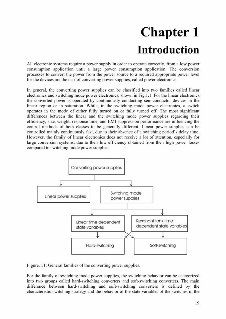
Introduction All electronic systems require a power supply in order to operate correctly, from a low power consumption application until a large power consumption application. The conversion processes to convert the power from the power source to a required appropriate power level for the devices are the task of converting power supplies, called power electronics. In general, the converting power supplies can be classified into two families called linear electronics and switching mode power electronics, shown in Fig.1.1. For the linear electronics, the converted power is operated by continuously conducting semiconductor devices in the linear region or in saturation. While, in the switching mode power electronics, a switch operates in the mode of either fully turned on or fully turned off. The most significant differences between the linear and the switching mode power supplies regarding their efficiency, size, weight, response time, and EMI suppression performance are influencing the control methods of both classes to be generally different. Linear power supplies can be controlled mainly continuously fast, due to their absence of a switching period’s delay time. However, the family of linear electronics does not receive a lot of attention, especially for large conversion systems, due to their low efficiency obtained from their high power losses compared to switching mode power supplies. Figure.1.1: General families of the converting power supplies. For the family of switching mode power supplies, the switching behavior can be categorized into two groups called hard-switching converters and soft-switching converters. The main difference between hard-switching and soft-switching converters is defined by the characteristic switching strategy and the behavior of the state variables of the switches in the

20
switching points. The switching strategies that result in zero voltage turn-on and/or zero current turn-off in the switching device introduce the family of soft-switching converters. In contrast to them, the family of hard-switching converters is defined where the switch device turns on and turns off during the voltage and/or the current not necessarily reaches zero. In other words, hard-switching converter switches operate at non-zero state variables. To be more accurate, we have to distinguish between converter types with linear time dependent state variables which are mostly hard-switching converters, and converter types with resonant tanks that change state variables non-linearly, mostly operated as soft-switching converters (see Fig.1.1). At the resonant converter, the resonant network consists of passive elements L and C or even an additional auxiliary diode and/or a switch are added into the circuit to shape the switch waveforms to achieve the zero voltage and/or zero current in the switching device at the switching point. In this work, the classification of resonant converters is based on the location of the resonant network. The characteristics of soft-switching waveform and the type of the resonant circuit are illustrated in Fig.1.2. Figure.1.2: A classification of resonant converter types. For a load resonant converter, the LC resonance tank is added to the load side in a series, parallel or in a combination of series and parallel connection [Rud 92] [Bat 94]. The oscillation of voltage and current due to LC resonance in the tank creates the zero voltage and/or zero current in the switching device. Generally, the transferred power is controlled by the switching frequency in the near of the resonant frequency of the tank [Joh 87] [Ste 88]. For a quasi resonant converter, a LC resonance circuit is added at the main switching device in order to yield a soft switching condition, either zero voltage and/or zero current. These families are called quasi resonant because the resonant mode of operation occurs only during one part of the switching cycle, while the PWM operation takes place during the rest of the switching period. This concept can be applied successfully to any PWM converter [Liu 84] [Liu 90] [Joz 89]. The zero current switching can be achieved by connecting L in series to the main switch. For the zero voltage switching, C is connected in parallel to the main switch.

21
The output power of these circuits is controlled by controlling the operating frequency, or PWM control at constant frequency can be used with some additional constraints to provide zero voltage and/or zero current switching in the switching device [Kaz1 87]. For a resonant link, a LC resonance circuit is located in between an input source and the PWM converter. For example, the input voltage applied to the converter oscillates between zero and slightly larger than twice the dc input voltage. The switches are then tuned on/off at the moment where the oscillation reaches the zero condition at the switches [Div 86] [Yam 94]. However, this work is focused on control concepts for the load resonant converter family and demonstrated their controllability on the example of the class-E topology [Sok 75]. It should be stated here, that load resonant converters in case of being controlled, require always a control of the output state variable by changing frequency and/or pulse width plus an appropriate control or tracking of at least one of the switching intervals due to the resonant tank frequency leading. The overview of the control scheme for the resonant converters is generalized in Fig.1.3.
Figure.1.3: Control scheme of resonant converters.
22
1.1 Objective Nowadays the developments of power supplies in military, industrial or commercial applications are growing rapidly. Not only to achieve the highest efficiency but also to focus on the size and weight minimization which are playing a major role in this area. Therefore, the research trends in dc-dc, ac-dc, dc-ac, ac-ac topologies are still continuously developing into the direction of new topologies, new control concepts, new material and devices to achieve highest efficiency and smallest size. The cost per unit is also one of the most important points regarding power supplies. Also, with new control methods and new ways of manufacturing the cost per unit might be reduced. Further, a simplified control concept might help to avoid discrete circuit expense especially at low power levels. Many topologies with difference control concepts were investigated in the past for achieving the best converter performance. Each of the topologies has a merit and demerit on themself wherein the impact of the control concept is not unimportant. Some general questions for the choice of a converter are “How large is the input voltage range”, “How large is the output load range”, “How to minimize the losses in the switches”, “How large is the highest efficiency that the converter can achieve”, “How fast is the regulation against any disturbances”, “How stable is the system after the disturbance” and “How is the smallest size and weight that the converter can reach”. These are some of the questions for the researcher has to find the answers. With the target of minimization, this research work explores the possibility to replace conventional electromagnetic transformers considered as the most bulky devices in power supplies by piezoelectric transformers (PT) for innovative off-line power supplies. PTs have several advantages over magnetic transformers. They provide a high efficiency (up to 98%) at smaller size than magnetic transformers, and low radiation due to the absence of the magnetic field. Thus, with the replacement by the PT the size of the converter can be reduced to be smaller and lighter at good efficiency [Lin 94] [Ben 06] [Yam 98] [Pri 01] [Dal 99] [Zai 98] [Dan 01]. The minimization effect is more providing for very large step-up or step-down voltage transfer ratios, compared to smaller transfer ratios due to experienced design constructions of PT. Several research works have proved that the excellent performance of the PT can be obtained by utilizing the PT in a suited switched power converter [Lee 98] [San 04] [Hem 02] [Sho 97] [Ben 05] [Wei 04] [Zai 95] [Zai 96] [Dia 04] [Pri 02] [San 03] [Ish 03] [Ive 04]. The investigated application of this work, to prove theoretically achieved results, is a smart-card off-line power supply for mobile phones, where the thickness is below 5 mm. The application allows for 3 Watts at 6 V/DC output voltage for universal input voltage range of 80-450 V/DC. The PT samples were 2.3 mm thick with a diameter of 17 mm. Control concepts for the target application had to be derived and to be optimized as a practical result of developed theories and methods. Generally in this work, several control methods for a load resonant converter, focusing on class-E topology by utilizing a PT, were developed in order to investigate and to select an appropriate control method capable of improving the efficiency of the converter and reducing the effect of electromagnetic interference (EMI). Different controllers were evaluated for optimizing the effect of disturbance against line and load variation. Finally, simplified mathematical expressions of the resonant converter regarding the controllability were derived to confirm the behavior of the converter system. The suitable control concepts were chosen to obtain a converter prototype for developing an integrated circuit (IC), which will be available in the near future.
23
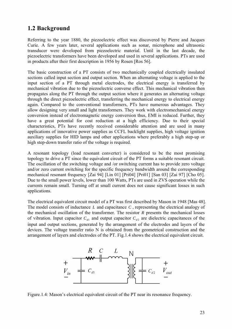
1.2 Background Referring to the year 1880, the piezoelectric effect was discovered by Pierre and Jacques Curie. A few years later, several applications such as sonar, microphone and ultrasonic transducer were developed from piezoelectric material. Until in the last decade, the piezoelectric transformers have been developed and used in several applications. PTs are used in products after their first description in 1956 by Rosen [Ros 56]. The basic construction of a PT consists of two mechanically coupled electrically insulated sections called input section and output section. When an alternating voltage is applied to the input section of a PT through metal electrodes, the electrical energy is transferred by mechanical vibration due to the piezoelectric converse effect. This mechanical vibration then propagates along the PT through the output section where it generates an alternating voltage through the direct piezoelectric effect, transferring the mechanical energy to electrical energy again. Compared to the conventional transformers, PTs have numerous advantages. They allow designing very small and light transformers. They work with electromechanical energy conversion instead of electromagnetic energy conversion thus, EMI is reduced. Further, they have a great potential for cost reduction at a high efficiency. Due to their special characteristics, PTs have recently received considerable attention and are used in many applications of innovative power supplies as CCFL backlight supplies, high voltage ignition auxiliary supplies for HID lamps and other applications where preferably a high step-up or high step-down transfer ratio of the voltage is required. A resonant topology (load resonant converter) is considered to be the most promising topology to drive a PT since the equivalent circuit of the PT forms a suitable resonant circuit. The oscillation of the switching voltage and /or switching current has to provide zero voltage and/or zero current switching for the specific frequency bandwidth around the corresponding mechanical resonant frequency [Zai 94] [Lin 01] [Pri04] [Pri01] [San 03] [Zai 97] [Cho 05]. Due to the small power levels, lower than 100 Watts, PTs are used in ZVS operation while the currents remain small. Turning off at small current does not cause significant losses in such applications. The electrical equivalent circuit model of a PT was first described by Mason in 1948 [Mas 48]. The model consists of inductance L and capacitance C , representing the electrical analogy of the mechanical oscillation of the transformer. The resistor R presents the mechanical losses of vibration. Input capacitor 1dC and output capacitor 2dC are dielectric capacitances of the input and output sections, generated by the arrangement of the electrodes and layers of the devices. The voltage transfer ratio N is obtained from the geometrical construction and the arrangement of layers and electrodes of the PT. Fig.1.4 shows the electrical equivalent circuit. Figure.1.4: Mason’s electrical equivalent circuit of the PT near its resonance frequency.

24
The narrow frequency band behavior of the PT transfer characteristics requires as well considered control concepts and controller design, which is the focus of the presented work. Conclusions of this work are nevertheless not limited to narrow band resonant converters. Targeted generalization of resonant converter control will be derived as well. 1.3 Outline of the Thesis Chapter 2 contains an overview of the pulse width modulation (PWM) switching mode technique. Basic definitions, concepts and topologies for the PWM switching mode technique are discussed. Several well-known control techniques to control the duty cycle ratio of a switch in the PWM converter were discussed in detail. Their advantages and disadvantages are discussed. However, it can be shown that these concepts are barely usable for load resonant converter control as required in the targeted PT applications. Chapter 3 shows the feasibility to replace the conventional transformer by the PT in a resonant converter using the class-E topology or other load resonant topologies allowing reliable control techniques. The principle operation of the class-E topology is discussed. The existing controls methods of the class-E topology are mentioned. A proposed analysis method is introduced to investigate the class-E behavior during suboptimum operation mode with the normalized parameters of duty cycle 321 ,,),( AAADc and 1Q . This normalized consideration is used to take advantage of the maximum possible degree of freedom in control design. Thus, the designed optimum parameters achieved the zero voltage switching (ZVS) condition over wide input voltage and output load range. Several control methods for resonant converters have been presented at the example of the class-E converter. The solution to achieve ZVS condition over a wide input voltage and output load range in a resonant converter was developed for class-E topology and extended to a suited family of comparable topologies as the inductor-less half-bridge. An optimum control concept for resonant converters was extracted from different opportunities to be compared. Chapter 4 describes at first an open loop dynamic equivalent modeling approach of resonant converters presented by the class-E topology. The behavior of open loop transient response of the output voltage in the class-E topology against changed conditions of input voltage steps, switching frequency and output load can be predicted by this open loop dynamic modeling. In order to design an optimum closed loop control, a closed loop modeling of the class-E converter was developed. The systematic procedure for calculation of an approximated time constant for a class-E converter by linearization around an operation point for the closed loop modeling was presented. The idea of linearization of the steady-state transfer function behavior was introduced in order to simplify the mathematical calculation in the closed loop regulation. The verification procedure of the proposed closed loop modeling was implemented into different control methods proposed in chapter three. Further, the transfer function of the linearization method was shown to predict the stability condition in the resonant converter for the class-E topology, extendable to any resonant converter topology. The simplified closed loop modeling by approximation of a first order equation model was done to achieve maximum simplification of the control loop design procedure. The evaluation shows that this model gives always a good result in case of large output filter capacitor in case of AC-DC rectification at the output. Closed loop modeling of resonant converters has been demonstrated to be more accurate, even for different modeling approaches, compared to open loop modeling requiring extended consideration of non-linearity. Chapter 5 discusses several controller concepts which have been used in resonant converters. It also shows the capability of the classical controllers implemented in resonant converters

25
considered on the example of the class-E topology. Conventional controllers as P, I, PI or PID controllers guarantee stability and sufficiently fast transient response behavior in load resonant converters, compared to hard-switching PWM converters for the same application. Furthermore, a simplified regulation scheme, achieved by matching an appropriate switching frequency according to the input voltage in a feed forward control, has been presented for resonant converters on the example of the class-E topology.

26
27
Chapter 2
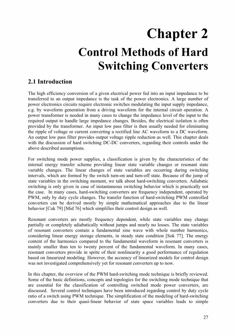
Control Methods of Hard Switching Converters
2.1 Introduction The high efficiency conversion of a given electrical power fed into an input impedance to be transferred to an output impedance is the task of the power electronics. A large number of power electronics circuits require electronic switches modulating the input supply impedance, e.g. by waveform generation from a driving waveform for the internal circuit operation. A power transformer is needed in many cases to change the impedance level of the input to the required output to handle large impedance changes. Besides, the electrical isolation is often provided by the transformer. An input low pass filter is then usually needed for eliminating the ripple of voltage or current converting a rectified line AC waveform to a DC waveform. An output low pass filter provides output voltage ripple reduction as well. This chapter deals with the discussion of hard switching DC-DC converters, regarding their controls under the above described assumptions. For switching mode power supplies, a classification is given by the characteristics of the internal energy transfer scheme providing linear state variable changes or resonant state variable changes. The linear changes of state variables are occurring during switching intervals, which are formed by the switch turn-on and turn-off state. Because of the jump of state variables in the switching moment, we talk about hard-switching converters. Adiabatic switching is only given in case of instantaneous switching behavior which is practically not the case. In many cases, hard-switching converters are frequency independent, operated by PWM, only by duty cycle changes. The transfer function of hard-switching PWM controlled converters can be derived mostly by simple mathematical approaches due to the linear behavior [Cuk 79] [Mid 76] which simplifies their control design as well. Resonant converters are mostly frequency dependent, while state variables may change partially or completely adiabatically without jumps and nearly no losses. The state variables of resonant converters contain a fundamental sine wave with whole number harmonics, considering linear energy storage elements, in steady state condition [Sok 77]. The energy content of the harmonics compared to the fundamental waveform in resonant converters is mainly smaller than ten to twenty percent of the fundamental waveform. In many cases, resonant converters provide in sprite of their nonlinearity a good performance of regulation based on linearized modeling. However, the accuracy of linearized models for control design was not investigated comprehensively yet for resonant converters up to now. In this chapter, the overview of the PWM hard-switching mode technique is briefly reviewed. Some of the basic definitions, concepts and topologies for the switching mode technique that are essential for the classification of controlling switched mode power converters, are discussed. Several control techniques have been introduced regarding control by duty cycle ratio of a switch using PWM technique. The simplification of the modeling of hard-switching converters due to their quasi-linear behavior of state space variables leads to simple
28
approaches of their control methods. It shall be evaluated whether control methods of PWM converters are also suitable for load resonant converters. 2.2 Pulse Width Modulation Switching Mode Power Supplies (PWM controlled hard switching converters) In general, the PWM modulated DC-DC converter may be presented in a simple circuit diagram in Fig.2.1. The input source can be either a voltage or a current source. The output loads generally consist either of a series inductor or of a parallel capacitor to the load resistance in order to provide a constant output current or a constant output voltage, respectively. The computational network of the converter consists of a number of energy storage elements, transformers and switches arranged in a certain topology, in which periodic opening and closing of the switches lead to power transfer through the network to obtain a required output voltage or current. Figure.2.1: Generalized switching mode power supplies. The number and the arrangement of the energy storage elements define the order of the converter. For example, in a first order converter such as buck, boost or buck-boost, there is only one inductor located in the converter. These arrangements are emerged from a basic understanding of switching mode converter concepts. The synthesis of higher order converters can be achieved by cascading lower order converters to get the desired functionality of the resulting converter such as a cascade of boost and buck converter led to discover the C´uk converter [Cuk 77]. A number of several synthesis methods were proposed to search for switching converter topologies such as the property of duality concepts was applied to discover new topologies of switching converters [Cuk 79]. Another generalization was proposed to find new converter topologies by three terminal port networks of converter cells connected with the input source and the output load. The variation in the configuration of converter cells lead to the generation of families of converters derived from these cells [Tym 86]. In a publication of Pietkiewicz the approach was based on the recognition of basic topologies of PWM, and a synthesis procedure for generation of new families was formulated as a set of topological rules [Pie 84]. In a paper of Erickson the basic synthesis approach is the recognition that reactive elements are switched between circuit topologies. The importance of this approach is that the synthesis of a converter was formulated and solved analytically [Eri 83].
29
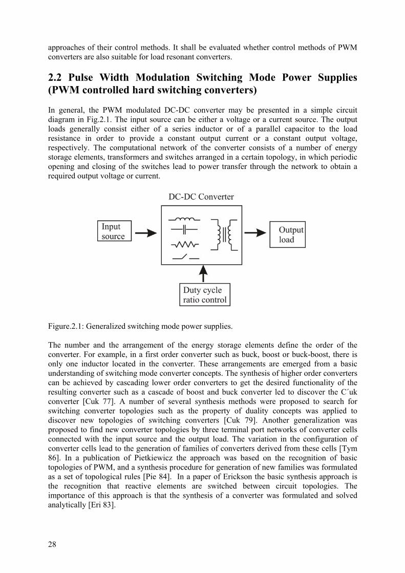
The researchers claim that some higher order optimum topologies can eliminate undesirable characteristics over the lower order topologies, as using quadratic functions of the duty cycle at reasonable values of duty cycle being not so small (e.g. duty cycle > 0.1). However, with the increasing order of a topology, more elements are needed thus, higher costs and size of implementation are unavoidable. With higher order converters, the expense of control and stability achievement is increasing as well. This is one reason, why higher order converters are practically avoided in products, but transformer coupling is preferred if feasible. Some examples of different order PWM controlled converters are shown in Fig.2.2.
Figure.2.2: Examples of different order PWM controlled hard switching converters. Although, several higher order PWM converters contain a number of reactive elements, the
steady state conversion ratio )(in
out
VV
MM = is always a function of the duty cycle ratio Dc of
the active switches (only at continuous mode): )(DcfM = . The power of the parameter Dc is mainly identified with the degree of the converter, depending on the number of active and

30
passive switches. It becomes also clear that the order of the transfer function follows the order of the converter. General modeling techniques for switching power converters can be divided into two categories, numerical and analytical. The numerical techniques use various algorithms to produce an accurate quantitative result also due to the nonlinear, time-varying nature of the converter. The analysis is time consuming and physical relationships in the system are not perceivable consequently. With analytic techniques the modeling procedure and mathematical results are obtained with quantitative analysis. Such as proposed by Vorperian [Vor 90] [Vor1 90] the switching device in the PWM converter was substituted by a three terminal nonlinear device equivalent, as an average circuit model. The transfer function then can be determined directly without the changing status of the switching device. The concept of a switching flow graph modeling technique was introduced for an analysis of the transfer function of PWM converters [Sme 90]. An important analytical approach to calculate the transfer function of PWM converters in general, based on the averaging technique that each interval of the duty cycle is described by its state space representation was introduced by Middlebrook [Mid 76]. This method shall be the base for following consideration of PWM converter transfer functions. The state space description during the on-time interval is represented by
][1][][1][1]'[
xCYuBxAX
=+=
During turn on interval )(Dc (2.1)
The state space during the off-time interval is represented by
][2][][2][2]'[
xCYuBxAX
=+=
During turn on interval )1( Dc− (2.2)
To represent an average description of the circuit over a switching period, the equations correspond to give a single period result from the following equations:
].)][1(21[][])][1(21[])][1(21[]'[
xDCCDcCyuDcBDcBxDcADcAx
−+=−++−+=
(2.3)
Using Laplace transformation in equation (2.3), we obtain
)]()][1(21[)]()][1(21[)]0([)]([ suDcBDcBsxDcADcAxsxs −++−+=− (2.4)
)].()][1(21[)]([ sxDCCDcCsy −+= (2.5) The initial condition )]0([x is zero since the transfer function was previously defined when the input initial conditions were zero, then equation (2.4) becomes
−= sIsx [)]([ 1)]]1(21[ −−+ DcADcA )].()][1(21[ suDcBDcB −+ (2.6) By substituting equation (2.6) into equation (2.5), the transfer function becomes
−−+= sIDCCDcCsusy )][1(21[)](/[)]([ 1)]]1(21[ −−+ DcADcA )].1(21[ DcBDcB −+ (2.7)
31
With the derived equation (2.1)-(2.7), the transfer functions of Buck, Boost, Buck-Boost and C´uk (for the continuous mode) in Fig.2.2 are summarized as
Buck: LL
L
in
out
RsLCLRsR
DcVV
++=
)(2
Boost: 22 )1(
)1(
DcRLsLCs
RDcVV
L
L
in
out
−++
−=
Buck-Boost: 22 )1(
)1(
DcRLsLCs
DcRDcVV
L
L
in
out
−++
−=
C´uk: 54321
)1(234 ωωωωω ++++
−=
ssssDcRDc
VV L
in
out
where
2111 LLCC=ω ; 2112 LLC=ω ; ))1((3 12
22
11 LCDcLDcCLCRL +−+=ω ;)2)((4 2221
2 LDcLLLDc +−+=ω ; .)1(5 2DcRL −=ω Actually, a PWM circuit can be designed as an isolated switched mode supply by utilizing transformer coupling. With the transformer coupling, the output is isolated from the input. The nominal output voltage can vary in a wide range by choosing the suitable transformer ratio. However, the PWM topologies with transformer isolation will not be considered in this discussion as extra ordinary, although they provide other challenges in control due to leakage inductance limitations. Snubber networks, resonant or non-resonant, may limit the control speed by additional time delays in the closed loop. Generally spoken, a soft-commutating network delays the control speed while a hard-commutated snubber network can help to increase control speed. The PWM converter also can be utilized by more than one switching device. In single switching topologies the switching device should be capable of high voltage blocking, especially when operated at a rectified AC main supply. Thus, a single switch topology is not a suitable solution for a high power converter since these converters need a high current rating of the switch. Therefore, multi switch devices are more suited for higher power conversion. In the PWM converters, when the switches are switched from the off-state to fully on-state (fully conducting state), there is a time interval until the current through the device has risen before the voltage across the switching device has dropped to zero, and vice versa as, shown in Fig.2.3 [Moh 89]. During these intervals, the switching device produces power losses and high switching stress. Thus, the total power loss in the switch depends on the number of switching operations per time unit. It is essential, that the size of the components, such as the transformer, inductors or capacitors can be reduced by increasing the switching frequency. Due to increasing losses, the PWM converter can not be decreased unlimited to reduce the converter size and weight. On the other hand, the control characteristic is mainly improving by increasing the switching frequency.

32
Figure.2.3: Voltage, current and power waveforms of the switching device in a hard switching PWM converter. 2.3 Closed Loop Control for Hard-Switching PWM Converters In the PWM circuit, the average output power is controlled by changing the switch on and off duration as described in earlier sections. The control of a DC-DC converter should be designed to reach the following goals:
- Regulation against the input line voltage; the output voltage remains constant if the input voltage is changed
- Regulation against the output load; the output voltage remains constant when the output load varies
- Having a fast transient response against system disturbances; as sudden changes in the input voltage and/or output load
- Remaining stable under all operating conditions. The above given requirements can be achieved by designing an efficient feedback control system, which will control the duty cycle to keep the output voltage constant all the time. The general block diagram of a closed-loop feed back PWM converter can be presented as in Fig.2.4.
Figure.2.4: Control block diagram of PWM converters. The transfer function of the controller )(1 sT must be designed properly, so that the output response meets the speed performance requirement, and the requirement of ensuring stability. The controller characteristic can be implemented by a well-known classical controller such as P, I, PI, PID or by other controllers, till the elegant idea of one-cycle control, sliding mode control or flat control. )(2 sT depends on the type of control signal feed back and signal
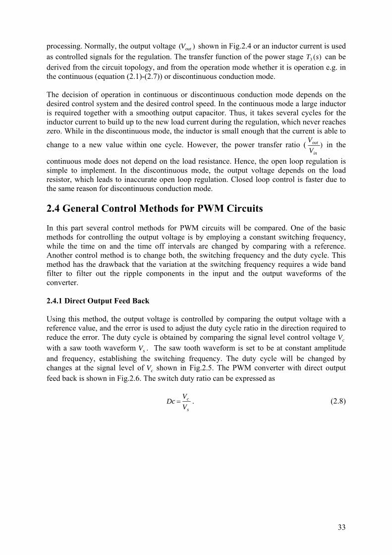
33
processing. Normally, the output voltage )( outV shown in Fig.2.4 or an inductor current is used as controlled signals for the regulation. The transfer function of the power stage )(3 sT can be derived from the circuit topology, and from the operation mode whether it is operation e.g. in the continuous (equation (2.1)-(2.7)) or discontinuous conduction mode. The decision of operation in continuous or discontinuous conduction mode depends on the desired control system and the desired control speed. In the continuous mode a large inductor is required together with a smoothing output capacitor. Thus, it takes several cycles for the inductor current to build up to the new load current during the regulation, which never reaches zero. While in the discontinuous mode, the inductor is small enough that the current is able to
change to a new value within one cycle. However, the power transfer ratio ( )in
out
VV in the
continuous mode does not depend on the load resistance. Hence, the open loop regulation is simple to implement. In the discontinuous mode, the output voltage depends on the load resistor, which leads to inaccurate open loop regulation. Closed loop control is faster due to the same reason for discontinuous conduction mode. 2.4 General Control Methods for PWM Circuits In this part several control methods for PWM circuits will be compared. One of the basic methods for controlling the output voltage is by employing a constant switching frequency, while the time on and the time off intervals are changed by comparing with a reference. Another control method is to change both, the switching frequency and the duty cycle. This method has the drawback that the variation at the switching frequency requires a wide band filter to filter out the ripple components in the input and the output waveforms of the converter. 2.4.1 Direct Output Feed Back Using this method, the output voltage is controlled by comparing the output voltage with a reference value, and the error is used to adjust the duty cycle ratio in the direction required to reduce the error. The duty cycle is obtained by comparing the signal level control voltage cV with a saw tooth waveform sV . The saw tooth waveform is set to be at constant amplitude and frequency, establishing the switching frequency. The duty cycle will be changed by changes at the signal level of cV shown in Fig.2.5. The PWM converter with direct output feed back is shown in Fig.2.6. The switch duty ratio can be expressed as
s
c
VV
Dc = . (2.8)
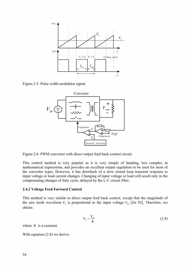
34
Figure.2.5: Pulse width modulator signal. Figure.2.6: PWM converter with direct output feed back control circuit. This control method is very popular as it is very simple of handing, less complex in mathematical expressions, and provides an excellent output regulation to be used for most of the converter types. However, it has drawback of a slow closed loop transient response to input voltage or load current changes. Changing of input voltage or load will result only in the compensating changes of duty cycle, delayed by the L-C circuit filter. 2.4.2 Voltage Feed Forward Control This method is very similar to direct output feed back control, except that the magnitude of the saw tooth waveform sV is proportional to the input voltage inV [Jin 92]. Therefore, we obtain:
K
VV in
s = (2.9)
where K is a constant. With equation (2.8) we derive:
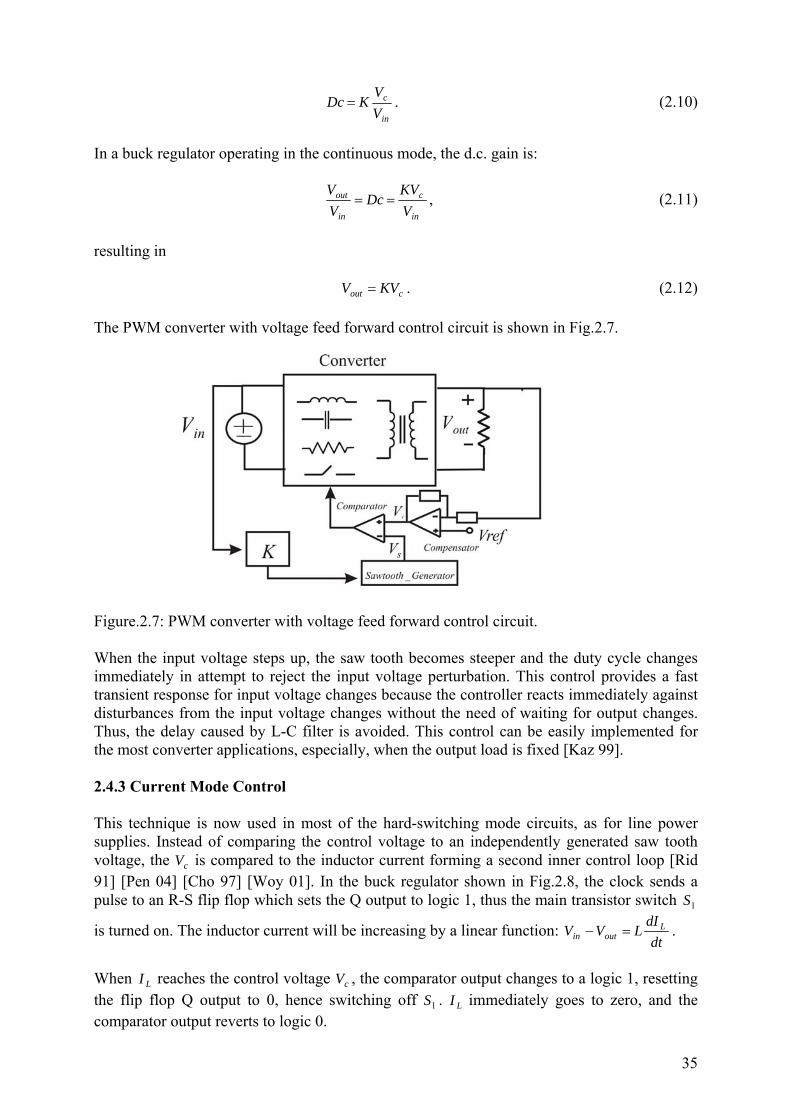
35
in
c
VV
KDc = . (2.10)
In a buck regulator operating in the continuous mode, the d.c. gain is:
in
c
in
out
VKV
DcVV
== , (2.11)
resulting in
cout KVV = . (2.12)
The PWM converter with voltage feed forward control circuit is shown in Fig.2.7.
Figure.2.7: PWM converter with voltage feed forward control circuit. When the input voltage steps up, the saw tooth becomes steeper and the duty cycle changes immediately in attempt to reject the input voltage perturbation. This control provides a fast transient response for input voltage changes because the controller reacts immediately against disturbances from the input voltage changes without the need of waiting for output changes. Thus, the delay caused by L-C filter is avoided. This control can be easily implemented for the most converter applications, especially, when the output load is fixed [Kaz 99]. 2.4.3 Current Mode Control This technique is now used in most of the hard-switching mode circuits, as for line power supplies. Instead of comparing the control voltage to an independently generated saw tooth voltage, the cV is compared to the inductor current forming a second inner control loop [Rid 91] [Pen 04] [Cho 97] [Woy 01]. In the buck regulator shown in Fig.2.8, the clock sends a pulse to an R-S flip flop which sets the Q output to logic 1, thus the main transistor switch 1S
is turned on. The inductor current will be increasing by a linear function: dt
dILVV L
outin =− .
When LI reaches the control voltage cV , the comparator output changes to a logic 1, resetting the flip flop Q output to 0, hence switching off 1S . LI immediately goes to zero, and the comparator output reverts to logic 0.

36
The current mode control has several advantages. First, since the switch turns off when reaching the control signal hence, the current limit protection is easy to be implemented by limiting the maximum value of cV . This protection also protects the entire converter from overload damage. Second, because the inductor current is being controlled directly, the effect of the inductor in the feed back loop is eliminated, simplifying second order control system into a first order system by removing the inductor pole from the loop. The resulting system is that why much easier to be stabilized [Cuk 84]. Also, this control technique provides a comparable result of voltage feed forward control for line regulation. Thus, no delay in the loop involving keeps the duty ratio instantaneous. However, in this method there is an inherent disadvantage of open loop stability when operating at duty cycle > 0.5. After a finite number of switching cycles the perturbation in the inductor current will increase. This growing oscillation does not become smaller. This instability problem is common for all converter topologies. The problem can be eliminated by adding ramp voltage to the current sense signal, so that the total slope of the rising section of the inductor current signal plus the ramp becomes larger than the slope of the falling section minus the ramp [Red 06]. A further problem is that there can be a sub-harmonic oscillation at the half of the switching frequency. This problem can be solves by including slope compensation also. Another main disadvantage of this control technique is that control is dependent on the load current hence, steady state errors might occur at high load currents. Figure.2.8: Buck converter with current mode control circuit. 2.4.4 Hysteresis Control The physical explanation of the hysteresis control is given in terms of the two operation boundaries [Mas 92] [Leu 03]. For example, in case of controlled output voltage, Fig.2.9 describes, that the output voltage is controlled by remaining within the boundary condition range ( maxVoutput , minVoutput ). Then, it can be said that the output is in normal steady state condition. The maximum and minimum boundary setting can be associated with the switching boundary that determines the control action, and the switch action takes place when the state trajectory crosses the boundary. The space between the two boundaries of maximum and minimum defines a region where no control action take place, called dead band.

37
Figure.2.9: The hysteresis control with boundary condition of the output voltage. In case of a PWM converter, the hysteresis control can involve variables such as the output voltage, the inductor current, or another variable that can be controlled. For the output voltage feed back, the general circuit diagram is illustrated in Fig.2.10. When the switch is turned on, the output voltage starts to rise up. As soon as the output voltage reaches the maximum boundary, the switch turns off and remains off until the output voltage falls down to the minimum boundary. The switch turns on again at the minimum boundary. The specific switching time and the state value are determined by the action of the circuit. Once the output voltage is between the boundaries, the switch action keeps it in the vicinity of the boundaries under all conditions. This control provides a good transient response for both, line and load regulation. Further, this control technique provides a less complex implementation and applicability for most converter types but it is strongly depended on the parasitic of the output capacitor (ESR). Figure.2.10: Hysteresis control of PWM converters based on output voltage feed back. 2.4.5 One-Cycle Control This method was developed by Smedley in 1990 [Sme 90] [Sme 95]. Assuming that the input signal to the switch is )(tx , the switch chops the input signal with the duty ratio Dc . The duty ratio of the switch operates as a switch function )(tk . The output product signal of the modulation between )(tx and )(tk called )(ty has a same frequency and pulse width of )(tk with the envelope of )(tx , as shown in Fig.2.11.
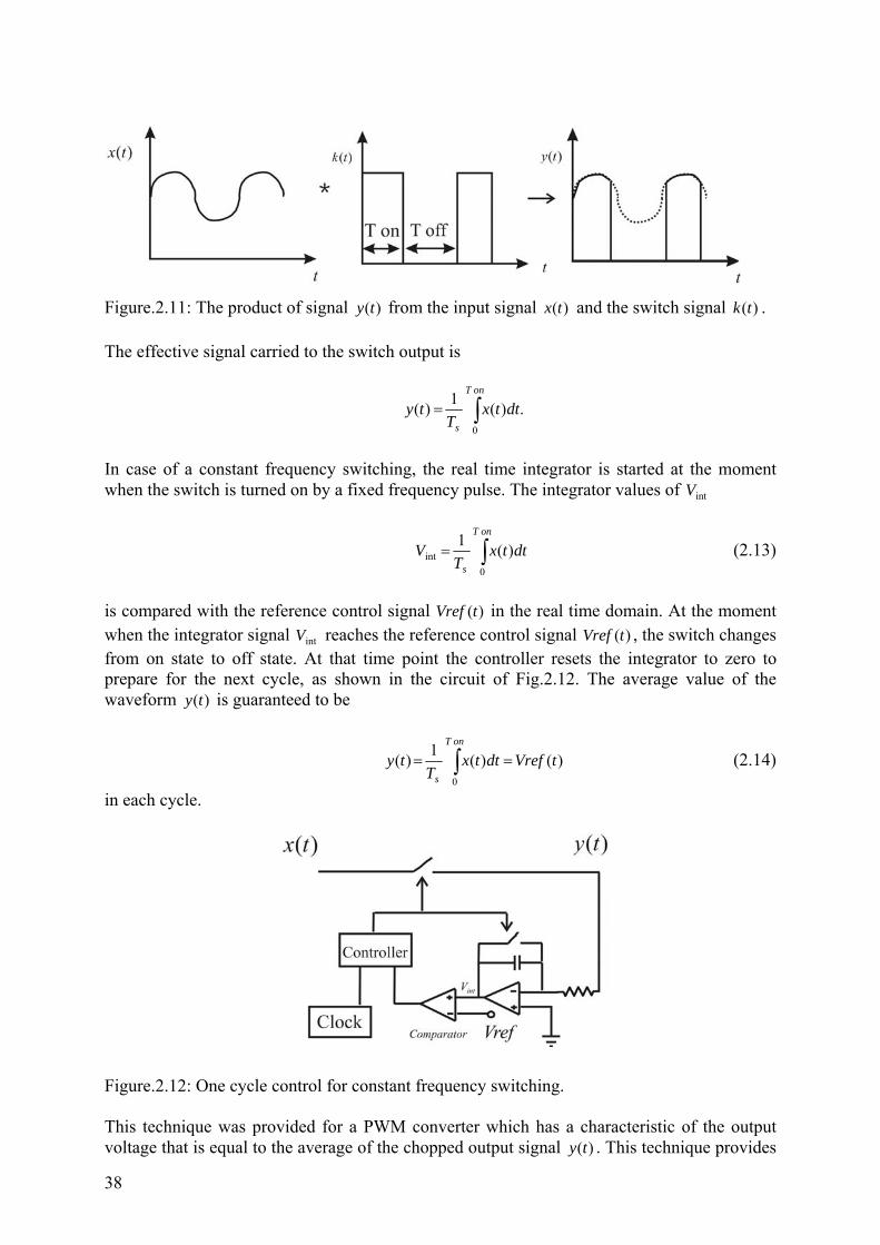
38
Figure.2.11: The product of signal )(ty from the input signal )(tx and the switch signal )(tk . The effective signal carried to the switch output is
.)(1)(0∫=onT
sdttx
Tty
In case of a constant frequency switching, the real time integrator is started at the moment when the switch is turned on by a fixed frequency pulse. The integrator values of intV
∫=onT
sdttx
TV
0int )(1 (2.13)
is compared with the reference control signal )(tVref in the real time domain. At the moment when the integrator signal intV reaches the reference control signal )(tVref , the switch changes from on state to off state. At that time point the controller resets the integrator to zero to prepare for the next cycle, as shown in the circuit of Fig.2.12. The average value of the waveform )(ty is guaranteed to be
)()(1)(
0
tVrefdttxT
tyonT
s== ∫ (2.14)
in each cycle. Figure.2.12: One cycle control for constant frequency switching. This technique was provided for a PWM converter which has a characteristic of the output voltage that is equal to the average of the chopped output signal )(ty . This technique provides
39
a fast transient response against the input voltage perturbation. Supposing the control reference and the load is constant while the input voltage is perturbated, the changing of the chopped output signal )(ty is integrated in real time and, the slope of this integrated signal changes exactly and immediately. Therefore, the input voltage directly and instantly affects the duty ratio in such way that the integration of the chopped output signal )(ty is constant in each cycle. This control method is also suitable for changing the control reference. With the same principle of operation, the controller can adjust the duty ratio to follow the control reference change in one cycle. Moreover, one cycle control technique is found for any type of switching method, such constant on time, constant off time, and variable frequency control. 2.4.6 Sliding Mode Control Since many years, different forms of sliding mode control have been used to improve the dynamic response in any kind of control systems [Mat 93] [Ros 94]. Venkataramanan first applied the idea of sliding mode control into the PWM converter [Ven 86]. This control is suitable for power converters due to the inherent discrete switching action. The variable structure system (VSS) is constructed according to the internally change of the system. For example, in the PWM converter, normally two variable structure systems have been designed in case of turn on and turn off switching condition. The sliding surface has been defined passing through a desired operating point according to the VSS in the phase plane under the condition that
dtVrefVoutdVrefVoutK )()( −
+−=σ . (2.15)
The condition control law says that for 0>σ , the switch turns off ( 0)( =tu ), and for 0<σ the switch turns on ( 1)( =tu ). Describing a stable trajectory, the sliding boundaries in the phase plane have been designed.
The phase plane is constructed under the variable VrefVout − and dt
VrefVoutd )( − in the X
axis and Y axis, respectively. The trajectory of the two switch states reaches the sliding surface, from the opposite side. The system motion is restricted along the sliding line. The hysteresis might be including into the sliding surface ∆+<<∆− σσσ . The switch is turned on when the trajectory reaches the lower limit, and is turned off when the trajectory reaches the upper limit as shown in Fig.2.13. The example of control schematic of a sliding mode controller for the buck converter is shown in Fig.2.14 [Ven 86]. When the system order is higher than two, a sliding surface is very complicated to be found that satisfies the reaching condition and the converging condition. With this problem, this method is not suitable for controlling converters of an order higher than two.
40
Figure.2.13: The sliding surface of the sliding mode control in PWM converters. Figure.2.14: The control schematic of the sliding mode controller for the buck converter. 2.4.7 Charge Control This control technique has been presented by Wei Tang in 1993 [Tan 93]. The control characteristic presents a special method of using inductor current of a PWM converter as a part of its feed-back mechanism, apart from output voltage feed back. The main feature of charge control is the ability to control the per-cycle charge of the switch current of PWM converters without output voltage feed back. The basic operation of the charge control applied in a buck converter illustrates in Fig.2.15. The active switch turns on at the beginning of each cycle. During the switch turns on, the switch current is equal to the inductor current. The switch current is sensed and integrated to charge a timing capacitor TC up from zero volts until it reaches a reference voltage refV at which point the active switch is turned off, and the switch across TC turns on to discharge TC to zero. TC is totally discharged before the next cycle switching starts. Hence, the average value of the inductor current in one cycle is controlled since the switch current is equal to the inductor current during the on time interval.

41
Figure.2.15: Charge control for the buck converter and the steady state waveforms. Compared to the peak current mode control in chapter 2.4.3, this control scheme provides an excellent noise immunity due to the use of the integration of the on-time inductor current as the feed back control signal. However, the stability condition of charge control is different from the current mode control in chapter 2.4.3. In the current mode control, the stability is affected by the duty cycle while in the charge control; it is affected by both, the duty cycle, and the output resistance. In the same way as in case of current mode control, the stability margin can be increased by adding an external ramp. The dynamic properties of charge control has been improved compared to the output voltage feed back due to the elimination of the effect of inductor caused time delay in the feed back loop. 2.4.8 Flatness Control A flatness system, introduced by Fliess [Fli 95], provides a system property that extends the notion of controllability from linear systems to nonlinear systems. In the flat system, the flat output ( y ) is a function of system variables. It need not satisfy any autonomous differential equation. Furthermore, all other variables can be expressed in outputs and its time derivates. The idea of flatness control was implemented into the DC-DC PWM converter in the work of Gensior and Weber, respectively [Gen 06] [Web 04]. In these works the boost converter was selected as an applicable topology because its behavior belongs to the class of flat systems.
42
First, the state variables of differential equations of the system were derived as a function of inductor current )( 1z and output capacitor voltage )( 2z where the switching function )(q serves as the control input variable of the boost converter. The block diagram of flatness control is shown in Fig.2.16. The original system represents the boost converter. The auxiliary system contains a load observer and a model of the boost
converter to calculate the state vector ~z for trajectory planning. The measured state vector z
is only needed to calculate the estimated load ~R . Signals ', yy are not measured, but can be
computed from the signal ~z and
~R by a trajectory plan. Then, the switching function
(controlled signal) )(q can be processed by defined conditions according to~~
,,', Rzyy . Figure.2.16: Flatness control block diagram. The flat control has the fundamental advantage that the trajectory planning designed as a physically variable trajectory for the flat output directly prescribes the trajectories of all system variables. Thus, a fast system response can be achieved by a reasonably planned trajectory for flat output. However, the flat control has a limitation that it is not generalized for any kind of application. It is applicable only in the systems considered as flat systems. Examples of the standard SEPIC and C´uk converter are not applicable for flat control because they do not belong to the class of flat systems. It can be assumed that resonant converters of higher complexity are also not belonging to the flat systems, if not linearization of such systems can lead to simplifications of the system description.
43
2.4.9 H-infinity control The example of applying the H-infinity control into the Boost power converter was presented in the publication of Naim [Nai 97]. The idea of H-infinity control was implemented to improve the stability condition in the switching mode power supplies which are encountered with a right-half-plane zero. For example for boost or fly-back converters, the transfer functions of the duty cycle to the output voltage consist of a zero in the right half plane. Thus, the bandwidth of the closed-loop has to be restricted due to the stability. The general control scheme of the H-infinity control is shown in Fig.2.17. Po is the converter transfer function. Co is the controller transfer function. W is a stable weight function. The vector w contains the perturbations ( ), outin IV . The vector Y contains the measurement of output, input voltage of the converter ),( inout VV . The control input is the duty cycle ( )Dc . The output 'Z is the weighted error signal. The transfer functions of the controller (Co) can be found via the solution of two algebraic Riccati equations. The weight function W is defined as single pole and zero located in the left hand side of half plane. Figure.2.17: H-infinity control scheme. The result of the implementation shows that H-infinity control provides good transient behavior against the input voltage and output load perturbations compared to the feed forward control and current mode control. However, this control provides several drawbacks such as the order of the converter is increased due to the weight function. Also the solution for the transfer function of the controller (Co) might consist of a positive unstable pole. Thus, an addition assumption has to be assumed to eliminate the positive unstable pole. Consequently, the switching frequency range is limited. Moreover, H-infinity control provides a low dc gain compared with the feed back output voltage, feed forward or current mode controller. It can be assumed that H-infinity control is not an optimum solution also for the load resonant converters (in case of class-E, inductor-less half-bridge) since these load resonant converters are not consisting of right-half-plane zero. Thus, the instability condition is not sensitive as in case of boost or fly back converters. Otherwise, an addition of one order of the closed loop due to the weight function is unavoidable. As a result, the analysis of the model will be much more complicated especially in the topologies which are already of high order. Moreover, there is a trade-off between the improved stability and the steady state error. Even the improved stability can be achieved but the zero steady state error might not be achieved due to the low dc gain.

44
2.5 Conclusion The PWM converters have been considered as the majority of usual power converters at this time for DC-DC applications. Typical applications of such PWM converters are power supplies required in many electronic devices, uninterruptible power systems, motor drives, solar energy applications, etc. According to the increasing diversity of possible applications and due to continuous demand of smaller size and weight, at reduced losses, PWM converters have been developed to fulfill the product requirements. It was shown in this chapter that the control methods play an important role to simplify the control system at one hand. On the other hand, control speed in transient response behavior is not only receivable by frequency increase due to size reduction requirements, but also by an efficient control method and optimum controller design. It came out that not only an optimum controller will solve the design tasks, but also an optimum feed back concept provides fast control opportunities. PWM converters are consisting of repetitively switched linear networks consisting of reactive elements connected between the input source and output load corresponding to their topology. The output voltage and/or output current have to be maintained at a required constant level. Two main disturbances in PWM converters are the input voltage variation and the output load variation. Thus, the control circuit is necessary to regulate the output power against these disturbances. To reach these goals, it is desirable to eliminate the time constant of the power stage by proper feed back methods. The drawback of a fast closed-loop control without the stabilization of the output capacitor time constant is an additional expense of stabilizing measures which could be shown in the comparison of control methods of this chapter. In general, the power transfer ratio in a PWM converter is controlled by modulating the duty ratio. Several techniques such as closed loop feed back control and feed forward control have been used to regulate the duty ratio in order to reduce the deviation after disturbances. Different well-known control methods (direct output feed back, voltage feed forward control, current mode control, one-cycle control, hysteresis control, sliding mode control, charge control, etc.) for PWM circuits have been discussed in this chapter with their advantages and disadvantages. The transfer functions of the control technique and of the power stages have been addressed to be important for a simple fast responding and stable control concept. The high complexity of a converter might impact the controllability for an optimum control method to be not applicable. Due to this reason, two conclusions are possible. First, the simplest topologies of PWM converters are preferable for optimum controllability. Second, due to the limitation of switching frequency of hard-switching converters, soft-switched converter may substitute them in several applications if the transfer characteristics will remain mathematically simple, e.g. by suited methods of linearization. However, the main obstacle in a PWM converter is the limitation of the switching frequency. The current and voltage in the switching device can not change their value instantaneously. Thus, both switch voltage and switch current are not zero during the switching interval causing the switching losses. These losses increase proportionally according to the switching frequency. As a result, the implementation of size reduction at high efficiency is the limitation of PWM converters. Typically, the switching frequency of the PWM converter is in the range of a few kilohertz to a few hundred kilohertz, depending on power level and application. The switching stress during the device turns on/off due to high voltage and current spikes is an additional problem of non-adiabatic switching. Thus, the techniques of soft-switching called quasi resonant or quasi square wave (ZVS, ZCS) have been introduced to solve these problems of PWM converters [Liu 84] [Liu 90] [Joz 89]. Soft commutated PWM converters are representing the same transfer characteristic as hard-switching

45
converters of the same basic topology. However, the resonant interval of soft-switching PWM converter has to be considered carefully in the controller design process. In such case a synchronization of one of the switching pulse on or off is provided in relation to the frequency generator. The synchronization requirement in order to obtain ZVS or ZCS in all operating conditions reduces the applicability of efficient control methods. For the methods of direct output feed back [Kaz1 87] and current mode control [Huy 90], soft-switching behaviors can be implemented without significant drawbacks. For hysteresis control and all two points control methods where a switching signal is generated by direct feed back of a state variable for all of the switching points, soft switching by auxiliary resonant circuits is not possible or limits the operation area significantly. For DC-DC line applications, the power range defines the configuration or topology for a PWM converter summarized by C´uk [Cuk 84]. He showed that for the low power operation range (below 50 W), the simplicity of a fly-black converter with one magnetic component as an isolating transformer, is usually favored in terms of cost perspective. In the operation range of 100-200 W, the buck or forward converter is the preferred solution since it retains the low cost single switch. However, for 300-400 W, a topology with two switches such as push pull or half-bridge is considered due to the stress reduction in the switching devices. In the high operation range (more than 500 W) the four transistors full bridge is a prevailing topology or interleaving converters are used. All of these topologies can be controlled by discussed control methods of this chapter. The feasibility of applying PWM control methods for load resonant converters depends on three conditions. First, the duty cycle has to be substituted by the switching period in order to achieve controllability. Second, the converter transfer function has to be simplified representing a linearized approximation being non-sensitive against approximation errors. Third, suitable control feedback and observing variables have to be extracted which might be phase angles or sine wave peaks instead of average currents or voltages.

46
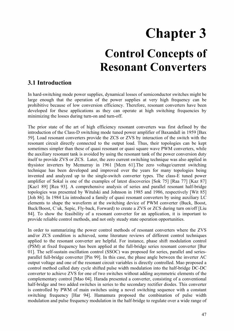
47
Chapter 3
Control Concepts of Resonant Converters
3.1 Introduction In hard-switching mode power supplies, dynamical losses of semiconductor switches might be large enough that the operation of the power supplies at very high frequency can be prohibitive because of low conversion efficiency. Therefore, resonant converters have been developed for these applications as they can operate at high switching frequencies by minimizing the losses during turn-on and turn-off. The prior state of the art of high efficiency resonant converters was first defined by the introduction of the Class-D switching mode tuned power amplifier of Baxandall in 1959 [Bax 59]. Load resonant converters provide the ZCS or ZVS by interaction of the switch with the resonant circuit directly connected to the output load. Thus, their topologies can be kept sometimes simpler than these of quasi resonant or quasi square wave PWM converters, while the auxiliary resonant tank is avoided by using the resonant tank of the power conversion duty itself to provide ZVS or ZCS. Later, the zero current switching technique was also applied in thysistor inverters by Mcmurray in 1961 [Mcm 61].The zero voltage/current switching technique has been developed and improved over the years for many topologies being invented and analyzed up to the single-switch converter types. The class-E tuned power amplifier of Sokal is one of the examples of latest discoveries [Sok 75] [Raa 77] [Kaz 87] [Kaz1 89] [Rea 93]. A comprehensive analysis of series and parallel resonant half-bridge topologies was presented by Witulski and Johnson in 1985 and 1986, respectively [Wit 85] [Joh 86]. In 1984 Liu introduced a family of quasi resonant converters by using auxiliary LC elements to shape the waveform at the switching device of PWM converter (Buck, Boost, Buck/Boost, C´uk, Sepic, Fly-back, Forward) to create a ZVS or ZCS during turn on/off [Liu 84]. To show the feasibility of a resonant converter for an application, it is important to provide reliable control methods, and not only steady state operation opportunities. In order to summarizing the power control methods of resonant converters where the ZVS and/or ZCS condition is achieved, some literature reviews of different control techniques applied to the resonant converter are helpful. For instance, phase shift modulation control (PSM) at fixed frequency has been applied at the full-bridge series resonant converter [Bur 01]. The self-sustain oscillation control (SSOC) was proposed for series, parallel and series-parallel full-bridge converter [Pin 99]. In this case, the phase angle between the inverter AC output voltage and one of the resonant circuit variables is directly controlled. Mao proposed a control method called duty cycle shifted pulse width modulation into the half-bridge DC-DC converter to achieve ZVS for one of two switches without adding asymmetric elements of the complementary control [Mao 04]. Harada presented a converter, consisting of a conventional half-bridge and two added switches in series to the secondary rectifier diodes. This converter is controlled by PWM of main switches using a novel switching sequence with a constant switching frequency [Har 94]. Hamamura proposed the combination of pulse width modulation and pulse frequency modulation in the half-bridge to regulate over a wide range of

48
the input voltage [Ham 00]. Kazimierczuk developed a method of phase control for the resonant inverter of the class-D topology in order to regulate the output voltage operated at a constant switching frequency [Kaz 93]. Phase control is popular when only output power has to be controlled [Rib 98]. However, generally it is well-known that in a resonant converter, the output power depends on the relation between the switching frequency and the resonant frequency [Ste 88]. This fact implies that the output power in the load resonant converter can be always controlled by the method of frequency modulation. Many examples of applications where the output voltage is controlled by frequency modulation were published [Kaz2 89] [Ste 88] [You1 04] [Pol 97] [Dia 04] [Red 83] [Gut 80] [Bis1 06]. Moreover, Steigerwald showed that, for load resonant converters (half-bridge resonant converter; series, parallel, series-parallel load), the ZVS condition can be achieved for frequency modulation when the switching frequency is above the resonant frequency [Ste 88]. Youssef showed that, with a variable frequency control, the bandwidth of suitable switching frequency is larger than with a phase shift modulation at fixed frequency in the full-bridge converter [You 04]. Comparing the voltage-fed inductor-less half-bridge topology and the class-E circuit, which is a current feed topology, the transfer ratio range of the class-E is larger than this of the inductor-less half-bridge topology at comparable load and voltage transfer conditions [Bis 06]. With this benefit, a larger frequency bandwidth control range of class-E is possible to cover a wider input voltage range, compared to an inductor-less half-bridge. Moreover, there is a better EMI suppression of the class-E by the input inductor than in a half-bridge, and lower switch current peaks. The class-E topology is a single switch topology with low side driving, while a half-bridge needs more than one switching device including high side driving. To evaluate the replacement of the magnetic transformer by the PT in a resonant converter for innovative off-line power supplies, the class-E topology proposed by N.Sokal [Sok 75] was considered to drive a piezoelectric transformer in such application, while the inductor-less half-bridge topology was less suited for wide range application [Bis1 04]. It has to be demonstrated, also that the control of the class-E can be provided in reliable mode as it has been demonstrated for the inductor-less half-bridge [Lin 01]. The literature review about class-E topology in terms of the principle operation, the existing control methods, and the analysis design with normalized parameters will be discussed in chapter 3.2. In chapter 3.3, the normalized analysis of class-E under suboptimum operation mode will be presented. The analysis was derived under the normalized parameters of duty cycle
321 ,,, AAADc and 1Q . It will be shown how normalization improves the design process of the control system. Taking advantage of the normalizing method, as shown in chapter 3.4, the ZVS condition for a wide input voltage range and wide output load range can be achieved by a method called duty cycle tracking with frequency control. Then, with the improved design of a PT containing an auxiliary tap, the ZVS condition for a resonant converter can be obtained by a method called turn on synchronization with frequency control. The controlled output voltage, current, or power is achieved by a variable frequency control. Several possible control methods were presented for the class-E resonant converter. Besides, the dissipative energy of a power converter is not reduced only by ZVS condition, but also by non-switched intervals during an operation sequence known as burst mode control. This method is proposed as an
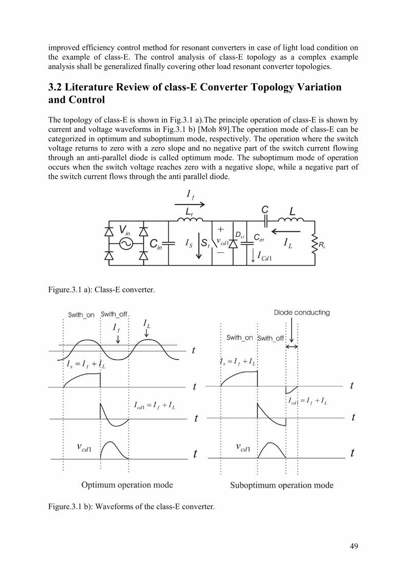
49
improved efficiency control method for resonant converters in case of light load condition on the example of class-E. The control analysis of class-E topology as a complex example analysis shall be generalized finally covering other load resonant converter topologies. 3.2 Literature Review of class-E Converter Topology Variation and Control The topology of class-E is shown in Fig.3.1 a).The principle operation of class-E is shown by current and voltage waveforms in Fig.3.1 b) [Moh 89].The operation mode of class-E can be categorized in optimum and suboptimum mode, respectively. The operation where the switch voltage returns to zero with a zero slope and no negative part of the switch current flowing through an anti-parallel diode is called optimum mode. The suboptimum mode of operation occurs when the switch voltage reaches zero with a negative slope, while a negative part of the switch current flows through the anti parallel diode. Figure.3.1 a): Class-E converter. Figure.3.1 b): Waveforms of the class-E converter.

50
If the input inductor ( fL ) is a sufficiently large inductor, the input current fI is approximately constant. If the loaded quality factor is high, the motion current LI is approximately a sine wave. When the switch is turned on, Lfs III += flows through the switch. When the switch is turned off, because of capacitor 1dC , the voltage across the switch builds up by defined slope until it reaches a peak, and finally returns to zero (Fig.3.1 b). In the class-E topology used for DC-DC application, the DC output voltage is obtained by rectifying the resonant AC current. When the load resistor is changed, the switching frequency is changed accordingly to regulate the amplitude of the resonant current and to maintain the output voltage constant. Unfortunately, the switching frequency has to be changed over a wide range to accommodate to the load resistor and input voltage variations. Moreover, in the class-E topology, when a small output current occurs (at the light load), the resonant current might be unable to discharge the parallel input capacitor completely, as a result zero voltage turn on cannot be obtained in the switching device. Several attempts have been made to solve this problem of a class-E converter [Liu 95]. Some methods of control using output circuit variations which have been applied to the class-E topology are the following:
1. Class-E converter with inductive impedance inverter [Kaz2 89] 2. Class-E converter with switch controlled capacitor [Gu 88] 3. Class-E combined converter [Hu 89] 4. Half-wave controlled current rectifier [Yan 95].
To achieve controllability, additive circuit has been used in the mentioned examples which are increases the expense of the converter. 3.2.1 Class-E Converter with Inductive Impedance Inverter This control method was discovered by Kazimierczuk in 1989 [Kaz2 89]. An additional inductor )( 2L and a coupling capacitor )( 2C are added at the input of the output rectifier, as shown in Fig.3.2. With the additional passive components the inductor L2 is used as an impedance inverter which provides zero voltage switching in a larger range of the output load variation. It was shown that the variation range of the switching frequency is also reduced by this extension (narrow band frequency modulation). With this concept, the circuit can operate at no load condition. Unfortunately, there are still existing some values of the load resistor at which ZVS is lost. However, size and cost of this concept is not optimized in a real application owing to the additional elements of 2L and 2C . Moreover, in order to regulate under the narrow band condition, the stability might cause a problem due to noise influence. Figure.3.2: Class-E converter with inductive impedance inverter.

51
3.2.2 Class-E Converter with Switching Controlled Capacitor Jian-Gu proposed his method in 1988 [Gu 88]. He provided a concept in such a way that in the resonant converter the output depends not only upon switching frequency but also on resonant frequency. Hence, to change from the switching frequency modulation ( )1S to the resonant frequency modulation )( 2S , the output voltage can be maintained constant with a constant switching frequency. The idea of switch controlled inductor (SCI) was extended to a switch controlled capacitor (SCC) to change the equivalent resonant frequency of the resonant branch to regulate the output voltage. The auxiliary switch circuit containing )( 2S was implemented into the class-E topology as shown in Fig.3.3. Figure.3.3: Class-E converter with switch controlled capacitor. When the switch S2 conducts all the time, the capacitor C2 is shorted all the time and the
resonant frequency is determined by Lr and Cr as resonantω =rr CL
1 . When the auxiliary switch
S2 does not conduct at all, the capacitor C2 acts as an element of the resonant circuit together
with rL and rC . The corresponding resonant frequency is resonantω =2
11CLCL rrr
+ . By
changing the conduction angle of the switch S2, the equivalent resonant frequency is changed and the output voltage can be regulated at a constant switching frequency at 1S . However, for light load application, the ZVS condition for S1 is basically lost. Thus, the circuit cannot operate at light load condition. 3.2.3 Class-E Combined Converter Hu developed his control method by controlling the phase shift of the resonant current in two class-E topologies in 1989 [Hu 89]. At this control method, two identical conventional class-E converters are combined together with the common input and output terminal. Using this control method, the output voltage can be regulated at a fixed switching frequency, and the ZVS condition can be achieved from the full load to the no load condition. The circuit for this control scheme is shown in Fig.3.4. This concept requires that the values of the internal parameters at the two converters have to be exactly the same 21 CC = , 21 rr LL = , 21 rr CC = . The output voltage is controlled by the phase shift between the driving signals of S1 and S2. The output current is the vector summation of the resonant current I1 and I2. When the switching signal S1 and S2 are in phase, the current I1 and I2 are also in phase with the same amplitude owing to the two identical class-E circuits. Hence, the output current coming from the summation of I1 and I2, being
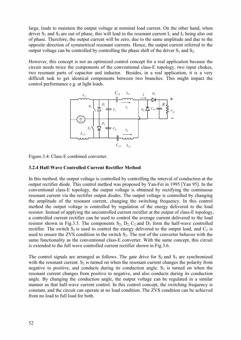
52
large, leads to maintain the output voltage at nominal load current. On the other hand, when driver S1 and S2 are out of phase, this will lead to the resonant current I1 and I2 being also out of phase. Therefore, the output current will be zero, due to the same amplitude and due to the opposite direction of symmetrical resonant currents. Hence, the output current referred to the output voltage can be controlled by controlling the phase shift of the driver S1 and S2. However, this concept is not an optimized control concept for a real application because the circuit needs twice the components of the conventional class-E topology, two input chokes, two resonant parts of capacitor and inductor. Besides, in a real application, it is a very difficult task to get identical components between two branches. This might impact the control performance e.g. at light loads. Figure.3.4: Class-E combined converter. 3.2.4 Half-Wave Controlled Current Rectifier Method In this method, the output voltage is controlled by controlling the interval of conduction at the output rectifier diode. This control method was proposed by Yan-Fei in 1995 [Yan 95]. In the conventional class-E topology, the output voltage is obtained by rectifying the continuous resonant current via the rectifier output diodes. The output voltage is controlled by changing the amplitude of the resonant current, changing the switching frequency. In this control method the output voltage is controlled by regulation of the energy delivered to the load resistor. Instead of applying the uncontrolled current rectifier at the output of class-E topology, a controlled current rectifier can be used to control the average current delivered to the load resistor shown in Fig.3.5. The components S2, D2, C2 and D3 form the half-wave controlled rectifier. The switch S2 is used to control the energy delivered to the output load, and C2 is used to ensure the ZVS condition in the switch S2. The rest of the converter behaves with the same functionality as the conventional class-E converter. With the same concept, this circuit is extended to the full wave controlled current rectifier shown in Fig.3.6. The control signals are arranged as follows. The gate drive for S2 and S3 are synchronized with the resonant current. S2 is turned on when the resonant current changes the polarity from negative to positive, and conducts during its conduction angle. S3 is turned on when the resonant current changes from positive to negative, and also conducts during its conduction angle. By changing the conduction angle, the output voltage can be regulated in a similar manner as that half-wave current control. In this control concept, the switching frequency is constant, and the circuit can operate at no load condition. The ZVS condition can be achieved from no load to full load for both.

53
Figure.3.5: Class-E converter with half-wave controlled current rectifier.
Figure.3.6: Class-E converter with full-wave controlled current rectifier. 3.2.5 Conventional Regulation by Frequency Regulation The idea of using frequency regulation over a wide operation range for the class-E converter was presented by Redl in 1983 [Red1 83]. The application was carried out with the operating frequency 1.5 MHz producing 40 Watts at the efficiency of 85%, assuming high Q approximation. The control of the switch was accomplished by the output voltage regulation via frequency variation produced by a VCO. The impedance diagrams for any duty cycle ratio were derived for determining the boundary operation at a given duty ratio. The impedance diagram provided the allowed range for a duty cycle at the given impedance. A PI controller was implemented to regulate the switching frequency. An addition circuit was required to control the duty cycle according to the impedance range. It can be seen that the researchers have been trying to develop various control methods for resonant converters in order to overcome the problem of wide load range. From no load to full load, and also for a wide input voltage range, the ZVS condition over the whole operation range is only given by additional circuit extensions and/or parameter optimization. Some existing presented control methods can solve this problem, while some of them can only solve the problem partly. In the proposed control voltage method, shown in the next chapter, the ZVS condition can be achieved over the wide input and output load range, and the numbers of the components are reduced compared to existing solutions methods. Moreover, the size of the converter can be optimized by eliminating the bulky components of existing solutions using a PT as a load resonant network. It shall become clear that the parameter optimization of a given topology plays a significant role in the circuit optimization and in size reduction. Steady state parameter optimization leads to the control definition more than only a topology defines the control concept itself.
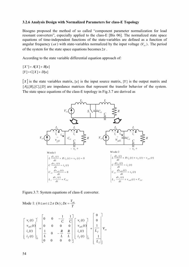
54
3.2.6 Analysis Design with Normalized Parameters for class-E Topology Bisogno proposed the method of so called “component parameter normalization for load resonant converters”, especially applied to the class-E [Bis 06]. The normalized state space equations of time-independent functions of the state-variables are defined as a function of angular frequency ( tω ) with state-variables normalized by the input voltage )( ccV . The period of the system for the state space equations becomes π2 . According to the state variable differential equation approach of:
][][][][][]'[
uDXCYuBXAX
+=+=
[ ]X is the state variables matrix, ][u is the input source matrix, ][Y is the output matrix and
][],[],[],[ DCBA are impedance matrices that represent the transfer behavior of the system. The state space equations of the class-E topology in Fig.3.7 are derived as Figure.3.7: System equations of class-E converter.
Mode 1: ( )20 Dct πω ≤≤ ;T
TDc on=
cc
f
f
f
s
cd
c
f
s
cd
c
V
L
Ltiti
tvtv
LR
LR
L
CC
titi
tvtv
⎥⎥⎥⎥⎥⎥⎥⎥
⎦
⎤
⎢⎢⎢⎢⎢⎢⎢⎢
⎣
⎡
+
⎥⎥⎥⎥⎥
⎦
⎤
⎢⎢⎢⎢⎢
⎣
⎡
⎥⎥⎥⎥⎥⎥⎥
⎦
⎤
⎢⎢⎢⎢⎢⎢⎢
⎣
⎡
−
−
=
⎥⎥⎥⎥⎥
⎦
⎤
⎢⎢⎢⎢⎢
⎣
⎡
1
100
)()(
)()(
0000
010000
1100
)()(
)()(
1
1
'
1
1

55
Mode 2: ( )22 πωπ ≤≤ tDc ;T
TDc on=
.
2
11
'
2
1
1
100
)()(
)()(
0010
111
0100
1100
)()(
)()(
cc
f
f
f
s
cd
c
f
f
d
f
s
cd
c
V
L
Ltiti
tvtv
L
LR
LR
LLL
C
CC
titi
tvtv
⎥⎥⎥⎥⎥⎥⎥⎥
⎦
⎤
⎢⎢⎢⎢⎢⎢⎢⎢
⎣
⎡
+
⎥⎥⎥⎥⎥
⎦
⎤
⎢⎢⎢⎢⎢
⎣
⎡
⎥⎥⎥⎥⎥⎥⎥⎥⎥⎥⎥
⎦
⎤
⎢⎢⎢⎢⎢⎢⎢⎢⎢⎢⎢
⎣
⎡
−
−⎟⎟⎠
⎞⎜⎜⎝
⎛+−
−
=
⎥⎥⎥⎥⎥
⎦
⎤
⎢⎢⎢⎢⎢
⎣
⎡
The normalized state space equations of class-E are further:
Mode 1: ( )20 Dct πω ≤≤ ;T
TDc on=
⎥⎥⎥⎥⎥⎥
⎦
⎤
⎢⎢⎢⎢⎢⎢
⎣
⎡
+
⎥⎥⎥⎥⎥⎥⎥⎥⎥⎥⎥
⎦
⎤
⎢⎢⎢⎢⎢⎢⎢⎢⎢⎢⎢
⎣
⎡
⎥⎥⎥⎥⎥⎥⎥⎥
⎦
⎤
⎢⎢⎢⎢⎢⎢⎢⎢
⎣
⎡
−
−
=
⎥⎥⎥⎥⎥⎥⎥⎥⎥⎥⎥
⎦
⎤
⎢⎢⎢⎢⎢⎢⎢⎢⎢⎢⎢
⎣
⎡
1
00
)(
)(
)(
)(
0000
01
0000
00
)(
)(
)(
)(
22
23
1
1
122
123
1
1
22
21
232
1
'
1
1
AA
VtiL
VtiL
Vtv
Vtv
QAAA
QA
AAA
A
VtiL
VtiL
Vtv
Vtv
cc
ff
cc
s
cc
cd
cc
c
cc
ff
cc
s
cc
cd
cc
c
ωω
ωω
ω
ω
ωω
ωω
ω
ω
Mode 2: ( )22 πωπ ≤≤ tDc ;T
TDc on=
⎥⎥⎥⎥⎥⎥
⎦
⎤
⎢⎢⎢⎢⎢⎢
⎣
⎡
+
⎥⎥⎥⎥⎥⎥⎥⎥⎥⎥⎥
⎦
⎤
⎢⎢⎢⎢⎢⎢⎢⎢⎢⎢⎢
⎣
⎡
⎥⎥⎥⎥⎥⎥⎥⎥
⎦
⎤
⎢⎢⎢⎢⎢⎢⎢⎢
⎣
⎡
−
−⎟⎟⎠
⎞⎜⎜⎝
⎛+−
−
=
⎥⎥⎥⎥⎥⎥⎥⎥⎥⎥⎥
⎦
⎤
⎢⎢⎢⎢⎢⎢⎢⎢⎢⎢⎢
⎣
⎡
1
00
)(
)(
)(
)(
0010
11
000
00
)(
)(
)(
)(
22
23
2
1
122
123
1
122
23
22
22
21
232
1
'
2
1
AA
VtiL
VtiL
Vtv
Vtv
QAAA
QA
AA
A
AAA
A
VtiL
VtiL
Vtv
Vtv
cc
ff
cc
s
cc
cd
cc
c
cc
ff
cc
s
cc
cd
cc
c
ωω
ωω
ω
ω
ωω
ωω
ω
ω
where
13
121
1;1;1
dfd CLLCCL=== ωωω
;;; 33
22
11 ω
ωωω
ωω
=== AAA
RL
Q 11
ω= ; with fπω 2= ; f defines the switching frequency.
56
This solution for the optimum operation point, zero voltage and zero current turn-on condition at the switch, called optimum solution (optimum operation mode) was calculated by the initial conditions of
;0)0(1 =
Vccvcd
.0)0()0(==
cc
s
cc
s
ViL
Ii ω
With the free designed variables of 13 ,QA and Dc the values of variables 1,)0(
,)0(
AViL
Vv
cc
f
cc
c ω
and 2A were calculated from the system solution for the optimum operation mode [Bis 06]. 3.3 Normalized class-E Analysis under Suboptimum Operation Mode Due to the requirements that the converter needs to operate under a wide range operation area in terms of variation of input voltage and of output load range, a systematic analysis to investigate the behavior of internal parameters such as switch current ( sI ), switch voltage ( 1cdv ) or motional current ( )LI , when the switching frequency and the output load are modulated away from the optimum operation mode (suboptimum operation mode), are necessary. As a result of this investigation, it is desirable to determine the bandwidth of ZVS frequency operation range (ZVS-band width of switching frequency) of the class-E converter, and thus, of other load resonant converters by a suitable methodology. A proposed method to determine the ZVS bandwidth of switching frequency by Bronstein [Bro 02], suggests to considering that the input capacitor )( 1Cd is being completely charged and discharged within the switching off time. Thus, the normalized parameters of the
converter and the normalized charging time equations )(Tt
r r=∆ , where rt is the charging time
and T is the switching period, are required. The normalized charging time equation was
derived as a function of normalized operation frequency ( )(r
rωω
∆ ), whereω is the switching
frequency and rω is the resonant frequency. Then, a bandwidth of ZVS is derived by modulating the switching frequency, where the normalized charging time equations within the
dead time ( )(r
rωω
∆ <41 ) are achieved for the upper boundary of the output load )( LR . The
lower boundary of output load )( LR is derived by the normalized power dissipated at the inductor-less half-bridge topology. With here the proposed method, the switching bandwidth can be determined from the optimum operation point (ZVS and ZCS), where the switching frequency is modulated in the direction of reduced transferred output power (e.g. increasing switching frequency in over resonant case), until the reverse interval of switch current disappears defining the maximum switching frequency. The proposed method has an advantage over the method proposed of Bronstein in which the ZVS window of the reverse interval of switch current can be determined by complete duty cycle and frequency dependent ZVS window. The method of Bronstein does not provide the explicit duty cycle range of ZVS operation. We can conclude
57
also that the proposed method is applicable for any load resonant converter including duty cycle range information. The normalized component parameters discussed in chapter 3.2, where optimum operation mode has been determined with the designed variables of 13 ,QA and Dc [Bis 06] are used. In case that the switching frequency and/or the output load are changing, the variables
321 ,, AAA and 1Q will change by the following calculation. Assuming that the switching frequency is modulated away from the optimum operation point in direction of above resonance increasing frequency with the sweeping variable frequency )(n , the variables 21 , AA and 3A will become
11
1' nAn
A ==ωω ; 2
22' nA
nA ==
ωω ; 3
33' nA
nA ==
ωω . (3.1)
It is important to be noted that in chapter 3.3 and 3.4, as well as in appendix A2 the following parameters are initial parameters as initAA 11 = , initAA 22 = , initAA 33 = , initQQ 11 = and initDcDc = at the conditions ZCS and ZVS.
The value of 1Q will be changed according to the following calculation. For a given load resonant circuit shown in appendix A.1 (Fig.A.1.1-Fig.A.1.4), the simplified analysis of the equivalent circuit can be applied. First, the output bridge rectifier, the output capacitor and the output load are assumed as an equivalent circuit resistor ( EQR ). Second, the equivalent resistor ( EQR ) and the capacitor 2dC are transferred to the primary side as EQR' and 2'dC . Then, the parallel network of EQR' and 2'dC is equivalent to the series frequency dependent network as
SEQR and SEQC , shown in appendix A.1. In a generalized approach of any load resonant circuit, for the optimum load operation mode at its nominal output power, the value of EQR' is defined as )(' opR EQ , where
)('' 2 opR
rCEQn
d ω= (3.2)
fnn πω 2= defines an optimum frequency when the value of r is equal to 1 regarding
maximum efficiency of a PT containing the load circuit [Lin 97]. All of the results in this work are investigated under this condition )1( =r . The optimum operation mode according to
)(' opR EQ is defined at ZVS/ZCS condition of a load resonant converter, addressing the maximum power delivered at continuous operation (Fig.3.1b)). From the equation of the parallel output equivalent circuit we obtain the serial circuit
222
2 ''1
'
ωdEQ
EQSEQ
CR
RR
+= . (3.3)
The optimum point of the parameter SEQR is defined from substituting equation (3.2) into equation (3.3)
21
)(')(
r
opRopR EQ
SEQ += .

58
Hence, for the optimum mode, the parameter 1Q is defined as
)(')1(
)(
211
1 opRrL
opRL
QEQSEQ
+==ωω . (3.4)
Thus, the parameter 2'dC in equation (3.2) at the optimum mode was derived according to equation (3.4) as
)1(' 2
1
12 rL
rQC
nd +=
ωω. (3.5)
At the suboptimum operation mode, the Q parameter ( 1'Q ), assuming that the switching frequency is ω , and the output load is EQR ' , can be derived based on the optimum operation mode ( 1Q ) as
22
12
12
111
))1(
('1
''
ωωω
ωω
LrrQ
R
RL
RL
Q
nEQ
EQSEQ
++
==
222
12
1
1
)())1(
()'
(1
'
n
EQ
EQ
rrQ
LR
RL
ωω
ω
ω
++
= . (3.6)
An auxiliary parameter of variable 1Q , defined as 2Q is need to consider load changes:
EQRL
Q'1
2ω
= . (3.7)
By replacing equation (3.7) in equation (3.6), the simplified equation (3.6) becomes
)))1(
()()1(1(' 22
122
221 r
rQQ
QQn +
+=ωω . (3.8)
The normalized load parameter k is defined from equation (3.7) and (3.4) by
EQ
EQ
RopR
QQr
k'
)(')1(
1
22
=+
= . (3.9)
Thus, the normalized equation of the variable Q parameter ( 1'Q ) depending on the optimum operation point of output load ( )(' opR EQ ), described by normalized load parameter k , and the
normalized switching frequency (nωω ), derived from equation (3.8) and equation (3.9), valid
for any load resonant converter, is obtained by.
))()(1()1(
' 222
11
nkr
rkQ
Qωω
++
= . (3.10)

59
The suboptimum operation mode will provide a normalized frequency band at reverse current at the switch (ZVS, non-ZCS) at turn-on. This so called ZVS window can be derived from normalized parameters only. Compared to other methods using normalized parameters [Bro 02], we obtain the ZVS frequency window and the ZVS duty cycle window in one at the same result, as shown by the following. The state space equations of class-E for the suboptimum operation mode become
Mode 1: ( )20 Dct πω ≤≤ ;T
TDc on=
⎥⎥⎥⎥⎥⎥
⎦
⎤
⎢⎢⎢⎢⎢⎢
⎣
⎡
+
⎥⎥⎥⎥⎥⎥⎥⎥⎥⎥⎥
⎦
⎤
⎢⎢⎢⎢⎢⎢⎢⎢⎢⎢⎢
⎣
⎡
⎥⎥⎥⎥⎥⎥⎥⎥
⎦
⎤
⎢⎢⎢⎢⎢⎢⎢⎢
⎣
⎡
−
−
=
⎥⎥⎥⎥⎥⎥⎥⎥⎥⎥⎥
⎦
⎤
⎢⎢⎢⎢⎢⎢⎢⎢⎢⎢⎢
⎣
⎡
1''
00
)(
)(
)(
)(
0000''''
''
01
0000'
''00
)(
)(
)(
)(
22
23
1
122
123
1
1
22
21
2'32
1
'
1
AA
VtiL
VtiL
Vtv
Vtv
QAAA
QA
AAA
A
VtiL
VtiL
Vtv
Vtv
cc
ff
cc
s
cc
cd
cc
c
cc
ff
cc
s
cc
cd
cc
c
ωω
ωω
ω
ω
ωω
ωω
ω
ω
(3.11)
Mode 2: ( )22 πωπ ≤≤ tDc ;T
TDc on=
⎥⎥⎥⎥⎥⎥
⎦
⎤
⎢⎢⎢⎢⎢⎢
⎣
⎡
+
⎥⎥⎥⎥⎥⎥⎥⎥⎥⎥⎥
⎦
⎤
⎢⎢⎢⎢⎢⎢⎢⎢⎢⎢⎢
⎣
⎡
⎥⎥⎥⎥⎥⎥⎥⎥
⎦
⎤
⎢⎢⎢⎢⎢⎢⎢⎢
⎣
⎡
−
−⎟⎟⎠
⎞⎜⎜⎝
⎛+−
−
=
⎥⎥⎥⎥⎥⎥⎥⎥⎥⎥⎥
⎦
⎤
⎢⎢⎢⎢⎢⎢⎢⎢⎢⎢⎢
⎣
⎡
1''
00
)(
)(
)(
)(
0010''''
''
''
11
0'00
'''
'00
)(
)(
)(
)(
22
23
1
122
123
1
122
23
22
22
21
232
1
'
1
AA
VtiL
VtiL
Vtv
Vtv
QAAA
QA
AA
A
AAA
A
VtiL
VtiL
Vtv
Vtv
cc
ff
cc
s
cc
cd
cc
c
cc
ff
cc
s
cc
cd
cc
c
ωω
ωω
ω
ω
ωω
ωω
ω
ω
. (3.11)
The solution for the state-space equations (3.11) can be obtained by well-known methods as Lapalce transformation as
ττ dtBuexetxt
tAAt )()0()(0
)(∫ −++= .
With the initial conditions of considering the last mode changes into the previous mode, as the cycle will repeat circularly, we provide
.)0]([)2]([)2]([)2]([
12
21
XXDcXDcX
==
πππ
The solutions of equation (3.11) are:
60
Mode 1: ( )20 Dct πω ≤≤ ; T
TDc on=
[ ]( )
∫→
−+
=Dct
tQAAAAtQAAAA dAABexe
QAAAXtXπω
τωω τπ
πω2
0132
)()',',',']([2
)()',',',']([
113212
)',']([)2]([
',',',',)2]([,0,
1132111321
Mode 2: ( )22 πωπ ≤≤ tDc ;T
TDc on=
[ ]( )
.)',']([)2]([
',',',',)2]([,2,2
2232
)()',',',']([1
)()',',',']([
213212
2132121321 ∫→
−+
=πω
π
τωω τπ
ππωt
Dc
tQAAAAtQAAAA dAABeDcxe
QAAADcXDctX
The results of simulation illustrated in appendix A.2 show that the influence of parameter 3A plays a major role on the extension of the ZVS frequency operation range. If parameter 3A is designed as a small value ( 3A 5.0≈ ), the ZVS condition can be achieved at a narrow frequency operation range only. If parameter 3A is designed larger ( 3A 1.1≈ ), the ZVS condition can be achieved in a wider range, implied that the ZVS frequency operation range increases approximately exponentially to the value of parameter 3A (Fig.A.2.28 in appendix A.2). Moreover, the simulations in appendix A.2 show that the ZVS frequency operations range also depend on the Dc value at the designed optimum operation pint (ZVS and ZCS). If the Dc at the optimum operation is designed larger (at the equal free designed variable of 3A and
1Q ), the ZVS condition can be achieved in a wider range.
However, when parameter 3A is designed too large ( 3A 5.1≈ ), the ZVS condition can be achieved in a wide frequency operation range only in case of the optimum output load ( 1=k ). When the output load is chosen far away from the optimum value such ( 012,.12.=k ), the ZVS
condition can be achieved at limited range of nω
ω only. This ZVS range is influenced by the
parameter 1Q as well. For example, when 1Q is designed as a small value ( )101 ≈Q , the
minimum frequency to achieve ZVS condition is given nω
ω>1.05, while when 1Q is designed
as a large value ( )1001 ≈Q , the minimum frequency to achieve ZVS condition is given by
nωω
>1.01. For application of constant output voltage, the parameter 3A might be chosen as
large as possible, limited by sensitivity [Bis 06], or by switching losses due to larger fI flowing through the switch, and due to non ZVS at higher load. For application with large
output voltage range 3A should be chosen according to the ZVS behavior described above, including efficiency considerations of a PT at higher output voltages than the nominal output voltage. The minimum value of parameter 3A is defined by the range of input voltage and output load. Further, Fig.A.2.3, A.2.6, A.2.12, A.2.15, A.2.18 and A.2.21 in appendix A.2 show, that if parameter 3A is designed too large ( 3A =1.5), the ZVS condition can not be achieved, even at the nominal output load, if frequency increases from the ZVS/ZCS optimum operation point.
(3.12)
61
The smaller 1Q at the ZVS/ZCS operation point was chosen, and the smaller the duty cycle was selected, the larger the non-ZVS window will be. This result can be explained by referring to the result of the power transfer ratio, where at 3A ≥ 1.5 the transferred power reduces drastically with smaller duty cycle, which means with increasing frequency as well [Bis 06, see there Fig.B.1 of appendix B]. At strong power reduction with frequency, the apparent power does not provide sufficient inherent current to discharge the input capacitor
1dC of the load resonant circuit. With this reason the value of parameter 3A should be designed around 3A ≈ 1.1 or smaller on the other hand. If the parameter 3A is designed too small, it can be achieved only a small output power transfer ratio. In a real application, when 3A is designed as a large value, it means that either fL or 1dC has to be small. If fL is chosen small there will be a large input current fI and of a large input voltage at the switching device, it is causing high stress in the switching device. On the other hand, when 1dC is designed as a small value, the size of a PT as a network transformer cannot be optimized in terms of size reduction in any case. The optimum value of parameter 3A for this application of off-line power supplies was found ( 3A ≈ 1.1) regarding a sufficient ZVS
window at the defined input voltage and load range ( 6.51)(
−≈opVin
Vin and )1012. −=k . Further,
fL and 1dC cannot be chosen free if 3A was defined. Thus, it is necessary to find a compromise between the operation range of an application, the losses in the switching device, and the design properties of a PT regarding 1dC in terms of size. For the targeted application of an off-line power supply the value of 3A might be chosen around 3A ≈ 1.1. Also, the influence of the designed parameter 1Q defines the ZVS frequency operation range. The ZVS frequency operation range is approximately exponentially inverse to the value of parameter 1Q (see appendix A.2, Fig.A.2.29). The ZVS frequency operation range when
1Q =10 is larger than when 1Q =100. Thus, the optimum value of parameter 1Q for a large operation range should be small. For class-E, the minimum loaded factor 1Q at nominal load is found at ( 1Q about 30) depending on material and geometrical design restrictions of the PT, if applied for an off-line power supply using duty cycle≤ 0.5 Appendix A.2 gives detailed information on parameter ranges to be preferred for optimum class-E operation. If the optimum duty cycle (ZVS/ZCS) is chosen too small at the operation point, the frequency range will be significantly reduced. This leads to non-ZVS due to different duty cycle requirements at different loads for the maximum frequency possible at small 3A . If the duty cycle is tracked with the frequency, the frequency window of ZVS is further reduced this way (see Fig.A.2.10 and A.2.13). On the other hand, if the optimum duty cycle is chosen large within the expected non-sensitive operation range [Bis 06], the ZVS behavior improves to handle larger frequency windows, and thus, larger input voltage range as explained by Fig.A.2.24 toA.2.40. The only reason to limit the duty cycle below 50% might be comparability to symmetric driving and control circuits for half-bridge topologies. With this analysis the bandwidth of the switching frequency in order to achieve ZVS condition including information of the switch turn-on duty cycle interval at different 1Q and
3A were determined shown in appendix A.2.

62
Further, the analysis of the normalized power transfer ratio (in
out
VRMSV )(
) for the class-E
topology was investigated by the method of normalized frequency modulation with the following calculation procedure. According to the series equivalent circuit of parallel output circuit of class-E topology in appendix A.1, the normalized output voltage )(RMS of the parallel circuit can be calculated from
222 ))(
())(
())(
(in
Cseq
in
Rseq
in
out
VRMSV
VRMSV
VRMSV
+= . (3.13)
The voltage across seqR , ( RseqRMSV )( ), can be determined from
∫=π
ωω
π
2
0
22 ))(
(21)
)(( td
V
tiRV
RMSV
in
Lseq
in
Rseq .
According to the normalizing component parameter for class-E topology [Bis 06 equation (1.18)],
∫=π
ωωω
ωπ
2
0
222
22 )
)((
21)
)(( td
V
tiL
L
RV
RMSV
in
Lseq
in
Rseq
∫=π
ωωω
π
2
0
22
1
212 )
)((
21)
)(( td
V
tiL
QA
VRMSV
in
L
in
Rseq . (3.14)
In the class-E topology, according to the behavior of the parameters fi and si , Li can be determined from
).)(
())(
(
))(
())(
()(
22
23
in
s
in
ff
in
s
in
ff
fin
L
VtLi
V
tiL
AA
VtLi
V
tiLLL
VtLi
ωωωω
ωωωωωω
−=
−=
(3.15)
In case of switching frequency or output load changes (suboptimum operation mode), the parameters 321 ,, AAA and 1Q in equation (3.14) and equation (3.15) have to be replaced with
321 ',',' AAA and 1'Q according to the calculated equation (3.1) and equation (3.10),
respectively. Thus, the equation of 2))(
(in
Rseq
VRMSV
for the suboptimum operation mode as a
function of fi and si is presented as
∫ −=π
ωωωωω
π
2
0
222
23
21
212 ))
)(()
)((
''
(''
21)
)(( td
VtLi
V
tiL
AA
QA
VRMSV
in
s
in
ff
in
Rseq . (3.16)

63
The voltage across seqC , ))(( cseqRMSV can be determined from the normalized voltage of
capacitor C (in
c
Vtv )(ω ) from equation (3.11) with seqC in the following formula
∫+=
π
ωω
π
2
0
22 ))(
(21)
)(( td
Vtv
CCC
VRMSV
in
c
seqin
cseq . (3.17)
Considering seqCC << (valid for step-down designed PTs), C is neglected in the denominator of equation (3.17), according to the equation of the equivalent capacitor for the serial circuit of
22
2
222
2
''
''1
ω
ω
dEQ
dEQseq
CR
CRC
+= .
Thus, seqCC
C+
form (3.17) becomes under the assumption of a so preferred step-down
behavior of the PT
.''1
'''
''1
''
222
2
222
2
2
222
2
22
2
ω
ω
ω
ω
dEQ
dEQ
d
dEQ
dEQ
seq
CR
CRC
C
CR
CRCC
C
+=
+=
(3.18)
Substituting equation (3.5) in equation (3.18), equation (3.18) becomes
.
)1('1
)1('
'2
2
12
12
2
2
12
12
2ω
ωω
ωωω
⎟⎟⎠
⎞⎜⎜⎝
⎛
++
⎟⎟⎠
⎞⎜⎜⎝
⎛
+=
nEQ
nEQ
dseq
LrrQ
R
LrrQ
R
CC
CC (3.19)
Substituting equation (3.4) in equation (3.19), we obtain
.
)(''
1
)(''
' 22
2
22
2
2
⎟⎟⎠
⎞⎜⎜⎝
⎛⎟⎟⎠
⎞⎜⎜⎝
⎛+
⎟⎟⎠
⎞⎜⎜⎝
⎛⎟⎟⎠
⎞⎜⎜⎝
⎛
=
nEQ
EQ
nEQ
EQ
dseq
opRR
r
opRR
r
CC
CC
ωω
ωω
(3.20)
Substituting equation (3.9) in equation (3.20) and in (3.17), (3.17) becomes

64
∫⎟⎟⎟⎟⎟⎟
⎠
⎞
⎜⎜⎜⎜⎜⎜
⎝
⎛
⎟⎟⎠
⎞⎜⎜⎝
⎛⎟⎠⎞
⎜⎝⎛+
⎟⎟⎠
⎞⎜⎜⎝
⎛⎟⎠⎞
⎜⎝⎛
=π
ωω
π
ωω
ωω
2
0
222
2
222
2
2 ))(
(21
11
1
')
)(( td
Vtv
kr
kr
CC
VRMSV
in
c
n
n
din
cseq . (3.21)
The result of this calculation was applied to investigate the power transfer ratio, for the
current application of %45,1.1,30 31 === DcAQ at 1,1 ==n
kωω , as an example result. The
behavior of the normalized input voltage over frequency is shown in Fig.3.8. At the condition that the output voltage is maintained as a constant value, the increasing input voltage and the switching frequency remain in the shown relation starting from the nominal point
( 1,1 ==n
kωω ). The minimum input voltage )(opinV defines the point of ZVS/ZCS condition at
nominal output voltage. The results of normalized relation between the input voltage and the switching frequency for a constant output voltage with different designed parameters of
DcQ ,1 and 3A are shown in appendix A.2 (Fig.A.2.24-A.2.40).
Figure.3.8: The normalized relation between the input voltage and the switching frequency for a constant output voltage for different output loads ( )1.0,5.0,1=k . As a result, steady state solutions of a resonant converter, as shown at the example of class-E, can be derived consequently normalized. At the design parameters 1Q and 3A a ZVS window will be always obtained from the minimum duty cycle up to the maximum duty cycle. It is possible, further, to derive any completely normalized factors of steady state parameters related to the normalized frequency. Thus, a normalized control concept of resonant converters can be implemented by driving circuits being integrated with a minimum trimming expense. Such integrated solutions have advantages in covering generalized operation areas. It can be concluded for the class-E that a maximum ZVS window is achieved for the parameter 1Q being as small as possible at nominal load. Further, the parameter 3A has to be designed depending on the input voltage and load range. For small input voltage range, 3A may be chosen small around 3A =0.5, if the maximum duty cycle is limited to be less than duty cycle =50%. For large input voltage range, the optimum duty cycle shall be increased if
3A is chosen small. The switching stress regarding the maximum switch current can be
Q1=30, Dc= .45%, A3=1.1
0.98
1
1.02
1.04
1.06
1.08
1.1
1.12
1.14
1.16
1.18
1.2
0 2 4 6 8 10 12
Vin/Vin(op)
f/fo
K=1K=0.1K=0.5
Q1=30, Dc=.45%, A3=1.1 at k=1 and n=1
f/fn

65
reduced this way. If the maximum voltage stress of the switch shall be reduced 3A should be chosen larger (around 3A 1.1≈ ), and the optimum duty cycle shall be reduced to %50≤Dc . This can guarantee not to exceed the maximum blocking voltage at the switch, mainly not during dynamical transient events. For low input voltage applications the duty cycle should be chosen as large as possible, but limited by sensitivity issue ( %70≤Dc ). The parameter 3A has to be selected as small as possible then by the input voltage range requirement keeping the ZVS condition upright as to be found in appendix A.2. With small 3A , the peak current stress of the switch can be reduced significantly [Bis 06, appendix B]. The switch blocking voltage might have some reverse. For high input voltage applications, the duty cycle shall be made smaller to reduce the value and the size of the input inductor fL by a larger parameter 3A 1.1≈ . The input voltage range has to be met this way. If 3A becomes larger than 3A 1.1= , the application will not be suited for variable output voltage control, due to the non-ZVS gap between nominal load at ZVS/ZCS operating point and smaller loads (appendix A.2, diagrams with 3A =1.5). For constant output voltage control, the parameter 3A might be increased to increase the input voltage range to its requirement. For variable output voltage control, the only way to meet a large input voltage range is to increase the duty cycle beyond 5.0=Dc . The initial duty cycle should be generally designed as large as possible but with respect of other resonant converter applications. It was chosen below 5.=Dc to meet half-bridge applications by the chosen concept. The minimum duty cycle was evaluated from the diagrams of appendix A.2 according to the designed parameters 3A and 1Q . Diagrams A.2.10 to A.2.21 show the behavior of the class-E for optimum duty cycles of 0.3 and 0.7. It can be seen that minimum duty cycle for all chosen values of the optimum duty cycle at the ZVS/ZCS operating point was found close to %15min =Dc . This was validated for optimum duty cycle 45% (diagram A.2.1 to A.2.9) as well as for optimum duty cycle 30% and 70%. 3.4 Proposed Control Methods for class-E Topology In order to achieve the ZVS condition at a constant output voltage over a wide input voltage range and output load range of a load resonant converter of class-E type, the regulation can be accomplished by either controlling the turn-on period of the positive switch current, or by frequency modulation with fixed or variable duty cycle adjustment [Red1 83]. The control of a ZCS load resonant converter of complementary class-E type can be achieved according to the resonant principle by controlling turn-off period, or by frequency modulation, respectively. The transfer ratio versus the switching frequency for typical high-Q narrow band load resonant converter is shown in Fig.3.9 a) Figure.3.9 a): Characteristics of the output transfer ratio versus switching frequency for a narrow band resonant converter.
Resonant frequency

66
For the method of controlling the turn-on period of ZVS converters, where the switch turns on and off periodically at the switching frequency, the active switch has to turn on automatically when the switch current crosses zero, but a previously occurring negative current in the switch can be conducted by a voltage-driven passive switch like reverse diode. Since the switch turns on at zero voltage, the turn-on switching loss is zero. The turn-on duration is defined by the state variable to be controlled, for instance the output voltage of a converter, the output current, or another parameter like output power. In case of output voltage control, as far as the output voltage is less than the designed nominal value, the controller gives a command to increase the turn-on period in over resonant case. The converter will then deliver more power to the output as shown in Fig.3.9 b), the frequency is controlled indirectly by the turn-on period. Figure.3.9 b): Class-E regulation method by turn-on adjustment. For the method of frequency modulation, a state variable as the output voltage is controlled directly by varying the switching frequency according to the characteristics of the transfer ratio in Fig. 3.9 a). The turn-on duty cycle has to be adjusted separately to turn on when the switch voltage is zero, during the negative interval of the switch current, as shown in Fig.3.9 c).
Figure.3.9 c): Class-E regulation method by frequency control. In this work, several control methods of resonant converters were demonstrated for the class-E topology, based on the frequency modulation control concept. The advantage of the frequency control concept for practical application is that the control operates properly also at

67
non-ZVS condition. Using the method of turn-on adjustment the moment of turn-on is undefined in case of non-ZVS behavior, which causes that the converters switching frequency could run out of the frequency band. Two concepts to achieve the ZVS condition were developed. First, the ZVS condition was achieved by the method called duty cycle tracking. Alternatively, the method called turn on synchronization for duty cycle adjustment was proposed. The ZVS control methods have been derived from the need of reliable controllability in any case of operation mode avoiding non-ZVS. The generalized feed back control methods of load resonant converters can be presented as in Fig.3.10. First, direct feed back of output voltage or output current can be controlled via frequency modulation. Second, the output voltage can be controlled in the two boundaries of maximum and minimum output voltage by defining the interval of frequency being on or off. Third, the information form the resonant current and/or voltage are used to control the phase angle for achieving the ZVS, or ZCS conditions and the output voltage. The realization of the proposed control concepts based on generalized feed back control methods in Fig.3.10 covering typical requirements of off-line power supplies regulation targets are presented as following
1. Non-isolated output feed back closed loop with PI control and duty cycle tracking 2. Auxiliary tap regulation with synchronization for duty cycle adjustment 3. Isolated Output voltage feed back (with opto-coupler) 4. Multi loop regulation 5. Isolated PI control regulation with lag circuit 6. Burst mode control 7. Tap regulation using reference correction function.
There selected control concepts and their combinations will cover all necessaries of product implementations of load resonant power converters using PT. The linearization and simplifications used in the following subchapters can be easily applied or modified for other load resonant converters than class-E (duty cycle tracking, controller adjustment, VCO adjustment, tap implementation of PT, zero crossing angle adjustment, auxiliary tap regulation, isolated feed back burst mode control).

68
Figure.3.10: Generalized feed back control methods of the load resonant converter. 3.4.1 Non-isolated Output Feed Back Closed-Loop with PI Control and Duty Cycle Tracking With the solution from equation (3.12), the interval of the reveres switching current ( si ) at suboptimum operation mode was calculated. As explained in Fig.3.1 b) that the range of the reverse switching current defines the range that the negative part of the switch current flowing through the anti-parallel diode while keeping the switch voltage at zero. Thus, if the turn-on duty cycle can be tracked and turned on during this reverse current interval corresponding to its switching frequency point (shown as a solid line in Fig.3.11), the ZVS condition can be achieved for the whole frequency operation range. Fig.3.11 shows the results of the reveres switching current interval of simulation and measurement for the application example of 1Q = 30, %45=Dc and 1.13 =A (at 12 Ω, f/fn=1). The evaluation of this ZVS achievement was applied to load resonant converters using class-E topology and inductor-less half-bridge as example applications. In both case the ZVS can be achieved due to similar behavior of these topologies. The output voltage regulation was achieved by frequency modulation. The conventional method for achieving the ZVS condition
Frequency or(turn on time)(turn off time)

69
in resonant converters where the switch turn-on has to be designed separately from the switching frequency demands that the turn-on moment can be accomplished e.g. by detecting the reverse switch current at the free wheeling diode [Kaz1 87]. The duty cycle tracking has advantages over this conventional method by eliminating the components and redundancy circuits for detecting the reverse switch current. Also, the robustness of the converter is increased since the noise occurring during the detecting reverse switch current is not considered to define the turn-on moment.
Q1=30, Dc=.45%, A3=1.1 (optimum ZVS point) measurement result at 100 Ohms
0
10
20
30
40
50
1.05 1.1 1.15 1.2
f/fn
Dc-
On(
%)
measurement simulation
Q1=30, Dc=45%, A3=1.1 at 12 Ohms, f/fn=1 for 100 Ohms load
Dc_onmin.
Q1=30, Dc=.45%, A3=1.1 (optimum ZVS point) measurement result at 12 Ohms
0102030405060
0.95 1 1.05 1.1 1.15
f/fn
Dc_
on(%
)
measurement simulation
Q1=30, Dc=45%, A3=1.1 at 12 Ohms, f/fn=1 for 12 Ohms load
Dc_onmin.
Dc_onmax.
Dc_onmax.
Q1=30, Dc=.45%, A3=1.1 (optimum ZVS point) measurement result at 1.2 kOhms
0
10
20
30
40
50
1.05 1.1 1.15 1.2
f/fn
Dc_
on(%
)
measurement simulation
Q1=30, Dc=45%, A3=1.1 at 12 Ohms, f/fn=1 for 1.2 kOhms load
Dc_onmin.
Dc_onmax.

70
Figure.3.11: Bandwidth and switching turn-on interval for the ZVS condition at the application example of 1Q = 30, %45=Dc and 1.13 =A at 12 Ω, f/fn=1, 76.3530'1 −≈Q for 12 Ω, 81.1708.126'1 −≈Q for 100 Ω, 16901250'1 −≈Q for 1.2 kΩ. Classical controllers (P/I/PI/PID) were implemented to maintain a constant output voltage against the input voltage and output load changes as shown in schematic of Fig.3.12. The output voltage is fed back and compared with a reference value. The error is used to adjust the controller to generate a suitable frequency via the VCO (Voltage Controlled Oscillator) [Red1 83]. Figure.3.12: Class-E converter with PI control and duty cycle tracking. At the fixed duty cycle adjustment proposed by Redl that predefines the duty cycle according to the impedance load diagram required, the regulation over a wide operation range can not be achieved without redefining the duty cycle adjustment [Red1 83]. With the duty cycle tracking method, the relation between the duty cycle and the switching frequency is determined according to the normalized values of output load )(k . Thus, ZVS condition can be achieved over the large operation range of output load changes without any further adjustment. The optimum operation duty cycle of 45% was chosen empirically as a compromise between large bandwidth and applicability for different circuits (half-bridge topology require duty cycle < 50%). At the same time, parameter 3A has to be chosen around 1.13 =A to maintain ZVS by the duty cycle tracking function. At maximum frequency the value of duty cycle was always chosen to be 15%.
Q1=30, Dc=45%, A3=1.1 (optimum ZVS point) measurement result
0102030405060
0.98 1.03 1.08 1.13 1.18 1.23
f/fn
DC
_on(
%)
12Ohms
12Ohms
100Ohms
100 Ohms
1.2 kOhms
1.2 kOhms
Q1=30, Dc=45%, A3=1.1 at 12 Ohms, f/fn=1 (Measurement results)

71
The validation of the purposed method was done by implementation in a 3 Watts off-line application. The controller was tested successfully to maintain constant 6 V/DC at the output with varying output loads (12 Ω, 22 Ω, 44 Ω, 100 Ω and 1.2 kΩ) with different designed PTs. The implemented controller can adjust the switching frequency range and the duty cycle range according to the ZVS condition by changing external components, capacitor (Cf) and resistor (Rf) of the controller board, respectively, shown in Fig.3.12. The circuit diagram of the used PI controller is shown in Fig.3.13. The class-E PI controller board with PT is shown in Fig.3.14.
The steady state measurements compared to the simulations with the output load of 12 Ω at 260 V/AC input voltage are shown in appendix A.3. The transient responses (dynamic behaviour) of the controller were derived experimentally with the jump of the output load and of the input voltage. The transient responses of the output voltage for jump load tests of the controller were observed with different PK and IK parameters from 1.2 kΩ to 44 Ω at input voltage of 65 V/DC. The transient behaviour can be adjusted by adjustment of PK and IK control parameters. As far as PK increases, the transient time to the steady state is shorter but it also provides a bigger overshoot. While, when IK increases, the steady state error is reduced but the transient time to come to the steady is also longer. The results of the transient responses for the output load jump tests were shown in appendix A.4. The transient responses for the input voltage jumps from 0 to 65 V/DC were applied at 1.2 kΩ output load as examples. The adjustments of transient behaviour have the same tendency as explained for the output load jump tests. The results of input voltage jump test are shown in appendix A.5. In additional, the concept of duty cycle tracking is also applicable for a load resonant converter with the inductor-less half-bridge topology, shown in Fig.3.15. The same explanation as of the class-E converter is valid that the ZVS condition can be achieved when the input resonant capacitor ( 1dC ) connected in parallel with the low side switch ( 1S ) discharges to zero. After the low side switch ( 1S ) turns off the input resonant capacitor ( 1dC ) is charged by the inductor L .When the voltage at 1dC reaches the input voltage, the diode 2sD starts to conduct and the voltage across the high side switch becomes zero, the high side switch turns on. After that the high side switch turns off, 1dC discharges until zero, the diode
1sD starts to conduct. The voltage across the low side switch becomes zero. The low side switch can turn on in the range of reverse switching current. While, at the high side driving, the positive turn on duty cycle is defined as same as for low side driving with 180° phase shift.
PT
Figure.3.13: Used PI controller. Figure.3.14: The class-E controller board with PT.
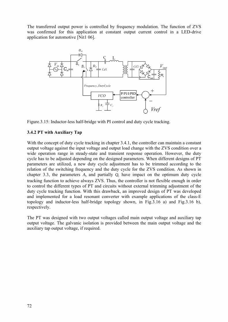
72
The transferred output power is controlled by frequency modulation. The function of ZVS was confirmed for this application at constant output current control in a LED-drive application for automotive [Nit1 06]. Figure.3.15: Inductor-less half-bridge with PI control and duty cycle tracking. 3.4.2 PT with Auxiliary Tap With the concept of duty cycle tracking in chapter 3.4.1, the controller can maintain a constant output voltage against the input voltage and output load change with the ZVS condition over a wide operation range in steady-state and transient response operation. However, the duty cycle has to be adjusted depending on the designed parameters. When different designs of PT parameters are utilized, a new duty cycle adjustment has to be trimmed according to the relation of the switching frequency and the duty cycle for the ZVS condition. As shown in chapter 3.3, the parameters 3A and partially 1Q have impact on the optimum duty cycle tracking function to achieve always ZVS. Thus, the controller is not flexible enough in order to control the different types of PT and circuits without external trimming adjustment of the duty cycle tracking function. With this drawback, an improved design of PT was developed and implemented for a load resonant converter with example applications of the class-E topology and inductor-less half-bridge topology shown, in Fig.3.16 a) and Fig.3.16 b), respectively. The PT was designed with two output voltages called main output voltage and auxiliary tap output voltage. The galvanic isolation is provided between the main output voltage and the auxiliary tap output voltage, if required.

73
Figure.3.16 a): Class-E converter with auxiliary tapped PT. Figure.3.16 b): Inductor-less half-bridge with auxiliary tapped PT.
In case of class-E topology, if the PT is designed at the condition 133 >≈=
ωω
A . The motion
current LI and the switching current sI are approximated to be in-phase at the zero crossing point. This was proved by the mathematic calculation with the normalized class-E analysis under suboptimum operation mode explained in chapter 3.3. From solution equation (3.12), the phase angels of the switch current ( sI ), and the motion current ( LI ), at the zero crossing point were determined. The difference of phase angles of the motion current ( LI ) and the switching current ( sI ), of an example application ( 301 =Q %45, =Dc and 1.13 =A at 12 Ω, 1/ =nff ), at the zero crossing point were plotted in Fig.3.17 a) illustrated with the waveforms in Fig.3.17 b). The results of different design parameters of DcQ ,1 and 3A are shown in appendix A.6. The behavior that the motion current LI and the switching current sI at the low side switch ( 1S ) are approximated to be in-phase at the zero crossing point also happens in case of inductor-less half-bridge topology, where the phase shift is always zero.
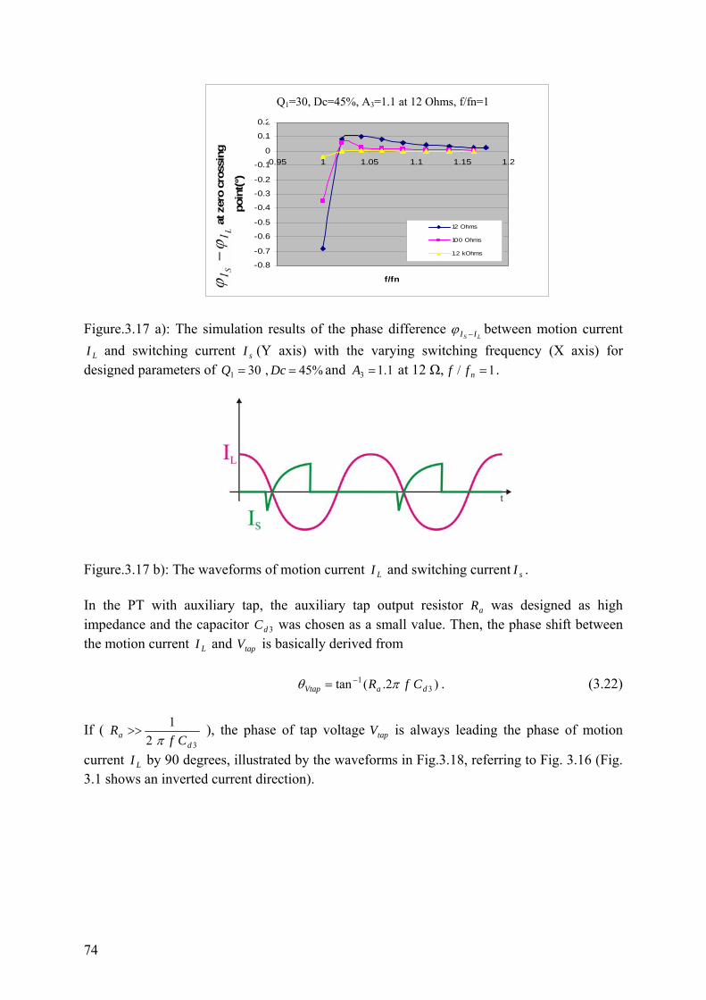
74
Figure.3.17 a): The simulation results of the phase difference
LS II −ϕ between motion current
LI and switching current sI (Y axis) with the varying switching frequency (X axis) for designed parameters of 301 =Q %45, =Dc and 1.13 =A at 12 Ω, 1/ =nff . Figure.3.17 b): The waveforms of motion current LI and switching current sI . In the PT with auxiliary tap, the auxiliary tap output resistor aR was designed as high impedance and the capacitor 3dC was chosen as a small value. Then, the phase shift between the motion current LI and tapV is basically derived from
)2.(tan 31
daVtap CfR πθ −= . (3.22)
If ( 32
1
da Cf
Rπ
>> ), the phase of tap voltage tapV is always leading the phase of motion
current LI by 90 degrees, illustrated by the waveforms in Fig.3.18, referring to Fig. 3.16 (Fig. 3.1 shows an inverted current direction).
Q1=30, Dc=.45%, A3=1.1 (optimum ZVS point)
-0.8
-0.7
-0.6
-0.5
-0.4
-0.3
-0.2
-0.1
0
0.1
0.2
0.95 1 1.05 1.1 1.15 1.2
f/fn
I s-I L
at z
ero
cros
sing
poin
t(°)
12 Ohms
100 Ohms
1.2 kOhms
Q1=30, Dc=45%, A3=1.1 at 12 Ohms, f/fn=1
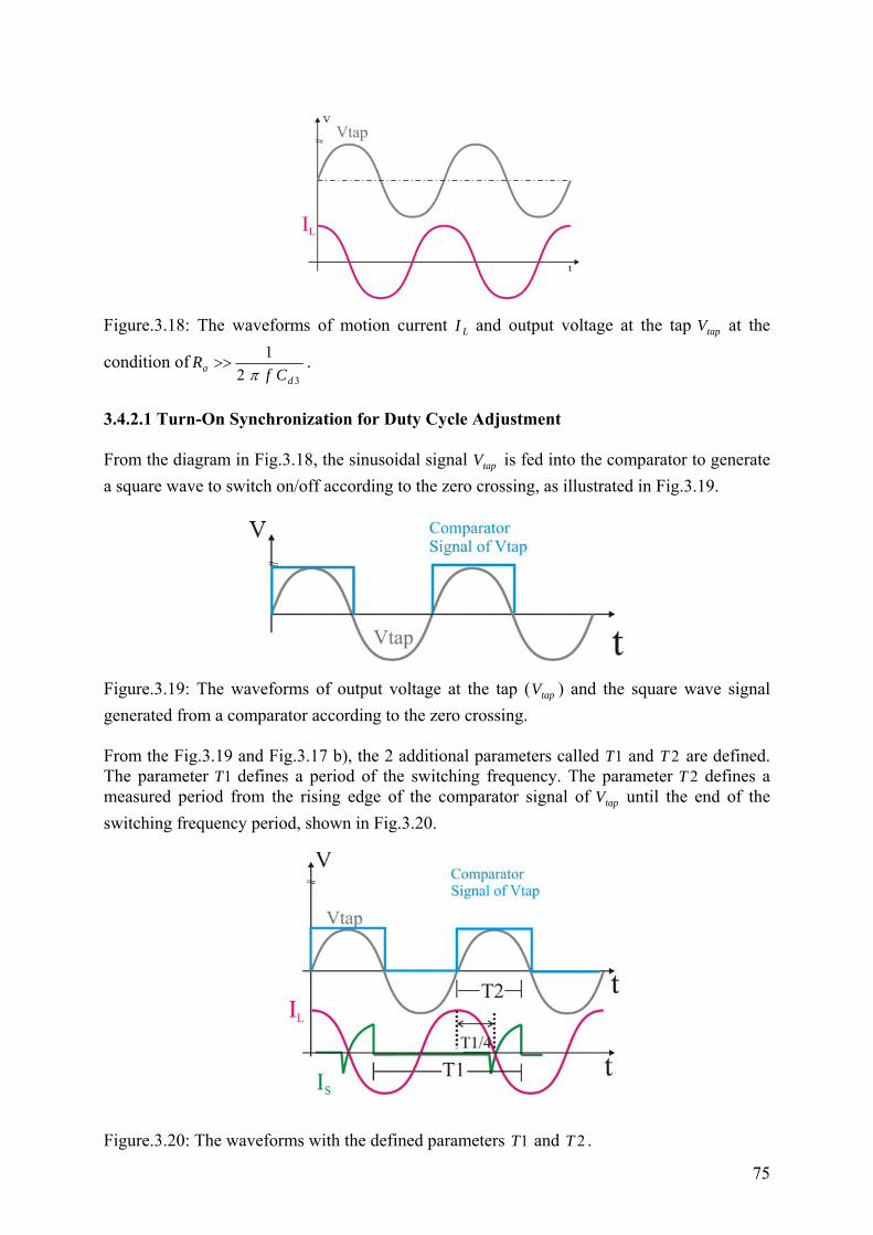
75
Figure.3.18: The waveforms of motion current LI and output voltage at the tap tapV at the
condition of32
1
da Cf
Rπ
>> .
3.4.2.1 Turn-On Synchronization for Duty Cycle Adjustment From the diagram in Fig.3.18, the sinusoidal signal tapV is fed into the comparator to generate a square wave to switch on/off according to the zero crossing, as illustrated in Fig.3.19. Figure.3.19: The waveforms of output voltage at the tap ( tapV ) and the square wave signal generated from a comparator according to the zero crossing. From the Fig.3.19 and Fig.3.17 b), the 2 additional parameters called 1T and 2T are defined. The parameter 1T defines a period of the switching frequency. The parameter 2T defines a measured period from the rising edge of the comparator signal of tapV until the end of the switching frequency period, shown in Fig.3.20. Figure.3.20: The waveforms with the defined parameters 1T and 2T .
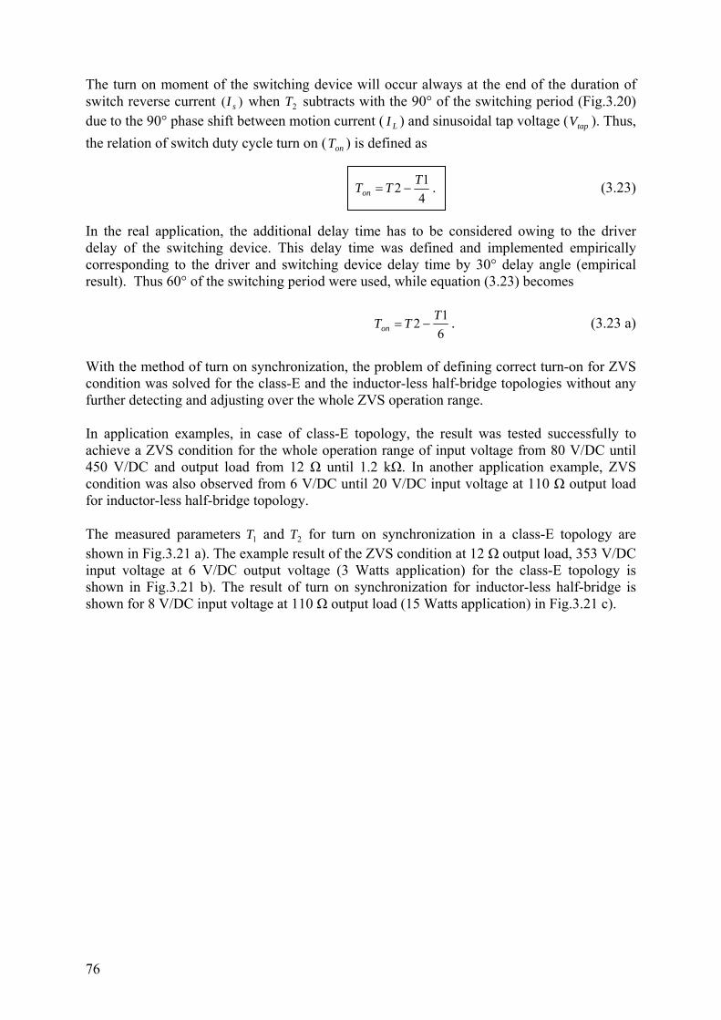
76
The turn on moment of the switching device will occur always at the end of the duration of switch reverse current )( sI when 2T subtracts with the 90° of the switching period (Fig.3.20) due to the 90° phase shift between motion current ( LI ) and sinusoidal tap voltage ( tapV ). Thus, the relation of switch duty cycle turn on ( onT ) is defined as
412 TTTon −= . (3.23)
In the real application, the additional delay time has to be considered owing to the driver delay of the switching device. This delay time was defined and implemented empirically corresponding to the driver and switching device delay time by 30° delay angle (empirical result). Thus 60° of the switching period were used, while equation (3.23) becomes
612 TTTon −= . (3.23 a)
With the method of turn on synchronization, the problem of defining correct turn-on for ZVS condition was solved for the class-E and the inductor-less half-bridge topologies without any further detecting and adjusting over the whole ZVS operation range. In application examples, in case of class-E topology, the result was tested successfully to achieve a ZVS condition for the whole operation range of input voltage from 80 V/DC until 450 V/DC and output load from 12 Ω until 1.2 kΩ. In another application example, ZVS condition was also observed from 6 V/DC until 20 V/DC input voltage at 110 Ω output load for inductor-less half-bridge topology. The measured parameters 1T and 2T for turn on synchronization in a class-E topology are shown in Fig.3.21 a). The example result of the ZVS condition at 12 Ω output load, 353 V/DC input voltage at 6 V/DC output voltage (3 Watts application) for the class-E topology is shown in Fig.3.21 b). The result of turn on synchronization for inductor-less half-bridge is shown for 8 V/DC input voltage at 110 Ω output load (15 Watts application) in Fig.3.21 c).
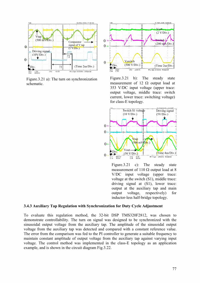
77
3.4.3 Auxiliary Tap Regulation with Synchronization for Duty Cycle Adjustment To evaluate this regulation method, the 32-bit DSP TMS320F2812, was chosen to demonstrate controllability. The turn on signal was designed to be synchronized with the sinusoidal output voltage from the auxiliary tap. The amplitude of the sinusoidal output voltage from the auxiliary tap was detected and compared with a constant reference value. The error from the comparison was fed to the PI controller to generate a suitable frequency to maintain constant amplitude of output voltage from the auxiliary tap against varying input voltage. The control method was implemented in the class-E topology as an application example, and is shown in the circuit diagram Fig.3.22.
Figure.3.21 b): The steady state measurement of 12 Ω output load at 353 V/DC input voltage (upper trace: output voltage, middle trace: switch current, lower trace: switching voltage) for class-E topology.
Figure.3.21 a): The turn on synchronization schematic.
Figure.3.21 c): The steady state measurement of 110 Ω output load at 8 V/DC input voltage (upper trace: voltage at the switch (S1), middle trace: driving signal at (S1), lower trace: output at the auxiliary tap and main output voltage, respectively) for inductor-less half-bridge topology.
(Time 2us/Div.) (Time 2us/Div.)
(Time 4us/Div.)
Vtap (500 mV/Div.)
Driving signal (10V/Div.)
Comparator signal of V tap (1 V/Div.)
Vswitch (500 V/Div.)
Iswitch (200 mA/Div.)
Vout (2 V/Div.)
Driving signal (5V/Div.)
Switch S1 voltage (10 V/Div.)
Vtap (500 mV/Div.)
Vout (50 V/Div.)
Div. Div.
Div.
0
0
0 0
0
0 0
0
0

78
Figure.3.22: Auxiliary tap regulation method. The information from the synchronization described in chapter 3.4.2.1 was used to adjust the duty cycle to achieve the ZVS condition over the whole operation range. This regulation method is a load dependence regulation. The proportionality between the main output voltage and the output voltage at the auxiliary tap is given by the following calculation. The motion current LI is transferred from the primary side to the secondary side with the
transfer ratio No and Nt to be NoI L and
NtI L , respectively. The output bridge rectifier, output
capacitor and output load is substituted by the equivalent resistor EQR . At the main output, the complex voltage 2U is derived by
2U12 +
=EQd
EQL
RCjR
NoI
ω. (3.24)
At the auxiliary tap output, the complex voltage 3U is derived by
3U13 +
=ad
aL
RCjR
NtI
ω. (3.25)
Thus the ratio between 32
UU is
32
UU
⎥⎥⎥⎥
⎦
⎤
⎢⎢⎢⎢
⎣
⎡ +
+=
a
da
dEQ
EQ
d
d
RC
Rj
CRj
RCC
NoNt 3
2
2
3
1
1
ω
ω. (3.26)
The impedance of 3dC was chosen as a small value compared to aR , hence, (3.26) becomes

79
32
UU
⎥⎥⎥⎥
⎦
⎤
⎢⎢⎢⎢
⎣
⎡
+=
2
2
3
11
1
dEQ
d
d
CRjCC
NoNt
ω
,
with RMS value:
⎥⎥⎥⎥⎥
⎦
⎤
⎢⎢⎢⎢⎢
⎣
⎡
+
=
22
2
3
)(11
132
dEQ
d
d
CRCC
NoNt
UU
ω
. (3.27)
In case of light load, assuming2
1
dEQ C
Rω
>> , the output voltage can be assumed as the
amplitude of the sine wave output voltage, due to near zero current consumption at the output load. Thus, equation (3.27) becomes
2
3^32
d
dout C
CNoNtUUV == . (3.28)
In case of full load, considering 2
1
dEQ C
Rω
= to achieving the maximum efficiency of the PT,
the output voltage was assumed as a rectangular voltage. Thus, equation (3.27) becomes
.23
21
232
2
3
^2
3
^
d
d
d
dout
CC
NoNtU
CC
NoNtUUV
=
==
(3.29)
Resuming this method, the output voltage is constant against the input voltage change for a fixed load application, but it cannot be maintained constant for a varying load application by using constant reference. With the constant reference at the auxiliary tap, the steady state output voltage declines following the tendency of heavy load (equations (3.28) to (3.29)). The steady state output voltage measurement from the full load until no load (12 Ω, 22 Ω, 100 Ω, 1.2 k Ω and 10 k Ω) against the input voltage regulation at 170 V/DC and 353 V/DC for class-E topology are shown in Fig.3.23. The relation of no-load to full-load output voltage can be achieving 2:1 maximum. Practically, by clamping the no-load output voltage to light load condition, and because of the output current at full load is not get a sine wave,
6.1)(
)( ≤−
−
loadfullout
ladnoout
VV
.

80
Figure.3.23: The steady state output voltages for the auxiliary tap regulation. The transient response of the output voltage can be adjusted by tuning the control parameters
PK and IK .Some example experiments were evaluated with difference control parameters for observing the transient behavior. The example results of transient response for an input voltage jump from 120 V/DC to 353 V/DC at 100 Ω of difference control parameters PK and
IK are shown in appendix A.7. 3.4.4 Isolated Output Voltage Feed Back (with Opto-Coupler) The functionality of this regulation method is comparable with the output voltage feed back in chapter 3.4.1 except the output part of the converter is isolated by the opto-coupler. The output from the opto-coupler referring to output voltage is fed back and compared with the reference value. The error is used to generate a suitable frequency via PI control to maintain a constant output voltage for a varying output load and/or input voltage as shown in the circuit diagram in Fig.3.24. To regulate without the synchronization information from the auxiliary tap, the ZVS condition can be achieved by the duty cycle tracking as described in chapter 3.4.1.The turn-on duty cycle for achieving the ZVS condition according to switching frequency point has to be determined. In case of utilizing a PT with the auxiliary tap, the method of turn on synchronization in chapter 3.4.2.1 can be implemented in order to achieve a ZVS condition for the whole operation range.
Measurement Results
0
2
4
6
8
10
12
0 100 200 300 400 500
Current (mA)
Volta
ge (V
)
Measurement at Vin 170 V/DC
Measurement at Vin 353 V/DC
Calculated result at Vin 170 and 353 V/DC
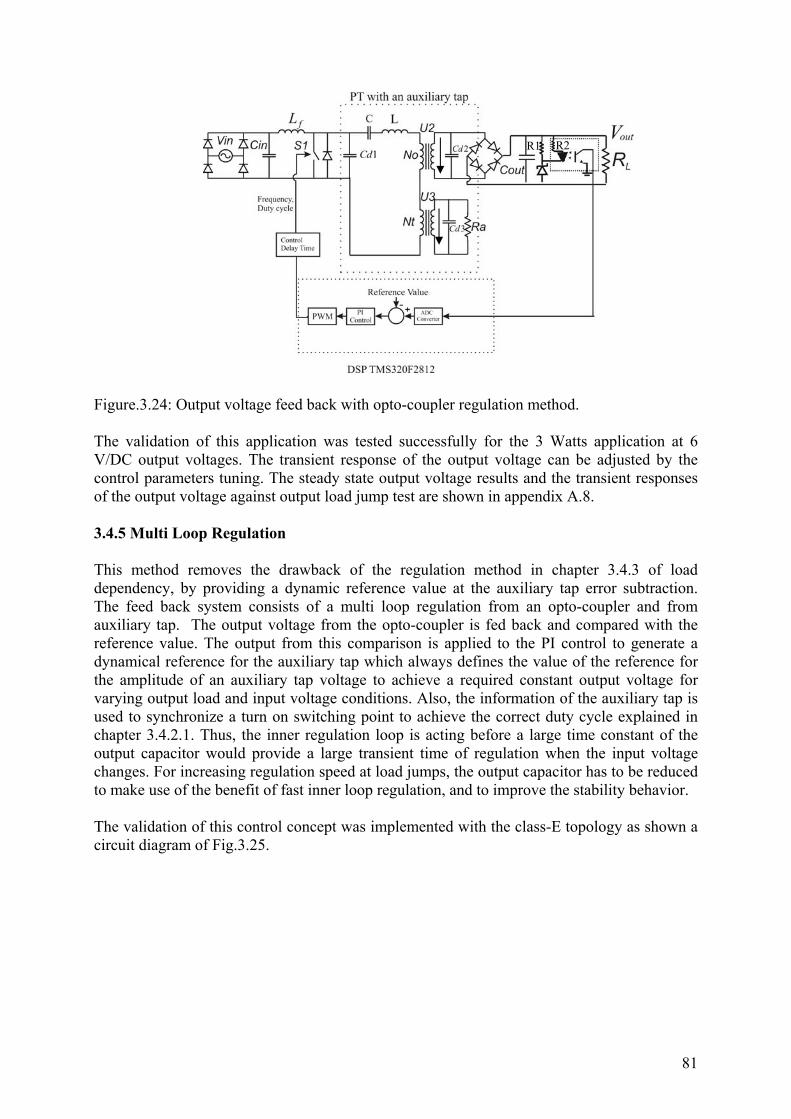
81
Figure.3.24: Output voltage feed back with opto-coupler regulation method. The validation of this application was tested successfully for the 3 Watts application at 6 V/DC output voltages. The transient response of the output voltage can be adjusted by the control parameters tuning. The steady state output voltage results and the transient responses of the output voltage against output load jump test are shown in appendix A.8. 3.4.5 Multi Loop Regulation This method removes the drawback of the regulation method in chapter 3.4.3 of load dependency, by providing a dynamic reference value at the auxiliary tap error subtraction. The feed back system consists of a multi loop regulation from an opto-coupler and from auxiliary tap. The output voltage from the opto-coupler is fed back and compared with the reference value. The output from this comparison is applied to the PI control to generate a dynamical reference for the auxiliary tap which always defines the value of the reference for the amplitude of an auxiliary tap voltage to achieve a required constant output voltage for varying output load and input voltage conditions. Also, the information of the auxiliary tap is used to synchronize a turn on switching point to achieve the correct duty cycle explained in chapter 3.4.2.1. Thus, the inner regulation loop is acting before a large time constant of the output capacitor would provide a large transient time of regulation when the input voltage changes. For increasing regulation speed at load jumps, the output capacitor has to be reduced to make use of the benefit of fast inner loop regulation, and to improve the stability behavior. The validation of this control concept was implemented with the class-E topology as shown a circuit diagram of Fig.3.25.
R1 R2

82
Figure.3.25: Multi loop regulation method. The validation of this method was implemented for the 3 Watts application at 6 V/DC output voltages. The results of steady state output voltage with the varying load and the transient response of the output voltage against the output load jump with different control parameters are shown in appendix A.9. The results from the optimized control parameters show that the overshoot and the transient time of the output voltage depend significantly on the control parameters of the inner and the outer loops. The gain PK of the inner loop is always set to be smaller than the outer loop since the regulation under the inner loop is operated without the large time constant of the output capacitor. Also, the transient behavior can be improved by increasing the gain of the outer loop. Further, with the double integration control part in the closed loop, instability might occur when either the integration part of inner loop or outer loop is selected to be too large. 3.4.6 Isolated PI Control Regulation with Lag Circuit This regulation method, as a modification of the output voltage feed back with opto-coupler, was implemented with an external PI control with first order lag compensator [App 01]. The advantage of a lag circuit over the normal PI control will be discussed in chapter five and provides stability at higher gain near to the switching frequency. The PI controller was implemented with external active and passive devices. The DSP acts only as a linear VCO to generate a suitable frequency to maintain a constant output voltage (Fig.3.26). The controller was implemented with the TL431 and passive elements such resistors and capacitors. The IC1 (TL431), shows an equivalent circuit as in Fig.3.26 a), and serves as a comparator which has a 2.5 volts reference at non-inverting input. The circuit diagram of implemented converter is shown in Fig.3.26 b). When the output voltage achieves a larger value than the designed output voltage, the reference voltage, from voltage divider R4 and R5, will be larger than voltage reference of the IC1 (2.5 volts). This will turn the output comparator to high and, the connected output driver transistor of IC1 will more conduct. This let the secondary side of the opto-coupler be more conductive. Thus, the input node of the VCO will be pulled down to lower voltage. With the
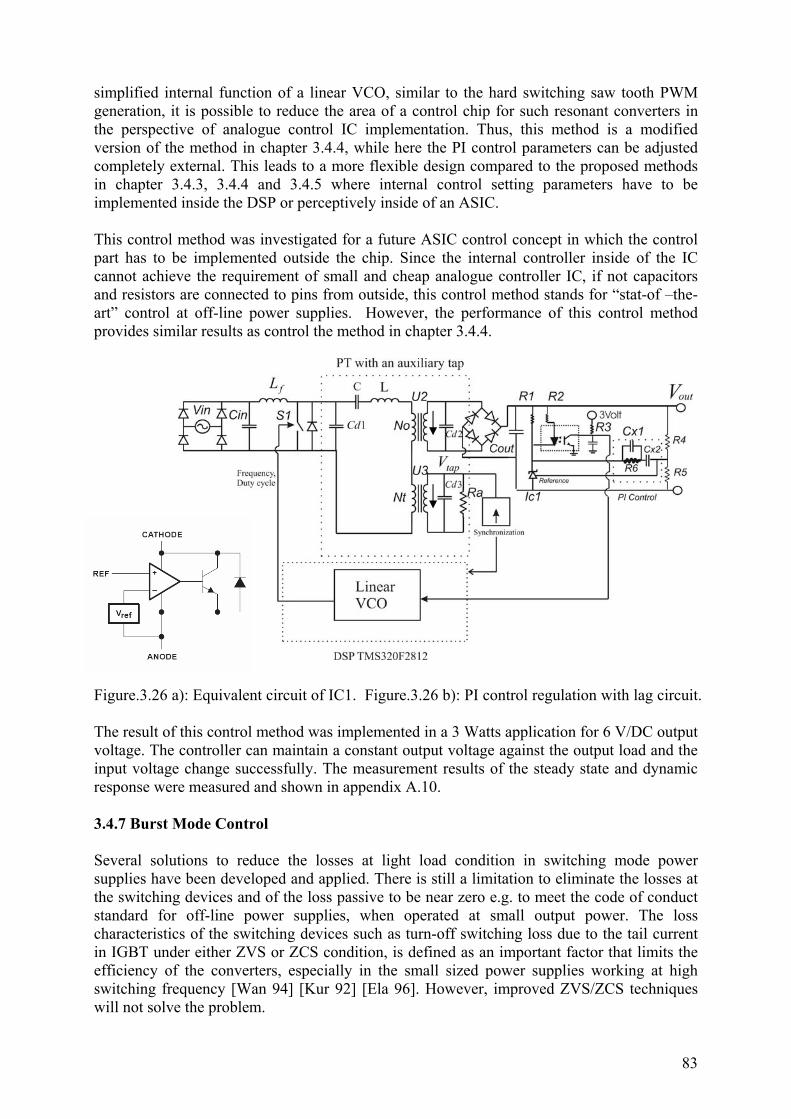
83
simplified internal function of a linear VCO, similar to the hard switching saw tooth PWM generation, it is possible to reduce the area of a control chip for such resonant converters in the perspective of analogue control IC implementation. Thus, this method is a modified version of the method in chapter 3.4.4, while here the PI control parameters can be adjusted completely external. This leads to a more flexible design compared to the proposed methods in chapter 3.4.3, 3.4.4 and 3.4.5 where internal control setting parameters have to be implemented inside the DSP or perceptively inside of an ASIC. This control method was investigated for a future ASIC control concept in which the control part has to be implemented outside the chip. Since the internal controller inside of the IC cannot achieve the requirement of small and cheap analogue controller IC, if not capacitors and resistors are connected to pins from outside, this control method stands for “stat-of –the-art” control at off-line power supplies. However, the performance of this control method provides similar results as control the method in chapter 3.4.4. Figure.3.26 a): Equivalent circuit of IC1. Figure.3.26 b): PI control regulation with lag circuit. The result of this control method was implemented in a 3 Watts application for 6 V/DC output voltage. The controller can maintain a constant output voltage against the output load and the input voltage change successfully. The measurement results of the steady state and dynamic response were measured and shown in appendix A.10. 3.4.7 Burst Mode Control Several solutions to reduce the losses at light load condition in switching mode power supplies have been developed and applied. There is still a limitation to eliminate the losses at the switching devices and of the loss passive to be near zero e.g. to meet the code of conduct standard for off-line power supplies, when operated at small output power. The loss characteristics of the switching devices such as turn-off switching loss due to the tail current in IGBT under either ZVS or ZCS condition, is defined as an important factor that limits the efficiency of the converters, especially in the small sized power supplies working at high switching frequency [Wan 94] [Kur 92] [Ela 96]. However, improved ZVS/ZCS techniques will not solve the problem.

84
In order to improve efficiency in the switching mode power supplies, the burst mode was developed to reduce the losses in the switching device during the operation by shut-down intervals of the converter operation. The work has been proved for a class-E topology, fulfilling the “Code of conduct on efficiency of external power supplies” in a 3 Watts off-line power supply application [Cod 04] [Nit 07]. The system was considered to include 2 cases of output load, light load and heavy load. In case of the heavy load, the converter needs much more energy to transfer to the load, in order to keep the constant output voltage, than at light load. Thus, in the light load situation the converter can optimize the transferred energy without losing the constant output regulation behaviour, using a sufficiently large output capacitor to the improvement of efficiency at burst mode operation. With this principle, the control has to be adapted for the difference load situations. In the light load condition, the control regulates with two intervals called time-off and time-on intervals [Pri 04]. While in the heavy load application, the converter transfers a power to the load by continuous mode. During the time-off interval, the converter transfers zero power to the output load while at the time-on interval the converter transfers enough power to the load to recharge the output capacitor. If this control concept would be implemented for the heavy load, the converter needs to deliver a large amount of power during the time-on for compensating the power which is not delivered during the time-off. This could lead to increased stress of the switching device and other passive components. Hence, if the converter can determine the difference of the output load, the system control uses burst mode for light loads. In the heavy load condition, the converter control uses continuous control mode shown in Fig.3.27. Figure.3.27: Classification of control mode either continuous mode or burst mode operation. Fig.3.28 shows burst mode control measurements. The upper trace shows the driving frequency divided into two parts (time-on, time-off). The middle trace shows the output voltage. The lower trace shows the output voltage of the auxiliary tap.
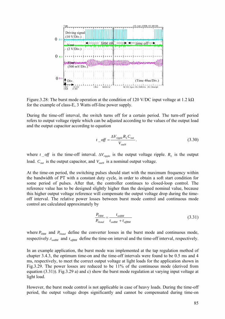
85
Figure.3.28: The burst mode operation at the condition of 120 V/DC input voltage at 1.2 kΩ for the example of class-E, 3 Watts off-line power supply. During the time-off interval, the switch turns off for a certain period. The turn-off period refers to output voltage ripple which can be adjusted according to the values of the output load and the output capacitor according to equation
outN
outLripple
VCRV
offt∆
=_ . (3.30)
where offt _ is the time-off interval. rippleV∆ is the output voltage ripple. LR is the output load. outC is the output capacitor, and outNV is a nominal output voltage. At the time-on period, the switching pulses should start with the maximum frequency within the bandwidth of PT with a constant duty cycle, in order to obtain a soft start condition for some period of pulses. After that, the controller continues to closed-loop control. The reference value has to be designed slightly higher than the designed nominal value, because this higher output voltage reference will compensate the output voltage drop during the time-off interval. The relative power losses between burst mode control and continuous mode control are calculated approximately by
offBMonBM
onBM
Vtotal
VBM
ttt
PP
+= (3.31)
where VBMP and VtotalP define the converter losses in the burst mode and continuous mode, respectively. onBMt and offBMt define the time-on interval and the time-off interval, respectively. In an example application, the burst mode was implemented at the tap regulation method of chapter 3.4.3, the optimum time-on and the time-off intervals were found to be 0.5 ms and 4 ms, respectively, to meet the correct output voltage at light loads for the application shown in Fig.3.29. The power losses are reduced to be 11% of the continuous mode (derived from equation (3.31)). Fig.3.29 a) and c) show the burst mode regulation at varying input voltage at light load. However, the burst mode control is not applicable in case of heavy loads. During the time-off period, the output voltage drops significantly and cannot be compensated during time-on
time on time off
(Time 40us/Div.) Div.
Vout (2 V/Div.)
Vtap (500 mV/Div.)
Driving signal (10 V/Div.) 0
0
0
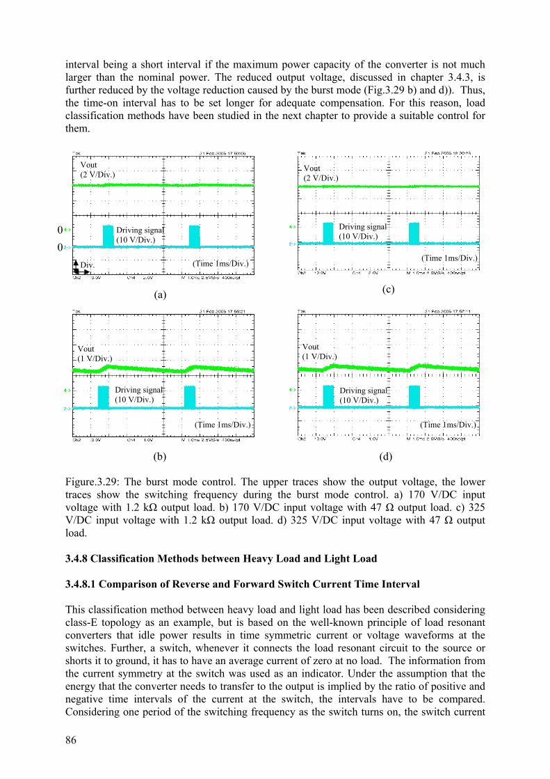
86
interval being a short interval if the maximum power capacity of the converter is not much larger than the nominal power. The reduced output voltage, discussed in chapter 3.4.3, is further reduced by the voltage reduction caused by the burst mode (Fig.3.29 b) and d)). Thus, the time-on interval has to be set longer for adequate compensation. For this reason, load classification methods have been studied in the next chapter to provide a suitable control for them.
Figure.3.29: The burst mode control. The upper traces show the output voltage, the lower traces show the switching frequency during the burst mode control. a) 170 V/DC input voltage with 1.2 kΩ output load. b) 170 V/DC input voltage with 47 Ω output load. c) 325 V/DC input voltage with 1.2 kΩ output load. d) 325 V/DC input voltage with 47 Ω output load. 3.4.8 Classification Methods between Heavy Load and Light Load 3.4.8.1 Comparison of Reverse and Forward Switch Current Time Interval This classification method between heavy load and light load has been described considering class-E topology as an example, but is based on the well-known principle of load resonant converters that idle power results in time symmetric current or voltage waveforms at the switches. Further, a switch, whenever it connects the load resonant circuit to the source or shorts it to ground, it has to have an average current of zero at no load. The information from the current symmetry at the switch was used as an indicator. Under the assumption that the energy that the converter needs to transfer to the output is implied by the ratio of positive and negative time intervals of the current at the switch, the intervals have to be compared. Considering one period of the switching frequency as the switch turns on, the switch current
(a) (c)
(b) (d)
(Time 1ms/Div.) (Time 1ms/Div.)
(Time 1ms/Div.) (Time 1ms/Div.)
Div.
Vout (2 V/Div.)
Vout (2 V/Div.)
Vout (1 V/Div.)
Vout (1 V/Div.)
Driving signal (10 V/Div.)
Driving signal (10 V/Div.)
Driving signal (10 V/Div.)
Driving signal (10 V/Div.)
0 0
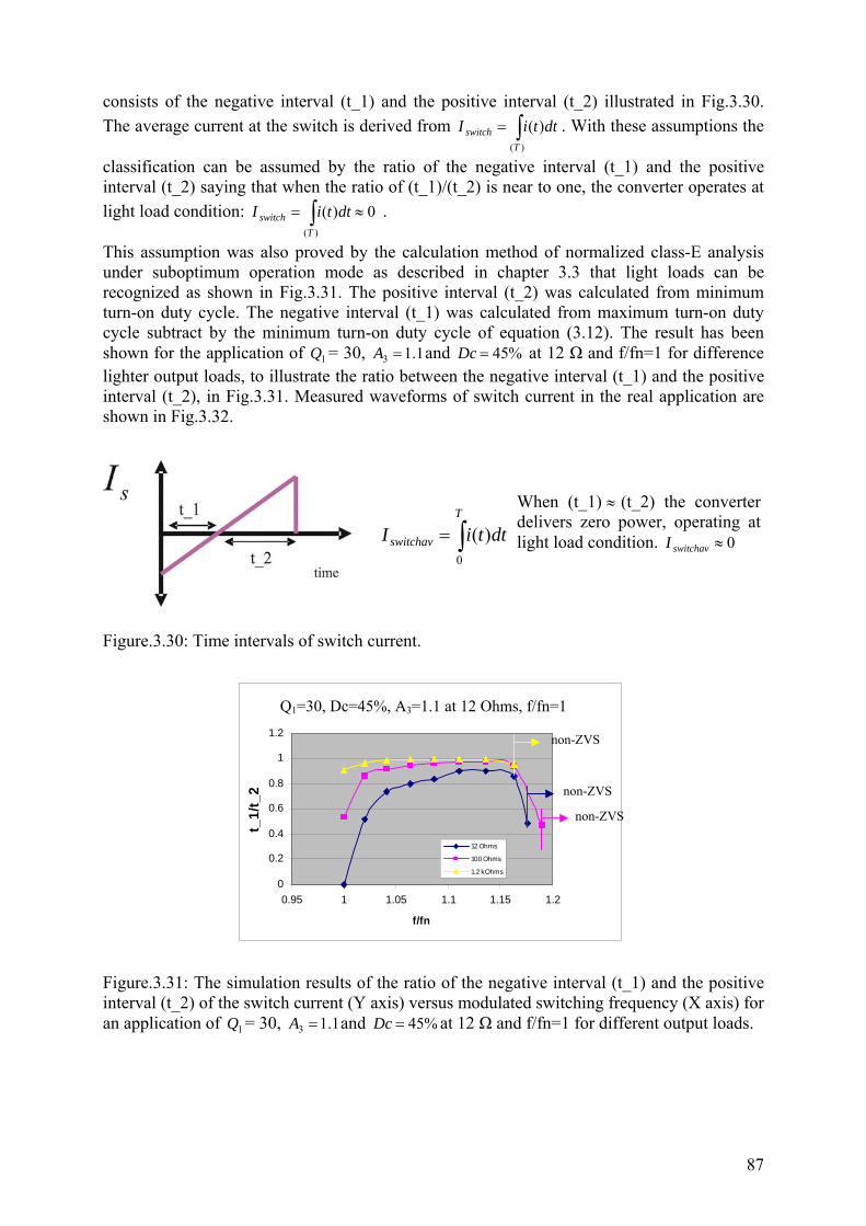
87
consists of the negative interval (t_1) and the positive interval (t_2) illustrated in Fig.3.30. The average current at the switch is derived from ∫=
)(
)(T
switch dttiI . With these assumptions the
classification can be assumed by the ratio of the negative interval (t_1) and the positive interval (t_2) saying that when the ratio of (t_1)/(t_2) is near to one, the converter operates at light load condition: 0)(
)(
≈= ∫T
switch dttiI .
This assumption was also proved by the calculation method of normalized class-E analysis under suboptimum operation mode as described in chapter 3.3 that light loads can be recognized as shown in Fig.3.31. The positive interval (t_2) was calculated from minimum turn-on duty cycle. The negative interval (t_1) was calculated from maximum turn-on duty cycle subtract by the minimum turn-on duty cycle of equation (3.12). The result has been shown for the application of 1Q = 30, 1.13 =A and %45=Dc at 12 Ω and f/fn=1 for difference lighter output loads, to illustrate the ratio between the negative interval (t_1) and the positive interval (t_2), in Fig.3.31. Measured waveforms of switch current in the real application are shown in Fig.3.32.
Figure.3.30: Time intervals of switch current. Figure.3.31: The simulation results of the ratio of the negative interval (t_1) and the positive interval (t_2) of the switch current (Y axis) versus modulated switching frequency (X axis) for an application of 1Q = 30, 1.13 =A and %45=Dc at 12 Ω and f/fn=1 for different output loads.
∫=T
switchav dttiI0
)(
When (t_1) ≈ (t_2) the converter delivers zero power, operating at light load condition. 0≈switchavI
Q1=30, Dc=.45%, A3=1.1(optimum ZVS point)
0
0.2
0.4
0.6
0.8
1
1.2
0.95 1 1.05 1.1 1.15 1.2
f/fn
t_1/
t_2
12 Ohms
100 Ohms
1.2 kOhms
Q1=30, Dc=45%, A3=1.1 at 12 Ohms, f/fn=1
non-ZVS
non-ZVS
non-ZVS
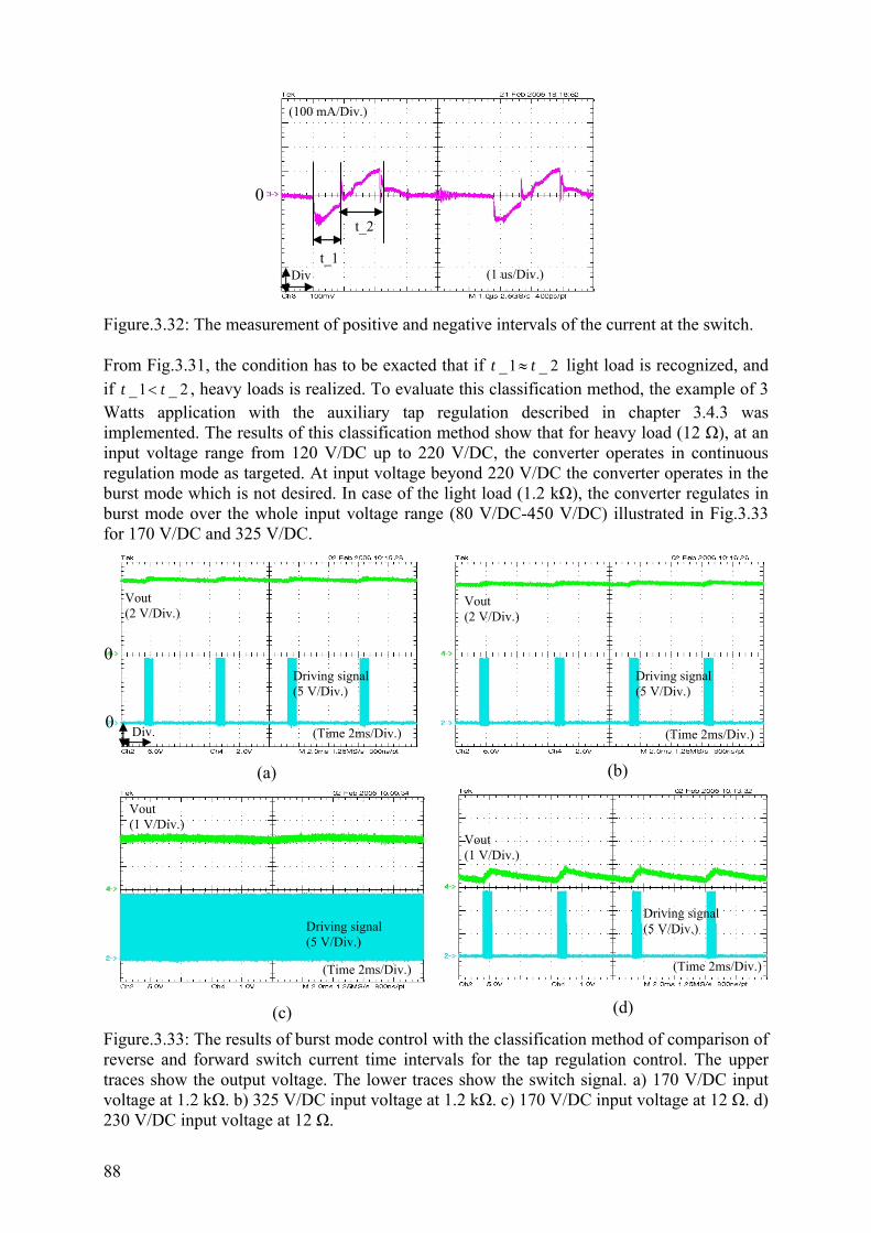
88
Figure.3.32: The measurement of positive and negative intervals of the current at the switch. From Fig.3.31, the condition has to be exacted that if 2_1_ tt ≈ light load is recognized, and if 2_1_ tt < , heavy loads is realized. To evaluate this classification method, the example of 3 Watts application with the auxiliary tap regulation described in chapter 3.4.3 was implemented. The results of this classification method show that for heavy load (12 Ω), at an input voltage range from 120 V/DC up to 220 V/DC, the converter operates in continuous regulation mode as targeted. At input voltage beyond 220 V/DC the converter operates in the burst mode which is not desired. In case of the light load (1.2 kΩ), the converter regulates in burst mode over the whole input voltage range (80 V/DC-450 V/DC) illustrated in Fig.3.33 for 170 V/DC and 325 V/DC.
Figure.3.33: The results of burst mode control with the classification method of comparison of reverse and forward switch current time intervals for the tap regulation control. The upper traces show the output voltage. The lower traces show the switch signal. a) 170 V/DC input voltage at 1.2 kΩ. b) 325 V/DC input voltage at 1.2 kΩ. c) 170 V/DC input voltage at 12 Ω. d) 230 V/DC input voltage at 12 Ω.
t_1
t_2
(100 mA/Div.)
(1 us/Div.)Div
0
(a) (b)
(d) (c)
Div.
0
0 (Time 2ms/Div.) (Time 2ms/Div.)
(Time 2ms/Div.) (Time 2ms/Div.)
Vout (2 V/Div.)
Vout (2 V/Div.)
Vout (1 V/Div.)
Vout (1 V/Div.)
Driving signal (5 V/Div.)
Driving signal (5 V/Div.)
Driving signal (5 V/Div.)
Driving signal (5 V/Div.)

89
This uncertainty can be explained, that at high input voltages and at full load operation, the converter needs to operate at larger switching frequency. Referred to the simulation in Fig.3.31, the converter operates in this range with a ratio of t_1/t_2 is close to one. Further, the noise occurring in the real application leads to faults of distinguishing between light and heavy loads at larger frequencies, thus at larger input voltage. 3.4.8.2 Comparison of Phase Angle between Auxiliary Tap Zero Crossing and Switch Turn-Off This classification method is available only for PT utilized with auxiliary tap. The information from the switching current turn-off and additional information from the voltage zero-crossing of the auxiliary tap was used to find the classification conditions of light or heavy load. The output sine wave voltage from the tap is fed into a comparator to generate a square wave with small hysteresis to switch on and off according to the reference value of zero shown in the middle trace in Fig.3.34. The difference between phase angles at the zero crossing of the voltage at the auxiliary tap (falling edge of the square wave auxiliary signal) called 1φ , and the end of the switch turn-on interval, called 2φ was used as an indicator for the classification. If the end of the switch turn-on signal occurs on the left hand side of the falling edge, the time period ( 3_t ) was defined as a positive value. The difference of phase angle ( 21 φφθ −= ) by time period ( 3_t ) was defined by the equation
°=−=− 360..3_21 ftVtapIs φφθ . (3.32)
Parameter, f presents the switching frequency. Figure.3.34: The classification by the phase angle between auxiliary tap zero crossing and switch turn-off. The upper trace shows the output voltage of the tap. The middle trace shows the square wave signal from tap output generated via comparator. The lower trace shows the current at the switch. The results of the simulation of normalized class-E analysis under suboptimum operation (explained in 3.3.3) show that if the converter operates at a lower switching frequency, the phase angles show negative values. When the frequency is increased, the difference of the phase angles become larger until it reaches a positive value, as shown in Fig.3.35. For this reason the classification can be based on the load dependency of the switching frequency.
(1 us/Div.)
Vtap (200 mV/Div.)
Comparator signal of V tap (1 V/Div.)
Iswitch (100 mA/Div.)
Div.
0 0
0
fπ2/
fπ2/
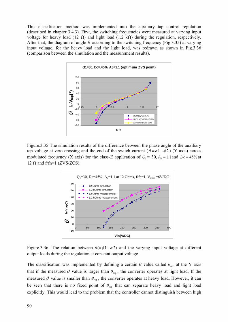
90
This classification method was implemented into the auxiliary tap control regulation (described in chapter 3.4.3). First, the switching frequencies were measured at varying input voltage for heavy load (12 Ω) and light load (1.2 kΩ) during the regulation, respectively. After that, the diagram of angle θ according to the switching frequency (Fig.3.35) at varying input voltage, for the heavy load and the light load, was redrawn as shown in Fig.3.36 (comparison between the simulation and the measurement results).
Figure.3.35 The simulation results of the difference between the phase angle of the auxiliary tap voltage at zero crossing and the end of the switch current ( 21 φφθ −= ) (Y axis) across modulated frequency (X axis) for the class-E application of 1Q = 30, 1.13 =A and %45=Dc at 12 Ω and f/fn=1 (ZVS/ZCS). Figure.3.36: The relation between )21( φφθ −= and the varying input voltage at different output loads during the regulation at constant output voltage. The classification was implemented by defining a certain θ value called refθ at the Y axis that if the measured θ value is larger than refθ , the converter operates at light load. If the measured θ value is smaller than refθ , the converter operates at heavy load. However, it can be seen that there is no fixed point of refθ that can separate heavy load and light load explicitly. This would lead to the problem that the controller cannot distinguish between high
Q1=30, Dc .45% (simulation result)
-10
0
10
20
30
40
50
60
0 50 100 150 200 250 300 350 400
Vin(V/DC)
Is-V
tap(
°)
12 Ohms simulation1.2 kOhms simulation12 Ohms measurement1.2 kOhms measurement
Q1=30, Dc=45%, A3=1.1 at 12 Ohms, f/fn=1, VoutN =6V/DC
Q1=30, Dc=45%, A3=1.1 at 12 Ohms, f/fn=1
12 Ohms 100 Ohms 1.2 kOhms
Q1=30, Dc=.45%, A3=1.1 (optimum ZVS point)
-80
-60
-40
-20
0
20
40
60
80
100
0.95 1 1.05 1.1 1.15 1.2
f / f n
I s-V t
ap(°
)
12 Ohms(Q=30-35.76)
100 Ohms(Q=126.8-170.81)
1.2 kOhms(Q=1250-1690)

91
or low voltage at the same time as between light or heavy load. Therefore, an auxiliary angle Addθ was implemented to shift both curves up according to the input voltage.
The input voltage was detected and used to create a linear function which allows for a fixed reference value refθ . The function of Addθ is derived by the equation
BAVinAdd +=θ . (3.33) With this function, the angleθ of each point in different curves is added to Addθ to shift the curves up. The coefficients A and B were determined by this addition obtaining a nearly constant value refθ over the load and voltage range, shown in Fig.3.37. If Addθθ + is larger than refθ , light load occurs. While, if Addθθ + is less than refθ , heavy load occurs. Figure.3.37: Calculation result of the relation between )21( φφθ −= and the varying input voltage at different loads during regulation after shifting of Addθ at constant output voltage. The operation in the burst mode or in the continuous control mode without oscillations between the modes can be slightly improved by adding a hysteresis loop parameter called hysθ . The condition to operate in the burst mode can be defined as, if Addθθ + is larger than
hysref θθ + , light load occurs. If the Addθθ + is less than hysref θθ − , the controller switches back to the continuous control mode. This classification method shows capability of linearizing the selected functions but remains uncertain or at least limited in the range of input voltage and output load. Even if a mathematical proof of the generality of equation 3.33 for the other parameters can be found, this method has similar limits like that of switch current time interval comparison. The results of the implementation for auxiliary tap regulation method (described in chapter 3.4.3) show that for the light load (1.2 kΩ) the controller always stays in the burst mode during the whole input voltage operation range (80 V/DC-450 V/DC). At the heavy load condition the controller operates in continuous control mode until an input voltage of 325 V/DC. At input voltages higher than 325 V/DC the controller operates mistakenly in burst
)Vtap(-Is °θ VoutN=6V/DC
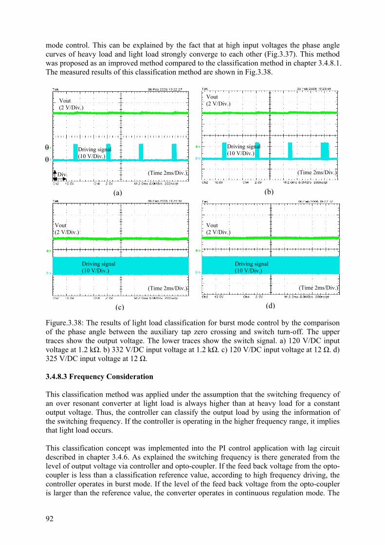
92
mode control. This can be explained by the fact that at high input voltages the phase angle curves of heavy load and light load strongly converge to each other (Fig.3.37). This method was proposed as an improved method compared to the classification method in chapter 3.4.8.1. The measured results of this classification method are shown in Fig.3.38.
Figure.3.38: The results of light load classification for burst mode control by the comparison of the phase angle between the auxiliary tap zero crossing and switch turn-off. The upper traces show the output voltage. The lower traces show the switch signal. a) 120 V/DC input voltage at 1.2 kΩ. b) 332 V/DC input voltage at 1.2 kΩ. c) 120 V/DC input voltage at 12 Ω. d) 325 V/DC input voltage at 12 Ω. 3.4.8.3 Frequency Consideration This classification method was applied under the assumption that the switching frequency of an over resonant converter at light load is always higher than at heavy load for a constant output voltage. Thus, the controller can classify the output load by using the information of the switching frequency. If the controller is operating in the higher frequency range, it implies that light load occurs. This classification concept was implemented into the PI control application with lag circuit described in chapter 3.4.6. As explained the switching frequency is there generated from the level of output voltage via controller and opto-coupler. If the feed back voltage from the opto-coupler is less than a classification reference value, according to high frequency driving, the controller operates in burst mode. If the level of the feed back voltage from the opto-coupler is larger than the reference value, the converter operates in continuous regulation mode. The
(a) (b)
(c) (d)
Div. (Time 2ms/Div.) (Time 2ms/Div.)
(Time 2ms/Div.) (Time 2ms/Div.)
Vout (2 V/Div.)
Vout (2 V/Div.)
Vout (2 V/Div.)
Vout (2 V/Div.)
Driving signal (10 V/Div.)
Driving signal (10 V/Div.)
Driving signal (10 V/Div.)
Driving signal (10 V/Div.)
0 0
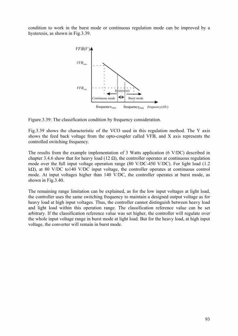
93
condition to work in the burst mode or continuous regulation mode can be improved by a hysteresis, as shown in Fig.3.39.
Figure.3.39: The classification condition by frequency consideration. Fig.3.39 shows the characteristic of the VCO used in this regulation method. The Y axis shows the feed back voltage from the opto-coupler called VFB, and X axis represents the controlled switching frequency. The results from the example implementation of 3 Watts application (6 V/DC) described in chapter 3.4.6 show that for heavy load (12 Ω), the controller operates at continuous regulation mode over the full input voltage operation range (80 V/DC-450 V/DC). For light load (1.2 kΩ), at 80 V/DC to140 V/DC input voltage, the controller operates at continuous control mode. At input voltages higher than 140 V/DC, the controller operates at burst mode, as shown in Fig.3.40. The remaining range limitation can be explained, as for the low input voltages at light load, the controller uses the same switching frequency to maintain a designed output voltage as for heavy load at high input voltages. Thus, the controller cannot distinguish between heavy load and light load within this operation range. The classification reference value can be set arbitrary. If the classification reference value was set higher, the controller will regulate over the whole input voltage range in burst mode at light load. But for the heavy load, at high input voltage, the converter will remain in burst mode.
frequencymin. frequencymax
Continuous mode Burst mode

94
Figure.3.40: The classification method of burst mode control by frequency consideration for PI regulation with lag circuit. The upper traces show the output voltage. The middle traces show the feed back voltage from the opto-coupler (VFB). The lower traces show the driving signal. a) 150 V/DC input voltage at 12 Ω. b) 350 V/DC input voltage at 12 Ω. c) 100 V/DC input voltage at 1.2 kΩ. d) 350 V/DC input voltage at 1.2 kΩ. Further, the burst mode control with constant off/on time intervals has the drawback that the output voltage ripple cannot be maintained constant when either output capacitor or output load are changed, as shown in Fig.3.41. The tests were done with a constant input voltage at 1.2 kΩ output load and different output capacitors.
(c) (d)
(b) (a)
(Time 1ms/Div.) (Time 2ms/Div.)
(Time 2ms/Div.) (Time 2ms/Div.)
Driving signal (10 V/Div.)
Driving signal (10 V/Div.)
Driving signal (10 V/Div.)
Driving signal (10 V/Div.)
VFB (1 V/Div.) VFB
(1 V/Div.)
VFB (1 V/Div.) VFB
(1 V/Div.)
Div.
0
0 0
Vout (1 V/Div.)
Vout (1 V/Div.)
Vout (1 V/Div.)
Vout (1 V/Div.)

95
Figure.3.41: The results of burst mode control with difference output capacitors at constant off/on time intervals. The upper traces show the output voltage. The middle traces show the feed back voltage from the opto-coupler (VFB). The lower traces show the driving signal. a) 350 V/DC input voltage at 220 uF output capacitor. b) 350 V/DC input voltage at 110 uF output capacitor. For a small output capacitor, the output voltage contains a larger ripple leading to the output voltage feed back of the opto-coupler rising rapidly. The swing of the feed back voltage is changing significantly stronger than the output voltage itself, but is a good indicator of output voltage ripple. Using this result and to implement an active burst mode with constant output voltage ripple, the observed window of VFB can be shifted according to the input voltage. As it becomes clear that the VFB is not constant, regarding the threshold VFB and VFBmax. A function of the thresholds has to be implemented depending on input voltage. Fixed threshold as for hard-switching converters [MAS 92] cannot be applied due to gain reduction of the resonant converter limited frequency and duty cycle control range. The implementation will be preceded as follows. Consider in the burst mode operation, during the switching turn-on interval, that VFB starts to drop until the end of the switching turn-on interval. In this moment the value of VFB has to be stored and called VFBmin. Then, VFBmin is added to a constant number. This constant number defines the swing of the output voltage ripple( ripple∆ ), shown in Fig.3.42. After that VFBmax is set to be VFBmax = VFBmin + ripple∆ . The controller switches to the off-time interval until VFBmax is achieved. If VFB reaches VFBmax the controller starts the turn-on interval again. The controller keeps going on in the same procedure for each cycle. With this algorithm a constant output voltage ripple can be achieved. The value of ripple∆ is proportional to the output voltage ripple by VoutKKripple VDFB ∆=∆
VDK presents a transfer function of the voltage divider and FBK presents the gain of the opto-coupler explained in detail in equation (4.26) and (4.27) in chapter four.
(a) (b)
Div.
Vout (1 V/Div.)
Vout (1 V/Div.)
VFB (1 V/Div.)
VFB (1 V/Div.)
Driving signal (10 V/Div.)
Driving signal (10 V/Div.)
(Time 2ms/Div.) (Time 2ms/Div.) 0
0
0
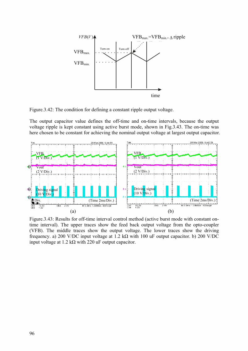
96
Figure.3.42: The condition for defining a constant ripple output voltage. The output capacitor value defines the off-time and on-time intervals, because the output voltage ripple is kept constant using active burst mode, shown in Fig.3.43. The on-time was here chosen to be constant for achieving the nominal output voltage at largest output capacitor.
Figure.3.43: Results for off-time interval control method (active burst mode with constant on-time interval). The upper traces show the feed back output voltage from the opto-coupler (VFB). The middle traces show the output voltage. The lower traces show the driving frequency. a) 200 V/DC input voltage at 1.2 kΩ with 100 uF output capacitor. b) 200 V/DC input voltage at 1.2 kΩ with 220 uF output capacitor.
(a) (b)
(Time 2ms/Div.) (Time 2ms/Div.)
Driving signal (10 V/Div.)
Driving signal (10 V/Div.)
Vout (2 V/Div.)
Vout (2 V/Div.)
VFB (1 V/Div.)
VFB (1 V/Div.)
Div.
0
0 0
time
VFBmin.
VFBmax. Turn-on Turn-off
VFBmax.=VFBmin.+∆ ripple

97
Figure.3.44: Results with constant off-time and on-time intervals control. The upper traces show the feed back voltage from the opto-coupler (VFB). The middle traces show the output voltage. The lower traces show the driving signal. a) 200 V/DC input voltage at 1.2 kΩ with 100 uF output capacitor. b) 200 V/DC input voltage at 1.2 kΩ with 220 uF output capacitor. 3.4.8.4 Frequency Consideration plus Information of Input Voltage This improved method was applied under the assumption that at light load condition, the switching frequency is always higher than at heavy load condition, at the same input voltage for achieving a constant output voltage. With this principle, combining information from the input voltage and switching frequency, the classification can be accomplished satisfying for class-E applications. The characteristics of the switching frequency and the input voltage are plotted in Fig.3.45 a) for heavy load and light load (proved by the calculation method from equations (3.13)-(3.21) and shown in Fig.3.8). The information from the input voltage was detected and used by an auxiliary function BAVf inAdd += to shift each point of the switching frequency up according to the input voltage. The coefficients A and B were determined by the same way as explained in chapter 3.4.8.2. Then, if the result of shifting exceeds the reference value fRef, it means that light load occurs and vice versa for heavy load, shown in Fig.3.45 b).
(a) (b)
Div.
Driving signal (10 V/Div.)
Driving signal (10 V/Div.)
Vout (2 V/Div.)
Vout (2 V/Div.)
VFB (1 V/Div.)
VFB (1 V/Div.)
(Time 2ms/Div.) (Time 2ms/Div.)
0
0 0
Figure.3.45 a): The characteristics of the switching frequencies vs. input voltage at difference load conditions, and constant output voltage.
Figure.3.45 b): The characteristics of frequency shifting over input voltage at different load conditions to determine the border between heavy load and light load at constant output voltage.
fRef
Addf

98
The validation of this method was examined in the 3 Watts application for PI control regulation with lag circuit (described in chapter 3.4.6). The results show that the controller can classify between heavy load and light load explicitly for the whole input voltage range (80 V/DC-450 V/DC), shown in Fig.3.46 at input voltage of 120 V/DC and 320 V/DC.
Figure.3.46: The results of burst mode control classification method with frequency consideration plus information of input voltage. The upper traces show the output voltage, the lower traces show the driving signal. a) 120 V/DC input voltage at 12 Ω. b) 320 V/DC input voltage at 12 Ω. c) 120 V/DC input voltage at 1.2 kΩ. d) 320 V/DC input voltage at 1.2 kΩ. Moreover, the results of this classification method were proved to distinguish satisfying the load type explicitly also in the application of auxiliary tap regulation (in chapter 3.4.3) for the whole input voltage range (80 V/DC-450 V/DC). 3.4.9 Tap Regulation Using Reference Correction Function This control method is an extension of auxiliary tap regulation control derived in chapter 3.4.3 to reduce the effect of load dependency. Improving the steady state output voltage being constant against varying output loads can be achieved by changing the reference value according to the output load. The schematic of tap regulation using reference correction function is shown in Fig.3.47.
(b)
(c) (d)
(a)
(Time 2ms/Div.) (Time 2ms/Div.)
(Time 2ms/Div.) (Time 2ms/Div.)
Vout (2 V/Div.)
Vout (2 V/Div.)
Vout (2 V/Div.)
Vout (2 V/Div.)
Driving signal (10 V/Div.)
Driving signal (10 V/Div.)
Driving signal (10 V/Div.)
Driving signal (10 V/Div.)
Div.
0
0
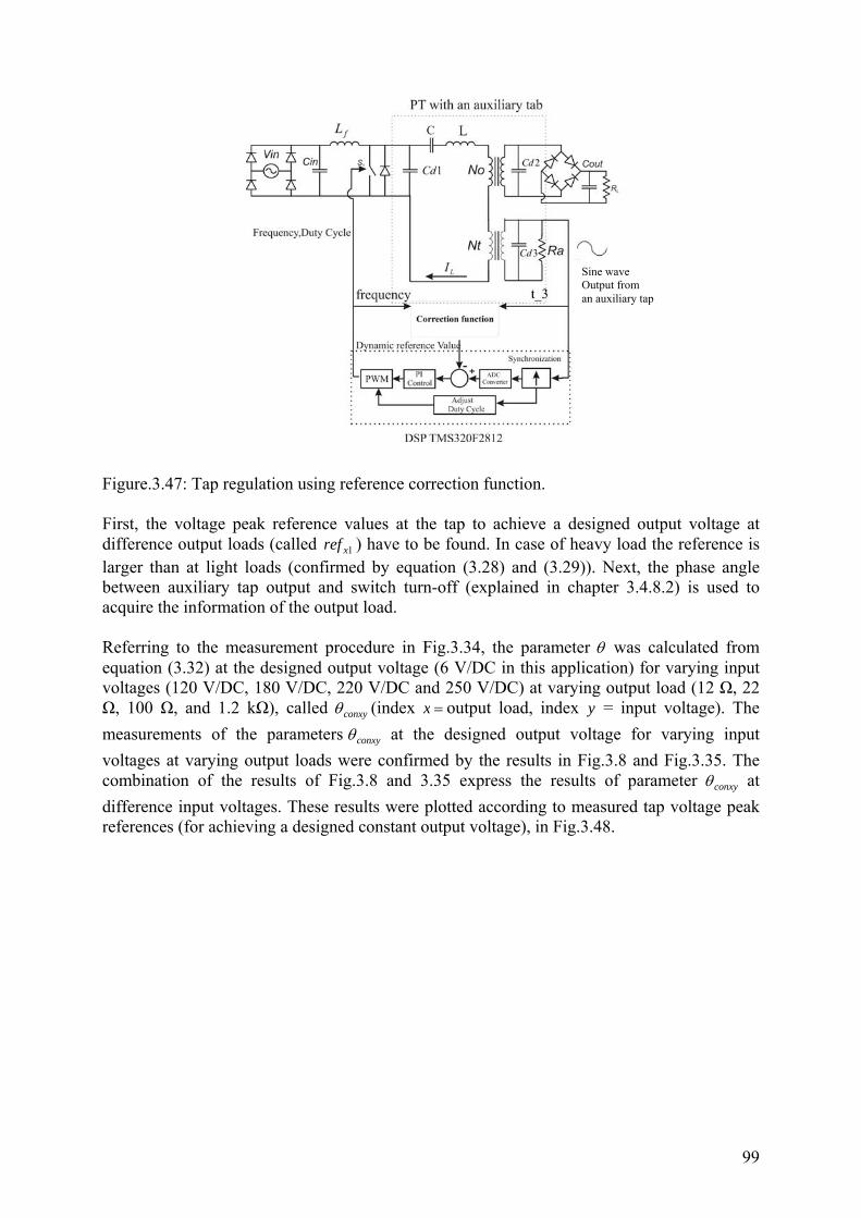
99
Figure.3.47: Tap regulation using reference correction function. First, the voltage peak reference values at the tap to achieve a designed output voltage at difference output loads (called 1xref ) have to be found. In case of heavy load the reference is larger than at light loads (confirmed by equation (3.28) and (3.29)). Next, the phase angle between auxiliary tap output and switch turn-off (explained in chapter 3.4.8.2) is used to acquire the information of the output load. Referring to the measurement procedure in Fig.3.34, the parameter θ was calculated from equation (3.32) at the designed output voltage (6 V/DC in this application) for varying input voltages (120 V/DC, 180 V/DC, 220 V/DC and 250 V/DC) at varying output load (12 Ω, 22 Ω, 100 Ω, and 1.2 kΩ), called conxyθ (index =x output load, index y = input voltage). The measurements of the parameters conxyθ at the designed output voltage for varying input voltages at varying output loads were confirmed by the results in Fig.3.8 and Fig.3.35. The combination of the results of Fig.3.8 and 3.35 express the results of parameter conxyθ at difference input voltages. These results were plotted according to measured tap voltage peak references (for achieving a designed constant output voltage), in Fig.3.48.
Sine wave Output from an auxiliary tap
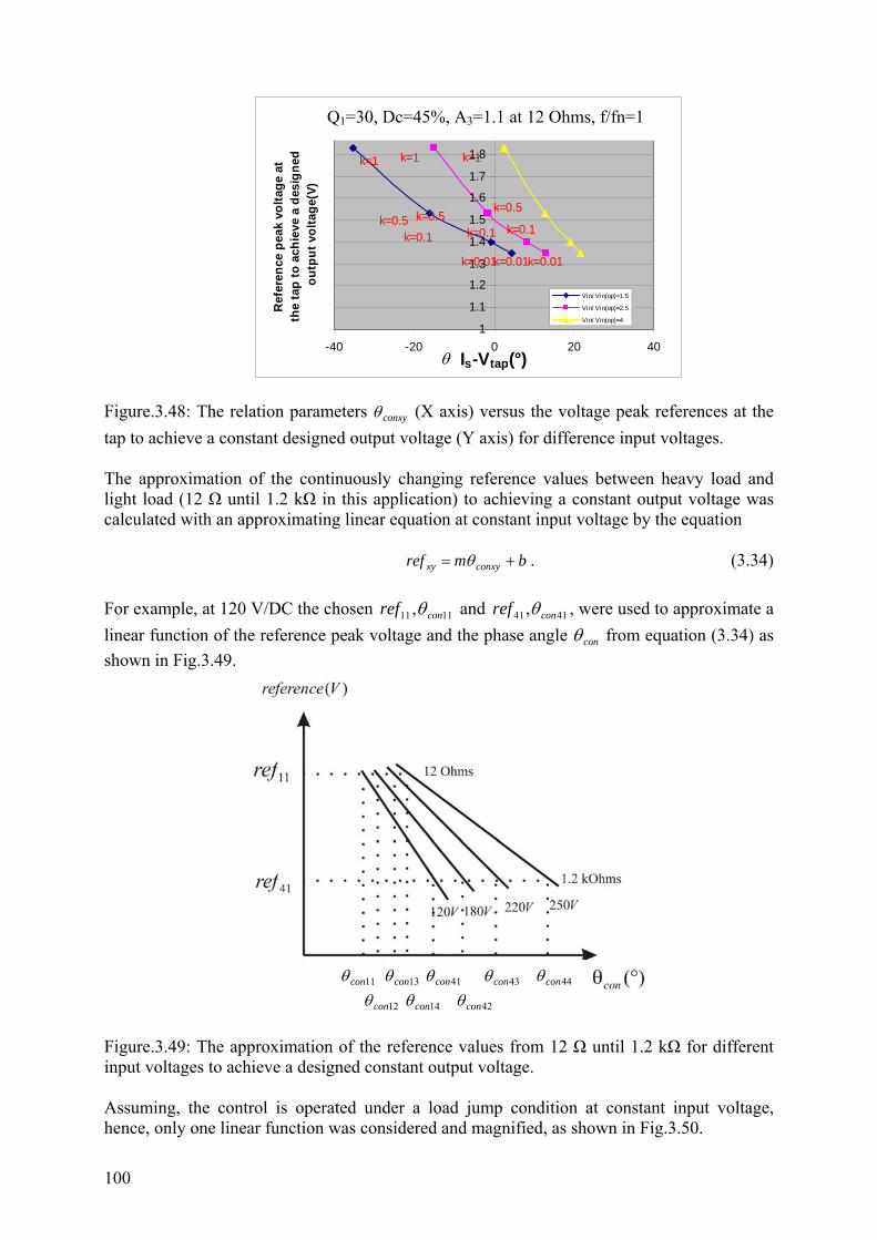
100
Figure.3.48: The relation parameters conxyθ (X axis) versus the voltage peak references at the tap to achieve a constant designed output voltage (Y axis) for difference input voltages. The approximation of the continuously changing reference values between heavy load and light load (12 Ω until 1.2 kΩ in this application) to achieving a constant output voltage was calculated with an approximating linear equation at constant input voltage by the equation
bmref conxyxy += θ . (3.34) For example, at 120 V/DC the chosen 1111 , conref θ and 4141 , conref θ , were used to approximate a linear function of the reference peak voltage and the phase angle conθ from equation (3.34) as shown in Fig.3.49. Figure.3.49: The approximation of the reference values from 12 Ω until 1.2 kΩ for different input voltages to achieve a designed constant output voltage. Assuming, the control is operated under a load jump condition at constant input voltage, hence, only one linear function was considered and magnified, as shown in Fig.3.50.
Q1=30, Dc=.45%,A3=1.1
1
1.1
1.2
1.3
1.4
1.5
1.6
1.7
1.8
1.9
-40 -20 0 20 40Is-Vtap(°)
Ref
eren
ce p
eak
volta
ge a
t th
e ta
p to
ach
ieve
a d
esig
ned
outp
ut v
olta
ge(V
)Vin/ Vin(op)=1.5
Vin/ Vin(op)=2.5
Vin/ Vin(op)=4
k=1 k=1 k=1
k=0.5 k=0.5k=0.5
k=0.1 k=0.1 k=0.1
k=0.01k=0.01k=0.01
Q1=30, Dc=45%, A3=1.1 at 12 Ohms, f/fn=1
θ
421412
4443411311
conconcon
conconconconcon
θθθθθθθθ

101
Figure.3.50: The approximation of the reference value from 12 Ω until 1.2 kΩ for a constant input voltage to achieve a constant designed output voltage. In the steady state at point A (12 Ω output load), the reference must be 11ref and the conθ in the actual measurement must be 14conθ presenting the output load of 12 Ω with 6 V/DC at the output. If the load jump occurs from 12 Ω to 1.2 kΩ, conθ in the current measurement will shift from point A at 14conθ to point B at 1conactθ . The controller realizes that conθ in the current measurement is not located on the line of 6 V/DC output. Then controller compares the conθ in the current measurement which is now at 1conactθ , with 14conθ . If 14conθ < 1conactθ , the controller reduces the reference value. Assume the reference value is reduced to be 1xref , at point C. In this point 1conactθ , the current measurement should be 1conxθ located on the line of 6 V/DC. But in the reality, the current measurement of conθ achieves 2conactθ , which is not located on the line of 6 V/DC output voltage, which means, that the reference has still not the correct value to reach a constant voltage of 6 volts. The controller compares again between
2conactθ and 1conxθ . If 1conxθ < 2conactθ , the controller reduces the reference value again continuously until point E. In this point, the reference is set to be 41ref and conθ is measured as 44conθ which means that the controller already generated 6 V/DC at the output. In a real application, one cannot assume to have only a fixed input voltage because the converter also needs to regulate against the line input voltage change. Therefore, a further approximation of different input voltages needs to be calculated. The complete approximation with varying input voltage was calculated as follows. For example, at equations (3.34) of input voltage consideration at 120 V/DC and 250 V/DC are
11 BAref conxyxy += θ and 22 BAref conxyxy += θ ,respectively. Then, the equation to approximate the coefficient 1A and 2A according to the input voltages was calculated from 11 FVEA iny += . The value of yA was substituted by 1A and 2A at inV is 120 V/DC and 250 V/DC, respectively. The values of 1E and 1F were determined. The same calculations are proceeded to approximate the coefficients 1B and 2B according to the input voltages.
1114 conactconxcon θθθ 2conactθ 44conθ
)(°conθ

102
Finally, the equation of conθ for different input voltages was derived as a linear function of the reference peak value at the tap ( )Vtapref and the input voltage )(Vin , as shown in equation (3.35)
4).3().2()..1( KVinKVtaprefKVtaprefVinKcon −−−=θ . (3.35) The results of dynamic response are shown for an example of an output load jump in Fig.3.51.
Figure.3.51: The output voltage response at a load jump from 1.2 kΩ to 22 Ω and from 22 Ω to 1.2 kΩ at 230 V/DC input voltage, respectively. The comparison between the control including the correction function and the control without the correction function is shown in Fig.3.52.
(Time 100 ms/Div.) (Time 100 ms/Div.)
(5 V/Div.)
(5 V/Div.)
Div.
0

103
Figure.3.52: The compared output voltage response for the regulation with correction function and without correction function. a) Input voltage of 220 V/DC from 1.2 kΩ to 47 Ω at output load with correction function. b) Input voltage of 220 V/DC from 47 Ω to 1.2 kΩ at output load with correction function. c) Input voltage of 220 V/DC from 1.2 kΩ to 47 Ω at output load without correction function. d) Input voltage of 220 V/DC from 47 Ω to 1.2 kΩ at output load without correction function. However, this control method has limitations of losing the reference regulation behaviour in some operating points, coming from the linear approximation of the non linear behaviour of the class-E converter given by equation (3.34) and (3.35). With the linear approximation, the coefficients 3,1,1 KKK and 4K were derived from using two points only. Thus, the results of reference regulation will work very well in these operation points. If the operating point is far from the used approximation points, the results either might be an error of the reference value regulation or losing the reference regulation behaviour. These problems have to be solved in a future work, e.g. by investigating the feasibility at different parameters 1,QDc and 3A as initial parameters.
(a) (b)
(c) (d)
(Time 200 ms/Div.) (Time 200 ms/Div.)
(Time 10 ms/Div.) (Time 10 ms/Div.)
(2 V/Div.)
(2 V/Div.)
(2 V/Div.)
(2 V/Div.)
Div.
0

104
3.4.10 Power Transfer Capability At the end of this chapter, a comparison of the maximum power transfer ratio for step up applications of different converter topologies is shown below [Bis 06].
Topology
Duty cycle (at ZVS/ZCS)
Power transfer ratio
Half bridge
50% 2
2π
=0.2026
Full bridge
50% 81.08
2 =π
Push pull
50% 23.1
8
2
=π
class-E at 03 =A ( ∞=1Q )
50%
0.5768
class-E at 5.03 =A ( 1001 =Q )
50%
0.6329
class-E at 1.13 =A ( 1001 =Q )
50%
1.007
class-E at 5.13 =A ( 1001 =Q )
50%
1.2753
class-E at 5.03 =A ( 1001 =Q )
70%
1.3514
class-E at 1.13 =A ( 1001 =Q )
70%
1.439
class-E at 5.13 =A ( 1001 =Q )
70%
1.549
It can be seen that the class-E provides highest power transfer capability compared to half- bridge, full-bridge and push pull, if the optimum duty cycle is chosen large, but still within reliable operation range regarding sensitivity issues[Bis 06]. An alternative of high power transfer ratio is available by the push pull or full bridge converter the class-E topology has a benefit over the other topologies since it provides fewer components than other topologies (two switching devices and inductors for push pull, two switching devices for half-bridge and four switching devices for full-bridge). By this reason, the class-E topology is also considered as a potential candidate for low expense step up applications.

105
3.5 Conclusion It was demonstrated with the class-E concept that, it is always possible to maintain output voltage constant, using a resonant tank with an output parallel capacitance as inherent in piezo transformer application at wide range of output load and input voltage maintaining ZVS at the switch by frequency modulation control and duty cycle adjustment. A systematic methodology to analyze complex resonant converters, focussed on class-E topology, was proposed. The analyzed system is independent of design parameters containing physical units, by replacing then by normalized parameters. With this calculation method, proposed by Bisogno [Bis 06] the behaviour of the class-E resonant converter under suboptimum operation mode was investigated. All explicit parameters such as switch current/voltage or motion current can be retrieved. Further, the analysis predicts the bandwidth of switching frequency for ZVS condition by detecting the reverse switching current based on normalized parameters as 321 ,,, AAADc and 1Q of the class-E resonant converter. It was shown, that the ZVS window of a resonant converter, presented by the class-E example, will be comprehensively obtained using normalized parameters as DcA ,3 and 1Q providing thresholds of the duty cycle range across the normalized switching frequency. Therefore, a linearized approximation of duty cycle tracking by the normalized switching frequency could be achieved for an unexpected large operation and design parameter range. To provide near-ZVS behavior, it was demonstrated by a tapped narrow band transformer as a PT, that synchronization can be archived over nearly all desired design parameter settings. Frequency control was found to be a highly reliable control method compared with turn-on adjustment control, improving near-ZVS or ZVS behavior controllability. Further the classical linear controllers such as P, I, PI were investigated and confirmed to provide a good performance at static and dynamic responses over a wide operation range. The proposed techniques to maintain ZVS condition for a wide operation range were presented for load resonant converters with input capacitor of the resonant tank in parallel with the switching device, such as class-E and inductor-less half-bridge, called duty cycle tracking and synchronization duty cycle adjustment combined with classical feed back loops. Several control concepts based on variable frequency control, namely non-isolated output feed back closed loop, auxiliary tap regulation, multi loop regulation, isolated output voltage feed back with opto-coupler, tap regulation using reference correction function control have been developed and compared by their effecting of steady state and dynamic responses under input voltage and output load variations. The advantages and disadvantages of each proposed control method have been discussed. An improved efficiency control method, called burst mode control, has been presented. Four classification methods between heavy load and light load have been addressed. The performances of four classification methods were compared, and the preferably suited method of frequency classification including input voltage observation was selected finally. Linearization methods of burst mode classification and of reference correction using tap regulation have been confirmed to be applicable. Summarizing it can be concluded that a complete static operation range and design parameter analysis of class-E and of the inductor-less half-bridge topology was established, deriving the

106
static control range under ZVS condition, and providing suited methodologies to control frequency, duty cycle and light load thresholds to achieve a burst mode for a fully functional concept of the investigated resonant power converters.
107
Chapter 4
Modeling of Load Resonant Converters
4.1 Introduction Usually, the PWM converters and resonant converters are widely applied for AC/DC or DC/DC power supplies. In these applications either the output voltage or current is required to be controlled as constant or variable. Consequently, it is important to know the response of the converter on variations at the input voltage, the output load or reference signal to generate the control signals. In order to evaluate, to design and to optimize control, dynamic models of the PWM converters and/or resonant converters are required. The modeling of the PWM converters and resonant converters usually can be described in terms of differential equations obtained by using physical laws based on Maxwell’s equations. Mathematical models may assume many different forms depending on the circumstances. For example, in the steady state analysis of power converters, it is advantageous to use the state space representations. While, regarding the dynamic behavior, the linearized transfer function may be more convenient than any other description. Generally, the accuracy of a model is possible to be improved by increasing its complexity. In some cases, hundreds of equations are included to describe an accurate system but questionable on its practical for real technical application. However, there is a compromise between the simplicity of the model and the accuracy of the results. In practical, it is generally satisfying, if the model obtains an adequate accuracy for the objective of a chosen analysis at minimum complexity for the considered problem. A number of research works have been provided by analysis of the resonant converters in the steady state behavior. For instance, the steady state evaluation process was developed for half-bridge parallel and series-parallel converters in a publication of Ivensky [Ive 99]. The modeling of PT utilized in the half-bridge topology was discussed by Ivensky also [Ive 00]. Liu presented the analysis of quasi resonant converters (applied to the Buck converter) with zero current switching [Liu 85]. Bhat presented a unified approach for steady state analysis of resonant converters. Different tank circuits are combined into a single circuit called generalized tank circuit, and analysis is carried out for this configuration using ac circuit analysis [Bha 91]. The fourth elements parallel resonant DC-DC converter operating in continuous mode was presented by Ojo [Ojo 93]. Class-E steady state analysis was proposed by dividing the steady state operation mode into six intervals according to the switching intervals of the converter, in the work of Song [Son 96]. The steady state of two zero voltage switching converters based on class-E topology was derived by using proper state variable transformations to derive a state plane diagram by Lee [Lee 89]. The phase plane analysis was also used to analyze the steady state characteristics by Tanaka [Tan 96]. Vorperian introduced the equivalent circuit model of the switch in the resonant converter by three terminal devices by determining the relationship between its average terminal voltage and current [Vor 89]. These mentioned research works provide a reliable design procedure for the steady state condition in resonant converters.
108
However, the model specifications of any switching converters are related to the response for the output load and/or line input voltage regulations. Consequently, the behavior of the switching converters under the transient conditions can be obtained by linearization with small signal or large signal modeling. The small signal methods which are suitable for a small signal perturbation are commonly used when linearized around the operation point [So 97] [Vor 83] [Wit 91] [Kin 85] [Bat 96]. Small signal models generally provide enough insight to design a feed back control loop around quiescent operation point due to a small deviation. This model is very useful to the closed loop modeling, since it is compatible with a linear technique such as Bode plot and root locus for further analysis. For a large signal perturbation such as in open loop, the non-linear terms become significant and cannot be predicted properly with the small signal model. Thus, the large signal model is required for the open loop situation [Her 91] [Eri 82]. In this work, the dynamic modeling for open loop and closed loop of the load resonant converters, focused on the class-E topology, is introduced which leads to considerable simplification in the further analysis [Gu 89] [For 92]. The transient behavior of the output voltage for the open loop class-E converter against perturbations such as the input voltage change, the switching frequency change, or the output load change are obtained by replacing the complete circuit of the class-E converter by simple equivalent circuit models. Another advantage in using these proposed models is that the simple dynamic model allows to be analyzed using simple linear electronic circuit analysis programs such as PSIPCE, PSIM or Mathlab-Simulink at shorter simulation time. A simpler open loop model for class-E topology was presented by substituting the higher order equations being solved by the convergent of several linear differential equation systems by a first order equation only. The accuracy of the first order equation was improved by an exponential function model. Next, the results from the analysis of the open loop dynamic behavior are applied to modeling the closed loop class-E converter with presented several control methods from chapter three. Subsequently, the closed loop dynamic analysis which resulted in considerable simplification over the calculation attempt of the higher order of the circuit was presented. The basics of large signal linearization methods for the steady state analysis were purposed in this chapter. The models of the linearization for class-E topology were implemented into the controller to investigate the accuracy of the regulation. Besides, the linearization models were used to observe the stability condition of the proposed controls. A simplified closed loop model neglecting time delays of the resonant converter is suitable under the working condition that the output time constant is being much larger than the time constant of the high frequency part in the class-E or of another resonant converter topology.

109
4.2 Decomposition Method for Dynamic Model of Resonant Converters by the class-E Example In order to simplify the analysis of the load resonant converter focused on class-E topology, the method of decomposition was applied by Bisogno [Bis 05] [Bis 06]. This method divides the resonant circuit of class-E topology into two parts called high frequency section and low frequency section. In the high frequency section, the system consists of passive elements that provide a small delay by time constants such as 21 ,,,, ddf CLCCL , and of the switch device
1S in Fig.4.1. On the other hand, in the low frequency section, the system consists of passive elements that provide a large time constant such as output capacitor ( outC ) and output load ( LR ). The analysis of decomposition method is applied to analyze the high frequency section and low frequency section separately. The following assumptions were provided for the high frequency section. The input capacitor is large enough that the input voltage, the rectifier bridge and the input capacitor are considered to be a constant input DC voltage source. The output capacitor is large enough that the output voltage should be kept constant over a considered time interval, replaced with a constant voltage source, in Fig.4.1 a). In the low frequency section, the circuit is substituted by the input current source connected in parallel with the output capacitor ( outC ) and the output load ( LR ) in Fig.4.1 b). The connection between two sections is considered by the energy that is transferred from the resonant circuit (high frequency section) to the output load (low frequency section). The delivered current in the high frequency section does not depend on the waveform, but derived from the amount of the energy. The output voltage is considered as a constant DC source. Also the delivered current in the high frequency section is assumed as an input DC current source transferred to the low frequency section shown in Fig.4.1.
Figure.4.1: Decomposition class-E: a) High frequency section. b) Low frequency section. The analysis of the high frequency section is analyzed by differential equations. The circuit was divided into several operation modes that are defined by switching of semiconductors (switch and diodes) and by linear operation behavior at six possible different time intervals [Bis 05] [Bis 06].
(a) (b)

110
The result of the calculation shows the average output current at a certain value of output voltage source depending on the switching frequency and on the input voltage in Fig.4.2. This solution of the high frequency section is used to predict only the steady state of class-E behavior. The result of this analysis does not yet consider the dynamic behavior. The model of decomposition is applicable if output voltage of the high frequency part remains constant, thus the dynamical time delay of the resonant converter has to be neglected against the output time dealy ( )resonantoutput ττ >> . Otherwise, the value of output voltage has to be updated at each switching cycle. In this case, the time delay of the high frequency part can be considered correctly.
Figure.4.2: The static result of the average output current depending on the input voltage and the switching frequency used for the decomposition method [Bis 06]. 4.3 Open Loop class-E Dynamic Model (Large signal model) The dynamic behavior of the class-E resonant converter is further analyzed by using the results from the steady state analysis under the assumption that the time constant of the low frequency part is considered to be significantly larger than the time constant of the high frequency part. Therefore, the dominant pole dominating effects on the transient responses of the system is contained in the low frequency part only. Thus, the dynamic behavior can be analyzed by considering mainly the model of low frequency part. It can be assumed that such proposed open loop dynamic models are considered as a simple approach, containing less complexity in mathematical calculation while an adequate accuracy is obtained. The models are developed for analysis of an open loop transient output voltage response at perturbation conditions such as input voltage jump, switching frequency jump or output load jump. The information about internal variables such as voltage and current at the switching device or inside of the resonant tank, are neglected. Only the DC output voltage is involved in the consideration. The open loop dynamic model is verified with PSPICE which allows direct implementation of mathematical expressions. The assumptions used in the modeling are presented by the following 1) The ZVS condition is always achieved, 2) all of the losses in the circuit are neglected and 3) effects of parasitic are neglected.
(DC)
60V
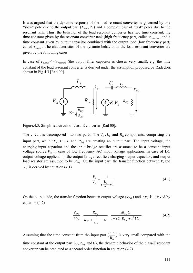
111
It was argued that the dynamic response of the load resonant converter is governed by one “slow” pole due to the output part ( Lout RC , ) and a complex pair of “fast” poles due to the resonant tank. Thus, the behavior of the load resonant converter has two time constant, the time constant given by the resonant converter tank (high frequency part) called resonantτ , and a time constant given by output capacitor combined with the output load (low frequency part) called outputτ . The characteristics of the dynamic behavior in the load resonant converter are given by the following cases. In case of outputτ < < resonantτ (the output filter capacitor is chosen very small), e.g. the time constant of the load resonant converter is derived under the assumption proposed by Radecker, shown in Fig.4.3 [Rad 00]. Figure.4.3: Simplified circuit of class-E converter [Rad 00]. The circuit is decomposed into two parts. The inV , fL and dcR components, comprising the
input part, while sKV , ,C L and EQR are creating an output part. The input voltage, the charging input capacitor and the input bridge rectifier are assumed to be a constant input voltage source inV in case of low frequency AC input voltage application. In case of DC output voltage application, the output bridge rectifier, charging output capacitor, and output load resistor are assumed to be EQR . On the input part, the transfer function between sV and
inV is derived by equation (4.1)
1
1
+=
dc
fin
s
RL
sVV . (4.1)
On the output side, the transfer function between output voltage ( EQV ) and sKV is derived by equation (4.2)
LCsRsC
CsR
sLsC
R
RKVV
EQ
EQ
EQ
EQ
s
EQ211 ++
=++
= . (4.2)
Assuming that the time constant from the input part (dc
f
RL
) is very small compared with the
time constant at the output part ( EQRC, and L ), the dynamic behavior of the class-E resonant converter can be predicted as a second order function in equation (4.2).
K=dc
EQ
RR

112
In case of
outputτ >> resonantτ (4.2 a) the output capacitor was chosen big enough to achieve a reasonable output voltage ripple in an application where a DC output voltage is required. When outputτ is chosen to be much larger than resonantτ , the time constant of output capacitor combined with the output load ( outputτ ) dominates the dynamic behavior of the converter and presents a first order system, shown in Fig.4.4.
Figrue.4.4: Dynamic behavior of class-E converter considering outputτ >> resonantτ . The transfer function of the first order equivalent circuit of class-E in Fig.4.4 is derived by connecting an input current source in parallel with the equivalent output capacitor combined with the equivalent output load, shown in Fig.4.5. Figure.4.5: Dynamic behavior equivalent circuit of class-E converter considering
outputτ >> resonantτ . The transfer function in Fig.4.5 is derived now in equation (4.3)
1''
')(
)(+
=Lout
Lout
RsCR
sIsV . (4.3)
4.3.1 First Order Open Loop Dynamic Model with Two Points Approximation This proposed open loop dynamic model is developed under the assumption that the time constant of the low frequency section is significantly larger than that of the high frequency section. The proposed dynamic model consists of the time varying input current source )(tI connected in parallel with the output capacitor and the output load shown in Fig.4.6 a). The input current source )(tI presents the steady state value of the average output current of the high frequency part without considering its time constant.
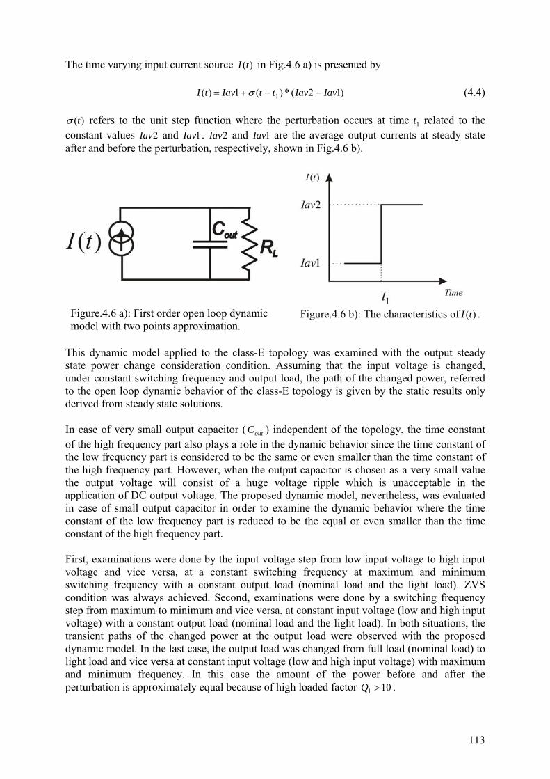
113
The time varying input current source )(tI in Fig.4.6 a) is presented by
)12(*)(1)( 1 IavIavttIavtI −−+= σ (4.4)
)(tσ refers to the unit step function where the perturbation occurs at time 1t related to the constant values 2Iav and 1Iav . 2Iav and 1Iav are the average output currents at steady state after and before the perturbation, respectively, shown in Fig.4.6 b).
This dynamic model applied to the class-E topology was examined with the output steady state power change consideration condition. Assuming that the input voltage is changed, under constant switching frequency and output load, the path of the changed power, referred to the open loop dynamic behavior of the class-E topology is given by the static results only derived from steady state solutions. In case of very small output capacitor ( outC ) independent of the topology, the time constant of the high frequency part also plays a role in the dynamic behavior since the time constant of the low frequency part is considered to be the same or even smaller than the time constant of the high frequency part. However, when the output capacitor is chosen as a very small value the output voltage will consist of a huge voltage ripple which is unacceptable in the application of DC output voltage. The proposed dynamic model, nevertheless, was evaluated in case of small output capacitor in order to examine the dynamic behavior where the time constant of the low frequency part is reduced to be the equal or even smaller than the time constant of the high frequency part. First, examinations were done by the input voltage step from low input voltage to high input voltage and vice versa, at a constant switching frequency at maximum and minimum switching frequency with a constant output load (nominal load and the light load). ZVS condition was always achieved. Second, examinations were done by a switching frequency step from maximum to minimum and vice versa, at constant input voltage (low and high input voltage) with a constant output load (nominal load and the light load). In both situations, the transient paths of the changed power at the output load were observed with the proposed dynamic model. In the last case, the output load was changed from full load (nominal load) to light load and vice versa at constant input voltage (low and high input voltage) with maximum and minimum frequency. In this case the amount of the power before and after the perturbation is approximately equal because of high loaded factor 101 >Q .
Figure.4.6 a): First order open loop dynamic model with two points approximation.
Figure.4.6 b): The characteristics of )(tI .

114
In this example evaluation, the low and high input voltages were defined as 120 V/DC and 360 V/DC, respectively. The minimum and maximum switching frequencies were defined as 155.5 kHz and 170 kHz, respectively. The output loads at full load and light load were defined as 12 Ω and 100 Ω, respectively. These values cover the required operation range of an off-line power supply. The simulations for observing the dynamic behavior were implemented by PSPICE simulation with equivalent schematics in Fig.4.7. The results of the perturbation from the schematics in Fig.4.7 were called exact dynamic characteristics. The results of the dynamic behavior from the examples of perturbation by experiments and simulations from the exact model are shown in Fig.4.8. The results in Fig.4.8 show that the exact model was investigated and proved as in a good agreement with the real measurements. Thus, the results of the proposed open loop dynamic models can be compared with these exact models. Figure.4.7 a): The perturbation condition for input voltage change. b) The perturbation condition for output load change. c) The perturbation condition for switching frequency change.
(a)
(b)
(c)
RLmin,RLmax.
RLmin,RLmax.

115
Figure.4.8: Compared results of output voltage measurements and simulations using exact models. a) Input voltage jump from 360 V/DC to 120 V/DC at switching frequency 170 kHz at 100 Ω output load. b) Input voltage jump from 360 V/DC to 120 V/DC at switching frequency 170 kHz at 12 Ω output load. c) Output load jump from 12 Ω to 100 Ω at 360 V/DC input voltage at 170 kHz switching frequency. The parameters 2Iav and 1Iav in equation (4.4) can be determined from the calculation of steady state analysis in the work of Bisogno [Bis 05]. The result of the steady state analysis provides the information on average output current as a function of switching frequency at varying input voltages for the high frequency part (in Fig.4.2). In case that an input voltage jump occurs from inAV to inBV , at defined switching frequency and output load, the output voltage will change from outAV to outBV . The results of the static
Time (2 ms/Div.) Time (ms)
V (V)
Time
68ms 70ms 72ms 74ms 76ms 78ms 80ms 82ms 84ms 86ms 88ms 90msV(R2:2,R2:1)
0V
0.5V
1.0V
1.5V
2.0V
2.5V
2.8V
V (0.5 V/Div.)
(b)
0
Time
120ms 130ms 140ms 150ms 160ms 170ms 180ms 190ms 200ms 210ms 220msV(V1:+,R11:1)
0V
2.0V
4.0V
6.0V
8.0V
Time(10 ms/Div.) Time (ms)
V(2 V/Div.) V(V)
(c)
0
0
0
Time
120ms 130ms 140ms 150ms 160ms 170ms 180ms 190ms 200ms 210ms 220ms 230msV(Cout1:2,R2:1)
0V
2.0V
4.0V
6.0V
8.0V
Time (10 ms/Div.) Time (ms)
V (2 V/Div.) V (V)
(a)
0 0 Div.
2
10
4
20
0.5
1
2 4
2
4
10 20

116
analysis at output voltages outAV and outBV are demonstrated in Fig.4.9 a) and Fig.4.9 b), respectively. Figure.4.9 a): The results from the static analysis for the average output current at Vout = VoutA for input voltage jump. Figure.4.9 b): The results from the static analysis for the average output current at Vout = VoutB for input voltage jump. The behavior of the simplified dynamic model in Fig.4.6 was simulated by PSPICE at defined
2Iav and 1Iav average output current after and before the perturbation, respectively. The results at input voltage jump of the exact model and the proposed simplified dynamic model were compared. The transient paths of power change at the output load were compared as results, shown in appendix B.1 at different output capacitors. Further, the relative errors between the exact model and the proposed dynamic model described by the following equation were included in appendix B.1
elexact
elexactellinear
elexact PPP
PP
mod_
mod_mod_
mod_
−=
∆ . (4.5)
In case of switching frequency jump, the constant values of 1Iav and 2Iav are determined as following, shown in Fig.4.10 a) and Fig.4.10 b).
f(Hz)
Vout = VoutB
Vin=VinAVin=VinB
Iav(A)
fa
Iav2
f(Hz)
Vout = VoutA
Vin=VinA
Vin=VinB
fa
Iav1
Iav(A)
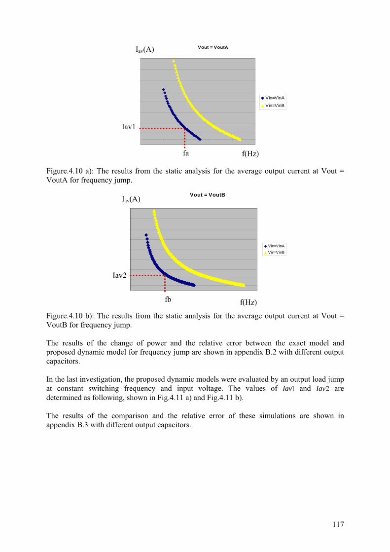
117
Figure.4.10 a): The results from the static analysis for the average output current at Vout = VoutA for frequency jump. Figure.4.10 b): The results from the static analysis for the average output current at Vout = VoutB for frequency jump. The results of the change of power and the relative error between the exact model and proposed dynamic model for frequency jump are shown in appendix B.2 with different output capacitors. In the last investigation, the proposed dynamic models were evaluated by an output load jump at constant switching frequency and input voltage. The values of 1Iav and 2Iav are determined as following, shown in Fig.4.11 a) and Fig.4.11 b). The results of the comparison and the relative error of these simulations are shown in appendix B.3 with different output capacitors.
f(Hz)
Vout = VoutB
Vin=VinAVin=VinB
fb
Iav2
Iav(A)
f(Hz)
Vout = VoutA
Vin=VinA
Vin=VinB
fa
Iav1
Iav(A)
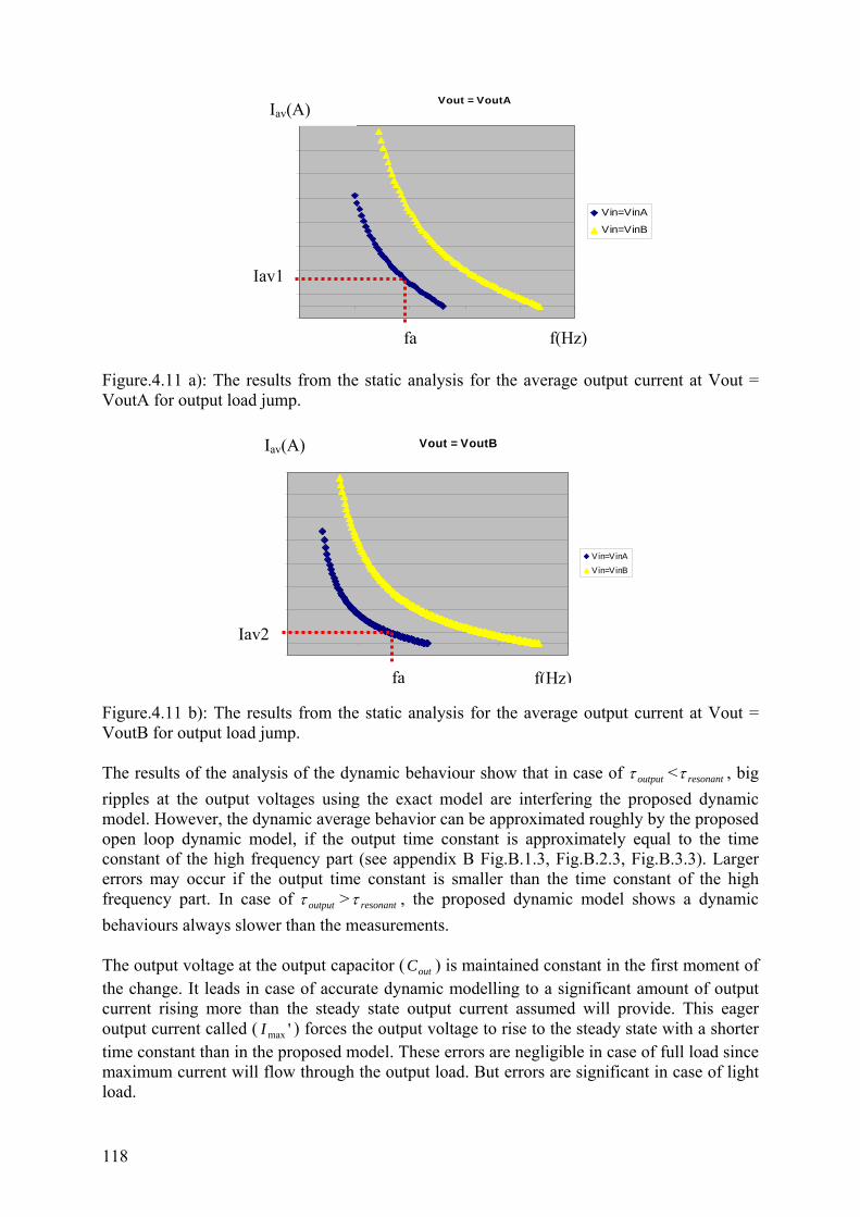
118
Figure.4.11 a): The results from the static analysis for the average output current at Vout = VoutA for output load jump. Figure.4.11 b): The results from the static analysis for the average output current at Vout = VoutB for output load jump. The results of the analysis of the dynamic behaviour show that in case of outputτ < resonantτ , big ripples at the output voltages using the exact model are interfering the proposed dynamic model. However, the dynamic average behavior can be approximated roughly by the proposed open loop dynamic model, if the output time constant is approximately equal to the time constant of the high frequency part (see appendix B Fig.B.1.3, Fig.B.2.3, Fig.B.3.3). Larger errors may occur if the output time constant is smaller than the time constant of the high frequency part. In case of outputτ > resonantτ , the proposed dynamic model shows a dynamic behaviours always slower than the measurements. The output voltage at the output capacitor ( outC ) is maintained constant in the first moment of the change. It leads in case of accurate dynamic modelling to a significant amount of output current rising more than the steady state output current assumed will provide. This eager output current called ( 'maxI ) forces the output voltage to rise to the steady state with a shorter time constant than in the proposed model. These errors are negligible in case of full load since maximum current will flow through the output load. But errors are significant in case of light load.
f(Hz)
Vout = VoutB
Vin=VinAVin=VinB
fa
Iav2
Iav(A)
Vout = VoutA
Vin=VinA
Vin=VinB
f(Hz)
Iav(A)
fa
Iav1

119
The further empirical investigations of the dynamic behaviour show that the time constant of the class-E topology can be approximated as time constant of output capacitor combined with the output load ( Lout RC ), when the output load is chosen smaller than the optimum load. When the output load is chosen larger than the optimum load, this time constant will be saturated, called satτ . This phenomenon can be explains by the following. The amplitude of the exceeding output current ( 'maxI ) is increased according to the value of the output load. If the load is considered as light load ( LR is a large value) the capability to absorb the current is less than at heavy load. Hence, when there is a power change, the amplitude of the output current ( 'maxI ) at light load will be higher than at heavy load. Considering the circuit in Fig.4.6 a), when the input current source is replaced by the diagram in Fig.4.17 a) (current source with exceed current ( 'maxI )), as explained in the next chapter, the time constant can be derived from
tV
CI
out ∆∆
=∆
1'
)12(1' maxmax IavI
RIavIavCIavIVC
t Loutout
−−
=−∆
=∆ . (4.6)
From equation (4.6) when LR is increased, 'maxI is also increased, providing an approximated time constant of t∆ . The experiments show that this saturation constant time ( satτ ) depends on switching frequency and independents form the input voltage. This sentence was confirmed by the measurements in Fig.4.12. The experiments were tested to measure a constant time against input voltage and switching frequency change at the difference output loads. The X-axis defines a logarithm of the output load. The Y-axis presents a time constant for difference output capacitors. The curves were plotted for difference change situations.
3 Watts application for input voltage jump at 160 kHz switching frequency
02468
101214
0 1 2 3 4 5
log (RL/Ohm)
time
cons
tant
of t
he
outp
ut re
spon
se (
ms)
47uF(Cout)
220uF(Cout)
(a)
outovτ
satτ
satτ

120
Figure.4.12: The measured time constant against the step perturbations at different output capacitors with varying output loads. a) 3 Watts application at input voltage jump for 160 kHz switching frequency. b) 3 Watts application at input voltage jump for 170 kHz switching frequency. c) 3 Watts application at switching frequency jump from 170 kHz to 160 kHz. d) 35 Watts application at input voltage jump for 93.4 kHz switching frequency.
3 Watts application for input voltage jump at 170 kHz switching frequency
0
2
4
6
8
10
12
14
0 1 2 3 4 5log (RL/Ohm)
time
cons
tant
of t
he o
utpu
t re
spon
se (m
s)
220uF(Cout)47uF(Cout)470uF(Cout)
(b)
outovτ
satτ
satτ
satτ
3 Watts application for switching frequency jump from 170 kHz to 160 kHz
0
2
4
6
8
10
12
14
0 1 2 3 4 5
log (RL/Ohm)
time
cons
tant
of t
he o
utpu
t re
spon
se (m
s)
220uF(Cout)
47uF(Cout)
(c)
outovτ
satτ
satτ
35 Watts application for input voltage jump at 93.4 kHz switching frequency
0
2
4
6
8
10
12
14
0 1 2 3 4 5log (RL/Ohm)
time
cons
tant
of t
he o
utpu
t re
spon
se(m
s)
470uF(Cout)220uF(Cout)47uF(Cout)
(d)
outovτ
satτ
satτ
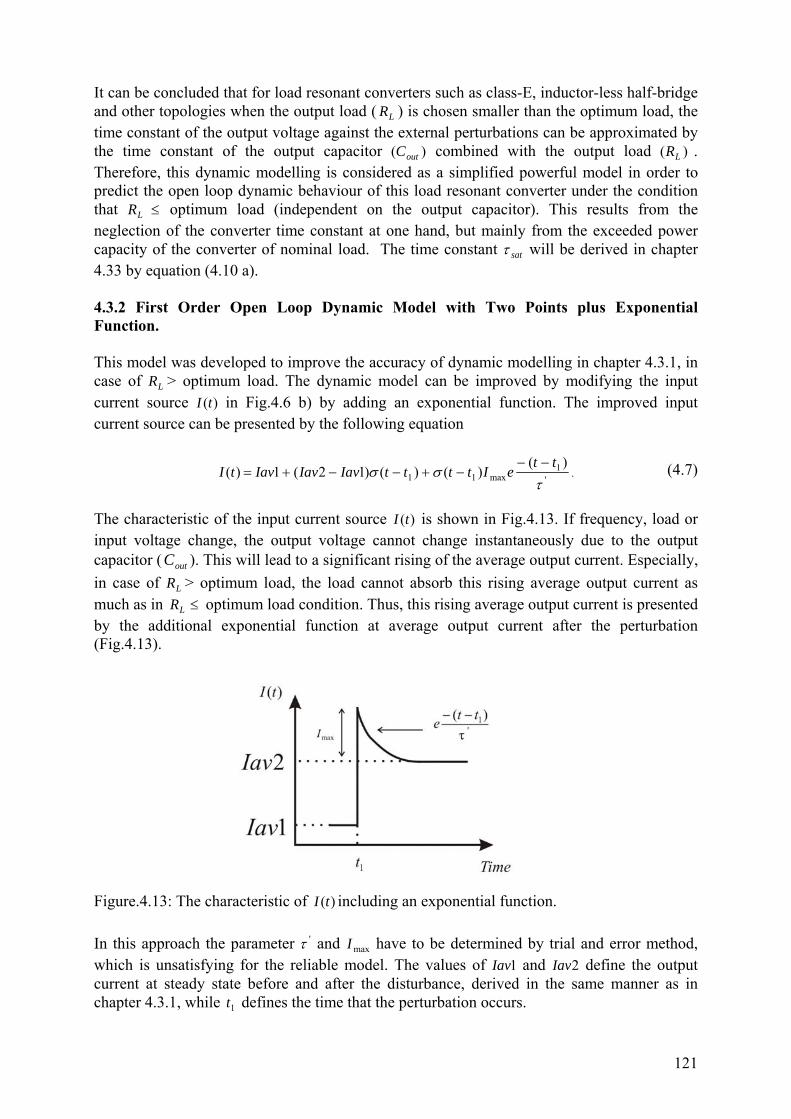
121
It can be concluded that for load resonant converters such as class-E, inductor-less half-bridge and other topologies when the output load ( LR ) is chosen smaller than the optimum load, the time constant of the output voltage against the external perturbations can be approximated by the time constant of the output capacitor )( outC combined with the output load )( LR . Therefore, this dynamic modelling is considered as a simplified powerful model in order to predict the open loop dynamic behaviour of this load resonant converter under the condition that LR ≤ optimum load (independent on the output capacitor). This results from the neglection of the converter time constant at one hand, but mainly from the exceeded power capacity of the converter of nominal load. The time constant satτ will be derived in chapter 4.33 by equation (4.10 a). 4.3.2 First Order Open Loop Dynamic Model with Two Points plus Exponential Function. This model was developed to improve the accuracy of dynamic modelling in chapter 4.3.1, in case of LR > optimum load. The dynamic model can be improved by modifying the input current source )(tI in Fig.4.6 b) by adding an exponential function. The improved input current source can be presented by the following equation
'1
max11)(
)()()12(1)(τ
σσtt
eIttttIavIavIavtI−−
−+−−+= . (4.7)
The characteristic of the input current source )(tI is shown in Fig.4.13. If frequency, load or input voltage change, the output voltage cannot change instantaneously due to the output capacitor ( outC ). This will lead to a significant rising of the average output current. Especially, in case of LR > optimum load, the load cannot absorb this rising average output current as much as in LR ≤ optimum load condition. Thus, this rising average output current is presented by the additional exponential function at average output current after the perturbation (Fig.4.13).
Figure.4.13: The characteristic of )(tI including an exponential function. In this approach the parameter 'τ and maxI have to be determined by trial and error method, which is unsatisfying for the reliable model. The values of 1Iav and 2Iav define the output current at steady state before and after the disturbance, derived in the same manner as in chapter 4.3.1, while 1t defines the time that the perturbation occurs.
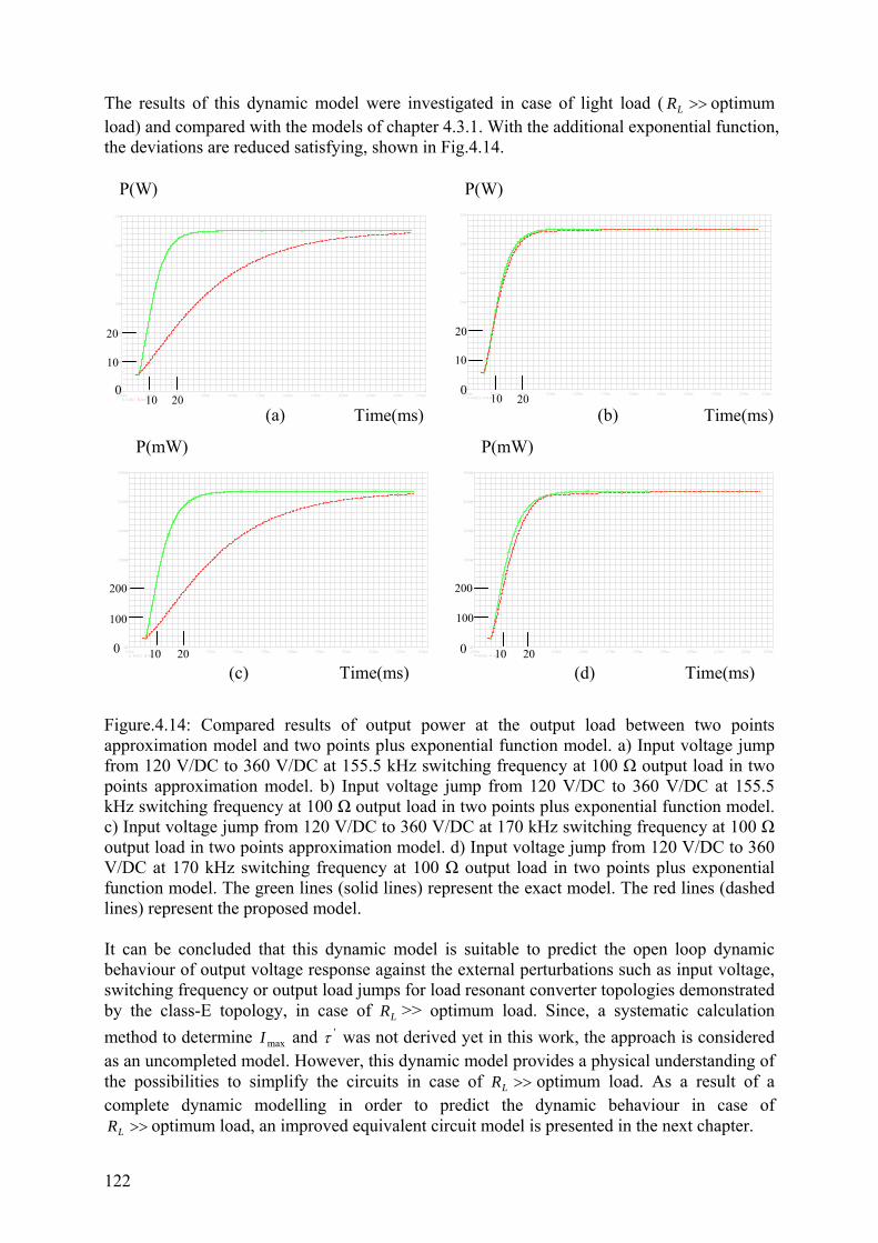
122
The results of this dynamic model were investigated in case of light load ( >>LR optimum load) and compared with the models of chapter 4.3.1. With the additional exponential function, the deviations are reduced satisfying, shown in Fig.4.14.
Figure.4.14: Compared results of output power at the output load between two points approximation model and two points plus exponential function model. a) Input voltage jump from 120 V/DC to 360 V/DC at 155.5 kHz switching frequency at 100 Ω output load in two points approximation model. b) Input voltage jump from 120 V/DC to 360 V/DC at 155.5 kHz switching frequency at 100 Ω output load in two points plus exponential function model. c) Input voltage jump from 120 V/DC to 360 V/DC at 170 kHz switching frequency at 100 Ω output load in two points approximation model. d) Input voltage jump from 120 V/DC to 360 V/DC at 170 kHz switching frequency at 100 Ω output load in two points plus exponential function model. The green lines (solid lines) represent the exact model. The red lines (dashed lines) represent the proposed model. It can be concluded that this dynamic model is suitable to predict the open loop dynamic behaviour of output voltage response against the external perturbations such as input voltage, switching frequency or output load jumps for load resonant converter topologies demonstrated by the class-E topology, in case of LR >> optimum load. Since, a systematic calculation method to determine maxI and 'τ was not derived yet in this work, the approach is considered as an uncompleted model. However, this dynamic model provides a physical understanding of the possibilities to simplify the circuits in case of >>LR optimum load. As a result of a complete dynamic modelling in order to predict the dynamic behaviour in case of
>>LR optimum load, an improved equivalent circuit model is presented in the next chapter.
0 0 Time
120ms 130ms 140ms 150ms 160ms 170ms 180ms 190ms 200ms 210ms 220ms 230msW(R2) W(R9)
0W
10W
20W
30W
40W
50W
60W
Time
120ms 130ms 140ms 150ms 160ms 170ms 180ms 190ms 200ms 210ms 220ms 230msW(R2) W(R9)
0W
10W
20W
30W
40W
50W
60W
P(W)
Time(ms) (a) Time(ms)
P(W)
(b)
10
20
10 20 10 20
10
20
Time
120ms 130ms 140ms 150ms 160ms 170ms 180ms 190ms 200ms 210ms 220ms 230msW(R2) W(R9)
0W
100mW
200mW
300mW
400mW
500mW
600mW
Time
120ms 130ms 140ms 150ms 160ms 170ms 180ms 190ms 200ms 210ms 220ms 230msW(R2) W(R9)
0W
100mW
200mW
300mW
400mW
500mW
600mW
P(mW) P(mW)
Time(ms) Time(ms)(c) (d) 0 0
100
200
10 20
100
200
10 20
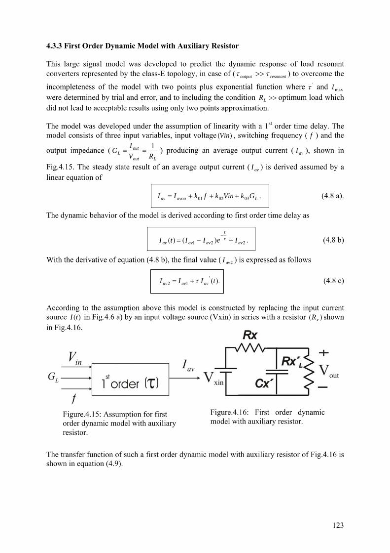
123
4.3.3 First Order Dynamic Model with Auxiliary Resistor This large signal model was developed to predict the dynamic response of load resonant converters represented by the class-E topology, in case of ( resonantoutput ττ >> ) to overcome the
incompleteness of the model with two points plus exponential function where 'τ and maxI were determined by trial and error, and to including the condition >>LR optimum load which did not lead to acceptable results using only two points approximation. The model was developed under the assumption of linearity with a 1st order time delay. The model consists of three input variables, input voltage )(Vin , switching frequency ( f ) and the
output impedance (Lout
outL RV
IG 1
== ) producing an average output current ( avI ), shown in
Fig.4.15. The steady state result of an average output current ( avI ) is derived assumed by a linear equation of
Lavooav GkVinkfkII 030201 +++= . (4.8 a). The dynamic behavior of the model is derived according to first order time delay as
221 )()( av
t
avavav IeIItI +−=−τ . (4.8 b)
With the derivative of equation (4.8 b), the final value ( 2avI ) is expressed as follows
).('12 tIII avavav τ+= (4.8 c) According to the assumption above this model is constructed by replacing the input current source )(tI in Fig.4.6 a) by an input voltage source (Vxin) in series with a resistor )( xR shown in Fig.4.16.
The transfer function of such a first order dynamic model with auxiliary resistor of Fig.4.16 is shown in equation (4.9).
Figure.4.15: Assumption for first order dynamic model with auxiliary resistor.
Figure.4.16: First order dynamic model with auxiliary resistor.
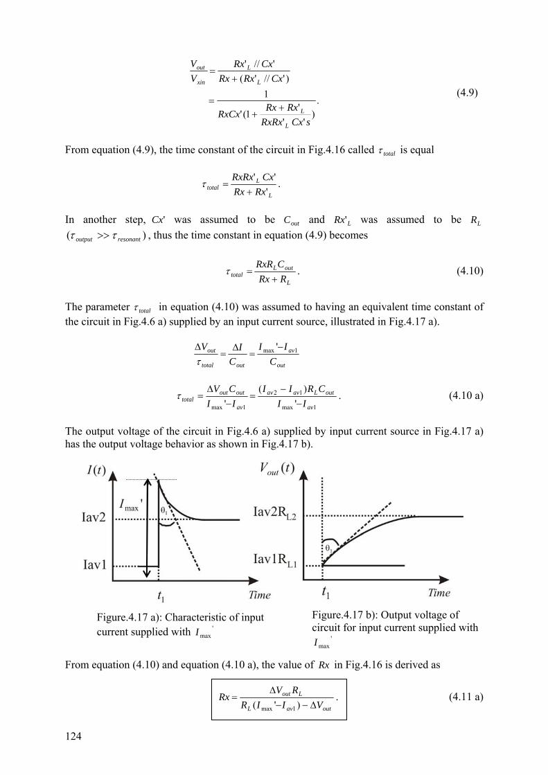
124
.)
'''
1('
1)'//'(
'//'
sCxRxRxRxRx
RxCx
CxRxRxCxRx
VV
L
L
L
L
xin
out
++
=
+=
(4.9)
From equation (4.9), the time constant of the circuit in Fig.4.16 called totalτ is equal
L
Ltotal RxRx
CxRxRx'
''+
=τ .
In another step, 'Cx was assumed to be outC and LRx' was assumed to be LR
)( resonantoutput ττ >> , thus the time constant in equation (4.9) becomes
L
outLtotal RRx
CRxR+
=τ . (4.10)
The parameter totalτ in equation (4.10) was assumed to having an equivalent time constant of the circuit in Fig.4.6 a) supplied by an input current source, illustrated in Fig.4.17 a).
out
av
outtotal
out
CII
CIV 1max '−=
∆=
∆τ
1max
12
1max ')(
' av
outLavav
av
outouttotal II
CRIIII
CV−
−=
−∆
=τ . (4.10 a)
The output voltage of the circuit in Fig.4.6 a) supplied by input current source in Fig.4.17 a) has the output voltage behavior as shown in Fig.4.17 b).
From equation (4.10) and equation (4.10 a), the value of Rx in Fig.4.16 is derived as
outavL
Lout
VIIRRV
Rx∆−−
∆=
)'( 1max. (4.11 a)
Figure.4.17 a): Characteristic of input current supplied with '
maxI Figure.4.17 b): Output voltage of circuit for input current supplied with
'maxI

125
The input voltage step of xinV from Fig.4.16 is derived as follows. In the steady state, the capacitor ( 'Cx ) behaves as an open circuit, thus the input voltage before the perturbation ( 1xinV ) is
))'(
()(1 11max1
1111 L
outavL
LoutavLavxin R
VIIRRV
IRRxIV +∆−−
∆=+= . (4.11 b)
In the same manner, the input voltage after the perturbation ( 2xinV ) is derived by
))'(
()(2 21max2
2222 L
outavL
LoutavLavxin R
VIIRRV
IRRxIV +∆−−
∆=+= . (4.11 c)
The verification of this model can be done by using the result of the steady state analysis by the following. The non-linear behavior of the steady state characteristics avI of a load resonant converter can be linearized by parameter estimation or tangential method within the targeted operating area. Thereafter, the linear equation system including a first order delay can be solved for each transient event of the open loop or closed loop system. In an approach different from this methodology, the non linear curves avI of a load resonant converter can be used directly following the equations (4.12) and (4.13) as described below. Assuming a situation of an input voltage step at a constant switching frequency and output load, the value at the steady state of average output current before the perturbation (equation 4.8 a) can be presented by
.)1(
1
03
102101
1
1031021011
out
avoo
out
avavooav
Vk
VinkfkIVI
kVinkfkII
−
++=
+++=
(4.12 a)
The value of the steady state average output current after the perturbation (equation 4.8 a) can be presented by
.)1(
2
03
202101
2
2032021012
out
avoo
out
avavooav
Vk
VinkfkIVI
kVinkfkII
−
++=
+++=
(4.12 b)
The value of )(' 3max avII can be determined under the assumption that the output voltage is maintained constant due to the output capacitor ( outC ). The steady state value of 3avI can be presented by
.)1(
1
03
202101
1
3032021013
out
avoo
out
avavooav
Vk
VinkfkIVI
kVinkfkII
−
++=
+++=
(4.12 c)
Thus, xR in equation (4.11 a) can be presented by
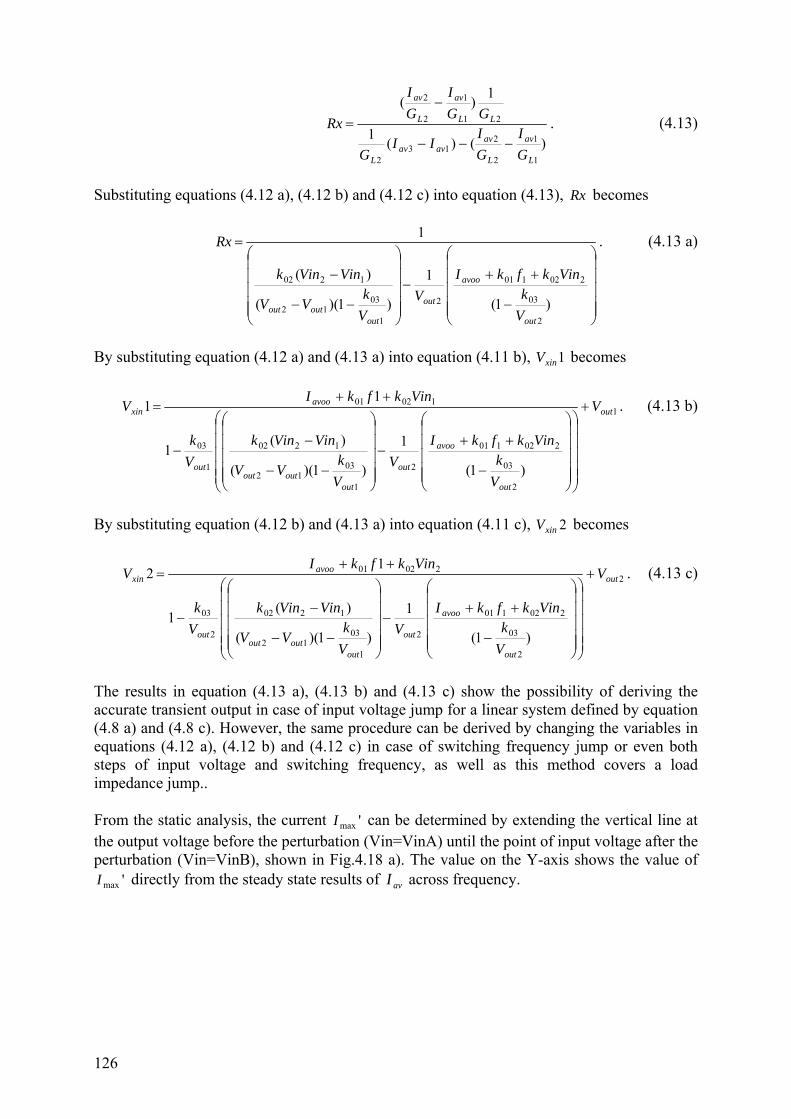
126
)()(1
1)(
1
1
2
213
2
21
1
2
2
L
av
L
avavav
L
LL
av
L
av
GI
GI
IIG
GGI
GI
Rx−−−
−= . (4.13)
Substituting equations (4.12 a), (4.12 b) and (4.12 c) into equation (4.13), Rx becomes
⎟⎟⎟⎟⎟
⎠
⎞
⎜⎜⎜⎜⎜
⎝
⎛
−
++−
⎟⎟⎟⎟⎟
⎠
⎞
⎜⎜⎜⎜⎜
⎝
⎛
−−
−
=
)1(
1
)1)((
)(
1
2
03
202101
2
1
0312
1202
out
avoo
out
outoutout V
kVinkfkI
VVk
VV
VinVink
Rx . (4.13 a)
By substituting equation (4.12 a) and (4.13 a) into equation (4.11 b), 1xinV becomes
1
2
03
202101
2
1
0312
1202
1
03
10201
)1(
1
)1)((
)(1
11 out
out
avoo
out
outoutout
out
avooxin V
Vk
VinkfkIV
Vk
VV
VinVinkVk
VinkfkIV +
⎟⎟⎟⎟⎟
⎠
⎞
⎜⎜⎜⎜⎜
⎝
⎛
⎟⎟⎟⎟⎟
⎠
⎞
⎜⎜⎜⎜⎜
⎝
⎛
−
++−
⎟⎟⎟⎟⎟
⎠
⎞
⎜⎜⎜⎜⎜
⎝
⎛
−−
−−
++= . (4.13 b)
By substituting equation (4.12 b) and (4.13 a) into equation (4.11 c), 2xinV becomes
2
2
03
202101
2
1
0312
1202
2
03
20201
)1(
1
)1)((
)(1
12 out
out
avoo
out
outoutout
out
avooxin V
Vk
VinkfkIV
Vk
VV
VinVinkVk
VinkfkIV +
⎟⎟⎟⎟⎟
⎠
⎞
⎜⎜⎜⎜⎜
⎝
⎛
⎟⎟⎟⎟⎟
⎠
⎞
⎜⎜⎜⎜⎜
⎝
⎛
−
++−
⎟⎟⎟⎟⎟
⎠
⎞
⎜⎜⎜⎜⎜
⎝
⎛
−−
−−
++= . (4.13 c)
The results in equation (4.13 a), (4.13 b) and (4.13 c) show the possibility of deriving the accurate transient output in case of input voltage jump for a linear system defined by equation (4.8 a) and (4.8 c). However, the same procedure can be derived by changing the variables in equations (4.12 a), (4.12 b) and (4.12 c) in case of switching frequency jump or even both steps of input voltage and switching frequency, as well as this method covers a load impedance jump.. From the static analysis, the current 'maxI can be determined by extending the vertical line at the output voltage before the perturbation (Vin=VinA) until the point of input voltage after the perturbation (Vin=VinB), shown in Fig.4.18 a). The value on the Y-axis shows the value of
'maxI directly from the steady state results of avI across frequency.
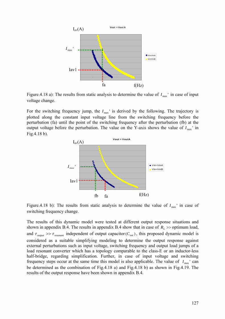
127
Figure.4.18 a): The results from static analysis to determine the value of 'maxI in case of input voltage change. For the switching frequency jump, the 'maxI is derived by the following. The trajectory is plotted along the constant input voltage line from the switching frequency before the perturbation (fa) until the point of the switching frequency after the perturbation (fb) at the output voltage before the perturbation. The value on the Y-axis shows the value of 'maxI in Fig.4.18 b).
Figure.4.18 b): The results from static analysis to determine the value of 'maxI in case of switching frequency change. The results of this dynamic model were tested at different output response situations and shown in appendix B.4. The results in appendix B.4 show that in case of >>LR optimum load, and resonantoutput ττ >> independent of output capacitor )( outC , this proposed dynamic model is considered as a suitable simplifying modeling to determine the output response against external perturbations such as input voltage, switching frequency and output load jumps of a load resonant converter which has a topology comparable to the class-E or an inductor-less half-bridge, regarding simplification. Further, in case of input voltage and switching frequency steps occur at the same time this model is also applicable. The value of 'maxI can be determined as the combination of Fig.4.18 a) and Fig.4.18 b) as shown in Fig.4.19. The results of the output response have been shown in appendix B.4.
fa
Vout = Vout A
Vin=VinA
Vin=VinB
f(Hz)
Iav(A)
fa
'maxI
Iav1
Vout = VoutA
Vin=VinA
Vin=VinB
f(Hz)
Iav(A)
'maxI
fb fa
Iav1

128
Figure 4.19: The results from static analysis to determine the value of 'maxI in case of switching frequency and input voltage change. It can be concluded that weakly non-linear output current behavior across frequency and across voltage ratio between input and output respectively, allows for a first order dynamic model at open loop response. To obtain sufficient linearity, the adiabatic switching condition (ZVS or ZCS) has to be maintained during dynamical transient response. Further, this model can be implemented by accessing a look-up table of the average output current of a load resonant converter across frequency as well as across input and output voltage. 4.4 Closed Loop Control Modeling of Load Resonant Converters (Small signal model) In order to design an optimum closed loop control of a power converter to achieve the criteria of load regulation, line regulation, stability, response time etc., it is important to know the response of a converter to variations at input and output, as well as to variation of the control signals in the environment of any operating point. Various equivalent circuit models have been proposed as closed loop models of load resonant converters. The use of small signal equivalent circuits has been introduced to investigate the dynamic behavior of load resonant converters [Wit 91] [Tse 97] [Gu 89] [Oli 05] [For 92]. The method of decomposition was presented for class-E topology by Bisogno [Bis 05], but previously introduced as usual model. In this work, the further development of dynamic closed loop model focused on class-E topology is based on this decomposition method [Bis 05]. As explained in the chapter 4.2, the feed back closed loop control was implemented at the low frequency part shown in Fig.4.20 [Bis 05]. Figure.4.20: Class-E converter feed back model of low frequency part [Bis 05].
fa
Vout = VoutA
Vin=VinA
Vin=VinB
f(Hz)
Iav(A)
'maxI
fb
Iav1
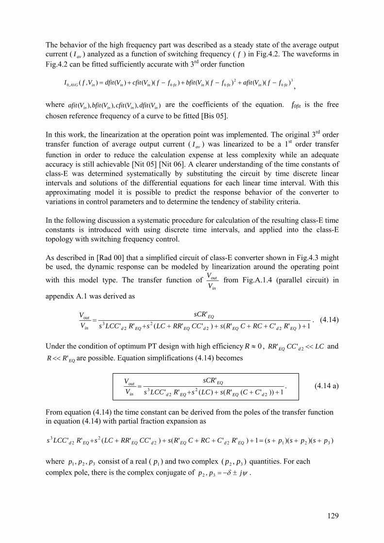
129
The behavior of the high frequency part was described as a steady state of the average output current ( avI ) analyzed as a function of switching frequency ( f ) in Fig.4.2. The waveforms in Fig.4.2 can be fitted sufficiently accurate with 3rd order function
3
02
00,0 ))(())(())(()(),( fitinfitinfitinininAVG ffVafitffVbfitffVcfitVdfitVfI −+−+−+= ,
where )(),(),(),( inininin VdfitVcfitVbfitVafit are the coefficients of the equation. f0fit is the free chosen reference frequency of a curve to be fitted [Bis 05]. In this work, the linearization at the operation point was implemented. The original 3rd order transfer function of average output current ( avI ) was linearized to be a 1st order transfer function in order to reduce the calculation expense at less complexity while an adequate accuracy is still achievable [Nit 05] [Nit 06]. A clearer understanding of the time constants of class-E was determined systematically by substituting the circuit by time discrete linear intervals and solutions of the differential equations for each linear time interval. With this approximating model it is possible to predict the response behavior of the converter to variations in control parameters and to determine the tendency of stability criteria. In the following discussion a systematic procedure for calculation of the resulting class-E time constants is introduced with using discrete time intervals, and applied into the class-E topology with switching frequency control. As described in [Rad 00] that a simplified circuit of class-E converter shown in Fig.4.3 might be used, the dynamic response can be modeled by linearization around the operating point
with this model type. The transfer function of in
out
VV from Fig.A.1.4 (parallel circuit) in
appendix A.1 was derived as
1)'''()''(''
'
222
23 ++++++
=EQdEQdEQEQd
EQ
in
out
RCRCCRsCCRRLCsRLCCs
sCRVV . (4.14)
Under the condition of optimum PT design with high efficiency 0≈R , LCCCRR dEQ <<2'' and
EQRR '<< are possible. Equation simplifications (4.14) becomes
1))'('()(''
'
22
23 ++++
=dEQEQd
EQ
in
out
CCRsLCsRLCCs
sCRVV . (4.14 a)
From equation (4.14) the time constant can be derived from the poles of the transfer function in equation (4.14) with partial fraction expansion as
))()((1)'''()''('' 321222
23 pspspsRCRCCRsCCRRLCsRLCCs EQdEQdEQEQd +++=++++++
where 321 ,, ppp consist of a real ( 1p ) and two complex ),( 32 pp quantities. For each complex pole, there is the complex conjugate of ψδ jpp ±−=32 , .
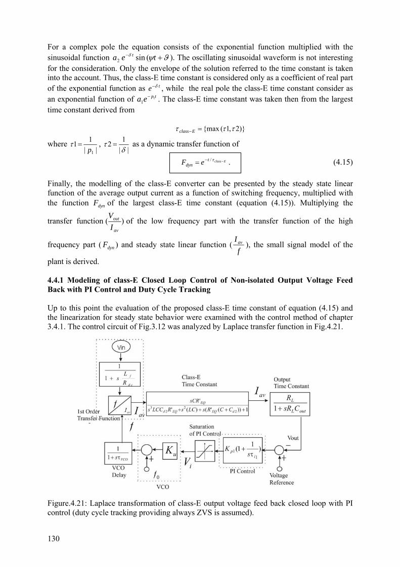
130
For a complex pole the equation consists of the exponential function multiplied with the sinusoidal function ϑψδ +− tea t (sin2 ). The oscillating sinusoidal waveform is not interesting for the consideration. Only the envelope of the solution referred to the time constant is taken into the account. Thus, the class-E time constant is considered only as a coefficient of real part of the exponential function as te δ− , while the real pole the class-E time constant consider as an exponential function of tpea 1
1− . The class-E time constant was taken then from the largest
time constant derived from )2,1(max τττ =−Eclass
where ||
111p
=τ , ||
12δ
τ = as a dynamic transfer function of
Eclasstdyn eF −−= τ/ . (4.15)
Finally, the modelling of the class-E converter can be presented by the steady state linear function of the average output current as a function of switching frequency, multiplied with the function dynF of the largest class-E time constant (equation (4.15)). Multiplying the
transfer function )(av
out
IV
of the low frequency part with the transfer function of the high
frequency part ( dynF ) and steady state linear function (f
I av ), the small signal model of the
plant is derived. 4.4.1 Modeling of class-E Closed Loop Control of Non-isolated Output Voltage Feed Back with PI Control and Duty Cycle Tracking Up to this point the evaluation of the proposed class-E time constant of equation (4.15) and the linearization for steady state behavior were examined with the control method of chapter 3.4.1. The control circuit of Fig.3.12 was analyzed by Laplace transfer function in Fig.4.21. Figure.4.21: Laplace transformation of class-E output voltage feed back closed loop with PI control (duty cycle tracking providing always ZVS is assumed).

131
The derived output current Iav, depending on input voltage and switching frequency, is multiplied with the function dynF class-E time constant derived from equation (4.15) to be avI ' .
avI ' is transferred to an output voltage via the transfer function of output capacitor ( outC )
connected in parallel with the output load LR( ) to beoutL
L
CsRR
+1. The output voltage was
compared with the reference value to produce an error signal fed into the PI control circuit. The output signal from the PI controller was supplied to the transfer function of the VCO via the limitation function of saturation switching frequency range. The time constant of the integration part of the PI control (τi) has to be designed properly. If τi is too small, it will lead to an instability of the regulation system in case that Cout is chosen too small. On the other hand, if τi is chosen to big, the regulation will not be accurate enough to provide a steady state transient output voltage response to be zero. From Fig.3.13 the PI control parameters are defined
i
iP R
RK 1= ,
RiCiK I
1= , iii CR 1=τ .
The linear static transfer function of the class-E was presented as a 1st order transfer function in Fig.4.21 with a linear equation
0avfav IfkI += . (4.16)
The input time constant of
dc
f
RL
s+1
1 was assumed to be small due to a large value of 3A and
was neglected in the consideration being always around twenty times smaller than the largest class-E time constant in equation (4.15). This assumption will be used also for the modelling in the further chapter. The factor fk defines the linearized negative gradient of the average output current with frequency causing depending on different input voltage . avoI is a theoretical offset at the Y axis. “class-E time constant” defines an adequate function for the time constant of the class-E transient behavior derived from equation 4.14 a) but reducible to the expression of equation (4.15). The transfer function of “output time constant” was derived from the output capacitor Cout and the load resistor RL. The transfer function of the used PI control is shown in “PI control”. The limitation of the linear range of the control output value is defined by “Saturation of PI control”. “VCO delay” defines a delay time of the used VCO. The transfer function of the used VCO provides a linear falling curve of the switching frequency with the integrator voltage (Vi) including the offset frequency ( )0f as iuVKff += 0 . To investigate the purposed dynamic model based on linearization, the Laplace transformation in Fig.4.21 was transferred into the time domain and tested as example for an output load jump with a constant input voltage. Assuming, that the output load was changed from 1.2 kΩ to 44 Ω at the constant input voltage of 85 V/DC, the linearization was done on the line represented at 85 V/DC of the class-E converter in Fig.4.22. According to Ohm’s law, in case of the output load is 44 Ω at 6 V/DC output voltage, the output current is 0.13 A. While, if the output load is 1.2 kΩ at 6 V/DC output voltage the output current is 5 mA. The linearization was done with these chosen two operation points for investigation of output load jump shown as a solid line in Fig.4.22.

132
Using this linearization, the original 3rd order equation of class-E transfer function is reduced to be a linear 1st order equation of 0avfav IfkI += . This linear steady state transfer function was implemented as “1st order transfer function” in Fig.4.21. Figure.4.22: Linearized steady state class-E transfer function. The compared result of the simulation between the 3rd order transfer function [Bis 05] and purposed 1st order transfer function in case of output load jump from 1.2 kΩ to 44 Ω with the same control parameter is shown in Fig.4.23. Figure.4.23: Compared output voltages using 3rd order transfer function [Bis 05] and 1st order modelling by Mathmatica simulation, for a load jump test from 1.2 kΩ to 44 Ω. It can be seen by the compared results that the transient behaviour of the 1st order is slightly faster than of the 3rd order transfer function. This can be explained by the trajectory of the linear line is faster than the nonlinear of 3rd order transfer function. However, the error is in the range of acceptable derivations. With different control parameters, the results from the linearization modeling were tested and compared with the measurement results shown in Fig.4.24 as well.
Time(s)
Vout (V)
0.001 0.002 0.003 0.004 0.005 0.006 0.007 0.008 0.009
1
2
3
4
5
6
7
80.001 0.002 0.003 0.004 0.005 0.006 0.007 0.008 0.009
Vo Vout (V)
Time(s) 0.001 0.002 0.003 0.004 0.005 0.006 0.007 0.008 Time(s)
7
6
5
4
3
2
1
f(Hz)
Iav(A) Vin(85,120,170,248,325,353 V/DC)
160k 165k 170k 175k
0.6 0.5 0.4 0.3 0.2 0.1
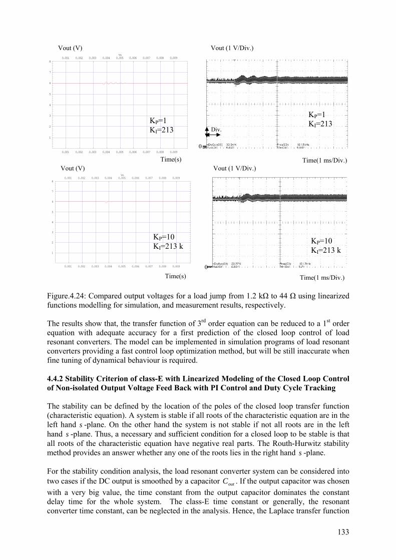
133
Figure.4.24: Compared output voltages for a load jump from 1.2 kΩ to 44 Ω using linearized functions modelling for simulation, and measurement results, respectively. The results show that, the transfer function of 3rd order equation can be reduced to a 1st order equation with adequate accuracy for a first prediction of the closed loop control of load resonant converters. The model can be implemented in simulation programs of load resonant converters providing a fast control loop optimization method, but will be still inaccurate when fine tuning of dynamical behaviour is required. 4.4.2 Stability Criterion of class-E with Linearized Modeling of the Closed Loop Control of Non-isolated Output Voltage Feed Back with PI Control and Duty Cycle Tracking The stability can be defined by the location of the poles of the closed loop transfer function (characteristic equation). A system is stable if all roots of the characteristic equation are in the left hand s -plane. On the other hand the system is not stable if not all roots are in the left hand s -plane. Thus, a necessary and sufficient condition for a closed loop to be stable is that all roots of the characteristic equation have negative real parts. The Routh-Hurwitz stability method provides an answer whether any one of the roots lies in the right hand s -plane. For the stability condition analysis, the load resonant converter system can be considered into two cases if the DC output is smoothed by a capacitor outC . If the output capacitor was chosen with a very big value, the time constant from the output capacitor dominates the constant delay time for the whole system. The class-E time constant or generally, the resonant converter time constant, can be neglected in the analysis. Hence, the Laplace transfer function
Vout (V)
Time(1 ms/Div.) Time(s)
KP=1 KI=213
0.001 0.002 0.003 0.004 0.005 0.006 0.007 0.008 0.009
1
2
3
4
5
6
7
80.001 0.002 0.003 0.004 0.005 0.006 0.007 0.008 0.009
Vo
Vout (1 V/Div.)
KP=1 KI=213
Vout (1 V/Div.)
Time(s) Time(1 ms/Div.)
KP=10 KI=213 k
0.001 0.002 0.003 0.004 0.005 0.006 0.007 0.008 0.009
1
2
3
4
5
6
7
80.001 0.002 0.003 0.004 0.005 0.006 0.007 0.008 0.009
Vo
Vout (V)
KP=10 KI=213 k
Div.
0
0

134
is simplified as in Fig.4.25. The value of fK will be derived according to the different input voltage a values to be different.
Figure.4.25: Laplace transformation of class-E with closed loop control using a linear function, applied for large output time constant. The characteristic equation of linear class-E function from Fig.4.25 is expressed in equation (4.17)
.0)1()(2 =+++i
LpfuLpfuOutL
RKKKsRKKKCRs
τ (4.17)
According to the Routh-Hurwitz stability criterion method, the system was proved that all roots of the characteristic function are on the left hand s -plane. Thus, the system is always stable when Cout is considered as a big value, compared to all the other time delays of the system:
outLCR >> Eclass−τ (4.17 a). When the output capacitor (Cout) is designed to be a small value so that equation (4.17 a) is not fulfilled, the class-E time constant or generally, the resonant converter time constant plays a role in the system and has to be considered. For this case, the Laplace transformation is considered as in Fig.4.26.
Figure.4.26: Laplace transformation of class-E with closed loop control using a linear function, applied for small output time constant. The characteristic equation of the linear class-E function from Fig.4.26 is expressed in equation (4.18)
0432
23
14
0 =++++ bsbsbsbsb (4.18) while
EQdoutL RLCCCRb '' 20 =

135
LCCRRLCCb outLEQd += '' 21 LCCCRCRb dEQoutL ++= )'(' 22
)'(' 2'
3 dEQLpEQfuoutL CCRRkCRKKCRb +++= ./'4 ifuEQpL KKCRkRb τ=
The characteristic equation was solved with the Routh-Hurwitz stability criterion method. The result from the calculation shows that the system will be always stable if the conditions in equations (4.19) are fulfilled:
;0;0;0;0 4310 >>>> bbbb
;01
30215 >
−=
bbbbb
b (4.19)
05
41356 >
−=
bbbbb
b .
The result of the stability condition from equation (4.19) was proved to be in good agreement with the real application (deviation of 10..20% compared to measurements). It can be observed that the 1st order linear transfer function provides sufficient stability proof potential at differential parameters and operation ranges. 4.4.3 Modeling of class-E Converter for PT with Auxiliary Tap In this chapter the modeling of a PT with auxiliary tap is introduced referring to the circuit diagram of Fig.3.16 a). The steady state transfer function of the class-E converter with the tapped PT between output average current ( avI ) and the switching driving frequency ( f ) is shown in Fig.4.27 a), derived by the same procedure as of the PT without auxiliary tap. The transfer function of the voltage amplitude at the auxiliary tap ( tapV ) and the switching frequency ( f ) was calculated as following. The motion current ( LI ) from a primary side of the PT is transferred by the transformer ratio Nt to a secondary side considered as ( 2LI ). Then, the sine wave output voltage across aR (Vtap ) was determined from the equation
)(2 tI L = )()(3 t
RVtap
dttdVtapC
ad + . (4.20)
The amplitudes of the sine wave at the auxiliary tap (Vtap ) from equation (4.20) were plotted as a transfer function versus switching driving frequency, shown in Fig.4.27 b).
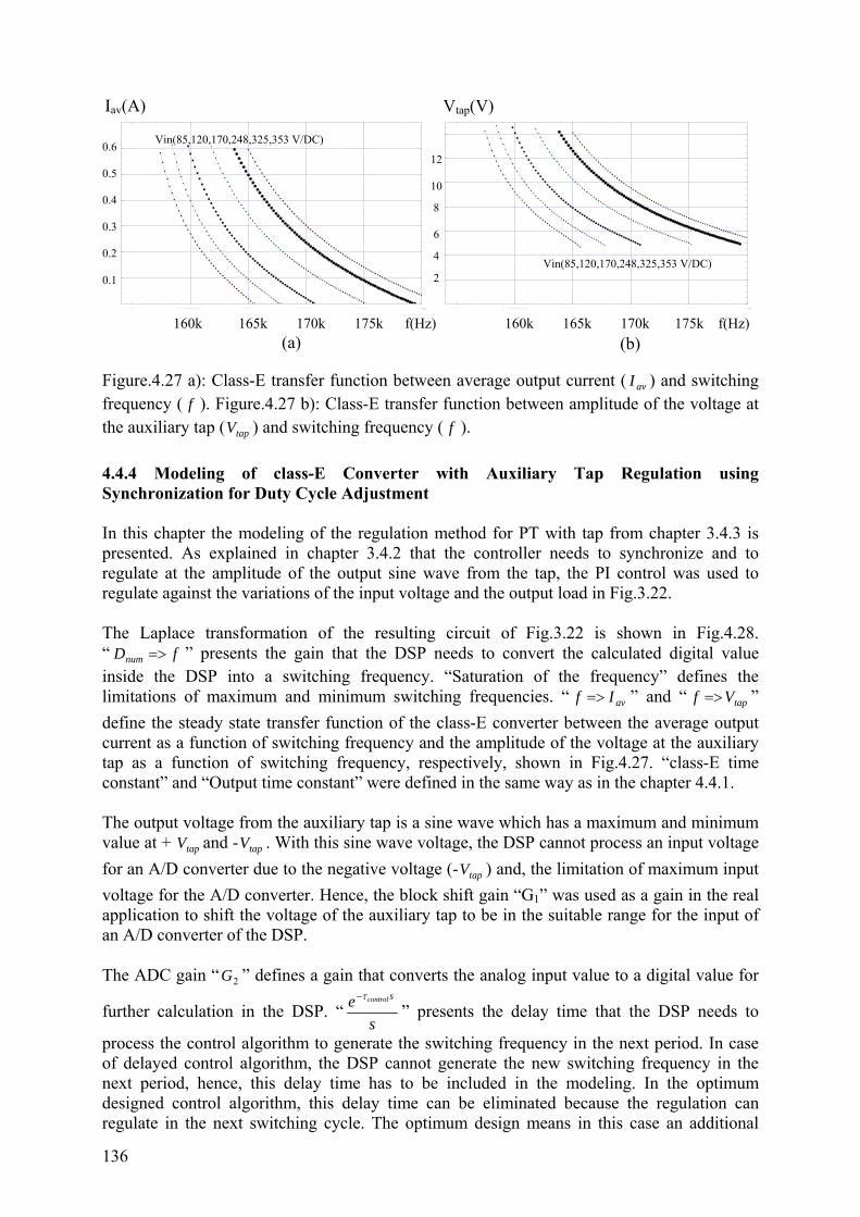
136
Figure.4.27 a): Class-E transfer function between average output current ( avI ) and switching frequency ( f ). Figure.4.27 b): Class-E transfer function between amplitude of the voltage at the auxiliary tap ( tapV ) and switching frequency ( f ). 4.4.4 Modeling of class-E Converter with Auxiliary Tap Regulation using Synchronization for Duty Cycle Adjustment In this chapter the modeling of the regulation method for PT with tap from chapter 3.4.3 is presented. As explained in chapter 3.4.2 that the controller needs to synchronize and to regulate at the amplitude of the output sine wave from the tap, the PI control was used to regulate against the variations of the input voltage and the output load in Fig.3.22. The Laplace transformation of the resulting circuit of Fig.3.22 is shown in Fig.4.28. “ fDnum => ” presents the gain that the DSP needs to convert the calculated digital value inside the DSP into a switching frequency. “Saturation of the frequency” defines the limitations of maximum and minimum switching frequencies. “ avIf => ” and “ tapVf => ” define the steady state transfer function of the class-E converter between the average output current as a function of switching frequency and the amplitude of the voltage at the auxiliary tap as a function of switching frequency, respectively, shown in Fig.4.27. “class-E time constant” and “Output time constant” were defined in the same way as in the chapter 4.4.1. The output voltage from the auxiliary tap is a sine wave which has a maximum and minimum value at + tapV and - tapV . With this sine wave voltage, the DSP cannot process an input voltage for an A/D converter due to the negative voltage (- tapV ) and, the limitation of maximum input voltage for the A/D converter. Hence, the block shift gain “G1” was used as a gain in the real application to shift the voltage of the auxiliary tap to be in the suitable range for the input of an A/D converter of the DSP. The ADC gain “ 2G ” defines a gain that converts the analog input value to a digital value for
further calculation in the DSP. “s
e scontrolτ−
” presents the delay time that the DSP needs to
process the control algorithm to generate the switching frequency in the next period. In case of delayed control algorithm, the DSP cannot generate the new switching frequency in the next period, hence, this delay time has to be included in the modeling. In the optimum designed control algorithm, this delay time can be eliminated because the regulation can regulate in the next switching cycle. The optimum design means in this case an additional
155000 160000 165000 170000 175000 180000
0.1
0.2
0.3
0.4
0.5
0.6
io x f
155000 160000 165000 170000 175000 180000
2
4
6
8
10
12
14
Vt x f
f(Hz)
Iav(A)
Vin(85,120,170,248,325,353 V/DC)
f(Hz)
Vtap(V)
Vin(85,120,170,248,325,353 V/DC) 0.1 0.2
160000 165000 160000 165000
2
4
160k 165k 170k 175k f(Hz) 160k 165k 170k 175k f(Hz)
0.6 0.5 0.4 0.3 0.2 0.1
12 10
8 6
4
2
(a) (b)

137
gain reduction in case of non-filtered defection of tapV , to avoid instability due to ripple amplification. The corner frequency has to be chosen small enough, which can be done by an additional time delay of the controller at higher frequencies or by delayed frequency generation over several periods described before. Figure.4.28: The class-E modeling of auxiliary tap regulation with synchronization for duty cycle adjustment. The derived average output current ( avI ) is multiplied with the function of the class-E time constant and the output time constant. The amplitude of the voltage at the auxiliary tap ( tapV ) is multiplied with the function of the class-E time constant. The derived voltage amplitude at the tap after considering the time constant ( tapV ' ) is shifted with the shift gain and fed into the DSP via ADC gain into the PI control. The output from the PI controller was used to produce the suitable switching frequency to regulate at the amplitude of the output tap voltage. To investigate the modeling in Fig.4.28, a test was implemented by the input voltage jump at a constant output load. The inverse Laplace transformation of Fig.4.28 was simulated in the time domain. Assuming that the input voltage was changed form 250 V/DC to 353 V/DC at a 100 Ω output load, the linearization was implemented at the lines of input voltage 250 V/DC and 353 V/DC. At an output load of 100 Ω with 6 V/DC at the output, the average output current is 0.06 A. The linearization was made at these points and the linear line was drawn to linearize the original 3rd order transfer function, shown in Fig.4.29.
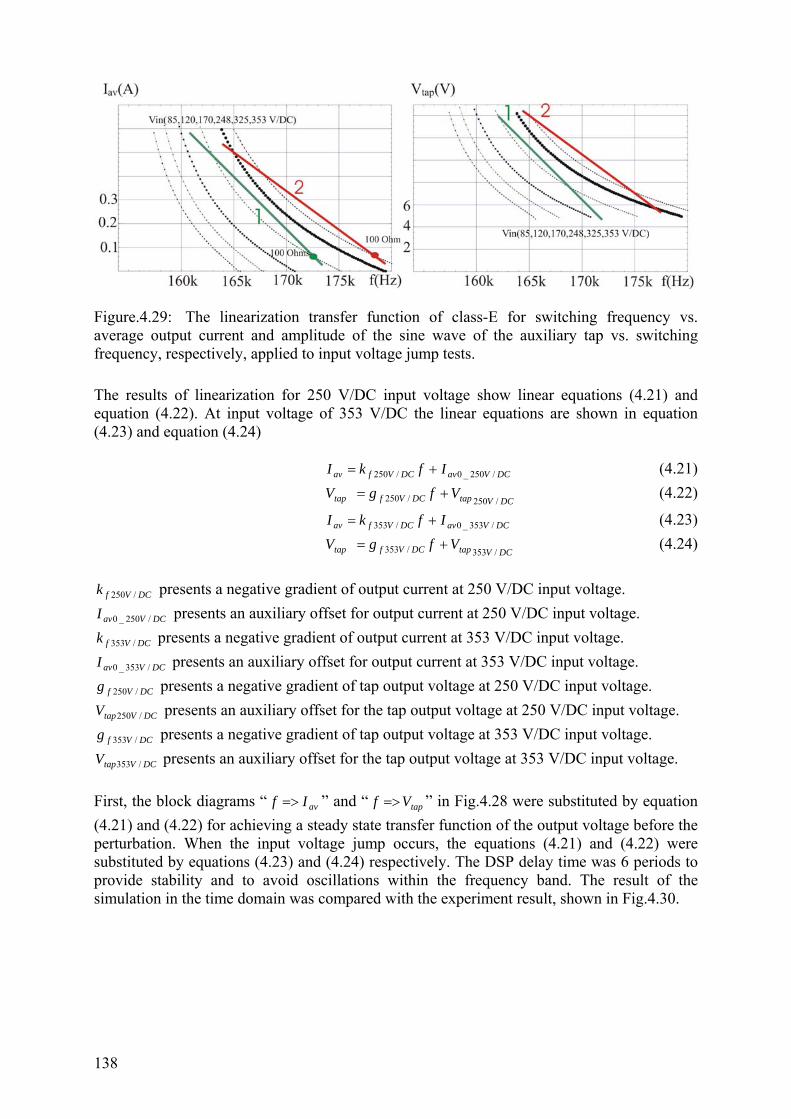
138
Figure.4.29: The linearization transfer function of class-E for switching frequency vs. average output current and amplitude of the sine wave of the auxiliary tap vs. switching frequency, respectively, applied to input voltage jump tests.
The results of linearization for 250 V/DC input voltage show linear equations (4.21) and equation (4.22). At input voltage of 353 V/DC the linear equations are shown in equation (4.23) and equation (4.24)
DCVavDCVfav IfkI /250_0/250 += (4.21)
DCVtapDCVftap VfgV/250/250 += (4.22)
DCVavDCVfav IfkI /353_0/353 += (4.23)
DCVtapDCVftap VfgV/353/353 += (4.24)
DCVfk /250 presents a negative gradient of output current at 250 V/DC input voltage.
DCVavI /250_0 presents an auxiliary offset for output current at 250 V/DC input voltage.
DCVfk /353 presents a negative gradient of output current at 353 V/DC input voltage.
DCVavI /353_0 presents an auxiliary offset for output current at 353 V/DC input voltage.
DCVfg /250 presents a negative gradient of tap output voltage at 250 V/DC input voltage.
DCVtapV /250 presents an auxiliary offset for the tap output voltage at 250 V/DC input voltage.
DCVfg /353 presents a negative gradient of tap output voltage at 353 V/DC input voltage.
DCVtapV /353 presents an auxiliary offset for the tap output voltage at 353 V/DC input voltage. First, the block diagrams “ avIf => ” and “ tapVf => ” in Fig.4.28 were substituted by equation (4.21) and (4.22) for achieving a steady state transfer function of the output voltage before the perturbation. When the input voltage jump occurs, the equations (4.21) and (4.22) were substituted by equations (4.23) and (4.24) respectively. The DSP delay time was 6 periods to provide stability and to avoid oscillations within the frequency band. The result of the simulation in the time domain was compared with the experiment result, shown in Fig.4.30.

139
Figure.4.30: Comparison of output voltage for an input voltage jump from 250 V/DC to 353 V/DC at 100 Ω output load between measurement and simulation results, respectively. The control delay time from the DSP can be eliminated to regulate cycle by cycle if the amplitude of the tap voltage is filtered capacitively to have low noise. The results in Fig.4.31 show the regulation done cycle by cycle. The example was implemented with an input voltage jump from 120 V/DC to 353 V/DC at 100 Ω output load and 220 uF output capacitor. The results show good agreement between the first order linearized model and the reality, except that the amplitude of the tap voltage contains further small oscillations being negligible. In sprite of noise from the probe of the measurement equipment in Fig.4.31 c), the envelope of the measurement curves is satisfying compared to the simulated envelopes.
0 0.002 0.004 0.006 0.008 0.01
2
4
6
8
10Vo
Vout (V)
Time (2 ms/Div.) Time (s)
Div. 0
Vout (1V/Div.)

140
Figure.4.31 a): The output voltage. Figure.4.31 b): The amplitude of the auxiliary tap voltage.
Figure.4.31 c): The output voltage (upper trace) with the scale in the Y-axis of (2 V/Div.), the tap output voltage (lower trace) with the scale in the Y-axis of (1 V/Div.) at auxiliary tap regulation.
Time (100 us/Div.)
V (V)
Div.
Vout (2 V/Div.)
Vtap (1 V/Div.)
0
0
0 0.0001 0.0002 0.0003 0.0004 0.0005
1
2
3
4
5Vtap
Vout (V) Vtap(V)
Time (s) Time (s)0 0.0001 0.0002 0.0003 0.0004 0.0005
6.02
6.04
6.06
6.08
Vo
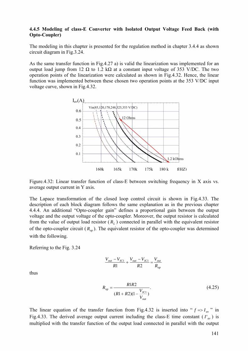
141
4.4.5 Modeling of class-E Converter with Isolated Output Voltage Feed Back (with Opto-Coupler) The modeling in this chapter is presented for the regulation method in chapter 3.4.4 as shown circuit diagram in Fig.3.24. As the same transfer function in Fig.4.27 a) is valid the linearization was implemented for an output load jump from 12 Ω to 1.2 kΩ at a constant input voltage of 353 V/DC. The two operation points of the linearization were calculated as shown in Fig.4.32. Hence, the linear function was implemented between these chosen two operation points at the 353 V/DC input voltage curve, shown in Fig.4.32.
Figure.4.32: Linear transfer function of class-E between switching frequency in X axis vs. average output current in Y axis. The Lapace transformation of the closed loop control circuit is shown in Fig.4.33. The description of each block diagram follows the same explanation as in the previous chapter 4.4.4. An additional “Opto-coupler gain” defines a proportional gain between the output voltage and the output voltage of the opto-coupler. Moreover, the output resistor is calculated from the value of output load resistor ( LR ) connected in parallel with the equivalent resistor of the opto-coupler circuit ( opR ). The equivalent resistor of the opto-coupler was determined with the following. Referring to the Fig. 3.24
op
outICoutICout
RV
RVV
RVV
=−
+−
2111
thus
.)1)(21(
211
out
ICop
VV
RR
RRR−+
= (4.25)
The linear equation of the transfer function from Fig.4.32 is inserted into “ avIf => ” in Fig.4.33. The derived average output current including the class-E time constant ( avI ' ) is multiplied with the transfer function of the output load connected in parallel with the output
f(Hz)
Iav(A) Vin(85,120,170,248,325,353 V/DC)
160000 165000
0.1
0.2
160k 165k 170k 175k 180 k f(HZ)
0.6 0.5 0.4 0.3 0.2 0.1
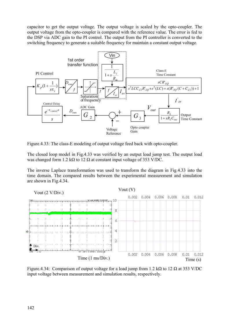
142
0.002 0.004 0.006 0.008 0.01 0.012
2
4
6
8
100.002 0.004 0.006 0.008 0.01 0.012
Vo
capacitor to get the output voltage. The output voltage is scaled by the opto-coupler. The output voltage from the opto-coupler is compared with the reference value. The error is fed to the DSP via ADC gain to the PI control. The output from the PI controller is converted to the switching frequency to generate a suitable frequency for maintain a constant output voltage. Figure.4.33: The class-E modeling of output voltage feed back with opto-coupler. The closed loop model in Fig.4.33 was verified by an output load jump test. The output load was changed form 1.2 kΩ to 12 Ω at constant input voltage of 353 V/DC. The inverse Laplace transformation was used to transform the diagram in Fig.4.33 into the time domain. The compared results between the experimental measurement and simulation are shown in Fig.4.34.
Figure.4.34: Comparison of output voltage for a load jump from 1.2 kΩ to 12 Ω at 353 V/DC input voltage between measurement and simulation results, respectively.
Time (s)Time (1 ms/Div.)
Vout (2 V/Div.) Vout (V)
Div.
0
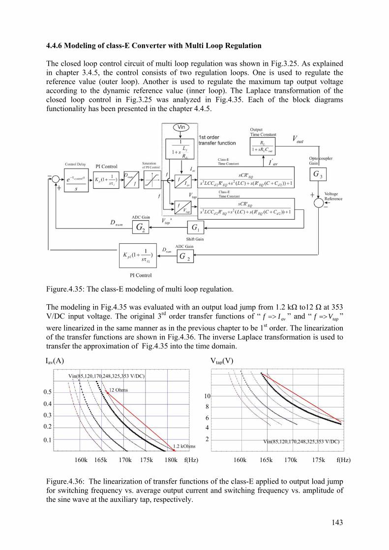
143
4.4.6 Modeling of class-E Converter with Multi Loop Regulation The closed loop control circuit of multi loop regulation was shown in Fig.3.25. As explained in chapter 3.4.5, the control consists of two regulation loops. One is used to regulate the reference value (outer loop). Another is used to regulate the maximum tap output voltage according to the dynamic reference value (inner loop). The Laplace transformation of the closed loop control in Fig.3.25 was analyzed in Fig.4.35. Each of the block diagrams functionality has been presented in the chapter 4.4.5. Figure.4.35: The class-E modeling of multi loop regulation. The modeling in Fig.4.35 was evaluated with an output load jump from 1.2 kΩ to12 Ω at 353 V/DC input voltage. The original 3rd order transfer functions of “ avIf => ” and “ tapVf => ” were linearized in the same manner as in the previous chapter to be 1st order. The linearization of the transfer functions are shown in Fig.4.36. The inverse Laplace transformation is used to transfer the approximation of Fig.4.35 into the time domain.
Figure.4.36: The linearization of transfer functions of the class-E applied to output load jump for switching frequency vs. average output current and switching frequency vs. amplitude of the sine wave at the auxiliary tap, respectively.
Vin(85,120,170,248,325,353 V/DC)
f(Hz)
Vtap(V)
f(Hz)
Iav(A)
Vin(85,120,170,248,325,353 V/DC)
160000 165000 160000 165000
0.1 0.2
2
4
160k 165k 170k 175k f(Hz) 160k 165k 170k 175k 180k f(Hz)
0.5
0.4
0.3
0.2 0.1
10
8
6
4
2

144
The comparison between the experimental measurement and the simulation of the output load jump is shown in Fig.4.37. Figure.4.37: Comparison of output voltage for a load jump from 1.2 kΩ to 12 Ω at 353 V/DC input voltage between measurement and simulation. 4.4.7 Modeling of class-E Converter with Isolated PI Control Regulation plus Lag Circuit This model was developed for PI control regulation plus lag circuit of chapter 3.4.6 shown in circuit diagram Fig.3.26. The Laplace modeling for this regulation method is analyzed in Fig.4.38 a). The lag circuit is used to reduce the gain near to the switching frequency beyond the corner frequency of the closed loop circuit as usual for off-line power supplies, to avoid the oscillations and instability. Figure.4.38 a): The class-E modeling of PI control regulation plus lag circuit. The description of the functionality at each block refers to an application note of Infineon for off-line power supplies regarding the external control circuit [App 01]. “ fVFB => ” defines the linear equation converting the feed back voltage from the opto-coupler into a switching frequency. The block “ VDK ” presents the transfer function of the voltage divider 4R and 5R
Vout (2V/Div.)
Time (1 ms/Div.) Time (s)
Vout (V)
0.0020.0040.0060.008 0.01 0.0120.0140.0160.018
2
4
6
8
100.0020.0040.0060.008 0.01 0.0120.0140.0160.018
Vo
Div.
0
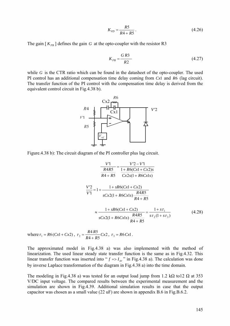
145
54
5RR
RKVD += . (4.26)
The gain [ FBK ] defines the gain G at the opto-coupler with the resistor R3
23
RRG
K FB = (4.27)
while G is the CTR ratio which can be found in the datasheet of the opto-coupler. The used PI control has an additional compensation time delay coming from 1Cx and 6R (lag circuit). The transfer function of the PI control with the compensation time delay is derived from the equivalent control circuit in Fig.4.38 b). Figure.4.38 b): The circuit diagram of the PI controller plus lag circuit.
)161(2)21(61
1'2'
5454
1'
sCxRsCxsCxCxR
VV
RRRR
V
+++
−=
+
5454)161(2
)21(6111'2'
RRRRsCxRsCx
CxCxsRVV
++
+++=
)1(
1
5454)161(2
)21(61
32
1
τττss
s
RRRRsCxRsCx
CxCxsR+
+=
++
++≈ (4.28)
where )21(61 CxCxR +=τ , 254
542 Cx
RRRR+
=τ , 163 CxR=τ .
The approximated model in Fig.4.38 a) was also implemented with the method of linearization. The used linear steady state transfer function is the same as in Fig.4.32. This linear transfer function was inserted into “ avIf => ” in Fig.4.38 a). The calculation was done by inverse Laplace transformation of the diagram in Fig.4.38 a) into the time domain. The modeling in Fig.4.38 a) was tested for an output load jump from 1.2 kΩ to12 Ω at 353 V/DC input voltage. The compared results between the experimental measurement and the simulation are shown in Fig.4.39. Additional simulation results in case that the output capacitor was chosen as a small value (22 uF) are shown in appendix B.6 in Fig.B.6.2.
2'V

146
Figure.4.39: Comparison between measurement and simulation results of output voltage for a load jump from 1.2 kΩ to 12 Ω at 353 V/DC input voltage. Until this point, it can be concluded from the results in chapter 4.4 that the closed loop modeling of class-E converter, considering DC output voltage, can be simplified by linearization of the steady state transfer function of average output current defined as a function of switching frequency and input voltage, in series with the first order largest class-E
time constant and in series with the transfer function of )(av
out
IV of the low frequency output
part (output capacitor connected in parallel with the output load). With the simplification to considering only the first order largest class-E time constant, the modeling was proved to provide satisfying accuracy. The value of output capacitor ( outC ) was empirically proved to be related to the time constant of the low frequency part ( outLCR , where =LR nominal load) being larger than twenty times of the largest class-E time constant at nominal load. This model provides an adequate accuracy in order to design and to predict the output response in the closed loop control by using the largest class-E time constant. Compared to the work of Oliver [Oli 05], where the connection between the high frequency part and the low frequency part is linked by the AC signal, the additional consideration of conduction angle of the output bridge is there required. Moreover, the Fourier transformation is required for obtaining the first harmonic of the input signal at the low frequency part for further deriving the output voltage signal. The proposed method provides a generalized modeling approach applicable for all resonant converter topologies, especially when the first harmonic as a fundamental frequency of the load resonant circuit cannot be found easily as it is possible in symmetric topologies like half-bridge or full-bridge. The example of class-E topology for the proposed closed loop dynamic modeling approach can be extended to analyze other load resonant converters. The comparing evaluation of the grade of non linearity of a load resonant converter has to be done in future works to derive prediction of accuracy of any topology comparing to the here well investigated class-E topology. However, the feasibility of linearization of other topologies as half-bridge, full-bridge, push pull or other class-E circuit is expected to be excellent using reliable static operation ranges.
Vout (V)
Time (1 ms/Div.) Time (s)
0 0.001 0.002 0.003 0.004 0.005 0.006
5.5
6
6.5
7
7.5
8Vout
Vout (V)
6
5.5
5
4.5 Div.
6.5
147
4.4.8 Stability Criterion with Linearized Modeling for class-E PI Control plus Lag Circuit In this chapter, the stability analysis for the PI control regulation plus lag circuit is given as an example to investigate the stability criterion being applicable for the linear modeling of higher order feed back transfer functions compared to chapter 4.4.2, in this case extend by lag circuit. From Fig.4.38 a) the characteristic equation of this regulation method was calculated as a 5th order differential equation system of
0542
33
24
15
0 =+++++ bsbsbsbsbsb (4.29) while
320 '' τoutLEQd CRRLCCb =
33221 '''' ττ outLEQdoutLEQd CLCRRLCCCRRLCCb ++=
32322 )'(''' ττ outLdEQoutLEQd CRCCRLCCLCRRLCCb ++++=
33223 )'(')'(' ττ outLdEQouTLdEQ CRCCRCRCCRLCb +++++=
221324 /')'(' τττ ufVDFBEQLoutLdEQ KKKKGCRRCRCCRb ++++= 1/' 225 += τEQLFBVDfu CRRGKKKKb .
With the characteristic equation in equation (4.29), the further analysis for the stability condition was determined with the Routh-Hurwitz stability criterion to find the stability condition. The result shows that the stability is given, if the equations below are full filled
;0;0;0;0;0;0 543210 >>>>>> bbbbbb
;0;01
50417
1
30216 >
−=>
−=
bbbbb
bb
bbbbb
.0;08
56789
6
71368 >
−=>
−=
bbbbb
bb
bbbbb (4.30)
The result of the stability criterion shows the stability is in a good agreement with the real application. However, in the real application the stability is limited by the saturation of switching frequency. When the gain FBK is increased too large the system faces the problem that it regulates by two points operation (maximum and minimum switching frequency). Therefore, an additional boundary observation of the non linear element “saturation of frequency” has to be implemented to evaluate the feasibility of the described stability analysis. In this stability analysis the stability was discussed only in the linear operation range of PI control. The stability in the saturation area was not considered in this work. The phase margin for the stability condition in equation (4.30) was confirmed by the bode plot in appendix B.5. If the stability is guaranteed in the linear frequency range, it is nearly sure that the frequency boundaries will not cause unstable behaviour as remaining boundary oscillations, which was proved empirically. 4.5 Simplified Closed loop Modeling of Load Resonant Converters As mentioned in the previous chapters, the proposed simplified closed loop modeling of load resonant converters was developed in order to eliminate the complexity in mathematical calculation of higher order equations to derive the steady state solutions for a closed loop control modeling. The complicated higher order transfer function of an average output current

148
vs. a switching frequency was substituted by a 1st order linear function. The simplified model was utilized to investigate the closed loop output response of the controller for class-E topology. This technique is suitable under the operation condition based on the filter output capacitor )( outC is chosen to maintain the condition outputτ >> resonantτ (equation 4.2 a). Once the output capacitor )( outC is chosen large enough regarding outputτ , the time constant of the high frequency part can be neglected. The transfer function of the average output current vs. switching frequency can be presented simply by using a 1st order linear equation described in Fig.4.32. Thus, the simplified closed loop of class-E converter considering large output capacitor )( outC can be presented in Fig.4.40. Figure.4.40: Simplified dynamic model of class-E considering large output capacitor
outputτ >> resonantτ . The assumption
avofav IfkI += (4.31) will cause different parameters fk = ),,( 1int QDcVk inf and ),,( 1int QDcVII inavoavo = for different input voltage, different loaded factor 1Q , different initial duty cycle( intDc ). The model was evaluated with the control scheme of PI control regulation plus lag circuit (chapter 4.4.7). The Laplace closed loop control scheme in Fig.4.38 a) was substituted by the Laplace closed loop diagram shown in Fig.4.41. The functionality of each block diagram remains as mentioned above. The evaluation was done by an output load jump with different values of the output capacitor. The model provides a good agreement with the real measurements shown in Fig.4.42 and additionally in appendix B.6 (Fig.B.6.1). When the values of output capacitor were chosen smaller (Fig.4.43 a) and b)), the output response in case of load jump from light load to heavy load provides a smaller deviation than the opposite situation (from heavy load to light load). This phenomenon can be explained by when the time constant after the perturbation defined by the light load being larger than in case of heavy load. Thus, when the high frequency part time constant at the light load was neglected, it will provide a larger effect than neglecting the time constant of the high frequency part in case of heavy load.
Satuation of frequency
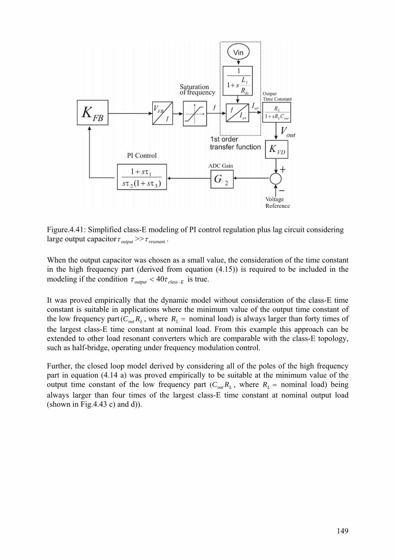
149
Figure.4.41: Simplified class-E modeling of PI control regulation plus lag circuit considering large output capacitor outputτ >> resonantτ . When the output capacitor was chosen as a small value, the consideration of the time constant in the high frequency part (derived from equation (4.15)) is required to be included in the modeling if the condition Eclassoutput −< ττ 40 is true. It was proved empirically that the dynamic model without consideration of the class-E time constant is suitable in applications where the minimum value of the output time constant of the low frequency part Lout RC( , where =LR nominal load) is always larger than forty times of the largest class-E time constant at nominal load. From this example this approach can be extended to other load resonant converters which are comparable with the class-E topology, such as half-bridge, operating under frequency modulation control. Further, the closed loop model derived by considering all of the poles of the high frequency part in equation (4.14 a) was proved empirically to be suitable at the minimum value of the output time constant of the low frequency part Lout RC( , where =LR nominal load) being always larger than four times of the largest class-E time constant at nominal output load (shown in Fig.4.43 c) and d)).
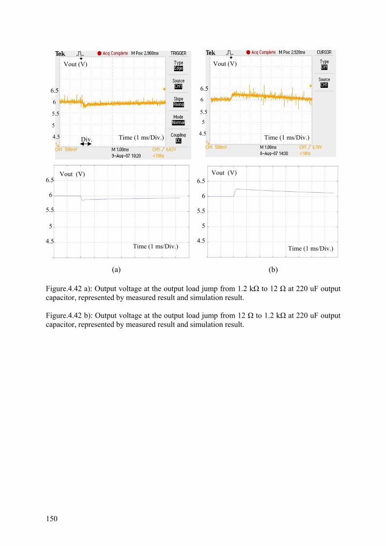
150
Figure.4.42 a): Output voltage at the output load jump from 1.2 kΩ to 12 Ω at 220 uF output capacitor, represented by measured result and simulation result. Figure.4.42 b): Output voltage at the output load jump from 12 Ω to 1.2 kΩ at 220 uF output capacitor, represented by measured result and simulation result.
Time (1 ms/Div.)
(b)
Vout (V)
Time (1 ms/Div.)
Time (1 ms/Div.)
(a)
Time (1 ms/Div.)
Vout (V)
4.5
6
5.5
5
6
5.5
5
4.5
6
5.5
5
4.5
Time (1 ms/Div.)
Div.
6.5
6.5 6.5
Vout (V) Vout (V)
6.5 6 5.5 5 4.5
6.5 6 5.5 5 4.5
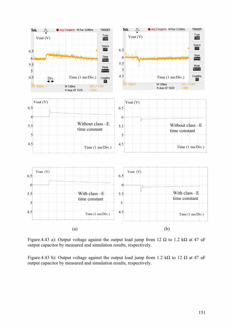
151
Figure.4.43 a): Output voltage against the output load jump from 12 Ω to 1.2 kΩ at 47 uF output capacitor by measured and simulation results, respectively. Figure.4.43 b): Output voltage against the output load jump from 1.2 kΩ to 12 Ω at 47 uF output capacitor by measured and simulation results, respectively.
Time (1 ms/Div.) Time (1 ms/Div.)
Vout (V) Vout (V)
(a) (b)
With class –E time constant
With class –E time constant
Vout (V) Vout (V)
Time (1 ms/Div.) Time (1 ms/Div.)
Vout (V) Vout (V)
Time (1 ms/Div.) Time (1 ms/Div.)
Without class –E time constant
Without class –E time constant
6.5 6 5.5 5 4.5
Div.
6.5 6 5.5 5 4.5
6.5 6 5.5 5 4.5
6.5 6 5.5 5 4.5
6.5
6
5.5
5
4.5
6.5
6
5.5
5
4.5

152
Figure.4.43 c): Output voltage against the output load jump from 12 Ω to 1.2 kΩ at 4.7 uF output capacitor by measured and simulation results, respectively. Figure.4.43 d): Output voltage against the output load jump from 1.2 kΩ to 12 Ω at 4.7 uF output capacitor by measured and simulation results, respectively.
Time (1ms/Div.) Time (1ms/Div.)
Time (1ms/Div.) Time (1ms/Div.)
Considering all of the poles in high frequency part
Considering all of the poles in high frequency part
6.5
6
5.5
5
4.54.5
5
5.5 6
6.5
Vout (V) Vout (V)
Vout (V) Vout (V)
(d) (c)
6.5 6 5.5 5 4.5
6.5 6 5.5 5 4.5

153
4.6 Approximation of Steady State Behavior with an Empirical Heuristic Method 4.6.1 Empirical Heuristic Method The following empirical heuristic method was introduced to approximate the normalized power transfer ratio of load resonant converters for the class-E topology at the optimum operation point (ZVS/ZCS) by Radecker in 2000 [Rad 00]. It was proved that the empirical heuristic method provides sufficiently accurate results in the parameter insensitive area, but larger deviations are occurring in the parameter sensitive areas. The approach assumes the input source power is divided into two parts called source forward and source backward. This complete input power is transferred into the converter configuration. At the converter configuration the power is also divided into two parts (forward two parts output) and transferred into the load. The equation of the normalized power transfer function is derived from the switch operator ( )PV defined for each converter type. For the class-E topology, PV was integrated over an approximation sine wave function of normalized switch state variable as
⎟⎟⎠
⎞⎜⎜⎝
⎛
++
=1)(2
)1)((2
2
DcCosDcCosVP ππ (4.32)
where Dc defines the turn on duty cycle at the optimum operation point (ZVS and ZCS). The load factor is given by parameter pk defined as a parameter derived from 1Q as
⎟⎟⎠
⎞⎜⎜⎝
⎛+
+=121
1121
Qk p . (4.33)
The normalized transfer power ratio is given by
⎥⎥⎦
⎤
⎢⎢⎣
⎡++−=
pPin
out
kVzzDc
VRP
222
2 214
' (4.34)
where 'R defines the output load in the series equivalent circuit (Fig.A.1.4 in appendix A.1) as RRR seq +=' , z is defined as a function of 3A as follow. When 03 =A , then z is given by
⎟⎟⎠
⎞⎜⎜⎝
⎛+== 23
411
21)0(
PVAz [Ray 04] (4.35)
and when 13 =A , then z is given by
⎟⎟⎠
⎞⎜⎜⎝
⎛+== 23
41
21
21)1(
PP VVAz [Ray 04]. (4.36)

154
4.6.2 Approximation of Steady State Behavior with Empirical Heuristic Method The validation of the heuristic method was derived at the optimum operation point (ZVS and ZCS). The parameters 1A and 2A are obtained automatically depending on the free designed parameters of 13 ,QA and Dc . In order to approximate the steady state behavior at the suboptimum operation point (ZVS, non ZCS) from the optimum operation point (ZVS and ZCS) the following assumptions have to be done. The generalized parameter z was derived by interpolation equation (4.35) and equation (4.36) corresponding to parameter 3A for the deriving of the initial point (ZVS/ZCS) as
⎟⎟⎠
⎞⎜⎜⎝
⎛++−= 2
333
41
2)1(
21)(
PP VVA
AAz . (4.37 a)
In case of the switching frequency changes, the parameter 3A is modulated according to the switching frequency (equation 3.1) thus, the parameter z in equation (4.37 a) becomes
⎟⎟⎠
⎞⎜⎜⎝
⎛++−= 2
333
41
2'
)'1(21)'(
PP VVA
AAz . (4.37 b)
The duty cycle ( Dc ) at the optimum operation point (ZVS and ZCS) in equation (4.32) and equation (4.34) was approximated by minimum turn on duty cycle (Dc_onmin from Fig.3.11) as a function of switching frequency. The linear function of the minimum turn on duty cycle (Dc_onmin) was linearized as a function of normalized switching frequency )/( nff in application of 1.1%,45,30 31 === ADcQ at 1,1/ == kff n (Fig.A.2.5 in appendix A.2)
== )(%)/min(_(%) nffonDcDc -248.76 )/( nff +293.76. (4.38) Thus, the parameter Dc in the switch operator ( )PV from equation (4.32), and the normalized power transfer ratio from equation (4.34) will be defined as a function of switching frequency by inserting equation (4.38) into equation (4.32). The equation of the switch operator defined as a function of normalized switching frequency becomes
⎟⎟⎠
⎞⎜⎜⎝
⎛+
+=
1))/min(_(2)1))/min(_((
)/( 2
2
n
nnP ffonDcCos
ffonDcCosffV
ππ
. (4.39)
The normalized power transfer ratio becomes
⎥⎥⎦
⎤
⎢⎢⎣
⎡++−=
pnPn
in
out
kffVAzAzffonDc
VRP
22
332
2 )/(21)'()'()/min(_4
'. (4.40)
From equation (4.40), the RMS output current ( outRMSI ), (Fig.A.1.4 of appendix A.1) can be calculated from

155
21
2'
2
22
332
)/(21)'()'()/min(_4 ⎟
⎟
⎠
⎞
⎜⎜
⎝
⎛
⎥⎥⎦
⎤
⎢⎢⎣
⎡++−=
RV
kffVAzAzffonDcI in
pnPnoutRMS . (4.41)
The results of approximated RMS output current ( outRMSI ) as a function of the switching frequency from equation (4.41) at the example application of 30,1.13%,45 1 === QADc (at optimum operation point) at the nominal output load ( 301 =Q ) with the input voltage of 353 V/DC compared to the exact results simulated with 1Q =30 and 1Q =600 by PSPICE are shown in Fig.4.44. Figure.4.44: The steady state results of the RMS output current vs. the normalized switching frequency at an input voltage of 353 V/DC, derived from the empirical heuristic method compared with exact solutions. It was shown in Fig.4.44 that if 1Q is large, the RMS output current ( outRMSI ) is slightly changing even if 1Q is significantly changed (comparing the exact results between 1Q =30 and
1Q =600). Thus, the RMS output current ( outRMSI ) will be approximated at the nominal output load ( 1Q =30), even, if 1Q is significantly changed (output load is significantly changed). The RMS output current ( outRMSI ) at the low frequency part can be derived by transferring from the primary side to the secondary side with the transformer transfer ratio of the circuit as shown in appendix A.1, Fig.A.1.3. In order to cover all of the load applications, the additional discussion about the 1Q factor in case of nominal load, short circuit load and light load can be done by following.
In case of nominal load, 1Q is derived by RopR
LQ
SEQ +=
)(1
1ω (Fig.A.1.4 in appendix A.1). R
defines the PT loss resistor considered to be much smaller than the load resistor and can be
neglected in this case. Thus, 30)('
2)(
111 ===
opRL
opRL
QEQSEQ
ωω at optimum operation point.
RMS output current vs. switching frequency at constant input voltage
0
0.05
0.1
0.15
0.2
0.25
0.3
0.35
0.98 1 1.02 1.04 1.06 1.08 1.1 1.12
f/fn
Iout
RM
S(A
)
Heuristic approximation at Q1=30exact result at Q1=30exact result at Q1=600
f/fn

156
In case of short circuit load, the load resistor SEQR is equal zero. The equivalent resistor of the
output bridge rectifier was taken into account and approximated assh
ddiode I
VR
2= , measured
value of mAI sh 600≈ , mVVd 300≈ , Ω≈1diodeR for 3 Watts application, where dV defines a forward voltage drop across diode. shI defines an output current at the short circuit. diodeR is transferred to the primary side with the formula derived in appendix A.1. 1Q becomes
diodeRRLQ'
11 +=
ω ( 1Q =170 at this example application) illustrated in Fig.A.1.5 in appendix A.1.
In case of light load, the output load is assumed as an open circuit (Fig.A.1.6 in appendix A.1).
The capacitor in the circuit is 2
2
''
'd
d
CCCC
C+
= . With 2'dC >> C , we obtain CC ≈' . The factor 1Q is
=1QR
L1ω = 682 (at this example application).
From these calculations, the relation between 1Q and the logarithm *
LR can be plotted as shown in Fig.4.45 a) (solid line). *
LR was assumed to be transformed by the so called “Steigerwald” equation (A.1.1) in appendix A.1. The realistic value of LR must be slightly corrected to be LL RR ≥* depending on correct evaluation by the conduction angle of the output rectifier bridge [Ive 04]. It can be seen that 1Q is always in the range 30< 1Q <682 from nominal load to open circuit, including short circuit for the described application. Hence, it can be concluded that the heuristic method at defined nominal 1Q is applicable to approximate the RMS output current ( outRMSI ) covering all of application load ranges. It is remarkable that outRMSI has a same tendency as 1Q but the current flowing to the load ( )'EQRI flows to the load only at a short circuit condition. The current ( )'EQRI flows decreasing to the load when the load is a light load, as illustrated in dashed lines in Fig.4.45 b).
outRMSI
EQRI '
Log( RL*/Ω )
Figure.4.45 a): The relation between 1Q and the logarithm LR .
Figure.4.45 b): Tendency of outRMSI and
EQRI '
050
100150200250300350400450500
0 1 2 3 4
Log RL
Q1
( */Ω )
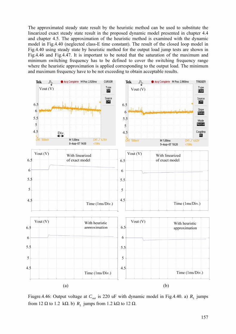
157
The approximated steady state result by the heuristic method can be used to substitute the linearized exact steady state result in the proposed dynamic model presented in chapter 4.4 and chapter 4.5. The approximation of the heuristic method is examined with the dynamic model in Fig.4.40 (neglected class-E time constant). The result of the closed loop model in Fig.4.40 using steady state by heuristic method for the output load jump tests are shown in Fig.4.46 and Fig.4.47. It is important to be noted that the saturation of the maximum and minimum switching frequency has to be defined to cover the switching frequency range where the heuristic approximation is applied corresponding to the output load. The minimum and maximum frequency have to be not exceeding to obtain acceptable results. Fiugre.4.46: Output voltage at outC is 220 uF with dynamic model in Fig.4.40. a) LR jumps from 12 Ω to 1.2 kΩ. b) LR jumps from 1.2 kΩ to 12 Ω.
(a) (b)
Time (1ms/Div.)
6
5.5 5
4.5
With linearized of exact model
Time (1 ms/Div.)
V(V)
6
5.5
5
4.5
With linearized of exact model
With linearized of exact model
Time (1ms/Div.)
Time (1ms/Div.)
With heuristic approximation
With heuristic approximation
Time (1ms/Div.)
Vout (V) Vout (V)
Vout (V) Vout (V)
Vout (V) Vout (V)
Div.
6.5 6.5
6.5 6 5.5 5 4.5
6.5 6 5.5 5 4.5
6.5 6 5.5 5 4.5
6.5 6 5.5 5 4.5
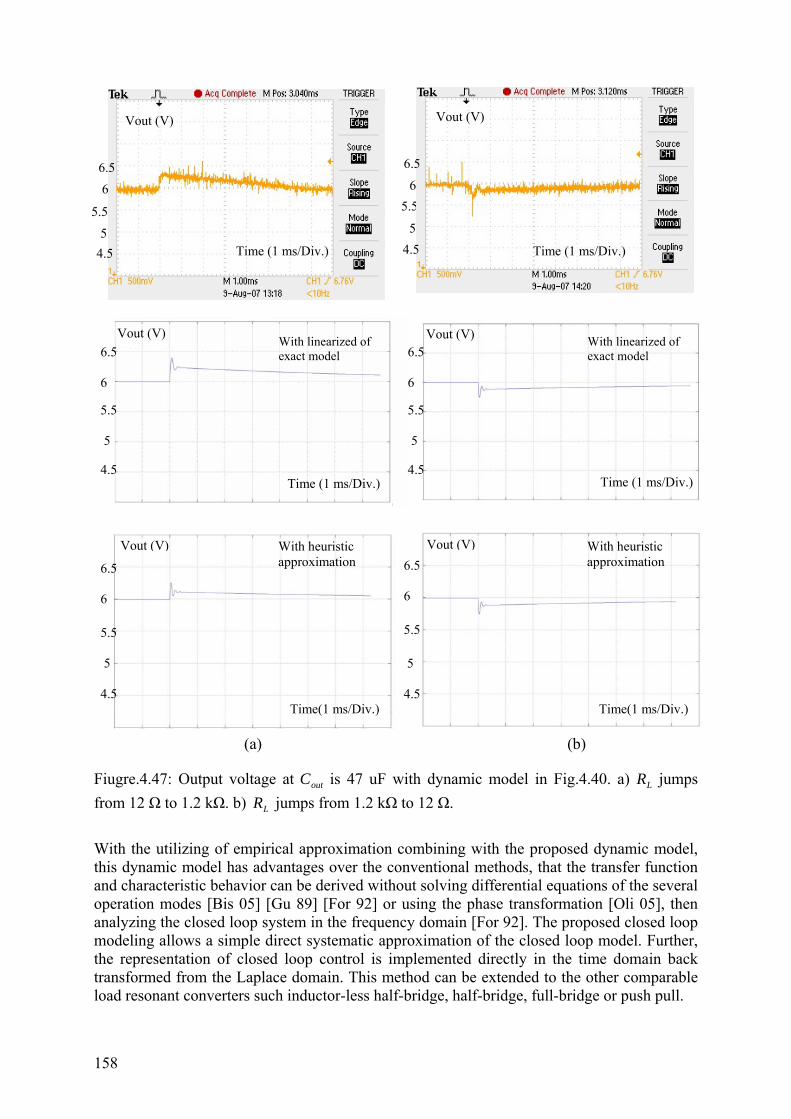
158
Fiugre.4.47: Output voltage at outC is 47 uF with dynamic model in Fig.4.40. a) LR jumps from 12 Ω to 1.2 kΩ. b) LR jumps from 1.2 kΩ to 12 Ω. With the utilizing of empirical approximation combining with the proposed dynamic model, this dynamic model has advantages over the conventional methods, that the transfer function and characteristic behavior can be derived without solving differential equations of the several operation modes [Bis 05] [Gu 89] [For 92] or using the phase transformation [Oli 05], then analyzing the closed loop system in the frequency domain [For 92]. The proposed closed loop modeling allows a simple direct systematic approximation of the closed loop model. Further, the representation of closed loop control is implemented directly in the time domain back transformed from the Laplace domain. This method can be extended to the other comparable load resonant converters such inductor-less half-bridge, half-bridge, full-bridge or push pull.
Div.
Vout (V) Vout (V)
5
Time(1 ms/Div.) Time(1 ms/Div.)
With heuristic approximation
With heuristic approximation
6
5.5 5
6 5.5
Vout (V) Vout (V)
Time (1 ms/Div.) Time (1 ms/Div.)
Vout (V) Vout (V)
Time (1 ms/Div.) Time (1 ms/Div.)
With linearized of exact model
With linearized of exact model
Vout (V) Vout (V)6.5 6 5.5 5 4.5
6.5 6 5.5 5 4.5
6.5 6 5.5 5 4.5
6.5 6 5.5 5 4.5
(a) (b)
4.5
6.5 6.5
4.5
159
4.6.3 Approximation of 'maxI with an Empirical Heuristic Method
This chapter discusses the approximation of the value of '
maxI to obtain open loop modeling with the heuristic method by approach of chapter 4.3.3. According to the derived normalized power transfer ratio in equation (4.40), the power at the output is equal
⎥⎥⎦
⎤
⎢⎢⎣
⎡++−= '
2
22
332
)/(21)'()'()/min(_4
RV
kffVAzAzffonDcP in
pnPnout . (4.42)
The results in Fig.4.44 show that 1Q is designed being larger always than 30 at the nominal load. If the load factor 1Q is extremely changed, the RMS output current ( outRMSI ) is slightly changed only. Thus, the approximation of the behavior at larger 1Q (output load is changed) can be approximated by the 1Q at the nominal load. The current '
maxI is determined at the point where the output power is changed but the output voltage is remaining constant as explained in chapter 4.3.3. Hence, the current '
maxI can be derived further by deriving outP as a function of RMS output current ( outRMSI ) after the perturbation, and from the output voltage before the perturbation as
⎥⎥⎦
⎤
⎢⎢⎣
⎡++−= outA
in
pnPn V
RV
kffVAzAzffonDcI '
2
22
332'
max )/(21)'()'()/min(_4 . (4.43)
Then, the procedure to determine 1, inVRx and 2inV will be determined according to the derived equations (4.11 a b and c), respectively. The results of the first order dynamic model with auxiliary resistor with approximation of the '
maxI by the heuristic method are shown in appendix B.7. These obtained open loop modeling is not satisfying inaccuracy. 4.7 Combination of Large Signal Model and Small Signal Model The chapter discusses shortly the possible modeling which could be extended in the future by implementing the open loop model with first order dynamic function and auxiliary resistor, into the closed loop model. Applying this idea, the transfer functions of the class-E time constant and output time constant will be substituted by the open loop model of Fig.4.16. The input voltage source will be removed. The average output current avI as a function of switching frequency will be connected to the auxiliary resistor XR . The value of the auxiliary resistor XR will be up dated at each cycle of the switching frequency according to the equation (4.11 a). The value of 'maxI will be determined by the procedure as explained in Fig.4.18 b). The derived results in the previous chapter regarding sufficient accuracy allow for the conclusion that the combination of large signal model of the load resonant and small signal model of the closed loop will provide appropriate results.

160
4.8 Conclusion The specification of load resonant converters is required for load regulation, line regulation, stability and response time as these converters are not investigated comprehensively like hard-switching PWM converter are. Consequently, it is important to know the response of a load resonant converter to variations at the input and output, as well as to variations at the control signals. This leads to three kinds of analysis upon the operating conditions of the converters,1) the steady state analysis, 2) the large signal analysis and 3) the small signal analysis. The steady state analysis provides the results at the steady state conditions. The small signal analysis is generally related to the dynamic response of the converter to small perturbations in its steady state operating condition. Hence, it is usually used in a closed loop regulator system where the small perturbation occurs around steady state points. However, if the variations are larger around one operation point such as in open loop transient behavior, the small signal might not meet designed specifications. A large signal model provides therefore, a tool to correctly predict transient response in a large deviation case. The main object of this chapter was to introduce a dynamic equivalent circuit modeling of load resonant converter, focused on class-E topology. The dynamic equivalent circuit modeling can be extending to other converters which has a comparable topology such as in inductor-less half-bridge where the small perturbation (close loop control) and large perturbations (open loop circuit) are given, and where synchronization is achievable in the some way. However, the derived procedure of modeling is applicable to any load resonant converter, if the grade of the non linearity has been evaluated to be light enough to achieve acceptable accurate results by linearization. A general analytical procedure for the dynamic equivalent circuit modeling of load resonant converters is presented and applied to the class-E topology. The closed loop model is obtained based on the decomposition method analysis on one hand, assuming that the low frequency part of the output stage does not change the voltage during considered response time interval of the high frequency part of the resonant converter stage )( resonantoutput ττ >> . On the other hand, the higher order statically equation resulting in high order approximation (3rd order) of output current, will be additionally linearized by first order equation. If Eclassoutput −> ττ 40 was fulfilled, the model was always in good agreement with the measurement. With a proposed simplified open loop dynamic model the dynamic output voltage response can be further easily predicted under disturbance conditions such as steps of input voltage, switching frequency and output load. The accuracy of the model can be further improved by taking care of additional exponential function introducing an auxiliary resistor. A good agreement between theoretical prediction and experiment measurements were confirmed in case of open loop response. The systematic procedure for closed loop calculation of an approximation time constant of a load resonant converter to retrieve an equivalent first order delay was identified by linearizing around an operation point. The example of class-E converter was impressively used to predict the closed loop regulation, if the original class-E transfer function was linearized to be a first order linear equation superposed by linear largest time constant of the resonant converters, and of the output at Eclassoutput −> ττ 20 . The result of the linearization was applied successfully to the proposed control methods in chapter three and proved to obtain sufficient accuracy. The stability was predicted by the model and confirmed a good agreement with the experimental measurements. However, the stability analysis was discussed only in the linear frequency

161
operation range of the converters. The advantage of the proposed dynamic models is the simplification approach which allows direct implementation without deriving several complex state space differential equation solutions during simulation and analysis. A linearized approximation as Linavooav GkVkfkII 030201 +++= was sufficient to derive satisfying results. If a look-up table of the accurate solutions is available, the proposed equation might be adapted to the current operation area. If Eclassoutput −> ττ 40 is fulfilled, the time constants of the resonant converter can be neglected. In case of Eclassoutput −> ττ 20 , the largest time constant of the resonant converter shall be considered. If all time constants of the resonant converter are considered the condition Eclassoutput −> ττ 4 will still lead to acceptable results. These conclusion can be prolonged to any other resonant converter topology if the grade of nonlinearity of the static output transfer function is compared to the investigated class-E example.

162

163
Chapter 5
Controller Design of Resonant Converters
5.1 Introduction The target for a controller of the converters is to regulate a stable constant output voltage, output current or output power with an optimized time response under the environmental changes. For instance, variation of the input voltage, output load and possible component parametric changes under all expected operating conditions, are typical disturbations. For the switching mode power supplies, the topologies and controls in general can be divided into two categories: pulse width modulated (PWM) converter and resonant converter. Generally in the PWM converter, the output energy storage has a very large time constant, for DC-DC application, much larger than switching intervals of the converter. The time constant of the PWM converter itself can be reduced by using discontinuous mode and by other efficient measuring discussed in chapter two. PWM converters provide good properties to be controlled by dead beat control or other cycle by cycle failure cancellation due to its quasi linear transfer behavior. The output power is regulated directly by controlling the input energy according to the slow responding time constant of the output filter. The duty cycle control method plays a major role to regulate the changed energy in the system. The dynamic properties of the converters are easily to be determined and will predict the control configuration discussed in chapter two. Unlike the PWM converter, the resonant converter consists of two sets of energy storage elements, LC resonant tank circuit and output filter being different in their property regarding linearization. Normally, the output filter provides a slow time constant, while LC resonant tanks provide a small time constant but a higher than first order delay. With this reason, LC resonant tank circuits make operation more complex and more difficult. The fast dynamics of the high frequency LC resonant tank make the controller design difficult especially at inner loop control in narrow band converters with changing gain of the plant characteristics. This fact that the resonant converters behave as a nonlinear system, creates difficulty for the linear control implementation. The control parameters must be adjusted carefully that the controller can achieve stability in the approximated range of linear operation area. The stability has to be achieved for the worst case point, normally at the highest system gain but not necessary at this point only. Otherwise, a nonlinear control has to be analyzed and implemented. Many existing controller concepts have been presented to control the output voltage of a resonant converter [Ban 04] [Bon 95] [Que 02] [Ven 04] [Ojo 95] [Kim 91] [Oru 93] [Oru1 85] [Oru2 85] [Oru 88] [Wan 96] [Far 01] [Bib 00]. The controllers are discussed in chapter 5.2. These concepts are mostly of large expense which shall be avoided in practicable implementations and productions.

164
In chapter 5.3, the author attempts to evaluate well-known classical control such P, I, PI, PD and PID into a load resonant converter, considered to be class-E topology in this application. The principle understanding of the classical control was applied to the linearized class-E system of chapter three and four. The results show that the regulation with the classical controls can achieves sufficient efficiency, stability and fast transient behaviour in wide designed operation ranges. The results of these several controller concepts are compared and discussed for an optimal controller design. Further, the simplified controller scheme of a load resonant converter, considered by the class-E topology, was proposed by open loop control with feed forward. This method is comparable with the method of input voltage feed forward for hard-switching converters proposed by Kazimierczuk in 1999 [Kaz 99]. The controller achieves a regulation by matching an appropriate switching frequency according to an input voltage. The results of this regulation method are discussed and compared with the classical controller methods. 5.2 Controllers for Load Resonant Converters This chapter presents some of the well-known controllers for load resonant converters which have been developed over the years. 5.2.1 Optimal Trajectory Control of Resonant Converters Oruganti addressed that a state-plane analysis is a powerful method to clearly portray the steady state and transient operation of resonant converters. Moreover, the directly indicating energy level of the resonant tank provides the ability of a control to keep tank energy levels within bounds under transient conditions. This energy boundary tracking procedure can be evaluated with state plane analysis [Oru1 85]. The control of resonant converters is viewed on the two dimension state-planes. The optimal trajectory is plotted as normalized circuit variables of resonant capacitor voltage and resonant inductor current. The control utilizes the desired transistor trajectory as a control law by continuously evaluating the radius of the desired transistor trajectory. The transistor turn-on is designed by the trajectory path according to the working operation. The control alternates between frequency control and phase modulation corresponding to the operable frequency range [Oru 93] [Oru2 85] [Oru 88]. This control method was shown to provide excellent transient responses corresponding to the input voltage step or output load change. But this method requires expensive high frequency sensors to sense the values of resonant capacitor voltage and resonant inductor current, further input supply voltage and rectified output voltage. Overmore, a complex control circuit is required to realize the state plane for the optimal trajectory. With the mentioned reasons this control scheme is considered as a poor alternative for an application of low size and low cost innovative power supplies. Besides, in an application where a PT is utilized to form a resonant circuit, it very complicates to obtain the information of resonant capacitor voltage and resonant inductor current. 5.2.2 Fuzzy Logic Control of Resonant Converters An example of Fuzzy Logic Control (FLC) has been implemented into a resonant converter by Bonissone under the basic control principle for a resonant circuit that the output voltage is controlled by modulating switching frequency [Bon 95].

165
The FLC consists of 3 modules called fuzzification, inference and defuzzification. In the fuzzification module, the controlled input values are transferred into the overlapping regions of fuzzy sets and they are interpreted as scaling factors. The scaling factors determine the extremes of the numerical range of values for both, input and output variables. Referring to the fuzzy sets, the control rules have an intuitive interpretation. For example, if the input has a negative medium value, the appropriate control action is a positive medium increasing of the value output control signal. The fuzzy sets have to be defined properly, so that the input falls into the overlapping area to interpolate a proper scaling factor is provided. The inference module matches the scaled factor into the interpolation mechanized for each control rule to generate a possibility distribution of values on the output. The defuzzification summarizes this distribution, interpolates and provides a proper control output signal as the resulting control action. For a used FLC in [Bon 95], the input of the FLC was defined by two levels as errorV and
errordV , where errorV is the difference of output voltage and reference and errordV is the difference of current and previous value of errorV (proportional and integration fuzzy). The
errorV term provides control action equal to a gain of the error, while the errordV term forces the steady state to be zero. Based on the mentioned control rule, the output voltage ( outV ) is adjusted for a closed loop regulation in Fig.5.1. The results of the implementation showed that FLC provides a good performance of dynamic response and maintains stable performance for different regulation conditions [Ban 04] [Bon 95]. However, this controller has the disadvantage for which several experiments are required for defining optimum fuzzy sets and the control rules. Also, several components are necessary to realize the controller. Especially, in case that several fuzzy sets and control rules are necessary, they require large computational resources usually unavailable when working with analog devices. Figure.5.1: Closed loop control diagram with fuzzy logic control. 5.2.3 Neural Network Control of Resonant Converters The example of neural network control (NNC) has been presented as a controller for a resonant converter in the work of Quero and Banu [Que 02] [Ban 04], respectively. Neural network structure is a collection of parallel processors connected together in the form of directed graphs. These processors and connections are called neurons and weights. Neurons are arranged in layers. The input layer of the neurons receives input signals from the environment and their output signals are fed into a cascade of hidden layers. The last layer (output layer) generates a set of output signals corresponding to the desired processing shown in Fig.5.2. In order to perform a designed task, a neural network must be configured in neural
166
network connection architecture and in calculation of a set of weights. This processing is performed during the learning phase. During the learning phase a predefined set of input-output pairs of values must be defined. The phase starts by applying an input pattern into the first layer of the network and it is propagated through each upper layer until an output is generated. The output pattern is compared to the defined output, and the error is computed to adjust weights and neurons in the hidden layer. Figure.5.2: Neural network. In [Ban 04] the input signals of the NNC are the change in the input voltage, the output voltage and the load current. The output of NNC is the switching frequency and the duty cycle of the switch. The NNC consists of two layers with fifteen neurons in the hidden layer and a single neuron in the output layer. In [Que 02], the NNC consist of three inputs, ten hidden layers, and one output unit. The input signals are resonant capacitor voltage, resonant inductor current and output voltage. The neural output signal is the turn-on time of the switching signal. Even the result of NNC control provides a good dynamic response and stability performance but the problem of learning phase leads to inflexibility in order to apply it in different designs. Also, additional costs during the learning process increase the cost factor during the production. Several sensors are necessary in order to provide adequate information for the regulation. Moreover, in order to construct network structures consisting of several hidden layers in integrated circuits such implementation is considered as a big obstacle which make the NNC not suitable for cost reduction of switched mode power supplies. 5.2.4 Adaptive Control of Resonant Converters In order to cover the large operation range of the converters, sometimes it is difficult to achieve a good performance over large operation ranges with a single control scheme. An adaptive control technique is augmented to obtain a progressively better performance of the system. Adaptive control is a technique of applying some system identifications to obtain a model of the process from input-output experiments such as neural network and using this mode to design a controller. The parameters of the controllers are adjusted online during the operation. For example, the controlled parameters are automatically adjusted when the output error is larger than the reference value over a certain number of regulation periods. The general structure of the adaptive control is shown in Fig.5.3.
167
Figure.5.3: Adaptive controller. Some examples of applying an adaptive control into resonant converter were discussed by Farhangi [Far 01]. In this work, the full-bridge parallel resonant converter is controlled via switching frequency control. The control loop consists of two operation loops, inner loop and outer loop. The inner loop controls the input current to have a form of the input voltage and amplitude proportional to the output power. The amplitude of input current is determined by factor called k. The outer loop controls the output current. The determined factor k is evaluated by adaptive control. Adaptive control guarantees the stability and good performance during the whole operation range at highest possible control speed. Another example of adaptive control is to find auxiliary process variables (the information of current output voltage and previous output voltage) to compensate the output by changing the fixed parameters of the regulator such as IP KK , and DK to achieve a better performance including stability issue. In general, adaptive control provides a better performance to the control system, but the complexity of the control method and its high costs make this method not very suitable for size and cost reduction of power supplies, because the real time identifier circuits and control parameters setting circuits are quite expensive. 5.2.5 Predictive Control of Resonant Converters Even digital control provides a number of benefits over analog control such as better noise immunity, ability to handle complex control schemes and monitoring functions, as well as easy reprogramming for different applications. But one of the major drawbacks of digital control is the limitation of time delay caused by sampling, analog to digital conversion, computation and PWM generation etc. This time delay causes that the duty ratio or switching frequency cannot be updated in each switching cycle. Such delay will degrade significantly the transient performance. To overcome the time delay effect, the compensation with a predictive control is widely used in digital control systems. Predictive control means that the controller has the possibility to predict future changes of the measured signals, and to base control action on this prediction. Some examples of predictive control have been implemented into the resonant power supplies in the work of Bibian [Bib 00]. The discrete control variable nu , calculated to compensate the error between the output ny and the reference value refy , is used only at the next sampling
168
period because of the delay. The main idea behind the prediction concept is to update the controller using 1+ny instead. A predictive control variable 1+nu can be, thus, obtained at time
nTt = . As a result, the system output is adjusted without delay. The computational time delay is fully compensated. Derived in [Bib 00], the estimate of 1+ny for a second order system can be expressed as: ][2 1111 −−+ −+−= nnsnnn uuTkyyy where 1k defines the coefficient through open loop gain, and sT defines the sampling period. The result of the implementation shows that the performance has been improved if the open loop gain has been accurate identified by ( 1k ). If the plant is poorly identified (inaccurate 1k ), the robustness of the control loop cannot be guaranteed. Moreover, the solutions by digital control have been mostly reserved for applications where the switching frequency is relatively low, due to inherent delay time of the digital processor. Also, the cost of digital controllers play a vital role for overall system cost optimization compared to analog control. 5.3 Proposed Controllers for Fast Inner-Loop Control Many controller methods proposed in chapter 5.2 have been investigated to provide good system transient response and steady state system response, but the lack of low cost, simple design, less complexity and avoiding expensive components are major obstacles for innovative power supplies, considering the size and cost optimization as a main issue. The simple classical control methods and feed forward open loop control with fitting function have demonstrated and confirmed advantages of very good control response and stability condition, while still maintaining low cost, uncomplicated controller circuit and allowing for use of inexpensive circuit elements for off-line power supplies. This result shall be confirmed for resonant power converters in the following chapters. The controller design will be discussed for the regulation at the auxiliary tap of a PT in a load resonant converter to prove the feasibility of controllability at higher order plant being linearized or considered to be weakly non linear only. If the 3rd order transfer function of the tap feed back loop including non linear static transfer characteristic can be handled by suggested controllers, their application can be extended to the quasi 1st order delay of the output stage when the time constants of the load resonant converter can be neglected in case of output voltage feed back control. 5.3.1 Proportional (P) Control Normally, in the simple closed loop system the system consists of controller, plant (considered as resonant converter) and reference value connected to the closed loop. The output from the plant is measured and compared with the reference value. The difference of this comparison called “ error ” is used to process a new value, called U , for manipulate the process input via the controller in order to eliminate or reduce the error as much as possible, shown in Fig.5.4.

169
Figure.5.4: Closed loop control diagram. By increasing the gain called ( PK ), the system will reduce the settling time and generate more overshoot. If the gain PK is increased too much, it will make the loop go unstable. Only P control cannot eliminate the steady state error of the system as well. The behaviour of P control is described as in equation (5.1)
.errorKU PP = (5.1) The validation of P control was implemented for the auxiliary tap regulation method explained in chapter 3.4.3 modelling in Fig.4.28 in chapter 4.4.4. In this case the error between the tap reference value and the tap output value is fed into the VCO to modulate the switching frequency in order to maintain a constant output voltage. The steady state output voltage and the amplitude of the auxiliary tap voltage were measured at variation of the input voltage with the optimized PK of 0.04, shown in Fig.5.5. The transient response was observed as an input voltage jump test from 120 V/DC to 350 V/DC at 100 Ω output load, shown in Fig.5.6. The difference of the output voltage behaviour of the static and transient measurements is caused by different control parameters. The used control parameters for the static measurements are designed for a controller dead time of six switching periods. The used control parameters for the dynamic measurements are designed for cycle by cycle control. Thus, the gain of the controller in the transient measurements had to be designed smaller to guarantee the stability.
P-Control
0,00
2,00
4,00
6,00
8,00
10,00
12,00
120 140 180 220 240 300 340
Input _voltage(V/DC)
Out
put_
volta
ge(V
/DC
)
Vtap_12RVtap_100RVtap_1K2Vout_12RVout_100RVout_1K2
Figure.5.5: The output voltage and the maximum auxiliary tap voltage (peak) over the variation of the input voltage at different output loads for P control.
Plant
170
Figure.5.6: The transient response of the output voltage (upper trace) and the auxiliary tap voltage (lower trace) for an input voltage jump from 120 V/DC to 350 V/DC at 100 Ω load for P control obtained from measurement and simulation, respectively. 5.3.2 Integral (I) Control Term I ( IK ) describes a summing of previous errors over the process time being multiplied by gain IK . With the integral system, the average difference of the error is always being reduced. So if the gain is big enough, it will provide a zero steady state error to the system. However, an increasing IK will lead to worse settling time of the system also. The behaviour of the I control is described as in equation (5.2)
∫= dterrorKU II . (5.2)
The numerical expression of equation (5.2) is
Div. Time (200 us/Div.)
Vout (5 V/Div.)
Vtap (500 mV/Div.)
0
0
0
6
2
4
8
0.2 0.6 1 1.4 Time(ms)
V(V)
Vtap
Vout
0
1
2
0.2 0.4 Time(ms)
171
S
n
iiII TerrorKU ∑
=
=0
(5.3)
where sT is a sampling time. In the practical application the summing can be removed by a recursive method with the following approach. Considering the point where i = n, we obtain IU in equation (5.3) as
s
n
inIIn TerrorKU ∑
=
=0
. (5.4)
Consider at the point where i = n-1 so IU in equation (5.3) is
.1
0)1()1( ∑
−
=−− =
n
isnInI TerrorKU (5.5)
Combining equation (5.4) and (5.5), we obtain
)()1( nsInIIn errorTKUU += − . (5.6) The validation of I control was proved for the auxiliary tap regulation explained in chapter 3.4.3 and modelling by Fig.4.28 in chapter 4.4.4. The optimized control parameter of sI TK was 0.1, while sT defines period of the sampling time, considered as the switching frequency period. The results of steady state and transient response against input voltage jump from 120 V/DC to 350 V/DC at 100 Ω are shown in Fig.5.7 and Fig.5.8, respectively.
I-Control
0.00
1.00
2.00
3.00
4.00
5.00
6.00
7.00
8.00
120 140 180 220 240 300 340
Input_voltage(V/DC)
Out
put_
volta
ge(V
/DC
)
Vtap_12RVtap_100RVtap_1K2Vout_12RVout_100RVout_1K2
Figure.5.7: The output voltage and the maximum auxiliary tap voltage (peak) over the variation of the input voltage at different output loads for I control.

172
Figure.5.8: The transient response of the output voltage (upper trace) and the auxiliary tap voltage (lower trace) for an input voltage jump from 120 V/DC to 350 V/DC at 100 Ω load for I control obtained from measurement and simulation, respectively. 5.3.3 Proportional and Derivative (PD) Control Term D describes the present error is measured and subtract by the error from the period before. With the gain DK the controller response more rapidly and reduces the overshoot of the output. This controller is a combination between the P and the D part. However, without I parts, a controller cannot maintain an error to be zero in the steady state. The behaviour of the D control is described in equation (5.7)
.dt
errordKU DD = (5.7)
The numerical expression for the D controller in equation (5.7) is
Div.
Vtap (500 mV/Div.)
Vout (5 V/Div.)
Time (200 us/Div.)
0
0
0
2
4
6
8
0.2
V(V)
Vtap
Vout
0.2 Time(ms)
0
1
2
0.4

173
s
nnDDn T
errorerrorKU )1( −−
= . (5.8)
Hence, the numerical expression for the PD controller is the summing of equation (5.8) and equation (5.1)
nps
nnDPnDn errorK
Terrorerror
KUU +−
=+ − )1( . (5.9)
The evaluation of the PD control was applied for the auxiliary tap regulation in chapter 4.4.4 (Fig.4.28). The implemented optimized control parameter PK was 0.04, and sD TK was 0.008. The results of the steady state and the transient response for the output voltage and the voltage from the auxiliary tap are shown in Fig.5.9 and Fig.5.10, respectively.
P-Control
0,00
2,00
4,00
6,00
8,00
10,00
12,00
120 140 180 220 240 300 340
Input _voltage(V/DC)
Out
put_
volta
ge(V
/DC
)
Vtap_12RVtap_100RVtap_1K2Vout_12RVout_100RVout_1K2
Figure.5.9: The output voltage and the maximum auxiliary tap voltage (peak) over the variation of the input voltage at different output loads for PD control.
PD-Control

174
Figure.5.10: The transient response of the output voltage (upper trace) and the auxiliary tap voltage (lower trace) for an input voltage jump from 120 V/DC to 350 V/DC at 100 Ω load for PD control. 5.3.4 Proportional and Integral (PI) Control This controller combines the characteristics of P and I parts to improve the control performance in the system. Together with the I part, the controller can extinguish a steady state error using the advantage of the P control over the I control to reduce the transient time. The behavior of the PI control is described in equation (5.10)
∫+=+ dterrorKerrorKUU IPIP . (5.10)
The numerical expression for PI control is expressed as follow
∑=
+=+n
isIpIP errorTKerrorKUU
0
(5.11)
where sT is the sampling time. In the practical applications the summing can be removed by recursive methods by the following approach. Considering at i = n, equation (5.11) becomes
∑=
+=+n
isnInpInPn TerrorKerrorKUU
0
. (5.12)
Considering at i = n-1, equation (5.11) becomes
.1
011)1()1( ∑
−
=−−−− +=+
n
isnInpnInP TerrorKerrorKUU (5.13)
Combining equation (5.12) and (5.13), we obtain
Vtap (500 mV/Div.)
Vout (5 V/Div.)
Time (200 us/Div.) Div.
0
0
175
nsInnpnInpInPn errorTKerrorerrorKUUUU +−++=+ −−− )( 1)1()1( . (5.14) The evaluation of the PI control was done for the auxiliary tap regulation explained in chapter 3.4.3(Fig.4.28). The implemented optimized control parameters have been derived with PK = 0.01 and sI TK = 0.2. The results of the steady state and the transient response for the output voltage and the voltage from the auxiliary tap are shown in Fig.5.11 and Fig.5.12, respectively.
PI-Control
0.00
1.00
2.00
3.00
4.00
5.00
6.00
7.00
8.00
120 140 180 220 240 300 340
Input_voltage(V/DC)
Out
put_
volta
ge(V
/DC
)
Vtap_12RVtap_100RVtap_1K2Vout_12RVout_100RVout_1K2
Figure.5.11: The output voltage and the maximum auxiliary tap voltage (peak) over the variation of the input voltage at different output loads for PI control.
Div. Time (200 us/Div.)
Vout (5 V/Div.)
Vtap (500 mV/Div.)
0
0
176
Figure.5.12: The transient response of the output voltage (upper trace) and the auxiliary tap voltage (lower trace) for an input voltage jump from 120 V/DC to 350 V/DC at 100 Ω load for PI control. 5.3.5 Proportional, Integral and Derivative (PID) Control This controller is a combination of P, I and D parts, hence, the controller can achieve the steady state zero error with the help of I control. Moreover, the overshoot can be reduced and the transient time can be decreased by the D part. The behavior of PID control is expressed in equation (5.15)
dt
derrorKerrorKerrorKUUU DIPDIP ++=++ ∫ dt . (5.15)
The numerical expression for PID control is given as following
s
nnD
n
isIpDIP T
errorerrorKerrorTKerrorKUUU )1(
0
−
=
−++=++ ∑ (5.16)
where sT is the sampling time. In the practical applications the summing can be removed by recursive methods by the following approach. Considering i = n, equation (5.16) becomes
∑=
−−++=++
n
i s
nnDsnInpDInPn T
errorerrorKTerrorKerrorKUUU
n0
)1( . (5.17)
Considering i = n-1, equation (5.16) becomes
∑−
=
−−−−−−−
−++=++
1
0
)2()1(11)1()1()1( .
n
i s
nnDsnInpnDnInP T
errorerrorKTerrorKerrorKUUU (5.18)
Combining equations (5.17) and (5.18), we obtain
V(V)
Vout
Vtap
0
1
2
0.2 0.4 Time(ms)
177
)2()( )2()1()1()1( −−−− +−++−+= nnns
DnsInnpnn errorerrorerror
TK
errorTKerrorerrorKUU (5.19)
where DnInPnn UUUU ++= and )1()1()1()1( −−−− ++= nDnInPn UUUU . The evaluation of the PID control was done for the auxiliary tap regulation in chapter 3.4.3 (Fig.4.28). The results of steady state and transient response for the optimized control parameters PK = 0.04, sI TK = 0.2 and sD TK = 0.2 as shown in Fig.5.13 and Fig.5.14, respectively, sT defines as the period of the sampling time considered as the switching frequency period.
PID-Control
0.00
1.00
2.00
3.00
4.00
5.00
6.00
7.00
8.00
9.00
120 140 180 220 240 300 340
Input_voltage(V/DC)
Out
put_
volta
ge(V
/DC
)
Vtap_12RVtap_100RVtap_1K2Vout_12RVout_100RVout_1K2
Figure.5.13: The output voltage and the maximum auxiliary tap voltage (peak) over the variation of the input voltage at different output loads for PID control.
Div.
Vtap (500 mV/Div.)
Time (200 us/Div.)
Vout (5 V/Div.)
0
0

178
Figure.5.14: The transient response of the output voltage (upper trace) and the auxiliary tap voltage (lower trace) for an input voltage jump from 120 V/DC to 350 V/DC at 100 Ω load for PID control. 5.3.6 Open Loop Input Voltage Feed Forward Control The controlled system operates without using a closed loop feed back to maintain a constant output voltage. Thus, the regulation is valid only within parameters range of the fed forward variables. Other disturbances not taken into account cannot be removed by such control regime. The disturbance of the variation of the input voltage is considered to be a feed forward variable in this application. The controller characteristics reveal a good performance in applications with a single point load. The variation of either output load or components was not taken into account. However, the controller ensures that stability is given during the whole operation. Referring to the theoretical background of the steady state behavior of the class-E converter derived in chapter three in equations (3.13)-(3.21), the results of the calculation are illustrated in Fig.3.8, While the output voltage can be maintained constant against the variation of the input voltage by varying of the switching frequency. Thus, the regulation is accomplished by matching an appropriate switching frequency reflecting to the input voltage as applied to PWM converters [Kaz 99]. The controller continuously monitors the change of the input voltage and generates a suitable frequency according to the control trajectory, shown in Fig.3.8, while the output voltage is maintained constant. Unlike the classical closed loop control where the feed back control faces an unavoidable delay time provided by the system, this controller reacts immediately against disturbances from input voltage. The control scheme of the feed forward open loop input voltage control is shown in Fig.5.15.
0.2 0.4 0 1
2
V(V)
Vout
Vtap
Time(ms)
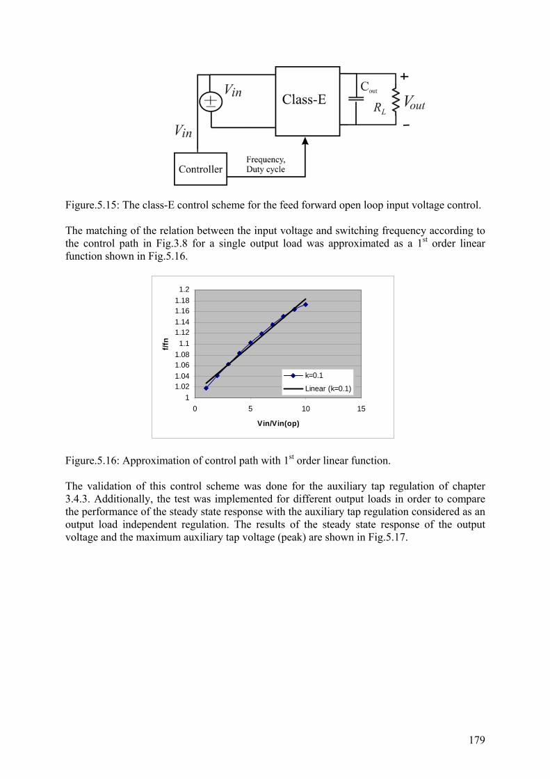
179
Figure.5.15: The class-E control scheme for the feed forward open loop input voltage control. The matching of the relation between the input voltage and switching frequency according to the control path in Fig.3.8 for a single output load was approximated as a 1st order linear function shown in Fig.5.16. Figure.5.16: Approximation of control path with 1st order linear function. The validation of this control scheme was done for the auxiliary tap regulation of chapter 3.4.3. Additionally, the test was implemented for different output loads in order to compare the performance of the steady state response with the auxiliary tap regulation considered as an output load independent regulation. The results of the steady state response of the output voltage and the maximum auxiliary tap voltage (peak) are shown in Fig.5.17.
11.021.041.061.081.1
1.121.141.161.181.2
0 5 10 15
Vin/Vin(op)
f/fn
k=0.1
Linear (k=0.1)
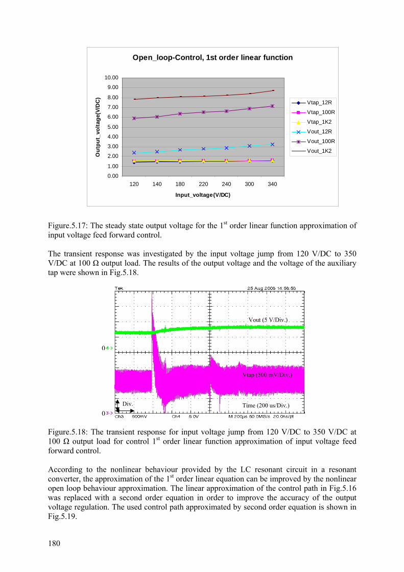
180
Figure.5.17: The steady state output voltage for the 1st order linear function approximation of input voltage feed forward control. The transient response was investigated by the input voltage jump from 120 V/DC to 350 V/DC at 100 Ω output load. The results of the output voltage and the voltage of the auxiliary tap were shown in Fig.5.18. Figure.5.18: The transient response for input voltage jump from 120 V/DC to 350 V/DC at 100 Ω output load for control 1st order linear function approximation of input voltage feed forward control. According to the nonlinear behaviour provided by the LC resonant circuit in a resonant converter, the approximation of the 1st order linear equation can be improved by the nonlinear open loop behaviour approximation. The linear approximation of the control path in Fig.5.16 was replaced with a second order equation in order to improve the accuracy of the output voltage regulation. The used control path approximated by second order equation is shown in Fig.5.19.
Open_loop-Control, 1st order linear function
0.00
1.00
2.00
3.00
4.00
5.00
6.00
7.00
8.00
9.00
10.00
120 140 180 220 240 300 340
Input_voltage(V/DC)
Out
put_
volta
ge(V
/DC
)Vtap_12R
Vtap_100R
Vtap_1K2
Vout_12R
Vout_100R
Vout_1K2
Div.
Vtap (500 mV/Div.)
Time (200 us/Div.)
Vout (5 V/Div.)
0
0

181
Figure.5.19: Approximation of control path with second order function. The results of the steady state output voltage against the variation of input voltage from 120 V/DC to 350 V/DC with a second order function are shown with the varying output loads in Fig.5.20.
Open_loop-Control, 2nd order
0.00
1.00
2.00
3.00
4.00
5.00
6.00
7.00
8.00
9.00
120 140 180 220 240 300 340
Input_voltage(V/DC)
Out
put_
volta
ge(V
/DC
) Vtap_12RVtap_100RVtap_1K2Vout_12RVout_100RVout_1K2
Figure.5.20: The steady state output voltage for the second order function approximation of input voltage feed forward control. The transient response of the output voltage for an input voltage jump from 120 V/DC to 350 V/DC at 100 Ω output load with the second order approximation is shown in Fig.5.21.
11.021.041.061.081.1
1.121.141.161.181.2
0 5 10 15
Vin/Vin(op)
f/fn
k=0.1Polynomisch (k=0.1)Polynom 2nd(k=0.1)

182
Figure.5.21: The transient response for the input voltage jump from 120 V/DC to 350 V/DC at 100 Ω output load for second order approximation of input voltage feed forward control. The nonlinear control trajectory was also approximated by the logarithm function in order to compare the accuracy with the second order approximation equation in the steady state. The result of implemented logarithm function control path is shown in Fig.5.22. Figure.5.22: Approximation of control path with logarithm function. The results of steady state output voltage against the line input regulation for the logarithm control path approximation at different output loads is shown in Fig.5.23.
0.981
1.021.041.061.081.1
1.121.141.161.181.2
0 5 10 15
Vin/Vin(op)
f/fn
k=0.1
Logarithmisch (k=0.1)Logarithm(k=0.1)
Div.
Vtap (500 mV/Div.)
Time (200 us/Div.)
Vout (5 V/Div.)
0
0
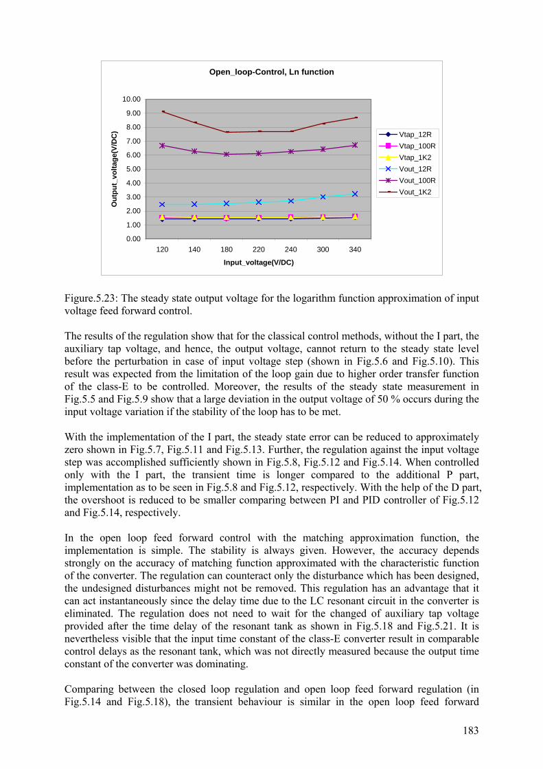
183
Open_loop-Control, Ln function
0.00
1.00
2.00
3.00
4.00
5.00
6.00
7.00
8.00
9.00
10.00
120 140 180 220 240 300 340
Input_voltage(V/DC)
Out
put_
volta
ge(V
/DC
) Vtap_12RVtap_100RVtap_1K2Vout_12RVout_100RVout_1K2
Figure.5.23: The steady state output voltage for the logarithm function approximation of input voltage feed forward control. The results of the regulation show that for the classical control methods, without the I part, the auxiliary tap voltage, and hence, the output voltage, cannot return to the steady state level before the perturbation in case of input voltage step (shown in Fig.5.6 and Fig.5.10). This result was expected from the limitation of the loop gain due to higher order transfer function of the class-E to be controlled. Moreover, the results of the steady state measurement in Fig.5.5 and Fig.5.9 show that a large deviation in the output voltage of 50 % occurs during the input voltage variation if the stability of the loop has to be met. With the implementation of the I part, the steady state error can be reduced to approximately zero shown in Fig.5.7, Fig.5.11 and Fig.5.13. Further, the regulation against the input voltage step was accomplished sufficiently shown in Fig.5.8, Fig.5.12 and Fig.5.14. When controlled only with the I part, the transient time is longer compared to the additional P part, implementation as to be seen in Fig.5.8 and Fig.5.12, respectively. With the help of the D part, the overshoot is reduced to be smaller comparing between PI and PID controller of Fig.5.12 and Fig.5.14, respectively. In the open loop feed forward control with the matching approximation function, the implementation is simple. The stability is always given. However, the accuracy depends strongly on the accuracy of matching function approximated with the characteristic function of the converter. The regulation can counteract only the disturbance which has been designed, the undesigned disturbances might not be removed. This regulation has an advantage that it can act instantaneously since the delay time due to the LC resonant circuit in the converter is eliminated. The regulation does not need to wait for the changed of auxiliary tap voltage provided after the time delay of the resonant tank as shown in Fig.5.18 and Fig.5.21. It is nevertheless visible that the input time constant of the class-E converter result in comparable control delays as the resonant tank, which was not directly measured because the output time constant of the converter was dominating. Comparing between the closed loop regulation and open loop feed forward regulation (in Fig.5.14 and Fig.5.18), the transient behaviour is similar in the open loop feed forward

184
regulation compared to the auxiliary tap. The accuracy of the regulation can be improved by applying a nonlinear equation in the approximating feed forward function of the resonant converter. The improvement is not achieved for any output load as the approximation has to be different following Fig.3.8 and related frequency in appendix A.2. The implementation was done example for 100 Ω output load shown in Fig.5.17 and Fig.5.20, respectively. This regulation is suitable a single point load application where a fast dynamic response against the line regulation is required but can be substituted as well by a tapped resonant tank current control with PI or PID leading to similar improved results. The comparisons of the transient responses in Fig.5.6, Fig.5.8, Fig.5.12 and Fig.5.14 between the measurements and simulations at the tap voltage )( tapV are slightly different, since in the simulation the parasitic capacitance between the 1dC and 3dC leading to the equivalent circuit in Fig.5.24 is not considered. Also the consideration of the time gap during the changing input voltage sources during the step input voltage and saturation of fL are not considered.
Figure.5.24: Equivalent circuit of the tap voltage measurement. 5.4 Optimal Controller Design for Resonant Converters In this chapter, the discussion of the optimum designed controller will be presented utilizing the classical control schemes for a load resonant converter at the output voltage feed back control loop including dominant output time constant )( resonantoutput ττ >> . There are many possible of selecting the controller parameters to meet given performance specifications. One of the well-known tuning techniques for PID control for general purposes was introduced by Ziegler and Nichols. The procedure for determining the control parameters are suggested by the following. First applying the proportional control action only, PK is increased from 0 to a critical value called crK where the output first sustains oscillations. At the critical value of crK , the

185
corresponding period of oscillations called crP is determined. Then, the controlled parameters iPK τ, and dτ are set as following.
Type of controller PK iτ dτ
P 0.5 crK ∞ 0 PI 0.45 crK
2.11
crP 0
PID 0.6 crK 0.5 crP 0.125 crP As far as, the realization of the controller for a load resonant converter by the method of Ziegler and Nichols could be applied, the optimization might not be achieved. In order to achieve an optimal performance the controller design can be achieved by the following. The steady state error should be always zero. In additional the regulation should not react against the output voltage ripple. In order to achieve these requirements, the frequency response of the controller has to be designed as follows. The amplification gain at the low frequency response (DC-level) has to be designed as large as possible for achieving a steady state error to be zero after short transient response. The limitation of the gain is defined by the stability condition, derived in chapter 4.4.8. The bandwidth (at 0 dB) of the frequency response has to be designed as large as possible for obtaining a fast transient response. The amplification at the switching frequency range has to be designed as small as possible avoiding output voltage ripple regulation. Therefore, the suitable asymptotic frequency response plot of the controller has to be designed as shown in Fig.5.25. Figure.5.25: Frequency dependent gain response of the controller. The frequency response (Bode plot) of the implemented PI control plus lag circuit for the continuous mode control in Fig.4.38 b) is designed in Fig.5.26.
As small as possible avoiding output voltage ripple regulation

186
Figure.5.26: The frequency dependent gain response (Bode plot) of the implemented PI control plus lag circuit for continuous mode. In case of burst mode control, a significant output voltage ripple provided by the time-on and time-off intervals has to be additionally considered for the optimum controller design. At the frequency range of the time-on and time-off output voltage ripple the controller should amplified the burst mode output voltage ripple in the range of VCO input voltage range without reaching the saturation region. The decrease of the time-on, time-off output voltage ripple gain can be done by reducing the FBK gain (equation 4.27). However, when reducing the FBK gain, the speed of the control is also reduced. Therefore, there is a trade-off between reducing the time-on, time-off output voltage ripple gain and the speed of the controller. In the real application, the FBK gain should be increased as much as possible as far as the VCO input stay in the linear range without touching the saturation region, as shown in Fig.5.27. Finally, it can be seen that the PI control with lag circuit has an advantage over the normal PI control for this application providing the -20 dB/decade beyond the bandwidth frequency of 0 dB point.
minf maxf
Bandwidth at 0 dB (Defines the speed)
12 dB
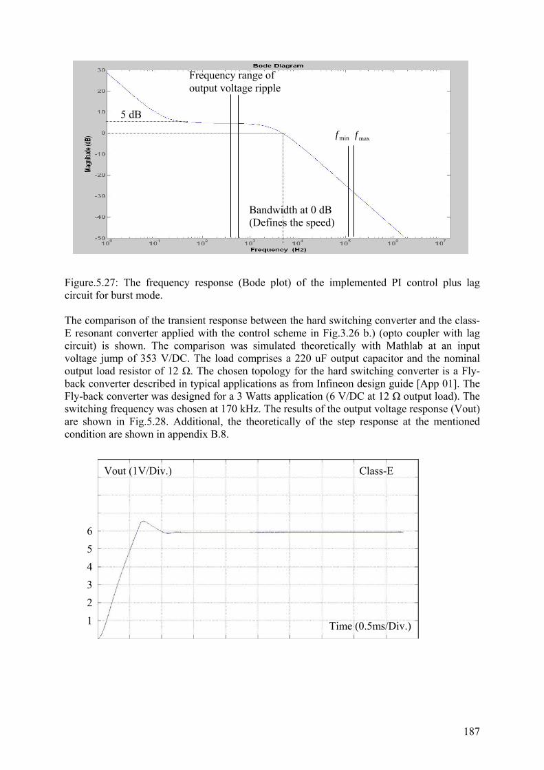
187
Figure.5.27: The frequency response (Bode plot) of the implemented PI control plus lag circuit for burst mode. The comparison of the transient response between the hard switching converter and the class-E resonant converter applied with the control scheme in Fig.3.26 b.) (opto coupler with lag circuit) is shown. The comparison was simulated theoretically with Mathlab at an input voltage jump of 353 V/DC. The load comprises a 220 uF output capacitor and the nominal output load resistor of 12 Ω. The chosen topology for the hard switching converter is a Fly-back converter described in typical applications as from Infineon design guide [App 01]. The Fly-back converter was designed for a 3 Watts application (6 V/DC at 12 Ω output load). The switching frequency was chosen at 170 kHz. The results of the output voltage response (Vout) are shown in Fig.5.28. Additional, the theoretically of the step response at the mentioned condition are shown in appendix B.8.
minf maxf
Bandwidth at 0 dB (Defines the speed)
Frequency range of output voltage ripple
5 dB
Vout (1V/Div.)
Time (0.5ms/Div.)
Class-E
6
5
4
3
2
1
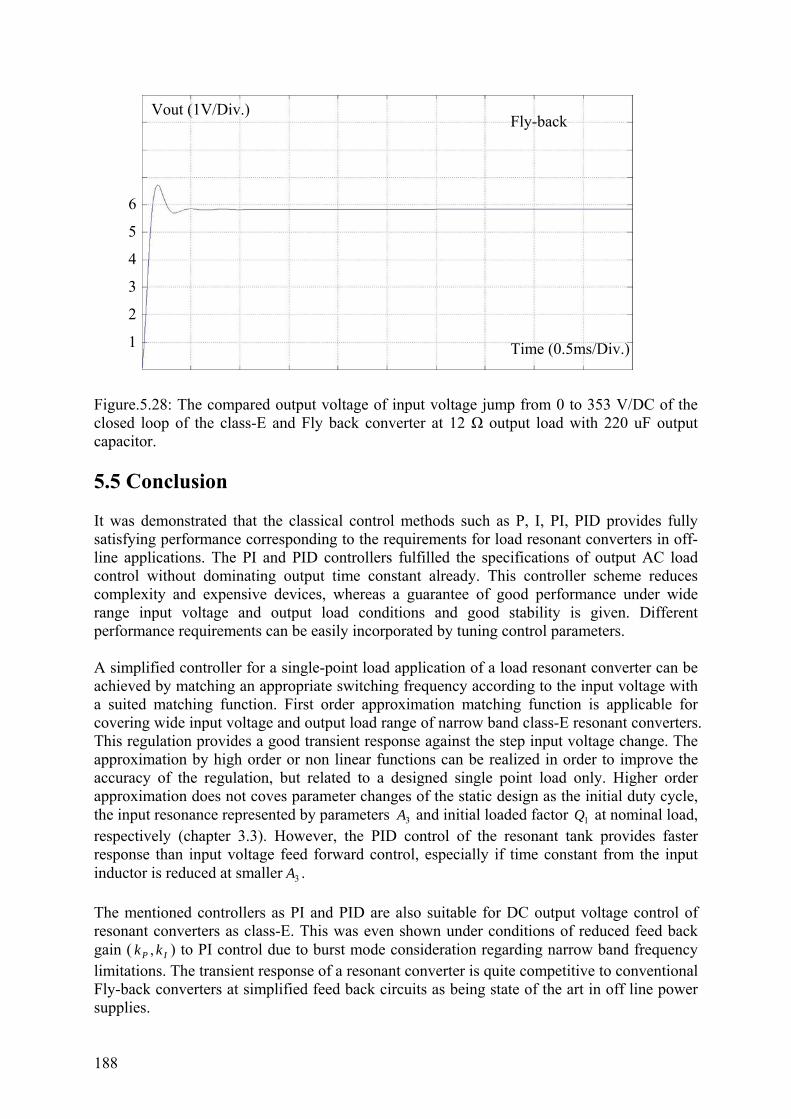
188
Figure.5.28: The compared output voltage of input voltage jump from 0 to 353 V/DC of the closed loop of the class-E and Fly back converter at 12 Ω output load with 220 uF output capacitor. 5.5 Conclusion It was demonstrated that the classical control methods such as P, I, PI, PID provides fully satisfying performance corresponding to the requirements for load resonant converters in off-line applications. The PI and PID controllers fulfilled the specifications of output AC load control without dominating output time constant already. This controller scheme reduces complexity and expensive devices, whereas a guarantee of good performance under wide range input voltage and output load conditions and good stability is given. Different performance requirements can be easily incorporated by tuning control parameters. A simplified controller for a single-point load application of a load resonant converter can be achieved by matching an appropriate switching frequency according to the input voltage with a suited matching function. First order approximation matching function is applicable for covering wide input voltage and output load range of narrow band class-E resonant converters. This regulation provides a good transient response against the step input voltage change. The approximation by high order or non linear functions can be realized in order to improve the accuracy of the regulation, but related to a designed single point load only. Higher order approximation does not coves parameter changes of the static design as the initial duty cycle, the input resonance represented by parameters 3A and initial loaded factor 1Q at nominal load, respectively (chapter 3.3). However, the PID control of the resonant tank provides faster response than input voltage feed forward control, especially if time constant from the input inductor is reduced at smaller 3A . The mentioned controllers as PI and PID are also suitable for DC output voltage control of resonant converters as class-E. This was even shown under conditions of reduced feed back gain ( IP kk , ) to PI control due to burst mode consideration regarding narrow band frequency limitations. The transient response of a resonant converter is quite competitive to conventional Fly-back converters at simplified feed back circuits as being state of the art in off line power supplies.
Vout (1V/Div.) Fly-back
Time (0.5ms/Div.)
6
5
4
3
2
1

189
Appendix A.1 The Equivalent Circuit Assumption for Resonant Load Circuit with Output Rectifier (Full Bridge) This appendix deals with equivalent circuit assumption necessary for effective approximation in output load including rectification. Assumed the output bridge rectifier, the output capacitor and the output load resistor in steady state operation mode as an equivalent circuit resistor EQR [Yam 98], in Fig.A.1.1. The assumption is based on the illustration of Fig.A.1.2, assuming high 101 >Q obtaining a sine wave current 2i and voltage jump of 2v ( 02 ≈dC ):
LEQ RR 2
8π
≈ . (A1.1)
Figure.A.1.1: Output bridge equivalent resistance. Figure.A.1.2: Waveform assumption.
2dC and EQR are transferred from the secondary side of the transformer to the primary side
with the transfer ratio of N:1 as 2' NRR EQEQ = and 22
2'
NC
C dd = , in Fig.A.1.3.
Figure.A.1.3: Transformation of 2dC and EQR to the primary side. The parallel output circuit was transferred into the series equivalent circuit of the resonant tank shown in Fig.A.1.4 by equation
22
2'2'
'
1 ωdEQ
EQSEQ
CRRR
+= ,
22
'2'
222
'2'1ωω
dEQ
dEQSEQ
CRCRC +
=
whereω is fπ2 ; f is a switching frequency.

190
Figure.A.1.4: Series equivalent circuit of the parallel output circuit.
Figure.A.1.5: Equivalent circuit of the short circuit considering the resistance of diode bridge. Figure.A.1.6: Equivalent circuit of light load.
diode
191
Appendix A.2 The Analyzed Bandwidth of the Switching Frequency of the class-E Converter The analyzed band width of the switching frequency and the information of the switch turn-on interval for the ZVS condition for different designed parameters of 3A and 1Q are shown below.
Figure.A.2.1: Bandwidth and switching turn-on interval for the ZVS condition at the application of 1Q = 10, %45=Dc and 5.03 =A at k=1, f/fn=1.
Figure.A.2.2: Bandwidth and switching turn-on interval for the ZVS condition at the application of 1Q = 10, %45=Dc and 1.13 =A at k=1, f/fn=1.
Q1=10, Dc=.45%, A3=.5 (optimum ZVS point)
0
10
20
30
40
50
60
70
0.98 1.03 1.08 1.13 1.18
f/fn
Dc_
on(%
)
k=1
k=1
k=.12
k=.12
k=.012
k=.012
Q1=10, Dc=45%, A3=.5 at f/fn=1, k=1
Q1=10, Dc=.45%, A3=1.1 (optimum ZVS point)
0
10
20
30
40
50
60
70
0.98 1.08 1.18 1.28
f/fn
Dc_
on(%
)
k=1
k=1
k=.12
k=.12
k=.012
k=.012
Q1=10, Dc=45%, A3=1.1 at f/fn=1, k=1
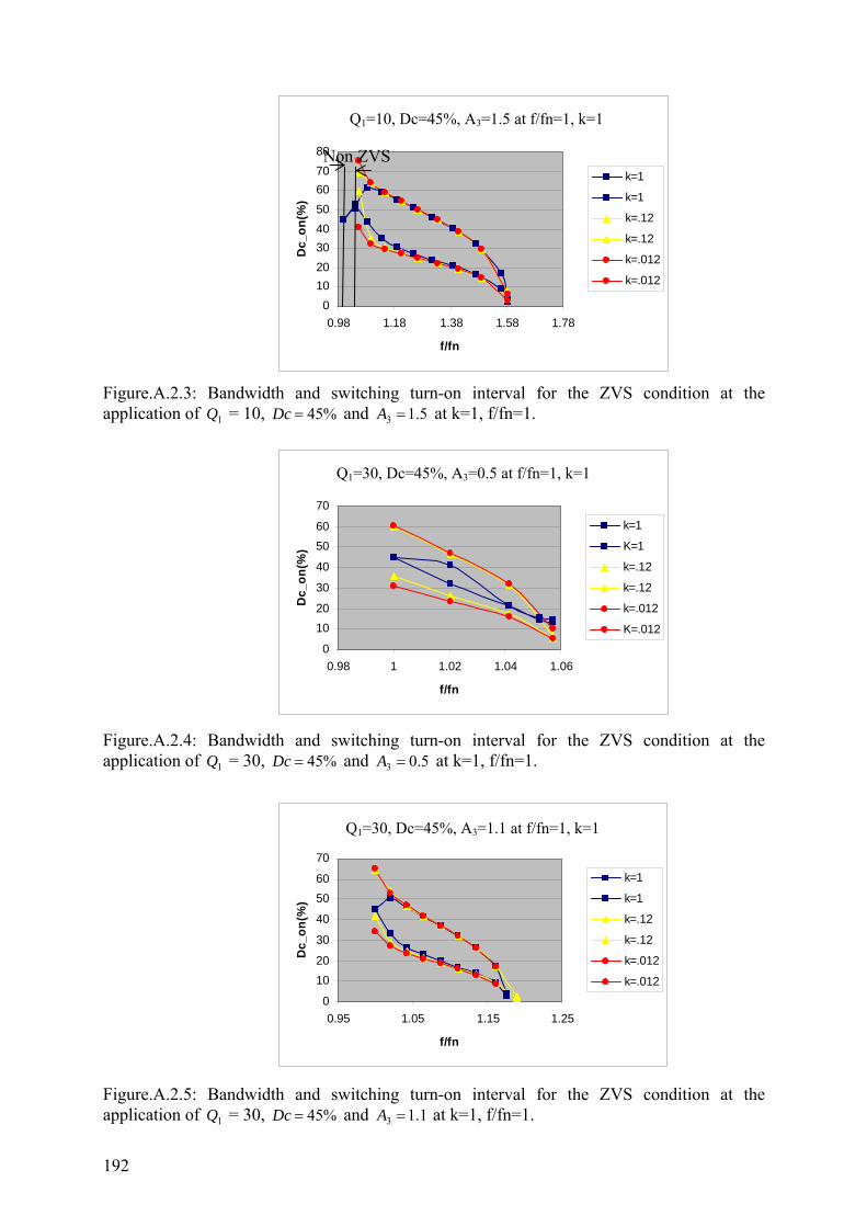
192
Figure.A.2.3: Bandwidth and switching turn-on interval for the ZVS condition at the application of 1Q = 10, %45=Dc and 5.13 =A at k=1, f/fn=1.
Figure.A.2.4: Bandwidth and switching turn-on interval for the ZVS condition at the application of 1Q = 30, %45=Dc and 5.03 =A at k=1, f/fn=1.
Figure.A.2.5: Bandwidth and switching turn-on interval for the ZVS condition at the application of 1Q = 30, %45=Dc and 1.13 =A at k=1, f/fn=1.
Q1=10, Dc=.45%, A3=1.5 (optimum ZVS point)
01020304050607080
0.98 1.18 1.38 1.58 1.78
f/fn
Dc_
on(%
)
k=1
k=1
k=.12
k=.12
k=.012
k=.012
Q1=10, Dc=45%, A3=1.5 at f/fn=1, k=1
Q1=30, Dc=.45%, A3=.5 (optimum ZVS point)
0
1020
30
40
5060
70
0.98 1 1.02 1.04 1.06
f/fn
Dc_
on(%
)
k=1
K=1
k=.12
k=.12
k=.012
K=.012
Q1=30, Dc=45%, A3=0.5 at f/fn=1, k=1
Q1=30, Dc =.45%, A3=1.1 (optimum ZVS point)
0
1020
30
40
5060
70
0.95 1.05 1.15 1.25
f/fn
Dc_
on(%
)
k=1
k=1
k=.12
k=.12
k=.012
k=.012
Q1=30, Dc=45%, A3=1.1 at f/fn=1, k=1
Non ZVS

193
Figure.A.2.6: Bandwidth and switching turn-on interval for the ZVS condition at the application of 1Q = 30, %45=Dc and 5.13 =A at k=1, f/fn=1.
Figure.A.2.7: Bandwidth and switching turn-on interval for the ZVS condition at the application of 1Q = 100, %45=Dc and 5.03 =A at k=1, f/fn=1.
Figure.A.2.8: Bandwidth and switching turn-on interval for the ZVS condition at the application of 1Q = 100, %45=Dc and 1.13 =A at k=1, f/fn=1.
Q1=30, Dc=.45%, A3=1.5 (optimum ZVS point)
01020304050607080
0.95 1.15 1.35 1.55 1.75
f/fn
Dc_
on(%
)
k=1
k=1
k=.12
k=.12
k=.012
k=.012
Q1=30, Dc=45%, A3=1.5 at f/fn=1, k=1
Q1=100, Dc=.45%, A3=.5 (optimum ZVS point)
0
10
20
30
40
50
60
70
0.99 1 1.01 1.02 1.03
f/fn
Dc_
on(%
)
k=1
k=1
k=.12
k=.12
k=.012
k=.012
Q1=100, Dc=45%, A3=0.5 at f/fn=1, k=1
Q1=100, Dc=.45%, A3=1.1 (optimum ZVS point)
0
10
20
30
40
50
60
70
0.95 1 1.05 1.1 1.15
f/fn
Dc_
on(%
)
k=1
k=1
k=.12
k=.12
k=.012
k=.012
Q1=100, Dc=45%, A3=1.1 at f/fn=1, k=1
Non ZVS
1
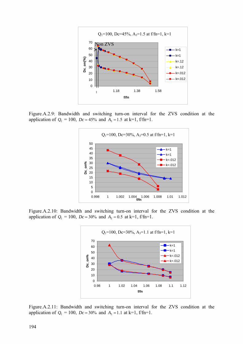
194
Figure.A.2.9: Bandwidth and switching turn-on interval for the ZVS condition at the application of 1Q = 100, %45=Dc and 5.13 =A at k=1, f/fn=1.
Q1=100, Dc=30%, A3=.5
05
101520253035404550
0.998 1 1.002 1.004 1.006 1.008 1.01 1.012f/fn
Dc_
on%
k=1k=1k=.012k=.012
Figure.A.2.10: Bandwidth and switching turn-on interval for the ZVS condition at the application of 1Q = 100, %30=Dc and 5.03 =A at k=1, f/fn=1.
Q1=100, Dc=30%, A3=1.1
0
10
20
30
40
50
60
70
0.98 1 1.02 1.04 1.06 1.08 1.1 1.12
f/fn
Dc_
on%
k=1k=1k=.012k=.012
Figure.A.2.11: Bandwidth and switching turn-on interval for the ZVS condition at the application of 1Q = 100, %30=Dc and 1.13 =A at k=1, f/fn=1.
Q1=100, Dc=.45%, A3=1.5
0
10
20
30
40
50
60
70
0.98 1.18 1.38 1.58
f/fn
Dc_
on(%
)
k=1
k=1
k=.12
k=.12
k=.012
k=.012
Q1=100, Dc=45%, A3=1.5 at f/fn=1, k=1
Q1=100, Dc=30%, A3=0.5 at f/fn=1, k=1
Q1=100, Dc=30%, A3=1.1 at f/fn=1, k=1
Non ZVS
1

195
Q1=100, Dc=30%, A3=1.5
01020304050607080
0.98 1.08 1.18 1.28 1.38 1.48 1.58
f/fnD
c_on
%
k=1k=1k=.012k=.012
Figure.A.2.12: Bandwidth and switching turn-on interval for the ZVS condition at the application of 1Q = 100, %30=Dc and 5.13 =A at k=1, f/fn=1.
Q1=30, Dc=30%, A3=0.5
0
10
20
30
40
50
0.99 1 1.01 1.02 1.03 1.04
f/fn
Dc_
on%
k=1k=1k=.012k=.012
Figure.A.2.13: Bandwidth and switching turn-on interval for the ZVS condition at the application of 1Q = 30, %30=Dc and 5.03 =A at k=1, f/fn=1.
Q=30, Dc=30%, A3=1.1
010203040506070
0.95 1 1.05 1.1 1.15
f/fn
Dc_
on%
k=1k=1k=.012k=.012
Figure.A.2.14: Bandwidth and switching turn-on interval for the ZVS condition at the application of 1Q = 30, %30=Dc and 1.13 =A at k=1, f/fn=1.
Q1=100, Dc=30%, A3=1.5 at f/fn=1, k=1
Non ZVS
1
Q1=30, Dc=30%, A3=0.5 at f/fn=1, k=1
Q1=30, Dc=30%, A3=1.1 at f/fn=1, k=1
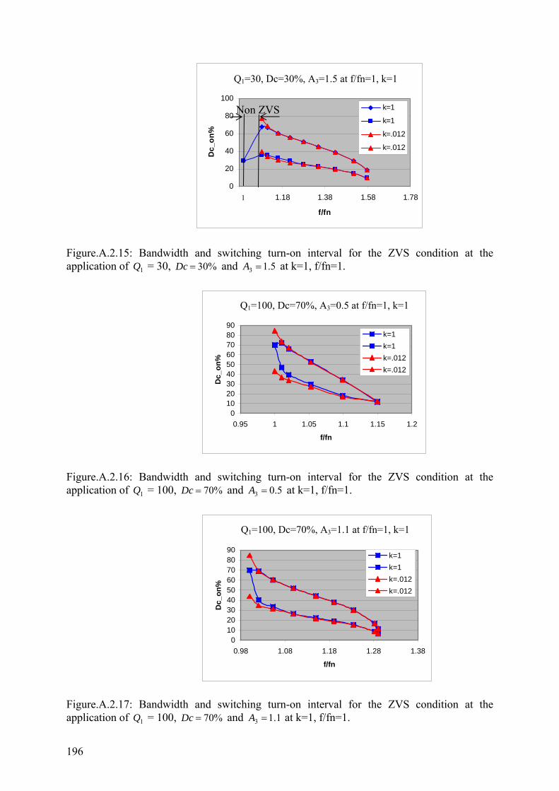
196
Figure.A.2.15: Bandwidth and switching turn-on interval for the ZVS condition at the application of 1Q = 30, %30=Dc and 5.13 =A at k=1, f/fn=1.
Q=100, Dc=70%, A3=.5
0102030405060708090
0.95 1 1.05 1.1 1.15 1.2
f/fn
Dc_
on%
k=1k=1k=.012k=.012
Figure.A.2.16: Bandwidth and switching turn-on interval for the ZVS condition at the application of 1Q = 100, %70=Dc and 5.03 =A at k=1, f/fn=1.
Q=100, Dc=70%, A3=1.1
0102030405060708090
0.98 1.08 1.18 1.28 1.38
f/fn
Dc_
on%
k=1k=1k=.012k=.012
Figure.A.2.17: Bandwidth and switching turn-on interval for the ZVS condition at the application of 1Q = 100, %70=Dc and 1.13 =A at k=1, f/fn=1.
Q1=100, Dc=70%, A3=0.5 at f/fn=1, k=1
Q1=100, Dc=70%, A3=1.1 at f/fn=1, k=1
Q=30,Dc=30,A3=1.5
0
20
40
60
80
100
0.98 1.18 1.38 1.58 1.78
f/fnD
c_on
%
k=1
k=1
k=.012
k=.012
Non ZVS
1
Q1=30, Dc=30%, A3=1.5 at f/fn=1, k=1
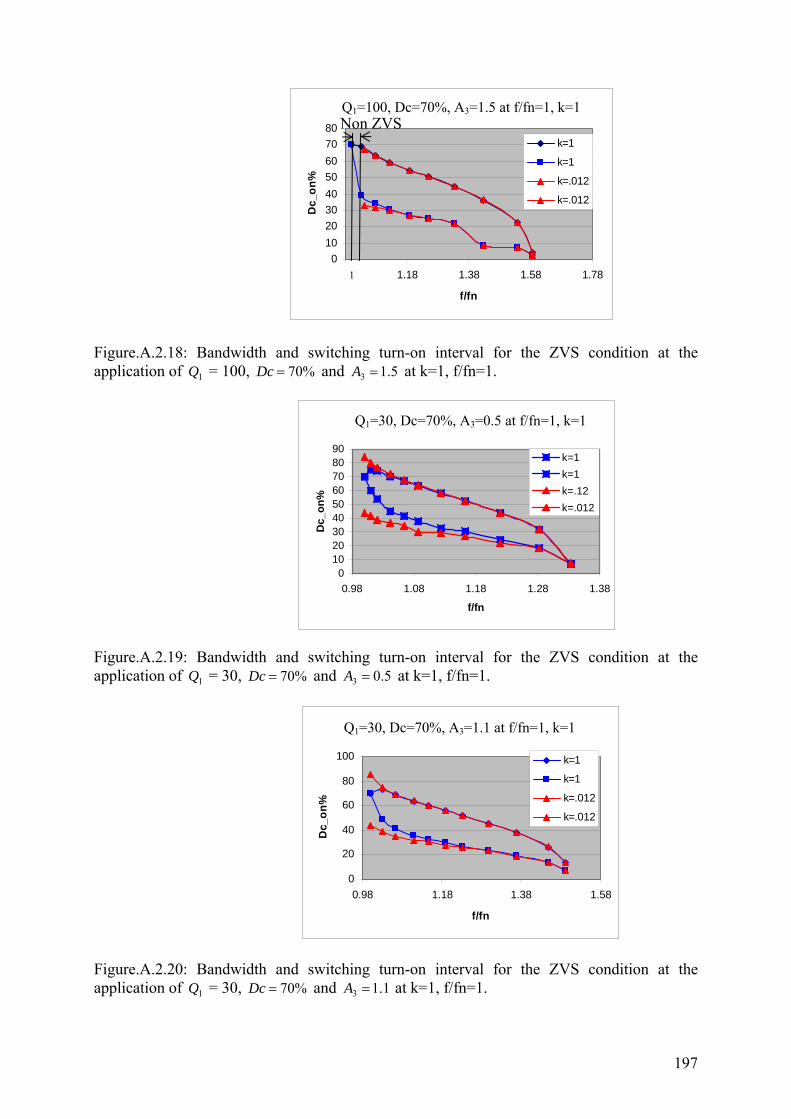
197
Figure.A.2.18: Bandwidth and switching turn-on interval for the ZVS condition at the application of 1Q = 100, %70=Dc and 5.13 =A at k=1, f/fn=1.
Q1=30, Dc=70%, A3=.5
0102030405060708090
0.98 1.08 1.18 1.28 1.38
f/fn
Dc_
on%
k=1k=1k=.12k=.012
Figure.A.2.19: Bandwidth and switching turn-on interval for the ZVS condition at the application of 1Q = 30, %70=Dc and 5.03 =A at k=1, f/fn=1. Figure.A.2.20: Bandwidth and switching turn-on interval for the ZVS condition at the application of 1Q = 30, %70=Dc and 1.13 =A at k=1, f/fn=1.
Q=100, Dc=70%, A3=1.5
01020304050607080
0.98 1.18 1.38 1.58 1.78
f/fnD
c_on
%
k=1
k=1
k=.012
k=.012
Q1=100, Dc=70%, A3=1.5 at f/fn=1, k=1
Q1=30, Dc=70%, A3=0.5 at f/fn=1, k=1
Q=30, Dc=30%, A3=1.1
0
20
40
60
80
100
0.98 1.18 1.38 1.58
f/fn
Dc_
on%
k=1
k=1
k=.012
k=.012
Q1=30, Dc=70%, A3=1.1 at f/fn=1, k=1
Non ZVS
1
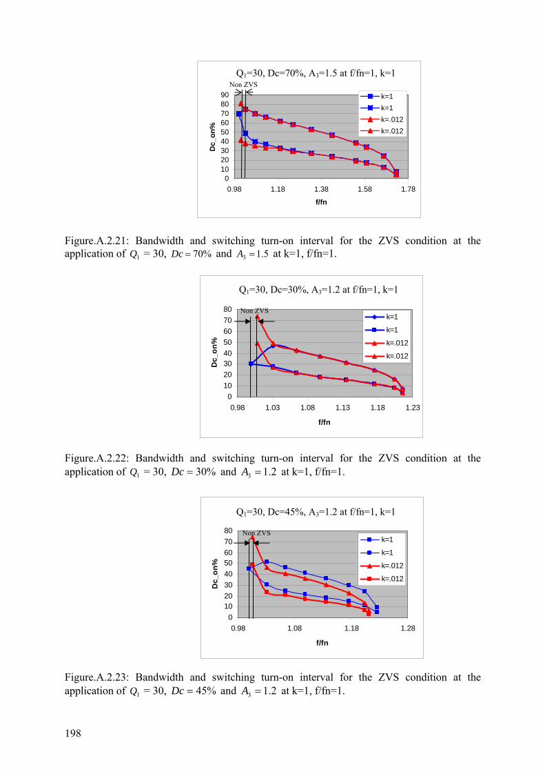
198
Q=30, Dc=70%, A3=1.5
0102030405060708090
0.98 1.18 1.38 1.58 1.78
f/fnD
c_on
%
k=1k=1k=.012k=.012
Figure.A.2.21: Bandwidth and switching turn-on interval for the ZVS condition at the application of 1Q = 30, %70=Dc and 5.13 =A at k=1, f/fn=1. Figure.A.2.22: Bandwidth and switching turn-on interval for the ZVS condition at the application of 1Q = 30, %30=Dc and 2.13 =A at k=1, f/fn=1.
Figure.A.2.23: Bandwidth and switching turn-on interval for the ZVS condition at the application of 1Q = 30, %45=Dc and 2.13 =A at k=1, f/fn=1.
Q1=30, Dc=70%, A3=1.5 at f/fn=1, k=1 Non ZVS
Q1=30,Dc=45%;A3=1.2
01020304050607080
0.98 1.08 1.18 1.28
f/fn
Dc_
on%
k=1
k=1
k=.012
k=.012
Q1=30, Dc=45%, A3=1.2 at f/fn=1, k=1
Q1=30,Dc=30%,A3=1.2
01020304050607080
0.98 1.03 1.08 1.13 1.18 1.23
f/fn
Dc_
on%
k=1
k=1
k=.012
k=.012
Q1=30, Dc=30%, A3=1.2 at f/fn=1, k=1
Non ZVS
Non ZVS
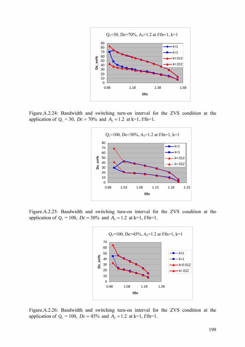
199
Figure.A.2.24: Bandwidth and switching turn-on interval for the ZVS condition at the application of 1Q = 30, %70=Dc and 2.13 =A at k=1, f/fn=1. Figure.A.2.25: Bandwidth and switching turn-on interval for the ZVS condition at the application of 1Q = 100, %30=Dc and 2.13 =A at k=1, f/fn=1. Figure.A.2.26: Bandwidth and switching turn-on interval for the ZVS condition at the application of 1Q = 100, %45=Dc and 2.13 =A at k=1, f/fn=1.
Q=30,Dc=70%,A3=1.2
0102030405060708090
0.98 1.18 1.38 1.58
f/fnD
c_on
%
k=1
k=1
k=.012
k=.012
Q1=30, Dc=70%, A3=1.2 at f/fn=1, k=1
Q1=100,Dc=30%,A3=1.2
01020304050607080
0.98 1.03 1.08 1.13 1.18 1.23
f/fn
Dc_
on%
k=1
k=1
k=.012
k=.012
Q1=100, Dc=30%, A3=1.2 at f/fn=1, k=1
Q1=100,Dc=45%,A3=1.2
010
20304050
6070
0.98 1.08 1.18 1.28
f/fn
Dc_
on%
k=1
k=1
k=0.012
k=.012
Q1=100, Dc=45%, A3=1.2 at f/fn=1, k=1
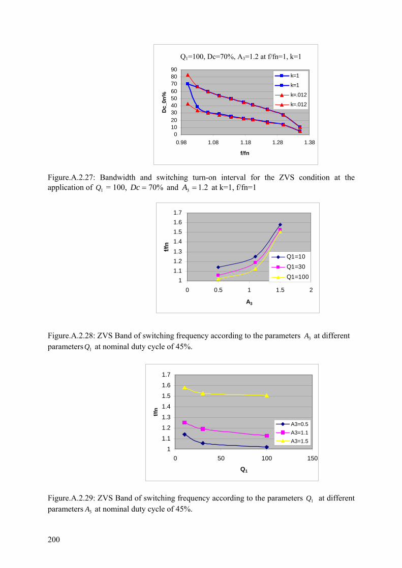
200
Figure.A.2.27: Bandwidth and switching turn-on interval for the ZVS condition at the application of 1Q = 100, %70=Dc and 2.13 =A at k=1, f/fn=1
Figure.A.2.28: ZVS Band of switching frequency according to the parameters 3A at different parameters 1Q at nominal duty cycle of 45%.
1
1.1
1.2
1.3
1.4
1.5
1.6
1.7
0 50 100 150
Q1
f/fn
A3=0.5A3=1.1A3=1.5
Figure.A.2.29: ZVS Band of switching frequency according to the parameters 1Q at different parameters 3A at nominal duty cycle of 45%.
11.11.21.31.41.51.61.7
0 0.5 1 1.5 2
A3
f/fn
Q1=10
Q1=30
Q1=100
Q=100,Dc=70%,A3=1.2
0102030405060708090
0.98 1.08 1.18 1.28 1.38
f/fn
Dc_
0n%
k=1
k=1
k=.012
k=.012
Q1=100, Dc=70%, A3=1.2 at f/fn=1, k=1

201
Figure.A.2.30: The relation between the input voltage and the switching frequency for a constant output voltage for different output loads ( 1.0,1=k ) Figure.A.2.31: The relation between the input voltage and the switching frequency for a constant output voltage for different output loads ( 1.0,1=k ) Figure.A.2.32: The relation between the input voltage and the switching frequency for a constant output voltage for different output loads ( 1.0,1=k )
Q1=30, Dc=45%, A3=0.5
0.991
1.011.021.031.041.051.06
0 1 2 3 4
Vin/Vin(op)f/f
n k=1
k=0.1
Q1=30, Dc=45%, A3=0.5 at f/fn=1, k=1
Q1=30, Dc=45%, A3=1.5
0.98
1.08
1.18
1.28
1.38
1.48
1.58
0 5 10 15 20
Vin/Vin(op)
f/fn k=1
k=0.1
Q1=30, Dc=45%, A3=1.5 at f/fn=1, k=1
Q=30, Dc=70%, A3=0.5
0.981.031.081.131.181.231.281.331.38
0 5 10 15 20
Vin/Vin(op)
f/fn k=1
k=0.1
Q1=30, Dc=70%, A3=0.5 at f/fn=1, k=1

202
Figure.A.2.33: The relation between the input voltage and the switching frequency for a constant output voltage for different output loads ( 1.0,1=k ) Figure.A.2.34: The relation between the input voltage and the switching frequency for a constant output voltage for different output loads ( 1.0,1=k ) Figure.A.2.35: The relation between the input voltage and the switching frequency for a constant output voltage for different output loads ( 1.0,1=k )
Q=30,Dc=30%, A3=0.5
0.9951
1.0051.01
1.0151.02
1.0251.03
0 1 2
Vin/Vin(op)
f/fn k=1
k=0.1
Q1=30, Dc=30%, A3=0.5 at f/fn=1, k=1
Q=30, Dc=70%, A3=1.1
0.98
1.08
1.18
1.28
1.38
1.48
1.58
0 10 20 30
Vin/Vin(op)f/f
n k=1
k=0.1
Q1=30, Dc=70%, A3=1.1 at f/fn=1, k=1
Q=30, Dc=70%, A3=1.5
0.981.081.181.281.381.481.581.681.78
0 10 20 30
Vin/Vin(op)
f/fn k=1
k=0.1
Q1=30, Dc=70%, A3=1.5 at f/fn=1, k=1
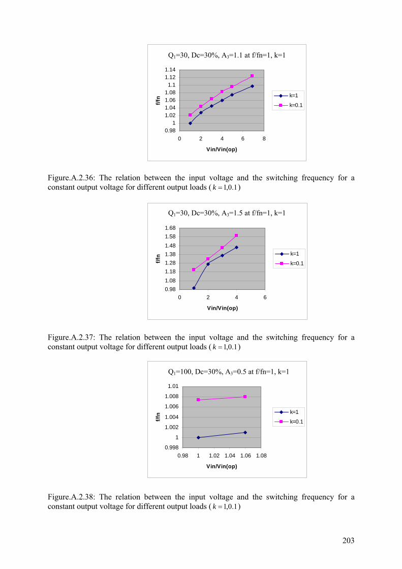
203
Figure.A.2.36: The relation between the input voltage and the switching frequency for a constant output voltage for different output loads ( 1.0,1=k ) Figure.A.2.37: The relation between the input voltage and the switching frequency for a constant output voltage for different output loads ( 1.0,1=k ) Figure.A.2.38: The relation between the input voltage and the switching frequency for a constant output voltage for different output loads ( 1.0,1=k )
Q=30,Dc=30%, A3=1.5
0.981.081.181.281.381.481.581.68
0 2 4 6
Vin/Vin(op)
f/fn k=1
k=0.1
Q1=30, Dc=30%, A3=1.5 at f/fn=1, k=1
Q=100, Dc=30%, A3=0.5
0.998
1
1.002
1.004
1.006
1.008
1.01
0.98 1 1.02 1.04 1.06 1.08
Vin/Vin(op)
f/fn k=1
k=0.1
Q1=100, Dc=30%, A3=0.5 at f/fn=1, k=1
Q=30, Dc=30%, A3=1.1
0.981
1.021.041.061.081.1
1.121.14
0 2 4 6 8
Vin/Vin(op)f/f
n k=1
k=0.1
Q1=30, Dc=30%, A3=1.1 at f/fn=1, k=1
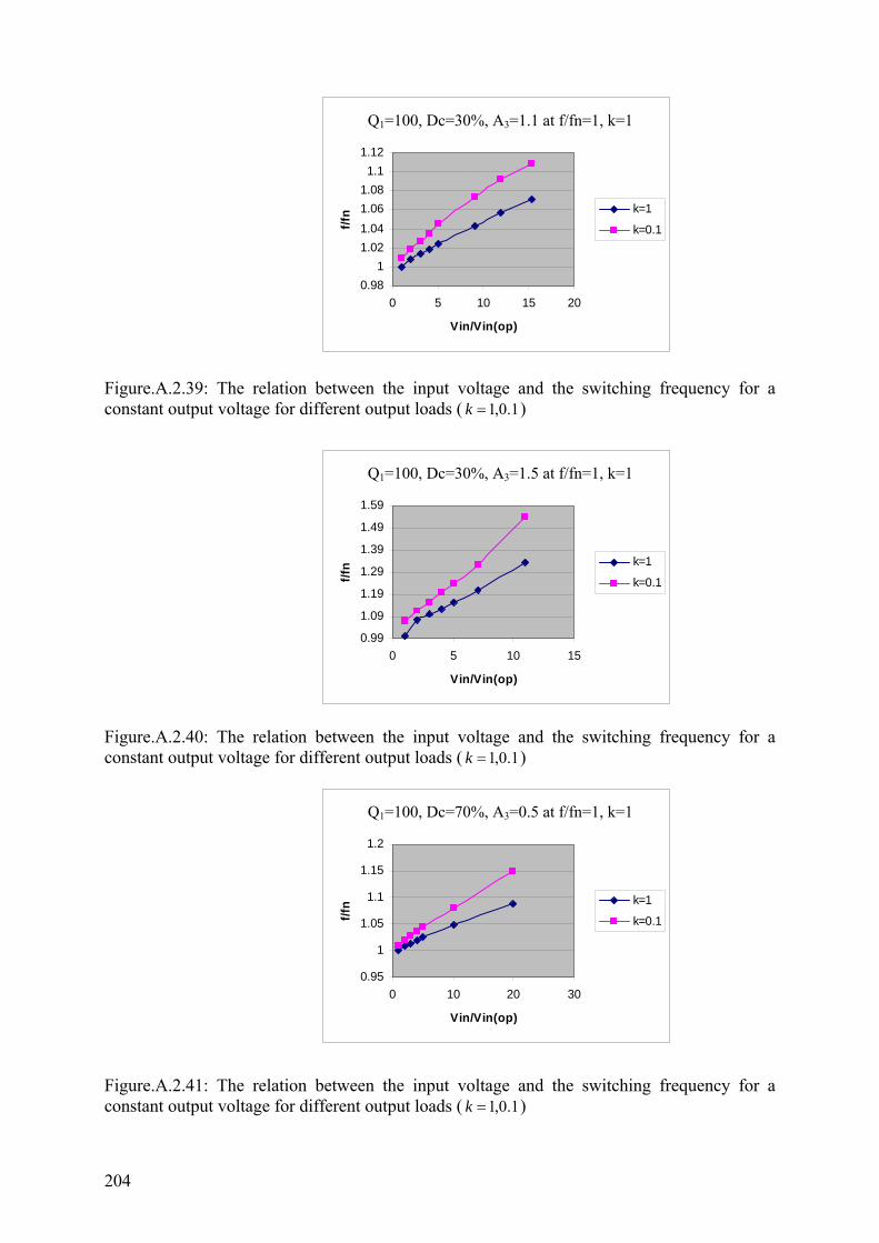
204
Figure.A.2.39: The relation between the input voltage and the switching frequency for a constant output voltage for different output loads ( 1.0,1=k ) Figure.A.2.40: The relation between the input voltage and the switching frequency for a constant output voltage for different output loads ( 1.0,1=k ) Figure.A.2.41: The relation between the input voltage and the switching frequency for a constant output voltage for different output loads ( 1.0,1=k )
Q=100, Dc=30%, A3=1.1
0.981
1.021.041.061.081.1
1.12
0 5 10 15 20
Vin/Vin(op)f/f
n k=1
k=0.1
Q1=100, Dc=30%, A3=1.1 at f/fn=1, k=1
Q=100, Dc=30%, A3=1.5
0.99
1.09
1.19
1.29
1.39
1.49
1.59
0 5 10 15
Vin/Vin(op)
f/fn k=1
k=0.1
Q1=100, Dc=30%, A3=1.5 at f/fn=1, k=1
Q=100, Dc=70%, A3=0.5
0.95
1
1.05
1.1
1.15
1.2
0 10 20 30
Vin/Vin(op)
f/fn k=1
k=0.1
Q1=100, Dc=70%, A3=0.5 at f/fn=1, k=1

205
Figure.A.2.42: The relation between the input voltage and the switching frequency for a constant output voltage for different output loads ( 1.0,1=k ) Figure.A.2.43: The relation between the input voltage and the switching frequency for a constant output voltage for different output loads ( 1.0,1=k ) Figure.A.2.44: The relation between the input voltage and the switching frequency for a constant output voltage for different output loads ( 1.0,1=k )
Q=100, Dc=45%, A3=0.5
0.995
1
1.005
1.01
1.015
1.02
0.9 1.4 1.9 2.4
Vin/Vin(op)
f/fn k=1
k=0.1
Q1=100, Dc=45%, A3=0.5 at f/fn=1, k=1
Q=100, Dc=70%, A3=1.1
0.981.031.081.131.181.231.281.33
0 20 40 60
Vin/Vin(op)f/f
n k=1
k=0.1
Q1=100, Dc=70%, A3=1.1 at f/fn=1, k=1
Q=100, Dc=70%, A3=1.5
0.981.081.181.281.381.481.581.68
0 20 40 60 80
Vin/Vin(op)
f/fn k=1
k=0.1
Q1=100, Dc=70%, A3=1.5 at f/fn=1, k=1
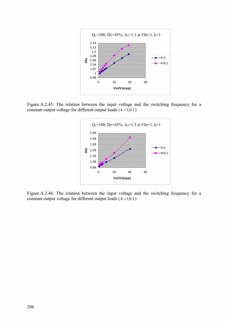
206
Figure.A.2.45: The relation between the input voltage and the switching frequency for a constant output voltage for different output loads ( 1.0,1=k ) Figure.A.2.46: The relation between the input voltage and the switching frequency for a constant output voltage for different output loads ( 1.0,1=k )
Q=100, Dc=45%, A3=1.1
0.981
1.021.041.061.081.1
1.121.14
0 10 20 30
Vin/Vin(op)f/f
n k=1
k=0.1
Q1=100, Dc=45%, A3=1.1 at f/fn=1, k=1
Q=100, Dc=45%, A3=1.5
0.98
1.08
1.18
1.28
1.38
1.48
1.58
0 20 40 60
Vin/Vin(op)
f/fn k=1
k=0.1
Q1=100, Dc=45%, A3=1.5 at f/fn=1, k=1
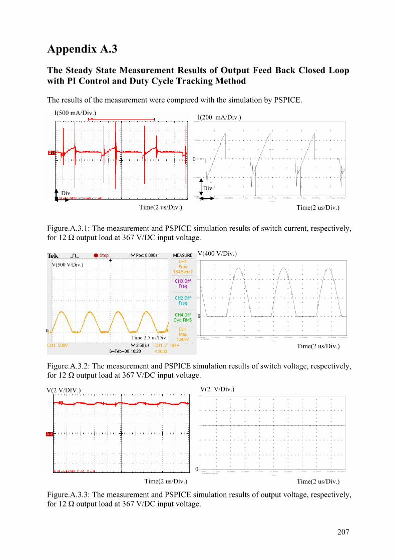
207
Appendix A.3 The Steady State Measurement Results of Output Feed Back Closed Loop with PI Control and Duty Cycle Tracking Method The results of the measurement were compared with the simulation by PSPICE.
Figure.A.3.1: The measurement and PSPICE simulation results of switch current, respectively, for 12 Ω output load at 367 V/DC input voltage.
Figure.A.3.2: The measurement and PSPICE simulation results of switch voltage, respectively, for 12 Ω output load at 367 V/DC input voltage.
Figure.A.3.3: The measurement and PSPICE simulation results of output voltage, respectively, for 12 Ω output load at 367 V/DC input voltage.
Div.
Time(2 us/Div.) Time(2 us/Div.)
I(200 mA/Div.)
Time
37.980ms 37.982ms 37.984ms 37.986ms 37.988ms 37.990ms 37.992ms 37.994ms 37.996ms 37.998ms 38.000msI(Vs)
-400mA
-200mA
0A
200mA
400mA
I(500 mA/Div.)
Div.
0 0
Time(2 us/Div.)
V(2 V/DIV.)
Time(2 us/Div.)
V(2 V/Div.)
Time
37.980ms 37.982ms 37.984ms 37.986ms 37.988ms 37.990ms 37.992ms 37.994ms 37.996ms 37.998ms 38.000msV(R2:2,Cout:1)
0V
2V
4V
6V
8V
10V
0
0
Time(2 us/Div.)
V(400 V/Div.)
Time
37.980ms 37.982ms 37.984ms 37.986ms 37.988ms 37.990ms 37.992ms 37.994ms 37.996ms 37.998ms 38.000msV(Lf:2)
-0.4KV
0V
0.4KV
0.8KV
1.2KV
0
0
V(500 V/Div.)
Time 2.5 us/Div.

208
Appendix A.4 The Transient Response of the Output Voltage for the Output Load Jump for Output Feed Back Closed Loop with PI Control and Duty Cycle Tracking The output loads were chosen to change from 1.2 kΩ to 44 Ω at input voltage of 65 V/DC. The transient responses of the output voltage were tested with different pK and IK control parameters shown in Fig.A.4.1.
Figure.A.4.1: Output voltages at load jump from 1.2 kΩ to 44 Ω at 65 V/DC input.
Time(2 ms/Div.) Time(2 ms/Div.)
KP=10 KP=10
KI=213 k KI=147 k
V(1 V/Div.) V(1 V/Div.)
KP= 47 KP= 47
KI= 213 k KI= 147 k
V(1 V/Div.) V(1 V/Div.)
Time(2 ms/Div.) Time(2 ms/Div.)
Div. 0 0
0 0
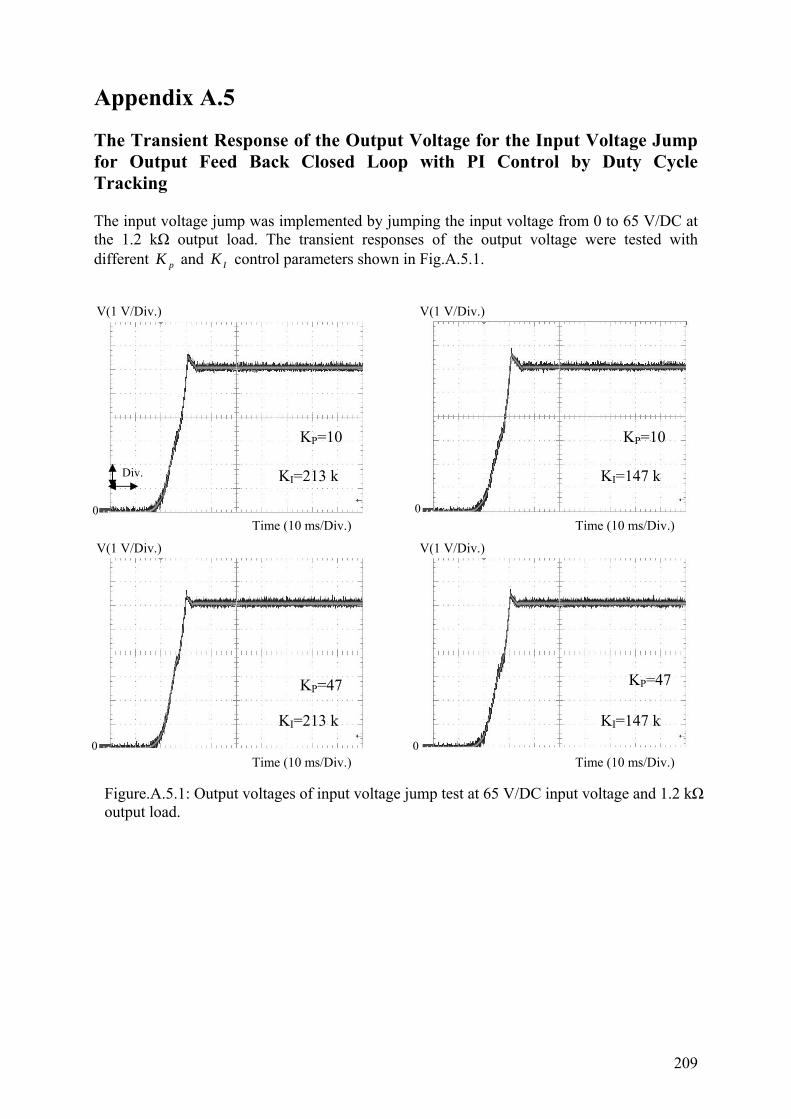
209
Appendix A.5 The Transient Response of the Output Voltage for the Input Voltage Jump for Output Feed Back Closed Loop with PI Control by Duty Cycle Tracking The input voltage jump was implemented by jumping the input voltage from 0 to 65 V/DC at the 1.2 kΩ output load. The transient responses of the output voltage were tested with different pK and IK control parameters shown in Fig.A.5.1.
Time (10 ms/Div.)
Time (10 ms/Div.) Time (10 ms/Div.)
Time (10 ms/Div.)
V(1 V/Div.) V(1 V/Div.)
V(1 V/Div.) V(1 V/Div.)
KP=10
KI=213 k KI=147 k
KI=213 k KI=147 k
KP=10
KP=47 KP=47
Div.
0 0
0 0
Figure.A.5.1: Output voltages of input voltage jump test at 65 V/DC input voltage and 1.2 kΩ output load.
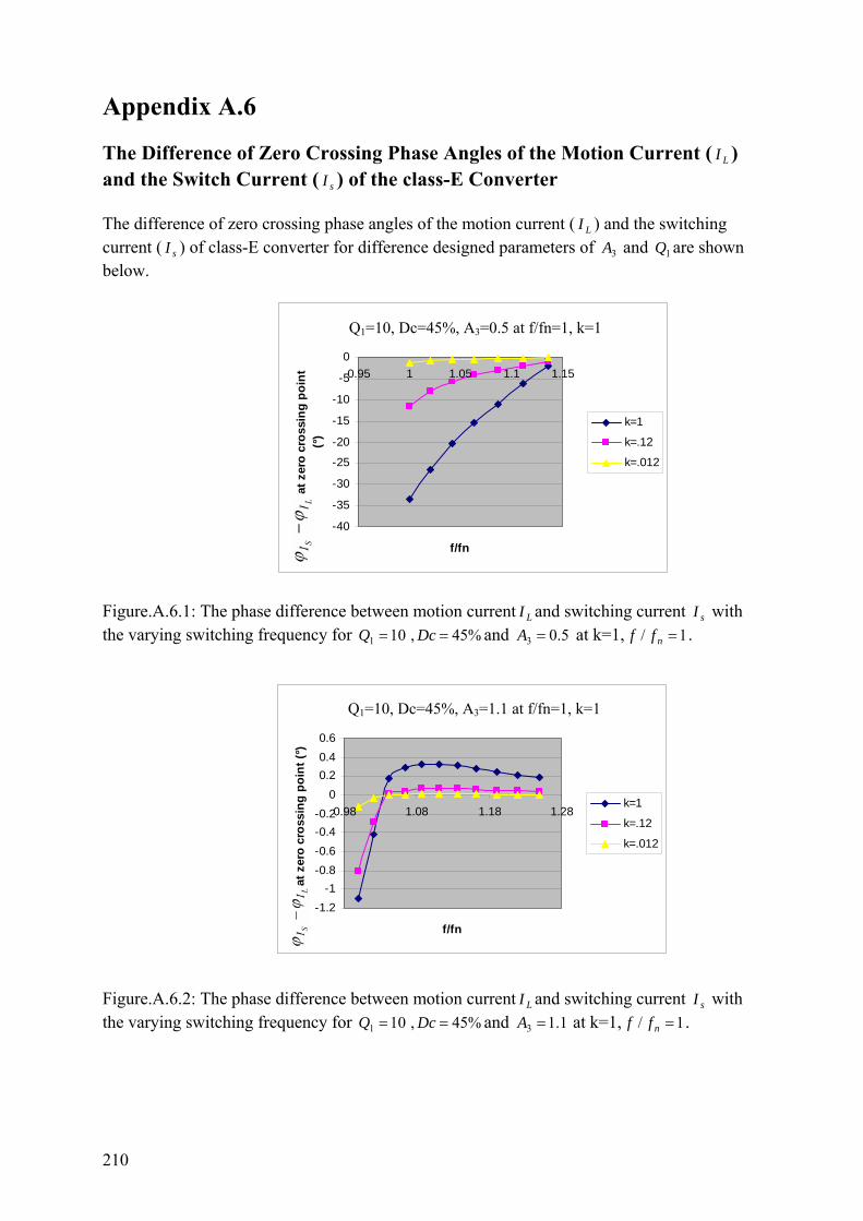
210
Appendix A.6 The Difference of Zero Crossing Phase Angles of the Motion Current ( LI ) and the Switch Current ( sI ) of the class-E Converter The difference of zero crossing phase angles of the motion current ( LI ) and the switching current ( sI ) of class-E converter for difference designed parameters of 3A and 1Q are shown below.
Figure.A.6.1: The phase difference between motion current LI and switching current sI with the varying switching frequency for 101 =Q %45, =Dc and 5.03 =A at k=1, 1/ =nff .
Figure.A.6.2: The phase difference between motion current LI and switching current sI with the varying switching frequency for 101 =Q %45, =Dc and 1.13 =A at k=1, 1/ =nff .
Q1=10, Dc=.45%, A3=.5 (optimum ZVS point)
-40
-35
-30
-25
-20
-15
-10
-5
00.95 1 1.05 1.1 1.15
f/fn
Is-IL
at z
ero
cros
sing
poi
nt
(°)
k=1
k=.12
k=.012
Q1=10, Dc=45%, A3=0.5 at f/fn=1, k=1
Q1=10, Dc=.45%,A3=1.1 (optimum ZVS point)
-1.2-1
-0.8-0.6-0.4-0.2
00.20.40.6
0.98 1.08 1.18 1.28
f/fn
I s-I L a
t zer
o cr
ossi
ng p
oint
(°)
k=1
k=.12
k=.012
Q1=10, Dc=45%, A3=1.1 at f/fn=1, k=1

211
Figure.A.6.3: The phase difference between motion current LI and switching current sI with the varying switching frequency for 101 =Q %45, =Dc and 5.13 =A at k=1, 1/ =nff .
Figure.A.6.4: The phase difference between motion current LI and switching current sI with the varying switching frequency for 301 =Q %45, =Dc and 5.03 =A at k=1, 1/ =nff .
Figure.A.6.5: The phase difference between motion current LI and switching current sI with the varying switching frequency for 301 =Q %45, =Dc and 1.13 =A at k=1, 1/ =nff .
Q1=10, Dc=.45%, A3=1.5 (optimum ZVS point)
-3.5-3
-2.5-2
-1.5-1
-0.50
0.51
0.98 1.18 1.38 1.58 1.78
f/fn
I s-I L
at z
ero
cros
sing
poi
nt(°
)
k=1
k=.12
k=.012
Q1=10, Dc=45%, A3=1.5 at f/fn=1, k=1
Q1=30, Dc=.45%, A3=0.5 (optimum ZVS point)
-14
-12
-10
-8
-6
-4
-2
0
2
0.98 1 1.02 1.04 1.06
f/fn
I s-I L a
t zer
o cr
ossi
ng p
oint
(°)
k=1
k=.12
k=.012
Q1=30, Dc=45%, A3=0.5 at f/fn, k=1
Q1=30, Dc=.45%, A3=1.1 (optimum ZVS point)
-0.8-0.7-0.6-0.5-0.4-0.3-0.2-0.1
00.10.2
0.95 1 1.05 1.1 1.15 1.2
f/fn
I S-I L
at z
ero
cros
sing
poi
nt (°
)
k=1
k=.12
k=.012
Q1=30, Dc=45%, A3=1.1 at f/fn=1, k=1

212
Figure.A.6.6: The phase difference between motion current LI and switching current sI with the varying switching frequency for 301 =Q %45, =Dc and 5.13 =A at k=1, 1/ =nff .
Figure.A.6.7: The phase difference between motion current LI and switching current sI with the varying switching frequency for 1001 =Q %45, =Dc and 5.03 =A at k=1, 1/ =nff .
Figure.A.6.8: The phase difference between motion current LI and switching current sI with the varying switching frequency for 1001 =Q %45, =Dc and 1.13 =A at k=1, 1/ =nff .
Q1=30, Dc=.45%, A3=1.5 (optimum ZVS point)
-0.25
-0.2-0.15
-0.1-0.05
0
0.050.1
0.15
0.95 1.15 1.35 1.55 1.75
f/fnI s-
I L at z
ero
cros
sing
poi
nt
(°)
k=1
k=.12
k=.012
Q1=30, Dc=45%, A3=1.5 at f/fn=1, k=1
Q1=100, Dc=.45%, A3=.5 (optimum ZVS point)
-4
-3.5
-3
-2.5
-2
-1.5
-1
-0.5
00.995 1 1.005 1.01 1.015 1.02
f/fn
I S-I L a
t zer
o cr
ossi
ng p
oint
(°)
k=1
k=.12
k=.012
Q1=100, Dc=45%, A3=0.5 at f/fn=1, k=1
Q1=100, Dc=.45%, A3=1.1 (optimum ZVS point)
-0.3
-0.25
-0.2
-0.15
-0.1
-0.05
0
0.05
0.95 1 1.05 1.1 1.15
f/fn
I S-I L
at z
ero
cros
sing
poi
nt (°
)
k=1
k=.12
k=.012
Q1=100, Dc=45%, A3=1.1 at f/fn=1, k=1

213
Figure.A.6.9: The phase difference between motion current LI and switching current sI with the varying switching frequency for 1001 =Q %45, =Dc and 5.13 =A at k=1, 1/ =nff .
Q=100, Dc=30%, A=.5
-1.2
-1
-0.8
-0.6
-0.4
-0.2
0
0.2
0.4
0.998 1 1.002 1.004 1.006 1.008 1.01 1.012
f/fn
Is-IL
at z
ero
cros
sing
(°)
k=1k=.012
Figure.A.6.10: The phase difference between motion current LI and switching current sI with the varying switching frequency for 1001 =Q %30, =Dc and 5.03 =A at k=1, 1/ =nff .
Q=100, Dc=30% A3=1.1
-0.005
0
0.005
0.01
0.015
0.02
0.025
0.03
0.035
0.04
0.045
0.98 1 1.02 1.04 1.06 1.08 1.1 1.12
f/fn
Is-IL
at z
ero
cros
sing
po
int(°
)
k=1
k=.012
Figure.A.6.11: The phase difference between motion current LI and switching current sI with the varying switching frequency for 1001 =Q %30, =Dc and 1.13 =A at k=1, 1/ =nff .
Q1=100, Dc=.455, A3=1.5 (optimum ZVS point)
-0.0020
0.0020.0040.0060.0080.01
0.0120.0140.0160.0180.02
0.98 1.18 1.38 1.58
f/fn
I S-I L a
t zer
o cr
ossi
ng p
oint
(°)
k=1
k=.12
k=.012
Q1=100, Dc=45%, A3=1.5 at f/fn=1, k=1
Q1=100, Dc=30%, A3=0.5 at f/fn=1, k=1
Q1=100, Dc=30%, A3=1.1 at f/fn=1, k=1
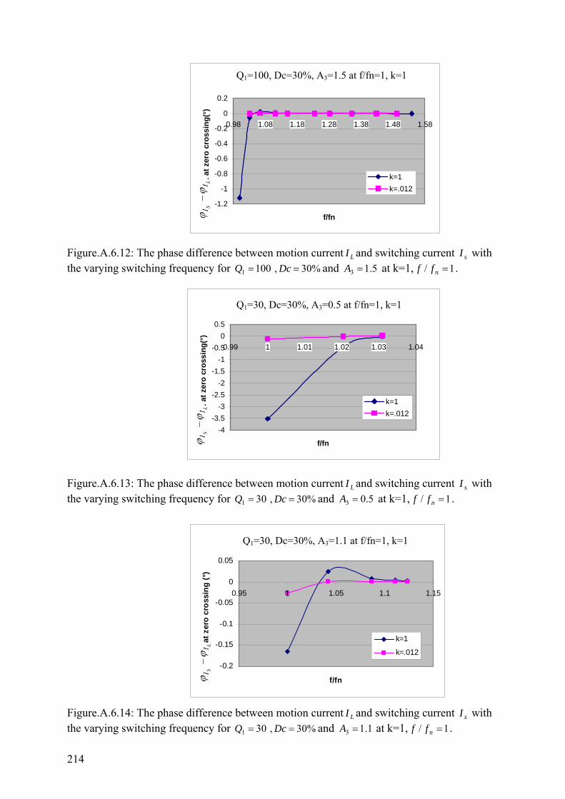
214
Q=100, Dc=30% A3=1.5
-1.2
-1
-0.8
-0.6
-0.4
-0.2
0
0.2
0.98 1.08 1.18 1.28 1.38 1.48 1.58
f/fnIs
-IL a
t zer
o cr
ossi
ng(°
)
k=1k=.012
Figure.A.6.12: The phase difference between motion current LI and switching current sI with the varying switching frequency for 1001 =Q %30, =Dc and 5.13 =A at k=1, 1/ =nff .
Q=30, Dc=30%, A3=.5
-4-3.5
-3-2.5
-2-1.5
-1-0.5
00.5
0.99 1 1.01 1.02 1.03 1.04
f/fn
Is-IL
at z
ero
cros
sing
(°)
k=1k=.012
Figure.A.6.13: The phase difference between motion current LI and switching current sI with the varying switching frequency for 301 =Q %30, =Dc and 5.03 =A at k=1, 1/ =nff .
Figure.A.6.14: The phase difference between motion current LI and switching current sI with the varying switching frequency for 301 =Q %30, =Dc and 1.13 =A at k=1, 1/ =nff .
Q=30, Dc=30, A3=1.1
-0.2
-0.15
-0.1
-0.05
0
0.05
0.95 1 1.05 1.1 1.15
f/fn
Is-IL
at z
ero
cros
sing
(°)
k=1
k=.012
Q1=100, Dc=30%, A3=1.5 at f/fn=1, k=1
Q1=30, Dc=30%, A3=0.5 at f/fn=1, k=1 Q1=30, Dc=30%, A3=0.5 at f/fn=1, k=1
Q1=30, Dc=30%, A3=1.1 at f/fn=1, k=1

215
Q=30, Dc=30%, A3=1.5
-6
-5
-4
-3
-2
-1
0
1
0.98 1.18 1.38 1.58 1.78
f/fnIs
-IL a
t zer
o cr
ossi
ng(°
)
k=1k=.012
Figure.A.6.15: The phase difference between motion current LI and switching current sI with the varying switching frequency for 301 =Q %30, =Dc and 5.13 =A at k=1, 1/ =nff .
Q=100, Dc=70%, A3=.5
-60
-50
-40
-30
-20
-10
00.95 1 1.05 1.1 1.15 1.2
f/fn
Is-IL
at z
ero
cros
sing
(°)
k=1k=.012
Figure.A.6.16: The phase difference between motion current LI and switching current sI with the varying switching frequency for 1001 =Q %70, =Dc and 5.03 =A at k=1, 1/ =nff .
Q=100, Dc=70%, A3=1.1
-10
-8
-6
-4
-2
0
2
0.98 1.08 1.18 1.28 1.38
f/fn
Is-IL
at z
ero
cros
sing
(°)
k=1k=.012
Figure.A.6.17: The phase difference between motion current LI and switching current sI with the varying switching frequency for 1001 =Q %70, =Dc and 1.13 =A at k=1, 1/ =nff .
Q1=30, Dc=30%, A3=1.5 at f/fn=1, k=1
Q1=100, Dc=70%, A3=0.5 at f/fn=1, k=1
Q1=100, Dc=70%, A3=1.1 at f/fn=1, k=1
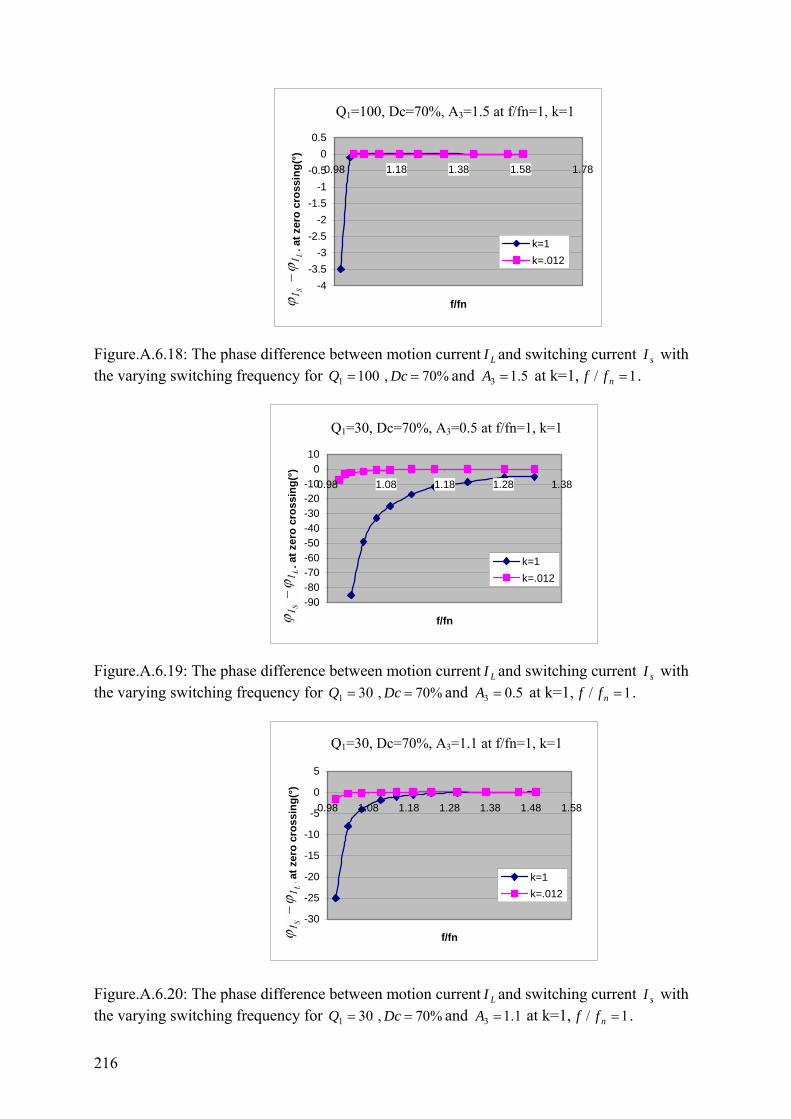
216
Q=100, Dc=70%, A3=1.5
-4-3.5
-3-2.5
-2-1.5
-1-0.5
00.5
0.98 1.18 1.38 1.58 1.78
f/fnIs
-IL a
t zer
o cr
ossi
ng(°
)
k=1k=.012
Figure.A.6.18: The phase difference between motion current LI and switching current sI with the varying switching frequency for 1001 =Q %70, =Dc and 5.13 =A at k=1, 1/ =nff .
Q=30, Dc=70%, A3=.5
-90-80-70-60-50-40-30-20-10
010
0.98 1.08 1.18 1.28 1.38
f/fn
Is-IL
at z
ero
cros
sing
(°)
k=1k=.012
Figure.A.6.19: The phase difference between motion current LI and switching current sI with the varying switching frequency for 301 =Q %70, =Dc and 5.03 =A at k=1, 1/ =nff .
Q=30, Dc=70, A3=1.1
-30
-25
-20
-15
-10
-5
0
5
0.98 1.08 1.18 1.28 1.38 1.48 1.58
f/fn
Is-IL
at z
ero
cros
sing
(°)
k=1k=.012
Figure.A.6.20: The phase difference between motion current LI and switching current sI with the varying switching frequency for 301 =Q %70, =Dc and 1.13 =A at k=1, 1/ =nff .
Q1=100, Dc=70%, A3=1.5 at f/fn=1, k=1
Q1=30, Dc=70%, A3=0.5 at f/fn=1, k=1
Q1=30, Dc=70%, A3=1.1 at f/fn=1, k=1

217
Q=30, Dc=70%, A3=1.5
-12
-10
-8
-6
-4
-2
0
2
0.98 1.18 1.38 1.58 1.78
f/fnIL
-Is a
t zer
o cr
ossi
ng(°
)
k=1k=.012
Figure.A.6.21: The phase difference between motion current LI and switching current sI with the varying switching frequency for 301 =Q %70, =Dc and 5.13 =A at k=1, 1/ =nff .
Q1=30, Dc=70%, A3=1.5 at f/fn=1, k=1

218
Appendix A.7 The Transient Response of the Auxiliary Tap Regulation with Duty Cycle Adjustment by Synchronization Method The input voltage jump was implemented by changing the input voltage from 120 V/DC to 353 V/DC at the 100 Ω output load. The transient responses of the output voltage were tested with different pK and IK control parameters shown in Fig.A.7.1.
(a) (b) Figure.A.7.1: Input voltage jump for tap regulation: upper trace shows the output voltage, lower trace shows the tap voltage with different control parameters. a) PI controller: PK 0.035 and sI TK . 0.1. b) I controller: sI TK . 0.017, while sT is the period of switching frequency.
Div. Time (100 us/Div.) Time (100 us/Div.)
Vtap (1 V/Div.) Vtap (1 V/Div.)
Vout (2 V/Div.) Vout (2 V/Div.)
0
0
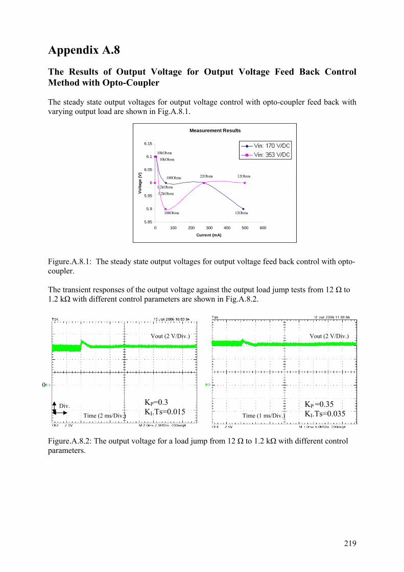
219
Measurement Results
5.85
5.9
5.95
6
6.05
6.1
6.15
0 100 200 300 400 500 600
Current (mA)
Volta
ge (V
)
120 Vin250 Vin
12Ohms
12Ohms22Ohms100Ohms
100Ohms
10kOhms10kOhms
1.2kOhms1.2kOhms
Appendix A.8 The Results of Output Voltage for Output Voltage Feed Back Control Method with Opto-Coupler The steady state output voltages for output voltage control with opto-coupler feed back with varying output load are shown in Fig.A.8.1. Figure.A.8.1: The steady state output voltages for output voltage feed back control with opto-coupler. The transient responses of the output voltage against the output load jump tests from 12 Ω to 1.2 kΩ with different control parameters are shown in Fig.A.8.2.
Figure.A.8.2: The output voltage for a load jump from 12 Ω to 1.2 kΩ with different control parameters.
KP=0.3 KI.Ts=0.015
KP =0.35 KI.Ts=0.035
Div.
Vout (2 V/Div.) Vout (2 V/Div.)
Time (2 ms/Div.) Time (1 ms/Div.)
0

220
Measurement Results
5.65
5.7
5.75
5.8
5.85
5.9
5.95
6
6.05
-100 0 100 200 300 400 500
Current (mA)
Volta
ge (v
)
120 Vin250 Vin
12Ohms
22Ohms
100Ohms
1.2kOhms10kOhms
12Ohms
22Ohms
100Ohms1.2kOhms10kOhms
Outer loop: KP=20.5 KI.Ts=0.005 Inner loop: KP=0.028 KI.Ts=0.005
Outer loop: KP=0.15 KI.Ts= 0.09 Inner loop: KP=0.01 KI.Ts=0.03
Appendix A.9 The Results of Output Voltage for Multi Loop Regulation Method The steady state output voltages for multi loop regulation method with the varying output load are shown in Fig.A.9.1. Figure.A.9.1: The output voltage for multi loop regulation method. The transient behavior was observed with different control parameters at an output load jump from 12 Ω to 1.2 kΩ, shown in Fig.A.9.2.
Figure.A.9.2: The output voltage at load jump tests from 12 Ω to 1.2 kΩ with different control parameters.
Time (1 ms/Div.) Time (20 ms/Div.)
Div.
Vout (2 V/Div.)
Vout (2 V/Div.)
0

221
Appendix A.10 The Results of PI Control Regulation with Lag Circuit The steady state output voltages for PI control regulation with lag circuit at varying output loads are shown in Fig.A.10.1. Figure.A.10.1: The output voltage of the PI control regulation with lag circuit. The shown examples of transient behavior are observed with an input voltage jump and an output load jump as shown in Fig.A.10.2 and Fig.A.10.3, respectively.
Figure.A.10.2: Input voltage jump: the upper traces show the output voltage, the lowers traces show the tap voltage at an input voltage jump from 120 V/DC to 353 V/DC and from 353 V/DC to 120 V/DC at 1.2 kΩ output load, respectively.
Measurement Results
6.26
6.28
6.3
6.32
6.34
6.36
6.38
6.4
6.42
6.44
6.46
-100 0 100 200 300 400 500 600
Current (mA)
Vol
tage
(V)
120 Vin250 Vin
12Ohms
12Ohms
22Ohms
22Ohms
100Ohms
100Ohms
10kOhms
1.2kOhms
1.2kOhms
10kOhms
Vout (2 V/Div.) Vout (2 V/Div.)
Vtap (1 V/Div.) Vtap (1 V/Div.)
Time (200 us/Div.) Time (200 us/Div.) Div.
0
0

222
Figure.A.10.3: Output load jump: the upper traces show the output voltage, the lowers traces show the tap voltage at an output load jump from 12 Ω to 1.2 kΩ and from 1.2 kΩ to 12 Ω at 353 V/DC input voltage, respectively.
Time (200 us/Div.) Time (200 us/Div.)
Vout (2 V/Div.) Vout (2 V/Div.)
Vtap (1 V/Div.) Vtap (1 V/Div.)
Div.
0
0
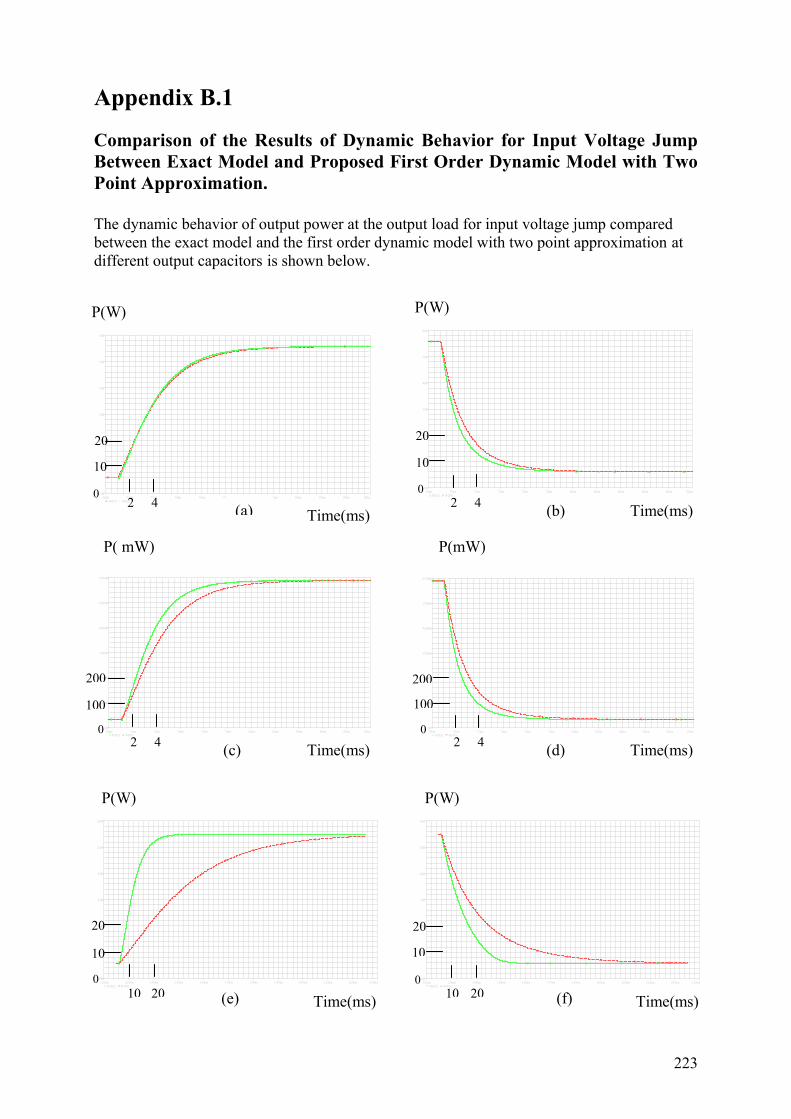
223
Appendix B.1 Comparison of the Results of Dynamic Behavior for Input Voltage Jump Between Exact Model and Proposed First Order Dynamic Model with Two Point Approximation. The dynamic behavior of output power at the output load for input voltage jump compared between the exact model and the first order dynamic model with two point approximation at different output capacitors is shown below.
2 4
Time
68ms 70ms 72ms 74ms 76ms 78ms 80ms 82ms 84ms 86ms 88ms 90msW(R9) W(R2)
0W
10W
20W
30W
40W
50W
60W
P(W)
Time(ms) Time
68ms 70ms 72ms 74ms 76ms 78ms 80ms 82ms 84ms 86ms 88ms 90msW(R2) W(R9)
0W
10W
20W
30W
40W
50W
60W
P(W)
Time(ms) (a) (b)
Time
68ms 70ms 72ms 74ms 76ms 78ms 80ms 82ms 84ms 86ms 88ms 90msW(R2) W(R9)
0W
100mW
200mW
300mW
400mW
500mW
600mW
Time(ms)
P(mW)
Time
68ms 70ms 72ms 74ms 76ms 78ms 80ms 82ms 84ms 86ms 88ms 90msW(R2) W(R9)
0W
100mW
200mW
300mW
400mW
500mW
600mW
P( mW)
Time(ms) (c) (d)
Time
120ms 130ms 140ms 150ms 160ms 170ms 180ms 190ms 200ms 210ms 220ms 230msW(R2) W(R9)
0W
10W
20W
30W
40W
50W
60W
P(W)
Time(ms) Time
120ms 130ms 140ms 150ms 160ms 170ms 180ms 190ms 200ms 210ms 220ms 230msW(R2) W(R9)
0W
10W
20W
30W
40W
50W
60W
P(W)
Time(ms) (e) (f)
0 0
0 0
0 0
10
20
2 4
10
20
2 4
100
200
100
200
2 4
10
20
10 20
10
20
10 20

224
Figure.B.1.1: The power at the output load at input voltage jump for 220 uF output capacitor. a) Input voltage jump from 120 V/DC to 360 V/DC at 155.5 kHz switching frequency at 12 Ω output load. b) Input voltage jump from 360 V/DC to 120 V/DC at 155.5 kHz switching frequency at 12 Ω output load. c) Input voltage jump from 120 V/DC to 360 V/DC at 170 kHz switching frequency at 12 Ω output load. d) Input voltage jump from 360 V/DC to 120 V/DC at 170 kHz switching frequency at 12 Ω output load. e) Input voltage jump from 120 V/DC to 360 V/DC at 155.5 kHz switching frequency at 100 Ω output load. f) Input voltage jump from 360 V/DC to 120 V/DC at 155.5 kHz switching frequency at 100 Ω output load. g) Input voltage jump from 120 V/DC to 360 V/DC at 170 kHz switching frequency at 100 Ω output load. h) Input voltage jump from 360 V/DC to 120 V/DC at 170 kHz switching frequency at 100 Ω output load (Dashed lines refer to proposed model and solid lines refer to exact model). The results of the relative error for the input voltage jump tests for 220 uF output capacitor are shown in Fig.B.1.2.
Time
120ms 130ms 140ms 150ms 160ms 170ms 180ms 190ms 200ms 210ms 220ms 230msW(R2) W(R9)
0W
100mW
200mW
300mW
400mW
500mW
600mW
P(mW)
Time(ms) Time
120ms 130ms 140ms 150ms 160ms 170ms 180ms 190ms 200ms 210ms 220ms 230msW(R2) W(R9)
0W
100mW
200mW
300mW
400mW
500mW
600mW
P(mW)
Time(ms) (g) (h) 0 0
Time
68ms 70ms 72ms 74ms 76ms 78ms 80ms 82ms 84ms 86ms 88ms 90ms(W(R9)/W(R2))-1
-50m
0
50m
100m
150m
200m
250m
Time(ms) Time
68ms 70ms 72ms 74ms 76ms 78ms 80ms 82ms 84ms 86ms 88ms 90ms(W(R9)/ W(R2))-1
-100m
0
100m
200m
300m
Time(ms)(a) (b)
0 0
10 20
100
200
100
200
10 20
.05
.1
2 4
.1
.2
2 4

225
Figure.B.1.2: The relative error between the proposed model in chapter 4.3.1 and the exact model for 220 uF output capacitor. a) Input voltage jump from 120 V/DC to 360 V/DC at 155.5 kHz switching frequency at 12 Ω output load. b) Input voltage jump from 360 V/DC to 120 V/DC at 155.5 kHz switching frequency at 12 Ω output load. c) Input voltage jump from 120 V/DC to 360 V/DC at 170 kHz switching frequency at 12 Ω output load. d) Input voltage jump from 360 V/DC to 120 V/DC at 170 kHz switching frequency at 12 Ω output load. e) Input voltage jump from 120 V/DC to 360 V/DC at 155.5 kHz switching frequency at 100 Ω output load. f) Input voltage jump from 360 V/DC to 120 V/DC at 155.5 kHz switching frequency at 100 Ω output load. g) Input voltage jump from 120 V/DC to 360 V/DC at 170 kHz switching frequency at 100 Ω output load. h) Input voltage jump from 360 V/DC to 120 V/DC at 170 kHz switching frequency at 100 Ω output load.
Time
68ms 70ms 72ms 74ms 76ms 78ms 80ms 82ms 84ms 86ms 88ms 90ms(W(R9)/W(R2))-1
-300m
-200m
-100m
0m
100m
200m
300m
Time(ms) Time
68ms 70ms 72ms 74ms 76ms 78ms 80ms 82ms 84ms 86ms 88ms 90ms(W(R9)/ W(R2))-1
0
100m
200m
300m
400m
500m
600m
Time(ms)(c) (d)
0
0
(e) Time
120ms 130ms 140ms 150ms 160ms 170ms 180ms 190ms 200ms 210ms 220ms 230ms(W(R9)/ W(R2))-1
-800m
-600m
-400m
-200m
0
200m
Time(ms) Time
120ms 130ms 140ms 150ms 160ms 170ms 180ms 190ms 200ms 210ms 220ms 230ms(W(R9)/ W(R2))-1
-0.4
0
0.4
0.8
1.2
1.6
2.0
Time(ms)(f)
Time
120ms 130ms 140ms 150ms 160ms 170ms 180ms 190ms 200ms 210ms 220ms 230ms(W(R9)/ W(R2))-1
-800m
-600m
-400m
-200m
0
200m
Time(ms) Time
120ms 130ms 140ms 150ms 160ms 170ms 180ms 190ms 200ms 210ms 220ms 230ms(W(R9)/ W(R2))-1
-0.5
0
0.5
1.0
1.5
Time(ms)(g) (h)
0
0
0
0
.1
.2
2 4
.1
.2
2 4
-.2
-.4
10 20
0.4
0.8
10 20
-.2
-.4
10 20
0.5
1
10 20

226
Figure.B.1.3: The power at the output load at input voltage jump for 1 uF output capacitor. a) Input voltage jump from 120 V/DC to 360 V/DC at 155.5 kHz switching frequency at 12 Ω output load. b) Input voltage jump from 360 V/DC to 120 V/DC at 155.5 kHz switching
Time
68.0ms 68.5ms 69.0ms 69.5ms 70.0ms 70.5ms 71.0ms 71.5ms 72.0msW(R9) W(R2)
0W
0.2W
0.4W
0.6W
0.8W
1.0W
Time(ms)
P(W)
(c) (d) Time(ms)
P(mW)
Time
68ms 70ms 72ms 74ms 76ms 78ms 80ms 82ms 84ms 86ms 88ms 90msW(R2) W(R9)
0W
200mW
400mW
600mW
800mW
(e) Time(ms)
P(W)
Time
125ms 126ms 127ms 128ms 129ms 130ms 131ms 132ms 133ms 134ms 135msW(R2) W(R9)
0W
10W
20W
30W
40W
50W
60W
Time(ms)(f)
P(W)
Time
125ms 126ms 127ms 128ms 129ms 130ms 131ms 132ms 133ms 134ms 135msW(R2) W(R9)
0W
10W
20W
30W
40W
50W
60W
P(mW)
(g) Time(ms) Time
125ms 126ms 127ms 128ms 129ms 130ms 131ms 132ms 133ms 134ms 135msW(R2) W(R9)
0W
100mW
200mW
300mW
400mW
500mW
600mW
P(mW)
(h) Time(ms) Time
125ms 126ms 127ms 128ms 129ms 130ms 131ms 132ms 133ms 134ms 135msW(R2) W(R9)
0W
100mW
200mW
300mW
400mW
500mW
600mW
Time
68ms 70ms 72ms 74ms 76ms 78ms 80ms 82ms 84ms 86ms 88ms 90msW(R2) W(R9)
0W
20W
40W
60W
80W
P(W)
Time(ms)(a) Time
68ms 70ms 72ms 74ms 76ms 78ms 80ms 82ms 84ms 86ms 88ms 90msW(R2) W(R9)
0W
20W
40W
60W
80W
P(W)
Time(ms)(b)0 0
0 0
0 0
0 0
20
40
2 4
20
40
2 4
0.2
0.4
0.5 1 2 4
200
400
10
20
1 2
10
20
1 2
100
200
1 2
100
200
1 2
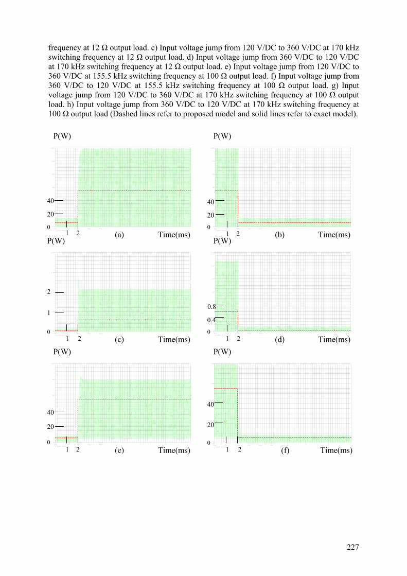
227
frequency at 12 Ω output load. c) Input voltage jump from 120 V/DC to 360 V/DC at 170 kHz switching frequency at 12 Ω output load. d) Input voltage jump from 360 V/DC to 120 V/DC at 170 kHz switching frequency at 12 Ω output load. e) Input voltage jump from 120 V/DC to 360 V/DC at 155.5 kHz switching frequency at 100 Ω output load. f) Input voltage jump from 360 V/DC to 120 V/DC at 155.5 kHz switching frequency at 100 Ω output load. g) Input voltage jump from 120 V/DC to 360 V/DC at 170 kHz switching frequency at 100 Ω output load. h) Input voltage jump from 360 V/DC to 120 V/DC at 170 kHz switching frequency at 100 Ω output load (Dashed lines refer to proposed model and solid lines refer to exact model).
Time
40ms 41ms 42ms 43ms 44ms 45ms 46ms 47ms 48ms 49ms 50ms 51ms 52msW(R2) W(R9)
0W
20W
40W
60W
80W
100W
120W
Time(ms)
P(W)
(a) Time
40ms 41ms 42ms 43ms 44ms 45ms 46ms 47ms 48ms 49ms 50ms 51ms 52msW(R2) W(R9)
0W
20W
40W
60W
80W
100W
120W
Time(ms)
P(W)
(b)
Time
40ms 41ms 42ms 43ms 44ms 45ms 46ms 47ms 48ms 49ms 50ms 51ms 52msW(R2) W(R9)
0W
0.4W
0.8W
1.2W
1.6W
2.0W
2.4W
Time(ms)
P(W)
(d) Time
40ms 41ms 42ms 43ms 44ms 45ms 46ms 47ms 48ms 49ms 50ms 51ms 52msW(R2) W(R9)
0W
1.0W
2.0W
3.0W
4.0W
P(W)
Time(ms)(c)
Time
40ms 41ms 42ms 43ms 44ms 45ms 46ms 47ms 48ms 49ms 50ms 51ms 52msW(R2) W(R9)
0W
20W
40W
60W
80W
100W
Time(ms)
P(W)
(e) Time
40ms 41ms 42ms 43ms 44ms 45ms 46ms 47ms 48ms 49ms 50ms 51ms 52msW(R2) W(R9)
0W
20W
40W
60W
80W
Time(ms) (f)
P(W)
0 0
0 0
0 0
20
40
1 2
20
40
1 2
1
2
1 2
0.4
0.8
1 2
20
40
1 2
20
40
1 2
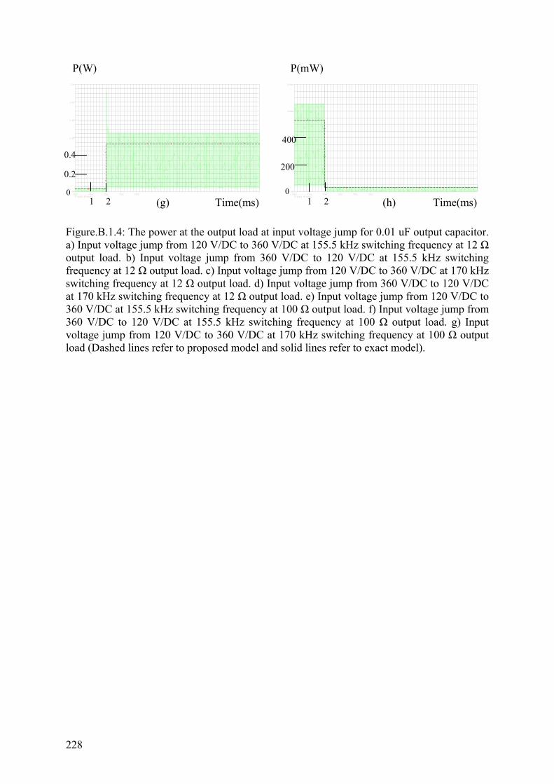
228
Figure.B.1.4: The power at the output load at input voltage jump for 0.01 uF output capacitor. a) Input voltage jump from 120 V/DC to 360 V/DC at 155.5 kHz switching frequency at 12 Ω output load. b) Input voltage jump from 360 V/DC to 120 V/DC at 155.5 kHz switching frequency at 12 Ω output load. c) Input voltage jump from 120 V/DC to 360 V/DC at 170 kHz switching frequency at 12 Ω output load. d) Input voltage jump from 360 V/DC to 120 V/DC at 170 kHz switching frequency at 12 Ω output load. e) Input voltage jump from 120 V/DC to 360 V/DC at 155.5 kHz switching frequency at 100 Ω output load. f) Input voltage jump from 360 V/DC to 120 V/DC at 155.5 kHz switching frequency at 100 Ω output load. g) Input voltage jump from 120 V/DC to 360 V/DC at 170 kHz switching frequency at 100 Ω output load (Dashed lines refer to proposed model and solid lines refer to exact model).
Time
40ms 41ms 42ms 43ms 44ms 45ms 46ms 47ms 48ms 49ms 50ms 51ms 52msW(R2) W(R9)
0W
0.2W
0.4W
0.6W
0.8W
1.0W
1.2W
Time(ms)
P(W)
(g) Time
40ms 41ms 42ms 43ms 44ms 45ms 46ms 47ms 48ms 49ms 50ms 51ms 52msW(R2) W(R9)
0W
200mW
400mW
600mW
800mW
Time(ms)
P(mW)
(h) 0 0
0.2
0.4
1 2
200
400
1 2

229
Appendix B.2 Comparison of the Results of Dynamic Behavior for Frequency Jump Between Exact Model and Proposed First Order Dynamic Model with Two Point Approximation The dynamic behavior of the output power at the output load for a switching frequency jump compared between the exact model and the first order dynamic model with two point approximation at different output capacitors is shown below.
P(W)
Time
68ms 70ms 72ms 74ms 76ms 78ms 80ms 82ms 84ms 86ms 88ms 90msW(R10) W(R4)
0W
2.0W
4.0W
6.0W
8.0W
Time
68ms 70ms 72ms 74ms 76ms 78ms 80ms 82ms 84ms 86ms 88ms 90msW(R4) W(R10)
0W
2.0W
4.0W
6.0W
8.0W
Time(ms)
P(W)
Time(ms)(a) (b)
Time
68ms 70ms 72ms 74ms 76ms 78ms 80ms 82ms 84ms 86ms 88ms 90msW(R10) W(R4)
0W
10W
20W
30W
40W
50W
60W
P(W)
Time(ms) Time
68ms 70ms 72ms 74ms 76ms 78ms 80ms 82ms 84ms 86ms 88ms 90msW(R4) W(R10)
0W
10W
20W
30W
40W
50W
60W
P(W)
Time(ms) (c) (d)
P(W)
Time(ms) (e) Time
120ms 130ms 140ms 150ms 160ms 170ms 180ms 190ms 200ms 210ms 220ms 230ms 240msW(R4) W(R10)
0W
1.0W
2.0W
3.0W
4.0W
5.0W
6.0W
Time(ms)
P(W)
(f) Time
120ms 140ms 160ms 180ms 200ms 220ms 240ms 260msW(R4) W(R10)
0W
1.0W
2.0W
3.0W
4.0W
5.0W
6.0W
0 0
0 0
0 0
2
4
2 4
2
4
2 4
10
20
2 4
10
20
2 4
1
2
10 20
1
2
20 40
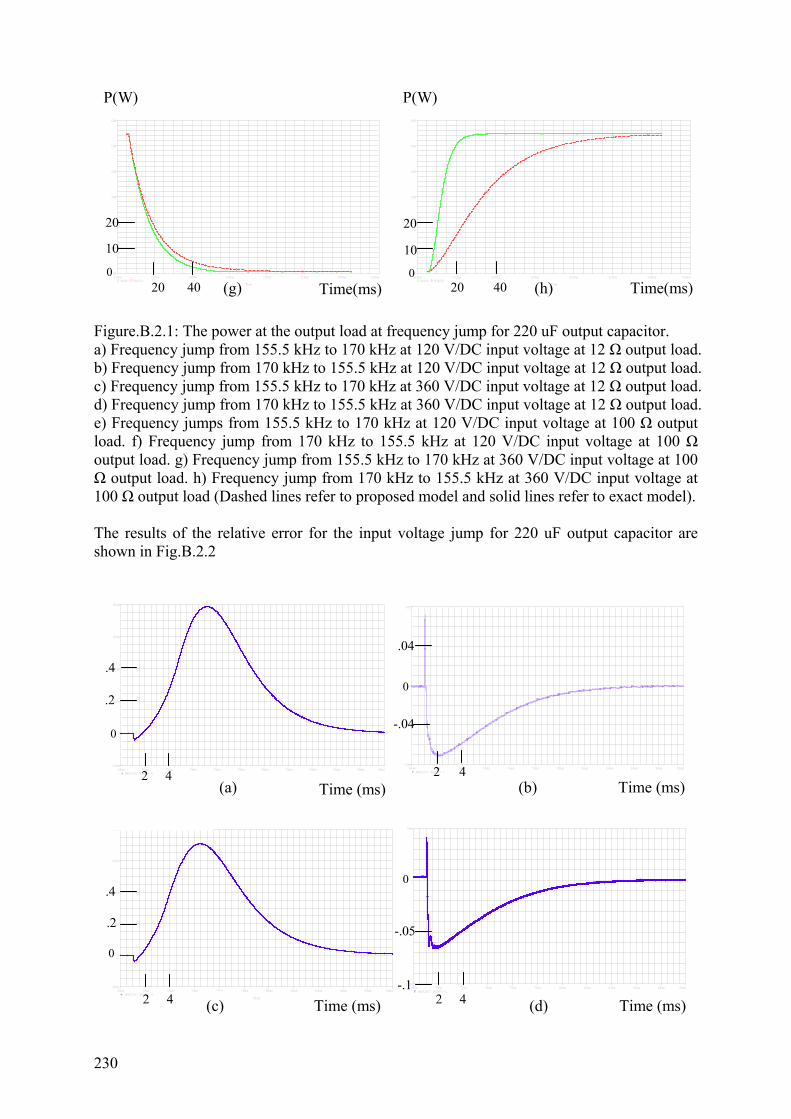
230
Figure.B.2.1: The power at the output load at frequency jump for 220 uF output capacitor. a) Frequency jump from 155.5 kHz to 170 kHz at 120 V/DC input voltage at 12 Ω output load. b) Frequency jump from 170 kHz to 155.5 kHz at 120 V/DC input voltage at 12 Ω output load. c) Frequency jump from 155.5 kHz to 170 kHz at 360 V/DC input voltage at 12 Ω output load. d) Frequency jump from 170 kHz to 155.5 kHz at 360 V/DC input voltage at 12 Ω output load. e) Frequency jumps from 155.5 kHz to 170 kHz at 120 V/DC input voltage at 100 Ω output load. f) Frequency jump from 170 kHz to 155.5 kHz at 120 V/DC input voltage at 100 Ω output load. g) Frequency jump from 155.5 kHz to 170 kHz at 360 V/DC input voltage at 100 Ω output load. h) Frequency jump from 170 kHz to 155.5 kHz at 360 V/DC input voltage at 100 Ω output load (Dashed lines refer to proposed model and solid lines refer to exact model). The results of the relative error for the input voltage jump for 220 uF output capacitor are shown in Fig.B.2.2
P(W)
(g) Time(ms) Time
120ms 140ms 160ms 180ms 200ms 220ms 240ms 260msW(R4) W(R10)
0W
10W
20W
30W
40W
50W
60W
(h) Time(ms)
P(W)
Time
120ms 140ms 160ms 180ms 200ms 220ms 240ms 260msW(R4) W(R10)
0W
10W
20W
30W
40W
50W
60W
0 0
Time
68ms 70ms 72ms 74ms 76ms 78ms 80ms 82ms 84ms 86ms 88ms 90ms(W(R10)/ W(R4))-1
-200m
0
200m
400m
600m
800m
Time (ms) Time
68ms 70ms 72ms 74ms 76ms 78ms 80ms 82ms 84ms 86ms 88ms 90ms(W(R10)/ W(R4))-1
-80m
-40m
0
40m
80m
Time (ms) (a) (b)
Time (ms) Time
68ms 70ms 72ms 74ms 76ms 78ms 80ms 82ms 84ms 86ms 88ms 90ms(W(R10)/ W(R4))-1
-200m
0
200m
400m
600m
800m
Time
68ms 70ms 72ms 74ms 76ms 78ms 80ms 82ms 84ms 86ms 88ms 90ms(W(R10)/ W(R4))-1
-100m
-50m
0
50m
Time (ms) (c) (d)
0
0
0
0
10
20
20 40 20 40
10
20
.2
.4
2 4
.04
-.04
2 4
.2
.4
2 4
-.05
-.1 2 4
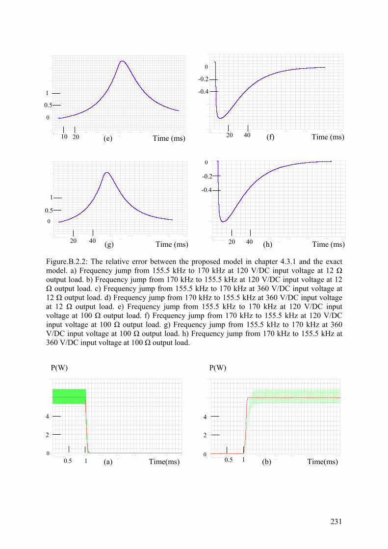
231
Figure.B.2.2: The relative error between the proposed model in chapter 4.3.1 and the exact model. a) Frequency jump from 155.5 kHz to 170 kHz at 120 V/DC input voltage at 12 Ω output load. b) Frequency jump from 170 kHz to 155.5 kHz at 120 V/DC input voltage at 12 Ω output load. c) Frequency jump from 155.5 kHz to 170 kHz at 360 V/DC input voltage at 12 Ω output load. d) Frequency jump from 170 kHz to 155.5 kHz at 360 V/DC input voltage at 12 Ω output load. e) Frequency jump from 155.5 kHz to 170 kHz at 120 V/DC input voltage at 100 Ω output load. f) Frequency jump from 170 kHz to 155.5 kHz at 120 V/DC input voltage at 100 Ω output load. g) Frequency jump from 155.5 kHz to 170 kHz at 360 V/DC input voltage at 100 Ω output load. h) Frequency jump from 170 kHz to 155.5 kHz at 360 V/DC input voltage at 100 Ω output load.
0
Time (ms) (e) Time
120ms 130ms 140ms 150ms 160ms 170ms 180ms 190ms 200ms 210ms 220ms 230ms 240ms(W(R10)/W(R4))-1
-0.5
0
0.5
1.0
1.5
2.0
2.5
Time (ms)(f) Time
120ms 140ms 160ms 180ms 200ms 220ms 240ms 260ms(W(R10)/W(R4))-1
-1.0
-0.8
-0.6
-0.4
-0.2
0
0.2
Time (ms)
(g) Time
120ms 140ms 160ms 180ms 200ms 220ms 240ms 260ms(W(R10)/W(R4))-1
-0.5
0
0.5
1.0
1.5
2.0
2.5
Time (ms)
(h) Time
120ms 140ms 160ms 180ms 200ms 220ms 240ms 260ms(W(R10)/W(R4))-1
-1.0
-0.8
-0.6
-0.4
-0.2
0
0
0
0
Time(ms)(a)
P(W)
Time
68.0ms 68.5ms 69.0ms 69.5ms 70.0ms 70.5ms 71.0ms 71.5ms 72.0msW(R4) W(R10)
0W
2.0W
4.0W
6.0W
8.0W
(b)
P(W)
Time(ms) Time
68.0ms 68.5ms 69.0ms 69.5ms 70.0ms 70.5ms 71.0ms 71.5ms 72.0msW(R4) W(R10)
0W
2.0W
4.0W
6.0W
8.0W
0 0
0.5
1
20 40
0.5
1
10 20
-0.2
-0.4
20 40
-0.2
-0.4
20 40
2
4
0.5 1
2
4
0.5 1
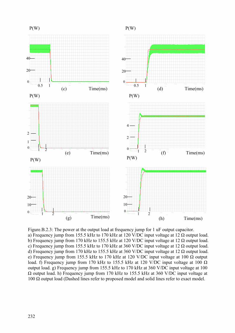
232
Figure.B.2.3: The power at the output load at frequency jump for 1 uF output capacitor. a) Frequency jump from 155.5 kHz to 170 kHz at 120 V/DC input voltage at 12 Ω output load. b) Frequency jump from 170 kHz to 155.5 kHz at 120 V/DC input voltage at 12 Ω output load. c) Frequency jump from 155.5 kHz to 170 kHz at 360 V/DC input voltage at 12 Ω output load. d) Frequency jump from 170 kHz to 155.5 kHz at 360 V/DC input voltage at 12 Ω output load. e) Frequency jump from 155.5 kHz to 170 kHz at 120 V/DC input voltage at 100 Ω output load. f) Frequency jump from 170 kHz to 155.5 kHz at 120 V/DC input voltage at 100 Ω output load. g) Frequency jump from 155.5 kHz to 170 kHz at 360 V/DC input voltage at 100 Ω output load. h) Frequency jump from 170 kHz to 155.5 kHz at 360 V/DC input voltage at 100 Ω output load (Dashed lines refer to proposed model and solid lines refer to exact model.
(c)
P(W)
Time(ms) Time
68.0ms 68.5ms 69.0ms 69.5ms 70.0ms 70.5ms 71.0ms 71.5ms 72.0msW(R4) W(R10)
0W
20W
40W
60W
80W
(d)
P(W)
Time(ms) Time
68.0ms 68.5ms 69.0ms 69.5ms 70.0ms 70.5ms 71.0ms 71.5ms 72.0msW(R4) W(R10)
0W
20W
40W
60W
80W
(e)
P(W)
Time(ms) Time
125ms 126ms 127ms 128ms 129ms 130ms 131ms 132ms 133ms 134ms 135msW(R4) W(R10)
0W
1.0W
2.0W
3.0W
4.0W
5.0W
6.0W
(f)
P(W)
Time
125ms 126ms 127ms 128ms 129ms 130ms 131ms 132ms 133ms 134ms 135msW(R4) W(R10)
0W
2.0W
4.0W
6.0W
8.0W
Time(ms) P(W)
(g) Time(ms) Time
125ms 126ms 127ms 128ms 129ms 130ms 131ms 132msW(R4) W(R10)
0W
10W
20W
30W
40W
50W
60W
(h)
P(W)
Time(ms) Time
125ms 126ms 127ms 128ms 129ms 130ms 131ms 132msW(R4) W(R10)
0W
10W
20W
30W
40W
50W
60W
0 0
0
0 0
0
20
40
0.5 1
20
40
0.5 1
1
2
1 2
2
4
1 2
10
20
1 2
10
20
1 2
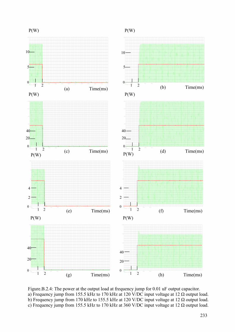
233
Figure.B.2.4: The power at the output load at frequency jump for 0.01 uF output capacitor. a) Frequency jump from 155.5 kHz to 170 kHz at 120 V/DC input voltage at 12 Ω output load. b) Frequency jump from 170 kHz to 155.5 kHz at 120 V/DC input voltage at 12 Ω output load. c) Frequency jump from 155.5 kHz to 170 kHz at 360 V/DC input voltage at 12 Ω output load.
Time
40ms 41ms 42ms 43ms 44ms 45ms 46ms 47ms 48ms 49ms 50ms 51ms 52msW(R4) W(R10)
0W
5W
10W
15W
Time(ms)(a)
P(W)
Time
40ms 41ms 42ms 43ms 44ms 45ms 46ms 47ms 48ms 49ms 50ms 51ms 52msW(R4) W(R10)
0W
5W
10W
15W
Time(ms)(b)
P(W)
Time
40ms 41ms 42ms 43ms 44ms 45ms 46ms 47ms 48ms 49ms 50ms 51ms 52msW(R4) W(R10)
0W
20W
40W
60W
80W
100W
120W
Time(ms)(c)
P(W)
Time
40ms 41ms 42ms 43ms 44ms 45ms 46ms 47ms 48ms 49ms 50ms 51ms 52msW(R4) W(R10)
0W
20W
40W
60W
80W
100W
120W
P(W)
Time(ms)(d)
Time
40ms 41ms 42ms 43ms 44ms 45ms 46ms 47ms 48ms 49ms 50ms 51ms 52msW(R4) W(R10)
0W
2W
4W
6W
8W
10W
P(W)
Time(ms)(e) Time
40ms 41ms 42ms 43ms 44ms 45ms 46ms 47ms 48ms 49ms 50ms 51ms 52msW(R4) W(R10)
0W
2W
4W
6W
8W
10W
Time(ms)
P(W)
(f)
Time
40ms 41ms 42ms 43ms 44ms 45ms 46ms 47ms 48ms 49ms 50ms 51ms 52msW(R4) W(R10)
0W
20W
40W
60W
80W
Time(ms)
P(W)
(g) Time
40ms 41ms 42ms 43ms 44ms 45ms 46ms 47ms 48ms 49ms 50ms 51ms 52msW(R4) W(R10)
0W
20W
40W
60W
80W
100W
Time(ms)(h)
P(W)
0 0
0 0
0 0
0 0
5
10
5
10
1 2 1 2
20
40
1 2
20
40
1 2
2 1
20
40 40
20
1 2
2
4
2
4
1 2
1 2

234
d) Frequency jump from 170 kHz to 155.5 kHz at 360 V/DC input voltage at 12 Ω output load. e) Frequency jump from 155.5 kHz to 170 kHz at 120 V/DC input voltage at 100 Ω output load. f) Frequency jump from 170 kHz to 155.5 kHz at 120 V/DC input voltage at 100 Ω output load. g) Frequency jump from 155.5 kHz to 170 kHz at 360 V/DC input voltage at 100 Ω output load. h) Frequency jump from 170 kHz to 155.5 kHz at 360 V/DC input voltage at 100 Ω output load (Dashed lines refer to proposed model and solid lines refer to exact model).
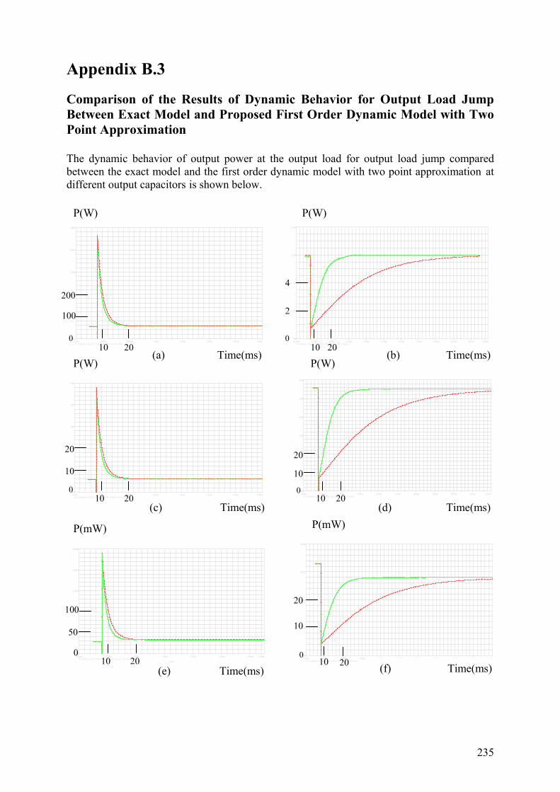
235
Appendix B.3 Comparison of the Results of Dynamic Behavior for Output Load Jump Between Exact Model and Proposed First Order Dynamic Model with Two Point Approximation The dynamic behavior of output power at the output load for output load jump compared between the exact model and the first order dynamic model with two point approximation at different output capacitors is shown below.
P(W) P(W)
Time
120ms 130ms 140ms 150ms 160ms 170ms 180ms 190msV(D18:2,R11:1)*I(V1) V(V2:+,0)*I(V2)
0W
100W
200W
300W
400W
500W
Time(ms) (a) Time
120ms 130ms 140ms 150ms 160ms 170ms 180ms 190ms 200ms 210ms 220ms 230ms(V(V1:+,R11:1)*I(V1)) (V(V2:+,0)*I(V2))
0W
2.0W
4.0W
6.0W
8.0W
Time(ms) (b)
Time
120ms 130ms 140ms 150ms 160ms 170ms 180ms 190ms(V(Cout1:2,R11:1)*I(V1)) (V(V2:+,0)*I(V2))
0W
10W
20W
30W
40W
50W
P(W)
Time(ms) (c) Time
120ms 130ms 140ms 150ms 160ms 170ms 180ms 190ms 200ms 210ms 220ms(V(D18:2,R2:1)*I(V1)) (V(V2:+,0)*I(V2))
0W
10W
20W
30W
40W
50W
60W
P(W)
Time(ms) (d)
Time
120ms 130ms 140ms 150ms 160ms 170ms 180ms 190ms 200ms 210ms 220ms(V(Cout1:2,R11:1)*I(V1)) V(V2:+,0)*I(V2)
0W
10mW
20mW
30mW
40mW
P(mW)
Time(ms) (f)
P(mW)
Time(ms) (e) Time
120ms 130ms 140ms 150ms 160ms 170ms 180ms 185ms(V(V2:+,0)*I(V2)) (V(Cout1:2,R11:1)*I(V1))
0W
50mW
100mW
150mW
200mW
250mW
0 0
0
0
0
100
200
10 20
2
4
10 20
10
20
10 20
50
0
10 20
10
20
10
20
100
10 20
10 20

236
Figure.B.3.1: The power at the output load at output load jump for 220 uF output capacitor. a) Output load jump from 100 Ω to 12 Ω at 360 V/DC input voltage at 155.5 kHz switching frequency. b) Output load jump from 12 Ω to 100 Ω at 120 V/DC input voltage at 155.5 kHz switching frequency. c) Output load jump from 100 Ω to 12 Ω at 120 V/DC input voltage at 155.5 kHz switching frequency. d) Output load jump from 12 Ω to 100 Ω at 360 V/DC input voltage at 155.5 kHz switching frequency. e) Output load jump from 100 Ω to 12 Ω at 120 V/DC input voltage at 170 kHz switching frequency. f) Output load jump from 12 Ω to 100 Ω at 120 V/DC input voltage at 170 kHz switching frequency. g) Output load jump from 100 Ω to 12 Ω at 360 V/DC input voltage at 170 kHz switching frequency. h) Output load jump from 12 Ω to 100 Ω at 360 V/DC input voltage at 170 kHz switching frequency (Dashed lines refer to proposed model and solid lines refer to exact model). The results of the relative error for the output load jump at 220 uF output capacitor are shown in Fig.B.3.2
Time
120ms 130ms 140ms 150ms 160ms 170ms 180ms 190ms 200ms 210ms 220ms(V(V1:+,R11:1)*I(V1)) (V(V2:+,0)*I(V2))
0W
100mW
200mW
300mW
400mW
500mW
600mW
P(mW)
(h) Time(ms)
P(W)
Time(ms) Time
120ms 130ms 140ms 150ms 160ms 170ms 180ms 190ms 200ms 210ms 220ms(V(V1:+,D17:1)*I(V1)) (V(V2:+,0)*I(V2))
0W
1.0W
2.0W
3.0W
4.0W
5.0W
(g) 0 0
Time
120ms 130ms 140ms 150ms 160ms 170ms 180ms 190ms((V(V2:+,0)*I(V2))/(V(Cout1:2,R11:1)*I(V1)))-1
-200m
-100m
0
100m
200m
300m
400m
Time(ms) (c)
Time
120ms 130ms 140ms 150ms 160ms 170ms 180ms 190ms((V(V2:+,0)*I(V2))/(V(D18:2,R11:1)*I(V1)))-1
-1.0
-0.5
-0.0
0.5
(a) Time(ms)
Time(ms) Time
120ms 130ms 140ms 150ms 160ms 170ms 180ms 190ms 200ms 210ms 220ms 230ms((V(V2:+,0)*I(V2))/(V(V1:+,R11:1)*I(V1)))-1
-800m
-600m
-400m
-200m
0
200m
(b)
Time
120ms 130ms 140ms 150ms 160ms 170ms 180ms 190ms 200ms 210ms 220ms((V(V2:+,0)*I(V2))/(V(D18:2,R2:1)*I(V1)))-1
-800m
-600m
-400m
-200m
0
200m
Time(ms) (d)
0
0
0
0
1
2
10 20
100
200
10 20
-.5
-1 10 20
-.2
-.4
10 20
-.2
-.4 .1
.2
10 20 10 20
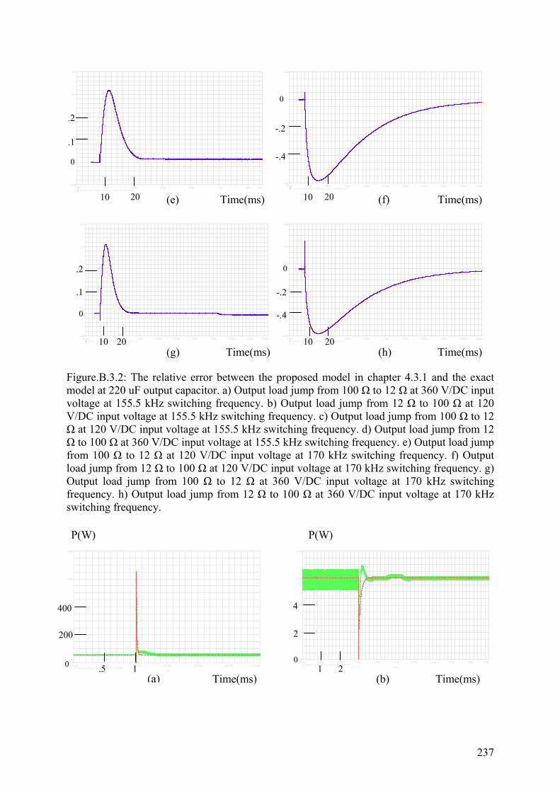
237
Figure.B.3.2: The relative error between the proposed model in chapter 4.3.1 and the exact model at 220 uF output capacitor. a) Output load jump from 100 Ω to 12 Ω at 360 V/DC input voltage at 155.5 kHz switching frequency. b) Output load jump from 12 Ω to 100 Ω at 120 V/DC input voltage at 155.5 kHz switching frequency. c) Output load jump from 100 Ω to 12 Ω at 120 V/DC input voltage at 155.5 kHz switching frequency. d) Output load jump from 12 Ω to 100 Ω at 360 V/DC input voltage at 155.5 kHz switching frequency. e) Output load jump from 100 Ω to 12 Ω at 120 V/DC input voltage at 170 kHz switching frequency. f) Output load jump from 12 Ω to 100 Ω at 120 V/DC input voltage at 170 kHz switching frequency. g) Output load jump from 100 Ω to 12 Ω at 360 V/DC input voltage at 170 kHz switching frequency. h) Output load jump from 12 Ω to 100 Ω at 360 V/DC input voltage at 170 kHz switching frequency.
(a) Time(ms)
P(W)
Time
127.0ms 127.5ms 128.0ms 128.5ms 129.0ms 129.5ms 130.0msV(Cout1:2,R11:1)*I(V1) V(V2:+,0)*I(V2)
0W
200W
400W
600W
800W
Time(ms)(b)
P(W)
Time
125ms 126ms 127ms 128ms 129ms 130ms 131ms 132ms 133ms 134ms 135msV(Cout1:2,R2:1)*I(V1) V(V2:+,0)*I(V2)
0W
2.0W
4.0W
6.0W
8.0W
0 0
Time
120ms 130ms 140ms 150ms 160ms 170ms 180ms 190ms 200ms 210ms 220ms((V(V2:+,0)*I(V2))/(V(Cout1:2,R11:1)*I(V1)))-1
-600m
-400m
-200m
0
200m
Time(ms) (e) Time
120ms 130ms 140ms 150ms 160ms 170ms 180ms 185ms((V(V2:+,0)*I(V2))/(V(Cout1:2,R11:1)*I(V1)))-1
-100m
0
100m
200m
300m
400m
Time(ms) (f)
Time
120ms 130ms 140ms 150ms 160ms 170ms 180ms 190ms 200ms 210ms 220ms((V(V2:+,0)*I(V2))/(V(V1:+,R11:1)*I(V1)))-1
-600m
-400m
-200m
0
200m
400m
Time
120ms 130ms 140ms 150ms 160ms 170ms 180ms 190ms 200ms 210ms 220ms((V(V2:+,0)*I(V2))/(V(V1:+,D17:1)*I(V1)))-1
-100m
0
100m
200m
300m
400m
Time(ms) Time(ms) (g) (h)
0
0
0
0
-.2
-.4
10 20
.1
.2
10 20
-.2
-.4
10 20
.1
.2
10 20
2
4
1 2
200
400
.5 1
238
Figure.B.3.3: The power at the output load at output load jump at 1 uF output capacitor. a) Output load jump from 100 Ω to 12 Ω at 360 V/DC input voltage at 155.5 kHz switching frequency. b) Output load jump from 12 Ω to 100 Ω at 120 V/DC input voltage at 155.5 kHz switching frequency. c) Output load jump from 100 Ω to 12 Ω at 120 V/DC input voltage at 155.5 kHz switching frequency. d) Output load jump from 12 Ω to 100 Ω at 360 V/DC input voltage at 155.5 kHz switching frequency. e) Output load jump from 100 Ω to 12 Ω at 120 V/DC input voltage at 170 kHz switching frequency. f) Output load jump from 12 Ω to 100 Ω at 120 V/DC input voltage at 170 kHz switching frequency. g) Output load jump from 100 Ω to 12 Ω at 360 V/DC input voltage at 170 kHz switching frequency. h) Output load jump from 12 Ω to 100 Ω at 360 V/DC input voltage at 170 kHz switching frequency (Dashed lines refer to proposed model and solid lines refer to exact model).
P(W)
(c) Time(ms) Time
127.0ms 127.5ms 128.0ms 128.5ms 129.0ms 129.5ms 130.0msV(Cout1:2,Cout1:1)*I(V1) V(V2:+,0)*I(V2)
0W
20W
40W
60W
80W
(d) Time(ms)
P(W)
Time
120ms 122ms 124ms 126ms 128ms 130ms 132ms 134ms 136msV(V1:+,Cout1:1)*I(V1) V(V2:+,0)*I(V2)
0W
20W
40W
60W
80W
(e) Time(ms)
P(mW)
Time
126.0ms 126.5ms 127.0ms 127.5ms 128.0ms 128.5ms 129.0ms 129.5ms 130.0msV(V1:+,R11:1)*I(V1) V(V2:+,0)*I(V2)
0W
100mW
200mW
300mW
400mW
Time(ms) (f)
P(mW)
Time
125ms 126ms 127ms 128ms 129ms 130ms 131ms 132msV(D16:2,R11:1)*I(V1) V(V2:+,0)*I(V2)
0W
10mW
20mW
30mW
40mW
P(W)
(g) Time(ms) Time
126.0ms 126.5ms 127.0ms 127.5ms 128.0ms 128.5ms 129.0ms 129.5ms 130.0ms 130.5ms 131.0msV(V1:+,D17:1)*I(V1) V(V2:+,0)*I(V2)
0W
2.0W
4.0W
6.0W
8.0W
Time(ms)
P(mW)
(h) Time
125ms 126ms 127ms 128ms 129ms 130ms 131ms 132ms 133ms 134ms 135msV(V1:+,D17:1)*I(V1) V(V2:+,0)*I(V2)
0W
200mW
400mW
600mW
800mW
0 0
0 0
0 0
20
40
0.5 1
20
40
2 4
10
20
1 2 .5 1
100
200
200
400
1 2
2
4
.5 1

239
Figure.B.3.4: The power at the output load at output load jump at 0.01 uF output capacitor. a) Output load jump from 100 Ω to 12 Ω at 360 V/DC input voltage at 155.5 kHz switching frequency. b) Output load jump from 12 Ω to 100 Ω at 120 V/DC input voltage at 155.5 kHz switching frequency. c) Output load jump from 100 Ω to 12 Ω at 120 V/DC input voltage at
Time
40ms 41ms 42ms 43ms 44ms 45ms 46ms 47ms 48ms 49ms 50msV(D16:2,Cout1:1)*I(V1) V(V2:+,0)*I(V2)
0W
200W
400W
600W
800W
P(W)
Time(ms)(a) Time
40.0ms 40.5ms 41.0ms 41.5ms 42.0ms 42.5ms 43.0msV(V3:-,D17:1)*I(V1) V(V2:+,0)*I(V2)
0W
10W
20W
30W
40W
P(W)
Time(ms)(b)P(W)
Time
40.0ms 40.5ms 41.0ms 41.5ms 42.0ms 42.5ms 43.0ms 43.5ms 44.0ms 44.5ms 45.0msV(D16:2,Cout1:1)*I(V1) V(V2:+,0)*I(V2)
0W
20W
40W
60W
80W
P(W)
Time(ms)(c) Time
40.0ms 40.5ms 41.0ms 41.5ms 42.0ms 42.5ms 43.0ms 43.5ms 44.0ms 44.5ms 45.0msV(D16:2,Cout1:1)*I(V1) V(V2:+,0)*I(V2)
0W
20W
40W
60W
80W
100W
120W
Time(ms)(d)
Time
40.0ms 40.5ms 41.0ms 41.5ms 42.0ms 42.5ms 43.0ms 43.5ms 44.0ms 44.5ms 45.0msV(V1:+,R2:1)*I(V1) V(V2:+,0)*I(V2)
0W
50mW
100mW
150mW
200mW
250mW
P(mW)
Time(ms)(e) Time
40.0ms 40.5ms 41.0ms 41.5ms 42.0ms 42.5ms 43.0msV(D16:2,Cout1:1)*I(V1) V(V2:+,0)*I(V2)
0W
50mW
100mW
150mW
Time(ms)
P(mW)
(f)
Time
40.0ms 40.5ms 41.0ms 41.5ms 42.0ms 42.5ms 43.0ms 43.5ms 44.0ms 44.5ms 45.0msV(Cout1:2,R11:1)*I(V1) V(V2:+,0)*I(V2)
0W
1.0W
2.0W
3.0W
4.0W
5.0W
P(W)
Time(ms)(g) Time
40.0ms 40.5ms 41.0ms 41.5ms 42.0ms 42.5ms 43.0ms 43.5ms 44.0ms 44.5ms 45.0msV(Cout1:2,Cout1:1)*I(V1) V(V2:+,0)*I(V2)
0W
0.4W
0.8W
1.2W
1.6W
2.0W
2.4W
Time(ms)
P(W)
(h)
0 0
0 0
0 0
0 0
200
400
1 2
10
20
.5 1
20
40 20
40
.5 1 .5 1
50
100
.5 1
50
100
.5 1
.4
.8 1
2
.5 1 .5 1

240
155.5 kHz switching frequency. d) Output load jump from 12 Ω to 100 Ω at 360 V/DC input voltage at 155.5 switching frequency. e) Output load jump from 100 Ω to 12 Ω at 120 V/DC input voltage at 170 kHz switching frequency. f) Output load jump from 12 Ω to 100 Ω at 120 V/DC input voltage at 170 kHz switching frequency. g) Output load jump from 100 Ω to 12 Ω at 360 V/DC input voltage at 170 kHz switching frequency. h) Output load jump from 12 Ω to 100 Ω at 360 V/DC input voltage at 170 kHz switching frequency (Dashed lines refer to proposed model and solid lines refer to exact model).

241
Appendix B.4 Comparison of the Results of Dynamic Behavior for Different Perturbation Conditions Between Exact Model and Proposed First Order Dynamic Model with Auxiliary Resistor The dynamic behavior of output power at the output load for different perturbation conditions compared between the exact model and a first order dynamic model with auxiliary resistor is shown below.
Time
68ms 72ms 76ms 80ms 84ms 88ms 92ms 96ms 100ms 104ms 108ms 112msW(R13) W(R12)
0W
0.5W
1.0W
1.5W
2.0W
Time
68ms 72ms 76ms 80ms 84ms 88ms 92ms 96ms 100ms 104ms 108ms 112msW(R13) W(R12)
0W
0.5W
1.0W
1.5W
2.0W
P(W) P(W)
Time(ms) Time(ms)
Time
68ms 72ms 76ms 80ms 84ms 88ms 92ms 96ms 100ms 104ms 108ms 112msW(R13) W(R12)
0W
1.0W
2.0W
3.0W
4.0W
Time
68ms 72ms 76ms 80ms 84ms 88ms 92ms 96ms 100ms 104ms 108ms 112msW(R13) W(R12)
0W
1.0W
2.0W
3.0W
4.0W
P(W) P(W)
Time(ms) Time(ms)(c) (d)
Time
68ms 72ms 76ms 80ms 84ms 88ms 92ms 96ms 100ms 104ms 108ms 112msW(R13) W(R12)
0W
0.2W
0.4W
0.6W
0.8W
1.0W
Time
68ms 72ms 76ms 80ms 84ms 88ms 92ms 96ms 100ms 104ms 108ms 112msW(R13) W(R12)
0W
0.2W
0.4W
0.6W
0.8W
1.0W
P(W) P(W)
Time(ms) Time(ms)(e) (f)
0 0
0 0
0 0
.5
1
4 8
.5
4 8
1
1
2
1
2
4 8 4 8
.2
.4
4 8 4 8
.2
.4
(a) (b)
242
Figure.B.4.1: The power at the output load for different perturbation situations. (a) Input voltage jump from 85 V/DC to 240 V/DC at 60 Ω output load at 163 kHz switching frequency at 220 uF output capacitor. (b) Input voltage jump from 85 V/DC to 240 V/DC at 60 Ω output load at 163 kHz switching frequency at 47 uF output capacitor. (c) Input voltage jump from 85 V/DC to 360 V/DC at 100 Ω output load at 163.2 kHz switching frequency at 220 uF output capacitor. (d) Input voltage jump from 85 V/DC to 360 V/DC at 100 Ω output load at 163.2 kHz switching frequency at 47 uF output capacitor. (e) Frequency jump from 166.5 kHz to 161.1 kHz at 120 V/DC input voltage at 220 uF output capacitor at 100 Ω output load. (f) Frequency jump from 166.5 kHz to 161.1 kHz at 120 V/DC input voltage at 47 uF output capacitor at 100 Ω output load. (g) Voltage resoponse at the output load of frequency jump from 166.5 kHz to 161.1 kHz and input voltage jump from 85 V/DC to 360 V/DC at 220 uF output capacitor at 100 Ω output load. (h) Output current at the output load of frequency jump from 166.5 kHz to 161.1 kHz and input voltage jump from 85 V/DC to 360 V/DC at 220 uF output capacitor at 100 Ω output load. (i) Voltage resoponse at the output load of frequency jump from 166.5 kHz to 161.1 kHz and input voltage jump from 85 V/DC to 360 V/DC at 4.7 uF output capacitor at 100 Ω output load. (j) Output current at the output load of frequency jump from 166.5 kHz to 161.1 kHz and input voltage jump from 85 V/DC to 360 V/DC at 4.7 uF output capacitor at 100 Ω output load. (Solid line: exact mode, dashed line: proposed first order model).
Vout (V)
5 5
5
100
Iout (mA)
Vout (V)
Time (ms) Time (ms)
Iout (mA)
0.5 1 0.5 1
50
100 10
5
Time (ms) Time (ms) (g) (h)
(i) (j)
10
10 10
50
243
Appendix B.5 The Phase Margin of the open Loop for Isolated PI Control Regulation plus Lag Circuit The stability condition of the modeling of class-E converter with isolated PI control regulation plus lag circuit with the bode plot is shown below.
Figure.B.5.1: The phase margin of the open loop for isolated PI control regulation plus lag circuit.
Phase margin
Gain margin
-36(dB)
-121(deg)

244
Appendix B.6 Comparison of the Results of Simplified Closed Loop Control Considering the Output Capacitor is Being a Large Value ( resonantoutput ττ >> ) The compared results of the output voltage against the load jump of the simplified closed loop control (in chapter 4.5) considering the output capacitor being very large are shown below.
Figure.B.6.1: Output voltage responses of the output load jump without considering the class-E time constants. a): Output voltage against the output load jump from 1.2 kΩ to 12 Ω at 1000 uF output capacitor comparing between measured result and simulation result, respectively. b): Output voltage against the output load jump from 12 Ω to 1.2 kΩ at 1000 uF output capacitor comparing between measured result and simulation result, respectively.
Time(1 ms/Div.) Time(1 ms/Div.)
5.5
(a) (b)
6
5
4.5
6
5.5
5
4.5
Time (1 ms/Div.) Time (1 ms/Div.)
Time (1 ms/Div.) Time (1 ms/Div.)
Vout(V) Vout(V)
Vout(V) Vout(V)
Div.
6.5 6 5.5 5 4.5
6.5 6 5.5 5 4.5Div.

245
In case of considering the output capacitor is being small, the time constant in equation (4.15) is required. Thus, the modeling in Fig.4.38 a) is necessary. The results below show the output voltage against an output load jump with the model in Fig.4.38 a) at small output capacitor.
Figure.B.6.2: Output voltage responses of the output load jump considering the approximated class-E time constant in Fig.4.38 a). a): Output voltage against the output load jump from 1.2 kΩ to 12 Ω at 22 uF output capacitor comparing between measured result and simulation result, respectively. b): Output voltage against the output load jump from 12 Ω to 1.2 kΩ at 22 uF output capacitor comparing between measured result and simulation result, respectively.
5
5
(a) (b)
Time(1 ms/Div.) Time(1 ms/Div.)
Time(1 ms/Div.) Time(1 ms/Div.)
4.5 4.5
5
5.5 5.5
6 6
Vout(V) Vout(V)
Vout(V) Vout(V)
Div.
6.5 6 5.5 5 4.5
6.5 6 5.5 5 4.5
Div.
246
Appendix B.7 Comparison of the Results of Dynamic Behavior for Different Perturbation Conditions between First Order Dynamic Model with Auxiliary Resistor by Approximation of '
maxI with Heuristic Method and Exact Model The dynamic behavior of the output power at the output load for different perturbation conditions is shown below.
Figure.B.7.1 a) Frequency jump form 166.5 kHz to 161.1 kHz at 120 V/DC input voltage at 220 uF output capacitor and 1 kΩ output load. b) Input voltage jump form 85 V/DC to 360 V/DC at 100 Ω output load at 163.2 kHz switching frequency at 220 uF output capacitor; (solid lines heuristic method, dashed lines exact model).
(a)
Div.
P(40 mW/Div.)
Time(5 ms/Div.)
Div.
P(.5 W/Div.)
Time(4 ms/Div.)
(b)
0
0
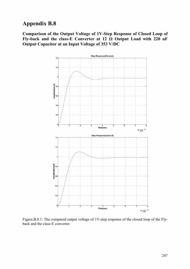
247
Appendix B.8 Comparison of the Output Voltage of 1V-Step Response of Closed Loop of Fly-back and the class-E Converter at 12 Ω Output Load with 220 uF Output Capacitor at an Input Voltage of 353 V/DC
Figure.B.8.1: The compared output voltage of 1V-step response of the closed loop of the Fly-back and the class-E converter.
410* −
410* −

248

249
Thesen 1. Eine Methode zur Bestimmung des Null-Spannungs-Schaltungs-Fensters eines Lastresonanzkonverters definiert sich ausgehend von einem Punkt mit Null-Spannungsschalten und Null-Stromschalten (ZVS/ZCS) durch Verschiebung der Frequenz in Richtung abnehmender übertragener Leistung. Damit wird abhängig von normierten variablen Parametern des Konverters das maximal mögliche Frequenzfenster des Null-Spannungsschaltens gefunden, einschließlich von Unterbrechungen, in denen Null-Spannungsschalten nicht möglich ist. Gleiches gilt in Dualität für die Bestimmung eines Null-Strom-Schaltungs-Fensters einer dualen Topologie. Innerhalb eines gefundenen Null-Spannungsschaltungs-Fensters tritt in den Schaltern Reversstrom auf, sobald jeweils ein antiparalleler Schalter (Diode) durch negative Schalterspannung einschaltet, so dass der ZVS/ZCS Zustand innerhalb des ZVS-Fensters nicht erhalten bleibt, und erst im letzten Punkt des Frequenzfensters ZVS/ZCS wieder erreicht werden kann.
In normalisierter Schreibweise wird ein Frequenzverschiebungsfaktor ωωnn = definiert, der
das Verhältnis aus der Schaltfrequenz des ZVS/ZCS Anfangzustandes nω und der variierten
Schaltfrequenz ω bildet. Weiterhin wird ein LastverschiebungsfaktorEQ
opEQ
RR
k'
' )(= als
Verhältnis der Anfangslast )(' opEQR im ZVS/ZCS-Anfangszustand zur variablen Ausgangslast
EQR' verwendet. Im Ergebnis dieses Verfahrens erhält man eine variable Lastkreisgüte im Fall einer im Ausgangspunkt der Last gleichen kapazitiven Parallelimpedanz zur Last von
))()1(1(2
' 2211
nkkQQ
ωω
+= , und im Allgemeinfalle ))()(1()1(
' 22211
nkr
rkQQ
ωω
++
= , für welche
das Differentialgleichungssystem in Zustandsraum erneut zu lösen ist, um den so erhaltenen Betriebspunkt des Konverters auf die ZVS-Bedingung zu prüfen. Das Verhältnis
)(2' ' opEQnd RCr ω= ist für den allgemeinen Fall definiert, wenn die Nennausgangslast von der
kapazitiven Parallelimpedanz abweicht. Die Grenzen der relativen Einschaltzeit (Duty-Cycle), welche den ZVS-Bereich eines Frequenzpunktes bezeichnet, werden direkt aus der Methode gewonnen, ebenso, wie weitere normalisierte, frei variierbare Parameter des Konverters als Variablen im normalisierten Zustandsraum eintragbar sind (Lastkreisgüte 1Q , relative Eingangsresonanzfrequenz 3A ). 2. Die vorgestellte Methode erreicht durch sämtlich einheitslose Darstellung von Zustandvariablen und Parametern den maximal möglichen Abstraktionsgrad, welcher die Vollständigkeit der gefundenen ZVS-Fenster garantiert und direkte Schaltungssynthese erlaubt. 3. Die Frequenzbandbreite der Nullspannungs-Schaltfähigkeit (ZVS) einer Klasse-E-Schaltung nach N. Sokal mit hoher Lastkreisgüte in normalisierter, einheitsloser Darstellung aller beeinflussenden Parameter ( initinitinit DcQA ,13 , ) steigt mit dem Faktor 3A der Eingangs-Resonanzfrequenz, sowie mit dem initialen maximalen Duty-Cycle ( initDc ) deutlich an.

250
Begrenzt wird dieser Anstieg im Falle des Parameters 5,1...1,13 ≥initA durch Verlust des Nullspannungsbetriebes bei Lastwechsel von maximal vorgesehener Last zu leichter Last durch Unterbrechung des Frequenzfensters des ZVS-Betriebes infolge von verlustbehaftetem Nicht-Nullspanungsbetrieb. Bis zu einem Parameterwert ≤initA3 1,1 ist ein ununterbrochenes Nullspannungs-Schaltungsfenster des normalisierten Frequenzbereiches der Schaltfrequenz bei jeder gewählten minimalen Lastkreisgüte 101 ≥initQ gegeben, wenn der maximale Duty-Cycle
7,03,0 ≤≤ initDc gewählt wird. Unter gleichen Bedingungen )7,03,0;10( 1 ≤≤≥ initinit DcQ ist ab einem Parameterwert 5,13 ≥initA das Nullspannungsschaltungsfenster in jedem Falle unterbrochen. 4. Der erreichbare normalisierte Eingangsspannungsbereich )(max / opinin VV einer Klasse-E- Schaltung nach N.Sokal mit hoher Lastkreisgüte in normalisierter, einheitsloser Darstellung aller beeinflussenden Parameter ),,( 13 initinitinit DcQA für ununterbrochenen Nullspannungsbetrieb steigt deutlich mit den Parametern initA3 und initDc an, und fällt geringfügig mit wachsendem Parameter initQ1 ab. Zwischen der normalisierten Eingangs-spannung )(max / opinin VV und der normalisierten Frequenz nff / besteht ein nahezu linearer Zusammenhang, wenn damit eine konstante Ausgangsspannung erreicht werden soll. 5. Entsprechend These 3 wird bei einer Klasse-E-Schaltung mit steigender maximaler relativer Einschaltzeit initDc eine signifikante Vergrößerung des Nullspannungsschaltungs-Frequenzfensters erreicht, wenn der Parameter 1,1≤initA , also die Eingangsresonanzfrequenz gleich order kleiner als die Lastkreisresonanzfrequenz gewählt wird. Für größere Werte von
1,13 ≥initA bleibt das Nullspannungs-Schaltungs-Frequenzfenster unabhängig von der gewählten maximalen relativen Einschaltzeit initDc etwa konstant. 6. Entsprechend der Thesen 3 und 5 gilt für eine Klasse-E-Schaltung bei gewählter maximaler relativer Einschaltzeit 5,0≤initDc ,und einem Parameterbereich 0,13 ≥initA näherungsweise der Zusammenhang, dass die Größe des Nullspannungsschaltungs-Frequenzfensters ( ZVSnff )/max etwa gleich oder geringfügig größer als der Parameter 3A angenommen werden kann:
3max )/( Aff ZVSn ≥ . Dieser Zusammenhang wird insbesondere mit einer Genauigkeit von 0%...+10% Fehlerabweichung festgestellt, wenn die minimale Lastkreisgüte 301 ≥initQ und der Parameter
0,13 ≥initA gewählt wurden: initZVSn
init Af
fA 3
max3 1,1)( << .
7. Zur Steuerung einer Klasse-E-Schaltung nach Thesen 3 bis 6 kann der Duty-Cycle stets mit der Frequenz f , beginnend bei ( ninit fDc , ) mit steigender Frequenz bei beliebiger Last
LNL RR ≥ ( LNcd RX =2 =Nennlast bei impedanzgleicher Ausgangskapazität) linear vermindert werden, ohne, dass der Nullspannungs-Betrieb (ZVS) verloren geht, solange das Nullspannungsschaltungs-Frequenzfenster nach These 3 unterbrechungsfrei ist. Dabei kann
vorzugsweise die lineare Funktion fnn
o kffDcDc −= Verwendung finden, indem

251
1max
min
−
−=
n
initfn
ff
DcDck , und
1
1
1
1max
min
max
int
−−
−=
n
no
ff
Dc
ff
DcDc ;
)1)(
1)(()
1)(
)(11(
maxmin
max −
−+
−
−+=
n
n
n
ninit
ff
ff
Dc
ff
ff
DcDc erhalten werden.
Der minimale Duty-Cycle )( minDc wurde in einem weiten Parameterbereich ( 5,03 =initA bis 1,1; 101 =initQ bis 100; 3,0=initDc bis 0,7) mit einem konstanten Wert für alle Lastfälle
LNL RR ≥ mit 15,0min =Dc ermittelt. Der maximale Duty-Cycle initDc wurde in eben demselben Parameterbereich für alle Lastfälle LNL RR ≥ als konstant wählbar ermittelt.
8. Eine normalisierte Funktion )(nffDcDc = nach These 7 kann für einen Klasse-E-Konverter
insbesondere in Form einer festgelegten integrierten Schaltung, als fester Zusammenhang zwischen Frequenz f und Duty-Cycle Dc als Steuerfunktion verwendet werden, welche das Null-Spannungs-Schalten in einem weiten Parameterbereich garantiert ( 7,03,0 ≤≤ initDc ;
101 ≥initQ ; 1,15,0 3 ≤≤ initA ). 9. Der Phasenwinkel des Stromnulldurchganges einer Klasse-E-Schaltung nach N.Sokal zwischen Schalterstrom und Resonanzstrom des Lastkreises weicht von null nur geringfügig ab, wenn initA3 groß gewählt wird ( 1,13 ≥initA ; °≤− 25
Ls IIϕ ). Wird 3A in einem weiten Bereich gewählt ( 5,15,0 3 ≤≤ initA ), weicht der Phasenwinkel im Parameterbereich ( 45,03,0 ≤≤ initDc , und 301 ≥Q ) ebenfalls nur geringfügig von null ab ( °≤− 12
Ls IIϕ ). Um eine kleine Winkelabweichung °≤− 5
Ls IIϕ zu erzielen muss entweder die Lastkreisgüte 1001 ≥initQ und der Duty-Cycle initDc ( 45,03,0 ≤≤ initDc ) gewählt werden, oder der Duty-Cycle
initDc wird klein gewählt )3,0( =initDc , und die Lastkreisgüte 1Q kann im Bereich 10030 1 ≤≤ initQ gewählt werden.
10. Eine Klasse-E-Schaltung mit hoher Lastkreisgüte 1Q kann nach These 9 bezüglich optimalen Einschaltens (ZVS) dadurch synchronisiert werden, dass der Laststrom des Resonanzkreies outRMSI bezüglich seines Nulldurchgangs abgetastet wird, und zugleich im Nulldurchgang der Schalter eingeschaltet wird. Dieses kann vorzugsweise dadurch geschehen, dass der Laststrom über eine Kapazität ausgekoppelt wird, und der Schalter mit einer Phasen-Verzögerung von 90° eingeschaltet wird. Eine kapazitive Auskopplung dieser Art ist auf natürliche Weise bei einer Hilfselektrode eines piezoelektrischen Trafos gegeben, welche eine um 90° gegenüber dem Laststrom nacheilende Spannung im unbelasteten Fall der Hilfselektrode erzeugt. Zur Erzielung praktisch ausreichender Genauigkeit der Einschaltsynchronisation ist ein maximaler Phasenwinkelfehler von -12°...+1° ausreichend, und wird im Parameterbereich 5,15,0;45,03,0;30 31 ≤≤≤≤≥ initinitinit ADcQ stets erreicht. 11. Eine Klasse-E-Schaltung nach These 4 kann durch eine lineare Funktion der Schaltfrequenz )( inVff = bzw. in einheitsloser Darstellung )/(// )(opininnn VVffff = in Abhängigkeit von der Eingangspannung bezüglich konstanter Ausgangspannung gesteuert

252
werden, ohne dass ein geschlossener Regelbreis erforderlich ist. Insbesondere lässt sich so eine konstante Ausgangspannung für eine konstante Last einstellen. Die Ausgangsspannung variiert hierbei mit variabler Last, bleibt aber fast unabhängig von der Eingangsspannung. Die Eingangsspannungs-Unabhängigkeit ist für eine gewählte Ausgangslast am besten, wenn eine Linearisierung für eben diese Last vorgenommen wird. Für abweichende Ausgangslasten steigt die Eingangsspannungsabhängigkeit einer so gewählten Linearisierungsfunktion geringfügig an. 12. Eine Steuerfunktion des Duty-Cycle nach Thesen 7 und 8, sowie nach Thesen 9 und 10, kann für eine Ausführung einer Klasse-E–Schaltung alternativ Verwendung finden, wenn der Parameter initA3 in einem Bereich 1,15,0 3 ≤≤ initA , die initiale Lastkreisgüte initQ1 in einem Bereich 301 >initQ , und der initiale Duty-Cycle initDc in einem Bereich
45,03,0 ≤≤ initDc gewählt werden. 13. Die Ausgangsgleichspannung eines Lastresonanzkonverters mit einem Brückengleichrichter ausgangsseitig kann durch Konstanthalten der Amplitude des Lastkreisstromes in einem maximalen Verhältnis von 2:1 variieren, wenn der Nennlast eine gleichgroße kapazitive Impedanz vor der Gleichrichtung parallel geschaltet wird. Dieses geschieht vorzugsweise durch Impedanzanpassung, sobald ein Piezotransformator als Lastkreis verwendet wird. In praktischen Anwendungen kann das Ausgangsspannungs- Verhältnis zwischen Leerlauf und Volllast durch Vermeidung idealen Leerlaufes etwa 1.5 bis
1.6 betragen. Im Leerlauf gilt: 2
3^
d
d
tap
out
CC
NoNt
V
V= .
14. Die Erkennung einer leichten Last an einer Klasse-E-Schaltung nach N.Sokal mit hoher Lastkreisgüte kann näherungsweise durch eine lineare Funktion der Schaltfrequenz sf in Abhängigkeit von der Eingangsspannung inV erfolgen, indem ein Frequenzwert
BAVff ins ++= mit konstanten Koeffizienten A und B mit einem konstanten Referenzwert
feRf verglichen wird, welcher bei konstanter Ausgangsspannung einem eingangsspannungs- unabhängigen Laststrom entspricht. Eine solche Funktion erlaubt den Eintritt in eine Burst-Mode-Funktion bei immer der gleichen Ausgangslast, ohne dass der Laststrom selbst gemessen werden muss. 15. Eine nahezu konstante, eingangsspannungs- und lastunabhängige Ausgangsspannung bei einem Klasse-E-Konverter nach N.Sokal mit hoher Lastkreisgüte lässt sich erzielen, wenn eine lineare Funktion conθ des Phasenwinkels zwischen dem Stromnulldurchgang des Lastkreisstromes und dem Ausschaltpunkt des Schalterstromes zur Bildung eines Referenzwertes für die Amplitude des Lastkreisstromes LI der Form taprefV verwendet wird, welche den Phasenwinkel
LS II ϕϕ − mit der Funktion 4*3*2**1 KVKVKVVinK intapreftaprefcon −−−=θ in Übereinstimmung bringt.
16. Eine Klasse-E-Schaltung nach N.Sokal mit hoher Lastkreisgüte 1Q kann bezüglich ihrer dynamischen Eigenschaften, wie auch andere Lastresonanzkonverter mit hoher Lastkreisgüte, in ein Hochfrequenz-Modell des Resonanzkonverters, und ein Niederfrequenzmodell der geglätteten Ausgangsgleichspannung nach dem Ausgangsgleichrichter zerlegt werden, wenn die Ausgangszeitkonstante ( outLNoutput CR=τ ) viel größer als die größte Zeitkonstante des Lastresonanzkreises einschließlich einer eventuell vorhandenen Eingangskreiszeitkonstante

253
des Lastresonanzkonverters ist. Der Ausgangslastwiderstand LNR ist bei dieser Betrachtung der kleinste in der Modellbildung vorkommende Wert, in der Regel der Nennlastwert. 17. Ein Lastresonanzkonverter nach These 16 kann zur Modellierung von transienten Vorgängen eines nicht geregelten Übertragungssystems (offener Regelkreis) durch ein statisches Zweipunktmodell dargestellt werden, wenn die Ausgangszeitkonstante outputτ wenigstes vier mal größer als die größte Zeitkonstante des Lastresonanzkreises ist, und wenn der Lastwiderstand LR kleiner oder gleich dem Nennlastwiderstand LNR ist, bei denn eine gleichgroße Impedanz des Wechselspannungsausganges des Lastresonanzkonverters vor dem
Ausgangsgleichrichter Leqd
RC
=2
1ω
geschaltet ist. Die Punkte des Zweipunktmodells
entsprechen der statischen Ausgangsübertragungsfunktion des Stromes bei vorwiegender Spannungspufferung, oder der Spannung bei vorwiegender Strompufferung, vor und nach dem abgeschlossen transienten Vorgang. 18. Ein Lastresonanzkonverter nach These 16 kann zur Modellierung von transienten Vorgängen eines nicht geregelten Übertragungssystems (offener Regelkreis) durch ein statisches Zweipunktmodell zuzüglich einer Hilfsimpedanz XR in Serie zur spannungsgepufferten Ausgangslast, oder parallel zur stromgepufferten Ausgangslast dargestellt werden, wenn die Ausgangszeitkonstante outputτ wenigstens vier mal größer als die größte Zeitkonstante des Lastresonanzkreises ist, und wenn der Lastwiderstand LR beliebig größer oder beliebig kleiner als der Nennlastwiderstand LNR ist, bei dem eine gleich große Impedanz des Wechselspannungsausganges des Lastresonanzkonverters vor dem
Ausgangsgleichrichter Leqd
RC
=2
1ω
geschaltet ist.
Die Punkte des Zweipunktmodells entsprechen der statischen Ausgangsübertragungsfunktion des Stromes bei vorwiegender Spannungspufferung, oder der Spannung bei vorwiegender Strompufferung. Ein dritter Punkt des statischen Übertragungskennlinienfeldes ergibt sich als Maximalwert max
'I des abgegebenen Stromes avI durch Auslesen des Kennlinienfeldes der statischen Ausgangsvariablen Strom im Falle ausgangsseitiger Spannungspufferung, oder Spannung im Falle ausgangsseitiger Stromspufferung, im Moment einer sprunghaften Störung (Eingangsspannung, Frequenz, Last). 19. Ein Lastresonanzkonverter kann bezüglich seiner Übertragungsfunktion in eine lineare Nährung arxV des statischen Übertragungsverhaltens überführt werden, indem der Ausgangsstrom bei vorwiegend gepufferter Ausgangsspannung, oder die Ausgangsspannung bei vorwiegend gepuffertem Ausgangsstrom, oder der Lastkreisstrom einer serienresonanten Schaltung, oder die Lastkreisspannung einer parallelresonanten Schaltung durch eine allgemeine Funktion inxarxxoxarx VkfkkV _21 ++= dargestellt werden, so dass die statischen und dynamischen Übertragungseigenschaften für geschlossene Regelkreise zur Aufrechterhaltung eines Sollwertes der genannten Statusvariablen arxV in ausreichend hoher Modellgenauigkeit der Realität entsprechen. 20. Ein Lastresonanzkonverter nach These 16 kann zur Modellierung eines geregelten Übertragungssystems (geschlossener Regelkreis) durch ein Modell mit genäherter linearer Übertragungsfunktion und festen Zeitkonstanten (Pole, Nullstellen) eines in den Bildbereich transformierten Differentialgleichungssystems (Laplace-Transformation) dargestellt werden, wenn die Ausgangszeitkonstante )( outputτ wenigstens vier mal größer als die größte

254
Zeitkonstante des Lastresonanzkreises ist, und wenn der Lastwiderstand LR beliebig größer oder kleiner als der Nennlastwiderstand LNR ist, bei dem eine gleichgroße Impedanz des Wechselspannungsausganges des Lastresonanzkonverters vor dem Ausgangsgleichrichter
Leqd
RC
=2
1ω
geschaltet ist.
21. Ein Lastresonanzkonverter nach These 16 kann zur Modellierung eines geregelten Übertragungssystems (geschlossener Regelkreis) durch ein Modell mit genäherter linearer Übertragungsfunktion und der größten festen Zeitkonstante des Lastresonanzkreises eines in den Bildbereich transformierten Differentialgleichungssystems (Laplace-Transformation) dargestellt werden, wenn die Ausgangszeitkonstante )( outputτ wenigstens 20 mal größer als die größte Zeitkonstante des Lastresonanzkreises ist, und wenn der Lastwiderstand LR beliebig größer oder kleiner als der Nennlastwiderstand LNR ist, bei dem eine gleichgroße Impedanz des Wechselspannungsausganges des Lastresonanzkonverters vor dem Ausgangsgleichrichter
Leqd
RC
=2
1ω
geschaltet ist.
22. Ein Lastresonanzkonverter nach These 16 kann zur Modellierung eines geregelten Übertragungssystems (geschlossener Regelkreis) durch ein Modell mit genäherter linearer Übertragungsfunktion und unter Vernachlässigung aller Zeitkonstanten des Lastresonanzkreises eines in den Bildbereich transformierten Differentialgleichungssystems (Laplace-Transformation) dargestellt werden, wenn die Ausgangszeitkonstante )( outputτ wenigstens 40 mal größer als die größte Zeitkonstante des Lastresonanzkreises ist, und wenn der Lastwiderstand LR beliebig größer oder kleiner als der Nennlastwiderstand LNR ist, bei den eine gleich große Impedanz des Wechselspannungsausganges des Lastresonanzkonverters
vor dem Ausgangsgleichrichter Leqd
RC
=2
1ω
geschaltet ist.
23. Ein Lastresonanzkonverter nach Thesen 16, 20, 21 und 22, kann bezüglich einer genäherten Übertragungsfunktion, resultierend aus exakten statischen Lösungen des eingeschwungenen Zustandes, auch durch eine genäherte Übertragungsfunktion, resultierend aus einem heuristischen Modell eines empirischen Energiegleichungssystems nach [Rad 00] beschrieben werden, wenn der betrachtete normierte Frequenzbereich entsprechend den statischen Fehlern der heuristischen Methode ausreichend erweitert wird, und wenn das Verfahren in Bereichen geringer Parametersensitivität der übertragenen Leistung, also bei ausreichender Genauigkeit der heuristischen Lösungen nach [Bis 06], angewandt wird. Das dynamische Verhalten des geschlossenen Regelkreises eines Lastresonanzkonverters kann dann ebenso genau genähert werden wie durch Verwendung einer Linearisierung auf der Basis exakter Lösungspunkte des statischen Übertragungsverhaltens. 24. Ein heuristisches Verfahren nach These 23 ist nicht mit ausreichender Genauigkeit für die Modellierung eines Lastresonanzkonverters nach Thesen 17 und 18 in offenen Regelkreisen, also für große Änderungen der Ausgangsgrößen, anwendbar. 25. Ein Lastresonanzkonverter mit hoher Lastkreisgüte, wie sie beispielsweise durch eine Klasse-E-Schaltung nach N. Sokal gegeben sein kann, kann aufgrund seiner höheren Ordnung der genäherten dynamischen Übertragungsfunktion lediglich durch PI-Regler oder PID-Regler ausreichend genau bezüglich der verbleibenden Regelabweichung und bezüglich einer zur

255
Schaltfrequenz in einem Verhältnis von 1:15 bis 1:32 stehenden Eckfrequenz des Reglers mit stabilen Regeleigenschaften geregelt werden. 26. Ein Lastresonanzkonverter mit hoher Lastkreisgüte, wie sie beispielsweise durch eine Klasse-E-Schaltung nach N. Sokal gegeben sein kann, kann durch eine lineare Funktion der Frequenz in Abhängigkeit von der Eingangsspannung bezüglich konstanter Ausgangsspannung oder in Abhängigkeit vom Eingangstrom bezüglich konstanten Ausgangsstromes gesteuert werden, wobei die Konstanz der Ausgangsgröße in einem Bereich von +/-10% bis +/- 20% gehalten werden kann, solange die Last kleiner oder gleich einer Nennlast LNR mit einer bei Nennlast gleichgroßen beschalteten Impedanz des
Wechselspannungsausganges LeqNd
RC
=2
1ω
ist.
27. Wird nach These 26 eine quadratische Näherung der Frequenz in Abhängigkeit von der Eingangsgröße gewählt, so ist die Konstanz der Ausgangsgröße in einem ausgewählten Lastfall, und nur in diesem einen Lastfall, auf wenigstens +/-5% Abweichung reduzierbar, solange die Last kleiner oder gleich einer Nennlast LNR mit einer bei Nennlast gleichgroßen
beschalteten Impedanz des Wechselspannungsausganges LeqNd
RC
=2
1ω
ist.
28. Ein Klasse-E-Konverter nach N. Sokal mit hoher Lastkreisgüte kann aufgrund der höheren Ordnung des Lastresonanzkreises, vergleichsweise zu einem hart schaltenden Konverter vom Sperrwandler-Typ (Fly-Back Converter) bei gleichen Zielparametern (Frequenz, Ausgangsspannung, Eingangsspannung, Nennlast) lediglich eine um einen Faktor 6,2 größere dynamische Einschwingzeit bei Nennlast erreichen, wobei der Sperrwandler im stets lückenden Betrieb (DCM) ausgelegt wird, und wobei der Klasse-E-Konverter bei minimaler Eingangsverzögerung 13 ≈A , sowie einer bei Nennlast LNR zur Ersatznennlast LeqNR
gleichgroßen am Wechselspannungsausgang geschalteten Impedanz Leqd
RC
=2
1ω
betrieben
wird.

256
257
Reference [App 01] Application note AN-SMPS-ICE2AXXX-1 published by Infineon Technologies AG. [Ban 04] Banu U., Uma G.: Artificial controlled neural network emulator for quasi resonant converter: IEEE DELTA 2004, January 2004. [Bat 94] Batarseh I.: Resonant converter topologies with three and four energy storage elements: IEEE Transactions on power electronics, Vol.9, January 1994. [Bat 96] Batarseh I., Megalemos C., Sznaier M.: Small signal analysis of the LCC-type parallel resonant converter: IEEE Aerospace and Electronic systems, Vol.32, April 96. [Bax 59] Baxandall P.J.: Transistor sine wave LC oscillators, some general considerations and new developments: Proceeding of the IEEE, May 1959. [Ben 05] Ben-Yaakov S., Ivensky G.: Drivers and rectifiers for piezoelectric elements: PESC 05, Tutorial session 3, June 2005. [Ben 06] Ben-Yaakov S., Lineykin S.: Maximum power tracking of Piezoelectric transformer HV converters under load variation: IEEE Transactions on power electronics, Vol.21, January 2006. [Bha 91] Bhat K.S.: A unified approach for the steady-state analysis of resonant converters: IEEE Transactions on industrial electronics, Vol.38, August 1991. [Bib 00] Bibian S., Jin H.: Time delay compensation of digital control for DC switch mode power supplies using prediction techniques: IEEE transactions on power electronics, Vol.15, September 2000. [Bis 04] Bisogno F.E., Radecker M., et.al.: Dynamic behavior of high voltage mosfet and IGBTs in resonant power converter using piezoelectric: PCIM 04 International Exhibition & Conference. [Bis1 04] Bisogno F.E., Radecker M., Knoll A., et.al.: Comparison of resonant topologies for step-down application using piezoelectric transformers: IEEE PESC 2004, Vol.4, June 2004. [Bis 05] Bisogno F.E., Nittayarumphong S., Radecker M., et.al.: Dynamic modelling of class-E resonant converter for step-down application using piezoelectric transformer: IEEE PESC 05, pp 2797-2803, June 2005. [Bis 06] Bisogno F.E.: Energy–related system normalization and decomposition targeting sensitivity consideration: Ph.D. Thesis, TU Chemnitz, June 2006. [Bis1 06] Bisogno F.E., Nittayarumphong S., et.al.: A line power-supply for LED lighting using piezoelectric transformers in class-E: IEEE IPEMC 06, Vol.2, August 2006. [Bon 95] Bonissone P., Khedkar P., Schutten M.: Fuzzy logic control of resonant converters for power supplies: IEEE control application 1995, September 1995.

258
[Bro 02] Bronstein S., Ben-Yaakov S.: Design consideration for achieving ZVS in a half bridge inverter that a driver a piezoelectric transformer with no series inductor: IEEE PESC 02, Vol.2, June 2002. [Bur 01] Burdio J.M., Canales F., Barbosa P.M., Lee F.C.: A comparison study of fixed-frequency control strategies for ZVS DC/DC series resonant converter: IEEE PESC2001 32nd, Pages 427-432 Vol.1, June 2001. [Cho 05] Choi S., Kim T., Cho B.H.: Design of half-bridge piezo-transformer converters in the AC adapter applications: IEEE APEC05, Vol.1, March 2005. [Cho 97] Choi B.: Step load response of a current-mode-controlled DC-to-DC converter: IEEE Transaction on aerospace and electronics systems, Vol.33, October 1997. [Cod 04] Code of conduct on energy efficiency of external power supplies, European commission, November 2004. [Cuk 79] Cuk S.: General topological properties of switching structures: IEEE PESC 79, pp 109-130. [Cuk 84] Cuk S.: Survey of switching converter topologies, magnetic and control: Proc. IEE international conference on power electronics and variable-speed drive, May 1984. [Cuk 77] Cuk S., Middlebrook R.D.: A new optimum topology switching DC-to-DC converter: IEEE PESC 77, pp.160-179. [Dal 99] Dale H., et al.: Piezoelectric transformer with voltage feedback: United States patent 5,872,419, February 1999. [Dan 01] Danov G.: Converter with piezoceramic transformer: United States patent 6,188,163 B1, February 2001. [Dia 04] Diaz J., Nuno F., Prieto M.A.: A new control strategy for an AC/DC converter based on a piezoelectric transformer: IEEE Transaction on industrial electronics, Vol.51, August 2004. [Div 86] Divan D.M.: The resonant DC link converter-a new concept in static power conversion: IEEE IAS annual meeting record 1986. [Ela 96] Elasser A., Schuttel M.J., Vlatkovic V., et.al.: Switching losses of IGBTs under zero-voltage and zero-current switching: IEEE PESC 96, Vol.1, June 1996. [Eri 82] Erickson R.W., Cuk S., Middlebrook R.D.: Large signal modeling and analysis of switching regulator: IEEE PESC82, June 1982. [Eri 83] Erickson R.W.: Synthesis of switched-mode converter: IEEE PESC 83, pp 9-22. [Far 01] Farhangi S., Yazdani A., Fahimi B.: Model-reference adaptive-control of a PFC-equipped battery-charger: IEEE IECON’01, Vol.2, November 2001. [Fli 95] Fliesse M., Levine J., Martin P., Rouchon P.: Flatness and defect of nonlinear systems: Introductory theory and examples, Int.J. Contr., Vol. 61, 1995.
259
[For 92] Forsyth A.J., Ma S.H., Leung Y.T.: Dynamic characteristics of the Class E DC/DC converter using sampled-data modelling: IEE Proceeding-B, Vol.139, July 1992. [Gen 06] Gensior A., Woywode O., Rudolph J. Güldner H.: On differential flatness, trajectory planning, observers, and stabilization for DC–DC converters: IEEE Transaction on fundamental theory and applications, Vol.53, September 2006. [Gu 88] Gu W. J., Harada K.: A new method to regulate resonant converter: IEEE Transaction on Power Electronics, October 1988. [Gu 89] Gu W., Harada K.: Dynamic analysis of class E resonant DC-DC converter regulated under fixed switching frequency: IEEE PESC 1989, Vol.1, June 1989. [Gut 80] Gutmann R.F.: Application of RF circuit design principle to distributed power converters: IEEE Teans. Industrial electronics and control instrumentation, August 1980. [Ham 00] Hamamura S., Kurose D., Ninomiya T., Yamamoto M.: New control method of piezoelectric transformer converter by PWM and PFM for wide range of input voltage: IEEE CIEP 2000, October 2000. [Har 91] Hernandaz A.F., Erickson R.W., et.al.: A large signal computer model for the series resonant converter: IEEE PESC91, June 1991. [Har 94] Harada K., Ishihara Y., Todaka T.: A novel ZVS PEM half bridge converter: IEEE INTELEC’94 16th, November 1994. [Hem 02] Hemsel T., Littmann W. Wallaschek J.: Piezoelectric transformers-state of the art and development trends: IEEE ultrasonic symposium 2002. [Hu 89] Hu C. Q., Zhang P.: class-E combined converter by phase-shift control: IEEE Power Electronics Specialists Conference Record, pp.229-234, (1989). [Huy 90] Huy-Le H., Viarouge P., Slimani K.: A current-controlled quasi-resonant converter for switched reluctance motor: IEEE Industrial electronics society, IECON’90, November 1990. [Ish 03] Ishizuka Y., Lee K., Oyama T.: Consideration of a single switch inverter for piezo-electric transformer with a new control method: IEEE PESC 2003, Vol.4, June 2003. [Ive 99] Ivensky G., Kats A., Ben-Yaakov S.: An RC load model of parallel and series-parallel resonant DC-DC converters with capacitive output filter: IEEE Transactions on power electronics, Vol.14, May 1999. [Ive 00] Ivensky G., Shvaratsas M., Ben-Yaakov S.: Analysis and modelling of a piezoelectric transformer in high output voltage applications: IEEE APEC 2000, February 2000. [Ive 04] Ivensky G., Shvartsas M., Ben-Yaakov S.: Analysis and modeling of a voltage doubler rectifier fed by piezoelectric transformer: IEEE Transaction on power electronics, Vol.19, March 2004. [Jin 92] Jin H., Joos G. Pande M., Biogas P.D.: Feedforward techniques using voltage integral duty-cycle control [for power converters]: IEEE PESC92, Vol.1, July 1992.

260
[Joh 86] Johnson S., Erickson R.: Steady-state analysis and design of the parallel resonant converter: IEEE PESC 86, June 1986. [Joh 87] Johnson S.D., Witulski A.F., Erickson R.W.: A comparison of resonant topologies in high voltage application: IEEE Applies power electronics conference 87, March 1987 [Joz 89] Jozwik J., Kazimierczuk M.: Optimal topologies of resonant DC/DC converters: IEEE Transaction on aerospace and electronics systems, Vol.25, May 1989. [Kaz 87] Kazimierczuk M.K., Puczko K.: Exact analysis of class-E tuned power amplifier at any Q and switch suty cycle: IEEE Vol. CAS-34, No.2, February 1987. [Kaz1 87] Kazimiercuk M., Puczko K.: Feedback control of zero-voltage-switching resonant DC/DC converters: In proceeding of the second high frequency power conversion conference, April 1987. [Kaz1 89] Kazimierczuk M.K., Jozwik J.: Resonant dc/dc converter with class-E inverter and class-E rectifier: IEEE Vol.36, November 1989. [Kaz2 89] Kazimierzuck M.K., Bui X.T.:class-E DC/DC converter with an inductive impedance inverter: IEEE Transactions on power Electronics, January 1989. [Kaz 93] Kazimierczuk M., Czarkowski D.: A new phase –controlled parallel resonant converter: IEEE Transactions on industrial electronics, Vol. 40, December 1993. [Kaz 99] Kazimierczuk M.: Dynamic performance of PWM DC-DC boost converter with input voltage feed forward control: IEEE transaction on circuits and systems, Vol. 46, December 1999. [Kim 91] Kim G., Lee D., Youn M.: A new state feed back control of resonant converters: IEEE transactions on industrial electronics, Vol.38, June 1991. [Kin 85] King R.J., Stuart T.A.: Small signal model for the series resonant converter: IEEE Transactions on aerospace and electronics systems, May 1985. [Kur 92] Kurnia A., Stielau O.H., Venkataramanan R., et.al: Loss mechanisms in IGBT’s under zero voltage switching: IEEE PESC 92, Vol.2, July 1992. [Lee 89] Lee C. Q., Sooksatra S.: Novel class-E converters: IEEE PESC 89, Vol.1, June 1989. [Lee 98] Lee S., Hong J., Yoo J., Gong G.: Characteristics of piezoelectric transformer for power supply: IEEE ultrasonic symposium 1998, Vol.1, October 1998. [Leu 03] Leung K., Chung H., Hui R.: Use of state trajectory prediction in hysteresis control for achieving fast transient response of the buck converter: IEEE ISCAS 03, Vol.3, May2003. [Liu 85] Liu K., Oruganti R., Lee. F.: Resonant switched topologies and characteristic: IEEE PESC 1985, P. 106-116. [Lin 94] Lin C.Y., Lee F.C.: Design of a piezoelectric transformer converter and its matching networks: IEEE PESC94, Vol.1, June 94
261
[Lin 97] Lin C.Y.: Design and analysis of piezoelectric transformer converters: Ph.D. Dissertation, Virginia Tech, July 1997. [Lin 01] Lin R.L., Lee F., et.al.: Inductor-less piezoelectric transformer electronic ballast for linear fluorescent lamp: IEEE APEC01, March 2001. [Liu 84] Liu K., Lee F.C.: Resonant switches a unified approach to improve performance of switching converters: IEEE TELEC 84. [Liu 90] Liu K., Lee F.C.: Zero-voltage switching technique in DC/DC converters: IEEE Transaction on power electronics, Vol.5, July 1990. [Liu 95] Liu Y., Sen P.C.: A novel resonant converter topology for DC-to-DC power supply: IEEE transaction on aerospace and electronic systems, Vol.31, October 1995. [Mao 04] Mao H., Abu-Qahouq, et.al.: Zero voltage switching half bridge DC-DC converter with modified PWM control method: IEEE Transactions on power electronics, July 2004. [Mas 48] Mason W.P.: Electromechanical transducers and wave filters, Princeton 1948. [Mas 92] Mascarenhas P.: Hysteresis control of a continuous boost regulator: IEE Colloquium on static power conversion, November 1992. [Mat 93] Mattavelli P., Rossetto L., Spiazzi G., Tenti P.: General purpose sliding mode controller for DC/DC converter application: IEEE PESC 93, June 1993. [Mcm 61] Mcmurray W., Shattuck D.P.: A silicon controlled rectifier inverter with improved communication: AIEE Transactions, November 1961. [Mid 76] Middlebrook R.D., Cuk S.: A general unified approach to modeling switching converter power stages: IEEE PESC 1976. [Moh 89] Mohan N., Undeland T.M., Robbins W.P.: Power electronics second edition, John Wiley& Sons, INC. 1989. [Nai 97] Naim R., Weiss G., Ben-Yaakov S.: H infinity control applied to boost power converters: IEEE Transactions on power electronics, Vol.12, July 1997. [Nit 05] Nittayarumphong S., Bisogno F., Radecker M.: Dynamic behaviour of PI controlled class-E resonant converter for step-down application using piezoelectric transformers: IEEE EPE 2005, September 2005. [Nit 06] Nittayarumphong S., Bisogno F., Radecker M.: Comparison of control concepts for off-line power supplies using piezoelectric transformer in class-E topology: IEEE PESC 06, June 2006. [Nit1 06] Nitschke Markus, Entwicklung eines Demonstrators als innovative Netz-stromversogung mit Piezo-Transformer für 50 Watt Ausgangsleistung. Diplomarbeit, Universität der Bundeswehr München, Dezember 2006.

262
[Nit 07] Nittayarumphong S., Bisogno F., Radecker M., et.al.: High efficiency control methods for class-E resonant converter for step-down application using piezoelectric transformer (PT): IEEE EPE 2007, September 2007. [Ojo 93] Ojo O., Bhat I.: Steady-state and dynamic analyses of high-order parallel resonant convertors: IEE Electric Power Application, Vol.140, May 1993. [Ojo 95] Ojo O.: Robust control of series parallel resonant converters: IEE Proc.-Control theory Appl., Vol.42, September 1995. [Oli 05] Oliver J.A., Fernandez C., Prieto R.: Circuit oriented model of rectifiers for large signal envelope simulation: IEEE PESC 05, September 2005. [Oru 88] Oruganti R., Lee F.: Implementation of optimal trajectory control of series resonant converter: IEEE transactions on power electronics, Vol.3, July 1988. [Oru 93] Oruganti R.: Resonant-tank control of parallel resonant converter: IEEE transaction on power electronics, Vol.8, April 1993. [Oru1 85] Oruganti R., Lee F.: Resonant power processors, Part I-state plane analysis: IEEE transaction on industry applications, Vol.IA-21, November 1985. [Oru2 85] Oruganti R., Lee F.: Resonant power processors, Part II-method of control: IEEE transaction on industry applications, Vol.IA-21, November 1985. [Pen 04] Peng L., Lehman B.: A design method for paralleling current mode control for DC/DC converters: IEEE CIEP2000, October 2000. [Pie 84] Pietkiewicz A., Tollik D.: Systematic derivation of two-state switches DC-DC: IEEE INTELEC 84, pp 473-477. [Pin 99] Pinheiro H., Jain P.K., Joos G.: Self-sustained oscillating resonant converters operating above the resonant frequency: IEEE Transactions on power electronics, Vol.14, September 1999. [Pol 97] Pollock H., Flower J.O.: New method of power control for series-parallel load-resonant converter maintaining zero-current switching and unity power factor operation: IEEE Transaction on power electronics, Vol.12, January 1997. [Pri 01] Prieto M.J., Diaz J., Martin A., Nuno F.: A very simple DC/DC converter using piezoelectric transformer: IEEE PESC 2001, Vol.1 June 2001. [Pri 02] Prieto M.J., Diaz J., Martin J.A.: Design guidelines for DC/DC converter using piezoelectric transformer: IEEE IECON02, Vol.1, November 2002. [Pri 04] Prieto M.J., Diaz J., Ramos J.A., Nuni F.: Closing a second loop in DC/DC converter based on Piezoelectric transformers: IEEE PESC 04, Vol. 6, June 2004. [Que 02] Quero J., Carrasco J., Franquelo L.: Implementation of a neural controller for the series resonant converter: IEEE transaction on industrial electronics, Vol.49, June 2002.

263
[Raa 77] Raab F.H.: Idealized operation of the Class E tuned power amplifier: IEEE Transactions on circuit and systems, Vol.Cas-24, December 1977. [Rad 00] Radecker M.: Effiziente Berechnung und Entwicklung Energieübertragender Systeme: Dissertation Technische Universität Chemnitz, Germany, May 2000. [Ray 04] Rayala S.: Averaging system description: Symester report Fachhochschule Bonn-Rhein-Sieg, 2004. [Rea 93] Reatti A., Kazimierczuk.: Class-E full-wave low dv/dt rectifier: IEEE Transactions on circuit and systems, Vol.40, February 1993. [Red 83] Redl R., Molnar B.: Class-E resonant regulated dc/dc power converter; analysis of operation and experiment results at 1.5 MHz: IEEE PESC83, June 1983. [Red1 83] Redl R., Molnar B.: Design of a 1.5 MHz regulated DC/DC power: PCI/Motorcon proceeding, September 1983. [Red 06] Redl R.: Advanced control techniques for DC-DC converter: Tutorial No.4, PCIM 2006. [Rib 98] Ribarich, Thomas J.: Phase detection control circuit for an electronic ballast: United States patent 6,002,214, December 1999. [Rid 91] Ridley R.: A new continuous-time model for current-mode control: IEEE Transaction on power electronics, Vol.6, April 1991. [Ros 56] Rosen C.A.: Ceramic transformer and filters: Proceeding of Electronic Comp, Symp. pp. 205-211, 1956. [Ros 94] Rossetto L., Spiazzi G., Tenti P., et.al.: Fast-response high-quality rectifier with sliding mode control: IEEE Transaction on power electronics, Vol.2, March 1994. [Rud 92] Rudolf P.: Topologies fro three-element resonant converters: IEEE Transactions on power electronics, Vol.7, January 1992. [San 03] Sanz M., Alou P., Soto A.: Magnetic-less converter based on Piezoelectric transformers for step-down DC/DC and low power application: IEEE APESC 03, Vol.2, February 2003. [San 04] Sanchez A.M., Sanz M., Alou P., et.al.: Experimental validation of an optimized piezoelectric transformer design with interleaving of electrodes: IEEE PESC04, Vol.2, June 2004. [Sho 97] Shoyama M., Horikoshi K., et.al.: Steady-state Characteristics of the push-pull piezoelectric inverter: IEEE PESC97, Vol.1, June 1997. [Sme 90] Smedley K.M.: Control art of switching converters: Ph.D Thesis, California Institute of Technology 1990. [Sme 95] Smedley K.M., Cuk S.: One-cycle control of switching converters: IEEE Transactions on power electronics, Vol.10, November 1995.

264
[So 97] So W.C., Lee Y.S., Tse C.K.: Dynamic modelling of phase-shifted full-bridge series resonanat converter: IEEE PESC 97, Vol.1, June 1997. [Sok 75] Sokal N.O., Sokal A.D.: Class-E A new class of high efficiency tuned single ended switch power amplifier: IEEE journal of solid state circuits, Vol.SC-10, June 1975. [Sok 77] Sokal A.: A remark on exact analysis of linear circuit containing periodically operated switches with applications: IEEE transactions on circuit and syst., Vol. CAS-24, October 1977. [Son 96] Song J., Greenwood A., Batarseh I.: Analysis and design of zero-voltage-switching class-E converter: IEEE Bringing together education, science and technology 96, April 1996. [Ste 88] Steigerwald R.L.: A comparison of half-bridge converter topologies: IEEE transaction on power electronics, Vol.3, April 1988. [Tan 93] Tang W., Lee F., et.al.: Charge control: modeling analysis and design: IEEE Transactions on power electronics, Vol.8, October 1993. [Tan 96] Tanaka H., Ninomiya T., Shoyama M.: Novel PWM controlled resonant converter: IEEE INTELEC 1996, October 1996. [Tym 86] Tymerski R., Vorperian V.: Generation, classification and analysis of switched-mode DC-to-DC converters by the use of converter cells: IEEE INTELEC 86, pp 181-195. [Ven 86] Venkataramanan R.: Sliding mode control of power converters: Ph.D Thesis, California Institute of Technology 1986. [Ven 04] Venketraman S., Sriram V.: Choosing a nonlinear controller for a series resonant DC-DC converter: Power electronics system and applications, November 2004. [Vor 83] Vorperian V., Cuk S.: Small signal analysis of resonant converters: IEEE PESC83, June 1983. [Vor 89] Vorperian V., Tymerski R., Lee F.: Equivalent circuit models for resonant and PWM switches: IEEE Transactions on power electronics, Vol. 4, April 1989. [Vor 90] Vorperian V.: Simplified analysis of PWM converter using model of PWM switch, continuous conduction mode: IEEE Transactions, Vol. 26 Issue 3, May 1990 P 490-496. [Vor1 90] Vorperian V.: Simplified analysis of PWM converter using model of PWM switch, discontinuous conduction mode: IEEE Transactions, Vol. 26 Issue 3, May 1990 P 490-496. [Wan 94] Wang K., Lee F. C., et.al.: A comparative study of switching losses of IGBTs under hard-switching, zero-voltage-switching and zero-current-switching: IEEE PESC 94, Vol.2, June 1994. [Wan 96] Wang Z., Sznaier M., et.al.: Robust controller design for a series resonant converter: IEEE transactions on aerospace and electronic systems, Vol. 32, January 1996. [Web 04] Weber J., Gensior A., Güldner H.: Flatness based control for chaotic boost converters: IEEE PESC 2004, Vol.2, June 2004.

265
[Wei 04] Weiping Z., Dongyan Z., et.al.:A low-cost-ZVS-class-E converter using PT: IEEE PESC’04 35th, June 2004. [Wit 91] Witulski A.F., Hernandaz A.F., Erickson R.: Small signal equivalent circuit modeling of resonant converter: IEEE Transaction on power electronics, Vol.6, January 1991. [Wit 85] Witulski A., Erickson R.: Steady-state analysis of series resonant converter: IEEE Trans. AES, November 1985. [Woy 01] Woywode O., Weber J., Güldner H.: Topological and statistical approach to DC-DC converters, IEEE PESC 2001, Vol.1, June 2001 [Yam 94] Yamamoto S., Hayasaka H., Matsuse K.: Analysis of series-resonant AC link inverter for improving output current: IEEE PESC 94, Vol.2, June 1994. [Yam 98] Yamane T., Hamura S., Zaitsu T., et.al.: Efficiency improvement of piezoelectric transformer DC-DC converter: IEEE PESC98, Vol.2, May 1998. [Yan 95] Yan-Fei L., Sen P.C.: A novel resonant converter topology for DC-to-DC power supply: IEEE T-AES /31/4/12729, pp.1301-1313, October 1995. [You 04] Youssef M.Z., Jain P.K.: A new ultra fast variable frequency self-sustained oscillation 48 V voltage regulator module: IEEE 30th industrial electronics society, November 2004. [You1 04] Youssef M.Z., Jain P.K.: A review and performance evaluation of control techniques in resonant converter: IEEE 30th industrial electronics society, November 2004. [Zai 94] Zaitsu T., Ohnishi O., et.al.: Piezoelectric transformer operating in thickness extensional vibration and its application to switching converter: IEEE PESC94, June 1994. [Zai 95] Zaitsu T., Shigehisa T., et.al.: Piezoelectric transformer converter with frequency control: IEEE INTELEC’95,17th International, pp.175-180, October 1995. [Zai 96] Zaitsu T., Shigehisa T., et.al.: Piezoelectric transformer converter with PWM control: IEEE APEC’96 11th, pp.279-283 , March 1996. [Zai 97] Zaitsu T., Fuda Y., et.al.: New piezoelectric transformer converter for AC-adapter: IEEE APESC97, Vol.2, February 1997. [Zai 98] Zaitsu T., et.al.: AC/DC converter with piezoelectric transformer: European patent application EP 0 854 562 A2, 22/07/1998. [Zie 42] Ziegler J.G., Nichols N.B.: Optimum setting for automatic controllers: ASME Trans. 1942.

266

267
CURRICULUM VITAE
Personal Details Name: Sadachai Nittayarumphong Date of Birth: 19.08.1980 Place of Birth: Bangkok, Thailand Nationality and Race: Thai Sex: Male Education Background 1992-1997, High school, Triamudomsuksa Pattanakarn School, Bangkok, Thailand 1997-2001, B.Eng. in Electrical Engineering, Kasetsart University, Bangkok, Thailand 2001-2003, M.Sc. in Mechatronics Engineering, Universität Siegen,
Siegen, Germany 2004-2008, Ph.D. candidate at Fraunhofer Institut Intelligente Analyse-und
Informationssysteme (IAIS), Sankt Augustin, Germany and Technische Universität Dresden,
Department of Electrical Engineering and Information Technology, Professur Leistungselektronik, Dresden, Germany