TECHNICAL JOURNAL
223
THE BELL SYSTEM TECHNICAL JOURNAL DEVOTED TO.THE SCIENTIFIC AND ENGINEERING ASPECTS OF ELECTRICAL COMMUNICATION Development of Silicon Crystal Rectifiers for Microwave Radar Receivers ..................... J. H. Scaff and R. S. Ohl 1 End Plate and Side Wall Currents in Circular Cylinder Cavity Resonator J. P. Kinzer and I. G. Wilson 31 First and Second Order Equations for Piezoelectric Crys- tals Expressed in Tensor Form ................ W. P. Mason 80 The Biased Ideal Rectifier ............................. W. R. Bennett 139 Properties and Uses of Thermistors—Thermally Sensitive Resistors.. J. A. Becker, C. B. Green and G. L. Pearson 170 Abstracts of Technical Articles by Bell System Authors.. 213 Contributors to This Issue .......................................................... 217 volume xxvi JANUARY, 1947 no. i AMERICAN TELEPHONE AND TELEGRAPH COMPANY NEW YORK 50i per copy $1.50 per Year
-
Upload
khangminh22 -
Category
Documents
-
view
0 -
download
0
Transcript of TECHNICAL JOURNAL
THE BELL SYSTEMTECHNICAL JOURNAL
DEVOTED TO.THE SCIENTIFIC AND ENGINEERING ASPECTS
OF ELECTRICAL COMMUNICATION
Development of Silicon Crystal Rectifiers for Microwave Radar Receivers..................... J. H. Scaff and R. S. Ohl 1
End Plate and Side Wall Currents in Circular Cylinder Cavity Resonator J. P. Kinzer and I. G. Wilson 31
First and Second Order Equations for Piezoelectric Crystals Expressed in Tensor Form................ W. P. Mason 80
The Biased Ideal Rectifier............................. W. R. Bennett 139
Properties and Uses of Thermistors—Thermally SensitiveResistors.. J. A. Becker, C. B. Green and G. L. Pearson 170
Abstracts of Technical Articles by Bell System Authors.. 213
Contributors to This Issu e.......................................................... 217
v o l u m e x x v i JANUARY, 1947 n o . i
AMERICAN TELEPHONE AN D TELEGRAPH COMPANYNEW YORK
50i per copy $1.50 p er Year
I v O a J
THE BELL S Y S T E M T E C H N I C A L J O U R N A L
Published quarterly by the
American Telephone and Telegraph Company
195 Broadway, N ew York, N . Y.
EDITORS
R. W. King J. O. Perrine
EDITORIAL BOARD
W. H. Harrison O. E. BuckleyO. B. Blackwell M. J. KellyH. S. Osborne A. B. ClarkJ. J. Pilliod S. Bracken
SUBSCRIPTIONS
Subscriptions are accepted at $1.50 per year. Single copies a re 50 c e n ts each. The foreign postage Is 35 cents per year or 9 c e n ts per copy.
Copyright, 1947 A m erican Telephone and Telegraph Company
PR IN TED IN U . S A
T h e Bell System Technical JournalVol. X X V I January, 1947 No. /
D evelop m en t of S ilicon Crystal R ectifiers for M icrow ave R adar R eceivers
By J . H . SC A FF a n d R . S . O H L
I n t r o d u c t io n
0 THOSE not familiar with the design of microwave radars the extensive war use of recently developed crystal rectifiers1 in radar receiver
frequency converters may be surprising. In the renaissance of this once familiar component of early radio receiving sets there have been developments in materials, processes, and structural design leading to vastly improved converters through greater sensitivity, stability, and ruggedness of the rectifier unit. As a result of these developments a series of crystal rectifiers was engineered for production in large quantities to the exacting electrical specifications demanded by advanced microwave techniques and to the mechanical requirements demanded of combat equipment.
The work on crystal rectifiers at Bell Telephone Laboratories during the war was a part of an extensive cooperative research and development program on microwave weapons. The Office of Scientific Research and Development, through the Radiation Laboratory at the Massachusetts Institute of Technology, served as the coordinating agency for work conducted at various university, government, and industrial laboratories in this country and as a liaison agency with British and other Allied organizations. However, prior to the inception of this cooperative program, basic studies on the use of crystal rectifiers had been conducted in Bell Telephone Laboratories. The series of crystal rectifiers now available may thus be considered to be the outgrowth of work conducted in three distinct periods. First, in the interval from 1934 to the end of 1940, devices incorporating point contact rectifiers came into general use in the researches in ultra- high-frequency and microwave communications techniques then under way a t the Holmdel Radio Laboratories of Bell Telephone Laboratories.
1 A crystal rectifier is an assym m etrical, non-linear circuit elem ent in which the seat of rectification is immediately underneath a point contact applied to the surface of a semiconductor. This element is frequently called “ point contact lectifier” and “ crystal detector” also. In this paper these term s are considered to be synonymous.
1
2 B E L L S Y S T E M T E C H N I C A L J O U R N A L
At that time the improvement in sensitivity of microwave receivers employing crystal rectifiers in the frequency converters was clearly recognized, as were the advantages of rectifiers using silicon rather than certain well known minerals as the semi-conductor. In the second period, from 1941 to 1942, the advent of important war uses for microwave devices stimulated increased activity in both research and development. During these years the pattern for the interchange of technical information on microwave devices through government sponsored channels was established and was continued through the entire period of the war. With the extensive interchange of information, considerable international standardization was achieved. In view of the urgent equipment needs of the Armed Services emphasis was placed on an early standardization of designs for production. This resulted in the first of the modern series of rectifiers, namely, the ceramic cartridge design later coded through the Radio Manufacturers Association as type 1N21. In the third period, from 1942 to the present time, process and design advances accruing from intensive research and development made possible the coding and manufacture of an extensive series of rectifiers all markedly superior to the original 1N21 unit.
I t is the purpose of this paper to review the work done in Bell Telephone Laboratories on silicon point contact rectifiers during the three periods mentioned above, and to discuss briefly typical properties of the rectifiers, several of the more important applications and the production history.
C r y s t a l R e c t if i e r s i n t h e E a r l y M ic r o w a v e R e s e a r c h
The technical need for the modern crystal rectifier arose in research on ultra-high frequency communications techniques. Here as the frontier of the technically useful portion of the radio spectrum was steadily advanced into the microwave region, certain limitations in conventional vacuum tube detectors assumed increasing importance. Fundamentally, these limitations resulted from the large interelectrode capacitance and the finite time of transit of electrons between cathode and anode within the tubes. At the microwave frequencies (3000 megacycles and higher), they became of first importance. As transit time effects are virtually absent in point contact rectifiers, and since the capacitance is minute, it was logical that the utility of these devices should again be explored for laboratory use.
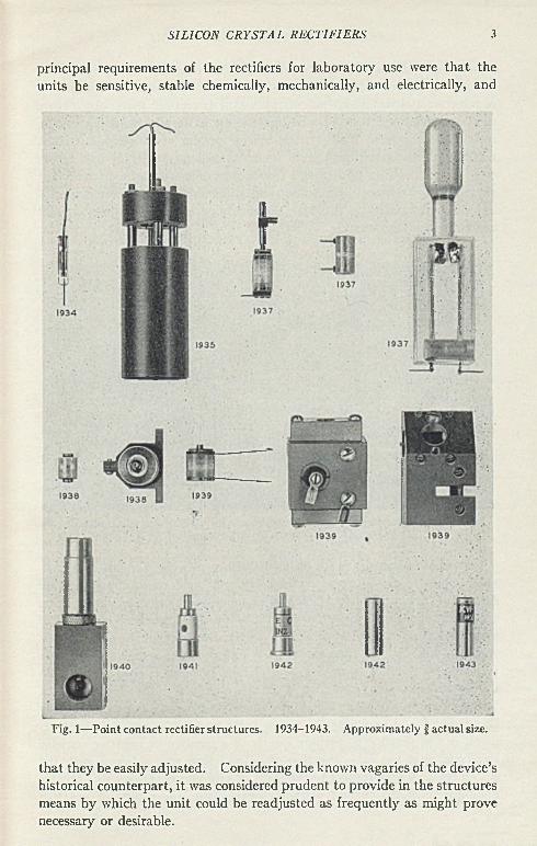
The design of the point contact rectifiers used in these researches was dictated largely, of course, by the needs of the laboratory. Frequently the rectifier housing formed an integral part of the electrical circuit design while other structures took the form of a replaceable resistor-like cartridge. A variety of structures, including the modern types, arranged in chronological sequence, are shown in the photograph, Fig. 1. In general, the
S IL IC O N C R Y S T A L R E C T IF IE R S 3
principal requirements of the rectifiers for laboratory use were that the units be sensitive, stable chemically, mechanically, and electrically, and
Fig. 1—P oin t contact rectifier structures. 1934-1943. Approxim ately § actual size.
that they be easily adjusted. Considering the known vagaries of the device’s historical counterpart, it was considered prudent to provide in the structures means by which the unit could be readjusted as frequently as might prove necessary or desirable.
4 B E L L S Y S T E M T E C H N IC A L J O U R N A L
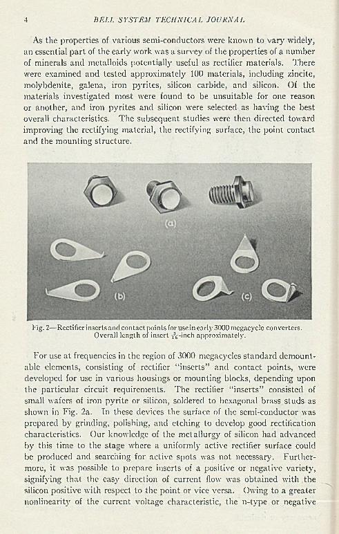
As the properties of various semi-conductors were known to vary widely, an essential part of the early work was a survey of the properties of a number of minerals and metalloids potentially useful as rectifier materials. There were examined and tested approximately 100 materials, including zincite, molybdenite, galena, iron pyrites, silicon carbide, and silicon. Of the materials investigated most were found to be unsuitable for one reason or another, and iron pyrites and silicon were selected as having the best overall characteristics. The subsequent studies were then directed toward improving the rectifying material, the rectifying surface, the point contact and the mounting structure.
Fig. 2—Rectifier inserts and contact points for use in early 3000 megacycle converters.Overall length of insert ,V inch approxim ately.
For use at frequencies in the region of 3000 megacycles standard demountable elements, consisting of rectifier “ inserts” and contact points, were developed for use in various housings or mounting blocks, depending upon the particular circuit requirements. The rectifier “inserts” consisted of small wafers of iron pyrite or silicon, soldered to hexagonal brass studs as shown in Fig. 2a. In these devices the surface of the semi-conductor was prepared by grinding, polishing, and etching to develop good rectification characteristics. Our knowledge of the metallurgy of silicon had advanced by this time to the stage where a uniformly active rectifier surface could be produced and searching for active spots was not necessary. Furthermore, it was possible to prepare inserts of a positive or negative variety, signifying that the easy direction of current flow was obtained with the silicon positive with respect to the point or vice versa. Owing to a greater nonlinearity of the current voltage characteristic, the n-type or negative
S IL IC O N C R Y S T A L R E C T I F I E R S 5
insert tended to give better performance as microwave converters while the p-type, or positive insert, because of greater sensitivity a t low voltages, proved to be more useful in test equipment such as resonance indicators in frequency meters. In certain instances also, it was advantageous for the designer to be able to choose the polarity best suited to his circuit design. In contrast, however, to the striking uniformity obtained with the silicon processed in the laboratory, the pyrite inserts were very non-uniform. Active rectification spots on these natural mineral specimens could be found only by tediously searching the surface of the specimen. Moreover, rectifiers employing the pyrite inserts showed a greater variation in properties with frequency than those in which silicon was used.
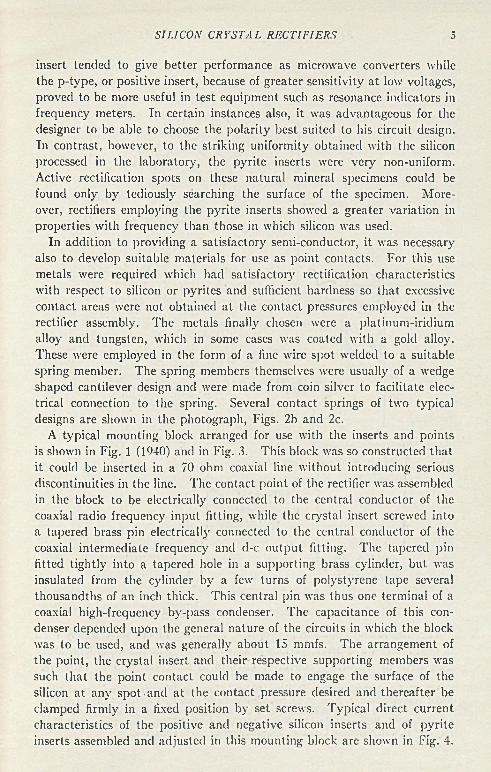
In addition to providing a satisfactory semi-conductor, it was necessary also to develop suitable materials for use as point contacts. For this use metals were required which had satisfactory rectification characteristics with respect to silicon or pyrites and sufficient hardness so that excessive contact areas were not obtained at the contact pressures employed in the rectifier assembly. The metals finally chosen were a platinum-iridium alloy and tungsten, which in some cases was coated with a gold alloy. These were employed in the form of a fine wire spot welded to a suitable spring member. The spring members themselves were usually of a wedge shaped cantilever design and were made from coin silver to facilitate electrical connection to the spring. Several contact springs of two typical designs are shown in the photograph, Figs. 2b and 2c.
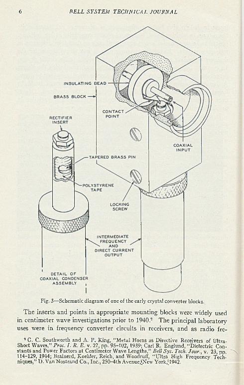
A typical mounting block arranged for use with the inserts and points is shown in Fig. 1 (1940) and in Fig. 3. This block was so constructed that it could be inserted in a 70 ohm coaxial line without introducing serious discontinuities in the line. The contact point of the rectifier was assembled in the block to be electrically connected to the central conductor of the coaxial radio frequency input fitting, while the crystal insert screwed into a tapered brass pin electrically connected to the central conductor of the coaxial intermediate frequency and d-c output fitting. The tapered pin fitted tightly into a tapered hole in a supporting brass cylinder, but was insulated from the cylinder by a few turns of polystyrene tape several thousandths of an inch thick. This central pin was thus one terminal of a coaxial high-frequency by-pass condenser. The capacitance of this condenser depended upon the general nature of the circuits in which the block was to be used, and was generally about 15 mmfs. The arrangement of the point, the crystal insert and their respective supporting members was such that the point contact could be made to engage the surface of the silicon at any spot-and at the contact pressure desired and thereafter be clamped firmly in a fixed position by set screws. Typical direct current characteristics of the positive and negative silicon inserts and of pyrite inserts assembled and adjusted in this mounting block are shown in Fig. 4.
6 B E L L S Y S T E M T E C E N I C A L J O U R N A L
Fig. 3—Schematic diagram of one of the early crystal converter blocks.
The inserts and points in appropriate mounting blocks were widely used in centimeter wave investigations prior to 1940.2 The principal laboratory uses were in frequency converter circuits in receivers, and as radio fre-
* G. C. Southworth and A. P . King, “ M etal H orns as D irective Receivers of U ltra- Short W aves,” Proc. I . R . E . v. 27, pp. 95-102, 1939; Carl R. Englund, “ Dielectric Constan ts and Power Factors a t Centim eter W ave Lengths,” Bell Sys. Tech. Jour., v . 23, pp. 114-129, 1944; Brainerd, Koehler, Reich, and Woodruff, “ U ltra H igh Frequency Techniques,” D . Van N ostrand Co., Inc., 250-4th Avenue,[New Y ork,[1942.
S IL IC O N C R Y S T A L R E C T IF IE R S
quency instrument rectifiers. They were also used to a relatively minor extent in some of the early radar test equipment. Moreover, the availability of these devices and the knowledge of their properties as microwave converters tended to focus attention on the potentialities of radar designs employing crystal rectifiers in the receiver’s frequency converter. Similarly, the techniques established for preparation of the inserts tended to orient subsequent manufacturing process developments. For example, the methods now generally used for preparing silicon ingots, for cutting the rectifying element from the ingot with diamond saws, and for forming the
I0 "a 10~7 10"6 I0 "5 10~4 10 '3 10"2 10"'CURRENT IN AMPERES
Fig. 4— D irect-current characteristics of silicon and iron pyrite rectifiers fabricated as inserts, 1939.
back contact to the rectifying element by electroplating procedures, are still essentially similar to the techniques used for preparing the inserts in 1939. As a contribution to the defense research effort, this basic information, with various samples and experimental assemblies, was made available to governmental agencies for dissemination to authorized domestic and foreign research establishments.
D e v e l o p m e n t o f t h e C e r a m ic T y p e C a r t r id g e St r u c t u r e
The block rectifier structure previously described was well adapted to various laboratory needs because of its flexibility, but for large scale utilization certain limitations are evident. Not only was it necessary that the parts be accurately machined, but also the adjustment of the rectifier in
B E L L S Y S T E M T E C H N I C A L J O U R N A L
the block structure required considerable skill. With recognition of the military importance of silicon crystal rectifiers, effort was intensified in the development of standardized structures suitable for commercial production.
In the 1940-1941 periodj contributions to the design of silicon crystal rectifiers Were made by British workers as a part of their development of new military implements. For these projected military uses, the problem of replacement and interchangeability assumed added importance. The design trend was, therefore, towards the development of a cartridge type structure with the electrical adjustment fixed during manufacture, so that the unit could be replaced easily in the same manner as vacuum tubes.
In the latter part of 1941 preliminary information was received in this country through National Defense Research Committee channels on a rectifier design originating in the laboratories of the British Thomson- Houston Co., Ltd. A parallel development of a similar device was begun in various American laboratories, including the Radiation Laboratory at the Massachusetts Institute of Technology, and Bell Telephone Laboratories. In the work at Bell Laboratories, emphasis was placed both on development of a structure similar to the British design and on exploration and test of various new structures which retained the features of socket interchangeability but which were improved mechanically and electrically.
In the work on the ceramic cartridge, the external features of the British design were retained for reasons of mechanical standardization but a number of changes in process and design were made both to improve performance and to simplify manufacture. To mention a few, the position of the silicon wafer and the contact point were interchanged because measurements indicated that an improvement in performance could thereby be obtained. To obviate the necessity for searching for active spots on the surface of the silicon and to improve, performance, fused high purity silicon was substituted for the “commercial” silicon then employed by the British. The rectifying element was cut from the ingots by diamond saws, and carefully polished and etched to. develop optimum rectification characteristics. Similar improvements were made in the preparation of the point or “cats whisker”, replacing hand operations by machine techniques. To protect the unit from mechanical shock and the ingress of moisture, a special impregnating compound was developed which was completely satisfactory even under conditions of rapid changes in temperature from —40° to +70°C. All such improvements were directed towards improving quality and establishing techniques for mass production.
In this early work time was at a premium because of the need for prompt standardization of the design in order that radar system designs might in
S IL IC O N C R Y S T A L R E C T I F I E R S 9
turn be standardized, and that manufacturing facilities might be established to supply adequate quantities of the device. The development and initial production of the device was accomplished in a short period of time. This was possible because process experience had been acquired in the insert development, and centimeter wave measurements techniques and facilities were then available to measure the characteristics of experimental units at the operating frequency. By December 1941, a pattern of manufacturing techniques had been established so that production by the Western Electric Company began shortly thereafter. This is believed to have been the first commercial production of the device in this country.
As a result of the basic information on centimeter wave measurements techniques which was available from earlier microwave research at the Holmdel Radio Laboratory, it was possible also, a t this early date, to propose to the Armed Services that each unit be required to pass an acceptance test consisting of measurement of the operating characteristics at the intended operating frequency. This plan was adopted and standard test methods devised for production testing. Considering the complexity of centimeter wave measurements, this was an accomplishment of some magnitude and was of first importance to the Armed Services because it assured by direct measurement that each unit would be satisfactory for field use.
The cartridge structure resulting from these developments and meeting the international dimensional standards is shown in Fig. 5. I t consists of two metal terminals separated by an internally threaded ceramic insulator. The rectifying element itself consists of a small piece of silicon (p- type) soldered to the lower metal terminal or base. The contact spring or “cats whisker” is soldered into a cylindrical brass pin which slides freely into an axial hole in the upper terminal and may be locked in any desired position by set screws. The spring itself is made from tungsten wire of an appropriate size, formed into an S shape. The free end of the wire, which in a finished unit engages the surface of the silicon and establishes rectification, is formed to a cone-shaped configuration in order that the area of contact may be held at the desired low value.
The silicon elements used in the rectifiers are prepared from ingots of fused high purity silicon. Alloying additions are made to the melt when required to adjust the electrical resistivity of the silicon to the value desired. The ingots are then cut and the silicon surfaces prepared and cut into small pieces approximately 0.05 inch square and 0.02 inch thick suitable for use in the rectifiers. The contact springs are made from tungsten wire, gold plated to facilitate soldering. Depending upon the application, the wires
10 B E L L S Y S T E M T E C H N IC A L J O U R N A L
may be 0.005 inch, 0.0085 inch, or 0.010 inch in diameter. After forming the spring to the desired shape, the tip is formed electrolytically.
In assembling the rectifier cartridge, the two end terminals, consisting of the base with the silicon element soldered to it, and the top detail containing the contact spring, are threaded into the ceramic tube so that the free end of the spring does not engage the silicon surface. An adhesive
Fig. 5— Ceramic cartridge rectifier struc tu re and parts.Overall length of assembled rectifier is approxim ately finch .
is employed to secure the parts firmly to the ceramic. The rectifier is then “adjusted” by bringing the point into engagement with the silicon surface and establishing optimum electrical characteristics. Finally the unit is impregnated with a special compound to protect it from moisture and from damage by mechanical shock. Units so prepared are then ready for the final electrical tests.
The adjustment of the rectifier is an interesting operation for a t this
PO INT AS SEM BLY
C E R A M IC TUBE
S IL IC O N C R Y S T A L R E C T IF IE R S 11
stage in the process the rectification action is developed, and to a considerable degree, controlled. If the point is brought into contact with the silicon surface and a small compressional deflection applied to the spring, direct- current measurements will show a moderate rectification represented by the passage of more current at a given voltage in the forward direction than in the reverse. If the side of the unit is now tapped sharply by means of a small hammer, the forward current will be increased, and, a t the same time, the reverse current decreased.3 With successive blows the reverse current is reduced rapidly to a constant low value while the forward current increases, but a t a diminishing rate, until it also becomes relatively constant. The magnitude of the changes produced by this simple operation is rather surprising. The reverse current at one volt seldom decreases by less than a factor of 10 and frequently decreases by as much as a factor of 100, while the forward current at one volt increases by a factor of 10. Paralleling these changes are improvements in the high-frequency properties, the conversion loss and noise both being reduced. The tapping operation is not a haphazard searching for better rectifying spots, for with a given silicon material and mechanical assembly the reaction of each unit to tapping is regular, systematic and reproducible. The condition of the silicon surface also has a pronounced bearing on “ tappability” for by modifications of the surface it is possible to produce, at will, materials sensitive or insensitive in their reaction to the tapping blows.
In the development of the compounds for filling the rectifier, special problems were met. For example, storage of the units for long periods of time under either arctic or tropical conditions was to be expected. Also, for use in air-borne radars operating at high altitudes, where equipment might be operated after a long idle period, it was necessary that the units be capable of withstanding rapid heating from very low temperatures. The temperature range specified was from —40° to + 70°C. Most organic materials normally solid at room temperature, as the hydrocarbon waxes, are completely unsuitable, as the excessive contraction which occurs at low temperatures is sufficient to shift the contact point and upset the precise adjustment of the spring. Nor are liquids satisfactory because of their tendency to seep from the unit. However, special gel fillers, consisting of a wax dispersed in a hydrocarbon oil, were devised in Bell Telephone Laboratories to meet the requirements, and were successfully applied by the leading manufacturers of crystal rectifiers in this country. Materials of a similar nature, though somewhat different in composition, were also used subsequently in Britain. Further improvements in these compounds have been made recently, extending the temperature range 10°C at low
5 Southworth and King; loc. cit.
12 B E L L S Y S T E M T E C H N I C A L J O U R N A L
temperatures and about 30°C at high temperatures in response to the design trend towards operation of the units a t higher temperatures. The units employing this compound may, if desired, be repeatedly heated and cooled rapidly between — 50°C and +100°C without damage.
Use of the impregnating compound not only improves mechanical stability but prevents ingress or absorption of moisture. Increase of humidity would subject the unit not only to changes in electrical properties such as variation in the radio frequency impedance, but also to serious corrosion, for the galvanic couple at the junction would support rapid corrosion of the metal point. In fact, with condensed moisture present in unfilled units corrosion can be observed in 48 hours. For this reason alone, the development of a satisfactory filling compound was an important step in the successful utilization of the units by the Armed Services under diverse and drastic field conditions.
T a b l e IS h e lf Aging Data on Silicon Crystal Rectifiers of the Ceramic Cartridge Design
Storage C onditions
In itia l Values V alues A fter S torage for 7 M onths
ConversionLoss
(M edian;(L)
N oiseR atio
(M edian)(Nr)
Con\*ersionLoss
(m edian)(L)
N oiseR atio
(median)(Nr)
db db db db
75°F. 65% Relative H u m id ity .............. 6 .8 3.9 6.7 4.3110°F. 95% Relative H u m id ity .............. 6.9 3.9 6.9 4.3- 4 0 ° C ............................................................... 7.0 3.9 6 .8 3.9
The large improvement in stability achieved in the present device as compared with the older crystal detectors may be attributed to the design of the contact spring, correct alignment of parts in manufacture and to the practice of filling the cavity in the unit with the gel developed for this purpose. Considering the apparently delicate construction of the device, the stability to mechanical or thermal shock achieved by these means is little short of spectacular. Standard tests consist of dropping the unit three feet to a wood surface, immersing in water, and of rapidly heating from —40 to 70°C. None of these tests impairs the quality of the unit. Similarly the unit will withstand storage for long periods of time under adverse conditions. Table I summarizes the results of tests on units which were stored for approximately one year under arctic (—40°), tropical (114°F—95% relative humidity), and temperate conditions. Though minor changes in the electrical characteristics were noted in the accelerated tropical test, none of the units was inoperative after this drastic treatment.
S IL IC O N C R Y S T A L R E C T I F I E R S 13
D e v e l o p m e n t o p t h e S h ie l d e d R e c t if ie r St r u c t u r e
Rectifiers of the ceramic cartridge design, though manufactured in very- large quantities and widely and successfully used in military apparatus, have certain well recognized limitations. For example, they may be accidentally damaged by discharge of static electricity through the small point contact in the course of routine handling. If one terminal of the unit is held in the hand and the other terminal grounded, any charge which may have accumulated will be discharged through the small contact. Since such static charges result in potential differences of several thousand volts it is understandable that the unit might suffer damage from the discharge. Although damage from this cause may be avoided by following a few simple precautions in handling, the fact that such precautions are needed constitutes a disadvantage of the design.
Certain manufacturing difficulties are also associated with the use of the threaded insulator. The problem of thread fit requires constant attention. Lack of squareness at the end of the ceramic cylinder or lack of concentricity in the threaded hole tends to cause an undesirable eccentricity or angularity in the assembled unit which can be minimized only by rigid inspection of parts and of final assemblies. At the higher frequencies (10,000 megacycles), uniformity in electrical properties, notably the radio frequency impedance, requires exceedingly close control of the internal mechanical dimensions. In the cartridge structure where the terminal connections are separated by a ceramic insulating member, the additive variations of the component parts make close dimensional control inherently difficult.
To eliminate these difficulties the shielded structure, shown in Fig. 6, was developed. In this design the rectifier terminates a small coaxial line. The central conductor of the line, forming one terminal of the rectifier, is molded into an insulating cylinder of silica-filled bakelite, and has spot welded to it a 0.002-inch diameter tungsten wire spring of an offset C design. The free end of the spring is cone shaped. The rectifying element is soldered to a small brass disk. Both the disk, holding the rectifying element, and the bakelite cylinder, holding the point, are force- fits in the sleeve which forms the outer conductor of the rectifier. By locating the bakelite cylinder within the sleeve so that the free end of the central conductor is recessed in the sleeve, the unit is effectively protected from accidental static damage as long as the holder or socket into which the unit fits is so designed that the sleeve establishes electrical contact with the equipment at ground potential before the central conductor. The sleeve also shields the rectifying contact from effects of stray radiation.
The radio frequency impedance of the shielded unit can be varied within certain limits by modifying the diameter of the central conductor. For
l i B E L L S Y S T E M T E C H N I C A L J O U R N A L
example, in the 1N26 unit, which was designed for use at frequencies in the region of 24,000 megacycles, a small metal slug fitting over the central conductor makes it possible to match a coaxial line having a 65-ohm surge impedance. For certain circumstances this modification in design is advantageous, while in others it is a disadvantage because the matching slug is effective only over a narrow range of frequencies.
PO INT ASSEM BLY
OUTER METAL SILICON PO INT INSULATING CENTRAL
Fig. 6—Shielded rectifier structu re and parts . Overall length of assembled rectifierisapproxim ately $ inch.
The shielded structure was developed in 1942 and since it was of a simplified design with reduced hazard of static damage, it was proposed to the Armed Services for standardization in June of that year. However, because of the urgency of freezing the design of various radars and because the British had already standardized on the outline dimensions of the ceramic type cartridge, Fig. 5, the Services did not consider it advantageous to standardize the new structure when first proposed. In deference to this international standardization program, plans for the manufacture of this
S IL IC O N C R Y S T A L R E C T IF IE R S IS
structure were held in abeyance during 1942 and 1943. However, an opportunity for realizing the advantages inherent in the shielded design was afforded later in the war and a sufficient quantity of the units was produced to demonstrate its soundness. As anticipated from the constructional features, marked uniformity of electrical properties was obtained.
T y p e s , Ap p l ic a t io n s , a n d O p e r a t in g C h a r a c t e r is t ic s
Various rectifier codes, engineered for specific military uses, were manufactured by Western Electric Company during the war. These are listed in Table II. The units are designated by RMA type numbers, as 1N21, 1N23, etc., depending upon their properties and the intended use, Letter suffixes, as 1N23A, 1N23B, indicate successively more stringent performance requirements as reflected in lower allowable maxima in loss and noise ratio, and, usually, more stringent power proof-tests. In general, different codes are provided for operation in the various operating frequency ranges. For example, the 1N23 series is tested at 10,000 megacycles while the 1N21 series is tested at 3,000 megacycles and the 1N25 at 1000 megacycles, approximately. Since higher transmitter powers are frequently employed at the lower frequencies, somewhat greater power handling ability is provided in units for operation in this range.
One of the more important uses of silicon crystal rectifiers in military equipment was in the frequency converter or first detector in superheterodyne radar receivers. This utilization was universal in microwave receivers. In this application the crystal rectifier serves as the non-linear circuit element required to generate the difference (intermediate) frequency between the radio frequency signal and the local oscillator. The intermediate frequency thus obtained is then amplified and detected in conventional circuits. As the crystal rectifier is normally used at that point in the receiving circuit where the signal level is a t its lowest value, its performance in the converter has a direct bearing on the overall system performance. I t was for this reason that continued improvements in the performance of crystal rectifiers were of such importance to the war effort.
For the converter application, the signal-to-noise properties of the unit at the operating frequency, the power handling ability, and the uniformity of impedance are important factors. The signal-to-noise properties are measured as conversion loss and noise ratio. The loss, L, is the ratio of the available radio frequency signal input power to the available intermediate frequency output power, usually expressed in decibels. The noise ratio, N r , is the ratio of crystal output noise power to thermal (KTB) noise power, The loss and noise ratio are fundamental properties of the
T a b l e I I
Performance S p ec if calions— Silicon Crystal Rectifiers
Code W .E . Spec. N o. S tructu re
Nom inal O pera ting F requency
T e stPower
megacycles
m illiwatts
IN21 D -163366 Cartridge 3000 0 .41N21A D-1683S5 it << 0 .41N21B D-169113 u (< 0 .51N23 D-1683S6 it .10000 1.01N23A D -169304 it t( 1.01N23B D -169305 it l( 1.01N2S D-17C247 tt 1000 1.25
1N26 D -168707 Shielded 24000 1.01N27 D-172981 Cartridge 3000 .005
max.1N28 D -168030 H << 0.41N31 D-171936 Shielded 10000 .005
max.
Max.Conver
sionLoss
M ax.N oiseR atio7
In t. F rcq. Im pedance
M in.Figure
ofM erit
Low-LevelR esistance
ProofT e st
M ethod,N ote
T e st Level
db ohms ohms
8 .5 4 .07.5 3 .0 3 0 .3 erg6 . 5 2 .0 375‘ 5 2 .0 ergs
10.0 3 .0 a 5 0 .3 erg8 .0 2.7 u 0 1 .0 erg6 .5 2.7 u 0 0 .3 erg8 .0 2.5 100-4002 6 12 .5 v 3
6 .¡o '8 .5 2 .5 300-6002 0 0 .1 erg
60 4000 max. a t Imv
7.0 2 .0 3001 5 5 .0 erg55 6000-23,000 a t 5 6 1. 5 v 3
mv max. 25. or120-25°C.
1 Average values under conditions of production test-—not lim ited directly by specifications. 1 Values lim ited by specifications.3 Pulse generator voltage.4 Pulse generator impedance.5 Single D.C. spike.6 M ultiple square pulse.7 Num erical ratio.
N orm al Use
Converter
(<Low-Level
D etectorConverterLow-Level
D etector
BELL SYSTEM
TE
CH
NIC
AL
JOU
RN
AL
S IL IC O N C R Y S T A L R E C T IF IE R S 17
c r y s t a l
CO NVERTER
R E T A IN IN G PLUG
Fig. 7— C onverter for wave guide circuits as installed in the radio frequency unit of the A N /A P Q 13 radar system . T his was standard equipm ent in B-29 bombers for
rad ar bombing and navigation.
RA D IOFREQUENCY
U N IT
C A V IT Y
PARTS(EN LAR G ED )
If i CRYSTAL | EXTENSION
& CRYSTAL RECTIFIER
IS B E L L S Y S T E M T E C H N I C A L J O U R N A L
converter. From these data and other circuit constants, the designer may calculate4 expected receiver performance.
For operation as converters,5 crystal rectifiers are employed in suitable holders. These may be arranged for use with either coaxial line or wave guide circuits, depending upon the application. Figure 7 shows a converter for wave guide circuits installed in the radio frequency unit of an air-borne radar system. A typical converter designed for use with coaxial lines is shown in the photograph Fig. 8. A schematic circuit of this converter is shown in Fig. 9. In such circuits the best signal-to-noise ratio is realized when an optimum amount of beating oscillator power is supplied. The optimum power depends, in part, on the properties of the rectifier itself, and, in part, on other circuit factors as the noise figure of the intermediate
Fig. 8— Converter for use a t 3000 megacycles. T he crystal rectifier is located ad jacen t to its socket in the converter.
frequency amplifier. For a well designed intermediate frequency amplifier with a noise figure of about 5 decibels, the optimum beating oscillator power is such that between 0.5 and 2.0 milliamperes of rectified current flows through the rectifier unit. Under these conditions and with the unit matched to the radio frequency line, the beating oscillator power absorbed by the unit is about one milliwatt. For intermediate frequency amplifiers
4 T he quantities L and N r are related to receiver perform ance by the relationship F r = ¿ ( N r - 1 + F i f )
where F r is the receiver noise figure and F i f is the noise figure of the interm ediate frequency amplifier. All term s are expressed as power ratios. A rigorous definition of receiver noise figure has been given by H . T . Friis “ Noise Figures of Radio Receivers,” Proc. I . R. E., vol. 32, pp. 419-422; Ju ly , 1944.
* C. F . Edwards, “M icrowave C onverters,” presented orally a t the W inter Technical M eeting of the I . R. E ., January 1946 and subm itted to th e I- R- E. for publication.
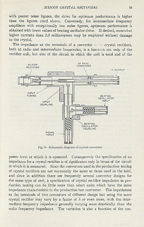
S IL IC O N C R Y S T A L R E C T IF IE R S 19
with poorer noise figures, the drive for optimum performance is higher than the figures cited above. Conversely, for intermediate frequency amplifiers with exceptionally low noise figures, optimum performance is obtained with lower values of beating oscillator drive. If desired, somewhat higher currents than 2.0 milliamperes may be employed without damage to the crystal.
The impedance at the terminals of a converter u: : /_■ crystal rectifiers, both a t radio and intermediate frequencies, is a function not only of the rectifier unit, but also of the circuit in which the unit is used and of the
power level at which it is operated. Consequently the specification of an impedance for a crystal rectifier is of significance only in terms of the circuit in which it is measured. Since the converters used in the production testing of crystal rectifiers are not necessarily the same as those used in the field, and since in addition there are frequently several converter designs for the same type of unit, a specification of crystal rectifier impedance in production testing can do little more than select units which have the same impedance characteristic in the production test converter. The impedances at the terminals of two converters of different design but using the same crystal rectifier may vary by a factor of 3 or even more, with the intermediate frequency impedance generally varying more drastically than the radio frequency impedance. The variation is also a function of the con-
20 B E L L S Y S T E M T E C H N I C A L J O U R N A L
version loss. Crystals with large conversion losses are less susceptible to impedance changes from reactions in the radio frequency circuit than are low conversion loss units.
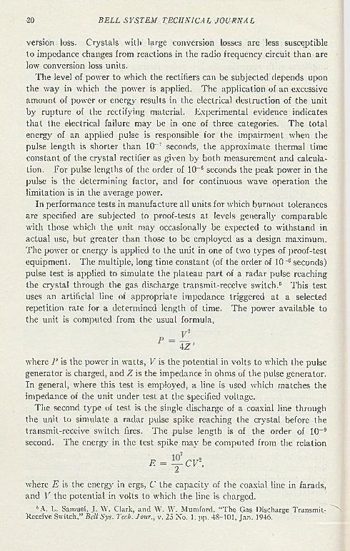
The level of power to which the rectifiers can be subjected depends upon the way in which the power is applied. The application of an excessive amount of power or energy results in the electrical destruction of the unit by rupture of the rectifying material. Experimental evidence indicates that the electrical failure may be in one of three categories. The total energy of an applied pulse is responsible for the impairment when the pulse length is shorter than 10“ 7 seconds, the approximate thermal time constant of the crystal rectifier as given by both measurement and calculation. For pulse lengths of the order of 10~6 seconds the peak power in the pulse is the determining factor, and for continuous wave operation the limitation is in the average power.
In performance tests in manufacture all units for which burnout tolerances are specified are subjected to proof-tests a t levels generally comparable with those which the unit may occasionally be expected to withstand in actual use, but greater than those to be employed as a design maximum. The power or energy is applied to the unit in one of two types of proof-test equipment. The multiple, long time constant (of the order of 10~6 seconds) pulse test is applied to simulate the plateau part of a radar pulse reaching the crystal through the gas discharge transmit-receive switch.6 This test uses an artificial line of appropriate impedance triggered at a selected repetition rate for a determined length of time. The power available to the unit is computed from the usual formula,
4 Z ’where P is the power in watts, V is the potential in volts to which the pulse generator is charged, and Z is the impedance in ohms of the pulse generator.In general, where this test is employed, a line is used which matches the impedance of the unit under test a t the specified voltage.
The second type of test is the single discharge of a coaxial line through the unit to simulate a radar pulse spike reaching the crystal before the transmit-receive switch fires. The pulse length is of the order of 10-9 second. The energy in the test spike may be computed from the relation
E = ~ y CV 2,
where E is the energy in ergs, C the capacity of the coaxial line in farads, and V the potential in volts to which the line is charged.
6 A. L. Samuel, J. W. Clark, and \V. W. M um ford, “ T he Gas Discharge T ransm it- ^ Receive Switch,” Bell Sys. Tech. Jour., v. 25 No. 1, pp. 48-101, Jan . 1946.
S IL IC O N C R Y S T A L R E C T I F I E R S 21
Specification proof-test levels are, of course, not design criteria. Since the units are generally used in combination with protective devices, such as the transmit-receive switch, it is necessary to conduct tests in the circuits of interest to establish satisfactory operating levels.
In general, however, the units may be expected to carry, without deterioration, energy of the order of a third of that used in the single d-c spike proof- test or peak powers of a magnitude comparable with that used in the multiple flat-top d-c pulse proof-test. The upper limit for applied continuous wave signals has not been determined accurately, but, in general, rectified currents below 10 milliamperes are not harmful when the self bias is less than a few tenths of a volt.
The service life of a crystal rectifier will depend completely upon the conditions under which it is operated and should be quite long when its ratings are not exceeded. During the war, careful engineering tests conducted on units operating as first detectors in certain radar systems revealed no impairment in the signal-to-noise performance after operation for several hundred hours. A small group of 1N21B units showed only minor impairments when operated in laboratory tests for 100 hours with pulse powers (3000 megacycles) up to 4 watts peak available to the unit under test.
Another important military application of silicon crystal rectifiers was as low-power radio frequency rectifiers for use in wave meters or other items of radar test equipment. Here the rectification properties of the unit at the operating frequency are of primar}' interest. Since units which are satisfactory as converters also function satisfactorily as high-frequency rectifiers special types were not required for this application.
Units were also used in military equipment as detectors to derive directly the envelope of a radio frequency signal received at low power levels. These signals were modulated usually in the video range. The low-level performance is a function of the resistance at low voltages and the direct- current output for a given low-power radio frequency input. These may be combined to derive a figure of merit which is a measure of receiver performance.7
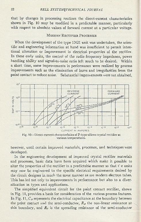
Typical direct-current characteristics of the silicon rectifiers a t temperatures of —40°, 25° and 70°C are given in Fig. 10. I t will be noted in these curves that both the forward and reverse currents are decreased by reducing the temperature and increased by raising the temperature. The reverse current changes more rapidly with temperature than the forward current, however, so that the rectification ratio is improved by reducing the temperature, and impaired by raising the temperature. The data shown are for typical units of the converter type. It should be emphasized, however,
7 R. Betinger, R adiation Laboratory R eport No. 61-15, M arch 16, 1943.
22 B E L L S Y S T E M I T E C n N I C A L J O U R N A L
that by changes in processing routines the direct-current characteristics shown in Fig. 10 may be modified in a predictable manner, particularly with respect to absolute values of forward current a t a particular voltage.
M o d e r n R e c t i f i e r P r o c e s s e s
When the development of the type 1N21 unit was undertaken, the scientific and engineering information at hand was insufficient to permit intentional alteration or improvement in electrical properties of the rectifier. In these early units, the control of the radio frequency impedance, power handling ability and signal-to-noise ratio left much to be desired. Within a short time, some improvements in performance were realized by process improvements such as the elimination of burrs and irregularities from the point contact to reduce noise. Substantial improvements were not obtained,
Fig. 10—D irect-current characteristics of P -type silicon crystal rectifier a t various tem peratures.
however, until certain improved materials, processes, and techniques were developed.
In the engineering development of improved crystal rectifier materials and processes, basic data have been acquired which make it possible to alter the properties of the rectifier in a predictable manner so that the units may now be engineered to the specific electrical requirements desired by the circuit designer in much the same manner as are modern electron tubes. This has led not only to improvements in performance but also to a diversification in types and applications.
The simplified equivalent circuit for the point contact rectifier, shown in Fig. 11, provides a basis for consideration of the various process features. In Fig. 11, CB represents the electrical capacitance at the boundary between the point contact and the semi-conductor, R n the non-linear resistance at this boundary, and Rs is the spreading resistance of the semi-conductor
S IL IC O N C R Y S T A L R E C T IF IE R S 23
proper, that is the total ohmic resistance of the silicon to current through the point. The capacitance CB being shunted across the rectifying boundary, decreases the efficiency of the device by its by-pass action because the current through it would be dissipated as heat in the resistance R s. Losses from this source increase rapidly with increased frequency because of the enhanced by-pass action. I t would appear, therefore, that to improve efficiency it would be important to minimize both R s and C„ by some method such as reducing the area of the rectifying contact and lowering the body resistance of the silicon employed. For a given silicon material, the impedances desired for reasons of circuitry and considerations of mechanical stability place a limit on the extent to which performance may be improved by reducing the contact area. Rs may be reduced by using silicon of lower resistivity, but this generally results in poorer rectification. This impairment is due apparently to some subtle change in the properties of the rectifying junction resulting from decreasing the specific resistance of the silicon material.
r b ( n o n - l in e a r
BARRIER RESISTANCE)
Rs W V-----(SPREADING RESISTANCE)
v w -------------- ------
If-------------C B
(BARRIER CAPACITY)
Fig. 11— Simplified equivalent circuit of crystal rectifier.
The answer to this apparent dilemma lies in the application of an oxidizing heat treatment to the surface of the semi-conductor. This process derives from researches conducted independently in this country and in Britain, though there was considerable interchange of information between various interested laboratories. In the oxidizing treatment, apparently the impurities in the silicon which contribute to its conductivity diffuse into the adhering silica film, thereby depleting impurities from the surface of the silicon. When the oxide layer is then removed by solution in dilute hydrofluoric acid, the underlying silicon layer is exposed and remains intact as the acid does not readily attack the silicon itself.
Since decreasing the impurity content of a semi-conductor increases its resistivity, the silicon surface has higher resistivity after the oxidizing treatment than before. Thus by oxidation of the surface of low resistance silicon it is possible to secure the enhanced rectification associated with the high resistance surface layer, while by virtue of the lower resistivity of the underlying material the PR losses through Rs are reduced.
24 B E L L S Y S T E M T E C H N IC A L J O U R N A L
In actual practice the properties of the rectifier are governed by the resistivity of the silicon material, the contact area, and the degree of oxidation of the surface. By the controlled alteration of these factors units may be engineered for specific applications. The body resistance of the silicon is controlled by the kind and quantity of the impurities present. Aluminum, beryllium or boron may be added to purified silicon to reduce its resistivity to the desired level. Boron is especially effective for this purpose, the quantity added usually being less than 0.01 per cent. As little as 0.001 per cent has a very pronounced effect upon the electrical properties. The contact area is determined by the design of contact spring employed and the deflection applied to it in the adjustment of the rectifier. The degree of oxidation is controlled by the time and temperature of the treatment and the atmosphere employed.
In the development of the present rectifier processes, certain experimental relationships were obtained between the performance and the contact area on the one hand, and the power handling ability and contact area on the other. These show the manner in which the processes should be changed to produce a desired change in properties. For example, Fig. 12 shows the relationship between the spring deflection applied to a unit and the conversion loss at a given frequency. The apparent contact area, (i.e., the area of the flattened tip of the spring in contact with the silicon surface, as measured microscopically) also increases with increasing spring deflection. It will be seen in Fig. 12 that for a given silicon material, the conversion loss at 10,000 megacycles increases rapidly with the contact area. The curves tend to reach constant loss values a t the higher spring deflections. It is believed that this may be ascribed to the fact that for a given spring size and form, the increment in contact area obtained by successive increments in spring deflection would diminish and finally become zero after the elastic limit of the spring is exceeded.
The losses plotted in Fig. 12 were measured on a tuned basis, that is, the converter was adjusted for maximum intermediate frequency output a t a fixed beating oscillator drive for each measurement. Were these measurements made on a fixed tuned basis, that is, with the converter initially adjusted for maximum intermediate frequency output for a unit to which the minimum spring deflection is applied, and the units with larger deflections then measured without modification of the converter adjustment, even greater degradation in conversion loss than that shown in Fig. 12 would be observed. This results from the dependence of the radio frequency impedance upon the contact area. In loss measurements made on the tuned basis, changes in the radio frequency impedance occasioned by the changes in the contact area do not affect the values of mismatch loss obtained, while on the
S I L I C O N C R Y S T A L R E C T I F I E R S 25
fixed tuned basis they would result in an increase in the apparent loss because of the mismatch of the radio frequency circuits.
While the conversion loss is degraded by increasing the contact area, the power handling ability8 of the rectifiers is improved, as shown in Fig. 13.
Fig. 12—R elationship between spring deflection and conversion loss in silicon crystal rectifiers.
2 3 4 5 6 7SPRING DEFLECTION IN THOUSANDTHS OF AN INCH
This is not surprising because the larger area contact gives a wider current distribution and thus minimizes the localized heating effects near the contact. Generally, therefore, in the development of units for operation at a
8 The measurement of power handling ability of crystal rectifiers by application of radio frequency power is complicated by the fact th a t the impedance of the unit under test varies w ith power level. If a un it is m atched in a converter a t a low-power level and power a t a higher level is then applied, no t all of the power available is absorbed by the unit bu t a portion of i t is reflected (due to the change in impedance). This factor has been called the self protection of the un it and it necessitates the distinction between the power absorbed by and the power available to the un it under test. The d a ta for Fig. 13 were acquired by first m atching the un it in converters a t low powers (about 0.3 m illiw atts CVV 3000 mcs) and then exposing it for a short period to successively higher levels of pulse power of square wave form of 0.5 microseconds w idth a t a repetition ra te of 2000 pulses per second, m easuring the loss and noise ratio after each power application. The power handling ability is then expressed as the available peak power required to cause a 3 db im pairm ent in the conversion loss or the receiver noise figure. This m ethod was employed because in radar receivers the units are m atched for low-power levels. In this respect the m ethod sim ulates field operating conditions, bu t the “ spike” of radar pulses is absent.
T he increase in power handling ability w ith increasing area shown in Fig. 13 is confirmed by similar m easurem ents w ith radio frequency pulse power w ith the un it m atched a t high-level powers, by d irect-current tests, and by' simple 60-cycle continuous wave tests. The m agnitude of the increase depends, however, upon the particular m ethod employed for m easurement.
26 B E L L S Y S T E M T E C H N I C A L J O U R N A L
given frequency, a compromise must be effected between these two important performance factors. Because of increased condenser by-pass action a smaller area must be used to obtain a given conversion loss at a higher frequency. For this reason the power handling ability of units designed for use a t the higher frequencies is somewhat less than that of the lower-fre-
4 0 0
« 3| in - > cr z£ 8g zLÜ t «/) z- i UJ
2 2
a sUJ Gj J CO
n
100
80
60
20
- FREQUENCY:: 3 000 MEGACYCLES
•
»
•
•
- •
- • •
-•
•• •
• •
• •
-i
• # «
•
• »
L v -
»
m
•
• ••
•
••
-
- 4 » t
- • • •
-
1 ' i i i 1 I _L i i
0.02 0 .0 4 0 .0 6 0.1 0.2
APPARENT CONTACT AREA
0.4 0.6 0 .8 1.0
SQUARE INCHES
4X K T
Fig. 13- -C orrelation between power handling ability measured with microsecond radio frequency pulses and contact area in silicon crystal rectifiers.
quency units because emphasis has been placed upon achieving a given sig- nal-to-noise performance in each frequency band.
Use of the improved materials and processes produced rather large improvements in the d-c rectification ratio, conversion loss, noise, power handling ability, and uniformity. Typical direct-current rectification characteristics of units produced by both the old and the new processes are shown in Fig. 14. These curves show that reverse currents at one volt were decreased by a factor of about 20 while the forward currents were increased by
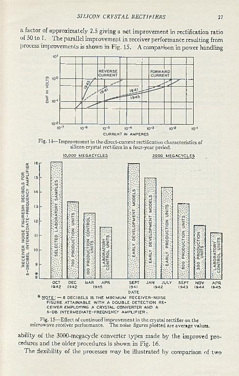
S IL IC O N C R Y S T A L R E C T I F I E R S 27
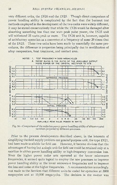
a factor of approximately 2.5 giving a net improvement in rectification ratio of 50 to 1. The parallel improvement in receiver performance resulting from process improvements is shown in Fig. 15. A comparison in power handling
CURRENT IN AMPERES
Fig. 14—Im provem ent in the direct-current rectification characteristics of silicon crystal rectifiers in a four-year period.
10,000 M EG ACYCLES 3 0 0 0 MEGACYCLES
OCT DEC MAR APR SEPT JA N JULY SEPT NOV APR1942 1942 1945 1941 1942 1943 1 94 4 1 9 4 5
DATE
* n o t e : — a d e c ib e l s is t h e m in im u m r e c e iv e r - n o is e
FIGURE ATTAIN AB LE W ITH A DO UBLE DETECTION RECEIVER EMPLOYING A CRYSTAL CONVERTER AND A S -D B INTERM EDIATE-FREQUENCY A M P L IF IE R .
Fig. 15—Effect of continued improvem ent in the crystal rectifier on the microwave receiver performance. The noise figures p lotted are average values.
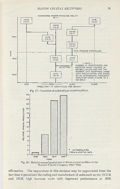
ability of the 3000-megacycle converter types made by the improved procedures and the older procedures is shown in Fig. 16.
The flexibility of the processes may be illustrated by comparison of two
28 B E L L S Y S T E M T E C H N I C A L J O U R N A L
very different units, the 1N26 and the 1N25. Though direct comparison of power handling ability is complicated by the fact that the burnout test methods employed in the development of the two codes were widely different, it may be stated conservatively that while the 1N26 would be damaged after absorbing something less than one w att peak pulse power, the 1N25 unit will withstand 25 watts peak or more. The 1N26 unit is, however, capable of satisfactory operation as a converter at a frequency of some 20 times that of the 1N25. These two units have been made by essentially the same procedures, the difference in properties being principally due to modification of alloy composition, heat treatment, and contact area.
NO TES: I . TEST FREQUENCY = 3 0 0 0 MEGACYCLES
2 . N O IS E R A TIO IS THE RATIO OF THE AV AILAB LE OUTPUT NOISE POWER OF THE CRYSTAL RECTIFIER TO KTB
lu 6 . 0
œ 7.0 U 8 .0 Q 9.0_J0^ 6.2
1 72 8.2 9.2
_____ 1___ 1 ! 1, I 1 .1, ■ _ 1 1IM P R O VED PROCESS
ÇÛOID
i i i i i i ...i. i j_ i ! 1 ^ -
1 . 1
2.13.1 .4.1
1.12.13.14.1
2 “ 6.0$ 7.03 8.02 9 .0OölS 6-3> 7 . 3 O 8.3 u 9.3
N-VA
, _ l _ 1 1 V y1 , w ____ 1___ ....1- 1 —L_
IN IT IA L PROCESS
0.1 0.6 1.0 2 4 6 8 10 2 0 4 0
AV AILAB LE PEAK PULSE POWER IN WATTS
3.2 g4 .2 S5 .2 *
6.2 SOZ
2.33.34 .35 .3
200
Fig. 16— Comparison of the radio frequency power handling ability of silicon crystal rectifiers prepared by different processes.
Prior to the process developments described above, in the interests of simplifying the field supply problem one general purpose unit, the type 1N21, had been made available for field use. However, it became obvious that the advantages of having but a single unit for field use could be retained only a t a sacrifice in either power handling ability or high-frequency conversion loss. Since the higher power radar sets operated at the lower microwave frequencies, it seemed quite logical to employ the new processes to improve power handling ability at the lower microwave frequencies and to improve the loss and noise at the higher frequencies. A recommendation accordingly was made to the Services that different units be coded for operation at 3000 megacycles and at 10,000 megacycles. The decision in the m atter was
S IL IC O N C R Y S T A L R E C T IF IE R S 29
INCREASING POWER-HANDLING ABILITY
1000 -3 0 0 0 -FREOUENCY IN MEGACYCLES PER SECOND
Fig. 17—Evolution of coded silicon crystal rectifiers. 2 6 r
24,000
ui 10 >
m m .* EXTRAPOLATED FROM 9 MONTHS DATA
1942 1945 ^1943 1944
YEAR
Fig. 18—Relative annual production of silicon crystal rectifiers a t the W estern Electric Company 1942-1945.
affirmative. The importance of this decision may be appreciated from the fact that it permitted the coding and manufacture of units such as the 1N21B and 1N28, high burnout units with improved performance at 3000
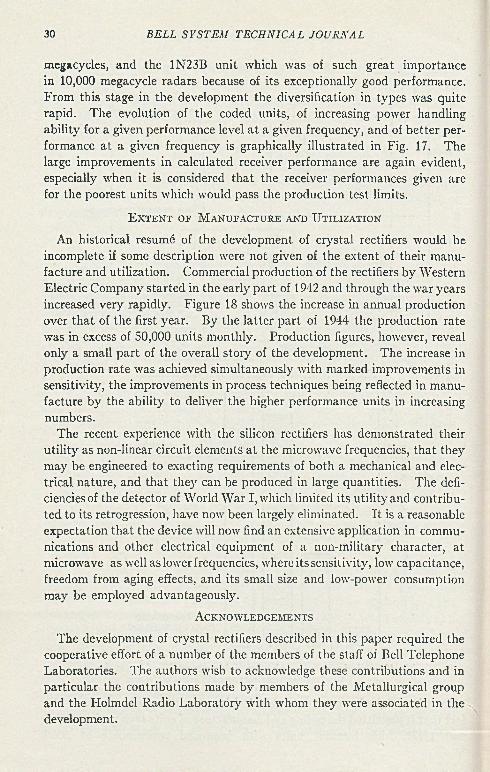
30 B E L L S Y S T E M T E C H N I C A L J O U R N A L
megacycles, and the 1N23B unit which was of such great importance in 10,000 megacycle radars because of its exceptionally good performance. From this stage in the development the diversification in types was quite rapid. The evolution of the coded units, of increasing power handling ability for a given performance level a t a given frequency, and of better performance a t a given frequency is graphically illustrated in Fig. 17. The large improvements in calculated receiver performance are again evident, especially when it is considered that the receiver performances given are for the poorest units which would pass the production test limits.
E x t e n t o f M a n u f a c t u r e a n d U t il iz a t io n
An historical resumé of the development of crystal rectifiers would be incomplete if some description were not given of the extent of their manufacture and utilization. Commercial production of the rectifiers by Western Electric Company started in the early part of 1942 and through the war years increased very rapidly. Figure 18 shows the increase in annual production over that of the first year. By the latter part of 1944 the production rate was in excess of 50,000 units monthly. Production figures, however, reveal only a small part of the overall story of the development. The increase in production rate was achieved simultaneously with marked improvements in sensitivity, the improvements in process techniques being reflected in manufacture by the ability to deliver the higher performance units in increasing numbers.
The recent experience with the silicon rectifiers has demonstrated their utility as non-linear circuit elements a t the microwave frequencies, that they may be engineered to exacting requirements of both a mechanical and electrical nature, and that they can be produced in large quantities. The deficiencies of the detector of World War I, which limited its utility and contributed to its retrogression, have now been largely elhninated. I t is a reasonable expectation that the device will now find an extensive application in communications and other electrical equipment of a non-military character, a t microwave as well as lower frequencies, where its sensitivity, low capacitance, freedom from aging effects, and its small size and low-power consumption may be employed advantageously.
A c k n o w l e d g e m e n t s
The development of crystal rectifiers described in this paper required the cooperative effort of a number of the members of the staff of Bell Telephone Laboratories. The authors wish to acknowledge these contributions and in particular the contributions made by members of the Metallurgical group and the Holmdel Radio Laboratory with whom they were associated in the-., development.
End P la te and S id e W all C urrents in Circular Cylinder Cavity R esonator
By J . P . K IN Z E R a n d I . G . W IL SO N
Form ulas are given for the calculation of the current stream lines and in tensity in the walls of a circular cylindrical cavity resonator. Tables are given which perm it the calculation to be carried ou t for m any of the lower order modes.
/ x J^x), dx is discussed; the integration is carried ou t for
J { \x )t — 1 ,2 and 3 and tables of the function are given.
T he current d istribution for a num ber of modes is shown by p lates and figures.
I n t r o d u c t io n
In waveguides or in cavity resonators, a knowledge of the electromagnetic field distribution is of prime importance to the designer. Representations of these fields for the lower modes in rectangular, circular and elliptical waveguide, as well as coaxial transmission line, have frequently been described.
For the most part, however, these representations have been diagrammatic or schematic, intended only to give a general physical picture of the fields. In actual designs, such as high Q cavities for use as echo boxes,1 accurately made plates of the distributions were found necessary to handle adequately problems of excitation of the various modes and of mode suppression.
One use of the charts is to determine where an exciting loop or orifice should be located and how the field should be oriented for maximum coupling to a particular mode. Optimum locations for both launchers and absorbers can be found. Naturally, when attention is concentrated on a single mode these will be located at the maximum current density points. If, however, two or more modes can coexist, and only one is desired, compromise locations can sometimes be found which minimize the unwanted phenomena.
Also, in a cylindrical cavity resonator of high Q with diameter large compared with the operating wavelength, there are many high order modes of oscillation whose resonances fall within the design frequency band. Some of these are undesired and one of the objectives of a practical design is to reduce their responses to a tolerable amount. This process is termed
1 “ High Q R esonant Cavities for Microwave Testing,” Wilson, Schramm, Kinzer, Ju ly 1946.
31
32 B E L L S Y S T E M T E C H N I C A L J O U R N A L
“suppression of the extraneous modes” . In this process, an exact knowledge of the distribution of the currents in the cavity walls has been found highly’- useful.
For example, it has been found experimentally that annular cuts in the end plates of the cylinder give a considerable amount of suppression to many types of extraneous modes with very little effect on the performance of the desired T E Oln mode. These cuts are narrow slits concentric with the axis of the cylinder and going all the way through the metallic end plates into a dielectric beyond.2 The physical explanation is that an annular slit cuts through the lines of current flow of the extraneous modes, and thereby interrupts the radial component of current and introduces an impedance which damps, or suppresses, the mode. For the TE Oln mode, the slits
T E Modes T M M odes
c/34>■*->cáPh
B , = ^ J( {k xp) cos (0ki
- sin (6 k ip
r*W He =
_ t h ¿ ¿ h p ) sinCdki k\ p He — J f (kyp) COS Id
C/3ci
i i„ =r h j ( { h D / 2)'\L ki k v D / 2 J ID = J({k\ D /2 ) cos Í9 cos kz z
43 [sin (9 cos h sirs H = 0CO £ u J f (k\ D / 2 ) cos (9 sin k¡z
k = = k\ + k\A
r = vith root of J ( (a-') = 0 for TM Modes.
= mth root of J({x) = 0 for TE Modes.
D = cavity diameter
L = cavity lengthFig. 1— Com ponents of H vector a t walls of c ircular cylinder cav ity resonator.
are parallel to the current streamlines and there is no such interruption; presumably there is a slight increase in current density alongside the slit,
2 Similar cuts through the side wall of th e cylinder in planes perpendicular to the '" cylinder axis are also beneficial, bu t are more troublesome mechanically.
C I R C U L A R C Y L I N D E R C A V I T Y R E S O N A T O R 33
as the current formerly on the surface of the removed metal crowds over onto the adjacent metal, but this is a second-order effect.
To determine the best location of such cuts, therefore, it is necessary to know the vector distributions of the wall currents for the various modes. This current vector, I , is proportional to and perpendicular to the magnetic vector, II, of the field at the surface. Expressions for the components of the //-vector at the surfaces of the end plates and side walls are given in
At the end plates, the magnitude of the //-vector at any point is given by:
Now substitute values of //,, and 11$ from Fig. 1 into (1); drop an}' constant factors common to IIp and 11$ as these can be swallowed in a final proportionality constant; introduce the new variable x:
The formulas (4) to (6) apply to both TE and TM modes. The values obtained depend on r, which is different for each mode.
When 9 = 0, / is proportional to J (- and when 9 = ir/2t, I is proportional to />,.. Relative values of / are thus easily calculated for these cases, once tables of J( are available. Such tables have been prepared and are attached. For TE modes, when 6 — 0, 11$ = 0, and the currents are all in the 9 direction. For TM modes, when 9 — 0, II„ = 0, and the currents are all in the p-direction. When 9 = ~/2(, the converse holds.
Figures 3 to 18 are a set of curves showing the relative magnitude of II (or I) for several of the lower order TE and TM modes. The abscissae
Fig. 1.
E n d P l a t e : Contour Lines
IP = II + Her- ( 1)
z. Px = ¿i p = r - . (2)
where R = D /2 = cavity radius. Thus is obtained:
Now J i and j ' l , are expressed in terms of JC i and Jt\-\ and a further reduction leads to:
IP = ( j ( - cos (9 f + (J(+ sin f9)2 (4)
where
(5)and
J(+ — (6)
34 B E L L S Y S T E M T E C H N I C A L J O U R N A L
are relative radius, i.e., p/R; the ordinates are relative magnitude referred to the maximum value. The drawings also give r = ttD / \ c for each mode, where \ e is the cutoff wavelength in a circular guide of diameter D. Values for any point of the surface of the end plate can be calculated by using these curves in conjunction with equation (4).
In general, for each mode there are certain radii a t which the current flow is entirely radial, (/« = 0 ) . At these radii, which correspond to zeros of Jl(x) or Jl(x), the annular cuts mentioned in the introduction are quite effective. However, the maxima of / p do not coincide with the zeros of Is) and a more sophisticated treatment gives the best radius as that which maximizes p lp~. Values of the relative radius for this last condition are given in Table IV.
Contour lines of equal relative current intensity are obtained by setting W- constant in (4), which then expresses a relation between x and 6. The easiest and quickest way to solve (4) is graphically, by plotting II vs. x for different values of 6.
E n d P l a t e : Current Streamlines
I t is easy to show that the equations of the current streamlines are given by the solutions of the differential equation
In the case of the TE modes, (7) is easily solved by separation of the variables, leading to the final result:
in which C is a parameter whose value depends on the streamline under consideration. In the TE modes, the E-lines in the interior of the cavity also satisfy (8), hence a plot of the current streamlines in the end plate serves also as a plot of the E lines.
In the case of the TM modes, (7) is not so easily solved. Separation of the variables leads to:
Jt{x) cos 16 = C (8)
(9)
The right-hand side of (9) can be reduced somewhat, yielding
(1 0 )
but no further reduction is possible. The remaining integral represents a new function which must be tabulated. Its evaluation is discussed at
C IR C U L A R C Y L I N D E R C A V I T Y R E S O N A T O R 35
length in the Appendix, where it is denoted by Fi(x). Table I I of the Appendix gives its values (for I = 1 ,2 and 3) and also those of Gt(x) where
F((x) = —log Gi(x) (11)
Thus (10) becomes
— log sin (0 = log [* f({x)/G({x)\ + C' (12)
and the final equation for the current streamlines is
[xJt{x)/Gt{x)} sin 10 = C (13)
where C is a parameter as before.I t is not difficult to show that Gl(x)/Ji(x) has zeros at the zeros of Ji(x).
For these values of x, sin ( 0 = 0 whatever the value of C, and all streamlines converge on (or diverge from) 2(m points on the end plate.
The flow lines of (13) are orthogonal to the family (8) and could readily be drawn in this manner. However, better accuracy is obtained by plotting (13).
E n d P l a t e : Distributions
The 32 attached plates show the distribution of current in the end plates of a circular cylinder cavity resonator for a number of modes.
In the first set of 21, the scaling is such that the diameters of the figures are proportional to those of circular waveguides which would have the same cutoff frequency. This group is of particular interest to the waveguide engineer.
In a second group of 11, the scaling is such as to make the outside diameters of the cylinders uniform. This group is of particular interest to a cavity designer.
This distribution is a vector function of position; that is, a t each point in the end plate the surface current has a different direction of flow and a different magnitude or intensity. The variation in current intensity is represented by ten degrees of background shading. The lightest indicates regions of least current intensity and the darkest greatest intensity. The direction of current flow is shown by streamlines. Streamlines are lines such that a tangent at an}' point indicates the direction of current flow at that point.
The modes represented are the
TE 01, 02, 03 TM 01, 02, 03TE 11, 12, 13 TM 11,12,13TE 21, 22, 23 TM 21,22TE 31, 32 TM 31,32
36 B E L L S Y S T E M T E C H N I C A L J O U R N A L
in the nomenclature which has become virtually standard. In this system, TE denotes transverse electric modes, or modes whose electric lines lie in planes perpendicular to the cylinder axis; TM denotes transverse magnetic modes, or modes whose magnetic lines lie in transverse planes. The first numerical index refers to the number of nodal diameters, or to the order of the Bessel function associated with the mode. The second numerical index refers to the number of nodal circles (counting the resonator boundary as one such) or to the ordinal number of a root of the Bessel function associated with the mode. On the end plates, the distribution does not depend upon the third index (number of half wavelengths along the axis of the cylinder) used in the identification of resonant modes in a cylinder. This considerably simplifies the problem of presentation. The orientation of the field inside the cavity and hence the currents in the end plate depend on other things; thus the orientation of the figures is to be considered arbitrary.
The plates also apply to the corresponding modes of propagation in a circular waveguide as follows: The background shading represents the instantaneous relative distribution of energy across a cross section of guide. For TE modes, the current streamlines depict the E lines; for the TM modes, they depict the projection of the E lines on a plane perpendicular to the cylinder axis.
S id e W a l l :
The current distribution in the side walls is easily obtained from the field equations of Fig. 1. For T M modes, the currents are entirely longitudinal; their magnitudes vary as cos (9 cos nirz/L. This distribution is so simple as not to require plotting.
For TE modes, the situation is more complicated, since both 11 z and He exist along the side wall. The current streamlines are given by the solutions of the differential equation
By separation of the variables, the solution is found to be
In the above, C and K are parameters, different values of which correspond^ to different streamlines or contour lines, respectively.
Contour lines of constant magnitude of the current are given by
i
C IR C U L A R C Y L I N D E R C A V I T Y R E S O N A T O R 37
Since both streamlines and contours are periodic in s and 6, it is not essential to represent more than is covered in a rectangular piece of the side wall corresponding to quarter periods in z and 0. These are covered in a
L irDlength ~ along the cavity and in a distance around the cavity. If
such a piece of the surface be rolled out onto a plane it forms a rectangle tth!)
of proportions — J •
The difficulty in depicting the side wall currents of TE modes, as compared with the end plate currents, is now apparent. For the end plate, the “proportions” are fixed as being a circle. Furthermore, for a given I, as m increases the effect is merely to add on additional rings to the previous streamline and contour plots. Here, however, the proportions of the rectangle are variable, in the first place. And for a given rectangle the streamlines and contours both change as I and m are varied. Another way of expressing the same idea is that for end plates the current distribution does not depend upon the mode index and varies only in an additive way with the index m, whereas for the side walls the distribution depends in nearly equal strength on (, m and n.
Some simplification of the situation is accomplished by introducing two new parameters, the “shape” and the “mode” parameters, defined by:
kvD (.S = — M = - (17)2iL r
and two new variables
Z = k3z <j>= (0. (18)
Substitution of the above, and also the expressions for k i and k3 (see Fig.1) into (15) and (16) yields
cos Z = C(cos 4>)s~'r' (streamlines) (19)
cos Z =xr2 2 ,A — cos 4>
{S-M A sin'2 4> - cos2 </>).
1/2
(contours). (20)
For given proportions S, one can calculate the streamlines and contours for various values of M. Thus a “square array” of side wall currents can be prepared, such as shown on Fig. 2.
The mode parameter, M, in the physical case takes on discrete values which depend on the mode. Some of its values are given in the following table. They all lie between 0 and 1 and there are an infinite number of them.
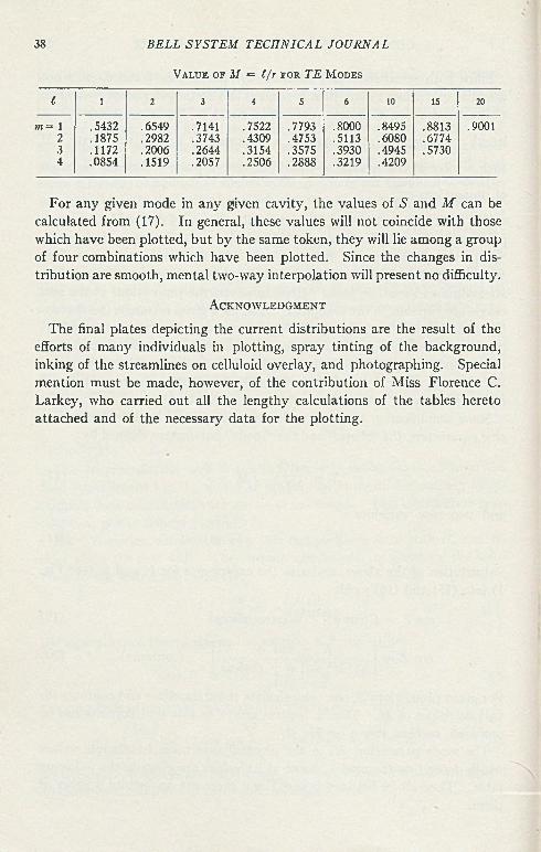
38 B E L L S Y S T E M T E C H N I C A L J O U R N A L
V a lu e o r M >= l / r t o r T E M o d e s
1 l 2 3 4 5 6 10 15 20
m = 1 .5432 .6549 .7141 .7522 .7793 .8000 .8495 .8813 .90012 .1875 .2982 .3743 .4309 .4753 .5113 .6080 .67743 .1172 .2006 .2644 .3154 .3575 .3930 .4945 .57304 .0854 .1519 .2057 .2506 .2888 .3219 .4209
For any given mode in any given cavity, the values of S and M can be calculated from (17). In general, these values will not coincide with those which have been plotted, but by the same token, they will lie among a group of four combinations which have been plotted. Since the changes in distribution are smooth, mental two-way interpolation will present no difficulty.
A c k n o w l e d g m e n t
The final plates depicting the current distributions are the result of the efforts of man}’- individuals in plotting, spray tinting of the background, inking of the streamlines on celluloid overlay, and photographing. Special mention must be made, however, of the contribution of Miss Florence C. Larkey, who carried out all the lengthy calculations of the tables hereto attached and of the necessary data for the plotting.
M = 0.1 •
M = 0.5 '
M = 0.9 ■
2 ,m ,n = MODE INDICES
Fig. 2 Side wall curren ts in circular cylinder cav ity resonato r for T E modes (/ > 0).
L = CAVITY LENGTH
r Cm = BE SSE L ZERO CO RRES-PONDING TO TE Km MODE
EACH RECTANGLE REPRESENTS A PIECE OP THE SIDE WALL SURFACE ROLLED OUT ONTO A P L A N E . TH E DOTTED L IN E S ARE CONTOURS OF EQUAL CURRENT IN TE N S ITY ; THE SOLID LINES ARE STREAM LINES. I .e . ,
DIRECTIONS OF CURRENT FLOW.
SINCE BOTH ST R E A M L IN E S AND CONTOURS ARE PERIODIC, THE
ENTIRE SURFACE IS O BTAINED BY REFLECTIONS AND REPETITIO NS OF THE
SECTIO N SH O W N .
A X IA L DIRECTION : 9 0 “ IN Z CORRESPONDS TO DISTANCE j f j - ALONG CAVITY
R A D IA L DIRECTION; 9 0 ” IN <J> CORRESPONDS TO ARC AROUND CAVITY
TO COVER SIDE W ALL S U R FA C E , 8(tn R E FLE C TIO N S AN D REPETITIONS ARE REQUIRED
S = = SHAPE PARAM ETER2K L
M = J " ■ = M ODE PARAM ETER rKmD = CAVITY DIAM ETER
RE
LAT
IVE
IN
TEN
SIT
Y
OF
MA
GN
ETI
C
FIEL
D (H
) R
ELA
TIV
E
INTE
NS
ITY
OF
M
AGN
ETIC
FI
ELD
(H)
RE
LAT
IVE
IN
TEN
SIT
Y
OF
MA
GN
ETI
C
FIEL
D (H
) OR
C
UR
RE
NT
(I
) OR
^C
UR
RE
NT
(I
) __
OR
CU
RR
EN
T
(I)
C IR C U L A R C Y L IN D E R . C A V I T Y R ESO N AT O R 39
RELATIVE RADIUS
Fig. 3— E nd p late currents in T E 11 mode.
RELATIVE RADIUS
Fig. 4— E nd plate curren ts in T M 01 mode.
RELATIVE RADIUS
Fig. 5— E nd p la te curren ts in T E 21 mode.
TTD _
Fig. 7— E nd p late curren ts in T E 01 mode.
o r i 0
0 = 90°
40 B E L L S Y S T E M T E C H N IC A L J O U R N A L
zo<2u. - 0 .2 O >- toS - 0 .4
>P - 0 . 6 <
Fig. 6— E nd p late cu rren ts in T M 11 mode.
0.4 0.5 0.6
RELATIVE RADIUS
C IR C U L A R C Y L I N D E R C A V I T Y R E S O N A T O R 41
RELATIVE RADIUS
Fig. 8— E nd p late curren ts in T E 31 mode.
Fig. 9— E nd p late curren ts in T M 21 mode.
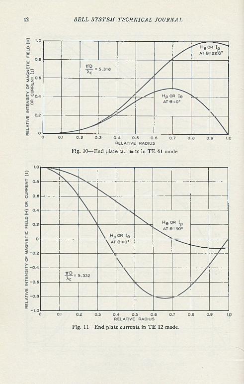
42 B E L L S Y S T E M T E C H N I C A L J O U R N A L
Fig. 10— E nd p la te cu rren ts in T E 41 mode.
Fig. 11— E n d p la te curren ts in T E 12 mode.
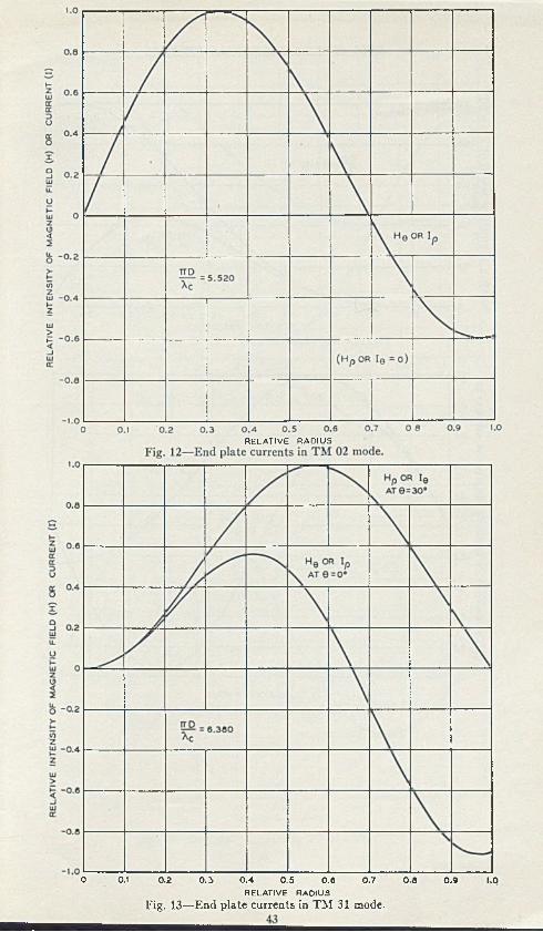
RELATIVE RAOIUS
O 0.1 0.2 0 .3 0 .4 0 .5 0 .6 0 .7 0 .« 0 .9 1.0RELATIVE RADIUS
Fig. 13—E n d p late curren ts in T M 31 mode.
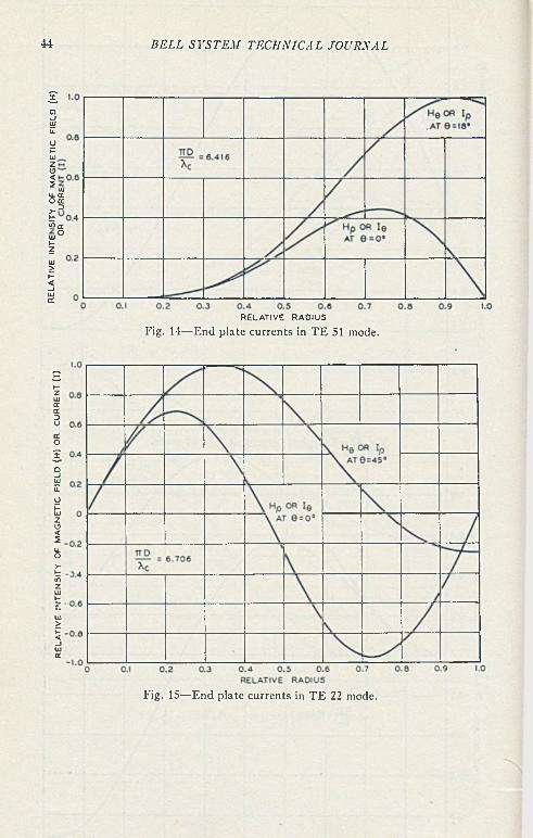
RE
LAT
IVE
IN
TEN
SIT
Y
OF
MA
GN
ETI
C
FIEL
D
(H)
OR
CU
RR
EN
T (I
) R
ELA
TIV
E
INT
Eq
|I™
u^
e“*
G*
ETIC
FI
ELD
(H
)44 B E L L S Y S T E M T E C H N I C A L J O U R N A L
RELATIVE RADIUS
Fig. 14— E nd p late cu rren ts in T E 51 mode.
Fig. 15— E nd p late curren ts in T E 22 mode.
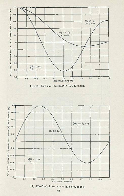
RE
LATI
VE
IN
TEN
SIT
Y
OF
MA
GN
ET
IC
FIEL
O
(H)
OR
CU
RR
EN
T (I
)
Fig. 16—E nd p la te curren ts in T M 12 mode.
Fig. 17—E n d p la te curren ts in T E 02 mode. 45
RE
LAT
IVE
IN
TE
NS
ITY
OF
M
AG
NE
TIC
FI
ELD
(H
) OR
C
UR
RE
NT
(I)
46 B E L L S Y S T E M T E C H N I C A L J O U R N A L
O 0.1 0 .2 0 .3 0 .4 0 .5 0 .6 0 .7 0 .8 0 .9 1.0RELATIVE RADIUS
Fig. 18— E nd p late cu rren ts in T E 61 mode.
C IR C U L A R C Y L I N D E R C A V I T Y R E S O N A T O R 47
Fig. 20—T E 02 mode.
B E L L S Y S T E M T E C H N IC A L J O U R N A L
Fig. 21—T E 03 mode.
Fig. 22—T E 11 mode.
Fig. 23—T E 12 mode.
Fig. 24—T E 13 mode, 49
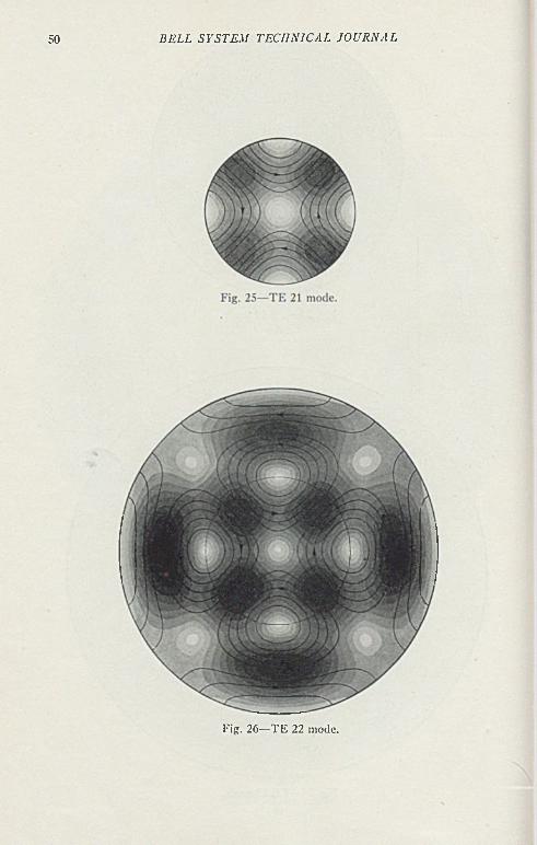
50 B E L L S Y S T E M T E C H N IC A L J O U R N A L
Fig. 26—T E 22 mode.
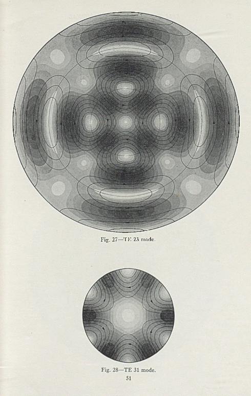
Fig. 27—T E 23 mode.
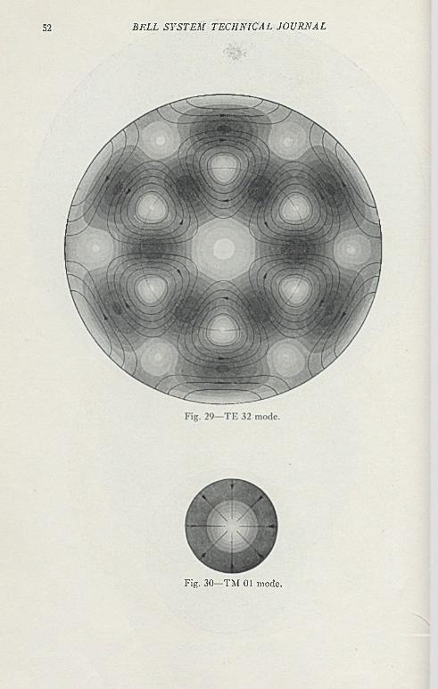
52 B E L L S Y S T E M T E C H N IC A L J O U R N A L
Fig. 30—T M 01 mode.
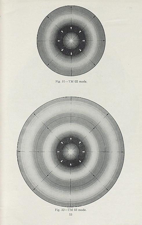
Fig. 31—T M 02 mode.
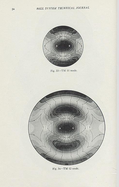
54 B E L L S Y S T E M T E C H N IC A L J O U R N A L
Fig. 34—T M 12 mode.
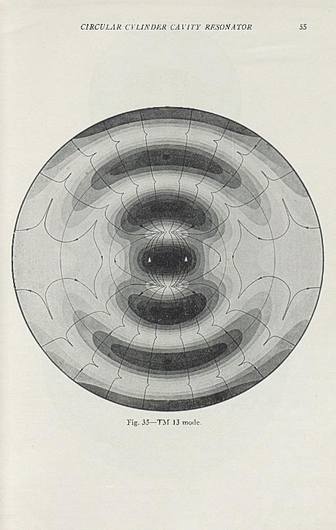
C IR C U L A R C Y L I N D E R C A V I T Y R E S O N A T O R 55
Fig. 35—T M 13 mode.
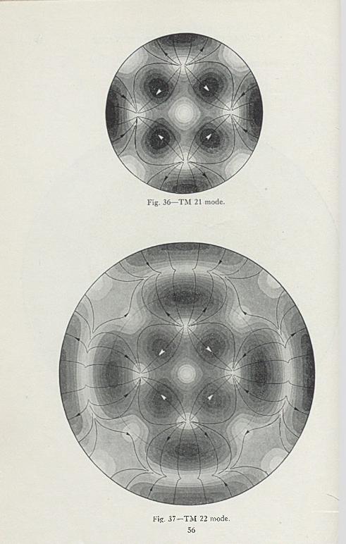
Fig. 37—T M 22 mode.
56
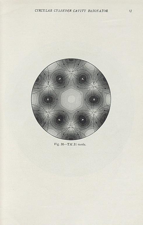
C IR C U L A R C Y L I N D E R C A V I T Y R E SO N A T O R 57
Fig. 38—T M 31 mode.
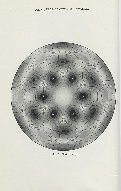
58 B E L L S Y S T E M T E C H N IC A L J O U R N A L
Fig. 39—T M 32 mode.
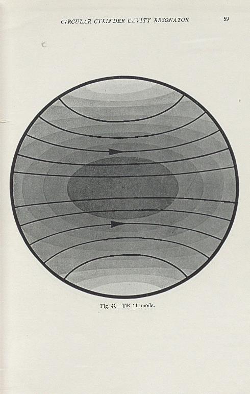
C IR C U L A R C Y L I N D E R C A V I T Y R E SO N A T O R 59
Fig. 40—T E 11 mode.
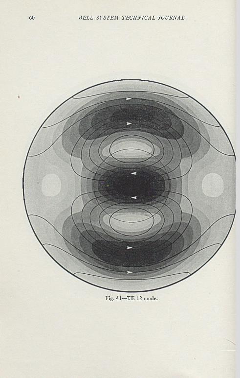
60 B E L L S Y S T E M T E C H N IC A L J O U R N A L
Fig. 41—T E 12 mode.
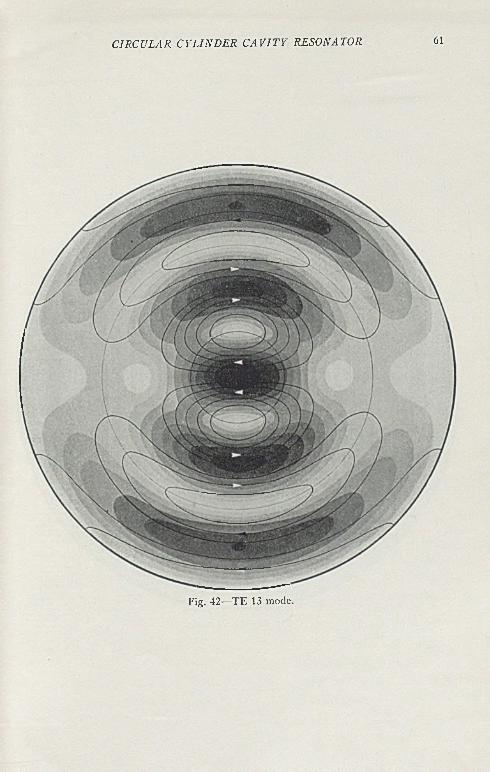
C IR C U L A R C Y L I N D E R C A V I T Y R E S O N A T O R 61
Fig. 42—T E 13 mode.
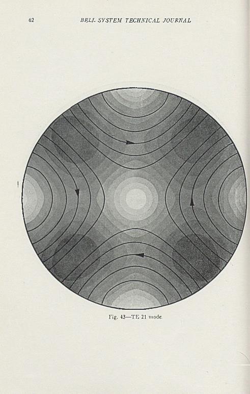
62 B E L L S Y S T E M T E C H N IC A L J O U R N A L
Fig. 43—T E 21 mode.
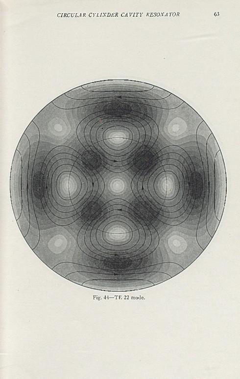
C IR C U L A R C Y L I N D E R C A V I T Y R E S O N A T O R 63
Fig. 44— T E 22 mode.
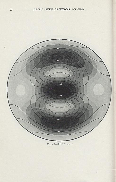
60 B E L L S Y S T E M T E C H N IC A L J O U R N A L
Fig. 41— T E 12 m ode.
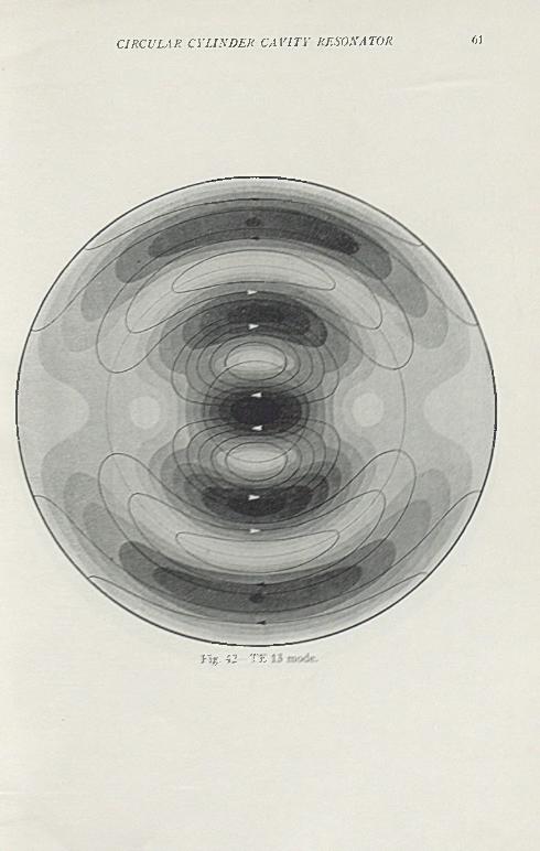
C IR C U L A R C Y L I N D E R C A V I T Y R E S O N A T O R 61
H *. 42— T E
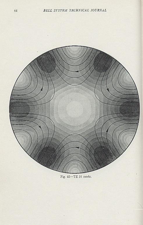
64 B E L L S Y S T E M T E C H N IC A L J O U R N A L
Fig. 45—T E 31 mode.
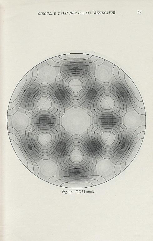
C IR C U LA R C Y L I N D E R C A V I T Y R ESO N AT O R 65
Fig. 46—T E 32 mode.
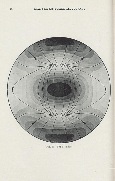
66 B E L L S Y S T E M T E C H N IC A L J O U R N A L
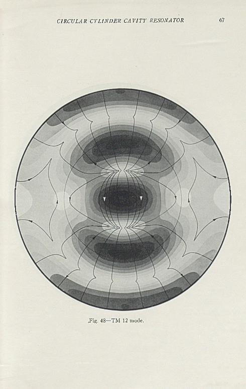
C IR C U L A R C Y L I N D E R C A V I T Y R E S O N A T O R 67
J i g . 48—TiM 12 mode.
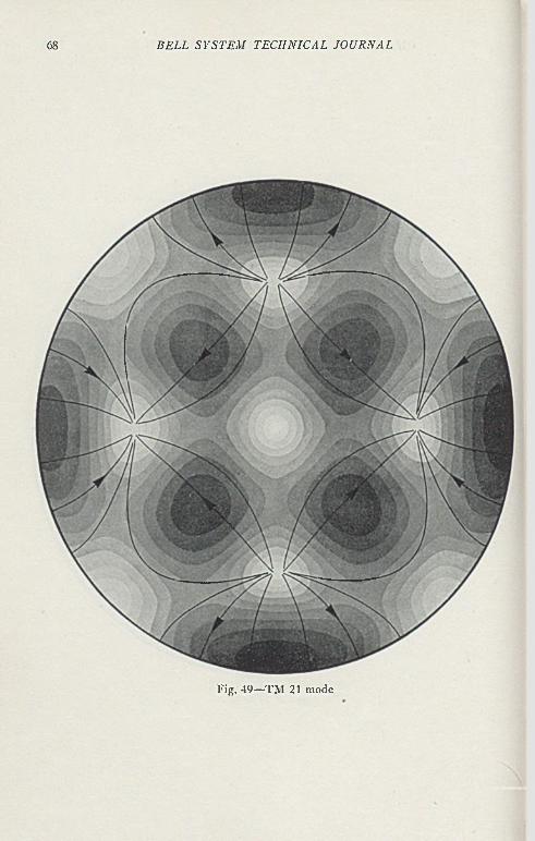
68 B E L L S Y S T E M T E C H N IC A L J O U R N A L
Fig. 49—T M 21 mode
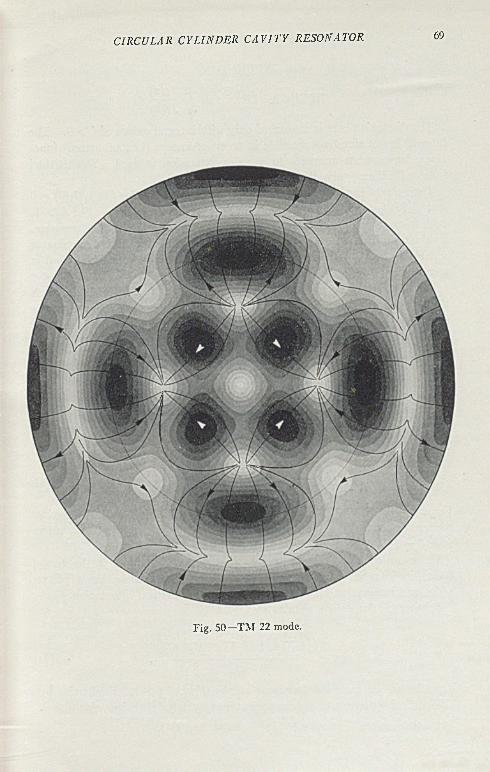
C IR C U L A R C Y L I N D E R C A V I T Y R E S O N A T O R 69
Fig. SO—TM 22 mode.
70 B E L L S Y S T E M T E C H N IC A L J O U R N A L
APPENDIX
FíJoJ f ( % )
INTEGRATION OF / - 77“ dxJ((x)
The discussion here is concerned only with integral values of I > 0. The integral is not simply expressible in terms of known (i.e., tabulated) functions, hence what amounts to a series expansion is used. The method follows Ludinegg1 who gives the details for I = 1 .
The value of the integrand at a- = 0 is first discussed. For t = 1, /i(0 ) = 0 and ,/i(0) = 0.5, hence the integrand has the value zero. For i > 1, both numerator and denominator are zero, hence the value is indeterminate. Evaluation by (I — 1) differentiations of numerator and denominator separately leads to the result that the integrand (and the integral also) is zero at x = 0 for all C.
We now introduce a constant pt and a function pt(x) which are such that the following equation is satisfied, a t least for a certain range of values of x:
J l = ~ p l ( f t ~ + pi f t . (1)
Denote the desired integral by Ft(x), i.e.:
' J f f )f l ix )
Then substitution of (1) into (2) yields:
rr J((x)w = I m d x • (2 )
P t = - p i [log + I PI dx. (3)
For x = 0 , J'l/x(( 1} >s indeterminate, but evaluation by differentiating numerator and denominator separately (i — 1 ) times gives the value1/2 V ~ 1)!
If we can now arrange matters so that pi remains finite in the range (0 , x), its integration can be carried out, a) by expansion into a power series and integration term-by-term, or, b) by numerical integration.
Solving (1) for pi one obtains
(C - l) /£ )J t + pi ( J f^ —-L . (4)
J lEquation (4) becomes indeterminate at x = 0, when C > 1 . Evaluation by differentiating numerator and denominator separately C times shows pt(0) = 0.
1 Hochfrequenztech. u. Elcklroak., V. 62, pp. 38-44, Aug. 1943.
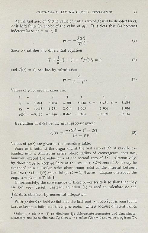
C IR C U L A R C Y L I N D E R C A V I T Y R ESO N AT O R 71
At the first zero of J t (the value of x at a zero of J i will be denoted by r),4>( is held finite by choice of the value of p i . I t is clear that (4) becomesindeterminate at x — r, if
Jf(r) rrvPC JK r) ■ (5)
Since J( satisfies the differential equation
f t + - J t + (1 - ¿ 7 x)Jl = 0 (6)X
and = 0, one has by substitution
p( — • (7)r- — C-
Values of p for several cases are:
£ = 1 2 3 4 1 1
n = 1.841 3 .054 4.201 5.318 r~ = 5.331 r, = 8.536
pt = 1.418 1.751 2.040 2.303 1.036 1.014
0 /(r) = - 0 .1 2 6 - 0 .286 - 0 .446 - 0.604 - 0 .180 - 0.115
Evaluation of by the usual process3 gives:
, , s - r f ( r 2 - i 2 - 2f)*t(r) = — j f T i r p f — (8)
Values of <pc(r) are given in the preceding table.Since <j>( is finite at the origin and at the first zero of J ( , it may be ex
panded into a Maclaurin series whose radius of convergence does not, however, exceed the value of x a t the second zero of J c . Alternatively, by choosing pi to keep <j>l finite at the second (or kth) zero of J i it may be expanded into a Taylor series about some point in the interval between the first (or (k — 1)"‘) and third (or {k + l)"1) zeros. Expansions about the origin are given in Table I.
Unfortunately, the convergence of these power series is so slow that they are not very useful. Instead, equation (4) is used to calculate <j>t and
/■4>c dx is obtained by numerical integration.
With pi fixed to hold <f>t finite at the first root, n , of J t , it is soon found that 4>t becomes infinite at the higher roots. This is because different values
! Substitu te (6) into (4) to elim inate JJ,'; differentiate num erator and denom inator separately; use (6) to elim inate J allow x —> r, using /¿ ( r ) = 0 and value of from (7).
72 B E L L S Y S T E M T E C H N IC A L J O U R N A L
of p are required at the different roots, as shown for C = 1 in the table above. A logical extension would therefore be to make p a function of x such that it takes on the required values at n , r i , r3, • ■ • . When this is done and pc(x) is introduced into (1) and (2), one has to integrate
Hence p(x) is made a discontinuous function, such that p has the value pi corresponding to n for values of a- from zero to a point bi between rx and r-2 ; the value pi corresponding to r2 for values of x from ¿1 to a point ¿2 between 72 and r3; and so forth. This introduces discontinuities in <f>. No discontinuities exist, however, in the function
which is given in Table II. The calculations were made by Miss F. C. Larkey; numerical integration was according to Weddle’s rule.
Within the limits of this tabulation, then, G( and F( are now considered to be known functions.
[ p(x)j"(x)J / '( * ) ^
and this is intractable.3
Gc = e~r( (9)
T a b l e I
P o w e r Se r ie s E x p a n s io n s op
= — 0.063313.* —0.001178.Ï3 -0 .0000358a5 -
<h(x) 1152 1 7 2 8 0 / '
= +0.1545 la +0.01648.V5 - 0.00580a5 -
<fr>(a)
= +0.12210.V +0.00667a3 +0.00375.Ï5 - •••
3 Unless p = b + c J ' (b and c constants), which is not of any use.
C IR C U L A R C Y L I N D E R C A V I T Y R E S O N A T O R 73
T a b l e I I
f x J , ( x )V a l u e s o f F i ( x ) = / 7 7 7 - : d x ; G , ( x ) = c_ i- i
Jo *'1
X 0 .1 .2 .3 .4 .5 .6 .7 .s .9
0 0 0050 0201 0455 0S16 1291 1887 2616 3493 45391 57S2 7261 9036 1.1192 1.3874 1.7336 2.2103 2.9577 4.6961 4.18462 2.7727 2.0S01 1.6199 1.2775 1.0073 7864 6018 4454 3117 19703 0987 0147 -0 5 6 4 -1 1 5 7 -1 6 4 0 -2 0 1 S -2 2 9 6 -2 4 7 5 -2 5 5 6 —25374 -2 4 1 6 -2 1 8 S -1 8 4 5 -1 3 7 7 -0 7 6 9 0 +0960 2153 3646 5549
5 8060 1.1595 1.7307 3.2014 2.3S51 1.4478 9635 6373 3939 20246 0470 -0 8 1 2 -1 8 7 9 -2 7 6 8 -3 5 0 6 -4 111 -4 5 9 4 -4 9 6 6 -5 2 3 3 -5 3 9 S7 -5 4 6 3 -5 4 2 9 -5 2 9 2 -5 0 4 9 -4 6 9 3 -4 2 1 4 -3 5 9 8 -2 8 2 6 -1 S 6S -0 6 8 58 +0789 2657 5107 8530 1.3992 2.7313 2.1565 1.1974 7154 39429 1562 -0 3 0 0 -1 8 0 2 -3 0 3 4 -4 0 5 3 -4 S 9 7 -5 5 9 0 -6 1 5 0 -6 5 9 1 -6 9 2 1
<?.(*)X 0 .1 .2 .3 .4 .5 .6 .7 .8 .9
0 1.0000 9950 9S01 9555 9216 8789 S2S0 7698 7052 63511 5609 483S 4051 3265 2497 1766 1097 0519 0091 01522 0625 1249 1979 2787 3652 4555 5478 6406 7322 82123 9060 9854 1.05S0 1.1226 1.1781 1.2236 1.25S1 1.2808 1.2912 1.28884 1.2733 1.2445 1.2026 1.1476 1.0799 1.0000 9085 8063 6945 5741
5 4467 3136 1772 0407 0921 2351 3816 5287 6744 81686 9541 1.0846 1.2067 1.3190 1.4200 1.50S4 1.5S31 1.6432 1.6877 1.71577 1.7269 1.7209 1.6976 1.6568 1.5989 1.5241 1.4331 1.3265 1.2054 1.07098 9241 7667 C001 4261 246S 0613 1157 3020 4S90 67429 8554 1.0304 1.1974 1.3545 1.4998 1.6318 1.7489 1.8497 1.9330 1.9978
74 B E L L S Y S T E M T E C H N I C A L J O U R N A L
V a lu e s o f I'?(x ) — [ dx; G¡(x) = c_ f'¿ Jo ■*!WF m(x )
X 0 .1 .2 .3 .4 .5 .6 .7 .8 .9
0 0 0025 0100 0220 0403 0632 0914 1251 1645 20971 2012 3192 3840 4503 5305 6253 7230 8323 952S 1.08662 1.2357 1.4008 1.5913 1.8061 2.0541 2.3450 2.6972 3.13S0 3.7263 4.01103 6.4527 0.7044 4.7528 3.8572 3.280S 2.S597 2.5316 2.2658 2.0451 1.85904 1.7002 1.5041 1.4470 1.3466 1.2007 1.1881 1.1275 1.0783 1.0396 1.0112
5 9928 9S43 9858 9974 1.0196 1.0530 1.09S5 1.1573 1.2311 1.32236 1.4345 1.5720 1.7447 1.9640 2.2555 2.6743 3.3910 0.5119 3.5122 2.71447 2.2595 1.9432 1.7034 1.5131 1.3579 1.2294 1.1223 1.0328 .9586 .89778 .8490 .8115 • 7S4G .7679 .7612 .7045 .7779 .S020 • S372 .88459 .9452 1.0212 1.1149 1.2301 1.3725 1.5512 1.7817 2.0950 2.5000 3.4864
Gt(x)X 0 .1 .2 .3 A .5 .6 .7 .8 .9
0 1.0000 9975 9900 9777 9005 93S8 9127 SS24 S4S3 81081 7701 7267 6811 6336 584S 5351 4850 4350 3856 33732 2900 2459 2036 1043 12S2 095S 0674 0434 0241 00993 0017 0012 00SG 0211 0376 0573 0795 1037 1294 155S4 1S26 2093 2353 2601 2834 3048 323S 3402 3536 363S
5 3705 3737 3731 3688 3607 34S9 3334 3143 2920 20050 2383 2075 1747 1403 1048 0690 0337 0015 029S 0062t 10-14 1432 1S21 2202 2572 2925 3255 3560 3834 40758 427S 4442 4563 4640 4671 4650 4593 4484 4329 41299 3S80 3602 32S0 2923 2535 2120 16S3 1231 076S 0306
C IR C U L A R C Y L I N D E R C A V I T Y R E SO N A T O R 75
V a lu e s o r A (a;) = f 777-7 <lx; G, (x) = c~F3Jo d 3{x)F z(x)
X 0 .1 .2 .3 .4 .5 .6 .7 .8 .9
0 0 0017 0067 0152 0268 0420 060-1 0S26 1081 13731 1703 2070 2476 2922 3410 3942 451S 5141 5S14 65392 7319 S15S 9060 1.0028 1.1070 1.2192 1.3401 1.4706 1.6118 1.76503 1.9321 2.1150 2.3165 2.5402 2.790S 3.0752 3.4034 3.7905 4.2624 4.S0694 5.7117 7.1373 16.2303 7.23S3 5.8409 5.0409 4.4852 4.0643 3.7292 3.4543
5 3.2239 3.0282 2.8605 2.7160 2.5913 2.4838 2.3914 2.3128 2.2467 2.19220 2.1487 2.1156 2.0927 2.0798 2.076S 2.0838 2.1012 2.1293 2.1ÖS5 2.22081 2.2864 2.3674 2.4661 2.586S 2.7340 2.9159 3.1460 3.4491 3.S790 4.59508 0.940S 4.9414 4.0348 3.534S 3.1912 2.9324 2.7276 2.560S 2.4227 2.30749 2.2108 2.1302 2.0637 2.0097 1.9676 1.9361 1.9147 1.9036 1.9025 1.9115
G3(x )•
a; 0 .1 .2 .3 .4 .5 .6 .7 .8 .9
0 1.0000 9983 9933 9S49 9734 95S9 9413 920S 8975 87171 S434 8130 7S06 7466 7110 6742 6365 59S0 5591 52002 4810 4423 4041 366S 3305 2955 2618 2298 1995 17123 1448 1206 09S6 0789 0614 0462 0333 0226 0141 00774 0033 0008 0000 0007 0029 0065 0113 0172 0240 0316
5 0398 0484 0572 0661 0749 0834 0915 0990 1057 11170 1166 1206 1233 1250 1253 1244 1223 11S9 1143 10857 1016 0937 0S49 0753 0650 0542 0430 0318 0207 01018 0010 0071 0177 0292 0411 0533 0654 0772 08S7 09959 1096 11SS 1270 1340 1398 1443 1474 1490 1492 1479
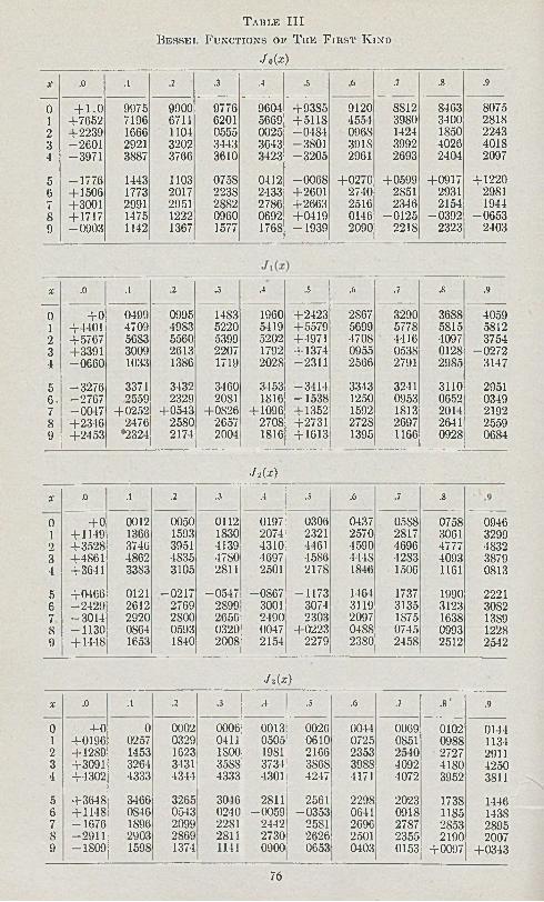
T a b l e I I I
B e s s e l F u n c t io n s o p T h e F i r s t K in d
/*(*)X .0 .1 .2 .3 .4 .5 .6 .7 .8 .9
n + 1 .0 9975 9900 9776 9604 +93S5 9120 8812 8463 S075i +7652 7196 6711 6201 5669 +5118 4554 3980 3400 28182 +2239 1666 1104 0555 0025 -0 4 8 4 0968 1424 1850 22433 -2 6 0 1 2921 3202 3443 3643 -3S01 3918 3992 4026 40184 -3 9 7 1 3887 3766 3610 3123 -3 2 0 5 2961 2693 2404 2097
5 -1 7 7 6 1443 1103 075S 0412 -0 0 6 8 + 0 2 10 +0599 +0917 + 1220fi + 1506 1773 2017 2238 2433 +2601 2740 2851 2931 29817 +3001 2991 2951 2882 2786 +2663 2516 2346 2154 19448 + 1717 1475 1222 0960 0692 +0419 0146 -0 1 2 5 -0 3 9 2 -0 6 5 39 -0 9 0 3 1142 1367 1577 176S -1 9 3 9 2090 2218 2323 2403
X .0 .1 .2 .3 .4 .5 .6 .7 .8 .9
0 + 0 0499 0995 1483 1960 +2423 2867 3290 3688 40591 +4401 4709 4983 5220 5419 +5579 5699 577S 5815 58122 +5767 5683 5560 5399 5202 +4971 4708 4416 4097 37543 +3391 3009 2613 2207 1792 + 1374 0955 053S 0128 -0 2 7 24 -0 6 6 0 1033 1386 1719 202S -2 3 1 1 2566 2791 2985 3147
5 -3 2 7 6 3371 3432 3460 3453 -3 4 1 4 3343 3241 3110 29516 . -2 7 6 7 2559 2329 2081 1816 -1 5 3 S 1250 0953 0652 03497 -0 0 1 7 +0252 +0543 +0S26 + 1096 + 1352 1592 1813 201! 21928 +2346 2476 2580 2657 2708 +2731 272S 2697 2641 25599 +2453 *2324 2174 2004 1816 + 1613 1395 1166 092S 06S4
• / * ( x )
X .0 .1 .2 .3 .4 .5 .6 .7 .8
0 + 0 0012 0050 0112 0197 0306 0437 058S 0758 09461 + 1149 1366 1593 1830 2074 2321 2570 2817 3061 32992 + 3528 3746 3951 4139 4310 4461 4590 4696 4777 48323 +4861 4862 4835 4780 4697 45S6 4448 4283 4093 38794 +3641 33S3 3105 2S11 2501 2178 1846 1506 1161 0813
5 +0466 0121 -0 2 1 7 -0 5 4 7 -0 S 6 7 -1 1 7 3 1464 1737 1990 22216 -2 4 2 9 2612 2769 2899 3001 3074 3119 3135 3123 30S27 -3 0 1 4 2920 2800 2656 2490 2303 2097 1875 1638 13898 -1 1 3 0 0S64 0593 0320 0047 +0223 04 SS 0745 0993 12289 +1448 1653 1840 200S 2154 2279 23S0 2458 2512 2542
/»(*)X .0 .1 .2 .3 .4 .5 .6 .7 .8 ' .9
0 + 0 0 0002 0006 0013 0026 0041 0069 0102 01441 +0196 0257 0329 0411 0505 0610 0725 0851 0988 11342 + 1289 1453 1623 1800 19S1 2166 2353 2510 2727 29113 +3091 3264 3431 35SS 3734 3868 398S 4092 4180 42504 +4302 4333 4344 4333 4301 4247 4171 4072 3952 3811
5 +364S 3466 3265 3016 2811 2561 2298 2023 173S 14466 + 1148 0S46 0543 0240 -0 0 5 9 -0 3 5 3 0641 091S 1185 14387 -1 6 7 6 1896 2099 2281 2442 2581 2696 2787 2S53 2895S -2 9 1 1 2903 2869 2S11 2730 2626 2501 2355 2190 20079 -1 8 0 9 159S 1374 1141 0900 0653 0403 0153 +0097 +0343
76
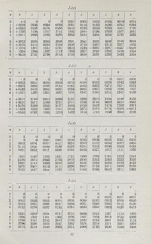
Ji ( z)
X .0 .1 .2 .3 .4 .5 .6 .7 .8 .9
0 + 0 0 0 0 0001 0002 0003 0006 0010 00161 +0025 0036 0050 0068 0091 0118 0150 0188 0232 02832 +0340 0405 0476 0556 0643 0738 0S40 0950 1037 11903 + 1320 1456 1597 1743 1892 2044 219S 2353 2507 26614 +2811 2958 3100 3236 3365 3484 3594 3693 3780 3853
5 +3912 3956 3985 3996 3991 3967 3926 3SG6 37SS 36916 +357G 3444 3294 3128 2945 2748 2537 2313 2077 18327 + 1578 1317 1051 0781 0510 0233 -0 0 3 1 -0 2 9 7 -0 5 5 7 -0 8 1 08 - 1054 1286 1507 1713 1903 2077 2233 2369 2485 25819 -2 6 5 5 2707 2736 2743 2728 2691 2633 2553 2453 2334
/.(*)X .0 .i .2 .3 .4 .5 .6 .7 .8 .9
0 + 0 0 0 0 0 0 0 0 0001 00011 +0002 0004 0006 0009 0013 0018 0025 0033 0043 00552 +0070 0088 0109 0134 0162 0195 0232 0274 0321 03733 +0430 0493 0562 0637 0718 OS04 0897 0995 1098 12074 + 1321 1439 1561 16S7 1816 1947 2080 2214 2347 2480
•5 +2611 2740 2865 2986 3101 3209 3310 3403 3486 35596 +3G21 3071 370S 3731 3741 3736 3716 36S0 3629 35627 +3479 3380 3266 3137 2993 2835 2663 247S 2282 20758 +1858 1632 1399 1161 09 IS 0671 0424 0176 -0 0 7 0 -0 3 1 39 -0 5 5 0 0782 1005 1219 1422 1613 1790 1953 2099 2229
M X )
X .0 .1 .2 .3 .4 .5 .6 .7 .8 .9
0 0 0 0 0 0 0 0 . 0 0 01 0 0 0001 0001 0002 0002 0003 0005 0007 00092 0012 0016 0021 0027 0034 0042 0052 0065 0079 00953 0114 0136 0160 0188 0219 0254 0293 0336 03S3 04354 0491 0552 0817 0688 0763 0S13 0927 1017 1111 1209
5 1310 1416 1525 1637 1751 186S 1986 2104 2223 23416 2458 2574 2686 2795 2900 2999 3093 3180 3259 3330i 3392 3444 3486 3516 3535 3541 3535 3516 3483 34368 3376 3301 3213 3111 2996 2887 2725 2571 2406 22309 2043 1S47 1644 1432 1215 0993 0768 0540 0311 0082
JÁX)
X .0 .1 .2 .3 .4 .5 .6 .7 .8 .9
0 0 0 0 0 0 0 0 0 0 01 0 0 0 0 0 0 0 0001 0091 00012 0002 0002 0003 0004 0006 0008 0010 0013 0016 00203 0025 0031 0038 0047 0056 0067 ooso 0095 0112 01304 0152 0176 0202 0232 0264 0300 0340 0382 0429 0179
5 0534 0592 0654 0721 0791 0SG6 0045 1027 1113 12036 1296 1392 1491 1592 1696 ÍSOI 1908 2015 2122 2230i 2336 2441 2543 2643 2739 2832 2919 3001 3076 31458 3206 3259 3303 3337 3362 3376 3379 3371 3351 33199 3275 3218 3149 306S 2974 2868 2750 2620 24S0 2328
77
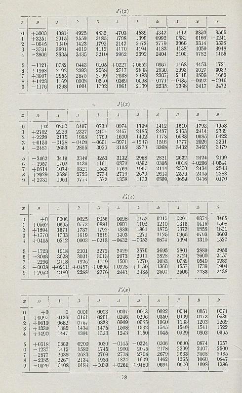
r i(x)
.0 .1 .2 .3 .4 .5 .6 .7 .8 .9
n +5000 4981 4925 4S32 4703 4539 4342 4112 3852 3565i +3251 2915 2559 21S5 1798 1399 0992 0581 0169 -0 2 4 12 -0 6 4 5 1040 1423 1792 2142 2472 2779 3060 3314 35383 -3 7 3 1 3891 4019 4112 4170 4194 41S3 413S 4059 39484 -3 8 0 6 3635 3435 3210 2962 2692 2104 2100 1782 1455
5 -1 1 2 1 0782 0443 0105 +0227 +0552 0867 1168 1453 17210 + 196S 2192 2393 256S . 2717 2838 2930 2993 3027 30327 +3007 2955 2875 2769 2638 24 S3 2307 2110 1S96 16668 + 1423 1169 0908 0640 0369 0098 -0 1 7 1 -0 4 3 5 -0 6 9 2 -0 9 4 09 -1 1 7 6 139S 1604 1792 1961 2109 2235 233S 2417 2472
X .0 .1 .2 .3 .4 .5 .6 .7 .8 .9
0 + 0 0250 0497 0739 0974 1199 1412 1610 1793 19581 +2102 2226 2327 2404 2457 2485 2487 2463 2414 23392 +2239 2115 196S 1799 1010 1402 1178 0938 0685 04223 + 0150 -0 1 2 S -0 4 0 9 -0 6 9 1 -0 9 7 1 -1 2 4 7 1516 1777 2020 22614 -2 4 S 1 2683 2865 3020 3105 3279 3308 3432 3469 3479
5 -3 4 6 2 3419 3349 3253 3132 298S 2S21 2632 2421 21996 -1 9 5 7 1702 1436 1101 0S79 0592 0305 001S +0266 +05447 +0S14 1074 1321 1553 1769 1967 2144 2300 2434 25438 +2629 2689 2725 2734 2719 2679 2614 2526 2415 22839 +2131 1961 1774 1572 1358 1133 0S99 0659 0410 0170
r ,( x)
X .0 .1 .2 .3 .4 .5 .6 .7 .8 .9
0 + 0 0006 0025 0056 009S 0152 0217 0291 0374 04651 +0562 0665 0772 0SS1 0991 1102 1210 1315 1415 15082 +1594 1671 1737 1792 1S33 1S61 1875 1873 1S55 18213 + 1770 1703 1619 1519 1403 1271 1125 0965 0793 06094 +0415 0212 0003 -0 2 1 3 -0 4 3 2 -0 6 5 3 0874 1094 1310 1520
5 -1 7 2 3 1918 2101 2272 2429 2570 2695 2801 2889 29566 -3 0 0 3 3028 3031 3013 2973 2911 2828 2724 2600 24577 -2 2 9 6 2118 1925 1719 1500 1270 1033 07S9 0510 02898 -0 0 3 S +0211 +0157 +0696 +0928 + 1150 1360 1557 1739 19049 +2052 2180 22SS 2376 2441 24S5 2507 2506 2483 2438
J \{x )
X .0 •4 i .2 .3 .4 .5 .6 .7 .8 .9
0 + 0 o! 0001 0003 0007’; 0013 0022 0034 0051 00711 +0097 0126; 0161 0201 0216: 0296 0350 0409 0473 05392 +0610 0682; 0757 0833 0909, 09S5 1060 1133 1203 12693 + 1330 13851 1434 1475 150S; 1532 1545 1549 1541 15224 + 1490 1447! 1391 1323 1243; 1150 1045 0929 0S02 0665
5 +0518 0363! 0200 0030 -0 1 4 5 ' -0 3 2 4 0506 0690 0874 10576 -1 2 3 7 1412 j 1582 1745 1900. 2045 217S 2299 2407 25007 -2 5 7 7 2638; 2683 2709: 2718: 2708 2679 2633 2568 24S58 -2 3 S 5 2267 2134 19S6 1S24; 1649 1462 1265 1060 08479 -0 6 2 9 0408 0184 +0039 +0261; + 0480 0694 0900 1098 12S6
78
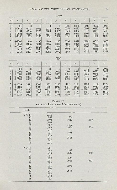
C IR C U L A R C Y L I N D E R C A V I T Y R ESO N AT O R
JUx)X .0 .1 .2 .3 .4 .5 .6 .7 .8 .9
0 + 0 0 0 0 0 0001 0002 0003 0005 00081 +0012 001S 0025 0034 0015 005S 0073 0092 0113 01372 +0161 0194 0228 0265 0305 0348 0394 0443 0494 05483 +0603 0660 0718 0777 0836 0S95 0952 100S 1062 11134 +1160 1203 1242 1274 1301 1321 1333 133S 1335 1322
5 +1301 1270 1230 1180 1120 1050 0970 0881 0782 06756 +0559 0435 030-1 0166 0023 -0 1 2 0 0278 0433 0591 07497 -0 9 0 7 1064 1217 1368 1513 1652 1783 1906 2020 21238 -2 2 1 5 2294 2360 2412 2449 2472 2479 2470 2446 2-1059 -2 3 4 9 2277 2190 208S 1972 1842 1700 1546 13S2 120S
J l(x)
X .0 .1 .2 .3 .4 .5 .6 .7 .8 .9
0 + 0 0 0 0 0 0 0 0 0 00011 +0001 0002 0003 0004 0006 0009 0012 0016 0021 00272 +0034 0043 0053 0065 007S 009-1 0111 0130 0152 01763 +0202 0231 0262 0295 0331 036S 040S 0450 0493 05384 +0585 0632 06S0 0728 0776 0823 0S70 0916 0959 1000
5 + 1039 1074 1105 1132 1155 1172 1183 1188 1187 11786 + 1163 1139 110S 1069 1022 0967 0904 0833 0753 0666i +0572 0470 0362 0247 0127 0002 -0 1 2 8 -0 2 6 1 -0 3 9 7 -0 5 3 58 -0 6 7 4 0813 0952 108S 1222 1352 1478 1597 1710 1S169 -1 9 1 2 2000 2077 2143 219S 2240 2270 22S7 2290 2279
T a b l e IV R e la t iv e R a d iu s f o r M axim um o f p i I
M ode
T E 11 .73712 .982 .25413 .993 .61321 .89422 .988 .40723 .995 .66431 .93732 .991 .49141 .95642 .993 .54851 .96761 .974
TM 01 .90102 .983 .39303 .993 .62711 .96112 .989 .52513 .995 .68221 .97722 .992 .59631 .98432 .994 .64341 .98851 .99061 .992
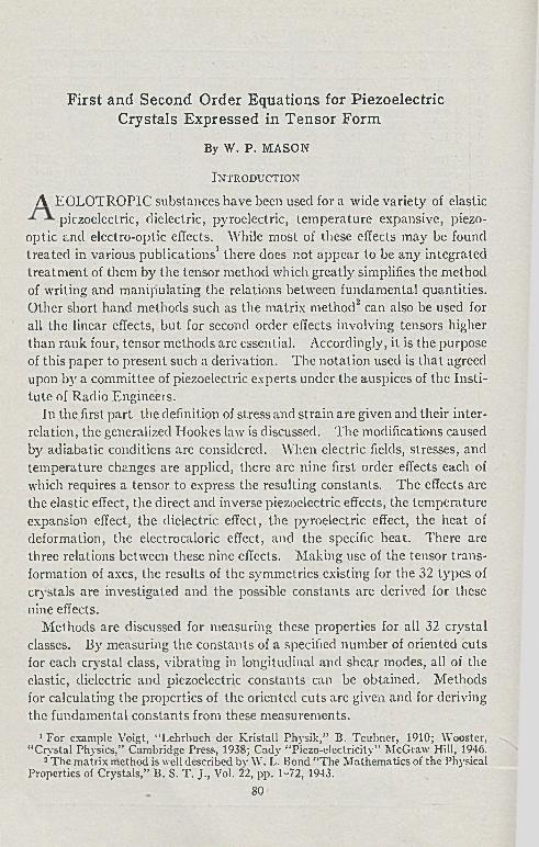
First and Second Order Equations for Piezoelectric Crystals Expressed in Tensor Form
By W . P . M A SO N
I n t r o d u c t io n
A EOLOTROPIC substances have been used for a wide variety of elastic piezoelectric, dielectric, pyroelectric, temperature expansive, piezo
optic and electro-optic effects. While most of these effects may be found treated in various publications1 there does not appear to be any integrated treatment of them by the tensor method which greatly simplifies the method of writing and manipulating the relations between fundamental quantities. Other short hand methods such as the matrix method2 can also be used for all the linear effects, but for second order effects involving tensors higher than rank four, tensor methods are essential. Accordingly, it is the purpose of this paper to present such a derivation. The notation used is that agreed upon by a committee of piezoelectric experts under the auspices of the Institute of Radio Engineers.
In the first part the definition of stress and strain are given and their interrelation, the generalized Hookes law is discussed. The modifications caused by adiabatic conditions are considered. When electric fields, stresses, and temperature changes are applied, there are nine first order effects each of which requires a tensor to express the resulting constants. The effects are the elastic effect, the direct and inverse piezoelectric effects, the temperature expansion effect, the dielectric effect, the pyroelectric effect, the heat of deformation, the electrocaloric effect, and the specific heat. There are three relations between these nine effects. Making use of the tensor transformation of axes, the results of the symmetries existing for the 32 types of crystals are investigated and the possible constants are derived for these nine effects.
Methods are discussed for measuring these properties for all 32 crystal classes. By measuring the constants of a specified number of oriented cuts for each crystal class, vibrating in longitudinal and shear modes, all of the elastic, dielectric and piezoelectric constants can be obtained. Methods for calculating the properties of the oriented cuts are given and for deriving the fundamental constants from these measurements.
1 For example Voigt, “ I.ehrbuch der K ristall Physik,” B. Teubner, 1910; Wooster, “ Crystal Physics,” Cambridge Press, 1938; Cady “ Piezo-electricity” McGraw Hill, 1946.
2 The m atrix m ethod is well described by W . L. Bond “ The M athem atics of the Physical Properties of Crystals,” B. S. T . J ., Vol. 22, pp. 1-72, 1943.
80
P IE Z O E L E C T R IC C R Y S T A L S I N TE N SO R FORM 81
Second order effects are also considered. These effects (neglecting second order temperature effects) are elastic constants whose values depend on the applied stress and the electric displacement, the electrostrictive effect, piezoelectric constants that depend on the applied stress, the piezo-optical effect and the electro-optical effect. These second order equations can also be used to discuss the changes that occur in ferroelectric type crystals such as Rochelle Salt, for which between the temperature of — 18°C. and + 24°C., a spontaneous polarization occurs along one direction in the crystal. This spontaneous polarization gives rise to a first order piezoelectric deformation and to second order electrostrictive effects. I t produces changes in the elastic constants, the piezoelectric constants and the dielectric constants. Some measurements have been made for Rochelle Salt evaluating these second order constants.
Mueller in his theory of Rochelle Salt considers that the crystal changes from an orthorhombic crystal to a monoclinic crystal when it becomes spontaneously polarized. An alternate view developed here is that all of the new constants created by the spontaneous polarization are the result of second order effects in the orthorhombic crystal. As shown in section 7 these produce new constants proportional to the square of the spontaneous polarization which are the ones existing in a monoclinic crystal. On this view “morphic” effects are second order effects produced by the spontaneous polarization.
1. St r e s s a n d St r a in R e l a t io n s i n A e o l o t r o p ic C r y s t a l s
1.1. Specification of Stress
The stresses exerted on any elementary cube of material with its edges along the three rectangular axes X, Y and Z can be specified by considering the stresses on each face of the cube illustrated by Fig. 1. The total stress acting on the face ABCD normal to the X axis can be represented by a resultant force R, with its center of application at the center of the face, plus a couple which takes account of the variation of the stress across the face. The force R is directed outward, since a stress is considered positive if it exerts a tension. As the face is shrunk in size, the force R will be proportional to the area of the face, while the couple will vary as the cube of the dimension. Hence in the limit the couple can be neglected with respect to the force R. The stress (force per unit area) due to R can be resolved into three components along the three axes to which we give the designation
Tx , Tyzi , Tzxz • (1)
Here the first letter designates the direction of the stress component and the second letter a'2 denotes the second face of the cube normal to the X axis. Similarly for the first X face OEFG, the stress resultant can be resolved
82 B E L L S Y S T E M T E C H N IC A L J O U R N A L
into the components TXXi , TVZi , T zx, , which are oppositely directed to those of the second face. The remaining stress components on the other four faces have the designation
(2 )
Face OABE T 7 vvi j 7'i'ji
CFGD T1 XV 2 > Fyvi , Fzy 2
OADG 7 ii, , Fyn , Tzzt
BCFE 1 II2 , 7 VXn I TX ZZ-y
The resultant force in the X direction is obtained by summing all the forces with components in the X direction or
Fx — (T«, — TXXi) dydz + {TXVi — T XVi) dxdz + (Txz, — TXZt) dxdy. (3)
But
Tx T - L 11"T~ 7 dx jO X
Tłu* — T'XV\
+ d- ~ v dy, TXZi = - T „ t + dTx,dz
(4)dz
and equation (3) can be written in the form
f . = - ( : -j- -f- dFx dx dy dz.0 Txx dJ\ dx dy ' dz
Similarly the resultant forces in the other directions are
(5)
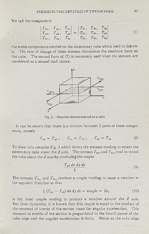
P IE Z O E L E C T R IC C R Y S T A L S I N T E N S O R FORM S3
We call the components
Txx, ^ m , Txz Tn , T n , TnTyx , Tyyt Tyx = Tn, 7 22 , TnTzx, Tzy , Txx Tn, Tn, Ts 3
the stress components exerted on the elementary cube which tend to deform it. The rate of change of these stresses determines the resultant force on the cube. The second form of (7) is commonly used when the stresses are considered as a second rank tensor.
Fig. 2.—Shearing stresses exerted on a cube.
It can be shown that there is a relation between 3 pairs of these components, namely
Tn = Tyz ■ TIZ = T zx ; TVI = T:v. (8)
To show this consider Fig. 2 which shows the stresses tending to rotate the elementary cube about the Z axis. The stresses TVXl and Tyx, lend to rotate the cube about the Z axis by producing the couple
Tyx dx dy dz 2 •
The stresses T1Vl and TIV, produce a couple tending to cause a rotation in the opposite direction so that
\ {Tyx — Txy) dx dy dz = couple = I<x>z (10)
is the total couple tending to produce a rotation around the Z axis. But from dynamics, it is known that this couple is equal to the product of the moment of inertia of the section times the angular acceleration. This moment of inertia of the section is proportional to the fourth power of the cube edge and the angular acceleration is finite. Hence as the cube edge
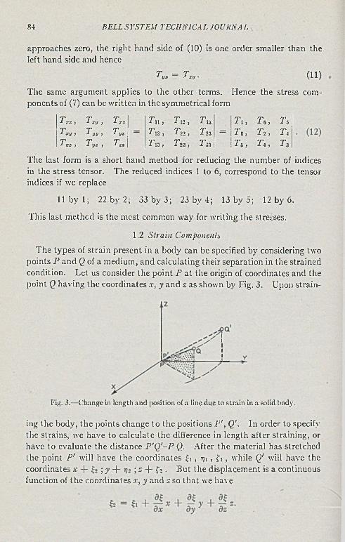
84 B E L L S Y S T E M T E C H N IC A L J O U R N A L
approaches zero, the right hand side of (10) is one order smaller than the left hand side and hence
T y x = T j y . (11)
The same argument applies to the other terms. Hence the stress components of (7) can be written in the symmetrical form
T „ , T x , j , T x z T n , T n , T n T i , T s , T s
T x y , T y y , T y x — T n , T 2, , T ¡ 3 = T s , T 2 , T i
T x x , P y x > T z z P 13 ) T 23, T ¡ 3 T s , T . i , T s
The last form is a short hand method for reducing the number of indices in the stress tensor. The reduced indices 1 to 6, correspond to the tensor indices if we replace
11 by 1; 22 by 2; 33 by 3; 23 by 4; 13 by 5; 12 by 6.
This last method is the most common way for writing the stresses.
1.2 Strain Components
The types of st rain present in a body can be specified by considering two points P and Q of a medium, and calculating their separation in the strained condition. Let us consider the point P at the origin of coordinates and the point Q having the coordinates x, y and s as shown by Fig. 3. Upon strain
ing. 3.—Change in length and position of a line due to strain in a solid body.
ing the body, the points change to the positions P ', Q'. In order to specify the strains, we have to calculate the difference in length after straining, or have to evaluate the distance P'Q'-P Q. After the material has stretched the point P' will have the coordinates £ i , j?i , f i , while Q' will have the coordinates x -(- ; y -f- ; z + f 2 • But the displacement is a continuousfunction of the coordinates x, y and s so that we have
Similarly, dri . dt] .dr)
, 2 = r/1 + - a - + - y + - S(13)
h „ t l + f X + * y + $ ' .dx dy dz
Hence subtracting the two lengths, we find that the increases in separation in the three directions are
5x = x — + y — + Z - . dx dy dz
S. , x f + y f + , §dx dy dz
dtThe net elongation of the line in the x direction is x and the elongation ° ax
P IE Z O E L E C T R IC C R Y S T A LS I N T E N S O R FORM 85
dJ
dxWe have therefore that the linear strains in the x, y and z directions are
per unit length is — which is defined as the linear strain in the a- direction. dx
dx dy dz
The remaining strain coefficients are usually defined as
o _ _i_ dy . o _ i . c. = — + — (16)S i - d - y + d z ‘ S i ~ d z + § x ’ S * d x dy (16}
(17)
and the rotation coefficients by the equations
dt dt) _ d$ _ dt _ dv _ d |Wl “ dy dz ’’ dz dx ' "* dx dy '
Hence the relative displacement of any two points can be expressed as
«, - * ( - 4 ^ ) + + 2 ( c r * ) (18)
j , _ » + , ( ^ - ) + zS,
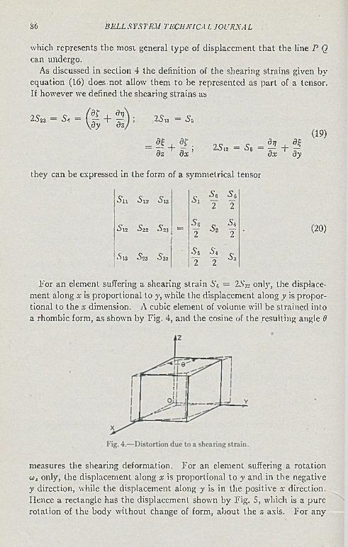
86 B E L L S Y S T E M TE C IIN IC A L J O U R N A L
which represents the most general type of displacement that the line P Q can undergo.
As discussed in section 4 the definition of the shearing strains given by equation (16) does.not allow them to be represented as part of a tensor. If however we defined the shearing strains as
2S23 = 5 , = ( f + ÿ\dy dz25(3 — ¿¡,
= Üf + •dz dx ’
2S„ = s , - p + aJox oy
(19)
they can be expressed in the form of a symmetrical tensor
S i l ¿ 1 2 ¿ 1 3 ¿ 1¿ 6
2
¿ 6
2
-S'12 ¿ 2 2 ¿ 2 3 =¿ 6
2¿ 2
¿ i
2
¿ 1 3 ¿ 2 3 ¿ 3 3¿ 5
2
¿■1
2¿ 3
(20)
For an element suffering a shearing strain ¿ 6 = 2Si2 only, the displacement along x is proportional to y, while the displacement along y is proportional to the $ dimension. A cubic element of volume will be strained into a rhombic form, as shown by Fig. 4, and the cosine of the resulting angle 6
measures the shearing deformation. For an element suffering a rotation w, only, the displacement along a; is proportional to y and in the negative y direction, while the displacement along y is in the positive x direction. Hence a rectangle has the displacement shown by Fig. 5, which is a pure rotation of the body without change of form, about the z axis. For any
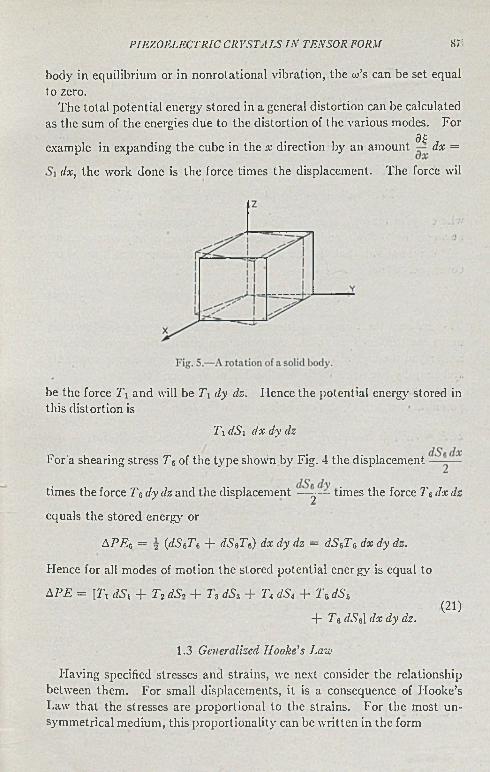
P IE Z O E LE C TR IC C R Y S T A L S I N TE N SO R FORM 87’
body in equilibrium or in nonrotational vibration, the co’s can be set equal to zero.
The total potential energy stored in a general distortion can be calculated as the sum of the energies due to the distortion of the various modes. For
dtexample in expanding the cube in the x direction by an amount dx =
dx, the work done is the force times the displacement. The force wil
be the force T% and will be Ti dy dz. Hence the potential energy stored in this distortion is
T i dS\ dx dy dz
For'a shearing stress T e of the type shown by Fig. 4 the displacement
times the force T o dy dz and the displacement —y — times the force 7’6 dx dz
equals the stored energy or
AP E 6 = 5 (dSnTe + dSoTo) dx dy dz = dS^Tt dx dy dz.
Hence for all modes of motion the stored potential energy is equal to
A PE = [T, dSi + T* dS, + 7 3 dS, + 7\ d.S\ + T&dS6(21)
+ To dS6] dx dy dz.
1 .3 Generalized Hooke’s Law
Having specified stresses and strains, we next consider the relationship between them. For small displacements, it is a consequence of Hooke’s Law that the stresses are proportional to the strains. For the most un- symmetrical medium, this proportionality can be written in the form
(22)
T\ = cnS i + C10S2 + C13S3 + £14^4 + C1555 + Cic^s
T<> = C21S1 4~ C22S2 4~ C23.S3 4” C24S4 4 " C25.S5 4~ C2ryS'o
T i = C3K>1 + C32S2 + C33S3 + C34>S’4 4" 4“ C3G'S’g
14 = l'41'S'l + C42S2 4" C43^3 4" C44-S.1 + C.IB-S's + Cif,S(,
T 5 = C6i‘S'i 4" c&S« 4~ CmS s 4 ” Cs^-t 4 ” C55.S5 4~ CsoS'e
T 6 = C6K>4 4" C62‘S'2 4“ 663* 3 4“ CM-Sii 4“ C65^5 4“ ^66'5"6
where cn for example is an elastic constant expressing the proportionality between the Si strain and the 74 stress in the absence of any other strains.
I t can be shown that the law of conservation of energy, it is a necessary consequence that
C12 = C21 and in general c;,- = c,,-. (23)
This reduces the number of independent elastic constants for the most unsymmetrical medium to 21. As shown in a later section, any symmetry existing in the crystal will reduce the possible number of elastic constants and simplify the stress strain relationship of equation (22).
Introducing the values of the stresses from (22) in the expression for the potential energy (2 1 ), this can be written in the form
2P E = cn«Si + 2C12S 1S2 4" 2C13S 1S3 4" 2C14S1S4 4“ 2C15S1S 5 4” 2ci$SiSb
4- C22-S 2 4“ 2c23‘S'2'S'3 4“ 2C24A2S4 4“ 2C25 2-5b 4" 2c2e&S6
4" C33.S3 4“ 2C343'3.S’4 4- 2C35S3S5 4" 2C3oSsSo
4~ C44S4 + 2c.i&SiSs + 2('4fr5VS'6 (24)
4~ C65S5 4* 2c5qSsS$
4- c t z S i .
The relations (22) thus can be obtained by differentiating the potential energy according to the relation
r ' - S f - r - - S f - <25>
88 B E L L S Y S T E M T E C H N IC A L J O U R N A L
I t is sometimes advantageous to express the strains in terms of the stresses. This can be done by solving the equations (22) simultaneously for the strains resulting in the equations
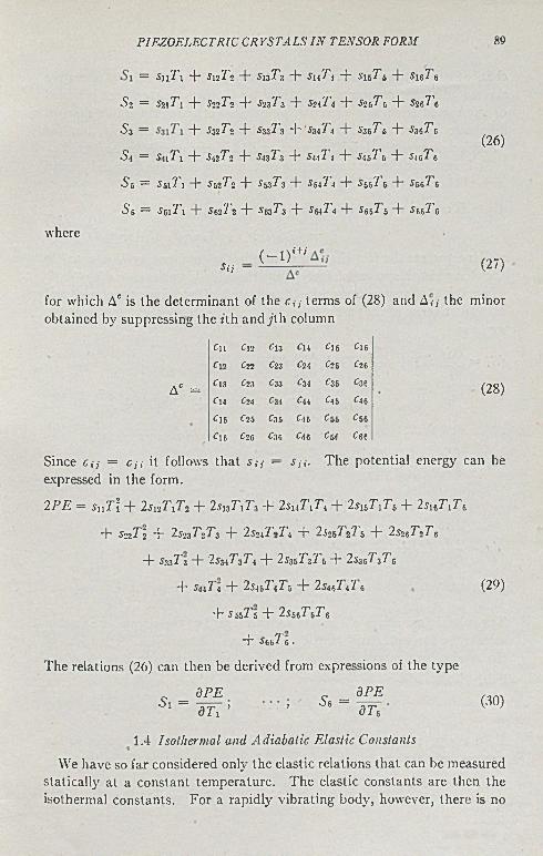
P IE Z O E L E C T R IC C R Y S T A L S I N T E N S O R FORM 89
= SiiiTi + SnTz + SnT3 + Su'Ti + suT 6 + sm'16
Si = Si\T 1 + S22T2 + 523 7’a + SuTi + S2&T 6 + 52c7’s
■S3 = + S32T2 + S33T3 + "SziTt + S33T 3 + S33T 3
S i = S n T l + S i i T i + S4 3T 3 + 544 7 ) + S4 5 T 5 + 54 6 ^ 6
■S i = 55l 7 ' i + 5527'2 + 553T3 + 554^4 + S 3 3 T 5 + S 3 3 T 3
Si = SnTl + SuTi + 5c37'3 + s^Ti + s ^ l 5 + 5667'o
(26)
where
S i j —( - 1) i+i
(27)
for which Ac is the determinant of the c,y terms of (28) and A</ the minor obtained by suppressing the tth and7 th column
Ac =
C U C12 C13 C14 C15 ClG
Cl» C22 C23 C24 Cib C26
C13 Í23 C33 C34 C35 C36
C14 C24 C34 C44 C45 C46
C l5 C25 C35 C45 C55 C¿ c
C16 C25 C36 Cte C6f Ce c
(28)
Since d j = cn it follows that s {j - 5 ,-,-. The potential energy can be expressed in the form.
2 PE = snTl + IsnTiTi + IsnTiTb + 2su T xTA + 2sXbTxTb + 25i67'17'6
+ 5227'5 + 2S23T2T3 + 2s3iT«Ti + 2j»7’*7’, + 2suT->T e
+ 533?'3 + 2S3iT3Ti + 2535 r 37'6 + 2536 r 3T6
+ 544T4 + 2s ie l \ I5 -f- 254ç7 4? 6
+ 5 65T5 + 2s$eT eT 6
+ 56fj7~6 .
The relations (26) can then be derived from expressions of the type
(29)
Si =dPE Se =
dPE(30)
dTi ’ ’ dTe
1.4 Isothermal and Adiabatic Elastic Constants%We have so far considered only the elastic relations that can be measured
statically at a constant temperature. The elastic constants are then the isothermal constants. For a rapidly vibrating body, however, there is no
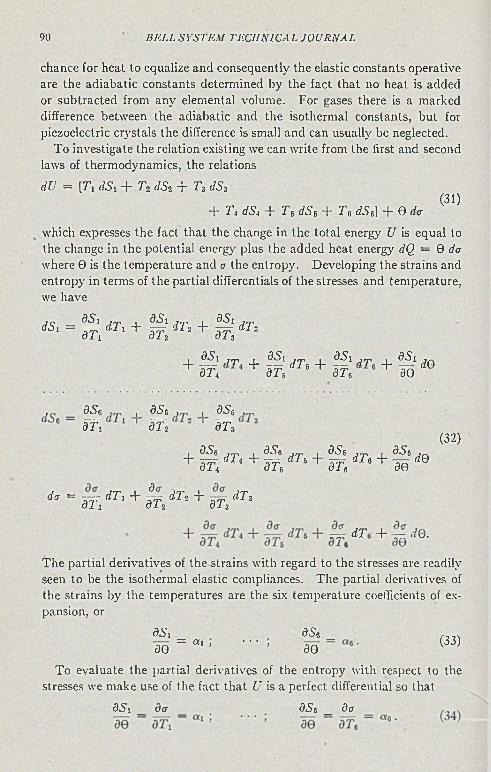
90 B E L L S Y S T E M T E C H N IC A L J O U R N A L
chance for heat to equalize and consequently the elastic constants operative are the adiabatic constants determined by the fact that no heat is added or subtracted from any elemental volume. For gases there is a marked difference between the adiabatic and the isothermal constants, but for piezoelectric crystals the difference is small and can usually be neglected.
To investigate the relation existing we can write from the first and second laws of thermodynamics, the relations
dV = [T\ dSi + T2 dS2 + T3 dS3(31)-f- T .i dS.i -T 7 5 dS5 -\- I c ¿Se] H- © da
which expresses the fact that the change in the total energy U is equal to the change in the potential energy plus the added heat energy dQ = 0 da where 0 is the temperature and u the entropy. Developing the strains and entropy in terms of the partial differentials of the stresses and temperature, we have
.<o &Si , T , dSi , . dSi ,i s , - m JT , + m IT , + W t a ,
_J_ d S l , J T 4 - 551 J T - L d S l J T J - d S l J a+ ST. d T ‘ + ST. , m + ST. + 36
, dSe . , dSn , , dS6 ,ST, ST, ST.
(32), dS6 dS6 , , OSo ,T , OSa ,+ ST. d T ‘ + ST. d T ‘ + ST. d T ' + m d e
d’ - m dT' + l r , dT- + m dT-
+ k d T ‘ + m i T r +
The partial derivatives of the strains with regard to the stresses are readily seen to be the isothermal elastic compliances. The partial derivatives of the strains by the temperatures are the six temperature coefficients of expansion, or
dSi dS& . .de = a i ’ • • • ’ a e = (33)
To evaluate the partial derivatives of the entropy with respect to the stresses we make use of the fact that U is a perfect differential so that
dSi _ da _ dSt _ dcr
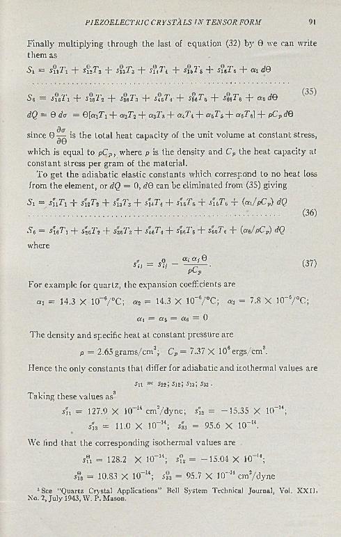
Finally multiplying through the last of equation (32) by 0 we can writethem as
S i = SiiTy -j- SiÇI'n -)- S13T 3 -f- -S' 1*17 4 T in, 7/ + SisTn -f- ai dQ
Sg = SisTi + SïçJ'o + ¿ggTj + SirJ\' sfeTe + s^Te -f- aodQ
dQ = 0 dcr = 0[«iTi + aÇI\ + (X3T3 + aiT\ + «5 5 + a^Te] + pCpdQ
since 0 — is the total heat capacity of the unit volume at constant stress,
which is equal to pCp, where p is the density and Cp the heat capacity atconstant stress per gram of the material.
To get the adiabatic elastic constants which correspond to no heat loss from the element, or dQ = 0, dQ can be eliminated from (35) giving
S i = shTi + snT, + sn'I\ + in 7/ + s \ J \ + i u T , + («i/pCp) dQ .................................................................................... (36)
Se — A û 1 + sleTi -f- 536T3 + SieTi + s ^ T 5 + ieoTc + (««/pCp) dQ
where
so = 4 - ° ^ - (37)pCp
For example for quartz, the expansion coeff.cients are
<*i = 14.3 X 10"V°C; 011 = 14.3 X 10~6/°C ; « 3 = 7.8 X l ( r 6/°C;
aj = a j = «6 = 0
The density and specific heat at constant pressure are
p = 2.65 grams/cm3; CP = 7.37 X 10⁶ergs/cm3.
Hence the only constants that differ for adiabatic and isothermal values are
ill = S22; il2 j il3; i33 •Taking these values as3
in = 127.9 X 10-M cm2/dyne; i î2 = —15.35 X 10~14;
su = 11.0 X 10- u ; i33 = 95.6 X 10~14.
We find that the corresponding isothermal values are
sfi = 128.2 X 10~14; if, = -15 .04 X 10-14;
i®3 = 10.83 X 10~14; S33 = 95.7 X 10⁻¹⁴ cm2/dyne3 See “Q uartz Crystal Applications” Bell System Technical Journal, Vol. X X II.
No. 2, Ju ly 1943, W. P. Mason.
P IE Z O E L E C T R IC C R Y S T A L S I N T E N S O R FORM 91
92 B E L L S Y S T E M T E C H N IC A L JO U R N A L
at 25°C. or 298° absolute. These differences are probably smaller than the accuracy of the measured constants.
If we express the stresses in terms of the strains by solving equation (35) simultaneously, we find for the stresses
71 = tn5'i + CviSr C13S 3 T Cn-S.i + Clip’s + CiV'o — Ai <70
where\ O 1 O 1 „0 , O 1 .0 1 ,0Ai — (*iCii + CX2C12 + <*3Ci3 + a.iCu + a 5Ci5 + acCi6
\ .0 1 0 1 0 1 0 1 O 1 0Ab = C*lCl6 + «5 26 + «3^30 + « 1C4G + « 5 ^ 6 + “ 0^66 •
The A’s represent the temperature coefficients of stress when all the strains are zero. The negative sign indicates that a negative stress (a compression) has to be applied to keep the strains zero. If we substitute equations (38) in the last of equations (35), the relation between increments of heat and temperature, we have
dQ = Oder = 0[Xi5i + A2S2 -f" A3.S'3 A4.S4 T A5.S5 + Ao-S"e]' (39)
-j- [pCP — 0(«iAi -f- a» Al + <13X3 + «4A4 + <*5X5 + a6Ab)](70.
If we set the strains equal to zero, the size of the element does not change, and hence the ratio between dQ and dQ should equal p times the specific heat at constant volume C„. We have therefore the relation
p[CP — Cv] = 0[cxiAi + «2X2 + 0:3X3 + 0:4X4 + a 5X5 + ooXe]. (40)
The relation between the adiabatic and isothermal elastic constants ca thus becomes
4 - = 4 - + (41)
Since the difference between the adiabatic and isothermal constants is so small, no differentiation will be made between them in the following sections.
2. E x p r e s s io n ’ f o r T h e E l a s t ic , P i e z o e l e c t r ic , P y r o e l e c t r ic a n d D ie l e c t r ic R e l a t io n s o f a P ie z o e l e c t r ic C r y s t a l
When a crystal is piezoelectric, a potential energy is stored in the crystal when a voltage is applied to the crystal. Hence the energy expressions of (31) requires additional terms to represent the increment of energy dU. If we employ CGS units which have so far been most widely used, as applied
P IE Z O E L E C T R IC C R Y S T A L S I N T E N S O R FORM 93
to piezoelectric crystals, the energy stored in any unit volume of the crystal is
dU = Ti dSi + T2 dS2 + T3 dS3 + T, dSt + T, dSs + T, dS6
, _ dDi , r dDt , „ dH, (42)+ Ei — + Ei — + E3 +Qdcr 4 tt Ax Ax
where Ey, E2 and £ 3 are the components of the field existing in the crystal and Dy, D« and D3 the components of the electric displacement. In order to avoid using the factor 1 / 47t we make the substitution
£ = S. (43)47T
The normal component of 5 at any bounding surface is £0 the surface charge. On the other hand if we employ the MKS systems of units the energy of any component is given by E ndD„ directly and in the following formulation 5 can be replaced by D.
There are two logical methods of writing the elastic, piezoelectric, pyroelectric and dielectric relations. One considers the independent variables as the stresses, fields, and temperature, and the dependent variables as the strains, displacements and entropy. The other system considers the strains, displacements and entropy as the fundamental independent variables and the stresses, fields, and temperature as the independent variables. The first system appears to be more fundamental for ferroelectric types of crystals.
If we develop the stresses, fields, and temperature in terms of their partial derivatives, we can write
E x = E i
94 K E LL S Y S T E M T E C H N IC A L J O U R N A L
oLE: 3£
3£as,
- ) ¿Sl + | f ) + d~ 0 ) dS3 + d- § ) dS*\ / D , o 0 0 2 / D , c O O z/ d , * 0 0 \ / D,<t
f ) dSb+d^ ) dS6 + w ) d S i + W ) d5i35 / D . f f 0 0 6 / D , a O 0 \ / S ,a 0 0 2 / S ,a
+ | f ) ¿8. + ~ ) dao o z / s . o d a J s .d
Et = £ 3 = | f ) ¿Si + | f ) ¿£2 + dS3 + | f ) r/S.,O O l/D .ff O O 2/ D , a O O 3/D ,< t 0O 4/ D , a
+ | f ) dS6 + | f ) ¿£6 + | f ) dS 1 + | f ) ¿620 0 6 / D,a 0 0 6 / d ,<x O0\ / 8 ,0 O O o /s .o
+ f )* + « ) 3 . « * » )OO3 / s . a C7(T / 8 ,D
¿ 0 = 1 1 ) ¿S, + I I ) ¿Si + I f ) ¿S3 + I I ) ¿£4O O l/D .f f 002/ 2) ,<r O O z / d .o 0 0 \ / D , a
¿ S 6 + | | ) ¿ 5l + | | ) ¿52<r C/0l/5,«r C/O2 / 8,0
? ) l 1 ......J / S . D+ di) s / 8 3 + f c r ) ( h -
The subscripts under the partial derivatives indicate the quantities kept constant. A subscript D indicates that the electric induction is held constant, a subscript <7 indicates that the entropy is held constant, while a subscript S indicates that the strains are held constant.
Examining the first equation, we see that the partial derivatives of the stress Ty by the strains are the elastic constants c,-}- which determine the ratios between the stress £ 1 and the appropriate strain with all other strains equal to zero. To indicate the conditions for the partial derivatives, the superscripts D and a are given to the elastic constants and they are written cDi f . The partial derivatives of the stresses by 5 = D/Ax are the piezoelectric constants //,-,• which measure the increases in stress necessary to hold the crystal free from strain in the presence of a displacement. Since if the crystal tends to expand on the application of a displacement, the stress to keep it from expanding has to be a compression or negative stress, the negative sign is given to the //¿,- constants. As the only meaning of the h constants is obtained by measuring the ratio of the stress to 5 = D/Ax at constant strains, no superscript S is added. However there is a difference between isothermal and adiabatic piezoelectric constants in general, so
P IE Z O E L E C T R IC C R Y S T A L S I N T E N S O R FORM 95
that these piezoelectric constants are written //“,•. Finally the last partial derivatives of the stresses by the entropy a can be written
T “ ) (h = 5 T"“) 9 (h = 5 T n) ,/(? =O ff /s ,Z > 0 O ff / S ,D Ö O ff /S ,DdQ (45)
where dQ is the added heat. We designate 1/0 times the partial derivative as — 7 „d and note that it determines the negative stress (compression) necessary to put on the crystal to keep it from expanding when an increment of heat dQ is added to the crystal. The electric displacement is held constant and hence the superscripts S, and D are used. The first six equations then can be written in the form
Tn = cltSx + c%S, + c * ; s , + cl-:s, + cdJ S , + e f t s .
/tn lS l — h nA — /l n3^3 7 » dQ-(46)
To evaluate the next three equations involving the fields, we make use of the fact that the expression for dU in equation (42) is a perfect differential. As a consequence there are relations between the partial derivatives, namely
a n , = 50 .da dSm ’
dTmd5n
We note also thatdS„, '■
dEnda
dQ
d in(47)
dE,d5- ) =
n / S,tr4ir/3*/„ (4S)
where /3 is the so called “impermeability” matrix obtained fi om : lie dielectric matrix tnm by means of the equation
/ __ \m+ n^m,n (49)
where A is the determinant
A =£11 , tn , *13€12 , £22 <=23
€18 , €23 , €33
(50)
and A”*'" the minor obtained by suppressing the wth row and nth column. The partial derivatives of the fields by the entropy can be written
dJ p ) da = i ^ 1 0 5ada / s .d 0 da ) s .d
1 <3£m\0 da ) s n
dQ 8.D-q,n dQ (51)
where q„ is a pyroelectric constant measuring the increase in field required to produce a zero charge on the surface when a heat dQ is added to the
96 B E L L S Y S T E M T E C H N IC A L J O U R N A L
crystal. Since the voltage will be of opposite sign to the charge generated on the surface of the crystal in the absence of this counter voltage a negative sign is given to qs„D.
Finally the last partial derivative
6e\ . i a e \ . . i s e \ dQt ~) = s r 0 da = s j r ) dQ = ~ r h ^o < r / s , D 0 o a / s . D 0 u<r / s , d p O *
represents the ratio of the increase in temperature due to the added amount of heat dQ when the strains and electric displacements are held constant. I t is therefore the inverse of the specific heat at constant volume and constant electric displacement per gram of material times the density p . Hence the ten equations of equation (44) can be written in the generalized forms
T n — c'n lS l + c'i’o S i + Cn3% + CDn'iS i + C?nbSi + C^i sA
— IhxA ~ It’niSi — If„z8z ~ 7 n dQ
E m = —ALA - ALA - ALA - ALA - ALA - *LA +
+ — qSm° dQ (53)
dQ = - e [ 7t % + y t '% + 7 ! % + 7 4 '% + 75 % + 7 « % ]
— + 3 63] + ~ b .
n — 1 to 6; m — 1 to 3
If, as is usually the case with vibrating crystals the vibration occurs with no interchange of heat betwe'en adjacent elements dQ = 0 and the ten equations reduce to the usual nine given by the general forms
T n — CnlSl + C®A + C ^S l + CniSt + C ^S z + CnA
— A„i5i — lin2S2 — A,i353
E m h\mS 1 h2mS 2 A3,„5 3 A4„ A A 5,„F 5 A g„,.SV,(54)
+ 4x|3mlÔl + 4t/3ÎL252 ”b 47T/3fl3Ô3.
In these equations the superscript <r has been dropped since the ordinary constants are adiabatic. The tenth equation of (53) determines the increase in temperature caused by the strains and displacements in the absence of any flow of heat.
If we introduce the expression of equations (53) into equation (42) the total energy of the crystal is per unit volume.
277 = c t f S l + 2 c f r 5 i 5 2 + 2c?i*S1S3 + 2 cffSiS* + 2c?5<r5 15 6 + 2c?fSiS,
-\-CzïS\ -f- -2c2z S -¡Sx + 2c X S A + 2ctt'StS 6 + 2026” S2S0
+ C 33<r‘Sa + 2czfS 3S4 + 2c3è'rSsS3 + 2c3i‘7S3S6
+c<icS l + 2 Æ ' & S î + 2Æ % S 6
+ C6B<,*Sl T" 2 66 S 5S3
+ & Ü (55)
— (2An5i5i + IhnhS» + 2huhS3 + 2I§5 A + 2//uW*5 + 2/îÎ,Îi5,)
— (27/21Ô2-S-! + 2lll2diSi + 2ll23SiS3 + 2//2l^2*S'4 + 2//255»S5 + 2/&j(fcS6)
— ( 2 / / '3 i0 3 5 l + 2 //3 2 5 35 '2 + 27/33 0 3 ^3 + 2 / / j. ( 0 3 5 . i + 27/35 0 3 ^ ' 5 + 27/3603>S e)
— (2yf’DS 1dQ + 2Y>DS2dQ + 2yt'DSi dQ
+ 2 y ï°S idQ + 2yl'nS,dQ + 2 y f DS 6dQ)
+ 47r[/3'ii‘r6 ï + 2/3'i2,75lÎ2 + 2/3l3 &lS3 + @22 ¿2 + 2/3*23 5203 + /333 63]
— (2qf'D5idQ -f- 2q2,D5adQ -J- 2q'3 DS3dQ) + d •(S-SV
Equations (53) can be derived from this expression by employing the partial derivatives
r- = sf ; *-Scj J0 = W) (56>The other form for writing the elastic, piezoelectric, pyroelectric and di
electric relations is to take the strains, displacements, and entropy as the fundamental variables and the stresses, fields and temperature increments as the dependent variables. If we develop them in terms of their partial derivatives as was done in (44), use the relations between the partial derivatives shown in equation (57).
dbm _ 0S_n . ^5« _ dcr . d5m _ doÔ T n ~ dEm ’ 0 0 dTn ’ 5 0 d £ m
and substitute for the partial derivatives their equivalent elastic, piezoelectric, pyroelectric, temperature expansions, dielectric and specific heat constants, there are 10 equations of the form
P IE Z O E L E C T R IC C R Y S T A L S IS 7 T E N S O R FORM 97
98 B E L L S Y S T E M TECI1 N IC A L J O U R N A L
S n = s l fT r + SnfTn + sEn? T 3 + s l f 'T , + sBn? T 3 + sEn? T 6 + d°nlE,
+ d°n 2^2 + d°n3E 3 + aldQ
Sm = dfmTi + & r 2 + d'LT, + dfmTi + d3mTs + df^T ,
+ e| l El + E , + E3 + pldQ (58)47t 47r 47t
ilQ = 0 t/cr = 0 [a f7 i + a i 7 2 + £*3 T3 -(- a t 7 4 -(- « 5 T 5 + a^T'e]
+ ©[Pi" -El + plEv + p3E3] + pCpdQ.
n = 1 to 6, m = 1 to 3
The superscripts E, 0, and T indicate respectively constant field, constant temperature and constant stress for the measurements of the respective constants. It will be noted that the elastic compliance and the piezoelectric constants dmn are for isothermal conditions. The a K constants are the temperature expansion constants measured at constant field, while the p 1 constants are the pyroelectric constants relating the ratio of 5 = D/^ir to increase in temperature dQ, measured at constant stress. Since there is constant stress, these constants take into account not only the “true” pyroelectric effect which is the ratio of 5 = D /4tt to the temperature a t constant volume, but also the so called “false” pyroelectric effect of the first kind which is the polarization caused by the temperature expansion of the crystal. This appears to be a misnomer. A better designation for the two effects is the pyroelectric effect at constant strain and the pyroelectric effect at constant stress. CEV is the specific heat a t constant pressure and constant field.
If we substitute these equations into equation (42), the total free energy becomes
iu = E 'E'&nTmTn + 2 E E d9n0TnEo + 2 E a nT J Qm*=l n = l n=»l 0=1 n » l
+ E j > , + i ± p S E j e + <E?io. ( ’0 „ l 47T 0=1 0
Equation (58) can then be obtained by partial derivatives of the sort
_ dU_ _ dU _ dQ _ dU_S n - ^ ; So - dE^ ; da = Q = .
By tensor transformations the expression for U in (59) can be shown tobe equal to the expression for U in (55).
The adiabatic equations holding for a rapidly vibrating crystal can be
P IE Z O E L E C T R IC C R Y S T A L S I N T E N S O R FORM 99
obtained by setting dQ equal to zero in the last of equations (58) and eliminating dQ from the other nine equations. The resulting equations are
Sn = sEnll \ + s U T i + S*ZT3 + s f tT t
4~ SnsTi + SnuTe + dn\E l + dnlEl + dr3E 3
8m - dlm T\ + dim T 2 + d3m T3 + dim T t (60)
+ d6m r 5 + ¿fc. r 6 + Ji-1 £ 1 + ^ £ 2 + J * £ 3 4tt 4tt 4tr
where the symbol a for adiabatic is understood and where the relations between the isothermal and adiabatic constants are given by
« B n E i f n T , c T ,O h T h T O^ E ,Q CXm a n 0 _ ;<r jQ Ot-m p ( y fmn _ ¿m n _ p m y .n - jOS m « ------- r r n — Î ( / / — CLf - " —°m n pCH » pC? ’ 47T 4x pCf
Hence the piezoelectric and dielectric constants are identical for isothermal and adiabatic conditions provided the crystal is not pyroelectric, but differ if the crystal is pyroelectric. The difference between the adiabatic and isothermal elastic compliances was discussed in section (1.4) and was shown to be small. Hence the equations in the form (60) are generally used in discussing piezoelectric crystals.
Two other mixed forms are also used but a discussion of them will be delayed until a tensor notation for piezoelectric crystals has been discussed. This simplifies the writing of such equations.
3 . G e n e r a l P r o p e r t i e s o e T e n s o r s
The expressions for the piezoelectric relations discussed in section 2 can be considerably abbreviated by expressing them in tensor form. Furthermore, the calculation of elastic constants for rotated crystals is considerably simplified by the geometrical transformation laws established for tensors. Hence it has seemed worthwhile to express the elastic, electric, and piezoelectric relations of a piezoelectric crystal in tensor form. I t is the purpose of this section to discuss the general properties of tensors applicable to Cartesian coordinates.
If we have two sets of rectangular axes (Ox, Oy, Os) and (Ox', Oy', Os)having the same origin, the coordinates of any point P with respect to thesecond set are given in terms of the first set by the equations
x' = t\X + ni\y + ii\S
y' = h x + ntiy + «¡.s (61)
s' — ¿¡x + m¡y + >2j3.
100 B E L L S Y S T E M T E C H N IC A L .TOURNA L
The quantities {(\, ■ • ■, n3) are the cosines of the angles between the various axes; thus l\ is the cosine of the angle between the axes Ox', and Ox; n3 the cosine of the angle between Os' and Oz, and so on. By solving the equations (61) simultaneously, the coordinates x, y, z can be expressed in terms of x', y', s' by the equations.
x — L\x' T 4y ' ~T
y = mix' + vhy' + m g' (62)
Z — ) l \ x ' + H o y ' + u 3z ' .
We can shorten the writing of equations (61) and (62) considerably by changing the notation. Instead of x, y , z let us write X \ , x? , x3 and in place of x', y', s ' we write x i , x2 , x3. We can now say that the coordinates with respect to the first system are x , , where i may be 1, 2, 3 while those with respect of the second system are x ,■, where j = 1, 2 or 3. Then in (61) each coordinate x,- is expressed as the sum of three terms depending on the three x,-. Each X,- is associated with the cosine of the angle between the direction of x ,• increasing and that of x,- increasing. Let us denote this cosine by a,-,-. Then we have for all values of j ,
3
x'j = oijXi + a2ixo + a«*3 = X) o-ijXi- (63)* = 1
0
Conversely equation (62) can be written3
*£ = 1 TTijXj (64)i-1
where the a have the same value as in (63), for the same values of i and_/, since in both cases the cosine of the angle is between the values of x; and x,- increasing. Such a set of three quantities involving a relation between two coordinate systems is called a tensor of the first rank or a vector.
We note that each of the equations (63), (64) is really a set of three equations. Where the suffix i or j appears on the left it is to be given in turn all the values 1, 2, 3 and the resulting equation is one of the set. In each such equation the right side is the sum of three terms obtained by giving or i the values 1, 2, 3 in turn and adding. Whenever such a summation occurs a suffix is repeated in the expression for the general term as a ¡¡x'j. We make it a regular convention that whenever a suffix is repeated it is to be given all possible values and that the terms are to be added for all. Then (63) can be written simply as
/•X- y (Z j yd i
the summation being automatically understood by the convention.
P IE Z O E L E C T R IC C R Y S T A L S I N T E N S O R FORM 101
There are single quantities such as mass and distance, that are the same for all systems of coordinates. These are called tensors of the zero rank or scalars.
Consider now two tensors of the first rank «,■ and ■ Suppose that each component of one is to be multiplied by each component of the other, then we obtain a set of nine quantities expressed by «,• i%, where i and k are independently given all the values 1, 2, 3. The components of «,• a* with respect to the x] set of axes are u 'j l y , and
u'j v'( = (a i , u i ) (ak(vk) = a n aH u ¡ v k . (63)
The suffixes i and k are repeated on the right. Hence (65) represents nine equations, each with nine terms. Each term on the right is the product of two factors, one of the form a./Ciy, depending only on the orientation of the axes, and the other of the form m.-t*, representing the products of the components referred to the original axes. In this way the various «,• t y can be obtained in terms of the original «ft1* . But products of vectors are not the only quantities satisfying the rule. In general a set of nine quantities » ik referred to a set of axes, and transformed to another set by the rule
w'j( = a ¡a k( w ik (66)
is called a tensor of the second rank.Higher orders tensors can be formed by taking the products of more
vectors. Thus a set of n quantities that transforms like the vector product Xi Xj ■ ■ ■ xp is called a tensor of rank it, where n is the number of factors.
On the right hand side of (66) the i and k are dummy suffices; that is, they are given the numbers 1 to 3 and summed. It, therefore, makes no difference which we call i and which k so that
wi( — a i!aktlVik = akia <tWkf • (67)
Hence wk[ transforms by the same rule as w ¡k and hence is a tensor of the second rank. The importance of this is that if we have a set of quantities
Ti'llW'21
«£■’31
W12 »22 W 32
» 1 3
» 2 3
» 3 3
which we know to be a tensor of the second rank, the set of quantities
» 1 1 » 2 1 » 3 1
W12 i£'22 ft'32Í¿ 'l3 ^ '3 3
(68)
(69)
is another tensor of the second rank. Hence the sum (»,•* + »*,-) and the difference (»,* — wk,) are also tensors of the second rank. The first of
102 B E L L S Y S T E M T E C H N IC A L J O U R N A L
these has the property that it is unaltered by interchanging i and k and therefore it is called a symmetrical tensor. The second has its components reversed in sign when i and k are interchanged. It is therefore an antisym- metrical tensor. Clearly in an antisymmetric tensor the leading diagonal components will all be zero, i.e., those with i = k will be zero. Now since
W i k = -I ( W i k + W k i ) + V ( f f l i t — w'lfci) (70)
we can consider any tensor of the second rank as the sum of a symmetrical and an antisymmetrical tensor. Most tensors in the theory of elasticity are symmetrical tensors.
The operation of putting two suffixes in a tensor equal and adding the terms is known as contraction of the tensor. I t gives a tensor two ranks lower than the original one. If for instance we contract the tensor «,• v* we obtain
u%i)i = itii'i + U2V 2 + H3V3 (71)
which is the scalar product of u ; and 1% and hence is a tensor of zero rank.We wish now to derive the formulae for tensor transformation to a new
set of axes. For a tensor of the, first rank (a vector) this has been given by equation (61). But the direction consines A to n3 can be expressed in the form
A =
(72)
Hence equation (61) can be expressed in the tensor form
1 dxiXj = — = anXi. (73)dXi
Similarly since a tensor of the second rank can be regarded as the product of two vectors, it can be transformed according to the equation
1 1 ( dxi \ (dx'f \ dx'; dx'f" U n m v = as d * * <74)
which can also be expressed in the generalized form
dx'Ô.V
_ dx[ dxi ’
I'»'II _ dx[
dX2 ’dx'm = — dz
_ dx[ dx3
d ÿdx
dx3~ dXi ’
d ÿm2 = -ÿ- dy
_ dx* ~ dx2 ’
dy' >h = - f - dz
dx '2ÔX3
dz'dx
_ dx '3 , dxi ’
dz’m3 = — dy
_ d ÿ .dX2 ’
dz'ih - 3 - dz
_ dxi dx¡
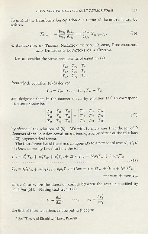
P IE Z O E L E C T R IC C R Y S T A L S I N T E N S O R FORM 103
In general the transformation equation of a tensor of the nth rank can be written
X'kl. ■*ndxk!, dxk:, _ _ _ dxk’ndXji O.X'j 2 dXjn
(76)
4 . A p p l ic a t io n o f T e n s o r N o t a t io n t o t h e E l a s t ic , P ie z o e l e c t r ic a n d D ie l e c t r ic E q u a t io n s o f a C r y s t a l
Let us consider the stress components of equation (7)
« Txy Txz Vi Tyy Tyz
T zx T zy T 1Z
from which equation (8) is derived
TItJ = Tvx ; Txz = T xx ; Tyz = T xy
and designate them in the manner shown by equation (77) to correspond with tensor notations
(77)
by virtue of the relations of (8). We wish to show now that the set of 9 elements of the equation constitutes a tensor, and by virtue of the relations of (8) a symmetrical tensor.
The transformation of the stress components to a new set of axes x’, y ' , s' has been shown by Love4 to take the form
T n Tn Tn Tn Tn TnTn T-n t ,3 = Tn T22 T ;3
Tn Tn T33 T 13 T‘l3 T33
T'xx = t \ Txx + mlTlrj + n \Tzz + 2ltfiyTxy + 2¿nuT„ + 2nm{Ty(78)
Txy = (lC,Txx+ m1m2Ty,J + ihn,Tzx+ ((pth + (pni)Txy + (Coh + (°Jh)Txz
-)- (inph "f- >hf>te)Tyz
where A to n3 are the direction cosines between the axes as specified by equation (61), Noting that from (72)
(i =dx[ n3 =
dx3dxi ’ ’ d.t'3
the first of these equations can be put in the form
4 See “Theory of E lasticity ,” Love, Page 80.
104 B E L L S Y S T E M T E C H N I C A L J O U R N A L
, / dx'A dxi dx( TT n - \ a ï j 11 T
m
i dx\ dx\ —12 "r T— T— i 13
G .Ti U.X*3
a.ri" r — — i 2i - r ox 2 o£i
dæi d.ri d.%*i ¿teí1 22 T * A — T — 1 23 — T — T — 1 k (
O X 2 O X 3 OXic u X ¿( 79)
, ¿teí <toi , d.ri d.ri ,+ T — 3 — 7 31 + T — T 32 +
C/.V3 O .T i 0 .T3 O.To (ëJwhile the last equation takes the form
, dxi dx2 , dxi dx2 , dxi dx24 12 = -r— T— 4 11 T -r— -r— 4 12 -r T— 7— 4 13dxi 0X1 0X1 ox2 dxi 0 .V3
. dxi dxi ~ . dx[ dxi , dxi dxi dxi dxi+ V~ T— Í 21 + r— r— 4 22 T 3— T— 4 23 — r— 3— 4dx2 ox i 0x2 0.T2 0x2 0X3 ox* dx¿
. dx[ dxi . dxi dxi ~ i 3xi dxi ™"T T— 4 31 -+• V~ T— 4 32 "T -5— T— 4 33 •dx3 dxi dx3 d.x2 dx3 dx3
(80)
The general expression for any component then is
dx'i dXj ™4 a = r— r— 4 */ dx* dx;(81)
which is the transformation equation of a tensor of the second rank. Hence the stress components satisfy the conditions for a second rank tensor.
The strain components
5« Sxy SxxSyx Syy SyzSzx Sxy Szx
do not however satisfy the conditions for a second rank tensor. This is shown by the transformation of strain components to a new set of axes, which have been shown by Love to satisfy the equations
Sxx 1 S XX i lSyy “b IIlS ZZ T ( \)il l.S r-y T" f j t lSzx I MlitlSjjz
Sxy — 2( 1(2Sxx T 2 » l \1 > l« S n y T 2)1 \ t l 2SZ Z T (fifth (2l>ll)Sxy
+ (fill2 + lll(2)Sxx + (ftl 1«2 + f>h!ll)Sxy .
P IE Z O E L E C T R IC C R Y S T A L S I N T E N S O R FORM 105
If, however, we take the strain components as
(83)
1 ( dl + d. A2 \d y d z j
the nine components
¿11 ¿12 ¿13
¿ 2 1 ¿ 2 2 ¿ 2 3
¿ 3 1 ¿ 3 2 ¿ 3 3
(83)
will form a tensor of the second rank, as can be shown by the transformation equations of (82).
The generalized Hooke’s law given by equation (22) becomes
djkC is a fourth rank tensor. The right hand side of the equation being the product of a fourth rank tensor by a second rank tensor is a sixth rank tensor, but since it has been contracted twice by having k and I in both terms the resultant of the right hand side is a second rank tensor. Since Ci,k( ’s a tensor of the fourth rank it will, in general, have 81 terms, but on account of the symmetry of the T tj and Ski tensors, there are many equivalences between the resulting elastic constants. These equivalences can be determined by expanding the terms of (84) and comparing with the equivalent expressions of (22). For example
Comparing this equation with the first of (22) noting that ¿12 — ¿21 —
1 a — Cijk(Sic( (84)
T 1 1 = C m i ¿ i 2 + C n i 2 ¿ i 2 + C n i 3 ¿ i3
“f " C ll2 1 ¿2 1 4 " C ll2 2 ¿ 2 2 4 “ C ll2 3 ¿2 3
+ C ll3 1 ¿3 1 + C ll3 2 ¿ 3 2 4 ~ C l l3 3 ¿ 33 .
(85)
, etc., we have
C xni — Cu ; Cm2 — C1121 — C10 I C1133 - C13 c u i 3 — c im — C15 ;(86)
C1122 — C12 ; C1123 — C1132 — Cu •
(87)
In a similar manner it can be shown that the elastic constants of (22) correspond to the tensor elastic constants c ,•¡k( according to the relations
C11 = C l l l l ; C12 = C l l22 = ¿2211 i C l3 = C' 133 = C 3 3 n i C l4 = C l123 = Cl132 =
C2311 = C3211; C15 = C1113 = C1131 - C1311 = C3111 ; C i6 = c m 2 = C1121 = C 1211 =
C'2 151 ‘ C22 ~ C‘2222 j C23 = C2233 = C3322 j £24 = £2223 = £2232 = £2322 = £3222 J
C2 5 — £2213 = £2231 = £1322 = £3122 ! £26 = £2212 = £2221 = C]222 = C2122 ! C33 =
C3333; C34 = C3323 = C3332 = C2333 ~ C3233; C35 = 3313 = C3331 = C1333 = C3133;
C36 = C3 3 1 2 = C3321 = C1 2 3 3 = C2 1 3 3 ; cm = C2 3 2 3 = c i 332 = C3223 — C3 2 3 2 ; C45 =
£2313 = £2331 = C32 I3 — £3231 = 1323 = 1332 = C3 I32 — £3123 ; £46 = C l312 =
C2321 = C3212 = C3221 = C1223 = C1232 — C2123 = C2 1 3 2 ; C55 = C1313 = C1331 =
C3113 = C313 1; c50 = C1312 = C1321 = C3112 = C3121 = C1213 = C1231 = C2113 =
£2131 ; C66 — C1212 = C12 2 I = £2112 = £»121 •
Hence there are only 21 independent constants of the 81 a ]k( constantswhich are determined from the ordinarily elastic constants c,-/ by replacing
1 by 11; 2 by 22; 3 by 33; 4 by 23; 5 by 13; 6 by 12 (88)
and taking all possible permutations of these constants by interchangingthem in pairs.
The inverse elastic equations (26) can be written in the simplified form
S a = Sijk(Tk( . (89^
By expanding these equations and comparing with equations (26) we can establish the relationships
_ _ _ _ _ J 14 _i l l — i l l l l ; i l 2 — i l l 2 2 — i2 2 U ; i l 3 — S1133 — ^3311 j ~ i l l 2 3 _ i l l 3 2 — ^2311 =
i l 5 _ _ _ _ i l 6i3211 ~2 ~ i l l 13 ~ i l l 3 1 — il3 1 1 — i3111 J ~2 ~ i l l l 2 — i l l 2 1 — i l2 1 1 — i2 1 U
_________________ __ i2 4 i2 5i» 2 — i2222 J i2 3 — i 2 ’33 — i3322 ~ — i2223 — i2232 ~ i2322 — i3222 "V =
(90 A)_ _ _ 523 _ _
i2213 — i2231 — il3 2 2 — i3122 ; J ~ S2212 — i2221 — i l2 2 2 — i2122 ; i3 3 = i3333
i3 4 __ __ __ __ i3 E __ i3 6~2 — i3323 — i3332 — i2333 — i3233 ~ i3313 — i3331 — il3 3 3 — i3133 ^ =
106 B E L L S Y S T E M TE C II N I C A L J O U R N A L
P IE Z O E L E C T R IC C R Y S T A L S I N T E N S O R FORM 107
(90 B)* 2 1 2 — * 2 2 1 — * 2 2 3 — -S'12.12 — * 1 2 3 — * 1 3 2 V ~ * 1 1 3 — -*331 — * 1 1 34
*G _ *212 — *221 — *112 = *121 •4
Here again the Si,kl elastic constants are determined from the ordinary elastic constants s<j by replacing
However for any number 4, 5, or 6 the elastic compliance has to be divided by two to equal the corresponding s ,•,■*£ compliance, and if 4, 5 or 6 occurs twice, the divisor has to be 4.
The isothermal elastic compliance of equations (39) can be expressed in tensor form
where as before « ¡ ; is a tensor of the second rank having the relations to the ordinary coefficients of expansion
By eliminating dQ from (92) and substituting in (91) the adiabatic constants are given in the simple form
The combination elastic and piezoelectric equations (60) can be written in the tensor form
1 by 11, 2 by 22, 3 by 33, 4 by 23, 5 by 13, 6 by 12.
S a = s^jkl T kC + a a dQ (91)
«i = «a ; «2 = a 22 ; «3 = «33 ;«i2 0123 ’
« 5J = « . 3 ;
The heat temperature equation of (35) is written in the simple form
< / ( ? = + otkC TkC 0 + pC p dQ. (92)
•J oStjkC — SijkC
CtjjCLkl 9pCp (93)
TS i i = slkCTkC + dmijEm ; on = ™ Em + dnk( T k(. (94)
10S B E L L S Y S T E M TE C H N I C A L JO U R N A L
Here dmi,- is a tensor of third rank and ej,„ one of second rank. The dm,•, constants are related to the eighteen ordinary constants d a by the equations
in — dm | dr> — dm ; dn — dm ; — dm — r/132 ; dm — dm
dm — dm ; dnd-21
i/222; i/23 — i/233; — — i/223 — i/232;
— i/213 — i/231 ; — i/212 — i/221; i/31 — i/311 ; i/32 — i/322; i/33 — dm(95)
i /3 4 _ ,~2----- “323 i/332; — i/313 — i/331; — i/312 — i/321 •
The tensor equations (94) give a simple method of expressing the piezoelectric equations in an alternate form which is useful for some purposes. This involves relating the stress, strain, and displacement, rather than the applied field strength as in (91). To do this let us multiply through the right hand equation of (94) by the tensor 4ir/3m„ , obtaining
4 7 t5 „ - ,1 5 ti t m n @ m n E m ~f" A i r ( I ri f: C (dm n d k t (96)
where /3m n is a tenror of the “free” dielectric impermeability obtained from the determinant.
3tJ m n
whe: c A* is the determ inan t
__j y m + n)
A 7 -
T 1 T¿11 ¿12 ¿13
r T T¿ 12 ¿ 22 ¿23
T T r¿13 ¿23 ¿33
(97)
(98)
and A t h e minor obtained from this by suppressing the »2th row and «th column. If we take the product ej,„ 0m„ for the three values of m, we have as multipliers of E \ , E2, £ 3 , respectively
T oT I T oT 1 T oT 1¿ 1 1 p i l + ¿1 2 P 12 + ¿13 P 1 3 — 1
T q T I T 0 T I T 0 T 1¿21 P21 i - ¿22 P22 I" ¿23 P23 — 1T o T , T o T I T a T 1¿31 P31 T" ¿32 P32 "T ¿33 P33 — 1*
(99)
But by virtue of equations (97) and (98) it is obvious that the value of each term of (99) is unity. Hence we have
Em = iTTjSmn S„ — (4tT d nkC Pmn) T k( . (100)
P IE Z O E L E C T R IC C R Y S T A L S I N T E N S O R FORM 109
Since the dummy index 11 is summed for the values 1, 2, and 3, we can set the value of the terms in brackets equal to
gmkt = 4:7r dnkl ftmn = ^v[d\kt fimi + (hkl fiml + d$kt (101)
and equation (100) becomes
Em = 47r /jJ,„ 8„ — gmkt Tkt ■ (102)
Substituting this equation in the first equations of (94) we have
S i , = s'ijkt T k( + gnii <5n (103)where
Sijkt Sijkt dmi j gmkt S ijkt 47r[finm dnkt dmi ;] ■
By substituting in the various values of i , j , ¿ and C corresponding to the 21 elastic constants, the difference between the constant displacement and constant potential elastic constants can be calculated. If equations (102) and (103) are expressed in terms of the S\,- ■ ■, S$ strains and Ti,- ■ ■, Tt> stresses, the g„ a constants are related to the gi, constants as are the corresponding dij constants to the constants of equation (95).
Another variation of the piezoelectric equations which is sometimes employed is one for which the stresses are expressed in terms of the strainsand field strength. This form can be derived directly^ from equations (94)by multiplying both sides of the first equation by the tensor cfyjtf for the elastic constants, where these are defined in terms of the corresponding Sij elastic compliances by the equation
Cij — (—l ) (,+i) A 'f/A '* (104)
where A is the determinantE
$ 1 1E
$ 1 2E
$13E
$14E
$1 5E
$1 6
E$ 1 2
E$ 2 2
E$23
E$24
E$25
E$ 2 6
E$13
E$23
E$33
E$34
E$35
E$ 3 6
E$14
E$24
E$34
E$44
E$45
E$ 4 6
E$15
E$25
E$35
E$45
E$55
E$56
E$16
E$2 6
E$36
E$46 $5 6
E$ 6 6
and A;,- in the minor obtained by suppressing the fth row and j th column. Carrying out the tensor multiplication we have
C i j k t S { j C i j k t S i j k t 1 k t 4 “ d m i j C j j k t E m . (105)
110 B E L L S Y S T E M T E C H N I C A L J O U R N A L
As before we find that the tensor product of cfjU s ^ u is unity for all values of k and I. Hence equation (105) can be written in the form
summed for all values of the dummy indices i and j . If we substitute the equation (106) in the last equation of (94) we find
where the clamped dielectric constant is related to the free dielectric constant by the equation
Expressed in two index piezoelectric constants involving the strains Sn • • • 5i2 and stresses Tn ■ ■ - Tn the relation between the two and three index piezoelectric constants is given by the equation
Cii = eni ; Ci2 = 6122 ; 613 = £m ; C ii = Cm = Cm ; 615 — C113 — £m ;
Ci6 — eii2 = £ m ; cai = 6211 ; 622 = 6222; 623 = 6233 ; £24 = e223 = 6232 ;
e25 — 6213 — 6231; £26 — 6212 — £221; £31 — 6311; £32 — 6322; 633 — 6333;
£31 — 6323 = 6332; 635 = 6313 = 6331; 636 = e3i2: 6321 •
Finally, the fourth form for expressing the piezoelectric relation is the one given by equation (53). Expressed in tensor form, these equations become
In this equation the three index piezoelectric constants of equation (111) are related to the two index constants of equation (53) as the e constants of (110). These equations can also be derived directly from (106) and (108) by eliminating E m from the two equations. This substitution yields the additional relations
l l n k t 47TGmkC @ m n , £ t j k C C i j k C “ 1” G m k t l l m i j 6 i j k t
T U — C i j k t S i j C m kt E m (106)
where e„,u is the sum
(107)
(108)
Gmn k m n 47T \ d nkC & m k Í \ ’ (109)
(110)
T u — CijU S i j — linkt S„ ; E m = Airßm „ 5 n — hmij S ¡ ¡ ( 111)
~f~ 47T 6m k ( G n i j ß f n n
(112)
where
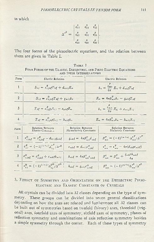
P IE Z O E L E C T R IC C R Y S T A L S I N T E N S O R FORM 111
in whichs .S s
Cll 612 €13s •S' S
€12 622 €23s s S
€13 €23 633
The four forms of the piezoelectric equations, and the relation between them are given in Table I.
T a b l e IF o u r F orm s o f t h e E l a s t ic , D ie l e c t r ic , a n d P ie z o E l e c t r ic E q u a t io n s
AND THEIR INTERRELATIONS
Form Elastic Relation Electric Relation
1 Sij = j fy i /F k ( + dmiiE mT
= ^ 7 E„ + d„ tiTk(
2 Sij ~ S{j kf.Tk¿ 4" gnij5n E>m ~ 7rftmnOn gmklTkf,
3jf
= C i j ( k S i j Cmk(EmS
Em + e„ ijS ij
1 „ j T k (y — C i j k ( , S \ j hn k f f in Em = 47r/3')n„5„ — hmiiSij
Form Relation Between Elastic Conjlau.j
Relation Between Piezoelectric Constants
Relation Between Dielectric Constants
1 S °iik ( = s f ,k ( - d m i j g m k l gmkC = ^ U n k l &T = ( - 1 ) < ’" + » > A ' T/ A <rmn x ' m n'
2 cf . = ( —1 )< ^ > A”'V a*b V m k t ~ d m i j c P k £ es = eT — 4rir(dnkfemkf)mn mn v ,iKi
3 Ci ik f . = Cijk r . + e ’nk/.hm i i hnkl = * r t smnemkf oS _ o T | g n k fM m k t mn rmn 4 v
4 <?,■ = ( - l ) ( i+ i)A ^ /A sC <KkC = gnijC ^kl /3® n = ( - l ) ( " +n) A ^ /A ,S
5. E f f e c t o f S y m m e t r y a n d O r ie n t a t io n o n t h e D ie l e c t r ic P ie z o e l e c t r ic a n d E l a s t ic C o n s t a n t s o f C r y s t a l s
All crystals can be divided into 32 classes depending on the type of symmetry. These groups can be divided into seven general classifications depending on how the axes are related and furthermore all 32 classes can be built out of symmetries based on twofold (binary) axes, threefold (trigonal) axes, fourfold axes of symmetry, sixfold axes of symmetry, planes of reflection symmetry and combinations of axis reflection symmetry besides a simple symmetry through the center. Each of these types of symmetry
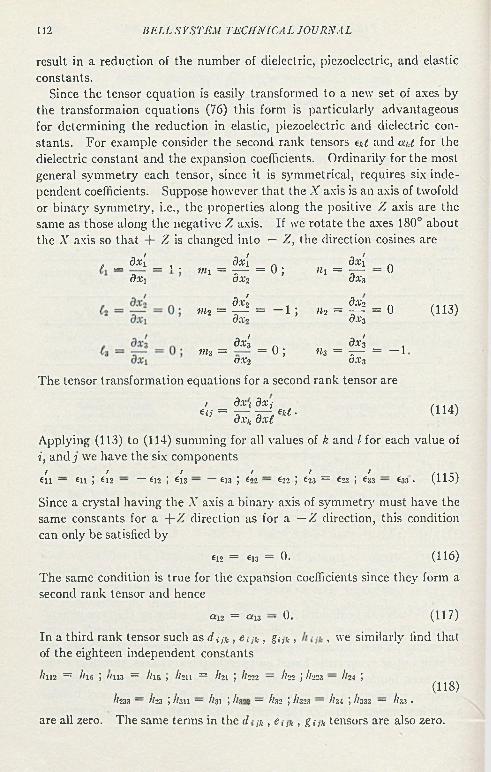
112 B E L L S Y S T E M T E C H N IC A L J O U R N A L
result in a reduction of the number of dielectric, piezoelectric, and elastic constants.
Since the tensor equation is easily transformed to a new set of axes by the transformaion equations (76) this form is particularly advantageous for determining the reduction in elastic, piezoelectric and dielectric constants. For example consider the second rank tensors ek( and a u for the dielectric constant and the expansion coefficients. Ordinarily for the most general symmetry each tensor, since it is symmetrical, requires six independent coefficients. Suppose however that the X axis is an axis of twofold or binary symmetry, i.e., the properties along the positive Z axis are the same as those along the negative Z axis. If we rotate the axes 180° about the X axis so that + Z is changed into — Z, the direction cosines are
(113)
/ _ dx't _ 1. dx\
dx'i mi = -T— OX 2
= 0 ;dx[« 1 = —dx3
= 0
dx'i m2 = -r—dxn = - 1 ;
dx2 «2 = —_ 3.r3
= 0
dx '3m3 =ox 2
= 0 ; dx '3 th = t — OX 3 = - 1
The tensor transformation equations for a second rank tensor are
/ dx i dxj / . ,U i = ~ T J.ik ( . (114)dXh dx(.
Applying (113) to (114) summing for all values of k and I for each value of i, and j we have the six components
/ / / / / / / . . . >
«11 — «u ; «12 — — « 1 2 ; « is — — « i s ; «22 — « 2 2 ; «23 — « 2 3 ; «33 — «33 • ft 10 ,)
Since a crystal having the X axis a binary axis of symmetry must have the same constants for a + Z direction as for a — Z direction, this condition can only be satisfied by
«12 = «13 = 0- (116)The same condition is true for the expansion coefficients since they form a second rank tensor and hence
ai2 = «*13 - 0. (117)
In a third rank tensor such as d ,■ ¿k , e , ,x , g,-,* , , we similarly find thatof the eighteen independent constants
h m = A 16 ; « 1 1 3 = h 15 > h m = I1 2 1 ; I h i 2 — I h 2 ; h m — ! h \ ;
(118)/í233 — h'iz ; //311 — A31 ; //302 — hyi ] I1323 — It34 ; 7/333 — h:a •
are all zero. The same terms in the d¡k , e , ,k , g ¿ ,k tensors are also zero.
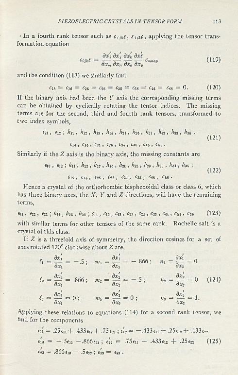
P IE Z O E L E C T R IC C R Y S T A L S I N T E N S O R FORM 113
» In a fou rth ran k tensor such as c ; , Sijkt, app ly ing th e tensor tra n sfo rm ation equation
(1 1 9 )<5.rm dxn dx„ dxp
and the condition (113) we sim ilarly find
Cl5 = Cl6 — C26 = ~ C35 = C36 = C45 == Cl6 = 0. (120)
If the b inary axis h a d been th e Y axis th e corresponding m issing term scan be ob ta ined by cyclically ro ta tin g th e tensor indices. T h e m issing term s are for th e second, th ird an d fo u rth ran k tensors, transfo rm ed to tw o index sym bols,
«2 3 , « 1 2 ; h 1 1 , h 1 2 , h a , h u , I12 1 , ¡ha , I131 , h32 , I133, lh&;(121)
Cl4 , C l6 , C24 , C26 , C34 , C36 , C45 , C55 .
Sim ilarly if th e Z axis is th e b inary axis, th e m issing constan ts are
« 1 3 , «12 ; h 1 1 , h\2 , h \3 , / / i e , It2 1 , I122, I123 , h2 6 , I13 1 , I133 >( 122)
Cl4 , C15 , C24 , C26 , C34 , C35 , C46 , C 56 .
lie n e e a crysta l of th e orthorhom bic b isphenoidal class or class 6 , which has th ree b in a ry axes, th e X , Y a n d Z directions, will have th e rem aining term s,
«11 ) «22 , «33 ; llu , h25 ) ^36 ; Cu , Cl2 , C13 , C22 , C23 , C33 , C44 , C55 , C66 (123)
w ith sim ilar term s for o ther tensors of th e sam e rank . R ochelle sa lt is a crysta l of th is class.
If Z is a threefold axis of sym m etry , the d irection cosines fo r a se t of axes ro ta te d 120° clockwise abou t Z are,
(124)
A pplying these rela tions to equations (114) for a second ran k tensor, we find for th e com ponents
cu = .25«ii -)- .433 «12 “k .”5 £22 ; «12 = — .433 «n -f- .25 £12 4* .433 £22
«13 - —*5 £i3 —.8 6 6 £23 j £22 ■ .75€11 — .433£12 T* -25€22 (125)
«23 = .8 6 6 «13 — .5 «23 J «33 = «33 ■
f _ d x 'l
1 .5 ; V l \ =dx[dxt
= - . 8 6 6 ;dx[
= — - = 0
f d.Vn C 2 — —
O X 1= .8 6 6 ; « ¡ 2 =
dx'2S X 2
= .5 jdx'2
« 2 = r —dx3
= 0
/ d a -3c3 — —
O X 1= 0 ; D h =
dx'3dx2
= 0 ;dx'3
« 3 = i p - O X 3
= 1
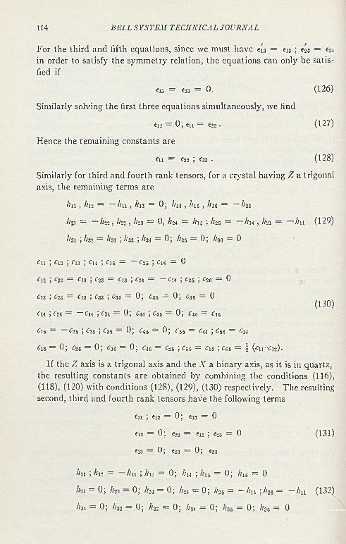
F o r th e th ird an d fifth equations, since we m ust h av e «13 = «13 ; «23 =in o rder to satisfy th e sym m etry rela tion , th e equa tions can only be s a tis fied if
«13 = «23 = 0. (126)
Sim ilarly solving the first th ree equations sim ultaneously , we find
«12 = 0; «u = «22 • (127)
H ence the rem ain ing co n s tan ts are
€ 11 — «22 ; «33 • (128)
Sim ilarly fo r th ird an d fo u rth ran k tensors, for a crysta l hav ing Z a trigonal axis, th e rem ain ing te rm s are
/ i n , A12 — — / i n , /113 = 0 ; Z / i4 , 7 /is 1 7/ig — —/122
7/21 = —7/22 J 7/22 ) 7/23 = 0, ¿24 = 7/l5 ; 7/25 = 7/14 , 7/21 — /ill (129)
/13 1 ; 7/32 = 7/3i ; /133 ; h n = 0 ; /13 5 = 0 ; /130 = 0
C1 1 ; C12 ; C13 ; cu ; C15 = —C2 5 ; cm = 0
C12 1 «-22 = Cu ; C23 = C13 ; C24 = C14 ; C2 5 ; C26 = 0
C13 ; C23 = C13 ; C33 ; C34 = 0; C35 = 0 ; C36 = 0
C14 ; C24 = — C14 ;c 34 = 0; C44 ; C45 = 0; c4e = c 15
Ci5 = c25 ; C25 ; C35 = 0 ; C45 = 0 ; c55 = C44 ; Cse = Cu
Ci6 = 0; C26 = 0; C36 = 0; C4e = C25 ; C55 = cu ; Coe = i (cn-ci«).
I f th e Z axis is a trigonal axis an d th e -Y a binary' axis, as it is in quartz , th e resulting co n stan ts a re ob ta ined by' com bining th e conditions (116), (118), (120) w ith conditions (128), (129), (130) respectively . T h e resulting second, th ird an d fo u rth ran k tensors have th e following term s
« 1 1 ; «12 = 0; «13 = 0
«12 = 0; £22 = «11 ; «23 = 0 (131)
613 = 0; «23 = 0; £33
/in ; 7/i2 = /in ; 7/i3 = 0; 7/14 ; = 0 ; /lie = 0
7/ai = 0; 7/22 — 0; /123 = 0; 7/24 = 0; / /25 = —hu ; 7/2g = — /in (132)
7/ 3 i = 0 ; /132 = 0 ; /133 = 0 ; / / 34 = 0 ; = 0 ; 7/36 = 0
114 B E L L S Y S T E M T E C H N I C A L J O U R N A L
(130)
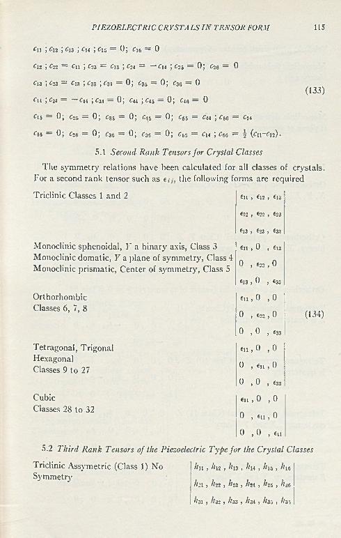
P IE Z O E L E C T R IC C R Y S T A L S I N T E N S O R FORM 115
(133)
cn ; Cn ; C1 3 ; cu ; C15 = 0 ; cic = 0
C12 ; C22 = Cu ; C23 = c 13 ; C24 = —C14 ; C25 = 0 ; C26 — 0
C13 ; C23 = C13 ; C33 ; C31 = 0 ; C35 = 0 ; C30 = 0
C14 ; C24 = —C14 ; C34 = 0 ; C44 ; C45 = 0 ; C46 — 0
C15 = 0 ; C25 = 0 ; C35 = 0 ; C45 = 0 ; Cs5 = C44 ; £50 = C14
Ci6 — 0 ; C26 = 0 ; C35 = 0 ; C30 = 0 ; C53 = cu ; ¿66 = (cii-ci2)-
5.1 Second Rank Tensors for Crystal Classes
The symmetry relations have been calculated for all classes of crystals. For a second rank tensor such as the following forms arc required
Triclinic Classes 1 and 2 en , «12 , «13
€12 , *22 , *23
*13 , *23 , *33
*11 , 0 , €13
0 , *22 , 0
*13 j 0 ,633
*11 , 0 , 0
0 , *22, 0 (134)
0 , 0 , €33
*u, 0 , 0
0 , *n , 0
0 ,0 , *33
* 1 1 , 0 , 0
0 , en , 0
0 , 0 , 6)1
5.2 Third Rank Tensors of the Piezoelectric Type for the Crystal Classes
Monoclinic sphenoidal, Y a binary axis, Class 3 Monoclinic domatic, Y a plane of symmetry, Class 4 Monoclinic prismatic, Center of symmetry, Class 5
Orthorhombic Classes 6 , 7, 8
Tetragonal, Trigonal Hexagonal Classes 9 to 27
CubicClasses 28 to 32
Triclinic Assymetric (Class 1 ) No Symmetry
hw , //12, h \ z , //14, h \z , h i6
h21 , //22 , 7*23 , 7/24 , /?2S , h i6
h31 , hi2 , Il33 , 7/34 , 7/35 , 7/33
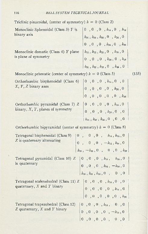
Triclinic pinacoidal, (center of symmetry) h = 0 (Class 2)
0 ,0 ,0 , //u , 0 , //16
Ihl , U22 , It23 , 0 , /?25 , 0
0 ,0 ,0 , //34 , 0 , 7/36
/in , 7/i2, 7/i3, 0 , 7/ie, 0
0 ,0 ,0 , 7/24 j 0 , 7/26
7/31 , 7/32 , 7/33 , 0 , 7/36 , 0
Monoclinic prismatic (center of symmetry) 7/ = 0 (Class 5)
0 ,0 ,0 ,7/14,0 ,0
0 ,0 ,0 ,0 ,7/25 j
0 ,0 ,0 ,0 ,0 ,7/36
0 ,0 ,0 ,0 ,7/15, o
0 ,0 ,0 ,7/24, 0 , 0
7/31 , 7/32 , 7/33 J C ,0 ,0
Orthorhombic bipyramidal (center of symmetry) h — 0 (Class 8)
0 , 0 , 0 , 7/i4,7/16 > 0
116 B E L L S Y S T E M T E C IIN IC A L JO U R S7A L
Monoclinic Sphenoidal (Class 3) Y is binary axis
Monoclinic domatic (Class 4) Y plane is plane of symmetry
Orthorhombic bisphenoidal (Class 6) X, Y, Z binary axes
Orthorhombic pyramidal (Class 7) Z binar}', Ar, Y, planes of symmetry
Tetragonal bisphenoidal (Class 9) Z is quaternary' alternating
Tetragonal pyramidal (Class 10) Z is quaternary
Tetragonal scalenohedral (Class 11) Z quaternary, X and Y binary
Tetragonal trapezohedral (Class 12) Z quaternary, X and Y binary'
0 , 0 , 0 , — 7 / 1 6 , Itu , 0
7/31 , — 7/31 , 0 , 0 , 0 , 7/36
0 , 0 , 0 , 7 / i 4 , 7 / i s , 0
0 , 0 , 0 , 7 / i 6 , — 7 / i 4 , 0
7 / 3 i , 7 t 3 i , Ä3 3 , 0 , 0 , 0
0 , 0 , 0 , 7 / 1 4 , 0 , 0
0 ,0 ,0 ,0 , 7 / 1 4 , 0
0 ,0 ,0 ,0 ,0 , //so
0 ,0 ,0 , 7 /1 4 , 0 ,0
0 ,0 ,0 ,0 , —7 /1 4 , 0
0 ,0 ,0 ,0 , 0 ,0
(135)
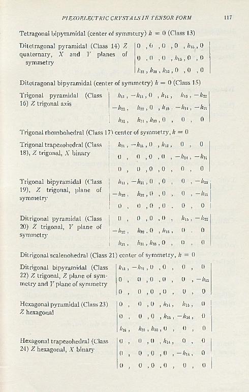
P IE Z O E L E C T R IC C R Y S T A L S I N T E N S O R FORM
Tetragonal bipyramidal (center of symmtery) A = 0 (Class 13)
0 ,0 ,0 ,0 , Al5 ,0
0 . 0 , 0 ,7/15,0 , 0
/■'31 j /hi , 7/33 , 0 , 0 , 0
Ditetragonal bipyramidal (center of symmetry) A = 0 (Class 15)
Ditetragonal pyramidal (Class 14) Z quaternary, X and T planes of
symmetry
Trigonal pyramidal (Class An, ■-An , 0 , Itu , 7/16 — A 2216) Z trigonal axis
A22, A22 , 0 , A i5 An —An
A;u , 7/31 , A33 , 0 , 0 0
Trigonal rhombohedral (Class 17) center of symmetry, A = 0
Trigonal trapezohedral (Class An, --An , 0 , Au , 0 018), Z trigonal, X binary
0 , 0 , 0 , 0 -A h — An
0 , 0 , 0 , 0 , 0 0
Trigonal bipyramidal (Class An, -An , 0 , 0 , 0 — A2219), Z trigonal, plane of //•> 0 . A22 , 0 , 0 , 0 —Ansymmetry
0 , 0 , 0 , 0 , 0 0
Ditrigonal pyramidal (Class 0 , 0 , 0 , 0 , //is — A2220) Z trigonal, Y plane of //oo . A 22 , 0 , 7/15 , 0 0symmetry
Ihi , A3 1 , A33 , 0 , 0 0
Ditrigonal scalenohedral (Class 21) center of symmetry, A = 0
Ditrigonal bipyramidal (Class An , -An , 0 , 0 , 0 . 022) Z trigonal, Z plane of sym n 0 0 0 () , —Anmetry and Y plane of symmetry u 1 J J ,
0 , 0 , 0 , 0 , 0 , 0
Hexagonal pyramidal (Class 23) 0 , 0 , 0 , An , 7/15 , 0Z hexagonal
0 , 0 , 0 , Ais , — Al4 , 0
7/31 > 7/31 , A33 , 0 , 0 , 0
Hexagonal trapezohedral (Class 0 , 0 , 0 , Ah , 0 , 024) Z hexagonal, X binary
0 , 0 , 0 , 0 , —Ah , 0
0 , 0 . 0 , 0 , 0 , 0
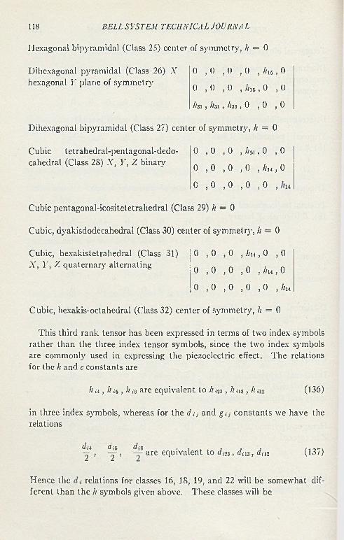
Hexagonal bipyramidal (Class 25) center of symmetry, h = 0
118 B E L L S Y S T E M T E C H N I C A L J O U R N A L
Dihexagonal pyramidal (Class 26) .Y hexagonal Y plane of symmetry
0 , 0 , 0 , 0 , //,5 , 0
0 , 0 , 0 , / / 1 5 ,0 , 0
h 31 , I hi , It 33 , 0 , 0 , 0
Dihexagonal bipyramidal (Class 27) center of symmetry, h = 0
Cubic tetrahedral-pentagonal-dedo- cahedral (Class 28) X, Y, Z binary'
0 ,0 ,0 , / / u , 0 , 0
0 , 0 , 0 , 0 , h n , 0
C , 0 , 0 , 0 , 0 ,
Cubic pentagonal-icositetetrahedral (Class 29) h — 0
Cubic, dyakisdodecahedral (Class 30) center of symmetry, h — 0
Cubic, hexakistetrahedral (Class 31) X , F, Z quaternary alternating
0 ,0 ,0 , //i4, 0 ,0
0 ,0 ,0 ,0 . //h , 0
0 ,0 ,0 ,0 ,0 , / im
Cubic, hexakis-octahedral (Class 32) center of symmetry, /; = 0
This third rank tensor has been expressed in terms of two index symbols rather than the three index tensor symbols, since the two index syunbols are commonly' used in expressing the piezoelectric effect. The relations for the h and c constants are
h ,m , h i&, h it are equivalent to h i23, h a s , hi (136)
in three index symbols, whereas for the d¡,- and g constants we have the relations
d \ 4 (t,'5
I ’ T ’<7i6 are equivalent to d, ^ , d m , d,vl (137)
Hence the relations for classes 16, 18, 19, and 22 will be somewhat different than the h sy-mbols given above. These classes will be
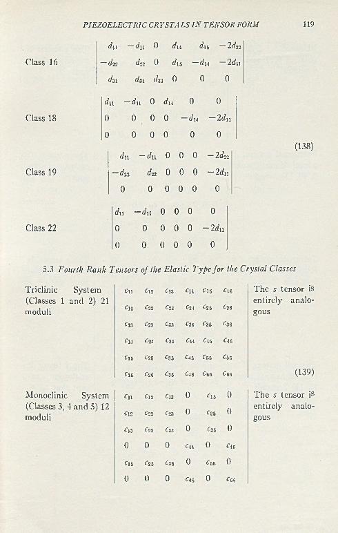
P IE Z O E L E C T R IC C R Y S T A L S I N T E N S O R FORM 119
Class 16
Class 22
d\\ —du 6 du d ] 5 2dn
— i/22 d'2'2 0 i / l f, — i / ] ! 2 i / U
i/31 i/31 i/33 0 0 6
i/11 - d u 0 d u 0 0
Class 18 0 0 0 0 d u — 2¿n
0 0 0 0 0 0
d a - d u 0 0 0 — 2¿22
Class 19 í/22 i/22 0 0 0 — 2 d n
0 0 0 0 0 0
i/ 1 1 — i / n 0 0 0 0
0 0 0 0 0 - 2dn
0 0 0 0 0 0
(138)
5.3 Fourth Rank Tensors of the Elastic Type for the Crystal Classes
Triclinic System (Classes 1 and 2) 21 moduli
Monoclinic System (Classes 3, 4 and 5) 12 moduli
C il C12 C13 C u C 15 Cie
C12 C22 C23 C2A C25 C26
Cl3 C23 C33 ¿34 C35 C36
Cl4 C 24 C34 C44 C45 C46
Cl5 ¿25 C35 C45 C55 C50
Cl6 C26 C36 C46 C06 Ccc
C il C\2 Cl3 0 Cl5 0
Cl2 C22 C23 0 C25 0
Cl3 C2Z C33 0 C35 0
0 0 0 C44 0 ClO
C15 C25 C36 0 C 55 0
0 0 0 C46 0 Cg6
The 5 tensor is entirely analogous
(139)
The s tensor is entirely analogous
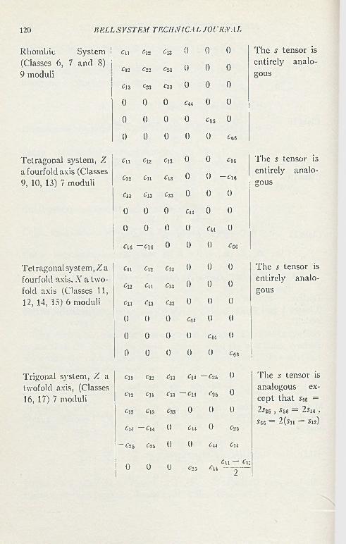
120 B E L L S Y S T E M TE C H N IC A L TO U R N A L
Rhombic System I Cll Cl2 Cl3 0 0 0 The s tensor is(Classes 6, 7 and 8) j 9 moduli Cl2 C22 C23 0 0 0 entirely analo
gousCl3 C23 C33 0 0 0
0 0 0 Cm 0 0
0 0 0 0 C55 0
0 0 0 0 0 Cb 6
Tetragonal system, Z Cll C12 C13 0 0 CIO The s tensor isa fourfold axis (Classes 9, 10, 13) 7 moduli Cl2 Cll Cl3 0 0 ~ ClG
entirely analogous
Cl3 Cl3 C33 0 0 0
0 0 0 Cm 0 0
0 0 0 0 Cm 0
Cl6 — ClG 0 0 0 Coo
Tetragonal system, Z a Cn Cl2 C13 0 0 0 The s tensor isfourfold axis. X a twofold axis (Classes 11, C n Cll Cl3 0 0 0
entirely analogous
12, 14, 15) 6 moduli Cl.'I Cl3 C33 0 0 0
0 0 0 C41 0 0
0 0 0 0 Cm 0
0 Ü 0 0 0 C6G
Trigonal system, Z a cn C12 Cl3 c m — C25 0 The s tensor istwofold axis, (Classes 16, 17) 7 moduli C n Cll C13 — Cm C26 0
analogous except that 546 =
Cl3 Cl3 C33 0 0 0 2$25 , C56 = 2$h •
Cm — Cm 0 Cm 0 C25 i'66 = 2(su — S12)
— C*2& C20 0 0 Cm Cm
0 0 (J C25 CmCu — Cis
2
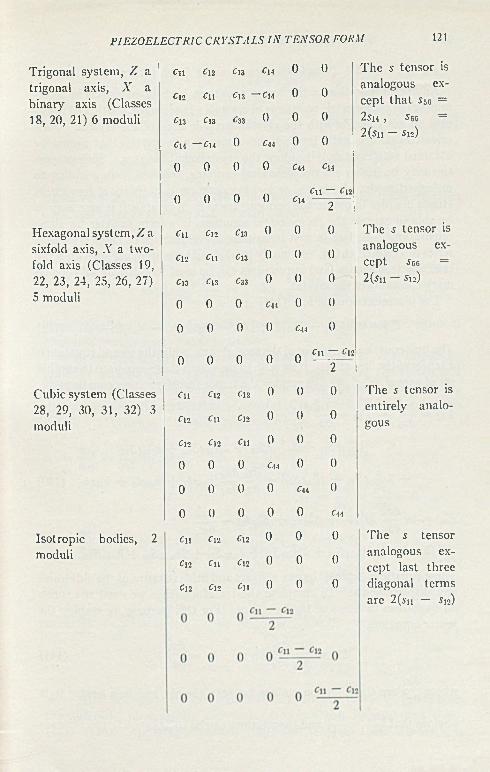
P IE Z O E L E C T R IC C R Y S T A L S I N T E N S O R FORM 121
Trigonal system, Z a Cn ¿12 ¿13 ¿14 0 0trigonal axis, X a binary axis (Classes ¿ 1 2 ¿11 ¿13 •¿14 0 0
18, 20, 21) 6 moduli ¿ 1 3 ¿13 ¿33 0 0 0
¿14 ~ - ¿ 1 4 0 ¿44 0 0
0 0 0 0 ¿44 ¿14
0 0 0 0 ¿14¿11 - ¿12
2
Hexagonal system, Z a ¿ 1 1 C12 ¿13 0 0 0sixfold axis, X a twofold axis (Classes 19, ¿12 C\\ ¿13 0 0 0
22, 23, 24, 25, 26, 27) ¿13 C\3 ¿33 0 0 05 moduli 0 0 0 ¿44 0 0
0 0 0 0 ¿44 0
0 0 0 0 0 ¿11 — ¿12
2
Cubic system (Classes ¿11 ¿12 ¿12 0 0 028, 29, 30, 31, 32) 3 moduli ¿12 ¿11 ¿12 0 0 0
¿12 ¿12 ¿11 0 0 0
0 0 0 ¿44 0 0
0 0 0 0 ¿44 0
0 0 0 0 0 ¿44
Isotropic bodies, 2 ¿11 ¿12 ¿12 0 0 0moduli
¿12 ¿11 ¿12 0 0 0
¿12 ¿12 ¿11 0 0 0
The s tensor is analogous except that S56 = 2 s m , S i 0 =
2(sn — S12)
Tlie 5 tensor is analogous except Son = 2(xn — ¿12)
The s tensor is entirely analogous
The s tensor analogous except last three diagonal terms are 2(sn — Si2)
122 B E L L S Y S T E M T E C H N IC A L J O U R N A L
5.4 Piezoelectric Equations for Rotated Axes
Another application of the tensor equations for rotated axes is in determining the piezoelectric equations of crystals whose length, width, and thickness do not coincide with the crystallographic axes of the crystal. Such oriented cuts are useful for they sometimes give properties that cannot be obtained with crystals lying along the crystallographic axes. Such properties may be higher electromechanical coupling, freedom from coupling to undesired modes of motion, or low temperature coefficients of frequency. Hence in order to obtain the performance of such crystals it is necessary to be able to express the piezoelectric equations in a form suitable for these orientations. In fact in first measuring the properties of these crystals a series of oriented cuts is commonly used since by employing such cuts the resulting frequencies, and impedances can be used to calculate all the primary constants of the crystal.
The piezoelectric equations (111) are
Tkf = c'ijkcSii — hnk(&n ; Em = 47rj3m„5„ — IlmijSij . ( I l l )
The first equation is a tensor of the second rank, while the second equation is a tensor of the first rank. If we wish to transform these equations to another set of axes y ' , s', we can employ the tensor transformation equations
; _ dx'k dx'( _ dxu dxj dxk dXf dxk dx(
• [ciWSn + .S’ 12 + 2ciu(Sa + cliklS^
+ 2c%3kCSw + Cmf-Sw] — -r-- r— VhkCSi + Ihklfa + Ihkl¿>3] (140)uX/c OX(
Em = ilr —A‘ [/3ml 5l + |0'm2 So + /3„3 63] —dxm dxm
• [^m ii*511 4~ 2/;mHSi2 4~ I h m u S u 4 “ hm aSvi - f - 2hmiiS<a - f - l/muSii]-
These equations express the new stresses and fields in terms of the old strains and displacements. To complete the transformation we need to express all quantities in terms of the new axes. For this purpose we employ the tensor equations
dxi dxi , dxn ,S i i = d7 '< ^ S i i ; 5n = o 7 n Sn (1 4 1 )
dxiwhere ~ ? are the direction cosines between the old and new axes. I t is ox i
d x 8 xobvious that ~ = —[ and the relations can be written
a#,- o.t i
P IE Z O E L E C T R IC C R Y S T A L S IN' T E N S O R F ORM 123
f — •dxi dxi ’
ÖX2
Wl = i 5 :
dx3th = 5o\\
daiiA
dxiA = ’ = dxi
d%2 dx2»¡2
= d^i ’m3 = dx3
dx3 dx3«2 = dxi ’ n3
p*. e-sH 1 fOii
(142)
Hence substituting equations (141) in equations (140) the transformation equations between the new and old axes become
/ _ n dxi dx'f dX{ dXj , _ dxk dx( dxn , !.( CukC Qxk Qx¿ dx'i dx'j " mk dxj¡ dX{ dx'n
EL = irß],sdxm dxn / i dxm dxi dXj p/T— I » » " m i j r — X —, -T —, S i j .O X n t O X n dX /H u X i O X j
(143)
These equations then provide means for determining the transformation of constants from one set of axes to another.
As an example let us consider the case of an ADP crystal, vibrating longitudinally with its length along the x[ axis, its width along the xi axis and its thickness along the x% axis, which is also the x3 axis, and determine the elastic, piezoelectric and dielectric constants that apply for this cut when x[ is 9 = 45° from .ti . Under these conditions
, dx[ d*i , dx2 dxiA = = cos 0; A = -7.— — x—> = ~ s in 0;dxi dxi dxi dxi
dx '3 _ dxi (3 — -r— — -r—? — Uox 3
dx[ dXi . dx> dx2 .mx = _ _ = _ = sin 0 ; m2 = cos 6 ,dx2 dxi ox i dx2
, . (144)dx3 dx-2 n m == == = 0dX2 dx3
dx3 dxi " dx¡ dx2dx[ dx3 _ dx2 dx3
»1 = ITT = TD = 0; ,l2 — TT = ~X~> = °i
dx3 dx3 >h = T - = t~ , = 1. dx$ dxz
Since ADP belongs to the orthorhombic bisphenoidal (Class 6), it will have the dielectric, piezoelectric and elastic tensors shown by equations (134), (135), (139). Applying equations (143) and (144) to these tensors it is
124 B E L L S 7 5 T E M TE C H N I C A L J O U R N A L
read ily show n th a t th e stresses for 0 = 45° are given b y the equations expressed in tw o index sym bols
( c f i + C l 2 + 2 c f 6) c r2 i — -----------z----------2
(c fl + C\2 — 2 c f6) c / J _ d 0 / ,,"T" ------------------Z------------------ 0 2 C 1303 — «3603
(cfi + cl 2 — 2cf6) /2 ~ “ 2 5l
, (c fi + cf2 + 2c f6) „ / , D 1 1 (1 4 5 )T ------------ 2------------- 03 03 -f- «36 0 3
T 3 = C13 S i + ClZ Sn + C33.S3
7 4 = c « S \ + hu 52 ; E\ = —/;ik)5 4* 4rir[/3n5i]
r s = cfi Si — hu ¿1 ; £ 2 = huSi + 4ir[/3n5o]
r i = (CU ~ Cl2) ; £3 = -/»*.& - ¿'2I + 4tt[/?33 ¿3].
F o r a long th in longitud inally v ib ra ting cry sta l a ll th e stresses are zero except th e stress T 1 along th e leng th of th e crysta l. H ence it is m ore ad van tageous to use equations w hich express th e stra in s in te rm s of th estresses since all th e stresses can be se t equal to zero except T[ . All the s tra in s are th en d ependen t functions of th e s tra in S i an d th is only has tobe solved for. F urthe rm ore , since p la ted crysta ls are usually used todeterm ine the p roperties of crysta ls, an d th e field perpend icu la r to a p la ted surface is zero, th e only field existing in a th in c rysta l will be £ 3 if th e th ick ness is ta k en along th e x3 or Z axis. H ence th e equations th a t express the stra in s in term s of th e stresses an d fields are m ore advantageous for calculating th e p roperties of longitud inally v ib ra ting crystals. B y orienting such crysta ls w ith respect to th e crysta llographic axis, all of the elastic constan ts except the shear elastic constan ts can be determ ined. All of th e piezoelectric an d dielectric constan ts can be determ ined from m easurem en ts on oriented longitudinally v ib ra tin g crystals.
F or such m easurem ents i t is necessary to determ ine the ap p ro p ria te elastic, piezoelectric, an d dielectric constan ts for a crysta l orien ted in any d irec tion w ith respect to th e crysta llographic axes. W e assum e th a t the length lies along th e a i axis, th e w id th along th e x'> axis an d th e thickness along the x3 axis. S tartin g w ith equations of the form
S i i — SEijk(Tkl + dijmEm
and transforming to a rotated system of axes whose direction cosines are given by (142), the resulting equation becomes
_ k dx'i dx'j d x k d x ( rp' , j àx'i dx'j dx m >S i i SiikC „ - - / - , I kC T" Uijm ~ - » / " ■ >
cJ.x'i Ox,- dxk oX( aXi ox,- 0xm (147)
_/ fmn d x n d x m „ r , * d x n 0Xk d x ( rprOn — ^—7 i O-nkC ^ ^ / T } kC ■
47T dXn OXm OXn OXk OXfi
AIL the stresses except T [i can be set equal to zero and all the fields except E 3 vanish. Furthermore, all the strains are dependently related to 5 n . Hence for a thin longitudinal crystal the equation of motion becomes
c / _ £ â x i dx[ d x k d x i / . , dx[ dx[ dx m t11 ~~ Siikt r ■ — -r—, T > I II ~T A\jm ~ « « / 21m ,
dx; da:,- dxi d.-ti ox< da;,- ( t e (148)
/ 6mn d x 3 d x m / , t d x 3 dXk dxC¿3 = — -— r - j h s T « n i i "3 7T~7 V - / 2 l i •47r da;M da;3 da;„ dan dxi
In terms of'the two index symbols for the most general type of crystal, we have
■sfni = s fi = i f i i i + (2 sf2 + s£e)t i « h + (2si3 + s33) ( in i
+ 2(jf4 + Ssis)^lWl«l + 2ll5^l7il + 2516 17771 + 5^ 7771
+ (2s?3 + Sii)vwil + 2sum\n\ + 2(5« + 5io)7?7iA77i
+ 25267771 1 + 533771 d* 2s3illi»!i + 2s3i>l\(\
+ 2(536 + sfs)nl(imi(149)
din = du — (/nftft -f- d \il3n i\ -j- di3t3iii d~ dufa>ii>h d- d i3l3t\n i
d~ diatiiiV h d- d3\m 3t \ + d3iiii3tnl d- d33m3>ik d* diAm3m\ny
d~ disthCith -f- disnhCimi d- (/31773ft d- d33n3m\ -f- d33ii3ih
d~ duH pm ni d- d3$n3(itii -f- d33>i3l\ViiT 21 0 *p T p IT* 2 1 2 ' 2
€33 = €11^ 3 + 2 eiîltfHz + 2 613/ 3K3 + €2 2 ^ 3 + 2 €23^3^3 + *33«3
Hence by cutting 18 crystals with independent direction cosines 9 elastic constants and 6 relations between the remaining twelve constants can be determined. All of the piezoelectric constants and all of the dielectric constants can be determined from these measurements. These constants can be measured by measuring the resonant and antiresonant frequencies and the capacity a t low frequencies. The resonant frequency f R is determined by the formula
P IE Z O E L E C T R IC C R Y S T A L S I N T E N S O R FORM 125
1 1 . n ~
126 B E L L S Y S T E M T E C H N IC A L J O U R N A L
for any long thin crystal vibrating longitudinally. Hence when the density is known, sii can be calculated from the resonant frequency and the length of the crystal. Using the values of sfi obtained for 15 independent orientations enough data is available to solve for the constants of the first of equations (149). The capacities of the different crystal orientations measured a t low frequencies determine the dielectric constant tH and six orientations are sufficient to determine the six independent dielectric constants emn ■ The separation between resonance and antiresonance Af — f A — f R determines the piezoelectric constant dn according to the formula
dn = *33 E '
H r*11(151)'A f
2 T UThe values of dn measured for 18 independent orientations are sufficient to determine the eighteen independent piezoelectric constants.
The remaining six elastic constants can be determined by measuring long thin crystals in a face shear mode of motion. Since this is a contour mode of motion, the equations are considerably more complicated than for a longitudinal mode and involve elastic constants that are not constant field or constant displacement constants. I t can be shown5 that the fundamental frequency of a crystal with its length along * i , width (frequency determining direction) along x3 and thickness (direction of applied field) along x3 , will be
/J _ \ / H~ cl* ± {c\f — c«’/ ) 2 -f-2 4 , y ................................................................................................................................. ip .....
(152)
where the contour elastic constants are given in terms of the fundamental elastic constants by
K E E-c .E ->11 Xg6 S l e
£ 0 ., — — ------E E E E
c .E __ X l j S l g X l l i 2 6C26 — :
E Esn X22 il2(153)
where A is th e determ inan t
A =
A
E E ES 11 , S i t , •$16
E E E■$12 j S 22 ) ■$26
E E ESie 1 •$26 , ■$66
(154)
Since all of the constants except if2 and sf6 can be determined by measurements on longitudinal crystals and the value of (2sf2 + if«) has been de-
5 This is proved in a recent paper “ Properties of Dipotassium T artra te (D K T) Crystals,” Phys. Rev., Nov., 1946.
P IE Z O E L E C T R IC C R Y S T A L S I N T E N S O R FORM 127
termined, the measurement of the lowest mode of the face shear crystal gives one more relation and hence the values of sf2 and sfe can be uniquely determined.
Similar measurements with crystals cut normal to ®i and width along *3 and with crystals cut normal to .v> and width along Xi determine the constants •s« , i*3 and 55 5 , sf s respectively. The equivalent constants are obtained by adding 1 to each subscript 1 , 2, 3 or 4, 5, 6 for the first crystal with the understanding that 3 + 1 = 1 and 6 + 1 = 4 . For the second crystal 2 is added to each subscript.
Finally the remaining three constants can be determined by measuring the face shear mode of three crystals that have their lengths along one of the crystallographic axes and their width (frequency determining axis) 45° from the other two axes.
Any symmetry existing in the crystal will cut down on the number of constants and hence on the number of orientations to determine the fundamental constants.
6 . T e m p e r a t u r e E f f e c t s i n C r y s t a l s
In section 2 a general expression was developed for the effects of tempera*ture and entropy on the constants of a crystal. Two methods were given,one which considers the stresses, field, and temperature differentials as the independent variables, and the second which considers the strains, displacements and entropy as the independent variables. In tensor form the 10 equations for the first method take the form
TtC = Ci&tSii - h’nktd „ - \t'e dQ
Em = —Itmi¡Sif + 4 r / O n - q l f dQ (155)
do = -ex< fS (y - OqsnDon + d %pcv
The piezoelectric relations have already been discussed for adiabatic conditions assuming that no increments of heat dQ have been added to the crystal.
If now an increment of heat dQ is suddenly added to any element of the crystal, the first equation shows that a sudden expansive stress is generated
<S Dproportional to the constant Xk‘( which has to be balanced by a negative stress (a compression) in order that no strain or electric displacement shall be generated. This effect can be called the stress caloric effect. The second equation of (155) shows that if an increment of heat dQ is added to the crystal an inverse field Em has to be added if the strain and surface charge are to remain unchanged. This effect may be called the field caloric
128 B E L L S Y S T E M T E C H N I C A L J OU R N À L
effect. Finally the third equation of (155) shows that there is a reciprocal effect in which a stress or a displacement generates a change in temperature even in the absence of added heat dQ. These effects can be called the strain temperature and charge temperature effects.
The second form of the piezoelectric equations given by (58) are more familiar. In tensor form these can be written
Si,- = sfi°k(T ,( + dmijEm + a h dO
5n = denkl Tkl + ~ E m + p Tn dQ (156)47r
dQ = 0 da = QccklTkC + 0 pmEm + pCEp dQ
The a f¡ are the temperature expansion coefficients measured at constant field. In general these are a tensor of the seejnd rank having six components. The constants p i are the pyroelect ric constants measured at displacements which relate the increase in polarization or surface charge due to an increase in temperature. They are equal to the so-called “ true” pyroelectric constants which are the polarizations at constant volume caused by an increase in tempeiature plus the “false” pyioelectric effect of the first kind which represents the polarization caused by a uniform temperature expansion of the crystal as its temperature increases by dQ. As mentioned previously it is more logical to call the two effects the pyroelectric effects at constant stress and constant strain. By eliminating the stresses fromthe first of equations (156) and substituting in the second equation it isreadily shown that
. S . T E O / 4 5 7 .P n pn O ijCnij \\SlJ
Hence the difference between the pyroelectric effect a t constant stress and the pyroelectric effect a t constant strain is the so-called “false” pyroelectric effect of the first kind .
The first term on the right side of the last equation is called the heat of deformation, for it represents the heat generated by the application of the stresses Tkl. The second term is called the electrocaloric effect and it represents the heat generated by the application of a field. The last term is p times the specific heat at constant pressure and constant field.
The temperature expansion coefficients a?,- form a tensor of the second rank and hence have the same components for the various crystal classes as do the dielectric constants shown by equation (134).
The pyroelectric tensor p \ and psn are tensors of the first rank and in general will have three components p i , p•>, and p i . In a similar manner to that used for second, third and fourth rank tensors it can be shown that the various crystal classes have the following components for the first rank tensor p„ .
P IE Z O E L E C T R IC C R Y S T A L S I N T E N S O R FORM 129
Class 1: components p i , p2 , ps ■Class 3: Y axis of binary symmetry, components 0, p i , 0 (158)Class 4: components p i , 0, p i .Classes 7, 10, 14, 16, 20, 23, and 26: components 0, 0, pi ; and Classes
2, 5, 6, 8, 9, 11, 12, 13, 15, 17, 18, 19, 21, 22, 24, 25, 27, 28, 29, 30, 31, and 32: components 0, 0, 0, i.e., p = 0.
For a hydrostatic pressure, the stress tensor has the components
Tn = T2 2 = T33 = —p — pressure; T l2 = T 13 — = 0 (159)
Hence the displacement equations of (156) can be written in the form
5n = e- P E m - d® p + Pi dQ (160)47T
whereifnp — d^nllTll + d?n22T22 + d°n1lTll
that is the contracted tensor d„kkTkk ■ This is a tensor of the first rank which has the same components as the pyroelectric tensor p n for the various crystal classes.
7 . S e c o n d O r d e r E f f e c t ' s i n P i e z o e l e c t r i c C r y s t a l s
We have so far considered only the conditions for which the stresses and fields are linear functions of the strains and electric displacements. A number of second order effects exist when we consider that the relations are not linear. Such relations are of some interest in ferroelectric crystals such as Rochelle salt. A ferroelectric crystal is one in which a spontaneous polarization exists over certain temperature ranges due to a cooperative effect in the crystal which lines up all of the elementary dipoles in a given “domain” all in one direction. Since a spontaneous polarization occurs in such crystals it is more advantageous to develop the equations in terms of the electric displacement rather than the external field. Also heat effects are not prominent in second order effects so that we develop the strains and potentials in terms of the stresses and electric displacements D. By means of McLaurin’s theorem the first and second order terms are in tensoi form
ds« dSa i r a\Sii<i ~ dTkt TkC + dSn 5n + 2! LdTk(dTqr Tk(Tqr
d2Sn , dKSij+ 2 T k t fn + a - , , dn8o
dTk(d5„ o o ndó(í
_ dEm dEm 1Em = d ñ ( T k (+ a ¡ ; s" + 2~!
- ( - •• • higher terms( 1 6 1 )
d-Em , d2E m+ 2 dTk(d5n Tk(Sn + d5nd8o 5nSo
d2E m STkCdTqr TklTqT
+ • • • higher terms
whereas before 8 = D/Att.
130 B E L L S Y S T E M TE C H N IC A L J O U R N A L
In this equation the linear partial differentials have already been discussed and are given by the equations
d S y D OSij dE„ d E m ,
dTkl ~ S'iki ’ dSn ~ dT u ~ giin ’ dSn ~ ^"'n ^
where s,;a£ are the elastic compliances of the crystal a t constant displace- ment, g,y„ the piezoelectric constants relating strain to electric displacement /Air, and fil„n the dielectric “ impermeability” tensor measured at constant stress. We designate the partial derivatives
dSjj _ D d2Sjj ^ d-Em ^ DdTk(dTqr ~ iik(qr ’ dTktdSm ~ dTk(dTqr " iikU
(163)d S n _ d E n _ n n . d E„, _ nD
ddlddo ~ dTijdSo ~ Liino ’ OSndSo ~ mn0
The tensors N, M, Q, and 0 are respectively tensors of rank 6, 5, 4 and 3 whose interpretation is discussed below. Introducing these definitions equations (161) can be written in the form
S a = T ¡¡(Wij/A + %NljkCqrTqr + M ,;a /n5n] + 5„[gtJ„ + IQonofo]
E m = T k([g„.k(-{- W " , U n T QT + Qjq>,ł<l5„] + 5„[47r^m,l + ¿OmnoSo]
Written in this form the interpretation of the second order terms is obvious. Nljktqr represents the nonlinear changes in the elastic compliances slik( caused by the application of stress T qr. Since the product of N j k ( qrT qr represents a contracted fourth rank tensor, there is a correction term for each elastic compliance. The tensor M'li-Cn can represent either the nonlinear correction to the elastic compliances due to an applied electric displacement D „ or it can represent the correction to the piezoelectric constant gijn due to the stresses Tk( . By virtue of the second equation of (162), the second equivalence of (163) results. The fourth rank tensor represents the electrostrictive effect in a crystal for it determines the strains existing in a crystal which are proportional to the square of the electric displacement. Twice the value of the electrostrictive tensor $(??,• „o, which appears in the second equation of (164) can be interpreted as the change in the inverse dielectric constant or “impermeability” constant. Since a change in dielectric constant with applied stress causes a double refraction of light through the crystal, this term is the source of the piezo-optical effect in crystals. The third rank tensor 0 ° „ 0 represents the change in the “ impermeability” constant due to an electric field and hence is the source of the electro-optical effect in crystals.
These equations can also be used to discuss the changes that occur in ferroelectric type crystals such as Rochelle Salt when a spontaneous polariza
P IE Z O E L E C T R IC C R Y S T A L S I N T E N S O R FORM 131
tion occurs in the crystal. When spontaneous polarization occurs, the dipoles of the crystal are lined up in one direction in a given domain. For Rochelle salt this direction is the ± .Y axis of the crystal. Now the electric displacement D x is equal to
5x = ^ = & + F + F xd = ^ 1 ° PxD (165)4ir 4ir 4 tt
where P Xo is the electronic and atomic polarization, and P XD the dipole polarization The electronic and atomic polarization is determined by the field and hence can be combined with the field through the dielectric constant fo, which is the temperature independent part of the dielectric constant. When the crystal becomes spontaneously polarized, a field E x will result, but this soon is neutralized by the flow of electrons through the surface and volume conductance of the crystal and in a short time E x — 0. Hence for any permanent changes occurring in the crystal we can set
5X = — — PXD = dipole polarization (166)47T
which we will write hereafter as P j .In the absence of external stresses the direct effects of spontaneous polari
zation are a spontaneous set of strains introduced by the product of the spontaneous polarization by the piezoelectric constant, and another set produced by the square of the polarization times the appropriate electrostrictive components. For example, Rochelle salt has a spontaneous polarization I \ along the Xi axis between the temperatures — 18°C to +24°C. The curve for the spontaneous polarization as a function of temperature is shown by Fig. 6.6 The only piezoelectric constant causing a spontaneous strain will be gun — £123 • Hence the spontaneous polarization causes a spontaneous shearing strain
5., = gu P x = 120 X 10~8 X 760 = 9.1 X 10~4 (167^
if we introduce the experimentally determined values. Since W is thecosine of 90° plus the angle of distortion, this would indicate that the right angled axes of a rhombic system would be distorted 3.1 minutes of arc. This is the value that should hold for any domain. For a crystal with several domains, the resulting distortion will be partly annulled by the different signs of the polarization and should be smaller. Mueller' measured an angle of 3'45" at 0°C for one crystal. This question has also been
6 This has been measured by measuring the rem anent polarization, when all the domains are lined up. See “T he Dielectric Anomalies of Rochelle Salt,” H . Mueller, Annals ofthe N . Y. Acad. Science, Vol. X L , Art. 5, page 338, Dec. 31, 1940.
1 “ Properties of Rochelle Salt,” H . M ueller, Phys. Rev., Vol. 57, No. 9, M ay 1, 1940.
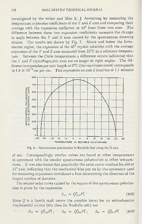
132 B E L L S Y S T E M T E C H N IC A L J O U R N A L
investigated by the writer and Miss E. J. Armstrong by measuring the temperature expansion coefficients of the Y and Z axes and comparing their average with the expansion coefficient a t 45° from these two axes. The difference between these two expansion coefficients measures the change in angle between the Y and Z axes caused by the spontaneous shearing strains. The results are shown by Fig. 7. Above and below the ferroelectric region, the expansion of the 45° crystal coincides with the average expansion of the Y and Z axes measured from 25°C as a reference temperature. Between the Curie temperatures a difference occurs indicating that the Y and Z crystallographic axes are no longer at right angles. The difference in expansion per unit length at 0°C (the maximum point) corresponds to 1.6 X 10~4cm per cm. This represents an axis d istortion of 1.1 minutes
TEMPERATURE IN DEGREES CENTIGRADE
Fig. 6.—Spontaneous polarization in Rochelle Salt along the X axis.
of arc. Correspondingly smaller values are found at other temperatures in agreement with the smaller spontaneous polarization at other temperatures. It was also found that practically the same curve resulted for either 45° axis, indicating that the mechanical bias put on by the optometer used for measuring expansions introduced a bias determining the direction of the largest number of domains.
The second order terms caused by the square of the spontaneous polarization is given by the expression
S i i = QunPl (168)Since Q is a fourth rank tensor the possible terms for an orthorhombic bisphenoidal crystal (the class for Rochelle salt) are
•811 — QuiiTl ; S22 — Q2211P 1 S 33 = Q33uPl (169)
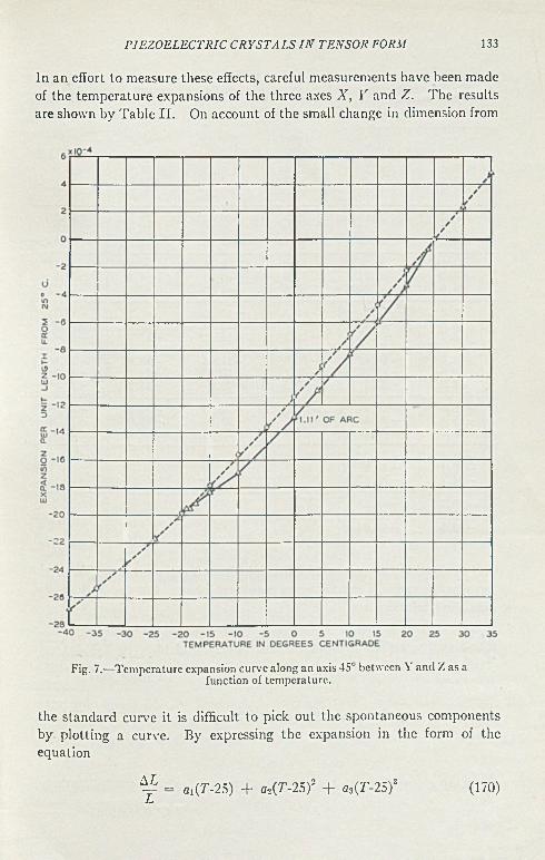
P IE Z O E L E C T R IC C R Y S T A L S I N T E N S O R FORM 133
In an effort to measure these effects, careful measurements have been made of the temperature expansions of the three axes X, Y and Z. The results are shown by Table II. On account of the small change in dimension from
Fig. 7.—Tem perature expansion curve along an axis 45° between Y and Z as a function of tem perature.
the standard curve it is difficult to pick out the spontaneous components by. plotting a curve. By expressing the expansion in the form of the equation
^ = ay(T- 25) + a,(T- 25)2 + a3(T-25)3 (170)I s
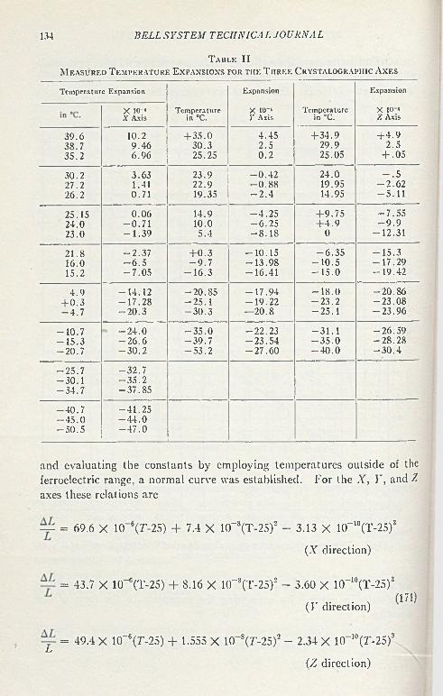
134 B E L L S Y S T E M T E C H N I C A L J O U R N A L
T a b l e I IM e a s u r e d T e m p e r a t u r e E x p a n s io n s f o r t h e T h r e e C r y s t a l o g r a p h ic A x e s
Temperature Expansion Expansion Expansion
X io-* Temperature X 10-* Temperature X 10-*X Axis in °C. Y Axis in °C. 7. Axis
39 .6 10.2 + 3 5 .0 4.45 + 3 4 .9 + 4 .938.7 9 .46 30.3 2.5 29.9 2 .535 .2 6.96 25.25 0 .2 25.05 + .05
30 .2 3.63 23.9 - 0 .4 2 24.0 — .527.2 1.41 22.9 - 0 .8 8 19.95 - 2 .6 226.2 0.71 19.35 - 2 . 4 14.95 - 5 .1 1
25.15 0.06 14.9 - 4 .2 5 + 9 .7 5 — 7.5524.0 - 0 .7 1 10.0 - 6 .2 5 + 4 .9 - 9 . 923.0 - 1 .3 9 5 .4 - 8 .1 8 0 - 1 2 .3 1
21.8 - 2 .3 7 + 0 .3 - 1 0 .1 5 - 6 .3 5 - 1 5 .316.0 - 6 . 5 - 9 . 7 - 1 3 .9 8 - 1 0 .5 - 1 7 .2 915.2 - 7 .0 5 - 1 6 .3 - 1 6 .4 1 - 1 5 .0 - 1 9 .4 2
4 .9 - 1 4 .1 2 - 2 0 .8 5 - 1 7 .9 4 - 1 8 .0 - 2 0 .8 6+ 0 .3 - 1 7 .2 8 - 2 5 .1 - 1 9 .2 2 - 2 3 .2 - 2 3 .0 8- 4 . 7 - 2 0 .3 - 3 0 .3 — 20.8 - 2 5 .1 - 2 3 .9 6
- 1 0 .7 - 2 4 .0 - 3 5 .0 - 2 2 .2 3 - 3 1 .1 - 2 6 .5 9- 1 5 .3 - 2 6 .6 - 3 9 .7 - 2 3 .5 4 - 3 5 .0 - 2 8 .2 8- 2 0 .7 - 3 0 .2 - 5 3 .2 - 2 7 .6 0 - 4 0 .0 - 3 0 .4
- 2 5 .7 - 3 2 .7- 3 0 .1 - 3 5 .2- 3 4 .7 - 3 7 .8 5
- 4 0 .7 - 4 1 .2 5- 4 5 .0 - 4 4 .0- 5 0 .5 - 4 7 .0
and evaluating the constants by employing temperatures outside of the ferroelectric range, a normal curve was established. For the X, V, and 7. axes these relations are
~ = 69.6 X 10_6(r-25) + 7.4 X l(T8(T-25)2 - 3.13 X l(T IO(T-25)3
(AT direction)
= 43.7 X 10~6(T-25) + 8.16 X l<rs(T-25)2 - 3.60 X 10_1°(T-25)3x (171)
(F direction)
= 49.4 X 10_6(r-25) + 1.555 X \ 0 ~ \ T - 2 5 ) 2 - 2.34 X 10~10(r-25)3Li(Z direction)
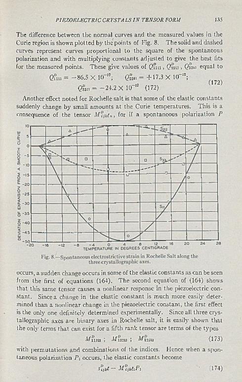
P IE Z O E L E C T R IC C R Y S T A L S I N TE N SO R FORM 135
The difference between the normal curves and the measured values in the Curie region is shown plotted by the points of Fig. 8. The solid and dashed curves represent curves proportional to the square of the spontaneous polarization and with multiplying constants adjusted to give the best fits for the measured points. These give values of Qfm , Qr.m , Q3311 equal to
Qnii = -8 6 .5 X 1(T12; Q°un = +17.3 X 1(T12;(172)
Qlm = -2 4 .2 X 10“12 (172)
Another effect noted for Rochelle salt is that some of the elastic constants suddenly change by small amounts at the Curie temperatures. This is a consequence of the tensor for if a spontaneous polarization P
occurs, a sudden change occurs in some of the elastic constants as can be seen from the first of equations (164). The second equation of (164) shows that this same tensor causes a nonlinear response in the piezoelectric constant. Since a change in the elastic constant is much more easily determined than a nonlinear change in the piezoelectric constant, the first effect is the only one definitely determined experimentally. Since all three crys- lallographic axes are binary axes in Rochelle salt, it is easily shown that the only terms that can exist for a fifth rank tensor are terms of the types
M u m 4/12223 ; 4 f123.13 (173)with permutations and combinations of the indices. Hence when a spontaneous polarization Pi occurs, the elastic constants become
S i i k ( - MijkhPi • (174)
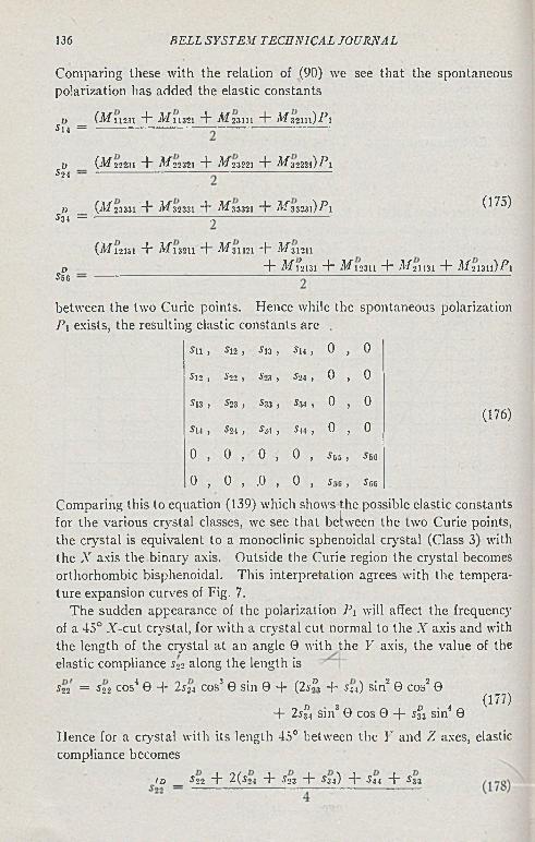
136 B E L L S Y S T E M T E C H N I C A L J O U R N A L
Comparing these with the relation of (90) we see that the spontaneous polarization has added the elastic constants
« _ (M um + M in n d- M^zni + Mznn)Pi S u -
V _ {Mi2231 d~ M i2321 + M i3221 d" Mz22Zl)P l524 ------------------------------------------ --------------------------------------
I) _ (M 23331 + M 3233I d- M 33321 d" ^ 3 3 2 3 1)^ 1 Í34 — ---------------------------- X----------------------------
(175)
D S 56
(AiTl21Sl d" M u n i d- M 31121 d- M 31211d- M 3 2131 d~ M i2311 d~ M n in + Miuii)Pi
between the two Curie points. Hence while the spontaneous polarization Pi exists, the resulting elastic constants are .
ill , i l 2 , i l 3 , Í14 , 0 , 0
i l 2 , Í2 2 , i2 3 , Í2 4 , 0 , 0
Í13 , Í23 , Í33 , Í34 , 0 , 0
i l l , Í24 , Í34 , i l l , 0 , 0
0 , 0 , 0 , 0 , Í 55 ) Í 56
0 , 0 , .0 , 0 , iyG , ÍC6
(176)
Comparing this to equation (139) which shows the possible elastic constants for the various crystal classes, we see that between the two Curie points, the crystal is equivalent to a monoclinic sphenoidal crystal (Class 3) with the X axis the binary axis. Outside the Curie region the crystal becomes orthorhombic bisphenoidal. This interpretation agrees with the temperature expansion curves of Fig. 7.
The sudden appearance of the polarization Pi will affect the frequency of a 45° X-cut crystal, for with a crystal cut normal to the X axis and with the length of the crystal at an angle 0 with the Y axis, the value of the elastic compliance i« along the length is
S22 = S22 cos4 0 + 2su cos3 0 sin 0 + (2s?3 + Su) sin2 0 cos2 0» 3 D 4 ( 1 7 7 )+ 2 j 34 sin 0 cos 0 + S33 sin 0
Hence for a crystal with its length 45° between the Y and Z axes, elastic compliance becomes
>D _ Í 2 2 d" 2(ío4 d* Í 2 3 d" 5 3 4 ) d" Í4 4 d~ S33
P IE Z O E L E C T R IC C R Y S T A L S I N T E N S O R FORM 137
UJ 217 2
ZÍ <0 Z
8 2 0 9
2 2 08 UJ
g 207
-20 - 1 6 -12
For a 45° Y-cut crystal we would expect a sudden change in the value of as the crystal becomes spontaneously polarized between the two Curie
points due to the addition of the and elastic compliances. Such a change has been observed for Rochelle salt8 as shown by Fig. 9 which shows the frequency constant of a nonplated crystal for which the elastic compliances s'ij should hold.
Fig. 9.—Frequency constant and Q of an unplatcd45°X cu t Rochelle Salt crystal plotted as a function of tem perature.
Hence the sudden change in the elastic constant is a result of the two second order terms s + s'3\ , which are caused by the spontaneous polarization. The value of the sum of these two terms at the mean temperature of the Curie range, 3°C is
Su + s3.\ = 4.1 X 10“14 cm2/dyne (179)
Crystals cut normal to the Y and Z axes should not show a spontaneous change in their frequency characteristic since the spontaneous terms s» , S2 1 , S31 and s56 do not affect the value of Young’s modulii in planes normal to V and Z. Experiments on a 45° F-cut Rochelle salt crystal do not show a spontaneous change in frequency at the Curie temperature, although there is a large change in the temperature coefficient of the elastic compliance between the two Curie points. This is the result of third order term and is
8 “The Location of Hysteresis Phenom ena in Rochelle Salt Crystals,” W. P. Mason, Phys. Rev., Vol. SO, p. 744-750, October 15, 1940.
138 B E L L S Y S T E M T E C H N I C A L J O U R N A L
not considered here. The spontaneous constant affects the shear constant ice for crystals rotated about the X axis and could be detected experimentally. No experimental values have been obtained.
The effects of spontaneous polarization in the second equation of (164) are of two sorts. For an unplated crystal, a spontaneous voltage is generated on the surface, which, however, quickly leaks off due to the surface and volume leakage of the crystal. The other effects are that the spontaneous polarization introduces new piezoelectric constants through the tensor Qkfm „, changes the dielectric constants through the tensor 0 " no and introduces a stress effect on the piezoelectric constants through the tensor Mkfmqr ■ Since piezoelectric constants are not as accurately measured as elastic constants, the first effect has not been observed. The additional piezoelectric constants introduced by the tensor Qk/mn are shown by equation (180)
¿11 ¿12 ¿13 ¿14 0 00 0 0 0 ¿26 ¿26 (180)
0 0 0 0 ¿36 ¿30Since the only constants for the Rochelle salt class, the orthorhombic bisphenoidal, are ¿M , ¿»6 , ¿se, this shows that between the two Curie points the crystal becomes monoclinic sphenoidal, with the X axis being the binary' axis. The added constants are, however, so small that the accuracy of measurement is not sufficient to evaluate them. From the expansion measurements of equation (172) and the spontaneous polarization values, three of them should have maximum values of
¿,i = - 6.6 X 1(T8; ga = +.1.3 X 10-8; g„ = -1 .8 X 10-8 (181)
These amount to only 6 per cent of the constant ¿14 , and hence they are not easily evaluated from piezoelectric measurements.
The effect of the tensor O£ „ 0 is to introduce a spontaneous dielectric constant «23 between the Curie temperatures so that the dielectric tensor becomes
«11 , 0 , 00 , «22 j «23 (182)
0 , €23 , «33As discussed at length by Mueller9 this introduces a spontaneous birefringence for light passing through the crystal along the X , Y and Z axes which adds to the birefringence already present.
9 “ Properties of Rochelle Salt I and IV ,” Phys. Rev. 47,175 (1935); 58,805 November 1, 1940.
T he B iased Id eal R ectifierBy W . R . B E N N E T T
M ethods of solution and specific results arc given for the spectrum of the response of devices which have- sharply defined transitions between conducting and non-conducting regions in their characteristics. The input wave consists of one or more sinusoidal components and the operating point is adjusted by bias, which m ay either be independently applied or produced by the rectified output itself.
I n t r o d u c t i o n
THE concept of an ideal rectifier gives a useful approximation for the analysis of many kinds of communication circuits. An ideal rectifier
conducts in only one direction, and by use of a suitable bias may have the critical value of input separating non-conduction from conduction shifted to any arbitrary value, as illustrated in Fig. 1. A curve similar to Fig. 1 might represent for example the current versus voltage relation of a biased diode. By superposing appropriate rectifying and linear characteristics with different conducting directions and values of bias, we may approximate the characteristic of an ideal limiter, Fig. 2, which gives constant response when the input voltage falls outside a given range. Such a curve might approximate the relationship between flux and magnetizing force in certain ferromagnetic materials, or the output current versus signal voltage in a negative-feedback amplifier. The abrupt transitions from non-conducting to conducting regions shown are not realizable in physical circuits, but the actual characteristics obtained in many devices are much sharper than can be represented adequately by a small number of terms in a power series or in fact by any very simple analytic function expressible in a reasonably small number of terms valid for both the non-conducting and conducting regions.
In the typical communication problem the input is a signal which may be expressed in terms of one or more sinusoidal components. The output of the rectifier consists of modified segments of the original resultant of the individual components separated by regions in which the wave is zero or constant. We are not so much interested in the actual wave form of these chopped-up portions, which would be very easy to compute, as in the frequency spectrum. The reason for this is that the rectifier or limiter is usually followed by a frequency-selective circuit, which delivers a smoothly varying function of time. Knowing the spectrum of the chopped input to the selective network and the steady-state response as a function of
139
B E L L S Y S T E M T E C H N IC A L J O U R N A L
APPLIED VOLTAGE
Fig. 1.—Ideal biased linear rectifier characteristic.
(t )L IN E A R
CHARACTERISTIC I
( 2 )BIASED PO SITIVE
RECTIFIER
Fig. 2.—Synthesis of lim iter characteristic.
( 3 )BIASED NEGATIVE
RE C TIFIER
MBIASED ID EA L
L IM IT E R
T I IE B I A S E D I D E A L R E C T IF IE R 141
frequency of the network, we can calculate the output wave, which is the one having most practical importance. The frequency selectivity may in many cases be an inherent part of the rectifying or limiting action so that discrete separation of the non-linear and linear features may not actually be possible, but even then independent treatment of the two processes often yields valuable information.
The formulation of the analytical problem is very simple. The standard theory of Fourier series may be iised to obtain expressions for the amplitudes of the harmonics in the rectifier output in the case of a single applied frequency, or for the amplitudes of combination tones in the output when two or more frequencies are applied. These expressions are definite integrals involving nothing more complicated than trigonometric functions and the functions defining the conducting law of the rectifier. If we were content to make calculations from these integrals directly by numerical or mechanical methods, the complete solutions could readily be written down for a variety of cases covering most communication needs, and straightforward though often laborious computations could then be based on these to accumulate eventually a sufficient volume of data to make further calculations unnecessary.
Such a procedure however falls short of being satisfactory to those who would like to know more about the functions defined by these integrals without making extensive numerical calculations. A question of considerable interest is that of determining under what conditions the integrals may be evaluated in terms of tabulated functions or in terms of any other functions about which something is already known. Information of this sort would at least save numerical computing and could be a valuable aid in studying the more general aspects of the communication system of which the rectifier may be only one part. I t is the purpose of this paper to present some of these relationships that have been worked out over a considerable period of time. These results have been found useful in a variety of problems, such as distortion and cross-modulation in overloaded amplifiers, the performance of modulators'and detectors, and effects of saturation in magnetic materials. I t is hoped that their publication will not only make them available to more people, but also stimulate further investigations of the functions encountered in biased rectifier problems.
The general forms of the integrals defining the amplitudes of harmonics and side frequencies when one or two frequencies are applied to a biased rectifier are written down in Section I. These results are based on the standard theory of Fourier series in one or more variables. Some general relationships between positive and negative bias, and between limiters and biased rectifiers are also set down for further reference. Some discussion is given of the modifications necessary when reactive elements are used in the circuit.
142 B E L L S Y S T E M T E C H N I C A L J O U R N A L
Section I I summarizes specific results on the single-frequency biased rectifier case. The general expression for the amplitude of the typical harmonic is evaluated in terms of a hypergeometric function for the power law case with arbitrary exponent.
Section I I I takes up the evaluation of the two-frequency modulation products. I t is found that the integer-power-law case can be expressed in finite form in terms of complete elliptic integrals of the first, second, and third kind for almost all products. Of these the first two are available in tables, directly, and the third can be expressed in terms of incomplete integrals of the first and second kinds, of which tables also exist. No direct tabulation of the complete elliptic integrals of the third kind encountered here is known to the author. They are of the hyperbolic type in contrast to the circular ones more usual in dynamical problems. Imaginary values of the angle ¡3 would be required in the recently published table by Heuman1.
A few of the product amplitudes depend on an integral which has not been reduced to elliptic form, and which is a transcendental function of two variables about which little is known. Graphs calculated by numerical integration are included.
The expressions in terms of elliptic integrals, while finite for any product, show a rather disturbing complexity when compared with the original integrals from which they are derived. I t appears that elliptic functions are not the most natural ones in which the solution to our problem can be expressed. If we did not have the elliptic tables available, we would prefer to define new functions from our integrals directly, and the study, of, such functions might be an interesting and fruitful mathematical exercise..
Solutions for more than two frequencies are theoretically possible by the same methods, although an increase of complexity occurs as the first few components are added. When the number of components becomes very large, however, limiting conditions may be evaluated which reduce the problem to a manageable simplicity again. The case of an infinite number of components uniformly spaced along an appropriate frequency range has been used successfully as a representation of a noise wave, and the detected output from signal and noise inputs thus evaluated2. The noise problem will not be treated in the present paper.
I . T i i e G e n e r a l P r o b l e m
Let the biased rectifier characteristic, Fig. 1, be expressed by
/ 0, E < b \I = (1-1)
\ f ( E - b), b < E )
1 Carl H eum an, Tables of Complete E lliptic In tegrals, Jour. M ath, and Physics, Vol- X X , No. 2, pp. 127-206, April, 1941.
2 W. R. B ennett, Response of a L inear Rectifier to Signal and Noise, Jour. Acous. Soc. A m e r . , Vol. 15, pp. 164-172, Jan . 1944.
T H E B I A S E D I D E A L R E C T I F I E R 143
Then if a single frequency wave defined by
E = P cos pt, — P < b < P, (1.2)
is applied as input, the output contains only the tips of the wave, as shown in Fig. 3. I t is convenient to place the restrictions on P and b given in Eq. (1.2). The sign of P is taken as positive since a change of phase may be introduced merely by shifting the origin of time and is of trivial interest. If the bias b were less than — P, the complete wave would fall in the conducting region and there would be no rectification. If b were greater than
Pcos pt
Fig. 3.— Response of biased rectifier to single-frequency wave.
P, the output would be completely suppressed. Applying the theory of Fourier series to (1.1) and (1.2), we have the results
I = 2 cos n ptL n - 1
2 fUn = - /
7T Jo
arc cos b fP
f (P cos x — b) cos 11 x dx
(1-3)
(1.4)
When two frequencies are applied, the output may be represented by a double Fourier series. The typical coefficient may be found by the method explained in an earlier paper by the author3. The problem is to obtain the double Fourier series expansion in a and y of the function g(x,y) defined by:
S(x-,y) ----'0 , P cos x + Q cos y < b )
\ f (P cos x Q cos y — 6), b < P cos x + Q cos y/(1.5)
1 W. R, B ennett, New R esults in the Calculation of M odulation Products, B .S .T J ., pp. 228-243, April, 1933.
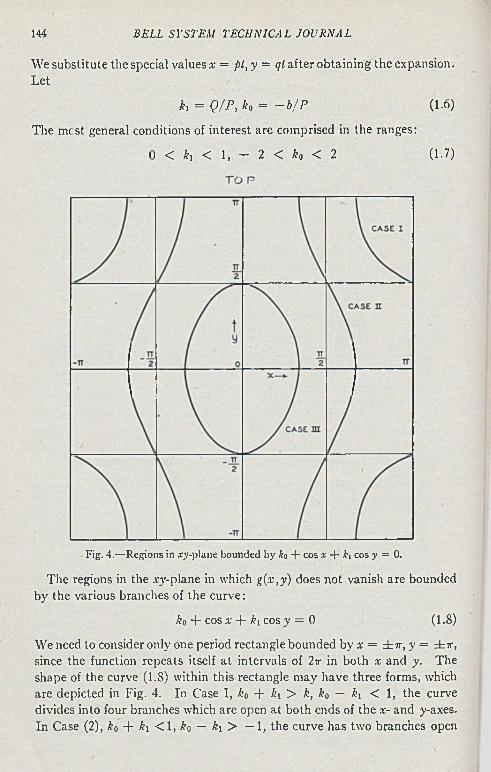
We substitute the special values x = pt, y = qt after obtaining the expansion.Let
h = Q/P, k0 = - b / P (1.6)
The mcst general conditions of interest are comprised in the ranges:
0 < ¿i < 1, - 2 < k0 < 2 (1.7)
144 B E L L S Y S T E M T E C H N I C A L J O U R N A L
Fig. 4.—Regions in ay-plane bounded by ko - f cos x + ki cos y = 0.
The regions in the .rj'-plane in which g(x,y) does not vanish are bounded by the various branches of the curve:
¿o + cosa- + ¿icosy = 0 (1.8)
We need to consider only one period rectangle bounded by a- = ± x , y = ± x , since the function repeats itself at intervals of 2ir in both x and y. The shape of the curve (1.8) within this rectangle may have three forms, which are depicted in Fig. 4. In Case I, k0 + ki > k, k0 — ki < 1 , the curve divides into four branches which are open at both ends of the x- and y-axes. In Case (2), k0 + ¿ 1 < 1 , ¿o — ki > — 1, the curve has two branches open
at the ends of the y-axis. In Case (3), —1 < k0 + ki < 1, k0 — h < —1, a single closed curve is obtained. The limits of integration must be chosen to fit the proper case. The Fourier series expansion of g(x,y) may be written:
00 00
sO, y) = amn cos mx cos ny (1.9)m=0 7i “0
where amn is found from integrals of the form:
fmin f v2 f*'A = / dy / f (P cos a + Q cos y — b) cos mx cos ny dx (1.10)ir JVl
Here, as usual, em is Neumann’s discontinuous factor equal to two when mis not zero and unity when m is zero. The values of the limits for the different cases a re :Case I, amn = Ai + A?
/ (ai = 0, a2 = arc cos (— k0 — ki cos y)'
-4i = A with limits ( 1 — /fe0 ) ( l - ^ )yi - arc cos — -— , y2 = x
a | p x(1-12)
T H E B I A S E D I D E A L R E C T I F I E R 145
a2 = arc cos ( — k0 — ki cos y
y2 =(1.13)
(ai = 0, a2 = arc cos (— k0 — ki cos y)
L im i t s 1 . / i + 1 . \ I < U 4 )(yi = 0, y2 = arc cos ( — — — 1
For a considerable variety of rectifier functions/, the inner integration may be performed at once leaving the final calculation in terms of a single definite integral.
A somewhat different point of view is furnished by evaluating the integral (1.4) for the biased single-frequency harmonic amplitude, and then replacing the bias by a constant plus a sine wave having the second frequency. When each harmonic of the first frequency is in turn expanded in a Fourier series
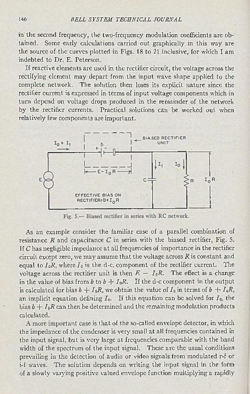
146 B E L L S Y S T E M T E C H N I C A L J O U R N A L
in th e second frequency, th e tw o-frequency m odulation coefficients are obta ined . Some early calcu lations carried o u t graphically in th is w ay are the source of th e curves p lo tted in Figs. IS to 21 inclusive, for which I am indeb ted to D r. E . P eterson .
I f reactive elem ents a re used in th e rectifier circu it, th e vo ltage across the rectify ing elem ent m ay d e p a r t from the in p u t w ave shape app lied to the com plete netw ork . T h e solution then loses its explicit n a tu re since the rectifier cu rren t is expressed in te rm s of in p u t vo ltage com ponents which in tu rn depend on vo ltage d rops p roduced in th e rem ainder of th e netw ork by the rectifier cu rren ts . P ra c tica l solutions can be w orked o u t when re la tive ly few com ponents a re im p o rta n t.
As an example consider the familiar case of a parallel combination of resistance R and capacitance C in series with the biased rectifier, Fig. 5. If C has negligible impedance a t all frequencies of importance in the rectifier circuit except zero, we may assume that the voltage across R is constant and equal to I 0R, where I 0 is the d-c. component of the rectifier current. The voltage across the rectifier unit is then E — I 0R ■ The effect is a change in the value of bias from b to b + I 0R- If the d-c component in the output is calculated for bias b + I 0R, we obtain the value of I 0 in terms of b + I 0R, an implicit equation defining I 0. If this equation can be solved for I 0, the bias b + IoR can then be determined and the remaining modulation products calculated.
A more important case is that of the so-called envelope detector, in which the impedance of the condenser is very small a t all frequencies contained in the input signal, but is very large a t frequencies comparable with the band width of the spectrum of the input signal. These are the usual conditions prevailing in the detection of audio or video signals from modulated r-f or i-f waves. The solution depends on writing the input signal in the form of a slowly varying positive valued envelope function multiplying a rapidly
T H E B I A S E D I D E A L R E C T I F I E R 147
oscillating cosine function. That is, if the input signal can be represented as
E = A (() cos 4> (/), (1-15)
where A (l) is never negative and has a spectrum confined to the frequency range in which 2t / C is negligibly small compared with 1/i?, while cos </>(/) has a spectrum confined to the frequency range in which 1/i? is negligibly small compared with 2irfC, we divide the components in the detector output into two groups, viz.:
1. A low-frequency group I n containing all the frequencies comparablewith those in the spectrum of A (/). The components of this group flowthrough i?.
2. A high-frequency group if,/ containing all the frequencies comparable to and greater than those in the spectrum of cos <t> (I). The components of this group flow through C and produce no voltage across i?.
The instantaneous voltage drop across i? is therefore equal to Ii/R, and hence the bias on the rectifier is b + /¡//?. If A and <f> were constants, we could make use of (1.3) and (1.4) to write:
00
I it + h t = t;0 + X) an COS n d (1.16)Z n-1
2 rare cos [ (b+li/R)/A]an = - / f (A cos x — b — I u R ) cos nx dx (1.17)
ir Jo
If A and <j> are variable, the equation still holds provided /;/f? < .4 at all times. Assuming the latter to be true (keeping in mind the necessity of checking the assumption when I l{ is found), we note that terms of the form an cos a 0 consist of high frequencies modulated by low frequencies and hence the main portion of their spectra must be in the high-frequency range. Hence we must have as a good approximation when the envelope frequencies are well separated from the intermediate frequencies,
, i (■arccos [(b+Ii/R)!A]I v ~ x-° = - / /(A cos x — b — I l fR)dx (1.18)2 IT Jo
This equation defines 7// as a function of A, and if it is found that the condition b + I i /R < A is satisfied by the resulting value of 7t/, the problem is solved. If the condition is not satisfied, a more complicated situation exists requiring separate consideration of the regions in which b - f Ii/R < A and b + Iif R > A.
To be specific, consider the case of a linear rectifier with forward conductance a = 1/7?, and write V — I tfR. Then
V = \ / A — (b + V )2 — (b + V) arc cos (1.19)
148 B E L L S Y S T E M T E C H N I C A L J O U R N A L
When b = 0 (ihe case of no added bias), this equation may be satisfied by setting
V = cA, 0 < c < 1, (1.20)
which leads to
= a / j 2 - 1 - arc cos c, (1.21)
defining c as a function of Ro/R- The value of c approaches unity when the ratio of rectifier resistance to load resistance approaches zero and falls off to zero as Ro/R becomes large. The curve may be found plotted elsewhere4. This result justifies the designation of this circuit as an envelope detector since with the proper choice of circuit parameters the output voltage is proportional to the envelope of the input signal.
The equations have been given here in terms of the actual voltage applied to the circuit. The results may also be used when the signal generator contains an internal impedance. For example, a nonreactive source independent of frequency may be combined with the rectifying element to give a new resultant characteristic. If the source impedance is a constant pure resistance r0 throughout the frequency range of the signal input but is negligibly small a t the frequencies of other components of appreciable size flowing in the detector, we assume the voltage drop in r0 is r0ai cos <j> (/). We then set n = 1 in (1.17) and replace a\ by (A0 — A ) / r 0, where A 0 is the voltage of the source. The value of 7;/ in terms of A from (1.18) is then substituted, giving an implicit relation between A and A 0 ■
A further noteworthy fact that may be deduced is the relationship between the envelope and the linearly rectified output. By straightforward Fourier series expansion, the positive lobes of the wave (1.15), may be written as:
Er =/ E , E > 0 \
C- += Alt)\o> E <Z 0 / _7T
_ 2 ^ 2 ( —)m cos 2m (1.22)T m-1 Am- — 1
Hence if we represent the low-frequency components of E r by E l t , we have:
E u = — (1.23)7T
orA (I) = ioEu (1.24)
1 See, for example, the top curve of Fig. 9-25, p. 311, H . J . Reich, Theory and Applications of Electron Tubes, McGraw-Hill, 1944.
T H E B I A S E D I D E A L R E C T I F I E R 149
Equation (1.23) expresses the fact that we may calculate the signal component in the output of a half-wave linear rectifier by taking l/V times the envelope. Equation (1.24) shows that we may calculate the response of an envelope detector by taking 7r times the low-frequency part of the Fourier series expansion of the linearly rectified input. Thus two procedures
solution, and in specific cases a saving of labor is possible by a proper choice between the two methods. The final result is of course the same, although there may be some difficulty in recognizing the equivalence. For example, the solution for linear rectification of a two-frequency wave P cos pt + Q cos qt was given by the author in 19333, while the solution for the envelope was given by Butterworth in 19295. Comparing the two expressions for the direct-current component, we have:
— IPEit = — [2E — (1 — k2) K], where K and E are complete elliptic integrals7T-
of the first and second kinds with modulus k = Q/P 2 pA (l) = — (1 + k) Ei, where Ei is a complete elliptic intregal of the
second kind with modulus k y = 2 \ / k / ( l + k ) . Equation (1.24) implies the existence of the identity
The identity can be demonstrated by making use of Landen’s transformation in the theory of elliptic integrals.
The expression for the harmonic amplitudes in the output of the rectifier can be expressed in a particularly compact form when the conducting part of the characteristic can be described by a power law with arbitrary exponent. Thus in (1.4) if/ ( s) = a z , we set X = b/P and get
are in general available for either the envelope detector or linear rectifier
7r
(1 + k) F.i = IE - (1 - k2) K (1.25)
2. S i n g l e - F r e q u e n c y S ig n a l
(cos x — A)' cos nx dx
= 2»r(» + \ )a P \ \ - \ y +i
7r»r3 1 - X2 ’ 2
) (2.1 )
5 S. Butterw orth, A pparent Dem odulation of a W eak Station by a Stronger One Experimental IVireless, Vol. 6, pp. 619-621, Nov. 1929.
150 B E L L S Y S T E M T E C H N I C A L J O U R N A L
The equation holds for all real values of v greater than —1. The symbol F represents the Gaussian hypergeometric function6:
The derivation of (2.1) requires a rather long succession of substitutions, expansions, and rearrangements, which will be omitted here.
When v is an integer, the hypergeometric function may be expressed in finite algebraic form, either by performing the integration directly, or by making use of the formulas:
together with recurrence formulas for the /''-function. W ien v is an odd multiple of one half, the /•’-function may be expressed in terms of complete elliptic integrals of the first and second kind with modulus [(1 — A)/2]1/2 by means of the relations,
and the recurrence formulas for the /'-function. For the case of zero bias, we set A = 0, and apply the formula
We point out that the above results may be applied not only when the applied signal is of the form P cos pi with P and p constants, but to signals
6 For an account of the properties of the hvpergeom etric function, see Ch. X IV of W hittaker and W atson, M odern Analysis, Cambridge, 1940. A discussion of elliptic integrals is given in Ch. X X II of the same book.
F{fl, b; c; z) = 1 + a~C 1 !
(2.3)
(2.4)
7T
F(a, 1 - a; c; 1/2) (2.5)
obtaining the result:
T H E B I A S E D I D E A L R E C T I F I E R 151
in which P and p arc variable, provided that P is always positive. We thus can apply the results to detection of an ordinary amplitude-modulated wave or to the detection of a frequency-modulated wave after it has passed through a slope circuit.
A case of considerable practical interest is that of an amplitude-modulated wave detected by a diode in series with a parallel combination of resistance Ii and capacitance C. Tire value of C is assumed to be sufficiently large so that the voltage across R is equal to the a0/2 component of the current through the diode multiplied by the resistance. This is the condition for envelope detection mentioned in Part 1. The diode is assumed to follow Child’s law, which gives v = 3/2. We write
j _ V _ /0 _ r (5 /2 ) ( l - \ f <xPm ( l .1 - X \ ,h _ _ _ a0/ 2 ----------- _ _ _ P ^ , 2 , 3, — J (2./)
where X = V/P . Note that V is a constant equal to the direct-voltage output if P is constant. If P varies slowly with time compared with the high-frequency term cos pt, V represents the slowly varying component of the output and hence is the recovered signal.But
F(h 3; k2) = [2(2k2 - 1 )E + (2 - 3**)(1 - k2)K) (2.8)
where K and E are complete elliptic integrals of the first and second kind with modulus k. Hence
37r (1 + 3 X ) ( i + X ) k _ 8 £ ( 2 9 )R i V 2 P P X
where the modulus of K and E is \ / ( l — X)/2- This equation defines p as a function of X, and hence by inversion gives X as a function of p. The resulting curve of X vs. p is plotted in Fig. 6 and may be designated as the function X = g (p). If we substitute X = V /P we then have
V = P g (3tt/Ra \ / l P ) (2.10)
This enables us to plot V as a function of P, for various values of Ra, Fig. 7. Since P may represent the envelope of an amplitude-modulated (or differentiated PM) wave, and V the corresponding recovered signal output voltage, the curves of Fig. 7 give the complete performance of the circuit as an envelope detector. In general the envelope would be of form P = -Poll + c s(/)], where s(t) is the signal. We may substitute this value of P directly in (2.10) provided the absolute value of c s(t) never exceeds unity.
152 B E L L S Y S T E M T E C H N I C A L J O U R N A L
(.0
10 12 P : V O L TS
Kg- ■ Perform ance of 3 /2 —power-law rectifier as an envelope detector with low-imped-ance signal generator.
To express the output in terms of a source voltage P q in series with an impedance equal to the real constant value ro a t the signal frequency and zero at all other frequencies, we write
Po - P 3 aP * 'H l - X)2 / 1 - X \
~ — 4 V 2 3 ; — ) (2-11)
0 4 a 12 16 2 0 2 4 2 8 3 2
P
Fig. 6. The Function X = g(p) defined by Eq. (2.9).
T H E B I A S E D I D E A L R E C T I F I E R 153
or
p. - ( i +1 n) p,
where
E _ 3 M L - x p g / _ 1( 3 . L n * \“ 4 V 2 v ’ *’ 2 /
= V ÏP [2 (1 - ¿2 + k4)E - (2 - ¿2)(1 - k2)K].Ô7T
1.4
1.2
1.0
0. 8
0.6
0.4
0.2
00 5 10 15 2 0 2 5 3 0 3 5 4 0
P0 IN VO LTS
Fig. 8.—Performance of 3 /2 —power-law rectifier as an envelope detector w ith impedance of signal generator low except in signal band.
By combining the curves of Fig. 7 giving V in terms of P with the above equations giving the relation between P and P 0, we obtain the curves of Figs. 8, 9, 10, giving V as a function of P q. The curves approach linearity as Ra is made large. On the assumption that the curves are actually linear, we define the conversion loss D of the detector in db in terms of the ratio of maximum power available from the source to the power delivered to the load:
,D = (2.14)
Curves of D vs ra/ R are given in Figs. 11 and 12. The optimum relation between r0 and R when the forward resistance of the rectifier vanishes has long been known to be r0/ R — .5. The curves show a minimum in this
( 2.12)
(2.13)
154 B E L L S Y S T E M T E C H N I C A L J O U R N A L
region when Ra is large. In the limit as Ra approaches infinity, we may show that the relation between P 0 and V approaches:
p . = y ( i + 2i° ) (2-15)
P0 IN VOLTS
Fig. 9.—Perform ance of 3 /2 —power-law rectifier as an envelope detector w ith impedance of signal generator low except in signal band.
p0 IN VOLTS
Fig. 10.—Perform ance of 3 /2 —power-law rectifier as an envelope detector w ith impedance of signal generator low except in signal band.
The corresponding limiting formula for D is
D - 10 H £ (* + 1 > (2-i6)
T H E B I A S E D I D E A L R E C T I F I E R 155
The minimum value of D is then found to occur at ro = R / 2 and is zero db. We note from the curves that the minimum loss is 1.2 db when Ra = 10 and 0.4 when Ra = 100.
This example is intended mainly as illustrative rather than as a complete tabulation of possible detector solutions. The methods employed are sufficiently general to solve a wide variety of problems, and the specific evaluation process included should be sufficiently indicative of the procedures required. Cases in which various other selective networks are associated with the detector have been treated by Wheeler7.
Fig. 11.—Conversion loss of 3 /2 —power-law rectifier as envelope detector w ith impedance of signal generator low except in signal band.
Fig. 12.—Conversion loss of 3 /2 —power-law rectifier as envelope detector w ith impedance of signal generator low except in signal band.
3 . T w o - F r e q u e n c y I n p u t s
lhe general formula for the coefficients in the two-frequency case depends on a double integral as indicated by (1.10). In many cases one integration may be performed immediately, thereby reducing the problem to a single definite integral which may readily be evaluated by numerical or mechanical
A. W heeler, Design Form ulas for Diode D etectors, Proc. I. R. E., Vol. 26, pp. 'Is-780 , June 193s!
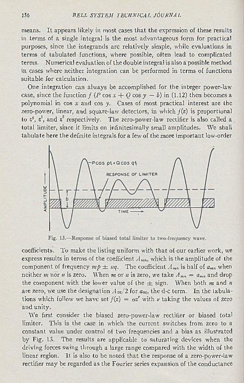
156 B E L L S Y S T E M T E C H N I C A L J O U R N A L
means. I t appears likely in most cases that the expression of these results in terms of a single integral is the most advantageous form for practical purposes, since the integrands are relatively simple, while evaluations in terms of tabulated functions, where possible, often lead to complicated terms. Numerical evaluation of the double integral is also a possible method in cases where neither integration can be performed in terms of functions suitable for calculation.
One integration can always be accomplished for the integer power-law case, since the function / (P cos x + Q cos y — b) in (1.12) then becomes a polynomial in cos x and cos y. Cases of most practical interest are the zero-power, linear, and square-law detectors, in which /(z) is proportional to z°, z1, and z2 respectively. The zero-power-law rectifier is also called a total limiter, since it limits on infinitesimally small amplitudes. We shall tabulate here the definite integrals for a few of the more important low-order
coefficients. To make the listing uniform with that of our earlier work, we express results in terms of the coefficient A mn, which is the amplitude of the component of frequency mp ± nq. The coefficient A mn is half of amn when neither m nor it is zero. When m or n is zero, we take A mn = amn and drop the component with the lower value of the ± sign. When both m and n are zero, we use the designation zloo/2 for a0o, the d-c term. In the tabulations which follow we have set /(z) = ctz" with v taking the values of zero and unity.
We first consider the biased zero-power-law rectifier or biased total limiter. This is the case in which the current switches from zero to a constant value under control of two frequencies and a bias as illustrated by Fig. 13. The results are applicable to saturating devices when the driving forces swing through a large range compared with the width of the linear region. I t is also to be noted that the response of a zero-power-law rectifier may be regarded as the Fourier series expansion of the conductance
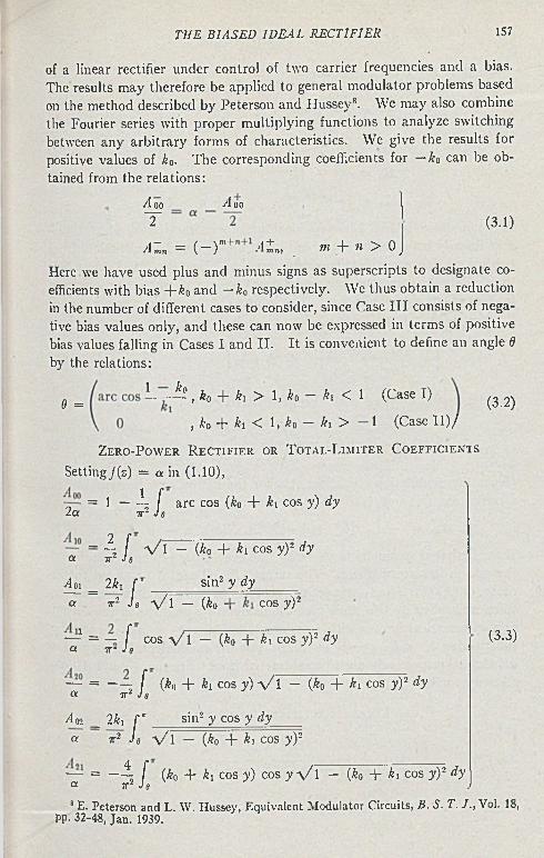
T H E B I A S E D I D E A L R E C T I F I E R 157
of a linear rectifier under control of two carrier frequencies and a bias. The results may therefore be applied to general modulator problems based on the method described by Peterson and Hussey8. We may also combine the Fourier series with proper multiplying functions to analyze switching between any arbitrary forms of characteristics. We give the results for positive values of ko■ The corresponding coefficients for —ko can be obtained from the relations:
zlooT
zloo(3.1)
AZn = (~r -Cn, . « , + » > 0 ,Here we have used plus and minus signs as superscripts to designate coefficients with bias + ¿ 0 and — ko respectively. We thus obtain a reduction in the number of different cases to consider, since Case I I I consists of negative bias values only, and these can now be expressed in terms of positive bias values falling in Cases I and II. I t is convenient to define an angle 6 by the relations:
0 = 1 \ k0 + ki > 1, ¿o - ki < 1 (Case I) (3.2), ko -j- ki < 1, A’o — ki ^ 1 (Case I I ) /
Z e r o - P o w e r R e c t i f i e r o r T o t a l - L i m i t e r C o e f f i c i e n t s
Setting/(s) = a in (1.10),
= 1 — A; f arc cos (k0 + ki cos y ) dy 2a tt2 Jg
~ Ą [ V l — (ko + ki cos y Y dy OC 7T J e
fin! = 2 k l f sin2 y dya 7T2 Jg y / \ — (k0 + cos y Y
—1 = ~ f cos v T — (ka + ki cos y)2 dya 7T- J g
— = —— [ (ko + ki cos y) V l — (¿0 + ki cos y Y dya i t 2 J g
A os _ 2&i f 1 sin2 y cos y dy
a Tr2 Jg V 1 — (¿o + k, cos y Y
~ = —4: f (ko + h cos y) cos y \ / l — (ko + ki cos y Y dya i r 2 Jg
8 E. Peterson and L. W. H ussey, E quivalent M odulator Circuits, B. S . T. J ., Vol. 18,PP. 32-48, Jan . 1939.
(3.3)
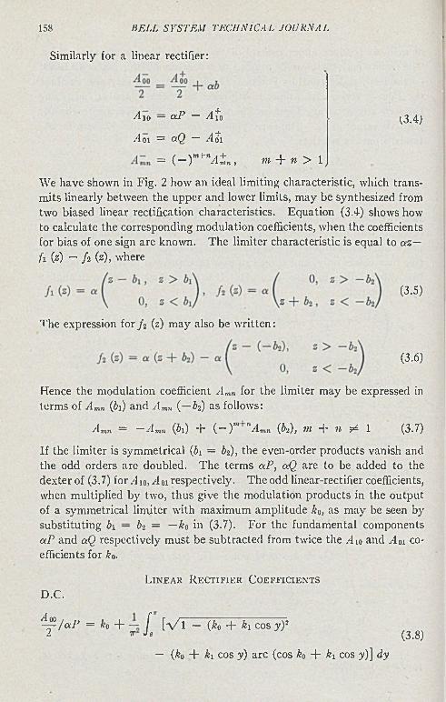
158 B E L L S Y S T E M T E C H N IC A L J O U R N A L
Similarly for a linear rectifier:
A 10 — aP — Ato
A 01 = ocQ — Ati
f3.4)
= ( - ) m+n4 L , tn + n > l jm+ n A +
We have shown in Fig. 2 how an ideal limiting characteristic, which transmits linearly between the upper and lower limits, may be synthesized from
to calculate the corresponding modulation coefficients, when the coefficients for bias of one sign are known. The limiter characteristic is equal to az— h 0 ) - f t (z), where
If the limiter is symmetrical (61 = i 2), the even-order products vanish and the odd orders are doubled. The terms aP, aQ are to be added to the dexter of (3.7) for A 10, A 01 respectively. The odd linear-rectifier coefficients, when multiplied by two, thus give the modulation products in the output of a symmetrical limiter with maximum amplitude ka, as may be seen by substituting bi — b-i = —ko in (3.7). For the fundamental components aP and aQ respectively must be subtracted from twice the A 10 and A 01 coefficients for kn.
two biased linear rectification characteristics. Equation (3.4) shows how
(3.5)
The expression for/ 2 (z) may also be written:
(3.6)
Hence the modulation coefficient A mr. for the limiter may be expressed in terms of A mn (bi) and A mn (—¿2) as follows:
A mn = — A mn (¿l) + (— )”*: nA mn (62), »1 + 11 jA \ (3.7)
L i n e a r R e c t i f i e r C o e f f i c i e n t s
D.C.
^ / a P = ko + — [ [ V 1 — (ko + ki cos y )2 ¿ 7r Je (3.8)
— (¿o + ki cos y) arc (cos k0 + ki cos y)] dy
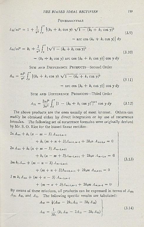
T I IE B I A S E D I D E A L R E C T I F I E R 159
(3.9)
(3.10)
(3.11)
(3.12)
F u n d a m e n t a l s
/lio/aP = 1 + [ [(¿o + ki cos y) V 1 — (k0 + cos y )2TTZ JO
— arc cos (k0 + h cos y)] dy
A n / a P = k\ + — f [ V 1 — (k0 + ki cos y ) 27T" J e
— (k0 + h cos y) arc cos (k0 + ¿1 cos y)] cos y dy
Sum a n d D i f f e r e n c e P r o d u c t s —Second Ordera p I•* ___________________________
A ii = — / [(¿o + ki cos y) V l — (k0 + ki cos y ) 27T“ J e
— arc cos (k0 + ki cos y)] cos y dy
Sum a n d D i f f e r e n c e P r o d u c t s —T h ird Order
A n = ^ f t 1 - (*« + cos y)2]3/2 cos y dy 3ir Je
The above products are the ones usually of most interest. Others can readily be obtained either by direct integration or by use of recurrence formulas. The following set of recurrence formulas were originally derived by Mr. S. 0 . Rice for the biased linear rectifier:
2n Amn -p ki (n — m — 3) A m+i,n—i
+ ki + n + 3)ylm+i,n—i + 2koii Am+i,„ = 0
2n A mn -p ki (n -p m — 3) / lm-i,n+i
+ k\ {n — in + 3)/lm-i,n+i + 2k0n A m~i,n = 0
2m ki Ann + {m — n — 3) A m—i,n+i
+ {m + n -p 3)Am+i,n+i + 2koin Am,„+i = 0
2 m k\ A mn -p {m + 11 — 3) A m- i,„-i
+ {m — ii + 3) d m+i,„_x + 2koin / l m,n- i = 0By means of these relations, all products can be expressed in terms of Aoo, A io, /Ioi, and An. The following specific results are tabulated:
A?o = 3 {Aoo — 2ki A n 2kt>Aio)
(3.13)
160 B E L L S Y S T E M T E C H N I C A L J O U R N A L
^21 — |(^101 — k \A io — ko A u)
A i2 = — {k\A\o — Aoi — Æo/ln)¿K\
A 30 = —ko A 2o — ki An
(3.15)
A 03 = — T (ko A 02 + A 12) k l
(3.16)
The third-order product A21 is of considerable importance in the design of carrier amplifiers and radio transmitters, since the (2p — ^-product is the cross-product of lowest order falling back in the fundamental band when overload occurs. Figure 14 shows curves of A n calculated by Mr. J. O. Edson from Eq. (3.12) by mechanical integration.
We point out also that the linear-rectifier coefficients give the Fourier series expansion of the admittance of a biased square-law rectifier when two frequencies are applied.
We shall next discuss the problem of reduction of the integrals appearing above to a closed form in terms of tabulated elliptic integrals9. This can be done for all the coefficients above except the d-c for the zero-power law and for the d-c and two fundamentals for the linear rectifier. These contain the integral
H(&o, ¿ 1) = / arc cos (k0 + ¿ 1 cos y) dy (3.17)Jo
which has been calculated separately and plotted in Fig. 22. When the arc cos term is accompanied by cos my as a multiplier with m ^ 0, an integration by parts is sufficient to reduce the integrand to a rational function of cos y and the radical - \ / i — (¿0 + ¿ 1 cos y)2, which may be reduced at once to a recognizable elliptic integral by the substitution z = cos y. I t is found that all the integrals except that of (3.17) appearing in the results can be expressed as the sum of a finite number of integrals of the form:
pcoso zm dzZm = 1 1 V (1 - 22)[1 - (k0 + k i z / } > w = 0, 1, 2, • • ■ (3.18)
By differentiating the expression zm~3 \ / ( l — s)2[1 — (k0 + ki s2] withrespect to 2, we may derive the recurrence formula:
z m = - ^ T l 2 [(2w — 3)£o ki zm~i(m — 1)&i+ (m - 2)(*§ - *i - l)Z m_* (3.19)
— (2 m — 5)k0 ki Z m- 3 + (m — 3)(1 — k\)Zm-.4]3 Power series expansions of coefficients such as treated here have been given by A. G.
T ynan , M odulation Products in a Power Law M odulator, Pro(. I . R. E ., Vol. 21, pp. 1203-1209, Aug. 1933.
AMPL
ITUDE
OF
(2 P+
q ) P
RODU
CT
: Aj|/
P
Fig. 14.— (2p ± q)—Product from linear rectifier w ith bias.
THE BIASED
ID
EAL R
EC
TIF
IER
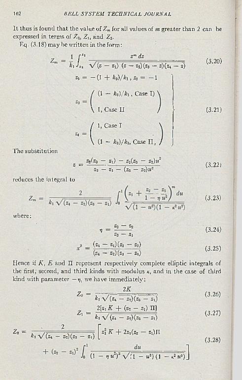
162 B E L L S Y S T E M T E C H N I C A L J O U R N A L
I t thus is found that the value of Zm for all values of m greater than 2 ean be expressed in terms of Z 0, Zi, and Z2.
Eq. (3.18) may be written in the form:
1 r 8hi J ¡2
zm dz
The substitution
V (Z — 2i) (z — Z2) ( z 3 - z ) ( z 4 - z)
Z\ = — (1 + k 0) / h i , 22 = — 1
/ (1 — ho)/hi, Case I) \
\ 1, Case II /
( if Case I \
(1 — k0)/hi, Case I I , /
22(z3 — Zi) — Z i(z3 — Z i ) u
Za
2 =•z3 — Zi — (z3 — Z2) î i 2
reduces the integral to
where:Z3 — 22
V = -------------z3 — Z]
2 _ (z4 — 2 i) (z 3 — z2)
(3.20)
(3.21)
(3.22)
(3.23)
(3.24)
(3.25)(z i - z3) ( z3 — 2i)
Hence if A’, E and II represent respectively complete elliptic integrals of the first, second, and third kinds with modulus k, and in the case of third kind with parameter — 77, we have immediately:
2 KZ„ =
Zi =
Z,, =
hi V (z4 — z2)(z3 — z 1)2[zi K + (z2 — zi) n]
k i \ / ( z i — 22)(z3 — Zi)
Wfe-lx».-*.) f* * + 2i,ta _ *,)nfo(1 — n«')1 V i 1 — «*) (1 — i.-2«1) ]
(3.26)
(3.27)
(3.28)
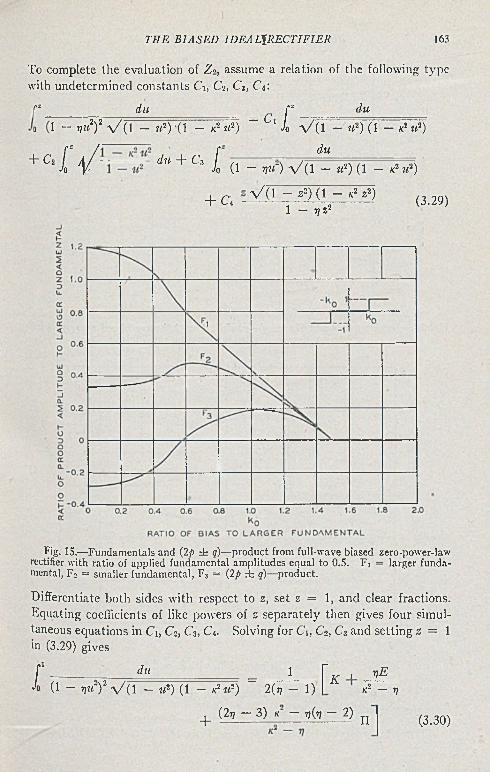
T E E B I A S E D I D E A L \ R E C T I F I E R 163
To complete the evaluation of Z«, assume a relation of the following type with undetermined constants Ci, Ci, Cj, C4:
i l y =dii - c jJo
du
+ Ci
7III2)2 s / (1 — u 2) *(1 — K2 It2) 1 Jo s / (1 — m2) ( 1 — k! u 2)
duIV ¿W “t“ C3i a - -(1 — 17«") \ / ( l — « 2) ( 1 — K2 2i2)
+ C4V ( 1 - 22) (1 ~ K2 22)
1 — 77 22(3.29)
Fig. 15.—Fundam entals and (2p ± q)—product from full-wave biased zero-power-law rectifier with ratio of applied fundam ental am plitudes equal to 0.5. F i = larger fundamental, F 2 = smaller fundam ental, F 3 = (2/> ± q)—product.
Differentiate both sides with respect to 2, set 2 = 1 , and clear fractions. Equating coefficients of like powers of 2 separately then gives four simultaneous equations in Ci, C2, C3, C4. Solving for Cj, C2, C3 and setting 2 = 1 in (3.29) gives
f 1 ------- du........... = 1 r K . veJo (1 — TjZi')2 - \ / ( l — if2) ( 1 — K2« 2) 2(77 — 1 ) K2 — 77
_l_ (2t; — 3) K — 77(77 — 2) n (3.30)
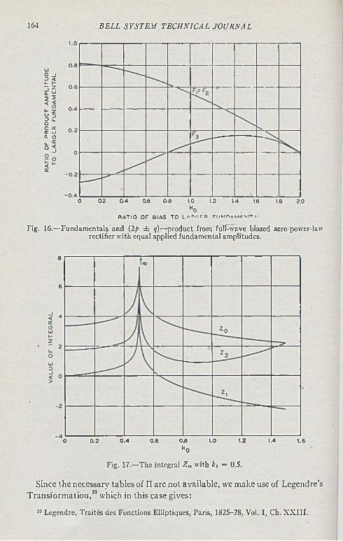
164 B E L L S Y S T E M T E C H N I C A L J O U R N A L
9 -> t í
i i
y*3 u. ÛO CC CC ua. o
S<
0 0.2 0.4 0.6 0.8 1.0 1.2 1.4 1.6 1.8 2.0
koR A TIO OF BIAS TO l / i n f = r o n i M M M r M T » '
Fig. 16.—Fundam entals and (2p ± q)—product from full-wave biased zero-power-law rectifier w ith equal applied fundam ental am plitudes.
0 0 .2 0 .4 0.6 OB 1.0 1.2 1.4 1.6
k0
Fig. 17.—T he integral Z m with k i = 0.5.
Since the necessary tables of II are not available, we make use of Legendre’s Transformation,10 which in this case gives:
10 Legendre, T raités des Fonctions Elliptiques, Paris, 1825-28, Vol. I, Ch. X X III .
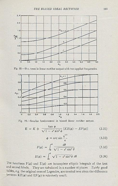
T H E B I A S E D I D E A L R E C T I F I E R 165
Aoo 2 1
0 0.2 0.4 0.6 0.8 1.0 1.2 1.4 1.6 1.8 2 .0
K0
Fig. 19.— Smaller fundam ental in biased linear rectifier output.
n = k + / i tan / - ^ (3-31)V I — «2 sin2 01/2
<t> = arc sin — (3.32)K
I* d6= 71 2 ■ , . (3.33)Jo V I - « sin- 9
r't’ __________E(<t>) = / V l - k2 sin2 0 </0 (3.34)
Jo
The functions F(<£) and E($) are incomplete elliptic integrals of the first and second kinds. They are tabulated in a number of places. Fairly goodtables, e.g. the original ones of Legendre, are needed here since the differencebetween KE($) and EF(0) is relatively small.
"iFig. 18.— D-c. term in linear rectifier o u tp u t with two applied frequencies.
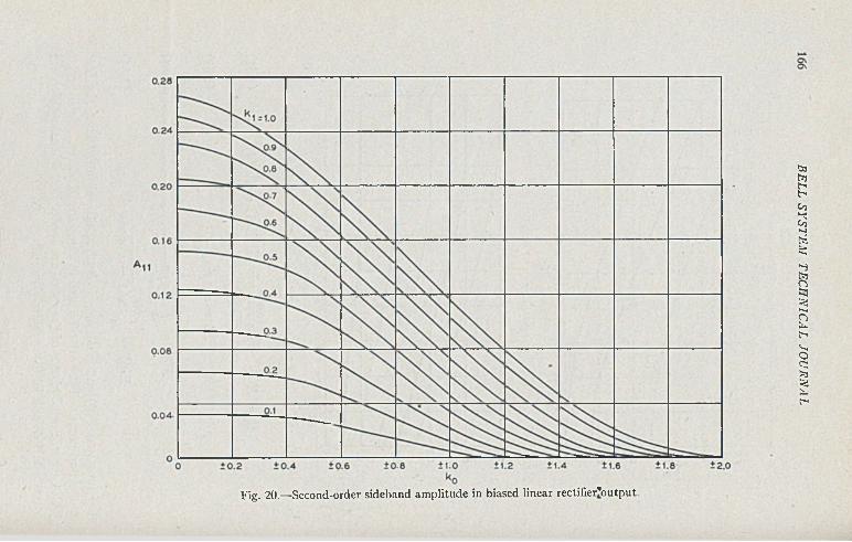
Fig. 20.—Second-order sideband am plitude in biased linear rectifier’output.
BELL SYSTEM
TE
CH
NIC
AL
JOU
RN
AL
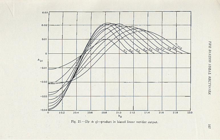
koFig. 21.— (3p ± q)—product in biased linear rectifier o u tpu t.
Cs
THE B
IASED
ID
EAL H
EC
TIF
IER
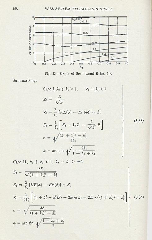
168 B E L L S Y S T E M T E C H N I C A L J O U R N A L
Summarizing:
Fig. 22.— G raph of the integral S (A’o, Ai).
Case I, Ao 4~ Ax 1, Ao — Ai <C 1
KZ„ =
V k ,
Z l = ± [KE(4>) - EF(<j>)] - Z okl
Ä ” S [ Z" h ' Z ' ~ V k , £]
in ' / r
*> 7,2«0
<j> = arc sin4~ Ao 4" Ai
(3.35)
Case II , Ao + Ax < 1, Ao — Ax > 1
2 K Z o ~ V (1 + Ax)2 - A2
Zx = I [A'£(<iO - EF(*)J - Zo Ax
* - 2 * ?(1 + AÎ - Ao)Z0 - 2A0AxZx - 2E V (1 + Ai)2 - AgJ
= 4Axy (1 + Ax)2 - A2
<j> = arc sin Aq 4" Ax
(3.36)
T I I E B I A S E D I D E A L R E C T I F I E R 169
The values of the fundamentals and third-order sum and difference products for the biased zero-power-law rectifier have been calculated by the formulas above for the cases ki = .5 and k \= 1. The resulting curves are shown in Fig. (15) and (16). The values of the auxiliary integrals Zo, Z \ , and Zi are shown for k\ = .5 in Fig. (17). These integrals become infinite at k0 = 1 — ki so that the formulas for the modulation coefficients become indeterminate at this point. The limiting values can be evaluated from the integrals (3.3), etc., directly in terms of elementary functions when the relation k0 = 1 — k\ is substituted, except for the E-function.
Limiting forms of the coefficients when k0 is small are of value in calculating the effect of a small signal superimposed on the two sinusoidal components in an unbiased rectifier. By straightforward power-series expansion in k0, we find:Zero-Power-Law Rectifier, k0 Small:
A io = — E 2 E7T2(1 — k2) kl +
~ [E - (1 - k\)K] + 4 i u y-TT k l 7T- k l \ 1 — k l
An = - J L [(i _ 2k\)E - (1 - ¿ï)i£]
K ) i m -
+
3TT2kl
2TT2k\
K - 1 - 2kl 1 - k\
E kl +
(3.37)
In the above expressions, the modulus of K and E is k\. When k0 = 0, these coefficients reduce to half the values of the full-wave unbiased zero- power-law coefficients, which have been tabulated in a previous publication.11
A c k n o w le d g m e n t
In addition to the persons already mentioned, the writer wishes to thank Miss M. C. Packer, Miss J. Lever and Mrs. A. J. Shanklin for their assistance in the calculations of this paper.
11 R. M . Kalb and W . R . B ennett, Ferrom agnetic D istortion of a Two-Frequency Wave, B. S. T . / . , Vol. X IV , April 1935, Eq. (21), p. 336.
Properties and U ses of Thermistors—Thermally Sensitive Resistors*
By J . A. B E C K E R , C. B . G R E E N a n d G. L . P E A R S O N
A new circuit elem ent and control device, the therm istor or therm ally sensitive resistor, is m ade of solid sem iconducting m aterials whose resistance decreases abou t four per cen t per centigrade degree. T he therm istor presents interesting opportunities to the designer and engineer in m any fields of technology for accomplishing tasks more simply, economically and bette r than w ith available devices. P a r t I discusses the conduction mechanism in sem iconductors and the criteria for usefulness of circuit elem ents m ade from them . T he fundam ental physical properties of therm istors, their construction, their sta tic and dynamic characteristics and general principles of operation are treated .
P a rt I I of this paper deals w ith the applications of therm istors. These include: sensitive therm om eters and tem perature control elem ents, simple tem perature compensators, u ltrahigh frequency power meters, au tom atic gain controls for transmission system s such as the Types K2 and L I carrier telephone system s, voltage regulators, speech volume lim iters, compressors and expandors, gas pressure gauges and flowmeters, m eters for therm al conductivity determ ination of liquids, and contactless tim e delay devices. Therm istors w ith short tim e cons ta n ts have been used as sensitive bolometers and show promise as simple comp ac t audio-frequency oscillators, m odulators and amplifiers.
PART I—PRO PERTIES OF THERM ISTORS
I n t r o d u c t io n
THERMISTORS, or tlierma&y sensitive resistors, are devices made of solids whose electrical resistance varies rapidly with temperature.
Even though they are only about 15 years old they have already found important and large scale uses in the telephone plant and in military equipments. Some of these uses are as time delay devices, protective devices, voltage regulators, regulators in carrier systems, speech volume limiters, test equipment for ultra-high-frequency power, and detecting elements for very small radiant power. In all these applications thermistors were chosen because they are simple, small, rugged, have a long life, and require little maintenance. Because of these and other desirable properties, thermistors promise to become new circuit elements which will be used extensively in the fields of communications, radio, electrical and thermal instrumentation, research in physics, chemistry and biology, and war technolog)'. Specific types of uses which will be discussed in the second part of this paper include: 1) simple, sensitive and fast responding thermometers,
* Published in Elec. Engg., Novem ber 1946.The authors acknowledge their indebtedness to M essrs. J . H . Scad and H . C. Theucrer
for furnishing samples for m ost of the curves in Fig. 4, and to M r. G. K . Teal for the data for the lowest curve in th a t figure.
170
P R O P E R T I E S A N D U S E S OF T H E R M I S T O R S 171
temperature compensators and temperature control devices; 2) special switching devices without moving contacts; 3) regulators or volume limiters; 4) pressure gauges, flowmeters, and simple meters for measuring thermal conductivity in liquids and gases; 5) time delay and surge suppressors; 6) special oscillators, modulators and amplifiers for relatively low frequencies. Before these uses are discussed in detail it is desirable to present the physical principles which determine the properties of thermistors.
The question naturally arises “why have devices of this kind come into use only recently?” The answer is that thermistors are made of semiconductors and that the resistance of these can vary by factors up to a thousand or a million with surprisingly small amounts of certain impurities, with heat treatment, methods of making contact and with the treatment during life or use. Consequently the potential application of semiconductors was discouraged by experiences such as the following: two or more units made by what appeared to 'be the same process would show large variations in their properties. Even the same unit might change its resistance by factors of two to ten by exposure to moderate temperatures or to the passage of current. Before semiconductors could seriously be considered in industrial applications, it was necessary to devote a large amount of research and development effort to a study of the nature of the conductivity in semiconductors, and of the effect of impurities and heat treatment on this conductivity, and to methods of making reliable and permanent contacts to semiconductors. Even though Faraday discovered that the resistance of silver sulphide changed rapidly with temperature, and even though thousands of other semiconductors have been found to have large negative temperature coefficients of resistance, it has taken about a century of effort in physics and chemistry to give the engineering profession this new tool which may have an influence similar to that of the vacuum tube and may replace vacuum tubes in many instances.
If thermistors are to be generally useful in industry:1) it should be possible to reproduce units having the same character
istics;2) it should be possible to maintain constant characteristics during use;
the contact should be permanent and the unit should be chemically inert;
3) the units should be mechanically rugged;4) the technique should be such that the material can be formed into
various shapes and sizes;5) it should be possible to cover a wide range of resistance, temperature
coefficient and power dissipation.I hermistors might be made by any method by which a semiconductor
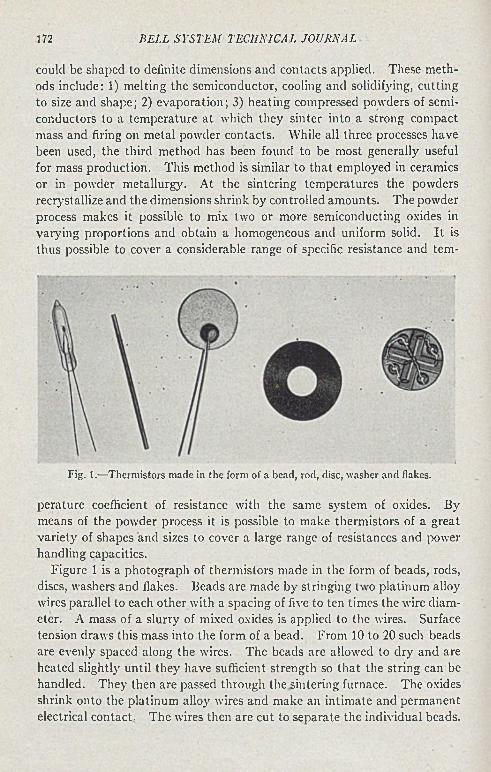
172 B E L L S Y S T E M T E C H N IC A L J O U R N A L
could be shaped to definite dimensions and contacts applied. These methods include: 1) melting the semiconductor, cooling and solidifying, cutting to size and shape; 2) evaporation; 3) heating compressed powders of semiconductors to a temperature at which they sinter into a strong compact mass and firing on metal powder contacts. While all three processes have been used, the third method has been found to be most generally useful for mass production. This method is similar to that employed in ceramics or in powder metallurgy. At the sintering temperatures the powders recrystallize and the dimensions shrink by controlled amounts. The powder process makes it possible to mix two or more semiconducting oxides in varying proportions and obtain a homogeneous and uniform solid. I t is thus possible to cover a considerable range of specific resistance and tem-
Fig. 1.—Therm istors m ade in the form of a bead, rod, disc, washer and flakes.
perature coefficient of resistance with the same system of oxides. By means of the powder process it is possible to make thermistors of a great variety of shapes and sizes to cover a large range of resistances and power handling capacities.
Figure 1 is a photograph of thermistors made in the form of beads, rods, discs, washers and flakes. Beads are made by stringing two platinum alloy wires parallel to each other with a spacing of five to ten times the wire diameter. A mass of a slurry of mixed oxides is applied to the wires. Surface tension draws this mass into the form of a bead. From 10 to 20 such beads are evenly spaced along the wires. The beads are allowed to dry and are heated slightly until they have sufficient strength so that the string can be handled. They then are passed through the sintering furnace. The oxides shrink onto the platinum alloy wires and make an intimate and permanent electrical contact, The wires then are cut to separate the individual beads.
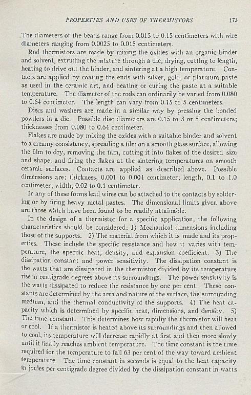
P R O P E R T I E S A N D U S E S OF T H E R M I S T O R S 173
The diameters of the beads range from 0.015 to 0.15 centimeters with wire diameters ranging from 0.0025 to 0.015 centimeters.
Rod thermistors are made by mixing the oxides with an organic binder and solvent, extruding the mixture through a die, drying, cutting to length, heating to drive out the binder, and sintering at a high temperature. Contacts are applied by coating the ends with silver, gold, or platinum paste as used in the ceramic art, and heating or curing the paste a t a suitable temperature. The diameter of the rods can ordinarily be varied from 0.080 to 0.64 centimeter. The length can vary from 0.15 to 5 centimeters.
Discs and washers are made in a similar way by pressing the bonded powders in a die. Possible disc diameters are 0.15 to 3 or 5 centimeters; thicknesses from 0.080 to 0.64 centimeter.
Flakes are made by mixing the oxides with a suitable binder and solvent to a creamy consistency, spreading a film on a smooth glass surface, allowing the film to dry, removing the film, cutting it into flakes of the desired size and shape, and firing the flakes at the sintering temperatures on smooth ceramic surfaces. Contacts are applied as described above. Possible dimensions are: thickness, 0.001 to 0.004 centimeter; length, 0.1 to 1.0 centimeter; width, 0.02 to 0.1 centimeter.
In any of these forms lead wires can be attached to the contacts by soldering or by firing heavy metal pastes. The dimensional limits given above are those which have been found to be readily attainable.
In the design of a thermistor for a specific application, the following characteristics should be considered: 1) Mechanical dimensions including those of the supports. 2) The material from which it is made and its properties. These include the specific resistance and how it varies with temperature, the specific heat, density, and expansion coefficient. 3) The dissipation constant and power sensitivity. The dissipation constant is the watts that are dissipated in the thermistor divided b y its temperature rise in centigrade degrees above its surroundings. The power sensitivity is the watts dissipated to reduce the resistance by one per cent. These constants are determined by the area and nature of the surface, the surrounding medium, and the thermal conductivity of the supports. 4) The heat capacity which is determined by specific heat, dimensions, and density. 5) The. time constant. This determines how rapidly the thermistor will heat or cool. If. a thermistor is heated above its surroundings and then allowed to cool, its temperature will decrease rapidly at first and then more slowly until it finally reaches ambient temperature. The time constant is the time required for the temperature to fall 63 per cent of the way toward ambient temperature. The time constant in seconds is equal to the heat capacity m joules per centigrade degree divided by the dissipation constant in watts
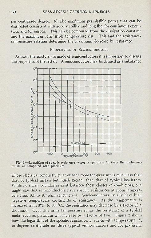
m B E L L S Y S T E M T E C H N I C A L J O U R N A L
per centigrade degree. 6) The maximum permissible power that can be dissipated consistent with good stability and long life, for continuous operation, and for surges. This can be computed from the dissipation constant and the maximum permissible temperature rise. This and the resistance- temperature relation determine the maximum decrease in resistance.
P r o p e r t i e s o f S e m i c o n d u c t o r s
As most thermistors are made of semiconductors it is important to discuss the properties of the latter. A semiconductor may be defined as a substance
Fig. 2.—Logarithm of specific resistance versus tem perature for three therm istor m aterials as com pared w ith p latinum .
whose electrical conductivity a t or near room temperature is much less than that of typical metals but much greater than that of typical insulators. While no sharp boundaries exist between these classes of conductors, one might say that semiconductors have specific resistances a t room temperature from 0.1 to 109 ohm centimeters. Semiconductors usually have high negative temperature coefficients of resistance. As the temperature is increased from 0°C. to 300°C., the resistance may decrease by a factor of a thousand. Over this same temperature range the resistance of a typical metal such as platinum will increase by a factor of two. Figure 2 shows how the logarithm of the specific resistance, p, varies with temperature, T, in degrees centigrade for three typical semiconductors and for platinum.
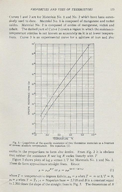
P R O P E R T I E S A N D U S E S OF T H E R M I S T O R S 175
Curves 1 and 2 are for Materials No. 1 and No. 2 which have been extensively used to date. Material No. 1 is composed of manganese and nickel oxides. M aterial No. 2 is composed of oxides of manganese, nickel and cobalt. The dashed part of Curve 2 covers a region in which the resistance- temperature relation is not known as accurately a s it is a t lower temperatures. Curve 3 is an experimental curve for a mixture of iron and zinc
Fig. 3.—Logarithm of the specific resistance of two therm istor m aterials as a function of inverse absolute tem perature. See equation (1).
oxides in the proportions to form zinc ferrite. From Fig. 2 it is obvious that neither the resistance R nor log R varies linearly with T.
Figure 3 shows plots of log p versus 1 / T for Materials No. 1 and No. 2. These do form approximate straight lines. lienee
_ b i t „ _ ( B / r ) - ( s / r 0) / «p = pxt or p = p0e (1)
where T = temperature in degrees Kelvin ;p„ = p when T = °o or \ / T = 0; Po = p when T = T 0 ; e = Naperian base = 2.718 and B is a constant equal to 2.303 times the slope of the straight lines in Fig. 3. The dimensions of B
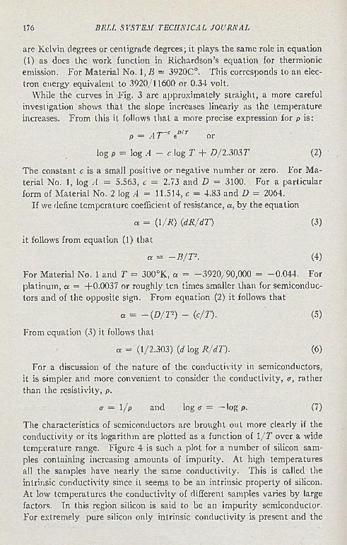
176 B E L L S Y S T E M T E C H N I C A L J O U R N A L
are Kelvin degrees or centigrade degrees; it plays the same role in equation (1) as does the work function in Richardson’s equation for thermionic emission. For Material No. 1, B = 3920C0. This corresponds to an electron energy equivalent to 3920/11600 or 0.34 volt.
While the curves in Fig. 3 are approximately straight, a more careful investigation shows that the slope increases linearly as the temperature increases. From this it follows that a more precise expression for p is:
, r j^ -C D lTp = A I t or
log p = log A - c log T + D/2.3031' (2)
The constant c is a small positive or negative number or zero. For M aterial No. 1, log A = 5.563, c = 2.73 and D — 3100. For a particular form of Material No. 2 log A = 11.514, c — 4.83 and D = 2064.
If we define temperature coefficient of resistance, a, by the equation
a = (1 /R ) (dR /dT ) (3)
it follows from equation (1) that
a = - B / T - . (4)
For Material No. 1 and T = 300°K, a = -3920/90,000 = -0 .044 . For platinum, a = +0.0037 or roughly ten times smaller than for semiconductors and of the opposite sign. From equation (2) it follows that
« = — (D /T 2) - (c/T). (5)
From equation (3) it follows that
a = (1/2.303) (d log R /dT ). (6)
For a discussion of the nature of the conductivity in semiconductors, it is simpler and more convenient to consider the conductivity, cr, rather than the resistivity, p.
c = 1/p and log a = —log p. (7)
The characteristics of semiconductors are brought out more clearly if the conductivity or its logarithm are plotted as a function of 1 / T over a wide temperature range. Figure 4 is such a plot for a number of silicon samples containing increasing amounts of impurity. At high temperatures all the samples have nearly the same conductivity. This is called the intrinsic conductivity since it seems to be an intrinsic property of silicon. At low temperatures the conductivity of different samples varies by large factors. In this region silicon is said to be an impurity semiconductor. For extremely pure silicon only intrinsic conductivity is present and the
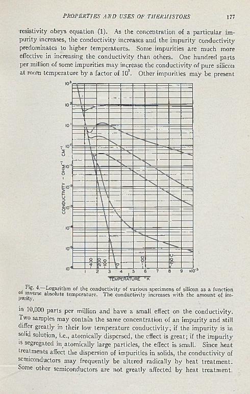
P R O P E R T I E S A R D U S E S OE T H E R M I S T O R S 177
resistivity obeys equation (1). As the concentration of a particular impurity increases, the conductivity increases and the impurity conductivity predominates to higher temperatures. Some impurities are much more effective in increasing the conductivity than others. One hundred parts per million of some impurities may increase the conductivity of pure silicon at room temperature by a factor of ID7. Other impurities may be present
Fig. 4. Logarithm of the conductivity of various specimens of silicon as a function y ™ absolute tem perature. T he conductivity increases w ith the am ount of im-
'n 10,000 parts per million and have a small effect on the conductivity. Two samples may contain the same concentration of an impurity and still differ greatly in their low temperature conductivity; if the impurity is in solid solution, i.e., atomically dispersed, the effect is great; if the impurity is segregated in atomically large particles, the effect is small. Since heat treatments affect the dispersion of impurities in solids, the conductivity of semiconductors may frequently be altered radically by heat treatm ent. Some other semiconductors are not greatly affected by heat treatment.
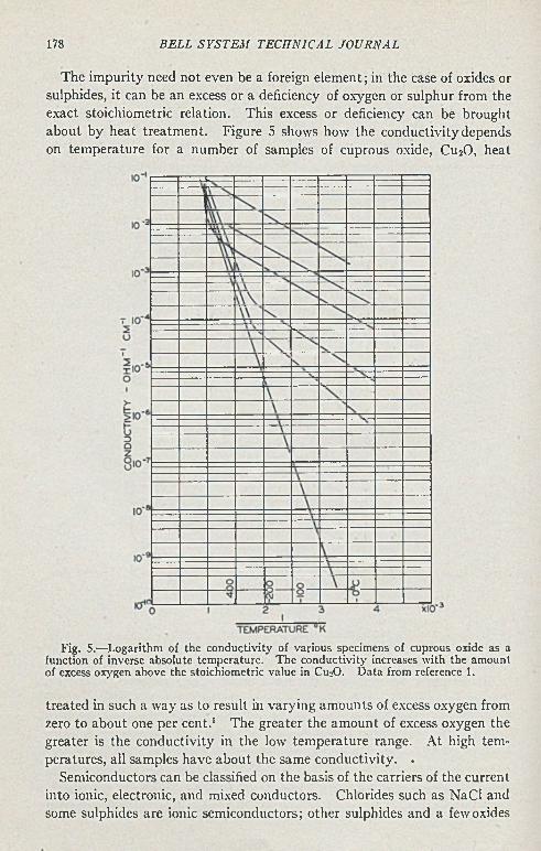
178 B E L L S Y S T E M T E C H N I C A L J O U R N A L
The impurity need not even be a foreign element; in the case of oxides or sulphides, it can be an excess or a deficiency of oxygen or sulphur from the exact stoichiometric relation. This excess or deficiency can be brought about by heat treatment. Figure 5 shows how the conductivity depends on temperature for a number of samples of cuprous oxide, Cu20 , heat
Fig. 5.—Logarithm of the conductivity of various specimens of cuprous oxide as a function of inverse absolute tem perature. T he conductivity increases w ith the am ount of excess oxygen above the stoichiom etric value in Cu:0 . D a ta from reference 1.
treated in such a way as to result in varying amounts of excess oxygen from zero to about one per cent.1 The greater the amount of excess oxygen the greater is the conductivity in the low temperature range. At high temperatures, all samples have about the same conductivity. .
Semiconductors can be classified on the basis of the carriers of the current into ionic, electronic, and mixed conductors. Chlorides such as NaCl and some sulphides are ionic semiconductors; other sulphides and a few oxides
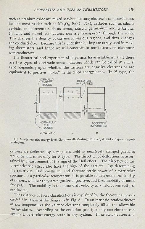
P R O P E R T IE S A N D U S E S OF T H E R M I S T O R S 179
such as uranium oxide are mixed semiconductors; electronic semiconductors include most oxides such as M n20 3 , Fe203, NiO, carbides such as silicon carbide, and elements such as boron, silicon, germanium and tellurium. In ionic and mixed conductors, ions are transported through the solid. This changes the density of carriers in various regions, and thus changes the conductivity. Because this is undesirable, they are rarely used in making thermistors, and hence we will concentrate our interest on electronic semiconductors.
The theoretical and experimental physicists have established that there are two types of electronic semiconductors which can be called N and P type, depending upon whether the carriers are negative electrons or are equivalent to positive “holes” in the filled energy band. In N type, the
IN T R IN S IC N P
Fig. 6.—Schematic energy level diagram s illustrating intrinsic, N and P types of semiconductors.
carriers are deflected by a magnetic field as negatively charged particles would be and conversely for P type. The direction of deflections is ascertained by measurement of the sign of the Hall effect. The direction of the thermoelectric effect also fixes the sign of the carriers. By determining the resistivity, Flail coefficient and thermoelectric power of a particular specimen at a particular temperature it is possible to determine the density of carriers, whether they are negative or positive, and their mobility or mean free path. The mobility is the mean drift velocity in a field of one volt per centimeter.
The existence of these classifications is explained by the theoretical physicist2 •3 ■4 in terms of the diagrams in Fig. 6. In an intrinsic semiconductor at low temperatures the valence electrons completely fill all the allowable energy states. According to the exclusion principle only one electron can occupy a particular energy state in any system. In semiconductors and
180 B E L L S Y S T E M T E C H N I C A L J O U R N A L
insulators there exists a region of energy values, just above the allowed band, which are not allowed. The height of this unallowed band is expressed in equivalent electron volts, AE. Above this unallowed band there exists an allowed band; but at low temperatures there are no electrons in this band. When a field is applied across such a semiconductor, no electron can be accelerated, because if it were accelerated its energy would be increased to an energy state which is either fdled or unallowed. As the temperature is raised some electrons acquire sufficient energy to be raised across the unallowed band into the upper allowed band. These electrons can be accelerated into a slightly higher energy state by the applied field and thus can carry current. For every electron that is put into an “activated” state there is left behind a “hole” in the normally filled band. Other electrons having slightly lower energies can be accelerated into these holes by the applied field. The physicist has shown that these holes act toward the applied field as if they were particles having a charge equal to that of an electron but of opposite sign and a mass equal to or somewhat larger than the electronic mass. In an intrinsic semiconductor about half the conductivity is due to electrons and half due to holes.
The quantity AE is related to B in equation (1) by:
in which B is in centigrade degrees, AE is in volts, e is the electronic charge in coulombs, k is Boltzmann’s constant in joules per centigrade degree. The value of e/k is 11,600 so that
The difference between metals, semiconductors, and insulators results from the value of AE. For metals AE is zero or very small. For semiconductors AE is greater than about 0.1 volt but less than about 1.5 volts. For insulators AE is greater than about 1.5 volts.
Some impurities with positive valencies which may be present in the semiconductor may have energy states such that A£i volts equivalent energy can raise the valence electron of the impurity atom into the allowed conduction band. See Figure 6. The electron now can take part in conduction; the donator impurity is a positive ion which is usually bound to a particular location and can take no part in the conductivity. These are excess or N type conductors. The conductivity depends on the density of dono- tors, A £ i , and T.
Similarly some other impurity with negative valencies may have an energy state A£2 volts above the top of the filled band. At room temperature or higher, an electron in the filled band may be raised in energy and
2B = (AE) e/k (B)
AE = B/5800. (8a)
P R O P E R T I E S A R D U S E S OF T H E R M I S T O R S 181
accepted by the impurity which then becomes a negative ion and usually is immobile. However, the resulting hole can take part in the conductivity.
In all cases represented in Fig. 6 an electron occupying a higher energy level than a positive ion or a hole has a certain probability that in any short interval of time it will drop into a lower energy state. However, during this same time interval there will be electrons which will be raised to a higher energy level by thermal agitation. When the number of electrons per second which are being elevated is equal to the number which are descending in energy, equilibrium prevails. The conductivity, a, is then
<r = N e Vi + P e vt (9)
where N and P are the concentrations of electrons and holes respectively, e is the charge on the electron, i'i and v2 are the mobilities of electrons and holes respectively.
The above picture explains the following experimental facts which otherwise are difficult to interpret. 1) N type oxides, such as ZnO, when heated in a neutral or slightly reducing atmosphere become good conductors, presumably because they contain excess zinc which can donate electrons. If they then are heated in atmospheres which are increasingly more oxidizing their conductivity decreases until eventually they are intrinsic semiconductors or insulators. 2) P type oxides, such as NiO, when heat treated in strongly oxidizing atmospheres are good conductors. Very likely they contain oxygen in excess of the stoichiometric relation and this oxygen accepts additional electrons. When these are heated in less oxidizing or neutral atmospheres they become poorer conductors, semiconductors, or insulators. 3) When a P type oxide is sintered with another P type oxide, the conductivity increases. Similarly for two N type oxides. But when a P type is added to an N type the conductivity decreases. 4) If a metal forms several oxides the one in which the metal exerts its highest valence is N type, while the one in which it exerts its lowest valence will be P type.5
For several reasons it is desirable to survey the whole field of semiconductors for resistivity and temperature coefficient. One way in which this might be done is to draw a line in Figure 3 for each specimen. Before long such a figure would consist of such a maze of intersecting lines that it would be difficult to single out and follow any one line. The information can be condensed by plotting log p0 versus B in equation (1) for each specimen.6 The most important characteristics of a specimen thus are represented by a single point and many more specimens can be surveyed in a single diagram. Figure 7 shows such a plot for a large number of semiconductors investigated at these Laboratories or reported in the literature. Values for po and B are given for T = 25 degrees centigrade. The points form a sort of
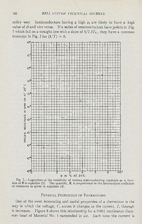
182 B E L L S Y S T E M T E C H N IC A L J O U R N A L
milky way. Semiconductors having a high p0 are likely to have a high value of B and vice versa. If a series of semiconductors have points in Fig. 7 which fall on a straight line with a slope of 1/2.3jF0 , they have a common intercept in Fig. 3 for (1/7") = 0.
10'
10'
io-
I0‘
1 'O3! zU< I01 i—
2o 10U.
ëV)
10'
10"
icp 3 4B IN °C AT 2 5 qC
XIO3
Fig. 7.—Logarithm of the resistivity of various semiconducting m aterials as a function of B in equation (1). T he quantity , B , is proportional to the tem perature coefficient of resistance as given in equation (4).
P h y s i c a l P r o p e r t i e s o f T h e r m i s t o r s
One of the most interesting and useful properties of a thermistor is the way in which the voltage, V, across it changes as the current, I , through it increases. Figure 8 shows this relationship for a 0.061 centimeter diameter bead of Material No. 1 suspended in air. Each time the current is
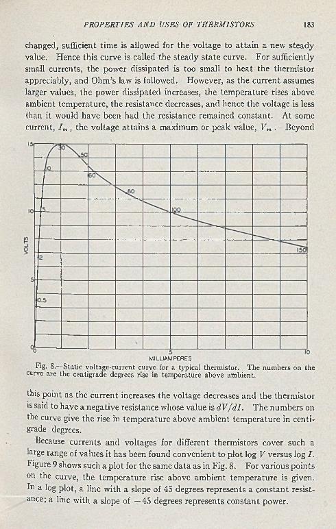
P R O P E R T I E S A N D U S E S OF T H E R M I S T O R S 183
changed, sufficient time is allowed for the voltage to attain a new steady value. Hence this curve is called the steady state curve. For sufficiently small currents, the power dissipated is too small to heat the thermistor appreciably, and Ohm’s law is followed. However, as the current assumes larger values, the power dissipated increases, the temperature rises above ambient temperature, the resistance decreases, and hence the voltage is less than it would have been had the resistance remained constant. At some current, I m , the voltage attains a maximum or peak value, Vm . Beyond
M ILU AM PERES
Fig. S.—Static voltage-current curve for a typical therm istor. The num bers on the curve are the centigrade degrees rise in tem perature above am bient.
this point as the current increases the voltage decreases and the thermistor is said to have a negative resistance whose value is d V /d l. The numbers on the curve give the rise in temperature above ambient temperature in centigrade degrees.
Because currents and voltages for different thermistors cover such a large range of values it has been found convenient to plot log V versus log I. Figure 9 shows such a plot for the same data as in Fig. 8. For various points on the curve, the temperature rise above ambient temperature is given. In a log plot, a line with a slope of 45 degrees represents a constant resistance; a line with a slope of —45 degrees represents constant power.
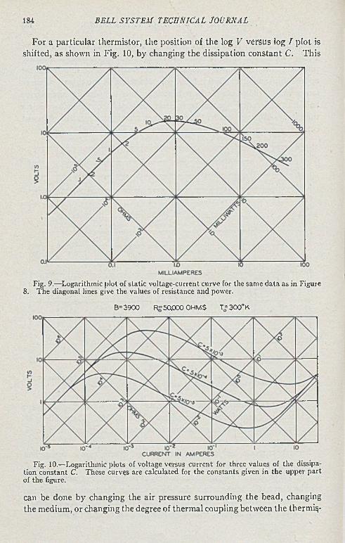
184 B E L L S Y S T E M T E C H N I C A L J O U R N A L
For a particular thermistor, the position of the log V versus log I plot is shifted, as shown in Fig. 10, by changing the dissipation constant C. This
Fig. 9.—Logarithm ic plo t of s ta tic voltage-current curve for the same d a ta as in Figure 8. T he diagonal lines give the values of resistance and power.
B -3 9 0 0 R =50,000 OHMS T = 3 00°K
Fig. 10.—Logarithm ic plots of voltage versus curren t for three values of the dissipation constan t C. These curves are calculated for the constants given in the upper p a rt of the figure.
can be done by changing the air pressure surrounding the bead, changing the medium, or changing the degree of thermal coupling between the thermi$-
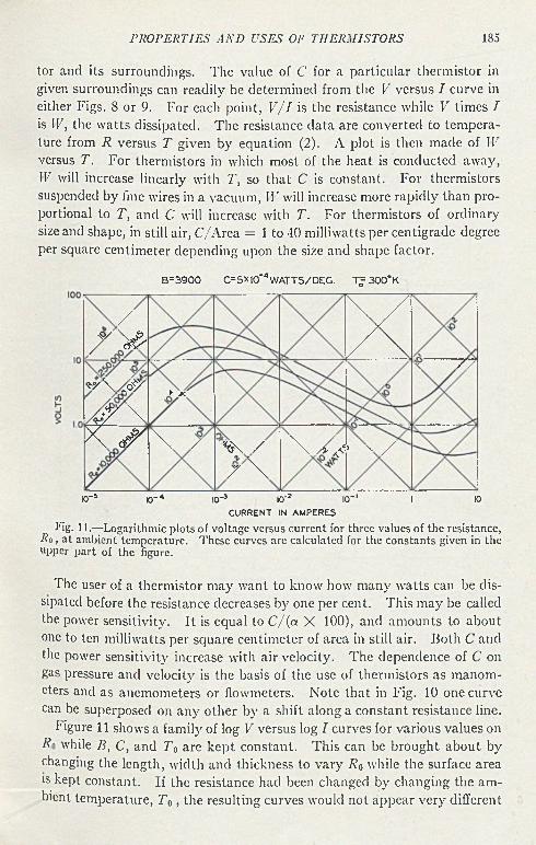
P R O P E R T I E S A N D U S E S OF T H E R M I S T O R S 185
tor and its surroundings. The value of C for a particular thermistor in given surroundings can readily be determined from the V versus I curve in either Figs. 8 or 9. For each point, V /I is the resistance while V times I is IF, the watts dissipated. The resistance data are converted to temperature from R versus T given by equation (2). A plot is then made of IF versus T. For thermistors in which most of the heat is conducted away, IF will increase linearly with T, so that C is constant. For thermistors suspended by fine wires in a vacuum, IF will increase more rapidly than proportional to T, and C will increase with T. For thermistors of ordinary size and shape, in still air, C/Area = 1 to 40 milliwatts per centigrade degree per square centimeter depending upon the size and shape factor.
B=3900 C=5X10'4 WATTS/DEG. T ^3 0 0 °K
/ Q - x*y\/&/X y \A«/ \
► jK
X / /
X. rfX \ / kX /z \
V / / > Nv X
10 '4 10' * I0 '3 IO'z 1 0 '1 I 10
CURRENT IN AMPERES
Fig. 11.—Logarithmic plots of voltage versus curren t for three values of the resistance, R o, a t am bient tem perature. These curves are calculated for the constan ts given in the upper p a r t of the figure.
The user of a thermistor may want to know how many watts can be dissipated before the resistance decreases by one per cent. This may be called the power sensitivity. I t is equal to C /(a X 100), and amounts to about one to ten milliwatts per square centimeter of area in still air. Both C and the power sensitivity increase with air velocity. The dependence of C on gas pressure and velocity is the basis of the use of thermistors as manometers and as anemometers or flowmeters. Note that in Fig. 10 one curve can be superposed on any other by a shift along a constant resistance line.
1'igure 11 shows a family of log V versus log I curves for various values on Ro while B , C, and T 0 are kept constant. This can be brought about by changing the length, width and thickness to vary R 0 while the surface area is kept constant. If the resistance had been changed by changing the am bient temperature, T 0 , the resulting curves would not appear very different
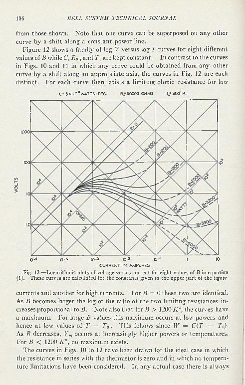
186 B E L L S Y S T E M T E C H N I C A L J O U R N A L
from those shown. Note that one curve can be superposed on any other curve by a shift along a constant power line.
Figure 12 shows a family of log V versus log I curves for eight different values of B while C, R o , and T 0 are kept constant. In contrast to the curves in Figs. 10 and 11 in which any curve could be obtained from any other curve by a shift along an appropriate axis, the curves in Fig. 12 are each distinct. For each curve there exists a limiting ohmic resistance for low
C = 5 X 1 0 '4 WATTS/DEG. 50,000 OHMS To“ 3 0 0 "K
1000
100
o
l.(
O '5 K>-4 I0 -3 I0-2 10-' I 10
CURRENT IN AMPERES
Fig. 12.—Logarithm ic p lo ts of voltage versus cu rren t for eight values of B in equation (1). These curves are calculated for the constan ts given in the upper p a r t of the figure.
currents and another for high currents. For B = 0 these two are identical. As B becomes larger the log of the ratio of the two limiting resistances increases proportional to B. Note also that for B > 1200 K°, the curves have a maximum. For large B values this maximum occurs a t low powers and hence a t low values of T — T0 ■ This follows since IV = C(T — T 0)- As B decreases, Vm occurs at increasingly higher powers or temperatures. For B < 1200 K°, no maximum exists.
The curves in Figs. 10 to 12 have been drawn for the ideal case in which the resistance in series with the thermistor is zero and in which no temperature limitations have been considered. In any actual case there is always
P R O P E R T I E S A N D U S E S OF T H E R M I S T O R S 187
some unavoidable small resistance, such as that of the leads, in series with the thermistor and hence the parts of the curves corresponding to low resistances may not be observable. Also at high powers the temperature may attain such values that something in the thermistor structure will go to pieces thus limiting the range of observation. These unobservable ranges have been indicated by dashed lines in Fig. 12. The exact location of the dashed portions will of course depend on how a completed thermistor is constructed. In setting these limits consideration is given to temperature limitations beyond which aging effects might become too great.
The curves in Figs. 9 to 12 have been computed on the basis of the following.equations:
R = R 0 = y i j (1Q)
W = C (T - To) = V I (11)
For these curves the constants R 0 , T0 , B, and C are specified. The values of temperature, Tm , power, Wm , resistance, Rm , voltage, Vm , and current, Im , that prevail a t the maximum in the voltage current curve are given by the following equations in which Tm is chosen as the independent parameter. By differentiating equations (10) and (11) with respect to I, putting the derivatives equal to zero, one obtains
T l = B (T m - To) (12)
whose solution is
Tm = (/i/2) (1 T V l - 4To/B). (13)
The minus sign pertains to the maximum in Figs. 10 to 12 while the plus sign pertains to the minimum. Note that T m depends only on B and T 0 , and not on R, R 0 or C. From equations (4), (10) and (11) it follows that:
- am (Trn - To) = 1 (14)
Wm = C(Tm - To) (15)
Rm = Ro t~rm'To = Ro <-1[l - (Tm - To)/T0 +
(1/2){(Tm - To)/To}2 ] (16)
Vm = [C R 0 (Tm - To) (e~Tm,To)]m
= {[C Ro (Tm - To) [1 - (Tm - To)/To +
(1/2) {(T,n - T o )/T o \ ' ] | ! 1/2 (17)
In = [(C/Ro) (Tm - To) er ”‘/r °]1/2
= 11 (C/Ro) (Tm - To) e[l + (Tm ~ To)/To +
(1/2) {(r m — To)/Toy -+ ••• ])}>/2 (18)
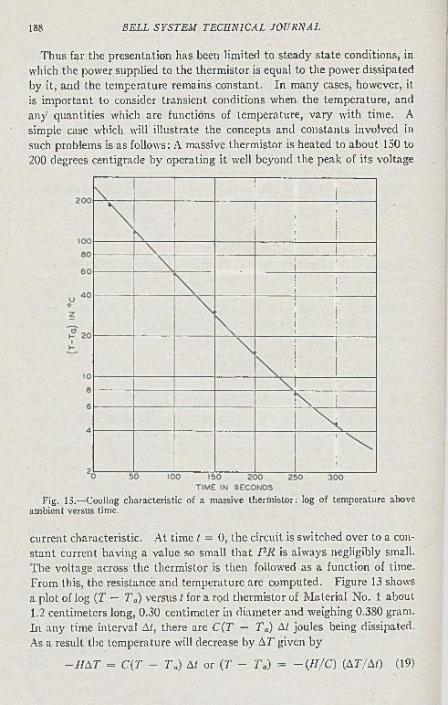
188 B E L L S Y S T E M T E C H N IC A L J O U R N A L
Thus far the presentation has been limited to steady state conditions, in which the power supplied to the thermistor is equal to the power dissipated by it, and the temperature remains constant. In many cases, however, it is important to consider transient conditions when the temperature, and any quantities which are functions of temperature, vary with time. A simple case which will illustrate the concepts and constants involved in such problems is as follows: A massive thermistor is heated to about 150 to 200 degrees centigrade by operating it well beyond the peak of its voltage
Fig. 13.—Cooling characteristic of a massive therm istor: log of tem perature above am bient versus time.
current characteristic. At time t = 0, the circuit is switched over to a constant current having a value so small that P R is always negligibly small. The voltage across the thermistor is then followed as a function of time. From this, the resistance and temperature are computed. Figure 13 shows a plot of log (T — T a) versus t for a rod thermistor of Material No. 1 about 1.2 centimeters long, 0.30 centimeter in diameter and weighing 0.380 gram. In any time interval At, there are C (T — T a) At joules being dissipated. As a result the temperature will decrease by AT given by
—H AT = C(T - T a) At or (T - T a) = ~ (H /C ) (AT/At) (19)
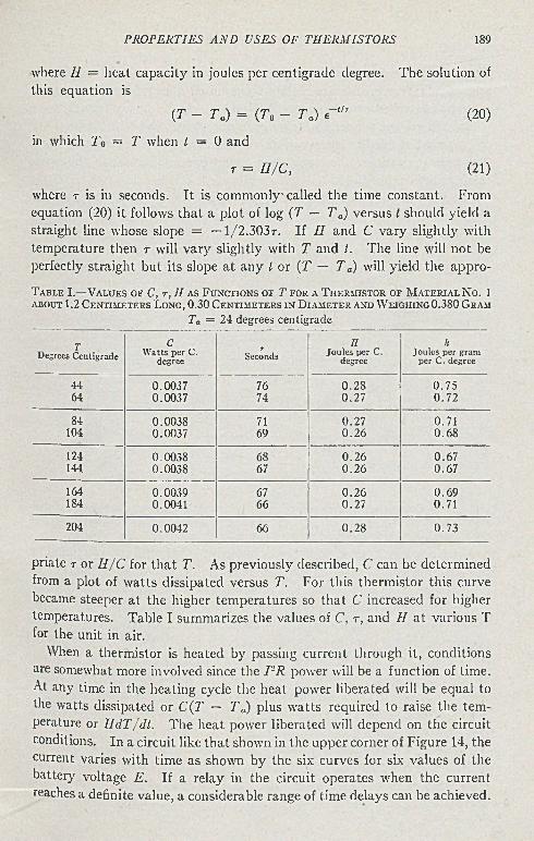
P R O P E R T IE S A N D U S E S OF T H E R M I S T O R S 189
where II = heat capacity in joules per centigrade degree. The solution of this equation is
(T - T a) = (To - T a) T i/T (20)
in which To = T when I — 0 and
r = E /C , (21)
where t is in seconds. I t is commonly called the time constant. From equation (20) it follows that a plot of log (T — T a) versus t should yield a straight line whose slope = — 1/2.303t. If II and C vary slightly with temperature then r will vary slightly with T and t. The line will not be perfectly straight but its slope at any I or (T — T a) will yield the appro-
T a b lf . I . — V a lu e s o f C, t , I I as F u n c t io n s o f T f o r a T h e rm is to r o f M a t e r ia l N o. ] ab ou t 1.2 C e n tim e te rs L o n g , 0.30 C e n tim e te rs in D ia m e te r a n d W e ig h in g 0.380 G ram
Ta = 24 degrees centigrade
TDegrees Centigrade
CWatts per C.
degreeT
SecondsI I
Joules per C. degree
hJoules per gram
per C. degree
44 0.0037 76 0 .28 0.7564 0.0037 74 0.27 0.72
84 0.0038 71 0.27 0.71104 0.0037 69 0 .26 0.68
124 0.0038 68 0 .26 0.67144 0.0038 67 0 .26 0.67
164 0.0039 67 0 .26 0.69184 0.0041 66 0.27 0.71
204 0.0042 66 0 .28 0.73
priate r or II/C for that T. As previously described, C can be determined from a plot of watts dissipated versus T. For this thermistor this curve became steeper at the higher temperatures so that C increased for higher temperatures. Table I summarizes the values of C, r, and II a t various T for the unit in air.
When a thermistor is heated by passing current through it, conditions are somewhat more involved since the P R power will be a function of time. At any time in the heating cycle the heat power liberated will be equal to the watts dissipated or C (T — T a) plus watts required to raise the temperature or H dT/dl. The heat power liberated will depend on the circuit conditions. In a circuit like that shown in the upper comer of Figure 14, the current varies with time as shown by the six curves for six values of the battery voltage E. If a relay in the circuit operates when the current reaches a definite value, a considerable range of time delays can be achieved.
190 B E L L S Y S T E M T E C H N I C A L J O U R N A L
This family of curves will be modified by changes in ambient temperature and where rather precise time delays are required, the ambient temperature must be controlled or compensated.
Since thermistors cover a wide range in size, shape, and heat conductivity of surrounding media, large variations in II, C, and r can be produced. The time constant can be varied from about one millisecond to about ten minutes or a millionfold.
One very important property of a thermistor is its aging characteristic or how constant the resistance at a given temperature stays with use. To obtain a stable thermistor it is necessary to: 1) select only semiconductors which are pure electronic conductors; 2) select those which do not change chemically when exposed to the atmosphere at elevated temperatures;
Fig. 14.— C urrent versus time curves for six values of the b a tte ry voltage in the circuit shown in the insert.
3) select one which is not sensitive to impurities likely to be encountered in manufacture or in use; 4) treat it so that the degree of dispersion of thecritical impurities is in equilibrium or else that the approach to equilibrium is very slow at operating temperatures; 5) make a contact which is intimate,sticks tenaciously, has an expansion coefficient compatible with the semiconductor, and is durable in the atmospheres to which it will be exposed;6) in some cases, enclose the thermistor in a thin coat of glass or material impervious to gases and liquids, the coat having a suitable expansion coefficient; 7) preage the unit for several days or weeks at a temperature somewhat higher than that to which it will be subjected. By taking these precautions remarkably good stabilities can be attained.
Figure 15 shows aging data taken on three-quarter inch diameter discs of Materials No. 1 and No. 2 with silver contacts and soldered leads. These discs were measured soon after production, were aged in an oven at 105 degrees centigrade and were periodically tested at 24 degrees centigrade.
P R O P E R T I E S A N D U S E S OP T H E R M I S T O R S 191
The percentage change in resistance over its initial value is plotted versus the logarithm of the time in the aging oven. I t is to be noted that most of the aging takes place in the first day or week. If these discs were preaged for a week or a month and the subsequent change in resistance referred to the resistance after preaging, they would age only about 0.2 per cent in one year. In a thermistor thermometer, this change in resistance would correspond to a temperature change of 0.05 centigrade degree. Thermistors mounted in an evacuated tube or coated with a thin layer of glass age even less than those shown in the figure. For some applications such high stability is not essential and it is not necessary to give the thermistors special treatment.
TIME IN HOURS AT 105* C.
Fig. 15.—Aging characteristics of therm istors made of M aterials No. 1 and No. 2 aged in an oven a t 105°C. Per cent increase in resistance over its initial value versus time on a logarithmic scale.
Thermistors have been used a t higher temperatures with satisfactory aging characteristics. Extruded rods of Material No. 1 have been tested for stability by treating them for two months at a temperature of 300 degrees centigrade. Typical units aged from 0.5 to 1.5 per cent of their initial resistance. Similar thermistors have been exposed alternately to temperatures of 300 degrees centigrade and —75 degrees centigrade for a total of 700 temperature cycles, each lasting one-half hour. The resistance of typical units changed by less than one per cent.
In some applications of thermistors very small changes in temperature produce small changes in potential across the thermistor which then are amplified in high gain amplifiers. If a t the same time the resistance is fluctuating randomly by as little as one part in a million, the potential across the thermistor will also fluctuate by a magnitude which will be
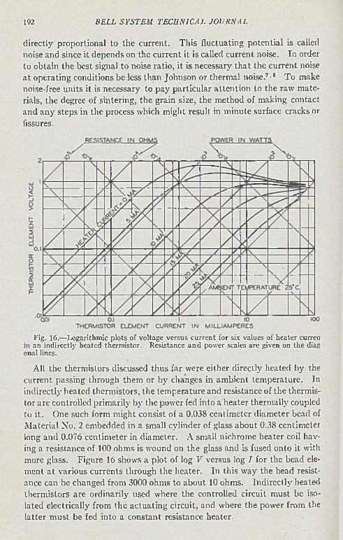
192 B E L L S Y S T E M T E C H N I C A L J O U R N A L
directly proportional to the current. This fluctuating potential is called noise and since it depends on the current it is called current noise. In order to obtain the best signal to noise ratio, it is necessary that the current noise a t operating conditions be less than Johnson or thermal noise.7' 8 To make noise-free units it is necessary to pay particular attention to the raw materials, the degree of sintering, the grain size, the method of making contact and any steps in the process which might result in minute surface cracks or fissures.
Fig. 16.—Logarithm ic plots of voltage versus cu rren t for six values of h eater curren in an indirectly heated therm istor. Resistance a n d power scales are given on th e diag onal lines.
All the thermistors discussed thus far were either directly heated by the current passing through them or by changes in ambient temperature. In indirectly heated thermistors, the temperature and resistance of the thermistor are controlled primarily by the power fed into a heater thermally coupled to it. One such form might consist of a 0.038 centimeter diameter bead of M aterial No. 2 embedded in a small cylinder of glass about 0.38 centimeter long and 0.076 centimeter in diameter. A small nichrome heater coil having a resistance of 100 ohms is wound on the glass and is fused onto it with more glass. Figure 16 shows a plot of log V versus log I for the bead element a t various currents through the heater. In this way the bead resistance can be changed from 3000 ohms to about 10 ohms. Indirectly heated thermistors are ordinarily used where the controlled circuit must be isolated electrically from the actuating circuit, and where the power from the latter must be fed into a constant resistance heater.
P R O P E R T IE S A N D U S E S OF T H E R M I S T O R S 193
PART I I—USES OF THERM ISTORS
The thermistor, or thermally sensitive resistor, has probably excited more interest as a major electric circuit element than any other except the vacuum tube in the last decade. Its extreme versatility, small size and ruggedness were responsible for its introduction in great numbers into communications circuits within five years after its first application in this field. The next five year period spanned the war, and saw thermistors widely used in additional important applications. The more important of these uses ranged from time delays and temperature controls to feed-back amplifier automatic gain controls, speech volume limiters and superhigh frequency power meters. I t is surprising that such versatility can result from a temperature dependent resistance characteristic alone. However, this effect produces a very useful nonlinear volt-ampere relationship. This, together with the ability to produce the sensitive element in a wide variety of shapes and sizes results in applications in diverse fields. The variables of design are many and interrelated, including electrical, thermal and mechanical dimensions.
The more important uses of thermistors as indication, control and circuit elements will be discussed, grouping the uses as they fall under the primary characteristics: resistance-temperature, volt-ampere, and currenttime or dynamic relations.
R e s i s t a n c e - T e m p e r a t u r e R e l a t i o n s
It has been pointed out in Part I that the temperature coefficient of electrical resistance of thermistors is negative and several times that of the ordinary metals a t room temperature. In Thermistor Material No. 1, which is commonly used, the coefficient a t 25 degrees centigrade is —4.4 per cent per centigrade degree, or over ten times that of copper, which is +0.39 per cent per centigrade degree a t the same temperature. A circuit element made of this thermistor material has a resistance at zero degrees centigrade which is nine times the resistance of the same element a t 50 degrees centigrade. I or comparison, the resistance of a copper wire at 50 degrees centigrade is 1.21 limes its value a t zero degrees centigrade.
The resistance-temperature characteristics of thermistors suggest their use as sensitive thermometers, as temperature actuated controls and as compensators for the effects of varying ambient temperature on other elements in electric circuits.
T h e r m o m e t r y
I he application of thermistors to temperature measurement follows the usual principles of resistance thermometry. However, the large value of temperature coefficient of thermistors permits a new order of sensitivity to be obtained. This and the small size, simplicity and ruggedness of thermis
194 B E L L S Y S T E M T E C H N I C A L J O U R N A L
tors adapt them to a wide variety of temperature measuring applications. When designed for this service, thermistor thermometers have long-time stability which is good for temperatures up to 300 degrees centigrade and excellent for more moderate temperatures. A well aged thermistor used in precision temperature measurements was found to be within 0.01 centigrade degree of its calibration after two months use a t various temperatures up to 100 degrees centigrade. As development proceeds, the stability of thermistor thermometers may be expected to approach that of precision platinum thermometers. Conventional bridge or other resistance measuring circuits are commonly employed with thermistors. As with any resistance thermometer, consideration must be given to keeping the measuring current sufficiently small so that it produces no appreciable heating in order that the
T a b l e I I .—T e m p e r a t u r e -R e s is t a n c e C h a r a c t e r is t ic o f a T y p ic a l T h e r m is t o r T h e r m o m e t e r
Temperature ResistanceTemperature Coefficients
B a
— 25°C. 580,000 ohms 3780 C. dcg. - 6 .1 % / C . d e g .0 145,000 3850 - 5 . 2
25 46,000 3920 - 4 . 450 16.400 3980 - 3 . 875 6,700 4050 - 3 . 3
100 8.200 4120 - 3 . 0150 830 4260 - 2 . 4200 305 4410 - 2 . 0275 100 4600 - 1 . 5
Dissipation constan t in still air, approx.............................................. 4 m illiw atts/C . dcg.Therm al tim e constan t in still air, approx ......................................... 70 secondsDimensions of therm istor, d iam eter approx....................................... 0.11 inch
length approx............................................ 0 .5 4 inch
thermistor resistance shall be dependent upon the ambient temperature alone.
Since thermistors are readily designed for higher resistance values than metallic resistance thermometers or thermocouples, lead resistances are not ordinarily bothersome. Hence the temperature sensitive element can be located remotqly from its associated measuring circuit. This permits great flexibility in application, such as for instance wire line transmission of temperature indications to control points.
Table II gives the characteristics of a typical thermistor thermometer. The dissipation constant is the ratio of the power input in watts dissipated in the thermistor to the resultant temperature rise in centigrade degrees. The time constant is the time required for the temperature of the thermistor to change 63 per cent of the difference between its initial value and that of the surroundings. As a sensitive thermometer, this thermistor with a simple Wheatstone bridge and a galvanometer whose sensitivity is 2 X
PR
OP
ER
TIES
ARID U
SES OF
TH
ER
MIST
OR
S
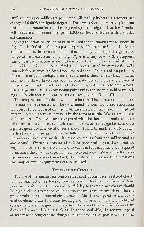
196 B E L L S Y S T E M T E C H N I C A L J O U R N A L
10-10 amperes per millimeter per meter will readily indicate a temperature change of 0.0005 centigrade degree. For comparison a precision platinum resistance thermometer and the required special bridge such as the Mueller will indicate a minimum change of 0.003 centigrade degree with a similar galvanometer.
Several thermistors which have been used for thermometry are shown in Fig. 17. Included in the group are types which are suited to such diverse applications as intravenous blood thermometry and supercharger rotor temperature measurement. In Fig. 17, A is a tin)' bead with a response time of less than a second in air. B is a probe type unit for use in air streams or liquids. C is a meteorological thermometer used in automatic radio transmission of weather data from free balloons. D is a rod shaped unit. E is a disc or pellet, adapted for use in a metal thermometer bulb. Discs like the one shown have been sweated to metal plates to give a low thermal impedance connection to the object whose temperature is to be determined. F is a large disc with an enveloping paint finish for use in humid surroundings. The characteristics of these types are given in Table III.
The temperature of objects which are inaccessible, in motion, or too hot for contact thermometry can be determined by permitting radiation from the object to be focussed on a suitable thermistor by means of an elliptical mirror. Such a thermistor may take the form of a thin flake attached to a solid support. Its advantages compared with the thermopile and resistance bolometer are its more favorable resistance value, its ruggedness, and its high temperature coefficient of resistance. I t can be made small to reduce its heat capacity so as rapidly to follow changing temperatures. Flake thermistors have been made with time constants from one millisecond to one second. Since the amount of radiant power falling on the thermistor may be quite small, sensitive meters or vacuum tube amplifiers are required to measure the small changes in the flake resistance. Where rapidly varying temperatures are not involved, thermistors with longer time constants and simpler circuit equipments can be utilized.
T e m p e r a t u r e C o n t r o l
The use of thermistors for temperature control purposes is related closely to their application as temperature measuring devices. In the ideal temperature sensitive control element, sensitivity to temperature change should be high and the resistance value a t the control temperature should be the proper value for the control circuit used. Also the temperature rise of the control element due to circuit heating should be low, and the stability of calibration should be good. The size and shape of the sensitive element are dictated by several factors such as the space available, the required speed of response to temperature changes and the amount of power which must
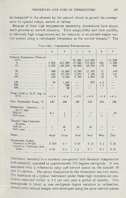
P R O P E R T IE S A N D U S E S OF T H E R M I S T O R S 197
be dissipated in the element by the control circuit to permit the arrangement to operate relays, motors or valves.
Because of their high temperature sensitivity, thermistors have shown much promise as control elements. Their adaptability and their stability at relatively high temperatures led, for instance, to an aircraft engine control system using a rod-shaped thermistor as the control element.9 The
T a b l e I I I . — T h e r m is t o r T h e r m o m e t e r s
A B C D E F
Nominal Resistance, Ohms a t — 25°C...................................... 87,500 610,000 13,000
0 ......................................................... 5,000 325,000 37,500 153,000 490 3,20025.......................................... 2 ,000 100,000 18,000 48,500 175 950
SO......................................................... 900 33,000 9,700 17,300 71 34075.......................................... 460 13,000 5,500 7,100 32 145
100................................................... 250 6,000 3,700 3,400 16 70
150............................ 95 1,600 _ 870 4 .5 __
200........................ — 500 _ — 1.6 —300 ........................... — 80 — — — —
Temp. Cocff. or, % /C . deg. a t 25°C.................. - 3 . 4 - 4 . 4 - 2 . 8 - 4 . 4 - 3 . 8 - 4 . 4
Max. Permissible Tem p., °C . . 150 300 100 150 200 100
Dissipation C onstant, C, mw/C. deg.
Still a ir .............. 0 .1 1 7 7 20Still w a ter ........................... 7 — — — —
Thermal Time C onstant, Seconds
Still a ir .............. 1 30 25 60Still w a ter .................. 4 — —
Shape............ Bead Probe Rod Rod Disc Disc
Dimensions, Inches Diameter or W id th .............. 0.015 0.1 0.05 0.15 0 .2 0.56I.ength or Thickness (less
leads)........... 0 .02 0 .6 1.2 0 .7 0 .1 0.31
thermistor, mounted in a standard one-quarter inch diameter temperature bulb assembly, operated at approximately 275 degrees centigrade. I t was associated with a differential relay and control motor on the aircraft 28 volt d-c system. The power dissipation in the thermistor was two watts, dhe resistance of a typical thermistor under these high temperature conditions remained within ± 1.5 per cent over a period of months. This corresponds to about ± one centigrade degree variation in calibration. Several other related designs were developed using the same control system
198 B E L L S Y S T E M T E C H N I C A L J O U R N A L
with other thermistors designed for both higher and lower temperature operation. In the lower temperature applications, typical thermistors maintained their calibrations within a few tenths of a centigrade degree.
In general, electron tube control circuits dissipate less power in the thermistor than relay circuits do. This result^ in less temperature rise in the thermistor and leads to a more accurate control. While the average value of this temperature rise can be allowed for in the design, the variations in different installations require individual calibration to correct the errors if they are large. The corrections may be different as a result of variations of the thermal conductivity of the surrounding media from time to time or from one installation to another. The greater the power dissipated in the thermistor the greater the absolute error in the control temperature for a given change in thermal conductivity. This follows from the relation
NT = W /C (22)
where NT is the temperature rise, W is the power dissipated and C is the dissipation constant which depends on thermal coupling to the surroundings. For the same reason, the temperature indicated by a resistance thermometer immersed in an agitated medium will depend on the rate of flow if the temperature sensitive element is operated several degrees hotter than its surroundings.
The design of a thermistor for a ventilating duct thermostat might proceed as follows as far as temperature rise is concerned:
1. Determine the power dissipation. This depends upon the circuit selected and the required overall sensitivity.
2. Estimate the permissible temperature rise of the thermistor, set by the expected variation in air speed and the required temperature control accuracy.
3. Solve Equation (22) for the dissipation constant and select a thermistor of appropriate design and size for this constant in the nominal air speed. Where more than one style of thermistor is available, the required time constant will determine the choice.
C o m p e n s a t o r s
I t is a natural and obvious application of thermistors to use them to compensate for changes in resistance of electrical circuits caused by ambient temperature variations. A simple example is-the compensation of a copper wire line, the resistance of which increases approximately 0.4 per cent per centigrade degree. A thermistor having approximately one-tenth the resistance of the copper, with a temperature coefficient of —4 per cent per centigrade degree placed in series with the line and subjected to the same ambient temperature, would serve to compensate it over a narrow tempera
P R O P E R T I E S A N D U S E S OF T H E R M I S T O R S 199
ture range. In practice however, the compensating thermistor is associated with parallel and sometimes series resistance, so that the combination gives a change in resistance closely equal and opposite to that of the circuit to be compensated over a wide range of temperatures. See Fig. 18.
Fig. 18.—Tem perature compensation of a copper conductor by means of a therm istor network.
A copper winding having a resistance of 1000 ohms at 25 degrees centigrade can be compensated by means of a thermistor of 566 ohms at 25 degrees centigrade in parallel with an ohmic resistance of 44'5 ohms as shown in Fig. 18. The winding with compensator has a resistance of 1250 ohms constant to ± 1.6 per cent over the temperature range —25 degrees centigrade to +75 degrees centigrade. Over this range the copper alone varies from 807.5 ohms to 1192.5 ohms, or ± 19 per cent about the mean. The
200 B E L L S Y S T E M T E C H N I C A L J O U R N A L
total resistance of the circuit has been increased only 6.1 per cent a t the upper temperature limit by the addition of a compensator. This increase is small because of the high temperature coefficient of the compensating thermistor. The characteristics of such a thermistor are so stable that the resistance would remain constant within less than one per cent for ten years if maintained at any temperature up to about 100 degrees centigrade. Figure 15 shows aging characteristics for typical thermistors suitable for use in compensators. These curves include the change which occurs during the seasoning period of several days at the factory, so that the aging in use is a fraction of the total shown.
In many circuits which need to function to close tolerances under wide ambient temperature variation, the values of one or more circuit elements may vary undesirably with temperature. Frequently the resultant overall variation with temperature can be reduced by the insertion of a simple thermistor placed a t an appropriate point in the circuit. This is particularly true if the circuit contains vacuum tube amplifiers. In this manner frequency and gain shifts in communications circuits have been cancelled and temperature errors prevented in the operation of devices such as elecfric meters. The change in inductance of a coil due to the variation of magnetic characteristics of the core material with temperature has been prevented by partially saturating’ the coil with direct current, the magnitude of which is directly controlled by the resistance of a thermistor imbedded in the core. In this way the amount of d-c magnetic flux is adjusted by the thermistor so that the inductance of the coil is independent of temperature.
In designing a compensator, care must be taken to ensure exposure of the thermistor to the temperature affecting the element to be compensated. Power dissipation in the thermistor must be considered and either limited to a value which will not produce a significant rise in temperature above ambient, or offset in the design.
V o l t - A m p e r e C h a r a c t e r i s t i c s
The nonlinear shape of the static characteristic relating voltage, current, resistance and power for a typical thermistor was illustrated by Fig. 9. The part of the curve to the right of the voltage maximum has a negative slope, applicable in a large number of ways in electric circuits. The particular characteristic shown begins with a resistance of approximately 50,000 ohms at low power. Additional power dissipation raises the temperature of the thermistor element and decreases its resistance. At the voltage maximum the resistance is reduced to about one-third its cold value, or 17,000 ohms, and the dissipation is 13 milliwatts. The resistance becomes approximately 300 ohms when the dissipation is 100 milliwatts. Such resistance-power characteristics have resulted in the use of thermistors as sensitive power measuring devices, and as automatically variable resistances
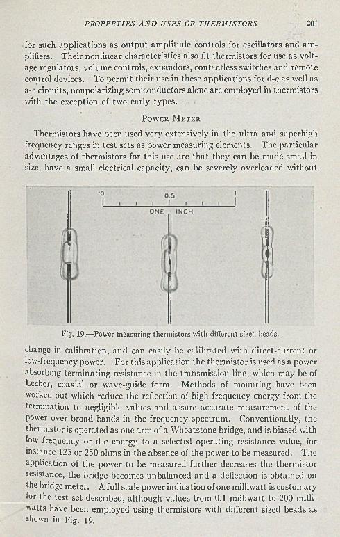
for such applications as output amplitude controls for oscillators and amplifiers. Their nonlinear characteristics also fit thermistors for use as voltage regulators, volume controls, expandors, contactless switches and remote control devices. To permit their use in these applications for d-c as well as a-c circuits, nonpolarizing semiconductors alone are employed in thermistors with the exception of two earl}' types.
P o w e r M e t e r
Thermistors have been used very extensively in the ultra and superhigh frequency ranges in test sets as power measuring elements. The particular advantages of thermistors for this use are that they can be made small in size, have a small electrical capacity, can be severely overloaded without
P R O P E R T I E S Ä N D U S E S OE T H E R M I S T O R S 201
Fig. 19.—Power m easuring therm istors w ith different sized heads.
change in calibration, and can easily be calibrated with direct-current or low-frequency power. For this application the thermistor is used as a power absorbing terminating resistance in the transmission line, which may be of Lecher, coaxial or wave-guide form. Methods of mounting have been worked out which reduce the reflection of high frequency energy from the termination to negligible values and assure accurate measurement of the power over broad bands in the frequency spectrum. Conventionally, the thermistor is operated as one arm of a Wheatstone bridge, and is biased with low frequency or d-c energy to a selected operating resistance value, for instance 125 or 250 ohms in the absence of the power to be measured. The application of the power to be measured further decreases the thermistor resistance, the bridge becomes unbalanced and a deflection is obtained on the bridge meter. A full scale power indication of one milliwatt is customary for the test set described, although values from 0.1 milliwatt to 200 milliwatts have been employed using thermistors with different sized beads as shown in Fig. 19.
202 B E L L S Y S T E M T E C H N IC A L J O U R N A L
Continuous operation tests of these thermistors indicate very satisfactory stability with an indefinitely long life. A group of eight power meter thermistors, normally operated a t 10 milliwatts and having a maximum ratin'g cf 20 milliwatts, were operated for over 3000 hours a t a power input of 30 milliwatts. During this time the room temperature resistance remained within 1.5 per cent of its initial value, and the power sensitivity, which is the significant characteristic, changed by less than 0.5 per cent.
When power measuring test sets are intended for use with wide ambient temperature variations, it is necessary to temperature compensate the thermistor. This is accomplished conventionally by the introduction of two other thermistors into the bridge circuit. These units are designed to be insensitive to bridge currents but responsive to ambient temperature. One of the compensators maintains the zero point and the other holds the meter scale calibration independent of the effect of temperature change on the measuring thermistor characteristics.
A u t o m a t i c O s c i l l a t o r A m p l i t u d e C o n t r o l
Meacham,10 and Shepherd and Wise11 have described the use of thermistors to provide an effective method of amplitude stabilization of both low and high frequency oscillators. These circuits oscillate because of positive feedback around the vacuum tube. The feedback circuit is a bridge with at least one arm containing a thermistor which is heated by the oscillator output. Through this arrangement, the feedback depends in phase and magnitude upon the output, and there is one value of thermistor resistance which if attained would balance the bridge and cause the oscillation amplitude to vanish. Obviously this condition can never be exactly attained, and the operating point is just enough different to keep the bridge slightly unbalanced and produce a predetermined steady value of oscillation output. Such oscillators in which the amplitude is determined by thermistor non- linearity have manifold advantages over those whose amplitude is limited by vacuum tube nonlinearity. The harmonic content in the output is smaller, and the performance is much less dependent upon the individual vacuum tube and upon variations of the supply voltages. I t is necessary that the thermal inertia of the thermistor be sufficient to prevent it from varying in resistance at the oscillation frequency. This is easily satisfied for all frequencies down to a small fraction of a cycle per second. Figure 20 shows a thermistor frequently used for oscillator control together with its static electrical characteristic. This thermistor is satisfactory in oscillators for frequencies above approximate!}' 100 cycles per second. Similar types have been developed with response characteristics suited to lower frequencies and for other resistance values and powers.
P R O P E R T I E S A N D U S E S OF T H E R M I S T O R S 203
CURRENT IN M ILLIA M PERES
Fig. 20B.—Steady s ta te characteristics of am plitude control therm istor shown in Figure 20A.
thermostating it with a heater and compensating thermistor network, as shown in Fig. 21.
A m p l i f i e r A u t o m a t ic G a i n C o n t r o l
Since the resistance of a thermistor of suitable design varies markedly with the power dissipated in it or in a closely associated heater, such ther
Where the ambient temperature sensitivity of the thermistor is disadvantageous in oscillator controls, the thermistor can be compensated by
Fig. 20A.— An am plitude control therm istor. T he glass bulb is 1.5 inches in length.
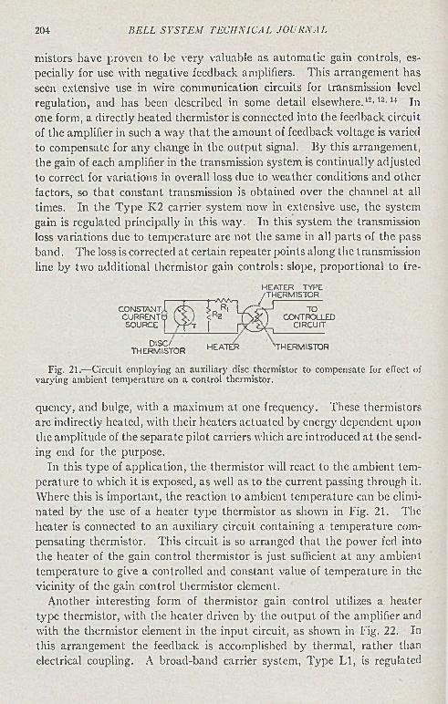
204 B E L L S Y S T E M T E C H N IC A L J O U R N A L
mistors have proven to be very valuable as automatic gain controls, especially for use with negative feedback amplifiers. This arrangement has seen extensive use in wire communication circuits for transmission level regulation, and has been described in some detail elsewhere.12' 13' 14 In one form, a directly heated thermistor is connected into the feedback circuit of the amplifier in such a way that the amount of feedback voltage is varied to compensate for any change in the output signal. By this arrangement, the gain of each amplifier in the transmission system is continually adjusted to correct for variations in overall loss due to weather conditions and other factors, so tha t constant transmission is obtained over the channel at all times. In the Type K2 carrier system now in extensive use, the system gain is regulated principally in this way. In this system the transmission loss variations due to temperature are not the same in all parts of the pass band. The loss is corrected a t certain repeater points along the transmission line by two additional thermistor gain controls: slope, proportional to fre-
HEATER TYPE
CONSTANT,! /C K CURRENTS (SOURCE I V p T
DISC/THERMISTOR
Fig. 21.— Circuit employing an auxiliary disc therm istor to compensate for effect of varying am bient tem perature on a control therm istor.
quency, and bulge, with a maximum a t one frequency. These thermistors are indirectly heated, with their heaters actuated by energy dependent upon the amplitude of the separate pilot carriers which are introduced at the sending end for the purpose.
In this type of application, the thermistor will react to the ambient temperature to which it is exposed, as well as to the current passing through it. Where this is important, the reaction to ambient temperature can be eliminated by the use of a heater type thermistor as shown in Fig. 21. The heater is connected to an auxiliary circuit containing a temperature compensating thermistor. This circuit is so arranged that the power fed into the heater of the gain control thermistor is just sufficient a t any ambient temperature to give a controlled and constant value of temperature in the vicinity of the gain control thermistor element.
Another interesting form of thermistor gain control utilizes a heater type thermistor, with the heater driven by the output of the amplifier and with the thermistor element in the input circuit, as shown in Fig. 22. In this arrangement the feedback is accomplished by thermal, rather than electrical coupling. A broad-band carrier system, Type L I, is regulated
/THERMISTOR rw w . / i------------V *' LvCCv1 ™< 2 T ^ > X 1 CONTROLLED I F v - j A i c ir c u it
HEATER 'THERMISTOR
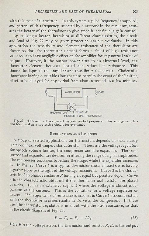
P R O P E R T I E S A N D U S E S OF T H E R M I S T O R S 205
with this type of thermistor. In this system a pilot frequency is supplied, and current of this frequency, selected by a network in the regulator, actuates the heater of the thermistor to give smooth, continuous gain control.
By utilizing a heater thermistor of different characteristics, the circuit and load of Fig. 22 may be given protection against overloads. In this application the sensitivity and element resistance of the thermistor are chosen so that the thermistor element forms a shunt of high resistance value so as to have negligible effect on the amplifier for any normal value of output. However, if the output power rises to an abnormal level, the thermistor element becomes heated and reduced in resistance. This shunts the input to the amplifier and thus limits the output. Choice of a thermistor having a suitable time constant permits the onset of the limiting effect to be delayed for any period from about a second to a few minutes.
Fig. 22.—Therm al feedback circuit for gain control purposes. This arrangem ent has also been used as a pro tective circuit for overloads.
R e g u l a t o r s a n d L i m i t e r s
A group of related applications for thermistors depends on their steady state nonlinear volt-ampere characteristic. These are the voltage regulator, the speech volume limiter, the compressor and the expandor. The compressor and expandor are devices for altering the range of signal amplitudes. The compressor functions to reduce the range, while the expandor increases it. In Fig. 23, Curve 1 is a typical thermistor static characteristic having negative slope to the right of the voltage maximum. Curve 2 is the characteristic of an ohmic resistance R having an equal but positive slope. Curve 3 is the characteristic obtained if the thermistor and resistor are placed in series. I t has an extensive segment where the voltage is almost independent of the current. This is the condition for a voltage regulator or limiter. If a larger value of resistance is used, as in Curve 4, its combination with the thermistor in series results in Curve 5, the compressor. In these uses the thermistor regulator is in shunt with the load resistance, so that in the circuit diagram of Fig. 23,
E = E„ = E , - IRs. (23)
Here E is the voltage across the thermistor and resistor R, E0 is the output
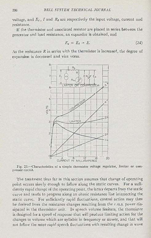
206 B E L L S Y S T E M T E C H N I C A L J O U R N A L
voltage, and E j , I and Ra are respectively the input voltage, current and resistance.
If the thermistor and associated resistor are placed in series between the generator and load resistance, an expandor is obtained, and
E0 = Ei — E. (24)
As the resistance R in series with the thermistor is increased, the degree of expansion is decreased and vice versa.
Fig. 23.—C haracteristics of a simple therm istor voltage regulator, lim iter or compressor circuit.
The treatment thus far in this section assumes that change of operating point occurs slowly enough to follow along the static curves. For a sufficiently rapid change of the operating point, the latter departs from the static curve and tends to progress along an ohmic resistance line intersecting the static curve. For sufficiently rapid fluctuations, control action may then be derived from the resistance changes resulting from the r.m.s. power dissipated in the thermistor unit. In speech volume limiters, the thermistor is designed for a speed of response that will produce limiting action for the changes in volume which are syllabic in frequency or slower, and that will not follow the more rapid speech fluctuations with resulting change in wave
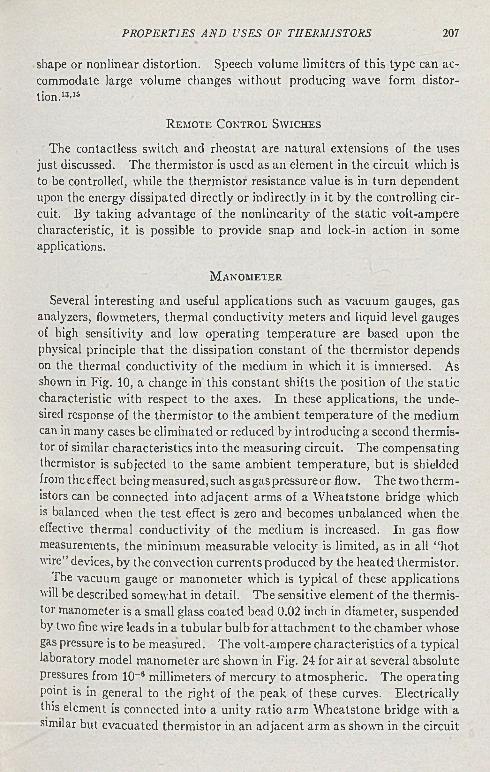
P R O P E R T I E S A N D U S E S OF T H E R M I S T O R S 207
shape or nonlinear distortion. Speech volume limiters of this type can accommodate large volume changes without producing wave form distortion.13'15
R e m o t e C o n t r o l S w ic h e s
The contactless switch and rheostat are natural extensions of the uses just discussed. The thermistor is used as an element in the circuit which is to be controlled, while the thermistor resistance value is in turn dependent upon the energy dissipated directly or indirectly in it by the controlling circuit. By taking advantage of the nonlinearity of the static volt-ampere characteristic, it is possible to provide snap and lock-in action in some applications.
M a n o m e t e r
Several interesting and useful applications such as vacuum gauges, gas analyzers, flowmeters, thermal conductivity meters and liquid level gauges of high sensitivity and low operating temperature are based upon the physical principle that the dissipation constant of the thermistor depends on the thermal conductivity of the medium in which it is immersed. As show in Fig. 10, a change in this constant shifts the position of the static characteristic with respect to the axes. In these applications, the undesired response of the thermistor to the ambient temperature of the medium can in many cases be eliminated or reduced by introducing a second thermistor of similar characteristics into the measuring circuit. The compensating thermistor is subjected to the same ambient temperature, but is shielded from theeffect being measured, such as gas pressure or flow. The two therm istors can be connected into adjacent arms of a Wheatstone bridge which is balanced when the test effect is zero and becomes unbalanced when the effective thermal conductivity of the medium is increased. In gas flow measurements, the minimum measurable velocity is limited, as in all “hot wire” devices, by the convection currents produced by the heated thermistor.
The vacuum gauge or manometer which is typical of these applications will be described somewhat in detail. The sensitive element of the thermistor manometer is a small glass coated bead 0.02 inch in diameter, suspended by two fine wire leads in a tubular bulb for attachment to the chamber whose gas pressure is to be measured. The volt-ampere characteristics of a typical laboratory model manometer are shown in Fig. 24 for air a t several absolute pressures from 10~6 millimeters of mercury to atmospheric. The operating point is in general to the right of the peak of these curves. Electrically this element is connected into a unity ratio arm Wheatstone bridge with a similar but evacuated thermistor in an adjacent arm as s h o w in the circuit
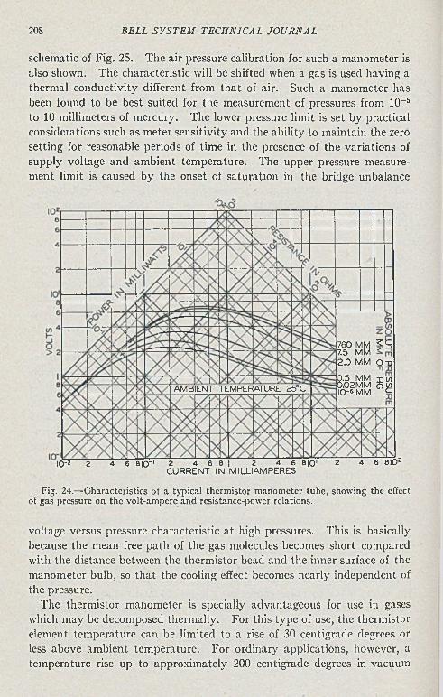
208 B E L L S Y S T E M T E C H N IC A L J O U R N A L
760 MM I 57.5 M M2.0 MM O "o
0.5 MM X w JÖ.02MM o iû 10-6 MM tAMBIENT TEMPERATURE 25°C
schematic of Fig. 25. The air pressure calibration for such a manometer is also shown. The characteristic will be shifted when a gas is used having a thermal conductivity different from that of air. Such a manometer has been found to be best suited for the measurement of pressures from 10-5 to 10 millimeters of mercury. The lower pressure limit is set by practical considerations such as meter sensitivity and the ability to maintain the zero setting for reasonable periods of time in the presence of the variations of supply voltage and ambient temperature. The upper pressure measurement limit is caused by the onset of saturation in the bridge unbalance
I0 ‘ 2 2 4 6 8 I 0 '1 2 4 6 8 ¡ 2 4 6 8 |0 ' 2 4 6 8 IÜ 2CURRENT IN MILLIAMPERES
Fig. 24.—Characteristics of a typical therm istor m anom eter tube, showing the effect of gas pressure on the volt-am pcre and resistance-power relations.
voltage versus pressure characteristic a t high pressures. This is basically because the mean free path of the gas molecules becomes short compared with the distance between the thermistor bead and the inner surface of the manometer bulb, so that the cooling effect becomes nearly independent of the pressure.
The thermistor manometer is specially advantageous for use in gases which may be decomposed thermally. For this type of use, the thermistor element temperature can be limited to a rise of 30 centigrade degrees or less above ambient temperature. For ordinary applications, however, a temperature rise up to approximately 200 centigrade degrees in vacuum
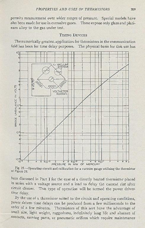
P R O P E R T IE S A N D U S E S OF T H E R M I S T O R S 209
permits measurement over wider ranges of pressure. Special models have also been made for use in corrosive gases. These expose only glass and platinum alloy to the gas under test.
T im in g D e v ic e s
The numerically greatest application for thermistors in the communication field has been for time delay purposes. The physical basis for this use has
2 4 6 6 |PRESSURE IN MM OF MERCURY
Fig. 25.—Operating circuit and calibration for a vacuum gauge utilizing the therm istor of Figure 24.
been discussed in P art I for the case of a directly heated thermistor placed in series with a voltage source and a load to delay the current rise after circuit closure. This type of operation will be termed the power driven time delay.
By the use of a thermistor suited to the circuit and operating conditions, power driven time delays can be produced from a few milliseconds to the order of a few minutes. Thermistors of this sort have the advantage of small size, light weight, ruggedness, indefinitely long life and absence of contacts, moving parts, or pneumatic orifices which require maintenance
210 B E L L S Y S T E M T E C H N IC A L J O U R N A L
care. Power driven time delay thermistors are best fitted for applications where close limits on the time interval are not required. In some communications uses it is satisfactory to permit a six to one ratio between maximum and minimum times as a result of the simultaneous variation from nominal values of all the following factors which affect the delay: operating voltage ± 5 per cent; ambient temperature 20 degrees centigrade to 40 degrees centigrade; operating current of the relay ± 25 per cent; relay resistance ± 5 per cent; and thermistor variations such as occur from unit to unit of the same type.
After a timing operation a power driven time delay thermistor should be allowed time to cool before a second operation. If this is not done, the second timing interval will be shorter than the first. The cooling period depends on particular circuit conditions and details of thermistor design, but generally is several times the working time delay. In telephone relay circuits requiring a timing operation soon after previous use, the thermistor usually is connected so that it is short circuited by the relay contacts at the close of the working time delay interval. This permits the thermistor to cool during the period when the relay is locked up. If this period is sufficiently long, the thermistor is available for use as soon as the relay drops out. Time delay thermistors have been operated more than half a million times on life test with no significant change in their timing action.
To avoid the limitations of wide timing interval limits and extended cooling period between operations usually associated with the power driven time delay thermistor, a cooling time delay method of operation has been used. In this arrangement, two relays or the equivalent are employed and the thermistor is heated to a low resistance-value by passing a relatively large current through it for an interval short compared with the desired time interval. The current then is reduced automatically to a lower value and the thermistor cools until its resistance increases enough to reduce the current further and trip the working relay. This part of the operating cycle accounts for the greater part of the desired time interval. With this arrangement, the thermistor is available for re-use immediately after a completed timing interval, or, as a m atter of fact, after any part of it. By proper choice of operating currents and circuit values, wide variations of voltage and ambient temperature may occur with relatively little effect upon the time interval. The principal variable left is the cooling time of the thermistor itself. This is fixed in a given thermistor unit, but may vary from unit to unit, depending upon dissipation constant and thermal capacity, as pointed out above.
In addition to their use as definite time delay devices, thermistors have been used in several related applications. Surges can be prevented from
P R O P E R T I E S A N D U S E S OF T H E R M I S T O R S 211
operating relays or disturbing sensitive apparatus by introducing a thermistor in series with the circuit component which is to be protected. In case of a surge, the high initial resistance of the thermistor holds the surge current to a low value provided that the surge does not persist long enough to overcome the thermal inertia of the thermistor. The normal operating voltage, on the other hand, is applied long enough to lower the thermistor resistance to a negligible value, so that a normal operating current will flow after a short interval. In this way, the thermistor enables the circuit to distinguish between an undesired signal of short duration and a desired signal of longer duration even though the undesired impulse is several times higher in voltage than the signal.
O s c i l l a t o r s , M o d u l a t o r s a n d A m p l i f i e r s
A group of applications already explored in the laboratory but not put into engineering use includes oscillators, modulators and amplifiers for the low and audio-frequer.cy range. If a thermistor is biased at a point on the negative slope portion of the steady-state volt-ampere characteristic, and if a small alternating voltage is then superposed on the direct voltage, a small alternating current will flow. If the thermistor has a small time constant, t , and if the applied frequency is low enough, the alternating volt- ampere characteristic will follow the steady-state curve and d V /d l will be negative. As the frequency of the applied a-c voltage is increased, the value of the negative resistance decreases. At some critical frequency, f c , the resistance is zero ar.d the current is 90 degrees out of phase with the voltage. In the neighborhood o f /c , the thermistor acts like an inductance whose value is of the order of a he.iry. As the frequency is increased beyond f c, the resistance is positive and increases steadily until it approaches the d-c value when the current and voltage are in phase. The critical frequency is given approximately by
fc = 1/2 T .
If r can be made as small as 5 X 10~5 seconds, f c is equal to 10,000 cycles per second and the thermistor would have an approximately constant negative resistance up to half this frequency. Point contact thermistors having such critical frequencies or even higher have been made in a number of laboratories. Plowever, none of them have been made with sufficient reproducibility and constancy to be useful to the engineer. It has been shown both theoretically and experimentally that any negative resistance device can be used as an oscillator, a modulator, or an amplifier. With further development, it seems probable that thermistors will be used in these fields.
212 B E L L S Y S T E M T E C H N I C A L J O U R N A L
S u m m a r y
The general principles of thermistor operation and examples of specific uses have been given to facilitate a better understanding of them, with the feeling that such an understanding will be the basis for increased use of this new circuit and control element in technology.
R e f e r e n c e s
1. Zur E lektrischen Leitfähigkeit von Kupferoxydul, W. P. Ju sea n d B . W. K urtschatow .Physikalische Zeitschrift Der Sowjetunion, Volume 2, 1932, pages 453-67.
2. Semi-conductors and M etals (book), A. H . Wilson. T he U niversity Press, Cam bridge, England, 1939/
3. T he M odern Theory of Solids (book), Frederick Seitz. M cGraw-Hill Book Com pany,New York, N. Y., 1940.
4. Electronic Processes in Ionic C rystals (book), N . F . M o tt and R . W. Gurney. TheClarendon Press, Oxford, England, 1940.
5. Die Elektroncnleitfahigkeit von Festen Oxyden Verschiedener Valenzstufen, M . Le-Blanc and H . Sachse. Physikalische Zeitschrift, Volume 32, 1931, pages 887-9.
6. Uber die E lektrizitatsleitung Anorganischer Stoffe m it Elektroncnleitfahigkeit, W ilfried M eyer. Zeitschrift Für Physik, Volume 85, 1933, pages 278-93.
7. Therm al Agitation of Electricity in Conductors, J . B. Johnson. Physical Review,Volume 32, Ju ly 1928, pages 97-113.
8. Spontaneous Resistance F luctuations in Carbon M icrophones and O ther GranularResistances, C. J . Christensen and G. L . Pearson. T he Bell System Technical Journal, Volume 15, April 1936, pages 197-223.
9. A utom atic T em perature Control for A ircraft, R . A. Gund. A IE E Transactions,Volume 64, 1945, October section, pages 730-34.
10. T he Bridge Stabilized Oscillator, L. A. M eacham . Proc. IR E , Volume 26, October1938, pages 1278-94.
11. Frequency Stabilized Oscillator, R . L. Shepherd and R . 0 . Wise. Proc. IR E , Volum e 31, June 1943, pages 256-68.
12. A Pilot-Channel Regulator for the K -l Carrier System , J. II . Bollman. Bell L aboratories Record, Volume 20, No. 10, June 1942, pages 258-62.
13. Therm istors, J . E. Twceddale. W estern E lectric Oscillator, Decem ber 1945, pages3-5 , 34-7.
14. Therm istor Technics, J. C. Johnson. Electronic Industries, Volume 4, August 1945,pages 74-7.
15. Volume L im iter for Leased-Line Service, J. A. Weller. . Bell Laboratories Record,Volume 23, No. 3, M arch 1945, pages 72-5.
A bstracts of T ech n ical A rticles by B ell S y stem A uthors
Capacitors—Their Use in Electronic Circuits.1 M. B r o t h e r t o n . This book tells how to choose and use capacitors for electronic circuits. I t explains the basic factors which control, the characteristics of capacitors and determine their proper operation. I t helps to provide that broad understanding of the capacitor problem which is indispensable to the efficient design of circuits. I t tells the circuit designer what he must understand and consider in transforming capacitance from a circuit symbol into a practical item of apparatus capable of meeting the growing severity of today’s operation requirements.
Mica Capacitors for Carrier Telephone Systems? A. J. C h r i s t o p h e r
a n d J. A. K a t e r . Silvered mica capacitors, because of their inherently high capacitance stability with temperature changes and with age, now are used widely in oscillators, networks, and other frequency determining circuits in the Bell Telephone System. Their use in place of the previous dry stack type, consisting of alternate layers of mica and foil clamped under high pressures, has made possible considerable manufacturing economies in addition to improving the transmission performance of carrier telephone circuits. These economies are the result of their relatively simple unit construction and the ease of adjustment to the very close capacitance tolerance required.
Visible Speech Translators with External Phosphors. 3 H o m e r D u d l e y
a n d O t t o 0 . G r u e n z , J r . This paper describes some experimental apparatus built to give a passing display of visible speech patterns. These patterns show the analysis of speech on an intensity-frequency-time basis and move past the reader like a printed line. The apparatus has been called a translator as it converts speech intended for aural perception into a form suitable for visual prception. The phosphor employed is not in a cathode-ray tube but in the open on a belt or drum.
The Pitch, Loudness and Quality of Musical Tones (A demonslration- lecture introducing the new Tone Synthesizer).4 H a r v e y F l e t c h e r . Relations are given in this paper which show how the pitch of a musical tone
‘ Published by D. Van N ostrand Com pany, Inc ., New York, N . Y., 1946.* Elec. Engg., Transactions Section, October 1946.
Jour. Aeons. Soc. Amer., Ju ly 1946.Amer. Jour, of Physics, Ju ly-A ugust 1946.
213
2 1 4 “ B E L L S Y S T E M T E C H N I C A L J O U R N A L
depends upon the frequency, the intensity and the overtone structure of the sound wave transmitting the tone. Similar relations are also given which show how the loudness and the quality depend upon these same three physical characteristics of the sound wave. These relationships were demonstrated by using the new Tone Synthesizer. By means of this instrument one is able to imitate the quality, pitch and intensity of any musical tone and also to produce many combinations which are not now used in music.
The Sound Spectrograph. 5 W. K o e n i g , H. K. D u n n , a n d L. Y. L a c y .
The sound spectrograph is a wave analyzer which produces a permanent visual record showing the distribution of energy in both frequency and time. This paper describes the operation of this device, and shows the mechanical arrangements and the electrical circuits in a particular model. Some of the problems encountered in this type of analysis are discussed, particularly those arising from the necessity for handling and portraying a wide range of component levels in a complex wave such as speech. Spectrograms are shown for a wide variety of sounds, including voice sounds, animal and bird sounds, music, frequency modulations, and miscellaneous familiar sounds.
Geometrical Characterizations of Some Families of Dynamical Trajectories.6 L. A. M a c C o l l . A broad problem in differential geometry is that of characterizing, by a set of geometrical properties, the family of curves which is defined by a given system of differential equations, of a more or less special form. The problem has been studied especially by Kasner and his students, and characterizations have been obtained for various families of curves which are of geometrical or physical importance. However, the interesting problem of characterizing the family of trajectories of an electrified particle moving in a static magnetic field does not seem to have been considered heretofore. The present paper gives the principal results of a study of this problem.
Visible Speech Cathode-Ray Translator.' R . R . R i e s z a n d L. S c h o t t . A system has been developed whereby speech analysis patterns are made continuously visible on the moving luminescent screen of a special cathode- ray tube. The screen is a cylindrical band that rotates with the tube about a vertical axis. The electron beam always excites the screen in the same vertical plane. Because of the persistence of the screen phosphor and the rotation of the tube, the impressed patterns are spread out along a horizon-
0 Jour. Acous. Soc. Amer., Ju ly 1946.6 Amer. M ath. Soc. Transactions, Ju ly 1946.7 Jo u r. Acous,Soc. Amer., Ju ly 1946.
A B S T R A C T S OF T E C H N I C A L A R T I C L E S 215
tal time axis so that speech over an interval of a second or more is always visible. The upper portion of the screen portrays a spectrum analysis and the lower portion a pitch analysis of the speech sounds. The frequency band up to 3500 cycles is divided into 12 contiguous sub-bands by filters. The average speech energy in the sub-bands is scanned and made to control the excitation of the screen by the electron beam which is swept synchronously across the screen in the vertical direction. A pitch analyzer produces a d-c. voltage proportional to 'th e instantaneous fundamental frequency of the speech and this controls the width of a band of luminescence that the electron beam produces in the lower part of the screen. The translator had been used in a training program to study the readability of visible speech patterns.
Derivatives of Composite Functions. 8 J o h n R i o r d a n . The object of this note is to show the relation of the Y polynomials of E. T. Bell, first to the formula of DiBruno for the ;;th derivative of a function of a function, then to the more general case of a function of many functions. The subject belongs to the algebra of analysis in the sense of Menger; all that is asked is the relation of the derivative of the composite function to the derivatives of its component functions when they exist and no questions of analysis are examined.
The Portrayal of Visible Speech. 9 J . C. S t e i n b e r g a n d N. R . F r e n c h . This paper discusses the objectives and requirements in the protrayal of visible patterns of speech from the viewpoint of their effects on the legibility of the patterns. The portrayal involves an intensity-frequency-time analysis of speech and the display of the results of the analysis to the eye. Procedures for accomplishing this are discussed in relation to information on the reading of print and on the characteristics of speech and its interpretation by the ear. Also methods of evaluating the legibility of the visible patterns are described.
Short Survey of Japanese Radar—/ . 10 R o g e r I. W i l k in s o n . The result of a study made immediately following the fall of Japan and recently made available for public information, this two-part report is designed to present a quick over-all evaluation of Japanese radar, its history and development. As the Japanese army and navy developed their radar equipment independently of each other, P art I of this article concentrates on the army s contributions.
* Amer. Math. Soc. Bulletin, August 1946.Jour. Acous. Soc. Amer., Ju ly 1946.Elec. Engg., Aug.-Sept. 1946.
216 B E L L S Y S T E M T E C H N IC A L J O U R N A L
A Variation on ilie Gain Formula for Feedback Amlificrs for a Certain Driving-Impedancc C o n f ig u r a t io n T. W . W i n t e r n i t z . An expression for the gain of a feedback amplifier, in which the source impedance is the only significant impedance across which the feedback voltage is developed, is derived. As examples of the use of this expression, it is then applied to three common circuits in order to obtain their response to a Heaviside unit step-voltage input.
11 Proc. I .R .E ., Septem ber 1946.
\
Contributors to T his Issu e
J o s e p h A. B e c k e r , A.B., Cornell University 1918; PhD., Cornell University, 1922. National Research Fellow, California Institute of Technology, 1922-24; Asst. Prof. of Physics, Stanford University, 1924. Engineering Dept., Western Electric Company, 1924-1925; Bell Telephone Laboratores, 1925-. Mr. Becker has worked in the fields of X-Rays, magnetism, thermionic emission and adsorption, particularly in oxide coated filaments, the properties of semiconductors, as applied in varistors and thermistors.
W. R. B e n n e t t , B. S., Oregon State College, 1925; A.M., Columbia University, 1928. Bell Telephone Laboratories, 1925-. Mr. Bennett has been active in the design and testing of multichannel communication systems, particularly with regard to modulation processes and the effects of nonlinear distortion. As a member of the Transmission Research Department, he is now engaged in the study of pulse modulation techniques for sending telephone channels by microwave radio relay.
C. B. G r e e n , Ohio State University, B.A. 1927; M.A. in Physics, 1928. Additional graduate work a t Columbia University. Bell Telephone Laboratories, 1928-. For ten years Mr. Green was concerned with transmission development for telephotography and television systems and with the design of vacuum tubes. Since 1938 he has been engaged in the development and application of thermistors.
J. P. K i n z e r , M. E., Stevens Institute of Technology, 1925. B.C.E., Brooklyn Polytechnic Institute, 1933. Bell Telephone Laboratories, 1925-. Mr. Kinzer’s work has been in the development of carrier telephone repeaters; during the war his attention was directed to investigation of the mathematical problems involved in cavity resonators.
V . P. M a s o n , B.S. in E.E., Univ. of Kansas, 1921; M.A., Ph.D., Columbia, 1928. Bell Telephone Laboratories, 1921—. Dr. Mason has been engaged principally in investigating the properties and applications of piezoelectric crystals and in the study of ultrasonics.
R. S. Oiil, B. S. in Electro-Chemical Engineering, Pennsylvania State College, 1918; U. S. Army, 1918 (2nd Lieutenant, Signal Corps); Vacuum tube development, Westinghouse Lamp Company, 1919-21; Instructor in
217
218 B E L L S Y S T E M T E C H N I C A L J O U R N A L
Physics, University of Colorado, 1921-1922. Department of Development and Research, American Telephone and Telegraph Company, 1922-27; Bell Telephone Laboratories, 192 7-. Mr. Ohl has been engaged in various exploratory phases of radio research, the results of which have led to numerous patents. For the past ten or more years he has been working on some of the problems encountered in the use of millimeter radio waves.
G. L. P e a r s o n , A. B., Willamette University, 1926; M. A. in Physics, Stanford University, 1929. Bell Telephone Laboratories, 1929-. Mr. Pearson is in the Physical Research Department where he has been engaged in the study of noise in electric circuits and the properties of electronic semiconductors.
J. H. S c a r f , B.S.E. in Chemical Engineering, University of Michigan, 1929. Bell Telephone Laboratories, 1929-. Mr. Scaff’s early work in the Laboratories was concerned with metallurgical investigations of impurities in metals with particular reference to soft magnetic materials. During the war he was project engineer for the development of silicon and germanium crystal rectifiers for radar applications. At the present time, he is responsible for metallurgical work on varistor and magnetic materials.
I. G. W il s o n , B.S. and M.E., University of Kentucky, 1921. Western Electric Co., EngineeringDepartment, 1921-25. Bell Telephone Laboratories, 1925-. Mr. Wilson has been engaged in the development of amplifiers for broad-band systems. During the war he was project engineer in charge of the design of resonant cavities for radar testing.