Surface Charge Accumulation on Spacers Under Switching ...
202
Surface Charge Accumulation on Spacers Under Switching Impulses in Sulphur Hexafluoride Gas by Sudhakar Ellapragada Cherukupalli B.E., B.M.S. College of Engineering, Bangalore, INDIA, 1974 M.E., Indian Institute of Science, Bangalore, 1976 A THESIS SUBMITTED IN PARTIAL FULFILMENT OF THE REQUIREMENTS FOR THE DEGREE OF DOCTOR OF PHILOSOPHY in THE FACULTY OF GRADUATE STUDIES Department of Electrical Engineering We accept this thesis as conforming to the required standard THE UNIVERSITY OF BRITISH COLUMBIA July, 1987 © Sudhakar Ellapragada Cherukupalli, 1987
-
Upload
khangminh22 -
Category
Documents
-
view
0 -
download
0
Transcript of Surface Charge Accumulation on Spacers Under Switching ...

Surface Charge Accumulation on Spacers Under Switching Impulses
in Sulphur Hexafluoride Gas
by
S u d h a k a r E l l a p r a g a d a C h e r u k u p a l l i B . E . , B.M.S. College of Engineering, Bangalore, INDIA, 1974
M . E . , Indian Institute of Science, Bangalore, 1976
A THESIS S U B M I T T E D IN PARTIAL F U L F I L M E N T OF T H E R E Q U I R E M E N T S F O R T H E D E G R E E OF
D O C T O R O F PHILOSOPHY
in T H E F A C U L T Y OF G R A D U A T E STUDIES
Department of Electrical Engineering
We accept this thesis as conforming to the required standard
T H E UNIVERSITY O F BRITISH C O L U M B I A July, 1987
© Sudhakar Ellapragada Cherukupalli, 1987

In presenting this thesis in partial fulfilment of the requirements for an advanced
degree at the University of British Columbia, I agree that the Library shall make it
freely available for reference and study. I further agree that permission for extensive
copying of this thesis for scholarly purposes may be granted by the head of my
department or by his or her representatives. It is understood that copying or
publication of this thesis for financial gain shall not be allowed without my written
permission.
Department of
The University of British Columbia 1956 Main Mall Vancouver, Canada V6T 1Y3
Date /SOCT 1$2>?
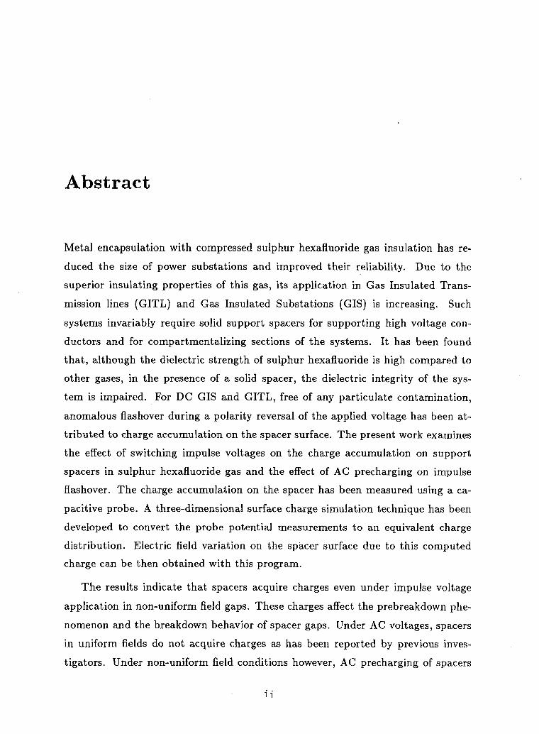
Abstract
Metal encapsulation with compressed sulphur hexafluoride gas insulation has re
duced the size of power substations and improved their reliability. Due to the
superior insulating properties of this gas, its application in Gas Insulated Trans
mission lines (GITL) and Gas Insulated Substations (GIS) is increasing. Such
systems invariably require solid support spacers for supporting high voltage con
ductors and for compartmentalizing sections of the systems. It has been found
that, although the dielectric strength of sulphur hexafluoride is high compared to
other gases, in the presence of a solid spacer, the dielectric integrity of the sys
tem is impaired. For DC GIS and GITL, free of any particulate contamination,
anomalous fiashover during a polarity reversal of the applied voltage has been at
tributed to charge accumulation on the spacer surface. The present work examines
the effect of switching impulse voltages on the charge accumulation on support
spacers in sulphur hexafluoride gas and the effect of AC precharging on impulse
fiashover. The charge accumulation on the spacer has been measured using a ca-
pacitive probe. A three-dimensional surface charge simulation technique has been
developed to convert the probe potential measurements to an equivalent charge
distribution. Electric field variation on the spacer surface due to this computed
charge can be then obtained with this program.
The results indicate that spacers acquire charges even under impulse voltage
application in non-uniform field gaps. These charges affect the prebreakdown phe
nomenon and the breakdown behavior of spacer gaps. Under AC voltages, spacers
in uniform fields do not acquire charges as has been reported by previous inves
tigators. Under non-uniform field conditions however, AC precharging of spacers
i i

iii
does affect the impulse fiashover. The variation however, seems to fall within the
statistical scatter of pure impulse fiashover.

Contents
A B S T R A C T i i
L I S T O F T A B L E S
vi1 L I S T O F F I G U R E S
vm
A C K N O W L E D G E M E N T S x v
1 I N T R O D U C T I O N 1
2 B R E A K D O W N B E H A V I O R O F S P A C E R S I N G I S 10
2.1 Spacer Material 10
2.2 Behavior of a Spacer in the Presence of Contamination 13
2.2.1 Free Metallic Particles , 13
2.2.2 Fixed Metallic Particles 16
2.2.3 Non conducting Particles 21
2.2.4 Water Vapor 22
2.2.5 Decomposed Gases 22
2.3 Spacer Profiles 22
2.3.1 Post Spacers 22
2.3.2 Conical Spacers 25
2.3.3 Disc Spacers 26
2.3.4 Multiblade Spacers 27
2.4 Effect of Voltage Waveshape 27
2.5 Models for Surface Charge Accumulation 31 iv

V
2.5.1 DC Voltages 31
2.5.2 Impulse and AC Voltages 36
2.6 Surface Discharge Initiation and Propagation 37
2.7 Present Work 3 9
3 T E C H N I Q U E S F O R S U R F A C E C H A R G E M E A S U R E M E N T 44
3.1 Introduction 44
3.2 Electro Optic Methods 44
3.2.1 The Kerr Effect 45
3.2.2 The Pockel Effect 45
3.3 Electric Field Mill 46
3.4 Capacitance Probes 48
3.4.1 Design of the Capacitance Probes 52
3.5 Dust Figure Technique 58
4 E X P E R I M E N T A L S E T U P 60
4.1 Introduction 60
4.2 Pressure Vessels 60
4.3 Electrode Assembly 66
4.4 Electrode Drive Assembly 66
4.5 Capacitance Probe Assembly 68
4.6 Power Supplies 75
4.7 Insulating Spacers 75
4.7.1 Selection of a method to neutralize surface charges 77
5 E L E C T R I C F I E L D C O M P U T A T I O N 81
5.1 Introduction 81
5.2 Principle of Charge Simulation Method 83

vi
5.2.1 CSM Applied to Two Dielectric Arrangement 85
5.3 Principle of Surface Charge Simulation 85
5.4 Present Problem 89
6 R E S U L T S A N D D I S C U S S I O N S 96
6.1 Introduction 96
6.2 Pre-breakdown phenomenon 97
6.2.1 Pre - breakdown currents 98
6.3 Probability Distribution of Corona Inception Time 103
6.4 Von-Laue Plots 103
6.4.1 Discussion 106
6.5 Surface Potential Measurements 119
6.5.1 Experimental procedure 119
6.6 Results with switching impulses 120
6.6.1 Results with lightning impulses 142
6.6.2 Discussion 146
6.6.3 Mechanism of charging 153
6.7 Effect of AC Pre-Charging 158
6.8 Breakdown Behavior of the Spacer Gap 166
6.8.1 Plane-Parallel Electrodes 166
6.8.2 Rod-plane Electrodes 167
7 C O N C L U S I O N S A N D S U G G E S T I O N S F O R F U T U R E W O R K 1 7 2
7.1 Pre-breakdown phenomena 172
7.2 Spacer Charge Accumulation 173
7.3 Scope for future work 175
B I B L I O G R A P H Y 177

List o f Tables
2.1 Effects of various kinds of particles on the fiashover voltage of prac
tical spacers at 310 kPa SF 6 [17]
vii

List of Figures
1.1 Section through a typical GIS [2] 3
1.2 Various cast-epoxy spacer designs [3] 5
1.3 Effect on spacer fiashover in uniform field of a gap at an electrode
interface or in middle of spacer[8] 8
2.1 DC fiashover voltages for four different types of post spacers with
6.4 mm wire particle in SF 6 [18] 15
2.2 Effect of amount of fine copper powder (30//m) on the AC breakdown
voltages of a coaxial system with cone type spacer [17] 17
2.3 Lift-off and crossing voltages for free particles and breakdown volt
ages for free and fixed particles in a SF 6 filled 76/250 mm coaxial
system with post type spacer[43] 18
2.4 Influence of the length of copper wire on the fiashover voltage of a
disc type spacer [30] 19
2.5 Arrangement of a cylindrical spacer between plane parallel elec
trodes, 1 - Electrodes, 2 - Insulating spacer. Gap d\ is exaggerated
to expose the triple junction 24
2.6 Residual fields on post spacers after test at +600kV DC stress [38]. . 28
2.7 The uniform field fiashover voltages of a 10 mm cylindrical spacer
under AC, DC, and Impulse voltages [39] 30
2.8 Residual potential distribution on both untreated and roughened
spacers and theoretical calculation of charge accumulation. Gap
spacing between metal inserts is 20mm [50] 34
viii

ix
2.9 Radial and tangential field components of post spacer in a coaxial
bus and dust figure of spacer energized with negative DC of 100kV
for 5 hours [50] 35
2.10 A toroid test chamber for surface fiashover studies[54] 40
3.1 A schematic diagram of the field mill 47
3.2 A schematic diagram of a capacitance probe showing its different
capacitances 49
3.3 Cross sectional view of the various probes 53
3.4 Experimental setup to determine probe resolution 55
3.5 Variation of probe sensitivity with probe to surface spacing for var
ious probes 56
4.1 Test arrangement at the BC Hydro Laboratory 61
4.2 Schematic of the gas cart 63
4.3 Arrangement of the electrode drive and probe in the high pressure
test chamber 64
4.4 Test arrangement at the UBC laboratory 65
4.5 Electrode drive arrangement in the small pressure vessel 67
4.6 Electrode drive arrangement in the high pressure vessel 69
4.7 Cross-sectional view of the electrode drive used in the high pressure
vessel 70
4.8 Cross-section of the probe cable 72
4.9 Levels at which the residual charge measurements were made. Dis
tance x is the measure of the charge scan radius from the axis along
the spacer surface 73
4.10 Schematic of the charge recording setup 74
4.11 Photographs of the insulating spacers. . .' 76

X
4.12 Experimental setup to establish a suitable residual charge neutral
izing technique 78
4.13 Effect of using various techniques to neutralize residual charge on a
small disc spacer 80
5.1 Representation of conical and spherical surface charges. . 88
5.2 Charge and contour point location for the divergent field geometry. . 90
5.3 Surface field distribution on unenergised insulating spacer 94
5.4 Surface field distribution on spacer following impulse voltage appli
cation 95
6.1 Surface electric field distribution in a rod-plane gap with an cylin
drical insulating spacer. In case of a gas gap the field calculation is
along the imaginary boundary of the spacer 99
6.2 Current and voltage oscillogram (a) lightning impulse voltage (+52kV)
and current (48.2mA):(b) switching impulse displacement current
and corona current (rise time 1.5/us) current:(c) same as in (b) but
with spacer (rise time 0.9/xs) 100
6.3 Variation of the mean corona pulse current with applied voltage for
different materials 102
6.4 Variation of the mean corona inception time with applied voltage
for different materials 104
6.5 Computed log-normal distributions of the corona pulses with and
without epoxy spacer at different voltages with 5mm rod 105
6.6 Von-Laue plots for different materials at +94kV (Rod electrode di
ameter: 5mm) 107
6.7 Von-Laue plots for acrylic spacer at different voltages (Rod electrode
diameter: 5mm) 108
6.8 Von-Laue plots for epoxy spacer at different voltages (Rod electrode
diameter: 5mm) 109

xi
6.9 Von-Laue plots for epoxy spacer at +77kV (Rod electrode diameter:
5mm and 10mm) 110
6.10 Von-Laue plots for 5/xm epoxy spacer at +108kV for 2 different
pressures. (Rod electrode diameter: 6mm) I l l
6.11 Von-Laue plots for 5/im epoxy spacer at +124kV for 2 different
pressures. (Rod electrode diameter: 6mm) 112
6.12 Surface potential variation for epoxy spacer placed between plane-
parallel electrodes prior to voltage application 122
6.13 Surface potential variation for acrylic spacer placed between rod-
plane electrodes prior to voltage application 123
6.14 Surface potential variation for epoxy spacer placed between plane-
parallel electrodes after subjecting it to positive switching impulses
upto 190kV 124
6.15 Surface potential variation for 5/zm surface finish epoxy spacer placed
between rod-plane electrodes at different voltages, rod diameter 5mm
a) OkV b) +48kV 127
6.16 Surface potential variation for 5/j,m surface finish epoxy spacer placed
between rod-plane electrodes at different voltages, rod diameter 5mm
a) +66kV b) +77kV (on the spacer top) c) +77kV (entire spacer) . 128
6.17 Surface potential variation for 5p,m surface finish acrylic spacer placed
between rod-plane electrodes at different voltages, rod diameter 5mm
a) OkV b) +48kV 129
6.18 Surface potential variation for a 5/xm surface finish acrylic spacer
placed between rod-plane electrodes at different voltages, rod diam
eter 5mm a) +63kV b) +77kV 130
6.19 Surface potential variation for a 20/xm surface finish acrylic spacer
placed between rod-plane electrodes at different voltages, rod diam
eter 5mm a) +77kV (top surface only) b) +77kV (entire spacer) . . 131

xi i
6.20 Surface potential variation for 20/xm surface finish ptfe spacer placed
between rod-plane electrodes at different voltages, rod diameter 5mm
a) OkV b) +48kV 133
6.21 Surface potential variation for 20/im surface finish ptfe spacer placed
between rod-plane electrodes at different voltages, rod diameter 5mm
a) +62kV b) +62kV (entire spacer) c) +77kV (entire spacer) . . . . 134
6.22 Surface potential variation for a 5/zm surface finish epoxy spacer
placed between rod-plane electrodes at different voltages, rod diam
eter 10mm a) OkV b) +48kV 135
6.23 Surface potential variation for 5/xm surface finish epoxy spacer placed
between rod-plane electrodes at different voltages, rod diameter 10mm
a) +77kV b) +116kV (insulator top) c) +116kV (entire spacer) . . 136
6.24 Surface potential variation for 4/xm surface finish acrylic spacer placed
between rod-plane electrodes at different voltages, rod diameter 10mm
a) OkV b) +49kV 137
6.25 Surface potential variation for 4/xm surface finish acrylic spacer placed
between rod-plane electrodes at different voltages, rod diameter 10mm
a) +63kV b) +77kV i 138
6.26 Surface potential variation for 20/zm surface finish acrylic spacer
placed between rod-plane electrodes at different voltages, rod diam
eter 10mm a) +77kV (top surface) b) -f 77kV (entire spacer) . . . . 139
6.27 Surface potential variation for 20/zm surface finish ptfe spacer placed
between rod-plane electrodes at different voltages, rod diameter 10mm
a) OkV b) +49kV 140
6.28 Surface potential variation for 20/zm surface finish ptfe spacer placed
between rod-plane electrodes at different voltages, rod diameter 10mm
a) +77kV b) +95kV 141
6.29 Shot-to-shot variation spacer placed between rod-plane electrodes
with repeated positive switching impulse application at 62kV [rod
diameter 5mm]: a) Shot 1 b) Shot 2 . 142
xiii
6.30 Surface potential variation for a epoxy spacer placed between rod-
plane electrodes following positive lightning impulse, [rod diameter
10mm]: a) 62kV b) 77kV c) 95kV 144
6.31 Surface potential variation for a 20/j,m acrylic spacer placed between
rod-plane electrodes following negative 62kV lightning impulse, [rod
diameter 10mm] 145
6.32 Shot-to-shot variation spacer placed between rod-plane electrodes
with repeated negative lightning impulse application at 62kV [rod
diameter 5mm]: a) Shot 1 b) Shot 2 147
6.33 Surface potential distribution on an acrylic spacer placed between
a 3.2mm rod-plane gap in air at O.lMPa subjected to positive DC
voltages for 20 minutes, a) lOkV b)20kV c)30kV d)Maller et al.,
results[82] 150
6.34 Surface potential distribution on a ptfe spacer placed under a 10 mm
rod-plane gap in air at O.lMPa subjected to negative DC voltages
for 20 minutes, a) 20kV b)40kV 154
6.35 Surface potential distribution on a ptfe spacer placed under a 10 mm
rod-plane gap in N2 at O.lMPa subjected to negative DC voltages
for 20 minutes, a) OkV b)20kV c)40kV d) +40kV 155
6.36 Surface potential distribution on a ptfe spacer placed under a 10 mm
rod-plane gap in SF6 at O.lMPa subjected to negative DC voltages
for 20 minutes, a) 20kV b)55kV c)80kV 156
6.37 a) Negative ion density distribution along a rod-plane gap for vari
ous DC voltages; b) Negative ion density in a rod-plane gap at var
ious times during a negative impulse application. Voltage=124kV,
p=0.1MPa and T=293K[84] 159
6.38 Surface potential variation for a spacer placed between plane-parallel
electrodes subjected to AC voltage of 70kVrms for 20 minutes . . . . 161
6.39 Surface potential variation for a spacer placed between rod-plane
electrodes subjected to AC pre-charging, rod diameter 5mm . . . . . 162
xiv
6.40 Surface potential variation for a spacer placed between rod-plane
electrodes subjected to AC pre-charging, rod diameter 10mm a)
30kV 5min b) 30kV 30min c) 30kV 60min d)43kV 30min 163
6.41 Shot-to-shot variation for a spacer between rod-plane electrodes
with no AC pre-charging (a) positive impulse fiashover voltage (b)
fiashover time 168
6.42 Shot-to-shot variation for a spacer between rod-plane electrodes,
with AC pre-charging at 50kV for 30 minutes (a) positive impulse
fiashover voltage (b) fiashover time 169

X V
Acknowledgements
I wish to express my gratitude to my parents, who inspired me to undertake this
venture.
I would like to thank all the staff in Electrical Engineering workshop for all
the help rendered during the fabrication of the various components necessary for
this investigation. My thanks to Mr. A. Reed and Dr. J.B. Neilson of BC Hy
dro Research Laboratory for providing me the facility to undertake a part of this
investigation.
I am grateful to my friend Subroto for spending the long hours developing
the Surface Charge Simulation program. My appreciation to Dr. S.R. Naidu for
offering the many suggestions during my thesis writing. My special thanks to my
office-mates Nick and William for the lively and inspiring debates during the coffee
breaks. I am thankful to my colleagues for making my stay at UBC memorable
one.
The financial assistance of the Natural Sciences and Engineering Research
Council of Canada is gratefully acknowledged.
I wish to express my gratitude to my teacher and supervisor, Prof. K.D.Srivastava,
who despite his very busy schedule always found time to help me out with the prob
lems I faced during this work.
On the purely personal side, I thank my wife, Kamala, for the patience and
forbearance during my doctoral program.

Dedicated
TO My PAJUNTS
Geeta V-16
r
x v i

Chapter 1
INTRODUCTION
Sulphur Hexafluoride (SF6 ) gas is a non-toxic, non-flammable gas. Its dielectric
strength is substantially greater than that of traditional dielectric gases like Nitro
gen and. Helium. Its dielectric strength is attributed to the electron attachment
property of the SF 6 molecules. By forming relatively heavy and sluggish negative
ions, higher electric fields are required to cause cumulative ionization in the gas
leading to a sparkover, as compared with the case when only free electrons are
present. Further, its molecules when dissociated due to sparkovers at high electric
fields, recombine rapidly. Thus, when the source of spark energy is removed, the
gas recovers its strength quite rapidly. This makes it uniquely effective in quench
ing of high energy arcs. As a result, it has found widespread application in modern
high power circuit breakers.
Metal encapsulation with compressed SF 6 gas insulation has reduced the size
of power substations and improved their reliability over conventional air insulated
substations. Due to the superior insulating properties of compressed sulphur hex
afluoride gas, its application in Gas Insulated Substations (GIS) and Gas Insulated
Transmission Lines (GITL) is increasing. Both GIS and GITL provide inherent
compactness, improved aesthetics and simultaneously provide immunity to pol
luted environments as compared to conventional equipment both at extra high
voltage (EHV) and ultra high voltages (UHV) used for transmission. High Voltage
AC (HVAC) compressed gas insulated systems are now under operation world-wide
at voltages ranging from 145 kV to 550 kV [l]. More recently, there have been pro
totype installations at voltage levels of 800 kV and 1200 kV which are under test.
1

2
Most of these systems have been of the isolated phase rigid bus design. The cen
tral coaxial conductor in these designs is supported by cast epoxy spacers located
in an aluminum enclosure. This enclosure can either be an extrusion or a spiral
welded aluminum pipe. Typical gas pressures at which these systems operate lie
between 0.4 and 0.5 MPa. Recent research has been directed to building both 3
phase enclosed systems and semi- flexible systems. This concerted effort in devel
oping GITL has been motivated by the ability to build sealed inert systems with
low losses. In comparison to conventional air insulated lines, GITL offer improved
reliability, reduced fire hazards and improved aesthetics.
High voltage direct current (HVDC) transmission is becoming a more significant
factor in power systems because of its advantages of system isolation, stability and
efficient power transfer over long distances. Experimental installations of DC GITL
have been used to explore the possibility of their use for bulk power transmission.
The use of DC GITL would also mitigate the pollution problems associated with
conventional air insulated DC transmission lines. From the design point of view a
DC GITL is identical in construction to an AC system. Typically, it is made in
modules, 18m in length, and shipped to site for assembly.
Although DC GITL construction is similar to AC GITL, they differ in me
chanical and electrical considerations in their design. For example, in a DC GITL
there are no hysteresis and eddy current losses. Consequently, the outer conductor
can be made of plain steel. This results in a reduction in the overall system costs
(both fabrication and material). On the other hand, however, with an aluminum
enclosure, for the DC GITL, power can still be delivered using ground as return in
the event of a pole fault. Electrically a DC GITL is subjected to different types of
stresses as compared to AC GITL. Particularly, an operation involving a reversal
of polarity in the DC system can cause system overvoltages to reach levels of upto
2.5 p.u. This results in a severe stress on spacers and can cause a drastic reduction
in the fiashover voltage. There are no commercial DC GITL systems in service,
but a few experimental facilities do exist. More recently, attempts have also been
made to build DC converter stations by encapsulating them in an SF 6 environment
for upto 330 kV.
Another area where SF6 gas has found application is in Gas Insulated Substa-

3
1. Busbar 6. Cable isolator
2. Busbar isolator 7. Make-proof earthing switch
3. Current Transformer 8. Vokage transformer
4. Work-in progress earthing switch 9. Cable termination
5. Circuit Breaker 10. Gas-tight, arc proof bushing
Figure 1.1: Section through a typical GIS [2j.

4
tions (GIS). A metal enclosed substation (GIS) is an integrated system comprising
high voltage bus, circuit breakers, isolators, disconnect switches, current transform
ers, potential transformers and surge arresters. Figure 1.1 shows a cross-sectional
view of a typical GIS system. Several utilities worldwide have installed GIS par
ticularly in regions where land costs are high. This is because the use of SF 6 gas
as an insulating medium has reduced the station sizes by a third. The advantages
of a maintenance free and reliable system has spurred their extensive use in power
systems. Typically these systems operate in an SF6 gas pressure range of 0.24 - 0.4
MPa.
A critical part in the development of GIS has been the support spacer. Improved
insulating materials, electric stress analysis and contamination control techniques
have played significant roles in developing practical spacers which are able to with
stand high electrical stresses. Spacer geometries change with the type of applica
tion. Figure 1.2 illustrates some of the typical designs that have been developed and
the following section describes the advantages and disadvantages of these designs
from the flashover performance point of view.
Spacers in GIS are principally manufactured in two ways, namely :
• the spacer is cast directly on to the central conductor
• it is separately cast (usually of a polymeric material, polysulfone, polypropy
lene etc.) and fitted into the system.
Disc spacers have been frequently used in GITL systems. They have the ad
vantage that they are of simple geometry and occupy less space.
It was probably around 1973 that post spacers were employed at UHV for GITL
systems. Due to the relatively large system sizes involved at these voltages post
spacers offered considerable economic savings, as compared to the disc spacers.
Simple post spacers are cast with metallic inserts to make the surface field on the
spacer nearly uniform in order to reduce the stress at the gas-electrode-insulator
junction. Improper design of these inserts can result in substantial stresses inside
the spacer which might exceed the breakdown strength. Tripost spacers were
developed in an attempt to reduce both the internal and surface electric fields.

5
Cutout Disc
Tripost
SINGLE CONDUCTOR DESIGNS
Dipost
MULTI CONDUCTOR DESIGNS
DISC SPACERS Inner conductor ^ 1
V 7 P
Shielding electrodes Outer conductor
POST SPACERS Inner conductor
CONICAL SPACERS • Metal Inserts Outer conductor
Shielding electrodes Metal Inserts
Figure 1.2: Various cast-epoxy spacer designs [3].

6
These spacers essentially consist of three posts distributed symmetrically around
the conductor (see figure 1.2) moulded with a hub on the central conductor of the
coaxial system.
A complex metal enclosed substation is shipped to the site in sections. Indi
vidually tested sections are then assembled at site. Conical spacers (see figure 1.1)
are normally used to assemble these individual units. There are several practical
advantages in using compartmentalized units, ease of maintenance, being one of
the important reasons. Conical spacers, however, tend to occupy more space.
With developments pertaining to flexible EHV GITL systems, new types of
spacer designs have evolved. The thrust in the design has been to reduce the triple
junction stresses and find low-cost alternatives to replace the cast epoxy spacers.
The flexible GITL has 2 or 3 separate subconductors which fit around the star
shaped thermoset moulded spacer (see figure 1.2). Typically, in these designs the
maximum field on the insulator surface is 40% lower than a conventional coaxial
spacer [4],[6]. This results in a higher fiashover voltage. The disadvantage however,
is that the maximum conductor field for the bundled system is higher by 30% in
comparison to a coaxial design so care is needed with the conductor.
Cylindrical post spacers are perhaps the simplest shapes that have been used to
study the effects of spacer on a plain gas gap fiashover. For spacers with this kind of
geometry, the fiashover performance is dependant on the degree of contact between
the electrode and spacer, and the surface condition of the spacer. Corrugated
cylindrical spacers have also been employed and the choice of profile depends on
the type of application and material used.
Quite recently, new types of ribbed post and conical spacers have been devel
oped for a 500kV 8000A GITL [7]. The authors claim that the performance of
these spacers under particulate contamination shows a substantial improvement
over the existing designs.
It has been recognized that most often the presence of a spacer in GIS or GITL
systems reduces the breakdown voltage in comparison to a plain gas gap. The
fiashover voltage of a spacer in such a system, (measured as a function of increasing
pressure), may be lower than in the gas gap without the spacer. Of course, this

7
will be a strong function of the spacer shape, spacer material, electrode, spacer
gas interface, presence of contamination and the voltage waveform. Figure 1.3
illustrates this reduction. The reduction in the breakdown voltage may even be up
to 60% for a poor spacer configuration.
It has been found that often it is the gas-spacer-electrode junction, also known
as the triple junction, which constitutes the weakest point in the system. Due to
the high local electrical stress, microdischarges originating at the junction can lead
to surface flashover. Studies have been conducted with narrow gas gaps 0.5mm
[8],[9] underneath a spacer placed between plane parallel electrodes. These studies
have shown that discharges occurring at the junction can lower the overall flashover
voltages (FOV) by a factor of 2 to 3 when compared to the case with no gap. This
deterioration was found to increase with applied voltage and gas pressure. There
fore, in order to get a better understanding of the physical phenomenon, attempts
to isolate these triple junction effects have been made by several investigators. One
of the measures adopted has been to metallize the insulators at the junction where
they make contact with the electrodes.
The presence of water-vapor, free and fixed conducting and non-conducting
particles, decomposed gases resulting from arcing, can also alter the flashover char
acteristics of spacers.
Particulate contamination, in the form of thin wire particles, has been found to
drastically reduce the dielectric integrity of both GIS and GITL systems. As these
systems are assembled on site, it is difficult to ensure the cleanliness of the system.
Further, during the operation of the circuit breaker and disconnect switches, metal
particles (dust) can be introduced into the system. Better contact designs with
minimum wear have been found to minimize this ingress of particulate contamina
tion. Considerable amount of research has been directed towards the understanding
of particulate behavior and methods to trap them. Test techniques together with
particle traps have been able to minimize the problem. These particle traps es
sentially deactivate the particles by physically moving them into regions of zero
or low electric field where they cannot acquire charge and levitate under the am
bient electric field. Careful designs, like application of adhesive to particle traps,
have made it possible to prevent these particles from levitating. It has been re-

8
500-1
Figure 1.3: Effect on spacer flashover in uniform field of a gap at an electrode interface or in middle of spacer[8].
9
ported [1] that typically 40% of GITL systems in service, have these particle traps.
Other measures like applying a dielectric coating to the outer electrode surface has
been found to prevent a particle from acquiring charge and thus preventing it from
levitating under the operating electrical stress.
Despite all the above mentioned problems with GIS and GITL systems research
efforts are still being made to improve the system reliability and at the same time
provide economical designs. In a recent publication, Cookson [1] predicted that,
"the major thrust for future research and development for new GITL systems
will be driven by economics and reliability". Research is already underway to
examine methods to automate factory and field assembly of GIS and GITL systems.
There have been attempts to design semi-flexible and flexible SFe gas cables to
reduce the number of field joints and reduce the associated problems, improving
reliability. Present epoxy spacers have proven to be expensive and the operating
stresses are limited, thus providing little to economize on the system costs. Future
research attempts to use improved materials, particularly thermoplastics, have been
suggested. Increasing the operating stresses in the system would reduce system size
and hence costs. Efforts have also been directed to using alternate gases or gas
mixtures of SF6 and N2 . This would result in a cost reduction.
In summary, spacer flashover is a little understood phenomenon. Despite rigor
ous factory testing of both GIS and GITL systems, in-service failures are causing
concern in the industry. There have been several studies undertaken to determine
the cause for breakdown voltage reduction for a gas gap in the presence of a spacer.
Particulate contamination, pressure and spacer geometry are some of the several
factors that affect the breakdown behavior. In an effort to give a broad overview of
the role of each of these parameters on the breakdown behavior (surface flashover)
the following chapter presents a literature survey.

Chapter 2
B R E A K D O W N BEHAVIOR OF SPACERS IN GIS
For a gas insulated system, not only is the intrinsic quality of the gas important,
but also the supporting spacer plays a significant role in determining the overall
insulation strength. In addition, a practical gas insulated substation system is
contaminated with non-conducting and conducting contaminating particles, water
vapor and decomposition products due to arcing. Some of this contamination may
be present on the spacer surface. All these factors significantly affect the dielectric
integrity of the system. The following is a review of these factors.
1.1 Spacer Material
In practical GIS and GITL systems, various types of spacer materials have been
tested and used, which include porcelain, epoxy resins and thermoplastics.
The choice of a specific material involves examining the following properties
(this list is not made in any particular order of importance):
• the dielectric constant
• ability to withstand surface arcing
• volume and surface resistivities
• performance at elevated temperatures
10

11
• compatibility with SF 6 environment especially under the influence of arc
byproducts of the gas
• mechanical strength.
• high internal electrical strength and long life endurance at the operating stress
• surface secondary emission characteristics
Some of these factors will now be discussed and their influence on spacer fiashover
performance examined.
Under impulse and AC voltages, the voltage distribution along the spacer sur
face and inside the spacer is dependent on the dielectric constant of the spacer.
A spacer with a high dielectric constant having surface irregularities such as a
depression may strongly distort the electric field acting along its surface. Cooke
and Trump [10] have shown that a spacer with surface irregularities, significantly
distorts the local electric field along the spacer surface. To examine the effect of
a conducting particle adhering to a spacer surface, Andrias and Trump [11] con
ducted experiments in which it was shown that conducting particles on a high
dielectric constant spacer could initiate microdischarges at relatively low voltages.
The microdischarges could in turn trigger a premature fiashover. In cases where
the spacers are premoulded and later fitted on the conductor, it is preferable to use
a low dielectric constant material for the spacer. This would minimize the stress en
hancement at the spacer triple junction, the junction at the gas - electrode - spacer
interface.
In contrast, for DC operation of spacers, the situation is more complex. It has
been recognized that the breakdown behavior of SF6 gas itself at DC stress does
not differ significantly from AC stress (except for corona stabilization). In the
presence of a spacer located in the electric field, the breakdown stress under DC is
lower than that under AC stress. The initial voltage distribution under DC voltage
application will be determined by the capacitive grading. Over prolonged periods
of DC voltage application the stress distribution is determined by the resistivity of
the spacer. Any surface charging will introduce additional changes in the voltage
distribution. The bulk and surface resistivity of the spacer material influence this

12
charge accumulation and dissipation. A decrease in surface resistivity facilitates
the decay of such trapped charges and reduces the enhancement of the electric
field.
Under high alternating voltage stresses, partial discharges can cause deteriora
tion of the spacers made of synthetic material. Although great care is taken during
manufacture to eliminate cavities in the spacer material, differential expansion be
tween the conductor and spacer can lead to cavity formation in the spacer and/or
at the electrode -gas - insulator junction and lead to partial discharges within the
cavities. It is extremely important for a spacer material to be highly resistant to
the effects of these discharges which can occur either within internal gas cavities
of the spacer or on its surface. Dakin and Studianarz [12] have shown that even
if spacer cavities in the bulk of the spacer go undetected at the primary testing
stage, they can still be present resulting in an accelerated failure of the spacer
under voltage stress. So the choice of the spacer material must be made on the
basis of its resistance to these discharges.
A spacer needs to have a good tracking resistance. In a practical gas insu
lated substation or gas insulated transmission line, arcing occurs during discon
nect switch operation. During high energy discharges involving a spacer surface,
certain spacer materials erode resulting in damage to the spacer surface. This will
deteriorate the insulation performance of the system. The self-restoring quality of
the insulation system should be maintained. P T F E and unfilled epoxy resins tend
to carbonize under a high energy discharge along the spacer surface[l3,14]. Alu
mina filled Cycloaliphatic and Hydantoin resin spacers have good resistance to arc
damage under high energy discharges. By introducing fillers like Aluminum Trihy-
drate into the spacer composition, surface damage problems have been mitigated.
However, the relative dielectric permittivity of the spacer material is increased by
the Aluminum Trihydrate fillers. Also, Aluminum Trihydrate filled spacers have a
higher thermal expansion coefficient as compared to a silica or quartz filled epoxy
spacer. For this reason sometimes, blends of fillers are used to obtain a spacer
material having a low dielectric constant and also a low thermal coefficient of ex
pansion. Chenoweth et al. [15] have described the development of a high track
resistant epoxy resin.

13
Although spacer materials mentioned above do not react with pure SF6 , de
composition byproducts of SF 6 gas attack and degrade the spacer. Therefore, the
choice of a suitable resin/filler system should take into account the presence of
decomposition by-products of arced SF$ gas.
Due to its high resistance to arcing damage, porcelain has been used as a
support spacer. But the combination of arcing byproducts deposited on the spacer
together with moisture has proven to deteriorate the spacer performance. Also,
porcelain is expensive, extremely brittle and has a high dielectric constant. On
the other hand, thermoplastic spacers deform under elevated temperatures and
hence are not suitable for GIS application. The most successful spacer material
developed so far is a low-cost epoxy compound (Hydantoin) having a high resistance
to arc damage. More recent installations of gas insulated transmission lines and
gas insulated substations utilize epoxy resins as spacer material for post, conical
and disc spacers. P T F E has been employed for multiblade spacers used in flexible
GITL systems.
2.2 Behavior of a Spacer in the Presence of Contamination
GIS and GITL are generally transported from the factory to the site, in sections.
Metallic contaminants inadvertently get introduced into the system during final
site assembly. Mechanical abrasion and arcing occurring during operation of the
isolating switches and circuit breakers produce metallic particles. Further, the
system may contain water vapor, nonconducting particles and byproducts of gas
decomposition as a result of discharges. It is well known that any metallic particle
present in the gas lowers the corona onset and breakdown voltages considerably.
The effect of particle contamination on spacer fiashover is reviewed in the following
subsections.
2.2.1 Free Metallic Particles
A gas insulated substation or transmission line with spacers is sensitive to particles
[17,40]. The influence of these particles on the breakdown behavior of a spacer

14
system is difficult to predict as it depends on the location of the particles, their
sizes, their number, shape and the gas pressure. When a conducting particle lying
on the outer conductor of a horizontal GIS/GITL section is exposed to a DC
electrical field, it acquires charge and levitates and moves towards the inner high
voltage electrode. If the particle is close to the high voltage electrode it may lose
charge through a microdischarge. It has been suggested that the microdischarge
makes the particle behave as an extended protrusion from the electrode into the
inter-electrode gap. This results in a premature breakdown [41].
In the presence of a spacer however, particle contaminants may lift off the
enclosure (low voltage electrode) and then get attached to the spacer. Under DC
voltages, the spacer accumulates charge and the particles adhere strongly to the
spacer. Cronin et al. [42] have found that under positive polarity of the inner
conductor, the particles tend to accumulate on the spacer surface, whereas for
negative polarity they strike the inner conductor. The reasons for this behavior are
obscure. Figure 2.1 shows the maximum breakdown strength of 4 different types
of spacers for rapidly applied DC voltages [18]. Flashover of the gaseous insulation
and spacer flashover voltages without contamination are shown by solid and dashed
lines respectively. The figure also shows the effect of metallic particles (6.4 mm
long 0.45mm in diameter) on the surface flashover strength of spacers with and
without corrugations. Spacer types a and b failed at lower voltages as compared
to those of type c and d. These studies showed that the increase in creepage path
does not necessarily increase the breakdown voltage and that insulator surfaces
should avoid high stress.
For alternating applied voltages free conducting particles in the GIS/GITL
systems hover in dynamic equilibrium around the inner conductor accompanied by
a certain luminosity. These particles are referred to as fireflies [18]. In the presence
of a spacer, fireflies are frequently seen approaching the vicinity of the spacer and
moving away without touching or hopping on to the spacer surface.
Experimental evidence shows that the flashover characteristics of a spacer with
metallic particle on its surface depends on the particle location. It has been shown
for example, that, for a conical spacer, particles present on the convex side of the
spacer result in lower flashover voltages as compared to when particles are present

15
I 1 1 1 0 500 1000 1500
PRESSURE [kPa]
Figure 2.1: DC fiashover voltages for four different types of post spacers with 6.4 mm wire particle in SF 6 [18].

16
on the concave side [42]. Nitta [17] found that a small amount of metallic powder
(350 mg, size 30//inch) is harmful to the flashover performance of the spacer.
Figure 2.2 shows the influence of copper powder on the AC breakdown of two
systems, with and without spacers [17].
Figure 2.3 shows the liftoff, crossing and breakdown voltages for free particles
present in a coaxial gap, as well as the breakdown voltages for particles fixed
on a spacer. It can be seen that for SF$ gas at pressures below 500 kPa, the
AC breakdown voltages are the lowest for free particles when compared to fixed
particles on the spacer and on the conductor.
2.2.2 Fixed Metallic Particles
Several researchers [30,36,39] have studied surface fiashovers with the particle ei
ther fixed on the spacer or on the electrode surface close to the spacer surface. With
protrusions on an electrode surface, breakdown is usually caused by field enhance
ment. Figure 2.4 shows the effect on surface flashover voltage when a particle is
located on a spacer surface. DC breakdown voltages of a post spacer in compressed
SF 6 , with a particle fixed to the spacer surface, have been found to be upto 30%
lower than the corresponding minimum AC voltages. The length of the particle
fixed on the spacer has a profound effect on the flashover voltages of disc spacers
under AC and impulse voltages. For DC voltages the values are substantially lower
than the corresponding AC breakdown voltages.
In order to get a better understanding of the factors controlling the discharge
propagation on a spacer surface, Pfeiffer et al. [44] recorded the luminous phe
nomenon using a highly sensitive image intensifier in a spacer gap. The test elec
trode arrangement comprised of two hemispherically capped electrodes embedded
in an insulating spacer so that the spacer was aligned in the region of the high
electric field. The quasi-uniform field distribution was perturbed by two arrange
ments. In one case, a small hole on the spacer (0.8mm in diameter) was filled with
conductive paint at regions close to the anode and cathode on 2 different samples.
In the other small conducting particle protruded from the surface of the
insulator (1 mm) at regions close to the anode and cathode on 2 different samples.

17
Figure 2.2: Effect of amount of fine copper powder (30/xm) on the AC breakdown voltages of a coaxial system with cone type spacer [17].

18
4 0 0 - 1
E >
o >
o
< L d o: C D
3 0 0 -
2 0 0 -
1 0 0 -
o
Free • particle [with spacer] Fixed O particle on spacer Fixed V particle on conductor [with spacer] 6.4 mm long wire particle
Lift Off
Breakdown
Crossing _
O r 0
—I \ — 5 0 0 1 0 0 0
PRESSURE [kPa] 1 5 0 0
Figure 2.3: Lift-off and crossing voltages for free particles and breakdown voltages for free and fixed particles in a SF 6 filled 76/250 mm coaxial system with post type spacer[43].
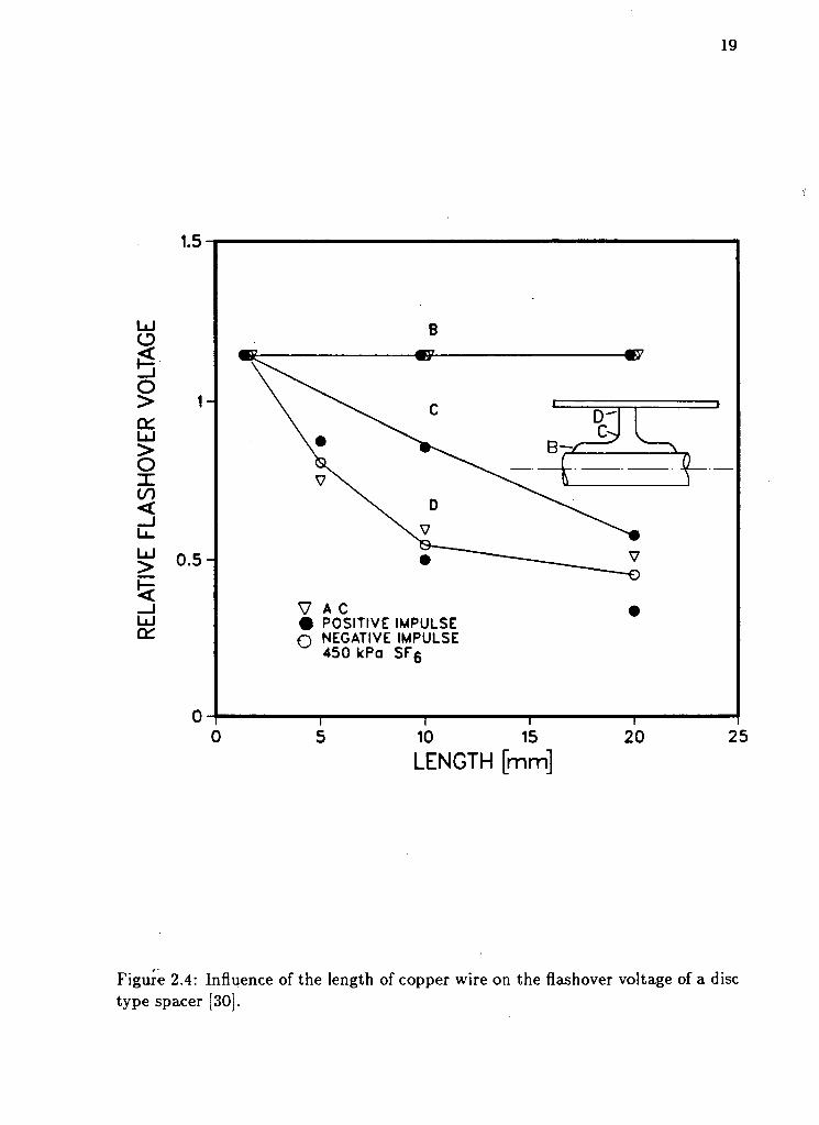
Figure 2.4: Influence of the length of copper wire on the flashover voltage of a disc type spacer [30].

20
It was found that in direct stress breakdown experiments, in samples with conduct
ing paint, the decrease in breakdown voltage as compared to an unperturbed field
arrangement was 10% regardless of the position of the conducting spot. The pre-
breakdown discharge altered with the location of the conducting paint spot on the
insulator. In similar experiments with the latter samples, the breakdown voltages
were lower than 30%. The image intensifier pictures showed that the discharge
initiation and propagation did not involve the spacer surface but the discharge
developed in the same manner as in a field distorted gas gap.
Laghari and Qureshi [39] investigated protrusion initiated breakdown in SFe
-N 2 mixtures, for a uniform field (Harrison profile plane-parallel electrodes). With
a hemispherically capped protrusion on the electrode (cathode), the breakdown
voltages were observed to be reduced as compared to a uniform field gap. However,
with a spacer located in the vicinity of this protrusion the DC flashover voltage
of this field distorted gas gap was found to increase. This increase in breakdown
voltage was ascribed by the authors to the possible reduction in the electric field at
the protrusion due to the presence of the spacer. Similar results were obtained for
gas pressures of upto 500 kPa. Cronin et al. [33] concluded that, in the presence
of contamination, corrugated disc spacers show a more consistent performance
compared with that of a smooth disc spacer, particularly under impulse conditions.
To examine the breakdown behavior of a disc spacer with particles, under impulse
conditions, Eteiba et al. [36] located a particle oriented radially ie., in the direction
of the surface electric field, on a disc spacer placed in a coaxial SF 6 bus. They
determined that this orientation was the most effective way to reduce the flashover
voltage of a disc spacer. So if particle contamination on a spacer aligns itself in the
direction of the surface electric field it effectively shortcircuits the gap (proportional
to its length) causing a reduction in the breakdown voltage.
Under long term DC voltage application, volume charges in clean epoxy spacers
accumulate at a moderate rate and distribute uniformly. The charge polarity is the
same as that of the inner electrode of the coaxial system. However, with a particle
fixed to the spacer, this homogeneity is lost. Not only have sharp peaks in the
charge intensity been observed corresponding to the particle position but also their
polarity are reversed. Steady pre-breakdown currents have also been observed in

21
Kinds of % Fiashover voltage (kV) particles AC Impulse no contamination 95-100 95-100 copper wires 0.2mm dia., 20mmlong 52-62 70-90
0.18mm dia. 5-10mm long 70-85 80-95 aluminum filings, 0.3mm, 50mg total 80-90 90-100 epoxy pieces 10-20mm 95-100 92-100 epoxy powder 95-100 92-100 cotton lint 10-20mm 95-100 95-100
Table 2.1: Effects of various kinds of particles on the fiashover voltage of practical spacers at 310 kPa SF 6 [17]
the case of an elongated fixed particle on the spacer surface which eventually leads
to a fiashover.
For alternating voltages, experiments conducted with a particle fixed on a spacer
have also revealed a drastic reduction in breakdown voltages. With increasing pres
sure it has been found that the corona inception and breakdown voltages coincide.
In more recent experiments [69] with a particle contaminated system subjected
to AC voltages, it has been found that wire particles lift and reach the spacer at
voltages comparable to the system operating voltage. The particles adhere to the
spacer surface for several hours but do not crawl towards the high voltage conduc
tor. If the particle is near the high voltage conductor and on the spacer, a dramatic
reduction in breakdown voltage (down to 25% of an uncontaminated system) has
been observed.
2.2.3 Non conducting Particles
The effect of insulating particles in reducing the fiashover voltages of a coaxial
system is less than that due to conducting particles [17]. Table 2.1 indicates the
effect of various particulate contamination on spacer fiashover voltages. It has
been observed that insulating particles in combination with conducting particles
[18] could impair the insulation performance. The conductivity of a particle really
influences the fiashover in a particle contaminated SF 6 gas gap.

22
2 . 2 . 4 Water Vapor
Although there are reports available [47] which indicate a reduction in breakdown
voltage for a plain gas gap in the presence of moisture, Nitta [17] reports that
the presence of moisture hardly influences the flashover voltages as long as no
condensation takes place on the spacer surface. Hogg et al. [48] have observed a
similar behavior.
2.2.5 Decomposed Gases
One of the major products of decomposition as a result of arcing in SF$ has been
found to be SF 4 [48]. Under moist conditions, SF 4 is likely to react with the
Si0 2 filler in the epoxy spacer to form SiOF 2 , HF etc. These compounds are
deposited on the spacer surface and lead to reduction in the surface resistivity.
The reduced surface resistivity could result in a non-uniform field distribution and
partial breakdowns between resistive layers which can eventually lead to a flashover.
Further, arcing on the spacer surface could release carbon byproducts which are
also deposited on the spacer surface. Deterioration of the spacer material and
premature flashover of the spacer follow rapidly. More recently, it has been found
that silica filler and cycloaliphatic resin spacers are prone to react with the arc
by-products of SF 6 gas. It is therefore important to select the appropriate filler for
a spacer.
2.3 Spacer Profiles
The mechanisms of surface flashover of spacers in compressed gases are not fully
understood and there is a lack of agreement on the actual parameters controlling
surface flashover. For this reason, several optimal designs of spacers have been
proposed. The following sections review the spacer designs that have been proposed
and their relative merits.

23
2.3.1 Post Spacers
One of the simplest support spacers, the post spacer, was introduced by Cooke
and Trump [10]. Metal inserts are generally used in post spacers to reduce the
triple junction effects. Simple cylindrical post spacers have also been extensively
employed by many researchers [8,16]. They have been used both in uniform and
non-uniform field gaps to study the influence of a spacer on the breakdown of an
SF 6 gas gap.
The exposed surface area of the post spacer is small thereby reducing the prob
ability of contaminating particles getting attached to the spacer under operating
conditions. Studies have been undertaken to examine the effect of corrugations
on post spacers. It has been observed that under clean conditions corrugations
on spacers reduce the fiashover voltages [16,17]. Under contaminated conditions,
however, corrugations did not necessarily increase the fiashover voltage of a con
taminated spacer [18]. Experimental results reported in literature indicate that
corrugations could either increase or even decrease the fiashover voltages [20],[21].
Trump [11] et al. have reported the advantages of these corrugations at higher
pressures. They have suggested that corrugations provide shielding effects against
microdischarges initiated at a triple junction. It appears that when a corrugated
spacer is terminated at its depression on the electrode, the nearest corrugation
may act as a shield for microdischarges initiated at the triple junction. Thus,
studies carried out to improve the performance of these spacers in the presence of
contamination have been inconclusive.
The factors controlling breakdown behavior of post spacers when placed be
tween plane parallel electrodes are:
• the degree of contact between the electrode and spacer
• the condition of the spacer
Figure 2.5 illustrates a typical arrangement of a cylindrical spacer placed between
plane parallel electrodes. Manufacturing defects could give rise to a small gas gap
between the electrode and the spacer, as shown in the figure. The electric field in
this region would be the product of the dielectric constant and the average field

Figure 2.5: Arrangement of a cylindrical spacer between plane parallel electrodes, ] - Electrodes, 2 - Insulating spacer. Gap dx is exaggerated to expose the triple junction.

25
[20]. As an example, consider a cylindrical spacer placed between a pair of plane
parallel electrodes. If d\ is the gas gap and c is the spacer length, er the relative
dielectric constant of the material, then the average stress in the gas gap is given
by:
Eg = — T — . 2.1
Corona inception starts at a relatively low voltage and is given by:
d2 Vi = Vd 1 + (2.2) [di X 6r)_
where Vd is the gap sparking potential. In order to improve the corona inception
voltage, the triple yurcc£icm(gas-metal-spacer junction) may be shielded by recessing
the HV and ground electrodes as shown in figure 2.5. It has been found that
such a measure improves the spacer fiashover performance. Thus, the inception
voltage depends on gap length, spacer dielectric constant and pressure. Skipper
and McNeal [20] indicate that for spacer gaps less than 200 micrometers, a perfect
contact is not essential.
The spacer surface also has significant influence on the discharge development.
Surface defects, charge patches etc., could attract metallic particles and initiate
microdischarges leading to a premature fiashover. These factors lower the fiashover
voltages in uniform fields.
2.3.2 Conical Spacers
Figure 1.2 shows the cross-section of typical conical spacers. Conical spacers occupy
more space than other spacers. They are extensively used, however, as gas stop
joints [24,28] for single phase GITL. Their contamination performance has also
been observed to be better than other types [27].
The angle of inclination which the spacer surface makes with the high voltage
conductor influences the overall field distribution. A smaller angle of inclination
results in a reduction of the spacer surface field but the electric field at the triple
junction near the high voltage electrode is increased. Increasing the angle of incli
nation causes higher stresses at the triple junction near the outer grounded sheath.
The optimal angle of inclination for conical spacers for use in GIS and GITL spac
ers has been found to be 45° [27]. Shielding electrodes are inserted in the post and

26
disc spacers, both at the inner and outer electrodes, to reduce the triple junction
stresses. In contrast, for conical spacers the inner conductor is moulded to the
spacer and the outer boundary has an insert and is flanged to facilitate its assem
bly between two GITL sub-sections. With electric field analysis, Itaka [19] reports
further reductions in the the triple junction stresses at the low voltage electrode for
conical spacers with the optimum angle of inclination. The authors describe the
modifications made to the shape of the flanged end of a conical spacer (where it is
bolted between two flanges of the SF 6 gas insulated apparatus). This modification
permitted dispensing with the normal metallic inserts which are used to reduce
the triple junction stresses. Problems associated with the incompatibility in the
coefficients of expansion of metal inserts and spacer material leading to cavity for
mation, partial discharge and eventual failure are therefore avoided. The successful
installation of corrugated conical spacers in a 420kV bus is reported in [28].
2.3.3 Disc Spacers
Figure 1.2 shows the construction of disc spacers. Due to their compactness and
simple geometry, these spacers have been very widely used [29,33] Split disc [25],
doughnut shaped [26] disc and corrugated disc [33] are some of the variations
employed in GIS and GITL.
Takuma et al. [34] derived the optimum disc spacer profile by means of field
computations for materials with different permittivities. A spacer profile angle
was defined to be the angle between the tangent to the spacer surface and the
electric field lines for a coaxial electrode gap with a disc spacer. Depending on this
angle and the dielectric constant of the spacer, the electric field distribution on the
spacer gets altered. Evidently, the optimum spacer profile angle is a function of
the relative diameters of the conductors of the coaxial system. They also report
that the spacer profile angle is larger for smaller inner to outer diameter ratios.
However, the maximum breakdown electric field strength in the presence of the
optimum profile spacer decreases to 70-80% of that of a coaxial gas gap without
a spacer. Comparative studies undertaken by Vandermeeren [35] showed that an
optimal disc spacer performs better than a conical spacer. For the disc spacer the
discharge initiation at the triple junction can be delayed due to the uniformity in

27
the tangential field. However, once the discharge is initiated, discharge propagation
cannot be arrested. The cone spacer on the other hand is very susceptible to
triple junction effects but has reduced surface tangential field, criticalfor discharge
propagation. Researchers at IREQ, based on field computation and experiments,
developed a composite profile cone spacer. The profile was a combination of both
the disc and cone spacers. This design combined the advantage of a long leakage
path of a conical spacer (30° angle) with the near uniform field of a disc spacer.
By introducing additional metal inserts at the outer end i.e., at the low voltage
end, triple junction stresses were further reduced. They claimed that the flashover
performance of this design was almost as good as that of the system without the
spacer.
2.3.4 Multiblade Spacers
Figure 1.2 shows a schematic of the Trefoil spacer which is particularly convenient
to use in multiconductor SF 6 GITL. Conventional spacers are difficult to apply
in a flexible cable because the spacers have to be fitted around the flexible inner
conductor (eg. post spacers supporting the central conductor in a coaxial system).
Therefore, a design in which the conductor is fitted around the spacer is more
advantageous. This has been achieved by use of multi-blade spacers fitted around
the conductors. The normal central conductor is replaced by several sub-conductors
at the same potential with the spacer blades protruding between the conductors.
It has been shown by Hampton [4] that the maximum surface stress for these 2, 3
and 4 blade spacers are approximately 50, 60 and 65% of that possible for a plain
disc spacer, with the same outer to inner diameter ratios of 2.7. Also the flashover
voltage has been observed to be independent of small gaps between the spacer and
conductor. Banford [37] has reported that a 3 blade Trefoil spacer performed well
under contamination conditions.
2.4 Effect of Voltage Waveshape
The breakdown behavior of solid support spacers in GIS, depends on the wave
shape of the applied voltage. In the case of alternating and impulse voltages the

28
Figure 2.6: Residual fields on post spacers after test at +600kV DC stress [38 .

29
voltage distribution over the spacer is governed by the distributed capacitance.
For direct voltages however, the spacer resistivity determines the field distribution.
Further, the flashover performance of spacers for the various types of voltages is
quite different in a particle contaminated environment because the dynamics of
free particle motion is also dependant on the waveshape of the applied voltage. In
the case of DC voltages it has been reported [38] that the spacer may accumulate
both surface and volume charges when the voltage is applied over long periods of
time. Figure 2.6 shows the maximum residual field at the inner conductor of a
post spacer in SF6 as a function of duration of the applied voltage. It may be ob
served that the amount of surface charging depends on the length of time the field
is maintained and the magnitude of the applied voltage [38]. The resulting field
distribution due to the charges could result in the breakdown of the surrounding
gas: Further, charge patches of this kind can attract contaminating free metallic
particles present in the system, resulting in excessive local stresses and promoting
long-term failure by stress enhancement.
Figure 2.7 shows the variation of flashover voltage with pressure for different
voltage waveshapes [39]. The results have been obtained with rapid application of
the voltages. From the figure it is apparent that the impulse flashover voltages are
higher than alternating or DC voltages.
In a coaxial system, the impulse breakdown voltages depend on the spacer
shape, type, size and location of particulate contamination. For example, a Tre
foil spacer [4] has a higher positive impulse flashover voltage as compared to the
negative impulse flashover voltage; the opposite when there is a metallic particle
on the spacer. Thus, the prediction of spacer performance subjected to different
waveshapes is difficult. Inspite of the volume of experimental data that have been
collected so far on the surface flashover in SFQ , the following questions still remain
unanswered:
• What is the nature of the accumulated charges ?
• What are the energy levels of these trapped charges!
• Are the measured charges only surface charges or are they in the bulk of the
solid?

30
240-1
> Uj 160 O
O > cr > o
< 80 H
0 - T
• IMPULSE [1.5/50 s]
1.5 2 2.5 3 3.5
PRESSURE [aim,abs]
Figure 2.7: The uniform field fiashover voltages of a 10 mm cylindrical spacer under AC, DC, and Impulse voltages [39].

31
• What is the interaction between a charged spacer surface and an adjacent
electron avalanche?
9 What is the physical mechanism of a surface fiashover and how does the
surface influence the discharge propagation?
The following section reviews some of the work reported so far, and the models
that have been advanced to explain spacer surface charging and fiashover phenom
ena.
2.5 Models for Surface Charge Accumulation
Most of the investigations on surface charge accumulation of spacers have been
carried out with direct voltages. Over extended periods of DC voltage application,
the bulk conductivity of the spacer together with its surface conductivity plays
a significant role in determining the overall charge distribution. By using mate
rials with higher surface conductivity as compared to volume conductivity, some
investigators [50] maintain that the bulk conductivity is no longer the dominant
mechanism, for the formation of surface charges.
2.5.1 D C Voltages
Charge accumulation on the spacer surface has been studied using post and coni
cal spacers by several authors [38,50]. Mangelsdorf and Cooke [38], have identified
two distinct charge patterns for post spacers stressed at high DC voltages in an
SF6 environment. They found that the post spacers accumulated a smooth con
tinuous charge. The magnitude of these charges increases with time and voltage.
This smooth charging has been found to be of the same polarity as of the central
conductor of the coaxial system of electrodes. The charge distributions have been
measured by removing the sample from the SF 6 environment. The maximum resid
ual field appears to level off with increased duration of the applied voltage, at levels
of +100kV. However, the residual field shows a pronounced non-linearity at voltage
levels of +600kV. It is suggested by the authors that this non-linearity in charging

32
may be due to the non-linear conductivity of the material or perhaps due to the on
set of another charging mechanism whose threshold is around +600kV. The author
reported analogous results when the polarity of the applied voltage was reversed.
On the other hand, with a particle deliberately fixed to the spacer, at the center
of the spacer and located parallel to the spacer axis, the spacer surface around the
particle was flooded with charges opposite to that of the inner electrode, thereby
disturbing the homogeneity of the uniform charge pattern seen earlier. Due to the
time dependent nature of homogenous charging, Mangelsdorf and Cooke suggest
that the bulk conductivity of the spacer was responsible for charge accumulation.
The second charge pattern that has been observed by Mangelsdorf and Cook
is termed as streak charging. This pattern has been attributed to the possible
ionization of the gas surrounding the particle. It has been concluded that this
static charge accumulation would lead to a high electric field which could result in
an electron avalanche in the gas adjacent to the spacer.
Knecht [51] examined the surface charge accumulation under both AC and DC
voltages in N 2 and SF 6 environments using cylindrical epoxy spacers 40 mm in
diameter and 40 mm in length. The spacers, with suitably placed metal inserts
have been located between plane parallel electrodes in the gas environment. The
gas pressures used by Knecht are 0.1-0.4 MPa for SFQ and 0.4MPa for nitrogen. At
constant voltage no clear dependence of the charge accumulation on either the gas
pressure or gas type has been observed. From the measured charge patterns, it has
been suggested that the charge accumulation is determined by the concentration of
carriers and their mobility in the direction of the electric field normal to the spacer
surface. The source of these charges has not been discussed. Knecht's hypothesis
has been supported by the fact that the volume and surface conductivities were
low for the spacer materials employed, thereby minimizing their influence on the
charge accumulation. These experiments suggest that spacer charge accumulation
is a consequence of gaseous conduction.
Nakanishi et al. [50] have proposed that the nonlinear surface conduction of
the spacer is the principal cause for heterogeneous charge accumulation. By using
cylindrical samples cast with metal inserts to reduce the triple junction effects and
placing them in a uniform field, it has been observed that the spacer surface con-

33
dition strongly influences the charge pattern. It has therefore been suggested that
the charging is due to surface conduction only. Theoretical considerations based on
surface and volume conductivity measurements show that the bulk charging mech
anism would require more than 80 hours of charging at high voltages to produce
the observed charge distributions. On the other hand, the experimental charge
patterns appeared within five hours of voltage application. Therefore bulk con
duction could not have been the dominant charging mechanism. Nakanishi et al.
attribute the charging to a mechanism solely involving the spacer surface. Intro
ducing the concept that the surface conductivity has a strong dependence on the
local electric field, the possible charge distribution on the spacer surface has been
computed and it matches the measured charge distribution. An example of the
calculated and measured charge distributions are shown in figure 2.8. It can be
seen that, in a field dependent surface conduction model, the computed charge dis
tribution matches both the dust figures and the probe measurements along the line
A - A'. Figure 2.9(a) and (c) indicate the type of spacer used between the coaxial
electrodes. Ez is the component of the electric field tangential to the spacer sur
face and En is the electric field normal to the spacer surface. Figure 2.9(b) shows
the distribution of the tangential and normal components Ez and En as shown in
figure 2.9a of the electric field on the spacer. Despite the asymmetric distribution
of the normal component of the electric field, the measured charge pattern has a
symmetric distribution.
There is less agreement between the observed charge patterns and the theo
retical charge distributions predicted by Knecht's model. In particular, Knecht's
model does not yield a symmetric charge distribution even though the normal
component of the electric field is asymmetrically distributed. The field-dependant
surface conduction model provides a better explanation for the observed charge
patterns.
Nakanishi et al. have further observed that when the the inner electrode of the
coaxial system is negative and has a surface finish of approximately 20 to 30 /zm, the
inner surface of the conical spacer accumulates charge. On the contrary, with the
inner electrode positive, no charge accumulation has been observed. Further, when
the inner electrode was polished to a finish of 5/zm, there is no charge accumulation

34
Figure 2.8: Residual potential distribution on both untreated and roughened spacers and theoretical calculation of charge accumulation. Gap spacing between metal inserts is 20mm [50].

35
c Dust fig u r e pattern following voltage a p p l i c a t ion
Figure 2.9: Radial and tangential field components of post spacer in a coaxial bus and dust figure of spacer energized with negative D C of 100kV for 5 hours [50].

36
observed on the spacer irrespective of the polarity of the inner electrode, giving
some credence to the field-emission theory. However, more recent studies [52] with
-500kV applied to the central conductor of a DC GIS with a conical spacer show
that the application of DC voltages for 30 minutes at 0.4 MPa SF 6 pressure does
result in a negative charge distribution on the concave side and a positive charge
accumulation on the convex side respectively. When the the central conductor
is made positive, a weak positive charge distribution is observed on the concave
side and a negative charge distribution on the convex side. The mechanism of
positive charge generation is not well understood at the present time. It has been
suggested that field emission is probably not the only mechanism causing this
charge accumulation [52].
From the experimental evidence presented it may be recognized that spacers
get charged under DC voltage application. Studies on scaled models and also on
actual spacers used in GIS seem to indicate that these charges have large decay
times (i.e, they reside on the spacer surface over several hours [61]). Under such
circumstances, these charges can distort the normal electric field which can result
in a premature spacer flashover.
2.5.2 Impulse and A C Voltages
Few systematic investigations have been reported on charge accumulation on a
spacer and its influence on the surface flashover voltage with impulse and alternat
ing applied voltages. Cun-Yi Yu et al. [53] have examined the influence of charge
accumulation due to DC voltages on the impulse flashover of spacers in SF6 . In
this study, the spacers have been subjected initially to direct voltages and par
ticulate contamination introduced in the test arrangement. The influence of the
spacer profile on the impulse flashover voltage has been subsequently examined.
They found that corrugated spacers tested at 0.2MPa SFe pressure have almost
the same first flashover as a spacer with smooth surface. However, when the spac
ers are exposed for a long time to direct voltages or spacers are contaminated by
metal particles, the performance of the corrugated spacer is superior. There has
been very little reported on charge accumulation on spacer surfaces subjected to
impulse and AC voltages [46]. The evidence of spacer charging under AC voltages

37
is conflicting. Knecht [51] observed a very small charge accumulation apart from
a local peak under AC stress. Other experiments with hollow spacers in vacuum
and N 2 gas indicate that spacers do get charged under alternating stress. But no
pre - breakdown currents were recorded. The authors attribute this anomaly to
bandwidth limitations of the equipment.
It has been recognized that spacers in GIS have a significant influence on the
V - t characteristics of the insulation. Experimental work conducted at IREQ
[55] indicates that spacers subjected to repeated impulse voltages of a particular
polarity cause sudden reductions in the predicted 50% probability of breakdown
voltages (V50) It has been suggested that surface charging is the probable reason
for this sudden reduction in the V 5 0 voltages. No systematic investigation to deter
mine the cause for this abnormal behaviour is reported. In summary, it has been
recognized that with DC stress, insulating spacers in GIS accumulate charge. The
nature of charge accumulation is one of the principle causes for sudden reductions
in the fiashover voltages. Systematic investigations of this nature with alternating
and impulse voltages have not been reported so far. The following section discusses
studies undertaken to determine the interaction between a spacer and the adjacent
gas gap.
2.6 Surface Discharge Initiation and Propagation
In a gas gap without space charge, the highest electric stress according to Laplace
equation is always at an electrode surface and in a direction normal to the electrode
surface. As mentioned earlier, a dielectric introduced in the same field distorts the
homogeneity of the field resulting in both normal and tangential components on
the spacer surface. The magnitudes of these components will get altered with sur
face and bulk charges. In an attempt to determine if solid dielectric surfaces are
inherently much more limited in their ability to sustain electric fields, Cooke [54]
compared published data on the electric stress for fields, mainly normal and tan
gential to a spacer surface. Cooke [54] suggests that an epoxy surface is capable of
sustaining electric stress comparable to that of a gas gap and that for a clean uncon-

38
taminated insulation system with a spacer, gas ionization is an important process
and provides the upper bound for improved insulation. Since surface flashover
voltages are sensitive to external perturbations e.g., triple junction effects, charges
and surface irregularities etc., these factors have to be isolated and/or controlled
for a systematic study of surface flashovers.
Surface flashover process is typically a two step event: first, the discharge initi
ation and then propagation. The initiation of the discharge results from local field
disturbances of sufficient magnitude. Propagation results when there is sufficient
field along the propagation path.
Cooke [54] describes an experimental model to explain the observation of surface
flashover voltages. In these studies, a cylindrical spacer, with a piece of conducting
wire attached to its surface, has been placed between toroidal electrodes. Triple
junction effects have therefore been eliminated by shielding. The growth of the
number of electrons in the vicinity of the wire have been considered, with a critical
avalanche size of 108 electrons being taken as the criterion for discharge inception.
The spacer by itself was not considered to be active in the discharge development
process, except as a means to influence the electric field pattern because of its
geometry and relative permittivity. It is presumed that flashover results at every
instant the critical field is reached. In very divergent geometries, this criterion for
the critical avalanche size does not necessarily result in a flashover. This condition
is also known as the streamer criterion and results in a corona discharge. Fig
ure 2.10 gives the details of the experimental setup used to verify the predicted
discharge inception stress. A good correlation between the calculated discharge in
ception stress and the flashover voltage was found. It is also reported that, a direct
stress application followed by a polarity reversal resulted in a very low breakdown
voltage which deviated considerably from the predicted voltage using the streamer
criterion. It is possible that surface or space charges have an influencing role on
breakdown. The described criterion does not account for these charges in the pre
diction of the breakdown voltages. The possible role of the spacer on the ionization
process, the role of the spacer on charging and its subsequent influence on break
down have not been accounted for, by his model. Cooke's experiments represent
one of the earliest attempts to explain surface flashover in SF 6 gas with direct

39
voltages.
In order to study spatial and temporal pre-discharge development, Pfeiffer et al.
[58] used a special electrode/spacer configuration. The geometry is described on
page 16. A high speed image converter system has been used to record the pre-
discharge phenomenon occurring between the hemispherical electrodes subjected to
impulse voltage excitation. Due to the high framing speed and short exposure time
of the camera, only two frames with a framing interval of 1 nanosecond (ns) could
be recorded at each impulse voltage application. The impulses have been applied
repeatedly to obtain different time frames prior to final breakdown. Finally, several
records have been put together to reconstruct the discharge development process.
It has been found that in SF6 , the first luminous spot may be observed at random
points along the spacer surface. The number of luminous spots grow with time
eventually combining and leading to breakdown. It has also been observed that
the discharge propagation velocity on the spacer is higher than that in a plain gas
gap.
In an attempt to determine the role of surface charges on the corona discharge
phenomenon, Mailer and Srivastava [56] have conducted experiments using a cylin
drical spacer placed in a non-uniform field (rod plane gap). They suggested that
the charges on the spacer surface may have a significant influence on the corona
discharge phenomenon. The study has been aimed at determining the role of ini
tiatory electrons in a developing discharge.
Stoop et al. [61] describe the role of surface charges on the discharge devel
opment. By using a laser beam to trigger a fiashover across a cylindrical spacer
placed between plane parallel electrodes subjected to DC voltages, they have ob
served that the fiashover times are smaller than that of a plain gas gap fiashover.
It has been suggested that photon induced detachment of electrons from the spacer
surface is the cause of reduced fiashover times with spacers.
2.7 Present Work
Surface fiashover of spacers in compressed SFQ is a much studied but poorly un
derstood phenomenon. Much of the modelling of spacer fiashover has been based

40
R o d I n s u l a t o r studies
Toroids: 7in OD, 3in s e p a r a t i o n
TOROID
Rod Diameter: 2.0inch
Rod dielectric constant: 2.5
Rod length: 12inch
Figure 2.10: A test chamber for surface flashover studies[54].

41
on the more mature understanding of breakdown in gases. Breakdown in gases has
been modelled by considering the Townsends's ionization coefficients namely: a
the rate of free electron and positive ion formation by electron impact ionization,
n the rate coefficient for formation of negative ions by attachment, 7 , the rate of
secondary electron formation at the cathode, 6 the electron formation rate from an
unstable negative ion and (3 the conversion of an unstable negative ion into a stable
one. All these coefficients for each gas are in turn a function of the gas pressure
and the electric field. Breakdown, at or near a spacer involves a modification of the
above ionization coefficients in some yet unknown manner. Variations in the ion
ization coefficients are, in turn, affected by a host of other parameters. Although
considerable data has been collected on the parameters affecting spacer fiashover,
little progress has been made in building a theoretical model. Surface charging
has been recognized as an important parameter influencing spacer fiashover. The
present work therefore deals mainlv with the phenomena of surface charging.
The fundamental parameter of interest, related to surface fiashover, has been
surface charge densities. It has been mentioned earlier that most of the investi
gations on spacer surface charging have been conducted with DC voltages. The
present work is concerned with the study of charge accumulation on spacer fiashover
with impulse voltages primarily because it has been widely recognized from work
with direct voltages that charge accumulation on an insulator surface modifies the
electric field distribution in the gap which, in turn, influences the initiation and
propagation of a surface discharge. Impulse voltages have been chosen in order
to minimize the role of bulk conductivity in charge accumulation. The choice of
impulse voltages also assists in a better interpretation of the electric field probe
data, since it has been recognized that bulk charges complicate the extraction of
surface charge densities from probe measurements.
A rod-plane and a parallel-plane gap have been used in the experiments. This
choice of gap geometries has been made for the following reasons:
• They are representative of the spectrum of uniform and highly non-uniform
fields in service
• The degree of non-uniformity may be easily controlled by varying the rod

42
diameter
• The axial symmetry built into the system provides easier electric field com
putation. Therefore theoretical models may be tested against experimental
data.
• Triple junction effects may be shielded by having a recess (2 mm deep 45 mm
dia.) cut into the electrodes for the plane-parallel electrode configuration.
For a systematic study of the complex surface flashover phenomena, it is essential
that the investigation be clearly focussed on a few limited aspects of the phenom
ena. The selected aspects however, should be aimed at elucidating the phenomena
and be of practical engineering interest. It is therefore of interest to study the
role of surface charging on impulse flashover of spacers in the absence of particle
contamination.
It has been recognized that, to be able to obtain an understanding of the nature
and growth of charges under electric stress in an SF6 environment, it is important
to monitor these charges in-situ. Exposure of the spacer to air following voltage
application could significantly alter the charge pattern. By removing the spacer
out of the SF 6 gas environment, the dielectric strength of the gas (air in this case)
surrounding the spacer has altered (reduced). Thus local discharges can occur
resulting in a modification of the original charge formation. Many researchers in
the past, while monitoring surface charge accumulation on spacers in SF 6 , have
removed the specimen from the SF 6 environment to measure the residual charge.
Conclusions based on charge magnitudes and fields under these conditions could
yield misleading results.
There are practical difficulties associated with in-situ measurements of surface
charges using a field mill or a capacitive probe. The complexities of building an
in-situ charge measuring system increase with the size of the SF 6 system. For
the geometry used in this study, a in-situ charge measuring system is designed to
provide for charge scanning of a cylindrical spacer approximately 40mm in diameter
and 30 mm long placed on a recessed plane (low voltage) electrode. To reduce the
probe measurement errors due to probe vibration, the insulating spacer should be
moved past the probe. This requires an electrode drive arrangement by which both

43
the top face of the spacer (the region close to the high voltage conductor) and the
cylindrical side could be scanned. The drives have been designed to provide both
an axial and a rotary motion of the bottom electrode thereby enabling the spacer
scans in-situ. Appropriate sealing is essential, since the drives are being located
external to the pressure vessel. Since the capacitive probe heads were connected to
the electrometer through the flanges and had to be withdrawn during the voltage
application, special seals were made at these joints. The details of the charge
measuring system and electrode drive, are included in chapters 3 and 4.
To summarize, the main objective of this research is to examine the role that
surface charges may have on surface fiashover of spacers in SF 6 gas. This study
examines the nature of charging of spacers subjected to impulse voltages. The
particular choice of impulse voltages was made to minimize the role of bulk con
ductivity of spacers in charge accumulation. Although precise in - situ charge
measurements are difficult to make, it is essential to have at least an approximate
knowledge of the charge patterns and their behaviour for improving the understand
ing of the surface fiashover phenomenon. This study would entail the development
of proper measurement and interpretation techniques. Hitherto, such work with
impulse voltages has not been reported in the literature.
Another aspect of the work focuses on the behaviour of an SF 6 spacer system
when subjected to composite stresses for example, AC and impulse. Both the
long term and short term effects of 60Hz AC pre-charging on subsequent impulse
fiashover is studied. Typically, GIS systems in service are subject to these com
posite stresses and their insulation performance has been unpredictable. All the
above investigations have been conducted in both quasi-uniform and non-uniform
field configurations.
Chapter 3 examines the techniques available for monitoring charge accumula
tion on spacers and the design of the capacitive probes used in this work. Chapter
4 describes the experimental setup used in this investigation. Chapter 5 describes
the numerical method used to compute the electric field distribution on the spacer
surface from the measured probe data. Chapter 6 presents the results and conclu
sions with the Chapter 7 describing the scope for future work.

Chapter 3
T E C H N I Q U E S FOR S U R F A C E C H A R G E M E A S U R E M E N T
3.1 Introduction
Several techniques for measuring the charge distributions on spacer surfaces have
evolved. Passive and active capacitance probes, electrostatic flux meters, free body
probes, vibrating and biased vibrating probes and electro-optic devices are some
examples. The discussions in the subsequent section will, however, be confined to
the capacitance probes, field mill and electro-optic device since they are the more
commonly used systems.
3.2 Electro Optic Methods
The electro-optic methods exploit the change in the index of refraction of a material
caused by an electric field. The material on which the charge is to be measured,
should either be optically active (i.e., a material whose refractive index changes with
change in the electric field), or, such a material should be embedded in the dielectric
at locations where the charges have to be measured. Electro-optic methods rely on
the Kerr, Faraday or Pockel effects.
The relation between the index of refraction and the electric field is given by
[62]
An = a + j3E + ^E2 + . . . , (3.1)
44

45
where a, f3,7 . . . are constants and
An is the unspecified change in the refractive index,
E is the electric field.
3.2.1 The Kerr Effect
The electro-optic Kerr effect may be defined by the expression:
An = npar - nper = XBE2 , (3.2)
where npar and nper are the indices of refraction parallel and perpendicular to the
applied field E. A is the wavelength of light transmitted through the Kerr Cell
and B is the Kerr coefficient. Nitrobenzene is a liquid which exhibits the Kerr
Effect. A plane polarized light beam is passed through a test cell to ensure that
the components are oriented parallel and perpendicular to the applied field. Upon
voltage application, a phase difference is introduced between these two orthogonal
components by the Kerr Effect. A polarization analyser is used to detect the phase
difference. The measurement of the phase difference enables the calculation of the
electric field. It has been shown [46] that the electric field may be calculated from
the undisturbed background fringe spacing Ay and the fringe displacement 6y by
the expression:
g - e = w k ' (3'3)
where 1 is the length of the light path in the cell.
3.2.2 The Pockel Effect
The Pockel effect may be described by the expression:
An = nlfijE , (3.4)
where
UQ is the ordinary index of refraction,
rij is the Pockel's coefficient, and
E is the applied field.

46
The Pockel effect may only be observed in solids and the direction of the ori
enting field may be transverse or longitudinal with respect to the incident beam.
All pockel crystals are piezoelectric, i.e., the crystal dimensions alter with applied
field [62]. This has been a drawback in constructing accurate charge measuring
systems based on Pockel Effect.
Electromagnetic interference, stray capacitance effects and grounding problems
are eliminated in electro-optic methods and the frequency response of the measuring
system is high (typically GHz). The light beam processing equipment of the electro-
optic device may be located at considerable distance from the high voltage source
thus requiring very little insulation from high voltages. Kerr cells have been built
to measure electric fields with an accuracy of ±0.3% . They have been used for field
measurements in liquid dielectrics. In contrast, electric field distributions may be
measured with an accuracy of ±4.5% with measuring systems based on the Pockel
The application of electro-optic techniques to measure electric fields is quite
complex. The instrumentation is comprised of lasers, optical sensors, lenses, po
larizers etc. The advantage is that the charge/field measurements may be made
during voltage application. On the other hand capacitive probes are intrusive and
they cause a local perturbation of the fields to be measured. The following sec
tion presents the capacitive probe technique for measuring charge distributions on
dielectric spacers.
Figure 3.1 shows the general construction of a field mill. It essentially consists
of a multivane rotor, rotating in front of a multivane sensor plate. The rotor
alternately exposes each sensor blade to the ambient electric field and shields the
sensor blade by the grounded rotor blade [63]. When each sensor blade is shielded,
the accumulated charge on the sensor plate is discharged.
The induced charge from the displacement current is given by:
Effect.
3.3 Electric Field Mi l l
(3.5)

Sensor Plate
Figure 3.1: A schematic diagram of the field mill.

48
substituting for D = Eeo in equation 3.5,
q = £0 • A • e0 (3.6)
The measured voltage across an impedance is related to the electric field by [63]:
V = ± * f p , (3.7)
and the maximum current can be expressed in terms of capacitance as:
i = / • V(Cmax - Cmin) , (3.8)
where A is the area exposed, Z is the impedance, f is the frequency of exposure and
shielding and EQ is the static electric field. The impedance Z is typically a capacitor
of about 100 pF, and an electrometer with an input impedance of lOMfi is used
to measure the voltage across the impedance. It has been found that the accuracy
of these probes is ±1%. In the above system, the polarity of the electric field
cannot be obtained. By employing a phase sensitive circuit these instruments have
been made polarity sensitive. Recently [51] this device has been used to monitor
surface charge on spacers placed between plane parallel electrodes subjected to DC
voltages in N 2 and SF6 environments.
3.4 Capacitance Probes
A capacitance probe consists essentially of an electrode surface insulated from a
surrounding grounded screen (coaxial electrode system). The central electrode is
usually mounted flush with the screen. The central electrode is then connected to
a high impedance electrostatic voltmeter. This device measures the charge induced
on the probe surface due to electric flux density emanating from the charges on
the spacer surface.
Figure 3.2 shows the construction of a capacitance probe. The probe is placed
a distance d from the dielectric with surface charges (density o over an effective
are Ae. The dielectric has a thickness t and a relative permittivity of er. Figure
3.2 shows the various capacitances involved. Csg represents the capacitance of
the dielectric to ground immediately below the probe head and Cps represents

BNC Connector
Probe body •
Probe tip
(a)
(b) Coaxial cable
Screen T
ps
Z Csg Sample
Figure 3.2: A schematic diagram of a capacitance probe showing its different pacitances.

50
the capacitance between the probe and the dielectric surface. Since the spacing
between the probe head and dielectric film is kept constant and is small compared
to the screen dimensions i.e., d/D is small, the electric field may be assumed to
be uniform. The charge induced on the probe is proportional to the voltage across
Cm. It has been shown by Foord [64] that the voltage drop across Cm is related to
the charge density by the expression:
v m = ; c—5 r • 3.9 Cm(l + ^ + Csg)
If Cm » Csg then a x Ae ,
It may be seen from equation 3.10 that Vm is proportional to the induced charge.
An initial calibration of the probe is required to determine the ratio of Ae/Cm. The
accuracy of this measurement depends on the uniformity of the sample thickness
t, the uniformity of the probe to surface spacing d and on the probe scan time.
It has been suggested that if the time constant RCm is made approximately 100
times larger than the scan time, accuracies of 1% could be achieved. Usually, an
electrometer with an input impedance of the order of lOMfi is used for measuring
the probe voltage. Due to the dominating influence of the cable capacitance on
the measurement, movement of the cable can lead to large errors in measurements.
The following factors have to be considered when using capacitance probes:
• For good sensitivity the probe-head to dielectric distance must be kept as
small as possible. A minimum spacing is, however, required to avoid dis
charges between probe head and the charged surface. These discharges could
give rise to spikes on the measuring signal leading to a misinterpretation of
the actual charge distribution.
• The probe signal is considerably influenced by the area of charge Ae on the
dielectric surface. If the probe tip dimension (d) becomes comparable to the
charge area Ae, then the probe may underestimate the charge density on the
small area. Reducing the diameter of the central conductor in the probe head
improves spatial resolution at the loss of probe sensitivity. Such a resolution
is desired when scanning narrow channels of charge produced, for example,
by surface streamers. Probe tip diameters as low as 80/Lim have been used.

51
• The probe signal is dependent on the distance between probe tip and charged
surface as well as on the rigidity of the probe structure and its associated
cable. As a consequence, it is always preferable to keep the probe fixed and
move the charged area past the probe tip.
• The presence of surrounding metal surfaces close to the charged area could
significantly affect the probe measurements. Therefore, the errors in mea
surements caused by the presence of metallic surfaces should be corrected for
by some numerical techniques.
• Finally, probe measurements do not provide us with a means to distinguish
between charges on the dielectric surface and those in the bulk (volume
charges) and therefore assumptions regarding the location of charges are un
avoidable.
Though capacitive probes are easy to apply and require simple instrumentation,
they have become the subject of serious controversy [65]. The main objection to the
interpretations of capacitive probe measurements has been the procedure adopted
for their calibration. Typically, a capacitance probe is calibrated using a conducting
surface at a known potential. This condition implies that the surface being scanned
has a uniform charge distribution. It is likely, however, that narrower lines of
charge may exist on the dielectric surface to be scanned. Further, surface charges
of both polarities can coexist on the spacer surface. Under such circumstances,
severe field distortions at the probe tip could occur. The field distortions would
cause deviations in the assumptions of a plane-parallel capacitor geometry. The
equations 3.9 and 3.10 are based on the assumption that the capacitances indicated
in figure 3.2 are plane - parallel capacitors and therefore the surface charge on
the dielectric spacer is easily calculated from the surface potential measurement.
In practice, however, these assumptions are incorrect and they lead to erroneous
charge magnitudes. Further, in the presence of bulk charges in the insulating
material, there is no simple relationship between the voltage measured by the
probe and the surface charge on the dielectric spacer. Despite these drawbacks,
there has been a noticeable increase in the use of both capacitive and field mill
probes for monitoring surface charges on spacers. Several researchers [50,52], have

52
used numerical techniques to reconstruct the charge distribution from the observed
probe potentials, thereby overcoming these drawbacks to a certain extent.
In the present work, several capacitive probes have been described. The choice
of the probe has been made after several experiments on probe sensitivity and res
olution. A probe with a shield diameter of approximately 12mm and tip diameter
of 2mm has been used in the final measurements.
3.4.1 Design of the Capacitance Probes
It may be recalled from Chapter 2, that the spacer geometry used in the present
work is cylindrical. Since the charge growth needs to be monitored both on the
top face of the cylindrical spacer (close to the high voltage electrode) and the side
of the spacer, two probes have been used. One of the probes has been used to
monitor the charges on the cylindrical surface of the spacer and the other probe
has been used for measuring charges on the plane surface. For measurements in
the plane parallel electrode configuration, the charge has been monitored only on
the cylindrical side of the spacer. Figure 3.3 shows the cross-sectional view of the
various probes constructed.
Following voltage application, both the high voltage and low voltage electrodes
were connected to ground. The gas pressure was increased by 0.04 MPa above
system pressure. The maximum charge density which can be measured by the
probe is limited by breakdown of the gas between the probe and the charged
surface. For thin films in air at atmospheric pressure, the limit is a few 100(xC / cm2,
while for thick insulators the maximum density that can be measured in SF6 at
O.lMPa is approximately 80//C/cm2. By increasing the gas pressure, therefore,
the dielectric strength between the charged surface and probe is increased. The
spacer was lowered by operating the electrode drive and each probe in turn was
brought within a distance of 2mm from the spacer surface. The rotary drive was
used to move the spacer past the probe face and the probe voltage recorded. The
drive enabled both updown and rotary motions about the spacer axis. The probe
cable was made rigid to ensure that the cable remained immobile during the probe
potential measurement.

53
A
Figure 3.3: Cross sectional view of the various probes.

54
To obtain reasonable information about the charge distribution on the spacer
surface using capacitive probes it is important to establish: a) the minimum de
tectable charge (sensitivity) and b) accuracy of reproduction (precision) of the
spatial variation of the charge. It is apparent that the geometrical configuration
of the probe sets the limit for reproducing the spatial variation of the charge dis
tribution. To establish the sensitivity and precision of the probes, the following
experiments have been conducted:
• The experimental arrangement shown in figure 3.4 has been used to obtain
the relationship between the probe sensitivity and probe spacing. The probes
are held at several positions from a charged metallic plate which is charged
to 5kV by a stabilized DC power supply (stability ±1%). The probe voltage
is then measured with a Keithley 610C electrometer. Figure 3.5 shows the
variation of probe sensitivity with spacing for various probes. It can be seen
from the results that probes numbered 5 and 6 (in figure 3.3) give the best
results. The larger the spacing between the probe and charged surface the
lower is the sensitivity of the probe. Reducing the probe to charged surface
spacing, improves the probe sensitivity. Reducing this spacing, however, can
cause sparkovers to occur between the charged surface and the probe. It is
for this reason that a tradeoff between the probe sensitivity and the risk of
unwanted flashover is to be made and a suitable probe - dielectric spacing
selected.
• The probe resolution is established using the arrangements shown in figure 3.4
a and b. Evenly spaced ridges are cut on a piece of metal as shown in fig
ure 3.4a. The width of the ridges are progressively reduced, ranging between
5mm and 0.5mm. This experiment establishes the capability of each of the
probes in identifying a minimum line charge width of 0.5mm. Below this
width it was seen that the probe voltage was negligible indicating that this
is the minimum width of charge which the probe could resolve.
A similar experiment has been conducted to determine whether two line charges
of opposite polarity could be discriminated by the probe. For this test, several brass
rods of the same diameter (approximately 2mm) are placed parallel to each other
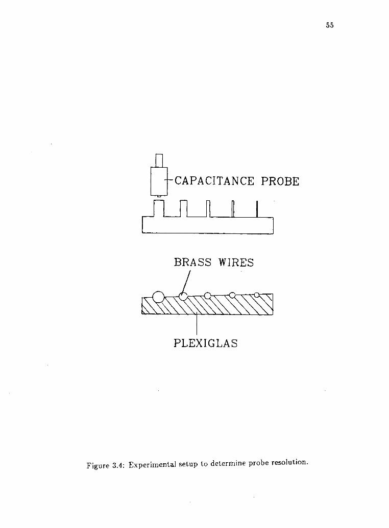
55
- C A P A C I T A N C E PROBE
i n fl i
BRASS WIRES
PLEXIGLAS
Figure 3.4: Experimental setup to determine probe resolution.

56
SPACING = 2 m m
SPACING = 3 m m
SPACING = 4 m m
0 2 4 CHARGE WIDTH [mm]
Figure 3.5: Variation of probe sensitivity with probe to surface spacing for various probes.

57
on a dielectric sheet of acrylic. The spacing between the rods is progressively
reduced with alternate rods held at positive and negative voltages. It is found that
when the spacing between the rods is less than 0.25mm, the probe is unable to
distinguish between the positive and negative lines of charge. Thus, if line charges
(such as in a streamer channel on a spacer) of both polarities coexisted within
0.5mm, the probe will be incapable of resolving this difference.
From these experiments it has been established that for the present application,
probes 5 and 6 are best suited to monitor spacer charge on the side and top face
respectively. A probe - to - spacer spacing of 2mm has been considered to be the
optimum value. This spacing is adequate from the sensitivity point of view of the
test arrangement. The probes are provided with a coaxial connector to enable
easy hookup to the electrometer. With this scheme, interchanging of probes is
considerably simplified.
Pedersen [65] has shown that the relationship between the voltage recorded by
the probe and the charge density distribution on the dielectric really requires a
prior knowledge of the charge distribution on the dielectric. The presence of other
metal objects in the region of the field introduce additional errors in the derived
charge distribution. It is therefore necessary to adopt some analytical or numerical
technique by which the measurement errors could be corrected. Ootera et al. [70]
have reported the development of a computer program to account for the inac
curacies mentioned above and transform the probe voltage into an equivalent 3
dimensional surface charge distribution. Using this technique, the surface charge
distribution on a conical spacer in a ±500kV DC GIS has been reconstructed from
the probe data. Their results show reasonable agreement with dust figures. It has
been assumed that no bulk charges exist in the dielectric. In the present investiga
tion, a similar attempt has been made to reconstruct the charge distribution from
probe measurements and to compute the surface electric fields on the spacer. The
surface charge simulation (SSM) technique has been used in the computations. In
the technique described by Ootera, the conductors and spacers are segmented into
triangular patches of charge. The charge density is assumed to be uniformly dis
tributed across each triangular surface. A set of points on both electrodes, spacer
and probe, equal in number to the number of charge elements are selected and the

58
Dirichlet and Neumann boundary conditions imposed. The probe potential at the
ith measurement location P, is expressed as follows:
where C, is the potential on the probe caused by the metal boundaries around the
spacer, Oj is the charge density at jth small triangle and is a coefficient dependant
on the geometry of the system. The surface charge distribution is evaluated by
substituting the probe data into the equation 3.11. The method used in this thesis
replaces the various boundaries by axisymmetric parabolic and conical charges
instead, to simulate the geometry. The details of the technique are discussed in
Chapter 5. The advantage of using this method was that for the geometry used,
programming was simpler. Details of this numerical technique are discussed in
Chapter 5.
This technique enables a qualitative assessment of the surface charge distribution.
Typically red and black powders used in electrostatic copiers are used to dust
the charged insulators. The obtained pattern (with regions of red indicative of
negative charges and the black regions indicative of positive charge) may be used
to get a qualitative picture. This method suffers from the disadvantage that the
charged spacer needs to be taken out of the SF 6 environment for dusting. Once
dusted the spacer needs to be cleaned before being used again. This is a very
awkward and laborious technique to merely establish the polarity of the charges.
The charge distribution could be disturbed by local discharges between regions of
high charge concentrations, during the process of removing the spacer from the SF 6
environment to dust it in air. This technique has been used as a secondary method
to confirm probe interpretation of the charge distributions [51,50].
In summary, capacitive probes are simple to use and require no elaborate in
strumentation. They have been quite extensively used in the industry. With care,
it is possible to obtain reasonably accurate estimates of the original surface charge
distribution. For these reasons, capacitive probes have been used in the present
n
(3.11)
3.5 Dust Figure Technique
work for surface charge measurements.
Chapter 4
E X P E R I M E N T A L S E T U P
4.1 Introduction
This chapter discusses the details of the experimental apparatus for the study of the
charging of spacer surfaces in SF6 gas. The details of the electrode geometries, types
of spacers, electrode and spacer polishing techniques, electric field probe assemblies
and the design of the electrode drive are given. Some of the probe measurements
have been obtained with a high pressure vessel in the British Columbia Hydro (BC
Hydro) Research and Development Laboratory in Surrey. The major part of the
measurements, however, have been obtained with the small pressure vessel in the
Electrical Engineering Department of The University of British Columbia. The
designs of the electrode drive mechanisms and the capacitance probe holders are
different for the two pressure vessels due to the differences in the two pressure
vessels.
4.2 Pressure Vessels
Figure 4.1 shows the high pressure vessel (HPV) in the BC Hydro Research and
Development Laboratory. It is a coaxial SF 6 GITL approximately 13m long. The
inner conductor has an external diameter of 0.12m and the inner diameter of the
outer enclosure is 0.36m. The HPV has two end-T sections and two 6m long
straight bus sections. Conical spacers are located at each of the joints. A vertical
high voltage gas insulated bushing rated for 2S0kVrms is bolted to one of the T -
sections. The second T - section is used as the test chamber which is sealed
60
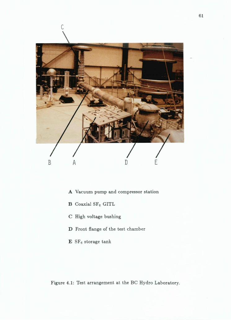
61
c
A Vacuum pump and compressor station
B Coaxial SF 6 GITL
C High voltage bushing
D Front flange of the test chamber
E SF 6 storage tank
Figure 4.1: Test arrangement at the BC Hydro Laboratory.

62
from the rest of the bus. Since the test chamber is isolated from the main S F 6
G I T L , it can be evacuated and pressurized independent of the main system. The
test chamber is evacuated and pressurized using a rotary vacuum pump (Edwards
Hivac Model E l M40, 40m 3 and a compressor (Corken oil less single stage D90)
respectively. The vacuum pump, compressor and an SFg gas cylinder are connected
to a manifold with appropriate valving. This arrangement enables:
• evacuation of the test chamber to a vacuum of 8Pa;
• extraction of the SF6 gas from the test chamber and compressing it into the
spare gas tank (capacity 1.57m3);
• replenishment of the gas in the test chamber from the S F 6 gas bottle in case
of need;
• storage of the used gas from the test chamber into the spare gas tank.
Figure 4.2 gives the schematic of the gas cart. A thermocouple gauge [Varian 531]
calibrated against a Mcleod gauge has been used to monitor the in-line vacuum at
the pressure vessel. High pressure dial gauges indicate the gas pressure in the test
chamber. Three ports of varying sizes and two additional observation windows,
approximately 75mm in diameter, are provided on the test chamber. The flange at
the front end (D in figure 4.1) is used for mounting the electrode drive assembly.
The test chamber can be evacuated to a vacuum of 8Pa. and pressurized to a
maximum gas pressure of 0.4MPa. Figure 4.3 shows the arrangement of the
electrode drive and the electrodes mounted on the high pressure test chamber.
Figure 4.4 shows the small pressure vessel which is provided with four port
holes. Two of the port holes are utilized to manipulate the low voltage electrode
from the outside. A flexible Neoprene rubber hose connects the third port to a
250 lit/min two-stage Sargent Welch rotary vacuum pump. A high pressure dial
gauge and a thermocouple gauge head are also connected to this flange in order
to monitor both the S F 6 gas pressure and the vacuum during pressure cycling. A
Tygon tubing connection to the same flange with a needle valve allows S F 6 gas
from the gas bottle into the chamber. The test chamber is fitted with a bushing
rated 150kVrTn3.

63
To lest chamber Ail vent To storage tank To SF f c bottle
Figure 4.2: Schematic of the gas cart

64
1. High Voltage electrode
2. Capacitive probes
3. Low voltage electrode
4. Rotary and linear drives
Figure 4.3: Arrangement of the electrode drive and probe in the high pressure test chamber.

65
2 4
1. Pressure vessel
2. Rotary drive
3. Linear drive
4. Observation window
5. Multi-test set
Figure 4.4: Test arrangement at the UBC laboratory.

66
4.3 Electrode Assembly
The plane parallel electrodes were made of aluminum and were approximately
150mm in diameter and 30mm thick. One pair of electrodes had a recess approx
imately 45mm in diameter and 2mm deep. The recess was provided to shield the
triple junction. The plane parallel electrodes were 150mm in diameter and 30mm
thick. The hemispherically capped rod electrodes were made of brass with tip
diameters of 5mm and 10mm. The HV electrode was firmly fixed to the central
conductor in both the pressure vessels and the low voltage (LV) electrode was
supported by an electrode drive mechanism.
After each test series, breakdown tracks on the electrode surfaces were removed
by the following procedure:
• The electrodes were remachined.
• The electrodes were then wet polished with 600 grit paper.
• Subsequently they were polished with 1/z alumina powder.
If the electrode damage was extensive, it was necessary to commence the polishing
with a 400 grit paper.
4.4 Electrode Drive Assembly
The electrode drive system enabled both an up - down motion as well as a rotation
of the LV electrode about its own axis. It was operated by reversible DC motors
located external to the test chamber. By using nylon shafts, insulation was provided
between the bottom electrode and ground. The LV electrode was insulated from
ground for 100 volts so that, by connecting a resistor between the LV electrode
and ground, the gap currents can be monitored. Dynamic oil seals incorporated
in the flanges provided the necessary sealing both under vacuum as well as at
high pressure. Linear potentiometers (Piher 10kf2) were connected to the drive
shaft which facilitated the recording of the angular and linear movements of the

Figure 4.5: Electrode drive arrangement in the small pressure vessel.

68
electrode. Limit switches restricted the total angular travel (360° ±2° ) and the
linear up - down motion (20mm ± 1 mm).
Figure 4.6 shows the drive arrangement for use in the high pressure vessel.
Figure 4.7 shows the cross-sectional view of the flange and the drive mechanism.
Both the rotary and linear drives have been located on the same flange. Once
again, dynamic oil seals have been used to seal the drive shaft feed- through in
the flange. These seals proved to be adequate for a vacuum of 8Pa. and gas
pressure of 0.4MPa. A linear bearing incorporated in the central section of the
flange converts the rotary motion of the motor shaft to a linear up - down motion
of the LV electrode. Limit switches have been set to give the desired travel. A linear
potentiometer (Piher 10kf7) provides information on the linear spatial movement.
The rotary motion has been provided by a gear drive. In this case however, the
information on rotary movement has been provided by a three and a half turn
rotary potentiometer. The LV electrode is supported by a shaft which is aligned
by the linear bearing in the electrode drive (see figure 4.7).
After each test series, the linear drive was used to lower the LV electrode (i.e.
spacer was moved away from the high voltage electrode) to permit the charge
scan of the top face of the insulating spacer. At each position, the rotary drive
was operated to rotate the spacer in a clockwise direction (looking down on the
spacer) past the probe tip. After completing the scan of both the spacer top and
the sides the linear drive was operated to move the spacer back towards the high
voltage electrode (as it was during the voltage application). The output of the
potentiometer was fed to the X-channel of a YEW X-Y plotter. Power for the
for the motor operation and the potentiometers were provided by adjustable DC
power supplies.
4.5 Capacitance Probe Assembly
Figure 4.8 shows the cross-sectional view of the probe cable and the seal. The
probe cable has been drawn through a 10mm diameter, 300mm long stainless steel
tube. Adequate dynamic sealing has been provided to prevent gas leaks during the
movement of the probe assembly. Silicone sealant provides sealing against leaks

69
Figure 4.6: Electrode drive arrangement in the high pressure vessel.
70
Figure 4.7: Cross-sectional view of the electrode drive used in the high pressure vessel.

71
from the core and sheath of the RG58 cable used.
The experimental procedure adopted for the measurements consisted of the
following steps:
• The insulating spacer is placed on the low voltage electrode after cleaning.
• The pressure vessel is then evacuated to a vacuum of 8Pa and then filled with
SFQ gas to the desired pressure.
• The lower electrode is moved away from the high voltage electrode until it
reaches the farthest (lowermost) position from the high voltage electrode.
The capacitive probe (6 in figure 3.3) is then moved towards the spacer and
set to scan the flat face of the spacer at 5 levels as shown in Fig 4.9. At each
position (levels 1-5), the rotary drive is operated to rotate the spacer past the
probe, thereby obtaining a 360° scan. The probe voltage is measured using
a 610C Kiethley Electrometer and plotted on a YEW X-Y plotter at each
level.
• This probe is then withdrawn and the second probe (5 in figure 3.3) to scan
the cylindrical side of the spacer is moved inwards. A similar scan is con
ducted.
• The lower electrode is then raised (moved towards the high voltage electrode)
by the drive so that a 360° scan can be performed at 4 different levels (levels
6-9) as shown in figure 4.9.
• After the scans, the probes are withdrawn fully.
• The bottom electrode is raised so that the insulating spacer is firmly fixed
between the two electrodes.
• The voltage is then applied.
• Following the voltage application, the gas pressure is raised slightly and the
LV electrodes is lowered. Probe voltage scans are then performed as described
above.

Silicone sealant
Adapted BNC connector(female) Stainless steel tube
Figure 4.8: Cross-section of the probe cable.
73
QUASI-UNIFORM FIELD NON-UNIFORM FIELD CONFIGURATION CONFIGURATION
Level Number Distance x in mm
Level Number Rod-plane
gap Parallel-plane
gap
1 0.5 3.5
2 5.0 8.5
3 10.0 13.5
A 15.0 18.5
5 19.5
6 23.5
7 28.5
8 33.5
9 38.5
Figure 4.9: Levels at which the residual charge measurements were made. Distance x is the measure of the charge scan radius from the axis along the spacer surface.

Figure 4.10: Schematic of the charge recording setup.

75
4.6 Power Supplies
The Haefely Multi-Test system has been used as the voltage source for the ex
periments in the small pressure vessel. The system generates 190kV lightning or
180kV switching impulses or 200kV DC or 80fcVrma voltages. A capacitive voltage
divider (CVD, 500pF) has been used to measure the high voltage. The voltage
signal across the secondary of the CVD has been connected to an impulse peak
voltmeter (Haefely Type 65) and also to a Biomation waveform digitizer (Type
6500) for recording the signal. The trigger signal for the Biomation unit has been
derived from the trigger spark gap of the impulse generator. A fiber - optic link
has been used to lead the light of the spark gap discharge into a light - to - volt
age conversion unit. This unit provides a clean trigger signal for the Biomation
unit. Improved shielding of the laboratory, use of triax cables, proper grounding
are some of the steps taken to overcome any jitter in the triggering of the Bioma
tion unit. A flexible aluminium lead has been used as the connector between the
impulse generator and the test chamber.
The high voltage transformer provided in the multi-test has been rated for 80
Kmsj 5kVA . The supply to the low voltage winding is regulated by a variac and
the high voltage output recorded by the peak voltmeter connected to the secondary
of the CVD.
For the measurements at BC Hydro, a 500kV five-stage impulse generator has
been used. Various combinations of front and tail resistors are available to generate
different waveforms. The charge measurements at BC Hydro have been obtained
with the 1.2/50 /us and 100/2500 fis waveforms. The impulse voltage has been
measured with a 500pF SF 6 gas insulated CVD having a division ratio of 1:9958.
4.7 Insulating Spacers
Figure 4.11 shows the cylindrical spacers used in this investigation. All samples
have been carefully machined to obtain surface finishes of 4/mi and 40/xm to exam
ine the influence of surface finish on the charging phenomenon. The spacers have
been made of PTFE, acrylic and unfilled epoxy, and were 40mm in diameter and

76
Figure 4.11: Photographs of the insulating spacers

77
30mm long. The surface finish has been confirmed by SEM scans performed on
small samples machined under identical speed-feed ratios.
4.7.1 Selection of a method to neutralize surface charges
With voltage, insulator surfaces in gases collect charge when the rate of charge
arrival exceeds the rate of removal from the surface by conduction or other neu
tralizing mechanisms. Such accumulation is dependent upon the source of free
charges, transport of charges to the surface and the charge neutralization processes.
When drifting charges accumulate on the spacer surface, they alter the electric field
thus affecting the flashover behavior. It is important to have a relatively charge
free spacer before the commencement of voltage application to obtain the exact
nature of charging. Therefore, it is necessary to find means of neutralizing the
charges on spacer surfaces at the beginning of each test series. Some experiments
were conducted to obtain a quick, simple and an effective method for minimizing
residual charges on the spacer before introduction into the pressure vessel for the
high voltage tests. Neutralization of surface charges by infra - red radiation and
thermal radiation have been investigated with thin insulating disc samples before
establishing a procedure for charge neutralization between tests.
Figure 4.12 shows the experimental arrangement. All these experiments have
been conducted in air. A needle electrode has been used to charge disc specimens
of acrylic, P T F E and ceramic placed on a rotating metallic platform.
The samples were cleaned and washed in distilled water and dried in a vacuum
oven at 60°C for 4 hours, then wiped with alcohol and placed on a metallic platform.
The point electrode was then connected to a DC supply and maintained at 3 kV
for 1 min. This caused the formation of a corona discharge at the tip, resulting in
charge deposition on the spacer surface. The surface was then scanned by the field
probe at the same radius as that of the corona source. Surface scans were then
obtained following an infrared lamp exposure, using a hot air blower and a 1000W
lamp.
It may be seen from the charge profiles, shown in figure 4.13 that the 1000
W lamp and the hot blower give the best results. These measurements establish
78
Electrode drive
1. High Voltage DC supply
2. Electrometer
3. X-Y plotter
4. Corona source
5. Capacitive probe
6. Turntable (LV electrode)
7. Support stand
8. Blow drier
Figure 4.12: Experimental setup to establish a suitable residual charge neutralizing technique.

79
that charge neutralization is effective when the surface temperatures of the spacer
reach 70°C approximately. Although the blower is equally effective, the lamp ar
rangement has been preferred.
Before introduction of the spacers into the pressure vessel, they are cleaned and
discharged by adopting the following procedure:
• Ultrasonic cleaning with Alconox detergent for 20 minutes.
• Rinsing in plain tap water.
• Thorough rinsing in deionized water.
• The samples are then heated in an oven at 65°C for 4 hours and stored in an
evacuated dessicator.
• Prior to their introduction into the pressure vessel, they are washed with
isopropanol and any trace of dust is wiped clean with Kleenex tissue dipped
in isopropanol.
• The sample is finally placed on a stand and exposed to a high intensity
(1000W) lamp for 5-8 minutes to minimize any residual charge on the spacer.
Spacers and electrodes are always handled with disposable plastic gloves. The
electrodes are wiped clean with Kleenex tissue dipped in isopropanol before being
introduced into the pressure vessel. Subsequently, the spacer is introduced into
the test chamber and the test chamber is immediately evacuated. Charge scans
performed under vacuum following the above treatment have indicated that the
residual charge on the insulator is of the order 0.1 nC/cra 2 . S F 6 gas is introduced
into the test chamber following its evacuation to 8Pa. At times, traces of residual
charge greater than 1 n C / c m 2 has been neutralized by the gas. This has been
demonstrated by the charge scans performed after the introduction of the S F 6 gas.

80
Blow drier 6-4°
0.16 pC/m* Infra-red lamp
-0J6 p/m1 , a B p l e
1000 W lamp •0.03
Charged aample -3.73 ^Cjrrf-
1000 H lamp
Charged sample
-0.36 pC./^
CERAMIC 55.0 aim d ia .
9 .0 an thk.
PLEXIGLAS 77.0 an d ia . 3.6 am thk.
TEFLON 77.0 an d i a . 3.3 an thk.
Figure 4.13: Effect of using various techniques to neutralize residual charge on a small disc spacer.

Chapter 5
E L E C T R I C FIELD C O M P U T A T I O N
5.1 Introduction
The surface charge distribution on the spacer surface should be derived from the ca
pacitive probe measurements which are in the form of the probe potential variation
as a function of its position. Either a computational technique, like for example a
surface charge simulation technique, or calibration against a known charge distribu
tion is used for the transformation of the probe potential variation to an equivalent
surface charge charge distribution. The surface charge simulation technique is used
for the conversion of probe data to surface charge distribution. The principle of
the technique and the approximations used in the analysis, have been described.
It was mentioned in chapter 3 that capacitance probes are normally calibrated
against a charged metallic surface held at a known potential V volts. If Vpr is the the
voltage indicated by the electrometer connected to the probe held at a distance d
from a charged metallic surface held at V volts, the electric field between the probe
and the charged object is E = ^ = f^. Hence the charge density on the metal
object is a = l u y ^ , where e0 is the permittivity of free space. The probe potential
is related to the charge density as Vpr = aa, where a is the probe transformation
function. Substituting the value of a in the expression for the probe potential Vpr,
the probe transformation function a is obtained. Using this probe transformation
function a, the surface charge distribution on an insulating spacer is determined.
The electric field in the gas near a charged spacer (whose relative permittivity
is er) is modified when a metal object is brought near the surface charge. This is
81

82
because the electric field is concentrated in the gas layer between the spacer and
the metal. The charge density due to a local charge AQ, on an area AAi is defined
as a = The electric field between the charged area and the metal object(the
probe in this case) is given as E = 7 ^ - where ej of the gas is unity. It is assumed
that this charged patch resides on the surface of the dielectric. When the probe
is withdrawn from the charged area the electric field is reduced to E = — T T X — •
The above interpretation implies the following assumptions:
• a plane parallel electrode configuration,
• the absence of other metal objects,
• the absence of any bulk charges
• the absence of both positive and negative charges coexisting on the spacer
surface.
• the effects of the material can be neglected (specifically the relative dielectric
permittivity)
Pedersen [73] has shown that the probe response function for probe measurements
with a simple geometry (similar to figure 3.3) depends on the relative permittivity
of the insulating spacer, the relative dimensions of the entire system and the probe
position. Further, meaningful interpretation of the surface charge distribution on
the insulating spacer from probe measurements are possible if these factors are
considered.
The surface charge simulation technique takes into consideration the presence
of the insulating spacer and the electrodes. It is more accurate than the calibra
tion of the probe against a charged metallic surface because a systematic error is
introduced in such a calibration by the internal molecular polarization which is
present in the dielectrics with residual charges. The principal assumption made
in this analysis is that no charges exist in the bulk of the specimen following the
impulse voltage application. This is a reasonable assumption since the volume con
ductivities of the spacer samples are of the order of 6 x 10 - 1 6f2 - 1/cm and the time
constants for charge migration are of the order of 60 hours.

83
Computational techniques may be broadly classified into differential and integral
methods. The Finite Difference (FDM) and the Finite Element Methods (FEM)
are differential methods and charge simulation methods are integral methods. The
F E M and FDM are also referred to as the Domain methods and CSM and SSM as
the Boundary methods. The SSM technique has been chosen as the computational
procedure for the following reasons:
• The F E M technique requires the generation of isoparametric elements, due to
the 3-dimensional nature of the problem, thereby, increasing the complexity
in programming;
• The axisymmetry in the model enables the use of conventional ring-like sim
ulation charges for which the potential and field coefficients could be easily
derived. Any asymmetry due to the spacer surface charges may be accounted
for by selecting a charge distribution which periodically varies with the angle
of rotation around the axis of symmetry;
• The electric field distribution on the electrode surface may be obtained di
rectly from the surface charge density using the Guass theorem:
= f . (5.1)
Although a finite difference technique has been developed to asses the influence
of the charge on an insulating spacer from probe measurements on the overall elec
tric field distribution, the study is restricted to a 2-dimensional problem [74]. The
authors have directly used the charge density distributions obtained by previous
investigators to compute the electric field distribution of the system under the in
fluence of the charges. However, the accuracy of the original charge distribution
magnitudes and the technique used to interpret the probe data remains uncertain.
5.2 Principle of Charge Simulation Method
The distributed surface charges on the conductors, are substituted by a set of dis
crete charges which are placed inside the region in which the field is to be computed
(for example inside the conductors). The choice of the type of charges (i.e., line,

84
point or ring charge) depends on the electrode configuration. The magnitude of
these charges are then determined such that the boundary conditions are satisfied
exactly at a selected number of points on the boundary.
The accuracy of the CSM improves with the number of simulation charges. The
computational procedure involves the following steps for a geometry not involving
any solid dielectric:
• Locate n (point, line or ring) charges inside the electrodes,
• Selecting a set number of n contour points on the boundaries. It is required
that at the contour points, the potential resulting from all the the charges
should be exactly equal to the electrode potential. Application of this prin
ciple to the ith contour point on an electrode results in an equation of the
form given by:
Efli9y = *<, (5-2)
where Pij is the potential coefficient at the ith contour point due to all n
charges (i.e., j = 1,2,3 ri). The potential coefficient is typically a metric
coefficient involving distance terms. Similar equations are obtained at each
contour point, leading to a system of n linear equations:
= [P] [Q] = [•] • (M t'=l j=l
The P matrix in equation 5.3 is often referred to as the potential coefficient
matrix. The vector Q is the array of unknown discrete charges and $ is the
vector of prescribed potentials (Dirichlet condition)
• Solve the system of equations 5.3 to obtain the magnitudes of the discrete
simulation charges.
• Having obtained the magnitudes of the simulation charges, it is necessary
to check the potential at points on the boundaries other than those used
in step2. As a measure of accuracy, Singer [68]et al. define the difference
between the known electrode potential and the value computed by CSM as
the potential error. It has been shown [68] that in order to obtain a 1 %
85
accuracy for the field magnitude in the region of interest, it is necessary to
limit the potential error to less than 1%.
• With the potential error checked, the field at any other point can be computed
in the x and y directions for a 2-dimensional problem. For example the electric
field in the x direction at any point i due to all the charges j = 1,2,3...n can
be written as:
and in the y direction
Equations 5.4 and 5.5 can be expressed as
E = [£,niQi+ (5-6) 3 = 1 3=1
Ffj and F^ are the called the field coefficients in the x and y directions.
5.2.1 C S M Applied to Two Dielectric Arrangement
Due to the realignment of the dipoles in a dielectric exposed to an electric field, the
charges internal to the dielectric cancel each other. A net surface charge however,
appears on the dielectric surface. The dielectric may therefore be simulated by
locating discrete charges on either side of the dielectric boundary [68]. It should
be noted that:
• The dielectric boundary does not represent an equipotential surface;
• The electric field should be calculated on both sides of the boundary. The
usual boundary conditions for the tangential and normal components of the
electric field should be satisfied.
5.3 Principle of Surface Charge Simulation
In the SSM, the distributed surface charges on the conductor and dielectric bound
aries are substituted by sheet-like charges which are positioned directly on these

86
boundaries. The magnitude of these charges are such that the boundary condi
tions are exactly satisfied at a selected number of points. The Dirichlet condition
is used for the electrode boundaries and the Neumann condition at the dielectric
interface. For fields which do not have a rotational symmetry, ring charges whose
density varies with angle of rotation a (a Fourier-type surface charge) are used as
the simulation charges. A charge distribution given by [71];
n n A = ^ A ^ c o s ^ a ) + ^AMsin()ua) , (5.7)
may be used. In equation 5.7, n represents the order of the harmonic charge
distribution and A is the charge density (charge per unit length). The expression
for the potential at any point P(rp,tp, zp) (in cylindrical coordinates) due to the
mth harmonic charge whose coordinates are Q(rc,0,zc) is
«Mr„ zp) = £-£fipQ*-i t ( ' P ' 2 c ) 2 r t c
r c 2 + r p 2 ] C O S ^ ' ( 5 " 8 )
considering only the cosine function in the charge representation. ...j is com
monly referred to as the torus function. Several methods have been used to solve
this function but a matrix method described by Sato [72] is used in this work. In
reference [71] it was shown that 3-dimensional axi-symmetric fields like a sphere-
plane geometry could be computed by using charges in the form of cones placed
directly on the sphere surface. The effect of the ground plane was simulated by
considering the image charges. The charge density around the axis of symmetry is
similar to the equation 5.7 except that charge density variation along the conical
surfaces could be expressed as a function of a non-dimensional parameter u which
adequately describes the contour. This choice of a charge element essentially con
stitutes a surface charge representation. Both linear and parabolic expressions have
been employed for defining the charge density variation along the u direction (see
figure5.1). For contours with circular arcs, r c and zc are trigonometric functions of
an angle. Thus a surface charge element can be represented as
n n
Hu) = HA^(u)cos(^) + EM")8"1^) , (5-9) where A(u) indicates that the charge density varies along the u direction. In order
to generalize the application, the charge density was considered variable in the xj)

87
direction as well. The potential at any point F(rp,ip,zp) (see figure5.l) due to the
mth harmonic surface charge element, described by equation 5.9 is given by:
i t , -v cos(m?/;) f \FC (zp- zc)2 + rc
2 + rp
2
<Pm{rp,ip,zp) = x / A m ( u ) J - g m _ i [ ^ '-— p-\du , u *
i s i n( mV0 w /" w x f ( z p - z c ) 2 + r e
2 + r p
2
+ - ^ x / A - ( u ) V ^ g m " [ — ^ — 1 ( }
u V P c
The potential at a point i due to all the harmonic charges is given by; n
= £ $ m • (5.11)
In a similar manner the electric field in the (r, ip, z) directions can be computed [72].
In equation 5.10, the coefficients obtained after excluding the charge term is referred
to as the potential coefficient as in charge simulation. It is quite apparent that
this expression for potential coefficient is a metric term just involving the various
distances between the charge location and the point at which the potential is being
computed. In a similar manner, the field coefficients are obtained by differentiating
the expression for potential in the {r,tb,z).
Contours may be described by polynomials; for example a sphere is replaced
by parabolic elements [71] and other axi-symmetric 3D surfaces are represented by
conical, cylindrical and toroidal segments [72]. It is apparent from the above that
for a 3-dimensional axi-symmetric field problem with a CSM technique a very large
number of charge rings will have to be used to solve for the field distribution. In
the case of the SSM, however, by using relatively few area charges as given by the
equation 5.9, the field distribution can be computed. Depending on the complexity
of the problem, the use of SSM will speed up the computation.
Sato and Zaengl [72] have used cylindrical and toroidal segments to compute
the electrostatic field distribution for a 3D problem consisting of 3 hemispherically
capped metal electrodes and a dielectric sphere placed above a ground plane. For
this problem 3 harmonics and 54 area charges were used. The ground plane was
simulated by using image charges. Therefore, a charged axi-symmetric surface
c:[rc, 0, zc] has been defined by means of the angular parameter 0(0 < 0 < 2n) and
a nondimensional unit parameter u(0 < u < 1). By this representation, cylindrical,
conical, spherical and toroidal charged surfaces are easily described. Figure 5.1

88
Figure 5.1: Representation of conical and spherical surface charges.
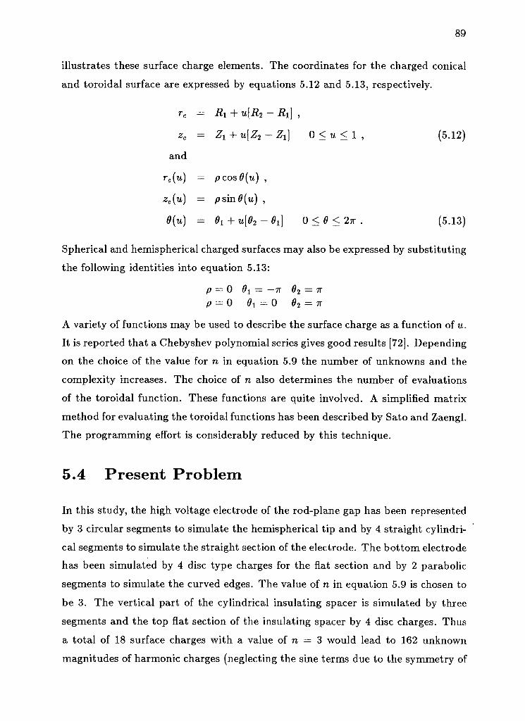
89
illustrates these surface charge elements. The coordinates for the charged conical
and toroidal surface are expressed by equations 5.12 and 5.13, respectively.
r c = i2i + u[R2 - Ri] ,
zc = Zi + u[Z2 -Zt] 0 < u < 1 , (5.12)
and
rc(u) — pcos0(u) ,
zc(u) = ps'm0(u) ,
0{u) = 6X + u[02 -h] 0 < 0 < 2TT . (5.13)
Spherical and hemispherical charged surfaces may also be expressed by substituting
the following identities into equation 5.13:
p = 0 0i = —TV 02 = 7T
0 = 0 0! = O 02 = 7T
A variety of functions may be used to describe the surface charge as a function of u.
It is reported that a Chebyshev polynomial series gives good results [72]. Depending
on the choice of the value for n in equation 5.9 the number of unknowns and the
complexity increases. The choice of n also determines the number of evaluations
of the toroidal function. These functions are quite involved. A simplified matrix
method for evaluating the toroidal functions has been described by Sato and Zaengl.
The programming effort is considerably reduced by this technique.
5.4 Present Problem
In this study, the high voltage electrode of the rod-plane gap has been represented
by 3 circular segments to simulate the hemispherical tip and by 4 straight cylindri
cal segments to simulate the straight section of the electrode. The bottom electrode
has been simulated by 4 disc type charges for the fiat section and by 2 parabolic
segments to simulate the curved edges. The value of n in equation 5.9 is chosen to
be 3. The vertical part of the cylindrical insulating spacer is simulated by three
segments and the top fiat section of the insulating spacer by 4 disc charges. Thus
a total of 18 surface charges with a value of n = 3 would lead to 162 unknown
magnitudes of harmonic charges (neglecting the sine terms due to the symmetry of

II.
W. 73-99
PS
High Voltage Electrode
16 It l< 13. II.
196-162
• 9. • • - e, —| •
Low Voltage Electrode 1-45
196-162 It.
• • - e, —| •
Low Voltage Electrode 1-45
196-162
17.
• • - e, —| •
Low Voltage Electrode 1-45
f i . *• I. •A
Figure 5.2: Charge and contour point location for the divergent field geometry.
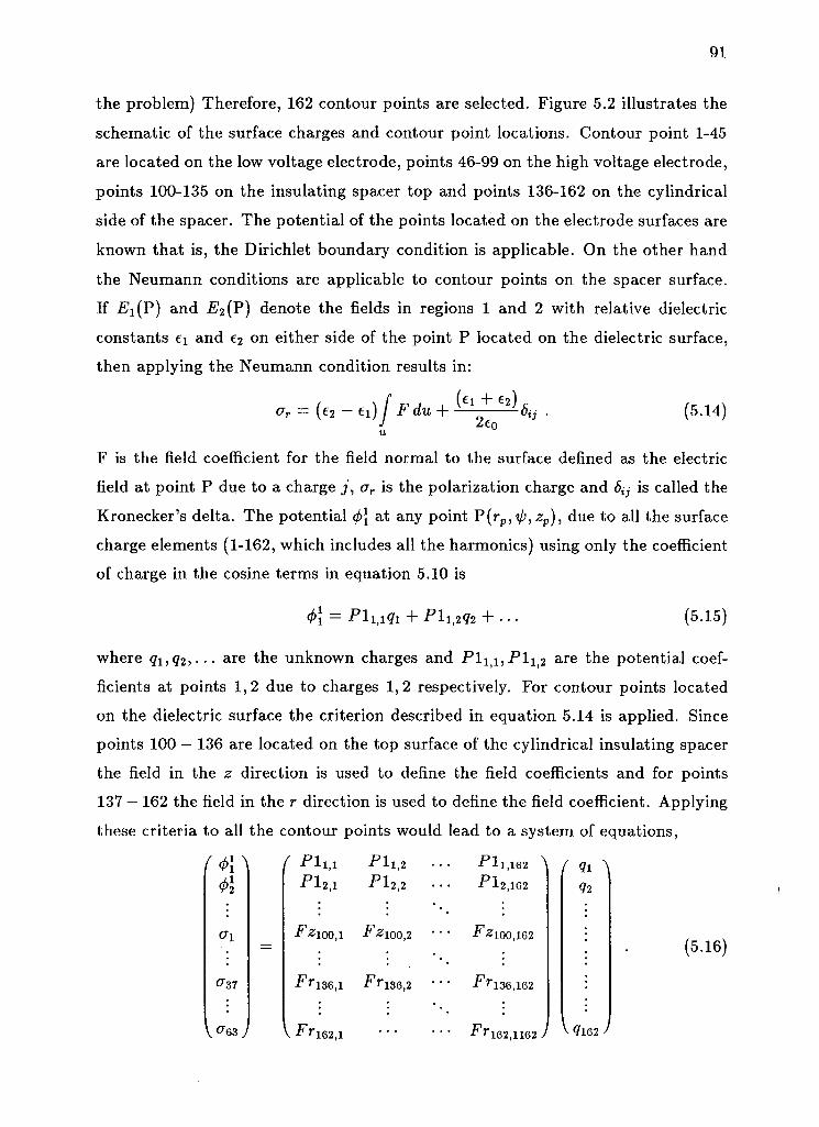
91
the problem) Therefore, 162 contour points are selected. Figure 5.2 illustrates the
schematic of the surface charges and contour point locations. Contour point 1-45
are located on the low voltage electrode, points 46-99 on the high voltage electrode,
points 100-135 on the insulating spacer top and points 136-162 on the cylindrical
side of the spacer. The potential of the points located on the electrode surfaces are
known that is, the Dirichlet boundary condition is applicable. On the other hand
the Neumann conditions are applicable to contour points on the spacer surface.
If -E'i(P) and JE^P ) denote the fields in regions 1 and 2 with relative dielectric
constants ei and e2 on either side of the point P located on the dielectric surface,
then applying the Neumann condition results in:
o-r = {z2-el)t Fdu+ (V e 2 )%
J Z€o (5.14)
F is the field coefficient for the field normal to the surface defined as the electric
field at point P due to a charge j, ar is the polarization charge and 6tJ is called the
Kronecker's delta. The potential <p\ at any point F(rp,ip,zp), due to all the surface
charge elements (1-162, which includes all the harmonics) using only the coefficient
of charge in the cosine terms in equation 5.10 is
(5.15)
where qi,q2,--- a r e the unknown charges and P l i i , P l i 2 are the potential coef
ficients at points 1,2 due to charges 1,2 respectively. For contour points located
on the dielectric surface the criterion described in equation 5.14 is applied. Since
points 100 — 136 are located on the top surface of the cylindrical insulating spacer
the field in the z direction is used to define the field coefficients and for points
137 — 162 the field in the r direction is used to define the field coefficient. Applying
these criteria to all the contour points would lead to a system of equations,
(<t>\\ Ph.l
Pll,2 •
Ph,2 •
-Pll,162 ^ ^12,162 ( ^ \
?2
0\ -F^lOO.l ^100,2 - FZ100IIQ2
0~37 F 7*136,2 - 7*136,162
\0-63 J . . . •P1r162,1162 / V ?162 /
(5.16)
92
The formulation of Fz and Fr are similar to those described in [72]. It is apparent
that voltage vector on the left hand side of equation 5.16 is not completely known,
because o~\ through <763 charges on the dielectric are unknown, (i.e., for points
100-162 on the dielectric surface the surface charge density is not known). Using
the equation 5.16 the charges <fr (q\ through <7i62) can be expressed by
99 63
3=1 k=l
In equation 5.17 the first summation term may be calculated whereas the second
summation term is unknown. To determine these unknown surface charges on the
dielectric surface a new set of contour points (63 in this case) are then chosen
at which the probe potentials are measured after voltage application. The probe
potential at any new point P due to all the charges can be expressed as:
<t>\ = E p*n*j • 3 = 1
(5.18)
Substituting equation5.17 into equation 5.18 will give a system of equations which
describe the known probe potentials as a function of the unknown charge distribu
tions both the dielectric and the electrode surfaces which are expressed as
2 2
( P*i,i
Wis)
P2l,2 P 2 2 2
\P2, 63,1
-P21162
-P22 162
-P263 X62 /
X
Pl2,l PU.2 •
PU.2 •
Pll,162 ^
-P12.162
-1 (*\\ <t>\
P^ioo.i FzWo,2 F0ioo,162
^136,1 0-37
• -^162,1162 J V<763 J
(5.19)
Once again the terms P 2 i i etc., are the potential coefficients due to all the un
known simulation charges including the desired residual charges on the dielectric
surface, at the new points at which the probe potentials have been measured. Us
ing this equation 5.19 the dielectric charges Oy to <763 are calculated. These values
are then backsubstituted into equation 5.16 and the overall charge distribution is
93
obtained. Finally, the voltage and the electric fields in the three directions (r,V>,z)
are computed. Figures 5.3 and 5.4 show the overall field distribution on the insu
lator surface prior to the voltage application and subsequent to the impulse voltage
application, respectively.
It is important to select the contour points such that the boundary conditions
can be applied. It is also important to select these points to prevent the P matrix
from becoming singular. For the geometry described by Sato et al., [79] to keep the
field errors low, the first set of 163 contour points should be selected such that they
are symmetrically distributed around the electrodes and spacer in the ip direction
and located at the zeros of the Chebyshev polynomial in the u direction.
In summary, a numerical method which takes into account the presence of the
dielectric and metallic objects has been developed. The technique also enables the
computation of the surface electric field on the spacer surface from which com
parisons could be made between the fields magnitudes due to the applied voltages
and the corresponding magnitudes due to surface charges acquired by the spacer
following impulse voltage application. Such comparisons should establish whether
the electric fields due to the surface charges significantly distort the the main field
(during voltage application) and cause anomalous fiashover.

Figure 5.3: Initial tangential field distribution on a spacer during impulse voltage
application prior to the charge accumulation on the spacer.

95
Figure 5.4: Surface field distribution on spacer following impulse voltage application.

Chapter 6
RESULTS A N D DISCUSSIONS
6.1 Introduction
In this chapter, the experiments to investigate the nature of charge growth on
spacers in S F 6 gas under impulse and A C voltages are presented. The repeated
application of impulse voltages to a spacer gap in S F 6 gas and its effect on spacer
fiashover voltage and time has been studied with the aid of capacitive probes. The
effects of A C pre-charging of spacers on the subsequent impulse fiashover voltages
are also included.
As mentioned before, both plane-parallel and rod-plane geometries have been
used in these experiments. This particular choice of electrode geometry served two
purposes: (a) the axis of symmetry permitted easier measurement of surface charge
on the spacer and also made it amenable for simpler field calculation, and (b) they
were representative of both quasi-uniform and non-uniform fields in service. By
altering the rod diameter (5mm and 10mm), the degree of non-uniformity could
be selected.
Three different insulating spacer materials were used namely, unfilled epoxy,
ptfe and acrylic. These materials have different surface and bulk resistivities and
the effects of these parameters on the charge accumulation and dissipation have
been studied. Insulating spacers were also made with both smooth(4/zm) and
rough(40//ra) surface finish to examine the influence of surface finish on the charge
growth.
Two different capacitive probes were used to measure the surface charge dis-
96

97
tribution on the spacer. In case of the rod-plane spacer gap, both the top and
cylindrical sides of the spacer were scanned. Physical limitations prevented charge
measurements of the spacer from being performed in the region close to the low
voltage electrode (approximately upto 12mm above the low voltage electrode). In
case of the plane-parallel gap however, the top face of the spacer (facing the high
voltage electrode) was not scanned. As described in chapter 4 the probe registers
the potential at its tip due to surface charges on the spacer. Most of the results
on charge accumulation are presented as 3D plots. The X and the Y axes indicate
the radial distance from the tip of the high voltage electrode at which the probe
potential was measured. The Z axis indicates the magnitude of the probe potential
as a result of these charges on the spacers.
Switching, lightning and AC voltages were used in the experiments. The re
spective voltage waveforms were 100/2000/us, 1.2/50/xs and 60Hz.
Most of the experiments presented in the following sections were conducted at
room temperature (20° C ) and an SF 6 gas pressure of O.lMPa. Limited exper
iments were done at higher gas pressures of 0.2MPa and 0.3MPa, under impulse
voltages only.
The measured currents and the distributions of the inception time are presented
first. The effect of the spacer material, surface finish and gas pressure on the corona
inception times are discussed. This is followed by an examination of the nature
of charge growth on spacers in SF 6 subjected to higher voltages. The influence of
the material, its surface finish and electrode geometry is also discussed. Finally,
the effect of these accumulated charges and the associated electric field on impulse
flashover voltage and time are1 presented and discussed.
6.2 Pre-breakdown phenomenon
Figure 6.1 shows the tangential surface electric field distribution for a rod-plane
gap with a cylindrical insulating spacer placed in the gap. The X-axis shows the
distance (in cm) from the tip of the high voltage electrode along the insulator sur
face and the Y-axis is the tangential surface electric field in kV/cm, normalized
with respect to the applied voltage. As expected when a dielectric spacer is placed

98
in the gap, the electric field distribution in the region close to the high voltage
electrode gets altered depending on the dielectric constant of the spacer and the
diameter of the rod electrode, keeping the other dimensions unaltered. For com
parison, the electric field distribution for a plain rod-plane gap along the imaginary
boundary of the spacer is also included. These calculations were performed using a
charge simulation program developed on the theory described adequately by [68].
It is apparent that the presence of an insulating spacer with no surface charges
in the gas gap alters (increases) the electric field distribution when compared to
a plain gas gap. It is of interest to examine the perturbation of this symmetric
field distribution due to surface charges accumulated by the spacer under different
voltage application.
The following section describes the effect of the spacer on pre-breakdown cur
rents in a rod-plane spacer gap under impulse voltages. The nature of pre-breakdown
currents (corona pulses) and the distribution of their inception times, should aid
in understanding the role of the spacer in the pre - breakdown current growth.
6.2.1 Pre - breakdown currents
Pre - breakdown currents have been measured both with and without spacers in
a rod-plane gap under positive switching impulse voltage application. Figure 6.2b
shows a typical oscillogram of the current in the gap following a positive switching
impulse voltage application to a plain gas gap. The pre - breakdown current
was measured as described in section 4.4. Figure 6.2a shows the oscillogram of
the applied lightning impulse voltage pulse and the corresponding gap current.
Figure 6.2c shows the gap current for a spacer gap. For a plain gas gap, at low
voltages, a single corona pulse was observed. This signals the formation of the
streamer in the region near the rod electrode. With increasing amplitude of the
applied voltage, the number of pulses increased and the duration between the
subsequent pulses decreased. The corona pulses then decay due to the cessation of
the ionization activity. This is due to the decrease in the space charges left behind
by the previous avalanches. If the voltage is increased it clears the space charge
quickly, restoring the original electric field distribution. Fresh avalanche activity is
initiated.

99
ELECTRODE RADII = 0.8 and 5mm
Surface field with spacer e r = 2.0 Rod radius = 0.8mm
Surface field with spacer e r = 8.0
Surface field with spacer e r = 2.0
Field along imaginary boundary Plain gas gap
1 2 3 4 DISTANCE FROM T H E HV E L E C T R O D E [cm]
NOTE: Surface f i e ld is tangential to the spacer surface
Figure 6.1: Surface electric field distribution in a rod-plane gap with an cylindrical insulating spacer. In case of a gas gap the field calculation is along the imaginary boundary of the spacer

100
-.
- f \
- l U i i u
>
a
c. Corona pulse rise time 0.9 us
Figure 6.2: Current and voltage oscillogram (a) lightning impulse voltage (+52kV) and current (48.2mA) :(b) switching impulse displacement current and corona current (rise time 1.5/xs) current:(c) same as in (b) but with spacer (rise time 0.9/is)

101
In case of a spacer gap, however, the corona pulse had a faster rise time. With
increasing voltage the number of corona pulses increased and the time interval be
tween the pulses reduced. The successive pulse heights either increased or decreased
in magnitude in relation to the first pulse perhaps indicating that the local fields
setup by the charges deposited on the spacer influenced the streamer propagation.
With higher voltages, the subsequent pulses increased in magnitude in relation to
the first pulse ultimately leading to breakdown. Figure 6.3 shows the mean value
of the peak corona pulse current (in mA) measured as a function of the applied
voltage for two different materials at a pressure of O.lMPa for a 5mm diameter
rod. It can be seen that the current gradually increases at low voltages, but at
higher voltages however, the increase is relatively steep. This may be attributed
to the surface charges deposited on the spacer which are perturbing the local field
distribution. Further, in case of ptfe, the currents are the lowest in comparison
to the other specimen suggesting lower charge deposition on the spacer surface.
This will be discussed in light of the surface potential measurements made at these
voltages. Another observation that has been made with regard to the corona pulses
is that their amplitudes reduce with increasing gas pressure. This is attributed to
the higher charge magnitudes deposited on the spacer near the rod electrode which
is diminishing the electric field and thus inhibiting the current flow. No significant
differences were observed for acrylic spacers with different surface finish (smooth
and rough finish) with regard to the current growth as a function of the applied
voltage. This suggests that for the choice of the surface finish of spacers made in
these experiments its effect on current growth as a function of the applied voltage is
minimal. Typically, insulating spacers in GIS have a surface roughness of 4 — 5/tm.
The mean value of the corona inception times from inception voltages upto those
close to breakdown are shown in Fig. 6.4 for epoxy, acrylic and ptfe spacer gaps.
The corona inception time is defined as the time interval from the virtual zero of
the applied impulse wave to the appearance of the first corona spike on the current
wave. In case of the acrylic spacers, results are included for two different grades of
surface finish namely smooth (4jum) and rough finish (20pm). It may be seen that
both the spacer material and the spacer surface finish have a considerable influence
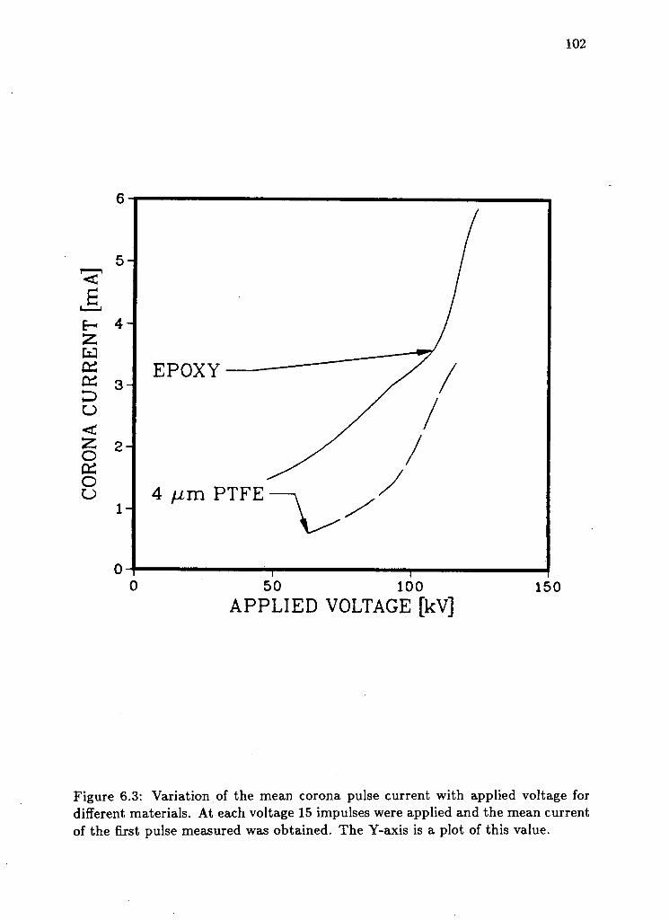
102
Figure 6.3: Variation of the mean corona pulse current with applied voltage for different materials. At each voltage 15 impulses were applied and the mean current of the first pulse measured was obtained. The Y-axis is a plot of this value.

103
on the mean corona inception time which is in agreement with the observations
reported earlier by [56].
6.3 Probability Distribution of Corona Inception Time
The corona time delay shows a considerable variation near the inception voltage
even when impulses of the same peak magnitude are applied. It has been shown
that the most suitable distribution which fits the experimental values of corona
inception time t is the log-normal distribution given by the equation 6.1
1.0 -(lnt - Int)2 , . . , x p{t) = — = x exp K ' - 0 < ln(t < oo 6.1 OlyjTX la*
where t is the mean value of time t and a is the log standard deviation
The delay of the first corona pulse was recorded irrespective of whether it was
followed by other pulses or not. The dispersion in the discharge inception time is
linked with the rate of production of initiatory electrons. The measured data was
analysed and the computed distributions have been plotted. Figure 6.5 shows the
computed distributions using equation 6.1 for an epoxy spacer at various voltages
placed in a rod-plane gap (with a rod diameter of 5mm). For comparison, the
results for the same rod-plane gap without the spacer have been included. It
is apparent from fig. 6.5 that with increasing voltages, the average value of the
time delay and standard deviation decrease. The presence of the spacer causes a
considerable decrease in the time delay. As an example at a pressure of O.lMPa and
+77kV, the mean value of the corona inception time is about 40/xs, but this value
is without the spacer. It is apparent that the spacer plays an important role
in the avalanche development. This fact becomes obvious in the following section.
6.4 Von-Laue Plots
The Von-Laue plot has been used to determine the initiating electron density in
the critical volume of the gas in the region near the positive rod electrode. The
plot is essentially a probability plot of — log(l — p(t)) versus time to appearance

104
140-i
40 H 1 1 1 ! 0 50 100 150 200
TIME IN MICROSECONDS
Figure 6.4: Variation of the mean corona inception time with applied voltage for different materials
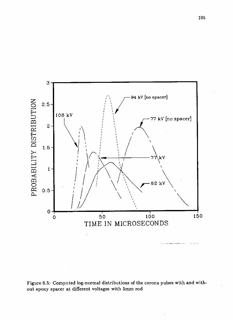
105
3 - 1
TIME IN MICROSECONDS
Figure 6.5: Computed log-normal distributions of the corona pulses with and without epoxy spacer at different voltages with 5mm rod
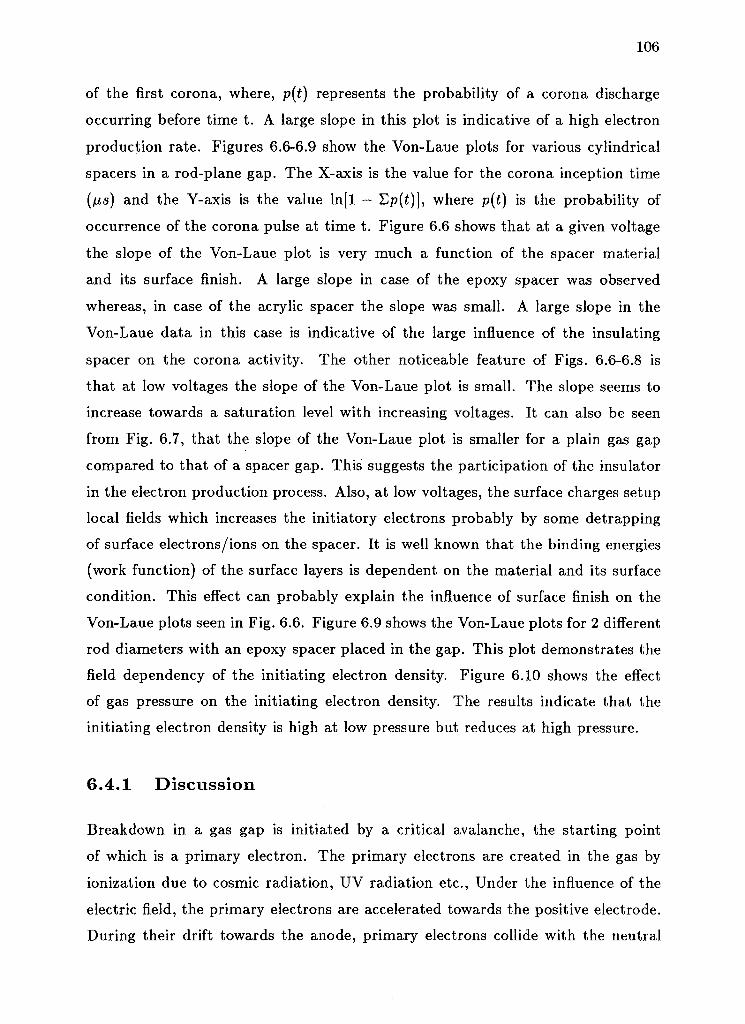
106
of the first corona, where, p(t) represents the probability of a corona discharge
occurring before time t. A large slope in this plot is indicative of a high electron
production rate. Figures 6.6-6.9 show the Von-Laue plots for various cylindrical
spacers in a rod-plane gap. The X-axis is the value for the corona inception time
(/AS) and the Y-axis is the value ln[l — Ep(t)], where p(t) is the probability of
occurrence of the corona pulse at time t. Figure 6.6 shows that at a given voltage
the slope of the Von-Laue plot is very much a function of the spacer material
and its surface finish. A large slope in case of the epoxy spacer was observed
whereas, in case of the acrylic spacer the slope was small. A large slope in the
Von-Laue data in this case is indicative of the large influence of the insulating
spacer on the corona activity. The other noticeable feature of Figs. 6.6-6.8 is
that at low voltages the slope of the Von-Laue plot is small. The slope seems to
increase towards a saturation level with increasing voltages. It can also be seen
from Fig. 6.7, that the slope of the Von-Laue plot is smaller for a plain gas gap
compared to that of a spacer gap. This suggests the participation of the insulator
in the electron production process. Also, at low voltages, the surface charges setup
local fields which increases the initiatory electrons probably by some detrapping
of surface electrons/ions on the spacer. It is well known that the binding energies
(work function) of the surface layers is dependent on the material and its surface
condition. This effect can probably explain the influence of surface finish on the
Von-Laue plots seen in Fig. 6.6. Figure 6.9 shows the Von-Laue plots for 2 different
rod diameters with an epoxy spacer placed in the gap. This plot demonstrates the
field dependency of the initiating electron density. Figure 6.10 shows the effect
of gas pressure on the initiating electron density. The results indicate that the
initiating electron density is high at low pressure but reduces at high pressure.
6.4.1 Discussion
Breakdown in a gas gap is initiated by a critical avalanche, the starting point
of which is a primary electron. The primary electrons are created in the gas by
ionization due to cosmic radiation, UV radiation etc., Under the influence of the
electric field, the primary electrons are accelerated towards the positive electrode.
During their drift towards the anode, primary electrons collide with the neutral

4/urn EPOXY 20 fxm ACRYLIC Plain gas gap 4 /zm ACRYLIC 20 / u m PTFE
100 200 300 TIME IN MICROSECONDS
400
Figure 6.6: Von-Laue plots for different materials at 94 kV (Rod electrode diameter 5mm)

108
94 kV
109 kV
115 kV
124 kV
0 50 100 150
TIME IN MICROSECONDS 200
Figure 6.7: Von-Laue plots for acrylic spacer at different voltages (Rod electrode diameter: 5mm)

109
o . H
82.8 kV
_77_kV_
JK3.1JcV
108 kV
116 kV
01-
1 L
1 " | 0 20 4 0 60 80
TIME IN MICROSECONDS 100
Figure 6.8: Von-Laue plots for epoxy spacer at different voltages (Rod electrode diameter: 5mm)

110
100 TIME IN MICROSECONDS
Figure 6.9: Von-Laue plots for epoxy spacer at +77kV (Rod electrode diameter: 5mm and 10mm)

Figure 6.10: Von-Laue plots for 5/xm epoxy spacer at +108kV for 2 different pressures. (Rod electrode diameter: 6mm)

112
Figure 6.11: Von-Laue plots for 5/xm epoxy spacer at +124kV for 2 different pressures. (Rod electrode diameter: 6mm)

113
molecules, some of the collisions resulting in ionization. The secondary electrons
move rapidly to the head of the avalanche, whereas, the heavy ions are left behind
in the tail of the avalanche.
Let a be the number of electrons produced per unit length per unit time by
ionizing collisions. Since SF6 is an electronegative gas, some of the electrons are
attached to the SF6 molecule to form relatively sluggish negative ions. The process
of attachment results in a depletion of the electrons in the region of the avalanche
formation and let n be the attachment probability of an electron per unit volume.
The well known streamer criterion states that breakdown takes place when the
number of electrons at the head of the avalanche reaches the critical size of 108
electrons. In other words, when the number of electrons n(x) at any point distance
x from the cathode becomes:
where no is the number of electrons released from cathode at x = 0, breakdown
ensues. Thus, in order that breakdown may occur two conditions must be satisfied:
(a) there must be at least one primary electron in a suitable location in the gap in
order to initiate the first avalanche and (b) the electric field must be of sufficient
strength and adequate distribution to produce a sequence of avalanches thereby
satisfying equation 6.2. This criterion [57] has been found to give breakdown
voltages close to the measured values in uniform fields in SF6 gas. In non-uniform
field in SF 6 however, the above process describes the onset of corona.
With DC voltages there is usually adequate time for the initiating electrons
created by natural ionizing events to form an avalanche. In case of impulse voltage
application, unless the presence of the initiating electron is ensured for example
by artificial irradiation, breakdown may not occur even at voltage levels beyond
the DC levels. The time lag defined as the time elapsed between voltage level
sufficient to cause breakdown and the time at which breakdown actually occurs
can be decomposed into a statistical time lag and a formative time lag. The
statistical time lag corresponds to the creation of an initial electron inside the
critical volume around the stressed electrode. The formative time lag is associated
with the formation of an avalanche of a critical size. So, in the case of impulse
(6.2)

114
voltage application both these times affect the breakdown voltages.
The critical volume or the initiation volume is the region associated with
the surface area around the point electrode (in case of a rod-plane gap geometry)
for negative corona and for a positive corona corresponds to a volume in the gas
gap. In other words, these are regions where the release of an electron could give
rise to an avalanche containing at least 108 electrons. For a positive point plane
geometry the critical volume is bounded by two boundaries. The outer boundary
is the contour of all points at which the net ionization coefficient (a — n) > 0 and
the boundary closest to the rod electrode is determined by the minimum length x
needed for the avalanche formation of a critical size.
In an SF 6 non-uniform field gap, the formation of an avalanche of a critical
size signals the appearance of a corona pulse under impulse voltages. Therefore,
in the rapidly time varying field it becomes important for the initiatory electron
to be present in the critical volume so as to produces the ionization required
for the avalanche formation. It can be seen from equation 6.2 that the timing
of the entire process clearly depends on n0 the number of the initiatory electrons
and consequently the delay of streamer formation. Therefore, both the density of
initiatory electrons in the gap and their position in the gap determine the pro
cess of an avalanche formation. Under impulse voltages, this quantity no becomes
extremely important, since the applied voltage is continuously changing during
the production and acceleration of electrons. Also, the position of the initiatory
electron would determine the likelihood of a streamer formation.
In SF 6 , the predominant species of negative ions is SFg. Negative ions may
loose their electrons by several processes which include field detachment, photo
detachment and collisional detachment. It has been shown that amongst the above
processes the predominant mechanism resulting in electron generation is collisional
detachment ie.,
SFe + SFe => 2SF6 + e (6.3)
In a non-uniform field gap, negative corona is initiated by electrons released from
the cathode by field emission and for positive corona by field-enhanced collisional
detachment. In case of gaps exposed to artificial irradiation, corona activity is

115
enhanced by photoelectric emission from the cathode surface in case of negative
corona and photodetachment of negative ions for positive corona. The probability
per unit time for the formation of a detectable electron avalanche can be expressed
as:
Pt = x / P\(r)pi{r)pz{r),
Pi(r) = probability per unit time that an electron exists at position r,
P2(r) = probability of release of an electron from the electron site,
P3( r) = probability that an electron released from the site yields an avalanche
<pi = the critical volume
In case of a positive corona in S F 6 , the probability pi (r) of electrons being available
at a suitable position in the gas gap per unit time is mainly given by the rate at
which negative ions become available for detachment at any location in the critical
volume (assuming that the electron production is by negative ion detachment).
The probability of an electron release from a site is determined basically by the
mechanism of electron release. Obviously, the factor P2(r) is a function of the
electric field, gas pressure and ambient radiation. It has been suggested [76] that
electron detachment from negative ions is the most likely contributing factor to
the factor p 2(r). The third probability factor Pz{?) depends on the electric field to
number density ratio at the point of the initial electron release.
In summary, therefore the dispersion in the discharge pulse delay is a function
of the production rate of initiatory electrons, which in turn is dependent on the gas
pressure, the impulse wave shape, the electrode shape and hence the electric field
distribution. It has been shown by Anis [60] that the number of electrons detached
per unit gas volume per unit time rp(E,p) can be expressed as shown below:
Negative ion density ' collisional detachment lifetime
The product of the electron production rate and the critical volume indicate the
number of initiatory electrons expected to contribute to the streamer formation.
The initiation volume is a function of the field distribution around the point
electrode and thus varies with time under impulse voltage application.

116
In the presence of an insulating spacer in a rod-plane, the critical volume calcu
lations are difficult to perform because of the perturbation of the ambient electric
field distribution caused by the presence of surface charges.
It can be seen from Figures 6.4 and 6.5 that the mean value of the corona
inception time decreases with increasing applied voltages. Also, the dispersion in
the corona inception times is reduced with increasing voltage. From figure 6.5 it is
also apparent that the dispersion in the corona inception times for a plain gas gap is
larger than the dispersion in the case of an insulator gap. These results suggest that
the initial corona activity close to the rod electrode is influenced by the presence
of the insulating spacer. The presence of the insulator in the high field region can
result in a secondary feedback mechanism, with the insulating surface playing an
important role in the corona discharge mechanism. Jaksts and Cross [81] made
preliminary measurements to examine the influence of a spacer on the electron and
ion current components of prebreakdown current pulses. The measurements were
made by bridging a uniform field gap with a ptfe spacer in air and iV2 gas. An
UV pulse of approximately 10ns duration from a iV2 laser was used to photoemit
electrons from the cathode surface. Measurement of avalanche currents with and
without the insulating spacer present in the gap indicated an alteration in the
electron component of the gas in the presence of an insulating spacer. The ion
component remained unchanged. More recently, Mahajan et al.,[80] reported the
differences in the prebreakdown current measurements made near acrylic and nylon
spacer surfaces placed in a plane parallel field configuration in iV2 gas at 101.3kPa.
Whereas, the avalanches near an acrylic spacer were very similar to that of a plain
gas gap, increased avalanche current (the electron component) was observed in
case of the nylon spacer. No mechanism was proposed to explain the increased
avalanche current but it was postulated that the photoemission yield of the spacer
was a dominant factor in altering the ionization coefficients and increasing the
prebreakdown currents. It is evident that the decrease in the dispersion of time
delays in case of the spacer gap as compared to a plain gas gap is a direct result
of the contribution of the spacer to the initial electron density and hence streamer
propagation. The Von-Laue plot can give some clues as to both the type and
number of possible mechanisms.

117
The Von-Laue plot gives an image of the initiating electron density in the
critical volume of the gas to initiate a streamer. From fig. 6.6 it is apparent that
the probability of finding an electron inside the critical volume of the gas to initiate
a streamer is very much dependent on the insulating material. Further, since no
sharp discontinuities are seen in the Von-Laue plots it can be said that there is only
one kind of possible mechanism for the electron generation. The larger slope in the
Von-Laue plot at low voltages for a spacer gap, as compared to that of a plain gas
gap suggests that the spacer has a dominant effect on electron production. This
larger slope (hence more initiatory electrons) in a spacer gap may be due to the
removal of trapped electrons from the spacer surface by secondary processes, like
photoemission. It may also be due to the increase in the local field due to the
deposited charges thereby supporting electron detachment in the gas surrounding
the electrode. With increased voltages, since the ambient fields are very high, the
influence of the spacer on the measured corona inception times is reduced. Since
the phenomenon of electron/ion detachment from the insulating spacer surface is
an extremely complex phenomenon, one can only postulate a possible mechanism
leading to electron detachment from the spacer surface. It is postulated here that
photoemission yield from the spacer surface is a dominant factor contributing to
electron/ion detachment from the spacer surface. To a first approximation, it
can be said that the photoemissive yield of an insulator can be affected both by
the material and its surface condition. It is well known that polymer solids are
not 100% crystalline. The non-crystalline or amorphous regions are structurally
irregular and are potential sites for impurities. Also the surface of the polymer
indicates the irregularity of the crystal structure. These surface states are located
in the band gap. Further, the surface can hold impurities which have been absorbed
and the degree of absorption depends on the surface condition of the spacer. The
photoemissive yield therefore, is a function of both the material and its surface
condition. The differences in the prebreakdown currents measured for different
materials (figure 6.3) and the observations by Mahajan et al., and those of Jaksts
and Cross, discussed earlier lend some credence to this hypothesis. The results
of figure 6.6 also support this hypothesis. In case of the 5mm rod the electric
fields are higher in the region close to the rod electrode as compared to a 10mm
118
rod. The higher fields associated with the 5mm rod imply a higher photon efficiency
providing for a larger number of charge carriers from the spacer resulting in a higher
slope of the Von-Laue plot. In summary, it can be said that the high electric field
results in photon generated charge carriers from the spacer surface which contribute
to the streamer formation. Although considerable work has been reported about
photoconduction in solids, similar work on the photoemissive yield from surface
layers of insulating spacers placed in an SF6 environment when exposed to UV
light is not available.
Figure 6.10 indicates that the slope of the Von-Laue plot decreases with increas
ing pressure at low voltages. Anis and Srivastava [60] by performing calculations
of the critical volume at different voltages and gas pressures (O.lMPa - 0.3MPa)
have shown that at voltages close to the inception voltages, the critical volume re
duces considerably with pressure, whereas, this change is smaller at higher applied
voltages. Further, at a given pressure, the critical volume increases sharply with
voltage but then saturates at higher voltages. These results, discussed in light of
the slope of the Von-Laue plots imply that:
• At a given pressure of the SF 6 gas, the slope of the Von-Laue plot is small
at voltages close to the inception levels and increases sharply with voltage
higher than the inception levels. The difference in the slope at these high
voltages is insignificant. This is apparent from figures 6.7 and 6.8.
• At voltages close to inception, the the slope of the Von-Laue plots should
be high at lower pressures for a given field configuration as compared to
the slopes for higher pressures. At higher applied voltages, however, the
effect of SF 6 gas pressure on the Von-Laue slopes should be small. This is
demonstrated by the results shown in figures 6.10 and 6.11.
This observation has been consistent with that of previously reported figures for
spacer gaps [56]. Quantitative analysis of the critical volume for spacer gaps is
rendered difficult because of the perturbation of the symmetric field distribution
around the rod electrode due to the asymmetric fields caused by the surface charges
on the spacer.

119
The above results suggest the following for the pre-breakdown behavior of rod-
plane spacer gaps under positive switching impulses:
• The insulating spacer significantly reduces the corona inception time of a
spacer gap
• Both the material and its surface roughness have some influence on the pre -
breakdown activity
• The rate of electron production is very much field-dependent
• Due to the presence of the spacer in the high field region, photoemissivity
from the spacer surface has been suggested to be a possible mechanism for
the charge generation contributing to the streamer growth
6.5 Surface Potential Measurements
6.5.1 Experimental procedure
The surface potential has been measured in both quasi-uniform (plane parallel
electrodes) and non-uniform fields with various insulating spacers. For experiments
with the rod-plane gaps, capacitive probes scanned the top surface of the spacer
(this probe will be referred to as the top probe ) as well as the cylindrical surface
of the spacer (this probe will be referred to as the side side probe ). In case of
the plane-parallel configuration only the cylindrical side of the spacer was scanned
using the side probe .
The experimental procedure adopted in obtaining the surface potential distri
bution is given below:
• Following the cleaning procedure for both the electrodes and the spacer, as
described in Chapter 4, the vessel was evacuated to approximately 8 Pa. For
experiments with the plane parallel electrodes the side probe was brought
to a distance of 2mm from the spacer and the probe potential recorded by
a 610C Keithley electrometer. The X-Y plotter recorded the potential as a
function of the angular position of the spacer.

120
• SF& gas was then introduced into the chamber and the scans described above
were repeated.
• The probes were then withdrawn and the voltage was applied. Switching,
lightning and 60Hz AC voltages were all used in different experiments.
• The gas pressure in the chamber was then increased slightly (by approxi
mately 0.03MPa) and the probes reintroduced into the vicinity of the spacer
for fresh surface potential scans. This increase in gas pressure avoided the
possibility of spurious fiashovers to the probe shield from occurring due to
possible large charge magnitudes on the spacer.
• The probes were then withdrawn and the gas pressure was restored.
• This procedure was repeated for different voltages. No attempt was made to
discharge the spacer before the voltage level was increased.
In case of the rod-plane spacer gap, the top probe was used to scan the spacer first,
followed by a scan of the cylindrical surface by the side probe . The measured
potentials have been digitized and replotted as a three dimensional distribution.
In the following text, both surface potential and surface charge distribution have
been used. This is based on the premise that the relationship between the measured
potential distribution and the equivalent charge distribution can be obtained using
the charge simulation program described in chapter 5.
6.6 Results with switching impulses Figures 6.12 and 6.13 show the surface potential distribution for two different
spacers prior to the application of voltage in experiments with plane-parallel and
rod-plane spacer gaps respectively. It may be seen that the measured surface
potentials are very small. The circular base shown in the figure represents the
concentric scans made both on the top and cylindrical sides of the insulating spacer.
If the distances along the X and Y axes are in the range 0 < i < 20 the plots
correspond to the scans only on the top surface of the spacer. If the distances are in
the range 0 < x < 40 the scans include both the top and cylindrical surfaces of the
spacer. The surface potential distribution due to the residual charge on the spacer

121
is very low (typically < 0.05 volts), which corresponds to approximately 0.5pCm~2
and a maximum surface electric field of about 0.05kV/mm. On an average, at the
commencement of the experiments all the insulating spacers showed similar levels
of residual charge.
For an insulating spacer placed between plane-parallel electrodes the surface
potential distribution was monitored following 20 impulse voltage applications at
each pre-determined level of voltage. The voltage application was started from
approximately +45kV upto +190kV (the limit of the impulse generator). Surface
potential scans made at these levels did not show any noticeable change in the
surface potential distribution and the maximum voltage was still less than 0.1 volt,
corresponding to a charge magnitude of about lpCm~2. This is illustrated by the
Fig. 6.14. These experiments with plane-parallel electrodes were done with a recess
on both the high and low voltage electrode surfaces, thereby shielding the triple-
junction at both the high and low voltage electrodes. Experiments with flat (i.e.
unrecessed) electrodes showed a similar behavior. In order to examine the effect
of perturbing the uniform field, spacers shaped in the form of frustrum of a cone
(see figure 4.11) were also used. The surface potential distributions showed similar
low levels. The gap current monitored during the experiments did not indicate any
corona activity even upto average electric field magnitudes of 6.3 kV/mm under
positive switching impulse voltages. This figure of the electric field is obtained
by assuming a uniform field distribution for a 30mm spacer gap subjected to a
switching impulse of +190kV. Due to the low levels of charging observed with
switching impulses for both polarities of the top electrode, in case of the plane-
parallel electrode configuration, no further experiments were conducted. Higher
voltages could not be achieved due to voltage limitation of the high voltage source.
For the voltage levels used in this study in case of the plane parallel electrode
spacer gaps it may be said that no significant deposition of charge on the spacer
occurs. In an experiment conducted with an imperfect spacer (which had its edge
damaged accidentally) higher levels of charge were measured on the spacer surface
at the voltage levels described earlier. This may be attributed to the field distor
tion created by this imperfection. It is well known that a spacer introduced in a

122
Figure 6.12: Surface potential variation for epoxy spacer placed between plane-parallel electrodes prior to voltage application

123
Figure 6.13: Surface potential variation for acrylic spacer placed between rod-plane electrodes prior to voltage application

124
Figure 6.14: Surface potential variation for epoxy spacer placed between plane-parallel electrodes after subjecting it to positive switching impulses upto 190kV

125
plane parallel gap with an imperfect contact with the electrode can lead to partial
discharges due to the resulting high stress in the gap between the spacer and the
electrode even at low voltages. These partial discharges can explain the higher
charge levels observed in case of the damaged spacer.
It has been established [50,51] that under DC voltage application, cylindrical
spacers placed between plane parallel electrodes in SFQ gas accumulate significant
levels of charge at high voltages and extended periods of time. There is no agree
ment on a mechanism to explain this charge accumulation. Gaseous conduction,
bulk conduction and non-linear surface conduction have been some of the mech
anisms proposed to explain this charge accumulation under DC voltages. These
charges, however, have been identified to be one of the principal causes for spacer
flashovers during a polarity reversal. The use of impulses (both lightning and
switching) provide very little time for either bulk or surface conductivities to con
tribute to the charge accumulation process. This is because the mobility of charge
carrier in the bulk of the material is in the range 10 - 1 1 to 10 _ 1 5cm 2jV • s. So,
gas conduction process appears to be the only mechanism which can explain any
charge accumulation under impulse voltages. More detailed discussions regarding
the possible charging mechanism under impulse application are presented in section
6.6.2.
Using the procedure described earlier, surface potential scans were made on
cylindrical spacers placed in a rod-plane gap subjected to switching impulses. Fig
ures 6.15-6.16, show the surface potential variation of a 5pm surface finish epoxy
spacer placed in a 5mm rod-plane configuration. The plots show the surface po
tential variation of the top surface of the spacers, i.e., the region close to- the
high voltage electrode. Scans were made initially for a cleaned spacer to exam
ine the residual charge levels and were followed by 20 impulse applications at
pre-determined voltage levels. Figures 6.16 b and c show the surface potential
variation both on the top surface and the entire surface of the cylindrical spacer
respectively. Under this level of charging, impulse fiashover occurred when the volt
age level was raised to +124kV. Surface potential scans made following a fiashover
show considerable amounts of residual charges. From figures 6.15-6.16, it is quite
obvious that at low voltage levels, the surface potentials are quite low. Further, in

126
the immediate vicinity of the rod electrode, for positive impulses, negative charge
deposition is seen and positive charge appears to have been deposited towards the
spacer edge, where there is an abrupt change in the direction of the ambient field.
At voltages close to fiashover levels, significant positive charge is deposited on the
spacer surface. The above results were reproducible when the experiments were re
peated on the same spacer which was cleaned by the procedure described to reduce
the residual charge. The results were not identical but the same general trend was
apparent.
Figures 6.17-6.18 show the results for a 4/j,m surface finish acrylic spacer. The
residual charge in this case showed similar charge patterns as observed for the
epoxy spacer. Upto a voltage level of +77kV, significant negative charges were
observed on the top surface of the spacer in the vicinity of the rod electrode with
the positive charges towards the spacer edge. At higher voltages of +95kV and
+ 108kV, the charge patterns reversed with the positive charges being deposited
on the spacer. Figure 6.19 shows the results obtained for a 20//m surface finish
spacer and shows that the top surface of the spacer has significant positive charges,
including the cylindrical surface, with localized peaks of negative charge appearing
on the cylindrical surface. Although bipolar charging is seen at voltage levels of
+77kV and +H6kV, significant positive charging has been observed. Different
samples of the spacer, subjected to similar voltage levels, showed similar charge
patterns with minor variations in the location of the peaks. Experimental results
with a 20/xm surface finish acrylic spacer showed similar charging behavior. No
significant differences were observed in charge magnitudes for the different surface
roughness of the selected acrylic spacer.
Figures 6.20-6.21 show the results for a 20/xm surface finish ptfe spacer placed in
a rod-plane gap. The distinct feature in the charge distribution at various voltages
was that the magnitudes were lower in comparison to those obtained for the epoxy
and acrylic spacers at similar voltage levels. A further increase in the voltage level
from +62kV to +77kV only increased the magnitudes of the respective positive
and negative peaks with minimal changes in the overall charge distributions. Once
again, at low voltages (+62kV) regions close to the high voltage electrode had
negative charge deposition, and those further away from the high voltage electrode
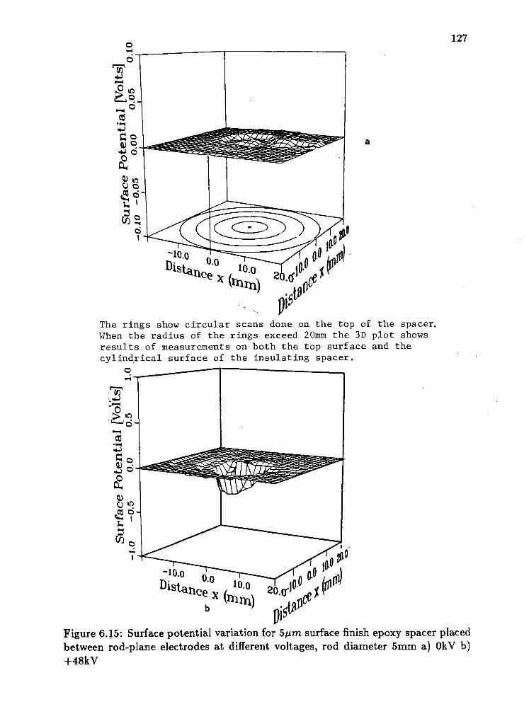
127
The rings show c i r c u l a r scans done on the top of the spacer. When the radius of the rings exceed 20mm the 3D plo t shows r e s u l t s of measurements on both the top surface and the c y l i n d r i c a l surface of the i n s u l a t i n g spacer.
Figure 6.15: Surface potential variation for h\im surface finish epoxy spacer placed between rod-plane electrodes at different voltages, rod diameter 5mm a) OkV b) +48kV

128
Figure 6.16: Surface potential variation for 5p,m surface finish epoxy spacer placed between rod-plane electrodes at different voltages, rod diameter 5mm a) +66kV b) +77kV (on the spacer top) c) +77kV (entire spacer)

129
Figure 6.17: Surface potential variation for bum surface finish acrylic spacer placed between rod-plane electrodes at different voltages, rod diameter 5mm a) OkV b) +48kV

130
Figure 6.18: Surface potential variation for a 5/xm surface finish acrylic spacer placed between rod-plane electrodes at different voltages, rod diameter 5mm a) +63kV b) +77kV

131
a
b
Figure 6.19: Surface potential variation for a 20/xm surface finish acrylic spacer placed between rod-plane electrodes at different voltages, rod diameter 5mm a) +77kV (top surface only) b) +77kV (entire spacer)

132
had positive charge deposition.
Figures 6.22-6.23 show the corresponding results obtained for a 5/xm surface
finish epoxy spacer placed in a 10mm rod-plane gap. Once again, at low voltage,
negative charges appear in the vicinity of the rod electrode and positive charges
appear towards the spacer edge. At high voltages, significant positive charges are
seen on the spacer surface. In this case, the charge levels are lower.
Figures 6.24-6.25 show the results obtained for a 4/ura surface finish acrylic
spacer placed in a 10mm rod-plane gap. Figure 6.26 shows the results for a 20/j,m
surface finish acrylic spacer. Figures 6.27-6.28 show the results for a 20/zm surface
finish ptfe spacer.
It is apparent from these results that despite the very random nature of charg
ing, and coexistence of bipolar charges there are some noticeable trends:
• At low voltages, the spacer is negatively charged in the vicinity of the rod
electrode with the positive charges depositing towards the spacer edge.
• As the voltage is increased say between +62kV and +77kV in the case of
epoxy, significant negative charges are deposited on the spacer surface with
some positive charges appearing towards the spacer edge.
• At higher voltages, close to the breakdown levels, the spacer is mainly charged
positively.
Figure 6.29 shows the shot-to-shot variation in surface charge on a spacer placed
between rod-plane electrodes subjected to repeated switching impulses. Initially
the spacer, as seen in figure 6.15a, was with low levels of residual charges. The
impulse voltage was then applied to the system and the procedure described in
section 6.5.1 was used to scan the spacer surface. Following the scan, another
impulse was applied to the spacer. The charge scan was performed once again.
In this manner the charge distribution was monitored with each application of
the impulse voltage. It can be seen from the figure that minor changes occur
in the charge distributions. These results were obtained for a 20/xm ptfe spacer.
All the above results were obtained for an SF 6 gas pressure of O.lMPa. First
order approximations of the charge magnitudes (i.e., uniform field distribution

133
Figure 6.20: Surface potential variation for 20/xm surface finish ptfe spacer placed between rod-plane electrodes at different voltages, rod diameter 5mm a) OkV b) +48kV

134
Figure 6.21: Surface potential variation for 20/zm surface finish ptfe spacer placed between rod-plane electrodes at different voltages, rod diameter 5mm a) +62kV b) +62kV (entire spacer) c) +77kV (entire spacer)

135
Figure 6.22: Surface potential variation for a 5/xm surface finish epoxy spacer placed between rod-plane electrodes at different voltages, rod diameter 10mm a) OkV b) +48kV

136
Figure 6.23: Surface potential variation for 5/xm surface finish epoxy spacer placed between rod-plane electrodes at different voltages, rod diameter 10mm a) +77kV b) +116kV (insulator top) c) +116kV (entire spacer)

137
Figure 6.24: Surface potential variation for 4pm surface finish acrylic spacer placed between rod-plane electrodes at different voltages, rod diameter 10mm a) OkV b) +49kV

138
Figure 6.25: Surface potential variation for 4/iro surface finish acrylic spacer placed between rod-plane electrodes at different voltages, rod diameter 10mm a) +63kV b) +77kV

139
Figure 6.26: Surface potential variation for 20/xm surface finish acrylic spacer placed between rod-plane electrodes at different voltages, rod diameter 10mm a) +77kV (top surface) b) +77kV (entire spacer)

140
Figure 6.27: Surface potential variation for 20/zm surface finish ptfe spacer placed between rod-plane electrodes at different voltages, rod diameter 10mm a) OkV b) +49kV

141
Figure 6.28: Surface potential variation for 20/im surface finish ptfe spacer placed between rod-plane electrodes at different voltages, rod diameter 10mm a) +77kV b) +95kV

142
between the probe and the charged patch) estimated from the probe potentials
are 20fj,Cm~2, which corresponds to surface fields of the order of 1.5kV/mm. In
comparison to the applied field for these corresponding figures, these values of the
field due to the surface charges are approximately ±20%. This suggests that the
ambient field i.e., the electric field distribution on the spacer surface without the
surface charges may be perturbed by upto ±20% due to the presence of charges.
In summary, under uniform field conditions, insulating spacers subjected to im
pulse voltages at atmospheric pressure SF 6 do not acquire significant charge. On
the contrary, under non-uniform field conditions, spacers can get charged signifi
cantly. The nature of charging is very random and depends on many parameters
such as the material, its surface finish and the applied voltage. In order to examine
the effect of increasing the rate of rise of the impulse voltage on charging, lightning
impulse voltages (1.2/AS rise time) were used. The following section presents the
results obtained.
6.6.1 Results with lightning impulses
Figure 6.30 shows the surface potential distribution for a spacer subjected to pos
itive lightning impulse voltage. The insulating spacer was of surface finish
epoxy placed in a 10mm rod-plane gap. The charge patterns were similar to those
with positive switching impulse voltage applications. At low voltages, significant
negative charges can be seen in the region close to the rod electrode, with positive
charges deposited at the edge of the insulating spacer. At higher voltages however,
significant positive charging is seen on the entire spacer.
Figure 6.31 shows the results of application of a negative polarity to the rod
electrode with a 20/j.m surface finish ptfe spacer placed in the rod-plane gap. Sig
nificant positive charges are now deposited on the spacer in the vicinity of the rod
electrode. At low voltages positive charges appear towards the edge of the insu
lating spacer. This pattern of charging is opposite to the results obtained with
the positive polarity. At higher voltages the insulating spacer acquires significant
negative charges. In conclusion, therefore, both lightning and switching impulse
voltages show similar behavior.

143
Figure 6.29: Shot-to-shot variation spacer placed between rod-plane electrodes with repeated positive switching impulse application at 62kV [rod diameter 5mm]: a) Shot 1 b) Shot 2

144
Figure 6.30: Surface potential variation for a epoxy spacer placed between rod-plane electrodes following positive lightning impulse, [rod diameter 10mm]: a) 62kV b) 77kV c) 95kV

145
Figure 6.31: Surface potential variation for a 20/xm acrylic spacer placed between rod-plane electrodes following negative 62kV lightning impulse, [rod diameter 10mm]

146
To examine the shot-to-shot variation in the charge pattern experiments were
conducted to monitor surface potential distributions following each impulse voltage
application. Figure 6.32 shows the results obtained after two consecutive negative
lightning impulse voltage applications. The results are analogous to those obtained
for the case with positive switching impulse voltage application i.e., at low voltages
the region on the spacer close to the high voltage electrode had significant positive
charges with little or some negative charge towards the spacer edge. These conclu
sion may be drawn by comparing the results presented in the figures 6.29 and 6.32.
In conclusion, comparing the results of positive switching and lightning impulse
voltage application the trend in the charge deposition are matched. The charge
patterns under positive impulse applications are complementary to the results of
the negative impulse application i.e., reflect a mirror image behavior.
6.6.2 Discussion
Comparing the results obtained with SF6 spacer gaps in quasi-uniform and non
uniform fields, the following principal conclusions may be drawn:
• Under uniform field conditions, insulating spacers subjected to impulse volt
ages in SF 6 at atmospheric pressure do not acquire significant surface charge.
Defects present on the spacer or the electrode surface principally at the triple
junction can cause charge deposition. The magnitude and the nature of the
charges are dependent entirely on the severity and location of the defect and
the applied voltage.
• Under non-uniform field conditions, even under impulse voltage application
significant charge deposition on the spacer surface can occur. The charge
patterns show the existence of bipolar charges. At low voltages, in the vicinity
of the high voltage electrode charges of a polarity opposite to the applied
voltage are deposited with homopolar charges deposited further away from
the high voltage electrode. However, at very high voltages close to breakdown
the spacer is principally charged to the same polarity as that of the applied
voltage in the vicinity of the high voltage electrode.
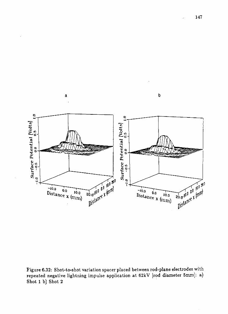
147
Figure 6.32: Shot-to-shot variation spacer placed between rod-plane electrodes with repeated negative lightning impulse application at 62kV [rod diameter 5mm]: a) Shot 1 b) Shot 2

148
Mailer et al.,[56] have also shown the coexistence of both positive and negative
charges on spacers subjected to positive impulse voltages in SF6 gas at O.lMPa.
Their results, however, were obtained following the depressurization of SF6 and
making the measurements in air. Further, the surface potential measurements
were made only across one diameter of the cylindrical spacer thereby not giving
adequate information as to the overall charge distribution. Since their measure
ments were not made in-situ their validity is questionable. This is because the
dielectric strength of the gas between the capacitive probe and the charged surface
has been reduced by depressurization which can result in back discharges to oc
cur between the charged patches following the introduction of the probe into the
vicinity of the charge patch. This can affect the original charge distribution. This
fact was confirmed by some experiments during this investigation. The residual
charge distribution following DC voltage application to a spacer gap in SF 6 gas
yielded different results when the chamber was depressurized and measurements
were made in air. Further, back discharges occurred between the spacer and the
probe tip consequently altering the original charge distribution. Mailer's [82] ex
periments conducted in air under DC conditions indicated a trend similar to those
obtained in this investigation, i.e., the charge distribution in the vicinity of the high
voltage electrode at high voltages reverses polarity as compared to the distribu
tions observed at low voltages. Of course, in their case the results, show that: with
experiments in air at O.lMPa that the charge distribution on the top surface of the
spacer has the same polarity as that of the applied voltage at low voltages. For
example the charge distribution is principally positive, for positive polarity of the
rod electrode at low voltages. At high voltages on the rod electrode, however, the
charge distribution is reversed in the region close to the electrode. Once again these
observations were made in their experiments after surface potential measurements
made across one diameter. In order to confirm their observations the experiments
reported by Mailer et al.,[82] were duplicated to the extent possible. A cylindrical
acrylic spacer 40mm in diameter and 30mm long was placed in a 3.2mm rod-plane
gap. In the experimental results reported by Mailer, the rod diameter was 1.6mm.
Ensuring very low levels of residual charges on the spacer prior to voltage appli
cation, the insulator was subjected to positive DC voltages of 10, 20 and 35kV

149
in air at O.lMPa. The voltage was maintained for approximately 20 minutes at
each voltage level and the surface potential scans were done. Figure 6.33 show the
results obtained. The X and Y axes refer to the distance from the tip of the high
voltage electrode and the Z axis is the surface potential distribution. At a volt
age of 40kV the spacer flashed over. The experiments were discontinued following
the occurrence of flashover. It can be seen that even in this case bipolar charging
is dominant. Further, reconstructing the distribution across a suitable diameter
a match was obtained with the results reported by Mailer et al. This however,
does not give the composite picture of the behavior of the charge distribution on
the spacer in air subjected to DC voltages. The explanation given for their ob
servations was that the corona generated light at higher voltages induced charge
injection into the bulk of the material. This is supposed to have caused electrons to
appear at the spacer surface and neutralize the homopolar charge distribution and
result in a heterogenous charge distribution. The argument here is that the overall
charge distribution is extremely heterogenous even under low voltage and not ho
mopolar as suggested by them. Previous investigators [51] have also confirmed the
existence of bipolar charges on spacers subjected to DC voltages in SF 6 gas. No at
tempt however, was made by them to explain the observed bipolar (heterogenous)
charging.
Cooke [85] has stated that charges arriving from a surrounding gaseous atmo
sphere may accumulate on an insulating surface. The accumulation of charges are
dependent on their source, for example, a protrusion on an electrode surface, and
on their transport in the gas to the insulating surface. Once on the surface, the
charges can either migrate on the surface, which depends on the surface condition
of the spacer or migrate into the bulk. These charges can also get neutralized via
the gas. Therefore, the net charge on the insulator surface can be expressed by the
equation 6.5:
= charge arrival rate — charge loss rate. (6-5)
The charges transported to the insulator surface may employ a gas ionization mech
anism or other field dependent processes. A remote ionization emitter in the form
of a pin 0.25cm to 2cm in length and placed at varying distances from a post
insulator in SF6 gas was used. The insulator was placed between plane parallel

150
Figure 6.33: Surface potential distribution on an acrylic spacer placed between a 3.2mm rod-plane gap in air at O.lMPa subjected to positive DC voltages for 20 minutes, a) lOkV b)20kV c)30kV d)Maller et al., results[82]
151
electrodes with the pin located on the ground plane. Cooke confirmed that the
observed charging of the insulator could be explained using the basic properties of
charge transport in the surrounding gas even at elevated gas pressures and volt
ages (+600kV DC voltage). It was found that the charges followed drift patterns
and were deflected according to the space charge field. It is important to mention
here that the observed charge patterns were obtained after the chamber was de-
pressurized and exposed to atmospheric air. Further, the capacitive probe had a
probe tip diameter of 6mm and was placed at a distance of 10mm from the charged
surface. As is well known, under these conditions it is quite likely that integration
of the local charge distribution could have possibly masked the possible existence
of bipolar charges. No definite conclusions can be drawn as to the possibility of
heterogenous charging of the spacer under corona charging in SFQ gas.
The results mentioned above indicate that corona charging in SF© leads to
bipolar charging. There seems to be some contradiction in the results obtained by
Mailer et al., and the present investigation with regards to the observations made
with DC voltages in air at O.lMPa. There seems to be agreement with their results
obtained in SF6 gas under impulse voltage application.
In order to get a better understanding of the phenomenon of corona charging
and consequent charge deposition on the spacer surface simple experiments were
conducted to examine the influence of the gas on the gas conduction and transport
phenomenon. Insulating spacers 40mm in diameter and 20mm long were placed
in a rod-plane gap in the pressure vessel. Negative DC voltage was applied to
the rod electrode. The spacers used were cleaned to ensure relatively low levels of
residual charges. The spacers were subjected to DC voltages for 20 minutes. At
each voltage level, the surface potential scan was carried out. Since the electric
field lines intercept the spacer surface at right angles to the surface, with the
shortened spacer, negative charge carriers generated in the gap in the vicinity of
the rod electrode are expected to follow the field lines and deposit on the spacer
surface. Figures 6.34-6.36 show the results obtained with DC corona charging on
spacers with air [87], N 2 and SF 6 gas at O.lMPa respectively. In case of air and SF 6
the results showed bipolar charging. At low voltages, immediately below the rod
electrode, positive charge accumulates. At higher voltages, however, the overall

152
charge distribution is principally negative in the regions immediately below the
electrode with pockets of positive charges appearing at the spacer edge. In case
of N2, for voltages upto — 40kV the insulator surface is charged negative. When
the polarity was reversed on the same insulating spacer previously subjected to
negative voltages the charge deposition on the spacer was principally positive.
These results suggest that the intervening gas has an important role to play in the
charge accumulation process.
Both air and SF 6 are electronegative gases. The major ionic species in a neg
ative corona in air at O.lMPa is the CO3 ion. The negative ions generated by
the corona should then follow the field lines (moving away from the negative rod
electrode) and land on the spacer surface. This ion may then be neutralized by
giving up an electron to the conduction band near the surface. The electron is
subsequently trapped in a surface state and needs some activation energy to fa
cilitate its movement into the bulk. As stated by Baum [83] this energy can be
supplied thermally or by excited molecules. The energy supplied by the excited
molecules may take place through the emission of a photon of sufficient energy
by the excited molecule, with subsequent photoinjection of the trapped charge. A
similar phenomenon may occur for SF 6 gas gap in corona. Data on the ion species
for corona in low fields in SF6 gas, has suggested the existence of SFQ ion together
with heavy cluster negative ions [84]. It has been suggested that in GIS, even
at electric fields under normal service conditions, SF$ ions or associated clusters
exist. With increased ^ ratios, i.e., the ratio of the electric field to the gas pres
sure, these clusters will be destroyed by collisions, so that the dominant species of
negative ions under pre-breakdown conditions will be SF$ . There is no published
information as to the behavior of these ions or the clustered species when they are
incident on the spacer surface, with regards to their mobility, charge transfers etc.
The results however, show similarities as to the heterogenous nature of charging of
spacers subjected to DC corona in air and SFg .
Similar experiments conducted with iV2 gas seems to indicate the absence of
bipolar charging and the charging is predominantly homopolar. Unlike in SF 6 and
air, in the case of N2 no negative ion formation occurs. The electrons released from
the cathode in these experiments, follow the field lines and deposit on the spacer

153
resulting in a homopolar distribution consistent with the present understanding
of corona charging of spacers. The above results showed that the spacer charge
accumulation in N2 gas is consistent with the present understanding of gaseous
conduction and significant differences in the charge accumulation are observed if
the surrounding gas is electronegative in nature. Thus, in case of the SFe gas
significant bipolar charging of the spacer occurs.
6.6.3 Mechanism of charging
In the experimental investigations conducted with a 30mm spacer placed in a rod
plane gap there is a component of the electric field tangential to the spacer surface.
The experiments described earlier suggest that an insulating spacer in SF 6 gas at
O.lMPa acquires charge under both lightning and switching impulses. From the
design and operations standpoint, this is an important finding and is cause for
concern. Although, the nature and phenomenon of charging is quite complex, a
designer is interested in the following:
• How do these charges perturb the original ambient field distribution?
• Do these charges really affect the overall insulation performance of the sys
tem?
Before one can attempt to answer these questions, accepting the fact that the
spacer does get charged, it is of interest to know:
• What are the sources of charges on spacer?
• Why does the spacer gets charged in the manner illustrated in Figures 6.15-
6.28 at various voltages?
• Can these charges explain the observed changes in the Von-Laue plots, i.e.,
small slopes at low voltages and large slopes with increasing voltages? The
differences in these slopes at low voltages for plain gas gaps and spacer gaps?
The following discussion focuses on the above mentioned aspects, in an attempt to
explain the mechanics of charge accumulation. The phenomenon of spacer charging

154
Figure 6.34: Surface potential distribution on a ptfe spacer placed under a 10 mm rod-plane gap in air at O.lMPa subjected to negative DC voltages for 20 minutes, a) 20kV b)40kV

Figure 6.35: Surface potential distribution on a ptfe spacer placed under a 10 mm rod-plane gap in N 2 at O.lMPa subjected to negative DC voltages for 20 minutes, a) OkV b)20kV c)40kV d) +40kV

156
Figure 6.36: Surface potential distribution on a ptfe spacer placed under a 10 mm rod-plane gap in SF 6 at O.lMPa subjected to negative DC voltages for 20 minutes, a) 20kV b)55kV c)80kV

157
is a complex process. A clearer understanding of this phenomenon may be possi
ble by drawing an analogy with the present understanding of the phenomenon of
positive impulse flashover of gas gaps. A quantitative model for the prediction of
breakdown voltages of highly inhomogenous electric field gas gaps (as an example
a rod plane gap) has been developed by Wiegart et al [84]. This breakdown model
was restricted to positive polarity because of its greater practical importance. The
present studies show that negative breakdown voltages for spacer gaps are much
higher than the positive impulse breakdown voltages. The probability of failure
of an SF 6 gas gap subjected to impulse voltages depends on the appearance of a
free electron in the region of high electric field of sufficient magnitude to cause an
avalanche. For positive impulse voltages the electron is detached from the negative
ions in the gas due to field-induced collisional detachment. The negative ions in
the SFe gas are also generated by cosmic rays. Some of these ions are lost through
recombination or by collision with the walls of the test apparatus. An equilibrium
zero field ion density distribution is then established. Computations have been
made to determine this equilibrium distribution and comparisons have been made
with measurements. Wiegart et al., [84] have shown that the initial electron re
lease would have to result from an ionization of the SF 6 molecule by cosmic rays or
from negative ion detachment. For DC voltages, it has been suggested that both
these processes may be contributing factors for the electron release. Under impulse
voltage application, however, only electron detachment from the negative ion is re
sponsible for the availability of the initial electron for the avalanche development.
Further, it has also been shown that the statistical time lag is directly proportional
to the critical volume which in turn is proportional to the ion concentration.
The electron production rate is a field dependent process. In other words, the
detachment coefficient is sensitive to the electric field.
It has been shown that the equilibrium zero-field ion density distribution is
sensitive to small voltage changes. The distributions have been shown to alter
dramatically even for small bias voltages. This is as a consequence of the high
field-induced mobility of the negative ions. When an impulse is applied to an
electrode arrangement, as a result of the field-induced ion drift, the ion density has
been shown to be altered appreciably. Thus each impulse can either reduce the

158
ion concentration or increase the equilibrium distribution. In summary, the ion
density distribution in a gas gap is sensitive to low fields.
The results of the surface charge distributions show that at low voltages the
spacer has negative charges in the vicinity of the rod electrode for positive im
pulses. From the previous discussion it may be said that the presence of the
negative charges on the spacer can result in the depletion of negative ions in the
gas gap between the rod electrode and spacer. So, the depletion of negative ions
imply the depletion of the initiatory electrons in the critical volume, resulting in
a reduced slope of the Von-Laue plot. This argument seems to be consistent with
the observations. In summary, it may be said that the presence of the charges on
the spacers in the present investigations are due to gas conduction. The influence
of the spacer material on the charge accumulation/dissipation on the surface will
also influence the final charge magnitude. For example, the differences observed
between epoxy and ptfe spacers. The spacer acquires charges and modifies the
ambient field distribution. The results obtained are consistent with those obtained
bv previous investigators.
6.7 Effect of A C Pre-Charging These experiments were carried out to investigate the effect of 60Hz AC voltage
application on spacers placed in both quasi-uniform and non-uniform fields. Fol
lowing the initial cleaning procedure and the measurement of the residual charge on
the spacer (i.e. the measurement of the surface potential by the probe), 60Hz AC
voltage was applied at different voltages for different durations. In case of the quasi-
uniform field configuration, the effect of duration of voltage application and the
magnitude of the applied voltage on the spacer charging was minimal. Figure 6.38
shows the surface potential variation for a spacer placed between plane-parallel
electrodes subjected to AC voltages of 70kVrmAoT 20 minutes. The same spacer
was subjected to varying durations of voltage at the same magnitude. This did
not increase the surface potential magnitudes. Since the high voltage test gener
ator could generate a maximum of only 75/cVrmsthis was applied to the system.
No fiashover was observed at these voltage levels. These results were obtained for
electrodes which shielded the triple junction. Similar results were obtained when
unrecessed electrodes were used in the tests. It is quite apparent in these experi-

159
4000
2 4 ELECTRODE SPACING [cm]
4 0 0 0 -
I
2 4 6
ELECTRODE SPACING [cm]
Figure 6.37: a) Negative ion density distribution along a rod-plane gap for various D C voltages; b) Negative ion density in a rod-plane gap at various times during a negative impulse application. Voltage=124kV, p=0.lMPa and T=293K[84]
160
ments that the electric field on the insulator surface was uniform and in a direction
only tangential to its surface. Experiments conducted with conical spacers which
resulted in both normal and tangential components of electric fields on the spacer
surface produced very similar results. Assuming that charges were generated in
the gas or from the electrode surface, they would follow the field lines and de
posit on the spacer surface. This is because of a component of the electric field
normal to the spacer surface. The results with conical spacers also did not show
any appreciable charging. This suggests that under uniform field conditions with
reasonably good electrode surfaces charge accumulation of spacers in SFQ gas at
O.lMPa is minimal. This observation is independent of the relative proportions of
the normal and tangential components of the electric field on the spacer surface
and the duration of the applied voltage. Also for the range of the applied voltage
no significant charging of the spacer occurs.
Figure 6.39 shows the surface potential distribution with AC pre-charging on
epoxy spacers placed in a rod-plane gap, with rod diameter of 5mm. Figure 6.40
shows the surface potential distribution on a spacer placed in a rod-plane gap
subjected to various magnitudes of DC voltage for different times. The rod diameter
was 10mm. In the region close to the high voltage electrode some charging is
observed. Regions away from the high voltage electrode, however, show very low
levels of charge. With the duration of the applied voltage increased from 5 minutes
to 60 minutes some increase in the charge levels were observed. Once again the
region close to the high voltage electrode has a higher charge deposition. When the
voltage level was increased to 43kV, charge magnitudes close to the high voltage
electrode increased. It can be seen from these figures that charging increases with
the AC voltage. Both positive and negative charges co-exist and no single polarity
charge dominates. These patterns become more complex with increasing level of
the AC voltage and duration.
The results of charge distributions obtained with AC and impulse voltage ap
plication to spacers suggests that spacers in non-uniform fields acquire charges.
The charge patterns are heterogenous in nature in both air and SFQ gas. In case
of N 2 , however, the results indicate homopolar charging under corona conditions.
Negligible charging was observed on the spacers placed in quasi-uniform fields.

161
Figure 6.38: Surface potential variation for a spacer placed between plane-parallel electrodes subjected to AC voltage of 70fcVrmg for 20 minutes

162
Figure 6.39: Surface potential variation for a spacer placed between rod-plane electrodes subjected to AC pre-charging, rod diameter 5mm

163
o 6
Figure 6.40: Surface potential variation for a spacer placed between rod-plane electrodes subjected to AC pre-charging, rod diameter 10mm a) 30kV 5min b) 30kV 30min c) 30kV 60min d)43kV 30min

164
Slight perturbation of the uniform field with the use of spacers in the form of
conical frustra also showed very low levels of charge accumulation on the spacer.
This suggests that under quasi-uniform fields charge accumulation on the spacer is
negligible both under AC and impulse voltage applications.
The sources of charges in case of the rod-plane spacer gap are due to gaseous
conduction and the secondary emission yield from the spacer surface. The observed
charge patterns are most likely due to the interaction between the charge carriers
in the gas and the spacer surface. The bulk conductivities for the spacers used
in these experiments are very low. So, for any significant charging to occur via
the bulk the voltage must be applied over several hours. Under impulse voltage
application the duration of the applied voltage is very small when compared to the
time required for the charge carriers in the bulk of the spacer to move. So, if the
bulk has to play any role in the charge accumulation process the bulk conductivity
must be highly non-linear or non-uniform. Nakanishi et al., [50] have shown that
in epoxy spacers, bulk conductivity is almost constant and independent of the
electric stress. Therefore, bulk conduction is not considered to play an influencing
role in the observed charging phenomenon. The phenomenon of spacer charging
under non-uniform fields is quite complex. Having examined the possible sources of
charges, and their nature of distribution on the spacer it is important to establish
the significance of these charges on the breakdown behavior of the spacer gap. The
questions that need to be addressed are:
• Do these charge patches alter the breakdown behavior of a spacer gap?
• Do they influence the time-to-breakdown under impulse application?
• Does AC pre-charging of the spacer affect the spacer impulse breakdown
behavior?
As far as a gas gap is concerned, the statistical time lag plays an important role in
impulse stressing of SF 6 insulated equipment. This determines both the temporal
and spatial distributions of breakdowns. As mentioned before, most of the primary
electrons are produced by collisional detachment processes from negative ions and
it has been shown both by measurements and calculations that bias voltages may

165
effectively influence the ion density distribution in the gap and thus the statistical
time-lag. A lack of primary electrons will lead to a greater variation in the time-
to-breakdown. On the other hand, an excess of primary electrons will reduce the
statistical scatter of the formative time-lag.
A typical GIS system is stressed with AC voltages at the rated voltage of the
system. Under abnormal conditions, either a switching or a lightning transient
can appear on the system resulting in a composite stress of the insulation system.
It is of importance to know how the GIS would behave under the application of
this composite stress. It is well known that for plain gas gaps, subject to impulse
voltages in SF6 gas, the necessary and sufficient conditions for breakdown are:
• The presence of a negative ion in the critical volume from which an electron
can be detached,
• A field distribution along the gap which promotes the growth of an avalanche
formation to a critical size. These two conditions are considered adequate to
describe streamer breakdown in a gas gap. At higher gas pressures and higher
voltages these conditions become only necessary conditions but still do not
qualify to signal the onset of breakdown and a third condition is necessitated
namely;
• A field distribution in the gap such that the maximum field at the leader
tip remains sufficiently large such that a critical charge is injected into the
critical volume [84].
It has been suggested [84] that normal AC voltage application can cause a peri
odic lack of negative ions in the critical volume close to the high voltage electrode.
Further, as mentioned earlier, low DC bias voltages can also cause a redistribution
in the equilibrium negative ion density profiles. Extending this observation to a
spacer gap, it may be said that the presence of charges on the spacer can affect
the negative ion density in the region close to the high voltage electrode. As a
consequence of this, it may be said that the presence of surface charges on the
spacer may influence the impulse breakdown probability of the spacer gap. This
hypothesis is a direct extension from the observations made for plain gas gaps.

166
For plain gas gaps it has been observed that higher breakdown probabilities are
obtained when impulse voltages are applied sequentially without adequate wait
ing time between voltage applications. In other words, it has been proposed [84]
that to obtain statistical independence from the time between voltage applications,
measurements should be made with a minimum waiting time of 6 minutes between
voltage applications.
The following section presents the results obtained for breakdown voltages of
spacer gaps under both sequential impulse voltage application and those with AC
precharging.
6.8 Breakdown Behavior of the Spacer Gap
It has been shown that large reductions in the dielectric strength of a spacer gap are
observed when pre-existing stress of DC voltage and the applied impulse voltage
are of opposite polarities. Further, for fast transients the breakdown behavior of
spacer gaps is different when compared to plain gas gaps. Although work with DC
pre-charging of a spacer and its influence on impulse behavior have been reported
quite extensively, very little has been reported on the composite stress of preexisting
AC voltage on the impulse fiashover behavior of the system. The breakdown of
quasi-uniform and non-uniform fields spacer gaps due to impulses with different
levels of AC pre-stress are presented.
6.8.1 Plane-Parallel Electrodes
In a plane-parallel electrode configuration, very low levels of charging have been
observed with impulse voltage application. Due to the limitation in the available
voltage source voltages beyond ±190kV could not be obtained. No flashovers,
however, were observed upto +190kV impulse levels. Moreover, even with AC
pre-charging at 70kV for 20 minutes, no premature flashovers of the spacer gap
have been observed. Similar results have been obtained when the AC pre-charging
time is increased to 6 hours. It is known that long-term DC pre-stressing of spac
ers in SF 6 gas leads to increased charge accumulation [50]. It is evident from
fig. 6.38, however, that no noticeable charging occurs over extended periods of AC

167
pre-charging in the uniform field configuration used. In a limited number of exper
iments, charges of both polarity have been observed with AC pre-charging. This
is probably due to imperfections at the triple junction.
6.8.2 Rod-plane Electrodes
In an attempt to investigate the effect of pre-charging in non-uniform fields ex
periments, similar to the one described above have been conducted with epoxy
and acrylic spacers between a 10mm hemispherically capped rod and a plane elec
trode. In case of recording the impulse breakdown voltage of the spacer with AC
pre-charging it was important to obtain the breakdown voltage values free of any
history of the residual charge on the spacer. Consequently, spacers were charged
to an AC voltage at a desired level, initially ensuring low levels of residual charge.
The AC voltage was then removed and the generator was setup to generate impulse
voltages. The charging voltage on the generator was adjusted to voltage levels close
to breakdown. The impulse voltage was applied and the breakdown voltage was
recorded. If the flashover occurred on the tail of the impulse wave, the peak value
of the impulse was recorded as the breakdown voltage. If the flashover, however,
occurred on the impulse front, then the voltage at breakdown was recorded as
the breakdown voltage. This was consistent with industry practice. The spacer
was replaced following each flashover by depressurizing the system and replacing
it with a freshly cleaned spacer. Thus, each data point in figure 6.42 corresponds
to measurements with a fresh sample.
Figure 6.41 shows the shot-to-shot variation in positive impulse flashover volt
age for the epoxy and acrylic spacers. It may be observed that there is a wide
variation in the flashover voltage. It is also apparent that the flashover voltage does
not recover following repeated flashover for the epoxy spacer. In fact, attempts to
restore the strength by applying impulses of the opposite polarity (negative) so as
to discharge the surface have not been successful. Figure 6.42 shows the effect of
AC pre-charging on both the first flashover voltage and the time-to-flashover for
impulses. The results show that the scatter in the pure impulse flashover voltages
can be high. It may be seen that although the AC pre-charging influences the first
flashover (both voltage and time) the variation falls well within the statistical scat-

168
u < St ma O > DC U > o X < b. W
3 Cu S
o z z H as o
80-
60-
40
20-
A l l A \ ^ V
A ACRYLIC
X
x _EP0XY
10
SHOT NUMBER 15 20
u S3 r— a: w > o as
<
w D CU
1.5
1.2
o.g
0.6
0.3
0 -
A ACRYLIC x EPOXY
10
SHOT NUMBER
— r -15 20
Figure 6.41: Shot-toshot variation for a spacer between rod-plane electrodes with no AC pre-charging (a) positive impulse fiashover voltage (b) fiashover time

169
110
70-
80- * ACRYLIC
x EPOXY
SO-10 20 30 40 50
AC PRECHARGING VOLTAGE [KV rms] 60
2
Figure 6.42: Shot-to-shot variation for a spacer between rod-plane electrodes, with AC pre-charging at 50kV for 30 minutes (a) positive impulse flashover voltage (b) flashover time

170
ter for positive lightning impulse flashover voltages with no A C pre-charging. In
some experiments, it has been observed that following the first flashover the sub
sequent flashovers occurred at lower voltages. With repeated flashovers, however,
this downward trend is reversed in some cases.
Giesselmann et al., [86] examined the role of an insulating spacer on the D C
flashover of spacer in SF6 and JV2 gas. The pre-discharge development along the
spacer surface was recorded using a sensitive high speed image intensifier. The pre-
discharge development figures showed that, in case of SF6 gas, multiple discharges
initiate along the spacer surface. The results showed that even under D C voltage
application, there is a considerable scatter in the breakdown voltage of the spacer
gap. Trinh et al., [55] reported that the presence of a spacer in a coaxial gap in
SFe gas reduced the withstand voltage of the system. Also, under sequential appli
cation of impulse voltages, (about 100 shots) a considerable scatter was observed
in the breakdown voltages. For example, under positive impulses, the scatter was
approximately +20% to —35%. During this application, they also observed certain
flashovers to occur at unexpectedly low voltages. This was attributed to possible
surface charging of the spacer. The recovery in the spacer flashover levels was
attributed to a partial or a complete neutralization of the trapped charges during
subsequent breakdowns. In their experiments, no attempt was made to measure the
surface charge distributions following impulse voltage application. In the present
investigation, a similar scatter in the breakdown voltages under impulse voltage
application was observed. These results are in agreement with the results reported
by Trinh et al.
In case of D C GIS it is well known that spacers subjected to one polarity voltage
cause a dramatic reduction in the breakdown voltage of the spacer when the polarity
of the D C voltage is reversed. In the industry, this type of reduction in the spacer
flashover voltage is referred to as a polarity reversal type of breakdown. From the
measured surface charge distributions following impulse voltage application, it is
apparent that the spacer acquires bipolar charges. The charge distributions vary
depending on the applied voltage, spacer material etc. These charges perturb the
ambient electric field distribution in the spacer gap. The presence of bipolar charges
can also explain the possibility of a polarity reversal type breakdown behavior.

171
Following flashover, a redistribution of the charges on the spacer can occur. Thus
charge accumulation on the spacer can occur even under impulse voltages and
explains the anomalous breakdown behavior reported by Trinh et al. following
sequential impulse application on a GIS spacer in SF6 gas. The presence of these
charges can also explain the statistical scatter observed during sequential impulse
tests. In the present study it was observed that the scatter in the pure impulse
flashover was ±35% in case of the acrylic spacer. In the case of epoxy spacer,
repeated flashover of the spacer resulted in damage to the spacer. This explains
the deterioration in the impulse flashover voltage seen in figure 6.42a with the shot
number.

Chapter 7
CONCLUSIONS AND SUGGESTIONS FOR F U T U R E WORK
This thesis examined the role of charge accumulation on spacers in uniform and
non-uniform field gaps in SF$ gas in both the pre-breakdown and breakdown stages
of the discharge phenomena. Charge accumulation under AC voltages and the
effect of AC pre-charging on impulse fiashover were also studied. Section 7.3 makes
suggestions for future research.
7.1 Pre-breakdown phenomena
From the results obtained for a point-plane geometry it is apparent that the pres
ence of a spacer in the high field region affects the pre-breakdown behavior of a
spacer gap as compared to that of a plain gas gap. This effect is demonstrated by
comparing the results of the Von-Laue plots for spacer gaps and plain gas gaps in
Chapter 6. Since, no sharp discontinuities in the Von-Laue plots exist, it may be
said that there is only one mechanism active for initial electron generation. Also,
at a given pressure of the SF6 gas, the slope in the Von-Laue plot increases sharply
with voltages above the inception level. Moreover, the slope of the Von-Laue plot
for a spacer gap is larger compared to that of a plain gas gap. This larger slope
in the Von-Laue plot indicates an increase in the initiatory electron density for
a spacer gap, and may be due to the enhanced local electric field from trapped
surface charges and the corona-light induced photoemission yield from the spacer
surface. It is concluded that the insulating spacer significantly reduces the corona
172

173
inception time of a spacer gap. Both the spacer material and its surface roughness
influence the mean corona inception times.
7.2 Spacer Charge Accumulation
Under uniform field conditions, spacers subjected to impulse voltages in SF6 gas
at atmospheric pressure do not acquire significant surface charge. Results of this
investigation have shown that any defects present either on the spacer or on the
electrode surface can lead to charge deposition on the spacer for both AC and
impulse voltage application. The magnitude and the nature of charging under
these conditions are dependent on the severity and location of the defect and the
applied voltage. On the other hand, under non-uniform field conditions, spacers
acquire significant charge under AC and impulse voltage application. The charge
distribution is highly non-uniform with both positive and negative charges present
in close proximity. At low voltages, the charges near the rod electrode have opposite
polarity to that of the electrode, with the same polarity charges deposited towards
the spacer edge with peak values of about 2 — 5/iCm"2 corresponding to fields of
about 13-19kV/cm. This is about 25-30% of the ambient field. When the voltage
nears the the breakdown levels, the charge on the spacer surface close to the high
voltage rod electrode has the same polarity as that of the rod electrode. The peak
charge magnitudes at these levels range between 15 — 20fxCm~2. Also, the charge
magnitudes increase with the applied voltage. The cylindrically symmetric field
distribution in case of the spacer with no charges is destroyed following this charge
accumulation. It is necessary to make in-situ charge measurements in order to draw
some meaningful conclusions as to the nature of charging, polarity and magnitudes
of the accumulated charge. By opening the test chamber the dielectric strength of
the gas surrounding the spacer is reduced. Thus local back discharges can occur
between the spacer and the capacitive probe resulting in a modification of the
original charge dsitribution. The spacer retains charges over considerable periods
of time. Charge measurements made several times following a voltage application,
showed very little change in the overall pattern, indicating the tenacity of the
charges and their poor mobility on the spacer surface. Similar experiments were

174
conducted to examine the influence of the probes on the charge mobility. Once
again, the results demonstrated the low mobility of these charges on the spacer
surface.
Experimental results for different gases, show that there is a distinct difference
in the charge patterns obtained on the spacers when exposed to N2 gas as compared
to the results obtained in air and SF6 . For example, in experiments with a rod-
plane spacer gap, with the rod electrode held at a certain distance from the spacer,
for a negative voltage application to the rod, the spacer top was charged negatively
in case of N2 gas. In case of SFe and air the spacer had both positive and negative
charges. Similarly, for a positive voltage application with N2, the spacer top was
charged positively but bipolar charges were present in case of SF6 and air. The
electronegative nature of the gas seems to affect these charge patterns.
The sources of charges in the case of the rod-plane spacer gap are due to gaseous
conduction and the secondary emission yield from the spacer surface. The observed
charge patterns are most likely due to a complex interaction between the charge
carriers the spacer surface and the local electric field.
Since the decay time constant of the trapped surface charges are large and
their surface mobility poor, despite the high local fields, brought about by the
introduction of the probes, it may be concluded that surface conductivity has a
negligible role to play in the charge accumulation process. It is well known that the
mobility of charge carriers in the bulk of the spacer is very low so it would require
considerable time of voltage application to observe any significant accumulation of
charges on the spacer. The present investigations reveal that even under impulse
voltages (where voltage application lasts for only 2 ms) the spacer acquires charges,
suggesting the insignificant role bulk conductivity has in the charge accumulation
process. In conclusion it may be said that under impulse voltages, both bulk and
surface conductivity have a minimal role to play in the charge accumulation on
spacers and it is principally due to ionization and conduction in the surrounding
gas.
Results of the spacer fiashover under sequential application of impulse voltages
show a considerable scatter, amounting up to ±30%. The presence of charges

175
on the spacer results in a perturbation of the symmetric ambient field distribution
which may account for this statistical scatter in the breakdown voltage values. The
spatial distribution of bipolar charges changes after each fiashover and may trigger
a reversal of polarity type of breakdown observed in DC GIS breakdown studies.
Although AC pre-charging influences the first fiashover and time-to-fiashover for
impulse voltages, the variation falls well within the statistical scatter for positive
impulses with no AC pre-charging.
7.3 Scope for future work
The present work has shown that spacer charging may explain the anomalous
fiashover under impulse voltages that has been reported in literature. The observed
surface charge accumulation takes place for a variety of reasons. Some of the more
important ones being:
• emission sites on the electrode surface giving rise to charge carriers that follow
field lines and deposit themselves on the spacer surface.
• charge carriers generated by ambient irradiation of the surrounding gas in
the spacer gap causing charge deposition on the spacer surface.
Extensive investigations have revealed that the time constants for charge decay are
very large (can be several hours or days, depending on the ambient gas pressure). In
order to examine the effect of the spacer charging on spacer fiashover, in greater de
tail, it is important to know the influence these charges and their fields have on the
transport and ionization properties of the charge carriers involved in breakdown.
From high speed photographs of surface fiashover, there is evidence to suggest that
local fields anywhere on the spacer can initiate breakdown of spacer gaps. Due
to charge patches of both polarities such local field concentrations exist and may
explain their influence on the breakdown behavior. From a practical standpoint,
therefore, it is important to examine how the ionization coefficients are affected
and how one can include surface charging to build a reasonable model to predict
spacer fiashover in SF 6 . Field calculations with strategically located known charge
distributions can be used to compare the predicted pre-breakdown current growth

176
and the measured values of the pre-breakdown corona current. By improving the
bandwidth for the fast risetime corona current measurements, better correlation
between the deposited charge and the measured current is possible. This work
can then be extended to examine the influence of charges (both magnitude and
location) on the breakdown voltages. This may lead to a better understanding of
the reasons as to why local discharges occur and conditions under which this could
result in spacer fiashover. It is also important to conduct these studies using higher
gas pressures since in a practical system the typical operating SF 6 gas pressure is
about 0.3-0.6MPa. These experiments have to be complemented with high speed
photographic techniques using image intensifiers. Application of the model for cur
rent growth to a practical GIS system with spacers operating at higher pressure
may provide a better understanding of the phenomenon and ultimately help in
improvement of the fiashover performance of these systems.
Although it has been established in this work that spacer pre-charging under
AC does not influence the impulse fiashover voltage significantly, spacer charging
is undesirable since the presence of charges on a spacer can attract metallic con
tamination. It is well known that the presence of such contamination on a spacer
causes a dramatic reduction in the breakdown voltage. The practical implications
of this are:
• spacer charge accumulation is to be minimized and
• even if the spacer accumulates charge it is important to explore means to
dissipate these charges quickly.
A solution to the first problem could be to ensure by suitable design, for both the
spacer and the electrode system,that charge accumulation on the spacer surface
is minimized. A solution to the second problem could be to suitably coat the
spacer with a material whose photoemissive yield is low, thus ensuring that charge
accumulation is minimized. Another aspect of the study could examine spacer
coatings which provide quick dissipation of any accumulated charge.

Bibliography
[l] Cookson A. H., Gas-Insulated Cables, IEEE Transactions on Electrical Insu
lation, Vol EI-20, No. 5, Oct 1985, pp.859-890
[2] Siemens Catalog No. E-129/1420-101
[3] Cookson A. H., Review of high voltage gas breakdown and insulators in com
pressed gases, Proceedings of the IEE, Vol 128, Part A, No. 4, 1981, pp.303-312
[4] Hampton, B. F. Outline of a flexible SFQ insulated cable, Proceedings of the
IEE, Vol. 123, 1976, pp.159-164
[5] Giao-Trinh, H., Vincent, C. Bundled conductors for EHV Transmission, IEEE
Power Engg. Society, Summer Meeting, Paper No. 78-192-7, 1977.
[6] Lautenschlager, G., Cooke, C. M. Bundled conductors for gas insulated high
voltage power transmission cables, IEEE Transactions on Power Apparatus
and Systems, Vol PAS-100, 1981, pp.394
[7] Kobayashi, T., Mori, S., Koshiishi, M. , Minomiya, K. Development of compact
500 kV 8000 A gas insulated transmission line - Study on insulator design,
IEEE Transactions on Power Apparatus and Systems, Vol PAS-103, No. 11,
1984, pp.3154-3164
[8] Takuma, T., Watanabe, T., Kuono, T. Effect of a narrow gas gap on the sur
face flashover of spacers in, International Symp. on High Voltage Engineering,
Zurich, 1975, pp.440-450
[9] Laghari, V.R., Quereshi, A. H. Flashover studies of cylindrical spacers in SFG
and N2 mixtures, IEEE Power Engg. Society Winter Meeting Paper No. A80-
055-4, New York, 1980.
177

178
[10] Cooke, C. M., Trump, J. G. Post type spacers for compressed gas insulated
cables, IEEE Transactions on Power Apparatus and Systems, Vol PAS-92, No.
5, 1973, pp.1441-1447
[11] Trump, J. G., Andrias, J. High voltage DC flashover of solid spacers in com
pressed nitrogen, Trans. AIEE No. 41, 1941, pp.986-990
[12] Dakin. T. W., Studianarz, S. A. The voltage endurance of epoxy resins, Con
ference Record of the 1978 IEEE International Symposium on Elec. Ins., 1978,
pp.216-221
[13] Wooton, R. E. , Emery, F. T., Cookson, A. H. A test for the effect of high
energy arcs on the flashover strength of insulation in compressed SF$ gas,
IEEE Transactions on Electrical Insulation, Vol EI-75, No. 2, 1980, pp.74-80
[14] Greenwood, P. Surface flashover in compressed SFQ , Proc. II Int. Symp. on
Gas Discharges and their applications, 1983, pp.233-235
[15] Chenoweth, T. E. , Meoman, F. A., Cookson, A. H. Epoxy castings for
UHV service in compressed SFQ gas insulation equipment, Proc. 13th Elec
trical/Electronics Insulation Conference, 1977, pp.322-326
[16] Cookson, A. H., Electrical breakdown for uniform fields in compressed gases,
Proceedings of the IEE, Vol 117, No. 1, 1970, pp.269-280
[17] Nitta, T. Factors controlling surface flashover in SFQ gas insulated systems,
IEEE Transactions on Power Apparatus and Systems, Vol-97, No. 3, 1978,
pp.959-965
[18] Cooke, C. M. Particle contamination in compressed gas insulation, limitations
and control, International Symp. on Gaseous Dielectrics, 1978, pp.162-189
[19] Itaka, K., Hara, T., Misaki, T., Tsuboi, H. Improved structure avoiding lo
cal field intensification on spacers in SF$ gas, IEEE Transactions on Power
Apparatus and Systems, Vol PAS-102, No. 1, 1983, pp.250-255

179
[20] Skipper, D. J., McNeal, P. I. Impulse fiashover measurements on compressed
gas spacers for EHV power cables, Proceedings of the IEE, Vol-102, 1965,
pp.102-108.
[21] Hampton, B. F. IEE Conf, Publication 44, 1968, pp.61-64.
[22] Laghari, J. R., Quereshi, A. H. Surface fiashover in SF$ - N2 mixtures under
uniform and non-uniform DC fields, Proc. Conf. on Electrical Insulation and
Dielectric Phenomenon, 1979, pp.268-276
[23] Laghari, J. R., Quereshi, A. H., Proc. Canadian Conf. on Communication and
Power, 1980.
[24] Cookson, A. H., Garrity, T. E. Research and development in the U.S. on a
3 conductor compressed gas insulated transmission lines for heavy load trans
mission lines, Proc. Int. Conf. on High Voltage Systems, CIGRE Paper 23-12,
1978, pp.1-12
[25] Cookson, A. H. Compressed gas insulated transmission systems : the present
and the future, International Symp. on Gaseous Dielectrics, 1978, pp.268-313
[26] Mizukami, T. Gas insulated transmission with semi- fabricated unit, IEEE
Transactions on Power Apparatus and Systems, Vol PAS-98, 1979, pp.1709-
1716
[27] Menju, S. Electrical potential and field of conical spacers used for metalclad
switchgear, IEEE Transactions on Power Apparatus and Systems, Vol PAS-92,
No. 2, 1973, pp.390-398
[28] Baer, G. R., Diessner, A., Luxa, G. F., J^20kV SFQ insulated tubular bus for
the Wehr pumped storage plant : electric tests, IEEE Transactions on Power
Apparatus and Systems, Vol PAS-95, No. 2, 1976, pp.469-477
[29] Itaka, K., Ikeda, G. Dielectric characteristics of compressed gas insulated ca
bles, IEEE Transactions on Power Apparatus and Systems, Vol PAS-89, No.
8, 1970, pp.1966-1970

180
[30] Nitta, T., Fujiwara, Y., Endo, F., Ozawa, J. Effects of electrode and solid
insulation on flashover in compressed SFQ , Proc. Int. Conf. on Large High
Voltage Systems, 1976, Paper 15-04, pp.1-12
[31] Itaka, K., Influence of local field concentration on surface flashover character
istics of spacers in SF$ gas, IEEE Transactions on Electrical Insulation, Vol
EI-80, 1980, pp.56-60
[32] Trinh, N. G., Vincent, C. Bundled conductors for EHV Transmission systems
•with compressed SFG insulation, IEEE Transactions on Power Apparatus and
Systems, Vol PAS-97, No. 6, 1978, pp.2198-2206.
[33] Cronin, J. C , Perry, E. R. Optimization of spacers for gas-insulated systems,
IEEE Transactions on Power Apparatus and Systems, Vol PAS-92, No. 2,
1973, pp.558-564.
[34] Takuma, T., Watanabe, T. Optimum profiles of disc type spacers for gas in
sulation, Proceedings of the IEE, Vol 122, No. 2, 1975, pp.183-188.
[35] Vandermeeren, L. Discussion in the paper published in IEEE Transactions on
Power Apparatus and Systems, Vol PAS-97, No. 3, 1978, pp.919-925.
[36] Eteiba, M. , Rizk, F. A. M. , Trinh, N. G., Vincent, C. Influence of a con
ducting particle attached to an epoxy resin spacer on the breakdown voltage of
compressed gas insulation, Proc. II Int. Symp. on Gas Discharges and their
applications, 1980, pp.250-255
[37] Banford, H. M. Particles and breakdown in SFQ insulated apparatus, Proceed
ings of the IEE, Vol-122, No. 2, 1976, pp.159-162.
[38] Mangelsdorf, C. W., Cooke, C. H. Static charge accumulated by epoxy post in
sulation stressed at high DC voltages, Conf. on Elect. Insulation and Dielectric
Phenomenon, 1981, pp.220-226
[39] Laghari, J. R., Quereshi, A. H., it Surface flashover of spacers in compressed
gas insulated systems, IEEE Transactions on Electrical Insulation, Vol EI-16,
No. 5, 1981, pp.373-387

181
[40] Kuwahara, H., Imamura, S. , Watanabe, T., Arahata, Y. Effect of solid im
purities on breakdown in compressed SFQ gas, IEEE Transactions on Power
Apparatus and Systems, Vol PAS-93, No. 5, 1974, pp.1546-1555
[41] Rizk, F. A. M., Masetti, C , Comsa, R. P. Particle initiated breakdown in SF$
insulated systems under high voltages, IEEE Transactions on Power Apparatus
and Systems, Vol PAS-98, No. 3, 1979, pp.825-836.
[42] Cronin , J.C., International Symp. on Gaseous Dielectrics, 1978, pp.116-137
[43] Report No. DOE(ERDA) E(49-18)-2125, March 1979
[44] Pfeiffer, W., Volker, P. Influence of conducting particles on the DC voltage
strength of spacers in compressed SFQ gas, International Symp. on Gaseous
Dielectrics, 1980, pp.243-249
[45] Laghari, J. R., Quereshi, A. H. Fiashover studies in SF6 - N2 mixtures us
ing direct applied voltages, International Symp. on Gaseous Dielectrics, 1980,
pp.227-235
[46] Lee, R., Rhinehart, H., Thompson, H., Sudarshan, T. S. Pre-discharge current
measurements and optical surface field measurements associated with insulator
surfaces fiashover, International Symp. on Gaseous Dielectrics, 1982, pp.349-
355
[47] Watson, P. K. The electric strength of N2 at elevated pressure and small gap
spacing, J. of App. Phys., Vol 40, 1969, pp.328-334.
[48] Hogg, P., Schmidt, W., Strasser, H. Dimensioning of SFQ metalclad switchgear
to ensure high reliability, Proc. Int. Conf. on Large High Voltage Systems, 1972,
paper 23-10.
[49] Cookson, A. H., Eaton, E. R. Discussions in International Symp. on Gaseous
Dielectrics, 1984, pp.545
[50] Nakanishi, K., Yoshioka, A., Arahata, Y., Shibuya, Y. Surface charging on
epoxy spacer stressed at DC stresses in compressed SF6 gas, IEEE Summer
Power meeting, 1983, Paper No. 83 SM 306-8

182
[51] Knecht, A. Development of surface charges on epoxy resin spacers stressed
with Direct Applied voltages, International Symp. on Gaseous Dielectrics, 1982,
pp.356
[52] Ootera, H., Nakanishi, K., Shibuya, Y., Arahata, Y., Nitta, T. Measurement
of charge accumulation on conical spacer for 500 kV DC GIS, International
Symp. on High Voltage Engineering, Athens 1983, Paper No. 52
[53] Cun-Yi Y., Rusck, S., Vlastos, A. E. The influence of charge accumulation on
impulse fiashover of spacer in compressed SFQ , International Symp. on High
Voltage Engineering, , 1983, Paper No. 34-06
[54] Cooke, C. M. Surface fiashover of gas/solid interfaces, International Symp. on
Gaseous Dielectrics, 1982, pp.331-347
[55] Giao Trinh, G., Mitchell, G., Vincent, C , Influence of an insulating spacer on
the V - t characteristics of a coaxial gas-insulated cable, Part I: Study on a
reduced scale coaxial conductor, IEEE PES Summer Power Meeting, Mexico,
1986
[56] Mailer, V. N., Srivastava, K. D. Corona discharge studies in 5F 6 with in
sulators under positive switching impulses, IEEE Transactions on Electrical
Insulation, Vol EI-18, No. 5, Oct 1983, pp.528-535
[57] Pedersen, A. Criteria for spark breakdown in sulphur hexafluoride, IEEE
Transactions on Power Apparatus and Systems, Vol PAS-89, No. 8, 1970,
pp.2043-2048
[58] Pfeiffer, W., Gieselmann, M., Volker, P., Spatial and temporal pre - discharge
development at insulator surfaces in compressed gases, IEE Gas Discharges,
1980, pp.277-279
[59] Berger, G., Gayet, P., Hutzler, B., Jouaire, J., Senouci, B. Time-lags in SFQ
under impulse conditions, International Symp. on Gaseous Dielectrics, 1982,
pp.219-226
183
[60] Anis, H., Srivastava, K. D. Prebreakdown discharges in rod-plane gaps in SF$
under positive switching impulses, IEEE Transactions on Electrical Insulation,
Vol EI-16, No. 6, 1981, pp.552-563
[61] Stoop, Th., Tom, J., Verhaart, H. F. A., Verhage, A. J. L. The influence of
surface charges on flashover of spacers in Gas Insulated Systems, International
Symp. on High Voltage Engineering, Athens 1983, PaperNo. 32-10
[62] Hebner, R. E. , Malewski, R. A., Cassidy, E. C , Optical methods of electrical
measurements at high voltage levels, Proceedings of IEEE, Vol 65, Nov 1977,
pp.1524-1548
[63] Seeker, P. E. The design of simple instruments for measurement of charge on
insulating surfaces, J. of Electrostatics, Vol. 1, 1975, pp.27
[64] Foord, T. R. Measurement of distribution of surface electric charge by use of
a capacitive probe, J. Phys. E - J. Sci. Inst., Vol 2, No. 2, 1969,pp.411-413
[65] Pedersen, A. On the electrostatic field near a charged surface of an insula
tor with special reference to surface charge probe measurements, International
Symp. on Gaseous Dielectrics, 1984, pp.414-421 1975, pp.27-36
[66] Davies, D. K. The examination of electric properties of spacers by surface
charge measurements, J. Phys. E - J. Sci. Inst., Vol. 44, 1967, pp.521-524.
[67] Diessner, A., Trump, J. G. Free conducting particles in a coaxial GIS system,
IEEE Transactions on Power Apparatus and Systems, Vol PAS-89, No. 8,
1970, pp. 1970-1978
[68] Singer, H., Steinbigler, H., Weiss, P. A charge simulation for the calculation
of high voltage fields, IEEE Transactions on Power Apparatus and Systems,
Vol PAS-93, 1974, pp.1660-1668
[69] Srivastava, K. D., Van HeesWijk, R. G., Particle initiated breakdown at spacer
surface in Gas-Insulated bus, CEA Report 154 - T343, 1985
[70] Ootera, H., Nakanishi, K., Analytical method for evaluating surface charge
distribution on a dielectric from capacitive probe measurements - Application

184
to a cone type spacer in ±500 kV DC-GIS, Paper No. 86 SM 451-9, IEEE-PES
Summer meeting, Mexico City, July 20-25 1986
[71] Singer, H. Flachenladungen zur Felberechnung von Hochspannung system, Bull
SEV/VSE 65, 10, 1974, pp.739-746
[72] Sato, S. Zaengl, W. S., Effective 3-dimensional electric field calculation by
surface charge simulation method, Proceedings of the IEE, Vol. 133, Pt. A,
March 1986, pp.77-83
[73] Pedersen, A., On the electrostatics of probe measurements of surface charge
densities, International Symp. on Gaseous Dielectrics, 1987
[74] Bektas, S. I., Farish, O., Hizal, M. , Computation of the electric field at a
solid/gas interface in the presence of volume and surface charges, Proceedings
of the IEE, , Vol 133, Pt A, No. 9, Dec 1986, pp.577-586
[75] Boeck, W., SFe - insulation breakdown behaviour under impulse stress, Surges
in high voltage networks, Ed. K. Ragaller, Plenum Press, NY, 1980 pp.207-226
[76] Van Brunt, R. J., Misakian, M. , Mechanism for inception of DC, 60Hz AC
corona in SFe , IEEE Transactions on Electrical Insulation, Vol EI-A, 1982,
pp.106-120
[77] Van Brunt, R. J., Misakian, M. , Role of photo-detachment in initiation of
electric discharges in SFQ and 02 , J. App. Phy. 54, 1983, pp.3074-3079
[78] Wiegart, N., Pinnekamp, F., Final Report of the CEA contract 153 T310,
1986
[79] Sato, S., Private communications
[80] Mahajan, S. M. , Sudarshan, T. S., Dougal, R. A., Avalanches near a solid
insulator in Nitrogen gas, presented at the Fifth Int. Symp. on Gaseous Di
electrics, Knoxville, Tennessee, USA, May 3-7 1987.
[81] Jaksts, A., Cross, J. D., The influence of a solid dielectric spacer on electron
avalanches in Nitrogen gas at atmospheric pressure, Can. Elec. Eng. Jour. Vol
6, No. 2, 1981, pp.149-152
185
[82] Mailer, V. N., Srivastava, K. D., Corona inception phenomena in solid-air
composite systems IEEE Transactions on Electrical Insulation, Vol EI-18, No.
4, 1983, pp.402-408
[83] Baum, E. A., Lewis, T. J. , Toomer, R. Decay of electrical charge on polyethy
lene films J. Phys. D:Appl. Phys., Vol. 10, 1977, pp.487-497
[84] Wiegart, N. Corona stabilization to the testing of Gas-insulated switchgear
CEA Report # 153 T310.
[85] Cooke, C. M. Charging of insulator surfaces by ionization and transport in
gases IEEE Transactions on Electrical Insulation, Vol. EI-17, No. 2, 1982,
pp.172-177.
[86] Giesselmann, M. , Pfeiffer, W., Influence of solid dielectrics upon breakdown
voltage and predischarge development in compressed gases International Symp.
on Gaseous Dielectrics, ,1984, pp.431-436
[87] Tsuruta, K., Private communications