Hierarchical Self-Assembly in Monoaxially electrospun P3HT PCBM nanofibers
Upload
uni-siegenCategory
view
1download
0
European Polymer Journal 47 (2011) 2189–2196
Contents lists available at SciVerse ScienceDirect
European Polymer Journal
journal homepage: www.elsevier .com/locate /europol j
GY
Macromolecular Nanotechnology
Structural and morphological changes of P3HT films in the planargeometry of an OFET device under an applied electric field
Souren Grigorian a,⇑, Davide Tranchida b,1, Dmitriy Ksenzov a, Franz Schäfers c,Holger Schönherr b,⇑, Ullrich Pietsch a
a Solid State Physics, University of Siegen, Science & Technology, 57072 Siegen, Germanyb Physical Chemistry I, University of Siegen, Science & Technology, 57068 Siegen, Germanyc Helmholtz Center Berlin, 12489 Berlin, Germany
a r t i c l e i n f o a b s t r a c t
RN
AN
OTE
CHN
OLO
Article history:Received 2 September 2011Accepted 4 September 2011Available online 17 September 2011
Keywords:RSoXRAFMOrganic semiconductorsConducting polymer films
0014-3057/$ - see front matter � 2011 Elsevier Ltddoi:10.1016/j.eurpolymj.2011.09.003
⇑ Corresponding authors.E-mail addresses: [email protected]
[email protected] (H. Schönherr).1 Current address: Borealis Polyolefine GmbH,
Support, Advanced Polymer Characterisation, Sankt PLinz, Austria.
OLE
CULA
We show that both the morphology and crystal structure of regioregular poly(3-hexylthi-ophene) (RR-P3HT) films in organic field effect transistor (OFET) devices with top surfacecontacts are altered, when an electric field is applied. Grazing incidence X-ray diffraction(GIXD) analysis reveals a dramatic decrease in structural order in the non-linear currentregime and, by contrast, much less pronounced structural changes of the (h 00) peaks inthe linear current regime. Using for the first time resonance soft X-ray reflectivity (RSoXR)on RR-P3HT to avoid radiation damaged and to enhance the scope of the attained depthresolved information, we show that these changes are located in a several tens of nanome-ter thin sub-surface layer of the active polymer in the device. Furthermore, the RSoXR datareveal that the changes are strongly related to the C 1s ? p⁄ and C 1s ? r⁄-resonances. Insitu AFM measurements of the RR-P3HT device surface support the reciprocal space anal-ysis results by showing a substantial softening and lateral expansion of the RR-P3HT films,when 20 V are applied between the contacts. These morphological and structural changesare partially reversible in nature.
� 2011 Elsevier Ltd. All rights reserved.
ROM
MA
C
1. IntroductionOrganic electronics comprises an area of science andtechnology that has received increasing attention in the pastdecade [1]. Among the different classes of materials studiedfor organic electronics, conjugated polymers have garneredparticular interest for the realization of low-cost, large-areaelectronic products [2]. Semiconducting regioregularpoly(3-hexylthiophene) (RR-P3HT) is among the most com-mon and promising material for application in organic solarcells [3] and organic field effect transistors (OFETs) [4].
. All rights reserved.
.de (S. Grigorian),
InnoTech Operationaleter Strasse 25, 4021
The overall performance of OFET devices is determinedprimarily by the charge carrier mobility. Sirringhaus et al.reported already in 1999 that the ratio of amorphous andcrystalline fractions in conjugated semi-crystalline poly-mers on the one hand and the presence of a sufficient num-ber of highly oriented crystallites on the other hand havebeen identified as possible primary determinants for obtain-ing high charge carrier mobilities [5]. Numerous studies inrecent years [6–10] have shown that the mobility dependscritically on the structure and morphology of the polymer,among other factors. However, an increase in the degree ofcrystallinity does not necessarily improve the electronictransport characteristics, which becomes evident fromstudies that conclude different relations between chargecarrier mobility and degree of crystallinity [9–12]. Thesecontradictory results might be understood on a microstruc-tural level, when the orientation of both nanocrystals andinterconnecting regions are taken into account [13,14].
2190 S. Grigorian et al. / European Polymer Journal 47 (2011) 2189–2196
MA
CRO
MO
LECU
LAR
NA
NO
TECH
NO
LOG
Y
Much more recently, high mobilities of up to 0.4 cm2 V�1 s�1
observed for a highly RR-P3HT were achieved due to the rel-atively low contact resistance and high crystallinity [15]with a highly ordered micro-phase structure, where thedensely packed and planarized backbones are separatedfrom a more disordered phase.
Despite the current efforts to unravel the relationbetween the microstructural properties and device per-formance, most of the studies addressed these issuesseparately [10–17]. Furthermore, due to experimentalconstraints, mechanistic studies of semiconducting poly-mers are mostly limited to the bulk, i.e. they are notperformed in planar OFET devices. Hence there is astrong demand in techniques that directly probe thecorrelation of the electronic and structural propertiesin situ on the nanoscale in actual devices. In particular,highly sensitive characterization methods are neededthat provide fundamental mechanistic insight into the ori-entation and molecular level structure of semiconduct-ing polymers.
In this context, grazing incidence X-ray diffraction(GIXD) methods may provide crucial information aboutthe structural properties associated with the crystallinefraction of the polymer [7–10]. However, the non-crystal-line fraction eludes a thorough characterization even whensynchrotron radiation sources are applied. This furthermotivates the development and application of alternativetechniques, which are suitable to probe on the molecularlevel both the ordered (crystalline) and the disordered(amorphous) domains. Finally, the depth-dependent local-ization of the active transport channel is also required tounderstand (on a fundamental level) and further improvethe performance-determining transport properties insemiconducting polymer films. Since structure investiga-tions have only been performed without applied externalelectric field so far [5–10], it is interesting to know howstructure and morphology may change under conditionsof device operation.
Here we report on a combined in situ real and reciprocalspace study of the structure and morphology changes in theplanar geometry of OFET devices due to the presence of anapplied electric field. Atomic force microscopy (AFM) wasused to address in situ the morphological changes uponapplication of a voltage in a thin film RR-P3HT device, GIXDusing hard X-rays was applied to interrogate the crystallinefraction of the semiconducting polymer, while the internalchemical structure was probed locally with depth sensitiv-ity by the recently developed resonant soft X-ray reflectivity(RSoXR) technique [18].
2. Materials and methods
2.1. Materials
RR-P3HT (with a number average molar mass Mn of30 kg/mol and a polydispersity index of 1.33) was synthe-sized at the Macromolecular Chemistry group at theUniversity of Wuppertal using a Grignard metathesisprocedure [19]. The regioregularity was higher than 98%,calculated on the basis of 1H NMR spectroscopy data.
2.2. OFET device fabrication
RR-P3HT films were prepared by drop-casting a RR-P3HT solution in chloroform (2 mg/mL) on cleaned Si sub-strates covered by a 300 nm thick thermal oxide layer. Topelectrodes of 50 nm thickness were deposited by sputter-ing Au onto the films yielding conducting channels witha length of 2 mm and a width of 2 mm. The voltage was ap-plied only on the planar Au electrodes (the gate voltagewas set to zero), thus proving an estimate of the overallconductivity of the polymer channel. The voltage was var-ied from the initial non-perturbed state at 0.0 to 20 V,resulting in an electric current of maximum 100 nA. Thedevice performance observed agrees to within the experi-mental errors with a previous report by our group [10]. Itis worth to mention that all in situ cycles for the AFMand RSoXR experiments were conducted in the linearcurrent–voltage regime, where the overall resistance ofthe conducting polymer channel remained constant.During all measurement cycles from initially 0.0 to 20 V(and back) the temperature in the device remainedconstant (23.4 �C, assessed using an infrared thermometerAMiR 7811-45 B with an accuracy of 1%).
2.3. Hard X-ray diffraction experiments
The depth resolved GIXD of the thin polymer films wascarried out at the beamline ID10b at ESRF at an energy of9.987 keV with a beam spot size of 0.1 mm � 0.5 mm inthe horizontal and vertical directions, respectively, utiliz-ing a PSD containing 1024 channels (70 channels corre-spond to 1�). All in situ X-ray measurements in thepresence of an electric field were performed under heliuminert gas atmosphere using a DHS 1100 (Anton PaarGmbH) domed hot stage provided by the Graz Universityof Technology, Graz, Austria. The applied voltage was var-ied in the range from �200 to +200 V. In all measurementsthe incident angle and the angle of exit within the incidentplane are denoted ai and af, respectively, and the in-planescattering angle corresponds to 2h. For comparison allangular coordinates are transformed into Q-space [9].
2.4. RSoXR measurements
The RSoXR experiments shown in this work were ac-quired for energies near the carbon K-edge using thereflectometer at the optics beamline PM4 of the BESSY IIstorage ring (Berlin). This beamline is designed to achievea large tunable energy range, good energy resolution(50 meV at the carbon K-edge) and a low scattering back-ground. In situ RSoXR studies of the conducting polymerchannel in the presence off an external electric field werecarried out under high vacuum. During the measurementsa beam spot size of 300 � 90 lm in the horizontal and ver-tical directions was used with a corresponding divergenceof 3 � 1.5 mrad, respectively.
2.5. Atomic force microscopy
Complementary real space evidence for the modifica-tion of the surface and the near-surface region was
S. Grigorian et al. / European Polymer Journal 47 (2011) 2189–2196 2191
obtained by imaging the polymer films within the same2 mm long channel by atomic force microscopy (AFM)[23] using a Digital Instruments/Veeco/Bruker BioScope Ioperated on a NanoScope IV controller, while simulta-neously applying an external voltage at ambient condi-tions. Olympus OMCL-AC160TS cantilevers with anominal spring constant of 40 N/m were used both forimaging (the rms amplitude was set to 1.5 V, the setpointratio to 0.65–0.70) and indentation measurements.
MA
CRO
MO
LECU
LAR
NA
NO
TECH
NO
LOG
Y
3. Results and discussion
3.1. Hard X-ray experiments
There are many constraints associated with in situ X-raystudies of real OFET devices with submicron-channellengths even at the most advanced synchrotron sources,as already alluded to in the introduction. The main con-straints comprise the comparatively small active channellengths up to a few tens of micrometers of the workingOFET device and the relatively weak scattering of poly-mers, when using micro-sized X-ray beams. To enhancethe X-ray signal, we investigated the evolution of the struc-ture and morphology under the influence of an appliedvoltage between source and drain for larger conductivechannels of each 2 mm in length and width. In case of atop contact device structure it is expected that, if at all, avery thin sublayer close to the surface may be affected byelectric field induced changes, which requires surface sen-sitive techniques for investigation.
In general, GIXD is considered to be a powerful methodfor the depth-resolved characterization of structural order-ing and crystallinity in thin films. By changing the angle ofincidence with respect to the sample surface below orabove the critical angle of total reflection ac, the penetra-tion depth of the X-ray beam into the sample can be con-trolled. In particular, the in- and out-of-plane GIXDgeometries are sensitive to orientation dependent struc-tural properties in the perpendicular and the parallel direc-tions with respect to the substrate normal, respectively. Inaddition, depth resolved information can be acquired.
For the both grazing incidence geometries we foundtypical diffraction peaks of the (h00) series (Figs. 1 and2), which are associated with alkyl side chains, and the(020) peak, which corresponds to the conjugation direc-tion in the case of spin coated films. As it was reported pre-viously (see references in [2]), drop-cast films reveal apreferentially edge-on orientation of p–p conjugatedplanes with respect to the SiO2/Si substrates.
A typical out-of-plane intensity profile of a drop-castfilm is shown in Fig. 1(A). Together with the (h00) seriesfor the higher Q values a broad amorphous halo centeredat about Q � 1.5 �1 can be observed. Fig. 1(B) shows amonotonous decrease of the (100) out-of-plane peakintensity as a function of applied voltage. Upon approach-ing 150 V, the crystalline structure only partially remains(�30% of the initial value). Even at 20 V (red curve, Fig1(B)) structural changes of the (100) peak become detect-able similarly to the weak decrease of the (h00) series inthe first time interval (t1 � t2) in Fig. 2.
The electric field induced structural changes of the inte-grated intensities of the (h00) peaks measured in the out-of-plane geometry with a few reference time positions t1–5
are shown in Fig. 2(A). These drop-cast samples display awell pronounced periodicity of the alkyl side chains associ-ated (h00) planes normal to the surface. For the long timeinterval from t1 to t2 (around 4650 s) the intensity of thepeak associated with the crystalline structure decreasesmonotonously under the applied voltage. Afterwards, uponchanging the polarity and approaching �200 V, the inte-grated intensities of the structural peaks decrease by a fac-tor of three during 630 s (interval t2 � t3) and, finally, themelt state is reached, as can be concluded from the vanish-ing intensities (interval t4 � t5, 230 s). This ‘‘structuralmelting’’ caused by Joules heating the applied electric field,similarly to a thermal induced melting, was accompaniedby a shift of the peak positions to the smaller Q values indi-cating an expansion of the interplanar distances. Interest-ingly, after switching off the voltage, the out-of-plane(100) peaks recovered during a period of 10 min to 50%of the initial integrated intensity.
In situ GIXD probes primarily the crystalline nanodo-mains in polymer films and the corresponding structuralchanges under the external electric field. Here one can sep-arate on two regimes: (1) a linear response of the currentto the applied voltage (low current regime) and (2) anon-linear regime (high current regime, starting from50 V). For the high current regime there is a dramaticreduction of the structural ordering, which shows up as apronounced in decrease of (h00) peak intensities (seeFigs. 1(B) and 2). By contrast, the structural changes forthe initial low current regime (up to 20 V) are moderate(Fig. 1(B)).
There are two main factors, which may contribute tothese structural changes: An alteration of the working or-ganic device or the presence of radiation damage. Radia-tion damage is an important issue, which should betaken into account in hard X-ray studies on organic filmsat synchrotron sources [24]. Recent findings of high perfor-mance OFETs made of amorphous p-conjugated polymers[25,26] support speculations that electric field-inducedchanges may affect the entire film, including the crystallinedomains and the disordered interconnecting regions. Onthe other hand, the low current regime is particularlyimportant because of its strong relevance to the prototypeOFET device. Finally by using hard X-ray we are not able todifferentiate between surface and bulk effects. Therefore,there is a strong demand in an alternative X-ray techniqueto probe the moderate structural changes in the low cur-rent regime addressing both the crystalline and amor-phous fractions simultaneously.
3.2. Soft X-ray experiments
To address the mentioned shortcomings, soft X-rayscattering can be applied, which is an established and verypowerful technique to non-destructively probe the surface,sub-surface and interfaces of complex materials. Amongthe more recently developed X-ray scattering methods,resonance soft X-ray reflectivity (RSoXR) [18] is a well sui-ted technique to address the analysis of the polymer films

0.4 0.8 1.2 1.6
102
103
104
105
106A
(300)(200)
(100)
αi = 0.22° HMW
Q, [Å-1]
Inte
nsity
, (a.
u.)
0.32 0.36 0.40 0.44 0.48
2000
4000
6000
8000
10000
Inte
nsity
, (a.
u.)
Q, [Å-1]
B 0 V20 V30 V40 V50 V70 V110 V130 V150 V
(100)
Fig. 1. (A) Out-of-plane GIXD intensity profiles of drop-cast film, (B) first order (100) peak under electric field.
2000 4000 6000 8000 10000
104
105
t5t4
t3
t2
(h00
) Int
egra
ted
Inte
nsiti
es, (
a.u.
)
time, (seconds)
out of plane geometry
t1
B A
Fig. 2. In situ studies of the structural changes of the (h00) series under an applied electric field. For details see text.
2192 S. Grigorian et al. / European Polymer Journal 47 (2011) 2189–2196
MA
CRO
MO
LECU
LAR
NA
NO
TECH
NO
LOG
Y
as it combines the advantages of well established methods,such as soft X-ray reflectivity and near edge X-ray absorp-tion fine structure (NEXAFS) spectroscopy performed closeto a K-edge of a certain element. Such a combination isespecially useful because NEXAFS is highly surface sensi-tive and probes the chemical nature of the molecules inde-pendent from its structural organization, i.e. it does notdifferentiate crystalline and amorphous regions. At thesame time, in soft X-ray reflectivity the crystalline struc-ture is probed with a certain depth dependence near thesample surface.
The scattering intensity pattern of RR-P3HT film close tothe carbon K-edge is shown in Fig. 3 as a function of photonenergy and incident angle h. Depending on energy and h adifferent depth below the sample surface was probed. Forshallow angles (h < 1.5�) the penetration depth is nearlyindependent from energy in the total external reflectionregime and is limited to a few nanometers, i.e. it is muchsmaller than for experiments performed with hard X-rays.However, the large footprint of X-ray beam for the grazingangles (h < 1.5�) does not allow one to measure the abso-lute X-ray reflectivity. Increasing the incident angle toh = 2�, the calculated X-ray penetration depth is two timeshigher for energies below the C K-edge (Fig. 3, bottom).Line profiles at the fixed h = 2.0� were chosen for in situstudies in the presence of an applied electric field. For thispurpose the 300 lm wide beam was focused to the areabetween the Au contacts in the channels (channel length:
2 mm), thereby avoiding scattered signals from the Auelectrodes. Prior to the application of the electric field,the stability of the polymer channel under soft X-ray irra-diation was measured at fixed sample position during 1 hwithout any observable beam damage.
RSoXR profiles in energy range between 275 and 300 eVas a function of voltage are shown in Fig. 4(A). The blackcurve corresponds to the initial C K-edge spectrum withtwo well pronounced peaks corresponding to strong C1s ? p⁄ and C 1s ? r⁄-resonances. The relatively narrowintensity distribution close to 285 eV in Fig. 4(A) corre-sponds to the strong C 1s ? p⁄-resonance, whereas thebroad peak at about 293 eV is due to the 1s ? r⁄-reso-nance of carbon, superimposed by carbon-hydrogen andcarbon–sulfur transitions.
Starting with a pristine sample from 0.0 V the appliedvoltage was increased up to 20 V (red curve, Fig. 4(A)) insteps of 5.0 V and was reduced afterwards using the samesteps down to 0.0 V (blue curve, Fig. 4(A)). At each step thevoltage was held constant for at least 15 min before acquir-ing the corresponding RSoXR profile. During the in situstudies we observed a linear decrease of reflectivity R forincreasing voltage. However, R remained constant oncethe voltage was held at a fixed value.
Taking the reflectivity at the different angles into ac-count, the corresponding dispersion and absorption com-ponents, i.e. d and b, were calculated [21]. However, thisapproach is only applicable for positive values of d and is
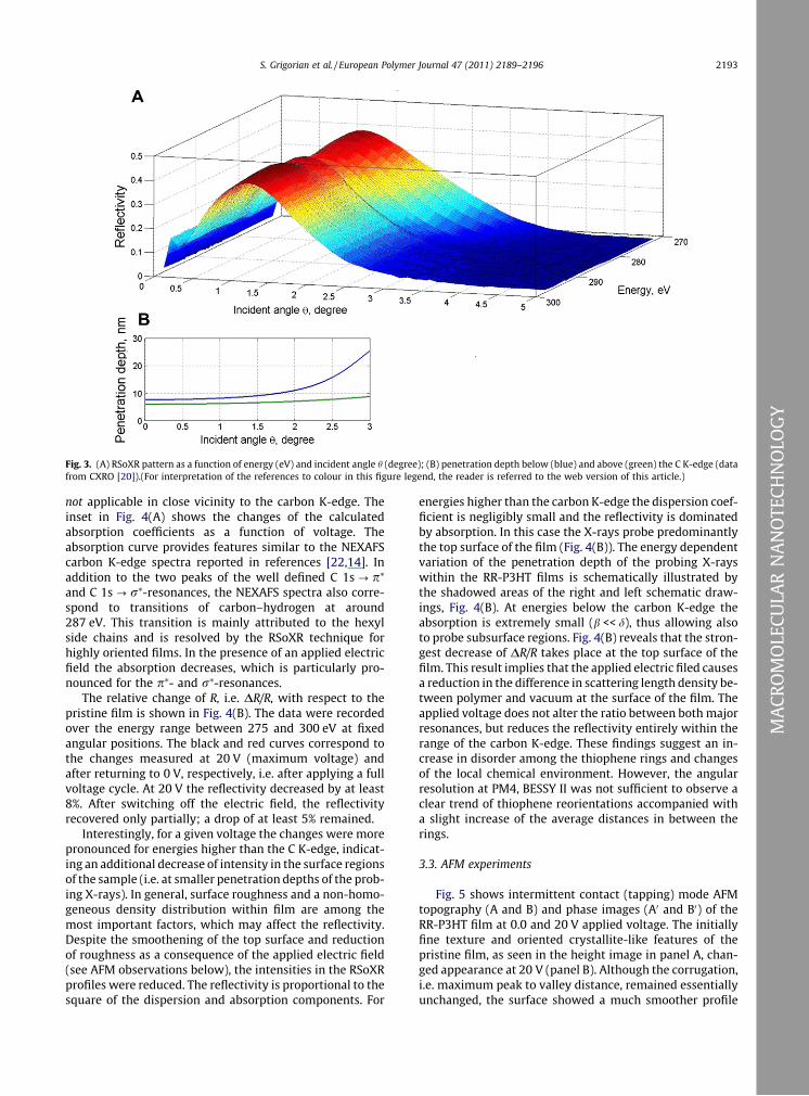
Fig. 3. (A) RSoXR pattern as a function of energy (eV) and incident angle h (degree); (B) penetration depth below (blue) and above (green) the C K-edge (datafrom CXRO [20]).(For interpretation of the references to colour in this figure legend, the reader is referred to the web version of this article.)
S. Grigorian et al. / European Polymer Journal 47 (2011) 2189–2196 2193
MA
CRO
MO
LECU
LAR
NA
NO
TECH
NO
LOG
Y
not applicable in close vicinity to the carbon K-edge. Theinset in Fig. 4(A) shows the changes of the calculatedabsorption coefficients as a function of voltage. Theabsorption curve provides features similar to the NEXAFScarbon K-edge spectra reported in references [22,14]. Inaddition to the two peaks of the well defined C 1s ? p⁄
and C 1s ? r⁄-resonances, the NEXAFS spectra also corre-spond to transitions of carbon–hydrogen at around287 eV. This transition is mainly attributed to the hexylside chains and is resolved by the RSoXR technique forhighly oriented films. In the presence of an applied electricfield the absorption decreases, which is particularly pro-nounced for the p⁄- and r⁄-resonances.
The relative change of R, i.e. DR/R, with respect to thepristine film is shown in Fig. 4(B). The data were recordedover the energy range between 275 and 300 eV at fixedangular positions. The black and red curves correspond tothe changes measured at 20 V (maximum voltage) andafter returning to 0 V, respectively, i.e. after applying a fullvoltage cycle. At 20 V the reflectivity decreased by at least8%. After switching off the electric field, the reflectivityrecovered only partially; a drop of at least 5% remained.
Interestingly, for a given voltage the changes were morepronounced for energies higher than the C K-edge, indicat-ing an additional decrease of intensity in the surface regionsof the sample (i.e. at smaller penetration depths of the prob-ing X-rays). In general, surface roughness and a non-homo-geneous density distribution within film are among themost important factors, which may affect the reflectivity.Despite the smoothening of the top surface and reductionof roughness as a consequence of the applied electric field(see AFM observations below), the intensities in the RSoXRprofiles were reduced. The reflectivity is proportional to thesquare of the dispersion and absorption components. For
energies higher than the carbon K-edge the dispersion coef-ficient is negligibly small and the reflectivity is dominatedby absorption. In this case the X-rays probe predominantlythe top surface of the film (Fig. 4(B)). The energy dependentvariation of the penetration depth of the probing X-rayswithin the RR-P3HT films is schematically illustrated bythe shadowed areas of the right and left schematic draw-ings, Fig. 4(B). At energies below the carbon K-edge theabsorption is extremely small (b << d), thus allowing alsoto probe subsurface regions. Fig. 4(B) reveals that the stron-gest decrease of DR/R takes place at the top surface of thefilm. This result implies that the applied electric filed causesa reduction in the difference in scattering length density be-tween polymer and vacuum at the surface of the film. Theapplied voltage does not alter the ratio between both majorresonances, but reduces the reflectivity entirely within therange of the carbon K-edge. These findings suggest an in-crease in disorder among the thiophene rings and changesof the local chemical environment. However, the angularresolution at PM4, BESSY II was not sufficient to observe aclear trend of thiophene reorientations accompanied witha slight increase of the average distances in between therings.
3.3. AFM experiments
Fig. 5 shows intermittent contact (tapping) mode AFMtopography (A and B) and phase images (A0 and B0) of theRR-P3HT film at 0.0 and 20 V applied voltage. The initiallyfine texture and oriented crystallite-like features of thepristine film, as seen in the height image in panel A, chan-ged appearance at 20 V (panel B). Although the corrugation,i.e. maximum peak to valley distance, remained essentiallyunchanged, the surface showed a much smoother profile
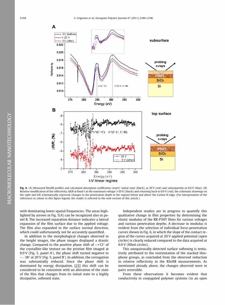
Fig. 4. (A) Measured RSoXR profiles and calculated absorption coefficients (inset): initial state (black), at 20 V (red) and subsequently at 0.0 V (blue). (B)Relative modification of the reflectivity DR/R at fixed h at the maximum voltage (+20 V) (black) and returning back to 0.0 V (red), the schematic drawings onthe right and left schematically represent changes in the penetration depth in the regions below and above the Carbon K-edge. (For interpretation of thereferences to colour in this figure legend, the reader is referred to the web version of this article.)
2194 S. Grigorian et al. / European Polymer Journal 47 (2011) 2189–2196
MA
CRO
MO
LECU
LAR
NA
NO
TECH
NO
LOG
Y
with dominating lower spatial frequencies. The areas high-lighted by arrows in Fig. 5(A) can be recognized also in pa-nel B. The increased separation distance indicates a lateralexpansion of the film surface due to the applied voltage.The film also expanded in the surface normal direction,which could unfortunately not be accurately quantified.
In addition to the morphological changes observed inthe height images, the phase images displayed a drasticchange. Compared to the positive phase shift of �+12� ofthe crystallite-like texture on the pristine film imaged at0.0 V (Fig. 5, panel A0), the phase shift turned negative to��38� at 20 V (Fig. 5, panel B0). In addition, the corrugationwas substantially reduced. Since the phase shift isdominated by energy dissipation, [23] this shift can beconsidered to be consistent with an alteration of the stateof the film that changes from its initial state to a highlydissipative, softened state.
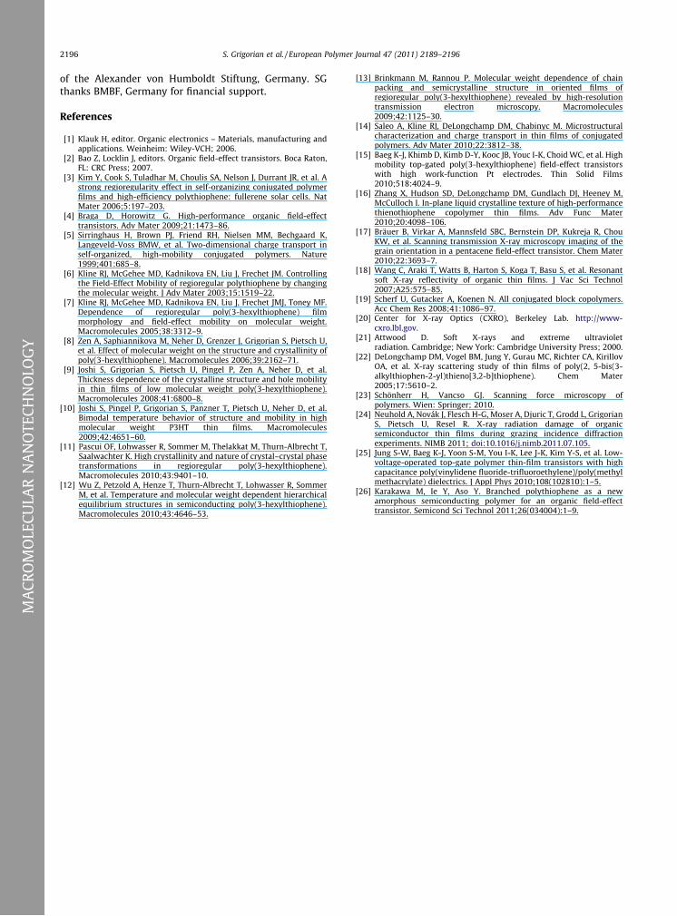
Independent studies are in progress to quantify thisqualitative change in film properties by determining theelastic modulus of the RR-P3HT films for various voltagesand various penetration depths. A decrease in modulus isevident from the selection of individual force-penetrationcurves shown in Fig. 6, in which the slope of the contact re-gion of the curves acquired at 20 V applied potential (opencircles) is clearly reduced compared to the data acquired at0.0 V (filled circles).
This unequivocally detected surface softening is tenta-tively attributed to the reorientation of the stacked thio-phene groups, as concluded from the observed reductionin relative reflectivity in the RSoXR measurements. Asmentioned already above, the changes observed were inparts reversible.
From these observations it becomes evident thatconductivity in conjugated polymer systems (in an open
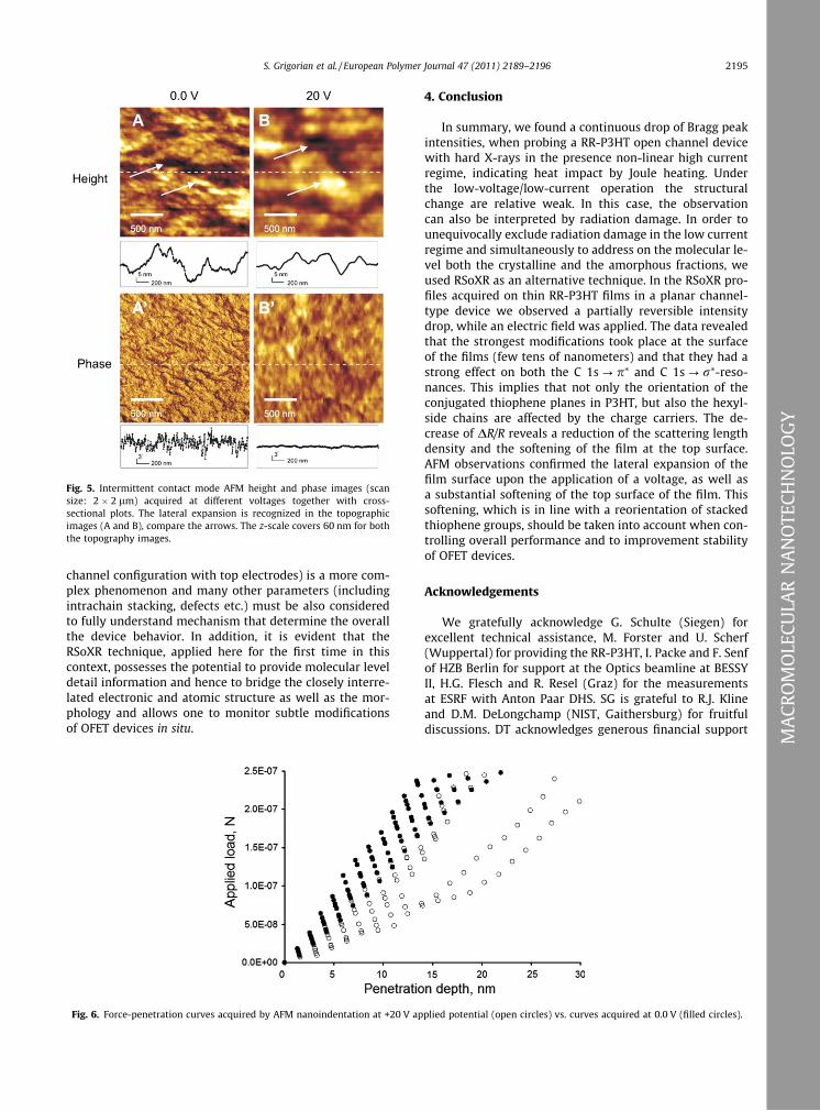
Fig. 5. Intermittent contact mode AFM height and phase images (scansize: 2 � 2 lm) acquired at different voltages together with cross-sectional plots. The lateral expansion is recognized in the topographicimages (A and B), compare the arrows. The z-scale covers 60 nm for boththe topography images.
S. Grigorian et al. / European Polymer Journal 47 (2011) 2189–2196 2195
ACR
OM
OLE
CULA
RN
AN
OTE
CHN
OLO
GY
channel configuration with top electrodes) is a more com-plex phenomenon and many other parameters (includingintrachain stacking, defects etc.) must be also consideredto fully understand mechanism that determine the overallthe device behavior. In addition, it is evident that theRSoXR technique, applied here for the first time in thiscontext, possesses the potential to provide molecular leveldetail information and hence to bridge the closely interre-lated electronic and atomic structure as well as the mor-phology and allows one to monitor subtle modificationsof OFET devices in situ.
Fig. 6. Force-penetration curves acquired by AFM nanoindentation at +20 V ap
4. Conclusion
In summary, we found a continuous drop of Bragg peakintensities, when probing a RR-P3HT open channel devicewith hard X-rays in the presence non-linear high currentregime, indicating heat impact by Joule heating. Underthe low-voltage/low-current operation the structuralchange are relative weak. In this case, the observationcan also be interpreted by radiation damage. In order tounequivocally exclude radiation damage in the low currentregime and simultaneously to address on the molecular le-vel both the crystalline and the amorphous fractions, weused RSoXR as an alternative technique. In the RSoXR pro-files acquired on thin RR-P3HT films in a planar channel-type device we observed a partially reversible intensitydrop, while an electric field was applied. The data revealedthat the strongest modifications took place at the surfaceof the films (few tens of nanometers) and that they had astrong effect on both the C 1s ? p⁄ and C 1s ? r⁄-reso-nances. This implies that not only the orientation of theconjugated thiophene planes in P3HT, but also the hexyl-side chains are affected by the charge carriers. The de-crease of DR/R reveals a reduction of the scattering lengthdensity and the softening of the film at the top surface.AFM observations confirmed the lateral expansion of thefilm surface upon the application of a voltage, as well asa substantial softening of the top surface of the film. Thissoftening, which is in line with a reorientation of stackedthiophene groups, should be taken into account when con-trolling overall performance and to improvement stabilityof OFET devices.
Acknowledgements
We gratefully acknowledge G. Schulte (Siegen) forexcellent technical assistance, M. Forster and U. Scherf(Wuppertal) for providing the RR-P3HT, I. Packe and F. Senfof HZB Berlin for support at the Optics beamline at BESSYII, H.G. Flesch and R. Resel (Graz) for the measurementsat ESRF with Anton Paar DHS. SG is grateful to R.J. Klineand D.M. DeLongchamp (NIST, Gaithersburg) for fruitfuldiscussions. DT acknowledges generous financial support
plied potential (open circles) vs. curves acquired at 0.0 V (filled circles).
M
2196 S. Grigorian et al. / European Polymer Journal 47 (2011) 2189–2196
MA
CRO
MO
LECU
LAR
NA
NO
TECH
NO
LOG
Y
of the Alexander von Humboldt Stiftung, Germany. SGthanks BMBF, Germany for financial support.
References
[1] Klauk H, editor. Organic electronics – Materials, manufacturing andapplications. Weinheim: Wiley-VCH; 2006.
[2] Bao Z, Locklin J, editors. Organic field-effect transistors. Boca Raton,FL: CRC Press; 2007.
[3] Kim Y, Cook S, Tuladhar M, Choulis SA, Nelson J, Durrant JR, et al. Astrong regioregularity effect in self-organizing conjugated polymerfilms and high-efficiency polythiophene: fullerene solar cells. NatMater 2006;5:197–203.
[4] Braga D, Horowitz G. High-performance organic field-effecttransistors. Adv Mater 2009;21:1473–86.
[5] Sirringhaus H, Brown PJ, Friend RH, Nielsen MM, Bechgaard K,Langeveld-Voss BMW, et al. Two-dimensional charge transport inself-organized, high-mobility conjugated polymers. Nature1999;401:685–8.
[6] Kline RJ, McGehee MD, Kadnikova EN, Liu J, Frechet JM. Controllingthe Field-Effect Mobility of regioregular polythiophene by changingthe molecular weight. J Adv Mater 2003;15:1519–22.
[7] Kline RJ, McGehee MD, Kadnikova EN, Liu J, Frechet JMJ, Toney MF.Dependence of regioregular poly(3-hexylthiophene) filmmorphology and field-effect mobility on molecular weight.Macromolecules 2005;38:3312–9.
[8] Zen A, Saphiannikova M, Neher D, Grenzer J, Grigorian S, Pietsch U,et al. Effect of molecular weight on the structure and crystallinity ofpoly(3-hexylthiophene). Macromolecules 2006;39:2162–71.
[9] Joshi S, Grigorian S, Pietsch U, Pingel P, Zen A, Neher D, et al.Thickness dependence of the crystalline structure and hole mobilityin thin films of low molecular weight poly(3-hexylthiophene).Macromolecules 2008;41:6800–8.
[10] Joshi S, Pingel P, Grigorian S, Panzner T, Pietsch U, Neher D, et al.Bimodal temperature behavior of structure and mobility in highmolecular weight P3HT thin films. Macromolecules2009;42:4651–60.
[11] Pascui OF, Lohwasser R, Sommer M, Thelakkat M, Thurn-Albrecht T,Saalwachter K. High crystallinity and nature of crystal–crystal phasetransformations in regioregular poly(3-hexylthiophene).Macromolecules 2010;43:9401–10.
[12] Wu Z, Petzold A, Henze T, Thurn-Albrecht T, Lohwasser R, SommerM, et al. Temperature and molecular weight dependent hierarchicalequilibrium structures in semiconducting poly(3-hexylthiophene).Macromolecules 2010;43:4646–53.
[13] Brinkmann M, Rannou P. Molecular weight dependence of chainpacking and semicrystalline structure in oriented films ofregioregular poly(3-hexylthiophene) revealed by high-resolutiontransmission electron microscopy. Macromolecules2009;42:1125–30.
[14] Saleo A, Kline RJ, DeLongchamp DM, Chabinyc M. Microstructuralcharacterization and charge transport in thin films of conjugatedpolymers. Adv Mater 2010;22:3812–38.
[15] Baeg K-J, Khimb D, Kimb D-Y, Kooc JB, Youc I-K, Choid WC, et al. Highmobility top-gated poly(3-hexylthiophene) field-effect transistorswith high work-function Pt electrodes. Thin Solid Films2010;518:4024–9.
[16] Zhang X, Hudson SD, DeLongchamp DM, Gundlach DJ, Heeney M,McCulloch I. In-plane liquid crystalline texture of high-performancethienothiophene copolymer thin films. Adv Func Mater2010;20:4098–106.
[17] Bräuer B, Virkar A, Mannsfeld SBC, Bernstein DP, Kukreja R, ChouKW, et al. Scanning transmission X-ray microscopy imaging of thegrain orientation in a pentacene field-effect transistor. Chem Mater2010;22:3693–7.
[18] Wang C, Araki T, Watts B, Harton S, Koga T, Basu S, et al. Resonantsoft X-ray reflectivity of organic thin films. J Vac Sci Technol2007;A25:575–85.
[19] Scherf U, Gutacker A, Koenen N. All conjugated block copolymers.Acc Chem Res 2008;41:1086–97.
[20] Center for X-ray Optics (CXRO), Berkeley Lab. http://www-cxro.lbl.gov.
[21] Attwood D. Soft X-rays and extreme ultravioletradiation. Cambridge; New York: Cambridge University Press; 2000.
[22] DeLongchamp DM, Vogel BM, Jung Y, Gurau MC, Richter CA, KirillovOA, et al. X-ray scattering study of thin films of poly(2, 5-bis(3-alkylthiophen-2-yl)thieno[3,2-b]thiophene). Chem Mater2005;17:5610–2.
[23] Schönherr H, Vancso GJ. Scanning force microscopy ofpolymers. Wien: Springer; 2010.
[24] Neuhold A, Novák J, Flesch H-G, Moser A, Djuric T, Grodd L, GrigorianS, Pietsch U, Resel R. X-ray radiation damage of organicsemiconductor thin films during grazing incidence diffractionexperiments. NIMB 2011; doi:10.1016/j.nimb.2011.07.105.
[25] Jung S-W, Baeg K-J, Yoon S-M, You I-K, Lee J-K, Kim Y-S, et al. Low-voltage-operated top-gate polymer thin-film transistors with highcapacitance poly(vinylidene fluoride-trifluoroethylene)/poly(methylmethacrylate) dielectrics. J Appl Phys 2010;108(102810):1–5.
[26] Karakawa M, Ie Y, Aso Y. Branched polythiophene as a newamorphous semiconducting polymer for an organic field-effecttransistor. Semicond Sci Technol 2011;26(034004):1–9.
Copyright © 2022 FDOKUMEN