Space-Grade, 100-krad, Voltage-Controlled Current Sink (0 ...
12
Application Brief Space-Grade, 100-krad, Voltage-Controlled Current Sink (0–200 mA) Circuit Fadi Matloob Design Goals Parameter Design Goal Supply Voltage Single Supply, 12V DAC Output Range 0V–4.9V Current Sink Control Voltage 0mV–500mV Output Current Range 0mA–200mA Uncalibrated Accuracy ±2% (±4mA) Calibrated Accuracy ±1% (±2mA) Total Ionizing Dose (TID) 100-krad(Si) Single Event Latch-up (SEL) Immunity 85 MeV·cm 2 /mg Design Description Voltage controlled current sinks are an integral part of many current-controlled space applications. One of its most popular applications is adjustable-current, laser diode drivers which are often used in laser communications systems (also known as optical inter-satellite links (OISL)). The circuit is also seen in other applications like LiDAR which might benefit from laser diodes. It consists of three main elements: the sense resistor (R Sense ), an N-channel MOSFET (Q1), and an operational amplifier (op amp) that controls the MOSFET. The basic operating principle of the circuit starts with current flowing through the load from a voltage supply (in this case 5 V). As current flows through the load, a voltage is developed on R Sense . The op amp uses the sensed voltage as feedback and drives its output until the sensed voltage is equal to the DAC output (non-inverting input). In this case, Q1 is operated in the linear region and serves as a voltage-controlled resistance. The components: Riso, CF, and RF are used to compensate the circuit and ensure stable operation. DAC121S101QML-SP U2 - DAC Riso 75 Q1 JANSR2N7467U2 + – U1A ¼ LMP7704-SP 15 Resistive Load 5 V GND RSense 2.5 CF 30 nF RF 1k 5 V R1 13.2 k R2 1.50 k 12 V 12 V CIN_LDO 10 F GND GND TPS7A4501-SP U3 - LDO COUT_LDO 10 F GND 5 V CREF 60 F Current Sink Circuit 12.0 V to 5.0 V Supply Current Sink Control LM4050QML-SP 5.0-V Reference RREF 1.0 k RB 3.7 k RT 11.5 k www.ti.com SNOAA79 – JUNE 2021 Submit Document Feedback Space-Grade, 100-krad, Voltage-Controlled Current Sink (0–200 mA) Circuit 1 Copyright © 2021 Texas Instruments Incorporated
-
Upload
khangminh22 -
Category
Documents
-
view
0 -
download
0
Transcript of Space-Grade, 100-krad, Voltage-Controlled Current Sink (0 ...
Application BriefSpace-Grade, 100-krad, Voltage-Controlled Current Sink (0–200 mA) Circuit
Fadi Matloob
Design Goals
Parameter Design GoalSupply Voltage Single Supply, 12V
DAC Output Range 0V–4.9V
Current Sink Control Voltage 0mV–500mV
Output Current Range 0mA–200mA
Uncalibrated Accuracy ±2% (±4mA)
Calibrated Accuracy ±1% (±2mA)
Total Ionizing Dose (TID) 100-krad(Si)
Single Event Latch-up (SEL) Immunity 85 MeV·cm2/mg
Design Description
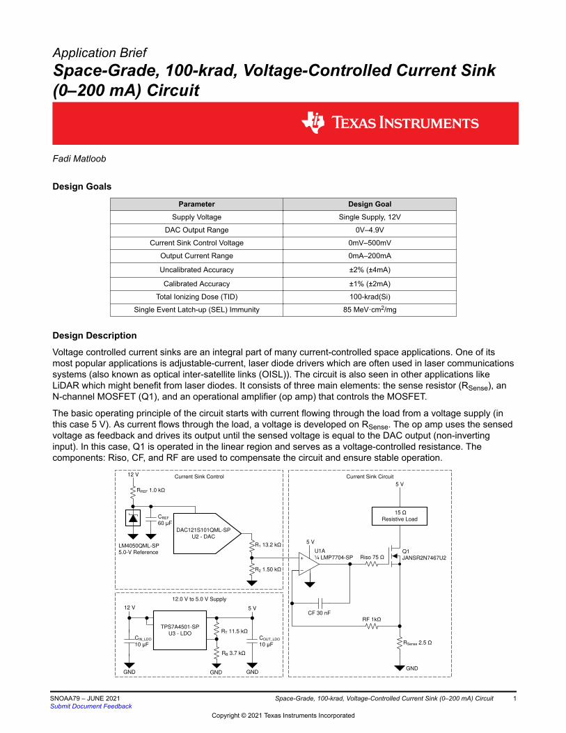
Voltage controlled current sinks are an integral part of many current-controlled space applications. One of its most popular applications is adjustable-current, laser diode drivers which are often used in laser communications systems (also known as optical inter-satellite links (OISL)). The circuit is also seen in other applications like LiDAR which might benefit from laser diodes. It consists of three main elements: the sense resistor (RSense), an N-channel MOSFET (Q1), and an operational amplifier (op amp) that controls the MOSFET.
The basic operating principle of the circuit starts with current flowing through the load from a voltage supply (in this case 5 V). As current flows through the load, a voltage is developed on RSense. The op amp uses the sensed voltage as feedback and drives its output until the sensed voltage is equal to the DAC output (non-inverting input). In this case, Q1 is operated in the linear region and serves as a voltage-controlled resistance. The components: Riso, CF, and RF are used to compensate the circuit and ensure stable operation.
DAC121S101QML-SP
U2 - DAC
Riso 75 Q1
JANSR2N7467U2 +
±
U1A
¼ LMP7704-SP
15
Resistive Load
5 V
GND
RSense 2.5
CF 30 nFRF 1k
5 VR1 13.2 k
R2 1.50 k
12 V
12 V
CIN_LDO
10 F
GND GND
TPS7A4501-SP
U3 - LDOCOUT_LDO
10 F
GND
5 V
CREF
60 F
Current Sink Circuit
12.0 V to 5.0 V Supply
Current Sink Control
LM4050QML-SP
5.0-V Reference
RREF 1.0 k
RB 3.7 k
RT 11.5 k
www.ti.com
SNOAA79 – JUNE 2021Submit Document Feedback
Space-Grade, 100-krad, Voltage-Controlled Current Sink (0–200 mA) Circuit 1
Copyright © 2021 Texas Instruments Incorporated

Design Notes
• Use a high-precision and low-drift resistor for RSense.• The RSense power rating should be considered to ensure that no failures occur at the desired current load.• If a large resistive load is present, a separate high-voltage supply may be used for driving the current to the
load.• The LMP7704-SP supply voltage of 5V was selected according the derating specifications provided by the
National Aeronautics and Space Administration (NASA) in document EEE-INST-002 (April 2008) and the European Cooperation for Space Standardization (ECSS) in document ECSS-Q-ST-30-11C Rev.1 (4 October 2011). The documents specify a derating of the absolute maximum supply voltage for linear ICs to at least 80% and 90%, respectively.
• For proper operation, the power supplies must be decoupled. For supply decoupling, TI recommends placing 10-nF to 1-µF capacitors as close as possible to the op-amp power supply pins. For the single supply configuration shown, place a capacitor between the V+ and V– supply pins. Bypass capacitors must have a low ESR of less than 0.1Ω.
www.ti.com
2 Space-Grade, 100-krad, Voltage-Controlled Current Sink (0–200 mA) Circuit SNOAA79 – JUNE 2021Submit Document Feedback
Copyright © 2021 Texas Instruments Incorporated

Design Steps
Component Selection
1. Identify the current sink specifications:• Specifications for the circuit shown:
– Input voltage range (DAC output): 0mV to 500mV– Resistive load: 15Ω– Load current range: 0mA to 200mA– Current error: ±4mA
2. Sense resistor selection (RSense):• The selection of RSense comes down to power dissipation versus precision.
– Smaller values of RSense yield smaller voltage drops for the same amount of current and ultimately dissipate less power. However, since the RSense voltage drop is smaller, higher precision components may need to be used to achieve the same error tolerance.
– Higher values of RSense can be created by paralleling resistors to share the power dissipation.• In the circuit shown, the RSense value is selected based on the maximum DAC output voltage (VDACMax)
and the maximum load current (IMax) as shown:RSense = VDACMaxIMaxRSense = 2.5Ω = 500mV200mA
• In this case, the 2.5-Ω RSense produces a voltage of 10mV per 4mA of load current. Therefore, to meet the desired current error specification of ±4mA, the total voltage error should be less than 10mV (2.5Ω × 4mA). The total voltage error includes the offset voltage error from the op amp, the op amp input bias current error through resistor RF, DAC output error, and the RSense resistor error.– Fortunately, the LMP7704-SP has great DC performance with a typical offset voltage of ±32µV and a
typical input bias current of ±0.2pA. Calculate the error contribution as follows:Error mV = Vos + IB × RF × 1000Error mV = 0.032mV = ±32uV + ±0.2pA × 1kΩ × 1000– The DC error of the amplifier, as shown, is not a significant contributor to the allowed 10mV of error.– In many cases, most of the error is observed from the RSense tolerance, RSense drift, and the DACs
offset error, gain error, and drift.– Use the DAC121S101QML-SP to achieve the circuit requirements and maintain the radiation
performance.3. Amplifier selection (U1A):
• The amplifier selection is rather straightforward. From the perspective of meeting the current error specifications, consider the offset voltage of the op amp and its input bias current (as shown previously in the Sense Resistor Selection section).
• The op amp should also have an input common-mode range that extends to the negative rail (GND in this case) to support the low output range of the DAC. However, there is a hidden criterion for selection under one or both of the following two conditions: (1) the MOSFET has a threshold voltage (VGS(th)) close to the available supply rail, (2) the resistive load of the system is close to the maximum load the supply rail can handle.
• The hidden criterion is the output voltage swing of the op amp. Looking the circuit, the selected MOSFET Q1 has a maximum VGS(th) across TID exposure of 4V and the circuit supply rail is 5V. At peak current, the source voltage of the MOSFET is at 0.5V which is also the voltage across RSense (200mA × 2.5Ω). In this case, the op amp with the 5-V supply must be able to swing to at least (V+) – 0.5V or 4.5V to reach VGS(th). Similarly, in the case of condition (2) the op amp must be able to swing close to the positive rail to maximize the largest resistive load that can be driven.
www.ti.com
SNOAA79 – JUNE 2021Submit Document Feedback
Space-Grade, 100-krad, Voltage-Controlled Current Sink (0–200 mA) Circuit 3
Copyright © 2021 Texas Instruments Incorporated

• Calculate the largest resistive load as follows (assuming no voltage drop across Q1):RLoadMax = VCC − IMax × RSenseIMaxRLoadMax = 22.5Ω = 5V − 200mA × 2.5Ω200mA4. MOSFET selection:
• Ensure that the MOSFET VGS(th) can be driven by the op amp and that it can handle the power dissipation for the expected load resistance and maximum current:PQ1 = VCC × IMax− IMax2 × RLoad+ RSense
PQ1 = 0.3W = 5V × 200mA − 200mA 2 × 15Ω+ 2.5Ω5. Current Sink Control Circuit
DAC121S101QML-SP
U2 - DAC
R1 13.2 k
R2 1.50 k
12 V
CREF
60 F
LM4050QML-SP
5.0-V Reference
RREF 1.0 k
VCTRL
• The DAC121S101QML-SP can provide a means of adjusting the voltage used to control the current sink.• The LM4050QML-SP provides a 5.0-V reference to the DAC. When CREF = 60μF, the LM4050QML-SP is
immune to SETs.• Since the DAC121S101QML-SP is a 12-bit DAC, it could have errors in the range of 10s of millivolts,
which would dominate the system error. Therefore, the output voltage is scaled down by a factor of 5/49, given a maximum DAC operating voltage of 4.9V:VDAC max = 4.9V VCTRL max = 500mV ILOAD max = 200mA
• Scaling down the voltage also means that any error introduced by the DAC121S101QML-SP or the LM4050QML-SP voltage reference are reduced by a factor of 5/49. Using a ratio of 5/49 also allows for the selection of standard 0.1% resistor values. The resistors introduce up to 0.179735% of error given the nominal resistor values and accounting for potential resistor value variation.
• A key consideration for the system accuracy is the error introduced by the DAC and other devices. The error is often referred to as the Total Unadjusted Error (TUE) and is relative to the control voltage (VCTRL) which is the dominant source of error for the circuit. In the circuit, the following error sources must be considered:– LM4050QML-SP 5.0-V Voltage Reference: Initial Accuracy, Drift over temperature (ΔVR/ΔT)– DAC121S101QML-SP DAC: Zero Code Error (ZEC), Gain Error (GE), ZEC Drift, and GE Drift– Resistor Divider (R1 and R2) Tolerance Error– LMP7704-SP: VOS, IOS, and IBIAS
www.ti.com
4 Space-Grade, 100-krad, Voltage-Controlled Current Sink (0–200 mA) Circuit SNOAA79 – JUNE 2021Submit Document Feedback
Copyright © 2021 Texas Instruments Incorporated

• In this circuit, both Beginning of Life (BOL) and temperature tolerances are considered for calculating the VCTRL TUE. Root Sum Square (RSS) is used to represent the added error of all sources. Error contributions from the voltage reference and the DAC are scaled by 5/49 in the TUE calculation.
DAC Data SheetSpecification
TUET= 25°C
Data SheetSpecification
TUEΔT = –55 to 125°C
TUE + Gain Calibration
ΔT = –55 to 125°C
INL (V) 2.75 LSB 3.357E-3 8.0 LSB 9.766E-3 9.766E-3
DNL (V) 0.21 LSB 256.348E-6 1.0 LSB 1.221E-3 1.221E-3
ZCE (V) 4 mV 4.000E-3 10 mV 10.000E-3 10.000E-3
ZCE-Drift (V) –20 µV/°C –3.6E-3 –3.600E-3
GE (V) –0.11% 5.500E-3 1.00% 50.000E-3 1.221E-3
GE-Drift (V) –1 ppm/°C –900.0E-6 –900.000E-6
Volt. Ref.
Initial Acc. (V) 0.23% at IR<1mA
11.500E-3 0.23% at IR<1mA 11.500E-3 9.000E-6
ΔVR/ΔT (V) 34 ppm/°C 30.6E-3 30.600E-3
Op Amp
VOS (V) ±37 μV 37.000E-6 ±500 μV 500.000E-6 500.000E-6
IBIAS (A) ±200 fA 200.000E-12 ±400 pA 400.000E-12 400.000E-12
IBIAS × R2 (V) 300.000E-9 600.000E-9 600.000E-9
VOSDrift (V) ±5 μV/°C 900.000E-6 900.000E-6
Scaling Res.
Resistor Div. 898.674E-6 898.674E-6 898.674E-6
VCTRL RSS TUE (mV) 1.669E-3 6.420E-3 3.718E-3
VCTRL RSS Error% 0.334% 1.284% 0.744%
• The first TUE calculation does not include drift over temperature and achieves less than 1% accuracy. The next TUE calculation accounts for the variation in temperature for ΔT = 180°C (–55 to 125°C) as well as the extreme maximum and minimum values provided in each respective data sheet over temperature. Accounting for both extreme values as well as the effect of temperature drift on certain specifications, the second TUE calculation achieves less 2% TUE.
• In the previous calculation the error is dominated by the Gain Error (GE) of the DAC, which over temperature and radiation can vary as much as 1.0%. The GE accounts for up to 50mV of error at the output of the DAC or 5.102mV when scaled by a factor of 5/49. Reduce this error, as well as the error introduced by the initial accuracy of the reference, by performing gain calibration. With gain calibration, the TUE is reduced to 3.718mV or 0.759% of VCTRL. The calibration allows for the design to achieve 1.0% accuracy.
www.ti.com
SNOAA79 – JUNE 2021Submit Document Feedback
Space-Grade, 100-krad, Voltage-Controlled Current Sink (0–200 mA) Circuit 5
Copyright © 2021 Texas Instruments Incorporated

6. Compensation components selection:• Stability analysis is done in the frequency domain and circuit stability is verified by the small signal
transient step response. The criterion to ensure stability is a minimum phase margin of 45 degrees or a rate-of-closure (ROC) of 20dB/decade at fcl (loop gain, AOLB = 0dB) where the AOL curve intersects 1/β.
• The following open-loop AC simulation breaks the loop at the input and the following equations are used to plot the relevant curves:AOL = Vo1β = VoVFBAOLβ = VFB
• The following figure shows the open-loop AC response of the circuit if Riso, RF, and CF are all zero (not in the circuit). The AOLB phase margin is 13.77° which indicates that the circuit is only marginally stable.
• Cin is the equivalent input capacitance of the LMP7704-SP and is added due to the inductor L1 breaking the interaction of AOLB with the amplifier input capacitance.
5V
5V
5VQ1 JANSR2N7467U2
Cin 25p
L1 1T
+
VG1
C1 1T
RLoad 15
-
++
U1 LMP7704-SP
V1 5
CF 0
RF 0
Riso 0
AOLB
Vin 250mAOL
RSense 2.5
1 AOL
$2/%
• The AC simulation can be verified by the small signal step transient response. The small signal transient step response shows that the circuit has a long settling time with excessive ringing. Therefore, it is highly susceptible to oscillations.
5V
5V
5V
Q1 JANSR2N7467U2
RLoad 15
IOUT:3
RSense 2.5
-
++
U1 LMP7704-SP
+
Vin:1 240m
V1 5
CF 0
RF 0
Riso 0
VOUT:2
• The reason for the instability is: the op amp output impedance interacts with the MOSFET input capacitance and creates a pole in the AOL curve that causes a 40-dB/decade ROC. To compensate the circuit, start by finding the value for the isolation resistor Riso, needed to mitigate the problem. Two things are needed to find Riso, (1) the frequency where AOL is 20dB (f20dBAOL), previously shown in the figure as 228.3kHz, (2) the input capacitance of the MOSFET which is found in the data sheet as 9.11nF. Then, use the following equation:Riso = 12 × π × f20dBAOL × Cload
www.ti.com
6 Space-Grade, 100-krad, Voltage-Controlled Current Sink (0–200 mA) Circuit SNOAA79 – JUNE 2021Submit Document Feedback
Copyright © 2021 Texas Instruments Incorporated

Riso = 75Ω ≈ 12 × π × 228.3kHz × 9.11nF• For more details on Riso and driving capacitive loads, see TI Precision Labs - Op Amps: Stability -
Capacitive loads.• The new open loop AC response, after adding Riso, is shown next. Even though the second pole in AOL
was eliminated, the circuit remains only marginally stable due to a zero in 1/β caused by the delay from Riso and the input capacitance of the MOSFET in the V-I loop.
5V
5V
5V
Q1 JANSR2N7467U2
Cin 25p
L1 1T
+
VG1
C1 1T
RLoad 15
-
++
U1 LMP7704-SP
V1 5
CF 0
RF 0
Riso 75
AOLB
Vin 250mAOL
RSense 2.5
1 AOL
$2/%
• The simple fix to this is to create a high frequency pole in 1/β and bypass the MOSFET at higher frequencies. By adding the capacitor CF, the amplifier returns to unity gain over the frequency range of interest. Calculate the value of CF by looking at the location of the 1/β zero (fz1/β), shown in the previous figure as 67.78kHz. The value of CF is then calculated as:CF = 12 × π × Riso × fz1β
• With CF added, the new open loop AC response looks like the following:
5V
5V
5V
Q1 JANSR2N7467U2
Cin 25p
L1 1T
+
VG1
C1 1T
RLoad 15
-
++
U1 LMP7704-SP
V1 5
CF 30n
RF 0
Riso 75
AOLB
Vin 250mAOL
RSense 2.5
1 AOL
$2/%
• CF successfully formed the pole in 1/β; however, there is peaking in 1/β that causes instability. This occurs when CF interacts with the transconductance of the MOSFET. The effect of the interaction is two feedback loops to the amplifier. In this case, both feedback loops interact with each other around the resonant frequency. Adding a small value for RF (10Ω) can isolate the two feedback loops. With an RF of 10Ω, the circuit seems to have 70° of phase margin at fcl; however, in reality, it is still not stable. The next figure shows the instability through the rapid phase shifts in AOLB and the peaking in 1/β.
www.ti.com
SNOAA79 – JUNE 2021Submit Document Feedback
Space-Grade, 100-krad, Voltage-Controlled Current Sink (0–200 mA) Circuit 7
Copyright © 2021 Texas Instruments Incorporated

5V
5V
5V
Q1 JANSR2N7467U2
Cin 25p
L1 1T
+
VG1
C1 1T
RLoad 15
-
++
U1 LMP7704-SP
V1 5
CF 30n
RF 10
Riso 75
AOLB
Vin 250mAOL
RSense 2.5
1 AOL
$2/%
• This may be confirmed by looking at the small signal transient step response which shows oscillation at the resonant frequency of about 170kHz for small values of RF.
5V
5V
5V
Q1 JANSR2N7467U2
RLoad 15
IOUT:3
RSense 2.5
-
++
U1 LMP7704-SP
+
Vin:1 240m
V1 5
CF 30n
RF 0 *
Riso 75
VOUT:2
• The final step to stabilizing the circuit is to add a sufficiently large resistor (RF) to flatten out 1/β and fully isolate CF from the MOSFET. Obtain the final value of RF through trial-and-error until the desired small signal step response is achieved. Typically, RF is in the range of 1kΩ to 10kΩ. The final open loop AC response is seen in the AC Simulation Results section. As seen from the previous simulation, different RF values yield different small signal step responses. With a zero or small RF value, oscillations and overshoot is observed. A value of 1kΩ for RF is sufficient to give the desired small signal transient response.
www.ti.com
8 Space-Grade, 100-krad, Voltage-Controlled Current Sink (0–200 mA) Circuit SNOAA79 – JUNE 2021Submit Document Feedback
Copyright © 2021 Texas Instruments Incorporated

Design Simulations
Transient Simulation – Small Signal Step Response
The following figure shows the small signal transient step response has minimal overshoot and indicates that the circuit is stable and has adequate phase margin.
5V
5V
5V
Q1 JANSR2N7467U2
RLoad 15
IOUT:3
RSense 2.5
-
++
U1 LMP7704-SP
+
Vin:1 240m
V1 5
CF 30n
RF 1k
Riso 75
VOUT:2
Compliance Voltage
The following figure shows where the circuit saturates as the load resistance is varied. The maximum supported load is 22.47Ω which is almost exactly as anticipated by the previous maximum load calculation.
5V
5V
5V
V
+
VLoad:2
IOUT:1
Q1 JANSR2N7467U2
RLoad 15
RSense 2.5
-
++
U1 LMP7704-SP
+
Vin:1 500m
V1 5
CF 30n
RF 1k
Riso 75
www.ti.com
SNOAA79 – JUNE 2021Submit Document Feedback
Space-Grade, 100-krad, Voltage-Controlled Current Sink (0–200 mA) Circuit 9
Copyright © 2021 Texas Instruments Incorporated

DC Simulation Results
Load Current
The following plot shows the load current as a function of the input voltage (DAC output voltage). The current goes from 0mA to 200mA as the input voltage changes from 0mV to 500mV. This meets the design specifications.
5V
5V
5V
Q1 JANSR2N7467U2Riso 75
RF 1k
CF 30n
V1 5
+
Vin:1 240m
-
++
U1 LMP7704-SP
RSense 2.5
IOUT:3
RLoad 15
AC Simulation Results
Stability
The following plot shows the open-loop, AC, gain and phase plot of the circuit. The phase margin is found to be ≈ 62°. The rate-of-closure at fcl (AOLB = 0dB) is 20dB/decade between AOL and 1/β. As discussed previously, components Riso, RF, and CF compensate the circuit and ensure stability. For more details, see TI Precision Labs - Op Amps: Stability - Introduction.
5V
5V
5V
Q1 JANSR2N7467U2
Cin 25p
L1 1T
+
VG1
C1 1T
RLoad 15
-
++
U1 LMP7704-SP
V1 5
CF 30n
RF 1k
Riso 75
AOLB
Vin 250mAOL
RSense 2.5
1 AOL
$2/%
www.ti.com
10 Space-Grade, 100-krad, Voltage-Controlled Current Sink (0–200 mA) Circuit SNOAA79 – JUNE 2021Submit Document Feedback
Copyright © 2021 Texas Instruments Incorporated

Design References
1. Sahu, K., and Leidecker, H. (April 2008). EEE-INST-002: Instructions for EEE Parts Selection, Screening, Qualification, and Derating. Retrieved from https://nepp.nasa.gov/DocUploads/FFB52B88-36AE-4378-A05B2C084B5EE2CC/EEE-INST-002_add1.pdf
2. European Cooperation for Space Standardization. (October 2011). ECSS-Q-ST-30-11C Rev.1 – Derating – EEE components. Retrieved from https://ecss.nl/standard/ecss-q-st-30-11c-rev-1-derating-eee-components-4-october-2011
Design Featured Op Amp
LMP7704-SPVss 2.7V to 12V
VinCM Rail-to-rail
Vout Rail-to-rail
Vos ±32µV
Iq 2.9mA
Ib ±0.2pA
UGBW 2.5MHz
SR 1V / µs
#Channels 4
Total Ionizing Dose (TID) 100-krad(Si)
Single Event Latch-up (SEL) Immunity 85 MeV·cm2/mg
https://www.ti.com/product/LMP7704-SP
Design Alternate Op Amp
LM124AQML-SPVss 3V to 32V
Vos 2mV
Ib 45nA
UGBW 1MHz
SR 0.1V / µs
#Channels 4
Total Ionizing Dose (TID) 100-krad(Si)
SEL Immunity SEL Immune (Bipolar process)
https://www.ti.com/product/LM124AQML-SP
www.ti.com
SNOAA79 – JUNE 2021Submit Document Feedback
Space-Grade, 100-krad, Voltage-Controlled Current Sink (0–200 mA) Circuit 11
Copyright © 2021 Texas Instruments Incorporated

IMPORTANT NOTICE AND DISCLAIMERTI PROVIDES TECHNICAL AND RELIABILITY DATA (INCLUDING DATA SHEETS), DESIGN RESOURCES (INCLUDING REFERENCE DESIGNS), APPLICATION OR OTHER DESIGN ADVICE, WEB TOOLS, SAFETY INFORMATION, AND OTHER RESOURCES “AS IS” AND WITH ALL FAULTS, AND DISCLAIMS ALL WARRANTIES, EXPRESS AND IMPLIED, INCLUDING WITHOUT LIMITATION ANY IMPLIED WARRANTIES OF MERCHANTABILITY, FITNESS FOR A PARTICULAR PURPOSE OR NON-INFRINGEMENT OF THIRD PARTY INTELLECTUAL PROPERTY RIGHTS.These resources are intended for skilled developers designing with TI products. You are solely responsible for (1) selecting the appropriate TI products for your application, (2) designing, validating and testing your application, and (3) ensuring your application meets applicable standards, and any other safety, security, regulatory or other requirements.These resources are subject to change without notice. TI grants you permission to use these resources only for development of an application that uses the TI products described in the resource. Other reproduction and display of these resources is prohibited. No license is granted to any other TI intellectual property right or to any third party intellectual property right. TI disclaims responsibility for, and you will fully indemnify TI and its representatives against, any claims, damages, costs, losses, and liabilities arising out of your use of these resources.TI’s products are provided subject to TI’s Terms of Sale or other applicable terms available either on ti.com or provided in conjunction with such TI products. TI’s provision of these resources does not expand or otherwise alter TI’s applicable warranties or warranty disclaimers for TI products.TI objects to and rejects any additional or different terms you may have proposed. IMPORTANT NOTICE
Mailing Address: Texas Instruments, Post Office Box 655303, Dallas, Texas 75265Copyright © 2022, Texas Instruments Incorporated