
Solid state image pick-up apparatus - EP 0905975 A1
41
(19) J (12) ~ ™ MM II II II MM INI M Ml II II Ml European Patent Office Office europeen des brevets (11) EP 0 905 975 A1 EUROPEAN PATENT APPLICATION (43) Date of publication: (51) int. CI.6: H04N7/01, H 04 N 9/04, 31.03.1999 Bulletin 1999/13 H 04 N 9/64, H 04 N 9/79, (21) Application number: 98122393.6 H 04 N 9/804 (22) Date of filing: 08.10.1993 (84) Designated Contracting States: • Hattori, Jun DE FR c/o Sony Corporation Tokyo (JP) (30) Priority: 09.10.1992 JP 297766/92 (74) Representative: (62) Document number(s) of the earlier application(s) in Melzer, Wolfgang, Dipl.-lng. et al accordance with Art. 76 EPC: Patentanwalte 931 16376.0 / 0 592 005 Mitscherlich & Partner, SonnGnstrdssG 33 (71 ) Applicant: SONY CORPORATION 80331 Munchen (DE) Tokyo (JP) Remarks: (72) Inventors: This application was filed on 25 - 11 - 1998 as a • Asaida, Takashi divisional application to the application mentioned c/o Sony Corporation under INID code 62. Tokyo (JP) LO LO O <7> O Q_ LU (54) Solid state image pick-up apparatus (57) A solid-state image pickup apparatus for gener- ating digital image pickup data from image pickup sig- nals produced by a solid- state image sensor (IG, IR, IB, 2). The solid-state image pickup device digitizes the image pickup signals outputted from at least a solid- state image sensor (IG, IR, IB) driven at an fsi rate with a predetermined phase by a predetermined analog-to- digital converting unit (3) to form digital image data, generates a digital luminance signal Y and two digital chrominance signals CR, CB from the digital image data by a first digital processing unit (41) operated at a clock rate related to the rate fsi , and converts the signals Y CR and CB having an input data rate related to the fsi rate into signals Y CR and CB having an output data rate related to the fs2 rate by a second digital processor (42, 5). The second digital processor (42, 5) performs band- width limitation on the input data rate signals Y CR and CB generated by the first signal processor (41), at out- put data rates of 2fs1 , fsi and fsi , by a half band filter having a passband of fs2, fs2/2 and fs2/2 and performs rate conversion of from 2fs1 to fs2, from fs1 to fs2/2, from fs2/4, fsi to fs2/2 or fs2/4, for outputting the low order lin- ear phase finite impulse response sufficient to suppress high-order sideband components in the vicinity of n p 2fsi, n p fsi and npfsl,n being a positive integer, in a form that can be down-sampled at fs2, fs2/2 or fs2/4, fs2/2 or fs2/4. Besides, the bandpass roll-off characteristics of the rate converting filter may be compensated by the characteristics of the half band filter. This renders it pos- sible to perform rate conversion reliably by the second digital processing unit (42, 5) having a simplified con- struction. FIG.1 Printed byXerox (UK) Business Services 2.16.7/3.6
-
Upload
khangminh22 -
Category
Documents
-
view
1 -
download
0
Transcript of Solid state image pick-up apparatus - EP 0905975 A1

(19) J
(12)
~ ™ MM II II II M M INI M Ml II II Ml European Patent Office
Office europeen des brevets (11) E P 0 9 0 5 9 7 5 A 1
EUROPEAN PATENT A P P L I C A T I O N
(43) Date of publication: (51) int. CI.6: H04N7/01 , H 04 N 9/04, 31.03.1999 Bulletin 1999/13 H 04 N 9/64, H 04 N 9/79,
(21) Application number: 98122393.6 H 04 N 9 / 8 0 4
(22) Date of filing: 08.10.1993
(84) Designated Contracting States: • Hattori, Jun DE FR c/o Sony Corporation
Tokyo (JP) (30) Priority: 09.10.1992 JP 297766/92
(74) Representative: (62) Document number(s) of the earlier application(s) in Melzer, Wolfgang, Dipl.-lng. et al
accordance with Art. 76 EPC: Patentanwalte 931 1 6376.0 / 0 592 005 Mitscherlich & Partner,
SonnGnstrdssG 33 (71 ) Applicant: SONY CORPORATION 80331 Munchen (DE)
Tokyo (JP) Remarks:
(72) Inventors: This application was filed on 25 - 1 1 - 1998 as a • Asaida, Takashi divisional application to the application mentioned
c/o Sony Corporation under INID code 62. Tokyo (JP)
LO
LO O <7> O Q_ LU
(54) Solid state image pick-up apparatus
(57) A solid-state image pickup apparatus for gener- ating digital image pickup data from image pickup sig- nals produced by a solid- state image sensor (IG, IR, IB, 2). The solid-state image pickup device digitizes the image pickup signals outputted from at least a solid- state image sensor (IG, IR, IB) driven at an fsi rate with a predetermined phase by a predetermined analog-to- digital converting unit (3) to form digital image data, generates a digital luminance signal Y and two digital chrominance signals CR, CB from the digital image data by a first digital processing unit (41) operated at a clock rate related to the rate fsi , and converts the signals Y CR and CB having an input data rate related to the fsi rate into signals Y CR and CB having an output data rate related to the fs2 rate by a second digital processor (42, 5). The second digital processor (42, 5) performs band- width limitation on the input data rate signals Y CR and CB generated by the first signal processor (41), at out- put data rates of 2fs1 , fsi and fsi , by a half band filter having a passband of fs2, fs2/2 and fs2/2 and performs rate conversion of from 2fs1 to fs2, from fs1 to fs2/2, from fs2/4, fsi to fs2/2 or fs2/4, for outputting the low order lin- ear phase finite impulse response sufficient to suppress high-order sideband components in the vicinity of n p 2fsi, n p fsi and npfsl,n being a positive integer, in a form that can be down-sampled at fs2, fs2/2 or fs2/4, fs2/2 or fs2/4. Besides, the bandpass roll-off characteristics of the rate converting filter may be compensated by the
characteristics of the half band filter. This renders it pos- sible to perform rate conversion reliably by the second digital processing unit (42, 5) having a simplified con- struction.
FIG.1
Printed by Xerox (UK) Business Services 2.16.7/3.6

EP 0 905 975 A1
Description
BACKGROUND OF THE INVENTION
5 1 . Field of the Invention
[0001 ] This invention relates to a solid-state image pickup apparatus for producing digitized picture data from image pickup signals produced by a solid-state image sensor such as a CCD image sensor made up of charge-coupled devices (CCDs) and outputting the produced digitized picture data. More particularly, it relates to a solid-state image
10 pickup apparatus having a rate converting function of converting the data clock rates of the generated picture data. [0002] It is known in general that, in a solid-state image pickup apparatus having, as image pickup means, a solid- state image sensor having a discrete pixel structure, such as a CCD image sensor, since the solid-state image sensor itself is a sampling system, aliasing components from the spatial sampling frequency tend to be mixed into the image pickup signal from the solid-state image sensor. The conventional practice for preventing the generation of aliasing
15 components into the baseband component of the image pickup signals is to provide a double refraction type optical low- pass filter in the image pickup optical system to suppress high-frequency components of the baseband component of the image pickup signals to satisfy the Nyquist conditions of the sampling system constituted by the solid-state image sensor. [0003] On the other hand, with a color television camera device for imaging a color picture, a multiple CCD plate type
20 solid-state image pickup apparatus, such as a two CCD plate type solid-state image pickup apparatus, for imaging a three-color picture by a solid-state image sensor having for imaging a green-colored picture and a solid-state image sensor having a color coding filter for red-colored and blue-colored pictures, or a three CCD plate type solid-state image pickup apparatus for imaging a three-color picture by separate solid-state image sensors, has been put to practical use. [0004] Besides, as a technique for improving the resolution in the above-described multiple CCD plate type solid-state
25 image pickup apparatus, there is known a spatial pixel shifting method in which the solid-state image sensors for imag- ing red-colored pictures and blue-colored pictures are shifted with respect to the solid-state image sensor for imaging the red-colored picture by one-half the spatial pixel sampling period. By adopting the spatial pixel shifting method, a high resolution exceeding the threshold of the number of pixels of the solid-state image sensor may be realized with the multiple CCD plate type solid-state image pickup apparatus with an analog output.
30 [0005] On the other hand, a D-1 standard or a D-2 standard is prescribed as the standard for an industrial digital VTR employed in e.g. a telecasting station. Thus a digital interface for a digital video related equipment conforming to these standards has become necessary to provide for a color television apparatus. [0006] It is noted that with the D-1 standard for 4:2:2 digital component video signals, the sampling frequency is set to 13.5 MHz, corresponding to 858 times the horizontal frequency fH(NTSC) for tne NTSC system and to 864 times the
35 horizontal frequency fH(PAL) for tne PAl- system, and is adapted for being locked at a frequency equal to an integer number times the horizontal frequency for either systems. On the other hand, with the D-2 standard for the digital com- posite video signals, the sampling frequency is set to four times the subcarrier frequency to minimize beat interference between the subcarrier and sampling clocks, with the sampling frequency fs(NTSC) for tne NTSC system and the sam- pling frequency for the PAL system fS(PAL) being 14.3 MHz and 1 7.734 MHz, respectively.
40 [0007] Meanwhile, if it is desired to implement a solid-state image pickup apparatus capable of directly outputting dig- ital picture signals conforming to the above-mentioned D-1 and D-2 standards, such digital picture signals being high in resolution and picture quality and containing only little aliasing distortion components, it is necessary that the sampling rate (number of pixels) of the solid-state image sensor employed in the image pickup unit be set so as to be higher than the sampling rate for the D-1 or D-2 standard, in consideration that the optical low-pass filter as a pref ilter for the solid-
45 state image sensor is optically not unobjectionable, that is that only smooth roll-off characteristics may be obtained with the optical low-pass filter such that high modulation transfer function (MTF) characteristics may be obtained only at the costs of increase in the aliasing distortion components. [0008] Besides, if account is taken of the fact that correction of pixel-based defects in the image pickup signals by the solid-state image sensor is performed by a digital technique, and the beat interference has to be prevented from occur-
so ring, it is desirable that the sampling rate of the solid-state image sensor be coincident with that of the analog-to-digital converting unit adapted for digitizing the image pickup signals supplied by the solid-state image sensor. [0009] The CCD image sensor now in widespread use is driven at the clock rate of 1 4.3 MHz = fSC(NTSC)- Witn a digital camera having its image pickup unit constituted by such CCD image sensor, image pickup signals outputted from the solid-state image sensor are digitized at the above-mentioned clock rate of 14.3 MHz = fSC(NTSC) by way of performing
55 a digital signal processing operation. [0010] However, the clock rate in the D-1 standard, which is the standard for the above-mentioned 4:2:2 digital com- ponent video signals, cannot be matched to the clock rate for the above-mentioned digital camera having its image pickup unit constituted by such CCD image sensor, with the luminance signal Y and the color difference signals CR/CB
2

EP 0 905 975 A1
for the D-1 standard being 13.5 MHz and 6.75 MHz, respectively. If a CCD image sensor having the readout rate of 13.5 MHz is to be fabricated newly for meeting the D-1 standard, there is raised a problem in connection with costs and lim- itation in general adaptability. [001 1 ] On the other hand, with the multiple CCD plate type solid-state image pickup apparatus, constructed in accord-
5 ance with the spatial pixel shifting method, the analog output cannot be improved in resolution unless a signal process- ing system operated at a clock rate of 2fs1 , which is double the clock rate fsi of the CCD image sensor, is employed. Although it may be contemplated to process signals at fsi and 2fs1 and to turn the signals into analog signals at fsi and 2fs1, with the analog signals being then passed through an analog filter so as to be digitized again at the clock rate pre- scribed by the D-1 standard. However, in such case, beat interference is produced between the 14.3 MHz system and
10 the 13.5 MHz system to incur deterioration in picture quality.
OBJECTS OF THE INVENTION
[0012] In view of the above-depicted status of the art, it is an object of the present invention to provide a solid-state 15 image pickup apparatus wherein digital picture signals with the clock rate of the D-1 standard or other clock rates may
be obtained using a standard CCD image sensor. [0013] It is another object of the present invention to provide a solid-state image pickup apparatus wherein high pic- ture quality digital picture signals free of beat interference may be produced with the aid of a signal processing system operated at the same clock rate as the clock rate for the CCD image sensor.
20 [0014] It is a further object of the present invention to provide a solid-state image pickup apparatus wherein the digital picture signal with a high modulation transfer function (MTF) may be obtained with the use of the spatial pixel shifting method. [0015] It is yet another object of the present invention to provide a solid-state image pickup apparatus which is sim- plified in construction by simplifying the construction of digital processing means performing a rate converting opera-
25 tion.
SUMMARY OF THE INVENTION
[0016] In view of the above objects, the present invention provides a solid-state image pickup apparatus comprising 30 at least one solid-state image sensor driven at a rate fsi , an analog-to-digital converting unit for digitizing picture signals
outputted from the solid-state image sensor at the rate fsi of a predetermined phase, a first digital processing unit for generating at least a digital luminance signal Y and two digital color difference signals CR and CB from the picture data digitized by the digital-to-analog converting unit, and a second digital processing unit for converting the input data rate signals Y CR and CB related to the above rate fsi generated by the first digital processing unit into signals Y CR and CB
35 having the output data rate related to the above rate fsi . The second digital processing unit comprises a half band filter having a passband of fs2/2, fs2/4, fs2/4 for performing bandwidth limitation on the input data rate signals Y CR and CB generated by the first digital processing unit, at the output data rates of 2fs1 , fsi , fsi , and a rate converting filter for per- forming rate conversion of from 2fs1 to fs2, from fs1 to fs2/2 or fs2/4, from fs1 to fs2/2 or fs2/4, for outputting the low order linear phase finite impulse response sufficient to suppress high-order sideband components in the vicinity of n x 2fs1 , n
40 x fs1, n x fs1, n being a positive integer, in a form that can be down-sampled at fs2, fs2/2 or fs2/4, fs2/2 or fs2/4, with the half band filter having characteristics of compensating bandpass roll-off characteristics of the rate converting filter. [0017] With the solid-state image pickup apparatus according to the present invention, the rate converting filter has at least one zero point at n x 2fs1 , n x fs1 , n x fs1 and each two zero points in the vicinity thereof. [0018] With the solid-state image pickup apparatus according to the present invention, the rate converting filter is con-
45 stituted by a plurality of multipliers. [001 9] With the solid-state image pickup apparatus according to the present invention, the half band filter comprises a product of partial filters each constituted by integer coefficients. [0020] The present invention also provides a solid-state image pickup apparatus comprising a plurality of solid-state image sensors arranged in a color-separating system in accordance with the spatial pixel shifting method so as to be
so driven at a predetermined rate of fsi , analog-to-digital converting means coupled to the image sensors for digitizing the image signals at a rate of fsi , first digital processing means supplied with the image signals digitized by the analog-to- digital converting means for providing at least a digital luminance signal Y (2fs1) having a rate equal to 2fs1 and two dig- ital color difference signals CR (fsi) and CB (fsi) each having a rate equal to fsi, second digital processing means cou- pled to the first digital processing means for converting the data rate of the input data rate signals Y (2fs1), CR (fsi), CB
55 (fs1) from m to n, m and n being natural numbers, for providing a digital luminance signal Y(fs2) having a rate equal to f s2 = 2f s1 • n/m and two color difference signals CR (fs2) and CB (fs2) having a rate substantially equal to fs2/2. [0021 ] The second digital processing unit in the solid-state image pickup apparatus according to the present invention comprises a half band filter having a passband of fs2, fs2/2 and fs2/2 for the input data rate signals Y (2fs1), CR (fsi) and
3

EP 0 905 975 A1
Cb (fsi). respectively, generated by the first digital processing unit at output data rates of 2fs1 , fs1 and fsi , respectively, and a rate converting filter for performing suppression of high-order side-band components in the vicinity of n x 2fs1 , n x fs1 and n x fs1 , respectively, on signals Y (2fs1), CR (fsi) and CB (fsi) supplied via the half band filter in the down-sam- pled form of fs2, fS2/2 and fs2/2, respectively, q being a natural number.
5 [0022] The solid-state image pickup device digitizes image pickup (picture) signals outputted from at least a solid- state image sensor driven at a rate fsi, at a rate fsi with a predetermined phase by a predetermined analog-to-digital converting unit to form digital image pickup data, generates a digital luminance signal Y and two digital chrominance signals CR, CB from the digital image pickup data by a first digital processing unit operated at a clock rate related to the rate fsi , and converts the signals Y CR and CB having an input data rate related to the fsi rate into signals Y CR and
10 CB having an output data rate related to the fs2 rate by a second digital processing unit. The second digital processing unit performs bandwidth limitation on the input data rate signals Y CR and CB, generated by the first signal processor, at output data rates of 2fs1 , fsi and fsi , by a half band filter having a passband of fs2/2, fs2/4 and fs2/4, respectively, and performs rate conversion of from 2fs1 to fs2, from fsi to fs2/2 or fs2/4, from fsi to fs2/2 or fs2/4, for outputting the low order linear phase finite impulse response sufficient to suppress high-order sideband components in the vicinity of n x 2fs1 , n
15 x fs1 , n x fs1 , n being a positive integer, in a form that can be down-sampled at fs2, fs2/2 or fs2/4, fs2/2 or fs2/4, respec- tively. Besides, the bandpass roll-off characteristics of the rate converting filter may be compensated by the character- istics of the half band filter. [0023] With the solid-state image pickup apparatus according to the present invention, the signal limited in bandwidth by the half band filter is rate-converted by a rate converting filter having an integer coefficient impulse response having
20 at least one zero point at n x 2fs1 , n x fs1 and n x fs1 and each two zero points in the vicinity thereof. [0024] With the solid-state image pickup apparatus according to the present invention, the signals limited in bandwidth by the half band filter are rate-converted by a rate converting filter. [0025] With the solid-state image pickup apparatus according to the present invention, the input data rate signals Y CR and CB generated by the first digital processing unit, are limited in bandwidth by a half band filter comprising a prod-
25 uct of partial filters each constituted by integer coefficients. [0026] Besides, with the solid-state image pickup apparatus according to the present invention, output image pickup signals of plural solid-state image sensors arranged in the color-separation optical system in accordance with the spa- tial pixel shifting method so as to be driven at the rate fsi are digitized by the analog-to-digital converting unit at the rate fsi having a predetermined phase, at least a 2fs1 rate digital luminance signals Y (2fs1) and two fsi rate digital color dif-
30 ference signals CR (fsi) and CB (fsi) are generated by the first digital processing unit from the digitized image pickup data and rate-converted by the second digital processing unit from m to n, m and q being positive integers, for generat- ing digital luminance signals Y (fs2) having the rate of f s2 = f s1 • n/m and digital color difference signals CR (fs2) and CB (fS2) CB having substantially the data rate of fs2/2. [0027] On the other hand, with the solid-state image pickup apparatus according to the present invention, the second
35 digital processing unit performs bandwidth limitation on the input rate signals Y (2fs1), CR (fsi) and CB (fsi) generated by the first digital processing unit at the output rates of 2fs1 , fsi and fsi , by a half band filter having a passband of fs2/2, fs2/4 and fs2/4, respectively, and generates digital color difference signals CR (fs2), CB (fs2) CB having substantially the rate of fs2/2.
40 BRIEF DESCRIPTION OF THE DRAWINGS
[0028]
Fig. 1 is a block diagram showing an arrangement of a digital cam corder embodying the present invention. 45 Fig. 2 is a block diagram showing an illustrative example of a signal processing section for an analog output in the
digital cam corder shown in Fig. 1 . Fig. 3 is a block diagram showing another illustrative example of a signal processing section for an analog output in the digital cam corder shown in Fig. 1 . Fig. 4 is a block diagram showing an illustrative example of a rate converting circuit for luminance signals in the dig-
so ital cam corder shown in Fig. 1 . Fig. 5 is a block diagram showing the state of connection for a recording mode of the rate converting circuit for lumi- nance signals. Fig. 6 is a block diagram showing the state of connection for a playback mode of the rate converting circuit for lumi- nance signals.
55 Fig. 7 is a block diagram showing an illustrative example of a rate converting circuit for color difference signals in the digital cam corder shown in Fig. 1 . Fig. 8 is a block diagram showing the state of connection for a recording mode of the rate converting circuit for color difference signals.
4

EP 0 905 975 A1
Fig. 9 is a block diagram showing the state of connection for a playback mode of the rate converting circuit for color difference signals. Fig. 10 is a spectral diagram for illustrating the operation of the rate converting circuit for luminance signals. Fig. 1 1 is a timing chart for illustrating the operation of the rate converting circuit for luminance signals.
5 Fig. 12 is a block circuit diagram for illustrating an illustrative construction of a rate converting filter in the rate con- verting circuit for luminance signals. Fig. 13 is a timing chart for illustrating the operation of the rate converting filter for luminance signals. Fig. 14 is a block circuit diagram for illustrating an illustrative construction of a coefficient generator in the rate con- version filter for luminance signals.
10 Fig. 15 is a block circuit diagram for illustrating another illustrative construction of a coefficient generator in the rate conversion filter for luminance signals. Fig. 16 is a timing chart for illustrating the operation of the rate converting circuit for color difference signals. Fig. 17 is a timing chart for illustrating the operation of the rate converting filter for color difference signals. Fig. 18 is a block circuit diagram for illustrating an illustrative construction of the rate converting filter in the rate con-
15 verting circuit for color difference signals. Fig. 19 is a block circuit diagram for illustrating an illustrative construction of a coefficient generator in the rate con- version filter for color difference signals. Fig. 20 is a block circuit diagram for illustrating another illustrative construction of a coefficient generator in the rate conversion filter for color difference signals.
20 Fig. 21 is a graph showing a concrete example of the characteristics of the rate converting filter for luminance sig- nals. Fig. 22 is a block diagram showing the operating state of essential parts for the recording mode of the digital cam corder. Fig. 23 is a block circuit diagram showing the operating state of essential parts for the playback mode of the digital
25 cam corder.
DETAILED DESCRIPTION OF THE PREFERRED EMBODIMENTS
[0029] Referring to the drawings, certain preferred embodiments of the present invention will be explained in detail. 30 [0030] The solid state image pickup apparatus is arranged as shown for example in Fig.1 .
[0031 ] The solid-state imaging device according to the first embodiment shown in Fig. 1 is a digital cam corder in which imaging signals produced by an image pickup unit 1 are digitized so as to be recorded as picture data conforming to the D1 standard. The solid-state image pickup apparatus includes an analog-digital converting unit 3 to which three-color image pickup signals R, G and B produced by the image pick-up unit 1 are supplied via an analog signal processing
35 unit 2, a first digital processing unit 4 to which the color image pick-up data digitized by the A/D converting unit 3 are supplied, a second digital processing unit 5 to which a digital luminance signal Y and two digital color difference signals CR, CB generated by the first digital processing unit 4 are supplied, and a signal processing signal for an analog output 6. A recording/reproducing unit 7 for recording and reproducing picture data conforming to the D1 standard is con- nected to the second digital processing unit 5.
40 [0032] The color image pickup unit 1 is made up of three CCD plate type CCD image sensors 1 R, 1G and 1 B for sep- arating an image pickup light incident thereto from an image pickup lens, not shown, via an optical low-pass filter into three color light components by a color-separating prism, not shown, for forming a three-color picture of an object image. [0033] In the present embodiment, the three CCD image sensors 1 R, 1G and 1 B are arrayed in accordance with a
45 spatial pixel shifting method in which the red-color image pickup CCD image sensor 1 R and the blue-color image pickup CCD image sensor 1 B are arrayed with a spatial shift of one-half the spatial sampling period xs with respect to the green-color image pickup CCD image sensor 1G. [0034] Meanwhile, the present invention may be applied not only to the three CCD plate type solid-state image pickup apparatus constructed in accordance with the spatial pixel shifting method of the present embodiment, but may also be
so applied to a single CCD or double CCD plate type solid-state image pickup apparatus or to a three CCD plate type solid- state image pickup apparatus not constructed in accordance with the spatial pixel shifting method. [0035] Each of the three CCD image sensors 1 R, 1G and 1 B is driven at an fsi rate by a driving clock CK(fsi) gener- ated by a timing generator (TG) 9 on the basis of a 2 fsi rate clock supplied from a voltage controlled oscillator (VCO) 8. [0036] The number of pixels of each of the three CCD image sensors 1 R, 1G and 1 B is selected so that the image
55 pickup charges are read out at a rate of fsi = 910 fH for EIA and at a rate of fsi = 912 fH for CCIR. The oscillation fre- quency of VCO 8 is set to 2fs1 , while the timing generator 9 is adapted for driving the three CCD image sensors 1 R, 1 G and 1 B by the fsi rate driving clocks CK (fs1) obtained by halving the frequency of the clock CK (2fs1). [0037] The respective color image pickup signals R(fs1), G(fs-|) and B(fs1), read out at the fsi rate from the CCD image
5

EP 0 905 975 A1
sensors 1 R, 1G and 1 B, respectively, are supplied to the analog signal processing unit 2. [0038] The analog signal processing unit 2 is made up of a correlated double sampling processing circuits (CDS processing circuits) 21 R, 21G and 21 B, and level controlling circuits 22R, 22G and 22B. The CDS processing circuits 21 R, 21 G and 21 B perform correlated double sampling on the color image pickup signals R, G and B, read out from the
5 CCD image sensors 1 R, 1G and 1 B at the fsi rate, respectively. Besides, the level controlling circuits 22R, 22G and 22B perform level control, such as white balance or black balance control, on the color image pickup signals R, G and B, respectively. [0039] The A/D converter 3, supplied via the analog signal processor 2 with the respective color pickup signals R(fs1), G(fsi) and B(fs1), produced by the image-pickup unit 1, is made up of three A/D converters 3R, 3G and 3B, each having
10 a word length of 1 0 bits. These A/D converters 3R, 3G and 3B are supplied from the timing generator 9 with the driving clocks Ck (fsi) having a predetermined phase and a rate fsi equal to the sampling rate of each of the respective color image pickup signals R(fs1), G(fs-|) and B(fs1). The A/D converters 3R, 3G and 3B of the A/D converting unit 3 digitize the respective color signals R(fs1), G(fsi) and B(fs1) at the rate equal to fsi by the above-mentioned driving clocks CK(fs1), for forming respective digital color signals R(fs1), G(fsi) and B(fs1), having the same signal spectrum as the
15 spectrum of each of the respective color signals R(fs1), G(fsi) and B(fs1), respectively. [0040] Meanwhile, the A/D converters 3R, 3G and 3B may also be designed to have a word length on the order of 1 2 to 14 bits. [0041] The respective color signals R(fs1), G(fs-|) and B(fs1), with the rate equal to fsi, digitized by the A/D converting unit 3, are supplied to the first digital processing unit 4.
20 [0042] The first digital processing unit 4 is made up of a first digital processing circuit 41 and a second digital process- ing circuit 42. [0043] The first digital processing circuit 41 is activated at the rate equal to fsi by the driving clocks CK (fsi) supplied from the timing generator 9 for detecting a variety of correcting signal levels of the respective digital color signals R(fs1), G(fsi) and B(fs1) supplied from the A/D converting unit 3 for storing e.g. white balance controlling data, black balance
25 controlling data, black shading correction data, white shading correction data or defect correction data in a memory 43, converting the respective color signals into analog signals by D/A converters 44R, 44G and 44B, and feeding back the analog color signals to the level controlling circuits 22R, 22G and 22B of the analog signal processing unit 2, respec- tively, for performing white/black balance control, shading correction or defect correction. [0044] Meanwhile, the memory 43 is an SRAM connected to a battery 45 as a backup power source.
30 [0045] Thus, in the present embodiment, the respective color pickup signals R(fs1), G(fs-|) and B(fs1), read out at the rate equal to fsi from the respective CCD image sensors 1 R, 1G and 1 B, are digitized by the A/D converting unit 3 for producing the respective color image pickup signals R(fs1), G(fsi) and B(fs1), respectively, so that the first digital processing circuit 41 may be activated at the rate equal to fsi for performing pixel-based picture processing, such as shading correction or defect correction.
35 [0046] On the other hand, the second digital processing circuit 42 performs picture enhancement, pedestal addition, non-linear processing, such as gamma or knee processing or linear matrix processing, on the respective color image pickup signals R, G and B, processed with the pixel-based processing by the first digital processing circuit 41 . Besides, the second digital processing circuit 42 generates, by the matrix processing, a digital luminance signal Y (2fs1) and two digital color difference signals CR (fsi) and CB (fsi) from the respective color image pickup signals R(fs1), G(fsi) and
40 B(fs1). [0047] It is noted that the second digital processing circuit 42, supplied with the clocks CK (2fs1), having the rate equal to 2 fsi, from the VCO 8, and with the driving clocks CK (fsi), having the rate equal to fsi, from the timing generator 9, is activated with these clocks CK (2fs1) and CK (fsi) as master clocks for performing well-known high resolution processing corresponding to the spatial pixel shifting method in the image pickup unit 1 for generating the digital lumi-
45 nance signal Y (2fs1) having the rate equal to 2fs1 and the two digital color difference signals CR (fsi) and CB (fsi) each having the rate equal to fsi . [0048] Meanwhile, the master clocks CK (2fs1) and CK (fsi) are also supplied to a synchronizing signal generator (SG) 1 1 for generating various synchronizing signals, such as horizontal synchronizing signals HD or vertical synchronizing signals VD.
so [0049] On the other hand, the second digital processing unit 5 performs bidirectional rate conversion between signals having the data rate related to the rate fsi and signals having the data rate related to the rate fs2. For the recording mode, the second digital processing unit 5 converts the signals Y (2fs1), CR (fsi) and CB (fsi), related to the rate fsi, generated by the first digital processing unit 4, into signals Y (fs2), CR (fS2/2) and CB (fS2/2), related to the rate fs2, for supplying the converted data to the recording/reproducing unit 7. For the playback mode, the second digital processing
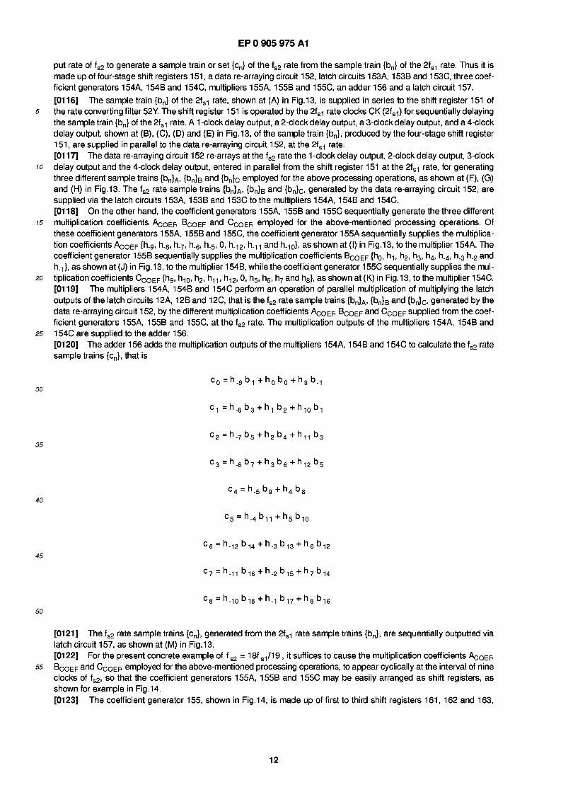
55 unit 5 converts the signals Y (fs2), CR (fS2/2) and CB (fS2/2), related to the rate fs2, into signals Y (2fs1), CR (fsi) and CB (fsi), related to the rate fs2, for supplying the converted data to the signal processing unit for analog output 6. [0050] The second digital processing unit 5 is made up of a rate converting circuit 50Y for the luminance signal and a rate converting circuit 50C for the color difference signals.
6

EP 0 905 975 A1
[0051 ] A digital interface 1 3 for external equipment is provided between the second digital processing unit 5 and the recording/reproducing unit 7. For an external input mode, the second digital processing unit 5 converts digital return sig- nals Y (fs2), CR (fS2/2) and CB (fS2/2), related to the rate fs2, entered from a digital camera control unit (D-CCU) 14 via a camera adapter D-CA 15, into signals Y (2fs1), CR (fsi) and CB (fsi), having the rate fsi, for supplying the converted
5 signals to the signal processing unit for analog output 6. [0052] In the present embodiment, the signal processing unit for analog output 6 plays the role of an analog interface for the signals Y (2fs1), CR (fsi) and CB (fsi), related to the rate fsi , generated by the first digital processing unit 4 or the second digital processing unit 5, and is made up of a digital/analog (D/A) converting unit 61 and an analog encoder 62. [0053] The D/A converting unit 61 is made up of three D/A converters 61 Y 61 CR and 61 CB and three post-filters
10 61 PFY, 61 PFCR and 61 PFCB. [0054] In the D/A converting unit 61 , the digital luminance signal Y (2fs1), having the data rate equal to 2fs1 , is con- verted into an analog signal, which is then freed of a sampling carrier component by the post-filter 61 Y playing the role of a Nyquist filter, before being supplied to the analog encoder 62. On the other hand, the two digital color difference signals CR (fsi) and CB (fsi), having the rate equal to fsi , are converted by the D/A converters 61 CR and 61 CB into ana-
15 log signals, which then are freed of sampling carrier components by the post-filters 61 PFCR and 61 PFCB playing the role of a Nyquist filter, before being supplied to the analog encoder 62. [0055] The analog encoder 62 is an encoder conforming to the usual NTSC or PAL and is adapted for outputting com- ponent signals Y CR and CB and a composite signal CS as well as for outputting a monitor signal YVf to be supplied to a view finder 16.
20 [0056] The analog encoder 62 is constructed as shown for example in Fig.2. [0057] In the analog encoder 62, the two analog color difference signals CR and CB, supplied from the D/A converting unit 61 , are bandwidth-limited to a predetermined bandwidth, with fc being approximately equal to 1 MHz, by low-pass filters 63CR and 63CB, and added to by a burst flag BF by signal synthesizers 64CR and 64CB before being supplied to a modulator 65. The modulator 65 modulates a quadrature 2-phase subcarrier SC by the analog color difference sig-
25 nals CR and CB for generating a modulated chroma signal Cqut- [0058] On the other hand, the analog luminance signal Y supplied by the D/A converter 61 , is compensated for delay caused by the low-pass filters 63CR and 63CB by a delay circuit 66, and subsequently added to by a synchronizing sig- nal and a setup signal by signal synthesizer 67 to form a prescribed luminance signal Yqut- Tne luminance signal Yqut. produced in this manner, is improved in resolution by digital processing corresponding to the above-mentioned spatial
30 pixel shifting method, while containing only little aliasing distortion components. [0059] The luminance signal Yqut anc) tne above-mentioned modulated chroma signal Cqut are mixed by a signal mixer for generating a composite signal CSqut [0060] On the other hand, the luminance signal Yqut is mixed with character signals from a character generator 69 by a signal mixer 70 and subsequently the mixed signal is outputted via a changeover circuit 71 as a monitoring signal
35 YVf The changeover circuit 71 performs switching between a return signal RET entered from outside and the above- mentioned luminance signal YOUt [0061] The signal processing unit for analog output 6 may also be so designed that a digital encoder 73 by a third digital processing unit operated with a clock rate related with the rate equal to fsi is employed in place of the analog encoder 62 . The digital luminance signal Yqut digital composite signal CSqut anc) tne digital monitoring signal YVF,
40 outputted by the digital encoder 73, may be converted into analog signals by D/A converter 74Y, 74CS and 75YVf so as to be outputted via post-filters 74PFY, 74PFCS and 75PFYVF [0062] With the present embodiment, the second digital processing unit 5 performs bidirectional rate conversion between signals having a data rate related to the rate of fsi and signals having a data rate related to the rate of fs2 and, as a principle, performs conversion from the digital luminance signal Y (2fs1), having the data rate equal to 2fs1 , into the
45 digital luminance signal Y (fs2), having the data rate equal to fs2 and from the digital color difference signals CR (fsi) and CB (fsi) having the rate equal to fsi into digital color difference signals CR (fS2/2) and CB (fS2/2) having the rate equal to fs2/2, for the recording mode. The second digital processing circuit 5 performs conversion from the digital luminance sig- nal Y (fs2), having the data rate equal to fs2, into the digital luminance signal Y (2fs1), having the data rate equal to 2fs1 , and from the digital color difference signals CR (fS2/2) and CB (fS2/2) having the rate equal to fs2/2 into digital color dif-
50 ference signals CR (fsi) and CB (fsi) having the rate equal to fsi , for the playback mode. For simplifying the construction of the rate conversion circuits 50Y, 50C, the digital luminance signal Y (fs2), having the data rate equal to fs2, are con- verted into the digital luminance signal Y (2fs2), having the data rate equal to 2fs2, while the digital color difference sig- nals CR (fS2/2) and CB (fS2/2), having the rate equal to fs2/2, are converted into the digital color difference signals CR (fs2) and CB (fs2) having the rate equal to fs2, for the playback mode.
55 [0063] The clock rate used in the D/A converting unit 61 is also changed over to 2fs2, fs2 and fs2. Since the frequencies fs1 and fs2 are rather close to each other, the post-filters 61 PFY, 61 PFCR and 61 PFCB may be used in common without changing their characteristics. [0064] As for the word length, a word length of the order of 10 bits suffices for signals Y CR and CB of the digital inter-
7

EP 0 905 975 A1
face and the D/A converter 61 . However, the word length for the signals Y, CR and CB to be supplied to the second dig- ital processing unit 5 needs to be set to a value one or two bits longer in view of the rounding errors brought about in the rate converting circuit. [0065] In the present embodiment, 1 1 -bit signals Y CR and CB are generated by the first digital processing unit 4 and upper 10 bits of the signals Y CR and CB are supplied to the D/A converter 61. The second digital processing unit 5 performs processing with a number of bits two to three bits larger and rounding to 1 0 bits is performed at an end stage. [0066] Concrete examples of the rate converting circuit 50Y for luminance signals and the rate converting circuit 50C for color difference signals 50C, making up the above-mentioned second digital processing unit 5, are explained. [0067] The rate converting circuit 50Y for luminance signals is made up of a half bandfilter 51 Y a rate conversion filter 52Y, a rounding circuit 53Y, a delay compensating circuit 54Y, a zero-stuffing circuit 55Y and first to sixth changeover circuits 56Y-| to 56Y6 for changing over the input and the output, as shown in Fig.4. [0068] For the recording mode, the digital luminance signals Y (2fs1) having the rate 2fs1 , generated by the first digital processing unit 4, are entered to the half-band filter 51 Y so as to be sequentially passed through the rate conversion filter 52Y, rounding circuit 53Y and the delay compensating circuit 54Y, so as to be rate-converted into digital luminance signals Y(fs2) having the data rate equal to fs2. [0069] The half band filter 51 Y has a passband of fs2/2 for the digital luminance signals Y (2fs1) pertaining to the rate 2fsi , at an output data rate of 2fs1 . Thus the half band filter has characteristics of functioning as a Nyquist filter for the rate equal to fs2. In the present embodiment, the characteristics are so set that 0 + 0.1 dB (~ 5.75 MHz), < -12dB (~ 6.75 MHz), < - 40dB(8.0 MHz). [0070] On the other hand, the rate converting filter 52Y suppresses 1st to (n-1)th order carrier components of the higher order carrier components contained in the digital luminance signals Y (2fs1) having the rate 2fs1 supplied via the half band filter 51 Y. The rate converting filter 52 includes an equalizing filter operated at the rate equal to 2fs1 for com- pensating the attenuation produced in the above-mentioned band of the half band filter 51 Y. [0071 ] The digital luminance signals Y (fs2), produced by the rate converting filter 52Y, are processed by the rounding circuit 53Y with scaling, clipping and rounding and subsequently processed with delay compensation with respect to the color difference signal channel by the delay compensation circuit 54 before being outputted. [0072] It is noted that the rate converting circuit 50Y for luminance signals performs rate conversion of from 2m to n for a frequencies f s2 = f s1 • n/m , where m and n are positive integers. For coping with a system in which plural fsi rates exist, depending on the number of pixels of the EIA/CCIR or CCD image sensors, plural rate conversion rates may be variably set, as shown in Table 1 , so that the operation may be made with plural modes.
TABLE 1
modes relation fsi (f H) fs2(f H) rate conversion ratio between fsi
and fs2 modeO 42=|4 14.31 81 8MHz(910fH) 13.58MHz(858fH) 70->33
model fS2=^fs 14.25MHz (91 2fH) 13.58MHz(858fH) 19->9
mode 2 fS2=Ws 14.625MHz (936fH) 13.58MHz(858fH) 13->6
general formula fS2=§,fsi 2m^n
[0073] It is necessary for the rate conversion circuit 50Y to change the characteristics and operation of the rate con- version responsive to the respective modes. However, since the values of fsi are closer for the respective modes, the half band filter 51 Y may have common characteristics, while it is only necessary to change the characteristics and oper- ation of the rate conversion filter 52Y. [0074] Also, for the playback mode, the rate converting circuit 50Y for luminance signals has its first to sixth change- over circuits 56Y-| to 46Y6 set as shown in Fig.6. [0075] That is, for the playback mode, the fs2 rate digital luminance signals Y (fs2) reproduced by the recording/replay unit 7 are supplied to the delay compensation circuit 54Y for delay compensation with respect to the color difference signal channel before being outputted via 0-stuffing circuit 55Y to the half band filter 51 Y. [0076] The 0 stuffing circuit 55Y inserts 0s between samples for up-conversion of the digital luminance signals Y (fs2) having the rate equal to fs2 to the rate of 2fs2. For the replay mode, the half band filter plays the role of a rate-raising converting filter of raising the frequency from fs2 to 2fs2 by suppressing odd-number order carrier components for the digital luminance signals Y (fs2) having the rate equal to 2fs2. [0077] The digital luminance signals Y(fs2) having the data rate equal to 2fs2 produced by the half band filter 51 Y are
8

EP 0 905 975 A1
processed by the rounding circuit 53Y with scaling, clipping and rounding before being outputted. [0078] Meanwhile, the rate converting filter 62Y is not employed for replay. [0079] The rate converting circuit 50C for color difference signals is made up of a multiplexor/demultiplexor (MPX/DMPX) 51 C, a half band filter 52C, a rate converting filter 53C, a rounding circuit 54C, a 0-stuffing circuit 55C and
5 first to fourth changeover circuits 56Ci to 56C4, as shown in Fig. 7. [0080] For the recording mode, the rate conversion circuit 50C has its first to fifth changeover circuits 56Ci to 56C4 set as shown in Fig.8. [0081] That is, for the recording mode, the fsi rate digital color difference signals CR (fsi), CB (fsi), generated by the first digital processing unit 4, are arrayed in a point-sequential manner by the multiplexor/demultiplexor (MPX/DMPX)
10 51 C, so as to be entered as the 2fs1 rate digital point-sequential color difference signals CR/CB (2fs2) to the half band filter 52C. The digital point-sequential color difference signals are passed through the rate converting filter 53C and the rounding circuit 54C, in this order, so as to be outputted as the fs2 rate digital point-sequential color difference signals CR/CB (fs2). [0082] The half band filter 52C has a passband of fs2 for the digital point-sequential color difference signals CR/CB
15 (2fs1), at an output data rate of 2fs1 . Thus the half band filter has characteristics of functioning as a Nyquist filter for the rate equal to fs2. [0083] On the other hand, the rate converting filter 53C suppresses the 1st to (n-1)th order carrier components of the higher order carrier components contained in the digital luminance signals Cf/Cb (2fs1) with the rate 2fs1 , supplied via the half band filter 52C. The rate converting filter 53C includes an equalizing filter operated at the rate equal to 2fs1 for
20 compensating the attenuation produced in the above-mentioned band of the half band filter 52C. [0084] The digital point-sequential fs2 rate digital point-sequentially color difference signals CR/CB (fs2), produced by the rate converting filter 53C, are processed by the rounding circuit 54C with scaling, clipping and rounding before being outputted. [0085] It is noted that the rate converting circuit 50C performs rate conversion of from 2m to n for frequencies
25 f s2 = f si * n/m . where m and n are positive integers. For coping with a system in which plural fsi rates exist, depend- ing on the number of pixels of the EIA/CCIR or CCD image sensors, plural rate conversion rates may be variably set so that the operation may be made with plural modes. [0086] It is necessary for the rate conversion circuit 50C to change the characteristics and operation of the rate con- version responsive to the respective modes. However, since the values of fsi are closer for the respective modes, the
30 half band filter 52C may have common characteristics, while it is only necessary to change the characteristics and oper- ation of the rate conversion filter 53C. [0087] Also, for the playback mode, the rate converting circuit 50Cf/Cb for luminance signals has its first to fourth changeover circuits 56C-| to 56C4 set as shown in Fig. 9. [0088] That is, for the playback mode, the fs2 rate digital point-sequential color difference signals CR/CB (fs2) repro-
35 duced by the recording/replay unit 7 are supplied via 0-stuffing circuit 55C to the half band filter 52C. [0089] The 0 stuffing circuit 55C inserts 0s between samples for up-conversion of the digital point-sequential color difference signals Cf/Cb (fs2) to the rate of 2fs2. For the replay mode, the half band filter 52C plays the role of a rate- raising converting filter of raising the frequency from fs2 to 2fs2 by suppressing odd-number order carrier components for the 2fs2 rate digital point-sequential color difference signals CR/CB (fs2).
40 [0090] The 2fs2 rate digital point-sequential color difference signals CR/CB (fs2), produced by the half band filter 52C, are processed by the rounding circuit 54C with scaling, clipping and rounding and arrayed into concurrent signals by the MPX/DMPX 51 C before being outputted as fsi rate digital color difference signals CR (fsi) and CB (fsi). [0091 ] Meanwhile, the rate converting filter 53C is not employed for the playback mode. [0092] In this manner, the rate converting circuit 50c for color difference signals handles the fsi rate digital color dif-
45 ference signals CR (fsi) and CB (fsi) as the 2fs1 rate digital point-sequential color difference signals CR/CB, so that the hardware may be diminished in scale, while it becomes possible to use the processing of the same nature for the two color difference signals. [0093] Meanwhile, in the present embodiment, in an output stage of the luminance signal channel of the second digital processing circuit 42 in the above-mentioned digital processing unit 4, a delay compensation circuit 42DLY is provided
so in a luminance signal channel. [0094] The delay compensation circuit 42DLY is used for compensating the delay caused in the low-pass filters 63CR, 63CB of the analog encoder 62 in the signal processing unit for analog output 6. The delay quantity of the delay com- pensation circuit 42DLY is so set that, if only the component signals Y CR and CB from the signal processing unit 6 are used, the delay compensation circuit is used for compensating the delay caused in the post-filters 61 PFY, 61 PFCR and
55 61 PFCB of the D/A converting unit 61 and, if the component signals Y CR and CB are not used but the composite signal CS or Y/C is used, the delay compensation circuit is used for compensating the delay of the low-pass filters 63CR, 63CB of the analog encoder 62. [0095] Meanwhile, the difference in delay between the post filter 61 PFY and the post filters 61 PFCR and 61 PFCB is
9

EP 0 905 975 A1
usually of a small value on the order of one or two clocks based on the fsi rate and may be corrected at any location in the processing system. [0096] Besides, in the present embodiment, the respective delay quantities are so set that, with the delay quantity of each of the low-pas filters 63CR and 63CB of the analog encoder 62 equal to DLLPR the delay quantity of a delay com-
5 pensation circuit 66 thereof being DL0, the delay quantity of the delay compensation circuit 42DLY provided at the out- put stage of the luminance signal channel of the first digital processing unit 4 being Dl_i , the delay quantities of the half band filter 52Y, rate converting filter 53Y and the delay compensation circuit 54Y of the rate converting circuit 50Y for the luminance signals being DL2, DL3 and DL, respectively, and with the delay quantities of the half band filter 52C and the rate converting filter 53C of the rate converting circuit 50C for the color difference signals being DL4 and Dl5, respec-
10 tively, the equations
DLi + DL2 + DL3 + DL = DL4 + DL5
and 15
DL2 + DL0 = DL4 + DLLPF
hold for the recording and playback modes, respectively. [0097] It is noted that the effective processing rate of the rate converting circuit 50C for color difference signals is lower
20 than that of the rate converting circuit 50Y for luminance signals, such that the inequalities DL2 < DL4 and DL3 < DL5 hold. [0098] An illustrative operation of the rate converting circuit 50Y for the luminance signals for converting the 2fs1 rate digital luminance signal Y (2fs1) generated by the first digital processing unit 4 into fs2 rate digital luminance signal Y (fs2) is explained for the rate conversion ratio of from 1 9 to 9, that is for f s2 = 1 8f s1/1 9 , by referring to the spectrum dia-
25 gram shown in Fig. 10 and to the timing chart shown in Fig.1 1 . [0099] That is, for the recording mode, the 2fs1 rate digital luminance signal Y (2fs1) with the spectrum as shown at (A) in Fig. 10, generated by the first digital processing unit 4 (bandwidth: 0 ~ fsi), is bandwidth-limited to the Nyquist fre- quency with respect to the fs2 rate, by half -band filter 51 Y having characteristics shown at (B) in Fig. 1 0, so as to be sup- plied to the rate converting filter 52Y as 2fs1 rate digital luminance signal Y (2fs1) (bandwidth: 0 ~ fS2/2).
30 [0100] That is, the digital luminance signal Y (2fs1), constituted by a set of samples {an} with the rate equal to 2fs1 , shown at (A) in Fig.1 1 , is bandwidth-limited by the half band filter 51 Y to the Nyquist frequency with respect to the fs2/2 rate, so as to be supplied to the rate converting filter 52Y. [01 01 ] For the set of samples {bn}, having the 2fs1 input rate, the rate converting filter 52Y divides the interval between neighboring samples into nine equal parts, and causes the original samples to remain at points where the samples {bm}
35 exist, shown by O at (B) in Fig.1 1, while stuffing 0 samples at points where the samples {bm} are absent, as indicated by dots at B in Fig.1 1 , for transforming the sample set into a set of samples {bp} having a rate of 9 x 2fs1 = 18 fs1 . The rate converting filter 52Y also generates a 1 8 fs1 rate interpolated samples by taking a convolution of the impulse response {hp} of the rate converting filter represented by the 1 8 fsi rate and the sample set having the 1 8fs1 rate. Mean- while, an imaginary interpolated sample set by the rate converting filter 52Y and an output sample set having the fs2
40 rate {cn} are indicated by X and ©, at (B) in Fig.1 1 , respectively. [0102] The rate converting filter 52Y has characteristics in which, as defined at (D) in Fig. 10, it has a passband of kx 18fs1 < fc , k being an integer, and a stop band of g x 18fs1 + fc , g being an integer. Thus the rate converting filter 52Y inhibits the 2fs1 sampling carrier components in the vicinity of 2fs1 and 4 to 1 6 fs1 of the 2fs1 rate digital luminance signals Y(2fs1) supplied from the half band filter 51Y, indicated at (C) in Fig. 10. I n this manner, the 2fs1 rate digital lumi-
45 nance signal Y (2fs1) are turned into digital luminance signal Y (1 8fs1), raised to a rate nine times as much as the orig- inal rate, or 1 8fs1 rate. [0103] The bandwidth characteristics of the digital luminance signals Y (1 8fs1) represent the fs2 rate Nyquist charac- teristics as defined by the half band filter 51 Y. [0104] It should be noted that the filtering to the 1 8fs1 rate is imaginary and in effect an output sample set {cn} having
so the rate equal to fs2 produced by down-sampling the 1 8fs1 rate output sample train for every 19 samples. [0105] Therefore, the convolution between the 1 8fs1 rate impulse response {hp} and the 1 8fs1 rate sample set {bp} needs to be carried out for the case of the sample train {bp} being non-zero sample train {bm}, such that it suffices to carry out the processing operations of
55 c0 = h.g b, + h0 b0 + hg b_,
10

EP 0 905 975 A1
c1 = h_8 b3 + h, b2 + h10 b,
c2 = h.7 b5 + h2 b4 + hn b3
c3 = h_6 b7 + h3 b6 + h12 b5
w c4 = h-5 b9 + h4 b8
c5 = h_4 bn + h5 b1Q
c6 = h-12 b14 + h-3 b13 + h6 b12 15
c7 = h-11 b16 + h-2 b15 + h7 b14
c8 = h-10 b18 + h-1 b17 + h8 b16
20
[0106] These processing operations may be carried out at e.g. the fsi rate or at the fs2 rate. 25 [0107] In the above-mentioned rate converting operations by the rate converting circuit 50Y, the following three con-
ditions are characteristically critical. [0108] First condition: That the 2fs1 rate digital luminance signal Y (2fs1), supplied to the half band filter 51 Y shown at (A) in Fig. 10, has the same characteristics as those of the 1 8fs1 rate digital luminance signals Y(18fs1), shown at (E) in Fig. 10, rate-raised by the rate converting filter 52Y to the 1 8fs1 rate which is imaginarily nine times as much as the
30 original rate, as long as the bandwidth of from 0 to fc is concerned, that is that the bandwidth of 0 to fc of the character- istics of the product of the characteristics of the half band filter 51 Y shown at (B) in Fig. 10 and those of the rate convert- ing filter 52Y shown at (D) in Fig. 10 may be approximated to unity. [0109] Second Condition: That2fs1 sampling carrier components of the digital luminance signals Y(18fs1), rate-raised to 18fsi rate, shown at (E) in Fig. 10, be suppressed sufficiently, as long as the range of from fc to (18fs1 - fc) is con-
35 cerned, that is that the characteristics of the product of the characteristics of the half band filter 51Y shown at (B) in Fig. 10 and the characteristics of the rate converting filter 52Y shown at (B) in Fig. 10 may be approximated to 0 as long as the range of from fc to (18fs1 - fc) is concerned, above all that the characteristics of the rate converting filter 52Y shown at (D) in Fig. 1 0 becomes 0 as long as the range of from 2fs1 to 1 6fs1 is concerned and no (a2fs1 -p fs2) compo- nent is generated at the output when the input is the direct current, and further that the characteristics of the product of
40 the characteristics of the half band filter 51 Y shown at (B) in Fig. 1 0 and those of the rate converting filter 52Y shown at (D) in Fig. 10 be sufficiently suppressed as long as the range of from 1fs2 to 18fs2 is concerned. [0110] Third Condition: That the filter characteristics of the rate converting circuit 50Y be so set that the frequency characteristics in the vicinity of fc of the digital luminance signal Y (1 8fs1) shown at (E) in Fig. 10, raised in rate to imag- inarily to nine times as much as the original frequency, or to 1 8fs1 rate, by the rate converting filter 52Y, be within a pre-
45 scribed value range. [01 1 1 ] With the rate converting circuit 51 of the present embodiment, the 2fs1 rate digital luminance signal Y (2fs1) is first passed through the half band filter 51 Y to satisfy the first and the second conditions, while the third condition may be satisfied by the rate converting filter 52Y. Besides, since the half band filter 51 Y is an FIR filter having a fixed coeffi- cient, the circuit size may be reduced by employing various filter designing methods. The rate converting filter 52Y,
so which is a variable coefficient filter, necessitates a multiplier. However, it may be constructed easily because it has smooth roll-off characteristics and subjected to only little constraint concerning the stop band, as shown at (D) in Fig. 10. [01 1 2] For example, the impulse response {hp} of the rate converting filter 52Y may be expressed by 24 orders of [0113] {1 , 3, 6, 10, 15, 21 , 28, 35, 43, 49, 54, 57, 58, 57 }/78 while three of the multipliers of the rate converting filter 52Y suffice. The word length of the coefficient becomes 6 bits in this case to simplify the coefficient generator or the
55 multiplier. [0114] The rate converting filter 52Y of the rate converting circuit 51 may be constructed as shown for example in Fig. 12. [0115] The rate converting filter 52Y shown in Fig. 12 executes the above-mentioned processing operations at the out-
11
EP 0 905 975 A1
put rate of fs2 to generate a sample train or set {cn} of the fs2 rate from the sample train {bn} of the 2fs1 rate. Thus it is made up of four-stage shift registers 1 51 , a data re-arraying circuit 1 52, latch circuits 1 53A, 1 53B and 1 53C, three coef- ficient generators 154A, 154B and 154C, multipliers 155A, 155B and 155C, an adder 156 and a latch circuit 157. [0116] The sample train {bn} of the 2fs1 rate, shown at (A) in Fig. 13, is supplied in series to the shift register 151 of
5 the rate converting filter 52Y. The shift register 1 51 is operated by the 2fs1 rate clocks CK (2fs1) for sequentially delaying the sample train {bn} of the 2fs1 rate. A 1 -clock delay output, a 2-clock delay output, a 3-clock delay output, and a 4-clock delay output, shown at (B), (C), (D) and (E) in Fig. 13, of the sample train {bn}, produced by the four-stage shift register 151 , are supplied in parallel to the data re-arraying circuit 152, at the 2fs1 rate. [0117] The data re-arraying circuit 152 re-arrays atthefs2 rate the 1 -clock delay output, 2-clock delay output, 3-clock
10 delay output and the 4-clock delay output, entered in parallel from the shift register 151 at the 2fs1 rate, for generating three different sample trains {bn}A, {bn}B and {bn}c employed for the above processing operations, as shown at (F), (G) and (H) in Fig. 13. The fs2 rate sample trains {bn}A, {bn}B and {bn}c, generated by the data re-arraying circuit 152, are supplied via the latch circuits 153A, 153B and 153C to the multipliers 154A, 154B and 154C. [0118] On the other hand, the coefficient generators 155A, 155B and 155C sequentially generate the three different
15 multiplication coefficients Aqqer BCOef anc) Ccoer employed for the above-mentioned processing operations. Of these coefficient generators 155A, 155B and 155C, the coefficient generator 155A sequentially supplies the multiplica- tion coefficients Aqoef {n-9. n-8. n-7. n-6. n-5. 0, h_i2, h_ii and h_i0}, as shown at (I) in Fig. 13, to the multiplier 154A. The coefficient generator 155B sequentially supplies the multiplication coefficients BCOef {no. ni. h2, h3, h4, h_4, h_3 h_2 and h_i}, as shown at (J) in Fig. 13, to the multiplier 154B, while the coefficient generator 155C sequentially supplies the mul-
20 tiplication coefficients CCOef {n9. nio. n2. nii. ni2. °. n5. n6. n7 anc) ns}. as shown at (K) in Fig. 13, to the multiplier 154C. [0119] The multipliers 154A, 154B and 154C perform an operation of parallel multiplication of multiplying the latch outputs of the latch circuits 12A, 12Band 12C, that is the fs2 rate sample trains {bn}A, {bn}Band {bn}c, generated by the data re-arraying circuit 1 52, by the different multiplication coefficients Aqoer BCOef anc) Ccoef supplied from the coef- ficient generators 155A, 155B and 155C, at the fs2 rate. The multiplication outputs of the multipliers 154A, 154B and
25 154C are supplied to the adder 156. [0120] The adder 156 adds the multiplication outputs of the multipliers 154A, 154B and 154C to calculate the fs2 rate sample trains {cn}, that is
c0 = h.9b1 + h0b0 + h9b..| 30
Ci =h.8b3 + h1 b2 + h10b1
c2 = h.7b5 + h2b4 + h11 b3 35
c3 = h.6b7 + h3b6 + h12b5
c4 = h_5 b9 + h4 b8 40
c5 = h.4b11 +h5b10
C6 = h-12b14 + h-3b13 + h6b12 45
C7 = h-11 b16 + h-2 b15 + h7 b14
C8 = h-10b18 + h-1 b17 + h8b16 50
[0121] The fs2 rate sample trains {cn}, generated from the 2fs1 rate sample trains {bn}, are sequentially outputted via latch circuit 157, as shown at (M) in Fig. 13. [0122] For the present concrete example of f s2 = 18f s1/19 , it suffices to cause the multiplication coefficients Aqoer
55 BCOEF anc) Cqoer employed for the above-mentioned processing operations, to appear cyclically at the interval of nine clocks of fs2, so that the coefficient generators 155A, 155B and 155C may be easily arranged as shift registers, as shown for example in Fig. 14. [0123] The coefficient generator 155, shown in Fig. 14, is made up of first to third shift registers 161, 162 and 163,
12

EP 0 905 975 A1
connected in tandem, a first switching circuit 164 for changing over the clocks of the shift registers 161, 162 and 163, a second switching circuit 165 for changing over the outputs and a control circuit 166 for controlling the operation of the switching circuits 164, 165. [0124] Each of the first to third shift registers 161 to 163 has its clock input terminal selectively connected via the first
5 switching circuit 164 to first or second clock input terminals 160A or 160B. Besides, the first shift register 161 has its data input terminal selectively connected via the second switching circuit 165 to a data output terminal of the first shift register 161, a data output terminal of the second shift register 162, a data output terminal of the third shift register 163 or a coefficient data input terminal 160C. The first shift register 161 is a six-stage shift register having its data output terminal connected to the coefficient data output terminal 1 55C. The second shift register 1 62 and the third shift register
10 1 63 are three-stage and 24-stage shift registers, respectively. [0125] The first clock input terminal 160A is supplied with fs2 rate clocks CK (fs2). The second clock input terminal 160B is supplied with load clocks LDCKI from a system controller, not shown. The coefficient data input terminal 160C is supplied with coefficient data COEFI from the system controller, while the control circuit 166 is supplied from the syn- chronizing signal generator 1 1 with a horizontal synchronizing signal HD from the synchronizing signal generator 1 1 ,
15 while being supplied with a mode signal MODEI from the system controller. [0126] In the present coefficient generator 155, the switching circuits 164 and 165 are controlled in the following man- ner by the control circuit 166 responsive to the mode signal MODEI supplied from the system controller, not shown. [0127] That is, when starting the camera operation, the first switching circuit 164 selects the load clock LDCKI sup- plied from the system controller. During the normal operation, the first switching circuit 164 selects the fs2 rate clock
20 CK(fs2). [0128] When starting the camera operation, the second switching circuit 165 selects the coefficient data COEFI sup- plied from the system controller. During the normal operation, the second switching circuit 165 selects output data of the first to third shift registers 161 to 163, that is, it selects the output data of the first shift register 161 , the output data of the second shift register 162 or the output data of the third shift register 163 for the modes 1 , 2 and 3, respectively.
25 [0129] With the above-described arrangement of the coefficient generator 155, the coefficient data COEFI required for rate conversion at the desired rate conversion ratio is supplied, at the time of starting the camera, from the system controller to the data input terminal of the shift register SR1 via the second switching circuit 1 65 for synchronized writing at the required stage numbers of the first to third shift registers 1 61 to 1 63 by the load clocks LDCK for setting the coef- ficient data COEFI having the desired conversion ratio in the first to third shift registers 161 to 163.
30 [0130] For the normal operation, the coefficient data as set in the first to third shift registers 161 to 163 are recycled responsive to the operating mode by clocks CK (fs2) at the fs2 rate for real-time outputting of the multiplication coefficient COEFI required for rate conversion at the desired rate conversion ratio. [0131] That is, for mode 1 , by recycling the coefficient data COEFI as set in the first shift register 161 at the fs2 rate by the clocks CK (fs2), wherein, according to the equation f s2 = 12 f s1/13 , the multiplication coefficient COEF neces-
35 sary for rate conversion at the rate conversion ratio of from 1 3 to 6 is outputted. [0132] For mode 2, by recycling the coefficient data COEFI as set in the first shift register 161 and the second shift register 162 at the fs2 rate by the clocks CK (fs2), wherein, according to the equation f s2 = 18 f s1/19 , the multiplication coefficient COEF necessary for rate conversion at the rate conversion ratio of from 19 to 9 is outputted. [0133] For mode 3, by recycling the coefficient data COEFI as set in the first shift register 161 , second shift register
40 162 and in the third shift register 163 at the fs2 rate by the clocks CK (fs2), wherein, according to the equation f s2 = 33 f s1/35 , the multiplication coefficient COEF necessary for rate conversion at the rate conversion ratio of from 70 to 33 is outputted. [01 34] The coefficient generator 1 55 may be constructed by a random access memory 1 71 , an address control circuit 172, a control circuit 173 etc., as shown in Fig. 15.
45 [0135] In the coefficient generator 155, shown in Fig. 15, the control circuit 173 performs the following control opera- tions responsive to the mode signal MODEI supplied from the system controller, not shown. [0136] That is, when starting the camera, the address control circuit 1 72 is controlled for generating write addresses responsive to load clocks LDCK supplied from the system controller, not shown, while controlling the random access memory 1 71 . During the normal operation, the control circuit 1 73 controls the address control circuit 1 72 for generating
so the readout addresses responsive to the fs2 rate clocks CK (fs2), while controlling the readout of the random access memory 171. [0137] When starting the camera, the coefficient data COEFI, necessary for rate conversion at the desired rate con- version ratio is written from the system controller, not shown, in the random access memory 171 via the control circuit 173. During the normal operation, the coefficient data COEFI as set in the random access memory 171 is repeatedly
55 read at the fs2 rate by the clocks CK (fs2), while the multiplication coefficient COEF required for rate conversion at the desired rate conversion ratio is outputted on the real-time basis via the latch circuit 1 74. [0138] On the other hand, the rate conversion circuit 50C for color difference signals in the present embodiment han- dles digital color difference signals CR (fsi) and CB (fsi), having the rate equal to fsi , as 2fs1 rate digital point-sequential
13

EP 0 905 975 A1
color difference signals CR/CB, as mentioned above. Similarly to the rate conversion circuit 50Y for luminance signals, the rate converting circuit 50C for the above-mentioned luminance signals performs the rate conversion of from 2m to n with the frequencies given by f s2 = f s1 • n/m , with m and n being positive integers, as shown in timing charts of Figs. 16 and 17, showing the operation for the rate conversion ratio of f s2 = 18f s1/19 , that is from 19 to 9.
5 [0139] The rate conversion filter 53C for the rate conversion circuit 50C for color difference signals my be constructed similarly to the rate conversion filter 52Y for the rate conversion circuit 50Y for luminance signals. Thus, as shown in Fig. 18, the rate conversion filter 53C is made up of a four-stage shift register 251 , a data re-arraying circuit 252, latch circuits 253A, 253B and 253C, three multipliers 254A, 254B and 254C, coefficient generators 255A, 255B and 255C, an adder 256 and a latch circuit 257, as shown in Fig. 18.
10 [0140] The coefficient generators 254A, 254B and 254C of the rate conversion filter 53C may be made up of first to third shift registers 261 , 262 and 263, connected in tandem, a first switching circuit 264 for changing over the clocks of the shift registers 261 , 262 and 263, a second switching circuit 265 for changing over the outputs and a control circuit 266 for controlling the operation of the switching circuits 264, 265, as shown in Fig. 19, or of a random access memory 271 , an address control circuit 272 and a control circuit 273 etc., as shown in Fig.20.
15 [0141] Since the operation of the rate conversion filter is the same as that of the rate converting filter 52Y for lumi- nance signals, the corresponding operation is not made for brevity. [0142] It will be noted that, in the rate converting operation indicated by n x 2f s1 = mf s2 , such as rate conversion of from 19 to 9 for m = 19 and n = 9, the 2fs1 rate input data set has a large energy at a frequency an integer number 1 ~ (n - 1) of times of 2fs1 . Thus it suffices for the rate converting filter performing the rate conversion to have filter charac-
20 teristics which will suppress the carrier components of these frequencies and higher-order carrier side band frequen- cies. Thus the rate conversion filter needs to have an impulse response of an integer number coefficient given by developing a product Hi (z"1) x H2 (z"1) of a first transfer function Hi (z"1) having a zero point at the frequency n x 2fs1 and a second transfer function H2 (z"1) having zero points above and below the frequency n x 2fs1 . [0143] That is, it is possible for the rate converting filter 52Y for luminance signals to have an impulse response of an
25 integer coefficient having at least one zero point at n x 2fs1 and two zero points in the vicinity thereof, while it is possible for the rate converting filter 53C for color difference signals to have an impulse response of an integer coefficient having at least one zero point at n x fs1 and two zero points in the vicinity thereof. [0144] The first and second transfer functions Hi (z"1) and H2 (z"1) may for example be given by the following equa- tions:
30 n-1
H1(z"1)=£Z"p (equation 1) p-0
35 n-1 H2(z"1)={^Z"p}2-H0(z"1) (equation 2)
p-0
40 [0145] The first transfer function Hi (z"1) has an (n - 1)th order integer coefficient and is given for example by
l, , -1. H -1 -2 -3 -4 -5 -6 -7 -8 H (Z )=1+Z +Z +Z +Z +Z +Z +Z +Z .
45 [0146] The second transfer function H2 (z"1) has an 2(n-1)th order integer coefficient and is given for example by
(z"1) = 1 +2z"1 +3z"2 +4z"3 + 5z"4 +6z"5 + 7z"6 +8z"7 + 9z"8
-16 „ -15 „ -14 . -13 c 12 _ -11 -10 0 -9. , -7 „ -8 -9. + z + 2z + 3z + 4z +5z- + 6z + 7z + 8z ) - (z + 2z + z ) 50 n o -1 o "2 a -3 ,- -4 _ -5 -. -6 -. -7 = 1 + 2z + 3z + 4z + 5z + 6z + 7z + 7z
-8 -. -9 -, -10 _ -11 r- -12 . -13 „ -14 _ -15 -16 + 7z + 7z + 7z + 6z + 5z + 4z + 3z + 2z + z
55 whereby the rate conversion filter has a 3nth order integer coefficient and has characteristics as shown in Fig.21 . Mean- while, z"1 is a unit delay operator corresponding to n x 2fs1 . [0147] With the data string entered to the rate converting filter, since real samples are present at an interval of q with respect to the impulse response of the rate converting filter, three multipliers suffice for performing an actual convolu-
14

EP 0 905 975 A1
tion. By operating the rate converting filter only for suppressing high carrier components of 2fs1 , the number of the mul- tipliers necessary for the actual circuit may be diminished. Although the roll-off of the amplitude characteristics becomes blunt in the vicinity of the base band, it may be corrected in advance by the half band filter. [0148] With the above-described digital cam corder, the image pickup signals R, G and B outputted from the solid-
5 state image sensors 1 R, 1G and 1 B of the image pickup unit 1 driven at the fsi rate are digitized at the fsi rate at the predetermined phase by the A/D converting unit 3, and at least the digital luminance signals Y and the two digital color difference signals CR and CB are generated by the first digital processing unit 4 operated at a clock rate related with the fsi rate, so that digital picture signals having an excellent picture quality may be obtained without suffering from beat interference.
10 [0149] For the recording mode, as shown in Fig.22 showing the operating state during recording, the fsi rate related digital luminance signals Y and the two digital color difference signals CR and CB, generated by the first digital process- ing unit 4, are converted by the second digital processing unit 5 into fs2 rate related digital luminance signals Y and two digital color difference signals CR, CB so as to be supplied to the recording/reproducing unit 7, while the fsi rate related digital luminance signals Y and the two digital color difference signals CR, CB are outputted via the signal processing
15 unit 6 for analog output 6. Also, as shown in Fig.23 showing the operating state during the playback mode, the fs2 rate related digital luminance signals Y and the two digital color difference signals CR, CB, reproduced by the record- ing/reproducing unit 7 are converted by the second digital processing unit 5 into fsi rate related digital luminance signals Y and the two digital color difference signals CR and CB so as to be outputted via the signal processing nit for analog output 6.
20 [01 50] That is, with the present digital cam corder, the second digital processing unit 5 has the function of bidirectional rate conversion between the fsi rate related data rate and the fs2 rate related data rate. Thus, for the recording mode, the second digital processing unit 5 outputs the digital luminance signals Y and the two digital color difference signals CR and CB, generated by the first digital processing unit 4, via the signal processing unit 6, while supplying the same signals to the recording/reproducing unit 7 via the second digital processing unit 5. For the playback mode, the second
25 digital processing unit 5 supplies the fs2 rate related data rate signals Y CR and CB, reproduced by the recording/repro- ducing unit 7, to the signal processing unit via the second digital processing unit 7, while outputting playback signals via the signal processing unit 6, so that the fs2 rate related data rate, signals Y CR and CB may be recorded and/or repro- duced by the recording/reproducing unit 7. [01 51 ] Besides, with the present digital cam corder, the second digital processing unit 5 may set plural rate conversion
30 ratio, the input data signals Y,CR and CB related to the fsi rate are converted to the output data signals Y CR, and CB related to the fs2. So that, by employing the standard CCD image sensor as CCD image sensor 1 R, 1G and 1 B of the image pick-up unit 1 , the digital imaging signal at D-1 standard clock rate or other clock rate may be obtained. [0152] On the other hand, with the present digital cam corder, the first digital processing unit 4 generates the 2fs1 rate digital luminance signals Y (2fs1), while the second digital processing unit 5 performs rate conversion of from 2fs1 to fs2
35 on the digital luminance signals Y (2fs1), for the recording mode. Besides, for the playback mode, the second digital processing unit performs the rate conversion of from fs2 to 2fs1 or to 2fs2 on the fs2 rate digital luminance signals sup- plied from the recording/reproducing unit 7, so that it becomes possible to simplify the construction of the second digital processing unit. [0153] On the other hand, the second digital processing unit 5 operates for the recording mode at the clock rates of
40 2fs2, fs2 and fs2 to play the role of a Nyquist filter for the signals Y(2fsi), CR (fsi) and CB (fsi), with the clock rates of fs2/2, fs2/4 and fs2/4. For the playback mode, the second digital processing unit 5 operates at the clock rates of 2fs1 , fsi and fsi, so that the half bandfilters 51 Y 52C having the same frequency characteristics as those during the recording mode is employed for both the playback and recording modes. Thus, during the recording mode, the second digital processing unit 5 processes the signals Y(2fs1), CR (fsi) and CB (fsi), supplied from the rate converting filters 52Y and 53C via the
45 half band filters 51 Y and 52C, by performing the rate conversion of from 2fs1 to fs2 on the digital luminance signals Y (2fsi), and by performing the rate conversion of from fsi to fs2/2 on the digital color difference signals CR (fsi) and CB (fsi). The construction of the second digital processing unit 5 may be simplified in this manner by employing the half band filters 51 Y and 52C in common for the playback and recording modes. [0154] Besides, the second digital processing unit 5 limits the bandwidth of the input data rate signals Y CR and CB,
so generated by the first digital processing unit 5, by half band filters 51 Y and 52C, having fs2/2, fs2/4 and fs2/4 as the pass- bands, with the output data rate of 2fs1 , fs1 and fsi , and performs rate conversion of from 2fs1 to fs2, fsi to fs2/2 or fs2/4 and from fsi to fs2/2 or fs2/4 to output the low-order linear phase finite impulse response sufficient to suppress high order sideband components in the vicinity of n x 2fs1 , n x fs1 and n x fs1 , n being a positive integer, in the down-sampled form of fs2. W2 or W4 anc) W2 or W4- Tne Pass roll-off characteristics of the rate converting filters 52Y, 53C may also be
55 compensated by the characteristics of the half band filters 51Y and 52C. This enables the rate conversion to be exe- cuted reliably by the second digital processing unit 5 of a simplified construction. [0155] Besides, with the present digital cam corder, the rate converting filters 52Y and 53C for effecting rate conver- sion of the signals bandwidth-limited by the half band filters 51 Y and 52C have an impulse response of an integer coef-
15
EP 0 905 975 A1
ficient having at least one zero point at n x 2fs1, n x fs1 and n x fs1, and two zero points in the vicinity thereof, so that these filters may each be constructed by three multipliers 154A to 154C and 254A to 254C. [0156] Besides, the half band filters 51 Y, 52C for bandwidth limiting the input data rate signals Y CR and CB, gener- ated by the first digital processing unit 4, may be of a simplified structure comprising products of partial filters consti-
5 tuted by integer coefficients. [0157] With the present digital cam corder, the output image pick-up signals R, G and B of the solid-state image sen- sors 1 R, 1G and 1B, arranged in the color-separating optical system of the image pickup unit 1 constructed in accord- ance with the spatial pixel shifting method, are digitized by the A/D converting unit 3 at the predetermined phase at the fsi rate. At least the fsi rate digital luminance signals Y (2fs1) and two fsi rate CR (fsi) and CB (fsi) are generated by the
10 first digital processing unit 4, and rate conversion of from 2m to n, where m and n are positive integers, is performed by the second digital processing unit 5 capable of setting plural rate conversion ratios n/m for generating digital luminance signals Y (fs2) having the rate of f S2 = f S1 ■ n̂ m and digital color difference signals CR (fS2/2) and CB (fS2/2) having substantially the fs2/2 rate. In this manner, high quality high MTF digital picture signals free of beat interference and aliasing distortion components may be produced in accordance with the spatial pixel shifting method.
15 [0158] With the present digital cam corder, the signals Y (2fs1) and CR (fsi) and CB (fsi), generated by the first digital processing unit 4, are converted into analog signals by the D/A converting unit 61 of the signal processing unit 6 to out- put analog luminance signals Yqut ar|d analog color difference signals CROut ar|d Cbout. so that nigh resolution ana- log picture signals and high MTF digital picture signals with little aliasing distortion components may be produced simultaneously. The signal processing unit 6 converts the 2fs1 rate digital luminance signals Y (2fs1), generated by the
20 first digital processing unit 4, into output analog signals by the D/A converting unit 61 for the recording mode, while con- verting the 2fs2 rate digital luminance signals Y (2fs2), generated by the second digital processing unit 5, into output analog signals by the D/A converting unit 61 for the playback mode, so that high resolution analog luminance signals may be obtained for both the recording and playback modes. [0159] With the above-described second digital processing unit 5, the digital luminance signal Y is interfaced by the
25 digital interface 1 3 at the clock rate of 2fs2 and the digital color difference signals CR and CB are interfaced by the digital interface 1 3 at the clock rate of fs2/2, so that the 2fs2 rate digital luminance signals Y (2fs2) and the fs2/2 clock rate digital color difference signals CR (fs2/2) and CB (fs2/2) may be exchanged with external equipment. [0160] With the present digital cam corder, the first delay compensation circuit 42DLY for compensating the group delay caused by low-pass filters 63, 64 adapted for bandwidth-limiting the analog color difference signals in the analog
30 encoder 62 supplied with analog luminance signals and analog color difference signals converted by the D/A converter 61 of the signal processing unit 6 from the signals Y CR and CB generated by the first digital processing unit 4 is pro- vided at the output stage of the luminance signal channel of the second digital processing circuit 42 of the first digital processing unit 4, so that the differential delay between the luminance signal Y and the color difference signals CR and CB generated by the CCD image sensors 1 R, 1G and 1 B of the image pickup unit 1 may be compensated to assure
35 high quality analog picture signals. [0161] With the present digital cam corder, since the second delay compensating circuit 54Y for outputting the fs2 rate related output data rate signals Y CR and CB generated by the second digital processing unit 5 with an equalized group delay is provided in the rate converting circuit 50Y for luminance signals of the second processing unit 5, the differential delay between the luminance signal Y and the color difference signals CR and CB generated by the CCD image sensors
40 1 R, 1G and 1 B of the image pickup unit 1 may be compensated to assure high quality analog picture signals. [01 62] Besides, with the present digital cam corder, since the second digital processing unit 5 has the function of bidi- rectional rate conversion between the fsi rate related data rate and the fs2 rate related data rate, and generates fs2 rate related data rate digital luminance and digital color difference signals, entered from the second delay compensation cir- cuit 54Y during external input mode, and the fsi rate related output data rate signals Y CR and CB, having the same
45 group delay as that of the signals Y CR and CB, outputted from the first digital processing unit 4, to supply the generated signals to the A/D converting unit 61 of the signal processing unit 6, the differential delay between the luminance signal Y and the color difference signals CR and CB may be compensated even during the external input mode to assure high quality analog picture signals. [0163] With the solid-state image pickup apparatus according to the present invention, the picture signals outputted
so from at least one solid-state image sensor driven at the fsi rate are digitized at the fsi rate at a predetermined phase by a predetermined A/D converting unit and at least the digital luminance signals Y and two digital color chrominance sig- nals CR and CB are generated from the digitized pickup data by the first digital processing unit operated at the fsi related clock rate, so that high quality picture signals free of beat interference may be produced. Besides, since the fsi related input data rate signals Y CR and CB are converted by the second digital processing unit into signals Y CR and CB hav-
55 ing the fs2 related output data rate, the digital picture signals having the D-1 standard clock rate or other clock rate may be produced using a standard CCD image sensor. [0164] With the solid-state image pickup apparatus according to the present invention, the second digital processor performs bandwidth limitation of the input data rate signals Y CR and CB, generated by the first digital processing unit,
16

EP 0 905 975 A1
at the output data rate of 2fs1 , fs1 and fsi , by half band filters having the passbands of fs2/2, fs2/4 and fs2/4, while per- forming the rate conversion of from 2fs1 to fs2, fsi to fs2/2 or fs2/4 and from fsi to fs2/2 or fs2/4 for outputting the low order linear phase finite impulse response to suppress the high order sideband component in the vicinity of n x 2fs1 , n x fs1 and n x fs1, n being a positive integer, in the down-sampled form at fs2, fs2/2 or fs2/4, fs2/2 or fs2/4. Besides, the band-
5 pass roll-off characteristics of the rate converting filter are compensated by the characteristics of the half-band filter. This enables the rate conversion operation to be performed reliably by the second digital processing unit of a simplified construction. [0165] In the solid-state image pickup apparatus according to the present invention, the rate converting filter for per- forming the rate conversion on the signals limited in bandwidth by the half band filters has an impulse response of an
10 integer coefficient having at least one zero point n x 2fs1 , n x fs1 and n x fs1 and two zero points in the vicinity thereof, and may be constructed by a plurality of multipliers. [0166] In the solid-state image pickup apparatus according to the present invention, the half band filter for bandwidth- limiting the input data rate signals Y, CR and CB, generated by the first digital processing unit, may be constructed in a simple manner by the product of partial filters constructed by integer coefficients.
15 [0167] In addition, with the solid-state image pickup apparatus according to the present invention, since the image pickup signals, outputted from plural solid-state image sensors, arranged in the color-separating optical system in accordance with the spatial pixel shifting method so as to be driven at the fsi rate, are digitized by the A/D converting unit at the fsi rate, at a predetermined phase, the digital luminance signals Y (2fs1) having the rate 2fs1 and the digital color difference signals CR (fsi) and CB (fsi) having the rate equal to fsi are generated by the first digital processing unit
20 so as to be processed by the second digital processing unit with rate conversion of from m to n, where m and n are pos- itive integers, for generating the digital luminance signal Y (fs2) having the rate of f s2 = f s-| * n/m and the fs2/2 clock rate digital color difference signals CR (fs2) and CB (fs2), so that high TMF high quality digital picture signals may be gen- erated without producing beat interference.
25 Claims
1 . A solid-state image pickup apparatus comprising
at least one solid-state image sensor (IG, IR, IB, 2) driven at a rate equal to fsi, 30 analog-to-digital converting means (3) for digitizing image pickup signals outputted by said solid-state image
sensor (IG, IR, IB)at a rate equal to fsi at a predetermined phase, first digital processing means (41) operated at a clock rate related to said rate of fsi for generating, from said image signals digitized by said analog-to-digital converting means (3), at least a digital luminance signal (Y) having a data rate related to said rate of fsi and two digital color difference signals (CR, CB) having a data rate
35 related to said rate of fsi , second digital processing means (42, 5) for converting said digital luminance signal (Y) having a data rate related to said rate of fsi and two digital color difference signals (CR, CB) having a data rate related to said rate of fsi into a digital luminance signal (Y(2fs1)) having a data rate related to a rate of fs2 and two digital color dif- ference (CR/CB(fs2)) signals having a data rate related to a rate of fs2, respectively,
40 said second digital processing Means (42, 5) having a half band filter having a passband of fs2/2 for said digital luminance signal (Y) from said first digital processing means (41) having a data rate related to said rate of fsi, with a data rate being 2fs1 , and a passband of fs2/4 for said digital luminance signal (Y) from said first digital processing means (41) having a data rate related to said rate of fsi , with a data rate being fsi , and a rate con- verting filter (5) for performing rate conversion of from 2fs1 to fs2 on the digital luminance signals (Y) supplied
45 via said half band filter and down-sampling a low order linear phase finite length impulse response sufficient to suppress higher order sideband components in the vicinity of n • 2fs1 , where n is an positive integer, at a down-sampling rate of fs2 for outputting down-sampled impulse response, said rate converting filter (5) also performing rate conversion of from fsi to fs2/2 or fs2/4 on the digital luminance signals (Y) supplied via said half band filter and down-sampling a low order linear phase finite length impulse response sufficient to suppress
so higher order sideband components in the vicinity of n • fs1 , where n is an positive integer, at a down-sampling rate of fs2/2 or fs2/4 for outputting down-sampled impulse response.
2. The solid-state image pickup apparatus s claimed in claim 1 wherein said half band filter has characteristics of com- pensating roll-off characteristics of said rate converting filter.
55 3. The solid-state image pickup apparatus as claimed in claim 2 wherein said rate converting filter (5) has at least one
zero point at n • 2fs1 for said digital luminance signal (Y) and at n • fs1 for said two digital color difference signals (CR, CB), said rate converting filter (5) also having each two zero points in the vicinity thereof.
17

EP 0 905 975 A1
4. The solid-state image pickup apparatus s claimed in any of claims 1 to 3 wherein said rate converting filter (5) com- prises a plurality of multipliers (155A, 155B, 155C).
5. The solid-state image pickup apparatus as claimed in any of claims 1 to 4 wherein said half band filter comprises a product of partial filters each constituted by integer coefficients.
6. A solid-state image pickup apparatus comprising
a solid-state image sensor (IG, IR, IB, 2) for providing an image pickup signal at a predetermined rate fsi, analog-to-digital converting means (3) coupled to said solid- state image sensor (IG, IR, IB, 2) for digitizing said image pickup signal at a clock rate equal to said rate fs1 to form digital image pickup signals, first digital processing means (41) supplied with the digital image pickup signals from said analog-to-digital converting means (3) for providing at least a digital luminance signal (Y) having a rate equal to 2fs1 and two digital color difference signals (CR, CB) each having a rate equal to fsi , signal processing means (6) supplied with said digital luminance signal (Y) and the two digital color difference signals (CR, CB) for generating output signals, recording/reproducing means (7) interfaced with a clock rate related to fs2, second digital processing means (42, 5) coupled to said first digital processing means (41), said second digital processing means (42, 5) and said recording/reproducing means (7) converting the data rate of said digital luminance signals (Y) and the two color difference signals (CR, CB) supplied from said first digital processing means (41) to a rate related to fs2 for generating rate-converted digital luminance signal (Y(fs2)) and the rate- converted color difference signals (CR/CB(fs2)), said second digital processing means (42, 5) supplying the rate-converted digital luminance signal (Y(fs2)) and the rate-converted digital color difference signals (CR/CB(fs2)) to said recording/reproducing means (7), said second digital processing means (42, 5) converting the data rate of the digital luminance signal (Y) and the color difference signals (CR, CB) supplied thereto from said recording/reproducing means (7) to a data rate related to fsi for generating rate-converted digital lumi- nance signal (Y) and rate-converted color difference signals (CR, CB), said second digital processing means (42, 5) supplying the rate-converted digital luminance signal (Y) and rate-converted color difference signals (CR/CB) to said signal processing means (7).
7. The solid-state image pickup apparatus as claimed in claim 6 wherein
for the recording mode, the digital luminance signal (Y) and the two color difference signals (CR, CB) generated by said first digital processing means (41) are outputted via said signal processing means (6) and supplied via said second digital processing unit (42, 5) to said recording/reproducing unit (7), and wherein for the playback mode, the digital luminance signal (Y) and the two digital color difference signals (CR, CB) of a data rate related to the rate of fs2, supplied from said recording/reproducing (7) means, are supplied via said second digital processing unit to said signal processing unit (6), via which the signals supplied from said recording/reproducing means (7) are outputted as playback signals.
8. The solid-state image pickup apparatus as claimed in claims 6 or 7 wherein said signal processing unit (6) com- prises digital-to-analog converting means (6/Y, 6/CR, 6/CB).
9. The solid-state image pickup apparatus as claimed in any of claims 6 to 8 wherein, for the recording mode, said first digital processing unit (41) produces the digital luminance signal (Y) at a data rate of 2fs1 and said second dig- ital processing means (42, 5) performs rate conversion of from 2fs1 to fs2 on the digital luminance signal (Y) having the data rate of 2fs1 .
10. The solid-state image pickup apparatus as claimed in claim 9 wherein, for the playback mode, said second digital processing unit (42, 5) performs rate conversion of from fs2 to 2fs1 on the digital luminance signal (Y) of the rate equal to fs2 supplied from said recording/reproducing means (7).
11. The solid-state image pickup apparatus as claimed in claim 9 wherein, for the playback mode, said second digital processing unit (42, 5) performs rate conversion of from fs2 to 2fs2 on the digital luminance signal (Y) of the rate equal to fs2 supplied from said recording/reproducing means (7).
12. The solid-state image pickup apparatus as claimed in claim 11 wherein said signal processing means (6) com- prises digital-to-analog converting means (6/Y, 6/CR, 6/CB) for converting, for the recording mode, the digital lumi-
18
EP 0 905 975 A1
nance signal (Y) at a data rate of 2fs1, produced by said first digital processing means (41), into analog signals, which are outputted, said digital-to-analog converting means (6/Y, 6/CR, 6/CB) converting, for the playback mode, the digital luminance signal (Y) at a data rate of 2fs2, produced by said second digital processing means (42, 5), into analog signals, which are outputted.
5 13. The solid-state image pickup apparatus as claimed in any of claims 6 to 12 wherein, for the recording mode, said
first digital processing unit (41) produces the digital luminance signal (Y) at a data rate of 2fs1 and two digital color difference signals (CR, CB), each at the rate of fsi, and wherein said second digital processing means (42, 5) per- forms rate conversion of from 2fs1 to fs2 on the digital luminance signal (Y) at the data rate of 2fs1 and rate conver-
10 sion of substantially from fsi to fs2/2 on said two color difference signals (CR, CB).
14. The solid-state image pickup apparatus as claimed in claim 13 wherein, for the playback mode, said second digital processing unit (42, 5) performs rate conversion of from fs2 to 2fs1 on the digital luminance signal (Y) having the rate equal to fs2 and rate conversion of substantially from fs2/2 to fsi on the two digital color difference signals (CR,
15 CB) having the rate equal to fs2/2.
15. The solid-state image pickup apparatus as claimed in claim 13 wherein, for the playback mode, said second digital processing unit (42, 5) performs rate conversion of from fs2 to 2fs2 on the digital luminance signal (Y) having the rate equal to fs2 and rate conversion of substantially from fs2/2 to fsi on the two digital color difference signals (CR,
20 CB) having the rate equal to fs2/2.
16. The solid-state image pickup apparatus as claimed in claim 15 wherein said signal processing means (6) com- prises digital-to-analog converting means (6/Y, 6/CR, 6/CB) for converting, for the recording mode, the 2fs1 rate dig- ital luminance signal and the fsi rate two digital color chrominance signals (CR, CB), produced by said first digital
25 processing means (41), into analog signals, which are outputted, said digital-to-analog converting means (6/Y, 6/CR, 6/CB) converting, for the playback mode, the 2fs2 rate digital luminance signal (Y) and the two fs2 rate digital color chrominance signals (CR, CB), produced by said second digital processing means (42, 5), into analog signals, which are outputted.
30 17. The solid-state image pickup apparatus as claimed in claims 15 or 16 wherein said second digital processing unit (42, 5) comprises a filter operated for the recording mode at a clock rate of 2fs1 and functioning as a Nyquist filter for the clock rate of 2fs1 for 2fs1 rate digital luminance signals Y (2fs1) generated by said first digital processing unit (41), said filter being operated for the reproducing mode at clock rates of 2fs2 and fs2 for digital luminance signals (Y) and digital color difference signals (CR, CB), respectively, and presenting the same frequency characteristics as
35 those for the recording mode, and
rate converting filter (5) connected to said filter for performing rate conversion of substantially from 2fs1 to fs2 and rate conversion of substantially from fs1 to fs2/2 on digital luminance signals (Y) supplied via said filter and on two digital color difference signals (CR, CB) for the recording mode, respectively, said filter being used both
40 for the playback mode and for the recording mode.
18. A solid-state image pickup apparatus comprising
a solid-state image sensor (IG, IR, IB, 2) for providing an image pickup signal at a predetermined rate fsi, 45 analog-to-digital converting means (3) coupled to said solid-state image sensor (IG, IR, IB, 2) for digitizing said
image pickup signal at a clock rate equal to said rate fs1 for outputting digital image pickup signal, first digital processing means (41) supplied with said digital image pickup signal for providing at least a digital luminance signal (Y) having a rate equal to 2fs1 and two digital color difference signals (CR, CB) having a rate equal to fsi ,
so signal processing means (6) supplied with said digital luminance signal (Y) and said color difference signals (CR, CB) for generating an output signal, recording/reproducing means (7) interfaced with a clock rate elated to fs2, second digital processing means (42, 5) connected to said first digital processing means (41), said signal processing means (6) and said recording/reproducing means (7), said second digital processing means (42,
55 5) converting the data rate of said digital luminance signal (Y) supplied from said first digital processing means (41) to a rate equal to fs2 for outputting a converted digital luminance signal (Y(fs2)) and supplying said con- verted digital luminance signal (Y(fs2)) to said recording/reproducing means (7) for the recording mode, said second digital processing means (42, 5) converting the data rate of said digital luminance signal (Y) supplied
19

EP 0 905 975 A1
from said recording/reproducing means (7) to a rate equal to 2fs2 for outputting a converted digital luminance signal (Y(2fs2)) and supplying said converted digital luminance signal (Y(2fs2)) to said signal processing means (6) for the playback mode.
19. The solid-state image pickup apparatus as claimed in any of claims 1 to 18 wherein said second digital processing unit (42, 5) is capable of setting a plurality of rate conversion ratios.
20. The solid-state image pickup apparatus as claimed in any of claims 1 to 19 wherein said second digital processing unit (42, 5) comprises
a filter functioning as a Nyquist filter for the clock rate of fs2 for 2fs1 rate digital luminance signals (Y) generated by said first digital processing unit (41), for outputting 2fs1 rate digital luminance signals (Y), and a rate converting filter (5) for performing rate conversion of from 2fs1 to fs2 on said 2fs1 rate digital luminance signals (Y), said filter having constant characteristics and said rate converting filter (5) having a variable rate converting ratio.
21. The solid-state image pickup apparatus as claimed in any of claims 1 to 20 wherein said signal processing means (6) comprises
a digital-to-analog converting circuit (6/Y, 6/CR, 6/CB) for converting the digital luminance signal (Y) and the two digital color difference signals (CR, CB) generated by said first digital processing means (41) into an analog luminance signal and analog color difference signals, and an analog encoder (62) supplied with said analog luminance signal and analog color difference signals gener- ated by said digital-to-analog converting circuit.
22. The solid-state image pickup apparatus as claimed in claim 21 comprising
a delay compensation circuit in a luminance signal channel of said first digital processing means (41) for com- pensating the group delay caused by a low-pass filter adapted for bandwidth-limiting on the analog color differ- ence signals in said analog encoder (62).
20

LU s ? o — =>
0 2 — 0 S o 9
- Q 3 f - Q
T
A
DNISS3C M/n 1 o u t
0 0 \ 4 r 5

EP 0 905 975 A1
YVF
SYNC.SET UP
6 3 C r 6 4 C r
T MOD 1 »~
6 5 *
■ COUT
C r o u t
C b o u t
F I G . 2
7 5 Y V F 7 4 P F Y V F
D/A
D/A
D/A
D/A P O S T F
75 Y 7 4 P F Y
D/A — - POST F
75SCS 7 4 ^ F C S
-»- D/A — *- POST F
P O S T F
P O S T F
P O S T F
YVF
YOUT
CSOUT
YOUT
C r o u t
C b o u t
F I G . 3
22

ID — t -
to — -
r

>- L_<v o

* to m I
1
r — o ^ p
I O Jh-
LZ— ^

* _

° * ■
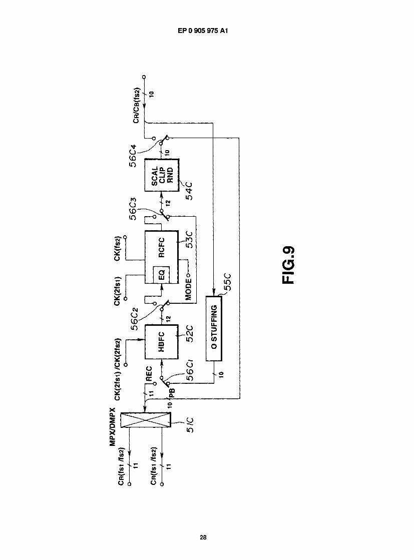
*2
At.

CO w >< X
oo oo
to CO
i
I I
I
I �

EP 0 905 975 A1
30

1 _
! £i
r

IP 0 905 975 A1
CM i- O Ok CO S w oj - - a .Q -o -o
m 1 — to O ■ ^ ■ ^ , - 7 T 2 e o f < « . ^ J Q A j = J = - C U U 8 o> ® C:
S -o £ S 5
. O - O - a . O . a . o S . Q . c . c - C O O
.q .Q .a .O .q
u> 2 eo £ n £i £> S
■ O . Q . O . C . C p 0 0
10 m *t S2 2! .Q J3 .Q .Q £3
m * to cm i- .O A XJ n jQ
T - o ' - o > o c n o r " — — — — — n £ ± <e £ o 6
* <*» S3 - 2 .Q ^ a dO JQ
« CM i- o v £ -o .o -Q .o
< CD o Q l u l l O X — J 2
CO CO c o c o c o c o c o c o c o c o c o c o c o
d o o d d o o o o o o d o
LL LL L L L L l L L L L L l L L L L L l L U . i l
32

EP 0 905 975 A1
1 6 3
SR3 24
-STAGE
I 6 2
SR2 3
-STAGE COEF
SR1 6
-STAGE
/ 5 5 C
1 6 6 ' I 6 5 - \ 6 \
F I G . 1 4
1 7 2 -
CK(fS2) COEFI LDCKI
HD MODEI
ADDRESS CONTROL CIRCUIT
CTL
SRAM R7W
R/W I 7 I
I 7 3
CK(fs2)
D
1 7 4
COEF
F I G . 1 5
33

EP 0 905 975 A1
34

EP 0 905 975 A1
CQ m CD cn m O
oo ffl o
cn CC o
GO CC O r. 2 CC
O m O
cc O
cc cn CC O
oo CC O
m CQ en m O
co m O
r- m O m
O <0 m O
1X7 m O
m o
CC O
in * co £i m m m ffl o o o o
lO «f CO CM CC CC CC CC o o o O
S 00 cm CO CO ffl CD o o o o
■tf CO CM r- CC CC CC CC O O o O
CO CM *~ O ffl ffl ffl m o o o o
CO CM t- o CC CC CC CC o o o o
CO CM r- CC CC CC O o o
■»- o T ffl m m o o o
o T CC CC CC O O O
t- CM CO CQ CQ CO o o o
cc U CO
o
0 ffl o CC
O
x: SI
cc o
ffl o
< CQ U O LU Li. O X — D ^ - l S
h - r*- r^- i — r — i^- r ^ i ^ - r ^ i ^
o o o o o o o d d d o d o
LL LL LL LL LL LL LL LL LL LL LL LL L L
35

f 5

EP 0 905 975 A1
CK(fS2)
? 2 6 0 A
LDCKI ?
2 6 0 B
2 6 3
2 6 4
COEFI
2 6 0 C HD o *-
MODEI o
J
CTL 6 6 6 /
2 6 6 2 6 5 T
SR3 24
-STAGE
2 6 2
SR2 3
-STAGE COEF
2 6 0 SR1
6 -STAGE
I " * -J n c 2 6 1
F I G . 1 9
2 7 2
CK(fS2/2) COEFI LDCKI
HD MODEI
ADDRESS CONTROL CIRCUIT
2 7 3
F I G . 2 0
37

EP 0 905 975 A1
(X2fS1)
F I G . 2 1
FIRST DIGITAL
PROCESSING UNIT
Y(2fsi) r
CR(fS2) r *"
CB(fS2) | D/A — *- A. U/A ENC
\ } 61 6 2
1 6
YVF ■H VF
YOUT/CSOUT
YOUT/CROUT/CBOUT
SECOND DIGITAL
PROCESSING UNIT
Y(fS2)
CR/CB(fS2) RECORDING/
REPRODNCING UNIT
F I G . 2 3
38

— H P
? £ 2
L
5 of O a! A* «.
l l

EP 0 905 975 A1
J European Patent Office
EUROPEAN SEARCH REPORT Application Number EP 98 12 2393
DOCUMENTS CONSIDERED TO BE RELEVANT
Category Citation of document with indication, where appropriate, of relevant passages
Relevant to claim
CLASSIFICATION OF THE APPLICATION (lnt.CI.6)
A
A
A
P,A
GB 2 069 795 A (SONY CORP) 26 August 1981 * claim 1 *
EP 0 420 612 A (SONY CORP) 3 April 1991 * claim 1 *
GUESS M M: "A COMPLETE POST-PRODUCTION SYSTEM FOR ALL VIDEO FORMATS" SMPTE JOURNAL, vol. 100, no. 1, 1 January 1991, pages 19-22, XP000173303 * page 19, left-hand column * * page 21, line 4 - line 55 *
EP 0 520 759 A (SONY CORP) 30 December 1992 * claim 1 *
1-22
1-22
1-22
H04N7/01 H04N9/04 H04N9/64 H04N9/79 H04N9/804
1-22
TECHNICAL FIELDS SEARCHED (lnt.CI.6)
H04N
The present search report has been drawn up for all claims riace ot searcn
THE HAGUE Date ot completion of the search 20 January 1999
Examiner De Paepe, W
CATEUORY Or CITED DOCUMENTS X : particularly relevant if taken alone Y : particularly relevant if combined with another
document of the same category A : technological background O : non-written disclosure P : intermediate document
T : theory or pnnciple underlying the invention E : earlier patent document, but published on, or after the filing date D : document cited in the application L : document cited for other reasons & : member of the same patent family, corresponding document
10

EP 0 905 975 A1
ANNEX TO THE EUROPEAN SEARCH REPORT ON EUROPEAN PATENT APPLICATION NO. EP 98 12 2393
This annex lists the patent family members relating to the patent documents cited in the above-mentioned European search report. The members are as contained in the European Patent Office EDP file on The European Patent Office is in no way liable for these particulars which are merely given for the purpose of information. 20-01-1999
Patent document cited in search report
Publication date
Patent family member(s)
Publication date
GB 2069795 A 26-08-1981 JP 1467339 C 30-11-1988 JP 56107682 A 26-08-1981 JP 63012434 B 18-03-1988 AT 380612 B 25-06-1986 AT 43181 A 15-10-1985 AU 538956 B 06-09-1984 AU 6654681 A 06-08-1981 CA 1146264 A 10-05-1983 DE 3103216 A 26-11-1981 FR 2475337 A 07-08-1981 NL 8100439 A,B, 01-09-1981
EP 0420612 A 03-04-1991 JP 2770479 B 02-07-1998 JP 3112287 A 13-05-1991 JP 2785211 B 13-08-1998 JP 3139981 A 14-06-1991 DE 69024577 D 15-02-1996 DE 69024577 T 13-06-1996 US 5095364 A 10-03-1992
EP 0520759 A 30-12-1992 JP 5014818 A 22-01-1993 DE 69226680 D 24-09-1998 US 5272524 A 21-12-1993
u For more details about this annex : see Official Journal of the European Patent Office, No. 12/82
11