Cell Division, Genetics, and Molecular Biology Cell Division ...
Upload
khangminh22Category
view
2download
0
ORNL-6816 Distribution—UC-404
SOLID STATE DIVISION PROGRESS REPORT
for Period Ending September 30,1993
J. B. Roberto, Director R. M. Moon, Associate Director
L. A. Boatner, Section Head J. F. Cooke, Section Head
B. C. Larson, Section Head H. A. Mook, Section Head
D. M. Zehner, Section Head
Edited by: P. H. Green
L. W. Hinton
Date Published-August 1994
Prepared for the Division of Materials Sciences
Prepared by the OAK RIDGE NATIONAL LABORATORY
Oak Ridge, Tennessee 37831 managed by
MARTIN MARIETTA ENERGY SYSTEMS, INC. for the
DEPARTMENT OF ENERGY UNDER CONTRACT NO. DE-AC05-84OR21400
y 0!?ff»BtITIOK OF THIS DOCUMENT IS UNL!IV!!tt6
^^MWWCMZ'M§'
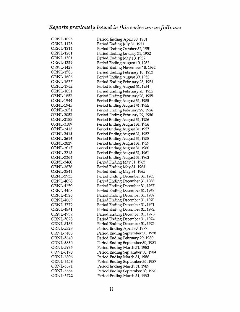
Reports previously issued in this series are as follows:
ORNL-1095 Period Ending April 30,1951 ORNL-1128 Period Ending July 31,1951 ORNL-1214 Period Ending October 31,1951 ORNL-1261 Period Ending January 31,1952 ORNL-1301 Period Ending May 10,1952 ORNL-1359 Period Ending August 10,1952 ORNL-1429 Period Ending November 10,1952 ORNL-1506 Period Ending February 10,1953 ORNL-1606 Period Ending August 30,1953 ORNL-1677 Period Ending February 28,1954 ORNL-1762 Period Ending August 31,1954 ORNL-1851 Period Ending February 28,1955 ORNL-1852 Period Ending February 28,1955 ORNL-1944 Period Ending August 31,1955 ORNL-1945 Period Ending August 31,1955 ORNL-2051 Period Ending February 29,1956 ORNL-2052 Period Ending February 29,1956 ORNL-2188 Period Ending August 31,1956 ORNL-2189 Period Ending August 31,1956 ORNL-2413 Period Ending August 31,1957 ORNL-2414 Period Ending August 31,1957 ORNL-2614 Period Ending August 31,1958 ORNL-2829 Period Ending August 31,1959 ORNL-3017 Period Ending August 31,1960 ORNL-3213 Period Ending August 31,1961 ORNL-3364 Period Ending August 31,1962 ORNL-3480 Period Ending May 31,1963 ORNL-3676 Period Ending May 31,1964 ORNL-3841 Period Ending May 31,1965 ORNL-3935 Period Ending December 31,1965 ORNL-4098 Period Ending December 31,1966 ORNL-4250 Period Ending December 31,1967 ORNL-4408 Period Ending December 31,1968 ORNL-4526 Period Ending December 31,1969 ORNL-4669 Period Ending December 31,1970 ORNL-4779 Period Ending December 31,1971 ORNL-4861 Period Ending December 31,1972 ORNL-4952 Period Ending December 31,1973 ORNL-5028 Period Ending December 31,1974 ORNL-5135 Period Ending December 31,1975 ORNL-5328 Period Ending April 30,1977 ORNL-5486 Period Ending September 30,1978 ORNL-5640 Period Ending February 29,1980 ORNL-5850 Period Ending September 30,1981 ORNL-5975 Period Ending March 31,1983 ORNL-6128 Period Ending September 30,1984 ORNL-6306 Period Ending March 31,1986 ORNL-6453 Period Ending September 30,1987 ORNL-6571 Period Ending March 31,1989 ORNL-6664 Period Ending September 30,1990 ORNL-6722 Period Ending March 31,1992
11
DISCLAIMER
This report was .prepared as an account of work sponsored by an agency of the United States Government. Neither the United States Government nor any agency thereof, nor any of their employees, make any warranty, express or implied, or assumes any legal liability or responsibility for the accuracy, completeness, or usefulness of any information, apparatus, product, or process disclosed, or represents that its use would not infringe privately owned rights. Reference herein to any specific commercial product, process, or service by trade name, trademark, manufacturer, or otherwise does not necessarily constitute or imply its endorsement, recommendation, or favoring by the United States Government or any agency thereof. The views and opinions of authors expressed herein do not necessarily state or reflect those of the United States Government or any agency thereof.
DISCLAIMER
Portions of this document may be illegible in electronic image products. Images are produced from the best available original document.

Contents
ACRONYMS xix
INTRODUCTION xxi
1. Theoretical Solid State Physics
SUPERCONDUCTIVITY Energy Gap Structure of Layered Superconductors—S. H. Liu and R. A. Klemm 2
High-Tc Superconducting Superlattices—R. F. Wood 3
Spin-Polaron Theory of High-Tc Superconductivity—R. F. Wood 3
Electron-Phonon Interaction Near Van Hove Singularities—G.D. Mahan 4
Resistivity and Superconductivity from Anharmonic Phonons—G. D. Mahan and J. O.Sofo 5
Frustration-Induced Disorder of Flux Lines in Layered Superconductors—G. I. Watson and G. S. Canright 5
NUMERICAL SIMULATION AND BAND STRUCTURE A New Extended Point Defect Structure in Diamond Cubic Crystals—Mark Mostoller,
Theodore Kaplan, and M. F. Chisholm 6
A New Empirical Potential for Si and Ge—Mark Mostoller, Benjamin Liu, and Theodore Kaplan 8
Numerical Simulation of He + and Li + Collisions with Cso—T. Kaplan, M. Rasolt,
M. Karimi, and Mark Mostoller 8
The Statistics of Sputtering—Mark T. Robinson 10
Simulation of Plasma-Based Materials Processing Techniques—C.-L. Liu, D. B. Geohegan, J.-N. G. Leboeuf, and R. F. Wood 10
i i i
IV
Quantum Monte Carlo with Complex Weights—Lizeng Zhang, G. S. Canright, and T. Barnes 11
Large-Scale ab Initio Study of the Binding and Diffusion of a Ge Adatom on the Si(100) Surface—V. Milman, D. E. Jesson, S. J. Pennycook, M. C. Payne, M. H. Lee, and I. Stich 12
Hydration of Mg-Cordierite Investigated by ab Initio Total Energy Calculations— B.Winkler, V. Milman, and M.C.Payne 14
MAGNETIC PROPERTIES Magnetic Structure and Spin Dynamics of Chromium Alloys—R. S. Fishman and S. H. Liu 15
Role of Electronic Screening in Itinerant-Electron Magnets—/. F. Cooke, }. M. Bass, and J. A. Blackman 15
Electronic Theory and the Magnetic Moment of Itinerant-Electron Systems—/. F. Cooke 17
Longitudinal and Transverse Spin Dynamics in the Sinusoidal Phase of Erbium and Thulium—S. H. Liu and }. F. Cooke 17
Spontaneous Magnetization of Anyons with Long-Range Repulsion—Jaichul Yi and G. S. Canright 18
Magnetoplasma Edge Modes of Two-Dimensional Electron Gas Systems—/. J. Quinn and X. Xia 19
Numerical Studies of Two-Dimensional Electron-Hole Systems in a Strong Magnetic Field—/. /. Quinn and Ximing Chen 19
MANY-BODY THEORY, PHOTOVOLTAICS, AND SUCH Advanced Deposition and Substrate Technologies for Thin-Film Polycrystalline Silicon
Photovoltaics—R. F. Wood, G. E. Jellison, Jr., D. Eres, S. M. Gorbatkin, R. D. Westbrook, A. }. Moorhead, and P. A. Menchhofer 20
Fractal Vertex for Electron-Electron Interactions—G. D. Mahan 21
Restricted Applicability of Onsager's Reciprocity Relations to Models of Interface Motion—
Theodore Kaplan, M. }. Aziz, and L. J. Gray 21
Screening and Mobility of n-Silicon—B. A. Sanborn, P. B. Allen, and G. D. Mahan 22
Nonlinear Polarizability of Correlated One-Dimensional Systems—A. G. Rojo and G. D. Mahan 23
Mean-Field Theory of Elastic Dipoles on a FCC Lattice—R. S. Pfeiffer and G. D. Mahan 23
V
2. Neutron Scattering
SMALL-ANGLE SCATTERING AND NEUTRON REFLECTOMETRY
Compatibility of Blends of Polyethylene in the Melt and Solid States by Small-Angle Neutron Scattering (SANS)—G. D. Wignall, R. G. Alamo, L. Mandelkern, J. D. Londono, and F. C. Stehling 26
Miscibility and Cocrystallization in Homopolymer Segmented Block Copolymer Blends— K. P. Gallagher, X. Zhang, J. P. Runt, G. Huynh-ba, and J. S. Lin 27
Statistical Segment Length Mismatch on Polymer Blend Miscibility—G. D. Wignall, M. D. Gehlsen, and F. S. Bates 28
The Morphology of Blends of Linear and Branched Polyethylenes in Solid State by Small-Angle Neutron Scattering (SANS)—G. D. Wignall, R. G. Alamo, L. Mandelkern, J. D. Londono, and F. C. Stehling 29
Microdomain Contraction in Microphase-Separated Multiblock Copolymers— S. D. Smith, R. J. Spontak, M. M. Satkowski, A. Ashraf, and J. S. Lin 30
Temperature Coefficients for the Chain Dimensions of Polystyrene and Polymethylmethacrylate—G. D. Wignall, A. J. Boothroyd, and A. R. Rennie 30
Structural Characterization of C6o and C70 Fullerenes by Small-Angle Neutron Scattering (SANS)—K. A. Affholter, G. D. Wignall, S. J. Henderson, G. J. Bunick, R. E. Haufler, and R. N. Compton 31
Evaluation of Precipitate Evolution in 6XXX Alloys Using Small-Angle Neutron Scattering Techniques—C. W. Bartges and Steve Spooner 32
Matrix Precipitate Evolution During Decomposition of Aluminum Alloy 7075— C. W. Bartges, L. H. Edelson, S. Y. Tzeng, and J. S. Lin 33
Characterization of Porosity in Ceramic Materials by Small-Angle Scattering— D. W. Schaefer, R. K. Brow, B. J. Oliver, T. Rieker, G. Beaucage, L. Hrubesh, and J. S. Lin 33
Shear-Induced "Crystallization" of Rodlike Micelles—W. A. Hamilton, P. D. Butler, S. M. Baker, G. S. Smith, J. B. Hayter, L. f. Magid, and R. Pynn 34
NEUTRON DIFFRACTION Neutron Scattering Measurements of Residual Stress in Austenitic and Ferritic Plates—
Steve Spooner, C. R. Hubbard, Xun-Li Wang, and S. A. David 35
VI
Weld Metal Chemistry Measured With Neutron Powder Diffraction—S. Spooner and J. A. Fernandez-Baca 36
Martensitic Phase Transition in Ino.77Tlo.23—/• L. Robertson and H. G. Smith 37
Neutron Scattering Study of the t -» m Phase Transition in Al 2O 3-Zr0 2 (12 mol % Ce0 2) Ceramic Composites—Xun-Li Wang, J. A. Fernandez-Baca, C. R. Hubbard, K. B. Alexander, and P. F. Becher 39
S IrCXi: A Two-Dimensional Spin-1/2 Heisenberg Antiferromagnet—M. K. Crawford, M. A. Subramanian, R. L. Harlow, J. A. Fernandez-Baca, Z. R. Wang, and
D. C. Johnston 39
Spin Density Waves in Dilute CuMn Alloys—/. W. Cable and Y. Tsunoda 40
Structure of the Modulated Magnetic Phase of M^Sn—J. W. Cable, N. Wakabayashi, and P. Radhakrishna 41
Neutron Diffraction Study of the Magnetic Ordering of BaCu02+;t—Xun-Li Wang, J. A. Fernandez-Baca, Z. R. Wang, D. Vaknin, and D. C. Johnston 42
Crystal Structure and Superconductivity of La2-xBaxCu04—S. Katano, J. A. Fernandez-Baca, S. Funahashi, N. Mori, and K. Koga 43
Observation of the Flux Lattice in Bi2.i5Bai.95CaCu208+x—M. Yethirajr-H. A. Mook, E. M. Forgan, R. Cubitt, M. Wylie, D. Mck. Paul, S. L. Lee, P. H. Kes, T. W. Li, and K. Mortensen 44
Anisotropic Flux Lattice in YBa2Cu3U7—M. Yethiraj, H. A. Mook, R. Cubitt, E. M. Forgan S. L. Lee, and D. Mck. Paul 45
INELASTIC NEUTRON SCATTERING Magnetic Excitations in the Triangular Antiferromagnets M^Sn and M^Ge—J. W. Cable,
N. Wakabayashi, and P. Radhakrishna 46
Transverse Spin Excitations in the Sinusoidal Magnetic Phase of Erbium— R. M. Nicklow and N. Wakabayashi 47
Fracton Excitations in a Diluted Heisenberg Antiferromagnet Near the Percolation Threshold—H. Ikeda, J. A. Fernandez-Baca, R. M. Nicklow, M. Takahashi, and K. Iwasa 48
Low-Energy Excitations in Superconducting LAi.86Sro.i4Cu04—T. E. Mason, G. Aeppli, S. M. Hoyden, A. P. Ramirez, and H. A. Mook 49
Magnetic Excitations in YBa2Cu307—H. A. Mook, M. Yethiraj, G. Aeppli, T. E. Mason, and T. Armstrong 50
V l l
Ground-State Wave Functions of Tb 3 + Ions in Paramagnetic TbPC^: A Neutron Scattering Study—C.-K. Loong, L. Soderholm, G. L. Goodman, M. M. Abraham, and L. A. Boatner 51
Rare-Earth Energy Levels and Magnetic Properties of DyPC>4—C.-K. Loong, L. Soderholm, J. S. Xue, M. M. Abraham, and L. A. Boatner 53
Crystal-Field Excitations and Magnetic Properties of TmP04—C.-K. Loong, L. Soderholm, M. M. Abraham, L. A. Boatner, and N. M. Edelstein 54
Rare-Earth Energy Levels and Magnetic Properties of H0PO4 and ErPC»4—C.-K. Loong, L. Soderholm, J. P. Hammonds, M. M. Abraham, L. A. Boatner, and N. M. Edelstein 55
3. Synthesis, Processing, and Characterization of Materials
SUPERCONDUCTIVITY Effects of Columnar Defects on the Superconducting Properties of YBa2Cu3C>7_5: Limits to
the Irreversibility Line—D. K. Christen, S. Zhu, C. E. Klabunde, H. R. Kerchner, J. R. Thompson, R. Feenstra, L. Civale, and]. M. Phillips 58
Limits to Critical Currents in High-Temperature Superconductors: What We Can Learn From Tailored Defects—D. K. Christen, J. R. Thompson, H. R. Kerchner, B. C. Sales, B. C. Chakoumakos, L. Civale, A. D. Marwick, and F. Holtzberg 59
Systematics of Flux Pinning vs Oxygen Deficiency 5 In Aligned YBa2Cu3C>7_5 Materials— /. R. Thompson, J. G. Ossandon, D. K. Christen, Y. R. Sun, B. C. Sales, H. R. Kerchner, J. E. Tkaczyk, and K. W. Lay 59
Enhanced Vortex-Pinning Strength and Magnetic Irreversibility Via Columnar Defects in Single-Crystal BiaS^CaC^Og—H. R. Kerchner,}. R. Thompson, Y. R. Sun, D. K. Christen, J. O. Thomson, B. C. Sales, B. Chakoumakos, L. Civale, and A. D. Marwick 60
Vortex Pinning, Supercurrent Decay, and Weak Links in the Hg-Based High-Tc Material HgBa2CuC>4+5—J. R. Thompson, D. K. Christen, Y. R. Sun, M. Paranthaman, and J. Brynestad 61
Enhanced Transport Critical Current at High Fields After Heavy Ion Irradiation of Textured TlBa 2Ca 2Cu 3O x Thick Films—/. E. Tkaczyk, J. A. DeLuca, P. L. Karas, P. f. Bednarczyk, D. K. Christen, C. E. Klabunde, and H. R. Kerchner 62
Vortex Fluctuations, Magnetic Penetration Depth, and Upper Critical Magnetic Field HC2 in Hg- and Tl-Based High-Tc Superconductors—/. R. Thompson, J. G. Ossandon, D. K. Christen, B. C. Chakoumakos, Y. R. Sun, M. Paranthaman, and J. Brynestad 63
V l l l
Effect of Flux Creep on the Temperature Dependence of the Current Density in YBaCuO Crystals—/. R. Thompson, Y. R. Sun, L. Civale, A. P. Malozemoff, M. W. McElfresh, A. D. Marwick, and F. Holtzberg 64
Observation of Free-Flux Flow at High Dissipation Levels in YBa2Cu3C>7 Epitaxial Films—M. N. Kunchur, D. K. Christen, and]. M. Phillips 64
Magnetic Relaxation Studies in YBa2Cu3C>7_5 Superconductors—Y. R. Sun, J. R. Thompson, D. K. Christen, Y. }. Chen, and A. Goyal 65
Correlations Between the Hall Coefficient and the Superconducting Transport Properties of Oxygen-Deficient YBa2Cu307_5 Epitaxial Thin Films—E. C. Jones, D. K. Christen, J. R. Thompson, R. Feenstra, S. Zhu, D. H. Lowndes, J. M. Phillips, M. P. Siegal, and J. D. Budai 66
Upper Critical Fields of YBa2Cu307_s Epitaxial Thin Films with Variable Oxygen Deficiency 8—E. C. Jones, D. K. Christen, J. R. Thompson, J. G. Ossandon, R. Feenstra, J. M. Phillips, and M. P. Siegal 67
Electron-Doped and Hole-Doped Infinite-Layer Sri.xCu02-8 Films Grown by Laser Molecular Beam Epitaxy—R. Feenstra, X. Li, M. Kanai, T. Kawai, S. Kawai, J. D. Budai, E. C. Jones, Y. R. Sun, J. R. Thompson, S. J. Penny cook, and D. K. Christen 67
Anisotropic Electrical Resistivity of YBCO/PBCO Superlattice Films Grown on Miscut Substrates—H. R. Kerchner, C. E. Klabunde, D. K. Christen, J. D. Budai, D. H. Lowndes, D. P. Norton, and J. O. Thomson 68
THIN-FILM BATTERIES AND SOLID ELECTROLYTES Rechargeable Thin-Film Lithium Batteries—/. B. Bates, G. R. Gruzalski, N. J. Dudney,
C. F. Luck, and Xiaohua Yu 70
Cycling a Thin-Film Solid State Lithium Battery: Li/Lipon/LiMn204—G. R. Gruzalski
and J. B. Bates 71
AC Impedance of Thin-Film Lithium Batteries—/. B. Bates and G. R. Gruzalski 72
Synthesis, Crystal Structure, and Ionic Conductivity of a Polycrystalline Lithium Phosphorus Oxynitride With the y-Li3P04 Structure—B. Wang, B. C. Chakoumakos, B. C. Sales, B. S. Kwak, and J. B. Bates 73
Ionic Conductivities and Structure of Lithium Phosphorus Oxynitride Glasses- B. Wang, B. S. Kwak, B. C. Sales, and J. B. Bates 74
Deposition of Organic-Inorganic Composite Thin Films by L13PO4 Sputtering and C2H4 Plasma Polymerization—B. S. Kwak, R. A. Zuhr, and J. B. Bates 75
Radio-Frequency Magnetron Sputtering of Pure and Mixed Targets of Li4Si04 and Li20— N. J. Dudney, J. B. Bates, and J. D. Robertson 75
IX
Composite Thin Films by IJ3PO4 Sputtering and Si(OC2Hs)4 Polymerization—
B. S. Kwak, R. A. Zuhr, and J. B. Bates 76
Composite Electrolytes—N. J. Dudney 77
Magnetron Sputter Deposition of CaF2 Films—N. J. Dudney 78
Electrical Conduction in CaF2 and CaF2-Al2C>3 Nanocomposite Films on AI2O3 Substrates— F. A. Modine, D. Lubben, and }. B. Bates 78
FERROELECTRICS AND PEROVSKITE-STRUCTURE OXIDES
Epitaxial YBa 2 Cu 3 0 7 Growth on KTa0 3 (001) Single Crystals—W. Prusseit, L. A. Boatner, and D. Rytz 79
Domain Formation and Strain Relaxation in Epitaxial Ferroelectric Heterostructures— B. S. Kwak, A. Erbil, } . D. Budai, M. F. Chisholm, L. A. Boatner, and W. ]. Wilkens 80
Raman Difference Spectra of PbTiC>3 Thin Films Grown by Metalorganic Chemical Vapor Deposition (MOCVD)—Z. C. Feng, B. S. Kwak, A. Erbil, and L. A. Boatner 81
Raman Scattering and X-ray Diffraction Investigations of Highly Textured (Pbi-xLa^)Ti03 Thin Films—Z. C. Feng, B. S. Kwak, A. Erbil, and L. A. Boatner 82
Oxide Ferroelectric Materials Grown by Metalorganic Chemical Vapor Deposition (MOCVD)—A. Erbil, W. Braun, B. S. Kwak, B. }. Wilkens, L. A. Boatner, and } . D. Budai 83
Polar Fluctuations and First-Order Raman Scattering in Highly Polarizable KTa03 Crystals With Off-Center Li and NB Ions—P. DiAntonio, B. E. Vugmeister, J. Toulouse, and L. A. Boatner 84
Determination of the Ai (TO) Soft-Mode Damping Rate in KTao.93Nbo.07O3— P. Grenier, S. Jandl, D. Houde, and L. A. Boatner. 85
Polarization and Crystal-Geometry Dependences of the Nonlinear Optical Responses of KTai.xNbj:03 Crystals After Picosecond-Pulse Laser Excitation—H. Liu, R. }. Reeves, R. C. Powell, and L. A. Boatner 86
Infrared Absorption Investigations of OH Impurities in Doped KTa03 Single Crystals— S. Jandl, }. Rousseau, and L. A. Boatner 87

X
MATERIALS PROPERTIES Unstable Neck Formation During Initial-Stage Sintering—/. Rankin and L. A. Boatrier 88
Textured Coatings from Colloidal Suspensions of Faceted Oxide Microcrystals— G. W. Steadman, J. R. Brewster, J. D. Budai, and L. A. Boatner 89
Structural Properties of the Amorphous Phases Produced by Heating Crystalline M g H P 0 4 « 3 H 2 0 — B . C. Sales, B. C. Chakoumakos, L. A. Boatner, and } . O. Ramey 91
Chromatographic Determination of the Phosphate Anions in Crystalline and Glassy N a 4 N b P 3 O z — B . C. Sales and B. C. Chakoumakos 92
Microstructural Formation in Longitudinal Bicrystal Welds—M. Rappaz, J. M. Vitek, S. A. David, and L. A. Boatner 93
Modeling of Single-Crystal Laser-Weld Microstructures—/. M. Vitek, T. Zacharia, S. A. David, M. Rappaz, and L. A. Boatner 94
OPTICAL CHARACTERIZATION OF MATERIALS Cerium-Doped Orthophosphates: New Promising Scintillators—A. Lempicki, E. Berman,
A. } . Wojtowicz, M. Balcerzyk, and L. A. Boatner 95
Two-Photon Excitation of the if—» 5d Transitions of C e 3 + In L u P 0 4 and YPO4—/. Sytsma, D. Piehler, N. M. Edelstein, L. A. Boatner, and M. M. Abraham 97
Zero-Field Splitting of C m 3 + In L u P 0 4 Single Crystals—W. K. Kot, N. M. Edelstein, M. M. Abraham, and L. A. Boatner 98
Electron Paramagnetic Resonance (EPR) of P u 3 + and Cf3"1" In Single Crystals of LuP0 4 — W. K. Kot, N. M. Edelstein, M. M. Abraham, and L. A. Boatner 99
Luminescence Properties of Deformed CaO Crystals—R. Gonzalez, Y. Chen, C. Ballesteros, H. Liu, G. H. Rosenblatt, R. T. Williams, and W. Gellerman 100
Errors In Polarization Measurements Because of Static Retardation in Photoelastic Modula tors—F. A. Modine and G. E. Jellison, Jr 101
Positron Annihilation Spectroscopy of Vacancy Aggregates in Neutron-Irradiated MgO Crystals—R. Pareja, R. M. de la Cruz, R. Gonzalez, and Y. Chen 102
Protons in Neutron-Irradiated and Thermochemically Reduced MgO Crystals Doped With Lithium Impurities—R. Gonzalez, R Pareja, and Y. Chen 103
Thermochemical Reduction of Yttrium Aluminum Garnet (YAG) Crystals—R. Gonzalez, C. Ballesteros, Y.-J Liu, Yi Chen, X.-F Zong, and Y. Chen 104
XI
Precipitation of Copper and Chromium Impurities in Lanthanum Magnesium Aluminate Crystals During Reduction—C. Ballesteros, R. Gonzalez, Y. Chen, and M. R. Kokta 105
4. Ion Beam and Laser Processing
ION BEAM PROCESSING Formation of Au and Ag Nanoclusters in Fused Silica by Ion Implantation—C. W. White,
D. S. Zhou, J. D Budai, R. A. Zuhr, R. A. Magruder, and R. F. Haglund 108
Nanosize Metal Alloy Particle Formation in Ag and Cu Sequentially Implanted Silica— R. A. Zuhr, R. H. Magruder III, T. A. Anderson, and J. E. Wittig 109
Formation of Oriented Nanocrystals of Si and Ge in AI2O3 By Ion Implantation— C. W. White, J. D. Budai, S. P. Withrow, S. J. Pennycook, R. A. Magruder, and D. M. Hembree 110
Formation of Oriented SiGe Nanocrystals in AI2O3 by Ion Implantation—C. W. White, J. D. Budai, S. P. Withrow, S. J. Pennycook, R. A. Magruder, and D. M. Hembree I l l
Colloidal Au And Ag Nanocrystals Formed in AI2O3 by Ion Implantation and Annealing— C. W. White, J. D. Budai, D. K. Thomas, D. K. Hensley, R. A. Magruder, R. F. Haglund, L. Yang, J. C McCallum, and A. Pogany 112
Kinetics of Solid-Phase-Epitaxial Crystallization in Amorphous Sii_xGex Thin Films— T. E. Haynes, C. Lee, and K. S. Jones 113
Freestanding Homoepitaxial Chemical Vapor Deposited (CVD) Diamond Films Lifted Off Implanted Substrates—/. D. Hunn, S. P. Withrow, C. W. White, R. E Clausing, L. Heatherly, J. Bentley, D. M. Hembree, Jr., and N. R. Parikh 114
Accumulation of Implantation Damage in Mev-Implanted Diamond Crystals—/. D. Hunn, S. P. Withrow, C. W. White, R. E Clausing, L. Heatherly, J Bentley, D. M. Hembree, Jr., and N. R. Parikh 115
Development of an Electron Cyclotron Resonance (ECR) Plasma Source for Copper Metallization—L. A. Berry, S. M. Gorbatkin, G. H. Henkel, and R. L. Rhoades 117
Boron Nitride Thin-Film Deposition Using Electron Cyclotron Resonance Microwave Plasmas—S. M. Gorbatkin, R. F. Burgie, W. C. Oliver, J. C. Barbour, T. M. Mayer, and M. L. Thomas 118
Spatial Profiling of Ion and Neutral Excitation in Nobel Gas Electron Cyclotron Resonance (ECR) Plasmas—R. L. Rhoades and S. M. Gorbatkin 119
Deuterium-Induced Reconstruction of Cu(110): Correlation of Surface Structures with Absolute Coverage—C. F Walters, D. B. Poker, D. M. Zehner, and E. W. Plummer 120
Xll
Plastic Flow Induced by Ionization Processes in Ion-Damaged MgO—R. Brenier, B. Canut, L. Gea, S. M. M. Ramos, P. Thevenard, J. Rankin, L. Romana, and L. A. Boatner 121
ION IMPLANTATION AND ANALYSIS Ion Implantation Effects in Tin-Doped Indium Oxide Thin Films—T. E. Haynes,
Yuzo Shigesato, and D. C. Paine 122
Implantation Damage and Electrical Activation in Si-Implanted GaAs—T. E. Haynes,
R. Morton, and S. S. Lau 123
Microvoiding in High Current Density Irradiated Si—Ling Xie and O. W. Holland 124
A Dislocation-Free Process for Producing Silicon-On-Insulator by Implantation— O. W. Holland, D. S. Zhou, D. K. Thomas, and J. D. Budai 125
Ion Beam Synthesis of IrSi3 in Si(lll)—T. P. Sjoreen, H.-J Hinneberg, and M. F. Chisholm 126
Ion Beam Synthesis of Ti-Rich Epitaxial Buried Layers in LiNb03—D. B. Poker and
D. S. Zhou 127
Ion Implantation of Orthopedic Alloys—/. M. Williams and L. Riester 128
Ion Beam Mixing Studies in Pt/Ti and Pt/Ni Bilayered Samples—/. M. Williams and D. B. Poker 129
Study of Hydrogen Diffusion in AlCu Alloy—T. P. Sjoreen, C. W. White, O. W. Holland, and S. R. Wilson 130
Protective Oxide Formation on NbAl3 and TiAl Alloys Via Ion Implantation— S. P. Withrow, R. J. Hanrahan, Jr., E. D. Verink, Jr., and E. Ristolainen 131
LASER AND MOLECULAR BEAM PROCESSING OF THIN FILMS
Pulsed-Laser Growth of Epitaxial Compound Semiconductor Films with Continuously Variable Composition—/. W. McCamy and D. H. Lowndes 132
Growth of ZnS-ZnSe Strained-Layer Superlattices by Multitarget Pulsed-Laser Ablation— /. W. McCamy and D. H. Lowndes 133
Growth of Epitaxial Zn-S-Se Heterostructures Incorporating Both Continuously Graded and Abrupt, Periodic Compositional Changes—/. W. McCamy, D. H. Lowndes, and T. M. Rosseel 134
Growth of Epitaxial ZnSe Films by Pulsed-Laser Ablation—/. W. McCamy, D. H. Lowndes, and G. E. Jellison, Jr 135
Xll l
Investigation of the Kinetics of Digermane Chemisorption and Reaction Product Desorption in Thin-Film Growth of Germanium—G. Eres and J. W. Sharp 136
Kinetics of Hydrogen Desorption in Surface-Limited Thin-Film Growth of SiGe Alloys— /. W. Sharp and G. Eres 137
Laser Ablation of Graphite into Rare Gases for Fullerene Production—D. B. Geohegan, A. A. Puretzty, R. E. Haufler, R. L. Hettich, X.-Y. Zheng, and R. N. Compton 138
Fast Intensified Charge-Coupled Device (ICCD) Photography of the Pulsed-Laser Deposition Process—D. B. Geohegan 139
Imaging and Temperature Measurements of Hot Particulates Generated During Excimer Laser Ablation—D. B. Geohegan 141
Transport Properties of Ultrathin YBa2Cu3G"7-5 Layers: Evidence for Two-Dimensional Vortex Fluctuations—D. P. Norton and D. H. Lowndes 142
Epitaxial Growth of Bai.xKxBi03 Thin Films By Pulsed-Laser Deposition— D. P. Norton, J. D. Budai, B. C. Chakoumakos, and R. Feenstra 143
Epitaxial Pulsed-Laser Growth and Properties of Single-Crystal Cai_xSrxCu02 Thin Films—D. P. Norton, B. C. Chakoumakos, E. C. Jones, J. D. Budai, D. K. Christen, and D. H. Lowndes 144
Growth Mechanisms and Superconductivity of Ultrathin YBa2Cu307_x Epitaxial Films on (001) MgO Substrates—S. Zhu, D. H. Lowndes, X. Y. Zheng, B. C. Chakoumakos, S. J. Pennycook, and R. J. Warmack 145
In Situ Growth of Epitaxial Bi2Sr2CaCu20s.x and Bi2Sr2Cu06-x Films by Pulsed-Laser Ablation—S. Zhu, D. H. Lowndes, B. C. Chakoumakos, D. K. Christen X.-Y. Zheng, E. Jones, J. D Budai, and R. J. Warmack 146
Optical Functions of Transparent Thin Films of Si03, BaTiOs, and SiOx Determined Using Spectroscopic Ellipsometry—G. E. Jellison, Jr., L. A. Boatner, D. H. Lowndes, R. A. McK.ee, and M. Godbole 147
Optical Functions of GaAs, GaP, and Ge Determined by Two-Channel Polarization Modulation Ellipsometry—G. E. Jellison, Jr 148
Optical Functions of Chemical Vapor Deposited Thin-Film Silicon Determined by Spectroscopic Ellipsometry—G. E. Jellison, Jr., M. F. Chisholm, and S. M. Gorbatkin 149
Optical Functions of Silicon-Germanium Alloys Determined Using Spectroscopic Ellipsometry—G. E. Jellison Jr., T. E. Haynes, and H. H. Burke 150
Spectroscopic Ellipsometry and Interference Reflectometry Measurements for Chemical Vapor Deposited Silicon Grown on Oxidized Silicon—G. E. Jellison, Jr., M. Keefer, and L. Thornquist 151
Data Analysis for Spectroscopic Ellipsometry—G. E. Jellison, Jr 152
T7?vriiir ;HSSFII; m: > -~w S¥£K^i%.^
XIV
Ion Channeling and Spectroscopic Ellipsometry Examinations of Thin-Film SiO2/epi-Si(001) Structures—A. T. Fiory, P. K. Roy, and G. E. Jellison, Jr 153
Excimer Laser Ablation and Surface Activation of SiOx and SiO* Ceramic Couples for Subsequent Electroless Copper Plating—M. J. Godbole, D. H. Lowndes, and G. E. Jellison, Jr 154
Ablation, Melting, and Smoothing of Polycrystalline Alumina by Pulsed Excimer Laser Radiation—D. H. Lowndes, M. De Silva, M. J. Godbole, A. J. Pedraza, and D. B. Geohegan 155
Design and Microfabrication of Planar Pickup Coils for Quantum Oscillation Measurements in HTSc Films—D. H. Lowndes, M. J. Godbole, and R. G. Goodrich 156
5. Structure of Solids and Surfaces
SURFACE PHYSICS Determination of the True Reconstruction of Cu(110)-(2 x 3)-N With High-Energy
Ion Scattering—H. Dtirr, D. B. Poker, D. M. Zehner, and J. H. Barrett 160
Terrace-Width and Step-Height Enlargement: Reconstruction of the TaC(310) Surface—J.-K. Zuo and D. M. Zehner 161
Segregation and Oxidation Behavior of the Feo.53Alo.47(110) Surface—H. Graupner, L. Hammer, K. Miiller, and D. M. Zehner 162
X-Ray Reflectivity of the Cu(110) Surface—G. Helgesen, Doon Gibbs, A. P. Baddorf, D. M. Zehner, and S. G. J. Mochrie 163
Thermal Roughness of a Close-Packed Metal Surface: Pt(001)—D. L. Abernathy, S. G. J. Mochrie, D. M. Zehner, G. Grubel, and D. Gibbs 164
Faceting Transformations of the Stepped Pt(001) Surface—G. M. Watson, D. Gibbs, D. M. Zehner, M. Yoon, and S. G. J. Mochrie 164
Experimental Study of Smoothing Kinetics on a Rough Surface—J.-K. Zuo and J. F. Wendelken 165
Anharmonicity and Vibrational Relaxation on the Cu(110)-(2 x l)-0 Surface—H. Diirr and A. P. Baddorf. 166
Surface Dynamics of Beryllium—/. B. Hannon, R. L. Sameth, E. J. Mele, and E. W. Plummer 167
New Resonances in High Resolution Electron Energy Loss Spectroscopy of Adsorbed Molecules: Electronic Excitation of Physisorbed O2—/. C. Barnard, K. M. Hock, L. Siller, M. R. C. Hunt, J. F. Wendelken, and R. E. Palmer 169
XV
Core-Level Spectroscopy Investigation of the Moo.7sReo.25(100) Surface—P. F. Lyman
and D. M. Zehner 170
The Adsorption of Sulfur on W(001)—D. R. Mullins, P. F. Lyman, and S. H. Overbury 171
Methanethiol on W(001) and Ru(0001)—D. R. Mullins and P. F. Lyman 172
Atomic Layer-By-Layer Surface Removal by Force Microscopy—B. C. Sales, T. Thundat, B. C. Chakoumakos, L. A. Boatner, D. P. Allison, and R. J. Warmack 173
ELECTRON MICROSCOPY Atomic-Resolution Compositional Imaging of the Sub-Lattice in III-V Semiconductors—
A. J. McGibbon, S. J. Pennycook, and Z. Wasilewski 174
New Interface Structure for A-Type CoSi2/Si(lll)—M. F. Chisholm, S. J. Pennycook, R. Jebasinski, and S. Mantl 175
The Ordered Atomic Interface of CoSi2/Si(001)—M. F. Chisholm, N. D. Browning, S. J. Pennycook, R. Jebasinski, and S. Mantl 176
Atomic-Resolution Chemical Analysis—N. D. Browing, M. F. Chisholm, and S. J. Pennycook 178
Cell-by-Cell Mapping of Carrier Concentrations in High-Temperature Superconductors— N. D. Browning, M. F. Chisholm, and S. J. Pennycook 179
Atomic-Scale Analysis of a SrTiC>3 Grain Boundary by Combined Z-Contrast Imaging and Energy Loss Spectroscopy in the SSD Stem—M. M. McGibbon, N. D. Browing, M. F. Chisholm, and S. J. Pennycook 181
Atomic Structure of Grain Boundaries in YBa2Cu3G"7_5 as Observed by Z-Contrast Imaging—M. F. Chisholm, S. J. Pennycook, D. P. Norton, and N. D. Browning 182
Incoherent Imaging of Thin Specimens Using Coherently Scattered Electrons— D. E. Jesson and S. J. Pennycook 183
Incoherent Imaging of Crystals Using Thermally Scattered Electrons—D. E. Jesson and S. J. Pennycook 184
Direct Imaging of Surface Cusp Evolution During Strained-Layer Epitaxy—D. E. Jesson, S. J. Pennycook, J.-M. Baribeau, and D. C. Houghton 185
Interplay Between Evolving Surface Morphology, Atomic-Scale Growth Modes, and Ordering During SixFei_x Epitaxy—D. E. Jesson, S. J. Pennycook, J. Z. Tischler, J. D. Budai, J.-M. Baribeau, and D. C. Houghton 186
Morphological Instabilities in Strained Films—K. M. Chen, D. E. Jesson, S. J. Pennycook, T. C. Estes, T. Thundat, and R. J. Warmack 187
XVI
X-RAY DIFFRACTION Structure and Orientation of Si, Ge, and SiGe Nanocrystals Formed by Ion Implantation—
/. D. Budai, C. W. White, S. P. Withrow, S. J. Pennycook, D. C. Paine, and D. M. Hembree 189
Structure of Ordered SiGe Epitaxial Layers—/. Z. Tischler, J. D. Budai, P. Zschack, D. E. Jesson, J.-M. Baribeau, and D. C. Houghton 190
Preferential Domain Growth of Ordered SiGe Films—/. Z. Tischler, J. D. Budai, P. Zschack, D. E. Jesson, J.-M. Baribeau, and D. C. Houghton 191
Energy Time Correlations in Resonant Nuclear Bragg Scattering—/. Z. Tischler, B. C. Larson, and E. E. Alp 192
Oriented High-Tc Superconducting Films on Arbitrary Substrates—/. D. Budai, D. P. Norton, D. K. Christen, B. C. Chakoumakos, R. Feenstra, and E. C. Jones 193
Structure of Infinite-Layer Sri_xCaxCu02 Thin Films—/. D. Budai, D. P. Norton, R. Feenstra, B. C. Chakoumakos, E. C. Jones, D. K. Christen, and T. Kawai 194
In-Plane Epitaxial Alignment of YBa2Cu307_x Films Grown on Silver Crystals and Buffer Layers—/. D. Budai, R. T. Young, D. P. Norton, D. K. Christen, R. Feenstra, and B. S. Chao 195
Epitaxial Lead Zirconate-Titanate Thin Films on Sapphire—W. Braun, B. S. Kzvak, A. Erbil, J. D. Budai, and B. J. Wilkens 196
Refinement of Oxide Crystal Structures by Rietveld Analysis of Neutron Powder Diffraction Data—B. C. Chakoumakos, J. A. Fernandez-Baca, M. M. Abraham, and L. A. Boatner 196
Anomalous Dispersion and Thermal Expansion in Lightly Doped KTai_2NB203— P. M. Gehring, H. Chou, S. M. Shapiro, J. A. Hriljac, D. H. Chen, J. Toulouse, D. Rytz, and L. A. Boatner 197
X-Ray Absorption Spectroscopy of the Rare-Earth Orthophosphates—D. K. Shuh, L. J. Terminello, L. A. Boatner, and M. M. Abraham 198
Collaborative Synchrotron Beam Line for the Advanced Photon Source—B. C. Larson, G. E. Ice, J. Z. Tischler, J. D. Budai, C. J. Sparks, and E. Specht 200
PUBLICATIONS AND PAPERS 201
SEMINARS 263
SCIENTIFIC ACTIVITIES, AWARDS, AND HONORS 271
xvii
PERSONNEL CHANGES 279
ORGANIZATION CHART 283
AUTHOR INDEX 285

Acronyms
AES - auger electron spectroscopy ANS - Advanced Neutron Source APS - Advanced Photon Source APECS - Auger-photoelectron coincidence
spectroscopy BCA - binary collision approximation CHESS - Cornell High-Energy
Synchrotron Source CPA - constant-phase angle CVD - chemical vapor deposition DSC - differential scanning calorimetry ECR - electron cyclotron resonance EDX - energy dispersive x-ray EELS - electron energy loss spectroscopy EPR - electron paramagnetic resonance FWHM - full width at half maximum HFIR - High Flux Isotope Reactor HPLC - high-performance liquid
chromatography HREM - high-resolution electron
microscopy HREELS - high-resolution electron
energy loss spectroscopy HRLEED - high-resolution low-energy
electron diffraction HRTEM - high-resolution transmission
electron microscopy HTSc - high-temperature superconductors IBD - ion beam deposition IPNS - Intense Pulsed Neutron Source LDA - local density approximation LEED - low-energy electron diffraction MBE - molecular beam epitaxy MOCVD - metallo-organic chemical
vapor deposition
NSLS - National Synchrotron Light Source
ORISE - Oak Ridge Institute of Science and Engineering
PIGE - proton-induced gamma emission PIXE - particle-induced x-ray emission PLA - pulsed-laser ablation PLD - pulsed-laser deposition QMS - quadrupole mass spectrometer RBS - Rutherford backscattering
spectroscopy RHEED - reflection high-energy electron
diffraction SANS - small-angle neutron scattering SAXS - small angle x-ray scattering SEM - scanning electron microscopy SPEG - solid-phase-epitaxial growth STEM - scanning transmission electron
microscopy STM - scanning tunneling microscopy TCR - thermochemical reduction TDS - thermal desorption spectroscopy TEM - transmission electron microscopy TRR - time-resolved reflectivity UHV - ultrahigh vacuum UIUC - University of Illinois at Urbana-
Champaign WAND - wide-angle neutron
diffractometer WAXD - wide-angle x-ray diffraction XDCD - x-ray double-crystal diffraction XPS - x-ray photoemission spectroscopy YSZ - yttria-stabilized zirconia
xix

Introduction
This report covers research progress in the Solid State Division from April 1, 1992, to September 30, 1993. During this period, the division conducted a broad, interdisciplinary materials research program with emphasis on theoretical solid state physics, neutron scattering, synthesis and characterization of materials, ion beam and laser processing, and the structure of solids and surfaces. This research effort was enhanced by new capabilities in atomic-scale materials characterization, new emphasis on the synthesis and processing of materials, and increased partnering with industry and universities.
The theoretical effort included a broad range of analytical studies, as well as a new emphasis on numerical simulation stimulated by advances in high-performance computing and by strong interest in related division experimental programs. Superconductivity research continued to advance on a broad front from fundamental mechanisms of high-temperature superconductivity to the development of new materials and processing techniques. The Neutron Scattering Program was characterized by a strong scientific user program and growing diversity represented by new initiatives in complex fluids and residual stress.
The national emphasis on materials synthesis and processing was mirrored in division research programs in thin-film processing, surface modification, and crystal growth. Research on advanced processing techniques such as laser ablation, ion implantation, and plasma processing was complemented by strong programs in the characterization of materials and surfaces including ultrahigh resolution scanning transmission electron microscopy, atomic-resolution chemical analysis, synchrotron x-ray research, and scanning tunneling microscopy. The materials processing research spanned the continuum from basic studies to applications and included more than a dozen cooperative research agreements with industry in areas such as superconductivity, thin-film battery materials, plasma processing, thermoelectric materials, crystal growth, and photovoltaic materials.
In addition to the research progress summarized in the report, the division continued a tradition of service and leadership in the scientific community. During this period, 18 division staff members chaired or co-chaired national conferences and workshops, 5 served as national officers or executive committee members for professional societies, 14 served on national or international review committees, 12 served on editorial boards for technical journals, and 7 edited or co-edited books and proceedings.
xxi
1. Theoretical Solid State Physics
During the period of time covered by this report, the scope of the Theory of Condensed Matter Program has continued to expand into new areas of fundamental research. Much of this new activity is motivated by participation in Laboratory Director's Research and Development, Cooperative Research and Development Agreement, and DOE/Division of Materials Sciences 2% initiative programs. Significant progress has also been made in ongoing research programs. A comprehensive overview of these research accomplishments is given in this chapter which is organized into four sections—Superconductivity, Numerical Simulation and Band Structure, Magnetic Properties, and Many-Body Theory, Photovoltaics, and Such.
The recent availability of the INTEL Paragon, a massively parallel computer located at ORNL, has opened up new opportunities for research. Six projects are currently being pursued; three of these are incorporated in this chapter. This work includes the prediction of a new extended point defect in diamond cubic crystals, first-principles study of a Ge atom adsorbed on a Si surface, and computer modeling of the laser ablation process for producing thin films.
Work on high-temperature superconductors has established the important role played by band structure effects, both for theoretical predictions and interpretation of experiments. An analysis of the resistivity of superlattices composed of superconducting and barrier layer materials has revealed the roles played by a number of effects (e.g., charge transfer, dimensionality). Predictions based on specific pairing models have also helped define their possible role in real systems.
Research on magnetism has led to an explanation of why small transition-metal impurities have such a profound effect on the magnetic properties of chromium, predictions of the impact electron screening has in transition-metal ferromagnets, and predictions about longitudinal and transverse spin modes in the sinusoidal phase of rare-earth magnets.
The contributions explicitly mentioned in this introduction constitute less than half of the research covered in this chapter. Other contributions are, however, equally important and help reflect the versatility, breadth, and capabilities of the overall theory program.
1

SUPERCONDUCTIVITY
ENERGY GAP STRUCTURE OF LAYERED SUPERCONDUCTORS1
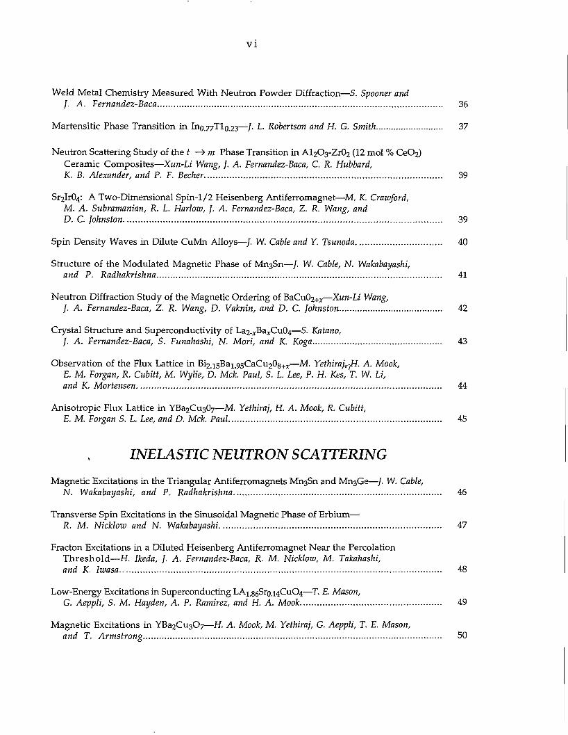
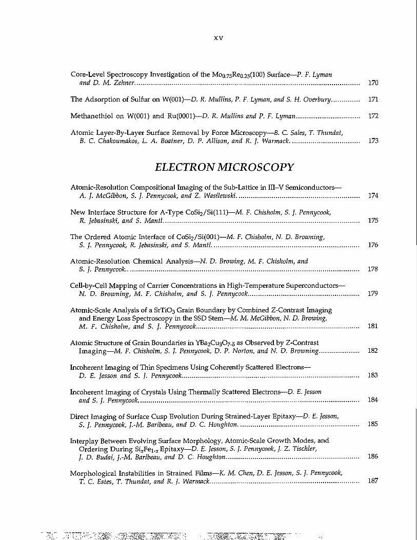
S. H. Liu and R. A. Klemm2
All copper-oxide-based h igh-T c s u p e r
conductors have a stratified crystal structure.
The charge carriers move freely within the Cu02
layers, but hop weakly between the layers. The
effects of the crystal structure on the super
conducting properties have been studied using a
simple model consisting of one superconducting
layer and one normal layer within a unit cell. In
general, the critical temperature T c decreases
with increasing hopping, as shown in Fig. 1.1.
This prediction is in qualitative agreement with
the observation that higher Tc is correlated with
a higher degree of c-axis to ab-plane anisotropy.
One surprising result of the calculation is
that the density-of-states curves (Fig. 1.2) show
double-peaked structures for hopping strengths
comparable to T c although there is only one
ORNL-DWG 93-15791
ORNL-DWG 93-15793R
0.8
<S 0.6
0.4
0.2
S-N Model
0.1 10
Ji/TcO
Fig. 1.1. The dependence of the critical tpm-perature Tc on the hopping strengths for the two-layer model , showing the monotor.ic decrease of T c with increasing hopping.
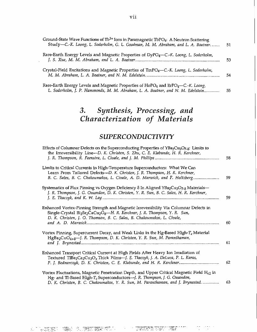
10
8
o ? 6
£ 4
2
0
1 1 1 1 1 1 ' 1 1 1 1 '
ti M
M M
\ j J2/Tc0 = 5
'\r \>
k It l \ 1 v 1/
, 0.1
^ 10
i . . . . I . . . . I . .
- 4 - 3 - 2 - 1 0 1 2 3 4 CO/ Tc0
Fig. 1.2. A set of density-of-states curves at zero temperature for the two-layer model. The curves are displaced vertically by 2 units successively.
energy gap. Neither set of peaks corresponds to
the energy gap, which is marked by arrows.
This contradicts a commonly accepted explana
tion of tunneling data on high-T c materials (i.e.,
that the peaks correspond to the energy gaps in
two different layers). It has been shown that the
two sets of peaks represent the order parameters
of intra- and interband pairing, respectively.
Also, in this range of parameter space, the
density-of-states curves are gapless with V-
shaped bottoms, as seen in many tunneling
experiments. It is concluded that the tunneling
data can be understood on the basis of singlet
pairing without any need to invoke exotic pair
ing mechanisms or electronic properties.
111.
1. Summary of paper to be published. 2. Argonne National Laboratory, Argonne
HIGH-TC SUPERCONDUCTING SUPERLATTICES1
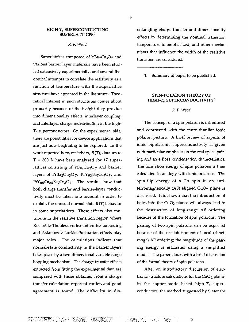
R. F. Wood
Superlattices composed of YBa2Cu3C>7 and
various barrier layer materials have been stud
ied extensively experimentally, and several the
oretical attempts to correlate the resistivity as a
function of temperature with the superlattice
structure have appeared in the literature. Theo
retical interest in such structures comes about
primarily because of the insight they provide
into dimensionality effects, interlayer coupling,
and interlayer charge redistribution in the high-
Tc superconductors. On the experimental side,
there are possibilities for device applications that
are just now beginning to be explored. In the
work reported here, resistivity, R(T), data up to
T = 300 K have been analyzed for 17 super-
lattices consisting of YBa2Cu307 and barrier
layers of PrBa2Cu307, PrYo3Ba2Cu307, and
PrYo5Cao.5Ba2Cu307. The results show that
both charge transfer and barrier-layer conduc
tivity must be taken into account in order to
explain the unusual normal-state R(T) behavior
in some superlattices. These effects also con
tribute in the resistive transition region where
Kosterlitz-Thouless vortex-antivortex unbinding
and Aslamozov-Larkin fluctuation effects play
major roles. The calculations indicate that
normal-state conductivity in the barrier layers
takes place by a two-dimensional variable range
hopping mechanism. The charge transfer effects
extracted from fitting the experimental data are
compared with those obtained from a charge
transfer calculation reported earlier, and good
agreement is found. The difficulty in dis-
3
entangling charge transfer and dimensionality
effects in determining the nominal transition
temperature is emphasized, and other mecha
nisms that influence the width of the resistive
transition are considered.
1. Summary of paper to be published.
SPIN-POLARON THEORY OF HIGH-TC SUPERCONDUCTIVITY1
R. F. Wood
The concept of a spin polaron is introduced
and contrasted with the more familiar ionic
polaron picture. A brief review of aspects of
ionic bipolaronic superconductivity is given
with particular emphasis on the real-space pair
ing and true Bose condensation characteristics.
The formation energy of spin polarons is then
calculated in analogy with ionic polarons. The
spin-flip energy of a Cu spin in an anti-
ferromagnetically (AF) aligned Cu02 plane is
discussed. It is shown that the introduction of
holes into the Cu02 planes will always lead to
the destruction of long-range AF ordering
because of the formation of spin polarons. The
pairing of two spin polarons can be expected
because of the reestablishment of local (short-
range) AF ordering; the magnitude of the pair
ing energy is estimated using a simplified
model. The paper closes with a brief discussion
of the formal theory of spin polarons.
After an introductory discussion of elec
tronic structure calculations for the Q1O2 planes
in the copper-oxide based h igh -T c super
conductors, the method suggested by Slater for
studying AF metals is described. In this
method, as applied here, the chemical unit cell is
doubled to form a magnetic unit cell which con
tains one Cu ion with predominantly up spin
and one with predominantly down spin. Down
spins are kept off up-spin sites and, conversely,
by the introduction of a Hubbard U term. As a
result, the band structure obtained is typical of
that for a Mott-Hubbard (M-H) or, more gener
ally, a charge transfer insulator. Conductivity in
the a-b plane results when holes are introduced
into the M-H valence band. The band structure
as a function of the parameters in Koster-Slater
type calculations is discussed, and the Fermi
surface is described. A calculation of the
derealization energy for spin-polaron formation
is carried out within the context of the band
calculations.
Results from previous papers in this series
are used for the gap and T c within the frame
work of a Cooper-pairing approach. The possi
ble symmetry types of the gap are discussed. It
is shown how the proximity of the Fermi level to
the M-H band edge and the interplay of O 2pa
and 2p% bands and /o r localization effects can
provide good fits to the variation of Tc with x in
La2-x Sr r Cu04 and YBa2Cu307_x It is concluded
that the in-plane gap is either s- or d-like but
anisotropic in either case. Other aspects and
implications of the model and of the calculations
are given, and comparisons with Mott's spin-
bipolaron model are made.
1. Summary of three papers: in Proceedings of the International Symposium on High-Tc Superconductivity and Its Applications, Cairo, Egypt, April 4-16,1993 (in press).
ELECTRON-PHONON INTERACTION NEAR VAN HOVE SINGULARITIES1
G D. Mohan2
Superconductivity occurs when electrons
bind in pairs in a solid. High-temperature
superconductors are composed of planes of
copper oxide, and the motion of super
conducting electrons are confined to these
planes. In two dimensions, the density of
energy states for electrons always have a loga
rithmic singularity at some energy Eg, which is
called the van Hove singularity. There have
been numerous suggestions that this singularity
in the density of states is the cause of high-
temperature superconductivity.
The Eliashberg equations describe the pair
ing of electrons. These equations were solved
for the case where the interaction between elec
trons was caused by the electron-phonon inter
action. It was desirable to see whether the van
Hove singularity increased the transition tem
perature of the superconductor, and it was
found that it did increase T c significantly when
the chemical potential \i was very near Es. How
ever, whenever I |i - Eg I was more than 10% of
the bandwidth, the singularity had no effect on
T c. Because actual superconductors are obtained
by impurity doping, they have a chemical poten
tial which is far from E ; therefore, the van Hove
singularity does not cause high-temperature
superconductivity.
Another calculation was made on the
increase in T c because of an anisotropic energy
gap. It is assumed that the energy gap of the
superconductor was s-wave, but anisotropic; the
variation of the energy gap with angle around

the Fermi line is A((J>) = Ao + A4 cos(4(j)) which
maintains s-wave symmetry. It was also shown
that in addition to the normal electron-phonon
coupling constant Xo, there is another coupling
constant X4 which is associated with an
anisotropic interaction. If X4 is large, then Tc is
increased significantly.
1. Summary of paper: Physical Review B (in press).
Z ORNL/UT Distinguished Scientist.
RESISTIVITY AND SUPERCONDUCTIVITY FROM ANHARMONIC PHONONS1
G. D. Mahan2 and J. O. Soft?
The electrical resistivity is calculated for electron scattering from anharmonic phonons. Phonon potential energies of the form ~Q", as well as double-well potentials ~Q 4 - ocQ2, were considered. For phonon potential energies with a power law ~Qn, the resistivity at high temperatures is proportional to T^/n. At low temperatures, the resistivity rises rapidly and then flattens, thereby forming a knee shape. This behavior explains the resistivity of cuprate superconductors in the normal state.
A question that appears immediately is are these anharmonic phonons the gluing bosons of the superconducting state. To answer this question, the Eliashberg theory was applied to calculate the critical temperature, using the anharmonic phonons, to see if the same set of parameters used to explain the resistivity measurements can explain the high critical temperature of the cuprates. These results show that it is
5
impossible to find a proper set of parameters to
match the results of the resistivity and the criti
cal temperature.
Quite reasonable values explain the electri
cal resistivity. However, much larger values of
the electron phonon coupling constant are
needed for higher values of Tc. These large
values would predict a much larger resistivity
than is observed. The situation is different in the
A-15 compounds. They have large values of
resistivity, and smaller values of Tc. It is more
likely that the anharmonic phonons are pairing
the electrons in the superconducting state.
1. Summary of paper: Phys. Rev. B 47,8050 (1993).
Z ORNL/UT Distinguished Scientist. 3. ORNL/ORISE postdoctoral research
associate.
FRUSTRATION-INDUCED DISORDER OF FLUX LINES IN LAYERED
SUPERCONDUCTORS1
G. I. Watson2 and G. S. Canright?
A "frustrated" system is one whose Hamil-tonian is a sum of terms which cannot all be minimized simultaneously. For such systems, it is often a nontrivial task to deduce the ground state; furthermore, there may be many metastable states which are strongly competitive with the global minimum of the free energy. All these low-energy states are, in general, quite complex and not easily studied.
A standard technique for frustrating a system is to introduce random disorder into the Hamiltonian. However, this widely studied
idea neatly circumvents one-half of the problem,
because the disorder presumably came from
some underlying frustration in a simple Hamil-
tonian without disorder (e.g., the Hamiltonian of
a set of impurities interacting with a host
material).
A model which lacks disorder in the Hamil
tonian, but nevertheless is highly frustrated, has
been chosen for study. This model may be
physically real ized 4 by flux lines in layered
superconductors. It also may be mapped to a
one-dimensional XV model with long-range
antiferromagnetic coupling—hence, the frustra
tion. (The purely antiferromagnetic, long-range
coupling arises from the pure repulsion among
the flux lines.) Some interesting but highly
structured metastable states were found by
Levitov. 4 Prior to our work, however, there was
no systematic way to study the enormously
many complex metastable states which may, in
fact, compete with the ground state for a frus
trated system. Pursuing Levitov's analogy of
this problem with plant growth (phyllotaxis),
flux-line lattices were numerically "grown"
using an algorithm which should give energeti
cally favorable configurations as attractors. Both
periodic (of many different periods) and
aperiodic (chaotic) attractors for the algorithm,
representing long-period and disordered flux-
line lattices, respectively, were found. It was
also shown that all of these structures are com
petitive in energy with the lowest state, which is
still (so far) a simple period-one (Bravais) lattice.
This method is the only one, to our knowledge,
which allows the systematic generation of com
plex (including disordered) metastable states.
The method will be exploited further with a
number of frustrated one-dimensional models,
such as the Frenkel -Kontorova mode l
(representing lattice mismatch between substrate
and overlayer) and the ANNNI model (relevant
to s tacking po ly typ i sm in metals and
semiconductors).
1. Summary of paper to be published. 2. Guest scientist from the ORNL/UT
Distinguished Scientist Program. 3. Guest scientist from The University of
Tennessee, Knoxville, Term. 4. L. S. Levitov, Phys. Rev. Lett. 66,224
(1991).
NUMERICAL SIMULATION AND BAND STRUCTURE
A NEW EXTENDED POINT DEFECT STRUCTURE IN DIAMOND
CUBIC CRYSTALS1
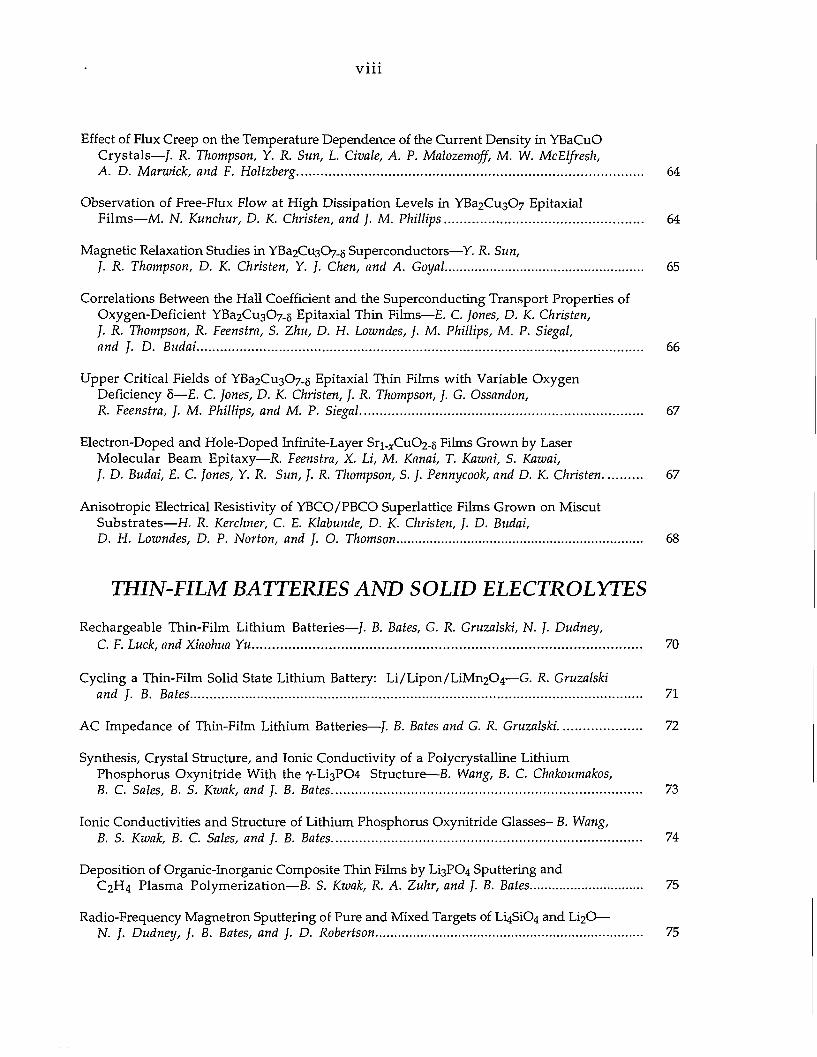
Mark Mostoller, Theodore Kaplan, and M. F. Chisholm
In the course of atomistic simulations of the
dislocation array at the Ge/Si(001) interface, a
new closed symmetric defect structure compris
ing 18 atoms has been generated that may be
found in a variety of circumstances, including
dislocations and grain boundaries. The struc
ture maintains tetrahedral bonding with reason
able changes in bond lengths and angles and
may have interesting electronic properties. This
new structure is called a "dreidl" after the
child's top that it resembles. 2
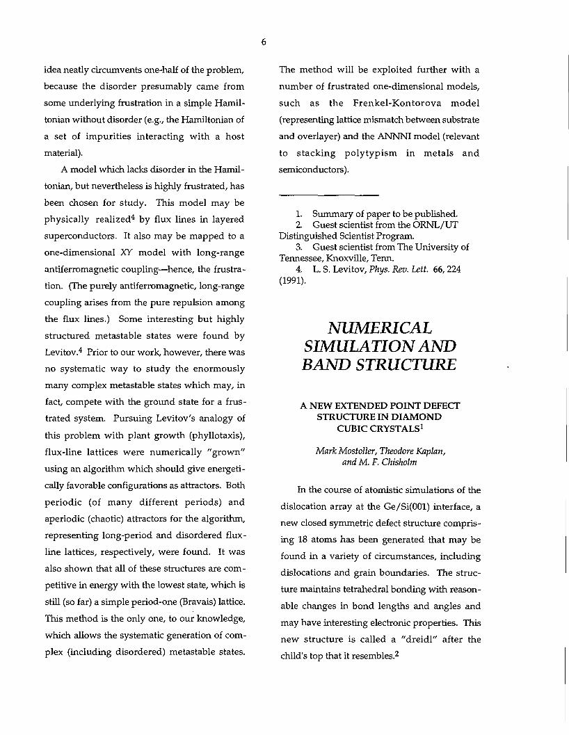
In a perfect diamond cubic structure, the atoms form sixfold rings viewed along [1,±1,0]. Commonly observed defect structures are alternating fivefold and sevenfold rings, joined to form a figure of 10 atoms with 2 shared by the pentagon and the heptagon. These occur, for example, in the core of the (a/2)[l,l,0] edge dislocation, in the 90° partial dislocation, and in the S9 twin boundary.
There is almost precisely a 4% mismatch between the lattice constants of Ge and Si. When a film of Ge is grown epitaxially on an Si(001) substrate, the misfit strain can result in the formation at the interface of a regular two-dimensional array of edge dislocations with Burgers' vectors (a /2)[1,±1,0]. Classical molecular dynamics simulations have been made of this dislocation array for rather large microcrystals (~20,000 atoms). The minimum energy structure of the dislocation grid was obtained by a sequence of simulated annealing runs followed by conjugate gradient minimization using the Stillinger-Weber and Tersoff potentials.
The simulations yield orthogonal edge dislocations, each with the five- plus sevenfold core structure, with the core of one displaced above the other by one layer a /4 along [0,0,1]. At their intersection, they form the closed symmetric structure shown in Fig. 1.3, the dreidl. The fivefold rings join at the bottom; the sevenfold rings at the top. While tetrahedral bonding is maintained, changes in bond lengths and angles are somewhat larger than those at the core of a single-edge dislocation, raising the possibility that electronic states localized at the dreidl may penetrate deeper into the band gap and make
SSDN-4670
Fig. 1.3. The dreidl, a closed symmetric structure of 18 atoms predicted by simulations to occur at the intersection of (fl/2)[l,l,0] dislocations in Ge/Si. The [0,0,1] direction connects the bottom Si atom and the top Ge atom.

the defect electrically active. At the Ge-Si inter
face, these new defects may reach a very high
planar concentration of ~10 1 2 / cm 2 .
1. Summary of paper to be published. 2. dreidl \ rhymes with cradleM: a 4-sided
toy marked with Hebrew letters and spun like a top in a game of chance, Webster's Ninth New Collegiate Dictionary.
A NEW EMPIRICAL POTENTIAL FOR Si AND Ge
Mark Mostoller, Benjamin Liu} and Theodore Kaplan
Several empirical potential models, notably
those of Stillinger and Weber 2 and of Tersoff,3
have been widely used in classical simulations
of bulk Si and Ge, of their surface structure and
dynamics, and of various defects and interfaces.
These models combine central pair potentials
with three-body angular terms that penalize
variations away from tetrahedral bonding.
Despite some successes, these potentials suffer
from some well-known shortcomings. They are
both very short range, with the pair potential
contributions extending only to first nearest
neighbors (INNs), so that, for example, a stack
ing fault introduces no change in total energy.
They predict symmetric dimers at the Si(OOl)
surface, where buckled asymmetric dimers are
observed. They do a poor job of fitting the bulk
lattice vibrations, particularly the elastic con
stants, which are crucial to simulations of dis
location properties.
A new empirical potential model that
includes four-body as well as two- and three-
body interactions in a fashion demanded by the
bulk lattice dynamics has been formulated. A
family of numerically specified potentials has
been found, extending from the INN separation
on out, that matches the experimental values for
the lattice constant and cohesive energy and that
gives a good fit to the bulk phonon dispersion
curves. The pair potentials for this family do not
exhibit a single well, but rather a minimum near
the INN separation, then a rise to a shoulder or
actually oscillatory behavior at greater distances.
As yet, however, it has not been possible to con
struct a simple functional form for the pair
potential that extends to shorter distances than
INN in a way that retains diamond cubic as the
equilibrium structure.
1. Graduate student from the University of Pennsylvania, Philadelphia, Pa.
2 F. H. Stillinger and T. A. Weber, Phys. Rev. B 31,5262 (1985).
3. J. Tersoff, Phys. Rev. B 39,5566 (1989).
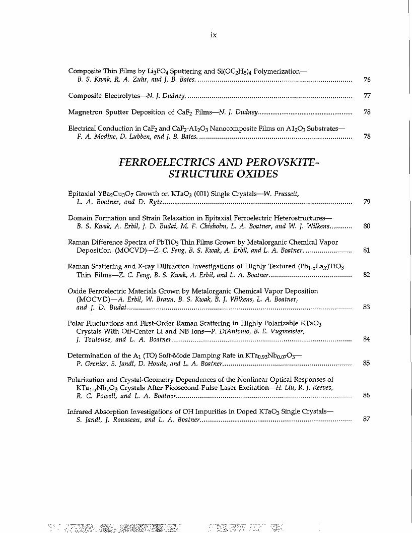
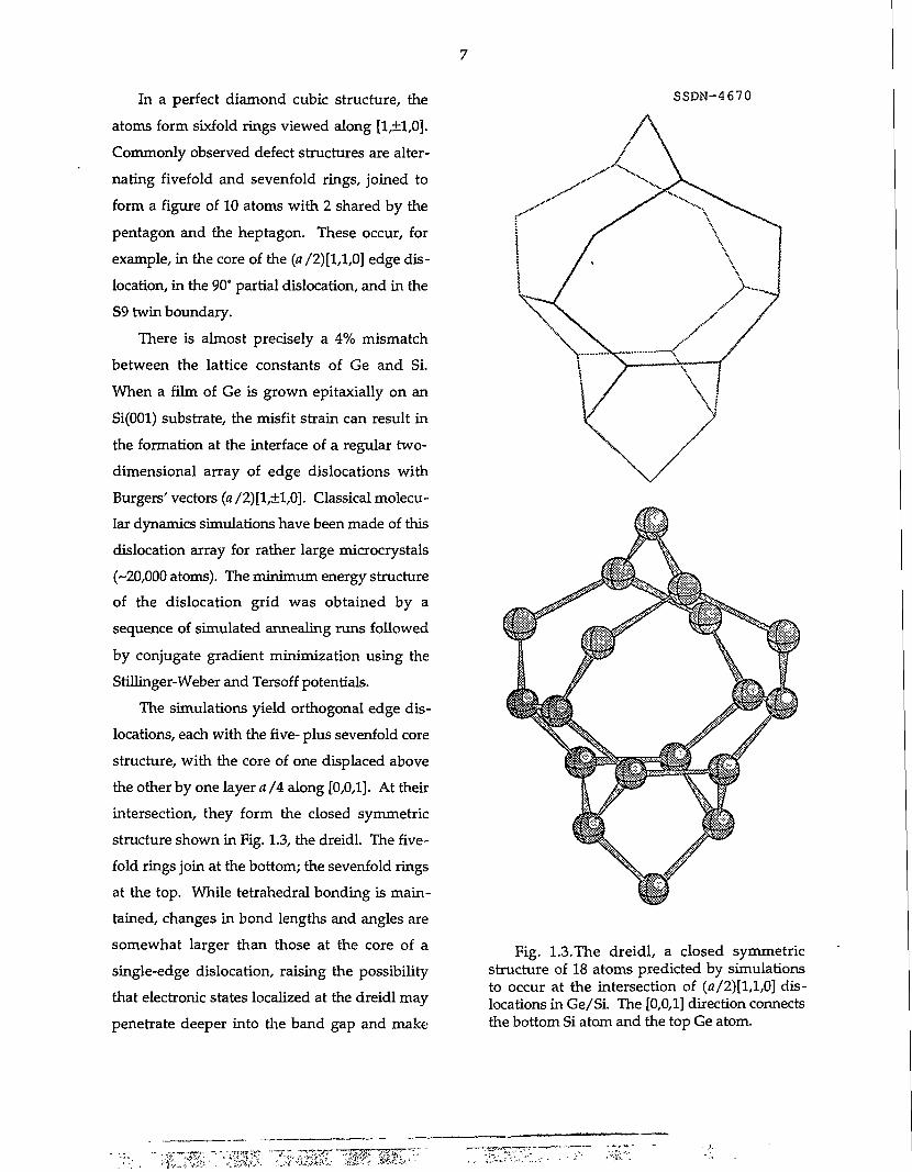
NUMERICAL SIMULATION OF H e +
AND Li + COLLISIONS WITH Q Q 1
T. Kaplan, M. Rasolt,2
M. Karimi,3, and Mark Mostoller
Since the recent discovery of an efficient
process for the synthesis of fullerenes, there has
been a dramatic increase in interest in these
compounds. Recent research efforts have
focused on developing new fullerene-based
materials. One method that has been investi
gated is the incorporation of dopants into the
hollow cage structure of C60 through high-
energy collisions. Numerical simulations of
high-energy collisions of He + and Li+ with Cgo in
free space and on the surface of an Fe substrate
have been carried out. These calculations were
undertaken with the aims of interpreting and
serving as a rough complementary guide to
ongoing experiments by R. A. Zuhr and
collaborators.
Classical molecular dynamics is used to
simulate the collision process. The implantation
of He + has been observed to form endohedral
0.01 ps
0.05 ps
He+@Cgo a * various energies in the energy range 35-90 eV. Figure 1.4 shows a few frames for a 45-eV He + collision at normal incidence on a six-member ring of the C^o molecule on an Fe substrate. Li + collisions with C60 do not form Li+@C6o • Instead, insertion and fragmentation were found to form Li+@Cs4 and Li+@C56 in the energy range 115-200 eV. The yield of any particular collision depends strongly not only on the incident energy but also on the incident
SSDN-4669
0.03 ps
0.11 ps
Fig. 1.4. The 45-eV He + collision at normal incidence with the six-member ring of a Cgo molecule on an Fe substrate at 0.01,0.03, 0.05, and 0.11 ps. The H e + ion is indicated by the larger ball and the position of the substrate by the solid bar. The H e + is trapped in the endohedral cavity of the C(,Q.
10
angle and the point of impact and has a weak
dependence on whether or not the C(,Q is on the
substrate or in free space.
1. Summary of paper: /. Phys. Chem. 97, 6124 (1993).
Z Deceased. 3. ORISE faculty research participant from
Indiana University of Pennsylvania, Indiana, Pa.
THE STATISTICS OF SPUTTERING1
Mark T. Robinson
The sputtering of crystalline solids by ener
getic ions has well-known dependences on the
kinetic energy and direction of the incident ions
and on the crystallographic orientation of the
target surface, as well as on the nature of the
atoms and other variables. The sputtering yield
is the number of atoms ejected by a single ion,
averaged over the asymmetric mesh on the tar
get surface. Unlike currently feasible experi
ments, computer simulations allow the study of
fluctuations in the yield from one ion to another.
Several studies report distributions of single ion
yields, without discussing the origin of the fluc
tuations (for a review, see ref. 2). At low ion
energies, these show a moderately broad distri
bution with a mode somewhat near the mean.
At higher energies, however, a significant frac
tion of the ions, increasing with energy, pro
duces no sputtering at all, the distribution
extends to yields much higher than the mean,
and there is often no well-defined mode near the
mean.
The MARLOWE program was used to study
the statistics of sputtering, on the example of
1-100-keV Au atoms, normally incident on static
{001} and {111} Au crystals. The yield of sput
tered target atoms was examined as a function
of the impact point of the incident atoms on the
target surfaces. At a given energy, yields varied
over a wide range: for 20-keV Au on {001}, for
example, yields ranged from 0 to 104 in a sample
of 1225 events, with a mean of 25.6 ± 0.6; at 100
keV, where the mean is 25.6 + 1.4, individual
values ranged from 0 to 328. Spatial structure
was observed in the yield on two different
scales. The effects of axial and planar channel
ing could be traced, with the details depending
on the target orientation and the ion energy.
Channeling is clearly responsible for broad
regions of low yield. Locally, however, the yield
was very sensitive to the impact point, small
changes in position often producing large
changes in yield. The results indicate strongly
that the sputtering yield is a random ("chaotic")
function of the impact point, superimposed on a
structural variation because of channeling.
1. Summary of paper: Nuclear Instruments and Methods in Physics Research Section B (in press).
Z M. T. Robinson, K. Dan. Vidensk. Selsk. Mat. Fys. Medd. 43,27 (1993).
SIMULATION OF PLASMA-BASED MATERIALS PROCESSING TECHNIQUES
C.-L. Liu} D. B. Geohegan, J.-N. G. Leboeuf,2 and R. F. Wood
Progress has been made in this first year
toward all three original goals of this project;
namely, development of plasma formation and
transport modules, module integration, and
module optimization. In the laser ablation area, integration of laser materials interactions and plasma plume transport modules has been achieved. A one-dimensional (ID) version of Laser8 has been extended to handle not only the melting of the material by the laser but also its vaporization, as well as the plasma formation phase. Output from Laser8 now provides input density and temperature profiles to a ID, gas dynamics, plasma plume transport module. This module provides for absorption of the laser energy by way of several plasma processes (e.g., electron-neutral and election-ion inverse bremsstrahlung and plasma resonance.) As the temperature of the plasma increases, charged species of Si are assumed to be generated in concentrations predicted by the Saha equation. Even before vaporization of the surface, electrons and ions can be generated by thermionic emission, and these also may contribute to plasma ignition. The integrated model shows formation of shock and ionization fronts in the early stages of plume expansion and yields velocities in the experimentally measured range. Moreover, a novel 2D particle-in-cell hydro-dynamic plume transport model with appropriate boundary conditions has been devised. Expansion and transport of the plasma from point of formation to the substrate, including reflections therefrom, have been simulated successfully. Modeling of laser ablation is leading to the consideration of otherwise neglected ion-
•TJmy $&•• %--iW-'MfWF:
11
ization and absorption mechanisms and motivating more detailed experiments in silicon.
1. ORNL/ORISE postdoctoral research associate.
Z Physics Division, ORNL.
QUANTUM MONTE CARLO WITH COMPLEX WEIGHTS1
Lizeng Zhang,2 G. S. Canright,2 and T. Barnes3
Quantum Monte Carlo techniques are widely used for problems for which standard analytical techniques, such as mean-field and perturbation theory, are not reliable. Previously, such techniques were applied to two types of many-particle problems: bosons—which are relatively tractable even at low temperatures because their ground state is nodeless—and fermions. Given the importance of electrons in condensed matter, the fermion problem has always been a very high priority, but unfortunately much more difficult to treat by Monte Carlo sampling, because of the presence of alternating signs in the wave function—the "sign problem."
An algorithm (previously used almost exclusively for bosons) has been adapted to allow for a continuous variation of the statistics parameter (i.e., the exchange phase 6) from the Bose to the fermi limit. In between, the particles
12
are anyons, and the Hamiltonian and ground
state are necessarily complex. It has been shown
that anyons can be successfully simulated by
this technique; this represents the first applica
tion of quantum Monte Carlo to the anyon prob
lem. It has also been shown that fermions can be
represented in a "complex gauge" as anyons
with 0 = 7C. By treating fermions in this "anyon
representation," it has been possible to explore
the many possible "gauge choices" for the sta
tistical "flux." In fact, the sampling error (and
therefore the computing time needed) for
fermions can be greatly reduced by an appropri
ate choice of gauge. However, it remains to be
seen whether this (improved) method can be a
practical method for treating many fermions,
because the improvement gained is with respect
to a starting point which was not practical and
other methods exist. Further work will be
needed to optimize the current method and
assess its ultimate efficiency.
Particles in an external magnetic field—
another "complex" problem—have been investi
gated. This is another first for our method. It
has been shown that the noise arising from the
"statistical" flux and from the external flux can
cancel to a large extent. Hence, fermions can be
treated in a large external field much more easily
than zero-field fermions. Plans are being con
sidered to exploit this possibility to simulate the
quantum Hall effect in future work.
1. Summary of papers: p. 199 in Computer Simulation Studies in Condensed-Matter Physics VI, ed. by D. P. Landau, K. K. Mon, and H.-B. Schiittler, Springer-Verlag, Berlin, 1993; to be published.
2. Guest scientist from The University of Tennessee, Knoxville, Term.
3. The University of Tennessee, Knoxville, Tenn., and Physics Division, ORNL.
LARGE-SCALE AB INITIO STUDY OF THE BINDING AND DIFFUSION OF A
Ge ADATOM ON THE S i(100) SURFACE'
V. Milman,2 D. E. Jesson, S. J Pennycook, M. C Payne,3 M. H. Lee,3 and I. Stich3
The study of fundamental atomistic pro
cesses that govern the surface kinetics of the
epitaxial growth of Si-Ge materials is of consid
erable scientific and technological interest. 4 ' 5
Scanning tunneling microscopy (STM) experi
ments cannpt establish the exact nature of the
adsorption site or the migration path for an
individual Ge adatom. These important issues
can be resolved by a theoretical study of Ge
adsorption and diffusion on the Si surface from
first principles. Using the pseudopotential total
energy method, it was possible to resolve the
controversy regarding the binding geometry and
migration path for the adatom and to investigate
its influence on the buckling of Si dimers. The
supercell that was of a sufficient size for this
purpose contained 194 atoms, and the study was
made possible only by using massively parallel
computers. 6
The energy surface was mapped out by cal
culating the total energy for fixed (x,y) positions
of the adatom with the total energy minimiza
tion in the space of ionic coordinates and wave-
function expansion coefficients. The global min
imum is found on top of the second layer atom
(Fig. 1.5), while the pedestal site on top of the
13
SSDN-4668
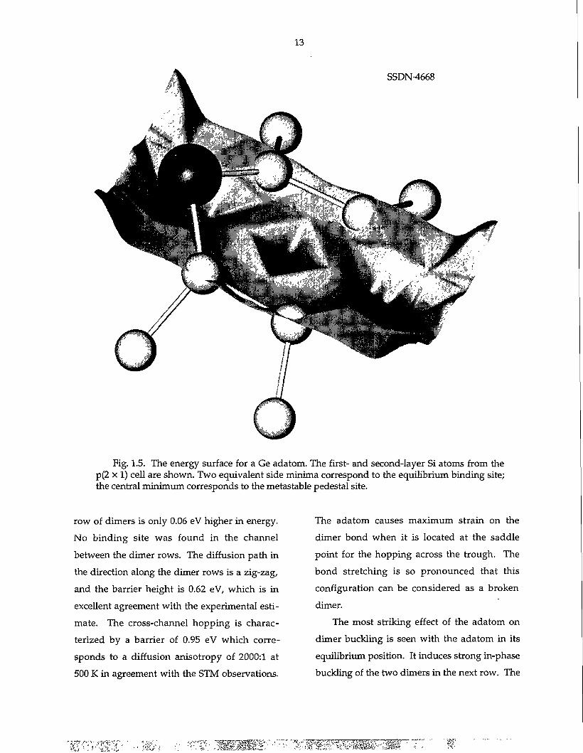
Fig. 1.5. The energy surface for a Ge adatom. The first- and second-layer Si atoms from the p(2 x 1) cell are shown. Two equivalent side minima correspond to the equilibrium binding site; the central minimum corresponds to the metastable pedestal site.
row of dimers is only 0.06 eV higher in energy. No binding site was found in the channel between the dimer rows. The diffusion path in the direction along the dimer rows is a zig-zag, and the barrier height is 0.62 eV, which is in excellent agreement with the experimental estimate. The cross-channel hopping is characterized by a barrier of 0.95 eV which corresponds to a diffusion anisotropy of 2000:1 at 500 K in agreement with the STM observations.
The adatom causes maximum strain on the dimer bond when it is located at the saddle point for the hopping across the trough. The bond stretching is so pronounced that this configuration can be considered as a broken dimer.
The most striking effect of the adatom on dimer buckling is seen with the adatom in its equilibrium position. It induces strong in-phase buckling of the two dimers in the next row. The
14
resulting configuration of two adjacent dimers
buckled in the same direction has indeed been
observed experimentally, and it is suggested
that the observed buckle-inducing defects might
correspond to single Si adatoms. Their imaging
gives the only experimental information avail
able on the binding site of the adatom.
1. Summary of paper to be published. Z ORNL/ ORISE postdoctoral research
associate. 3. University of Cambridge, Cambridge,
United Kingdom. 4. D. E. Jesson, S. J. Pennycook, and J.-M.
Baribeau, Phys. Rev. Lett. 66,750 (1991). 5. D. E. Jesson et al., Phys. Rev. Lett. 68,
2062 (1992). 6. This research is part of the Grand Chal
lenge Project on "First-Principles Simulation of Materials Properties," funded by the High-Performance Computing and Communications Initiative.
HYDRATION OF Mg-CORDIERITE INVESTIGATED BY AB INITIO TOTAL
ENERGY CALCULATIONS l
B. Winkler,2 V. Milman,3 and M. C. Payne^
Ab initio total energy calculations based on
the local density approximation (LPA) have
been performed for hydrated Mg-cordierite to
elucidate the location, orientation, and total
energy of hydration in the ground state. The
orientation and dynamics of the water molecule
in cordierite, Mg2Al4SisOi8 • 71H2O, have been
the subject of several contradicting spectroscopic
and structural studies. In view of experimental
difficulties, quantum mechanical calculations
present a unique tool for the atomistic modeling
of this system. This is especially true for the
hydrogen-containing materials, as these are dif
ficult to simulate using empirical potentials.
Modeling of hydrated cordierite required a
supercell containing 61 atoms of 5 different
species, which represents the most complicated
inorganic compound ever studied using the
first-principles LDA method.
In contrast to structural studies, but consis
tent with the interpretation of infrared experi
ments, the calculations demonstrate that the
stable configuration of the water molecule in
alkali-free Mg-cordierite has a proton-proton
vector aligned parallel to the (001) direction.
The water molecule is found to be nearly undis-
torted, and there is only a weak hydrogen
bonding. This result confirms an interpretation
of the existing spectroscopic and quasielastic
neutron scattering data. Furthermore, the ab
initio calculation predicts that the water
molecule is displaced with respect to the center
of the cavity by 0.04 A along (001), which is con
sistent with the results of quasielastic neutron
scattering experiments. The calculated internal
structure opens the way to correct interpretation
of the recent contradictory structural and
calorimetric studies.
The total energy of hydration for cordierite
with one water molecule per primitive unit cell
has been calculated to be 0.4 eV. The local dis
tortions caused by the hydration are very small,
thus indicating an ideal mixing behavior. The
results related to the water molecule docking in
the cavity are expected to be applicable to a
number of water-bearing minerals.
1. Summary of paper to be published.
2. Kiel University, Kiel, Germany. 3. ORNL/ORISE postdoctoral research
associate. 4 University of Cambridge, Cambridge,
United Kingdom.
MAGNETIC PROPERTIES
MAGNETIC STRUCTURE AND SPIN DYNAMICS OF CHROMIUM ALLOYS1
R. S. Fishman2 and S. H. Liu
It has been known for many years that the antiferromagnetic ordering properties of chromium are profoundly influenced by adding a small amount of transition-metal impurities. For instance, while 4% of vanadium impurity can suppress magnetic ordering entirely, the same percentage of manganese impurity doubles the Neel temperature T^. Also, the ordered state of pure chromium is a spin-density wave with a periodicity incommensurate with the lattice; as little as 1% of manganese impurity renders the magnetic structure commensurate.
A consistent model, which has answered a number of puzzles, for the impurity effects has been constructed. There are three factors involved. Impurities on the right-hand side of chromium on the periodic table add electrons to the systems, which improve Fermi surface nesting and raise T^. Conversely, impurities on the left-hand side of chromium on the periodic table lower Tfj. Impurity sites also provide scattering centers for the band electrons, and these cause Tfj to decrease. The third factor is that the nest-
15
ing model is only approximately correct. The spin-density wave state with minimum free energy has a wave vector slightly shifted from the nesting position. The combined effects of these three factors give an excellent account of the observed magnetic ordering properties of chromium alloys.
The same model has been used to predict the nature of paramagnetic spin fluctuations above T^. In general, the constant-energy neutron scattering cross section shows two peaks at positions corresponding to the wave vectors of magnetic ordering below T^. The two peaks can be shifted by adding impurities in the same way as the magnetic ordering wave vector. The temperature provides an additional parameter which modifies the linewidths and peak positions. Detailed predictions have been made and are being tested experimentally at the Brookhaven National Laboratory.
1. Summary of papers: Phys. Rev. B 47, 11870 (1993); ibid 48,3820 (1993).
2. ORISE faculty research participant from North Dakota State University, Fargo, N. Dak.
ROLE OF ELECTRONIC SCREENING IN ITINERANT-ELECTRON MAGNETS1
/. F. Cooke, J. M. Bass,2 and }. A. Blackman2
Results from previous calculations of the static and dynamic properties of itinerant-electron magnets have been shown to be in excellent agreement with corresponding experimental results for nickel, iron, and cobalt at low
16
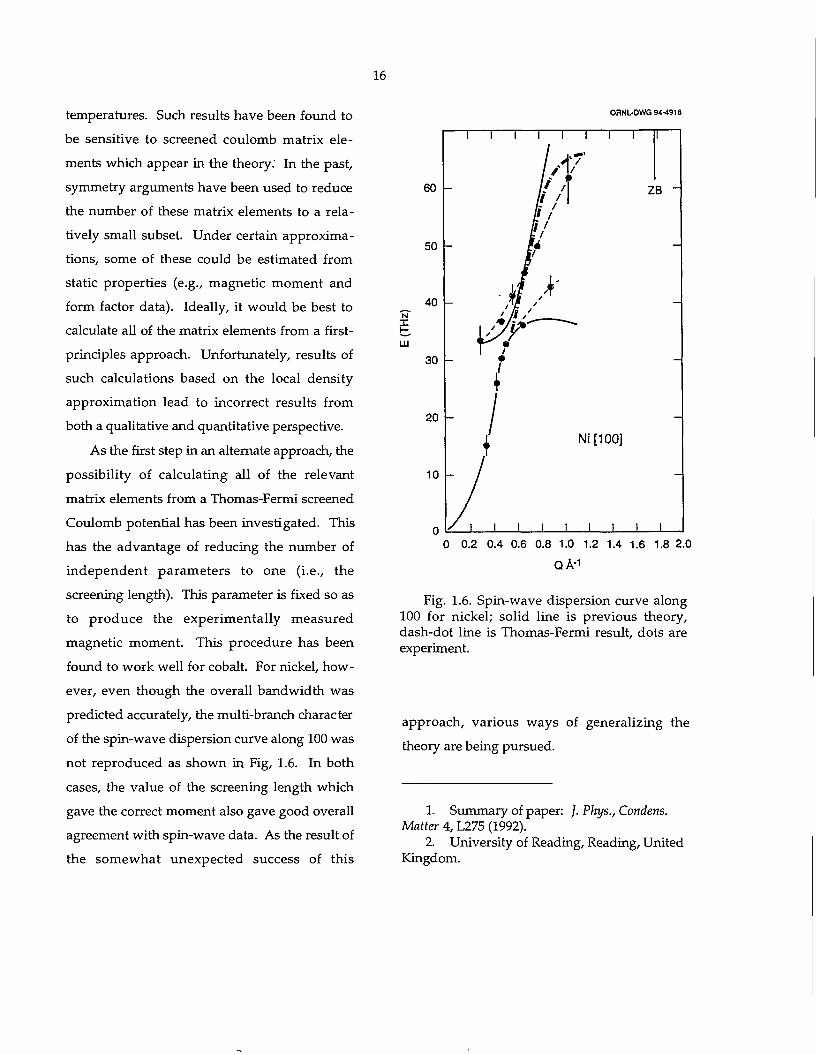
temperatures. Such results have been found to
be sensitive to screened coulomb matrix ele
ments which appear in the theory. In the past,
symmetry arguments have been used to reduce
the number of these matrix elements to a rela
tively small subset. Under certain approxima
tions, some of these could be estimated from
static properties (e.g., magnetic moment and
form factor data). Ideally, it would be best to
calculate all of the matrix elements from a first-
principles approach. Unfortunately, results of
such calculations based on the local density
approximation lead to incorrect results from
both a qualitative and quantitative perspective.
As the first step in an alternate approach, the
possibility of calculating all of the relevant
matrix elements from a Thomas-Fermi screened
Coulomb potential has been investigated. This
has the advantage of reducing the number of
independent parameters to one (i.e., the
screening length). This parameter is fixed so as
to produce the experimentally measured
magnetic moment. This procedure has been
found to work well for cobalt. For nickel, how
ever, even though the overall bandwidth was
predicted accurately, the multi-branch character
of the spin-wave dispersion curve along 100 was
not reproduced as shown in Fig, 1.6. In both
cases, the value of the screening length which
gave the correct moment also gave good overall
agreement with spin-wave data. As the result of
the somewhat unexpected success of this
ORNL-DWQ 94-4918
N X UJ
0 0.2 0.4 0.6 0.8 1.0 1.2 1.4 1.6 1.8 2.0 QA-1
Fig. 1.6. Spin-wave dispersion curve along 100 for nickel; solid line is previous theory, dash-dot line is Thomas-Fermi result, dots are experiment.
approach, various ways of generalizing the
theory are being pursued.
1. Summary of paper: /. Phys., Condens. Matter 4, L275 (1992).
2. University of Reading, Reading, United Kingdom.
17
ELECTRONIC THEORY AND THE MAGNETIC MOMENT OF
ITINERANT-ELECTRON SYSTEMS 1
/. F. Cooke
The magnetic moment of itinerant-electron
systems can be determined directly from the
correlation function <ct^(Cft^a> where n is the
energy band index, k is the wave vector, and a is
the spin. One of the most straightforward ways
of determining this correlation function is to use
the Green's function formalism. The relevant
Green's function which must be calculated is the
single-particle propagator. By using diagram
matic expansions, functional derivative, or equa
tion of motion methods, an equation can be
derived for the single-particle propagator in
terms of the electronic self-energy. This
approach establishes a direct link between the
electronic self-energy, the electronic band struc
ture, and the.magnetic moment of itinerant-
electron systems. The simplest application of
this theory is based on the random phase
approximation (RPA). This leads to predictions
that the magnetic moment per site decreases
with increasing temperature, eventually going to
zero at a Curie temperature, which is well above
experimental values for t ransi t ion-metal
systems.
There are, of course, many factors which
could account for this discrepancy. Perhaps the
most obvious is that the RPA calculation does
not include spin-wave contributions. In princi
ple, creation of spin waves reduces the moment
of the system. This is obvious for local moment
systems where the zero temperature moment is
directly reduced by the number of spin waves.
For itinerant systems, such contributions must
be included in the electron self-energy
expression. Phenomenological approaches of
including spin-wave contributions lead to
minimal corrections. In order to assess the
importance of terms in the self-energy beyond
RPA, formal expressions have been derived
using the functional derivative technique. The
terms can be divided into contributions from
ladder, bubble, and exchange diagrams. Work
on obtaining numerical estimates of the size of
these various terms is currently under way. In
addi t ion, numer ica l investigation of the
temperature dependence of relevant coulomb
matrix elements, which result from the spin
dependence of the radial part of the electronic
wave function, indicates that this effect may also
be important.
1. Summary of paper to be published.
LONGITUDINAL AND TRANSVERSE SPIN DYNAMICS IN THE SINUSOIDAL PHASE
OF ERBIUM AND THULIUM1
S. H. Liu and ]. F. Cooke
Spin dynamics in the sinusoidal phase of
erbium and thulium have been studied experi
mentally for some time. Unlike the low-
temperature phases, data for the sinusoidal
phase are difficult to interpret because the
inelastic neutron scattering lines are broad and a
reliable theory has not been developed. This
deficiency has been addressed by formulating a
theory using a radically different approach from
the conventional spin-wave theory.
All theories of spin dynamics rely on some
form of mean-field decoupling approximation.
The conventional spin-wave theory treats the
ordered moment as an approximate constant of
motion. In the sinusoidal phase where the
ordered moment is small and spatially varying,
this procedure becomes questionable. This new
method calculates the moments of the fre
quency, treating both the ordered moments and
the two-spin correlation functions as constants
of motion. As a result, the theory should be reli
able from the well-ordered phase up to the
paramagnetic phase. A drawback is that it does
not give a formula for the line shape directly.
With enough moments, however, one can fit the
results to a sum of Gaussian lines and obtain a
theoretical line shape that can be compared with
experiments. In the sinusoidal phase, calcula
tions up to the fourth moment of the frequency
have been made, and the results have been fit to
two Gaussian functions. It is found that both
transverse and longitudinal modes are broad
lines, but for different physical reasons. There
has been one report on narrow longitudinal
modes in Er, but it is concluded that the obser
vation may be spurious. Only broad longi
tudinal lines are seen in Tm, which is in agree
ment with our theory.
1. Summary of paper to be published.
SPONTANEOUS MAGNETIZATION OF ANYONS WITH
LONG-RANGE REPULSION1
Jaichul Yi2 and G. S. Canright2
One of the controversial tests of the "anyon
s u p e r c o n d u c t o r " m o d e l for the h igh-
temperature superconductors (HTSc) has been
the search for spontaneous magnetic moments 3
arising from the broken time-reversal symmetry
of the anyons. The controversy arises from the
theoretical side, because there are a variety of
estimates 4 ' 5 for the spontaneous magnetization,
ranging from zero to much larger than the
experimental threshold of resolution. One of the
main problems in this area is the use of mean-
field theory for the fractional statistics; it is not
clear whether estimates of physical properties
which are derived from mean-field theory are
reliable.
This question has been examined previ
o u s l y 4 for noninteracting anyons, using the
virial expansion, which is a high-temperature,
low-density expansion which avoids the use of
mean-field theory. In the present work, it was
found that the second virial coefficient for
anyons interacts with a long-range repulsion
(°=l/r 2). It was also found that the spontaneous
magnetization, derived in this limit from the
second virial coefficient, is drastically reduced
by the repulsive interaction. This result, coupled
with our earlier estimate 3 from exact numerical
results at T = 0, implies that the spontaneous
magnetization of interacting anyons is small or
zero over a wide range of temperatures. Hence,
it is believed that measurements of the local
magnetization in the HTSc are not a good test
for the anyon hypothesis.
1. Summary of paper: Phys. Rev. B 47,273, 1993.
2. Guest scientist from The University of Tennessee, Knoxville, Term.
3. B. I. Halperin, J. March-Russell, and F. Wilczek, Phys. Rev. B 40,8726,1989.
4. G. S. Canright and M. D. Johnson, Phys. Rev. B 42,7931 (1990).
5. Y. Kitazawa, Phys. Rev. Lett. 65,1275 (1990).
MAGNETOPLASMA EDGE MODES OF TWO-DIMENSIONAL
ELECTRON GAS SYSTEMS1
/. /. Quinn2 and X. Xia2
A two-dimensional (2D) electron gas in
which the electron concentration drops abruptly
from its bulk value to zero supports an edge
plasmon whose frequency is about 10% lower
than the frequency of a bulk 2D plasmon of the
same wavelength. For an edge electron density
profile which does not drop abruptly to zero, a
sequence of higher multipole edge modes occur
below the bulk 2D plasma frequency. These
modes have been studied for several model edge
density profiles, and the results are consistent
with picturing them as bulk modes of the low-
density surface region which cannot propagate
into the bulk. In the presence of a dc magnetic
field B normal to the 2D layer, a number of new
low-frequency modes are found for one direc
tion of propagation along the edge. For a
double-step profile, these low-frequency modes
'•:--?k"' "•Wr^MKr%'
appear to be coupled inter- and regular-edge
magnetoplasma modes. For smooth profiles,
many low-frequency magnetoplasma edge
modes are found. The nature of these modes
and their potential use in VLSI circuits are being
investigated.
1. Summary of paper to be published. 2 Guest scientist from The University of
Tennessee, Knoxville, Tenn.
NUMERICAL STUDIES OF TWO-DIMENSIONAL ELECTRON-HOLE
SYSTEMS IN A STRONG MAGNETIC FIELD1
/. /. Quinn2 and Ximing Chen2
The eigenstates of a two-dimensional system
containing a finite number (Ne = 6, 7, 8) of elec
trons interacting with one or more valence band
holes are obtained by numerical diagonalization
within the subspace of the lowest Landau level.
The valence band holes are located on a plane
separated by a distance d from the electron layer,
and the holes can be free or localized on defects.
Studies of the energy spectrum as a function of
Landau level degeneracy 2S + 1 and layer sepa
ration d help to illuminate the nature of the low-
lying excitations of the quantum Hall states.
Strong evidence for the existence of stable
"anyonic ions" or "anyonic excitons," bound
states of the valence band hole and one or more
Laughlin quasielectrons, is found. The lumines
cence spectrum is studied as a function of s, d,
and temperature T. This spectrum can contain
one, two, or three peaks and can be understood
20
in terms of processes involving the annihilation
and creation of Laughlin quasiparticles and the
"band" structure of the initial and final state
energy spectra.
1. Summary of paper to be published. 2. Guest scientist from The University of
Tennessee, Knoxville, Tenn.
MANY-BODY THEORY, PHOTOVOLTAICS,
AND SUCH
ADVANCED DEPOSITION AND SUBSTRATE TECHNOLOGIES FOR
THIN-FILM POLYCRYSTALLINE SILICON PHOTOVOLTAICS
R. F. Wood, G. E. Jellison, Jr., D. Eres, S. M. Gorbatkin, R. D. Westbrook,1
A.J. Moorhead,2and P. A. Menchhofer2
Research under this Cooperative Research
and Development Agreement (CRADA) with
the Electric Power Research Institute seeks to
demonstrate the feasibility of a photovoltaic
technology that uses films (H50 |xm) of
polycrystalline silicon (p-Si) deposited on low-
cost ceramic substrates. The work has three
general research tasks.
Task 1. Development of Low-Cost Substrates.
Substrate materials must have thermal proper
ties compatible with those of Si from room tem
perature to the melting point of Si (1410°C).
Several ceramics meet the requirement, but
mullite and SiC have proved particularly inter
esting and probably can be made to satisfy the
low-cost criteria. It is important that molten Si
wet the substrate and that large-grained films
result from the coating process. In addition,
certain impurities must not diffuse from the
substrate into the Si on which the solar cells will
be made. Other conditions also must be met,
but space precludes discussing them here. Suf
fice it to say that considerable progress has been
made in developing the type of substrate
needed.
Task 2. Recrystallization of Deposited Films.
The p-Si on which the cells are to be made must
have large grain sizes in order to prevent exces
sive carrier recombination at grain boundaries.
This will probably involve some type of melting
and recrystallization. Large-grained material
has been obtained by directional solidification in
crystal growth furnaces. A zone-melting recrys
tallization apparatus was built, and zone melt
ing was demonstrated. In this method, a narrow
molten zone is swept through the deposited
coating in much the same way as in float-zone
crystal growth. A flat heater on which the sub
strate is held is used to heat the sample to
~1200°C, while a strip of graphite serves as a top
heater to supply the incremental heating needed
to create the molten zone. The substrate can be
translated beneath the graphite strip to move the
molten zone through the silicon.
Task 3. Advanced Film Deposition Technologies.
Different Si film deposition techniques have
been investigated, including pulling from the
melt, e-beam evaporation, plasma spray, sput
tering, molecular-jet chemical vapor deposition
(MJ-CVD), and liquid-phase epitaxy (LPE). The
last two are of particular interest because they
21
can provide epitaxial growth on a p-Si substrate
at temperatures well below 1410°C. For exam
ple, a 20- urn thick layer of large-grained p-Si has
been grown epitaxially on a Si-coated SiC sub
strate by MJ-CVD at 800°C. Similar results can
be obtained by LPE at ~1000°C. A suggested
approach is first to obtain a highly doped,
"dirty" layer of Si by pulling from the melt and
then to deposit a "clean" layer of Si by MJ-CVD
or LPE. The dirty layer serves as the back con
tact while the clean layer provides the active
material for solar cell fabrication. This approach
is now under active investigation.
1. Consultant representing self. 2 Metals and Ceramics Division, ORNL.
FRACTAL VERTEX FOR ELECTRON-ELECTRON INTERACTIONS1
G. D. Mahan2
Electron-electron interactions cause the
motions of electrons to be mutually correlated.
The lowest level of an approximate theory is
called the random phase approximation. Higher
levels of theoretical approximation include
adding vertex corrections to evaluations of the
correlation functions. The most common
approximation is to add a set of ladder
diagrams.
An exact expression which included all
ladder diagrams was derived. It was shown that
this approximation has a fractal character, in
that the diagrams can be reduced to hierarchical
sets. Each ladder diagram has a vertex correc
tion on each end. These corrections are also
ladders, which have their own vertex correc
tions. The numerical implications of this theory
are still being developed.
1. Summary of paper: Mod. Phys. Lett. B 7, 13 (1993).
2. ORNL/UT Distinguished Scientist.
RESTRICTED APPLICABILITY OF ONSAGER'S RECIPROCITY RELATIONS TO MODELS OF INTERFACE MOTION 1
Theodore Kaplan, M. J. Aziz,2 and L. ]. Gray2,
Rapid solidification experiments in binary
alloys have demonstrated that there is a break
down of local equilibrium at the crystal-melt
interface and a kinetic coupling between the
motions of the two atomic species across the
interface dur ing rapid interface motion. A
number of models for interface motion have
been developed to account for this behavior, as
well as for similar behavior in other growth pro
cesses. A common goal of this work is a predic
tion of the interface velocity and the composition
of the growing phase in terms of the tempera
ture and composition of the parent phase at the
interface. Because of the experimental difficul
ties involved in measuring the relevant quanti
ties at a rapidly moving interface, only partial
tests of some of these models have been possible
to da'te.
Onsager 's theorem for irreversible pro
cesses, deduced from time-reversal symmetry of
the microscopic fluctuations that comprise
steady-state behavior, identifies certain symme
tries that hold for the coefficients of the linear
22
flow equations near equilibrium. These symme
tries are referred to as Onsager's reciprocity rela
tions. For theories of phase transformations in
alloys, Onsager 's theorem can provide an
important test of their validity near equilibrium
and potentially reduce the number of theories
that need to be tested experimentally. In an ear
lier paper, 4 Onsager's relations were applied to a
phase transformation at a moving planar inter
face in a two-component system. Appropriate
pairs of thermodynamic forces and conjugate
fluxes were determined and then used to test
two proposed models for binary alloy solidifica
tion, the continuous growth model "with solute
drag" and "without solute drag" of Aziz and
Kaplan. 5 It is shown that these two models and
several others are members of a class of models
for which Onsager's relations do not apply,
because of a dependency in the thermodynamic
driving forces near equilibrium.
1. Summary of paper: /. Chan. Phys. 99, 8031 (1993).
2 Harvard University, Cambridge, Mass. 3. Engineering Physics and Mathematics
Division, ORNL. 4. T. Kaplan, M. J. Aziz, and L. J. Gray,
/. Chetn. Phys. 90,1133 (1989). 5. M. J. Aziz and T. Kaplan, Acta Metall. 36,
2335 (1988).
SCREENING AND MOBILITY O F M - S I L I C O N 1
B. A. Sanborn,2 P. B. Allen,2 and G. D. Mahan,3
The electron mobility of n-silicon was calcu
lated at room temperature as a function of the
concentration of donors. Because the chemical
potential is near the band edge, the integrals
over particle distributions must be done numeri
cally. Silicon is the most well-studied of any
material, and all parameters are known. Prior
calculations of the mobility, done without
adjusting any parameters, gave results which
disagreed with experiments by a factor of 4.
The present calculation was done in order to
improve the agreement between theory and
experiment. Great care was exercised in the cal
culation of the scattering of electrons from the
ionized donors. All scattering was characterized
by energy-dependent phase shifts which were
calculated numerically. Screening by the elec
trons of the donor potential was calculated using
both the random phase approximation (RPA) or
the Singwi-Tosi-Land-Sjolander (STLS) theories.
The screening was calculated at an appropriate
nonzero temperature, and the mobility was cal
culated by solving Boltzmann's transport equa
tion using Rode's method which is numerically
exact. Elastic scattering was included from
impurit ies and acoustic phonons, and the
inelastic scattering was included from optical
phonons.
The theoretical mobilities agreed well with
experimental results for donor concentrations
exceeding 1 0 1 9 cm' 3 at both T = 77 and 300 K.
The agreement was poor for donor concentra
tions less than this value. Little difference was
found between RPA and STLS results.
An unexpected result of the calculation was
the value of the compressibility of the electron
gas that was found. At T = 77 K, it was found to
be negative over a wide range of donor concen
trations. This theoretical result had not been

published previously and was a major new
result of the calculation.
1. Summary of paper: Phys. Rev. B 46, 15123 (1992).
2. State University of New York, Stony Brook, N.Y.
3. ORNL/UT Distinguished Scientist.
NONLINEAR POLARIZABILITY OF CORRELATED
ONE-DIMENSIONAL SYSTEMS 1
A. G. Rojo2 and G. D. Mohan3
Conducting polymers are very nonlinear
optical materials. Because they are relatively
inexpensive to manufacture, they are very
promising as optical materials. The third-order
polarizability y, called the hyperpolarizability,
increases rapidly with the number N of
monomers according to the empirical power law
y = A +B Nn, where A is the contribution of end-
effects on the polymer chain and B and n charac
terize the monomer.
Free-electron theories predict that the expo
nent n = 5. Electron-electron interactions usually
suppress charge fluctuations and are expected to
reduce polarizabilities. Electron-electron inter
actions were introduced using the Hubbard
model, which includes only the largest inter
action, that occurs when two electrons of oppo
site spinS occupy the same % -orbital. Using
Lanczos methods, the one-dimensional Hubbard
model with an electric field was solved exactly.
Results were obtained for chains of length N up
t o N = 10.
' " Tv. ' S i © ' . W. -•*•?•>'&> 'W^WS^
These results were totally surprising. Con
trary to all expectations, it was found that the
hyperpolarizability increased for moderate
values of U/t, where U is the Hubbard on-site
interaction and t is the bandwidth in the tight-
binding model. Secondly, it was found that the
exponent n increased to n = 6 for U — t. It is,
therefore, concluded that electron-electron inter
actions increase the hyperpolarizability of con
ducting polymers.
1. Summary of paper: Phys. Rev. B 47,1794 (1993).
Z Guest scientist from the ORNL/UT Distinguished Scientist Program.
3. ORNL/UT Distinguished Scientist.
MEAN-FIELD THEORY OF ELASTIC DIPOLES ON A FCC LATTICE1
R. S. Pfeiffer2 and G. D. Mahan3
Long-range interactions between atoms in
solids can occur through either coulomb or
elastic forces. For neutral atoms, the elastic
interactions dominate. Molecular solids com
posed of diatomics such as N2 or CO have an
ordering transition. At low temperatures, the
molecules are orientationally ordered, while at
higher temperatures they are disordered.
Because the molecules are neutral, their ordering
must occur through interactions between elastic
dipoles.
The general form of the short- and long-
range interactions from elastic dipoles for cubic
lattices was calculated. These interactions were
,'-••£:;.!&'--''tfi-'M •
24
used to construct interaction potentials between near- and far-neighboring molecules. Mean-field theory was used to calculate the temperature for orientational ordering.
1. Summary of paper: Phys. Rev. B 48,669 (1993).
2. Auburn University, Auburn, Ala. 3. ORNL/UT Distinguished Scientist.
2. Neutron Scattering
The High-Flux Isotope Reactor (HFIR) operated normally through this period with an availability of about 64%. The user program operated well with the number of users in the Neutron Scattering and Small-Angle X-Ray programs increasing to 152.
The Neutron Scattering Program has been growing strongly in the area of structural determinations of important materials. Fascinating new structures have been observed in complex fluids under shear as a result of the Structures of Anistropic Colloidal Materials Program, in collaboration with The University of Tennessee and Los Alamos. Residual stress has been determined for industrially important materials, and a new Center for Residual Stress has been developed in collaboration with the ORNL Metals and Ceramics Division. Measurements continued on the fluxoid lattice in high-temperature superconductors, and two-dimensional melting was measured for the first time. The powder diffractometer worked well, and a number of new structures were determined. Measurements were started on biological materials with the new full-circle diffractometer that was built in collaboration with the ORNL Biology Division.
The HFIR, operated at 85 MW, is still the world's highest flux reactor. The neutron instrumentation is being upgraded to take full advantage of the reactor. The second and third axes of the three main triple-axis spectrometers are being completely rebuilt with the most modern equipment available. These spectrometers will be unsurpassed worldwide in neutron flux and performance, particularly in the area of polarization analysis. The powder diffractometer will be modified to utilize a new collimator system and will achieve a large take-off angle for high resolution and intensity. Two new small-angle scattering spectrometers are being installed. One will use multiple-bounce Si reflections to obtain very high resolution. The other will use spherically bent Si crystals to obtain very high intensities at moderate resolution. The neutron reflectometer will also be improved by moving it to a much more intense beam. Residual stress measurements have been so productive that a dedicated spectrometer will be built for these measurements.
The U.S.-Japan Cooperative Program on Neutron Scattering continues to produce important results. Funds have been provided from the Japan Atomic Energy Institute for a major upgrade of the wide-angle diffractometer that will include a new computer and data interface and a new position-sensitive detector which will utilize the latest electronic developments to accommodate very high data rates and obtain high angular resolution.
25
26
SMALL-ANGLE SCATTERING AND
NEUTRON REFLECTOMETRY
COMPATIBILITY OF BLENDS OF POLYETHYLENE IN THE MELT
AND SOLID STATES BY SMALL-ANGLE NEUTRON SCATTERING (SANS) 1
G. D. Wignall, R. C. Alamo,2 L. Mandelkem,2
J. D. Londonor" and F. C. Stehling^
Polyethylene (PE) can be classified as high
density (HD), low density (LD), or linear low
density (LLD), depending on the chain structure
and branch content. Blends of HDPE, LDPE,
and LLDPE have attained widespread commer
cial applications, although understanding the
mechanical and melt-flow properties of the
blends is handicapped by the absence of a con
sensus at the most fundamental level (i.e., the
degree of mixing of the components both in the
melt and in the solid state). Despite the fact that
PEs have been used since the 1930s, widely
different views continue to be expressed in the
literature, ranging from liquid-liquid phase seg
regation 5 to complete homogeneity in the melt 6
for HDPE/LDPE mixtures.
An obvious way to distinguish between
these options is to perform SANS experiments.
These were attempted over a decade ago using
the scattering contrast obtained by deuterium
labeling one of the components, and the results
were interpreted in terms of miscibility for
HDPE/LDPE in the melt . 6 However, the anal
ysis was inconclusive because of some puzzling
features that were not understood at the time.
For example, SANS from 50/50 mixtures indi
cated that the components were compatible in
the melt when only part of the HDPE was
D-labeled. However, if all of the HDPE was
deuterated, the system apparently phase sepa
rated. As a result of recent s tudies 7 of isotope
effects in D-labeled PEs, this behavior can now
be understood as result ing from a small
enthalpic interaction parameter (%HD) between
labeled and unlabeled segments, because the
number of units on the chains (N) was large
enough to exceed the critical condition for
demixing (NXHD = 2). Thus, phase segregation
at higher labeling levels was an artifact caused
by isotope effects ra ther than a basic
incompatibility between the species. Recent
experiments 7 with components of lower molecu
lar weight (and hence lower N) ensure that
N% < 2 and demonstrate that HDPE/LDPE mix
tures are compatible in the melt for all compo
sitions. This is illustrated in Fig. 2.1 which
shows a fit to the SANS data from a blend of
103 e ' i ' 1 ' 1 • =
10° I | 1 i | i | i 0 00 0 01 0 02 0.03 0 04
O (A"1)
Fig. 2.1. Fit to random phase approximation for blend of branched LDPE (<)>H = 0.91) and deuterated linear HDPE (<j>D = 0.09) at 143°C.
27
deuterated linear HDPE-D and unlabeled
branched LDPE. For high volume fractions ((j>)
of branched material, a phase-separated melt
had been proposed previously,5 based on in
direct measurements of the solid state after
quenching (e.g., melting points). Direct SANS
measurements in the melt state indicate that the
blend is homogenous, and a fit to the random
phase approximation gives an interaction
parameter close to the isotopic interaction mea
sured in linear/linear blends. 7 This research is
relevant to determining phase structures, to
interpreting observed property changes on mix
ing, and to guiding strategies to improve blend
properties.
1. Summary of paper: Macromolecules (in press).
2 Florida State University, Tallahassee, Fla.
3. ORNL/ORISE postdoctoral research associate.
4 Exxon Chemical Company, Baytown, Tex.
5. M.J.HiU,P.H.Barham,andA.KeUer, Polymer 33,2530 (1992).
6. F. S. Stehling and G. D. Wignall, Am. Chem. Soc. Div. Polym. Chem. Prepr. 24,211 (1983).
7. J. D. Londono et al., Macromolecules (submitted for publication).
MISCIBILITY AND COCRYSTALLIZATION IN HOMOPOLYMER SEGMENTED
BLOCK COPOLYMER BLENDS1
K. P. Gallagher,2 X. Zhang,2 J. P. Runt,2
G. Huynh-ba,3 and J. S. Lin
In the development of poly(ester-ether) (PEE) segmented block copolymers, it became
apparent that the mechanical properties of blends of the copolymers with poly(butylene terephthalate) (PBT) were, in general, grossly different from pure copolymers containing the same overall hard segment concentration. Since PBT is the homopolymer analog of the crystallizing copolymer segments and preliminary experiments suggest that some PBT/PEE blends are miscible, it was postulated previously that PBT and certain PEE copolymers are capable of cocrystallization (i.e., crystallization into the same lamellar crystal).4
In this investigation, it was found that the amorphous phase behavior of blends of PBT and PEE varied from completely immiscible to miscible, depending on the copolymer composition. The predictions of the Flory-Huggins relationship are in general agreement with the observed behavior when the interaction parameters are estimated from solubility parameters. The result of thermal analysis (e.g., differential scanning calorimetry) and small-angle x-ray scattering experiments strongly suggest that the PBT and PEE copolymers are capable of cocrystallization in the miscible blends under all conditions. The cocrystalline microstructure results from the complete miscibility and the blocky nature of the copolymer (i.e., the identical chemical and crystalline structures of PEE hard segments and PBT). The crystallization rate of the copolymer in the miscible blends was found to be enhanced significantly because of the presence of PBT, and the resulting crystal thickness was found to be the same as that observed for PBT. Partially miscible blends of PBT with copolymers
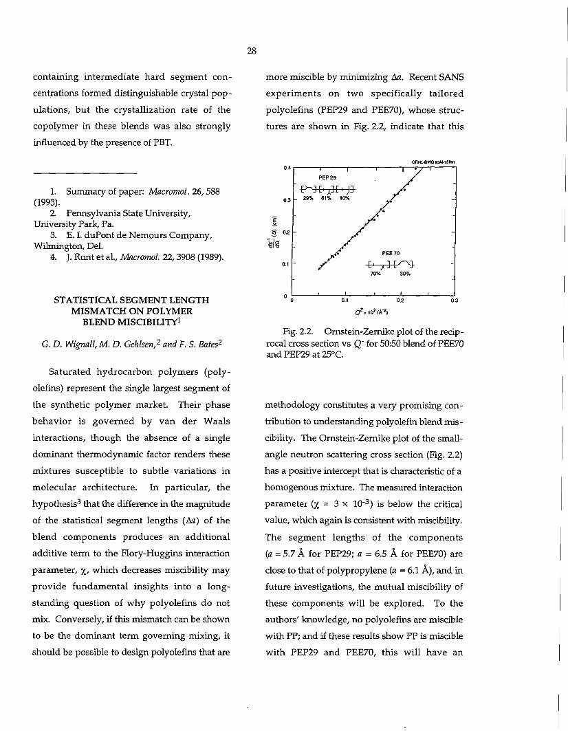
28
containing intermediate hard segment concentrations formed distinguishable crystal populations, but the crystallization rate of the copolymer in these blends was also strongly influenced by the presence of PBT.
1. Summary of paper: Macromol. 26,588 (1993).
2. Pennsylvania State University, University Park, Pa.
3. E. I. duPont de Nemours Company, Wilmington, Del.
4. J. Runt et al., Macromol. 22,3908 (1989).
STATISTICAL SEGMENT LENGTH MISMATCH ON POLYMER
BLEND MISCIBILITY1
G. D. Wignall, M. D. Gehlsen,2 and F. S. Bates2
Saturated hydrocarbon polymers (poly-olefins) represent the single largest segment of the synthetic polymer market. Their phase behavior is governed by van der Waals interactions, though the absence of a single dominant thermodynamic factor renders these mixtures susceptible to subtle variations in molecular architecture. In particular, the hypothesis3 that the difference in the magnitude of the statistical segment lengths (Afl) of the blend components produces an additional additive term to the Flory-Huggins interaction parameter, %, which decreases miscibility may provide fundamental insights into a longstanding question of why polyolefins do not mix. Conversely, if this mismatch can be shown to be the dominant term governing mixing, it should be possible to design polyolefins that are
more miscible by minimizing Afl. Recent SANS experiments on two specifically tailored polyolefins (PEP29 and PEE70), whose structures are shown in Fig. 2.2, indicate that this
0.3
? S 0.2
"sis 0.1
P " ] [ - A ] [ l J] 29% 61% 10%
ORNL-DWQ S3M-I583I 1
[• ; ] [ / ^ 9 -
0.2
O 2 x10 ! (A" 2 )
Fig. 2.2. Ornstein-Zernike plot of the reciprocal cross section vs Q" for 50:50 blend of PEE70 andPEP29at25°C.
methodology constitutes a very promising contribution to understanding poly olefin blend miscibility. The Ornstein-Zernike plot of the small-angle neutron scattering cross section (Fig. 2.2) has a positive intercept that is characteristic of a homogenous mixture. The measured interaction parameter (x = 3 x 10' 3) is below the critical value, which again is consistent with miscibility. The segment lengths of the components (a = 5.7 A for PEP29; a = 6.5 A for PEE70) are close to that of polypropylene (a = 6.1 A), and in future investigations, the mutual miscibility of these components will be explored. To the authors' knowledge, no polyolefins are miscible with PP; and if these results show PP is miscible with PEP29 and PEE70, this will have an
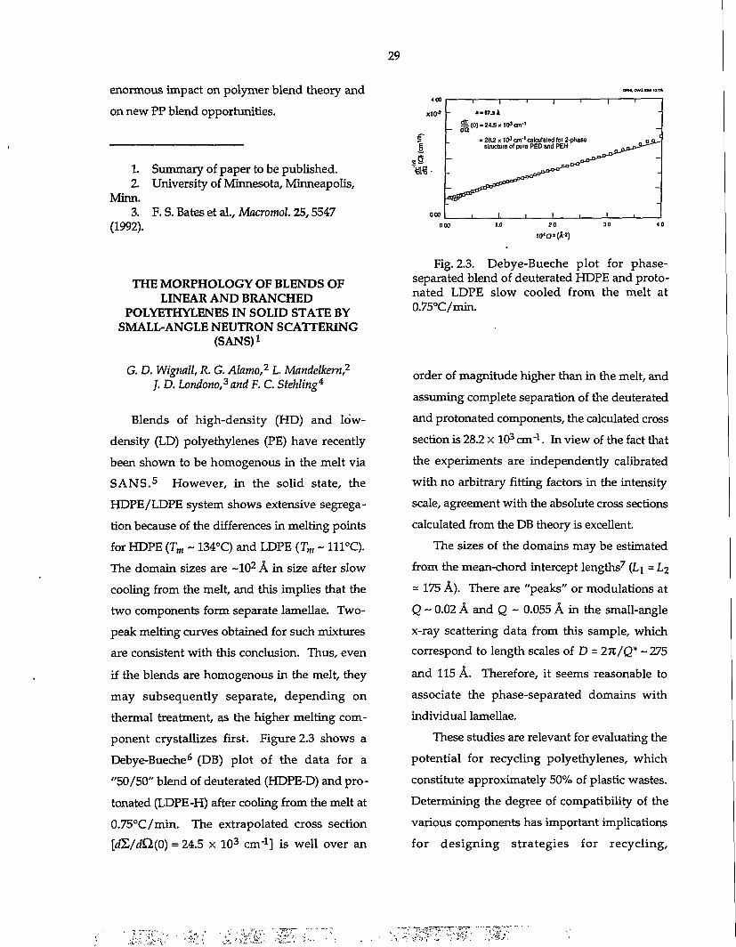
29
enormous impact on polymer blend theory and
on new PP blend opportunities. 400
1. Summary of paper to be published. Z University of Minnesota, Minneapolis,
Minn. 3. F. S. Bates et al., Macromol. 25,5547
(1992).
THE MORPHOLOGY OF BLENDS OF LINEAR AND BRANCHED
POLYETHYLENES IN SOLID STATE BY SMALL-ANGLE NEUTRON SCATTERING
(SANS)1
G. D. Wignall, R. G. Alamo,2 L. Mandelkern,2
J. D. Londono,3 and F. C. Stealing*
Blends of high-density (HD) and low-density (LD) polyethylenes (PE) have recently been shown to be homogenous in the melt via SANS. 5 However, in the solid state, the HDPE/LDPE system shows extensive segregation because of the differences in melting points for HDPE (Tm ~ 134°C) and LDPE (Tm - 111°C). The domain sizes are ~102 A in size after slow cooling from the melt, and this implies that the two components form separate lamellae. Two-peak melting curves obtained for such mixtures are consistent with this conclusion. Thus, even if the blends are homogenous in the melt, they may subsequently separate, depending on thermal treatment, as the higher melting component crystallizes first. Figure 2.3 shows a Debye-Bueche6 (DB) plot of the data for a "50/50" blend of deuterated (HDPE-D) and pro-tonated (LDPE-H) after cooling from the melt at 0.75°C/min. The extrapolated cross section [dL/dQ.(0) = 24.5 x 10 3 c m 4 ] is well over an
£(0)-24.5,<103cnv1
da = 2&2 x 10 3 cm"1 calculated lor 2-phase
structure ol pure PED and PEH
20
Fig. 2.3. Debye-Bueche plot for phase-separated blend of deuterated HDPE and proto-nated LDPE slow cooled from the melt at 0.75°C/min.
order of magnitude higher than in the melt, and assuming complete separation of the deuterated and protonated components, the calculated cross section is 28.2 x 103 cm"1. In view of the fact that the experiments are independently calibrated with no arbitrary fitting factors in the intensity scale, agreement with the absolute cross sections calculated from the DB theory is excellent.
The sizes of the domains may be estimated from the mean-chord intercept lengths7 (L\ - Lj - 175 A). There are "peaks" or modulations at Q ~ 0.02 A and Q - 0.055 A in the small-angle x-ray scattering data from this sample, which correspond to length scales of D = 2%/Q* ~ 275 and 115 A. Therefore, it seems reasonable to associate the phase-separated domains with individual lamellae.
These studies are relevant for evaluating the potential for recycling polyethylenes, which constitute approximately 50% of plastic wastes. Determining the degree of compatibility of the various components has important implications for designing strategies for recycling,
<-.' u:J&>-™ " liSST*?"' .m:
30
reprocessing, and evaluating the usefulness of
the resulting blend material.
1. Summary of paper: Macromolecules (in press).
2. Florida State University, Tallahassee, Fla.
3. ORNL/ORISE postdoctoral research associate.
4. Exxon Chemical Company, Baytown, Tex.
5. G. D. Wignall et al., "Compatibility of Blends of Polyethylenes in the Melt and Solid States by Small-Angle Neutron Scattering," this report.
6. P. Debye and A. M. Bueche, /. Appl. Phys. 20,518 (1949); P. Debye, H. R. Anderson, and H. Brumberger, /. Appl. Phys. 28,679 (1957).
7. R. A. Alamo et al., Macromolecules (in press).
MICRODOMAIN CONTRACTION IN MICROPHASE-SEPARATED
MULTIBLOCK COPOLYMERS1
S. D. Smith,2 R. ]. Spontak? M. M. Satkowski,2
A. Ashraf,2 and J. S. Lin
When chemically dissimilar contiguous
sequences (blocks) of an AB diblock copolymer
are sufficiently incompatible, the copolymer
undergoes microphase separation and self-
organizes into periodic microdomains which
measure on the order of the gyration radius (Rg)
of the domain forming block. For a symmetric
(50/50 vol %) copolymer, the transition from a
disordered state to one possessing long-range
order occurs when %N = (%N)C ~ 10.5 (% is the
Flory-Huggins interaction parameter, and N is
the number of monomers along the copolymer
backbone) in the absence of critical fluctuations.4
When %N » ( xN) C / a strongly segregated
symmetric copolymer orders into a lamellar
morphology of alternating A and B blocks.
Linear multiblock copolymers, like their
diblock analogs, also undergo order-disorder
transitions. To explore the conformations of
such materials, four symmetric poly(styrene-b-
isoprene)M copolymers with In (1 < n < 4) per
fectly alternating blocks of nearly equal mass
have been synthesized. Small-angle x-ray
scattering reveals that the microdomain peri
odicity decreases with n along the lamellar
normal, thereby confirming theoretical predic
tions 5 ' 6 and providing direct evidence for bridg
ing among the 2(n -1) middle blocks.
1. Summary of paper: Phys. Rev. B 47, 14555 (1993).
2. The Procter and Gamble Co., Cincinnati, Ohio.
3. North Carolina State University, Raleigh, N.C.
4. G. H. Fredrickson and E. Helfand, /. Chem. Phys. 87,697 (1987).
5. H. Benoit and G. Hadziioannou, 'Macromol. 21,1449 (1988).
6. T. Kavassalis and M. D. Whitmore, Macromol. 24, 5340 (1991).
TEMPERATURE COEFFICIENTS FOR THE CHAIN DIMENSIONS OF POLYSTYRENE
AND POLYMETHYLMETHACRYLATE1
G. D. Wignall, A. ]. Boothroyd,2
and A. R. Rennie3
The temperature dependence of the un
perturbed dimensions of a polymer relates to the
variation in thermal population of the different
rotational configurations of adjacent bonds and
is r epresen ted by the paramete r K =
31
d ln<S2>o/dT, where <S 2> 0 is the unperturbed, square radius of gyration. A reliable knowledge of K for different polymers is essential to the development of microscopic models of polymers in bulk and in solution because many physical properties depend crucially on chain size. Traditional methods for measuring K (from the intrinsic viscosity in a series of theta solvents, or by viscoelastic measurements on cross-linked networks) are indirect and so depend upon the assumptions of the model used. Small-angle neutron scattering (SANS), on the other hand, measures the change in dimensions directly, and for polyethylene, the SANS value for K agrees well with that obtained by the old techniques. With other polymers, however, the situation is much less clear. Polystyrene, for instance, was thought for many years to have a K value of 0.4 xlO"3, but more recently a variety of conflicting results have been obtained by rheological and viscoelastic methods that vary both in magnitude and in sign. A similar confusion exists with polymethylmethacrylate (PMMA). These two polymers are common materials of great commercial interest, and definitive measurements of them have been performed to facilitate a comparison of values of K obtained by SANS, viscometric, and rheological measurements which may point toward defects in theory that cause the latter two techniques to produce errant results.
Contrary to most previous reports based on rheological measurements, it was found that neither polymer exhibits a significant change in dimensions with temperature. Coefficients of K = (0.0 ± 0.1) x 10"3 K"1 for polystyrene and
(0.1 ± 0.1) x 10"3 K"1 for PMMA were deduced.
These values are close to those given by
thermoelastic measurements but are difficult to
reconcile with theoretical predictions of the
rotational isomeric state model. In order to
resolve this apparent contradiction further,
SANS measurements in dilute solutions are cur
rently being performed to explore whether the
unperturbed dimensions are the same in the
molten state as in an ideal solvent, and whether
the dimensions obtained by intrinsic viscosity
and SANS are identical.
1. Summary of paper: Journal of Physical Chemistry (in press).
2 Oxford University, Oxford, United Kingdom.
3. Cambridge University, Cambridge, United Kingdom.
STRUCTURAL CHARACTERIZATION OF C 6 0 AND CTO FULLERENES BY SMALL-
ANGLE NEUTRON SCATTERING (SANS)1
K. A. Afflwlter,2 G. D. Wignall, S. ]. Henderson,3 G. J. Bunick}
R. E. Haufler,4 and R. N. Compton4
The discovery that Ceo and C70 molecules can be produced in quantity with high purity has generated significant interest in the basic and applied research communities. Potential applications are being considered in many areas (tribology, photoconductivity, nuclear medicine, superconductivity, etc.). Although the research and resulting publications have increased exponentially, a nondestructive technique to study fullerenes in solution had not
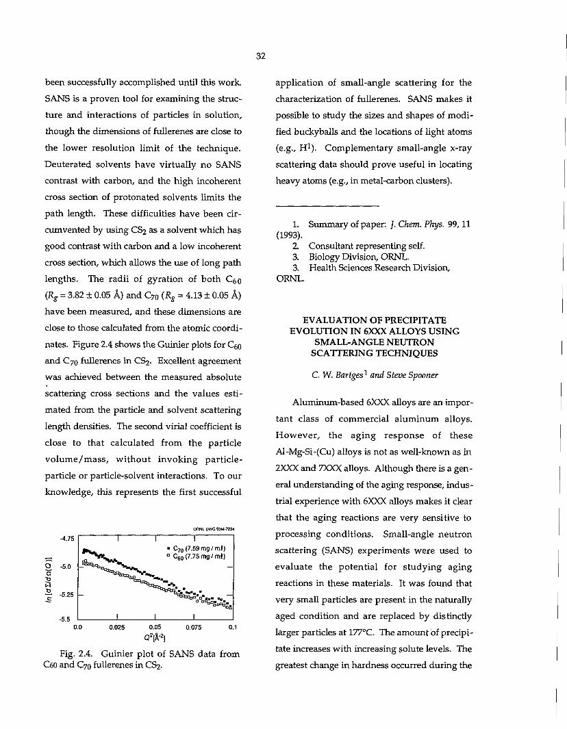
32
been successfully accomplished until this work. SANS is a proven tool for examining the structure and interactions of particles in solution, though the dimensions of fullerenes are close to the lower resolution limit of the technique. Deuterated solvents have virtually no SANS contrast with carbon, and the high incoherent cross section of protonated solvents limits the path length. These difficulties have been circumvented by using CS2 as a solvent which has good contrast with carbon and a low incoherent cross section, which allows the use of long path lengths. The radii of gyration of both Cgo (Rg = 3.82 + 0.05 A) and C 7 0 (R g = 4.13 ± 0.05 A) have been measured, and these dimensions are close to those calculated from the atomic coordinates. Figure 2.4 shows the Guinier plots for Cgo and C70 fullerenes in CS2. Excellent agreement was achieved between the measured absolute scattering cross sections and the values estimated from the particle and solvent scattering length densities. The second virial coefficient is close to that calculated from the particle volume/mass, without invoking particle-particle or particle-solvent interactions. To our knowledge, this represents the first successful
ORNL DWG 93M-7234
-4.75
-5.5
• C 7 0 (7.59 mg / ml) ° C 6 0(7.75mg/ml)
0.0 0.025 0.05 Q2[k2\
0.075 0.1
application of small-angle scattering for the characterization of fullerenes. SANS makes it possible to study the sizes and shapes of modified buckyballs and the locations of light atoms (e.g., H 1). Complementary small-angle x-ray scattering data should prove useful in locating heavy atoms (e.g., in metal-carbon clusters).
Fig. 2.4. Guinier plot of SANS data from C60 and C70 fullerenes in CS2.
1. Summary of paper: J. Chem. Phys. 99,11 (1993).
2. Consultant representing self. 3. Biology Division, ORNL. 3. Health Sciences Research Division,
ORNL.
EVALUATION OF PRECIPITATE EVOLUTION IN 6XXX ALLOYS USING
SMALL-ANGLE NEUTRON SCATTERING TECHNIQUES
C. W. Bartges1 and Steve Spooner
Aluminum-based 6XXX alloys are an important class of commercial aluminum alloys. However, the aging response of these Al-Mg-Si-(Cu) alloys is not as well-known as in 2XXX and 7XXX alloys. Although there is a general understanding of the aging response, industrial experience with 6XXX alloys makes it clear that the aging reactions are very sensitive to processing conditions. Small-angle neutron scattering (SANS) experiments were used to evaluate the potential for studying aging reactions in these materials. It was found that very small particles are present in the naturally aged condition and are replaced by distinctly larger particles at 177°C. The amount of precipitate increases with increasing solute levels. The greatest change in hardness occurred during the

first 8 h at 177°C which parallels the most obvi
ous changes in the precipitate scattering. The
results show SANS to be very sensitive to pre
cipitate evolution. The present findings will be
used as a foundation for more quantitative eval
uations of the aging response of 6XXX alloys.
1. Alcoa Technology Center, Alcoa, Pa.
MATRIX PRECIPITATE EVOLUTION DURING DECOMPOSITION OF
ALUMINUM ALLOY 70751
C. W. Bartges,2 L. H. Edelson,3
S. Y. Tzeng,2 and J. S. Lin
Many important properties of aluminum alloys are developed during artificial aging. This process involves decomposition of a supersaturated solid solution to yield a homogeneous distribution of matrix precipitates. The primary objective of this study was to develop a quantitative understanding of matrix precipitate microstructural evolution of one particular Al alloy (7075) containing 5.8 wt% Zn, 2.7 wt% Mg, 1.5 wt% Cu, plus trace amounts of Si, Fe, Cr, Ti, etc. Electrical conductivity, wide-angle x-ray diffraction, differential scanning calorimetry, and transmission electron microscopy can provide a qualitative description of the decomposition process. Small-angle x-ray scattering (SAXS) can better quantify the matrix precipitate characteristics in the process.
Analysis of SAXS results from alloy 7075 annealed at 121°C from 6 to 192 h concluded that: (1) The Guinier-Preston zones are the primary strengthening precipitates in the naturally
" r ^ ? & - ' * : •
aged specimen, but they play a minor role in artificial aging. (2) The volume fraction and number density of matrix precipitates, r\' and n, increase dramatically in the first 24 h at 121°C, and the coarsening occurs after 24 h.
(3) Throughout the decomposition process, the particles grew according to a ta / 9 law.
(4) Particle size distribution of matrix precipitate was obtained via the method of Fedorova and Schmidt.4
1. Summary of paper to be published. 2 ALCOA Technical Center, Alcoa, Pa. 3. Xerox Corporation, Rochester, N.Y. 4. I. S. Fedorova and P. W. Schmidt,
/. Appl. Crystallogr. 11,406 (1978).
CHARACTERIZATION OF POROSITY IN CERAMIC MATERIALS BY
SMALL-ANGLE SCATTERING1
D. W. Schaefer,2 R. K. Brow,2 B.}. Olivier,2
T. Rieker,2 G. Beaucage,2
L. Hrubesh,3 and J. S. Lin
Porosity is a dominant factor affecting the performance of ceramic materials. Failure of structural ceramics, for example, offer results from flaws that originate at voids present in green compacts. Ceramists employ the tools of colloid chemistry to prepare powders that sinter in such a way as to eliminate such troublesome voids.
Equally important are ceramic materials that depend on engineered porosity to fulfill their intended role. Membranes and filters are prime examples. Particulate filters require porosity in the micron-size range, whereas gas separation
34
membranes require tightly controlled pores
below 10 A. Porous ceramics also serve as
catalyst s u p p o r t s and h igh- tempera tu re
insulators. An emerging class of selective
adsorbents use crystalline silicotitanates with
lattice constants in the range 5-15 A. In all cases,
porosity with specific morphology and topology
is required.
Small-angle x-ray scattering (SAXS) and
small-angle neutron scattering are powerful
tools for the characterization of porosity in
ceramic materials. The chord lengths, internal
surface area, pore volume, and size distribution
can be determined from scattering data. A series
of aerogels from acid-catalyzed and base-
catalyzed hydrolysis of Si(OCH3)4 has been
studied to determine how the structure of
solution-derived silica aerogels depends on
density. Recent results on Vycor (a commercial
leached borosilicate) glass have illustrated the
value of SAXS in distinguishing competing
models for the origin of porosity.
1. Summary of paper: in Modern Aspects of Small-Angle Scattering, Kluwer Academic Publisher, Boston, Mass., in press.
Z Sandia National Laboratories, Albuquerque, New Mex.
3. Lawrence Livermore National Laboratory, Livermore, Calif.
SHEAR-INDUCED "CRYSTALLIZATION" OF RODLIKE MICELLES1
W. A. Hamilton, P. D. Butler,2 S. M. Baker? G. S. Smith,3 } . B. Hayter, L.}. Magid* andR. Pynn3
Aqueous solutions of certain cationic surfac
tants can be made strongly viscoelastic by the
introduction of an appropriate counterion. The
micellar structure in these fluids has been shown
in some cases to involve highly extended,
threadlike micelles which entangle, producing
solutions with polymer-like properties. Small-
angle neutron scattering (SANS) measurements
which revealed the existence of a new type of
shear-induced anisotropic colloidal phase
occurring in the near-surface region when such a
fluid flows past a solid interface were performed
recently.
Our measurements were made using the
ORNL 30-m SANS camera at the High-Flux
Isotope Reactor. The sample was a dilute
(20-mM) viscoelastic solution of the surfactant
hexadecyl tr imethylammonium 3,5-dichloro-
benzoate (CTA3,5ClBz) in D2O. In a specially
developed reflection geometry shear cell,^ the
solution is pumped in a closed cycle through a
shallow channel beneath a polished slab of
crystalline quartz. Neutrons are incident
through the slab, passing into the solution at low
angle to the solid-liquid interface, along the
direction of flow. Some are reflected at the
interface, but most enter and are scattered in the
solution. The absorption in the fluid is such that
coherent scattering is only seen for neutrons
which scatter back through the quartz slab from
the first 30 u.m below the interface. This
coincides with the fluid flow boundary layer, a
region of dramatic shear strain {dv/dz -100/s).
A difference in scattering pattern for shear-on vs
no flow is shown in Fig. 2.5. The scattering
indicates that under shear the solution's rod like
micelles (5-nm diam x 200 nm in length) have
not only aligned with the flow, but are also
ordered in a hexagonal array across the flow
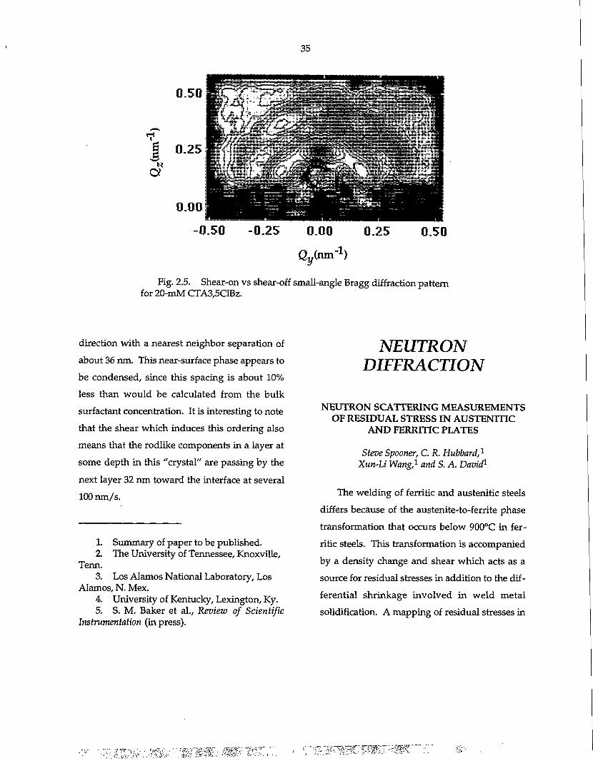
35
0.50
0.25
0.00
QydinT1)
0.25 0.50
Fig. 2.5. Shear-on vs shear-off small-angle Bragg diffraction pattern for 20-mM CTA3,5ClBz.
direction with a nearest neighbor separation of about 36 nm. This near-surface phase appears to be condensed, since this spacing is about 10% less than would be calculated from the bulk surfactant concentration. It is interesting to note that the shear which induces this ordering also means that the rodlike components in a layer at some depth in this "crystal" are passing by the next layer 32 nm toward the interface at several 100 nm/s.
1. Summary of paper to be published. 2 The University of Tennessee, Knoxville,
Tenn. 3. Los Alamos National Laboratory, Los
Alamos, N. Mex. 4 University of Kentucky, Lexington, Ky. 5. S. M. Baker et al., Review of Scientific
Instrumentation (in press).
NEUTRON DIFFRACTION
NEUTRON SCATTERING MEASUREMENTS OF RESIDUAL STRESS IN AUSTENITIC
AND FERRITIC PLATES
Steve Spooner, C. R. Hubbard,1
Xun-Li Wang,1 and S. A. David1
The welding of ferritic and austenitic steels differs because of the austenite-to-ferrite phase transformation that occurs below 900°C in ferritic steels. This transformation is accompanied by a density change and shear which acts as a source for residual stresses in addition to the differential shrinkage involved in weld metal solidification. A mapping of residual stresses in
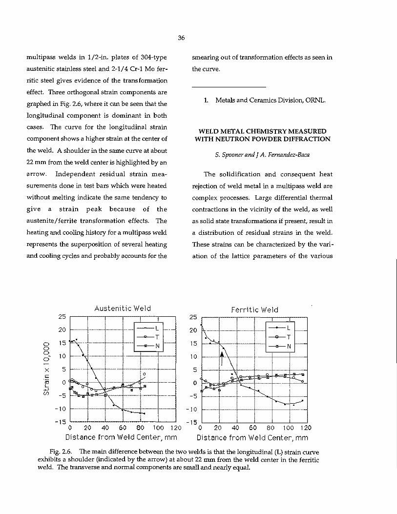
36
multipass welds in 1/2-in. plates of 304-type
austenitic stainless steel and 2-1/4 Cr-1 Mo fer
ritic steel gives evidence of the transformation
effect. Three orthogonal strain components are
graphed in Fig. 2.6, where it can be seen that the
longitudinal component is dominant in both
cases. The curve for the longitudinal strain
component shows a higher strain at the center of
the weld. A shoulder in the same curve at about
22 mm from the weld center is highlighted by an
arrow. Independent residual strain mea
surements done in test bars which were heated
without melting indicate the same tendency to
give a s t ra in peak because of the
austenite/ferrite transformation effects. The
heating and cooling history for a multipass weld
represents the superposition of several heating
and cooling cycles and probably accounts for the
smearing out of transformation effects as seen in
the curve.
1. Metals and Ceramics Division, ORNL.
WELD METAL CHEMISTRY MEASURED WITH NEUTRON POWDER DIFFRACTION
S. Spooner and } A. Fernandez-Baca
The solidification and consequent heat
rejection of weld metal in a multipass weld are
complex processes. Large differential thermal
contractions in the vicinity of the weld, as well
as solid state transformations if present, result in
a distribution of residual strains in the weld.
These strains can be characterized by the vari
ation of the lattice parameters of the various
Austenitic Weld Ferrit ic Weld
o o o" x
L. CO
0 20 40 60 80 100 120 Distance from Weld Center, mm
0 20 40 60 80 100 120 Distance from Weld Center, mm
Fig. 2.6. The main difference between the two welds is that the longitudinal (L) strain curve exhibits a shoulder (indicated by the arrow) at about 22 mm from the weld center in the ferritic weld. The transverse and normal components are small and nearly equal.
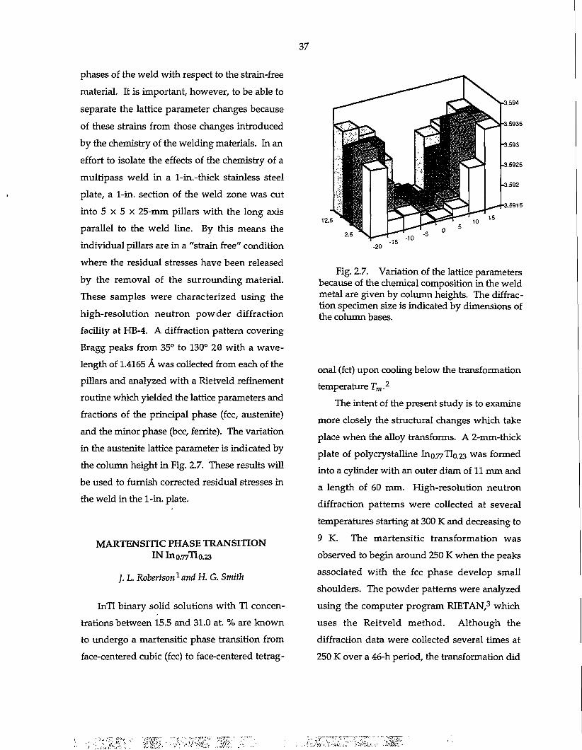
phases of the weld with respect to the strain-free material. It is important, however, to be able to separate the lattice parameter changes because of these strains from those changes introduced by the chemistry of the welding materials. In an effort to isolate the effects of the chemistry of a multipass weld in a l-in.-thick stainless steel plate, a 1-in. section of the weld zone was cut into 5 x 5 x 25-mm pillars with the long axis parallel to the weld line. By this means the individual pillars are in a "strain free" condition where the residual stresses have been released by the removal of the surrounding material. These samples were characterized using the high-resolution neutron powder diffraction facility at HB-4. A diffraction pattern covering Bragg peaks from 35° to 130° 29 with a wavelength of 1.4165 A was collected from each of the pillars and analyzed with a Rietveld refinement routine which yielded the lattice parameters and fractions of the principal phase (fee, austenite) and the minor phase (bec, ferrite). The variation in the austenite lattice parameter is indicated by the column height in Fig. 2.7. These results will be used to furnish corrected residual stresses in the weld in the 1-in. plate.
MARTENSmC PHASE TRANSITION IN Ino.77Tlo.23
/. L. Robertson1 and H. G. Smith
InTl binary solid solutions with Tl concentrations between 15.5 and 31.0 at. % are known to undergo a martensitic phase transition from face-centered cubic (fee) to face-centered tetrag-
37
Fig. 2.7. Variation of the lattice parameters because of the chemical composition in the weld metal are given by column heights. The diffraction specimen size is indicated by dimensions of the column bases.
onal (fct) upon cooling below the transformation temperature Tm.2
The intent of the present study is to examine more closely the structural changes which take place when the alloy transforms. A 2-mm-thick plate of polycrystalline Ino.77Tlo.23 was formed into a cylinder with an outer diam of 11 mm and a length of 60 mm. High-resolution neutron diffraction patterns were collected at several temperatures starting at 300 K and decreasing to 9 K. The martensitic transformation was observed to begin around 250 K when the peaks associated with the fee phase develop small shoulders. The powder patterns were analyzed using the computer program RIETAN,3 which uses the Reitveld method. Although the diffraction data were collected several times at 250 K over a 46-h period, the transformation did
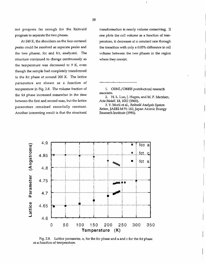
38
not progress far enough for the Reitveld program to separate the two phases.
At 240 K, the shoulders on the face-centered peaks could be resolved as separate peaks and the two phases, fee and fct, analyzed. The structure continued to change continuously as the temperature was decreased to 9 K, even though the sample had completely transformed to the fct phase at around 200 K. The lattice parameters are shown as a function of temperature in Fig. 2.8. The volume fraction of the fct phase increased somewhat in the time between the first and second scan, but the lattice parameters remained essentially constant. Another interesting result is that the structural
transformation is nearly volume conserving. If one plots the cell volume as a function of temperature, it decreases at a constant rate through the transition with only a 0.05% difference in cell volume between the two phases in the region where they coexist.
1. ORNL/ORISE postdoctoral research associate.
2. H. L. Luo, J. Hagen, and M. F. Merriam, Acta Metall. 13,1012 (1965).
3. Y. Morii et al., Reitveld Analysis System Reitan, JAERI-M 91-162, Japan Atomic Energy Research Institute (1991).
„ , 4.9 w E o 4-* 4.85 CO O) C < , 4.8 i _
*-• CD 4.75 E cc i-co 4.7 0.
CD
u 4.65 CO
4.6
; { *
e
fee a
fct Q. ' < >' "<
< > • fct a
^ i i"i ' w *"
i i
i
i i
i
i"i ' w *"
"i" i i
0 50 100 150 200 250 300 350 Temperature (K)
Fig. 2.8. Lattice parameter, a, for the fee phase and a and c for the fct phase as a function of temperature.
NEUTRON SCATTERING STUDY OF THE t-» m PHASE TRANSITION IN Al 2 0 3 -Zr0 2
(12 mol % Ce02) CERAMIC COMPOSITES
Xun-Li Wang,1 J. A. Fernandez-Baca, C. R. Hubbard,1 K. B. Alexander,1
and P. F. Becher1
The introduction of tetragonal (£)-Zr02 particles into a ceramic matrix can result in a significant increase in the ceramic fracture toughness of the ceramic. This improved toughness is achieved when the t-TxOi grains at a crack tip transform to monoclinic (m) TxOi during the fracture process. Thus an understanding of the t -> m phase transition in this type of materials is of considerable interest in the field of ceramics engineering. For this reason, a neutron diffraction study of the temperature dependence of the t -» m transformation in Al203-Zr02 (12 mol % Ce02) ceramic composites containing 40 and 10 vol % Zr02 has been performed. This type of study is a valuable complement to conventional transport measurements because the diffraction technique provides a direct observation of the phase transformation, as well as a quantitative measure of the volume fraction of the transformed phases. These measurements were performed using the high-resolution neutron powder diffractometer (HB-4) at the HFIR. This study confirmed that the sharp increase in the thermal expansion upon cooling, typically observed in composites with a high content (e.g., 40 vol %) of Zr02, corresponds to the onset of the t -> m phase transformation in these materials. The neutron diffraction patterns were refined using the Rietveld analysis technique to determine the volume fraction of the W1-Z1O2
39
phase as a function of temperature. Below the onset transformation temperature, the amount of the m-Zr02 phase increased progressively until it reached a maximum at lower temperatures. This maximum indicated that only a fraction of the t-Zr02 phase (e.g., 23% in the sample containing 40 vol % Zr02) transformed into m-Zr02- The observed temperature dependence of the transformation can be explained in terms of the size distribution of i-Zr02 grains. The lattice parameters of the AI2O3 matrix and the remaining £-ZiC>2 phases exhibited dramatic changes related to the stress changes resulting from the transformation. The refined cell parameters were used to calculate the bulk thermal expansion of the composite. The calculated thermal expansion was in excellent agreement with the dilatometry measurements.
1. Metals and Ceramics Division, ORNL.
Sr 2 Ir0 4 : A TWO-DIMENSIONAL SPIN-l/2 HEISENBERG ANTIFERROMAGNET1
M. K. Crawford,2 M. A. Subramanian,2
R. L. Harlow,2 }. A. Fernandez-Baca, Z. R. Wang,3 and D. C Johnston3
The discovery of high-temperature superconductivity in doped copper oxides, which in their insulating (undoped) forms are nearly ideal two-dimensional (2D) spin-1/2 Heisenberg anti-ferromagnets, has stimulated great interest in finding new examples of such magnetic systems. It is of particular interest to find new oxides, other than cuprates, which exhibit this spin-1/2
40
2D antiferromagnetic behavior and may be candidates for high-temperature superconductivity. The Sr2lr0 4 oxide has a K 2NiF 4 structure in which the Ir4"1" ions are octahedrally coordinated. The ground state of these Ir 4* ions is a (spin-1/2) Kramers doublet, the same as found in Cu 2 + . In this study, x-ray and neutron powder diffraction, as well as magnetic susceptibility measurements, were performed. The x-ray measurements were performed at the National Synchrotron Light Source at Brookhaven National Laboratory. The neutron measurements were performed using the high-resolution powder diffractometer (HB-4) at the HFIR. The magnetic susceptibility measurements were performed at Ames. The x-ray data at T = 20 K showed weak superlattice peaks that indicated a distortion from the I4/tnmm structure. In order to resolve if this distortion involved the displacement of oxygen atoms, the neutron diffraction experiment was performed at the HFIR. From this analysis on the neutron data at T = 13 K, it is proposed that the IrC>6 octahedra are rotated about the crystallo graphic c axis by about 11°, reducing the space group symmetry of this system from I4/mmm to I4/acd. The magnetic susceptibility measurements showed a distinctive magnetic transition at T= 250 K. Magnetic hysteresis measurements at T = 5K showed that the magnetic structure has a ferromagnetic component, although this component is too small (10"2(iB per Ir ion) to attribute it to ferromagnetically aligned Ir4* spins. Instead, it seems more reasonable to attribute this magnetic response to canted antiferromagnetism, the origin of the canting being the structural distor
tion described above. Preliminary attempts to observe the magnetic reflections of this structure by neutron diffraction have failed. It is presumed that this failure might be due to the combination of the small ordered moment, the appreciable neutron absorption cross section of Ir, and the large incoherent scattering cross section of the vanadium holder. Efforts to improve these measurements are in progress.
1. Summary of paper to be published. 2. Dupont, Wilmington, Del. 3. Ames Laboratory, Iowa State University,
Ames, Iowa.
SPIN DENSITY WAVES IN DILUTE CuMn ALLOYS
/. W. Cable and Y. Tsunoda1
Neutron polarization analysis measurements 2 on CuMn alloys show the presence of incommensurate magnetic modulations that have now been identified3 as spin density waves (SDW). The SDW model, as originally proposed by Overhauser4 to explain the peculiar thermal and magnetic properties of CuMn alloys, is a collective, deformed state of the conduction electron gas that can be stabilized for particular wave vectors. The localized solute spins interact with the SDW, and this leads to helical ordering of the localized spins with an ordering wave vector characteristic of the SDW and, therefore, incommensurate with the lattice. The interaction with the localized solute spins also contributes to the SDW stability, so there may well be a critical Mn concentration below which the
static SDW are no longer stable. There is no such cutoff in the Overhauser SDW model where the transition temperature is simply linear with concentration, but it has been established5 that the SDW are absent in pure Cu, and this suggests a critical concentration for SDW stability. Furthermore, a recent calculation by loffe and Feigel'man6 for a random array of localized spins subject to a modified RKKY interaction gives magnetic order that depends on the interaction range and the density of spins on the lattice. For CuMn alloys, they obtain spin-glass behavior at low concentration and a crossover to short-range helical order near 10% Mn. This does not agree with previous resul ts 2 on annealed CuMn alloys, which showed short-range SDW ordering down to 5% Mn. Even so, the interaction range is not well established, so a crossover at some lower concentration remains a possibility. It was decided to extend these measurements to lower Mn concentrations to determine which of these two models provides the best description of magnetic order in CuMn alloys.
Neutron scattering measurements were made on single crystals of CuMn alloys containing 1.4 and 3.0% Mn. Elastic scans along (l£0) at temperatures well below 7V yield the same type of intensity distribution as that previously observed for the more concentrated alloys and show the existence of static SDW at dilutions down to 1.4% Mn. Inelastic scans in the same Q region for the Cu-3% Mn alloy clearly show the presence of dynamic SDW at temperatures up to T/Tf = 7.5. These results favor the SDW model of
.'--: :tv;&:>V rUsv f!4''itkP :-$k'<. ~i"-'"-. •'.
41
Overhauser as the best description of magnetic order in dilute CuMn alloys.
1. Guest scientist from Osaka University, Osaka, Japan.
2 J. W. Cable et al., Phys. Rev. Lett. 49,829 (1982); Phys. Rev. B 29,1268 (1984).
3. S. A. Werner, J. J. Rhyne, and J. A. Gotaas, Solid State Commun. 56,457 (1985).
4. A. W. Overhauser, Phys. Rev. Lett. 3,414 (1959); /. Phys. Chem. Solids 13,71 (1960).
5. S. A. Werner, Comments Condens. Matter Phys. 15,55 (1990).
6. L. B. loffe and M. V. Feigel'man, Sov. Phys. JETP 61(2), 354 (1985).
STRUCTURE OF THE MODULATED MAGNETIC PHASE OF Mn 3Sn
/. W. Cable, N. Wakabayashi,1 and P. Radhakrishna2
The intermetallic compound Mn3Sn has a hexagonal DO 19 crystal structure with six Mn and two Sn atoms per unit cell. Below 420 K, triangular antiferromagnetic order develops by which the three spins within each layer assume 120° relative orientations and the interlayer Mn atoms connected through a center of inversion are aligned parallel.3 Below 270 K, this triangular order remains within each layer, but the parallel interlayer coupling is replaced by a long-period modulation along the c axis. This has generally been described as a helical modulation with temperature-independent periods ranging from about 10 CQ to about 12 CQ. In a recent study 2 of the magnetic excitations of MnsSn, an energy gap of about 4 meV for both the triangular and the modulated phases was
*''#>''-?:r'«3n "5M "•' H1&
42
observed. For the triangular phase, this gap was
attributed to the energy required for a uniform
fluctuation of spins away from the easy-axis
directions within the basal plane. The energy
gap is not so readily explained for the modu
lated phase where a gap can occur only if the
modulation period is commensurate with the
lattice and if a uniform fluctuation of spins
forces an appreciable fraction of the spins to
move away from the easy axes. This does not
seem possible for such a long-period helical
modulation since the rotation angle per layer
becomes so small that spins are just as likely to
approach hard axes as easy axes. This inconsis
tency called into question the helical model and
prompted a reexamination of the magnetic
structure of the modulated phase.
Two distinct modulations, both propagating
along the c axis and both with periods that are
commensurate with the lattice below about
120 K, were found. The satellite reflections
associated with these two modulations have
quite different intensities and temperature
dependences suggesting coexistent modulated
phases. For the dominant 11 Co phase, a third
harmonic with an intensity that is 4% of the first
harmonic was observed, but no fifth or seventh
harmonic to a sensitivity of about 1 0 4 was
found. The presence of this third harmonic
shows a significant distortion of the helical
modulation wave. The observed harmonic
intensity distribution was compared with mag
netic structure factor calculations for configura-
tional models with moment directions bunched
around the easy axes in the basal plane. The
results suggest a model for which the moments
are bunched around the 6-fold axes in a
(7-2-2-7-2-2) sequence.
1. Consultant from Keio University, Yokohama, Japan.
2. Consultant from Jawaharlal Nehru Centre for Advanced Scientific Research, Bangalore, India.
3. J. S. Kouvel and J. S. Kasper, p. 169 in Proceedings of Conference on Magnetism, Nottingham, 1964.
NEUTRON DIFFRACTION STUDY OF THE MAGNETIC ORDERING OF B a C u 0 2 + x
Xun-Li Wang,1 J. A. Fernandez-Baca, Z. R. Wang,2 D. Vaknin,2 and D. C. Johnston2
The study of the magnetism of BaCu02+x is
of practical and fundamental interest. This
system is a common impurity in RBa2Cu307_x
superconducting materials, 3 and the character
ization of its magnetic properties is of impor
tance in interpreting magnetic measurements on
RBa2Cu307_x-type systems. The fundamental
aspect of this study derives from the fact that,
despite its simple chemical formula, B a C u 0 2 + x
has a rather complicated crystal structure. This
compound has a large body-centered-cubic unit
cell (space group Im3m, a = 18.25 A) with 90
formula units per unit cell. Each cell contains
eight CugOi2 ring clusters, two CU18O24 sphere
clusters, and six incomplete Q12O12 clusters. A
study of the magnetic properties of BaCu02+ z
should provide valuable insights on the nature
of the magnetic interactions (intracluster and
intercluster) in this rather complex system. For
this reason, neutron diffraction experiments
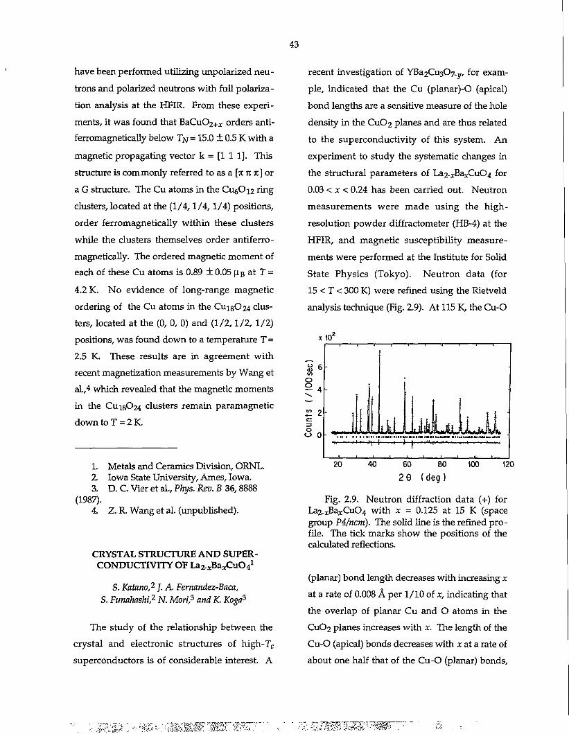
43
have been performed utilizing unpolarized neutrons and polarized neutrons with full polarization analysis at the HFIR. From these experiments, it was found that BaCu02+* orders anti-ferromagnetically below T^ = 15.0 ± 0.5 K with a magnetic propagating vector k = [1 1 1]. This structure is commonly referred to as a [% K JC] or a G structure. The Cu atoms in the Cu^O^ ring clusters, located at the (1/4,1/4,1/4) positions, order ferromagnetically within these clusters while the clusters themselves order antiferro-magnetically. The ordered magnetic moment of each of these Cu atoms is 0.89 ± 0.05 |i.B at T = 4.2 K. No evidence of long-range magnetic ordering of the Cu atoms in the CU18O24 clusters, located at the (0, 0, 0) and (1/2,1/2, 1/2) positions, was found down to a temperature T= 2.5 K. These results are in agreement with recent magnetization measurements by Wang et aL,4 which revealed that the magnetic moments in the CU18O24 clusters remain paramagnetic down to T = 2 K.
1. Metals and Ceramics Division, ORNL. 2 Iowa State University, Ames, Iowa. 3. D. C. Vier et al., Phys. Rev. B 36,8888
(1987). 4. Z. R. Wang et al. (unpublished).
CRYSTAL STRUCTURE AND SUPERCONDUCTIVITY OF La2.A;Baa:Cu041
S. Katano,2 }. A. Fernandez-Baca, S. Funahashi,2 N. Mori,3 and K. Koga3
The study of the relationship between the crystal and electronic structures of high-T c
superconductors is of considerable interest. A
recent investigation of YBa2Cu307_„, for exam
ple, indicated that the Cu (planar)-O (apical)
bond lengths are a sensitive measure of the hole
density in the Q1O2 planes and are thus related
to the superconductivity of this system. An
experiment to study the systematic changes in
the structural parameters of La2-xBaxCu04 for
0.03 < x < 0.24 has been carried out. Neutron
measurements were made using the high-
resolution powder diffractometer (HB-4) at the
HFIR, and magnetic susceptibility measure
ments were performed at the Institute for Solid
State Physics (Tokyo). Neutron data (for
15 < T < 300 K) were refined using the Rietveld
analysis technique (Fig. 2.9). At 115 K, the Cu-O
x tCT
iillhm^Mjl^JX -4- frM^W*—*~*
20 40 60 80 100 2 6 (deg)
120
Fig. 2.9. Neutron diffraction data (+) for La2-xBaxCu04 with x = 0.125 at 15 K (space group P4/ncm). The solid line is the refined profile. The tick marks show the positions of the calculated reflections.
(planar) bond length decreases with increasing x at a rate of 0.008 A per 1/10 of x, indicating that the overlap of planar Cu and O atoms in the Q1O2 planes increases with x. The length of the Cu-O (apical) bonds decreases with x at a rate of about one half that of the Cu-O (planar) bonds,
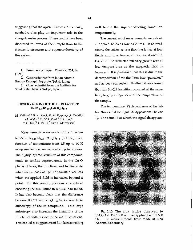
44
suggesting that the apical O atoms in the CuC>6
octahedra also play an important role in the
charge transfer process. These results have been
discussed in terms of their implication to the
electronic structure and superconductivity of
this system.
1. Summary of paper: Physica C 214,64 (1993).
2. Guest scientist from Japan Atomic Energy Research Institute, Tokai, Japan.
3. Guest scientist from the Institute for Solid State Physics, Tokyo, Japan.
OBSERVATION OF THE FLUX LATTICE IN BiusBa-LgsOsQ^Os+x
M. Yethiraj,1 H. A. Mook, E. M. Forgan,2 R. Cubitt,2
M. Wylie,2 D. Mck. Paul,3 S. L. Lee,4
P. H. Kes,5 T. W. Li,5 and K. Mortensen6
well below the superconducting transition
temperature T c.
The current set of measurements were done
at applied fields as low as 20 mT. It showed
clearly the existence of a flux-line lattice at low
fields and low temperatures, as shown in
Fig. 2.10. The diffracted intensity goes to zero at
low temperatures as the magnetic field is
increased. It is presumed that this is due to the
decomposition of the flux lines into "pancakes"
as has been suggested. Further, it was found
that this 3d-2d transition occurred at the same
field, largely independent of the temperature of
the sample.
The temperature (T) dependence of the lat
tice shows that the signal disappears well below
T c. The actual T at which the signal disappears
Measurements were made of the flux-line
lattice in Bi2.15BaL95CaCu2O84.jr (BSCCO) as a
function of temperature from 1.5 up to 60 K
using small-angle neutron scattering techniques.
The highly layered structure of this compound
tends to confine supercurrents in the Cu-O
planes. Hence, the flux lines tend to dissociate
into two-dimensional (2d) "pancake" vortices
when the applied field is increased beyond a
point. For this reason, previous attempts at
observing the flux lattice in BSCCO had failed.
It has also become clear that the difference
between BSCCO and YBa2Cu307 is a very large
anisotropy of the Bi compound. This large
anisotropy also increases the instability of the
flux lattice with respect to thermal fluctuations.
This has led to suggestions of flux-lattice melting
S**/' Fig. 2.10. The flux lattice observed in
BSCCO at T = 1.5 K with an applied field of 500 Oe. The measurements were made at Rise National Laboratory.
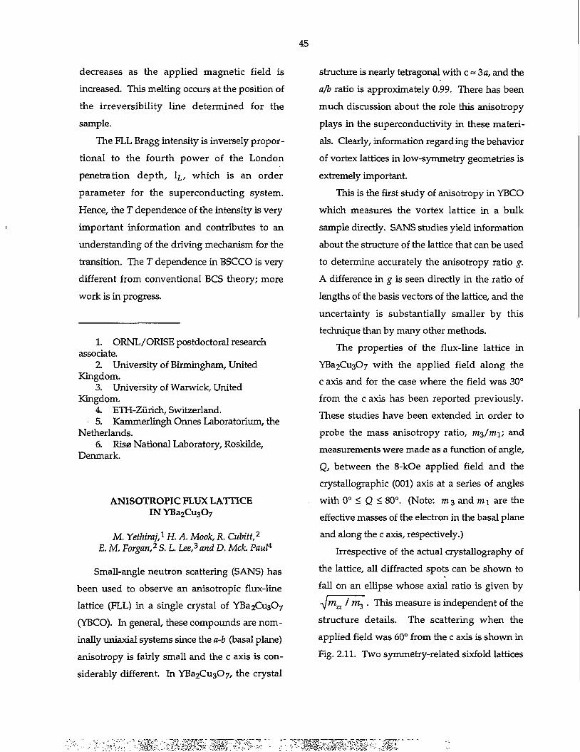
45
decreases as the applied magnetic field is increased. This melting occurs at the position of the irreversibility line determined for the sample.
The FLL Bragg intensity is inversely proportional to the fourth power of the London penetration depth, ljr,, which is an order parameter for the superconducting system. Hence, the T dependence of the intensity is very important information and contributes to an understanding of the driving mechanism for the transition. The T dependence in BSCCO is very different from conventional BCS theory; more work is in progress.
1. ORNL/ORISE postdoctoral research associate.
2. University of Birmingham, United Kingdom.
3. University of Warwick, United Kingdom.
4. ETH-Zurich, Switzerland. 5. Kammerlingh Onnes Laboratorium, the
Netherlands. 6. Ris0 National Laboratory, Roskilde,
Denmark.
ANISOTROPIC FLUX LATTICE IN YBa 2Cu 30 7
M. Yethiraj,1 H. A. Mook, R. Cubitt2
E. M. Forgan,2 S. L. Lee,3 and D. Mck. Paufi
Small-angle neutron scattering (SANS) has been used to observe an anisotropic flux-line lattice (FLL) in a single crystal of YBa2Cu307 (YBCO). In general, these compounds are nominally uniaxial systems since the a-b (basal plane) anisotropy is fairly small and the c axis is considerably different. In YBa2Cu307, the crystal
structure is nearly tetragonal with c~3a, and the a/b ratio is approximately 0.99. There has been much discussion about the role this anisotropy plays in the superconductivity in these materials. Clearly, information regarding the behavior of vortex lattices in low-symmetry geometries is extremely important.
This is the first study of anisotropy in YBCO which measures the vortex lattice in a bulk sample directly. SANS studies yield information about the structure of the lattice that can be used to determine accurately the anisotropy ratio g. A difference in g is seen directly in the ratio of lengths of the basis vectors of the lattice, and the uncertainty is substantially smaller by this technique than by many other methods.
The properties of the flux-line lattice in YBa2Cu307 with the applied field along the c axis and for the case where the field was 30° from the c axis has been reported previously. These studies have been extended in order to probe the mass anisotropy ratio, mj,lm\; and measurements were made as a function of angle, Q, between the 8-kOe applied field and the crystallographic (001) axis at a series of angles with 0° < Q < 80°. (Note: m3 and mi are the effective masses of the electron in the basal plane and along the c axis, respectively.)
Irrespective of the actual crystallography of the lattice, all diffracted spots can be shown to fall on an ellipse whose axial ratio is given by y m a / ^ . This measure is independent of the structure details. The scattering when the applied field was 60° from the c axis is shown in Fig. 2.11. Two symmetry-related sixfold lattices
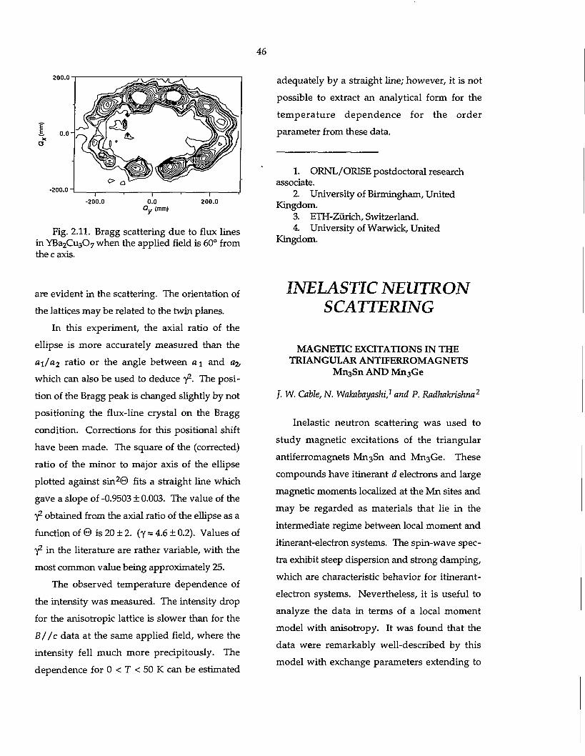
46
-200.0 0.0 200.0 Q„ (mm)
Fig. 2.11. Bragg scattering due to flux lines in YBa2Cu307 when the applied field is 60° from thee axis.
are evident in the scattering. The orientation of the lattices may be related to the twin planes.
In this experiment, the axial ratio of the ellipse is more accurately measured than the a\lai ratio or the angle between a\ and a^ which can also be used to deduce y2-. The position of the Bragg peak is changed slightly by not positioning the flux-line crystal on the Bragg condition. Corrections for this positional shift have been made. The square of the (corrected) ratio of the minor to major axis of the ellipse plotted against sin 2© fits a straight line which gave a slope of -0.9503 ± 0.003. The value of the y 2 obtained from the axial ratio of the ellipse as a function of 0 is 20 ±2. (y = 4.6 ±0.2). Values of Y2 in the literature are rather variable, with the most common value being approximately 25.
The observed temperature dependence of the intensity was measured. The intensity drop for the anisotropic lattice is slower than for the B/ /c data at the same applied field, where the intensity fell much more precipitously. The dependence for 0 < T < 50 K can be estimated
adequately by a straight line; however, it is not possible to extract an analytical form for the temperature dependence for the order parameter from these data.
1. ORNL/ORISE postdoctoral research associate.
2. University of Birmingham, United Kingdom.
3. ETH-Zurich, Switzerland. 4. University of Warwick, United
Kingdom.
INELASTIC NEUTRON SCATTERING
MAGNETIC EXCITATIONS IN THE TRIANGULAR ANTIFERROMAGNETS
Mn3Sn AND Mn3Ge
/. W. Cable, N. Wakabayashi,1 and P. Radhakrishna2
Inelastic neutron scattering was used to study magnetic excitations of the triangular antiferromagnets Mn3Sn and M^Ge. These compounds have itinerant d electrons and large magnetic moments localized at the Mn sites and may be regarded as materials that lie in the intermediate regime between local moment and itinerant-electron systems. The spin-wave spectra exhibit steep dispersion and strong damping, which are characteristic behavior for itinerant-electron systems. Nevertheless, it is useful to analyze the data in terms of a local moment model with anisotropy. It was found that the data were remarkably well-described by this model with exchange parameters extending to
47
fifth nearest neighbors and with both axial- and basal-plane anisotropy. The axial anisotropy parameters were determined from the uniform out-of-plane spin fluctuation, and the signs show that the spins were confined to the basal plane. The second-order basal-plane anisotropy constants were determined by satisfying both the magnitude of the weak basal-plane ferromagnetic moments and the observed splitting of a doubly degenerate acoustic spin-wave branch. The sixth-order basal-plane anisotropy was determined by adjusting to the observed energy gap associated with spin fluctuations within the basal plane. The exchange parameters have the correct signs to stabilize the triangular anti-ferromagnetic structure but yield Neel temperatures that are higher than those observed by a factor of 3 or 4. This over estimation of the Neel temperature is not an uncommon result when a local moment model is applied to an itinerant-electron system.
1. Consultant from Keio University, Yokohama, Japan.
2 Consultant from Jawaharlal Nehru Centre for Advanced Scientific Research, Bangalore, India.
TRANSVERSE SPIN EXCITATIONS IN THE SINUSOIDAL MAGNETIC PHASE
OF ERBIUM
R. M. Nicklow and N. Wakabayashi1
Erbium is a heavy rare-earth (hep) metal with a variety of unusual magnetic structures.2
Between -52 K and Tjsf (-87 K), the ordered component of the Er moment is parallel to the
c axis, and its magnitude varies sinusoidally as one moves along the c direction. In this c-axis amplitude-modulated phase (CAM), the modulation wave vector q is not commensurate with the crystal lattice periodicity, although it is within 2% of (2/7) c*. Previous neutron scattering measurements of the excitations in this phase showed a rather featureless, broad intensity distribution in energy which showed some dependence on Q. While the broad distribution was qualitatively consistent with expectations, the data were not quantitatively analyzed because of a lack of appropriate theoretical models.
Recently, quite different theoretical treatments of the transverse excitations of a sinusoidally modulated spin structure have been put forward by Lovesey 3 and McEwen et al. 4
Lovesey has produced an exact mathematical formulation, based on linear spin-wave theory, for the excitation spectrum at T = 0 K for a model system having small magnetic anisotropy. The main features of Lovesey's results include a broad continuum of excitation energies with a finite neutron scattering cross section at E = 0, which is independent of wave vector, and a sharp peak at the top of the continuum which may be broadened by interactions. The theory of McEwen et al. is an RPA theory based on a numerical diagonalization of the molecular-field Hamiltonian. It explicitly includes magnetoelastic interactions, crystal-field anisotropy of arbitrarily large magnitude and finite temperatures. However, it involves a difficult iterative numerical calculation of a two-site Green's function, and it has only been applied to thulium.
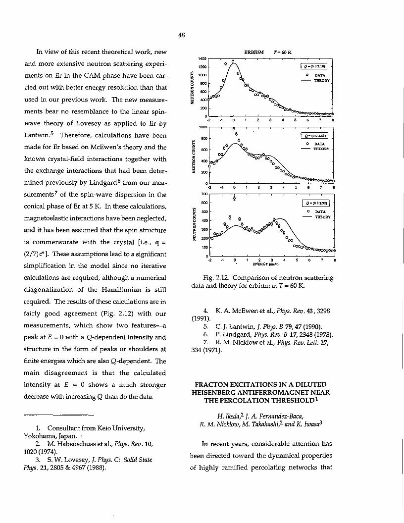
48
In view of this recent theoretical work, new and more extensive neutron scattering experiments on Er in the CAM phase have been carried out with better energy resolution than that used in our previous work. The new measurements bear no resemblance to the linear spin-wave theory of Lovesey as applied to Er by Lantwin.5 Therefore, calculations have been made for Er based on McEwen's theory and the known crystal-field interactions together with the exchange interactions that had been determined previously by Lindgard6 from our measurements7 of the spin-wave dispersion in the conical phase of Er at 5 K. In these calculations, magnetoelastic interactions have been neglected, and it has been assumed that the spin structure is commensurate with the crystal [i.e., q = (2/7) c*]. These assumptions lead to a significant simplification in the model since no iterative calculations are required, although a numerical diagonalization of the Hamiltonian is still required. The results of these calculations are in fairly good agreement (Fig. 2.12) with our measurements, which show two features—a peak at E = 0 with a Q-dependent intensity and structure in the form of peaks or shoulders at finite energies which are also Q-dependent. The main disagreement is that the calculated intensity at E = 0 shows a much stronger decrease with increasing Q than do the data.
1400
1200
1000
800
600
400'
200
0
ERBIUM T=60K
0 / * 0 / | C-(002.10) | -
/ o\ O DATA
7 THEORY
sPo° °°%C oJSs. -
•
i . .
-•
i . . , *-* u , J Ut^v^U 1 _fl_|l
1000 — i i 5
1— 1 '
B00
— i i 5
1—
1 2-<00Z53) |
^8 . O DATA 600 - OV THEORY .
400 -&A
T 200 -
0 0 / ^ 0 0 ° * 5 5 oX o \ oo \
,
700
600
500
400
300
200
100
0
§ ' ' ' 1 1
-§
\a- (002.91) | -
- o DATA
Oj;!
§ v r 5o \ o \
00 x
THEORY
^30000500"
1 2 3 4 ENERGY (mtV)
Fig. 2.12. Comparison of neutron scattering data and theory for erbium at T = 60 K.
4. K. A. McEwen et al., Phys. Rev. 43,3298 (1991).
5. C. J. Lantwin, /. Phys. B 79,47 (1990). 6. P. Lindgard, Phys. Rev. B 17,2348 (1978). 7. R. M. Nicklow et al., Phys. Rev. Lett. 27,
334 (1971).
FRACTON EXCITATIONS IN A DILUTED HEISENBERG ANTIFERROMAGNET NEAR
THE PERCOLATION THRESHOLD1
1. Consultant from Keio University, Yokohama, Japan. •
Z M. Habenschuss et al., Phys. Rev. 10, 1020 (1974).
3. S. W. Lovesey, /. Phys. C: Solid State Phys. 21,2805 &4967 (1988).
H. Ikeda,2 J. A. Fernandez-Baca, R. M. Nicklow, M. Takahashi,2 and K. Iivasa3
In recent years, considerable attention has been directed toward the dynamical properties of highly ramified percolating networks that

exhibit fractal geometry. Recent theories4 and computer simulations5 of these systems predict the existence of highly localized fracton excitations. The ideal system to probe the existence of these excitations is a random site-diluted Heisenberg antiferromagnet, where a fractal geometry is realized at length scales shorter than the geometrical correlation length £,Q. Thus an inelastic neutron scattering experiment has been performed to study the spin dynamics of RbMnxMgi.xF3 (x = 0.39), where x is close to the percolation concentration, Cp = 0.312.
This system is better suited for the study of fracton excitations than Mno5Zrio5F2, studied by Uemura and Birgeneau, 6 because RbMnxMgi.xF3 exhibits negligible anisotropy and is considerably closer to the percolation concentration (cp = 0.245 for the MnF2 structure). It is believed that this study constitutes the first quantitative measurement of fracton excitations in a near-percolating system. The experiments were performed at triple-axis spectrometers at the HFIR. At T = 4.5 K, no evidence of propagating spin waves in this system was observed, but instead energy spectra consisting of a broad peak superimposed on narrow peaks because of Ising cluster excitations were observed. This broad peak exhibits the following characteristics: (1) the linewidth is much larger than the instrumental energy resolution and increases with increasing wave vector, (2) the energy also increases with increasing wave vector, (3) the integrated intensity decreases with increasing wave vector, (4) the integrated intensity is much higher than that of the Ising cluster excitations, and (5) it persists
:; ^m^Mi-'-£-mhM^ v
even at T = 100 K, while the Ising-cluster
excitations disappear above Tfj - 18 K. This
magnetic response is attributed to the excitation
of fractons in a percolating network. This broad
magnetic response was fitted to a damped
harmonic oscillator (DHO) form, and it was
found that the fitted values of the energy E{q) and width T(q) satisfy a power-law relationship
with the same exponent [i.e., E(q) °= T(q) °=
ql.l±0.2j Yhis result, based on an analysis using
the DHO form, is in qualitative agreement with
the single-length scale postulate, 5 although
recent calculations by Yakubo et al. 7 using a
Lorentzian form yielded an exponent of 2.5
instead of 1.1.
1. Summary of paper to be published. 2. Guest scientist from National Labora
tory for High-Energy Physics, Tsukuba, Japan. 3. Guest scientist from Keio University,
Yokohama, Japan. 4. R. Orbach, Science 251,814 (1986). 5. T. Nakayama, K. Yakubo, and
R. Orbach, Reviews of Modern Physics (in press). 6. Y. J. Uemura and R. J. Birgeneau, Phys.
Rev. Lett. 57,1947 (1986). 7. K. Yakubo, T. Terao, and T. Nakayama,
private communication.
LOW-ENERGY EXCITATIONS IN SUPERCONDUCTING LA 1. 8 6Sro.i4Cu0 4
1
T. E. Mason,2 G. Aeppli,3 S. M. Hoyden,^ A. P. Ramirez,3 and H. A. Mook
One signature of unconventional superconductivity is a gap function with nodes on the Fermi surface. In a clean BCS superconductor, such nodes do not occur, and the low-energy quasiparticle excitations are absent for energies
M^*:!'
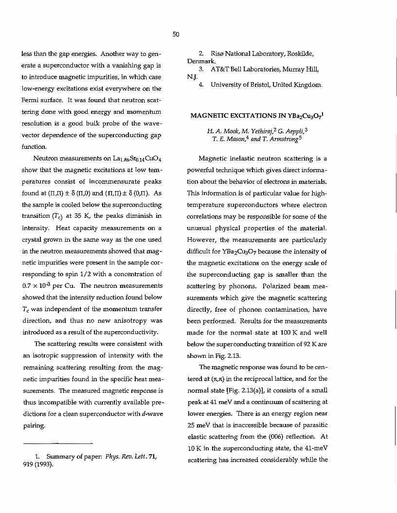
50
less than the gap energies. Another way to generate a superconductor with a vanishing gap is to introduce magnetic impurities, in which case low-energy excitations exist everywhere on the Fermi surface. It was found that neutron scattering done with good energy and momentum resolution is a good bulk probe of the wave-vector dependence of the superconducting gap function.
Neutron measurements on Lai.86Sro.i4CuC>4 show that the magnetic excitations at low temperatures consist of incommensurate peaks found at (n,n) ± 8 (n,0) and (n,n) ± 8 (0,n). As the sample is cooled below the superconducting transition (Tc) at 35 K, the peaks diminish in intensity. Heat capacity measurements on a crystal grown in the same way as the one used in the neutron measurements showed that magnetic impurities were present in the sample corresponding to spin 1/2 with a concentration of 0.7 x 10"3 per Cu. The neutron measurements showed that the intensity reduction found below Tc was independent of the momentum transfer direction, and thus no new anisotropy was introduced as a result of the superconductivity.
The scattering results were consistent with an isotropic suppression of intensity with the remaining scattering resulting from the magnetic impurities found in the specific heat measurements. The measured magnetic response is thus incompatible with currently available predictions for a clean superconductor with d-wave pairing.
1. Summary of paper: Phys. Rev. Lett. 71, 919 (1993).
2. Risa National Laboratory, Roskilde, Denmark.
3. AT&T Bell Laboratories, Murray Hill, N.J.
4. University of Bristol, United Kingdom.
MAGNETIC EXCITATIONS IN YBazCuaOy1
H. A. Mook, M. Yethiraj,2 G. Aeppli,3
T. E. Mason,4 and T. Armstrong5
Magnetic inelastic neutron scattering is a powerful technique which gives direct information about the behavior of electrons in materials. This information is of particular value for high-temperature superconductors where electron correlations may be responsible for some of the unusual physical properties of the material. However, the measurements are particularly difficult for YBa2Cu3C»7 because the intensity of the magnetic excitations on the energy scale of the superconducting gap is smaller than the scattering by phonons. Polarized beam measurements which give the magnetic scattering directly, free of phonon contamination, have been performed. Results for the measurements made for the normal state at 100 K and well below the superconducting transition of 92 K are shown in Fig. 2.13.
The magnetic response was found to be centered at (7C,7t) in the reciprocal lattice, and for the normal state [Fig. 2.13(a)], it consists of a small peak at 41 meV and a continuum of scattering at lower energies. There is an energy region near 25 meV that is inaccessible because of parasitic elastic scattering from the (006) reflection. At 10 K in the superconducting state, the 41-meV scattering has increased considerably while the
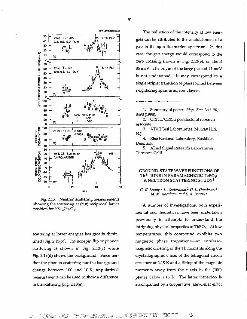
51
ORNIDWG 53U.50MB
50 40 30 20
+ 10
s 0 c )/( 70 C3 m 60
or 50 O e 40 z 30 o ?0 o « 10 c« 1 - 0 z 3 o
100 o 80
60 40 20 0
c 100 aM t - 2 au
OUN
MO
fin a w 40
80 DC O 60 1 -
* z 40 H O y s ?n ^ * o • o 0 • o
-20 2r"Z 3 -40
o o -60
I X"(co) T-100K
- (0.5.0.5,-5.2) fait)
(a)
r i SPIN FLIP
_ X"(co) T -10K (0.5.0.5,-5.2) (ji.n)
"rt SPIN FLIP _
~ (c)
, £ * • NON SPIN FLIP • 0 a 10K
, o 100K
BACKGROUND Q10K I
: ^ O100K
8 % o o
I -
(0.5.0.5,-5.2) (n.n) UNPOLARIZED y *
HB-1 -
-(e)
20 40 meV
60
Fig. 2.13. Neutron scattering measurements showing the scattering at (JC,7C) reciprocal lattice position for YBa2Cu3C>7.
scattering at lower energies has greatly diminished [Fig. 2.13(b)]. The nonspin flip or phonon scattering is shown in Fig. 2.13(c) while Fig. 2.13(d) shows the background. Since neither the phonon scattering nor the background change between 100 and 10 K, unpolarized measurements can be used to show a difference in the scattering [Fig. 2.13(e)].
The reduction of the intensity at low energies can be attributed to the establishment of a gap in the spin fluctuation spectrum. In this case, the gap energy would correspond to the zero crossing shown in Fig. 2.13(e), or about 35 meV. The origin of the large peak at 41 meV is not understood. It may correspond to a singlet-triplet transition of pairs formed between neighboring spins in adjacent layers.
1. Summary of paper: Phys. Rev. Lett. 70, 3490 (1993).
2 ORNL/ORISE postdoctoral research associate.
3. AT&T Bell Laboratories, Murray Hill, N.J.
4. Riso National Laboratory, Roskilde, Denmark.
5. Allied Signal Research Laboratories, Torrance, Calif.
GROUND-STATE WAVE FUNCTIONS OF Tb3*- IONS IN PARAMAGNETIC TbP0 4 :
A NEUTRON SCATTERING STUDY1
C.-K. Loong2 L. Soderholm,2 G. L. Goodman,2
M. M. Abraham, and L. A. Boatner
A number of investigations, both experimental and theoretical, have been undertaken previously in attempts to understand the intriguing physical properties of TbP04. At low temperatures, this compound exhibits two magnetic phase transitions—an antiferro-magnetic ordering of the Tb moments along the crystallographic c axis of the tetragonal zircon structure at 2.28 K and a tilting of the magnetic moments away from the c axis in the (100) planes below 2.15 K. The latter transition is accompanied by a cooperative Jahn-Teller effect
*M&te ^^m-:;m^M^- :x.-& m&x&&-?.-J& imi
52
involving Tb ion-lattice coupling that induces a
tetragonal-to-monoclinic distortion of the crystal
lattice. The crystal-field states and spin dynam
ics of the T b 3 + ions have important conse
quences for the magnetic and luminescence
properties of TbPC>4, which are manifested in the
magnetic susceptibility, magnetization, specific
heat, magnetic phase transitions, and optical-
adsorption/emission spectra. A characterization
of the electronic wave functions of the crystal-
field states and the nature of the spin-spin and
spin-lat t ice in teract ions are useful for
understanding both the bulk and microscopic
properties of the material.
Magnetic neutron scattering probes the low-
lying electronic states via magnetic-dipole
transitions as opposed to the electric-dipole
transitions between the ground state and the
significantly higher energy states normally
observed in an optical study. Therefore, these
two techniques provide complementary infor
mation regarding the energy-level structure of
magnetic ions.
In the p re sen t inves t iga t ions , the
paramagnetic-excitation spectrum of TbPC>4 has
been investigated by means of inelastic neutron
scattering techniques, and the observed crystal-
field transitions were analyzed using a Hamil-
tonian that included the atomic free-ion and
crystal-field interactions for an f1 configuration.
The resulting crystal-field level scheme for the
T b 3 f 7F6 ground multiplet is shown schemati
cally in Fig. 2.14. Five parameters for the
crystal-field potential that provided a satisfac
tory description of the neutron data collected at
r5(2)-
n -LM
r 5 ( ^
d# m
% H
SSDN-4688
meV cm-"1
323 260.7 31.0 249.6 29.4 237.1
./931 793 - 9.50 76.6 ^920 742
J K
rv(2) BCDEFGP
2.60 21.0 0.97 7.82 0.46 3.74 0 0
Tb 3 + : 7 F 6 in T b P 0 4
Fig. 2.14. Schematic diagram of the splitting of the T b 3 + ground multiplet by the crystal field into seven singlets 2 r x + T2 + 2T3 + 2 r 4 + and three doublets, 3 ^ .
temperatures between 4.2 and 150 K were
obtained. The calculated crystal-field contribu
tion to the specific heat in the 4-10-K tempera
ture range and the paramagnetic susceptibility
agree well with the experimental results. The
large anisotropy of the magnetic ground-state
doublet of the Tb ions with respect to the crystal -
lographic c axis has important consequences for
the spin structure in the antiferromagnetic
phases at low temperatures. The effective inter
nal magnetic field in antiferromagnetic TbP04
was estimated based on the crystal-field level
scheme, and a molecular-field approximation
53
and was found to be in good agreement with the values reported from other measurements.
1. Summary of paper: Phys. Rev. B 48,6124 (1993).
2 Argonne National Laboratory, Argonne, ni.
RARE-EARTH ENERGY LEVELS AND MAGNETIC PROPERTIES OF DyP0 4
1
C.-K. Loong,2 L. Soderholm,2 J. S. Xue2
M. M. Abraham, and L. A. Boatner
Crystal-field (CF) states and spin dynamics of Dy *" ions have important consequences for the magnetic properties of DVPO4. In spite of numerous prior studies, information regarding the CF-split ground-multiplet wave functions of the Dy3"*" ions in DVPO4 is still incomplete. From neutron diffraction, optical absorption, and Mossbauer effect studies, the ground state is known to have large 115/2 ± 15/2 > components and spectroscopic splitting g factors parallel and perpendicular to the c-axis given by g\\ = 19 and gx = 0, respectively. The energies and symmetries of all other states, however, are not known. Consequently, the magnetic behavior has been interpreted by Ising-like interactions of magnetic ions with effective spins of 1/2. Since the excited states are ignored in this approach, only the low-temperature data can be analyzed quantitatively.
In the present work, inelastic neutron scattering and magnetic-susceptibility measurements are performed, along with a corresponding determination of the crystal-field parameters
for the orthophosphate DVPO4. DyP04 exhibits a number of intriguing magnetic properties at low temperatures. In the absence of an applied magnetic field, DyP04 orders anti-ferromagnetically with the Dy moments oriented parallel and antiparallel to the crystallography c-axis at temperatures T < T^ = 3.4 K. Below T^, an antiferromagnetic-to-paramagnetic phase transition can be induced by a magnetic field applied along the c-axis. The nature of the spin structure and phase transitions in the region of mixed metamagnetic phases (T < Tj, 0.5 < H < 1 T), however, is not yet understood.
In the present investigation, the dynamic and static paramagnetic responses of DyP04 were studied by neutron inelastic scattering and single-crystal magnetic susceptibility measurements. The observed energies and intensities of the magnetic transitions at 15 and 100 K were used to refine the parameters of the crystal-field potential for Dy3*" ions in DVPO4. The resulting crystal-field level scheme for the Dy^" 6Hi5/2 ground multiplet is shown schematically in Fig. 2.15, and the derived crystal-field level structure provides a basis for explaining the low-temperature magnetic properties of this compound.
1. Summary of paper: Journal of Alloys and Compounds (in press).
2. Argonne National Laboratory, Argonne, HI.
>! .• ;%mt- 'Mx ; T W I F •;: :• ~wm&wym
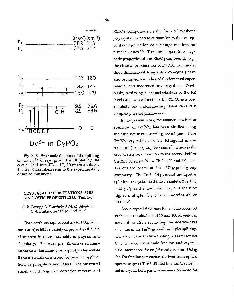
54
r 6
(meVKcrrr1) -38.9 313 -37.5 302
r-,
r A-6 BCDE
/, /,
•22.3 180
•18.2 147 16.0 129
G H •9.5 8.5
76.6 68.6
0 0
Dy 3 + in DyP04
Fig. 2.15. Schematic diagram of the splitting of the D y 3 + 6 H i s / 2 ground multiplet by the crystal field into 41^ + 4 TV Kramers doublets. The transition labels refer to the experimentally observed transitions.
CRYSTAL-HELD EXCITATIONS AND MAGNETIC PROPERTIES OF T m P 0 4
1
C.-K. Loong,2 L. Soderholm,2 M. M. Abraham, L. A. Boatner, and N. M. Edelstein3
Rare-earth orthophosphates (REFO4, RE =
rare earth) exhibit a variety of properties that are
of interest in many subfields of physics and
chemistry. For example, RE-activated lumi
nescence in lanthanide orthophosphates makes
these materials of interest for possible applica
tions as phosphors and lasers. The structural
stability and long-term corrosion resistance of
REPO4 compounds in the form of synthetic
poly crystalline ceramics have led to the concept
of their application as a storage medium for
nuclear wastes. 4 ' 5 The low-temperature mag
netic properties of the KEPO4 compounds (e.g.,
the close approximation of DyP04 to a model
three-dimensional Ising antiferromagnet) have
also prompted a number of fundamental exper
imental and theoretical investigations. Obvi
ously, achieving a characterization of the RE
levels and wave functions in REPO4 is a pre
requisite for understanding these relatively
complex physical phenomena.
In the present work, the magnetic-excitation
spectrum of T m P 0 4 has been studied using
inelastic neutron scattering techniques. Pure
TmP04 crystallizes in the tetragonal zircon
structure (space group I 4 i / a m d ) , 1 5 which is the
crystal structure common to the second half of
the KEPO4 series {RE = Tb-Lu, Y, and Sc). The
Tm ions are located at sites of D u point-group
symmetry. The T m 3 + : 3 H 6 ground multiplet is
split by the crystal field into 7 singlets, 1Y\ + 1^
+ 2 T 3 T 4 , and 3 doublets, 3T 5 ; and the next
higher multiplet 3 F 4 lies at energies above
5000 cm" 1 .
Sharp crystal-field transitions were observed
in the spectra obtained at 15 and 100 K, yielding
new information regarding the energy-level
structure of the T m 3 + ground-multiplet splitting.
The data were analyzed using a Hamiltonian
that included the atomic free-ion and crystal-
field interactions for a n / 1 2 configuration. Using
the Tm free-ion parameters derived from optical
spectroscopy of T m 3 + diluted in a LUPO4 host, a
set of crystal-field parameters were obtained for
Tm 3 f in pure T111PO4. The calculated magnetic spectra of T111PO4 agree very well with the results of neutron and Raman measurements. The calculated bulk magnetic susceptibility of TmPC>4 exhibited a large anisotropy at low temperatures and is in good agreement with the experimental data. A significant contribution to the specific heat from T m 3 + crystal-field states was found at temperatures below 100 K. The present analysis provides an estimate of the contributions from the Tin3*" low-lying crystal-field states to both the bulk magnetic susceptibility and the specific heat in TmP04.
1. Summary of paper: /. Chem. Phys. 98, 4214 (1993).
2 Argonne National Laboratory, Argonne, m.
3. Lawrence Berkeley Laboratory, Berkeley, Calif.
4. L. A. Boatner et al., p. 411 in Management of Alpha-Contaminated Wastes, IAEA-SM-246/73, IAEA, Vienna, Austria, 1981.
5. L. A. Boatner, p. 289 in Scientific Basis for Nuclear Waste Management, ed. by C. J. Northrup, Vol. II, Plenum Press, New York, 1980.
RARE-EARTH ENERGY LEVELS AND MAGNETIC PROPERTIES
OFH0PO4 ANDErP0 4
1
C.-K. Loong,2 L. Soderholm,2
J. P. Hammonds,2 M. M. Abraham, L. A. Boatner, and N. M. Edelstein3
Mixed natural rare-earth orthophosphates, REFO4 (RE = rare earths), form the minerals monazite (RE = La-Gd) and xenotime (RE = Tb-Lu). The high melting temperatures (about 2000°C), structural and chemical stability, and long-term corrosion resistance of the REPO4
••-:&«•,*. '&% ,.MWM.:M;;^ C-
compounds make these substances attractive for applications as high-temperature components and nuclear waste storage media.4-5
The optical and magnetic properties of the RE ions in RPO4 hosts, including their i n activated luminescence, magnetic phase transitions, and Jahn-Teller effects, have also prompted numerous fundamental experimental and theoretical investigations. Increasing our knowledge of the RE energy levels and wave functions in REPO4 compounds is, of course, essential to understanding both the bulk and microscopic properties of these materials.
A systematic study of magnetic excitations in the stoichiometric REPO4 series using neutron spectroscopy has recently been initiated. In the present work, the static and dynamic magnetic responses of H0PO4 and ErPC>4 have been studied by means of neutron spectroscopy and magnetic susceptibility measurements. The inelastic neutron scattering spectra exhibit well-defined transitions characteristic of crystal-field excitations of the RE ions. The data were analyzed using a Hamiltonian that included atomic free-ion and crystal-field interactions for an/^configuration (N = 10 and 11 for H o 3 + and Er3*, respectively). Using the free-ion parameters derived from optical spectroscopy of the corresponding RE ions diluted in a YPO4 host, crystal-field parameters for both H0PO4 and ErPC>4 were obtained. The derived crystal-field level structure provides a basis for explaining the low-temperature magnetic properties of both compounds. The calculated and measured paramagnetic susceptibilities agree well for H0PO4 and ErPC>4 in the tem-
56
perature range 5-300 K. The highly anisotropic, saturated magnetization of the ground doublet in H0PO4 may act as a "bootstrap" for long-range magnetic ordering of the moments parallel to the c-axis at low temperatures. The nearly spherically symmetric moments of the low-lying Kramers doublets of ErPC>4, however, tend to couple less effectively via exchange interactions. The effective exchange field in antiferromagnetic H0PO4, as estimated based on the crystal-field level scheme and a molecular-field approximation, is found to be in good agreement with that reported from a specific-heat analysis. The paramagnetic specific-heat, spectroscopic splitting g factors of the low-lying doublet states and saturated moments for
H0PO4 and ErPC>4 obtained from the present study are applicable to interpreting specific heat, hyperfine interaction, electron paramagnetic resonance, and neutron diffraction measurements.
1. Summary of paper: J. Phys. Condens. Matter 5,5121 (1993);/. Appl. Phys. 73, 6069 (1993).
2. Argonne National Laboratory, Argonne, HI.
3. Lawrence Berkeley Laboratory, Berkeley, Calif.
4. L. A. Boatner et al., p. 411 in 2982 Management of Alpha-Contaminated Wastes, LAEA-SM-246/73, Vienna, Austria, 1981.
5. L. A. Boatner et al., p. 289 in 2980 Scientific Basis for Nuclear Waste Management II, ed. by C. J. Northrup, Plenum Press, New York, 1980.
3. Synthesis, Processing, and Characterization of Materials
Breakthroughs in the related fields of solid state physics and materials sciences often depend on the synthesis and subsequent characterization of new materials. Research in the Solid State Division has a strong tradition of emphasizing a broad range of material synthesis activities which include superconductors, glasses, insulating crystals, metal alloys and crystals, nanophase solids, and solid electrolytes. The selection of materials to be synthesized are carefully coordinated with other research activities in the division and are designed to answer fundamental or applied questions concerning energy-related problems. Many of the materials that are produced are unique or rare research samples which naturally lead to collaborative activities involving university laboratories, other divisions at ORNL, other national laboratories, and industrial research centers.
This chapter is divided into the following five sections: Superconductivity, which reports some striking fundamental results on the role of both extrinsic and intrinsic defects on flux pinning and flux motion; Thin-Film Batteries and Solid Electrolytes, which describes a dynamic blend of applied and basic research projects aimed at understanding and producing new types of solid state electrolytes and thin-film rechargeable batteries; Ferroelectric and Perovskite-Structure Oxides, which describes interesting research activities dealing with an important class of ferroelectric materials for electro-optic, photorefractive, and thin-film substrate applications; Materials Properties, which reports some new characterization and processing techniques that have led to a better understanding of the initial stages of sintering, a more complete structural model of an important class of amorphous phosphates, and production of a remarkable theoretical model that can accurately reproduce the microstructure of welded single crystals; and Optical Characterization of Materials, which reports on a new promising scintillator material and on fundamental studies of optically active ions and defects in single-crystal hosts.
57
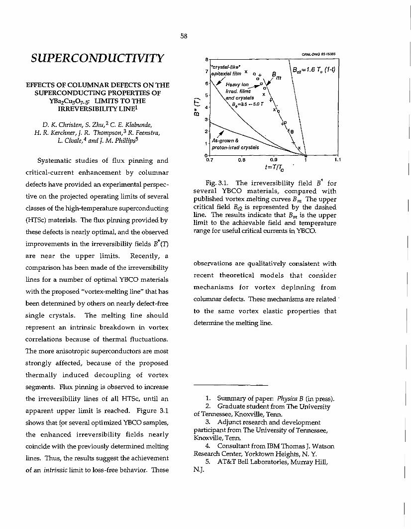
58
SUPERCONDUCTIVITY
EFFECTS OF COLUMNAR DEFECTS ON THE SUPERCONDUCTING PROPERTIES OF
YBa 2Cu 30 7. 5: LIMITS TO THE IRREVERSIBILITY LINE1
D. K. Christen, S. Zhu,2 C. E. Klabunde, H. R. Kerchner,}. R. Thompson,3 R. Feenstra,
L. Ovale,4 and]. M. Phillips5
Systematic studies of flux pinning and critical-current enhancement by columnar defects have provided an experimental perspective on the projected operating limits of several classes of the high-temperature superconducting (HTSc) materials. The flux pinning provided by these defects is nearly optimal, and the observed improvements in the irreversibility fields B (T) are near the upper limits. Recently, a comparison has been made of the irreversibility lines for a number of optimal YBCO materials with the proposed "vortex-melting line" that has been determined by others on nearly defect-free single crystals. The melting line should represent an intrinsic breakdown in vortex correlations because of thermal fluctuations. The more anisotropic superconductors are most strongly affected, because of the proposed thermally induced decoupling of vortex segments. Flux pinning is observed to increase the irreversibility lines of all HTSc, until an apparent upper limit is reached. Figure 3.1 shows that for several optimized YBCO samples, the enhanced irreversibility fields nearly coincide with the previously determined melting lines. Thus, the results suggest the achievement of an intrinsic limit to loss-free behavior. These
ORNL-DWG 9315385
* OQ
\Bci=1.6 Tc (1-t)
1.1
Fig. 3.1. The irreversibility field B for several YBCO materials, compared with published vortex melting curves Bm The upper critical field B^ is represented by the dashed line. The results indicate that B m is the upper limit to the achievable field and temperature range for useful critical currents in YBCO.
observations are qualitatively consistent with recent theoretical models that consider mechanisms for vortex depinning from columnar defects. These mechanisms are related to the same vortex elastic properties that determine the melting line.
1. Summary of paper: Physica B (in press). 2. Graduate student from The University
of Tennessee, Knoxville, Tenn. 3. Adjunct research and development
participant from The University of Tennessee, Knoxville, Tenn.
4. Consultant from IBM Thomas J. Watson Research Center, Yorktown Heights, N. Y.
5. AT&T Bell Laboratories, Murray Hill, N.J.
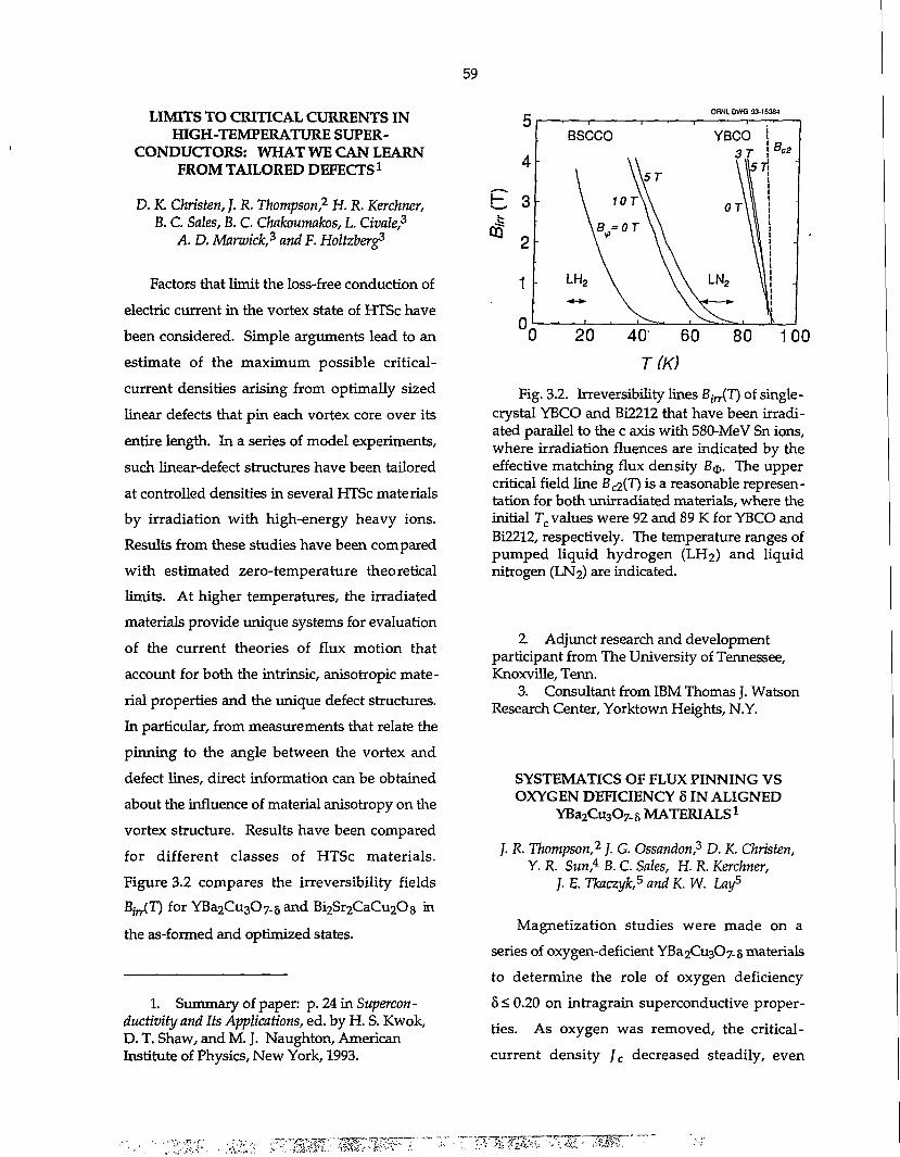
59
LIMITS TO CRITICAL CURRENTS IN HIGH -TEMPERATURE SUPER
CONDUCTORS: WHAT WE CAN LEARN FROM TAILORED DEFECTS1
D. K. Christen, J. R. Thompson,2 H. R. Kerchner, B. C. Sales, B. C. Chakoumakos, L. Ovale,3
A. D. Marwick,3 and F. Holtzberg?
Factors that limit the loss-free conduction of electric current in the vortex state of HTSc have been considered. Simple arguments lead to an estimate of the maximum possible critical-current densities arising from optimally sized linear defects that pin each vortex core over its entire length. In a series of model experiments, such linear-defect structures have been tailored at controlled densities in several HTSc materials by irradiation with high-energy heavy ions. Results from these studies have been compared with estimated zero-temperature theoretical limits. At higher temperatures, the irradiated materials provide unique systems for evaluation of the current theories of flux motion that account for both the intrinsic, anisotropic material properties and the unique defect structures. In particular, from measurements that relate the pinning to the angle between the vortex and defect lines, direct information can be obtained about the influence of material anisotropy on the vortex structure. Results have been compared for different classes of HTSc materials. Figure 3.2 compares the irreversibility fields Bin{T) for YBa 2Cu30 7 . 5 and Bi2Sr2CaCu208 in the as-formed and optimized states.
5 OHNLOWG 93-15334
5 BSCCO YBCO
4 \ \ V r
3T !
\ 1 5 T BC2
£ 3 0 3 2
\ 10TX\ or\|
1 LH2 \ \ \ LN2 \l -
°C °C 20 40 60 80 10 T(K)
1. Summary of paper: p. 24 in Superconductivity and Its Applications, ed. by H. S. Kwok, D. T. Shaw, and M. J. Naughton, American Institute of Physics, New York, 1993.
Fig. 3.2. Irreversibility lines Birr(T) of single-crystal YBCO and Bi2212 that have been irradiated parallel to the c axis with 580-MeV Sn ions, where irradiation fluences are indicated by the effective matching flux density B<j>. The upper critical field line B^T) is a reasonable representation for both unirradiated materials, where the initial Tc values were 92 and 89 K for YBCO and Bi2212, respectively. The temperature ranges of pumped liquid hydrogen (LH 2) and liquid nitrogen (LN2) are indicated.
2. Adjunct research and development participant from The University of Tennessee, Khoxville, Tenn.
3. Consultant from IBM Thomas J. Watson Research Center, Yorktown Heights, N.Y.
SYSTEMATICS OF FLUX PINNING VS OXYGEN DEFICIENCY 8 IN ALIGNED
YBa2Cu307_6 MATERIALS1
/. R. Thompson,2 J. G. Ossandon,3 D. K. Christen, Y.R. Sunt B. C. Sales, H. R. Kerchner,
J. E. Tkaczyk,5 and K. W. Lay5
Magnetization studies were made on a series of oxygen-deficient YBa2Cu307-g materials to determine the role of oxygen deficiency 8 < 0.20 on intragrain superconductive properties. As oxygen was removed, the critical-current density Jc decreased steadily, even
60
where T c was nearly constant. Flux-creep studies were analyzed to obtain the effective vortex-pinning energy U^Q), which depends on the instantaneous current density /. The results were well-described by the vortex glass/collective-pinning relation UgffQ) = (Uo/mido/D^l with u = 0.9 for all oxygen compositions studied. Experimental values for the pinning energy scale U0 are compared with predictions from coUective-pinning theory. The resulting interpretation within a collective-pinning/collective-creep framework gives a picture that is internally consistent. Specifically, similar values for the characteristic exponent \x are obtained from direct analysis of M (t) and analysis of the vortex-pinning energy U(J). These values lie between the respective theoretical values, 1/7 and 3/2. In magnitude and compositional dependence, the calculated energy scales are consistent with this interpretation. Finally, the experimental values for the energy scale U0 and (i are similar to those used to model /C(T) in comparable single crystals.
1. Summary of papers: Cryogenics 32, 982 (1992); Applied Superconductivity L 371 (1993).
2. Adjunct research and development participant from The University of Tennessee, Knoxville, Tenn.
3. Guest scientist from University of Talca, Talca, Chile.
4. Graduate student from The University of Tennessee, Knoxville, Tenn.
5. General Electric Corporate R&D Laboratory, Schenectady N.Y.
ENHANCED VORTEX-PINNING STRENGTH AND MAGNETIC
IRREVERSIBILITY VIA COLUMNAR DEFECTS IN SINGLE-CRYSTAL
Bi 2Sr 2CaCu 20 8
1
H. R. Kerchner,}. R. Thompson,2 Y. R. Sun,3
D. K. Christen, J. O. Thomson? B. C. Sales, B. Chakoumakos,
L. Civale,5 and A. D. Marwick6
To enhance vortex pinning in the high-Tc
superconductor Bi2Sr2CaCu208, single crystals were irradiated with energetic heavy ions to create columnar defects. Ions impinged samples at various angles with respect to the c axis. Quasistatic magnetization measurements showed magnetic hysteresis (and critical-current density), which approaches zero as shown in Fig. 3.3 at a line of irreversibility, Tirr(B).6
Dynamic ac susceptibility measurements showed shielding currents that approached zero at a somewhat higher temperature T . Thermally assisted flux-flow resistivity PJAFF
was deduced in the regime between Tirr and T , and the pinning energy U0 was determined from the Arrhenius temperature dependence of pjApp-Irradiation-induced defects showed U0 values larger than observed in unirradiated samples by a factor of ~3, relatively independent of the ion beam exposure, which increased both } c and the irreversible B-T regime. Independence of Jc and U0 from the magnetic-field orientation suggests the predominance of strong pins interacting with two-dimensional pancake vortices.
1. Summary of paper: Physica B (in press). 2. Adjunct research and development
participant from The University of Tennessee, Knoxville, Tenn.
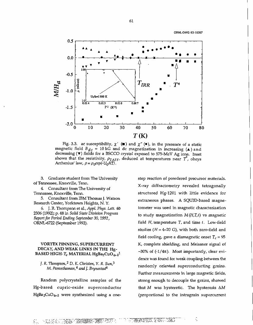
61
$
ORNL-DWG 93-16387
0.5
0.0
-0.5
-1.0
-1.5
-2.0
~i • r
AA • A
^ A / : • • • • • • •
• • • • • A
100
- Q .
Uo*=1500K 10 0.014
• I A
IRR • y*
0.015 0.016 0.017
10 20 30 40 50 60 70 80
r(K) Fig. 3.3. ac susceptibility, %' (•) and %" (•)/ in the presence of a static
magnetic field B^c = 10 kG and dc magnetization in increasing (A) and decreasing (T) fields for a BSCCO crystal exposed to 575-MeV Ag ions. Inset shows that the resistivity, pTAFF, deduced at temperatures near T*, obeys Arrhenius' law, p = p^xpi-Uf/kT).
3. Graduate student from The University of Tennessee, Knoxville, Term.
4. Consultant from The University of Tennessee, Knoxville, Term.
5. Consultant from IBM Thomas J. Watson Research Center, Yorktown Heights, N. Y.
6. J. R. Thompson et al., Appl. Phys. Lett. 60 2306 (1992); p. 48 in Solid State Division Progress Report for Period Ending September 30,1992, ORNL-6722 (September 1992).
VORTEX PINNING, SUPERCURRENT DECAY, AND WEAK LINKS IN THE Hg-
BASEDHIGH-TC MATERIAL HgBa2CuO a1
/. R. Thompson,2 D. K. Christen, Y. R. Sun,3
M. Paranthaman,* and J. Brynestad4
Random polycrystalline samples of the Hg-based cupric-oxide superconductor HgBaaCuO^s were synthesized using a one-
step reaction of powdered precursor materials. X-ray diffractometry revealed tetragonally structured Hg-1201 with little evidence for extraneous phases. A SQUID-based magnetometer was used in magnetic characterization to study magnetization M(H,T,t) vs magnetic field H, temperature T, and time t. Low-field studies (H = 4-20 G), with both zero-field and field cooling, gave a diamagnetic onset Tc = 95 K, complete shielding, and Meissner signal of ~30% of (-l/47t). Most importantly, clear evidence was found for weak coupling between the randomly oriented superconducting grains. Further measurements in large magnetic fields, strong enough to decouple the grains, showed that M was hysteretic. The hysteresis AM (proportional to the intragrain supercurrent
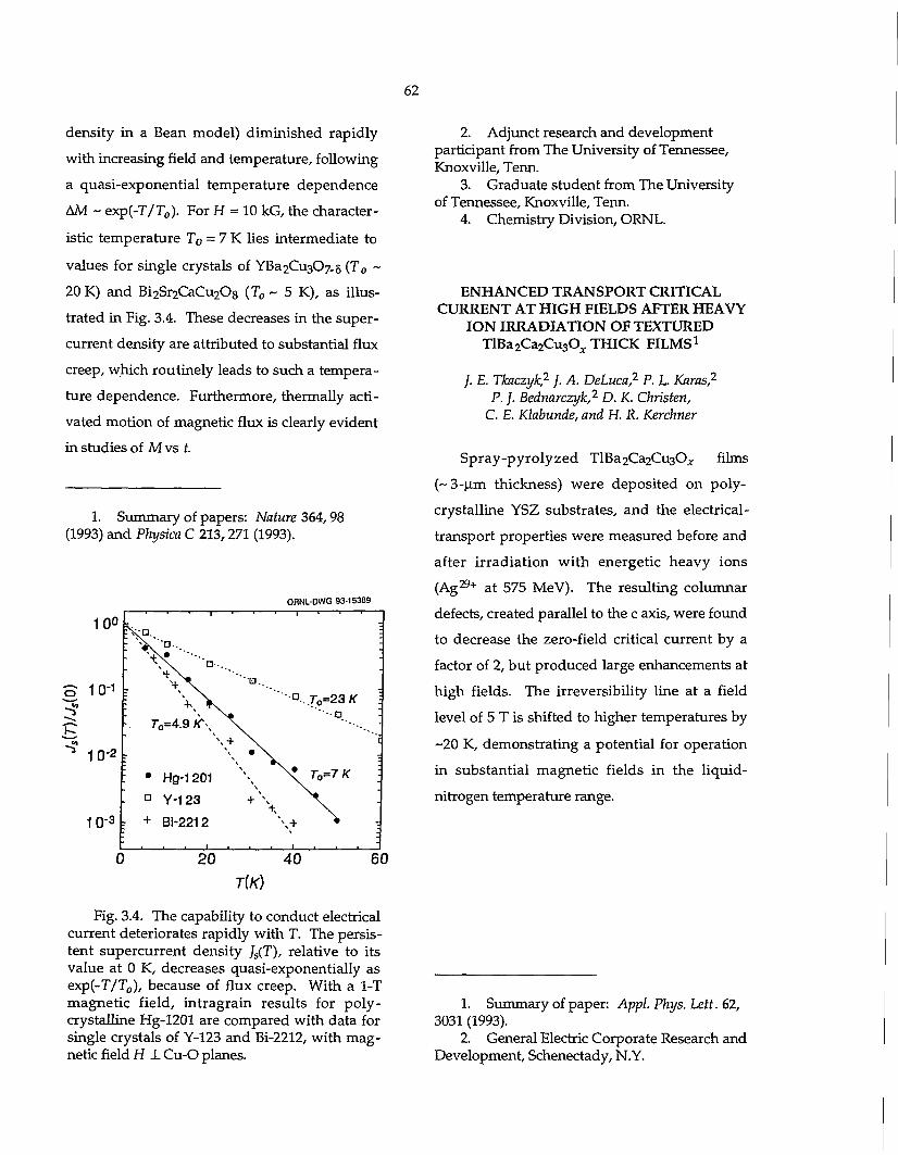
62
density in a Bean model) diminished rapidly
with increasing field and temperature, following
a quasi-exponential temperature dependence
AM ~ exp(-T/T 0). For H = 10 kG, the character
istic temperature T 0 = 7 K lies intermediate to
values for single crystals of YBa2Cu307_5 (T 0 ~
20 K) and BiaS^CaO^Og (T 0 ~ 5 K), as illus
trated in Fig. 3.4. These decreases in the super-
current density are attributed to substantial flux
creep, which routinely leads to such a tempera
ture dependence. Furthermore, thermally acti
vated motion of magnetic flux is clearly evident
in studies of M vs t.
1. Summary of papers: Nature 364,98 (1993) and Physica C 213,271 (1993).
ORNL-DWG 93-15389
S 10-1
10-2
10- 3
T0=4.9 K*
• Hg-1201 D Y-123
+ Bi-2212
J i •
D..Jo=23K •a
\ 7 W K
• i i_
20 40 T(K)
60
Fig. 3.4. The capability to conduct electrical current deteriorates rapidly with T. The persistent supercurrent density JS(T), relative to its value at 0 K, decreases quasi-exponentially as exp(-T/T 0), because of flux creep. With a 1-T magnetic field, intragrain results for poly-crystalline Hg-1201 are compared with data for single crystals of Y-123 and Bi-2212, with magnetic field H J. Cu-O planes.
2. Adjunct research and development participant from The University of Tennessee, Knoxville, Tenn.
3. Graduate student from The University of Tennessee, Knoxville, Tenn.
4. Chemistry Division, ORNL.
ENHANCED TRANSPORT CRITICAL CURRENT AT HIGH FIELDS AFTER HEAVY
ION IRRADIATION OF TEXTURED TlBa 2Ca 2Cu30 : t. THICK FILMS1
/. E. Tkaczyk2 J. A. DeLuca,2 P. L. Karas,2
P. J. Bednarczyk,2 D. K. Christen, C. E. Klabunde, and H. R. Kerchner
Spray-pyrolyzed TlBa2Ca2Cu30 x films
(~3-|i.m thickness) were deposited on poly-
crystalline YSZ substrates, and the electrical-
transport properties were measured before and
after irradiation with energetic heavy ions
(Ag 2 9 * at 575 MeV). The resulting columnar
defects, created parallel to the c axis, were found
to decrease the zero-field critical current by a
factor of 2, but produced large enhancements at
high fields. The irreversibility line at a field
level of 5 T is shifted to higher temperatures by
~20 K, demonstrating a potential for operation
in substantial magnetic fields in the liquid-
nitrogen temperature range.
1. Summary of paper: Appl. Phys. Lett. 62, 3031 (1993).
2. General Electric Corporate Research and Development, Schenectady, N.Y.
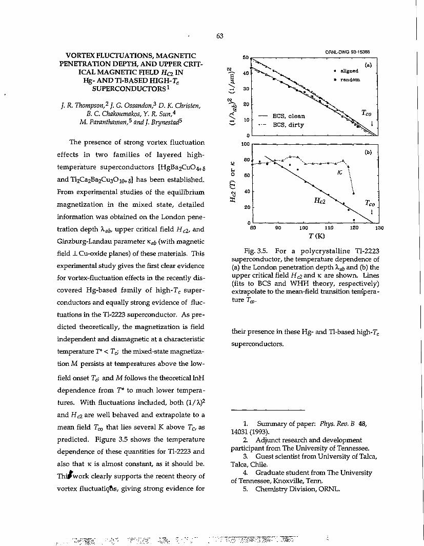
63
VORTEX FLUCTUATIONS, MAGNETIC PENETRATION DEPTH, AND UPPER CRIT
ICAL MAGNETIC FIELD Ha IN Hg- AND Tl-BASED HIGH-TC
SUPERCONDUCTORS *
/. R. Thompson,2 J. G. Ossandon,3 D. K. Christen, B. C. Chakoumakos, Y. R. Sun,4
M. Paranthaman,5 and J. Brynestad5
The presence of strong vortex fluctuation effects in two families of layered high-temperature superconductors [HgBa2Cu04f5 and Tl2Ca2Ba2Cu30io+5] has been established. From experimental studies of the equilibrium magnetization in the mixed state, detailed information was obtained on the London penetration depth Xaf,, upper critical field HC2, and Ginzburg-Landau parameter Kflj, (with magnetic field J. Cu-oxide planes) of these materials. This experimental study gives the first clear evidence for vortex-fluctuation effects in the recently discovered Hg-based family of high-T c superconductors and equally strong evidence of fluctuations in the Tl-2223 superconductor. As predicted theoretically, the magnetization is field independent and diamagnetic at a characteristic temperature T* < Tc; the mixed-state magnetization M persists at temperatures above the low-field onset T& and M follows the theoretical InH dependence from T* to much lower temperatures. With fluctuations included, both (1/X)2
and Hc2 are well behaved and extrapolate to a mean field T c o that lies several K above Tc, as predicted. Figure 3.5 shows the temperature dependence of these quantities for Tl-2223 and also that K is almost constant, as it should be. ThiFwork clearly supports the recent theory of vortex fluctuations, giving strong evidence for
ORNL-DWQ 93-15388
CQ
E 30
20
10
0 100
— BCS, clean — BCS. dirty
« 80
u o 60
p 1 40
20
0
t...A—•g.*^
K, \
(b)
- i •
Hc2 ico
• J
SO 90 100 110 TOO
120 130
Fig. 3.5. For a polycrystalline Tl-2223 superconductor, the temperature dependence of (a) the London penetration depth %.<$ and (b) the upper critical field HC2 and K are shown. Lines (fits to BCS and WHH theory, respectively) extrapolate to the mean-field transition temperature TQ,.
their presence in these Hg- and Tl-based high-Tc
superconductors.
1. Summary of paper: Phys. Rev. B 48, 14031 (1993).
2. Adjunct research and development participant from The University of Tennessee.
3. Guest scientist from University of Talca, Talca, Chile.
4. Graduate student from The University of Tennessee, Knoxville, Term.
5. Chemistry Division, ORNL.
64
EFFECT OF FLUX CREEP ON THE TEMPERATURE DEPENDENCE OF
THE CURRENT DENSITY IN YBaCuO CRYSTALS1
/. R. Thompson,2 Y.R. Sun,3 L. Civale* A. P. Malozemoff,5 M. W. McElfresh,6
A. D. Marwick,7 and F. Holtzberg?
The temperature-dependent persistent-
current density and normalized flux-creep rate,
together with the current dependence of the
vortex-pinning energy, were studied in as-
grown and proton-irradiated YBaCuO crystals.
A consistent interpretation of these features has
been found within the collective-pinning or
vortex-glass models. It is noteworthy that the
same theoretical treatment gives a good descrip
tion of both unirradiated and irradiated crystals,
with similar and physically reasonable param
eter values. Only the overall scale of current
density differs significantly. These features are
consistent with the idea that the increased
critical-current density in proton-irradiated
YBaCuO crystals arises primarily from an
increased density of point-like defects. Thus, we
can conclude that among existing theories,
vortex glass and /o r collective pinning theories
provide the first successful phenomenological
interpretation of the quasi-exponential depen
dence on temperature for the persistent current
density, the normalized flux-creep rate S (T), and
the current dependence of the vortex-pinning
energy U(f).
1. Summary of paper: Phys. Rev. B 47, 14440 (1993).
2 Adjunct research and development participant from The University of Tennessee, Knoxville, Term.
3. Graduate student from The University of Tennessee, Knoxville, Tenn.
4. Consultant from Centro Atomico Bariloche, Bariloche, Argentina.
5. American Superconductor Corporation, Watertown, Mass.
6. Purdue University, West Lafayette, Ind. 7. IBM T. J. Watson Research Center,
Yorktown Heights, N. Y.
OBSERVATION OF FREE-FLUX FLOW AT HIGH DISSIPATION LEVELS IN
YBa 2 Cu 3 0 7 EPITAXIAL FILMS 1
M. N. Kunchur,2 D. K. Christen, and ]. M. Phillips3
Highly controlled pulsed currents were used
to investigate superconducting transport proper
ties at exceptionally high power dissipation
levels (approaching 10 9 W/cm 3 !) . Although the
phenomenon of superconductivity is often
associated with a state of vanishing resistance,
this is neither a necessary nor sufficient condi
tion for characterizing the superconducting
state. At current densities beyond the critical
value, J > Jc dissipation sets in—although super
conductivity itself persists up to / = J& the pair-
breaking current. Novel and interesting physics
is expected to occur between Jc and J& and some
of these effects have been investigated.
In the mixed state of a superconductor, the
material is permeated by quantized flux vortices.
The motion of these vortices leads to dissipation
and thus finite resistivity. For the idealized case
of unhindered free-flux motion, the variation of
resistivity with field is described by the well-
known Bardeen-Stephen model 4 ( p / p n = B/H^).
Because ordinarily flux motion is hindered by
various crystalline defects, this behavior had
unt i l now not been observed in a n y
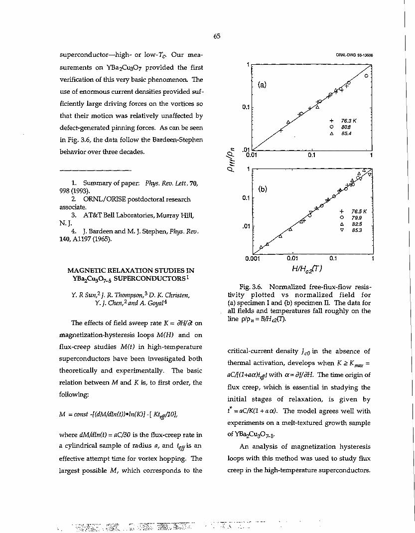
superconductor—high- or low-Tc. Our mea
surements on YBa2Cu307 provided the first
verification of this very basic phenomenon. The
use of enormous current densities provided suf
ficiently large driving forces on the vortices so
that their motion was relatively unaffected by
defect-generated pinning forces. As can be seen
in Fig. 3.6, the data follow the Bardeen-Stephen
behavior over three decades.
1. Summary of paper: Phys. Rev. Lett. 70, 998 (1993).
2 ORNL/ORISE postdoctoral research associate.
3. AT&T Bell Laboratories, Murray Hill, N.J.
4. J. Bardeen and M.J. Stephen, Phys. Rev. 140, A1197 (1965).
MAGNETIC RELAXATION STUDIES IN YBajCuaOy.s SUPERCONDUCTORS1
Y. R Sun,2 J. R. Thompson,3 D. K. Christen, Y. J. Chen,2 and A. Goyal4
The effects of field sweep rate K = dH/dt on magnetization-hysteresis loops M(H) and on flux-creep studies M(t) in high-temperature superconductors have been investigated both theoretically and experimentally. The basic relation between M and K is, to first order, the following:
M = const -[(dM/dln(t))»ln(K)]-[ Kt^/10],
where dM/dln(t) = aC/30 is the flux-creep rate in a cylindrical sample of radius a, and £e«-is an
effective attempt time for vortex hopping. The largest possible M, which corresponds to the
65
ORNL-DWG 93-13606
0.001 0.01 0.1 1
H/HCJT)
Fig. 3.6. Normalized free-flux-flow resistivity plotted vs normalized field for (a) specimen I and (b) specimen n. The data for all fields and temperatures fall roughly on the line p/pM = B/HaCT).
critical-current density Jc0 in the absence of thermal activation, develops when K > Kj^^ = aC/[(l+aa)tggr] with a= dJ/dH. The time origin of flux creep, which is essential in studying the initial stages of relaxation, is given by t =aC/K(l +acc). The model agrees well with experiments on a melt-textured growth sample 0fYBa2Cu3O7.5.
An analysis of magnetization hysteresis loops with this method was used to study flux creep in the high-temperature superconductors.
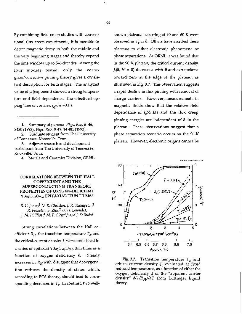
66
By combining field creep studies with conven
tional flux creep experiments, it is possible to
detect magnetic decay in both the middle and
the very beginning stages and thereby expand
the time window up to 5-6 decades. Among the
four m o d e l s tes ted , only the vor tex
glass/corrective pinning theory gives a consis
tent description for both stages. The analyzed
value of |X (exponent) showed a strong tempera
ture and field dependence. The effective hop
ping time of vortices, t^, is ~0.1 s.
1. Summary of papers: Phys. Rev. B 46, 8480 (1992); Phys. Rev. B 47,14 481 (1993).
2. Graduate student from The University of Tennessee, Knoxville, Tenn.
3. Adjunct research and development participant from The University of Tennessee, Knoxville, Tenn.
4. Metals and Ceramics Division, ORNL.
CORRELATIONS BETWEEN THE HALL COEFFICIENT AND THE
SUPERCONDUCTING TRANSPORT PROPERTIES OF OXYGEN-DEFICIENT YBa 2 Cu 3 0 7 . S EPITAXIAL THIN FILMS1
£. C. Jones,2 D. K. Christen, J. R. Thompson,3
R. Feenstra, S. Zhu,2 D. H. Lowndes, ]. M. Phillips,4 M. P. Siegal?and]. D Budai
Strong correlations between the Hall co
efficient RH, the transition temperature Tc, and
the critical-current density ]c were established in
a series of epitaxial YBa2Cu307_5 thin films as a
function of oxygen deficiency 8. Steady
increases in RH with 8 suggest that deoxygena-
tion reduces the density of states which,
according to BCS theory, should lead to corre
sponding decreases in Tc. In contrast, two well-
known plateaus occurring at 90 and 60 K were
observed in Tc vs 8. Others have ascribed these
plateaus to either electronic phenomena or
phase separations. At ORNL it was found that
in the 90-K plateau, the critical-current density
/ c(8, H = 0) decreases with 8 and extrapolates
toward zero at the edge of the plateau, as
illustrated in Fig. 3.7. This observation suggests
a rapid decline in flux pinning with removal of
charge carriers. However, measurements in
magnetic fields show that the relative field
dependence of / c (8 , H) and the flux creep
pinning energies are independent of 8 in the
plateau. These observations suggest that a
phase separation scenario occurs on the 90-K
plateau. However, electronic origins cannot be
ORNL-OWG92M-13313
6.4 6.5 6.6 6.7 6.8 6.9 7.0 Approx. 7-5
Fig. 3.7. Transition temperature Tc, and critical-current density Jc evaluated at fixed reduced temperatures, as a function of either the oxygen deficiency d or the "apparent carrier density" d(l/RH)/dT from Luttinger liquid theory.
67
ruled out at present because of difficulties in
determining the equilibrium superconducting
properties of oxygen-deficient YBa2Cu307-5
films.
1. Summary of paper: Phys. Rev. B 47,8986 (1993).
2. Graduate student from The University of Tennessee, Knoxville, Tenn.
3. Adjunct research and development participant from The University of Tennessee, Knoxville, Tenn.
4. AT&T Bell Laboratories, Murray Hill, N.J.
UPPER CRITICAL FIELDS OF YBa 2Cu 30 7 . s
EPITAXIAL THIN FILMS WITH VARIABLE OXYGEN DEFICIENCY S 1
E. C. Jones,2 D. K. Christen, J. R. Thompson,3
J. G. Ossandon,2 RJeenstra, J. M. Phillips* andM. P. Siegal4
Through low-temperature heat treatments, the oxygen deficiencies of three epitaxial thin films of YBa2Cu307_5 were systematically varied in the range 8 < 0.3. Electrical resistivities in the magnetic-field-dependent supercon ducting transition were analyzed using recent fluctuation theories in the limit of high magnetic fields. For oxygen contents corresponding to the 90-K "Tc plateau," the three-dimensional (3D) theory yielded an upper critical field slope at Tc, dHgffl/dT = -1.7 T/K for H\\c, consistent with previous observations of transport and magnetic properties on single crystals. Moreover, the 3D scaling showed better convergence than the two-dimensional scaling, which gave relatively low values of H c 2 . In contrast, the transitions were not described adequately by either scaling for 8
values where Tc < 90 K, off the 90-K plateau. It
is speculated that this arises from an extrinsic
broadening of the transitions, possibly because
of the lack of a complete percolation path of the
ortho-I phase (5 = 0).
1. Summary of paper: Phys. Rev. B 49,572 (1994).
2 Graduate student from The University of Tennessee, Knoxville, Tenn.
3. Adjunct research and development participant from The University of Tennessee, Knoxville, Tenn.
4. AT&T Bell Laboratories, Murray Hill, N.J.
ELECTRON-DOPED AND HOLE-DOPED INFINITE-LAYER S r 1 . x C u 0 2 . 6 FILMS
GROWN BY LASER MOLECULAR BEAM EPITAXY1-2
R. Feenstra, X. Li? M.Kanai,3 T. Kawai,3
S. Kawai,3 J. D. Budai, E. C. Jones,4 Y. R. Sun,4
J. R. Thompson,5 S. J. Pennycook, and D. K. Christen
Comprising a simple oxygen-deficient perovskite unit cell, the so-called "infinite-layer'' AQ1O2 structure is the simplest structure containing the CUO2 sheets necessary for high-temperature superconductivity. Basically, all the presently known superconducting cuprates may be structurally derived from the infinite-layer structure by the insertion of chemically distinct metal-oxide lattice planes parallel to the G1O2 sheets. Because of the intimate relation between the charge carriers injected into the G1O2 sheets because of these intermediate oxide layers and the onset of high-T c superconductivity, there is great interest in the intrinsic
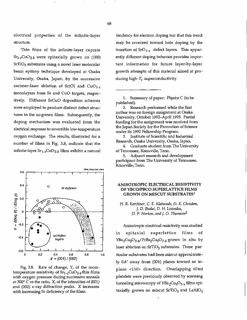
68
electrical propert ies of the infinite-layer
structure.
Thin films of the infinite-layer cuprate
Sri. xCu02-8 were epitaxially grown on (100)
SrTiC>3 substrates using a novel laser molecular
beam epitaxy technique developed at Osaka
University, Osaka, Japan, by the successive
excimer-laser ablation of Sr(O) and CuOi_ x
monolayers from Sr and CuO targets, respec
tively. Different SrCuO deposition schemes
were employed to produce distinct defect struc
tures in the as-grown films. Subsequently, the
doping mechanism was evaluated from the
electrical response to reversible low-temperature
oxygen exchange. The results, illustrated for a
number of films in Fig. 3.8, indicate that the
infinite-layer Sri. rCu02-5 films exhibit a natural
ORNL-OWG 93M M909
0.4 0.6 A-= (001)/(002)
0.8 1.0
Fig. 3.8. Rate of change, Y, of the room-temperature resistivity of Sri_ i XCu02-sthin films with oxygen pressure during successive anneals at 300° C vs the ratio, X, of the intensities of (001) and (002) x-ray diffraction peaks. X increases with increasing Sr deficiency of the films.
tendency for electron doping but that this trend
may be reversed toward hole doping by the
insertion of STO\.X defect layers. This appar
ently different doping behavior provides impor
tant information for future layer-by-layer
growth attempts of this material aimed at pro
ducing high- T c superconductivity.
1. Summary of paper: Physica C (to be published).
2. Research performed while the first author was on foreign assignment at Osaka University, October 1992-April 1993. Partial funding for the assignment was received from the Japan Society for the Promotion of Science under its 1992 Fellowship Program.
3. Institute of Scientific and Industrial Research, Osaka University, Osaka, Japan.
4. Graduate student from The University of Tennessee, Knoxville, Tenn.
5. Adjunct research and development participant from The University of Tennessee, Knoxville, Tenn.
ANISOTROPIC ELECTRICAL RESISTIVITY OF YBCO/PBCO SUPERLATTICE FILMS
GROWN ON MISCUT SUBSTRATES1
H. R. Kerchner, C. E. Klabunde, D. K. Christen, J. D. Budai, D. H. Lowndes,
D. P. Norton, and ]. O. Thomson2
Anisotropic electrical resistivity was studied
in e p i t a x i a l s u p e r l a t t i c e f i lms of
YBa 2 Cu30 7 . 5 /P rBa 2 Cu30 7 . 8 grown in situ by
laser ablation on SrTi0 3 substrates. These par
ticular substrates had been miscut approximate
ly 0.6° away from (001) planes toward an in-
plane <110> direction. Overlapping tilted
platelets were previously observed by scanning
tunneling microscopy of YBa 2Cu 307_. c films epi
taxially grown on miscut S rTi0 3 and LaA10 3
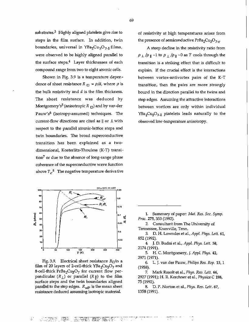
69
substrates.3 Highly aligned platelets give rise to steps in the film surface. In addition, twin boundaries, universal in YBa 2 Cu 3 0 7 .g films, were observed to be highly aligned parallel to the surface steps.4 Layer thicknesses of each compound range from two to eight atomic cells.
Shown in Fig. 3.9 is a temperature dependence of sheet resistance R n = p/d, where p is the bulk resistivity and d is the film thickness. The sheet resistance was deduced by Montgomery's5 (anisotropic R n ) and by van der Pauw's 6 (isotropy-assumed) techniques. The current-flow directions are cited as || or _L with respect to the parallel atomic-lattice steps and twin boundaries. The broad superconductive transition has been explained as a two-dimensional, Kosterlitz-Thouless (K-T) transition 7 or due to the absence of long-range phase coherence of the superconductive wave function above T c . 8 The negative temperature derivative
of resistivity at high temperatures arises from the presence of semiconductive PrBa2Cu307.£.
A steep decline in the resistivity ratio from P11? || ~ 1 t o P ± /P || ~0 a s T cools through the transition is a striking effect that is difficult to explain. If the crucial effect is the interactions between vortex-antivortex pairs of the K-T transition, then the pairs are more strongly bound in the direction parallel to the twins and step edges. Assuming the attractive interactions between vortices are only within individual YBa2Cu307_5 platelets leads naturally to the observed low-temperature anisotropy.
ORNLDWG 93 15306
150 200 T(K)
Fig. 3.9. Electrical sheet resistance i?rjrn a film of 20 layers of 2-cell-thick YBa 2 Cu 3 0 7 and 8-cell-thick PrBa 2Cu30 7 for current flow perpendicular (Rj_) or parallel (2111) to the film surface steps and the twin boundaries aligned parallel to the step edges. R^p is the mean sheet resistance deduced assuming isotropic material.
1. Summary of paper: Mat. Res. Soc. Symp. Proc. 275,353 (1992).
2 Consultant from The University of Tennessee, Knoxville, Term.
3. D. H. Lowndes et al., Appl. Phys. Lett. 61, 852 (1992).
4. J. D. Budai et al., Appl. Phys. Lett. 58, 2174 (1991).
5. H. C. Montgomery, /. Appl. Phys. 42, 2971 (1971).
6. L. J. van der Pauw, Philips Res. Rep. 13,1 (1958).
7. Mark Rasolt et al., Phys. Rev. Lett. 66, 2927 (1991); H. R. Kerchner et al., Physica C 198, 75 (1992).
8. D. P. Norton et al., Phys. Rev. Lett. 67, 1358 (1991).
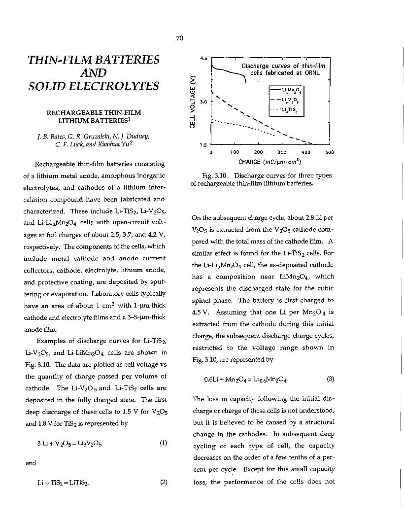
70
THIN-FILM BATTERIES AND
SOLID ELECTROLYTES
RECHARGEABLE THIN-FILM LITHIUM BATTERIES1
/. B. Bates, G. R. Gmzalski, N.}. Dudney, C. F. Luck, and Xiaohua Yu2
Rechargeable thin-film batteries consisting
of a lithium metal anode, amorphous inorganic
electrolytes, and cathodes of a lithium inter
calation compound have been fabricated and
characterized. These include Li-TiS2, L1-V2O5,
and Li-Li^M^C^ cells with open-circuit volt
ages at full charges of about 2.5, 3.7, and 4.2 V,
respectively. The components of the cells, which
include metal cathode and anode current
collectors, cathode, electrolyte, lithium anode,
and protective coating, are deposited by sput
tering or evaporation. Laboratory cells typically
have an area of about 1 c m 2 with l-|xm-thick
cathode and electrolyte films and a 3-5-pm-thick
anode film.
Examples of discharge curves for Li-TiS2,
Li-V^Os, and Li-LiMn2C>4 cells are shown in
Fig. 3.10. The data are plotted as cell voltage vs
the quantity of charge passed per volume of
cathode. The Li-V20 5 and Li-TiS2 cells are
deposited in the fully charged state. The first
deep discharge of these cells to 1.5 V for V2O5
and 1.8 V for TiS2 is represented by
4.5
3Li + V 2 0 5 = Li3V205
and
Li + TiS2 = LiTiS2.
(1)
(2)
< o >
UJ U
3.0
1.5
Discharge curves of thin-film cells fabricated at ORNL
-LI Mn 0 X 2 4
- L I V O X 2 5
"LIJIS.
100 200 300 400 500
CHARGE (mC/nm-cmz)
Fig. 3.10. Discharge curves for three types of rechargeable thin-film lithium batteries.
On the subsequent charge cycle, about 2.8 Li per
V2O5 is extracted from the V2O5 cathode com
pared with the total mass of the cathode film. A
similar effect is found for the Li-TiS2 cells. For
the Li-Li zMn204 cell, the as-deposited cathode
has a composit ion near LiMn2C>4, which
represents the discharged state for the cubic
spinel phase. The battery is first charged to
4.5 V. Assuming that one Li per Mn20 4 is
extracted from the cathode during this initial
charge, the subsequent discharge-charge cycles,
restricted to the voltage range shown in
Fig. 3.10, are represented by
0.6Li + Mn2C>4 = Lio.6Mn2C>4. (3)
The loss in capacity following the initial dis
charge or charge of these cells is not understood,
but it is believed to be caused by a structural
change in the cathodes. In subsequent deep
cycling of each type of cell, the capacity
decreases on the order of a few tenths of a per
cent per cycle. Except for this small capacity
loss, the performance of the cells does not
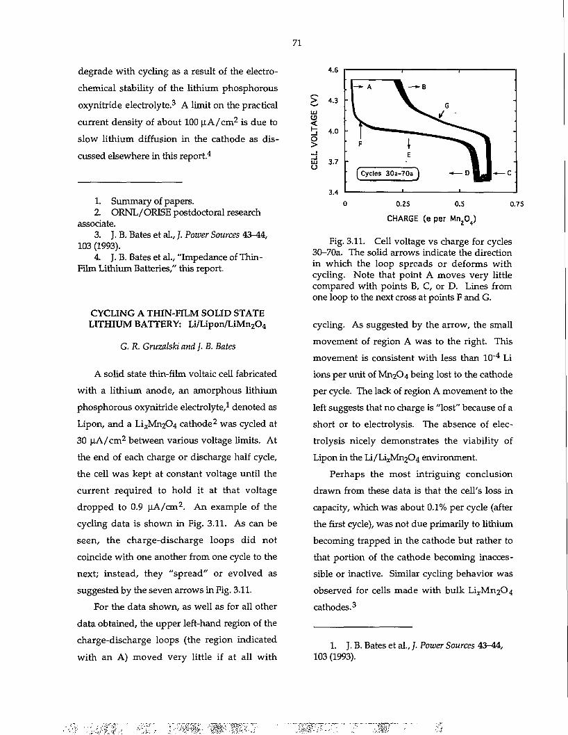
71
degrade with cycling as a result of the electro
chemical stability of the lithium phosphorous
oxynitride electrolyte.3 A limit on the practical
current density of about 100 u.A/cm 2 is due to
slow lithium diffusion in the cathode as dis
cussed elsewhere in this report.4
1. Summary of papers. 2. ORNL/ORISE postdoctoral research
associate. 3. J. B. Bates et al., /. Power Sources 43-44,
103 (1993). 4 J. B. Bates et al., "Impedance of Thin-
Film Lithium Batteries," this report.
CYCLING A THIN-FILM SOLID STATE LITHIUM BATTERY: Li/Lipon/LiMn204
G. R. GruzalsM and J. B. Bates
A solid state thin-film voltaic cell fabricated with a lithium anode, an amorphous lithium phosphorous oxynitride electrolyte,1 denoted as Lipon, and a LijM^C^ cathode2 was cycled at 30 uA/cm 2 between various voltage limits. At the end of each charge or discharge half cycle, the cell was kept at constant voltage until the current required to hold it at that voltage dropped to 0.9 uA/cm 2 . An example of the cycling data is shown in Fig. 3.11. As can be seen, the charge-discharge loops did not coincide with one another from one cycle to the next; instead, they "spread" or evolved as suggested by the seven arrows in Fig. 3.11.
For the data shown, as well as for all other data obtained, the upper left-hand region of the charge-discharge loops (the region indicated with an A) moved very little if at all with
* . t > 1 — i •
* . t >
. I-*" A % —- B
— i •
> 4.3 - 1 ^^ g -
VOLT
AG
E
4.0 • F \
^V -
CEL
L
3.7
3.4 (
E
""— D « J-—c CEL
L
3.7
3.4 (
[ Cycles 30a-70a J ""— D « J-—c 3.7
3.4 ( D 0.25 0.5 0.
CHARGE (e per Mn 20 4)
Fig. 3.11. Cell voltage vs charge for cycles 30-70a. The solid arrows indicate the direction in which the loop spreads or deforms with cycling. Note that point A moves very little compared with points B, C, or D. Lines from one loop to the next cross at points F and G.
cycling. As suggested by the arrow, the small movement of region A was to the right. This movement is consistent with less than 10"4 Li ions per unit of Mn2C>4 being lost to the cathode per cycle. The lack of region A movement to the left suggests that no charge is "lost" because of a short or to electrolysis. The absence of electrolysis nicely demonstrates the viability of Lipon in the Li/LijMn^C^ environment.
Perhaps the most intriguing conclusion drawn from these data is that the cell's loss in capacity, which was about 0.1% per cycle (after the first cycle), was not due primarily to lithium becoming trapped in the cathode but rather to that portion of the cathode becoming inaccessible or inactive. Similar cycling behavior was observed for cells made with bulk Li^M^C^ cathodes.3
1. J. B. Bates et al., /. Power Sources 43-44, 103 (1993).
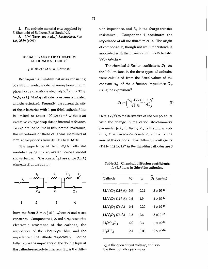
2. The cathode material was supplied by F. Shokoohi of Bellcore, Red Bank, N.J.
3. J. M. Tarascon et al., /. Electrochem. Soc. 138,2859 (1991).
AC IMPEDANCE OF THIN-FILM LITHIUM BATTERIES1
/. B. Bates and G. R. Gruzalski
Rechargeable thin-film batteries consisting
of a lithium metal anode, an amorphous lithium
phosphorus oxynitride electrolyte, 2 and a TiS^
V2O5, or LixMn2C>4 cathode have been fabricated
and characterized. Presently, the current density
of these batteries with 1-um-thick cathode films
is limited to about 100 | i .A/cm 2 without an
excessive voltage drop due to internal resistance.
To explore the source of this internal resistance,
the impedance of these cells was measured at
25°C at frequencies from 0.01 Hz to 10 MHz.
The impedance of the Li-V2C»5 cells was
modeled using the equivalent circuit model
shown below. The constant phase angle (CPA)
elements Z in the circuit
have the form Z = A (jay)'", where A and n are
constants. Components 1,2, and 4 represent the
electronic resistance of the cathode, the
impedance of the electrolyte film, and the
impedance of the cathode, respectively. For the
latter, Z^/ is the impedance of the double layer at
the cathode-electrolyte interface, Zw is the diffu-
72
sion impedance, and Rd is the charge transfer
resistance. Component 4 dominates the
impedance of all the thin-film cells. The origin
of component 3, though not well understood, is
associated with the formation of the electrolyte-
V2O5 interface.
The chemical diffusion coefficients Dy for
the lithium ions in the three types of cathodes
were calculated from the fitted values of the
constant Aw of the diffusion impedance Zw
using the expression 3
Here dV/dx is the derivative of the cell potential
with the change in the cation stoichiometry
parameter (e.g., L l ^ O s , Vm is the molar vol
ume, F is Faraday's constant, and a is the
area of the cathode. The diffusion coefficients
(Table 3.1) for L i + in the thin-film cathodes are 3
Table 3.1. Chemical diffusion coefficients for Li + ions in thin-film cathodes.
Cathode V0 x D L i (cm 2 / s )
L i x V 2 0 5 (119A) 3.5 0.14 3 x 10"1 4
Li x V 2 0 5 (119A) 1.6 2.9 2 x 10"1 2
Li x V 2 0 5 (76A) 3.4 0.29 4 x 10"1 5
L i r V 2 0 5 (76 A) 1.8 2.6 3 xlO" 1 2
Li^M^C^ 4.0 0.3 3 x 10"1 2
LixTiS2 2.4 0.05 2 x 10"1 4
V0 is the open circuit voltage, and x is the stoichiometry parameter.
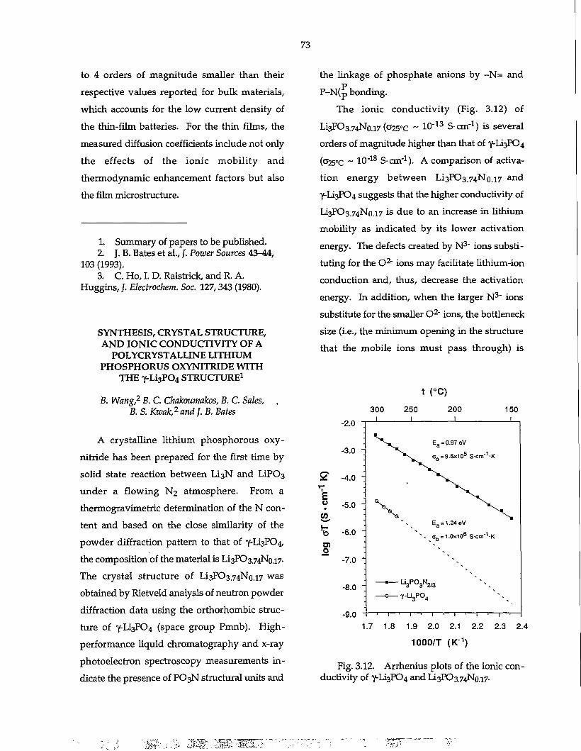
73
to 4 orders of magnitude smaller than their respective values reported for bulk materials, which accounts for the low current density of the thin-film batteries. For the thin films, the measured diffusion coefficients include not only the effects of the ionic mobility and thermodynamic enhancement factors but also the film microstructure.
1. Summary of papers to be published. 2 J. B. Bates et al., /. Power Sources 43-44,
103 (1993). 3. C. Ho, I. D. Raistrick, and R. A.
Huggins,/. Electrochem. Soc. 127,343 (1980).
SYNTHESIS, CRYSTAL STRUCTURE, AND IONIC CONDUCTIVITY OF A
POLYCRYSTALLINE LITHIUM PHOSPHORUS OXYNITRIDE WITH
THE Y-L13PO4 STRUCTURE1
B. Wang,2 B. C. Chakoumakos, B. C. Sales, . B. S. Kzvak,2 and J. B. Bates
A crystalline lithium phosphorous oxy-nitride has been prepared for the first time by solid state reaction between Li3N and LiP03 under a flowing N2 atmosphere. From a thermogravimetric determination of the N content and based on the close similarity of the powder diffraction pattern to that of y-Li3P04, the composition of the material is Li3PO3.74N0.17. The crystal structure of Li3PO3.74N0.17 was obtained by Rietveld analysis of neutron powder diffraction data using the orthorhombic structure of Y-Li3P04 (space group Pmnb). High-performance liquid chromatography and x-ray photoelectron spectroscopy measurements indicate the presence of PO3N structural units and
the linkage of phosphate anions by -N= and P-N<p bonding.
The ionic conductivity (Fig. 3.12) of Li3PO3.74N0.17 (c?25°c ~ 10" 1 3 S-cm:1) is several orders of magnitude higher than that of 7-Li3P04 (o"25°c ~ 10"1 8 S-cm"1). A comparison of activation energy between Li3PO3.74N0.17 and y-Li3P04 suggests that the higher conductivity of Li3PO3.74N0.17 is due to an increase in lithium mobility as indicated by its lower activation energy. The defects created by N 3" ions substituting for the O2" ions may facilitate lithium-ion conduction and, thus, decrease the activation energy. In addition, when the larger N 3" ions substitute for the smaller O2" ions, the bottleneck size (i.e., the minimum opening in the structure that the mobile ions must pass through) is
t (°C)
-2.0
-3.0 "
* -4.0 T -
E » -5.0 (0,
*5 -6.0
O ~~ -7.0
-8.0
-9.0
300 250 1 1
200 1
150
o 0 = 1.0x10⁶ Scm"1-K
• L i „P0 0 N„ "3 " 3 2/3 -e Y-Li 3PQ 4
-l 1 1 1 1 1 1 1 • 1 > 1 r
1.7 1.8 1.9 2.0 2.1 2.2 2.3 2.4
1 0 0 0 / T ( K - 1 )
Fig. 3.12. Arrhenius plots of the ionic conductivity of y-Li3P04 and Li3PO3.74N0.17.
ML-.s '-ror
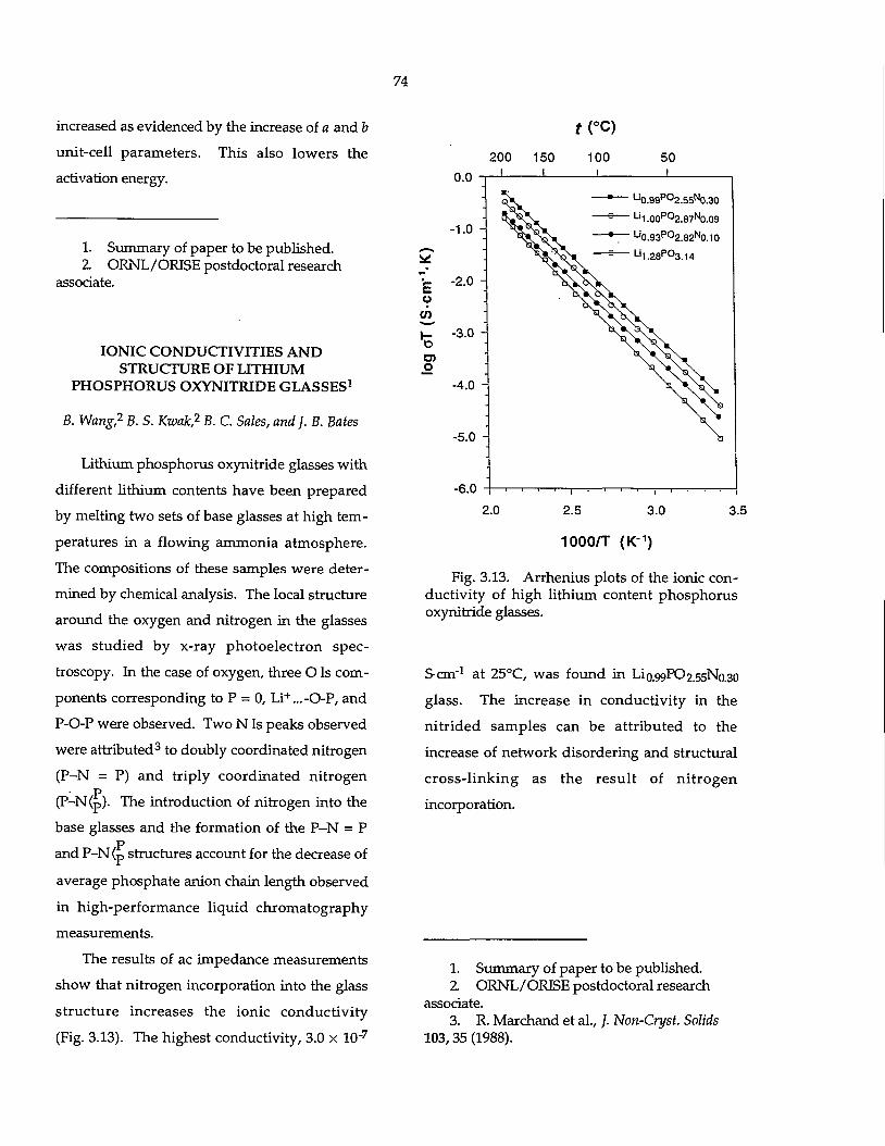
74
increased as evidenced by the increase of a and b
unit-cell parameters. This also lowers the
activation energy.
1. Summary of paper to be published. 2 ORNL/ORISE postdoctoral research
associate.
IONIC CONDUCTIVITIES AND STRUCTURE OF LITHIUM
PHOSPHORUS OXYNITRIDE GLASSES1
B. Wang,2 B. S. Kwak,2 B. C. Sales, and]. B. Bates
Lithium phosphorus oxynitride glasses with
different lithium contents have been prepared
by melting two sets of base glasses at high tem
peratures in a flowing ammonia atmosphere.
The compositions of these samples were deter
mined by chemical analysis. The local structure
around the oxygen and nitrogen in the glasses
was studied by x-ray photoelectron spec
troscopy. In the case of oxygen, three O Is com
ponents corresponding to P = 0, Li + . . .-0-P, and
P-O-P were observed. Two N Is peaks observed
were attributed 3 to doubly coordinated nitrogen
(P-N = P) and triply coordinated nitrogen
(P-N(p). The introduction of nitrogen into the
base glasses and the formation of the P -N = P p
and P-N(p structures account for the decrease of
average phosphate anion chain length observed
in high-performance liquid chromatography
measurements.
The results of ac impedance measurements
show that nitrogen incorporation into the glass
s tructure increases the ionic conductivity
(Fig. 3.13). The highest conductivity, 3.0 x 10"7
E o en
o
0.0
-1.0
-2.0
-3.0
-4.0
t (°C) 200 150 100
, I I I 50
_l
-5.0 -
-6.0 2.0 2.5 3.0
1000/T (K- 1)
3.5
Fig. 3.13. Arrhenius plots of the ionic conductivity of high lithium content phosphorus oxynitride glasses.
Scm" 1 at 25°C, was found in Li0.99PO2.55N0.30
glass. The increase in conductivity in the
nitr ided samples can be attributed to the
increase of network disordering and structural
cross-l inking as the resul t of n i t rogen
incorporation.
1. Summary of paper to be published. 2 ORNL/ORISE postdoctoral research
associate. 3. R. Marchand et al., /. Non-Cryst. Solids
103,35 (1988).
75
DEPOSITION OF ORGANIC-INORGANIC COMPOSITE THIN FILMS BY Li 3 P0 4
SPUTTERING AND C2H4 PLASMA POLYMERIZATION1
B. S. Kwak,2 R. A. Zuhr, and J. B. Bates
Results from the deposition of organic-inorganic composite macro-molecular thin films by combined rf magnetron sputtering and plasma-polymerization techniques are reported. Ethylene, C2H4, and lithium orthophosphate, Li3P04, were used as the monomer and inorganic sources, respectively. The working gases were Ar, N2, and A1/O2, of which only the Ar/02 mixture provided suitable control over the codeposition. It was found that the codeposition process requires a component in the gas mixture that can etch away the plasma-polymerized organic component from the inorganic target surface and, in so doing, preserve the sputtering of the inorganic species.
As-deposited films were characterized to determine the composition, structure, and ionic conductivity. The characterization techniques used included x-ray photoelectron spectroscopy (XPS), scanning electron microscopy, Fourier transform infrared spectroscopy (FTIR), Rutherford backscattering spectroscopy, x-ray diffraction, and ac-impedance measurements. The composite films were x-ray amorphous. The surface was featureless, smooth, and free of pinholes and voids. The compositions (i.e., relative variation with respect to parameter changes) were determined entirely with XPS. The spectra from ac-impedance measurements consisted of two features indicative of two distinct phases. 3 From the XPS and FTIR mea
surements, it appears that the inorganic phase is
incorporated both as a separate phase and as a
part of the polymeric backbone. The ionic
conductivity of the composite thin films from
this system was about 10"9 (Hem)"1 at room
temperature and varied inversely with the
amount of the organic phase in the sample.
Unlike most polymer ionic conductors, the tem
perature behavior appeared to be purely
Arrhenius rather than VTF which occurs
because of a cooperative effect of the segmental
motions in the polymeric backbone.4
1. Summary of paper to be published. 2 ORNL/ORISE postdoctoral research
associate. 3. J. B. Bates et al., Solid State Ionics 55,467
(1992). 4. M. A. Ratner and D. F. Shriver, Chem.
Rev. 88,109 (1988).
RADIO-FREQUENCY MAGNETRON SPUTTERING OF PURE AND MIXED
TARGETS OF Li4Si04, Li 3P0 4 AND LiaO1
N. J. Dudney, J. B. Bates, and J. D. Robertson2
Sintered targets of Li4Si04, Li3P04, and IA2O have been sputtered in argon and argon/oxygen atm. at 20-mTorr total pressure and 20-30 W rf power. The extent of lithium sputtering and the resulting film compositions varied greatly among the different compounds. Lithium orthophosphate sputtered normally yielding films with close to the stoichiometric target composition. Upon sputtering of lithium orthosilicate, however, much of the lithium was observed to segregate toward the center and rim
76
of the targets, away from the sputtered area,
leaving large deposits of O2O on the target sur
face. This resulted in silicate films with a
lithium concentration much less than that of the
original LijSiC^ target. A large redistribution of
target material has also been observed for sput
tered lithium oxide targets. For mixed silicate-
phosphate targets, even a small amount of
Li4SiC>4 can facilitate the segregation of almost
all the lithium in the target, including the
lithium in the Li3PC>4 phase.
A variety of experiments have indicated that
the lithium segregation occurs by lithium migra
tion along the surface of the target. An estimate
of the magnitude of the lithium diffusivity
required to compete with the observed sputter
rate is much higher than the lithium diffusivity
in the bulk crystalline compounds, but adequate
lithium diffusivity could result if a thin layer of
an amorphous silicate is formed on the surface
of the sputtered target. The different behavior of
Li3P04 vs Li4SiC>4 may be due to a difference in
this tendency to form such a conductive phase.
The silicate and phosphate materials may also
differ in the direction of the lithium migration
upon A r + bombardment. Such a difference has
been documented for Na migration in silicate vs
phosphate glasses upon A r + irradiation.
It was shown that the reproducible and
homogeneous lithium phosphosilicate films can
best be produced by codeposition with inde
pendently controlled sputter sources onto a
rotating substrate.
1. Summary of paper: /. Vac. Sci. and Technol. A 11,377 (1993).
2 University of Kentucky, Lexington, Ky.
COMPOSITE THIN FILMS BY L i 3 P 0 4
SPUTTERING AND Si(OC 2 H 5 ) 4
POLYMERIZATION
B. S. Kwak,1 R. A. Zuhr, and } . B. Bates
Results from studies on the extended net
work structures based on C-O-Si chains are
reported. The structures were synthesized by
combined rf magnetron sputtering and plasma-
polymerization techniques in off-axis geometry.
Tetraethoxysilane (TEOS), S i (OC 2 H 5 )4 , and
lithium orthophosphate (Li;}P04) were used as
the m o n o m e r and inorgan ic sources ,
respectively. The working gases were Ar, N2,
and AT/OZ-
The polymerization behavior of TEOS and
codeposition process with Li3P04 in A1/O2 were
found to be very stable—in particular, for the
codeposition where the deposition rate was
stable in Ar without losing Li + intensity in the
optical emission spectrum. Both the TEOS and
codeposited thin films were x-ray amorphous.
The TEOS and composite thin films grown in
A1/O2 appear to consist entirely of Si-O-C, Si-O-
Si, and O-H functional groups, whose relative
ratios change with O2 percent in the gas mixture.
In the composite films, the modes related to
Li3P0 4 ( and L i 2 C 0 3 ) cou ld no t be
unambiguously identified. Without the O2 flow,
the C-H related modes appear. The films,
however, were more disordered. The composite
th in films exhibi ted ra ther low ionic
conductivity, about 10" 1 2 (Qcm)"1 at room tem
perature. As with the Li3P04/C2H4 system, 2 the
impedance spectrum implied multiple phases.
The films appeared to possess good mechanical
properties.
77
Future experiments will attempt to improve
the ionic conductivity by codeposition in N2.
Possibly, this will result in producing nitrogen
cross-links in the system.3
1. ORNL/ORISE postdoctoral research associate.
2 B. S. Kwak, R. A. Zuhr, and J. B. Bates (to be published).
3. J. B. Bates et al., /. Power Sources 43-44, 103 (1993).
COMPOSITE ELECTROLYTES1
N. J. Dudney
Recent research related to composite electrolytes has been reviewed. The term "composite electrolytes" refers to a class of crystalline electrolytes for which the ionic conductivity is enhanced greatly by the incorporation of fine particles or fibers of an insoluble rigid second phase. There are many examples of such composites; some of the more extensively studied composites include Lil, AgCl, Agl and CaF2 containing dispersed submicron particles of alumina and other oxides (e.g., Ce02 and Si02). The conductivities of these materials have been enhanced by 1 to 3 orders of magnitude in the composite compared with the pure matrix phase. This has generated much interest in these materials, both in research to identify the mechanisms responsible for the enhanced conduction and also as a new technique to fabricate useful electrolytic materials for batteries and other devices.
There is a growing body of evidence to demonstrate that the primary role of the second-
phase particles is to stabilize a more conductive phase or a finer and more disordered microstructure than would exist in the pure electrolyte materials. The fine particles effectively inhibit both grain boundary migration and dislocation motion associated with the recrystallization or phase transformation. For example, a recent study of vapor-deposited CaF2 films have shown an enhanced ionic conduction clearly related to the dislocation structure.2 The dislocations were effectively stabilized by the addition of an alumina phase. Earlier work on composites of AgCl with alumina fibers, demonstrated that the presence of the fibers stabilized a fine-grain structure which can account for the enhanced conduction reported for the AgCl and AgBr composites.3 X-ray examination of Agl alumina-fiber composites along with evidence in the literature have shown that the as-prepared composites are of a more highly conductive metastable Agl phase. 4 If this phase could be fully stabilized in the form of a composite electrolyte, it would have a conductivity comparable to the superionic Ag electrolyte materials.
1. Summary of paper to be published. 2 F. A. Modine, D. Lubben and J. B. Bates,
/. Appl. Phys. 7<k, 2658 (1993); "Electrical Conduction in CaF2 and CaF2-Al203 Nanocomposite Films on AI2O3 Substrates," this report.
3. N. J. Dudney, /. Am. Ceram. Soc. 70,65 (1987).
4. N. J. Dudney, /. Imag. Sci. 34,104 (1990).
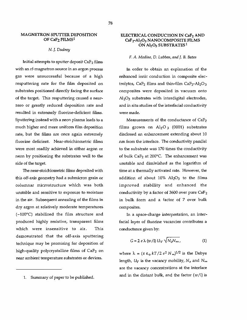
78
MAGNETRON SPUTTER DEPOSITION OF CaF2 FILMS1
N. J. Dudney
Initial attempts to sputter deposit CaF2 films
with an rf-magnetron source in an argon process
gas were unsuccessful because of a high
resputtering rate for the film deposited on
substrates positioned directly facing the surface
of the target. This resputtering caused a near-
zero or greatly reduced deposition rate and
resulted in extremely fluorine-deficient films.
Sputtering instead with a neon plasma leads to a
much higher and more uniform film deposition
rate, but the films are once again extremely
fluorine deficient. Near-stoichiometric films
were most readily achieved in either argon or
neon by positioning the substrates well to the
side of the target.
The near-stoichiometric films deposited with
this off-axis geometry had a submicron grain or
columnar microstructure which was both
unstable and sensitive to exposure to moisture
in the air. Subsequent annealing of the films in
dry argon at relatively moderate temperatures
(~100°C) stabilized the film structure and
produced highly resistive, transparent films
which were insensi t ive to air. This
demonstrated that the off-axis sput ter ing
technique may be promising for deposition of
high-quality polycrystalline films of CaF2 on
near ambient temperature substrates or devices.
ELECTRICAL CONDUCTION IN CaF2 AND CaF 2 -Al 2 0 3 NANOCOMPOSITE FILMS
ON A 1 2 0 3 SUBSTRATES1
F. A. Modine, D. Lubben, and J. B. Bates
In order to obtain an explanation of the
enhanced ionic conduction in composite elec
trolytes, CaF2 films and thin-film CaF2-Al203
composites were deposited in vacuum onto
AI2O3 substrates with interdigital electrodes,
and in situ studies of the interfacial conductivity
were made.
Measurements of the conductance of CaF2
films grown on AI2O 3 (0001) substrates
disclosed an enhancement extending about 10
nm from the interface. The conductivity parallel
to the substrate was 170 times the conductivity
of bulk CaF2 at 200°C. The enhancement was
unstable and diminished as the logarithm of
time at a thermally activated rate. However, the
addition of about 10% AI2O3 to the films
i m p r o v e d s tabi l i ty and enhanced the
conductivity by a factor of 3600 over pure CaF2
in bulk form and a factor of 7 over bulk
composites.
In a space-charge interpretation, an inter
facial layer of fluorine vacancies contributes a
conductance given by:
G = 2eX (w/l) Uv -N/NONOO, (1)
1. Summary of paper to be published.
where X = (ee0 kT/2 e2 N ^ 2 is the Debye
length, lly is the vacancy mobility, N0 and Noo
are the vacancy concentrations at the interface
and in the distant bulk, and the factor (w/l) is
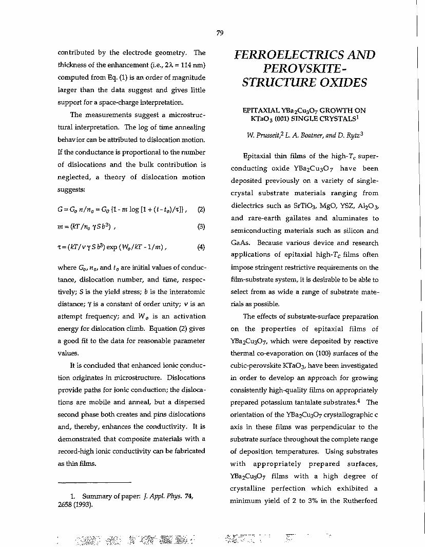
79
contributed by the electrode geometry. The thickness of the enhancement (i.e., 21 = 114 nm) computed from Eq. (1) is an order of magnitude larger than the data suggest and gives little support for a space-charge interpretation.
The measurements suggest a microstruc-tural interpretation. The log of time annealing behavior can be attributed to dislocation motion. If the conductance is proportional to the number of dislocations and the bulk contribution is neglected, a theory of dislocation motion suggests:
G = G0 n/n0 = G0 (1 - m log [1 + (t - t0)/x]), (2)
m = (Kr/ti0ySb3) , (3)
x = (kT/vy S b3) exp (W0/kT - 1/m), (4)
where G0, n0, and 10 are initial values of conductance, dislocation number, and time, respectively; S is the yield stress; b is the interatomic distance; 7 is a constant of order unity; v is an attempt frequency; and W0 is an activation energy for dislocation climb. Equation (2) gives a good fit to the data for reasonable parameter values.
It is concluded that enhanced ionic conduction originates in microstructure. Dislocations provide paths for ionic conduction; the dislocations are mobile and anneal, but a dispersed second phase both creates and pins dislocations and, thereby, enhances the conductivity. It is demonstrated that composite materials with a record-high ionic conductivity can be fabricated as thin films.
1. Summary of paper: J.Appl.Phys. 74, 2658 (1993).
FERROELECTRICS AND PEROVSKITE-
STRUCTURE OXIDES
EPITAXIAL YBa 2 Cu 3 0 7 GROWTH ON KTa0 3 (001) SINGLE CRYSTALS1
W. Prusseit,2 L. A. Boatner, and D. Rytz3
Epitaxial thin films of the high-T c superconducting oxide YBa2Cu307 have been deposited previously on a variety of single-crystal substrate materials ranging from dielectrics such as SrTi0 3, MgO, YSZ, AI2O3, and rare-earth gallates and aluminates to semiconducting materials such as silicon and GaAs. Because various device and research applications of epitaxial high-T c films often impose stringent restrictive requirements on the film-substrate system, it is desirable to be able to select from as wide a range of substrate materials as possible.
The effects of substrate-surface preparation on the properties of epitaxial films of YBa2Cu307, which were deposited by reactive thermal co-evaporation on (100) surfaces of the cubic-perovskite KTa03, have been investigated in order to develop an approach for growing consistently high-quality films on appropriately prepared potassium tantalate substrates.4 The orientation of the YBa2Cu307 crystallographic c axis in these films was perpendicular to the substrate surface throughout the complete range of deposition temperatures. Using substrates with appropriately prepared surfaces, YBa2Cu307 films with a high degree of crystalline perfection which exhibited a minimum yield of 2 to 3% in the Rutherford
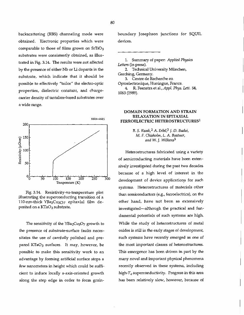
80
backscattering (RBS) channeling mode were
obtained. Electronic properties which were
comparable to those of films grown on SrTiC>3
substrates were consistently obtained, as illus
trated in Fig. 3.14. The results were not affected
by the presence of either Nb or Li dopants in the
substrate, which indicate that it should be
possible to effectively "tailor" the electro-optic
properties, dielectric constant, and charge-
carrier density of tantalate-based substrates over
a wide range.
SSDN-4685
200 r 1
-=• 150 - /S
2^ 100 - y / • - s ^
£ 50- [
p i . . . . i . . . I i i . , , . 0 50 100 150 200 250 300
Temperature (K)
Fig. 3.14. Resistivity-vs-temperature plot illustrating the superconducting transition of a 110-nm-thick YBa2Cu307 epitaxial film de posited on a KTaC>3 substrate.
The sensitivity of the YBa2Cu3C>7 growth to
the presence of substrate-surface faults neces
sitates the use of carefully polished and pre
pared KTaC>3 surfaces. It may, however, be
possible to make this sensitivity work to an
advantage by forming artificial surface steps a
few nanometers in height which could be suffi
cient to induce locally a-axis-oriented growth
along the step edge in order to form grain-
boundary Josephson junctions for SQUIL
devices.
1. Summary of paper: Applied Physics Letters (in press).
Z Technical University Munchen, Garching, Germany.
3. Centre de Recherche en Optoelectronique, Huningue, France.
4. R. Feenstra et al., Appl. Phys. Lett. 54, 1063 (1989).
DOMAIN FORMATION AND STRAIN RELAXATION IN EPITAXIAL
FERROELECTRIC HETEROSTRUCTURES1
B. S. Kwak,2 A. Erbil,2 J. D. Budai, M. F. Chisholm, L. A. Boatner,
and W. /. WUkens3
Heterostructures fabricated using a variety
of semiconducting materials have been exten
sively investigated during the past two decades
because of a high level of interest in the
development of device applications for such
systems. Heterostructures of materials other
than semiconductors (e.g., ferroelectrics), on the
other hand, have not been as extensively
investigated—although the practical and fun
damental potentials of such systems are high.
While the study of heterostructures of metal
oxides is still in the early stages of development,
such systems have recently emerged as one of
the most important classes of heterostructures.
This emergence has been driven in part by the
many novel and important physical phenomena
recently observed in these systems, including
high-T c superconductivity. Progress in this area
has been relatively slow, however, because of
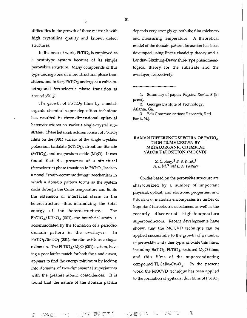
81
difficulties in the growth of these materials with high crystalline quality and known defect structures.
In the present work, PbTiC>3 is employed as a prototype system because of its simple perovskite structure. Many compounds of this type undergo one or more structural phase transitions, and in fact, PbTiC>3 undergoes a cubic-to-tetragonal ferroelectric phase transition at around 770 K.
The growth of PbTiC>3 films by a metal-organic chemical-vapor-deposition technique has resulted in three-dimensional epitaxial heterostructures on various single-crystal substrates. These heterostructures consist of PbTiC>3 films on the (001) surface of the single crystals: potassium tantalate (KTaOs), strontium titanate (SrTiOs), and magnesium oxide (MgO). It was found that the presence of a structural (ferroelectric) phase transition in PbTiC>3 leads to a novel "strain-accommodating" mechanism in which a domain pattern forms as the system cools through the Curie temperature and limits the extension of interfacial strain in the heterostructure—thus minimizing the total energy of the heterostructure. For P b T i 0 3 / K T a 0 3 (001), the interfacial strain is accommodated by the formation of a periodic-domain pattern in the overlayer. In PbTi0 3 /SrTi0 3 (001), the film exists as a single c-domain. The PbTiC>3/MgO (001) system, having a poor lattice match for both the a and c axes, appears to find the energy minimum by locking into domains of two-dimensional superlattices with the greatest atomic coincidences. It is found that the nature of the domain pattern
depends very strongly on both the film thickness
and measuring temperature. A theoretical
model of the domain-pattern formation has been
developed using linear-elasticity theory and a
Landau-Ginzburg-Devonshire-type phenomeno-
logical theory for the substrate and the
overlayer, respectively.
1. Summary of paper: Physical Review B (in press).
2 Georgia Institute of Technology, Atlanta, Ga.
3. Bell Communications Research, Red Bank, N.J.
RAMAN DIFFERENCE SPECTRA OF PbTi0 3
THIN FILMS GROWN BY METALORGANIC CHEMICAL
VAPOR DEPOSITION (MOCVD)1
Z. C. Feng,2 B. S. Kwak,3
A. Erbil,3 and L. A. Boatner
Oxides based on the perovskite structure are characterized by a number of important physical, optical, and electronic properties, and this class of materials encompasses a number of important ferroelectric substances as well as the recently discovered high-temperature superconductors. Recent developments have shown that the MOCVD technique can be applied successfully to the growth of a number of perovskite and other types of oxide thin films, including BaTi03, PbTi03, textured MgO films, and thin films of the superconducting compound Tl2CaBa2Cu20y. In the present work, the MOCVD technique has been applied to the formation of epitaxial thin films of PbTi03
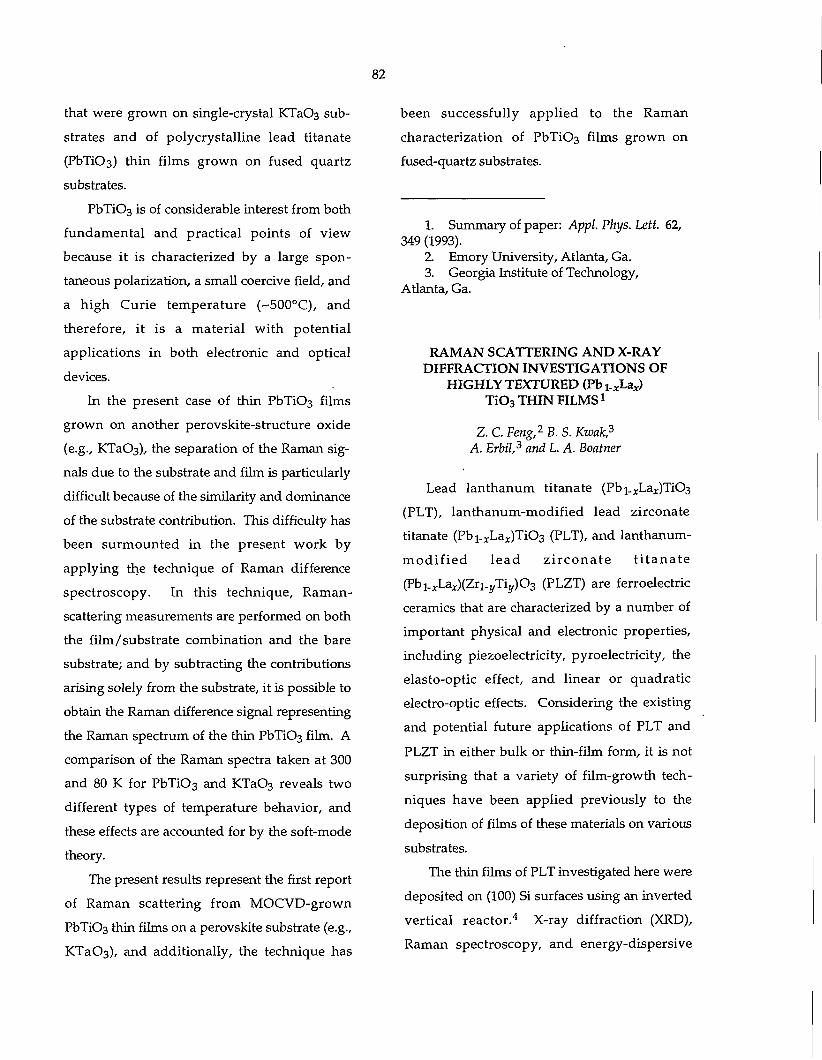
that were grown on single-crystal KTaC>3 sub
strates and of polycrystalline lead titanate
(PbTiC>3) thin films grown on fused quartz
substrates.
PbTiC>3 is of considerable interest from both
fundamental and practical points of view
because it is characterized by a large spon
taneous polarization, a small coercive field, and
a high Curie temperature (~500°C), and
therefore, it is a material with potential
applications in both electronic and optical
devices.
In the present case of thin PbTiC>3 films
grown on another perovskite-structure oxide
(e.g., KTaC>3), the separation of the Raman sig
nals due to the substrate and film is particularly
difficult because of the similarity and dominance
of the substrate contribution. This difficulty has
been surmounted in the present work by
applying the technique of Raman difference
spectroscopy. In this technique, Raman-
scattering measurements are performed on both
the film/substrate combination and the bare
substrate; and by subtracting the contributions
arising solely from the substrate, it is possible to
obtain the Raman difference signal representing
the Raman spectrum of the thin PbTiC>3 film. A
comparison of the Raman spectra taken at 300
and 80 K for PbTiC>3 and KTaC>3 reveals two
different types of temperature behavior, and
these effects are accounted for by the soft-mode
theory.
The present results represent the first report
of Raman scattering from MOCVD-grown
PbTi03 thin films on a perovskite substrate (e.g.,
KTaC>3), and additionally, the technique has
82
been successfully appl ied to the Raman
characterization of PbTiC>3 films grown on
fused-quartz substrates.
1. Summary of paper: Appl. Phys. Lett. 62, 349 (1993).
2. Emory University, Atlanta, Ga. 3. Georgia Institute of Technology,
Atlanta, Ga.
RAMAN SCATTERING AND X-RAY DIFFRACTION INVESTIGATIONS OF
HIGHLY TEXTURED (Pb i^La*) T i 0 3 THIN FILMS1
Z. C. Feng,2 B. S. Kwak,3
A. Erbil,5 and L. A. Boatner
Lead lanthanum titanate (Pbi_ xLa x)Ti03
(PLT), lanthanum-modified lead zirconate
titanate (Pb i . x La x )T i0 3 (PLT), and lanthanum-
m o d i f i e d l e a d z i r c o n a t e t i t a n a t e
(Pb 1 . x La x )(Zri .yTi y )0 3 (PLZT) are ferroelectric
ceramics that are characterized by a number of
important physical and electronic properties,
including piezoelectricity, pyroelectricity, the
elasto-optic effect, and linear or quadratic
electro-optic effects. Considering the existing
and potential future applications of PLT and
PLZT in either bulk or thin-film form, it is not
surprising that a variety of film-growth tech
niques have been applied previously to the
deposition of films of these materials on various
substrates.
The thin films of PLT investigated here were
deposited on (100) Si surfaces using an inverted
vertical reactor . 4 X-ray diffraction (XRD),
Raman spectroscopy, and energy-dispersive
83
x-ray analysis were used to characterize PLT
films whose x values were <0.18. The XRD
results established that the films had a
polycrystalline structure with strong (100)
t ex tu r ing re la t ive to the Si subs t ra te .
Additionally, the XRD results revealed a gradual
change in the crystal structure with the system
moving in the tetragonal-to-cubic sense with
increasing values of x. Raman spectra, including
the first spectra obtained at low temperature
(i.e., 80 K), were obtained, and the results were
compared with those reported previously.
The dependence of the mode frequencies on
x is shown in Fig. 3.15 for the four different
types of PLT films on Si substrates. As
ORM.-DWG93M.1U24
(Pb^La^TiOs/Si 300 K 80 K
800
700 ^r
600
Ai(LO)
E 500 o
5 400 >, I 300 HI
k.. A, (TO)
A,(LO)+E(LO) • • • • • • • - • £ { « » » • • • <^» • •
L_ A,fro) Silent"" ' ' — • • * -
a -DOT
w E f O ) 200 Y^" " V "—^ V-
E( L O> ^ o <>•—i 100
0
. ECTO) {soft mode)
-J 1 I 1 I ! ' ' '
• i . . . ^ A,(TO)
A,(LO)+E(LO) £ "
JMTO)
Silent
.....&...
— A-yJ ••D D-D
• - v —V V' E(LO)
A, (TO) O O O
E(TO) {soft mode)
_j—i i i I ' I ' ' 0.0 0.1
*fl-a) 0.0 0.1
x(La)
Fig. 3.15. Raman shift variations of various PLT modes with x varying from 0 to 0.18, at temperatures of 300 and 80 K.
illustrated in Fig. 3.15, all the modes, with the
exception of the so-called "silent mode," show
some systematic change as a function of the film
composition and sample temperature. The silent
mode, which is neither Raman nor infrared
active, exhibits a unique compositional and
temperature dependence. The appearance of
this feature may be attributed to the presence of
disorder in the samples. Empirical trends were
derived from the observed composition- and
temperature-dependent behavior of the PLT
Raman modes. In particular, the TO-like and
LO-like modes were found to decrease and
increase, respectively, with increasing x, and the
silent mode did not depend on x over the range
of variables investigated.
1. Summary of paper: Applied Physics Letters (in press).
2 National University of Singapore, Singapore.
3. Georgia Institute of Technology, Atlanta, Ga.
4. Z. C. Feng et al., Appl. Phys. Lett. 62,349 (1993).
OXIDE FERROELECTRIC MATERIALS GROWN BY METALORGANIC CHEMICAL
VAPOR DEPOSITION (MOCVD) 1
A. Erbil,2 W. Braun,2
B. S. Krvak,2 B. J. Wilkens,3
L. A. Boatner, and } . D. Budai
The discovery of high-T c superconductors in
the layered perovskite oxides has stimulated a
considerable amount of new research devoted to
finding appropriate techniques for depositing
perovskite-type compounds in thin-film form
84
for use in fundamental investigations and, ulti
mately, for possible microelectronics applica
tions. Perovskite-type materials are also of
interest for a variety of reasons other than high-
temperature superconductivity, and many
compounds of this type undergo one or more
ferroelectric phase transitions. There are
numerous potentially important applications of
these ferroelectric oxides in the field of elec
tronics and optoelectronics. The MOCVD tech
nique has been established previously as a ver
satile thin-film growth method for compound
semiconductors. Recent studies have also
demonstrated its utility in the growth of
perovskite oxide thin films with high-crystalline
quality.
In the present investigations, various ferro
electric perovskite-type oxides were successfully
grown using the MOCVD technique. Both
horizontal and vertical-type reactors were used
to deposit oxide thin films. However, the
inverted vertical reactor had an advantage
because it minimized the free-convection effects
and, thereby, led to an enhanced laminar-flow
pattern over the substrate. The metalorganic
precursors used consisted of both solid and
liquid compounds.
Results were obtained for the growth of
PbTi0 3 , B a T i 0 3 / and PZT. P b T i 0 3 thin films
grown on fused quartz and Si(100) were poly-
crystalline and were fully textured with the a-
and c-axes perpendicular to the surface. Epitaxy
was achieved on the (001) surfaces of the single
crystals K T a 0 3 , S r T i 0 3 , and MgO. The
prediction of thin-film properties was carried
out using a Landau-Ginzburg-Devonshire-type
free-energy functional. The ferroelectric prop
erties and domain orientation of epitaxial
P b T i 0 3 thin films strongly depend on the sub
strate used and on film thickness in the range
200-8000 A. The spontaneous polarization
decreased with decreasing thickness for films
grown on K T a 0 3 . The films grown on K T a 0 3
were found to consist of periodic alternating a-
and c-domains with 90° domain walls making
an angle of about 45° with the surface.
1. Summary of paper: /. Cryst. Growth 124, 684 (1992).
2. Georgia Institute of Technology, Atlanta, Ga.
3. Bell Communications Research, Red Bank, N.J.
POLAR FLUCTUATIONS AND FIRST-ORDER RAMAN SCATTERING IN HIGHLY
POLARIZABLE KTa0 3 CRYSTALS WITH OFF-CENTER Li AND Nb IONS 1
P. DiAntonio,2 B. E. Vugmeister2
J. Toulouse2and L. A. Boatner
Highly polarizable crystal lattices doped
with ions that can occupy off-center positions
offer particularly interesting opportunities for
the study of collective effects associated with
impurities in condensed matter. These collective
effects can include impuri ty- induced fluc
tuations and phase transitions, as well as dis
order and other effects. During the past 15
years, the study of highly polarizable crystalline
materials such as K T a 0 3 doped with off-center
impurities has led to the observation of new
types of interactions and effects. 3 ' 4 In spite of
these relatively extensive prior investigations,
the physical nature of the effects observed in systems of this type is still a subject of considerable controversy, and the experimental results have only provided partial answers to such fundamental questions as: (1) Does the system undergo a normal ferroelectric transition at low dopant concentrations or is some type of dipolar glass state formed? (2) What factors determine the critical concentration for the occurrence of a ferroelectric transition? (3) How does the physical nature of the transition evolve with increasing dopant concentration?
Accordingly, the two purposes of the present work were to contribute to a resolution of the controversy surrounding the problem of first-order Raman scattering that is observed in highly polarizable crystals doped with off-center ions and to provide new insights into the nature of the transitions observed for the KLT and KTN systems. To that effect, a detailed investigation of the Raman spectra of two of the hard modes, TO2 and TO3, observed in KLT and KTN crystals has been performed.
Relatively low concentrations of randomly substituted off-center ions are known to induce ferroelectric order in highly polarizable crystals. In the case of potassium tantalate (KTaOa) doped with lithium or niobium, the results of first-order Raman scattering from two hard phonon modes (TO2 and TO3) show that polar microregions are formed at relatively high temperatures. At lower temperatures and above a certain critical dopant concentration, the Raman results are consistent with the occurrence of a structural phase transition. These results can be reasonably explained by using a random-
85
molecular-field theory that takes into account
the indirect dipolar interactions mediated by the
soft lattice. This approach accounts for the
characteristic asymmetry of the TO2 Raman
scattering detected at high temperatures and for
the subsequent increase in the integrated
scattering intensity with decreasing
temperature. An analysis of the Raman results
provides a means for deterrnining the size of the
polar microregions formed in the highly
polarizable KTaC>3 lattice. The good agreement
obtained between the theoretical and
experimental results provides support to the
physical concepts embodied in the theoretical
approach developed here for describing the
onset of order in these systems.
1. Summary of paper: Phys. Rev. B 47,5629 (1993).
2 Lehigh University, Bethlehem, Perm. 3. U. T. Hochli, H. E. Weibel, and L. A.
Boatner, Phys. Rev. Lett. 41,1410 (1978). 4. R. L. Prater, L. L. Chase, and L. A.
Boatner, Phys. Rev. B 23,221 (1981).
DETERMINATION OF THE Aj(TO) SOFT-MODE DAMPING RATE IN KTao.93Nbo.07O31
P. Grenier,2 S. fandl2
D. Houde,2 and L. A. Boatner
The dynamical behavior associated with structural phase transitions in perovskite-structure materials is a subject of long-standing research interest and activity.3'4 In particular, the relationship between the "relaxation-mode" vs "soft-mode" dynamics and the relative importance of "order-disorder" vs "displacive"
•W, :
effects in driving the phase transition remain a subject of current controversy.3 Recently, experiments were carried out using time-resolved third-order optical-susceptibility techniques (also called impulsive-stimulated Raman scattering or ISRS) with the goal of obtaining new insight into the dynamics of phase transitions in perovskites.4 This previous work has shown that ISRS techniques are more appropriate for investigations of systems characterized by a highly damped vibrational mode mixed with a relaxation mode than are other optical methods.
In a previous report of the results of experiments performed on a KTao.93Nbo.07O3 (KTN) single crystal using the ISRS technique, it was noted that the observed damping rate of the soft-mode appears to be twice the value obtained by other techniques for similar crystals. In order to confirm this interesting observation, Raman scattering and infrared reflectivity experiments have been performed using the identical KTao.93Nbo.07O3 crystal investigated in Ref. 4 with a T c = 68 K. The values obtained for the damping rate of the Ai(TO) soft-mode appear to be half those determined by impulsive-stimulated Raman scattering. Because the latter experiments probe the soft-mode in the polariton regime while the former probes outside this region, the observed discrepancy points toward some additional interaction for the polariton soft mode.
Similar behavior has been observed in other samples, and these results suggest the existence of important interactions between the polariton and low-frequency excitations. Currently, time-resolved third-order optical susceptibility
86
measurements as a function of polariton wave vector and temperature are being performed to investigate these interactions further.
1. Summary of paper: Canadian Journal of Physics (in press).
2. Universite de Sherbrooke, Sherbrooke, Canada.
3. E. Lee, L. L. Chase, and L. A. Boatner, Phys. Rev. B 31,1438 (1985).
4. P. Grenier et al., Phys. Rev. B 47,1 (1993).
POLARIZATION AND CRYSTAL-GEOMETRY DEPENDENCES OF THE
NONLINEAR OPTICAL RESPONSES OF KTa^Nb^Os CRYSTALS AFTER
PICOSECOND-PULSE LASER EXCITATION1
H. Liu,2 R. ]. Reeves,2
R. C. Powell,2 and L. A. Boatner
The mixed-crystal system KTai. xNbjp3 (KTN) is of particular interest among perovskite-structure ABO3 materials3-4 because at room temperature it undergoes a phase transition from the cubic paraelectric phase to tetragonal and orthorhombic ferroelectric phases as the niobium concentration x increases from 0 (KTaOs) to 1 (KNbOs). In recent years, research efforts have focused on understanding the mechanisms responsible for these structural changes. The soft-mode contributions to the linewidth of the central peak were determined in orthorhombic KNb03 from inelastic light scattering.4 These components have the linewidths, line shapes, and thermal properties of relaxation modes and symmetry properties consistent with an eight-site order-disorder model for successive phase transitions. The
87
different structural phases are a consequence of the preferential occupation of a certain set of potential minima by the B ions. The dynamic aspects of this model predict relaxation modes in which the B ions (Nb or Ta) move from one equilibrium site to another in the multiwell potential. This movement of ions between potential minima manifests itself in the presence of hopping modes parallel and perpendicular to the polar axis.
In order to enhance our understanding of these polar ion hopping modes and other fast physical processes in this class of materials, degenerate four-wave-mixing (DFWM) studies of KTN crystals have been initiated using a picosecond-laser excitation source.
In the present investigations, the fast nonlinear optical signals on picosecond and nanosecond time scales have been studied in the mixed-crystal system KTai_xNb203 using transient DFWM. The two distinct signal components, denoted as an instantaneous response and slow response in previous studies,5 changed intensity as the niobium concentration was varied. The dependences of these signals on the crystal orientation and the polarization configuration of the optical pulses were characterized. The results were consistent with a lattice-relaxation model based on the laser-induced dynamic displacement of the Nb ion. In this model, the signal variations result from the competition between the dynamic displacement and intrinsic distortion associated with the spontaneous polarization along the optic axis.
1. Summary of paper: Physical Review B (in press).
2 Oklahoma State University, Stillwater, Okla.
3. J. Toulouse, X. M. Wong, and L. A. Boatner, Solid State Commun. 68,353 (1988).
4 J. P. Sokoloff, L. L. Chase, and L. A. Boatner, Phys. Rev. B 41,2398 (1990).
5. H. Liu, R. C. Powell, and L. A. Boatner, Phys. Rev. B 44,2461 (1991).
INFRARED ABSORPTION INVESTIGATIONS OF OH IMPURITIES IN DOPED KTa0 3 SINGLE CRYSTALS1
S. Jandl,2 J. Rousseau2 and L. A. Boatner
Hydrogen impurities are generally present in single crystals of the perovskite-structure oxides KTa03 and SrTi03 in the "as-grown" state. 3' 4 Hydrogen impurities can also be intentionally introduced at higher concentrations by annealing these crystals at elevated temperatures in water-vapor-containing ambients. The presence of hydrogen in these materials is manifested in the observation of infrared-absorption bands that correspond to the OH-stretching mode and that occur in the vicinity of 3480 cm"1. Usually these bands consist of a primary intense absorption plus one or more weaker "satellite" bands. The fundamental properties of hydrogen in KTaOs and SrTi03 have been the subject of a number of previous spectroscopic studies that have led to two different proposed crystallographic locations for the incorporation of hydrogen in the perovskite lattice.
The present work reports the results of infrared-absorption measurements as a function of temperature of hydroxyl radicals in pure KTa03 crystals doped with either Ni, Co, or Nb. The objectives of this work are, first, to
88
determine the effects of the different dopants on the OH-stretching mode (including the influence of the ferroelectric soft mode in the case of the Nb-doped material); second, to evaluate the validity of the cubic-face model vs the octahedron-edge model for the location of the hydrogen; and, third, to confirm the infrared-active character of the previously observed Raman-active OH stretching mode as affected by the ferroelectric soft mode.
Two distinct infrared-absorption bands associated with the stretching mode of OH radicals have been observed in pure KTa03 and in doped KTa03 single crystals. In the absence of the ferroelectric phase transition that occurs for the KTN case, the effects due to doping are restricted to band broadening without affecting the frequency. The identical three frequencies observed in Raman scattering are also detected in the splitting of band 1 that occurs at low temperatures. The relatively reduced intensity of the outer bands observed for pure KTa03 and for Ni- and Co-doped KTa03 indicates that the influence of the soft mode is greatly reduced in the nonferroelectric materials as compared with that characteristic of KTN below the ferroelectric transition temperature where the three infrared-absorption bands are of comparable intensity. Bands 1 and 2 are consistent with the occupation of site locations that are described by both the crystal-face and octahedron-edge models—both of which predict a triplet structure at low temperatures so that the hydrogen may be located either along the cube-
face diagonals or along the oxygen-oxygen
bonds.
1. Summary of paper: Solid State Communications (in press).
2. Universite de Sherbrooke, Sherbrooke, Quebec, Canada.
3. H. Engstrom, J. B. Bates, and L. A. Boatner, /. Chan. Phys. 73,1073 (1980).
4. R. Gonzalez et al., /. Chem. Phys. 78,660 (1983).
MATERIALS PROPERTIES
UNSTABLE NECK FORMATION DURING INITIAL-STAGE SINTERING1
/. Rankin2 and L. A. Boatner
Previous fundamental investigations of the coalescence of particles during the initial stages of sintering have frequently employed idealized systems consisting of polycrystalline, micron-sized particles with approximately circular cross sections. The experimental approach used in these previous sintering studies usually consisted of ex situ microscopic observations of the particles subsequent to heat treatment to produce neck formation and coalescence through mass transport processes. In one of the more significant early sintering investigations3
(whose results, in fact, provided the basis for the development of initial-stage sintering theory), polycrystalline copper cylinders were sintered onto flat copper plates by conventional furnace
89
heating and were then mechanically cross-sectioned. The neck morphologies were subsequently examined and analyzed ex situ using optical microscopy. Numerous intervening studies of the alterations in neck and pore morphologies that occur during the sintering of both ceramic and metal systems have been carried out,4 but with one exception, these investigations have been based on ex situ observations. Such ex situ analytical methods are not capable of addressing a number of critical issues because these studies can only provide average measurements subsequent to the evolution of the neck morphology and particle size that are "averaged" over the total time of the heating cycle. In contrast to most of the previous work in this area, continuous transmission electron microscopy (TEM) observations of the particle size and neck morphology as they evolve during the initial-stage sintering of faceted particles heated in situ on a hot stage mounted in the microscope have been carried out. The present application of this experimental approach to the TEM/video observation of the initial-stage coalescence of cubic-faceted, single-crystal MgO particles has led to the discovery of a fundamental neck instability for certain particle-contact geometries.
These studies show that the initial-stage sintering behavior of cubic-faceted MgO particles is strongly dependent on the initial particle-contact geometry. Particle pairs in face-to-face contact form stable necks which continue to grow as the two particles coalesce into one nonfaceted particle. In contrast to this behavior, particle pairs with corner-to-corner or edge-to-
edge contact form necks that initially grow, but
subsequently shrink and abruptly break. These
findings are quite general since they are
potentially relevant in any system where small
contact areas and large contact angles are found
and where high-energy sources of material are
present; they are not limited to systems of cubes
or highly symmetric faceted particles.
1. Summary of paper: Journal of the American Ceramic Society (in press).
2 Consultant from Brown University, Providence, R.I.
3. G. C. Kuczynski, /. Trans. AIME185, 796 (1949).
4. Sintering—Key Papers, S. Somiya and Y. Moriyoshi, Eds., Elsevier Science Publishing Co., Inc., New York, 1989.
TEXTURED COATINGS FROM COLLOIDAL SUSPENSIONS OF
FACETED OXIDE MICROCRYSTALSl
G. W. Steadman,2 J. R. Brewster,5
J. D. Budai, and L. A. Boatner
Achieving full control of the microstructural properties of ceramics both in the form of bulk materials and as coatings encompasses, in general, controlling not only the component grain sizes and shapes but also the relative orientations of these constituent microstructural grains as well. Until recently, most ceramic microstructural research has primarily emphasized the development of techniques for controlling the grain size and shape, and an additional level of control involving the development of preferred orientations or "texturing" in ceramic microstructures has
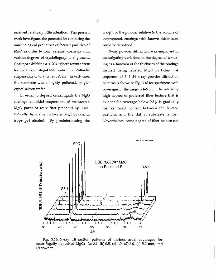
90
received relatively little attention. The present
work investigates the potential for exploiting the
morphological properties of faceted particles of
MgO in order to form ceramic coatings with
various degrees of crystallographic alignment.
Coatings exhibiting a <100> "fiber" texture were
formed by centrifugal sedimentation of colloidal
suspensions onto a flat substrate. In each case,
the substrate was a highly polished, single-
crystal silicon wafer.
In order to deposit centrifugally the MgO
coatings, colloidal suspensions of the faceted
MgO particles were first prepared by ultra-
sonically dispersing the faceted MgO powder in
isopropyl alcohol. By predetermining the
weight of the powder relative to the volume of
isopropanol, coatings with known thicknesses
could be deposited.
X-ray powder diffraction was employed in
investigating variations in the degree of textur
ing as a function of the thickness of the coatings
formed using faceted MgO particles. A
sequence of 5 0-29 x-ray powder diffraction
patterns is shown in Fig. 3.16 for specimens with
coverages in the range 0.1-5.0 \i. The relatively
high degree of preferred fiber texture that is
evident for coverage below 0.5 \i is gradually
lost as direct contact between the faceted
particles and the flat Si substrate is lost.
Nevertheless, some degree of fiber texture can
ORNLDWG 94M-65J3
Fig. 3.16. X-ray diffraction patterns of various areal coverages for centrifugally deposited MgO: (a) 0.1, (b) 0.5„ (c) 1.0, (d) 3.0, (e) 5.0 mm, and (f) powder.
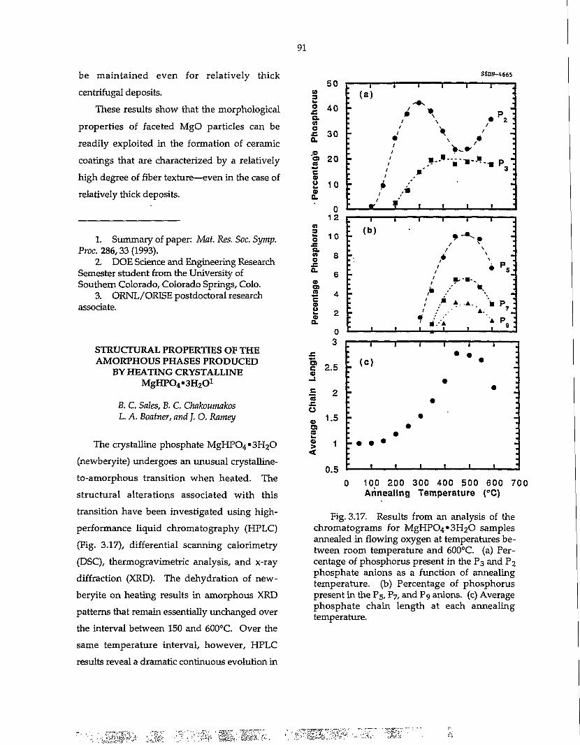
91
be maintained even for relatively thick
centrifugal deposits.
These results show that the morphological
properties of faceted MgO particles can be
readily exploited in the formation of ceramic
coatings that are characterized by a relatively
high degree of fiber texture—even in the case of
relatively thick deposits.
1. Summary of paper: Mat. Res. Soc. Symp. Proc. 286,33 (1993).
2 DOE Science and Engineering Research Semester student from the University of Southern Colorado, Colorado Springs, Colo.
3. ORNL/ORISE postdoctoral research associate.
STRUCTURAL PROPERTIES OF THE AMORPHOUS PHASES PRODUCED
BY HEATING CRYSTALLINE MgHP0 4«3H 20 1
B. C. Sales, B. C. Chakoumakos L. A. Boatner, and J. O. Ramey
The crystalline phosphate MgHP0 4 «3H 2 0 (newberyite) undergoes an unusual crystalline-to-amorphous transition when heated. The structural alterations associated with this transition have been investigated using high-performance liquid chromatography (HPLC) (Fig. 3.17), differential scanning calorimetry (DSC), thermogravimetric analysis, and x-ray diffraction (XRD). The dehydration of newberyite on heating results in amorphous XRD patterns that remain essentially unchanged over the interval between 150 and 600°C. Over the same temperature interval, however, HPLC results reveal a dramatic continuous evolution in
M 3
O c a. .« a CO
«•» B CD U i » CB
Q.
01 s Q. CO o
Q
S CD U hm CD
Q .
C CD
a JC a CD O) CO k . CD
<
50
40
30
20
10
0 12
10
8
6
4
2
0 3
2.5
2
1.5
1
0.5
SSDN-4665
. • (a ) : • - • x
• ^ . p ' • • ^ . p ' „ / • 2 :
« • \ , • / \ / • • * - • -
- . » - • • - • - • - * - . ? : •
* 3 :
B> t •*' : " t •*' :
/ / • •
' . V f ! ! ! _ 1
B — i — — I — —i 1 1 r , 1,1 1 1 1 1 1
( b )
> •
luji
xL
> •
' ' ' 1"' ' '1 in
a.
' / • ' A . P7].
L t - • 1, M 1 1 L. p :
9 .
1 1 - r —r T " i a
" • • " : (c) • ' . fl
• • a
• • " , • ; • « _ • -a • " • • •
~ • • •
1.1-
1.1
• | _ i _ ,—!,.. _J_ _J
"1
0 100 200 300 400 500 600 700 Annealing Temperature (°C)
Fig. 3.17. Results from an analysis of the chromatograms for MgHP04»3H20 samples annealed in flowing oxygen at temperatures between room temperature and 600°C. (a) Percentage of phosphorus present in the P3 and P2 phosphate anions as a function of annealing temperature, (b) Percentage of phosphorus present in the P5, P7, and P9 anions, (c) Average phosphate chain length at each annealing temperature.
92
the distribution of phosphate chains of corner-
linked PO4 tetrahedra leading to the formation
of chains up to 13 PO4 tetrahedra in length.
Above 600°C, crystalline Mg2P2C>7 is formed. At
each annealing temperature in the interval from
150 to 600°C, the measured distribution of
phosphate anions is in quantitative agreement
with theory. During the dehydration-induced
crystalline-to-amorphous transition, the original
faceted crystal shape is preserved even though
the crystals lose up to 36% of their original
weight. High-pressure DSC experiments in
which the waters of hydration were retained in
the specimens during heating resulted in the
formation of a unique new crystalline phosphate
phase that contained equal amounts of
orthophosphate and pyrophosphate anions. The
results of HPLC, DSC, and XRD measurements
on C a H P 0 4 - 2 H 2 0 , S rHP0 4 , and BaHP0 4 were
also investigated.
1. Summary of paper: /. Non-Cryst. Solids 159,121 (1993).
CHROMATOGRAPHIC DETERMINATION OF THE PHOSPHATE ANIONS IN
CRYSTALLINE AND GLASSY N a 4 N b P 3 O z
1
B. C. Sales and B. C. Chakoumakos
Crystalline Na4NbP30 z was found by
Jazouli et a l . 2 ' 3 to exhibit a reversible crystalline -
to-glass phase change. On the basis of Raman
and optical investigations, they concluded that
the crystalline phase was an orthophosphate
with a structure similar to the NASICON struc
ture; hence, the crystalline composition was
given as N a 4 N b ( P 0 4 ) 3 - Very few orthophos-
phates convert to the glassy phase by conven
tional melt quenching, which made this material
even more intriguing. This observation was also
made by Prabakar and Rao, 4 who concluded on
the basis of magic-angle spinning 3 1 P nuclear
magnetic resonance (NMR) spectroscopy that
the local phosphorus environments were quite
different in the glassy and crystalline forms of
N a 4 N b ( P 0 4 ) 3 - They suggested that the crys
talline material was actually a metaphosphate,
which would account for the relative ease of
glass formation as well as the change in local
environments suggested by the NMR spectra. If
single crystals of N a 4 N b P 3 0 z could easily be
produced, x-ray.or neutron diffraction tech
niques could determine precisely the structure.
For the glassy phase, however, diffraction tech
niques provide limited structural information.
High-performance liquid chromatography
(HPLC) provides another approach to the reso
lution of some of the structural questions con
cerning crystalline and glassy N^NbPsOz. The
HPLC technique is only sensitive to the distribu
tion of phosphate anions present in the solid and
is applicable to a large number of metal-phos--
phate materials. HPLC measurements on crys
talline and glassy N a 4 N b P 3 0 z (Fig. 3.18) prove
that the crystalline phase is a pyrophosphate
and that the glassy material contains a distribu
tion of phosphate anions with anions up to five
FO4 tetrahedra in length. Powder x-ray diffrac
tion data for a new trimetaphosphate crystalline
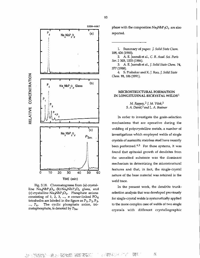
93
SSDN-4667
o < or H 2 UJ O 2 O O UJ > I-< _J UJ a:
phase with the composition Na3NbP30z are also
reported.
1 1 ~1 1 1
p
2 -Na NbP 0 Glass £ 4 3 Z
i
(b)
p •': i •.
« :i ps
5 1; 1 P „
^ i i ^ i i • ' • • — I " — — 1 1
Na NbP 0 3 3 Z
T -'(c)
P3/77.
I
-
—^+=-— , — — r ~ -r* A -
0 10 20 30 40 50 60
TIME (min)
Fig. 3.18. Chromatograms from (a) crystalline Na4NbP 3O z, (b) Na 4 NbP 3 O z glass, and (c) crystalline Na3NbP30z. Phosphate anions consisting of 1, 2, 3, ..., n corner-linked PO4 tetrahedra are labeled in the figure as Pj , P2, P3, ..., P„. The cyclic phosphate anion, tri-metaphosphate, is denoted by P3 r a.
1. Summary of paper: /. Solid State Chetn. 105,406 (1993).
2 A. E. Jazouli et al., G R. Acad. Sci. Paris Ser. 2 303,1005 (1986).
3. A. E. Jazouli et al., /. Solid State Chem. 74, 377 (1988).
4 S. Prabakar and K. J. Rao, /. Solid State Chem. 91,186 (1991).
MICROSTRUCTURAL FORMATION IN LONGITUDINAL BICRYSTAL WELDS1
M. Rappaz,2 J. M. Vitek,3
S. A. David,3 and L. A. Boatner
In order to investigate the grain-selection mechanisms that are operative during the welding of polycrystalline metals, a number of investigations which employed welds of single crystals of austenitic stainless steel have recently been performed. 4 ' 5 For these systems, it was found that epitaxial growth of dendrites from the unmelted substrate was the dominant mechanism in determining the microstructural features and that, in fact, the single-crystal nature of the base material was retained in the weld trace.
In the present work, the dendrite trunk-selection analysis that was developed previously for single-crystal welds is systematically applied to the more complex case of welds of two single crystals with different crystallographic
94
orientations. The formation and selection
processes in dendritic microstructures that occur
during the welding of two differently oriented
Fe-15 wt. % Ni-15 wt. % Cr single-crystal pieces
were analyzed. The specimens were oriented
and cut a long precise crystallographic
orientations in order to weld specific surfaces in
a manner that joined two predetermined
crystallographic directions. Six orientation
configurations were selected in the present
investigation: a (001) surface with a [100] or
[110] direction, a (011) surface with a [100], [011],
or [211], and a (111) surface with a [211]
direction. Using all the possible combinations,
two crystal halves were welded along their
boundary using an electron beam to form
longitudinal bicrystal welds. Experimental and
simulated metallographic sections have been
directly compared for the bicrystal-weld
configurations. The dendritic pattern observed
in transverse-metallographic sections was
analyzed for each single-crystal half on the basis
of a selection criterion that had been developed
previously for single-crystal welds [i.e., at a
given location in the melt pool, the selected (100)
dendrite trunk has a minimum undercooling or,
equivalently, a minimum velocity]. In general,
the bicrystal-weld microstructure is a simple
composite of microstructures expected in each of
the two single-crystal halves. However, near the
weld center line, it was shown that grain
competition between dendrites belonging to
different single crystals also occurred according
to this same minimum undercooling criterion.
This competition is known to occur either by the
disappearance of less favorably oriented
dendrite trunks or by branching mechanisms
giving rise to a new trunk from a tertiary arm.
Accordingly, a full picture of this grain
competition can only be given if the grain
boundary is specified with respect to the heat-
flow direction. Additional work is currently
under way to analyze this competition in
transverse bicrystal welds.
1. Summary of paper: Metall. Trans. A 24, (1993).
2. Ecole Polytechnique Federate de Lausanne, Lausanne, Switzerland.
3. Metals and Ceramics Division, ORNL. 4. M. Rappaz et al., Metall. Trans. A 20,
1125 (1989). 5. M. Rappaz et al., Metall. Trans. A 21,
1767 (1990).
MODELING OF SINGLE-CRYSTAL LASER-WELD MICROSTRUCTURES1
/. M. Vitek,2 T. Zacharia,3 S. A. David,2
M. Rappaz,3 and L. A. Boatner
In recent years, numerous advances have
been made in the field of heat and fluid-flow
modeling in welds. These previous studies have
provided much-needed insight as to what
variables and conditions have a strong influence
on the development of the weld pool and are
valuable in and of themselves because they
serve to predict the weld-pool shape and pene
tration. Heat and fluid-flow modeling can also
be a valuable aid in attempting to understand
and predict the development of the solidifica
tion microstructure in a weld. Accurate and
reliable models can provide information that is
often unavailable or extremely difficult to obtain
95
experimentally, but which plays a fundamental role in determining the nature of the solidification microstructure.
The purpose of the present investigation is to combine the two fields of heat and fluid-flow modeling and microstructural development in single-crystal welds in order to model and predict the solidification microstructure in laser-welded single crystals. The application of heat and fluid-flow modeling to the study of microstructural development in single crystals is an ideal case because the welded microstructure in single crystals is controlled almost exclusively by the weld-pool geometry, which can be readily calculated.4'5
A heat and fluid-flow model has been used to calculate the weld-pool size and shape for a high-speed, single-pass laser weld as a function of time. Based on the calculated weld-pool shape and with the use of a geometric model relating the dendrite growth to the weld-pool shape, a dendrite growth pattern was calculated for a single-crystal laser weld with a (001) surface that was welded along the [100] direction. The calculated results were compared with an actual experimental laser weld of an Fe-15Cr-15Ni alloy for the same orientation and weld direction. Agreement was obtained between the calculations and experimental observations, and an experimental dendritic growth pattern was accurately reproduced.
The following conclusions can be drawn: (1) The microstructure of single-crystal welds can be calculated from first principles. (2) Features that can be calculated include weld-pool size and shape, active dendritic growth
directions, and the resultant dendritic growth pattern. (3) Reasonable agreement was found between the calculated and the observed microstructures. (4) Comparison of the calculated and observed microstructures in single-crystal welds provides an accurate means of evaluating the three-dimensional weld-pool-shape calculations.
1. Summary of paper: Plasma and Laser Processing of Materials (in press).
2. Metals and Ceramics Division, ORNL. 3. Guest scientist from the Ecole
Polytechnique Federale de Lausanne, Lausanne, Switzerland.
4. M. Rappaz et al., Metall. Trans. A 21, 1767(1990).
5. M. Rappaz et al., Metall. Trans. A 20, 1125 (1989).
OPTICAL CHARACTERIZATION
OF MATERIALS
CERIUM-DOPED ORTHOPHOSPHATES: NEW PROMISING SCINTILLATORS1
A. Lempicki,2 E. Berman,2 A. J. Wojtowicz2
M. Balcerzyk,2and L. A. Boatner
There are at the present time two generic types of scintillators which use the Ce 3 + ion as the light-emitting species. They fall into the category of "concentrated" or stoichiometric compounds in which Ce is a chemical constituent (e.g., CeF3) and "diluted" or doped compounds [e.g., Lu2(Si04)0 (LSO) and GSO, the latter being'an analog of LSO, but incorporating Gd instead of Lu]. There is no question
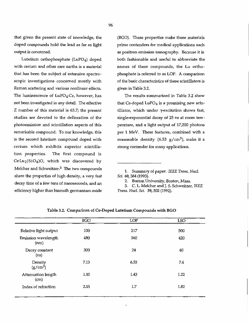
96
that given the present state of knowledge, the
doped compounds hold the lead as far as light
output is concerned.
Lutetium orthophosphate (LUPO4) doped
with cerium and other rare earths is a material
that has been the subject of extensive spectro
scopic investigations concerned mostly with
Raman scattering and various nonlinear effects.
The luminescence of LuPO^Ce, however, has
not been investigated in any detail. The effective
Z number of this material is 63.7; the present
studies are devoted to the delineation of the
photoemission and scintillation aspects of this
remarkable compound. To our knowledge, this
is the second lutetium compound doped with
cerium which exhibits superior scintilla
tion propert ies . The first compound is
Ce:Lu2(SiC>4)0, which was discovered by
Melcher and Schweitzer. 3 The two compounds
share the properties of high density, a very fast
decay time of a few tens of nanoseconds, and an
efficiency higher than bismuth germanium oxide
Table 3.2. Comparison of Ce-]
BGO
Relative light output 100
Emission wavelength 480 (nm)
Decay constant 300 (ns)
Density 7.13 (g/cm 3 )
Attenuation length 1.10 (cm)
Index of refraction 2.15
(BGO). These properties make these materials
prime contenders for medical applications such
as positron emission tomography. Because it is
both fashionable and useful to abbreviate the
names of these compounds, the Lu ortho-
phosphate is referred to as LOP. A comparison
of the basic characteristics of these scintillators is
given in Table 3.2.
The results summarized in Table 3.2 show
that Ce-doped LUPO4 is a promising new scin
tillator, which under y-excitation shows fast,
single-exponential decay of 25 ns at room tem
perature, and a light output of 17,200 photons
per 1 MeV. These features, combined with a
reasonable density (6.53 g / c m 3 ) , make it a
strong contender for many applications.
1. Summary of paper: IEEE Trans. Nucl. Sri. 40,384 (1993).
2 Boston University, Boston, Mass. 3. C. L. Melcher and J. S. Schweitzer, IEEE
Trans. Nucl. Sci. 39,502 (1992).
Lutetium Compounds with BGO
LOP LSO
217 500
360 420
24 40
6.53 7.4
1.43 1.22
1.7 1.82
TWO-PHOTON EXCITATION OF THE 4/'->5d 1 TRANSITIONS OF Ce34"
IN LuP0 4 AND YPO4 1
/. Sytsma,2 D. Piehler,2 N. M. Edelstein,2
L. A. Boatner, and M. M. Abraham
The past decade has witnessed an increasing
interest in the two-photon spectroscopy of
lanthanide ions. This type of spectroscopy can
be divided into two groups: (a) two-photon
excitation (TPE), in which two photons are
absorbed simultaneously by the lanthanide ion,
and (b) electronic Raman scattering (ERS), in
which a photon is inelastically scattered from an
ion such that the ion is excited to a different
electronic state. Both processes are parity-
allowed for the 4/—>4f transitions and are to be
considered as complementary to single-photon
spectroscopy.
ERS is especially suited to the study of low-
lying energy levels. Despite a large amount of
single-photon spectroscopic data for Ce3*" in the
orthophosphates, only the first 5dl level has
been determined accurately. The goal of the
present work, therefore, was to apply TPE to
Ce3*" in LUPO4 in order to obtain this
information for the other 5d} levels as well. One
practical st imulus for the study of Ce3*" in
orthophosphate hosts is their very promising
scintillator characteristics, plus their potential as
nuclear waste storage hosts and as a tunable
UV-laser mater ial . The 4 / 1 crystal-field
components of Ce 3 1" have energies up to =2500
cm"1. The positions of all seven crystal-field
components were determined previously, and
resonance-enhancement effects were studied.
';m$l :7m:. •%. :-M 'm£M^
In the present work, TPE spectra of the
^ - ^ d 1 transitions of Ce 3 1" in L u P 0 4 and YPO4
were observed as zero-phonon lines. The sym
metry properties of the levels were obtained
from the polarization dependence of the TPE
signals. Measurements on C e 3 + in YPO4 sup
ported the assignments. Although a crystal-field
fit yields a satisfactory rms energy deviation, an
unrealistic value of the spin-orbit coupling
parameter cji5d^) was obtained. The vibronic
coupling appears to be smaller than for the
single-photon absorption spectra, and the
vibronic bands show a rich structure. There are
striking differences between the energies and the
relative intensities of the vibronic lines and the
associated zero-phonon lines. The vibronic
coupling is also found to be strongly dependent
on the Ce3*" concentration. Since the 5d a
configuration is not shielded from the crystal
environment, as is the 4 / 1 configuration, this
effect in itself is expected, but is surprisingly
noticeable for small changes in the Ce 3 *
concentration.
In order to understand TPE of Ce3*", it is
essential to carry out a systematic study of these
vibronic effects. A comparison should be made
for C e 3 + in different host lattices in a manner
similar to that used in the case of single-photon
spectroscopic studies of G d 3 + .
1. Summary of paper: Phys. Rev. B 47, 14786 (1993).
2 Lawrence Berkeley Laboratory, Berkeley, Calif.
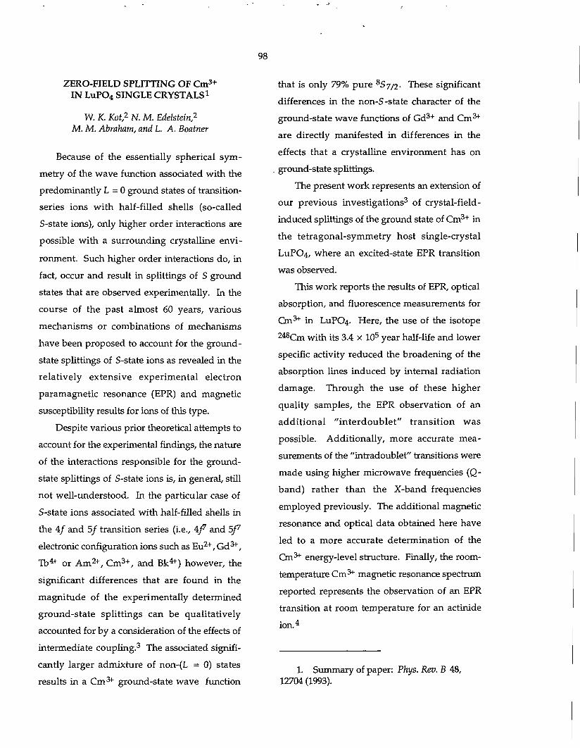
ZERO-FIELD SPLITTING OF C m 3 +
IN LuP0 4 SINGLE CRYSTALS1
W. K. Kot,2 N. M. Edelstein,2
M. M. Abraham, and L. A. Boatner
Because of the essentially spherical sym
metry of the wave function associated with the
predominantly L = 0 ground states of transition-
series ions with half-filled shells (so-called
S-state ions), only higher order interactions are
possible with a surrounding crystalline envi
ronment. Such higher order interactions do, in
fact, occur and result in splittings of S ground
states that are observed experimentally. In the
course of the past almost 60 years, various
mechanisms or combinations of mechanisms
have been proposed to account for the ground-
state splittings of S-state ions as revealed in the
relatively extensive experimental electron
paramagnetic resonance (EPR) and magnetic
susceptibility results for ions of this type.
Despite various prior theoretical attempts to
account for the experimental findings, the nature
of the interactions responsible for the ground-
state splittings of S-state ions is, in general, still
not well-understood. In the particular case of
S-state ions associated with half-filled shells in
the 4 / and 5 / transition series (i.e., 4J 7 and 5f
electronic configuration ions such as E u 2 + , Gd3*",
lb 4*" or A m 2 + , C m 3 + , and Bk4*") however, the
significant differences that are found in the
magnitude of the experimentally determined
ground-state splittings can be qualitatively
accounted for by a consideration of the effects of
intermediate coupling. 3 The associated signifi
cantly larger admixture of non-(L = 0) states
results in a Cm3*" ground-state wave function
98
that is only 79% pure sSy/2- These significant
differences in the non-S-state character of the
ground-state wave functions of G d 3 + and Cm3*"
are directly manifested in differences in the
effects that a crystalline environment has on
. ground-state splittings.
The present work represents an extension of
our previous investigations 3 of crystal-field-
induced splittings of the ground state of C m 3 + in
the tetragonal-symmetry host single-crystal
LUPO4, where an excited-state EPR transition
was observed.
This work reports the results of EPR, optical
absorption, and fluorescence measurements for
Cm3*" in LUPO4. Here, the use of the isotope 2 4 8 C m with its 3.4 x 10 5 year half-life and lower
specific activity reduced the broadening of the
absorption lines induced by internal radiation
damage. Through the use of these higher
quality samples, the EPR observation of an
addi t ional " in te rdouble t" t ransi t ion was
possible. Additionally, more accurate mea
surements of the "intradoublet" transitions were
made using higher microwave frequencies (Q-
band) rather than the X-band frequencies
employed previously. The additional magnetic
resonance and optical data obtained here have
led to a more accurate determination of the
On3+ energy-level structure. Finally, the room-
temperature Cm3*" magnetic resonance spectrum
reported represents the observation of an EPR
transition at room temperature for an actinide
ion. 4
1. Summary of paper: Phys. Rev. B 48, 12704 (1993).
99
Z Lawrence Berkeley Laboratory, University of California, Berkeley, Calif.
3. M. M. Abraham and L. A. Boatner, Phys. Rev. B 26,1434 (1982).
4. L. A. Boatner and M. M. Abraham, Rep. Prog. Phys. 41,87 (1978).
ELECTRON PARAMAGNETIC RESONANCE (EPR) OF Pu 3 + AND Cf 3 t
IN SINGLE CRYSTALS OF LUPO41
W. K. Kot2 N. M. Edelstein2
M. M. Abraham, and L. A. Boatner
the tetragonal-symmetry host LUPO4. The Pu3* and Cf^-doped tetragonal single crystals of LUPO4 employed in the present spectroscopic studies were grown in a glove-box-contained, platinum-wound furnace using a flux technique.4
As illustrated in Fig. 3.19, the g values of the electronic ground states were determined experimentally at a sample temperature of 4 K. These
The EPR spectrum of the ion Pu 3 + (5J5 electronic configuration) in the form of a dilute impurity has been investigated previously for a number of host single crystals. For the hosts employed in these previous studies, the symmetry properties were such that the local crystal-field environment of the Pu34" ion was characterized by cubic symmetry. The cumulative results emerging from these previous spectroscopic investigations have established that in contrast to the case of the 4/ lanthanide ions, for the 5 / actinide ions, intermediate-coupling effects play an important role in determining the properties of the electronic energy levels. In particular, in the case of P u 3 + , the / = 5/2 manifold ground state was found to contain only 66% of the pure 6 Hs/2 state, with the remainder of the wave function consisting of other 7 = 5/2 states admixed by intermediate-coupling effects.
In the present study of actinide electronic properties, EPR spectroscopy has been used to investigate the ground-state properties of the actinide ions Pu 3* (5/ 5) and Cf 3 + (5/5) incorporated as dilute impurities in single crystals of
SSDN-4687
0.78
0.76
0.74
J 0.72
1,0.70 0.68
0.66
0.64
expt. data least squares
-100 -50 0 50 Angle (degrees)
-100 -50 0 50 Angle (degrees)
100
, — , ,._ , 1 • 1
> ^ ^ \ ( b ) " 8 ^-^ least squares > ^ ^ \ ( b ) " + expt data
/ 7 /
ra 6 \ / •
tn 5 \ 1 -
4 . 1 1 . 1
-
100
Fig. 3.19. Experimental EPR measurements as a function of the angle between the crystal-lographic c axis and magnetic field. The solid curves represent a least-squares fit of the data to the expression g2 = g» cos 28 + g2^ sin 28. (a) Pu 3 + /LuP04 , microwave frequency of 9.223 GHz, g|| = 0.772(2), and g± = 0.658(2). (b) Cf 3/LuP04, microwave frequency of 9.217 GHz, g| =3.56(2), and g± = 7.79(3).
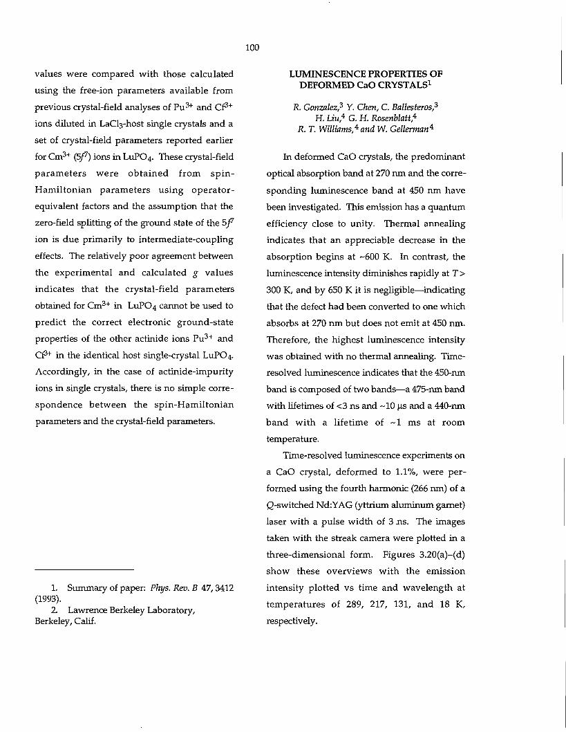
100
values were compared with those calculated
using the free-ion parameters available from
previous crystal-field analyses of Pu 3 4" and Cf 3 +
ions diluted in LaCLj-host single crystals and a
set of crystal-field parameters reported earlier
for C m 3 + (5Z7) ions in IA1PO4. These crystal-field
pa rame te r s were ob ta ined from sp in-
Hamil tonian parameters us ing opera tor -
equivalent factors and the assumption that the
zero-field splitting of the ground state of the 5f
ion is due primarily to intermediate-coupling
effects. The relatively poor agreement between
the experimental and calculated g values
indicates that the crystal-field parameters
obtained for C m 3 + in LUPO4 cannot be used to
predict the correct electronic ground-state
properties of the other actinide ions P u 3 + and
Cf3* in the identical host single-crystal LUPO4.
Accordingly, in the case of actinide-impurity
ions in single crystals, there is no simple corre
spondence between the spin-Hamil tonian
parameters and the crystal-field parameters.
1. Summary of paper: Phys. Rev. B 47,3412 (1993).
2 Lawrence Berkeley Laboratory, Berkeley, Calif.
LUMINESCENCE PROPERTIES OF DEFORMED CaO CRYSTALS1
R. Gonzalez,3 Y. Chen, C. Ballesteros,3
H. Liu,4 G. H. Rosenblatt4
R. T. Williams,4 and W. Gellerman4
In deformed CaO crystals, the predominant
optical absorption band at 270 ran and the corre
sponding luminescence band at 450 ran have
been investigated. This emission has a quantum
efficiency close to unity. Thermal annealing
indicates that an appreciable decrease in the
absorption begins at ~600 K. In contrast, the
luminescence intensity diminishes rapidly at T>
300 K, and by 650 K it is negligible—indicating
that the defect had been converted to one which
absorbs at 270 ran but does not emit at 450 ran.
Therefore, the highest luminescence intensity
was obtained with no thermal annealing. Time-
resolved luminescence indicates that the 450-nm
band is composed of two bands—a 475-nm band
with lifetimes of <3 ns and -10 (is and a 440-nm
band wi th a lifetime of - 1 ms at room
temperature.
Time-resolved luminescence experiments on
a CaO crystal, deformed to 1.1%, were per
formed using the fourth harmonic (266 ran) of a
Q-switched Nd:YAG (yttrium aluminum garnet)
laser with a pulse width of 3 ns . The images
taken with the streak camera were plotted in a
three-dimensional form. Figures 3.20(a)-(d)
show these overviews with the emission
intensity plotted vs time and wavelength at
temperatures of 289, 217, 131, and 18 K,
respectively.
101
ORNL/DWG-92-2253
289 K
<***Z*r
Fig. 3.20. Time-resolved emission spectra taken at temperatures of (a) 289, (b) 217, (c) 131, and (d) 18 K for a CaO sample deformed to 1.1%. The excitation was a 3-ns pulse of 266-nm light. The intensities are given in arbitrary units and are normalized to 10.
The optimum conditions for a deformed crystal to exhibit maximum luminescence intensity with minimum strain would be a 2-mm-thick unannealed sample with 1% deformation. Optical gain was tested using a pulsed excimer laser operating at 248 nm. No laser activity was observed at 77 and 300 K, with excitation powers up to the crystal-damage threshold.
1. Summary of paper: Phys. Rev. B 47,4910 (1993).
2. Guest scientist from Universidad Carlos III, Madrid, Spain.
3. Universidad Complutense, Madrid, Spain.
4. Wake Forest University, Winston-Salem, N.C.
5. University of Utah, Salt Lake City, Utah. 6. R. Gonzalez et al., Phys. Rev. B 43,5228
(1991).
ERRORS IN POLARIZATION MEASUREMENTS BECAUSE OF
STATIC RETARDATION IN PHOTOELASTIC MODULATORS1
F. A. Modine and G. E. Jellison, Jr.
A photoelastic modulator (PEM) imparts a time-dependent phase retardation to a light beam. The device consists of a piece of crystalline quartz (-18° X cut) and a piece of fused quartz. The piezo-electric crystalline quartz is driven at its resonant frequency (~50 kHz) by an applied ac voltage. Mechanical coupling induces a strain in the fused quartz, which is tuned to the same resonance frequency. The oscillating strain results in a time-dependent retardation (photoelastic effect). The PEM is
,&.- M- m
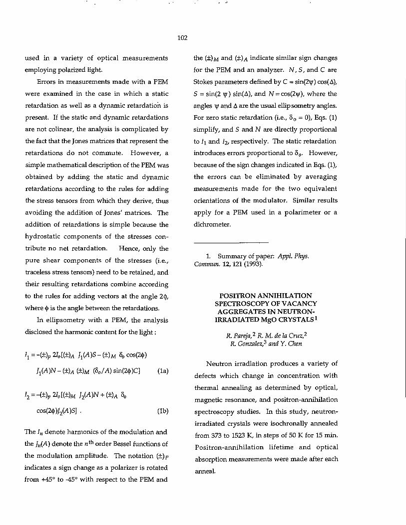
102
used in a variety of optical measurements
employing polarized light.
Errors in measurements made with a PEM
were examined in the case in which a static
retardation as well as a dynamic retardation is
present. If the static and dynamic retardations
are not colinear, the analysis is complicated by
the fact that the Jones matrices that represent the
retardations do not commute. However, a
simple mathematical description of the PEM was
obtained by adding the static and dynamic
retardations according to the rules for adding
the stress tensors from which they derive, thus
avoiding the addition of Jones' matrices. The
addition of retardations is simple because the
hydrostatic components of the stresses con
tribute no net retardation. Hence, only the
pure shear components of the stresses (i.e.,
traceless stress tensors) need to be retained, and
their resulting retardations combine according
to the rules for adding vectors at the angle 2(j),
where § is the angle between the retardations.
In ellipsometry with a PEM, the analysis
disclosed the harmonic content for the light:
/ 1=-(±)^27 0[(±)^ J1(A)S-(±)M 50cos(2<l))
/ a(A)N - (±)A (±)M (8 0/A) sin(2<t))C] (la)
I2 = -(±)p 2I0[(±)M J2(A)N + (±) A 8 0
cos(2(t>)/2(A)S] . (lb)
The In denote harmonics of the modulation and
the Jn{A) denote the n t h order Bessel functions of
the modulation amplitude. The notation (±)p
indicates a sign change as a polarizer is rotated
from +45° to -45° with respect to the PEM and
the (±)M a n £ l (± )A indicate similar sign changes
for the PEM and an analyzer. N,S, and C are
Stokes parameters defined by C = sin(2v|/) cos(A),
S = sin(2 \|/) sin(A), and N = cos(2\)/), where the
angles vj/ and A are the usual ellipsometry angles.
For zero static retardation (i.e., 8 0 = 0), Eqs. (1)
simplify, and S and N are directly proportional
to I\ and I2, respectively. The static retardation
introduces errors proportional to 8 0 . However,
because of the sign changes indicated in Eqs. (1),
the errors can be eliminated by averaging
measurements made for the two equivalent
orientations of the modulator. Similar results
apply for a PEM used in a polarimeter or a
dichrometer.
1. Summary of paper: Appl. Phys. Commun. 12,121 (1993).
POSITRON ANNIHILATION SPECTROSCOPY OF VACANCY AGGREGATES IN NEUTRON-
IRRADIATED MgO CRYSTALS1
R. Pareja,2 R. M. de la Cruz? R. Gonzalez? and Y. Chen
Neutron irradiation produces a variety of
defects which change in concentration with
thermal annealing as determined by optical,
magnetic resonance, and positron-annihilation
spectroscopy studies. In this study, neutron-
irradiated crystals were isochronally annealed
from 373 to 1523 K, in steps of 50 K for 15 min.
Positron-annihilation lifetime and optical
absorption measurements were made after each
anneal.
103
All the lifetime spectra of these neutron-
irradiated crystals were decomposed unam
biguously into components. Figure 3.21 shows
the annihilation parameters of these crystals as a
function of the heating temperature; X\ (bottom)
and %2 (middle) are the decay constants associ
ated with the exponential terms; 1% (top) is the
relative intensity of the second component, and
the average lifetime is x = (1 - I^fix + hx2- The
value of x = 160 ps remained approximately
constant for T < 673 K and reached its maximum
400 800 1200 TEMPERATURE (K)
1600
value of -206 ps at 873 K. The second
component lifetime, X2, increased from (187 ± 10)
ps initially to a value of (295 ± 25) ps after
annealing at -1100 K. Simultaneously, the
intensity of this second component, I2, decreased
from 83% to 12%. Annealing above 1100 K only
induced a slight decrease in x accompanied by a
continuous reduction of the Xi value while I2 remained practically constant.
Although the concentration of defects is
very high, the positron average lifetime is
noticeably shorter than in virgin crystals.
Higher doses result in a higher defect concen
tration and a shorter positron lifetime. This
suggests that the defects are positively charged.
Fig. 3.21. Positron annihilation parameters vs temperature in H-doped MgO crystals.
1. Summary of paper: Philos. Mag. A 66, 597 (1992).
2. Universidad Complutense, Madrid, Spain.
3. Guest scientist from Universidad Carlos III, Madrid, Spain.
PROTONS IN NEUTRON-IRRADIATED AND THERMOCHEMICALLY REDUCED
MgO CRYSTALS DOPED WITH LITHIUM IMPURITIESl
R. Gonzalez,3 R. Pareja,3 and Y. Chen
The present study focuses on protons in three types of lithium-doped MgO crystals— thermochemically reduced (TCR), neutron irradiated, and crystals which had previously been oxidized at high temperatures prior to neutron irradiation. TCR produces primarily anion vacancies and H" ions. While three local modes are observed in undoped MgO crystals, only one of them (1024 cm"1) is present in
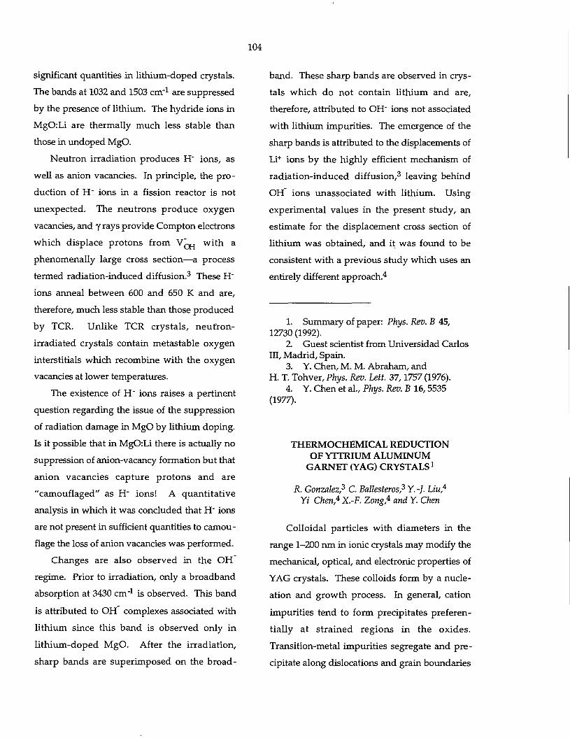
104
significant quantities in lithium-doped crystals.
The bands at 1032 and 1503 cm"1 are suppressed
by the presence of lithium. The hydride ions in
MgO:Li are thermally much less stable than
those in undoped MgO.
Neutron irradiation produces H" ions, as
well as anion vacancies. In principle, the pro
duction of H" ions in a fission reactor is not
unexpected. The neutrons produce oxygen
vacancies, and y rays provide Compton electrons
which displace protons from V ^ j with a
phenomenally large cross section—a process
termed radiation-induced diffusion. 3 These H"
ions anneal between 600 and 650 K and are,
therefore, much less stable than those produced
by TCR. Unlike TCR crystals, neutron-
irradiated crystals contain metastable oxygen
interstitials which recombine with the oxygen
vacancies at lower temperatures.
The existence of H" ions raises a pertinent
question regarding the issue of the suppression
of radiation damage in MgO by lithium doping.
Is it possible that in MgO:Li there is actually no
suppression of anion-vacancy formation but that
anion vacancies capture protons and are
"camouflaged" as H" ions! A quantitative
analysis in which it was concluded that H" ions
are not present in sufficient quantities to camou
flage the loss of anion vacancies was performed.
Changes are also observed in the OH
regime. Prior to irradiation, only a broadband
absorption at 3430 cm" 1 is observed. This band
is attributed to OH complexes associated with
lithium since this band is observed only in
l i thium-doped MgO. After the irradiation,
sharp bands are superimposed on the broad
band. These sharp bands are observed in crys
tals which do not contain lithium and are,
therefore, attributed to OH" ions not associated
with lithium impurities. The emergence of the
sharp bands is attributed to the displacements of
Li + ions by the highly efficient mechanism of
radiation-induced diffusion, 3 leaving behind
OH ions unassociated with lithium. Using
experimental values in the present study, an
estimate for the displacement cross section of
lithium was obtained, and it was found to be
consistent with a previous study which uses an
entirely different approach. 4
1. Summary of paper: Phys. Rev. B 45, 12730 (1992).
2. Guest scientist from Universidad Carlos III, Madrid, Spain.
3. Y. Chen, M. M. Abraham, and H. T. Tohver, Phys. Rev. Lett. 37,1757 (1976).
4. Y. Chen et al., Phys. Rev. B 16,5535 (1977).
THERMOCHEMICAL REDUCTION OF YTTRIUM ALUMINUM
GARNET (YAG) CRYSTALS1
R. Gonzalez,3 C. Ballesteros,3Y.-}. Liu* Yi Chen,4'X.-F. Zong* and Y. Chen
Colloidal particles with diameters in the
range 1-200 nm in ionic crystals may modify the
mechanical, optical, and electronic properties of
YAG crystals. These colloids form by a nucle-
ation and growth process. In general, cation
impurities tend to form precipitates preferen
tially at s trained regions in the oxides.
Transition-metal impurities segregate and pre
cipitate along dislocations and grain boundaries
105
to form metallic precipitates when oxide samples are heated in a reducing atmosphere, or an oxygen-free inert gas, a process referred to as decoration. These colloids are usually identified by transmission electron microscopy (TEM) and x-ray fluorescence and give rise to characteristically broad extinction bands, attributed to Mie scattering.
Strained regions were first identified in slabs of YAG single crystals via transmitted light viewed with crossed polarizers. The strained region had a symmetrical pattern and was situated at the center of the slabs. Because of the symmetry both in pattern and in location, it is believed that they were induced thermally during crystal growth.
TEM, x-ray microanalysis, and optical absorption were used to characterize the strained and unstrained regions in as-grown and subsequently thermochemically reduced (TCR) YAG crystals. As TCR takes place at increasing temperatures, a dark coloration emerges at the strained region. The strained region was always darker than the surrounding unstrained region, regardless of the temperature of reduction (Fig. 3.22). Optical measurements reveal that the coloration is due to a very broad band peaking at about 800 nm. There is no evidence from TEM and x-ray microanalysis to indicate the presence of precipitates in as-grown and TCR crystals, in contrast to oxides in which cation impurities form metallic precipitates preferentially at strained regions during TCR.
oaoon M-uiM
16 | — " I I i i
s« ' YAG (Allied)
1 strained region s« 4
Hi \ / \ ^ >^1673 K ^ ^ \ . 8 a
ABSO
RPT
ION
V as-grown
n i i i i 200 400 600 800 1000
WAVELENGTH (nm)
1200
1. Summary of paper: Philos. Mag. A 67, 207 (1993).
Fig. 3.22. Optical absorption spectra of an as-grown YAG single crystal and after TCR for 2 h at 1673 K.
2 Guest scientist from Universidad Carlos HI, Madrid, Spain.
3. Universidad Complutense, Madrid, Spain.
4. Fudan University, Shanghai, P.R. China.
PRECIPITATION OF COPPER AND CHROMIUM IMPURITIES IN LANTHANUM
MAGNESIUM ALUMINATE CRYSTALS DURING REDUCTION1
C. Ballesteros,2 R. Gonzalez,3
Y. Chen, and M. R. Kokta*
Thermochemical reduction (TCR) at high temperatures has been performed on chromium-doped lanthanum magnesium aluminate (LMA:Cr) crystals. Analytical transmission electron microscopy (TEM) and optical absorption techniques were used to characterize the crystals. There were two stages of impurity aggregation. In the first stage, copper impurities inherently present in the crystals began to aggregate and form Cu-rich particles at 1500 K near the surface region. Below 1870 K, there was
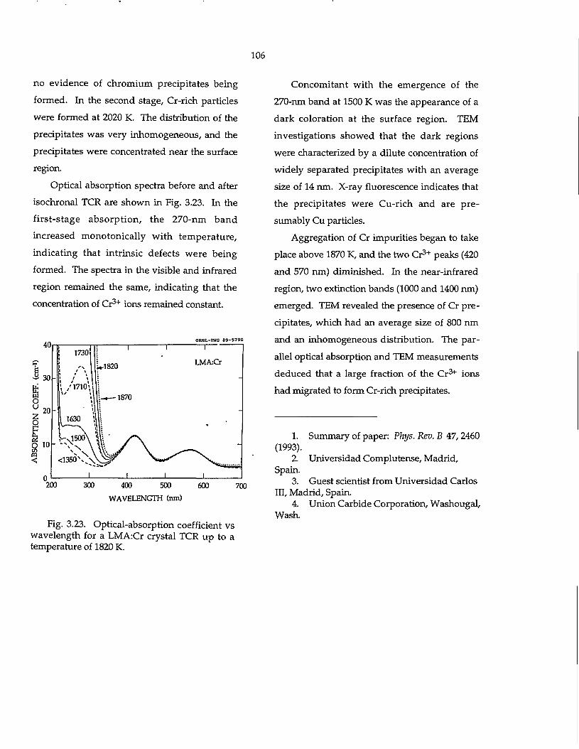
106
no evidence of chromium precipitates being formed. In the second stage, Cr-rich particles were formed at 2020 K. The distribution of the precipitates was very inhomogeneous, and the precipitates were concentrated near the surface region.
Optical absorption spectra before and after isochronal TCR are shown in Fig. 3.23. In the first-stage absorption, the 270-nm band increased monotonically with temperature, indicating that intrinsic defects were being formed. The spectra in the visible and infrared region remained the same, indicating that the concentration of Cr3"1" ions remained constant.
ORNL-ITWG 8 9 - 5 7 9 0
200 300 400 500 600 700 WAVELENGTH (nm)
Fig. 3.23. Optical-absorption coefficient vs wavelength for a LMA:Cr crystal TCR up to a temperature of 1820 K.
Concomitant with the emergence of the 270-nm band at 1500 K was the appearance of a dark coloration at the surface region. TEM investigations showed that the dark regions were characterized by a dilute concentration of widely separated precipitates with an average size of 14 nm. X-ray fluorescence indicates that the precipitates were Cu-rich and are presumably Cu particles.
Aggregation of Cr impurities began to take place above 1870 K, and the two Cr3* peaks (420 and 570 nm) diminished. In the near-infrared region, two extinction bands (1000 and 1400 nm) emerged. TEM revealed the presence of Cr precipitates, which had an average size of 800 nm and an inhomogeneous distribution. The parallel optical absorption and TEM measurements deduced that a large fraction of the Cr3* ions had migrated to form Cr-rich precipitates.
1. Summary of paper: Phys. Rev. B 47,2460 (1993).
2 Universidad Complutense, Madrid, Spain.
3. Guest scientist from Universidad Carlos III, Madrid, Spain.
4. Union Carbide Corporation, Washougal, Wash.
4. Ion Beam and Laser Processing
Basic research in materials science using ion beams, molecular beams, and lasers are emphasized in this chapter. Progress in ion beam processing, ion implantation and analysis, and laser and molecular beam processing of thin films are reported. This research is performed at the Surface Modification and Characterization Research Center (SMAC RC) and the SSD pulsed-laser ablation and molecular-jet growth facilities.
The SMAC RC provides the scientific community with extensive capabilities for ion beam processing of the near-surface region of solids. The following are some recent examples included in this report. Formation of random or oriented nanocrystals of metals, semiconductors, and compounds in a variety of substrates has been achieved, and the structural, optical, and electrical properties of these nanoclusters are being investigated. A dislocation-free process for producing silicon-on-insulator by implantation, the kinetics of solid-phase-epitaxial crystallization in amorphous Sii^Ge* thin films following implantation, and the effects of implantation-induced damage on electrical carrier concentrations in tin-doped indium oxide and GaAs have been studied. A new lift-off technique for obtaining freestanding diamond films and the development of an electron cyclotron resonance plasma source for copper metallization have been demonstrated. Ion beams have been used to synthesize Ti-rich epitaxial buried layers in LiNb03, to modify the hardness of the surfaces of orthopedic alloys, and to provide oxygen needed to form a protective oxide coating on NbAl3 and TiAl alloys. The adsorption of hydrogen on surfaces and its diffusion in the bulk have been studied by nuclear reaction and elastic recoil techniques.
The Semiconductor Physics and Thin Films Group has developed a pulsed-laser deposition (PLD) technique for depositing ternary semiconductor films with continuously variable composition and doping from a single target. PLD has facilitated electrical property investigations of the so-called "infinite-layer" parent structure of the high-temperature superconductors (HTSc) through the growth of very high quality thin films, and studies of the dimensionality and transport properties of high-temperature superconductivity have been carried out using superlattice and sandwich structures of YBCO. In addition, techniques are being developed for measuring Landau quantum oscillations in thin-film HTSc materials. Fast imaging has provided new information on the interaction of PLD ablation plumes with substrates and on the formation of fullerenes during ablation of graphite. Differential optical reflectivity has been used to characterize the kinetics of hydridic pulsed-jet chemical vapor deposition.
107
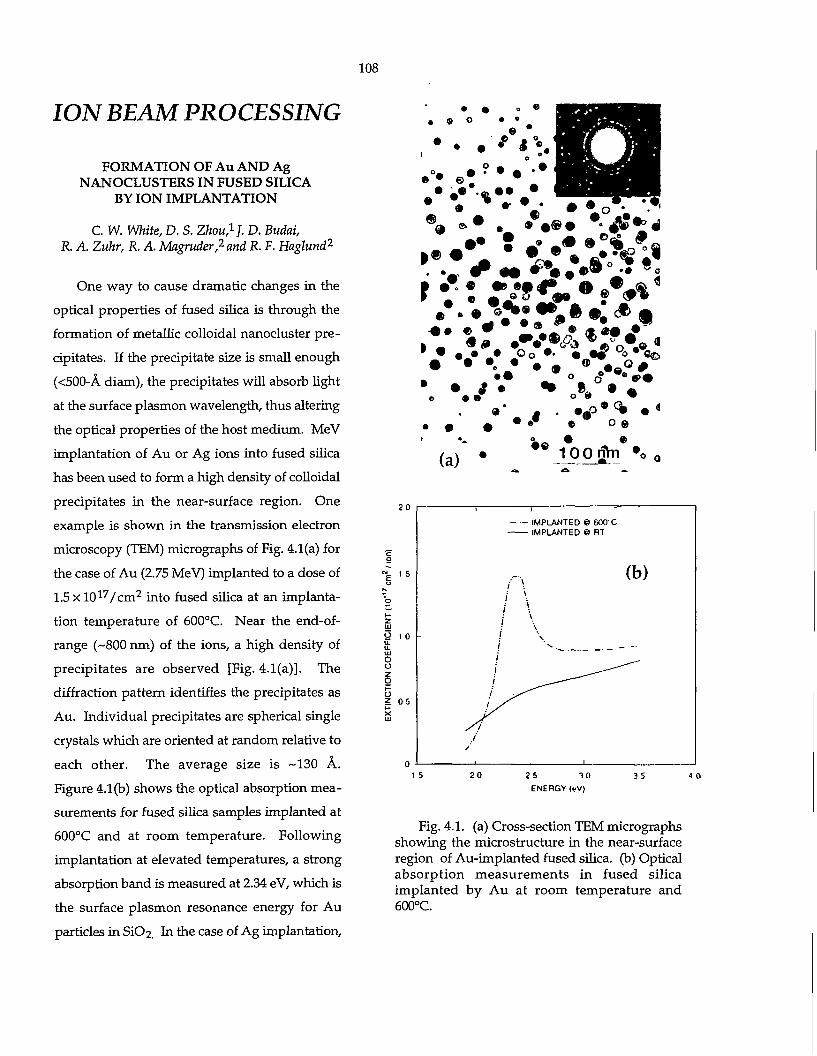
108
ION BEAM PROCESSING
FORMATION OF Au AND Ag NANOCLUSTERS IN FUSED SILICA
BY ION IMPLANTATION
C. W. White, D. S. Zhou,1 J. D. Budai, R. A. Zuhr, R. A. Magruder,2 and R. F. Haglund2
One way to cause dramatic changes in the
optical properties of fused silica is through the
formation of metallic colloidal nanocluster pre
cipitates. If the precipitate size is small enough
(<500-A diam), the precipitates will absorb light
at the surface plasmon wavelength, thus altering
the optical properties of the host medium. MeV
implantation of Au or Ag ions into fused silica
has been used to form a high density of colloidal
precipitates in the near-surface region. One
example is shown in the transmission electron
microscopy (TEM) micrographs of Fig. 4.1(a) for
the case of Au (2.75 MeV) implanted to a dose of
1.5 x 1 0 1 7 / c m 2 into fused silica at an implanta
tion temperature of 600°C. Near the end-of-
range (-800 nm) of the ions, a high density of
precipitates are observed [Fig. 4.1(a)]. The
diffraction pattern identifies the precipitates as
Au. Individual precipitates are spherical single
crystals which are oriented at random relative to
each other. The average size is -130 A.
Figure 4.1(b) shows the optical absorption mea
surements for fused silica samples implanted at
600°C and at room temperature. Following
implantation at elevated temperatures, a strong
absorption band is measured at 2.34 eV, which is
the surface plasmon resonance energy for Au
particles in Si02. In the case of Ag implantation,
2 0
y 1 o
o o 2 o I-o 2 0 5
IMPLANTED 0 600'C IMPLANTED ® RT
2 0 2S 3 0 ENERGY (eV)
35
Fig. 4.1. (a) Cross-section TEM micrographs showing the microstructure in the near-surface region of Au-implanted fused silica, (b) Optical absorpt ion measurements in fused silica implanted by Au at room temperature and 600°C.
strong absorption is observed at the surface plasmon energy for Ag in SiC>2 (3.1 eV).
Precipitate size and size distribution can be varied from ~30 to -150 A by an appropriate choice of implantation or annealing conditions. Precipitate volume fractions of several percent have been achieved in the near surface by ion implantation and annealing. This is much greater than that (~0.01% or less) which can be achieved by adding metal to the glass melt. The very high volume fraction and small precipitate size lead to very large nonlinear optical properties in the implanted materials as demonstrated in recent measurements.3
1. ORNL/ORISE postdoctoral research associate.
2 Vanderbilt University, Nashville, Term. 3. R. H. Magruder et al., Appl. Phys. Lett.
62,1730 (1993).
NANOSIZE METAL ALLOY PARTICLE FORMATION IN Ag AND Cu
SEQUENTIALLY IMPLANTED SILICA1
R. A. Zuhr, R. H. Magruder III2
T. A. Anderson,2 and J. E. Wittig2
Recently, composites of nanosize metal particles (2-30 run in diam) embedded in glass have been shown to exhibit third-order optical nonlinearities with a magnitude of 10"11 esu and a response time of less than 5 ps. The large nonlinear susceptibility is attributed to local-field enhancement for frequencies near the surface plasmon resonance of the metallic particles. As strong enhancements of the nonlinear response are expected to occur on or near the surface
plasmon resonance, the ability to control the frequency of this resonance is of interest for possible wavelength tunability.
Figure 4.2 shows representative bright field images of the planar view of the implanted layer for Corning 7940 silica samples implanted with 6 x 10 1 6 Cu ions/cm 2 at 160 keV and then sequentially with 2,4, and 6 x 10 1 6 Ag ions/cm 2
at 300 keV. The implantation energies were chosen using TRIM 89 calculations so that the depth distributions of the elements would overlap. The nanosize particles formed are uniform in shape and are spherical. The mean particle sizes for the three samples are 3.7 ± 3.2, 22.4 ± 6.0, 27.6 ± 9.7 nm, respectively. The volume fraction of the Ag-Cu alloy metal particles is -5% in the center of the implanted region.
Sequentially implanted samples exhibit significantly different optical spectra than samples implanted with single elements. Shifts in both peak position and magnitude compared with single implantations are observed. These results indicate that the changes in the optical absorption are due to the presence of the two different metallic elements. The shift in the wavelength of the surface plasmon resonance with sequential implantation is attributed to alloying of the Cu-Ag ions during implantation, as observed by dispersive x-ray analysis. The difference in optical response with increasing Ag concentration is attributed to different degrees of alloying as well as to increasing particle size.
1. Summary of paper to be published. 2 Vanderbilt University, Nashville, Term.
'"•^WZZCT^i*
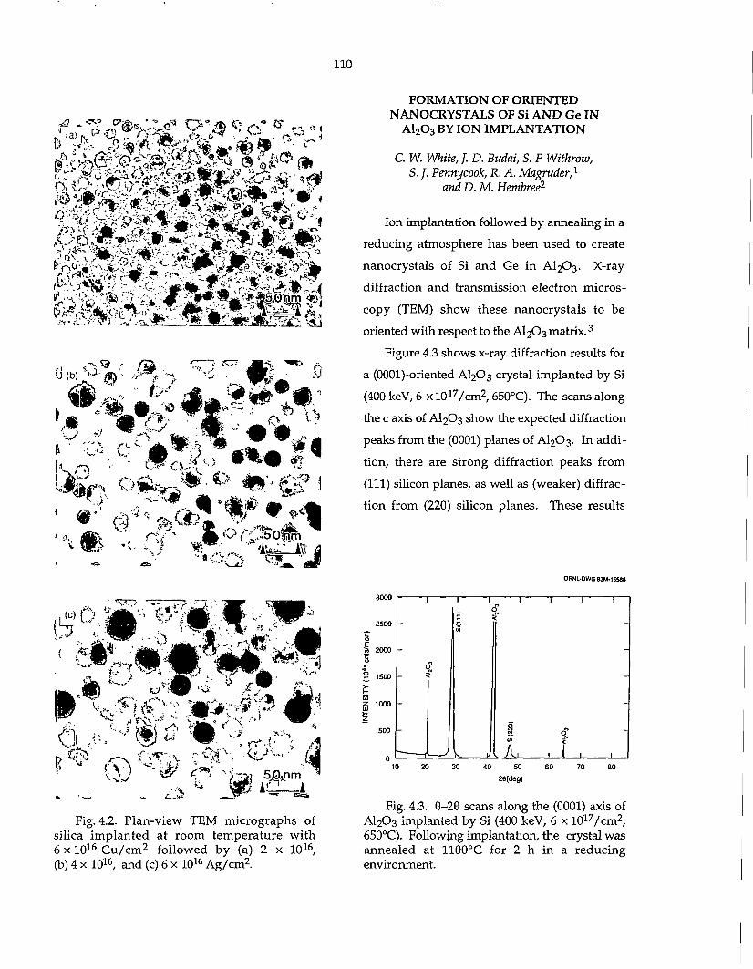
110
f. fcfc^J^ ^fr". c- Q° "
&(a)K ^ % « X ^ A S 1 ; « M » ' °"i
D>^-!
FORMATION OF ORIENTED NANOCRYSTALS OF Si AND Ge IN
A1 2 0 3 BY ION IMPLANTATION
C. W. White,}. D. Bwdaf, S. P Withrozo, S. J. Pennycook, R. A. Magruder,1
and D. M. Hembree2
*$?\/^m fc'VsSS&v^v - ^ -<#t%: ^£ f<V*^ ( * $ w ! r ^ ;1
W;
• r !^*i i^l
» •
o* • +** i " " v . '
* • ? •
f%T"^\ •-•'v5ivi - < ^ w (ij
" ^ C S a ^
Fig. 4.2. Plan-view TEM micrographs of silica implanted at room temperature with 6 x 10 1 6 Cu/cm 2 followed by (a) 2 x 10 1 6 , (b) 4 x 10 1 6, and (c) 6 x 10 1 6 Ag/cm2.
Ion implantation followed by annealing in a reducing atmosphere has been used to create nanocrystals of Si and Ge in AI2O3. X-ray diffraction and transmission electron microscopy (TEM) show these nanocrystals to be oriented with respect to the AI2O3 matrix.3
Figure 4.3 shows x-ray diffraction results for a (OOOl)-oriented AI2O3 crystal implanted by Si (400 keV, 6 x 101 7/cm2,650°C). The scans along the c axis of AI2O3 show the expected diffraction peaks from the (0001) planes of AI2O3. In addition, there are strong diffraction peaks from (111) silicon planes, as well as (weaker) diffraction from (220) silicon planes. These results
ORNLDWG 93M-1S58S
3000
2500
ft 2000
1500
1000
500 -
1 1 1 \ i
1 1 1
c 0
: -
-
^ Y> v
s CM CM
I A, , f , ," 40 50
26(deg) 60 80
Fig. 4.3. 0-29 scans along the (0001) axis of A1 2 0 3 implanted by Si (400 keV, 6 x 10 1 7 /cm 2
/
650°C). Following implantation, the crystal was annealed at 1100°C for 2 h in a reducing environment.

I l l
show that the silicon nanocrystals are three -dimensionally aligned predominantly in the orientation Si(lll) || A1 2 0 3 (0001), Si [ 110] 11A1203 [ 112 0 ] . To a much lesser extent, the orientation Si(110) || Al2O3(0001), Si [001] || AI2O3 [1010] is observed. Both domains exhibit sixfold rotational symmetry about the surface normal. The 6-29 width of the Si(lll) diffraction peak is consistent with a nano-crystalline thickness of ~140 A normal to the surface. Particle sizes depend on both the dose and the thermal treatment. Initial TEM results suggest that at high doses, the nanocrystals may have a pancake shape.
For Ge-implanted Al20 3 , Ge nanocrystals oriented with (111) planes parallel to (0001) Al20 3 are observed. In addition, crystallites with (110) planes oriented approximately parallel to (0001) AI2O3 planes are observed with nearly equal x-ray intensity. However, the (110) domains have the Ge [110] axis tilted by -3° away from the AI2O3 [0001] axis toward three symmetry-equivalent directions. In contrast to the Si observations, both types of Ge domains exhibit three-fold rotational symmetry about the surface normal. Sizes of Ge nanocrystals inferred from the width of the diffraction lines are in the range 50-100 A (depending on dose and temperature), and initial TEM results show the shapes to be nearly spherical.
1. Vanderbilt University, Nashville, Term. 2. Oak Ridge Y-12 Plant, Oak Ridge, Tenn. 3. J. D. Budai et al., "Structure and Orien
tation of Si, Ge, and SiGe Nanocrystals Formed by Ion Implantation," this report.
M:. '.WiSU.'.'^'^M
FORMATION OF ORIENTED SiGe NANOCRYSTALS IN A1 2 0 3 BY
ION IMPLANTATION
C. W. White, J. D. Budai, S. P Withrow, S. J. Pennycook, R. A. Magruder,1
and D. M. Hembree2
Ion implantation, followed by annealing, has been used to create nanocrystals of SiGe in Al20 3. The nanocrystals were formed by sequential implantation of Si and Ge at equal doses with the ion energy adjusted to give the same projected range. Following implantation, annealing was carried out in a reducing atmosphere at temperatures up to 1100°C for time periods of 1 h. Raman scattering and x-ray diffraction were used to confirm the existence of SiGe crystallites, and x-ray diffraction was used to determine the orientation of the SiGe nanocrystals with respect to the AI2O3 matrix.
Figure 4.4 gives Raman scattering results showing the presence of SiGe crystallites in Al20 3 following the implantation of Si and Ge and annealing for 1 h at 1100°C. Shown in Fig. 4.4 are Raman lines characteristic of Si-Si bonds (at 501 cm' 1), Ge-Ge bands (at 287 cm"1), and Si-Ge bonds (at 409 cm"1). Wavelengths characteristic of the individual bonds were determined from Raman spectra obtained from bulk SiGe alloys. X-ray diffraction results show that the SiGe nanocrystals are oriented with their (111) planes || to A1 2 0 3 (0001) planes.3 The observed x-ray diffraction peak position for the nanocrystalline (111) planes lies intermediate between the calculated bulk Si and bulk Ge positions and, hence, suggests the presence of mixed SiGe nanocrystals rather than separate Si
..bM.$m-m, mi. :&
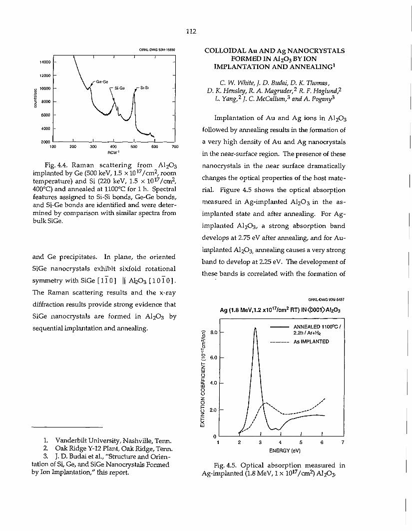
112
ORNL-DWG 93M-15592
14000 - \ ' 1 1
12000 -\ y-Ge-Ge
-
10000 -\ y-Ge-Ge
- Si-Ge ^ - Si-Si
8000 - -
6000 -
4000
1 1 I -
1 100 400
RCM"' 600
Fig. 4.4. Raman scattering from AI2O3 implanted by Ge (500 keV, 1.5 x 1 0 1 7 / c m 2 , room temperature) and Si (220 keV, 1.5 x 1 0 1 7 / c m 2 , 400°C) and annealed at 1100°C for 1 h. Spectral features assigned to Si-Si bonds, Ge-Ge bonds, and Si-Ge bonds are identified and were determined by comparison with similar spectra from bulk SiGe.
and Ge precipitates. In plane, the oriented
SiGe nanocrystals exhibit sixfold rotational
symmetry with SiGe [ 1 1 0 ] || A1 2 0 3 [ 1 0 1 0 ] .
The Raman scattering results and the x-ray
diffraction results provide strong evidence that
SiGe nanocrystals are formed in AI2O3 by
sequential implantation and annealing.
1. Vanderbilt University, Nashville, Term. 2. Oak Ridge Y-12 Plant, Oak Ridge, Tenn. 3. J. D. Budai et al., "Structure and Orien
tation of Si, Ge, and SiGe Nanocrystals Formed by Ion Implantation," this report.
COLLOIDAL Au AND Ag NANOCRYSTALS FORMED IN A 1 2 0 3 BY ION
IMPLANTATION AND ANNEALING 1
C. W. White, J. D. Budai, D. K. Thomas, D. K. Hensley, R. A. Magruder,2 R. F. Haglund,2
L. Yang,2 } . C. McCallum,3 and A. Pogamp1
Implantation of Au and Ag ions in AI2O3
followed by annealing results in the formation of
a very high density of Au and Ag nanocrystals
in the near-surface region. The presence of these
nanocrystals in the near surface dramatically
changes the optical properties of the host mate
rial. Figure 4.5 shows the optical absorption
measured in Ag-implanted AI2O3 in the as-
implanted state and after annealing. For Ag-
implanted AI2O3, a strong absorption band
develops at 2.75 eV after annealing, and for Au-
implanted Al203 ; annealing causes a very strong
band to develop at 2.25 eV. The development of
these bands is correlated with the formation of
ORNL-DWG 93M-5457
Ag (1.8 MeV,1.2 x101 7/cm2 RT) IN<0001>AI2O3
8.0
it 4.0
O 2.0
HI
ANNEALED 1100°C/ 2.2h / Ar+H2
As IMPLANTED
3 4 5 ENERGY (eV)
Fig. 4.5. Optical absorption measured in Ag-implanted (1.8 MeV, 1 x 10 1 7 / cm 2 ) A1 2 0 3 .
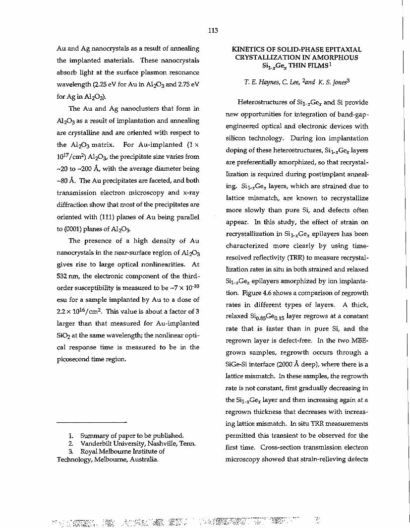
Au and Ag nanocrystals as a result of annealing the implanted materials. These nanocrystals absorb light at the surface plasmon resonance wavelength (2.25 eV for Au in A1 2 0 3 and 2.75 eV for Ag in AI2O3).
The Au and Ag nanoclusters that form in AI2O3 as a result of implantation and annealing are crystalline and are oriented with respect to the AI2O3 matrix. For Au-implanted (1 x 10 1 7/cm 2) A1203, the precipitate size varies from ~20 to ~200 A, with the average diameter being ~80 A. The Au precipitates are faceted, and both transmission electron microscopy and x-ray diffraction show that most of the precipitates are oriented with (111) planes of Au being parallel to (0001) planes of A1 2 0 3 .
The presence of a high density of Au nanocrystals in the near-surface region of AI2O3 gives rise to large optical nonlinearities. At 532 run, the electronic component of the third-order susceptibility is measured to be ~7 x 10"10
esu for a sample implanted by Au to a dose of 2.2 x 10 1 6 /cm 2 . This value is about a factor of 3 larger than that measured for Au-implanted SiC>2 at the same wavelength; the nonlinear optical response time is measured to be in the picosecond time region.
1. Summary of paper to be published. 2 Vanderbilt University, Nashville, Tenn. 3. Royal Melbourne Institute of
Technology, Melbourne, Australia.
••.; i;mm.; m Armrm ,is:;;
KINETICS OF SOLID-PHASE EPITAXIAL CRYSTALLIZATION IN AMORPHOUS
Sij^Ge^ THIN FILMS1
T. E. Haynes, C. Lee, 2and K. S. Jones*
Heterostructures of Sii^Ge^ and Si provide new opportunities for integration of band-gap -engineered optical and electronic devices with silicon technology. During ion implantation doping of these heterostructures, Sii_2Gex layers are preferentially amorphized, so that recrystal-lization is required during postimplant annealing. Sii-xGex layers, which are strained due to lattice mismatch, are known to recrystallize more slowly than pure Si, and defects often appear. In this study, the effect of strain on recrystallization in Si^Ge* epilayers has been characterized more clearly by using time-resolved reflectivity (TRR) to measure recrystallization rates in situ in both strained and relaxed Sii_rGex epilayers amorphized by ion implantation. Figure 4.6 shows a comparison of regrowth rates in different types of layers. A thick, relaxed Si0 8 5 G e 0 1 5 layer regrows at a constant rate that is faster than in pure Si, and the regrown layer is defect-free. In the two MBE-grown samples, regrowth occurs through a SiGe-Si interface (2000'A deep), where there is a lattice mismatch. In these samples, the regrowth rate is not constant, first gradually decreasing in the Sii_xGe r layer and then increasing again at a regrown thickness that decreases with increasing lattice mismatch. In situ TRR measurements permitted this transient to be observed for the first time. Cross-section transmission electron microscopy showed that strain-relieving defects
mmm:rw '-w. •
114
OHNLOWG 9315391
, - , 3 . 0 K>
< O
> ' • $
- | 1 1 1 I ' | I 1 1—I J 1 l ~~I
540°C
Relaxed Si0.85Ge0.i5
MBE S i 0 8 G e 0 2 -
MBE S i 0 8 8 G e 0 1 2 •
2000 1500 1000 500 0 Interface Depth (A)
Fig. 4.6. The rate of solid-phase-epitaxial regrowth in various Sii . x Ge x epilayers at 540°C is normalized to that in pure Si and shown as a function of the position of the amorphous-crystal interface. The original interface was ~3500 A deep in all cases. The two MBE-grown Sii_ rGe x layers were only 2000 A thick, so that regrowth was initiated in the Si substrate, whereas the "relaxed" Sio.85Geo.15 layer was 7 (Jm thick.
formed at the same depth where the regrowth
rate began to increase. These results conclu
sively demonstrated that the regrowth rate in
strained S i i . z Ge x is not constant, as previously
assumed, and that the transient retardation is
due to compressive strain, disappearing when
the strain is relieved by defects.
1. Summary of papers: Appl. Phys. Lett. 62, 501 (1993); p. 479 in Semiconductor Hetero-structures for Photonic and Electronic Applications, ed. by C. W. Tu, D. C. Houghton, and R. T. Tung, Materials Research Society, Pittsburgh, Pa., 1993.
2 SURA/ORNL Summer Cooperative Program student research participant from the University of Florida, Gainesville, Fla.
3. University of Florida, Gainesville, Fla.
FREESTANDING HOMOEPITAXIAL CHEMICAL VAPOR DEPOSITED (CVD)
DIAMOND FILMS LIFTED OFF IMPLANTED SUBSTRATES1
/. D. Hunn,2 S. P. Withrow, C. W. White, R. E. Clausing,5 L. Heatherly,3 J. Bentley,3
D. M.Hembree,Jr.*andN. R. Parikh5
A method has been developed by which thin
(l-|im) plates can be lifted off a single-crystal
diamond. 6 This technique involves implanting a
diamond with high-energy (4-5-MeV) ions
(usually carbon or oxygen) in order to create a
buried amorphous layer at a depth of 1-2 |xm.
The buried amorphous region preferentially
reacts with oxygen under the right conditions
resulting in a gaseous residue. By controlling
this reaction, the amorphous layer can be etched
away without affecting the still crystalline sur
face plate.
A sample was implanted wi th 1.3 x
1 0 1 8 C / c m 2 at 4 MeV. At this dose, the first two
microns of the diamond are heavily damaged.
A Raman spectrum from the implanted surface
shows no evidence of the diamond peak at
1332 cm- 1 . Rutherford backscattering (RBS)/
channeling shows a large buried amorphous
layer but a remarkably low channeling yield
right at the surface [Fig. 4.7(a)]. A homoepitaxial
film was grown on the implanted surface by hot-
filament CVD. RBS/channeling shows this film
to be of good crystalline quality [Fig. 4.7(b)].
Raman scattering shows only the peak at 1332
cm - 1 as is observed in virgin single-crystal
diamond. The full width half maximum of this
peak was as good as the virgin material at
1.9 cm- 1.
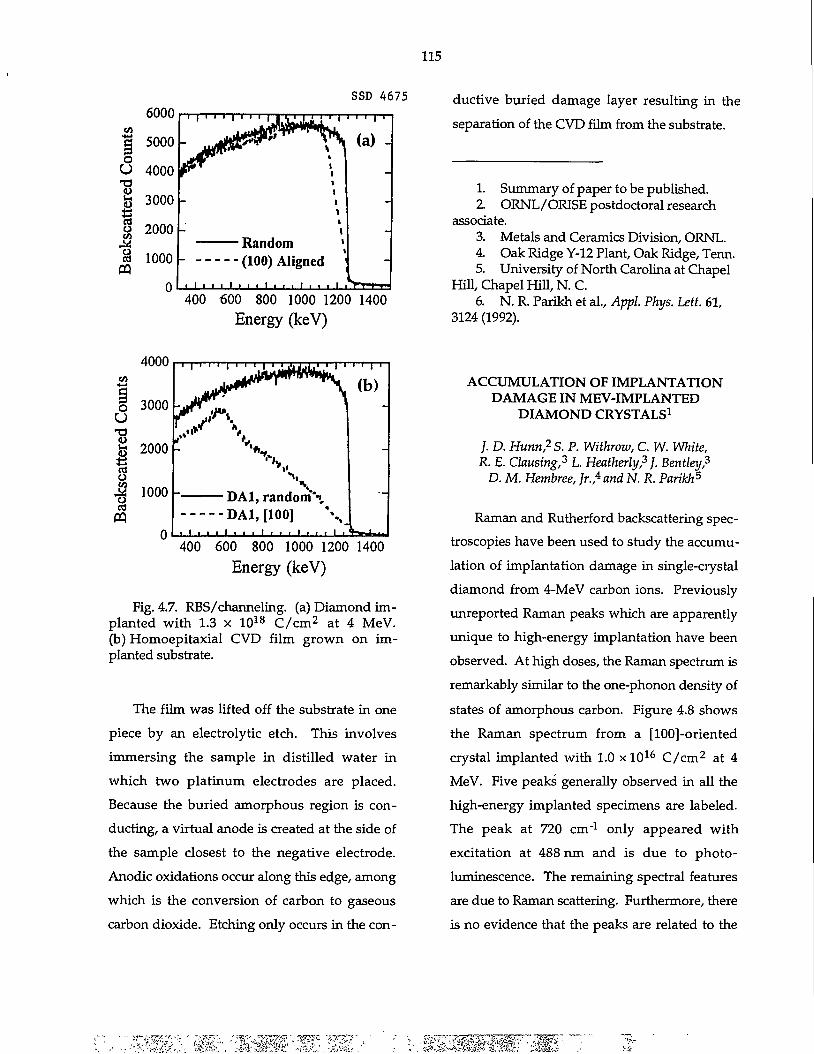
115
6000 § 5000 U 4000 13 <D i>
S 2000 % 1000
0
I ' ' ' I ' ' ' IJ 'l SSD 4675
i i i I i i i I i
Random (100) Aligned
(a) -
• i • • * i i i • i i i • I i T ' l 4 • ) •
400 600 800 1000 1200 1400 Energy (keV)
ductive buried damage layer resulting in the separation of the CVD film from the substrate.
1. Summary of paper to be published. 2 ORNL/ORISE postdoctoral research
associate. 3. Metals and Ceramics Division, ORNL. 4. Oak Ridge Y-12 Plant, Oak Ridge, Term. 5. University of North Carolina at Chapel
Hill, Chapel Hill, N.C. 6. N. R. Parikh et al., Appl. Phys. Lett. 61,
3124 (1992).
4000
§ 3000 U T3 § 2000
o Jg 1000 • DAI, random*•>,
DAI, [100] • ' • • • i • • • * • • • ' • • •
400 600 800 1000 1200 1400 Energy (keV)
Fig. 4.7. RBS/channeling. (a) Diamond implanted with 1.3 x 10 1 8 C /cm 2 at 4 MeV. (b) Homoepitaxial CVD film grown on implanted substrate.
The film was lifted off the substrate in one piece by an electrolytic etch. This involves immersing the sample in distilled water in which two platinum electrodes are placed. Because the buried amorphous region is conducting, a virtual anode is created at the side of the sample closest to the negative electrode. Anodic oxidations occur along this edge, among which is the conversion of carbon to gaseous carbon dioxide. Etching only occurs in the con-
ACCUMULATION OF IMPLANTATION DAMAGE IN MEV-IMPLANTED
DIAMOND CRYSTALS1
/. D. Hunn,2S. P. Withrow, C. W. White, R. E. Clausing,3 L. Heatherly,3}. Bentley3
D. M. Hembree, Jr.,4 and N. R. Parikh5
Raman and Rutherford backscattering spectroscopies have been used to study the accumulation of implantation damage in single-crystal diamond from 4-MeV carbon ions. Previously unreported Raman peaks which are apparently unique to high-energy implantation have been observed. At high doses, the Raman spectrum is remarkably similar to the one-phonon density of states of amorphous carbon. Figure 4.8 shows the Raman spectrum from a [100]-oriented crystal implanted with 1.0 x 10 1 6 C/cm 2 at 4 MeV. Five peaks generally observed in all the high-energy implanted specimens are labeled. The peak at 720 cm"1 only appeared with excitation at 488 nm and is due to photo-luminescence. The remaining spectral features are due to Raman scattering. Furthermore, there is no evidence that the peaks are related to the
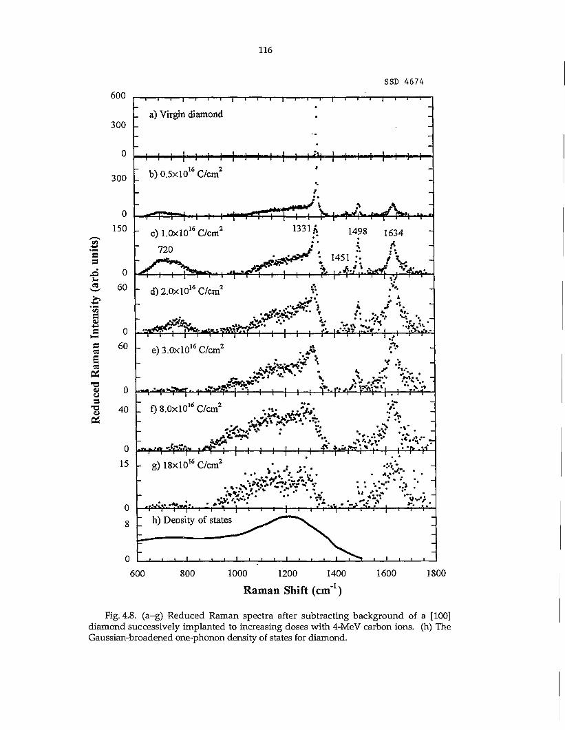
116
SSD 4674 600
300
-i—i—i—i—i—i—[—
_ a) Virgin diamond
n s .a
C
s £
u 3
300
0 150
0 60
T 1 1 1 1 1—i r -i 1 1 J 1 1 r-
1 1 1 I 1 I 1 I I I 1 1 l ' ' l 1 1 4—4-
b) 0 .5xl0 1 6 C/cm 2
1 3 3 1 A 1498 1634 • • • ^
^ — i — i T S » * v . i .fh.«<*T-i—i—.—> ft '••*••
c )1 .0x l0 1 6 C/cm 2
720
l p > * > . . | . ' ^ f ^ T i 1 i i ^ |
d) 2.0x10 1 6 C/cm 2
0 60
0
40
Jfl^^'-V. . f - V %V
/•.* - e )3 .0x l0 1 6 C/cm 2
.V
I f) 8 .0xl0 1 6 C/cm 2
i % :
0 Lh^- foSi fW f r f ^ 15
0
8
g) 18x l0 1 6 C/cm 2
-t-H—I—I—h i i f - t
0 I ' ' ' T i i I I i i i — J ' ' ' L I t I
600 800 1000 1200 1400
Raman Shift (cm"1) 1600 1800
Fig. 4.8. (a-g) Reduced Raman spectra after subtracting background of a [100] diamond successively implanted to increasing doses with 4-MeV carbon ions, (h) The Gaussian-broadened one-phonon density of states for diamond.
117
implant species; oxygen and argon yield the
same result. The peaks at 1451, 1498, and 1634
cm"1 have hitherto not been reported in the
literature. These peaks are only observed for
MeV-energy implants.
The 1332-cm"1 peak is the only allowed
mode in single-crystal diamond [Fig. 4.8(a)].
The decrease in intensity of this peak is directly
related to the ion implantation damage. As the
ion dose is increased, the 1332-cm"1 peak can be
seen to broaden and shift down in energy,
finally approaching the one-phonon density of
states. The reduced Raman spectrum of an
amorphous material is expected to replicate the
density of states. This Raman feature can,
therefore, be interpreted as coming from an
amorphous carbon network with fourfold coor
dinated (diamond-like) bonds. Furthermore, no
sp2 related Raman peaks are observed in the
implanted material.
1. Summary of paper to be published. 2. ORNL/ORISE postdoctoral research
associate. 3. Metals and Ceramics Division, ORNL. 4. Oak Ridge Y-12 Plant, Oak Ridge, Tenn. 5. University of North Carolina at Chapel
Hill, Chapel Hill, N. C.
DEVELOPMENT OF AN ELECTRON CYCLOTRON RESONANCE (ECR) PLASMA SOURCE FOR COPPER METALLIZATION1-2
L. A. Berry,3 S. M. GorbatMn, G. H. Henkel,3and R. L. Rhoades*
The semiconductor industry's drive toward
higher performance devices with shrinking
feature sizes requires continuing efforts to
develop new manufacturing tools and processes.
Copper has been identified as a potential
material for metallization because of its lower
resistivity compared with aluminum, and there
is a need for equipment capable of filling sub
0.25-micron features with aspect ratios in the 3-4
range.
This work, a Cooperative Research and
Development Agreement between ORNL and
IBM, is aimed at developing a metal ion plasma
source capable of Cu metallization which is
amenable to product ion implantation and
processing of 200-250-mm-diam wafers. A
permanent magnet is used for magnetic field
production and is significantly more compact
than ECR sources using electromagnetic coils,
with a sputter target used as a simple, reliable
source of neutrals.
Normally, to achieve arbitrarily high plasma
densit ies, high-field injection, where the
microwaves propagate parallel to the magnetic
field, is used. This requires a dielectric
microwave entrance window exposed to the
processing plasma, which is unacceptable for
metal deposition because the window becomes
quickly coated, and microwaves cannot pene
trate into the processing chamber. To get
around this problem, a coupler has been
designed which allows microwave injection ini
tially perpendicular to the magnetic field while
still maintaining the ability to avoid microwave
cutoff. The window position in the system is out
of the line of sight of the plasma and allows
operation with Cu. The source has been
successfully operated with Ar gas and Cu
targets, yielding sputter target current densities
above 30 mA/cm 2 .
118
Use of a sputter target, however, results in a
longer mean-free path for ionization compared
with the use of a thermal evaporation source
and reduces the ratio of metal ions /meta l
neutrals. Future efforts are aimed at increasing
the total ion fraction, understanding trench and
via filling in more detail, and developing
specific Cu metallization processes.
1. Summary of paper to be published. 2. Work funded by Defense Programs
Technology Commercialization Initiative. 3. Fusion Energy Division, ORNL. 4. ORNL/ORISE postdoctoral research
associate.
BORON NITRIDE THIN-FILM DEPOSITION USING ELECTRON CYCLOTRON
RESONANCE MICROWAVE PLASMAS 1
S. M. Gorbatkin, R. F. Burgie,2 W. C. Oliver,3
}. C. Barbour* T. M. Mayer* and M. L. Thomas4
Electron cyclotron resonance (ECR)
microwave plasma deposition has been used to
deposit B x Ni_ r thin films from borazine
(B3N3Hg)-based plasmas. Deposited films were
analyzed using infrared absorption, x-ray
diffraction, forward elastic recoil detection, and
enhanced cross-section backscattering spec
trometry, with precise quantitative measure
ments of low-mass elements (e.g., boron, nitro
gen, and hydrogen) of particular interest. All
three elements were detected using 24-MeV S i 4 5
for forward elastic recoil analysis at Sandia
National Laboratories, with backscattering
measurements used for additional determina
tions of B and N concentrations.
Mass spectrometry was used to identify ions
bombarding the surface during film growth, and
large concentrations of H + , H 2 + , and H 3 + were
observed. In addition, a large fraction of the B
and N incident on the growing film surface was
tied up in hydrogen-containing precursors,
which may be resputtered easily from the
growing film surface.
Film hardness and modulus measurements
were performed using an ultralow load
indenter. For films deposited with pure
borazine and NH3-borazine mixtures, both
hardness and modulus varied considerably from
1.4 to 10.5 GPa and 42 to 144 GPa, respectively,
and were highest for films deposited at low
substrate bias where the films were amorphous.
A wide range of stoichiometries were acces
sible, even with pure borazine as the source gas,
with the ratio of B / N ranging from 0.54 to 4.4.
The hydrogen atomic fraction varied from ~1 to
20 at. % and was typically 2-3 at. % for stoi
chiometric BN. No evidence of cubic phase
formation was observed, and attempts at
increasing the momentum transfer to the surface
using Rr resulted in resputtering of the film well
before the momentum transfer to the surface
was 200 (eV a m u ) 1 / 2 , a value identified in recent
ion beam deposition studies to be required for
cubic phase formation. 5 There were, however,
marked changes observed in infrared absorption
and x-ray diffraction as a function of incident
ion energy. Films deposited at lower ion
energies were amorphous, while those deposited
at higher ion energies, near the threshold for
complete resputtering of the growing film,
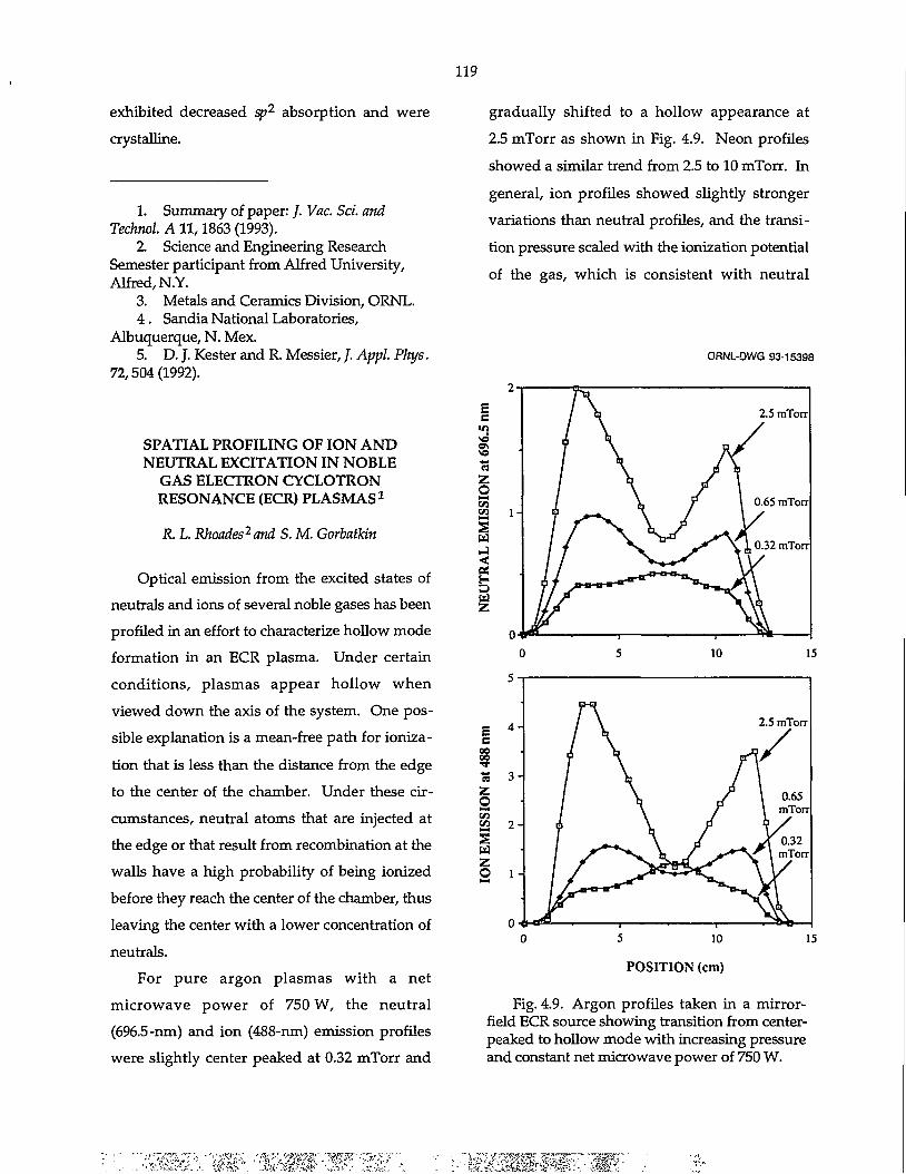
119
exhibited decreased sp2 absorption and were
crystalline.
1. Summary of paper: /. Vac. Sci. and Technol. A11,1863 (1993).
2. Science and Engineering Research Semester participant from Alfred University, Alfred, N.Y.
3. Metals and Ceramics Division, ORNL. 4 . Sandia National Laboratories,
Albuquerque, N. Mex. 5. D. J. Kester and R. Messier, /. Appl. Phys.
72,504 (1992).
SPATIAL PROFILING OF ION AND NEUTRAL EXCITATION IN NOBLE
GAS ELECTRON CYCLOTRON RESONANCE (ECR) PLASMAS1
R. L. Rhoades2and S. M. Gorbatkin
Optical emission from the excited states of neutrals and ions of several noble gases has been profiled in an effort to characterize hollow mode formation in an ECR plasma. Under certain conditions, plasmas appear hollow when viewed down the axis of the system. One possible explanation is a mean-free path for ionization that is less than the distance from the edge to the center of the chamber. Under these circumstances, neutral atoms that are injected at the edge or that result from recombination at the walls have a high probability of being ionized before they reach the center of the chamber, thus leaving the center with a lower concentration of neutrals.
For pure argon plasmas with a net microwave power of 750 W, the neutral (696.5-nm) and ion (488-nm) emission profiles were slightly center peaked at 0.32 mTorr and
gradually shifted to a hollow appearance at
2.5 mTorr as shown in Fig. 4.9. Neon profiles
showed a similar trend from 2.5 to 10 mTorr. In
general, ion profiles showed slightly stronger
variations than neutral profiles, and the transi
tion pressure scaled with the ionization potential
of the gas, which is consistent with neutral
ORNL-DWG 93-15398
E e «n \o o\ ve ts Z o CO CO
s w < OS H 3 U
z
E c oe 9 a Z o V)
a z o
2.5 mTorr
0.65 mTorr
0.32 mTorr
10 15
5 10
POSITION (cm)
Fig. 4.9. Argon profiles taken in a mirror-field ECR source showing transition from center-peaked to hollow mode with increasing pressure and constant net microwave power of 750 W.
15
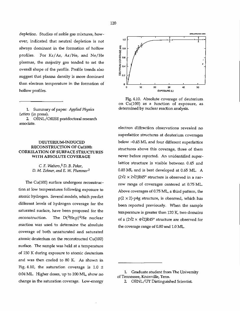
120
depletion. Studies of noble gas mixtures, how
ever, indicated that neutral depletion is not
always dominant in the formation of hollow
profiles. For Kr /Ar , A r / N e , and N e / H e
plasmas, the majority gas tended to set the
overall shape of the profile. Profile trends also
suggest that plasma density is more dominant
than electron temperature in the formation of
hollow profiles.
ORNL-DWO I1U 16MS
1. Summary of paper: Applied Physics Letters (in press).
2 ORNL/ORISE postdoctoral research associate.
DEUTERIUM-INDUCED RECONSTRUCTION OF Cu(100):
CORRELATION OF SURFACE STRUCTURES WITH ABSOLUTE COVERAGE
C. F. Walters} D. B. Poker, D. M. Zehner, and E. W. Plummer2
The Cu(100) surface undergoes reconstruc
tion at low temperatures following exposure to
atomic hydrogen. Several models, which predict
different levels of hydrogen coverage for the
saturated surface, have been proposed for the
reconstruction. The D( 3 He,p) 4 He nuclear
reaction was used to determine the absolute
coverage of both unsaturated and saturated
atomic deuterium on the reconstructed Cu(100)
surface. The sample was held at a temperature
of 150 K during exposure to atomic deuterium
and was then cooled to 80 K. As shown in
Fig. 4.10, the saturation coverage is 1.0 ±
0.04 ML. Higher doses, up to 200 ML, show no
change in the saturation coverage. Low-energy
20 30 EXPOSURE (L)
Fig. 4.10. Absolute coverage of deuterium on Cu(100) as a function of exposure, as determined by nuclear reaction analysis.
electron diffraction observations revealed no
superlattice structures at deuterium coverages
below -0.45 ML and four different superlattice
structures above this coverage, three of them
never before reported. An unidentified super-
lattice structure is visible between 0.45 and
0.85 ML and is best developed at 0.65 ML. A
(2V2 x 2V2)R45° structure is observed in a nar
row range of coverages centered at 0.75 ML.
Above coverages of 0.75 ML, a third pattern, the
p(2 x 2)-p4g structure, is observed, which has
been reported previously. When the sample
temperature is greater than 120 K, two domains
of a (2V2 x 4V2)R45° structure are observed for
the coverage range of 0.80 and 1.0 ML.
1. Graduate student from The University of Tennessee, Knoxville, Term.
2. ORNL/UT Distinguished Scientist.
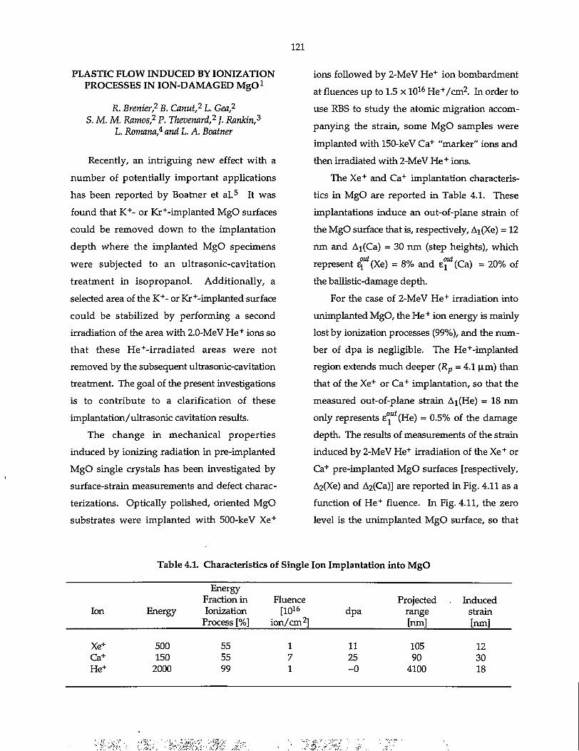
121
PLASTIC FLOW INDUCED BY IONIZATION PROCESSES IN ION-DAMAGED MgO 1
R. Brenier,2 B. Canut,2 L. Gea,2
S. M. M. Ramos,2 P. Thevenard,2]. Rankin,3
L. Romana,* and L. A. Boatner
Recently, an intriguing new effect with a number of potentially important applications has been reported by Boatner et al. 5 It was found that K + - or Kr+-implanted MgO surfaces could be removed down to the implantation depth where the implanted MgO specimens were subjected to an ultrasonic-cavitation treatment in isopropanol. Additionally, a selected area of the K + - or Kr+-implanted surface could be stabilized by performing a second irradiation of the area with 2.0-MeV He + ions so that these He +-irradiated areas were not removed by the subsequent ultrasonic-cavitation treatment. The goal of the present investigations is to contribute to a clarification of these implantation/ultrasonic cavitation results.
The change in mechanical properties induced by ionizing radiation in pre-implanted MgO single crystals has been investigated by surface-strain measurements and defect characterizations. Optically polished, oriented MgO substrates were implanted with 500-keV Xe +
ions followed by 2-MeV He + ion bombardment at fluences up to 1.5 x 10 1 6 He + /cm 2 . In order to use RBS to study the atomic migration accompanying the strain, some MgO samples were implanted with 150-keV Ca + "marker" ions and then irradiated with 2-MeV H e + ions.
The Xe + and Ca + implantation characteristics in MgO are reported in Table 4.1. These implantations induce an out-of-plane strain of the MgO surface that is, respectively, Ai(Xe) = 12 nm and Ai(Ca) = 30 nm (step heights), which represent <f(Xe) = 8% and e f (Ca) = 20% of the ballistic-damage depth.
For the case of 2-MeV H e + irradiation into unimplanted MgO, the H e + ion energy is mainly lost by ionization processes (99%), and the number of dpa is negligible. The He+-implanted region extends much deeper (Rp = 4.1 |im) than that of the Xe+ or Ca + implantation, so that the measured out-of-plane strain Ai(He) = 18 nm only represents e°" (He) = 0.5% of the damage depth. The results of measurements of the strain induced by 2-MeV He + irradiation of the Xe + or Ca+ pre-implanted MgO surfaces [respectively, A2(Xe) and A2(Ca)] are reported in Fig. 4.11 as a function of H e + fluence. In Fig. 4.11, the zero level is the unimplanted MgO surface, so that
Table 4.1. Characteristics of Single Ion Implantation into MgO
Ion Energy
Energy Fraction in Ionization
Process [%]
Fluence [1016
ion/cm 2] dpa
Projected Induced range strain [nm] [nm]
Xe+ 500 55 1 11 105 12 Ca + 150 55 7 25 90 30 He + 2000 99 1 ~0 4100 18
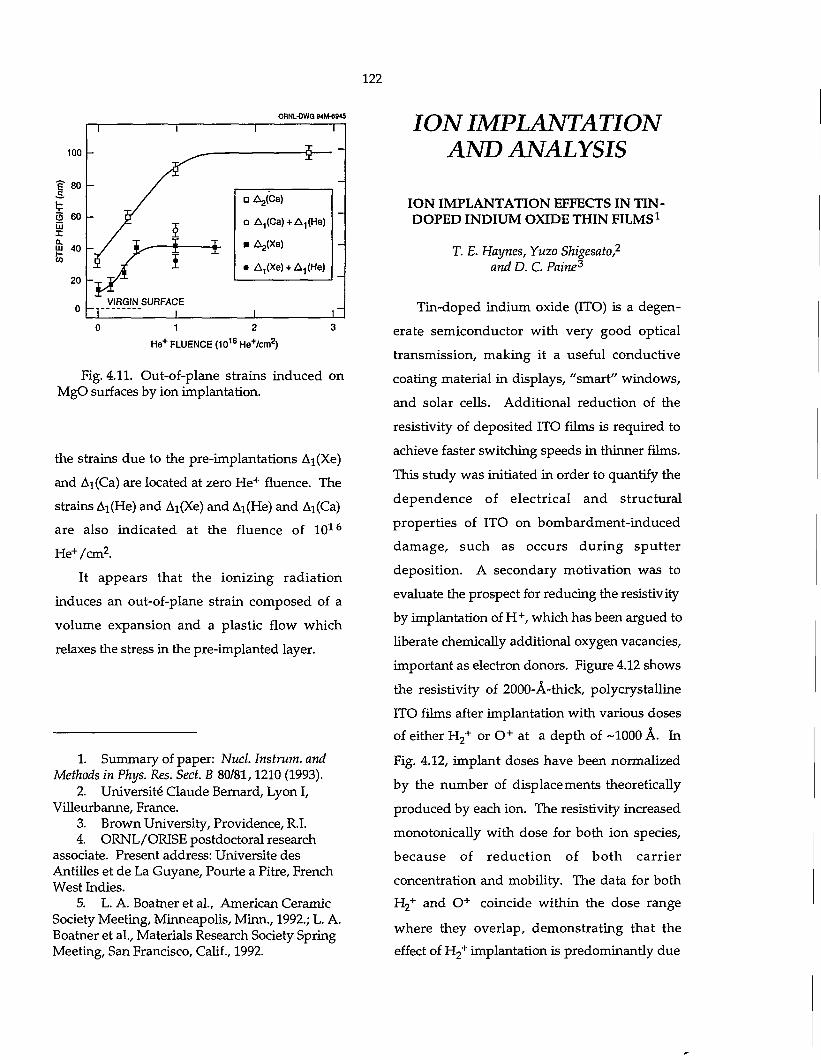
122
ORNL-DWG 94M-6MS
100
a 60
• A^Ca)
o A,(Ca) ^ hA^He)
• AjfXe)
• A,(Xe) H -A^He)
o --, VIRGIN SURFACE
0 1 2 3
He + FLUENCE (10 1 6 He+/cm2)
Fig. 4.11. Out-of-plane strains induced on MgO surfaces by ion implantation.
the strains due to the pre-implantations Ai(Xe) and Ai(Ca) are located at zero He + fluence. The strains Ai(He) and Ai(Xe) and Ai(He) and Ai(Ca) are also indicated at the fluence of 1 0 1 6
He +/cm 2 . It appears that the ionizing radiation
induces an out-of-plane strain composed of a volume expansion and a plastic flow which relaxes the stress in the pre-implanted layer.
1. Summary of paper: Nucl. Instrum. and Methods in Phys. Res. Sect. B 80/81,1210 (1993).
2. Universite Claude Bernard, Lyon I, Villeurbanne, France.
3. Brown University, Providence, R.I. 4. ORNL/ORISE postdoctoral research
associate. Present address: Universite des Antilles et de La Guyane, Pourte a Pitre, French West Indies.
5. L. A. Boatner et al., American Ceramic Society Meeting, Minneapolis, Minn., 1992.; L. A. Boatner et al., Materials Research Society Spring Meeting, San Francisco, Calif., 1992.
ION IMPLANTATION AND ANALYSIS
ION IMPLANTATION EFFECTS IN TIN-DOPED INDIUM OXIDE THIN FILMS1
T. E. Haynes, Yuzo Shigesato,2
and D. C. Paine3
Tin-doped indium oxide (ITO) is a degenerate semiconductor with very good optical transmission, making it a useful conductive coating material in displays, "smart" windows, and solar cells. Additional reduction of the resistivity of deposited ITO films is required to achieve faster switching speeds in thinner films. This study was initiated in order to quantify the dependence of electrical and structural properties of ITO on bombardment-induced damage, such as occurs during sputter deposition. A secondary motivation was to evaluate the prospect for reducing the resistivity by implantation of H + , which has been argued to liberate chemically additional oxygen vacancies, important as electron donors. Figure 4.12 shows the resistivity of 2000-A-thick, polycrystalline ITO films after implantation with various doses of either H2+ or 0 + at a depth of -1000 A. In Fig. 4.12, implant doses have been normalized by the number of displacements theoretically produced by each ion. The resistivity increased monotonically with dose for both ion species, because of reduction of both carrier concentration and mobility. The data for both H 2
+ and 0 + coincide within the dose range where they overlap, demonstrating that the effect of H 2
+ implantation is predominantly due
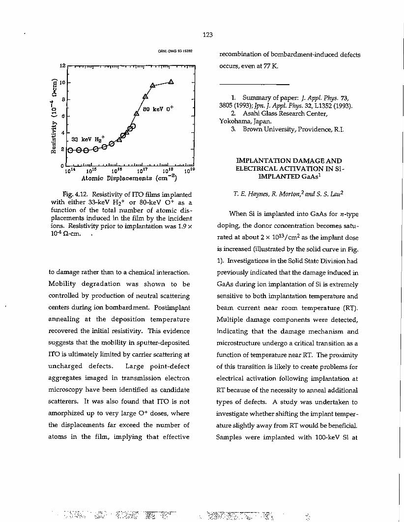
123
0RN1.-DWG 93 15392
12
10
I o
0) U p
« 2
— i i i | i u i | — i — n iiiui i 11 inn) i 11 | in i | i
-JQQ keV 0 +
-
. 33 keV H 2
+
-U - U f c / ^ - '
-
,14 i l iml
,15 ,18 ' ,1V
I I Mill • • . I . . . . 1 •>18 ,19
Atomic Displacements (cm )
Fig. 4.12. Resistivity of ITO films implanted with either 33-keV H 2
+ or 80-keV 0 + as a function of the total number of atomic displacements induced in the film by the incident ions. Resistivity prior to implantation was 1.9 x 10"4 ft-cm. .
to damage rather than to a chemical interaction. Mobility degradation was shown to be controlled by production of neutral scattering centers during ion bombardment. Postimplant annealing at the deposition temperature recovered the initial resistivity. This evidence suggests that the mobility in sputter-deposited YTO is ultimately limited by carrier scattering at uncharged defects. Large point-defect aggregates imaged in transmission electron microscopy have been identified as candidate scatterers. It was also found that ITO is not amorphized up to very large 0 + doses, where the displacements far exceed the number of atoms in the film, implying that effective
recombination of bombardment-induced defects occurs, even at 77 K.
1. Summary of paper: /. Appl. Phys. 73, 3805 (1993); Jpn.}. Appl. Phys. 32, L1352 (1993).
2. Asahi Glass Research Center, Yokohama, Japan.
3. Brown University, Providence, R.I.
IMPLANTATION DAMAGE AND ELECTRICAL ACTIVATION IN Si-
IMPLANTED GaAs1
T. E. Haynes, R. Morton,2 and S. S. Lau2
When Si is implanted into GaAs for n-type doping, the donor concentration becomes saturated at about 2 x 10 1 3 /cm 2 as the implant dose is increased (illustrated by the solid curve in Fig. 1). Investigations in the Solid State Division had previously indicated that the damage induced in GaAs during ion implantation of Si is extremely sensitive to both implantation temperature and beam current near room temperature (RT). Multiple damage components were detected, indicating that the damage mechanism and microstructure undergo a critical transition as a function of temperature near RT. The proximity of this transition is likely to create problems for electrical activation following implantation at RT because of the necessity to anneal additional types of defects. A study was undertaken to investigate whether shifting the implant temperature slightly away from RT would be beneficial. Samples were implanted with 100-keV Si at
m '':mr^^ M-
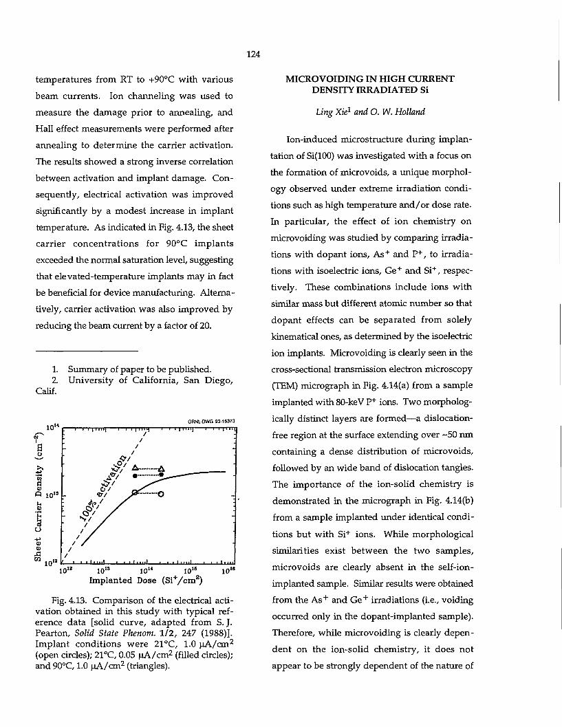
124
temperatures from RT to +90°C with various
beam currents. Ion channeling was used to
measure the damage prior to annealing, and
Hall effect measurements were performed after
annealing to determine the carrier activation.
The results showed a strong inverse correlation
between activation and implant damage. Con
sequently, electrical activation was improved
significantly by a modest increase in implant
temperature. As indicated in Fig. 4.13, the sheet
carrier concentrat ions for 90°C implants
exceeded the normal saturation level, suggesting
that elevated-temperature implants may in fact
be beneficial for device manufacturing. Alterna
tively, carrier activation was also improved by
reducing the beam current by a factor of 20.
1. Summary of paper to be published. 2 University of California, San Diego,
Calif.
10 1 ORNL-DWG 93-15373
s O
m a V
a to"
o
i ' i l " ' i | — i i i 1 1 i » H I p i l l ] 1 1 1 \ l l l l
. / -• / * - / / -
&' * &/ A — -A '
&/ •
— <ov %*>•• o — '• A0/ / ; - N/ / ' / / " • / / / / •
/ / -/
/ 1
101' 10" 101' 10" 10" Implanted Dose (S i + / cm 8 )
Fig. 4.13. Comparison of the electrical activation obtained in this study with typical reference data [solid curve, adapted from S. J. Pearton, Solid State Phenom. Ill, 247 (1988)]. Implant conditions were 21°C, 1.0 u A / c m 2
(open circles); 21 °C, 0.05 u A / c m 2 (filled circles); and 90°C, 1.0 uA/cm 2 (triangles).
MICROVOIDING IN HIGH CURRENT DENSITY IRRADIATED Si
Ling Xie1 and O. W. Holland
Ion-induced microstructure during implan
tation of Si(100) was investigated with a focus on
the formation of microvoids, a unique morphol
ogy observed under extreme irradiation condi
tions such as high temperature and /o r dose rate.
In particular, the effect of ion chemistry on
microvoiding was studied by comparing irradia
tions with dopant ions, A s + and P + , to irradia
tions with isoelectric ions, G e + and S i + , respec
tively. These combinations include ions with
similar mass but different atomic number so that
dopant effects can be separated from solely
kinematical ones, as determined by the isoelectric
ion implants. Microvoiding is clearly seen in the
cross-sectional transmission electron microscopy
(TEM) micrograph in Fig. 4.14(a) from a sample
implanted with 80-keV P + ions. Two morpholog
ically distinct layers are formed—a dislocation-
free region at the surface extending over ~50 nm
containing a dense distribution of microvoids,
followed by an wide band of dislocation tangles.
The importance of the ion-solid chemistry is
demonstrated in the micrograph in Fig. 4.14(b)
from a sample implanted under identical condi
tions but with S i + ions. While morphological
similarities exist between the two samples,
microvoids are clearly absent in the self-ion-
implanted sample. Similar results were obtained
from the A s + and G e + irradiations (i.e., voiding
occurred only in the dopant-implanted sample).
Therefore, while microvoiding is clearly depen
dent on the ion-solid chemistry, it does not
appear to be strongly dependent of the nature of
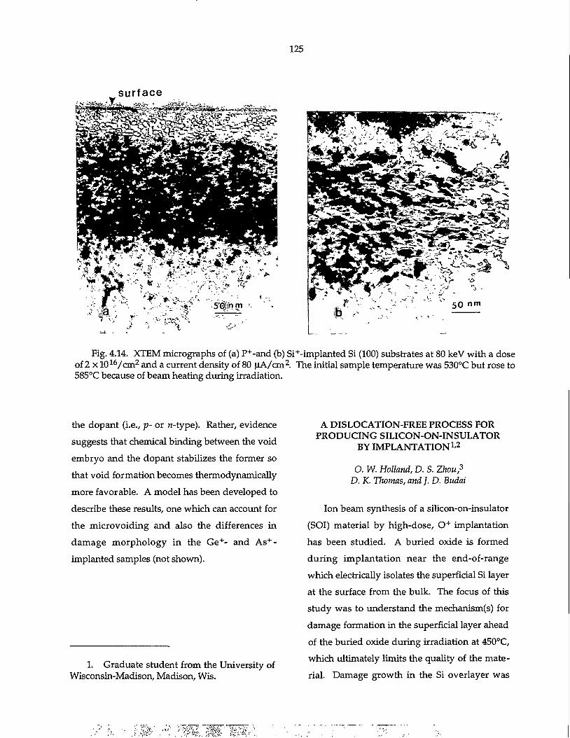
125
surface
the dopant (i.e., p- or n-type). Rather, evidence suggests that chemical binding between the void embryo and the dopant stabilizes the former so that void formation becomes thermodynamically more favorable. A model has been developed to describe these results, one which can account for the microvoiding and also the differences in damage morphology in the Ge + - and A s + -implanted samples (not shown).
1. Graduate student from the University of Wisconsin-Madison, Madison, Wis.
A DISLOCATION-FREE PROCESS FOR PRODUCING SILICON-ON-INSULATOR
BY IMPLANTATION W
O. W. Holland, D. S. Zhou,3
D. K. Thomas,and}. D. Budai
Ion beam synthesis of a silicon-on-insulator (SOI) material by high-dose, 0 + implantation has been studied. A buried oxide is formed during implantation near the end-of-range which electrically isolates the superficial Si layer at the surface from the bulk. The focus of this study was to understand the mechanism(s) for damage formation in the superficial layer ahead of the buried oxide during irradiation at 450°C, which ultimately limits the quality of the material. Damage growth in the Si overlayer was
Fig. 4.14. XTEM micrographs of (a) P+-and (b) Si+-implanted Si (100) substrates at 80 keV with a dose of 2 x 10 1 6 /cm 2 and a current density of 80 uA/cm 2. The initial sample temperature was 530°C but rose to 585°C because of beam heating during irradiation.

126
found to exhibit two distinctly different
regimes—an initial one characterized by slow
growth of vacancy-type clusters, followed by a
transition to a faster growth regime marked by
the onset of dislocation formation. This transi
tion in the growth behavior was correlated with
marked changes in the strain state in the super
ficial layer, as well as the damage morphology.
These results established a causal relation
between lattice strain and damage in which dis
locations are formed when the buildup of nega
tive strain arising from the vacancy-type defects
in the superficial layer exceeds the yield point of
the lattice. This suggested that it might be pos
sible to intervene prior to the yield point to
suppress dislocation formation by elimination or
reduction of the lattice strain. This was, in fact,
accomplished by a very simple but elegant
method using Si + , self-ion implantation. Prior to
the yield point, 0 + implantation was interrupted
so that Si + ions could be implanted into the
strained layer. The self-ion implantat ion
reduced the lattice strain presumably by provid
ing excess Si atoms to occupy the vacant lattice
sites. The strain relief provided by this tech
nique delayed the onset of dislocation formation
during subsequent 0 + implantation to a much
higher fluence than observed in samples irradi
ated only with 0 + ions. Therefore, knowledge of
the damage formation mechanism has led to the
development of a processing technique to yield
a higher quality SOI material by suppressing
dislocation formation during high-dose 0 +
implantation.
1. Summary of paper: Appl. Phys. Lett. 63, 896 (1993).
2. D. S. Zhou, O. W. Holland, and J. D. Budai, Applied Physics Letters ( in press).
3. ORNL/ORISE postdoctoral research associate.
ION BEAM SYNTHESIS OF IrSi 3 IN Si (111)
T. P. Sjoreen, H.-J. Hinneberg,1 andM. F. Chisholm
Epitaxial metal silicides are of interest both
for studies of the basic electronic properties of
metal-semiconductor interfaces and for device
applications. Of the metallic silicides, IrSi3 has
the highest measured Schottky barrier to n-type
Si (0.94 eV) and, hence, the lowest to p-type,
making it a possible material for use in long-
wavelength infrared detectors. Because it is the
stable phase of the iridium silicides and the most
Si rich, it can be grown as a buried epitaxial
layer in Si( l l l ) by ion beam synthesis (i.e., high-
dose Ir ion implantation followed by thermal
annealing). Figure 4.15 shows a cross-sectional
transmission electron microscope (TEM) image
of a 90-nm thick IrSi3 layer under 200 nm of Si
that was produced by implanting 1-MeV Ir ions
Fig. 4.15. XTEM image of an epitaxial, buried IrSi3 layer in Si ( l l l ) , produced by implanting 1.6 x l O 1 7 Ir / c m 2 at 1 MeV and 550°C and subsequent annealing at 1100°C for 5 h.
127
with a dose of 1.6 x 1 0 1 7 I r / c m 2 at a substrate
temperature of 550°C and annealing for 5 h at
1100°C. Transmission electron diffraction
results show that the epitaxial relationship of the
suicide layer with the substrate is [2110] IrSi3 I I
[ l l l]Si and [0110] IrSi 3 11 [220]Si. In contrast to
this single-epitaxial relationship, IrSi3 films
grown by interfacial reactions or by molecular
beam epitaxy have two or three. Presently,
experiments are in progress to find the ion
implantation parameters which produce the best
Si/IrSi3/Si s t ructure. Recent Rutherford
backscattering results seem to indicate that
channeled ion implantation produces a superior
structure, but additional characterization is
needed.
1. Guest scientist from Technische Universitat Chemnitz-Zwickau, Chemnitz, Germany.
ION BEAM SYNTHESIS OF Ti-RICH EPITAXIAL BURIED LAYERS IN L i N b 0 3
D. B. Poker and D. S. Zhou1
Implantation of Ti into LiNb03 has been
shown to be an effective technique for the fabri
cation of optical waveguides. The technique
offers advantages in the control of the Ti con
centration profile as well as the maximum
attainable concentration. However, the need to
perform solid-phase epitaxy and thermal anneal
ing following implantation can result in signifi
cant migration of the implanted Ti. The stability
of the implanted Ti (2.5 x 1 0 1 7 / c m 2 , 500°C) fol
lowing high-temperature annealing (1000°C,
1-4 h) can be improved dramatically by an addi
tional implant of oxygen before annealing, as
measured by Rutherford backscat ter ing
(RBS)/channeling spectroscopy and secondary
ion mass spectroscopy (SIMS). The improve
ment exhibits a threshold dependence upon the
O/Ti ratio. Little effect is seen at ratios of 1.5
and below, while higher ratios produce signifi
cant improvements. At an O/Ti ratio of 3, the
annealed samples showed evidence of the for
mation of a distinct buried layer, rich in Ti,
which was epitaxially oriented with the LiNb03
substrate, as indicated by RBS analysis. SIMS
analysis indicated that the concentration profile
of the Ti narrowed significantly, and the concen
tration gradients on both sides of the peak
became very sharp, as shown in Fig. 4.16(a).
Without the extra oxygen implantation, the Ti
migrates to the surface during solid-phase epi
taxy and gradually diffuses deeper during
annealing [Fig. 4.16(b)]. Cross sectional trans
mission electron microscopy indicated that the
buried layer is distinct, with sharp interfaces,
epitaxial with the LiNb03 matrix. Furthermore,
the buried layer was shown to be continuous,
which validated the RBS channeling analysis.
1. ORNL/ORISE postdoctoral research associate. Present address: Los Alamos National Laboratory, Los Alamos, N. Mex.
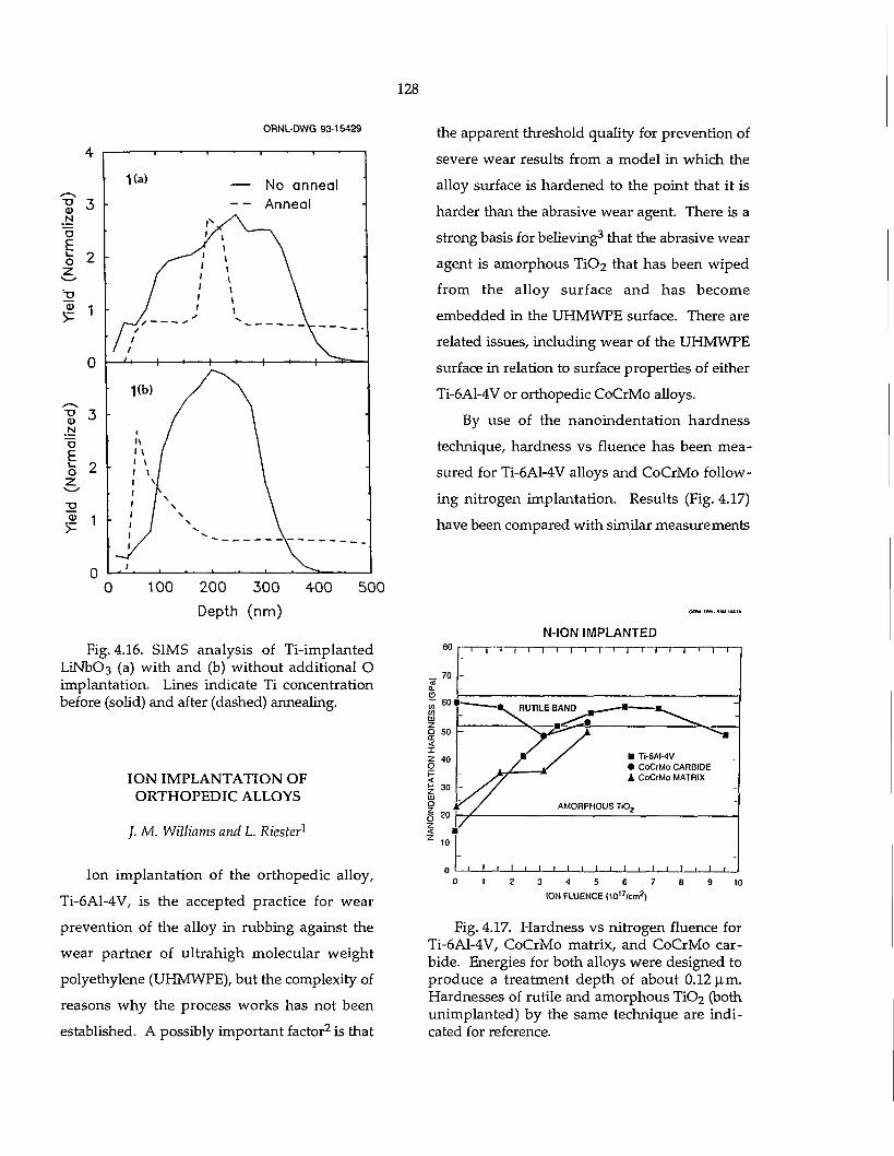
128
ORNX-DWG 93-15429
0 100 200 300 400 500 Depth (nm)
Fig. 4.16. SIMS analysis of Ti-implanted LiNbC>3 (a) with and (b) without additional O implantation. Lines indicate Ti concentration before (solid) and after (dashed) annealing.
ION IMPLANTATION OF ORTHOPEDIC ALLOYS
/. M. Williams and L. Riester1
Ion implantation of the orthopedic alloy,
Ti-6A1-4V, is the accepted practice for wear
prevention of the alloy in rubbing against the
wear partner of ultrahigh molecular weight
polyethylene (UHMWPE), but the complexity of
reasons why the process works has not been
established. A possibly important factor 2 is that
the apparent threshold quality for prevention of
severe wear results from a model in which the
alloy surface is hardened to the point that it is
harder than the abrasive wear agent. There is a
strong basis for believing 3 that the abrasive wear
agent is amorphous Ti02 that has been wiped
from the alloy surface and has become
embedded in the UHMWPE surface. There are
related issues, including wear of the UHMWPE
surface in relation to surface properties of either
Ti-6A1-4V or orthopedic CoCrMo alloys.
By use of the nanoindentation hardness
technique, hardness vs fluence has been mea
sured for Ti-6A1-4V alloys and CoCrMo follow
ing nitrogen implantation. Results (Fig. 4.17)
have been compared with similar measurements
on»* owi,t>u ii
N-ION IMPLANTED
• Ti-6AI-4V • CoCiMo CARBIDE A CoCrMo MATRIX
AMORPHOUS T i0 2
0 I I I I I I i I i I i I i I i 0 1 2 3 4 5 6 7 8 9 10
ION FLUENCE (10 , 7 /cm 2)
Fig. 4.17. Hardness vs nitrogen fluence for Ti-6A1-4V, CoCrMo matrix, and CoCrMo carbide. Energies for both alloys were designed to produce a treatment depth of about 0.12 (im. Hardnesses of rutile and amorphous Ti02 (both unimplanted) by the same technique are indicated for reference.
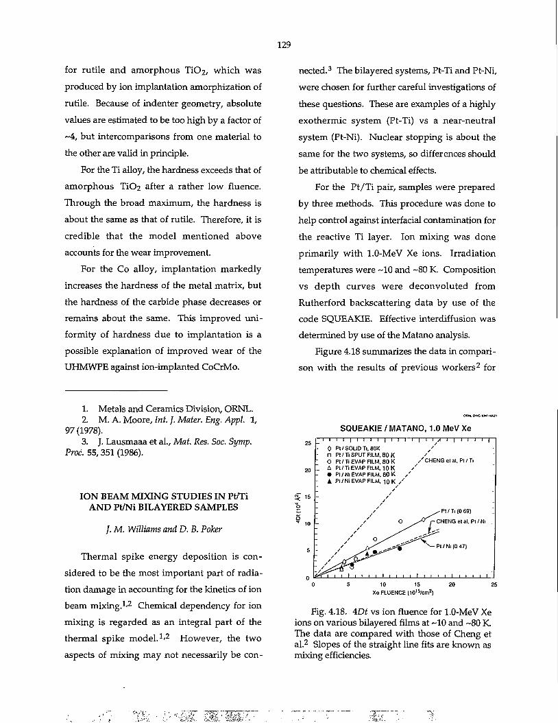
129
for rutile and amorphous TiC>2, which was produced by ion implantation amorphization of rutile. Because of indenter geometry, absolute values are estimated to be too high by a factor of ~4, but intercomparisons from one material to the other are valid in principle.
For the Ti alloy, the hardness exceeds that of amorphous Ti02 after a rather low fluence. Through the broad maximum, the hardness is about the same as that of rutile. Therefore, it is credible that the model mentioned above accounts for the wear improvement.
For the Co alloy, implantation markedly increases the hardness of the metal matrix, but the hardness of the carbide phase decreases or remains about the same. This improved uniformity of hardness due to implantation is a possible explanation of improved wear of the UHMWPE against ion-implanted CoCrMo.
nected.3 The bilayered systems, Pt-Ti and Pt-Ni, were chosen for further careful investigations of these questions. These are examples of a highly exothermic system (Pt-Ti) vs a near-neutral system (Pt-Ni). Nuclear stopping is about the same for the two systems, so differences should be attributable to chemical effects.
For the Pt/Ti pair, samples were prepared by three methods. This procedure was done to help control against interracial contamination for the reactive Ti layer. Ion mixing was done primarily with 1.0-MeV Xe ions. Irradiation temperatures were ~10 and ~80 K. Composition vs depth curves were deconvoluted from Rutherford backscattering data by use of the code SQUEAKIE. Effective interdiffusion was determined by use of the Matano analysis.
Figure 4.18 summarizes the data in comparison with the results of previous workers 2 for
1. Metals and Ceramics Division, ORNL. 2. M. A. Moore, Int. J. Mater. Eng. Appl. 1,
97 (1978). 3. J. Lausmaaa et al., Mat. Res. Soc. Symp.
Prod. 55,351 (1986).
ION BEAM MIXING STUDIES IN Pt/Ti AND Pt/Ni BILAYERED SAMPLES
/. M. Williams and D. B. Poker
Thermal spike energy deposition is considered to be the most important part of radiation damage in accounting for the kinetics of ion beam mixing.1'2 Chemical dependency for ion mixing is regarded as an integral part of the thermal spike model. 1 ' 2 However, the two aspects of mixing may not necessarily be con-
OflM OWC *]U IMN
SQUEAKIE / MATANO, 1.0 MeV Xe
25 I,
I I I | I I I I | I I I l | 1 1 A 1 | 1 1 1 t 1
0 Pt / SOLID Tl.BOK / '
- r> Pt/TiSPUTFILM.80K ' O PI/TiEVAPFILM.80K / CHENG etal. PI/Ti
20 - A Pl/Ti EVAP FILM. 10 K / • PI/Nl EVAP FILM. 80 K / A PI /Ni EVAP FILM. 10 K / /
15 1 • / / / /
- / ^ P t / T l ( 0 6 9 ) I
10 / O ^ > r CHENG el al. PI / Ni
5
n
/ frS"^ ^f^"^ ^^Pl /N l (0 47)
^ 1 1 1 1 1 1 1 1 1 1 1 1 1 1 1 1 1 1 1 1 1 1 1 1 1
10 15 Xe FLUENCE (10 , 5/cm 2)
25
Fig. 4.18. 4Df vs ion fluence for 1.0-MeV Xe ions on various bilayered films at -10 and -80 K. The data are compared with those of Cheng et al. 2 Slopes of the straight line fits are known as mixing efficiencies.
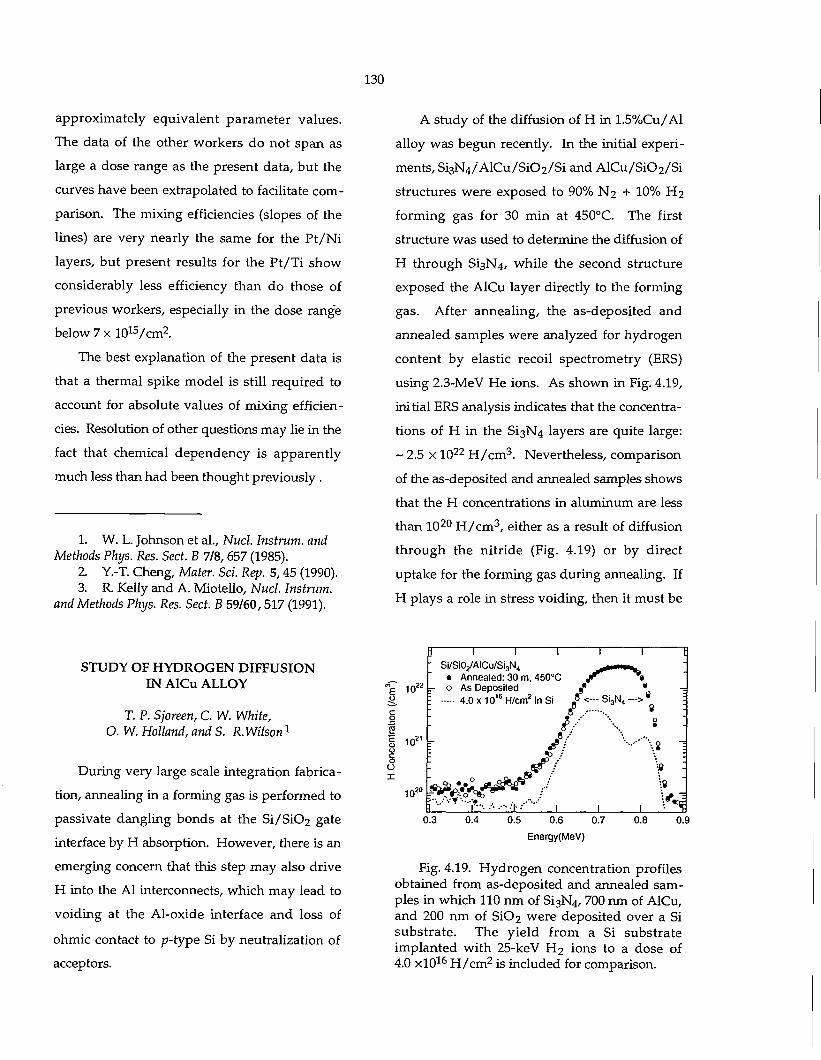
130
approximately equivalent parameter values.
The data of the other workers do not span as
large a dose range as the present data, but the
curves have been extrapolated to facilitate com
parison. The mixing efficiencies (slopes of the
lines) are very nearly the same for the P t /N i
layers, but present results for the P t /T i show
considerably less efficiency than do those of
previous workers, especially in the dose range
below 7 x 10 1 5 / cm 2 .
The best explanation of the present data is
that a thermal spike model is still required to
account for absolute values of mixing efficien
cies. Resolution of other questions may lie in the
fact that chemical dependency is apparently
much less than had been thought previously .
1. W. L. Johnson et al., Nucl. Instrum. and Methods Phys. Res. Sect. B 7/8,657 (1985).
2 Y.-T. Cheng, Mater. Sci. Rep. 5,45 (1990). 3. R. Kelly and A. Miotello, Nucl. Instrum.
and Methods Phys. Res. Sect. B 59/60,517 (1991).
STUDY OF HYDROGEN DIFFUSION IN AlCu ALLOY
T. P. Sjoreen, C. W. White, O. W. Holland, and S. RMlson1
During very large scale integration fabrica
tion, annealing in a forming gas is performed to
passivate dangling bonds at the Si/Si02 gate
interface by H absorption. However, there is an
emerging concern that this step may also drive
H into the Al interconnects, which may lead to
voiding at the Al-oxide interface and loss of
ohmic contact to p-type Si by neutralization of
acceptors.
A study of the diffusion of H in 1.5%Cu/Al
alloy was begun recently. In the initial experi
ments, S i 3 N 4 /AlCu/S i02 /S i and AlCu /S i0 2 /S i
structures were exposed to 90% N2 + 10% H2
forming gas for 30 min at 450°C. The first
structure was used to determine the diffusion of
H through Si3N4, while the second structure
exposed the AlCu layer directly to the forming
gas. After annealing, the as-deposited and
annealed samples were analyzed for hydrogen
content by elastic recoil spectrometry (ERS)
using 2.3-MeV He ions. As shown in Fig. 4.19,
initial ERS analysis indicates that the concentra
tions of H in the Si3N4 layers are quite large:
~ 2.5 x 1 0 2 2 H / c m 3 . Nevertheless, comparison
of the as-deposited and annealed samples shows
that the H concentrations in aluminum are less
than 1 0 2 0 H / c m 3 , either as a result of diffusion
through the nitride (Fig. 4.19) or by direct
uptake for the forming gas during annealing. If
H plays a role in stress voiding, then it must be
j 1 1 1 1 1 t ' Si/SKyAICu/Si3N,, - ^ s * * ^ .
• Annealed: 30 m, 450°C jf i - 0 As Deposited 8 * • z- 4.0 x 10'6 H/cm2 in Si , 8 <--1 88 , -
- Si3N, --> 9 : 8 :
i/ O • / / '
: «b : • y 7 '••? y 7
rv*«--^,./,:••- , 0.3 0.4 0.5 0.6 0.7 0.8 0.9
Energy(MeV)
Fig. 4.19. Hydrogen concentration profiles obtained from as-deposited and annealed samples in which 110 nm of Si3N4, 700 ran of AlCu, and 200 nm of Si02 were deposited over a Si substrate. The yield from a Si substrate implanted with 25-keV H2 ions to a dose of 4.0 x lO 1 6 H / c m 2 is included for comparison.
131
at concentrations of less than 10 2 0 H/cm 3 , which seems unlikely. However, these initial measurements have a background limitation of about 0.5 x 10 1 8 H / c m 3 per mC of ion beam charge (0.4-0.5 MeV in Fig. 4.19), which is believed to arise from H atoms knocked out of the mylar absorber. Studies are presently under way with different absorbing films in an attempt to lower the background.
1. Motorola, Inc., Mesa, Ariz.
PROTECTIVE OXIDE FORMATION ON NbAl3 AND TiAl ALLOYS
VIA ION IMPLANTATION
S. P. Withrow, R. J. Hanrahan, Jr.,1
E. D. Verink, Jr.,1 and E. Ristolainen1
High-temperature oxidation resistance in aluminide intermetallic compounds and related alloys can be achieved with the formation of a protective layer of alumina (AI2O3) by selective oxidation at high temperatures. The formation of alumina can be complicated, however, by the preferential reaction of the other elements to make nonprotective transient oxides at the onset of oxygen exposure. Surface modification by oxygen ion implantation to form a thin oxide layer just below the surface prior to annealing has been investigated as a technique for altering the high-temperature oxidation kinetics. Initial experiments have been made on the binary compounds NbAl3 and TiAl.
Oxygen-18 was implanted at room temperature into NbAl3 and TiAl samples at selected energies up to 168 keV to achieve both stoi
chiometric and substoichiometric alumina concentrations. The samples were subsequently annealed in oxygen at 1000°C for short times (up to 30 min). The oxides formed on both implanted and nonimplanted samples were characterized using secondary ion mass spectroscopy, Auger electron spectroscopy, and transmission electron microscopy.
For implantation of 1 x 10 1 8 O/cm 2 , an oxygen-saturated region is formed in both alloys. Auger depth profiles, which are sensitive to the bonding of the Al, indicated essentially all of the Al in this region is oxidized. The as-implanted region is amorphous or contains nanocrystalline precipitates. Annealing the NbAl3 sample for 15 min produced a mixture of Nb metal and alumina. In contrast, the annealed TiAl sample contained both Ti and Al oxides at the surface. For lower dose, substoichiometric implantations (peak concentration ~20 at. %), the as-implanted results are similar to those seen at higher doses except that all the Al is not oxidized. Annealing induces an alumina (titania) layer to form on the NbAl3 (TiAl) surface. The scale that forms over the implanted region is thinner, indicating that implantation slows the oxidation process.
1. University of Florida, Gainesville, Fla.
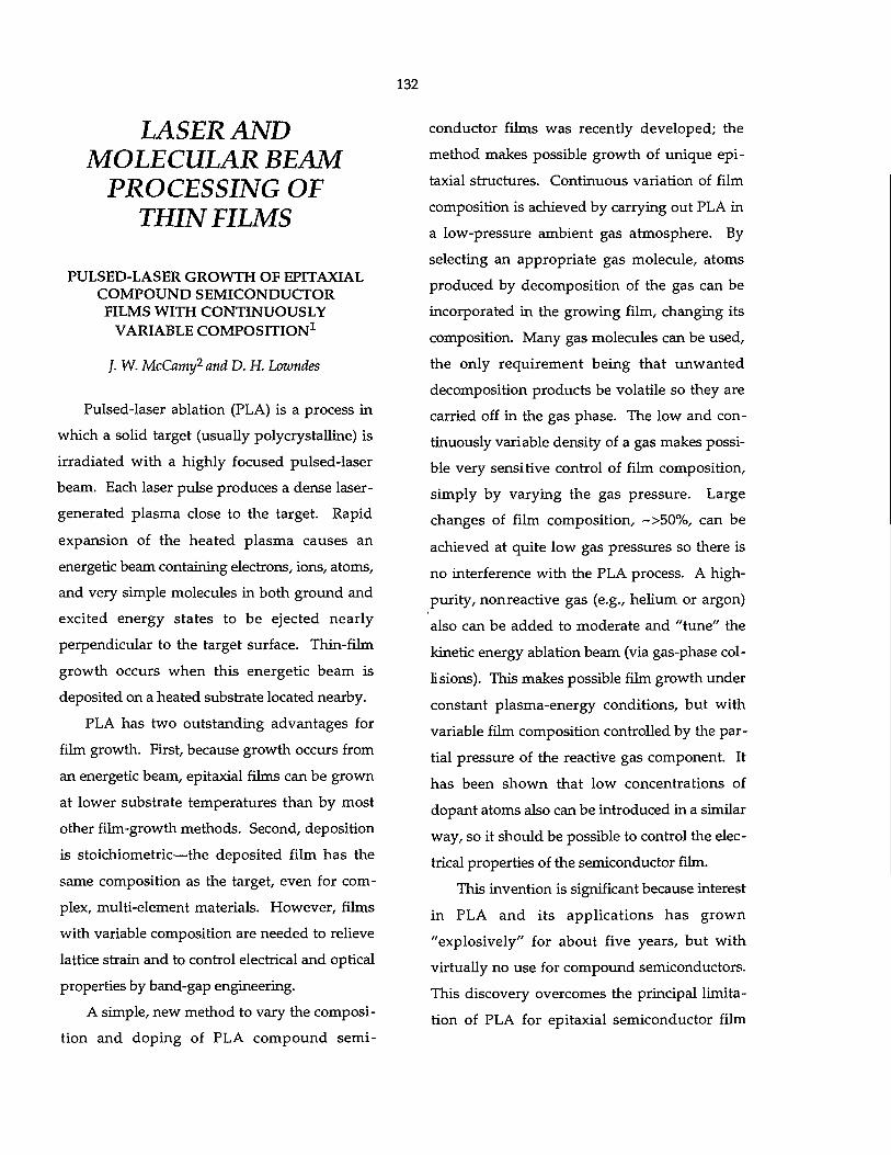
132
LASER AND MOLECULAR BEAM
PROCESSING OF THIN FILMS
PULSED-LASER GROWTH OF EPITAXIAL COMPOUND SEMICONDUCTOR FILMS WITH CONTINUOUSLY
VARIABLE COMPOSITION 1
/. W. McCamy2 and D. H. Lowndes
Pulsed-laser ablation (PLA) is a process in
which a solid target (usually polycrystalline) is
irradiated with a highly focused pulsed-laser
beam. Each laser pulse produces a dense laser-
generated plasma close to the target. Rapid
expansion of the heated plasma causes an
energetic beam containing electrons, ions, atoms,
and very simple molecules in both ground and
excited energy states to be ejected nearly
perpendicular to the target surface. Thin-film
growth occurs when this energetic beam is
deposited on a heated substrate located nearby.
PLA has two outstanding advantages for
film growth. First, because growth occurs from
an energetic beam, epitaxial films can be grown
at lower substrate temperatures than by most
other film-growth methods. Second, deposition
is stoichiometric—the deposited film has the
same composition as the target, even for com
plex, multi-element materials. However, films
with variable composition are needed to relieve
lattice strain and to control electrical and optical
properties by band-gap engineering.
A simple, new method to vary the composi
tion and doping of PLA compound semi
conductor films was recently developed; the
method makes possible growth of unique epi
taxial structures. Continuous variation of film
composition is achieved by carrying out PLA in
a low-pressure ambient gas atmosphere. By
selecting an appropriate gas molecule, atoms
produced by decomposition of the gas can be
incorporated in the growing film, changing its
composition. Many gas molecules can be used,
the only requirement being that unwanted
decomposition products be volatile so they are
carried off in the gas phase. The low and con
tinuously variable density of a gas makes possi
ble very sensitive control of film composition,
simply by varying the gas pressure. Large
changes of film composition, ~>50%, can be
achieved at quite low gas pressures so there is
no interference with the PLA process. A high-
purity, nonreactive gas (e.g., helium or argon)
also can be added to moderate and "tune" the
kinetic energy ablation beam (via gas-phase col
lisions). This makes possible film growth under
constant plasma-energy conditions, but with
variable film composition controlled by the par
tial pressure of the reactive gas component. It
has been shown that low concentrations of
dopant atoms also can be introduced in a similar
way, so it should be possible to control the elec
trical properties of the semiconductor film.
This invention is significant because interest
in PLA and its applications has grown
"explosively" for about five years, but with
virtually no use for compound semiconductors.
This discovery overcomes the principal limita
tion of PLA for epitaxial semiconductor film
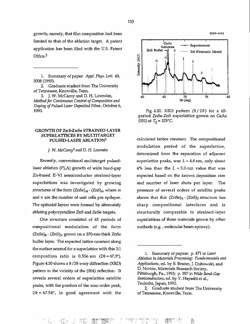
133
growth; namely, that film composition had been
limited to that of the ablation target. A patent
application has been filed with the U.S. Patent
Office.3
SSDN-4662
1. Summary of paper: Appl. Phys. Lett. 63, 3008 (1993).
2. Graduate student from The University of Tennessee, Knoxville, Term.
3. J. W. McCamy and D. H. Lowndes, Method for Continuous Control of Composition and Doping of Pulsed-Laser Deposited Films, October 6, 1993.
GROWTH OF ZnS-ZnSe STRAINED-LAYER SUPERLATTICES BY MULTITARGET
PULSED-LASER ABLATION1
/. W. McCamy2 and D. H. Lowndes
Recently, conventional multitarget pulsed-
laser ablation (PLA) growth of wide band-gap
Zn-based II-VI semiconductor strained-layer
superlattices was investigated by growing
structures of the form (ZnSe) m - (ZnS)„, where m
and n are the number of unit cells per epilayer.
The epitaxial layers were formed by alternately
ablating polycrystalline ZnS and ZnSe targets.
One structure consisted of 65 periods of
composit ional modu la t i on of the form
(ZnSe)6 - (ZnS)3, grown on a 370-nm-thick ZnSe
buffer layer. The expected lattice constant along
the surface normal for a superlattice with this 2:1
composition ratio is 0.556 nm (20 = 67.3°).
Figure 4.20 shows a 9 /20 x-ray diffraction (XRD)
pattern in the vicinity of the (004) reflection. It
reveals several orders of superlattice satellite
peaks, with the position of the zero-order peak,
20 = 67.54°, in good agreement wi th the
GaAs Substrate
T
Experimental ZnS Buffer -ft o 3 x 6 Kn^fo M o d e l
1
70 26 (deg)
80
Fig. 4.20. XRD pattern ( 6 / 2 0 ) for a 65-period ZnSe-ZnS superlattice grown on GaAs (001)atT g = 325°C.
calculated lattice constant. The compositional
modula t ion per iod of the super la t t ice ,
determined from the separation of adjacent
superlattice peaks, was L = 4.8 nm, only about
4% less than the L = 5.0-nm value that was
expected based on the known deposition rate
and number of laser shots per layer. The
presence of several orders of satellite peaks
shows that this (ZnSe)6- (ZnS)3 structure has
sharp composi t ional interfaces and is
structurally comparable to s trained-layer
superlattices of these materials grown by other
methods (e.g., molecular beam epitaxy).
1. Summary of papers: p. 471 in Laser Ablation in Materials Processing: Fundamentals and Applications, ed. by B. Braren, J. Dubowski, and D. Norton, Materials Research Society, Pittsburgh, Pa., 1993; p. 357 in Wide Band-Gap Semiconductors, ed. by Y. Hayashi et al., Tsukuba, Japan, 1992.
2. Graduate student from The University of Tennessee, Knoxville, Term.
134
GROWTH OF EPITAXIAL Zn-S-Se HETEROSTRUCTURES INCORPORATING
BOTH CONTINUOUSLY GRADED AND ABRUPT, PERIODIC
COMPOSITIONAL CHANGES 1
/. W. McCamy,2 D. H. Lowndes, and T. M. Rosseel3
As described previously, 4 it was recently
discovered that compound semiconductor
ternary alloy films can be grown by ablating a
target of fixed composition into an appropriate
ambient gas and controlling film composition
via the gaseous partial pressure. In order to
demonstrate and evaluate this method for spa
tial control of heterostructure composition,
multilayered heteroepitaxial structures based on
ZnSei_j5 x that incorporate both abrupt, periodic,
and con t inuous ly g r a d e d changes in
composition have been fabricated.
A polycrystalline ZnSe target was ablated
into an ambient atmosphere containing H2S.
Abrupt compositional changes were produced
by interrupting laser ablation briefly, changing
the H2S partial pressure, and then resuming
ablation. The thickness of each layer was con
trolled by the number of laser pulses, while its
composition "x" was determined by ambient
H2S pressure. By periodically varying the gas
pressure and number of laser shots, epitaxial
layers with highly reproducible thickness and
composition were grown. By changing the H2S
partial pressure gradually without interrupting
growth, layers having continuously graded
composition were grown.
Figure 4.21 shows a secondary ion mass
spectrometry (SIMS) profile of the S 3 2 content in
an epitaxial Z n S e i . x S x s tructure grown by
SSDN-4663
Composition Modulation njmnnnnnmnjiJinriM
-150 0 150 300 450 600 Distance From Buffer Layer (nm)
750
Fig. 4.21. Top two curves: Ideal periodically modulated and continuously graded sulfur compositional profiles. Bottom curve: Experimental SIMS profile of sulfur content vs depth.
depositing a ZnSeo.94So.06 buffer layer in order to
match lattice constants with the GaAs (001)
substrate and then increasing x abruptly to 0.18
and holding constant while a rectangle-wave
compositional modulation simultaneously was
imposed. Next, the average sulfur content
gradually was ramped down from x = 0.18 (at
165 nm) to x = 0.06 (at 600-nm thickness), still
wi th the rec tangle-wave compos i t iona l
modulation present. Finally, a pure ZnSe cap
layer was grown. Because the depth resolution
of SIMS is only 5-10 nm, the compositional
modulation actually achieved is considerably
more abrupt than that shown in Fig. 4.21.
The technological significance of this dis
covery is that it directly addresses the require
ment for compound semiconductor films with
continuously variable composition in semi
conductor devices: (1) compositionally graded
buffer layers are needed for strain relief between
semiconductor layers with different lattice con
stants; (2) abrupt compositional transitions are
135
needed to form quantum well structures, to con
fine carriers, and to enhance their mobility
("band-gap engineering"); (3) dopant-atom con
centrations must be varied precisely to control
electrical properties of semiconductor films in
unipolar devices; and (4) an ability to change
dopant type abruptly (e.g., from n-type to p-
type) is the key to fabrication of p-n junctions
and bipolar devices. These examples also apply
to thin-film photovoltaic cells used to convert
solar energy to electricity, an application of
direct interest to industry and the DOE.
1. Summary of paper: Appl. Phys. Lett. 63, 3008 (1993).
2. Graduate student from The University of Tennessee, Knoxville, Term.
3. Analytical Chemistry Division, ORNL. 4. J. W. McCamy and D. H. Lowndes,
"Growth of ZnS-ZnSe Strained-Layer Super-lattices by Multitarget Pulsed-Laser Ablation," this report.
GROWTH OF EPITAXIAL ZnSe FILMS BY PULSED-LASER ABLATION1
/. W. McCamy,2 D. H. Lowndes, and G. E. Jellison, Jr.
ZnSe is an attractive optoelectronic material
because of its wide direct band-gap (Eg = 2.7 eV,
Xg = 459 nm). Thin, epitaxial ZnSe films are
needed for active device applications such as
blue LEDs or laser diodes, as well as for passive
structures such as optical waveguides and
windows for solar cells.
Pulsed KrF (248 nm) laser ablation of a
carbon-free polycrystalline ZnSe target was used
to grow high-quality, epitaxial ZnSe thin films
on GaAs (001), GaAs (111), and GaP (001). The
films were grown at temperatures in the range
200-400°C, using a rotating substrate heater
geometry that permitted growth of uniform-
thickness films (-200 nm ± 1%) over an area
~75mm 2 . The effects of film-substrate lattice-
constant mismatch and of growth temperature
on the defect structure of the films were
determined by a combination of x-ray diffraction
(XRD), Rutherford backscattering spectrometry,
and electron microscopy measurements.
The optimal growth temperature, T„, was
found from the XRD linewidth to be 325
(± 25)°C, at which temperature the ZnSe (004)
XRD rocking curve width for a 225-nm-thick
film implied a misfit dislocation density
Prf~1.6xl0 1 4 cm- 3 .
The electronic band structure of ZnSe films
grown on (001) GaAs was investigated by using
spectroscopic two-channel polarization modu
lation ellipsometry to determine the dielectric
function. Transparency of the films below the
band edge, as well as observation of a variety of
optical transitions in the dielectric function
spectrum, demonstrated that PLA-grown ZnSe
films are of high optical quality.
Photoluminescence measurements for an
800-nm-thick film on GaAs (001) showed both
donor-bound and acceptor-bound excitonic
emissions, as well as emission from the free
exciton. The free-exciton peak was split into
heavy- and light-hole components because of
strain present in the film. The observed splitting
corresponded to a strain of 1.6 x 10"3. This value
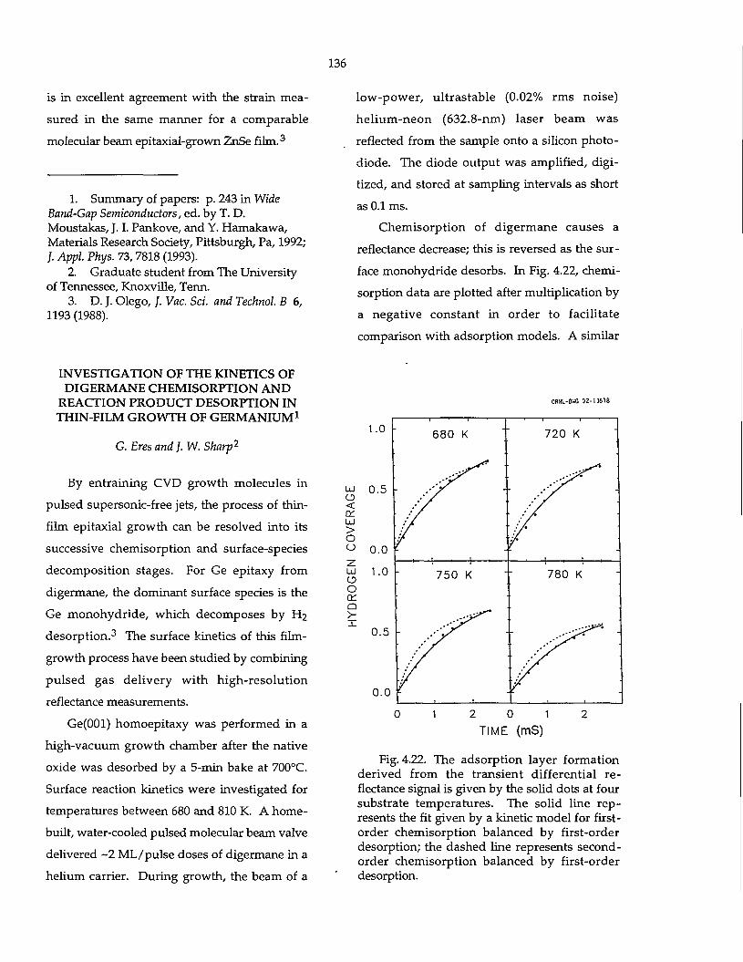
136
is in excellent agreement with the strain mea
sured in the same manner for a comparable
molecular beam epitaxial-grown ZnSe film. 3
1. Summary of papers: p. 243 in Wide Band-Gap Semiconductors, ed. by T. D. Moustakas, J. I. Pankove, and Y. Hamakawa, Materials Research Society, Pittsburgh, Pa, 1992; /. Appl. Phys. 73,7818 (1993).
2. Graduate student from The University of Tennessee, Knoxville, Tenn.
3. D. J. Olego, /. Vac. Sci. and Technol. B 6, 1193 (1988).
low-power, ultrastable (0.02% rms noise)
he l ium-neon (632.8-nm) laser beam was
reflected from the sample onto a silicon photo-
diode. The diode output was amplified, digi
tized, and stored at sampling intervals as short
as 0.1 ms.
Chemisorption of digermane causes a
reflectance decrease; this is reversed as the sur
face monohydride desorbs. In Fig. 4.22, chemi
sorption data are plotted after multiplication by
a negative constant in order to facilitate
comparison with adsorption models. A similar
INVESTIGATION OF THE KINETICS OF DIGERMANE CHEMISORPTION AND
REACTION PRODUCT DESORPTION IN THIN-FILM GROWTH OF GERMANIUM 1
G. Eres and ]. W. Sharp2
By entraining CVD growth molecules in
pulsed supersonic-free jets, the process of thin-
film epitaxial growth can be resolved into its
successive chemisorption and surface-species
decomposition stages. For Ge epitaxy from
digermane, the dominant surface species is the
Ge monohydride, which decomposes by H2
desorpt ion. 3 The surface kinetics of this film-
growth process have been studied by combining
pulsed gas delivery with high-resolution
reflectance measurements.
Ge(001) homoepitaxy was performed in a
high-vacuum growth chamber after the native
oxide was desorbed by a 5-min bake at 700°C.
Surface reaction kinetics were investigated for
temperatures between 680 and 810 K. A home-
built, water-cooled pulsed molecular beam valve
delivered - 2 ML/pulse doses of digermane in a
helium carrier. During growth, the beam of a
0RNL-D-G 92-13618
2 0 1 TIME (mS)
Fig. 4.22. The adsorption layer formation derived from the transient differential reflectance signal is given by the solid dots at four substrate temperatures. The solid line represents the fit given by a kinetic model for first-order chemisorption balanced by first-order desorption; the dashed line represents second-order chemisorption balanced by first-order desorption.
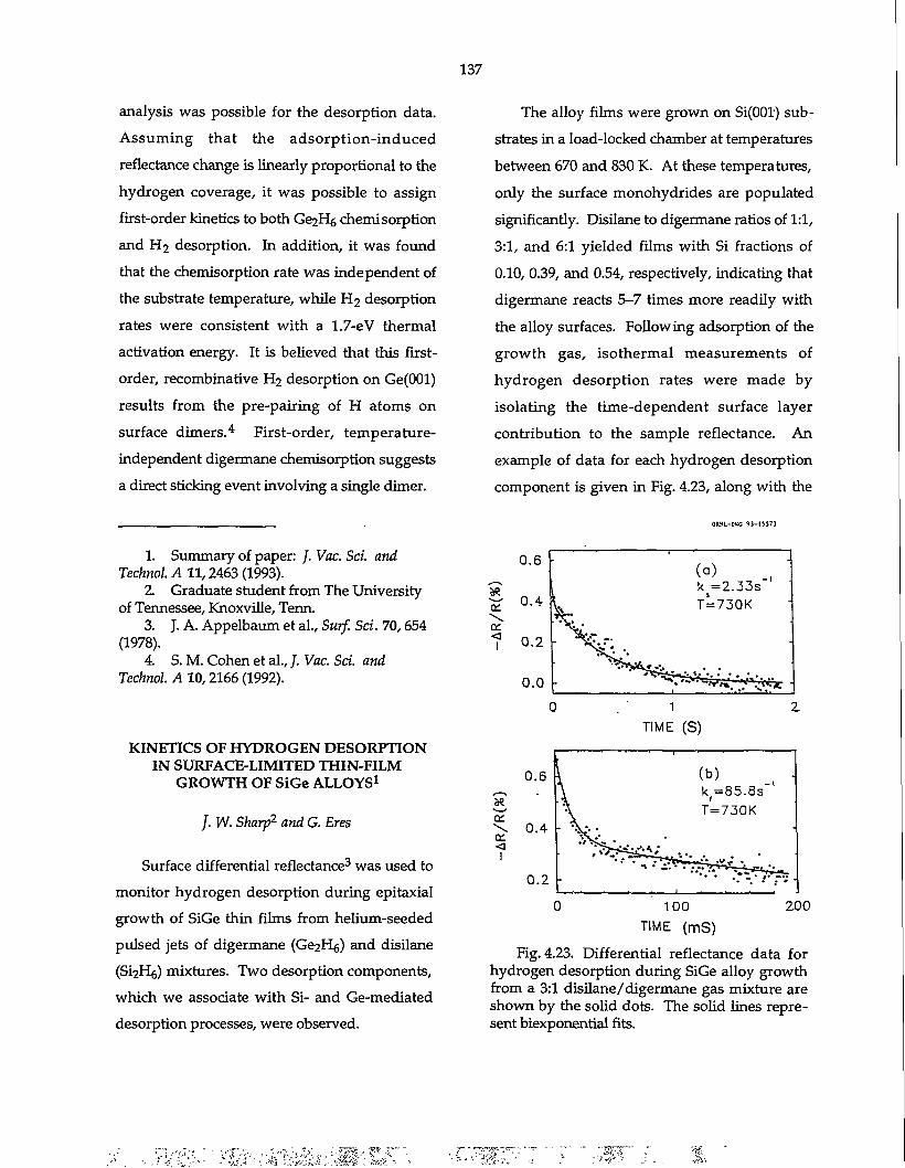
137
analysis was possible for the desorption data. Assuming that the adsorption-induced reflectance change is linearly proportional to the hydrogen coverage, it was possible to assign first-order kinetics to both Ge2Hg chemisorption and H2 desorption. In addition, it was found that the chemisorption rate was independent of the substrate temperature, while H2 desorption rates were consistent with a 1.7-eV thermal activation energy. It is believed that this first-order, recombinative H2 desorption on Ge(OOl) results from the pre-pairing of H atoms on surface dimers. 4 First-order, temperature-independent digermane chemisorption suggests a direct sticking event involving a single dimer.
The alloy films were grown on Si(OOl) substrates in a load-locked chamber at temperatures between 670 and 830 K. At these temperatures, only the surface monohydrides are populated significantly. Disilane to digermane ratios of 1:1, 3:1, and 6:1 yielded films with Si fractions of 0.10, 0.39, and 0.54, respectively, indicating that digermane reacts 5-7 times more readily with the alloy surfaces. Following adsorption of the growth gas, isothermal measurements of hydrogen desorption rates were made by isolating the time-dependent surface layer contribution to the sample reflectance. An example of data for each hydrogen desorption component is given in Fig. 4.23, along with the
ORNL-DWG 9 3 - 1 5 5 7 3
1. Summary of paper: /. Vac. Sci. and Technol. A 11,2463 (1993).
2. Graduate student from The University of Tennessee, Knoxville, Tenn.
3. J. A. Appelbaum et al., Surf. Sci. 70,654 (1978).
4. S. M. Cohen et al., /. Vac. Sci. and Technol. A 10,2166 (1992).
KINETICS OF HYDROGEN DESORPTION IN SURFACE-LIMITED THIN-FILM
GROWTH OF SiGe ALLOYS1
/. W. Sharp2 and G. Eres
Surface differential reflectance3 was used to monitor hydrogen desorption during epitaxial growth of SiGe thin films from helium-seeded pulsed jets of digermane (Ge2Hg) and disilane (Si2H£) mixtures. Two desorption components, which we associate with Si- and Ge-mediated desorption processes, were observed.
01 \ or < 1
TIME (S)
0.6 ,.\
1 1
(b) k f =85 .8s " ' T=730K
0.4- - ^ - . -
0.2
•7^ 1% ^ "~^Vft£_i__. •.
100 TIME (mS)
200
Fig. 4.23. Differential reflectance data for hydrogen desorption during SiGe alloy growth from a 3:1 disilane/digermane gas mixture are shown by the solid dots. The solid lines represent biexponential fits.
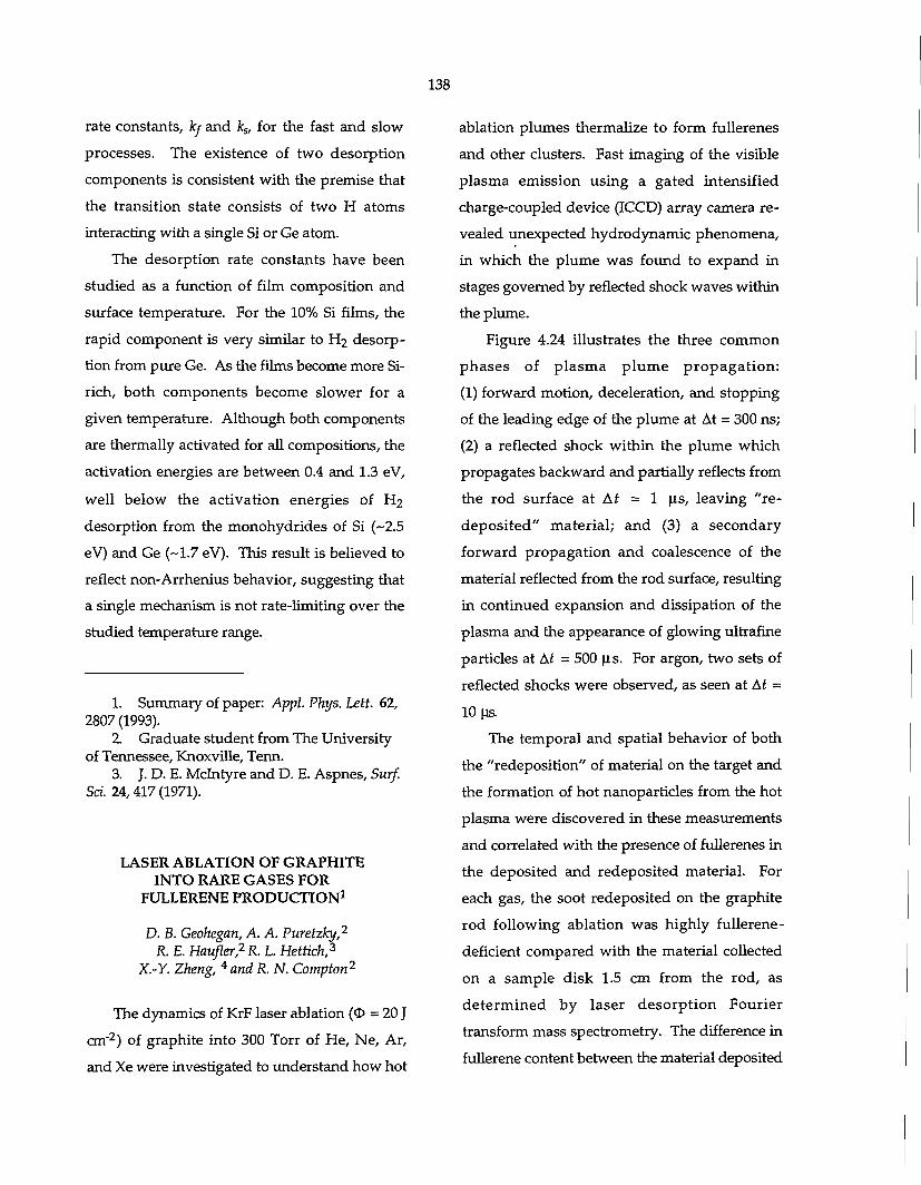
138
rate constants, kj and kg, for the fast and slow processes. The existence of two desorption components is consistent with the premise that the transition state consists of two H atoms interacting with a single Si or Ge atom.
The desorption rate constants have been studied as a function of film composition and surface temperature. For the 10% Si films, the rapid component is very similar to H2 desorption from pure Ge. As the films become more Si-rich, both components become slower for a given temperature. Although both components are thermally activated for all compositions, the activation energies are between 0.4 and 1.3 eV, well below the activation energies of H2 desorption from the monohydrides of Si (~2.5 eV) and Ge (~1.7 eV). This result is believed to reflect non-Arrhenius behavior, suggesting that a single mechanism is not rate-limiting over the studied temperature range.
1. Summary of paper: Appl. Phys. Lett. 62, 2807 (1993).
2. Graduate student from The University of Tennessee, Knoxville, Term.
3. J. D. E. Mclntyre and D. E. Aspnes, Surf. Sri. 24,417(1971).
LASER ABLATION OF GRAPHITE INTO RARE GASES FOR
FULLERENE PRODUCTION1
D. B. Geohegan, A. A. Puretzky,2
R. E. Haufler,2R. L. Hettich,3
X.-Y. Zheng, 4 and R. N. Compton2
The dynamics of KrF laser ablation (<& = 20 J cm"2) of graphite into 300 Torr of He, Ne, Ar, and Xe were investigated to understand how hot
ablation plumes thermalize to form fullerenes and other clusters. Fast imaging of the visible plasma emission using a gated intensified charge-coupled device (ICCD) array camera revealed unexpected hydrodynamic phenomena, in which the plume was found to expand in stages governed by reflected shock waves within the plume.
Figure 4.24 illustrates the three common phases of plasma plume propagation: (1) forward motion, deceleration, and stopping of the leading edge of the plume at At = 300 ns; (2) a reflected shock within the plume which propagates backward and partially reflects from the rod surface at At = 1 \is, leaving "re-deposited" material; and (3) a secondary forward propagation and coalescence of the material reflected from the rod surface, resulting in continued expansion and dissipation of the plasma and the appearance of glowing ultrafine particles at At = 500 us. For argon, two sets of reflected shocks were observed, as seen at At = 10 us.
The temporal and spatial behavior of both the "redeposition" of material on the target and the formation of hot nanoparticles from the hot plasma were discovered in these measurements and correlated with the presence of fullerenes in the deposited and redeposited material. For each gas, the soot redeposited on the graphite rod following ablation was highly fullerene-deficient compared with the material collected on a sample disk 1.5 cm from the rod, as determined by laser desorption Fourier transform mass spectrometry. The difference in fullerene content between the material deposited
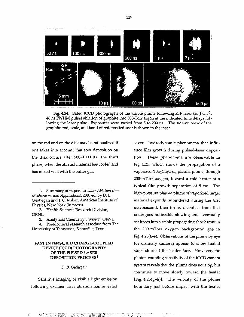
139
Fig. 4.24. Gated ICCD photographs of the visible plume following KrF laser (20 J cm"2, 46 ns FWHM pulse) ablation of graphite into 300-Torr argon at the indicated time delays following the laser pulse. Exposures were varied from 5 to 200 ns. The side-on view of the graphite rod, scale, and band of redeposited soot is shown in the inset.
on the rod and on the disk may be rationalized if one takes into account that soot deposition on the disk occurs after 500-1000 jis (the third phase) when the ablated material has cooled and has mixed well with the buffer gas.
1. Summary of paper: in Laser Ablation II— Mechanisms and Applications, 288, ed. by D. B. Geohegan and J. C. Miller, American Institute of Physics, New York (in press).
2 Health Sciences Research Division, ORNL.
3. Analytical Chemistry Division, ORNL. 4. Postdoctoral research associate from The
University of Tennessee, Knoxville, Term.
FAST INTENSIFIED CHARGE-COUPLED DEVICE (ICCD) PHOTOGRAPHY
OF THE PULSED-LASER DEPOSITION PROCESS1
D. B. Geohegan
Sensitive imaging of visible light emission following excimer laser ablation has revealed
several hydrodynamic phenomena that influence film growth during pulsed-laser deposition. These phenomena are observable in Fig. 4.25, which shows the propagation of a vaporized YBa2Cu307_x plasma plume, through 200-mTorr oxygen, toward a cold heater at a typical film-growth separation of 5 cm. The high-pressure plasma plume of vaporized target material expands unhindered during the first microsecond, then forms a contact front that undergoes noticeable slowing and eventually coalesces into a stable propagating shock front in the 200-mTorr oxygen background gas in Fig. 4.25(a-e). Observations of the plume by eye (or ordinary camera) appear to show that it stops short of the heater face. However, the photon-counting sensitivity of the ICCD camera system reveals that the plume does not stop, but continues to move slowly toward the heater [Fig. 4.25(g-h)]. The velocity of the plume boundary just before impact with the heater
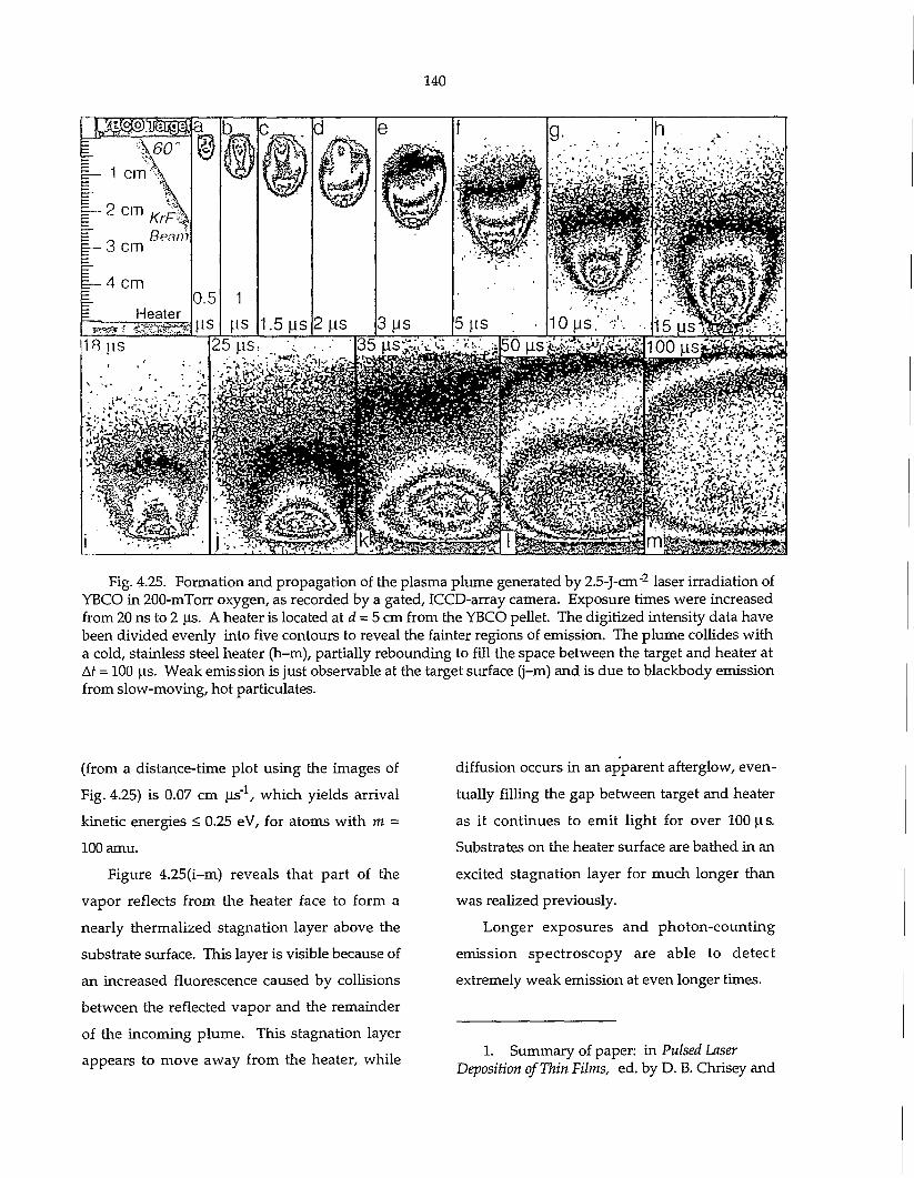
140
Fig. 4.25. Formation and propagation of the plasma plume generated by 2.5-J-cm"2 laser irradiation of YBCO in 200-mTorr oxygen, as recorded by a gated, ICCD-array camera. Exposure times were increased from 20 ns to 2 us. A heater is located at d = 5 cm from the YBCO pellet. The digitized intensity data have been divided evenly into five contours to reveal the fainter regions of emission. The plume collides with a cold, stainless steel heater (h-m), partially rebounding to fill the space between the target and heater at At = 100 us. Weak emission is just observable at the target surface (j-m) and is due to blackbody emission from slow-moving, hot particulates.
diffusion occurs in an apparent afterglow, eventually filling the gap between target and heater as it continues to emit light for over 100 us. Substrates on the heater surface are bathed in an excited stagnation layer for much longer than was realized previously.
Longer exposures and photon-counting emission spectroscopy are able to detect extremely weak emission at even longer times.
1. Summary of paper: in Pulsed Laser Deposition of Thin Films, ed. by D. B. Chrisey and
(from a distance-time plot using the images of Fig. 4.25) is 0.07 cm us"1, which yields arrival kinetic energies < 0.25 eV, for atoms with m = 100 amu.
Figure 4.25(i-m) reveals that part of the vapor reflects from the heater face to form a nearly thermalized stagnation layer above the substrate surface. This layer is visible because of an increased fluorescence caused by collisions between the reflected vapor and the remainder of the incoming plume. This stagnation layer appears to move away from the heater, while
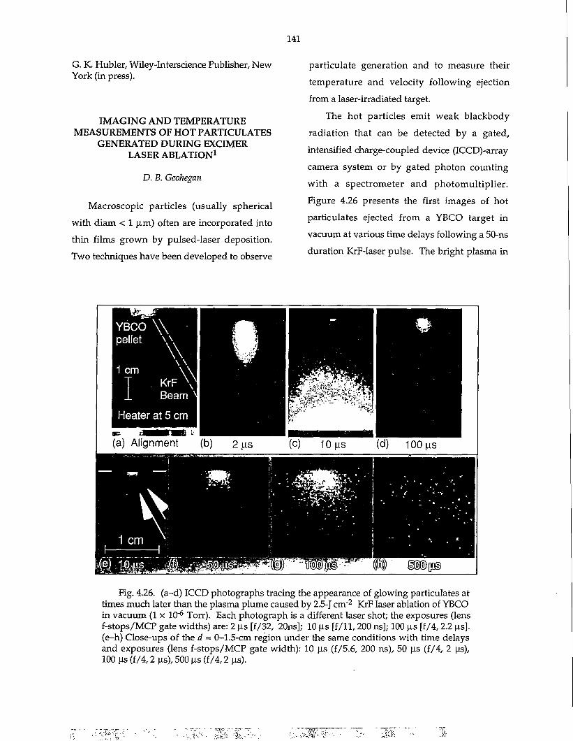
141
G. K. Hubler, Wiley-Interscience Publisher, New York (in press).
IMAGING AND TEMPERATURE MEASUREMENTS OF HOT PARTICULATES
GENERATED DURING EXCIMER LASER ABLATION1
D. B. Geohegan
Macroscopic particles (usually spherical with diam < 1 urn) often are incorporated into thin films grown by pulsed-laser deposition. Two techniques have been developed to observe
particulate generation and to measure their temperature and velocity following ejection from a laser-irradiated target.
The hot particles emit weak blackbody radiation that can be detected by a gated, intensified charge-coupled device (ICCD)-array camera system or by gated photon counting with a spectrometer and photomultiplier. Figure 4.26 presents the first images of hot particulates ejected from a YBCO target in vacuum at various time delays following a 50-ns duration KrF-laser pulse. The bright plasma in
YBCO \ \ pellet \ \
\ \ 1 cm y T KrF X
1 Beam
Heater at 5 cm
Fig. 4.26. (a-d) ICCD photographs tracing the appearance of glowing particulates at times much later than the plasma plume caused by 2.5-J cm"2 KrF laser ablation of YBCO in vacuum (1 x 10"6 Torr). Each photograph is a different laser shot; the exposures (lens f-stops/MCP gate widths) are: 2 us [f/32, 20ns]; 10 us [f/11,200 ns]; 100 us [f/4,2.2 us], (e-h) Close-ups of the d = 0-1.5-cm region under the same conditions with time delays and exposures (lens f-stops/MCP gate width): 10 us (f/5.6, 200 ns), 50 us (f/4, 2 us), 100 us (f/4,2 us), 500 us (f/4,2 us).
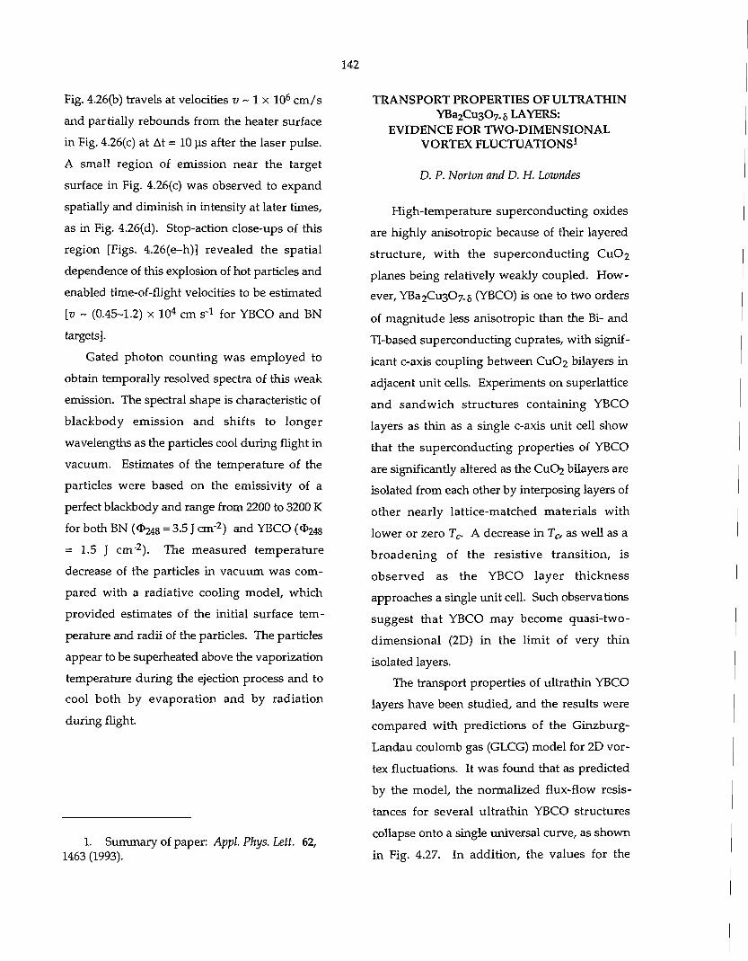
142
Fig. 4.26(b) travels at velocities v ~ 1 x 106 cm/s and partially rebounds from the heater surface in Fig. 4.26(c) at At = 10 us after the laser pulse. A small region of emission near the target surface in Fig. 4.26(c) was observed to expand spatially and diminish in intensity at later times, as in Fig. 4.26(d). Stop-action close-ups of this region [Figs. 4.26(e-h)] revealed the spatial dependence of this explosion of hot particles and enabled time-of-flight velocities to be estimated [v ~ (0.45-1.2) x 10 4 cm s' 1 for YBCO and BN targets].
Gated photon counting was employed to obtain temporally resolved spectra of this weak emission. The spectral shape is characteristic of blackbody emission and shifts to longer wavelengths as the particles cool during flight in vacuum. Estimates of the temperature of the particles were based on the emissivity of a perfect blackbody and range from 2200 to 3200 K for both BN ( # 2 4 8 = 3.5 J cm"2) and YBCO (<D248
= 1.5 J cm - 2 ). The measured temperature decrease of the particles in vacuum was compared with a radiative cooling model, which provided estimates of the initial surface temperature and radii of the particles. The particles appear to be superheated above the vaporization temperature during the ejection process and to cool both by evaporation and by radiation during flight.
1. Summary of paper: Appl. Phys. Lett. 62, 1463 (1993).
TRANSPORT PROPERTIES OF ULTRATHIN YBa2Cu307.8 LAYERS:
EVIDENCE FOR TWO-DIMENSIONAL VORTEX FLUCTUATIONS1
D. P. Norton and D. H. Lowndes
High-temperature superconducting oxides are highly anisotropic because of their layered structure, with the superconducting C u 0 2
planes being relatively weakly coupled. However, YBa2Cu307-5 (YBCO) is one to two orders of magnitude less anisotropic than the Bi- and Tl-based superconducting cuprates, with significant c-axis coupling between C u 0 2 bilayers in adjacent unit cells. Experiments on superlattice and sandwich structures containing YBCO layers as thin as a single c-axis unit cell show that the superconducting properties of YBCO are significantly altered as the Cu0 2 bilayers are isolated from each other by interposing layers of other nearly lattice-matched materials with lower or zero T c. A decrease in Tc, as well as a broadening of the resistive transition, is observed as the YBCO layer thickness approaches a single unit cell. Such observations suggest that YBCO may become quasi-two-dimensional (2D) in the limit of very thin isolated layers.
The transport properties of ultrathin YBCO layers have been studied, and the results were compared with predictions of the Ginzburg-Landau coulomb gas (GLCG) model for 2D vortex fluctuations. It was found that as predicted by the model, the normalized flux-flow resistances for several ultrathin YBCO structures collapse onto a single universal curve, as shown in Fig. 4.27. In addition, the values for the
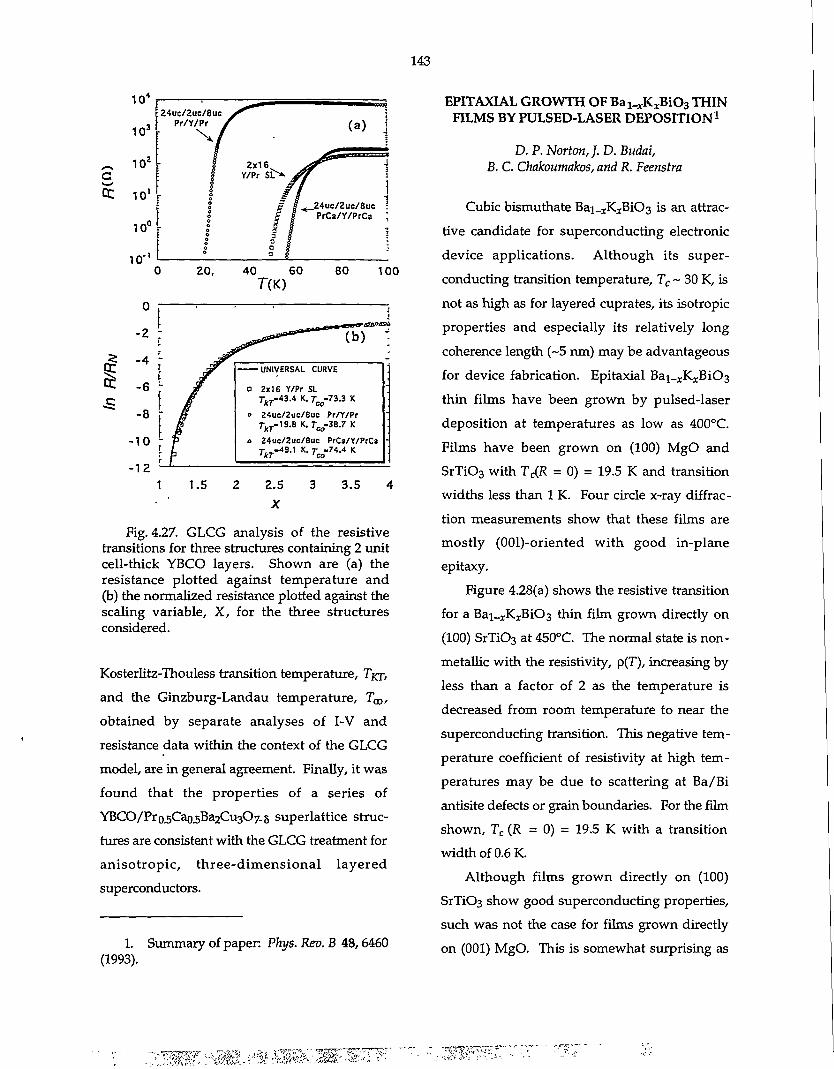
143
10 4
a
1 0 3
F
10 z
10'
10°
10"'
24uc/2uc/8uc Pr /Y/Pr
20, 40 60 T(K)
80 100
a 2x16 Y/Pr SL 7 A r - 4 3 . 4 K. r^ -73 .3 K
o 24uc/2uc/8uc Pr/Y/Pr r k 7 - - 1 9 . 8 K . r c o - 3 8 . 7 K
24uc/2uc/Buc PrCa/Y/PrCa r , T - 4 9 . 1 K. T -74.4 K 'kT 'co
2.5
Fig. 4.27. GLCG analysis of the resistive transitions for three structures containing 2 unit cell-thick YBCO layers. Shown are (a) the resistance plotted against temperature and (b) the normalized resistance plotted against the scaling variable, X, for the three structures considered.
Kosterlitz-Thouless transition temperature, T^j-, and the Ginzburg-Landau temperature, T^, obtained by separate analyses of I-V and resistance data within the context of the GLCG model, are in general agreement. Finally, it was found that the properties of a series of YBCO/Pro,5Cao.5Ba2Cu3G"7_5 superlattice structures are consistent with the GLCG treatment for anisotropic, three-dimensional layered superconductors.
1. Summary of paper: Phys. Rev. B 48,6460 (1993).
EPITAXIAL GROWTH OF Ba^K^BiOa THIN FILMS BY PULSED-LASER DEPOSITION1
D. P. Norton, J. D. Budai, B. C. Chakoumakos, and R. Feenstra
Cubic bismuthate Bai_ rKxBi03 is an attractive candidate for superconducting electronic device applications. Although its superconducting transition temperature, Tc ~ 30 K, is not as high as for layered cuprates, its isotropic properties and especially its relatively long coherence length (~5 nm) may be advantageous for device fabrication. Epitaxial Bai_ rK xBi03 thin films have been grown by pulsed-laser deposition at temperatures as low as 400°C. Films have been grown on (100) MgO and SrTi0 3 with Tc(R = 0) = 19.5 K and transition widths less than 1 K. Four circle x-ray diffraction measurements show that these films are mostly (OOl)-oriented with good in-plane epitaxy.
Figure 4.28(a) shows the resistive transition for a Bai_xKxBi03 thin film grown directly on (100) SrTi0 3 at 450°C. The normal state is non-metallic with the resistivity, p(T), increasing by less than a factor of 2 as the temperature is decreased from room temperature to near the superconducting transition. This negative temperature coefficient of resistivity at high temperatures may be due to scattering at Ba/Bi antisite defects or grain boundaries. For the film shown, Tc (R = 0) = 19.5 K with a transition width of 0.6 K.
Although films grown directly on (100) SrTi03 show good superconducting properties, such was not the case for films grown directly on (001) MgO. This is somewhat surprising as
::^M. '-W.^ «* , - .» -s&! «* ;%m^. -

144
1 2
<•> 1 0
a
> W 0) Ul EC
(a)
50 100 150 2 0 0 250 300 TEMPERATURE (K)
0 50 100 150 2 0 0 250 .300 TEMPERATURE (K)
Fig. 4.28. Resistivity as a function of temperature for Ba i_ x K x Bi0 3 thin films grown on (a) (100) S r T i 0 3 and (b) (100) MgO with a BaBiC>3 epitaxial buffer layer. In both cases, the Bai.j-K^BiOs films are ~1 |xm thick.
the lattice constant for Bai_ xK xBi03 is closer to
that of MgO than to SrTiC>3. Nevertheless, sig
nificant improvement was made in the quality of
the Bai_ xK xBi03 films on (001) MgO by growing
a BaBi03 buffer layer at 600°C before initiating
Ba^Kj-BiOs film growth. Figure 4.28(b) shows
the dc resistivity for a Bai_ xK xBi03 thin film
grown at a heater block temperature of 400°C on
(001) MgO with an initial BaBi03 layer grown at
600°C. For this film, T c (R = 0) = 19.2 K with a
transition width of -1.0 K. Utilizing an epitaxial
BaBiOs buffer l aye r , superconducting
Bai_xKxBi03 films were g rown over the
temperature range 350°-450°C.
1. Summary of paper: Appl. Phys. Lett. 62, 414 (1993).
EPITAXIAL PULSED-LASER GROWTH AND PROPERTIES OF SINGLE-CRYSTAL
Ca 1_ xSr a :Cu02 THIN FILMS 1
D. P. Norton, B. C. Chakoumakos, E. C. Jones,2
J. D. Budai, D. K. Christen, and D. H. Lowndes
The parent compound of the copper oxide
superconductors, Cai_ rSr ; cCu02, has a simple
layered structure consisting of CUO2 planes
separated by planes of alkaline-earth elements.
It has been shown that this material can be made
to superconduct either by electron doping
(trivalent substitution on the alkaline-earth site)
or by hole doping (vacancies on the alkaline-
earth sites). However, bulk synthesis of
Cai_ xSr ; cCu02 with a tetragonal, infinite layer
structure, in either the undoped, insulating
phase or the doped, superconducting phase, has
proven difficult. At ambient pressure, only
Cai. x Sr x Cu02 with x ~ 0.14 can be synthesized
in bulk; other compositions are possible only
with high-pressure and high-temperature bulk
processing techniques.
Very high quality epitaxial single-crystal
Cai_xSrxCu02 thin films have been grown uti
lizing pulsed-laser deposition. In contrast to
earlier work, these films were grown by
codepositing from a single target for the entire
compositional range 0.15 < x < 1.0. X-ray
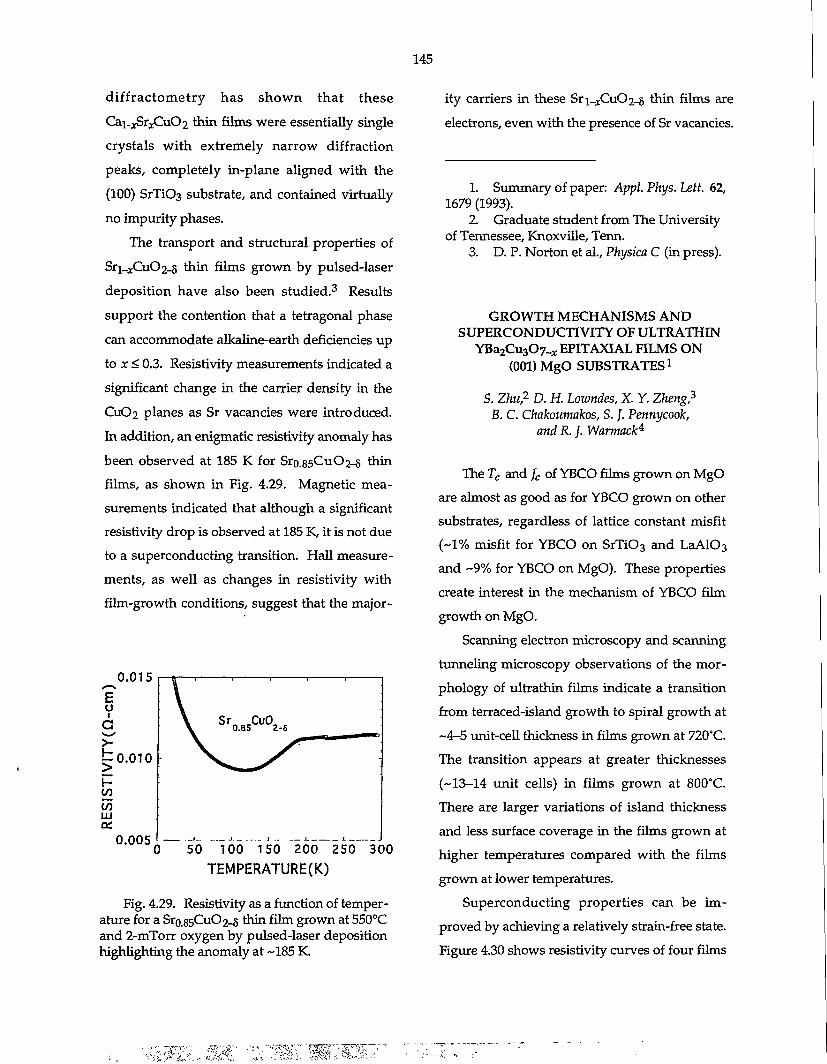
145
diffractometry has shown that these Cai_jSrxCu02 thin films were essentially single crystals with extremely narrow diffraction peaks, completely in-plane aligned with the (100) SrTiOa substrate, and contained virtually no impurity phases.
The transport and structural properties of Sri_xCu02-s thin films grown by pulsed-laser deposition have also been studied. 3 Results support the contention that a tetragonal phase can accommodate alkaline-earth deficiencies up to x < 0.3. Resistivity measurements indicated a significant change in the carrier density in the Q1O2 planes as Sr vacancies were introduced. In addition, an enigmatic resistivity anomaly has been observed at 185 K for Sro.85CuO2.-5 thin films, as shown in Fig. 4.29. Magnetic measurements indicated that although a significant resistivity drop is observed at 185 K, it is not due to a superconducting transition. Hall measurements, as well as changes in resistivity with film-growth conditions, suggest that the major
ity carriers in these Sri_xCu02_5 thin films are
electrons, even with the presence of Sr vacancies.
0.015 E o
to .010
(/) to LU
0.005 50 100 150 200 250 300
TEMPERATURE(K)
Fig. 4.29. Resistivity as a function of temperature for a Sro.85Cu02-s thin film grown at 550°C and 2-mTorr oxygen by pulsed-laser deposition highlighting the anomaly at -185 K.
1. Summary of paper: Appl. Phys. Lett. 62, 1679 (1993).
2 Graduate student from The University of Tennessee, Knoxville, Term.
3. D. P. Norton et al., Physica C (in press).
GROWTH MECHANISMS AND SUPERCONDUCTIVITY OF ULTRATHIN
YBa2Cu307_^ EPITAXIAL FILMS ON (001) MgO SUBSTRATES1
S. Zhu,2 D. H. Lowndes, X. Y. Zheng,2
B. C. Chakoutnakos, S. J. Pennycook, and R. f. Warmack4
The Tc and Jc of YBCO films grown on MgO are almost as good as for YBCO grown on other substrates, regardless of lattice constant misfit (-1% misfit for YBCO on SrTi0 3 and LaA10 3
and ~9% for YBCO on MgO). These properties create interest in the mechanism of YBCO film growth on MgO.
Scanning electron microscopy and scanning tunneling microscopy observations of the morphology of ultrathin films indicate a transition from terraced-island growth to spiral growth at ~4-5 unit-cell thickness in films grown at 720°C. The transition appears at greater thicknesses (~13-14 unit cells) in films grown at 800°C. There are larger variations of island thickness and less surface coverage in the films grown at higher temperatures compared with the films grown at lower temperatures.
Superconducting properties can be improved by achieving a relatively strain-free state. Figure 4.30 shows resistivity curves of four films
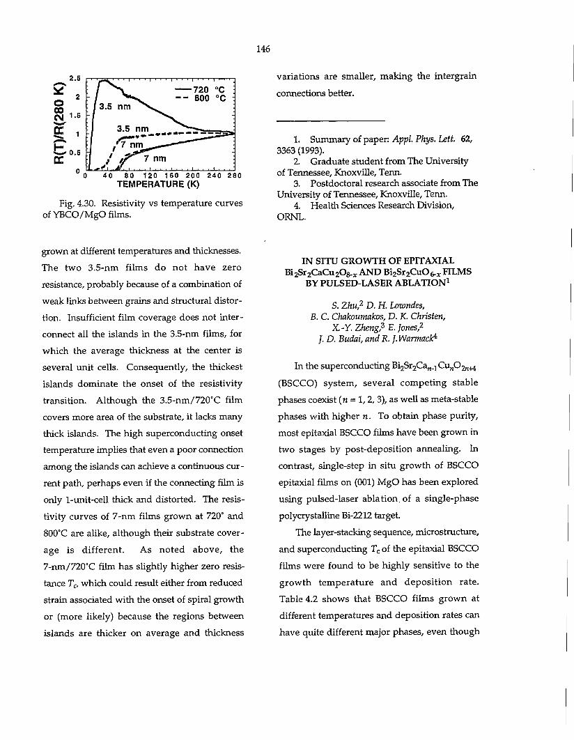
146
TEMPERATURE (K)
Fig. 4.30. Resistivity vs temperature curves of YBCO/MgO films.
grown at different temperatures and thicknesses.
The two 3.5-nm films do not have zero
resistance, probably because of a combination of
weak links between grains and structural distor
tion. Insufficient film coverage does not inter
connect all the islands in the 3.5-nm films, for
which the average thickness at the center is
several unit cells. Consequently, the thickest
islands dominate the onset of the resistivity
transition. Although the 3.5-nm/720°C film
covers more area of the substrate, it lacks many
thick islands. The high superconducting onset
temperature implies that even a poor connection
among the islands can achieve a continuous cur
rent path, perhaps even if the connecting film is
only 1-unit-cell thick and distorted. The resis
tivity curves of 7-nm films grown at 720° and
800°C are alike, although their substrate cover
age is different. As noted above, the
7-nm/720°C film has slightly higher zero resis
tance Tc, which could result either from reduced
strain associated with the onset of spiral growth
or (more likely) because the regions between
islands are thicker on average and thickness
variations are smaller, making the intergrain
connections better.
1. Summary of paper: Appl. Phys. Lett. 62, 3363 (1993).
2. Graduate student from The University of Tennessee, Knoxville, Term.
3. Postdoctoral research associate from The University of Tennessee, Knoxville, Term.
4. Health Sciences Research Division, ORNL.
IN SITU GROWTH OF EPITAXIAL Bi 2 Sr 2 CaCu 2 0 8 . a : AND B ^ S ^ O i O ^ FILMS
BY PULSED-LASER ABLATION1
S. Zhu,2 D. H. Lowndes, B. C. Chakoumakos, D. K. Christen,
X.-Y. Zheng? E.Jones,2
J. D. Budai, and R. J.Warmack*
In the superconducting Bi 2 Sr 2 Ca n . 1 C u n 0 2 n 4 4
(BSCCO) system, several competing stable
phases coexist (n = 1,2,3), as well as meta-stable
phases with higher n. To obtain phase purity,
most epitaxial BSCCO films have been grown in
two stages by post-deposition annealing. In
contrast, single-step in situ growth of BSCCO
epitaxial films on (001) MgO has been explored
using pulsed-laser ablation, of a single-phase
polycrystalline Bi-2212 target.
The layer-stacking sequence, microstructure,
and superconducting Tc of the epitaxial BSCCO
films were found to be highly sensitive to the
growth temperature and deposit ion rate.
Table 4.2 shows that BSCCO films grown at
different temperatures and deposition rates can
have quite different major phases, even though
147
Table 4.2. Phase and Tc of films grown at different temperatures and deposition rates. The major phase, determined by XRD, is underlined. Tco is the zero-resistance transition temperature.
Rep. Rate 0.5 Hz 3.3 Hz
Temperature Phase Tco (K) Phase Tco (K)
800°C 2201 — 2201 + 2212 —
770°C 2212 68 2212 52
740°C 2212 71 2212 + 2223 50
700°C 2212 + 2223 35 2223 + 2212 15
the ablation target composition (Bi-2212) is unchanged. Pure Bi-2212 films were found to exist over only a narrow temperature range, and pure Bi-2201 films were found at higher growth temperatures, while lower growth temperatures enhanced the Bi-2223 phase, though it was always mixed with Bi-2212.
The phase homogeneity, in-plane connections among grains, and superconducting T c of Bi-2212 grown at a given temperature were found to be improved greatly by reducing the deposition rate. Epitaxial Bi-2212 films grown at 740°C and 0.5 Hz (-0.05 nm/s) have Jc = 8 x 10 5
A / c m 2 at 50 K and 5 x 10 6 A/cm 2 at 4.2 K, which is almost one magnitude larger than some MOCVD films.5-6
1. Summary of paper: Appl. Phys. Lett. 62, 3363 (1993).
2. Graduate student from The University of Tennessee, Knoxville, Tenn.
3. Postdoctoral research associate from The University of Tennessee, Knoxville, Tenn.
4. Health Sciences Research Division, ORNL.
5. T. Sugimoto et al., Appl. Phys. Lett. 57, 928 (1990).
6. T. Sugimoto et al., Physica C 185-189,2045 (1991).
OPTICAL FUNCTIONS OF TRANSPARENT THIN FILMS OF Si0 3 , BaTi0 3 , AND
SiO* DETERMINED USING SPECTROSCOPIC ELLIPSOMETRY1
G. E. Jellison, Jr, L. A. Boatner, D. H. Lowndes, R. A. McK.ee} and M. Godbole3
A procedure has been developed to determine accurately the thickness, optical functions, and surface roughness characteristics of thin-film insulators from two-channel spectroscopic polarization modulation ellipsometry data. For films with minimal surface roughness, the optical functions can be determined over the entire measured spectrum; for very rough films, analyses of spectroscopic ellipsometry data yield meaningful values of the optical functions only in the transparent region. In general, the films
rm.k-7m * < « * ; • ' • -••?*•>&&
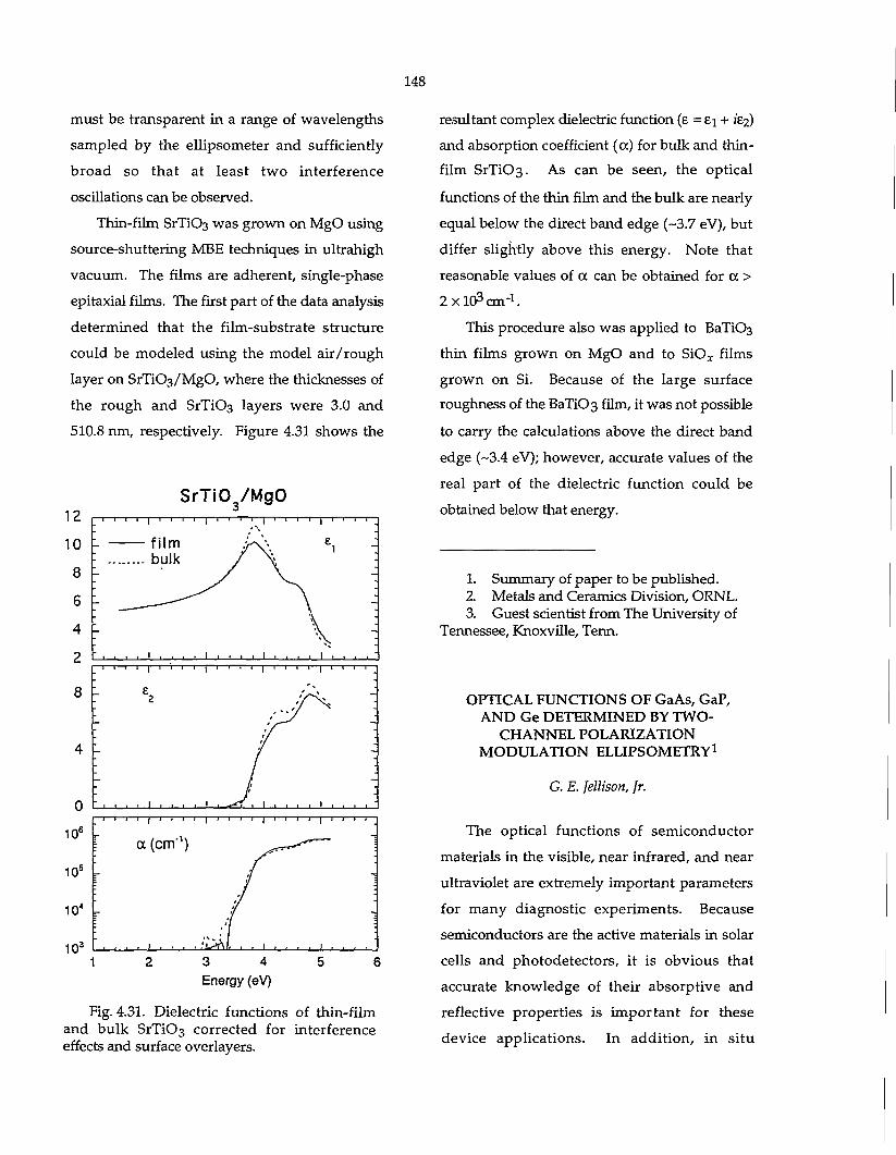
148
must be transparent in a range of wavelengths
sampled by the ellipsometer and sufficiently
broad so that at least two interference
oscillations can be observed.
Thin-film SrTi03 was grown on MgO using
source-shuttering MBE techniques in ultrahigh
vacuum. The films are adherent, single-phase
epitaxial films. The first part of the data analysis
determined that the film-substrate structure
could be modeled using the model air / rough
layer on SrTiOs/MgO, where the thicknesses of
the rough and SrTiOa layers were 3.0 and
510.8 nm, respectively. Figure 4.31 shows the
12
10
8
6
4
SrTiCWMgO —i—r — i — i - j — I — i i—i | t i t ^ i . . i . | i i I—T-
- film :r _
bulk / -_
• , , , , i . . . . i , , , i , . . , i , . ' ' - i — i — I — i — i — i — r - - i — i — | — i — I — I — i — I — i — I — i — r -
- I i ' • \ ' 1—JL i 1 I I I I t _
106
10"
104
10 3
- I — I — i — I — | — I — I — I — I — ] — I — l — I — I — I — I — I — I — I — [ — I — I — I -
a (cm )
• . - ' i^n 1 2 3 4 5 6
Energy (eV)
Fig. 4.31. Dielectric functions of thin-film and bulk SrTiC>3 corrected for interference effects and surface overlayers.
resultant complex dielectric function (e = £\ + iz^)
and absorption coefficient (a) for bulk and thin-
film SrTiC>3. As can be seen, the optical
functions of the thin film and the bulk are nearly
equal below the direct band edge (-3.7 eV), but
differ slightly above this energy. Note that
reasonable values of a can be obtained for a >
2 x 1 0 s cm- 1 .
This procedure also was applied to BaTiC>3
thin films grown on MgO and to SiO* films
grown on Si. Because of the large surface
roughness of the BaTiC>3 film, it was not possible
to carry the calculations above the direct band
edge (~3.4 eV); however, accurate values of the
real part of the dielectric function could be
obtained below that energy.
1. Summary of paper to be published. 2. Metals and Ceramics Division, ORNL. 3. Guest scientist from The University of
Tennessee, Knoxville, Term.
OPTICAL FUNCTIONS OF GaAs, GaP, AND Ge DETERMINED BY TWO-
CHANNEL POLARIZATION MODULATION ELLIPSOMETRY1
G. E. Jellison, ]r.
The optical functions of semiconductor
materials in the visible, near infrared, and near
ultraviolet are extremely important parameters
for many diagnostic experiments. Because
semiconductors are the active materials in solar
cells and photodetectors, it is obvious that
accurate knowledge of their absorptive and
reflective properties is important for these
device applications. In addit ion, in situ
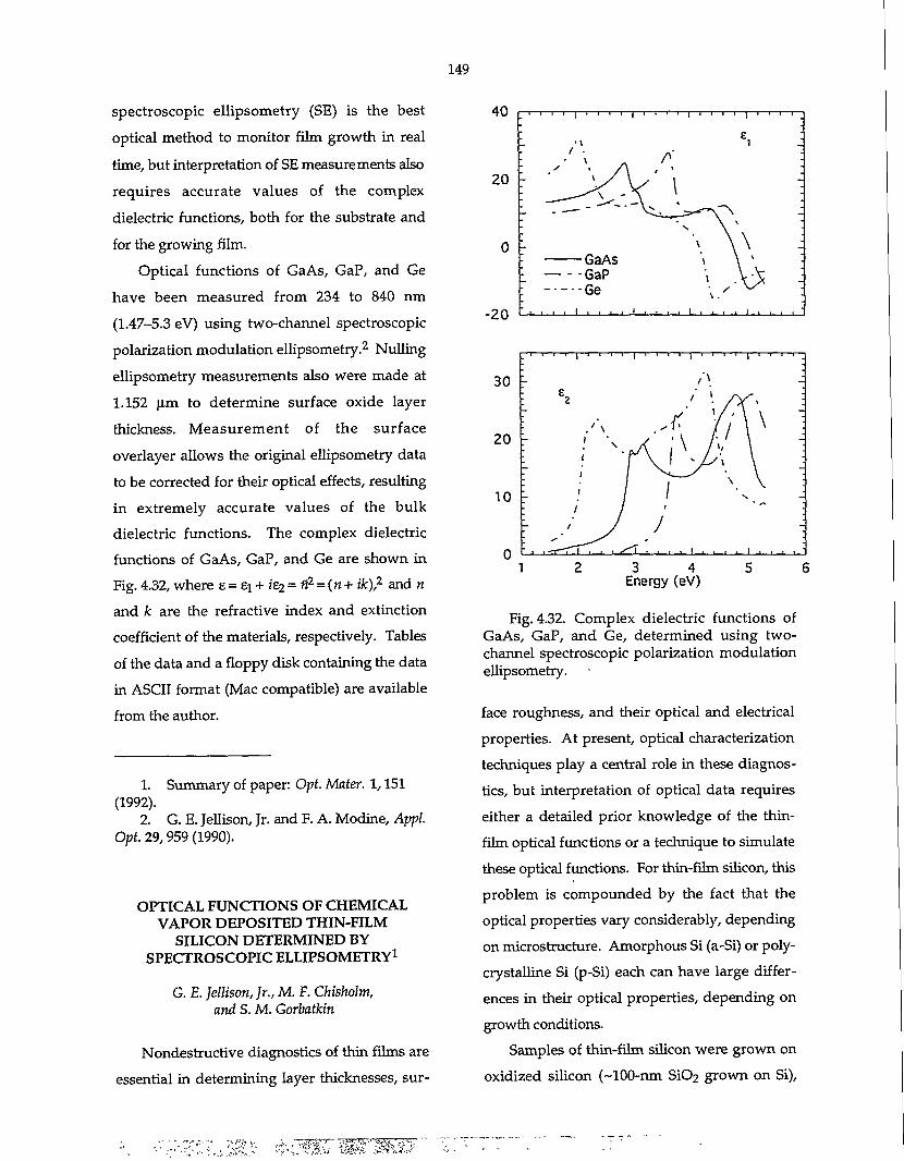
149
spectroscopic ellipsometry (SE) is the best optical method to monitor film growth in real time, but interpretation of SE measurements also requires accurate values of the complex dielectric functions, both for the substrate and for the growing film.
Optical functions of GaAs, GaP, and Ge have been measured from 234 to 840 nm (1.47-5.3 eV) using two-channel spectroscopic polarization modulation ellipsometry.2 Nulling ellipsometry measurements also were made at 1.152 um to determine surface oxide layer thickness. Measurement of the surface overlayer allows the original ellipsometry data to be corrected for their optical effects, resulting in extremely accurate values of the bulk dielectric functions. The complex dielectric functions of GaAs, GaP, and Ge are shown in Fig. 4.32, where e = Z\ + it2 = n2 = («+ ik),2 and n and k are the refractive index and extinction coefficient of the materials, respectively. Tables of the data and a floppy disk containing the data in ASCII format (Mac compatible) are available from the author.
1. Summary of paper: Opt. Mater. 1,151 (1992).
2. G. E. Jellison, Jr. and F. A. Modine, Appl. Opt. 29,959 (1990).
OPTICAL FUNCTIONS OF CHEMICAL VAPOR DEPOSITED THIN-FILM
SILICON DETERMINED BY SPECTROSCOPIC ELLIPSOMETRY1
G. E. Jellison, Jr., M. F. Chisholm, and S. M. Gorbatkin
Nondestructive diagnostics of thin films are
essential in determining layer thicknesses, sur-
40
20
0 -
-20
30 r
. > I 1 1 1 • 1 1 1 1 . . > i | i . . . . . . ' ' -
L. M £ ! ; / •
- ' \ / \ A
' I "O1
-j
• \ •
\ \ \ : oaAS \ \ \ : • GaP : Ge
-J . . l i l t . , , ! , ,
20
10
' ' ' 1 . i • i | i . . . | . . . i | , , •
~ E 2 '' '• /Y> ,
. ,
, 1
,
\ ' \
\ 1 ^ / •' \
~ - \ r
\ 1 ^ / •' \ -_
'• V I y>v \ '-
1,1
11 / \ V
:
- / i -|- / / -_ • ** , • - , i - T - r T , , ,-rf . . . , ! . . . , ! , , , -
1 2 3 4 5 Energy (eV)
Fig. 4.32. Complex dielectric functions of GaAs, GaP, and Ge, determined using two-channel spectroscopic polarization modulation ellipsometry.
face roughness, and their optical and electrical properties. At present, optical characterization techniques play a central role in these diagnostics, but interpretation of optical data requires either a detailed prior knowledge of the thin-film optical functions or a technique to simulate these optical functions. For thin-film silicon, this problem is compounded by the fact that the optical properties vary considerably, depending on microstructure. Amorphous Si (a-Si) or poly-crystalline Si (p-Si) each can have large differences in their optical properties, depending on growth conditions.
Samples of thin-film silicon were grown on oxidized silicon (~100-nm Si02 grown on Si),
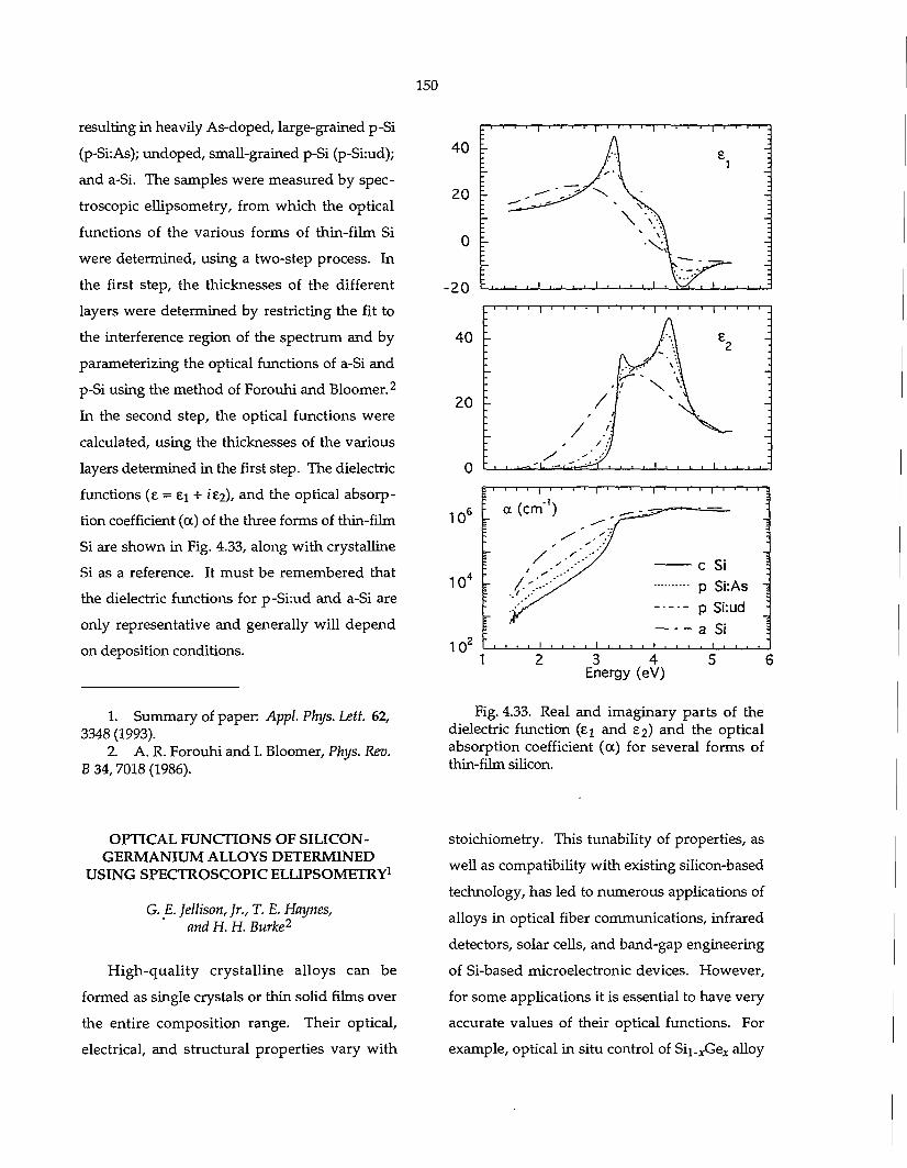
150
resulting in heavily As-doped, large-grained p-Si
(p-Si:As); undoped, small-grained p-Si (p-Si:ud);
and a-Si. The samples were measured by spec
troscopic ellipsometry, from which the optical
functions of the various forms of thin-film Si
were determined, using a two-step process. In
the first step, the thicknesses of the different
layers were determined by restricting the fit to
the interference region of the spectrum and by
parameterizing the optical functions of a-Si and
p-Si using the method of Forouhi and Bloomer. 2
In the second step, the optical functions were
calculated, using the thicknesses of the various
layers determined in the first step. The dielectric
functions (e = 81 + 1E2), and the optical absorp
tion coefficient (a) of the three forms of thin-film
Si are shown in Fig. 4.33, along with crystalline
Si as a reference. It must be remembered that
the dielectric functions for p-Si:ud and a-Si are
only representative and generally will depend
on deposition conditions.
1. Summary of paper: Appl. Phys. Lett. 62, 3348 (1993).
2 A. R. Forouhi and I. Bloomer, Phys. Rev. B 34,7018 (1986).
10
icr
10*
6 "
; ' • . 1 1 , . • 1 , 1
40 '•_ e„ j ' 2 "
& ' A • ' V « ^ x A * • Ai \ v \ -
20 ~ /} v \ •\ ; / /f -- / :j -. y y j .
n • , . 1 — . ' L i-r f 11 - ^ T 1 1 , , 1 , . . , 1 , ,
3 4 Energy (eV)
Fig. 4.33. Real and imaginary parts of the dielectric function (8i and £2) and the optical absorption coefficient (a) for several forms of thin-film silicon.
OPTICAL FUNCTIONS OF SILICON-GERMANIUM ALLOYS DETERMINED
USING SPECTROSCOPIC ELLIPSOMETRY1
G. E. Jettison, Jr., T. E. Haynes, and H. H. Burke2
High-quali ty crystalline alloys can be
formed as single crystals or thin solid films over
the entire composition range. Their optical,
electrical, and structural properties vary with
stoichiometry. This tunability of properties, as
well as compatibility with existing silicon-based
technology, has led to numerous applications of
alloys in optical fiber communications, infrared
detectors, solar cells, and band-gap engineering
of Si-based microelectronic devices. However,
for some applications it is essential to have very
accurate values of their optical functions. For
example, optical in situ control of Si i . x Ge x alloy
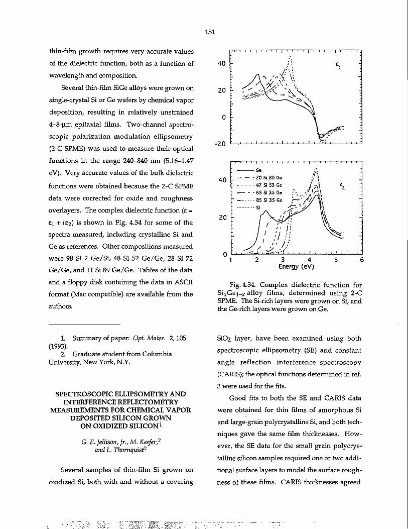
151
thin-film growth requires very accurate values of the dielectric function, both as a function of wavelength and composition.
Several thin-film SiGe alloys were grown on single-crystal Si or Ge wafers by chemical vapor deposition, resulting in relatively unstrained 4-8-|im epitaxial films. Two-channel spectroscopic polarization modulation ellipsometry (2-C SPME) was used to measure their optical functions in the range 240-840 nm (5.16-1.47 eV). Very accurate values of the bulk dielectric functions were obtained because the 2-C SPME data were corrected for oxide and roughness overlayers. The complex dielectric function (e = £l +162) is shown in Fig. 4.34 for some of the spectra measured, including crystalline Si and Ge as references. Other compositions measured were 98 Si 2 Ge/Si, 48 Si 52 Ge/Ge, 28 Si 72 Ge/Ge, and 11 Si 89 Ge/Ge. Tables of the data and a floppy disk containing the data in ASCII format (Mac compatible) are available from the authors.
1 ' •
40 - 1 1
e, -j
'- A^ ,'A$ \\ -
20
min
i
0 1' ^ ^ \ -_
•3f\ • . . . . 1 > - : . 1 1 >
3 4 Energy (eV)
Fig. 4.34. Complex dielectric function for Si xGei_ r alloy films, determined using 2-C SPME. The Si-rich layers were grown on Si, and the Ge-rich layers were grown on Ge.
1. Summary of paper: Opt. Mater. 2,105 (1993).
2. Graduate student from Columbia University, New York, N.Y.
SPECTROSCOPIC ELLIPSOMETRY AND INTERFERENCE REFLECTOMETRY
MEASUREMENTS FOR CHEMICAL VAPOR DEPOSITED SILICON GROWN
ON OXIDIZED SILICON1
G. E. Jellison, Jr., M. Keefer,2
and L. Thornquist2
Several samples of thin-film Si grown on oxidized Si, both with and without a covering
SiC>2 layer, have been examined using both spectroscopic ellipsometry (SE) and constant angle reflection interference spectroscopy (CARIS); the optical functions determined in ref. 3 were used for the fits.
Good fits to both the SE and CARIS data were obtained for thin films of amorphous Si and large-grain polycrystalline Si, and both techniques gave the same film thicknesses. However, the SE data for the small grain polycrystalline silicon samples required one or two additional surface layers to model the surface roughness of these films. CARIS thicknesses agreed
152
with SE thicknesses, if the total thickness of the
thin-film Si plus any surface overlayers were
used as the total SE thickness. Interpretation of
the SE data for the oxided films required an
additional interface layer between the top SiC>2
and the thin-film Si, which was not included in
the CARIS interpretation; this resulted in minor
differences between the thicknesses determined
from SE and CARIS.
In summary, the SE technique and the
CARIS technique determine very similar thick
nesses, when the optical functions of all of the
layers are known. Since CARIS measurements
are faster than commercially available SE
instruments, CARIS is the preferred technique if
there are no layers with unknown optical func
tions. On the other hand, SE measures two or
three quantities at each wavelength, compared
with only one quantity from CARIS. This
advantage, coupled with proper data interpreta
tion, allows SE measurements to be interpreted
even when the optical functions of a layer are
not known, and SE should be used in these
circumstances.
1. Summary of paper: Mat. Res. Soc. Symp. Proc. 283,561 (1993).
2. Prometrix Corporation, Santa Clara, Calif.
3. G. E. Jellison, Jr., M. F. Chisholm, and S. M. Gorbatkin, Appl. Phys. Lett. 62,3348 (1993), "Optical Functions of Chemical Vapor Deposited Thin-Film Silicon Determined by Spectroscopy Ellipsometry," this report.
DATA ANALYSIS FOR SPECTROSCOPIC ELLIPSOMETRY1
G. E. Jellison, Jr.
There are many applications for spectro
scopic ellipsometry (SE) as a nondestructive
diagnostic technique for thin-film characteriza
tion. SE is fast and very sensitive to changes in
the film dielectric function in the direction per
pendicular to the sample surface. However, SE
data often require considerable mathematical
analysis before they can be related directly to
parameters of interest (e.g., thin-film mor
phology, film thickness, surface roughness, or
the true dielectric functions of the film or sub
strate. In order to relate the SE-measured
parameters with actual characteristics of the
near-surface region, a model must be con
structed in three phases.
The first phase involves a model of the near-
surface region and selection of the technique
used to calculate the Fresnel reflection coeffi
cients (FRCs). Calculation of the FRCs for light
reflected from a layered structure of known
dielectric functions and thicknesses is well-
known and straightforward if it is assumed that
each layer is isotropic and uniform. Most
modern techniques involve 2 x 2 Abeles
mat r i ces 2 or 2 x 2 transfer matr ices. 3 If the
medium is anisotropic, then a 4 x 4 matrix for
malism must be used. 4
The second phase involves the parameteri
zation or selection of the spectroscopic optical
functions used to describe the layers. For films
153
with well-defined structure and for many sub
strates, the dielectric functions of the bulk mate
rials themselves can be used. However, the op
tical functions of thin films often are different
from bulk values, so their film wavelength-
dependent dielectric functions must be parame
terized in some way. For insulators, the Lorentz
oscillator model works reasonably well; while
for semiconductors the parameterization of
Forouhi and Bloomer 5 works well in restricted
wavelength regions. For materials that consist
of a mixture of phases, the Bruggeman effective
medium approximation 6 often is used.
The third phase involves the determination
of wavelength-independent parameters (e.g.,
film thicknesses) using an appropriate fitting
procedure. Generally, one has to specify a
figure of merit and minimize it by varying the
fitting parameters. The choice of the figure of
merit must result in a measure of the "goodness
of fit," and both the correlated and uncorrelated
errors of the fitted parameters must be
calculated. 7
1. Summary of paper: Thin Solid Films (in press).
2. F. Abeles, Ann. Phys. 5,596(1950). 3. R. M. A. Azzam and N. M. Bashara,
Ellipsometry and Polarized Light, North-Holland, Amsterdam, 1977.
4. D. W. Berreman, /. Opt. Soc. Am. 62,502 (1972).
5. A. R. Forouhi and I. Bloomer, Phys. Rev. B 34,7018 (1986).
6. D. A. G. Bruggeman, Ann. Phys. (Leipzig) 24,636 (1935).
7. G. E. Jellison, Jr., Appl. Opt. 30,3354 (1991).
ION CHANNELING AND SPECTROSCOPIC ELLIPSOMETRY EXAMINATIONS OF THIN-
FILMSiO2/epi-Si(001) STRUCTURES1
A. T. Fiory,2 P. K. Roy,3 and G. E. Jellison, Jr.
Structure-sensi t ive measurement s are
important in understanding and gaining control
over the production of reliable thin oxides for
MOS devices. The stacked-oxide method devel
oped at AT&T is noted both for its compatibility
with current manufacturing practice and for its
marked improvement in reliability and yield of
ultrathin films, compared with conventional
oxidization.
The sample wafers for this study were taken
from device development lots with 3-16-nm
Si02 either after completion of the gate-oxide
layer or after the first oxidation step in the
stacked-oxide method. Samples for the Ruther
ford backscattering (RBS) and spectroscopic
ellipsometry (SE) measurements were cut from
adjacent areas near the centers of the wafers.
The RBS measurements were used to deter
mine the areal densities of oxygen and silicon,
N o and Nsi, residing on the surface. The excess
scattering for silicon, ANgi, was determined from
these results, subtracting off the theoretical sur
face peak. No systematic differences were
observed for the three channeling directions. It
was observed that AN si depended upon film
thicknesses, being greater for thicker films than
for thinner films, and ANsi reached a minimum
of 1-1.4 x l O 1 5 a toms /cm 2 after complete oxide
removal. The excess scattering indicates the
existence of an extremely thin roughness layer
(possibly SiO z ); even for zero oxide thickness,
the nonzero AN$i indicates that the surface does
154
not have bulk-like termination. Although the
excess AN si for the stacked oxides is less than for
conventional oxides of comparable thicknesses,
the differences are not statistically significant.
SE measurements also were performed on
these samples. The data were fitted using an
air/Si02/c-Si model, in which the optical func
tions of the SiC>2 layer were parameterized using
the s ingle- term Sellmeier approximat ion
[n2 = 1 + Ak2/(X2 - XQ2)], with XQ = 92.3 nm, and
the optical functions of c-Si were taken from
Ref. 4. Two parameters (A and d^o2, the thick
ness of the SiC>2 layer) were sufficient to obtain a
good fit to the data.
The density of the film can be calculated
from N o (determined from RBS) and from dsiC>2
(determined from SE). It was found that the
densities of these films were independent of
thickness and not significantly different from
that of fused SiC>2, although the SE results indi
cated that the refractive index of the very thin
films was considerably greater than the refrac
tive index of fused SiO^
1. Summary of paper: Mat. Res. Soc. Symp. Proc. 259,131 (1992).
2. AT&T Bell Laboratories, Murray Hill, NJ 3. AT&T Bell Laboratories, Allentown, Pa. 4. G. E. Jellison, Jr., Opt. Mater. 1,41 (1992).
EXCIMER LASER ABLATION AND SURFACE ACTIVATION-OF SiO* AND
SiO^CERAMIC COUPLES FOR SUBSEQUENT ELECTROLESS
COPPER PLATING 1
M. /. Godbole,2 D. H. Lowndes, and G. E. Jellison, Jr.
Surface activation by pulsed-laser irradi
ation has been observed in polycrystalline
AI2O3 and A1N. "Activation" in this context
means that when the laser-treated ceramic is
subsequently placed in an electroless copper
plat ing bath, copper is autocatalytically
deposited on the laser-irradiated part of the
ceramic surface, leaving barren the non-
irradiated regions. Such activation has
significant technological potential, as it could
eliminate several steps currently required to
achieve selective deposition. Because the
energy band gap for most ceramics (typically
8-12 eV) is much larger than the single-photon
energies conveniently available from the
4.0-6.4-eV pulsed UV lasers, the possibility of
surface activation of substoichiometric silicon
oxide (SSO), S iO x with x ~ 1.0, as a UV-
absorb ing surface coa t ing , h a s been
investigated.
A XeCl (4.0-eV photon energy) pulsed
excimer laser was used to study the ablation
behavior of SSO where the ablation threshold
was found to be quite low (~0.3 J / c m 2 ) and
amenable to pulsed-laser patterning without
the use of deep-UV radiation. Surface
activation, as illustrated by subsequent copper
deposition in the electroless process, was
observed along well-defined narrow (-10-20
155
|im) lines just beyond the edges of laser-ablated trenches in SSO films that were deposited on XeCl-transparent fused silica substrates. When a thin layer of SSO was deposited on polycrystalline AI2O3 or A1N substrates and subsequently laser treated, surface activation of these ceramics occurred on the laser-irradiated regions at much lower fluences and with fewer exposures than are required to activate the bare ceramic substrates. In both the SSO/Si02 and the SSO/AI2O3 or SSO/A1N experiments, activation is believed to result from redeposition of elemental silicon, which is produced by ablative etching of SSO. The important conclusion for metal deposition is that ceramic substrates such as alumina and aluminum nitride can be activated at much lower fluences and with far fewer exposures through the use of a thin, deposited SSO film.
1. Summary of paper: Applied Physics Letters (in press).
2. Guest scientist from The University of Tennessee, Knoxville, Term.
3. D. H. Lowndes et al v p. 321 in Laser Ablation: Mechanisms and Applications-II, ed. by J. C. Miller and D. B. Geohegan, American Institute of Physics, New York, 1993 (in press).
ABLATION, MELTING, AND SMOOTHING OF POLYCRYSTALLINE ALUMINA BY
PULSED EXCIMER LASER RADIATION1
D. H. Lowndes, M. De Silva,2
M. J. Godbole,3 A. J. Pedraza,3
and D. B. Geohegan
The use of pulsed UV radiation to etch, micromachine, or alter the near-surface chemical
properties of ceramic materials is of strong technological interest. However, photonic mechanism(s) to produce these changes efficiently are not obvious, because a number of widely used ceramics have energy band gaps, Eg, that are much larger than the highest photon energies conveniently available (4.0, 5.0, or 6.4 eV) from pulsed excimer lasers. Consequently, a recent suggestion4 that laser etching of wide band-gap ceramics might be accomplished using easily controlled single-photon processes— simply by introducing a sufficient concentration of mid-gap electronic energy levels associated with near-surface defects—is of great practical interest.
In order to understand better the phenomenon of ceramic etching by sub-band-gap radiation, a comparison of pulsed XeCl (308 ran, hv = 4.0 eV) laser etching of the two technologically important forms of AI2O3 (E g ~ 9 eV), polycrystalline alumina (99.6% pure) and single-crystal sapphire was made recently. Polycrystalline alumina contains a high concentration of "native defects" in the form of grain boundaries and irregular crystalline facets on the micrometer scale.
No XeCl laser etching of either alumina or sapphire was detected below a threshold fluence value. For instance, no ablation was observed for sapphire at 3 J /cm 2 even after 20 exposures, whereas etching was initiated for alumina after just 5 laser shots at 2 J/cm. 2 Above their respective threshold fluences, laser etching of both alumina and sapphire was observed, but only after a number of incubation (induction) pulses. This incubation number also was much

156
larger for sapphire than for alumina, but
decreased with fluence for both materials. Laser
etching rates for both materials were similar at
high fluences after their incubation periods.
Scanning electron micrographs showed that
alumina melted and flowed under repeated
irradiation at fluences > 0.7 J / cm. 2 Atomic force
microscopy and surface profilometry revealed
significant smoothing of the polycrystalline
alumina surface after multiple exposures to XeCl
radiation at moderate fluences (1-3 J /cm 2 ) ,
apparently due to the molten flow of alumina.
At the relatively high fluences used in these
studies, the laser energy couples into the AI2O3
surface after the first few nanoseconds of each
laser pulse, primarily through the formation of a
near-surface laser-generated plasma (Knudsen-
layer formation). Ion probe measurements
(carried out in vacuum for alumina) confirmed
the incubation behavior and revealed that at a
fixed fluence of 1.1 J / c m 2 , the (positive) charge
collected per pulse saturated after a sufficient
number of pulses, as did the etch-plume
velocity.
It is concluded that the mechanism for
ablation in the high-fluence regime is primarily
thermal, as suggested by the melting of alumina.
These results reveal the importance of the
"defect" absorption mechanism associated with
grain boundaries, which drastically reduces both
the ablation threshold and the incubation period
for alumina relative to sapphire. However, it
also is clear from our high-fluence results that
these differences in ablation behavior are present
only for the first few laser shots if the laser
fluence is well above the etching thresholds for
both materials. Consequently, these differences
may totally disappear in the high-fluence regime
( » 6 J /cm 2 ) , as a high concentration of defects is
generated in sapphire.
1. Summary of paper: Mat. Res. Soc. Symp. Proc. 285,191 (1993).
2. Graduate student from The University of Tennessee, Knoxville, Term.
3. Guest scientist from The University of Tennessee, Knoxville, Term.
4. P. A. Eschbach et al., /. Vac. Sri. and Technol. A 7,2943 (1989).
DESIGN AND MICROFABRICATION OF PLANAR PICKUP COILS FOR QUANTUM
OSCILLATION MEASUREMENTS IN HTSc FILMS
D. H. Lowndes, M. J. Godbole,1
and R. G. Goodrich2
A collaboration exists with an NSF-
sponsored program 3 to develop facilities and
methods for detection of Landau quantum oscil
lations (LQO) in epitaxial high-temperature
superconductor (HTSc) films. A recent discov
ery 4 that magnetization [de Haas-van Alphen,
(dHvA)] oscillations can be observed even in the
mixed state (H < H &) of strong-coupling
superconductors, combined with the existence of
high-quality epitaxial HTSc film specimens, has
created great interest in using HTSc films for
LQO measurements. Measurements on HTSc
Fermi surface dimensions, quasi-particle effec
tive masses and scattering rates, and perhaps
also the study of electron-vortex interactions in
the mixed state will be possible. However,
because techniques do not exist to observe
157
dHvA oscillations even in normal-metal thin
films, a major experimental challenge has been
to fabricate miniature planar pickup coils that
couple efficiently to the dHvA magnetic flux
oscillations. Because the dHvA oscillation
amp l i t ude increases exponent ia l ly wi th
magnetic field, the pickup coil-HTSc film pairs
must be small enough to fit in the bore of
30-100-T pulsed-field magnets.
Consideration of how to achieve maximum
flux linkage between the pickup coil and thin
film has led to the conclusion that the sample's
perimeter-to-area ratio should be maximized. In
these studies, the HTSc films have been pat
terned in a "comb" design, in which the
"backbone" and each of 32 "teeth" are only
100 urn wide, separated by 100-um spaces with
the pickup coil following the sample's perimeter
and placed as close as possible to the sample
plane. Using photolithographic patterning, dry
plasma etching in low-pressure CCI4 and MgF2
encapsulation, a successful fabrication of
electrically continuous pickup coils consisting of
2-um thick x 20-um wide Al lines on transparent
(001) MgO substrates has been completed. Al,
which saturates at low magnetic field, was used
because of its low magneto resistance, while a
transparent substrate was required in order to
align the pickup coil/HTSc film pairs within a
few urn. MgO was chosen because its thermal
expansion coefficient closely matches that of
SrTiC>3 and other ceramics on which the HTSc
films were grown, so that alignment could be
maintained down to temperatures below 1 K.
LQO measurements are expected to commence
early in 1994.
1. Guest scientist from The University of Tennessee, Knoxville, Term.
Z Louisiana State University, Baton Rouge, La.
3. R. G. Goodrich and D. H. Lowndes, High-Precision Landau Quantum Oscillation Measurements in the Normal and Mixed States of High-Temperature Superconductors., NSF grant No. DMR-9115594.
4. F. M. Mueller et al., Phys. Rev. Lett. 68, 3928 (1992).

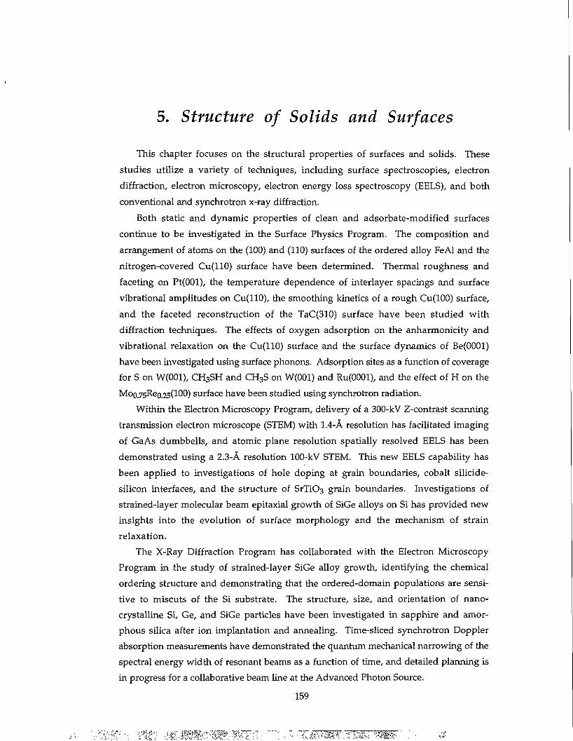
5. Structure of Solids and Surfaces
This chapter focuses on the structural properties of surfaces and solids. These studies utilize a variety of techniques, including surface spectroscopies, electron diffraction, electron microscopy, electron energy loss spectroscopy (EELS), and both conventional and synchrotron x-ray diffraction.
Both static and dynamic properties of clean and adsorbate-modified surfaces continue to be investigated in the Surface Physics Program. The composition and arrangement of atoms on the (100) and (110) surfaces of the ordered alloy FeAl and the nitrogen-covered Cu(110) surface have been determined. Thermal roughness and faceting on Pt(001), the temperature dependence of interlayer spacings and surface vibrational amplitudes on Cu(110), the smoothing kinetics of a rough Cu(100) surface, and the faceted reconstruction of the TaC(310) surface have been studied with diffraction techniques. The effects of oxygen adsorption on the anharmonicity and vibrational relaxation on the Cu(110) surface and the surface dynamics of Be(0001) have been investigated using surface phonons. Adsorption sites as a function of coverage for S on W(001), CH3SH and CH3S on W(001) and Ru(0001), and the effect of H on the Moo.75Reo.25(100) surface have been studied using synchrotron radiation.
Within the Electron Microscopy Program, delivery of a 300-kV Z-contrast scanning transmission electron microscope (STEM) with 1.4-A resolution has facilitated imaging of GaAs dumbbells, and atomic plane resolution spatially resolved EELS has been demonstrated using a 2.3-A resolution 100-kV STEM. This new EELS capability has been applied to investigations of hole doping at grain boundaries, cobalt silicide-silicon interfaces, and the structure of SrTiC>3 grain boundaries. Investigations of strained-layer molecular beam epitaxial growth of SiGe alloys on Si has provided new insights into the evolution of surface morphology and the mechanism of strain relaxation.
The X-Ray Diffraction Program has collaborated with the Electron Microscopy Program in the study of strained-layer SiGe alloy growth, identifying the chemical ordering structure and demonstrating that the ordered-domain populations are sensitive to miscuts of the Si substrate. The structure, size, and orientation of nano-crystalline Si, Ge, and SiGe particles have been investigated in sapphire and amorphous silica after ion implantation and annealing. Time-sliced synchrotron Doppler absorption measurements have demonstrated the quantum mechanical narrowing of the spectral energy width of resonant beams as a function of time, and detailed planning is in progress for a collaborative beam line at the Advanced Photon Source.
159
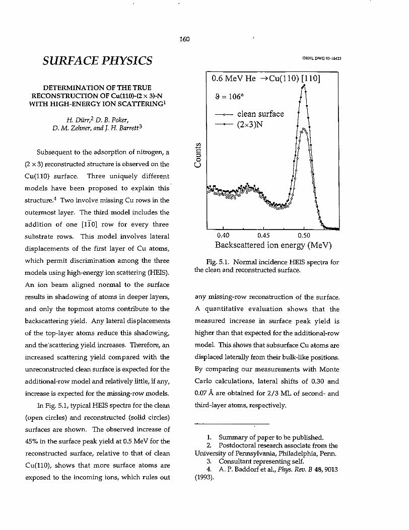
SURFACE PHYSICS
DETERMINATION OF THE TRUE RECONSTRUCTION OF Cu(110)-(2 x 3)-N
WITH HIGH-ENERGY ION SCATTERING1
H. Diirr,2 D. B. Poker, D. M. Zehner, and}. H. Barrett3
Subsequent to the adsorption of nitrogen, a
(2 x 3) reconstructed structure is observed on the
Cu(llO) surface. Three uniquely different
models have been proposed to explain this
structure. 4 Two involve missing Cu rows in the
outermost layer. The third model includes the
addition of one [110] row for every three
substrate rows. This model involves lateral
displacements of the first layer of Cu atoms,
which permit discrimination among the three
models using high-energy ion scattering (HEIS).
An ion beam aligned normal to the surface
results in shadowing of atoms in deeper layers,
and only the topmost atoms contribute to the
backscattering yield. Any lateral displacements
of the top-layer atoms reduce this shadowing,
and the scattering yield increases. Therefore, an
increased scattering yield compared with the
unreconstructed clean surface is expected for the
additional-row model and relatively little, if any,
increase is expected for the missing-row models.
In Fig. 5.1, typical HEIS spectra for the clean
(open circles) and reconstructed (solid circles)
surfaces are shown. The observed increase of
45% in the surface peak yield at 0.5 MeV for the
reconstructed surface, relative to that of clean
Cu(110), shows that more surface atoms are
exposed to the incoming ions, which rules out
160
ORNL DWG 93-16423
0.40 0.45 0.50 Backscattered ion energy (MeV)
Fig. 5.1. Normal incidence HEIS spectra for the clean and reconstructed surface.
any missing-row reconstruction of the surface.
A quantitative evaluation shows that the
measured increase in surface peak yield is
higher than that expected for the additional-row
model. This shows that subsurface Cu atoms are
displaced laterally from their bulk-like positions.
By comparing our measurements with Monte
Carlo calculations, lateral shifts of 0.30 and
0.07 A are obtained for 2 / 3 ML of second- and
third-layer atoms, respectively.
1. Summary of paper to be published. 2. Postdoctoral research associate from the
University of Pennsylvania, Philadelphia, Perm. 3. Consultant representing self. 4. A. P. Baddorf et al., Phys. Rev. B 48,9013
(1993).
161
TERRACE-WIDTH AND STEP-HEIGHT ENLARGEMENT: RECONSTRUCTION OF
THE TaC(310) SURFACE1
J.-K. ZucP- and D. M. Zehner
Because atoms in a surface might not be in a stable state when the surface is created, a reconstruction into a new energetically favored state differing from the bulk truncation frequently occurs. These new surface structures provide an opportunity for investigating and understanding the driving forces and their contributions to the surface-free energy, a rich testing ground for two-dimensional statistical models of collective phenomena and can serve as templates for epitaxial growth. Mechanisms for surface reconstructions of elemental materials can generally be grouped into atomic displacements, missing rows, facets, and their combinations. It has been shown that the TaC(llO) surface exhibits a massive unidirectional reconstruction.3 To determine if this reconstruction exists for other TaC surfaces, the (310) surface has been examined using high-resolution electron energy loss spectroscopy. The ideally truncated surface exhibits the staircase structure shown in Figs. 5.2(a) and 5.2(b). Instead of this arrangement, from the diffraction results a tripling of the terrace width and step height has been observed as shown in Fig. 5.2(c), maintaining the staircase geometry. On average, each unit of the reconstructed surface consists of a (100) terrace with nine row spacings and a (010) step wall with a step height of three row spacings. This structure is dramatically different from the ideal, bulk truncation for which each unit consists of a (100) terrace with three row spacings and a single-step
(a) Q :: o • o • o •
. o • o 2.228 A-H a i~
step edge 9 * o
(b) o • ^o- ^ • o • o
o
o-^Ta
(100) (310)
-18.44°
[001], z L [ 0 1 0 ] , y
f t o • o • o -!-• O • O
2.228 A
• o • -o - _ o • o • o •"" -o-
r ^ 3 a ^
(c) o • ^o-• o • o • o • o •-'-o o • o
9 a -o • •©-
Fig. 5.2. (a) and (b) are the top view from the [100] direction and side view from the [001] direction, respectively, for the ideally truncated TaC(310) surface, where the elongated circle indicates the Ta-C basis and the square is the surface unit mesh, (c) is the side view of the reconstructed TaC(310) surface.
height step. These are believed to be trapped during the reconstruction process. Also, the step edges are shown to be well-ordered through the angular profile analysis.
1. Summary of paper: Phys. Rev. B 46, 16122 (1992).
2 ORISE faculty research participant from Southwest Missouri State University, Springfield, Mo.
3. J.-K. Zuo et al., Phys. Rev. B 47,10743 (1993).
162
SEGREGATION AND OXIDATION BEHAVIOR OF THE
Fe0.53Al0.47(110) SURFACE
H. Graupner,1 L. Hammer,2
K. Muller,2 and D. M. Zehner
Transit ion-metal a luminides are very
promising materials for high strength and
medium- to high-temperature applications. The
most widely studied systems in this respect are
NiAl and FeAl. Both form ordered intermetallic
alloys of the CsCl type. The surface structure of
clean NiAl(l lO) 3 and its oxidation behavior 4
have been investigated in great detail. This sur
face shows a bulk-like termination with a large
rippled reconstruction over a wide temperature
range, whereas Feo.53Alo.47(110) is characterized
by several different surface structures, caused by
Al segregation with increasing temperatures.
Following sputtering at room temperature, the
disordered surface is depleted in Al. Annealing
this surface to ~400°C leads to a (2 x 1) super
structure in the low-energy electron diffraction
pattern. Further annealing to ~600°C gives rise
to an incommensurate superstructure, probably
formed by a segregated monolayer of Al. Above
~600°C, the Al concentration on the surface does
not increase further. The diffraction pattern in
this temperature region shows severe streaking,
which might result from the development of
(lOO)-oriented facets, possibly terminated in Al
like the (100) surface. 5 At temperatures higher
than 800°C, Al sublimes resulting in the forma
tion of the incommensurate surface. The differ
ing behavior of the surface of these two alloys
can be understood by considering their heats of
formation. The FeAl alloy gains only 24 kj/mol
by forming the CsCl-like structure, compared
with 59 kj/mol for NiAl. It is, therefore, ener
getically more favorable for the FeAl system to
lower its total energy by lowering the surface-
free energy by Al segregation.
The compos i t ion of the oxide on
Feo.53Alo.47(110) is dependent on the oxidation
rate. For low rates, such as in normal ultrahigh
vacuum experiments, a film of pure AI2O3 is
formed, passivating the surface against further
oxidation. At very high oxidation rates, a
thicker film develops, which contains FeO as
well. This behavior is different with respect to
the NiAl alloy, where only films of AI2O3 form.
For FeAl, the film is amorphous up to ~500°C;
while at higher temperatures, the structure of
the film is related to a metastable modification of
AI2O3. Between 500° and 700°C, Y-AI2O3 forms.
Around 850°C, a well-ordered film of most
probably 8-AI2O3 grows, which is a tetragonally
distorted form of the y modification. Even at
very low exposures of oxygen, the sharp diffrac
tion pattern of the film is already visible, indicat
ing initial film growth by island formation. An
oxide film with identical structure is observed
on NiAl(llO). On both alloys, the oxide layer
decomposes with the upper boundary of the
stability region for the d modification of the
oxide.
1. Graduate student from the University of Erlangen-Ntirnberg, Germany.
2. Guest scientist from the University of Erlangen-Nurnberg, Germany.
3. H. L. Davis and J. R. Noonan, Phys. Rev. Lett. 54, 566 (1985).
163
4. D. M. Zehner and G. R. Gruzalski, Mat. Res. Soc. Symp. Proc. 83,199 (1987).
5. C. P. Wang et al.,Surf. Sci. 298,114 (1993).
X-RAY REFLECTIVITY OF THE Cu(llO) SURFACE1
G. Helgesen,2 Doon Gibbs,2A. P. Baddorf, D. M. Zehner, and S. G. J. Mochrie?
It is generally expected that the surface of a crystal will become more disordered as the tern-perature is raised toward the bulk melting point. In this work, structural disorder in the Cu(llO) surface has been studied between 300 and 1000 K using x-ray specular reflectivity. Transverse scans (8 scans) were measured for a range of values of the surface-normal wave vector Q r
The data were analyzed with two approaches: transverse line shapes identified long-range order parallel to the surface, and integrated intensities were modeled to determine unit cell structures normal to the surface. For small values of Q ., line shapes exhibited two components, one sharp (resolution limited), the other broad. In our view, the simplest interpretation involves surface faceting. The narrow component originates from flat terraces with widths at 300 K greater than 2000 A. The broad component results from surface regions with high step densities at 300 K on the order of 600 A wide. Steps appear to be pinned at 300 K to limited regions of the surface, probably by defects. As the temperature is increased, the sharp component slowly disappears, while the broad component increases slightly in intensity and width. This suggests the steps are no longer pinned and
proliferate across the formerly smooth (110) facets. No distinct phase transition is observed nor was it possible to characterize the long-range behavior of the height-height correlation function, as is necessary to distinguish rough and step-disordered surfaces.
Integrated peak intensities, or reflectivities, were compared with a model using simple calculations to determine atomic displacements and root-mean-square (rms) vibrational amplitudes normal to the surface. At 300 K, the outermost layer was found to be contracted 7.9% of the bulk layer spacing, and the second layer expanded 2%. These values agree with those of other surface techniques and are typical for fcc(110) metal surfaces. As T is increased, the outerlayer relaxation decreases to 4.5% at 950 K. This rate of thermal expansion is four times greater than that in the bulk. The expansion rate at the surface appears to be nonlinear, increasing at higher temperatures, particularly above 700 K. At the same time, rms vibrational amplitudes also increase. At 300 K, the rms of the outermost layer is about 50% greater than the bulk value, with second and lower levels essentially bulk-like. Above 700 K, the rms of the outermost layer increases to three times the bulk value, and second and third layer values are significantly increased. The increases in rms motion with temperature are also nonlinear. Both the greater thermal expansion and rms motion of the surface layers indicate enhanced anharmonicity of the Cu(110) surface.
1. Summary of paper: Phys. Rev. B 48, 15320 (1993).
164
2. Brookhaven National Laboratory, Upton, N.Y.
3. Massachusetts Institute of Technology, Cambridge, Mass.
THERMAL ROUGHNESS OF A CLOSE-PACKED METAL SURFACE: Pt(OOl)1
D. L. Abemathy,2 S. G.}. Mochrie,2
D. M. Zehner, G. Grubel,3 and D. Gibbs3
The equilibrium shape of a crystal of fixed
volume is determined by the minimum of its
surface-free energy. In many cases, the equilib
rium shape involves facets. For example, the
(001) and (111) orientations of fee metals are
believed to be faceted at room temperature.
However, at high temperatures, orientations
which appear rounded, reminiscent of a liquid
droplet, may also occur. Crystal surfaces which
correspond to rounded orientations are expected
to support capillary modes in a manner similar
to liquid surfaces. In both cases, liquid and
solid, a surface with capillary modes is rough.
X-ray scattering was used to s tudy the
Pt(001) surface from room temperature to the
bulk melting temperature. Because of the fine
reciprocal space resolution possible with x-ray
scattering techniques, it has been possible to
investigate the surface morphology on length
scales up to several thousand angstroms. Below
1820 K, the line shape of the specular reflectivity
indicates that the clean hexagonally recon
structed surface is atomically smooth on length
scales exceeding 5000 A. However, above
1820 K, there is a dramatic change in the profile
shape which indicates that the surface is rough.
The results yield new insight into the micro
scopic structure of a rough metal surface.
Specifically, the scattering near the specular
condition is diffuse and may be modeled using a
height-height correlation function which
diverges logarithmically at large distances. In
addition, it was found that the average separa
tion between thermally generated steps is many
lattice constraints.
1. Summary of paper: Phys. Rev. Lett. 69, 941 (1993).
2. Massachusetts Institute of Technology, Cambridge, Mass.
3. Brookhaven National Laboratory, Upton, N.Y.
FACETING TRANSFORMATIONS OF THE STEPPED Pt(001) SURFACE1
G. M. Watson2 D. Gibbs2 D. M. Zehner, M. Yoon,3 and S. G. J. Mochrie3
Equilibrium faceting is a remarkable phe
nomenon in which a crystal surface increases its
area in order to decrease its free energy. It is
accomplished through the rearrangement of sur
face steps so that their distribution across the
surface is no longer uniform. Instead, the
surface separates into regions of high and low
step densities. Our present understanding of
faceting is based on a description of the surface-
free energy in which the surface orientation is a
key thermodynamic variable. Thus, a faceting
transformation is an example of thermodynamic
phase separation in which a surface phase of
uniform orientation is replaced by coexistence
among phases with different orientations and
separated by sharp edges.
165
To investigate this phenomenon, x-ray scattering and a Pt sample in which the surface normal was deliberately miscut by 1.4° away from the (001) direction and toward the (110) direction have been used. This corresponds to an average monatomic step separation of approximately 30 near-neighbor distances. For temperatures above T0 = 1820 K, the surface reflectivity is aligned to the direction of the macroscopic miscut. Its line shape is diffuse and suggests that the miscut surface is rough as was found for the (OOl)-oriented surface at these temperatures. Below 1820 K, there is a faceting transformation which leads to coexistence among hexagonally reconstructed, step-free domains, called facets, aligned to the (001) direction, and stepped, unreconstructed domains. Between 1820 and 1620 K, the phase behavior of the (001) facets is similar to that of the Pt(001) surface. On the stepped domains, the surface normal is tilted at an angle a to the (001) direction. Remarkably, the data show that a follows a one-half power-law dependence on reduced temperature. This implies that the free energy of a rough, solid surface varies quadratically with misorientation, consistent with simple theoretical ideas.
At 1620 K, there is a second faceting transformation at which the rough domains disappear. Instead, the surface is populated by two new domain types with ordered step distributions, in addition to the step-free, hexagonally reconstructed (001) facets. The terraces of the stepped domains are reconstructed to form a buckled and rotated hexagonal structure. Surface buckling refers to the sinusoidal displace-
•:y-&:v mimmmm:m^;-.
ment of atoms along the surface normal direc
tion and is a defining characteristic of the close-
packed, hexagonal reconstructions of Pt and
Au(001) surfaces. Finally, for temperatures
below 1500 K, the step wave vector locks to the
buckling wave vector with a periodicity four
times smaller than the terrace width. This corre
sponds to the first experimental observation of
the formation of a commensurate magic vicinal.
1. Summary of paper: Phys. Rev. Lett. 71, 3166 (1993).
2. Brookhaven National Laboratory, Upton, N.Y.
3. Massachusetts Institute of Technology, Cambridge, Mass.
EXPERIMENTAL STUDY OF SMOOTHING KINETICS ON A ROUGH SURFACE1
J.-KZuo2 and }. F. Wendelken
While a substantial body of theoretical work examines the mechanisms by which a smooth layer develops using molecular beam epitaxy, experimental work has been extremely limited. In this work, high-angular-resolution low-energy electron diffraction has been used to observe for the first time the smoothing kinetics of a rough surface prepared by the epitaxial deposition of Cu on Cu(100) to produce a multilayer terrace-type structure. Upon deposition of Cu on Cu(100) at room temperature on an initially smooth Cu(100) surface, square islands developed in the first atomic layer. But with the deposition equivalent of 100 atomic layers, the surface developed a multilevel terrace structure
yw%&:rMvm~~
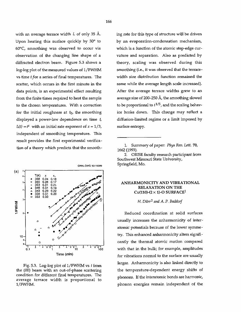
166
with an average terrace width L of only 35 A.
Upon heating this surface quickly by 30° to
60°C, smoothing was observed to occur via
observation of the changing line shape of a
diffracted electron beam. Figure 5.3 shows a
log-log plot of the measured values of 1/FWHM
vs time f/or a series of final temperatures. The
scatter, which occurs in the first minute in the
data points, is an experimental effect resulting
from the finite times required to heat the sample
to the chosen temperatures. With a correction
for the initial roughness at to, the smoothing
displayed a power-law dependence on time t,
L(t) °=F with an initial rate exponent of x = 1/3,
independent of smoothing temperature. This
result provides the first experimental verifica
tion of a theory which predicts that the smooth-
ORNL-DWG 93-15399
(a)
2 X
10-
T(K) x x, 368 0.24 0.18 360 0.26 0.17 353 0.31 348 0.31 343 0.29 338 0.31 333 0.30
'I 0.1
i 1 i ' A T I 1 I ' i ' i ' i ' l
10 4 ' i ' A T I
100 Time (min)
Fig. 5.3. Log-log plot of 1/FWHM vs t from the (00) beam with an out-of-phase scattering condition for different final temperatures. The average terrace width is proport ional to 1/FWHM.
ing rate for this type of structure will be driven
by an evaporation-condensation mechanism,
which is a function of the atomic step-edge cur
vature and separation. Also as predicted by
theory, scaling was observed dur ing this
smoothing (i.e., it was observed that the terrace-
width size distribution function remained the
same while the average length scale increased).
After the average terrace widths grew to an
average size of 200-250 A, the smoothing slowed
to be proportional to t1^5, and the scaling behav
ior broke down. This change may reflect a
diffusion-limited regime or a limit imposed by
surface entropy.
1. Summary of paper: Phys Rev. Lett. 70, 1662 (1993).
2. ORISE faculty research participant from Southwest Missouri State University, Springfield, Mo.
ANHARMONICITY AND VIBRATIONAL RELAXATION ON THE
Cu(110)-(2 x D-O SURFACE1
H. Diirr2 and A. P. Baddorf
Reduced coordination at solid surfaces
usually increases the anharmonicity of inter
atomic potentials because of the lower symme
try. This enhanced anharmonicity alters signifi
cantly the thermal atomic motion compared
with that in the bulk; for example, amplitudes
for vibrations normal to the surface are usually
larger. Anharmonicity is also linked directly to
the temperature-dependent energy shifts of
phonons. If the interatomic bonds are harmonic,
phonon energies remain independent of the
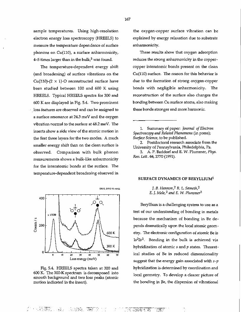
167
sample temperatures. Using high-resolution electron energy loss spectroscopy (HREELS) to measure the temperature dependence of surface phonons on Cu(llO), a surface anharmonicity, 4-5 times larger than in the bulk,3 was found.
The temperature-dependent energy shift (and broadening) of surface vibrations on the Cu(110)-(2 x l ) -0 reconstructed surface have been studied between 100 and 600 K using HREELS. Typical HREELS spectra for 300 and 600 K are displayed in Fig. 5.4. Two prominent loss features are observed and can be assigned to a surface resonance at 24.3 meV and the oxygen vibration normal to the surface at 48.2 meV. The inserts show a side view of the atomic motion in the first three layers for the two modes. A much smaller energy shift than on the clean surface is observed. Comparison with bulk phonon measurements shows a bulk-like anharmonicity for the interatomic bonds at the surface. The temperature-dependent broadening observed in
ORNL DWG 93-16-122
400
S 200 -o U
20 30 40 50
Loss energy (meV)
Fig. 5.4. HREELS spectra taken at 300 and 600 K. The 300-K spectrum is decomposed into smooth background and two loss peaks (atomic motion indicated in the insert).
the oxygen-copper surface vibration can be explained by energy relaxation due to substrate anharmonicity.
These results show that oxygen adsorption reduces the strong anharmonicity in the copper-copper interatomic bonds present on the clean Cu(110) surface. The reason for this behavior is due to the formation of strong oxygen-copper bonds with negligible anharmonicity. The reconstruction of the surface also changes the bonding between Cu surface atoms, also making these bonds stronger and more harmonic.
1. Summary of paper: Journal of Electron Spectroscopy and Related Phenomena (in press); Surface Science, to be published.
2. Postdoctoral research associate from the University of Pennsylvania, Philadelphia, Pa.
3. A. P. Baddorf and E. W. Plummer, Phys. Rev. Lett. 66,2770 (1991).
SURFACE DYNAMICS OF BERYLLIUM1
/. E. Hannon,2 R. L. Sameth,2
E. ]. Mele2 and E. W. Plummer3
Beryllium is a challenging system to use as a test of our understanding of bonding in metals because the mechanism of bonding in Be depends dramatically upon the local atomic geometry. The electronic configuration of atomic Be is ls 22s 2 . Bonding in the bulk is achieved via hybridization of atomic s and p states. Theoretical studies of Be in reduced dimensionality suggest that the energy gain associated with s-p hybridization is determined by coordination and local geometry. To develop a clearer picture of the bonding in Be, the dispersion of vibrational
•;$mw
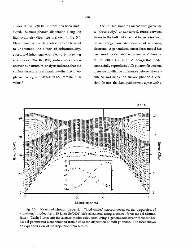
168
modes at the Be(0001) surface has been mea
sured. Surface phonon dispersion along the
high-symmetry directions is shown in Fig. 5.5.
Measurements of surface vibrations can be used
to understand the effects of anharmonicity,
stress, and inhomogeneous electronic screening
at surfaces. The Be(0001) surface was chosen
because our structural analysis indicates that the
surface structure is anomalous—the first inter-
planar spacing is expanded by 6% from the bulk
value. 4
The unusual bonding mechanism gives rise
to "three-body," or noncentral, forces between
atoms in the bulk. Noncentral forces arise from
an inhomogeneous distribution of screening
electrons. A generalized tensor-force model has
been used to calculate the dispersion of phonons
at the Be(0001) surface. Although this model
successfully reproduces bulk phonon dispersion,
there are qualitative differences between the cal
culated and measured surface phonon disper
sion. In fact, the data qualitatively agree with a
SSD 4671
80-
60
> o 6 >-. S3 4 0 -c W
20-
0-1
;:,:ii:!-ii::!!!'',/;::!:£=!;i$iijiii!!:;|i'' ••''
. • V . , ! : ! : : ! • '
- 20
Mi' 1 V \ , : - i V
'.•••J
4 " i -„ ' " -»
44- s
m. i • • ' 43 - * 42 - * 4 1 - •
4 0 - • . 1 1 ••
W-
^lilPift-iiP^ %fg
m «£
15
3 ft "-!
N
J - 0 1 K M r
Momentum (Arb.)
Fig. 5.5. Measured phonon dispersion (filled circles) superimposed on the dispersion of vibrational modes for a 30-layer Be(0001) slab calculated using a central-force model (dotted lines). Dashed lines are the surface modes calculated using a generalized tensor-force model. Model parameters were obtained from a fit to the dispersion of bulk phonons. The inset shows an expanded view of the dispersion from K to M.
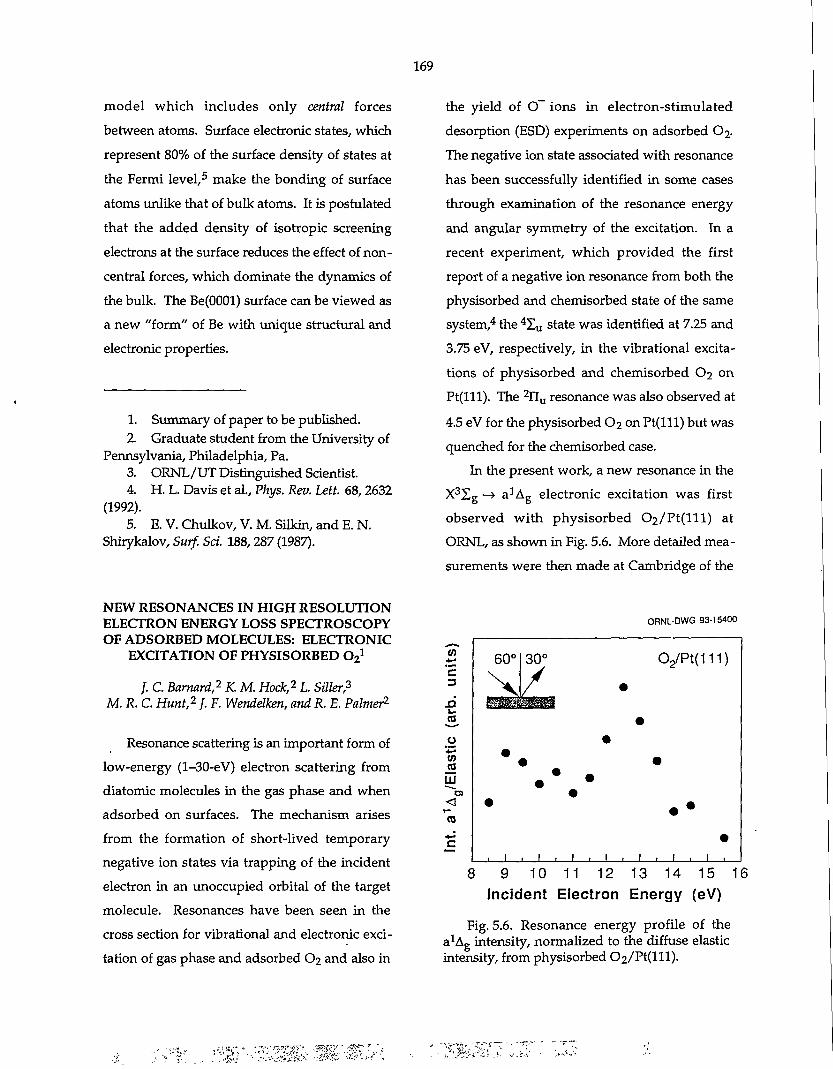
169
model which includes only central forces between atoms. Surface electronic states, which represent 80% of the surface density of states at the Fermi level,5 make the bonding of surface atoms unlike that of bulk atoms. It is postulated that the added density of isotropic screening electrons at the surface reduces the effect of non-central forces, which dominate the dynamics of the bulk. The Be(0001) surface can be viewed as a new "form" of Be with unique structural and electronic properties.
1. Summary of paper to be published. 2. Graduate student from the University of
Pennsylvania, Philadelphia, Pa. 3. ORNL/UT Distinguished Scientist. 4. H. L. Davis et al., Phys. Rev. Lett. 68,2632
(1992). 5. E. V. Chulkov, V. M. Silkin, and E. N.
Shirykalov, Surf. Sci. 188,287 (1987).
the yield of O - ions in electron-stimulated desorption (ESD) experiments on adsorbed O2. The negative ion state associated with resonance has been successfully identified in some cases through examination of the resonance energy and angular symmetry of the excitation. In a recent experiment, which provided the first report of a negative ion resonance from both the physisorbed and chemisorbed state of the same system,4 the 4 Z U state was identified at 7.25 and 3.75 eV, respectively, in the vibrational excitations of physisorbed and chemisorbed O2 on Pt(lll). The 2 n u resonance was also observed at 4.5 eV for the physisorbed O2 on Pt(lll) but was quenched for the chemisorbed case.
In the present work, a new resonance in the X3I E -> a1A„ electronic excitation was first -g ^ a "g observed with physisorbed 02 /P t ( l l l ) at ORNL, as shown in Fig. 5.6. More detailed mea
surements were then made at Cambridge of the
NEW RESONANCES IN HIGH RESOLUTION ELECTRON ENERGY LOSS SPECTROSCOPY OF ADSORBED MOLECULES: ELECTRONIC
EXCITATION OF PHYSISORBED O21
/. C. Barnard,2 K. M. Hock,2 L. Siller,3
M. R. C. Hunt,2 f. F. Wendelken, and R. E. Palmer2
Resonance scattering is an important form of low-energy (1-30-eV) electron scattering from diatomic molecules in the gas phase and when adsorbed on surfaces. The mechanism arises from the formation of short-lived temporary negative ion states via trapping of the incident electron in an unoccupied orbital of the target molecule. Resonances have been seen in the cross section for vibrational and electronic excitation of gas phase and adsorbed O2 and also in
ORNL-DWG 93-15400
(0 *^ E 3
S3 i_
3-o *s <n jo UJ
a < CO
8 9 10 11 12 13 14 15 16 Incident Electron Energy (eV)
Fig. 5.6. Resonance energy profile of the a 2 A g intensity, normalized to the diffuse elastic intensity, from physisorbed 02/Pt(lll).
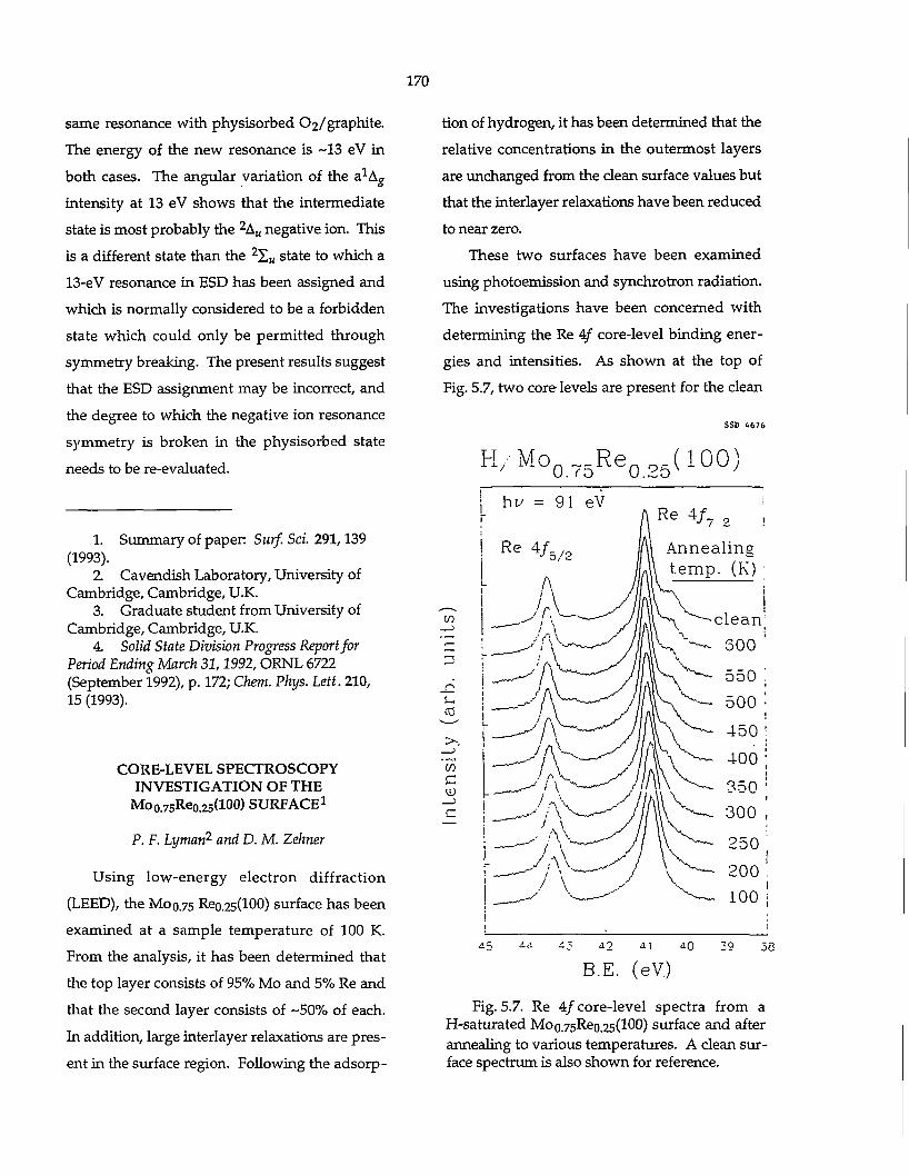
170
same resonance with physisorbed 02/graphite.
The energy of the new resonance is ~13 eV in
both cases. The angular variation of the a)-Ag
intensity at 13 eV shows that the intermediate
state is most probably the 2AU negative ion. This
is a different state than the 2 E U state to which a
13-eV resonance in ESD has been assigned and
which is normally considered to be a forbidden
state which could only be permitted through
symmetry breaking. The present results suggest
that the ESD assignment may be incorrect, and
the degree to which the negative ion resonance
symmetry is broken in the physisorbed state
needs to be re-evaluated.
1. Summary of paper: Surf. Sci. 291,139 (1993).
2 Cavendish Laboratory, University of Cambridge, Cambridge, U.K.
3. Graduate student from University of Cambridge, Cambridge, U.K.
4. Solid State Division Progress Report for Period Ending March 31,1992, ORNL 6722 (September 1992), p. 172; Chem. Phys. Lett. 210, 15 (1993).
CORE-LEVEL SPECTROSCOPY INVESTIGATION OF THE
Moo.75Re0.25(100) SURFACE 1
P. F. Lyman2 and D. M. Zehner
Using low-energy electron diffraction
(LEED), the Mo 0.75 Reo.2s(100) surface has been
examined at a sample temperature of 100 K.
From the analysis, it has been determined that
the top layer consists of 95% Mo and 5% Re and
that the second layer consists of -50% of each.
In addition, large interlayer relaxations are pres
ent in the surface region. Following the adsorp
tion of hydrogen, it has been determined that the
relative concentrations in the outermost layers
are unchanged from the clean surface values but
that the interlayer relaxations have been reduced
to near zero.
These two surfaces have been examined
using photoemission and synchrotron radiation.
The investigations have been concerned with
determining the Re 4/ core-level binding ener
gies and intensities. As shown at the top of
Fig. 5.7, two core levels are present for the clean
SSD 6676
/ 0. ro 0.2o v J
hv = 91 eV Re 4 / 7 2
aling t e m p . (K)
(n
>-, )
c
4 ? A\ *0 30
B.E. (eV.)
Fig. 5.7. Re 4 / core-level spectra from a H-saturated Moo.7sReo.25(100) surface and after annealing to various temperatures. A clean surface spectrum is also shown for reference.
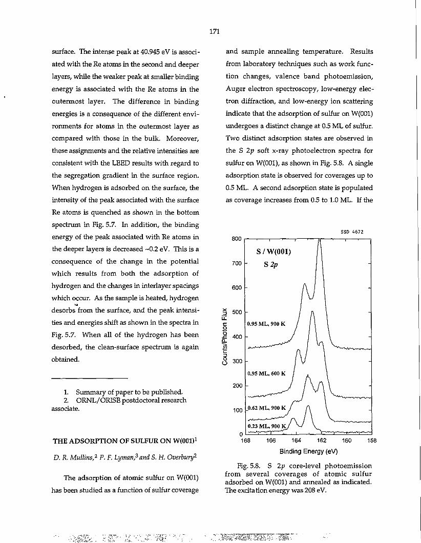
171
surface. The intense peak at 40.945 eV is associated with the Re atoms in the second and deeper layers, while the weaker peak at smaller binding energy is associated with the Re atoms in the outermost layer. The difference in binding energies is a consequence of the different environments for atoms in the outermost layer as compared with those in the bulk. Moreover, these assignments and the relative intensities are consistent with the LEED results with regard to the segregation gradient in the surface region. When hydrogen is adsorbed on the surface, the intensity of the peak associated with the surface Re atoms is quenched as shown in the bottom spectrum in Fig. 5.7. In addition, the binding energy of the peak associated with Re atoms in the deeper layers is decreased ~0.2 eV. This is a consequence of the change in the potential which results from both the adsorption of hydrogen and the changes in interlayer spacings which occur. As the sample is heated, hydrogen desorbs from the surface, and the peak intensities and energies shift as shown in the spectra in Fig. 5.7. When all of the hydrogen has been desorbed, the clean-surface spectrum is again obtained.
1. Summary of paper to be published. 2. ORNL/ORISE postdoctoral research
associate.
THE ADSORPTION OF SULFUR ON W(OOl)1
D. R. Mullins,2 P. F. Lyman,3 and S. H. Overbury2
The adsorption of atomic sulfur on W(001) has been studied as a function of sulfur coverage
and sample annealing temperature. Results from laboratory techniques such as work function changes, valence band photoemission, Auger electron spectroscopy, low-energy electron diffraction, and low-energy ion scattering indicate that the adsorption of sulfur on W(001) undergoes a distinct change at 0.5 ML of sulfur. Two distinct adsorption states are observed in the S 2p soft x-ray photoelectron spectra for sulfur on W(001), as shown in Fig. 5.8. A single adsorption state is observed for coverages up to 0.5 ML. A second adsorption state is populated as coverage increases from 0.5 to 1.0 ML. If the
168 166 164 162 160 158
Binding Energy (eV)
Fig. 5.8. S 2p core-level photoemission from several coverages of atomic sulfur adsorbed on W(001) and annealed as indicated. The excitation energy was 208 eV.
172
sample is annealed to 600 K, the two states are
occupied by nearly equal amounts of sulfur at
1.0 ML. However, if the sample is annealed to
900 K, most of the sulfur which originally
adsorbed in the low-coverage state is shifted to
the new state.
The prevai l ing s t ruc tura l mode l for
S/W(001) is that the sulfur adatoms occupy
evenly dispersed fourfold sites up to a coverage
of 0.5 ML. The low-coverage state observed in
the S 2p spectra is consistent with this model.
Crowding between the sulfur atoms makes con
tinued adsorption in the fourfold sites unfavor
able at higher coverage. The S 2p spectra indi
cate either that lower coordination sites are
populated on an unperturbed surface or that the
surface is reconstructed. Low-energy ion scat
tering experiments and high-resolution photo -
emission spectra from the W 4 / level provide
strong evidence that the substrate reconstructs,
resulting in vacancy formation at high sulfur
coverages and elevated temperatures.
1. Summary of paper: Surf. Sci. 277,64 (1992).
2. Chemistry Division, ORNL. 3. ORNL/ORISE postdoctoral research
associate. Present address: Northwestern University, Evanston, Ind.
METHANETHIOL ON W(001) ANDRu(OOOl)1
D. R. Mullins2 and P. F. Lyman3
The adsorption and decomposit ion of
methanethiol, CH 3 SH, on W(001) and Ru(0001)
have been studied as a function of coverage and
temperature. As has been observed on other
surfaces, CH3SH follows two distinct reaction
pa thways on W(001) and Ru(0001)—-total
decomposition to adsorbed atomic sulfur and
carbon with desorption of molecular hydrogen
or partial decomposition to adsorbed sulfur and
desorbed methane. Ru(0001) is more reactive in
the sense that carbon-sulfur bond cleavage
occurs at a lower temperature on Ru(0001) than
on W(001). Methyl thiolate, CH 3 S, is readily
formed at 100 K on both surfaces. The adsorp
tion and reaction of CH3SH were followed by
temperature-programmed desorption, soft x-ray
photoelectron spectroscopy (SXPS), Auger elec
tron spectroscopy, and valence band photo-
electron spectroscopy.
As shown in Fig. 5.9, numerous adsorption
states can be differentiated in the SXPS spectra
of the S 2p core level. Molecular CH3SH, which
is seen at the highest binding energy, is only
observed at very high exposures at 100 K.
Experiments at coverages up to saturation indi
cate that all of the chemisorbed CH3SH partially
decomposes at 100 K into two distinct states.
The two states are believed to result from the
same nominal species, CH3S, adsorbed in differ
ent adsorption sites. By analogy with atomic
sulfur on W(001), the higher binding energy
state results from CH3S in either a fourfold or
threefold site on W(001) or Ru(001), respectively.
The lower binding energy state results from
adsorption in a twofold or a top site.
1. Summary of papers: /. Phys. Chem. 97, 9226 (1993); Journal of Physical Chemistry (in press).
2. Chemistry Division, ORNL.
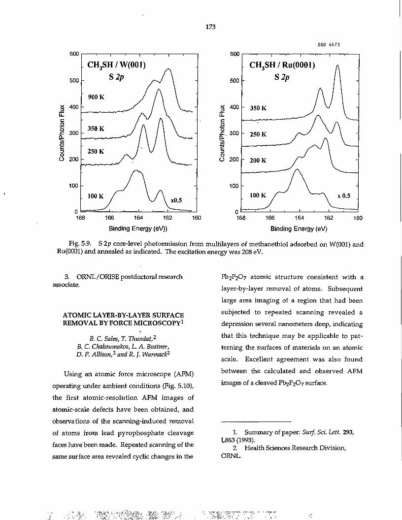
173
SSD 4673
600
168 166 164 162 Binding Energy (eV))
160
600
166 164 162 Binding Energy (eV)
160
Fig. 5.9. S 2p core-level photoemission from multilayers of methanethiol adsorbed on W(001) and Ru(0001) and annealed as indicated. The excitation energy was 208 eV.
3. ORNL/ORISE postdoctoral research associate.
ATOMIC LAYER-BY-LAYER SURFACE REMOVAL BY FORCE MICROSCOPY1
B. C. Sales, T. Thundat,2
B. C. Chakoumakos, L. A. Boatner, D. P. Allison,2 and R. /, Warmack2
Using an atomic force microscope (AFM)
operating under ambient conditions (Fig. 5.10),
the first atomic-resolution AFM images of
atomic-scale defects have been obtained, and
observations of the scanning-induced removal
of atoms from lead pyrophosphate cleavage
faces have been made. Repeated scanning of the
same surface area revealed cyclic changes in the
Pt ,2P207 atomic structure consistent with a
layer-by-layer removal of atoms. Subsequent
large area imaging of a region that had been
subjected to repeated scanning revealed a
depression several nanometers deep, indicating
that this technique may be applicable to pat
terning the surfaces of materials on an atomic
scale. Excellent agreement was also found
between the calculated and observed AFM
images of a cleaved Pb2P207 surface.
1. Summary of paper: Surf. Sci. Lett. 293, L863 (1993).
2. Health Sciences Research Division, ORNL.
-mm
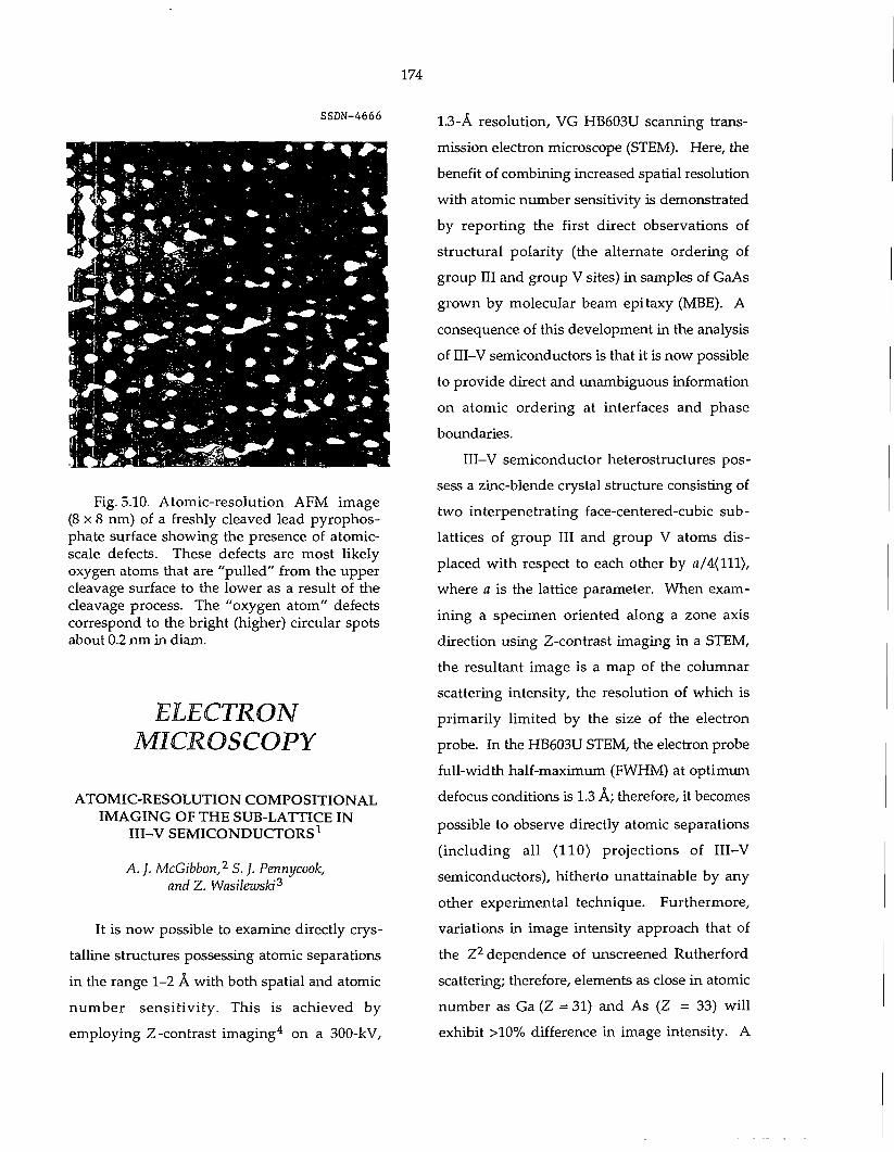
SSDN-4666
Fig. 5.10. Atomic-resolution AFM image ( 8 x 8 ran) of a freshly cleaved lead pyrophosphate surface showing the presence of atomic-scale defects. These defects are most likely oxygen atoms that are "pulled" from the upper cleavage surface to the lower as a result of the cleavage process. The "oxygen atom" defects correspond to the bright (higher) circular spots about 0.2 ran in diam.
ELECTRON MICROSCOPY
ATOMIC-RESOLUTION COMPOSITIONAL IMAGING OF THE SUB-LATTICE IN
III-V SEMICONDUCTORS1
A. ]. McGibbon,2 S.}. Pennycook, and Z. Wasileiuski3
It is now possible to examine directly crys
talline structures possessing atomic separations
in the range 1-2 A with both spatial and atomic
n u m b e r sensi t ivi ty. This is achieved by
employing Z-contrast imaging 4 on a 300-kV,
1.3-A resolution, VG HB603U scanning trans
mission electron microscope (STEM). Here, the
benefit of combining increased spatial resolution
with atomic number sensitivity is demonstrated
by reporting the first direct observations of
structural polarity (the alternate ordering of
group III and group V sites) in samples of GaAs
grown by molecular beam epitaxy (MBE). A
consequence of this development in the analysis
of III-V semiconductors is that it is now possible
to provide direct and unambiguous information
on atomic ordering at interfaces and phase
boundaries.
III-V semiconductor heterostructures pos
sess a zinc-blende crystal structure consisting of
two interpenetrating face-centered-cubic sub-
lattices of group III and group V atoms dis
placed with respect to each other by a /4( l l l ) ,
where a is the lattice parameter. When exam
ining a specimen oriented along a zone axis
direction using Z-contrast imaging in a STEM,
the resultant image is a map of the columnar
scattering intensity, the resolution of which is
primarily limited by the size of the electron
probe. In the HB603U STEM, the electron probe
full-width half-maximum (FWHM) at optimum
defocus conditions is 1.3 A; therefore, it becomes
possible to observe directly atomic separations
(including all (110) projections of III-V
semiconductors), hitherto unattainable by any
other experimental technique. Furthermore,
variations in image intensity approach that of
the Z 2 dependence of unscreened Rutherford
scattering; therefore, elements as close in atomic
number as Ga (Z = 31) and As (Z = 33) will
exhibit >10% difference in image intensity. A
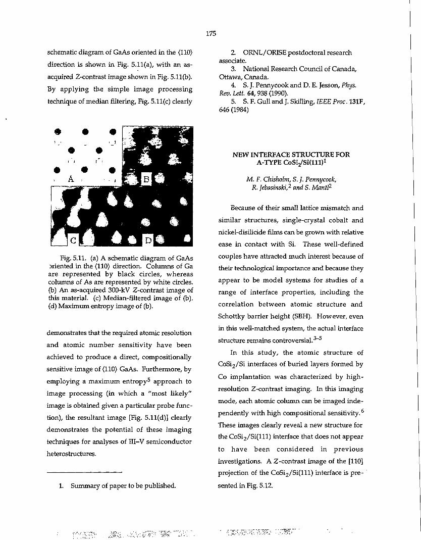
175
schematic diagram of GaAs oriented in the (110)
direction is shown in Fig. 5.11(a), with an as-
acquired Z-contrast image shown in Fig. 5.11(b).
By applying the simple image processing
technique of median filtering, Fig. 5.11(c) clearly
Fig. 5.11. (a) A schematic diagram of GaAs oriented in the (110) direction. Columns of Ga are represented by black circles, whereas columns of As are represented by white circles, (b) An as-acquired 300-kV Z-contrast image of this material, (c) Median-filtered image of (b). (d) Maximum entropy image of (b).
demonstrates that the required atomic resolution and atomic number sensitivity have been achieved to produce a direct, compositionally sensitive image of (110) GaAs. Furthermore, by employing a maximum entropy 5 approach to image processing (in which a "most likely" image is obtained given a particular probe function), the resultant image [Fig. 5.11(d)] clearly demonstrates the potential of these imaging techniques for analyses of III-V semiconductor heterostructures.
1. Summary of paper to be published.
2 ORNL/ORISE postdoctoral research associate.
3. National Research Council of Canada, Ottawa, Canada.
4. S. J. Pennycook and D. E. Jesson, Phys. Rev. Lett. 64,938 (1990).
5. S. F. Gull and J. Skilling, IEEE Proc. 131F, 646 (1984)
NEW INTERFACE STRUCTURE FOR A-TYPE CoSij/SKlll)1
M. F. Chisholm, S. J. Pennycook, R. Jebasinski,2 and S. Mantfi
Because of their small lattice mismatch and similar structures, single-crystal cobalt and nickel-disilicide films can be grown with relative ease in contact with Si. These well-defined couples have attracted much interest because of their technological importance and because they appear to be model systems for studies of a range of interface properties, including the correlation between atomic structure and Schottky barrier height (SBH). However, even in this well-matched system, the actual interface structure remains controversial.3 - 5
In this study, the atomic structure of CoSi2/Si interfaces of buried layers formed by Co implantation was characterized by high-resolution Z-contrast imaging. In this imaging mode, each atomic column can be imaged independently with high compositional sensitivity.6
These images clearly reveal a new structure for the CoSi 2/Si(lll) interface that does not appear to have been considered in previous investigations. A Z-contrast image of the [110] projection of the CoSi 2/Si(lll) interface is presented in Fig. 5.12.
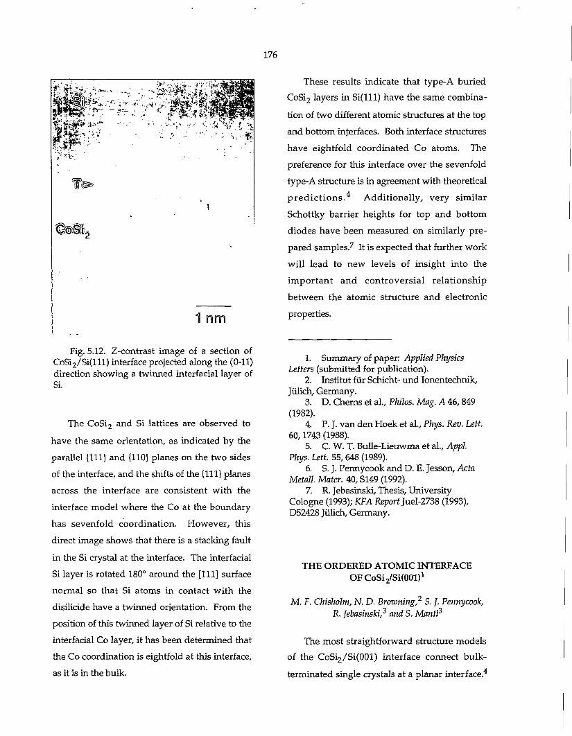
176
IP"
i«iu
1 nm
Fig. 5.12. Z-contrast image of a section of CoSi 2 /Si( l l l ) interface projected along the (0-11) direction showing a twinned interfacial layer of Si.
The CoSi 2 and Si lattices are observed to
have the same orientation, as indicated by the
parallel {111} and {110} planes on the two sides
of the interface, and the shifts of the {111} planes
across the interface are consistent with the
interface model where the Co at the boundary
has sevenfold coordination. However, this
direct image shows that there is a stacking fault
in the Si crystal at the interface. The interfacial
Si layer is rotated 180° around the [111] surface
normal so that Si atoms in contact with the
disilicide have a twinned orientation. From the
position of this twinned layer of Si relative to the
interfacial Co layer, it has been determined that
the Co coordination is eightfold at this interface,
as it is in the bulk.
These results indicate that type-A buried
CoSi 2 layers in Si( l l l ) have the same combina
tion of two different atomic structures at the top
and bottom interfaces. Both interface structures
have eightfold coordinated Co atoms. The
preference for this interface over the sevenfold
type-A structure is in agreement with theoretical
p r e d i c t i o n s . Additionally, very similar
Schottky barrier heights for top and bottom
diodes have been measured on similarly pre
pared samples. 7 It is expected that further work
will lead to new levels of insight into the
impor tant and controversial relat ionship
between the atomic structure and electronic
properties.
1. Summary of paper: Applied Physics Letters (submitted for publication).
2. Institut fur Schicht- und Ionentechnik, Julich, Germany.
3. D. Cherns et al., Philos. Mag. A 46,849 (1982).
4. P. J. van den Hoek et al., Phys. Rev. Lett. 60,1743 (1988).
5. C. W. T. Bulle-Lieuwma et al., Appl. Phys. Lett. 55,648 (1989).
6. S. J. Pennycook and D. E. Jesson, Acta Metall. Mater. 40, S149 (1992).
7. R. Jebasinski, Thesis, University Cologne (1993); KFA Report Juel-2738 (1993), D52428 Julich, Germany.
THE ORDERED ATOMIC INTERFACE OFCoSi^SKOOl)1
M. F. Chisholm, N. D. Browning,2 S. J. Pennycook, R. Jebasinski,3 and S. Mantl3
The most straightforward structure models
of the CoSi 2/Si(001) interface connect bulk-
terminated single crystals at a planar interface. 4
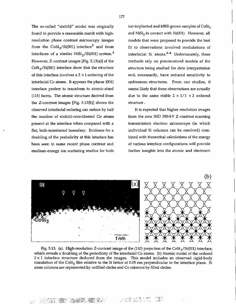
177
The so-called "sixfold" model was originally found to provide a reasonable match with high-resolution phase contrast microscopy images from the CoSi2/Si(001) interface5 and from interfaces of a similar NiSi2/Si(001) system.4
However, Z-contrast images [Fig. 5.13(a)] of the CoSi2/Si(001) interface show that the structure of this interface involves a 2 x 1 ordering of the interfacial Co atoms. It appears the planar {001} interface prefers to transform to atomic-sized {111} facets. The atomic structure derived from the Z-contrast images [Fig. 5.13(b)] shows the observed interfacial ordering can reduce by half the number of sixfold-coordinated Co atoms present at the interface when compared with a flat, bulk-terminated boundary. Evidence for a doubling of the periodicity at this interface has been seen in some recent phase contrast and medium-energy ion scattering studies for both
ion-implanted and MBE-grown samples of CoSi2
and NiSi2 in contact with Si(001). However, all models that were proposed to provide the best fit to observations involved modulations of interfacial Si a toms. 6 - 8 Unfortunately, these methods rely on preconceived models of the structure being studied for data interpretation and, necessarily, have reduced sensitivity to unforeseen structures. From our studies, it seems likely that these observations are actually due to the same stable 2 x 1 / 1 x 2 ordered structure.
It is expected that higher resolution images from the new SSD 300-kV Z -contrast scanning transmission electron microscope (in which individual Si columns can be resolved) combined with theoretical calculations of the energy of various interface configurations will provide further insights into the atomic and electronic
Fig. 5.13. (a). High-resolution Z-contrast image of the (110) projection of the CoSi2/Si(001) interface, which reveals a doubling of the periodicity of the interfacial Co atoms, (b) Atomic model of the ordered 2 x 1 interface structure deduced from the images. This model includes an observed rigid-body translation of the CoSi2 film relative to the Si lattice of 0.05 nm perpendicular to the interface plane. Si atom columns are represented by unfilled circles and Co columns by filled circles.
178
structure of this technologically important
interface.
1. Summary of paper: Applied Physics Letters (submitted for publication).
Z ORNL/ORISE postdoctoral research associate.
3. Institiit fur Schicht- und Ionentechnik, Jiilich, Germany.
4. D. Cherns et a l , Philos. Mag. A 49,165 (1984).
5. J. M. Gibson et al., Appl. Phys. Lett. 41, 818 (1982).
6. C. W. T. Bulle-Lieuwma et al., Philos. Mag. A 64,255 (1991).
7. D. Loretto et al., Phys. Rev. Lett. 63,298 (1989).
8. M. Copel and J. Falta, Phys. Rev. B 36, 4769 (1993).
ATOMIC-RESOLUTION CHEMICAL ANALYSIS l
N. D. Browning,2 M. F. Chisholm, and S. ]. Pennycook
In the SSD scanning transmission electron
microscope (STEM), changes in atomic structure
and composition can be observed directly by the
high-resolution Z-contrast imaging technique. 3
Additionally, as the image requires only high-
angle scattering, it can be used to position the
probe for simultaneous electron energy loss
spectroscopy with atomic precision. For the core
loss region of the spectrum (>300 eV), the energy
loss signal is sufficiently localized that the spa
tial resolution is limited only by the probe. 4 The
electronic structure of the material can thus be
determined on the same scale as changes in
composition and atomic structure can be
observed in the image, allowing the structure
and chemical bonding at interfaces and bound
aries to be characterized at the atomic level.
This high spatial resolution has been
demonstrated by studying epitaxial CoSi2-Si
interfaces produced by high-dose implantation
of C o + ions in a heated Si(OOl) substrate. A
Z-contrast image of a {111} facet produced by
this method is shown in Fig. 5.14(a), with the
brighter region corresponding to the increased
scattering power of the heavier cobalt atoms in
the silicide. A stacking fault is visible at the
interface, which leads to a separation of the
planes across the boundary of 2.7 A rather than
the 3.1-A planar spacing of the bulk. Cobalt L ^
edges obtained from individual planes across
the interface are shown in Fig. 5.14(b), where an
intensity variation dropping from 86% to 7% is
observed on moving a single atomic plane across
the interface. This is in good agreement with the
image and predicted spatial resolution. The
slight reduction in the contrast at the two planes
on either side of the interface is most likely due
to an amorphous surface layer broadening the
probe or possibly elastic scattering of the probe
out of the channeling condition.
The energy loss profile in Fig. 5.14(b) clearly
demonstrates atomic resolution in one dimen
sion. Since the Z-contrast image shows two-
dimensional resolution, this result demonstrates
that atomic-resolution microanalysis from a
single column is possible, in principle. This
method overcomes problems caused by beam
broadening and uncertainties in the interface
structure that occur in microanalysis without the
benefit of a high-resolution reference image.
Therefore, column-by-column compositional
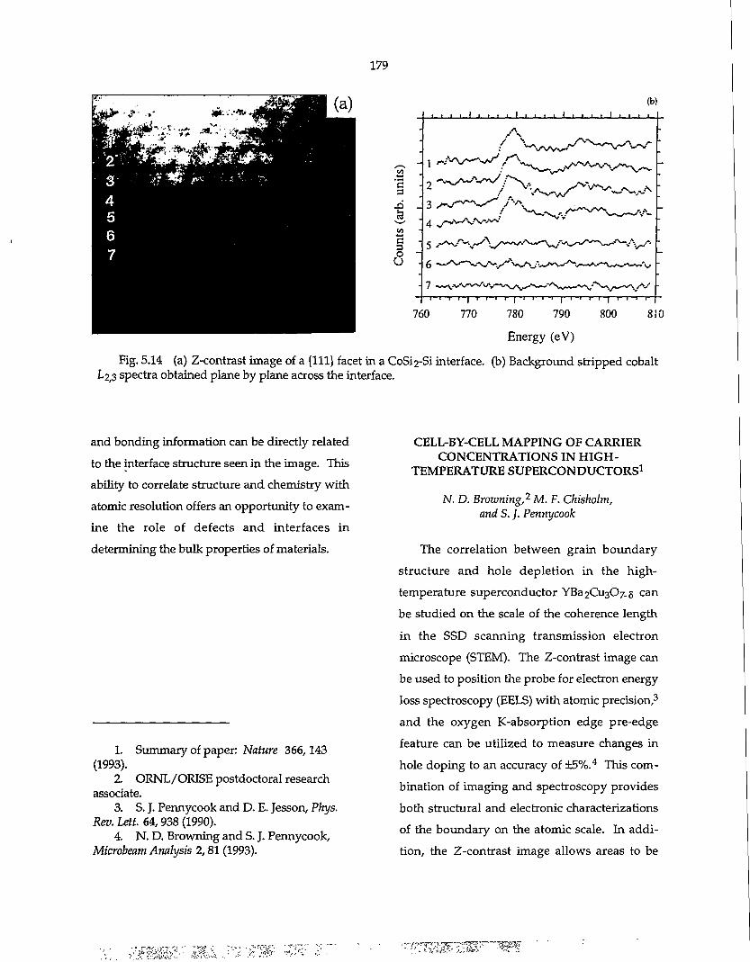
179
(b)
T — i — i — i — | — i — i — i — i — | — i — i — i — i — | — i — i — i — r
760 770 780 790 800 810
Energy (eV)
Fig. 5.14 (a) Z-contrast image of a {111} facet in a CoSi2-Si interface, (b) Background stripped cobalt Z-2,3 spectra obtained plane by plane across the interface.
and bonding information can be directly related
to the interface structure seen in the image. This
ability to correlate structure and chemistry with
atomic resolution offers an opportunity to exam
ine the role of defects and interfaces in
determining the bulk properties of materials.
1. Summary of paper: Nature 366,143 (1993).
2 ORNL/ORISE postdoctoral research associate.
3. S. J. Pennycook and D. E. Jesson, Phys. Rev. Lett. 64,938 (1990).
4. N. D. Browning and S. J. Pennycook, Microbeam Analysis 2,81 (1993).
CELL-BY-CELL MAPPING OF CARRIER CONCENTRATIONS IN HIGH-
TEMPERATURE SUPERCONDUCTORS 1
N. D. Browning,2M. F. Chisholm, and S. J. Pennycook
The correlation between grain boundary
structure and hole depletion in the high-
temperature superconductor YBa2Cu307_5 can
be studied on the scale of the coherence length
in the SSD scanning transmission electron
microscope (STEM). The Z-contrast image can
be used to position the probe for electron energy
loss spectroscopy (EELS) with atomic precision, 3
and the oxygen K-absorption edge pre-edge
feature can be utilized to measure changes in
hole doping to an accuracy of ±5%. 4 This com
bination of imaging and spectroscopy provides
both structural and electronic characterizations
of the boundary on the atomic scale. In addi
tion, the Z-contrast image allows areas to be
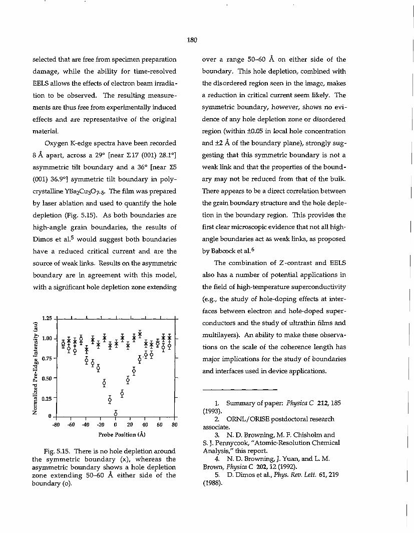
180
selected that are free from specimen preparation damage, while the ability for time-resolved EELS allows the effects of electron beam irradiation to be observed. The resulting measurements are thus free from experimentally induced effects and are representative of the original material.
Oxygen K-edge spectra have been recorded 8 A apart, across a 29° [near Z17 (001) 28.1°] asymmetric tilt boundary and a 36° [near 15 (001) 36.9°] symmetric tilt boundary in poly-crystalline YBa2Qi307-5. The film was prepared by laser ablation and used to quantify the hole depletion (Fig. 5.15). As both boundaries are high-angle grain boundaries, the results of Dimos et al. 5 would suggest both boundaries have a reduced critical current and are the source of weak links. Results on the asymmetric boundary are in agreement with this model, with a significant hole depletion zone extending
1.25
S 1.00
60 W
v N
0.75
0.50
« 0.25 o Z
i 1 1 1 1 1 r -80 -60 -40 -20 0 20 40 60 80
Probe Position (A)
Fig. 5.15. There is no hole depletion around the symmetric boundary (x), whereas the asymmetric boundary shows a hole depletion zone extending 50-60 A either side of the boundary (o).
over a range 50-60 A on either side of the boundary. This hole depletion, combined with the disordered region seen in the image, makes a reduction in critical current seem likely. The symmetric boundary, however, shows no evidence of any hole depletion zone or disordered region (within ±0.05 in local hole concentration and ±2 A of the boundary plane), strongly suggesting that this symmetric boundary is not a weak link and that the properties of the boundary may not be reduced from that of the bulk. There appears to be a direct correlation between the grain boundary structure and the hole depletion in the boundary region. This provides the first clear microscopic evidence that not all high-angle boundaries act as weak links, as proposed byBabcocketal.6
The combination of Z -contrast and EELS also has a number of potential applications in the field of high-temperature superconductivity (e.g., the study of hole-doping effects at interfaces between electron and hole-doped superconductors and the study of ultrathin films and multilayers). An ability to make these observations on the scale of the coherence length has major implications for the study of boundaries and interfaces used in device applications.
1. Summary of paper: Physica C 212,185 (1993).
2 ORNL/ORISE postdoctoral research associate.
3. N. D. Browning, M. F. Chisholm and S. J. Pennycook, "Atomic-Resolution Chemical Analysis," this report.
4. N. D. Browning, J. Yuan, and L. M. Brown, Physica C 202,12 (1992).
5. D. Dimos et al., Phys. Rev. Lett 61,219 (1988).
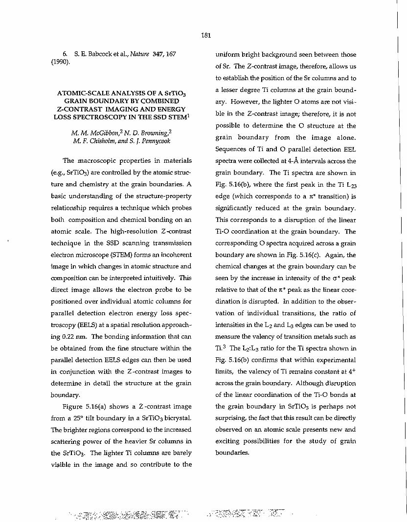
181
6. S. E. Babcock et al v Nature 347,167 (1990).
ATOMIC-SCALE ANALYSIS OF A SrTi0 3
GRAIN BOUNDARY BY COMBINED Z-CONTRAST IMAGING AND ENERGY
LOSS SPECTROSCOPY IN THE SSD STEM1
M. M. McGibbon,2 N. D. Browning,2
M. F. Chisholm, and S. J. Pennycook
The macroscopic properties in materials (e.g., SrTiOa) are controlled by the atomic structure and chemistry at the grain boundaries. A basic understanding of the structure-property relationship requires a technique which probes both composition and chemical bonding on an atomic scale. The high-resolution Z-contrast technique in the SSD scanning transmission electron microscope (STEM) forms an incoherent image in which changes in atomic structure and composition can be interpreted intuitively. This direct image allows the electron probe to be positioned over individual atomic columns for parallel detection electron energy loss spectroscopy (EELS) at a spatial resolution approaching 0.22 nm. The bonding information that can be obtained from the fine structure within the parallel detection EELS edges can then be used in conjunction with the Z-contrast images to determine in detail the structure at the grain boundary.
Figure 5.16(a) shows a Z-contrast image from a 25° tilt boundary in a SrTiOa bicrystal. The brighter regions correspond to the increased scattering power of the heavier Sr columns in the SrTi03. The lighter Ti columns are barely visible in the image and so contribute to the
uniform bright background seen between those of Sr. The Z-contrast image, therefore, allows us to establish the position of the Sr columns and to a lesser degree Ti columns at the grain boundary. However, the lighter O atoms are not visible in the Z-contrast image; therefore, it is not possible to determine the O structure at the grain boundary from the image alone. Sequences of Ti and O parallel detection EEL spectra were collected at 4-A intervals across the grain boundary. The Ti spectra are shown in Fig. 5.16(b), where the first peak in the Ti L23 edge (which corresponds to a 7t* transition) is significantly reduced at the grain boundary. This corresponds to a disruption of the linear Ti-O coordination at the grain boundary. The corresponding O spectra acquired across a grain boundary are shown in Fig. 5.16(c). Again, the chemical changes at the grain boundary can be seen by the increase in intensity of the a* peak relative to that of the %* peak as the linear coordination is disrupted. In addition to the observation of individual transitions, the ratio of intensities in the L2 and L3 edges can be used to measure the valency of transition metals such as Ti. 3 The L2:L3 ratio for the Ti spectra shown in Fig. 5.16(b) confirms that within experimental limits, the valency of Ti remains constant at 4 +
across the grain boundary. Although disruption of the linear coordination of the Ti-O bonds at the grain boundary in SrTi03 is perhaps not surprising, the fact that this result can be directly observed on an atomic scale presents new and exciting possibilities for the study of grain boundaries.
.y'::m^Mvsr- M. tm^mMmskmrm:
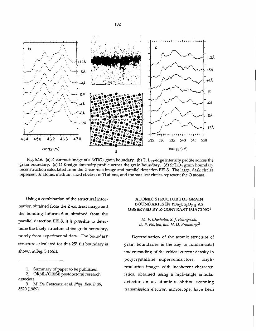
182
454 458 462 466
energy (ev)
/~---
• • • • i i * i i i • i i i
^*\ •':.S* " ^ ^ / X
% '•*v/>-^
X
Wv TT~i i | i i i i | i i i i | i i I i | i i I
+12A
+8A
+4A
gb
"-4A
-8A
-12A
525 530 535 540 545
energy (eV)
550
Fig. 5.16. (a) Z-contrast image of a SrTi0 3 grain boundary, (b) Ti L 23-edge intensity profile across the grain boundary, (c) O K-edge intensity profile across the grain boundary, (d) SrTi03 grain boundary reconstruction calculated from the Z-contrast image and parallel detection EELS. The large, dark circles represent Sr atoms, medium sized circles are Ti atoms, and the smallest circles represent the O atoms.
Using a combination of the structural infor
mation obtained from the Z-contrast image and
the bonding information obtained from the
parallel detection EELS, it is possible to deter
mine the likely structure at the grain boundary,
purely from experimental data. The boundary
structure calculated for this 25° tilt boundary is
shown in Fig. 5.16(d).
1. Summary of paper to be published. 2. ORNL/ORISE postdoctoral research
associate. 3. M. De Crescenzi et al. Phys. Rev. B 39,
5520 (1989).
ATOMIC STRUCTURE OF GRAIN BOUNDARIES IN Y B a 2 C u 3 0 7 . 5 AS
OBSERVED BY Z-CONTRAST IMAGING 1
M. F. Chisholm, S. J. Pennycook, D. P. Norton, and N. D. Browning2
Determination of the atomic structure of
grain boundaries is the key to fundamental
understanding of the critical-current density in
polycrysta l l ine superconduc tors . High-
resolution images with incoherent character
istics, obtained using a high-angle annular
detector on an atomic-resolution scanning
transmission electron microscope, have been
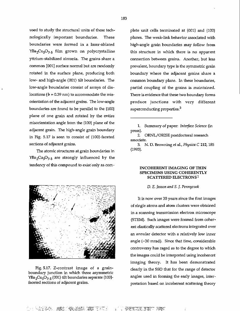
183
used to study the structural units of these technologically important boundaries. These boundaries were formed in a laser-ablated YBa 2Cu 307. 5 film grown on polycrystalline yttrium-stabilized zirconia. The grains share a common [001] surface normal but are randomly rotated in the surface plane, producing both low- and high-angle (001) tilt boundaries. The low-angle boundaries consist of arrays of dislocations (b = 0.39 run) to accommodate the mis-orientation of the adjacent grains. The low-angle boundaries are found to be parallel to the {100} plane of one grain and rotated by the entire misorientation angle from the {100} plane of the adjacent grain. The high-angle grain boundary in Fig. 5.17 is seen to consist of {100}-faceted sections of adjacent grains.
The atomic structures at grain boundaries in YBa2Cu307.g are strongly influenced by the tendency of this compound to exist only as corn-
Fig. 5.17. Z-contrast image of a grain-boundary junction in which three asymmetric YBa 2Cu 30 7.. 6 (001) tilt boundaries separate {100}-faceted sections of adjacent grains.
plete unit cells terminated at {001} and {100} planes. The weak-link behavior associated with high-angle grain boundaries may follow from this structure in which there is no apparent connection between grains. Another, but less prevalent, boundary type is the symmetric grain boundary where the adjacent grains share a common boundary plane. In these boundaries, partial coupling of the grains is maintained. There is evidence that these two boundary forms produce junctions with very different superconducting properties.3
1. Summary of paper: Interface Science (in press).
2 ORNL/ORISE postdoctoral research associate.
3. N. D. Browning et al., Physica C 212,185 (1993).
INCOHERENT IMAGING OF THIN SPECIMENS USING COHERENTLY
SCATTERED ELECTRONS1
D. E. Jesson and S.). Pennycook
It is now over 30 years since the first images of single atoms and atom clusters were obtained in a scanning transmission electron microscope (STEM). Such images were fonned from coherent elastically scattered electrons integrated over an annular detector with a relatively low inner angle (~30 mrad). Since that time, considerable controversy has raged as to the degree to which the images could be interpreted using incoherent imaging theory. It has been demonstrated clearly in the SSD that for the range of detector angles used in forming the early images, interpretation based on incoherent scattering theory

184
was justified, but with the important proviso
that atoms need to be separated in a plane per
pendicular to the optic axis. It has also been
shown that interference effects between atoms
possessing identical projected coordinates must
be considered explicitly, which has led to a
re-evaluation of the early images of atomic
columns.
Figure 5.18 illustrates the important physics
underlying the use of incoherent imaging theory
to interpret images from two point scatterers
separated by 1.5 A in the transverse plane.
Increasing the inner detector angle from 10.3 to
50 mrad samples more fringes in the detector
plane intensity distribution, and the integrated
signal approaches the incoherent scattering
limit. A useful condition for the minimum
Fig. 5.18. Detector plane intensity distribution resulting from two point scatterers separated by 1.5 A. The solid circle represents an increase of the 10.3-mrad inner detector angle to 50 mrad.
detector angle required for incoherent imaging
is
where AR is the atomic separation and X is the
incident electron wavelength. This result should
allow the extension of scanning transmission
electron microscopy incoherent imaging meth
ods to a number of scientifically and technologi
cally important samples, including heavy atom
stained biological materials and catalysts.
1. Summary of paper: Proc. R. Soc. Lond. A 441,261 (1993).
INCOHERENT IMAGING OF CRYSTALS USING THERMALLY
SCATTERED ELECTRONS1
D. E. Jesson and S. J. Pennycook
Z-contrast scanning transmission electron
microscopy images are usually formed from
thermally scattered electrons. From a simplified
Einstein picture of atoms acting as independent
oscillators, it can be expected that coherence
effects, even along an atomic column, will be
destroyed as long as Bragg reflections do not
make a significant contribution to the high-angle
signal. However, unlike a full phonon thermal
diffuse scattering (TDS) description involving
correlated displacements, the Einstein model
assumes incoherent scattering from each atom in
the vibrating column and, therefore, does not
properly describe the interference effects present
in large-angle TDS. Such residual interference is
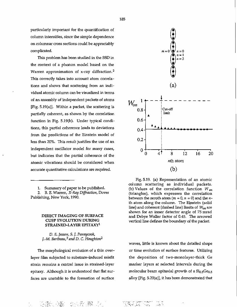
185
particularly important for the quantification of column intensities, since the simple dependence on columnar cross sections could be appreciably complicated.
This problem has been studied in the SSD in the context of a phonon model based on the Warren approximation of x-ray diffraction.2
This correctly takes into account atom correlations and shows that scattering from an individual atomic column can be visualized in terms of an assembly of independent packets of atoms [Fig. 5.19(a)]. Within a packet, the scattering is partially coherent, as shown by the correlation function in Fig. 5.19(b). Under typical conditions, this partial coherence leads to deviations from the predictions of the Einstein model of less than 20%. This result justifies the use of an independent oscillator model for many cases, but indicates that the partial coherence of the atomic vibrations should be considered when accurate quantitative calculations are required.
1. Summary of paper to be published. 2 B. E. Warren, X-Ray Diffraction, Dover
Publishing, New York, 1990.
DIRECT IMAGING OF SURFACE CUSP EVOLUTION DURING STRAINED-LAYER EPITAXY1
D. E. Jesson, S. J. Pennycook, J.-M. Baribeau,2 and D. C. Houghton2
The morphological evolution of a thin over-layer film subjected to substrate-induced misfit strain remains a central issue in strained-layer epitaxy. Although it is understood that flat surfaces are unstable to the formation of surface
m = 0
(a)
YYon Cut-off limit
i u t A A A A A A A A A A
16 20 T-T I I
4* 8 12 nth atom (b)
Fig. 5.19. (a) Representation of an atomic column scattering as individual packets, (b) Values of the correlation function W on (triangles), which expresses the correlation between the zeroth atom (m = 0, n = 0) and the n-th atom along the column. The Einstein (solid line) and coherent (dashed line) limits of W^ are shown for an inner detector angle of 75 mrad and Debye Waller factor of 0.45. The arrowed vertical line defines the boundary of the packet.
waves, little is known about the detailed shape or time evolution of surface features. Utilizing the deposition of two-monolayer-thick Ge marker layers at selected intervals during the molecular beam epitaxial growth of a Sio.sGeo.5 alloy [Fig. 5.20(a)], it has been demonstrated that
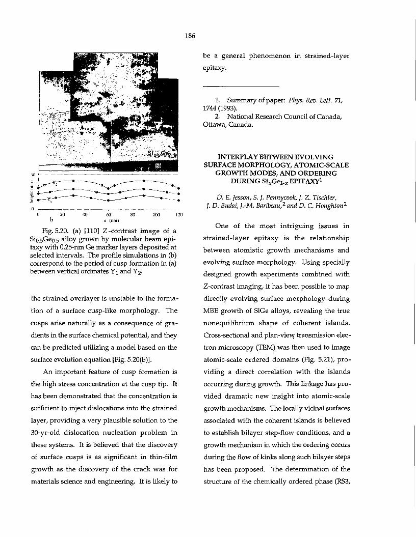
186
be a general phenomenon in strained-layer
epitaxy.
O 20 b
40 60 x (nm)
100 120
Fig. 5.20. (a) [110] Z-contrast image of a Sio.sGeo.5 alloy grown by molecular beam epitaxy with 0.25-nm Ge marker layers deposited at selected intervals. The profile simulations in (b) correspond to the period of cusp formation in (a) between vertical ordinates Y\ and Y2.
the strained overlayer is unstable to the forma
tion of a surface cusp-like morphology. The
cusps arise naturally as a consequence of gra
dients in the surface chemical potential, and they
can be predicted utilizing a model based on the
surface evolution equation [Fig. 5.20(b)].
An important feature of cusp formation is
the high stress concentration at the cusp tip. It
has been demonstrated that the concentration is
sufficient to inject dislocations into the strained
layer, providing a very plausible solution to the
30-yr-old dislocation nucleation problem in
these systems. It is believed that the discovery
of surface cusps is as significant in thin-film
growth as the discovery of the crack was for
materials science and engineering. It is likely to
1. Summary of paper: Phys. Rev. Lett. 71, 1744 (1993).
2. National Research Council of Canada, Ottawa, Canada.
INTERPLAY BETWEEN EVOLVING SURFACE MORPHOLOGY, ATOMIC-SCALE
GROWTH MODES, AND ORDERING DURING Si^-Ge!^ EPITAXY1
D. E. Jesson, S. J. Pennycook,}. Z. Tischler, }. D. Budai, J.-M. Baribeau,2 and D. C. Houghton2
One of the most intr iguing issues in
strained-layer epitaxy is the relationship
between atomistic growth mechanisms and
evolving surface morphology. Using specially
designed growth experiments combined with
Z-contrast imaging, it has been possible to map
directly evolving surface morphology during
MBE growth of SiGe alloys, revealing the true
nonequil ibrium shape of coherent islands.
Cross-sectional and plan-view transmission elec
tron microscopy (TEM) was then used to image
atomic-scale ordered domains (Fig. 5.21), pro
viding a direct correlation with the islands
occurring during growth. This linkage has pro
vided dramatic new insight into atomic-scale
growth mechanisms. The locally vicinal surfaces
associated with the coherent islands is believed
to establish bilayer step-flow conditions, and a
growth mechanism in which the ordering occurs
during the flow of kinks along such bilayer steps
has been proposed. The determination of the
structure of the chemically ordered phase (RS3,
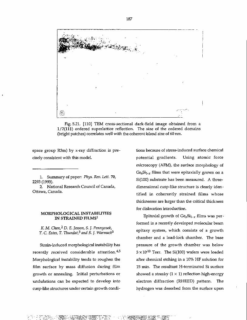
187
^•mm^i.
Fig. 5.21. [110] TEM cross-sectional dark-field image obtained from a 1/2(111) ordered superlattice reflection. The size of the ordered domains (bright patches) correlates well with the coherent island size of 60 ran.
space group R3m) by x-ray diffraction is pre
cisely consistent with this model.
1. Summary of paper: Phys. Rev. Lett. 70, 2293 (1993).
2. National Research Council of Canada, Ottawa, Canada.
MORPHOLOGICAL INSTABILITIES IN STRAINED FILMS1
K. M. Chen,2 D. E. Jesson, S.}. Pennycook, T. C. Estes, T. Thundat,3 and R. J. Warmack3
Strain-induced morphological instability has
recently received considerable a t tent ion. 4 ' 5
Morphological instability tends to roughen the
film surface by mass diffusion during film
growth or annealing. Initial perturbations or
undulations can be expected to develop into
cusp-like structures under certain growth condi
tions because of stress-induced surface chemical
potential gradients . Using atomic force
microscopy (AFM), the surface morphology of
GexSii-x films that were epitaxially grown on a
Si(100) substrate has been measured. A three-
dimensional cusp-like structure is clearly iden
tified in coherently strained films whose
thicknesses are larger than the critical thickness
for dislocation introduction.
Epitaxial growth of Ge x Si i . x films was per
formed in a recently developed molecular beam
epitaxy system, which consists of a growth
chamber and a load-lock chamber. The base
pressure of the growth chamber was below
3 x 10"10 Torr. The Si(100) wafers were loaded
after chemical etching in a 10% HF solution for
15 min. The resultant H-terminated Si surface
showed a streaky (1 x 1) reflection high-energy
electron diffraction (RHEED) pattern. The
hydrogen was desorbed from the surface upon
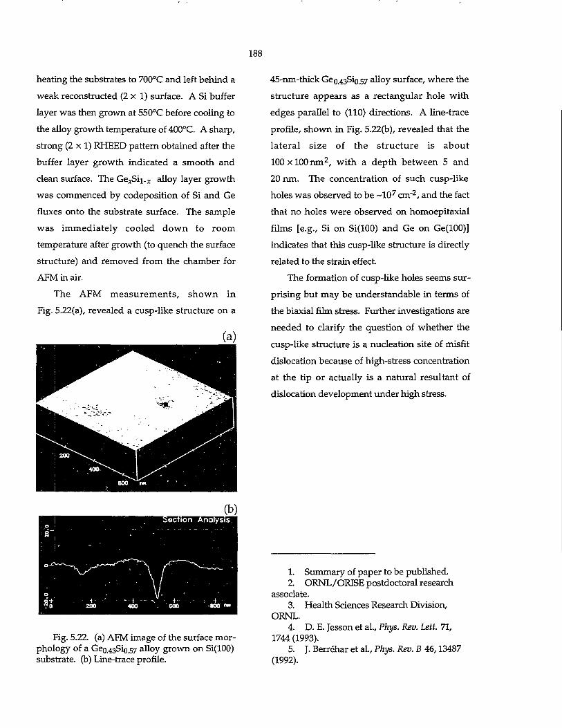
188
heating the substrates to 700°C and left behind a
weak reconstructed (2 x 1) surface. A Si buffer
layer was then grown at 550°C before cooling to
the alloy growth temperature of 400°C. A sharp,
strong (2 x 1) RHEED pattern obtained after the
buffer layer growth indicated a smooth and
clean surface. The Ge^Sii.j- alloy layer growth
was commenced by codeposition of Si and Ge
fluxes onto the substrate surface. The sample
was immediately cooled down to room
temperature after growth (to quench the surface
structure) and removed from the chamber for
AFMinair.
The AFM measuremen t s , s h o w n in
Fig. 5.22(a), revealed a cusp-like structure on a
(a)
Fig. 5.22. (a) AFM image of the surface morphology of a Geo.43Sio.57 alloy grown on Si(100) substrate, (b) Line-trace profile.
45-nm-thick Geo.43Sio.57 alloy surface, where the
structure appears as a rectangular hole with
edges parallel to (110) directions. A line-trace
profile, shown in Fig. 5.22(b), revealed that the
la teral size of the s t ruc ture is about
100 x 100 ran2, with a depth between 5 and
20 nm. The concentration of such cusp-like
holes was observed to be ~10 7 cm" 2, and the fact
that no holes were observed on homoepitaxial
films [e.g., Si on Si(100) and Ge on Ge(100)]
indicates that this cusp-like structure is directly
related to the strain effect.
The formation of cusp-like holes seems sur
prising but may be understandable in terms of
the biaxial film stress. Further investigations are
needed to clarify the question of whether the
cusp-like structure is a nucleation site of misfit
dislocation because of high-stress concentration
at the tip or actually is a natural resultant of
dislocation development under high stress.
1. Summary of paper to be published. 2. ORNL/ORISE postdoctoral research
associate. 3. Health Sciences Research Division,
ORNL. 4. D. E. Jesson et al., Phys. Rev. Lett. 71,
1744 (1993). 5. J. Berrehar et al., Phys. Rev. B 46,13487
(1992).
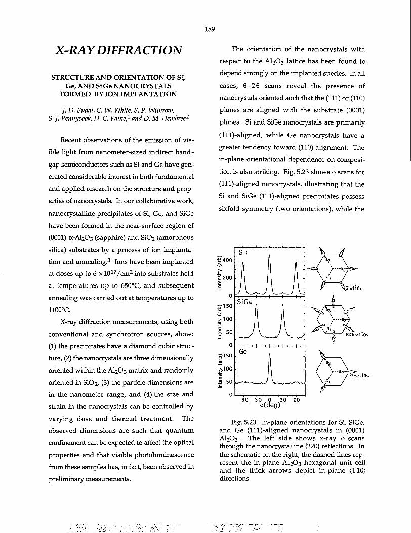
189
X-RAY DIFFRACTION
STRUCTURE AND ORIENTATION OF S i Ge, AND SiGe NANOCRYSTALS
FORMED BY ION IMPLANTATION
/. D. Budai, C. W. White, S. P. Withrow, S. ]. Pennycook, D. C. Paine,1 and D. M. Hembree2
Recent observations of the emission of vis
ible light from nanometer-sized indirect band-
gap semiconductors such as Si and Ge have gen
erated considerable interest in both fundamental
and applied research on the structure and prop
erties of nanocrystals. In our collaborative work,
nanocrystalline precipitates of Si, Ge, and SiGe
have been formed in the near-surface region of
(0001) OC-AI2O3 (sapphire) and SK>2 (amorphous
silica) substrates by a process of ion implanta
tion and annealing. 3 Ions have been implanted
at doses up to 6 x 1 0 1 7 / c m 2 into substrates held
at temperatures up to 650°C, and subsequent
annealing was carried out at temperatures up to
1100°C.
X-ray diffraction measurements, using both
conventional and synchrotron sources, show:
(1) the precipitates have a diamond cubic struc
ture, (2) the nanocrystals are three dimensionally
oriented within the AI2O3 matrix and randomly
oriented in Si02, (3) the particle dimensions are
in the nanometer range, and (4) the size and
strain in the nanocrystals can be controlled by
varying dose and thermal treatment. The
observed dimensions are such that quantum
confinement can be expected to affect the optical
properties and that visible photoluminescence
from these samples has, in fact, been observed in
preliminary measurements.
The orientation of the nanocrystals with
respect to the AI2O3 lattice has been found to
depend strongly on the implanted species. In all
cases, 0 -29 scans reveal the presence of
nanocrystals oriented such that the (111) or (110)
planes are aligned with the substrate (0001)
planes. Si and SiGe nanocrystals are primarily
( l l l ) -al igned, while Ge nanocrystals have a
greater tendency toward (110) alignment. The
in-plane orientational dependence on composi
tion is also striking. Fig. 5.23 shows ((> scans for
(l l l)-aligned nanocrystals, illustrating that the
Si and SiGe (l l l)-aligned precipitates possess
sixfold symmetry (two orientations), while the
\Si<iio>
£ /""a«t - j > — SiGe<110> f
Ge<110>
-60 -30 0 30 60 4>(deg)
Fig. 5.23. In-plane orientations for Si, SiGe, and Ge ( l l l ) -a l igned nanocrystals in (0001) AI2O3. The left side shows x-ray § scans through the nanocrystalline {220} reflections. In the schematic on the right, the dashed lines represent the in-plane AI2O3 hexagonal unit cell and the thick arrows depict in-plane (110) directions.

190
Ge (lll)-aligned nanocrystals possess threefold
symmetry (a single orientation). Surprisingly,
the orientation observed for SiGe nanocrystals is
not intermediate between those seen for Si or Ge
nanocrystals, but instead is rotated by 30°. The
origin of this strong orientational dependence on
composition is currently being investigated.
1. Brown University, Providence, R.I. 2 Y-12 Plant, Oak Ridge, Term. 3. C. W. White et a l , "Formation of Ori
ented Nanocrystals of Si and Ge in AI2O3 by Ion Implantation," this report.
STRUCTURE OF ORDERED SiGe EPITAXIAL LAYERS1
/. Z. Tischler,}. D. Budai, P. Zschack,2
D. E. Jesson, J.-M. Baribeau,3 and D. C. Houghton3
Sio.sGeo.s alloy films grown on (001)-
oriented Si substrates show compositional order
ing of the SiGe epitaxial layer when grown by
either metal-organic chemical vapor deposition
or molecular beam epitaxy near 400°C. This
ordering is believed to occur because of the
kinetics of growth on the (001) surface, as it is
not seen in growth on other crystallographic
faces nor in bulk grown alloys. This ordering is
of interest because of the current use of SiGe
alloys for fabrication of strained-layer super-
lattices, as well as the insight that the ordering
provides into the surface kinetics of film growth.
Previous studies using electron diffraction
have observed half-integral superlattice reflec
tions, which have led to the proposal of a
number of epitaxial growth models where the
conventional cubic unit cell is doubled by chem
ical ordering.
The X-14 synchrotron beam line at the
National Synchrotron Light Source has been
used to make absolute measurements of the
integrated intensity from superlattice reflections
to determine the ordered structure. In both
relaxed and coherently strained alloy films, it
was found that the RS3 structure (described in
Ref. 4) accurately describes the ordered phase as
shown in Fig. 5.24. The RS3 structure has
chemical ordering on one of the four {lll}-type
planes, and it is the only proposed structure
with a nonzero value for the (002) reflection.
The (002) reflection not only singles out the RS3
structure, but also its relative strength provides
information on the growth kinetics in the bilayer
step-flow model. 4
In addition to the observed half-order reflec
tions, the first observations of integral (hkZ)
i 2
1 1 ' • ' ' 1 ' • ' ' 1 Si^Ge 5 [001] surface normal
•*- measured 1/2 order • RS3 model • measured integral • CuAu-l ordering
0.10 0.15 0.20 0.25 sin(6)A (A1)
0.30 0.35
Fig. 5.24. Measured and computed structure factors for an ordered SiGe film. The solid circles and squares denote measurements, and the gray diamonds and squares denote calculations for the RS3 and CuAu-I structures. Note that both models are needed to account for all the measurements.
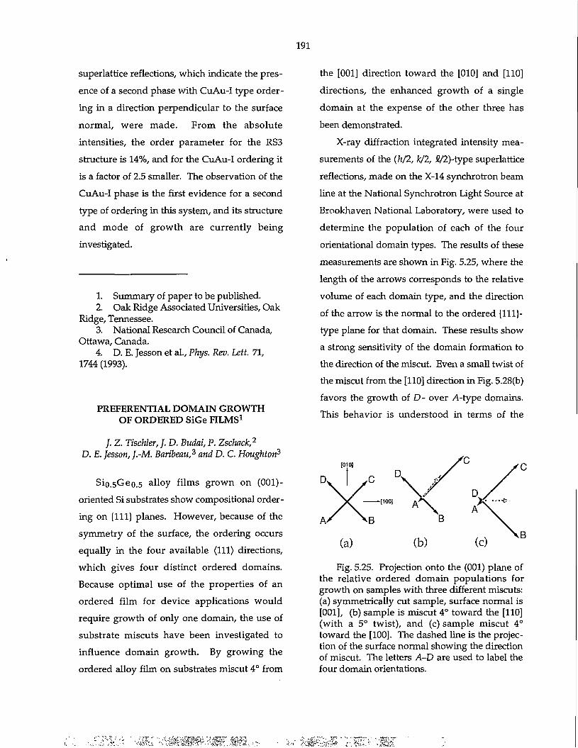
191
superlattice reflections, which indicate the presence of a second phase with CuAu-I type ordering in a direction perpendicular to the surface normal, were made. From the absolute intensities, the order parameter for the RS3 structure is 14%, and for the CuAu-I ordering it is a factor of 2.5 smaller. The observation of the CuAu-I phase is the first evidence for a second type of ordering in this system, and its structure and mode of growth are currently being investigated.
1. Summary of paper to be published. 2. Oak Ridge Associated Universities, Oak
Ridge, Tennessee. 3. National Research Council of Canada,
Ottawa, Canada. 4. D. E. Jesson et al., Phys. Rev. Lett. 71,
1744 (1993).
PREFERENTIAL DOMAIN GROWTH OF ORDERED SiGe FILMS1
/. Z. Tischler,}. D. Budai, P. Zschack,2
D. E. Jesson, J.-M. Baribeau,3 and D. C. Houghton3
Sio.sGeo.s alloy films grown on (001)-oriented Si substrates show compositional ordering on {111} planes. However, because of the symmetry of the surface, the ordering occurs equally in the four available (111) directions, which gives four distinct ordered domains. Because optimal use of the properties of an ordered film for device applications would require growth of only one domain, the use of substrate miscuts have been investigated to influence domain growth. By growing the ordered alloy film on substrates miscut 4° from
the [001] direction toward the [010] and [110] directions, the enhanced growth of a single domain at the expense of the other three has been demonstrated.
X-ray diffraction integrated intensity measurements of the (h/2, k/2, fi/2)-type superlattice reflections, made on the X-14 synchrotron beam line at the National Synchrotron Light Source at Brookhaven National Laboratory, were used to determine the population of each of the four orientational domain types. The results of these measurements are shown in Fig. 5.25, where the length of the arrows corresponds to the relative volume of each domain type, and the direction of the arrow is the normal to the ordered {111}-type plane for that domain. These results show a strong sensitivity of the domain formation to the direction of the miscut. Even a small twist of the miscut from the [110] direction in Fig. 5.28(b) favors the growth of D - over A-type domains. This behavior is understood in terms of the
Fig. 5.25. Projection onto the (001) plane of the relative ordered domain populations for growth on samples with three different miscuts: (a) symmetrically cut sample, surface normal is [001], (b) sample is miscut 4° toward the [110] (with a 5° twist), and (c) sample miscut 4° toward the [100]. The dashed line is the projection of the surface normal showing the direction of miscut. The letters A-D are used to label the four domain orientations.
bilayer step flow model for growth discussed
elsewhere in this report. 4 '^ This work is contin
uing with variations in the miscut (direction and
magnitude) and the film-growth procedure to
investigate the degree to which single-ordered
domains may be grown and to investigate the
mechanisms responsible for the ordering.
1. Summary of paper to be published. 2. Oak Ridge Institute for Science and
Education, Oak Ridge, Term. 3. National Research Council of Canada,
Ottawa, Canada. 4. J. Z. Tischler et al., "Structure of
Ordered SiGe Epitaxial Layers," this report. 5. D. E. Jesson et al., "Direct Imaging of
Surface Cusp Evolution During Strained-Layer Epitaxy," this report.
ENERGY TIME CORRELATIONS IN RESONANT NUCLEAR BRAGG
SCATTERING1
/. Z. Tischler, B. C. Larson, and E. E. Alp2
The spectral energy widths of resonant x-ray
beams from nuclear Bragg reflections are much
greater than those from radioactive Mossbauer
sources as a result of the collective excitation of
the resonant nuclei. In this study, the time-
structure of synchrotron radiation has been used
to make time-sliced Doppler absorption mea
surements on the resonant beam from a mosaic 5 7 Fe203 resonant monochromator. These time-
resolved measurements have demonstrated the
increased width of the time-integrated energy
spectrum and the quantum mechanical narrow
ing of the spectral width as a function of time.
In addition, comparison of the computed
192
Doppler absorption widths of nuclear Bragg res
onant beams for thick and thin absorbers has
been made in order to assess their performance
for elastic/inelastic and quasi-elastic x-ray scat
tering spectroscopy measurements.
The time-resolved Doppler absorption mea
surements were carried out at the Cornell High
Energy Synchrotron Source (CHESS) using a
resonant beam from the (777) reflection of a
mosaic 5 7 Fe203 crystal and a 9 .6-mg/cm 2
5 7 Fe203 absorber. As shown in Fig. 5.26(a, b,
and c), measurements were made for the time
interval [40-294 ns] and for time slices at the
beginning and end of this interval. The energy
width of the long interval is ~35 neV, while the
widths for the [40-70-ns] and [100-294-ns] time
intervals are ~60 and 20 neV. Both the shape
and the widths of the absorption spectra are in
agreement with numerical, dynamical diffrac
tion calculations, including details such as the
shoulders on the side of the absorption dip in
Fig. 5.26(c).
The 9.6-mg/cm 2 5 7 Fe203 absorber used in
these measurements is much thicker than the
~0.5-mg/cm 2 absorbers that are normally used
in radioactive source Mossbauer measurements.
However, the wider energy widths associated
with collective excitation of a resonant nuclear
reflection encourages the use of a thicker
absorber. This is demonstrated in Fig. 5.26(a),
which shows calculated absorption spectra for a
0.5-mg/cm 2 5 7 Fe203 absorber (with the magni
tude of the dip normalized to that of the thick
absorber). Although decreasing the absorber
thickness has a small effect upon the width, the
thin absorber produced only a 3% dip before
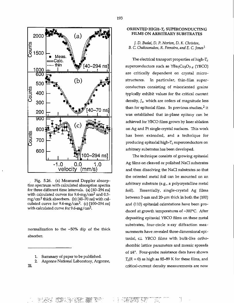
193
Fig. 5.26. (a) Measured Doppler absorption spectrum with calculated absorption spectra for three different time intervals, (a) [40-294 ns] with calculated curves for 9.6-mg/cm 2 and 0.5-m g / c m 2 thick absorbers, (b) [40-70 ns] with calculated curve for 9.6-mg/cm 2 . (c) [100-294 ns] with calculated curve for 9.6-mg/cm 2.
normalization to the ~50% dip of the thick
absorber.
1. Summary of paper to be published. 2 Argonne National Laboratory, Argonne,
DL
ORIENTED HIGH-r c SUPERCONDUCTING FILMS ON ARBITRARY SUBSTRATES
/. D. Budai, D. P. Norton, D. K. Christen, B. C. Chakoumakos, R. Feenstra, and E. C. Jones1
The electrical transport properties of high-T c
superconductors such as YBa2Cu307_x (YBCO)
are critically dependent on crystal micro-
structures. In particular, thin-film super
conductors consisting of misoriented grains
typically exhibit values for the critical current
density, ]0 which are orders of magnitude less
than for epitaxial films. In previous studies, 2 it
was established that in-plane epitaxy can be
achieved for YBCO films grown by laser ablation
on Ag and Pt single-crystal surfaces. This work
has been extended, and a technique for
producing epitaxial high-T c superconductors on
arbitrary substrates has been developed.
The technique consists of growing epitaxial
Ag films on cleaved or polished NaCl substrates
and then dissolving the NaCl substrates so that
the oriented metal foil can be mounted on an
arbitrary substrate (e.g., a polycrystalline metal
foil). Essentially, single-crystal Ag films
between 2-um and 20-|im thick in both the (100)
and (110) epitaxial orientations have been pro
duced at growth temperatures of ~300°C. After
depositing epitaxial YBCO films on these metal
substrates, four-circle x-ray diffraction mea
surements have revealed three-dimensional epi
taxial, c.L YBCO films with bulk-like ortho-
rhombic lattice parameters and mosaic spreads
of <4°. Four-probe resistance data have shown
TC(R = 0) as high as 85-89 K for these films, and
critical-current density measurements are now
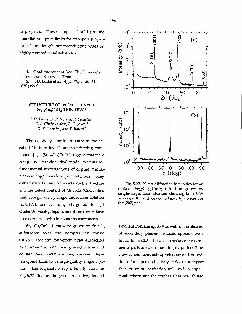
194
in progress. These samples should provide
quantitative upper limits for transport proper
ties of long-length, superconducting wires on
highly textured metal substrates.
1. Graduate student from The University of Tennessee, Knoxville, Term.
2 J. D. Budai et al.7 Appl. Phys. Lett. 62, 1836 (1993).
STRUCTURE OF INFINITE-LAYER Sr 1. J :Ca a :Cu02 THIN FILMS
/. D. Budai, D. P. Norton, R. Feenstra, B. C. Chakoumakos, E. C. Jones,1
D. K. Christen, and T. Kawai2
The relatively simple structure of the so-
called "infinite layer" superconducting com
pounds [e.g., (Sri_ xCa x)Cu02] suggests that these
compounds provide ideal model systems for
fundamental investigations of doping mecha
nisms in copper oxide superconductors. X-ray
diffraction was used to characterize the structure
and the defect content of (Sr i-jCaJCuG^ films
that were grown by single-target laser ablation
(at ORNL) and by multiple-target ablation (at
Osaka University, Japan), and these results have
been correlated with transport measurements.
Sri . x Ca z Cu02 films were grown on SrTi03
subst ra tes over the composi t ion range
0.0 < x < 0.85; and four-circle x-ray diffraction
measurements, made using synchrotron and
conventional x-ray sources, showed these
tetragonal films to be high-quality single crys
tals. The log-scale x-ray intensity scans in
Fig. 5.27 illustrate large coherence lengths and
1 1 1 1 1 1 1 1 1 1 1 1 1 1 1 1 1 1 1 1 1 1 1 1 1 1 1 1 1 j 1 1 1 1 1 1 1 1 1 j 1 1 1 1
0 20 40 60 80 29 (deg)
' • • ' • • ' • • ' • • ' • • ' • • •
10'
CO
10" CO c CO
c10 J
10'
(b)
yr W 1sWtt 'vw»W^ V ^ r * * ^ , ^ ^ ^ w I I I I I I I I I I 1 • I I I I I 'I I I I
-90 -60 -30 0 30 60 90 <j> (deg)
Fig. 5.27. X-ray diffraction intensities for an epitaxial Sro.7Cao.3CuO2 thin film grown by single-target laser ablation showing (a) a 0-26 scan near the surface normal and (b) a § scan for the (202) peak.
excellent in-plane epitaxy as well as the absence
of secondary phases. Mosaic spreads were
found to be <0.2°. Because resistance measure
ments performed on these highly perfect films
showed semiconducting behavior and no evi
dence for superconductivity, it does not appear
that structural perfection will lead to super
conductivity, and the emphasis has now shifted
195
toward the introduction of structural defects for
providing carriers to the CuC>2 planes.
Comparisons of measured (001) and (002)
x-ray integrated intensities with calculated
values have shown that Sri^CuC^-g films can be
grown with a substantial density of stable Sr
vacancies, using either single- or multiple-target
sources. Distinct planar defects have been
intentionally incorporated into thin films as
well, and characterization of these samples after
a series of reversible oxygen anneals showed
that hole doping can be achieved by the inser
tion of defect layers, even though Sri^CuC^-g
films have a natural tendency toward electron
doping.
1. Graduate student from The University of Tennessee, Knoxville, Tenn.
Z Osaka University, Osaka, Japan.
IN-PLANE EPITAXIAL ALIGNMENT OF YBa 2Cu 30 7. 3 : FILMS GROWN ON SILVER
CRYSTALS AND BUFFER LAYERS1
/. D. Budai, R. T. Young,2 D. P. Norton, D. K. Christen, R. Feenstra, and B. S. Chad1
In contrast to the tremendous amount of research involving the growth of epitaxial high-T c films on oxide crystals such as SrTi03 and LaA103, very little is known about oriented film growth on metal substrates. Interactions between superconducting films and metal substrates are particularly important in determining physical properties of metal-sheathed superconducting wires where high critical currents and mechanical flexibility are required. In this
study, it has been established that specific epitaxial relationships exist between high-Tc superconducting films and metal substrates; and further, it has been demonstrated that near-coincidence site lattice (NCSL) models can provide a basis for understanding the nature of the epitaxy and the atomic structure of the metal-oxide interface.
YBa2Cu307_z (YBCO) films were grown by in situ pulsed-laser ablation on Ag(OOl), Ag(110), and Ag(lll) bulk single-crystal surfaces. Four-circle x-ray diffraction measurements made on ~200-nm-thick YBCO films showed that in all cases, the films were aligned with specific in-plane epitaxial relationships with respect to the crystallographic axes of the substrate. This technique for achieving three-dimensional film alignment was extended to include a Ag(lll) epitaxial buffer layer on mica and a Pt(001) buffer layer on KTa03 in place of bulk single crystals. YBCO-metal interfacial structures as a function of rotation angle, <j), were geometrically modeled using a NCSL analysis. As summarized in Table 5.1, observed orientations were found to correspond to boundaries possessing high atomic coincidences (i.e., low a) and small lattice mismatches (small e). These epitaxial growth properties are presently being applied to the development of processing techniques that eliminate weak-link grain boundary effects and, hence, greatly enhance critical-current densities.
1. Summary of paper: Appl. Phys. Lett. 62, 1836 (1993).
Z Energy Conversion Devices, Inc., Troy, Mich.
196
Table 5.1. Summary of NCSL orientations for cJL YBCO on metal surfaces. O: Observed,
NO: Not Observed.
Ag(OOl) d> A<|> 0"AE C?Y £l(%) e2(%) 0 0° 2 1 -6.0 NO 18.4° 9 5 -0.8 NO 26.6° 8 5 +5.1 O 45° 16 9 -0.1
Ag(llO) 0 0° OP 4 3 -0.1 -6.0 NO 18.4° 0° 12 10 -0.8 +5.1 0 26.6° 0° 6 5 +5.1 -0.8 0 45° 0° 4 3 -0.1 -6.0
Ag(lll) 0 0° 0° 24 12 -0.1 +2.5 NO 4.3° 1.7° 15 7 -1.4 -0.8 0 15°±4° 0° 4 2 -6.0 +8.3
Pt(OOl) O 0° 2 1 -1.3
EPITAXIAL LEAD ZIRCONATE-TITANATE THIN FILMS ON SAPPHIRE1
W. Braun,2 B. S. Kwak2A. Erbil2
}. D. Budai, and B. J. Wilkens3
Pb(Zri.xTi z)03 (PZT) thin films covering the compositional range x = 0 to x = 1 have been grown on a sapphire (1102) plane for the first time using metalorganic chemical vapor deposition. Four-circle x-ray diffraction measurements have shown that the films are three dimension-ally epitaxial with PZT(llO) || Al 2O 3(li02) and PZT[001] || Al2O3[1120]. The structural transitions examined by x-ray diffraction were found to be shifted slightly from the bulk single-crystal values. Ferroelectric hysteresis curves and the dielectric constant of the films were investigated
using interdigitated electrodes fabricated by photolithography.
1. Summary of paper: Appl. Phys. Lett. 63, 467 (1993).
2 Georgia Institute of Technology, Atlanta, Ga.
3. Bell Communications Research, Red Bank, N.J.
REFINEMENT OF OXIDE CRYSTAL STRUCTURES BY RIETVELD
ANALYSIS OF NEUTRON POWDER DIFFRACTION DATA1
B. C. Chakoutnakos, J. A. Fernandez-Baca, M. M. Abraham, and L. A. Boatner
It has been confirmed by Pabst,2 who made an early refinement of the M = Ca structure by film methods, that the compounds MCuSi^io (M = Ca, Sr, Ba) are isostructural with gillespite (BaFeSi^io). These compounds are an intense blue color, and the Ca analog ("Egyptian blue") has been used as a pigment since ancient times. The MCuSi^Oio structure is tetragonal, with space group symmetry PA/ncc. For M = Ca, a = 7.3017 (3) A, c = 15.1303 (6) A, R^ = 0.0515, for 487 reflections. For M = Sr, a = 7.3707 (2) A, c = 15.5904 (6) A, Rvp = 0.0489, for 521 reflections. For M = Ba, a = 7.4409 (3) A, c = 16.1367 (8) A, Rjup = 0.0522, for 546 reflections. The structure contains an unusual, unbranched single-silicate layer, which can be viewed as a tessellation of corner-linked S^Oio rings. The Cu is in square-planar coordination with the nonbridging
197
oxygens of the corrugations of the silicate layer. The alkaline-earth atom, in distorted cubic coordination, joins together adjacent [CuSi^io]2" slabs. Increasing the size of the alkaline-earth atom increases the cell dimensions anisotropically (i.e., Ac > As) because of the inflexibility of the silicate anion. The lattice mismatch between the [CuSi^io] 2" slabs of the gillespite-structure type and the square-planar Q1O2 layers of the cuprate superconductors is small, which suggests possible applications of these materials as exotic thin-film substrates for the high-T c
cuprates or other novel structures having cuprate and silicate layers.
Improved precision of the structural parameters of the zircon-type MVO4 vanadates (including also YVO4 and SCVO4 and new results for PrVC>4, TmV0 4 , and the LuV0 4 end members) has been achieved. These compounds are of interest for their luminescence and magnetic properties. High-quality powders were prepared by homogeneous co-precipitation in molten urea. The zircon structure has space group symmetry I4i/amd. In all, 22 parameters were refined with final agreement values of RWv = 0.0361-0.0511 and G-of-F = 1.210-1.962. The average V-O bond length for all of the MVO4 samples is 1.7088 A, and the V-O distance exhibits a small systematic shortening with decreasing M-atom size. The oxygen positional parameters, cell dimensions, and M-O distances vary systematically with the metal-ion atomic number. The oxygen displacement about its mean position is highly anisotropic, with the largest amplitude
normal to the shared polyhedral edge between the VO4 tetrahedron and MO$ bisdisphenoid. Empirical relations are given for the cell dimensions and oxygen-atom position as a function of the size of the lanthanide ion which can be used to estimate structural parameters for other zircon-type lanthanide-vanadate end members and vanadate solid solutions.
1. Summary of papers: /. Solid State Chem. 103,105 (1993); Journal of Solid State Chemistry (in press).
2 A. Pabst, Am. Mineral. 28,372 (1943).
ANOMALOUS DISPERSION AND THERMAL EXPANSION IN
LIGHTLY DOPED KTa^NhzOa1
P. M. Gehring,2 H. Chou,2 S. M. Shapiro,2
J. A. Hriljac,2 D. H. Chen,2 }. Toulouse,3
D. Rytz,A and L. A. Boatner
It is widely accepted that concentrated KTai-zNb203 (KTN) undergoes the same sequence of three structural phase transitions as the pure-niobate compound—but at progressively lower temperatures as the concentration of Nb is reduced. There is, however, considerable debate about what happens at very low impurity levels. For x < 0.060, the dielectric constant shows only a single peak as a function of temperature, implying a single-phase transition.5 The issue, then, is whether this peak still signals the occurrence of a static structural phase transition with long-range ferroelectric order or a freezing of dipolar impurities in analogy to a spin-glass phase and, thus, no change in symmetry.
198
In an effort to shed new light on this subject,
high-resolution x-ray diffraction experiments
have been performed to look for changes in
symmetry between 300 and 10 K in a series of
single-crystal specimens of KTN in the limit x <
0.060.
The temperature dependences of the lattice
constant and TA phonon dispersion in dilute
single crystals of KTN with 0.012 < x < 0.09 have
been studied using x-ray diffraction and neutron
scattering techniques, respectively. For x < 0.06,
an anomalous low-temperature expansion of the
cubic lattice parameter is observed at a
temperature Tmxn that increases monotonically
with Nb concentration, with no measurable
change in symmetry down to 10 K (i.e., there is
no deviation from cubic symmetry at any
temperature for 0.012 < x < 0.06 within
experimental uncertainty). Upper bounds are
established for the size of any structural distor
tion which might be present, but too small to be
detected, given the finite resolution of the x-ray
spectrometer. Inelastic neutron scattering mea
surements reveal that the coupling between TA
and TO modes, first observed in pure KTaC>3, is
both wave vector and concentration dependent.
In addition, a characteristic temperature T 0 is
observed above and below which both TA and
TO branches harden and which coincide with
T •
The observed behavior, along with the lack
of evidence of any structural phase transition
seen by the x-ray diffraction experiments argues
in favor of a dipolar-glass description for the
low-temperature polar phase and against the
presence of a long-range-ordered ferroelectric
phase in dilute KTN. Instead, it is likely that
small, ordered clusters of dipoles form below
the freezing temperature (T r a i M ) in dilute KTN,
thereby producing a strain in the crystal. Such a
scenario would also explain the observation of
diffuse x-ray scattering observed in a single
crystal of KTN.
1. Summary of paper: Ferroelectrics (in press).
2 Brookhaven National Laboratory, Upton, N.Y.
3. Lehigh University, Bethlehem, Pa. 4. Centre de Recherche en Opto-
electronique, Huningue, France. 5. U. T. Hochli, H. E. Weibel, and L. A.
Boatner, Phys. Rev. Lett. 39,1158 (1977).
X-RAY ABSORPTION SPECTROSCOPY OF THE RARE-EARTH ORTHOPHOSPHATES1
D. K. Shuh,2 L.}. Terminello,3
L. A. Boatner, and M. M. Abraham
The electronic structures of the rare-earth
(RE) ions in the orthophosphates (La, Ce,
Nd...)P04 are of particular interest because these
materials are geological s tandards 4 and actinide
material substitutes/prototypes. RE orthophos
phates are also analogs of the corresponding
actinide orthophosphates, which have been con
sidered as materials for primary nuclear waste
containment and disposal. 5 RE orthophosphates
are suitable materials for the characterization of
transitions originating from trivalent cores, and
they provide useful information for studies of
mixed-valence systems. The RE ions are also
ideal from a spectroscopic perspective, because
the M4 r5 cross sections are large. In addition,
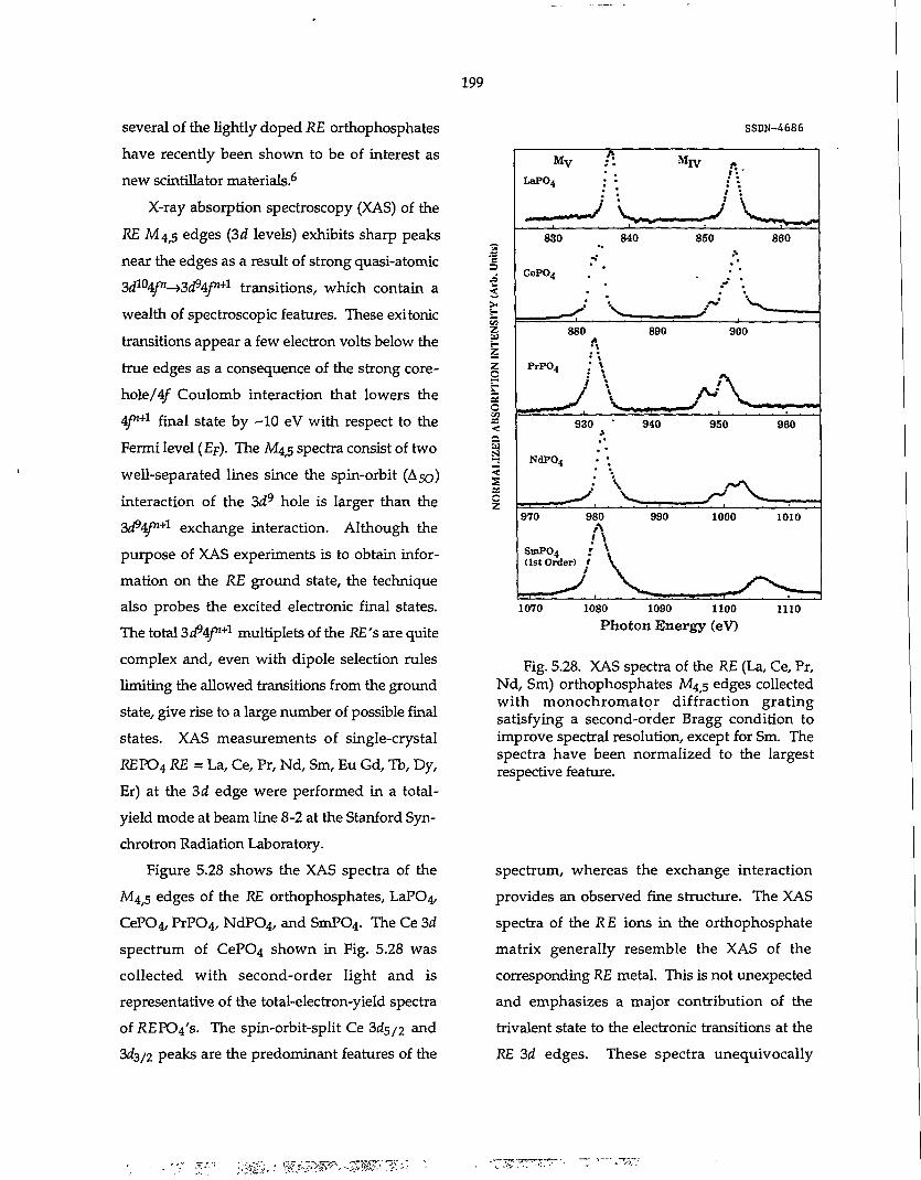
199
several of the lightly doped RE orthophosphates have recently been shown to be of interest as new scintillator materials.6
X-ray absorption spectroscopy (XAS) of the RE M 4 / 5 edges (3d levels) exhibits sharp peaks near the edges as a result of strong quasi-atomic 3d104fn^3d9Afn*1 transitions, which contain a wealth of spectroscopic features. These exitonic transitions appear a few electron volts below the true edges as a consequence of the strong core-hole/4f Coulomb interaction that lowers the 4fM+1 final state by -10 eV with respect to the Fermi level (Ep). The M4 /5 spectra consist of two well-separated lines since the spin-orbit (Aso) interaction of the 3d 9 hole is larger than the 3^4/"+1 exchange interaction. Although the purpose of XAS experiments is to obtain information on the RE ground state, the technique also probes the excited electronic final states. The total 3d94fl+1 multiplets of the RE's are quite complex and, even with dipole selection rules limiting the allowed transitions from the ground state, give rise to a large number of possible final states. XAS measurements of single-crystal KEFO4 RE = La, Ce, Pr, Nd, Sm, Eu Gd, Tb, Dy, Er) at the 3d edge were performed in a total-yield mode at beam line 8-2 at the Stanford Synchrotron Radiation Laboratory.
Figure 5.28 shows the XAS spectra of the M 4 /5 edges of the RE orthophosphates, LaPO^, CeP0 4 , PrP0 4 , NdP0 4 , and SmP0 4. The Ce 3d spectrum of CeP0 4 shown in Fig. 5.28 was collected with second-order light and is representative of the total-electron-yield spectra of i?EP0 4 's. The spin-orbit-split Ce 3e?5/2 and 3^3/2 peaks are the predominant features of the
SSDN-4686
z a f-z z c
c
a
s
M v
LaPOi
S—
.
^J 830
CeP0 4
840 850 860
V. 880 890 900
PrPO,
^ * M % — f c n *^mm**mm
930 940 950 960
NdP0 4
1070 1080 1090 1100 Photon Energy (eV)
1110
Fig. 5.28. XAS spectra of the RE (La, Ce, Pr, Nd, Sm) orthophosphates M 4 /5 edges collected with monochromator diffraction grating satisfying a second-order Bragg condition to improve spectral resolution, except for Sm. The spectra have been normalized to the largest respective feature.
spectrum, whereas the exchange interaction provides an observed fine structure. The XAS spectra of the RE ions in the orthophosphate matrix generally resemble the XAS of the corresponding RE metal. This is not unexpected and emphasizes a major contribution of the trivalent state to the electronic transitions at the RE 3d edges. These spectra unequivocally
200
identify the transitions originating from well-
characterized RE cores and correlate well with
previous theoretical investigations.
1. Summary of paper: Materials Research Society Symposium Proceedings, Vol. 307, in press.
2. Lawrence Berkeley Laboratory, Berkeley, Calif.
3. Lawrence Livermore National Laboratory, Livermore, Calif.
4. E. Jarosewich and L. A. Boatner, Geostandards Newsletter 15,397 (1991).
5. L. A. Boatner and B. C. Sales, p. 495 in Radioactive Waste Forms for the Future, ed. by W. Lutze and R. C. Ewing, Elsevier Science Publishers, New York, 1988.
6. A. Lempicki et a l , IEEE Trans. Nucl. Sci. 40,384 (1993).
COLLABORATIVE SYNCHROTRON BEAM LINE FOR THE
ADVANCED PHOTON SOURCE
B. C. Larson, G. E. Ice,1 } . Z. Tischler, ]. D. Budai, C. } . Sparks,1 and E. Specht1
A high-brightness synchrotron beam line is
under development in collaboration with the
Universi ty of Illinois Materials Research
Laboratory and UOP Research and Develop
ment, Inc., for construction as an x-ray scattering
user facility at the Advanced Photon Source
(APS). Detailed planning and engineering are
in progress on beam line hardware and optical
components , and APS approval has been
received for the beam line conceptual design
and management plan. Engineering design has
been completed, and fabrication has been initi
ated on an inclined geometry, high heat load
focusing monochromator for an undulator inser
tion device as part of a research and develop
ment agreement with the APS Experimental
Facilities Division. The results of this devel
opment will be available for general use at the
APS as well as by the UNI-CAT beam line con
sortium. Construction progress by the APS on
the synchrotron storage ring facility indicates
that initial photon beams will be available for
test purposes by mid-1995, and UNI-CAT plans
are to complete the undulator beam line so that
testing, alignment, and final beam line com
ponent development can begin at that time.
Discussions are in progress with personnel
from the National Institute for Standards and
Technology (NIST) as an additional collab
orator. In addition to general x-ray scattering,
the proposed NIST scientific program includes
extended x-ray absorption fine structure, topog
raphy, and small-angle scattering capabilities
which are largely complementary to the
programs of the present collaborators and
would strengthen the consortium.
1. Metals and Ceramics Division, ORNL.
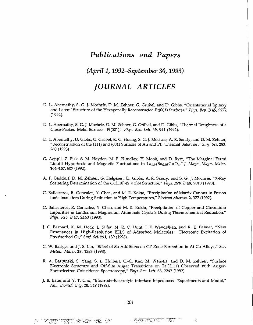
Publications and Papers
(April 1,1992-September 30,1993)
JOURNAL ARTICLES
D. L. Abernathy, S. G. J. Mochrie, D. M. Zehner, G. Grubel, and D. Gibbs, "Orientational Epitaxy and Lateral Structure of the Hexagonally Reconstructed Pt(OOl) Surfaces," Phys. Rev. B 45, 9272 (1992).
D. L. Abernathy, S. G. J. Mochrie, D. M. Zehner, G. Grubel, and D. Gibbs, "Thermal Roughness of a Close-Packed Metal Surface: Pt(OOl)," Phys. Rev. Lett. 69, 941 (1992).
D. L. Abernathy, D. Gibbs, G. Grubel, K. G. Huang, S. G. J. Mochrie, A. R. Sandy, and D. M. Zehner, "Reconstruction of the (111) and (001) Surfaces of Au and Pt: Thermal Behavior," Surf. Sci. 283, 260 (1993).
G. Aeppli, Z. Fisk, S. M. Hayden, M. F. Hundley, H. Mook, and D. Rytz, "The Marginal Fermi Liquid Hypothesis and Magnetic Fluctuations in Lai^Bao.osCuO^" /. Magn. Magn. Mater. 104-107,507 (1992).
A. P. Baddorf, D. M. Zehner, G. Helgesen, D. Gibbs, A. R. Sandy, and S. G. J. Mochrie, "X-Ray Scattering Determination of the Cu(110)-(2 x 3)N Structure," Phys. Rev. B 48, 9013 (1993).
C. Ballesteros, R. Gonzalez, Y. Chen, and M. R. Kokta, "Precipitation of Matrix Cations in Fusion Ionic Insulators During Reduction at High Temperatures," Electron Microsc. 2,377 (1992).
C. Ballesteros, R. Gonzalez, Y. Chen, and M. R. Kokta, "Precipitation of Copper and Chromium Impurities in Lanthanum Magnesium Aluminate Crystals During Thermochemical Reduction," Phys. Rev. B 47, 2460 (1993).
J. C. Barnard, K. M. Hock, L. Siller, M. R. C. Hunt, J. F. Wendelken, and R. E. Palmer, "New Resonances in High-Resolution EELS of Adsorbed Molecules: Electronic Excitation of Physisorbed O2," Surf. Sci. 291,139 (1993).
C. W. Bartges and J. S. Lin, "Effect of Sn Additions on GP Zone Formation in Al-Cu Alloys," Scr. Metall. Mater. 28, 1283 (1993).
R. A. Bartynski, S. Yang, S. L. Hulbert, C.-C. Kao, M. Weinert, and D. M. Zehner, "Surface Electronic Structure and Off-Site Auger Transitions on TaC(lll) Observed with Auger-Photoelectron Coincidence Spectroscopy," Phys. Rev. Lett. 68, 2247 (1992).
J. B. Bates and Y. T. Chu, "Electrode-Electrolyte Interface Impedance: Experiments and Model," Ann. Biomed. Eng. 20, 349 (1992).
201
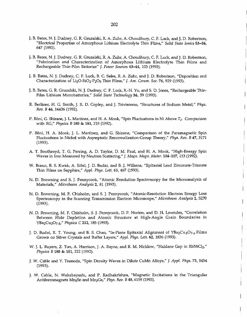
202
J. B. Bates, N. J. Dudney, G. R. Gruzalski, R. A. Zuhr, A. Choudhury, C. F. Luck, and J. D. Robertson, "Electrical Properties of Amorphous Lithium Electrolyte Thin Films," Solid State Ionics 53-56, 647 (1992).
J. B. Bates, N. J. Dudney, G. R. Gruzalski, R. A. Zuhr, A. Choudhury, C. F. Luck, and J. D. Robertson, "Fabrication and Characterization of Amorphous Lithium Electrolyte Thin Films and Rechargeable Thin-Film Batteries" /. Power Sources 43-44, 103 (1993).
J. B. Bates, N. J. Dudney, C. F. Luck, B. C. Sales, R. A. Zuhr, and J. D. Robertson, "Deposition and Characterization of L i 2 0 - S i 0 2 - P 2 0 5 Thin Films," /. Am. Ceram. Soc. 76, 929 (1993).
J. B. Bates, G. R. Gruzalski, N. J. Dudney, C. F. Luck, X.-H. Yu, and S. D. Jones, "Rechargeable Thin-Film Lithium Microbatteries," Solid State Technology 36, 59 (1993).
R. Berliner, H. G. Smith, J. R. D. Copley, and J. Trivisonno, "Structures of Sodium Metal," Phys. Rev. B 46,14436 (1992).
P. Boni, G. Shirane, J. L. Martinez, and H. A. Mook, "Spin Fluctuations in Ni Above Tc: Comparison with RG," Physica B 180 & 181, 219 (1992).
P. Boni, H. A. Mook, J. L. Martinez, and G. Shirane, "Comparison of the Paramagnetic Spin Fluctuations in Nickel with Asymptotic Renormalization-Group Theory," Phys. Rev. B 47, 3171 (1993).
A. T. Boothroyd, T. G. Perring, A. D. Taylor, D. M. Paul, and H. A. Mook, "High-Energy Spin Waves in Iron Measured by Neutron Scattering," /. Magn. Magn. Mater. 104-107,113 (1992).
W. Braun, B. S. Kwak, A. Erbil, J. D. Budai, and B. J. Wilkens, "Epitaxial Lead Zirconate-Titanate Thin Films on Sapphire," Appl. Phys. Lett. 63, 467 (1993).
N. D. Browning and S. J. Pennycook, "Atomic Resolution Spectroscopy for the Microanalysis of Materials," Microbeam Analysis 2, 81 (1993).
N. D. Browning, M. F. Chisholm, and S. J. Pennycook, "Atomic-Resolution Electron Energy Loss Spectroscopy in the Scanning Transmission Electron Microscope," Microbeam Analysis 2, S270 (1993).
N. D. Browning, M. F. Chisholm, S. J. Pennycook, D. P. Norton, and D. H. Lowndes, "Correlation Between Hole Depletion and Atomic Structure at High-Angle Grain Boundaries in Y B a 2 C u 3 0 7 _ 5 / " Physica C 212, 185 (1993).
J. D. Budai, R. T. Young, and B. S. Chao, "In-Plane Epitaxial Alignment of Y B a 2 C u 3 0 7 - x Films Grown on Silver Crystals and Buffer Layers," Appl. Phys. Lett. 62, 1836 (1993).
W. J. L.' Buyers, Z. Tun, A. Harrison, J. A. Rayne, and R. M. Nicklow, "Haldane Gap in RbNiCl 3 ," Physica B 180 & 181, 222 (1992).
J. W. Cable and Y. Tsunoda, "Spin Density Waves in Dilute CuMn Alloys," /. Appl. Phys. 73, 5454 (1993).
J. W. Cable, N. Wakabayashi, and P. Radhakrishna, "Magnetic Excitations in the Triangular Antiferromagnets Mn 3 Sn and Mn 3 Ge," Phys. Rev. B 48, 6159 (1993).
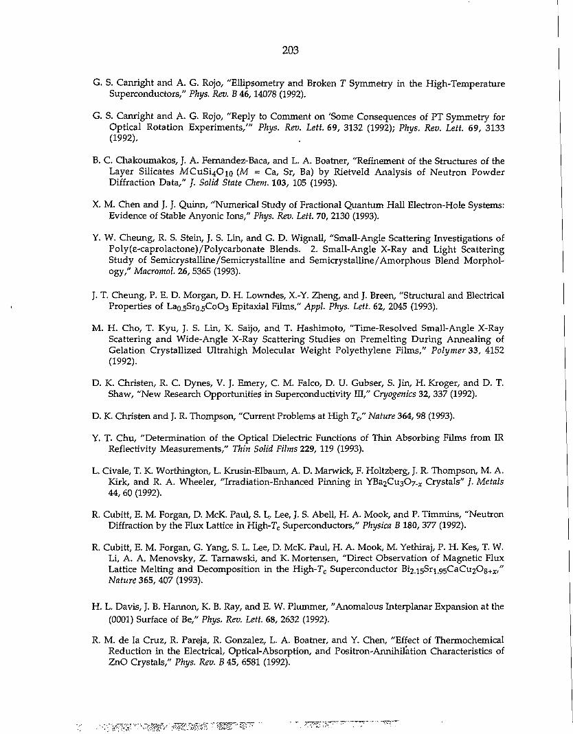
203
G. S. Canright and A. G. Rojo, "Ellipsometry and Broken T Symmetry in the High-Temperature Superconductors," Phys. Rev. B 46,14078 (1992).
G. S. Canright and A. G. Rojo, "Reply to Comment on 'Some Consequences of PT Symmetry for Optical Rotation Experiments/" Phys. Rev. Lett. 69, 3132 (1992); Phys. Rev. Lett. 69, 3133 (1992).
B. C. Chakoumakos, J. A. Fernandez-Baca, and L. A. Boatner, "Refinement of the Structures of the Layer Silicates MCuSi40io (M = Ca, Sr, Ba) by Rietveld Analysis of Neutron Powder Diffraction Data," /. Solid State Chem. 103, 105 (1993).
X. M. Chen and J. J. Quinn, "Numerical Study of Fractional Quantum Hall Electron-Hole Systems: Evidence of Stable Anyonic Ions," Phys. Rev. Lett. 70, 2130 (1993).
Y. W. Cheung, R. S. Stein, J. S. Lin, and G. D. Wignall, "Small-Angle Scattering Investigations of Poly(e-caprolactone)/Polycarbonate Blends. 2. Small-Angle X-Ray and Light Scattering Study of Semicrystalline/Semicrystalline and Semicrystalline/Amorphous Blend Morphology," Macromol. 26, 5365 (1993).
J. T. Cheung, P. E. D. Morgan, D. H. Lowndes, X.-Y. Zheng, and J. Breen, "Structural and Electrical Properties of La0.5Sr0.5CoO3 Epitaxial Films," Avpl. Phys. Lett. 62, 2045 (1993).
M. H. Cho, T. Kyu, J. S. Lin, K. Saijo, and T. Hashimoto, "Time-Resolved Small-Angle X-Ray Scattering and Wide-Angle X-Ray Scattering Studies on Premelting During Annealing of Gelation Crystallized Ultrahigh Molecular Weight Polyethylene Films," Polymer 33, 4152 (1992).
D. K. Christen, R. C. Dynes, V. J. Emery, C. M. Falco, D. U. Gubser, S. Jin, H. Kroger, and D. T. Shaw, "New Research Opportunities in Superconductivity III," Cryogenics 32, 337 (1992).
D. K. Christen and J. R. Thompson, "Current Problems at High Tc," Nature 364, 98 (1993).
Y. T. Chu, "Determination of the Optical Dielectric Functions of Thin Absorbing Films from IR Reflectivity Measurements," Thin Solid Films 229, 119 (1993).
L. Civale, T. K. Worthington, L. Krusin-Elbaum, A. D. Marwick, F. Holtzberg, J. R. Thompson, M. A. Kirk, and R. A. Wheeler, "Irradiation-Enhanced Pinning in YBa2Cu307_x Crystals" /. Metals 44, 60 (1992).
R. Cubitt, E. M. Forgan, D. McK. Paul, S. L. Lee, J. S. Abell, H. A. Mook, and P. Timmins, "Neutron Diffraction by the Flux Lattice in High-Tc Superconductors," Physica B 180, 377 (1992).
R. Cubitt, E. M. Forgan, G. Yang, S. L. Lee, D. McK. Paul, H. A. Mook, M. Yethiraj, P. H. Kes, T. W. Li, A. A. Menovsky, Z. Tarnawski, and K. Mortensen, "Direct Observation of Magnetic Flux Lattice Melting and Decomposition in the High-Tc Superconductor Bi2.15Sr1.95CaCu2O8.Kr," Nature 365, 407 (1993).
H. L. Davis, J. B. Harmon, K. B. Ray, and E. W. Plummer, "Anomalous Interplanar Expansion at the (0001) Surface of Be," Phys. Rev. Lett. 68, 2632 (1992).
R. M. de la Cruz, R. Pareja, R. Gonzalez, L. A. Boatner, and Y. Chen, "Effect of Thermochemical Reduction in the Electrical, Optical-Absorption, and Positron-Annihilation Characteristics of ZnO Crystals," Phys. Rev. B 45, 6581 (1992).
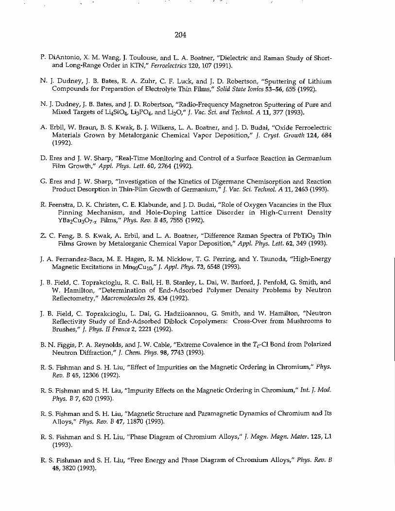
204
P. DiAntonio, X. M. Wang, J. Toulouse, and L. A. Boatner, "Dielectric and Raman Study of Short-and Long-Range Order in KTN," Ferroelectrics 120,107 (1991).
N. J. Dudney, J. B. Bates, R. A. Zuhr, C. F. Luck, and J. D. Robertson, "Sputtering of Lithium Compounds for Preparation of Electrolyte Thin Films," Solid State Ionics 53-56, 655 (1992).
N. J. Dudney, J. B. Bates, and J. D. Robertson, "Radio-Frequency Magnetron Sputtering of Pure and Mixed Targets of L^SiO^ L13PO4, and L i 2 0 ," /. Vac. Sci. and Technol. A 11, 377 (1993).
A. Erbil, W. Braun, B. S. Kwak, B. J. Wilkens, L. A. Boatner, and J. D. Budai, "Oxide Ferroelectric Materials Grown by Metalorganic Chemical Vapor Deposition," /. Cryst. Growth 124, 684 (1992).
D. Eres and J. W. Sharp, "Real-Time Monitoring and Control of a Surface Reaction in Germanium Film Growth," Appl. Phys. Lett. 60, 2764 (1992).
G. Eres and J. W. Sharp, "Investigation of the Kinetics of Digermane Chemisorption and Reaction Product Desorption in Thin-Film Growth of Germanium," /. Vac. Sci. Technol. A 11, 2463 (1993).
R. Feenstra, D. K. Christen, C. E. Klabunde, and J. D. Budai, "Role of Oxygen Vacancies in the Flux Pinning Mechanism, and Hole-Doping Lattice Disorder in High-Current Density Y B a 2 C u 3 0 7 . x Films," Phys. Rev. B 45, 7555 (1992).
Z. C. Feng, B. S. Kwak, A. Erbil, and L. A. Boatner, "Difference Raman Spectra of P b T i 0 3 Thin Films Grown by Metalorganic Chemical Vapor Deposition," Appl. Phys. Lett. 62, 349 (1993).
J. A. Fernandez-Baca, M. E. Hagen, R. M. Nicklow, T. G. Perring, and Y. Tsunoda, "High-Energy Magnetic Excitations in M n 9 0 C u i 0 , " J. Appl. Phys. 73, 6548 (1993).
J. B. Field, C. Toprakcioglu, R. C. Ball, H. B. Stanley, L. Dai, W. Barford, J. Penfold, G. Smith, and W. Hamilton, "Determination of End-Adsorbed Polymer Density Problems by Neutron Reflectometry," Macromolecides 25, 434 (1992).
J. B. Field, C. Toprakcioglu, L. Dai, G. Hadziioannou, G. Smith, and W. Hamilton, "Neutron Reflectivity Study of End-Adsorbed Diblock Copolymers: Cross-Over from Mushrooms to Brushes," /. Phys. II France 2, 2221 (1992).
B. N. Figgis, P. A. Reynolds, and J. W. Cable, "Extreme Covalence in the TC-C1 Bond from Polarized Neutron Diffraction," /. Chem. Phys. 98, 7743 (1993).
R. S. Fishman and S. H. Liu, "Effect of Impurities on the Magnetic Ordering in Chromium," Phys. Rev. B 45, 12306 (1992).
R. S. Fishman and S. H. Liu, "Impurity Effects on the Magnetic Ordering in Chromium," Int. } . Mod. Phys. B 7, 620 (1993).
R. S. Fishman and S. H. Liu, "Magnetic Structure and Paramagnetic Dynamics of Chromium and Its Alloys," Phys. Rev. B 47, 11870 (1993).
R. S. Fishman and S. H. Liu, "Phase Diagram of Chromium Alloys," /. Magn. Magn. Mater. 125, LI (1993).
R. S. Fishman and S. H. Liu, "Free Energy and Phase Diagram of Chromium Alloys," Phys. Rev. B 48, 3820 (1993).
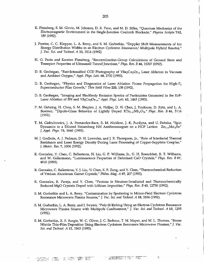
205
K. Flensberg, S. M. Girvin, M. Johnson, D. R. Perm, and M. D. Stiles, "Quantum Mechanics of the Electromagnetic Environment in the Single-Junction Coulomb Blockade," Physica Scripta T42, 189 (1992).
J. Forster, C. C. Klepper, L. A. Berry, and S. M. Gorbatkin, "Doppler Shift Measurements of Ion Energy Distribution Widths in an Electron Cyclotron Resonance/ Multipole Hybrid Reactor," /. Vac. Sci. and Technol. A 10, 3114 (1992).
H. O. Frota and Karsten Flensberg, "Renormlization-Group Calculations of Ground State and Transport Properties of Ultrasmall Tunnel Junctions," Phys. Rev. B 46,15207 (1992).
D. B. Geohegan, "Fast-Intensified CCD Photography of YBa2Cu307^ Laser Ablation in Vacuum and Ambient Oxygen," Appl. Phys. Lett. 60, 2732 (1992).
D. B. Geohegan, "Physics and Diagnostics of Laser Ablation Plume Propagation for High-Tc
Superconductor Film Growth," Thin Solid Films 220,138 (1992).
D. B. Geohegan, "Imaging and Blackbody Emission Spectra of Particulates Generated in the KrF-Laser Ablation of BN and YB 2 Cu 3 0 7 . X / " Appl. Phys. Lett. 62, 1463 (1993).
P. M. Gehring, H. Chou, S. M. Shapiro, J. A. Hriljac, D. H. Chen, J. Toulouse, D. Rytz, and L. A. Boatner, "Dipole-Glass Behavior of Lightly Doped KTa^Nb^Os," Phys. Rev. B 46, 5116 (1992).
T. M. Giebultowicz, J. A. Fernandez-Baca, R. M. Nicklow, J. K. Furdyna, and U. Debska, "Spin Dynamics in a Diluted Heisenberg NN Antiferromagnet on a HCP Lattice: Zni. x Mn x Se" /. Appl. Phys. 73, 5660 (1993).
M. J. Godbole, A. J. Pedraza, D. H. Lowndes, and J. R. Thompson, Jr., "Role of Interfacial Thermal Resistance and Laser Energy Density During Laser Processing of Copper-Sapphire Couples," /. Mater. Res. 7, 1004 (1992).
R. Gonzalez, Y. Chen, C. Ballesteros, H. Liu, G. P. Williams, Jr., G. H. Rosenblatt, R. T. Williams, and W. Gellermann, "Luminescence Properties of Deformed CaO Crystals," Phys. Rev. B 47, 4910 (1993).
R. Gonzalez, C. Ballesteros, Y. J. Liu, Yi Chen, X. F. Zong, and Y. Chen, "Thermochemical Reduction of Yttrium Aluminum Garnet Crystals," Philos. Mag. A 67, 207 (1993).
R. Gonzalez, R. Pareja, and Y. Chen, "Protons in Neutron-Irradiated and Thermochemically Reduced MgO Crystals Doped with Lithium Impurities," Phys. Rev. B 45,12730 (1992).
S. M. Gorbatkin and L. A. Berry, "Contamination by Sputtering in Mirror-Field Electron Cyclotron Resonance Microwave Plasma Sources," /. Vac. Sci. and Technol. A 10, 3104 (1992).
S. M. Gorbatkin, L. A. Berry, and J. Swyers, "Poly-Si Etching Using an Electron Cyclotron Resonance Microwave Plasma Source with Multipole Confinement," /. Vac. Sci. and Technol. A 10, 1295 (1992).
S. M. Gorbatkin, R. F. Burgie, W. C. Oliver, J. C. Barbour, T. M. Mayer, and M. L. Thomas, "Boron Nitride Thin-Film Deposition Using Electron Cyclotron Resonance Microwave Plasmas," /. Vac. Sci. and Technol. A 11, 1863 (1993).
206
P. Grenier, S. Jandl, M. Blouin, and L. A. Boatner, "Study of Ferroelectric Microdomains Due to Oxygen Vacancies in KTa0 3," Ferroelectrics 137,105 (1992).
P. Grenier, D. Houde, S. Jandl, and L. A. Boatner, "Soft Mode Studies in KTao.93Nbo.07O3 with Use of the Time-Resolved Third-Order Optical Susceptibility X3," Phys. Rev. B 47, 1 (1993).
G. Grubel, D. Gibbs, D. M. Zehner, D. L. Abernathy, A. R. Sandy, and S. G. J. Mochrie, "Phase Behavior of Au and Pt Surfaces," Surf. Sci. 287/288, 842 (1993).
V. A. Hackley, M. A. Anderson, and S. Spooner, "A Small-Angle X-Ray Scattering Study of Microstructure Evolution During Sintering of Sol-Gel Derived Porous Nanophase Titania," /. Mater. Res. 7, 2555 (1992).
' M. Hagen, H. R. Child, J. A. Fernandez-Baca, and J. L. Zarestky, "A Study of the Magnetic Critical Scattering from the Longitudinally Modulated Antiferromagnets Thulium and Erbium," /. Phys.: Condens. Matter 4, 8879 (1992).
R. F. Haglund, Jr., R. H. Magruder III, S. H. Morgan, D. O. Henderson, R. A. Weller, L. Yang, and R. A. Zuhr, "Nonlinear Index of Refraction of Cu- and Pb-Implanted Fused Silica," Nucl. Instrum. and Methods Phys. Res. Sect. B 365, 405 (1992).
R. F. Haglund, Jr., L. Yang, R. H. Magruder III, J. E. Wittig, K. Becker, and R. A. Zuhr, "Picosecond Nonlinear Optical Response of a Cu:Silica Nanocluster Composite," Opt. Lett. 18, 373 (1993).
T. E. Haynes and O. W. Holland, "Damage Accumulation During Ion Implantation of Unstrained Si!_xGex Alloy Layers," April. Phys. Lett. 61, 61 (1992).
T. E. Haynes and O. W. Holland, "Lattice Damage in Ion-Implanted Silicon-Germanium Alloys," Nucl. lustrum, and Methods Phys. Res. Sect. B 80/81, 901 (1993).
O. W. Holland and T. E. Haynes, "Damage Saturation During High-Energy, Ion Implantation of Si^Ge*," Appl. Phys. Lett. 61, 3148 (1992).
0 . W. Holland, D. S. Zhou, and D. K. Thomas, "Damage Accumulation During High-Dose, 0 +
Implantation in Si," Appl. Phys. Lett. 63, 896 (1993).
H. Hosono, H. Fukushima, Y. Abe, R. A. Weeks, and R. A. Zuhr, "Cross-Sectional TEM Observation of Copper-Implanted Si0 2 Glass," /. Non-Cryst. Solids 143,157 (1992).
M. Hou, W. Eckstein, and M. T. Robinson, "Computer Simulation of Temporal Aspects of the Copper Single-Crystal Sputtering," Nucl. Instrum. and Methods Phys. Res. Sect. B 82, 234 (1993).
1. G. Hughes, J. Burgdorfer, L. Folkerts, C. C. Havener, S. H. Overbury, M. T. Robinson, D. M. Zehner, P. A. Zeijlmans van Emmichoven, and F. W. Meyer, "Separation of Kinetic and Potential Electron Emission Arising from Slow Multicharged Ion-Surface Interactions," Phys. Rev. Lett. 71, 291 (1993).
J. D. Hunn, N. R. Parikh, M. L. Swanson, and R. A. Zuhr, "Conduction in Ion-Implanted Single-Crystal Diamond," Diamond and Related Materials 2, 847 (1993).
G. E. Jellison, Jr., and J. W. McCamy, "Sample Deplorization Effects from Thin Films of ZnS on GaAs as Measured by Spectroscopic Ellipsometry," Appl. Phys. Lett. 61, 512 (1992).

207
G. E. Jellison, Jr., "Optical Functions of GaAs, GaP, and Ge Determined by Two-Channel Polarization Modulation Ellipsometry," Opt. Mater. 1, 151 (1992).
G. E. Jellison, Jr., T. E. Haynes, and H. H. Burke, "Optical Functions of Silicon-Germanium Alloys Determined Using Spectroscopic Ellipsometry," Opt. Mater. 2,105 (1993).
G. E. Jellison, Jr., M. F. Chisholm, and S. M. Gorbatkin, "Optical Functions of Chemical Vapor Deposited Thin-Film Silicon Determined by Spectroscopic Ellipsometry," Appl. Phys. Lett. 62, 3348 (1993).
D. E. Jesson, S. J. Pennycook, J.-M. Baribeau, and D. C. Houghton, "Atomistic Processes of Surface Segregation During Si-Ge MBE Growth," Thin Solid Films 222, 98 (1992).
D. E. Jesson and S. J. Pennycook, "Incoherent Imaging of Thin Specimens Using Coherently Scattered Electrons," Proc. R. Soc. London A 441,261 (1993).
D. E. Jesson, S. J. Pennycook, J. Z. Tischler, J. D. Budai, J.-M. Baribeau, and D. C. Houghton, "Interplay Between Evolving Surface Morphology, Atomic-Scale Growth Modes, and Ordering During Si^Gex.* Epitaxy," Phys. Rev. Lett. 70, 2293 (1993).
D. E. Jesson, S. J. Pennycook, J.-M. Baribeau, and D. C. Houghton, "Direct Imaging of Surface Cusp Evolution During Strained-Layer Epitaxy and Implications for Strain Relaxation," Phys. Rev. Lett. 71, 1744 (1993).
Q. T. Jiang, T. Gustafsson, P. Haberle, and D. M. Zehner, "Missing-Row Surface Reconstruction of Au(113) Induced by Adsorbed Calcium Atoms," Phys. Rev. B 45,14256 (1992).
Q. T. Jiang, P. Statiris, T. Gustafsson, P. Haberel, and D. M. Zehner, "Ion Scattering Study of the Adatom Induced Missing-Row Reconstructions of Ni(110) and Au(113)," /. Vac. Sci. and Technol. A 10, 2197 (1992).
E. C. Jones, D. K. Christen, J. R. Thompson, R. Feenstra, S. Zhu, D. H. Lowndes, J. M. Phillips, M. P. Siegal, and J. D. Budai, "Correlations Between the Hall Coefficient and the Superconducting Transport Properties of Oxygen-Deficient YBa2Cu30y_5 Epitaxial Thin Films," Phys. Rev. B 47, 8986 (1993).
T. Kanaya, M. Ohkura, K. Kaji, M. Furusaka, M. Misawa, H. Yamaoka, and G. D. Wignall, "Small-Angle Neutron Scattering From Polyvinyl Alcohol) Gels/' Physica B 180 & 181, 549 (1992).
T. Kaplan, M. Rasolt, M. Karimi, and M. Mostoller, "Numerical Simulation of He + and Li +
Collisions with C 6 0 ," /. Phys. Chem. 97, 6124 (1993).
M. Karimi, T. Kaplan, M. Mostoller, and D. E. Jesson, "Ge Segregation at Si-Ge (001) Stepped Surfaces," Phys. Rev. B 47, 9931 (1993).
S. Katano, S. Funahashi, N. Mori, Y. Ueda, and J. A. Fernandez-Baca, "Pressure Effects on the Structural Phase Transitions and Superconductivity of La2-xBa : cCu04 (x = 0.125)," Phys. Rev. B 48, 6569 (1993).
S. Katano, J. A. Fernandez-Baca, S. Funahashi, N. Mori, Y. Ueda, and K. Koga, "Crystal Structure and Superconductivity of La 2. 3 rBa rCu0 4 (0.03 < x < 0.24)," Physica C 214, 64 (1993).
208
H. R. Kerchner, D. K. Christen, C. E. Klabunde, J. O. Thomson, Y. R. Sun, and J. R. Thompson, "Evidence of Kosterlitz-Thouless Transition in YBa2Cu30y/PrBa2Cu307 Superlattice Films," Physica C 198, 75 (1992).
W. K. Kot, M. Edelstein, M. M. Abraham, and L. A. Boatner, "The EPR of P u 3 + and Cf3 + in Single Crystals of LuP0 4 , " Phys. Rev. B 47, 3412 (1993).
M. N. Kunchur, D. K. Christen, and J. M. Phillips, "Observation of Free Flux Flow at High Dissipation Levels in YBa 2 Cu 3 07_ 5 Epitaxial Films," Phys. Rev. Lett. 70, 998 (1993).
B. S. Kwak, A. Erbil, B. J. Wilkens, J. D. Budai, M. F. Chisholm, and L. A. Boatner, "Strain Relaxation by Domain Formation in Epitaxial Ferroelectric Thin Films," Phys. Rev. Lett. 68, 3733 (1992).
B. S. Kwak, P. N. First, A. Erbil, B. J. Wilkens, J. D. Budai, M. F. Chisholm, and L. A. Boatner, "Study of Epitaxial Platinum Thin Films Grown by Metalorganic Chemical Vapor Deposition," /. Appl. Phys. 72, 3735 (1992).
C. Lee, T. E. Haynes, and K. S. Jones, "Kinetics of Solid Phase Epitaxial Regrowth in Amorphized Si0.88Ge0.i2 Measured by Time-Resolved Reflectivity," Appl. Phys. Lett. 62, 501 (1993).
M. F. Lin and K. W.-K. Shung, "Magnetoplasmons and Persistent Currents in Cylindrical Tubules," Phys. Rev. B 48, 5567 (1993).
S. H. Liu, "Formation and Anomalous Properties of Fractals," Eng. Med. and Biology 11, 28 (1992).
S. H. Liu, "Electronic Polaron Effects in Mixed Valence and Heavy Fermion Materials," Int. ]. Mod. Phys. B 7, 9 (1993).
S. H. Liu and R. A. Klemm, "Intra- Versus Interlayer Pairing in Copper Oxide Superconductors: Response to Magnetic Field," Phys. Rev. B 48, 4080 (1993).
S. H. Liu and R. A. Klemm, "Energy Gap Structure and Tunneling Characteristics of Layered Superconductors," Physica C 216, 293 (1993).
J. D. Londono, V. M. Shah, G. D. Wignall, H. D. Cochran, and P. R. Bienkowski, "Small-Angle Neutron Scattering Studies of Dilute Supercritical Neon," /. Chem. Phys. 99, 466 (1993).
C.-K. Loong, L. Soderholm, M. M. Abraham, L. A. Boatner, and N. M. Edelstein, "Crystal-Field Excitations and Magnetic Properties of TmP0 4 , " /. Chem. Phys. 98, 4214 (1993).
D. H. Lowndes, X.-Y. Zheng, S. Zhu, J. D. Budai, and R. J. Warmack, "Suppression of the Spiral-Growth Mechanism in Epitaxial YBa2Cu 307_ x Films Grown on Miscut Substrates," Appl. Phys. Lett. 61, 852 (1992).
R. H. Magruder III, D. O. Henderson, S. H. Morgan, and R. A. Zuhr, "Optical Spectra of Pb-Implanted Fused Silica," /. Non-Cryst. Solids 152, 258 (1993).
R. H. Magruder III, L. Yang, R. F. Haglund, Jr., C. W. White, L. Yang, R. Dorsinville, and R. R. Alfano, "Optical Properties of Gold Nanocluster Composites Formed by Deep Ion Implantation in Silica," Appl. Phys. Lett. 62, 1730 (1993).
R. H. Magruder III, D. O. Henderson, C. W. White, and R. A. Zuhr, "Formation of Photosensitive Materials by Ion Implantation of Oxygen Ions in Silica," J. Non-Cryst. Solids 159, 269 (1993).
209
G. D. Mahan, "Ionic Polarization," Ferroelectrics 136, 57 (1992).
G. D. Mahan, "Electron-Electron Interactions: Ward Identities," Int. J. Mod. Phys. 6, 3381 (1992).
G. D. Mahan, "Fractal Vertex for Electron-Electron Interactions," Mod. Phys. Lett. B 7, 13 (1993).
G. D. Mahan and J. O. Sofo, "Resistivity and Superconductivity from Anharmonic Phonons," Phys. Rev. B 47, 8050 (1993).
A. G. Mal'shukov and G. D. Mahan, "Magnon Renormalization of a Localized Hole," Phys. Rev. Lett. 68, 2200 (1992).
J. M. Martin, R. K. Nadella, J. Vellanki, M. V. Rao, and O. W. Holland, "Thermally Stable Buried High Resistance Layers in P-Type InP Obtained by MeV-Energy Ti Implantation," /. Appl. Phys. 73, 7238 (1993).
A. D. Marwick, L. Civale, L. Krusin-Elbaum, R. Wheeler, J. R. Thompson, T. K. Worthington, M. A. Kirk, Y. R. Sun, H. R. Kerchner, and F. Holtzberg, "Processing High-Tc Superconductors with GeV Heavy Ions," Nucl. lustrum, and Methods Phys. Res. Sect. B 80/81, 1143 (1993).
T. E. Mason, G. Aeppli, S. M. Hayden, A. P. Ramirez, and H. A. Mook, "Low Energy Excitations in Superconducting La1.8 6Sro.i4Cu04," Phys. Rev. Lett. 71, 919 (1993).
J. W. McCamy, D. H. Lowndes, J. D. Budai, R. A. Zuhr, and X. Zhang, "Epitaxial ZnS Films Grown on GaAs (001) and (111) by Pulsed-Laser Ablation," /. Appl. Phys. 73, 7818 (1993).
C. J. McHargue and J. M. Williams, "Ion Implantation Effects in Silicon Carbide," Nucl. Instrum. and Methods Phys. Res. Sect. B 80/81, 889 (1993).
A. D. Migone, M. T. Alkhafaji, G. Vidali, and M. Karimi, "Thermodynamic Study of Argon Films Adsorbed on Boron Nitride," Phys. Rev. B 47, 6685 (1993).
F. A. Modine and G. E. Jellison, Jr., "Errors in Polarization Measurements Due to Static Retardation in Photoelastic Modulators," Appl. Phys. Commun. 12, 121 (1993).
F. A. Modine, D. C. Lubben, and J. B. Bates, "Electrical Conduction in CaF2 and CaF2-Al2C>3 Nanocomposite Films on A1 2 0 3 Substrates," /. Appl. Phys. 74, 2658 (1993).
H. A. Mook, B. C. Chakoumakos, M. Mostoller, A. T. Boothroyd, and D. McK. Paul, "Phonons and Superconductivity in Bi2Sr2CaCu208," Phys. Rev. Lett. 69, 2272 (1992).
H. A. Mook, M. Yethiraj, G. Aeppli, T. E. Mason, and T. Armstrong, "Polarized Neutron Determination of the Magnetic Excitations in YBa 2Cu 30 7," Phys. Rev. Lett. 70, 3490 (1993).
H. A. Mook, M. Yethiraj, G. D. Wignall, E. M. Forgan, S. L. Lee, R. Cubitt, D. McK. Paul, and T. Armstrong, "Neutron Measurements of the Vortex Lattice in YBa2Cu3C>7," /. Appl. Phys. 73, 5855 (1993).
H. A. Mook, C. L. Seaman, M. B. Maple, M. A. Lopez de la Torre, D. L. Cox, and M. Makivic, "Neutron Scattering Study of the Quadrupolar Kondo Alloy Y0.8U0.2Pd3," Physica B 186-188, 341 (1993).
T. Motooka and O. W. Holland, "Amorphization Processes in Ion-Implanted Si: Ion Species Effects," Appl. Phys. Lett. 61, 3005 (1992).
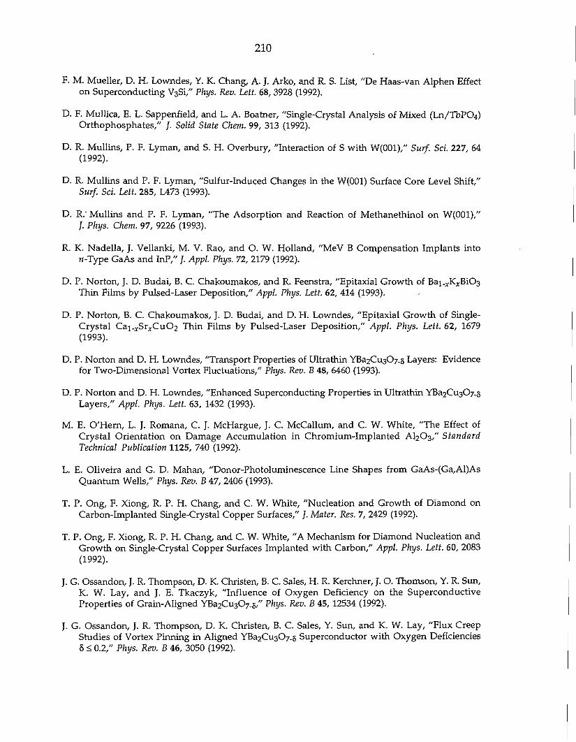
210
F. M. Mueller, D. H. Lowndes, Y. K. Chang, A. J. Arko, and R. S. List, "De Haas-van Alphen Effect on Superconducting V 3Si," Phys. Rev. Lett. 68, 3928 (1992).
D. F. Mullica, E. L. Sappenfield, and L. A. Boatner, "Single-Crystal Analysis of Mixed (Ln/TbP0 4 ) Orthophosphates," /. Solid State Chem. 99, 313 (1992).
D. R. Mullins, P. F. Lyman, and S. H. Overbury, "Interaction of S with W(001)," Surf. Sci. 227, 64 (1992).
D. R. Mullins and P. F. Lyman, "Sulfur-Induced Changes in the W(001) Surface Core Level Shift," Surf. Sci. Lett. 285, L473 (1993).
D. R." Mullins and P. F. Lyman, "The Adsorption and Reaction of Methanethinol on W(001)," /. Phys. Chem. 97, 9226 (1993).
R. K. Nadella, J. Vellanki, M. V. Rao, and O. W. Holland, "MeV B Compensation Implants into n-Type GaAs and InP," /. Appl. Phys. 72, 2179 (1992).
D. P. Norton, J. D. Budai, B. C. Chakoumakos, and R. Feenstra, "Epitaxial Growth of Bai_ xK xBi03 Thin Films by Pulsed-Laser Deposition," Appl. Phys. Lett. 62, 414 (1993).
D. P. Norton, B. C. Chakoumakos, J. D. Budai, and D. H. Lowndes, "Epitaxial Growth of Single-Crystal Cai-jSr^CuG^ Thin Films by Pulsed-Laser Deposition," Appl. Phys. Lett. 62, 1679 (1993).
D. P. Norton and D. H. Lowndes, "Transport Properties of Ultrathin YBa2Cu307_s Layers: Evidence for Two-Dimensional Vortex Fluctuations," Phys. Rev. B 48, 6460 (1993).
D. P. Norton and D. H. Lowndes, "Enhanced Superconducting Properties in Ultrathin YBa2Cu3C>7-5 Layers," Appl. Phys. Lett. 63, 1432 (1993).
M. E. O'Hern, L. J. Romana, C. J. McHargue, J. C. McCallum, and C. W. White, "The Effect of Crystal Orientation on Damage Accumulation in Chromium-Implanted AI2O3," Standard Technical Publication 1125, 740 (1992).
L. E. Oliveira and G. D. Mahan, "Donor-Photoluminescence Line Shapes from GaAs-(Ga,Al)As Quantum Wells," Phys. Rev. B 47, 2406 (1993).
T. P. Ong, F. Xiong, R. P. H. Chang, and C. W. White, "Nucleation and Growth of Diamond on Carbon-Implanted Single-Crystal Copper Surfaces," /. Mater. Res. 7, 2429 (1992).
T. P. Ong, F. Xiong, R. P. H. Chang, and C. W. White, "A Mechanism for Diamond Nucleation and Growth on Single-Crystal Copper Surfaces Implanted with Carbon," Appl. Phys. Lett. 60, 2083 (1992).
J. G. Ossandon, J. R. Thompson, D. K. Christen, B. C. Sales, H. R. Kerchner, J. O. Thomson, Y. R. Sun, K. W. Lay, and J. E. Tkaczyk, "Influence of Oxygen Deficiency on the Superconductive Properties of Grain-Aligned YBa 2Cu30 7 .5," Phys. Rev. B 45, 12534 (1992).
J. G. Ossandon, J. R. Thompson, D. K. Christen, B. C. Sales, Y. Sun, and K. W. Lay, "Flux Creep Studies of Vortex Pinning in Aligned YBa2Cu307_8 Superconductor with Oxygen Deficiencies 8 < 0.2," Phys. Rev. B 46, 3050 (1992).
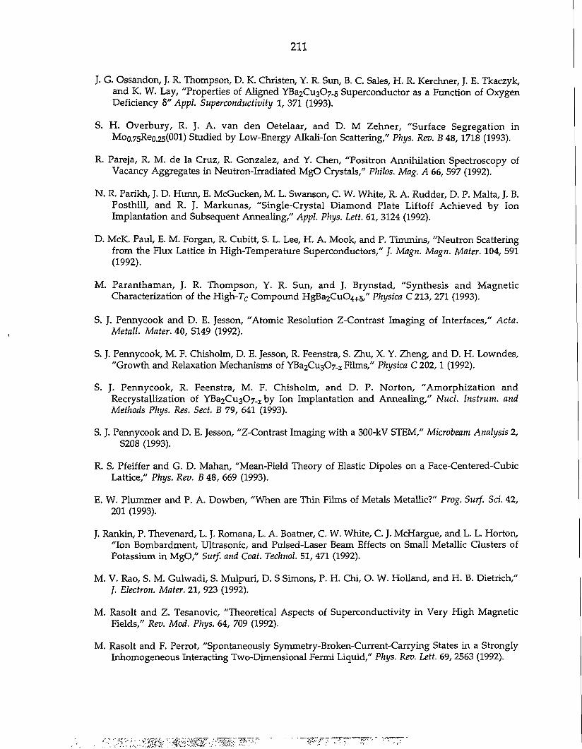
211
J. G. Ossandon, J. R. Thompson, D. K. Christen, Y. R. Sun, B. C. Sales, H. R. Kerchner, J. E. Tkaczyk, and K. W. Lay, "Properties of Aligned YBa2Cu3C>7-5 Superconductor as a Function of Oxygen Deficiency 8" Appl. Superconductivity 1, 371 (1993).
S. H. Overbury, R. J. A. van den Oetelaar, and D. M Zehner, "Surface Segregation in Mo0.75Reo.25(001) Studied by Low-Energy Alkali-Ion Scattering," Phys. Rev. B 48, 1718 (1993).
R. Pareja, R. M. de la Cruz, R. Gonzalez, and Y. Chen, "Positron Annihilation Spectroscopy of Vacancy Aggregates in Neutron-Irradiated MgO Crystals," Philos. Mag. A 66, 597 (1992).
N. R. Parikh, J. D. Hunn, E. McGucken, M. L. Swanson, C. W. White, R. A. Rudder, D. P. Malta, J. B. Posthill, and R. J. Markunas, "Single-Crystal Diamond Plate Liftoff Achieved by Ion Implantation and Subsequent Annealing," Appl. Phys. Lett. 61, 3124 (1992).
D. McK. Paul, E. M. Forgan, R. Cubitt, S. L. Lee, H. A. Mook, and P. Timrnins, "Neutron Scattering from the Flux Lattice in High-Temperature Superconductors," /. Magn. Magn. Mater. 104, 591 (1992).
M. Paranthaman, J. R. Thompson, Y. R. Sun, and J. Brynstad, "Synthesis and Magnetic Characterization of the High-Tc Compound HgBa2Cu04+8," Physica C 213, 271 (1993).
S. J. Pennycook and D. E. Jesson, "Atomic Resolution Z-Contrast Imaging of Interfaces," Acta. Metall. Mater. 40, S149 (1992).
S. J. Pennycook, M. F. Chisholm, D. E. Jesson, R. Feenstra, S. Zhu, X. Y. Zheng, and D. H. Lowndes, "Growth and Relaxation Mechanisms of YBa 2 Cu 3 0 7 . z Films," Physica C 202,1 (1992).
S. J. Pennycook, R. Feenstra, M. F. Chisholm, and D. P. Norton, "Amorphization and Recrystallization of YBa2Cu307_x by Ion Implantation and Annealing," Nucl. Instrum. and Methods Phys. Res. Sect. B 79, 641 (1993).
S. J. Pennycook and D. E. Jesson, "Z-Contrast Imaging with a 300-kV STEM," Microbeam Analysis 2, S208 (1993).
R. S. Pfeiffer and G. D. Mahan, "Mean-Field Theory of Elastic Dipoles on a Face-Centered-Cubic Lattice," Phys. Rev. B 48, 669 (1993).
E. W. Plummer and P. A. Dowben, "When are Thin Films of Metals Metallic?" Prog. Surf. Sci. 42, 201 (1993).
J. Rankin, P. Thevenard, L. J. Romana, L. A. Boatner, C. W. White, C. J. McHargue, and L. L. Horton, "Ion Bombardment, Ultrasonic, and Pulsed-Laser Beam Effects on Small Metallic Clusters of Potassium in MgO," Surf, and Coat. Technol. 51, 471 (1992).
M. V. Rao, S. M. Gulwadi, S. Mulpuri, D. S Simons, P. H. Chi, O. W. Holland, and H. B. Dietrich," /. Electron. Mater. 21, 923 (1992).
M. Rasolt and Z. Tesanovic, "Theoretical Aspects of Superconductivity in Very High Magnetic Fields," Rev. Mod. Phys. 64, 709 (1992).
M. Rasolt and F. Perrot, "Spontaneously Symmetry-Broken-Current-Carrying States in a Strongly Inhomogeneous Interacting Two-Dimensional Fermi Liquid," Phys. Rev. Lett. 69, 2563 (1992).
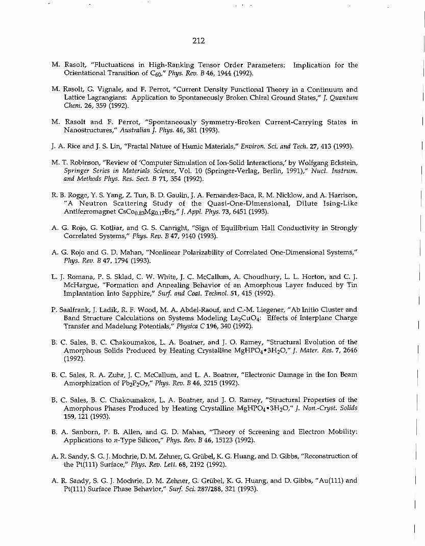
212
M. Rasolt, "Fluctuations in High-Ranking Tensor Order Parameters: Implication for the Orientational Transition of C6o," Phys. Rev. B 46, 1944 (1992).
M. Rasolt, G. Vignale, and F. Perrot, "Current Density Functional Theory in a Continuum and Lattice Lagrangians: Application to Spontaneously Broken Chiral Ground States," /. Quantum Chem. 26, 359 (1992).
M. Rasolt and F. Perrot, "Spontaneously Symmetry-Broken Current-Carrying States in Nanostructures," Australian J. Phys. 46, 381 (1993).
J. A. Rice and J. S. Lin, "Fractal Nature of Humic Materials," Environ. Sci. and Tech. 27, 413 (1993).
M. T. Robinson, "Review of 'Computer Simulation of Ion-Solid Interactions,' by Wolfgang Eckstein, Springer Series in Materials Science, Vol. 10 (Springer-Verlag, Berlin, 1991)," Nucl. Instrum. and Methods Phys. Res. Sect. B 71, 354 (1992).
R. B. Rogge, Y. S. Yang, Z. Tun, B. D. Gaulin, J. A. Fernandez-Baca, R. M. Nicklow, and A. Harrison, "A Neutron Scattering Study of the Quasi-One-Dimensional, Dilute Ising-Like Antiferromagnet CsCo0.83Mgo.i7Br3," /. Appl. Phys. 73, 6451 (1993).
A. G. Rojo, G. Kotliar, and G. S. Canright, "Sign of Equilibrium Hall Conductivity in Strongly Correlated Systems," Phys. Rev. B 47, 9140 (1993).
A. G. Rojo and G. D. Mahan, "Nonlinear Polarizability of Correlated One-Dimensional Systems," Phys. Rev. B 47, 1794 (1993).
L. J. Romana, P. S. Sklad, C. W. White, J. C. McCallum, A. Choudhury, L. L. Horton, and C. J. McHargue, "Formation and Annealing Behavior of an Amorphous Layer Induced by Tin Implantation Into Sapphire," Surf, and Coat. Technol. 51, 415 (1992).
P. Saalfrank, J. Ladik, R. F. Wood, M. A. Abdel-Raouf, and C.-M. Liegener, "Ab Initio Cluster and Band Structure Calculations on Systems Modeling La2Cu04: Effects of Interplane Charge Transfer and Madelung Potentials," Physica C196, 340 (1992).
B. C. Sales, B. C. Chakoumakos, L. A. Boatner, and J. O. Ramey, "Structural Evolution of the Amorphous Solids Produced by Heating Crystalline MgHP0 4 »3H 2 0," /. Mater. Res. 7, 2646 (1992).
B. C. Sales, R. A. Zuhr, J. C. McCallum, and L. A. Boatner, "Electronic Damage in the Ion Beam Amorphization of Pb 2P20 7," Phys. Rev. B 46, 3215 (1992).
B. C. Sales, B. C. Chakoumakos, L. A. Boatner, and J. O. Ramey, "Structural Properties of the Amorphous Phases Produced by Heating Crystalline MgHP04»3H20," /. Non.-Cryst. Solids 159,121 (1993).
B. A. Sanborn, P. B. Allen, and G. D. Mahan, "Theory of Screening and Electron Mobility: Applications to n-Type Silicon," Phys. Rev. B 46, 15123 (1992).
A. R. Sandy, S. G. J. Mochrie, D. M. Zehner, G. Griibel, K. G. Huang, and D. Gibbs, "Reconstruction of the Pt(lll) Surface," Phys. Rev. Lett. 68, 2192 (1992).
A. R. Sandy, S. G. J. Mochrie, D. M. Zehner, G. Griibel, K. G. Huang, and D. Gibbs, "Au(lll) and Pt(lll) Surface Phase Behavior," Surf. Sci. 287/288, 321 (1993).
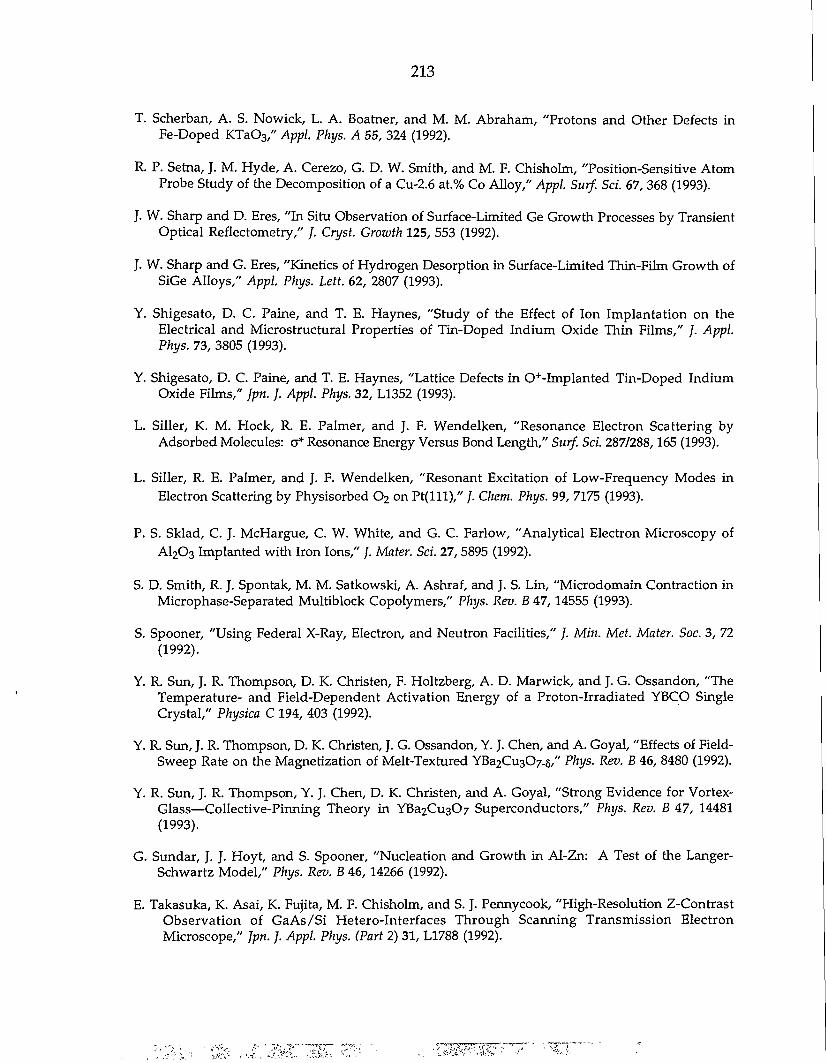
213
T. Scherban, A. S. Nowick, L. A. Boatner, and M. M. Abraham, "Protons and Other Defects in Fe-Doped KTa0 3," Appl. Phys. A 55, 324 (1992).
R. P. Setna, J. M. Hyde, A. Cerezo, G. D. W. Smith, and M. F. Chisholm, "Position-Sensitive Atom Probe Study of the Decomposition of a Cu-2.6 at.% Co Alloy," Appl. Surf. Sci. 67, 368 (1993).
J. W. Sharp and D. Eres, "In Situ Observation of Surface-Limited Ge Growth Processes by Transient Optical Reflectometry," /. Cryst. Growth 125, 553 (1992).
J. W. Sharp and G. Eres, "Kinetics of Hydrogen Desorption in Surface-Limited Thin-Film Growth of SiGe Alloys," Appl. Phys. Lett. 62, 2807 (1993).
Y. Shigesato, D. C. Paine, and T. E. Haynes, "Study of the Effect of Ion Implantation on the Electrical and Microstructural Properties of Tin-Doped Indium Oxide Thin Films," /. Appl. Phys. 73, 3805 (1993).
Y. Shigesato, D. C. Paine, and T. E. Haynes, "Lattice Defects in 0+-Implanted Tin-Doped Indium Oxide Films," Jpn. J. Appl. Phys. 32, L1352 (1993).
L. Siller, K. M. Hock, R. E. Palmer, and J. F. Wendelken, "Resonance Electron Scattering by Adsorbed Molecules: a* Resonance Energy Versus Bond Length," Surf. Sci. 287/288,165 (1993).
L. Siller, R. E. Palmer, and J. F. Wendelken, "Resonant Excitation of Low-Frequency Modes in Electron Scattering by Physisorbed 0 2 on Pt(lll)," /. Chem. Phys. 99, 7175 (1993).
P. S. Sklad, C. J. McHargue, C. W. White, and G. C. Farlow, "Analytical Electron Microscopy of A1 2 0 3 Implanted with Iron Ions," /. Mater. Sci. 27, 5895 (1992).
S. D. Smith, R. J. Spontak, M. M. Satkowski, A. Ashraf, and J. S. Lin, "Microdomain Contraction in Microphase-Separated Multiblock Copolymers," Phys. Rev. B 47, 14555 (1993).
S. Spooner, "Using Federal X-Ray, Electron, and Neutron Facilities," /. Min. Met. Mater. Soc. 3, 72 (1992).
Y. R. Sun, J. R. Thompson, D. K. Christen, F. Holtzberg, A. D. Marwick, and J. G. Ossandon, "The Temperature- and Field-Dependent Activation Energy of a Proton-Irradiated YBCO Single Crystal," Physica C194, 403 (1992).
Y. R. Sun, J. R. Thompson, D. K. Christen, J. G. Ossandon, Y. J. Chen, and A. Goyal, "Effects of Field-Sweep Rate on the Magnetization of Melt-Textured YBa 2Cu30 7. 5," Phys. Rev. B 46, 8480 (1992).
Y. R. Sun, J. R. Thompson, Y. J. Chen, D. K. Christen, and A. Goyal, "Strong Evidence for Vortex-Glass—Collective-Pinning Theory in YBa2Cu307 Superconductors," Phys. Rev. B 47, 14481 (1993).
G. Sundar, J. J. Hoyt, and S. Spooner, "Nucleation and Growth in Al-Zn: A Test of the Langer-Schwartz Model," Phys. Rev. B 46, 14266 (1992).
E. Takasuka, K. Asai, K. Fujita, M. F. Chisholm, and S. J. Pennycook, "High-Resolution Z-Contrast Observation of GaAs/Si Hetero-Interfaces Through Scanning Transmission Electron Microscope," Jpn. J. Appl. Phys. (Part 2) 31, L1788 (1992).
214
J. R. Thompson, J. G. Ossandon, D. K. Christen, Y. R. Sun, B. C. Sales, H. R. Kerchner, J. E. Tkaczyk, and K. W. Lay, "Systematics of Flux Pinning Versus Oxygen Deficiency 8 in Aligned YBa 2Cu 307_ 5 Materials," Cryogenics 32, 982 (1992).
J. R. Thompson, Y. R. Sun, L. Civale, A. P. Malozemoff, M. W. McElfresh, A. D. Marwick, and F. Holtzberg, "Effect of Flux Creep on the Temperature Dependence of the Current Density in Y-Ba-Cu-O Crystals," Phys. Rev. B 47, 14440 (1993).
J. R. Thompson, Y. R. Sun, H. R. Kerchner, D. K. Christen, B. C. Sales, B. C. Chakoumakos, A. D. Marwick, L. Civale, and J. O. Thomson, "Enhanced Current Density } c and Extended Irreversibility in Single-Crystal Bi 2Sr 2CaCu 2Os via Linear Defects from Heavy Ion Irradiation," Appl. Phys. Lett. 60, 2306 (1992).
T. Thundat, B. C. Sales, B. C. Chakoumakos, L. A. Boatner, D. P. Allison, and R. J. Warmack, "Atomic Layer-by-Layer Surface Removal by Force Microscopy," Surf. Sci. Lett. 293, L863 (1993).
J. Z. Tischler, B. C. Larson, G. E. Ice, and P. Zschack, "Time-Structure and Mossbauer Filtering of Nuclear Bragg Scattering from a Mosaic 5 7 F e 2 0 3 Crystal," Phys. Rev. B 47, 552 (1993).
J. E. Tkaczyk, J. A. DeLuca, P. L. Karas, P. J. Bednarczyk, D. K. Christen, C. E. Klabunde, and H. R. Kerchner, "Enhanced Transport Critical Current at High Fields After Heavy Ion Irradiation of Textured TlBa 2Ca 2Cu 3O z Thick Films," Appl. Phys. Lett. 62, 3031 (1993).
Y. Tsunoda and J. W. Cable, "Cu-Mn: Atomic Short-Range Order, Spin-Density Wave, and Spin Glass," Phys. Rev. B 46, 930 (1992).
C. E. Vallet, A. Choudhury, P. E. Sobol, and C. W. White, "XPS Characterization of Anodic Layers Grown on Ir- and Rh-Implanted Titanium," Electrochimica Acta 38,1313 (1993).
J. Vellanki, R. K. Nadella, M. V. Rao, O. W. Holland, D. S. Simons, and P. H. Chi, "MeV-Energy Fe and Co Implants to Obtain Buried Insulating Layers and to Compensate Donor Implant Tails in InP," /. Appl. Phys. 73, 1126 (1993).
J. M. Williams, I.-S. Lee, and R. A. Buchanan, "Charge Injection Properties of Iridium Oxide Films Produced on Ti-Y-Al-4V Alloy Substrates by Ion-Beam Mixing Techniques," Surf, and Coat. Technol. 51, 385 (1992).
S. P. Withrow, C. W. White, R. A. Zuhr, J. W. McCamy, S. J. Pennycook, and D. M. Hembree, Jr., "Analysis of C Films Formed on Single-Crystal Cu by Ion Implantation and Laser Annealing," /. Appl. Phys. 72, 3485 (1992).
J. Y. C. Wong, L. Zhang, G. Kakarantzas, P. D. Townsend, P. J. Chandler, and L. A. Boatner, "Ion-Implanted Optical Waveguides in KTa03," /. Appl. Phys. 71, 49 (1992).
W. Wu, G. D. Wignall, and L. Mandelkern, "A SANS Study of the Plastic Deformation Mechanism in Polyethylene," Polymer 33, 4137 (1992).
Y. S. Yang, B. D. Gaulin, J. A. Fernandez-Baca, N. Ali, and G. D. Wignall, "Small-Angle Neutron Scattering Studies of Ce(Fei.xAlx)2," /. Appl. Phys. 73, 6066 (1993).
215
M. Yethiraj, H. A. Mook, G. D. Wignall, R. Cubitt, E. M. Forgan, D. M. Paul, and T. Armstrong, "Small-Angle Neutron Scattering Study of Flux-Line Lattices in Twinned YBa2Cu307," Phys. Rev. Lett. 70, 857 (1993).
J. Yi and G. S. Canright, "Spontaneous Magnetization of Anyons with Long-Range Repulsion," Phys. Rev. B 47, 273 (1993).
R. T. Young, K. H. Young, M. D. Muller, S. R. Ovshinsky, J. D. Budai, C. W. White, and J. S. Martens, "High-Quality Epitaxial YBCO(F) Films Directly Deposited on Sapphire," Physica C 200,437 (1992).
P. A. Zeijlmans van Emmichoven, C. C. Havener, I. G. Hughes, D. M. Zehner, and F. W. Meyer, "Emission of Low-Energy Electrons from Multicharged Ions Interacting with Metal Surfaces," Phys. Rev. A 47, 3998 (1993).
L. Zhang and X.-W. Wang, "Critical Exponents for the Three-Dimensional Superfluid—Bose-Glass Phase Transition," Phys. Rev. B 47, 11518 (1993).
X.-Y. Zheng, D. H. Lowndes, S. Zhu, J. D. Budai, and R. J. Warmack, "Early Stages of YBa 2Cu 30 7.5 Epitaxial Growth on MgO and SrTiC>3," Phys. Rev. B 45, 7584 (1992).
S. Zhu, D. K. Christen, C. E. Klabunde, J. R. Thompson, E. C. Jones, R. Feenstra, D. H. Lowndes, and D. P. Norton, "Superconducting Transport Properties of Epitaxial YBa2Cu3C"7_5 Thin Films: A Consistent Description Based on Thermally Activated Flux Motion," Phys. Rev. B 46, 5576 (1992).
S. Zhu, D. H. Lowndes, B. C. Chakoumakos, J. D. Budai, D. K. Christen, X.-Y. Zheng, E. C. Jones, and B. Warmack, "In Situ Growth of Epitaxial Bi2Sr2CaCu208-x and Bi2Sr2Cu06-x Films by Pulsed-Laser Ablation," Appl. Phys. Lett. 63, 409 (1993).
S. Zhu, D. H. Lowndes, B. C. Chakoumakos, S. J. Pennycook, X.-Y. Zheng, and R. J. Warmack, "Growth Mechanisms and Superconductivity of Ultrathin YBa2Cu3C,7_;c Epitaxial Films on (001) MgO Substrates," Appl. Phys. Lett. 62, 3363 (1993).
J.-K. Zuo and D. M. Zehner, "Terrace Width and Step-Height Enlargement: Reconstruction of the TaC(310) Surface," Phys. Rev. B 46, 16122 (1992).
J.-K. Zuo, R. J. Warmack, D. M. Zehner, and J. F. Wendelken, "Periodic Faceting on TaC(llO): Observations Using High-Resolution Low-Energy Electron Diffraction and Scanning Tunneling Microscopy," Phys. Rev. B 47,10743 (1993).
J.-K. Zuo and J. F. Wendelken, "Experimental Study of Smoothing Kinetics on a Rough Surface," Phys. Rev. Lett. 70, 1662 (1993).
BOOKS AND PROCEEDINGS
J. B. Bates, G. R. Gruzalski, N. J. Dudney, and C. F. Luck, "New Amorphous Thin-Film Lithium Electrolyte and Rechargeable Microbattery," p. 337 in Proceedings of 35th International Power Sources Symposium, Institute of Electrical and Electronics Engineers, Piscataway, New Jersey, 1993.
216
J. B. Bates, G. R. Gruzalski, and C. F. Luck, "Rechargeable Solid State Lithium Microbatteries," p. 82 in Proceedings of IEEE Workshop on Micro Electro Mechanical Systems, Institute of Electrical and Electronics Engineers, Piscataway, New Jersey, 1993.
N. D. Browning and S. J. Pennycook, "Application of Z-Contrast Imaging to Obtain Column-by-Column Spectroscopic Analysis of Materials," p. 279 in Atomic-Scale Imaging of Surfaces and Interfaces, ed. by D. K. Biegelsen, D. J. Smith, and S. Y. Tong, Materials Research Society, Pittsburgh, Pennsylvania, 1993.
N. D. Browning, M. M. McGibbon, M. F. Chisholm, and S. J. Pennycook, "Atomic-Resolution Characterization of Interface Structures by Electron Energy Loss Spectroscopy," p. 576 in Proceedings of the 51st Annual Meeting of the Microscopy Society of America, ed. by G. W. Bailey and C. L. Rieder, San Francisco Press, Inc., San Francisco, California, 1993.
J. W. Cable and Y. Tsunoda, "Atomic Short-Range Order and Spin Density Wave Propagation in CuMn," p. 663 in International Conference on the Physics of Transition Metals, Vol. II, ed. by P. M. Oppeneer and J. Kubler, World Scientific, Singapore, New Jersey, London, Hong Kong, 1993.
G. S. Canright, "From Path Integrals to Anyons," p. 174 in Lectures on Path Integration: Trieste 1991, World Scientific, Singapore, New Jersey, London, Hong Kong, 1993.
M. F. Chisholm, D. E. Jesson, S. J. Pennycook, and S. Mantl, "Z-Contrast Imaging of an Ordered Interface Structure in the Si/CoSi2/Si System," p. 802 in Proceedings of the 51st Annual Meeting of the Electron Microscopy Society of America, ed. by G. W. Bailey and C. L. Rieder, San Francisco Press, Inc., San Francisco, California, 1993.
D. K. Christen, J. R. Thompson, H. R. Kerchner, B. C. Sales, B. C. Chakoumakos, L. Civale, A. D. Marwick, and F. Holtzberg, "Limits to Critical Currents in High-Temperature Superconductors: What We Can Learn From Tailored Defects," p. 24 in Superconductivity and Its Applications, Vol. 273, ed. by H. S. Kwok, D. T. Shaw, and M. J. Naughton, American Institute of Physics, New York, 1993.
D. Eres and J. W. Sharp, "Temperature-Dependent Evolution of Chemisorbed Digermane in Ge Thin-Film Growth," p. 243 in Interface Dynamics and Growth, ed. by K. S. Liang, M. P. Anderson, R. F. Bruinsma, and G. Scoles, Materials Research Society, Pittsburgh, Pennsylvania, 1992.
Y. N. Erokin, B. K. Patnaik, S. Pramanick, F. Hong, C. W. White, and G. A. Rozgony, "Thin Ni Silicon Formation by Low-Temperature-Induced Metal Atom Reaction with Ion-Implanted Amorphous Silicon," p. 237 in Beam Solid Interactions, ed. by M. A. Nastasi, N. Herbots, L. R. Harriott, and R. S. Averback, Materials Research Society, Pittsburgh, Pennsylvania, 1993.
R. Feenstra, D. K. Christen, C. E. Klabunde, J. D. Budai, M. D. Galloway, S. J. Pennycook, D. P. Norton, and D. H. Lowndes," Properties of Low-Temperature, Low Oxygen Pressure Postannealed YBa 2 Cu 3 0 7 . x Thin Films," p. 331 in High-Tc Superconductor Thin Films, ed. by L. Correra, North-Holland Elsevier Science Publishers B.V., Amsterdam, the Netherlands, 1992.
217
R. Feenstra, D. P. Norton, J. D. Budai, D. K. Christen, D. H. Lowndes, V. C. Matijasevic, C.-B. Eom, T. H. Geballe, E. S. Hellman, and E. H. Hartford, "Tc-8 Relations in YBa 2Cu 307. 5 Thin Films: Effects of Oxygen Pressure During Growth," p. 101 in Layered Superconductors: Fabrication, Properties, and Applications, ed. by D. T. Shaw, C. C. Tsuei, T. R. Schneider, and Y. Shiohara, Materials Research Society, Pittsburgh, Pennsylvania, 1992.
A. T. Fiory, P. K. Roy, and G. E. Jellison, Jr., "Ion Channeling and Spectroscopic Ellipsometry Examinations of Thin-Film Si0 2/EPI-Si (001) Structures," p. 131 in Chemical Surface Preparation, Passivation, and Cleaning for Semicondutor Growth and Processing, ed. by R. J. Nemanich, C. R. Helms, M. Hirose, and G. W. Rubloff, Materials Research Society, Pittsburgh, Pennsylvania, 1992.
R. S. Fishman and S. H. Liu, "Impurity Effects on the Magnetic Ordering in Chromium," p. 620 in International Conference on the Physics of Transition Metals, Vol. II, ed. by P. M. Oppeneer and J. Kubler, World Scientific, Singapore, New Jersey, London, Hong Kong, 1993.
D. J. W. Geldart and M. Rasolt, "Energy Functionals for Inhomogeneous Many-Electron Systems," p. 123 in Strongly Correlated Electron Systems, ed. by M. P. Das and D. Nelson, Nova Science Publishers, Inc., Commack, New York, 1992.
D. B. Geohegan, "Spectroscopic and Ion Probe Characterization of Laser Produced Plasmas Used for Thin-Film Growth," p. 28 in Laser Ablation—Mechanisms and Applications Proceedings, ed. by J. C. Miller and R. F. Haglund, Jr., Springer-Verlag, Berlin, Germany, 1992.
D. B. Geohegan, "Effects of Ambient Background Gases on YBCO Plume Propagation Under Film Growth Conditions: Spectroscopic, Ion Probe, and Fast Photographic Studies," p. 73 in Laser Ablation of Electronic Materials: Basic Mechanisms and Applications, ed. by E. Fogarassy and S. Lazare, Elsevier Science Publishers, Amsterdam, the Netherlands, 1992.
D. B. Geohegan, "Fast-ICCD Photography and Gated Photon Counting Measurements of Blackbody Emission from Particulates Generated in the KrF-Laser Ablation of BN and YBCO," p. 27 in Laser Ablation in Materials Processing: Fundamentals and Applications, ed. by B. Braren, J. Dubowski, and D. P. Norton, Materials Research Society, Pittsburgh, Pennsylvania, 1993.
B. L. Giammara, J. M. Williams, D. J. Birch, and J. J. Dobbins, "Quantitative Ruthenium Method for Analysis of Nitrogen Ion-Implanted Titanium Alloy (Ti-6A1-4V) and the Effect on Bacterial Adherence," p. 247 in Tissue-Inducing Biomaterials, ed. by L. G. Cima, M. Flanagan, and E. Ron, Materials Research Society, Pittsburgh, Pennsylvania, 1992.
R. F. Haglund, R. H. Magruder, L. Yang, J. E. Wittig, and R. A. Zuhr, "Optical Characteristics of Cu-Nanocluster Layers Assembled by Ion Implantation," p. 1239 in Proceedings of Conference on Physics and Chemistry of Finite Systems, ed. by P. Jena, S. N. Khasma, and B. K. Rao, Kluwer Academic Publishers, Amsterdam, the Netherlands, 1992.
R. F. Haglund, Jr., L. Yang, R. H. Magruder III, K. Becker, J. E. Wittig, C. W. White, R. A. Zuhr, L. Yang, R. Dorsinville, and R. R. Alfano, "Metal-Nanocluster Composites Made by Ion Implantation: A Novel Third-Order Nonlinear Material," p. 113 in Nonlinear Optical Properties of Advanced Materials, ed. by S. Etemad, International Society for Optical Engineering, Bellingham, Washington, 1993.
T. E. Haynes, O. W. Holland, and U. V. Desnica, "Damage Accumulation in Gallium Arsenide During Silicon Implantation Near Room Temperature," p. 823 in Advanced III-V Compound Semiconductor Growth, Processing, and Devices, ed. by S. J. Pearton, D. K. Sadana, and J. M. Zavada, Materials Research Society, Pittsburgh, Pennsylvania, 1992.
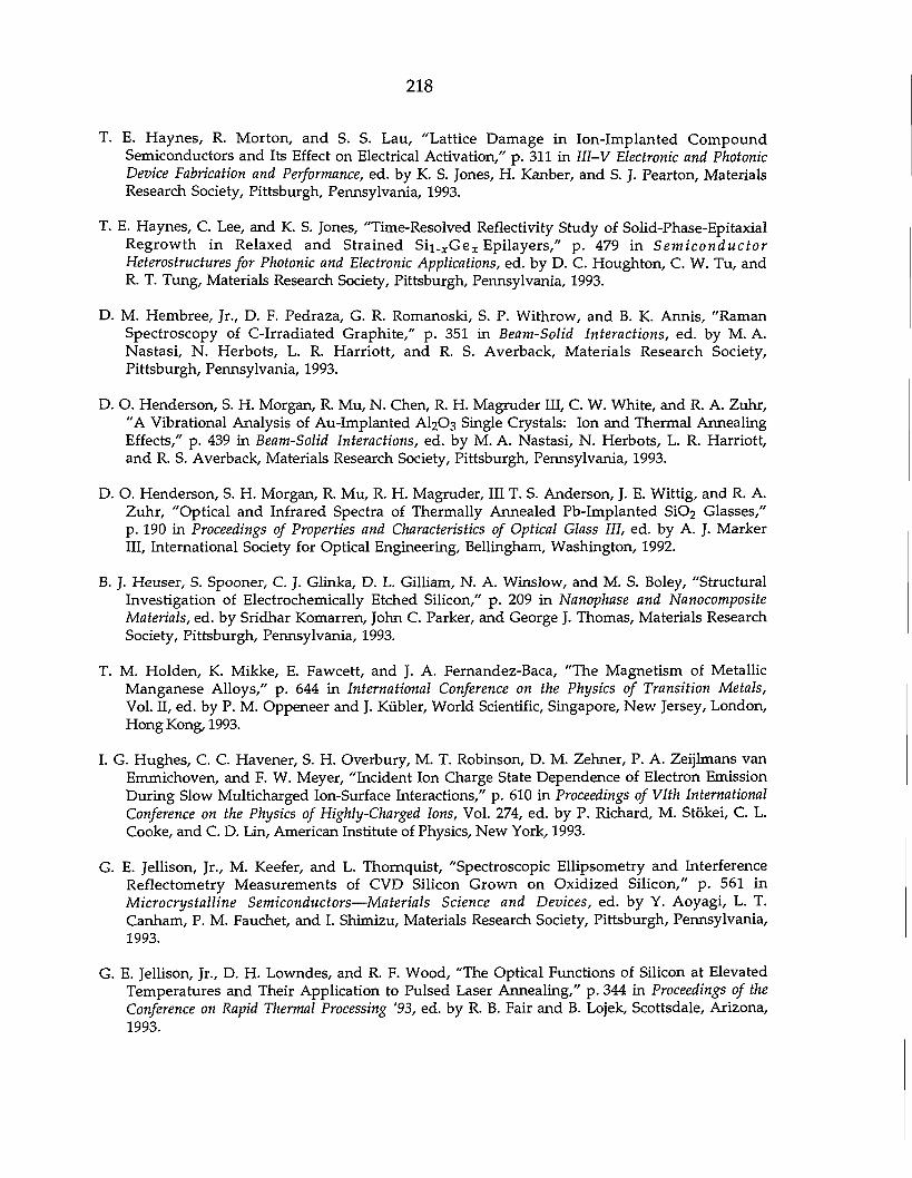
218
T. E. Haynes, R. Morton, and S. S. Lau, "Lattice Damage in Ion-Implanted Compound Semiconductors and Its Effect on Electrical Activation," p. 311 in III-V Electronic and Photonic Device Fabrication and Performance, ed. by K. S. Jones, H. Kanber, and S. J. Pearton, Materials Research Society, Pittsburgh, Pennsylvania, 1993.
T. E. Haynes, C. Lee, and K. S. Jones, "Time-Resolved Reflectivity Study of Solid-Phase-Epitaxial Regrowth in Relaxed and Strained S i i . x G e r Epilayers," p. 479 in Semiconductor Heterostructures for Photonic and Electronic Applications, ed. by D. C. Houghton, C. W. Tu, and R. T. Tung, Materials Research Society, Pittsburgh, Pennsylvania, 1993.
D. M. Hembree, Jr., D. F. Pedraza, G. R. Romanoski, S. P. Withrow, and B. K. Annis, "Raman Spectroscopy of C-Irradiated Graphite," p. 351 in Beam-Solid Interactions, ed. by M. A. Nastasi, N. Herbots, L. R. Harriott, and R. S. Averback, Materials Research Society, Pittsburgh, Pennsylvania, 1993.
D. O. Henderson, S. H. Morgan, R. Mu, N. Chen, R. H. Magruder III, C. W. White, and R. A. Zuhr, "A Vibrational Analysis of Au-Implanted AI2O3 Single Crystals: Ion and Thermal Annealing Effects," p. 439 in Beam-Solid Interactions, ed. by M. A. Nastasi, N. Herbots, L. R. Harriott, and R. S. Averback, Materials Research Society, Pittsburgh, Pennsylvania, 1993.
D. O. Henderson, S. H. Morgan, R. Mu, R. H. Magruder, III T. S. Anderson, J. E. Wittig, and R. A. Zuhr, "Optical and Infrared Spectra of Thermally Annealed Pb-Implanted SiC>2 Glasses," p. 190 in Proceedings of Properties and Characteristics of Optical Glass III, ed. by A. J. Marker III, International Society for Optical Engineering, Bellingham, Washington, 1992.
B. J. Heuser, S. Spooner, C. J. Glinka, D. L. Gilliam, N. A. Winslow, and M. S. Boley, "Structural Investigation of Electrochemically Etched Silicon," p. 209 in Nanophase and Nanocomposite Materials, ed. by Sridhar Komarren, John C. Parker, and George J. Thomas, Materials Research Society, Pittsburgh, Pennsylvania, 1993.
T. M. Holden, K. Mikke, E. Fawcett, and J. A. Fernandez-Baca, "The Magnetism of Metallic Manganese Alloys," p. 644 in International Conference on the Physics of Transition Metals, Vol. II, ed. by P. M. Oppeneer and J. Kubler, World Scientific, Singapore, New Jersey, London, Hong Kong, 1993.
I. G. Hughes, C. C. Havener, S. H. Overbury, M. T. Robinson, D. M. Zehner, P. A. Zeijlmans van Emmichoven, and F. W. Meyer, "Incident Ion Charge State Dependence of Electron Emission During Slow Multicharged Ion-Surface Interactions," p. 610 in Proceedings of Vlth International Conference on the Physics of Highly-Charged Ions, Vol. 274, ed. by P. Richard, M. Stokei, C. L. Cooke, and C. D. Lin, American Institute of Physics, New York, 1993.
G. E. Jellison, Jr., M. Keefer, and L. Thornquist, "Spectroscopic Ellipsometry and Interference Reflectometry Measurements of CVD Silicon Grown on Oxidized Silicon," p. 561 in Microcrystalline Semiconductors—Materials Science and Devices, ed. by Y. Aoyagi, L. T. Canham, P. M. Fauchet, and I. Shimizu, Materials Research Society, Pittsburgh, Pennsylvania, 1993.
G. E. Jellison, Jr., D. H. Lowndes, and R. F. Wood, "The Optical Functions of Silicon at Elevated Temperatures and Their Application to Pulsed Laser Annealing," p. 344 in Proceedings of the Conference on Rapid Thermal Processing '93, ed. by R. B. Fair and B. Lojek, Scottsdale, Arizona, 1993.
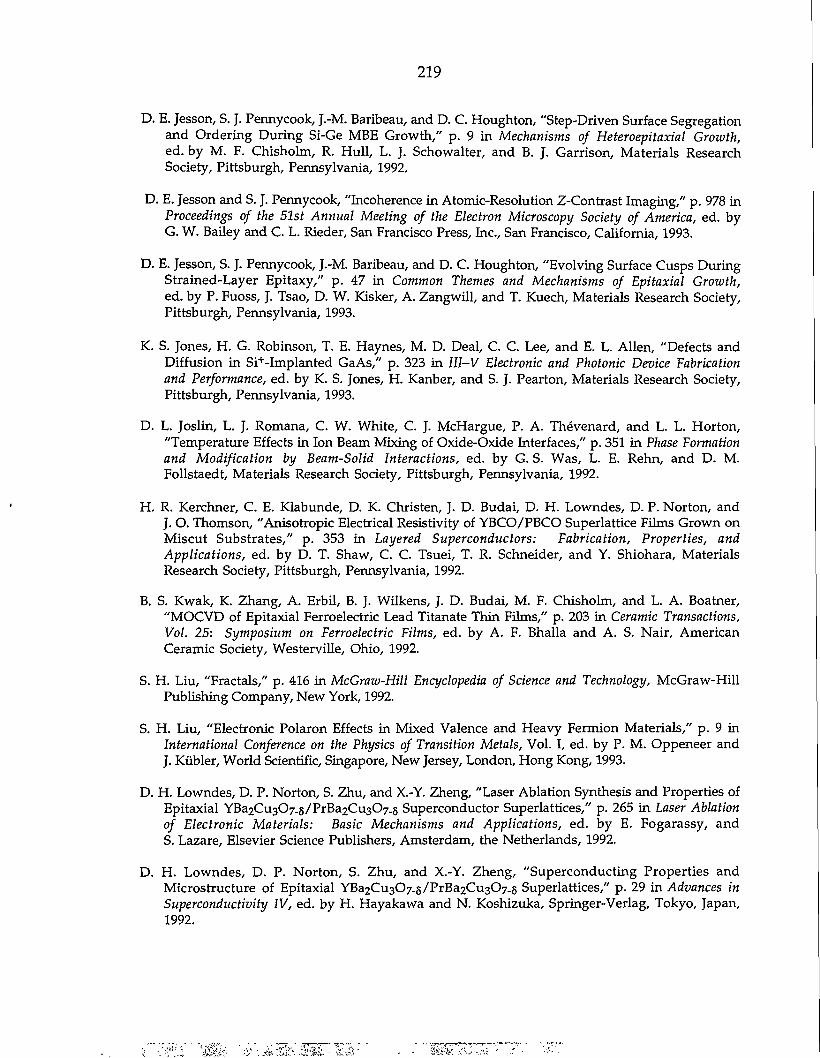
219
D. E. Jesson, S. J. Pennycook, J.-M. Baribeau, and D. C. Houghton, "Step-Driven Surface Segregation and Ordering During Si-Ge MBE Growth," p. 9 in Mechanisms of Heteroepitaxial Growth, ed. by M. F. Chisholm, R. Hull, L. J. Schowalter, and B. J. Garrison, Materials Research Society, Pittsburgh, Pennsylvania, 1992.
D. E. Jesson and S. J. Pennycook, "Incoherence in Atomic-Resolution Z-Contrast Imaging," p. 978 in Proceedings of the 51st Annual Meeting of the Electron Microscopy Society of America, ed. by G. W. Bailey and C. L. Rieder, San Francisco Press, Inc., San Francisco, California, 1993.
D. E. Jesson, S. J. Pennycook, J.-M. Baribeau, and D. C. Houghton, "Evolving Surface Cusps During Strained-Layer Epitaxy," p. 47 in Common Themes and Mechanisms of Epitaxial Growth, ed. by P. Fuoss, J. Tsao, D. W. Kisker, A. Zangwill, and T. Kuech, Materials Research Society, Pittsburgh, Pennsylvania, 1993.
K. S. Jones, H. G. Robinson, T. E. Haynes, M. D. Deal, C. C. Lee, and E. L. Allen, "Defects and Diffusion in Si+-Implanted GaAs," p. 323 in III-V Electronic and Photonic Device Fabrication and Performance, ed. by K. S. Jones, H. Kanber, and S. J. Pearton, Materials Research Society, Pittsburgh, Pennsylvania, 1993.
D. L. Joslin, L. J. Romana, C. W. White, C. J. McHargue, P. A. Thevenard, and L. L. Horton, "Temperature Effects in Ion Beam Mixing of Oxide-Oxide Interfaces," p. 351 in Phase Formation and Modification by Beam-Solid Interactions, ed. by G. S. Was, L. E. Rehn, and D. M. Follstaedt, Materials Research Society, Pittsburgh, Pennsylvania, 1992.
H. R. Kerchner, C. E. Klabunde, D. K. Christen, J. D. Budai, D. H. Lowndes, D. P. Norton, and J. O. Thomson, "Anisotropic Electrical Resistivity of YBCO/PBCO Superlattice Films Grown on Miscut Substrates," p. 353 in Layered Superconductors: Fabrication, Properties, and Applications, ed. by D. T. Shaw, C. C. Tsuei, T. R. Schneider, and Y. Shiohara, Materials Research Society, Pittsburgh, Pennsylvania, 1992.
B. S. Kwak, K. Zhang, A. Erbil, B. J. Wilkens, J. D. Budai, M. F. Chisholm, and L. A. Boatner, "MOCVD of Epitaxial Ferroelectric Lead Titanate Thin Films," p. 203 in Ceramic Transactions, Vol. 25: Symposium on Ferroelectric Films, ed. by A. F. Bhalla and A. S. Nair, American Ceramic Society, Westerville, Ohio, 1992.
S. H. Liu, "Fractals," p. 416 in McGraw-Hill Encyclopedia of Science and Technology, McGraw-Hill Publishing Company, New York, 1992.
S. H. Liu, "Electronic Polaron Effects in Mixed Valence and Heavy Fermion Materials," p. 9 in International Conference on the Physics of Transition Metals, Vol. I, ed. by P. M. Oppeneer and J. Kiibler, World Scientific, Singapore, New Jersey, London, Hong Kong, 1993.
D. H. Lowndes, D. P. Norton, S. Zhu, and X.-Y. Zheng, "Laser Ablation Synthesis and Properties of Epitaxial YBa2Cu307_5/PrBa2Cu307_5 Superconductor Superlattices," p. 265 in Laser Ablation of Electronic Materials: Basic Mechanisms and Applications, ed. by E. Fogarassy, and S. Lazare, Elsevier Science Publishers, Amsterdam, the Netherlands, 1992.
D. H. Lowndes, D. P. Norton, S. Zhu, and X.-Y. Zheng, "Superconducting Properties and Microstructure of Epitaxial YBa2Cu307_8/PrBa2Cu307-5 Superlattices," p. 29 in Advances in Superconductivity IV, ed. by H. Hayakawa and N. Koshizuka, Springer-Verlag, Tokyo, Japan, 1992.
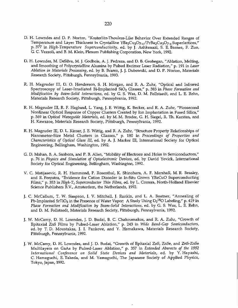
220
D. H. Lowndes and D. P. Norton, "Kosterlitz-Thouless-Like Behavior Over Extended Ranges of Temperature and Layer Thickness in Crystalline YBa2Cu307_x/PrBa2Cu307.x Superlattices," p. 377 in High-Temperature Superconductivity, ed. by J. Ashkenazi, S. E. Barnes, F. Zuo, G. C. Vezzoli, and B. M. Klein, Plenum Publishing Corporation, New York, 1992.
D. H. Lowndes, M. DeSilva, M. J. Godbole, A. J. Pedraza, and D. B. Geohegan, "Ablation, Melting, and Smoothing of Polycrystalline Alumina by Pulsed Excimer Laser Radiation," p. 191 in Laser Ablation in Materials Processing, ed. by B. Braren, J. J. Dubowski, and D. P. Norton, Materials Research Society, Pittsburgh, Pennsylvania, 1993.
R. H. Magruder III, D. O. Henderson, S. H. Morgan, and R. A. Zuhr, "Optical and Infrared Spectroscopy of Laser-Irradiated Bi-Implanted Si02 Glasses," p. 383 in Phase Formation and Modification by Beam-Solid Interactions, ed. by G. S. Was, D. M. Follstaedt, and L. E. Rehn, Materials Research Society, Pittsburgh, Pennsylvania, 1992.
R. H. Magruder III, R. F. Haglund, L. Yang, J. E. Wittig, K. Becker, and R. A. Zuhr, "Picosecond Nonlinear Optical Response of Copper Clusters Created by Ion Implantation in Fused Silica," p. 369 in Optical Waveguide Materials, ed. by M. M. Broder, G. H. Siegel, R. Th. Karsten, and H. Kawazoe, Materials Research Society, Pittsburgh, Pennsylvania, 1992.
R. H. Magruder III, D. L. Kinser, J. E. Wittig, and R. A. Zuhr, "Structure Property Relationships of Nanometer-Size Metal Clusters in Glasses," p. 180 in Proceedings of Properties and Characteristics of Optical Glass III, ed. by A. J. Marker III, International Society for Optical Engineering, Bellingham, Washington, 1992.
G. D. Mahan, B. A. Sanborn, and P. B. Allen, "Mobility of Electrons and Holes in Semiconductors," p. 76 in Physics and Simulation of Optoelectronic Devices, ed. by David Yevick, International Society for Optical Engineering, Bellingham, Washington, 1992.
V. C. Matijasevic, R. H. Hammond, P. Rosenthal, K. Shinohara, A. F. Marshall, M. R. Beasley, and R. Feenstra, "Evidence for Cation Disorder in In-Situ Grown YBaCuO Superconducting Films," p. 353 in High-Tc Superconductor Thin Films, ed. by L. Correra, North-Holland Elsevier Science Publishers B.V., Amsterdam, the Netherlands, 1992.
J. C. McCallum, T. W. Simpson, I. V. Mitchell, J. Rankin, and L. A. Boatner, "Annealing of Pb-Implanted SrTi0 3 in the Presence of Water Vapor: A Study Using D 2
l s O Labeling," p. 419 in Phase Formation and Modification by Beam-Solid Interactions, ed. by G. S. Was, L. E. Rehn, and D. M. Follstaedt, Materials Research Society, Pittsburgh, Pennsylvania, 1992.
J. W. McCamy, D. H. Lowndes, J. D. Budai, B. C. Chakoumakos, and R. A. Zuhr, "Growth of Epitaxial ZnS Films by Pulsed-Laser Ablation," p. 243 in Wide Band-Gap Semiconductors, ed. by T. D. Moustakas, J. I. Pankove, and Y. Hamakawa, Materials Research Society, Pittsburgh, Pennsylvania, 1992.
J. W. McCamy, D. H. Lowndes, and J. D. Budai, "Growth of Epitaxial ZnS, ZnSe, and ZnS-ZnSe Multilayers on GaAs by Pulsed-Laser Ablation," p. 357 in Extended Absracts of the 1992 International Conference on Solid State Devices and Materials, ed. by Y. Hayashi, C. Hamaguchi, E. Takeda, and M. Yamaguchi, The Japanese Society of Applied Physics, Tokyo, Japan, 1992.
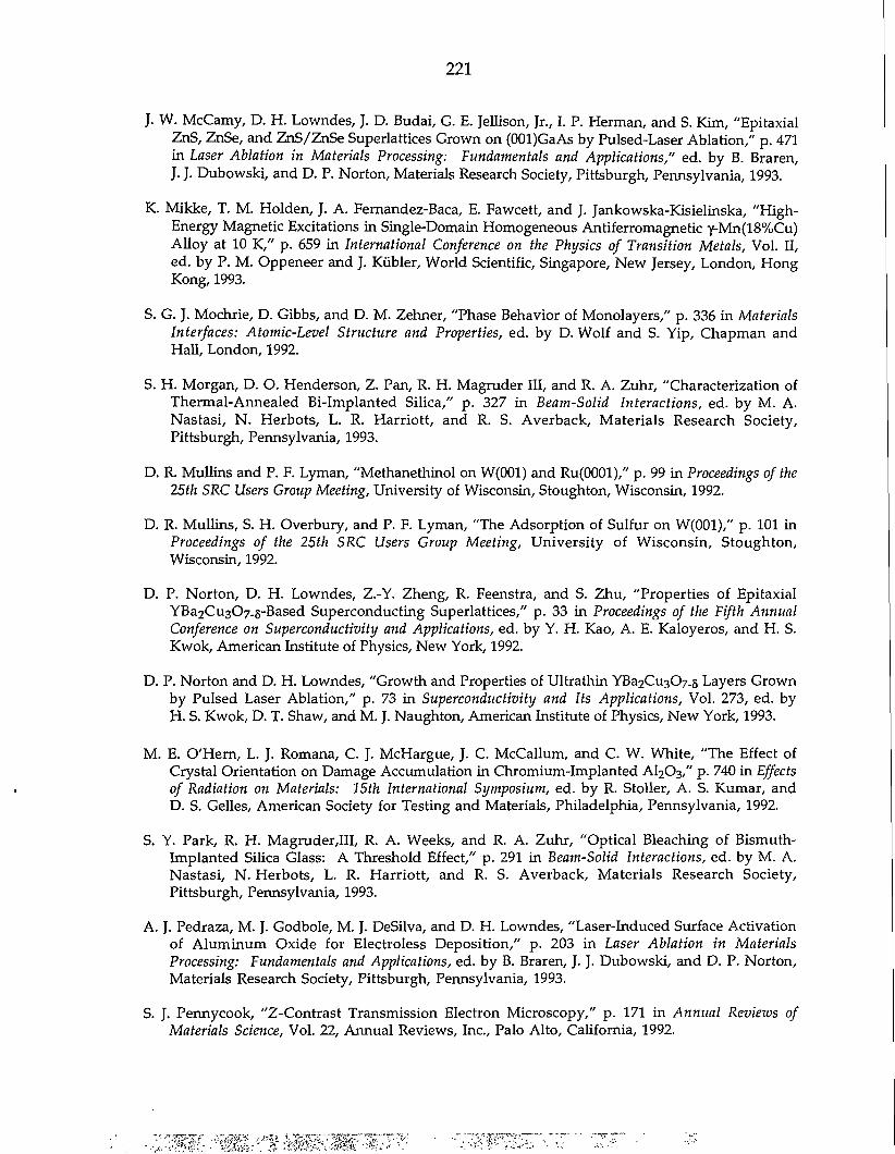
221
J. W. McCamy, D. H. Lowndes, J. D. Budai, G. E. Jellison, Jr., I. P. Herman, and S. Kim, "Epitaxial ZnS, ZnSe, and ZnS/ZnSe Superlattices Grown on (OOl)GaAs by Pulsed-Laser Ablation," p. 471 in Laser Ablation in Materials Processing: Fundamentals and Applications," ed. by B. Braren, J. J. Dubowski, and D. P. Norton, Materials Research Society, Pittsburgh, Pennsylvania, 1993.
K. Mikke, T. M. Holden, J. A. Fernandez-Baca, E. Fawcett, and J. Jankowska-Kisielinska, "High-Energy Magnetic Excitations in Single-Domain Homogeneous Antiferromagnetic y-Mn(18%Cu) Alloy at 10 K," p. 659 in International Conference on the Physics of Transition Metals, Vol. II, ed. by P. M. Oppeneer and J. Kiibler, World Scientific, Singapore, New Jersey, London, Hong Kong, 1993.
S. G. J. Mochrie, D. Gibbs, and D. M. Zehner, "Phase Behavior of Monolayers," p. 336 in Materials Interfaces: Atomic-Level Structure and Properties, ed. by D. Wolf and S. Yip, Chapman and Hall, London, 1992.
S. H. Morgan, D. O. Henderson, Z. Pan, R. H. Magruder III, and R. A. Zuhr, "Characterization of Thermal-Annealed Bi-Implanted Silica," p. 327 in Beam-Solid Interactions, ed. by M. A. Nastasi, N. Herbots, L. R. Harriott, and R. S. Averback, Materials Research Society, Pittsburgh, Pennsylvania, 1993.
D. R. Mullins and P. F. Lyman, "Methanethinol on W(001) and Ru(0001)," p. 99 in Proceedings of the 25th SRC Users Group Meeting, University of Wisconsin, Stoughton, Wisconsin, 1992.
D. R. Mullins, S. H. Overbury, and P. F. Lyman, "The Adsorption of Sulfur on W(001)," p. 101 in Proceedings of the 25th SRC Users Group Meeting, University of Wisconsin, Stoughton, Wisconsin, 1992.
D. P. Norton, D. H. Lowndes, Z.-Y. Zheng, R. Feenstra, and S. Zhu, "Properties of Epitaxial YBa2Cu3C>7-5-Based Superconducting Superlattices," p. 33 in Proceedings of the Fifth Annual Conference on Superconductivity and Applications, ed. by Y. H. Kao, A. E. Kaloyeros, and H. S. Kwok, American Institute of Physics, New York, 1992.
D. P. Norton and D. H. Lowndes, "Growth and Properties of Ultrathin YBa2Cu30/_5 Layers Grown by Pulsed Laser Ablation," p. 73 in Superconductivity and Its Applications, Vol. 273, ed. by H. S. Kwok, D. T. Shaw, and M. J. Naughton, American Institute of Physics, New York, 1993.
M. E. O'Hern, L. J. Romana, C. J. McHargue, J. C. McCallum, and C. W. White, "The Effect of Crystal Orientation on Damage Accumulation in Chromium-Implanted AI2O3," p. 740 in Effects of Radiation on Materials: 15th International Symposium, ed. by R. Stoller, A. S. Kumar, and D. S. Gelles, American Society for Testing and Materials, Philadelphia, Pennsylvania, 1992.
S. Y. Park, R. H. Magruder,III, R. A. Weeks, and R. A. Zuhr, "Optical Bleaching of Bismuth-Implanted Silica Glass: A Threshold Effect," p. 291 in Beam-Solid Interactions, ed. by M. A. Nastasi, N. Herbots, L. R. Harriott, and R. S. Averback, Materials Research Society, Pittsburgh, Pennsylvania, 1993.
A. J. Pedraza, M. J. Godbole, M. J. DeSilva, and D. H. Lowndes, "Laser-Induced Surface Activation of Aluminum Oxide for Electroless Deposition," p. 203 in Laser Ablation in Materials Processing: Fundamentals and Applications, ed. by B. Braren, J. J. Dubowski, and D. P. Norton, Materials Research Society, Pittsburgh, Pennsylvania, 1993.
S. J. Pennycook, "Z-Contrast Transmission Electron Microscopy," p. 171 in Annual Reviews of Materials Science, Vol. 22, Annual Reviews, Inc., Palo Alto, California, 1992.
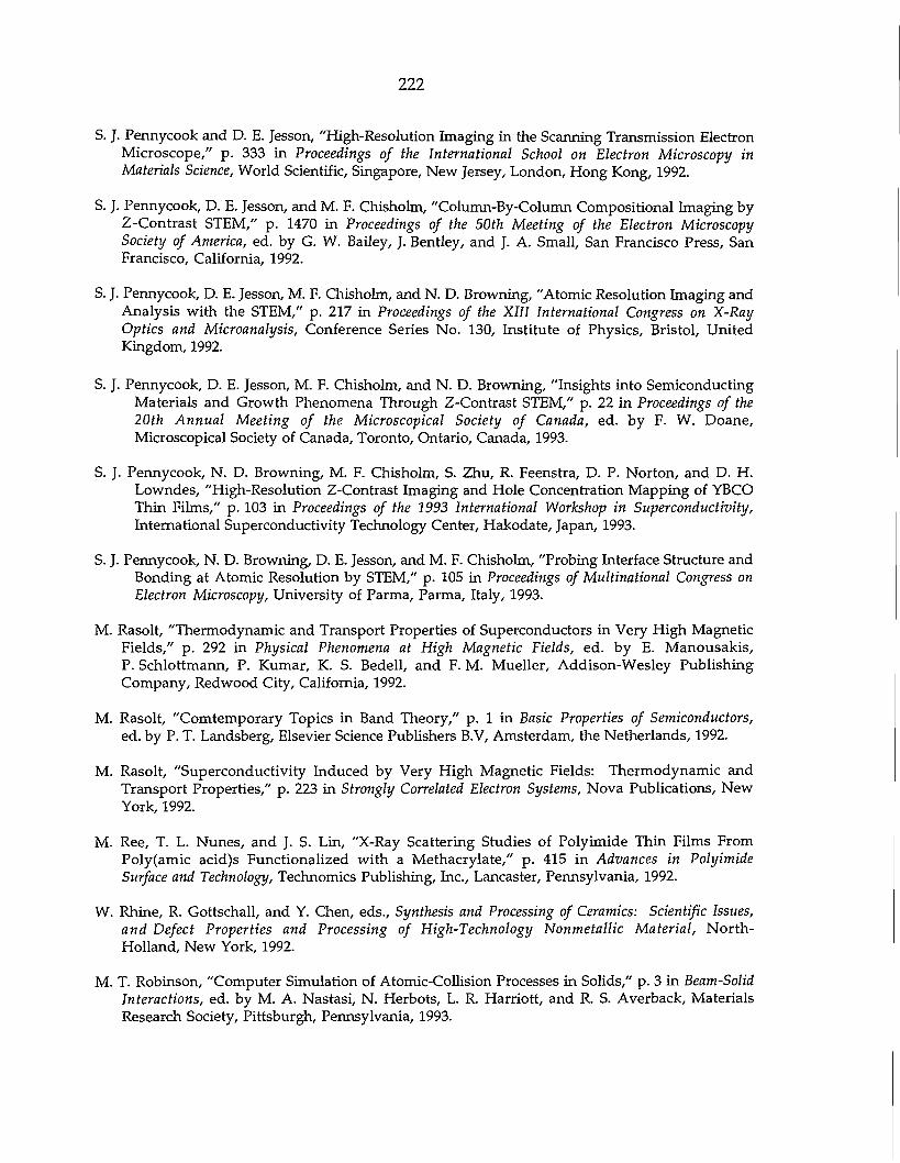
222
S. J. Pennycook and D. E. Jesson, "High-Resolution Imaging in the Scanning Transmission Electron Microscope," p. 333 in Proceedings of the International School on Electron Microscopy in Materials Science, World Scientific, Singapore, New Jersey, London, Hong Kong, 1992.
S. J. Pennycook, D. E. Jesson, and M. F. Chisholm, "Column-By-Column Compositional Imaging by Z-Contrast STEM," p. 1470 in Proceedings of the 50th Meeting of the Electron Microscopy Society of America, ed. by G. W. Bailey, J. Bentley, and J. A. Small, San Francisco Press, San Francisco, California, 1992.
S. J. Pennycook, D. E. Jesson, M. F. Chisholm, and N. D. Browning, "Atomic Resolution Imaging and Analysis with the STEM," p. 217 in Proceedings of the XIII International Congress on X-Ray Optics and Microanalysis, Conference Series No. 130, Institute of Physics, Bristol, United Kingdom, 1992.
S. J. Pennycook, D. E. Jesson, M. F. Chisholm, and N. D. Browning, "Insights into Semiconducting Materials and Growth Phenomena Through Z-Contrast STEM," p. 22 in Proceedings of the 20th Annual Meeting of the Microscopical Society of Canada, ed. by F. W. Doane, Microscopical Society of Canada, Toronto, Ontario, Canada, 1993.
S. J. Pennycook, N. D. Browning, M. F. Chisholm, S. Zhu, R. Feenstra, D. P. Norton, and D. H. Lowndes, "High-Resolution Z-Contrast Imaging and Hole Concentration Mapping of YBCO Thin Films," p. 103 in Proceedings of the 1993 International Workshop in Superconductivity, International Superconductivity Technology Center, Hakodate, Japan, 1993.
S. J. Pennycook, N. D. Browning, D. E. Jesson, and M. F. Chisholm, "Probing Interface Structure and Bonding at Atomic Resolution by STEM," p. 105 in Proceedings of Multinational Congress on Electron Microscopy, University of Parma, Parma, Italy, 1993.
M. Rasolt, "Thermodynamic and Transport Properties of Superconductors in Very High Magnetic Fields," p. 292 in Physical Phenomena at High Magnetic Fields, ed. by E. Manousakis, P. Schlottmann, P. Kumar, K. S. Bedell, and F. M. Mueller, Addison-Wesley Publishing Company, Redwood City, California, 1992.
M. Rasolt, "Comtemporary Topics in Band Theory," p. 1 in Basic Properties of Semiconductors, ed. by P. T. Landsberg, Elsevier Science Publishers B.V, Amsterdam, the Netherlands, 1992.
M. Rasolt, "Superconductivity Induced by Very High Magnetic Fields: Thermodynamic and Transport Properties," p. 223 in Strongly Correlated Electron Systems, Nova Publications, New York, 1992.
M. Ree, T. L. Nunes, and J. S. Lin, "X-Ray Scattering Studies of Polyimide Thin Films From Poly(amic acid)s Functionalized with a Methacrylate," p. 415 in Advances in Polyimide Surface and Technology, Technomics Publishing, Inc., Lancaster, Pennsylvania, 1992.
W. Rhine, R. Gottschall, and Y. Chen, eds., Synthesis and Processing of Ceramics: Scientific Issues, and Defect Properties and Processing of High-Technology Nonmetallic Material, North-Holland, New York, 1992.
M. T. Robinson, "Computer Simulation of Atomic-Collision Processes in Solids," p. 3 in Beam-Solid Interactions, ed. by M. A. Nastasi, N. Herbots, L. R. Harriott, and R. S. Averback, Materials Research Society, Pittsburgh, Pennsylvania, 1993.
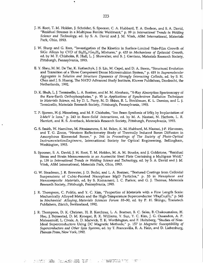
223
J. H. Root, T. M. Holden, J. Schroder, S. Spooner, C. A. Hubbard, T. A. Dodson, and S. A. David, "Residual Stresses in a Multipass Ferritic Weldment," p. 99 in International Trends in Welding Science and Technology, ed. by S. A. David and J. M. Vitek, ASM International, Materials Park, Ohio, 1993.
J. W. Sharp and G. Eres, "Investigation of the Kinetics in Surface-Limited Thin-Film Growth of SiGe Alloys by CVD of Si2H 6 /Ge 2 H 6 Mixtures," p. 433 in Mechanisms of Epitaxial Growth, ed. by M. F. Chisholm, R. Hull, L. J. Showalter, and B. J. Garrison, Materials Research Society, Pittsburgh, Pennsylvania, 1993.
E. Y. Sheu, M. M. De Tar, K. Kotlarchyk, J. S. Lin, M. Capel, and D. A. Storm, "Structural Evolution and Transition of a Three Component Dense Microemulsion System," p. 419 in Supramolecidar Aggregates in Solution and Structure Dynamics of Strongly Interacting Colloids, ed. by S. H. Chen and J. S. Huang, The NATO Advanced Study Institute, Kluwer Publishers, Dordrecht, the Netherlands, 1992.
D. K. Shuh, L. J. Terminello, L. A. Boatner, and M. M. Abraham, "X-Ray Absorption Spectroscopy of the Rare-Earth Orthophosphates," p. 95 in Applications of Synchrotron Radiation Techniques to Materials Science, ed. by D. L. Perry, N. D. Shinn, R. L. Stockbauer, K. L. Damico, and L. J. Terminello, Materials Research Society, Pittsburgh, Pennsylvania, 1993.
T. P. Sjoreen, H.-J. Hinneberg, and M. F. Chisholm, "Ion Beam Synthesis of IrSi3 by Implantation of 2-MeV Ir Ions," p. 243 in Beam-Solid Interactions, ed. by M. A. Nastasi, N. Herbots, L. R. Harriott, and R. S. Averback, Materials Research Society, Pittsburgh, Pennsylvania, 1993.
G. S. Smith, W. Hamilton, M. Fitzsimmons, S. M. Baker, K. M. Hubbard, M. Nastasi, J-P. Hirvonen, and T. G. Zocco, "Neutron Reflectometry Study of Thermally Induced Boron Diffusion in Amorphous Elemental Boron," p. 246 in Proceedings of The Society of Photo-Optical InstrumentationEngineers, International Society for Optical Engineering, Bellingham, Washington, 1993.
S. Spooner, S. A. David, J. H. Root, T. M. Holden, M. A. M. Bourke, and J. Goldstone, "Residual Stress and Strain Measurements in an Austenitic Steel Plate Containing a Multipass Weld," p. 139 in International Trends in Welding Science and Technology, ed. by S. A. David and J. M. Vitek, ASM International, Materials Park, Ohio, 1993.
G. W. Steadman, J. R. Brewster, J. D. Budai, and L. A. Boatner, "Textured Coatings from Colloidal Suspensions of Cubic-Faceted Nanophase MgO Particles," p. 33 in Nanophase and Nanocomposite Materials, ed. by S. Komarneni, I. C. Parker, and G. J. Thomas, Materials Research Society, Pittsburgh, Pennsylvania, 1993.
J. R. Thompson, C. Politis, and Y. C. Kim, "Properties of Materials with a Fine Length Scale: Mechanically Alloyed Metals and the High-Temperature Superconductor YBa2Cu307," p. 545 in Mechanical Alloying, Materials Sciences Forum 88-90, ed. by P. H. Shingu, Transtech Publishers, Zurich, Switzerland, 1992.
J. R. Thompson, D. K. Christen, H. R. Kerchner, L. A. Boatner, B. C. Sales, B. Chakoumakos, H. Hsu, J. Brynestad, D. M. Kroeger, R. K. Williams, Y. Sun, Y. C. Kim, J. G. Ossandon, A. P. Malozemoff, L. Civale, A. D. Marwick, T. K. Worthington, and F. Holtzberg, "Studies of Non-Ideal Superconductors Using DC Magnetic Methods," p. 157 in Magnetic Susceptibility of Superconductors and Other Spin Systems, ed. by T. Francavilla, R. A. Hein, and D. Liebenburg, Plenum Press, New York, 1992.
224
J. R. Thompson, Y. R. Sun, D. K. Christen, H. R. Kerchner, A. P. Malozemoff, L. Civale, A. D. Marwick, T. K. Worthington, L. Krusin-Elbaum, M. W. McElfresh, and F. Holtzberg, "Magnetization Studies of Irradiation Modified Single-Crystal YBa2Cu3C>7 Superconductors: Flux Creep and Annealing Effects," p. 573 in Physics and Materials Science of High-Temperature Super conductor s-II, ed. by R. Kossowski, B. Raveau, D. Wohllebin, and S. K. Patapis, Kluwer, Dordrecht, the Netherlands, 1992.
J. R. Thompson, "What Can We Learn From Magnetization Experiments on High-T c
Superconductors? An Overview," p. 23 in Layered Superconductors: Fabrication, Properties, and Applications, ed. by D. T. Shaw, C. C. Tsuei, T. R. Schneider, and Y. Shiohara, Materials Research Society, Pittsburgh, Pennsylvania, 1992.
J. R. Thompson, Y. R. Sun, J. G. Ossandon, D. K. Christen, H. R. Kerchner, B. C. Sales, B. C. Chakoumakos, L. Civale, A. D. Marwick, and F. Holtzberg, "Magnetic Studies of Current Conduction and Flux Pinning in High-Tc Cuprates: Virgin, Irradiated, and Oxygen-Deficient Materials," p. 179 in Superconductivity and Its Applications, Vol. 273, ed. by H. S. Kwok, D. T. Shaw, and M. J. Naughton, American Institute of Physics, New York, 1993.
J. R. Thompson, Y. R. Sun, J. G. Ossandon, D. K. Christen, H. R. Kerchner, B. C. Sales, B. C. Chakoumakos, L. Civale, A. D. Marwick, and F. Holtzberg, "Magnetization and Flux Pinning in High-T c Cuprates: Virgin, Irradiated, and Oxygen-Deficient Materials," p. 232 in Proceedings of Fifth US/Japan Workshop on High-Tc Superconductors, Society of Non-Traditional Technology, Tokyo, Japan, 1993.
H. S. von Harrach, D. E. Jesson, and S. J. Pennycook, "Towards 1 Angstrom Resolution STEM," p. 996 in Proceedings of the 51st Annual Meeting of the Electron Microscopy Society of America, ed. by G. W. Bailey and C. L. Rieder, San Francisco Press, Inc., San Francisco, California, 1993.
C. W. White, D. K. Thomas, R. A. Zuhr, J. C. McCallum, A. Pogany, R. F. Haglund, R. H. Magruder, and L. Yang, "Modification of the Optical Properties of AI2O3 by Ion Implantation," p. 331 in Materials Modification by Energetic Atoms and Ions, ed. by K. S. Grabowski, S. A. Barnett, S. M. Rossnagel, and K. Wasa, Materials Research Society, Pittsburgh, Pennsylvania, 1992.
G. D. Wignall, "Combined Small-Angle Neutron and X-Ray Scattering Studies of Polymers," p. 355 in Advances in X-Ray Analysis, ed. by J. V. Gilfrich, T. C. Huang, C. R. Hubbard, M. R. James, R. Jenkins, G. R. Lachance, D. K. Smith, and P. K. Predecki, Plenum Press, New York, 1993.
J. M. Williams, "High-Energy Ion Implantation of Materials," p. 151 in Current Status, Research Needs, and Opportunities in Applications of Surface Processing to Transportation and Utilities Technologies, ed. by A. W. Czanderna and A. R. Landgrebe, NREL, Golden, Colorado, 1992.
J. M. Williams, "High-Energy Ion Implantation of Materials," p. 151 in Critical Reviews in Surface Chemistry, ed. by P. M. A. Sherwood and guest ed. by A. W. Czanderna and A. R. Landgrebe, CRC Press, Inc.,'Boca Raton, Florida, 1993.
F. Xiong, R. P. H. Chang, and C. W. White, "Structure and Properties of a-C:N Films Prepared by Pulsed Excimer Laser Deposition," p. 587 in Laser Ablation in Materials Processing: Fundamentals and Applications, ed. by B. Braren, J. Dubowski, and D. P. Norton, Materials Research Society, Pittsburgh, Pennsylvania, 1993.

225
P. A. Zeijlmans van Emmichoven, C. C. Havener, I. G. Huges, D. M. Zehner, and F. W. Meyer, "Analysis of Low-Energy Electron Emission Arising During Slow Multicharged Ion-Surface Interactions," p. 606 in Proceedings of Vlth International Conference on the Physics of Highly Charged Ions, Vol. 274, ed. by P. Richard, M. Stockei, C. L. Cooke, and C. D. Lin, American Institute of Physics, New York, 1993.
X. Y. Zheng, D. H. Lowndes, S. Zhu, and R. J. Warmack, "Scanning Tunneling Microscope Studies of Initial Epitaxial Growth of YBa2Cu3C»7_5 Thin Films," p. 41 in Mechanisms of Epitaxial Growth, ed. by M. F. Chisholm, R. Hull, L. J. Showalter, and B. J. Garrison, Materials Research Society, Pittsburgh, Pennsylvania, 1993.
S. Zhu, D. H. Lowndes, X.-Y. Zheng, D. P. Norton, and R. J. Warmack, "Epitaxial YBa 2Cu 307. x
Thin Films: Scanning Tunneling Microscopy Study of the Initial Stages of Epitaxial Growth, Growth Mechanisms, and Effects of Substrate Temperature," p. 541 in Interface Dynamics and Growth, ed. by K. S. Liang, M. P. Anderson, R. F. Bruinsma, and G. Scoles, Materials Research Society, Pittsburgh, Pennsylvania, 1992.
REPORTS ISSUED
D. L. Abernathy, S. G. J. Mochrie, D. M. Zehner, G. Grubel, and D. Gibbs, "Capillary Modes on a Close-Packed Metal Surface: Pt(001)," p. 256 in National Synchrotron Light Source Annual Report 1991, Volume II, BNL-52317, Brookhaven National Laboratory, Upton, New York (1992).
Y. Chen and L. D. Hulett, Proceedings of the DOE Workshop Meeting on the Application of Positron Spectroscopy to Materials Sciences, Oak Ridge National Laboratory, CONF-9209221 (1993).
R. W. Dull and H. R. Kerchner, A Teacher's Guide to Superconductivity for High School Students, ORNL/M-3063 (October 1993).
R. Feenstra, "Atomic Layer Control in High-Tc Superconductors," Research Report to the Japan Society for the Promotion of Science, October 6, 1992-April 8, 1993 (May 8, 1993).
J. A. Fernandez-Baca, M. E. Hagen, R. M. Nicklow, T. G. Perring, and Y. Tsunoda, "High-Energy Magnetic Excitations in MngoCuio," p. A257 in ISIS Experimental Reports, Rutherford Appleton Laboratory, Didcot, England (July 1993).
G. R. Gruzalski, S.-C. Lui, D. Heskett, X. Shi, and D. M. Zehner, "Core-Level Spectroscopy from Low-Index Surfaces of HfC Exposed to Oxygen," p. 63 in National Synchrotron Light Source Annual Report 1991, Volume II, BNL-52317, Brookhaven National Laboratory, Upton, New York (1992).
B. S. Itchkawitz, P. F. Lyman, E. W. Plummer, and D. M. Zehner, "Photoemission Spectroscopy from Monolayer Graphite on TaC(lll)," p. 163 in National Synchrotron Light Source Annual Report, BNL-52371, Brookhaven National Laboratory, Upton, New York (1993).
S.-C. Lui, G. R. Gruzalski, D. Heskett, X. Shi, and D. M. Zehner, "Core-Level Spectroscopy from Low-Index Surfaces of TaC," p. 64 in National Synchrotron Light Source Annual Report 1991, Volume II, BNL-52317, Brookhaven National Laboratory, Upton, New York (1992).
R. M. Moon and R. M. Nicklow, General User Training for HEIR Access, (April 22, 1993).
226
D. R. Mullins and P. F. Lyman, "W(100) Surface Core Level Shifts Induced by S Adsorption," p. 165 in National Synchrotron Light Source Annual Report, BNL-52371, Brookhaven National Laboratory, Upton, New York (1993).
A. R. Sandy, D. L. Abernathy, S. G. J. Mochrie, D. M. Zehner, and L. D. Gibbs, "Au(113) Surface Studies," p. 259 in National Synchrotron Light Source Annual Report 1991, Volume II, BNL-52317, Brookhaven National Laboratory, Upton, New York (1992).
G. M. Watson, D. Gibbs, S. Song, S. G. J. Mochrie, and D. M. Zehner, "Temperature-Dependent Surface Morphology of Vicinal Au(lll)," p. 349 in National Synchrotron Light Source Annual Report, BNL-52371, Brookhaven National Laboratory, Upton, New York (1993).
G. M. Watson, D. Gibbs, S. Song, S. G. J. Mochrie, and D. M. Zehner, "High-Temperature Structure of Vicinal Au(lll)," p. 355 in National Synchrotron Light Source Annual Report, BNL-52371, Brookhaven National Laboratory, Upton, New York (1993).
S. P. Withrow, Surface Modification and Characterization Research Center at Oak Ridge National Laboratory, Oak Ridge National Laboratory (June 1993).
P. A. Zeijlmans van Emmichoven, C. C. Havener, I. G. Hughes, S. H. Overbury, M. T. Robinson, D. M. Zehner, and F. W. Meyer, "Electron Emission During Multicharged Ion-Metal Surface Interactions," p. 150 in Proceedings of the 14th Werner Brandt Workshop on Charged Particle Penetration Phenomena, Oak Ridge National Laboratory, CONF-9204144 (1992).
PATENTS GRANTED
D. Eres and D. H. Lowndes, Method and Apparatus for Rapidly Growing Films on Substrates Using Pulsed Supersonic Jets, U.S. Patent No. 5,164,040 (November 17, 1992).
R. Feenstra and L. A. Boatner, Superconducting Thin Films on Potassium Tantalate Substrates, U.S. Patent No. 5,110,790 (May 5, 1992).
R. Feenstra and L. A. Boatner, Substrates Suitable for Deposition of Superconducting Thin Films, U.S. Patent No. 5,188,906 (February 23, 1993).
THESES
E. C. Jones, "Electrical Transport Properties of Epitaxial and Granular-Oriented YBa2Cu307_5 Thin Films," Ph.D. Thesis, The University of Tennessee, Knoxville, Tennessee, 1992.
J. W. McCamy, "Growth of Epitaxial ZnS, ZnSe, and ZnSei. xS z Alloy Thin Films, Multilayers, and Superlattices by Pulsed-Laser Ablation," Ph.D. Thesis, The University of Tennessee, Knoxville, Tennessee, 1993.
J. W. Sharp, "An In Situ Investigation of Si^Gei.* Chemical Vapor Deposition by Differential Reflectance," Ph.D. Thesis, The University of Tennessee, Knoxville, Tennessee, 1993.
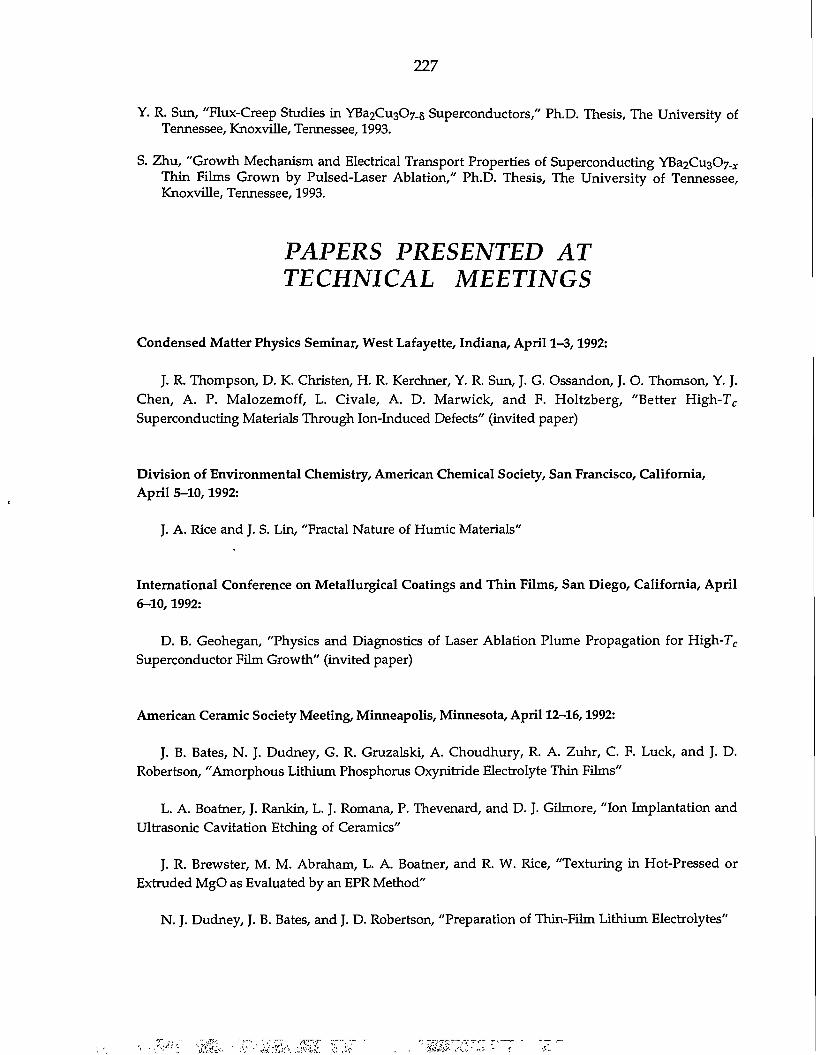
227
Y. R. Sun, "Flux-Creep Studies in YBa2Cu3C>7.5 Superconductors," Ph.D. Thesis, The University of Tennessee, Knoxville, Tennessee, 1993.
S. Zhu, "Growth Mechanism and Electrical Transport Properties of Superconducting YBaaCuaC^ Thin Films Grown by Pulsed-Laser Ablation," Ph.D. Thesis, The University of Tennessee, Knoxville, Tennessee, 1993.
PAPERS PRESENTED AT TECHNICAL MEETINGS
Condensed Matter Physics Seminar, West Lafayette, Indiana, April 1-3,1992:
J. R. Thompson, D. K. Christen, H. R. Kerchner, Y. R. Sun, J. G. Ossandon, J. O. Thomson, Y. J. Chen, A. P. Malozemoff, L. Civale, A. D. Marwick, and F. Holtzberg, "Better High-T c
Superconducting Materials Through Ion-Induced Defects" (invited paper)
Division of Environmental Chemistry, American Chemical Society, San Francisco, California, April 5-10,1992:
J. A. Rice and J. S. Lin, "Fractal Nature of Humic Materials"
International Conference on Metallurgical Coatings and Thin Films, San Diego, California, April 6-10,1992:
D. B. Geohegan, "Physics and Diagnostics of Laser Ablation Plume Propagation for High-Tc
Superconductor Film Growth" (invited paper)
American Ceramic Society Meeting, Minneapolis, Minnesota, April 12-16,1992:
J. B. Bates, N. J. Dudney, G. R. Gruzalski, A. Choudhury, R. A. Zuhr, C. F. Luck, and J. D. Robertson, "Amorphous Lithium Phosphorus Oxynitride Electrolyte Thin Films"
L. A. Boatner, J. Rankin, L. J. Romana, P. Thevenard, and D. J. Gilmore, "Ion Implantation and Ultrasonic Cavitation Etching of Ceramics"
J. R. Brewster, M. M. Abraham, L. A. Boatner, and R. W. Rice, "Texturing in Hot-Pressed or Extruded MgO as Evaluated by an EPR Method"
N. J. Dudney, J. B. Bates, and J. D. Robertson, "Preparation of Thin-Film Lithium Electrolytes"
228
S. J. Pennycook, M. F. Chisholm, and D. E. Jesson, "Z-Contrast Imaging of Interfaces" (invited paper)
J. Rankin, Q.-R. Fan, T. A. Nguyen, and L. A. Boatner, "In Situ TEM Study of the Coarsening of Nanophase MgO Particles"
Critical Currents in High-Tc Superconductors, Austria, April 22-24,1992:
J. G. Ossandon, J. R. Thompson, D. K. Christen, Y. R. Sun, B. C. Sales, H. R. Kerchner, J. E. Tkaczyk, and K. W. Lay, "Systematics of Flux Pinning Versus Oxygen Deficiency 8 in Aligned YBa2Cu307_5 Materials"
Materials Research Society Spring Meeting, San Francisco, California, April 27-May 1,1992:
L. A. Boatner, J. Rankin, L. J. Romana, P. Thevenard, and D. J. Gilmore, "A New Method for Etching Ceramic Materials Using Ion Implantation and Ultrasonic Cavitation"
M. F. Chisholm, T. Kaplan, M. E. Mostoller, and S. J. Pennycook, "Atomic Structure of Interracial Misfit Dislocations in SixGei.x/Si(001)"
D. Eres and J. W. Sharp, "Thin-Film Growth from a Heterogeneous Surface Reaction"
R. Feenstra, D. P. Norton, J. D. Budai, D. K. Christen, D. H. Lowndes, V. C. Matijasevic, C.-B. Eom, T. H. Geballe, E. S. Hellman, and E. H. Hartford, "Tc-8 Relations in YBa2Cu307_ s Thin Films: Oxygen Pressure During Growth"
A. T. Fiory, P. K. Roy, and G. E. Jellison, Jr., "Ion Channeling and Spectroscopic Ellipsometry Examinations of Thin-Film SiO2/EPI-Si(001) Structures"
H. R. Kerchner, C. E. Klabunde, D. K. Christen, J. D. Budai, D. H. Lowndes, D. P. Norton, and J. O. Thomson, "Anisotropic Electrical Resistivity of YBCO/PBCO Superlattice Films Grown on Miscut Substrates"
D. E. Jesson, S. J. Pennycook, J.-M. Baribeau, and D. C. Houghton, "Step-Driven Surface Segregation and Ordering During Si-Ge MBE Growth" (invited paper)
S. J. Pennycook, M. F. Chisholm, D. E. Jesson, R. Feenstra, S. Zhu, and D. H. Lowndes, "Growth Mechanisms of Layered Superconductors" (invited paper)
B. C. Sales, R. A. Zuhr, J. C. McCallum, and L. A. Boatner, "Dominant Role of Electronic Energy Losses in the Ion Beam Amorphization of Pb2P2C>7"
J. R. Thompson, "What Can We Learn From Magnetization Experiments on High-T c
Superconductors? An Overview" (invited paper)
229
C. W. White, D. K. Thomas, R. A. Zuhr, J. C. McCallum, A. Pogany, R. F. Haglund, R. H. Magruder, and L. Yang, "Modification of the Optical Properties of AI2O3 by Ion Implantation"
X.-Y. Zheng, D. H. Lowndes, S. Zhu, and R. J. Warmack, "Scanning Tunneling Microscope Studies of Epitaxial Growth of YBa 2Cu 30 7.5 Thin Films"
Spring College on Superconductivity, Trieste, Italy, April 27-June 30,1992:
G. D. Mahan, "Theory of Normal Metals" (invited paper)
Joint TMS-Australian IMM Rare Earth Symposium: Sources, Science, Technology, and Applications, San Diego, California, May 2-5,1992:
R. M. Moon, "Neutron Scattering from Rare-Earth Materials" (invited paper)
AIME Annual Meeting, San Diego, California, May 2-5,1992:
G. Sundar, J. J. Hoyt, and S. Spooner, "A Test of the Langer-Schwartz Model of Nucleation and Growth"
Workshop on Neutron and Synchrotron Radiation Studies of Materials, Upton, New York, May 4-8, 1992:
R. M. Nicklow, "Neutron Inelastic Scattering" (invited paper)
Proceedings of Phase Separation in Cuprate Superconductors, Erice, Italy, May 6-12,1992:
S. M. Hayden, T. E. Mason, G. Aeppli, H. A. Mook, S.-W. Cheong, and Z. Fisk, "Neutron Scattering Studies of the Spin Dynamics in La2.xSra:Cu04"
CLEO/QELS 1992 Conference on Lasers and Electro-Optics and Quantum Electronics and Laser Science, Anaheim, California, May 10-15,1992:
S. W. Allison, M. A. Abraham, L. A. Boatner, M. R. Cates, D. L. Beshears, K. W. Tobin, B. W. Noel, and W. D. Turley, "High-Temperature Spectroscopy of Fluorescent Materials for Thermometry Applications"
D. B. Geohegan, "Fast Imaging of Ablation Plume Propagation Through Background Gases Used for Pulsed-Laser Deposition"
230
6th International Meeting on Lithium Batteries, Minister, Germany, May 10-15,1992:
J. B. Bates, N. J. Dudney, G. R. Gruzalski, R. A. Zuhr, A. Choudhury, C. F. Luck, and J. D. Robertson, "Fabrication and Characterization of Amorphous Lithium Electrolyte Thin Films and Rechargeable Thin-Film Batteries" (invited paper)
Joint Meeting of the American Geophysical Union, Canadian Geophysical Union, and the Mineralogical Society of America, Montreal, Canada, May 12-15,1992:
B. C. Chakoumakos, J. A. Fernandez-Baca, and L. A. Boatner, "Crystal Growth and Structure Refinements of the Gillespite-Type Layer Silicates M C u S i ^ i o (M = Ca, Sr, Ba)"
181st Meeting of the Electrochemical Society, Inc., St. Louis, Missouri, May 17-22,1992:
S. H. Liu, "Theory of Interfacial Constant Phase Element in Electrode-Electolyte Systems" (invited paper)
National Synchrotron Light Source Workshop on Small-Angle Scattering for Materials Science, Upton, New York, May 18,1992:
B. C. Larson, "Small-Angle X-Ray Scattering Around Bragg Peaks; Diffuse Scattering From Clusters" (invited paper)
SAS Studies of Synthetic Polymers, With Particular Reference to Polyolefin Blends, Bartlesville, Oklahoma, May 18,1993:
G. D. Wignall, "Small-Angle Scattering Studies of Synthetic Polymers" (invited paper)
Near-Edge X-Ray Adsorption Fine Structure (NEXAFS), Stockholm, Sweden, May 18-20,1992:
L. Siller, K. M. Hock, R. E. Palmer, and J. F. Wendelken, "Negative Ion Resonances in EELS of Adsorbed Molecules: Physisorbed and Chemisorbed Oxygen on P t ( l l l ) "
Small-Angle X-Ray and Neutron Scattering from Polymers, Summit, New Jersey, May 20,1993:
G. D. Wignall, "Small-Angle Scattering Studies of Synthetic Polymers" (invited paper)
231
Joint Annual Meeting-Geological Association of Canada/Mineralogical Association of Canada, Wolfville, Nova Scotia, Canada, May 25-27,1992:
R. K. Eby, J. Janeczek, R. C. Ewing, B. C. Chakoumakos, T. S. Ercit, L. A. Groat, B. C. Can, and F. C. Hawthorne, "Metamictization and Alternation of Vesuvianite"
Beijing International Conference on High-Tc Superconductivity, Beijing, China, May 25-29,1992:
Y. R. Sun, J. R. Thompson, D. K. Christen, Y. J. Chen, J. G. Ossandon, F. Holtzberg, A. D. Marwick, and A. Goyal, "Flux Creep Studies in YBa2Cu3C>7-5"
Accuracy in Powder Diffraction II, Gaithersburg, Maryland, May 26-29,1992:
B. C. Chakoumakos, J. A. Fernandez-Baca, and G. A. Lager, "Crystal Structure Refinements of M3AI2O6 (M = Ca, Sr, Ba) Using Neutron Powder Diffraction Data—An Example Study from the New HB-4 Diffractometer at the HFIR, Oak Ridge"
J. A. Fernandez-Baca, H. A. Mook, H. S. White, B. S. Hoffheins, and B. C. Chakoumakos, "Neutron Powder Diffraction at the High-Flux Isotope Reactor at Oak Ridge"
3rd International Conference on Advances in Welding Research, Gatlinburg, Tennessee, June 1-5, 1992:
J. H. Root, T. M. Holden, J. Schroder, S. Spooner, C. A. Hubbard, T. A. Dodson, and S. A. David, "Residual Stresses in a Multipass Ferritic Weldment"
S. Spooner, S. A. David, J. H. Root, T. M. Holden, M. A. M. Bourke, and J. Goldstone, "Residual Stress and Strain Measurements in an Austenitic Steel Plate Containing a Multipass Weld"
J. M. Vitek, M. Rappaz, S. A. David, and L. A. Boatner, "Grain Competition in Bicrystal Welds"
Spring Meeting of the European Materials Research Society, Strasbourg, France, June 2-5,1992:
D. E. Jesson, S. J. Pennycook, J.-M. Baribeau, and D. C. Houghton, "Atomistic Processes of Surface Segregation During Si-Ge MBE Growth" (invited paper)
232
6th International Conference on Metalorganic Vapor Phase Epitaxy, Cambridge, Massachusetts, June 8-11,1992:
A. Erbil, W. Braun, B. S. Kwak, L. A. Boatner, and J. D. Budai, "Oxide Ferroelectric Materials Grown by Metalorganic Chemical Vapor Deposition".
International Seminar on High-Resolution STEM, Osaka, Japan, June 10,1992:
S. J. Pennycook, "Atomic Resolution Incoherent Imaging with the STEM: Applications to Superconductors and Semiconductors" (invited paper)
35th International Power Sources Symposium, Cherry Hill, New Jersey, June 22-25,1992:
J. B. Bates, G. R. Gruzalski, N. J. Dudney, A. Choudhury, and C. F. Luck, "New Amorphous Thin-Film Lithium Electrolyte and Rechargeable Microbattery"
International Workshop on Superconductivity, Honolulu, Hawaii, June 23-26,1992:
D. K. Christen, C. E. Klabunde, D. B. Chandler, M. J. Neal, M. V. Parish, B. C. Chakoumakos, A. Goyal, and D. M. Kroeger, "The Production and Properties of Melt-Zone-Textured YBa2Cu307_g Filaments" (invited paper)
J. R. Thompson, Y. R. Sun, H. R. Kerchner, D. K. Christen, B. C. Sales, B. C. Chakoumakos, A. D. Marwick, L. Civale, and J. O. Thomson, "Enhanced Current Density } c and Extended Irreversibility in Single-Crystal Bi2Sr2CaCu20s via Linear Defects from Heavy Ion Irradiation"
1992 Electronic Materials Conference, Cambridge, Massachusetts, June 24-26,1992:
T. E. Haynes and O. W. Holland, "Production of Lattice Damage During Ion Implantation of Si-Ge Alloys"
Gordon Research Conference on Ion-Solid Interactions, Plymouth, New Hampshire, July 6-10,1992:
D. B. Geohegan, "Laser Plasma Formation and Propagation in Vacuum and Background Gases Used for Pulsed-Laser Deposition" (invited paper)
M. T. Robinson, "Theory of Displacement Cascades" (invited paper)
233
10th European Congress on Electron Microscopy, Granada, Spain, July 13-17,1992:
C. Ballesteros, R. Gonzalez, Y. Chen, and M. R. Kokta, "Precipitation of Matrix Cations in Fusion Ionic Insulators During Reduction at High Temperatures"
Property and Characteristics of Optical Glass HI, San Diego, California, July 19-22,1992:
D. O. Henderson, S. H. Morgan, R. Mu, R. H. Magruder HI, T. S. Anderson, J. E. Wittig, and R. A. Zuhr, "Optical and Infrared Spectra of Thermally Annealed Pb-Implanted Si02 Glasses"
R. H. Magruder III, D. L. Kinser, J. Wittig, and R. A. Zuhr, "Structure Property Relationships of Nanometer-Size Metal Clusters in Glasses"
Workshop on Recent Advances in Two-Dimensional and Nanostructure Electron Systems, Sydney, Australia, July 20-21,1992:
M. Rasolt and F. Perrot, "Spontaneously Symmetry-Broken Current-Carrying States in Nanostructures" (invited paper)
International Conference on Martensitic Transformation (ICOMAT) 1992, Monterey, California, July 20-24,1992:
H. G. Smith, R. Berliner, and J. Trivisonno, "Neutron Scattering Studies of the Structures and Lattice Dynamics of the Alkali Metals"
International Conference on the Physics of Transition Metals, Darmstadt, Germany, July 20-24, 1992:
J. W. Cable and Y. Tsunoda, "Atomic Short-Range Order and Spin-Density Wave Propagation inCuMn"
R. S. Fishman and S. H. Liu, "Impurity Effects on the Magnetic Ordering in Chromium"
T. M. Holden, K. Mikke, E. Fawcett, and J. A. Fernandez-Baca, "The Magnetism of Metallic Manganese Alloys" (invited paper)
S. H. Liu, "Electronic Polaron Effects in Mixed-Valence and Heavy Fermion Materials" (invited paper)
K. Mikke, T. M. Holden, J. A. Fernandez-Baca, E. Fawcett, and J. Jankowska-Kisielinska, "High-Energy Magnetic Excitations in Single-Domain Homogeneous Antiferromagnetic y-Mn(18%Cu) Alloy at 10 K"
234
10th International Conference on Vacuum Ultraviolet Radiation Physics, Paris, France, July 27-31, 1992:
L. Siller, J. F. Wendelken, and R. E. Palmer, "Resonance EELS Study of Physisorbed and Chemisorbed 0 2 on Pt(lll): Comparison with NEXAFS"
41st Annual Denver X-Ray Conference, Colorado Spring, Colorado, August 3-7,1992:
X-L. Wang, C. R. Hubbard, K. B. Alexander, P. F. Becher, J. A. Fernandez-Baca, and S. Spooner, "Neutron Diffraction Study of the Pseudo-Macro Residual Stresses in Z r0 2 (Ce02)/Al2C>3 Ceramic Composites"
G. D. Wignall, "Combined Small-Angle Neutron and X-Ray Scattering Studies of Polymers" (invited paper)
G. D. Wignall, "Introduction to Small-Angle X-Ray Neutron Scattering"
Gordon Conference on Polymer Physics, Newport, Rhode Island, August 3-7,1992:
J. D. Londono, G. D. Wignall, H. D. Cochran, and A. H. Narten, "The Single-Chain Structure of C36 Chains in the Intermediate-Angle Region"
American Crystallographic Association 1992 Annual Meeting, Pittsburgh, Pennsylvania, August 9-14,1992:
J. W. Cable, "The Discovery of Antiferromagnetic Structures" (invited paper)
B. C. Larson, "X-Ray Diffraction with Nanosecond Time-Resolution and Nanovolt Energy Resolution Using the Pulsed Nature of Synchrotron Sources" (invited paper)
B. C. Sales, "Structural Analysis of Amorphous Phosphates Using High-Performance Liquid Chromatography" (invited paper)
11th Pfefferkorn Conference on Physics of Generation and Detection of Signals Used for Microcharacterization, Amherst, Massachusetts, August 9-14,1992:
S. J. Pennycook, D. E. Jesson, and N. D. Browning, "Electron Channeling with a Coherent STEM Probe: Column-by-Column Imaging and Analysis" (invited paper)
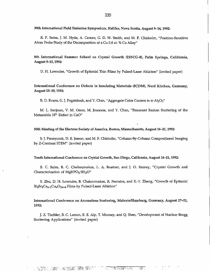
235
39th International Field Emission Symposium, Halifax, Nova Scotia, August 9-14,1992:
R. P. Setna, J. M. Hyde, A. Cerezo, G. D. W. Smith, and M. F. Chisholm, "Position-Sensitive Atom Probe Study of the Decomposition of a Cu-2.6 at. % Co Alloy"
8th International Summer School on Crystal Growth (ISSCG-8), Palm Springs, California, August 9-15,1992:
D. H. Lowndes, "Growth of Epitaxial Thin Films by Pulsed-Laser Ablation" (invited paper)
International Conference on Defects in Insulating Materials (ICDM), Nord Kirchen, Germany, August 15-19,1992:
B. D. Evans, G. J. Pogatshnik, and Y. Chen, "Aggregate Color Centers in CC-AI2O3"
M. L. Sanjuan, V. M. Orera, M. Jouanne, and Y. Chen, "Resonant Raman Scattering of the Metastable H2" Defect in CaO"
50th Meeting of the Electron Society of America, Boston, Massachusetts, August 16-21,1992:
S. J. Pennycook, D. E. Jesson, and M. F. Chisholm, "Column-By-Column Compositional Imaging by Z-Contrast STEM" (invited paper)
Tenth International Conference on Crystal Growth, San Diego, California, August 16-21,1992:
B. C. Sales, B. C. Chakoumakos, L. A. Boatner, and J. O. Ramey, "Crystal Growth and Characterization of MgHP0 4-3H 20"
S. Zhu, D. H. Lowndes, B. Chakoumakos, R. Feenstra, and X.-Y. Zheng, "Growth of Epitaxial Bi2Sr2Ca„_iCu„02H+4 Films by Pulsed-Laser Ablation"
International Conference on Anomalous Scattering, Malente/Hamburg, Germany, August 17-21, 1992:
J. Z. Tischler, B. C. Larson, E. E. Alp, T. Mooney, and Q. Shen, "Development of Nuclear Bragg Scattering Applications" (invited paper)
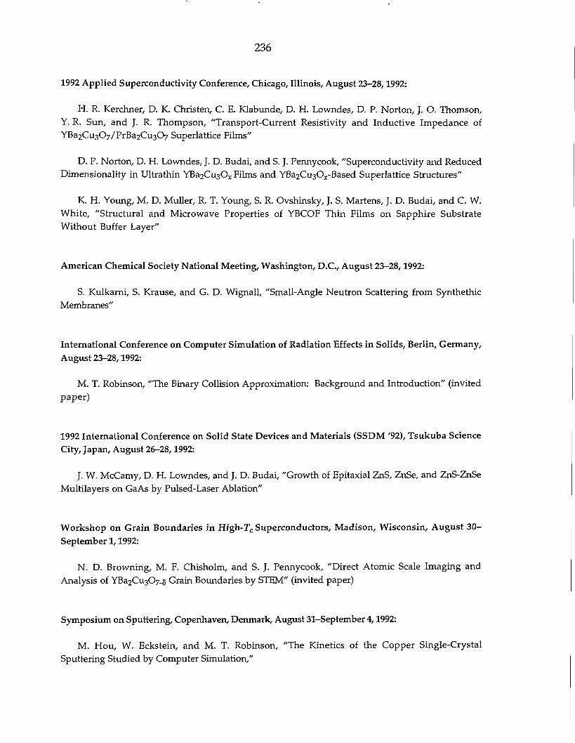
236
1992 Applied Superconductivity Conference, Chicago, Illinois, August 23-28,1992:
H. R. Kerchner, D. K. Christen, C. E. Klabunde, D. H. Lowndes, D. P. Norton, J. O. Thomson, Y. R. Sun, and J. R. Thompson, "Transport-Current Resistivity and Inductive Impedance of YBa 2 Cu307/PrBa 2 Cu 3 07 Superlattice Films"
D. P. Norton, D. H. Lowndes, J. D. Budai, and S. J. Pennycook, "Superconductivity and Reduced Dimensionality in Ultrathin YBa 2 Cu30 x Films and YBa2Cu30j--Based Superlattice Structures"
K. H. Young, M. D. Muller, R. T. Young, S. R. Ovshinsky, J. S. Martens, J. D. Budai, and C. W. White, "Structural and Microwave Properties of YBCOF Thin Films on Sapphire Substrate Without Buffer Layer"
American Chemical Society National Meeting, Washington, D.C., August 23-28,1992:
S. Kulkarni, S. Krause, and G. D. Wignall, "Small-Angle Neutron Scattering from Synthethic Membranes"
International Conference on Computer Simulation of Radiation Effects in Solids, Berlin, Germany, August 23-28,1992:
M. T. Robinson, "The Binary Collision Approximation: Background and Introduction" (invited paper)
1992 International Conference on Solid State Devices and Materials (SSDM '92), Tsukuba Science City, Japan, August 26-28,1992:
J. W. McCamy, D. H. Lowndes, and J. D. Budai, "Growth of Epitaxial ZnS, ZnSe, and ZnS-ZnSe Multilayers on GaAs by Pulsed-Laser Ablation"
Workshop on Grain Boundaries in High-T c Superconductors, Madison, Wisconsin, August 30-September 1,1992:
N. D. Browning, M. F. Chisholm, and S. J. Pennycook, "Direct Atomic Scale Imaging and Analysis of YBa2Cu3G"7-5 Grain Boundaries by STEM" (invited paper)
Symposium on Sputtering, Copenhaven, Denmark, August 31-September 4,1992:
M. Hou, W. Eckstein, and M. T. Robinson, "The Kinetics of the Copper Single-Crystal Sputtering Studied by Computer Simulation,"
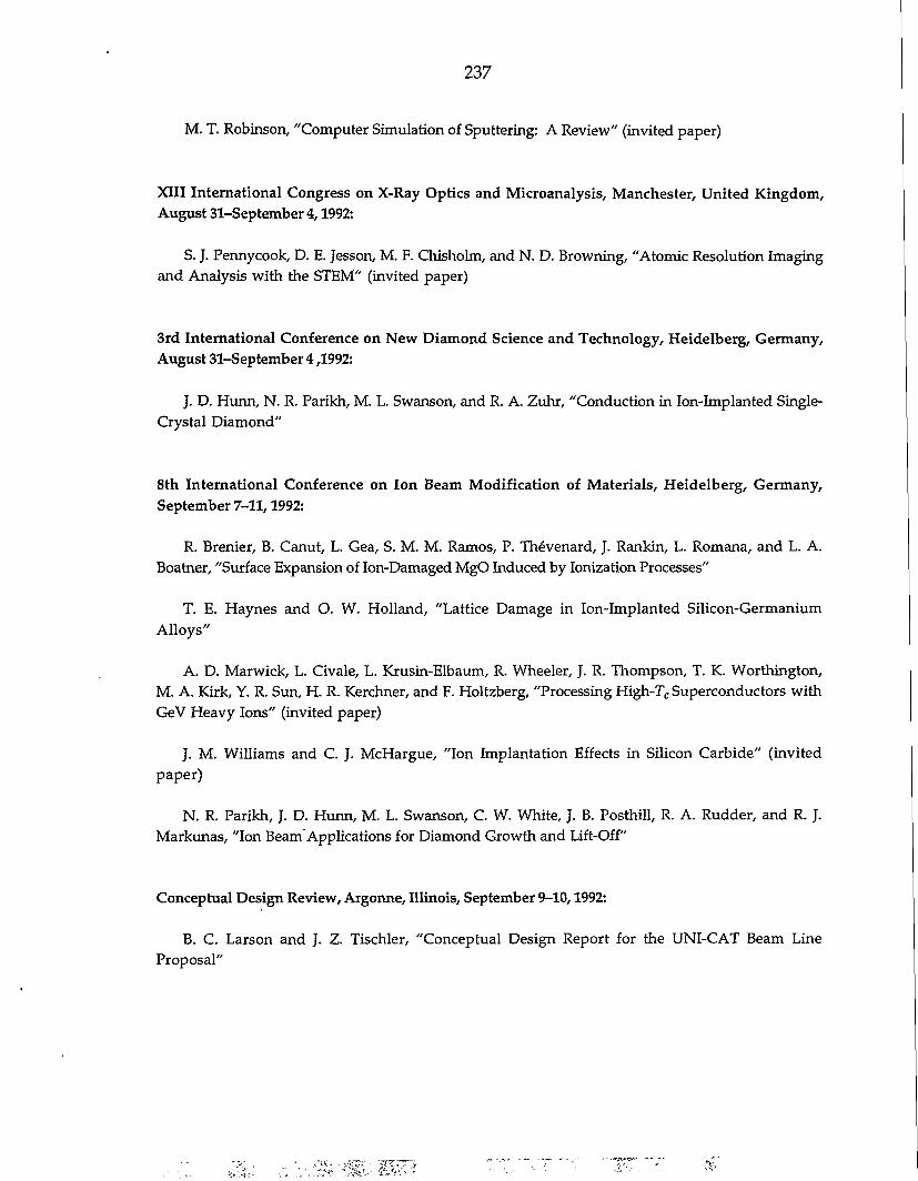
237
M. T. Robinson, "Computer Simulation of Sputtering: A Review" (invited paper)
XIII International Congress on X-Ray Optics and Microanalysis, Manchester, United Kingdom, August 31-September 4,1992:
S. J. Pennycook, D. E. Jesson, M. F. Chisholm, and N. D. Browning, "Atomic Resolution Imaging and Analysis with the STEM" (invited paper)
3rd International Conference on New Diamond Science and Technology, Heidelberg, Germany, August 31-September 4,1992:
J. D. Hunn, N. R. Parikh, M. L. Swanson, and R. A. Zuhr, "Conduction in Ion-Implanted Single-Crystal Diamond"
8th International Conference on Ion Beam Modification of Materials, Heidelberg, Germany, September 7-11,1992:
R. Brenier, B. Canut, L. Gea, S. M. M. Ramos, P. Thevenard, J. Rankin, L. Romana, and L. A. Boatner, "Surface Expansion of Ion-Damaged MgO Induced by Ionization Processes"
T. E. Haynes and O. W. Holland, "Lattice Damage in Ion-Implanted Silicon-Germanium Alloys"
A. D. Marwick, L. Civale, L. Krusin-Elbaum, R. Wheeler, J. R. Thompson, T. K. Worthington, M. A. Kirk, Y. R. Sun, H. R. Kerchner, and F. Holtzberg, "Processing High-Tc Superconductors with GeV Heavy Ions" (invited paper)
J. M. Williams and C. J. McHargue, "Ion Implantation Effects in Silicon Carbide" (invited paper)
N. R. Parikh, J. D. Hunn, M. L. Swanson, C. W. White, J. B. Posthill, R. A. Rudder, and R. J. Markunas, "Ion Beam'Applications for Diamond Growth and Lift-Off"
Conceptual Design Review, Argonne, Illinois, September 9-10,1992:
B. C. Larson and J. Z. Tischler, "Conceptual Design Report for the UNI-CAT Beam Line Proposal"
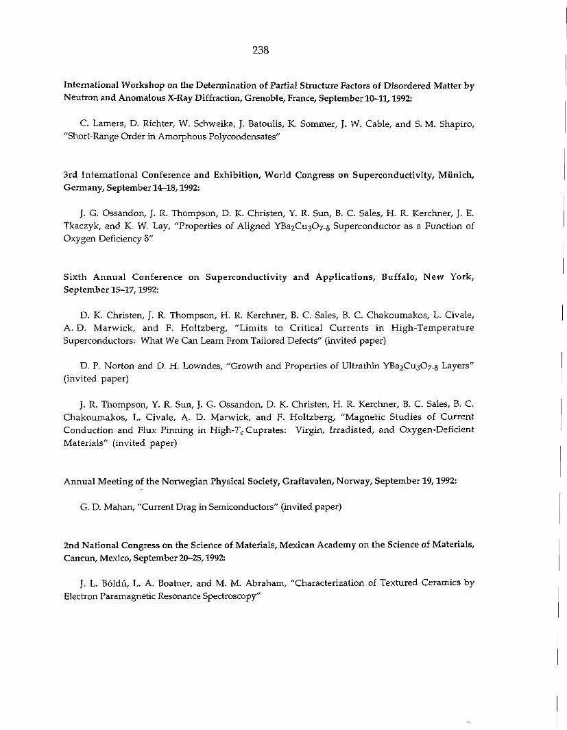
238
International Workshop on the Determination of Partial Structure Factors of Disordered Matter by Neutron and Anomalous X-Ray Diffraction, Grenoble, France, September 10-11,1992:
C. Lamers, D. Richter, W. Schweika, J. Batoulis, K. Sommer, J. W. Cable, and S. M. Shapiro, "Short-Range Order in Amorphous Polycondensates"
3rd International Conference and Exhibition, World Congress on Superconductivity, Munich, Germany, September 14-18,1992:
J. G. Ossandon, J. R. Thompson, D. K. Christen, Y. R. Sun, B. C. Sales, H. R. Kerchner, J. E. Tkaczyk, and K. W. Lay, "Properties of Aligned YBa2Cu307_5 Superconductor as a Function of Oxygen Deficiency 8"
Sixth Annual Conference on Superconductivity and Applications, Buffalo, New York, September 15-17,1992:
D. K. Christen, J. R. Thompson, H. R. Kerchner, B. C. Sales, B. C. Chakoumakos, L. Civale, A. D. Marwick, and F. Holtzberg, "Limits to Critical Currents in High-Temperature Superconductors: What We Can Learn From Tailored Defects" (invited paper)
D. P. Norton and D. H. Lowndes, "Growth and Properties of Ultrathin YBa2Cu307_5 Layers" (invited paper)
J. R. Thompson, Y. R. Sun, J. G. Ossandon, D. K. Christen, H. R. Kerchner, B. C. Sales, B. C. Chakoumakos, L. Civale, A. D. Marwick, and F. Holtzberg, "Magnetic Studies of Current Conduction and Flux Pinning in High-T c Cuprates: Virgin, Irradiated, and Oxygen-Deficient Materials" (invited paper)
Annual Meeting of the Norwegian Physical Society, Graftavalen, Norway, September 19,1992:
G. D. Mahan, "Current Drag in Semiconductors" (invited paper)
2nd National Congress on the Science of Materials, Mexican Academy on the Science of Materials, Cancun, Mexico, September 20-25,1992:
J. L. Boldu, L. A. Boatner, and M. M. Abraham, "Characterization of Textured Ceramics by Electron Paramagnetic Resonance Spectroscopy"
239
First International Conference on Nanostructure Materials, Cancun, Mexico, September 22-26,1992:
C. W. White, D. K. Thomas, D. K. Hensley, R. A. Zuhr, J. C. McCallum, A. Pogany, R. F. Haglund, R. H. Magruder, and L. Yang, "Colloidal Au and Ag Precipitates Formed in AI2O3 by Ion Implantation and Annealing" (invited paper)
Sixth International Humic Substances Society Meeting, Bari, Italy, September 23-27,1992:
J. A. Rice and J. S. Lin, "Fractal Dimension of Humic Materials"
Vlth International Conference on the Physics of Highly Charged Ions, Manhattan, Kansas, September 28-October 2,1992:
I. G. Hughes, C. C. Havener, S. H. Overbury, M. T. Robinson, D. M. Zehner, P. A. Zeijlmans van Emmichoven, and F. W. Meyer, "Incident Ion Charge State Dependence of Electron Emission During Slow Multicharged Ion-Surface Interactions"
F. W. Meyer, J. Burgdorfer, I. G. Hughes, S. H. Overbury, D. M. Zehner, and P. M. Zeijlmans van Emmichoven, "Neutralization of Slow Multicharged Ions Above a Cesiated Au Surface"
P. A. Zeijlmans van Emmichoven, C. C. Havener, I. G. Hughes, D. M. Zehner, and F. W. Meyer, "Analysis of Low-Energy Electron Emission Arising During Slow Multicharged Ion-Surface Interactions"
Midwest Solid State Conference, Champaign, Illinois, October 2-3,1992:
D. H. Lowndes, "Superconductivity in Epitaxial High-Tc Superconductor Multilayers" (invited paper)
XVIth International Congress on Glass, Madrid, Spain, October 4-9,1992:
R. H. Magruder, R. A. Weeks, S.-Y. Park, R. F. Haglund, Jr., L. Lang, and R. A. Zuhr, "Bi-Implanted Si02: A Potential Optical Device Material"
25th SRC Users Group Meeting, Stoughton, Wisconsin, October 5-6,1992:
D. R. Mullins, S. H. Overbury, and P. F. Lyman, "The Adsorption of Sulfur on W(001)"
D. R. Mullins and P. F. Lyman, "Methanethiol on W(001) and Ru(0001)"
240
16th International Seminar on Surface Physics, Kudowa, Poland, October 5-10,1992:
E. W. Plummer and P. A. Dowben, "When Are Thin Films of Metals Metallic?"
Eighth International Conference on Solid Surfaces, Utrecht, Netherlands, October 12-16,1992:
G. Griibel, D. Gibbs, D. M. Zehner, D. L. Abernathy, A. Sandy, and S. G. J. Mochrie, "Phase Behavior of Au and Pt Surfaces"
J.-K. Zuo, D. M. Zehner, J. F. Wendelken, and R. J. Warmack, "A High-Resolution LEED and STM Study of Reconstructed TaC(llO)"
12th International Vacuum Congress/Eighth International Conference on Solid Surfaces, Hague, the Netherlands, October 12-16,1992:
B. Dotsch, A. Schmidt, L. Hammer, M. Kottcke, R. Doll, K. Heinz, K. Muller, H. L. Davis, and D. M. Zehner, "The Structure of the Clean and H-Covered Alloy Mo^Re^lOO)"
D. C, Lubben, R. Tsu, T. R. Bramblett, and J. E. Greene, "Mechanisms and Kinetics of Photo-Stimulated Si Atomic-Layer Epitaxy on Si(001)2 x 1 and Ge(001)2 x 1" (invited paper)
A. R. Sandy, S. G. J. Mochrie, D. M. Zehner, G. Grabel, K. G. Huang, and D. Gibbs, "Au and Pt(lll) Surface Phase Behavior"
L. Siller, R. E. Palmer, and J. F. Wendelken, "Negative Ion Resonance in Electron Scattering by Physisorbed and Chemisorbed O2 on Pt(lll)"
L. Siller, K. M. Hock, R. E. Palmer, and J. F. Wendelken, "Resonance Electron Scattering by Adsorbed Molecules: a* Resonance Energy Versus Bond Length"
J.-K. Zuo, D. M. Zehner, J. F. Wendelken, and R. J. Warmack, "A High-Resolution LEED and STM Study of Reconstructed TaC(llO)"
TMS Fall Meeting, Chicago, Illinois, November 1-5,1992:
M. F. Chisholm and S. J. Pennycook, "Direct Atomic-Scale Imaging of Heterophase Boundaries by Z-Contrast STEM" (invited paper)
12th International Conference on the Application of Accelerators in Research and Industry, Denton, Texas, November 2-5,1992:
T. E. Haynes, "Growth of Lattice Damage During Ion Implantation of Compound Semiconductors" (invited paper)
241
D. Joslin and O. W. Holland, "Ion Beam Synthesis of Buried Insulating Layers in Single-Crystal Si and SiC" (invited paper)
S. J. Pennycook, R. Feenstra, D. P. Norton, D. H. Lowndes, and M. F. Chisholm, "Amorphization, Recrystallization, and Growth Mechanisms of YBa2Cu307_A: Films and Superlattices" (invited paper)
Analytical Laboratory Equipment Exposition and Conference, San Francisco, California, November 3-4,1992:
S. J. Pennycook, "Z-Contrast Scanning Transmission Electron Microscopy" (invited paper)
r Fifth US/Japan Workshop on High-Tc Superconductors, Tsukuba, Japan, November 9-10,1992:
J. R. Thompson, Y. R. Sun, J. G. Ossandon, D. K. Christen, H. R. Kerchner, B. C. Sales, B. C. Chakoumakos, L. Civale, A. D. Marwick, and F. Holtzberg, "Magnetization and Flux Pinning in High-T c Cuprates: Irradiated and Oxygen-Deficient Materials" (invited paper)
39th Annual AVS Symposium and Topical Conference, Chicago, Illinois, November 9-13,1992:
A. P. Baddorf, G. Helgesen, D. Gibbs, A. R. Sandy, and S. G. J. Mochrie, "X-Ray Scattering for Surface Structure Determination"
S. M. Gorbatkin, W. C. Oliver, J. C. Barbour, and T. M. Mayer, "Electron Cyclotron Resonance Microwave Plasma Deposition of BN Thin Films"
P. F. Lyman and D. R. Mullins, "Core Level Spectrosopy of S on W(0001)"
D. R. Mullins and P. F. Lyman, "Reactions of Sulfur-Containing Species on Metal Surfaces Characterized by Synchrotron Radiation"
L. Siller, J. F. Wendelken, and R. E. Palmer, "Observation of Negative Ion Resonances in Physisorbed and Chemisorbed O2 on Pt(lll)"
J.-K. Zuo, R. J. Warmack, D. M. Zehner, and J. F. Wendelken, "A Direct Observation of Periodic (100) Faceting on TaC(llO) by STM"
Fifty-Ninth Meeting of the Southeastern Section of the American Physical Society, Oak Ridge, Tennessee, November 12-14,1992:
N. D. Browning, M. F. Chisholm, and S. J. Pennycook, "Atomic-Scale Imaging and Analysis of Grain Boundaries in YBa2Cu307.s by Scanning Transmission Electron Microscopy" [Bull. Am. Phys. Soc. 37,1665 (1992)]
Y. J. Chen, J. R. Thompson, S. K. Patapis, D. K. Christen, Y. R. Sun, H. R. Kerchner, and B. C. Sales, "Enhanced Supercurrent Density in Single-Crystal Bi2_xPbxSr2CaCu20 z by Heavy Ion Irradiation" [Bull. Am. Phys. Soc. 37, 1666 (1992)]
242
D. K. Christen, "Electrical Transport Properties of High-Temperature Superconductors" [Bull. Am. Phys. Soc. 37, 1665 (1992)] (invited paper)
Z. C. Feng, B. S. Kwak, A. Erbil, and L. A. Boatner, "Raman Spectra of P b T i 0 3 Thin Films on Various Substrates Grown by Metalorganic Chemical Vapor Deposition" [Bull. Am. Phys. Soc. 37, 1657 (1992)]
T. R. Finlayson, H. G. Smith, and N. Wakabayashi, "Neutron Diffraction Study of the Martensitic Phase Transformation in In-Tl Alloys" [Bull. Am. Phys. Soc. 37,1651 (1992)]
E. C. Jones, D. K. Christen, J. R. Thompson, and S. Zhu, "Effect of Inhomogeneities on the Hall Effect in YBa2Cu3C>7_5 Thin Films Near the Superconducting Transition" [Bull. Am. Phys. Soc. 37, 1666 (1992)]
M. N. Kunchur, D. K. Christen, C. E. Klabunde, and J. M. Phillips, "Free-Flux Flow at High Dissipation Levels in YBa 2Cu 307_5 Films" [Bull. Am. Phys. Soc. 37, 1666 (1992)]
S. J. Pennycook, "Direct Atomic Imaging of Materials by Z-Contrast STEM" [Bull. Am. Phys. Soc. 37,1679 (1992)] (invited paper)
J. O. Sofo and G. D. Mahan, "Resistivity and Superconductivity from Anharmonic Phonons" [Bull. Am. Phys. Soc. 37, 1646 (1992)]
Y. R. Sun, J. R. Thompson, D. K. Christen, Y. J. Chen, and A. Goyal, "Measuring Critical Current Density in High-T c Superconductors" [Bull. Am. Phys. Soc. 37,1665 (1992)]
J. Z. Tischler, B. C. Larson, and Q. Shen, "The Effect of Crystal Mosaic on the Nanovolt-Range Energy Resolution of a 57Fe2C>3 Mossbauer Resonant Bragg Monochromator" [Bull. Am. Phys. Soc. 37, 1649 (1992)]
C. N. Yeh, L. E. McNeil, and T. E. Haynes, "Raman Scattering Study of Ion-Implanted Silicon Germanium Alloys" [Bull. Am. Phys. Soc. 37,1657 (1992)]
S. Zhu, D. K. Christen, C. E. Klabunde, J. R. Thompson, R. Feenstra, D. H. Lowndes, and D. P. Norton, "Flux Pinning Force Analysis of Epitaxial Y B a 2 C u 3 0 7 Thin Films" [Bull. Am. Phys. Soc. 37, 1665 (1992)]
Fall Meeting of the Materials Research Society, Boston, Massachusetts, November 30-December 4, 1992:
N. D. Browning and S. J. Pennycook, "Application of Z-Contrast Imaging to Obtain Column-by-Column Spectroscopic Analysis of Materials"
N. D. Browning, J. Yuan, and L. M. Brown, "Determination of Oxygen Deficiency in YBa2Cu307_5 with Nanometer Spatial Resolution by Electron Energy Loss Spectroscopy"
B. C. Chakoumakos, L. A. Boatner, J. O. Ramey, D. P. Norton, and M. Petek, "Textured Superconducting YBa2Cu307-5 Films by Electrodeposition on Semiconducting Oxide Substrates"
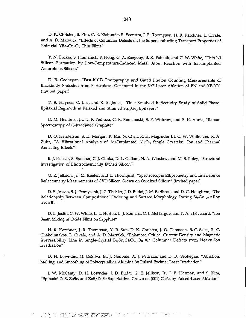
243
D. K. Christen, S. Zhu, C. E. Klabunde, R. Feenstra, J. R. Thompson, H. R. Kerchner, L. Civale, and A. D. Marwick, "Effects of Columnar Defects on the Superconducting Transport Properties of Epitaxial YBa 2 Cu 3 0 7 Thin Films"
Y. N. Erokin, S. Pramanick, F. Hong, G. A. Rozgony, B. K. Patnaik, and C. W. White, "Thin Ni Silicon Formation by Low-Temperature-Induced Metal Atom Reaction with Ion-Implanted Amorphous Silicon,"
D. B. Geohegan, "Fast-ICCD Photography and Gated Photon Counting Measurements of Blackbody Emission from Particulates Generated in the KrF-Laser Ablation of BN and YBCO" (invited paper)
T. E. Haynes, C. Lee, and K. S. Jones, "Time-Resolved Reflectivity Study of Solid-Phase-Epitaxial Regrowth in Relaxed and Strained Sii^Ge^ Epilayers"
D. M. Hembree, Jr., D. F. Pedraza, G. R. Romanoski, S. P. Withrow, and B. K. Annis, "Raman Spectroscopy of C-Irradiated Graphite"
D. O. Henderson, S. H. Morgan, R. Mu, N. Chen, R. H. Magruder III, C. W. White, and R. A. Zuhr, "A Vibrational Analysis of Au-Implanted AI2O3 Single Crystals: Ion and Thermal Annealing Effects"
B. J. Heuser, S. Spooner, C. J. Glinka, D. L. Gilliam, N. A. Winslow, and M. S. Boley, "Structural Investigation of Electrochemically Etched Silicon"
G. E. Jellison, Jr., M. Keefer, and L. Thornquist, "Spectroscopic Ellipsometry and Interference Reflectometry Measurements of CVD Silicon Grown on Oxidized Silicon" (invited paper)
D. E. Jesson, S. J. Pennycook, J. Z. Tischler, J. D. Budai, J.-M. Baribeau, and D. C. Houghton, "The Relationship Between Compositional Ordering and Surface Morphology During Si^Gei.* Alloy Growth"
D. L. Joslin, C. W. White, L. L. Horton, L. J. Romana, C. J. McHargue, and P. A. Thevenard, "Ion Beam Mixing of Oxide Films on Sapphire"
H. R. Kerchner, J. R. Thompson, Y. R. Sun, D. K. Christen, J. O. Thomson, B. C. Sales, B. C. Chakoumakos, L. Civale, and A. D. Marwick, "Enhanced Critical Current Density and Magnetic Irreversibility Line in Single-Crystal Bi2Sr2CaCu30s via Columnar Defects from Heavy Ion Irradiation"
D. H. Lowndes, M. DeSilva, M. J. Godbole, A. J. Pedraza, and D. B. Geohegan, "Ablation, Melting, and Smoothing of Polycrystalline Alumina by Pulsed Excimer Laser Irradiation"
J. W. McCamy, D. H. Lowndes, J. D. Budai, G. E. Jellison, Jr., I. P. Herman, and S. Kim, "Epitaxial ZnS, ZnSe, and ZnS/ZnSe Superlattices Grown on (001) GaAs by Pulsed-Laser Ablation"
244
S. H. Morgan, D. O. Henderson, Z. Pan, R. H. Magruder III, and R. A. Zuhr, "Characterization of Thermal-Annealed Bi-Implanted Silica"
D. P. Norton, B. C. Chakoumakos, J. D. Budai, and D. H. Lowndes, "Epitaxial Growth and Properties of Ca1.jSrj.CuO2 Thin Films Grown by Pulsed-Laser Deposition"
S. Y. Park, R. H. Magruder III, R. A. Weeks, and R. A. Zuhr, "Optical Bleaching of Bismuth-Implanted Silica Glass: Threshold Effects"
S. J. Pennycook, "Direct Atomic Imaging of Materials by Z-Contrast STEM" (invited paper)
M. T. Robinson, "Computer Simulation of Atomic-Collision Processes in Solids" (invited paper)
J. W. Sharp and D. Eres, "Investigation of the Kinetics in Surface-Limited Thin-Film Growth of SiGe Alloys by CVD of Si 2 H 6 /Ge 2 H 6 Mixtures"
T. P. Sjoreen, 'Ton Beam Synthesis of IrSi3 by Implantation of 2-MeV Ir Ions +"
G. W. Steadman, J. R. Brewster, J. D. Budai, and L. A. Boatner, "Textured Coatings from Colloidal Suspensions of Cubic-Faceted Nanophase MgO Particles"
J. R. Thompson, "Vortex Pinning by Line- and Point-Like Defects in High-Temperature Superconductors" (invited paper)
J. M. Williams and D. B. Poker, "Ion Beam Mixing Studies in Pt/Ti and Pt/Ni Bilayered Samples"
S. P. Withrow, S. J. Pennycook, N. Browning, J. D. Budai, and D. M. Hembree, Jr., "Epitaxial Regrowth of Highly Doped Si Using Ion Beams"
F. Xiong, R. P. H. Chang, and C. W. White, "Structure and Properties of a-C:N Films Prepared by Pulsed Excimer Laser Deposition"
J.-K. Zuo and J. F. Wendelken, "Experimental Study of Smoothing Kinetics on a Crystal Surface: Cu/Cu(100)"
37th Annual Conference on Magnetism and Magnetic Materials, Houston, Texas, December 1-4,1992:
J. W. Cable and Y. Tsunoda, "Spin Density Waves in Dilute CuMn Alloys"
C.-K. Loong, L. Soderholm, J. P. Hammonds, M. M. Abraham, L. A. Boatner, and N. M. Edelstein," Neutron Scattering Study of Crystal-Field Transitions in ErP0 4 "
J. A. Fernandez-Baca and H. A. Mook, "Search for the Breakdown of the Spin-Wave Approximation in EuO"
245
J. A. Fernandez-Baca, M. E. Hagen, R. M. Nicklow, T. G. Perring, and Y. Tsunoda, "High-Energy Magnetic Excitations in Mn^Cuio"
T. M. Giebultowicz, J. A. Fernandez-Baca, R. M. Nicklow, J. K. Furdyna, and U. Debska, "Spin Dynamics in a Diluted Heisenberg NN Antiferromagnet on a HCP Lattice: Zn^Mn^Se"
H. A. Mook, M. Yethiraj, G. D. Wignall, E. M. Forgan, S. L. Lee, R. Cubitt, D. McK. Paul, and T. Armstrong, "Neutron Measurements of the Vortex Lattice in YBa2Cu307" (invited paper)
R. B. Rooge, Y. S. Yang, Z. Tun, B. D. Gaulin, J. A. Fernandez-Baca, R. M. Nicklow, and A. Harrison, "A Neutron Scattering Study of the Quasi-One-Dimensional Dilute Ising-Like Antiferromagnet CsCoo.83Mgo.i7Br3"
Y. S. Yang, B. D. Gaulin, J. A. Fernandez-Baca, N. Ali, and G. D. Wignall, "Small-Angle Neutron Scattering Studies of Ce(Fei. rAy 2"
23rd Winter Colloquium on Quantum Electronics, Snowbird, Utah, January 1-5,1993:
R. C. Powell, H. Liu, R. J. Reeves, I. Floldvari, and L. A. Boatner, "Nonlinear Optical Responses of Photorefractive Crystals after Picosecond Pulse Excitation"
Gordon Conference on Superconductivity, Oxnard, California, January 4-8,1993:
M. N. Kunchur, D. K. Christen, C. E. Klabunde, and J. M. Phillips, "Free-Flux Flow at High Dissipation Levels in YBa2Cu307_§ Epitaxial Films" (invited paper)
First International Conference on Spectroscopic Ellipsometry, Paris, France, January 11-14,1993:
G. E. Jellison, Jr., "Data Analysis for Spectroscopic Ellipsometry" (invited paper)
1993 Los Angeles O-E Laser Program of the Society of Photo-Optical Instrumentational Engineers, Los Angeles, California, January 16,1993:
R. F. Haglund, Jr., L. Yang, R. H. Magruder III, K. Becker, J. E. Wittig, C. W. White, R. A. Zuhr, L. Yang, R. Dorsinville, and R. R. Alfano, "Metal-Nanocluster Composites Made by Ion Implantation: A Novel Third-Order Nonlinear Material"
IEEE Workshop on Micro Electro Mechanical Systems, Ft. Lauderdale, Florida, February 7-10,1993:
J. B. Bates, G. R. Gruzalski, and C. F. Luck, "Rechargeable Solid State Lithium Microbatteries" (invited paper)
246
Naval Special Warfare Command R&D Conference, Panama City, Florida, February 9-11,1993:
J. B. Bates and G. R. Gruzalski, "A Thin-Film Rechargeable Lithium Battery" (invited paper)
18th American Institute of Physics Condensed Matter Physics Meeting, Wagga Wagga, Australia, February 10-12,1993:
A. P. Radlinski, C. J. Boreham, G. D. Wignall, and J. S. Lin, "Small-Angle Scattering Study of Structural Evolution of Organic Macerals in Hydrocarbon Source Rocks"
A. P. Radlinski, G. D. Wignall, and J. S. Lin, "Application of SANS and SAXS to Structural Studies of Hydrocarbon-Bearing Rocks"
WATTec '93, Knoxville, Tennessee, February 16-19,1993:
D. P. Norton, "Laser Ablation Film Growth of High-Temperature Superconductors"
AIME Annua l Meet ing, Symposium on Nanocrystal l ine Mater ials , Denver , Colorado, February 21-25,1993:
S. Spooner and G. E. Ice, "On the Structure of Nanocrystalline Materials Seen by X-Ray and Neutron Diffraction" (invited paper)
122nd TMS Annual Meeting, Denver, Colorado, February 21-25,1993:
D. H. Lowndes and D. P. Norton, "Experimental Investigations of Superconductivity in Quasi-Two-Dimensional Epitaxial Copper Oxide Superlattice and Trilayers" (invited paper)
J. M. Vitek, T. Zacharia, S. A. David, M. Rappaz, and L. A. Boatner, "Modeling of Single-Crystal Laser-Weld Microstructures"
Workshop on Recent Developments in Computer Simulation Studies in Condensed Matter Physics, Athens, Georgia, February 22-26,1993:
L. Zhang, G. Canright, and T. Barnes, "Quantum Monte Carlo with Complex Weights"
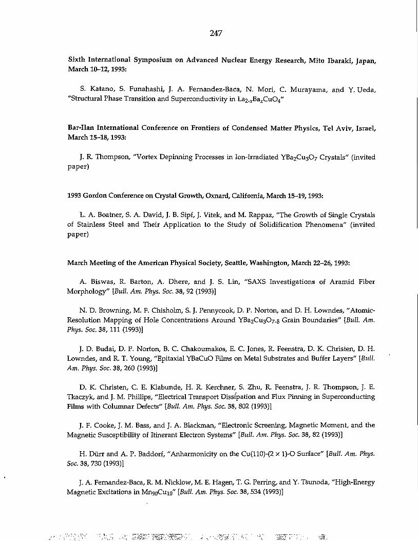
247
Sixth International Symposium on Advanced Nuclear Energy Research, Mito Ibaraki, Japan, March 10-12,1993:
S. Katano, S. Funahashi, J. A. Fernandez-Baca, N. Mori, C. Murayama, and Y. Ueda, "Structural Phase Transition and Superconductivity in I^.^Baj-CuCV
Bar-Ilan International Conference on Frontiers of Condensed Matter Physics, Tel Aviv, Israel, March 15-18,1993:
J. R. Thompson, "Vortex Depinning Processes in Ion-Irradiated YBa2Cu3C>7 Crystals" (invited paper)
1993 Gordon Conference on Crystal Growth, Oxnard, California, March 15-19,1993:
L. A. Boatner, S. A. David, J. B. Sipf, J. Vitek, and M. Rappaz, "The Growth of Single Crystals of Stainless Steel and Their Application to the Study of Solidification Phenomena" (invited paper)
March Meeting of the American Physical Society, Seattle, Washington, March 22-26,1993:
A. Biswas, R. Barton, A. Dhere, and J. S. Lin, "SAXS Investigations of Aramid Fiber Morphology" [Bull. Am. Phys. Soc. 38, 92 (1993)]
N. D. Browning, M. F. Chisholm, S. J. Pennycook, D. P. Norton, and D. H. Lowndes, "Atomic-Resolution Mapping of Hole Concentrations Around YBa2Cu3C>7_5 Grain Boundaries" [Bull. Am. Phys. Soc. 38, 111 (1993)]
J. D. Budai, D. P. Norton, B. C. Chakoumakos, E. C. Jones, R. Feenstra, D. K. Christen, D. H. Lowndes, and R. T. Young, "Epitaxial YBaCuO Films on Metal Substrates and Buffer Layers" [Bull. Am. Phys. Soc. 38, 260 (1993)]
D. K. Christen, C. E. Klabunde, H. R. Kerchner, S. Zhu, R. Feenstra, J. R. Thompson, J. E. Tkaczyk, and J. M. Phillips, "Electrical Transport Dissipation and Flux Pinning in Superconducting Films with Columnar Defects" [Bull. Am. Phys. Soc. 38, 802 (1993)]
J. F. Cooke, J. M. Bass, and J. A. Blackman, "Electronic Screening, Magnetic Moment, and the Magnetic Susceptibility of Itinerant Electron Systems" [Bull. Am. Phys. Soc. 38, 82 (1993)]
H. Diirr and A. P. Baddorf, "Anharmonicity on the Cu(110)-(2 x l)-0 Surface" [Bull. Am. Phys. Soc. 38, 730 (1993)]
J. A. Fernandez-Baca, R. M. Nicklow, M. E. Hagen, T. G. Perring, and Y. Tsunoda, "High-Energy Magnetic Excitations in Mn 9 0Cuio" [Bull. Am. Phys. Soc. 38, 534 (1993)]
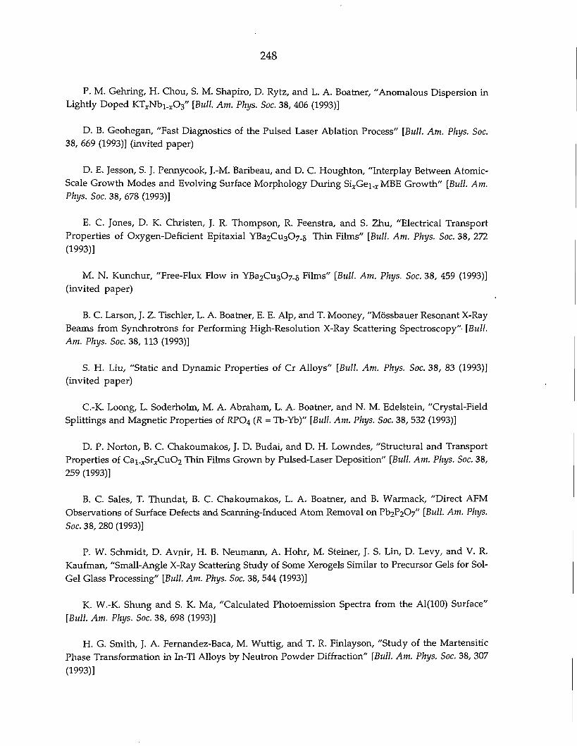
248
P. M. Gehring, H. Chou, S. M. Shapiro, D. Rytz, and L. A. Boatner, "Anomalous Dispersion in Lightly Doped KT x Nbi_ x 0 3 " [Bull. Am. Phys. Soc. 38, 406 (1993)]
D. B. Geohegan, "Fast Diagnostics of the Pulsed Laser Ablation Process" [Bull. Am. Phys. Soc. 38, 669 (1993)] (invited paper)
D. E. Jesson, S. J. Pennycook, J.-M. Baribeau, and D. C. Houghton, "Interplay Between Atomic-Scale Growth Modes and Evolving Surface Morphology During Si xGei_ x MBE Growth" [Bull. Am. Phys. Soc. 38, 678 (1993)]
E. C. Jones, D. K. Christen, J. R. Thompson, R. Feenstra, and S. Zhu, "Electrical Transport Properties of Oxygen-Deficient Epitaxial YBa 2 Cu 3 0 7 . 5 Thin Films" [Bull. Am. Phys. Soc. 38, 272 (1993)]
M. N. Kunchur, "Free-Flux Flow in YBa 2 Cu 3 07 . 5 Films" [Bull. Am. Phys. Soc. 38, 459 (1993)] (invited paper)
B. C. Larson, J. Z. Tischler, L. A. Boatner, E. E. Alp, and T. Mooney, "Mossbauer Resonant X-Ray Beams from Synchrotrons for Performing High-Resolution X-Ray Scattering Spectroscopy"- [Bull. Am. Phys. Soc. 38, 113 (1993)]
S. H. Liu, "Static and Dynamic Properties of Cr Alloys" [Bull. Am. Phys. Soc. 38, 83 (1993)] (invited paper)
C.-K. Loong, L. Soderholm, M. A. Abraham, L. A. Boatner, and N. M. Edelstein, "Crystal-Field Splittings and Magnetic Properties of R P 0 4 (R = Tb-Yb)" [Bull. Am. Phys. Soc. 38, 532 (1993)]
D. P. Norton, B. C. Chakoumakos, J. D. Budai, and D. H. Lowndes, "Structural and Transport Properties of Cai_j-SrxCu02 Thin Films Grown by Pulsed-Laser Deposition" [Bull. Am. Phys. Soc. 38, 259 (1993)]
B. C. Sales, T. Thundat, B. C. Chakoumakos, L. A. Boatner, and B. Warmack, "Direct AFM Observations of Surface Defects and Scanning-Induced Atom Removal on Pb2P207" [Bull. Am. Phys. Soc. 38, 280 (1993)]
P. W. Schmidt, D. Avnir, H. B. Neumann, A. Hohr, M. Steiner, J. S. Lin, D. Levy, and V. R. Kaufman, "Small-Angle X-Ray Scattering Study of Some Xerogels Similar to Precursor Gels for Sol-Gel Glass Processing" [Bull. Am. Phys. Soc. 38, 544 (1993)]
K. W.-K. Shung and S. K. Ma, "Calculated Photoemission Spectra from the Al(100) Surface" [Bull. Am. Phys. Soc. 38, 698 (1993)]
H. G. Smith, J. A. Fernandez-Baca, M. Wuttig, and T. R. Finlayson, "Study of the Martensitic Phase Transformation in In-Tl Alloys by Neutron Powder Diffraction" [Bull. Am. Phys. Soc. 38, 307 (1993)]
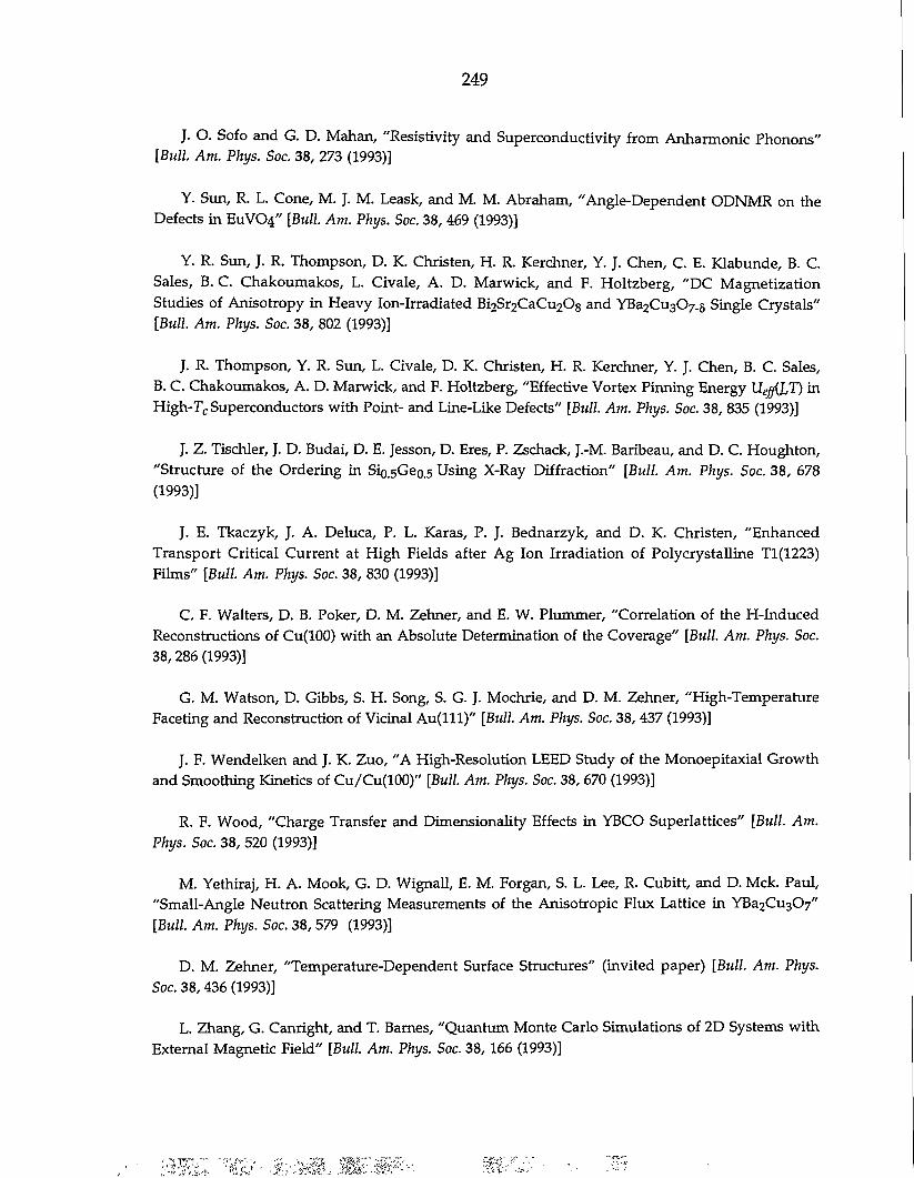
249
J. O. Sofo and G. D. Mahan, "Resistivity and Superconductivity from Anharmonic Phonons" [Bull. Am. Phys. Soc. 38, 273 (1993)]
Y. Sun, R. L. Cone, M. J. M. Leask, and M. M. Abraham, "Angle-Dependent ODNMR on the Defects in EUVO4" [Bull. Am. Phys. Soc. 38, 469 (1993)]
Y. R. Sun, J. R. Thompson, D. K. Christen, H. R. Kerchner, Y. J. Chen, C. E. Klabunde, B. C. Sales, B. C. Chakoumakos, L. Civale, A. D. Marwick, and F. Holtzberg, "DC Magnetization Studies of Anisotropy in Heavy Ion-Irradiated Bi2Sr2CaCu208 and YBa2Cu307.5 Single Crystals" [Bull. Am. Phys. Soc. 38, 802 (1993)]
J. R. Thompson, Y. R. Sun, L. Civale, D. K. Christen, H. R. Kerchner, Y. J. Chen, B. C. Sales, B. C. Chakoumakos, A. D. Marwick, and F. Holtzberg, "Effective Vortex Pinning Energy UeffQ,T) in High-Tc Superconductors with Point- and Line-Like Defects" [Bull. Am. Phys. Soc. 38, 835 (1993)]
J. Z. Tischler, J. D. Budai, D. E. Jesson, D. Eres, P. Zschack, J.-M. Baribeau, and D. C. Houghton, "Structure of the Ordering in Si0.5Ge0.5 Using X-Ray Diffraction" [Bull. Am. Phys. Soc. 38, 678 (1993)]
J. E. Tkaczyk, J. A. Deluca, P. L. Karas, P. J. Bednarzyk, and D. K. Christen, "Enhanced Transport Critical Current at High Fields after Ag Ion Irradiation of Polycrystalline Tl(1223) Films" [Bull. Am. Phys. Soc. 38, 830 (1993)]
C. F. Walters, D. B. Poker, D. M. Zehner, and E. W. Plummer, "Correlation of the H-Induced Reconstructions of Cu(100) with an Absolute Determination of the Coverage" [Bull. Am. Phys. Soc. 38,286 (1993)]
G. M. Watson, D. Gibbs, S. H. Song, S. G. J. Mochrie, and D. M. Zehner, "High-Temperature Faceting and Reconstruction of Vicinal Au(lll)" [Bull. Am. Phys. Soc. 38, 437 (1993)]
J. F. Wendelken and J. K. Zuo, "A High-Resolution LEED Study of the Monoepitaxial Growth and Smoothing Kinetics of Cu/Cu(100)" [Bull. Am. Phys. Soc. 38, 670 (1993)]
R. F. Wood, "Charge Transfer and Dimensionality Effects in YBCO Superlattices" [Bull. Am. Phys. Soc. 38, 520 (1993)]
M. Yethiraj, H. A. Mook, G. D. Wignall, E. M. Forgan, S. L. Lee, R. Cubitt, and D. Mck. Paul, "Small-Angle Neutron Scattering Measurements of the Anisotropic Flux Lattice in YBa2Cu3C>7" [Bull. Am. Phys. Soc. 38, 579 (1993)]
D. M. Zehner, "Temperature-Dependent Surface Structures" (invited paper) [Bull. Am. Phys. Soc. 38, 436 (1993)]
L. Zhang, G. Canright, and T. Barnes, "Quantum Monte Carlo Simulations of 2D Systems with External Magnetic Field" [Bull. Am. Phys. Soc. 38, 166 (1993)]
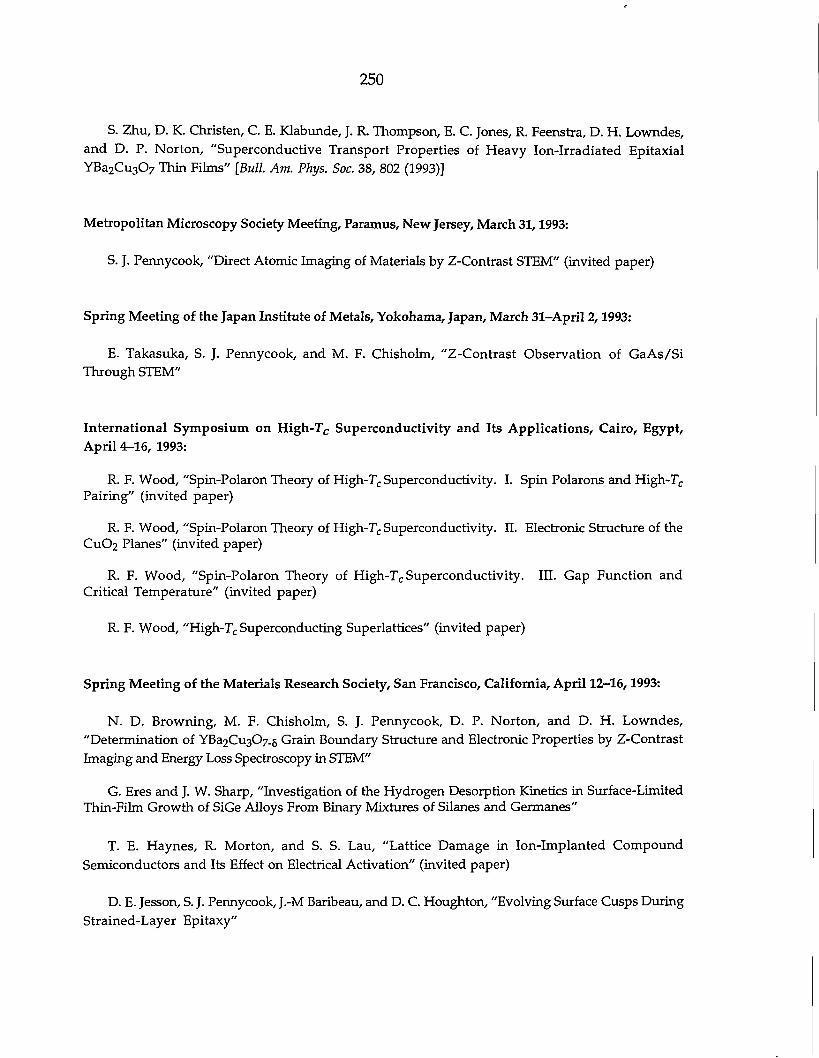
250
S. Zhu, D. K. Christen, C. E. Klabunde, J. R. Thompson, E. C. Jones, R. Feenstra, D. H. Lowndes, and D. P. Norton, "Superconductive Transport Properties of Heavy Ion-Irradiated Epitaxial YBa 2 Cu 3 0 7 Thin Films" [Bull. Am. Phys. Soc. 38, 802 (1993)]
Metropolitan Microscopy Society Meeting, Paramus, New Jersey, March 31,1993:
S. J. Pennycook, "Direct Atomic Imaging of Materials by Z-Contrast STEM" (invited paper)
Spring Meeting of the Japan Institute of Metals, Yokohama, Japan, March 31-April 2,1993:
E. Takasuka, S. J. Pennycook, and M. F. Chisholm, "Z-Contrast Observation of GaAs/Si Through STEM"
International Symposium on High-T c Superconductivity and Its Applications, Cairo, Egypt, April 4-16, 1993:
R. F. Wood, "Spin-Polaron Theory of High-Tc Superconductivity. I. Spin Polarons and High-Tc
Pairing" (invited paper)
R. F. Wood, "Spin-Polaron Theory of High-Tc Superconductivity. II. Electronic Structure of the CuC>2 Planes" (invited paper)
R. F. Wood, "Spin-Polaron Theory of High-Tc Superconductivity. III. Gap Function and Critical Temperature" (invited paper)
R. F. Wood, "High-Tc Superconducting Superlattices" (invited paper)
Spring Meeting of the Materials Research Society, San Francisco, California, April 12-16,1993:
N. D. Browning, M. F. Chisholm, S. J. Pennycook, D. P. Norton, and D. H. Lowndes, "Determination of YBa2Cu3C>7_5 Grain Boundary Structure and Electronic Properties by Z-Contrast Imaging and Energy Loss Spectroscopy in STEM"
G. Eres and J. W. Sharp, "Investigation of the Hydrogen Desorption Kinetics in Surface-Limited Thin-Film Growth of SiGe Alloys From Binary Mixtures of Silanes and Germanes"
T. E. Haynes, R. Morton, and S. S. Lau, "Lattice Damage in Ion-Implanted Compound Semiconductors and Its Effect on Electrical Activation" (invited paper)
D. E. Jesson, S. J. Pennycook, J.-M Baribeau, and D. C. Houghton, "Evolving Surface Cusps During Strained-Layer Epitaxy"
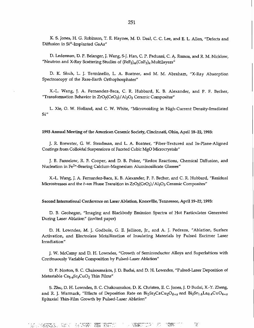
251
K. S. Jones, H. G. Robinson, T. E. Haynes, M. D. Deal, C. C. Lee, and E. L. Allen, "Defects and Diffusion in Si+-Implanted GaAs"
D. Lederman, D. P. Belanger, J. Wang, S-J. Han, C. P. Paduani, C. A. Ramos, and R. M. Nicklow, "Neutron and X-Ray Scattering Studies of (FeF2)m(CoF2)„ Multilayers"
D. K. Shuh, L. J. Terminello, L. A. Boatner, and M. M. Abraham, "X-Ray Absorption Spectroscopy of the Rare-Earth Orthophosphates"
X.-L. Wang, J. A. Fernandez-Baca, C. R. Hubbard, K. B. Alexander, and P. F. Becher, "Transformation Behavior in Zr02(Ce02)/Al2C>3 Ceramic Composites"
L. Xie, O. W. Holland, and C. W. White, "Microvoiding in High-Current Density-Irradiated Si"
1993 Annual Meeting of the American Ceramic Society, Cincinnati, Ohio, April 18-22,1993:
J. R. Brewster, G. W. Steadman, and L. A. Boatner, "Fiber-Textured and In-Plane-Aligned Coatings from Colloidal Suspensions of Faceted Cubic MgO Microcrystals"
J. B. Fanselow, R. F. Cooper, and D. B. Poker, "Redox Reactions, Chemical Diffusion, and Nucleation in Fe2+-Bearing Calcium-Magnesium Aluminosilicate Glasses"
X.-L. Wang, J. A. Fernandez-Baca, K. B. Alexander, P. F. Becher, and C. R. Hubbard, "Residual Microstresses and the t—>m Phase Transition in ZrC^CeC^/ALjOs Ceramic Composites"
Second International Conference on Laser Ablation, Knoxville, Tennessee, April 19-22,1993:
D. B. Geohegan, "Imaging and Blackbody Emission Spectra of Hot Particulates Generated During Laser Ablation" (invited paper)
D. H. Lowndes, M. J. Godbole, G. E. Jellison, Jr., and A. J. Pedraza, "Ablation, Surface Activation, and Electroless Metallization of Insulating Materials by Pulsed Excimer Laser Irradiation"
J. W. McCamy and D. H. Lowndes, "Growth of Semiconductor Alloys and Superlattices with Continuously Variable Composition by Pulsed-Laser Ablation"
D. P. Norton, B. C. Chakoumakos, J. D. Budai, and D. H. Lowndes, "Pulsed-Laser Deposition of Metastable Cai. x Sr x Cu0 2 Thin Films"
S. Zhu, D. H. Lowndes, B. C. Chakoumakos, D. K. Christen, E. C. Jones, J. D Budai, X.-Y. Zheng, and R. J. Warmack, "Effects of Deposition Rate on Bi 2Sr2CaCu20g + x and Bi2Sr 1 - 6Lao.4Cu06 + r
Epitaxial Thin-Film Growth by Pulsed-Laser Ablation"
252
X.-Y. Zheng, D. H. Lowndes, S. Zhu, and R. J. Warmack, "Particles on Surfaces of Laser-Ablated YBa 2 Cu 3 0 7 . 8 Films"
American Vacuum Society, New Mexico Chapter Meeting, Santa Fe, New Mexico, April 27-30, 1993:
J. M. Williams, R. A. Buchanan, and C. J. McHargue, "Ion Implantation for Corrosion and Wear Inhibition in Materials" (invited paper)
D. M. Zehner, "Atomic Structure and Composition of Ordered and Random Alloy Surfaces" (invited paper)
IXth International Congress on Small-Angle Scattering, Saclay, France, April 27-30,1993:
S.-L. Chang, C.-Y. Ku, S.-H. Chen, and J. S. Lin, "Measurement and Interpretation of Counterion Distributions Around Cylindrical Micelles" (invited paper)
Conference on Lasers and Electro-Optics (CLEO '93), Baltimore, Maryland, May 2-7,1993:
D. B. Geohegan, "Fast Diagnostics of Laser Ablation Used in Pulsed-Laser Deposition"
High Aspect Ratio Micro-Electro-Magnetic-Mechanical Systems Conference, Detroit, Michigan, May 17-18,1993:
S. M. Gorbatkin, G. T. Alley, J. B. Bates, L. A. Berry, S. C. Jacobson, and J. M. Ramsey, "Selected Oak Ridge National Laboratory Programs Relevant to Micro-Systems Development" (invited paper)
Annual Meeting of the American Crystallographic Association, Albuquerque, New Mexico, May 23-28,1993:
B. C. Chakoumakos, J. D. Budai, and D. P. Norton, "Structural Systematics of Alkaline-Earth Copper Oxide Films Grown by Pulsed-Laser Deposition on Single-Crystal Perovskites"
American Association for Information Science (ASIS) 1993 Mid-Year Meeting, Knoxville, Tennessee, May 24-27,1993:
S. J. Pennycook, "Direct Atomic Imaging of Materials Through Z-Contrast Electron Microscopy" (invited paper)
253
6th Symposium on Surface Physics, Czechoslovakia, May 24-29,1993:
E. W. Plummer, "Beryllium Surfaces" (invited paper)
Electronic Properties of Two-Dimensional Systems Conference, Newport, Rhode Island, May 31-June 4,1993:
X. M. Chen and J. J. Quinn, "Numerical Studies of the Photoluminescence Spectrum of Quantum Hall Systems"
5th European Workshop on Metal-Organic Vapor Phase Epitaxy and Related Growth Techniques, Malmo, Sweden, June 2-4,1993:
A. Erbil, W. Braun, B. S. Kwak, L. A. Boatner, and J. D. Budai, "Oxide Ferroelectric Materials Grown by Metalorganic Chemical Vapor Deposition"
Workshop on High-Temperature Superconductor Phase Diagrams, Santa Fe, New Mexico, June 2-4, 1993:
M. Paranthaman, J. R. Thompson, Y. R. Sun, J. Brynestad, and D. M. Kroeger, "Evidence for Phase Stability and Weak Links in Polycrystalline HgBa2Cu04+5" (invited paper)
20th Annual Meeting of the Microscopical Society of Canada, Toronto, Canada, June 2-5,1993:
S. J. Pennycook, D. E. Jesson, M. F. Chisholm, and N. D. Browning, "Insights into Semiconducting Materials and Growth Phenomena Through Z-Contrast STEM" (invited paper)
National Research Council Workshop on Quantum Dots and Mesoscopic Systems, Ontario, Canada, June 6-11,1993:
X. Chen and J. J. Quinn, "Numerical Studies of the Photoluminescence of Quantum Hall Systems," (invited paper)
13th Annual Tennessee Valley Chapter of the American Vacuum Society Symposium and Equipment Exhibit, Oak Ridge, Tennessee, June 9-10,1993:
J. B. Bates, "Rechargeable Thin-Film Lithium Batteries" (invited paper)
S. M. Gorbatkin, R. F. Burgie, W. C. Oliver, J. C. Barbour, T. M. Mayer, and M. L. Thomas, "Electron Cyclotron Resonance Microwave Plasma Processing of BN Thin Films" (invited paper)
^^mm^Tw^"mrT-
254
Vibrations at Surfaces VII, Genova, Italy, June 14-17,1993:
H. Durr and A. P. Baddorf, "Anharmonicity on the Cu(110)-(2 x l)-0 Surface"
J. B. Hannon and E. W. Plummer, "Shear Horizontal Vibrations at the (0001) Surface of Beryllium"
70th Birthday Symposium for Professor Bernard Goodman, Cincinnati, Ohio, June 19,1993:
Ordean S. Oen, "Discovery of Ion Channeling"
L. Zhang, "From Fermion Sign to Fermion Phase: Quantum Monte Carlo Simulations with Anyons"
53rd Physical Electronics Conference, Troy, New York, June 21-23,1993:
P. F. Lyman and D. M. Zehner, "Core Level Spectroscopy Investigation of the BCC Random Alloy Moo.75Reo.25"
1993 International Workshop on Superconductivity, Hakodate, Japan, June 28-July 1,1993:
S. J. Pennycook, N. D. Browning, M. F. Chisholm, S. Zhu, R. Feenstra, D. P. Norton, and D. H. Lowndes, "High-Resolution Z-Contrast Imaging and Hole Concentration Mapping of YBCO Thin Films" (invited paper)
6th Analytical Electron Microscopy (AEM) Workshop, Los Angeles, California, July 11-16,1993:
N. D. Browning, M. F. Chisholm, and S. J. Pennycook, "Atomic-Resolution Electron Energy Loss Spectroscopy in the Scanning Transmission Electron Microscope"
S. J. Pennycook and D. E. Jesson, "Z-Contrast Imaging with a 300-kV STEM"
NATO Advanced Research Workshop, Boca Raton, Florida, July 16-21,1993:
P. F. Lyman and D. M. Zehner, "Core-Level Spectroscopy Investigation of the Moo.75Reo.2s(100) Surface" (invited paper)
255
34th Annual Meeting of the Institute of Nuclear Materials Management, Scottscale, Arizona, July 18-21,1993:
L. A. Boatner and A. Lempicki, "Portable Nuclear Weapons and Fissile Materials Identification System"
M. L. Simpson, L. A. Boatner, D. E. Holcomb, S. A. McElhaney, J. T. Mihalczo, J. D. Muhs, M. R. Roberts, and N. W. Hill, "Passive Sensor Systems for Nuclear Material Monitoring"
1993 International Conference on Defects in Semiconductors, Gmiinden, Austria, July 18-23,1993:
M. Ivanda, U. V. Desnica, and T. E. Haynes, "Raman Study of 'Boson Peak' in Ion-Implanted GaAs: Dependence on Ion Dose and Dose Rate"
XVIIIth International Conference on the Physics of Electronic and Atomic Collisions, Aarhus, Denmark, July 21-27,1993:
I. G. Hughes, J. Burgdorfer, L. Folkerts, C. C. Havener, S. H. Overbury, M. T. Robinson, D. M. Zehner, P. A. Zeijlmans van Emmichoven, and F. W. Meyer, "The Role of Below-Surface Secondary Cascade Processes in Potential Electron Emission During Multicharged Ion-Surface Interactions"
F. W. Meyer, L. Folkerts, C. C. Havener, I. G. Hughes, S. H. Overbury, D. M. Zehner, and P. A. Zeijlmans van Emmichoven, "Electron Spectroscopic Studies of the Neutralization of Slow Muticharged Ions During Interactions with a Metal Surface" (invited paper)
The Society of Photo-Optical Instrumentational Engineers (SPIE) Neutron Optical Devices and Applications, San Diego, California, July 22-24,1993:
G. S. Smith, W.' Hamilton, M. Fitzsimmons, S. M. Baker, K. M. Hubbard, M. Nastasi, J-P. Hirvonen, and T. G. Zocco, "Neutron Reflectometry Study of Thermally Induced Boron Diffusion in Amorphous Elemental Boron"
15th International Conference on Atomic Collisions in Solids, London, Ontario, Canada, July 26-30, 1993:
M. T. Robinson, "The Statistics of Sputtering"
yt: • •' "-£tfl IM'- Wu •
256
Workshop on the Statics and Dynamics of Vortices in Superconductors, Eugene, Oregon, August 1-3, 1993:
E. C. Jones, "Intrinsic and Extrinsic Effects Observed in the Superconducting Hall Transitions of Epitaxial Thin Films of YBa 2 Cu 3 0 7 .5 and Polycrystalline TlCa 2 Ba 2 Cu30_ 8 " (invited paper)
M. N. Kunchur, "Mixed State Transport at High Current Densities" (invited paper)
International Summer School on the Fundamentals of Radiation Damage, Urbana, Illinois, August 1-5,1993:
M. T. Robinson, "Basic Physics of Radiation Damage Production" (invited paper)
51st Annual Meeting of the Microscopy Society of America, Cincinnati, Ohio, August 1-6,1993:
M. F. Chisholm, D. E. Jesson, S. J. Pennycook, and S. Mantl, "Z-Contrast Imaging of an Ordered Interface Structure in the Si/CoSi2/Si System"
N. D. Browning, M. M. McGibbon, M. F. Chisholm, and S. J. Pennycook, "Atomic-Resolution Characterization of Interface Structures by Electron Energy Loss Spectroscopy"
D. E. Jesson and S. J. Pennycook, "Incoherence in Atomic-Resolution Z-Contrast Imaging"
H. S. von Harrach, D. E. Jesson, and S. J. Pennycook, "Toward 1-Angstrom Resolution STEM"
International Workshop on Plasma-Based Ion Implantation, Madison, Wisconsin, August 4-6,1993:
J. M. Williams, C. C. Tsai, W. L. Stirling, and J. H. Whealton, "Potential Applications of Fusion Neutral Beam Facilities for Advanced Material Processing"
XXth International Conference on Low-Temperature Physics, Eugene, Ohio, August 4-11,1993:
D. K. Christen, S. Zhu, C. E. Klabunde, H. R. Kerchner, J. R. Thompson, R. Feenstra, L. Civale, and J. M. Phillips, "Effects of Columnar Defects on the Superconducting Properties of YBa2Cu307_g: Limits to the Irreversibility Line"
H. R. Kerchner, J. R. Thompson, Y. R. Sun, D. K. Christen, J. O. Thomson, B. C. Sales, B. C. Chakoumakos, L. Civale, and A. D. Marwick, "Enhanced Vortex-Pinning Strength and Magnetic-Irreversibility Line Via Columnar Defects in Single-Crystal Bi2Sr2CaCu20s"
S. H. Liu and R. A. Klemm, "Density of States and Tunneling Characteristics of Layered Superconductors"
257
J. R. Thompson, D. K. Christen, and J. G. Ossandon, "Equilibrium Magnetization of the High-Tc
Superconductor •n2Ca2Ba2Cu301o+5 and Fluctuation Effects"
International Conference on Applications of the Mossbauer Effect, Vancouver, Canada, August 8-13, 1993:
J. Z. Tischler, B. C. Larson, and E. E. Alp, "Resonantly Scattered Beams from Synchrotrons for High-Resolution X-Ray Scattering Spectroscopy" (invited paper)
International Conference on Luminescence, Storrs, Connecticut, August 9-13,1993:
G. Chen, R. G. Haire, J. R. Peterson, and M. M. Abraham, "A Luminescence Study of EuV0 4 at High Pressure"
A. J. Wojtowicz, M. Balcerzyk, A. Lempicki, and L. A. Boatner, "Rare-Earth Orthophosphate Scintillators"
Y. Sun, R. L. Cone, M. J. M. Leask, and M. M. Abraham, "Defect Structure and Dynamics in EuV0 4"
Workshop on Frontiers of Surface Diffraction and Imaging, Hong Kong, China, August 10-13,1993:
H. L. Davis, "LEED Investigation of Both the Multilayer Relaxation and the Layer-by-Layer Constituent Segregation in Surfaces of Substitutionally Random Binary Alloys" (invited paper)
Fourth International Conference on the Structure of Surfaces, Shanghai, China, August 16-19,1993:
H. L. Davis and J. R. Noonan, "Layer-by-Layer Segregation and Multilayer Relaxation of the Random Alloy Au62Ag3s(lll) Surface"
Workshop on Copper Interconnect Technology, Rensselaer Polytechnic Institute, Troy, New York, August 17-18,1993:
L. A. Berry and S. M. Gorbatkin, "Permanent Magnet ECR Plasma Source With Remote Window"
XVIth International Congress and General Assembly International Union of Crystallography, Beijing, China, August 21-29,1993:
H. G. Smith and J. B. Davidson, "A Neutron-Sensitive TV-Image Intensifier System"
258
206th American Chemical Society National Meeting, Chicago, Illinois, August 22-27,1993:
J. D. Londono, G. D. Wignall, A. H. Narten, K. G. Honnell, A. Yethiraj, and K. S. Schweizer, "Asymmetries in the Flory-Huggins Interaction Parameter in Isotropic Polymer Blends"
D. R. Mullins and P. F. Lyman, "The Adsorption and Reaction of Methanethiol on Clean and Modified W(001) and Ru(0001)"
3rd Annual International Conference and Exposition on Surface Mount Technology, San Jose, California, August 29-September 2,1993:
J. B. Bates, G. R. Gruzalski, N. J. Dudney, C. F. Luck, and X. Yu, "Rechargeable Thin-Film Lithium Batteries" (invited paper)
13th European Conference on Surface Science, Warwick, United Kingdom, August 30-September 4, 1993:
R. Doll, M. Kottoke, K. Heinz, L. Hammer, K. Miiller, and D. M. Zehner, "Chemical Tensor LEED and Its Application to MoxRei.x(100) Surfaces"
8th Electronic Materials and Processing Conference, San Jose, California, August 31-September 3, 1993:
J. B. Bates, "Rechargeable Thin-Film Lithium Batteries" (invited paper)
3rd International Union of the Materials Research Society International Conference on Advanced Materials, Tokyo, Japan, August 31-September 4,1993:
Y. Chen and R. Gonzalez, "Low-Temperature Diffusion of Hydrogenic Species in Oxide Crystals: Radiation-Induced Diffusion" (invited paper)
D. B. Geohegan, A. A. Purezky, R. L. Hettich, X.-Y. Zheng, R. E. Haufler, and R. N. Compton, "Gated ICCD Photography of the KrF-Laser Ablation of Graphite into Background Gases" (invited paper)
D. B. Geohegan, "Physics and Diagnostics of Pulsed-Laser Deposition Laser Plasmas" (invited paper)
T. E. Haynes, "Lattice Damage During Ion Implantation of Semiconductors" (invited paper)
C. J. McHargue, D. L. Joslin, J. M. Williams, and M. E. O'Hern, "Surface Modification of Sapphire for Enhanced Infrared Window Performance" (invited paper)
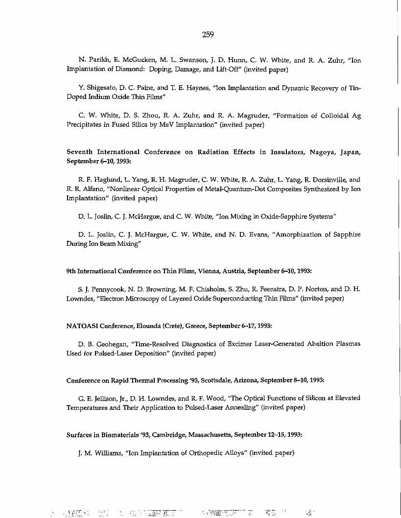
259
N. Parikh, E. McGucken, M. L. Swanson, J. D. Hunn, C. W. White, and R. A. Zuhr, "Ion Implantation of Diamond: Doping, Damage, and Lift-Off" (invited paper)
Y. Shigesato, D. C. Paine, and T. E. Haynes, "Ion Implantation and Dynamic Recovery of Tin-Doped Indium Oxide Thin Films"
C. W. White, D. S. Zhou, R. A. Zuhr, and R. A. Magruder, "Formation of Colloidal Ag Precipitates in Fused Silica by MeV Implantation" (invited paper)
Seventh International Conference on Radiation Effects in Insulators, Nagoya, Japan, September 6-10,1993:
R. F. Haglund, L. Yang, R. H. Magruder, C. W. White, R. A. Zuhr, L. Yang, R. Dorsinville, and R. R. Alfano, "Nonlinear Optical Properties of Metal-Quantum-Dot Composites Synthesized by Ion Implantation" (invited paper)
D. L. Joslin, C. J. McHargue, and C. W. White, "Ion Mixing in Oxide-Sapphire Systems"
D. L. Joslin, C. J. McHargue, C. W. White, and N. D. Evans, "Amorphization of Sapphire During Ion Beam Mixing"
9th International Conference on Thin Films, Vienna, Austria, September 6-10,1993:
S. J. Pennycook, N. D. Browning, M. F. Chisholm, S. Zhu, R. Feenstra, D. P. Norton, and D. H. Lowndes, "Electron Microscopy of Layered Oxide Superconducting Thin Films" (invited paper)
NATOASI Conference, Elounda (Crete), Greece, September 6-17,1993:
D. B. Geohegan, "Time-Resolved Diagnostics of Excimer Laser-Generated Abaltion Plasmas Used for Pulsed-Laser Deposition" (invited paper)
Conference on Rapid Thermal Processing '93, Scottsdale, Arizona, September 8-10,1993:
G. E. Jellison, Jr., D. H. Lowndes, and R. F. Wood, "The Optical Functions of Silicon at Elevated Temperatures and Their Application to Pulsed-Laser Annealing" (invited paper)
Surfaces in Biomaterials '93, Cambridge, Massachusetts, September 12-15,1993:
J. M. Williams, "Ion Implantation of Orthopedic Alloys" (invited paper)
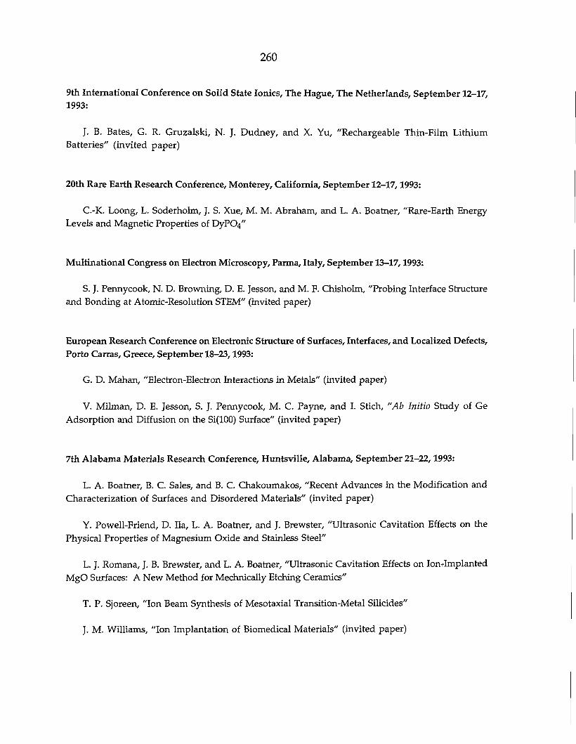
260
9th International Conference on Solid State Ionics, The Hague, The Netherlands, September 12-17, 1993:
J. B. Bates, G. R. Gruzalski, N. J. Dudney, and X. Yu, "Rechargeable Thin-Film Lithium Batteries" (invited paper)
20th Rare Earth Research Conference, Monterey, California, September 12-17,1993:
C.-K. Loong, L. Soderholm, J. S. Xue, M. M. Abraham, and L. A. Boatner, "Rare-Earth Energy Levels and Magnetic Properties of DyPQj"
Multinational Congress on Electron Microscopy, Parma, Italy, September 13-17,1993:
S. J. Pennycook, N. D. Browning, D. E. Jesson, and M. F. Chisholm, "Probing Interface Structure and Bonding at Atomic-Resolution STEM" (invited paper)
European Research Conference on Electronic Structure of Surfaces, Interfaces, and Localized Defects, Porto Carras, Greece, September 18-23,1993:
G. D. Mahan, "Electron-Electron Interactions in Metals" (invited paper)
V. Milman, D. E. Jesson, S. J. Pennycook, M. C. Payne, and I. Stich, "Ab Initio Study of Ge Adsorption and Diffusion on the Si(100) Surface" (invited paper)
7th Alabama Materials Research Conference, Huntsville, Alabama, September 21-22,1993:
L. A. Boarner, B. C. Sales, and B. C. Chakoumakos, "Recent Advances in the Modification and Characterization of Surfaces and Disordered Materials" (invited paper)
Y. Powell-Friend, D. Ila, L. A. Boatner, and J. Brewster, "Ultrasonic Cavitation Effects on the Physical Properties of Magnesium Oxide and Stainless Steel"
L. J. Romana, J. B. Brewster, and L. A. Boatner, "Ultrasonic Cavitation Effects on Ionrlmplanted MgO Surfaces: A New Method for Mechnically Etching Ceramics"
T. P. Sjoreen, "Ion Beam Synthesis of Mesotaxial Transition-Metal Silicides"
J. M. Williams, "Ion Implantation of Biomedical Materials" (invited paper)
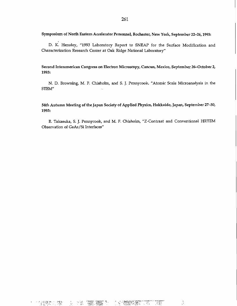
261
Symposium of North Eastern Accelerator Personnel, Rochester, New York, September 22-26,1993:
D. K. Hensley, "1993 Laboratory Report to SNEAP for the Surface Modification and Characterization Research Center at Oak Ridge National Laboratory"
Second Interamerican Congress on Electron Microscopy, Cancun, Mexico, September 26-October 2, 1993:
N. D. Browning, M. F. Chisholm, and S. J. Pennycook, "Atomic Scale Microanalysis in the STEM"
54th Autumn Meeting of the Japan Society of Applied Physics, Hokkaido, Japan, September 27-30, 1993:
E. Takasuka, S. J. Pennycook, and M. F. Chisholm, "Z-Contrast and Conventional HRTEM Observation of GaAs/Si Interfaces"

Seminars
SOLID STATE DIVISION SEMINARS AT ORNL
During the periodcovered by this report, S. J. Pennycook served as Seminar Chairman. The following seminars were held:
"Molecular Dynamics Analyses of Low-Energy Atom-Surface Interactions," C. Gilmore, George Washington University, Washington, D.C.
"Magic Strains, Magic Numbers, Magic Angles: Applications and Limitations of Density Functional Theory," T. Kaxiras, Harvard University, Boston, Mass.
"Compositional Disordering of Superlattices," W. Xia, University of California-San Diego, San Diego, Calif.
"Ultrasonic Studies on Martensitic Phase Transitions in Metals," J. Trivisonno, John Carroll University, Cleveland, Ohio
"Great Balls of Carbon! What's All the Fuss About Buckyballs?" P. Heiney, University of Pennsylvania, Philadelphia, Pa.
"Atomistic Simulation of Materials: Empirical and Ab Initio Investigations," A. Antonelli, Virginia Commonwealth University, Richmond, Va.
"TEM Investigations of the Damage Produced by Ion Implantation of GaAs and Other Semiconductors," M. W. Bench, University of Illinois, Urbana, El.
"Applications of Resonant Nuclear Bragg Scattering," J. Z. Tischler, Solid State Division, ORNL
"Toward a First-Principles Implementation of Density-Functional Theory at a Metal Surface," A. G. Eguiluz, Montana State University, Bozeman, Mont.
"Electron Cyclotron Resonance Microwave Plasmas for Thin-Film Processing," S. M. Gorbatkin, Solid State Division, ORNL
"Are High-Tc Cuprates Conventional Superconductors? A Van Hove Scenario for High-Temperature Superconductivity," C. C. Tseui, IBM T. J. Watson Research Center, Yorktown Heights, N.Y.
"Crystal Defects in Tetrahedrally, Closed-Packed Faces in Metals and Crystallography of Austenite Decomposition in Steels," D. Zhou, University of Virginia, Charlottesville, Va.
"Thermoelectrics: Materials, Modeling, and Physical Limits," G. D. Mahan, ORNL-UT Distinguished Scientist, Solid State Division, ORNL
263
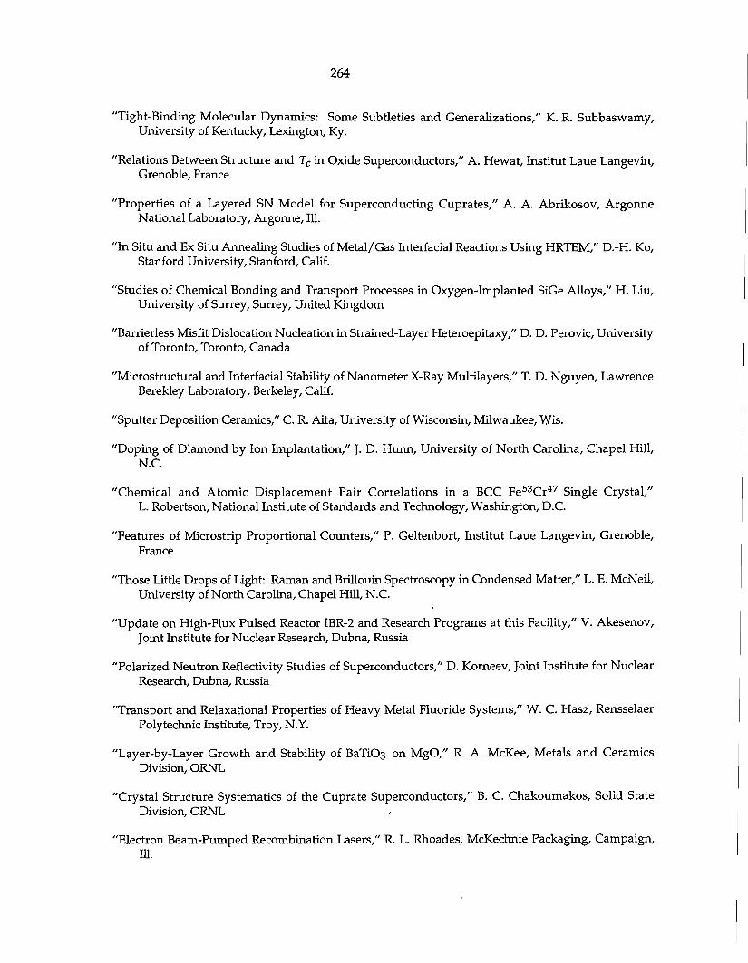
264
"Tight-Binding Molecular Dynamics: Some Subtleties and Generalizations," K. R. Subbaswamy, University of Kentucky, Lexington, Ky.
"Relations Between Structure and Tc in Oxide Superconductors," A. Hewat, Institut Laue Langevin, Grenoble, France
"Properties of a Layered SN Model for Superconducting Cuprates," A. A. Abrikosov, Argonne National Laboratory, Argonne, 111.
"In Situ and Ex Situ Annealing Studies of Metal/Gas Interfacial Reactions Using HRTEM," D.-H. Ko, Stanford University, Stanford, Calif.
"Studies of Chemical Bonding and Transport Processes in Oxygen-Implanted SiGe Alloys," H. Liu, University of Surrey, Surrey, United Kingdom
"Barrierless Misfit Dislocation Nucleation in Strained-Layer Heteroepitaxy," D. D. Perovic, University of Toronto, Toronto, Canada
"Microstructural and Interfacial Stability of Nanometer X-Ray Multilayers," T. D. Nguyen, Lawrence Berekley Laboratory, Berkeley, Calif.
"Sputter Deposition Ceramics," C. R. Aita, University of Wisconsin, Milwaukee, Wis.
"Doping of Diamond by Ion Implantation," J. D. Hunn, University of North Carolina, Chapel Hill, N.C.
"Chemical and Atomic Displacement Pair Correlations in a BCC F e 5 3 C r 4 7 Single Crystal," L. Robertson, National Institute of Standards and Technology, Washington, D.C.
"Features of Microstrip Proportional Counters," P. Geltenbort, Institut Laue Langevin, Grenoble, France
"Those Little Drops of Light: Raman and Brillouin Spectroscopy in Condensed Matter," L. E. McNeil, University of North Carolina, Chapel Hill, N.C.
"Update on High-Flux Pulsed Reactor IBR-2 and Research Programs at this Facility," V. Akesenov, Joint Institute for Nuclear Research, Dubna, Russia
"Polarized Neutron Reflectivity Studies of Superconductors," D. Korneev, Joint Institute for Nuclear Research, Dubna, Russia
"Transport and Relaxational Properties of Heavy Metal Fluoride Systems," W. C. Hasz, Rensselaer Polytechnic Institute, Troy, N.Y.
"Layer-by-Layer Growth and Stability of BaTi03 on MgO," R. A. McKee, Metals and Ceramics Division, ORNL
"Crystal Structure Systematics of the Cuprate Superconductors," B. C. Chakoumakos, Solid State Division, ORNL
"Electron Beam-Pumped Recombination Lasers," R. L. Rhoades, McKechnie Packaging, Campaign, 111.
265
"The Transition from the Thermal to Plasma Mechanism During the Excimer Ablation of Copper Metal," R. Dreyfus, IBM T. J. Watson Research Center, Yorktown Heights, N.Y.
"Materials Science in the Electron Microscope," F. M. Ross, Lawrence Berkeley Laboratory, Berkeley, Calif.
"Neutron Scattering Studies of the Magnetic Excitations of Itinerant-Electron Antiferromagnets: The Case of y-Mn Alloys," J. A. Fernandez-Baca, Solid State Division, ORNL
"Scanning Tunneling Microscope Studies of Surface and Subsurface Electronic Properties of Semiconductors," R. J. Hamers, University of Wisconsin, Madison, Wis.
"Two-Dimensional Model of a Magnetized Glow-Discharge Plasma," D. Graves, University of California, Berkeley, Calif.
"Spectroscopic Ellipsometry: A Technique for Thin-Film and Bulk Material Analysis," G. E. Jellison, Jr., Solid State Division, ORNL
"Ambient Temperature Solid State Batteries," B. B. Owens, University of Minnesota, Minneapolis, Minn.
"Epitaxy on GaAs {111JB: Physical Properties, Growth, and Devices," K. Yang, Rensselaer Polytechnic Institute, Troy, N.Y.
"Laser-Induced Site-Specific Reactions in Precursors for Materials Growth," S. Deshmukh, Tulane University, New Orleans, La.
"Strain Relief in Heteroepitaxial Systems: Where Did All the Threads Go?" L. J. Schowalter, Rensselaer Polytechnic Institute, Troy, N.Y.
"Structure and Atomistic Behavior of Silicate Glasses and Crystalline Alumina Surfaces," S. H. Garofalini, Rutgers University, Piscataway, N.J.
"Prospects for Atomic-Resolution Spectroscopy: Applications to High-Tc Superconductivity," N. D. Browning, Solid State Division, ORNL
"Molecular-Beam-Epitaxial Growth of Si/Ge and III/V Compound Semiconductors," K. Chen, University of Minnesota, Minneapolis, Minn.
"Ellipsometric Studies of Charge Transport in Conducting Polymer Films—Diffusion vs Migration," L. J. Kepley, University of New Mexico, Albuquerque, N. Mex.
"Photon Scattering by Magnetic Materials," S. W. Lovesey, Rutherford Appleton Laboratory, Oxfordshire, United Kingdom
1 "Experiments and Interpretation of Stopping Slow Highly Charged Ions in Insulators," J. P. Biersack, Hahn-Meitner Institut, Berlin, Germany
"Studies of Diffusion Mechanisms at Metal Surfaces Using the Embedded Atom Method," C.-L. Liu, University of Illinois, Urbana, Champaign, 111.
"Core Level Spectroscopy at Surfaces," M. Riffe, University of Texas, Austin, Tex.
266
"Dynamics of Gas-Surface Reactions in Heterogeneous Catalysis," P. Saalfrank, University of California, Berkeley, Calif.
"Gap Engineering in Alternating Layer and Interlayer Substituted BNC Compounds," P. Saalfrank, University of California, Berkeley, Calif.
"X-Ray Standing Wave Studies of Semiconductor Surfaces and Metal Semiconductor Interfaces," J. Woicik, Brookhaven National Laboratory, Upton, N.Y.
2 "A Tale of Two Topics: Epitaxial Growth and Atomistic Calculations of Large Systems," M. S. Daw, Sandia National Laboratories, Livermore, Calif.
"Inner-Shell Excitation by X-Ray Photons: A Probe of Structural and Electronic Information in Molecules and Solids," T. A. Tyson, Instituto Nazionale di Fisica Nucleare, Rome, Italy
"X-Ray Resonant Inelastic Scattering," Y. Ma, Brookhaven National Laboratory, Upton, N.Y.
"Structural- and Electronic-Phase Behavior in High-Tc Cuprates," J. Tallon, New Zealand Institute for Industrial Research and Development, Lower Hutt, New Zealand
"Structure, Metallization, and Electrical Transport at Metal-Semiconductor Interfaces," H. Weitering, University of Pennsylvania, Philadelphia, Penn.
"Sri-xCa^Ru03 (0 < x < 1) for Device Applications," C.-B. Eom, AT&T Bell Laboratories, Murray Hill, N.J.
"Free-Electron Lasers at CEBAF and Their Applications to Material Science Research," H. F. Dylla, Continuous Electron Beam Accelerator Facility, Newport News, Va.
"Charge Carriers and Internal Interfaces in Oxides," V. P. Dravid, Northwestern University, Evanston, 111.
"Thin-Film Fabrication of High-Temperature Superconductors," Y. K. Park, Korean Research Institute of Standards and Science, Taejon, Korea
"Magnetic Properties of Dilute Alloys of Chromium," S. H. Liu, Solid State Division, ORNL
"Vortex Motion in High-Temperature Superconductors," V. Guechkenbein, Weizmann Institute of Science, Rehovot, Israel
"Comparative Study of Ion Implantation Damage in III-V Compound Semiconductors," W. Wesch, Friedrich-Schiller-Universitat, Jena, Germany
"Characterization of Ordered Nickel Oxide Films Grown on Single-Crystal Metal Substrates," C. Ventrice, Tennessee Technology University, Cookeville, Term.
"Ab Initio Pseudopotential Simulations in Materials Physics: Theory and Applications," V. Y. Milman, Oak Ridge Institute for Science and Education and Solid State Division, ORNL
"Electron Scattering at Surfaces: Crystallography, Resonant States, and Dynamics," P. Rous, University of Maryland, College Park, Md.
267
"Crystal Surface According to Helium Atom Scattering," J. G. Skofronic, Florida State University, Tallahassee, Fla.
"Electronic Many-Body Effects in Metals," A. Eguiluz, Montana State University, Bozeman, Mont.
"Recent Advances in High-Resolution Soft X-Ray Spectroscopy," C.-T. Chen, AT&T Bell Laboratories, Murray Hill, N.J.
"Computer Simulations of Critical Behavior in the 3D Classical Heisenberg Ferromagnet," K. Chen, University of Georgia, Athens, Ga.
"Ab Initio Calculation of the Phonon Dispersion of Silicon and Germanium," S. Wei, Georgia Institute of Technology, Atlanta, Ga.
"Chiral Melting of Si(113)(3 x 1) Reconstruction," D. Abernathy, Massachusetts Institute of Technology, Cambridge, Mass.
"Excitonic Transitions at the Mott-Hubbard Gap of the Insulating Parent States of the Cuprate Superconductors: A Raman Scattering Study," M. Klein, University of Illinois, Urbana, 111.
"Structure and Growth of Xe on Ag(lll)," P. Dai, University of Missouri, Columbia, Mo.
"Structure and Dynamics for Low-Dimensional Systems," W. Zhong, Michigan State University, East Lansing, Mich.
"First-Principles Studies on Structural Properties of Beta-Cristobatlite SiC^," F. Liu, Rutgers University, Piscataway, N.J.
"First Principles MD Simulations of the Clean and Alkali-Covered Si(100) Surface," K. Terakura, University of Tokyo, Tokyo, Japan
"Elementary Excitations and Neutron Scattering in Liquid 4He," H. R. Glyde, University of Delaware, ' Newark, Del.
"Spin Ordering on a NiO(lOO) Surface Measured by Elastic Metastable He Scattering," A. K. Swan, Boston University, Boston, Mass.
3 "Photon Matter Interaction at Solid Surfaces—Material Processing and Optical Detection," C. Ying, University of Pennsylvania, Philadelphia, Pa.
"Characterization of Submonolayer Growth of Cu Islands on Cu(OOl)," G. Vidali, Syracuse University, Syracause, N.Y.
"Neutron Reflectivity Studies of Magnetic Coupling in Transition-Metal Multilayers," J. F. Ackner, National Institute of Standards and Technology, Gaithersburg, Md.
"Vortex Motion and Pinning in High-Temperature Superconductors," L. Civale, Centro Atomico Bariloche, Bariloche, Argentina
"The JEOL JSTM 4500-VT Variable Temperature Scanning Tunneling Microscope," M. Iwatsuki, JEOL USA, Inc., Peabody, Mass.
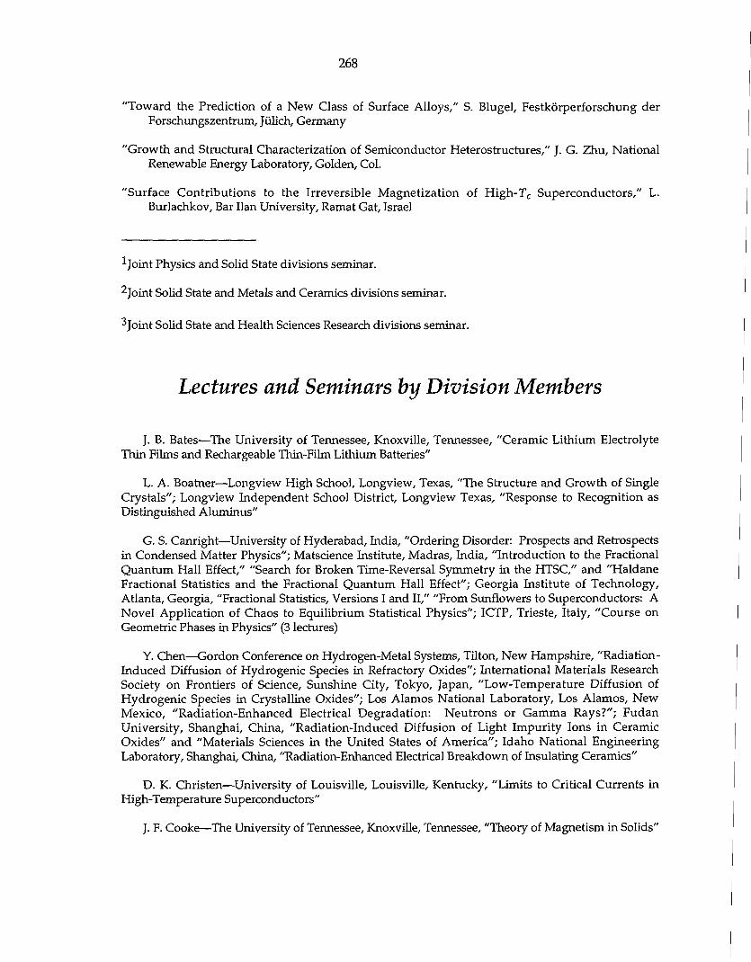
268
"Toward the Prediction of a New Class of Surface Alloys," S. Blugel, Festkorperforschung der Forschungszentrum, Julich, Germany
"Growth and Structural Characterization of Semiconductor Heterostructures," J. G. Zhu, National Renewable Energy Laboratory, Golden, Col.
"Surface Contributions to the Irreversible Magnetization of High-T c Superconductors," L. Burlachkov, Bar Ilan University, Ramat Gat, Israel
Joint Physics and Solid State divisions seminar.
•Joint Solid State and Metals and Ceramics divisions seminar.
'Joint Solid State and Health Sciences Research divisions seminar.
Lectures and Seminars by Division Members
J. B. Bates—The University of Tennessee, Knoxville, Tennessee, "Ceramic Lithium Electrolyte Thin Films and Rechargeable Thin-Film Lithium Batteries"
L. A. Boatner—Longview High School, Longview, Texas, "The Structure and Growth of Single Crystals"; Longview Independent School District, Longview Texas, "Response to Recognition as Distinguished Aluminus"
G. S. Canright—University of Hyderabad, India, "Ordering Disorder: Prospects and Retrospects in Condensed Matter Physics"; Matscience Institute, Madras, India, "Introduction to the Fractional Quantum Hall Effect," "Search for Broken Time-Reversal Symmetry in the HTSC," and "Haldane Fractional Statistics and the Fractional Quantum Hall Effect"; Georgia Institute of Technology, Atlanta, Georgia, "Fractional Statistics, Versions I and II," "From Sunflowers to Superconductors: A Novel Application of Chaos to Equilibrium Statistical Physics"; ICTP, Trieste, Italy, "Course on Geometric Phases in Physics" (3 lectures)
Y. Chen—Gordon Conference on Hydrogen-Metal Systems, Tilton, New Hampshire, "Radiation-Induced Diffusion of Hydrogenic Species in Refractory Oxides"; International Materials Research Society on Frontiers of Science, Sunshine City, Tokyo, Japan, "Low-Temperature Diffusion of Hydrogenic Species in Crystalline Oxides"; Los Alamos National Laboratory, Los Alamos, New Mexico, "Radiation-Enhanced Electrical Degradation: Neutrons or Gamma Rays?"; Fudan University, Shanghai, China, "Radiation-Induced Diffusion of Light Impurity Ions in Ceramic Oxides" and "Materials Sciences in the United States of America"; Idaho National Engineering Laboratory, Shanghai, China, "Radiation-Enhanced Electrical Breakdown of Insulating Ceramics"
D. K. Christen—University of Louisville, Louisville, Kentucky, "Limits to Critical Currents in High-Temperature Superconductors"
J. F. Cooke—The University of Tennessee, Knoxville, Tennessee, "Theory of Magnetism in Solids"

269
H. L. Davis—University of Alabama, Tuscaloosa, Alabama, "Low-Energy Electron Diffraction Investigation of Metallic Surface Relaxation—From Cu(llO) to NiAl(llO) and Beyond"; University of Alabama, Birmingham, Alabama, "The Why, The How, and the What of Low-Energy Electron Diffraction for the Investigation of Surface Atomic Structure"; Rutgers University, Piscataway, New Jersey, "Oak Ridge LEED Studies of Metallic Surface Relaxation"; Johns Hopkins University, Baltimore, Maryland, "Precision LEED Studies of Multilayer Relaxation in Monatomic Metallic Surfaces and Layer-by-Layer Segregation in Surface Regions of Binary Random Alloys"; University of Tokyo, Tokyo, Japan, "The Interaction of Hydrogen with Mo^Rej.^lOO) Surfaces"
R. Feenstra—Osaka University, Osaka, Japan, Kyoto University, Kyoto, Japan, Institute of Physical and Chemical Research, Tokyo, Japan, Tokyo Institute of Technology, Yokohama, Japan, University of Tokyo, Tokyo Japan, and Stanford University, Stanford, California, "Oxygen Vacancies in YBa2Cu307_5 Thin Films: Growth Properties, Lattice Disorder, and Flux Pinning"
J. A. Fernandez-Baca—University of Missouri, Kansas City, Missouri, "Neutron Scattering Studies of the Spin Dynamics of Itinerant Electron Antiferromagnets"
T. E. Haynes—FOM Institute for Atomic and Molecular Physics, Amsterdam, Netherlands, Forschungszentrum Jiilich, Julich, Germany, Daimler-Benz Research Center, Ulm, Germany, and Universitat Augsburg, Augsburg, Germany, "Production of Lattice Damage During Ion Implantation of Semiconductors"; Motorola, Inc., Mesa, Arizona, Texas Instruments, Inc., Dallas, Texas, Kyushu University, Fukuoka, Japan, Hitachi Research Laboratory, Hitachi-shi, Japan, and Asahi Glass Co., Ltd., Yokohama, Japan, "Lattice Damage During Ion Implantation of Semiconductors"
O. W. Holland—Motorola, Inc., Mesa, Arizona, and Texas Instruments, Inc., Dallas, Texas, "Formation of SOI by SIMOX: Mechanism for Dislocation Growth in the Superficial Si Layer"
G. E. Jellison, Jr.—Laboratory PHASE, Strasbourg, France, Max-Planck-Institut fur Festkorperforschung, Stuttgart, Germany, Ecole Polytechnique, Lausanne, Switzerland, Kopin Corporation, Stanton, Massachusetts, and Motorola Corporation, Mesa, Arizona, "Spectroscopic Ellipsometry: A Technique for Thin-Film and Bulk Materials Analysis"; Rudolph Research Inc., Flanders, New Jersey, "Two-Channel Spectroscopic Polarization Modulation Ellipsometry and Applications"
H. R. Kerchner—The University of Tennessee, Knoxville, Tennessee, "Superconductivity—The Phenomenon and Its Applications"
M. N. Kunchur—University of Maryland, College Park, Maryland, "Investigation of Superconducting Transport Behavior at High Dissipation Levels"
S. H. Liu—North Dakota State University, Fargo, North Dakota, "Fractals in Condensed Matter Physics"; Argonne National Laboratory, Argonne, Illinois, "Electronic Polaron Effects in Heavy Fermion Materials"; Iowa State University, Ames, Iowa, "Magnetic Properties of Dilute Chromium Alloys"; The University of Tennessee, Knoxville, Tennessee, "Deterministic Sand Pile, Route to Chaos in Large Systems"; University of Missouri, Columbia, Missouri, "The Chromium Story"
D. H. Lowndes—Department of Energy, Basic Energy Sciences/Materials Sciences Information Meeting, Oak Ridge, Tennessee, "Synthesis of Tailored Materials and Superconducting Superlattices by Pulsed-Laser Ablation"; Department of Energy Review of Research Projects, Bethesda, Maryland,
. "Superconductors with High Critical Temperatures"; University of Toronto, Toronto, Canada, "Epitaxial Growth of Films and Superlattices by Pulsed-Laser Ablation"
270
G. D. Mahan—Pennsylvania State University, University Park, Pennsylvania, Ohio State U \iversity, Columbus, Ohio, "Current Drag in Semiconductors"; Norwegian Institute of Technology, Trondheim, Norway, "Thermoelectrics"; Centre Europeen de Calcul Atomique et Moleculaire, Paris, France, "Electron-Electron Interactions in Metals"; International Centre Theoretical Physics, Trieste, Italy, "Theory of Metals" (8 lectures); Ohio State University, Columbus, Ohio, and Pennsylvania State University, University Park, Pennsylvania, "Coulomb Drag in Semiconductors"; Norwegian Institute of Technology, Trondheim, Norway, "Electron-Electron Interactions in Metals"
V. Milman—University of Cambridge, Cambridge, United Kingdom, "Ab Initio Study of Ge Adsorption and Diffusion on the Si(100) Surface"
H. A. Mook—McMaster University, Hamilton, Ontario, Canada, "Neutron Scattering Studies of High-Temperature Superconductors"
D. P. Norton—IBM T. J. Watson Research Center, Yorktown Heights, New York, "Epitaxial Growth of Properties of the 'Infinite Layer' Cai^Sr^-QC^ Compound"
S. J. Pennycook—Sumitomo Metal Industries, Osaka, Japan, "Atomic-Resolution Incoherent Imaging with the STEM: Applications to Superconductors and Semiconductors"; Osaka University, Osaka, Japan, "Growth Mechanisms of Layered Superconductors Visualized Through Z-Contrast Imaging"; University of Toronto, Toronto, Canada, "Atomic-Resolution Imaging and Analysis of Materials Based on Z-Contrast STEM"; Georgia Institute of Technology, Atlanta, Georgia, "Insights into Materials Through Z-Contrast Electron Microscopy"
D. B. Poker—Ohio University, Athens, Ohio, "Ion Scattering for Materials Analysis"
J. B. Roberto—Forschungszentrum (KFA), Julich, Germany, and Max Planck Institut fur Plasma Physik, Garching, Germany, "Deposition and Characterization of Thin Films"
M. T. Robinson—ORNL 50th Anniversary Seminar—50 Years of Ion Beam Research, Oak Ridge, Tennessee, "Radiation Damage and the Birth of Channeling"
J. R. Thompson—Japan Atomic Energy Research Agency, Tokai, Japan, "Intragrain Current Density and Vortex Pinning in High-Tc Superconductors"; The University of Tennessee, Knoxville, Tennessee (2 lectures) and University of Mississippi, University, Mississippi, "Improving Mother Nature's Gift: Processing High-Temperature Superconductors for High Current Conduction"
J. Z. Tischler—University of Hamburg, Hamburg, Germany, "Development of Nuclear Bragg Scattering Applications"
J. F. Wendelken—IBM Almaden Research Center, San Jose, California, "Surface Morphology and Thin-Film Growth Studies with High-Resolution LEED"
C. W. White—Motorola, Inc., Mesa, Arizona and Texas Instruments, Inc., Dallas, Texas, "Materials Modification and Materials Characterization Using Ion Beams"
G. D. Wignall—Sandia National Laboratories, Albuquerque, New Mexico, "Molecular Weight Scaling in Blends and Blockcopolymers by SANS"; Phillips Petroleum Company Research Laboratories, Bartlesville, Oklahoma, and Hoechst-Celanese Research Laboratories, Summit, New Jersey, "Small-Angle Scattering Studies of Synthetic Polymers"
Scientific Activities, Awards, & Honors
M. M. Abraham Member, ORNL-Universidad Nacional Autonoma de Mexico Joint Steering Committee, 1992-1993
Adjunct Professor, Instituto de Fisica, Universidad Nacional Autonoma de Mexico, 1992-1993
Advisor, Superconducting Super Collider GEM BaF2 Panel, Dallas, Texas, 1992
A. P. Baddorf
J. B. Bates
Past-President, Tennessee Valley Chapter, American Vacuum Society, 1992-1993
Recipient, Martin Marietta Energy Systems Technical Achievement Award for Invention, 1993
L. A. Boatner Recipient, Martin Marietta Corporate Fellowship, 1993 Executive Secretary, Materials Research Society, 1992-1993 Associate Editor, Optical Materials, 1990-1993 Co-Chairman, Eighth International Summer School on Crystal
Growth, Palm Springs, California, 1992 Member, Executive Committee, American Association for Crystal
Growth, 1993 Bohmische Physical Society, Scientific Member, 1992 Recipient, First in Class Award, International Metallographic
Contest, New and Unique Techniques, 1992 Recipient, Second in Class Award, American Ceramic Society,
Ceramographic Competition, Optical Microscopy, 1992 Recipient, Second Place Award, Tenth International Conference on
Crystal Growth, Crystal Photograph Competition, 1993 Recipient, Second Place Award, Ninth American Conference on
Crystal Growth, Crystal Photograph Competition, 1993 Member, William Hunt Eisenman Rare Book Committee of ASM
International, 1992-1993 Member, Fellowship Selection Committee, ASM International,
1992-1993 Vice-Chairman, Awards Committee, American Association for
Crystal Growth, 1992-1993 Member, Vitality Committee of the Glass and Optical Materials
Division, The American Ceramic Society, 1992-1993 Recipient, Distinguished Alumnus Award, Longview Independent
School District, Longview, Texas, 1993 Member, Showcase Talk Selection Committee, ORNL, 1990-1993 Chairman, ORNL-Universidad Nacional Autonoma de Mexico
Joint Steering Committee, 1991-1993 Special Graduate Faculty Member, Alabama A&M University,
1991-1993
271
*&S :.*?&•
272
Thesis Advisor, ORINS Graduate Research Program 1992-1993 Thesis Advisor, SSD/University of Tennessee Research Activity Research Advisor, ORNL/SERS Program, 1992-1993 Research Advisor, ORNL/GLCA Program, 1993 Member, Program Committee, 26th International Symposium on
Automotive Technology and Automation, Aachen, Germany, 1993
J. D. Budai
B. C. Chakoumakos
Y. Chen
M. F. Chisholm
Member, ORNL X-Ray Safety Review Committee, 1992-1993
Recipient, First in Class Award, International Metallographic Contest, New and Unique Techniques, 1992
Recipient, Second in Class Award, American Ceramic Society, Ceramographic Competition, Optical Microscopy, 1992
Recipient, Martin Marietta Energy Systems Technical Achievement Award for Publications, 1992
Chairman, DOE Workshop on the Application of Positron Spectroscopy to Materials Sciences, Rancho Mirage, California, 1992
Advisor, Superconducting Super Collider GEM BaF2 Panel, Dallas, Texas, 1992
Co-Organizer, TMS Symposium on Defects at Heterointerfaces, San Francisco, California, 1994
Detailee, Division of Materials Sciences, Office of Basic Energy Sciences, Department of Energy, Washington, D.C., 1992-1993
Co-Chairman, Symposium on Mechanisms of Heteroepitaxial Growth, San Francisco, California, 1992
Session Chairman, Materials Research Society Fall Meeting, Boston, Massachusetts, 1993
Traveling Lecturer, Oak Ridge Institute for Science and Education, 1992-1993
D. K. Christen
J. F. Cooke
H. L. Davis
Session Chairman, American Physical Society Meeting, March 1992 Session Chairman, Materials Research Society, November 1992 Member, Review Panel on High-Temperature Superconductivity
Program for Space Applications, 1992 Member, Review Panel for National Science Foundation Proposals
on Material Synthesis and Processing, 1993 Co-Chairman, Symposium on Superconductivity: Materials and
Properties, Materials Research Society Fall Meeting, 1993
Member, Advisory Committee, Journal of Physics, Condensed Matter
Traveling Lecturer, Oak Ridge Associated Universities, 1992-1993 Detailee, Division of Materials Sciences, Office of Basic Energy
Sciences, Department of Energy, Germantown, Maryland; Full-Time 10/1/91-3/31/93, Part-Time 4/1/93-9/30/94
Participant, Research Assistance Task Force on Photovoltaic Materials, Vail, Colorado/1992
Member, Organizing and Program Committees, Fourth International Conference on the Structure of Surfaces, Shanghai, China, 1993
273
N. J. Dudney
D. B. Geohegan
Session Chairman, Symposium on Application of Multiple Scattering Theory to LEED, Materials Research Society Fall Meeting, Boston, Massachusetts, 1992
Session Chairman, Symposium on New Materials, Fourth International Conference on the Structure of Surfaces, Shanghai, China, 1993
Recipient, Martin Marietta Energy Systems Technical Achievement Award for Invention, 1993
Co-Chairman, Second International Conference on Laser Ablation, Knoxville, Tennessee, 1993
Member, Advisory Committee, LASERION '93, Munich, Germany, 1993
S. M. Gorbatkin
G. R. Gruzalski
W. A. Hamilton
T. E. Haynes
Member, Plasma Science and Technology Program Committee, 40th Annual American Vacuum Society Symposium, 1993
Session Chairman, Second Workshop on High Density Plasmas and Applications, American Vacuum Society Topical Conference, San Francisco, California, 1993
Secretary, Plasma Science and Technology Division, American Vacuum Society, 1992-1993
Member, Executive Board, Tennessee Valley Chapter, American Vacuum Society, 1993
Member, Plasma Science and Technology Division Student Award Committee, American Vacuum Society, 1993
Research Advisor, ORISE/SERS Program, 1992 Research Advisor, ORISE/GLCA Program, 1993 Instructor, Introduction to Electrodynamics, Oak Ridge Science
Semester Program, 1993 Recipient, Martin Marietta Energy Systems Significant Event
Award, 1993
Recipient, Martin Marietta Energy Systems Technical Achievement Award for Invention, 1993
Traveling Lecturer, Oak Ridge Institute for Science and Education, 1992-1993
Participant, Workshop on Scientific Opportunities at Future Spallation Neutron Sources, Argonne, Illinois, 1993
Co-Chairman, Symposium on Crystallization and Related Phenomena in Amorphous Materials, Materials Research Society Fall Meeting, Boston, Massachusetts, 1993
Member, Executive Board, Tennessee Valley Chapter, American Vacuum Society, 1992-1993
Member, Symposium Organizing Committee, Third International Conference on Advanced Materials, 1993
Wk- \;«&-'^
274
O. W. Holland
G. E. Jellison, Jr.
D. E. Jesson
T. Kaplan
H. R. Kerchner
B. C. Larson
J. S. Lin
S. H. Liu
D. H. Lowndes
Co-Chairman, Symposium on Materials Synthesis and Processing Using Ion Beams, Materials Research Society, Boston, Massachusetts, 1993
Member, Publications Committee, Materials Research Society Session Organizer, Conference on Industrial AppHcations of Small
Accelerators, Denton, Texas, 1992
Member, Editorial Board, Applied Physics Communications Referee, Nebraska Engineering Research Initiative
Co-Chairman, Symposium on Si Epitaxy, American Physical Society, Seattle, Washington, 1993
Session Chairman, Microscopy Society of America, Cincinnati, Ohio, 1993
Traveling Lecturer, Oak Ridge Institute for Science and Education, 1992-1993
Session Chairman, Materials Research Society Spring Meeting, San Francisco, California, 1992
Session Chairman, Materials Research Society Fall Meeting, Boston, Massachusetts, 1992 and 1993
Co-Chairman, Symposium on Superconductivity, Materials Research Society Fall Meeting, Boston, Massachusetts, 1993
Mini-Workshop Presenter, National Educators Workshop, Hampton, Virginia, 1993
Chairman, Cornell High-Energy Synchrotron Source Policy and Advisory Board, 1992-1993
Member, ORNL Total Quality Management Benchmarking Committee, 1993
Research Advisor, ORISE/SERS Program, 1993-1994 Adjunct Professor, The University of Tennessee, Knoxville,
Tennessee Consultant, NASA High-Temperature Project Summitec
Corporation, Oak Ridge, Tennessee, 1992-1993
Member, Physics and Astronomy Council, Iowa State University Managing Editor, International Journal of Modern Physics B
Adjunct Professor, Department of Materials Science and Engineering, The University of Tennessee, Knoxville, Tennessee
Ph.D. Thesis Advisor, The University of Tennessee, Knoxville, Tennessee
Adjunct Professor, Department of Physics and Astronomy, Louisiana State University, Baton Rouge, Louisiana
Co-Director, Adriatico Research Conference on Vortex Fluctuations in Superconductors, Trieste, Italy, 1993
Judge, Graduate Student Research Awards, Materials Research Society Fall Meeting, Boston, Massachusetts, 1993
Member, International Program Committee, Third IUMRS-ICAM Conference, Tokyo, Japan, 1993
275
D.GLubben
C. F. Luck
G. D. Mahan
H. A. Mook
R-MMoon
Member, International Program Committee, Second International Conference on Laser Ablation, Knoxville, Tennessee, 1993
Member, Program Committee, Conference on Superconducting Superlattices and Multilayers, Los Angeles, California, 1993
Equipment Exhibit Organizer, 14th Tennessee Valley Chapter, American Vacuum Society Symposium on Innovative Technologies for Materials Processing and Analysis, Oak Ridge, Tennessee (to be held in 1994)
Recipient, Martin Marietta Energy Systems Technical Achievement Award for Invention, 1993
Member, Scandinavian Committee to choose Professorships for: • Experimental Solid State, Chalmers Technical
University, Sweden, Spring, 1992 • Theoretical and Experimental Solid State (2 positions),
Norwegian Institute of Technology, Trondheim, Norway, 1993
Judge, International Science and Engineering Fair, Nashville, Tennessee, 1992
Chairman, Scientific Committee, International Center of Condensed Matter Physics, Brasilia, 1989-1993
Member, Executive Committee, Division of Condensed Matter Physics, American Physical Society, 1989-1992
Co-Chairman, Conference on "Vortex Fluctuations in Superconductors," International Centre of Theoretical Physics, Trieste, Italy, 1993
Co-Editor, Plenum Publishing Company Book Series
Chairman, Corporate Fellows Council, ORNL Co-Chairman, First Advanced Neutron Source User Meeting, Oak
Ridge, Tennessee, 1993 Recipient, Martin Marietta Energy Systems Technical Achieve
ment Award for Publications, 1992 Member, LANSCE II External Advisory Committee, Los Alamos
National Laboratory Member, National Steering Committee for the Advanced Neutron
Source Member, Steering Committee for the U.S.-Japan Cooperative
Program on Neutron Scattering Member, ORNL Awards Committee Member, Brochures Development Task Force, ORNL Member, Nomination Committee, Sigma Xi Session Chairman, Magnetism and Magnetic Materials Conference,
Houston, Texas, 1993
Co-Chairman, First Advanced Neutron Source User Meeting, Oak Ridge, Tennessee, 1993
Recipient, American Association for the Advancement of Science Fellowship, 1994
Acting Division Director, Solid State Division, 1993 Member, Advisory Panel for Reactor Radiation Division, National
Institute for Standards and Technology
•mm M m*..m&s- i ••'vrmfr^j- •:•-•£&
276
Member, Advisory Committee, International Conference on Neutron Scattering, Sendai, Japan (to be held in 1994)
Executive Secretary, National Steering Committee for the Advanced Neutron Source
R. M. Nicklow Member, IPNS Program Advisory Committee, Argonne National Laboratory
Member, Research Committee, U.S.-Japan Cooperative Program on Neutron Scattering
S. J. Pennycook Recipient, MRS Medal, 1992 Kurt F. Heinrich Outstanding Young Scientist Award, Microbeam
Analysis Society, 1992 Martin Marietta Energy Systems Author of the Year, 1992 Recipient, Martin Marietta Energy Systems Technical Achieve
ment Award for Publication, 1992 Meeting Co-Chairman, Materials Research Society Fall Meeting,
Boston, Massachusetts, 1992 Member, National Science Foundation Panel on Atomic Resolution
Microscopy, 1992 ORNL Showcase Lecturer, 1993 Member, Editorial Board, Journal of Microscopy Member, Program Committee and Awards Committee, Materials
Research Society Lecturer, Saturday Academy, Oak Ridge Institute for Science and
Education, 1993
D. B. Poker Meeting Chair, Materials Research Society Fall Meeting, Boston, Massachusetts, 1993
Member, Nuclear Instruments and Methods in Physics Research Section B
Member, Materials Research Society Publication Committee, Program Committee, and Corporate Participation Committee
J. B. Roberto Acting Associate Director for Physical Sciences and Advanced Materials, ORNL, 1993
Member, Solid State Sciences Committee, National Research Council, 1993-1995
Member, Committee on Free-Electron Lasers and Other Coherent Light Sources, National Research Council, 1993-1994
Chairman, Advisory Review Board, Journal of Materials Research Past President, Materials Research Society, 1992 Focus Area Coordinator, Advanced Ceramics and Ceramic Thin
Films, DOE-BES Synthesis and Processing Center, 1993-1994 Member, Technology Area Coordination Team, Microelectronics and
Photonics, DOE Technology Commercialization Initiative (1992-1993)
Member, Organizing Committee, Second HBCU Conference on the Physics of Materials, Washington, D.C. (to be held in 1994)
Co-Organizer, Symposium on Surface Evolution and Epitaxy in Thin Film Growth, American Physical Society, Pittsburgh, Pennsylvania (to be held in 1994)

277
Chairman, BES Center of Excellence Workshop on Surface Hardness, Dallas, Texas, 1994
Participant, Milliken Pursuit of Excellence Seminar, Milliken Corporation, 1993
Member, Nominating Committee, Materials Research Society Member, ORNL Strategic Planning Committee, 1992-1993 Member, ORNL Fix-It Committee, 1993 Member, ORNL General Plant Projects Committee Member, Advisory Committee, Environmental, Safety, and Health
Compliance Directorate, ORNL
M. T. Robinson Proceedings of the International Conference on Computer Simulations of Radiation Effects in Solids, Berlin, Germany, August 23-28,1992, Dedicated to Mark T. Robinson
Recipient, Martin Marietta Energy Systems Technical Achievement Award, 1993
Member, International Committee for the International Conference on Computer Simulation of Radiation Effects in Solids, 1992-1994
Member, International Committee for a Symposium in Sputtering, a 250th Anniversary Symposium of the Royal Danish Academy of Sciences and Letters, 1990-1992
B. C. Sales
T. P. Sjoreen
S. Spooner
Member, Editorial Advisory Board, Journal of the Physics and Chemistry of Solids
Recipient, Martin Marietta Energy Systems Technical Achievement Award for Publications, 1992
Recipient, First in Class Award, International Metallographic Contest, New and Unique Techniques, 1992
Recipient, Second in Class Award, American Ceramic Society, Ceramographic Competition, Optical Microscopy, 1992
Member, ORNL Accelerator Safety Review Committee
Advisor, Journal of Metals, TMS-AIME, 1989-1993 Past Chairman, Physics and Chemistry of Materials Committee,
TMS-AIME, 1991-1992 Co-Organizer and Session Chairman, Symposium on
Nanocrystalline Materials, TMS-AIME Annual Meeting, Denver, Colorado, 1993
Member, Structures Activity, ASM-MSD Member, Shaping and Forming Committee, TMS-AIME Recipient, Martin Marietta Energy Systems Significant Event
Award, 1993
Y.R.Sun
J. R. Thompson
First Place-Graduate Student Paper Competition (Mathematical and Physical Sciences), Sigma Xi, the Scientific Research Society, 1993
Recipient, American Physical Society Fellowship, 1992 Recipient, The University of Tennessee Chancellor's Award for
Research and Creativity, 1992
A-OKV-*' wwism Ji:;^M& ic-£ WJ
278
Co-Chairman, Critical Currents—92 Conference, Vienna, Austria, 1992
Invited Member, Official U.S. Delegation for Japan-U.S. Workshop on Superconductivity, Tsukuba, Japan, 1992
Chairman, Pinning Via Irradiation Induced Defects Symposium, March Meeting of the American Physical Society, 1993
Professor of Physics, The University of Tennessee, Knoxville, Tennessee
Member, The University of Tennessee Science Alliance Faculty Review Committee
Visiting Scholar Lecturer, Oak Ridge Institute for Science and Education, 1993
J. F. Wendelken
C. W. White
Co-Chairman, 14th Tennessee Valley Chapter, American Vacuum Society Symposium on Innovative Technologies for Materials Processing and Analysis, Oak Ridge, Tennessee (to-be held in 1994)
Co-Chairman, Symposium on Ion Beam Processing of Materials, International Conference on Advanced Materials, Tokyo, Japan, 1993
Member, Advisory Review Board, Journal of Materials Research, 1992-1993
Chairman, International Relations Subcommittee, Materials Research Society, 1991, 1993
Member, External Affairs, Publications, and Long-Range Planning Committees, Materials Research Society, 1992-1993
Member, International Committee, Ion Beam Modification of Materials Conference, 1994
G. D. Wignall Contributing Editor, Chemtracts Organizer, Workshop on "Polymer Diffraction: Small-Angle X-
Ray Scattering," Denver X-Ray Conference, Denver, Colorado, 1992
Session Chairman, Denver X-Ray Conference, Denver, Colorado, 1992
Recipient, Martin Marietta Energy Systems Technical Achievement Award for Publications, 1993
R. A. Zuhr Treasurer, East Tennessee Section of the Materials Research Society, 1993-1994
Member, Organizing Committee, First Annual Symposium and Short Course Presentation of the East Tennessee Materials Research Society, 1993
Recipient, Martin Marietta Energy Systems Technical Achievement Award for Invention, 1993
Personnel Changes New Staff Members
A. Administrative and Technical Support Staff
S. J. Cox, Secretary R. B. Maples, Senior Laboratory Technician N. F. Delene, Secretary
Staff Transfers and Terminations
A. Scientific Staff
H. R. Child (retirement) M. Rasolt (deceased) H. G. Smith (retirement)
B. Administrative and Technical Support Staff
S. B. Harmon (voluntary resignation) S. L. Davis (transferred to MMES Central Staff Offices)
Guest Assignments
A. Scientific Staff
J. H. Barrett, Oak Ridge National Laboratory Retiree G. S. Canwright, The University of Tennessee, Knoxville, Tennessee S. S. Chandavakar, The University of Tennessee, Knoxville, Tennessee H. Durr, The University of Tennessee, Knoxville, Tennessee A. Eguiliuz, The University of Tennessee, Knoxville, Tennessee H. O. Frota, The University of Tennessee, Knoxville, Tennessee K. Fukutani, University of Tokyo, Tokyo, Japan H.-J. Hinneberg, Forschungszentrum Julich, Jiilich, Germany M. Karimi, Alabama A&M University, Normal, Alabama H. Khan, Forschung Institut fur Edelmetalle, Gmuend, Germany G. D. Mahan*, The University of Tennessee, Knoxville, Tennessee Y. Morii, Japan Atomic Energy Research Institute, Tokai, Japan M. Okada, University of Tokyo, Tokyo, Japan E. W. Plummer*, The University of Tennessee, Knoxville, Tennessee A. Rojo, The University of Tennessee, Knoxville, Tennessee B. Sernelius, The University of Tennessee, Knoxville, Tennessee
•ORNL/UT Distinguished Scientist
279
280
K. W. K. Shung, The University of Tennessee, Knoxville, Tennessee J. Sofo, The University of Tennessee, Knoxville, Tennessee J. I. Suzuki, Japan Atomic Energy Research Institute, Tokai, Japan E. Takasuka, Sumitomo Metal Industries, Ltd., Amagasaki, Japan R. Triolo, University of Palermo, Palermo, Italy N. Wakabayashi, Keio University, Yokohama, Japan G. Watson, The University of Tennessee, Knoxville, Tennessee H. H. Weitering, The University of Tennessee, Knoxville, Tennessee M. K. Wilkinson, Oak Ridge National Laboratory Retiree F. W. Young, Jr., Oak Ridge National Laboratory Retiree J. L. Zarestky, Ames Laboratory/Iowa State University, Ames, Iowa
B. Postgraduate Research Participation Program
M. Bartiowiak, A. Michiewicz University, Poznan, Poland J. R. Brewster, The University of Tennessee, Knoxville, Tennessee N. Browning, University of Cambridge, Cambridge, United Kingdom Kerning Chen, Fudan University, Shanghai, China Kun Chen, University of Georgia, Athens, Georgia J. D. Hunn, University of North Carolina, Chapel Hill, North Carolina E. C. Jones, The University of Tennessee, Knoxville, Tennessee B. S. L. Kwak, Georgia Institute of Technology, Atlanta, Georgia M. N. Kunchur, Rutgers University, Piscataway, New Jersey C. L. Liu, University of Illinois, Urbana, Illinois P. F. Lyman, University of Pennsylvania, Philadelphia, Pennsylvania A. J. McGibbon, Glasgow University, Glasgow, United Kingdom M. M. McGibbon, University of Cambridge, Cambridge, United Kingdom V. Milman, Institute of Metal Physics, Kiev R. L. Rhoades, University of Illinois, Urbana, Illinois J. L. Robertson, University of Houston, Houston, Texas J. W. Sharp, The University of Tennessee, Knoxville, Tennessee J. Sofo, Instituto Balseiro, Balseiro, Argentina B. Wang, Rutgers University, Piscataway, New Jersey M. Yethiraj, University of Missouri, Columbia, Missouri X. Yu, Universityof Minnesota, Minneapolis, Minnesota X. Y. Zheng, The University of Tennessee, Knoxville, Tennessee D. Zhou, University of Virginia, Charlottesville, Virginia J. K. Zuo, Renssealear Polytechnic Institute, Troy, New York
C. Graduate Students
S. Ackleh, The University of Tennessee, Knoxville, Tennessee H. H. Burke, Columbia University, New York, New York J. M. Carpinelli, The University of Tennessee, Knoxville, Tennessee Y. J. Chen, The University of Tennessee, Knoxville, Tennessee H. Graupner, University of Erlangen, Erlangen, Germany A. T. Hanbicki, The University of Tennessee, Knoxville, Tennessee J. B. Hannon, The University of Tennessee, Knoxville, Tennessee Q. He, The University of Tennessee, Knoxville, Tennessee S. Hong, The University of Tennessee, Knoxville, Tennessee E. C. Jones, The University of Tennessee, Knoxville, Tennessee B. C. Kim, University of Pennsylvania, Philadelphia, Pennsylvania
281
C. Graduate Students (cont'd)
R. A. Kumar, The University of Tennessee, Knoxville, Tennessee A. Lee, The University of Tennessee, Knoxville, Tennessee G. Lee, The University of Tennessee, Knoxville, Tennessee X. Y. Liu, University of Pennsylvania, Philadelphia, Pennsylvania J. W. McCamy, The University of Tennessee, Knoxville, Tennessee K. Pohl, The University of Tennessee, Knoxville, Tennessee C. Richardson, The University of Tennessee, Knoxville, Tennessee J. Sharp, The University of Tennessee, Knoxville, Tennessee J. P. Sipf, The University of Tennessee, Knoxville, Tennessee Y. R. Sun, The University of Tennessee, Knoxville, Tennessee C. Walters, University of Pennsylvania, Philadelphia, Pennsylvania G. E. Wang, The University of Tennessee, Knoxville, Tennessee L. Xie, University of Wisconsin, Madison, Wisconsin S. Zhu, The University of Tennessee, Knoxville, Tennessee
D. Undergraduate Students
R. Burgie, Alfred University, Alfred, New York D. L. Demarest, Grinnell College, Grinnell, Iowa N. L. Miles, DePauw University, Greencastle, Indiana Y. Powell, Alabama A&M University, Normal, Alabama G. Steadman, University of Southern Colorado, Pueblo, Colorado M. L. Stricklin, The University of Tennessee, Knoxville, Tennessee
Summer Assignments (1992)
A. Scientific Staff
M. J. Aziz, Harvard University, Cambridge, Massachusetts L. Civale, IBM Corporation, Yorktown Heights, New York H. Ikeda, National Laboratory for High-Energy Physics, Oho, Japan S. Kawarazaki, Osaka University, Osaka, Japan S. Patapis, University of Athens, Athens, Greece E. W. Plummer, University of Pennsylvania, Philadelphia, Pennsylvania L. J. Romana, University Claude-Bernard, Lyon, France R. Triolo, University of Palermo, Palermo, Italy
B. Students
T. C. Burwell, The University of Tennessee, Knoxville, Tennessee K. Boyd, University of Houston, Houston, Texas L. J. Carson, Lincoln Univesity, Jefferson City, Tennessee D. A. Harris, Middle Tennessee State University, Murfreesboro, Tennessee K. M. Hogan, Pennsylvania State University, University Park, Pennsylvania C. Lee, University of Florida, Gainesville, Florida J. J. Senkevich, California Poly State University, San Luis Obispo, California K. M. Severance, University of South Carolina, Columbia, South Carolina G. Steadman, Southern Colorado University, Pueblo, Colorado M. C. Stricklin, The University of Tennessee, Knoxville, Tennessee A. Von Zomeren, Delft University, Delft, the Netherlands
282
Summer Assignments (1993)
A. Scientific Staff
R. Dull, Largo High School, Clearwater, Florida O. Biham, Syracuse University, Syracuse, New York R. Gonzalez, Universite Carlos III, Madrid, Spain R. Fishman, North Dakota State University, Fargo, South Dakota J. Ossandon, Universidad de Talca, Talca, Chile J. J. Quinn, The University of Tennessee, Knoxville, Tennessee J. Rankin, Brown University, Providence, Rhode Island L. J. Romana, Universite des Antilles et de la Guyana, French West Indies J. Roth, Max-Planck-Institut fur Plasmaphysik, Garching, Germany R. Wunstorf, The University of Tennessee, Knoxville, Tennessee J.-K. Zuo, Southwest Missouri State University, Springfield, Missouri
A. Students
D. Corrigan, Rensselaer Polytechnic Institute, Troy, New York J. J. Hernandez, Florida State University, Tallahassee, Florida M. Antonell, University of Florida, Gainesville, Florida
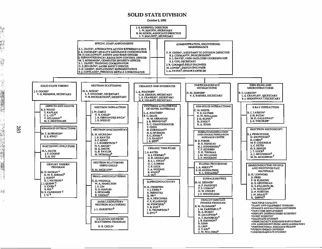
SOLID STATE DIVISION October 1,1393
J. B. ROBERTO, DIRECTOR L. W. HINTON, SECRETARY
R. M. MOON, ASSOCIATE DIRECTOR L. T. MALONE\ SECRETARY
SPECIAL STAFF ASSIGNMENTS
S. L. DAVIS*, AFFIRMATIVE ACTION REPRESENTATIVE J. Z. TISCHLER', QUALITY ASSURANCE COORDINATOR M. D. GALLOWAY*, SAFETY AND ES&H OFFICER J. FERNANDEZ-BACA*, RADIATION CONTROL OFFICER M. T. ROBINSON*, COMPUTER SECURITY OFFICER S. L. DAVIS*, TRAINING COORDINATOR G. E. JELLISON*, LASER SAFETY OFFICER P. H. GREEN*, EMPLOYMENT REPRESENTATIVE B. J. COPELAND*, PREaOUS METALS COORDINATOR
SOLID STATE THEORY
J.F.COOKE* V. G. HENDRIX, SECRETARY
NEUTRON SCATTERING
H.A.MOOK* L. F. MALONE*, SECRETARY T. H. RICHARDSON 3, SECRETARY
DEFECTS AND ALLOYS R. F. WOOD
T. KAPLAN C L . L I U 9
V.MILLMAN 9
M. E MOSTOLLER
ION-SOLID INTERACTIONS
M. T. ROBINSON* S. P. KING*
ELECTRONIC STRUCTURE
H. L. DAVIS J. F. COOKE* S.H.LIU
ORNL/UT THEORY PROGRAM
G . D . M A H A N 4
K. W. K. SHUNG 5
J. SOFO 9
G.I. WATSON 5 J.J.QUINN5
X . C H E N 5
XXIA^ G. S. CANRIGHT 5
J . Y I 6
ADMINISTRATION, ENGINEERING, MAINTENANCE
P. H. GREEN*, ASSISTANT TO DIVISION DIRECTOR B.J. COPELAND*, PROCUREMENT S. L. DAVIS*, USER FACILITIES COORDINATOR S. J. COX, SECRETARY
J. R. COOMBS1, HELD ENGINEER M. LOWER1, DESIGN ENGINEER I_ A. PAYNE 2, FINANCE OFFICER
CERAMICS AND INTERFACES
L. A. BOATNER* C H. ZEIGLER, SECRETARY L. S. CRAWLEY*, SECRETARY N. F. DELENE3, SECRETARY
NEUTRON DIFFRACTION
J. W. CABLE H. R. CHILD* J. A. FERNANDEZ-BACA* J. R. WEIR III
NEUTRON SPECTROMETRY
R. M. NICKLOW* J.B.HAYTER S. P. KING* J. L. ROBERTSON 9
H. A. MOOK* H. G. SMITH G. B. TAYLOR M. YETHIRAJ9
NEUTRON SCATTERING USERS GROUP
R. M. NICKLOW*
SMALL-ANGLE SCATTERING
G. D. WIGNALL W. A. HAMILTON J. S. LIN R. G. MAPLES S. SPOONER R. TRIOLO 7
PARTICLE-SURFACE INTERACTIONS
D. M. ZEHNER* V. E BARNES, SECRETARY
SYNTHESIS & PROPERTIES OF NOVEL MATERIALS
L. A. BOATNER* B. C SALES
M. M. ABRAHAM J. R. BREWSTER9
B. C CHAKOUMAKOS Y. CHEN D. CORRIGAN" H. E HARMON E C JONES' J. O. RAMEY 3
J. B. SIPF 6
CERAMIC THIN FILMS
J. B. BATES N.J.DUDNEY 3
G. R. GRUZALSKI B. S. L. KWAK 9
D. C LUBBEN C F. LUCK F. A. MODINE B. WANG 9
X . Y U 9
AMES LABORATORY NEUTRON SCATTERING
J. L. ZARESTKY 8
SUPERCONDUCTIVITY
D. K. CHRISTEN Y.J. CHEN 6 R. FEENSTRA Q.HE6 H. R. KERCHNER C E KLABUNDE M. KUNCHUR 9
Y. R. SUN 6
J. R. THOMPSON 3
S. ZHU 6
U.S.-JAPAN NEUTRON SCATTERING PROGRAM
H. R. CHILD*
THIN FILMS AND MICROSTRUCTURES
B. C LARSON* L. S. CRAWLEY*, SECRETARY B. J. SHOOPMAN ? SECRETARY
ION-SOLID INTERACTIONS C W. WHITE
T. E HAYNES O. W. HOLLAND J . D . H U N N 9
D . Z H O U 9
R. A. ZUHR
SURFACE MODIFICATION AND CHARACTERIZATION
RESEARCH CENTER D. B. POKER
D. K. HENSLEY H.J.HINNEBERG 5
T. P. SJOREEN D. K. THOMAS J. M. WILLIAMS S. P. WITHROW
PLASMA PROCESSING L. A. BERRY 1 0
S. M. GORBATKIN R. L. RHOADES 9
SURFACE PHYSICS D. M. ZEHNER*
A. P. BADDORF P. F. LYMAN 9
G. W. OWNBY J. F. WENDELKEN
X-RAY DIFFRACTION
B. C LARSON* J. D. BUDAI M. D. GALLOWAY* J. Z. TISCHLER*
ELECTRON MICROSCOPY
S.J.PENNYCOOK N. BROWNING 9
K. CHEN 9
M. F. CHISHOLM T. C ESTES D.EJESSON J. T. LUCK 3
A.J.MCGIBBON 9
M.M.MCGIBBON 9
ORNL/UT SURFACE PHYSICS PROGRAM
E W. PLUMMER4
J.M.CARPINELLI 6
H.A.DURR5 H. GRAUPNER 6
A.T.HANBECKI 6
J. B. H A N N O N 6
B.KIM6 G.LEE6 X Y. LIU 6
C W. WALTERS 6
SEMICONDUCTOR PHYSICS AND PHOTOVOLTAIC
MATERIALS D. H. LOWNDES
D.ERES P. H. FLEMING D. B. GEOHEGAN G . E JELLISON, JR. J. W. MCCAMY 6
D. P. NORTON J .W.SHARP 9
X. ZHENG 9
• MULTIPLE CAPACITY 1 PLANT AND EQUIPMENT DIVISION 'FINANCE AND MATERIALS DIVISION 'PART-TIME EMPLOYMENT •ORNIAJT DISTINGUISHED SCIENTIST 'GUEST SCIENTIST 'GRADUATE STUDENT JORISE FACULTY RESEARCH PARTICIPANT •ON ASSIGNMENT FROM AMES LABORATORY •POSTDOCTORAL RESEARCH FELLOW
"FUSION ENERGY DIVISION » UNDERGRADUATE STUDENT

Author Index
Abernathy, D. L—164 Abraham, A. A.—51,53,54,55,97, 98,99,196,
198 Aeppli, G.—49,50 Affholter, K. A.—31 Alamo, R. G.—26,29 Alexander, K. B.—39 Allen, P. B.—22 Allison, D. P.—173 Alp, E. E.—192 Anderson, T. A.—109 Armstrong, T.—50 Ashrad, A.—30 Aziz, M. J.—21 Baddorf, A. P.—163,166 Baker, S. M.—34 Balcerzyk, M—95 Ballesteros, C—100,104,105 Barbour, J. C—118 Baribeau, J.-M.—185,186,190,191 Barnard, J. C—169 Barnes, T.—11 Barrett, J. H.—160 Bartges, C. W.—32,33 Bass, J. M—15 Bates, F. S.—28 Bates, J. B.—70, 71, 72,73,74, 75,76,78 Beaucage, G—33 Becher, P. F.—39 Bednarczyk, P. J.—62 BentleyJ.—114,115 Berman, E.—95 Berry, L. A.—117 Blackman, J. A.—15 Boatner, L. A.—51,53,54,55,79,80,81,82,83,
84,85,86,87, 88,89,91,93,94,95,97,98, 99,121,147,173,196,197,198
Boothroyd, A. J.—30 Braun, W.—83,196 Brenier, R—121 Brewster, J. R.—89 Brow, R. K.—33 Browning, N. D.—176,178,179,181,182 Brynestad, J.—61,63
Budai, J. D.—66,67,68,80,83,89,108,110, 111, 112,125,143,144,146,186,189,190,191, 193,194,195,196,200
Bunick, G. J.—31 Burgie, R. F.—118 Burke, H. H.—150 Butler, P. D.—34 Cable,J .W.-^0,41,46 Canright, G. S.—5,11,18 Canut, B.—121 Chakoumakos, B. C—59,60,63, 73, 91, 92,143,
144,145,146,173,193,194,196 Chao, B. S.—195 Chen, D. H.—197 Chen, K. M.—187 Chen, Ximing—19 Chen, Y. J.—65 Chen, Y.—100,102,103,104,105 Chen, Yi—104 Chisholm, M. F.—6, 80,126,149,175,176,178,
179,181,182 Chou, H.—197 Christen, D. K.—58,59, 60,61,62,63,64,65,
66,67, 68,144,146,193,194,195 Civale, L.—58,59,60,64 Clausing, R. E.—114,115 Compton, R. N—31,138 Cooke, J. F.—15,17,17 Crawford, M. K—39 Cubitt, R.—44,45 David, S. A.—35,93,94 DeSilva,M.—155 de la Cruz, R. M.—102 DeLuca, J. A.—62 DiAntonio, P.—84 Dudney, N. J.—70,75, 77, 78 Diirr, H.—160,166 Edelson, L. H.—33 Edelstein, N. M.—54,55,97,98,99 Erbil, A.—80,81,82, 83,196 Eres, G.—20,136,137 Estes, T. C—187 Feenstra, R.—58,66,67,143,193,194,195 Feng, Z. C—81,82 Fernandez-Baca, J. A.—36,39,42,43,48,196 Fiory, A. T.—153
285

286
Fishman, R. S.—15 Forgan, E. M.—44,45 Funahashi, S.—43 Gallagher, K. F.—27 Gea, L.—121 Gehlsen, M. D.—28 Gehring, P. M.—197 Gellerman, W.—100 Geohegan, D. B.—10,138,139,141,155 Gibbs, Doon—163,164 Godbole, M. J.—147,154,155,156 Gonzalez, R.—100,102,103,104,105 Goodman, G. L.—51 Goodrich, R. G.—156 Gorbatkin, S. ML—20,117,118,119,149 Goyal, A.—65 Graupner, H.—162 Gray, L. J.—21 Grenier, P.—85 Griibel, G.—164 Gruzalski, G. R.—70, 71,72 Haglund, R. F.—108,112 Hamilton, W. A.—34 Hammer, L.—162 Hammonds, J. P.—55 Hannon, J. B.—167 Hanrahan, R. J.—131 Harlow, R. L.—39 Haufler, R. E.—31,138 Hayden, S. M.—49 Haynes, T. E.—113,122,123,150 Hayter, J. B.—34 Heatherly, L.—114,115 Helgesen, G.—163 Hembree, D. M., Jr.—110, 111, 114,115,189 Henderson, S. J.—31 Henkel, G. H.—117 Hensley, D. K.—112 Hettich, R. L.—138 Hinneberg, H.-J.—126 Hock, K. M.—169 Holland, O. W.—124,125,130 Holtzberg, F.—59,64 Houde, D.—85 Houghton, D. C—185,186,190,191 Hriljac, J. A.—197 Hrubesh, L.—33 Hubbard, C. R.—35,39 Hunn, J. D.—114,115 Hunt, M. R. C.—169 Huynh-Ba, G.—27 Ice, G. E.—200 Ikeda, H . - 4 8 Iwasa, K.—48
Jandl, S.—85,87 Jebasinski, R.—175,176 Jellison, Jr., G. E.—20,101,135,147,148,149,
150,151,152,153,154 Jesson, D. E.—12,183,184,185,186,187,190,
191 Johnston, D. C—39,42 Jones, E. C.—66,67,144,146,193,194 Jones, K. S.—113 Kanai, M.—67 Kaplan, Theodore—6,8,21 Karas, P. L.—62 Karimi, M.—8 Kawai, S.—8 Kawai, T.—67,194 Keefer,M.—151 Kerchner, H. R.—58,59, 60,62,68 Kes, P. H.—44 Klabunde, C. E.—58,62, 68 Klemm, R. A.—2 Koga, K—43 Kokta, M. R.—105 Kot, W. K.—98,99 Kunchur, M. N.—64 Kwak, B. S.—73, 74, 75,76,80,81, 82, 83,196 Larson, B. C—192,200 Lau, S. S.—123 Lay, K. W.—59 Leboeuf, J.-N. G.—10 Lee, C—113 Lee, M. H.—12 Lee, S. L.—44,45 Lempicki, A.—95 Li, T. W.—44 Li, X.—67 Lin, J. S.—27,30,33 Liu, Benjamin—8 Liu, C.-L.—10 Liu, H.—86,100 Liu, S. H.—2,15,17 Liu, Y. -J.—104 Londono, J. D.—26,29 Loong, C.-K.—51,53,54,55 Lowndes, D. H.—66,68,132,133,134,135,142,
144,145,146,147,154,155,156 Lubben, D.—78 Luck, C. F.—70 Lyman, P. F.—170,171,172 Magid, L. J.—34 Magruder, R. A.—108,110, 111, 112 Magruder, R. H., Ill—109 Mahan, G. D.—4,5,21,22,23 Malozemoff, A. P.—64 Mandelkern, L.—26,29
287
Mantl, S.—175,176 Marwick, A. D.—59,60,64 Mason,T. E—49,50 Mayer, T. M—118 McCaUumJ.C—112 McCamy, J. W.—132,133,134,135 McElfresh, M. W.—64 McGibbon, A. J.—174 McGibbon, M. M.—181 McKee, R. A.—147 Mele, E. J.—167 Menchhofer, P. A.—20 Milman, V.—12,14 Mochrie, S. G. J.—163,164 Modine, F. A.—78,101 Mook, H. A.—44,45,49,50 Moorehead, A. J.—20 Mori, N.—43 Mortensen, K.—44 Morton, R.—123 Mostoller, Mark—6,8 Miiller, K.—162 Mullins, D. R.—171,172 Nicklow, R. M.—47,48 Norton, D. P.—68,142,143,144,182,193,194,
195 Oliver, B. J.—33 Oliver, W. C—118 Ossandon, J. G.—59,63,67 Overbury, S. H.—171 Paine, D. C—122,189 Palmer, R. E.—169 Paranthaman, M.—61,63 Pareja, R.—102,103 Parikh, N. R.—114,115 Paul, D. Mck.—44,45 Payne, M. C—12,14 Pedraza, A. J.—155 Pennycook, S. J.—12,67,110, 111, 145,174,
175,176,178,179,181,182,183,184,185, 186,187,189
Pfeiffer, R. S.—23 Phillips, J. M.—58,64,66,67 Piehler, D.—97 Plummer, E. W.—120,167 Pogany, A.—112 Poker, D. B.—120,127,129,160 Powell, R. C—86 Prusseit, W—79 Puretzky, A. A.—138 QuinnJ.J.—19 Radhakrishna, P.—41,46 Ramey,J.O.—91 Ramiraz, A. P.—49
Ramos, S. M. M.—121 Rankin, J.—88,121 Rappaz, M.—94 Rasolt, M.—8 Reeves, R. J.—86 Rennie, A. R.—30 Rhoades, R. L.—117,119 Rieker, T.—33 Riester, L.—128 Ristolainen, E.—131 Robertson, J. L.—37, 75 Robinson, Mark T.—10 Rojo, A. G—23 Romana, L.—121 Rosenblatt, G. H.—100 Rosseel, T. M.—134 Rousseau, J.—87 Roy, P. K.—153 Runt, J. P.—27 Rytz, D.—79,197 Sales, B. C.—59,60, 73, 74,91,92,173 Sameth, R. L.—167 Satkowski, M. M—30 Schaefer, D. W.—33 Shapiro, S. M—197 Sharp, J. W.—136,137 Shigesato, Yuzo—122 Shuh, D. K.—198 Siegal, M. P.—66, 67 Siller, L.—169 Sjoreen, T. P.—126,130 Smith, G. S.—34 Smith, H. G.—37 Smith,S. D—30 Soderholm, L.—51,53,54,55 Sofo, J. O.—5 Sparks, C. J. —200 Specht, E.—200 Spontak, R. J.—30 Spooner, Steve—32,35,36 Steadman, G. W—89 Stehling, F. C.—26,29 Stich, I.—12 Subramanian, M. A.—39 Sun, Y. R.—59,60,61,63,64,65, 67 Sytsma, J.—97 Takahashi, M.—48 Terminello, L. J.—198 Thevenard, P.—121 Thomas, D. K.—112,125 Thomas, M. L.—118 Thompson, J. R.—58,59,60,61,63,64,65,66,
67 Thomson, J. O.—60,68
288
Thornquist, L.—151 Thundat, T.—173,187 Tischler, J. Z.—186,190,191,192,200 TkaczykJ. E.—59,62 Toulouse, J.—84,197 Tsunoda, Y.—40 Tzeng, S. Y.—33 Vaknin, D.—42 Verink, Jr., E. D.—131 VitekJ.M.—94 Vugmeister, B. E.—84 Wakabayashi, N.—41,46,47 Walters, C. F.—120 Wang, B.—73,74 Wang, Xun-Li—35,39,42 Wang, Z. R.—39,42 Warmack, R. J.—145,146,173,187 Wasilewski, Z.—174 Watson, G. M.—5,164 Wendelken, J. F.—165,169 Westbrook, R. D.—20 White, C. W.—108,110, 111, 112,114,115,130,
189 Wignall, G. D.—26,28,29,30,31 Wilkens, B. J.—80,83,196 Williams, J. M.—128,129 Williams, R. T.—100 Wilson, S. R.—130 Winkler, B.—14 Withrow, S. P.—110, 111, 114,115,131,189 WittigJ.E.—109 Wojtowicz, A. J.—95 Wood, R. F.—3,10,20 Wylie, M . - ^ 4 Xia, X.—19 Xie, Ling—124 XueJ.S.—53 Yang, L.—112 Yethiraj, M.-44,45,50 Yi, Jaichul—18 Yoon, M.—164 Young, R. T.—195 Yu, Xiaohua—70 Zacharia, T.—94 Zehner, D. M.—120,160,161,162,163,164,170 Zhang, X.—11,27 Zheng, X. -Y.—138,145,146 Zhou, D. S.—108,125,127 Zhu, S.—58,66,145,146 Zong, X. -F.—104 Zschack, P.—190,191 Zuhr, R. A.—75,76,108,109 Zuo, J.-K.—161,165
ORNL-6816 Distribution Category UC-404
Internal Distribution 1. M. Abdel-Raouf 58. G. G. Fee 2. M. M. Abraham 59. R. Feenstra 3. K. Affholter 60. R. E. Fenstermaker 4. B. R. Appleton 61. J. A. Fernandez-Baca 5. A. P. Baddorf 62. P. H. Fleming 6. J. B. Ball 63. W. Fulkerson 7. V. E. Barnes 64. M. D. Galloway 8. J. B. Bates 65. L. Gea 9. P. F. Becher 66. R K. Genung
10. B. A. Berven 67. D. B. Geohegan 11. L. E. Berry 68. H. A. Glovier 12. T. M. Besmann 69. S. M. Gorbatkin 13. E. E. Bloom 70. C. A. Grametbauer 14. P. J. Blau 71. H. Graupner
15-19. L. A. Boatner 72-76. P. H. Green 20. N. Browning 77. G. R. Gruzalski 21. J. D. Budai 78. W. A. Hamilton 22. G. J. Bunick 79. A. T. Hanbicki 23. W. H. Butler 80. J. B. Hannon 24. J. W. Cable 81. H. E. Harmon 25. J. Canright 82. F. C. Hartman 26. J. M. Carpinelli 83. T. E. Haynes 27. R. S. Carlsmith 84. J. B. Hayter 28. B. C. Chakoumakos 85. Q. He 29. S. S. Chandavarkar 86. V. G. Hendrix 30. Kerning Chen 87. D. K. Hensley 31. KunChen 88. J. N. Herndon 32. Y. Chen 89-93. L. W. Hinton 33. Y-J. Chen 94. O. W. Holland 34. M. F. Chisholm 95. R. B. Honea 35. D. K. Christen 96. S. Hong
36-40. J. F. Cooke 97. J.Hunn 41. B. J. Copeland 98. L. L. Horton
42-46. S. J. Cox 99. D. W. Jared 47: D. F. Craig 100. G. E. Jellison, Jr. 48. L. S. Crawley 101. D. E. Jesson 49. S. A. David 102. E. Jones 50. H. L. Davis 103. J. E. Jones, Jr. 51. N. F. Delene 104. T. Kaplan 52. E. R. DuBose 105. H. R. Kerchner 53. N. J. Dudney 106. B. Kim 54. L. B. Dunlap 107. Y.Kim 55. A. Eguiluz 108. S. P. King 56. D. Eres 109. P. W. King 57. T. C. Estes 110. C. E. Klabunde
289
290
111. F. C. Kornegay 215. B. J. Shoopman 112. E. H. Krieg 216. W. D. Shults 113. M. N. Kunchur 217. W. D. Siemens 114. B. S. Kwak 218. T. P. Sjoreen
115-119. B. C. Larson 219. E. J. Soderstrom 120. G.Lee 220. S. Spooner 122. R. P. Leinius 221. J. O. Stiegler 123. J. S. Lin 0 222. A. K. Swan 124. F.Liu 223. J. H. Swanks 125. S. H. Liu 224. G. B. Taylor 126. X.-Y. Liu 225. V. J. Tennery 127. D. H. Lowndes 226. D. K. Thomas 128. D. C. Lubben 227. J. R. Thompson 129. C. F. Luck 228. J. Z. Tischler 130. J. T. Luck 229. A. W. Trivelpiece 131. G. D. Mahan 230. R. I. Van Hook 132. L. F. Malone 231. A. Van Zomeron 133. L. K. Mansur 232. C. Walters 134. R. G. Maples 233. B. Wang 135. F. A. Modine 234. R. C. Ward
136-140. H . A . M o o k J r . 235. D. A. Waters 141-145. R. M. Moon, Jr. 236. G. I. Watson
146. M. E. Mostoller 237. J. R. Weir III 147. R. M. Nicklow 238. H. Weitering 148. D. P. Norton 239. J. F. Wendelken 149. G. E. Oliphant 240. C. D. West 150. C. E. Oliver 241. C. W. White 151. C. C. Overbey 242. G. E. Whitesides 152. S. H. Overbury 243. G. D. Wignall 153. G. W. Ownby 244. M. K. Wilkinson 154. S. J. Pennycook 245. J. M. Williams 155. E. W. Plummer 246. S. P. Withrow 156. K. Pohl 247. R. F. Wood 157. D. B. Poker 248. M. Yethiraj 158. M. L. Poutsma 249. X.Yu 159. J.J.Quinn 250. J. L. Zarestky 160. J. O. Ramey 251-255. D. M. Zehner 161. D. E. Reichle 256. C. H. Zeigler 162. R.L. Rhoades 257. S. Zhu 163. J. B. Richard 258. R. A. Zulu-164. T. H. Richardson 259. Biology Library 165. C. R. Richmond 260-264. Central Research Library
166-205. J. B. Roberto 265. ORNL Y-12 Technical Library 206. J. L. Robertson 266. Document Reference Section 207. M. T. Robinson 267-268. Laboratory Records Department 208. T. H. Row 269. Laboratory Records, ORNL-RC 209. B. C. Sales 210. M. J. Saltmarsh 211. A. C. Schaffhauser 212. J. W. Sharp 213. J. Sheffield 214. R. B. Shelton
291
External Distribution 270. Dr. A.A.Z. Ahmad, Chief Scientific Officer, Institute of Nuclear Science and Technology,
Atomic Energy Research Establishment, Ganakbari, Savar, Dhaka, G.P.O. Box 3787, Dhaka, Bangladesh
271. Dr. Craig Allison, Department of Physics, Oklahoma State University, Stillwater, OK 74078
272. Dr. S. Amelinckx, SCK/CEN, B 2400-Mol, Belgium 273. Dr. Rosalia N. Andrews, School of Engineering, University of Alabama at Birmingham,
University Station, Birmingham, AL 35294 274. Dr. R. R. Arons, Institut fur Festkorperforschung, Forschungszentrum, Postfach 1913,
D-5170, Jiilich, Germany 275. Dr. Neil W. Ashcroft, Laboratory of Atomic and Solid State Physics, Clark Hall, Cornell
University, Ithaca, NY 14853-2501 276. Prof. Frank Avignone, Chairman, Department of Physics, University of South Carolina,
Columbia, SC 29208 277. Dr. John Axe, Associate Director, Brookhaven National Laboratory, Upton, NY 11973 278. Dr. Michael J. Aziz, Department of Applied Science, Harvard University, Cambridge, MA
02138 279. Dr. K. J. Bachmann, Department of Chemistry, North Carolina State University, Box 5247,
Raleigh, NC 27650 280. Dr. R. W. Balluffi, Department of Materials Science and Engineering, Massachusetts
Institute of Technology, 77 Massachusetts Avenue, Cambridge, MA 02139 281. Dr. J. H. Barrett, 827 W. Outer Drive, Oak Ridge, TN 37830 282. Dr. F. S. Bates, 151 Amundson Hall, Department of Chemical Engineering, University of
Minnesota, Minneapolis, MN 55455 283. Prof. Boris W. Batterman, Applied and Engineering Physics, 227 Clark Hall, Cornell
University, Ithaca, NY 14853 284. Dr. Walter Bauer, Physical Research Division, Department 8340, Sandia National
Laboratories, P.O. Box 969, Livermore, CA 94550 285. Dr. Rainer Behrisch, Max-Planck-Institut fur Plasmaphysik, D-8046 Garching bei Munchen,
Germany 286. Dr. Ronald R. Berliner, Dept. of Physics, University of Missouri, Research Reactor Facility,
Columbia, MO 65211 287. Bibliotheque, Institut Max von Laue-Paul Langevin, 156 X 38042 Grenoble, Cedex, France 288. Dr. A. I. Bienenstock, Stanford Synchrotron Radiation Laboratory, Stanford University, P.O.
Box 4349, Bin 69, Stanford, CA 94305 289. Prof. H. Birnbaum, University of Illinois, Materials Research Laboratory, 104 South
Goodwin, Urbana, IL 61801 290. Dr. N. Bloembergen, Gordon McKay Laboratory, 9 Oxford Street, Cambridge, MA 02138 291. Dr. M. Blume, Brookhaven National Laboratory, Upton, NY 11973 292. Dr. Dawn Bonnell, Department of Materials Science, University of Pennsylvania, 3231
Walnut Street, Philadelphia, PA 19104 293. Dr. J. L. Boldu O., Instituto de Fisica, Universidad Nacional Autonoma de Mexico, Apartado
Postal 20-364, 01000 Mexico, D.F. 294. Dr. William F. Brinkman, Room 1C-224, AT&T Bell Laboratories, 600 Mountain Avenue,
Murray Hill, NJ 07974

292
295. Dr. Bruce Brown, PNS-372, Argonne National Laboratory, 9700 South Cass Avenue, Argonne, IL 60439
296. Dr. F. C. Brown, Department of Physics, University of Illinois, Urbana, IL 61801 297. Dr. Walter Brown, Room IE-452, AT&T Bell Laboratories, 600 Mountain Avenue, Murray
Hill, NJ 07974 298. Dr. Christoph J. Buchal, Kernforschungsanlage, Postfach 1913, 5170 Julich 1, Germany 299. Dr. R. Bullough, Atomic Energy Research Establishment, Harwell, Didcot, Oxon OXll ORA,
United Kingdom 300. Dr. John L. Burnett, Division of Chemical Sciences, ER-142, Office of Basic Energy Sciences,
Office of Energy Research, Department of Energy, Washington, DC 20585 301. Prof. W.J.L. Buyers, Atomic Energy of Canada Limited, Chalk River Nuclear Laboratories,
Chalk River, Ontario KOJ 1JO, Canada 302. Prof. Nicolas Cabrera, Departamento de Fisica Fundamental, Facultad de Ciencias,
Universidad Autonoma de Madrid, Canto-Bianco, Madrid 34, Spain 303. Prof. Robert W. Cahn, Department of Materials Science and Metallurgy, Cambridge
University, Pembroke Street, Cambridge CB2 3Q2, United Kingdom 304. Dr. J. M. Carpenter, Argonne National Laboratory, 9700 South Cass Avenue, Argonne, IL
60439 305. Prof. Ray W. Carpenter, Center for Solid State Science, Arizona State University, Tempe,
AZ 85287 306. Prof. Bruce H. T. Chai, University of Central Florida, CREOL, 12424 Research Parkway,
Suite 400, Orlando, FL 32826 307. Dr. R. L. Chaplin, Department of Physics, Clemson University, Clemson, SC 29631 308. Prof. Girish Chandra, Tata Institute of Fundamental Research, National Centre of the
Government of India for Nuclear Science and Mathematics, Homi Bhabha Road, Colaba, Bombay 400 005, India
309. Dr. Lloyd Chase, MS L-490, Lawrence Livermore National Laboratory, P.O. Box 808, Livermore, CA 94550
310. Dr. Andre Chatelain, Lab. Phys. Exp., Federal Institute of Technology, PH Ecublens, 1015 Lausanne, Switerland
311. Dr. D. S. Chemla, Lawrence Berkeley Laboratory, MS-66,1 Cyclotron Road, Berkeley, CA 94720
312. Dr. W. J. Choyke, Westinghouse R&D Center, 1310 Beulah Road, Pittsburgh, PA 15235 313. Dr. Wei-Kan Chu, Texas Center for Superconductivity, University of Houston, Science and
Research 1, Houston, TX 77204-5506 314. Dr. C. B. Clark, Department of Physics, University of North Carolina, Greensboro, NC 27412 315. Francisco H. Claro, Catholic University of Chile, Casilla 6177, Santiago, Chile 316. Dr. Frank Clinard, MS-546, Los Alamos National Laboratory, Los Alamos, NM 87545 317. Prof. Marvin Cohen, Department of Physics, University of California, Berkeley, CA 94720 318. Dr. Morrel H. Cohen, Corporate Research Science Laboratories, Exxon Research and
Engineering Company, Clinton Township, Route 22 East, Annandale, NJ 08801 319. Mr. Ralph R. Coltman, Jr., 7905 Wiebelo Drive, Knoxville, TN 37931 320. Prof. James W. Corbett, Department of Physics, State University of New York at Albany,
Albany, NY 12222 321. Dr. Roger A. Cowley, Department of Physics, Clarendon Laboratory, University of Oxford,
Parks Road, Oxford, OX1 3PU, United Kingdom 322. Dr. Juan C. Crespi, Comision Nacional de Energia Atomica, Gerencia Desarrollo-Dto.
Materiales, Avenida del Libertador 8250,1429 Buenos Aires, Argentina 323. Dr. Peter A. Curreri, NASA, Mail Code ES74, Space Science Laboratory, George C. Marshall
Space Flight Center, AL 35806 324. Dr. Gordon Czjzek, Kernforschungszentrum Karlsruhe, INFP, Postfach 3640, D-7500
Karlsruhe 1, Germany
293
325. Dr. L. S. Darken, Tennelec, Inc., 601 Oak Ridge Turnpike, Oak Ridge, TN 37830 326. Dr. Lubomir David, Director, Centro de Fisica, Instituto Venezolano de Investigaciones
Cientificas (IVIC), Apartado 1827, Caracas 1010-A, Venezuela 327. Dr. Robert F. Davis, Department of Materials Science & Engineering, North Carolina State
University, Box 7907, Raleigh, NC 27695 328. Prof. Dr. P. H. Dederichs, Institut fur Festkorperforschung der Forschungszentrum Julich
GmbH, Postfach 1913,5170 Julich 1, Germany 329. Dr. Adriaan M. de Graaf, Division of Materials Research, National Science Foundation,
1800 G Street NW, Washington, DC 20550 330. Dr. J. Diehl, Max-Planck-Institut fur Metallforschung, Institut fur Werkstoffwissen-
schaften, Sestrasse 92/BRD, D-7000 Stuttgart 1, Germany 331. Dr. J. Dienes, Department of Physics 510B, Brookhaven National Laboratory, Upton, NY
11973 332. Prof. Dr. H.-D. Dietze, Institut fur Theoretische Physik C, RWTH Aachen, 5100 Aachen,
Germany 333. Dr. Sam Divita, U.S. Army Communications, Electronics Command, AMSEL-COM-RM1,
Fiber Optics Team, Ft. Monmouth, NJ 07703 334. Dr. G. Dolling, Atomic Energy of Canada Limited, Chalk River Nuclear Laboratories,
Chalk River, Ontario KOJ 1JO, Canada 335. Dr. Mildred Dresselhaus, Rm. 13-2090, Massachusetts Institute of Technology, Cambridge,
MA 02139 336. Dr. C. B. Duke, Xerox Webster Research Center, 800 Phillips Rd 0114-38D, Webster, NY
14850 337. Dr. B. D. Dunlap, Argonne National Laboratory, MSD-212, 9700 South Cass Avenue,
Argonne, IL 60439 338. Dr. Robert C. Dynes, Department of Physics, 0319, University of California-San Diego,
La JoUa, CA 92093 339. Dr. Dean E. Eastman, Vice-President of Logic, Memory, and Packaging, International
Business Machines Corporation, P.O. Box 218, Yorktown Heights, NY 10598 340. Dr. Norman Edelstein, MMRD/Bldg. 70A/Room 1115, Lawrence Berkeley Laboratory,
Berkeley, CA 94720 341. Prof. Henry Ehrenreich, Division of Engineering and Applied Physics, Pierce Hall 205A,
Harvard University, Cambridge, MA 02138 342. Dr. Vic Emery, Department of Physics, Brookhaven National Laboratory, Upton, NY 11973 343. Dr. Ahmet Erbil, School of Physics, Georgia Institute of Technology, 225 North Avenue,
Atlanta, GA 30332-0430 344. Prof. T. L. Estle, Physics Department, Rice University, Houston, TX 77001 345. Dr. Peder J. Estrup, Department of Physics, Brown Uruversity, Providence, RI02912 346. Dr. R. C. Ewing, Department of Geology, University of New Mexico, Albuquerque, NM 87131 347. Ms. Harriet L. Fadem, Librarian, National Synchrotron Light Source, Brookhaven National
Laboratory, Upton, Long Island, NY 11973 348. Dr. G. C. Farlow, Physics Department, Wright State University, Dayton, OH 45435 349. Dr. G. C. Farrington, Department of Materials Science and Engineering, University of
Pennsylvania, 3231 Walnut Street, LSRM Building K-l, Philadelphia, PA 19104 350. Prof. Robert S. Feigelson, Center for Materials Research, Stanford University, 105
McCullough Building, Stanford, CA 94305 351. Dr. Jack Feinberg, Department of Physics, SSC-421, University of Southern California, Los
Angeles, CA 90089-0484 252. Dr. Martin M. Fejer, Ginzton Laboratory, Stanford University, Stanford, CA 94305 353. Dr. G. P. Felcher, Argonne National Laboratory, 9700 South Cass Avenue, Argonne, IL 60439 354. Dr. Trevor R. Finlayson, Department of Physics, Monash University, Clayton, Victoria,
3168, Australia
294
355. Mr. David Fitzgerald, President, Tennessee Innovation Center, Inc., 120 Badger Avenue, P.O. Box 607, Oak Ridge, TN 37830
356. Dr. Robert Fleischer, General Electric Research & Development Center, P. O. Box 8, Schenectady, NY 12301
357. Dr. M. Fluss, Lawrence Livermore National Laboratory, L-326, P. O. Box 808, Livermore, CA 94550
358. Dr. C. Peter Flynn, Materials Research Laboratory, University of Illinois, 104 S. Goodwin, Urbana, IL 61801
359. Dr. F. Y. Fradin, Associate Laboratory Director for Physical Sciences, Argonne National Laboratory, Building 221,9700 South Cass Avenue, Argonne, IL 60439
360. Prof. Dr. Werner Frank, Max-Planck-Institut fur Metallforschung, Institut fur Physik, Heisenbergstrasse 1, D-7000, Stuttgart 80, Germany
361. Dr. Larry Franks, EG&G/EM Santa Barbara Operations, 130 Robin Hill Road, Goleta, CA 93117
362. Dr. Roger Freeh, Department of Chemistry, University of Oklahoma, Norman, OK 73019 363. Prof. Arthur Freeman, Physics Department, Northwestern University, Evanston, IL 60201 364. Dr. Roger H. French, Central Research & Development Department, E.I. du Pont de Nemours
& Co., Experimental Station, E356-323, Wilmington, DE 19898 365. Dr. J. Friedel, Physique des Solides, Universite Paris Sud, 91405 Orsay, France 366. Dr. A. T. Fromhold, Department of Physics, Auburn University, Auburn, AL 36849 367. Dr. Noboru Fukuoka, Division of Science, Naruto University of Teacher Education, Naruto,
Tokushima 772, Japan 668. Dr. Y. Fujii, Institute of Solid State Physics, University of Tokyo, Roppongi Minato-ku,
Tokyo 106, Japan 369. Dr. S. Funahashi, Japan Atomic Energy Research Institute, Tokai-mura, Naka-gun, Ibaraki-
ken, Japan 370. Dr. B. Gaulin, McMaster University, Dept. of Physics, 1280 Main Street West, Hamilton,
Ontario, L8S 4M1, Canada 371. Dr. J. F. Gibbons, Stanford Electronics Laboratories, McCullough 220, Stanford University,
Stanford, CA 94305 372. Dr. Doon Gibbs, Brookhaven National Laboratory, Upton, NY 11973 373. Dr. Jill Glass, Sandia National Laboratories, Dept. 1845, P. O. Box 5800, Albuquerque, NM
87185-5800 374. Prof. Martin Glicksman, Rensselaer Polytechnic Institute, Materials Research Center, Troy,
NY 12181 375. Dr. A. N. Goland, Associate Chairman for Energy Sciences, Department of Applied Sciences,
Bldg. 179A, Brookhaven National Laboratory, Upton, NY 11973 376. Dr. A. Golanski, C.N.E.T.-R.P.T., B.P. 98, 38240 Meylan, France 377. Prof. Roberto Gonzalez, Dept. de Fisica del Estado Solido, Facultad de Ciencias Fisica,
Universidad Compulutense 28040, Madrid, Spain 378. Dr. R. Gotthardt, Ecole Polytechnique Federale de Lausanne, Dept. de Physique, CH-1015
Lausanne, Switzerland 379. Dr. R. J. Gottschall, Metallurgy & Ceramics Branch, Division of Materials Sciences, Office
of Basic Energy Sciences, ER-131, Washington, D.C. 20585 380. Dr. M. Guinan, Lawrence Livermore National Laboratory, P.O. Box 808, Livermore, CA 94550 381. Dr. Mark Hagen, Neutron Division, Rutherford Appleton Laboratory, Chilton, Didcot
OXON OX11 OQX, United Kingdom 382. Prof. Richard F. Haglund, Jr., Dept. of Phys. & Astronomy, Vanderbilt University,
Nashville, TN 37235 383. Dr. Carol A. Handwerker, Metallurgical Processing Group, Metallurgy Division, National
Bureau of Standards, Gaithersburg, MD 20899 384. Dr. B. N. Harmon, Ames Laboratory, Iowa State University, Ames, LA 50011
295
385. Dr. Craig S. Hartley, Department of Materials Engineering, University of Alabama at Birmingham, Birmingham, AL 35294
386. Dr. Werner Heiland, Fachbereich Physik, Universitat Osnabriick, Postfach 4469, D-4500 Osnabruck, Germany
387. Prof. Larry Hench, University of Florida, Advanced Materials Research Ctr., One Progress Blvd., #14, Alachua, FL 32615
388. Dr. Jim Herrington, Science & Technology, 11845 Forestgate Drive, Dallas, TX 75243 389. Dr. T. J. Hicks, Department of Physics, Monash University, Clayton, Victoria, Australia
3168 390. Dr. W. O. Hofer, Forschungszentrum, Postfach 1913, D-5170, Julich, Germany
391-395. Dr. William A. Hoffman, Jr., Director, Oak Ridge Science Semester, GLCA, Denison University, Main Street, Granville, OH 43023
396. Dr. P. H. Holloway, Department of Materials Sciences and Engineering, University of Florida, Gainesville, FL 32601
397. Dr. Marc Hou, Physique des Surfaces, Faculte des Sciences, Universite Libre de Bruxelles, Campus de la Plaine (C.P. 234), Boulevard de Triomphe, B-1050 Bruxelles, Belgium
398. Dr. John J. Hren, North Carolina State University, Raleigh, NC 27607 399. Dr. A. E. Hughes, Materials Development Division B552, Atomic Energy Research
Establishment, Harwell, Didcot, Oxon OX11 ORA, United Kingdom 400. Dr. Tom Hutchinson, A114 Thornton Hall, University of Virginia, Charlottesville, VA
22901 401. Prof. Daryush Ila, Dept. of Physics, Alabama A&M University, 4900 Meridian St., Normal,
AL 35762 402. Dr. M. Iizumi, Deputy Director General, Tokai Research Establishment, Japan Atomic
Energy Research Institute, Tokai-mura, Naka-gun, Ibaraki-ken, Japan 403. Dr. Tadao Iwata, Division of Physics, Japan Atomic Energy Research Institute, Tokai-mura,
Naka-gun, Ibaraki-ken 319-11, Japan 404. Dr. Vincent Jaccarino, Department of Physics, University of California, Santa Barbara, CA
93106 405. Dr. Leslie H. Jenkins, 817 Whirlaway Circle, Knoxville, TN 37923 406. Ms. Beth Jinkerson, University Programs Division, Oak Ridge Associated Universities, P.O.
Box 117, Oak Ridge, TN 37830 407. Dr. A. Wayne Johnson, Division 5126, Sandia National Laboratories, Albuquerque, NM
87185 408. Dr. R. H. Jones, P8-15, Pacific Northwest Laboratory, P. O. Box 999, Richland, WA 99352 409. Dr. Pierre H. Jourde, Charge du Centre d'Information sur les Dechets Nucleaires,
CEA/DCAEA/CIDN, CEN/CADARACHE, B.P. 1, F 13115 Saint Paul lez Durance, France 410. Dr. W. A. Kamitakahara, Division of Materials Sciences, Office of Basic Energy Sciences,
Office of Energy Research, ER-132, Department of Energy, Washington, DC 20585 411. Dr. Takuji Kaneda, Research Laboratories, Ashigara, Fuji Photo Film Company, Ltd.,
Minami-Ashigara, Kanagawa, 250-01 Japan 412. Dr. S. Katano, Japan Atomic Energy Research Institute, Tokai-mura, Naka-gun,
Iboraki-ken, Japan 413. Dr. Elton N. Kaufmann, Building 207 (TTC), Argonne National Laboratory, 9700 South Cass
Avenue, Argonne, IL 60439 414. Dr. Shinji Katano, Research Reactor Institute, Kyoto University, Kumatori, Sennan, Osaka
590-04, Japan 415. Dr. Fred Keller, Department of Physics, Clemson University, Clemson, SC 29631 416. Dr. Richard D. Kelley, Division of Materials Sciences, Office of Basic Energy Sciences,
Office of Energy Research, ER-132, Department of Energy, Washington, DC 20585 417. Dr. Q. H. Khan, N.P.D., PINSTECH, P.O. Nilore, Rawalpindi, Pakistan
296
418. Prof. Angus Kingon, North Carolina State University, Dept. of Mats. Sci. & Engrg., P. O. Box 7919, Raleigh, NC 27695-7919
419. Dr. Donald L. Kinser, Vanderbilt University, 610 Olin Hall, Box 1689-B, Nashville, TN 37235
420. Dr. J. K. Kjems, Rise National Laboratory, DK-4000 Roskilde, Denmark 421. Dr. J. S. Koehler, Physics Department, University of Illinois, Urbana, IL 61801 422. Prof. Walter Kohn, Physics Department, University of California, Santa Barbara, CA 93106 423. Dr. Daniel E. Koshland, Jr., Editor, Science, 1515 Massachusetts Avenue N.W., Washington,
DC 20005 424. Prof. Eckhard Kratzig, Universitat Osnabriick, Fachbereich Physik, Postfach 4469, 4500
Osnabriick, Germany 425. Prof. J. Kubler, Theoretische Physik, Institut fur Festkorperphysik, Technische Hochschule
Darmstadt, Hochschulstrasse 2, 6100 Darmstadt, Germany 426. Prof. Stewart K. Kurtz, Materials Research Laboratory, The University of Pennsylvania,
University Park, PA 16802 427. Dr. Gerard H. Lander, Tu-Euratom, Postfach 2340, D7500, Karlsruhe, Germany 428. Dr. S. S. Lau, Department of EECS, C-014, University of California at San Diego, La Jolla,
CA 92093 429. Dr. R. A. Laudise, Director, Materials and Processing Research Laboratory, AT&T Bell
Laboratories, 600 Mountain Avenue, Murray Hill, NJ 07974 430. Prof. H. J. Leamy, Director, C. C. Cameron Applied Research Center, Univ. of North
Carolina, Charlotte, NC 28223 431. Dr. Hassel Ledbetter, NIST, Materials Reliability Division, 325 Broadway, Boulder, CO
80303 432. Prof. F. Levy, Lab. de Physique des Materiaux Electroniques, Ecole Polytechnique Federal de
Lausanne, PHG Ecublens, CH-1015 Lausanne, Switzerland 433. Prof. Alex Leyderman, Physics Department, University of Puerto Rico, Mayaquez, PR 00680 434. Library, Building 465, Atomic Energy Research Establishment, Harwell, Didcot, Oxon OX11
ORB, United Kingdom 435. Library, Department of Physics, Quaid-I-Azam, University Islamabad, Pakistan 436. Dr. A. B. Lidiard, Theoretical Physics Division, Building 424.4, Atomic Energy Research
Establishment, Harwell, Didcot, Oxon OX11 ORA, United Kingdom 437. Prof. Per-Anker Lindgard, Physics Department, Ris0 National Laboratory, DK-4000
Roskilde, Denmark 438. Dr. Huimin Liu, Department of Physics, University of Puerto Rico, Mayaguez, Puerto Rico
00680 439. Dr. W. M. Lomer, Director, UKAEA Culham Laboratory, Abingdon, Oxon OX14 3DB, United
Kingdom 440. Dr. C.-K. Loong, Bldg. 360, Argonne National Laboratory, 9700 S. Cass Avenue, Argonne, IL
60439 441. Dr. Stephen W. Lovesey, Rutherford Appleton Laboratory, Chilton, Didcot, Oxon OX11
OQX, United Kingdom 442. Dr. G. Lucovsky, Department of Physics, North Carolina State University, Raleigh, NC
27650 443. Dr. Siu-Ching Lui, 2403 Merrywood Drive, Edison, NJ 08817 444. Dr. Paul Lyman, Brookhaven National Laboratory, Upton, L.I., NY 11973 445. Dr. D. W. Lynch, Department of Physics, Iowa State University, Ames, LA 50011 446. Dr. J. W. Lynn, Reactor Radiation Division, NIST, Gaithersburg, MD 20899 447. Prof. Allan R. Mackintosh, Physics Laboratory, H. C. Oersted Institute, Universitetsparken
5, DK 2100 Copenhagen, Denmark 448. Dr. R. W. Major, Department of Physics, University of Richmond, Richmond, VA 23173
297
449. Dr. W. C. Mallard, Department of Physics and Astronomy, Georgia State University, Atlanta, GA 30303
450. Dr. J. D. Mannhart, IBM Research Division, Zurich Research Laboratory, Saumerstrasse 4, CH-8803 Ruschikon, Switzerland
451. Professor M. Brian Maple, Department of Physics-0319, University of California-San Diego, 9500 Gilman Drive, La Jolla, CA 92093-0319
452. Dr. P. M. Marcus, T. J. Watson Research Center, International Business Machines Corporation, P.O. Box 218, Yorktown Heights, NY 10598
453. Prof. Egon Matijevic, Dept. of Chemistry, Clarkson University, Potsdam, NY 13676 454. Dr. J. W. Mayer, Department of Materials Sciences, Cornell University, Ithaca, NY 14853 455. Dr. G. L. McVay, Battelle-Pacific Northwest Laboratories, P. O. Box 999, Richland, WA
99352 456. Dr. Alfonso E. Merlini, Milano 13, 21027 Ispra (Va), Italy 457. Dr. James L. Merz, Electrical and Computer Engineering Department, University of
California, Santa Barbara, CA 93106 458. Dr. Pat Morris, DuPont Corporation, P. O. Box 80306, E356/317A, Wilmington, DE 19880-0306 459. Prof. Charles Myles, Chairman, Department of Physics, Texas Technology University, Box
4180, Lubbock, TX 79409-1051 460. Dr. I. V. Mitchell, Department of Physics, Physics and Astronomy Building, University of
Western Ontario, London, Ontario N6A 3K7, Canada 461. Dr. Y. Morii, Japan Atomic Energy Research Institute, Tokai-mura, Naka-gun, Ibaraki-ken
319-11, Japan 462. Prof. K. A. Miiller, Manager, Physics Department, International Business Machines
Corporation, Forschungslaboratorium Zurich, CH-8803 Riischlikon, Saumerstrasse 4, Switzerland 463. Prof. Klaus E. Muller, University of Erlangen-Nurnberg, Institut fur Angewandt Physik,
Lehrstuhl fur Festkorperphysik, Erwin-Rommel-Str 1, D-8520 Erlangen, Germany 464. Dr. R. B. Murray, Office of Graduate Studies, University of Delaware, Newark, DE 19711 465. Dr. H. Naramoto, Department of Physics, Japan Atomic Energy Research Institute, Tokai,
Ibaraki, Japan 466. Dr. Jagdish Narayan, Division of Materials Research, National Science Foundation, 1800 G
Street NW, Washington, DC 20550 467. Dr. Stuart Nelson, Director, Northern Research Laboratories, UK Atomic Energy Authority,
Risley, Warrington, Cheshire WA3 6AT, United Kingdom 468. Dr. M.-A. Nicolet, Department of Electrical Engineering, 116-81, California Institute of
Technology, Pasadena, CA 91125 469. Dr. C. J. Northrup, Jr., Sandia National Laboratories, Building 805, Albuquerque, NM 87185 470. Oak Ridge Institute for Science and Education (ORISE), DOE/Oak Ridge Associated
Universities, ATTN: H. T. Burn, Librarian, Information Center/EES, P. O. Box 117, Oak Ridge, TN 37831-0117
471. Office of Assistant Manager for Energy Research and Development, Department of Energy, Oak Ridge Operations Office, Oak Ridge, TN 37831
472. Dr. O. S. Oen, 119 Lehigh Lane, Oak Ridge, TN 37830 473. Dr. D. N. Olson, Department of Physics, St. Olaf College, Northfield, MN 55057 474. Dr. W. T. Oosterhuis, Chief, Solid State Sciences Branch, Division of Materials Sciences,
Office of Basic Energy Sciences, ER-132, Washington, D.C. 20585 475. Dr. V. M. Orera, Departamento de Optica, Facultad de Ciencias, Universidad de Zaragoza,
Zaragoza, Spain 476. Dr. A. W. Overhauser, Department of Physics, Purdue University, West Lafayette, IN 47907 477. Dr. Robert L. Park, Director, Center for Materials Research, University of Maryland,
College Park, MD 20742 478. Dr. D. Parkin, Los Alamos National Laboratory, MS-K765, P. O. Box 1663, Los Alamos, NM
87545
298
479. Dr. P. S. Peercy, Division 5112, Sandia National Laboratories, Albuquerque, NM 87115 480. Dr. Hans Peisl, Sektion Physik, Universitat Munchen, Geschwister-Scholl-Platz 1, 8000
Munchen 22, Germany 481. Dr. Norman E. Phillips, Lawrence Berkeley Laboratory, Cyclotron Road, Berkeley, CA
94720 482. Physics/Optics/Astronomy Library, 374 Bausch and Lomb Building, University of Rochester,
Rochester, NY 14627 483. Dr. Lothar A. R. Pintschovius, Kernforschungszentrum Karlsruhe GmbH, Postfach 3640,
D-7500 Karlsruhe 1, Germany 484. Dr. J. M. Poate, AT&T Bell Laboratories, 600 Mountain Avenue, Murray Hill, NJ 07974 485. Dr. C. P. Poole, Department of Physics, University of South Carolina, Columbia, SC 29208 486. Dr. Richard C. Powell, Director, Optical Sciences Center, University of Arizona, Tucson, AZ
85721 487. Dr. Rene Pretorius, Head, Ion-Solid Interaction Division, National Accelerator Centre, P.O.
Box 72, Faure 7131, South Africa 488. Dr. P. P. Pronko, Universal Energy Systems, 3195 Plainfield Road, Dayton, OH 45432 489. Dr. L. David Pye, Inst, of Glass & Engrg., New York State College of Ceramics, Alfred, NY
14802 490. Dr. Roger Pynn, LANSCE, MS H805, Los Alamos National Laboratory, Los Alamos, NM
87545 491. Dr. Y. Quere, Centre d'Etudes Nucleaires de Fontenay-aux-Roses, B.P. No. 6, 92260 Fontenay-
aux-Roses (Seine), France 492. Dr. V. R. Ramakrishnan, Biology Department, Brookhaven National Laboratory, Upton,
NY 11973 493. Dr. Michel Rappaz, Ecole Polytechnique Federate de Lausanne, Department des Materiaux,
34 ch. de Bellerive, CH-1007, Lausanne, Switzerland 494. Dr. W. Reichardt, Kernforschungszentrum Karlsruhe GmbH, Institut fur Angewandte
Kernphysik 1, Postfach 3640, D-7500 Karlsruhe, Germany 495. Dr. Robert C. Rhome, Director, Microgravity Science & Appl. Div., NASA, Washington, DC
20546-0001 496. Dr. James Rhyne, Research Reactor Facility, University of Missouri, Columbia, MO 65211 497. Dr. James R. Rice, Division of Applied Sciences, Rm 224, Pierce Hall, Harvard University,
29 Oxford Street, Cambridge, MA 02138 498. Dr. E. Rimini, Istituto di Struttura della Materia, Dell Universita, 57 Corso Italia, 195129
Catania, Italy 499. Dr. T. Riste, Institute for Energy Technology, P.O. Box 40, 2007 Kjeller, Norway 500. Dr. J. E. Rives, Department of Physics, University of Georgia, Athens, GA 30602 501. Dr. H. E. Rorschach, Physics Department, Rice University, Houston, TX 77251 502. Dr. Franz Rosenberger, Director, Center for Microgravity Research, University of Alabama-
Huntsville, Huntsville, AL 35899 503. Prof. G. R. Rossman, Division of Earth & Planetary Sciences, California Institute of
Technology, Pasadena, CA 01125 504. Dr. Joachim Roth, Max-Planck-Institut fur Plasmaphysik, 8046 Garching bei Munchen,
Germany 505. Dr. Marvin L. Roush, Chemical and Nuclear Engineering, University of Maryland, College
Park, MD 20742 506. Dr. J. M. Rowe, Reactor Radiation Division, National Institute of Standards and
Technology, Washington, DC 20234 507. Dr. J. J. Rush, Reactor Radiation Division, National Institute of Standards and Technology,
Washington, DC 20234 508. Dr. Daniel Rytz, Sandoz Produkte (Schweiz) AG Optoelectronics Research, BAU 88/301 CH-
4002, Basel, Switzerland
299
509. Dr. George Samara, Dept. 1150, P. O. Box 5800, Sandia National Laboratories, Albuquerque, NM 87115
510. Dr. F. W. Saris, FOM-Institute for Atomic and Molecular Physics, P.O. Box 41883,1009 DB Amsterdam, the Netherlands
511. Dr. H. Sato, School of Materials Engineering, Purdue University, West Lafayette, IN 47907 512. Dr. D. W. Schaeffer, Division 1152, Sandia National Laboratories, Albuquerque, NM 87185 513. Dr. Kurt Scharnberg, Institut fur Angewandte Physik, Universitat Hamburg, Jungiusstrasse
11, D-2000 Hamburg 36, Germany 514. Dr. W. Schilling, Institut fur Festkorperforschung der Forschungszentrum Jiilich GmbH,
Postfach 1913,5170 Jiilich 1, Germany 515. Prof. R. Schuttler, I.N.S.A. Service Informatique, Avenue de Rangueil, F-31077 Toulouse,
Cedex, France 516. Dr. H.-B. Schweer, Institut fur Plasmaphysik der Forschungszentrum Julich GmbH, Postfach
1913,5170 Julich 1, Germany 517. Prof. Dr. A. Seeger, Max-Planck-Institut fur Metallforschung, Institut fur Physik, Heisen-
bergstrasse 1, Postfach 80 06 65, 7000 Stuttgart 80, Germany 518. Dr. David N. Seidman, Northwestern University, Evanston, IL 60201 519. Prof. David Sherrington, Department of Theoretical Physics, Oxford University, 1 Keble
Road, Oxford OX1 3NP, United Kingdom 520. Prof. G. Graham Shipley, Professor of Biochemistry, Boston University Medical Center, 80
East Concord Street, Boston, MA 02118 521. Dr. G. Shirane, Department of Physics, Bldg. 510B, Brookhaven National Laboratory,
Upton, NY 11973 522. Dr. W. A. Sibley, Vice-President for Academic Affairs, University of Alabama-
Birmingham, UAB Station, Birmingham, AL 35294 523. Dr. R. H. Silsbee, Clark Hall, Physics Department, Cornell University, Ithaca, NY 14853 524. Prof. Joseph H. Simmons, Department of Materials Science & Engineering, University of
Florida, Gainesville, FL 32611 525. Dr. S. Sinha, Corporate Research Laboratory, Exxon Research & Engineering Co., Route 22
East, Annandale, NJ 08801 526. Dr. Jerry J. Smith, Division of Materials Sciences, Office of Basic Energy Sciences, Office of
Energy Research, Department of Energy, ER-132, Washington, DC 20585 527. Prof. Dr. T. Springer, Institut fur Festkorperforschung der Forschungszentrum Julich GmbH,
Postfach 1913, D-5170 Julich 1, Germany 528. Dr. C. Stassis, Physics Department, Iowa State University, Ames, LA 50011 529. Dr. J. R. Stevenson, Ionic Atlanta Inc., 1347 Spring Street, Atlanta, GA 30309 530. Prof. R. Street, Vice-Chancellor, The University of Western Australia, Nedlands, Western
Australia 6009, Australia 531. Prof. B. W. Stritzker, Universitat Augsburg, Institut fur Physik, Mernminger Strasse 6,
Augsburg D-8900, Germany 532. Dr. M. Strongin, Brookhaven National Laboratory, Dept. of Phys., Bldg. 510B, Upton, L.I.,
NY 11973 533. Dr. T. T. Sugihara, L-353, Lawrence Livermore National Laboratory, P.O. Box 808,
Livermore, CA 94550 534. Prof. S. Sundaram, Head, Department of Physics, University of South Florida, Tampa, FL
33620 535. Dr. Thomas Surek, Photovoltaic Program Office, Solar Energy Research Institute, 1617 Cole
Boulevard, Golden, CO 80401 536. Dr. M. L. Swanson, Department of Physics and Astronomy, University of North Carolina,
Chapel Hill, NC 27599-3255 537. Dr. Frank R. Szofran, ES75, Marshall Space Flight Center, Huntsville, AL 35812
300
538. Dr. E. H. Taheri, Department of Solid State Physics, NRC Atomic Energy Organization of Iran, Tehran, Iran
539. Dr. F. J. E. Tasset, Institut Max Von Laue-Paul Langevin, BP 156X, 38042 Grenoble Cedex, France
540. Dr. Paul Thevenard, Dept. de Physique des Materiaux, Universite Claude Bernard-Lyon 1, Unite de Recherche Associee au C.N.R.S., 43, Boulevard du 11 Novembre 1918, F 69622 Villeaurbanne Cedex, France
541. Dr. Iran L. Thomas, Acting Associate Director, Office of Basic Energy Sciences, Office of Energy Research, ER-10, Department of Energy, Washington, DC 20585
542. Dr. D. O. Thompson, Ames Laboratory, Iowa State University, Ames, LA 50010 543. Dr. M. W. Thompson, Vice-Chancellor, University of East Anglia, Norwich, Norfolk, NR4
7TJ, United Kingdom 544. Dr. R. B. Thompson, Ames Laboratory, Iowa State University, Ames, LA 50011 545. Dr. J. O. Thomson, Department of Physics, The University of Tennessee, Knoxville, TN
37996-1200 546. Dr. R. M. Thomson, Institute for Materials Science and Engineering, National Institute of
Standards and Technology, Gaithersburg, MD 20899 547. Dr. H. T. Tohver, Department of Physics, University of Alabama, Birmingham, AL 35233 548. Prof. Peter Townsend, School of Mathematical and Physical Science, University of Sussex,
Brighton, BN1 9QH United Kingdom 549. Dr. G. T. Trammell, Physics Department, Rice University, P.O. Box 1892, Houston, TX 77251 550. Dr. J. G. Traylor, Buena Vista College, Storm Lake, LA 50588 551. Dr. B. Y. Tsaur, MIT Lincoln Laboratory, Lexington, MA 02173 552. Dr. K. N. Tu, T. J. Watson Research Center, International Business Machines Corporation,
P.O. Box 218, Yorktown Heights, NY 10598 553. Prof. Harry Tuller, Dept. of Mats. Sci. & Engrg., MIT, 13-3126, Metallurgy Bldg., 60 Vassar
St. Underpass, Cambridge, MA 02139 554. Prof. David Turnbull, Division of Applied Sciences, Harvard University, Cambridge, MA
02138 555. Dr. Robert Ullman, Department of Nuclear Engineering, University of Michigan, Ann Arbor,
MI 48109-2104 556. Dr. Bob Uhrin, Deltronics Crystals, 60 Harding Avenue, Dover, NJ 07801 557. Universidade Federal de Minas Gerais, ICEx-Cx.P. 702-Depto. de Fisica (Instituto de
Ciencias Exatas), Servi^o de Documentagao, 30.000-Belo Horizonte-MG-Brasil 558. Dr. Jon Veigel, President, Oak Ridge Associated Universities, Oak Ridge, TN 37831 559. Dr. H. Verbeek, Max-Planck-Institut fur Plasmaphysik, 8046 Garching bei Miinchen, Germany 600. Dr. P. R. Vijayaraghavan, Nuclear Physics Division, Bhabha Atomic Research Centre,
Trombay, Bombay 400 085, India 601. Dr. F. L. Vook, Solid State Sciences, Org. 1100, Sandia National Laboratories, Albuquerque,
NM 87185 602. Dr. N. Wakabayashi, Keio University, Yokohama, Japan 603. Dr. Scott Walck, Department of Materials Engineering, University of Alabama-
Birmingham, University Station, Birmingham, AL 35294 604. Prof. Gwo-Ching Wang, Department of Physics, Rensselaer Polytechnic Institute, Troy, NY
12180-3590 605. Prof. Zhonglie Wang, Director, Institute for Low Energy Physics, Beijing Normal University,
Beijing, China 606. Prof. George D. Watkins, Sherman Fairchild Laboratory 161, Department of Physics,
Lehigh University, Bethlehem, PA 18015 607. Dr. Harlan L. Watson, Deputy Staff Director, Subcommittee on Energy Development &
Applications, Committee on Science & Technology, U.S. House of Representatives, B374 Rayburn House Office Building, Washington, DC 20515
301
608. Dr. Marvin J. Weber, L-326, Lawrence Livermore National Laboratory, P.O. Box 808, Livermore, CA 94550
609. Dr. William J. Weber, Battelle Pacific Northwest Lab., P. O. Box 999, MSIN K2-44, Richland, WA 99352
610. Dr. R. A. Weeks, P.O. Box 1687, Vanderbilt University, Nashville, TN 37235 611. Dr. Julia R. Weertman, Department of Materials Science and Engineering, Northwest
University, Evanston, IL 60201-9990 612. Prof. Dr. H. F. Wenzl, Institut fur Festkorperforschung der Forschungszentrum Jiilich GmbH,
Postfach 1913,5170 Julich 1, Germany 613. Prof. S. Werner, Department of Physics, University of Missouri, Columbia, MO 65211 614. Dr. C. A. Wert, Department of Metallurgy and Mining Engineering, University of Illinois,
Urbana, IL 61801 615. Mr. Tom E. Wessels, Manager, Ames Laboratory Energy and Mineral Resources Research
Institute, 52 Spedding Hall, Iowa State University, Ames, LA 50011 616. Mr. R. D. Westbrook, 1038 W. Outer Drive, Oak Ridge, TN 37830 617. Dr. Thomas Wichert, Fakultat fur Physik, Universitat Konstanz, D-7750 Konstanz, Germany 618. Prof. William R. Wilcox, Center for Advanced Materials Processing, Clarkson University,
Potsdam, NY 13676 619. Dr. A. R. Williams, T. J. Watson Research Center, International Business Machines
Corporation, P.O. Box 218, Yorktown Heights, NY 10598 620. Dr. S. R. Wilson, Semiconductor Group, Motorola, Inc., Mail Drop B-132,5006 East
McDowell, Phoenix, AZ 85008 621. Dr. T. M. Wilson, Department of Physics, Oklahoma State University, Stillwater, OK 74078 622. Dr. James C. Withers, KeraMont Corporation, 4233 South Freemont Avenue, Tucson, AZ 85714 623. Prof. Dr. H. Wollenberger, Hahn-Meitner-Lrtstitut fur Kernforschung Berlin GmbH,
Glienicker Strasse 100, D-1000 Berlin 39, Germany 624. Dr. Gary L. Workman, Materials Processing Lab., University of Alabama, 201 South Loop
Road, Huntsville, AL 35899 625. Dr. F. W. Young, Jr., 2900 W. Gallaher Ferry Road, KnoxviUe, TN 37932 626. Dr. R. T. Young, Energy Conversion Devices, Inc., 1675 West Maple Road, Troy, MI 48084 627. Prof. Richard Zallen, Physics Department, Virginia Institute of Technology, Blacksburg, VA
24061 628. Prof. Z.-K. Zuo, Physics & Astronomy Department, Southwest Missouri State University,
901 South National Avenue, Springfield, MO 65804 629-633. Office of Scientific and Technical Information, Department of Energy, P. O. Box 62, Oak Ridge, TN 37831
• U.S. GOVERNMENT PRINTING OFFICE: 1 9 9 4 - 5 5 0 - 1 6 5 / 0 0 0 0 1
Copyright © 2022 FDOKUMEN