Consider the serial adder below. Two shift registers SREG1 ...
Upload
khangminh22Category
view
1download
0
3D
C3
1D
C1
R
3D
C3
2D
C2
R
3D
C3
2D
C2
R
3D
C3
2D
C2
R
3D
C3
2D
C2
R
3D
C3
2D
C2
R
3D
C3
2D
C2
R
3D
C3
2D
C2
R
13
12
10
11
14
15
1
2
3
4
5
6
7
9
QA
QB
QC
QD
QE
QF
QG
QH
QH′
OE
SRCLR
RCLK
SRCLK
SER Q
Q
Q
Q
Q
Q
Q
Q
Q
Q
Q
Q
Q
Q
Q
Q
Product
Folder
Sample &Buy
Technical
Documents
Tools &
Software
Support &Community
SN74AHC595SCLS373K –MAY 1996–REVISED SEPTEMBER 2015
SN74AHC595 8-Bit Shift Registers With 3-State Output Registers1 Features 3 Description
The SN74AHC595 device contains an 8-bit serial-in,1• Operating Range: 2-V to 5.5-V VCC parallel-out shift register that feeds an 8-bit D-type• 8-Bit Serial-In, Parallel-Out Shift storage register. The storage register has parallel 3-• Latch-Up Performance Exceeds 100 mA Per state outputs. Separate clocks are provided for both
JESD 78, Class II the shift and storage registers. The shift register hasa direct overriding clear (SRCLR) input, a serial• ESD Protection Exceeds JESD 22(SER) input, and a serial output for cascading. When– 2000-V Human-Body Model (A114-A) the output-enable (OE) input is high, all outputs
– 200-V Machine Model (A115-A) except QH′ are in the high-impedance state.– 1000-V Charged-Device Model (C101)
Device InformationPART NUMBER PACKAGE BODY SIZE (NOM)2 Applications
SN74AHC595N PDIP (16) 19.31 mm × 6.35 mm• Network SwitchesSN74AHC595D SOIC (16) 9.90 mm × 3.90 mm• Power InfrastructuresSN74AHC595DB SSOP (16) 6.20 mm × 5.30 mm• LED DisplaysSN74AHC595PW TSSOP (16) 5.00 mm × 4.40 mm
• Servers(1) For all available packages, see the orderable addendum at
the end of the data sheet.
Logic Diagram (Positive Logic)
1
An IMPORTANT NOTICE at the end of this data sheet addresses availability, warranty, changes, use in safety-critical applications,intellectual property matters and other important disclaimers. PRODUCTION DATA.

SN74AHC595SCLS373K –MAY 1996–REVISED SEPTEMBER 2015 www.ti.com
Table of Contents8.1 Overview ................................................................. 131 Features .................................................................. 18.2 Functional Block Diagram ....................................... 132 Applications ........................................................... 18.3 Feature Description................................................. 143 Description ............................................................. 18.4 Device Functional Modes........................................ 144 Revision History..................................................... 2
9 Application and Implementation ........................ 155 Pin Configuration and Functions ......................... 39.1 Application Information............................................ 156 Specifications......................................................... 49.2 Typical Application .................................................. 156.1 Absolute Maximum Ratings ...................................... 4
10 Power Supply Recommendations ..................... 176.2 ESD Ratings.............................................................. 411 Layout................................................................... 176.3 Recommended Operating Conditions....................... 4
11.1 Layout Guidelines ................................................. 176.4 Thermal Information .................................................. 511.2 Layout Example .................................................... 176.5 Electrical Characteristics........................................... 5
12 Device and Documentation Support ................. 186.6 Operating Characteristics.......................................... 612.1 Documentation Support ........................................ 186.7 Timing Requirements: VCC = 3.3 V ± 0.3 V .............. 612.2 Community Resources.......................................... 186.8 Timing Requirements: VCC = 5 V ± 0.5 V ................. 712.3 Trademarks ........................................................... 186.9 Switching Characteristics: VCC = 3.3 V ± 0.3 V ........ 712.4 Electrostatic Discharge Caution............................ 186.10 Switching Characteristics: VCC = 5 V ± 0.5 V ......... 912.5 Glossary ................................................................ 186.11 Typical Characteristics .......................................... 11
13 Mechanical, Packaging, and Orderable7 Parameter Measurement Information ................ 12Information ........................................................... 188 Detailed Description ............................................ 13
4 Revision HistoryNOTE: Page numbers for previous revisions may differ from page numbers in the current version.
Changes from Revision J (July 2013) to Revision K Page
• Deleted SN54AHC595 device from the data sheet ............................................................................................................... 1• Added Device Information table, Pin Functions table, ESD Ratings table, Thermal Information table, Detailed
Description section, Applications and Implementation section, Power Supply Recommendations section, Layoutsection, Device and Documentation Support section, and Mechanical, Packaging, and Orderable Information section...... 1
Changes from Revision I (June 2004) to Revision J Page
• Changed Updated document to new TI data sheet format. ................................................................................................... 1• Extended operating temperature range to 125°C................................................................................................................... 4
2 Submit Documentation Feedback Copyright © 1996–2015, Texas Instruments Incorporated
Product Folder Links: SN74AHC595

1
2
3
4
5
6
7
8
16
15
14
13
12
11
10
9
B
C
D
E
F
G
H
Q
Q
Q
Q
Q
Q
Q
GND
VCC
Q
SER
A
OE
RCLK
SRCLK
SRCLR
QH′
SN74AHC595www.ti.com SCLS373K –MAY 1996–REVISED SEPTEMBER 2015
5 Pin Configuration and Functions
D, DB, N, PW Packages16-Pin SOIC, SSOP, PDIP, TSSOP
Top View
Pin FunctionsPIN
I/O DESCRIPTIONNAME NO.GND 8 — Ground PinOE 13 I Output EnableQA 15 O QA OutputQB 1 O QB OutputQC 2 O QC OutputQD 3 O QD OutputQE 4 O QE OutputQF 5 O QF OutputQG 6 O QG OutputQH 7 O QH OutputQH' 9 O QH' OutputRCLK 12 I RCLK InputSER 14 I SER InputSRCLK 11 I SRCLK InputSRCLR 10 I SRCLR InputVCC 16 — Power Pin
Copyright © 1996–2015, Texas Instruments Incorporated Submit Documentation Feedback 3
Product Folder Links: SN74AHC595

SN74AHC595SCLS373K –MAY 1996–REVISED SEPTEMBER 2015 www.ti.com
6 Specifications
6.1 Absolute Maximum Ratingsover operating free-air temperature range (unless otherwise noted) (1)
MIN MAX UNITVCC Supply voltage –0.5 7 VVI Input voltage (2) –0.5 7 VVO Output voltage (2) –0.5 VCC + 0.5 VIIK Input clamp current (VI < 0) –20 mAIOK Output clamp current (VO < 0 or VO > VCC) ±20 mAIO Continuous output current (VO = 0 to VCC) ±25 mA
Continuous current through VCC or GND ±75 mATJ Junction temperature 150 °CTstg Storage temperature –65 150 °C
(1) Stresses beyond those listed under Absolute Maximum Ratings may cause permanent damage to the device. These are stress ratingsonly, and functional operation of the device at these or any other conditions beyond those indicated under Recommended OperatingConditions is not implied. Exposure to absolute-maximum-rated conditions for extended periods may affect device reliability.
(2) The input and output voltage ratings may be exceeded if the input and output current ratings are observed.
6.2 ESD RatingsVALUE UNIT
Human body model (HBM), per ANSI/ESDA/JEDEC JS-001 (1) ±2000ElectrostaticV(ESD) Vdischarge Charged device model (CDM), per JEDEC specification JESD22-C101 (2) ±1000
(1) JEDEC document JEP155 states that 500-V HBM allows safe manufacturing with a standard ESD control process.(2) JEDEC document JEP157 states that 250-V CDM allows safe manufacturing with a standard ESD control process.
6.3 Recommended Operating Conditionsover operating free-air temperature range (unless otherwise noted) (1)
MIN NOM MAX UNITVCC Supply voltage 2 5.5 V
VCC = 2 V 1.5VIH High-level input voltage VCC = 3 V 2.1 V
VCC = 5.5 V 3.85VCC = 2 V 0.5
VIL Low-level Input voltage VCC = 3 V 0.9 VVCC = 5.5 V 1.65
VI Input voltage 0 5.5 VVO Output voltage 0 VCC V
VCC = 2 V –50 µAIOH High-level output current VCC = 3.3 V ± 0.3 V –4
mAVCC = 5 V ± 0.5 V –8VCC = 2 V 50 µA
IOL Low-level output current VCC = 3.3 V ± 0.3 V 4mA
VCC = 5 V ± 0.5 V 8VCC = 3.3 V ± 0.3 V 100
Δt/Δv Input transition rise or fall rate ns/VVCC = 5 V ± 0.5 V 20
TA Operating free-air temperature –40 125 °C
(1) All unused inputs of the device must be held at VCC or GND to ensure proper device operation. Refer to the TI application report,Implications of Slow or Floating CMOS Inputs, SCBA004.
4 Submit Documentation Feedback Copyright © 1996–2015, Texas Instruments Incorporated
Product Folder Links: SN74AHC595

SN74AHC595www.ti.com SCLS373K –MAY 1996–REVISED SEPTEMBER 2015
6.4 Thermal InformationSN74AHC595
THERMAL METRIC (1) D (SOIC) DB (SSOP) N (PDIP) PW (TSSOP) UNIT16 PINS 16 PINS 16 PINS 16 PINS
RθJA Junction-to-ambient thermal resistance 73 97.8 47.8 106.1 °C/WRθJC(top) Junction-to-case (top) thermal resistance — 48.1 35.1 40.8 °C/WRθJB Junction-to-board thermal resistance — 48.5 27.8 51.1 °C/WψJT Junction-to-top characterization parameter — 10.0 20.1 3.8 °C/WψJB Junction-to-board characterization parameter — 47.9 27.7 50.6 °C/W
(1) For more information about traditional and new thermal metrics, see the Semiconductor and IC Package Thermal Metrics applicationreport, SPRA953.
6.5 Electrical Characteristicsover operating free-air temperature range (unless otherwise noted) (1)
PARAMETER TEST CONDITIONS VCC MIN TYP MAX UNIT
TA = 25°C 1.9 2
IOH = –50 µA TA = –40°C to 85°C 2 V 1.9
TA = –40°C to 125°C Recommended 1.9
TA = 25°C 2.9 3
IOH = –50 µA TA = –40°C to 85°C 3 V 2.9
TA = –40°C to 125°C Recommended 2.9
TA = 25°C 4.4 4.5
VOH IOH = –50 µA TA = –40°C to 85°C 4.5 V 4.4 V
TA = –40°C to 125°C Recommended 4.4
TA = 25°C 2.58
IOH = –4 mA TA = –40°C to 85°C 3 V 2.48
TA = –40°C to 125°C Recommended 2.48
TA = 25°C 3.94
IOH = –8 mA TA = –40°C to 85°C 4.5 V 3.8
TA = –40°C to 125°C Recommended 3.8
TA = 25°C 0.1
IOL = 50 µA TA = –40°C to 85°C 2 V 0.1
TA = –40°C to 125°C Recommended 0.1
TA = 25°C 0.1
IOL = 50 µA TA = –40°C to 85°C 3 V 0.1
TA = –40°C to 125°C Recommended 0.1
TA = 25°C 0.1
VOL IOL = 50 µA TA = –40°C to 85°C 4.5 V 0.1 V
TA = –40°C to 125°C Recommended 0.1
TA = 25°C 0.36
IOL = 4 mA TA = –40°C to 85°C 3 V 0.44
TA = –40°C to 125°C Recommended 0.44
TA = 25°C 0.36
IOL = 8 mA TA = –40°C to 85°C 4.5 V 0.44
TA = –40°C to 125°C Recommended 0.44
TA = 25°C ±0.1
II VI = 5.5 V or GND TA = –40°C to 85°C 0 V to 5.5 V ±1 µA
TA = –40°C to 125°C Recommended ±1
TA = 25°C ±0.25VI = VCC or GND, TA = –40°C to 85°C ±2.5IOZ VO = VCC or GND, QA – QH 5.5 V μAOE = VIH or VIL, TA = –40°C to 125°C ±2.5Recommended
(1) On products compliant to MIL-PRF-38535, this parameter is not production tested at VCC = 0 V.
Copyright © 1996–2015, Texas Instruments Incorporated Submit Documentation Feedback 5
Product Folder Links: SN74AHC595

SN74AHC595SCLS373K –MAY 1996–REVISED SEPTEMBER 2015 www.ti.com
Electrical Characteristics (continued)over operating free-air temperature range (unless otherwise noted) (1)
PARAMETER TEST CONDITIONS VCC MIN TYP MAX UNIT
TA = 25°C 4
TA = –40°C to 85°C 40ICC VI = VCC or GND, IO = 0 5.5 V µATA = –40°C to 125°C 40Recommended
TA = 25°C 3 10Ci VI = VCC or GND 5 V pF
TA = –40°C TO 85°C 10
CO VO = VCC or GND, TA = 25°C 5 V 5.5 pF
6.6 Operating CharacteristicsVCC = 5 V, TA = 25°C
PARAMETER TEST CONDITIONS TYP UNITCpd Power dissipation capacitance No load, f = 1 MHz 25.2 pF
6.7 Timing Requirements: VCC = 3.3 V ± 0.3 Vover recommended operating free-air temperature range (unless otherwise noted)
MIN MAX UNIT
TA = 25°C 5
SRCLK high or low TA = –40°C to 85°C 5
TA = –40°C to 125°C Recommended 6
TA = 25°C 5
tW Pulse duration RCLK high or low TA = –40°C to 85°C 5 ns
TA = –40°C to 125°C Recommended 6
TA = 25°C 5
SRCLR low TA = –40°C to 85°C 5
TA = –40°C to 125°C Recommended 6.5
TA = 25°C 3.5
SER before SRCLK↑ TA = –40°C to 85°C 3.5
TA = –40°C to 125°C Recommended 4.5
TA = 25°C 8
SRCLK↑ before RCLK↑ (1) TA = –40°C to 85°C 8.5
TA = –40°C to 125°C Recommended 9.5tsu Set-up time ns
TA = 25°C 8
SRCLR low before RCLK↑ TA = –40°C to 85°C 9
TA = –40°C to 125°C Recommended 10
TA = 25°C 3SRCLR high (inactive) before TA = –40°C to 85°C 3SRCLK↑
TA = –40°C to 125°C Recommended 4
TA = 25°C 1.5
th Hold time SER after SRCLK↑ TA = –40°C to 85°C 1.5 ns
TA = –40°C to 125°C Recommended 2.5
(1) This set-up time allows the storage register to receive stable data from the shift register. The clocks can be tied together, in which casethe shift register is one clock pulse ahead of the storage register.
6 Submit Documentation Feedback Copyright © 1996–2015, Texas Instruments Incorporated
Product Folder Links: SN74AHC595
SN74AHC595www.ti.com SCLS373K –MAY 1996–REVISED SEPTEMBER 2015
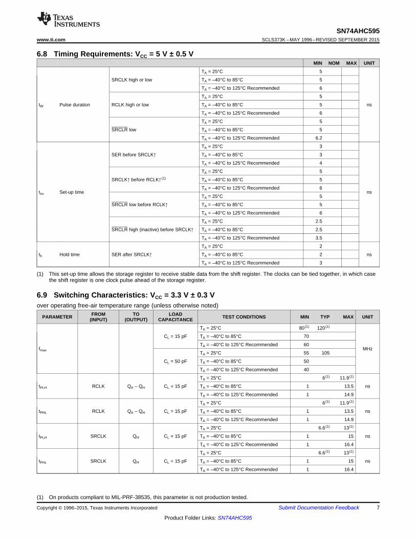
6.8 Timing Requirements: VCC = 5 V ± 0.5 VMIN NOM MAX UNIT
TA = 25°C 5
SRCLK high or low TA = –40°C to 85°C 5
TA = –40°C to 125°C Recommended 6
TA = 25°C 5
tW Pulse duration RCLK high or low TA = –40°C to 85°C 5 ns
TA = –40°C to 125°C Recommended 6
TA = 25°C 5
SRCLR low TA = –40°C to 85°C 5
TA = –40°C to 125°C Recommended 6.2
TA = 25°C 3
SER before SRCLK↑ TA = –40°C to 85°C 3
TA = –40°C to 125°C Recommended 4
TA = 25°C 5
SRCLK↑ before RCLK↑ (1) TA = –40°C to 85°C 5
TA = –40°C to 125°C Recommended 6tsu Set-up time ns
TA = 25°C 5
SRCLR low before RCLK↑ TA = –40°C to 85°C 5
TA = –40°C to 125°C Recommended 6
TA = 25°C 2.5
SRCLR high (inactive) before SRCLK↑ TA = –40°C to 85°C 2.5
TA = –40°C to 125°C Recommended 3.5
TA = 25°C 2
th Hold time SER after SRCLK↑ TA = –40°C to 85°C 2 ns
TA = –40°C to 125°C Recommended 3
(1) This set-up time allows the storage register to receive stable data from the shift register. The clocks can be tied together, in which casethe shift register is one clock pulse ahead of the storage register.
6.9 Switching Characteristics: VCC = 3.3 V ± 0.3 Vover operating free-air temperature range (unless otherwise noted)
FROM TO LOADPARAMETER TEST CONDITIONS MIN TYP MAX UNIT(INPUT) (OUTPUT) CAPACITANCE
TA = 25°C 80 (1) 120 (1)
CL = 15 pF TA = –40°C to 85°C 70
TA = –40°C to 125°C Recommended 60fmax MHz
TA = 25°C 55 105
CL = 50 pF TA = –40°C to 85°C 50
TA = –40°C to 125°C Recommended 40
TA = 25°C 6 (1) 11.9 (1)
tPLH RCLK QA – QH CL = 15 pF TA = –40°C to 85°C 1 13.5 ns
TA = –40°C to 125°C Recommended 1 14.9
TA = 25°C 6 (1) 11.9 (1)
tPHL RCLK QA – QH CL = 15 pF TA = –40°C to 85°C 1 13.5 ns
TA = –40°C to 125°C Recommended 1 14.9
TA = 25°C 6.6 (1) 13 (1)
tPLH SRCLK QH' CL = 15 pF TA = –40°C to 85°C 1 15 ns
TA = –40°C to 125°C Recommended 1 16.4
TA = 25°C 6.6 (1) 13 (1)
tPHL SRCLK QH' CL = 15 pF TA = –40°C to 85°C 1 15 ns
TA = –40°C to 125°C Recommended 1 16.4
(1) On products compliant to MIL-PRF-38535, this parameter is not production tested.
Copyright © 1996–2015, Texas Instruments Incorporated Submit Documentation Feedback 7
Product Folder Links: SN74AHC595
SN74AHC595SCLS373K –MAY 1996–REVISED SEPTEMBER 2015 www.ti.com
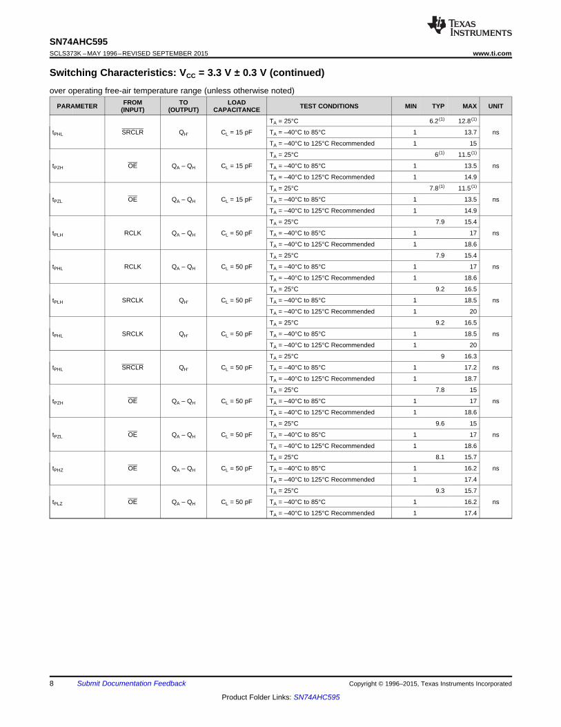
Switching Characteristics: VCC = 3.3 V ± 0.3 V (continued)over operating free-air temperature range (unless otherwise noted)
FROM TO LOADPARAMETER TEST CONDITIONS MIN TYP MAX UNIT(INPUT) (OUTPUT) CAPACITANCE
TA = 25°C 6.2 (1) 12.8 (1)
tPHL SRCLR QH' CL = 15 pF TA = –40°C to 85°C 1 13.7 ns
TA = –40°C to 125°C Recommended 1 15
TA = 25°C 6 (1) 11.5 (1)
tPZH OE QA – QH CL = 15 pF TA = –40°C to 85°C 1 13.5 ns
TA = –40°C to 125°C Recommended 1 14.9
TA = 25°C 7.8 (1) 11.5 (1)
tPZL OE QA – QH CL = 15 pF TA = –40°C to 85°C 1 13.5 ns
TA = –40°C to 125°C Recommended 1 14.9
TA = 25°C 7.9 15.4
tPLH RCLK QA – QH CL = 50 pF TA = –40°C to 85°C 1 17 ns
TA = –40°C to 125°C Recommended 1 18.6
TA = 25°C 7.9 15.4
tPHL RCLK QA – QH CL = 50 pF TA = –40°C to 85°C 1 17 ns
TA = –40°C to 125°C Recommended 1 18.6
TA = 25°C 9.2 16.5
tPLH SRCLK QH' CL = 50 pF TA = –40°C to 85°C 1 18.5 ns
TA = –40°C to 125°C Recommended 1 20
TA = 25°C 9.2 16.5
tPHL SRCLK QH' CL = 50 pF TA = –40°C to 85°C 1 18.5 ns
TA = –40°C to 125°C Recommended 1 20
TA = 25°C 9 16.3
tPHL SRCLR QH' CL = 50 pF TA = –40°C to 85°C 1 17.2 ns
TA = –40°C to 125°C Recommended 1 18.7
TA = 25°C 7.8 15
tPZH OE QA – QH CL = 50 pF TA = –40°C to 85°C 1 17 ns
TA = –40°C to 125°C Recommended 1 18.6
TA = 25°C 9.6 15
tPZL OE QA – QH CL = 50 pF TA = –40°C to 85°C 1 17 ns
TA = –40°C to 125°C Recommended 1 18.6
TA = 25°C 8.1 15.7
tPHZ OE QA – QH CL = 50 pF TA = –40°C to 85°C 1 16.2 ns
TA = –40°C to 125°C Recommended 1 17.4
TA = 25°C 9.3 15.7
tPLZ OE QA – QH CL = 50 pF TA = –40°C to 85°C 1 16.2 ns
TA = –40°C to 125°C Recommended 1 17.4
8 Submit Documentation Feedback Copyright © 1996–2015, Texas Instruments Incorporated
Product Folder Links: SN74AHC595

SN74AHC595www.ti.com SCLS373K –MAY 1996–REVISED SEPTEMBER 2015
6.10 Switching Characteristics: VCC = 5 V ± 0.5 Vover operating free-air temperature range (unless otherwise noted)
FROM TO LOADPARAMETER TEST CONDITIONS MIN TYP MAX UNIT(INPUT) (OUTPUT) CAPACITANCE
TA = 25°C 135 (1) 170 (1)
CL = 15 pFTA = –40°C to 85°C 115
fmax MHzTA = 25°C 95 140
CL = 50 pFTA = –40°C to 85°C 85
TA = 25°C 4.3 (1) 7.4 (1)
tPLH RCLK QA – QH CL = 15 pF nsTA = –40°C to 85°C 1 8.5
TA = 25°C 4.3 (1) 7.4 (1)
tPHL RCLK QA – QH CL = 15 pF nsTA = –40°C to 85°C 1 8.5
TA = 25°C 4.5 (1) 8.2 (1)
tPLH SRCLK QH' CL = 15 pF nsTA = –40°C to 85°C 1 9.4
TA = 25°C 4.5 (1) 8.2 (1)
tPHL SRCLK QH' CL = 15 pF nsTA = –40°C to 85°C 1 9.4
TA = 25°C 4.5 (1) 8 (1)
tPHL SRCLR QH' CL = 15 pF nsTA = –40°C to 85°C 1 9.1
TA = 25°C 4.3 (1) 8.6 (1)
tPZH OE QA – QH CL = 15 pF nsTA = –40°C to 85°C 1 10
TA = 25°C 5.4 (1) 8.6 (1)
tPZL OE QA – QH CL = 15 pF nsTA = –40°C to 85°C 1 10
TA = 25°C 5.6 9.4tPLH RCLK QA – QH CL = 50 pF ns
TA = –40°C to 85°C 1 10.5
TA = 25°C 5.6 9.4tPHL RCLK QA – QH CL = 50 pF ns
TA = –40°C to 85°C 1 10.5
TA = 25°C 6.4 10.2tPLH SRCLK QH' CL = 50 pF ns
TA = –40°C to 85°C 1 11.4
TA = 25°C 6.4 10.2tPHL SRCLK QH' CL = 50 pF ns
TA = –40°C to 85°C 1 11.4
TA = 25°C 6.4 10tPHL SRCLR QH' CL = 50 pF ns
TA = –40°C to 85°C 1 11.1
TA = 25°C 5.7 10.6tPZH OE QA – QH CL = 50 pF ns
TA = –40°C to 85°C 1 12
TA = 25°C 6.8 10.6tPZL OE QA – QH CL = 50 pF ns
TA = –40°C to 85°C 1 12
TA = 25°C 3.5 10.3tPHZ OE QA – QH CL = 50 pF ns
TA = –40°C to 85°C 1 11
TA = 25°C 3.4 10.3tPLZ OE QA – QH CL = 50 pF ns
TA = –40°C to 85°C 1 11
(1) On products compliant to MIL-PRF-38535, this parameter is not production tested.
Copyright © 1996–2015, Texas Instruments Incorporated Submit Documentation Feedback 9
Product Folder Links: SN74AHC595

SRCLK
SER
RCLK
SRCLR
OE
QA
QB
QC
QD
QE
QF
QG
QH
QH′
implies that the output is in 3-State mode.NOTE:
SN74AHC595SCLS373K –MAY 1996–REVISED SEPTEMBER 2015 www.ti.com
Figure 1. Timing Diagram
10 Submit Documentation Feedback Copyright © 1996–2015, Texas Instruments Incorporated
Product Folder Links: SN74AHC595

-100 -50 0 50 100
Temperature (°C)
tpd(ns)
4
8
12
16
20
0
150
SN74AHC595www.ti.com SCLS373K –MAY 1996–REVISED SEPTEMBER 2015
6.11 Typical Characteristics
VCC = 3.3 V 15-pF Load
Figure 2. SN74AHC595 RCLK to Q TPD vs Temperature
Copyright © 1996–2015, Texas Instruments Incorporated Submit Documentation Feedback 11
Product Folder Links: SN74AHC595

50% VCC
VCC
VCC
0 V
0 V
thtsu
VOLTAGE WAVEFORMS
SETUP AND HOLD TIMES
Data Input
tPLH
tPHL
tPHL
tPLH
VOH
VOH
VOL
VOL
VCC
0 V
50% VCC50% VCC
Input
Out-of-Phase
Output
In-Phase
Output
Timing Input
50% VCC
VOLTAGE WAVEFORMS
PROPAGATION DELAY TIMES
INVERTING AND NONINVERTING OUTPUTS
Output
Control
Output
Waveform 1
S1 at VCC(see Note B)
Output
Waveform 2
S1 at GND
(see Note B)
VOL
VOH
tPZL
tPZH
tPLZ
tPHZ
≈VCC
0 V
50% VCC VOL + 0.3 V
50% VCC≈0 V
VCC
VOLTAGE WAVEFORMS
ENABLE AND DISABLE TIMES
LOW- AND HIGH-LEVEL ENABLING
tPLH/tPHLtPLZ/tPZLtPHZ/tPZHOpen Drain
Open
VCCGND
VCC
TEST S1
VCC
0 V
50% VCC
tw
VOLTAGE WAVEFORMS
PULSE DURATION
Input
From Output
Under Test
CL(see Note A)
LOAD CIRCUIT FOR
3-STATE AND OPEN-DRAIN OUTPUTS
S1
VCC
RL = 1 kΩ
GNDFrom Output
Under Test
CL(see Note A)
Test
Point
LOAD CIRCUIT FOR
TOTEM-POLE OUTPUTS
Open
50% VCC
50% VCC 50% VCC
50% VCC
50% VCC 50% VCC
50% VCC 50% VCC
VOH – 0.3 V
SN74AHC595SCLS373K –MAY 1996–REVISED SEPTEMBER 2015 www.ti.com
7 Parameter Measurement Information
A. CL includes probe and jig capacitance.B. Waveform 1 is for an output with internal conditions such that the output is low except when disabled by the output
control.Waveform 2 is for an output with internal conditions such that the output is high except when disabled by the outputcontrol.
C. All input pulses are supplied by generators having the following characteristics: PRR ≤ 1 MHz, ZO = 50 Ω, tr ≤ 3 ns, tf≤ 3 ns.
D. The outputs are measured one at a time with one input transition per measurement.E. All parameters and waveforms are not applicable to all devices.
Figure 3. Load Circuit and Voltage Waveforms
12 Submit Documentation Feedback Copyright © 1996–2015, Texas Instruments Incorporated
Product Folder Links: SN74AHC595
3D
C3
1D
C1
R
3D
C3
2D
C2
R
3D
C3
2D
C2
R
3D
C3
2D
C2
R
3D
C3
2D
C2
R
3D
C3
2D
C2
R
3D
C3
2D
C2
R
3D
C3
2D
C2
R
13
12
10
11
14
15
1
2
3
4
5
6
7
9
QA
QB
QC
QD
QE
QF
QG
QH
QH′
OE
SRCLR
RCLK
SRCLK
SER Q
Q
Q
Q
Q
Q
Q
Q
Q
Q
Q
Q
Q
Q
Q
Q
SN74AHC595www.ti.com SCLS373K –MAY 1996–REVISED SEPTEMBER 2015
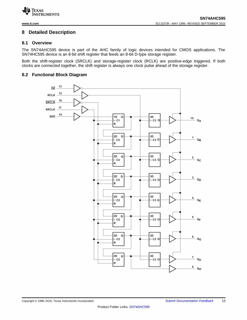
8 Detailed Description
8.1 OverviewThe SN74AHC595 device is part of the AHC family of logic devices intended for CMOS applications. TheSN74HC595 device is an 8-bit shift register that feeds an 8-bit D-type storage register.
Both the shift-register clock (SRCLK) and storage-register clock (RCLK) are positive-edge triggered. If bothclocks are connected together, the shift register is always one clock pulse ahead of the storage register.
8.2 Functional Block Diagram
Copyright © 1996–2015, Texas Instruments Incorporated Submit Documentation Feedback 13
Product Folder Links: SN74AHC595

SN74AHC595SCLS373K –MAY 1996–REVISED SEPTEMBER 2015 www.ti.com
8.3 Feature DescriptionThe SN74AHC595 device is an 8-bit serial-in, parallel-out shift registers that have a wide operating voltage rangefrom 2 V to 5.5 V and a low current consumption of 40-µA (max) ICC.
8.4 Device Functional Modes
Table 1. Function TableINPUTS
FUNCTIONSER SRCLK SRCLR RCLK OE
X X X X H Outputs QA−QH are disabled.X X X X L Outputs QA−QH are enabled.X X L X X Shift register is cleared.
First stage of the shift register goes low.L ↑ H X X Other stages store the data of previous stage, respectively.First stage of the shift register goes high.H ↑ H X X Other stages store the data of previous stage, respectively.
X X X ↑ X Shift-register data is stored into the storage register.
14 Submit Documentation Feedback Copyright © 1996–2015, Texas Instruments Incorporated
Product Folder Links: SN74AHC595

Controller
SRCLR
SRCLK
RCLK5
OE
SER
QA
QB
QC
QD
QE
QF
QG
VCC816
0.1 F
GND
15
1
2
3
4
5
6
7QH
10
11
12
13
14
9 Q+
1 k
1 k
1 k
1 k
1 k
1 k
1 k
1 k
+5V
SN74AHC595www.ti.com SCLS373K –MAY 1996–REVISED SEPTEMBER 2015
9 Application and Implementation
NOTEInformation in the following applications sections is not part of the TI componentspecification, and TI does not warrant its accuracy or completeness. TI’s customers areresponsible for determining suitability of components for their purposes. Customers shouldvalidate and test their design implementation to confirm system functionality.
9.1 Application InformationThe SN74AHC595 device is a low-drive CMOS device that can be used for a multitude of bus-interface typeapplications where output ringing is a concern. The low drive and slow edge rates minimize overshoot andundershoot on the outputs. Figure 4 shows an application where eight LEDs are used to visualize the data bitscontained within the shift register.
9.2 Typical Application
Figure 4. Shift Register Display of 8 bits
9.2.1 Design RequirementsThis device uses CMOS technology and has balanced output drive. Care must be taken to avoid bus contentionbecause it can drive currents that would exceed maximum limits. The high drive will also create fast edges intolight loads, so routing and load conditions must be considered to prevent ringing.
9.2.2 Detailed Design Procedure• Recommended input conditions:
– Specified high and low levels. See (VIH and VIL) in the Recommended Operating Conditions table.– Specified high and low levels. See (VIH and VIL) in the Recommended Operating Conditions table.– Inputs are overvoltage tolerant allowing them to go as high as 6.0 V at any valid VCC
Copyright © 1996–2015, Texas Instruments Incorporated Submit Documentation Feedback 15
Product Folder Links: SN74AHC595

-100 -50 0 50 100
Temperature (°C)
tpd(ns)
2
4
6
8
10
0
150
SN74AHC595SCLS373K –MAY 1996–REVISED SEPTEMBER 2015 www.ti.com
Typical Application (continued)• Recommend output conditions:
– Load currents must not exceed 25 mA per output and 75 mA total for the part– Outputs must not be pulled above VCC
9.2.3 Application Curve
VCC = 5 V 15-pF Load
Figure 5. SN74AHC595 RCLK to Q TPD vs Temperature
16 Submit Documentation Feedback Copyright © 1996–2015, Texas Instruments Incorporated
Product Folder Links: SN74AHC595

Vcc
Unused Input
Input
Output
Input
Unused Input Output
SN74AHC595www.ti.com SCLS373K –MAY 1996–REVISED SEPTEMBER 2015
10 Power Supply RecommendationsThe power supply can be any voltage between the MIN and MAX supply-voltage rating located in theRecommended Operating Conditions table.
Each VCC pin must have a good bypass capacitor to prevent power disturbance. For devices with a single supply,0.1-μf capacitor is recommended; if there are multiple VCC pins, then a 0.01-μf or a 0.022-μf capacitor isrecommended for each power pin. It is acceptable to parallel multiple bypass capacitors to reject differentfrequencies of noise. A 0.1-μf and a 1-μf capacitor are commonly used in parallel. The bypass capacitor must beinstalled as close to the power pin as possible for best results.
11 Layout
11.1 Layout GuidelinesWhen using multiple-bit logic devices, inputs must never float.
In many cases, functions or parts of functions of digital logic devices are unused, for example, when only twoinputs of a triple-input AND gate are used or only 3 of the 4 buffer gates are used. Such input pins must not beleft unconnected because the undefined voltages at the outside connections results in undefined operationalstates. Figure 6 specifies the rules that must be observed under all circumstances. All unused inputs of digitallogic devices must be connected to a high or low bias to prevent them from floating. The logic level that must beapplied to any particular unused input depends on the function of the device. Generally, these unused inputs willbe tied to GND or VCC, whichever makes more sense or is more convenient. It is generally acceptable to floatoutputs, unless the part is a transceiver. If the transceiver has an output-enable pin, it will disable the outputsection of the part when asserted. This will not disable the input section of the I/Os, so they cannot float whendisabled.
11.2 Layout Example
Figure 6. Layout Diagram
Copyright © 1996–2015, Texas Instruments Incorporated Submit Documentation Feedback 17
Product Folder Links: SN74AHC595

SN74AHC595SCLS373K –MAY 1996–REVISED SEPTEMBER 2015 www.ti.com
12 Device and Documentation Support
12.1 Documentation Support
12.1.1 Related DocumentationFor related documentation, wee the following:
Implications of Slow or Floating CMOS Inputs, SCBA004
12.2 Community ResourcesThe following links connect to TI community resources. Linked contents are provided "AS IS" by the respectivecontributors. They do not constitute TI specifications and do not necessarily reflect TI's views; see TI's Terms ofUse.
TI E2E™ Online Community TI's Engineer-to-Engineer (E2E) Community. Created to foster collaborationamong engineers. At e2e.ti.com, you can ask questions, share knowledge, explore ideas and helpsolve problems with fellow engineers.
Design Support TI's Design Support Quickly find helpful E2E forums along with design support tools andcontact information for technical support.
12.3 TrademarksE2E is a trademark of Texas Instruments.All other trademarks are the property of their respective owners.
12.4 Electrostatic Discharge CautionThese devices have limited built-in ESD protection. The leads should be shorted together or the device placed in conductive foamduring storage or handling to prevent electrostatic damage to the MOS gates.
12.5 GlossarySLYZ022 — TI Glossary.
This glossary lists and explains terms, acronyms, and definitions.
13 Mechanical, Packaging, and Orderable InformationThe following pages include mechanical, packaging, and orderable information. This information is the mostcurrent data available for the designated devices. This data is subject to change without notice and revision ofthis document. For browser-based versions of this data sheet, refer to the left-hand navigation.
18 Submit Documentation Feedback Copyright © 1996–2015, Texas Instruments Incorporated
Product Folder Links: SN74AHC595
PACKAGE OPTION ADDENDUM
www.ti.com 13-Aug-2021
Addendum-Page 1
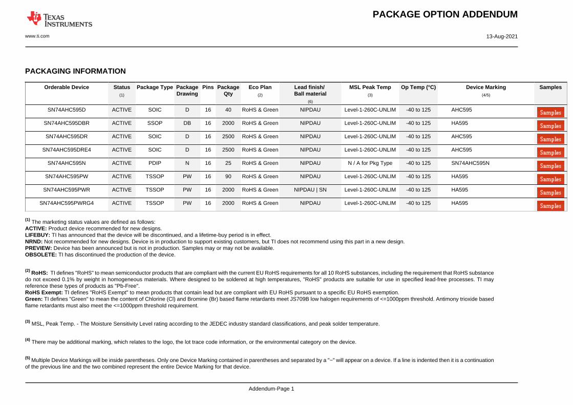
PACKAGING INFORMATION
Orderable Device Status(1)
Package Type PackageDrawing
Pins PackageQty
Eco Plan(2)
Lead finish/Ball material
(6)
MSL Peak Temp(3)
Op Temp (°C) Device Marking(4/5)
Samples
SN74AHC595D ACTIVE SOIC D 16 40 RoHS & Green NIPDAU Level-1-260C-UNLIM -40 to 125 AHC595
SN74AHC595DBR ACTIVE SSOP DB 16 2000 RoHS & Green NIPDAU Level-1-260C-UNLIM -40 to 125 HA595
SN74AHC595DR ACTIVE SOIC D 16 2500 RoHS & Green NIPDAU Level-1-260C-UNLIM -40 to 125 AHC595
SN74AHC595DRE4 ACTIVE SOIC D 16 2500 RoHS & Green NIPDAU Level-1-260C-UNLIM -40 to 125 AHC595
SN74AHC595N ACTIVE PDIP N 16 25 RoHS & Green NIPDAU N / A for Pkg Type -40 to 125 SN74AHC595N
SN74AHC595PW ACTIVE TSSOP PW 16 90 RoHS & Green NIPDAU Level-1-260C-UNLIM -40 to 125 HA595
SN74AHC595PWR ACTIVE TSSOP PW 16 2000 RoHS & Green NIPDAU | SN Level-1-260C-UNLIM -40 to 125 HA595
SN74AHC595PWRG4 ACTIVE TSSOP PW 16 2000 RoHS & Green NIPDAU Level-1-260C-UNLIM -40 to 125 HA595
(1) The marketing status values are defined as follows:ACTIVE: Product device recommended for new designs.LIFEBUY: TI has announced that the device will be discontinued, and a lifetime-buy period is in effect.NRND: Not recommended for new designs. Device is in production to support existing customers, but TI does not recommend using this part in a new design.PREVIEW: Device has been announced but is not in production. Samples may or may not be available.OBSOLETE: TI has discontinued the production of the device.
(2) RoHS: TI defines "RoHS" to mean semiconductor products that are compliant with the current EU RoHS requirements for all 10 RoHS substances, including the requirement that RoHS substancedo not exceed 0.1% by weight in homogeneous materials. Where designed to be soldered at high temperatures, "RoHS" products are suitable for use in specified lead-free processes. TI mayreference these types of products as "Pb-Free".RoHS Exempt: TI defines "RoHS Exempt" to mean products that contain lead but are compliant with EU RoHS pursuant to a specific EU RoHS exemption.Green: TI defines "Green" to mean the content of Chlorine (Cl) and Bromine (Br) based flame retardants meet JS709B low halogen requirements of <=1000ppm threshold. Antimony trioxide basedflame retardants must also meet the <=1000ppm threshold requirement.
(3) MSL, Peak Temp. - The Moisture Sensitivity Level rating according to the JEDEC industry standard classifications, and peak solder temperature.
(4) There may be additional marking, which relates to the logo, the lot trace code information, or the environmental category on the device.
(5) Multiple Device Markings will be inside parentheses. Only one Device Marking contained in parentheses and separated by a "~" will appear on a device. If a line is indented then it is a continuationof the previous line and the two combined represent the entire Device Marking for that device.

PACKAGE OPTION ADDENDUM
www.ti.com 13-Aug-2021
Addendum-Page 2
(6) Lead finish/Ball material - Orderable Devices may have multiple material finish options. Finish options are separated by a vertical ruled line. Lead finish/Ball material values may wrap to twolines if the finish value exceeds the maximum column width.
Important Information and Disclaimer:The information provided on this page represents TI's knowledge and belief as of the date that it is provided. TI bases its knowledge and belief on informationprovided by third parties, and makes no representation or warranty as to the accuracy of such information. Efforts are underway to better integrate information from third parties. TI has taken andcontinues to take reasonable steps to provide representative and accurate information but may not have conducted destructive testing or chemical analysis on incoming materials and chemicals.TI and TI suppliers consider certain information to be proprietary, and thus CAS numbers and other limited information may not be available for release.
In no event shall TI's liability arising out of such information exceed the total purchase price of the TI part(s) at issue in this document sold by TI to Customer on an annual basis.
OTHER QUALIFIED VERSIONS OF SN74AHC595 :
• Automotive : SN74AHC595-Q1
NOTE: Qualified Version Definitions:
• Automotive - Q100 devices qualified for high-reliability automotive applications targeting zero defects
PACKAGE MATERIALS INFORMATION
www.ti.com 3-Jun-2022
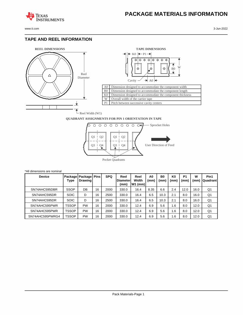
TAPE AND REEL INFORMATION
Reel Width (W1)
REEL DIMENSIONS
A0B0K0W
Dimension designed to accommodate the component lengthDimension designed to accommodate the component thicknessOverall width of the carrier tapePitch between successive cavity centers
Dimension designed to accommodate the component width
TAPE DIMENSIONS
K0 P1
B0 W
A0Cavity
QUADRANT ASSIGNMENTS FOR PIN 1 ORIENTATION IN TAPE
Pocket Quadrants
Sprocket Holes
Q1 Q1Q2 Q2
Q3 Q3Q4 Q4 User Direction of Feed
P1
ReelDiameter
*All dimensions are nominal
Device PackageType
PackageDrawing
Pins SPQ ReelDiameter
(mm)
ReelWidth
W1 (mm)
A0(mm)
B0(mm)
K0(mm)
P1(mm)
W(mm)
Pin1Quadrant
SN74AHC595DBR SSOP DB 16 2000 330.0 16.4 8.35 6.6 2.4 12.0 16.0 Q1
SN74AHC595DR SOIC D 16 2500 330.0 16.4 6.5 10.3 2.1 8.0 16.0 Q1
SN74AHC595DR SOIC D 16 2500 330.0 16.4 6.5 10.3 2.1 8.0 16.0 Q1
SN74AHC595PWR TSSOP PW 16 2000 330.0 12.4 6.9 5.6 1.6 8.0 12.0 Q1
SN74AHC595PWR TSSOP PW 16 2000 330.0 12.4 6.9 5.6 1.6 8.0 12.0 Q1
SN74AHC595PWRG4 TSSOP PW 16 2000 330.0 12.4 6.9 5.6 1.6 8.0 12.0 Q1
Pack Materials-Page 1

PACKAGE MATERIALS INFORMATION
www.ti.com 3-Jun-2022
TAPE AND REEL BOX DIMENSIONS
Width (mm)
W L
H
*All dimensions are nominal
Device Package Type Package Drawing Pins SPQ Length (mm) Width (mm) Height (mm)
SN74AHC595DBR SSOP DB 16 2000 356.0 356.0 35.0
SN74AHC595DR SOIC D 16 2500 356.0 356.0 35.0
SN74AHC595DR SOIC D 16 2500 340.5 336.1 32.0
SN74AHC595PWR TSSOP PW 16 2000 356.0 356.0 35.0
SN74AHC595PWR TSSOP PW 16 2000 364.0 364.0 27.0
SN74AHC595PWRG4 TSSOP PW 16 2000 367.0 367.0 35.0
Pack Materials-Page 2

PACKAGE MATERIALS INFORMATION
www.ti.com 3-Jun-2022
TUBE
L - Tube lengthT - Tube height
W - Tube width
B - Alignment groove width *All dimensions are nominal
Device Package Name Package Type Pins SPQ L (mm) W (mm) T (µm) B (mm)
SN74AHC595D D SOIC 16 40 507 8 3940 4.32
SN74AHC595D D SOIC 16 40 506.6 8 3940 4.32
SN74AHC595N N PDIP 16 25 506 13.97 11230 4.32
SN74AHC595N N PDIP 16 25 506 13.97 11230 4.32
SN74AHC595PW PW TSSOP 16 90 530 10.2 3600 3.5
Pack Materials-Page 3


www.ti.com
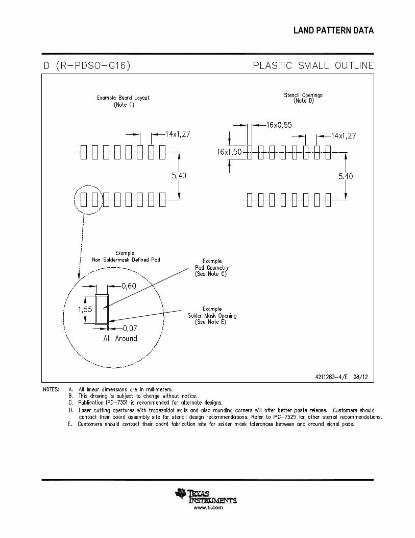
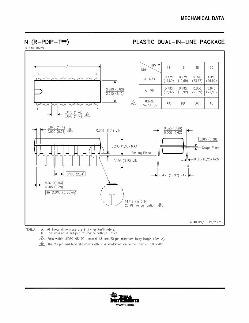
PACKAGE OUTLINE
C
14X 0.65
2X4.55
16X 0.300.19
TYP6.66.2
1.2 MAX
0.150.05
0.25GAGE PLANE
-80
BNOTE 4
4.54.3
A
NOTE 3
5.14.9
0.750.50
(0.15) TYP
TSSOP - 1.2 mm max heightPW0016ASMALL OUTLINE PACKAGE
4220204/A 02/2017
1
89
16
0.1 C A B
PIN 1 INDEX AREA
SEE DETAIL A
0.1 C
NOTES: 1. All linear dimensions are in millimeters. Any dimensions in parenthesis are for reference only. Dimensioning and tolerancing per ASME Y14.5M. 2. This drawing is subject to change without notice. 3. This dimension does not include mold flash, protrusions, or gate burrs. Mold flash, protrusions, or gate burrs shall not exceed 0.15 mm per side. 4. This dimension does not include interlead flash. Interlead flash shall not exceed 0.25 mm per side.5. Reference JEDEC registration MO-153.
SEATINGPLANE
A 20DETAIL ATYPICAL
SCALE 2.500

www.ti.com
EXAMPLE BOARD LAYOUT
0.05 MAXALL AROUND
0.05 MINALL AROUND
16X (1.5)
16X (0.45)
14X (0.65)
(5.8)
(R0.05) TYP
TSSOP - 1.2 mm max heightPW0016ASMALL OUTLINE PACKAGE
4220204/A 02/2017
NOTES: (continued) 6. Publication IPC-7351 may have alternate designs. 7. Solder mask tolerances between and around signal pads can vary based on board fabrication site.
LAND PATTERN EXAMPLEEXPOSED METAL SHOWN
SCALE: 10X
SYMM
SYMM
1
8 9
16
15.000
METALSOLDER MASKOPENING
METAL UNDERSOLDER MASK
SOLDER MASKOPENING
EXPOSED METALEXPOSED METAL
SOLDER MASK DETAILS
NON-SOLDER MASKDEFINED
(PREFERRED)
SOLDER MASKDEFINED
www.ti.com
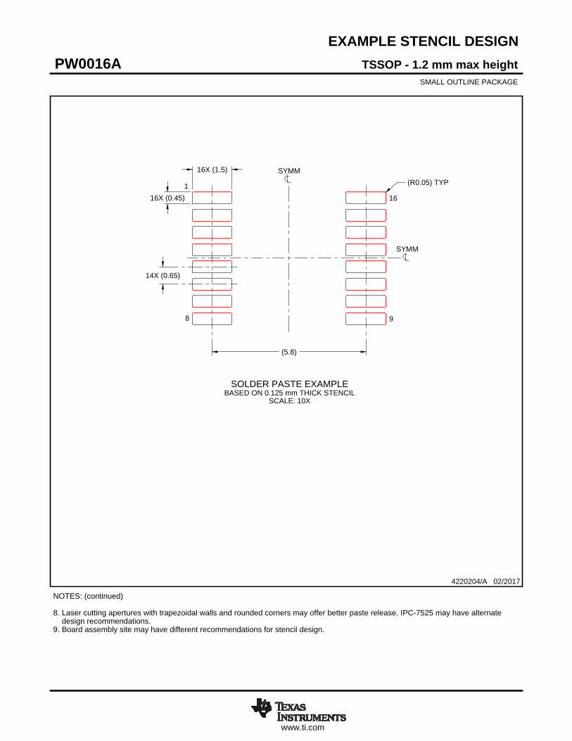
EXAMPLE STENCIL DESIGN
16X (1.5)
16X (0.45)
14X (0.65)
(5.8)
(R0.05) TYP
TSSOP - 1.2 mm max heightPW0016ASMALL OUTLINE PACKAGE
4220204/A 02/2017
NOTES: (continued) 8. Laser cutting apertures with trapezoidal walls and rounded corners may offer better paste release. IPC-7525 may have alternate design recommendations. 9. Board assembly site may have different recommendations for stencil design.
SOLDER PASTE EXAMPLEBASED ON 0.125 mm THICK STENCIL
SCALE: 10X
SYMM
SYMM
1
8 9
16

www.ti.com
PACKAGE OUTLINE
C
14X 0.65
2X4.55
16X 0.380.22
8.27.4 TYP
SEATINGPLANE
0.05 MIN
0.25GAGE PLANE
0 -8
2 MAX
0.250.09
B 5.65.0
NOTE 4
A
6.55.9
NOTE 3
0.950.55
SSOP - 2 mm max heightDB0016ASMALL OUTLINE PACKAGE
4220763/A 05/2022
1
89
16
0.1 C A B
PIN 1 INDEX AREA
SEE DETAIL A
0.1 C
NOTES: 1. All linear dimensions are in millimeters. Any dimensions in parenthesis are for reference only. Dimensioning and tolerancing per ASME Y14.5M. 2. This drawing is subject to change without notice. 3. This dimension does not include mold flash, protrusions, or gate burrs. Mold flash, protrusions, or gate burrs shall not exceed 0.15 mm per side. 4. Reference JEDEC registration MO-150.
A 15DETAIL ATYPICAL
SCALE 1.500

www.ti.com
EXAMPLE BOARD LAYOUT
0.05 MAXALL AROUND
0.05 MINALL AROUND
16X (1.85)
16X (0.45)
14X (0.65)
(7)
(R0.05) TYP
SSOP - 2 mm max heightDB0016ASMALL OUTLINE PACKAGE
4220763/A 05/2022
NOTES: (continued) 5. Publication IPC-7351 may have alternate designs. 6. Solder mask tolerances between and around signal pads can vary based on board fabrication site.
LAND PATTERN EXAMPLEEXPOSED METAL SHOWN
SCALE: 10X
SYMM
SYMM
1
8 9
16
15.000
METALSOLDER MASKOPENING
METAL UNDERSOLDER MASK
SOLDER MASKOPENING
EXPOSED METALEXPOSED METAL
SOLDER MASK DETAILS
NON-SOLDER MASKDEFINED
(PREFERRED)
SOLDER MASKDEFINED

www.ti.com
EXAMPLE STENCIL DESIGN
16X (1.85)
16X (0.45)
14X (0.65)
(7)
(R0.05) TYP
SSOP - 2 mm max heightDB0016ASMALL OUTLINE PACKAGE
4220763/A 05/2022
NOTES: (continued) 7. Laser cutting apertures with trapezoidal walls and rounded corners may offer better paste release. IPC-7525 may have alternate design recommendations. 8. Board assembly site may have different recommendations for stencil design.
SOLDER PASTE EXAMPLEBASED ON 0.125 mm THICK STENCIL
SCALE: 10X
SYMM
SYMM
1
8 9
16
IMPORTANT NOTICE AND DISCLAIMERTI PROVIDES TECHNICAL AND RELIABILITY DATA (INCLUDING DATA SHEETS), DESIGN RESOURCES (INCLUDING REFERENCE DESIGNS), APPLICATION OR OTHER DESIGN ADVICE, WEB TOOLS, SAFETY INFORMATION, AND OTHER RESOURCES “AS IS” AND WITH ALL FAULTS, AND DISCLAIMS ALL WARRANTIES, EXPRESS AND IMPLIED, INCLUDING WITHOUT LIMITATION ANY IMPLIED WARRANTIES OF MERCHANTABILITY, FITNESS FOR A PARTICULAR PURPOSE OR NON-INFRINGEMENT OF THIRD PARTY INTELLECTUAL PROPERTY RIGHTS.These resources are intended for skilled developers designing with TI products. You are solely responsible for (1) selecting the appropriate TI products for your application, (2) designing, validating and testing your application, and (3) ensuring your application meets applicable standards, and any other safety, security, regulatory or other requirements.These resources are subject to change without notice. TI grants you permission to use these resources only for development of an application that uses the TI products described in the resource. Other reproduction and display of these resources is prohibited. No license is granted to any other TI intellectual property right or to any third party intellectual property right. TI disclaims responsibility for, and you will fully indemnify TI and its representatives against, any claims, damages, costs, losses, and liabilities arising out of your use of these resources.TI’s products are provided subject to TI’s Terms of Sale or other applicable terms available either on ti.com or provided in conjunction with such TI products. TI’s provision of these resources does not expand or otherwise alter TI’s applicable warranties or warranty disclaimers for TI products.TI objects to and rejects any additional or different terms you may have proposed. IMPORTANT NOTICE
Mailing Address: Texas Instruments, Post Office Box 655303, Dallas, Texas 75265Copyright © 2022, Texas Instruments Incorporated
Copyright © 2022 FDOKUMEN