Shift Register (ShiftReg)
19
PSoC ® Creator™ Component Datasheet Cypress Semiconductor Corporation • 198 Champion Court • San Jose, CA 95134-1709 • 408-943-2600 Document Number: 001-79200 Rev. *A Revised July 29, 2015 Features Adjustable shift register size: 2 to 32 bits Simultaneous shift in and shift out Right shift or left shift Reset input forces shift register to all 0s Shift register value readable by CPU or DMA Shift register value writable by CPU or DMA General Description The Shift Register (ShiftReg) component provides synchronous shifting of data into and out of a parallel register. The parallel register can be read or written to by the CPU or DMA. The Shift Register component provides universal functionality similar to standard 74xxx series logic shift registers including: 74164, 74165, 74166, 74194, 74299, 74595 and 74597. In most applications the Shift Register component will be used in conjunction with other components and logic to create higher-level application-specific functionality, such as a counter to count the number of bits shifted. In general usage, the Shift Register component functions as a 2- to 32-bit shift register that shifts data on the rising edge of the clock input. The shift direction is configurable. It can be a right shift, where the MSB shifts in the input and the LSB shifts out the output, or a left shift, where the LSB shifts in the input and the MSB shifts out the output. The Shift Register value can be written by the CPU or DMA at any time. The rising edge of the component clock transfers pending FIFO data (previously written by the CPU or DMA) to the Shift Register when the load signal is set. A rising edge of the component clock transfers the current Shift Register value to the FIFO when a rising edge of the optional store input has been detected, where it can later be read by the CPU. The Shift Register component can generate an interrupt signal on any combination of the load, store or reset signals. Shift Register (ShiftReg) 2.10
-
Upload
khangminh22 -
Category
Documents
-
view
3 -
download
0
Transcript of Shift Register (ShiftReg)

PSoC® Creator™ Component Datasheet
Cypress Semiconductor Corporation • 198 Champion Court • San Jose, CA 95134-1709 • 408-943-2600
Document Number: 001-79200 Rev. *A Revised July 29, 2015
Features
Adjustable shift register size: 2 to 32 bits
Simultaneous shift in and shift out
Right shift or left shift
Reset input forces shift register to all 0s
Shift register value readable by CPU or DMA
Shift register value writable by CPU or DMA
General Description
The Shift Register (ShiftReg) component provides synchronous shifting of data into and out of a parallel register. The parallel register can be read or written to by the CPU or DMA. The Shift Register component provides universal functionality similar to standard 74xxx series logic shift registers including: 74164, 74165, 74166, 74194, 74299, 74595 and 74597. In most applications the Shift Register component will be used in conjunction with other components and logic to create higher-level application-specific functionality, such as a counter to count the number of bits shifted.
In general usage, the Shift Register component functions as a 2- to 32-bit shift register that shifts data on the rising edge of the clock input. The shift direction is configurable. It can be a right shift, where the MSB shifts in the input and the LSB shifts out the output, or a left shift, where the LSB shifts in the input and the MSB shifts out the output.
The Shift Register value can be written by the CPU or DMA at any time. The rising edge of the component clock transfers pending FIFO data (previously written by the CPU or DMA) to the Shift Register when the load signal is set. A rising edge of the component clock transfers the current Shift Register value to the FIFO when a rising edge of the optional store input has been detected, where it can later be read by the CPU.
The Shift Register component can generate an interrupt signal on any combination of the load, store or reset signals.
Shift Register (ShiftReg) 2.10
Shift Register (ShiftReg) PSoC® Creator™ Component Datasheet
Page 2 of 19 Document Number: 001-79200 Rev. *A
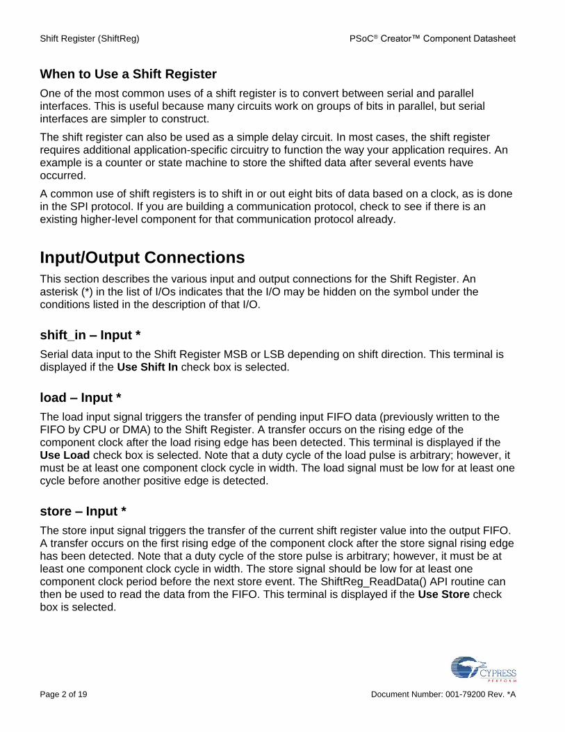
When to Use a Shift Register
One of the most common uses of a shift register is to convert between serial and parallel interfaces. This is useful because many circuits work on groups of bits in parallel, but serial interfaces are simpler to construct.
The shift register can also be used as a simple delay circuit. In most cases, the shift register requires additional application-specific circuitry to function the way your application requires. An example is a counter or state machine to store the shifted data after several events have occurred.
A common use of shift registers is to shift in or out eight bits of data based on a clock, as is done in the SPI protocol. If you are building a communication protocol, check to see if there is an existing higher-level component for that communication protocol already.
Input/Output Connections
This section describes the various input and output connections for the Shift Register. An asterisk (*) in the list of I/Os indicates that the I/O may be hidden on the symbol under the conditions listed in the description of that I/O.
shift_in – Input *
Serial data input to the Shift Register MSB or LSB depending on shift direction. This terminal is displayed if the Use Shift In check box is selected.
load – Input *
The load input signal triggers the transfer of pending input FIFO data (previously written to the FIFO by CPU or DMA) to the Shift Register. A transfer occurs on the rising edge of the component clock after the load rising edge has been detected. This terminal is displayed if the Use Load check box is selected. Note that a duty cycle of the load pulse is arbitrary; however, it must be at least one component clock cycle in width. The load signal must be low for at least one cycle before another positive edge is detected.
store – Input *
The store input signal triggers the transfer of the current shift register value into the output FIFO. A transfer occurs on the first rising edge of the component clock after the store signal rising edge has been detected. Note that a duty cycle of the store pulse is arbitrary; however, it must be at least one component clock cycle in width. The store signal should be low for at least one component clock period before the next store event. The ShiftReg_ReadData() API routine can then be used to read the data from the FIFO. This terminal is displayed if the Use Store check box is selected.
PSoC® Creator™ Component Datasheet Shift Register (ShiftReg)
Document Number: 001-79200 Rev. *A Page 3 of 19
reset – Input
The reset input (active high) causes the entire Shift Register to be set to zeros. This input does not affect the contents of the FIFOs. The reset input is synchronous to the clock input. The reset input may be left floating with no external connection. If nothing is connected to the reset line, the component will assign it a constant logic 0.
clock – Input
Clock source for the component. In some configurations this signal acts as an enable rather than a clock.
shift_out – Output *
Outputs serial data from the Shift Register MSB or LSB based on shift direction. This terminal is displayed if the Use Shift Out check box is selected.
interrupt – Output *
Interrupt signal generated by the shift register component. Interrupts are generated based on the specified parameters. This terminal is displayed if the Use Interrupt check box is selected.
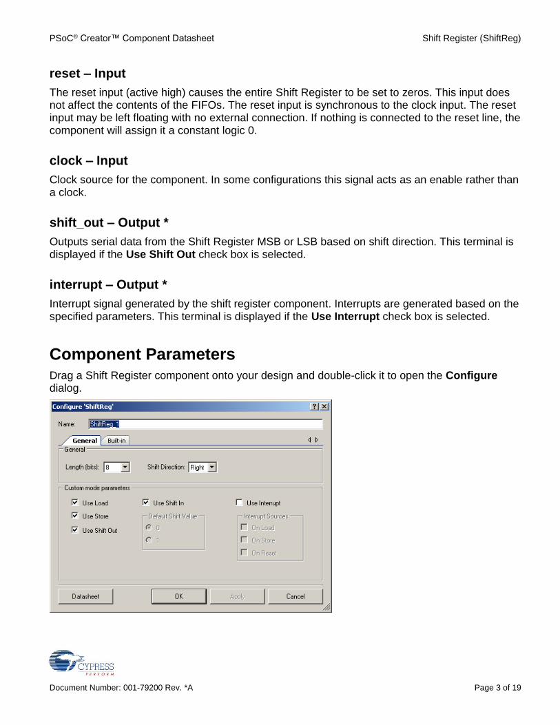
Component Parameters
Drag a Shift Register component onto your design and double-click it to open the Configure dialog.

Shift Register (ShiftReg) PSoC® Creator™ Component Datasheet
Page 4 of 19 Document Number: 001-79200 Rev. *A
Length (bits)
This parameter determines the length of the shift register in bits. Valid values are 2 through 32 bits. The default is 8.
Shift Direction
This parameter determines the shift direction, Right or Left. The default is Right (LSB first).
Use Load
When this option is selected, the load input terminal is shown on the Shift Register symbol. The load signal is internally routed to the control logic. As a result, a word from the input FIFO is transferred to the Shift Register on a rising edge of the component clock after the positive edge of load signal has been detected.
If Use Load is selected, the ShiftReg_WriteRegValue(), ShiftReg_ReadRegValue(), and ShiftReg_GetIntStatus() APIs are generated to work with the output FIFO. The component.h file has the necessary API prototypes and #define constants.
If Use Load is not selected, the load terminal is not shown on the component symbol and the associated API routines are not generated.
Use Store
When this option is selected, the store input terminal is shown on the Shift Register symbol. The store signal is internally routed to the control logic. On a rising edge of the component clock, after the store signal rising edge has been detected, the current word in the Shift Register is transferred to the output FIFO.
If Use Store is selected, the ShiftReg_WriteRegValue(), ShiftReg_ReadRegValue(), and ShiftReg_GetIntStatus() APIs are generated for working with the output FIFO. The component.h file has the necessary API prototypes and #define constants.
Caution
Be careful when using the ShiftReg_ReadRegValue() API routine in conjunction with the Use Store output FIFO functionality. The ShiftReg_ReadRegValue() API implementation transfers the current Shift Register ALU value into the output FIFO and then reads this data from the FIFO. Any data previously captured in the output FIFO using the Store signal, but not yet read by the application, will be lost.
If Use Store is not selected, the store terminal is not shown on the component symbol and the associated API routines are not generated.

PSoC® Creator™ Component Datasheet Shift Register (ShiftReg)
Document Number: 001-79200 Rev. *A Page 5 of 19
Use Shift Out
This parameter determines if the shift_out output of the Shift Register symbol is provided. It is selected by default.
Use Shift In
This parameter determines if the shift_in input of the Shift Register symbol is provided. It is selected by default.
Default Shift Value
This parameter allows you to define a default value for the input to the Shift Register. This parameter is only used if the Use Shift In parameter is not checked. The valid values for the Default Shift Value parameter are 0 and 1.
Use Interrupt
If this parameter is selected, the interrupt output terminal displays on the symbol. This enables the use of interrupts generated by the Shift Register.
If Use Interrupt is not selected, the interrupt terminal is not shown on the symbol and the associated API routines are generated.
Interrupt Sources
This parameter becomes enabled if you select Use Interrupt. The interrupt signal is used to indicate that one of the specified conditions has occurred. You can enable or disable interrupt generation and specify the events that will trigger an interrupt: On Load, On Store or On Reset.
Clock Selection
There is no internal clock in this component. You must attach a clock source. This component operates from a single clock connected to the component.
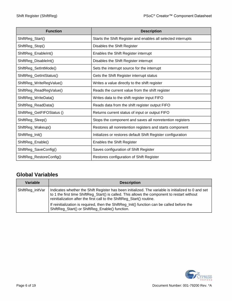
Application Programming Interface
Application Programming Interface (API) routines allow you to configure the component using software. The following table lists and describes the interface to each function. The subsequent sections cover each function in more detail.
By default, PSoC Creator assigns the instance name “ShiftReg_1” to the first instance of a component in a given design. You can rename it to any unique value that follows the syntactic rules for identifiers. The instance name becomes the prefix of every global function name, variable, and constant symbol. For readability, the instance name used in the following table is “ShiftReg.”
Shift Register (ShiftReg) PSoC® Creator™ Component Datasheet
Page 6 of 19 Document Number: 001-79200 Rev. *A
Function Description
ShiftReg_Start() Starts the Shift Register and enables all selected interrupts
ShiftReg_Stop() Disables the Shift Register
ShiftReg_EnableInt() Enables the Shift Register interrupt
ShiftReg_DisableInt() Disables the Shift Register interrupt
ShiftReg_SetIntMode() Sets the interrupt source for the interrupt
ShiftReg_GetIntStatus() Gets the Shift Register interrupt status
ShiftReg_WriteRegValue() Writes a value directly to the shift register
ShiftReg_ReadRegValue() Reads the current value from the shift register
ShiftReg_WriteData() Writes data to the shift register input FIFO
ShiftReg_ReadData() Reads data from the shift register output FIFO
ShiftReg_GetFIFOStatus () Returns current status of input or output FIFO
ShiftReg_Sleep() Stops the component and saves all nonretention registers
ShiftReg_Wakeup() Restores all nonretention registers and starts component
ShiftReg_Init() Initializes or restores default Shift Register configuration
ShiftReg_Enable() Enables the Shift Register
ShiftReg_SaveConfig() Saves configuration of Shift Register
ShiftReg_RestoreConfig() Restores configuration of Shift Register
Global Variables
Variable Description
ShiftReg_initVar Indicates whether the Shift Register has been initialized. The variable is initialized to 0 and set to 1 the first time ShiftReg_Start() is called. This allows the component to restart without reinitialization after the first call to the ShiftReg_Start() routine.
If reinitialization is required, then the ShiftReg_Init() function can be called before the ShiftReg_Start() or ShiftReg_Enable() function.

PSoC® Creator™ Component Datasheet Shift Register (ShiftReg)
Document Number: 001-79200 Rev. *A Page 7 of 19
void ShiftReg_Start(void)
Description: This is the preferred method to begin component operation. ShiftReg_Start() sets the initVar variable, calls the ShiftReg_Init() function, and then calls the ShiftReg_Enable() function.
Note that for Production PSoC 3 silicon, one component clock pulse is required to start the component logic after this function is called.
Parameters: None
Return Value: None
Side Effects: If the initVar variable is already set, this function only calls the ShiftReg_Enable() function.
void ShiftReg_Stop(void)
Description: Disables the Shift Register.
Parameters: None
Return Value: None
Side Effects: None
void ShiftReg_EnableInt(void)
Description: Enables the Shift Register interrupts.
Parameters: None
Return Value: None
Side Effects: None
void ShiftReg_DisableInt(void)
Description: Disables the Shift Register interrupts.
Parameters: None
Return Value: None
Side Effects: None

Shift Register (ShiftReg) PSoC® Creator™ Component Datasheet
Page 8 of 19 Document Number: 001-79200 Rev. *A
void ShiftReg_SetIntMode(uint8 interruptSource)
Description: Sets the interrupt source for the interrupt. Multiple sources may be ORed together.
Parameters: uint8 InterruptSource: Bit field containing the constant for the selected interrupt sources.
Multiple sources can be ORed together to select multiple interrupts.
Interrupt Source Description
ShiftReg_LOAD_INT_EN Enables the Load interrupt
ShiftReg_STORE_INT_EN Enables the Store interrupt
ShiftReg_RESET_INT_EN Enables the Reset interrupt
Return Value: None
Side Effects: None
uint8 ShiftReg_GetIntStatus(void)
Description: Gets the interrupt status for the Shift Register interrupts.
Parameters: None
Return Value: Bit field containing the status for the selected interrupt sources.
Return Value Description
ShiftReg_LOAD Load interrupt occurred
ShiftReg_STORE Store interrupt occurred
ShiftReg_RESET Reset interrupt occurred
Side Effects: Clears the Interrupt Status register.
void ShiftReg_WriteRegValue(uint8/16/32 shiftData)
Description: Writes a value directly to the Shift Register.
Parameters: uint8/16/32 shiftData: Data to be written. Data type is determined by the Shift Register Length parameter.
Return Value: None
Side Effects: The component must be stopped to use this API function.
Note The written value is available for reading after one component clock period.
PSoC® Creator™ Component Datasheet Shift Register (ShiftReg)
Document Number: 001-79200 Rev. *A Page 9 of 19
uint8/16/32 ShiftReg_ReadRegValue(void)
Description: Returns the current value from the shift register.
Parameters: None
Return Value: uint8/16/32 Shift Register value. Data type is determined by the Length parameter
Side Effects: Clears the shift register output FIFO. Wait at least one component clock period after calling ShiftReg_WriteRegValue() before calling this function.
Caution
Be careful when using the ShiftReg_ReadRegValue() API routine in conjunction with the Use Store output FIFO functionality. The ShiftReg_ReadRegValue() API implementation transfers the current Shift Register ALU value into the output FIFO and then reads this data from the FIFO. Any data previously captured in the output FIFO using the Store signal, but not yet read by the application, will be lost.
cystatus ShiftReg_WriteData(uint8/16/32 shiftData)
Description: Writes data to the shift register input FIFO. A data word is transferred to the shift register on a rising edge of the load input
Parameters: uint8/16/32 shiftData: Data to be written. Data type is determined by the Shift Register Length parameter.
Return Value: cystatus: Returns an error if the FIFO is full or CYRET_SUCCESS on successful operation. If the input FIFO is full then the data will not be written to the FIFO.
Return Value Description
CYRET_SUCCESS Successful operation
CYRET_INVALID_STATE Input FIFO is full
Side Effects: None
uint8/16/32 ShiftReg_ReadData(void)
Description: Reads data from the shift register output FIFO. A data word is transferred to the output FIFO on a rising edge of the store input.
Parameters: None
Return Value: uint8/16/32: next available data word. Data type is determined by the Shift Register Length parameter.
Side Effects: None

Shift Register (ShiftReg) PSoC® Creator™ Component Datasheet
Page 10 of 19 Document Number: 001-79200 Rev. *A
uint8 ShiftReg_GetFIFOStatus (uint8 fifoId)
Description: Returns the current status of the input or output FIFO.
Parameters: uint8 FifoID: identifies which FIFO status is read.
FifoID Value Description
ShiftReg_IN_FIFO Used to read status of the input FIFO
ShiftReg_OUT_FIFO Used to read status of the output FIFO
Return Value: uint8: FIFO Status of one of defined values.
Return Value Description
ShiftReg_RET_FIFO_FULL FIFO is full
ShiftReg_RET_FIFO_NOT_FULL FIFO is not full
ShiftReg_RET_FIFO_EMPTY FIFO is empty
Side Effects: None
void ShiftReg_Sleep(void)
Description: This is the preferred routine to prepare the component for sleep. The ShiftReg_Sleep() routine saves the current component state. Then it calls the ShiftReg_Stop() function and calls ShiftReg_SaveConfig() to save the hardware configuration.
Call the ShiftReg_Sleep() function before calling the CyPmSleep() or the CyPmHibernate() function. Refer to the PSoC Creator System Reference Guide for more information about power management functions.
Parameters: None
Return Value: None
Side Effects: None
void ShiftReg_Wakeup(void)
Description: This is the preferred routine to restore the component to the state when ShiftReg_Sleep() was called. The ShiftReg_Wakeup() function calls the ShiftReg_RestoreConfig() function to restore the configuration. If the component was enabled before the ShiftReg_Sleep() function was called, the ShiftReg_Wakeup() function will also re-enable the component.
Note that for Production PSoC3 silicon, one component clock pulse is required to return to normal operation after this function is called.
Parameters: None
Return Value: None
Side Effects: Calling the ShiftReg_Wakeup() function without first calling the ShiftReg_Sleep() or ShiftReg_SaveConfig() function may produce unexpected behavior.

PSoC® Creator™ Component Datasheet Shift Register (ShiftReg)
Document Number: 001-79200 Rev. *A Page 11 of 19
void ShiftReg_Init(void)
Description: Initializes or restores the component according to the customizer Configure dialog settings. It is not necessary to call ShiftReg_Init() because the ShiftReg_Start() routine calls this function and is the preferred method to begin component operation.
Parameters: None
Return Value: None
Side Effects: All registers will be set to values according to the Configure dialog.
void ShiftReg_Enable(void)
Description: Activates the hardware and begins component operation. It is not necessary to call ShiftReg_Enable() because the ShiftReg_Start() routine calls this function, which is the preferred method to begin component operation.
Parameters: None
Return Value: None
Side Effects: None
void ShiftReg_SaveConfig(void)
Description: This function saves the component configuration and nonretention registers. This function also saves the current component parameter values, as defined in the Configure dialog or as modified by appropriate APIs. This function is called by the ShiftReg_Sleep() function.
Parameters: None
Return Value: None
Side Effects: None
void ShiftReg_RestoreConfig(void)
Description: This function restores the component configuration and nonretention registers. This function also restores the component parameter values to what they were prior to calling the ShiftReg_Sleep() function
Parameters: None
Return Value: None
Side Effects: Call this routine only after calling the ShiftReg_SaveConfig() function. Calling it independently of the ShiftReg_SaveConfig() function overwrites the current settings with the initial settings.
Shift Register (ShiftReg) PSoC® Creator™ Component Datasheet
Page 12 of 19 Document Number: 001-79200 Rev. *A
Defines
ShiftReg_SR_SIZE – Defines Shift Register length in bits.
ShiftReg_USE_INPUT_FIFO – Indicates that an input FIFO is defined in the project.
Note The output FIFO is always defined because it is used for Software Capture.
ShiftReg_FIFOSize – Defines the size of the Input FIFO in Shift Register words. The Shift Register word size is determined by the Length (in bytes) parameter value.
ShiftReg_DIRECTION – Defines the direction of the shift (0 = Left Shift, 1 = Right Shift).
Sample Firmware Source Code
PSoC Creator provides many example projects that include schematics and example code in the Find Example Project dialog. For component-specific examples, open the dialog from the Component Catalog or an instance of the component in a schematic. For general examples, open the dialog from the Start Page or File menu. As needed, use the Filter Options in the dialog to narrow the list of projects available to select.
Refer to the “Find Example Project” topic in the PSoC Creator Help for more information.
Functional Description
The Shift Register parameters allow for considerable flexibility in the configuration of the component. This section provides additional explanation of the Shift Register operation and how the parameters can be used to customize the component for your application. The Shift Register can be used standalone, or in conjunction with other components to create application-specific functionality.
Default Configuration
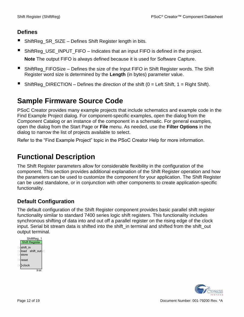
The default configuration of the Shift Register component provides basic parallel shift register functionality similar to standard 7400 series logic shift registers. This functionality includes synchronous shifting of data into and out off a parallel register on the rising edge of the clock input. Serial bit stream data is shifted into the shift_in terminal and shifted from the shift_out output terminal.

PSoC® Creator™ Component Datasheet Shift Register (ShiftReg)
Document Number: 001-79200 Rev. *A Page 13 of 19
Block Diagram and Configuration
Figure 1. Shift Register Block Diagram
FIFO
FIFO
Shift InShift Out
Load
Shift Register
Status Register
Status Register
Reset
Clock
8
CPU
8
8
Store
Control RegisterInterrupt
8
8
FIFO status
Control Logic
3
Status RegisterTo CPU
FIFO
clock
FIFO
clock
FIFO status
The Shift Register is a UDB-based component that consists of an input FIFO (F0), a direct shift register (A0 and A1 with duplicated value for providing the software capture), an output FIFO (F1), and control and status registers.
The input FIFO F0 is configured to input mode. This means that this FIFO can be written by the CPU (using the ShiftReg_WriteData() API function) and this value can be loaded into the A0 register for shifting. This function checks the current FIFO status before each cycle using the ShiftReg_GetFIFOStatus() function.
The value to be shifted can be also written directly to the A0 register by calling ShiftReg_WriteRegValue(). Because of internal hardware implementation it is strongly recommended to stop component operation (by using ShiftReg_Stop() function or stopping input clock) when using ShiftReg_WriteRegValue(). Otherwise, writing the A0 register during the shift operation will lead to incorrect data being written.
The Load operation has the hardware restriction that the load event can be provided only when input FIFO is not empty.
Shift Register (ShiftReg) PSoC® Creator™ Component Datasheet
Page 14 of 19 Document Number: 001-79200 Rev. *A
To provide the shift functionality, the UDB datapaths are used in the following configuration:
State == 100 (4) Shift Operation (Left or Right)
State == 101 (5) Reset (XOR A0 A0)
State == 110 (6) Load A0 <=F0
State == 111 (7) Reset (XOR A0 A0)
All operations except store are controlled from the datapath control store. Shift is a default operation (cs_addr = “000”). The load input is connected to the cs_addr[1] line and the reset input to cs_addr[0]. If some of these lines change their level it causes the control store address to change immediately. On the positive edge of the datapath clock (component clock in this case), the corresponding operation will be executed. The load causes the loading value to change from F0 to A0. The reset command causes the clearing of A0. In this case, the load value is ignored.
Two mechanisms are used to read the shifted value: hardware and software capture. The hardware capture event happens on each positive edge on the store input. It causes the Shift Register value to be written to the output FIFO. This value can be read by the ShiftReg_ReadData() API function. The store input has a hardware restriction that the store input will be active only if output FIFO is not full.
Software capture happens each time the ShiftReg_ReadRegValue() function is called. This function reads the A1 value where it duplicates the value of A0. This operation reduces the A1 value to be automatically written to the output FIFO F1 (because F1 is configured to software capture from A1). Before providing the software capture, the ShiftReg_ReadRegData() function clears the output FIFO. Therefore, you should be careful when using it.
Note Using this function, the actual value in the A1 will be available in the next clock cycle after writing the Shift Register.
The interrupt generation mechanism is implemented using the status register. It has three bits, which represent three interrupt sources: Load, Store, and Reset. When one of these bits changes its value from 0 to 1, the interrupt pulse on the appropriate status register output is automatically generated. These three bits are in “clear-on-read” mode.
The second status register is used for storing the current input and output FIFO's status. All status bits are in “sticky” mode (are not cleared after reading).
When the Shift Register size is more than 8, the datapath's chaining connectivity is provided to connect 2, 3, or 4 datapaths together to implement a component size 16, 24, or 32. To implement a Shift Register size that does not coincide with the datapath’s measures, a Verilog-controlled MSB is used with the datapath’s configurations.
The component is started and stopped using the CLK_EN bit of the control register.

PSoC® Creator™ Component Datasheet Shift Register (ShiftReg)
Document Number: 001-79200 Rev. *A Page 15 of 19
Registers
ShiftReg_SR_CONTROL
Bits 7 6 5 4 3 2 1 0
Value Reserved clk_en
clk_en : Enables Shift Register operation
ShiftReg_SR_STATUS
Bits 7 6 5 4 3 2 1 0
Value F1_not_ empty
F1_full F0_not_full F0_empty reset store load
load: Load status bit
store: Store status bit
reset: Reset status bit
F0_empty: Input FIFO is empty
F0_not_full: Input FIFO is not full
F1_full: Output FIFO full
F1_not_empty: Output FIFO is not empty
Resources
The Shift Register component is placed throughout the UDB array. The component utilizes the following resources.
Configuration
Resource Type
Datapath Cells
Macrocells Status Cells
Control Cells
DMA Channels
Interrupts
8-bit 1 2 1 1 – –
16-bit 2 2 1 1 – –
24-bit 3 2 1 1 – –
32-bit 4 2 1 1 – –

Shift Register (ShiftReg) PSoC® Creator™ Component Datasheet
Page 16 of 19 Document Number: 001-79200 Rev. *A
API Memory Usage
The component memory usage varies significantly, depending on the compiler, device, number of APIs used and component configuration. The following table provides the memory usage for all APIs available in the given component configuration.
The measurements have been done with the associated compiler configured in Release mode with optimization set for Size. For a specific design the map file generated by the compiler can be analyzed to determine the memory usage.
Configuration
PSoC 3 (Keil_PK51) PSoC 5 (GCC) PSoC 5LP (GCC)
Flash
Bytes
SRAM
Bytes
Flash
Bytes
SRAM
Bytes
Flash
Bytes
SRAM
Bytes
8-bit 342 4 482 5 462 5
16-bit 455 6 486 9 466 9
24-bit 454 10 510 17 490 13
32-bit 453 10 482 17 462 13
DC and AC Electrical Characteristics
Specifications are valid for –40 °C ≤ TA ≤ 85 °C and TJ ≤ 100 °C, except where noted. Specifications are valid for 1.71 V to 5.5 V, except where noted.
DC Characteristics
Parameter Description Min Typ[1] Max Units
IDD Component current consumption
8-bit – 13 – µA/MHz
16-bit – 20 – µA/MHz
24-bit – 27 – µA/MHz
32-bit – 34 – µA/MHz
1. Device IO and clock distribution current not included. The values are at 25 °C.

PSoC® Creator™ Component Datasheet Shift Register (ShiftReg)
Document Number: 001-79200 Rev. *A Page 17 of 19
AC Characteristics
Parameter Description Min Typ Max[2] Units
fCLOCK Component clock frequency
8-bit 52 MHz
16-bit 52 MHz
24-bit 50 MHz
32-bit 50 MHz
2. The values provide a maximum safe operating frequency of the component. The component may run at higher clock frequencies, at which point you will need to validate the timing requirements with STA results.
Shift Register (ShiftReg) PSoC® Creator™ Component Datasheet
Page 18 of 19 Document Number: 001-79200 Rev. *A
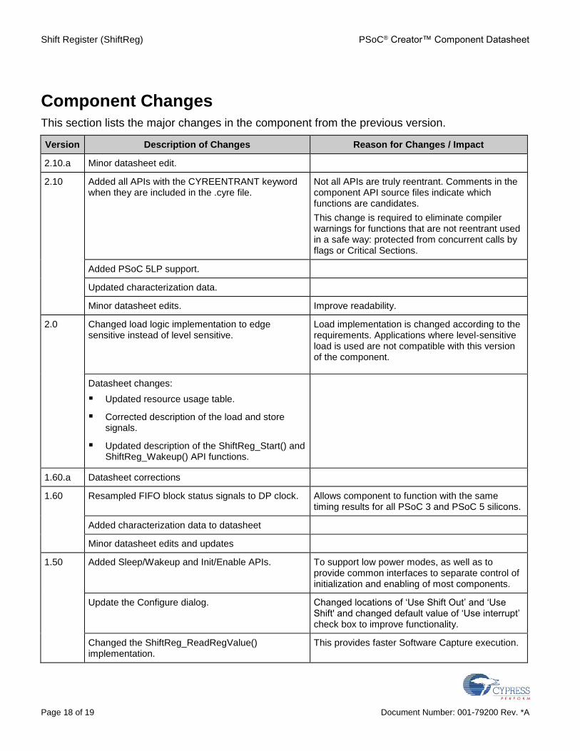
Component Changes
This section lists the major changes in the component from the previous version.
Version Description of Changes Reason for Changes / Impact
2.10.a Minor datasheet edit.
2.10 Added all APIs with the CYREENTRANT keyword when they are included in the .cyre file.
Not all APIs are truly reentrant. Comments in the component API source files indicate which functions are candidates.
This change is required to eliminate compiler warnings for functions that are not reentrant used in a safe way: protected from concurrent calls by flags or Critical Sections.
Added PSoC 5LP support.
Updated characterization data.
Minor datasheet edits. Improve readability.
2.0 Changed load logic implementation to edge sensitive instead of level sensitive.
Load implementation is changed according to the requirements. Applications where level-sensitive load is used are not compatible with this version of the component.
Datasheet changes:
Updated resource usage table.
Corrected description of the load and store signals.
Updated description of the ShiftReg_Start() and ShiftReg_Wakeup() API functions.
1.60.a Datasheet corrections
1.60 Resampled FIFO block status signals to DP clock. Allows component to function with the same timing results for all PSoC 3 and PSoC 5 silicons.
Added characterization data to datasheet
Minor datasheet edits and updates
1.50 Added Sleep/Wakeup and Init/Enable APIs. To support low power modes, as well as to provide common interfaces to separate control of initialization and enabling of most components.
Update the Configure dialog. Changed locations of ‘Use Shift Out’ and ‘Use Shift' and changed default value of ‘Use interrupt’ check box to improve functionality.
Changed the ShiftReg_ReadRegValue() implementation.
This provides faster Software Capture execution.

PSoC® Creator™ Component Datasheet Shift Register (ShiftReg)
Document Number: 001-79200 Rev. *A Page 19 of 19
Version Description of Changes Reason for Changes / Impact
1.20 Option of selecting FIFO size is disabled when load and store are not used.
Updated the Configure dialog.
Removed generated code for unused parameters.
Various changes were made to fix issues with version 1.10, which was not fully functional.
© Cypress Semiconductor Corporation, 2012-2015. The information contained herein is subject to change without notice. Cypress Semiconductor Corporation assumes no responsibility for the use of any circuitry other than circuitry embodied in a Cypress product. Nor does it convey or imply any license under patent or other rights. Cypress products are not warranted nor intended to be used for medical, life support, life saving, critical control or safety applications, unless pursuant to an express written agreement with Cypress. Furthermore, Cypress does not authorize its products for use as critical components in life-support systems where a malfunction or failure may reasonably be expected to result in significant injury to the user. The inclusion of Cypress products in life-support systems application implies that the manufacturer assumes all risk of such use and in doing so indemnifies Cypress against all charges.
PSoC® is a registered trademark, and PSoC Creator™ and Programmable System-on-Chip™ are trademarks and of Cypress Semiconductor Corp. All other trademarks or registered trademarks referenced herein are property of the respective corporations.
Any Source Code (software and/or firmware) is owned by Cypress Semiconductor Corporation (Cypress) and is protected by and subject to worldwide patent protection (United States and foreign), United States copyright laws and international treaty provisions. Cypress hereby grants to licensee a personal, non-exclusive, non-transferable license to copy, use, modify, create derivative works of, and compile the Cypress Source Code and derivative works for the sole purpose of creating custom software and or firmware in support of licensee product to be used only in conjunction with a Cypress integrated circuit as specified in the applicable agreement. Any reproduction, modification, translation, compilation, or representation of this Source Code except as specified above is prohibited without the express written permission of Cypress.
Disclaimer: CYPRESS MAKES NO WARRANTY OF ANY KIND, EXPRESS OR IMPLIED, WITH REGARD TO THIS MATERIAL, INCLUDING, BUT NOT LIMITED TO, THE IMPLIED WARRANTIES OF MERCHANTABILITY AND FITNESS FOR A PARTICULAR PURPOSE. Cypress reserves the right to make changes without further notice to the materials described herein. Cypress does not assume any liability arising out of the application or use of any product or circuit described herein. Cypress does not authorize its products for use as critical components in life-support systems where a malfunction or failure may reasonably be expected to result in significant injury to the user. The inclusion of Cypress’ product in a life-support systems application implies that the manufacturer assumes all risk of such use and in doing so indemnifies Cypress against all charges.
Use may be limited by and subject to the applicable Cypress software license agreement.