sn54lv221a, sn74lv221a dual monostable multivibrators with ...
18
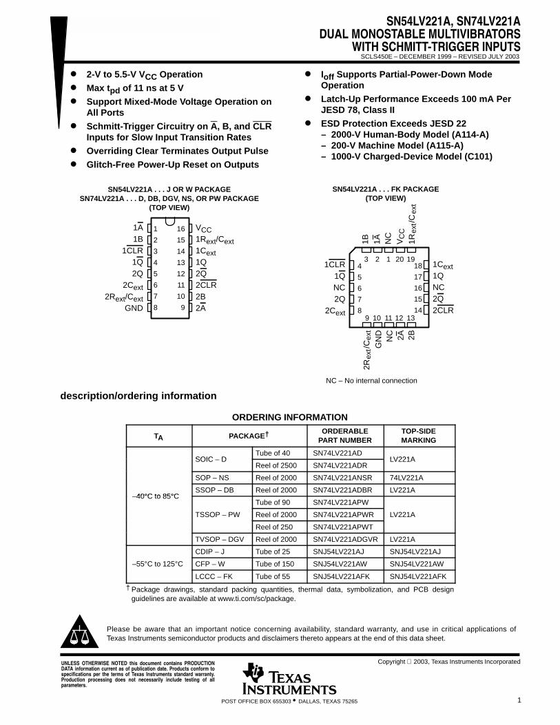
SN54LV221A, SN74LV221A DUAL MONOSTABLE MULTIVIBRATORS WITH SCHMITT-TRIGGER INPUTS SCLS450E – DECEMBER 1999 – REVISED JULY 2003 1 POST OFFICE BOX 655303 • DALLAS, TEXAS 75265 2-V to 5.5-V V CC Operation Max t pd of 11 ns at 5 V Support Mixed-Mode Voltage Operation on All Ports Schmitt-Trigger Circuitry on A , B, and CLR Inputs for Slow Input Transition Rates Overriding Clear Terminates Output Pulse Glitch-Free Power-Up Reset on Outputs I off Supports Partial-Power-Down Mode Operation Latch-Up Performance Exceeds 100 mA Per JESD 78, Class II ESD Protection Exceeds JESD 22 – 2000-V Human-Body Model (A114-A) – 200-V Machine Model (A115-A) – 1000-V Charged-Device Model (C101) SN54LV221A . . . J OR W PACKAGE SN74LV221A . . . D, DB, DGV, NS, OR PW PACKAGE (TOP VIEW) SN54LV221A . . . FK PACKAGE (TOP VIEW) 1 2 3 4 5 6 7 8 16 15 14 13 12 11 10 9 1A 1B 1CLR 1Q 2Q 2C ext 2R ext /C ext GND V CC 1R ext /C ext 1C ext 1Q 2Q 2CLR 2B 2A 3 2 1 20 19 9 10 11 12 13 4 5 6 7 8 18 17 16 15 14 1C ext 1Q NC 2Q 2CLR 1CLR 1Q NC 2Q 2C ext 1B 1A NC 2A 2B V 1R 2R GND NC CC NC – No internal connection ext /C ext ext /C ext description/ordering information ORDERING INFORMATION T A PACKAGE † ORDERABLE PART NUMBER TOP-SIDE MARKING SOIC D Tube of 40 SN74LV221AD LV221A SOIC – D Reel of 2500 SN74LV221ADR LV221A SOP – NS Reel of 2000 SN74LV221ANSR 74LV221A 40°C to 85°C SSOP – DB Reel of 2000 SN74LV221ADBR LV221A –40°C to 85°C Tube of 90 SN74LV221APW TSSOP – PW Reel of 2000 SN74LV221APWR LV221A Reel of 250 SN74LV221APWT TVSOP – DGV Reel of 2000 SN74LV221ADGVR LV221A CDIP – J Tube of 25 SNJ54LV221AJ SNJ54LV221AJ –55°C to 125°C CFP – W Tube of 150 SNJ54LV221AW SNJ54LV221AW LCCC – FK Tube of 55 SNJ54LV221AFK SNJ54LV221AFK † Package drawings, standard packing quantities, thermal data, symbolization, and PCB design guidelines are available at www.ti.com/sc/package. Copyright 2003, Texas Instruments Incorporated Please be aware that an important notice concerning availability, standard warranty, and use in critical applications of Texas Instruments semiconductor products and disclaimers thereto appears at the end of this data sheet. UNLESS OTHERWISE NOTED this document contains PRODUCTION DATA information current as of publication date. Products conform to specifications per the terms of Texas Instruments standard warranty. Production processing does not necessarily include testing of all parameters.
-
Upload
khangminh22 -
Category
Documents
-
view
1 -
download
0
Transcript of sn54lv221a, sn74lv221a dual monostable multivibrators with ...
SN54LV221A, SN74LV221ADUAL MONOSTABLE MULTIVIBRATORS
WITH SCHMITT-TRIGGER INPUTSSCLS450E – DECEMBER 1999 – REVISED JULY 2003
1POST OFFICE BOX 655303 • DALLAS, TEXAS 75265
2-V to 5.5-V VCC Operation
Max tpd of 11 ns at 5 V
Support Mixed-Mode Voltage Operation onAll Ports
Schmitt-Trigger Circuitry on A, B, and CLRInputs for Slow Input Transition Rates
Overriding Clear Terminates Output Pulse
Glitch-Free Power-Up Reset on Outputs
Ioff Supports Partial-Power-Down ModeOperation
Latch-Up Performance Exceeds 100 mA PerJESD 78, Class II
ESD Protection Exceeds JESD 22– 2000-V Human-Body Model (A114-A)– 200-V Machine Model (A115-A)– 1000-V Charged-Device Model (C101)
SN54LV221A . . . J OR W PACKAGESN74LV221A . . . D, DB, DGV, NS, OR PW PACKAGE
(TOP VIEW)
SN54LV221A . . . FK PACKAGE(TOP VIEW)
1
2
3
4
5
6
7
8
16
15
14
13
12
11
10
9
1A1B
1CLR1Q2Q
2Cext2Rext/Cext
GND
VCC1Rext/Cext1Cext1Q2Q2CLR2B2A
3 2 1 20 19
9 10 11 12 13
4
5
6
7
8
18
17
16
15
14
1Cext1QNC2Q2CLR
1CLR1QNC2Q
2Cext
1B 1A NC
2A 2BV 1R
2RG
ND
NC
CC
NC – No internal connection
ext/
Cex
t
ext/
Cex
t
description/ordering information
ORDERING INFORMATION
TA PACKAGE† ORDERABLEPART NUMBER
TOP-SIDEMARKING
SOIC DTube of 40 SN74LV221AD
LV221ASOIC – DReel of 2500 SN74LV221ADR
LV221A
SOP – NS Reel of 2000 SN74LV221ANSR 74LV221A
40°C to 85°CSSOP – DB Reel of 2000 SN74LV221ADBR LV221A
–40°C to 85°CTube of 90 SN74LV221APW
TSSOP – PW Reel of 2000 SN74LV221APWR LV221A
Reel of 250 SN74LV221APWT
TVSOP – DGV Reel of 2000 SN74LV221ADGVR LV221A
CDIP – J Tube of 25 SNJ54LV221AJ SNJ54LV221AJ
–55°C to 125°C CFP – W Tube of 150 SNJ54LV221AW SNJ54LV221AW
LCCC – FK Tube of 55 SNJ54LV221AFK SNJ54LV221AFK
† Package drawings, standard packing quantities, thermal data, symbolization, and PCB designguidelines are available at www.ti.com/sc/package.
Copyright 2003, Texas Instruments Incorporated
Please be aware that an important notice concerning availability, standard warranty, and use in critical applications ofTexas Instruments semiconductor products and disclaimers thereto appears at the end of this data sheet.
UNLESS OTHERWISE NOTED this document contains PRODUCTIONDATA information current as of publication date. Products conform tospecifications per the terms of Texas Instruments standard warranty.Production processing does not necessarily include testing of allparameters.
SN54LV221A, SN74LV221ADUAL MONOSTABLE MULTIVIBRATORSWITH SCHMITT-TRIGGER INPUTSSCLS450E – DECEMBER 1999 – REVISED JULY 2003
2 POST OFFICE BOX 655303 • DALLAS, TEXAS 75265
description/ordering information (continued)
The ’LV221A devices are dual multivibrators designed for 2-V to 5.5-V VCC operation. Each multivibrator hasa negative-transition-triggered (A) input and a positive-transition-triggered (B) input, either of which can be usedas an inhibit input.
The ’LV221A devices are dual multivibrators designed for 2-V to 5.5-V VCC operation. Each multivibrator hasa negative-transition-triggered (A) input and a positive-transition-triggered (B) input, either of which can be usedas an inhibit input.
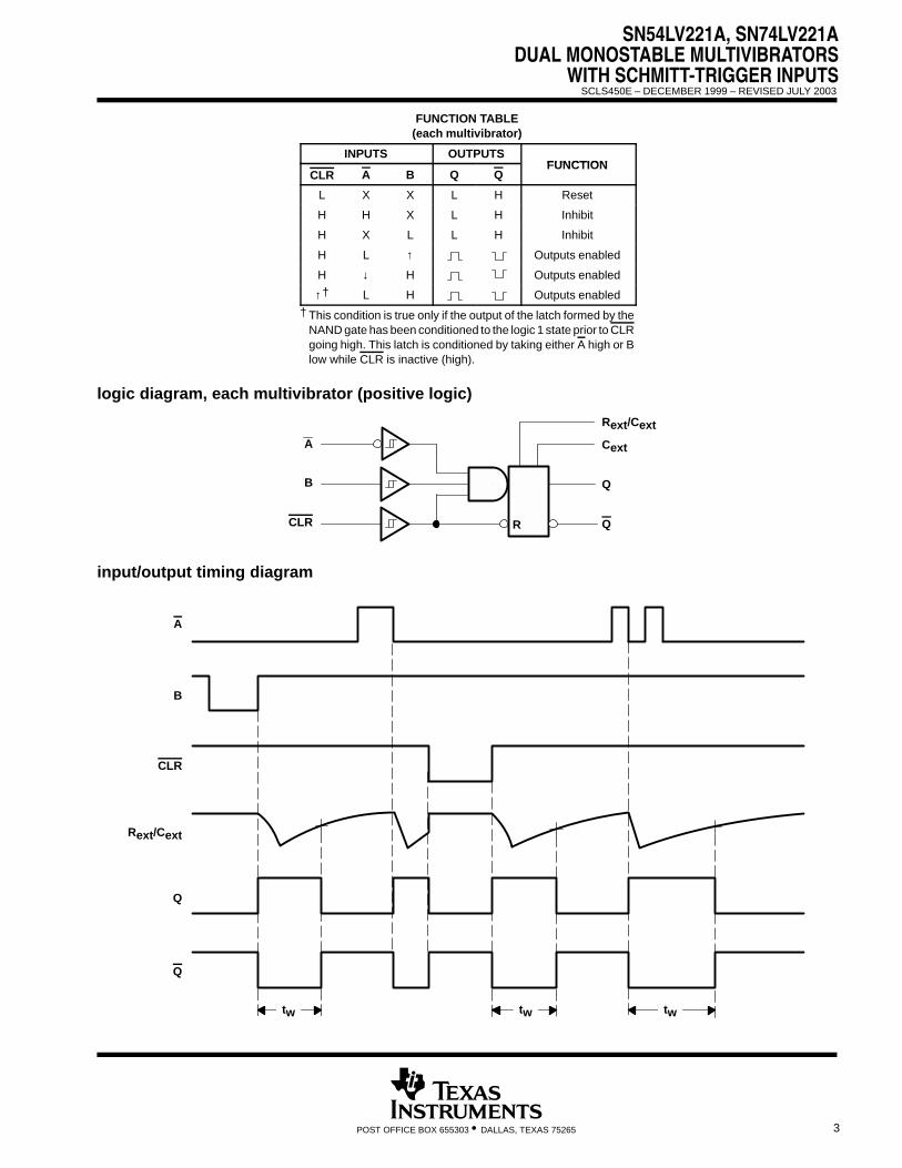
These edge-triggered multivibrators feature output pulse-duration control by three methods. In the first method,the A input is low and the B input goes high. In the second method, the B input is high and the A input goes low.In the third method, the A input is low, the B input is high, and the clear (CLR) input goes high.
The output pulse duration is programmable by selecting external resistance and capacitance values. Theexternal timing capacitor must be connected between Cext and Rext/Cext(positive) and an external resistorconnected between Rext/Cext and VCC. To obtain variable pulse durations, connect an external variable resistorbetween Rext/Cext and VCC. The output pulse duration also can be reduced by taking CLR low.
Pulse triggering occurs at a particular voltage level and is not related directly to the transition time of the inputpulse. The A, B, and CLR inputs have Schmitt triggers with sufficient hysteresis to handle slow input transitionrates with jitter-free triggering at the outputs.
Once triggered, the outputs are independent of further transitions of the A and B inputs and are a function ofthe timing components, or the output pulses can be terminated by the overriding clear. Input pulses can be ofany duration relative to the output pulse. Output pulse duration can be varied by choosing the appropriate timingcomponents. Output rise and fall times are TTL compatible and independent of pulse duration. Typical triggeringand clearing sequences are illustrated in the input/output timing diagram.
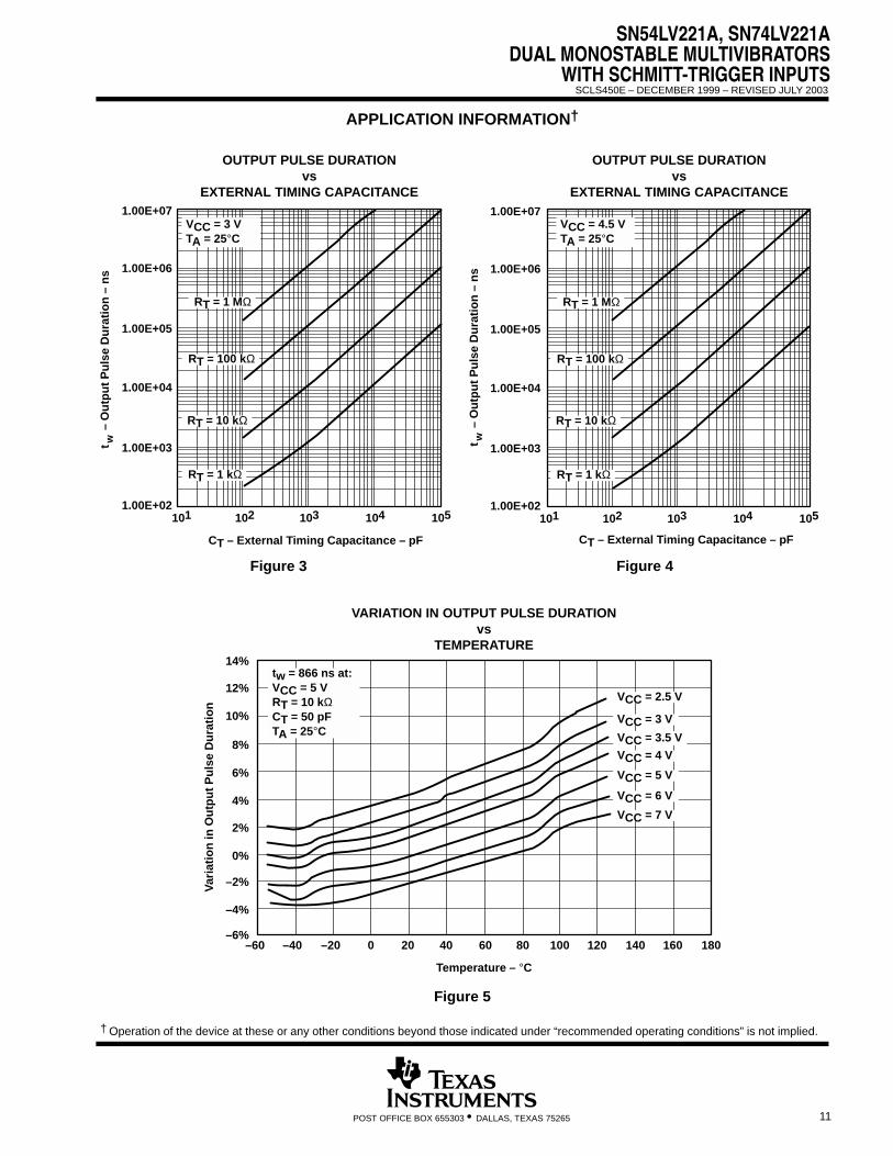
The variance in output pulse duration from device to device typically is less than ±0.5% for given external timingcomponents. An example of this distribution for the ’LV221A is shown in Figure 8. Variations in output pulseduration versus supply voltage and temperature are shown in Figure 5.
During power up, Q outputs are in the low state, and Q outputs are in the high state. The outputs are glitch free,without applying a reset pulse.
These devices are fully specified for partial-power-down applications using Ioff. The Ioff circuitry disables theoutputs, preventing damaging current backflow through the devices when they are powered down.
Pin assignments are identical to those of the ’AHC123A and ’AHCT123A devices, so the ’LV221A can besubstituted for those devices not using the retrigger feature.
For additional application information on multivibrators, see the application report Designing With TheSN74AHC123A and SN74AHCT123A, literature number SCLA014.
SN54LV221A, SN74LV221ADUAL MONOSTABLE MULTIVIBRATORS
WITH SCHMITT-TRIGGER INPUTSSCLS450E – DECEMBER 1999 – REVISED JULY 2003
3POST OFFICE BOX 655303 • DALLAS, TEXAS 75265
FUNCTION TABLE(each multivibrator)
INPUTS OUTPUTSFUNCTION
CLR A B Q QFUNCTION
L X X L H Reset
H H X L H Inhibit
H X L L H Inhibit
H L ↑ Outputs enabled
H ↓ H Outputs enabled
↑† L H Outputs enabled
† This condition is true only if the output of the latch formed by theNAND gate has been conditioned to the logic 1 state prior to CLRgoing high. This latch is conditioned by taking either A high or Blow while CLR is inactive (high).
logic diagram, each multivibrator (positive logic)
CLR
Cext
Rext/Cext
R
B
A
Q
Q
input/output timing diagram
A
B
CLR
Q
Q
tw tw
Rext/Cext
tw

SN54LV221A, SN74LV221ADUAL MONOSTABLE MULTIVIBRATORSWITH SCHMITT-TRIGGER INPUTSSCLS450E – DECEMBER 1999 – REVISED JULY 2003
4 POST OFFICE BOX 655303 • DALLAS, TEXAS 75265
absolute maximum ratings over operating free-air temperature (unless otherwise noted)†
Supply voltage range, VCC –0.5 V to 7 V. . . . . . . . . . . . . . . . . . . . . . . . . . . . . . . . . . . . . . . . . . . . . . . . . . . . . . . . . . Input voltage range, VI (see Note 1) –0.5 V to 7 V. . . . . . . . . . . . . . . . . . . . . . . . . . . . . . . . . . . . . . . . . . . . . . . . . . Output voltage range in high or low state, VO (see Notes 1 and 2) –0.5 V to VCC + 0.5 V. . . . . . . . . . . . . . . . . Output voltage range in power-off state, VO (see Note 1) –0.5 V to 7 V. . . . . . . . . . . . . . . . . . . . . . . . . . . . . . . . Input clamp current, IIK (VI < 0) –20 mA. . . . . . . . . . . . . . . . . . . . . . . . . . . . . . . . . . . . . . . . . . . . . . . . . . . . . . . . . . . Output clamp current, IOK (VO < 0 or VO > VCC) ±50 mA. . . . . . . . . . . . . . . . . . . . . . . . . . . . . . . . . . . . . . . . . . . . Continuous output current, IO (VO = 0 to VCC) ±25 mA. . . . . . . . . . . . . . . . . . . . . . . . . . . . . . . . . . . . . . . . . . . . . . Continuous current through VCC or GND ±50 mA. . . . . . . . . . . . . . . . . . . . . . . . . . . . . . . . . . . . . . . . . . . . . . . . . . . Package thermal impedance, θJA (see Note 3): D package 73°C/W. . . . . . . . . . . . . . . . . . . . . . . . . . . . . . . . . . .
DB package 82°C/W. . . . . . . . . . . . . . . . . . . . . . . . . . . . . . . . . DGV package 120°C/W. . . . . . . . . . . . . . . . . . . . . . . . . . . . . . . NS package 64°C/W. . . . . . . . . . . . . . . . . . . . . . . . . . . . . . . . . PW package 108°C/W. . . . . . . . . . . . . . . . . . . . . . . . . . . . . . . .
Storage temperature range, Tstg –65°C to 150°C. . . . . . . . . . . . . . . . . . . . . . . . . . . . . . . . . . . . . . . . . . . . . . . . . . .
† Stresses beyond those listed under “absolute maximum ratings” may cause permanent damage to the device. These are stress ratings only, andfunctional operation of the device at these or any other conditions beyond those indicated under “recommended operating conditions” is notimplied. Exposure to absolute-maximum-rated conditions for extended periods may affect device reliability.
NOTES: 1. The input and output voltage ratings may be exceeded if the input and output current ratings are observed.2. This value is limited to 5.5 V maximum.3. The package thermal impedance is calculated in accordance with JESD 51-7.
SN54LV221A, SN74LV221ADUAL MONOSTABLE MULTIVIBRATORS
WITH SCHMITT-TRIGGER INPUTSSCLS450E – DECEMBER 1999 – REVISED JULY 2003
5POST OFFICE BOX 655303 • DALLAS, TEXAS 75265
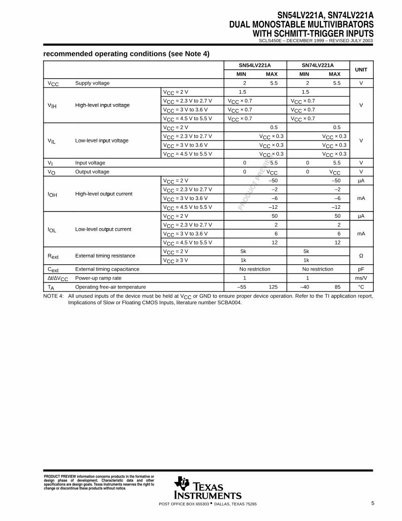
recommended operating conditions (see Note 4)
SN54LV221A SN74LV221AUNIT
MIN MAX MIN MAXUNIT
VCC Supply voltage 2 5.5 2 5.5 V
VCC = 2 V 1.5 1.5
VIH High level input voltageVCC = 2.3 V to 2.7 V VCC × 0.7 VCC × 0.7
VVIH High-level input voltageVCC = 3 V to 3.6 V VCC × 0.7 VCC × 0.7
V
VCC = 4.5 V to 5.5 V VCC × 0.7 VCC × 0.7
VCC = 2 V 0.5 0.5
VIL Low level input voltageVCC = 2.3 V to 2.7 V VCC × 0.3 VCC × 0.3
VVIL Low-level input voltageVCC = 3 V to 3.6 V VCC × 0.3 VCC × 0.3
V
VCC = 4.5 V to 5.5 V VCC × 0.3 VCC × 0.3
VI Input voltage 0 5.5 0 5.5 V
VO Output voltage 0 VCC 0 VCC V
VCC = 2 V –50 –50 µA
IOH High level output currentVCC = 2.3 V to 2.7 V –2 –2
IOH High-level output currentVCC = 3 V to 3.6 V –6 –6 mA
VCC = 4.5 V to 5.5 V –12 –12
VCC = 2 V 50 50 µA
IOL Low level output currentVCC = 2.3 V to 2.7 V 2 2
IOL Low-level output currentVCC = 3 V to 3.6 V 6 6 mA
VCC = 4.5 V to 5.5 V 12 12
R t External timing resistanceVCC = 2 V 5k 5k
ΩRext External timing resistanceVCC ≥ 3 V 1k 1k
Ω
Cext External timing capacitance No restriction No restriction pF
∆t/∆VCC Power-up ramp rate 1 1 ms/V
TA Operating free-air temperature –55 125 –40 85 °C
NOTE 4: All unused inputs of the device must be held at VCC or GND to ensure proper device operation. Refer to the TI application report,Implications of Slow or Floating CMOS Inputs, literature number SCBA004.
PRODUCT PREVIEW information concerns products in the formative ordesign phase of development. Characteristic data and otherspecifications are design goals. Texas Instruments reserves the right tochange or discontinue these products without notice.
SN54LV221A, SN74LV221ADUAL MONOSTABLE MULTIVIBRATORSWITH SCHMITT-TRIGGER INPUTSSCLS450E – DECEMBER 1999 – REVISED JULY 2003
6 POST OFFICE BOX 655303 • DALLAS, TEXAS 75265
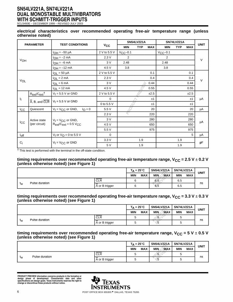
electrical characteristics over recommended operating free-air temperature range (unlessotherwise noted)
PARAMETER TEST CONDITIONS VSN54LV221A SN74LV221A
UNITPARAMETER TEST CONDITIONS VCC MIN TYP MAX MIN TYP MAXUNIT
IOH = –50 µA 2 V to 5.5 V VCC–0.1 VCC–0.1
VOHIOH = –2 mA 2.3 V 2 2
VVOHIOH = –6 mA 3 V 2.48 2.48
V
IOH = –12 mA 4.5 V 3.8 3.8
IOL = 50 µA 2 V to 5.5 V 0.1 0.1
VOLIOL = 2 mA 2.3 V 0.4 0.4
VVOLIOL = 6 mA 3 V 0.44 0.44
V
IOL = 12 mA 4.5 V 0.55 0.55
Rext/Cext† VI = 5.5 V or GND 2 V to 5.5 V ±2.5 ±2.5
IIA B d CLR VI = 5 5 V or GND
0 ±1 ±1 µAA, B, and CLR VI = 5.5 V or GND
0 to 5.5 V ±1 ±1
ICC Quiescent VI = VCC or GND, IO = 0 5.5 V 20 20 µA
2.3 V 220 220
ICCActive state VI = VCC or GND, 3 V 280 280
µAICC (per circuit)I CC ,
Rext/Cext = 0.5 VCC 4.5 V 650 650µA
5.5 V 975 975
Ioff VI or VO = 0 to 5.5 V 0 5 µA
Ci VI = VCC or GND3.3 V 1.9 1.9
pFCi VI = VCC or GND5 V 1.9 1.9
pF
† This test is performed with the terminal in the off-state condition.
timing requirements over recommended operating free-air temperature range, VCC = 2.5 V ± 0.2 V(unless otherwise noted) (see Figure 1)
TA = 25°C SN54LV221A SN74LV221AUNIT
MIN MAX MIN MAX MIN MAXUNIT
t Pulse durationCLR 6 6.5 6.5
nstw Pulse durationA or B trigger 6 6.5 6.5
ns
timing requirements over recommended operating free-air temperature range, VCC = 3.3 V ± 0.3 V(unless otherwise noted) (see Figure 1)
TA = 25°C SN54LV221A SN74LV221AUNIT
MIN MAX MIN MAX MIN MAXUNIT
t Pulse durationCLR 5 5 5
nstw Pulse durationA or B trigger 5 5 5
ns
timing requirements over recommended operating free-air temperature range, VCC = 5 V ± 0.5 V(unless otherwise noted) (see Figure 1)
TA = 25°C SN54LV221A SN74LV221AUNIT
MIN MAX MIN MAX MIN MAXUNIT
t Pulse durationCLR 5 5 5
nstw Pulse durationA or B trigger 5 5 5
ns
PRODUCT PREVIEW information concerns products in the formative ordesign phase of development. Characteristic data and otherspecifications are design goals. Texas Instruments reserves the right tochange or discontinue these products without notice.

SN54LV221A, SN74LV221ADUAL MONOSTABLE MULTIVIBRATORS
WITH SCHMITT-TRIGGER INPUTSSCLS450E – DECEMBER 1999 – REVISED JULY 2003
7POST OFFICE BOX 655303 • DALLAS, TEXAS 75265
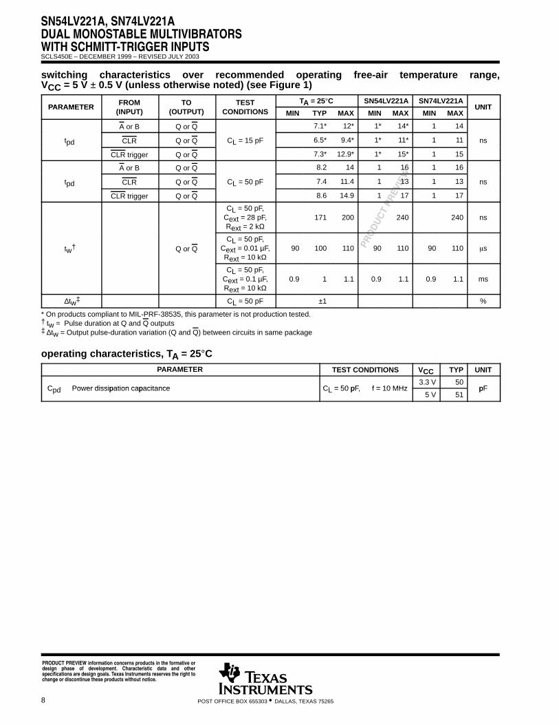
switching characteristics over recommended operating free-air temperature range,VCC = 2.5 V ± 0.2 V (unless otherwise noted) (see Figure 1)
PARAMETERFROM TO TEST TA = 25°C SN54LV221A SN74LV221A
UNITPARAMETER(INPUT) (OUTPUT) CONDITIONS MIN TYP MAX MIN MAX MIN MAX
UNIT
A or B Q or Q 14.6* 31.4* 1* 37* 1 37
tpd CLR Q or Q CL = 15 pF 13.2* 25* 1* 29.5* 1 29.5 ns
CLR trigger Q or Q 15.2* 33.4* 1* 39* 1 39
A or B Q or Q 16.7 36 1 42 1 42
tpd CLR Q or Q CL = 50 pF 15 32.8 1 34.5 1 34.5 ns
CLR trigger Q or Q 17.4 38 1 44 1 44
†
CL = 50 pF,Cext = 28 pF,Rext = 2 kΩ
203 260 320 320 ns
tw† Q or QCL = 50 pF,
Cext = 0.01 µF,Rext = 10 kΩ
90 100 110 90 110 90 110 s
CL = 50 pF,Cext = 0.1 µF,Rext = 10 kΩ
0.9 1 1.1 0.9 1.1 0.9 1.1 ms
∆tw‡ CL = 50 pF ±1 %
* On products compliant to MIL-PRF-38535, this parameter is not production tested.† tw = Pulse duration at Q and Q outputs‡ ∆tw = Output pulse-duration variation (Q and Q) between circuits in same package
switching characteristics over recommended operating free-air temperature range,VCC = 3.3 V ± 0.3 V (unless otherwise noted) (see Figure 1)
PARAMETERFROM TO TEST TA = 25°C SN54LV221A SN74LV221A
UNITPARAMETER(INPUT) (OUTPUT) CONDITIONS MIN TYP MAX MIN MAX MIN MAX
UNIT
A or B Q or Q 10.2* 20.6* 1* 24* 1 24
tpd CLR Q or Q CL = 15 pF 9.3* 15.8* 1* 18.5* 1 18.5 ns
CLR trigger Q or Q 10.6* 22.4* 1* 26* 1 26
A or B Q or Q 11.8 24.1 1 27.5 1 27.5
tpd CLR Q or Q CL = 50 pF 10.6 19.3 1 22 1 22 ns
CLR trigger Q or Q 12.3 25.9 1 29.5 1 29.5
†
CL = 50 pF,Cext = 28 pF,Rext = 2 kΩ
186 240 300 300 ns
tw† Q or QCL = 50 pF,
Cext = 0.01 µF,Rext = 10 kΩ
90 100 110 90 110 90 110 s
CL = 50 pF,Cext = 0.1 µF,Rext = 10 kΩ
0.9 1 1.1 0.9 1.1 0.9 1.1 ms
∆tw‡ CL = 50 pF ±1 %
* On products compliant to MIL-PRF-38535, this parameter is not production tested.† tw = Pulse duration at Q and Q outputs‡ ∆tw = Output pulse-duration variation (Q and Q) between circuits in same package
PRODUCT PREVIEW information concerns products in the formative ordesign phase of development. Characteristic data and otherspecifications are design goals. Texas Instruments reserves the right tochange or discontinue these products without notice.
SN54LV221A, SN74LV221ADUAL MONOSTABLE MULTIVIBRATORSWITH SCHMITT-TRIGGER INPUTSSCLS450E – DECEMBER 1999 – REVISED JULY 2003
8 POST OFFICE BOX 655303 • DALLAS, TEXAS 75265
switching characteristics over recommended operating free-air temperature range,VCC = 5 V ± 0.5 V (unless otherwise noted) (see Figure 1)
PARAMETERFROM TO TEST TA = 25°C SN54LV221A SN74LV221A
UNITPARAMETER(INPUT) (OUTPUT) CONDITIONS MIN TYP MAX MIN MAX MIN MAX
UNIT
A or B Q or Q 7.1* 12* 1* 14* 1 14
tpd CLR Q or Q CL = 15 pF 6.5* 9.4* 1* 11* 1 11 ns
CLR trigger Q or Q 7.3* 12.9* 1* 15* 1 15
A or B Q or Q 8.2 14 1 16 1 16
tpd CLR Q or Q CL = 50 pF 7.4 11.4 1 13 1 13 ns
CLR trigger Q or Q 8.6 14.9 1 17 1 17
†
CL = 50 pF,Cext = 28 pF,Rext = 2 kΩ
171 200 240 240 ns
tw† Q or QCL = 50 pF,
Cext = 0.01 µF,Rext = 10 kΩ
90 100 110 90 110 90 110 s
CL = 50 pF,Cext = 0.1 µF,Rext = 10 kΩ
0.9 1 1.1 0.9 1.1 0.9 1.1 ms
∆tw‡ CL = 50 pF ±1 %
* On products compliant to MIL-PRF-38535, this parameter is not production tested.† tw = Pulse duration at Q and Q outputs‡ ∆tw = Output pulse-duration variation (Q and Q) between circuits in same package
operating characteristics, TA = 25°CPARAMETER TEST CONDITIONS VCC TYP UNIT
C d Power dissipation capacitance CL = 50 pF f = 10 MHz3.3 V 50
pFCpd Power dissipation capacitance CL = 50 pF, f = 10 MHz5 V 51
pF
PRODUCT PREVIEW information concerns products in the formative ordesign phase of development. Characteristic data and otherspecifications are design goals. Texas Instruments reserves the right tochange or discontinue these products without notice.
SN54LV221A, SN74LV221ADUAL MONOSTABLE MULTIVIBRATORS
WITH SCHMITT-TRIGGER INPUTSSCLS450E – DECEMBER 1999 – REVISED JULY 2003
9POST OFFICE BOX 655303 • DALLAS, TEXAS 75265
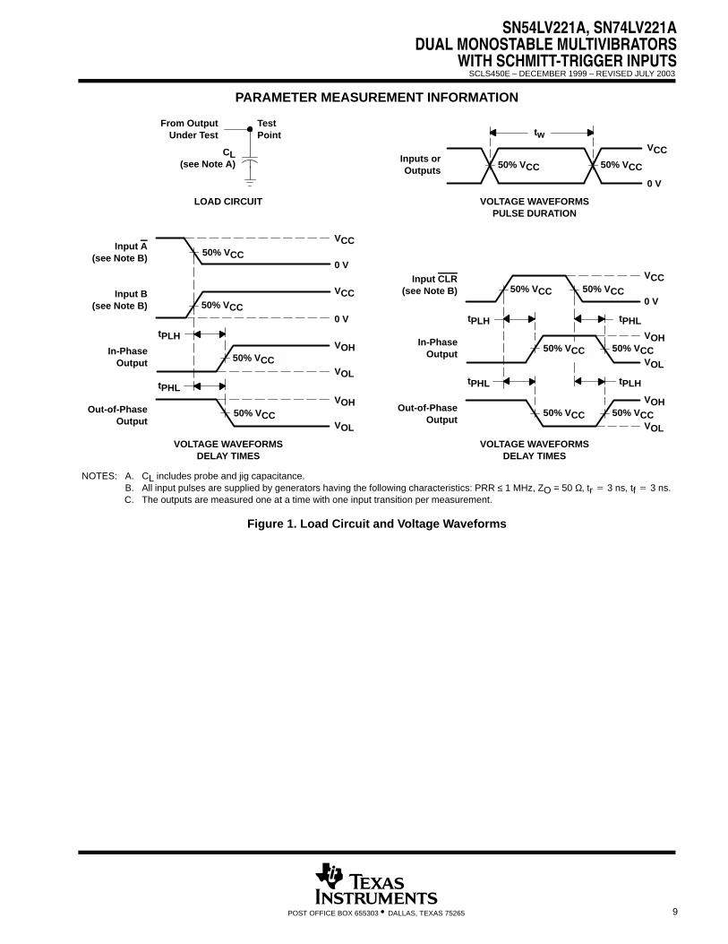
PARAMETER MEASUREMENT INFORMATION
NOTES: A. CL includes probe and jig capacitance.B. All input pulses are supplied by generators having the following characteristics: PRR ≤ 1 MHz, ZO = 50 Ω, tr 3 ns, tf 3 ns.C. The outputs are measured one at a time with one input transition per measurement.
50% VCC
tPLH
tPHL
VOH
VOL
VCC
50% VCC
50% VCC
VCCInput A(see Note B)
50% VCC0 V
0 V
In-PhaseOutput
Out-of-PhaseOutput
VOLTAGE WAVEFORMSDELAY TIMES
Input B(see Note B)
VOL
VOH
LOAD CIRCUIT
TestPoint
CL(see Note A)
From Output Under Test
50% VCC
tPLH
tPHL
tPHL
tPLH
VOH
VOH
VOL
VOL
VCC
0 V
50% VCC
Input CLR(see Note B)
Out-of-PhaseOutput
In-PhaseOutput
VOLTAGE WAVEFORMSDELAY TIMES
50% VCC
50% VCC
50% VCC 50% VCC
VCC
0 V
tw
VOLTAGE WAVEFORMSPULSE DURATION
Inputs orOutputs
50% VCC50% VCC
Figure 1. Load Circuit and Voltage Waveforms
SN54LV221A, SN74LV221ADUAL MONOSTABLE MULTIVIBRATORSWITH SCHMITT-TRIGGER INPUTSSCLS450E – DECEMBER 1999 – REVISED JULY 2003
10 POST OFFICE BOX 655303 • DALLAS, TEXAS 75265
APPLICATION INFORMATION
caution in use
To prevent malfunctions due to noise, connect a high-frequency capacitor between VCC and GND, and keepthe wiring between the external components and Cext and Rext/Cext terminals as short as possible.
power-down considerations
Large values of Cext can cause problems when powering down the ’LV221A because of the amount of energystored in the capacitor. When a system containing this device is powered down, the capacitor can dischargefrom VCC through the protection diodes at pin 2 or pin 14. Current through the input protection diodes must belimited to 30 mA; therefore, the turn-off time of the VCC power supply must not be faster thant = VCC × Cext/30 mA. For example, if VCC = 5 V and Cext = 15 pF, the VCC supply must turn off no faster thant = (5 V) × (15 pF)/30 mA = 2.5 ns. Usually, this is not a problem because power supplies are heavily filteredand cannot discharge at this rate. When a more rapid decrease of VCC to zero occurs, the ’LV221A can sustaindamage. To avoid this possibility, use external clamping diodes.
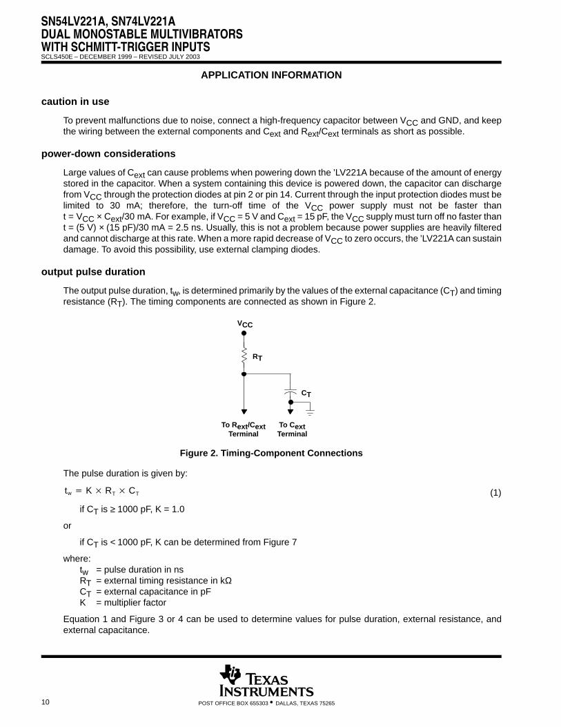
output pulse duration
The output pulse duration, tw, is determined primarily by the values of the external capacitance (CT) and timingresistance (RT). The timing components are connected as shown in Figure 2.
VCC
RT
CT
To Rext/CextTerminal
To CextTerminal
Figure 2. Timing-Component Connections
The pulse duration is given by:
tw K RT CT
if CT is ≥ 1000 pF, K = 1.0
or
if CT is < 1000 pF, K can be determined from Figure 7
where:tw = pulse duration in nsRT = external timing resistance in kΩCT = external capacitance in pFK = multiplier factor
Equation 1 and Figure 3 or 4 can be used to determine values for pulse duration, external resistance, andexternal capacitance.
(1)
SN54LV221A, SN74LV221ADUAL MONOSTABLE MULTIVIBRATORS
WITH SCHMITT-TRIGGER INPUTSSCLS450E – DECEMBER 1999 – REVISED JULY 2003
11POST OFFICE BOX 655303 • DALLAS, TEXAS 75265
APPLICATION INFORMATION†
Figure 3
OUTPUT PULSE DURATIONvs
EXTERNAL TIMING CAPACITANCE1.00E+07
t w–
Ou
tpu
t P
uls
e D
ura
tio
n –
ns 1.00E+06
1.00E+05
1.00E+04
1.00E+03
1.00E+02
CT – External Timing Capacitance – pF
101 102 103 104 105
VCC = 3 VTA = 25°C
RT = 1 MΩ
RT = 100 kΩ
RT = 10 kΩ
RT = 1 kΩ
Figure 4
OUTPUT PULSE DURATIONvs
EXTERNAL TIMING CAPACITANCE1.00E+07
t w–
Ou
tpu
t P
uls
e D
ura
tio
n –
ns 1.00E+06
1.00E+05
1.00E+04
1.00E+03
1.00E+02
CT – External Timing Capacitance – pF
101 102 103 104 105
RT = 1 MΩ
RT = 100 kΩ
RT = 10 kΩ
RT = 1 kΩ
VCC = 4.5 VTA = 25°C
tw = 866 ns at:VCC = 5 VRT = 10 kΩCT = 50 pFTA = 25°C
–60 –40 –20 0 20 40 60 80 100 120 140 160
VCC = 2.5 V
VCC = 3 V
VCC = 3.5 V
VCC = 4 V
VCC = 5 V
VCC = 6 V
VCC = 7 V
180–6%
–4%
–2%
0%
2%
4%
6%
8%
10%
12%
14%
Temperature – °C
Var
iati
on
in O
utp
ut
Pu
lse
Du
rati
on
VARIATION IN OUTPUT PULSE DURATIONvs
TEMPERATURE
Figure 5
† Operation of the device at these or any other conditions beyond those indicated under “recommended operating conditions” is not implied.
SN54LV221A, SN74LV221ADUAL MONOSTABLE MULTIVIBRATORSWITH SCHMITT-TRIGGER INPUTSSCLS450E – DECEMBER 1999 – REVISED JULY 2003
12 POST OFFICE BOX 655303 • DALLAS, TEXAS 75265
APPLICATION INFORMATION†
Figure 6
1.00 1.50 2.00 2.50 3.00 3.50 4.00 4.50
0.00001
0.0001
0.001
TA = 25°CVCC = 5 V
For Capacitor Values of0.001 µF or Greater, K = 1.0(K is Independent of R)
Multiplier Factor – K
EXTERNAL CAPACITANCEvs
MULTIPLIER FACTOR
CT
– E
xter
nal
Cap
acit
or
Val
ue
– µ F
Figure 7
1.20
1.15
1.10
1.05
1.00
0.95
0.901.5 2 2.5 3 3.5 4 4.5 5 5.5 6
RT = 10 kΩTA = 25°Ctw = K × CT × RT
VCC – Supply Voltage – V
OUTPUT PULSE DURATION CONSTANTvs
SUPPLY VOLTAGE
Ou
tpu
t P
uls
e D
ura
tio
n C
on
stan
t –
K
CT = 1000 pF
CT = 0.01 µF
CT = 0.1 µF
tw – Output Pulse Duration
Rel
ativ
e F
req
uen
cy o
f Occ
urr
ence
DISTRIBUTION OF UNITSvs
OUTPUT PULSE DURATION
Mean = 856 nsMedian = 856 nsStd. Dev. = 3.5 ns
VCC = 5 VTA = 25°CCT = 50 pFRT = 10 kΩ
–3 Std. Dev. +3 Std. Dev.Median99% of Data Units
Figure 8
† Operation of the device at these or any other conditions beyond those indicated under “recommended operating conditions” is not implied.
MECHANICAL DATA
MPDS006C – FEBRUARY 1996 – REVISED AUGUST 2000
1POST OFFICE BOX 655303 • DALLAS, TEXAS 75265
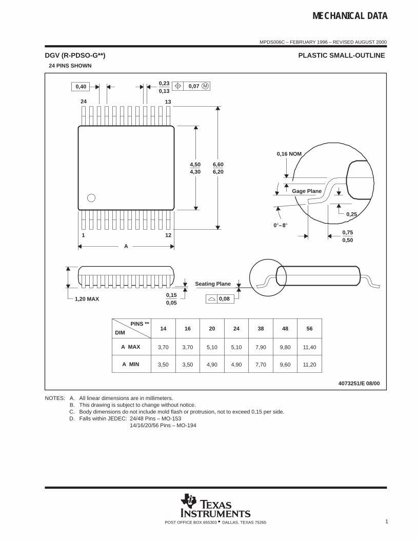
DGV (R-PDSO-G**) PLASTIC SMALL-OUTLINE 24 PINS SHOWN
14
3,70
3,50 4,90
5,10
20DIM
PINS **
4073251/E 08/00
1,20 MAX
Seating Plane
0,050,15
0,25
0,500,75
0,230,13
1 12
24 13
4,304,50
0,16 NOM
Gage Plane
A
7,90
7,70
382416
4,90
5,103,70
3,50
A MAX
A MIN
6,606,20
11,20
11,40
56
9,60
9,80
48
0,08
M0,070,40
0°–8°
NOTES: A. All linear dimensions are in millimeters.B. This drawing is subject to change without notice.C. Body dimensions do not include mold flash or protrusion, not to exceed 0,15 per side.D. Falls within JEDEC: 24/48 Pins – MO-153
14/16/20/56 Pins – MO-194

MECHANICAL DATA
MSOI002B – JANUARY 1995 – REVISED SEPTEMBER 2001
1POST OFFICE BOX 655303 • DALLAS, TEXAS 75265
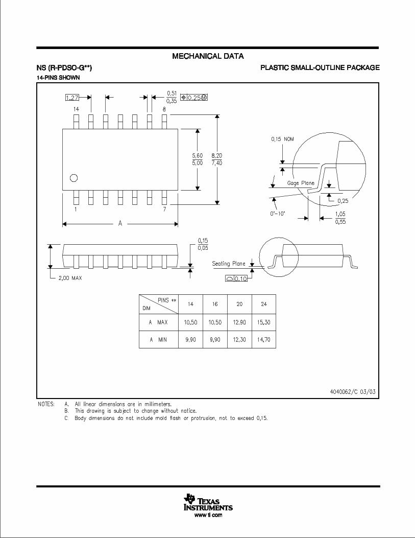
D (R-PDSO-G**) PLASTIC SMALL-OUTLINE PACKAGE8 PINS SHOWN
8
0.197(5,00)
A MAX
A MIN(4,80)0.189 0.337
(8,55)
(8,75)0.344
14
0.386(9,80)
(10,00)0.394
16DIM
PINS **
4040047/E 09/01
0.069 (1,75) MAX
Seating Plane
0.004 (0,10)0.010 (0,25)
0.010 (0,25)
0.016 (0,40)0.044 (1,12)
0.244 (6,20)0.228 (5,80)
0.020 (0,51)0.014 (0,35)
1 4
8 5
0.150 (3,81)0.157 (4,00)
0.008 (0,20) NOM
0°– 8°
Gage Plane
A
0.004 (0,10)
0.010 (0,25)0.050 (1,27)
NOTES: A. All linear dimensions are in inches (millimeters).B. This drawing is subject to change without notice.C. Body dimensions do not include mold flash or protrusion, not to exceed 0.006 (0,15).D. Falls within JEDEC MS-012

MECHANICAL DATA
MSSO002E – JANUARY 1995 – REVISED DECEMBER 2001
1POST OFFICE BOX 655303 • DALLAS, TEXAS 75265
DB (R-PDSO-G**) PLASTIC SMALL-OUTLINE
4040065 /E 12/01
28 PINS SHOWN
Gage Plane
8,207,40
0,550,95
0,25
38
12,90
12,30
28
10,50
24
8,50
Seating Plane
9,907,90
30
10,50
9,90
0,38
5,605,00
15
0,22
14
A
28
1
2016
6,506,50
14
0,05 MIN
5,905,90
DIM
A MAX
A MIN
PINS **
2,00 MAX
6,90
7,50
0,65 M0,15
0°–8°
0,10
0,090,25
NOTES: A. All linear dimensions are in millimeters.B. This drawing is subject to change without notice.C. Body dimensions do not include mold flash or protrusion not to exceed 0,15.D. Falls within JEDEC MO-150

MECHANICAL DATA
MTSS001C – JANUARY 1995 – REVISED FEBRUARY 1999
1POST OFFICE BOX 655303 • DALLAS, TEXAS 75265
PW (R-PDSO-G**) PLASTIC SMALL-OUTLINE PACKAGE14 PINS SHOWN
0,65 M0,10
0,10
0,25
0,500,75
0,15 NOM
Gage Plane
28
9,80
9,60
24
7,90
7,70
2016
6,60
6,40
4040064/F 01/97
0,30
6,606,20
8
0,19
4,304,50
7
0,15
14
A
1
1,20 MAX
14
5,10
4,90
8
3,10
2,90
A MAX
A MIN
DIMPINS **
0,05
4,90
5,10
Seating Plane
0°–8°
NOTES: A. All linear dimensions are in millimeters.B. This drawing is subject to change without notice.C. Body dimensions do not include mold flash or protrusion not to exceed 0,15.D. Falls within JEDEC MO-153
IMPORTANT NOTICE
Texas Instruments Incorporated and its subsidiaries (TI) reserve the right to make corrections, modifications,enhancements, improvements, and other changes to its products and services at any time and to discontinueany product or service without notice. Customers should obtain the latest relevant information before placingorders and should verify that such information is current and complete. All products are sold subject to TI’s termsand conditions of sale supplied at the time of order acknowledgment.
TI warrants performance of its hardware products to the specifications applicable at the time of sale inaccordance with TI’s standard warranty. Testing and other quality control techniques are used to the extent TIdeems necessary to support this warranty. Except where mandated by government requirements, testing of allparameters of each product is not necessarily performed.
TI assumes no liability for applications assistance or customer product design. Customers are responsible fortheir products and applications using TI components. To minimize the risks associated with customer productsand applications, customers should provide adequate design and operating safeguards.
TI does not warrant or represent that any license, either express or implied, is granted under any TI patent right,copyright, mask work right, or other TI intellectual property right relating to any combination, machine, or processin which TI products or services are used. Information published by TI regarding third-party products or servicesdoes not constitute a license from TI to use such products or services or a warranty or endorsement thereof.Use of such information may require a license from a third party under the patents or other intellectual propertyof the third party, or a license from TI under the patents or other intellectual property of TI.
Reproduction of information in TI data books or data sheets is permissible only if reproduction is withoutalteration and is accompanied by all associated warranties, conditions, limitations, and notices. Reproductionof this information with alteration is an unfair and deceptive business practice. TI is not responsible or liable forsuch altered documentation.
Resale of TI products or services with statements different from or beyond the parameters stated by TI for thatproduct or service voids all express and any implied warranties for the associated TI product or service andis an unfair and deceptive business practice. TI is not responsible or liable for any such statements.
Following are URLs where you can obtain information on other Texas Instruments products and applicationsolutions:
Products Applications
Amplifiers amplifier.ti.com Audio www.ti.com/audio
Data Converters dataconverter.ti.com Automotive www.ti.com/automotive
DSP dsp.ti.com Broadband www.ti.com/broadband
Interface interface.ti.com Digital Control www.ti.com/digitalcontrol
Logic logic.ti.com Military www.ti.com/military
Power Mgmt power.ti.com Optical Networking www.ti.com/opticalnetwork
Microcontrollers microcontroller.ti.com Security www.ti.com/security
Telephony www.ti.com/telephony
Video & Imaging www.ti.com/video
Wireless www.ti.com/wireless
Mailing Address: Texas Instruments
Post Office Box 655303 Dallas, Texas 75265
Copyright 2003, Texas Instruments Incorporated