SMP8654 - Create your own video
452
SMP8654 Secure Media Processor with Multiple A/V Codec Support Datasheet February, 2009 Document #: SMP8654-DS-A-10
-
Upload
khangminh22 -
Category
Documents
-
view
1 -
download
0
Transcript of SMP8654 - Create your own video

SMP8654Secure Media Processor with Multiple A/V Codec Support
DatasheetFebruary, 2009
Document #: SMP8654-DS-A-10

Copyright Information
© 2009 by Sigma Designs Inc. All rights reserved. No part of this document may be copied or reproduced in any form or by any means without the prior written consent of Sigma Designs Inc. The information in this document is subject to change without notice. Sigma Designs, REALmagic and the REALmagic logo are either registered trademarks or trademarks of Sigma Designs Inc. in the United States and/or other countries. Manufactured under license from Dolby Laboratories and Macrovision. Dolby, Pro Logic, and the double-D symbol are trademarks of Dolby Laboratories. All other trademarks or registered trademarks are the properties of their respective owners.
Sigma Designs products are sold by description only. Sigma Designs reserves the right to make changes in circuit design and/or specifications at any time without notice. Accordingly, the reader is cautioned to verify that the datasheet is current before placing orders. Information furnished by Sigma Designs is believed to be accurate and reliable. However, no responsibility is assumed by Sigma Designs or its subsidiaries for its use; nor for any infringements of patents or other rights of third parties which may result from its use. No license is granted by implication or otherwise under any patent or patent rights of Sigma Designs or its subsidiaries.
Disclaimer
Sigma Designs Inc. makes no warranty, express, statutory, implied or by description regarding the information set forth herein or regarding the freedom of the described devices from intellectual property infringement. Sigma Designs Inc. makes no warranty of merchantability or fitness for any purpose.
Sigma Designs Inc. shall not be responsible for any errors that may appear in this document. Sigma Designs Inc. makes no commit-ment to update or keep current the information contained in this document.
Confidentiality
This document contains confidential information, trade secrets or both that are the property of Sigma Designs Inc. It is to be treated as confidential under the Non Disclosure Agreement (NDA), which has been signed by the obtainer. Reproduction or transmission in any manner to others in whole or in part is prohibited without prior written permission from Sigma Designs Inc.
Export Control
Due to the inclusion of cryptographic functions, Sigma Designs has applied to the US Department of Commerce, Bureau of Industry and Security (BIS) for authorization to ship the SMP8654 and SMP8655 to customers around the world. These devices have been authorized by the BIS for license exception ENC under sections 740.17 (A) and (B3). The ECCN number under which this exception was granted is 5A002A.1. The following Web site lists all countries where this license exception applies (see country group B, as in B3 above): http://www.gpo.gov/bis/ear/pdf/740spir.pdf.
Life Support Policy
The product(s) described in this document is not intended for use as critical component(s) in life support devices or systems without prior written permission from Sigma Designs Inc.
• Life support devices or systems are devices or systems which, (a) are intended as surgical implant(s) into the body, or (b) sup-port or sustain life, and whose failure to perform, when properly used in accordance with instructions for use provided in the labeling, can be reasonably expected to result in a significant injury to the user.
• A critical component is any component of a life support device or system whose failure to perform can be reasonably expected to cause the failure of the life support device or system, or to affect its safety or effectiveness.
Trademarks
Secure Media Processor, SMP8654 and SMP8655 are trademarks of Sigma Designs Inc.
Address
Sigma Designs Inc. 1778 McCarthy Blvd. Milpitas CA USA - 95035 Tel: 408.262.9003 Fax: 408.262.9740 www.sigmadesigns.com Document #: SMP8654-DS-A-10

Table of Contents
Conventions ....................................................................................................................................10.1 Acronyms and Abbreviations .................................................................1
0.2 Units of Measurement .........................................................................4
0.3 General Conventions ...........................................................................5
1 Introduction ...................................................................................................................................71.1 Block Diagram of SMP8654 ...................................................................7
1.2 Main Features of SMP8654 ...................................................................8
1.3 Main Components of SMP8654 ............................................................ 11
1.4 Application Examples ......................................................................... 15
2 Host CPU Block ...........................................................................................................................172.1 Block Diagram of Host CPU Block......................................................... 17
2.2 Introduction ..................................................................................... 18
Central Processor Unit (CPU)............................................................................................... 192.3 Introduction...................................................................................... 19
2.4 Features........................................................................................... 19
2.5 Block Diagram................................................................................... 21
2.6 Functional Description ....................................................................... 22
Local Memory ....................................................................................................................... 422.7 Introduction...................................................................................... 42
2.8 Features........................................................................................... 42
2.9 Functional Description ........................................................................ 42
Interrupt Controller ............................................................................................................... 432.10 Introduction .................................................................................... 43
2.11 Features ......................................................................................... 43
2.12 Block Diagram................................................................................. 43
2.13 Functional Description ..................................................................... 44
Timers..................................................................................................................................... 502.14 Introduction .................................................................................... 50
2.15 Features ......................................................................................... 50
2.16 Block Diagram................................................................................. 51
2.17 Functional Description ...................................................................... 51
2.18 Register Map .................................................................................. 54
UARTs..................................................................................................................................... 542.19 Introduction .................................................................................... 54
Sigma Designs Confidential i

SMP8654-DS-A-10SMP8654 Datasheet
2.20 Features ........................................................................................ 55
2.21 Block Diagram ................................................................................ 56
2.22 Functional Description ..................................................................... 57
2.23 Register Map .................................................................................. 61
2.24 Pin Description ............................................................................... 62
2.25 Electrical Characteristics................................................................... 62
2.26 Timing Diagrams ............................................................................ 63
Smartcard Interface ..............................................................................................................642.27 Introduction ................................................................................... 64
2.28 Features ........................................................................................ 64
2.29 Block Diagram ............................................................................... 64
2.30 Functional Description...................................................................... 65
2.31 Register Map .................................................................................. 68
2.32 Pin Description................................................................................ 69
3 Security Subsystem ................................................................................................................... 713.1 Block Diagram of Security Subsystem .................................................. 71
3.2 Introduction .................................................................................... 72
3.3 Features ......................................................................................... 73
CPU of the Security Subsystem (XPU) ...............................................................................743.4 Description....................................................................................... 74
Hardware Cipher Block ........................................................................................................753.5 Description....................................................................................... 75
Boot ROM ...............................................................................................................................77
Serial Flash.............................................................................................................................78
XPU Timers ............................................................................................................................803.6 Introduction ..................................................................................... 80
3.7 Features .......................................................................................... 80
3.8 Block Diagram ................................................................................. 80
3.9 Functional Description........................................................................ 81
XPU Interrupt Controller........................................................................................................833.10 Introduction ................................................................................... 83
3.11 Features ........................................................................................ 83
3.12 Block Diagram ................................................................................ 84
3.13 Functional Description...................................................................... 84
Bus accessibility....................................................................................................................883.14 Description ..................................................................................... 88
4 IPU Subsystem ........................................................................................................................... 934.1 Block Diagram .................................................................................. 93
4.2 Introduction ..................................................................................... 93
4.3 Features .......................................................................................... 94
ii Sigma Designs Confidential

Table of Contents
IPU Processor ........................................................................................................................ 944.4 Description ....................................................................................... 94
5 DRAM Controllers .......................................................................................................................955.1 Block Diagram of DRAM Controller ....................................................... 95
5.2 Introduction ..................................................................................... 96
5.3 Features........................................................................................... 96
5.4 Functional Description ....................................................................... 97
5.5 Pin Description ............................................................................... 105
5.6 Electrical Characteristics ................................................................... 111
6 System Block .............................................................................................................................1136.1 Block Diagram of System Block ........................................................ 113
6.2 Introduction ................................................................................... 114
GPIO Block........................................................................................................................... 1146.3 General Purpose I/O (GPIO).............................................................. 114
6.4 Front Panel Controller Interface (FIP) ................................................ 122
6.5 Infrared Decoder ............................................................................ 126
Inter Integrated Circuits (I2C) ............................................................................................. 1326.6 Introduction.................................................................................... 132
6.7 Features......................................................................................... 132
6.8 Block Diagram................................................................................. 133
6.9 Functional Description ..................................................................... 134
6.10 Register Maps ............................................................................... 138
6.11 Pin Description .............................................................................. 139
6.12 Electrical Characteristics ................................................................ 140
6.13 Timing Diagrams ........................................................................... 140
Watchdog ............................................................................................................................ 1416.14 Introduction .................................................................................. 141
6.15 Block Diagram............................................................................... 141
6.16 Functional Description .................................................................... 141
6.17 Register Map ................................................................................ 143
6.18 Pin Description .............................................................................. 143
Clock Generator................................................................................................................... 1436.19 Introduction .................................................................................. 143
6.20 Features ...................................................................................... 144
6.21 Block Diagram............................................................................... 144
6.22 Functional Description ................................................................... 145
6.23 Register Map ................................................................................ 151
6.24 Pin Description .............................................................................. 153
6.25 Electrical Characteristics ................................................................ 154
iiiSigma Designs Confidential

SMP8654-DS-A-10SMP8654 Datasheet
7 Host Interface ............................................................................................................................ 1557.1 Block Diagram of Host Interface ........................................................155
7.2 Introduction ...................................................................................156
PCI Master/Slave/Host Interface .........................................................................................1567.3 Introduction ....................................................................................156
7.4 Features .........................................................................................156
7.5 Functional Description ......................................................................157
7.6 Register Map ...................................................................................163
7.7 Pin Descriptions ..............................................................................166
7.8 Electrical Characteristics ..................................................................169
7.9 Timing Diagrams .............................................................................170
USB 2.0 Embedded Host Interface ....................................................................................1727.10 Functional Description.....................................................................172
7.11 Pin Description...............................................................................173
7.12 Electrical Characteristics .................................................................175
Ethernet Interface ...............................................................................................................1777.13 Pin Description ..............................................................................179
7.14 Electrical Characteristics..................................................................181
7.15 Timing Diagram .............................................................................182
NAND Flash Interface .........................................................................................................1837.16 Introduction ..................................................................................183
7.17 Features .......................................................................................183
7.18 Functional Description.....................................................................183
7.19 Registers ......................................................................................185
7.20 Pin Description...............................................................................186
7.21 Electrical Characteristics .................................................................187
7.22 Timing Diagram .............................................................................187
SATA Interface ....................................................................................................................1887.23 Introduction ..................................................................................188
7.24 Features .......................................................................................188
7.25 Block Diagram ...............................................................................188
7.26 Functional Description.....................................................................188
7.27 Pin Description...............................................................................194
7.28 Electrical Characteristics .................................................................196
8 Video Decoder Subsystem ...................................................................................................... 1978.1 Block Diagram of Video Decoder Subsystem ........................................197
8.2 Introduction ...................................................................................198
8.3 Features ........................................................................................200
8.4 Functional Description.......................................................................200
iv Sigma Designs Confidential

Table of Contents
9 Video Processing Subsystem ..................................................................................................2059.1 Block Diagram of Video Processing Subsystem..................................... 205
9.2 Introduction ................................................................................... 207
9.3 Features ........................................................................................ 208
9.4 Functional Description ..................................................................... 209
9.5 Register Maps ................................................................................ 278
9.6 Pin Description ................................................................................ 288
9.7 Electrical Characteristics ................................................................... 292
9.8 Timing Diagrams ............................................................................. 294
10 Audio Processing Subsystem ...............................................................................................29510.1 Block Diagram of Audio Processing Subsystem................................... 295
10.2 Introduction ................................................................................. 296
10.3 Features ....................................................................................... 296
10.4 Functional Description .................................................................... 297
10.5 Register Maps ............................................................................... 309
10.6 Pin Description .............................................................................. 312
10.7 Electrical Characteristics ................................................................. 313
10.8 Timing Diagram ............................................................................ 314
11 Transport Demultiplexer .........................................................................................................31511.1 Block Diagram of Transport Demultiplexer......................................... 315
11.2 Introduction ................................................................................. 316
11.3 Features ....................................................................................... 316
11.4 Functional Description .................................................................... 318
11.5 Pin Description ............................................................................. 339
11.6 Electrical Characteristics ................................................................. 340
11.7 Timing Diagrams ........................................................................... 341
12 Pin Information ........................................................................................................................34512.1 Pin Layout .................................................................................... 345
12.2 Pin Listing by Pin Id ...................................................................... 350
12.3 Pin Listing by Pin Name ................................................................. 360
12.4 Miscellaneous Pins ........................................................................ 370
13 System Specifications ............................................................................................................37113.1 Electrical Specifications................................................................... 371
13.2 Power Consumption ....................................................................... 373
13.3 Power Supply Sequencing ............................................................... 374
13.4 Thermal Specifications.................................................................... 389
13.5 Mechanical Specifications ............................................................... 390
14 DDR Implementation ...............................................................................................................39314.1 Memory System Implementation Guidelines ...................................... 393
vSigma Designs Confidential

SMP8654-DS-A-10SMP8654 Datasheet
15 Ordering Information .............................................................................................................. 39715 Ordering Information.........................................................................397
16 Licensing ................................................................................................................................. 39916.1 Licensing.......................................................................................399
17 Appendix ................................................................................................................................. 40317.1 Basic Analog Video Parameters.........................................................403
17.2 Main Video Scaler Filters .................................................................405
17.3 Color Space Conversion Basic Matrices ..............................................407
17.4 Video Output Scaling Examples .......................................................408
17.5 SDTV vs. HDTV Colorimetry Example ................................................412
17.6 Supported Media Formats ...............................................................413
17.7 Supported File Formats ..................................................................418
17.8 Supported Broadcast Formats .........................................................422
17.9 Raster Operations...........................................................................422
List of Figures ................................................................................................................................ 433List of Tables ................................................................................................................................. 437
vi Sigma Designs Confidential

Conventions
This section presents the acronyms, abbreviations, units of measurement and other con-ventions used in this datasheet.
0.1 Acronyms and Abbreviations
The acronyms and abbreviations used in this datasheet are listed alphabetically in the table below:
Table 0-1 Acronyms and abbreviations
Acronym/Abbreviation Definition
2D/3D 2 Dimensional/3 Dimensional
AC Alternating Current
ADC Analog-to-Digital Converter
ATA AT Attachment
AV or A/V Audio Visual
BGA Ball Grid Array
BPP Bits per Pixel
CMOS Complementary Metal Oxide Semiconductor
CODEC Coder/Decoder
CPU Central Processing Unit
CSS Cascading Style Sheets or Content Scrambling System
D/A Digital-to-Analog
DAA Data Access Arrangement
DAC Digital-to-analog Converter
DC Direct Current
DDR SDRAM Double Data Rate Synchronous DRAM
DMA Direct Memory Access
DRAM Dynamic Random-access Memory
DSL Digital Subscriber Line
Sigma Designs Confidential 1

SMP8654-DS-A-10SMP8654 Datasheet
DSP Digital Signal Processor
DVD Digital Versatile Disc or Digital Video Disc
DVI Digital Visual Interface
EHCI Extended Host Controller Interface
EJTAG Enhanced Joint Test Action Group
EIA Electronic Industries Alliance
FCS Frame Check Sequence
FIFO First In/First Out
GPIO General Purpose Input/Output
HDMI High-Definition Multimedia Interface
HDTV High-Definition Television
I Input
I/O Input/Output
I2C Inter Integrated Circuit
IDE Integrated Drive Electronics
IEC International Electrotechnical Commission
IPTV Internet Protocol TV
IR Infrared
IRQ Interrupt Request Line
ISO International Organization for Standardization
JPEG Joint Photographic Experts Group
LCD Liquid Crystal Display
LSB Least Significant Bit/Byte
MIPS Millions of Instructions per Second
MMU Memory Management Unit
MPEG Moving Picture Experts Group
MSB Most Significant Bit/Byte
O Output
OHCI Open Host Controller Interface
OSD On Screen Display
Table 0-1 Acronyms and abbreviations
Acronym/Abbreviation Definition
2 Sigma Designs Confidential

Conventions
P/U Pull-up Resistor
PCB Printed Circuit Board
PCI Peripheral Component Interconnect
PID Program Id
PIP Picture In Picture
PKI public key infrastructure
PLL Phase Locked Loop
PVR Personal Video Recorder
RAM Random Access Memory
RGB Red Green Blue
RISC Reduced Instruction Set Computer
ROM Read Only Memory
RTC Real-time Clock
S/PDIF Sony/Philips Digital Interface
SDTV Standard Definition Television
SPI Synchronous Parallel Interface
SRAM Static Random Access Memory
SSI Synchronous Serial Interface
SSI Server-side Include or Single-system Image
TDMX Transport Demultiplexer
TLB Translation Look-aside Buffer
TMDS Transition Minimized Differential Signaling
UART Universal Asynchronous Receiver Transmitter
USB Universal Serial Bus
VOD Video On Demand
YCbCr Y is brightness (luma), Cb is blue minus luma (B-Y) and Cr is red minus luma (R-Y)
Table 0-1 Acronyms and abbreviations
Acronym/Abbreviation Definition
3Sigma Designs Confidential

SMP8654-DS-A-10SMP8654 Datasheet
0.2 Units of Measurement
The units of measurement used in this datasheet are listed alphabetically in the table below:
Table 0-2 Units of measurement
Symbol Unit of measurement
µA microampere
µF microfarad
µs microsecond (1,000 nanoseconds)
0C degree Celsius
GB gigabyte
bpp Bits Per Pixel
Hz Hertz (cycles per second)
kohm kiloohm
Kb kilobit
KB kilobyte (1,024 Bytes)
Kbps kilobit per second
KBps kilobyte per second
KHz kilohertz
mA milliampere
Mbps megabit per second
MBps megabyte (1,048,576 bits) per second
Mb megabit
MB megabyte (1,048,576 bytes)
MHz megahertz (1,000 kilohertz)
ms millisecond (1,000 micro seconds)
ns nanosecond
V volt
W watt
4 Sigma Designs Confidential

Conventions
0.3 General Conventions
Numbers and Number Bases
• Binary numbers are enclosed in single quotation marks when in text, e.g., ‘1’ desig-nates a binary number.
• Binary numbers are written with a lower case ‘b’ suffix. e.g., 16b.
• Binary numbers larger than four digits are written with a space dividing each group of four digits, as in 1011 0101 1010b.
Note: All other numbers are decimal.
Naming Conventions
• The register acronyms appear in capital letters such as SDIOVH or SDIN_EGD_HDG
• Register bits are listed in square brackets MSB-to-LSB separated by a colon mark, e.g., SDHE[3:0].
• TBD indicated that the values are ‘to be determined‘, NA or N/A indicate ‘not avail-able’ and NC indicates that a pin is ‘no connect‘.
5Sigma Designs Confidential

SMP8654-DS-A-10SMP8654 Datasheet
6 Sigma Designs Confidential

1 Introduction
1.1 Block Diagram of SMP8654
MIPS 24K f (500MHz)
Local RAM (8KB )
EJTAG
Host I nterface
Host CPU B lock
P
A
D
S Tim er
UA RT
IRQ Cont roller
I-Cache (32KB ) D-Cac he (32KB )
M IPS 4KE c (333MHz)
Smart Card Interfac e
B oot ROM
S ecuri ty S ubsystem
P
A
D
S Tim er
Edge Detec tor
IRQ Cont roller I-Cache (12KB ) D-Cac he (12KB )
Serial Flash
C iphers
P
A
D
S
PCI Slave
P CI Mas ter
NAND Flash Cont rol ler
SAT A (1.5Gbps ) Hos t (2)
32-bit DSP
Serial Out
Serial I n
Audi o P rocessing Subsystem
P
A
D
S Tim er
Semaphores
Reset Cont roller
IRQ Cont roller
DM (12Kx32) PM (3Kx32)
32-bit R ISC
Hardware Sec tion Filt er
Ci pher Engines
Transport Dem ultipl exer
P
A
D
S Tim er
Semaphores
Reset Cont roller
IRQ Cont roller
DM (4K x32) PM (6Kx32)
Parser
16-bi t RIS C
S ub-pict ure Decoder
Video Decoder
Video Decoder S ubsystem
Timer
Sem aphores
Reset Controller
I RQ Controller
DM (2Kx16) PM (3Kx32)
DRAM Unit
RAS Generator
A rbit er
System B lock
P
A
D
S V-Bus Unit
M-Bus Unit
G-Bus Unit
CAS Generat or
DDR Timing
GPI O Bl ock
Front P anel I nt erf ace (FIP )
General P urpose I /O (GPI O)
DRAM Controll ers
P
A
D
SI2C (Mas ter, S lave)
Semaphores
Clock Generat or
B us A rbit ers
Pulse Wi dt h Modul at ors (2)
I nf rared Decoder (IR)
P
A
D
S
M ai n Video Scal er
Hardware Cursor
OSD Graphic s S caler
V ideo P ro cessing Subsystem
V
B
u
s
Multi-format S caler 1
8-bit Graphi cs Scaler
Vi deo I nput
M
a
i
n
M
i
x
e
Rout er A nalog Out
Edge Detec tor
USB 2.0 (2-Port )
10/100 Et hernet MAC(2)
HDMI v1. 3a
LINK + PHY
HD->S D
2D Graphics Accelerat or
Color B ars
Generat or
Multi -f ormat Scal er 2/
V ideo Plane Channel
MIPS 4KEc (333MHz)
Timer
E dge Detec tor
IRQ Controller
I-Cache (16KB ) D-Cache (16KB)
Interrup t Processi ng Unit
A nalog Out
Figure 1-1 SMP8654 block diagram
Sigma Designs Confidential 7

SMP8654-DS-A-10SMP8654 Datasheet
1.2 Main Features of SMP8654
• Host CPU
- Embedded 500MHz MIPS 24Kf for operating system, middleware and applications - 32KB instruction and 32KB data caches - Interrupt controller and timers
• Highly secure DRM/CA solution
- Separate 333MHz MIPS 4KEc CPU to securely execute DRM and conditional access software
- 12KB instruction and 12KB data caches - 32KB instruction scratch memory and 24KB data scratch memory - Encrypted DRAM and flash memory, secure boot loader, secure PKI, encrypted I/O
interfaces - Supports a wide variety of DRM and conditional access solutions
• IO standards
- 32-bit PCI v2.1 (33 or 66MHz) bus master/slave/host - NAND Flash Interface supports up to 8GB of external memory (bootable) - Dual SATA (1.5Gbps) host ports - Supports Ethernet 10/100 (2 ports) - Supports USB2.0 (2 ports) - Front panel controller interface supports NEC uPD16311, NEC uPD16312, PTC
PT6311 and PTC PT6312 front panel controllers - Two ISO 7816 smartcard interfaces
- I2C master/slave interfaces - 8-bit parallel DVB-SPI transport stream interface plus single serial interface, or triple
serial transport stream interface
- I2S interface up to 20Mbps - Two UARTs - 16 dedicated general purpose I/O pins (up to 77 total GPIO)
• Video decoding standards
- Video decoding of MPEG-1, MPEG-2 MP@HL, MPEG-4.2 ASP@L5 (720p), MPEG-4.10 (H.264) BP@L3, [email protected] and [email protected], WMV9 MP@HL, SMPTE 421M (VC-1) MP@HL, AP@L3, AVS Jizhun profile @ L2.0, 4.0, and 6.0
- Hardware accelerated Baseline JPEG decoding - DVD-Video and Superbit DVD
* CSS decryption* 16:9 and 4:3 playback, letterbox, 3:2 pull-down* Multiple angles and sub-picture
- Error concealment, deblocking filter
8 Sigma Designs Confidential

1: Introduction
- Elementary video stream bit rate * MPEG-2 SDTV (HDTV): 20 (40) Mbps maximum* MPEG-4.2 SDTV (HDTV): 20 (40) Mbps maximum* MPEG-4.10 (H.264) SDTV (HDTV): 20 (40) Mbps maximum* WMV9/SMPTE 421M (SMPTE 421M (VC-1)) SDTV (HDTV): 20 (40) Mbps maxi-
mum
• Video processing
- Brightness, color and contrast controls for each output port - Hardware cursor (4096 pixels, 4-bpp, up to 255 pixels horizontally and vertically) - 2D graphics accelerator (up to 100M pixels per second operation for most operations)
* Line, Rectangle, Ellipse and Circle: generate a single-color line, rectangle, ellipse or circle with optional gradient fill
* Blend: alpha blend one rectangular region onto another* Move: move a rectangular region to another location* Replace: modified version of Move* Raster Operations: standard 256 Boolean operations
- OpenType/TrueType font rendering acceleration - 32-bit OSD with flicker filtering and scaling - Optional deinterlacing of interlaced sources - Arbitrary scaling of video and graphics up to 1920x1080 pixels - Alpha mixing of video, graphics, cursor and OSD - Picture-in-Picture (PIP) support
• Video interfaces
- NTSC/PAL composite and s-video outputs with optional Macrovision protection - 2 analog YPbPr/RGB video outputs with optional Macrovision protection in 480i,
576i, 480p and 576p YPbPr output modes (12-bit DACs, interlaced or progressive, SDTV or HDTV resolution)
- Integrated HDMI v1.3a A/V output interface includes 36-bpp deep color support, HDCP 1.3 content protection and integrated PHY
• Audio processing and interfaces
- DSP based audio decoding
- I2S and S/PDIF digital audio input interface
- DSP includes 3 I2S serial digital outputs to support 5.1-channel audio output - Digital serial S/PDIF (IEC 60958) audio output
9Sigma Designs Confidential

SMP8654-DS-A-10SMP8654 Datasheet
• Transport stream inputs
- Transport input interfaces* One 8-bit DVB-SPI and one SSI, or 3 SSI, with polarity control of data valid signal* PCI, SATA, Ethernet
- Transport demux supports 256 dedicated PIDs (aggregate) - Transport input bit rate: 486Mbps maximum (aggregate)
• Dedicated MIPS 4KEc processor (IPU)
- Executes video display handler - Can be optionally used for other main CPU off load and acceleration functions
• Media formats
- DVD-Video, SVCD (IEC 62107-2000), VCD 1.x and 2.0 - DVD-R, DVD-RW, DVD+R, DVD+RW (conditional) - HDV - Audio CD, CD-R, CD-RW, CompactFlash - WMA, JPEG, MP3 and MPEG-4.2 AVI files using ISO 9660 format - Picture CD (JPEG files using ISO 9660 format) - Navigation software, HighMAT™ support
• Streaming formats
- ISMA (Internet Streaming Media Alliance) MPEG-4.2 - MPEG-2, MPEG-4 - WM9 with DRM - MPEG-4.10 (H.264) and SMPTE 421M (VC-1) over MPEG-2 Transport
• On screen display
- High resolution, true-color OSD support - 2, 4, 7, and 8-bpp from 24-bit palette - Programmable OSD scaler - Programmable flicker filter for interlaced output modes - Alpha blending over video (8-bit)
• Operating system support
- Linux - WinCE
10 Sigma Designs Confidential

1: Introduction
1.3 Main Components of SMP8654
The SMP8654 is an advanced, single-chip audio/video decoder that provides highly-inte-grated solutions for HDTV, IPTV, MPEG-4.10 (H.264), WMV9, SMPTE 421M (VC-1) and AVS decoding. It incorporates flexible, advanced audio/video processing, enabling cost-effective solutions for consumer products, such as digital media adapters and IPTV set-top boxes.
The SMP8654 includes optimized features for tightly embedded applications such as TV/PDP integration, streaming video endpoints, and multifunction consumer appliances. The device also includes features that enable designers to easily incorporate advanced capabili-ties such as A/V streaming, Video-on-Demand (VOD) and Personal Video Recording (PVR) into their products.
In addition, the SMP8654 supports numerous popular media formats including DVD-Video, SVCD, VCD1.x, VCD2.0 and CD/CD-R/CD-RW (audio, JPEG, MP3 and MPEG-4 AVI files). It also supports ISMA MPEG-4 streaming format, and MPEG-4 over MPEG-2 transport streaming.
The SMP8654 architecture is composed of various hardware functional units – several incorporating custom-designed processor modules – interconnected by multiple high-speed synchronous data buses. Although the details of the on-chip buses are beyond the scope of this document, the primary buses and their functions are described below.
A 64-bit G-Bus connects the integrated MIPS host CPU with each functional unit. It pro-vides access to the programmable configuration, control and status registers contained within each unit. The state of the device is initialized, controlled, and reconfigured as nec-essary through this bus. The G-Bus also supports direct access to the memory areas con-trolled by two memory controllers, PCI, flash memory areas and 32-bits of address and data (4G dwords addressable). It is an arbitrated, multi master bus.
The M-Bus provides the data path that allows each functional unit to communicate with the external memory controllers. It provides a 64-bit data path resulting in a peak data bandwidth of 2664MB/sec at a system clock frequency of 333MHz. The M-Bus arbitrates access among numerous DMA channels. An arbitration algorithm provides programmable bus bandwidth to be allocated and guaranteed to each DMA channel.
The V-Bus provides a dedicated high-speed data path between the video processing engine and the external memory controllers.
In addition to these device-wide buses, the various functional units typically have one or more dedicated local buses within the unit. These buses are not further described in this document.
11Sigma Designs Confidential

SMP8654-DS-A-10SMP8654 Datasheet
The main modules of the SMP8654 are briefly described below. Each module is discussed in detail under their respective chapters.
Host CPU Block
The host CPU block of the SMP8654 contains a 500MHz MIPS 24Kf CPU with its instruction and data cache to support the embedded operating system, middleware and applications required for consumer appliances. The supported operating systems include Linux and WinCE. The software for the CPU is loaded from an external flash using a secure boot loader.
In addition to the RISC processor itself, the host CPU block contains the following addi-tional resources: 2K Dword (8KB) local memory, 3 interrupt controllers, edge detection logic, two programmable timers, two Universal Asynchronous Receiver/Transmitters (UARTs) and two ISO 7816 smartcard controllers.
Security Processor Subsystem
A separate 333MHz MIPS 4KEc CPU is used to securely execute conditional access and DRM software. The software for this CPU resides on an internal flash (encrypted and dig-itally signed) to facilitate upgrades and is loaded using a secure boot loader.
DRAM Controllers
The SMP8654 contains two identical double-data rate synchronous DRAM (DDR-2) con-trollers operating at the memory clock rate (333MHz nominal). Because the DDR technol-ogy transfers data on both edges of the clock, the effective burst data bandwidth of each controller is 2.66GB/sec when using the full 32-bit interface (total peak bandwidth of 5.32GB/sec with 2 controllers). The DRAM controllers can each interface up to 512MB of external DDR-2 SDRAM.
System Block
The SMP8654 system block contains the following modules: GPIO block, I2C master and slave controllers and a clock generator. The GPIO block in turn contains General Purpose I/O (GPIO) controller, Front Panel Interface (FIP) controller, Pulse Width Modulator (PWM) and an infrared decoder.
The general purpose I/O controller provides 16 pins of general purpose control signals and logic to help eliminate the glue logic necessary for system integration. Other interfaces can also be used to provide GPIO functionality (if not otherwise used); a total of 77 GPIO pins can be implemented.
12 Sigma Designs Confidential

1: Introduction
The Front Panel Interface (FIP) controller directly supports the NEC uPD16311, NEC uPD16312, PTC PT6311 and PTC PT6312. Other front panel controllers may be used by interfacing to the UART or the GPIO.
The infrared input allows the interfacing to an external IR receiver. The NEC and the Philips RC5/RC6 IR formats, commonly used by consumer equipment are supported.
The I2C master and slave interfaces enable the SMP8654 to read from and write to external
devices. Two I2C master controllers, which support the synchronous Inter Integrated Cir-
cuits (I2C) serial protocol, enable the host CPU to access an external I2C slave device using a simplified register interface. A separate slave interface allows the SMP8654 to be
the target of I2C transactions initiated by an external master.
The clock generator contains one audio clock, two video clocks, one system clock and one CPU clock. The clock generator creates two high speed clocks from a 27MHz external clock using two programmable PLLs, and creates the main system clock and multiple video and audio clocks by dividing either one of the high speed clocks or the 27MHz refer-ence.
Host Interface
The host interface unit provides the interface between the primary internal buses (G-bus and M-bus) and the PCI, Ethernet and the USB 2.0.
The SMP8654 supports a PCI bus for system-level interconnection. The PCI bus imple-mentation is a version 2.1 compliant, 32-bit wide bus capable of operating at 33 or 66MHz.
The SMP8654 includes a dual-port USB 2.0 Embedded Host Controller and integrated PHYs. It also includes 2 Ethernet 10/100 MACs with 2 MII (Media Independent Interface) interfaces to connect to an external PHY devices.
A NAND flash controller allows direct attachment of one or two NAND flash devices of up to 4GB capacity each for non-volatile storage of code and data. The NAND flash may be used as a boot device.
Video Decoder Subsystem
The SMP8654 contains a high-performance multi-codec video decoder. The video decoder subsystem executes the video decoding algorithms supported by the SMP8654. Its archi-tecture is a hybrid of both processor-based and hardwired logic approaches.
13Sigma Designs Confidential

SMP8654-DS-A-10SMP8654 Datasheet
The video decoder engine consists of a proprietary 16-bit RISC CPU which is augmented by a number of hardware functional units. These functional units perform the most com-pute-intensive portions of the video decompression algorithms supported by the SMP8654.
Video Processing Subsystem
The SMP8654 video processing engine provides sophisticated display processing, format-ting and output capabilities. The video processing and display unit (VPD) has extensive capabilities for retrieving graphics and video images from the memory, formatting the images as needed, mixing the images and then presenting the video stream for display in a required format. Other capabilities provided by the VPD include hardware-assisted 2D graphics acceleration, and support for an external video input port.
The 3 available video outputs consist of 2 main analog outputs (6 DACs), and a digital HDMI interface. The 2 analog video outputs share the 6 DACs. The HDMI and analog component outputs can each support output formats up to 1920x1080p.
The SMP8654 contains an integrated HDMI transmitter. The HDMI transmitter block in the SMP8654 is HDMI v1.3a compliant, which transports consumer electronics standard digital video and digital audio over a TMDS interface. The HDMI unit supports the HDCP v1.3 content protection standard.
Audio Processing Subsystem
The SMP8654 contains an integrated audio subsystem based on a custom-designed 32-bit digital signal processor (DSP). Audio decoding and processing algorithms are fully exe-cuted on the DSP without special hardware support. This firmware-based approach gives great flexibility for accommodating future audio standards or specialized audio require-
ments. The audio unit provides 3 I2S output channels, one S/PDIF output channel, and one
stereo I2S or S/PDIF audio input channel.
Transport Demultiplexer
The SMP8654 includes an on-chip, RISC processor-based transport demultiplexer (TDMX) unit. The transport demultiplexer block is capable of handling up to 6 multi-pro-gram bitstreams of up to 81Mbps each, with an aggregate total of up to 486Mbps.
14 Sigma Designs Confidential

1: Introduction
Interrupt processing Unit (IPU)
A dedicated MIPS processor (32-bit 4KEc core) is integrated to off load certain low-latency processing requirements from the main CPU. Currently, the IPU primarily handles interrupts generated by the video processing subsystem, but may also be used to off load other system functions and accelerate performance-critical tasks. The IPU executes at 333MHz and includes 16KB instruction and data caches.
1.4 Application Examples
1.4.1 Networked DVD Player
The networked DVD player example below provides the typical functionality required for a networked DVD player. System integration requires very little external logic since the SMP8654 provides most of the features including:
• Progressive DVD-Video, MPEG4.10 (H.264), WMV9/SMPTE 421M (VC-1) play-back
• Interlaced or progressive YPbPr or RGB video outputs
• NTSC/PAL composite and S-video outputs
• 5.1-channel and S/PDIF audio outputs
• I2C bus master function for controlling other chips
• A MIPS CPU for operating system, middleware and applications
IR
ANALOG RGB OR YPBPR
SPDIF DIGITAL AUDIO OUTPUT
5.1-CHANNEL ANALOG AUDIO OUTPUT
NTSC / PAL COMPOSITE AND S-VIDEO
HDMI OUT
CD / DVD DRIVE
PCI BUS
HDD
AUDIODACS
IRRECEIVER
FRONT PANELCONTROLLER
802.11A / B / G / N
DDR DRAMAND FLASH
SMP8654
ETHERNETPHY
Figure 1-2 Application example - networked DVD player
15Sigma Designs Confidential

SMP8654-DS-A-10SMP8654 Datasheet
1.4.2 Digital Media Adapter or IPTV Set-top Box
The Digital Media Adapter or IPTV Set-top Box application requires very little external logic since the SMP8654 provides most of the features including:
• Decoding of MPEG-1, MPEG-2, MPEG-4.10 (H.264) and WMV9/SMPTE 421M (VC-1) content
• 2D graphics, OSD and deinterlacing
• Interlaced or progressive YPbPr or RGB video outputs
• NTSC/PAL composite and S-video outputs
• 5.1-channel and S/PDIF audio outputs
• A MIPS CPU for operating system, middleware and applications
PCI BUS
ANALOG RGB OR YPBPR
SPDIF D IGITAL AUDIO OUTPUT
5.1-CHANNEL ANALOG AUDIO O UTPUT
NTSC / PAL COMPOSITE AND S-VIDEO
HDM I O UT
DDR DRAMAND FLASH
AUDIODACS
FRONT PANELCONTROLLER
IR INPUT
802.11A / B / G / N
ETHERNET
SM P8654
PHY
Figure 1-3 Application example - digital media adapter or IPTV set-top box
16 Sigma Designs Confidential

2 Host CPU Block
2.1 Block Diagram of Host CPU Block
`
G-Bus
MIPS EC-Bus
MIPS 24Kf (500MHz)
IRQ0
IRQ1
IRQ2
L-Bus
Edge Detector
IRQ0 Controller
IRQ2 Controller
IRQ1 Controller
UART0
UART1
Local RAM 8KB
Remap Control Registers
Bus Converter/Remap
RISC
I -Cache (32KB)
D-Cache
(32KB)
MMU
ISP
DSP
Timer0
Timer1
Smarctc ard1
Smartcard0
Figure 2-1 Block diagram of host CPU block
Sigma Designs Confidential 17

SMP8654-DS-A-10SMP8654 Datasheet
2.2 Introduction
The host CPU block of the SMP8654 contains a 500MHz MIPS 24Kf + FPU (Floating Point Unit) with its instruction and data cache to support the embedded operating system, middleware and applications required for the consumer products. Supported operating systems include Linux and WinCE. Software for the CPU is loaded from an external flash using a secure boot loader.
The host CPU block contains the following additional resources:
• 32KB program and 32KB data caches
• 3 interrupt controllers
• Edge detection logic
• 2 programmable timers
• 2 Universal Asynchronous Receiver/Transmitter (UARTs)
• 2 ISO-7816 ‘Smartcard’ controllers
The CPU accesses the G-Bus as a master. A bridge allows the CPU to access all the G-Bus mapped local resources through the L-Bus.
Other components of the host CPU block reside on a local bus and can be accessed by either the RISC or the other G-Bus master. Both the bridges in the host CPU block per-form a bus protocol adaptation and a configurable address translation (remap). The host CPU block connects to the rest of the chip via the G-Bus.
Table 2-1 Remap registers
Address1
1. G-Bus byte address relative to the host CPU block base (0x60000).
+F000 CPU_REMAP0 R/W CPU Remap 0 Register
+F004 CPU_REMAP1 R/W CPU Remap 1 Register
+F008 CPU_REMAP2 R/W CPU Remap 2 Register
+F00C CPU_REMAP3 R/W CPU Remap 3 Register
+F010 CPU_REMAP4 R/W CPU Remap 4 Register
+F014 CPU_REMAP5 R/W CPU Remap 5 Register
+F018 CPU_REMAP6 R/W CPU Remap 6 Register
+F01C CPU_REMAP7 R/W CPU Remap 7 Register
Register Name R/W/A2
2. Read/write/auto update.
Description
18 Sigma Designs Confidential

2: Host CPU Block
Central Processor Unit (CPU)
2.3 Introduction
The MIPS32® 24Kf™ core (~720 conforming DMIPS at 500MHz) from MIPS Technolo-gies is a high-performance, low-power, 32-bit MIPS RISC core designed for efficient embedded system-on-silicon applications. It implements the MIPS32 Release 2 Architec-ture in an 8-stage pipeline, and includes support for the MIPS16e™ application specific extension and the 32-bit privileged resource architecture. This standard architecture allows support by a wide range of industry standard tools and development systems.
To maintain high pipeline utilization, dynamic branch prediction is included in the form of a Branch History Table and a Return Prediction Stack. The Memory Management Unit (MMU) contains 4-entry instruction and 8-entry data Translation Lookaside Buffers (ITLB/DTLB) and a configurable 32 dual-entry joint TLB (JTLB).
The 24Kf core also features an IEEE 754 compliant Floating Point Unit (FPU). The FPU supports both single and double precision instructions.
The core includes a high performance Multiply/Divide Unit (MDU). The MDU is fully pipelined to support a single cycle repeat rate for 32x32 MAC instructions, which enables multiply-intensive algorithms to be performed efficiently.
Instruction and data level-one caches are organized as 4-way set associative. Data cache misses are non-blocking and up to 4 may be outstanding. Two instruction cache misses can be outstanding. Both caches are virtually indexed and physically tagged to allow them to be accessed in the same cycle that the address is translated.
2.4 Features
• 8-stage pipeline
• 32-bit address paths
• 64-bit data paths to caches and system buses
• MIPS32-Compatible Instruction Set
- Multiply-Accumulate and Multiply-Subtract Instructions (MADD, MADDU, MSUB, MSUBU)
- Targeted Multiply Instruction (MUL) - Zero/One Detect Instructions (CLZ, CLO) - Wait Instruction (WAIT)
19Sigma Designs Confidential

SMP8654-DS-A-10SMP8654 Datasheet
- Conditional Move Instructions (MOVZ, MOVN) - Prefetch Instruction (PREF)
• MIPS32 Enhanced Architecture (Release 2) Features
- Vectored interrupts and support for external interrupt controller - Programmable exception vector base - Atomic interrupt enable/disable - Bit field manipulation instructions
• MIPS32 Privileged Resource Architecture
• Programmable Memory Management Unit
- 32 dual-entry JTLB with variable page sizes - 4-entry ITLB - 8-entry DTLB
• MIPS16e™ Code Compression
- 16 bit encoding of 32 bit instructions to improve code density - Special PC-relative instructions for efficient loading of addresses and constants - SAVE & RESTORE macro instructions for setting up and tearing down stack frames
within subroutines - Improved support for handling 8 and 16 bit data types
• Caches
- Separate 32 KB Instruction and Data caches - 4-Way Set Associative - Up to 8 outstanding load misses - Write-back and write-through support - 32-byte cache line size - Virtually indexed, physically tagged - Cache line locking support - Non-blocking prefetches
• Multiply/Divide Unit
- Maximum issue rate of one 32x32 multiply per clock - 5 cycle multiply latency - Early-in iterative divide. Minimum 12 and maximum 38 clock latency (dividend (rs)
sign extension-dependent)
• Floating Point Unit (FPU)
- IEEE-754 compliant Floating Point Unit - Compliant to MIPS 64b FPU standards - Supports single and double precision data types
20 Sigma Designs Confidential

2: Host CPU Block
- Run at 2:1 core/FPU clock ratio (250MHz at 500MHz CPU clock)
• Power Control
- Power-down mode (triggered by WAIT instruction)
• EJTAG Debug
- Support for single stepping - Virtual instruction and data address/value breakpoints
2.5 Block Diagram
FETCH UNIT8-ENTRY
INSTRUCTIONBUFFER
EXECUTIONUNIT
(RF/ALU/Shift)
MMU32-ENTRY
JTLB
LOAD/STORE UNIT
NON-BLOCKING8 OUTSTANDING MISSES
D-CACHE32KB
4-WAY SETASSOCIATIVE
I-CACHE32KB
4-WAY SETASSOCIATIVE
SYSTEMCOPROCESSOR
BUSINTERFACE
UNIT
4-ENTRYMERGING
WRITEBUFFER
EJTAG
TAP
Figure 2-2 24Kf core block diagram
21Sigma Designs Confidential

SMP8654-DS-A-10SMP8654 Datasheet
2.6 Functional Description
2.6.1 Pipeline Flow
The 24Kf core implements an 8-stage pipeline. Three extra fetch stages are conditionally added when executing MIPS16e instructions. This pipeline allows the processor to achieve a high frequency while maintaining reasonable area and power numbers.
The 24Kf core pipeline consists of the following stages:
• IF - Instruction Fetch First
• IS - Instruction Fetch Second
• IR - Instruction Recode (MIPS16e only)
• IK - Instruction Kill (MIPS16e only)
• IT - Instruction Fetch Third (MIPS16e only)
• RF - Register File access
• AG - Address Generation
• EX - Execute
• MS - Memory Second
• ER - Exception Resolution
• WB - WriteBack
The 24Kf core implements a bypass mechanism that allows the result of an operation to be forwarded directly to the instruction that needs it without having to write the result to the register and then read it back.
Figure 2-3 24Kf™ core pipeline
22 Sigma Designs Confidential

2: Host CPU Block
2.6.2 24Kf™ Core Logic Blocks
The 24Kf core consists of the following logic blocks. These logic blocks are defined in the following subsections:
• Fetch Unit
• Execution Unit
• Floating Point Unit
• MIPS16e recode
• System Control Coprocessor (CP0)
• Memory Management Unit (MMU)
• Instruction/Data Cache
• Cache Controllers
• Power Management
• Enhanced JTAG (EJTAG) breakpoints
2.6.2.1 Fetch Unit
The 24Kf core fetch unit is responsible for fetching instructions and providing them to the rest of the pipeline, as well as handling control transfer instructions (branches, jumps, etc.). It calculates the address for each instruction fetch and contains an instruction buffer that decouples the fetching of instructions from their execution.
The fetch unit contains two structures for the dynamic prediction of control transfer instructions. A 512-entry Branch History Table (BHT) is used to predict the direction of branch instructions. It uses a bimodal algorithm with two bits of history information per entry. Also, a 4-entry Return Prediction Stack (RPS) is a simple structure to hold the return address from the most recent subroutine calls. The link address is pushed onto the stack whenever a JAL, JALR, or BGEZAL instruction is seen. Then that address is popped when a JR instruction occurs.
2.6.2.2 Execution Unit
The 24Kf core execution unit implements a load/store architecture with single-cycle ALU operations (logical, shift, add, subtract) and an autonomous multiply/divide unit. The 24Kf core contains thirty-two 32-bit general-purpose registers used for integer operations and address calculation. The register file consists of two read ports and one write port and is fully bypassed to minimize operation latency in the pipeline.
23Sigma Designs Confidential

SMP8654-DS-A-10SMP8654 Datasheet
The execution unit includes:
• 32-bit adder used for calculating the data address
• Logic for verifying branch prediction
• Load aligner
• Bypass multiplexers used to avoid stalls when executing instructions streams where data producing instructions are followed closely by consumers of their results
• Leading Zero/One detect unit for implementing the CLZ and CLO instructions
• Arithmetic Logic Unit (ALU) for performing bitwise logical operations
• Shifter & Store Aligner
2.6.2.3 Floating Point Unit (FPU)/Coprocessor 1
The 24Kf core Floating Point Unit (FPU) implements the MIPS64 ISA (Instruction Set Architecture) for floating-point computation. The implementation supports the ANSI/IEEE Standard 754 (IEEE Standard for Binary Floating-Point Arithmetic) for single and double precision data formats. The FPU contains thirty-two 64-bit floating-point registers used for floating point operations.
The FPU runs at one-half the clock rate of the integer core. The FPU is connected via an internal 64-bit coprocessor interface. Note that clock cycles related to floating point oper-ations are listed in terms of FPU clocks, not integer core clocks.
The performance is optimized for single precision formats. Most instructions have one FPU cycle throughput and four FPU cycle latency. The FPU implements the MIPS64 mul-tiply-add (MADD) and multiply-sub (MSUB) instructions with intermediate rounding after the multiply function. The result is guaranteed to be the same as executing a MUL and an ADD instruction separately, but the instruction latency, instruction fetch, dispatch bandwidth, and the total number of register accesses are improved.
IEEE denormalized input operands and results are supported by hardware for some instructions. IEEE denormalized results are not supported by hardware in general, but a fast flush-to-zero mode is provided to optimize performance. The fast flush-to-zero mode is enabled through the FCCR register, and use of this mode is recommended for best per-formance when denormalized results are generated.
24 Sigma Designs Confidential

2: Host CPU Block
The FPU has a separate pipeline for floating point instruction execution. This pipeline operates in parallel with the integer core pipeline and does not stall when the integer pipe-line stalls. This allows long-running FPU operations, such as divide or square root, to be partially masked by system stalls and/or other integer unit instructions. Arithmetic instruc-tions are always dispatched and completed in order, but loads and stores can complete out of order. The exception model is ‘precise’ at all times. The FPU is also denoted as “Copro-cessor 1” in this document.
FPU Pipeline
The FPU implements a high-performance 7-stage pipeline:
• Decode, register read and unpack (FR stage)
• Multiply tree - double pumped for double (M1 stage)
• Multiply complete (M2 stage)
• Addition first step (A1 stage)
• Addition second and final step (A2 stage)
• Packing to IEEE format (FP stage)
• Register writeback (FW stage)
The FPU implements a bypass mechanism that allows the result of an operation to be for-warded directly to the instruction that needs it without having to write the result to the FPU register and then read it back.
Figure 2-4 FPU pipeline
25Sigma Designs Confidential

SMP8654-DS-A-10SMP8654 Datasheet
FPU Instruction Latencies and Repeat Rates
The following table contains the floating point instruction latencies and repeat rates for the 24Kf core. In this table ‘Latency’ refers to the number of FPU cycles necessary for the first instruction to produce the result needed by the second instruction. The ‘Repeat Rate’ refers to the maximum rate at which an instruction can be executed per FPU cycle
Table 2-2 24Kf™ Core FPU latency and repeat rate
Opcode1
1. Format: S = Single, D = Double, W = Word, L = Longword.
ABS.[S,D], NEG.[S,D], ADD.[S,D], SUB.[S,D], C.cond.[S,D], MUL.S 4 1
MADD.S, MSUB.S, NMADD.S, NMSUB.S, CABS.cond.[S,D] 4 1
CVT.D.S, CVT.PS.PW, CVT.[S,D].[W,L] 4 1
CVT.S.D, CVT.[W,L].[S,D], CEIL.[W,L].[S,D], FLOOR.[W,L].[S,D], ROUND.[W,L].[S,D], TRUNC.[W,L].[S,D]
4 1
MOV.[S,D], MOVF.[S,D], MOVN.[S,D], MOVT.[S,D], MOVZ.[S,D] 4 1
MUL.D 5 2
MADD.D, MSUB.D, NMADD.D, NMSUB.D 5 2
RECIP.S 13 10
RECIP.D 26 21
RSQRT.S 17 14
RSQRT.D 36 31
DIV.S, SQRT.S 17 14
DIV.D, SQRT.D 32 29
MTC1, DMTC1, LWC1, LDC1, LDXC1, LUXC1, LWXC1 4 1
MFC1, DMFC1, SWC1, SDC1, SDXC1, SUXC1, SWXC1 1 1
.
Latency Repeat Rate
26 Sigma Designs Confidential

2: Host CPU Block
FPU Control Registers
The FPU contains a number of control registers as listed in the table below:
Table 2-3 Coprocessor 1 registers in numerical order
Register Number Register Name Function
0 FIR Floating Point Implementation Register. Identifies the capa-bilities of the floating point unit.
25 FCCR Floating Point Condition Codes Register. Alternate way of reading the FP condition codes in the FCSR.
26 FEXR Floating Point Exceptions Register. Alternate way of reading the exception condition codes in the FCSR.
28 FENR Floating Point Enables Register. Alternate way of reading the Enables field in the FCSR.
31 FCSR Floating Point Control and Status Register.
2.6.2.4 MIPS16e™ Application Specific Extension
The 24Kf core includes support for the MIPS16e ASE. This ASE improves code density through the use of 16-bit encoding of many MIPS32 instructions plus some MIPS16e-spe-cific instructions. PC relative loads allow quick access to constants. Save/Restore macro instructions provide for single instruction stack frame setup/teardown for efficient subrou-tine entry/exit.
Multiply/Divide Unit (MDU)
The 24Kf core includes a multiply/divide unit (MDU) that contains a separate pipeline for integer multiply and divide operations. This pipeline operates in parallel with the integer unit pipeline and does not stall when the integer pipeline stalls. This allows any long-run-ning MDU operations to be partially masked by system stalls and/or other integer unit instructions.
The MDU consists of a pipelined 32x32 multiplier, result/accumulation registers (HI and LO), a divide state machine, and the necessary multiplexers and control logic. The MDU supports execution of one multiply or multiply accumulate operation every clock cycle.
Divide operations are implemented with a simple 1 bit per clock iterative algorithm. An early-in detection checks the sign extension of the dividend (rs) operand. If rs is 8 bits wide, 23 iterations are skipped. For a 16-bit-wide rs, 15 iterations are skipped, and for a 24-bit-wide rs, 7 iterations are skipped. Any attempt to issue a subsequent MDU instruc-tion while a divide is still active causes a pipeline stall until the divide operation is com-pleted.
27Sigma Designs Confidential

SMP8654-DS-A-10SMP8654 Datasheet
The following table lists the latencies (number of cycles until a result is available) and repeat rates (peak issue rate of cycles until the operation can be reissued) for the 24Kf core multiply and divide instructions. The approximate latency and repeat rates are listed in terms of pipeline clocks.
Table 2-4 24Kf™ Core Integer multiply/divide unit latencies and repeat rates
Opcode
Operand size(mul rt)(div rs) Latency Repeat Rate
MULT/MULTU, MADD/MADDU, MSUB/MSUBU 32-bit 5 1
MUL 32-bit 5 11
1. If there is no data dependency, a MUL can be issued every cycle.
DIV/DIVU 8-bit 12/14 12/14
16-bit 20/22 20/22
24-bit 28/30 28/30
32-bit 36/38 36/38
.
2.6.2.5 System Control Coprocessor (CP0)
The system control coprocessor, CP0 is responsible for the virtual-to-physical address translation and cache protocols, the exception control system, the processor‘s diagnostic capability, the operating modes (kernel, user, supervisor, and debug), and whether inter-rupts are enabled or disabled.
Interrupt Handling
The 24Kf core supports six hardware interrupt sources, two software interrupts, a timer interrupt, and a performance counter interrupt. The Interrupt compatibility mode is used, which acts identically to that in an implementation of Release 1 of the Architecture.
Modes of Operation
The 24Kf core supports four modes of operation: user mode, supervisor mode, kernel mode, and debug mode. User mode is most often used for application programs. Supervi-sor mode gives an intermediate privilege level with access to the ksseg address space. Ker-nel mode is typically used for handling exceptions and operating system kernel functions, including CP0 management and I/O device accesses. An additional Debug mode is used during system bring-up and software development. Refer to the EJTAG section outlined later in this chapter for more information on the debug mode.
28 Sigma Designs Confidential

2: Host CPU Block
Supervisor Virtual Address SpaceMapped, 512MB
User Virtual Address SpaceMapped, 2048MB
Kernel Virtual Address SpaceUnmapped, 512MB
Kernel Virtual Address SpaceUnmapped, 512MB
Uncached
Memory Mapped
Memory/EJTAG1
Memory Mapped
1. This space is mapped to the memory in the user or the kernel mode, and by the EJTAG module inthe debug mode.
0x00000000
0x800000000x7FFFFFFF
0xA00000000x9FFFFFFF
0xC00000000xBFFFFFFF
0xE00000000xDFFFFFFF
0xFF2000000xF1FFFFFF
0xFF4000000xFF3FFFFF
0xFFFFFFFF
kseg0
kseg1
kssegsseg
kseg3
usegsusegkuseg
Figure 2-5 24Kf core virtual address map
2.6.2.6 Memory Management Unit (MMU)
The 24Kf core contains a configurable Memory Management Unit (MMU) that is primar-ily responsible for converting virtual addresses to physical addresses and providing attri-bute information for different segments of memory.
29Sigma Designs Confidential

SMP8654-DS-A-10SMP8654 Datasheet
Translation Lookaside Buffer (TLB)
The TLB consists of three address translation buffers:
• 32 dual-entry fully associative Joint TLB (JTLB)
• 4-entry fully associative Instruction Micro TLB (ITLB)
• 8-entry fully associative Data Micro TLB (DTLB)
When an instruction or data address is calculated, the virtual address is compared to the contents of the appropriate micro TLB (uTLB). If the address is not found in the ITLB or DTLB, the JTLB is accessed. If the entry is found in the JTLB, that entry is then written into the uTLB. If the address is not found in the JTLB, a TLB exception is taken.
The following figure shows how the ITLB, DTLB, and JTLB are implemented in the 24Kf core:
Data AddressCalculator
InstructionAddress
CalculatorITLB
Instruction CacheTag RAM
Comparator
JTLB
DTLB
Data Cache TagRAM
Comparator
InstructionHit/Miss
DataHit/Miss
Entry
EntryIVA
Virtual Address
Virtual Address
DVA
Figure 2-6 Address translation during a cache access
30 Sigma Designs Confidential

2: Host CPU Block
Joint TLB (JTLB)
The 24Kf core implements a fully associative JTLB containing 32 entries mapping up to 128 virtual pages to their corresponding physical addresses. The purpose of the TLB is to translate virtual addresses and their corresponding ASIDs into a physical memory address. The translation is performed by comparing the upper bits of the virtual address (along with the ASID) against each of the entries in the tag portion of the joint TLB structure.
The JTLB is organized as pairs of even and odd entries containing pages that range in size from 4KB to 256MB, in factors of four, into the 4GB physical address space. The JTLB is organized in page pairs to minimize the overall size. Each tag entry corresponds to two data entries: an even page entry and an odd page entry. The highest order virtual address bit not participating in the tag comparison is used to determine which of the data entries is used. Since page size can vary on a page-pair basis, the determination of which address bits participate in the comparison and which bit is used to make the even-odd determina-tion is decided dynamically during the TLB look-up.
Instruction TLB (ITLB)
The ITLB is a small 4-entry, fully associative TLB dedicated to performing translations for the instruction stream. The ITLB only maps 4KB or 1MB pages/subpages. For 4KB or 1MB pages, the entire page is mapped in the ITLB. If the main TLB page size is between 4KB and 1MB, only the current 4KB subpage is mapped.
Similarly, for page sizes larger than 1MB, the current 1MB subpage is mapped.
The ITLB is managed by hardware and is transparent to software. The larger JTLB is used as a backing structure for the ITLB. If a fetch address cannot be translated by the ITLB, the JTLB is used to attempt to translate it in the following clock cycle, or when available. If successful, the translation information is copied into the ITLB for future use. There is a minimum two cycle ITLB miss penalty.
Data TLB (DTLB)
The DTLB is a small 8-entry, fully associative TLB dedicated to performing translations for loads and stores. Similar to the ITLB, the DTLB only maps either 4KB or 1MB pages/subpages.
The DTLB is managed by hardware and is transparent to software. The larger JTLB is used as a backing structure for the DTLB. If a load/store address cannot be translated by the DTLB, a lookup is done in the JTLB. If the JTLB translation is successful, the transla-tion information is copied into the DTLB for future use. The DTLB miss penalty is also two cycles.
31Sigma Designs Confidential

SMP8654-DS-A-10SMP8654 Datasheet
Each tag entry corresponds to 2 data entries: an even page entry and an odd page entry. The highest order virtual address bit not participating in the tag comparison is used to determine which of the data entries is used. Since the page size can vary on a page-pair basis, the determination of which address bits participate in the comparison and which bit is used to make the even-odd determination is decided dynamically during the TLB look-up.
Instruction TLB (ITLB)
The ITLB is a small 4-entry, fully associative TLB dedicated to performing the transla-tions for the instruction stream. The ITLB only maps minimum sized pages/sub pages. The minimum page size is either 1KB or 4KB, depending on the PAGEGRAIN and CONFIG3 registers.
The ITLB is managed by the hardware and is transparent to the software. The larger JTLB is used as a backing store for the ITLB. If a fetch address cannot be translated by the ITLB, then the JTLB is used to attempt to translate it in the following clock cycle. If suc-cessful, then the translation information is copied into the ITLB for future use. There is a two cycle ITLB miss penalty.
Virtual-to-Physical Address Translation
Converting a virtual address to a physical address begins by comparing the virtual address from the processor with the virtual addresses in the TLB; there is a match when the virtual page number (VPN) of the address is the same as the VPN field of the entry, and either:
• The Global (G) bit of the TLB entry is set, or
• The ASID field of the virtual address is the same as the ASID field of the TLB entry.
This match is referred to as a TLB hit. If there is no match, a TLB miss exception is taken by the processor and software is allowed to refill the TLB from a page table of virtual/physical addresses in memory.
The following figure shows a flow diagram of the address translation process for two dif-ferent page sizes. The top portion shows a virtual address for a 4KB page size. The width of the Offset in the following figure is defined by the page size. The remaining 20 bits of the address represent the virtual page number (VPN), and index the 1M-entry page table.The bottom portion of the figure shows the virtual address for a 16MB page size. The remaining 8 bits of the address represent the VPN, and index the 256-entry page table.
The virtual address is extended with an 8-bit address space identifier (ASID), which reduces the frequency of TLB flushes during context switches. This 8-bit ASID contains the number assigned to that process and is stored in the CP0 EntryHi register.
32 Sigma Designs Confidential

2: Host CPU Block
Offset
Virtual Address with 256 (28) 16MB Pages
0
ASID VPN
12 1120 bits = 1M Pages32 3139
8 20 12
OffsetPFN031
32-bit Physical Address
TLB
Offset passedunchanged tothe physical
memory
Virtual-to-physical translation in TLB
Bit 31 of the virtualaddress selectsthe user and thekernel spaces
Offset
0
ASID VPN
24 2332 3139
8 8 248 bits = 256 Pages
Virtual Address with 1M (220) 4KB Pages
Offset passedunchanged to thephysical memory
TLBVirtual-to-physicaltranslation in TLB
Figure 2-7 32-bit virtual address translation
Hits, Misses and Multiple Matches
Each JTLB entry contains a tag portion and a data portion. If a match is found, the upper bits of the virtual address are replaced with the page frame number (PFN) stored in the cor-responding entry in the data array of the joint TLB (JTLB). The granularity of JTLB map-pings is defined in terms of TLB pages. The 24Kf core‘s JTLB supports pages of different sizes ranging from 4KB to 256MB in factors of 4.
The following table shows the address bits used for even/odd bank selection depending on page size and the relationship between the legal values in the mask register and the selected page size.
Table 2-5 Mask and page size values
Pagemask[28:11] Page Size Even/Odd Bank Select Bit
0000000000000000 4KB (used by Linux) VAddr[12]
0000000000000011 16KB VAddr[14]
0000000000001111 64KB VAddr[16]
0000000000111111 256KB VAddr[18]
0000000011111111 1MB VAddr[20]
0000001111111111 4MB VAddr[22]
33Sigma Designs Confidential

SMP8654-DS-A-10SMP8654 Datasheet
If no match occurs (TLB miss), an exception is taken and software refills the TLB from the page table resident in memory. Software can write over a selected TLB entry or use a hardware mechanism to write into a random entry.
The 24Kf core implements a TLB write compare mechanism to ensure that multiple TLB matches do not occur. On the TLB write operation, the write value is compared with all other entries in the TLB. If a match occurs, the 24Kf core takes a machine check excep-tion, sets the TS bit in the CP0 Status register, and aborts the write operation.
Compared with previous cores from MIPS Technologies, the 24Kf core uses a more relaxed check for multiple matches in order to avoid machine check exceptions while flushing or initializing the TLB. On a write, all matching entries are disabled to prevent them from matching on future compares. A machine check is only signaled if the entry being written has its valid bit set, the matching entry in the TLB has its valid bit set, and the matching entry is not the entry being written.
TLB Tag and Data Formats
The following shows the format of a TLB tag entry. The entry is divided into the follow-ing fields:
• Global process indicator
• Address space identifier
• Virtual page number
• Compressed page mask
Setting the global process indicator (G bit) indicates that the entry is global to all pro-cesses and/or threads in the system. In this case, the 8-bit address space identifier (ASID) value is ignored since the entry is not relative to a specific thread or process.
The ASID field can help to reduce the frequency of TLB flushes on a context switches. The existence of the ASID allows multiple processes to exist in both the TLB and instruc-tion caches. The current ASID value is stored in the EntryHi register and is compared to the ASID value of each entry.
0000111111111111 16MB VAddr[24]
0011111111111111 64MB VAddr[26]
1111111111111111 256MB VAddr[28]
Table 2-5 Mask and page size values (Continued)
Pagemask[28:11] Page Size Even/Odd Bank Select Bit
34 Sigma Designs Confidential

2: Host CPU Block
G ASID[7:0] VPN2[31:29] VPN2[2811] CMASK[8:0]1 8 3 18 9
Figure 2-8 TLB tag entry format
The following table shows the TLB tag entry fields:
Table 2-6 TLB tag entry fields
Field Name Description
G Global Bit. When set, indicates that this entry is global to all the processes and/or the threads and thus disables the inclusion of the ASID in the comparison.
ASID[7:0] Address Space Identifier. Identifies with which process or thread this TLB entry is associated.
VPN2[31:29], VPN2[28:13]
Virtual Page Number divided by 2. This field contains the upper bits of the virtual page number. Because it represents a pair of TLB pages, it is divided by 2. Bits [31:29] are always included in the TLB lookup comparison. Bits [28:13] are included depending on the page size.
CMASK[8:0] Compressed Page Mask Value. This field is a compressed version of the page mask. It defines the page size by masking the appropriate VPN2 bits from being involved comparison. It is also used to determine which address bit is used to make the even/odd page determination.
The following figure shows the TLB data array entry format:
PFN([31:12] C[2:0] D V20 3 1 1
Figure 2-9 TLB data array entry format
The following table shows the TLB data array entry fields:
Table 2-7 TLB data array entry fields
Field Name Description
PFN[31:12] Physical Frame Number. Defines the upper bits of the physical address.For page sizes larger than the 4KB, only a subset of these bits is actually used.
C[2:0] Cacheability. Contains an encoded value of the cacheability attributes and deter-mines whether the page should be placed in the cache or not.
D ‘Dirty’ or write-enable bit. Indicates that the page has been written and/or is writ-able. If this bit is set, stores to the page are permitted. If the bit is cleared, stores to the page cause a TLB Modified exception.
V Valid bit. Indicates that the TLB entry, and thus the virtual page mapping, are valid. If this bit is set, accesses to the page are permitted. If the bit is cleared, accesses to the page cause a TLB Invalid exception.
35Sigma Designs Confidential

SMP8654-DS-A-10SMP8654 Datasheet
Page Sizes and Replacement Algorithm
To assist in controlling both the amount of mapped space and the replacement characteris-tics of various memory regions, the 24Kf core provides two mechanisms. First, the page size can be configured, on a per-entry basis, to map a page size from 4KB to 256MB (in multiples of 4). The CP0 PageMask register is loaded with the mapping page size, which is then entered into the TLB when a new entry is written. Thus, operating systems can pro-vide special purpose maps. For example, a typical frame buffer might be memory mapped with only one TLB entry.
The second mechanism controls the replacement algorithm when a TLB miss occurs. To select a TLB entry to be written with a new mapping, the 24Kf core provides a random replacement algorithm. However, the processor also provides a mechanism where a pro-grammable number of mappings can be locked into the TLB via the CP0 Wired register, thus avoiding random replacement.
2.6.2.7 Instruction/Data Cache
Instruction Cache
The instruction cache is an on-chip memory block of 32KB, with 4-way associativity. Because the instruction cache is virtually indexed, the virtual-to-physical address transla-tion occurs in parallel with the cache access rather than having to wait for the physical address translation. A tag entry holds 20 bits of physical address, a valid bit, a lock bit, and an optional parity bit per way. The instruction data entry holds two instructions (64 bits) per way, as well as 6 bits of pre-decode information to speed the decode of branch and jump instructions, and 9 optional parity bits (one per data byte plus one more for the pre-decode information). The LRU replacement bits (6b) are stored in a separate array.
The instruction cache block also contains and manages the instruction line fill buffer. Besides accumulating data to be written to the cache, instruction fetches that reference data in the line fill buffer are serviced either by a bypass of that data, or data coming from the external interface. The instruction cache control logic controls the bypass function.
The 24Kf core supports instruction-cache locking. Cache locking allows critical code or data segments to be locked into the cache on a “per-line” basis, enabling the system pro-grammer to maximize the efficiency of the system cache.
The cache-locking function is always available on all instruction-cache entries. Entries can then be marked as locked or unlocked on a per entry basis using the CACHE instruc-tion.
36 Sigma Designs Confidential

2: Host CPU Block
Data Cache
The data cache is an on-chip memory block of 32KB, with 4-way associativity. Since the data cache is virtually indexed, the virtual-to-physical address translation occurs in parallel with the cache access. A tag entry holds 20 bits of physical address, a valid bit, a lock bit, and an optional parity bit per way. The data entry holds 64 bits of data per way, with optional parity per byte. There is an additional array holding dirty bits and LRU replace-ment algorithm bits (6b LRU, 4b dirty, and optionally 4b dirty parity).
In addition to instruction-cache locking, the 24Kf core also supports a data-cache locking mechanism identical to the instruction cache. Critical data segments are locked into the cache on a “per-line” basis. The locked contents can be updated on a store hit, but will not be selected for replacement on a cache miss.
The cache-locking function is always available on all data cache entries. Entries can then be marked as locked or unlocked on a per-entry basis using the CACHE instruction.
Cache Memory Configuration
The 24Kf core incorporates on-chip instruction and data caches that are accessed in two cycles: one cycle for the actual SRAM read and another cycle for the tag comparison, hit determination, and way selection. The instruction and data caches each have their own 64-bit data paths and can be accessed simultaneously. The following table lists the 24Kf core instruction and data cache attributes.
Table 2-8 24Kf™ core instruction and data cache attributes
Parameter Instruction Data
Size 32KB1
1. Logical size of instruction cache. Cache physically contains some extra bits used for precoding the instruc-tion type.
32KB
Organization 4 way set associative 4 way set associative
Line Size 32 Bytes1 32 Bytes
Read Unit 64 bits1 64 bits
Write Policies N/A write-through without write allocate,write-back with write allocate
Miss restart after transfer of
miss word miss word
Cache Locking per line (16 Bytes/line) per line
37Sigma Designs Confidential

SMP8654-DS-A-10SMP8654 Datasheet
2.6.2.8 Cache Protocols
The 24Kf core supports the following cache protocols:
• Uncached: Addresses in a memory area indicated as uncached are not read from the cache. Stores to such addresses are written directly to main memory, without changing cache contents.
• Write-through, no write allocate: Loads and instruction fetches first search the cache, reading main memory only if the desired data does not reside in the cache. On data store operations, the cache is first searched to see if the target address is cache resident. If it is resident, the cache contents are updated, and main memory is also written. If the cache look-up misses, only main memory is written.
• Write-back, write allocate: Stores that miss in the cache will cause a cache refill. Store data, however, is only written to the cache. Caches lines that are written by stores will be marked as dirty. If a dirty line is selected for replacement, the cache line will be written back to main memory.
• Uncached Accelerated: Like uncached, data is never loaded into the cache. Store data can be gathered in a write buffer before being sent out on the bus as a bursted write. This is more efficient than sending out individual writes as occurs in regular uncached mode.
2.6.2.9 EJTAG Debug Support
The 24Kf core includes an Enhanced JTAG (EJTAG) block for use in the software debug of application and kernel code. In addition to standard user/supervisor/kernel modes of operation, the 24Kf core provides a Debug mode that is entered after a debug exception (derived from a hardware breakpoint, single-step exception, etc.) is taken and continues until a debug exception return (DERET) instruction is executed. During this time, the pro-cessor executes the debug exception handler routine.
The EJTAG interface operates through the Test Access Port (TAP), a serial communica-tion port used for transferring test data in and out of the 24Kf core. In addition to the stan-dard JTAG instructions, special instructions defined in the EJTAG specification define what registers are selected and how they are used.
Debug Registers
Three debug registers (DEBUG, DEPC, and DESAVE) have been added to the MIPS Coprocessor 0 (CP0) register set. The DEBUG register shows the cause of the debug exception and is used for setting up single-step operations. The DEPC, or Debug Excep-tion Program Counter, register holds the address on which the debug exception was taken. This is used to resume program execution after the debug operation finishes. Finally, the DESAVE, or Debug Exception Save, register enables the saving of general-purpose regis-ters used during execution of the debug exception handler.
38 Sigma Designs Confidential

2: Host CPU Block
To exit debug mode, a Debug Exception Return (DERET) instruction is executed. When this instruction is executed, the system exits debug mode, allowing normal execution of application and system code to resume.
EJTAG Hardware Breakpoints
There are several types of simple hardware breakpoints defined in the EJTAG specifica-tion. These breakpoints stop the normal operation of the CPU and force the system into debug mode. There are two types of simple hardware breakpoints implemented in the 24Kf core: Instruction breakpoints and Data breakpoints. Four instruction and 2 data breakpoints are supported
Instruction breaks occur on instruction fetch operations, and the break is set on the virtual address. Instruction breaks can also be made on the ASID value used by the MMU. A mask can be applied to the virtual address to set breakpoints on a range of instructions.
Data breakpoints occur on load/store transactions. Breakpoints are set on virtual address and ASID values, similar to the Instruction breakpoint. The breakpoints can be set on a load, a store, or both. The breakpoints can also be set based on the value of the load/store operation. Finally, masks can be applied to both virtual address and the load/store value.
2.6.2.10 Register Map - EJTAG
Table 2-9 EJTAG registers
Address1
1. Address refers to G-Bus byte address relative to the host CPU block base.
+CB00 CPU_JTAG_MODE R/W EJTAG Mode Register
2.6.2.11 EJTAG Pin Description
Register Name R/W Description
Table 2-10 EJTAG pin descriptions
Pin Name Pin Id Direction Description Driver Type1
JTAG_UART1# E26 I A high level on this pin enables the EJTAG interface of certain UART1 pins (listed in this table). This pin includes an internal pull-down resistor.
G
UART1_DSR G25 I EJ_TRST_N. Active-low Test Reset Input (TRST) for the EJTAG TAP. At power-up, the assertion ofEJ_TRST_N causes the TAP controller to be reset.
A
UART1_DCD F26 I EJ_TCK. Test clock input (TCK) for the EJTAG TAP..
A
39Sigma Designs Confidential

SMP8654-DS-A-10SMP8654 Datasheet
2.6.2.12 Electrical Characteristics
EJTAG AC Electrical Characteristics
Table 2-11 EJTAG AC characteristics
Symbol Units Minimum Typical Maximum
TTCK ns 25
TTCKH ns 10
TTCKL ns 10
TSU ns 5
TH ns 3
TTDODLY ns 5
TTDOZ ns 5
TTRSTL ns 25
Trf ns 3
UART1_CTS H24 I EJ_TMS. Test mode select input (TMS) for the EJTAG TAP..
A
UART1_DTR C29 I EJ_TDI. Test data input (TDI) for the EJTAG TAP..
A
UART1_RTS D28 O EJ_TDO. Test data output (TDO) for the EJTAG TAP..
A
1. The letters under the column ‘Driver Type’ denote the DC characteristics of the corresponding pins as detailed in the ‘DC Characteristics’ table of the chapter ‘System Specifications‘.
Table 2-10 EJTAG pin descriptions (Continued)
Pin Name Pin Id Direction Description Driver Type1
40 Sigma Designs Confidential

2: Host CPU Block
2.6.2.13 Timing Diagram
TTCK
TTCKH TTCKL
TSU TH
TTDODLYTTDOZ
TTRSTL
TMSTDI
TRF
ALLSIGNALS
TCK
TDO
TRSTN
Figure 2-10 EJTAG timing diagram
41Sigma Designs Confidential

SMP8654-DS-A-10SMP8654 Datasheet
Local Memory
2.7 Introduction
The local RAM is a 2K Dword (8KB) memory that supports byte, word and dword accesses. This SRAM can be used to share various data items between the G-Bus masters, as well as to store critical RISC CPU code such as, reset vectors or interrupt service rou-tines (ISRs). The local RAM is accessible from the G-Bus and from the CPU L-Bus.
2.8 Features
• 2Kx32 memory
• Supports byte, word and dword accesses
• Supports 8, 16 and 32-bit reads and writes
2.9 Functional Description
The internal SRAM consists of 8KB of memory which is accessible by the processor for instruction fetches as well as data reads and writes. This memory can be used by the soft-ware as a general data scratchpad, or can be downloaded with the code in order to run per-formance critical software.
The internal memory consists of a 2048 x 32-bit synchronous SRAM. Accesses to this memory are performed in a single processor clock cycle so that no wait states are required. The internal memory logic supports 8, 16 and 32-bit reads and writes.
The SRAM introduces 1 wait state on the L-Bus on all the read transactions, and one non-dword write transaction. The dword writes have 0 wait state.
2.9.1 Memory Remapping
The internal memory is located at 0x60000 to 0x61FFF. A remap bit is provided in the CPU configuration register to remap the internal memory address space from its startup address mapping to the beginning of ROM space. Remapping the internal memory to ROM space allows the firmware to execute the code from the internal SRAM for faster access and greater flexibility. The default Remap0 points to 0x60000 and is presented as 0x1FC00000.
42 Sigma Designs Confidential

2: Host CPU Block
Interrupt Controller
2.10 Introduction
The interrupt controller is the central location for interrupt handling. It accepts the inter-rupts generated by the internal blocks and generates the processor interrupts. It enables and disables each interrupt individually or globally. A 2-level interrupt priority selection can be implemented.
2.11 Features
• Enabling/disabling of individual interrupts
• Global enable/disable
• 2-level interrupt priority selection
2.12 Block Diagram
Interrupt Controller
Interrupt Masking Interrupt PrioritySelection
IRQ0 Interrupt
IRQ1 Interrupt
IRQ2 Interrupt
Interruptfrom theBlocks
Reset
Clock
Figure 2-11 Interrupt controller block diagram
43Sigma Designs Confidential

SMP8654-DS-A-10SMP8654 Datasheet
2.13 Functional Description
The interrupt controller allows each interrupt to be asserted as three interrupt levels, IRQ0, IRQ1 or IRQ2. This allows the interrupt to be used for application-specific needs, while still fulfilling the real-time requirements. Each interrupt may be individually masked; alternatively, all interrupts may be masked without altering the individual interrupt masks.
The interrupt control for all the processor interrupts is provided in a central location. Each interrupt may be enabled or disabled individually, or a global enable/disable may be enforced. Interrupts must be cleared at the source once the service request is served. All the blocks with cascaded interrupt control provide an interrupt mask for each interrupt source and each source can be cleared individually. This is illustrated below:
Interrupt Controller
Interrupt Priority
Selection
IRQ0 Interrupt to CPU
IRQ1 Interrupt to CPU
Interrupt Masking
Interrupts from Other Blocks
Interrupt Register
Mask Register
Interrupt Masking
Block Interrupt
Global Mask
Block
IRQ2 Interrupt to CPU
Interrupt Register
Mask Register
Interrupt Register
Mask Register
Interrupt Register
Mask Register
Figure 2-12 Cascaded interrupt structure
Interrupt Priority
Each interrupt may be assigned a priority of IRQ0, IRQ1 or IRQ2 allowing the software to customize the priority of each block.
44 Sigma Designs Confidential

2: Host CPU Block
Global Disable
The interrupt controller provides a global disable control bit. This feature can be used to avoid interrupting critical portions of the code before completion. The global disable does not affect the individual interrupt masks. The software need not perform a save and restore. This saves time by reducing the code size and the interrupt latency if an interrupt is asserted when all the other interrupts are disabled.
2.13.1 Control (mask) Blocks
The control (masking) blocks allow the 40 (possibly edge-detected) interrupt lines to be masked, and routed to three CPU interrupt lines. They also contain registers to generate software interrupts.
2.13.1.1 Register Map - Control Block
Table 2-12 Control block registers
Address1
1. Address refers to G-Bus byte address relative to the host CPU block base.
Register Name2
2. XXX is IRQ0/IRQ1/IRQ2 (or, IRQ/ FIQ/FIQ respectively) depending on the address.
R/W/A3
3. Read/Write/Auto update
DescriptionIRQ0 IRQ1 IRQ2
+E000 +E100 +E300 CPU_XXX_STATUS R/A CPU IRQ0/1/2 Status Register
+E004 +E104 +E304 CPU_XXX_RAWSTAT R/A CPU IRQ0/1/2 Raw Status Regis-ter
+E008 +E108 +E308 CPU_XXX_ENABLESET R/W/A CPU IRQ0/1/2 Enable Set Regis-ter
+E00C +E10C +E30C CPU_XXX_ENABLECLR R/W CPU IRQ0/1/2 Enable Clear Reg-ister
+E010 +E110 +E310 CPU_XXX_SOFTSET R/W CPU IRQ0/1/2 Soft Set Register
+E014 +E114 +E314 CPU_XXX_SOFTCLR R/W CPU IRQ0/1/2 Soft Clear Regis-ter
+E018 +E118 +E318 CPU_XXX_STATUS_HI R/A CPU IRQ0/1/2 Status Hi High Register
+E01C +E11C +E31C CPU_XXX_RAWSTAT_HI
R/A CPU IRQ0/1/2 Raw Status High Register
+E020 +E120 +E320 CPU_XXX_ENABLESET_HI
R/W/A CPU IRQ0/1/2 Enable Set High Register
+E024 +E124 +E324 CPU_XXX_ENABLECLR_HI
R/W CPU IRQ0/1/2 Enable Clear High Register
45Sigma Designs Confidential

SMP8654-DS-A-10SMP8654 Datasheet
2.13.2 Processor Timer Interrupt
The CPU has six interrupt inputs and an internal timer capable of generating an interrupt. The processor interrupt inputs 0, 1 and 2 are connected to the interrupt control blocks pre-viously described. The processor interrupt inputs 3 and 4 are permanently deactivated and the processor interrupt input 5 is connected to the processor timer interrupt output.
2.13.3 Edge Detector
The CPU interrupt controller block receives up to 63 hardware interrupt sources. An edge detector receives these 63 lines, and if needed, an edge detection is performed on selected lines. The output of the edge detector consists of 63 ‘latched’ interrupt lines, driven to three identical control (masking) blocks. Each control block can independently mask each of its 63 inputs, plus one software controlled interrupt.
Edge Detector
IRQ0
“1” d q
X63 Control 0
X63
Soft IRQ x 16
… …
…
IRQ1
IRQ2
L-Bus
63 Interrupt Sources
Figure 2-13 Edge detector
The 63 interrupts are assigned as shown in the following table:
Table 2-13 Interrupt sources
Bit Source
0 Used for software interrupts
1 UART0
2 UART1
3 Unused
4 Unused
5 Timer0
46 Sigma Designs Confidential

2: Host CPU Block
6 Timer1
7 Unused
8 Unused
9 Host interface channel W0
10 Host interface channel W1
11 Host interface channel R0
12 Host interface channel R1
13 PCI INTA#
14 PCI INTB#
15 PCI INTC#
16 PCI INTD#
17 Unused
18 Unused
19 Front Panel Interface (FIP)
20 PCI local bus fault
21 Infrared receiver
22 I2C
23 Graphics accelerator
24 VSYNC 0 (Composite analog output)
25 VSYNC 1 (Component analog output)
26 VSYNC 2 (Main analog output)
27 VSYNC 3 (Digital output)
28 VSYNC 4 (Gfxin-vsync: start of v-blanking)
29 VSYNC 5 (Gfxin-vsync: end of v-blanking)
30 VSYNC 6 (Vidin-vsync: start of v-blanking)
31 VSYNC 7 (Vidin-vsync: end of v-blanking)
32 Smartcard
33 HDMI
34 HDMI I2C
35 V-Bus channel W0
Table 2-13 Interrupt sources (Continued)
Bit Source
47Sigma Designs Confidential

SMP8654-DS-A-10SMP8654 Datasheet
36 V-Bus channel W3
37 Ethernet PHY
38 Ethernet MAC
39 USB 1.1 Embedded Host
40 USB 2.0 Embedded Host
41 Serial ATA
42 Serial ATA DMA
43 XPU channel W0 (only on XPU, do not use in IPU/CPU)
44 XPU channel R0 (only on XPU, do not use in IPU/CPU)
45 XPU write to SP (only on XPU, do not use in IPU/CPU)
46 XPU read from SP (only on XPU, do not use in IPU/CPU)
47 GPIO 24
48 GPIO 25 (the GPIO pin used for this interrupt can be selected from GPIO 16-31)
49 GPIO 26 (the GPIO pin used for this interrupt can be selected from GPIO 16-31)
50 GPIO 27 (the GPIO pin used for this interrupt can be selected from GPIO 16-31)
51 V-Bus channel W4
52 Smartcard #2
53 HDMI CEC (System block)
54 SATA #1
55 SATA DMA #1
56 Ethernet PHY #1
57 Ethernet MAC #1
58 Host interface W2
59 Host interface R2
60 Reserved
61 Reserved
62 Reserved
63 Reserved
Table 2-13 Interrupt sources (Continued)
Bit Source
48 Sigma Designs Confidential

2: Host CPU Block
For each of the 63 interrupt lines, two bits called rise and fall select the operating mode according to the following table:
Table 2-14 Operating mode selection for interrupt lines
Ride Fall Operating Mode
0 0 Level sensitive (active high)
1 1 Level sensitive (active low = inverted)
1 0 Rising edge sensitive
0 1 Falling edge sensitive
Two configuration registers can be read or written, to set or verify the operating mode of all the 63 lines. In order to set/clear the operating mode of certain lines (without changing the others), a read-modify-write operation can be performed on these registers.
Reading the status register returns the individual interrupt lines values at the output of the edge detector. Reading the edge raw status register returns the individual interrupt lines values at the input of the edge detector. For interrupts lines that are in ‘level sensitive, active high’ mode, the two status registers will return the same value.
Writing the edge raw status register will clear the capture register (for each bit written as 1, of the corresponding interrupt). This should be done before exiting an interrupt service routine to avoid re-entering, only on edge sensitive interrupts.
2.13.3.1 Register Map - Edge Detector
Table 2-15 Edge detector registers
Address1 Register Name R/W/A2 Description
+E200 CPU_EDGE_STATUS_LO R/W CPU Edge Detector Status Low Regis-ter
+E204 CPU_EDGE_RAWSTAT_LO R/W/A CPU Edge Detector Raw Status Low Register
+E208 CPU_EDGE_CONFIG_RISE_LO R/W CPU Edge Detector Configuration Rise Low Register
+E20C CPU_EDGE_CONFIG_FALL_LO R/W CPU Edge Detector Configuration Fall Low Register
+E210 CPU_EDGE_CONFIG_RISE_SET_LO
R/W CPU Edge Detector Configuration Rise Set Low Register
+E214 CPU_EDGE_CONFIG_RISE_CLR_LO
R/W CPU Edge Detector Configuration Rise Clear Low Register
+E218 CPU_EDGE_CONFIG_FALL_SET_LO
R/W CPU Edge Detector Configuration Fall Set Low Register
49Sigma Designs Confidential

SMP8654-DS-A-10SMP8654 Datasheet
Timers
2.14 Introduction
The SMP8654 has a timer block implemented in the host CPU block. The timer block con-tains two independent timers, Timer0 and Timer1, each with two modes of operation peri-odic or free-running. They are identical except that, Timer0 is driven by the system clock, while Timer1 receives the external 27MHz clock source. Each timer is a 16-bit counter which decrements on each input clock (an optional divide-by-16 or divide-by-256 pre-scaler is supported). When the counter reaches zero, an interrupt is generated and the ini-tial count value is automatically reloaded.
2.15 Features
• Two timers
• Supports independent clock pre-scale for each timer
• Independent interrupt for each timer
+E21C CPU_EDGE_CONFIG_FALL_CLR_LO
R/W CPU Edge Detector Configuration Fall Clear Low Register
+E220 CPU_EDGE_STATUS_HI R/W CPU Edge Detector Status High Regis-ter
+E224 CPU_EDGE_RAWSTAT_HI R/W/A CPU Edge Detector Raw Status High Register
+E228 CPU_EDGE_CONFIG_RISE_HI R/W CPU Edge Detector Configuration Rise High Register
+E22C CPU_EDGE_CONFIG_FALL_HI R/W CPU Edge Detector Configuration Fall High Register
+E230 CPU_EDGE_CONFIG_RISE_SET_HI
R/W CPU Edge Detector Configuration Rise Set High Register
+E234 CPU_EDGE_CONFIG_RISE_CLR_HI
R/W CPU Edge Detector Configuration Rise Clear High Register
+E238 CPU_EDGE_CONFIG_FALL_SET_HI
R/W CPU Edge Detector Configuration Fall Set High Register
+E23C CPU_EDGE_CONFIG_FALL_CLR_HI
R/W CPU Edge Detector Configuration Fall Clear High Register
1. Address refers to G-Bus byte address relative to the host CPU block base.2. Read/Write/Auto update.
Table 2-15 Edge detector registers (Continued)
Address1 Register Name R/W/A2 Description
50 Sigma Designs Confidential

2: Host CPU Block
• Supports two modes of operation, periodic and free-running
2.16 Block Diagram
InterruptControl
System BusInterface
Load Value
Counter
Test Control
Prescale
Mode Control
Timer 0Timer Block CLK
Reset
Timer 0Interrupt
Timer 1Interrupt
SystemBus
Load Value
Counter
Test Control
Prescale
Mode Control
Timer 1
Figure 2-14 Timer block diagram (system overview)
2.17 Functional Description
Timers are primarily used to accurately track long periods of time (such as during time-outs and internal performance monitoring), freeing the processor for more important tasks. Two timers provide great flexibility, allowing small delay times to be programmed in one timer while the second is used for time-out functions, or to allow multiple concurrent tasks access to independent timers.
The timer block includes two timers with scalable processor ticks. They count down from a user-loaded value, which must be reloaded to avoid a time-out. Each timer has an inde-pendent clock pre-scale function and an independent interrupt. They can be set to a peri-odic or a free-running mode.
The timer is implemented as a 16-bit down counter. The timer counts down from the count value programmed in the timer load value register; on reaching zero an interrupt is gener-ated. Depending on the mode, the timer then reloads the load value, continues counting or stops. The timer load value register can be changed at any time; the timer will begin count-ing from the new value written to the this register.
51Sigma Designs Confidential

SMP8654-DS-A-10SMP8654 Datasheet
The timer load value registers hold the initial count value that is reloaded each time the counter reaches 0, when operating in the periodic mode. The value in the timer counter value registers decrement on each clock cycle until they reach 0. They are then automati-cally reloaded with the values in the timer load value registers, and the interrupt bit INT 5/6 is set. The values can be overwritten at any time, whatever the mode.
The timer control registers allow the selection between the periodic mode or the free-run-ning mode. Pre-scale sets the clock divisor to 1 (00), 16 (01) or 256 (10).
2.17.1 Timer Control
The timer powers up disabled. It can be enabled or disabled using the timer control regis-ter. When the timer is disabled, it stops counting and retains its current value. When it is enabled again, it resumes counting from its current value. The timer can be reset at any time to the value in the timer load value register using the timer control register. The coun-ter value immediately loads, irrespective of the timer being enabled.
The interrupts from the timer can be cleared through the timer clear register. Reading the interrupt bit will return the current status of the interrupts. Writing a ‘1’ to the correspond-ing interrupt bits clears the interrupts.
2.17.1.1 Load Value/Counter
A counter operating off of the system clock drives the timer. The load value register pro-grammed by the firmware controls its period. This register contains the load value for the timer. In all the modes except the free-running mode, this value is loaded into the timer counter before counting down. It may be updated at any time; the new value will be writ-ten to the counter immediately. Writing load value of 0 will disable the timer except in the free-running mode; in free-running mode, this register value is ignored.
2.17.1.2 Mode Control
Two modes of operation is available for the timers, namely, periodic and free-running. The timer control register controls the timer reloading and disabling.
Periodic
In the periodic mode, the timer counts down to zero from the load value. An interrupt is generated when the count is zero. After reaching zero, the load value is reloaded into the timer and the timer counts down again. A load value of zero disables the timer.
52 Sigma Designs Confidential

2: Host CPU Block
Free-running
In the free-running mode, the timer counts down to zero from FFFFh. An interrupt is gen-erated when the count is zero. After reaching zero, FFFFh is reloaded into the timer. The load register is ignored in this mode. This mode is identical to the periodic mode with a load value of 65535. When the timer is first enabled, it begins counting down from its cur-rent value, and not from FFFFh.
2.17.1.3 Interrupt Control
Each timer may generate an interrupt when it times out. The interrupts from the timers can be cleared through the timer clear registers. Reading the interrupt bit will return the current status of the interrupts. Writing a ‘1’ to the corresponding interrupt bits clears the inter-rupts.
2.17.1.4 Clock Pre-scale
A clock pre-scale is provided for the timer clock. When used, the pre-scale divides the sys-
tem clock by powers of two, from 22 to 216 in order to achieve higher resolution or longer timer periods as defined below:
Table 2-16 Timer clock pre-scale
Value1
1. The pre-scale value should not be changed unless the timer is disabled.
0 System clock
1 System clock / 4
2 System clock / 8
3..
System clock / 16..
14 System clock / 32,768
15 System clock / 65,536
Timer clock frequency
53Sigma Designs Confidential

SMP8654-DS-A-10SMP8654 Datasheet
2.18 Register Map
2.18.1 Timer Registers
UARTs
2.19 Introduction
The SMP8654 contains two instances of Universal Asynchronous Receiver-Transmitter (UART), UART0 and UART1, for supporting asynchronous serial communications.
The two UARTs, UART0 and UART1 are functionally equivalent to the industry-standard 16550, and differ only in a few minor configuration/control register definitions (listed in the Functional Description section below). Each UART includes an independent baud rate generator. Baud rates supported are dependent on the frequency of operation. The baud rate generator may either use the system clock (333MHz typically) or the 27MHz external clock as its reference.
The UARTs also provide debugging with full modem support that allows simultaneous connection to remote systems.
Table 2-17 Timer registers
Address1
1. Address refers to G-Bus byte address relative to the host CPU block base.
Register Name R/W/A2
2. Read/Write/Auto update.
Description
+C500 CPU_TIMER0_LOAD R/W Timer0 Load Value Register
+C504 CPU_TIMER0_VALUE R/W/A Timer0 Counter Value Register
+C508 CPU_TIMER0_CTRL R/W Timer0 Control Register
+C50C CPU_TIMER0_CLR W Timer0 Clear Register
+C600 CPU_TIMER1_LOAD R/W Timer1 Load Value Register
+C604 CPU_TIMER1_VALUE R/W/A Timer1 Counter Value Register
+C608 CPU_TIMER1_CTRL R/W Timer1 Control Register
+C60C CPU_TIMER1_CLR W Timer1 Clear Register
54 Sigma Designs Confidential

2: Host CPU Block
2.20 Features
• Supports modem communication
• Supports the ‘FIFO mode’ in which the transmitter and receiver are each buffered with 16 byte FIFO's to reduce the number of interrupts presented to the CPU
• Holding and shift registers eliminate the need for precise synchronization between the CPU and the serial data
• Supports independently controlled transmit, receive, line status and data set interrupts
• Supports 300 - 115.2kbps baud rate (higher rate will depend upon the clock fre-quency). The programmable baud generator divides any input clock by 1 to (216 - 1) and generates the 16 x clock.
• Supports fully programmable serial-interface with the following characteristics:
- 5, 6, 7 or 8-bit characters - Even, odd, stick or no-parity bit generation and detection - 1, 1 ½ or 2-stop bit generation
• Supports false start bit detection
• Supports complete status reporting capabilities
• Supports line break generation and detection
• Supports the following internal diagnostic capabilities:
- Loopback controls for communications link fault isolation - Break, parity, overrun, framing error simulation
• Supports full prioritized interrupt system controls
• Supports receive buffer interrupts for empty, half-full and byte-received
• Supports transmit buffer interrupt for empty
55Sigma Designs Confidential

SMP8654-DS-A-10SMP8654 Datasheet
2.21 Block Diagram
Transmit State Machine
Reset andClock Distribution
System Bus Controller
Interrupt Control
Receive State Machine
Transmit FIFO
Receive FIFO
Baud Generator
Modem Control
Mux
System BusSignals
27MHz
SystemClock
Figure 2-15 UART block diagram
56 Sigma Designs Confidential

2: Host CPU Block
2.22 Functional Description
The Universal Asynchronous Receiver/Transmitter is a peripheral device providing serial communications capabilities. It converts the internal data from parallel to serial format (or vice versa) for bidirectional transmission down a single cable. The device receives a char-acter, generates an interrupt, and stores it in a buffer until the next character is ready. The CPU must fetch the information and clear the interrupt flag before the next character is received.
The two UARTs, UART0 and UART1 in the SMP8654 are essentially compatible with the industry standard 16550. The differences between the SMP8654 UARTs and the 16550 are listed below:
• Registers are 4-byte apart in the SMP8654 UART versus the 1-byte in the 16550
• CPU_UART_RXD and CPU_UART_TXD registers are at two different addresses
• The 16-bit register CPU_UART_CLKDIV is the concatenation of the Multiplier Latch (MS) and Divisor Latch (LS) registers on the 16550
• The register CPU_UART_CLKSEL either selects the system clock (typically 333MHz), or the external clock (27MHz) as the clock source for the baud rate genera-tor
The UART block provides two independent UARTs, UART0 and UART1 for serial com-munication and debugging. The UARTs include full modem support, allowing simultane-ous connections to remote systems. The UARTs are compatible with generic UART devices used on PCs and other systems. Proper start, parity, and stop bits are appended to characters transmitted on the TXD output pin. Similarly, the characters received at the RXD input pin are stripped of the extra bits enveloping them. Receiver and transmitter logic runs on the clock derived from the main clock input (divided by 16) divided by the value in the clock divider control register.
The UART performs serial-to-parallel conversion on data characters received from an external device or a modem, and parallel-to-serial conversion on data characters received from the CPU. The CPU can read the complete status of the UART at any time during the functional operation. Status information reported includes the type and condition of the transfer operations being performed by the UART, as well as any error conditions (parity, overrun, framing or break interrupt).
57Sigma Designs Confidential

SMP8654-DS-A-10SMP8654 Datasheet
The UART supports serial data formats consisting of 5-8 data bits, 1-2 stop bits and even/odd/stick/no parity. The baud rate generator uses a selectable clock source, and the UART blocks support baud rates from 300 to 115.2kbps. Its 16-byte transmit buffer interrupts for empty data, and the 16-byte receiver interrupts for empty, half-full, and byte-received data. The UART also detects false start bits, breaks and supports modem communications.
The UART can be put into an alternate mode (FIFO mode) to relieve the CPU of excessive software overhead. In this mode internal FIFOs are activated allowing 16-byte (plus 3-bit of error data per byte in the RCVR FIFO) to be stored in both the receive and the transmit modes.
2.22.1 UART Data Formats
The UART includes a programmable baud rate generator that is capable of dividing the timing reference clock input by divisors of 2 to 65535 and by 16. The UART has complete modem-control capability, and a processor-interrupt system. Interrupts can be pro-grammed to the user's requirements, minimizing the computing required to handle the communications link.
D1 D2 D3 D4 D5 D6 D7 PARITY
D1 D2 D3 D4 D5 D6 D7 PARITY
STOP
STOP
START
START
START
START
BITTIME
BITTIME
Figure 2-16 UART data formats
27MHz
333MHz
fin Divide by N
16x clock
Baud rate clockDivide by 16
Baud rate (fbaud rate) = Input clock frequency (fin) / (16xN) = bits/sec, where N = 1 to 216-1
Bit time = 1 / Baud rate = sec/bit
58 Sigma Designs Confidential

2: Host CPU Block
Start bit
TXD and RXD are normally high. To transmit a character drive the TXD line low for one bit time. The receiver always samples the RXD line; when it detects a start bit it starts shifting a new character in.
Data
A character can be programmed for 5-8 data bits. Both the receiving and transmitting UARTs should be programmed for the same settings or communication fails.
Parity
The parity generation and checking can be enabled or disabled. If the parity is disabled, then no parity bit is transmitted and the receiver will not expect a parity bit. If the parity is enabled, then it can be an even, odd or a stick parity.
• Even parity: The parity bit is 1 if the character has an odd number of 1’s
• Odd parity: The parity bit is 1 if the character has an even number of 1’s
• Stick parity: The parity bit can be forced to be either ‘1’ or ‘0’
Stop Bit
The stop bits (‘1‘) are the last bits to be transmitted/received for each character. The num-ber of stop bits can be programmed to 1, 1½ or 2-bit times. The stop bits act as spacers between characters when transmitted back to back. Both the receiving and the transmitting UARTs need to be programmed for the same settings. The communication may fail if the number of stop bits expected by the receiver is greater than the number of stop bits actually received.
Break
A break is detected if the RXD line is held low longer than character time, which is the time taken to transmit or receive a character including start, parity and stop bits. This usu-ally happens if the RXD line is disconnected or if the transmitting UART forces a break or is turned off. To force a break, the break bit in the line control register needs to be set. An interrupt is generated if a break is detected.
Modes
While only a few modes are standard, nearly limitless combinations are possible. Any of the following variables can be combined to create distinct modes: baud rate, FIFO/non-FIFO, data bits, stop bits and parity.
59Sigma Designs Confidential

SMP8654-DS-A-10SMP8654 Datasheet
Interrupts
UART operation and line speed are controlled by the UART line control register and a few other registers. The UARTS generate data ready (DR) or character time-out, buffer empty (THRE), line status (OE, PE, FE, AND BI), and modem status (DCTS, DDSR, RI, and DCD) interrupts.
The data ready interrupt (DR) will be asserted when the receiver buffer depth is equal to the number of characters programmed in the trigger register.
The THRE interrupt will be asserted if the transmitter buffer depth is less than or equal to the number of characters programmed in the trigger register.
The line status interrupt is asserted when a receive overrun occurs (OE) or if the received parity is different from the expected value (PE) or, if a valid stop bit is not detected (FE) or, if a break is received when the RXD signal is at a low state for more than one character transmission time from start bit to stop bit (BI).
The modem status interrupt bit DCTS, is asserted when the CTSN (Clear to Send) pin changes, or when the DSRN (data set ready) pin changes or, when the RIN (ring indicator) pin is at a low value or, when the DCDN (data carrier detect) pin is changing.
If more than one category of interrupt is asserted, only the highest priority ID will be given. The line and modem status interrupts are cleared by reading the corresponding sta-tus register (LSR, MSR). The receiver data available interrupt will be cleared when all the data is read from the receiver buffer or the FIFO. The transmitter buffer empty will be cleared when the data is written to the TXD register, or if the IIR register is read and the THRE interrupt ID is set. The transmit and receive FIFOs have the effective depth of six-teen characters when enabled and a depth of one character when disabled.
2.22.2 UART Shared Function
2.22.2.1 GPIO Function
There are seven UART pins which can individually be used as GPIOs if the UART func-tionality is not required (see the UART ‘Pin Description’ table for more details). CPU_UART_GPIO_MODE: This register selects the UART mode/GPIO mode (0 = UART, 1 = GPIO) for each pin.
Common values are:
• 7F00 = All pins are in the UART mode (power-up value)
• 7F6E = All pins are in the GPIO mode (UART function is disabled)
60 Sigma Designs Confidential

2: Host CPU Block
• 7F6E = TXD-RXD are in the UART mode (allowing a 2 wire serial protocol), and the other pins are in the GPIO mode.
The CPU_UART_GPIO_DIR register determines the direction of the GPIOs (0 = input, 1 = output). This affects the pins in the GPIO mode only. The CPU_UART_GPIO_DATA register gives the value of the GPIO pin.
2.23 Register Map
2.23.1 UART Registers
Table 2-18 Register map - UARTs
Address1
UART0
1. Address refers to G-Bus byte address relative to the host CPU block base.
AddressUART1 Register Name R/W/A2
2. Read/Write/Auto update.
Description
+C100 +C200 CPU_UART_RXD3
3. These registers are at two different addresses.
R/A Receive Buffer Register
+C104 +C204 CPU_UART_TXD3 W Transmit Buffer Register
+C108 +C208 CPU_UART_INTEN R/W Interrupt Enable Register
+C10C +C20C CPU_UART_INTID R/A Interrupt Identification Register
+C110 +C210 CPU_UART_FIFOCTL R/W FIFO Control Register
+C114 +C214 CPU_UART_LINECTL R/W Line Control Register
+C118 +C218 CPU_UART_MODEMCTL R/W Modem Control Register
+C11C +C21C CPU_UART_LINESTAT R/W Line Status Register
+C120 +C220 CPU_UART_MODEMSTAT R/W Modem Status Register
+C124 +C224 CPU_UART_SCRATCH R/W Scratch Pad Register
+C128 +C228 CPU_UART_CLKDIV R/W UART Clock Divider Control Register
+C12C +C22C CPU_UART_CLKSEL R/W UART Clock Select Control Register
+C130 +C230 CPU_UART_GPIO_DIR R/W GPIO Direction Register
+C134 +C234 CPU_UART_GPIO_DATA R/W GPIO Data Register
+C138 +C238 CPU_UART_GPIO_MODE4
4. The CPU_UART_GPIO_MODE register must be written at address xx38, but read at xx3C.
R/W GPIO Mode Register
61Sigma Designs Confidential

SMP8654-DS-A-10SMP8654 Datasheet
2.24 Pin Description
2.24.1 UART Pins
2.25 Electrical Characteristics
2.25.1 UART AC characteristics
Table 2-19 UART pin descriptions
Pin Name Pin Id Direction Description Driver Type1
1. The letters under the column ‘Driver Type’ denote the DC characteristics of the corresponding pins as detailed in the ‘DC Characteristics’ table of the chapter ‘System Specifications‘.
UART0_RX F27 B UART0 receive data input.Alternate function: GPIO18
A
UART0_TX D29 B UART0 transmit data output.Alternate function: GPIO22
A
UART1_CTS H24 B UART1 clear to send. Flow control signal. Alternate function: GPIO26
A
UART1_DCD F26 B UART1 data carrier detect. Data set status signal. Alternate function: GPIO28
A
UART1_DSR G25 B UART1 data set ready. Data set status signal. Alternate function: GPIO27
A
UART1_DTR C29 B UART1 data terminal ready. Data terminal status signal. Alternate function: GPIO31
A
UART1_RTS D28 B UART1 request to send. Flow control signal. Alternate function: GPIO30
A
UART1_RX C30 B UART1 receive data input. Alternate function: GPIO25
A
UART1_TX E27 B UART1 transmit data output. Alternate function: GPIO29
A
Table 2-20 UART AC characteristics
Parameter Minimum Typical Maximum Units
TBIT 8.68 µs
Baud Rate (1/ TBIT) 115.2 Kbps
62 Sigma Designs Confidential

2: Host CPU Block
2.26 Timing Diagrams
Baud rate (fbaud rate) = Input clock frequency (fin) / (16xN) = bits/sec, where N = 1 to 216-1
Bit time = 1/Baud rate = sec/bit
U A R T x _ T X D
T ra n s m it te r T im in g
R e c e iv e r T im in g
U A R T x _ R X D
S T A R T D A T A (5 -8 ) P A R IT Y(o p t)
S T O P(1 o r 2 )
T B IT T B IT
Figure 2-17 UART timing diagram
63Sigma Designs Confidential

SMP8654-DS-A-10SMP8654 Datasheet
Smartcard Interface
2.27 Introduction
The security subsystem in the SMP8654 contains two identical smartcard interfaces. The smartcard interfaces support ISO/IEC7816 standard asynchronous protocols. They may be used for applications such as DVB-CSA conditional access and proprietary IPTV DRM solutions. The smartcard interface controllers are connected to the card readers via IC card interfaces, which perform all the supply, protection and control functions.
2.28 Features
• 2 smartcard interfaces
• Support ISO/IEC7816 standard asynchronous protocols
• May be used for applications requiring DVB-CSA conditional access
2.29 Block Diagram
Receive Logic and State Machine
D-Bus Interface
Transmit FIFO
Receive FIFO
Serial-out Shift Register Logic
Serial-in Shift Register Logic
Input/Output Control Logic Smart Card Interface Main State Machine
Transmit Logic and State Machine
To/From Smart Card
Reader
Transmit State Machine
Receive State Machine
Figure 2-18 Smartcard interface block diagram
64 Sigma Designs Confidential

2: Host CPU Block
2.30 Functional Description
The smartcard module contains a D-Bus interface, transmit logic, main state machine and output control logic sub modules. The D-Bus interface module contains all the registers. The transmit logic contains the state machine, transmit fifo and the transmit output shift register logic sub modules.
The transmit state machine waits for the byte(s) from the D-Bus interface. When it gets a byte, it tries to send it to the smartcard reader. When it completes the transfer it asserts an interrupt to indicate the completion of the transmission. After the interrupt has been asserted, the D-Bus interface (CPU) supplies the next byte. If the FIFO is enabled, then more bytes can be written into the FIFO. This reduces the number of interrupts to the CPU and increases the performance.
The main state machine of the card controls the state of the card by doing the card activa-tion, cold reset, warm reset, clock stopping and the deactivation of the card.
The main smartcard interface state machine contains the following states:
1. Unpowered idle state: Initial state after reset.
2. Activate card state: The card is activated.
3. Cold reset state: Cold reset is applied to the card.
4. Powered idle state: The card is powered and ready for use (read/write).
5. Warm reset state: Warm reset is applied to the card.
6. Clock stop state: The clock to the card is stopped.
7. Deactivate card state: The card is deactivated.
The default state after reset is the Unpowered idle state. The state machine should be in the powered idle state in order to communicate to the card. The initialization sequence from the unpowered idle to the powered idle state can be done either entirely by the hardware or by both the hardware and the software.
If the software performs the initialization sequence, then it should change the state by writ-ing into the STATE_REG register.
65Sigma Designs Confidential

SMP8654-DS-A-10SMP8654 Datasheet
Unpowered
Idle
Activate Card
Cold Reset
Warm Reset
Powered Idle
Clock Stop
DeactivateCard
Activate Card
Cold Reset
Cold Reset Done
Clock Stop
Th DoneWarm Reset Done
Warm Reset
Deactivate Card Done
Deactivate Card
Deactivate Card
Deactivate Card
Deactivate Card
Deactivate Card
Figure 2-19 Smartcard interface state machine
The receive logic contains the receive state machine, receive fifo and the receive input shift register logic. The receive state machine waits for any activity on the smartcard data line. As soon as it detects a transfer, it tries to catch the byte(s) in the shift register. After receiving one byte, it interrupts the CPU. If the receive FIFO is enabled, then more bytes can be read from the smartcard into the FIFO. This reduces the number of interrupts to the CPU and increases the performance.
Before any write/read to the smartcard, registers CLK_HIGH_VAL, CLK_LOW_VAL, EGT_ETU_REG, PARAM_REG, SCARD_CTRL_REG, SOFT_OUT_REG and INTEN_REG should be programmed to the desired values.
To write to the smartcard without the FIFO, data is written to the registers TX_BYTE_REG or TX_WORD_REG or TX_DWORD_REG. This starts the write proto-col to the smartcard. After the data is transmitted an interrupt is asserted. More data can be sent in the sane manner given above.
66 Sigma Designs Confidential

2: Host CPU Block
To write to the smartcard with the FIFO, write data to the registers TX_BYTE_REG or TX_WORD_REG or TX_DWORD_REG. Up to 16 bytes can be written into the transmit FIFO (FIFO depth = 16 bytes). The register STATE_REG gives the number of bytes in the transmit FIFO. If this is less than 16, then more bytes need to be written into the FIFO.
To read from the smartcard without the FIFO, wait for the RX_DONE interrupt. This inter-rupt is set once one byte is received. Then, read the data from the register RX_BYTE_REG. To receive more data repeat the steps given above.
To read from the smartcard with the FIFO, wait for the RX_DONE interrupt. This interrupt is set once the receive FIFO reaches the RFIFO_THRESHOLD value. Then, read the data from the registers RX_BYTE_REG or RX_WORD_REG or RX_DWORD_REG. Read until the FIFO is not empty. To receive more data repeat the steps given above.
Writing into the register TX_BYTE_REG sends one byte to the smartcard. Writing into the register TX_WORD_REG sends two bytes to the smartcard. Writing into the TX_DWORD_REG register sends four bytes to the smartcard.
If FIFO is enabled, then the data will be written into the FIFO. Then, from the FIFO the data will be sent to the smartcard.
Reading the register RX_BYTE_REG gets one byte from the smartcard. Reading the reg-ister RX_WORD_REG gets two bytes from the smartcard. Reading the register RX_DWORD_REG gets four bytes from the smartcard.
The register CLK_HIGH_VAL gives the smartcard output clock high value in number of sysclks. The register CLK_LOW_VAL gives the smartcard output clock low value in num-ber of sysclks. The register TIMEOUT_LOAD gives the time-out value programmed in number of smartcard clocks. The register PARAM_REG gives the Tc, Tb, Tg and Th counter load values programmed in number of 256 smartcard clocks. The register EGT_ETU_REG gives the EGT and ETU count load values. The ETU load value is pro-grammed in number of smartcard clocks and the EGT load value is programmed in num-ber of ETU units.
By using the register SOFT_OUT_REG, the smartcard pin values can be directly con-trolled. The smartcard control register activates/deactivates the card. The smartcard state register controls the states of the smartcard interface state machine.
67Sigma Designs Confidential

SMP8654-DS-A-10SMP8654 Datasheet
2.30.2 GPIO Function
All the 14 smartcard pins can individually be used as GPIOs if the smartcard functionality is not required (see the ‘Pin Description’ table in the following sections for details). The smartcard pins are in GPIO input mode after a hard or soft reset.
The register GPIO_MODE_REG selects between the smartcard mode and GPIO mode for each pin. When written, bits[6:0] contain the mode (0 = smartcard, 1 = GPIO) and bits [14:8] act as write masks. Only bits with write mask = 1 are changed. Common values are:
7F7F = All pins in the GPIO mode (power-up value; smartcard function is disabled).
7F00 = All pins in the smartcard mode.
7F6E = SCARD_RST and SCARD_CTL [0] are in the smartcard mode.
The register GPIO_OE_REG determines the direction of the GPIOs (0 = input, 1 = out-put). It affects pins in GPIO mode only and uses a write mask mechanism.The GPIO pin values are given by the register GPIO_DATA_REG.
2.31 Register Map
2.31.1 Smartcard Interface Registers
Table 2-21 Register map - Smartcard interface
Address1
SCARD0 SCARD1 Register Name R/W/C2 Description
+C300 +C380 TX_BYTE_REG W Smartcard Transmit Byte Register
+C304 +C384 TX_WORD_REG W Smartcard Transmit Word Register
+C308 +C388 TX_DWORD_REG W Smartcard Transmit Dword Register
+C30C +C38C Reserved
+C310 +C390 RX_BYTE_REG R Smartcard Receive Byte Register
+C314 +C394 RX_WORD_REG R Smartcard Receive Word Register
+C318 +C398 RX_DWORD_REG R Smartcard Receive Dword Register
+C31C +C39C Reserved
+C320 +C3A0 CLK_HIGH_VAL R/W Smartcard Clock High Value Register
+C324 +C3A4 CLK_LOW_VAL R/W Smartcard Clock Low Value Register
+C328 +C3A8 TIMEOUT_LOAD R/W Smartcard Time-out Value Register
68 Sigma Designs Confidential

2: Host CPU Block
2.32 Pin Description
2.32.1 Smartcard Interface Pins
+C32C +C3AC PARAM_REG R/W Smartcard Parameters Register
+C330 +C3B0 EGT_ETU_REG R/W Smartcard EGT and ETU Register
+C334 +C3B4 SOFT_OUT_REG R/W Smartcard Software Output Register
+C338 +C3B8 SCARD_CTRL_REG R/W Smartcard Control Register
+C33C +C3BC STATE_REG R/W Smartcard State Register
+C340 +C3C0 INT_REG R/C Smartcard Interrupt Register
+C344 +C3C4 INTEN_REG R/W Smartcard Interrupt Enable Register
+C348 +C3C8 ALT_ETU_CNT R Alternate ETU Count Register
+C34C +C3CC STATUS_REG R Smartcard Status Register
+C350 +C3D0 CRC_REG R Smartcard CRC Register
+C354 +C3D4 CRC_INIT_REG R/W Smartcard CRC Initial Value Register
+C358 +C3D8 SCARDx_GPIO_DIR R/W Smart Card0/1 GPIO Direction Register
+C35C +C3DC SCARDx_GPIO_DATA R/W Smart Card0/1 GPIO Data Register
+C360 +C3E0 SCARDx_GPIO_MODE R/W Smart Card0/1 GPIO Mode Register
+C364 +C3E4 RX_O_TX_IDLE R/W Receiver to Transmitter Idle Time Register
1. Address refers to G-Bus byte address relative to the security subsystem register base.2. Read/Write/Clear.
Table 2-21 Register map - Smartcard interface (Continued)
Address1
SCARD0 SCARD1 Register Name R/W/C2 Description
Table 2-22 Smartcard interface pin descriptions
Pin Name Pin Id Direction Description Driver Type1
SCARD0_CLK B28 B Smartcard 0 clock.Alternate function: GPIO71
A
SCARD0_CTL0 G23 B Smartcard 0 control 1.Alternate function: GPIO74
A
SCARD0_CTL1 F24 B Smartcard 0 control 2.Alternate function: GPIO75
A
SCARD0_CTL2 E25 B Smartcard 0 control 3.Alternate function: GPIO76
A
69Sigma Designs Confidential

SMP8654-DS-A-10SMP8654 Datasheet
SCARD0_FC# C27 B Smartcard 0 function code.Alternate function: GPIO72
A
SCARD0_IO D26 B Smartcard 0 IO.Alternate function: GPIO73
A
SCARD0_RST A29 B Smartcard 0 reset.Alternate function: GPIO70
A
SCARD1_CLK A27 B Smartcard 1 clock.Alternate function: GPIO78
A
SCARD1_CTL0 F23 B Smartcard 1 control 1.Alternate function: GPIO81
A
SCARD1_CTL1 E24 B Smartcard 1 control 2.Alternate function: GPIO82
A
SCARD1_CTL2 D25 B Smartcard 1 control 3.Alternate function: GPIO83
A
SCARD1_FC# B27 B Smartcard 1 function code.Alternate function: GPIO79
A
SCARD1_IO C26 B Smartcard 1 IO.Alternate function: GPIO80
A
SCARD1_RST A28 B Smartcard 1 reset.Alternate function: GPIO77
A
1. The letters under the column ‘Driver Type’ denote the DC characteristics of the corresponding pins as detailed in the ‘DC Characteristics’ table of the chapter ‘System Specifications‘.
Table 2-22 Smartcard interface pin descriptions (Continued)
Pin Name Pin Id Direction Description Driver Type1
70 Sigma Designs Confidential

3 Security Subsystem
3.1 Block Diagram of Security Subsystem
MIPS 4KEc333MHz
I-CACHE12KB
3-W AY
D-CACHE12KB
3-W AY
INSTRUCTONSCRATCH
MEM(32KB)
DATASCRATCH
MEM(24KB)
MMU
EDGEDETECT
INTCTRL
0
INTCTRL
1
INTCTRL
2
BUSCONVERT/
REMAP
REGS
MASKROM
M-BUSINTERFACESW ITCH
BOX
SERIALFLASHCTRL
SERIALFLASH(512Kb)
DESCIPHER
RC4CIPHER
AESCIPHER SHA-1
HARD KEYS
READ W RITE
TIMER0
TIMER1
REGISTERS
REGS
REGS
G-Bus
M-Bus
Figure 3-1 Security subsystem block diagram
Sigma Designs Confidential 71

SMP8654-DS-A-10SMP8654 Datasheet
3.2 Introduction
The SMP8654 includes a variety of features designed to ensure that the DRM/CA soft-ware runs with robust security:
• Security CPU (XPU)
• Secure boot loader - chip boots from the embedded flash only (trusted boot block)
• Embedded serial flash
• Parallel flash data can be encrypted and digitally signed
• DRAM data can be encrypted
• Secure PKI - on-chip key storage, keys are not externally accessible.
• Unique ID - programmable at production (inside embedded flash)
• As a PCI device, access to internal resources (registers, DRAM etc.) can be restricted by a hardware based lock mechanism
The security subsystem block of the SMP8654 includes a dedicated 333MHz MIPS 4KEc CPU (~509 conforming DMIPS). The application software for the XPU is loaded from external flash memory. In addition to the XPU processor itself, the security subsystem block contains the following additional resources:
• Boot ROM: Upon hardware reset, the XPU processor executes from the boot ROM.
• RSA public keys: On-chip ROM.
• Serial flash interface: Controls the embedded serial flash located in the chip package.
• Cipher block: For acceleration of AES, (3) DES and RC4 cipher operations.
• Interrupt controller
• 2 programmable timers
The XPU accesses the G-Bus as a master. As a master, the XPU can access all the G-Bus mapped local resources. Other components of the security subsystem can be accessed by either the XPU or another G-Bus master, if access permissions are programmed to allow. The bus converter in the security subsystem performs a bus protocol adaptation and a con-figurable address translation (remap). The security subsystem connects to the rest of the chip via the G-Bus and the M-Bus.
72 Sigma Designs Confidential

3: Security Subsystem
3.3 Features
• Dedicated 333MHz MIPS 4KEc CPU to securely execute the DRM and the condi-tional access software
• 32KB program and 24KB data memory
• Encrypted DRAM and flash memory, secure boot loader, secure PKI, encrypted I/O interfaces.
• Supports up to 4 DRM solutions simultaneously
• Supports a wide variety of DRM/CA solutions
- Available from Sigma Designs Inc.,* WM DRM-ND and WM DRM-PD* DTCP/IP* HDCP for DVI and HDMI* CPRM for DVD-R and DVD-RW playback* CSS for DVD-Video playback* VCPS for DVD+R/+RW* SSL* Macrovision copy protection for analog video outputs* Widevine Cypher® Virtual SmartCard™
- Third party solutions (requires the purchase of SMP8654 security SDK)* Irdeto Access* SecureMedia* ARIB, ATSC, DVB-CI and DVB-CSA
Note: The OEM is responsible for licensing and purchasing any production keys and programming them (in the encrypted form) into the on-chip serial flash during OEM product production. Sigma Designs provides the tools needed to do this.
Note: DRM software and/or keys are not included with SDKs and Development Kits. Once your license(s) are verified, software and/or keys for required features will be available via our devel-oper website.
73Sigma Designs Confidential

SMP8654-DS-A-10SMP8654 Datasheet
CPU of the Security Subsystem (XPU)
3.4 Description
The SMP8654 uses a separate 333MHz MIPS 4KEc CPU (~509 conforming DMIPS) to securely execute conditional access and DRM/CA software. The application software for this XPU resides in flash memory (encrypted and digitally signed) to facilitate upgrades.
The encryption and decryption keys are stored (in the encrypted form) in the on-chip serial ROM. Additional keys may be encrypted and loaded into the serial flash during the OEM product production. To ensure security, keys are not available to the software running on the host CPU.
The XPU core is a high-performance, low-power, 32-bit MIPS RISC core. It is a 32-bit privileged resource architecture. A Memory Management Unit (MMU) contains 4-entry instruction and data Translation Lookaside Buffers (ITLB/DTLB) and a 32 dual-entry joint TLB (JTLB) with variable page sizes. The 4KEc core includes a Multiply/Divide Unit (MDU) that implements single cycle MAC instructions, which enable the DSP algo-rithms to be performed efficiently. It allows 32-bit x 16-bit MAC instructions to be issued every cycle, while a 32-bit x 32-bit MAC instruction can be issued every 2 cycles.
The XPU contains 3-way set associative 12KB instruction and 12KB data caches. The load and fetch cache misses only block until the critical word becomes available. The pipeline resumes execution while the remaining words are being written to the cache. Both caches are virtually indexed and physically tagged to allow them to be accessed in the same clock that the address is translated.
3.4.1 XPU MIPS Requirements
The list below gives the MIPS requirements for various functions performed by the XPU:
Table 3-1 MIPS requirements for various functions performed by the XPU
function Typical MIPS needed
XPU baseline - WM DRM-ND - WM DRM-PD - DTCP/IP- HDCP for DVI and HDMI- CPRM for DVD-R and DVD-RW playback- CSS for DVD-Video playback- Verance audio watermark detection- VCPS for DVD+R/+RW
TBDTBDTBDTBDTBDTBDTBDTBDTBD
74 Sigma Designs Confidential

3: Security Subsystem
Hardware Cipher Block
3.5 Description
The cipher block for the XPU implements encryption/decryption ‘on-the-fly’ using a pair of DMA channels (one read and one write), a ‘switch box’ for steering the data streams, hardware cipher engines and a hardware SHA-1 module. Using these elements, the follow-ing types of transfers may be implemented (‘E/D/S’ denotes encryption/decryption/SHA-1 operations):
• DSP: DSP DMA (optional E/D/S)
• ISP: ISP DMA (optional E/D/S)
• System memory: DSP DMA (optional E/D/S)
• System memory: ISP DMA (optional E/D/S)
• DSP: System memory DMA (optional E/D/S)
• ISP: System memory (optional E/D/S)
3.5.1 DES Encryption/Decryption Unit
The DES encryption/decryption unit can either encrypt or decrypt a 64-bit data block using the DES or the Triple DES algorithm. The supported modes are DES ECB, CBC, OFB and Triple DES TECB, TCBC and TOFB, both in encryption and decryption. The configura-tion is unique for a group of 64-bit data blocks. The number of blocks in a data group is 1 to 255. The IV register is used in the OFB and CBC chaining modes (ignored in the ECB mode). It must be programmed before the encryption/decryption is started, and gets auto-matically updated after each block is processed. The IV is updated without user interven-tion in the following modes: OFB, TOFB, CBC, TCBC both encryption and decryption. These modes are chained modes in which the output depends on the outputs of the previ-ous blocks. The IV value at the end of a group is the value which would be required for an additional block in the group. It means that Encrypting 100 data blocks in CBC mode and then again 100 data blocks in CBC mode without writing any value in the IV between the two executions will be exactly the same as encrypting in one shot the 200 data blocks. This is to over run the limitation of 255 blocks in a group. There is thus no limitation in actual groups in either modes. The number of key pairs is 8 (even/odd).
75Sigma Designs Confidential

SMP8654-DS-A-10SMP8654 Datasheet
Key format
The Triple DES/DES algorithm uses a 56-bit key. However, 8-bit are added to the key (in key[63:0] bits 0, 8…56) to get a 64-bit key (these bits are the parity control bits). These parity bits are not used during encryption or decryption. However, a 64 bit key must be written in the registers. The value of bits 0, 8, 16, 24, 32, 40, 48, 56 of key[63:0] can be anything. Thus, the encryption using the key = 0000000000000000 and the key = 0101010101010101 will exactly be the same.
Data Format
The data interface (input and output) is a standard valid/ready interface. Data block[63:0] = 64‘h0011223344556677. The bytes will be sent in the order: 00 11 22 33 44 55 66 77. Thus the left most byte of the data block is sent first. The left most byte of the output block will be out first. If the encrypted/decrypted bytes received are in the order: 00, 11, 22, 33, 44, 55, 66 and 77, then output enciphered, deciphered block is 64‘h0011223344556677.
Table 3-2 Performance
DES - 64-bit to 8-byte Triple DES - 64- bit to 8- byte
One Block 50 Cycles 86 Cycles
Several blocks 34 Cycles 49 Cycles
The total number of clock cycles represents the time between the start of the ciphering and the rising edge of the DES_END. If the number of the blocks is higher than one, then the blocks are received and sent while the other blocks are encrypted.
3.5.2 AES Encryption/Decryption Unit
The AES encryption/decryption unit can either encrypt or decrypt a 128, 192 or 256-bit data block using the AES algorithm. The supported modes are ECB, OFB, CBC, CFB and CTR, both in encryption and decryption. The supported key lengths are 128, 192 and 256-bit independent of the data block size. The configuration is unique for a group of data blocks. The number of blocks in a data group is up to 255. The number of key pairs is 3 (even/odd).
The key registers (0x1E60 - 0x1E67) are write only while the IV registers is read and write capable. Although writing to the key register is permitted, as the AES module is acti-vated, the contents of the key and IV vector registers are over written with the contents in the code word RAM. When read from the key register, the D-Bus will return values of zeroes. Read of IV vector registers is permitted at the end of each block ciphering, to enable the continuation of the block ciphering in the chained modes.
76 Sigma Designs Confidential

3: Security Subsystem
In the ECB mode the IV registers are ignored. In the OFB, CBC and the CFB modes, these registers are used for IV storage. In the CTR mode these registers store the counter value.
The IV or counter is updated by the module in the following modes: OFB, CBC, CFB, and CTR (during both encryption and decryption). When the cipher is in a chaining mode, the output depends on the outputs of the previous blocks. The IV value at the end of a group is the value which would be required for an additional block in the group. It means that encrypting 100 data blocks in OFB mode, and then again 100 data blocks in any chaining modes without writing any value in the IV between the 2 executions will be exactly the same as encrypting in one step the 200 data blocks. This over runs the limitation of 255 blocks in a group. Thus there is no limitation in actual group size in any chaining mode.
In the CTR mode, the IV is composed of 3 components: a nonce (typically first 32-bit vec-tor), an initial vector and a 32-bit counter. The counter is incremented for every data block. At the end of the group, the value taken by the counter is the value which would be needed for an additional block in the previous group.
Data Format
The data interface (input and output) is a standard valid/ready interface. Data block[127:0] = 128‘h00112233445566778899aabbccddeeff. The bytes will be sent in the order: 00 11 22 33 44 55 66 77 88 99 aa bb cc dd ee ff. The left most byte of the data block is sent first. The left most byte of the output block will be out first. If the encrypted/decrypted bytes received are in the order, 00, 11, 22, 33, 44, 55, 66, 77...ff, then the output enciphered, deciphered block is 128‘h00112233445566778899aabbccddeeff.
Table 3-3 Performance
Size of block (byte) 16 16 16 24 24 24 32 32 32
Size of Key1
1. In clock cycle (333MHz clock)
16 24 32 16 24 32 16 24 32
Total Cycles 95 115 130 150 160 170 225 230 245
Boot ROM
The boot ROM contains the initial boot code, and the RSA keys used to verify the second-ary boot code. During system start-up, the device begins executing from the boot ROM. It then continues booting from the serial flash after authenticating the digital signature of the code.
77Sigma Designs Confidential

SMP8654-DS-A-10SMP8654 Datasheet
Serial Flash
The SMP8654 contains an embedded 1Mb serial flash memory. The flash memory con-tains the system boot code (in conjunction with the boot ROM) and any necessary encryp-tion/decryption keys for CPPM, CPRM, DTCP/IIP, etc. The serial flash image is encrypted and digitally signed using a 2048-bit RSA key. The boot ROM code verifies the signature, before executing. Only code and keys signed by Sigma Designs may reside in the serial flash.
3.5.1 Register Map
Table 3-2. Register map - Serial flash interface
Address1 Register Name R/W/A2 Description
+F300 SFLA_STATUS R/A Serial Flash Status Register
+F304 SFLA_READ_STATUS R Serial Flash Read Status Register
+F308 SFLA_READ_PARAMETERS R/W Serial Flash Read Parameters Register
+F30C SFLA_DRIVE_PADS R/W Serial Flash Drive Pads Register
+F310 SFLA_DRIVER_SPEED R/W Serial Flash Driver Speed Register
+F314 Reserved
+F318 Reserved
+F31C Reserved
+F320 SFLA_N_FOR_SEND_GET R/W Serial Flash Status Register
+F324 Reserved
+F328 SFLA_MBUS_XFER_ADDR R/W/A Serial Flash M-Bus Transfer Address Register
+F32C SFLA_MBUS_XFER_SIZE R/W/A Serial Flash M-Bus Transfer Size Reg-ister
+F330 SFLA_READ_DATA R/A Serial Flash Read Data Register
+F334 Reserved
+F338 Reserved
+F33C Reserved
+F340 SFLA_SEND_1 W Serial Flash Send 1 Register
+F344 SFLA_SEND_8 W Serial Flash Send 8 Register
+F348 SFLA_SEND_16 W Serial Flash Send 16 Register
+F34C SFLA_SEND_32 W Serial Flash Send 32 Register
78 Sigma Designs Confidential

3: Security Subsystem
+F350 SFLA_SEND_GET_1 W Serial Flash Send Get 1 Register
+F354 SFLA_SEND_GET_8 W Serial Flash Send Get 8 Register
+F358 SFLA_SEND_GET_16 W Serial Flash Send Get 16 Register
+F35C SFLA_SEND_GET_32 W Serial Flash Send Get 32 Register
+F360 SFLA_CHIP_SELECT W Serial Flash Select Register
+F364 SFLA_CHIP_DESELECT W Serial Flash Deselect Register
+F368 SFLA_SEND_N W Serial Flash Send N Register
+F36C SFLA_SEND_N W Serial Flash Send N Register
+F370 SFLA_GET_SLAVEOUT W Serial Flash Get Slave Output Register
+F374 SFLA_WAIT_TIMER R/W Serial Flash Wait Timer Register
+F378 SFLA_SEND_GET_N W Serial Flash Send Get N Register
+F37C SFLA_SEND_GET_N_ W Serial Flash Send Get N Register
+F380 SFLA_ASYNC_READ_BYTE R/W Serial Flash Asynchronous Read Byte Register
+F384 SFLA_ASYNC_READ_WORD R/W Serial Flash Asynchronous Read Word Register
+F388 Reserved
+F38C SFLA_ASYNC_READ_DWORD R/W Serial Flash Asynchronous Read Dword Select Register
+F390 SFLA_ASYNC_READ_DATA R Serial Flash Asynchronous Read Data Register
+F394 SFLA_ASYNC_READ_SIZE R Serial Flash Asynchronous Read Size Register
+F398 SFLA_ASYNC_READ_VALID R Serial Flash Asynchronous Read Valid Register
1. Address refers to G-Bus byte address relative to the XPU block register base.2. Read/Write/Auto update.
Table 3-2. Register map - Serial flash interface (Continued)
Address1 Register Name R/W/A2 Description
79Sigma Designs Confidential

SMP8654-DS-A-10SMP8654 Datasheet
XPU Timers
3.6 Introduction
The SMP8654 has a timer block implemented in the security subsystem. The timer block contains two independent timers, Timer0 and Timer1, each with two modes of operation periodic or free-running. They are identical except that, Timer0 is driven by the system clock, while Timer1 receives the external 27MHz clock source. Each timer is a 16-bit counter which decrements on each input clock (an optional divide-by-16 or divide-by-256 pre-scaler is supported). When the counter reaches zero, an interrupt is generated and the initial count value is automatically reloaded.
3.7 Features
• Two timers
• Independent clock pre-scale for each timer
• Independent interrupt for each timer
• Two modes of operation, periodic and free-running
3.8 Block Diagram
InterruptControl
System BusInterface
Load Value
Counter
Test Control
Prescale
Mode Control
Timer 0Timer Block CLK
Reset
Timer 0Interrupt
Timer 1Interrupt
SystemBus
Load Value
Counter
Test Control
Prescale
Mode Control
Timer 1
Figure 3-1 Timer block diagram (system overview)
80 Sigma Designs Confidential

3: Security Subsystem
3.9 Functional Description
Timers are primarily used to accurately track long periods of time (such as during time-outs and internal performance monitoring), freeing the processor for more important tasks. Two timers provide great flexibility, allowing small delay times to be programmed in one timer while the second is used for time-out functions, or to allow multiple concurrent tasks access to independent timers.
The timer block includes two timers with scalable processor ticks. They count down from a user-loaded value, which must be reloaded to avoid a time-out. Each timer has an inde-pendent clock pre-scale function and an independent interrupt. They can be set to a peri-odic or a free-running mode.
The system bus interface block interfaces the timer registers to the processor through the system bus. The timer is implemented as a 16-bit down counter. The timer counts down from the count value programmed in the timer load value register; on reaching zero an interrupt is generated. Depending on the mode, the timer then reloads the load value, con-tinues counting or stops. The timer load value register can be changed at any time; the timer will begin counting from the new value written to the this register.
The timer load value registers hold the initial count value that is reloaded each time the counter reaches 0, when operating in the periodic mode. The value in the timer counter value registers decrement on each clock cycle until they reach 0. They are then automati-cally reloaded with the values in the timer load value registers, and the interrupt bit INT 5/6 is set. The values can be overwritten at any time, whatever the mode. The timer control registers allow the selection between the periodic mode or the free-running mode. Pre-scale sets the clock divisor to 1 (00), 16 (01) or 256 (10).
3.9.1 Timer Control
The timer powers up disabled. It can be enabled or disabled using the timer control regis-ter. When the timer is disabled, it stops counting and retains its current value. When it is enabled again, it resumes counting from its current value. The timer can be reset at any time to the value in the timer load value register using the timer control register. The coun-ter value immediately loads, irrespective of the timer being enabled.
The interrupts from the timer can be cleared through the timer clear register. Reading the interrupt bit will return the current status of the interrupts. Writing a ‘1’ to the correspond-ing interrupt bits clears the interrupts.
81Sigma Designs Confidential

SMP8654-DS-A-10SMP8654 Datasheet
3.9.1.1 Load Value/Counter
A counter operating off of the system clock drives the timer. The load value register pro-grammed by the firmware controls its period. This register contains the load value for the timer. In all the modes except the free-running mode, this value is loaded into the timer counter before counting down. It may be updated at any time; the new value will be writ-ten to the counter immediately. Writing load value of 0 will disable the timer except in the free-running mode; in free-running mode, this register value is ignored.
3.9.1.2 Mode Control
Two modes of operation is available for the timers, namely, periodic and free-running. The timer control register controls the timer reloading and disabling.
Periodic
In the periodic mode, the timer counts down to zero from the load value. An interrupt is generated when the count is zero. After reaching zero, the load value is reloaded into the timer and the timer counts down again. A load value of zero disables the timer.
Free-running
In the free-running mode, the timer counts down to zero from FFFFh. An interrupt is gen-erated when the count is zero. After reaching zero, FFFFh is reloaded into the timer. The load register is ignored in this mode. This mode is identical to the periodic mode with a load value of 65535. When the timer is first enabled, it begins counting down from its cur-rent value, and not from FFFFh.
3.9.1.3 Interrupt Control
Each timer may generate an interrupt when it times out. The interrupts from the timers can be cleared through the timer clear registers. Reading the interrupt bit will return the cur-rent status of the interrupts. Writing a ‘1’ to the corresponding interrupt bits clears the interrupts.
3.9.1.4 Clock Pre-scale
A clock pre-scale is provided for the timer clock. When used, the pre-scale divides the
system clock by powers of two, from 22 to 216 in order to achieve higher resolution or lon-ger timer periods as defined below:
82 Sigma Designs Confidential

3: Security Subsystem
Table 3-1 Timer clock pre-scale
Value1
1. The pre-scale value should not be changed unless the timer is disabled.
0 System clock
1 System clock / 4
2 System clock / 8
3...
System clock / 16...
14 System clock / 32,768
15 System clock / 65,536
XPU Interrupt Controller
3.10 Introduction
The interrupt controller is the central location for interrupt handling. It accepts the inter-rupts generated by the internal blocks and generates the processor interrupts. It enables and disables each interrupt individually or globally. A 2-level interrupt priority selection can be implemented.
3.11 Features
• Enabling/disabling of individual interrupts
• Global enable/disable
• 2-level interrupt priority selection
Timer clock frequency
83Sigma Designs Confidential

SMP8654-DS-A-10SMP8654 Datasheet
3.12 Block Diagram
Interrupt Controller
Interrupt Masking Interrupt PrioritySelection
IRQ0 Interrupt
IRQ1 Interrupt
IRQ2 Interrupt
Interruptfrom theBlocks
Reset
Clock
Figure 3-2 Interrupt controller block diagram
3.13 Functional Description
The interrupt controller allows each interrupt to be asserted as three interrupt levels, IRQ0, IRQ1 or IRQ2. This allows the interrupt to be used for application-specific needs, while still fulfilling the real-time requirements. Each interrupt may be individually masked; alternatively, all interrupts may be masked without altering the individual interrupt masks.
The interrupt control for all the processor interrupts is provided in a central location. Each interrupt may be enabled or disabled individually, or a global enable/disable may be enforced. Interrupts must be cleared at the source once the service request is served. All the blocks with cascaded interrupt control provide an interrupt mask for each interrupt source and each source can be cleared individually. This is illustrated below:
84 Sigma Designs Confidential

3: Security Subsystem
Interrupt Controller
Interrupt Priority
Selection
IRQ0 Interrupt to CPU
IRQ1 Interrupt to CPU
Interrupt Masking
Interrupts from Other Blocks
Interrupt Register
Mask Register
Interrupt Masking
Block Interrupt
Global Mask
Block
IRQ2 Interrupt to CPU
Interrupt Register
Mask Register
Interrupt Register
Mask Register
Interrupt Register
Mask Register
Figure 3-3 Cascaded interrupt structure
Interrupt Priority
Each interrupt may be assigned a priority of IRQ0, IRQ1 or IRQ2, allowing the software to customize the priority of each block.
Global Disable
The interrupt controller provides a global disable control bit. This feature can be used to avoid interrupting critical portions of the code before completion. The global disable does not affect the individual interrupt masks. The software need not perform a save and restore. This saves time by reducing the code size and the interrupt latency if an interrupt is asserted when all the other interrupts are disabled.
3.13.1 Control (mask) Blocks
The control (masking) blocks allow the 31 (possibly edge-detected) interrupt lines to be masked, and routed to three XPU interrupt lines. They also contain registers to generate software interrupts.
85Sigma Designs Confidential

SMP8654-DS-A-10SMP8654 Datasheet
3.13.2 Processor Timer Interrupt
The XPU has six interrupt inputs and an internal timer capable of generating an interrupt. The processor interrupt inputs 0, 1 and 2 are connected to the interrupt control blocks pre-viously described. The processor interrupt inputs 3 and 4 are connected to 0 (inactive) and the processor interrupt input 5 is connected to the processor timer interrupt output.
3.13.3 Edge Detector
The XPU interrupt controller block receives up to 31 hardware interrupt sources. An edge detector receives these 31 lines, and if needed, an edge detection is performed on selected lines. The output of the edge detector consists of 31 ‘latched’ interrupt lines, driven to three identical control (masking) blocks. Each control block can independently mask each of its 31 inputs, plus one software controlled interrupt.
Edge Detector
IRQ0
“1” d q
x31 Control 0
x31
Soft IRQ x 16
… …
…
IRQ1
IRQ2
L-Bus
31 Interrupt Sources
Figure 3-4 Edge detector
The 31 interrupts are assigned as shown in the following table:
Table 3-2 Interrupt sources
Bit Source
0 Unused
1 UART0
2 UART1
3 Unused
4 Unused
5 XPU Timer0
86 Sigma Designs Confidential

3: Security Subsystem
6 XPU Timer1
7 DVD loader
8 Unused
9 Host interface channel W0
10 Host interface channel W1
11 Host interface channel R0
12 Host interface channel R1
13 PCI INTA#
14 PCI INTB#
15 PCI INTC#
16 PCI INTD#
17 Reserved
18 Reserved
19 Reserved
20 PCI local bus fault
21 Reserved for external interrupt
22 I2C
23 Graphics accelerator
24 VSYNC 0 (Component analog output)
25 VSYNC 1 (Composite analog output)
26 VSYNC 2 (Main analog output)
27 VSYNC 3 (Digital output)
28 Unused
29 Unused
30 VSYNC 6 (Vidin-vsync: start of v-blanking)
31 VSYNC 7 (Vidin-vsync: end of v-blanking)
Table 3-2 Interrupt sources (Continued)
Bit Source
87Sigma Designs Confidential

SMP8654-DS-A-10SMP8654 Datasheet
For each of the 31 interrupt lines, two bits called rise and fall select the operating mode according to the following table:
Table 3-3 Operating mode selection for interrupt lines
Rise Fall Operating Mode
0 0 Level sensitive (active high)
1 1 Level sensitive (active low = inverted)
1 0 Rising edge sensitive
0 1 Falling edge sensitive
Two configuration registers can be read or written, to set or verify the operating mode of all the 31 lines. In order to set/clear the operating mode of certain lines (without changing the others), a read-modify-write operation can be performed on these registers.
Reading the status register returns the individual interrupt lines values at the output of the edge detector. Reading the edge raw status register returns the individual interrupt lines values at the input of the edge detector. For interrupts lines that are in ‘level sensitive, active high’ mode, the two status registers will return the same value.
Writing the edge raw status register will clear the capture register (for each bit written as 1, of the corresponding interrupt). This should be done before exiting an interrupt service routine to avoid re-entering, only on edge sensitive interrupts.
Bus accessibility
3.14 Description
In the SMP8654 some restrictions are placed on the bus accesses. For example, the XPU will have access to certain areas of the DRAM that are inaccessible by the host CPU.
The following table shows the four top level busses that interconnect the top level blocks of the chip and their master/slave connections
88 Sigma Designs Confidential

3: Security Subsystem
:
Table 3-4 Top level bus connections
BusMaster Group1
1. G0…G3 are groups of G-Bus masters. D1…D3 are groups of DMA masters (i.e. M-Bus, V-Bus and the direct load port) and are therefore relevant to only one slave, the DRAM controller. Typically, a hierarchy G0>G1>G2>G3 is implemented, meaning that G0 has the maximum number of accesses and G3 the least.
G-Bus G0G0G1G1G1G2G3
GWD/GRD task during simulationSecurity subsystemVideo decoderAudio blockTransport demultiplexerHost CPU blockHost interface
Security subsystemVideo decoderAudio blockTransport demultiplexerVideo decoderDRAM controller System blockHost CPU blockHost interface
M-Bus D1D1D1D3
Video decoderAudio block Transport demultiplexerHost interface
DRAM controller
V-Bus D2 Video output DRAM controller
Direct load port D1 Video decoder DRAM controller
The bus accessibility is handled at the slave level, and is similar (with minor differences) to all the slaves described above.
Every time a slave is accessed it will, first check which of the masters is initiating the transaction. The initiating master ID is converted into a group code. A check on address is being accessed is placed. Whether the master group is allowed to access the requested address is verified. Depending on the outcome the request is either serviced or ignored. Any number masters from the same group can have accesses to the same address.
The information about group accessibilities and address accessibilities is stored in the accessibility configuration registers, which are accessible to group G0 (security subsys-tem) only.
3.14.1 Memory Area Accessibility
The memory area (256MB) is configurable on a 4KB page basis using the memory access-registers. These registers can be used in the increasing order, depending on how many areas are required (up to five). This is particularly important when less than 128MB of memory is implemented on the DRAM controller. For example, if only 64MB of area is present, then an access to any address above 64MB aliases to the address minus 64MB, defeating the protection mechanism.
Master Slave
89Sigma Designs Confidential

SMP8654-DS-A-10SMP8654 Datasheet
Reset Condition
Upon hardware reset, only the XPU (G0), and no other resource on the SMP8654 will have full access to the DRAM. A DRAM controller reset does not affect the access control registers.
Register Area Accessibility
The access registers are (64KB) configurable on a dword basis using the registers DC_REG_ACCESS_X. Unlike the DRAM itself, the DRAM controller registers are not accessible by the M-Bus, V-Bus or the direct load port. The group information contains four 2-bit fields (corresponding to 3 master groups). Within each 2-bit field,
• Bit 0 if set, allows write access to the corresponding group
• Bit 1 if set, allows read access to the corresponding group
The accessibility control for the transport demux, the video decoder and audio block is identical to the one from the DRAM controller, except that, in the DRAM controller, total memory space is 256MB, configurable with a granularity of 4KB. Transport demux mem-ory space is 128KB, configurable with a granularity of 4-byte and only two configuration registers are there for the register space accessibility.
The accessibility control for the security subsystem is identical to the one from the DRAM controller, except that, in the DRAM controller, total memory space is 256MB, configu-rable with a granularity of 4KB.
The XPU memory space is 4MB, configurable with a granularity of 256-byte; there are 6 registers for memory space accessibility, and three registers for register space accessibility and power-up values are discussed below.
Power-up values when the PROTECTED_BUSSES directive is present:
XPU_MEM_ACCESS0 = ‘h03_00_0000
XPU_MEM_ACCESS1 = ‘h00_00_0000 // Overridden by XPU_MEM_ACCESS0 -> unused
XPU_MEM_ACCESS2 = ‘h00_00_0000 // Overridden by XPU_MEM_ACCESS0 -> unused
XPU_MEM_ACCESS3 = ‘h00_00_0000 // Overridden by XPU_MEM_ACCESS0 -> unused
XPU_REG_ACCESS0 = ‘h57_00_2000
90 Sigma Designs Confidential

3: Security Subsystem
XPU_REG_ACCESS1 = ‘h03_00_7FE0
XPU_REG_ACCESS2 = ‘hFF_00_0000
With these values,
1. The XPU ROM is writable by all the resources, but readable only by the XPU. This is done for quickturn emulation where the ROM is replaced by a RAM to download the contents before starting the XPU. On the real chip, writability by any other resource will have no effect since a ROM will be implemented.
2. The XPU bridge registers are read-write accessible for all the resources, allowing the PCI to start the XPU once the ROM is loaded. One of the first instructions in the XPU ROM should make this registers inaccessible to prevent the CPU or PCI from resetting the XPU. On the real chip, the XPU starts automatically.
3. Other resources within the XPU register space are read/write accessible to the XPU only.
91Sigma Designs Confidential

SMP8654-DS-A-10SMP8654 Datasheet
92 Sigma Designs Confidential

4 IPU Subsystem
4.1 Block Diagram
MIPS 4KEc333MHz
I-CACHE16KB
4-WAY
D-CACHE16KB
4-WAY
MMU
EDGEDETECT
INTCTRL
0
INTCTRL
1
INTCTRL
2
BUSCONVERT/
REMAP
REGS
TIMER0
TIMER1
REGISTERS
G-Bus
Figure 4-1 Interrupt processing subsystem
4.2 Introduction
A dedicated MIPS processor (32-bit 4KEc core) is integrated to off load certain low-latency processing requirements from the main CPU. Currently, the IPU (Interrupt Pro-cessing Unit) primarily handles interrupts generated by the video processing subsystem, but may also be used to off load other system functions and accelerate performance-criti-cal tasks. The IPU executes at 333MHz and includes 16KB instruction and data caches.
In addition to the IPU processor itself, the interrupt processing subsystem contains the fol-lowing additional resources:
• The remap control registers block
• A performance monitoring block
• An interrupt controller block and,
• A timer/real time clock block
Sigma Designs Confidential 93

SMP8654-DS-A-10SMP8654 Datasheet
The IPU accesses the G-Bus as a master. As a master, the IPU can access all the G-Bus mapped local resources. Other components of the interrupt processing subsystem can be accessed by either the IPU or another G-Bus master, if access permissions are pro-grammed to allow. The bus converter in the interrupt processing subsystem performs a bus protocol adaptation and a configurable address translation (remap). The interrupt process-ing subsystem connects to the rest of the chip via the G-Bus and the M-Bus.
4.3 Features
• Dedicated 333MHz MIPS 4KEc processor for interrupt processing
• 16KB instruction and 16B data caches
IPU Processor
4.4 Description
The SMP8654 uses a separate 333MHz MIPS 4KEc CPU (~509 conforming DMIPS) for better interrupt processing capability.
The IPU core is a high-performance, low-power, 32-bit MIPS RISC core. It is a 32-bit privileged resource architecture. A Memory Management Unit (MMU) contains 4-entry instruction and data Translation Lookaside Buffers (ITLB/DTLB) and a 32 dual-entry joint TLB (JTLB) with variable page sizes. The 4KEc core includes a Multiply/Divide Unit (MDU) that implements single cycle MAC instructions, which enable the DSP algo-rithms to be performed efficiently. It allows 32-bit x 16-bit MAC instructions to be issued every cycle, while a 32-bit x 32-bit MAC instruction can be issued every 2 cycles.
The XPU contains 4-way set associative 16KB instruction and 16KB data caches. The load and fetch cache misses only block until the critical word becomes available. The pipeline resumes execution while the remaining words are being written to the cache. Both caches are virtually indexed and physically tagged to allow them to be accessed in the same clock that the address is translated.
The IPU contains timer and interrupt controller resources which are identical to the XPU subsystem. See the XPU section for a description of these components.
94 Sigma Designs Confidential
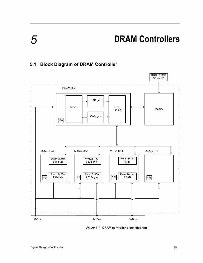
5 DRAM Controllers
5.1 Block Diagram of DRAM Controller
Write Buf fer 384-byte
A rb iter
M-Bus G-Bus
cfg
RAS gen
DDR Timing
PADS
DRAM Unit
G -Bus Unit
CAS gen
Read Buf fer 192-byte
Write FIFO 2624-byte
cfg
M-Bus Unit
Read Buffer2688-byte
Write Buffer1KB
cfg
V-Bus Unit
Read Buf fer 1.5KB cfg
G-Bus Unit
V-Bus
cfg
DDR 512MB maximum
Figure 5-1 DRAM controller block diagram
Sigma Designs Confidential 95

SMP8654-DS-A-10SMP8654 Datasheet
5.2 Introduction
The SMP8654 contains two identical double-data rate synchronous DRAM (DDR-SDRAM) controllers operating at up to 333MHz. Each DRAM controller supports up to 512MB of DDR-2 memory. Because the DDR technology transfers data on both edges of the clock, the maximum effective burst data bandwidth of each controller is 2.6GB/sec. No more than 80% of the memory bandwidth should be used (~2.1GB/sec for each 32-bit interface). The contents of the DRAM memory may also be encrypted (proprietary algo-rithm) to protect the contents.
Compatible external memory devices attached to the memory interface provide the data storage capability necessary for all the functions performed by the SMP8654. These func-tions include:
• Multiple audio, video and data buffers
• Temporary data storage for hardware function blocks
• Program and data memory for the on-chip CPUs, DSPs and RISC processors
• Transport stream buffers
The DRAM controllers supports memory devices which conform to JEDEC standard JESD79-2B. The electrical interface to the external memories supports JEDEC SSTL_1.8 compliant signaling.
5.3 Features
• Two 32-bit DRAM controllers
• Double-data rate synchronous DRAM (up to DDR-667)
• Effective aggregate burst data bandwidth of the 2 DRAM interfaces is up to 5.2GB/sec
• Interfaces up to 1GB of external DDR-2 SDRAM
96 Sigma Designs Confidential

5: DRAM Controllers
5.4 Functional Description
The two SMP8654 DRAM controllers (DRAM controller 0 and DRAM controller 1) can interface to up to 1GB of external DDR SDRAM, using two independent 32-bit wide inter-faces. The two DRAM controllers interface with the different modules of the SMP8654 through:
• A G-Bus for flat addressing of the DRAM, and configuration registers.
• An M-Bus for DMA transfers to/from all the blocks except the video output block
• A V-Bus for DMA transfers to/from the video output block
• A direct load port to interface to the video decoder for motion compensation loads
As shown in the block diagram, the memory controller connects to all four of the primary device buses. Each bus connects to the controller via an interface unit, which contains command queues as well as FIFOs for read and/or write data. The interface units in turn connect to the DRAM unit which actually controls the external memory.
Any G-Bus master can program the configuration registers of all four units. Also, a G-Bus master can access the entire DRAM space via the G-Bus unit.
Each of the DRAM controllers occupies two sections on the G-Bus space: A 512MB sec-tion for direct memory accesses and a 64KB section for configuration register accesses.
Within the DRAM units, an arbiter analyzes the pending requests from the many DMA channels in the various functional units. Based on the channel priority, the bank access requested and the currently available banks, the arbiter determines order of the service requested by the various channels. The DRAM units are designed to maximize utilization of the DRAMs, while simultaneously controlling read and write access latency.
The SMP8654 device uses a sophisticated delay-lock loop (DLL) technique to optimize critical timings in the DRAM interface. These timings are automatically updated on a peri-odic basis to maintain the critical characteristics under changing voltage and temperature conditions, and are not accessible to the customers.
97Sigma Designs Confidential

SMP8654-DS-A-10SMP8654 Datasheet
5.4.1 Memory Configurations
The two 32-bit DRAM controller interfaces can connect up to 1GB of DDR-2 SDRAM (512MB per controller).
Table 5-1 Typical memory configurations
Total Memory (MB) Bus Width (DRAM0/DRAM1) Memory Chip Configuration
256 32/32 Four 32Mx16
512 32/32 Four 64Mx16
1024 32/32 Four 128Mx16
Many factors affect the external memory configuration needed to support a particular application. In addition to the basic requirement of picture buffer areas needed to support the video decoding process and any necessary graphics planes, other storage requirements must also be considered. Additional factors which come into play may include:
• Font sets and graphics elements which must be maintained in the off-screen display memory
• Multiple graphics buffers required for ‘instant’ updates (animation effects)
• Use of video and graphics input ports
• Nature of processing tasks being performed on the host CPU
Determining the optimum memory configuration requires that the application require-ments be well defined. More demanding applications may require an analysis of the mem-ory bandwidth utilization.
The DRAM registers control the DRAM refresh timing, CAS latency, and DRAM organi-zation (total size, row/column size and the number [1x32 or 2x16] of DDR chips used). They also control the programmable delay lines affecting the data output delay (write transactions) and the input delay (read transactions). The registers allow the monitoring of the DRAM bandwidth usage.
98 Sigma Designs Confidential

5: DRAM Controllers
5.4.2 Memory Connection Diagram
DDR SDRAM
32/64/128M x 16b
A[13:6]A[5]A[4]
A[3:0]
BA[2:0]
RAS#CAS#WE#CS#
ODT
CKECLKCLK#
UDQSUDQS#LDQSLDQS#
UDMLDM
DQ[15:00]
DRAMx_A[13:6]DRAMx_A[5H]DRAMx_A[4H]
DRAMx_A[5]DRAMx_A[4]
DRAMx_A[3:0]
DRAMx_BA[2:0]
DRAMx_RAS#DRAMx_CAS#DRAMx_WE#DRAMx_CS#
DRAMx_ODT
DRAMx_CKEDRAMx_CLK
DRAMx_CLK#
DRAMx_DQS3DRAMx_DQS3#DRAMx_DQS2
DRAMx_DQS2#DRAMx_DQS1
DRAMx_DQS1#DRAMx_DQS0
DRAMx_DQS0#
DRAMx_DM3DRAMx_DM2DRAMx_DM1DRAMx_DM0
DRAMx_DQ[31:16]DRAMx_DQ[15:00]
A[13:6]
A[5]A[4]A[3:0]
BA[2:0]
RAS#CAS#WE#CS#
ODT
CKECLKCLK#
UDQSUDQS#LDQSLDQS#
UDMLDM
DQ[15:00]
SMP8654
Denotes differential pair
Denotes bus
Figure 5-2 Memory Connection diagram
99Sigma Designs Confidential

SMP8654-DS-A-10SMP8654 Datasheet
5.4.3 Memory Bandwidth Considerations
For complex applications, the available memory bandwidth may limit what can be done with SMP8654. In these cases the total available memory bandwidth (assuming DDR-667 DRAM) is as follows:
• For each 32-bit interface, maximum memory bandwidth is 2.6GB/s (2.1GB/s for DDR-533)
• Should not exceed 80% of maximum, resulting in 2.1GB/s available memory band-width for each 32-bit interface (1.7GB/s for DDR-533)
5.4.3.1 Memory Bandwidth Requirements for Video
Table 5-2 Memory bandwidth requirements for video
functionSource Format (frames per second) Memory bandwidth needed
MPEG-4.10 (H.264) video decode and display
1920 x 1080 x 301280 x 720 x 60720 x 576 x 50720 x 576 x 25720 x 480 x 60720 x 480 x 30
1.1GB/s (0.95GB/s decode only)1.0GB/s0.45GB/s0.22GB/s0.45GB/s0.22GB/s
SMPTE 421M (VC-1) video decode and display
1920 x 1080 x 301280 x 720 x 60720 x 576 x 50720 x 576 x 25720 x 480 x 60720 x 480 x 30
0.97GB/s0.86GB/s0.31GB/s0.15GB/s0.31GB/s0.15GB/s
MPEG-2 video decode and dis-play
1920 x 1080 x 301280 x 720 x 60720 x 576 x 50720 x 576 x 25720 x 480 x 60720 x 480 x 30
0.41GB/s0.37GB/s0.14GB/s0.07GB/s0.14GB/s0.07GB/s
Displaying 32-bit graphics 1920 x 1080 x 601920 x 1080 x 501920 x 1080 x 301920 x 1080 x 251280 x 720 x 601280 x 720 x 50720 x 576 x 50720 x 576 x 25720 x 480 x 60720 x 480 x 30
498MB/s415MB/s249MB/s207MB/s221MB/s184MB/s83MB/s41MB/s83MB/s41MB/s
100 Sigma Designs Confidential

5: DRAM Controllers
Displaying 24-bit graphics (24-bit data is written and read as 32-bit data)
1920 x 1080 x 60 1920 x 1080 x 50 1920 x 1080 x 30 1920 x 1080 x 25 1280 x 720 x 60 1280 x 720 x 50 720 x 576 x 50 720 x 576 x 25 720 x 480 x 60 720 x 480 x 30
498MB/s415MB/s249MB/s207MB/s221MB/s184MB/s83MB/s41MB/s83MB/s41MB/s
Displaying 16-bit graphics 1920 x 1080 x 60 1920 x 1080 x 50 1920 x 1080 x 30 1920 x 1080 x 25 1280 x 720 x 60 1280 x 720 x 50 720 x 576 x 50 720 x 576 x 25 720 x 480 x 60 720 x 480 x 30
249MB/s207MB/s124MB/s104MB/s111MB/s92MB/s41MB/s21MB/s41MB/s21MB/s
Displaying 8-bit graphics 1920 x 1080 x 60 1920 x 1080 x 50 1920 x 1080 x 30 1920 x 1080 x 25 1280 x 720 x 60 1280 x 720 x 50 720 x 576 x 50 720 x 576 x 25 720 x 480 x 60 720 x 480 x 30
124MB/s104MB/s62MB/s52MB/s55MB/s46MB/s21MB/s10MB/s21MB/s10MB/s
Additional bandwidth for Type 1 deinterlacing of main video
1920 x 1080i x 301920 x 1080i x 25720 x 576i x 25720 x 480i x 30
93MB/s78MB/s16MB/s16MB/s
Additional bandwidth for Type 2 (motion adaptive) deinterlacing of main video
1920 x 1080i x 301920 x 1080i x 25 720 x 576i x 25 720 x 480i x 30
187MB/s156MB/s31MB/s31MB/s
Additional bandwidth for simul-taneous HD+SD output- On-the-fly mode - Buffered mode
0MB/s42MB/s
Video decoder RISC - 3MB/s (assuming 24Mbps bit-stream)
Table 5-2 Memory bandwidth requirements for video (Continued)
functionSource Format (frames per second) Memory bandwidth needed
101Sigma Designs Confidential

SMP8654-DS-A-10SMP8654 Datasheet
5.4.3.2 Memory Bandwidth Requirements for Audio
Table 5-3 Memory bandwidth requirements for audio
function Typical memory bandwidth needed
Decoding, output formatting and routing- Dolby Digital 5.1- Dolby Digital Plus 2.0- Dolby Digital Plus 5.1- Dolby Digital Plus 7.1- Dolby TrueHD 5.1- Dolby TrueHD 7.1- MPEG-1 Layers I, II 2.0- MPEG -1 Layer III (mp3) 2.0- MPEG-4 AAC-LC 2.0- MPEG-4 AAC-LC 5.1- MPEG-4 HE-AAC 5.1- MPEG-4 BSAC 2.0- LPCM 7.1- WMA9 2.0- WMA Pro 5.1- ATRAC3 2.0
29MB/sTBDTBDTBDTBDTBD75MB/s65MB/sTBD49MB/s41MB/sTBD70MB/s53MB/s32MB/s1MB/s
Encoding- Dolby Digital 5.1 TBD
Other- Watermark detection- Post processing
1MB/sTBD
For example, displaying a HD MPEG-4.10 (H.264) video + SD MPEG-4.10 (H.264) + 32-bit HD graphics + 8-bit HD subtitle requires, 1.1 + 0.22 + 0.25 + 0.06 = 1.6GB/s of mem-ory bandwidth to display it on the TV. This does not include the additional memory band-width required for writing the graphics and the subpicture data, deinterlacing, audio, and the CPU/XPU requirements. Note that the display on the TV must always be at 30 (25) frames or 60 (50) fields per second.
102 Sigma Designs Confidential

5: DRAM Controllers
To assist in calculating the needed memory bandwidth for various applications, additional typical memory bandwidth values for various other operations are:
Table 5-4 Typical memory bandwidth values
function Typical memory bandwidth needed
XPU baseline- WM DRM-ND and WM DRM-PD - DTCP/IP - HDCP for DVI and HDMI - CPRM for DVD-R and DVD-RW playback- CSS for DVD-Video playback- Verance audio watermark detection- VCPS for DVD+R/+RW
1MB/s6MB/s (16Mbps bitstream max.)3MB/s1MB/s1MB/s1MB/s1MB/s1MB/s
5.4.4 Memory Size Requirements
The following tables list some of the major software/firmware components and the typical amount of DRAM they require.
Table 5-5 Video Decoding DRAM requirements (MB, includes all needed buffers, no deinterlacing or type 1 deinterlacing)
MPEG-2 MPEG-4.2 MPEG-4.10 (H.264)
SMPTE 421M (VC-1)
352x240352x288
1 1 3 2
352x480i352x576i
2 2 5 3
720x480i720x576i
4 4 7 4
1280x720p 7 8 13 8
1920x1080i 16 17 36 18
103Sigma Designs Confidential

SMP8654-DS-A-10SMP8654 Datasheet
Table 5-6 Video Decoding DRAM requirements (MB, includes all needed buffers, type 2 deinterlacing used)
MPEG-2 MPEG-4.2 MPEG-4.10 (H.264)
SMPTE 421M (VC-1)
352x240352x288
2 2 3 2
352x480i352x576i
3 3 5 3
720x480i720x576i
4 5 8 5
1280x720p 9 9 14 10
1920x1080i 19 20 39 21
Table 5-7 Typical Firmware DRAM requirements (MB)
FirmwareTotal DRAM Required
DRAM Bank 1
DRAM Bank 0
Video decoding (HD MPEG-4.10) 39 39
Audio decoding 5 5
Linux (11) + MRUA/DCC-HD/DirectFB (11) + kernel mode drivers (8)
30 30
XPU 4 4
2D graphics accelerator 1 1
Simultaneous HD + SD output 2 2
Total 81 41 40
104 Sigma Designs Confidential

5: DRAM Controllers
5.5 Pin Description
5.5.1 DRAM Controller Pins
Table 5-8 DRAM controller pin descriptions
Pin Name Pin Id Direction Description
DRAM0_A0 M27 O Memory address bit 0
DRAM0_A1 N30 O Memory address bit 1
DRAM0_A10 P29 O Memory address bit 10
DRAM0_A11 P28 O Memory address bit 11
DRAM0_A12 R25 O Memory address bit 12
DRAM0_A13 N25 O Memory address bit 13. Memory address bus provides the SDRAM with the row address for the active commands, and the column address and the auto-precharge value for read/write commands.
DRAM0_A2 P26 O Memory address bit 2
DRAM0_A3 T25 O Memory address bit 3
DRAM0_A4 N29 O Memory address bit 4
DRAM0_A4H M25 O Memory address bit 4H
DRAM0_A5 R26 O Memory address bit 5
DRAM0_A5H P25 O Memory address bit 5H
DRAM0_A6 N28 O Memory address bit 6
DRAM0_A7 T27 O Memory address bit 7
DRAM0_A8 N26 O Memory address bit 8
DRAM0_A9 T28 O Memory address bit 9
DRAM0_BA0 R28 O Bank address output 0
DRAM0_BA1 R30 O Bank address output 1. BA[1:0] define to which SDRAM bank an active, read, write or precharge command is being applied.
DRAM0_BA2 R29 O Bank address output 2. BA[1:0] define to which SDRAM bank an active, read, write or precharge command is being applied.
DRAM0_CAS# M28 O Column address strobe. Memory command out-put. In conjunction with CAS# and WE#, this signal determines the memory operation requested (active-low).
105Sigma Designs Confidential

SMP8654-DS-A-10SMP8654 Datasheet
DRAM0_CK M30 O Non-inverted clock output. CK and CK# are a differential clock signal pair. The SDRAM0 address and control signals are sampled on the crossing of the positive edge of CK and the neg-ative edge of CK#. SDRAM output (read) data is referenced to the crossings of CK and CK# in both directions.
DRAM0_CK# L30 O Inverted clock output. CK and CK# are a differ-ential clock signal pair. The SDRAM address and control signals are sampled on the crossing of the positive edge of CK and the negative edge of CK#. SDRAM output (read) data is referenced to the crossings of CK and CK# in both direc-tions (active-low).
DRAM0_CKE T30 O Clock enable. A high level activates, and a low level deactivates the internal clock signals in the SDRAM. This signal is driven low to activate the SDRAM power-down modes.
DRAM0_CS# L27 O Chip select (active low)
DRAM0_DM0 W26 O Write data mask for bits [07:00] of memory data
DRAM0_DM1 AB29 O Write data mask for bits [15:08] of memory data
DRAM0_DM2 K28 O Write data mask for bits [23:16] of memory data
DRAM0_DM3 H28 O Write data mask for bits [31:24] of memory data. Write data is masked when the corre-sponding DM bit is sampled high by the SDRAM during a write access.
DRAM0_DQ0 U25 B Memory data bus bit 0 (LSB)
DRAM0_DQ1 Y26 B Memory data bus bit 1
DRAM0_DQ10 AA28 B Memory data bus bit 10
DRAM0_DQ11 AB30 B Memory data bus bit 11
DRAM0_DQ12 AD30 B Memory data bus bit 12
DRAM0_DQ13 W30 B Memory data bus bit 13
DRAM0_DQ14 AB28 B Memory data bus bit 14
DRAM0_DQ15 Y29 B Memory data bus bit 15
DRAM0_DQ16 H27 B Memory data bus bit 16
DRAM0_DQ17 L25 B Memory data bus bit 17
DRAM0_DQ18 K25 B Memory data bus bit 18
DRAM0_DQ19 K26 B Memory data bus bit 19
DRAM0_DQ2 V26 B Memory data bus bit 2
Table 5-8 DRAM controller pin descriptions (Continued)
Pin Name Pin Id Direction Description
106 Sigma Designs Confidential

5: DRAM Controllers
DRAM0_DQ20 L26 B Memory data bus bit 20
DRAM0_DQ21 H26 B Memory data bus bit 21
DRAM0_DQ22 K29 B Memory data bus bit 22
DRAM0_DQ23 J25 B Memory data bus bit 23
DRAM0_DQ24 E29 B Memory data bus bit 24
DRAM0_DQ25 J28 B Memory data bus bit 25
DRAM0_DQ26 G29 B Memory data bus bit 26
DRAM0_DQ27 G30 B Memory data bus bit 27
DRAM0_DQ28 J30 B Memory data bus bit 28
DRAM0_DQ29 D30 B Memory data bus bit 29
DRAM0_DQ3 W27 B Memory data bus bit 3
DRAM0_DQ30 H29 B Memory data bus bit 30
DRAM0_DQ31 F28 B Memory data bus bit 31 (MSB)
DRAM0_DQ4 Y28 B Memory data bus bit 4
DRAM0_DQ5 U26 B Memory data bus bit 5
DRAM0_DQ6 W25 B Memory data bus bit 6
DRAM0_DQ7 U27 B Memory data bus bit 7
DRAM0_DQ8 W28 B Memory data bus bit 8
DRAM0_DQ9 AC29 B Memory data bus bit 9
DRAM0_DQS0 V28 B Data strobes for bits 07:00 of memory data
DRAM0_DQS0# V29 B Data strobes for bits 07:00 of memory data
DRAM0_DQS1 AA29 B Data strobes for bits [15:08] of memory data
DRAM0_DQS1# AA30 B Data strobes for bits [15:08] of memory data
DRAM0_DQS2 J27 B Data strobes for bits [23:16] of memory data
DRAM0_DQS2# J26 B Data strobes for bits [23:16] of memory data
DRAM0_DQS3 F30 B Data strobes for bits [31:24] of memory data bus. Output by the SMP8654 with the write data; output by the SDRAM with the read data.
DRAM0_DQS3# F29 B Data strobes for bits [31:24] of memory data bus. Output by the SMP8654 with the write data; output by the SDRAM with the read data.
DRAM0_ODT K30 O On die termination
Table 5-8 DRAM controller pin descriptions (Continued)
Pin Name Pin Id Direction Description
107Sigma Designs Confidential

SMP8654-DS-A-10SMP8654 Datasheet
DRAM0_RAS# L28 O Memory command output. In conjunction with WE#, this signal determines the memory opera-tion requested.
DRAM0_VREFSSTL0 AA27 I SSTL-2 voltage reference input (1.25V)
DRAM0_VREFSSTL1 U24 I SSTL-2 voltage reference input (1.25V)
DRAM0_VREFSSTL2 P24 I SSTL-2 voltage reference input (1.25V)
DRAM0_VREFSSTL3 L24 I SSTL-2 voltage reference input (1.25V)
DRAM0_VREFSSTL4 G27 I SSTL-2 voltage reference input (1.25V)
DRAM0_WE# U29 O Write enable (active-low). Memory command output. In conjunction with CAS# and WE#, this signal determines the memory operation requested.
DRAM1_A0 D14 O Memory address bit 0
DRAM1_A1 A15 O Memory address bit 1
DRAM1_A10 B16 O Memory address bit 10
DRAM1_A11 C16 O Memory address bit 11
DRAM1_A12 F17 O Memory address bit 12
DRAM1_A13 F15 O Memory address bit 13. Memory address bus provides the SDRAM with the row address for the active commands, and the column address and the auto-precharge value for read/write commands.
DRAM1_A2 E16 O Memory address bit 2
DRAM1_A3 F18 O Memory address bit 3
DRAM1_A4 B15 O Memory address bit 4
DRAM1_A4H F14 O Memory address bit 4H
DRAM1_A5 E17 O Memory address bit 5
DRAM1_A5H F16 O Memory address bit 5H
DRAM1_A6 C15 O Memory address bit 6
DRAM1_A7 D18 O Memory address bit 7
DRAM1_A8 E15 O Memory address bit 8
DRAM1_A9 C18 O Memory address bit 9
DRAM1_BA0 C17 O Bank address output 0
DRAM1_BA1 A17 O Bank address output 1. BA[1:0] define to which SDRAM bank an active, read, write or precharge command is being applied.
Table 5-8 DRAM controller pin descriptions (Continued)
Pin Name Pin Id Direction Description
108 Sigma Designs Confidential

5: DRAM Controllers
DRAM1_BA2 B17 O Bank address output 2. BA[1:0] define to which SDRAM bank an active, read, write or precharge command is being applied.
DRAM1_CAS# C14 O Column address strobe (active-low). Memory command output. In conjunction with WE#, this signal determines the memory operation requested.
DRAM1_CK A14 O Non-inverted clock output. CK and CK# are a differential clock signal pair. SDRAM address and control signals are sampled on the crossing of the positive edge of CK and the negative edge of CK#. SDRAM output (read) data is ref-erenced to the crossings of CK and CK# in both directions.
DRAM1_CK# A13 O Inverted clock output. CK and CK# are a differ-ential clock signal pair. SDRAM address and con-trol signals are sampled on the crossing of the positive edge of CK and the negative edge of CK#. SDRAM output (read) data is referenced to the crossings of CK and CK# in both direc-tions (active-low).
DRAM1_CKE A18 O Clock enable. A high level activates, and a low level deactivates the internal clock signals in the SDRAM. This signal is driven low to activate the SDRAM power-down modes.
DRAM1_CS# D13 O DRAM1 chip select (active-low).
DRAM1_DM0 E21 O Write data mask for bits [07:00] of memory data
DRAM1_DM1 B24 O Write data mask for bits [15:08] of memory data
DRAM1_DM2 C12 O Write data mask for bits [23:16] of memory data
DRAM1_DM3 C10 O Write data mask for bits [31:24] of memory data. Write data is masked when the corre-sponding DM bit is sampled high by the SDRAM during a write access.
DRAM1_DQ0 F19 B Memory data bus bit 0 (LSB)
DRAM1_DQ1 E22 B Memory data bus bit 1
DRAM1_DQ10 C23 B Memory data bus bit 10
DRAM1_DQ11 A24 B Memory data bus bit 11
DRAM1_DQ12 A26 B Memory data bus bit 12
DRAM1_DQ13 A21 B Memory data bus bit 13
DRAM1_DQ14 C24 B Memory data bus bit 14
DRAM1_DQ15 B22 B Memory data bus bit 15
DRAM1_DQ16 D10 B Memory data bus bit 16
Table 5-8 DRAM controller pin descriptions (Continued)
Pin Name Pin Id Direction Description
109Sigma Designs Confidential

SMP8654-DS-A-10SMP8654 Datasheet
DRAM1_DQ17 F13 B Memory data bus bit 17
DRAM1_DQ18 F12 B Memory data bus bit 18
DRAM1_DQ19 E12 B Memory data bus bit 19
DRAM1_DQ2 E20 B Memory data bus bit 2
DRAM1_DQ20 E13 B Memory data bus bit 20
DRAM1_DQ21 E10 B Memory data bus bit 21
DRAM1_DQ22 B12 B Memory data bus bit 22
DRAM1_DQ23 F11 B Memory data bus bit 23
DRAM1_DQ24 B7 B Memory data bus bit 24
DRAM1_DQ25 C11 B Memory data bus bit 25
DRAM1_DQ26 B9 B Memory data bus bit 26
DRAM1_DQ27 A9 B Memory data bus bit 27
DRAM1_DQ28 A11 B Memory data bus bit 28
DRAM1_DQ29 A6 B Memory data bus bit 29
DRAM1_DQ3 D21 B Memory data bus bit 3
DRAM1_DQ30 B10 B Memory data bus bit 30
DRAM1_DQ31 C8 B Memory data bus bit 31 (MSB)
DRAM1_DQ4 C22 B Memory data bus bit 4
DRAM1_DQ5 E19 B Memory data bus bit 5
DRAM1_DQ6 F21 B Memory data bus bit 6
DRAM1_DQ7 D19 B Memory data bus bit 7
DRAM1_DQ8 C21 B Memory data bus bit 8
DRAM1_DQ9 B25 B Memory data bus bit 9
DRAM1_DQS0 C20 B Data strobes for bits 07:00 of memory data
DRAM1_DQS0# B20 B Data strobes for bits [15:08] of memory data
DRAM1_DQS1 B23 B Data strobes for bits [23:16] of memory data
DRAM1_DQS1# A23 B Data strobes for bits [31:24] of memory data bus. Output by the SMP8654 with the write data; output by the SDRAM with the read data.
DRAM1_DQS2 D11 B Data strobes for bits 07:00 of memory data
DRAM1_DQS2# E11 B Data strobes for bits [15:08] of memory data
Table 5-8 DRAM controller pin descriptions (Continued)
Pin Name Pin Id Direction Description
110 Sigma Designs Confidential

5: DRAM Controllers
5.6 Electrical Characteristics
All DRAM I/O signals conform to the electrical characteristics specified for SSTL-1.8 Class II interface as specified in the JEDEC standard, JESD79D-2B, dated January 2005. Refer to the JEDEC standard for details regarding switching levels, drive performance, etc.
DRAM1_DQS3 A8 B Data strobes for bits [23:16] of memory data
DRAM1_DQS3# B8 B Data strobes for bits [31:24] of memory data bus. Output by the SMP8654 with the write data; output by the SDRAM with the read data.
DRAM1_ODT A12 O On die termination
DRAM1_RAS# C13 O DRAM1 row address strobe (active-low). Mem-ory command output. In conjunction with CAS# and WE#, this signal determines the memory operation requested.
DRAM1_VREFSSTL0 D23 I SSTL-2 voltage reference input (1.25V)
DRAM1_VREFSSTL1 G19 I SSTL-2 voltage reference input (1.25V)
DRAM1_VREFSSTL2 G16 I SSTL-2 voltage reference input (1.25V)
DRAM1_VREFSSTL3 G13 I SSTL-2 voltage reference input (1.25V)
DRAM1_VREFSSTL4 D9 I SSTL-2 voltage reference input (1.25V)
DRAM1_WE# B19 O DRAM1 write enable (active-low). Memory com-mand output. In conjunction with CAS# and WE#, this signal determines the memory opera-tion requested.
Table 5-8 DRAM controller pin descriptions (Continued)
Pin Name Pin Id Direction Description
111Sigma Designs Confidential

SMP8654-DS-A-10SMP8654 Datasheet
112 Sigma Designs Confidential

6 System Block
6.1 Block Diagram of System Block
V-Bus G-Bus
G-Bus Arbiter
M-Bus Arbiter
V-Bus Arbiter
M-Bus
Clock Generator
I2C
GPIO FIP
PWM IR
Watchdog
Figure 6-1 Block diagram of system block
Sigma Designs Confidential 113

SMP8654-DS-A-10SMP8654 Datasheet
6.2 Introduction
The SMP8654 system block contains the following modules:
• A GPIO block containing General Purpose I/O (GPIO), Front Panel Interface (FIP) Controller, Pulse Width Modulator (PWM) and infrared decoder
• Two I2C masters and one I2C slave
• A clock generator
• System bus arbiters
Many SMP8654 sub-blocks require shared accesses to the internal system buses. The bus arbiters allocate the access to the individual system buses based on the priority of the device. A bus bridge unit allows each of the above blocks to be configured through the G-Bus.
As shown in the block diagram, the system block connects to each of the three primary device data buses previously mentioned. The system controller unit provides the arbitra-tion logic for the four primary internal buses. The M-Bus and V-Bus arbiters implement a bandwidth allocation algorithm allowing each bus master to be assigned a certain mini-
mum and maximum bandwidth allocation in increments of 2-8 of the total available band-width.
When certain constraints are met in the allocation of minimum and maximum bandwidth, each master can be guaranteed to receive its minimum bandwidth, and often receives more.
GPIO Block
6.3 General Purpose I/O (GPIO)
The SMP8654 provides 16 dedicated general-purpose input/output (GPIO) pins to help reduce or eliminate external “glue logic” often needed for system implementation. In addi-tion to these dedicated GPIO pins, an additional 68 GPIO pins can be made available since certain other chip interfaces can have GPIO capability as an alternate function. The total number of available GPIO pins, therefore, depends on the usage of these shared interfaces. Shared GPIO pins are listed later in this section.
114 Sigma Designs Confidential

6: System Block
6.3.1 Dedicated GPIO
The system block contains a GPIO controller module which supports the 16 dedicated GPIO pins. The GPIO pins are individually configurable as inputs or outputs, and are con-trolled by software commands issued to registers within the module. All pins default to input mode upon device reset. Registers configure the direction and output value, or read the input value, of each pin. Because the control of the GPIO registers by the host CPU involves hardware elements (write buffers, shared buses) with variable latency, the GPIO pins should not be used for applications requiring precise control of timing. Generally, the GPIO pins should be used for low-speed or non-critical control and signaling applications.
6.3.1.1 Dedicated GPIO Features
• Supports 16 independently controllable inputs/outputs
• Up to four pins may be specified to provide CPU interrupts
• Masking function simplifies software control of individual GPIO pins
• ‘Special function’ can be used as needed which share GPIO pins
- Two pulse-width modulators (PWMs)
- Two I2C master interfaces
- One I2C slave interface - One Front Panel Interface controller - One HDMI CEC
6.3.1.2 GPIO Controller Operation
Direction of each GPIO pin is established by the contents of the direction register. The value of pins set as outputs is controlled by writing to the Output Data Register. When writing to this register, the 16 data bits corresponding to the state of the 16 GPIO pins is placed in the lower 16 bits of the 32-bit value written by the CPU. The upper 16 bits func-tion as a “mask” value: a logic zero in any of the upper 16 bits causes the corresponding data bit (lower 16 bits) to NOT be written (previous value is retained). As an example, a logic zero in bit position 24 causes Output Data Register bit 8 to be unchanged during a write. Conversely, a logic one in bit position 24 causes bit 8 to be written into the Output Data Register. The block diagram of the GPIO controller module is as shown below:
115Sigma Designs Confidential

SMP8654-DS-A-10SMP8654 Datasheet
G-BusInterface
DirectionRegister
Pads
OutputData
Register
16-to-4selector
InterruptRegister
Alternate Function Modules
I2CMaster
I2CSlave
PWM0
PWM1
FrontPanel
G-bus
toInterrupt
Controller
I2CMaster
Figure 6-2 GPIO controller block diagram
The GPIO controller includes both “alternate functions” and “selectable inputs” for greater flexibility.
6.3.1.3 Alternate functions and Selectable Inputs
As described above, the system block contains several special-function modules which, if used, share various GPIO pins for their I/O. The alternate functions implemented include 2
PWM modules, 2 I2C master controllers, one I2C slave controller, and a 4-wire serial Front Panel Interface Controller (FIP). When alternate functions are enabled the matching GPIO pins cannot be used for GPIO any more.
116 Sigma Designs Confidential

6: System Block
Selectable inputs are input functions only (e.g., PCI Interrupt A). They are assigned by default to particular pins at reset, but can be reassigned to a different pin under register control. Pins used as selectable inputs should be configured as GPIO pins in input mode.
The following table shows the GPIO alternate functions and selectable inputs in detail:
14
13
12
11
10
9
8
15
GPIO
6
5
4
3
2
1
0
7
Alternate Function
PWM Generator 0
PWM Generator 1
Front Panel Interface (FIP)
sda
I2C Master 0
Infrared Remote Input
(PCI) Interrupt Input D
(PCI) Interrupt Input C
(PCI) Interrupt Input B
(PCI) Interrupt Input A
sck
Slave I2C
sda
sck
clk
stb
dout
din
Selectable Inputs
I2C Master 1 sda
sck
HDMI CEC
6.3.1.4 GPIO Pin State During Initialization
The following figure depicts the state of GPIO pins during device initialization:
UNDEFINEDDIRECTION
OUTPUT DATAREG UNDEFINED
(*) CONDITION UNTIL CHANGED BY SOFTWARE WRITE TO GPIO REGISTERS
INPUT INPUT (*)
ZERO ZERO (*)
SYSTEMPOW ER
RESET#
Figure 6-3 Behavior of GPIO pins during chip initialization
117Sigma Designs Confidential

SMP8654-DS-A-10SMP8654 Datasheet
6.3.2 Additional GPIO
In addition to the 16 dedicated GPIO pins described above, certain other interfaces in the device can be utilized as GPIO pins if the interface is not used in the application. The table below lists all such “auxiliary” GPIO pins. Note that the GPIO pin numbering is not con-tiguous since several internal register bits are not brought out to physical pins of the device.
Table 6-1 Additional GPIO pins
GPIO # Primary function Ball # GPIO# Primary function Ball #
16 Unavailable - 50 ETH0_TX_ER AJ1
17 Unavailable - 51 ETH1_TXCLK AG6
18 UART0_RX F27 52 ETH1_TX_EN AF7
19 Unavailable - 53 ETH1_TXD0 AF6
20 Unavailable - 54 ETH1_TXD1 AK7
21 Unavailable - 55 ETH1_TXD2 AJ7
22 UART0_TX D29 56 ETH1_TXD3 AH7
23 Unavailable - 57 ETH1_RXCLK AH6
24 Unavailable - 58 ETH1_RX_DV AJ5
25 UART1_RX C30 59 ETH1_RX_ER AH4
26 UART1_CTS H24 60 ETH1_RXD0 AH5
27 UART1_DSR G25 61 ETH1_RXD1 AG5
28 UART1_DCD F26 62 ETH1_RXD2 AK6
29 UART1_TX E27 63 ETH1_RXD3 AJ6
30 UART1_RTS D28 64 ETH1_CRS AK5
31 UART1_DTR C29 65 ETH1_COL AE7
32 ETH0_TXCLK AG1 66 ETH1_MDC AJ4
33 ETH0_TX_EN AJ3 67 ETH1_MDIO AK4
34 ETH0_TXD0 AG2 68 ETH1_MDINT# AK3
35 ETH0_TXD1 AG3 69 ETH1_TX_ER AG7
36 ETH0_TXD2 AH1 70 SCARD0_RST A29
37 ETH0_TXD3 AH2 71 SCARD0_CLK B28
38 ETH0_RXCLK AF4 72 SCARD0_FC# C27
39 ETH0_RX_DV AE4 73 SCARD0_IO D26
118 Sigma Designs Confidential

6: System Block
6.3.3 Register Map
6.3.3.1 GPIO Registers
40 ETH0_RX_ER AE2 74 SCARD0_CTL0 G23
41 ETH0_RXD0 AE5 75 SCARD0_CTL1 F24
42 ETH0_RXD1 AF1 76 SCARD0_CTL2 E25
43 ETH0_RXD2 AF2 77 SCARD1_RST A28
44 ETH0_RXD3 AF3 78 SCARD1_CLK A27
45 ETH0_CRS AE3 79 SCARD1_FC# B27
46 ETH0_COL AK2 80 SCARD1_IO C26
47 ETH0_MDC AE1 81 SCARD1_CTL0 F23
48 ETH0_MDIO AD6 82 SCARD1_CTL1 E24
49 ETH0_MDINT# AD5 83 SCARD1_CTL2 D25
Table 6-2 Register map - GPIO
Address1 Register Name R/W/A2 Description
+0500 SYS_GPIO_DIR R/W GPIO Direction Register
+0504 SYS_GPIO_DATA R/W GPIO Data Register
+0508 SYS_GPIO_INT R/W GPIO Interrupt Register
+0510 SYS_GPIO15_PWM R/W GPIO15 PWM Register
+0514 SYS_GPIO14_PWM R/W GPIO14 PWM Register
+1B8303 TDMX_GPIO_DATA R/W Transport Demux GPIO Data Register
+1B834 TDMX_GPIO_DIR R/W Transport Demux GPIO Direction Reg-ister
+1B838 TDMX_GPIO_SEL R/W Transport Demux GPIO Selection Reg-ister
+C1304 CPU_UART0_GPIO_DIR R/W UART0 GPIO Direction Register
+C134 CPU_UART0_GPIO_DATA R/W UART0 GPIO Data Register
+C138 CPU_UART0_GPIO_MODE R/W UART0 GPIO Mode Register
+C230 CPU_UART1_GPIO_DIR R/W UART1 GPIO Direction Register
+C234 CPU_UART1_GPIO_DATA R/W UART1 GPIO Data Register
Table 6-1 Additional GPIO pins (Continued)
GPIO # Primary function Ball # GPIO# Primary function Ball #
119Sigma Designs Confidential

SMP8654-DS-A-10SMP8654 Datasheet
6.3.4 Pin Description
6.3.4.1 GPIO Pins
The SMP8654 provides 16 general-purpose I/O (GPIO) pins which may be individually configured as inputs or outputs and used for design-specific applications.
+C238 CPU_UART1_GPIO_MODE R/W UART1 GPIO Mode Register
1. Address refers to G-Bus byte address relative to the system block register base (0x10000).2. Read/Write/Auto update.3. The TDMX_GPIO_xxx addresses are relative to the transport demux memory base 0x14000. 4. The UART GPIO addresses are relative to the CPU block register base 0x60000.
Table 6-3 GPIO pin description
Pin Name Pin Id Direction Description Driver Type1
GPIO0 D5 B General-purpose IO pin 0
Alternate function: I2C Master 0.
A
GPIO1 E6 B General-purpose IO pin 1
Alternate function: I2C Master 0.
A
GPIO2 F7 B General-purpose IO pin 2Alternate function: Front Panel Interface (FIP).
A
GPIO3 G8 B General-purpose IO pin 3Alternate function: Front Panel Interface (FIP).
A
GPIO4 A3 B General-purpose IO pin 4Alternate function: Front Panel Interface (FIP).
A
GPIO5 B4 B General-purpose IO pin 5Alternate function: Front Panel Interface (FIP).
A
GPIO6 C5 B General-purpose IO pin 6
Alternate function: Slave I2C.
A
GPIO7 D6 B General-purpose IO pin 7
Alternate function: Slave I2C.
A
GPIO8 E7 B General-purpose IO pin 8Selectable input: (PCI) Interrupt Input A.
A
GPIO9 F8 B General-purpose IO pin 9Selectable input: (PCI) Interrupt Input B.
A
Table 6-2 Register map - GPIO (Continued)
Address1 Register Name R/W/A2 Description
120 Sigma Designs Confidential
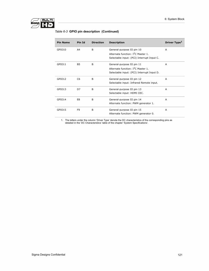
6: System Block
GPIO10 A4 B General-purpose IO pin 10
Alternate function: I2C Master 1.Selectable input: (PCI) Interrupt Input C.
A
GPIO11 B5 B General-purpose IO pin 11
Alternate function: I2C Master 1.Selectable input: (PCI) Interrupt Input D.
A
GPIO12 C6 B General-purpose IO pin 12Selectable input: Infrared Remote input.
A
GPIO13 D7 B General-purpose IO pin 13Selectable input: HDMI CEC.
A
GPIO14 E8 B General-purpose IO pin 14Alternate function: PWM generator 1.
A
GPIO15 F9 B General-purpose IO pin 15Alternate function: PWM generator 0.
A
1. The letters under the column ‘Driver Type’ denote the DC characteristics of the corresponding pins as detailed in the ‘DC Characteristics’ table of the chapter ‘System Specifications‘.
Table 6-3 GPIO pin description (Continued)
Pin Name Pin Id Direction Description Driver Type1
121Sigma Designs Confidential

SMP8654-DS-A-10SMP8654 Datasheet
6.4 Front Panel Controller Interface (FIP)
6.4.1 Introduction
The Front Panel Controller Interface (FIP) directly supports the NEC uPD16311, NEC uPD16312, PTC PT6311 and PTC PT6312. Other front panel controllers may be used by interfacing to the UART or the GPIO.
6.4.2 Features
• Supports NEC uPD16311 and uPD16312
• Supports PT6311 and PT6312
• Interrupt driven
• Works on a fixed clock rate of 27MHz
6.4.3 Block Diagram
VFD Display
FIP Registers
FIP State Machine
Syst
em B
us
INT
VFD/FIP IFController
FIP Clock Generator
DIN
DOUT
CLK
STB
uPD16311or
PT6311
VFD/FIPController
XIN
DIN
DOUT
Figure 6-4 FIP block diagram
122 Sigma Designs Confidential

6: System Block
6.4.4 Functional Description
This block is designed to connect directly to the NEC uPD16311, NEC uPD16312, PT6311 or PT6312 VFD/FIP controller chips. The VFD/FIP controller chips mentioned are commonly used to control VFD displays used in consumer appliances. When enabled PIO[5:2] are used as control pins DOUT, DIN, STB and CLK.
In some applications DIN and DOUT are connected together on both sides (SMP8654 and the VFD controller/FIP controller chip) to save one communication line. In this case, the tristate mode needs to be enabled and an external pull-up resistor connected.
The FIP command register is used to provide a command to a VFD/FIP device to set the display mode, data read/write mode, address of the display memory and the display con-trol. The display data register stores the display data. The LED data is stored by the LED data register.
The key data registers are used to the store key data. The FIP controller will serially shift out the key data from its key input storage RAM after a write to the FIP command register.
The switch data register is used to store the switch input data. It is valid after a write to the FIP command register.
The configuration register controls the enabling of the FIP controller interface. The config-uration register value is used to divide the input clock and generate the FIP clock (default = 27d).
Frequency (FIP_CLK) = Frequency (XIN) / (FIP_CLK_DIV + 1); where, FIP_CLK_DIV should be greater than 2, and values 0, 1 and 2 default to 2.
The configuration register also issues an interrupt on the completion of read or write trans-actions. The interrupt status register is used to clear the interrupts. It is recommended to clear this register before enabling the interrupts.
123Sigma Designs Confidential

SMP8654-DS-A-10SMP8654 Datasheet
6.4.5 Register Map
6.4.5.1 FIP Registers
6.4.6 Pin Description
6.4.6.1 FIP Pins
Table 6-4 FIP registers
Address1
1. Address refers to G-Bus byte address relative to the system block register base.
Register Name R/W/A2
2. Read/Write/Auto update.
Description
+0540 FIP_COMMAND R/W FIP Command Register
+0544 FIP_DISPLAY_DATA R/W FIP Display Data Register
+0548 FIP_LED_DATA R/W FIP LED Data Register
+054C FIP_KEY_DATA1 R FIP Key Data1 Register
+0550 FIP_KEY_DATA2 R FIP Key Data2 Register
+0554 FIP_SWITCH_DATA R FIP Switch Data Register
+0558 FIP_CONFIG R/W FIP Configuration Register
+055C FIP_INT R/C3
3. Read/Clear.
FIP Interrupt Status Register
Table 6-5 FIP pin description
Pin Name Pin Id Direction Description Driver Type1
1. The letters under the column ‘Driver Type’ denote the DC characteristics of the corresponding pins as detailed in the ‘DC Characteristics’ table of the chapter ‘System Specifications‘.
GPIO2 F7 B FIP serial data input A
GPIO3 G8 B FIP serial data output A
GPIO4 A3 B FIP data strobe A
GPIO5 B4 B FIP serial I/O clock A
124 Sigma Designs Confidential

6: System Block
6.4.7 Electrical Characteristics
6.4.7.1 FIP AC Electrical Characteristics
6.4.8 Timing Diagram
TCKHTCKL
TSU
TSTBDLY
TPWSTB
FIP_CLK
FIP_DOUT
FIP_DIN
TH
FIP_STB
FIP_STB
TDV
Figure 6-5 FIP timing diagram
Table 6-6 FIP AC characteristics
Symbol Units Minimum Typical Maximum
TCKL ns 500
TCKH ns 500
TDV ns 0 10
TSU ns 10
TH ns 6
TSTBDLY ns 1250
TPWSTB ns 1000
125Sigma Designs Confidential

SMP8654-DS-A-10SMP8654 Datasheet
6.5 Infrared Decoder
6.5.1 Introduction
The infrared input allows the interfacing to an external IR receiver. The NEC and Philips RC5/RC6 Mode 6A IR formats, commonly used by consumer equipment are supported.
6.5.2 Features
• Supports RC5 and RC6 Mode 6A formats
• Supports RC5 extended format
• Supports NEC format
• Interrupt driven
• Contains error detection
6.5.3 Block Diagram
GP
IO B
lock
1G
PIO
Blo
ck 0IR Receiver
Inpu
t Sel
ecto
r
InterruptMask
RC5/RC6Configuration
Registers
NECConfiguration
Registers
NEC Decoder
RC5/RC6 Decoder
Sys
tem
Bus
INT
GPIO Select
INT
Sel
ect
SYNC andDebounceIR
IRIR
IR Decoder
Figure 6-6 Infrared decoder block diagram
126 Sigma Designs Confidential

6: System Block
6.5.4 Functional Description
This block enables the user to receive the IR scan codes from a RC5/RC6 Mode 6A/ NEC standard compliant remote control.
The control register sets the number of bits to be captured in one frame. It also sets the pre-devider value for the NEC IR decoder. Using this register a GPIO pin may be selected to be used as an input for the NEC and RC5/RC6 Mode 6A IR decoder block.
The decoder data register contains the last scan code captured. This register can be used to detect whether a RC5/RC6 Mode 6A scan code, or a NEC scan code was received.
6.5.4.1 Supported RC6 Mode 6A Formats
Short Customer Information Field, duration X*8*2T X=1,2Long Customer Information Field, duration X*8*2T X=3, ... , 16
Short Customer Code, duration 8 * 2T, SCC [7] = 0Long Customer Code, duration 16 * 2T, LCC[15] = 1
LB
SB TMB[2:0]
SCC [7:0] orLCC [15:0]
RC6A frame
HEADER CTRL FIELD INFORMATION FIELD LO
SCIF [X*8-1:0]; X=1,2LCIF [X*8-1:0] X=3, ... , 16 SFTLB
2THeader Leader bit, duration 8T (6T high, 2T low) 6T
SB T T
MB[2:0]
Header Start bit, duration 2T (T high, T low)
TT 1:T T0:
T
Header Mode bits, duration 3 * 2T,in Mode 6A MB[2:0]='110'
2T0: 2T
SCC [7:0] orLCC [15:0]
Header Trailer bit, duration 4T,in Mode 6A T= '0'
SCIF [X*8-1:0]; X=1,2LCIF [X*8-1:0] X=3, ... , 16
TT 1:T T0:
TT 1:T T0:
SFT Lead out = Signal Free Time, duration 6T
T = 444.44 us
6T
127Sigma Designs Confidential

SMP8654-DS-A-10SMP8654 Datasheet
6.5.4.2 Supported RC5 Formats (Standard and Extended)
A frame is emitted from a RC5 compliant IR remote control once a key is pressed. If the key is held down, the same frame will be sent repeatedly. If the same key is pressed again (after releasing), the same frame will be sent again, except that the T bit will be inverted.
The extended RC5 format supports 128 commands rather than 64. This is achieved by using the 2nd start bit of the standard RC5 format as bit C6.
S S T A4 A3 A2 A1 A0 C4 C3 C2 C1 C0C5
S C6 T A4 A3 A2 A1 A0 C4 C3 C2 C1 C0C5
RC5 frame
RC5 extended frame
bitt
framet
'0' bit '1' bit
S: Start bit, T: Toggle bit, A[4:0]: 5 system address bits, C[5:0]: 6 system command bits (supported in the RC5 standard format), C[6:0]: 7 system command bits (supported only in the RC5 extended format)
Table 6-7 RC5 timing parameters
Minimum Typical Maximum Units
tbit 1.334 1.778 2.222 ms
tframe 24.889 ms
128 Sigma Designs Confidential

6: System Block
6.5.4.3 Supported NEC Format
A frame is emitted from a NEC compliant IR remote control once a key is pressed. After the START condition is transmitted, ADDRESS and ADDRESS# are sent (LSB first). The ADDRESS# represents the bit compliment of ADDRESS. Then the COMMAND and COMMAND# are transmitted wherein COMMAND# represents the bit compliment of COMMAND; transmission is LSB first. If the key is held down, a repeat frame is being sent by the remote.
START A4
NEC waveforms
'1' bit
ADDRESS ADDRESS A4COMMAND COMMAND
560us
2.25ms
'0' bit
560us
1.12ms
START
9ms 4.5ms
NEC frame
110 ms
AGC burst sp
ace
space
NEC repeat frame
9 ms
110 ms
2.25ms
560us
burs
t
spaceburst
START: Start condition, ADDRESS: 8-bit system address, COMMAND: 8-bit system command
Table 6-8 NEC timing parameters
Minimum Typical Maximum Units
tframe 110 ms
129Sigma Designs Confidential

SMP8654-DS-A-10SMP8654 Datasheet
6.5.4.4 Universal IR Receiver
The SMP8654 contains two universal IR receivers. These modules permit most scancode formats (e.g. RC5, RC6, NEC, RCMM, RCRF8, etc.) to be supported. Any incoming IR signal is captured, and the scancodes along with all the edges within a scancode are time-stamped. This allows the software to process the scancode from the memory via a user programmable software and without any latency issues.
The two separate Universal IR receivers (Universal IR Receiver 0 and 1) are present in order to be able to capture two different IR sources (e.g., a keyboard and a consumer elec-tronics remote control) simultaneously. The two blocks operate independent of each other.
The features of the universal IR decoder are,
• Supports up to 2 IR sources
• Contains debounce and noise filter
• Supports Timestamp mode or Delta mode
• Scancodes are timestamped for subsequent processing by the software
• Supports any IR protocol or format
• Supports any scancode length
• Timebase is either variable system clock or a fixed 27MHz clock
• Interrupt driven
• GPIO pin user selectable
6.5.5 Register Map
6.5.5.1 Infrared Decoder Registers
Table 6-9 Infrared decoder registers
Address1
IR0 IR1 Register Name R/W/A/C2 Description
+0518 - IR_NEC_CONTROL R/W Infrared NEC Control Regis-ter
+051C - IR_NEC_DECODER_DATA R Infrared NEC Decoder Data Register
+0520 - IR_RC5_DECODER_CONTROL R/W Infrared RC5 Decoder Con-trol Register
+0524 - IR_RC5_DECODER_CLK_DIV R/W Infrared RC5 Decoder Clock Divisor Register
130 Sigma Designs Confidential

6: System Block
+0528 - IR_RC5_DECODER_DATA R Infrared RC5 Decoder Data Register
+052C - IR_INT_STATUS R/C Infrared Interrupt Status Register
+05E0 - IR_RC6_DECODER_CONTROL R/W Infrared RC6 Decoder Con-trol Register
+05E4 - IR_RC6_T_CONTROL R/W Infrared RC6 Tolerance Con-trol Register
+05E8 - IR_RC6_DATA_OUT0 R Infrared RC6 Data Out0 Register
+05EC - IR_RC6_DATA_OUT1 R Infrared RC6 Data Out1 Register
+05F0 - IR_RC6_DATA_OUT2 R Infrared RC6 Data Out2 Register
+05F4 - IR_RC6_DATA_OUT3 R Infrared RC6 Data Out3 Register
+05F8 - IR_RC6_DATA_OUT4 R Infrared RC6 Data Out4 Register
+0800 +8880 IR_UNIVERSAL_DEBOUNCE_DENOISE
R Infrared Universal Debounce Denoise Register
+0804 +0884 IR_UNIVERSAL_CONFIG R Infrared Universal Configu-ration Register
+0808 +0888 IR_UNIVERSAL_CLK_DIV R Infrared Universal Clock Divisor Register
+080C +088C IR_UNIVERSAL_TIMEOUT R Infrared Universal Timeout Register
+0810 +0890 IR_UNIVERSAL_SUBTRACT R Infrared Universal Subtract Register
+0814 +0894 IR_UNIVERSAL_MEM_ADDRESS
R Infrared Universal Memory Address Register
+0818 +0898 IR_UNIVERSAL_SCANCODE_TIME_STAMP_CLK_DIV
R Infrared Universal Scan-code Timestamp Clock Divi-sor Register
+081C +089C IR_UNIVERSAL_SCANCODE_TIME_STAMP_MEM1
R Infrared Universal Scan-code Timestamp Memory1 Register
+0820 +08A0 IR_UNIVERSAL_SCANCODE_TIME_STAMP_MEM2
R Infrared Universal Scan-code Timestamp Memory2 Register
1. Address refers to G-Bus byte address relative to the system block register base. 2. Read/Write/Auto update/Clear.
Table 6-9 Infrared decoder registers (Continued)
Address1
IR0 IR1 Register Name R/W/A/C2 Description
131Sigma Designs Confidential

SMP8654-DS-A-10SMP8654 Datasheet
6.5.6 Pin Description
6.5.6.1 Infrared Decoder Pin
Inter Integrated Circuits (I2C)
6.6 Introduction
The SMP8654 provides 3 I2C interfaces - I2C Master 0, I2C Master 1 and I2C Slave. The
I2C master and slave interfaces together enable the SMP8654 to read from and write to
external devices. The two identical I2C master controllers, which support the synchronous
Inter Integrated Circuits (I2C) serial protocol, enable the host CPU to access an external
I2C slave device using a simplified register interface. A separate slave interface allows the
SMP8654 to be the target of I2C transactions initiated by an external master. Both inter-faces accommodate bidirectional data transfer, have programmable address width of up to 8-bit with sequential byte read or write capability, and generate interrupts whenever bytes are transmitted or received.
6.7 Features
• 2 identical I2C master interfaces and one I2C slave interface
• Supports synchronous Inter Integrated Circuits (I2C) serial protocol
• Supports bidirectional data transfer
• Supports programmable address width up to 8-bit
• Capable of sequential byte read or write
• Generates interrupts when bytes are received/transmitted
• Supports programmable I2C bus clock rate
Table 6-10 Infrared decoder pin description
Pin Name Pin Id Direction Description Driver Type1
1. The letters under the column ‘Driver Type’ denote the DC characteristics of the corresponding pins as detailed in the ‘DC Characteristics’ table of the chapter ‘System Specifications‘.
GPIO12 C6 B Default pin assigned to the IR decoder input function (may be mapped to any other GPIO pin under the software con-trol).
A
132 Sigma Designs Confidential

6: System Block
• Supports transmission of device address and register address to do device, page and address selection to perform read and write accesses.
• Each of the interfaces support 100Kbps or 400Kbps bit rates
6.8 Block Diagram``
re
we sel
addr wdata
int
rdata
clk
Por_
GPIO1/I2CM_SDA
GPIO0/I2CM_SCK
I2C Master Clock I2C Master Control
I2C Master Peripheral Bus
Interface
I2C Master State
Machine
Figure 6-7 I2C master block diagram
re
we sel
addr wdata
int
rdata
sysclk
Reset_n
GPIO7/ I2CS_SDA
GPIO6/I2CS_SCK
I2C Slave Control
I2C Slave System Bus
Interface I2C Slave
State Machine
Figure 6-8 I2C slave block diagram
133Sigma Designs Confidential

SMP8654-DS-A-10SMP8654 Datasheet
6.9 Functional Description
6.9.1 I2C Master (0 and 1)
This I2C master controller enables the host CPU to access an external I2C slave device using a simplified register interface.
A configuration register controls the status of the I2C master. When enabled, the I2C mas-
ter connects to the GPIO pins. When disabled, the state machine is reset and the I2C mas-
ter disconnects from the GPIO port. When the bit DEVADRDIS is set to ‘1‘, the I2C host controller will not transfer the device address. When set to ‘0‘, the device address will be transmitted before the register address or data. When the bit REGADRDIS is set to ‘1‘, the
I2C host controller will not transfer the register address data, but will only read or write the serial data. When set to ‘0‘, normal transfers will occur with the address being shifted out followed by the data being read or written.The register address register stores the address
to be sent to the external I2C slave devices, if the bit ADRDIS is not set.
First, the software will configure the I2C controller by programming the register CONFIG and selecting the proper value of the register CLKDIV. Then, the software may program the device address register DEVADR with an address and/or data to be written to or read
from the external I2C slave device. To access an external I2C slave device, the CPU should program the registers DEVADR and/or ADR/DATAOUT. To do a burst read or a burst write the register BYTECNT needs to be set as well.
The direction and the start of the transfer is determined by a bit in the register
STARTXFER. Writing to this bit starts the I2C state machine. It will handle all the proper hardware signalling.
The state machine starts by asserting a start condition on the I2C bus, followed by shifting the seven bits contained in the register DEVADR. It checks for an acknowledge signal from the addressed slave device. If there is no acknowledgement, then a bit is set in the
register I2C STATUS. In case the bit ADRDIS was set to ‘0‘, then the state machine will take the data from the register ADR. Then in the case of a write it will shift out the eight bits in the register DATAOUT or, in case of a read it will shift the data into the register DATAIN.
The I2C bus consists of two bidirectional lines, the serial data (SD) line, and the serial
clock (SCLK) line. A start condition on the I2C bus is indicated by asserting the SD low when the SCLK is high. Subsequent device address and data are shifted at the rate of 1-bit
per SCLK (see the I2C master timing diagram).
134 Sigma Designs Confidential

6: System Block
The transmitter on the I2C bus sets the data on the SD line during the low phase of the
clock, the receiver on the I2C bus samples the data on during the high phase of the clock.
When the host I2C controller is done transmitting or receiving data on the I2C bus it will assert a stop condition by releasing the SD line during the high phase of the SCLK. The
clock divider register is used to generate the I2C bus SCLK by applying the equation: SCLK = SYS_CLK / (2 x CLKDIV).
When the start transfer register is written to, the I2C state machine starts a read/write
access on the I2C bus. A read/write direction bit is sent out to the I2C slave devices. It is written with a ‘1’ for reads, and written with a ‘0’ for writes. For a sequential read/write the bit RWDIR needs to be programmed only once to start the transmission of the sequence.
Setting the bit DUMMY to ‘1’ will enable the DUMMY write, where no data transfer is required. This is useful when the host CPU is trying to do a random read from particular
I2C slave memory devices, the I2C state machine would shift the device address followed by the address, if not disabled, then returns to IDLE without shifting out the data in the
register DATAOUT. This bit should be written to ‘0’ for normal I2C bus accesses.
At the end of a transfer a ‘stop condition’ or a ‘no stop condition’ is issued. Therefore the next transfer will begin with a ‘repeated start’. The value written to the byte count register
(plus one) will indicate the number of bytes to be written to or read from the external I2C slave devices. It is used when the firmware is doing a sequential read or write. After every sequence, this register needs to be reprogrammed.
During the I2C writes, as soon as the register STARTXFER is written to by the processor, a start condition is automatically asserted. When the transfer starts, the bit I2CIDLE in the register STATUS is cleared to 0. The device address in the bit DEVADR will be serially shifted out followed by the bit RWDIR in the register STARTXFER, and the 8-bit write data is stored in the register DATAOUT.
Once the transaction is completed, the I2C host controller asserts a stop condition. Then
the I2CIDLE bit will be set to ‘1‘. During a sequential write to an external I2C slave device, the bit DOUTEMPTY is set in the register STATUS after every byte is shifted out.
The state machine then holds the I2C bus SCLK low, until the host CPU supplies new data
to the register DATAOUT. The I2C state machine keeps repeating the loop until all the bytes have been shifted out.
135Sigma Designs Confidential

SMP8654-DS-A-10SMP8654 Datasheet
During the I2C reads, as soon as the register STARTXFER is written to by the processor, a
Start Condition is automatically asserted on the I2C bus. When the transfer starts, the bit I2CIDLE in the register STATUS is cleared to 0. The device address in the bit DEVADR will be serially shifted out followed by the bit RWDIR. The external device begins driving
the read data on the serial data line, and the I2C host controller will start sampling the data
and store them in the register DATAIN. The transaction is completed, as soon as the I2C host controller initiates a stop condition. The bit I2CIDLE will be set to ‘1’. During a read
from the external device, the 8 bits which are received from the external I2C slave devices are stored in the data in register. The bit DATARDY in the register STATUS will be set to ‘1’ when this register contains valid data.
During a sequential read from an external I2C slave device, the bit DATAREADY is set in
the register STATUS after every byte is shifted in. The state machine then holds the I2C
bus SCLK low until the host CPU reads the register DATAIN. The I2C state machine keeps repeating the loop until all bytes have been shifted in.
6.9.2 I2C Slave
The SDA and SCL are the two pins that control the operation of the 2-wire-bus. The SDA is the bidirectional open-drain serial data IO and the SCL is the serial interface input clock controlled by the master. The SMP8654 acts as a slave device and the device address reg-ister is used to select the 7-bit slave address of the SMP8654. This register also enables the
I2C slave.
The data received and transmitted through the SDA must be stable while the SCL is high. The data on SDA can change their states only when the SCL is low. The start signal is the falling edge of SDA when the SCL is high. The start signal informs all the slave devices that a data transfer sequence is initiated. In contrast, the stop signal is signalled by the ris-ing of the SDA while the SCL is high. When the serial interface is not active, the logic level of the SDA and the SCL are both high, due to external pull-up resistors.
The first data transferred after the start signal is the 7-bit slave address and the bit R/W. When the bit R/W is high, the master reads from the registers in the slave. When the bit R/W is low, the master writes to the registers inside the slave. If the transmitted slave address matches the address programmed by the address register, then the SMP8654 acknowl-edges being selected by bringing the SDA low on the ninth pulse of the SCL clock. Other-wise, the SMP8654 does not acknowledge, and both the SDA and the SCL are high and the device remains in inactive mode.
136 Sigma Designs Confidential

6: System Block
In order to write the data to the SMP8654, the master needs to provide the 7-bit slave address and set the bit R/W to 0. Then the master needs to provide the data to the SMP8654. An interrupt will be generated and the SMP8654 software will need to read the data register. If an external master reads the device, then this 8-bit data will be sent to that master. During a write from the external device, the 8-bit data that was received from the
external I2C master device is stored here. The bit DATARDY in the register STATUS will be set to ‘1’ when this register contains valid data. It means that the register DATAIN has valid data in it. This bit is cleared when the register DATAIN is read by the host CPU.
If the I2C slave controller data has not been read fast enough by the host CPU before the
next byte from the external I2C master, then an ‘overflow’ error occurs and an interrupt is asserted. The register DATAIN needs to be read once to clear it from the corrupted (last) data. This way the register DATAIN, the status register, a pending ‘overflow’ interrupt and ‘data ready’ are all cleared for a new transaction.
If the host does not send new bytes to the I2C slave before the master read access, then an ‘underflow’ error occurs and an interrupt is asserted. The interrupt is cleared when the slave is supplied with new the data.
If a master is reading, and the data is not ready (inside the I2C slave), then the I2C slave
can hold the bus until the data becomes ready by forcing the I2C clock to low. The bus hold register can be used for this bus holding function.
When the master reads from the slave, and the data is not ready, the slave will hold the bus if the bit HOLDEN is 1. At the same time it will start a time-out counter (count down) by loading the value bit HOLDCOUNT. The slave will end the bus holding when either the data is read, or the counter expires (becomes zero). If the counter expires before the data is ready, then an ‘underflow’ interrupt is issued.
If the interrupt mode bit is 0, then the ‘doutempty’ interrupt is issued as soon as the current
data is read by an I2C master. That means that the bus hold register always contains the data provided that the interrupt is serviced. It also means that, a succession of bytes needs be provided to the slave. Inside the slave module are two registers, DATAOUT and SHIFT. When the slave detects that the master is starting a read transfer, it moves the data from the register DATAOUT to the register SHIFT and immediately issues a ‘doutempty’ interrupt to the host; so that the host will have more time to service the interrupt (interrupt service latency). Thus, there will always be an extra interrupt at the end of the transfer.
137Sigma Designs Confidential

SMP8654-DS-A-10SMP8654 Datasheet
If the interrupt mode bit is 1, then the ‘doutempty’ interrupt is issued only if a byte is requested by a master read. When the slave detects that the master is starting a read trans-
fer, it issues a ‘doutempty’ interrupt to the host and holds the I2C bus (by forcing the I2C clock to low) until, either the data is provided by the host CPU or the bus holding times
out. Thus, there will be no extra interrupt, but the I2C bus speed may reduce.
Also, in the I2C master write, after receiving one byte the slave will hold the bus until the host CPU reads the byte. Here the overflow does not occur and the bytes are not missed.
6.10 Register Maps
6.10.1 I2C Master 0 and 1 Registers
Table 6-11 Register map - I 2C master 0 and 1
Address1
Master 0
1. Address refers to G-Bus byte address relative to the system block register base.
Master 1 Register Name R/W/A2
2. Read/Write/Auto update.
Description
+0480 +0400 I2C_MASTER_CONFIG R/W I2C Master Configuration Register
+0484 +0404 I2C_MASTER_CLK_DIV R/W I2C Master Clock Divisor Register
+0488 +0408 I2C_MASTER_DEV_ADDR R/W I2C Master Device Address Register
+048C +040C I2C_MASTER_ADR R/W I2C Master Address Register
+0490 +0410 I2C_MASTER_DATAOUT R/W I2C Master Data Out Register
+0494 +0414 I2C_MASTER_DATAIN R I2C Master Data In Register
+0498 +0418 I2C_MASTER_STATUS R I2C Master Status Register
+049C +041C I2C_MASTER_STARTXFER R/W I2C Master Start Transfer Register
+04A0 +0420 I2C_MASTER_BYTE_CNT R/W I2C Master Byte Count Register
+04A4 +0424 I2C_MASTER_INTEN R/W I2C Master Interrupt Enable Register
+04A8 +0428 I2C_MASTER_INT R/C3
3. Read/Clear.
I2C Master Interrupt Register
138 Sigma Designs Confidential

6: System Block
6.10.2 I2C Slave Registers
Table 6-12 I2C slave registers
Address1
1. Address refers to G-Bus byte address relative to the system block register base.
+04C0 I2C_SLAVE_ADDR_REG R/W I2C Slave Device Address Register
+04C4 I2C_SLAVE_DATAOUT R/W I2C Slave Data Out Register
+04C8 I2C_SLAVE_DATAIN R I2C Slave Data In Register
+04CC I2C_SLAVE_STATUS R I2C Slave Status Register
+04D0 I2C_SLAVE_INTEN R/W I2C Slave Interrupt Enable Register
+04D4 I2C_SLAVE_INT R/C3
3. Read/Clear.
I2C Slave Interrupt Register
+04D8 I2C_BUS_HOLD R/W I2C Bus Hold Register
6.11 Pin Description
6.11.1 I2C Master and Slave Interface Pins
Register Name R/W/A2
2. Read/Write/Auto update.
Description
Table 6-13 I2C master and slave interface pin descriptions
Pin Name Pin Id Direction Description Driver Type1
1. The letters under the column ‘Driver Type’ denote the DC characteristics of the corresponding pins as detailed in the ‘DC Characteristics’ table of the chapter ‘System Specifications‘.
GPIO0 D5 B I2CM0_SCK. I2C master 0 interface serial clock.
A
GPIO1 E6 B I2CM0_SDA. I2C master 0 interface serial data.
A
GPIO6 C5 B I2CS_SCK. I2C slave interface serial clock.
A
GPIO7 D6 B I2CS_SDA. I2C slave interface serial data.
A
GPIO10 A4 B I2CM1_SCK. I2C master 1 interface serial clock.
A
GPIO11 B5 B I2CM1_SDA. I2C master 1 interface serial data.
A
139Sigma Designs Confidential

SMP8654-DS-A-10SMP8654 Datasheet
6.12 Electrical Characteristics
6.12.1 I2C Master and Slave Interface AC Characteristics
6.13 Timing Diagrams
THD;DAT
TLOW
SDA
SCL
TBUF
THIGH
TSU;DAT
THD;STA
TSU;STATSU;STO
SDA
SCL
Figure 6-9 I2C master transfer timing diagram
Table 6-14 I2C master and slave interface AC characteristics
Parameter Description Minimum Typical Maximum Units
FSCL SCL clock frequency 400 KHz
THIGH SCL clock high time 1.3 µs
TLOW SCL clock low time 0.6 µs
TBUF Bus free time 1.3 µs
TSU;DAT Data setup time 250 ns
THD;DAT Data hold time 0 ns
TSU;STA Setup time, START condition 0.6 µs
THD;STA Hold time, START condition 0.6 µs
TSU;STO Setup time, STOP condition 0.6 µs
140 Sigma Designs Confidential
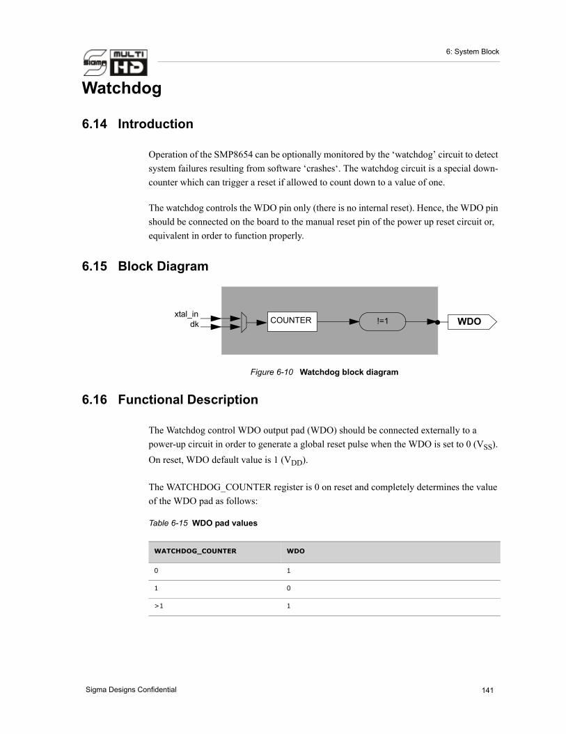
6: System Block
Watchdog
6.14 Introduction
Operation of the SMP8654 can be optionally monitored by the ‘watchdog’ circuit to detect system failures resulting from software ‘crashes‘. The watchdog circuit is a special down-counter which can trigger a reset if allowed to count down to a value of one.
The watchdog controls the WDO pin only (there is no internal reset). Hence, the WDO pin should be connected on the board to the manual reset pin of the power up reset circuit or, equivalent in order to function properly.
6.15 Block Diagram
WDO!=1COUNTERxtal_in
dk
Figure 6-10 Watchdog block diagram
6.16 Functional Description
The Watchdog control WDO output pad (WDO) should be connected externally to a power-up circuit in order to generate a global reset pulse when the WDO is set to 0 (VSS). On reset, WDO default value is 1 (VDD).
The WATCHDOG_COUNTER register is 0 on reset and completely determines the value of the WDO pad as follows:
Table 6-15 WDO pad values
WATCHDOG_COUNTER WDO
0 1
1 0
>1 1
141Sigma Designs Confidential

SMP8654-DS-A-10SMP8654 Datasheet
Moreover, if the WATCHDOG_COUNTER register is greater than 1, then it is decre-mented at each cycle of the source clock which can be selected by the WATCHDOG_CONFIGURATION register as follows:
Table 6-16 Register WATCHDOG_CONFIGURATION values
WATCHDOG_CONFIGURATION Value
Bit[0] Source Clock1
1. If the system clock is slower than XTAL_IN, then XTAL_IN cannot be used as the source clock for the watchdog counter.
0 System clock
1 XTAL_IN
Bit[31]2
2. The WATCHDOG_CONFIGURATION register must only be written using byte access, so that the bit 31 is not changed during a write in bit 0.
Mode
0 Normal mode (default)
1 Disabled mode
In the disabled mode, everything works as usual except that the WDO pad is forced to 1. This can be used to debug a production code which is using the watchdog to avoid resets during the debugging session. Note that the counter is still working normally, so that it is possible to know if it triggered by reading 1 in the WATCHDOG_COUNTER register.
The normal usage of the watchdog is to set the WATCHDOG_COUNTER to a non zero value in the software, which makes the counter not reach the value 1. If the software crashes, it will stop updating the WATCHDOG_COUNTER, which will then eventually reach a value of 1 and the whole system will be reset.
The delay can be computed using the system clock (default). If the system clock frequency is not constant, then XTAL_IN (always at 27MHz, see note above) can be used.
Writing 1 in WATCHDOG_COUNTER register causes an immediate reset of the system if the WDO pad has been connected as explained above. The WDO pad can also be used as a general purpose output; writing 0 or 1 in the WATCHDOG_COUNTER changes the value of the WDO pad.
142 Sigma Designs Confidential

6: System Block
6.17 Register Map
6.17.1 Watchdog Registers
6.18 Pin Description
6.18.1 Watchdog Pins
Clock Generator
6.19 Introduction
The clock generator contains audio clocks, video clocks, system clock and a CPU clock. The clock generator creates two high speed (up to 500MHz) clocks from a 27MHz exter-nal clock using two programmable PLLs, and creates the main system clock and multiple video and audio clocks by dividing either one of the high speed clocks or the 27MHz refer-ence.
The clock generator module receives seven different clock inputs, and generates 13 sepa-rate clock and timer tick outputs. The clock generator module contains four independent frequency synthesizers based on phase-locked loops (PLLs). Every PLL except one, can use any of the seven input sources as its reference clock.
Table 6-17 Watchdog registers
Address1
1. Address refers to G-Bus byte address relative to the system block base.
Register Name R/W/A2
2. Read/Write/Auto update.
Description
+FD00 SYS_WATCHDOG_COUNTER R/W/A Watchdog Counter Register
+FD04 SYS_WATCHDOG_CONFIGURATION
R/W/A Watchdog Configuration Register
Table 6-18 Watchdog pin description
Pin Name Pin Id Direction Description Driver Type1
1. The letters under the column ‘Driver Type’ denote the DC characteristics of the corresponding pins as detailed in the ‘DC Characteristics’ table of the chapter ‘System Specifications‘.
WDO F2 O Watchdog Control Output D
143Sigma Designs Confidential

SMP8654-DS-A-10SMP8654 Datasheet
6.20 Features
• Creates two high speed clocks (up to 500MHz)
• Contains audio clocks, video clocks, system clock and a CPU clock
• Supports programmable PLLs
6.21 Block Diagram
RCLK0_IN
XTAL_IN
RCLK3_OUT
X TAL_OUT
XTAL_BUF
x tal_in
cpu_clk
cl k
vo0_c lk vo1_c lk vo2_c lk vo3_c lk
ao0_clk
ao1_clk
Clean d iv 8
÷D 1
÷D 2
Clean d iv 9
C lea n div 10
Clean d iv 0
Clean d iv 1
PREM UX
CD_CLK Each c lean di v has 3 outputs : F, F / 2, F / 4
RCLK1_OUT RCLK0_OUT
SYS _CLK_MUX
÷2÷2
÷4÷2
÷3÷2
÷3÷3
÷D 1
÷D 2
AB PL L
CLKGEN0
CLKGEN1
1.2v PLL
÷D 1
÷D 2
AB PL L
CLKGEN2
VI 1_CLK
usb_c lkClean d iv 2
sata_clk
sdio_c lk
Clean d iv 3
Clean d iv 6
Clean d iv 4
Clean d iv 5
Clean d iv 7
See Tables for mux options
Figure 6-11 Clock generator block diagram
144 Sigma Designs Confidential

6: System Block
6.22 Functional Description
6.22.1 PLL Clock Generators
The SMP8654 has 3 PLL-based clock generators (CLKGEN0, 1 and 2). the input for each PLL can be selected from one of the 3 sources (XTAL_IN, RCLK0_IN or VI1_IN).The three PLL registers determine the multiplying and dividing factors. When the PLL bypass bit is set, the post-dividers are driven by the PLL input (rather than the PLL output). The direct output is not affected by the bypass. The PLL output frequency is equal to, FOut = FIn * (N+2) / (M+2).
The CG1 and CG2 have PLLs and each produces the outputs as follows:
• PLLx_1 = PLLx_0 / D1 (D1 = 2-15)
• PLLx_2 = PLLx_0 / D2 (D2 = 2-15)
Note: N and M should be such that In*(N+1)/(M+1) is within the range 700MHz to 1.4GHz.
6.22.2 System Pre-mux
Two clocks CD_CLK and PLL_SYSCLK can be derived from the PLLs as follows:
SYS 1 2 3PLL_SYSCLK PLL1_0 NA NA
CD 2 3 4 5 6 7CD_CLK PLL1_0 PLL1_1 PLL2_0 PLL2_1 NA NA
The CD_CLK is the source clock for the fractional dividers. For proper operation of the clean dividers, CD_CLK should be in the range 150-400MHz.
The PLL_SYSCLK is fed in the system or the CPU divider which derives the system clock, the CPU clock and the video decoder DSP clock.
6.22.3 System Mux
The bit S in the register SYS_SYSCLK_MUX selects whether XTAL_IN (0=power up value) or PLL_SYSCLK (1) is fed into the dividers.
145Sigma Designs Confidential

SMP8654-DS-A-10SMP8654 Datasheet
Ratio controls the dividers ratio as follows:
Table 6-19 Dividers ratio
Ratio System Clock CPU clock
0000 (power up value) ÷ 2 ÷ 2
0001 ÷ 4 ÷ 2
0010 ÷ 3 ÷ 2
0011 ÷ 3 ÷ 3
The ratio and S bits can be changed while the CPU clock, system clock and the video decoder clock are being used (Glitch free).
6.22.4 Clean Dividers
The SMP8654 has 11 clean dividers to divide CD_CLK. Each clean divider produces three output frequencies: CDx / 1, CDx / 2 and CDx / 4. The clean dividers are used as fol-lows:
1. CD0 and CD1 are used to generate the audio clocks.
2. CD2 is used to generate the USB clock.
3. CD3 is not used.
4. CD4, 5 and 7 are used to generate RCLK0,1 and 3 respectively.
5. CD6 is not used in SMP8654.
6. CD8 to CD10 are used to generate the video clocks.
Each clean divider can be turned off individually by writing 1 to the ‘P’ field of the regis-ter SYS_CLEANDIVX_CTRL.
The divider registers determine the post-dividers ratio (must be between 2 and 15). The PLL output (PLL input when bypass is activated) is divided by D1 to generate CK1, and divided by D2 to generate CK2. The clean dividers generate an output frequency equal to,
FOut = CD_CLK / (2 + divider x 2-27).
146 Sigma Designs Confidential

6: System Block
Table 6-20 System clock frequencies
SysClk Divider FOut
148.5MHz 0x593AC687 11289600Hz = 44100 * 256 (use for 44.1KHz sampling rate)
0x50AE0000 12288000Hz = 48000 * 256 (use for 48KHz sampling rate)
0x20570000 24576000Hz = 96000 * 256 (use for 96/192KHz sampling rate)
162MHz 0x62CBC14E 11289600Hz
0x59780000 12288000Hz
0x24BC0000 24576000Hz
6.22.5 Audio, Video, RCLK Muxing
The SYS_AVCLK_MUX register controls the last stage of muxing to generate 4 video clocks, 2 audio clocks and 4 RCLKs (sent to the RCLK out pins).
When a value is written to the register SYS_AVCLK_MUX, each field set to 0 indicates to keep the value. After booting, each clock is driven by XTAL_IN, until a source has been selected.
Note: For video clocks the bit VO0 controls muxing of the VO0_CLK and the HDMI_CLK simultaneously.
Table 6-21 Video clock muxing
Value VO0 - HDMI VO1
0 Keep Keep
1 CD8 - CD8 CD8
2 CD8/ 2 - CD8 CD8/ 2
3 CD8/ 4 - CD8 CD8/ 4
4 CD8/ 2 - CD8/ 2 CD9
5 CD8/ 4 - CD8/ 2 CD9/ 2
6 Off - Off CD9/ 4
7 Off - Off CD10
8 Off - Off CD10/ 2
9 Off - Off CD10/ 4
10 PLL1_1 - PLL1_2 PLL1_1
147Sigma Designs Confidential

SMP8654-DS-A-10SMP8654 Datasheet
11 PLL1_2 - PLL1_2 PLL1_2
12 PLL2_1 - PLL2_2 PLL2_1
13 Off - Off PLL1_0
14 Off - Off RCLK0in
15 Off - Off Off
Table 6-22 Audio clock and RCLK muxing
Value R3 R1 R0 AO1 AO0 USB SATA
0 Keep Keep Keep Keep Keep Keep Keep
1 CD7 CD5 CD4 RCLK0_in RCLK0in CD2 / 2 CD3
2 CD7/ 2 CD5 / 2 CD4 / 2 CD1 / 2 CD0 / 2 PLL2_1 PLL2_2
3 CD7/ 4 CD5 / 4 CD4 / 4 CD1 / 4 CD0 / 4 RCLK0in RCLK0in
4 RCLK0in
Not Applicable
5 NA
6 NA
7 VI1_CLK
8 NA
9 NA
10 PLL1_1
11 PLL1_2
12 PLL2_1
13 PLL2_2
14 NA
15 NA
Table 6-21 Video clock muxing (Continued)
Value VO0 - HDMI VO1
148 Sigma Designs Confidential

6: System Block
6.22.6 Host Interface Clock Muxing
The register SYS_HOSTCLK_MUX controls the last stage of muxing to generate the USB and the SATA clocks located in the host interface.
When a value is written to the register SYS_HOSTCLK_MUX, each field set to 0 indi-cates to keep the value.
Table 6-23 Host interface clock muxing
Value USB (48MHz) SATA (100MHz)
0 Keep Keep
1 CD2/ 2 CD3
2 PLL2_2 PLL2_2
3 Reserved VCXO1in
4 to 15 Reserved Reserved
Note: The two host clocks can be generated from a clean divider, a PLL or an external source. The best option is to use the clean dividers, to avoid an external source and to leave the PLL2 available for other functions.
Note: After booting, each clock is driven by XTAL_IN. Once a source has been selected for that clock, it is not possible to revert to XTAL_IN.
6.22.7 Counters
There are 3 dedicated counters and 5 configurable counters (i.e., the source clock is select-able). The counters can be read or written, and increment by one for each period of the associated clock.
SYS_CLK_CNT: System clock counter
SYS_XTAL_IN_CNT: 27MHz counter
SYS_RND_CNT: Counter used for random number generation.
SYS_CFG_CNT0-4: For each configurable counter, a 4-bit field of the register SYS_CNT_CFG selects the source clock. Fields written as 0 remain unchanged. The counters operate correctly only if the selected clock frequency is lower than the system clock.
149Sigma Designs Confidential

SMP8654-DS-A-10SMP8654 Datasheet
Table 6-24 Counters
Value CNT0, CNT1, CNT2, CNT3 and CNT4
0 Keep
1 CD0 / 4
2 CD1 / 4
3 NA
4 NA
5 CD4 / 4
6 CD5 / 4
7 NA
8 CD7 / 4
9 CD8 / 4
10 CD9 / 4
11 CD10 / 4
12 NA
13 VI1_CLK
14 PLL1_1
15 PLL2_1
150 Sigma Designs Confidential

6: System Block
6.23 Register Map
6.23.1 Clock Generation Registers
6.23.2 Clean Dividers Registers
Table 6-25 Clock generation registers
Address1
1. Address refers to G-Bus byte address relative to the clock generator base.
Register Name R/W/A2
2. Read/Write/Auto update.
Description
+0000 SYS_CLKGEN0_PLL R/W System Clock Generator 0 PLL Register
+0008 SYS_CLKGEN1_PLL R/W System Clock Generator 1 PLL Register
+000C SYS_CLKGEN1_DIV R/W System Clock Generator 1 Divider Register
+0010 SYS_CLKGEN2_PLL R/W System Clock Generator 2 PLL Register
+0014 SYS_CLKGEN2_DIV R/W System Clock Generator 2 Divider Register
+0030 SYS_HOSTCLK_MUX R/W System Clock Host Clock Mux Register
+0034 SYS_SYSCLK_PREMUX R/W System Clock Premux Register
+0038 SYS_AVCLK_MUX R/W System AV Clock Mux Register
+003C SYS_SYSCLK_MUX R/W System Clock Mux Register
Table 6-26 Clean dividers registers
Address1 Register Name R/W/A2 Description
+0080 SYS_CLEANDIV0_DIV R/W System Clock Clean Divider 0 Divider Register
+0084 SYS_CLEANDIV0_CTRL R/W/A System Clock Clean Divider 0 Control Register
+0088 SYS_CLEANDIV1_DIV R/W System Clock Clean Divider 1 Divider Register
+008C SYS_CLEANDIV1_CTRL R/W/A System Clock Clean Divider 1 Control Register
+0090 SYS_CLEANDIV2_DIV R/W System Clock Clean Divider 2 Divider Register
+0094 SYS_CLEANDIV2_CTRL R/W/A System Clock Clean Divider 2 Control Register
+0098 SYS_CLEANDIV3_DIV R/W System Clock Clean Divider 3 Divider Register
+009C SYS_CLEANDIV3_CTRL R/W/A System Clock Clean Divider 3 Control Register
151Sigma Designs Confidential

SMP8654-DS-A-10SMP8654 Datasheet
+00A0 SYS_CLEANDIV4_DIV R/W System Clock Clean Divider 4 Divider Register
+00A4 SYS_CLEANDIV4_CTRL R/W/A System Clock Clean Divider 4 Control Register
+00A8 SYS_CLEANDIV5_DIV R/W System Clock Clean Divider 5 Divider Register
+00AC SYS_CLEANDIV52_CTRL R/W/A System Clock Clean Divider 5 Control Register
+00B0 SYS_CLEANDIV6_DIV R/W System Clock Clean Divider 6 Divider Register
+00B4 SYS_CLEANDIV6_CTRL R/W/A System Clock Clean Divider 6 Control Register
+00B8 SYS_CLEANDIV7_DIV R/W System Clock Clean Divider 7 Divider Register
+00BC SYS_CLEANDIV7_CTRL R/W/A System Clock Clean Divider 7 Control Register
+00C0 SYS_CLEANDIV8_DIV R/W System Clock Clean Divider 8 Divider Register
+00C4 SYS_CLEANDIV8_CTRL R/W/A System Clock Clean Divider 8 Control Register
+00C8 SYS_CLEANDIV9_DIV R/W System Clock Clean Divider 9 Divider Register
+00CC SYS_CLEANDIV9_CTRL R/W/A System Clock Clean Divider 9 Control Register
+00D0 SYS_CLEANDIV10_DIV R/W System Clock Clean Divider 10 Divider Register
+00D4 SYS_CLEANDIV10_CTRL R/W/A System Clock Clean Divider 10 Control Register
+00D8 SYS_CLEANDIV11_DIV R/W System Clock Clean Divider 11 Divider Register
+00DC SYS_CLEANDIV11_CTRL R/W/A System Clock Clean Divider 11 Control Register
1. Address refers to G-Bus byte address relative to the clock generator base.2. Read/Write/Auto update.
Table 6-26 Clean dividers registers (Continued)
Address1 Register Name R/W/A2 Description
152 Sigma Designs Confidential

6: System Block
6.23.3 Clock Counter Registers
Table 6-27 Clock counter registers
Address1
1. Address refers to G-Bus byte address relative to the clock generator base.
+0040 SYS_CLK_CNT R/W/A System Clock Counter Register
+0044 SYS_RND_CNT R/W/A System Clock Random Generator Counter Register
+0048 SYS_XTAL_IN_CNT R/W System XTAL In Counter Register
+004C SYS_CNT_CFG R/W System Clock Counter Configuration Register
+0050 SYS_CFG_CNT0 R/W/A System Clock Configuration Counter 0 Register
+0054 SYS_CFG_CNT1 R/W/A System Clock Configuration Counter 1 Register
+0058 SYS_CFG_CNT2 R/W/A System Clock Configuration Counter 2 Register
+005C SYS_CFG_CNT3 R/W/A System Clock Configuration Counter 3 Register
+0060 SYS_CFG_CNT4 R/W/A System Clock Configuration Counter 4 Register
6.24 Pin Description
6.24.1 Clock Generator Pins
Register Name R/W/A2
2. Read/Write/Auto update.
Description
Table 6-28 Clock generator pin description
Pin Name Pin Id Direction Description Driver Type1
1. The letters under the column ‘Driver Type’ denote the DC characteristics of the corresponding pins as detailed in the ‘DC Characteristics’ table of the chapter ‘System Specifications‘.
XTAL_IN F1 I 27MHz crystal oscillator input
XTAL_OUT G1 O Crystal oscillator output
XTAL_BUF F4 O Buffered crystal oscillator output D
RCLK0_IN G2 I PLL reference clock input #0 I
RCLK0_OUT G3 O PLL reference clock output #0 D
RCLK1_OUT H1 O Auxiliary clock output #1 D
RCLK3_OUT H2 O Auxiliary clock output #3 D
153Sigma Designs Confidential

SMP8654-DS-A-10SMP8654 Datasheet
6.25 Electrical Characteristics
6.25.1 System Clock Characteristics
Table 6-29 System clock characteristics
Symbol Description Minimum Typical Maximum Units
FREF Reference clock frequency 27.000 MHz
Reference clock tolerance 30 ppm
DERIVED CLOCKS
FMEMCK DDR clock frequency 201 MHz
FVIDCLK Video output pixel clock fre-quency
148.5 MHz
FPCICLK PCI clock frequency 66 MHz
FAUDCLK Audio clock frequency 50 MHz
Delta (FMEMCK) DDR clock long-term jitter 350 ps
Delta (FVIDCLK) Video clock long-term jitter 500 ps
Delta (FPCICLK) PCI clock long-term jitter 950 ps
Delta (FAUDCLK) Audio clock long-term jitter 950 ps
154 Sigma Designs Confidential

7 Host Interface
7.1 Block Diagram of Host Interface
PCI Slave
PCI Master
(R+W)
L-Bus
NAN
D F
lash
P A D S
R-Bus
M-Bus Interface
R-Bus Remap R-Bus
R-Bus Arbiter
PC
I Bus
L-Bus
Switch
Box
NAND Flash Interface
SATA0
USB2.0
Ethernet1
Ethernet0
MII
Inte
rface
s
M-B
us
G-B
us
PCI Host
SATA1
Figure 7-1 Host interface block diagram
Sigma Designs Confidential 155

SMP8654-DS-A-10SMP8654 Datasheet
7.2 Introduction
The host interface unit provides the interface between the primary internal buses (G-bus and M-bus) and the PCI, SATA, Ethernet and USB interfaces. As a G-Bus slave, the host interface occupies two sections of the G-Bus space: A 64KB section for configuration reg-isters accesses, and a 64MB section for linear access to an external flash memory.
The SMP8654 supports a PCI for system-level interconnection. The PCI bus implementa-tion is a version 2.1 compliant, 32-bit wide bus capable of operating at 33 or 66MHz. The electrical interface supports both 3.3V and 5V signaling. The interface supports both mas-ter and target operation, as well as ACPI power management (v.2.2). On-chip logic option-ally implements the PCI bus configuration and arbitration functions (up to 3 external masters) so that no external PCI ‘host’ device is needed. This allows the design of small, tightly-embedded systems in which the SMP8654 hosts the PCI bus.
PCI Master/Slave/Host Interface
7.3 Introduction
The 32-bit PCI master/slave/host interface (33 or 66MHz) is designed for both reads and writes with programmable burst length, and is compliant with PCI v2.1 specifications. It supports 3.3V and 5V operation and PCI power management per the PCI Bus Power Man-agement Specification Revision 1.2. Only D0 and D3 power states are supported; PME#‘s are not supported. Up to 4 external PCI devices may be controlled by the SMP8654 in the PCI host mode.
7.4 Features
• Supports both reads and writes
• Supports programmable burst length
• Compliant with PCI v2.1 specifications
• PCI host supports up to 3 external PCI devices
• Supports AES, 3DES or DES encrypted/decrypted content
156 Sigma Designs Confidential

7: Host Interface
7.5 Functional Description
The host, as a PCI master, can perform G-Bus accesses through the PCI slave interface, the R-Bus and the R-Bus to G-Bus bridge. The entire G-Bus space (128MB) or a portion of it is mapped into the PCI space (configured through startup bits). The R-Bus is a single mas-ter (the PCI interface), single slave (the R-Bus to G-Bus bridge) bus.
The PCI slave block contains specific PCI configuration registers, and registers for the DRAM read/write operations. When these registers are accessed, the data is sent to, or received from the M-Bus interface through 8-bit ports. The M-Bus interface, programmed by any G-Bus master through the G-Bus to L-Bus bridge and L-Bus will exchange the data with the DRAM controller via the M-Bus.
The PCI master interface (which is also programmed through the L-Bus), can initiate data block moves to/from the host memory to 8-bit ports connected to the M-Bus interface.
An external PCI host can access the G-bus address space via the PCI slave interface. The slave interface also provides the PCI configuration register block and registers for the DRAM read/write operations. This allows for direct SDRAM access through the PCI slave interface. The PCI master interface can initiate block data moves between the SDRAM and the PCI host memory.
The host uses the PCI configuration space registers to auto-detect and configure PCI devices. Prior to the host reading the configuration block, several registers in the block must be initialized. Initialization of these registers is performed by the boot code stored in the internal serial flash memory. The boot code establishes the following nominal register values:
Table 7-1 Default values for PCI register fields
PCI Configuration Register Field Default Value (Hex)
VendorID 0x1105
DeviceID 0x8654
Class Code 0x048000
RevisionID 0x00
Subsystem Vendor ID 0x1105
Subsystem Device ID 0x0000
157Sigma Designs Confidential

SMP8654-DS-A-10SMP8654 Datasheet
The SMP8654 can function as the PCI host. To support this, it includes the PCI bus arbi-tration logic and 3 REQ#/GNT# pairs. In addition, it adds 3 IDSEL pins to support agent configuration cycle selection. These added pins and capabilities allow up to 3 external PCI masters and/or slave devices to be connected to the SMP8654 PCI bus without requiring an external host.
The following figures show the general connection topology for the arbitration pins and IDSEL pins in the SMP8654:
PCI Host Device or Bridge
GNTw#GNTx#GNTy#GNTz#
REQw#REQx#REQy#REQz#
IDSELwIDSELxIDSELyIDSELz
SMP8654
REQ0/GNT#
GNT0/REQ#
IDSEL0
to other masters
to other devices
from other masters
Figure 7-2 PCI arbitration pin connection diagram (PCI device)
SMP8654
REQ2#GNT2#IDSEL2
REQ1#GNT1#IDSEL1
REQ0/GNT#GNT0/REQ#
IDSEL0
PCI Master 2REQ#GNT#IDSEL
PCI Master 1REQ#GNT#IDSEL
PCI Master 0REQ#GNT#IDSEL
Figure 7-3 PCI arbitration pin connection diagram (PCI host)
158 Sigma Designs Confidential

7: Host Interface
7.5.1 PCI Slave Access
7.5.1.1 Direct Access
Figure 7-4 PCI slave direct access (8MB default setting)
When the SMP8654 is used on a PCI expansion board, the host can access all the configu-ration registers, internal memories and external DDR using the PCI slave access. At boot time, the SMP8654 requests between 1MB to 128MB of memory space (default is 8MB). This memory space is split into 8 regions. Each region can be mapped to a specific area of the processor memory space, using the region base address registers. Region 0 is hard-wired to start at address 0. The first 64K of the Region 0 is used for the region base address registers, the interrupt register, the slave DMA access and the time-out control registers, and cannot be used to access the G-Bus.
The region base address registers can also be accessed from the G-Bus, so the CPU can change them. This can be useful when that SMP8654 is used as a host, and master-capable devices attached to the SMP8654 need access to particular regions of the SMP8654 mem-ory.
Region 0 Configuration
RISC Memories
DRAM
DRAM
PCI Space G-Bus Space (Processor Space)
64KB
2MB
256MB
512MB
1MB+8MB
+16MB
+32MB
+64MB
+128MB
+256MB
+512MB
+1024MB
+64KB
Relative to PCI Base Address
This example assumes that the PCI memory is set to 8MB(default setting).
Region 1
Region 2
Region 3
Region 4
Region 5
Region 6
Region 7
159Sigma Designs Confidential

SMP8654-DS-A-10SMP8654 Datasheet
7.5.1.2 DMA Access
DMA transfers to the external DDR can be performed using the PCI slave access. Prior to writing or reading any data from the special DMA locations described below, the switch-box and the M-Bus interface should be set up for a DMA transfer. The DMA transfers are best performed using the PCI master access.
7.5.1.3 Time-out Control
Time-out control is the same for direct access and for the DMA access. In direct access, time-out can occur if the G-Bus is too slow to respond. This is most likely to happen with very slow G-Bus slaves, such as the serial flash controller. In DMA access, time-out can occur if the switchbox is not routing the PCI slave, or if the M-Bus interface is not expect-ing any data from the switchbox.
7.5.1.4 PCI Device Configuration
The PCI configuration space registers are used by the host to auto-detect and configure the devices on the bus. Some parameters must be setup before the host reads the registers: Vendor ID, Device ID, Class code, Revision ID, Subsystem vendor ID and Subsystem device ID.
Configuration should be performed by the boot code stored in the internal serial flash
memory, in less than 224 PCI clock periods. Once the configuration is complete, the boot code will write 1 to the bit VLD of the register HOST_REG2.
The Vendor ID should always be set to 0x1105 (denoting ‘Sigma Designs, Inc.‘). The top 16 bits of the class code should always be set to 0x0480 (denoting ‘Other Multimedia Device‘). The Revision ID shall be incremented for each new tape-out of the SMP8654. The values from the memory size field of register PCI_REG3 are defined as follows:
000 001 010 011 100 101 110 1118MB 16MB 32MB 64MB 128MB 256MB 512MB 1024MB
The other PCI configuration registers are read-only. They can be accessed by writing the number of the register (DWORD address) in the select part of the register PCI_REG3, and the contents of the selected register can be read from the register PCI_CONFIG.
160 Sigma Designs Confidential

7: Host Interface
7.5.2 PCI Master Access
Transferring Data from the Host to the SMP8654 (Read Transaction)
To transfer a block of data from the host to the SMP8654, the switchbox and the M-Bus interface are programmed with the destination address and size in the SMP8654 DDR. Then, the PCI master is programmed with the address in the host memory. In the case of a PC, the address is the physical address of the source data in the memory. The transfer is completed when the register READ_DMA_COUNTER is 0. The software then writes a 0 to the register READ_DMA_ENABLE.
Transferring Data from the SMP8654 to the Host (Write Transaction)
To transfer a block of data from the SMP8654 to the host, the switchbox and the M-Bus interface are programmed with the source address and size in the SMP8654 DDR. Then, the PCI master is programmed with the address in the host memory. In the case of a PC, the address is the physical address of the destination in the memory. The transfer is com-pleted when the register WRITE_DMA_COUNTER is 0. The software then writes a 0 to the register WRITE_DMA_ENABLE.
7.5.3 PCI Host
The PCI host regroups two functionalities:
1. PCI bus arbitration: 2-level priority round-robin arbitration of the bus ownership.
2. PCI host bridge: Low-latency PCI master (through G-Bus) available to the host sys-tem.
7.5.3.1 PCI Arbiter
Figure 7-5 PCI arbiter
SMP8654 Master
Device - 1 SMP8654 Host Bridge
Device - 3
L2 Devices representative
Device - 2 SMP8654 Master
Device - 1
Device - 2
Device - 3
Level 2
Level 1
161Sigma Designs Confidential

SMP8654-DS-A-10SMP8654 Datasheet
There are 2 loops, Level 1 and Level 2, and 6 agents. Two of them are always part of the Level 1 loop (host bridge and L2 representative) and the 4 others may be part of either loops (exclusive selection). The Level 2 representative is not an agent by itself but one of the agents of the Level 2 loop. It makes requests when any Level 2 agent makes a request.
The arbitration is request based. If requests are asserted, then the bus is granted to the first device requesting in the priority list. The arrows indicate the dynamics of the priority order. In each loop, given a current master agent, the arrow starting from this agent points at the highest priority potential next agent and so on. For example, when all the agents are level 1, and the current master is Device-1 then, the priority order for the next grant is Device-2, Device-3, Host Bridge, SMP8654 Master and Device-1.
When no new agent is requesting and the current master is done, the bus is parked on the current master. When the current level 1 master is the L2 representative, the level 2 loop toggles. Each level-versatile agent is attributed a programmable time-out that restricts its control of the bus after the address phase. A broken agent time-out gives 16 clocks to each master to start the address phase once the bus is idle.
A super request mode is available to the host bridge agent. It makes its request higher in the priority in any case. After a super request, the highest priority next agent is the agent next to the one that was ‘interrupted’ by the host.
7.5.3.2 PCI Host Bridge
The host bridge allows low latency G-Bus controlled master transactions on the PCI bus. Each transaction is a single address phase/single data phase (max one dword at one address). It can be of configuration read/write, IO read/write or a memory read/write access, as defined by the G-Bus address range being used. In the priority scheme, the host is usually like any other agent, unless the super request bit is turned on.
7.5.3.3 PCI Configuration Access
A direct mapping between the G-Bus address and the PCI address is implemented. It allows the host to perform type0 and type1 configuration accesses on the PCI bus. During a type 0 access, the device number can be programmed within the G-Bus address or through the L-Bus registers. If the L-Bus register agent selection is used, then the bit DEVICE # should be set to 0. Inversely if the G-Bus address agent selection is used, then the ‘agent select’ bits of the register HOST_REG2 should be set to 0.
During the type 1 access, the bit DEVICE # must be programmed through the G-Bus address. It is recommended to use the direct G-Bus address mapping. During an IO access, the G-Bus byte enable bits are mapped to PCI_AD[1:0].
162 Sigma Designs Confidential

7: Host Interface
7.5.3.4 Agent Detection
Upon power up to detect the PCI agents in the system the SMP8654 boot software resets the PCI bus. This is accomplished using a GPIO pin. After setting the registers MAMBO_IS_HOST and HOST_REG2, the Device ID and the Vendor ID of the selected device are read at the address of the host memory. If the agent is not present or the data is not ready within the configuration retry cycles, then an interrupt is generated. The register HOST_REG2 contains the interrupt status. At the end of the agent detection process, the software has the Device IDs and Vendor IDs of all the devices in the system. It then has to configure each one of the present devices, before using them.
Once the devices are configured for agent configuration registers, their I/O and memory spaces can be accessed by reading and writing to registers IOSPACE and MEMORYS-PACE.
Note: The software must also be careful to map all the devices in the lower 512MB of the PCI memory space, since the SMP8654 can only use 512MB on the PCI bus.
7.6 Register Map
7.6.1 PCI Slave Registers
7.6.1.1 PCI Slave Direct Access Registers
Table 7-2 PCI slave direct access registers
Address1 Register Name R/W/A2 Description
+9000 REGION_0_BASE R Region 0 Base Address Register
+9004 REGION_1_BASE R/W Region 1 Base Address Register
+9008 REGION_2_BASE R/W Region 2 Base Address Register
+900C REGION_3_BASE R/W Region 3 Base Address Register
+9010 REGION_4_BASE R/W Region 4 Base Address Register
+9014 REGION_5_BASE R/W Region 5 Base Address Register
+9018 REGION_6_BASE R/W Region 6 Base Address Register
+901C REGION_7_BASE R/W Region 7 Base Address Register
+9020 PCI_IRQ_STATUS R/A PCI Interrupt Status Register
+9024 PCI_IRQ_SET R/W PCI Interrupt Set Register
+9028 PCI_IRQ_CLEAR R/W PCI Interrupt Clear Register
163Sigma Designs Confidential

SMP8654-DS-A-10SMP8654 Datasheet
7.6.1.2 PCI Slave Time-out Control Registers
Table 7-3 PCI slave time-out control registers
Address1
1. Address refers to G-Bus byte address relative to the PCI base address.
+8000 TIMEOUT_VALUE R/W Time-out Value Register
+8004 TIMEOUT_STATUS R/A Time-out Status Register
+8008 TIMER_COUNTER R/W/A Timer Counter Register
+800C TIMER_TEST_REGISTER W Timer Test Register
+8010 WAKEUP_REGISTER W Wake Up Register
7.6.1.3 PCI Slave Device Configuration Registers
Table 7-4 PCI slave device configuration registers
Address1
1. Address refers to G-Bus byte address relative to the PCI base address.
+FED4 HOST_REG2 R/W Host Region 2 Register
+FEE8 PCI_REG0 R/W PCI Region 0 Register
+FEEC PCI_REG1 R/W PCI Region 1 Register
+FEF0 PCI_REG2 R/W PCI Region 2 Register
+FEF4 PCI_REG3 R/W PCI Region 3 Register
+FEF8 PCI_CONFIG R/A PCI Configuration Register
+FE883 PREFETCH R/A Prefetch Register
+FE8C3 DISC-LAT R/W Discard Latency Register
+FEFC3 ABORT R/W Abort Register
1. Address refers to G-Bus byte address relative to the host interface (0x20000).2. Read/Write/Auto update.3. Address refers to G-Bus byte address relative to the host register base address.
Register Name R/W/A2
2. Read/Write/Auto update.
Description
Register Name R/W/A2
2. Read/Write/Auto update.
Description
Table 7-2 PCI slave direct access registers (Continued)
Address1 Register Name R/W/A2 Description
164 Sigma Designs Confidential

7: Host Interface
7.6.2 PCI Master Access Registers
Table 7-5 PCI master access registers
Address1
1. Address refers to G-Bus byte address relative to the host register base address.
+FEC0 READ_DMA_ADDRESS R/W/A Read DMA Address Register
+FEC4 READ_DMA_COUNTER R/W/A Read DMA Counter Register
+FEC8 READ_DMA_ENABLE R/W Read DMA Enable Register
+FECC DMA_REV_ORDER R/W DMA Revision Order Register
+FED8 WRITE_DMA_ADDRESS R/W/A Write DMA Address Register
+FEDC WRITE_DMA_COUNTER R/W/A Write DMA Counter Register
+FEE0 WRITE_DMA_ENABLE R/W Write DMA Enable Register
+FEE4 DMA_BURST R/W DMA Burst Register
7.6.3 PCI Host Registers
Table 7-6 PCI host registers
Address1
1. Address refers to G-Bus byte address relative to the host register base address.
+FE90 MAMBO_IS_HOST R/W Mambo Is Host Register
+FED0 HOST_REG1 R/W Host Region1 Register
+FED4 HOST_REG2 R/W Host Region2 Register
+FE80 HOST_REG3 R/W Host Region3 Register
+FE84 HOST_REG4 R/W Host Region4 Register
+FE94 HOST_REG5 R/W Host Region5 Register
+1000_0000- +10FF_FFFC3
3. Address refers to G-Bus byte address relative to the host memory register base address.
CONFIGURATION R/W Configuration Register
+1800_0000- +2000_00003
I/O SPACE R/W I/O Space Register
+2000_0000- +4000_00003
MEMORY SPACE R/W Memory Space Register
Register Name R/W/A2
2. Read/Write/Auto update.
Description
Register Name R/W/A2
2. Read/Write/Auto update.
Description
165Sigma Designs Confidential

SMP8654-DS-A-10SMP8654 Datasheet
7.7 Pin Descriptions
7.7.1 PCI Pins
Table 7-7 System bus pin descriptions
Pin name Pin Id Direction Description
PCI_AD0 AG30 B PCI address/data pin 0 (LSB)
PCI_AD1 AH30 B PCI address/data pin 1
PCI_AD10 AJ26 B PCI address/data pin 10
PCI_AD11 AF25 B PCI address/data pin 11
PCI_AD12 AH25 B PCI address/data pin 12
PCI_AD13 AG25 B PCI address/data pin 13
PCI_AD14 AJ25 B PCI address/data pin 14
PCI_AD15 AF24 B PCI address/data pin 15
PCI_AD16 AH22 B PCI address/data pin 16
PCI_AD17 AK22 B PCI address/data pin 17
PCI_AD18 AF22 B PCI address/data pin 18
PCI_AD19 AJ22 B PCI address/data pin 19
PCI_AD2 AH29 B PCI address/data pin 2
PCI_AD20 AE22 B PCI address/data pin 20
PCI_AD21 AJ21 B PCI address/data pin 21
PCI_AD22 AG21 B PCI address/data pin 22
PCI_AD23 AH21 B PCI address/data pin 23
PCI_AD24 AF20 B PCI address/data pin 24
PCI_AD25 AJ20 B PCI address/data pin 25
PCI_AD26 AH20 B PCI address/data pin 26
PCI_AD27 AJ19 B PCI address/data pin 27
PCI_AD28 AF19 B PCI address/data pin 28
PCI_AD29 AH19 B PCI address/data pin 29
PCI_AD3 AJ29 B PCI address/data pin 3
PCI_AD30 AE19 B PCI address/data pin 30
PCI_AD31 AG19 B PCI address/data pin 31 (MSB). The address and the data are multiplexed on the AD pins during the memory and the I/O operations on the PCI bus.
166 Sigma Designs Confidential

7: Host Interface
PCI_AD4 AJ28 B PCI address/data pin 4
PCI_AD5 AK28 B PCI address/data pin 5
PCI_AD6 AH27 B PCI address/data pin 6
PCI_AD7 AK27 B PCI address/data pin 7
PCI_AD8 AK26 B PCI address/data pin 8
PCI_AD9 AH26 B PCI address/data pin 9
PCI_CBE0# AJ27 B Command/byte enable pin 0. Applies to PCI_AD(7:0).
PCI_CBE1# AK24 B Command/byte enable pin 1. Applies to PCI_AD(15:8).
PCI_CBE2# AG23 B Command/byte enable pin 2. Applies to PCI_AD(23:16).
PCI_CBE3# AK20 B Command/byte enable pin 3. During the address phase of a transaction the CBE(3:0)# defines the PCI command. During the data phase each signal indicates whether the associated data byte will be transferred. The CBE3# applies to PCI_AD(31:24).
PCI_CLK AK17 I Clock input for PCI interface section. Either 33MHz or a 66MHz clock signal.
PCI_DEVSEL# AJ23 B Device select pin. A target asserts DEVSEL# when it decodes its address.
PCI_FRAME# AE23 B Cycle frame pin. Current initiator asserts the FRAME# pin to indicate the start and duration of a transaction.
PCI_GNT0# AF17 O PCI host mode: Bus grant for master #0. Asserted low to grant the PCI ownership to an external master.PCI device mode: Bus request output to an exter-nal PCI host.
PCI_GNT1# AF18 O PCI host mode: Bus grant for master #1. Asserted low to grant the PCI ownership to an external master.PCI device mode: Unused, make no connection.
PCI_GNT2# AE18 O PCI host mode: Bus grant for master #2. Asserted low to grant the PCI ownership to an external master.PCI device mode: Unused, make no connection.
PCI_IDSEL0 AE20 B PCI host mode: ID select for PCI device #0. Asserted low by the SMP8654 to indicate a config-uration cycle to a PCI device.PCI device mode: Asserted low by an external PCI host to indicate a configuration cycle for the SMP8654.
Table 7-7 System bus pin descriptions (Continued)
Pin name Pin Id Direction Description
167Sigma Designs Confidential

SMP8654-DS-A-10SMP8654 Datasheet
PCI_IDSEL1 AE21 O PCI host mode: ID select for PCI device #1. Asserted low by the SMP8654 to indicate a config-uration cycle to a PCI device.PCI Device Mode: Unused, make no connection.
PCI_IDSEL2 AF21 O PCI host mode: ID Select for the PCI device #2. Asserted low by the SMP8654 to indicate a config-uration cycle to a PCI device.PCI device mode: Unused, make no connection.
PCI_INTA# AG17 B Interrupt A pin. Asserted by a PCI agent to request an interrupt.
PCI_IRDY# AH23 B Initiator ready pin. The current bus master asserts IRDY# to indicate that it is ready to com-plete a transaction.
PCI_PAR AH24 B Parity. Driven by an initiator (write) or currently-addressed target (read) to create even parity across AD(31:0) and CBE(3:0)#.
PCI_REQ0# AK18 I PCI host mode: Bus request for master #0. Asserted low by an external master requesting a PCI bus transaction.PCI device mode: Bus grant input from an exter-nal PCI host.
PCI_REQ1# AJ18 I PCI Host Mode: Bus Request for Master #1. Asserted low by external master requesting PCI bus transaction.PCI Device Mode: Unused, make no connection.
PCI_REQ2# AH18 I PCI host mode: Bus Request for master #2. Asserted low by external master requesting PCI bus transaction.PCI Device Mode: Unused, make no connection.
PCI_STOP# AJ24 O Stop pin. Asserted by an addressed target to request the bus master to terminate the current transaction in progress.
PCI_TRDY# AF23 B Target ready pin. The currently addressed target asserts TRDY# to indicate that it is ready to com-plete a transaction.
Table 7-7 System bus pin descriptions (Continued)
Pin name Pin Id Direction Description
168 Sigma Designs Confidential

7: Host Interface
7.8 Electrical Characteristics
7.8.1 PCI DC Characteristics
7.8.2 PCI AC Characteristics
The SMP8654 PCI I/O buffers fully conform to the electrical characteristics specified in the sections ‘Electrical Specification’ and ‘66MHz PCI Specification’ of the PCI Local Bus Specification, Revision 2.2. The PCI bus specification provides a comprehensive set of AC characteristics which compliant devices must meet. These characteristics are speci-fied in terms of V/I curves, output slew rates, and detailed measurement procedures, and are not reproduced in this document. The I/O cells used in the SMP8654 provide compli-ance with these specifications by design and characterization.
Table 7-8 PCI interface DC characteristics
Symbol Parameter Units Min Max
VIH Input high voltage V 0.5xVDD_3V3 5.5
VIL Input low voltage V -0.3 0.3xVDD_3V3
IIL Input leakage (condition: 0 < VIN < 3.3V) uA ± 10
VOH Output high voltage V 0.9xVDD_3V3
VOL Output low voltage V 0.1xVDD_3V3
CIN Input pin capacitance pF 10
CCLK CLK pin capacitance pF 5 10
CIDSEL IDSEL pin capacitance pF 8
LPIN Pin inductance nH 20
169Sigma Designs Confidential

SMP8654-DS-A-10SMP8654 Datasheet
7.9 Timing Diagrams
Timing Parameters
Certain PCI bus timing parameters have different values depending on whether the signal is ‘bused’ or ‘point-to-point’. The point-to-point signals are the REQ# and GNT# signals. The timing parameters which differ between these two groups are identified as ‘BUS’ or ‘PTP’ in the table below. For exact measurement conditions for all the timing parameters, refer to the PCI Local Bus Specification, Revision 2.2, Section 7.6.4.3.
Table 7-9 PCI timing parameters
Symbol Parameter Units Min Max
TCYC PCI_CLK cycle time (measured at 0.4xVDD_3V3 level)
ns 15
THIGH PCI_CLK high time (measured at 0.5xVDD_3V3 level)
ns 6
TLOW PCI_CLK low time (measured at 0.3xVDD_3V3 level)
ns 6
TVAL CLK to Signal Valid Delay (BUS) ns 2 6
TVAL CLK to Signal Valid Delay (PTP) ns 2 6
TON Float to Active Delay ns 2
TOFF Active to Float Delay ns 14
TSU Input Set Time to CLK (BUS) ns 3
TSU Input Set Time to CLK (PTP) ns 5
TH Input Hold Time from CLK ns 0
TCYC
PCI_CLK
TLOWTHIGH
Figure 7-6 PCI CLK timing diagram
170 Sigma Designs Confidential

7: Host Interface
TH
TSU
CLK
INPUT INPUTS VALID
Figure 7-7 PCI input timing diagram
T V A L
T O N
T O F F
P C I_ C L K
O U T P U T
3 -S T A T E O U T P U T
Figure 7-8 PCI output timing diagram
171Sigma Designs Confidential

SMP8654-DS-A-10SMP8654 Datasheet
USB 2.0 Embedded Host Interface
The SMP8654 includes a dual-port USB 2.0 Embedded Host Controller and two on-chip PHYs.
Although a Host Controller is included on-chip, the SMP8654 is designed to be used in a closed system where the end-user cannot install additional software and drivers. Due to the wide variety of USB peripherals and applications, manufacturers must implement their own peripheral-specific drivers and application software to be able to use the USB inter-face. Each manufacturer is also required to have a Targeted Peripheral List (TPL) in their manuals that tells the end-users which peripherals are supported. Entries in a TPL may refer to specific products (manufacturer and model) or, may refer to a class of products (HDD, wheel mouse, flash card, etc.). To receive the USB compliance certification, manu-facturers must submit their product with a fully function USB implementation.
7.10 Functional Description
7.10.1 USB 2.0 Embedded Host Controller
The USB 2.0 Embedded Host Controller is fully compliant with the USB 2.0 specification and the Enhanced Host Controller Interface (EHCI) specification revision 1.0. The con-troller supports high-speed (480Mbps) transfers. The controller comprehends the high-speed, full-speed and low-speed data ranges providing compatibility with a full range of USB devices. The full-speed and low-speed operations are supported via a USB 1.1 OHCI Host Companion Controller. The controller operates independently of the system bus of the SMP8654, shielding the complexities of the USB 2.0 Embedded Host Controller native protocol.
7.10.2 USB 2.0 Embedded Host Transceiver PHY
The USB 2.0 Embedded Host interface includes a fully integrated PHY core supporting High Speed (HS), Full-Speed (FS) and Low-Speed Transceivers and which is compliant with the USB 2.0 specification. It includes clock/data recovery, on-chip PLL, integrated and calibrated termination and pull-up/down resistors with full analog transceiver func-tionality for the complete USB 2.0 PHY.
172 Sigma Designs Confidential

7: Host Interface
The USB 2.0 Embedded Host Transceiver transmits the data onto the line, receives the data and recovers the clock correctly from the receive data. The analog front end includes a high-speed differential driver and an envelope detection/disconnection differential receiver. The high-speed receiver primarily consists of three functional elements; a differ-ential data receiver, a transmission envelope detector and a disconnection envelope detec-tor.
The differential data receiver receives the high-speed (480Mbps) differential data from the USB and converts it to a single-ended NRZI. A transmission envelope detector monitors the amplitude of the high-speed differential data signal from the USB. A disconnection envelope detector also monitors the amplitude of the differential data signal from the USB, but with a different operation and different signal levels of interest.
A high-speed current driver is used for high-speed data transmission. When the driver is not transmitting, a standby mode allows the current to be directed internally to ground and places the driver in a high-output-impedance state. The transition between standby and non-standby modes does not exhibit much delay, and use of the stand-by/non-standby modes ensures that the driver meets the required accuracy starting with the first symbol of a packet.
7.11 Pin Description
7.11.1 USB 2.0 Pins
Table 7-10 USB 2.0 pin descriptions
Pin Name Pin Id Direction Description
USB20_ATEST AJ15 B USB 2.0 analog test I/O
USB20_DM_0 AK13 B USB 2.0 line interface - port 0 -DM
USB20_DM_1 AK16 B USB 2.0 line interface - port 1 -DM
USB20_DP_0 AJ13 B USB 2.0 line interface - port 0 -DP
USB20_DP_1 AJ16 B USB 2.0 line interface - port 1 -DP
USB20_REXT AJ14 B USB 2.0 bias resistor input
USB20_VDDAC_3V3
AD14 I USB 2.0 analog power supply (3.3V)
USB20_VDDAC_3V3
AE14 I USB 2.0 analog power supply (3.3V)
USB20_VDDAT_3V3_0_0
AF13 I USB 2.0 analog power supply (3.3V)
USB20_VDDAT_3V3_0_1
AF14 I USB 2.0 analog power supply (3.3V)
173Sigma Designs Confidential

SMP8654-DS-A-10SMP8654 Datasheet
USB20_VDDAT_3V3_1_0
AF15 I USB 2.0 analog power supply (3.3V)
USB20_VDDAT_3V3_1_1
AF16 I USB 2.0 analog power supply (3.3V)
USB20_VDDC_1V0_0
AD13 I USB 2.0 digital power supply (1.0V)
USB20_VDDC_1V0_1
AD16 I USB 2.0 digital power supply (1.0V)
USB20_VSSAC AD15 I USB 2.0 analog ground
USB20_VSSAC AE15 I USB 2.0 analog ground
USB20_VSSAT_0 AG14 I USB 2.0 analog ground
USB20_VSSAT_0 AG13 I USB 2.0 analog ground
USB20_VSSAT_0 AH13 I USB 2.0 analog ground
USB20_VSSAT_1 AG15 I USB 2.0 analog ground
USB20_VSSAT_1 AH16 I USB 2.0 analog ground
USB20_VSSAT_1 AG16 I USB 2.0 analog ground
USB20_VSSAT_C AH14 I USB 2.0 analog ground
USB20_VSSAT_C AH15 I USB 2.0 analog ground
USB20_VSSC_0 AE13 I USB 2.0 analog ground
USB20_VSSC_1 AE16 I USB 2.0 analog ground
USB20_XI AK15 I USB 2.0 Xtal oscillator input (optional)
USB20_XO AK14 B USB 2.0 Xtal oscillator output (optional)
Table 7-10 USB 2.0 pin descriptions (Continued)
Pin Name Pin Id Direction Description
174 Sigma Designs Confidential

7: Host Interface
7.12 Electrical Characteristics
7.12.1 USB 2.0 DC Characteristics – FS Operation
7.12.2 USB 2.0 DC Characteristics – HS Operation
Table 7-11 USB 2.0 DC characteristics – FS operation
Parameter Description Conditions Minimum Typical Maximum Units
VDIFS Differential rcvr input sensitivity
0.2 V
VCMFS Differential rcvr com-mon-mode voltage
0.8 2.5 V
VILSE Single-ended rcvr low-level input voltage
0.8 V
VIHSE Single-ended rcvr high-level input voltage
2.0 V
VHYSSE Single-ended rcvr hyster-esis
50 150 mV
VFSOL Low-level output voltage 0.3 V
VFSOH High-level output voltage 2.8 3.6 V
ZFSDRV Driver output impedance 40.5 45 49.5 ohms
VTERM DP pullup resistor termi-nation voltage
3.0 3.6 V
Table 7-12 USB 2.0 DC characteristics – HS operation
Parameter Description Conditions Minimum Typical Maximum Units
VDIHS Differential rcvr input sensitivity
100 mV
VCMHS Common-mode voltage range
-50 500 mV
VHSSQ Squelch detection threshold (diff)
Squelch threshold
100 mV
VHSSQ Single-ended rcvr high-level input voltage
Unsquelch threshold
150 mV
VHSOL Low-level output voltage Ref. GND -10 10 mV
VHSOH High-level output volt-age
Ref. GND 360 440 mV
VOLHS Idle-level output voltage Ref. GND -10 10 mV
VCHIRPJ Chirp-J output voltage (diff)
700 1100 mV
175Sigma Designs Confidential
SMP8654-DS-A-10SMP8654 Datasheet
7.12.3 Dynamic Characteristics – FS Operation
Table 7-13 Dynamic Characteristics – FS Operation
Parameter Description Conditions Minimum Typical Maximum Units
TFSR Rise time CL= 50pF;10 to 90% of |VOH – VOL|
4 20 nS
TFSF Fall time CL= 50pF;10 to 90% of |VOH – VOL|
4 20 nS
VCRS Output crossover volt-age
Excluding first transi-tion from IDLE
1.3 2.0 V
7.12.4 Dynamic Characteristics – HS Operation
Table 7-14 Dynamic Characteristics – HS Operation
Parameter Description Conditions Minimum Typical Maximum Units
THSR Rise time 500 pS
THSF Fall time 500 pS
Additional dynamic specifications:
1. The USB2.0 PHY output drivers conform to the eye pattern requirements as specified in Template 1 of the USB2.0 Revision 2.0 specification.
2. The USB2.0 PHY receivers conform to the eye pattern (including source and receiver jitter tolerance requirements) as specified in Template 4 of the USB2.0 Revision 2.0 specification.
VCHIRPK Chirp-K output voltage (diff)
-900 -500 mV
ILZ Off-state leakage current +/-1 uA
CIN Transceiver input capaci-tance
Pin to GND 5 10 pF
Table 7-12 USB 2.0 DC characteristics – HS operation (Continued)
Parameter Description Conditions Minimum Typical Maximum Units
176 Sigma Designs Confidential

7: Host Interface
Ethernet Interface
The SMP8654 includes 2 identical 10/100Mbps Ethernet blocks. Each Ethernet block con-tains one MII interface for external PHYs (external PHY chips are required). Together, the 2 Ethernet blocks provide 2 ports. The Ethernet MAC module allows the SMP8654 to communicate data over the Ethernet protocol (IEEE. 802.3x).
7.12.1 Features
• IEEE 802.3x compliant
• Supports carrier extension and packet bursting
• Supports half and full duplex operations
• Supports full duplex flow control
• FCS generation for transmit, check for receiving packets
• Automatic retries after collision (programmable)
• One MII interface to PHY layer
7.12.2 Block Diagram
MII
INT
ERFA
CE
TO PHY
TransmitEngine
ReceiveEngine
From Application
To Application
Config Registers
Configuration by application
TransmitFIFO
ReceiveFIFO
MDIO
Figure 7-9 Ethernet block diagram
177Sigma Designs Confidential

SMP8654-DS-A-10SMP8654 Datasheet
7.12.3 Functional Description
Transmit FIFO
The Transmit FIFO accepts transmit data from the application and stores it temporarily until it is requested by the Transmit Engine.
Receive FIFO
The Receive FIFO temporarily store receive data from the Receive Engine, until the appli-cation requests it.
Transmit Engine
The Transmit Engine sends the data from the Transmit FIFO through to the MII interface, it also initiates the transfers and keeps track of the size of the transfer. This block manages packet bursting, carrier extension, appending padding, packet retries, deferral, back off, and appending FCS. The Transmit Engine can take back to back transmit requests to per-form packet bursting. If the packet sizes are less than 512-bytes, then carrier extension is performed.
Receive Engine
The Receive Engine manages the data transfers between MII interface and the Receive FIFO. Carrier extension and burst packet boundaries are identified, and packets are sepa-rated in this block. Status is generated for every packet received. The FCS is checked and reported as status.
MDIO
The MDIO block is used to communicate with the PHY on the serial MDIO interface that is standard on PHYs. The MDIO block takes information in the MDIO Command regis-ters and sends it across the serial MDIO interface to configure the PHY. On MDIO reads, the MDIO block accepts serial data from the MDIO data pin and loads the MDIO Status register with this read data, so that the application software can read it by reading the MDIO Status register.
MII Interface
The industry standard MII interface is provided in the SMP8654. The MII block also han-dles the flow control for half and full duplex.
178 Sigma Designs Confidential

7: Host Interface
7.13 Pin Description
7.13.1 MII Interface Pins
Table 7-15 MII interface pin descriptions
Pin Name Pin Id Direction Description Driver Type1
ETH0_COL AK2 B Ethernet 0 collision detect.Alternate function: GPIO46
A
ETH0_CRS AE3 B Ethernet 0 carrier senseAlternate function: GPIO45
A
ETH0_MDC AE1 B Ethernet 0 management data clockAlternate function: GPIO47
A
ETH0_MDINT# AD5 B Ethernet 0 management interruptAlternate function: GPIO49
A
ETH0_MDIO AD6 B Ethernet 0 management data I/OAlternate function: GPIO48
A
ETH0_RX_DV AE4 B Ethernet 0 receive data validAlternate function: GPIO39
A
ETH0_RX_ER AE2 B Ethernet 0 receive errorAlternate function: GPIO40
A
ETH0_RXCLK AF4 B Ethernet 0 receive clockAlternate function: GPIO38
A
ETH0_RXD0 AE5 B Ethernet 0 receive data 0Alternate function: GPIO41
A
ETH0_RXD1 AF1 B Ethernet 0 receive data 1Alternate function: GPIO42
A
ETH0_RXD2 AF2 B Ethernet 0 receive data 2Alternate function: GPIO43
A
ETH0_RXD3 AF3 B Ethernet 0 receive data 3Alternate function: GPIO44
A
ETH0_TX_EN AJ3 B Ethernet 0 transmit enableAlternate function: GPIO33
A
ETH0_TX_ER AJ1 B Ethernet 0 transmit errorAlternate function: GPIO50
A
ETH0_TXCLK AG1 B Ethernet 0 transmit clockAlternate function: GPIO32
A
ETH0_TXD0 AG2 B Ethernet 0 transmit data 0Alternate function: GPIO34
A
ETH0_TXD1 AG3 B Ethernet 0 transmit data 1Alternate function: GPIO35
A
179Sigma Designs Confidential

SMP8654-DS-A-10SMP8654 Datasheet
ETH0_TXD2 AH1 B Ethernet 0 transmit data 2Alternate function: GPIO36
A
ETH0_TXD3 AH2 B Ethernet 0 transmit data 3Alternate function: GPIO37
A
ETH1_COL AE7 B Ethernet 1 collision detectAlternate function: GPIO65
A
ETH1_CRS AK5 B Ethernet 1 carrier senseAlternate function: GPIO64
A
ETH1_MDC AJ4 B Ethernet 1 management data clockAlternate function: GPIO66
A
ETH1_MDINT# AK3 B Ethernet 1 management interruptAlternate function: GPIO68
A
ETH1_MDIO AK4 B Ethernet 1 management data I/OAlternate function: GPIO67
A
ETH1_RX_DV AJ5 B Ethernet 1 receive data validAlternate function: GPIO58
A
ETH1_RX_ER AH4 B Ethernet 1 receive errorAlternate function: GPIO59
A
ETH1_RXCLK AH6 B Ethernet 1 receive clockAlternate function: GPIO57
A
ETH1_RXD0 AH5 B Ethernet 1 receive data 0Alternate function: GPIO60
A
ETH1_RXD1 AG5 B Ethernet 1 receive data 1Alternate function: GPIO61
A
ETH1_RXD2 AK6 B Ethernet 1 receive data 2Alternate function: GPIO62
A
ETH1_RXD3 AJ6 B Ethernet 1 receive data 3Alternate function: GPIO63
A
ETH1_TX_EN AF7 B Ethernet 1 transmit enableAlternate function: GPIO52
A
ETH1_TX_ER AG7 B Ethernet 1 transmit errorAlternate function: GPIO69
A
ETH1_TXCLK AG6 B Ethernet 1 transmit clockAlternate function: GPIO51
A
ETH1_TXD0 AF6 B Ethernet 1 transmit data 0Alternate function: GPIO53
A
ETH1_TXD1 AK7 B Ethernet 1 transmit data 1Alternate function: GPIO54
A
Table 7-15 MII interface pin descriptions (Continued)
Pin Name Pin Id Direction Description Driver Type1
180 Sigma Designs Confidential

7: Host Interface
7.14 Electrical Characteristics
7.14.1 MII Interface AC Electrical Characteristics
ETH1_TXD2 AJ7 B Ethernet 1 transmit data Alternate function: GPIO55
A
ETH1_TXD3 AH7 B Ethernet 1 transmit data 3Alternate function: GPIO56
A
1. The letters under the column ‘Driver Type’ denote the DC characteristics of the corresponding pins as detailed in the ‘DC Characteristics’ table of the chapter ‘System Specifications‘.
Table 7-15 MII interface pin descriptions (Continued)
Pin Name Pin Id Direction Description Driver Type1
Table 7-16 MII interface AC characteristics
Symbol Units Minimum Typical Maximum
TRXCLK ns 40
TRXDSU ns 3
TRXDH ns 3
TTXCLK ns 40
TTXDVLD ns 0 8
181Sigma Designs Confidential

SMP8654-DS-A-10SMP8654 Datasheet
7.15 Timing Diagram
ETH_RX_CLK
ETH_RXDETH_RX_DVETH_RX_ER
TRXCLK
ETH_CRSETH_COL
TRXDSU TRXDH
ETH_TX_CLK
ETH_TXDETH_TX_EN
TTXCLK
TTXDVLD
Figure 7-10 MII Interface timing diagram
182 Sigma Designs Confidential

7: Host Interface
NAND Flash Interface
7.16 Introduction
The SMP8654 includes a NAND Flash Controller unit which provides an interface to low-cost, high-density NAND flash memories for nonvolatile storage of code and data. This interface supports specific SLC-type NAND flash devices having an 8-bit data interface.
Also, supported are certain NOR-type devices having NAND flash interface (SpansionTM
ORNANDTM).
7.17 Features
• Glueless connection to common SLC NAND flash devices (8-bit command/data inter-face)
• Support for SpansionTM ORNANDTM flash devices (NOTR technology/NAND inter-face)
• Very large capacities can be supported (up to 4GB per chip select)
• NAND flash read operations supported in XOS – allows boot from the NAND flash
• Hardware support for ECC generation (writes) and checking (reads)
• Sigma NAND flash driver supports the needed wear-leveling and bad-block manage-ment functions
7.18 Functional Description
The NAND flash controller is a simple module capable of producing the command, address and data transfer cycles necessary to support the NAND flash operation. The hard-ware unit is, in turn, controlled by a NAND flash driver to support application-level flash usage, or by the XOS for booting from the NAND flash. The hardware unit has program-mable cycle timing to support devices with differing timing characteristics. The hardware also includes ECC generation and checking logic required for reliable data integrity.
The NAND Flash driver supports the specialized ‘wear-leveling’ and bad-block replace-ment operations needed to support the NAND memory technology.
183Sigma Designs Confidential

SMP8654-DS-A-10SMP8654 Datasheet
7.18.1 Supported NAND Flash Devices
Due to the many variations which exist between the exact protocols used by various NAND flash devices, the Sigma NAND driver supports only specific devices. Both ‘large-block’ (2048+16 byte block size) and ‘small-block’ (512+16 byte block size) devices are supported.
The table below shows the various flash devices targeted for support. Contact Sigma for the most up-to-date information regarding the supported devices.
Note: Currently, software support for Numonyx devices is not available. It will be included after the upcoming SDK version 3.6 release.
Table 7-17 Supported NAND flash devices
Manufacturer Part Number Capacity Type
Samsung K9F1G08U0B 1Gb NAND, large page
Samsung K9F2G08U0A 2Gb NAND, large page
Samsung K9F4G08U0A 4Gb NAND, large page
Samsung K9K8G08U0M 8Gb NAND, large page
Numonyx NAND01GW3B2B 1Gb NAND, large page
Numonyx NAND02GW3B2D 2Gb NAND, large page
Numonyx NAND04GW3B2B 4Gb NAND, large page
Numonyx NAND08GW3B2ANAND08GW3B2C
8Gb NAND, large page
Micron MT29F2G08AADWP 2Gb NAND, large page
Micron MT29F4G08AACWC 4Gb NAND, large page
Micron MT29F8G08AAAWP 8Gb NAND, large page
Numonyx NAND512W3A2C 512Mb NAND, small page
Numonyx NAND256W3A2B 256Mb NAND, small page
Numonyx NAND128W3A2B 128Mb NAND, small page
Spansion S30ML512P 512Mb NOR, small page, NAND interface
Spansion S30ML256P 256Mb NOR, small page, NAND interface
Spansion S30ML128P 128Mb NOR, small page, NAND interface
184 Sigma Designs Confidential

7: Host Interface
7.19 Registers
7.19.1 Register Map - NAND Flash Configuration
Table 7-18 Register map - NAND flash configuration
Address1 Register Name R/W/A2 Description
+0800 PB0_TIMING0 R/W Peripheral Bus 0 Timing 0 Register
+0804 PB0_TIMING1 R/W Peripheral Bus 0 Timing 1 Register
+0808 PB0_TIMING2 R/W Peripheral Bus 0 Timing 2 Register
+080C PB0_TIMING3 R/W Peripheral Bus 0 Timing 3 Register
+0810 PB0_TIMING4 R/W Peripheral Bus 0 Timing 4 Register
+0814 PB0_TIMING5 R/W Peripheral Bus 0 Timing 5 Register
+0818 PB0_DEFAULT_TIMING R/W Peripheral Bus 0 Default Timing Register
+081C PB0_USE_TIMING0 R/W Peripheral Bus 0 Use Timing 0 Register
+0820 PB0_USE_TIMING1 R/W Peripheral Bus 0 Use Timing 1 Register
+0824 PB0_USE_TIMING2 R/W Peripheral Bus 0 Use Timing 2 Register
+0828 PB0_USE_TIMING3 R/W Peripheral Bus 0 Use Timing 3 Register
+082C PB0_USE_TIMING4 R/W Peripheral Bus 0 Use Timing 4 Register
+0830 PB0_USE_TIMING5 R/W Peripheral Bus 0 Use Timing 5 Register
+0834 PB0_CS_CONFIG0 R/W Peripheral Bus 0 CS Configuration Register
+0838 PB0_CS_CONFIG1 R/W Peripheral Bus 0 CS Configuration Register
+083C PB0_CS_CTRL R/W Peripheral Bus 0 IORDY State Register
+0840 PB0_AUTO_ADD R/W Peripheral Bus 0 Automode Start Address Register
+0844 PB0_AUTO_CTRL0 R/W Peripheral Bus 0 Automode Control 0 Register
+0848 PB0_AUTO_CTRL1 R/W Peripheral Bus 0 Automode Control 1 Register
+0880 PB0_STRAP_CTRL R/W Peripheral Bus 0 Strapping Control Register
+0884 PB0_STRAP0 R Peripheral Bus 0 Strapping 0 Register
+0888 PB0_STRAP1 R Peripheral Bus 0 Strapping 1 Register
+08C0 PB0_ECC_CODE0 R Peripheral Bus 0 ECC Code 0 Register
+08C4 PB0_ECC_CODE1 R Peripheral Bus 0 ECC Code 1 Register
+08C8 PB0_ECC_CODE2 R Peripheral Bus 0 ECC Code 2 Register
+08CC PB0_ECC_CODE3 R Peripheral Bus 0 ECC Code 3 Register
+08D0 PB0_ECC_CLEAR R Peripheral Bus 0 ECC Clear Register
185Sigma Designs Confidential

SMP8654-DS-A-10SMP8654 Datasheet
7.20 Pin Description
7.20.1 NAND Flash Pins
1. Address refers to G-Bus byte address relative to the host interface register base.2. Read/Write/Auto update.
Table 7-19 NAND flash pin descriptions
Pin Name Pin Id Direction Description Driver Type1
1. The letters under the column ‘Driver Type’ denote the DC characteristics of the corresponding pins as detailed in the ‘DC Characteristics’ table of the chapter ‘System Specifications‘.
FLASH_ALE AB25 O Address latch enable. Strobe for 8-bit address transfer cycle.
D
FLASH_CLE AC25 O Command latch enable. Strobe for 8-bit command transfer cycle.
D
FLASH_CS0# AD26 O Chip select 0 (active-low). Enables memory device #0.
D
FLASH_CS1# AD27 O Chip select 1 (active-low). Enables memory device #1.
D
FLASH_D0 AD28 B Bit 0 of 8-bit address/command/data bus.
C
FLASH_D1 AE26 B Bit 0 of 8-bit address/command/data bus.
C
FLASH_D2 AE27 B Bit 0 of 8-bit address/command/data bus.
C
FLASH_D3 AE28 B Bit 0 of 8-bit address/command/data bus.
C
FLASH_D4 AE29 B Bit 0 of 8-bit address/command/data bus.
C
FLASH_D5 AF27 B Bit 0 of 8-bit address/command/data bus.
C
FLASH_D6 AF29 B Bit 0 of 8-bit address/command/data bus.
C
FLASH_D7 AF30 B Bit 0 of 8-bit address/command/data bus.
C
FLASH_IORDY AC26 I Memory device READY/BUSY status. I
FLASH_RD# AD25 O Read command (active-low). D
FLASH_WR# AC27 O Write command (active-low). D
186 Sigma Designs Confidential

7: Host Interface
7.21 Electrical Characteristics
7.21.1 NAND Flash Interface AC Characteristics
7.22 Timing Diagram
FLASH_RD#FLASH_WR#
IORDY
FLASH_D(7:0) (read)
FLASH_D(7:0) (write)
FLASH_CS#(1:0)
FLASH_ALEFLASH_CLE
SYSCLK(internal)
TA+1 TB+1 TC+1 3 TD+3
Figure 7-11 NAND flash timing diagram
Table 7-20 NAND flash interface AC characteristics
Symbol Description Units Minimum Maximum
T1 Internal clock to earliest output transition NA1
1. No specifications supplied since parameter not externally measurable. Parameters used to explain TOPSKEW.
NA1
T2 Internal clock to latest output transition NA1 NA1
TOPSKEW Skew range for synchronous output signals ns 0 4
TRDSU Read data setup time to FLASH_RD# deas-serted
ns TSYSCLK + 8
TRDH Read data hold time from FLASH_RD# deas-serted
ns 0
TCMD-DEACT RD#WR# inactive after IODRY sampled active (after TC phase timed out)
ns 3*TSYSCLK 4*TSYSCLK
187Sigma Designs Confidential

SMP8654-DS-A-10SMP8654 Datasheet
SATA Interface
7.23 Introduction
The SMP8654 SATA Interface consists of a SATA dual-port Embedded Host Controller and two on-chip PHYs. The interface implements the Serial Advanced Technology Attachment (ATA) storage interface for physical storage devices. The SATA Embedded Host Controller complies with the Serial ATA II specification.
7.24 Features
SATA Host Controller
• Embedded Host Controller
• Supports SATA 1.5Gbps Generation 1 speed
• Compliant with SATA specification and applicable Serial ATA II Extension specifica-tion
7.25 Block Diagram
Figure 7-12 SATA interface block diagram
7.26 Functional Description
The Host Controller consists of 3 main functional blocks: Bus interface, Transport Layer, and Link Layer. Together with the physical layer (PHY) it forms a complete Serial ATA (SATA) host adapter.
188 Sigma Designs Confidential

7: Host Interface
7.26.1 SATA Host Controller
SATA is a half-duplex system. Either a receive or transmit operation is performed between the two agents (host and device) at any given time, but not both. This is true only for data frames transfer. Control traffic (primitives) is full duplex to maintain receiver synchroniza-tion. For example, SYNC primitives are sent continuously while both host and device sides are in their idle states.
Figure 7-13 SATA Host Controller
The host controller operates primarily in 2 or 3 clock domains, depending on where the Rx Buffer is located: Rx Buffer Mode dependent receive (Rx), transmit (Tx), and application. Rx (when present) and Tx clocks are generated in the PHY and are 150, 75, or 37.5MHz for Gen1 (300, 150, or 75MHz for Gen2), depending on the PHY data width. Most of the Link Layer (both receive and transmit data paths) and part of the Transport Layer always operate in the Tx clock domain. When the Rx Buffer is located in the Link Layer, the Rx clock is a clock recovered from the high-speed data in the PHY and is used for clocking data into the controller. This clock is also used for performing optional 8b/10b decoding, dropping ALIGNs and aligning data. When the Rx Buffer is located in the PHY, data is clocked into the controller on the Tx clock.
Host application software (driver) accesses the Host Controller using a set of ATA, SATA and Host Controller specific registers. The DMA flow control is implemented with several handshaking signals compatible with the DMA controller.
189Sigma Designs Confidential

SMP8654-DS-A-10SMP8654 Datasheet
The following subsections describe the basic Host Controller functionality in terms of Rx/Tx data, control paths and layers.
7.26.1.1 Internal Communication Paths
The following subsections describe the internal Host Controller communication paths.
Receive Path
The following list highlights the Receive Path functionality:
• Link Layer optionally detects Rx OOB signalling sequences from the device and ini-tializes the system.
• Link Layer receives SATA frames and primitives from the PHY sent by the device.
• Link Layer transmits primitives using backchannel to control the data flow.
• Link Layer optionally performs 10B/8B decoding, data alignment, descrambling, deframing and CRC checking on the frame FIS (frame payload), stripping SOF, EOF and other control primitives. A data-stream FIFO (DS FIFO) is used to cross data from the Rx to the Tx clock domain.
• Link Layer passes FIS to the Transport Layer Rx FIFO. The Rx FIFO is a two-clock 33-bit wide FIFO. Data is written in the Tx clock domain and is read in the application clock domain, thus providing clock-crossing function for receive data. The Rx FIFO depth is a configurable parameter.
• Transport Layer decodes FIS type from the least-significant byte of the FIS first DWORD.
• Transport Layer updates ATA/SATA registers if it is a register type FIS. Some FIS types are used for control only (example: DMA activate FIS).
• Transport Layer passes data from the Rx FIFO to the system bus using DMA or PIO modes via Bus Interface (example: Data FIS). In PIO mode, application software per-forms series of reads from the Data register. In DMA mode, Bus Interface requests transaction from the DMA controller, which in turn generates read access to the RxFIFO.
Transmit Path
The following list highlights the Transmit Path functionality:
• Link Layer optionally generates Tx OOB signalling sequences to the device and ini-tializes the system.
• Transport Layer receives data from the system bus either via the DMA channel or from the ATA/SATA registers after the application software writes to them. In the PIO mode, the application software performs series of writes to the Data register. In the
190 Sigma Designs Confidential

7: Host Interface
DMA mode, the Bus Interface requests transaction from the DMA controller, which in turn generates write access to the TxFIFO.
• Transport Layer constructs the appropriate FIS and passes it to the Link Layer via the Tx FIFO. The Tx FIFO is a two-clock 33-bit wide FIFO. The data is written in the application clock domain and read in the Tx clock domain, thus providing clock-cross-ing function for the transmit data.
• Link Layer receives FIS from the Tx FIFO, calculates the CRC, frames the data by inserting SOF, EOF and other flow control primitives, scrambles Repeat Primitives and data, optionally performs 8B10B encoding and multiplexes the data out to the PHY at the correct data width.
• Link Layer receives flow control and status primitives from the device on the back-channel and passes relevant information and status to the Transport Layer.
Control Path
The following list highlights the Control Path functionality:
• Link control implements the Link Layer and the initialization state machines, inter-faces to the PHY and the Transport Layer, and controls the data movement in both directions. The link detects all the PHY and Link Layer errors and passes them to the Transport Layer. In addition, the Link Layer controls the PHY interface power man-agement.
• Transport control implements the SATA Transport Layer state machine and interfaces to the Link Layer and to the bus interface. Various synchronizing modules provide clock-crossing functionality for all the control signals and data. The Transport Layer detects all the PHY/Link Layer/Transport Layer errors and passes them to the Bus Interface.
• Bus Interface control (not shown in the block diagram) provides Rx/Tx FIFO control functions, error handling, ATA/SATA register control, power management, DMA flow control, PHY control/status, interrupt control.
7.26.1.2 Transport Layer Overview
The Transport Layer constructs Frame Information Structures (FIS) for transmission and decomposes received FIS.
Transport Layer FIS Construction
The following list describes how an FIS is constructed:
• Gathers FIS content based on the type of FIS requested by the host application layer software.
• Places FIS content in the proper order.
191Sigma Designs Confidential

SMP8654-DS-A-10SMP8654 Datasheet
• Notifies the Link Layer of the required frame transmission and passes the FIS to the Link.
• Manages TxFIFO flow, notifies Link of the required flow control via TxFIFO flags.
• Receives frame receipt acknowledge from Link.
• Reports good transmission or errors to requesting higher layer.
Transport Layer FIS Decomposition
The following list describes how an FIS is decomposed:
• Receives the FIS from the Link Layer.
• Determines FIS type.
• Distributes the FIS content to the locations indicated by the FIS type.
• Reports good reception or errors to the application layer.
7.26.1.3 Link Layer Overview
The Link Layer controls initialization between the Link Layer, PHY and a connected device. In addition, the Link Layer optionally generates and detects OOB signalling, trans-mits and receives frames, transmits primitives based on control signals from the Transport Layer and PHY, and receives primitives from the PHY layer that are used to control the Transport and Link Layers. The Link Layer also controls power management via control of the PHY and PHY interface. A summary of the main Link Layer features are described in the following sections:
Initialization
The following list describes the Link Layer initialization process:
• Negotiates with its peer Link Layer and PHY to bring the system to an initialized state ready to transmit and receive data.
• Optionally transmits OOB sequences to the PHY, or instructs the PHY to generate them. These sequences are then forwarded to the remote device PHY per SATA spec-ifications, causing device PHY initialization.
• Optionally receives the OOB sequences or condition detection signals from the PHY, causing advancement in the initialization routine. When the OOB detection is per-formed by the PHY, the Link Layer detects these conditions via PHY_COMINIT and PHY_COMWAKE signals from the PHY.
• Once it has been determined that the remote device is ready, the Link Layer transi-tions to normal operation.
192 Sigma Designs Confidential

7: Host Interface
Frame Transmission
The following list describes the Link Layer frame transmission process:
• Negotiates with its peer Link Layer to transmit a frame, resolves arbitration conflicts if both host and device request transmission.
• Inserts frame envelope around Transport Layer data (i.e. SOF, CRC, EOF).
• Receives data in the form of DWORDs from the Transport Layer.
• Calculates CRC on Transport Layer data.
• Transforms (scrambles) data and Repeat Primitive DWORDs in such a way to distrib-ute the potential EMI emissions over a broader range.
• Optionally performs 8b/10b encoding.
• Transmits frame.
• Provides frame flow control in response to status from the TxFIFO or the peer Link Layer.
• Receives frame receipt acknowledge from peer Link Layer.
• Reports good transmission or Link/PHY Layer errors to Transport Layer.
Frame Receipt
The following list describes the Link Layer frame receipt process:
• Acknowledges to the peer Link Layer readiness to receive a frame.
• Receives data in the form of optionally encoded characters from the PHY layer.
• Optional decodes the encoded 8b/10b character stream into aligned DWORDs of data.
• Performs data alignment/realignment.
• Drops Repeat Primitive Data.
• De-scrambles the control and data DWORDs received from a peer Link Layer.
• Removes the envelope around frames (i.e. SOF, CRC, EOF Primitives).
• Calculates CRC on the received DWORDs.
• Compares the calculated CRC to the received CRC.
• Provides frame flow control in response to the status from the Rx FIFO or the peer Link Layer.
• Reports good reception status or Link/PHY Layer errors to Transport Layer and the peer Link Layer.
193Sigma Designs Confidential

SMP8654-DS-A-10SMP8654 Datasheet
7.26.2 SATA Host PHY
The SATA PHY provides the following services:
• Transmits a 1.5 Gb/sec differential NRZ serial stream at specified voltage levels.
• Provides a 100 Ohm matched termination (differential) at the transmitter.
• Serializes a 8/10, 16/20 or 32/40 bit wide parallel input from the Link for transmis-sion.
• Receives a 1.5 Gb/sec +350/-350ppm differential NRZ serial stream.
• Provides a 100 Ohm matched termination (differential) at the receiver.
• Extracts data and clock from the serial stream.
• Deserializes the serial stream.
• Detects the K28.5 comma character and forward it to the Link Layer along with the 8/10, 16/20 or 32/40 bit wide parallel output.
• Accepts and forward proper power-on/initialization sequences to device.
• Interacts with power management modes by way of Link Layer control.
• Provides proper transmitter and receiver differential pair impedances.
• Handles the input data rate frequency variation due to a spread spectrum transmitter clock (Nominal +0/-0.5% slow frequency variation, over a 33.33 ⎧s up/down triangu-lar wave period).
7.27 Pin Description
7.27.1 SATA Interface Pins
Table 7-21 SATA interface pin descriptions
Pin Name Pin Id Direction Description Driver Type1
SATA_REFCLKM AF10 I SATA PHY reference clock input (differ-ential, +)
SATA_REFCLKP AG10 I SATA PHY reference clock input (differ-ential, -)
SATA_REXT AE11 B Reference resistor connection 190ohm 1% resistor to VSS
SATA_TXP0 AJ12 O Differential transmit pair (+ polarity) for SATA port 0.
SATA_TXN0 AK12 O Differential transmit pair (- polarity) for SATA port 0.
194 Sigma Designs Confidential

7: Host Interface
SATA_RXP0 AK11 I Differential receive pair (+polarity) for SATA port 0.
SATA_RXN0 AJ11 I Differential receive pair (- polarity) for SATA port 0.
SATA_TXP1 AK9 O Differential transmit pair (+ polarity) for SATA port 1.
SATA_TXN1 AJ9 O Differential transmit pair (- polarity) for SATA port 1.
SATA_RXP1 AJ10 I Differential receive pair (+ polarity) for SATA port 1.
SATA_RXN1 AK10 I Differential receive pair (- polarity) for SATA port 1.
SATA_VP AF9 I SATA digital core power (1.0V)
SATA_VP AF11 I SATA digital core power (1.0V)
SATA_VP AF12 I SATA digital core power (1.0V)
SATA_VPH AG9 I SATA I/O power (3.3V)
SATA_VPH AG11 I SATA I/O power (3.3V)
SATA_VPH AG12 I SATA I/O power (3.3V)
SATA_TCK AH8 I SATA PHY EJTAG interface test clock input
I
SATA_TDI AF8 I SATA PHY EJTAG interface test data input
I
SATA_TDO AG8 O SATA PHY EJTAG interface test data output
D
SATA_TMS AE8 I SATA PHY EJTAG interface test mode select
I
1. The letters under the column ‘Driver Type’ denote the DC characteristics of the corresponding pins as detailed in the ‘DC Characteristics’ table of the chapter ‘System Specifications‘.
Table 7-21 SATA interface pin descriptions (Continued)
Pin Name Pin Id Direction Description Driver Type1
195Sigma Designs Confidential

SMP8654-DS-A-10SMP8654 Datasheet
7.28 Electrical Characteristics
7.28.1 SATA PHY Reference Clock Specifications
Table 7-22 SATA PHY reference clock specifications
Symbol Description Units Minimum Typical Maximum
VDIFF Differential peak voltage mV 350 850
VCMCommon mode voltage mV 175 2000
DC Duty cycle % 40 60
FREFCLK Reference clock frequency MHz 120
196 Sigma Designs Confidential

8 Video Decoder Subsystem
8.1 Block Diagram of Video Decoder Subsystem
16-bit Data 12-bit Address
M-Bus Interface
G-Bus
G-Bus Master Interface
L-Bus
16-bit
DSP core
DMEM 4Kx16
PMEM 2Kx32
R-Bus/L-Bus Arbiter R-Bus
Timer IRQ Ctrl
Reset Ctrl
R-Bus Interface
Sub-picture Decoder
Semaphore
D-Bus
M-B
us
Direct Load
Switch Box
Huffman Decoder MPEG/ VC-1
MPEG/ VC-1 ACDC
Predictor
MPEG/ VC-1
Inverse Quantizer
MPEG/ VC-1
Inverse DCT
VC-1 Deblocking
Filter
MPEG/ VC-1
Inverse Scan
Motion Compensation
Interface
MPEG/VC1
H.264 Huffman Decoder
H.264 Inverse
Transform
Motion Vector
Predictor
H.264 Deblocking
Filter
H.264 Inverse Scan
H.264
Figure 8-1 Video decoder subsystem block diagram
Sigma Designs Confidential 197

SMP8654-DS-A-10SMP8654 Datasheet
8.2 Introduction
The SMP8654 contains a video decoder subsystem capable of decoding HD MPEG-4.10 (H.264), HD SMPTE, SMPTE 421M (VC-1), HD WMV9, HD MPEG-2, MPEG-1, H.261 and AVS. The video decoder subsystem executes the video decoding algorithms supported by the SMP8654. Its architecture is a hybrid of both processor-based and hardwired logic approaches. The proprietary RISC CPU runs at 333MHz, and the hardware-based data path processing runs at 333MHz.
The maximum number of simultaneous programs that can be decoded and displayed depends on the source format and resolution. The video decoder subsystem can also sup-port the video decoding requirements for MSTV IPTV, HDV, AVCHD, FVD, DVD, SVCD, VCD, ARIB, ATSC, DMB, DVB and OpenCable applications.
Table 8-1 Number of programs that can be decoded simultaneously by SMP8654
MPEG-2 MPEG-4.2 WMV9SMPTE 421M
(VC-1) MPEG-4.10 (H.264)
Max profile and level
MP@HL ASP@L5 MP@HL MP@HL AP@L3 BP@L3 [email protected]@L4.0
1080i30 1 1 N/A N/A 1 N/A 1
1080p30 1 1 1 1 1 N/A 1
720p60 2 2 1 1 1 N/A 1
480p60576p50
2 2 2 2 1 2 2
480i30576i25
3 3 N/A N/A 2 3 3
The following minimum and maximum resolutions are supported by the video decoder. The source resolution information is extracted from the AVI/ASF bitstream or from the video elementary bitstream.
Table 8-2 Resolutions supported by video decoder
Minimum Maximum
MPEG-2 16x32 4096x4096
MPEG-4.2 64x64 4096x4096
MPEG-4.10 (H.264) 64x64 4096x4096
SMPTE 421M (VC-1) 64x64 2048x2048
198 Sigma Designs Confidential

8: Video Decoder Subsystem
Although the video decoder is capable of these maximum resolutions, a maximum resolu-tion of 1920x1080 is more realistic due to the many other functions required to be sup-ported in a typical design.
Common source program resolutions and frame refresh rates include,
• 480, 544 and 640 x 480i @ 25, 29.97 and 30Hz
• 480, 544 and 640 x 480p @ 23.976, 24, 29.97, 30, 59.94 and 60Hz
• 704 and 720 x 480i @ 29.97 and 30Hz
• 704 and 720 x 480p @ 23.976, 24, 29.97, 30, 59.94 and 60Hz
• 704 and 720 x 576i @ 25Hz
• 704 and 720 x 576p @ 23.976, 24, 25 and 50Hz
• 1280 x 720p @ 23.976, 24, 25, 29.97, 30, 50, 59.94 and 60Hz
• 960, 1280, 1440 and 1920 x 1080i @ 25, 29.97 and 30Hz
• 960, 1280, 1440 and 1920 x 1080p @ 23.976, 24, 25, 29.97 and 30Hz
The video decoder engine consists of a proprietary 16-bit RISC CPU which is augmented by a number of hardware functional units. These functional units perform the most com-pute-intensive portions of the video decompression algorithms supported by the SMP8654. The video RISC CPU executes certain portions of the algorithms, and prepares the data for, and coordinates the execution of the hardware units.
This architecture represents a carefully engineered trade-off between the hardware com-plexity, operating clock frequency and adaptability.
Appropriate microcode (supplied by Sigma Designs Inc.) is loaded into the video CPU program memory from the DRAM to perform the required video decompression.
The high memory bandwidth requirements created by the motion compensation features of the various video codecs is addressed by the ‘Direct Load Port’ feature of the engine. This port provides a dedicated, prioritized, high-bandwidth port to the system memory.
199Sigma Designs Confidential

SMP8654-DS-A-10SMP8654 Datasheet
8.3 Features
• MPEG-1
• MPEG-2 MP@HL
• MPEG-4.2 ASP@L5 (up to HD resolution, 1-point GMC)
• WMV9 MP@HL
• SMPTE 421M (VC-1) MP@HL and AP@L3
• MPEG-4.10 (H.264) [email protected] and [email protected].
• Microsoft MPEG-4 v3 for maximum DivX v3.11 compatibility
• H.261
• AVS
• Hardware accelerated Baseline am Progressive JPEG decoding
• In-loop deblocking filter for MPEG-4.10 (H.264) and SMPTE 421M (VC-1)
• Error concealment for MPEG-2 and MPEG-4.2
• Elementary video stream bit rate
- MPEG-2 SDTV (HDTV): 20 (40) Mbps maximum - MPEG-4.2 SDTV (HDTV): 20 (40) Mbps maximum - MPEG-4.10 (H.264) SDTV (HDTV): 20 (40) Mbps maximum - WMV9/SMPTE 421M (VC-1) SDTV (HDTV): 20 (40) Mbps maximum
8.4 Functional Description
8.4.1 MPEG-2 Decoding
Features and capabilities of MPEG-2 decoding include,
• MP@HL up to 1920x1080p30, 1920x1080i30 or 1280x720p60 resolution
• Supports low delay mode (no B pictures, no frame reordering delay, handling of VBV underflow)
200 Sigma Designs Confidential
8: Video Decoder Subsystem
An error detected during the texture decoding triggers the resynchronization to the next start code. The area corresponding to the macroblocks skipped (not decoded) during this resynchronization process keeps the content of the previously decoded picture in that buf-fer. Once an error is detected at the texture level, the decoded picture is marked as cor-rupted. The application decides if the corrupted pictures are displayed or not by setting the DisplayErrorThreshold (the default value is zero which means that only good pictures are displayed).
8.4.2 MPEG-4.2 Decoding
Features and capabilities of MPEG-4.2 decoding include,
• ASP@L5
• Rectangular shape video decoding up to 1920x1080p30, 1920x1080i30 or 1280x720p60 resolution
• Support for B Pictures, data partitioning and error resiliency
• Supports 1-point global motion compensation (GMC) for DivX 5 compatibility
8.4.3 MPEG-4.10 (H.264) Decoding
Features and capabilities of MPEG-4.10 (H.264) decoding include,
• BP@L3 up to 720x480p30 or 720x576p25 resolution, including FMO and ASO
• [email protected] and [email protected] up to 1920x1080p30, 1920x1080i30 or 1280x720p60 reso-lution.
• The High 10, High 4:2:2, High 4:4:4 and Extended profiles are not supported
• Decoding can start at any recovery point
• Handling of SPS and PPS between slices of a same picture
• DPB output delay information is used to output pictures as soon as possible (reduces latency)
• Almost all display meta data from the elementary video stream is output, including. but not limited to. aspect ratio, pan-scan, chromaticity, picture structure and cropping information
• Key-frame (aka I-frame) playback supported
• Supports up to TBD Mbin/s for CABAC streams
• Supports up to 135 slices per frame
201Sigma Designs Confidential

SMP8654-DS-A-10SMP8654 Datasheet
• An error detected during the texture decoding triggers:
- The discarding of the current picture - The display of the remaining anchor(s) and - The resynchronization to the next intra-picture
8.4.3.1 SEI Messages and VUI
Table 8-3 Supported MPEG-4.10 (H.264) SEI (Supplemental enhancement information) messages and VUI (video usability information)
Supported
Not Supported at this Time
Passed to Application
Buffering period SEI message X
Picture timing SEI message X
Pan-scan rectangle SEI message X
Filler payload SEI message X
User data registered by ITU-T Recommendation T.35 SEI message
X
User data unregistered SEI message X
Recovery point SEI message syntax X
Decoded reference picture marking repetition SEI message
X
Spare picture SEI message X
Scene information SEI message X
Sub-sequence information SEI message X
Sub-sequence layer characteristics SEI message X
Sub-sequence characteristics SEI message X
Full-frame freeze SEI message X
Full-frame freeze release SEI message X
Full-frame snapshot SEI message X
Progressive refinement segment start SEI message X
Progressive refinement segment end SEI message X
Motion-constrained slice group set SEI message X
All VUI content X
202 Sigma Designs Confidential

8: Video Decoder Subsystem
8.4.4 SMPTE 421M (VC-1) Decoding
Features and capabilities of SMPTE 421M (VC-1) decoding include,
• MP@HL up to 1280x720p60 or 1920x1080p30 resolution.
• AP@L3 up to 1920x1080i30, 1920x1080p30 or 1280x720p60 resolution.
• Almost all display metadata from the elementary video stream is output, including. but not limited to. aspect ratio, pan-scan, chromaticity, picture structure and cropping information
• Key-frame (aka I-frame) playback supported
• Pan-scan playback supported
• An error detected during the texture decoding triggers:
- The discarding of the current picture - The display of the remaining anchor(s) and, - The resynchronization to the next intra-picture
8.4.5 WMV9 Decoding
Features and capabilities of WMV9 decoding include,
• MP@HL up to 1280x720p60 or 1920x1080p30 resolution.
• Does not support WMV7 or WMV8 formats
• Does not support Screen, Image and Image Version 2 profiles
8.4.6 H.263 Decoding
Decoding of MPEG-4.2 ‘short_video_header’ bitstreams, which are technically identical to baseline H.263 bitstreams, is supported. Overlapped motion compensation and PB pic-tures are not supported.
8.4.7 H.261 Decoding
TBD
8.4.8 User Data Extraction
If user data (such as closed captioning, teletext, etc.) is present in the picture layer of the video stream, the video decoder extracts and stores it in a DRAM-based FIFO and pro-vides an interrupt to the host CPU. The application software on the host CPU may then access the user data for further processing.
203Sigma Designs Confidential

SMP8654-DS-A-10SMP8654 Datasheet
8.4.9 JPEG Decode Acceleration
Each video decoder supports the decoding of 4:2:0 YCbCr, 4:2:2 YCbCr, 4:4:4 YCbCr and 4:4:4 RGB baseline and progressive JPEG images (from 1x1 to 4096x4096 resolu-tion) using hardware acceleration. The resulting YCbCr or RGB image may be rendered into an appropriate display plane or off-screen memory (for additional processing). The JPEG decoding performance is:
Table 8-4 JPEG decode performance measurements
JPEG Source Decoding Performance (Mpixels/sec)
4:2:0 baseline TBD
4:2:2 baseline TBD
4:4:4 baseline TBD
4:2:0 progressive TBD
4:2:2 progressive TBD
4:4:4 progressive TBD
8.4.10 Subtitle Decode
Each video decoder supports decoding of the following subtitle formats,
• DVD-Video bit-mapped subpicture
The resulting image may be rendered into an appropriate display plane or off-screen mem-ory (for additional processing).
To improve subtitle rendering performance, the video decoder includes hardware accelera-tion for run-length decoding of,
• DVD-Video bit-mapped subpicture
204 Sigma Designs Confidential

9 Video Processing Subsystem
9.1 Block Diagram of Video Processing Subsystem
V-Bus
OSD scaler
HardwareCursor
GraphicsAcclerator
MIXER
Subtitle scaler
Multi-scaler 1
Multi-scaler 2
Main VideoScaler
Video Plane
Video Input
De-Interlace
PostProcess
R
R
R
R
R
R
RW
R
R
W
W
W
W
RR
R
R
R
R
*
Figure 9-1 Video processing subsystem block diagram - 1
Sigma Designs Confidential 205

SMP8654-DS-A-10SMP8654 Datasheet
ROUTER
HD=> SDDownscale
Analog Output
Analog Output
Digital Output
Color BarsGen
HDMI
ConstrainedImage
V-Bus
W
Multiscaler 1
Multiscaler 2
DACMux
Audio
*
Mixer Out
Figure 9-2 Video processing subsystem block diagram - 2
206 Sigma Designs Confidential

9: Video Processing Subsystem
9.2 Introduction
The video processing subsystem has extensive capabilities for retrieving graphics and video images from the memory, formatting the images as needed, mixing the images and then presenting the video stream for display in a required format. Other capabilities include hardware-assisted 2D graphics acceleration, and support for video and graphics input ports. The primary functions performed include:
• Up- or down-scaling video or graphic images to a specified resolution
• Data format conversion (color lookup, color space conversion, etc.)
• Independent positioning of each scaled image
• Ordering and merging (alpha-blending) of up to 8 video/graphics sources
• Brightness, contrast and saturation controls
• TV encoding to NTSC or PAL standards (composite and S-video)
• Selection of analog out mode (various RGB and YPbPr formats)
• Video digital-to-analog conversion
• HDMI digital video formatting and transmission
• Video capture from 8-bit input interface
• 2D graphics acceleration
Each video and graphics picture retrieved from the memory can be converted to other pixel formats as necessary, and scaled independently. The results are then alpha-blended on a pixel-by-pixel basis using a programmable priority of the plane order.
The video processing block also includes support for 2D graphics acceleration. The accel-erator is a bit-block transfer mechanism for moving, filling, merging and expanding rect-angular regions of display memory without the processor intervention after the initial setup. A pixel rate of up to 1 pixel per system clock can be supported when executing the acceleration operations.
The 3 available video outputs consist of,
1. HDMI digital A/V output: Supports 24 or 36-bit RGB/YCbCr HDMI display formats.
2. Analog component output: Supports RGB or YPbPr.
3. Analog CVBS/S-video outputs: Supports NTSC/PAL composite and S-video.
207Sigma Designs Confidential

SMP8654-DS-A-10SMP8654 Datasheet
9.3 Features
Video Processing
• Hardware cursor (4096 pixels, 4-bpp, up to 255 pixels horizontally and vertically)
• 2D graphics accelerator with OpenType/TrueType font rendering acceleration (up to 167M samples per second operation for most operations)
- Accelerator supports alpha/color merging alpha modulation - Supports line, rectangle, ellipse and circle to generate a single-color line, rectangle,
ellipse or circle with optional gradient fill - Supports blend to alpha blend of one rectangular region onto another - Supports move to move a rectangular region to another location - Supports replace (a modified version of move) - Supports raster operations (standard 256 boolean operations)
• Supports a 32-bit OSD with flicker filtering and scaling
• Supports optional deinterlacing of interlaced main video, including support for motion-adaptive deinterlacing with 3:2 and 2:2 pull-down detection
• Supports arbitrary scaling of video and graphics of up to 1920x1080 pixels, with all common HDTV set-top box and HDTV scaling modes supported.
• Supports pixel-based alpha mixing of video, OSD, subtitles, graphics and hardware cursor with programmable global plane priority
Video Input and Output Interfaces
• Supports an 8-bit Bt.601/Bt.656 video input interface
• Supports brightness, saturation and contrast controls for each output port
• Supports NTSC/PAL composite analog output with optional Macrovision v7.1.L1 protection (54MHz, 12-bit DAC)
• Supports NTSC/PAL S-video analog output with optional Macrovision v7.1.L1 pro-tection (54MHz, 12-bit DACs)
• Supports analog YPbPr / RGB with optional Macrovision v7.1.L1 and v1.2 protection in 480i, 576i, 480p and 576p YPbPr output modes (12-bit DACs, interlaced or pro-gressive, SDTV or HDTV resolution)
• Supports HDMI v1.3a output (internal PHY)
208 Sigma Designs Confidential

9: Video Processing Subsystem
9.4 Functional Description
9.4.1 Multi-plane Memory Architecture
Conceptually, the SMP8654 uses a multi-plane memory architecture. For many applica-tions typical planes include:
• Hardware cursor
• OSD
• Subtitles (includes subpictures, teletext and closed captions)
• Secondary video (picture-in-picture or PIP)
• Main video
9.4.1.1 OSD Plane
The OSD plane contains menus for setting user preferences and displaying playback sta-tus, program guides, user messages, etc.
Application software on the host CPU is typically responsible for rendering data into the OSD plane. The following sample software is available from Sigma:
• Navigation for,
- DVD-Video, DVD-VR, DVD+VR - VideoCD, SVCD - CD-DA - File Player (from HDD for example) - For additional information on sample navigation software, please refer to the appen-
dix.
• Picture CD (JPEG files using ISO 9660 format)
• ATSC/DVB program guide
To improve OSD rendering performance, the SMP8654 includes hardware acceleration for,
• OpenType/TrueType font rendering
• 2D graphics acceleration with optional simultaneous up/down scaling
209Sigma Designs Confidential

SMP8654-DS-A-10SMP8654 Datasheet
9.4.1.2 Subtitle Plane
The subtitle plane contains decoded bitmapped subtitles, text subtitles, animated graphics, subpictures, teletext and closed captioning data that is to be rendered over the main video. Whether or not it is rendered over the secondary video (PIP) is determined by the pro-grammable global plane priority order.
Application software on the host CPU is typically responsible for rendering into the subti-tle plane any subtitle formats not supported by the video decoder block. The following sample software are available from Sigma:
• Closed captioning for,
- CEA-608 - EIA-708
• Navigation for,
- DVD-Video - DVD-VR, DVD+VR - For additional information on sample navigation software, please refer to the appen-
dix.
While the video decoder block uses hardware to improve bit-mapped subtitle perfor-mance, text based subtitle performance is enhanced by using hardware acceleration for,
• OpenType/TrueType font rendering
• 2D graphics acceleration with optional simultaneous up/down scaling
9.4.1.3 Secondary Video Plane
The secondary video plane contains decompressed video data from the secondary video decoder for PIP or dual TV output applications. It may alternately contain foreground graphics, background graphics and still images.
9.4.1.4 Main Video Plane
The main video plane contains decompressed video data from the main video decoder.
210 Sigma Designs Confidential

9: Video Processing Subsystem
9.4.1.5 Typical Memory Plane and Scaler Usage
Each memory plane is typically capable of supporting a wide variety of picture buffer for-mats. In addition to support for double-buffered memory planes, off-screen graphics com-position can be done, with the result rendered into any memory plane that supports the graphics picture buffer formats. Each memory plane is also typically associated with a scaler, capable of color format conversion and independent x-y scaling. After scaling, pixel-based alpha mixing is done. The priority display order of the memory planes is pro-grammable, except for the on-chip hardware cursor which is always on top. How these memory planes and their associated scalers are typically used is shown below:
Table 9-1 Memory planes and scaler usage for a typical application
Memory Plane Scaler Used1
1. In engineering documents, Multi-format scaler 1 is also referred to as ‘VCR multi-scaler’ or ‘VCR scaler’. Multi-format scaler 2 is also referred to as ‘GFX multi-scaler’ or ‘GFX scaler. Subtitle scaler is also referred to as ‘OSD subpicture scaler’ or ‘subpicture scaler’.
OSD OSD scaler Device OSD
Subtitle Subtitle scaler Subtitles SubpicturesClosed CaptionsTeletext
Secondary Video Multi-format scaler 1 or,Video plane channel
Secondary Video (PIP)Photos
Main Video Main video scalerMulti-format scaler 1 or 2
Main VideoMotion Adaptive Deinterlacing
Multi-format scaler 1 or 2 Scaling during 2D Graphics Acceleration
9.4.2 Picture Buffer Formats
9.4.2.1 Indexed Graphics – 1/2/4/8-bpp, using LUT
Indexed graphics LUT formats with 1/2/4-bpp are supported by the 2D graphics accelera-tor (Y input only), OSD scaler and multi-format scalers.
Indexed graphics LUT formats with 8-bpp is supported by the 2D graphics accelerator (X and Y inputs, output) as well as the OSD scaler, subtitle and multi-format scalers.
function2
2. Each scaler may only be used for one of the indicated functions.
211Sigma Designs Confidential

SMP8654-DS-A-10SMP8654 Datasheet
0
B y t e A d d r e s s B i t 7 6 5 4 3 2 1 0
0
P ix e l # ( 1 b p p )
7 6 5 4 3 2 1 0
1
1 2 3 4 5 6 7 8 9 1 0 1 1 1 2 1 3 1 4 1 5
0 P i x e l # ( 2 b p p ) 1 2 3 4 5 6 7
0 P i x e l # ( 4 b p p ) 1 2 3
0 P i x e l # ( 8 b p p ) 1
9.4.2.2 Graphics - 16-bpp
There are six formats using 16-bpp. All are supported by the 2D graphics accelerator (X and Y inputs, output) and by the OSD and multi-format scalers.
0
Byte Address Bit 7 6 5 4 3 2 1 0
1 7 6 5 4 3 2 1 0
0
B[4:0]
7 6 5 4 3 2 1 0
3 7 6 5 4 3 2 1 0
2
G[4:0] R[4:0] α 1
B[4:0] G[4:0] R[4:0] α
0 B[4:0] G[5:0] R[4:0]
1 B[4:0] G[5:0] R[4:0]
Pixel # Component
0 B[3:0] G[3:0] R[3:0] α[3:0]
1 B[3:0] G[3:0] R[3:0] α[3:0]
0 Cb[4:0] Y[5:0] Cr[4:0]
1 Cb[4:0] Y[5:0] Cr[4:0]
RGB-565
Pixel # Component
CrYCb-565
0 Cb[4:0] Y[4:0] Cr[4:0] α
1 Cb[4:0] Y[4:0] Cr[4:0] α
Pixel # Component αRGB-1555
Pixel # Component αCbYCr-1555
Pixel # Component αRGB-4444
0 Cb[3:0] Y[3:0] Cr[3:0] α[3:0]
1 Cb[3:0] Y[3:0] Cr[3:0] α[3:0]
Pixel # Component αCrYCb-4444
In the above diagram bytes are swapped (1, 0, 3, 2, 5, 4...). When the processor (or another G-Bus master) reads a 16-bit word from the DRAM, it will receive the low address byte in low position, and the high address byte in the high position. Thus, the 16-bit word will appear as shown in the diagram.
212 Sigma Designs Confidential

9: Video Processing Subsystem
9.4.2.3 Graphics - 32-bpp
These modes are supported by the 2D graphics accelerator (source input, destination input and destination output) and by the OSD and multi-format scalers.
Byte Address Bit 7 0
3
0 B[7:0]
Pixel # Component G[7:0] R[7:0] α[7:0]
7 0
2 7 0
1 7 0
0 7 0
7 7 0
6 7 0
5 7
4
1 B[7:0] G[7:0] R[7:0] α[7:0]
0 Cb[7:0]
Pixel # Component Y[7:0] Cr[7:0] α[7:0]
1 Cb[7:0] Y[7:0] Cr[7:0] α[7:0]
αCrYCb-8888
αRGB-8888
9.4.2.4 Video-Luminance
When an MPEG bit stream is decoded, the resulting frames are in the 4:2:0 or the 4:2:2 format. In either case, the luminance and the chrominance are stored in separate buffers (one buffer for luminance and one buffer for Cb and Cr).
In the luminance buffer, data is stored as 8-bpp, with increasing byte address correspond-ing to increasing pixel X coordinates, except on tile crossing boundaries.
Byte Address Bit 7 0
0
0/1 Y1
Pixels # Component Cr Y0 Cb
7 0
1 7 0
2 7 0
3 7 0
4 7 0
5 7 0
6 7 0
7
2/3 Y3 Cr Y2 Cb
9.4.2.5 Video-Chrominance
In the chrominance, data is stored as 16-bpp, as shown below. A chrominance buffer typi-cally uses the same number of bytes per line, as the associated luminance buffer in the 4:2:2 or the 4:2:0 modes (half the number of pixels, but two components). However, in the 4:2:0 mode, there are half as many lines of chrominance compared to the luminance.
Byte Address Bit 7 6 5 4 3 2 1 0
0 7 6 5 4 3 2 1 0
1 7 6 5 4 3 2 1 0
2 7 6 5 4 3 2 1 0
3
0 Cb[7:0]
1 Pixel # (565 mode) Component Cr[7:0] Cr[7:0] Cb[7:0]
213Sigma Designs Confidential

SMP8654-DS-A-10SMP8654 Datasheet
9.4.2.6 Video – Interleaved 4:2:2
This format is used for the video coming from the video input ports. Each line contains 2xN pixels of luminance, N pixels of Cb and N pixels of Cr interleaved as follows:
Byte Address Bit 7 0
0
0/1 Y1
Pixels # Component Cr Y0 Cb
7 0
1 7 0
2 7 0
3 7 0
4 7 0
5 7 0
6 7 0
7
2/3 Y3 Cr Y2 Cb
9.4.3 OSD Scaler
The OSD enables full-screen menus, images and text to be blended over the video, graph-ics and subtitles. The OSD scaler accepts most graphics data formats, and performs pro-grammable edge adaptive scaling with directional filtering. Input resolutions of up to 2048x1080 are supported.
Supported input formats to the OSD scaler are:
• Indexed graphics - 1, 2, 4 and 8-bpp (no subtitle/subpicture support)
• Graphics - 16-bpp
- RGB-565 - CrYCb-565 - αRGB-1555
- αYCbCr-1555
- αRGB-4444
- αYCbCr-4444
• Graphics - 24-bpp
- RGB-888 - YCbCr-888
• Graphics - 32-bpp
- αRGB-8888
- αYCbCr-8888
Before scaling, four 256x8 LUTs are available to perform αRGB gamma correction, 0-255 to 16-235 RGB range conversion or Indexed Graphics to 16/24/32-bpp RGB/YCbCr con-version.
214 Sigma Designs Confidential

9: Video Processing Subsystem
The individually programmable H and V-scaler operates in a 4-tap mode (4-tap horizon-tally and 4-tap vertically so processing is done on a 4x4 matrix of data). 4-tap scaling is implemented as four 63-coefficient, 16 times interpolating filters - for each of the 16 inter-polating positions, 4 coefficients (taps) are used.
A horizontal downscaler before the H scaler is available to support larger downscaling fac-tors. It decreases the number of pixels per line (using pixel skipping) by a fractional ratio. Vertical downscaling before the V scaler (by skipping scan lines) is also possible.
The OSD scaler also implements a 3-tap flicker reduction filter with edge detection. Three sets of coefficients provide light, moderate, and strong flicker reduction options, in addi-tion to no filtering.
After scaling, BT.601 or BT.709 RGB to YCbCr conversion and colorimetry correction between BT.601 and BT.709 may be performed. No contrast (or ‘picture’ or ‘white level’), saturation (or ‘color’), brightness (or ‘black level’), hue (or ‘tint’) or sharpness control is provided. This also converts the 8-bit per component data to 12-bit per component.
The data (typically 48-bpp YCbCr) is then sent to the main mixer, 2D graphics accelerator (X input) or DRAM.
9.4.3.1 Alpha Support
For the 1/2/4/8-bpp, RGB-656, RGB-888, CrYCb-565 and CrYCb-888 source formats, 8 bits of alpha data can be generated via the α0 value in the VO_OSD_ALPHA_ROUTING register. By changing the value of α0, the entire OSD may be faded in and out.
For the αRGB-1555 and αYCbCr-1555 formats (either source or from the LUTs), two bytes are used to generate 8 bits of alpha information, the α0 and α1 values in the VO_OSD_ALPHA_ROUTING register. Which alpha value is used is determined by the 1-bit source alpha value. By changing the value of these bytes, the entire OSD may be faded in and out.
For the αRGB-4444, αYCbCr-4444, αRGB-8888 and αYCbCr-8888 formats (either source or from the LUTs), the entire OSD may be faded in or out by generating new alpha information as follows:
AO = (AS * α1) + ([1-AS] * α0) where,
ΑO = Output alpha value
AS = Source alpha value
α0, α1 = Values of the α0 and α1 in the VO_OSD_ALPHA_ROUTING register.
215Sigma Designs Confidential

SMP8654-DS-A-10SMP8654 Datasheet
9.4.3.2 Color Keying
Color keying forces the output alpha data to a value of 0 (transparent) whenever the input color falls within the color key value and 4-bit range. The color key value is set according to the input source color space (which may different from the output color space).
It is not possible to use the color key feature with Indexed Graphics data.
9.4.4 Hardware Cursor
The hardware cursor block generates a small picture for the main mixer block. It supports up to 4096 4-bit pixels and feeds into the alpha mixer. An arbitrary bitmap is stored in 4-bpp format in a 512x32 on-chip SRAM. No external memory bandwidth is required to support the cursor. It may be organized as any size, up to 255 pixels horizontally or verti-cally. Each 4-bit pixel is fed to a 16x32 look-up table which outputs 32-bit (8-8-8-8 for-mat) αYCbCr pixels.The data is then sent to the mixer.
The horizontal and vertical dimensions of the cursor picture are constrained as follows:
• X size less than or equal to 255
• Y size less than or equal to 255
• Total pixels (X x Y) less than or equal to 4096
9.4.5 Multi-format Scalers 1 and 2
The Multi-format scalers can be used for a variety of functions such as,
• Enabling a secondary video to be displayed over the main video to support picture-in-picture (PIP) applications
• Enabling the output of a second video stream for dual TV applications
• Supporting Type 2 deinterlacing (motion adaptive deinterlacing) of the main video
• Scaling during 2D graphics processing
• Scaling and displaying of high-resolution JPEG images (photos)
Input resolutions of up to 2048x1080 are supported. Supported input formats to the Multi-format scalers are,
• Video (4:2:0, 4:1:1 or 4:2:2 YCbCr)
• Indexed graphics - 1, 2, 4 and 8-bpp (no subtitle/subpicture support)
216 Sigma Designs Confidential

9: Video Processing Subsystem
• Graphics - 16-bpp
- RGB-565 - YCbCr-565 - αRGB-1555
- αYCbCr-1555
- αRGB-4444
- αYCbCr-4444
• Graphics - 24-bpp
- RGB-888 - YCbCr-888
• Graphics - 32-bpp
- αRGB-8888
- αYCbCr-8888
Before scaling, four 256x8 LUTs are available to perform αRGB gamma correction, 0-255 to 16-235 RGB range conversion or Indexed Graphics to 16/24/32-bpp RGB/YCbCr con-version.
Data input to the scalers is converted to 12-bit per component, so the scaling is done on 12-bit per component data.
For Multi-format scaler 1, the individually programmable H and V-scalers operate in a 2-tap mode (2-tap horizontally and 4-tap vertically so processing is done on a 2x4 matrix of data). The 2-tap scaling is implemented as two 63-coefficient, 16 times interpolating filters - for each of the 16 interpolating positions, 2 coefficients (taps) are used.
For Multi-format scaler 2, the individually programmable H and V-scaler operates in a 4-tap mode (4-tap horizontally and 4-tap vertically so processing is done on a 4x4 matrix of data). 4-tap scaling is implemented as four 63-coefficient, 16 times interpolating filters - for each of the 16 interpolating positions, 4 coefficients (taps) are used.
A horizontal downscaler before the H scaler is available to support larger downscaling fac-tors. It decreases the number of pixels per line (using pixel skipping) by a fractional ratio. Vertical downscaling before the V scaler (by skipping scan lines) is also possible.
Since Y and CbCr may be independently scaled, the scaler may be configured to accept video that uses a different YCbCr sampling scheme, such as rotated 4:2:2 YCbCr pictures.
The output of the Multi-format scalers is 12-bit per component.
217Sigma Designs Confidential

SMP8654-DS-A-10SMP8654 Datasheet
For displaying 4:3 content on a 16:9 display, the commonly used ‘pillar’, ‘wide’, ‘zoom’ and ‘panorama’ modes can be implemented. For the ‘pillar’ mode, the 4:3 source is dis-played without distortion; black/gray/colored bars are added to the left and right sides of the 4:3 image to fill the 16:9 screen. For the ‘wide’ mode, the 4:3 source is linearly scaled to fill the 16:9 display, resulting in a distorted image unless anamorphic content is used. For the ‘zoom’ mode, the center 16:9 portion of the 4:3 source is displayed without distor-tion. For ‘panorama’ mode, the center portion of the image is linearly scaled, while the left and right sides are nonlinearly scaled; the left and right locations where nonlinear scaling stops/starts is programmable.
For displaying 16:9 content on a 4:3 display, the commonly used ‘crop’, ‘letterbox’ and ‘squeeze’ modes can be implemented. For the ‘crop’ mode, the center 4:3 portion of the 16:9 source is displayed without distortion. For the ‘letterbox’ mode, the entire 16:9 source is displayed without distortion; black/gray/colored bars are added to the top and bottom of the 16:9 image to fill the 4:3 screen. For the ‘squeeze’ mode, the 16:9 source is linearly scaled to fill the 4:3 screen, resulting in a distorted image.
After scaling, a 3x3 matrix multiplier is used to implement,
• RGB to YCbCr conversion (BT.601 or BT.709)
• Contrast (or ‘picture’ or ‘white level’) control, range of 0 to 4x in 1/128 steps
• Saturation (or ‘color’) control, range of 0 to 4x in 1/128 steps
• BT.709 (HDTV) to BT.601 (SDTV) and BT.601 (SDTV) to BT.709 (HDTV) colorim-etry conversion
• 61966-2-4 (xvYCC) uses BT.709 colorimetry
The matrix multiplier is followed by 3 programmable DC offsets to provide optional brightness (or ‘black level’) control. The DC offsets have a range of -512 to +511.7/8, in steps of 1/8. No sharpness or hue (or ‘tint’) control is provided.
Note that the content being displayed via a Multi-format scaler must be authored for flicker-free display on an interlaced TV; there is no anti-flicker filtering filter available.
The output of Multi-format scaler 1 (typically 48-bpp αYCbCr) is input to the main mixer (when used for PIP), deinterlacer block (when used for motion adaptive deinterlacing), display routing block (when used for dual TV output), or 2D graphics accelerator (Y input), or may be stored in DRAM.
218 Sigma Designs Confidential

9: Video Processing Subsystem
The output of Multi-format scaler 2 (typically 48-bpp αYCbCr) is input to the main mixer (when used for PIP), the deinterlacer block (when used for motion adaptive deinterlacing), the 2D graphics accelerator, or may be stored in the DRAM. When the output of Multi-for-mat scaler 2 is input to the main mixer, the video plane channel is not available.
The 12-bit per component output of a Multi-format scaler must be reduced to 8-bit per component (using dithering) when the output of a Multi-format scaler
• is being saved to DRAM
• is being input to the constrained image scaler
• is being input to the HD to SD scaler
• is being input to the 2D graphics accelerator
9.4.5.3 Alpha Support
For the video, 1/2/4/8-bpp, RGB-656, RGB-888, CrYCb-565 and CrYCb-888 source for-mats, 8 bits of alpha data can be generated via the α0 value in the VO_VCR_ALPHA_ROUTING and VO_GFX_ALPHA_ROUTING registers. By chang-ing the value of α0, the entire picture may be faded in and out.
For the αRGB-1555 and αYCbCr-1555 formats (either source or from the LUTs), two bytes are used to generate 8 bits of alpha information, the α0 and α1 values in the VO_VCR_ALPHA_ROUTING and VO_GFX_ALPHA_ROUTING registers. Which alpha value is used is determined by the 1-bit source alpha value. By changing the value of these bytes, the entire picture may be faded in and out.
For the αRGB-4444, αYCbCr-4444, αRGB-8888 and αYCbCr-8888 formats (either source or from the LUTs), the entire picture may be faded in or out by generating new alpha information as follows:
AO = (AS * α1) + ([1-AS] * α0) where,
AO = Output alpha value
AS = Source alpha value
α0, α1 = Values of the α0 and α1 in the VO_VCR_ALPHA_ROUTING register and VO_GFX_ALPHA_ROUTING registers.
219Sigma Designs Confidential

SMP8654-DS-A-10SMP8654 Datasheet
9.4.5.4 Color Keying
Color keying forces the output alpha data to a value of 0 (transparent) whenever the input color falls within the color key value and 4-bit range. The color key value is set according to the input source color space (which may different from the output color space).
It is not possible to use the color key feature with Indexed Graphics data, 24-/32-bpp graphics data, or video data.
9.4.6 Main Video Scaler
The main video scaler is used to scale the main video. Input resolutions up to 2048x1080 are supported.
Supported input formats to the video scaler are:
• Video (4:2:0, 4:1:1, or 4:2:2 YCbCr)
Data input to the scalers is converted to 12-bit per component, so the scaling is done on 12-bit per component data. The individually programmable H and V-scaler operates in a 4-tap mode (4-tap horizontally and 4-tap vertically so processing is done on a 4x4 matrix of data). 4-tap scaling is implemented as four 63-coefficient, 16 times interpolating filters - for each of the 16 interpolating positions, 4 coefficients (taps) are used.
Since Y and CbCr may be independently scaled, the scaler may be configured to accept video that uses a different YCbCr sampling scheme, such as rotated 4:2:2 YCbCr pictures.
The output of the main video scaler is 12-bit per component.
For displaying 4:3 content on a 16:9 display, the commonly used ‘pillar’, ‘wide’, ‘zoom’ and ‘panorama’ modes can be implemented. For the ‘pillar’ mode, the 4:3 source is dis-played without distortion; black/gray/colored bars are added to the left and right sides of the 4:3 image to fill the 16:9 screen. For the ‘wide’ mode, the 4:3 source is linearly scaled to fill the 16:9 display, resulting in a distorted image unless anamorphic content is used. For the ‘zoom’ mode, the center 16:9 portion of the 4:3 source is displayed without distor-tion. For ‘panorama’ mode, the center portion of the image is linearly scaled, while the left and right sides are nonlinearly scaled; the left and right locations where nonlinear scaling stops/starts is programmable.
220 Sigma Designs Confidential

9: Video Processing Subsystem
For displaying 16:9 content on a 4:3 display, the commonly used ‘crop’, ‘letterbox’ and ‘squeeze’ modes can be implemented. For the ‘crop’ mode, the center 4:3 portion of the 16:9 source is displayed without distortion. For the ‘letterbox’ mode, the entire 16:9 source is displayed without distortion; black/gray/colored bars are added to the top and bottom of the 16:9 image to fill the 4:3 screen. For the ‘squeeze’ mode, the 16:9 source is linearly scaled to fill the 4:3 screen, resulting in a distorted image.
After scaling, a 3x3 matrix multiplier is used to implement,
• Contrast (or ‘picture’ or ‘white level’) control, range of 0 to 4x in 1/128 steps
• Saturation (or ‘color’) control, range of 0 to 4x in 1/128 steps
• BT.709 (HDTV) to BT.601 (SDTV) and BT.601 (SDTV) to BT.709 (HDTV) colorim-etry conversion
• BT.709 (HDTV) to 61966-2-4 (xvYCC) and 61966-2-4 (xvYCC) to BT.709 (HDTV) colorimetry conversion
• 61966-2-4 (xvYCC) uses BT.709 colorimetry
The matrix multiplier is followed by three programmable DC offsets to provide optional brightness (or ‘black level‘) control. The DC offsets have a range of -512 to +511.7/8, in steps of 1/8. No sharpness or hue (or ‘tint‘) control is provided.
The output of the main video scaler (typically 36-bpp YCbCr) is input to the main mixer, the HD to SD scaler, or 2D graphics accelerator (Y input).
The 12-bit per component output of the main video scaler must be reduced to 8-bit per component (using dithering) when the output of the scaler
• is being input to the HD to SD scaler
• is being input to the 2D graphics accelerator
9.4.6.1 Deinterlacing
Two deinterlacing modes are available, Type 1 and Type 2. The deinterlacing is done before any scaling by the main video scaler.
De-interlacing Type 1
This algorithm is not motion adaptive. A frame N is built from the fields N-1 and N. Cer-tain amount of data from the field N-1 is inserted in the output frame, giving a fixed pro-portion for the whole frame.
221Sigma Designs Confidential

SMP8654-DS-A-10SMP8654 Datasheet
The following figure illustrates the deinterlacing algorithm: F ie ld N -1 F ie ld N F ram e N
16 . L ne w = A . L N -1 + (16 -A ) . L N
16 . L cu r = B . L N -1 + (16 -B ) . L N
E x is ting lines in fie lds N o r N -1
In te rpo la ted lines (2 taps line averag ing) in fie lds N o r N -1
L ines o f fram e N w ith a co rrespond ing line in fie ld N (L cu rren t)
L ines o f fram e N w ith no co rrespond ing line in fie ld N (L old)
Figure 9-3 De-interlacing type 1
Here ‘A’ represents the fraction of data from the field N-1 used to create the new lines in the frame N (i.e. lines that do not exist in the field N). ‘B’ represents the fraction of data from the field N-1 inserted in the existing lines of field/frame N. The parity of the frame being deinterlaced must be programmed.
De-interlacing Type 2
This mode is motion and edge adaptive and uses 3 fields. A frame N is built from fields N-1, N and N+1. The lumas of the fields N-1 and N+1 (same polarity) are locally compared (4x2 blocks), resulting in a local motion detection. Information from field N-1 is locally inserted in the output frame depending on how much motion is locally detected. Like most motion adaptive algorithms, it continuously shifts between inter-field deinterlacing (‘weave’) when there is little motion, and intra-field deinterlacing (‘bob’) when there is more motion.
The main video scaler V-Bus channels have a ‘dual field’ operation mode. In this mode, 2 fields are simultaneously sent to the main scaler, by alternating their lines: line 0 of field 0, line 0 of field 1, line 1 of field 0, line 1 of field 1 and line 2 of field 0. In the type 1 mode, fields N-1 and N must be read that way from the DRAM. In the type 2 mode, fields N-1 and N+1 must be read that way from DRAM. At the same time, field N must be sent to the Multi-format scaler 1 or Multi-format scaler 2. The main video scaler will then output frame N-1 (upscaled from field N-1) with a modulated alpha indicating how much inser-tion is desired. In the same way, the Multi-format scaler 1 or Multi-format scaler 2 will output a frame N (upscaled from field N).
222 Sigma Designs Confidential

9: Video Processing Subsystem
Frame N-1 is then blended on top of frame N resulting into the motion adaptive de-inter-laced output frame N.
Contrary to type 1, the type 2 de-interlacing uses three blocks within the video output:
• The main video scaler which inputs fields N-1, N+1 and outputs an intra field direc-tional filtering de-interlaced frame N-1 with a motion modulated alpha.
• Multi-format scaler 3 which inputs field N and outputs an intra field directional filter-ing de-interlaced frame.
• The mixer which blends the intra field directional filtering frame N-1 on top of the intra field directional filtering frame N (with directional filtering).
Field N-1 Field N Fram e N
Lnew = f(LN-1,LN)
Lcur = f(LN-1,LN)
Existing lines in fields N , N-1 or N+1
Interpolated lines (2 taps line averaging) in fie lds N, N-1or N+1
Lines of frame N w ith a corresponding line in field N (Lcurrent)
L ines of frame N w ith no corresponding line in field N (Lold)
Field N+1
Figure 9-4 De-interlacing type 2
9.4.6.2 Deblocking Filter
For low-bitrate IPTV applications, the SMP8654 provides an 8x8 deblocking filter. Deblocking processing is done before any scaling.
9.4.6.3 Deringing Filter
For low-bitrate IPTV applications, the SMP8654 provides a deringing filter. Deringing processing is done before any scaling.
223Sigma Designs Confidential

SMP8654-DS-A-10SMP8654 Datasheet
9.4.7 Subtitle Scaler
This scaler enables closed captioning, teletext and various types of subtitles/subpictures to be blended over the video. Input resolutions of up to 2048x1080 are supported.
Supported input formats to the subtitle scaler are:
• Indexed graphics - 1, 2, 4 and 8-bpp
• Graphics - 16-bpp
- RGB-565 - CrYCb-565
- αRGB-1555
- αYCbCr-1555
- αRGB-4444
- αYCbCr-4444
• Graphics - 24-bpp
- RGB-888 - YCbCr-888
• Graphics - 32-bpp
- αRGB-8888
- αYCbCr-8888
Before scaling, four 256x8 LUTs are available to perform αRGB gamma correction, 0-255 to 16-235 RGB range conversion or Indexed Graphics to 16/24/32-bpp RGB/YCbCr con-version.
The individually programmable H and V-scaler operates in a 4-tap mode (4-tap horizon-tally and 4-tap vertically so processing is done on a 4x4 matrix of data). 4-tap scaling is implemented as four 63-coefficient, 16 times interpolating filters - for each of the 16 inter-polating positions, 4 coefficients (taps) are used.
A horizontal downscaler before the H scaler is available to support larger downscaling factors. It decreases the number of pixels per line (using pixel skipping) by a fractional ratio. Vertical downscaling before the V scaler (by skipping scan lines) is also possible.
The subtitle scaler also implements a 3-tap flicker reduction filter with edge detection. Three sets of coefficients provide light, moderate, and strong flicker reduction options, in addition to no filtering.
224 Sigma Designs Confidential

9: Video Processing Subsystem
After scaling, BT.601 or BT.709 RGB to YCbCr conversion and colorimetry correction between BT.601 and BT.709 may be performed. No contrast (or ‘picture’ or ‘white level’), saturation (or ‘color’), brightness (or ‘black level’), hue (or ‘tint’) or sharpness control is provided. This processing also converts the 8-bit per component data to 12-bit per compo-nent.
The data (typically 48-bpp YCbCr) is then sent to the main mixer.
9.4.7.1 Alpha Support
For the 1/2/4/8-bpp, RGB-656, RGB-888, CrYCb-565 and CrYCb-888 source formats, 8 bits of alpha data can be generated via the α0 value in the VO_OSD_ALPHA_ROUTING register. By changing the value of α0, the entire subtitle may be faded in and out.
For the αRGB-1555 and αYCbCr-1555 formats (either source or from the LUTs), two bytes are used to generate 8 bits of alpha information, the α0 and α1 values in the VO_OSD_ALPHA_ROUTING register. Which alpha value is used is determined by the 1-bit source alpha value. By changing the value of these bytes, the entire subtitle may be faded in and out.
For the αRGB-4444, αYCbCr-4444, αRGB-8888 and αYCbCr-8888 formats (either source or from the LUTs), the entire subtitle may be faded in or out by generating new alpha information as follows:
AO = (AS * α1) + ([1-AS] * α0) where,
ΑO = Output alpha value
AS = Source alpha value
α0, α1 = Values of the α0 and α1 in the VO_OSD_ALPHA_ROUTING register.
9.4.7.2 Color Keying
Color keying forces the output alpha data to a value of 0 (transparent) whenever the input color falls within the color key value and 4-bit range. The color key value is set according to the input source color space (which may different from the output color space).
It is not possible to use the color key feature with Indexed Graphics data.
225Sigma Designs Confidential

SMP8654-DS-A-10SMP8654 Datasheet
9.4.8 HD to SD Scaler
This scaler is used to downscale HD content to SD resolution to enable simultaneous HD and SD video outputs. It accepts 24-bit YCbCr data from either the main mixer output (used for simultaneous SD and HD outputs), constrained image scaler output, or main video scaler output (no OSD available, so useful for recording). Processing is done on 8-bit data, and converted to 12-data before being output.
The HD image is first horizontally downscaled, with a range of 1/8x to 1x in increments of 1/2048, using a bilinear filter. The first 0-1023 pixels and the first 0-1023 lines of the HD image can be ignored, and 3 different 3-tap low-pass filters can be enabled prior to the horizontal downscaling. 4:4:4 to 4:2:2 YCbCr or RGB-888 to RGB-565 conversion is then performed to reduce the DRAM memory bandwidth and the on-chip memory buffer sizes. Vertical downscaling, with a range of 1/8x to 1x in increments of 1/2048, is then per-formed using a bilinear filter. Up to 511 pixels or lines of black stripes can then be added on the left/right sides or top/bottom sides of the SD image.
The down-scaled content is sent either directly to the display routing block (on-the-fly mode) or stored in DRAM and read back before being displayed (buffered mode).
9.4.8.1 On-the-fly Mode
In on-the-fly mode, the 4:2:2 YCbCr or RGB-565 SD image is converted to 4:4:4 YCbCr or RGB-888 and sent directly to the display routing block. This mode does not use any DRAM memory bandwidth, but there are two considerations.
VSYNC frequency: The SD and HD outputs must be running at exactly the same VSYNC frequency.
Vertical scaling mismatch: The scaling ratio between the HD source and the SD output is determined by the ratio of total lines (for example 525 from 1125 = 0.467, when scaling from 1080i to 480i), which differs from the ratio of active lines (480 from 1080 = 0.444 using the same example). The first ratio is typically higher and as a consequence the on-the-fly mode will usually result in an active picture that is slightly stretched vertically. In the example, 480 / 0.467 * 0.444 = 457 active lines that will be stretched (~5%) and dis-played using 480 lines.
9.4.8.2 Buffered Mode
Although this implementation requires DRAM memory bandwidth, it makes it possible to output HD at 60Hz and SD at 59.94Hz (for example) and/or avoid the vertical scaling mis-match issue.
226 Sigma Designs Confidential

9: Video Processing Subsystem
The 4:2:2 YCbCr or RGB-565 SD image is written to DRAM at the HD display vsync fre-quency. The SD image is then read back from the DRAM at the SD display vsync fre-quency. Synchronization between the vsync frequencies is done in the software by using the multiple buffers in the DRAM. The SD image is converted back to 4:4:4 YCbCr or RGB-888 and the result delivered to the display routing block.
9.4.9 Constrained Image Scaler
This scaler is used to lower the effective resolution of an HD image down to 960x540. It accepts 24-bit YCbCr data from either the main mixer output or the HD to SD scaler out-put. Processing is done on 8-bit data, and converted to 12-data before being output.
Horizontal source resolutions greater than 1280 must be decimated 2:1 prior to vertical lowpass filtering. Horizontal source resolutions 1280 or less may be lowpass filtered directly.
The down-scaled content is sent either directly to the display routing block (on-the-fly mode) or stored in DRAM and read back before being displayed (buffered mode).
9.4.9.3 On-the-fly Mode
In on-the-fly mode, the 4:2:2 YCbCr or RGB-565 SD image is converted to 4:4:4 YCbCr or RGB-888 and sent directly to the display routing block. This mode does not use any DRAM memory bandwidth, but there are two considerations.
VSYNC frequency: The SD and HD outputs must be running at exactly the same VSYNC frequency.
Vertical scaling mismatch: The scaling ratio between the HD source and the SD output is determined by the ratio of total lines (for example 525 from 1125 = 0.467, when scaling from 1080i to 480i), which differs from the ratio of active lines (480 from 1080 = 0.444 using the same example). The first ratio is typically higher and as a consequence the on-the-fly mode will usually result in an active picture that is slightly stretched vertically. In the example, 480 / 0.467 * 0.444 = 457 active lines that will be stretched (~5%) and dis-played using 480 lines.
9.4.9.4 Buffered Mode
Although this implementation requires DRAM memory bandwidth, it makes it possible to output HD at 60Hz and SD at 59.94Hz (for example) and/or avoid the vertical scaling mis-match issue.
227Sigma Designs Confidential

SMP8654-DS-A-10SMP8654 Datasheet
The 4:2:2 YCbCr or RGB-565 SD image is written to DRAM at the HD display vsync fre-quency. The SD image is then read back from the DRAM at the SD display vsync fre-quency. Synchronization between the vsync frequencies is done in the software by using the multiple buffers in the DRAM. The SD image is converted back to 4:4:4 YCbCr or RGB-888 and the result delivered to the display routing block.
9.4.10 Video Plane Channel
The video plane channel reads YCbCr data from the DRAM, converts it to 4:4:4 YCbCr data (if required) and provides it to the main mixer. No scaling, color space conversion or user adjustments (brightness, contrast, etc.) are available. Input resolutions of up to 2047x2047 are supported.
Supported input formats are:
• 16-bpp 4:2:2 YCbCr (CbCr aligned with Y or half-way between Y samples)
• 24-bpp 4:4:4 YCbCr
• 32-bpp 4:4:4:4 αYCbCr
9.4.10.1 Alpha Support
For the 16-bpp 4:2:2 YCbCr and 24-bpp 4:4:4 YCbCr formats, 8 bits of alpha data can be generated via the alpha value in the register VO_VP_CONF. By changing the value of alpha, the entire image may be faded in and out.
For the 32-bit 4:4:4 αYCbCr format, the 8 bits of source alpha data are passed through.
9.4.10.2 Color Keying
Color keying forces the output alpha data to a value of 0 (transparent) whenever the input Y data has a value of 0 and/or 255 (selectable).
9.4.11 2D Graphics and OpenType/TrueType Font Accelerator
The 2D graphics accelerator is composed of the following:
1. A bitmap accelerator to execute the bitmap operations like blending two images, mov-ing a graphic in memory, combining graphics etc. It handles 2D bitmap basic opera-tions (moves, blends, replaces, merge, alpha modulation, raster operations etc.).
2. A vectorial accelerator to generate a two colors per pixel mask from a vectorial defini-tion (e.g. true type fonts). It renders quadratic and cubic vectorial streams (fonts).
3. The gradient generator to generate linear or radial fills.
228 Sigma Designs Confidential

9: Video Processing Subsystem
The accelerator can be combined with the OSD scaler, the Multi-format scaler 1, the Multi-format scaler 2 to support scaling and tiling. The Multi-format scaler 2 is connected to the Z input, the Multi-format scaler 1 can be connected to the Y input, the OSD scaler can be connected to the X input.
Figure 9-5 Graphics accelerator block diagram
The above figure shows the different utilization of the graphic accelerator and the corre-sponding data paths. The bitmap or the vectorial blocks can be used individually. The vec-torial can be an input of the bitmap block and so cutting a texture. Moreover, instead of loading a texture from the memory, the bitmap can use a generated gradient. Therefore it is possible to generate a vectorial image with a gradient filling. The graphics accelerator also includes a vectorial mode unit which greatly accelerates the rendering of vector mode fonts such as OpenType/TrueType.
9.4.11.3 Graphics Accelerator (Bitmap Mode)
The graphic accelerator has 3 inputs and 1 output to DRAM. 2 inputs are DRAM channels while the 3rd one allows to couple the accelerator with a multi-format scaler, thus giving scaling and format conversion capacities to the accelerator.
229Sigma Designs Confidential

SMP8654-DS-A-10SMP8654 Datasheet
The graphics accelerator provides 5 basic operations:
1. Fill: Generates a single-color filled rectangle in the memory.
2. Blend: Alpha blends one rectangular region on top of another.
3. Move: Moves a rectangular region to another location.
4. Replace: Combines graphics in the memory.
5. Raster Operations: Implements a standard 256 raster operation set on the source data.
In the move and the replace modes, the accelerator can merge the color object with an alpha field.
This engine renders vector fonts in the following steps:
1. Data defining the glyph outline is read from the system DRAM via a V-bus DMA channel and is loaded into a FIFO.
2. A ‘control point extraction’ unit parses the incoming data and re-orders the data on a per-control-point basis.
3. The outline points data is transformed as required in a transformation matrix to effect rotations, etc.
4. The transformed outline points are then scaled as required in a scaling unit.
5. An ‘outline drawing’ unit then draws the outline in 64x64 pixel areas (2-bpp) and stores the results in the on-chip memory. The resulting outline regions are then filled (1-bpp) and the 64x64 regions are written to DRAM via a V-bus DMA channel
The unit is capable of rendering linear or second-order outlines directly, and handles third-order outlines if necessary by substituting a sequence of second-order segments.
X, Y Input and Z Output Channels
The X channel can input:
1. 1/2/4/8-bpp alpha formats. In which case,
- 1 and 2-bpp data address a 4x8-bit alpha LUT - 4-bpp true alpha data is extended to 8-bit as αουτ = αιν, αιν
- 8-bpp is full true alpha information. - The X channel output is 8-bpp alpha data, that is used for alpha-color ‘merging‘
2. 16/24/32-bpp color (with or without alpha) formats. The X channel output is 32-bpp.
The Y channel can input,
1. 1/2/4/8-bpp color LUT formats.
2. 16/24/32-bpp true color formats.
230 Sigma Designs Confidential

9: Video Processing Subsystem
The Y channel has a 256x32-bit LUT that can be used to decode the 1/2/4/8-bpp formats. Depending on how the registers VO_GRAPH_ACC_CONTROL or OUTPUT_FORMAT are set,
1. The incoming 1/2/4/8-bpp data can be output as, 8-bpp or 16-bpp (the raw content for-mat of the LUT if the sub mode is set to 16-bpp) or 32-bpp (whatever the content for-mat of the LUT is).
2. The incoming 16-bpp data can be output as 16-bpp (unchanged) or 32-bpp.
3. Incoming 24/32-bpp data is output as 32-bpp.
Output formats that are not 32-bpp allow move/replace commands to be performed with-out altering the original DRAM format. However, even though the data is output in a non 32-bpp expanded format, the associated alpha information is processed and output along the original data. This is useful to determine whether the pixel is transparent or not, in case of a replace command. For example,
Y_for_mode = ‘b 010 (LUT 4-bpp)
Y_sub_mode = ‘b 001 (16-bpp 1555)
Y_alpha_0 = ‘h 00
Y_alpha_1 = ‘h FF
Output_format = ‘b 00 (8-bpp)
1. Input: Pn+1[3], Pn+1[2], Pn+1[1], Pn+1[0], Pn[3], Pn[2], Pn[1], Pn[0] (two 4-bit -pixels per byte).
2. Pixels are serialized (Pn and Pn+1 are separated).
3. For each n, Pn addresses the 256x32 LUT. The true color output is TC(Pn). In that case, TC(Pn) is in 16-bpp 1555.
4. The alpha associated to Pn is determined as follows: α(Pn) = [TC(Pn)[15] = 1] ? Y_alpha_1: Y_alpha_0
5. Output of the Y channel: α(Pn)[7:0], 20‘d 0, Pn[3:0]
In case the current command is replace, 4‘d 0, Pn[3:0] will be written in the DRAM, using a flag determined by α(Pn)[7:0].
The Z channel is the 32-bpp output of the Multi-format scaler 2.
231Sigma Designs Confidential

SMP8654-DS-A-10SMP8654 Datasheet
Commands
Fill: Fills a rectangle with a font. The V-Bus interface handles DRAM addressing to shape the rectangle. The active channels are X, Y/Z and X‘.
Blend: Blends any of X,Y or Z with any of X,Y or Z. The X resolution is 8-bit (no LUT encoding). Blend order is selected by BLEND_ORDER. The active channels are X/Y/Z, X/Y/Z and X‘. The ‘blend’ command requires 2 channels, data read through X, Y or Z.
If the full blending option is not enabled then the whether top layer is read through X,Y or Z is set by the scaling requirements. The top layer provides the alpha information. The output layer‘s alpha is calculated as follows: αout = ατop +αbottom (saturated to FF).If the alpha saturation bit in VO_GRAPH_ACC_CONTROL is enabled, αout = FF.
Otherwise the blending takes place as follows (with a normalized between 0 and 1):
αout = ατop + αbottom – ατop* αbottom
Dout = Dτop * ατop/αout + Dbottom * (1-ατop/αout)
The layer generated by this logic can be used for further blend operations in the accelera-tor or the mixer.
Move: Moves a graphic in the DRAM. The V-Bus interface handles the DRAM address-ing to move the graphic.The channel Y/Z is selected by SOURCE_CTRL. If MERGE_CTRL is enabled, then the X channel provides the accelerator with alpha infor-mation which is merged with the color information provided by Y/Z.The active channels are X, Y/Z or X‘.
The main purpose of this command is to move data from an area of DRAM to another (the frame buffer for instance), using channels Y or Z. While being moved, the data may be scaled, its pixel resolution may be increased, and it can be merged with the alpha data. In the latter case, a color layer can be read from the DRAM through Y or Z as well as an alpha layer through X. The merging operation is controlled by MERGE_CTRL (DATA_CTRL[1]). The alpha layer can be coded in 1/2-bpp (2/4 bytes LUT modes) or in 4/8-bpp (true alpha modes).
232 Sigma Designs Confidential

9: Video Processing Subsystem
Replace: Replaces data without using channel X. Similar to Move, but generates a 1-bpp flag (active high) to enable DRAM writing. For each pixel the flag is set to 1 if its alpha information is not nil. No source is needed, saves bandwidth (compared to Blend no need to read the destination).The channel Y/Z is selected by SOURCE_CTRL. If MERGE_CTRL is enabled, then the X channel provides the accelerator with alpha infor-mation which is merged with the color information provided by Y/Z.The active channels are X, Y/Z or X‘
The main purpose of this command is to move data from an area of DRAM to another (the frame buffer for instance), using channels Y or Z. While being moved, the data may be scaled, its pixel resolution may be increased, and it can be merged with the alpha data. In the latter case, a color layer can be read from the DRAM through Y or Z as well as an alpha layer through X. The merging operation is controlled by MERGE_CTRL (DATA_CTRL[1]). The alpha layer can be coded in 1/2-bpp (2/4 bytes LUT modes) or in 4/8-bpp (true alpha modes).
“Replace” generates a 1-bpp flag sent to the V-Bus write channel, that enables the writing of the pixel in the DRAM. The flag is generated as follows: flag = (alpha!= 0), where alpha is the transparency information of the output pixel.
Raster operations: (see Appendix for a description of the operations). The Destination is mapped on X, Source is mapped on Z and Pattern is mapped on Y. All 3 operands should therefore be stored in the DRAM and padded if necessary to fit the image dimensions. To avoid using the Z channel, a 2 operands operation code may be altered in order to use a Source instead of a Pattern.
Raster operations can be made in 16/24/32-bpp. They can also be performed in 8-bpp. The V-Bus channels must then be programmed in an 8-bpp mode and the graphic accelerator in a 32-bpp mode.
9.4.11.4 Graphic Accelerator (Vectorial Mode)
The font engine renders TrueType-like glyphs in 3 steps:
1. Reads a pre-parsed glyph from the DRAM (this data can also be provided directly by the G-Bus) and pre-processes the points stream.
2. Renders the glyph outline and fills the character.
3. A 1-bpp (black and white) bitmap is then generated in the DRAM.
233Sigma Designs Confidential

SMP8654-DS-A-10SMP8654 Datasheet
The data defining the glyph outline is read from the DRAM through the V-Bus R10 chan-nel and is cached. The engine is configured through the G-Bus. The ‘control point extrac-tion’ re-orders the data on a per control point basis. Then, the outline points coordinates undergo an affine transformation. Some points needed for the calculations are inserted and the coordinates are scaled for the output device.
The ‘outline drawing’ module draws the outline in a 64x64 pixel area (2-bpp) and stores it in a 1KB memory. Then the bitmap is filled (64x64x1-bpp) and each area is written to the DRAM through the W2 channel (8- byte x X line rectangle transfers). A state machine supervises all the memory accesses and the pixel areas sub-division.
Cache
The data read through the V-Bus or programmed by the G-Bus is stored in the cache. The glyph header (end point of each contour) is stored in the cache during the entire outline rendering process. This header must be a multiple of 4 bytes in order to be easily address-able. The outline control points information (flags and coordinates) is stored in a FIFO way in the remaining free part of the cache.
CACHE
End point of each contour Nb Contours
*2 bytes
Points Flags and Coordinates
256*32 bits
32
32 eol eof
1 Fifo overflow
from DRAM
from GBUS
Glyph Header Control points FIFO
4 bytes multiple
+D000 +D3FC 1
Reset
9 Nb of contours
Data
If the FIFO overflows with the points information, then the cache must signal it to the font rendering state machine so that the data can be read again from the DRAM for each work-ing area.
Control Point Extraction
Control Point Extraction
32 +
header
32 X-Y coordinates
End of contour End of glyph
Header decoding
Points’ flags decoding
Coordinates redirection
- Flags
positioning On/off curve 4
Cubic curve
234 Sigma Designs Confidential

9: Video Processing Subsystem
The ‘control point extraction’ module inputs the data stream read in the cache. The pur-pose is to separate the data into different buses relative to:
• The X coordinates (16-bit)
• The Y coordinates (16-bit)
• The ‘End of contour’ and ‘end of glyph’ flags (2-bit)
• The ‘On/off curve’ and ‘cubic curve’ flags (2-bit).
In the case of a composite glyph, the coordinates of the points undergo an affine transfor-mation defined by a 6-coefficient matrix. These coefficients (a, b, c, d, e, f) are calculated by the CPU and programmed by the G-Bus.
Transformation Matrix
In the case of a composite glyph, the points’ coordinates undergo an affine transformation defined by a 6-coefficient matrix. These coefficients (a, b, c, d, e, f) are calculated by the CPU and programmed by the G-Bus.
x' = a * x + c * y + e
y' = b * x + d * y + f
Transformation matrix 32
4
X-Y
eoc eog on/off cubic
32
4
X-Y
eoc eog on/off cubic
The scales (a, b, c, d) are 2.14 fixed point numbers (2-bit integer part, 14-bit decimal part). (e, f) offsets are 16-bit integers in funits, and are applied only for the first point of the glyph as the coordinates are still relatives at this point. Default values for a non-composite glyph must be 1, 0, 0, 1, 0, 0 (x’ = x and y’ = y).
Point Insertion
Cubic ⇒ Quadratic transfor-mation
Point insertion 32
4
X-Y
eoc eog on/off cubic
32
3
X-Y
eoc eog on/off
Contour beginning
with an on-curve control point
Middle
creation between 2 off points
235Sigma Designs Confidential

SMP8654-DS-A-10SMP8654 Datasheet
The module ‘point insertion’ inserts:
• The off-curve control points created when transforming a cubic Bezier curve into 4 quadratic ones. These points are the centers of the centers of the cubic curves points and they can be determined directly by an equation for each of them, depending on the three cubic vectors.
• An on-curve point beginning the contour when it is not the case.
• The on-curve point implied between two consecutive off-curve points in the case of TrueType outlines. This point is the middle of the two off-curve points.
As the coordinates are still relative ones, the middle point is just obtained by dividing the coordinates vector by 2 and repeating it twice (with a carry for odd numbers).
Scaling
When scaling, the original coordinates in funits are converted into pixel units. This step is done by multiplying the coordinates by the scale factor.
16
16
3
X Y
eoc eog on/off
Scaling
Scale Factor 19
19
19 X
Y
3
eoc eog on/off
The scale factor is calculated by the CPU and programmed by the G-Bus. This multiplica-tion increases the range of X-Y coordinates (16-bit to19-bit).
This module also scales other funits data, instead of control points X-Y coordinates, and the bounding box of the glyph (xmin, xmax, ymin and ymax). This data is programmed by the G-Bus.
236 Sigma Designs Confidential

9: Video Processing Subsystem
Outline Rendering
Outline Rendering
38 X-Y
3
eoc eog on/off
Working area coordinates
26
Intersection with the scan line and pixel
state read in the RAM
Outline RAM 1 KB
Line/curve division
Pixel written to the memory
Valid bitmap
1
Line/curve skip and number of divisions
calculation
Δx
Δy
32 32
Once the coordinates of the control points of the outline have been scaled, the outline is drawn in a 64x64 pixel area (2-bpp). First, the relative coordinates are accumulated and added to the previous coordinates generating absolute coordinates. By this, both the types can be used to draw the outline lines and curves, and the lines or curves that do not get in the area are skipped.
After a step of the lines or curves division into elementary segments, each intersection of these segments forming the outline with the working area scan lines is calculated. In the outline memory a 2-bit information for each touched pixel is stored.
• Dropout mode: The pixel bit indicates if there is a contour boundary, and if the pixel is set, then the flag indicates the direction of the contour. If the pixel is not set and the flag is, then there will be a dropout.
• No dropout control: These 2 bits indicates the ‘weight’ of the contour direction (01: 1 contour direction A or 3 direction B, 10: 2 contours direction A or B, 11: 1 contour direction B or 3 direction A).
A dropout and an intersecting contour can not be managed at the same time, as both use the same flag. There can not be more than 3 intersecting contours (2-bit). When the outline drawing is completed in the area, the final bitmap is filled and written to the DRAM through W2 channel (1-bpp, black and white).
237Sigma Designs Confidential

SMP8654-DS-A-10SMP8654 Datasheet
Bitmap Filling
When the outline drawing is completed in the area, the final bitmap is filled and written to the DRAM through the W2 channel (1-bpp, black and white).
Bitmap Filling
to DRAM Valid Outline
Outline RAM
1
32
32RAM reinitialization
16
The filling is processed line by line from left to right and top to bottom in each 64x64 working area. The status of the end of lines is memorized for the next working area.
Font Rendering State Machine
The font rendering the state machine supervises all the memory accesses required by the process.
Font rendering state machine
1 Fifo overflow
26 Scaled
bounding Box
26 Working area coordinates
DRAM control
Read Control (font data)
Write Control (raster bitmap)
Area division 1
Valid bitmap
From GBUS
The state machine deals with several tasks:
• Divides the glyph correctly into 64x64 pixel working areas and provides the current coordinates to the outline drawing module.
• Controls the font data read from the DRAM or programmed by the G-Bus. If the FIFO does not contain this data, then the information is retrieved again for each working area.
• Controls the writing operation of the glyph areas to the DRAM when they are valid.
• Initializes the outline RAM at the first launch of the graphic accelerator
• Controls the sub-modules reset signal
238 Sigma Designs Confidential

9: Video Processing Subsystem
9.4.11.5 Graphic Accelerator (Gradient Fill)
The gradient block is placed as an input of the bitmap graphic accelerator and is seen as a texture generator. This block does the gradient filling of a rectangular area of 2048 maxi-mum pixel width. The gradient can be of two kinds linear or radial.
Linear graduation is along a direction. The direction can be the horizontal axis, the vertical axis or a combination of the horizontal and the vertical. The linear gradient is the superpo-sition of a horizontal and a vertical gradient. The first color of the gradient is in the upper left hand corner, whereas the second color of the gradient is in the bottom right hand cor-ner of a rectangle. This rectangle is not necessary the drawing window area. Usually the drawing window is inside this rectangle, but it can be larger and in that case the same pat-tern will be repeated.
The size of the rectangle, and the position of the second color, is given by the horizontal and the vertical scale factor: The scale factors are the inverse of the dimensions along the gradient. These scale factors parameter the orientation of the gradient direction, for hori-zontal gradient the scale factor 2 = 0 and for vertical gradient the scale factor = 0.
In a linear gradient mode, the color is pondered by the distance between the two color points. The horizontal and vertical gradient filling are symmetrical.
The radial graduation is defined by a center and two radius. The two radius define a ring. The ring is filled by a radial gradient from one color to another. The color outside the ring can be transparent or the perimeter color. The interior and the exterior can be set indepen-dently.
239Sigma Designs Confidential

SMP8654-DS-A-10SMP8654 Datasheet
9.4.11.6 Porter-Duff Compatibility
The paper ‘Compositing Digital Images’ (1984) by Thomas Porter & Tom Duff sets vari-ous rules for properly blending graphics objects, and is referenced by many specifications. While their rules use RGB data that is premultiplied by alpha (r/α, g/α, b/α), the SMP8654 uses non-premultiplied RGB data plus alpha (r,g,b,α).
CLEAR Rule
Figure 9-6 CLEAR example
CLEAR is described by the following equations:
• If source_alpha = 0,
- destination_color = destination_color - destination_alpha = destination_alpha
• If source_alpha! = 0,
- destination_color = destination_color - destination_alpha = 0
The alpha of the destination is cleared. When source_alpha!= 0, the CLEAR rule can be viewed as simply overwriting existing data with the source data having its alpha set to zero. This can be achieved by setting the accelerator to the “replace” mode and forcing the output alpha to 0.
240 Sigma Designs Confidential

9: Video Processing Subsystem
SRC Rule
Figure 9-7 SRC example
SRC is described by the following equations:
• If source_alpha = 0,
- destination_color = destination_color - destination_alpha = destination_alpha
• If source_alpha! = 0,
- destination_color = source_color - destination_alpha = source_alpha
The source is copied to the destination. When source_alpha!= 0, the SRC rule can be viewed as simply overwriting existing data with the source data. This can be achieved by setting the accelerator to the “replace” mode.
241Sigma Designs Confidential
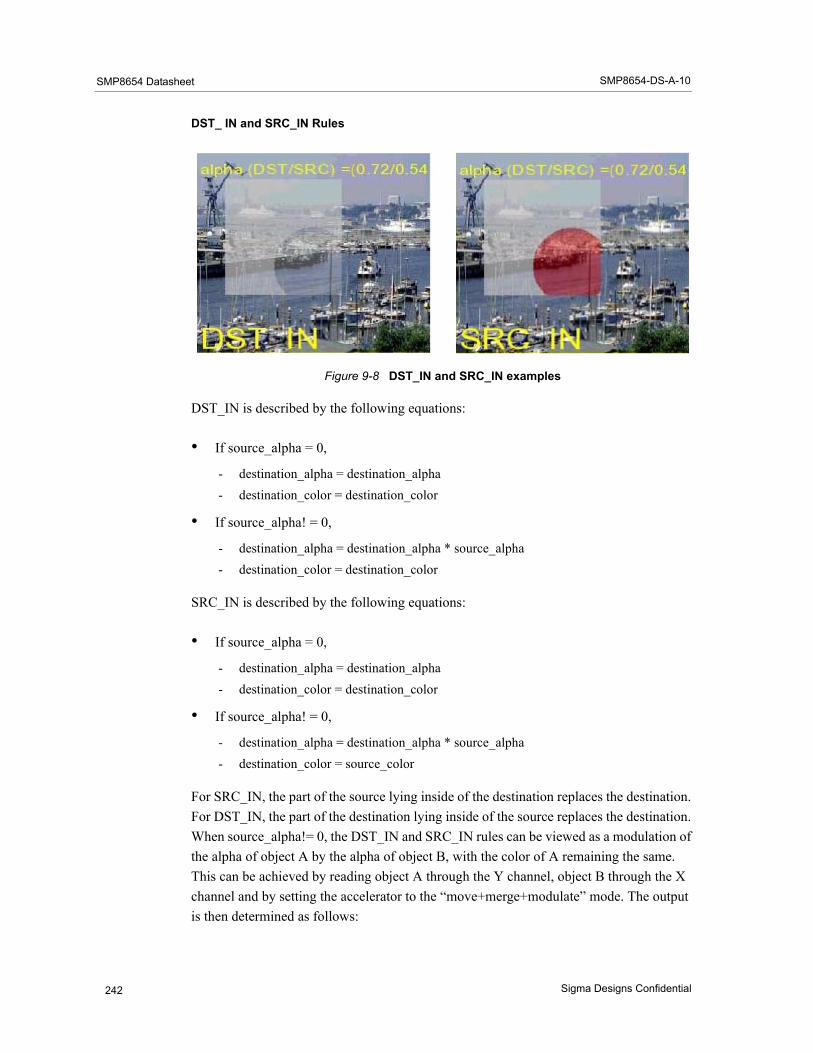
SMP8654-DS-A-10SMP8654 Datasheet
DST_ IN and SRC_IN Rules
Figure 9-8 DST_IN and SRC_IN examples
DST_IN is described by the following equations:
• If source_alpha = 0,
- destination_alpha = destination_alpha - destination_color = destination_color
• If source_alpha! = 0,
- destination_alpha = destination_alpha * source_alpha - destination_color = destination_color
SRC_IN is described by the following equations:
• If source_alpha = 0,
- destination_alpha = destination_alpha - destination_color = destination_color
• If source_alpha! = 0,
- destination_alpha = destination_alpha * source_alpha - destination_color = source_color
For SRC_IN, the part of the source lying inside of the destination replaces the destination. For DST_IN, the part of the destination lying inside of the source replaces the destination. When source_alpha!= 0, the DST_IN and SRC_IN rules can be viewed as a modulation of the alpha of object A by the alpha of object B, with the color of A remaining the same. This can be achieved by reading object A through the Y channel, object B through the X channel and by setting the accelerator to the “move+merge+modulate” mode. The output is then determined as follows:
242 Sigma Designs Confidential

9: Video Processing Subsystem
• color = color from Y channel (object A)
• alpha = alpha from X channel (object B) multiplied by alpha of Y channel (object A)
Y channel can be replaced with Z channel and it is possible to input alpha,color or alpha-only information in the X channel.
DST_OUT and SRC_OUT Rules
Figure 9-9 DST_OUT and SRC_OUT examples
DST_OUT is described by the following equations:
• If source_alpha = 0,
- destination_alpha = destination_alpha - destination_color = destination_color
• If source_alpha! = 0,
- destination_alpha = destination_alpha * (1-source_alpha) - destination_color = destination_color
SRC_OUT is described by the following equations:
• If source_alpha = 0,
- destination_alpha = destination_alpha - destination_color = destination_color
• If source_alpha! = 0,
- destination_alpha = source_alpha * (1-destination_alpha) - destination_color = source_color
243Sigma Designs Confidential

SMP8654-DS-A-10SMP8654 Datasheet
For SRC_OUT, the part of the source lying outside of the destination replaces the destina-tion. For DST_OUT, the part of the destination lying outside of the source replaces the destination. When source_alpha!= 0, the DST_OUT and SRC_OUT rules are similar to the “IN” rules, except that the complement of the alpha of object B is used to modulate the alpha of object A. With the SMP8654, two passes are no longer required to implement SRC_OUT and DST_OUT since the X and Y channels now have the ability to comple-ment the alpha value.The output is then determined as follows:
• color = color from Y channel (object A)
• alpha = 1-alpha from X channel (object B) multiplied by alpha of Y channel (object A)
Y channel can be replaced with Z channel and it is possible to input alpha,color or alpha-only information in the X channel.
DST_OVER and SRC_OVER Rules
Figure 9-10 DST_OVER and SRC_OVER examples
SRC_OVER is described by the following equations:
• If source_alpha = 0,
- destination_color = destination_color - destination_alpha = destination_alpha
• If source_alpha = 0,
- destination_color = source_color + [destination_color * (1 - source_alpha)] - destination_alpha = source_alpha + destination_alpha - (source_alpha *
destination_alpha)
244 Sigma Designs Confidential

9: Video Processing Subsystem
DST_OVER is described by the following equations:
• If source_alpha = 0,
- destination_color = destination_color - destination_alpha = destination_alpha
• If source_alpha = 0,
- destination_color = destination_color + [source_color * (1 - destination_alpha)] - destination_alpha = source_alpha + destination_alpha - (source_alpha *
destination_alpha)
For SRC_OVER, the source is composited over the destination. For DST_OVER, the des-tination is composited over the source and the result replaces the destination. The DST_OVER and SRC_OVER rules are implemented using the “full” blend command of the accelerator. The hardware does not differentiate between the DST_OVER and SRC_OVER, the command is symmetric from that point of view.
9.4.12 Main Mixer
The main mixer receives the picture streams from each of the following 7 sources. The global plane order (layer priority) is programmable, except for the hardware cursor which is always the top layer (highest priority).
1. Hardware cursor
2. OSD scaler
3. Subtitle scaler
4. Multi-format scaler 1
5. Multi-format scaler 2
6. Main video scaler
7. Video plane channel
Each incoming stream passes through a positioning block, which places the input picture at a specified horizontal and vertical position within the active display window.
245Sigma Designs Confidential

SMP8654-DS-A-10SMP8654 Datasheet
9.4.12.1 Positioning Blocks
There are eight positioning blocks (one per input stream). The purpose of the positioning block is, to position the input picture within a large frame as shown in the diagram:
Y p o s it io n
X p o s it io n
F ra m e X s iz e
F ra m e Y s iz e
O rig in a l P ic tu re
P o s it io n in g b lo c k o u tp u t
Figure 9-11 Positioning blocks
Each positioning block has four parameters:
1. A 13-bit signed X position (-4096 to 4095).
2. A 12-bit signed Y position (-2048 to 2047).
3. A 12-bit X active window size (0 to 4095).
4. A 11-bit Y active window size (0 to 2047).
The X and Y position parameters are signed to allow the top-left corner of the input pic-ture to be positioned outside of the output frame (the left and/or top portion of the input picture is not displayed). If the discarded portion of the input picture is too large, then bandwidth problems will appear. In this case, the input picture should be cut in the V-Bus interface.
9.4.12.2 Mixing
Within the mixer, the positioned streams can be assigned to any of the layers 0-6. The highest priority (layer 7, the top layer) is always assigned to the hardware cursor.
For each output pixel, the 8 input pixels are layered and mixed according to the pro-grammed layer (global priority) order. Each output pixel from the main mixer ultimately consists of the alpha-blended combination of the 4 highest-priority non-transparent input pixels.
246 Sigma Designs Confidential

9: Video Processing Subsystem
At any pixel location where there's no data provided by the sources, or where all the sources are transparent, a programmable background color (typically black) is output. The output of the main mixer is then sent to the display routing block.
9.4.13 Display Routing Block
The display router is essentially a crossbar switch, which couples 5 input video streams to any of the 3 video output blocks.
The 5 input sources to the display router are the main mixer output, the Multi-format scaler 1 or 2, the HD to SD downscaler output, constrained image scaler output, and the color bars generator.
The color bars generator generates a standard color bars pattern (in YCbCr) for testing pur-poses. The image size and the intensity (75% or 100%) are programmable. The white color can be 75% or 100%. The generation is enabled as soon as the block is put in ‘run’ reset level. There are 8 bars of equal width per line.
The 3 output ports of the display router drive 2 analog video output blocks and 1 HDMI digital video output block. Both analog video output blocks are capable of generating com-posite, S-video, and YPbPr or RGB video. The HDMI block forrnats the pixel data into an HDMI v1.3a compliant output interface.
9.4.14 Video Output Interfaces
9.4.14.1 Display Controllers
Each of the 3 video output blocks (2 analog, 1 digital) may be independently operated as either a video timing master or a slave. In the master mode, the display controller generates HSYNC and VSYNC from an internal video clock. In the slave mode, the display control-ler receives HSYNC and VSYNC from another video input/output port or an external device.
Commonly used output resolutions and frame refresh rates include:
• 704/720 x 480i @ 29.97 and 30Hz
• 704/720 x 480p @ 59.94 and 60Hz
• 704/720 x 576i @ 25Hz
• 704/720 x 576p @ 50Hz
• 1280 x 720p @ 50, 59.94 and 60Hz
• 1366 x 768p @ 50, 59.94 and 60Hz
247Sigma Designs Confidential

SMP8654-DS-A-10SMP8654 Datasheet
• 1024 x 1024p @ 50, 59.94 and 60Hz
• 1920 x 1080i @ 25, 29.97 and 30Hz
• 1920 x 1080p @ 23.976, 24, 50, 59.94 and 60Hz
The output video may be optionally rotated by 90, 180 or 270 degrees, with symmetry
with respect to the X-axis, 1st bisector, Y-axis or 2nd bisector.
As the video may be scaled to any resolution, these represent only the standard consumer resolutions. Resolutions unique to fixed-resolution displays, such as LCD, DLP and PDP are easily accommodated.
9.4.14.2 Frame Rate Conversion
The programmable output video timing, in addition to the 2:2 and 3:2 pull-down process-ing and deinterlacing, enables the following source-to-output frame rate conversions to be supported:
Table 9-2 Supported source and output frame rate combinations
Source/Output 23.976p 24p 25i29.97i30i 50p
59.94p60p
23.976p Yes Yes Yes Yes Yes Yes
24p Yes Yes Yes Yes Yes Yes
25i1
1. 25i, 29.97i and 30i are also commonly called 50i, 59.94i and 60i, respectively. The difference is whether frame rate or field rate is specified.
- - Yes Yes Yes Yes
25p - - Yes Yes Yes Yes
29.97i1 - - Yes Yes Yes Yes
29.97p - - Yes Yes Yes Yes
30i1 - - Yes Yes Yes Yes
30p - - Yes Yes Yes Yes
50p - - Yes Yes Yes Yes
59.94p - - Yes Yes Yes Yes
60p - - Yes Yes Yes Yes
Each field/frame from the video decoder has a PTS and is compared with the STC to decide what is the best field/frame to display.
248 Sigma Designs Confidential

9: Video Processing Subsystem
When frame rate converting interlaced sources, the output is either the source field closer in time (resulting in occasional dropped or duplicated fields) or has a matching phase (resulting in occasional dropped or duplicated frames).
For 24p and 23.976p sources, the 3:2 pull-down information is used as a hint to determine if a frame should be displayed again or not; the PTS and STC have the final say. For exam-ple, if displaying a frame 3 times leads to a large gap between the PTS and the STC, then the frame will be displayed twice. If there is no repeat_first_field flag, the display is com-pletely PTS/STC driven - the display sequence is the same as if there is the flag but the first repeated frame is random, instead of being the one set in the stream.
Table 9-3 Combinations of supported output frame rates - OSD, subtitles and graphics available on all outputs
Supported Output Frame Rates
HDMI 23.976p 24p 25i 29.97i 30i 50p 59.94p 60p
Analog Component1
1. Resolution of HDMI and analog component video is the same.
25i 29.97i 30i 50p 59.94p 60p
Analog Component2
2. Resolution and frame rate of analog component video and composite video is the same.
29.97i 25i29.97i
25i 29.97i 29.97i 25i 29.97i 29.97i
S-Video 29.97i 25i29.97i
25i 29.97i 29.97i 25i 29.97i 29.97i
Composite 29.97i 25i29.97i
25i 29.97i 29.97i 25i 29.97i 29.97i
Table 9-4 Combinations of supported output frame rates - no OSD, subtitles or graphics on analog component outputs
Supported Output Frame Rates
HDMI 23.976p 24p 25i 29.97i 30i 50p 59.94p 60p
Analog Compo-nent 21
1. Resolution of HDMI and analog component video may be different.
,
2. Requires additional memory bandwidth to read the main video plane a second time.
60p59.94p50p30i29.97i25i
60p59.94p50p30i29.97i25i
60p59.94p50p30i29.97i25i
60p59.94p50p30i29.97i25i
60p59.94p50p30i29.97i25i
60p59.94p50p30i29.97i25i
60p59.94p50p30i29.97i25i
60p59.94p50p30i29.97i25i
S-Video 29.97i 25i29.97i
25i 29.97i 29.97i 25i 29.97i 29.97i
Composite 29.97i 25i29.97i
25i 29.97i 29.97i 25i 29.97i 29.97i
249Sigma Designs Confidential

SMP8654-DS-A-10SMP8654 Datasheet
9.4.14.3 VBI Support on Video Outputs
Sigma‘s hardware library provides for the extraction, parsing, and output of various user data types onto the video outputs during the vertical blanking interval (VBI).
The VBI data is present on the composite output, the Y channel of the S-video output and the Y channel of the YPbPr output. Two of the GPIO pins may be used for adding the appropriate DC offsets to pins 8 and 16 of a SCART connector to indicate the program aspect ratio information. The GPIO pins may also be used to control the Line 1, Line 2, and Line 3 signals, and monitor the Plug Detect signal, for the EIAJ CP-4120 DTerminal interface.
Closed Captioning
480i closed captioning (including extended data services, XDS such as parental control, v-chip, etc.) on lines 21 and 284, as defined by CEA-608-C is supported. There is no stan-dard for transmitting closed captioning over the HDMI or 480p, 576i, 576p, 720p, 1080i or 1080p analog component interfaces.
The registers VO_MAIN_ANALOG_CC_AGC (CC_data[15:0]), VO_COMPONENT_OUT_TV_CONFIG (bits 17 and 18), VO_COMPOSITE_OUT_TV_CONFIG (bits 17 and 18) and VO_MAIN_ANALOG_TV_CONFIG (bits 17 and 18) control closed captioning. The bit 18 determines the extended closed captioning.
Closed captioning data (including XDS data) to be output during VBI may be provided by application software on the host CPU or by Sigma's hardware library.
The hardware library supports the following closed captioning formats,
• DVD
- MPEG-2* User_data_start_code = 0x000001B2* User data type = 0x4343
• ATSC
- MPEG-2* User_data_start_code = 0x000001B2* User_data_type_code = 0x03* Cc_type = 0x0 or 0x1
250 Sigma Designs Confidential

9: Video Processing Subsystem
• SCTE 20 and 21
- MPEG-2* User_data_start_code = 0x000001B2* User_data_type_code = 0x03* Cc_type = 0x0 or 0x1
• Minerva
Nielsen AMOL I and II
480i Nielson AMOL I and II data on lines 20 and 22, as defined by CEA-805-C, is not sup-ported.
Multi-level Pulse-Amplitude Modulation (PAM)
Multi-level pulse-amplitude modulation (PAM), used to reconstruct a VBI analog wave-form, is not supported on the SMP8654.
Wide Screen Signaling and Copy Protection Control
480i wide screen signaling (WSS), copy generation management (CGMS-A) and APS data on lines 20 and 283, as defined by IEC 61880-1 and EIAJ CPR1204, is supported. CGMS-A, APS and RCD data are also present on line 284 per CEA-608-C.
480p wide screen signaling (WSS), copy generation management (CGMS-A) and APS data on line 41, as defined by EIAJ CPR1204-1, CEA-805-C Type A and IEC 61880-2, is supported. CGMS-A, APS and RCI data as defined by CEA-805-C Type B on line 40 is supported.
576i wide screen signaling (WSS), copy generation management (CGMS-A) and APS data on line 23, as defined by ETSI EN 300 294 and ITU-R BT.1119, is supported.
576p wide screen signaling (WSS), copy generation management (CGMS-A) and APS data on line 43, as defined by IEC 62375, is supported.
720p copy generation management (CGMS-A) and APS data on line 24, as defined by CEA-805-C Type A and EIAJ CPR1204-2, is supported. CGMS-A, APS and RCI data as defined by CEA-805-C Type B on line 23 is supported.
1080i copy generation management (CGMS-A) and APS data on lines 19 and 582, as defined by CEA-805-C Type A and EIAJ CPR1204-2, is supported. CGMS-A, APS and RCI data as defined by CEA-805-C Type B on lines 18 and 581 is supported.
251Sigma Designs Confidential

SMP8654-DS-A-10SMP8654 Datasheet
The register VO_MAIN_ANALOG_CGMS (R/W) controls Wide Screen Signaling and CGMS.
Table 9-5 Wide Screen Signaling and CGMS - register VO_MAIN_ANALOG_CGMS
Bit # 1 0
23 CGMS/WSS odd field (NTSC) / WSS (PAL) CGMS/WSS disabled on odd fields / WSS disabled
22 CGMS/WSS on even fields (NTSC) CGMS/WSS disabled on even fields
21 Software CRC generation for CGMS/WSS(NTSC)
Hardware CRC generation for CGMS/WSS(NTSC)
20 x x
19:0 Copy Generation Management System data and WSS (NTSC)
13:0 Wide Screen Signaling Data (PAL)
WSS and CGMS data to be output during VBI must be provided by application software on the host CPU.
Teletext
The SMP8654 supports 3 systems:
• System B-625: for 625-line PAL systems in Europe
• System C-525: for 525-line NTSC systems in USA
• System D-525: for 525-line NTSC systems in Japan
The active teletext lines are located in the vertical blanking interval:
• For system B-625 (625 lines/frame):
- Top field line 6 to line 22 (17 lines max) - Bottom field line 318 to line 335 (18 lines max)
• For systems C-525 and D-525 (525 lines/frame):
- Top field line 7 to line 17 (11 lines max) - Bottom field line 269 to line 280 (12 lines max)
The teletext output is configured by the register VO_MAIN_ANALAOG_TV_TELETEXT_CONFIG. There are 2 parameters, CONFIG_LINE[17:0] and CONFIG_CODE[7:0]
252 Sigma Designs Confidential

9: Video Processing Subsystem
CONFIG_LINE[17:0] enables the active teletext lines within the blanking: this is an enable (high) register. Bit 0 corresponds to the first line of teletext as defined by the system and the polarity of the field (see previous paragraph), and so on. For instance in system B, in a top field, programming bit 0 at 1 will enable teletext on line 6.
CONFIG_CODE[7:0] (or framing code) identifies the system. It is,
• 8‘b 0010_0111 for system B-625
• 8‘b 1110_0111 for system C-525
• 8‘b 1010_0111 for system D-525
Bit 0 is output first. Each system outputs a different number of bits per line. Each line starts with a hardware generated clock run-in of 16 bits (alternating 0s & 1s), followed by the framing code byte. After these 3 bytes are output, the content of the teletext memory is output.
The maximum data lengths for each system are:
• System B-625: 42 bytes (+2 run-in +1 framing code=45)
• System C-525: 33 bytes (+2 run-in +1 framing code=36)
• System D-525: 34 bytes (+2 run-in +1 framing code=37)
Teletext data to be output during VBI must be provided by application software on the host CPU. Sample software is available from Sigma that extracts DVB teletext data (EN 300 472) and outputs it onto the 576i analog video outputs during VBI.
9.4.14.4 Sync Timing Generators
The programmable sync timing generators enable support for a wide variety of video tim-ing standards, including:
• EIA-770.2 and 770.3
- 480i30, 480p60, 720p60 and 1080i30
• SMPTE 170M
- NTSC-M
• SMPTE 267M
• SMPTE 274M
- 1080i25, 1080i30, 1080p24, 1080p25, 1080p30, 1080p50 and 1080p60
253Sigma Designs Confidential

SMP8654-DS-A-10SMP8654 Datasheet
• SMPTE 296M
- 720p24, 720p25, 720p30, 720p50 and 720p60
• ITU-R BT.470
- 480i30 and 576i25
• ITU-R BT.601
- 480i30 and 576i25
• ITU-R BT.656
- 480i30 and 576i25
• ITU-R BT.709
- 1080i25, 1080i30, 1080p24, 1080p25, 1080p30, 1080p50 and 1080p60
• ITU-R BT.1358
- 480p60 and 576p50
Custom timing to support various flat panel display resolutions, such as 1366x768, is also possible.
Active video – top field
Active video – bottom field
V=1
V=0
V=1
V=0
V=1
F=0
F=1
H=1 H=0 H=1“BT.656” parameters
OH
OV
“BT. 601” parameters
X offset
Y offset top
Y offset bottom
Figure 9-12 Video output timing parameters
254 Sigma Designs Confidential

9: Video Processing Subsystem
The range of programmability for each video timing parameter for the digital video output port is as follows:
Table 9-6 Range of programmability for digital video output timing
Parameter Range
Vt_total_size (vertical total per fame) 0 - 4095 lines
Hz_total_size (horizontal total per line) 0 - 4095 pixels
X_offset (Hsync to active video) 0 - 4095 pixels
Y_offset_top (Vsync to active video, top field) 0 - 4095 lines
Y_offset_bottom (Vsync to active video, bottom field) 0 - 4095 lines
Top_field_height (total size of top field) 0 - 8191 (half lines)
Hz_sync_width (Hsync width) 0 - 4095 pixels
Vt_sync_width (Vsync width) 0 - 8191 half lines
Vt_sync_fine_adjust, lower byte (Vsync to Hsync relative position adjust, top field)
0 to +/-127pixels
Vt_sync_fine_adjust, upper byte (Vsync to Hsync relative position adjust, bottom field)
0 to +/-127 pixels
The range of programmability for each video timing parameter for the component and composite/S-video output ports is as follows:
Table 9-7 Range of programmability for component, composite and S-video output timing
Parameter Range
Height (total line per frame) 0 - 4095 lines
Width (total pixels per line) 0 - 8191 pixels
Hsync0 (horizontal coordinate where Hsync goes low) 0 - 4095 pixels
Hsync1 (horizontal coordinate where Hsync goes high) 0 - 4095 pixels
Hsync_width (total Hsync width) 0 - 4095 pixels
Vsync_O_0_line (vertical coordinate where Vsync goes low for odd field) 0 - 4095 lines
Vsync_O_1_line (vertical coordinate where Vsync goes high for odd field)
0 - 4095 lines
Vsync_E_0_line (vertical coordinate where Vsync goes low for even field) 0 - 4095 lines
Vsync_E_1_line (vertical coordinate where Vsync goes high for even field)
0 - 4095 lines
Vsync_O_0_pixel (horizontal coordinate where Vsync goes low for odd field)
0 - 4095 pixels
255Sigma Designs Confidential

SMP8654-DS-A-10SMP8654 Datasheet
The appendix includes a listing of parameter values for standard video timings.
9.4.14.5 Analog Video Output
Two analog video output blocks are available. Each receives 36-bit YCbCr or RGB data from the display router. Each analog video output block also contains a video timing gen-erator that can operate in a master or slave timing mode.
Analog video output block 1 is capable of generating,
• 12-bit composite (CVBS) + 24-bit S-video,
• 36-bit YCbCr + 12-bit composite (CVBS) or,
• 36-bit RGB + 12-bit composite (CVBS)
Analog video output block 0 is capable of generating,
• 12-bit composite (CVBS) + 24-bit S-video,
• 36-bit YCbCr or,
• 36-bit RGB
Six 12-bit video DACs convert the digital video data from the 2 analog video output blocks to analog video.
Each video DAC can be configured to output one of the following:
• Composite video (CVBS)
• Y of S-video
• C of S-video
Vsync_O_1_pixel (horizontal coordinate where Vsync goes high for odd field)
0 - 4095 pixels
Vsync_E_0_pixel (horizontal coordinate where Vsync goes low for even field)
0 - 4095 pixels
Vsync_E_1_pixel (horizontal coordinate where Vsync goes high for even field)
0 - 4095 pixels
Vsync_start (horizontal coordinate where Vsync starts) 0 - 4095 lines
Vsync_width (total Vsync width) 0 - 4095 lines
Table 9-7 Range of programmability for component, composite and S-video output timing
Parameter Range
256 Sigma Designs Confidential

9: Video Processing Subsystem
• Y or G video
• Pr or R video
• Pb or B video
Each video DAC can also be configured as to which source to use for video:
• Analog video output block 0
• Analog video output block 1
This flexible configuration options enable supporting many output configurations includ-ing,
• YPbPr + S-video + composite
• RGB + S-video + composite
• full SCART (RGB + composite) + composite
• full SCART (RGB + composite) + S-video
Each video DAC can also be configured as to which source to use for teletext:
• Analog video output block 0
• Analog video output block 1
Each video DAC can be independently disabled when not used for significant power sav-ings.
For SD sources, the SMP8654 offers the ability to output composite, S-video, SD or upscaled HD analog component, and SD or upscaled HD HDMI outputs simultaneously. For HD sources, downscaled composite, downscaled S-video, HD or constrained-image HD analog component outputs, and HD HDMI outputs are simultaneously available. For two SD or HD sources, the SMP8654 also offers the ability to output both sources simulta-neously (one audio channel only).
The DRM software running on the XPU may restrict the ability to output upscaled HD analog component outputs from SD sources or the ability to output HD analog component outputs from HD sources.
257Sigma Designs Confidential

SMP8654-DS-A-10SMP8654 Datasheet
Component (YPbPr or RGB) Video Outputs
The component video outputs support optional Macrovision v7.1.L1 and v1.2 protection and DAC attenuation compensation. When generating 480i30 or 576i25 video, the DACs operate at 54MHz; for 480p60 or 576p50 video, the DACs operate at 108MHz; for 1080i30, 1080i25, 720p60 or 720p50 video, the DACs operate at 148.5MHz. For 1080p60 or 1080p50 video, the DACs operate at 148.5MHz. The analog video outputs are capable of driving a doubly-terminated 75-ohm load.
The Macrovision v7.1.L1 and v1.2 certifications that Sigma receive applies only to chip manufacturers. Other certifications (such as v7.1.S1, etc.) are implementation-dependent (i.e., they are dependent on the type of the end-product being produced) and therefore are up to the OEM/ODM to obtain.
Note: The Macrovision support is not available when outputting analog RGB video.
Component Video Output Timing
Both analog video output blocks contain a complete programmable sync timing generator for operating as a sync master, or the timing generator may be slaved to H/V sync timing from,
• Video input
• Composite/S-video analog output
• HDMI output
• External device connected to component video output port
H/V sync signals output onto this port may be obtained from,
• Sync timing generator
Either bi-level or tri-level sync pulses may be generated when outputting high-definition RGB or YPbPr signals.
258 Sigma Designs Confidential

9: Video Processing Subsystem
Component Video Output Processing
A 3x3 matrix multiplier with programmable coefficients is used to implement:
• YCbCr/RGB color space conversion
• Contrast (or ‘picture’ or ‘white level‘) control
• Saturation (or ‘color‘) control
• Hue (or ‘tint‘) control
• BT.709 (HDTV) to BT.601 (SDTV) and BT.601 (SDTV) to BT.709 (HDTV) colorim-etry conversion
• 61966-2-4 (xvYCC) uses BT.709 colorimetry
The inputs of the matrix multiplier are 36-bit YCbCr from the display routing block; the outputs are 36-bit YCbCr or RGB which can drive three 12-bit video DACs. The matrix coefficients have a range of -4 to +3.4095/4096, in steps of 1/4096. The matrix multiplier is followed by three programmable DC offsets to provide optional brightness (or ‘black level‘) control. The DC offsets have a range of -512 to + 511.15/16, in steps of 1/16. No sharpness control is provided for the component video outputs.
Component Video Output Formats
Supported component output formats are:
• RGB SCART (IEC 60933)
- RGB + CVBS (composite) - RGB: 0.700v range - 0 IRE blanking setup - No sync on R, G and B - No support for fast blanking signal
• RGB sync-on-green
- 0.300v bi-level sync (SD) or +/-0.300v tri-level sync (HD) - RGB: 0.700v range - 0 IRE blanking setup
• RGB SMPTE
- 0.300v bi-level sync (SD) or +/-0.300v tri-level sync (HD) - RGB: 0.700v range - 0 IRE blanking setup - sync on R, G and B
259Sigma Designs Confidential

SMP8654-DS-A-10SMP8654 Datasheet
• YPbPr Betacam
• YPbPr MII
• YPbPr SMPTE
- 0.300v bi-level sync (SD) or +/-0.300v tri-level sync (HD) - Y: 0.700v range - Pb, Pr: +/-0.350v range - 0 IRE blanking setup - sync on Y, Pb and Pr
• YPbPr EIA-770.2 and EIA-770.3
- 0.300v bi-level sync (SD) or +/-0.300v tri-level sync (HD) - Y: 0.700v range - Pb, Pr: +/-0.350v range - 0 IRE blanking setup - no sync on Pb and Pr
Component Video Output Configuration Options
Configuration register bits can be used to select a number of features and characteristics:
• H- and V-sync source
• H- and V-sync polarity
• Bi-level or tri-level sync pulses for HD output
• SD or HD output
• Progressive or interlaced output
• Closed caption and extended closed caption enable/disable
- CEA-608-C data is present on analog RGB outputs instead of only the G output
• Y and RGB filter options
- 9.00 MHz - 13.0 MHz
• PbPr filter options
- 6.50 MHz - 13.0 MHz
• YPbPr/RGB output mode
260 Sigma Designs Confidential

9: Video Processing Subsystem
Figure 9-13 Video waveform - 720p
Figure 9-14 Video waveform - 1080i
261Sigma Designs Confidential

SMP8654-DS-A-10SMP8654 Datasheet
Figure 9-15 Video waveform - 480i
Figure 9-16 Video waveform - 480p
262 Sigma Designs Confidential

9: Video Processing Subsystem
Figure 9-17 Video waveform - 576i
Figure 9-18 Video waveform - 576p
263Sigma Designs Confidential

SMP8654-DS-A-10SMP8654 Datasheet
Composite (CVBS) and S-Video Outputs
The NTSC/PAL encoder (with optional Macrovision v7.1.L1 protection and DAC attenua-tion compensation) supports the NTSC-M, NTSC-J, PAL-B/D/G/H/I, PAL-60, PAL-M and PAL-Nc baseband video standards. It uses three 54MHz 12-bit video DACs to gener-ate simultaneous composite and S-video outputs. The analog video outputs are capable of driving a doubly-terminated 75-ohm load.
The Macrovision v7.1.L1 certification that Sigma receives applies only to chip manufac-turers. Other certifications (such as v7.1.S1, etc.) are implementation-dependent (i.e. they are dependent on the type of the end-product being produced) and therefore are up to the OEM/ODM to obtain.
Composite and S-Video Output Timing
The block contains a complete programmable sync timing generator for operating as a sync master, or the timing generator may be slaved to H/V sync timing from,
• Component video analog output
• Digital video output
• External device connected to composite and S-video output port
H/V sync signals output onto this port may be obtained from,
• Sync timing generator
Composite and S-Video Output Processing
A 3x3 matrix multiplier with programmable coefficients is used to implement:
• Contrast (or ‘picture’ or ‘white level’) control
• Saturation (or ‘color’) control
• Hue (or ‘tint’) control
• BT.709 (HDTV) to BT.601 (SDTV) colorimetry conversion
• 61966-2-4 (xvYCC) uses BT.709 colorimetry
264 Sigma Designs Confidential

9: Video Processing Subsystem
The inputs of the matrix multiplier are 36-bit YCbCr from the display routing block; the outputs are 30-bit YCbCr which drives the NTSC/PAL encoder. The matrix coefficients have a range of -4 to +3.4095/4096, in steps of 1/4096. The matrix multiplier is followed by three programmable DC offsets to provide optional brightness (or ‘black level‘) control. The DC offsets have a range of -512 to + 511.15/16, in steps of 1/16. The sharpness can be adjusted from +/-12.5% to 100% in 8 steps. A color sub carrier notch filter is also avail-able.
The composite and S-video digital outputs from the NTSC/PAL encoder are 10-bit data. Oversampling filters output 12-bit data, which drives the three 12-bit video DACs.
When outputting 720 samples/line, either all 720 active samples may be output (does not meet the NTSC/PAL timing) or, 1-16 samples may be cropped from the left and right sides resulting in the center 688-720 active samples being output (in order to meet the NTSC/PAL timing). Typically, to meet the NTSC timing, 716 samples should be output and to meet the PAL timing, 702 samples should be output.
Composite and S-Video Output Formats
Supported composite and S-video output formats are:
• Baseband NTSC-M
• Baseband NTSC-J (NTSC-M for Japan)
• Baseband PAL-B/D/G/H/I
• Baseband PAL-M
• Baseband PAL-60
• Baseband PAL-N
• Baseband PAL-Nc (for Argentina)
Composite and S-Video Output Configuration
Configuration register bits can be used to select a number of features and characteristics:
• H- and V-sync source
• H- and V-sync polarity
• Closed caption and extended closed caption enable/disable
• CGMS, WSS and Teletext enable/disable
• Sharpness/notch filter enable/disable and gain/attenuation control
265Sigma Designs Confidential

SMP8654-DS-A-10SMP8654 Datasheet
• Luma filter options (separate filters used for CVBS and S-video)
- 4.5 MHz (driving RF modulator) - 6.5 MHz
• Chroma filter options (separate filters used for CVBS and S-video)
- 0.65 MHz (480i out, driving RF modulator) - 1.00 MHz (576i out, driving RF modulator) - 1.30 MHz (480i out) - 2.00 MHz (576i out)
• Y-C relative delay
- No delay - Delay C by 1, 2 or 3 sample clocks - Delay Y by 1, 2 or 3 sample clocks
• Composite and S-video output format
• Output three composite video signals instead of one composite and one S-video
Figure 9-19 NTSC c for S-video
266 Sigma Designs Confidential

9: Video Processing Subsystem
Figure 9-20 NTSC y for S-video
267Sigma Designs Confidential

SMP8654-DS-A-10SMP8654 Datasheet
Figure 9-21 CVBS (NTSC)
268 Sigma Designs Confidential

9: Video Processing Subsystem
9.4.14.6 HDMI v1.3a Output
The SMP8654 contains a fully integrated HDMI subsystem. It is fully HDMI compliant, and is used to transport consumer electronics standard digital video and digital audio over a TMDS interface. It supports the HDMI v1.3a (High Definition Multimedia Interface) and HDCP v1.3 (High-Bandwidth Digital Content Protection) specifications. The block provides a simple method for sending protected digital audio and video, providing end users with a truly all-digital experience. At the same time, built in backward compatibility with DVI 1.0 allows HDMI host systems to connect to any DVI 1.0 display (DTV, plasma display, LCD TV, PC monitor).
The integrated HDMI 1.3a link module includes the following features and capabilities:
• HDMI v1.3a, HDCP v1.3 and DVI v1.0 compliant transmitter
• Supports DTV from 480i to 1080i/p HD resolution
• Programmable 2-way color space converter
• Compliant with EIA/CEA-861D
• Deep color support (36 bit per pixel).
• xvYCC Enhanced Colorimetry
• Gamut Metadata transmission
• Supports RGB, YCbCr digital video input format includes ITU.656
• 36-bit RGB/YCbCr 4:4:4
• 24-bit YCbCr 4:2:2
• 12-bit YCbCr 4:2:2 (ITU.601 and 656)
• Supports standard SPDIF for stereo or compressed audio up to 192KHz
• Support PCM and Dolby digital
• IEC60958 or IEC61937 compatible
• High-bitrate compressed audio format
• Master I2C interface for DDC connection
• Programmable PLL characteristics, channel delay, and transmitter pre-emphasis rate
The HDMI transmitter block receives uncompressed digital video data from the prepro-cessing unit and compressed or uncompressed digital audio from the audio DSP, formats and encrypts the data received, and then drives the HDMI LVDS output pins.
269Sigma Designs Confidential

SMP8654-DS-A-10SMP8654 Datasheet
The integrated HDMI 1.3a PHY (transmitter) module includes the following features and capabilities:
• HDMI version 1.3a compliant transmitter
• Supports DTV from 480i to 1080i/p HD resolution, and PC from VGA to UXGA
• Adjustable analog characteristics:
- Output swing voltage - Pre-emphasis strength - PLL band width - VCO gain - BGR voltage
• Loop-back test support
• Low ISI jitter due to fully differential data path
Video Output Pre-processing
The HDMI digital video stream is preprocessed before being delivered to the HDMI link and PHY subsystem. The preprocessing unit uses a 3x3 matrix multiplier to optionally apply the following transformations to the video data:
• YCbCr/RGB color space conversion
• Contrast (or ‘picture’ or ‘white level’) control
• Saturation (or ‘color’) control
• Hue (or ‘tint’) control
• BT.709 (HDTV) to BT.601 (SDTV) and BT.601 (SDTV) to BT.709 (HDTV) colorim-etry conversion
• 61966-2-4 (xvYCC) uses BT.709 colorimetry
The inputs of the matrix multiplier are 36-bit YCbCr from the display routing block; the outputs are 36-bit YCbCr or RGB. The matrix coefficients have a range of -4 to +3.2047/2048, in steps of 1/2048. The matrix multiplier is followed by three programmable DC offsets to provide optional brightness (or ‘black level‘) control. The DC offsets have a range of -512 to + 511.7/8, in steps of 1/8. No sharpness control is provided for the digital video outputs.
270 Sigma Designs Confidential

9: Video Processing Subsystem
HDMI Output Video Processing
The registers are configured to describe which format of video is being supplied to the HDMI transmitter. This information is passed over the HDMI link in the CEA-861C Active Video Information (AVI) packets.
The optional YCbCr/RGB color space converter (CSC) within the HDMI transmitter block interfaces to the video output block with YCbCr-only outputs, and provides full DVI 1.0 backwards compatibility. The CSC performs the standard-definition conversions accord-ing to BT.601, or high-definition conversions (BT.709). An up-converter allows 4:2:2 YCbCr data input to be converted to 4:4:4 YCbCr for transmitting over the HDMI link.
The HDCP encryption engine encrypts the incoming audio and video data. The encryption process is entirely controlled by the security CPU (XPU) through a set sequence of register reads and writes. The HDCP keys and Key Selector Value (KSV) are used in the encryp-tion process.
HDMI Output Audio Processing
The HDMI block accepts digital audio from internal I2S and S/PDIF channels and forms
the audio data into packets in accordance with the HDMI specification. The I2S channels
used to drive the HDMI block are the same as those providing the audio DSP I2S outputs. Therefore, LPCM data over HDMI will have the same timing and format as the audio DSP
I2S output pins. The HDMI v1.3a interface supports up to 7.1-channel 192KHz LPCM audio. The S/PDIF channel used to drive the HDMI block is the same as that providing the audio DSP S/PDIF output. Therefore, S/PDIF-based audio data over HDMI will have the same timing and format as the audio DSP S/PDIF output pin.
Table 9-8 Supported audio output combinations
I2S Outputs S/PDIF Output HDMI Output Supported
LPCM Bitstream Bitstream Yes
LPCM Bitstream LPCM Yes
LPCM LPCM Bitstream No
LPCM LPCM LPCM Yes
271Sigma Designs Confidential

SMP8654-DS-A-10SMP8654 Datasheet
Within the HDMI block, the audio data may be down-sampled by one-half or one-fourth
with register control. This allows for the sharing of the I2S outputs with a high sample-rate audio DAC, while down-sampling HDMI audio for an attached display which supports only lower rates. Conversions from 192 to 48KHz, 176.4 to 44.1KHz, 96 to 48KHz and 88.2 to 44.1KHz are supported. The appropriate registers are configured to describe the format of audio being input. This information is passed over the HDMI link in the CEA-861C Audio Info (AI) packets.
HDMI Output DDC Control
A dedicated I2C master interface is used to control the DDC signals. This I2C interface is also available for use with an external HDMI transmitter chip.
9.4.14.7 HDMI CEC Interface
CEC is an HDMI option that provides automatic power-on, automatic signal routing, and single-point remote control for CEC-enabled products. For example, CEC allows users to place a DVD into the player, press PLAY, and let CEC handle the rest.
The CEC bus is a one-wire, “party line” that connects up to ten (10) AV devices through standard HDMI cabling. The CEC protocol includes automatic mechanisms for physical address (topology) discovery, (product type based) logical addressing, arbitration, retrans-mission, broadcasting, and routing control. Message opcodes support both device specific (e.g. set-top-box, DTV, and player) and general features (e.g. for power, signal routing, remote control pass-through, and on-screen display).
The HDMI CEC block represents a hardware assisted HDMI CEC initiator and follower implementation. The packet/message transmission on the CEC bus can be initiated, or intercepted automatically and is available for command processing through the software running on the host CPU.
The main features of the HDMI CEC are (based on the HDMI v1.3 specification - June 22, 2006):
• Supports the ‘HDMI CEC Initiator’ functionality
• Supports the ‘HDMI CEC Follower’ functionality
• Supports the ‘Point To Point’ or ‘Broadcast’ communications
• Supports total packet/message length of up to 170 bits
• Supports freely configurable EOM bits
• Device supports/represents up to 3 target devices
272 Sigma Designs Confidential

9: Video Processing Subsystem
• Configurable follower behavior for incoming ping
• Interrupt driven
• Contains error detection and signaling
• Uses GPIO[13] (if enabled)
The transmission of a packet/message on the CEC bus is signaled by initiators to followers by transmitting a start bit pattern. Then, a multiple of 10 bits is transmitted. Each of these 10 bits forms one block. One packet consisting of a start bit may contain from one block (= 1 header block = ping) to up to seventeen blocks (1 header block and 16 data blocks). All the header and data blocks are ten bits long and have the same basic structure.
logical 0A 3.7ms +/- 0.20ms
Start Bit
0 BA
B 4.5ms +/- 0.20msC 1.5ms +/- 0.20ms
0 DC
D 2.4ms +/- 0.35msE 0.6ms +/- 0.20ms
logical 1
FE
F 2.4ms +/- 0.35ms
0
D [7:0] DATA BITS
I [3:0] INITIATOR ADDRESST [3:0] TARGET / DESTINATION ADDRESS
EOM END OF MESSAGE BITACK ACKNOWLEGE BIT
I[3] I[2] I[1] I[0] T[3] T[2] T[1] T[0] EOM ACK
HEADER BLOCK
D[7] D[6] D[5] D[4] D[3] D[2] D[1] D[0] EOM ACK
DATA BLOCK
HEADER BLOCK
The header block consists of the source/initiator logical address field I [3:0], the target/des-tination logical address field T [3:0], the end of message bit (EOM) and the acknowledge bit (ACK). A packet/message with the EOM bit set in the header block can be used to ‘ping’ other devices, to ascertain that they are active.
DATA BLOCK
These bits are data or op-codes, depending on the context.
273Sigma Designs Confidential

SMP8654-DS-A-10SMP8654 Datasheet
CONTROL BITS – EOM and ACK
The control bits, EOM and ACK, are always present and always have the same usage.
EOM: The EOM bit is used to indicate the final block in the message. A 0 bit specifies that one or more data blocks follow. A 1 bit specifies that the message is complete.
ACK: The ACK bit is used by follower(s) to acknowledge the data or header block. It is always set to 1 by the initiator and a(ny) follower(s) might or might not pull the line to 0. It operates in one of following two modes:
- Point to Point messages (addressed to a single device) - A follower that reads its own address in the destination address field shall acknowledge with a 0 bit. All other devices shall generate a 1 bit. A 0 bit read by the initiator therefore indicates a suc-cessful transmission of the data or header block.
- Broadcast messages - The sense of the ACK bit is inverted to allow for a single device to reject a message. All followers shall acknowledge with a 1 ACK bit. A 1 read by the initiator therefore indicates that no device has rejected the data or header block – the message transmission can therefore continue if required. A 0 read by the initiator therefore indicates that one or more devices have rejected the message.
9.4.14.8 Simultaneous HD + CIT-HD + SD Outputs
The SMP8654 is capable of simultaneous HD via HDMI, constrained image HD (CIT-HD) via analog YPbPr (960x540 effective resolution with either 1080i30 or 720p60 tim-ing) and SD via composite and S-video outputs.
9.4.14.9 Dual TV Outputs
The SMP8654 is capable of decoding two programs and driving two TVs simultaneously. Possible modes of operation include SD+SD and HD+SD.
The source of the second TV output is the Multi-format scaler 1 or 2. No OSD is available for the second TV output.
Audio for the main video is output onto the audio DSP I2S and S/PDIF outputs. Only one audio is supported at a given time.
274 Sigma Designs Confidential

9: Video Processing Subsystem
9.4.15 Video Input Interface
One 8-bit digital video input interface is provided. It is typically used to support the con-nection of an external NTSC/PAL video decoder device for STB applications involving terrestrial broadcast support or, baseband analog video connectivity.
9.4.15.1 Video Input Interface
The digital video input interface is designed to capture 8-bit 4:2:2 408i/576i/480p/576p YCbCr digital video data in the BT.601 or BT.656 format. It supports clock rates up to 54MHz and resolutions of up to 720x576p. Video data is stored in the 16bpp 4:2:2 YCbCr format.
Sliced (binary) teletext data from select NTSC/PAL video decoders may also be captured and saved to memory for further processing. The closed captioning and wide screen signal-
ing sliced (binary) VBI data may be read from the NTSC/PAL video decoder via the I2C interface).
Digital video Input Timing
The video input block contains a complete programmable sync timing generator for oper-ating as a sync master, or the timing generator may be slaved to H/V sync timing from,
• External device connected to video input port
• Component analog output
• Composite/S-video analog output
H/V sync signals output onto this port may be obtained from,
• Sync timing generator
When the BT.601 format is used, the port can operate in master or slave timing mode. When the BT.656 format is used, the port can only operate in slave timing mode. A ‘valid video’ input signal is available for both the BT.601 and BT.656 formats.
The range of programmability for each video timing parameter for the digital video input port is as follows:
275Sigma Designs Confidential

SMP8654-DS-A-10SMP8654 Datasheet
Table 9-9 Range of programmability for digital video input timing
Parameter Range
Vt_total_size (vertical total per fame) 0 - 4095 lines
Hz_total_size (horizontal total per line) 0 - 4095 pixels
X_size (horizontal active per line) 0 - 4095 pixels
Y_size (vertical active per frame) 0 - 4095 lines
X_offset (Hsync to active video) 0 - 4095 pixels
Y_offset_top (Vsync to active video, top field) 0 - 4095 lines
Y_offset_bottom (Vsync to active video, bottom field) 0 - 4095 lines
Top_field_height (total size of top field) 0 - 8191 (half lines)
Hz_sync_width (Hsync width) 0 - 4095 pixels
Vt_sync_width (Vsync width) 0 - 8191 half lines
Vt_sync_fine_adjust, lower byte (Vsync to Hsync relative position adjust, top field)
0 to +/-127 pixels
Vt_sync_fine_adjust, upper byte (Vsync to Hsync relative position adjust, bot-tom field)
0 to +/-127 pixels
Table 9-10 Range of programmability for VBI capture
Parameter Range
Top_VBI_line_enable (VBI capture for top field or frame)1
1. 24-bit value. Each bit enables (1) or disables (0) VBI capture for 24 lines, starting with the line specified by top_VBI_offset.
-
Top_VBI_offset (reference line for starting top field or frame VBI capture)2
2. BT.656 progressive: line 0 = first line of vertical blankingBT.601 progressive: line 0 = first line of Vsync active edgeBT.656 interlaced: line 0 = first line after field ID changeBT.601 interlaced: line 0 = first line of Vsync active edge for top field and the line after for bottom field
0 - 31
Bot_VBI_line_enable (VBI capture for bottom field)3
3. 24-bit value. Each bit enables (1) or disables (0) VBI capture for 24 lines, starting with the line specified by bot_VBI_offset.
-
Bot_VBI_offset (reference line for starting bottom field VBI capture2) 0 - 31
H_size (width of VBI data, used only for VBI data during horizontal blanking) 0 - 4095 bytes
V_size (height of VBI data, used only for VBI data during horizontal blanking) 0 - 4095 lines
V_offset_top (top field line number where VBI window starts, used only for VBI data during horizontal blanking)
0 - 4095
V_offset_bottom (bottom field line number where VBI window starts, used only for VBI data during horizontal blanking)
0 - 4095
276 Sigma Designs Confidential
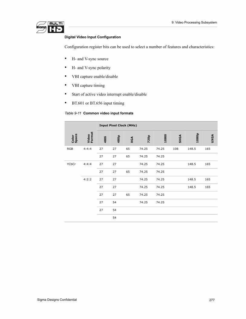
9: Video Processing Subsystem
Digital Video Input Configuration
Configuration register bits can be used to select a number of features and characteristics:
• H- and V-sync source
• H- and V-sync polarity
• VBI capture enable/disable
• VBI capture timing
• Start of active video interrupt enable/disable
• BT.601 or BT.656 input timing
Table 9-11 Common video input formats
Co
lor
Sp
ace
Vid
eo
Fo
rmat
Input Pixel Clock (MHz)
48
0i
48
0p
XG
A
72
0p
10
80
i
SX
GA
10
80
p
UX
GA
RGB 4:4:4 27 27 65 74.25 74.25 108 148.5 165
27 27 65 74.25 74.25
YCbCr 4:4:4 27 27 74.25 74.25 148.5 165
27 27 65 74.25 74.25
4:2:2 27 27 74.25 74.25 148.5 165
27 27 74.25 74.25 148.5 165
27 27 65 74.25 74.25
27 54 74.25 74.25
27 54
54
277Sigma Designs Confidential

SMP8654-DS-A-10SMP8654 Datasheet
9.5 Register Maps
9.5.1 Video Processing Registers
9.5.1.1 Multi-format Scaler Registers
Table 9-12 Register map - Multi-format scaler (MFS)
Address1
1. Address refers to G-Bus byte address relative to the video output base.
Register Name2
2. XXX is multi-format scaler 1 or 2 depending on the address.
R/W/A3
3. Read/Write/Auto update.
DescriptionMFS 1 MFS 2
+0500 +0700 VO_XXX_FORMAT_HDS R/W Video Output xxx Format HDS Register
+0504 +0704 VO_XXX_OUTPUT_SIZE R/W Video Output xxx Output Size Register
+0508 +0708 VO_XXX_SCALE_FACTOR R/W Video Output xxx Scale Factor Register
+050C +070C VO_XXX_SCALE_PHASE R/W Video Output xxx Phase Register
+0510 +0710 VO_XXX_ALPHA_ROUTING R/W Video Output xxx Alpha Routing Regis-ter
+0514 +0714 VO_XXX_KEY_COLOR R/W Video Output xxx Key Color Register
+0518 +0718 VO_XXX_BCS R/W Video Output xxx BCS Register
+051C +071C VO_XXX_STRIP_EDGE R/W Video Output xxx Strip Edge Register
+0520 +0720 VO_XXX_NONLINEAR_0 R/W Video Output xxx Nonlinear 0 Register
+0524 +0724 VO_XXX_NONLINEAR_1 R/W Video Output xxx Nonlinear 1 Register
+0528 +0728 VO_XXX_TILING R/W Video Output xxx Tiling Register
+052C +072C VO_XXX_BCS2 R/W Video Output xxx BCS 2 Register
+0530 +0730 VO_XXX_LUMA_KEY R/W Video Output xxx Nonlinear 0 Register
+0534 +0734 VO_XXX_CHROMA_SCALE_FACTOR
R/W Video Output xxx Chroma Scale Factor Register
+0538 +0738 VO_XXX_CHROMA_NONLINEAR_0
R/W Video Output xxx Chroma Nonlinear 0 Register
+053C +073C VO_XXX_CHROMA_NONLINEAR_1
R/W Video Output xxx Chroma Nonlinear 1 Register
+A000 +C000 VO_XXX_LUT0 R/W Video Output xxx LUT 0 Register
+A004 +C004 VO_XXX_LUT1 R/W Video Output xxx LUT 1 Register
+A3FC +C3FC VO_XXX_LUT255 R/W Video Output xxx LUT 255 Register
278 Sigma Designs Confidential

9: Video Processing Subsystem
9.5.1.2 Main Video Scaling Registers
Table 9-13 Main video scaling registers
Address1 Register Name R/W/A2 Description
+6400 VO_MAIN_FORMAT_HDS R/W Video Output Main Format HDS Regis-ter
+6404 VO_MAIN_OUTPUT_SIZE R/W Video Output Main Output Size Regis-ter
+6408 VO_MAIN_SCALE_FACTOR R/W Video Output Main Scale Factor Regis-ter
+640C VO_MAIN_SCALE_PHASE R/W Video Output Main Scale Phase Regis-ter
+6410 VO_MAIN_ALPHA_DEINT_ROUTING
R/W Video Output Main Alpha Deint Rout-ing Register
+6414 VO_MAIN_DEINT2 R/W Video Output Main Deint 2 Register
+6418 VO_MAIN_BCS R/W Video Output Main BCS Register
+641C VO_MAIN_PULLDOWN R/W Video Output Main Pull-down Register
+6420 VO_MAIN_STRIP_FILTER R/W Video Output Main Strip Filter Register
+6424 VO_MAIN_NONLINEAR_0 R/W Video Output Main Nonlinear 0 Regis-ter
+6428 VO_MAIN_NONLINEAR_1 R/W Video Output Main Nonlinear 1 Regis-ter
+642C VO_MAIN_BCS2 R/W Video Output Main BCS 2 Register
+6430 VO_MAIN_CHROMA_SCALE_FACTOR
R/W Video Output Main Chroma Scale Fac-tor Register
+6434 VO_MAIN_CHROMA_NONLINEAR_0
R/W Video Output Main Chroma Nonlinear 0 Register
+6438 VO_MAIN_CHROMA_NONLINEAR_1
R/W Video Output Main Chroma Nonlinear 1 Register
+643C VO_MAIN_DEINT_WINDOW0_MIN
R/W Video Output Main Deint Window0 Minimum Register
+6440 VO_MAIN_DEINT_WINDOW0_MAX
R/W Video Output Main Deint Window0 Maximum Register
+6444 VO_MAIN_PULLDOWN_WINDOW0
R/W Video Output Main Pulldown Window0 Register
+6448 VO_MAIN_PULLDOWN_WINDOW0_00
R/W Video Output Main Pulldown Window0 00 Register
+644C VO_MAIN_PULLDOWN_WINDOW0_01
R/W Video Output Main Pulldown Window0 01 Register
+6450 VO_MAIN_PULLDOWN_WINDOW0_10
R/W Video Output Main Pulldown Window0 10 Register
+6454 VO_MAIN_PULLDOWN_WINDOW0_11
R/W Video Output Main Pulldown Window0 11 Register
279Sigma Designs Confidential

SMP8654-DS-A-10SMP8654 Datasheet
9.5.1.3 OSD Scaler Registers
Table 9-14 OSD scaler registers
Address1
1. Address refers to G-Bus byte address relative to the video output block base.
+6000 VO_OSD_FORMAT_HDS R/W Video Output OSD Format HDS Regis-ter
+6004 VO_OSD_OUTPUT_SIZE R/W Video Output OSD Output Size Regis-ter
+6008 VO_OSD_SCALE_FACTOR R/W Video Output OSD Scale Factor Regis-ter
+600C VO_OSD_SCALE_PHASE_FLICKER
R/W Video Output OSD Scale Phase Flicker Register
+6010 VO_OSD_ALPHA_ROUTING R/W Video Output OSD Alpha Routing Reg-ister
+6014 VO_OSD_KEY_COLOR R/W Video Output OSD Key Color Register
+9000 VO_OSD_LUT0 R/W Video Output OSD LUT 0 Register
+9004 VO_OSD_LUT1 R/W Video Output OSD LUT 1 Register
.
.
.
+90FC VO_OSD_LUT255 R/W Video Output OSD LUT 255 Register
+6458 VO_MAIN_DEINT_WINDOW1_MIN
R/W Video Output Main Deint Window1 Minimum Register
+645C VO_MAIN_DEINT_WINDOW1_MAX
R/W Video Output Main Deint Window1 Maximum Register
+6460 VO_MAIN_PULLDOWN_WINDOW1
R/W Video Output Main Pulldown Window1 Register
+6464 VO_MAIN_PULLDOWN_WINDOW1_00
R/W Video Output Main Pulldown Window1 00 Register
+6468 VO_MAIN_PULLDOWN_WINDOW1_01
R/W Video Output Main Pulldown Window1 01 Register
+646C VO_MAIN_PULLDOWN_WINDOW1_10
R/W Video Output Main Pulldown Window1 10 Register
+6470 VO_MAIN_PULLDOWN_WINDOW1_11
R/W Video Output Main Pulldown Window1 11 Register
1. Address refers to G-Bus byte address relative to the video output base.2. Read/Write/Auto update.
Register Name R/W/A2
2. Read/Write/Auto update.
Description
Table 9-13 Main video scaling registers
Address1 Register Name R/W/A2 Description
280 Sigma Designs Confidential

9: Video Processing Subsystem
9.5.1.4 Hardware Cursor Registers
Table 9-15 Hardware cursor registers
Address1
1. Address refers to G-Bus byte address relative to the video output block base.
+6100 VO_CURSOR_SIZE_CTRL R/W Video Output Cursor Size Control Reg-ister
+6140 VO_CURSOR_ LUT0 R/W Video Output Cursor LUT 0 Register
.
.
.
+617C VO_CURSOR_LUT15 R/W Video Output Cursor LUT 15 Register
+8000 VO_CURSOR_PIX0 R/W Video Output OSD Cursor Pixel0 Reg-ister
.
.
.
+87FC VO_CURSOR_PIX511 R/W Video Output OSD Cursor Pixel 511 Register
9.5.1.5 Main Mixer Registers
Register Name R/W/A2
2. Read/Write/Auto update.
Description
Table 9-16 Register map - Main mixer
Address1 Register Name R/W/A2 Description
+6800 VO_MIX_0_POS R/W Video Output Main Mixer GFX Position Regis-ter
+6804 VO_MIX_1_POS R/W Video Output Main Mixer CRT Position Register
+6808 VO_MIX_2_POS R/W Video Output Main Mixer VCR Position Regis-ter
+680C VO_MIX_3_POS R/W Video Output Main Mixer Sub-picture Position Register
+6810 VO_MIX_4_POS R/W Video Output Main Mixer Main Video Position Register
+6814 VO_MIX_ 5_POS R/W Video Output Main Mixer OSD Position Regis-ter
+6818 VO_MIX_6_POS R/W Video Output Main Mixer Position GIN Register
+681C VO_MIX_7_POS R/W Video Output Main Mixer Cursor Position Reg-ister
+6820 VO_MIX_INDEX R/W Video Output Index Register
+6824 VO_MIX_ FRAME _SIZE R/W Video Output Frame Size Register
281Sigma Designs Confidential

SMP8654-DS-A-10SMP8654 Datasheet
9.5.1.6 Graphic Accelerator (Bitmap Mode) Registers
Table 9-17 Register map - Graphic accelerator (bitmap mode)
Address1
1. Address refers to G-Bus byte address relative to the video output block base.
+0A00 VO_GRAPH_ACC_X_FORMAT R/W Video Output Graphic Accelerator X Format Register
+0A04 VO_GRAPH_ACC_X_ALPHA R/W Video Output Graphic Accelerator X Alpha Register
+0A08 VO_GRAPH_ACC_X_KEYCOLOR R/W Video Output Graphic Accelerator X Key Color Register
+0A0C VO_GRAPH_ACC_Y_FORMAT R/W Video Output Graphic Accelerator Y Format Register
+0A10 VO_GRAPH_ACC_Y_KEYCOLOR R/W Video Output Graphic Accelerator Y Key Color Register
+0A14 VO_GRAPH_ACC_CONTROL R/W Video Output Graphic Accelerator Control Register
+0A18 VO_GRAPH_ACC_FILL R/W Video Output Graphic Accelerator Fill Register
+0A1C VO_GRAPH_ACC_CONTROL2 R/W Video Output Graphic Accelerator Control 2 Register
+0A20 VO_GRAPH_ACC_Z_FORMAT R/W Video Output Graphic Accelerator Z Format Register
+0A24 VO_GRAPH_ACC_CONTROL3 R/W Video Output Graphic Accelerator Control 3 Register
+6828 VO_MIX_ BACKGROUND_0
R/W Video Output Background Color 0 Register
+6828 VO_MIX_ BACKGROUND_1
R/W Video Output Background Color 1 Register
+6828 VO_MIX_ BACKGROUND_2
R/W Video Output Background Color 2 Register
+6828 VO_DEPTH R/W Video Output Depth Register
1. Address refers to G-Bus byte address relative to the video output block base.2. Read/Write/Auto update.
Register Name R/W/A2
2. Read/Write/Auto update.
Description
Table 9-16 Register map - Main mixer (Continued)
Address1 Register Name R/W/A2 Description
282 Sigma Designs Confidential

9: Video Processing Subsystem
9.5.1.7 Gradient Fill Generator
Table 9-18 Register map - Gradient fill generator
Address1
1. Address refers to G-Bus byte address relative to the video output block base.
+6A40 VO_GRAPH_ACC_GRD_COLOR0 R/W Video Output Graphic Accelerator Gra-dient Fill Generator Color 0 Register
+6A44 VO_GRAPH_ACC_GRD_COLOR1 R/W Video Output Graphic Accelerator Gra-dient Fill Generator Color 1 Register
+6A48 VO_GRAPH_ACC_GRD_SCALE_FACTOR
R/W Video Output Graphic Accelerator Gra-dient Fill Generator Scale Factor Reg-ister
+6A4C VO_GRAPH_ACC_GRD_VT_SCALE_INIT
R/W Video Output Graphic Accelerator Gra-dient Fill Generator Vertical Scale Reg-ister
+6A50 VO_GRAPH_ACC_GRD_INIT_SQUARE_DIST
R/W Video Output Graphic Accelerator Gra-dient Fill Generator Initial Square Dis-tance Register
+6A54 VO_GRAPH_ACC_GRD_EXT_RADIUS
R/W Video Output Graphic Accelerator Gra-dient Fill Generator Exterior Radius Register
+6A58 VO_GRAPH_ACC_GRD_INT_RADIUS
R/W Video Output Graphic Accelerator Gra-dient Fill Generator Interior Radius Register
+6A5C VO_GRAPH_ACC_GRD_CENTER R/W Video Output Graphic Accelerator Gra-dient Fill Generator Center Register
+6A60 VO_GRAPH_ACC_GRD_CONTROL R/W Video Output Graphic Accelerator Gra-dient Fill Generator Control Register
Registers
9.5.1.8 Graphic Accelerator (Vectorial Mode) Registers
Register Name R/W/A2
2. Read/Write/Auto update.
Description
Table 9-19 Graphic accelerator (vectorial mode) registers
Address1 Register Name R/W/A2 Description
+0A80 VO_GRAPH_ACC_MODE_CONTROL
R/W Video Output Graphic Accelerator Mode Control Register
+0A84 VO_GRAPH_ACC_DRAM_READ_ACCESS
R/W Video Output Graphic Accelerator DRAM Read Access Register
+0A88 VO_GRAPH_ACC_DRAM_WRITE_ACCESS
R/W Video Output Graphic Accelerator DRAM Write Access Register
+0A8C VO_GRAPH_ACC_X_BOUNDING_BOX
R/W Video Output Graphic Accelerator X Bounding Box Register
+0A80 VO_GRAPH_ACC_Y_BOUNDING_BOX
R/W Video Output Graphic Accelerator Y Bounding Box Register
+0A84 VO_GRAPH_ACC_SCALING_AND_CONTOURS
R/W Video Output Graphic Accelerator Scaling and Contours Register
283Sigma Designs Confidential

SMP8654-DS-A-10SMP8654 Datasheet
9.5.1.9 Display Routing Register
Table 9-20 Display routing register
Address1
1. Address refers to G-Bus byte address relative to the video output block base.
+1200 VO_ROUTING_CTRL R/W Video Output Routing Control Register
9.5.1.10 Color Bars Generator Registers
Table 9-21 Color bars generator registers
Address1
1. Address refers to G-Bus byte address relative to the video output block base.
+0D00 VO_COLOR_BARS_CTRL R/W Video Output Color Bars Control Reg-ister
+0D04 VO_COLOR_BARS_SIZE R/W Video Output Color Bars Size Register
9.5.1.11 HD to SD Scaler Registers
Table 9-22 Color bars generator registers
Address1
1. Address refers to G-Bus byte address relative to the video output block base.
+7300 VO_HDSD_CONFIG R/W Video Output HD to SD Configuration Register
+7304 VO_HDSD_XSCALE R/W Video Output HD to SD X-scale Register
+7308 VO_HDSD_YSCALE R/W Video Output HD to SD Y-scale Register
+730C VO_HDSD_DUMP R/W Video Output HD to SD Dump Register
+0A88 VO_GRAPH_ACC_MATRIX_COEFFS
R/W Video Output Graphic Accelerator Matrix Coefficients Register
+0A9C VO_GRAPH_ACC_MATRIX_COEFFS
R/W Video Output Graphic Accelerator Matrix Coefficients Register
+0AA0 VO_GRAPH_ACC_MATRIX_COEFFS
R/W Video Output Graphic Accelerator Matrix Coefficients Register
1. Address refers to G-Bus byte address relative to the video output block base.2. Read/Write/Auto update.
Register Name R/W/A2
2. Read/Write/Auto update.
Description
Register Name R/W/A2
2. Read/Write/Auto update.
Description
Register Name R/W Description
Table 9-19 Graphic accelerator (vectorial mode) registers (Continued)
Address1 Register Name R/W/A2 Description
284 Sigma Designs Confidential

9: Video Processing Subsystem
9.5.2 Video Input Registers
Table 9-23 Register map - Video input
Address1
1. Address refers to G-Bus byte address relative to the video output block base.
+6B00 VO_VID_IN_FORMAT R/W VO Video Input Format Register
+6B04 VO_VID_IN_DATA_SIZE R/W VO Video Input Data Size Register
+6B08 VO_VID_IN_DATA_XOFFSET R/W VO Video Input Data X-offset Register
+6B0C VO_VID_IN_DATA_YOFFSET R/W VO Video Input Data Y-offset Register
+6B10 VO_VID_IN_HZ_SYNC R/W VO Video Input Horizontal Sync Regis-ter
+6B14 VO_VID_IN_VT_SYNC R/W VO Video Input Vertical Sync Register
+6B18 VO_VID_IN_SYNC_COORD R/W VO Video Input Sync Coordinates Reg-ister
+6B1C VO_VID_IN_TOP_VBI R/W VO Video Input Top VBI Register
+6B20 VO_VID_IN_BOT_VBI R/W VO Video Input Bottom VBI Register
+6B24 VO_VID_IN_COUNTERS R VO Video Input Counters Register
+6B28 VO_VID_IN_VBI_SIZE R/W VO Video Input VBI Size Register
+6B2C VO_VID_IN_VBI_VSM R VO Video Input VBI VSM Register
+6B30 VO_VID_IN_VBI_VOFFSET R/W VO Video Input VBI V-offset Register
+6B34 VO_VID_IN_FORMAT2 R/W VO Video Input Format 2 Register
+6B38 VO_VID_IN_COUNTERS2 R VO Video Input Counters 2 Register
+6B50 VO_VID_IN_WINDOW R VO Video Input Window Register
9.5.3 Video Output Registers
9.5.3.1 Digital Output Registers
Register Name R/W/A2
2. Read/Write/Auto update.
Description
Table 9-24 Digital output registers
Address1 Register Name R/W/A2 Description
+0E00 VO_DIGIT_OUT_CONV0 R/W VO Digital Output Conversion 0 Register
+0E04 VO_DIGIT_OUT_CONV1 R/W VO Digital Output Conversion 1 Register
+0E08 VO_DIGIT_OUT_CONV2 R/W VO Digital Output Conversion 2 Register
+0E0C VO_DIGIT_OUT_CONV3 R/W VO Digital Output Conversion 3 Register
+0E10 VO_DIGIT_OUT_CONV4 R/W VO Digital Output Conversion 4 Register
285Sigma Designs Confidential

SMP8654-DS-A-10SMP8654 Datasheet
9.5.3.2 Main Analog Output Registers
+0E14 VO_DIGIT_OUT_CONV5 R/W VO Digital Output Conversion 5 Register
+0E20 VO_DIGIT_OUT_FORMAT R/W VO Digital Output Format Register
+0E24 VO_DIGIT_OUT_XOFFSET R/W VO Digital Output X-offset Register
+0E28 VO_DIGIT_OUT_YOFFSET R/W VO Digital Output Y-offset Register
+0E2C VO_DIGIT_OUT_HZ_SYNC R/W VO Digital Output Horizontal Sync Reg-ister
+0E30 VO_DIGIT_OUT_VT_SYNC R/W VO Digital Output Vertical Sync Register
+0E34 VO_DIGIT_OUT_VSYNC_COORD R/W VO Digital Output Vsync Coordinates Register
+0E3C VO_DIGIT_OUT_COLOR_DEPTH R/W VO Digital Output Color Depth Register
1. Address refers to G-Bus byte address relative to the video output block base.2. Read/Write/Auto update.
Table 9-25 Register map - Main analog output
Address1 Register Name R/W/A2 Description
+7000 +7100 VO_MAIN_ANALOG_CONV0 R/W VO Main Analog Output Conver-sion 0 Register
+7004 +7104 VO_MAIN_ANALOG_CONV1 R/W VO Main Analog Output Conver-sion 1 Register
+7008 +7108 VO_MAIN_ANALOG_CONV2 R/W VO Main Analog Output Conver-sion 2 Register
+700C +710C VO_MAIN_ANALOG_CONV3 R/W VO Main Analog Output Conver-sion 3 Register
+7000 +7100 VO_MAIN_ANALOG_CONV4 R/W VO Main Analog Output Conver-sion 4 Register
+7004 +7104 VO_MAIN_ANALOG_CONV5 R/W VO Main Analog Output Conver-sion 5 Register
+7008 +7108 VO_MAIN_ANALOG_XOFFSET_FIELD
R/W VO Main Analog Output X-offset Field Register
+701C +711C VO_MAIN_ANALOG_YOFFSET
R/W VO Main Analog Output Y-Offset Register
+7038 +7138 VO_ANALOG_OUT_SCPHASE_INIT
R/W VO Main Analog Output Subcarrier Phase Initialization Register
+7040 +7140 VO_MAIN_ANALOG_TV_CONFIG
R/W VO Main Analog Output TV Config-uration Register
+7044 +7144 VO_MAIN_ANALOG_TV_SIZE R/W VO Main Analog Output TV Size Register
Table 9-24 Digital output registers (Continued)
Address1 Register Name R/W/A2 Description
286 Sigma Designs Confidential

9: Video Processing Subsystem
+7048 +7148 VO_MAIN_ANALOG_TV_HSYNC
R/W VO Main Analog Output TV HSYNC Register
+704C +714C VO_MAIN_ANALOG_TV_VSYNC_O_0
R/W VO Main Analog Output TV VSYNC Odd 0 Register
+7050 +7150 VO_MAIN_ANALOG_TV_VSYNC_O_1
R/W VO Main Analog Output TV VSYNC Odd 1 Register
+7054 +7154 VO_MAIN_ANALOG_TV_VSYNC_E_0
R/W VO Main Analog Output TV VSYNC Even 0 Register
+7058 +7158 VO_MAIN_ANALOG_TV_VSYNC_E_1
R/W VO Main Analog Output TV VSYNC Even 1 Register
+705C +715C VO_MAIN_ANALOG_TV_HD_HSYNC_INFO
R/W VO Main Analog Output TV HD HSYNC Register
+7060 +7160 VO_MAIN_ANALOG_TV_HD_VSYNC
R/W VO Main Analog Output TV HD VSYNC Register
+7064 +7164 VO_MAIN_ANALOG_TV_CGMS
R/W VO Main Analog Output TV CGMS Register
+7068 +7168 VO_MAIN_ANALOG_TV_AGC R/W VO Main Analog Output TV AGC Register
+706C +716C VO_MAIN_ANALOG_TV_TEST_CONFIG
R/W VO Main Analog Output TV Test Configuration Register
+7070 +7170 VO_MAIN_ANALOG_TV_TELETEXT_CONFIG
R/W VO Main Analog Output TV Teletext Configuration Register
+7074 +7174 VO_MAIN_ANALOG_TV_CONFIG2
R/W VO Main Analog Output TV Config-uration 2 Register
+7078 +7178 VO_MAIN_ANALOG_TV_CAV_MINMAX
R/W VO Main Analog Output TV CAV Minimum Maximum Register
+707C +717C VO_MAIN_ANALOG_TV_TIMING_SYNC
R/W VO Main Analog Output TV Timing Sync Register
+7080 +7180 VO_MAIN_ANALOG_TV_MV_N_0_22
R/W VO Main Analog Output TV Test Configuration Register
+7084 +7184 VO_MAIN_ANALOG_TV_MV_N_1_2_3_4
R/W VO Main Analog Output TV Macro-vision N-1-2-3-4 Register
+7088 +7188 VO_MAIN_ANALOG_TV_MV_N_5_6_7_8
R/W VO Main Analog Output TV Macro-vision N-5-6-7-8 Register
+708C +718C VO_MAIN_ANALOG_TV_MV_N_9_10_11
R/W VO Main Analog Output TV Macro-vision N-9-10-11 Register
+7090 +7190 VO_MAIN_ANALOG_TV_MV_N_12_13_14
R/W VO Main Analog Output TV Macro-vision N-12-13-14 Register
+7094 +7194 VO_MAIN_ANALOG_TV_MV_N_15_16_17_18
R/W VO Main Analog Output TV Macro-vision N-11-16-17-18 Register
+7098 +7198 VO_MAIN_ANALOG_TV_MV_N_19_20_21
R/W VO Main Analog Output TV Macro-vision N-19-20-21 Register
Table 9-25 Register map - Main analog output (Continued)
Address1 Register Name R/W/A2 Description
287Sigma Designs Confidential

SMP8654-DS-A-10SMP8654 Datasheet
9.6 Pin Description
9.6.1 Video Input Pins
9.6.1.1 Digital Video Input Pins
+70C0 +71C0 VO_MAIN_ANALOG_OUT_VBI_EIA805B_CTRL
R/W VO Main Analog Output VBI EIA805B Control Register
+70C4 +71C4 VO_MAIN_ANALOG_OUT_VBI_EIA805B_DATA0
R/W VO Main Analog Output VBI EIA805B Data 0 Register
+70C8 +71C8 VO_MAIN_ANALOG_OUT_VBI_EIA805B_DATA1
R/W VO Main Analog Output VBI EIA805B Data 1 Register
+70CC +71CC VO_MAIN_ANALOG_OUT_VBI_EIA805B_DATA2
R/W VO Main Analog Output VBI EIA805B Data 2 Register
+70D0 +71D0 VO_MAIN_ANALOG_OUT_VBI_EIA805B_DATA3
R/W VO Main Analog Output VBI EIA805B Data 3 Register
1. Address refers to G-Bus byte address relative to the video output block base.2. Read/Write/Auto update.
Table 9-25 Register map - Main analog output (Continued)
Address1 Register Name R/W/A2 Description
Table 9-26 Digital video input pin descriptions
Pin Name Pin Id Direction Description Driver Type1
1. The letters under the column ‘Driver Type’ denote the DC characteristics of the corresponding pins as detailed in the ‘DC Characteristics’ table of the chapter ‘System Specifications‘.
VI1_CLK L1 I Video input port clock signal. Active edge programmable.
J
VI1_HS J1 B Video input port Hsync input or output B
VI1_P0 L3 I Video input port pixel bus bit 0 J
VI1_P1 L2 I Video input port pixel bus bit 1 J
VI1_P2 K6 I Video input port pixel bus bit 2 J
VI1_P3 K5 I Video input port pixel bus bit 3 J
VI1_P4 K4 I Video input port pixel bus bit 4 J
VI1_P5 K3 I Video input port pixel bus bit 5 J
VI1_P6 K2 I Video input port pixel bus bit 6 J
VI1_P7 K1 I Video input port pixel bus bit 7 J
VI1_VLD J2 I Video input port data valid J
VI1_VS J3 B Video input port Vsync input or output B
288 Sigma Designs Confidential

9: Video Processing Subsystem
9.6.2 Video Output Pins
9.6.2.1 Analog Video Output Pins - Composite and S-video
Table 9-27 Composite and S-video pin descriptions
Pin Name Pin Id Direction Description Driver Type1
1. The letters under the column ‘Driver Type’ denote the DC characteristics of the corresponding pins as detailed in the ‘DC Characteristics’ table of the chapter ‘System Specifications‘.
VO1_AVDD U5 I Video output analog block 3.3V power supply connection
L
VO1_AVDD_U V3 I Pb-channel DAC power supply. Con-nect to a 3.3V nominal supply.
M
VO1_AVDD_V U3 I Pr-channel DAC power supply. Con-nect to a 3.3V nominal supply.
M
VO1_AVDD_Y T3 I Y-channel DAC power supply. Con-nect to a 3.3V nominal supply.
M
VO1_AVSS T5 I Video output analog block ground connection
M
VO1_AVSS_U V2 I Pb-channel DAC ground connection M
VO1_AVSS_V U2 I Pr-channel DAC ground connection M
VO1_AVSS_Y T2 I Y-channel DAC ground connection M
VO1_RSET T4 O DAC current set pin. A resistor (140 ohm, 1% tolerance) connected between this pin and the ground sets the full-scale DAC current.
M
VO1_U V1 O Analog video output. Outputs Pb signal in the component YPbPr mode, the composite signal in S-video mode, or B signal in compo-nent RGB mode. Current output, intended to drive 75 ohm doubly-terminated load.
M
VO1_V U1 O Analog video output. Outputs Pr signal in component YPbPr mode, C (chrominance) signal in S-video mode, or R signal in component RGB mode. Current output, intended to drive 75 ohm doubly-terminated load.
M
VO1_VREF U4 B Video DAC current source reference voltage (1.25V nominal)
M
VO1_Y T1 O Analog video output. Output Y (luminance) signals in the compo-nent YPbPr or S-video mode, or G signal in the component RGB mode. Current output, intended to drive 75 ohm doubly-terminated load.
M
289Sigma Designs Confidential

SMP8654-DS-A-10SMP8654 Datasheet
9.6.2.2 Analog Video Output Pins - Component Analog Output
Table 9-28 Component analog output pin descriptions
Pin Name Pin Id Direction Description
VO2_AVDD Y5 I Video output analog block 3.3V power supply connection.
VO2_AVDD_U AA3 I Pb-channel DAC power supply. Connect to a 3.3V nominal supply.
VO2_AVDD_V Y3 I Pr-channel DAC power supply. Connect to a 3.3V nominal supply.
VO2_AVDD_Y W3 I Y-channel DAC power supply. Connect to a 3.3V nominal supply.
VO2_AVSS AA5 I Video output analog block ground connection
VO2_AVSS_U AA2 I Pb-channel DAC ground connection
VO2_AVSS_V Y2 I Pr-channel DAC ground connection
VO2_AVSS_Y W2 I Y-channel DAC ground connection
VO2_RSET AA4 O DAC current set pin. A resistor (140 ohm, 1% tol-erance) connected between this pin and the ground sets the full-scale DAC current.
VO2_U AA1 O Analog video output. Outputs Pb signal in compo-nent YPbPr mode, or B signal in component the RGB mode. Current output, intended to drive 75 ohm doubly-terminated load.
VO2_V Y1 O Analog video output. Outputs Pr signal in compo-nent YPbPr mode, or R signal in the component RGB mode. Current output, intended to drive 75 ohm doubly-terminated load.
VO2_VREF Y4 B Video DAC current source reference voltage (1.25V nominal)
VO2_Y W1 O Analog video output. Outputs Y (luminance) sig-nal in component YPbPr mode, or G signal in the component RGB mode. Current output, intended to drive 75 ohm doubly-terminated load.
290 Sigma Designs Confidential

9: Video Processing Subsystem
9.6.2.3 HDMI Pins
Table 9-29 HDMI pin descriptions
Pin Name Pin Id Direction DescriptionDriver Type1
HDMITX_SCL L4 B HDMI DDC clock C
HDMITX_SDA L5 B HDMI DDC data (open-drain) C
HDMITX_HPD L6 B HDMI hot plug detect input I
HDMITX_TX0_P N1 O Channel 0 TMDS LV differential signal (positive polarity)
HDMITX_TX0_N N2 O Channel 0 TMDS LV differential signal (negative polarity)
HDMITX_TX1_P P1 O Channel 1 TMDS LV differential signal (positive polarity)
HDMITX_TX1_N P2 O Channel 1 TMDS LV differential signal (negative polarity)
HDMITX_TX2_P R1 O Channel 2 TMDS LV differential signal (positive polarity)
HDMITX_TX2_N R2 O Channel 2 TMDS LV differential signal (negative polarity)
HDMITX_TXC_P M1 O Pixel clock LV differential signal (positive polarity)
HDMITX_TXC_N M2 O Pixel clock LV differential signal (negative polarity)
HDMITX_AMON N5 B Tie to VSS through 1000pF capacitor
HDMITX_REXT P5 O External resistor to 3.3V; 470 ohms / 1%
HDMITX_AVDD_1V0_0 N7 I HDMI PHY analog power supply (1.0V nominal)
HDMITX_AVDD_1V0_1 P7 I HDMI PHY analog power supply (1.0V nominal)
HDMITX_AVSS_0 M6 I HDMI PHY analog ground connec-tion (zero volt reference)
HDMITX_VDD_1V0_0 N6 I HDMI PHY digital power supply (1.0V nominal)
HDMITX_VDD_1V0_1 P6 I HDMI PHY digital power supply (1.0V nominal)
HDMITX_VDD_PLLA_3V3
M4 I HDMI PHY PLL0 power supply (3.3V nominal)
HDMITX_VDD_PLLB_3V3
R4 I HDMI PHY PLL1 power supply (3.3V nominal)
HDMITX_VDD_TX0_3V3
N4 I HDMI PHY I/O power supply (3.3V nominal)
291Sigma Designs Confidential

SMP8654-DS-A-10SMP8654 Datasheet
9.7 Electrical Characteristics
9.7.1 HDMI DC Characteristics
HDMITX_VDD_TX1_3V3
P4 I HDMI PHY I/O power supply (3.3V nominal)
HDMITX_VSS_1 R6 I HDMI PHY digital ground connec-tion (zero volt reference)
HDMITX_VSS_PLLA M5 I HDMI PHY PLL0 ground connec-tion (zero volt reference)
HDMITX_VSS_PLLB R5 I HDMI PHY PLL1 ground connec-tion (zero volt reference)
HDMITX_VSS_TX0 N3 I HDMI PHY channel 0 ground con-nection (zero volt reference)
HDMITX_VSS_TX1 P3 I HDMI PHY channel 1 ground con-nection (zero volt reference)
HDMITX_VSS_TX2 R3 I HDMI PHY channel 2 ground con-nection (zero volt reference)
HDMITX_VSS_TXC M3 I HDMI PHY channel 3 ground con-nection (zero volt reference)
1. The letters under the column ‘Driver Type’ denote the DC characteristics of the corresponding pins as detailed in the ‘DC Characteristics’ table of the chapter ‘System Specifications‘.
Table 9-29 HDMI pin descriptions (Continued)
Pin Name Pin Id Direction DescriptionDriver Type1
Table 9-30 HDMI DC electrical characteristics
Parameter Description Units Minimum Typical Maximum
HDMITX_VDD_PLLA_3V3HDMITX_VDD_PLLB_3V3HDMITX_VDD_TX0_3V3HDMITX_VDD_TX1_3V3
3.3V Supply Voltage V 3.15 3.3 3.45
HDMITX_AVDD_1V0_0HDMITX_AVDD_1V0_1HDMITX_VDD_1V0_0HDMITX_VDD_1V0_1
1.0V Supply Voltage V 0.95 1.0 1.05
REXT External resistor ohms 465 470 475
VCNCT MSENS detect volt-age for monitor con-nection
V 2
VDISC MSENS detect volt-age for monitor dis-connection
V 0.4
292 Sigma Designs Confidential

9: Video Processing Subsystem
9.7.2 Digital Video Input AC Characteristics
Table 9-31 Digital video input AC electrical characteristics
Parameter Conditions Units Minimum Typical Maximum
TVICLK - ns 6.7
FVICLK - MHz 148.5
TVICLKL - TVICLK 0.45 0.55
TVICLKH - TVICLK 0.45 0.55
TSU - NS 1.0
TH - ns 0
9.7.3 HDMI AC Characteristics
Table 9-32 HDMI AC electrical characteristics
Parameter Description Units Minimum Typical Maximum
TTMDS_CK TMDS Clock Period ns 4.0
TBIT Bit period ps 400
TR/TF Rise/fall time (20% - 80%) ps
TSKEW1 Intra-pair skew %TBIT TBD
TSKEW2 Inter-pair skew % TTMDS_CK TBD
TJITTER TMDS clock jitter %TBIT 25
VOH Single-ended high-level output voltage (Notes 1, 2)1
V AVCC – 0.01 AVCC AVCC + 0.01
VOL Single-ended low-level output voltage (Notes 1, 2)2
V AVCC – 0.6 AVCC – 0.4
VSWING Single-ended output voltage swing
mV 400 600
1. AVCC is termination supply voltage, 3.3V +/- 5%.2. RLOAD = 50 ohms, +/- 1%.
Table 9-30 HDMI DC electrical characteristics
Parameter Description Units Minimum Typical Maximum
293Sigma Designs Confidential

SMP8654-DS-A-10SMP8654 Datasheet
9.7.4 Analog Video Output DC Characteristics
Table 9-33 Analog video output electrical characteristics
Symbol Description Minimum Typical Maximum Units
DAC resolution 12 bits
RSET Current set resistor (1% tolerance) 140 ohms
IFS Full scale output current 35 37 mA
VFS Full scale output voltage (RLOAD = 37.5)
1.35 V
NLDIFF Differential nonlinearity 2 LSB
NLINT Integral nonlinearity 3 LSB
Offset error 1 LSB
Gain error 5 %FS
ZOUT Output impedance 1800 ohms
FPIXEL Update rate 148.5 MHz
9.8 Timing Diagrams
9.8.1 Digital Video Timing
9.8.1.1 Digital Video Input timing
Figure 9-22 Digital video input timing diagram
Ts = 1 ns (minimum), Th = 0 ns (minimum).
TVICLK
TSU
TVICLKHTVICLKL
VI1_CLK
VI1_HSVI1_VSVI1_VLD TH
VI1_P(N:0)
294 Sigma Designs Confidential

10 Audio Processing Subsystem
10.1 Block Diagram of Audio Processing Subsystem
32-bit Data14-bit Add
M-Bus
Interface
M-Bus
G-Bus
32-bit DSP Core
DMEM 12Kx32 PMEM 3Kx32
R-Bus, L-Bus
Arbiters
DSP
G-Bus Master
Interface
P A D S
L-Bus
8
D-Bus
Audio Miscellaneous
Timer
IRQ Control
RST Control
D-Bus Interface
R-Bus Interface
8
R-Bus
Semaphores
R0 W0
Fractional Clock Divider
I2S
I2S
S/PDIF
Audio Inputs
S/PDIF
I2S
I2S
Figure 10-1 Audio processing subsystem block diagram
Sigma Designs Confidential 295

SMP8654-DS-A-10SMP8654 Datasheet
10.2 Introduction
The SMP8654 contains an integrated audio subsystem based on a custom-designed 32-bit digital signal processor (DSP), operating at up to 333MHz. All audio decoding and pro-cessing algorithms are implemented on this proprietary DSP. This firmware-based approach gives great flexibility for accommodating future audio standards or specialized audio requirements.
The DSP is capable of decoding the following audio formats. In most cases, in order to enable a specific audio codec, the user must be a codec licensee. A list of currently avail-able audio codecs is available from Sigma Designs.
• Dolby Digital 5.1, Dolby Digital Plus 7.1, Dolby TrueHD 7.1, Dolby Pro Logic IIx 5.1 (supports movie, music, matrix, Dolby Pro Logic emulation, Dolby Digital EX, virtual compatible, and panorama modes)
• MPEG-1 Layers I, II and III (MP3) 2.0
• MPEG-4 AAC-LC 5.1
• MPEG-4 HE-AAC 5.1
• MPEG-4 BSAC 2.0
• WMA9 2.0, WMA9 Pro 5.1
• ATRAC3 2.0
• G.711 (A-law and µ-law), G.729
The audio subsystem can also support the audio requirements for MSTV IPTV, AV, DVD, SVCD, VCD, ARIB, ATSC, DMB, DVB and OpenCable applications.
10.3 Features
• Proprietary DSP-based audio processor
• 5.1-ch I2S digital audio outputs
• S/PDIF digital audio outputs
- IEC 60958 - IEC 61937-1 - IEC 61937-2 - IEC 61937-3 (Dolby Digital) - IEC 61937-4 (MPEG) - IEC 61937-6 (MPEG-2 AAC format)
296 Sigma Designs Confidential

10: Audio Processing Subsystem
• Stereo I2S or S/PDIF digital audio input
• Audio over HDMI
10.4 Functional Description
The audio block of the SMP8654 contains a proprietary 32-bit DSP, with the following additional hardware functions:
• A DMA logic to transfer data between the DSP program/data memories and the DRAM.
• A programmable timer, reset/irq control registers and semaphores.
• G-Bus interface: Allows the DSP to become G-Bus masters and access the G-Bus resources.
• Audio input: Receives a two channel serial audio stream (I2S or S/PDIF format). The audio data is shifted into registers that can be read by the DSP.
• Audio output: Sends three 2-channel serial audio stream (I2S or S/PDIF format). The audio data is shifted from registers that are written by the DSP.
• Interfaces to internal buses
10.4.1 Audio Processing Capabilities
The audio unit provides 3 5.1-ch I2S outputs, one S/PDIF outputs and one stereo I2S or S/PDIF audio input.
10.4.1.1 Audio Codec Support
Table 10-1 MPEG audio decode support
CodecMPEG-1 Layer I, II
MPEG-1 Layer III
MPEG-4 AAC-LC
MPEG-4 HE-AAC(aacPlus)
MPEG-4 BSAC
Maximum bit rate I: 448kbpsII:384kbps
320kbps 384kbps 384kbps 64kbps
Maximum channels 2.0 (48kHz) 2.0 (48kHz) 5.1 (48kHz)2.0 (96kHz)
5.1 (48kHz) 2.0 (48kHz)
297Sigma Designs Confidential

SMP8654-DS-A-10SMP8654 Datasheet
Table 10-2 Dolby audio decode support
Codec Dolby DigitalDolby Digital Plus Dolby TrueHD
Dolby Pro Logic IIx
Maximum bit rate 640kbps 4.736Mbps 18Mbps
Maximum chan-nels
5.1 (48kHz) 5.1 (48kHz) 5.1 (96kHz)2.0 (192kHz)
5.12.0
Supported sam-pling frequencies (kHz)
3244.148
3244.148
4896192 (2.0)
3244.148
Downmix support 2.0 5.12.0
5.12.0
2.0
Percentage of one audio DSP (333MHz) used
30% 48% (7.1)30% (5.1)21% (2.0)
59%
MIPS used on host CPU
- - - -
Supported sampling frequencies (kHz)
3244.148
1622.05243244.148
811.025121622.05243244.14864 (2.0)88.2 (2.0)96 (2.0)
811.025121622.05243244.148
811.025121622.05243244.148
Downmix support - - 2.0 2.0 -
Percentage of one audio DSP (333MHz) used
11% 14% 24% (5.1)6% (2.0)
32% TBD
MIPS used on host CPU
- - - - TBD
Table 10-1 MPEG audio decode support (Continued)
CodecMPEG-1 Layer I, II
MPEG-1 Layer III
MPEG-4 AAC-LC
MPEG-4 HE-AAC(aacPlus)
MPEG-4 BSAC
298 Sigma Designs Confidential

10: Audio Processing Subsystem
Table 10-3 LPCM, WMA9 and ATRAC3 audio decode support
Codec LPCM WMA9 WMA9 Pro ATRAC3
Maximum bit rate 36.864Mbps 192kbps (CBR)384kbps (VBR)
768kbps (CBR)768kbps (VBR)
768kbps
Maximum channels 7.1 (192kHz) 2.0 (96kHz) 5.1 (48kHz) 2.0 (48kHz)
Supported sampling frequencies (kHz)
3244.14888.296192
811.025121622.05243244.14896
3244.148
44.148
Downmix support 5.12.0
- 2.0 -
Percentage of one audio DSP (333MHz) used
18% 48% TBD
MIPS used on host CPU
- - - TBD
10.4.1.2 Additional Processing Capabilities
Additional capabilities include:
• Downloading of new firmware
• Mixing I2S or S/PDIF input with audio output
• Mixing and panning of 8 streams of LPCM 1.0 or 6 streams of LPCM 1.0 + 1 stream of LPCM 2.0
• Upsampling (44.1 to 48 kHz, 2x and 4x)
• De-emphasis (48 and 44.1 kHz audio only)
• Soft fade-in and fade-out
• Audio delay adjust, channel delay adjust, channel level adjust, test tone generation.
299Sigma Designs Confidential

SMP8654-DS-A-10SMP8654 Datasheet
10.4.2 Audio DSP
The SMP8654 audio subsystem contains a proprietary DSP. The DSP block is built around a 32-bit DSP core with the following features:
• 333MHz cycle time (system clock). All the instructions execute in one cycle, except for the branching instructions (bra, call, trap, ret etc.), which execute in 1 or 2 cycles and load store instructions with wait states.
• Separate program and data spaces (respectively accessed through the system bus and the D-Bus). The system bus is used for all the instruction fetches and the D-Bus is used through the load/store instructions. Data space: 24kword (48KB); Program space: 6kword (12KB).
• The initial program or data loads before the processor is started. Once the processor is running, it fetches additional program/data through a DMA mechanism from external memory to locations in program/data space.
• The stack is located in the data memory
• 16/32-bit instruction set. Frequently used 32-bit instructions have 16-bit equivalent instructions that can be used to minimize the code space. All the 16-bit instructions have 32-bit equivalent instructions. The instruction set consists of three groups:
- Data processing: ALU and DSP instructions. - Memory: Data memory load/stores. - Control: Flow control (sbra, bra, call, trap, ret, rti), push/pop, sp and stat operations.
10.4.3 Audio Miscellaneous
The audio miscellaneous block consists of an interrupt controller, reset controller, D-Bus and R-Bus interfaces, a timer and semaphores.
During a DMA transfer from the DRAM to the RISC Program/Data space, bytes received from the DRAM are assembled into dwords. The resulting dwords are written to the R-Bus. For each R-Bus transaction, the register MISC_DR_ADD is incremented by 1 and the register MISC_DR_CNT is decremented by 1 until it reaches 0.
The register MISC_DR_ADD specifies the R-Bus address used during the DMA from external the DRAM to the RISC program/data space. When the bit 14 =1, the data space is selected. When the bit 14=0, the program space is selected.
The register MISC_DR_CNT gives the number of the R-Bus transactions (the DMA trans-fer size). Writing a non-zero value to this register starts the DMA transfer, assuming that the M-Bus interface has already been programmed.
300 Sigma Designs Confidential

10: Audio Processing Subsystem
The registers MISC_DW_MODE, MISC_DW_ADD and MISC_DW_CNT control the DMAs from the RISC program/data spaces to DRAM. Their operation is identical to the read transfers.
The register MISC_TIMER_DIV needs to be programmed with the desired timer period. The resulting timer frequency is given by: F = FSYSCLK / (4 x MISC_TIMER_DIV).
For example, if FSYSCLK = 148.5MHz and MISC_TIMER_DIV = 7425, then the timer will generate an interrupt at 5KHz.
When the register MISC_TIMER_DIV is written to, the same value is also written into the register MISC_TIMER_CNT. The value 0, disables the timer operation.
The register MISC_TIMER_CNT is the timer count down register. When this register reaches 1, it is reloaded with the register MISC_TIMER_DIV and a timer interrupt is gen-erated. Writing to the register MISC_TIMER_CNT does not affect the counter, but clears the timer interrupt. This is typically done when entering the timer interrupt service routine.
10.4.4 Audio Input Interface
The audio input interface allows the DSP to receive and process audio from an external
source. The audio input may be received as either stereo I2S (3-wire synchronous) or S/
PDIF (1-wire self-clocked) audio data. Either the I2S or the S/PDIF input may be used, but
not both simultaneously. The I2S input operates only as a slave; it is not capable of operat-ing as a master.
Once the input mode is set (once at the beginning of each session), the input interface will issue an interrupt to the DSP as each new sample is made available. The interrupt service routine reads 2 samples and then writes in the L1 register. The L1 register then causes the interrupt line to become inactive until the next sample set is made available.
In the S/PDIF mode, the maximum input half-bit clock is 12MHz, which represents 6Mb/s (which is a 96KHz 2 channel 24-bits/sample signal, 32 bits are used by SPDIF to code a 24 bits sample).
In the I2S mode, the maximum frequency clock is 50MHz, so it supports 192KHz 2 chan-nel 32-bits/sample signal.
The audio input block contains 11 registers: 2 data registers (one per channel, in which the new audio samples can be read), 1 configuration register which must be programmed at the beginning of a recording session and 1 status registers (one for global information, and one for the S/PDIF channel status bits of the current S/PDIF input, if available). The data regis-ters are left aligned (on 32-bits) and MSB first.
301Sigma Designs Confidential

SMP8654-DS-A-10SMP8654 Datasheet
The audio input module is on when the reset input is 1, and tries to decode the audio sam-
ple in the adapted input module (I2S or S/PDIF) according to the bit INSEL of the config-uration register.
At the beginning of a recording session, the register SI_CONF must be programmed to match the expected input. If it is set to select S/PDIF then no more configuration is needed
as the S/PDIF automatically detects the sampling rate. If I2S is selected, then the other I2S configuration must be set properly.
Whatever mode is chosen, when a new frame is available, the IRQ output is set, the RISC can then read the new data in the data registers and write to the SI_L0_DATA register to deactivate the IRQ. In both the modes, the register SI_STATUS contains the value of the IRQ bit as bit 0. In the S/PDIF mode, the bit SPDIF_ON, indicates if a good S/PDIF signal
is detected. This bit is set to 0 in the I2S mode.
10.4.5 Audio Output Interface
The audio output interface provides the DSP with the ability to output the decoded sam-
ples in the I2S format for connection to external DAC(s), in the S/PDIF format for connec-tion to an external S/PDIF transmitter or optical interface, and in the HDMI format for transmission over HDMI.
The audio output has 8 channels organized as 4 pairs: (L1, R1), (L2, R2), (L3, R3) and
(LS, RS). The first 6 channels (3 pairs) drive the 3 I2S and the HDMI output blocks. The
4th pair drives the S/PDIF output block only. The I2S outputs operate only as a master;
they cannot operate in a slave mode. The audio data on the audio DSP I2S and S/PDIF out-puts may also be output via the HDMI output port.
Table 10-4 Supported audio output combinations
I2S Outputs S/PDIF Output HDMI Output Supported
LPCM Bitstream Bitstream Yes
LPCM Bitstream LPCM Yes
LPCM LPCM Bitstream No
LPCM LPCM LPCM Yes
The sample rate may be optionally divided by 2 or 4 for both the I2S and S/PDIF outputs.
This enables, for example, 192kHz audio over HDMI, 96 kHz audio over I2S and 48kHz audio over S/PDIF.
302 Sigma Designs Confidential

10: Audio Processing Subsystem
The configuration register bits for the DSP provide substantial flexibility in defining the audio output characteristics which include:
• Enable/disabling each I2S and S/PDIF channel
• Defining I2S data output alignment
• Defining audio bit clock (ACLK) output polarity
• Defining frame clock (LRCLK) output polarity
• Selecting I2S 16/32-bit mode
• Defining I2S bit order (MSB/LSB first)
• Selecting audio bit clock source
Once the sampling rate, output modes and the miscellaneous configuration registers are set (once at the beginning of a session), the audio output interface will issue an interrupt to the DSP at the sampling rate (32KHz, 44.1KHz, 48KHz, 96KHz or 192KHz) or at a lower rate. The interrupt service routine must write 8 samples into 8 dedicated registers (one per channel) and write 1 in the interrupt register. This causes the interrupt line to become inac-tive until the next sample set is required.
The audio output block has 2 groups of registers: Data Registers and Configuration regis-ters.
Data Registers
There are 8 data registers, one per channel. Typically, the DSP will write the new decoded samples in these registers at a rate equal to the sampling rate (e.g. 44.1KHz, 48KHz etc.). The first 3 pairs (L1R1, L2R2 and L3R3) are used for multi I2S output. The fifth pair (LSRS) is used for S/PDIF.
These 3 outputs (multi I2S, stereo I2S and S/PDIF) can work at the same frequency or at dif-ferent frequencies (which are multiple of a common frequency with multiplication factor of 1, 2 or 4). The highest frequency is input to the audio and the clock dividing ratio (1, 2 or 4) is programmed for each output in bit [5:0] of the SO_CH_CTRL2 register.
These 8 data registers address space is mapped to FIFOs. FIFO should be enabled if multi-ple frequencies are needed. Then the 8 data registers transfer the data into FIFOs. There are 8 FIFOs and each channel register is mapped to one FIFO with depth 16.
303Sigma Designs Confidential

SMP8654-DS-A-10SMP8654 Datasheet
Table 10-5 Audio output frequencies
Source Multi I2S Output S/PDIF Output Stereo I2S Output
48000 48000 48000 48000
96000 96000 48000 96000
96000 48000 48000
96000 96000(pcm) 96000
96000 96000(pcm) 48000
48000 48000 96000
48000 48000 48000
48000 96000(pcm) 96000
48000 96000(pcm) 48000
192000 192000 48000 192000
192000 48000 96000
192000 48000 48000
192000 96000(pcm) 192000
192000 96000(pcm) 96000
192000 96000(pcm) 48000
96000 48000 192000
96000 48000 96000
96000 48000 48000
96000 96000(pcm) 192000
96000 96000(pcm) 96000
96000 96000(pcm) 48000
48000 48000 192000
48000 48000 96000
48000 48000 48000
48000 96000(pcm) 192000
48000 96000(pcm) 96000
48000 96000(pcm) 48000
44100 44100 44100 44100
88200 88200 44100 88200
304 Sigma Designs Confidential

10: Audio Processing Subsystem
Interrupt is generated by the slowest working output lrclk; and the audio DSP writes the correct number of samples for each channel. The slowest working channel that generates the interrupt may get only one sample while other channels working at higher speeds may get more samples per interrupt. All FIFO depths can be read by the DSP from SO_FIFO_DEPTH registers (for debugging).
Configuration Registers
These registers are programmed once at the beginning of a decoding session.
The S/PDIF output can be programmed/controlled by the software using the register SO_CH_CTRL. The register SO_AUDIO_CLK_DIV specifies the fractional audio clock divider control bits. The output clock frequency is,
FDIV_CLK = FCLK x M / [2 x (M+N)]
For example,
If FCLK = 27MHz, M = 1024 and N = 101 then, FDIV_CLK = 48000 x 256
If FCLK = 27MHz, M = 1568 and N = 307 then, FDIV_CLK = 44100 x 256
If FCLK = 27MHz, M = 2048 and N = 1327 then, FDIV_CLK = 32000 x 256
Note: To reduce the audio clock jitter, clean dividers located in the system block can be used instead of the fractional clock divider.
88200 44100 44100
88200 88200(pcm) 88200
88200 88200(pcm) 44100
44100 44100 88200
44100 44100 44100
44100 88200(pcm) 88200
44100 88200(pcm) 44100
Table 10-5 Audio output frequencies (Continued)
Source Multi I2S Output S/PDIF Output Stereo I2S Output
305Sigma Designs Confidential

SMP8654-DS-A-10SMP8654 Datasheet
10.4.5.1 I2S Output Format
The I2S interfaces operate in the 32-bit (SFRAMEOUT = SCLKOUT/64) or 16-bit modes (SFRAMEOUT = SCLKOUT/32). For the 16-bit mode, only bits D23 to D8 are output starting with bit 8 (LSB first) or bit 23 (MSB first).
To control external audio DACs that do not use I2C for the control interface, GPIO pins may be used.
Table 10-6 I2S data alignment in the 32-bit mode
SlotLSB First Align = 0
LSB First Align=1
LSB First Align=30
MSB First Align=0
MSB First Align=1
MSB First Align=30
0 0 0 D22 D23 0 0
1 0 0 D23 D22 D23 0
2 0 0 0 D21 D22 0
3 0 0 0 D20 D21 0
4 0 0 0 D19 D20 0
5 0 0 0 D18 D19 0
6 0 0 0 D17 D18 0
7 0 D0 0 D16 D17 0
8 D0 D1 0 D15 D16 0
9 D1 D2 0 D14 D15 0
10 D2 D3 0 D13 D14 0
11 D3 D4 0 D12 D13 0
12 D4 D5 0 D11 D12 0
13 D5 D6 0 D10 D11 0
14 D6 D7 0 D9 D10 0
15 D7 D8 0 D8 D9 0
16 D8 D9 0 D7 D8 0
17 D9 D10 0 D6 D7 0
18 D10 D11 0 D5 D6 0
19 D11 D12 0 D4 D5 0
20 D12 D13 0 D3 D4 0
21 D13 D14 0 D2 D3 0
22 D14 D15 0 D1 D2 0
306 Sigma Designs Confidential
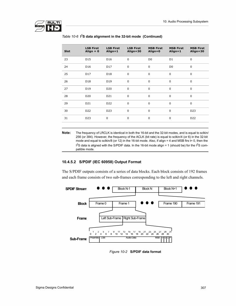
10: Audio Processing Subsystem
Note: The frequency of LRCLK is identical in both the 16-bit and the 32-bit modes, and is equal to sclkin/256 (or 384). However, the frequency of the ACLK (bit rate) is equal to sclkin/4 (or 6) in the 32-bit mode and equal to sclkin/8 (or 12) in the 16-bit mode. Also, if align = 4 and MSB firs t= 0, then the I2S data is aligned with the S/PDIF data. In the 16-bit mode align = 1 (should be) for the I2S com-patible mode.
10.4.5.2 S/PDIF (IEC 60958) Output Format
The S/PDIF outputs consists of a series of data blocks. Each block consists of 192 frames and each frame consists of two sub-frames corresponding to the left and right channels.
SPDIF Stream
31 30
29 27252321191715131197531 2826242220181614121086420
Preamble
Block
Block N-1 Block N Block N+1
Frame 0 Frame 1 Frame 190 Frame 191
Left Sub-Frame Right Sub-FrameFrame
Sub-Frame P C S VLSB Audio Data MSB
Figure 10-2 S/PDIF data format
23 D15 D16 0 D0 D1 0
24 D16 D17 0 0 D0 0
25 D17 D18 0 0 0 0
26 D18 D19 0 0 0 0
27 D19 D20 0 0 0 0
28 D20 D21 0 0 0 0
29 D21 D22 0 0 0 0
30 D22 D23 0 0 0 D23
31 D23 0 0 0 0 D22
Table 10-6 I2S data alignment in the 32-bit mode (Continued)
SlotLSB First Align = 0
LSB First Align=1
LSB First Align=30
MSB First Align=0
MSB First Align=1
MSB First Align=30
307Sigma Designs Confidential

SMP8654-DS-A-10SMP8654 Datasheet
Data bits and preamble coding
Each subframe consists of 32 bits, coded as a sequence of 64 half-bits. Except for the pre-amble, data bits are coded as follows:
• 0 is coded ‘11’ (if preceding half-bit = 0) or ‘00’ (if preceding half-bit = 1)
• 1 is coded ‘10’ (if preceding half-bit = 0) or ‘01’ (if preceding half-bit = 1)
There are three types of preambles:
• B (left sub-frame of the first frame of a block)
• M (left sub-frame of any frame except the first frame of a block)
• W (right sub-frame of any frame)
The three preamble types are coded as follows:
• Preamble B is coded ‘11101000’ (if preceding half-bit = 0) or ‘00010111’ (if preced-ing half-bit = 1)
• Preamble M is coded ‘11100010’ (if preceding half-bit = 0) or ‘00011101’ (if preced-ing half-bit = 1)
• Preamble W is coded ‘11100100’ (if preceding half-bit = 0) or ‘00011011’ (if preced-ing half-bit = 1)
Audio Data
The audio data field carries the 24-bit value written in the SO_LS_DATA/SO_RS_DATA registers. The LSB is transmitted first.
• Bit 0 of the register S0_LS_DATA (or the register S0_RS_DATA) appears at the bit position 4 within the S/PDIF sub-frame
• Bit 23 of the register S0_LS_DATA (or the register S0_RS_DATA) appears at the bit position 27 within the S/PDIF sub-frame
When 16-bit or 20-bit PCM samples are transmitted, they are left aligned on bit 23 of the registers SO_LS_DATA / SO_RS_DATA.
Validity Bit (Subframe Bit 28)
This bit (bit 28 of a sub-frame) is normally set to low to indicate valid data. The S/PDIF interface sets this bit when a data underflow occurs.
308 Sigma Designs Confidential

10: Audio Processing Subsystem
Subcode Data (Subframe Bit 29)
This bit (bit 29 of a sub-frame) is controlled by bit 19 of the register SO_CH_STRL, (default value= 0). Subcode data is used to convey user-specific data.
Channel Status Information (Subframe Bit 30)
This bit is used to carry side information on the S/PDIF stream, including SCMS informa-tion. The S/PDIF specification requires the channel status bit to be equal for both the sub-frames of a frame. Consequently, 192 bits of the channel status information are transmitted during a S/PDIF data block. A register contains the channel status information transmitted during the first 32 frames of a block, LSB first. During the remaining 160 (192-32) frames the channel status bit is set to 0.
Parity (Subframe Bit 31)
This bit is generated by the S/PDIF interface so that bits 4 to 31 (inclusive) of the sub-frame contain an even number of 1‘s (and 0‘s).
10.4.5.3 HDMI v1.3a Output Format
The HDMI v1.3a output supports LPCM and compressed audio. The audio data from the
audio DSP I2S outputs or the S/PDIF output may also be transferred over HDMI. Note that the audio capabilities are dependent on the video format being transmitted over HDMI. For additional information, please see CEA-861D and the HDMI video output section.
10.5 Register Maps
10.5.1 Audio Miscellaneous Registers
Table 10-7 Audio miscellaneous registers
Address1 Register Name R/W/A2 Description
+3E80 MISC_DR_MODE R/W DRAM Read Byte Assemble Mode Reg-ister
+3E81 MISC_DR_CNT R/W/A DRAM Read Byte Count Register
+3E82 MISC_DR_ADD R/W/A DRAM Read Address Register
+3E83 MISC_SBOX_MODE R/W Switchbox Mode Register
+3E84 MISC_DW_MODE R/W DRAM Write Byte Assemble Mode Register
+3E85 MISC_DW_CNT R/W/A DRAM Write Byte Count Register
+3E86 MISC_DW_ADD R/W/A DRAM Write Address Register
309Sigma Designs Confidential

SMP8654-DS-A-10SMP8654 Datasheet
10.5.2 Audio Input Interface Registers
+3E87 Reserved
+3E88 MISC_RESET0 R/W Reset 0 Register
+3E89 MISC_RESET1 R/W Reset 1 Register
+3E8A MISC_INTERRUPT R/W Interrupt Register
+3E8B MISC_TIMER_DIV R/W Timer Divisor Load Register
+3E8C MISC_TIMER_CNT R/A Timer Value (current) Register
+3E8D Reserved
+3E8E Reserved
+3E8F Reserved
+3E90 MISC_SEMAPHORE0 R/W Semaphore 0 Register
+3E91 MISC_SEMAPHORE1 R/W Semaphore 1 Register
+3E92 MISC_SEMAPHORE2 R/W Semaphore 2 Register
+3E93 MISC_SEMAPHORE3 R/W Semaphore 3 Register
+3E94 MISC_SEMAPHORE4 R/W Semaphore 4 Register
+3E95 MISC_SEMAPHORE5 R/W Semaphore 5 Register
+3E96 MISC_SEMAPHORE6 R/W Semaphore 6 Register
+3E97 MISC_SEMAPHORE7 R/W Semaphore 7 Register
1. Address refers to G-Bus byte address relative to the audio block base.2. Read/Write/Auto update.
Table 10-8 Audio input interface registers
Address1 Register Name R/W/A2 Description
+3E40 SI_L1_DATA R/W Audio Input Left Channel 1 Data Reg-ister
+3E41 SI_R1_DATA R Audio Input Right Channel 1 Data Register
+3E42 SI_STATUS R Audio Input Status Register
+3E43 SI_CONF R/W Audio Input Configuration Register
+3E44 SI_SPDIF_STATUS R S/PDIF Status Register
+3E45 SI_L2_DATA R Audio Input Left Channel 2 Data Reg-ister
Table 10-7 Audio miscellaneous registers (Continued)
Address1 Register Name R/W/A2 Description
310 Sigma Designs Confidential

10: Audio Processing Subsystem
10.5.3 Audio Output Interface Registers
+3E46 SI_R2_DATA R Audio Input Right Channel 2 Data Register
+3E47 SI_L3_DATA R Audio Input Left Channel 3 Data Reg-ister
+3E48 SI_R3_DATA R Audio Input Right Channel 3 Data Register
+3E49 SI_L4_DATA R Audio Input Left Channel 4 Data Reg-ister
+3E4A SI_R4_DATA R Audio Input Right Channel 4 Data Register
1. Address refers to G-Bus byte address relative to the audio block base.2. Read/Write/Auto update.
Table 10-9 Audio output interface registers
Address Register Name R/W Description
+3E00 SO_L1_DATA R/W I2S Pair Left Channel 1 Data Register
+3E01 SO_R1_DATA R/W I2S Pair Right Channel 1 Data Register
+3E02 SO_L2_DATA R/W I2S Pair Left Channel 2 Data Register
+3E03 SO_R2_DATA R/W I2S Pair Right Channel 2 Data Register
+3E04 SO_L3_DATA R/W I2S Pair Left Channel Data 3 Register
+3E05 SO_R3_DATA R/W I2S Pair Right Channel 3 Data Register
+3E06 SO_LS_DATA R/W S/PDIF Left Channel Data Register
+3E07 SO_RS_DATA R/W S/PDIF Right Channel Data Register
+3E08 SO_CH_INTR R/W Channel Interrupt Register
+3E09 SO_CH_CTRL R/W Channel Control Register
+3E0A SO_SPDIF_CH_STAT R/W S/PDIF Channel Status Register
+3E0B SO_L4_DATA R/W I2S Pair Left Channel 4 Data Register
+3E0C SO_R4_DATA R/W I2S Pair Right Channel 4 Data Register
+3E0C SO_L5_DATA R/W I2S Pair Left Channel 5 Data Register
+3E0E SO_AUDIO_CLK_DIV R/W Audio Fractional Clock Divider Register (M, N)
+3E0F SO_R5_DATA R/W I2S Pair Right Channel 5 Data Register
Table 10-8 Audio input interface registers (Continued)
Address1 Register Name R/W/A2 Description
311Sigma Designs Confidential
SMP8654-DS-A-10SMP8654 Datasheet
10.6 Pin Description
10.6.1 Audio Input Interface Pins
10.6.2 Audio Output Interface Pins
+3E10 SO_CH_CTRL2 R/W Channel Control 2 Register
+3E11 SO_FIFO_DEPTH1 R Audio Output FIFO Depth 1 Register
+3E12 SO_FIFO_DEPTH2 R Audio Output FIFO Depth 2 Register
Table 10-9 Audio output interface registers (Continued)
Address Register Name R/W Description
Table 10-10 Audio input interface pin descriptions
Pin Name Pin Id Direction Description Driver Type1
1. The letters under the column ‘Driver Type’ denote the DC characteristics of the corresponding pins as detailed in the ‘DC Characteristics’ table of the chapter ‘System Specifications‘.
SI0_BCLK AD3 I Audio input 0 serial bit clock = LRCLKx32 / 64. Maximum fre-quency is 12.288MHz.
J
SI0_DATA1 AD2 I Audio input 0 serial data J
SI0_LRCLK AD4 I Audio input 0 serial left/right clock J
Table 10-11 Audio output interface pin descriptions
Pin Name Pin Id Direction Description Driver Type1
SO0_BCLK AC2 O Audio output 0 I2S audio bit clock output. Maximum frequency is 12.288MHz.
D
SO0_DATA1 AC4 O Audio output 0 I2S channel 1 audio data output
D
SO0_DATA2 AC5 O Audio output 0 I2S channel 2 audio data output
D
SO0_DATA3 AC6 O Audio output 0 I2S channel 3 audio data output
D
SO0_LRCLK AC3 O Audio output 0 I2S audio frame clock output
D
SO0_MACLK AC1 O Audio output 0 audio clock gener-ator master clock output. Maxi-mum frequency is 50MHz.
D
312 Sigma Designs Confidential

10: Audio Processing Subsystem
10.7 Electrical Characteristics
10.7.1 I2S Input AC Electrical Characteristics
10.7.2 I2S Output AC Electrical Characteristics
Table 10-13 I2S Output AC characteristics
Symbol Units Minimum Typical Maximum
FBCLK MHz 12.288 20
TBCLK ns 50
TBCLKL TBCLK 0.48 0.52
TBCLKH TBCLK 0.48 0.52
TVLD ns TBCLKH - 10 TBCLKH + 10
SO0_SPDIF AD1 O Audio output 0 S/PDIF audio data output
E
1. The letters under the column ‘Driver Type’ denote the DC characteristics of the corresponding pins as detailed in the ‘DC Characteristics’ table of the chapter ‘System Specifications‘.
Table 10-11 Audio output interface pin descriptions (Continued)
Pin Name Pin Id Direction Description Driver Type1
Table 10-12 I2S Input AC characteristics
Symbol Units Minimum Typical Maximum
FBCLK MHz 12.288 20
TBCLK ns 50
TBCLKL TBCLK 0.35 0.65
TBCLKH TBCLK 0.35 0.65
TSR ns 10
THTR ns 0
313Sigma Designs Confidential

SMP8654-DS-A-10SMP8654 Datasheet
10.8 Timing Diagram
10.8.1 I2S Audio Input Timing Diagram
Figure 10-3 I2S audio input timing diagram
10.8.2 I2S Audio Output Timing Diagram
TBCLKLTBCLKH
TBCLK
SO0_BCLK
SO0_DATA(5:1)
SO0_LRCLK
TVLD
I2S Output Interfaces
Figure 10-4 I2S audio output timing diagram
TBCLKLTBCLKH
TBCLK
SI0_BCLK
SI0_DATA
SI0_LRCLK
TSRI THTRI
I2S Input Interfaces
SI0_DATA
SI0_LRCLK
TSRI THTRI
DEFAULT MODE
INVERTED CLOCK MODE
314 Sigma Designs Confidential

11 Transport Demultiplexer
11.1 Block Diagram of Transport Demultiplexer
HSF
tdmuxPADS Packet Framer
syncdetect (x3)
ser2par (x3)
PID Filter
PIDFiltering
PID Bank(128 X 64)
Splicing control & PCR extraction
MPM Memory
MPMDirect Access
PF-ODMA 1
RISC32
32-bitRISCCore
Pattern Search
DMEM4K X32
PMEM6K X 32 R
BUS/
LBUS
Arb
iter
32 CRC
Pattern Search
GBUSMaster
Interface
GBUS toLBUS Bridge MISC
IRQ ctl
RST ctl
Semaphor
RBUS IF
DBUS IF
MBUS
GBUS
DBUS
STC Counter
Timer
MBU
S IFW
0R
0
Switch Box
I-DM
A
O-DM
A
DVD
-C
SS
O-CIPH
0I-CIPH0
O-CIPH
1I-CIPH1
DECIPHER
Data Router
AES
RC4
DVB-CSMulti-2
TDES CWRAM(32x512)
Filters
Match Filter
Range Filter
switch box
MPM Arbiter
MPM
1K x
8
1K x
8
1K x
8
1K x
8
Parser Blocks
PF-ODMA 0 Tango3 Only
C2
SPI0
SPI1
TagController
ATS0
ATS
1A
TS2
DVD-CSSC2 SC RAM
Tag Memory
Ch 0
Ch 1
Ch 2
HSF RAM(32X512X3)
SRAM Locations
RC4RAM
TDMXGPIO PADs
GPIO
TDMXTSOUT PADs
TS ODMA
ATS0 ATS1
PCR0 PCR1
OUTIF
CRC32 SPY
Figure 11-1 Transport demultiplexer block diagram
Sigma Designs Confidential 315

SMP8654-DS-A-10SMP8654 Datasheet
11.2 Introduction
The SMP8654 includes an on-chip, RISC processor-based transport demultiplexer (TDMX) unit. The TDMX unit is implemented as 2 identical blocks, each capable of han-dling up to 3 multi-program bitstreams of up to 81Mbps each, with an aggregate total of up to 243Mbps. On-chip demultiplexing supports the following formats:
• DVD-Video, SVCD and VCD bitstreams
• MPEG-1 system bitstreams, MPEG-2 transport and program bitstreams
• MPEG-4 file, MPEG-4.2 over MPEG-2 transport bitstreams
• MPEG-4.10 (H.264) over MPEG-2 transport
• WMV9 ASF or AVI files, SMPTE 421M (VC-1) over MPEG-2 transport
Each TDMX block consists of a dedicated 32-bit RISC processor and parser blocks along with specialized support hardware. The parser block contains a multiport memory (MPM), organized as 1K by 32-bit (4 KB) with 6 independent access ports. The TDMX interfaces with the rest of the chip via the G-Bus and M-Bus datapaths. Additional internal buses connect the various components.
The bit stream data may be input via the transport stream inputs, PCI bus, SATA interface, Ethernet interface, etc. The bitstreams are loaded into the DRAM, processed by the trans-port demultiplexer RISC (including any decryption) and the result is written to the DRAM. The audio and video decoder DSPs then read the data from the DRAM and pro-cess it. The bitstreams and the data not used by the SMP8654 (such as EPG, etc.) are writ-ten to the DRAM and passed on to the middleware for processing.
11.3 Features
• 2 dedicated demultiplexer RISCs (one per 3-channel demux block)
- 32-bit 333MHz RISC CPU core (proprietary) - 16KB Data and 24KB Program memory - Timers and Interrupt controller support
• Compliant DTV standards
- ISO/IEC 13818-1: 2000 - ATSC: A-65B - DVB: ETS 300 428 v.1.4.1 - ARIB: STD-B32 Part 3
316 Sigma Designs Confidential

11: Transport Demultiplexer
• Transport stream input interface
- Any combination of up to three transport or program streams, up to 243Mbps total aggregate
- Hardware/software configurable one parallel and one serial, or three serial input inter-faces
• Conditional access
- Two NRSS-A (ISO-7816 form factor) or smartcard interfaces
• On-chip ciphers
- DES/TDES ECB, CBC and OFB mode support - DVB CS block and stream ciphering core - DVD CSS deciphering core - ARIB Multi-2 deciphering core - C2 for CPPM and CPRM applications - AES ECB, CBC, CTR, CFB and OFB mode support - RC4 - NDS NSA - v1 and v2
• PID filtering
- Up to 256 programmable PID Filters, aggregate - Each input channel has an additional set of six dedicated PID‘s for filtering of PAT,
CAT, PCR, DIT, MGT and Null packets - Flexible packet handling with errors (e.g., duplicated or missing packet detection as
indicated in the continuity counter field of TS header) - Splicing control
• Section filtering
- Up to 32 application controlled 12-byte match mask or range filters per channel. - Each filter block can be configured as either match-mask or range filter - Multiple filter blocks can be linked together in order to increase filtering depth or, to
build a more complex filter
• ECM filtering (per request)
- Up to 8 ECM filters implemented by RISC firmware - Automatic even/odd ECM filter switch - Enables both even/odd ECM‘s after power-up/reset or channel change
• PSI/SI/PSIP processing
- 32-bit hardware based section CRC check
317Sigma Designs Confidential

SMP8654-DS-A-10SMP8654 Datasheet
• PES header filtering
- PTS extraction - Private data stream type filtering - DSM-CC support for VOD, interactive video service or data broadcasting
• Clock recovery
- 6 independent hardware based PCR and STC extraction circuits - Software controlled PCR-jitter filters and output rendering rates - Hardware based DIT support for “partial” TS stream
• Stream record and PVR support
- Full partial programs from multiple TS can be recorded simultaneously - Optional arrival time stamp (ATS) marking for packets being recorded - Optional ATS based input data rate control for recorded streams - Simultaneous pause and playback/record support
11.4 Functional Description
The demultiplexer contains 6 independent transport stream processing channels. This pro-vides the capability to simultaneously handle up to 6 independent transport streams. In addition, program or PES bitstreams from external DRAM can be processed for DVD or PVR applications.
At any given time, all the 6 data processing pipelines can be used for the system clock recovery (by tracking the encoder clock rate). There is an added a flexibility of configur-ing any number of three clock recovery circuits to be associated with any channel. This allows the clocks to be adjusted for more than one program of a given processing pipeline.
The decoder clock frequency is adjusted according to the error terms computed, based on the differences in the value of the extracted PCR and the value of the STC running on the decoder system. The encoder samples its system clock counter periodically, and inserts the value in the bit stream as PCR.
As the decoder receives the sampled value, the current value of the decode system clock counter is compared against the extracted PCR. The difference produces the error term of the clock rates between the two systems. All the AV display clocks in the chip will be gen-erated and synchronized to this adjusted clock. Without this clock recovery scheme, ‘push’ type applications suffer from buffer underflow or over flow as there is limited con-trol over the input data.
318 Sigma Designs Confidential

11: Transport Demultiplexer
The packet framer block provides a seamless interface to various channel decoders (e.g. QAM, QPSK, 8-PSK, FEC) and accepts direct inputs from multiple detachable external conditional access modules, such as the common interface (CI) and the point of deploy-ment (POD) data ports. Pre-recorded data (program stream from a DVD ROM, or HDD etc.) can also be accepted from the external DRAM.
In general, the inputs from the external channel decoders are sourced from the ‘push’ type models in which the application data is transported in unidirectional manner. The receiving device accepts all the data transmitted from the source stream.
The applications whose inputs are coming from the external DRAM are grouped as ‘pull’ type models, where the data is available in a storage media and is supplied as needed. Hence, a full flow-control is employed.
The input to other pipelines can come from both ‘push’ and ‘pull’ types. As a result, the displayed video can suffer from occasional frame dropping or repeating due to the process-ing data rate mismatch if the data is sourced from ‘push’ type applications.
As the transport stream is ‘locked’ (i.e. the sync byte is found at every 188 valid byte inter-val), the packet framer starts to output the packets to the PID filtering block in 32-bit packet aligned fashion. Therefore the TS sync byte (0x47) is always located at the MS byte of the 32-bit output word if the word contains the sync byte. For systems using 192-byte transport streams, the 4-byte header is ignored.
During this process if the sync signal is provided by the interface protocol, then the trans-port sync input can be used to construct the packet-aligned transport stream data. Other-wise, the hardware will search for the transport stream sync byte for packet alignment. In the case of the demultiplexer configured to accept the serial transport stream inputs, the packet framer undergoes a bit-serial to 32-bit word data format conversion.
According to the PID settings, the input data packets are filtered, so that only the selected packets are kept in the MPM. For these selected packets, the PID filter also creates a corre-sponding packet attribute as TAG. This information is stored in the MPM at the end of each packet filtering process.
By saving the tag information at the end of each packet filtering process, the number of entries in the tag memory is always the same as the number of complete packets in the MPM. The tag information contains information like the packet types (e.g. audio, video or system), the payload destinations, the data parsing information and the sync byte location in the MPM. This tag data supplies sufficient information about the packet, so that the pro-cessing time for the RISC is reduced.
319Sigma Designs Confidential

SMP8654-DS-A-10SMP8654 Datasheet
The MPM is comprised of four 1K by 8-bit single port memories for storing the TS pack-ets and another memory (64- by 32-bit) for storing the tag information. The four 1KB MPM memories are stacked side-by-side in order to form one 32-bit by 1K memory. This 32-bit by 1K memory is then segmented into four equal 32x256 memories, each serving as 1KB stream buffers. The first three segments are used to store the transport packets from each TS channel, and the last segment processes of the data streams from the external memory.
This structure allows not only for 32-bit access in a single clock cycle, but also allows the data to be accessed from any byte location of the MPM.
The tag memory holds the packet attributes of the packets stored in the MPM memory. This tag information can be accessed through D-Bus with the assigned address space. The valid address for the last written tag address can be viewed through the status registers in the PID filtering block. Therefore, tracking the register value gives the number of packets newly written to the MPM since the last tag memory access.
The next destination of the packets in MPM is determined based on either the scrambling control status from the packet header or the packet type as indicated by the packet attribute. If the packet is a non-PSI packet, then the RISC firmware routes the payload data to the internal deciphering block.
If the section filter enable attribute is set, then the RISC firmware enables the section fil-tering for the PSI packets. The section filtering can be initiated by writing the section header data to the hardware section filter register, along with the filter enable attribute value that is obtained from the Tag memory.
Once the deciphering process is completed (either via an external CAM module or the internal descrambler), all the payload data in the MPM will be in a clear-text format. The RISC can determine whether any other packet processing needs to be done, before posting the data to the external DRAM.
The final destination of each packet and additional packet parsing are resolved according to the packet attribute information, such as the routing information and the packet types. The packet type attribute elects the firmware filtering actions (e.g. PES filtering for AV data, section/ECM filtering for system data etc.), while the routing information attributes decide the depth of the stream parsing depending on the playback type.
320 Sigma Designs Confidential

11: Transport Demultiplexer
The private data packet type can be used when parsing of the packet is ‘out of norm‘. For example, ATSC standard assigns PID value 0x1FFB to carry multiple tables, such as MGT, VCT, RRT, STT, DCCT and DCCSCT. In addition, SCTE assigns the same PID for emer-gency alert messages. If the application desires to use one independent buffer for each table, and the buffer has been assigned based on the section filter result, the firmware must observe not only the section data passes the two tests applied to PSI packets, but also which of the 32 filters the section passed.
To support trick-mode on recorded data, the payload data may be more closely examined and reformatted to define access units more clearly before it is stored in the external stor-age media. Unlike DVD streams, where the bit stream is created with clear random access points for supporting user interactivity, the access units in terrestrial bit streams are extremely loosely defined.
Although it is nearly impossible to make the access units in terrestrial bit streams as acces-sible as in DVD stream on-the-fly, providing some navigation information in order to make the access points more visible will help greatly the CPU on reducing the computa-tion.
The audio, video PES data and other data associated graphic display will be examined by the RISC for realigning, inserting or removing headers and marking the locations of ren-dering units. Consequently, the application CPU can construct tables, which reflect the structures of the reformatted bit streams in conjunction with the clearly defined access points and their display time stamps. These tables can be stored together with the reformat-ted bit streams.
11.4.1 Packet Framer
The primary purpose of the packet framer block is to accept asynchronous transport streams in order to produce 32-bit packet-aligned data output, along with other packet con-trol signals that are synchronous to the internal system clock.
The main features of this module are:
• This module can receive MPEG TS stream in any of the following 3 configurations:
- Three external serial input ports with data, valid, clock, and/or packet sync signals. The input data clocks can operate at any frequency up to 87.9MHz (81MHz x 204/188). Each parallel port can be configured to accept two serial transport streams; and the host can select any three serial inputs to process.
- One external 8-bit parallel input port and two serials with its own data, valid and/or packet sync signals. When the input port is configured in the parallel mode, the maxi-mum clock rate should be 10.99MHz (10.125MHz x 204/188) which is equivalent to 81Mbps in input data rate.
321Sigma Designs Confidential

SMP8654-DS-A-10SMP8654 Datasheet
- One internal 32-bit OF-DMA input at a maximum average input data rate of 2.53125Mword/sec and two additional streams from external SPI PAD inputs.
• Input TS rate control with ATS TS packet header
• 32-bit Time Stamp for every incoming TS packet during recording
• 32-bit word aligned output data with unified data flow control signals
• Programmable sync byte detection either by the hardware or assisted by the input sync signal
• Automatic sync-lock and sync-loss detection based on software controlled hysterisis mechanism
• Data synchronization to internal system clock
Up to 2 independent channel demodulators can be connected and simultaneously pro-cessed. The interface protocol used by each input channel is independent. The SMP8654 provides up to 3 digital tuner input ports. Tuners from different vendors can be connected at the same time. Each of these tuners can have its own protocol.
Four major logical partitions make up the packet framer: input switchbox, packet align-ment, sync detect and the packet framer output DMA (PF-ODMA) blocks. In order to sup-port concurrent processing of three independent channel interfaces, packet alignment and the sync detect blocks are instantiated three times, while the switchbox and the PF-ODMA are instantiated only once.
The PF-ODMA provides the filtering capability of the TS packets from external the DRAM, such as packets transported over the IP network or recorded in the hard disk. The unfiltered transport stream is temporarily transferred to the MPM from the external DRAM through the IDMA channels. This transport stream is then transferred to the input switchbox via PF-ODMA.
The input switchbox accepts the data traffic from either the input pads or the PF-ODMA and directs it to the assigned processing channels. The signal activities on the input ports are monitored by the input switchbox to see if channel demodulators are connected. When connected, the logic block reports the status to the RISC to communicate with the host CPU in order to obtain the channel routing instructions.
The packet synchronization is performed by the sync detect block. This is done by observ-ing the input data patterns and searching for the sync byte at the fixed packet interval. To prevent any false detection, this block keeps track of the sync state hysterisis by counting the number of consecutive valid packets. Once the packet synchronization is established, complete transport packets are transferred to the PID filtering block after the byte-to-word conversion by the packet alignment block.
322 Sigma Designs Confidential

11: Transport Demultiplexer
11.4.2 PID Filter Block
The PID filter block extracts the PID and compares it against the entries in the PID bank to see if there is any match. This is done by examining the 4-byte transport header of each packet.
The PID bank is a 128x64 memory. It is constructed with four single port 32x64 bit SRAM memories, whose entry represents PID with associated packet attributes. This SRAM can hold up to 128 PID entries that are accessed by all three the PID filtering channels.
The main features of the PID filter block are,
• Firmware based automatic PID switch for splicing control
• Hardware PCR extraction with dedicated PID filter register for each channel
• Handling of an arbitrary fixed packet size of MPEG-2 TS streams.
• Total of 128 general PID entries that can be accessed by all three channels
• Four additional hardwired PID filters for NULL, PAT, CAT and MGT for each channel
• Software controlled TS-level error handling
• Packet continuity check by monitoring the CC field in the TS header
• TAG entry creation for reducing the packet parsing processing load of RISC
• PID Filtering logic can be bypassed, allowing software PID filtering
• User data from the adaptation field extraction by Firmware
No content modification is made to the packet during the PID filtering, meaning. If a match is found, then the whole packet is stored in the MPM along with the packet attri-butes in the TAG memory. When no match is found, the packet is discarded by resetting the write pointer to the previous packet start address.
The packet PID is compared against the PCR PID value before it undergoes the general PID comparisons with the PID bank entries. Each filtering channel contains a dedicated register-based PCR PID whose value can be set by either the host CPU or the RISC. If the PID of a packet matches with that of PCR, then the PCR value in the packet adaptation field is copied to a register for the RISC to initiate the clock recovery process.
The result from PCR PID comparison will not affect the result of the general PID compar-ison. Regardless of the result in PCR PID comparison, the packet PID will be compared against the PID entries in the PID bank as this packet may contain either audio or video payload.
323Sigma Designs Confidential

SMP8654-DS-A-10SMP8654 Datasheet
During the PID filtering process, packet errors are checked in two ways: by examining the state of the transport error indicator (TEI) bit, and by observing the continuity counter (CC) 4-bit field. Depending on the attribute settings for a PID, the packets with are either discarded or stored in the MPM.
The splicing control is also handled by this block by monitoring the splicing counter in the adaptation field. The splicing requires two PID values (these two PID values may be iden-tical). When the splicing is enabled, the splicing logic monitors the splicing counter in the adaptation field of the packets associated with previous PID value, looking for the splicing point. Meanwhile, this logic block continues storing packets with the previous PID value. As the splicing counter reaches zero, the old PID is replaced with the new PID.
The time-base of the new packets need not be the same as that of the old packets. This causes PCR discontinuity. In this case, the host CPU is notified of the nature of PCR dis-continuity, so that the AV display units are handled properly.
Once the PID matching is done successfully, the attributes for the packet is prepared and stored in the TAG memory as the last word of the packet enters the MPM. Therefore, the number of entries in the TAG memory equals to the number of TS packets stored in MPM. The contents of TAG memory include the pre-parsed information such as the type of each packet (i.e. audio, video or system), routing information (i.e. playback or recording) and the packet start address in the MPM. These packet attributes come from both the host and the hardware logic states, in order to facilitate the packet parsing effort by the RISC.
11.4.3 Multi Port Memory (MPM)
The MPM memory has a total capacity of 4K bytes. It is physically implemented using four 1024x8-bit, single port SRAM to allow single cycle access of a 32-bit word at any byte position. These four SRAMs are horizontally stacked side-by-side to construct one 1K-by-32 bit RAM. This 1K-by-32 bit RAM is then vertically partitioned to form four 256-by-32 bit circular buffers, with each buffer identified by channel ID.
Up to 12 clients can be served, one at each clock cycle in the order of the priority each cli-ent is assigned to. In order to prevent starving situation at the low priority clients, hierar-chical priority structure has been designed. The clients are separated into three groups depending on the required bandwidth and the access timing sensitivity.
The first-level priority is assigned by a group, and within the group, a second-level prior-ity has been assigned to each client. There are hard limit, in terms of clock cycles in accessing MPM continuously, imposed on the two top-tier groups so that any clients in the lowest priority group do not wait longer than 8 cycles.
324 Sigma Designs Confidential
11: Transport Demultiplexer
The MPM block also includes several DMA blocks and a pattern search block. These DMA blocks are responsible for transferring data from or to MPM, and the pattern search block is designed to deliver two functionalists: searching for MPEG start_code and check-ing of the data integrity by computing the CRC.
The main features of the MPM are:
• Four 256x32-bit circular buffers with arbitrary word alignment access
• Two-level arbitration scheme with pre-defined maximum wait time
• ODMA with start-code search capability
• Two pairs of DMA channels dedicated to cipher blocks
• Dedicated channel for the D-Bus interface
11.4.4 Cipher Block
The ciphering module contains several modules to encrypt/decrypt the stream data. It sup-ports the following algorithms:
1. DES/Triple DES – (ECB, OFB, CBC)
2. AES – (ECB, OFB, CTR, CBC, CFB)
3. RC4
4. DVD
5. DVB-CSA (decryption only)
6. Multi-2 (ECB, OFB, CBC, CFB)
7. C2 block (ECB, CBC)
The cipher RAM provides a storage space for multiple key sets and the initialization vec-tors. The keys for all the ciphers, except for the DVD and C2, are written to the cipher RAM by the CPU in a secure manner. The DVD keys are written directly to the register space. The read access to any key address space is disabled by the hardware. The CPU informs the demultiplexer RISC of the key sets to be used for descrambling the contents by means of key indices, channel ID and the PID.
325Sigma Designs Confidential

SMP8654-DS-A-10SMP8654 Datasheet
Table 11-1 Cipher RAM code word allocations
Name Configuration Size Key Pairs Num. Words Address Range
TDES 8 8 128 0x2B80 – 0x2BFF
DVB 2 8 32 0x2B60 – 0x2B7F
AES 16 3 96 0x2B00 – 0x2B5F
RC4 8 4 64 0x2AC0 – 0x2AFF
Multi-2 12 8 192 0x2A00 – 0x2ABF
Cipher Block Clock Gating
The clock gating controls disabling of clock inputs for the lower-level blocks that are not in commission. Due to the limited number of data paths, the cipher blocks that can simul-taneously be commissioned is two (the other blocks are idling). By disabling the clock activities during idle time, the power can only be consumed by the active cipher blocks; thus overall power consumption is reduced. As a cipher is decommissioned (i.e. the cipher path for the block is disabled.) the clock will be active for 4 more cycles, and disabled until the path is re-enabled. The clock line for the cipher block will be alive after one clock cycle once the path is connected.
Except for the C2 cipher block, the internal registers of each disabled cipher block are reset to their default values once the clock is inactive. Therefore, the firmware must save the IV values before disabling the cipher data path if cipher chaining is needed.
0 11
0
4 cycles
Main clock
DES clock
Path enable 0
Path enable 1
DES reset
Figure 11-2 Clock gating timings
326 Sigma Designs Confidential

11: Transport Demultiplexer
11.4.4.1 DES Encryption/Decryption Unit
The DES encryption/decryption unit can either encrypt or decrypt a 64-bit data block using the DES or Triple DES algorithm. The supported modes are DES ECB, CBC, OFB and Triple DES TECB TCBC and TOFB, both in encryption and decryption. The configuration is unique for a group of 64-bit data blocks. The number of blocks in a data group is 1 to 255.
Key format
The Triple DES/DES algorithm uses a 56-bit key. However, 8-bit are added to the key (in key[63:0] bits 0, 8…56) to get a 64-bit key (these bits are the parity control bits). These parity bits are not used during encryption or decryption. However, a 64 bit key must be written in the registers. The value of bits 0, 8, 16, 24, 32, 40, 48, 56 of key[63:0] can be anything. Thus, the encryption using the key = 0000000000000000 and the key = 0101010101010101 will exactly be the same.
Data Format
The data interface (input and output) is a standard valid/ready interface. Data block[63:0] = 64‘h0011223344556677. The bytes will be sent in the order: 00 11 22 33 44 55 66 77. Thus the left most byte of the data block is sent for. The left most byte of the output block will be out first. If the encrypted/decrypted bytes received are in the order: 00, 11, 22, 33, 44, 55, 66 and 77, then output enciphered, deciphered block is 64‘h0011223344556677.
Table 11-2 DES encryption/decryption performance
DES - 64-bit to 8-byte Triple DES - 64- bit to 8- byte
One Block 50 Cycles 86 Cycles
Several blocks 34 Cycles 49 Cycles
The total number of clock cycles represents the time between the start of the ciphering and the rising edge of the DES_END. If the number of the blocks is higher than one, then the blocks are received and sent while the other blocks are encrypted.
11.4.4.2 AES Encryption/Decryption Unit
The AES encryption/decryption unit can either encrypt or decrypt a 128, 192 or 256-bit data block using the AES algorithm. The supported modes are ECB, OFB and CTR, both in encryption and decryption. The supported key lengths are 128, 192 and 256-bit indepen-dent of the data block size. The configuration is unique for a group of data blocks. The number of blocks in a data group can be up to 255.
327Sigma Designs Confidential

SMP8654-DS-A-10SMP8654 Datasheet
Data Format
The data interface (input and output) is a standard valid/ready interface. Data block[127:0] = 128‘h00112233445566778899aabbccddeeff. The bytes will be sent in the order: 00 11 22 33 44 55 66 77 88 99 aa bb cc dd ee ff. The left most byte of the data block is sent first. The left most byte of the output block will be out first.
If the encrypted/decrypted bytes received are in the order, 00, 11, 22, 33, 44, 55, 66, 77...ff, then the output enciphered, deciphered block is 128‘h00112233445566778899aabbccddeeff.
Table 11-3 AES encryption/decryption performance
Size of block (byte) 16 16 16 24 24 24 32 32 32
Size of Key1
1. In clock cycle (333MHz clock)
16 24 32 16 24 32 16 24 32
Total Cycles 95 115 130 150 160 170 225 230 245
11.4.4.3 RC4 Encryption/Decryption Unit
The RC4 encryption/decryption unit can encrypt or decrypt data up to 65535 bytes using the RC4 algorithm. This module handles all the key lengths from 8 to 256-bit with 8-bit increments.
Data Format
If the given key is 48-bit long, 7B311D8415F0 then, key_1[31:0]= 32'h7B311D84, key_2[31:0]= 32'h15F00000 and the Length_key [8:0] = 030.
Table 11-4 RC4 encryption/decryption performance
Clock Cycle
First initialization 258 clock cycles
Second initialization 1538 clock cycles
Encrypt\Decrypt first byte 8 clock cycles
Encrypt\Decrypt following byte 6 clock cycles
328 Sigma Designs Confidential

11: Transport Demultiplexer
11.4.4.4 DVD Decryption
The DVD decryption unit is controlled by 5 registers. The controller register indicates the number of bytes to process, typically 2048 for a DVD sector. If the count is programmed to 4095 (reset value), then the DVD decryption block is transparent. The start indicates how many bytes must be transferred before the decryption begins, typically 128 for a DVD sec-tor. In a 2048-byte encrypted sector, the first 128-byte are clear and the last 1920-byte are encrypted. Before starting the decryption, the 40-bit title key must be programmed in the key registers. The two state registers allow a backup of the decryption block internal state. This is required when a context switch occurs while a DVD sector is only partially pro-cessed.
11.4.4.5 DVB-CSA
Typically the 64-bit control words, which are used to ciphering the MPEG-2 bitstream contents by the authoring head end, (scrambling authorization module and conditional access system) are also encrypted and embedded in the same bitstream by the means of EMM and ECM. The ECM carries the control word, while the EMM carries the entitle-ment messages in conjunction with the key to deciphering keys for the control words. These scrambled control words are then extracted and deciphered by the authorized decod-ers. The following figure depicts the key delivery scheme.
SimulationHardware Implemented
ConfomanceMechanism
ScramblingAuthorization
Module
ConfomanceMechanism
Conditional Access System(Proprietary)
Super ScramblingMechanism
Super de-ScramblingMechanism
Control Words(64-bit) Control Words
(64-bit)
Common Keys(64-bit)
Common Keys(64-bit)
Scrambled SignalsPlain Text Plain Text
Figure 11-3 Overview of DVB-CSA
329Sigma Designs Confidential

SMP8654-DS-A-10SMP8654 Datasheet
Once the control words are deciphered, the common keys are obtained by the confor-mance mechanism. This conformance mechanism is a simple combination of addition and modulus operations that can be easily performed by the secure processor before the keys are put to use. The hardware is designed to work with a set of common keys, which has 64-bit in length derived from the 64-bit control word.
Key Transfer
In general, the control words are produced in a pair, namely even and odd keys by the head-end authoring tools and this pair of keys are used to scramble in an alternative fash-ion. One set of the keys is used to scramble the program contents for a fixed time frame. The other set of the keys, is used to scramble the content for the next time frame. These are transmitted through the bitstream. This alternate key transmission mechanism provides the system with enough time for the key delivery, computation and the initialization of the hardware.
The set of the key pair used to scramble the contents is indicated at the scrambling control field in the corresponding transport packet header. Hence, the RISC firmware must pro-gram the key registers with the appropriate set of the keys, before initiating the decipher-ing process by the hardware.
Setting up DMA channels
Because the DVB CSA allows the payload being scrambled at either TS-level or PES level, the DMA channels to (ODMA), or out of (IDMA) the decipher hardware must be properly programmed with the payload byte counts based on the scrambling layer infor-mation. This, scrambling layer information should come from either the security core or the host CPU (as a result of the table parsing).
When the payload is scrambled at TS-level, the payload length is described with the packet length (188-byte) subtracted by the TS headers (4-byte) and the adaptation field length. However, if the packet is scrambled at the PES-level, the PES header length must be excluded from the payload byte count in addition to the ones for the TS-layer payload length computation. Thereby, the PES header will not be scrambled.
The DVB impose the following rules in order to facilitate the decoder hardware imple-mentation in case the authoring head-end chooses the PES-layer scrambling schemes.
1. The PES header is not scrambled.
2. The TS packets containing parts of a scrambled PES packet do not contain an adapta-tion field, with the exception of the TS packet containing the end of the PES packet.
3. The first byte of a PES packet header is the first byte of the TS packet payload.
330 Sigma Designs Confidential

11: Transport Demultiplexer
In addition, a couple of rules described below will also be applied irrespective of whether the payload is scrambled at the TS-layer or the PES-layer.
1. The scrambled PES header does not span over multiple TS packets.
2. The TS packet carrying the start of a scrambled PES packet is filled by the PES header and the first part of the PES packet payload.
3. The end of the PES packet payload is aligned with the end of the TS packet by insert-ing an adaptation field of suitable size.
11.4.4.6 Multi-2
The Multi-2 module provides the encryption and the decryption of the Multi-2 algorithm in all the chaining modes. The module can do an encryption or a decryption in ECB, CBC, CFB and OFB mode with an iteration number from 1 to 255, for data size 1-byte to 255-byte. Though the size of the base data block is 64-bit, it is not necessary for the data size to be a multiple of 64-bit for encryption. Moreover, a packet is not always likely to be a mul-tiple of 8-byte. The base unit is a byte, therefore the module interface for data path will be based on 1-byte. The module loads data by 8-byte and processes it by 8 bytes block. If less than 8-byte remain, then this residual bytes are processed in an OFB mode.
The Multi-2 configuration is done through the D-Bus. The parameters are written into the cipher dedicated RAM. Writing into the configuration register (size of data to process, iter-ation number for the basic Multi-2 algorithm and the chaining mode) starts the module. The module begins to read the system key, the data key and the initial value from the RAM. It then computes the working key, reads the data, processes the data and writes the result back to the RAm. Except for the system keys, the current data, the initial value and the status bit can be read back through the D-Bus. As the last byte of the input data is pro-cessed, the module puts one of its outputs (end) high.
Performance
The performance measures the number of cycles to compute an encryption or a decryption once the module has all the parameters needed to do the computation. Therefore the time needed by the module to load the keys and the initial value from the cipher RAM (mini-mum 24 cycles, 12 values to load, 2 cycles per value) is not taken in the total. Moreover, the following performance asserts no delay in receiving the data from the input and no delay in sending the data to the output.
In the following performance table N is the number of 64-bit size blocks, R is the number of residual bytes, Twork is the number of cycles for the working keys and Tbase is the number of cycles for the base submodule.
331Sigma Designs Confidential

SMP8654-DS-A-10SMP8654 Datasheet
Table 11-5 Performance index for various cases
Round Size N R TWork TBase Cycles Bits/Cycle
1 1 0 1 14 2 23 0.34
1 8 1 0 6 2 29 2.20
16 8 1 0 6 21 48 1.30
32 1 0 1 14 21 62 0.12
32 8 1 0 6 21 68 0.94
32 128 16 0 6 21 698 1.40
32 255 31 7 6 21 1369 1.40
128 255 31 7 6 161 5209 0.39
11.4.4.7 C2 Block Cipher
The C2 Block deciphers the contents that are generated by the Content Protection for Pre-recorded Media (CPPM) licensed authoring devices. This block supports 5 different ciphering modes namely, C2-D, C2-G, C2E, C2-ECBC and C2-DCBC. All the 5 modes are required during the deciphering process. The mode C2-ECBC is used when content is Content Protection for Recordable Media (CPRM) protected and the SMP8654 is used as the decoder.
The functionality of this block is largely partitioned into 3 independent logical blocks: C2 register, C2 control and C2 stream blocks.The C2 register block is responsible for the D-Bus interface to configure the necessary parameters including the Secret Constant RAM and other data blocks to be processed. Once the D-Bus programming is completed, the C2 control block uses the configuration parameters to generate the data flow control timings based on its state machine.
The stream key generation and data ciphering are performed by the C2 stream block. Depending on the mode of operation, the ciphered data will be routed to either the output port of the cipher or the D-Bus registers.
When the cipher is in the CBC mode, the ciphering is applied to the data from the input cipher ports, allowing the chaining mode for the successive input data blocks. Unlike the CBC modes in other cipher modules (like AES or Multi-2), the cipher key is updated for each data block. Hence in C2, the CBC chaining mode is called the converted CBC mode as the cipher key is chained as opposed to the ciphered data in the other cipher modules.
332 Sigma Designs Confidential

11: Transport Demultiplexer
Once the C2 cipher block configuration is completed, it starts accepting the input data block from the input ports using the ready/valid protocol. Due to the C2-CBC algorithm, the first block takes 16 clock cycles longer then consecutive data blocks to generate the stream key. Two internal 64-bit buffers are provided at the block IO ports in order to elim-inate the delays caused by the 64-bit block conversion from eight 8-bit bytes.
Performance
For a data block of 240,or 1920 bytes, the C2 ciphering in the CBC mode will consume,
Num_cycles = 20 + (4 x [240-1]) + (30 x 240) + (2 x 240) + 16 = 8672 clock cycles.
This yields 1.77bits/cycle of total ciphering performance or 1.88bits/cycle without consid-ering the IO transactions. Unlike the CBC operation, the ECB mode and the one-way func-tion always apply the ciphering process block-by-block. Num_cycles = 2 + 20 + 30 + 1 = 53 cycles/block.
11.4.5 Clock Recovery Process
In the MPEG system it is assumed that the network has a constant end-to-end delay, and the encoded bit stream is delivered to the decoder over the constant delay network. The elapsed time between two time instances; capturing of a frame by the encoder and the dis-playing the frame by the decoder, is constant. This delay is independent of both the coding type of a frame (i.e. I, P and B), and of the network types the data is transmitted over (e.g. ATM, SONNET, DBS etc.).
Due to the packet based processing nature of the network, the instantaneous bit rate of the network is not always constant. Rather, in most of the cases, the bit rate is burst and intro-duces jitter. Consequently, the constant network delay model fails in most real time appli-cations. Typically, a well-behaved system accommodates the network jitter by putting a large amount of smoothing buffer at the decoder front end so that the output of the smooth-ing buffer is constant.
The clock recovery scheme at the decoder end has been developed based on the constant network delay assumption, by transporting the periodically sampled encoder system time to the decoder as part of the coded bit stream. These sampled time stamps are used to adjust the decoder clock frequency by comparing against its local time stamps.
333Sigma Designs Confidential

SMP8654-DS-A-10SMP8654 Datasheet
The difference between the two time stamps (one from encoder and the other from the decoder) is fed back to the clock controller for frequency adjustment. When the decoder clock continuously runs faster than the encoder clock, the decoder does not get enough data, causing the same frame to be displayed repeatedly to fill the gap. When the fre-quency of the decoder clock is lower than that of the encoder, the amount of data from encoder is more than the decoder can handle, causing the dropping of data (frames) in order to keep up with the encoder.
Therefore, to avoid losing or repeating the frames, the encoder and decoder share a com-mon time-base that synchronizes the display rate of decoded audio, video and other asso-ciated data. This also reduces the number of buffers needed for maintaining the appropriate frame rates, regardless of the amount of the data required for encoding a frame.
The clock reference resides within the MPEG packet. Although, the decoder can use other means to synchronize to the encoder clock, the use of a digital phase locked loop circuitry (DPLL) is discussed in this section.
For the decoder to decode and to display an MPEG bit stream, it should be able to generate a clock whose characteristics are the same as the encoder clock that produces the bit stream. Normally, a PLL is composed of the following parts: a reference clock, a system clock, a frequency multiplier and divider, a charge pump and control, a low pass filter and a voltage controlled oscillator (VCO). In a typical MPEG system, the PLL circuit consists of the following with all frequency multiplier and divider constants being 1:
1. Periodically sampled encoder system time stamps (SCR or PCR) as the clock refer-ence.
2. Decoder system clock as the system clock.
3. PCR and STC compare as phase and frequency detectors.
4. Digital low pass filter and scaler and 12-bit DAC as the charge pump and controllers.
5. Analog low pass filter as the low pass filter to the VCO.
6. VCXO as the VCO.
When the demultiplexer detects the PCR information from the bit stream, it samples the current system STC value as it extracts the last bit of the PCR value from the bit stream. The local STC value is subtracted from the extracted PCR and the difference is forwarded to the CPU for further computation. This value is used to provide fine adjustment to the 27MHz system clock frequency. The local STC up-counters are driven by this system clock, and have the same relationship as PCR or SCR. The counter values are sampled and compared whenever the availability of a PCR is detected from the bit stream.
334 Sigma Designs Confidential

11: Transport Demultiplexer
Both SCR and PCR are sampled at the 27MHz encoder clock and transmitted in two pieces, a 33-bit PCR base, sampled at 90KHz and a 9-bit PCR extension, sampled at 27MHz.
Since the PCR is sampled at the time when the last bit of the 33-bit base leaves the encoder, the MPEG spec requires this value to be compared against the value of the STC counter when LSB of the PCR base enters the decoder.
11.4.6 Section/ECM Filtering
512x32SRAM
RAM Controller
CSR
Match
RangeFilter Controller
ControlRegisters
StatusRegisters
HSF RAMInterface logic
Figure 11-4 Hardware section filter
This demultiplexer supports various filtering schemes that applies to the sections from PSI/SI/PSIP and private tables. The section filtering schemes are typically applied to the clear text packets after the PID filtering and the de-scrambling operations. The section headers embedded in the payload part of all general PIDs from the PID bank as well as the dedicated, fixed PIDs can be filtered. The packets that need to be filtered are indicated by the saved packet attribute set during the PID filtering. Their packet types are defined as system or private data. The RISC collects this information by reading the TAG memory.
The hardware performs 32 match or range section-filtering for more complicated section header filtering. The RISC performs simple ECM filtering. However, the hardware can be set up to perform ECM filtering as well.
335Sigma Designs Confidential

SMP8654-DS-A-10SMP8654 Datasheet
The section filter is a combination of 32 12-byte match/mask filters, or 12-byte range fil-ters. Simultaneous operation of both types of section filters is permitted by indicating the applied filter type in the Link byte of the filter. The filtering vectors are stored in the HSF RAM.
11.4.6.1 Section Filtering
Match/Mask Section Filtering
Each of the 32 filters can be applied to any of the general PID entries in the PID bank or other dedicated PSI/SI PIDs from each channel. Each filter is made of 12 sets of match, mask and mode bytes. Each bit of the 12-byte section filter is configured to mask or match (either a positive match or a negative match as indicated in the mode vector). The filtering operation consists of a bit-wise comparison between the section header and a compare vector.
A byte is taken from the section header and compared bit-by-bit, against the correspond-ing byte from the compare vector. This bit-wise comparison is carried out in two indepen-dent operations, one for positive and one for negative match operation according to the mode vector setting. A logic state 1 in the mode vector represents a positive operation, and a logic state 0 represents a negative operation.
The comparison is considered a match if all the bits match in the positive mode and at least one of the bits does not match in the negative mode. A mask is applied bit-wise to the results from the comparison. The result vector is AND operated with the mask vector in order to sort out only the match result of interest.
It is possible to enable multiple filters for the same section header. In this case, all the applied filtering outputs will be logically ANDed (or ORed) by the RISC firmware. This results in the section to be posted to the memory if all (or any) the selected filters pass.
The HSF RAM holds the vectors for the section filtering. Each section filter consists of a set of 12-byte compare (C vector), mode (N vector), mask (M vector) values and a link. The link is used to chain the filters in a linked list for comparison. Linking increases the filtering depth, but the processing time is longer. To reduce the load of the RISC CPU, the firmware filters 4-byte at a time and to stops the filtering processing when a mismatch is found. It moves on to the next filter, if the filter is not the end-of-link.
Each filter consumes 0x30 bytes in the system address space. The filter starting address can be obtained quickly by multiplying the filter number n with 0x30 (n times 0x30).
336 Sigma Designs Confidential

11: Transport Demultiplexer
Range Filter
The section range filtering compares the values of a byte from a section header, against a range specified for the byte in the section range filter. A section range filter consists of a minimum compare vector (Cmin), a maximum compare vector (Cmax), a minimum mask vector (MinM), a maximum mask vector (MaxM), function vector (FN) and a link value (LNK). Each of the Cmin and Cmax filtering vectors is 12-byte, FN is 12-bit and LNK is 8-bit, and are written by the applications in the HSF RAM area.
The operational range function is defined by the value of the FN byte. Each bit of the FN byte represents the corresponding compare byte range check operation. If a bit in FN is 0, then the operation on the corresponding byte is an ‘inner range’ check, or else it is an ‘outer range’ check.
11.4.6.2 ECM/EMM Filtering
The ECM filter mechanism allows selective transfer of new ECM messages to the external DRAM. It is used to eliminate the repeated ECM information from reaching the host CPU. The RISC supports up to 8 independent ECM filters, if the ECM bit CONSTRUCT fol-lows the private section syntax format, or when the section is PES packetized as defined in ISO/ISE 13818-1.
The filtering will be performed by comparing the table id or the first byte of the PES pay-load. The STREAM_ID will be a part of the filtering process if the section is PES pack-etized. The host sets the 8-bit PID attributes, in addition to the 3-bit PID PTI for each ECM PID with proper values, before applying the ECM filters to the packets.
Usually, broadcasters transmit even or odd ECM packets, updated every few seconds in an alternating fashion. At power-up (or after user changes the programs), the host configures the PID attributes to receive both ECM in order to descramble the selected program prop-erly. Once both the ECM‘s are obtained, the host configures the attribute settings again in order to receive the odd or even ECM information.
11.4.7 Arrival Time Stamp (ATS)
Some applications require generating non MPEG compliant transport streams. This block is used for controlling the input data flow based on this ATS information, or inserting ATS when desired. All ATS related control registers are located at D-Bus address of 0x3XXX range in order to allow the CPU to control directly.
337Sigma Designs Confidential

SMP8654-DS-A-10SMP8654 Datasheet
11.4.7.1 ATS Extraction
Each stream processing channel in the SMP8654 provides the ATS extraction capability. When this feature is enabled, the first ATS value that the logic encounters is loaded onto the ATS counter. The ATS value of each subsequent packet is compared against the cur-rent value of the ATS counter. The result of this ATS comparison is reflected in the status bit. This bit value is used to control the output data rate of this block. The logic block will set the status bit when the ATS counter value is greater than the packet ATS.
The clock rate of the ATS counter can be programmed with 4 different options; 27MHz, system clock, system clock divided by 2 or, system clock divided by 4. Typically it is 27MHz.
11.4.7.2 ATS Pause
In order to accommodate possible trick mode operation, ATS pause control bit is provided. The ATS counter will not be incremented when this bit is set.
11.4.7.3 ATS Insertion
A 32-bit ATS counter value can also be attached to each incoming packet. The counter value and clock speed can be programmed with any desired value. The logic extracts the current value of ATS counter as TS sync is detected, and inserts the value at the beginning of the packet, constructing 192 byte packets. This feature, ATS insert can not be used when ATS extract is enabled.
11.4.8 DIT Detection
When the input TS stream is sourced from a digital storage devices saved over IEEE 1394, the stream may be a “partial TS”. DVB-SI specification restricts PSI usage in partial TS stream. One of the mandated tables is DIT, whose presence in the stream indicates a dis-continuity in time occurs in the stream. The hardware detects the presence of the table and generates an interrupt for handling of time discontinuity.
338 Sigma Designs Confidential

11: Transport Demultiplexer
11.5 Pin Description
11.5.1 Transport Demultiplexer Pins
Table 11-6 SPI transport stream interface pin descriptions
Pin Name Pin Id Direction Description Driver Type1
1. The letters under the column ‘Driver Type’ denote the DC characteristics of the corresponding pins as detailed in the ‘DC Characteristics’ table of the chapter ‘System Specifications‘.
TSI0_CLK C3 I SPI port clock input data is trans-ferred on the positive-going edge of this clock. When the port is operated in the SSI mode, this pin is not used.
K
TSI0_D0 D2 I SPI input data bit 0 (LSB). When the port is operated in the SSI mode, this pin is the SSI0_DATA input.
J
TSI0_D1 D1 I SPI input data bit 1. When the port is operated in the SSI mode, this pin is the SSI0_CLK input.
J
TSI0_D2 C1 I SPI input data bit 2. When the port is operated in the SSI mode, this pin is the SSI0_SYNC input.
J
TSI0_D3 B1 I SPI input data bit 3. When the port is operated in the SSI mode, this pin is the SSI0_VLD input.
J
TSI0_D4 E5 I SPI input data bit 4. When the port is operated in the SSI mode, this pin is the SSI1_DATA input.
J
TSI0_D5 A2 I SPI input data bit 5. When the port is operated in the SSI mode, this pin is the SSI1_CLK input.
J
TSI0_D6 B3 I SPI input data bit 6. When the port is operated in the SSI mode, this pin is the SSI1_SYNC input.
J
TSI0_D7 C4 I SPI input data bit 7 (MSB). When the port is operated in the SSI mode, this pin is the SSI1_VLD input.
J
TSI0_SYNC C2 I SPI sync (selectable polarity, active high/low). Identifies the first byte of a packet. When the port is operated in the SSI mode, this pin is not used.
J
TSI0_VLD D3 I SPI data valid (active high). Indicates valid transport packet bytes. When the port is operated in the SSI mode, this pin is not used.
J
TSI1_IN_DATA E4 I SSI2_DATA input J
TSI1_IN_CLK E3 I SSI2_CLK input J
TSI1_IN_SYNC E2 I SSI2_SYNC input J
TSI1_IN_VLD E1 I SSI2_VLD input J
339Sigma Designs Confidential

SMP8654-DS-A-10SMP8654 Datasheet
11.6 Electrical Characteristics
11.6.1 Transport Demultiplexer AC Electrical Characteristics
11.6.1.1 8-bit Parallel (SPI) Input Mode
11.6.1.2 Serial Input (SSI) Mode
Table 11-8 Transport demultiplexer AC characteristics
Symbol Units Minimum Typical Maximum
TTSCLK ns 12.35
TTSCLKH ns 4.9
TTSCLKL ns 4.9
TTSDSU ns 4
TTSDH ns 1
Table 11-7 Transport demultiplexer AC characteristics
Symbol Units Minimum Typical Maximum
TTSCLK ns 98.77
TTSCLKH ns 3 x tSYSCLK
TTSCLKL ns 3 x tSYSCLK
TTSDSU ns 0
TTSDH ns 4 x tSYSCLK
340 Sigma Designs Confidential

11: Transport Demultiplexer
11.7 Timing Diagrams
TSI0_CLK
TTSDSU TTSDH
TTSCLKL TTSCLKH
TTSCLKH TTSCLKL
TSI0_CLK(inv)
TSI0_IN_D(n)TSI0_IN_VLDTSI0_IN_SYNC
TTSCLK
Figure 11-5 TS input timing diagram
11.7.1 Supported Transport Stream Input Interfaces
Serial Data Input Protocol
Clock
47 00 BA 46 73 E3 55 12 A7 C7 47 00 BA E5
188 X 8 Cycles
Sync
Data
Figure 11-6 Clock, Data, Sync Protocol
The above figure shows the 3-pin interface protocol, where the sync signal indicates the start of a packet. With this protocol, the data is assumed to be valid for next 188 x 8 clock cycles, and any data after 188th clock cycle will be discarded until a new sync is asserted
Clock
47 00 BA 46 73 E3 55 12 A7 C7 47 00 BA E5
188 X 8 Cycles
Data
Valid
Figure 11-7 Clock, Data, Valid Protocol
341Sigma Designs Confidential

SMP8654-DS-A-10SMP8654 Datasheet
Another possible 3-pin interface is shown in the above figure. In this protocol, the valid signal qualifies the data at the corresponding clock cycle. Since the channel decoder pro-cesses packet-wise data transfer in general, the valid signal is asserted during the entire packet time frame. However, with this protocol, intra-packet gaps are allowed, i.e., the channel decoder can de-assert the valid signal at any clock cycle.
Clock
47 00 BA 46 73 E3 12 A7 C7 47 00 BA E5
188 X 8 Valid Cycles
Data
Valid
Sync
Figure 11-8 Clock, Data, Sync, Valid Protocol
The above figure shows a 4-pin input interface that is composed of clock, data, sync and valid signals. The assertion of sync indicates the start of a packet, while the valid signal qualifies the validity of the data at the clock cycle. Although, a de-assertion of the valid signal from the channel decoder during each packet time frame (i.e. 1503 subsequent cycles after sync is asserted) is unlikely due to the nature of FEC coder, this demultiplexer allows inter-packet gaps.
Clock
47 00 BA 46 73 12 A7 C7 47 00 BA E5
188 X 8 Valid Cycles
Data
FEC_ERR
Pkt_clk
E3 55
Bad Packet Good Packet
Figure 11-9 Traditional TS Input Protocol
The above figure depicts the traditional serial input interface where the interface is com-posed of four signals: channel clock (clock), clock valid (PKT_CLK), FEC error (FEC_ERR) and serial data (data). When the valid signal in the previous protocol is replaced with the inverted FEC error signal, this protocol can be treated the same as the clock, valid, data 3-pin interface protocol.
342 Sigma Designs Confidential

11: Transport Demultiplexer
Parallel Data Input Protocol
Clock
47 00 BA 46 73 12 A7 C7 47 00 BA E5
188 Valid Cycles
Data
Valid
Sync
E3 55
Figure 11-10 Parallel Input Protocol
The 11-pin parallel input protocol is shown in the above figure. This protocol consists of the same signals as in the clock, data, sync, data protocol except for the 8-bit data inter-face. Unlike the other serial input protocols, the 8-bit data is latched at each rising edge of the channel clock.
343Sigma Designs Confidential

SMP8654-DS-A-10SMP8654 Datasheet
344 Sigma Designs Confidential

12 Pin Information
12.1 Pin Layout
Top left quadrant See figure 11.2
Top right quadrant See figure 11.3
Bottom right quadrant See figure 11.5
Bottom left quadrant See figure 11.4
Figure 12-1 Overview of SMP8654 BGA (844 BGA)
Sigma Designs Confidential 345

SMP8654-DS-A-10SMP8654 Datasheet
1 2 3 4 5 6 7 8 9 10 11 12 13 14 15
ATSI0_D5 GPIO4 GPIO10
VDD_1V8 DRAM1_DQ29 VSS DRAM1_
DQS3DRAM1_
DQ27 VDD_1V8 DRAM1_DQ28
DRAM1_ODT
DRAM1_CK#
DRAM1_CK
DRAM1_A1
BTSI0_D3
VSSTSI0_D6 GPIO5 GPIO11
VSS DRAM1_DQ24
DRAM1_DQS3#
DRAM1_DQ26
DRAM1_DQ30 VDD_1V8 DRAM1_
DQ22 VDD_1V8 VSS DRAM1_A4
CTSI0_D2
TSI0_SYNC TSI0_CLK TSI0_D7 GPIO6 GPIO12
VDD_1V8 DRAM1_DQ31 VSS DRAM1_
DM3DRAM1_
DQ25DRAM1_
DM2DRAM1_RAS#
DRAM1_CAS#
DRAM1_A6
DTSI0_D1 TSI0_D0 TSI0_VLD VDD_3V3 GPIO0 GPIO7 GPIO13
VSSDRAM1_VREFSST
L4
DRAM1_DQ16
DRAM1_DQS2 VSS DRAM1_
CS#DRAM1_
A0 VDD_1V8
ETSI1_D3 TSI1_D2 TSI1_D1 TSI1_D0 TSI0_D4 GPIO1 GPIO8 GPIO14
VDD_1V8 DRAM1_DQ21
DRAM1_DQS2#
DRAM1_DQ19
DRAM1_DQ20 VDD_1V8 DRAM1_
A8
FXTAL_IN WDO
VSS XTAL_BUF
XTAL_DISC
VSSGPIO2 GPIO9 GPIO15
VSS DRAM1_DQ23
DRAM1_DQ18
DRAM1_DQ17
DRAM1_A4H
DRAM1_A13
G XTAL_OUT
RCLK0_IN
RCLK0_OUT VDD_3V3 TEST RESET# VDD_3V3 GPIO3 VDD_3V3
VSS VDD_1V8 VDD_1V8DRAM1_VREFSST
L3VDD_1V8 VSS
H RCLK1_OUT
RCLK3_OUT
VSS NC VSS_PLL2
VSS_PLL1
VSS_PLL0
VSS VSS VSS VDD_1V8 VSS VDD_1V8 VSS VDD_1V8
JVI1_HS VI1_VLD VI1_VS
NC VDD_PLL2_3V3
VDD_PLL1_3V3
VDD_PLL0_1V0
VSS
KVI1_P7 VI1_P6 VI1_P5 VI1_P4 VI1_P3 VI1_P2
VSSVDD_3V3
VDD_1V0 VSS VSS VDD_
1V0VDD_1V0 VSS
LVI1_CLK VI1_P1 VI1_P0
HDMITX_SCL
HDMITX_SDA
HDMITX_HPD
VSSVDD_3V3
VSS VDD_1V0
VDD_1V0 VSS VSS VDD_
1V0
M HDMITX_TXC_P
HDMITX_TXC_N
HDMITX_VSS_TXC
HDMITX_VDD_PLL
A_3V3
HDMITX_VSS_PLL
A
HDMITX_AVSS_0 VSS
VDD_3V3VSS VDD_
1V0VDD_1V0 VSS VSS VDD_
1V0
N HDMITX_TX0_P
HDMITX_TX0_N
HDMITX_VSS_TX0
HDMITX_VDD_TX0
_3V3
HDMITX_AMON
HDMITX_VDD_1V0
_0
HDMITX_AVDD_1V
0_0VSS VDD_
1V0 VSS VSS VDD_1V0
VDD_1V0 VSS
P HDMITX_TX1_P
HDMITX_TX1_N
HDMITX_VSS_TX1
HDMITX_VDD_TX1
_3V3
HDMITX_REXT
HDMITX_VDD_1V0
_1
HDMITX_AVDD_1V
0_1VSS VDD_
1V0 VSS VSS VDD_1V0
VDD_1V0 VSS
Figure 12-2 SMP8654 pin diagram (top left quadrant)
346 Sigma Designs Confidential

12: Pin Information
16 17 18 19 20 21 22 23 24 25 26 27 28 29 30
VDD_1V8 DRAM1_BA1
DRAM1_CKE VSS VDD_1V8 DRAM1_
DQ13 VDD_1V8 DRAM1_DQS1#
DRAM1_DQ11 VSS DRAM1_
DQ12 SCARD1_CLK
SCARD1_RST
SCARD0_RST
A
DRAM1_A10
DRAM1_BA2 VDD_1V8 DRAM1_
WE#DRAM1_DQS0# VSS DRAM1_
DQ15DRAM1_DQS1
DRAM1_DM1
DRAM1_DQ9 VDD_1V8 SCARD1_
FC#SCARD0_
CLK VDD_3V3NC B
DRAM1_A11
DRAM1_BA0
DRAM1_A9 VSS DRAM1_
DQS0DRAM1_
DQ8DRAM1_
DQ4DRAM1_
DQ10DRAM1_
DQ14 VSS SCARD1_IO
SCARD0_FC#
VSS UART1_DTR
UART1_RX
C
VSS VDD_1V8 DRAM1_A7
DRAM1_DQ7 VDD_1V8 DRAM1_
DQ3 VSSDRAM1_VREFSST
L0VDD_1V8 SCARD1_
CTL2SCARD0_
IO VDD_3V3UART1_R
TSUART0_T
X
DRAM0_DQ29 D
DRAM1_A2
DRAM1_A5 VDD_1V8 DRAM1_
DQ5DRAM1_
DQ2DRAM1_
DM0DRAM1_
DQ1 VSS SCARD1_CTL1
SCARD0_CTL2
JTAG_UART1#
UART1_TX
VDD_1V8
DRAM0_DQ24 VSS E
DRAM1_A5H
DRAM1_A12
DRAM1_A3
DRAM1_DQ0 VSS DRAM1_
DQ6 VSS SCARD1_CTL0
SCARD0_CTL1 VDD_3V3
UART1_DCD
UART0_RX
DRAM0_DQ31
DRAM0_DQS3#
DRAM0_DQS3 F
DRAM1_VREFSST
L2VSS VDD_1V8
DRAM1_VREFSST
L1VDD_1V8 VDD_1V8 VSS SCARD0_
CTL0VSS UART1_D
SR
VDD_1V8
DRAM0_VREFSST
L4VSS DRAM0_
DQ26DRAM0_DQ27 G
VSS VDD_1V8 VSS VDD_1V8 VDD_1V8 VSS VSS VSS UART1_CTS
VSS DRAM0_DQ21
DRAM0_DQ16
DRAM0_DM3
DRAM0_DQ30
VDD_1V8 H
VSS VDD_1V8
DRAM0_DQ23
DRAM0_DQS2#
DRAM0_DQS2
DRAM0_DQ25 VSS DRAM0_
DQ28 J
VSS VDD_1V0
VDD_1V0 VSS VSS VDD_
1V0 VSS VDD_1V8 DRAM0_DQ18
DRAM0_DQ19 VDD_1V8 DRAM0_
DM2DRAM0_DQ22
DRAM0_ODT K
VDD_1V0 VSS VSS VDD_
1V0VDD_1V0 VSS VDD_1V8
DRAM0_VREFSST
L3
DRAM0_DQ17
DRAM0_DQ20
DRAM0_CS#
DRAM0_RAS# VDD_1V8 DRAM0_
CK# L
VDD_1V0 VSS VSS VDD_
1V0VDD_1V0 VSS VSS VDD_1V8 DRAM0_
A4H VSS DRAM0_A0
DRAM0_CAS# VSS DRAM0_
CK M
VSS VDD_1V0
VDD_1V0 VSS VSS VDD_
1V0 VDD_1V8 VSS DRAM0_A13
DRAM0_A8 VDD_1V8 DRAM0_
A6DRAM0_
A4DRAM0_
A1 N
VSS VDD_1V0
VDD_1V0 VSS VSS VDD_
1V0 VSSDRAM0_VREFSST
L2
DRAM0_A5H
DRAM0_A2 VSS DRAM0_
A11DRAM0_
A10VDD_1V8 P
Figure 12-3 SMP8654 pin diagram (top right quadrant)
347Sigma Designs Confidential

SMP8654-DS-A-10SMP8654 Datasheet
R HDMITX_TX2_P
HDMITX_TX2_N
HDMITX_VSS_TX2
HDMITX_VDD_PLL
B_3V3
HDMITX_VSS_PLL
B
HDMITX_VSS_1 VSS
VDD_3V3VSS VDD_
1V0VDD_1V0 VSS VSS VDD_
1V0
TVO1_Y
VO1_AVSS_Y
VO1_AVDD_Y
VO1_RSET
VO1_AVSS
VSS VSSVDD_3V3
VSS VDD_1V0
VDD_1V0 VSS VSS VDD_
1V0
UVO1_V
VO1_AVSS_V
VO1_AVDD_V
VO1_VREF
VO1_AVDD
VSSVDD_3V3
VSS VDD_1V0 VSS VSS VDD_
1V0VDD_1V0 VSS
VVO1_U
VO1_AVSS_U
VO1_AVDD_U
VSSVDD_3V3
VSSVDD_3V3
VSS VDD_1V0 VSS VSS VDD_
1V0VDD_1V0 VSS
WVO2_Y
VO2_AVSS_Y
VO2_AVDD_Y
VSSVDD_3V3
VSS VSSVDD_3V3
VSS VDD_1V0
VDD_1V0 VSS VSS VDD_
1V0
YVO2_V
VO2_AVSS_V
VO2_AVDD_V
VO2_VREF
VO2_AVDD
VSS VSSVDD_3V3
VSS VDD_1V0
VDD_1V0 VSS VSS VDD_
1V0
AAVO2_U
VO2_AVSS_U
VO2_AVDD_U
VO2_RSET
VO2_AVSS
VSS VSSVDD_3V3
VDD_1V0 VSS VSS VDD_
1V0VDD_1V0 VSS
AB VSS VSSVDD_3V3 VDD_3V3
VSS VSSVDD_3V3
VSS
AC SO0_MACLK
SO0_BCLK
SO0_LRCLK
SO0_DATA1
SO0_DATA2
SO0_DATA3 VDD_3V3
VSS VSSVDD_3V3 VDD_3V3 VDD_3V3
VSS VSSVDD_3V3
AD SO0_SPDIF
SI0_DATA1 SI0_BCLK
SI0_LRCLK
ETH0_MDINT#
ETH0_MDIO
VSSVDD_3V3 VDD_3V3
VSS VSS VSSUSB20_VDDC_1V0_0
USB20_VDDAC_3V3
USB20_VSSAC
AE ETH0_MDC
ETH0_RX_ER
ETH0_CRS
ETH0_RX_DV
ETH0_RXD0 VDD_3V3
ETH1_COL
SATA_TMS
VSS VSS SATA_REXT
VSS USB20_VSSC_0
USB20_VDDAC_3V3
USB20_VSSAC
AF ETH0_RXD1
ETH0_RXD2
ETH0_RXD3
ETH0_RXCLK
VSS ETH1_TXD0
ETH1_TX_EN
SATA_TDI SATA_VP
SATA_REFCLKM SATA_VP SATA_VP
USB20_VDDAT_3V3_0_0
USB20_VDDAT_3V3_0_1
USB20_VDDAT_3V3_1_0
AG ETH0_TXCLK
ETH0_TXD0
ETH0_TXD1 VDD_3V3
ETH1_RXD1
ETH1_TXCLK
ETH1_TX_ER
SATA_TDO
SATA_VPH
SATA_REFCLKP
SATA_VPH
SATA_VPH
USB20_VSSAT_0
USB20_VSSAT_0
USB20_VSSAT_1
AH ETH0_TXD2
ETH0_TXD3
VSS ETH1_RX_ER
ETH1_RXD0
ETH1_RXCLK
ETH1_TXD3
SATA_TCK
VSS VSS VSS VSS USB20_VSSAT_0
USB20_VSSAT_C
USB20_VSSAT_C
AJ ETH0_TX_ER VDD_3V3
ETH0_TX_EN
ETH1_MDC
ETH1_RX_DV
ETH1_RXD3
ETH1_TXD2 VDD_3V3
SATA_TXN1
SATA_RXP1
SATA_RXN0
SATA_TXP0
USB20_DP_0
USB20_REXT
USB20_ATEST
AK ETH0_COL
ETH1_MDINT#
ETH1_MDIO
ETH1_CRS
ETH1_RXD2
ETH1_TXD1
VSS SATA_TXP1
SATA_RXN1
SATA_RXP0
SATA_TXN0
USB20_DM_0
USB20_XO USB20_XI
1 2 3 4 5 6 7 8 9 10 11 12 13 14 15
Figure 12-4 SMP8654 pin diagram (bottom left quadrant)
348 Sigma Designs Confidential

12: Pin Information
VDD_1V0 VSS VSS VDD_
1V0VDD_1V0 VSS VDD_1V8 VSS DRAM0_
A12DRAM0_
A5 VDD_1V8 DRAM0_BA0
DRAM0_BA2
DRAM0_BA1 R
VDD_1V0 VSS VSS VDD_
1V0VDD_1V0 VSS VSS VDD_1V8 DRAM0_
A3VSS DRAM0_
A7DRAM0_
A9 VDD_1V8 DRAM0_CKE T
VSS VDD_1V0
VDD_1V0 VSS VSS VDD_
1V0 VDD_1V8DRAM0_VREFSST
L1
DRAM0_DQ0
DRAM0_DQ5
DRAM0_DQ7 VSS DRAM0_
WE# VSS U
VSS VDD_1V0
VDD_1V0 VSS VSS VDD_
1V0 VSS VDD_1V8 VSS DRAM0_DQ2 VDD_1V8 DRAM0_
DQS0DRAM0_DQS0#
VDD_1V8 V
VDD_1V0 VSS VSS VDD_
1V0VDD_1V0 VSS VDD_1V8 VSS DRAM0_
DQ6DRAM0_
DM0DRAM0_
DQ3DRAM0_
DQ8 VSS DRAM0_DQ13 W
VDD_1V0 VSS VSS VDD_
1V0VDD_1V0 VSS VSS VDD_1V8 VDD_1V8 DRAM0_
DQ1 VSS DRAM0_DQ4
DRAM0_DQ15
VDD_1V8 Y
VSS VDD_1V0
VDD_1V0 VSS VSS VDD_
1V0 VSS VSSVDD_3V3
VSSDRAM0_
VREFSSTL0
DRAM0_DQ10
DRAM0_DQS1
DRAM0_DQS1# AA
VSSVDD_3V3 PB_ALE VDD_3V3
VDD_1V8 DRAM0_DQ14
DRAM0_DM1
DRAM0_DQ11 AB
VDD_3V3VSS VSS
VDD_3V3 VDD_3V3 VDD_3V3VSS VSS
VDD_3V3 PB_CLEPB_IORD
Y PB_WR#VSS DRAM0_
DQ9 VSS AC
USB20_VDDC_1V0_1 VDD_3V3 VDD_3V3
VSS VSS VSSVDD_3V3 VDD_3V3
VSSPB_RD# PB_CS0# PB_CS1# PB_D0
VDD_1V8 DRAM0_DQ12 AD
USB20_VSSC_1
VSS PCI_GNT2#
PCI_AD30
PCI_IDSEL0
PCI_IDSEL1
PCI_AD20
PCI_FRAME#
VSSVDD_3V3 PB_D1 PB_D2 PB_D3 PB_D4
VSS AE
USB20_VDDAT_3V3_1_1
PCI_GNT0#
PCI_GNT1#
PCI_AD28
PCI_AD24
PCI_IDSEL2
PCI_AD18
PCI_TRDY#
PCI_AD15
PCI_AD11
VSSPB_D5 VDD_3V3 PB_D6 PB_D7
AF
USB20_VSSAT_1
PCI_INTA#
VSS PCI_AD31 VDD_3V3
PCI_AD22
VSS PCI_CBE2# VDD_3V3
PCI_AD13
VSSVDD_3V3
VSSVDD_3V3 PCI_AD0
AG
USB20_VSSAT_1
VSS PCI_REQ2#
PCI_AD29
PCI_AD26
PCI_AD23
PCI_AD16
PCI_IRDY# PCI_PAR
PCI_AD12 PCI_AD9 PCI_AD6
VSSPCI_AD2 PCI_AD1
AH
USB20_DP_1 VDD_3V3
PCI_REQ1#
PCI_AD27
PCI_AD25
PCI_AD21
PCI_AD19
PCI_DEVSEL#
PCI_STOP#
PCI_AD14
PCI_AD10
PCI_CBE0# PCI_AD4 PCI_AD3 VDD_3V3
AJ
USB20_DM_1 PCI_CLK
PCI_REQ0#
VSS PCI_CBE3# VDD_3V3
PCI_AD17
VSS PCI_CBE1# VDD_3V3 PCI_AD8 PCI_AD7 PCI_AD5 VDD_3V3
AK
16 17 18 19 20 21 22 23 24 25 26 27 28 29 30
Figure 12-5 SMP8654 pin diagram (bottom right quadrant)
349Sigma Designs Confidential

SMP8654-DS-A-10SMP8654 Datasheet
12.2 Pin Listing by Pin Id
Table 12-1. Pin listing by pin id
Pin Id Pin Name
A1 -
A10 VDD_1V8
A11 DRAM1_DQ28
A12 DRAM1_ODT
A13 DRAM1_CK#
A14 DRAM1_CK
A15 DRAM1_A1
A16 VDD_1V8
A17 DRAM1_BA1
A18 DRAM1_CKE
A19 VSS
A2 TSI0_D5
A20 VDD_1V8
A21 DRAM1_DQ13
A22 VDD_1V8
A23 DRAM1_DQS1#
A24 DRAM1_DQ11
A25 VSS
A26 DRAM1_DQ12
A27 SCARD1_CLK
A28 SCARD1_RST
A29 SCARD0_RST
A3 GPIO4
A30 -
A4 GPIO10
A5 VDD_1V8
A6 DRAM1_DQ29
A7 VSS
A8 DRAM1_DQS3
A9 DRAM1_DQ27
AA1 VO2_U
AA10 VDD_1V0
AA11 VSS
AA12 VSS
AA13 VDD_1V0
AA14 VDD_1V0
AA15 VSS
AA16 VSS
AA17 VDD_1V0
AA18 VDD_1V0
AA19 VSS
AA2 VO2_AVSS_U
AA20 VSS
AA21 VDD_1V0
AA23 VSS
AA24 VSS
AA25 VDD_3V3
AA26 VSS
AA27 DRAM0_VREFSSTL0
AA28 DRAM0_DQ10
AA29 DRAM0_DQS1
AA3 VO2_AVDD_U
AA30 DRAM0_DQS1#
AA4 VO2_RSET
AA5 VO2_AVSS
AA6 VSS
Pin Id Pin Name
AA7 VSS
AA8 VDD_3V3
AB1 VSS
AB2 VSS
AB23 VSS
AB24 VDD_3V3
AB25 FLASH_ALE
AB26 VDD_3V3
AB27 VDD_1V8
AB28 DRAM0_DQ14
AB29 DRAM0_DM1
AB3 VDD_3V3
AB30 DRAM0_DQ11
AB4 VDD_3V3
AB5 VSS
AB6 VSS
AB7 VDD_3V3
AB8 VSS
AC1 SO0_MACLK
AC10 VDD_3V3
AC11 VDD_3V3
AC12 VDD_3V3
AC13 VSS
AC14 VSS
AC15 VDD_3V3
AC16 VDD_3V3
AC17 VSS
AC18 VSS
Pin Id Pin Name
350 Sigma Designs Confidential

12: Pin Information
AC19 VDD_3V3
AC2 SO0_BCLK
AC20 VDD_3V3
AC21 VDD_3V3
AC22 VSS
AC23 VSS
AC24 VDD_3V3
AC25 FLASH_CLE
AC26 FLASH_IORDY
AC27 FLASH_WR#
AC28 VSS
AC29 DRAM0_DQ9
AC3 SO0_LRCLK
AC30 VSS
AC4 SO0_DATA1
AC5 SO0_DATA2
AC6 SO0_DATA3
AC7 VDD_3V3
AC8 VSS
AC9 VSS
AD1 SO0_SPDIF
AD10 VSS
AD11 VSS
AD12 VSS
AD13 USB20_VDDC_1V0_0
AD14 USB20_VDDAC_3V3
AD15 USB20_VSSAC
AD16 USB20_VDDC_1V0_1
AD17 VDD_3V3
AD18 VDD_3V3
Pin Id Pin Name
AD19 VSS
AD2 SI0_DATA1
AD20 VSS
AD21 VSS
AD22 VDD_3V3
AD23 VDD_3V3
AD24 VSS
AD25 FLASH_RD#
AD26 FLASH_CS0#
AD27 FLASH_CS1#
AD28 FLASH_D0
AD29 VDD_1V8
AD3 SI0_BCLK
AD30 DRAM0_DQ12
AD4 SI0_LRCLK
AD5 ETH0_MDINT#
AD6 ETH0_MDIO
AD7 VSS
AD8 VDD_3V3
AD9 VDD_3V3
AE1 ETH0_MDC
AE10 VSS
AE11 SATA_REXT
AE12 VSS
AE13 USB20_VSSC_0
AE14 USB20_VDDAC_3V3
AE15 USB20_VSSAC
AE16 USB20_VSSC_1
AE17 VSS
AE18 PCI_GNT2#
AE19 PCI_AD30
Pin Id Pin Name
AE2 ETH0_RX_ER
AE20 PCI_IDSEL0
AE21 PCI_IDSEL1
AE22 PCI_AD20
AE23 PCI_FRAME#
AE24 VSS
AE25 VDD_3V3
AE26 FLASH_D1
AE27 FLASH_D2
AE28 FLASH_D3
AE29 FLASH_D4
AE3 ETH0_CRS
AE30 VSS
AE4 ETH0_RX_DV
AE5 ETH0_RXD0
AE6 VDD_3V3
AE7 ETH1_COL
AE8 SATA_TMS
AE9 VSS
AF1 ETH0_RXD1
AF10 SATA_REFCLKM
AF11 SATA_VP
AF12 SATA_VP
AF13 USB20_VDDAT_3V3_0_0
AF14 USB20_VDDAT_3V3_0_1
AF15 USB20_VDDAT_3V3_1_0
AF16 USB20_VDDAT_3V3_1_1
AF17 PCI_GNT0#
AF18 PCI_GNT1#
AF19 PCI_AD28
Pin Id Pin Name
351Sigma Designs Confidential

SMP8654-DS-A-10SMP8654 Datasheet
AF2 ETH0_RXD2
AF20 PCI_AD24
AF21 PCI_IDSEL2
AF22 PCI_AD18
AF23 PCI_TRDY#
AF24 PCI_AD15
AF25 PCI_AD11
AF26 VSS
AF27 FLASH_D5
AF28 VDD_3V3
AF29 FLASH_D6
AF3 ETH0_RXD3
AF30 FLASH_D7
AF4 ETH0_RXCLK
AF5 VSS
AF6 ETH1_TXD0
AF7 ETH1_TX_EN
AF8 SATA_TDI
AF9 SATA_VP
AG1 ETH0_TXCLK
AG10 SATA_REFCLKP
AG11 SATA_VPH
AG12 SATA_VPH
AG13 USB20_VSSAT_0
AG14 USB20_VSSAT_0
AG15 USB20_VSSAT_1
AG16 USB20_VSSAT_1
AG17 PCI_INTA#
AG18 VSS
AG19 PCI_AD31
AG2 ETH0_TXD0
Pin Id Pin Name
AG20 VDD_3V3
AG21 PCI_AD22
AG22 VSS
AG23 PCI_CBE2#
AG24 VDD_3V3
AG25 PCI_AD13
AG26 VSS
AG27 VDD_3V3
AG28 VSS
AG29 VDD_3V3
AG3 ETH0_TXD1
AG30 PCI_AD0
AG4 VDD_3V3
AG5 ETH1_RXD1
AG6 ETH1_TXCLK
AG7 ETH1_TX_ER
AG8 SATA_TDO
AG9 SATA_VPH
AH1 ETH0_TXD2
AH10 VSS
AH11 VSS
AH12 VSS
AH13 USB20_VSSAT_0
AH14 USB20_VSSAT_C
AH15 USB20_VSSAT_C
AH16 USB20_VSSAT_1
AH17 VSS
AH18 PCI_REQ2#
AH19 PCI_AD29
AH2 ETH0_TXD3
AH20 PCI_AD26
Pin Id Pin Name
AH21 PCI_AD23
AH22 PCI_AD16
AH23 PCI_IRDY#
AH24 PCI_PAR
AH25 PCI_AD12
AH26 PCI_AD9
AH27 PCI_AD6
AH28 VSS
AH29 PCI_AD2
AH3 VSS
AH30 PCI_AD1
AH4 ETH1_RX_ER
AH5 ETH1_RXD0
AH6 ETH1_RXCLK
AH7 ETH1_TXD3
AH8 SATA_TCK
AH9 VSS
AJ1 ETH0_TX_ER
AJ10 SATA_RXP1
AJ11 SATA_RXN0
AJ12 SATA_TXP0
AJ13 USB20_DP_0
AJ14 USB20_REXT
AJ15 USB20_ATEST
AJ16 USB20_DP_1
AJ17 VDD_3V3
AJ18 PCI_REQ1#
AJ19 PCI_AD27
AJ2 VDD_3V3
AJ20 PCI_AD25
AJ21 PCI_AD21
Pin Id Pin Name
352 Sigma Designs Confidential

12: Pin Information
AJ22 PCI_AD19
AJ23 PCI_DEVSEL#
AJ24 PCI_STOP#
AJ25 PCI_AD14
AJ26 PCI_AD10
AJ27 PCI_CBE0#
AJ28 PCI_AD4
AJ29 PCI_AD3
AJ3 ETH0_TX_EN
AJ30 VDD_3V3
AJ4 ETH1_MDC
AJ5 ETH1_RX_DV
AJ6 ETH1_RXD3
AJ7 ETH1_TXD2
AJ8 VDD_3V3
AJ9 SATA_TXN1
AK1 -
AK10 SATA_RXN1
AK11 SATA_RXP0
AK12 SATA_TXN0
AK13 USB20_DM_0
AK14 USB20_XO
AK15 USB20_XI
AK16 USB20_DM_1
AK17 PCI_CLK
AK18 PCI_REQ0#
AK19 VSS
AK2 ETH0_COL
AK20 PCI_CBE3#
AK21 VDD_3V3
AK22 PCI_AD17
Pin Id Pin Name
AK23 VSS
AK24 PCI_CBE1#
AK25 VDD_3V3
AK26 PCI_AD8
AK27 PCI_AD7
AK28 PCI_AD5
AK29 VDD_3V3
AK3 ETH1_MDINT#
AK30 -
AK4 ETH1_MDIO
AK5 ETH1_CRS
AK6 ETH1_RXD2
AK7 ETH1_TXD1
AK8 VSS
AK9 SATA_TXP1
B1 TSI0_D3
B10 DRAM1_DQ30
B11 VDD_1V8
B12 DRAM1_DQ22
B13 VDD_1V8
B14 VSS
B15 DRAM1_A4
B16 DRAM1_A10
B17 DRAM1_BA2
B18 VDD_1V8
B19 DRAM1_WE#
B2 VSS
B20 DRAM1_DQS0#
B21 VSS
B22 DRAM1_DQ15
B23 DRAM1_DQS1
Pin Id Pin Name
B24 DRAM1_DM1
B25 DRAM1_DQ9
B26 VDD_1V8
B27 SCARD1_FC#
B28 SCARD0_CLK
B29 VDD_3V3
B3 TSI0_D6
B30 NC
B4 GPIO5
B5 GPIO11
B6 VSS
B7 DRAM1_DQ24
B8 DRAM1_DQS3#
B9 DRAM1_DQ26
C1 TSI0_D2
C10 DRAM1_DM3
C11 DRAM1_DQ25
C12 DRAM1_DM2
C13 DRAM1_RAS#
C14 DRAM1_CAS#
C15 DRAM1_A6
C16 DRAM1_A11
C17 DRAM1_BA0
C18 DRAM1_A9
C19 VSS
C2 TSI0_SYNC
C20 DRAM1_DQS0
C21 DRAM1_DQ8
C22 DRAM1_DQ4
C23 DRAM1_DQ10
C24 DRAM1_DQ14
Pin Id Pin Name
353Sigma Designs Confidential

SMP8654-DS-A-10SMP8654 Datasheet
C25 VSS
C26 SCARD1_IO
C27 SCARD0_FC#
C28 VSS
C29 UART1_DTR
C3 TSI0_CLK
C30 UART1_RX
C4 TSI0_D7
C5 GPIO6
C6 GPIO12
C7 VDD_1V8
C8 DRAM1_DQ31
C9 VSS
D1 TSI0_D1
D10 DRAM1_DQ16
D11 DRAM1_DQS2
D12 VSS
D13 DRAM1_CS#
D14 DRAM1_A0
D15 VDD_1V8
D16 VSS
D17 VDD_1V8
D18 DRAM1_A7
D19 DRAM1_DQ7
D2 TSI0_D0
D20 VDD_1V8
D21 DRAM1_DQ3
D22 VSS
D23 DRAM1_VREFSSTL0
D24 VDD_1V8
D25 SCARD1_CTL2
Pin Id Pin Name
D26 SCARD0_IO
D27 VDD_3V3
D28 UART1_RTS
D29 UART0_TX
D3 TSI0_VLD
D30 DRAM0_DQ29
D4 VDD_3V3
D5 GPIO0
D6 GPIO7
D7 GPIO13
D8 VSS
D9 DRAM1_VREFSSTL4
E1 TSI1_IN_VLD
E10 DRAM1_DQ21
E11 DRAM1_DQS2#
E12 DRAM1_DQ19
E13 DRAM1_DQ20
E14 VDD_1V8
E15 DRAM1_A8
E16 DRAM1_A2
E17 DRAM1_A5
E18 VDD_1V8
E19 DRAM1_DQ5
E2 TSI1_IN_SYNC
E20 DRAM1_DQ2
E21 DRAM1_DM0
E22 DRAM1_DQ1
E23 VSS
E24 SCARD1_CTL1
E25 SCARD0_CTL2
E26 JTAG_UART1#
Pin Id Pin Name
E27 UART1_TX
E28 VDD_1V8
E29 DRAM0_DQ24
E3 TSI1_IN_CLK
E30 VSS
E4 TSI1_IN_DATA
E5 TSI0_D4
E6 GPIO1
E7 GPIO8
E8 GPIO14
E9 VDD_1V8
F1 XTAL_IN
F10 VSS
F11 DRAM1_DQ23
F12 DRAM1_DQ18
F13 DRAM1_DQ17
F14 DRAM1_A4H
F15 DRAM1_A13
F16 DRAM1_A5H
F17 DRAM1_A12
F18 DRAM1_A3
F19 DRAM1_DQ0
F2 WDO
F20 VSS
F21 DRAM1_DQ6
F22 VSS
F23 SCARD1_CTL0
F24 SCARD0_CTL1
F25 VDD_3V3
F26 UART1_DCD
F27 UART0_RX
Pin Id Pin Name
354 Sigma Designs Confidential

12: Pin Information
F28 DRAM0_DQ31
F29 DRAM0_DQS3#
F3 VSS
F30 DRAM0_DQS3
F4 XTAL_BUF
F5 XTAL_DISC
F6 VSS
F7 GPIO2
F8 GPIO9
F9 GPIO15
G1 XTAL_OUT
G10 VSS
G11 VDD_1V8
G12 VDD_1V8
G13 DRAM1_VREFSSTL3
G14 VDD_1V8
G15 VSS
G16 DRAM1_VREFSSTL2
G17 VSS
G18 VDD_1V8
G19 DRAM1_VREFSSTL1
G2 RCLK0_IN
G20 VDD_1V8
G21 VDD_1V8
G22 VSS
G23 SCARD0_CTL0
G24 VSS
G25 UART1_DSR
G26 VDD_1V8
G27 DRAM0_VREFSSTL4
G28 VSS
Pin Id Pin Name
G29 DRAM0_DQ26
G3 RCLK0_OUT
G30 DRAM0_DQ27
G4 VDD_3V3
G5 TEST
G6 RESET#
G7 VDD_3V3
G8 GPIO3
G9 VDD_3V3
H1 RCLK1_OUT
H10 VSS
H11 VDD_1V8
H12 VSS
H13 VDD_1V8
H14 VSS
H15 VDD_1V8
H16 VSS
H17 VDD_1V8
H18 VSS
H19 VDD_1V8
H2 RCLK3_OUT
H20 VDD_1V8
H21 VSS
H22 VSS
H23 VSS
H24 UART1_CTS
H25 VSS
H26 DRAM0_DQ21
H27 DRAM0_DQ16
H28 DRAM0_DM3
H29 DRAM0_DQ30
Pin Id Pin Name
H3 VSS
H30 VDD_1V8
H4 NC
H5 VSS_PLL2
H6 VSS_PLL1
H7 VSS_PLL0
H8 VSS
H9 VSS
J1 VI1_HS
J2 VI1_VLD
J23 VSS
J24 VDD_1V8
J25 DRAM0_DQ23
J26 DRAM0_DQS2#
J27 DRAM0_DQS2
J28 DRAM0_DQ25
J29 VSS
J3 VI1_VS
J30 DRAM0_DQ28
J4 NC
J5 VDD_PLL2_3V3
J6 VDD_PLL1_3V3
J7 VDD_PLL0_1V0
J8 VSS
K1 VI1_P7
K10 VDD_1V0
K11 VSS
K12 VSS
K13 VDD_1V0
K14 VDD_1V0
K15 VSS
Pin Id Pin Name
355Sigma Designs Confidential

SMP8654-DS-A-10SMP8654 Datasheet
K16 VSS
K17 VDD_1V0
K18 VDD_1V0
K19 VSS
K2 VI1_P6
K20 VSS
K21 VDD_1V0
K23 VSS
K24 VDD_1V8
K25 DRAM0_DQ18
K26 DRAM0_DQ19
K27 VDD_1V8
K28 DRAM0_DM2
K29 DRAM0_DQ22
K3 VI1_P5
K30 DRAM0_ODT
K4 VI1_P4
K5 VI1_P3
K6 VI1_P2
K7 VSS
K8 VDD_3V3
L1 VI1_CLK
L10 VSS
L11 VDD_1V0
L12 VDD_1V0
L13 VSS
L14 VSS
L15 VDD_1V0
L16 VDD_1V0
L17 VSS
L18 VSS
Pin Id Pin Name
L19 VDD_1V0
L2 VI1_P1
L20 VDD_1V0
L21 VSS
L23 VDD_1V8
L24 DRAM0_VREFSSTL3
L25 DRAM0_DQ17
L26 DRAM0_DQ20
L27 DRAM0_CS#
L28 DRAM0_RAS#
L29 VDD_1V8
L3 VI1_P0
L30 DRAM0_CK#
L4 HDMITX_SCL
L5 HDMITX_SDA
L6 HDMITX_HPD
L7 VSS
L8 VDD_3V3
M1 HDMITX_TXC_P
M10 VSS
M11 VDD_1V0
M12 VDD_1V0
M13 VSS
M14 VSS
M15 VDD_1V0
M16 VDD_1V0
M17 VSS
M18 VSS
M19 VDD_1V0
M2 HDMITX_TXC_N
M20 VDD_1V0
Pin Id Pin Name
M21 VSS
M23 VSS
M24 VDD_1V8
M25 DRAM0_A4H
M26 VSS
M27 DRAM0_A0
M28 DRAM0_CAS#
M29 VSS
M3 HDMITX_VSS_TXC
M30 DRAM0_CK
M4 HDMITX_VDD_PLLA_3V3
M5 HDMITX_VSS_PLLA
M6 HDMITX_AVSS_0
M7 VSS
M8 VDD_3V3
N1 HDMITX_TX0_P
N10 VDD_1V0
N11 VSS
N12 VSS
N13 VDD_1V0
N14 VDD_1V0
N15 VSS
N16 VSS
N17 VDD_1V0
N18 VDD_1V0
N19 VSS
N2 HDMITX_TX0_N
N20 VSS
N21 VDD_1V0
N23 VDD_1V8
N24 VSS
Pin Id Pin Name
356 Sigma Designs Confidential

12: Pin Information
N25 DRAM0_A13
N26 DRAM0_A8
N27 VDD_1V8
N28 DRAM0_A6
N29 DRAM0_A4
N3 HDMITX_VSS_TX0
N30 DRAM0_A1
N4 HDMITX_VDD_TX0_3V3
N5 HDMITX_AMON
N6 HDMITX_VDD_1V0_0
N7 HDMITX_AVDD_1V0_0
N8 VSS
P1 HDMITX_TX1_P
P10 VDD_1V0
P11 VSS
P12 VSS
P13 VDD_1V0
P14 VDD_1V0
P15 VSS
P16 VSS
P17 VDD_1V0
P18 VDD_1V0
P19 VSS
P2 HDMITX_TX1_N
P20 VSS
P21 VDD_1V0
P23 VSS
P24 DRAM0_VREFSSTL2
P25 DRAM0_A5H
P26 DRAM0_A2
Pin Id Pin Name
P27 VSS
P28 DRAM0_A11
P29 DRAM0_A10
P3 HDMITX_VSS_TX1
P30 VDD_1V8
P4 HDMITX_VDD_TX1_3V3
P5 HDMITX_REXT
P6 HDMITX_VDD_1V0_1
P7 HDMITX_AVDD_1V0_1
P8 VSS
R1 HDMITX_TX2_P
R10 VSS
R11 VDD_1V0
R12 VDD_1V0
R13 VSS
R14 VSS
R15 VDD_1V0
R16 VDD_1V0
R17 VSS
R18 VSS
R19 VDD_1V0
R2 HDMITX_TX2_N
R20 VDD_1V0
R21 VSS
R23 VDD_1V8
R24 VSS
R25 DRAM0_A12
R26 DRAM0_A5
R27 VDD_1V8
R28 DRAM0_BA0
Pin Id Pin Name
R29 DRAM0_BA2
R3 HDMITX_VSS_TX2
R30 DRAM0_BA1
R4 HDMITX_VDD_PLLB_3V3
R5 HDMITX_VSS_PLLB
R6 HDMITX_VSS_1
R7 VSS
R8 VDD_3V3
T1 VO1_Y
T10 VSS
T11 VDD_1V0
T12 VDD_1V0
T13 VSS
T14 VSS
T15 VDD_1V0
T16 VDD_1V0
T17 VSS
T18 VSS
T19 VDD_1V0
T2 VO1_AVSS_Y
T20 VDD_1V0
T21 VSS
T23 VSS
T24 VDD_1V8
T25 DRAM0_A3
T26 VSS
T27 DRAM0_A7
T28 DRAM0_A9
T29 VDD_1V8
T3 VO1_AVDD_Y
T30 DRAM0_CKE
Pin Id Pin Name
357Sigma Designs Confidential

SMP8654-DS-A-10SMP8654 Datasheet
T4 VO1_RSET
T5 VO1_AVSS
T6 VSS
T7 VSS
T8 VDD_3V3
U1 VO1_V
U10 VDD_1V0
U11 VSS
U12 VSS
U13 VDD_1V0
U14 VDD_1V0
U15 VSS
U16 VSS
U17 VDD_1V0
U18 VDD_1V0
U19 VSS
U2 VO1_AVSS_V
U20 VSS
U21 VDD_1V0
U23 VDD_1V8
U24 DRAM0_VREFSSTL1
U25 DRAM0_DQ0
U26 DRAM0_DQ5
U27 DRAM0_DQ7
U28 VSS
U29 DRAM0_WE#
U3 VO1_AVDD_V
U30 VSS
U4 VO1_VREF
U5 VO1_AVDD
U6 VSS
Pin Id Pin Name
U7 VDD_3V3
U8 VSS
V1 VO1_U
V10 VDD_1V0
V11 VSS
V12 VSS
V13 VDD_1V0
V14 VDD_1V0
V15 VSS
V16 VSS
V17 VDD_1V0
V18 VDD_1V0
V19 VSS
V2 VO1_AVSS_U
V20 VSS
V21 VDD_1V0
V23 VSS
V24 VDD_1V8
V25 VSS
V26 DRAM0_DQ2
V27 VDD_1V8
V28 DRAM0_DQS0
V29 DRAM0_DQS0#
V3 VO1_AVDD_U
V30 VDD_1V8
V4 VSS
V5 VDD_3V3
V6 VSS
V7 VDD_3V3
V8 VSS
W1 VO2_Y
Pin Id Pin Name
W10 VSS
W11 VDD_1V0
W12 VDD_1V0
W13 VSS
W14 VSS
W15 VDD_1V0
W16 VDD_1V0
W17 VSS
W18 VSS
W19 VDD_1V0
W2 VO2_AVSS_Y
W20 VDD_1V0
W21 VSS
W23 VDD_1V8
W24 VSS
W25 DRAM0_DQ6
W26 DRAM0_DM0
W27 DRAM0_DQ3
W28 DRAM0_DQ8
W29 VSS
W3 VO2_AVDD_Y
W30 DRAM0_DQ13
W4 VSS
W5 VDD_3V3
W6 VSS
W7 VSS
W8 VDD_3V3
Y1 VO2_V
Y10 VSS
Y11 VDD_1V0
Y12 VDD_1V0
Pin Id Pin Name
358 Sigma Designs Confidential

12: Pin Information
Y13 VSS
Y14 VSS
Y15 VDD_1V0
Y16 VDD_1V0
Y17 VSS
Y18 VSS
Y19 VDD_1V0
Y2 VO2_AVSS_V
Y20 VDD_1V0
Y21 VSS
Y23 VSS
Y24 VDD_1V8
Y25 VDD_1V8
Y26 DRAM0_DQ1
Y27 VSS
Y28 DRAM0_DQ4
Y29 DRAM0_DQ15
Y3 VO2_AVDD_V
Y30 VDD_1V8
Y4 VO2_VREF
Y5 VO2_AVDD
Y6 VSS
Y7 VSS
Y8 VDD_3V3
Pin Id Pin Name
359Sigma Designs Confidential

SMP8654-DS-A-10SMP8654 Datasheet
12.3 Pin Listing by Pin Name
Table 12-2. Pin listing by pin name
Pin Name Pin Id
- A1
- A30
- AK1
- AK30
DRAM0_A0 M27
DRAM0_A1 N30
DRAM0_A10 P29
DRAM0_A11 P28
DRAM0_A12 R25
DRAM0_A13 N25
DRAM0_A2 P26
DRAM0_A3 T25
DRAM0_A4 N29
DRAM0_A4H M25
DRAM0_A5 R26
DRAM0_A5H P25
DRAM0_A6 N28
DRAM0_A7 T27
DRAM0_A8 N26
DRAM0_A9 T28
DRAM0_BA0 R28
DRAM0_BA1 R30
DRAM0_BA2 R29
DRAM0_CAS# M28
DRAM0_CK M30
DRAM0_CK# L30
DRAM0_CKE T30
DRAM0_CS# L27
DRAM0_DM0 W26
DRAM0_DM1 AB29
DRAM0_DM2 K28
DRAM0_DM3 H28
DRAM0_DQ0 U25
DRAM0_DQ1 Y26
DRAM0_DQ10 AA28
DRAM0_DQ11 AB30
DRAM0_DQ12 AD30
DRAM0_DQ13 W30
DRAM0_DQ14 AB28
DRAM0_DQ15 Y29
DRAM0_DQ16 H27
DRAM0_DQ17 L25
DRAM0_DQ18 K25
DRAM0_DQ19 K26
DRAM0_DQ2 V26
DRAM0_DQ20 L26
DRAM0_DQ21 H26
DRAM0_DQ22 K29
DRAM0_DQ23 J25
DRAM0_DQ24 E29
DRAM0_DQ25 J28
DRAM0_DQ26 G29
DRAM0_DQ27 G30
DRAM0_DQ28 J30
DRAM0_DQ29 D30
DRAM0_DQ3 W27
Pin Name Pin Id
DRAM0_DQ30 H29
DRAM0_DQ31 F28
DRAM0_DQ4 Y28
DRAM0_DQ5 U26
DRAM0_DQ6 W25
DRAM0_DQ7 U27
DRAM0_DQ8 W28
DRAM0_DQ9 AC29
DRAM0_DQS0 V28
DRAM0_DQS0# V29
DRAM0_DQS1 AA29
DRAM0_DQS1# AA30
DRAM0_DQS2 J27
DRAM0_DQS2# J26
DRAM0_DQS3 F30
DRAM0_DQS3# F29
DRAM0_ODT K30
DRAM0_RAS# L28
DRAM0_VREFSSTL0 AA27
DRAM0_VREFSSTL1 U24
DRAM0_VREFSSTL2 P24
DRAM0_VREFSSTL3 L24
DRAM0_VREFSSTL4 G27
DRAM0_WE# U29
DRAM1_A0 D14
DRAM1_A1 A15
DRAM1_A10 B16
DRAM1_A11 C16
Pin Name Pin Id
360 Sigma Designs Confidential

12: Pin Information
DRAM1_A12 F17
DRAM1_A13 F15
DRAM1_A2 E16
DRAM1_A3 F18
DRAM1_A4 B15
DRAM1_A4H F14
DRAM1_A5 E17
DRAM1_A5H F16
DRAM1_A6 C15
DRAM1_A7 D18
DRAM1_A8 E15
DRAM1_A9 C18
DRAM1_BA0 C17
DRAM1_BA1 A17
DRAM1_BA2 B17
DRAM1_CAS# C14
DRAM1_CK A14
DRAM1_CK# A13
DRAM1_CKE A18
DRAM1_CS# D13
DRAM1_DM0 E21
DRAM1_DM1 B24
DRAM1_DM2 C12
DRAM1_DM3 C10
DRAM1_DQ0 F19
DRAM1_DQ1 E22
DRAM1_DQ10 C23
DRAM1_DQ11 A24
DRAM1_DQ12 A26
DRAM1_DQ13 A21
DRAM1_DQ14 C24
Pin Name Pin Id
DRAM1_DQ15 B22
DRAM1_DQ16 D10
DRAM1_DQ17 F13
DRAM1_DQ18 F12
DRAM1_DQ19 E12
DRAM1_DQ2 E20
DRAM1_DQ20 E13
DRAM1_DQ21 E10
DRAM1_DQ22 B12
DRAM1_DQ23 F11
DRAM1_DQ24 B7
DRAM1_DQ25 C11
DRAM1_DQ26 B9
DRAM1_DQ27 A9
DRAM1_DQ28 A11
DRAM1_DQ29 A6
DRAM1_DQ3 D21
DRAM1_DQ30 B10
DRAM1_DQ31 C8
DRAM1_DQ4 C22
DRAM1_DQ5 E19
DRAM1_DQ6 F21
DRAM1_DQ7 D19
DRAM1_DQ8 C21
DRAM1_DQ9 B25
DRAM1_DQS0 C20
DRAM1_DQS0# B20
DRAM1_DQS1 B23
DRAM1_DQS1# A23
DRAM1_DQS2 D11
DRAM1_DQS2# E11
Pin Name Pin Id
DRAM1_DQS3 A8
DRAM1_DQS3# B8
DRAM1_ODT A12
DRAM1_RAS# C13
DRAM1_VREFSSTL0 D23
DRAM1_VREFSSTL1 G19
DRAM1_VREFSSTL2 G16
DRAM1_VREFSSTL3 G13
DRAM1_VREFSSTL4 D9
DRAM1_WE# B19
ETH0_COL AK2
ETH0_CRS AE3
ETH0_MDC AE1
ETH0_MDINT# AD5
ETH0_MDIO AD6
ETH0_RX_DV AE4
ETH0_RX_ER AE2
ETH0_RXCLK AF4
ETH0_RXD0 AE5
ETH0_RXD1 AF1
ETH0_RXD2 AF2
ETH0_RXD3 AF3
ETH0_TX_EN AJ3
ETH0_TX_ER AJ1
ETH0_TXCLK AG1
ETH0_TXD0 AG2
ETH0_TXD1 AG3
ETH0_TXD2 AH1
ETH0_TXD3 AH2
ETH1_COL AE7
ETH1_CRS AK5
Pin Name Pin Id
361Sigma Designs Confidential

SMP8654-DS-A-10SMP8654 Datasheet
ETH1_MDC AJ4
ETH1_MDINT# AK3
ETH1_MDIO AK4
ETH1_RX_DV AJ5
ETH1_RX_ER AH4
ETH1_RXCLK AH6
ETH1_RXD0 AH5
ETH1_RXD1 AG5
ETH1_RXD2 AK6
ETH1_RXD3 AJ6
ETH1_TX_EN AF7
ETH1_TX_ER AG7
ETH1_TXCLK AG6
ETH1_TXD0 AF6
ETH1_TXD1 AK7
ETH1_TXD2 AJ7
ETH1_TXD3 AH7
FLASH_ALE AB25
FLASH_CLE AC25
FLASH_CS0# AD26
FLASH_CS1# AD27
FLASH_D0 AD28
FLASH_D1 AE26
FLASH_D2 AE27
FLASH_D3 AE28
FLASH_D4 AE29
FLASH_D5 AF27
FLASH_D6 AF29
FLASH_D7 AF30
FLASH_IORDY AC26
FLASH_RD# AD25
Pin Name Pin Id
FLASH_WR# AC27
GPIO0 D5
GPIO1 E6
GPIO10 A4
GPIO11 B5
GPIO12 C6
GPIO13 D7
GPIO14 E8
GPIO15 F9
GPIO2 F7
GPIO3 G8
GPIO4 A3
GPIO5 B4
GPIO6 C5
GPIO7 D6
GPIO8 E7
GPIO9 F8
HDMITX_SCL L4
HDMITX_SDA L5
HDMITX_AMON N5
HDMITX_AVDD_1V0_0
N7
HDMITX_AVDD_1V0_1
P7
HDMITX_AVSS_0 M6
HDMITX_HPD L6
HDMITX_REXT P5
HDMITX_TX0_N N2
HDMITX_TX0_P N1
HDMITX_TX1_N P2
HDMITX_TX1_P P1
HDMITX_TX2_N R2
HDMITX_TX2_P R1
Pin Name Pin Id
HDMITX_TXC_N M2
HDMITX_TXC_P M1
HDMITX_VDD_1V0_0
N6
HDMITX_VDD_1V0_1
P6
HDMITX_VDD_PLLA_3V3
M4
HDMITX_VDD_PLLB_3V3
R4
HDMITX_VDD_TX0_3V3
N4
HDMITX_VDD_TX1_3V3
P4
HDMITX_VSS_1 R6
HDMITX_VSS_PLLA M5
HDMITX_VSS_PLLB R5
HDMITX_VSS_TX0 N3
HDMITX_VSS_TX1 P3
HDMITX_VSS_TX2 R3
HDMITX_VSS_TXC M3
JTAG_UART1# E26
NC B30
NC H4
NC J4
PCI_AD0 AG30
PCI_AD1 AH30
PCI_AD10 AJ26
PCI_AD11 AF25
PCI_AD12 AH25
PCI_AD13 AG25
PCI_AD14 AJ25
PCI_AD15 AF24
PCI_AD16 AH22
PCI_AD17 AK22
Pin Name Pin Id
362 Sigma Designs Confidential

12: Pin Information
PCI_AD18 AF22
PCI_AD19 AJ22
PCI_AD2 AH29
PCI_AD20 AE22
PCI_AD21 AJ21
PCI_AD22 AG21
PCI_AD23 AH21
PCI_AD24 AF20
PCI_AD25 AJ20
PCI_AD26 AH20
PCI_AD27 AJ19
PCI_AD28 AF19
PCI_AD29 AH19
PCI_AD3 AJ29
PCI_AD30 AE19
PCI_AD31 AG19
PCI_AD4 AJ28
PCI_AD5 AK28
PCI_AD6 AH27
PCI_AD7 AK27
PCI_AD8 AK26
PCI_AD9 AH26
PCI_CBE0# AJ27
PCI_CBE1# AK24
PCI_CBE2# AG23
PCI_CBE3# AK20
PCI_CLK AK17
PCI_DEVSEL# AJ23
PCI_FRAME# AE23
PCI_GNT0# AF17
PCI_GNT1# AF18
Pin Name Pin Id
PCI_GNT2# AE18
PCI_IDSEL0 AE20
PCI_IDSEL1 AE21
PCI_IDSEL2 AF21
PCI_INTA# AG17
PCI_IRDY# AH23
PCI_PAR AH24
PCI_REQ0# AK18
PCI_REQ1# AJ18
PCI_REQ2# AH18
PCI_STOP# AJ24
PCI_TRDY# AF23
RCLK0_IN G2
RCLK0_OUT G3
RCLK1_OUT H1
RCLK3_OUT H2
RESET# G6
SATA_REFCLKM AF10
SATA_REFCLKP AG10
SATA_REXT AE11
SATA_RXN0 AJ11
SATA_RXN1 AK10
SATA_RXP0 AK11
SATA_RXP1 AJ10
SATA_TCK AH8
SATA_TDI AF8
SATA_TDO AG8
SATA_TMS AE8
SATA_TXN0 AK12
SATA_TXN1 AJ9
SATA_TXP0 AJ12
Pin Name Pin Id
SATA_TXP1 AK9
SATA_VP AF9
SATA_VP AF11
SATA_VP AF12
SATA_VPH AG9
SATA_VPH AG11
SATA_VPH AG12
SCARD0_CLK B28
SCARD0_CTL0 G23
SCARD0_CTL1 F24
SCARD0_CTL2 E25
SCARD0_FC# C27
SCARD0_IO D26
SCARD0_RST A29
SCARD1_CLK A27
SCARD1_CTL0 F23
SCARD1_CTL1 E24
SCARD1_CTL2 D25
SCARD1_FC# B27
SCARD1_IO C26
SCARD1_RST A28
SI0_BCLK AD3
SI0_DATA1 AD2
SI0_LRCLK AD4
SO0_BCLK AC2
SO0_DATA1 AC4
SO0_DATA2 AC5
SO0_DATA3 AC6
SO0_LRCLK AC3
SO0_MACLK AC1
SO0_SPDIF AD1
Pin Name Pin Id
363Sigma Designs Confidential

SMP8654-DS-A-10SMP8654 Datasheet
TEST G5
TSI0_CLK C3
TSI0_D0 D2
TSI0_D1 D1
TSI0_D2 C1
TSI0_D3 B1
TSI0_D4 E5
TSI0_D5 A2
TSI0_D6 B3
TSI0_D7 C4
TSI0_SYNC C2
TSI0_VLD D3
TSI1_IN_CLK E3
TSI1_IN_DATA E4
TSI1_IN_SYNC E2
TSI1_IN_VLD E1
UART0_RX F27
UART0_TX D29
UART1_CTS H24
UART1_DCD F26
UART1_DSR G25
UART1_DTR C29
UART1_RTS D28
UART1_RX C30
UART1_TX E27
USB20_ATEST AJ15
USB20_DM_0 AK13
USB20_DM_1 AK16
USB20_DP_0 AJ13
USB20_DP_1 AJ16
USB20_REXT AJ14
Pin Name Pin Id
USB20_VDDAC_3V3
AD14
USB20_VDDAC_3V3
AE14
USB20_VDDAT_3V3_0_0
AF13
USB20_VDDAT_3V3_0_1
AF14
USB20_VDDAT_3V3_1_0
AF15
USB20_VDDAT_3V3_1_1
AF16
USB20_VDDC_1V0_0
AD13
USB20_VDDC_1V0_1
AD16
USB20_VSSAC AD15
USB20_VSSAC AE15
USB20_VSSAT_0 AG14
USB20_VSSAT_0 AH13
USB20_VSSAT_0 AG13
USB20_VSSAT_1 AG15
USB20_VSSAT_1 AH16
USB20_VSSAT_1 AG16
USB20_VSSAT_C AH14
USB20_VSSAT_C AH15
USB20_VSSC_0 AE13
USB20_VSSC_1 AE16
USB20_XI AK15
USB20_XO AK14
VDD_1V0 K10
VDD_1V0 K13
VDD_1V0 K14
VDD_1V0 K17
VDD_1V0 K18
VDD_1V0 K21
Pin Name Pin Id
VDD_1V0 L11
VDD_1V0 L12
VDD_1V0 L15
VDD_1V0 L16
VDD_1V0 L19
VDD_1V0 L20
VDD_1V0 M11
VDD_1V0 M12
VDD_1V0 M15
VDD_1V0 M16
VDD_1V0 M19
VDD_1V0 M20
VDD_1V0 N10
VDD_1V0 N13
VDD_1V0 N14
VDD_1V0 N17
VDD_1V0 N18
VDD_1V0 N21
VDD_1V0 P10
VDD_1V0 P13
VDD_1V0 P14
VDD_1V0 P17
VDD_1V0 P18
VDD_1V0 P21
VDD_1V0 R11
VDD_1V0 R12
VDD_1V0 R15
VDD_1V0 R16
VDD_1V0 R19
VDD_1V0 R20
VDD_1V0 T11
Pin Name Pin Id
364 Sigma Designs Confidential

12: Pin Information
VDD_1V0 T12
VDD_1V0 T15
VDD_1V0 T16
VDD_1V0 T19
VDD_1V0 T20
VDD_1V0 U10
VDD_1V0 U13
VDD_1V0 U14
VDD_1V0 U17
VDD_1V0 U18
VDD_1V0 U21
VDD_1V0 V10
VDD_1V0 V13
VDD_1V0 V14
VDD_1V0 V17
VDD_1V0 V18
VDD_1V0 V21
VDD_1V0 W11
VDD_1V0 W12
VDD_1V0 W15
VDD_1V0 W16
VDD_1V0 W19
VDD_1V0 W20
VDD_1V0 Y11
VDD_1V0 Y12
VDD_1V0 Y15
VDD_1V0 Y16
VDD_1V0 Y19
VDD_1V0 Y20
VDD_1V0 AA10
VDD_1V0 AA13
Pin Name Pin Id
VDD_1V0 AA14
VDD_1V0 AA17
VDD_1V0 AA18
VDD_1V0 AA21
VDD_1V8 A5
VDD_1V8 A10
VDD_1V8 A16
VDD_1V8 A20
VDD_1V8 A22
VDD_1V8 B11
VDD_1V8 B13
VDD_1V8 B18
VDD_1V8 B26
VDD_1V8 C7
VDD_1V8 D15
VDD_1V8 D17
VDD_1V8 D20
VDD_1V8 D24
VDD_1V8 E9
VDD_1V8 E14
VDD_1V8 E18
VDD_1V8 E28
VDD_1V8 G11
VDD_1V8 G12
VDD_1V8 G14
VDD_1V8 G18
VDD_1V8 G20
VDD_1V8 G21
VDD_1V8 G26
VDD_1V8 H11
VDD_1V8 H13
Pin Name Pin Id
VDD_1V8 H15
VDD_1V8 H17
VDD_1V8 H19
VDD_1V8 H20
VDD_1V8 H30
VDD_1V8 J24
VDD_1V8 K24
VDD_1V8 K27
VDD_1V8 L23
VDD_1V8 L29
VDD_1V8 M24
VDD_1V8 N23
VDD_1V8 N27
VDD_1V8 P30
VDD_1V8 R23
VDD_1V8 R27
VDD_1V8 T24
VDD_1V8 T29
VDD_1V8 U23
VDD_1V8 V24
VDD_1V8 V27
VDD_1V8 V30
VDD_1V8 W23
VDD_1V8 Y24
VDD_1V8 Y25
VDD_1V8 Y30
VDD_1V8 AB27
VDD_1V8 AD29
VDD_3V3 B29
VDD_3V3 D4
VDD_3V3 D27
Pin Name Pin Id
365Sigma Designs Confidential

SMP8654-DS-A-10SMP8654 Datasheet
VDD_3V3 F25
VDD_3V3 G4
VDD_3V3 G7
VDD_3V3 G9
VDD_3V3 K8
VDD_3V3 L8
VDD_3V3 M8
VDD_3V3 R8
VDD_3V3 T8
VDD_3V3 U7
VDD_3V3 V5
VDD_3V3 V7
VDD_3V3 W5
VDD_3V3 W8
VDD_3V3 Y8
VDD_3V3 AA8
VDD_3V3 AA25
VDD_3V3 AB3
VDD_3V3 AB4
VDD_3V3 AB7
VDD_3V3 AB24
VDD_3V3 AB26
VDD_3V3 AC7
VDD_3V3 AC10
VDD_3V3 AC11
VDD_3V3 AC12
VDD_3V3 AC15
VDD_3V3 AC16
VDD_3V3 AC19
VDD_3V3 AC20
VDD_3V3 AC21
Pin Name Pin Id
VDD_3V3 AC24
VDD_3V3 AD8
VDD_3V3 AD9
VDD_3V3 AD17
VDD_3V3 AD18
VDD_3V3 AD22
VDD_3V3 AD23
VDD_3V3 AE6
VDD_3V3 AE25
VDD_3V3 AF28
VDD_3V3 AG4
VDD_3V3 AG20
VDD_3V3 AG24
VDD_3V3 AG27
VDD_3V3 AG29
VDD_3V3 AJ2
VDD_3V3 AJ8
VDD_3V3 AJ17
VDD_3V3 AJ30
VDD_3V3 AK21
VDD_3V3 AK25
VDD_3V3 AK29
VDD_PLL0_1V0 J7
VDD_PLL1_3V3 J6
VDD_PLL2_3V3 J5
VI1_CLK L1
VI1_HS J1
VI1_P0 L3
VI1_P1 L2
VI1_P2 K6
VI1_P3 K5
Pin Name Pin Id
VI1_P4 K4
VI1_P5 K3
VI1_P6 K2
VI1_P7 K1
VI1_VLD J2
VI1_VS J3
VO1_AVDD U5
VO1_AVDD_U V3
VO1_AVDD_V U3
VO1_AVDD_Y T3
VO1_AVSS T5
VO1_AVSS_U V2
VO1_AVSS_V U2
VO1_AVSS_Y T2
VO1_RSET T4
VO1_U V1
VO1_V U1
VO1_VREF U4
VO1_Y T1
VO2_AVDD Y5
VO2_AVDD_U AA3
VO2_AVDD_V Y3
VO2_AVDD_Y W3
VO2_AVSS AA5
VO2_AVSS_U AA2
VO2_AVSS_V Y2
VO2_AVSS_Y W2
VO2_RSET AA4
VO2_U AA1
VO2_V Y1
VO2_VREF Y4
Pin Name Pin Id
366 Sigma Designs Confidential

12: Pin Information
VO2_Y W1
VSS A7
VSS A19
VSS A25
VSS B2
VSS B6
VSS B14
VSS B21
VSS C9
VSS C19
VSS C25
VSS C28
VSS D8
VSS D12
VSS D16
VSS D22
VSS E23
VSS E30
VSS F3
VSS F6
VSS F10
VSS F20
VSS F22
VSS G10
VSS G15
VSS G17
VSS G22
VSS G24
VSS G28
VSS H3
VSS H8
Pin Name Pin Id
VSS H9
VSS H10
VSS H12
VSS H14
VSS H16
VSS H18
VSS H21
VSS H22
VSS H23
VSS H25
VSS J8
VSS J23
VSS J29
VSS K7
VSS K11
VSS K12
VSS K15
VSS K16
VSS K19
VSS K20
VSS K23
VSS L7
VSS L10
VSS L13
VSS L14
VSS L17
VSS L18
VSS L21
VSS M7
VSS M10
VSS M13
Pin Name Pin Id
VSS M14
VSS M17
VSS M18
VSS M21
VSS M23
VSS M26
VSS M29
VSS N8
VSS N11
VSS N12
VSS N15
VSS N16
VSS N19
VSS N20
VSS N24
VSS P8
VSS P11
VSS P12
VSS P15
VSS P16
VSS P19
VSS P20
VSS P23
VSS P27
VSS R7
VSS R10
VSS R13
VSS R14
VSS R17
VSS R18
VSS R21
Pin Name Pin Id
367Sigma Designs Confidential

SMP8654-DS-A-10SMP8654 Datasheet
VSS R24
VSS T6
VSS T7
VSS T10
VSS T13
VSS T14
VSS T17
VSS T18
VSS T21
VSS T23
VSS T26
VSS U6
VSS U8
VSS U11
VSS U12
VSS U15
VSS U16
VSS U19
VSS U20
VSS U28
VSS U30
VSS V4
VSS V6
VSS V8
VSS V11
VSS V12
VSS V15
VSS V16
VSS V19
VSS V20
VSS V23
Pin Name Pin Id
VSS V25
VSS W4
VSS W6
VSS W7
VSS W10
VSS W13
VSS W14
VSS W17
VSS W18
VSS W21
VSS W24
VSS W29
VSS Y6
VSS Y7
VSS Y10
VSS Y13
VSS Y14
VSS Y17
VSS Y18
VSS Y21
VSS Y23
VSS Y27
VSS AA6
VSS AA7
VSS AA11
VSS AA12
VSS AA15
VSS AA16
VSS AA19
VSS AA20
VSS AA23
Pin Name Pin Id
VSS AA24
VSS AA26
VSS AB1
VSS AB2
VSS AB5
VSS AB6
VSS AB8
VSS AB23
VSS AC8
VSS AC9
VSS AC13
VSS AC14
VSS AC17
VSS AC18
VSS AC22
VSS AC23
VSS AC28
VSS AC30
VSS AD7
VSS AD10
VSS AD11
VSS AD12
VSS AD19
VSS AD20
VSS AD21
VSS AD24
VSS AE9
VSS AE10
VSS AE12
VSS AE17
VSS AE24
Pin Name Pin Id
368 Sigma Designs Confidential

12: Pin Information
VSS AE30
VSS AF5
VSS AF26
VSS AG18
VSS AG22
VSS AG26
VSS AG28
VSS AH3
VSS AH9
VSS AH10
VSS AH11
VSS AH12
VSS AH17
VSS AH28
VSS AK8
VSS AK19
VSS AK23
VSS_PLL0 H7
VSS_PLL1 H6
VSS_PLL2 H5
WDO F2
XTAL_BUF F4
XTAL_DISC F5
XTAL_IN F1
XTAL_OUT G1
Pin Name Pin Id
369Sigma Designs Confidential

SMP8654-DS-A-10SMP8654 Datasheet
12.4 Miscellaneous Pins
12.4.1 Miscellaneous Pins
Table 12-1 Miscellaneous pin descriptions
Pin Name Pin Id Direction Description Driver Type1
1. The letters under the column ‘Driver Type’ denote the DC characteristics of the corresponding pins as detailed in the ‘DC Characteristics’ table of the chapter ‘System Specifications‘.
- A1 - No connect
- A30 - No connect
- AK1 - No connect
- AK30 - No connect
NC B30 - No connect
NC H4 - No connect
NC J4 - No connect
RESET# G6 I Device reset input. Active low. K
TEST G5 I Test mode input. Tie to VSS for nor-mal operation.
G
XTAL_DISC F5 I Used for manufacturing purposes only
G
370 Sigma Designs Confidential

13 System Specifications
13.1 Electrical Specifications
13.1.1 Absolute Maximum Ratings
13.1.2 Recommended Operating Conditions
Table 13-2 Recommended operating conditions
Parameter Symbol Unit Minimum Nominal Maximum
DC supply voltage VDD_1V0 V 1.0 1.05 1.1
DC supply voltage VDD_1V8 V 1.7 1.8 1.9
DC supply voltage VDD_3V3 V 3.15 3.3 3.45
Operating temperature1
1. TOP specifies the case surface temperature as measured at the center of the device package, after reaching thermal equilibrium.
TOP 0C θ - 95
Table 13-1 Absolute maximum ratings
Parameter Symbol Unit Maximum
DC supply voltage VDD_1V0 V 1.2
DC supply voltage VDD_1V8 V 2.0
DC supply voltage VDD_3V3 V 3.6
DC input voltage VImax V 5.5
Storage temperature TSTG 0C 125
Sigma Designs Confidential 371

SMP8654-DS-A-10SMP8654 Datasheet
13.1.3 DC Characteristics
Table 13-3 DC characteristics
Parameter (Units)
VOH(V)
VOL(V)
IOH(mA)
IOL(mA)
VIH(V)
VIL(V)
VT(V)
VT+(V)
VT-(V)
IIN(µA)
RPU(KΩ)
RPD(KΩ)
Driver Type Dir
A I/O Min 2.4 13 10 2 -0.3 1.28 1.55 1.13
Typ 26 16 1.36 1.65 1.22
Max 0.4 50 23 5.5 0.8 1.44 1.72 1.29 ±10
B I/O Min 2.4 13 10 2 -0.3 1.28 63K
Typ 26 16 1.36 92K
Max 0.4 50 23 5.5 0.8 1.44 ±10 142K
C I/O Min 2.4 13 10 2 -0.3 1.28
Typ 26 16 1.36
Max 0.4 50 23 5.5 0.8 1.44 ±10
D O Min 2.4 13 10
Typ 26 16
Max 0.4 50 23
E O Min 2.4 25 20
Typ 51 32
Max 0.4 86 46
F I Min 2 -0.3 1.28 1.55 1.13
Typ 1.36 1.65 1.22
Max 5.5 0.8 1.44 1.72 1.29 ±10
G I Min 2 -0.3 1.28 57K
Typ 1.36 91K
Max 5.5 0.8 1.44 ±10 159K
H I Min 2 -0.3 1.28 1.55 1.13 57K
Typ 1.36 1.65 1.22 91K
Max 5.5 0.8 1.44 1.72 1.29 ±10 159K
I I Min 2 -0.3 1.28
Typ 1.36
Max 5.5 0.8 1.44 ±10
372 Sigma Designs Confidential

13: System Specifications
13.2 Power Consumption
The table below provides consolidated test and simulation results for the typical current requirements for the various SMP8654 power supply rails under typical operating condi-tions. The current and power figures DO NOT represent guaranteed worst case values, but values measured with device activity as established by Sigma demo applications. The data was measured with the device decoding MPEG-2 (1080P30), displaying 1080P60 over HDMI, all 6 video DACs enabled, and decoding AC-3 5.1 channel audio. All processors were enabled and running. It is possible that in some applications the device ‘activity’ could be increased somewhat over the test case, resulting in a corresponding increase in current and power. The designers are encouraged to measure supply current in the final configuration to ensure proper power supply sizing and thermal evaluation.
The data listed here represents averaged values over time rather than peak values. These values are useful for thermal evaluation, but power supplies should be designed to provide approximately 20% minimum ‘headroom’ to account for peak current demands.
Table 13-4 SMP8654 power consumption data
Power Supply V (nominal) V (maximum) I (typical) Power
Digital Core 1.05 1.10 1350mA 1.42W
DRAM I/F 1.8 1.9 160mA 0.30W
Digital I/O 3.3 3.45 40mA 0.14W
Video DACs 3.3 3.45 240mA 0.76W
USB I/F 3.3 3.45 80mA 0.28W
SATA I/F 3.3 3.45 42mA 0.15W
J I Min 2 -0.3 1.28 63K
Typ 1.36 92K
Max 5.5 0.8 1.44 ±10 142K
K I Min 2 -0.3 1.28 1.55 1.13 63K
Typ 1.36 1.65 1.22 92K
Max 5.5 0.8 1.44 1.72 1.29 ±10 142K
Table 13-3 DC characteristics (Continued)
Parameter (Units)
VOH(V)
VOL(V)
IOH(mA)
IOL(mA)
VIH(V)
VIL(V)
VT(V)
VT+(V)
VT-(V)
IIN(µA)
RPU(KΩ)
RPD(KΩ)
Driver Type Dir
373Sigma Designs Confidential

SMP8654-DS-A-10SMP8654 Datasheet
13.3 Power Supply Sequencing
In order to minimize excessive current flow through the device IO cells during power-up, and to eliminate the possibility of latch-up, the power supply sequencing guidelines shown in the figure below should be observed.
0V
0.1V
0.7V
1.00V
1.10V
3.15V
3.45V
VDD_3V3
10 ms
VDD_1V0
1.7V
1.9V
VDD_1V8
Figure 13-1 Power supply sequencing
1. Ideally, VDD_3V3 and VDD_1V8 should exceed VDD_1V0 at all times as the sup-plies are ramping up, and be within the range of 0.1V-0.7V (gray region in the above figure).
2. The rule VDD_3V3 > VDD_1V0 and VDD_1V8 > VDD_1V0 may be relaxed as long as both supplies ramp up through the 0.1V to 0.7V region in 250 microseconds or less, and VDD_1V0 at no time exceeds VDD_3V3 or VDD_1V8 by more than 0.5V.
3. VDD_3V3 and VDD_1V0 should each reach their specified operating ranges within 10ms of each other.
374 Sigma Designs Confidential

13: System Specifications
13.3.1 Power Reset Specifications
Figure 13-2 Power reset specifications
1. 50ms RESET# active interval may begin with power supplies reaching spec range or later, as shown in the diagram.
2. It is not necessary for RESET# to transition from high-to-low to begin the reset sequence. RESET# may be held low throughout the power-up and just taken inactive (high) a minimum of 50ms after the power supplies have reached spec limits.
13.3.2 Listing of Ground Pins (VSS)
The following table lists the SMP8654 ground pins:
All power supplieswithin specification
50 ms minimum
VDD_1V0VDD_1V8VDD_3V3
RESET#
Table 13-5 SMP8654 ground pins
Pin Name Pin Id Direction Description
VSS A7 I Ground
VSS A19 I Ground
VSS A25 I Ground
VSS B2 I Ground
VSS B6 I Ground
VSS B14 I Ground
VSS B21 I Ground
VSS C9 I Ground
VSS C19 I Ground
VSS C25 I Ground
VSS C28 I Ground
VSS D8 I Ground
375Sigma Designs Confidential

SMP8654-DS-A-10SMP8654 Datasheet
VSS D12 I Ground
VSS D16 I Ground
VSS D22 I Ground
VSS E23 I Ground
VSS E30 I Ground
VSS F3 I Ground
VSS F6 I Ground
VSS F10 I Ground
VSS F20 I Ground
VSS F22 I Ground
VSS G10 I Ground
VSS G15 I Ground
VSS G17 I Ground
VSS G22 I Ground
VSS G24 I Ground
VSS G28 I Ground
VSS H3 I Ground
VSS H8 I Ground
VSS H9 I Ground
VSS H10 I Ground
VSS H12 I Ground
VSS H14 I Ground
VSS H16 I Ground
VSS H18 I Ground
VSS H21 I Ground
VSS H22 I Ground
VSS H23 I Ground
VSS H25 I Ground
VSS J8 I Ground
VSS J23 I Ground
Table 13-5 SMP8654 ground pins (Continued)
Pin Name Pin Id Direction Description
376 Sigma Designs Confidential

13: System Specifications
VSS J29 I Ground
VSS K7 I Ground
VSS K11 I Ground
VSS K12 I Ground
VSS K15 I Ground
VSS K16 I Ground
VSS K19 I Ground
VSS K20 I Ground
VSS K23 I Ground
VSS L7 I Ground
VSS L10 I Ground
VSS L13 I Ground
VSS L14 I Ground
VSS L17 I Ground
VSS L18 I Ground
VSS L21 I Ground
VSS M7 I Ground
VSS M10 I Ground
VSS M13 I Ground
VSS M14 I Ground
VSS M17 I Ground
VSS M18 I Ground
VSS M21 I Ground
VSS M23 I Ground
VSS M26 I Ground
VSS M29 I Ground
VSS N8 I Ground
VSS N11 I Ground
VSS N12 I Ground
VSS N15 I Ground
Table 13-5 SMP8654 ground pins (Continued)
Pin Name Pin Id Direction Description
377Sigma Designs Confidential

SMP8654-DS-A-10SMP8654 Datasheet
VSS N16 I Ground
VSS N19 I Ground
VSS N20 I Ground
VSS N24 I Ground
VSS P8 I Ground
VSS P11 I Ground
VSS P12 I Ground
VSS P15 I Ground
VSS P16 I Ground
VSS P19 I Ground
VSS P20 I Ground
VSS P23 I Ground
VSS P27 I Ground
VSS R7 I Ground
VSS R10 I Ground
VSS R13 I Ground
VSS R14 I Ground
VSS R17 I Ground
VSS R18 I Ground
VSS R21 I Ground
VSS R24 I Ground
VSS T6 I Ground
VSS T7 I Ground
VSS T10 I Ground
VSS T13 I Ground
VSS T14 I Ground
VSS T17 I Ground
VSS T18 I Ground
VSS T21 I Ground
VSS T23 I Ground
Table 13-5 SMP8654 ground pins (Continued)
Pin Name Pin Id Direction Description
378 Sigma Designs Confidential

13: System Specifications
VSS T26 I Ground
VSS U6 I Ground
VSS U8 I Ground
VSS U11 I Ground
VSS U12 I Ground
VSS U15 I Ground
VSS U16 I Ground
VSS U19 I Ground
VSS U20 I Ground
VSS U28 I Ground
VSS U30 I Ground
VSS V4 I Ground
VSS V6 I Ground
VSS V8 I Ground
VSS V11 I Ground
VSS V12 I Ground
VSS V15 I Ground
VSS V16 I Ground
VSS V19 I Ground
VSS V20 I Ground
VSS V23 I Ground
VSS V25 I Ground
VSS W4 I Ground
VSS W6 I Ground
VSS W7 I Ground
VSS W10 I Ground
VSS W13 I Ground
VSS W14 I Ground
VSS W17 I Ground
VSS W18 I Ground
Table 13-5 SMP8654 ground pins (Continued)
Pin Name Pin Id Direction Description
379Sigma Designs Confidential

SMP8654-DS-A-10SMP8654 Datasheet
VSS W21 I Ground
VSS W24 I Ground
VSS W29 I Ground
VSS Y6 I Ground
VSS Y7 I Ground
VSS Y10 I Ground
VSS Y13 I Ground
VSS Y14 I Ground
VSS Y17 I Ground
VSS Y18 I Ground
VSS Y21 I Ground
VSS Y23 I Ground
VSS Y27 I Ground
VSS AA6 I Ground
VSS AA7 I Ground
VSS AA11 I Ground
VSS AA12 I Ground
VSS AA15 I Ground
VSS AA16 I Ground
VSS AA19 I Ground
VSS AA20 I Ground
VSS AA23 I Ground
VSS AA24 I Ground
VSS AA26 I Ground
VSS AB1 I Ground
VSS AB2 I Ground
VSS AB5 I Ground
VSS AB6 I Ground
VSS AB8 I Ground
VSS AB23 I Ground
Table 13-5 SMP8654 ground pins (Continued)
Pin Name Pin Id Direction Description
380 Sigma Designs Confidential

13: System Specifications
VSS AC8 I Ground
VSS AC9 I Ground
VSS AC13 I Ground
VSS AC14 I Ground
VSS AC17 I Ground
VSS AC18 I Ground
VSS AC22 I Ground
VSS AC23 I Ground
VSS AC28 I Ground
VSS AC30 I Ground
VSS AD7 I Ground
VSS AD10 I Ground
VSS AD11 I Ground
VSS AD12 I Ground
VSS AD19 I Ground
VSS AD20 I Ground
VSS AD21 I Ground
VSS AD24 I Ground
VSS AE9 I Ground
VSS AE10 I Ground
VSS AE12 I Ground
VSS AE17 I Ground
VSS AE24 I Ground
VSS AE30 I Ground
VSS AF5 I Ground
VSS AF26 I Ground
VSS AG18 I Ground
VSS AG22 I Ground
VSS AG26 I Ground
VSS AG28 I Ground
Table 13-5 SMP8654 ground pins (Continued)
Pin Name Pin Id Direction Description
381Sigma Designs Confidential

SMP8654-DS-A-10SMP8654 Datasheet
13.3.3 Volt Power Rail
13.3.3.1 1.05V Power Rail
VSS AH3 I Ground
VSS AH9 I Ground
VSS AH10 I Ground
VSS AH11 I Ground
VSS AH12 I Ground
VSS AH17 I Ground
VSS AH28 I Ground
VSS AK8 I Ground
VSS AK19 I Ground
VSS AK23 I Ground
VSS_PLL0 H7 I Ground. Dedicated connection for PLL#3.
VSS_PLL1 H6 I Ground. Dedicated connection for PLL#2.
VSS_PLL2 H5 I Ground. Dedicated connection for PLL#1.
Table 13-6 1.05V power rail
Pin Name Pin Id Direction Description
VDD_1V0 K10 I 1.05V (nominal) power supply
VDD_1V0 K13 I 1.05V (nominal) power supply
VDD_1V0 K14 I 1.05V (nominal) power supply
VDD_1V0 K17 I 1.05V (nominal) power supply
VDD_1V0 K18 I 1.05V (nominal) power supply
VDD_1V0 K21 I 1.05V (nominal) power supply
VDD_1V0 L11 I 1.05V (nominal) power supply
VDD_1V0 L12 I 1.05V (nominal) power supply
VDD_1V0 L15 I 1.05V (nominal) power supply
VDD_1V0 L16 I 1.05V (nominal) power supply
VDD_1V0 L19 I 1.05V (nominal) power supply
Table 13-5 SMP8654 ground pins (Continued)
Pin Name Pin Id Direction Description
382 Sigma Designs Confidential

13: System Specifications
VDD_1V0 L20 I 1.05V (nominal) power supply
VDD_1V0 M11 I 1.05V (nominal) power supply
VDD_1V0 M12 I 1.05V (nominal) power supply
VDD_1V0 M15 I 1.05V (nominal) power supply
VDD_1V0 M16 I 1.05V (nominal) power supply
VDD_1V0 M19 I 1.05V (nominal) power supply
VDD_1V0 M20 I 1.05V (nominal) power supply
VDD_1V0 N10 I 1.05V (nominal) power supply
VDD_1V0 N13 I 1.05V (nominal) power supply
VDD_1V0 N14 I 1.05V (nominal) power supply
VDD_1V0 N17 I 1.05V (nominal) power supply
VDD_1V0 N18 I 1.05V (nominal) power supply
VDD_1V0 N21 I 1.05V (nominal) power supply
VDD_1V0 P10 I 1.05V (nominal) power supply
VDD_1V0 P13 I 1.05V (nominal) power supply
VDD_1V0 P14 I 1.05V (nominal) power supply
VDD_1V0 P17 I 1.05V (nominal) power supply
VDD_1V0 P18 I 1.05V (nominal) power supply
VDD_1V0 P21 I 1.05V (nominal) power supply
VDD_1V0 R11 I 1.05V (nominal) power supply
VDD_1V0 R12 I 1.05V (nominal) power supply
VDD_1V0 R15 I 1.05V (nominal) power supply
VDD_1V0 R16 I 1.05V (nominal) power supply
VDD_1V0 R19 I 1.05V (nominal) power supply
VDD_1V0 R20 I 1.05V (nominal) power supply
VDD_1V0 T11 I 1.05V (nominal) power supply
VDD_1V0 T12 I 1.05V (nominal) power supply
VDD_1V0 T15 I 1.05V (nominal) power supply
VDD_1V0 T16 I 1.05V (nominal) power supply
VDD_1V0 T19 I 1.05V (nominal) power supply
Table 13-6 1.05V power rail (Continued)
Pin Name Pin Id Direction Description
383Sigma Designs Confidential

SMP8654-DS-A-10SMP8654 Datasheet
VDD_1V0 T20 I 1.05V (nominal) power supply
VDD_1V0 U10 I 1.05V (nominal) power supply
VDD_1V0 U13 I 1.05V (nominal) power supply
VDD_1V0 U14 I 1.05V (nominal) power supply
VDD_1V0 U17 I 1.05V (nominal) power supply
VDD_1V0 U18 I 1.05V (nominal) power supply
VDD_1V0 U21 I 1.05V (nominal) power supply
VDD_1V0 V10 I 1.05V (nominal) power supply
VDD_1V0 V13 I 1.05V (nominal) power supply
VDD_1V0 V14 I 1.05V (nominal) power supply
VDD_1V0 V17 I 1.05V (nominal) power supply
VDD_1V0 V18 I 1.05V (nominal) power supply
VDD_1V0 V21 I 1.05V (nominal) power supply
VDD_1V0 W11 I 1.05V (nominal) power supply
VDD_1V0 W12 I 1.05V (nominal) power supply
VDD_1V0 W15 I 1.05V (nominal) power supply
VDD_1V0 W16 I 1.05V (nominal) power supply
VDD_1V0 W19 I 1.05V (nominal) power supply
VDD_1V0 W20 I 1.05V (nominal) power supply
VDD_1V0 Y11 I 1.05V (nominal) power supply
VDD_1V0 Y12 I 1.05V (nominal) power supply
VDD_1V0 Y15 I 1.05V (nominal) power supply
VDD_1V0 Y16 I 1.05V (nominal) power supply
VDD_1V0 Y19 I 1.05V (nominal) power supply
VDD_1V0 Y20 I 1.05V (nominal) power supply
VDD_1V0 AA10 I 1.05V (nominal) power supply
VDD_1V0 AA13 I 1.05V (nominal) power supply
VDD_1V0 AA14 I 1.05V (nominal) power supply
VDD_1V0 AA17 I 1.05V (nominal) power supply
VDD_1V0 AA18 I 1.05V (nominal) power supply
Table 13-6 1.05V power rail (Continued)
Pin Name Pin Id Direction Description
384 Sigma Designs Confidential

13: System Specifications
13.3.3.2 1.8V Power Rail
The VDD_1V8 powers the SSTL-1.8 I/O signals which form the DDR DRAM interfaces. Nominal voltage for this supply is 1.8V when using DDR667 DRAMs (system clock fre-quency = 333MHz).
VDD_1V0 AA21 I 1.05V (nominal) power supply
VDD_PLL0_1V0 J7 I 1.05V (nominal) power supply Dedicated power connection for PLL#0.
Table 13-7 1.8V power rail
Pin Name Pin Id Direction Description
VDD_1V8 A5 I 1.8V (nominal) power supply
VDD_1V8 A10 I 1.8V (nominal) power supply
VDD_1V8 A16 I 1.8V (nominal) power supply
VDD_1V8 A20 I 1.8V (nominal) power supply
VDD_1V8 A22 I 1.8V (nominal) power supply
VDD_1V8 B11 I 1.8V (nominal) power supply
VDD_1V8 B13 I 1.8V (nominal) power supply
VDD_1V8 B18 I 1.8V (nominal) power supply
VDD_1V8 B26 I 1.8V (nominal) power supply
VDD_1V8 C7 I 1.8V (nominal) power supply
VDD_1V8 D15 I 1.8V (nominal) power supply
VDD_1V8 D17 I 1.8V (nominal) power supply
VDD_1V8 D20 I 1.8V (nominal) power supply
VDD_1V8 D24 I 1.8V (nominal) power supply
VDD_1V8 E9 I 1.8V (nominal) power supply
VDD_1V8 E14 I 1.8V (nominal) power supply
VDD_1V8 E18 I 1.8V (nominal) power supply
VDD_1V8 E28 I 1.8V (nominal) power supply
VDD_1V8 G11 I 1.8V (nominal) power supply
VDD_1V8 G12 I 1.8V (nominal) power supply
VDD_1V8 G14 I 1.8V (nominal) power supply
Table 13-6 1.05V power rail (Continued)
Pin Name Pin Id Direction Description
385Sigma Designs Confidential

SMP8654-DS-A-10SMP8654 Datasheet
VDD_1V8 G18 I 1.8V (nominal) power supply
VDD_1V8 G20 I 1.8V (nominal) power supply
VDD_1V8 G21 I 1.8V (nominal) power supply
VDD_1V8 G26 I 1.8V (nominal) power supply
VDD_1V8 H11 I 1.8V (nominal) power supply
VDD_1V8 H13 I 1.8V (nominal) power supply
VDD_1V8 H15 I 1.8V (nominal) power supply
VDD_1V8 H17 I 1.8V (nominal) power supply
VDD_1V8 H19 I 1.8V (nominal) power supply
VDD_1V8 H20 I 1.8V (nominal) power supply
VDD_1V8 H30 I 1.8V (nominal) power supply
VDD_1V8 J24 I 1.8V (nominal) power supply
VDD_1V8 K24 I 1.8V (nominal) power supply
VDD_1V8 K27 I 1.8V (nominal) power supply
VDD_1V8 L23 I 1.8V (nominal) power supply
VDD_1V8 L29 I 1.8V (nominal) power supply
VDD_1V8 M24 I 1.8V (nominal) power supply
VDD_1V8 N23 I 1.8V (nominal) power supply
VDD_1V8 N27 I 1.8V (nominal) power supply
VDD_1V8 P30 I 1.8V (nominal) power supply
VDD_1V8 R23 I 1.8V (nominal) power supply
VDD_1V8 R27 I 1.8V (nominal) power supply
VDD_1V8 T24 I 1.8V (nominal) power supply
VDD_1V8 T29 I 1.8V (nominal) power supply
VDD_1V8 U23 I 1.8V (nominal) power supply
VDD_1V8 V24 I 1.8V (nominal) power supply
VDD_1V8 V27 I 1.8V (nominal) power supply
VDD_1V8 V30 I 1.8V (nominal) power supply
VDD_1V8 W23 I 1.8V (nominal) power supply
VDD_1V8 Y24 I 1.8V (nominal) power supply
Table 13-7 1.8V power rail (Continued)
Pin Name Pin Id Direction Description
386 Sigma Designs Confidential

13: System Specifications
13.3.3.3 3.3V Power Rail
VDD_1V8 Y25 I 1.8V (nominal) power supply
VDD_1V8 Y30 I 1.8V (nominal) power supply
VDD_1V8 AB27 I 1.8V (nominal) power supply
VDD_1V8 AD29 I 1.8V (nominal) power supply
Table 13-8 3.3V power rail
Pin Name Pin Id Direction Description
VDD_3V3 B29 I 3.3V (nominal) power supply
VDD_3V3 D4 I 3.3V (nominal) power supply
VDD_3V3 D27 I 3.3V (nominal) power supply
VDD_3V3 F25 I 3.3V (nominal) power supply
VDD_3V3 G4 I 3.3V (nominal) power supply
VDD_3V3 G7 I 3.3V (nominal) power supply
VDD_3V3 G9 I 3.3V (nominal) power supply
VDD_3V3 K8 I 3.3V (nominal) power supply
VDD_3V3 L8 I 3.3V (nominal) power supply
VDD_3V3 M8 I 3.3V (nominal) power supply
VDD_3V3 R8 I 3.3V (nominal) power supply
VDD_3V3 T8 I 3.3V (nominal) power supply
VDD_3V3 U7 I 3.3V (nominal) power supply
VDD_3V3 V5 I 3.3V (nominal) power supply
VDD_3V3 V7 I 3.3V (nominal) power supply
VDD_3V3 W5 I 3.3V (nominal) power supply
VDD_3V3 W8 I 3.3V (nominal) power supply
VDD_3V3 Y8 I 3.3V (nominal) power supply
VDD_3V3 AA8 I 3.3V (nominal) power supply
VDD_3V3 AA25 I 3.3V (nominal) power supply
VDD_3V3 AB3 I 3.3V (nominal) power supply
VDD_3V3 AB4 I 3.3V (nominal) power supply
Table 13-7 1.8V power rail (Continued)
Pin Name Pin Id Direction Description
387Sigma Designs Confidential

SMP8654-DS-A-10SMP8654 Datasheet
VDD_3V3 AB7 I 3.3V (nominal) power supply
VDD_3V3 AB24 I 3.3V (nominal) power supply
VDD_3V3 AB26 I 3.3V (nominal) power supply
VDD_3V3 AC7 I 3.3V (nominal) power supply
VDD_3V3 AC10 I 3.3V (nominal) power supply
VDD_3V3 AC11 I 3.3V (nominal) power supply
VDD_3V3 AC12 I 3.3V (nominal) power supply
VDD_3V3 AC15 I 3.3V (nominal) power supply
VDD_3V3 AC16 I 3.3V (nominal) power supply
VDD_3V3 AC19 I 3.3V (nominal) power supply
VDD_3V3 AC20 I 3.3V (nominal) power supply
VDD_3V3 AC21 I 3.3V (nominal) power supply
VDD_3V3 AC24 I 3.3V (nominal) power supply
VDD_3V3 AD8 I 3.3V (nominal) power supply
VDD_3V3 AD9 I 3.3V (nominal) power supply
VDD_3V3 AD18 I 3.3V (nominal) power supply
VDD_3V3 AD22 I 3.3V (nominal) power supply
VDD_3V3 AD23 I 3.3V (nominal) power supply
VDD_3V3 AE6 I 3.3V (nominal) power supply
VDD_3V3 AE25 I 3.3V (nominal) power supply
VDD_3V3 AF28 I 3.3V (nominal) power supply
VDD_3V3 AG4 I 3.3V (nominal) power supply
VDD_3V3 AG20 I 3.3V (nominal) power supply
VDD_3V3 AG24 I 3.3V (nominal) power supply
VDD_3V3 AG27 I 3.3V (nominal) power supply
VDD_3V3 AG29 I 3.3V (nominal) power supply
VDD_3V3 AJ2 I 3.3V (nominal) power supply
VDD_3V3 AJ8 I 3.3V (nominal) power supply
VDD_3V3 AJ17 I 3.3V (nominal) power supply
VDD_3V3 AJ30 I 3.3V (nominal) power supply
Table 13-8 3.3V power rail (Continued)
Pin Name Pin Id Direction Description
388 Sigma Designs Confidential

13: System Specifications
13.4 Thermal Specifications
13.4.1 Package Thermal Characteristics
VDD_3V3 AK21 I 3.3V (nominal) power supply
VDD_3V3 AK25 I 3.3V (nominal) power supply
VDD_3V3 AK29 I 3.3V (nominal) power supply
VDD_PLL1_3V3 J6 I 3.3V (nominal) power supply Dedicated power connection for PLL#1.
VDD_PLL2_3V3 J5 I 3.3V (nominal) power supply. Dedicated power connection for PLL#2.
Table 13-8 3.3V power rail (Continued)
Pin Name Pin Id Direction Description
Table 13-9 Package thermal characteristics
Thermal Parameter Symbol Units Value Conditions
Junction temperature (max)
TJ (max) 0C 120
Case temperature (max)
TC (max) 0C 95 Device power = 3.2W0 m/s airflow
Thermal resistance, junction to case
θJC0C/W 4.4 4-layer PCB
0 m/s airflow
Thermal resistance, junction to ambient
θJA0C/W 12.4 0 m/s airflow
Thermal resistance, junction to ambient
θJA0C/W 10.5 1 m/s airflow
Thermal resistance, junction to ambient
θJA0C/W 9.9 2 m/s airflow
389Sigma Designs Confidential

SMP8654-DS-A-10SMP8654 Datasheet
13.5 Mechanical Specifications
13.5.1 Package Specifications
13.5.2 Package Drawings
Figure 13-3 Package diagram - top view (844 BGA)
390 Sigma Designs Confidential

13: System Specifications
Figure 13-4 Package diagram - bottom view (844 BGA)
391Sigma Designs Confidential

SMP8654-DS-A-10SMP8654 Datasheet
392 Sigma Designs Confidential

14 DDR Implementation
14.1 Memory System Implementation Guidelines
The SMP8654 supports the use of DDR2 SDRAM devices in the ‘point-to-point’ configu-ration. Two identical 32-bit wide DRAM channels are implemented, and the speed of operation is 333MHz (667Mbps/pin).
The DDR2 SDRAM technology includes several key new features, which together make a robust memory system easier to achieve. These features include:
• Small package footprints (FBGA packages)
• On-die termination
• Differential signaling on critical signals (clock and strobes)
• Programmable drive strength
14.1.1 Signal Topology
The recommended signal topologies are shown below. For signals that branch to drive two DDR devices (all signals except DRAMn_A5, DRAMn_A4, DRAMn_A5H, DRAMn_A4H), the total trace length from the split to each DRAM should be kept equal. Matching of trace length among all DDR signals should be kept within approximately 5mm.
A(13:0)BA(2:0)
RAS#CAS#WE#CS#CKEODT
DRAM 1
DRAM 2
Rs
Note: A5, A4, A5H, A4H do not branch. Connect to one DRAM only.
SMP8654
Figure 14-1 Signal topology: Address/Command
Sigma Designs Confidential 393

SMP8654-DS-A-10SMP8654 Datasheet
DQ(31:0)DM(3:0)
DRAM 1
DRAM 2
SMP8654
Figure 14-2 Signal topology: DQ/DM
CLK
CLK#
DRAM 1
DRAM 2
Rs
Rs
RT
RT
SMP8654
Route asdifferential pair
Figure 14-3 Signal topology: Differential clock
DQS(n)
DQS(n)#
DRAM 1
DRAM 2
SMP8654
Route asdifferential pair
Figure 14-4 Signal topology: Differential
394 Sigma Designs Confidential

14: DDR Implementation
14.1.2 Design Considerations
It is recommended that the PCB layout used in the Sigma reference designs be followed as closely as possible, since it has been tested, characterized and shown to provide reliable performance. Of particular importance are the following:
• Route the differential signals as true differential pairs. Careful matching of the differ-ential pairs will maximize timing margins.
• Clean Vref voltage is critical. Separate RC filters should be used to generate clean 1.8V sources for each SMP8634 DDR2 channel (5 Vref pins), and also for the DRAMs associated with each DDR2 channel. Follow the Vref filtering circuit as shown in the reference schematics.
• Series resistors (RS): Sigma recommends the use of series resistors on all address and control signals (An, BAn, RAS#, CAS#, CS#, WE#, CLKE, ODT). They are also rec-ommended to be used on each of the differential clock signals. Series terminators are NOT used on: DQSn pairs, DMn signals. Optimum resistor value can be determined experimentally, but 22 – 33 ohms can be used as a good starting point.
• Shunt resistors (RT): Sigma recommends a value of 300 ohms at each DRAM between CLK and CLK# (150 ohm effective termination impedance).
• The differential clock signal must be routed as parallel traces, and impedance value calculated as differential. The clock traces should have shield traces on both sides tied to Vss.
395Sigma Designs Confidential

SMP8654-DS-A-10SMP8654 Datasheet
396 Sigma Designs Confidential

15 Ordering Information
The SMP8654 Secure Media Processors are produced in 2 distinct variations, referred to as ‘Production’ or ‘Development’ versions. The versions differ in the internal keys which are used to authenticate and decrypt the software during the bootup process. The standard product configuration for the SMP8654 is the ‘production’ configuration. Most software development and system integration work can be easily done using the production devices. Certain developers who need to port DRM or CA software to run on the security processor (XPU) may require development versions of the device. Please contact your Sigma account representative to see if you are eligible to receive development devices, and to get additional ordering and availability information.
Ordering Information
Table 15-1. SMP8654 ordering information
Part Number KeysetSolder Type
Package Type
Package Size
Ball Pitch Macrovision
SMP8654A-CBE3 Production Pb-free 844BGA 31x31mm 1mm Yes
SMP8654AS-CBE3 Development Pb-free 844BGA 31x31mm 1mm Yes
SMP8655A-CBE3 Production Pb-free 844BGA 31x31mm 1mm No
Sigma Designs Confidential 397

SMP8654-DS-A-10SMP8654 Datasheet
398 Sigma Designs Confidential

16 Licensing
16.1 Licensing
16.1.1 General Notifications
‘Dolby’ and the ‘double-D’ symbol are trademarks of Dolby Laboratories. Manufactured under license from Dolby Laboratories. This product contains one or more programs pro-tected under international and U.S. copyright laws as unpublished works. They are confi-dential and proprietary to Dolby Laboratories. Their reproduction or disclosure, in whole or in part, or the production of derivative works therefrom without the express permission of Dolby Laboratories is prohibited. Copyright 1993-2005 by Dolby Laboratories. All rights reserved. Supply of this Implementation of Dolby technology does not convey a license nor imply a right under any patent, or any other industrial or intellectual property right of Dolby Laboratories, to use this Implementation in any finished end-user or ready-to-use final product. It is hereby notified that a license for such use is required from Dolby Laboratories.
16.1.2 3rd-party Intellectual Property Licenses
Many 3rd party intellectual property licenses are typically required before a product can go into production. These licenses are required regardless of the chosen chip supplier. For your convenience, we have indicated various 3rd party intellectual property licenses you may need.
16.1.2.1 Macrovision
Prior to ordering Macrovision-enabled chips, you will need to have a Macrovision (http://www.macrovision.com) license. Before shipping each order, Sigma Designs will verify your license with Macrovision.
16.1.2.2 Licenses that Sigma will Verify
If your product supports any of the following features, you will need to have the corre-sponding license(s) before ordering production chips. Before providing you with a secure ‘authorization token’ that enables the desired feature(s), Sigma Designs will ask for a copy of the appropriate license(s) and/or verify your license(s) with licensee(s). We will again verify your license(s) before shipping each order.
Sigma Designs Confidential 399

SMP8654-DS-A-10SMP8654 Datasheet
Audio
• Dolby audio decoding and /or encoding feature(s): appropriate license(s) from Dolby (http://www.dolby.com).
• WMA and/or WMA Pro audio decoding feature(s): ‘Windows Media Components Final Product Agreement’ from Microsoft (http://www.microsoft.com/windows/win-dowsmedia/licensing/default.aspx).
• ATRAC3 audio decoding feature: ATRAC3 license from Sony (http://www.sony.com).
Video
• WMV9 decoding feature: ‘Windows Media Components Final Product Agreement’ from Microsoft (http://www.microsoft.com/windows/windowsmedia/licensing/default.aspx).
Optical Media Playback
• DVD-Video playback feature: CSS license from DVD CCA (http://www.dvdcca.org). Note that you must get a DVD format/logo license from DVD FLLC before a CSS license will be issued. You will also need to sign our CSS Microcode License Agree-ment.
• DVD-R and DVD-RW playback feature: CPRM for DVD license from 4C (http://www.4centity.com)
• DVD+R and DVD+RW playback feature: VCPS license from Philips (http://www.licensing.philips.com)
DRM
• WM DRM 10 feature: ‘Windows Media DRM 10 for Devices Final Product Distribu-tion Agreement’ from Microsoft (http://www.microsoft.com/windows/windowsme-dia/licensing/default.aspx)
• DTCP/IP feature: DTCP/IP license from DTLA (http://www.dtcp.com)
• HDMI output feature: HDCP license from Digital Content Protection (http://www.digital-cp.com); HDMI license from HDMI LLC (http://www.hdmi.org)
Note that since Sigma Designs only provides low-level software tools, additional applica-tion-level software development is required to make any desired feature fully functional.
400 Sigma Designs Confidential

16: Licensing
16.1.2.3 Licenses that Sigma does not Verify
For your convenience, we also indicate other various 3rd party intellectual property licenses you may need to obtain prior to going into production. Sigma Designs does not verify these licenses and does not guarantee that all required licenses are listed.
• ATSC feature: MPEG LA (http://www.mpegla.com)
• DVB-T feature: MPEG LA (http://www.mpegla.com)
• DVD-Video feature: DVD FLLC (http://www.dvdfllc.com); DVD 6C (http://www.dvd6cla.com); Philips (4C) (http://www.licensing.philips.com); Nissim (http://www.nissim.com)
• HD DVD-Video feature: DVD FLLC (http://www.dvdfllc.com)
• JPEG feature: Forgent Networks (http://www.forgent.com)
• MPEG audio feature(s): Via Licensing (http://www.vialicensing.com) for MPEG-2 AAC and MPEG-4, including HE-AAC. Philips (http://www.licensing.philips.com) for Layers I and II for DVD players. For Layer III (mp3): Sisvel (http://www.sis-vel.com) (Philips) for non-US patents; Audio MPEG (http://www.audiompeg.com) (Philips) for US patents; MP3 Licensing (http://www.mp3licensing.com) (Thomson)
• MPEG-2 system and/or video feature(s): MPEG LA (http://www.mpegla.com)
• MPEG-4.2 video feature: MPEG LA (http://www.mpegla.com); AT&T (http://www.att.com)
• MPEG-4.10 (H.264) video feature: MPEG LA (http://www.mpegla.com); Via Licens-ing (http://www.vialicensing.com); AT&T (http://www.mpegla.com)
• MPEG-4.1 systems feature: MPEG LA (http://www.mpegla.com)
• SMPTE 421M (VC-1) video feature: MPEG LA (http://www.mpegla.com)
• WMA, WMV9, WM DRM and/or HighMAT feature(s): ‘Logo Agreement’ from Microsoft (http://www.microsoft.com/windows/windowsmedia/licensing/default.aspx)
16.1.3 Licenses and Royalty Responsibility
Licensing and any associated royalty payments for 3rd party intellectual property are the responsibility of the customer.
401Sigma Designs Confidential

SMP8654-DS-A-10SMP8654 Datasheet
402 Sigma Designs Confidential

17 Appendix
17.1 Basic Analog Video Parameters
Table 17-1 Basic analog video parameters
NTSC-MNTSC-J
PAL-B/D/G/H/I 480P 576P 720P 1080i 1080P
Frame Rate 29.97 29.97 59.94 25 59.94 29.97(25)
59.94
HEIGHT 0x020D525
0x0271625
0x020D525
0x0271625
0x02EE750
0x04651125
0x04651125
WIDTH 0x0D683432
0x0D803456
0x0D683432
0x0D803456
0x06721650
0x0898 (0x0A50)2200 (2640)
0x0898 (0x0A50)2200 (2640)
HSYNC1 0x0000 0x0000 0x0000 0x0000 0x0000 0x0000 0x0000
HSYNC0 0x0001 0x0001 0x0001 0x0001 0x0001 0x0001 0x0001
VSYNC_O_0_PIXEL 0x0001 0x0001 0x0001 0x0001 0x0001 0x0001 0x0001
VSYNC_O_0_LINE 0x0001 0x0001 0x0001 0x0001 0x0001 0x0001 0x0001
VSYNC_O_1_PIXEL 0x0000 0x0000 0x0000 0x0000 0x0000 0x0000 0x0000
VSYNC_O_1_LINE 0x0001 0x0001 0x0001 0x0001 0x0001 0x0001 0x0001
VSYNC_E_0_PIXEL 0x06B5WIDTH/2+11717
0x06C1WIDTH/2+11729
- - - 0x044D (0x0529)WIDTH/2+11101 (1321)
-
VSYNC_E_0_LINE 0x0107263
0x0139313
- - - 0x0233563
-
VSYNC_E_1_PIXEL 0x06B4WIDTH/21716
0x06C0WIDTH/21728
- - - 0x044C (0x0528)WIDTH/21100 (1320)
-
VSYNC_E_1_LINE 0x0107263
0x0139313
- - - 0x0233563
-
HSYNC_WIDTH - - - - 0x005080
0x005888
0x005858
Sigma Designs Confidential 403

SMP8654-DS-A-10SMP8654 Datasheet
VSYNC_START - - - - 0x0104260
0x0084132
0x0084132
VSYNC_WIDTH - - - - 0x05001280
0x0370880
0x07BC1980
X Offset 130*4 132*4 130*4 132*4 305 240 240
Y Offset (Top) 18 22 36 44 25 20 40
Y Offset (Bottom) 18 22 - - - 21 -
Table 17-1 Basic analog video parameters
NTSC-MNTSC-J
PAL-B/D/G/H/I 480P 576P 720P 1080i 1080P
404 Sigma Designs Confidential

17: Appendix
17.2 Main Video Scaler Filters
Four ‘4-taps’ filters are available in the main video scaler for luma/chroma horizontal/ver-tical filtering. They are four 63-coefficient, 16 times interpolating filters. For each of the 16 interpolating positions 4 coefficients (taps) are used (64 = 4 x 16).
17.2.1 Frequency Response
Figure 17-1 Frequency response
405Sigma Designs Confidential

SMP8654-DS-A-10SMP8654 Datasheet
17.2.2 Impulse Response (x 1024)
Filter 0 64 64 62 60 57 53 48 44 38 33 28 22 17 12 8 4 0 -2 -4 -6 -7 -7 -7 -7 -6 -6 -5 -4 -3 -2 -2 -2Filter 1 58 58 57 55 52 49 46 42 37 33 28 24 20 15 11 8 3 2 -1 -3 -4 -5 -5 -6 -5 -5 -5 -4 -4 -3 -3 -4Filter 2 52 52 51 50 48 46 43 40 36 33 29 25 21 17 14 10 6 5 2 1 -1 -2 -3 -4 -4 -5 -5 -5 -4 -4 -3 -3Filter 3 46 46 44 43 42 40 38 36 34 31 28 25 22 19 16 12 9 8 6 4 3 1 0 -1 -2 -2 -2 -2 -3 -2 -2 -2
Figure 17-2 Impulse response
406 Sigma Designs Confidential

17: Appendix
17.3 Color Space Conversion Basic Matrices
407Sigma Designs Confidential

SMP8654-DS-A-10SMP8654 Datasheet
17.4 Video Output Scaling Examples
Left and right portions of 16:9 picture cropped
16:9 source 4:3 display
Figure 17-3 Scaling 16:9 content for a 4:3 display – “Crop” mode
16:9 source 4:3 display
Figure 17-4 Scaling 16:9 content for a 4:3 display – “Letterbox” mode
408 Sigma Designs Confidential

17: Appendix
16:9 source 4:3 display
Entire picture horizontally squeezed to fit 4:3 display width, distorted picture
Figure 17-5 Scaling 16:9 content for a 4:3 display – “Squeezed” mode
4:3 source 16:9 display
Left and right portions of 16:9 display not used so
made black or gray
Figure 17-6 Scaling 4:3 content for a 16:9 display – “Pillar” mode
409Sigma Designs Confidential

SMP8654-DS-A-10SMP8654 Datasheet
4:3 source 16:9 display
Entire picture linearly scaled horizontally to fill 16:9 display, distorted picture unless used with anamorphic content
Figure 17-7 Scaling 4:3 content for a 16:9 display – “Wide” mode
4:3 source 16:9 display
Top and bottom portion of picture deleted, then scaled to fill 16:9 display
Figure 17-8 Scaling 4:3 content for a 16:9 display – “Zoom” mode
410 Sigma Designs Confidential

17: Appendix
4:3 source 16:9 display
Edges of picture nonlinearly scaled horizontally to fill 16:9 display, distorted picture on left and right sides
Figure 17-9 Scaling 4:3 content for a 16:9 display – “Panorama” mode
411Sigma Designs Confidential

SMP8654-DS-A-10SMP8654 Datasheet
17.5 SDTV vs. HDTV Colorimetry Example
Figure 17-10 SDTV Vs. SDTV Colorimetry Example
412 Sigma Designs Confidential

17: Appendix
17.6 Supported Media Formats
Table 17-2 Supported Media Formats
Format Feature Supported
DVD-Video Media DVD-R x
DVD-RW x
DVD-R Dual Layer x
Trick Play Pause / resume x
Stop x
Next / Previous x
Fast forward (2X, … 32X) x
Fast reverse (2X, … 32X) x
Audio playback during FF or RW x
Slow playback (1/2X, … 1/32X) x
Reverse playback
Frame advance x
Title Search x
Chapter Search x
Time search x
Time advance (user defined) x
Angle x
Subtitle x
Audio Select x
Changeable Subpicture position
Brightness control - subpicture x
‘Scan’ of (chapter, title) x
Playback speed control (x0.6 - x1.4), with audio
Instant replay x
Advance x seconds and resume playback x
Bookmark x
Playlist x
Shuffle playback x
Repeat (chapter, title, disc) x
413Sigma Designs Confidential

SMP8654-DS-A-10SMP8654 Datasheet
A-B Repeat x
Jacket picture support x
DVD-VR Media DVD-R x
DVD-RW x
DVD-RAM x
DVD-R Dual Layer
Trick Play Pause / resume x
Stop x
Next / Previous x
Fast forward (2X, … 32X) x
Fast reverse (2X, … 32X) x
Audio playback during FF or RW x
Slow playback (1/2X, … 1/32X) x
Reverse playback
Frame advance x
Title Search x
Chapter Search x
Time search x
Time advance (user defined) x
Angle x
Subtitle x
Audio Select x
Changeable Subpicture position
Brightness control - subpicture x
‘Scan’ of (chapter, title) - x
Playback speed control (x0.6 - x1.4), with audio x
Instant replay x
Advance x seconds and resume playback. x
Bookmark x
Playlist x
Table 17-2 Supported Media Formats
Format Feature Supported
414 Sigma Designs Confidential
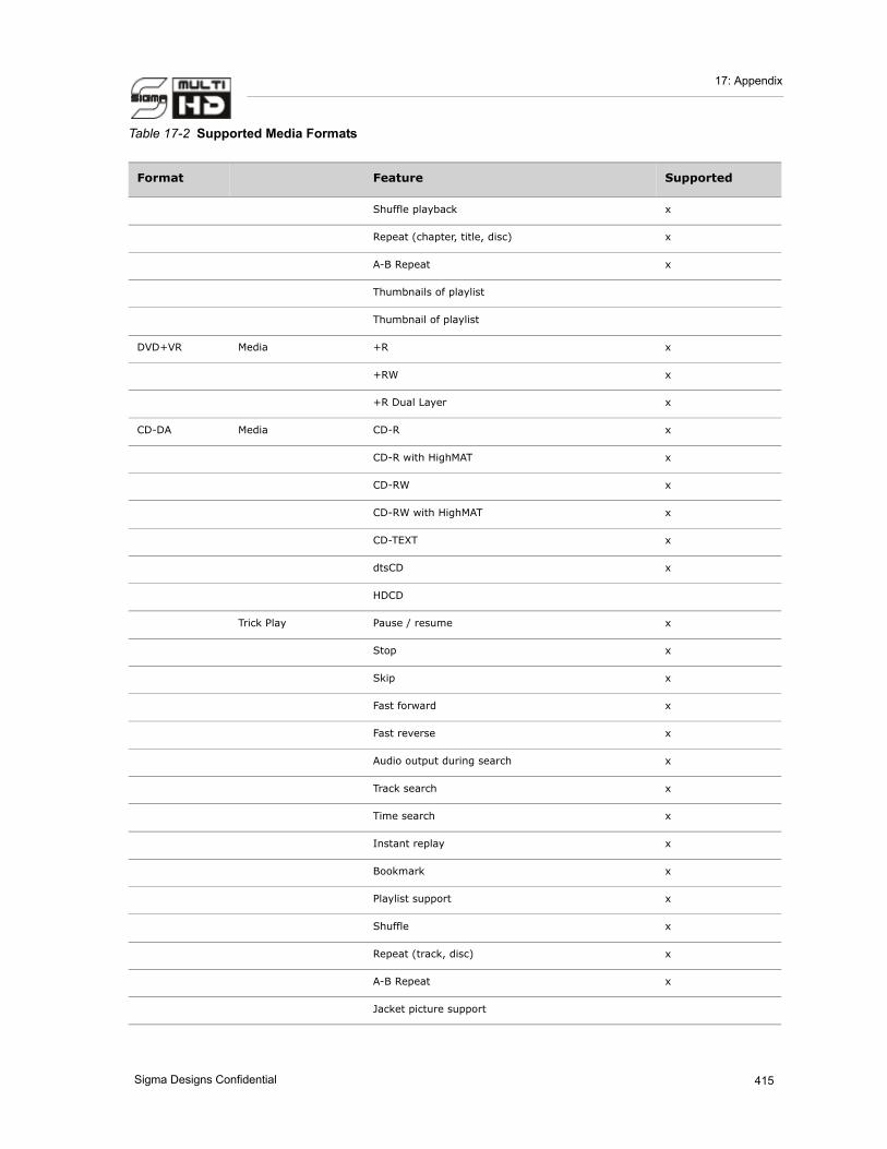
17: Appendix
Shuffle playback x
Repeat (chapter, title, disc) x
A-B Repeat x
Thumbnails of playlist
Thumbnail of playlist
DVD+VR Media +R x
+RW x
+R Dual Layer x
CD-DA Media CD-R x
CD-R with HighMAT x
CD-RW x
CD-RW with HighMAT x
CD-TEXT x
dtsCD x
HDCD
Trick Play Pause / resume x
Stop x
Skip x
Fast forward x
Fast reverse x
Audio output during search x
Track search x
Time search x
Instant replay x
Bookmark x
Playlist support x
Shuffle x
Repeat (track, disc) x
A-B Repeat x
Jacket picture support
Table 17-2 Supported Media Formats
Format Feature Supported
415Sigma Designs Confidential

SMP8654-DS-A-10SMP8654 Datasheet
VideoCDv1.x and v2.0
Media CD-R x
CD-RW x
Trick Play Pause / resume x
Stop x
Next / previous x
Fast forward x
Fast reverse x
Audio output during search x
Slow playback x
Reverse playback
Frame advance x
Time search x
Track search x
Audio Select (same audio to both left and right) x
Instant replay x
Advance x seconds and resume playback. x
Bookmark x
Playlist support x
Shuffle x
Repeat x
A-B Repeat x
PBC select x
PBC select during Play Back x
Zoom x
Karaoke CD x
VCD with CDDA x
SVCDIEC 62107-2000
Media CD-R x
CD-RW x
Trick Play Pause / resume x
Table 17-2 Supported Media Formats
Format Feature Supported
416 Sigma Designs Confidential

17: Appendix
Stop x
Next / previous x
Fast forward x
Fast reverse x
Audio output during search x
Slow playback x
Reverse playback
Frame advance x
Time search x
Track search x
Audio Select (same audio to both left and right) x
Instant replay x
Advance x seconds and resume playback. x
Bookmark x
Playlist support x
Shuffle x
Repeat x
A-B Repeat x
PBC select x
PBC select during Play Back x
Zoom x
Karaoke CD x
VCD with CDDA x
OGT display & select x
Table 17-2 Supported Media Formats
Format Feature Supported
417Sigma Designs Confidential

SMP8654-DS-A-10SMP8654 Datasheet
17.7 Supported File Formats
Table 17-3 File formats supported by SMP8654
Format Feature Supported
File Player ISO9660 level 2 x
UDF 1.02 x
UDF 1.5 x
UDF 2.01 x
UDF 2.5 x
UDF 2.6
Number of folders x
Number of files x
Display by filename x
Display font x
Slideshow mode x
AVI Video MPEG-2 x
MPEG-4.2 x
MPEG-4.10 (H.264)
SMPTE 421M (VC-1)
WMV9 x
Audio LPCM
Dolby Digital x
WMA
WMA Pro
ASF Video MPEG-2 x
MPEG-4.2 x
MPEG-4.10 (H.264)
SMPTE 421M (VC-1)
WMV9 x
Audio LPCM
Dolby Digital x
WMA
WMA Pro
418 Sigma Designs Confidential

17: Appendix
MP3 Trick Play Pause/resume x
Stop x
Next / previous x
Fast forward x
Fast reverse
Audio output during search x
Elapsed time x
WMA Trick Play Pause/resume x
Stop x
Next/previous x
Fast forward x
Fast reverse
Audio output during search x
Elapsed time x
Time search x
Instant replay x
Bookmark x
Playlist x
Shuffle x
Repeat x
A-B Repeat x
Time search x
Instant replay x
Bookmark x
Playlist x
Shuffle x
Repeat x
A-B Repeat x
WMA Pro Trick Play Pause/resume x
Stop x
Table 17-3 File formats supported by SMP8654
Format Feature Supported
419Sigma Designs Confidential

SMP8654-DS-A-10SMP8654 Datasheet
Next/previous x
Fast forward x
Fast reverse
Audio output during search x
Elapsed time x
Time search x
Instant replay x
Bookmark x
Playlist x
Shuffle x
Repeat x
A-B Repeat x
DivX v3.11 x
v4.x x
v5.x x
Trick Play Pause/resume x
Stop x
Next/previous x
Fast forward x
Fast reverse x
Audio output during search x
Slow playback x
Reverse playback x
Frame advance x
Time search x
Time advance (user defined) x
Subtitle x
Audio Select x
Changeable subpicture position x
Brightness control of subpicture x
Table 17-3 File formats supported by SMP8654
Format Feature Supported
420 Sigma Designs Confidential

17: Appendix
Instant replay x
Advance x seconds and resume playback x
Bookmark x
Playlist x
Shuffle x
Repeat x
A-B Repeat x
DivX DRM
JPEG Trick Play Pause/resume x
Stop x
Next/previous x
Bookmark x
Playlist x
Shuffle x
Repeat x
Zoom x
Rotate CW/CCW 90 degrees x
Thumbnail x
File information x
Slideshow x
Set up a time of slide show x
Table 17-3 File formats supported by SMP8654
Format Feature Supported
421Sigma Designs Confidential

SMP8654-DS-A-10SMP8654 Datasheet
17.8 Supported Broadcast Formats
17.8.1 Broadcast Formats supported by SMP8654
17.9 Raster Operations
Ternary (256) raster-operation codes define how GDI combines the bits in a source bitmap with the bits in the destination bitmap. Each raster-operation code represents a Boolean operation in which the values of the pixels in the source, the selected brush, and the desti-nation are combined. Following are the three operands used in these operations:
Table 17-5 Operands used in raster operations
Operand Meaning
D Destination bitmap
P Selected brush (also called pattern)
S Source bitmap
Boolean operators used in these operations follow:
Table 17-6 Boolean operator meanings
Operator Meaning
a Bitwise AND
n Bitwise NOT (inverse)
o Bitwise OR
X Bitwise exclusive OR (XOR)
Table 17-4 Broadcast Formats supported by SMP8654
Format Feature Supported
ATSC Video MPEG-2 x
Audio Dolby Digital x
DVB Video MPEG-2 x
Audio Dolby Digital x
422 Sigma Designs Confidential

17: Appendix
All Boolean operations are presented in reverse Polish notation. For example, the follow-ing operation replaces the values of the pixels in the destination bitmap with a combination of the pixel values of the source and brush: PSo
The following operation combines the values of the pixels in the source and brush with the pixel values of the destination bitmap (there are alternative spellings of the same function, so although a particular spelling may not be in the list, an equivalent form would be): DPSoo
Each raster-operation code is a 32-bit integer whose high-order word is a Boolean opera-tion index and whose low-order word is the operation code. The 16-bit operation index is a zero-extended, 8-bit value that represents the result of the Boolean operation on predefined brush, source, and destination values. For example, the operation indexes for the PSo and DPSoo operations are shown in the following list:
Table 17-7 Operation indexes for the PSo and DPSoo operations
P S D PSo DPSoo
0 0 0 0 0
0 0 1 0 1
0 1 0 1 1
0 1 1 1 1
1 0 0 1 1
1 0 1 1 1
1 1 0 1 1
1 1 1 1 1
Operation index: 00FCh 00FEh
In this case, PSo has the operation index 00FC (read from the bottom up); DPSoo has the operation index 00FE. These values define the location of the corresponding raster-opera-tion codes, as shown in the ‘Raster-Operation Codes’ table. The PSo operation is in line 252 (00FCh) of the table; DPSoo is in line 254 (00FEh).
The most commonly used raster operations have been given special names in the SDK header file, WINDOWS.H. You should use these names whenever possible in your appli-cations.
When the source and destination bitmaps are monochrome, a bit value of zero represents a black pixel and a bit value of 1 represents a white pixel. When the source and the destina-tion bitmaps are color, those colors are represented with RGB values.
423Sigma Designs Confidential

SMP8654-DS-A-10SMP8654 Datasheet
17.9.1 Raster Operation Codes
Table 17-8 Raster operation codes SMP8654
Boolean function (hexadecimal)
Raster operation (hexadecimal)
Boolean function in reverse Polish Common name
00 00000042 0 BLACKNESS
01 00010289 DPSoon –
02 00020C89 DPSona –
03 000300AA PSon –
04 00040C88 SDPona –
05 000500A9 DPon –
06 00060865 PDSxnon –
07 000702C5 PDSaon –
08 00080F08 SDPnaa –
09 00090245 PDSxon –
0A 000A0329 DPna –
0B 000B0B2A PSDnaon –
0C 000C0324 SPna –
0D 000D0B25 PDSnaon –
0E 000E08A5 PDSonon –
0F 000F0001 Pn –
10 00100C85 PDSona –
11 001100A6 DSon NOTSRCERASE
12 00120868 SDPxnon –
13 001302C8 SDPaon –
14 00140869 DPSxnon –
15 001502C9 DPSaon –
16 00165CCA PSDPSanaxx –
17 00171D54 SSPxDSxaxn –
18 00180D59 SPxPDxa –
19 00191CC8 SDPSanaxn –
1A 001A06C5 PDSPaox –
1B 001B0768 SDPSxaxn –
424 Sigma Designs Confidential

17: Appendix
1C 001C06CA PSDPaox –
1D 001D0766 DSPDxaxn –
1E 001E01A5 PDSox –
1F 001F0385 PDSoan –
20 00200F09 DPSnaa –
21 00210248 SDPxon –
22 00220326 DSna –
23 00230B24 SPDnaon –
24 00240D55 SPxDSxa –
25 00251CC5 PDSPanaxn –
26 002606C8 SDPSaox –
27 00271868 SDPSxnox –
28 00280369 DPSxa –
29 002916CA PSDPSaoxxn –
2A 002A0CC9 DPSana –
2B 002B1D58 SSPxPDxaxn –
2C 002C0784 SPDSoax –
2D 002D060A PSDnox –
2E 002E064A PSDPxox –
2F 002F0E2A PSDnoan –
30 0030032A PSna –
31 00310B28 SDPnaon –
32 00320688 SDPSoox –
33 00330008 Sn NOTSRCCOPY
34 003406C4 SPDSaox –
35 00351864 SPDSxnox –
36 003601A8 SDPox –
37 00370388 SDPoan –
38 0038078A PSDPoax –
39 00390604 SPDnox –
Table 17-8 Raster operation codes SMP8654
Boolean function (hexadecimal)
Raster operation (hexadecimal)
Boolean function in reverse Polish Common name
425Sigma Designs Confidential

SMP8654-DS-A-10SMP8654 Datasheet
3A 003A0644 SPDSxox –
3B 003B0E24 SPDnoan –
3C 003C004A PSx –
3D 003D18A4 SPDSonox –
3E 003E1B24 SPDSnaox –
3F 003F00EA PSan –
40 00400F0A PSDnaa –
41 00410249 DPSxon –
42 00420D5D SDxPDxa –
43 00431CC4 SPDSanaxn –
44 00440328 SDna SRCERASE
45 00450B29 DPSnaon –
46 004606C6 DSPDaox –
47 0047076A PSDPxaxn –
48 00480368 SDPxa –
49 004916C5 PDSPDaoxxn –
4A 004A0789 DPSDoax –
4B 004B0605 PDSnox –
4C 004C0CC8 SDPana –
4D 004D1954 SSPxDSxoxn –
4E 004E0645 PDSPxox –
4F 004F0E25 PDSnoan –
50 00500325 PDna –
51 00510B26 DSPnaon –
52 005206C9 DPSDaox –
53 00530764 SPDSxaxn –
54 005408A9 DPSonon –
55 00550009 Dn DSTINVERT
56 005601A9 DPSox –
57 00570389 DPSoan –
Table 17-8 Raster operation codes SMP8654
Boolean function (hexadecimal)
Raster operation (hexadecimal)
Boolean function in reverse Polish Common name
426 Sigma Designs Confidential

17: Appendix
58 00580785 PDSPoax –
59 00590609 DPSnox –
5A 005A0049 DPx PATINVERT
5B 005B18A9 DPSDonox –
5C 005C0649 DPSDxox –
5D 005D0E29 DPSnoan –
5E 005E1B29 DPSDnaox –
5F 005F00E9 DPan –
60 00600365 PDSxa –
61 006116C6 DSPDSaoxxn –
62 00620786 DSPDoax –
63 00630608 SDPnox –
64 00640788 SDPSoax –
65 00650606 DSPnox –
66 00660046 DSx SRCINVERT
67 006718A8 SDPSonox –
68 006858A6 DSPDSonoxxn –
69 00690145 PDSxxn –
6A 006A01E9 DPSax –
6B 006B178A PSDPSoaxxn –
6C 006C01E8 SDPax –
6D 006D1785 PDSPDoaxxn –
6E 006E1E28 SDPSnoax –
6F 006F0C65 PDSxnan –
70 00700CC5 PDSana –
71 00711D5C SSDxPDxaxn –
72 00720648 SDPSxox –
73 00730E28 SDPnoan –
74 00740646 DSPDxox –
75 00750E26 DSPnoan –
Table 17-8 Raster operation codes SMP8654
Boolean function (hexadecimal)
Raster operation (hexadecimal)
Boolean function in reverse Polish Common name
427Sigma Designs Confidential

SMP8654-DS-A-10SMP8654 Datasheet
76 00761B28 SDPSnaox –
77 007700E6 DSan –
78 007801E5 PDSax –
79 00791786 DSPDSoaxxn –
7A 007A1E29 DPSDnoax –
7B 007B0C68 SDPxnan –
7C 007C1E24 SPDSnoax –
7D 007D0C69 DPSxnan –
7E 007E0955 SPxDSxo –
7F 007F03C9 DPSaan –
80 008003E9 DPSaa –
81 00810975 SPxDSxon –
82 00820C49 DPSxna –
83 00831E04 SPDSnoaxn –
84 00840C48 SDPxna –
85 00851E05 PDSPnoaxn –
86 008617A6 DSPDSoaxx –
87 008701C5 PDSaxn –
88 008800C6 DSa SRCAND
89 00891B08 SDPSnaoxn –
8A 008A0E06 DSPnoa –
8B 008B0666 DSPDxoxn –
8C 008C0E08 SDPnoa –
8D 008D0668 SDPSxoxn –
8E 008E1D7C SSDxPDxax –
8F 008F0CE5 PDSanan –
90 00900C45 PDSxna –
91 00911E08 SDPSnoaxn –
92 009217A9 DPSDPoaxx –
93 009301C4 SPDaxn –
Table 17-8 Raster operation codes SMP8654
Boolean function (hexadecimal)
Raster operation (hexadecimal)
Boolean function in reverse Polish Common name
428 Sigma Designs Confidential

17: Appendix
94 009417AA PSDPSoaxx –
95 009501C9 DPSaxn –
96 00960169 DPSxx –
97 0097588A PSDPSonoxx –
98 00981888 SDPSonoxn –
99 00990066 DSxn –
9A 009A0709 DPSnax –
9B 009B07A8 SDPSoaxn –
9C 009C0704 SPDnax –
9D 009D07A6 DSPDoaxn –
9E 009E16E6 DSPDSaoxx –
9F 009F0345 PDSxan –
A0 00A000C9 DPa –
A1 00A11B05 PDSPnaoxn –
A2 00A20E09 DPSnoa –
A3 00A30669 DPSDxoxn –
A4 00A41885 PDSPonoxn –
A5 00A50065 PDxn –
A6 00A60706 DSPnax –
A7 00A707A5 PDSPoaxn –
A8 00A803A9 DPSoa –
A9 00A90189 DPSoxn –
AA 00AA0029 D –
AB 00AB0889 DPSono –
AC 00AC0744 SPDSxax –
AD 00AD06E9 DPSDaoxn –
AE 00AE0B06 DSPnao –
AF 00AF0229 DPno –
B0 00B00E05 PDSnoa –
B1 00B10665 PDSPxoxn –
Table 17-8 Raster operation codes SMP8654
Boolean function (hexadecimal)
Raster operation (hexadecimal)
Boolean function in reverse Polish Common name
429Sigma Designs Confidential

SMP8654-DS-A-10SMP8654 Datasheet
B2 00B21974 SSPxDSxox –
B3 00B30CE8 SDPanan –
B4 00B4070A PSDnax –
B5 00B507A9 DPSDoaxn –
B6 00B616E9 DPSDPaoxx –
B7 00B70348 SDPxan –
B8 00B8074A PSDPxax –
B9 00B906E6 DSPDaoxn –
BA 00BA0B09 DPSnao –
BB 00BB0226 DSno MERGEPAINT
BC 00BC1CE4 SPDSanax –
BD 00BD0D7D SDxPDxan –
BE 00BE0269 DPSxo –
BF 00BF08C9 DPSano –
C0 00C000CA PSa MERGECOPY
C1 00C11B04 SPDSnaoxn –
C2 00C21884 SPDSonoxn –
C3 00C3006A PSxn –
C4 00C40E04 SPDnoa –
C5 00C50664 SPDSxoxn –
C6 00C60708 SDPnax –
C7 00C707AA PSDPoaxn –
C8 00C803A8 SDPoa –
C9 00C90184 SPDoxn –
CA 00CA0749 DPSDxax –
CB 00CB06E4 SPDSaoxn –
CC 00CC0020 S SRCCOPY
CD 00CD0888 SDPono –
CE 00CE0B08 SDPnao –
CF 00CF0224 SPno –
Table 17-8 Raster operation codes SMP8654
Boolean function (hexadecimal)
Raster operation (hexadecimal)
Boolean function in reverse Polish Common name
430 Sigma Designs Confidential

17: Appendix
D0 00D00E0A PSDnoa –
D1 00D1066A PSDPxoxn –
D2 00D20705 PDSnax –
D3 00D307A4 SPDSoaxn –
D4 00D41D78 SSPxPDxax –
D5 00D50CE9 DPSanan –
D6 00D616EA PSDPSaoxx –
D7 00D70349 DPSxan –
D8 00D80745 PDSPxax –
D9 00D906E8 SDPSaoxn –
DA 00DA1CE9 DPSDanax –
DB 00DB0D75 SPxDSxan –
DC 00DC0B04 SPDnao –
DD 00DD0228 SDno –
DE 00DE0268 SDPxo –
DF 00DF08C8 SDPano –
E0 00E003A5 PDSoa –
E1 00E10185 PDSoxn –
E2 00E20746 DSPDxax –
E3 00E306EA PSDPaoxn –
E4 00E40748 SDPSxax –
E5 00E506E5 PDSPaoxn –
E6 00E61CE8 SDPSanax –
E7 00E70D79 SPxPDxan –
E8 00E81D74 SSPxDSxax –
E9 00E95CE6 DSPDSanaxxn –
EA 00EA02E9 DPSao –
EB 00EB0849 DPSxno –
EC 00EC02E8 SDPao –
ED 00ED0848 SDPxno –
Table 17-8 Raster operation codes SMP8654
Boolean function (hexadecimal)
Raster operation (hexadecimal)
Boolean function in reverse Polish Common name
431Sigma Designs Confidential

SMP8654-DS-A-10SMP8654 Datasheet
EE 00EE0086 DSo SRCPAINT
EF 00EF0A08 SDPnoo –
F0 00F00021 P PATCOPY
F1 00F10885 PDSono –
F2 00F20B05 PDSnao –
F3 00F3022A PSno –
F4 00F40B0A PSDnao –
F5 00F50225 PDno –
F6 00F60265 PDSxo –
F7 00F708C5 PDSano –
F8 00F802E5 PDSao –
F9 00F90845 PDSxno –
FA 00FA0089 DPo –
FB 00FB0A09 DPSnoo PATPAINT
FC 00FC008A PSo –
FD 00FD0A0A PSDnoo –
FE 00FE02A9 DPSoo –
FF 00FF0062 1 WHITENESS
Table 17-8 Raster operation codes SMP8654
Boolean function (hexadecimal)
Raster operation (hexadecimal)
Boolean function in reverse Polish Common name
432 Sigma Designs Confidential

List of Figures
1 IntroductionFigure 1-1 SMP8654 block diagram ............................................................................ 7
Figure 1-2 Application example - networked DVD player .............................................. 15Figure 1-3 Application example - digital media adapter or IPTV set-top box ................... 16
2 Host CPU BlockFigure 2-1 Block diagram of host CPU block ............................................................... 17Figure 2-2 24Kf core block diagram .......................................................................... 21
Figure 2-3 24Kf™ core pipeline ................................................................................ 22
Figure 2-4 FPU pipeline ........................................................................................... 25Figure 2-5 24Kf core virtual address map .................................................................. 29
Figure 2-6 Address translation during a cache access .................................................. 30
Figure 2-7 32-bit virtual address translation .............................................................. 33Figure 2-8 TLB tag entry format ............................................................................... 35
Figure 2-9 TLB data array entry format ..................................................................... 35
Figure 2-10 EJTAG timing diagram ........................................................................... 41Figure 2-11 Interrupt controller block diagram ........................................................... 43
Figure 2-12 Cascaded interrupt structure .................................................................. 44
Figure 2-13 Edge detector ....................................................................................... 46Figure 2-14 Timer block diagram (system overview) ................................................... 51
Figure 2-15 UART block diagram .............................................................................. 56
Figure 2-16 UART data formats ................................................................................ 58Figure 2-17 UART timing diagram ............................................................................ 63
Figure 2-18 Smartcard interface block diagram .......................................................... 64
Figure 2-19 Smartcard interface state machine .......................................................... 66
3 Security SubsystemFigure 3-1 Security subsystem block diagram ............................................................ 71
Figure 3-1 Timer block diagram (system overview) ..................................................... 80Figure 3-2 Interrupt controller block diagram ............................................................. 84
Figure 3-3 Cascaded interrupt structure .................................................................... 85
Figure 3-4 Edge detector ........................................................................................ 86
4 IPU SubsystemFigure 4-1 Interrupt processing subsystem ................................................................ 93
5 DRAM ControllersFigure 5-1 DRAM controller block diagram ................................................................. 95Figure 5-2 Memory Connection diagram .................................................................... 99
Sigma Designs Confidential 433

SMP8654-DS-A-10SMP8654 Datasheet
6 System BlockFigure 6-1 Block diagram of system block ................................................................ 113Figure 6-2 GPIO controller block diagram ................................................................ 116
Figure 6-3 Behavior of GPIO pins during chip initialization .......................................... 117
Figure 6-4 FIP block diagram ................................................................................. 122Figure 6-5 FIP timing diagram ................................................................................ 125
Figure 6-6 Infrared decoder block diagram .............................................................. 126
Figure 6-7 I2C master block diagram ...................................................................... 133Figure 6-8 I2C slave block diagram ......................................................................... 133
Figure 6-9 I2C master transfer timing diagram ......................................................... 140
Figure 6-10 Watchdog block diagram ...................................................................... 141Figure 6-11 Clock generator block diagram .............................................................. 144
7 Host InterfaceFigure 7-1 Host interface block diagram .................................................................. 155Figure 7-2 PCI arbitration pin connection diagram (PCI device) .................................. 158
Figure 7-3 PCI arbitration pin connection diagram (PCI host) ..................................... 158
Figure 7-4 PCI slave direct access (8MB default setting) ............................................ 159Figure 7-5 PCI arbiter ........................................................................................... 161
Figure 7-6 PCI CLK timing diagram ......................................................................... 170
Figure 7-7 PCI input timing diagram ....................................................................... 171
Figure 7-8 PCI output timing diagram ..................................................................... 171Figure 7-9 Ethernet block diagram .......................................................................... 177
Figure 7-10 MII Interface timing diagram ................................................................ 182
Figure 7-11 NAND flash timing diagram ................................................................... 187Figure 7-12 SATA interface block diagram ............................................................... 188
Figure 7-13 SATA Host Controller ........................................................................... 189
8 Video Decoder SubsystemFigure 8-1 Video decoder subsystem block diagram .................................................. 197
9 Video Processing SubsystemFigure 9-1 Video processing subsystem block diagram - 1 ......................................... 205Figure 9-2 Video processing subsystem block diagram - 2 ......................................... 206
Figure 9-3 De-interlacing type 1 ............................................................................. 222
Figure 9-4 De-interlacing type 2 ............................................................................. 223Figure 9-5 Graphics accelerator block diagram ......................................................... 229
Figure 9-6 CLEAR example .................................................................................... 240
Figure 9-7 SRC example ........................................................................................ 241Figure 9-8 DST_IN and SRC_IN examples ............................................................... 242
Figure 9-9 DST_OUT and SRC_OUT examples .......................................................... 243
Figure 9-10 DST_OVER and SRC_OVER examples ..................................................... 244Figure 9-11 Positioning blocks ................................................................................ 246
Figure 9-12 Video output timing parameters ............................................................ 254
Figure 9-13 Video waveform - 720p ........................................................................ 261Figure 9-14 Video waveform - 1080i ....................................................................... 261
Figure 9-15 Video waveform - 480i ......................................................................... 262
Figure 9-16 Video waveform - 480p ........................................................................ 262Figure 9-17 Video waveform - 576i ......................................................................... 263
434 Sigma Designs Confidential

:
Figure 9-18 Video waveform - 576p ........................................................................ 263
Figure 9-19 NTSC c for S-video .............................................................................. 266
Figure 9-20 NTSC y for S-video .............................................................................. 267Figure 9-21 CVBS (NTSC) ...................................................................................... 268
Figure 9-22 Digital video input timing diagram ......................................................... 294
10 Audio Processing SubsystemFigure 10-1 Audio processing subsystem block diagram ............................................. 295
Figure 10-2 S/PDIF data format ............................................................................. 307
Figure 10-3 I2S audio input timing diagram ............................................................. 314Figure 10-4 I2S audio output timing diagram ........................................................... 314
11 Transport DemultiplexerFigure 11-1 Transport demultiplexer block diagram ................................................... 315Figure 11-2 Clock gating timings ............................................................................ 326
Figure 11-3 Overview of DVB-CSA .......................................................................... 329
Figure 11-4 Hardware section filter ......................................................................... 335Figure 11-5 TS input timing diagram ....................................................................... 341
Figure 11-6 Clock, Data, Sync Protocol .................................................................... 341
Figure 11-7 Clock, Data, Valid Protocol .................................................................... 341Figure 11-8 Clock, Data, Sync, Valid Protocol ........................................................... 342
Figure 11-9 Traditional TS Input Protocol ................................................................. 342
Figure 11-10 Parallel Input Protocol ........................................................................ 343
12 Pin InformationFigure 12-1 Overview of SMP8654 BGA (844 BGA) .................................................... 345
Figure 12-2 SMP8654 pin diagram (top left quadrant) ............................................... 346Figure 12-3 SMP8654 pin diagram (top right quadrant) ............................................. 347
Figure 12-4 SMP8654 pin diagram (bottom left quadrant) .......................................... 348
Figure 12-5 SMP8654 pin diagram (bottom right quadrant) ........................................ 349
13 System SpecificationsFigure 13-1 Power supply sequencing ...................................................................... 374
Figure 13-2 Power reset specifications ..................................................................... 375Figure 13-3 Package diagram - top view (844 BGA) .................................................. 390
Figure 13-4 Package diagram - bottom view (844 BGA) ............................................. 391
14 DDR ImplementationFigure 14-1 Signal topology: Address/Command ....................................................... 393
Figure 14-2 Signal topology: DQ/DM ....................................................................... 394
Figure 14-3 Signal topology: Differential clock .......................................................... 394
Figure 14-4 Signal topology: Differential .................................................................. 394
17 AppendixFigure 17-1 Frequency response ............................................................................. 405
Figure 17-2 Impulse response ................................................................................ 406Figure 17-3 Scaling 16:9 content for a 4:3 display – “Crop” mode ............................... 408
Figure 17-4 Scaling 16:9 content for a 4:3 display – “Letterbox” mode ........................ 408
Figure 17-5 Scaling 16:9 content for a 4:3 display – “Squeezed” mode ........................ 409Figure 17-6 Scaling 4:3 content for a 16:9 display – “Pillar” mode .............................. 409
435Sigma Designs Confidential

SMP8654-DS-A-10SMP8654 Datasheet
Figure 17-7 Scaling 4:3 content for a 16:9 display – “Wide” mode .............................. 410Figure 17-8 Scaling 4:3 content for a 16:9 display – “Zoom” mode ............................. 410
Figure 17-9 Scaling 4:3 content for a 16:9 display – “Panorama” mode ....................... 411
Figure 17-10 SDTV Vs. SDTV Colorimetry Example ................................................... 412
436 Sigma Designs Confidential

List of Tables
ConventionsTable 0-1 Acronyms and abbreviations ....................................................................... 1
Table 0-2 Units of measurement ............................................................................... 4
2 Host CPU BlockTable 2-1 Remap registers ..................................................................................... 18
Table 2-2 24Kf™ Core FPU latency and repeat rate .................................................... 26Table 2-3 Coprocessor 1 registers in numerical order ................................................. 27
Table 2-4 24Kf™ Core Integer multiply/divide unit latencies and repeat rates ................ 28
Table 2-5 Mask and page size values ....................................................................... 33Table 2-6 TLB tag entry fields ................................................................................. 35
Table 2-7 TLB data array entry fields ....................................................................... 35
Table 2-8 24Kf™ core instruction and data cache attributes ........................................ 37Table 2-9 EJTAG registers ...................................................................................... 39
Table 2-10 EJTAG pin descriptions ........................................................................... 39
Table 2-11 EJTAG AC characteristics ........................................................................ 40Table 2-12 Control block registers ........................................................................... 45
Table 2-13 Interrupt sources .................................................................................. 46
Table 2-14 Operating mode selection for interrupt lines .............................................. 49Table 2-15 Edge detector registers .......................................................................... 49
Table 2-16 Timer clock pre-scale ............................................................................. 53
Table 2-17 Timer registers ..................................................................................... 54Table 2-18 Register map - UARTs ............................................................................ 61
Table 2-19 UART pin descriptions ............................................................................ 62
Table 2-20 UART AC characteristics ......................................................................... 62Table 2-21 Register map - Smartcard interface ......................................................... 68
Table 2-22 Smartcard interface pin descriptions ........................................................ 69
3 Security SubsystemTable 3-1 MIPS requirements for various functions performed by the XPU ..................... 74
Table 3-2 Performance .......................................................................................... 76
Table 3-3 Performance .......................................................................................... 77
Table 3-2. Register map - Serial flash interface ......................................................... 78Table 3-1 Timer clock pre-scale .............................................................................. 83
Table 3-2 Interrupt sources .................................................................................... 86
Table 3-3 Operating mode selection for interrupt lines ............................................... 88Table 3-4 Top level bus connections ........................................................................ 89
5 DRAM ControllersTable 5-1 Typical memory configurations ................................................................. 98Table 5-2 Memory bandwidth requirements for video ................................................100
Sigma Designs Confidential 437

SMP8654-DS-A-10SMP8654 Datasheet
Table 5-3 Memory bandwidth requirements for audio ............................................... 102Table 5-4 Typical memory bandwidth values ........................................................... 103
Table 5-5 Video Decoding DRAM requirements (MB, includes all needed buffers, no deinterlac-ing or type 1 deinterlacing) ................................................................................... 103Table 5-6 Video Decoding DRAM requirements (MB, includes all needed buffers, type 2 dein-terlacing used) .................................................................................................... 104
Table 5-7 Typical Firmware DRAM requirements (MB) .............................................. 104Table 5-8 DRAM controller pin descriptions ............................................................. 105
6 System BlockTable 6-1 Additional GPIO pins .............................................................................. 118Table 6-2 Register map - GPIO ............................................................................. 119
Table 6-3 GPIO pin description .............................................................................. 120
Table 6-4 FIP registers ......................................................................................... 124Table 6-5 FIP pin description ................................................................................ 124
Table 6-6 FIP AC characteristics ............................................................................ 125
Table 6-7 RC5 timing parameters .......................................................................... 128Table 6-8 NEC timing parameters .......................................................................... 129
Table 6-9 Infrared decoder registers ...................................................................... 130
Table 6-10 Infrared decoder pin description ............................................................ 132
Table 6-11 Register map - I 2C master 0 and 1 ...................................................... 138Table 6-12 I2C slave registers .............................................................................. 139
Table 6-13 I2C master and slave interface pin descriptions ....................................... 139
Table 6-14 I2C master and slave interface AC characteristics .................................... 140Table 6-15 WDO pad values ................................................................................. 141
Table 6-16 Register WATCHDOG_CONFIGURATION values ........................................ 142
Table 6-17 Watchdog registers .............................................................................. 143Table 6-18 Watchdog pin description ..................................................................... 143
Table 6-19 Dividers ratio ...................................................................................... 146
Table 6-20 System clock frequencies ..................................................................... 147Table 6-21 Video clock muxing .............................................................................. 147
Table 6-22 Audio clock and RCLK muxing ............................................................... 148
Table 6-23 Host interface clock muxing .................................................................. 149Table 6-24 Counters ............................................................................................ 150
Table 6-25 Clock generation registers .................................................................... 151
Table 6-26 Clean dividers registers ........................................................................ 151Table 6-27 Clock counter registers ........................................................................ 153
Table 6-28 Clock generator pin description ............................................................. 153
Table 6-29 System clock characteristics ................................................................. 154
7 Host InterfaceTable 7-1 Default values for PCI register fields ........................................................ 157
Table 7-2 PCI slave direct access registers .............................................................. 163Table 7-3 PCI slave time-out control registers ......................................................... 164
Table 7-4 PCI slave device configuration registers ................................................... 164
Table 7-5 PCI master access registers .................................................................... 165Table 7-6 PCI host registers ................................................................................. 165
Table 7-7 System bus pin descriptions ................................................................... 166
Table 7-8 PCI interface DC characteristics .............................................................. 169
438 Sigma Designs Confidential

:
Table 7-9 PCI timing parameters ........................................................................... 170
Table 7-10 USB 2.0 pin descriptions ....................................................................... 173
Table 7-11 USB 2.0 DC characteristics – FS operation .............................................. 175Table 7-12 USB 2.0 DC characteristics – HS operation .............................................. 175
Table 7-13 Dynamic Characteristics – FS Operation .................................................. 176
Table 7-14 Dynamic Characteristics – HS Operation ................................................. 176Table 7-15 MII interface pin descriptions ................................................................ 179
Table 7-16 MII interface AC characteristics ............................................................. 181
Table 7-17 Supported NAND flash devices .............................................................. 184Table 7-18 Register map - NAND flash configuration ................................................ 185
Table 7-19 NAND flash pin descriptions .................................................................. 186
Table 7-20 NAND flash interface AC characteristics ................................................. 187Table 7-21 SATA interface pin descriptions .............................................................. 194
Table 7-22 SATA PHY reference clock specifications .................................................. 196
8 Video Decoder SubsystemTable 8-1 Number of programs that can be decoded simultaneously by SMP8654 ......... 198
Table 8-2 Resolutions supported by video decoder ................................................... 198
Table 8-3 Supported MPEG-4.10 (H.264) SEI (Supplemental enhancement information) mes-sages and VUI (video usability information) ............................................................. 202
Table 8-4 JPEG decode performance measurements ................................................. 204
9 Video Processing SubsystemTable 9-1 Memory planes and scaler usage for a typical application ............................ 211
Table 9-2 Supported source and output frame rate combinations ............................... 248
Table 9-3 Combinations of supported output frame rates - OSD, subtitles and graphics avail-able on all outputs ................................................................................................ 249
Table 9-4 Combinations of supported output frame rates - no OSD, subtitles or graphics on analog component outputs .................................................................................... 249Table 9-5 Wide Screen Signaling and CGMS - register VO_MAIN_ANALOG_CGMS ......... 252
Table 9-6 Range of programmability for digital video output timing ............................ 255
Table 9-7 Range of programmability for component, composite and S-video output timing .255
Table 9-8 Supported audio output combinations ...................................................... 271
Table 9-9 Range of programmability for digital video input timing .............................. 276Table 9-10 Range of programmability for VBI capture ............................................... 276
Table 9-11 Common video input formats ................................................................ 277
Table 9-12 Register map - Multi-format scaler (MFS) ................................................ 278Table 9-13 Main video scaling registers .................................................................. 279
Table 9-14 OSD scaler registers ............................................................................ 280
Table 9-15 Hardware cursor registers ..................................................................... 281
Table 9-16 Register map - Main mixer .................................................................... 281Table 9-17 Register map - Graphic accelerator (bitmap mode) .................................. 282
Table 9-18 Register map - Gradient fill generator ..................................................... 283
Table 9-19 Graphic accelerator (vectorial mode) registers ......................................... 283Table 9-20 Display routing register ........................................................................ 284
Table 9-21 Color bars generator registers ............................................................... 284
Table 9-22 Color bars generator registers ............................................................... 284Table 9-23 Register map - Video input ................................................................... 285
Table 9-24 Digital output registers ......................................................................... 285
439Sigma Designs Confidential

SMP8654-DS-A-10SMP8654 Datasheet
Table 9-25 Register map - Main analog output ........................................................ 286Table 9-26 Digital video input pin descriptions ........................................................ 288
Table 9-27 Composite and S-video pin descriptions .................................................. 289
Table 9-28 Component analog output pin descriptions .............................................. 290Table 9-29 HDMI pin descriptions .......................................................................... 291
Table 9-30 HDMI DC electrical characteristics .......................................................... 292
Table 9-31 Digital video input AC electrical characteristics ........................................ 293Table 9-32 HDMI AC electrical characteristics .......................................................... 293
Table 9-33 Analog video output electrical characteristics .......................................... 294
10 Audio Processing SubsystemTable 10-1 MPEG audio decode support .................................................................. 297
Table 10-2 Dolby audio decode support .................................................................. 298
Table 10-3 LPCM, WMA9 and ATRAC3 audio decode support ..................................... 299Table 10-4 Supported audio output combinations .................................................... 302
Table 10-5 Audio output frequencies ...................................................................... 304
Table 10-6 I2S data alignment in the 32-bit mode ................................................... 306Table 10-7 Audio miscellaneous registers ............................................................... 309
Table 10-8 Audio input interface registers ............................................................... 310
Table 10-9 Audio output interface registers ............................................................. 311
Table 10-10 Audio input interface pin descriptions ................................................... 312Table 10-11 Audio output interface pin descriptions ................................................. 312
Table 10-12 I2S Input AC characteristics ................................................................ 313
Table 10-13 I2S Output AC characteristics .............................................................. 313
11 Transport DemultiplexerTable 11-1 Cipher RAM code word allocations .......................................................... 326
Table 11-2 DES encryption/decryption performance ................................................. 327Table 11-3 AES encryption/decryption performance ................................................. 328
Table 11-4 RC4 encryption/decryption performance ................................................. 328
Table 11-5 Performance index for various cases ...................................................... 332Table 11-6 SPI transport stream interface pin descriptions ........................................ 339
Table 11-7 Transport demultiplexer AC characteristics .............................................. 340
Table 11-8 Transport demultiplexer AC characteristics .............................................. 340
12 Pin InformationTable 12-1. Pin listing by pin id ............................................................................. 350
Table 12-2. Pin listing by pin name........................................................................ 360Table 12-1 Miscellaneous pin descriptions ............................................................... 370
13 System SpecificationsTable 13-1 Absolute maximum ratings ................................................................... 371Table 13-2 Recommended operating conditions ....................................................... 371
Table 13-3 DC characteristics ............................................................................... 372
Table 13-4 SMP8654 power consumption data ........................................................ 373Table 13-5 SMP8654 ground pins .......................................................................... 375
Table 13-6 1.05V power rail ................................................................................. 382
Table 13-7 1.8V power rail ................................................................................... 385Table 13-8 3.3V power rail ................................................................................... 387
Table 13-9 Package thermal characteristics ............................................................ 389
440 Sigma Designs Confidential

:
15 Ordering InformationTable 15-1. SMP8654 ordering information ............................................................. 397
17 AppendixTable 17-1 Basic analog video parameters .............................................................. 403Table 17-2 Supported Media Formats ..................................................................... 413
Table 17-3 File formats supported by SMP8654 ....................................................... 418
Table 17-4 Broadcast Formats supported by SMP8654 .............................................. 422Table 17-5 Operands used in raster operations ........................................................ 422
Table 17-6 Boolean operator meanings ................................................................... 422
Table 17-7 Operation indexes for the PSo and DPSoo operations ................................ 423Table 17-8 Raster operation codes SMP8654 ........................................................... 424
441Sigma Designs Confidential

SMP8654-DS-A-10SMP8654 Datasheet
442 Sigma Designs Confidential


Sales Offices Distributors
USA HeadquartersSigma Designs, Inc.1778 McCarthy Blvd.Milpitas, CA 95035Tel: (408) 262-9003Fax: (408) [email protected]
EuropeSigma Designs, Inc.Tel: +32 474-501234Fax: +32 234-72260
JapanMACNICA, Inc.Brilliant Technologies CompanyMacnica Bldg. No 1, 1-6-3 Shin-YokohamaKohoku-Ku, Yokohama-City, 222-8561JapanTel: +81 45-470-9831Fax: +81 45-470-9832www.btc.macnica.co.jp
ChinaSigma Designs China OfficeUnit 7C1, TianXiang BuildingTian‘An Cyber Zone,Futian District,Shenzhen, PRCPostcode 518048Tel: +86 755-83435669Fax: +86 755-83435629
JapanSigma Designs Japan4-16-8 Nakahara, Mitaka-shi,Tokyo 181-0005, JapanTel: +81 422-79-3067Fax: +81 422-79-3067
KoreaUniquest / TekclipsUniquest Building271-2 Seohyeon-dong,Bundang-gu, Seongnam-si,Gyeonggi-do, Korea, 463-824Tel: +82-31-776-9832Fax: +82-31-708-6596www.uniquest.co.kr
Hong KongSigma Designs (Asia) Ltd.Unit 4001B, Tower 2, Metroplaza223 Hing Fong RoadKwai Fong, N.T. Hong KongTel: +852 2401-7388Fax: +852 2610-2177
TaiwanSigma Designs TaiwanFar East World Center, C Tower8F-8, No. 79, Sec 1Hsin Tai Wu RoadHsichih, Taipei HsienTaiwanTel: +886 2-2698-2066Fax: +886 2-2698-2099
Indonesia, Malaysia, SingaporeConvergent Systems (S) Pte. Ltd.60 Albert Street#11-01 Albert ComplexSingapore 189969Tel: +65 6337-0177Fax: +65 6336-2247www.convergent.com.sg
License Requirements
Dolby Digital, Dolby Surround Pro Logic II, Dolby Headphone and/or Dolby Virtual Speaker features require license from Dolby. HighMAT, WMA and/or WMT feature require license from Microsoft. MPEG video features require license(s) from MPEG-LA. MPEG audio features require license(s) from Via Licensing, Sisvel and/or Thomson. DVD-Audio feature requires that the customer be a 4C CPPM, Verance ARIS/SOLANA-4C and Dolby MLP Lossless licensee. Other DVD features require licenses from DVD CCA (for CSS), DVD FLLC (for logo and format) and Philips. Customer must be a Macrovision licensee.Sigma Designs Worldwide
Copyright Information
© 2009 by Sigma Designs Inc. All rights reserved. No part of this document may be copied or reproduced in any form or by any means without the prior written consent of Sigma Designs Inc. The information in this document is subject to change without notice. Sigma Designs, REALmagic and the REAL-magic logo are either registered trademarks or trademarks of Sigma Designs, Inc. in the United States and/or other countries. Manufactured under license from Dolby Laboratories and Macrovision. Dolby, Pro Logic, and the double-D symbol are trademarks of Dolby Laboratories. All other trademarks or registered trademarks are the property of their respective owners.
Sigma Designs products are sold by description only. Sigma Designs reserves the right to make changes in circuit design and/or specifications at any time without notice. Accordingly, the reader is cautioned to verify that data sheets are current before placing orders. Information furnished by Sigma Designs is believed to be accurate and reliable. However, no responsibility is assumed by Sigma Designs or its subsidiaries for its use; nor for any infringements of patents or other rights of third parties which may result from its use. No license is granted by implication or otherwise under any patent or patent rights of Sigma Designs or its subsidiaries.