
Sm-induced reconstructions on Si(111) surface
10
Sm-induced reconstructions on Si(1 1 1) surface E. Ehret * , F. Palmino, L. Mansour, E. Duverger, J.-C. Labrune FEMTO-ST UMR CNRS 6174, Surface Interface Nanostructure Group, 4 place Tharradin, BP 71427, 25211 Montbeliard cedex, France Received 19 January 2004; accepted for publication 6 July 2004 Available online 21 August 2004 Abstract Using scanning tunneling microscopy (STM) and low energy electron diffraction (LEED), the surface recon- structions induced by submonolayer Sm adsorption on a Si(1 1 1) have been studied. This system forms a series of metal-induced n · 1(n = 3, 5, 7,...) reconstructions with increase of Sm coverage on the Si(1 1 1) substrate at elevated temperatures. Our STM results indicate that these reconstructions appear as well-ordered row-like structures. Local mixing of the 3 · 1 and n · 1 unit cells (or stripes) indicates that the atomic models for these phases should be closely related. The atomically resolved STM images reveal a strong bias dependence which determine the relative registry of the Si as well as Sm atoms for these reconstructions. Our results are consistent with the chain-channel models of the row-like structures of the Ca/Si(1 1 1) system as proposed in the literature. Ó 2004 Elseiver B.V. All rights reserved. Keywords: Silicon; Scanning tunneling microscopy; Surface relaxation and reconstruction 1. Introduction Adsorbate-induced chain structures on semi- conductor surfaces have been the subject of extensive studies for decades as a model system for the creation of one-dimensional (1D) system with a high degree of perfection [1,2]. The most well-known examples of such a chain structure are both the 3 · 1 and 3 · 2 reconstructions in- duced by the adsorption of a variety of metal atoms on the Si(1 1 1) substrate. The 3 · 1 recon- struction is formed by the adsorption of an alka- li metal (AM) at 1/3 monolayer (ML) coverage [3–6], whereas the 3 · 2 reconstruction is formed by the adsorption an alkaline earth metal (AEM) or a rare-earth metal (REM) at 1/6 ML coverage [7–10]. However, the similarities between the scanning tunneling microscopy (STM) images [9–11], the low energy electron diffraction (LEED) I–V curves [12,13] and the Si 2p core le- vel spectroscopy (CLS) spectra [8,14,15] obtained from those different reconstructions suggested that they adopt a common arrangement of Si adatoms. 0039-6028/$ - see front matter Ó 2004 Elseiver B.V. All rights reserved. doi:10.1016/j.susc.2004.07.005 * Corresponding author. Tel.: +33 381 994 688; fax: +33 381 994 610. E-mail address: [email protected] (E. Ehret). Surface Science 569 (2004) 23–32 www.elsevier.com/locate/susc
-
Upload
independent -
Category
Documents
-
view
2 -
download
0
Transcript of Sm-induced reconstructions on Si(111) surface

Surface Science 569 (2004) 23–32
www.elsevier.com/locate/susc
Sm-induced reconstructions on Si(111) surface
E. Ehret *, F. Palmino, L. Mansour, E. Duverger, J.-C. Labrune
FEMTO-ST UMR CNRS 6174, Surface Interface Nanostructure Group, 4 place Tharradin, BP 71427, 25211 Montbeliard cedex, France
Received 19 January 2004; accepted for publication 6 July 2004
Available online 21 August 2004
Abstract
Using scanning tunneling microscopy (STM) and low energy electron diffraction (LEED), the surface recon-
structions induced by submonolayer Sm adsorption on a Si(111) have been studied. This system forms a series of
metal-induced n · 1 (n = 3,5,7,. . .) reconstructions with increase of Sm coverage on the Si(111) substrate at elevated
temperatures. Our STM results indicate that these reconstructions appear as well-ordered row-like structures. Local
mixing of the 3 · 1 and n · 1 unit cells (or stripes) indicates that the atomic models for these phases should be closely
related. The atomically resolved STM images reveal a strong bias dependence which determine the relative registry of
the Si as well as Sm atoms for these reconstructions. Our results are consistent with the chain-channel models of the
row-like structures of the Ca/Si(111) system as proposed in the literature.
� 2004 Elseiver B.V. All rights reserved.
Keywords: Silicon; Scanning tunneling microscopy; Surface relaxation and reconstruction
1. Introduction
Adsorbate-induced chain structures on semi-
conductor surfaces have been the subject of
extensive studies for decades as a model system
for the creation of one-dimensional (1D) systemwith a high degree of perfection [1,2]. The most
well-known examples of such a chain structure
are both the 3 · 1 and 3 · 2 reconstructions in-
duced by the adsorption of a variety of metal
0039-6028/$ - see front matter � 2004 Elseiver B.V. All rights reserv
doi:10.1016/j.susc.2004.07.005
* Corresponding author. Tel.: +33 381 994 688; fax: +33 381
994 610.
E-mail address: [email protected] (E. Ehret).
atoms on the Si(111) substrate. The 3 · 1 recon-
struction is formed by the adsorption of an alka-
li metal (AM) at 1/3 monolayer (ML) coverage
[3–6], whereas the 3 · 2 reconstruction is formed
by the adsorption an alkaline earth metal (AEM)
or a rare-earth metal (REM) at 1/6 ML coverage[7–10]. However, the similarities between the
scanning tunneling microscopy (STM) images
[9–11], the low energy electron diffraction
(LEED) I–V curves [12,13] and the Si2p core le-
vel spectroscopy (CLS) spectra [8,14,15] obtained
from those different reconstructions suggested
that they adopt a common arrangement of Si
adatoms.
ed.
24 E. Ehret et al. / Surface Science 569 (2004) 23–32
Earlier models have been proposed for the me-
tal-induced 3 · 1 reconstruction, most notable is
the seiwatz-chain and the extended-Pandey-chain
models. Both of these were discarded recently.
The honeycomb-chain channel model (HCC),which incorporates Si double bond in the surface
layer, is now considered to be the most plausible
candidate. The HCC model has the lowest energy
among the one of models proposed so far, and
can best accounts for the experimental results [16].
Others chain structures appear at higher
absorbate coverages. Baski et al. [17] have shown
that the Ca/Si(111) system forms a series of odd-order n · 1 reconstructions that culminate in a
2 · 1 phase at 0.5 ML. This coverage behaviour
is similar to that observed for the divalent rare-
earth Yb and Eu [18–21]. It is suggested that these
additional reconstructions could be formed by an
appropriate combination of Seiwatz and HCC
chains.
The Sm/Si system has not been extensively stud-ied. Previous study reported that the valence state
of the Sm atom changes from divalent to trivalent
with increase of the Sm coverage [22]. LEED
observations and CLS measurements have shown
the presence of n · 1 phases whereas ap3 ·p
3�R30� phase is found at higher coverage. The
Sm atoms are respectively divalent and trivalent
state in these phases [18,23]. In this paper, we haveused STM in conjunction with LEED to investi-
gate the surface structures of Sm on Si(111).
LEED observations reveal that a series of metal-
induced n · 1 (n = 3,5,7,. . .) reconstructions are
formed with increasing Sm coverage on the
Si(111) substrate at elevated temperature. To our
knowledge, for the first time, the detailed STM
observations carefully determine the registry ofthe filled- and empty-state features of these recon-
structions. The appearance and the bias depend-
ence of the STM images are discussed in terms of
previously proposed structural models for the
Ca/Si(111) system.
2. Experiment
The experiments are performed in a two-cham-
ber ultrahigh vacuum system (under a pressure be-
low 3 · 10�10 mbar) equipped with an Omicron
STM and a LEED/AES facilities. The Si(111) sub-
strate (1–3 Xcm resistivity) is carefully degassed
and cleaned in situ by a series of rapid heating
up to 1200 �C under a pressure lower than5 · 10�10 mbar, and subsequently slowly cooled
down in order to obtain the 7 · 7 reconstruction.
Sm deposition is performed using an e-beam evap-
orator onto the Si(111) substrates at about 1/3
ML/min. One ML is referred to the Si(111) ideal
surface atomic density (7.8 · 10�14 atomcm�2).
Sm is deposited onto the substrate held at temper-
ature in the 400–850 �C range. Samples are subse-quently annealed at the temperature deposition
during 20 min. The Sm surface coverage is deter-
mined from STM images for low coverage and
extrapolated to high coverages. The procedure
used for the accurate determination of Sm cover-
age has been described elsewhere [10]. Both LEED
and STM observations are made at room temper-
ature, and the STM images are acquired in theconstant current mode with bias voltage applied
to the sample.
3. Results
3.1. Phase diagram
We have studied surface order as a function of
the Sm coverage and the annealing conditions
using STM as well as LEED. Structural transfor-
mations on the Si(111) surface induced by Sm
adsorption observed in the present study are sum-
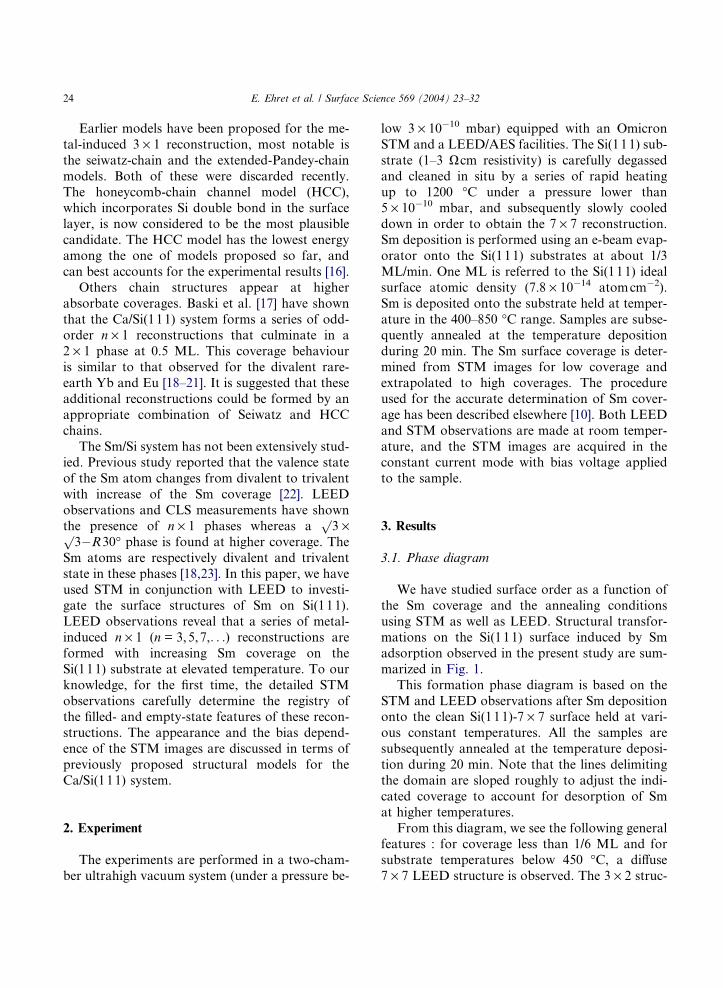
marized in Fig. 1.
This formation phase diagram is based on the
STM and LEED observations after Sm depositiononto the clean Si(111)-7 · 7 surface held at vari-
ous constant temperatures. All the samples are
subsequently annealed at the temperature deposi-
tion during 20 min. Note that the lines delimiting
the domain are sloped roughly to adjust the indi-
cated coverage to account for desorption of Sm
at higher temperatures.
From this diagram, we see the following generalfeatures : for coverage less than 1/6 ML and for
substrate temperatures below 450 �C, a diffuse
7 · 7 LEED structure is observed. The 3 · 2 struc-
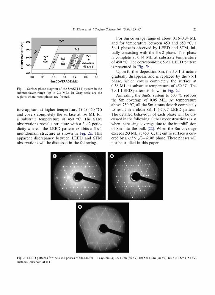
Fig. 1. Surface phase diagram of the Sm/Si(111) system in the
submonolayer range (up to 2/3 ML). In Gray scale are the
regions where monophases are formed.
E. Ehret et al. / Surface Science 569 (2004) 23–32 25
ture appears at higher temperature (T P 450 �C)
and covers completely the surface at 1/6 ML for
a substrate temperature of 450 �C. The STM
observations reveal a structure with a 3 · 2 perio-
dicity whereas the LEED pattern exhibits a 3 · 1
multidomain structure as shown in Fig. 2a. This
apparent discrepancy between LEED and STMobservations will be discussed in the following.
Fig. 2. LEED patterns for the n · 1 phases of the Sm/Si(111) system
surfaces, observed at RT.
For Sm coverage range of about 0.16–0.34 ML
and for temperature between 450 and 650 �C, a
5 · 1 phase is observed by LEED and STM, ini-
tially coexisting with the 3 · 2 phase. This phase
is complete at 0.34 ML at substrate temperatureof 450 �C. The corresponding 5 · 1 LEED pattern
is presented in Fig. 2b.
Upon further deposition Sm, the 5 · 1 structure
gradually disappears and is replaced by the 7 · 1
phase, which covers completely the surface at
0.38 ML at substrate temperature of 450 �C. The
7 · 1 LEED pattern is shown in Fig. 2c.
Annealing the Sm/Si system to 500 �C reducesthe Sm coverage of 0.05 ML. At temperature
above 750 �C, all the Sm atoms desorb completely
to result in a clean Si(111)-7 · 7 LEED pattern.
The detailed behaviour of each phase will be dis-
cussed in the following. Other reconstructions exist
when increasing coverage due to the interdiffusion
of Sm into the bulk [22]. When the Sm coverage
exceeds 2/3 ML at 450 �C, the entire surface is cov-ered by a
p3 ·
p3�R30� phase. These phases will
not be studied in this paper.
(a) 3 · 1-Sm (86 eV), (b) 5 · 1-Sm (78 eV), (c) 7 · 1-Sm (153 eV)

26 E. Ehret et al. / Surface Science 569 (2004) 23–32
Note that Sm/Si(111) system does not form
2 · 1 structure whatever the Sm coverage and the
substrate temperature. This behaviour distin-
guishes Sm from pure divalent metals-like Ca
and Yb, where such a reconstruction is observed[17,18,24].
3.2. The 3 · 2 phase
STM data showing the morphology and the
atomic structure of the lowest coverage 3 · 2 phase
is shown in Figs. 3 and 4.
In large-scale empty-state STM image of theFig. 3, the 3 · 2 phase appears as stripes domains
oriented in one of three symmetry directions. The
higher resolution empty-state image of Fig. 4a
shows rows of protrusions running in the ½1�10�direction. The separation between the rows is 3a,
where a ¼ ðffiffiffi
3p
=2Þa0 ¼ 3:32 A [a0 = 3.84 A, a unit
lattice spacing on a bulk terminated Si(111)].
Within the rows, the spacing between the protru-sions is 2a0. We have proposed in a previous paper
[10] that the 3 · 2 protrusions in the empty-state
image are assigned to the Sm atoms occupying a
specific site. The observation of a single protrusion
per 3 · 2 cell in the empty-state STM image with a
Fig. 3. Large scale STM image (40 · 40 nm2) (Vs = 1.8 V and
It = 0.34 nA) showing three domains of the Sm-induced 3 · 2
phases. Scale bar is 5 nm.
Fig. 4. High resolution (a) empty-state (Vs = 1.8 V and
It = 0.34 nA) and (b) filled-state (Vs = �3.2 V and It = 6.11
nA) STM images (5 · 5 nm2) of the 3 · 2 reconstruction. The
zigzag chains of the empty-state image form a 3 · 2 structure
rather than a 3 · 1 structure.
Sm coverage of 1/6 ML is supportive of thisinterpretation.
The filled-state STM image of the Sm/Si(111)-
3 · 2 surface is obtained with atomic resolution
as shown in Fig. 4b. There are bright double rows
running in the ½1�10� direction separated by dark
channels. The protrusions, in the double rows,
form zigzag chains with the ·1 periodicity. Thus,
the apparent unit cell formed by those protrusionsis a 3 · 1. The zigzag chain feature in the filled-

Fig. 5. High resolution (a) empty-state (Vs = 1.8 V and
It = 1.02 nA) and (b) filled-state (Vs = �3.7 V and It = 0.08
nA) STM images (11 · 11 nm2) of the 5 · 1 reconstruction. For
convenience, the position of the maxima are shown as filled
circles in the empty-state image. Lines with 3a, 2a and 5a
periodicities have been superimposed over the images.
E. Ehret et al. / Surface Science 569 (2004) 23–32 27
state image is nearly identical to those reported for
the Si(111)3 · 2-Ba phase [9] as well as for the
Si(111)3 · 1-AM [7,17] surfaces. This zigzag chain
feature is attributable to Si atoms, because the
3 · 2 protrusions in the empty-state STM imagesare naturally assigned to adsorbate atoms based
on the coverage of 1/6 ML [10].
3.3. The 5 · 1 phase
As indicated in a previous section, the 5 · 1
phase can be grown in a very narrow range of
temperature and coverage. With a 0.34 ML Smcoverage, the whole surface exhibits a 5 · 1 recon-
struction which is confirmed by the LEED pattern
and STM observations. As shown in the empty-
state STM image of the Fig. 5a, the 5 · 1 phase
consists of double bright rows of protrusions ori-
ented along the ½1�10� direction and with a 5a in-
ter-row spacing. Within the rows, the spacing of
the protrusions is a0. Inside a 5 · 1 unit cell, thebright lines are separated by 2a and the distance
between the bright lines adjacent to a dark
trenches is 3a. A ladder configuration between
the double rows prevails, as shown by the filled cir-
cles in the Fig. 5a.
The chain feature appears differently in the
filled-state images, as shown in Fig. 5b. In the
filled-state, the 5 · 1 reconstruction seems to beconstructed by the combination of a thin bright
row and a bright double row having both
inequivalent contrast. At this point, it is impossi-
ble to distinguish the atomic configuration (i.e.
ladder or zigzag arrangements) of the bright dou-
ble rows.
The Fig. 6 also illustrates the bias-dependent
behaviour of the 5 · 1 phase. To determine therelative positions of the bright features, the bias
voltage is reversed during the scan. The corre-
spondence between the maxima positions in
both empty- and filled-states are indicated by
the dotted and solid outlines in the image. We
see that the position of the bright double rows
in the filled-states (Vs < 0: upper and lower part
of Fig. 6) correspond to the position of thedark trenches of the empty-states (Vs > 0: mid-
dle part of the Fig. 6). The position of the thin
bright row in the filled-states is located at the
trough between the double rows of the empty-
states. The shift of the 5 · 1-Sm chains seems
to indicate that filled- and empty-states are lo-
cated on adjacent atomic rows. Such a lateral
separation of charge could reflect an ionic char-
acter. This feature is similar to the Si(111)3 · 2-
Sm chain structures where the Si and Sm
adatoms are imaged in the filled- and empty-states respectively.
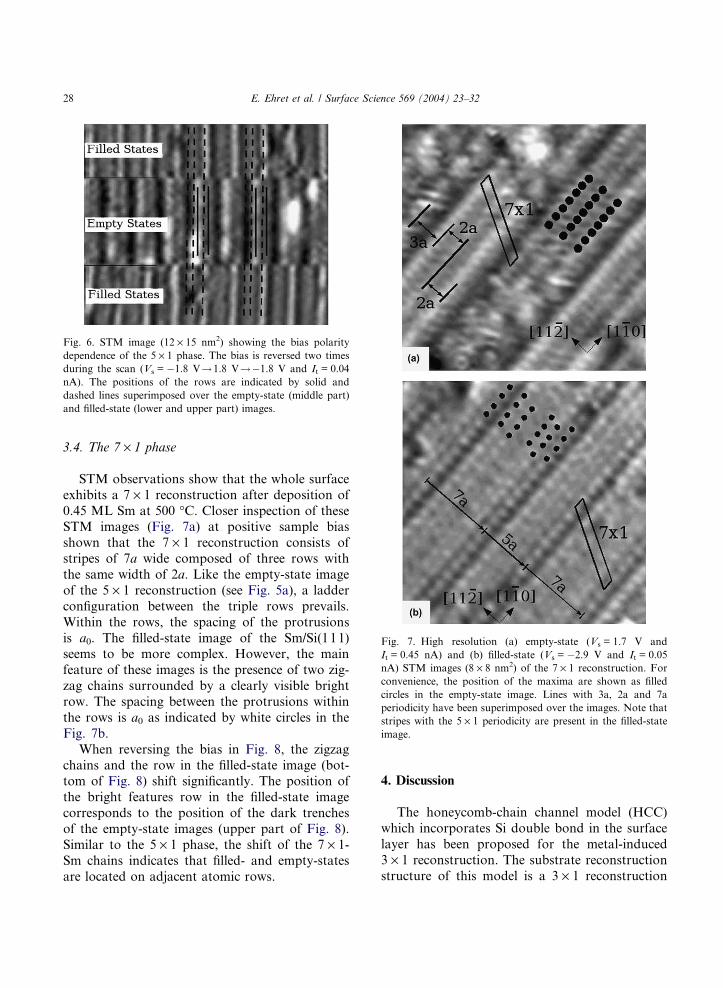
Fig. 6. STM image (12 · 15 nm2) showing the bias polarity
dependence of the 5 · 1 phase. The bias is reversed two times
during the scan (Vs = �1.8 V!1.8 V!�1.8 V and It = 0.04
nA). The positions of the rows are indicated by solid and
dashed lines superimposed over the empty-state (middle part)
and filled-state (lower and upper part) images.
Fig. 7. High resolution (a) empty-state (Vs = 1.7 V and
It = 0.45 nA) and (b) filled-state (Vs = �2.9 V and It = 0.05
nA) STM images (8 · 8 nm2) of the 7 · 1 reconstruction. For
convenience, the position of the maxima are shown as filled
circles in the empty-state image. Lines with 3a, 2a and 7a
periodicity have been superimposed over the images. Note that
stripes with the 5 · 1 periodicity are present in the filled-state
image.
28 E. Ehret et al. / Surface Science 569 (2004) 23–32
3.4. The 7 · 1 phase
STM observations show that the whole surface
exhibits a 7 · 1 reconstruction after deposition of
0.45 ML Sm at 500 �C. Closer inspection of theseSTM images (Fig. 7a) at positive sample bias
shown that the 7 · 1 reconstruction consists of
stripes of 7a wide composed of three rows with
the same width of 2a. Like the empty-state image
of the 5 · 1 reconstruction (see Fig. 5a), a ladder
configuration between the triple rows prevails.
Within the rows, the spacing of the protrusions
is a0. The filled-state image of the Sm/Si(111)seems to be more complex. However, the main
feature of these images is the presence of two zig-
zag chains surrounded by a clearly visible bright
row. The spacing between the protrusions within
the rows is a0 as indicated by white circles in the
Fig. 7b.
When reversing the bias in Fig. 8, the zigzag
chains and the row in the filled-state image (bot-tom of Fig. 8) shift significantly. The position of
the bright features row in the filled-state image
corresponds to the position of the dark trenches
of the empty-state images (upper part of Fig. 8).
Similar to the 5 · 1 phase, the shift of the 7 · 1-
Sm chains indicates that filled- and empty-states
are located on adjacent atomic rows.
4. Discussion
The honeycomb-chain channel model (HCC)
which incorporates Si double bond in the surface
layer has been proposed for the metal-induced
3 · 1 reconstruction. The substrate reconstruction
structure of this model is a 3 · 1 reconstruction

Fig. 8. STM image (10 · 10 nm2) showing the bias polarity
dependence of the 7 · 1 phase. The bias is reversed during the
scan (Vs = �1.8 V!2.1 V and It = 0.25 nA). The positions of
the rows are indicated by solid and dashed lines superimposed
over the empty-state (upper part) and filled-state (lower part)
images.
E. Ehret et al. / Surface Science 569 (2004) 23–32 29
constituted by four inequivalent Si adatoms which
form a ‘‘honeycomb chain’’ parallel to the surface
plane (the top Si layer reconstruction structure).These four Si atoms are threefold coordinated
and the inner atoms are in a planar configuration.
With the adsorption of the metal atom in the chan-
nel between the ‘‘honeycomb chain’’, the surface
structure acquires a 3 · 1 or 3 · 2 periodicity
dependent on the valency of the adsorbate. The
(HCC) model for the 3 · 2 reconstruction is repre-
sented in Fig. 11a.In a recent paper [10], we have interpreted the
Si(111)3 · 2-Sm reconstruction in terms of the
HCC model from the combined study of STM,
LEED and ab initio calculations. The 1/6 ML
Sm coverage was accommoded by putting one
Sm atom in every second 3 · 1 unit cell of the
HCC structure. The HCC structure is stabilized
by the saturation of the dangling bonds of the Siatoms surrounding the positively-ionized Sm. This
results in bright protrusions with the zigzag chain
appearance in the filled-state STM images shown
in Fig. 4b whereas in the empty-state STM image
of the Fig. 4a, the Sm atoms appear as rows of
bright protrusions with · 2 periodicity.
Let us return to LEED data. While the LEED
(Fig. 2a) exhibits a 3 · 1 pattern, the STM shows
the 3 · 2 surface structure (Fig. 3). We suggested
that the apparent discrepancy of the LEED and
STM data is explained by the lack of sensitivityof the Sm atoms with poor long-range order. Thus,
the 3 · 1 LEED pattern only reflects the well-or-
dered reconstruction structure of the (HCC) top
Si layer like the filled-state STM images does.
It is interesting to compare our experimental re-
sults of the 5 · 1-Sm and 7 · 1-Sm structures with
the other systems such as Ca and Yb [17,18,24].
These metals form high order n · 1 phases follow-ing the sequence (3 · 1), (5 · 1), (7 · 1) and (2 · 1)
for increasing the coverage. The present study
shows the (3 · 2), (5 · 1) and (7 · 1) sequence. As
a rule, one should not expect these reconstructions
to be identical because the 2 · 1 phase for the Sm/
Si(111) system is missing of the sequence. How-
ever, the previous works [17,24] of the Ca/
Si(111) system show interesting similarities. The5 · 1-Sm and 7 · 1-Sm structures in the empty-
state images appear as double and triple rows of
protrusions with ·2a periodicity separated by
·3a wide dark gaps. It is therefore suggested that
these high order n · 1 phases can be considered
as a mixture of 3 · 1 and 2 · 1 subunit cells. Fur-
ther evidence for this assumption is the local for-
mation of others n · 1 phases at Sm coverageswhere the 5 · 1 phase coexists with the 3 · 2 phase.
Indeed, at a appropriate Sm coverage, large
patches of the 8 · 2 reconstruction, which incorpo-
rate two 3 · 1 unit cells and one 2 · 1 unit cell,
appear on the Si(111) surface as shown in the
empty-state STM image of Fig. 9. These STM re-
sults fully support the view that the 3 · 1 and n · 1
phases should have closely related atomic models.On the basis of dual-polarity STM images and
ab initio calculations, it has been suggested that
the odd-order n · 1 (n = 3,5,7,. . .) phases of the
Ca/Si(111) interface consist of HCC chains (3 · 1
structural unit) and Seiwatz chains (2 · 1 struc-
tural unit) where the Ca atoms sit in the channel
between the Si chains. Notice that the Seiwatz
chain is a unit of the Seiwatz model previouslyproposed by Weitering et al. for the 3 · 1 AM
structures [8]. This is a missing top layer recon-
struction incorporating fivefold Si rings. We
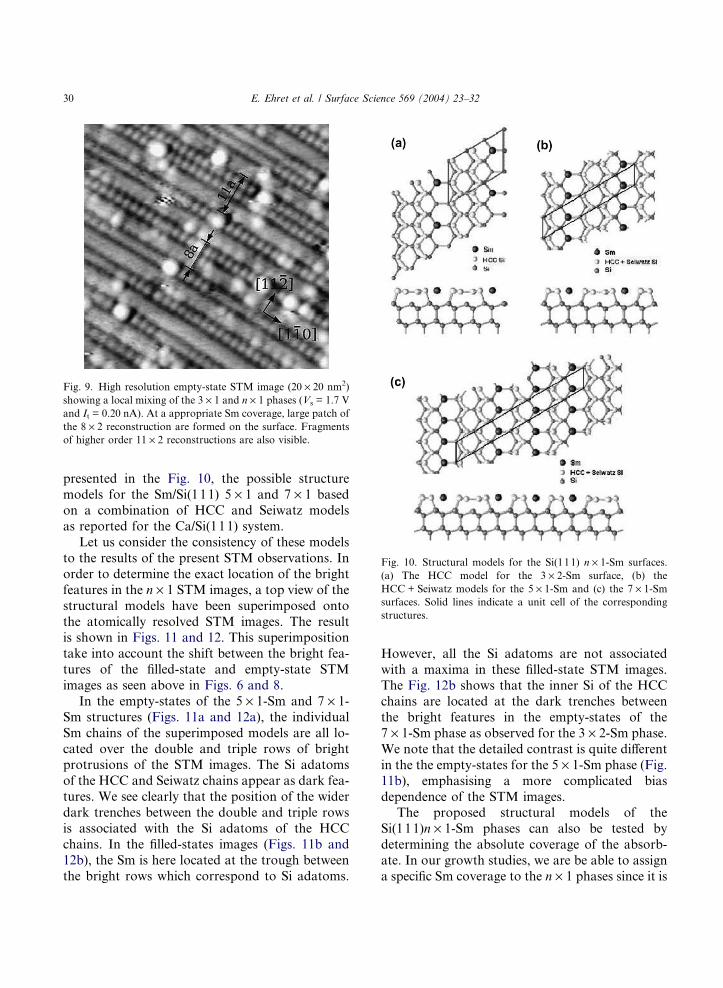
Fig. 9. High resolution empty-state STM image (20 · 20 nm2)
showing a local mixing of the 3 · 1 and n · 1 phases (Vs = 1.7 V
and It = 0.20 nA). At a appropriate Sm coverage, large patch of
the 8 · 2 reconstruction are formed on the surface. Fragments
of higher order 11 · 2 reconstructions are also visible.
Fig. 10. Structural models for the Si(111) n · 1-Sm surfaces.
(a) The HCC model for the 3 · 2-Sm surface, (b) the
HCC + Seiwatz models for the 5 · 1-Sm and (c) the 7 · 1-Sm
surfaces. Solid lines indicate a unit cell of the corresponding
structures.
30 E. Ehret et al. / Surface Science 569 (2004) 23–32
presented in the Fig. 10, the possible structure
models for the Sm/Si(111) 5 · 1 and 7 · 1 basedon a combination of HCC and Seiwatz models
as reported for the Ca/Si(111) system.
Let us consider the consistency of these models
to the results of the present STM observations. In
order to determine the exact location of the bright
features in the n · 1 STM images, a top view of the
structural models have been superimposed onto
the atomically resolved STM images. The resultis shown in Figs. 11 and 12. This superimposition
take into account the shift between the bright fea-
tures of the filled-state and empty-state STM
images as seen above in Figs. 6 and 8.
In the empty-states of the 5 · 1-Sm and 7 · 1-
Sm structures (Figs. 11a and 12a), the individual
Sm chains of the superimposed models are all lo-
cated over the double and triple rows of brightprotrusions of the STM images. The Si adatoms
of the HCC and Seiwatz chains appear as dark fea-
tures. We see clearly that the position of the wider
dark trenches between the double and triple rows
is associated with the Si adatoms of the HCC
chains. In the filled-states images (Figs. 11b and
12b), the Sm is here located at the trough between
the bright rows which correspond to Si adatoms.
However, all the Si adatoms are not associated
with a maxima in these filled-state STM images.The Fig. 12b shows that the inner Si of the HCC
chains are located at the dark trenches between
the bright features in the empty-states of the
7 · 1-Sm phase as observed for the 3 · 2-Sm phase.
We note that the detailed contrast is quite different
in the the empty-states for the 5 · 1-Sm phase (Fig.
11b), emphasising a more complicated bias
dependence of the STM images.The proposed structural models of the
Si(111)n · 1-Sm phases can also be tested by
determining the absolute coverage of the absorb-
ate. In our growth studies, we are be able to assign
a specific Sm coverage to the n · 1 phases since it is

Fig. 11. Magnified (a) empty-state (Vs = 1.8 V and It = 1.02
nA) and (b) filled-state (Vs = �3.7 V and It = 0.08 nA) STM
images of the 5 · 1-Sm reconstruction (6 · 6 nm2). Schematic
diagram of the corresponding structural models are superim-
posed over the images.
Fig. 12. Magnified (a) empty-state (Vs = 1.7 V and It = 0.45
nA) and (b) filled-state (Vs = �2.8 V and It = 0.43 nA) STM
images of the 7 · 1-Sm reconstruction (4 · 4 nm2). Schematic
diagram of the corresponding structural models are superim-
posed over the images.
E. Ehret et al. / Surface Science 569 (2004) 23–32 31
formed at substrate temperature at which Sm
desorption is very low. From our STM observa-
tions, we estimate that the Sm coverages for the
5 · 1 and 7 · 1 phases are 0.34 and 0.38 ML
respectively. This is also consistent with the 5 · 1
and 7 · 1 models which require a Sm density of
0.4 and 0.43 ML respectively.
Taking into account the information providedby the coverage determination, the polarity
dependence and the registration of the STM
images, we propose that Si(111) n · 1-Sm (n = 5,
7,. . .) surfaces consist of Seiwatz and HCC-based
Si substrate reconstruction structures. It should
be noted that the electronic nature of the n · 1-
Sm (n = 5,7, . . .) surfaces depends on the Sm cov-
erage. The 5 · 1-Sm and 7 · -Sm surfaces with a
Sm density of 0.4 and 0.43 ML respectively shouldbe metallic due to electron counting consideration.
However, the STM images have been recorded
32 E. Ehret et al. / Surface Science 569 (2004) 23–32
with sample biases of about 2 V suggesting that
these surfaces are semiconducting like. The reason
for this is not clear at this stage. Further experi-
ments, particularly photoemission measurements
are required to clarify the exact electronic natureof these surfaces.
5. Conclusion
We have been studied the surface reconstruc-
tions induced by submonolayer Sm adsorption
on a Si(111). This system forms a series ofmetal-induced n · 1 (n = 3,5,7,. . .) reconstructionswith increase of Sm coverage on the Si(111) sub-
strate at elevated temperatures. Our STM results
indicate that these reconstructions appear as
well-ordered row-like structures. Local mixing of
the 3 · 1 and n · 1 unit cells (or stripes) indicates
that the atomic models for these phases should
be closely related. The atomically resolved STMimages reveal a strong bias dependence which
determine the relative registry of the Si as well as
Sm atoms for these reconstructions. We presented
in the Fig. 10, the possible structure models for the
Sm/Si(111) 5 · 1 and 7 · 1 based on a combina-
tion of HCC and Seiwatz models as reported for
the Ca/Si(111) system.
References
[1] J. Nogami, Surf. Rev. Lett. 7 (2000) 555.
[2] A. Kirakosian, J.L. McChesney, R. Bennwitz, J.N. Crain,
J.-L. Lin, F.J. Himpsel, Surf. Sci. 498 (1999) 109.
[3] K. Sakamoto, T. Okuda, H. Nishimoto, H. Daimon, S.
Suga, T. Kinoshita, A. Kakisaki, Phys. Rev. B 50 (1994)
1725.
[4] T. Okuda, H. Daimon, S. Suga, Y. Tezuka, S. Ino, Surf.
Sci. 122/123 (1997) 89.
[5] A.A. Saranin et al., Phys. Rev. B 58 (1998) 7059.
[6] H.H. Weitering, X. Shi, S.C. Erwin, Phys. Rev. B 54
(1996) 10585.
[7] A.A. Saranin, A.V. Zotov, V.G. Lifshits, M. Katayama,
K. Oura, Surf. Sci. 426 (1999) 298.
[8] H.H. Weitering, Surf. Sci. Lett. 355 (1996) 271.
[9] G. Lee, S. Hong, H. Kim, D. Shin, J. Koo, H. Lee, D.W.
Moon, Phys. Rev. Lett. 87 (2001) 56104.
[10] F. Palmino, E. Ehret, L. Mansour, J.-C. Labrune, G. Lee,
H. Kim, J.-M Themlin, Phys. Rev. B 67 (2003) 195413.
[11] D. Jeon, T. Hashizume, T. Sakurai, J. Vac. Sci. Technol. B
12 (1994) 2044.
[12] W.C. Fan, A. Ignatiev, Phys. Rev. B 41 (1990) 3592.
[13] J. Quinn, F. Jona, Surf. Sci. 249 (1991) L307.
[14] C. Wigren, J.N. Andersen, R. Nyholm, M. Gothelid, M.
Hammar, C. Tornevik, U.O. Karlson, Phys. Rev. B 48
(1993) 11014.
[15] K. Sakamoto, W. Takeyama, H.M. Zhang, R.I.G. Uhr-
berg, Phys. Rev. B 66 (2002) 165319.
[16] S. Erwin, H.H. Weitering, Phys. Rev. Lett. 81 (1998) 2296.
[17] A.A. Baski, S.C. Erwin, M.S. Turner, K.M. Jones, J.W.
Dickinson, J.A. Carlisle, Surf. Sci. 476 (2001) 22.
[18] C. Wigren, J.N. Andersen, R. Nyholm, U.O. Karlson, J.
Nogami, A.A. Baski, C.F. Quate, Phys. Rev. B 47 (1993)
9663.
[19] R.-L. Vaara, M.V. Kuzmin, R.E. Perala, P. Laukkanen,
I.J. Vayrynen, Surf. Sci. 529 (2003) L229.
[20] M.V. Kuzmin, R.-L. Vaara, P. Laukkanen, R.E. Perala,
I.J. Vayrynen, Surf. Sci. 538 (2003) 124.
[21] M.V. Kuzmin, R.-L. Vaara, P. Laukkanen, R.E. Perala,
I.J. Vayrynen, Surf. Sci. 549 (2004) 183.
[22] A. Franciosi, J.H. Weaver, P. Perfetti, A.D. Katnani, G.
Margaritondo, Solid. State Commun. 47 (1983) 427.
[23] T.V. Krachino, M.V. Kuzmin, M.V. Loginov, M.A.
Mittsev, Phys. Solid State 40 (1998) 341.
[24] T. Sekiguchi, F. Shimokoshi, T. Nagao, S. Hasegawa,
Surf. Sci. 493 (2001) 148.