“SISTEMA DE SENSORES PARA SEGUIMIENTO DEL ...
179
Grado Universitario en Ingeniería de Sistemas Audiovisuales Imagen y Sonido 2017-2018 Trabajo Fin de Grado “SISTEMA DE SENSORES PARA SEGUIMIENTO DEL TRANSPORTE DE MERCANCÍAS” David Abarca Alzamora Tutor MARIA CALDERON PASTOR Leganés, 2018
-
Upload
khangminh22 -
Category
Documents
-
view
0 -
download
0
Transcript of “SISTEMA DE SENSORES PARA SEGUIMIENTO DEL ...

Grado Universitario en Ingeniería de Sistemas
Audiovisuales Imagen y Sonido
2017-2018
Trabajo Fin de Grado
“SISTEMA DE SENSORES PARA
SEGUIMIENTO DEL TRANSPORTE
DE MERCANCÍAS”
David Abarca Alzamora
Tutor
MARIA CALDERON PASTOR
Leganés, 2018

ii

iii
AGRADECIMIENTOS
A todos los compañeros, amigos y en especial a mi familia por todo el apoyo que me han
brindado durante toda mi época de estudios.
A mis padres, por todo su esfuerzo y paciencia. Ya que a pesar de ser el tercero de cinco hijos
no aflojaron nunca y me ayudaron a seguir adelante.
A mi abuelo, que siempre me repetía la importancia de seguir adelante y esforzarme en los
estudios. Lo prometido es deuda.
A Vicente, por todos sus consejos y apoyo.

iv
ÍNDICE GENERAL
1. INTRODUCCIÓN ..................................................................................................................... 1
1.1. Objetivos y motivación .................................................................................................. 1
1.2. Organización de la Memoria ....................................................................................... 2
1.3. Metodología .................................................................................................................. 3
1.4. Hitos .............................................................................................................................. 3
2. ANTECEDENTES Y ESTADO DEL ARTE .................................................................................... 4
2.1. Sistemas de seguimiento ............................................................................................... 4
2.1.1. Marco Regulador ............................................................................................................. 6
2.2. IoT. Internet Of things ................................................................................................... 6
2.3. Módulos inteligentes “Thinking things” ...................................................................... 10
2.4. Elección Hardware de Control: Arduino ...................................................................... 11
3. REQUISITOS DE SISTEMA ..................................................................................................... 14
4. HARDWARE EMPLEADO ...................................................................................................... 15
4.1. Arduino UNO ............................................................................................................... 16
4.2. Arduino MEGA ............................................................................................................. 18
4.3. Comunicaciones .......................................................................................................... 19
4.3.1. La comunicación serie ................................................................................................... 19
4.3.1.1. Comunicación en serie UART ..................................................................................... 21
4.3.1.2. Comunicación en serie del bus SPI ............................................................................. 21
4.3.1.3. Comunicación en serie I2C, I²C o TWI ........................................................................ 26
4.4. Dispositivos de Comunicación ..................................................................................... 29
4.4.1. Ethernet Shield .............................................................................................................. 30
4.5. Sensores ...................................................................................................................... 31
4.5.1. Sensor de Intensidad Lumínica LDR .............................................................................. 31
4.5.2. Sensor de Temperatura y Humedad GHT11 ................................................................. 33
4.5.3. Transistor LM35 ............................................................................................................ 35
4.5.4. IMU ................................................................................................................................ 36
4.5.4.1. MPU – 6050 ................................................................................................................ 36
4.6. Otros elementos .......................................................................................................... 38
4.6.1. Módulo RTC ................................................................................................................... 38
5. ENTORNO DE PROGRAMACION Y SOFTWARE UTILIZADO .................................................. 40
5.1. IDE Arduino ................................................................................................................. 40
6. DISEÑO MONTAJE Y EJECUCION ......................................................................................... 44
6.1. Modulo sensor de Temperatura y Humedad .............................................................. 44

v
6.1.1. Esquema LM35 .............................................................................................................. 44
6.1.2. Esquema DHT11 ............................................................................................................ 45
6.2. Modulo sensor de Iluminación .................................................................................... 46
6.2.1. Esquema LDR ................................................................................................................. 46
6.2.2. Esquema fotorresistencia 5528 ..................................................................................... 47
6.3. Modulo sensor de Giroscopio y Acelerómetro ........................................................... 48
6.4. Módulo RTC DS1307 .................................................................................................... 50
6.5. Montaje del módulo completo ................................................................................... 52
6.5.1. Código del módulo completo ........................................................................................ 53
6.5.1.1. Librerías Arduino: ....................................................................................................... 53
6.5.1.2. Definición de Variables: ............................................................................................. 54
6.5.1.3. Función SETUP: ........................................................................................................... 54
6.5.1.4. Función “LoggingTime”: ............................................................................................. 56
6.5.1.5. Función LogginTemperature: ..................................................................................... 57
6.5.1.6. Función LoggingHumidity: .......................................................................................... 58
6.5.1.7. Función LoggingBrightness:........................................................................................ 59
6.5.1.8. Función LoggingGiro: .................................................................................................. 60
6.5.1.9. Función LOOP: ............................................................................................................ 62
7. PRUEBAS, PROBLEMAS Y SOLUCIONES ............................................................................... 64
7.1. Aplicación y análisis: .................................................................................................... 64
7.1.1. Método de inferencia Montecarlo: ............................................................................... 66
7.1.1.1. Parámetros método Montecarlo ............................................................................... 66
7.1.1.2. Resultados .................................................................................................................. 67
7.1.1.3. Conclusiones: ............................................................................................................. 67
7.2. Problemas: .................................................................................................................. 68
8. CONCLUSIONES Y TRABAJOS FUTUROS .............................................................................. 70

vi
ÍNDICE FIGURAS
Fig. 1 Principales empresas de envíos [1] ..................................................................................... 4
Fig. 2 Empresas de seguimiento de envíos [5] .............................................................................. 4
Fig. 3 Seguimiento de correos España [6] ..................................................................................... 4
Fig. 4 Seguimiento Amazon [7]...................................................................................................... 5
Fig. 5 “Hype Cycle” de Gartner para tecnologías emergentes 2011 [8] ....................................... 7
Fig. 6 “Hype Cycle” de Gartner para tecnologías emergentes 2014 [8] ....................................... 8
Fig. 7 Esquema de IoT [9] .............................................................................................................. 8
Fig. 8 Incremento cronológico del IoT [10] ................................................................................... 9
Fig. 9 Partes de un dispositivo RFID [11] ..................................................................................... 10
Fig. 10 Placas de desarrollo Arduino [12] .................................................................................... 15
Fig. 11 Sensores y módulos de Arduino [12] ............................................................................... 16
Fig.12 Placa Arduino Dumelianove [13] ...................................................................................... 17
Fig. 13 Placa Arduino UNO [14] ................................................................................................... 17
Fig. 14 Placa Arduino Mega [14] ................................................................................................ 18
Fig. 15 Protocolo de comunicación en serie [15] ........................................................................ 19
Fig. 16 Protocolo de comunicación UART [15] ............................................................................ 21
Fig. 17 Protocolo de comunicación SPI [15] ................................................................................ 22
Fig. 18 Esquema comunicación Master Slave [15] ...................................................................... 22
Fig. 19 Línea de control SS [15] ................................................................................................... 23
Fig. 20 Múltiples líneas de control SS. [15] ................................................................................. 24
Fig. 21 Configuración en cascada [15] ......................................................................................... 24
Fig. 22 Pines placa Arduino UNO [15] ......................................................................................... 26
Fig. 23 Pines ICSP Placa Arduino UNO [15] ................................................................................. 26
Fig. 24 Conexión en I2C [16] ........................................................................................................ 27
Fig. 25 Formato de datos enviados de I2C [17] ........................................................................... 28
Fig. 26 Placa ethernet shield [18] ................................................................................................ 30
Fig. 27 Sensor LDR [19] ................................................................................................................ 31
Fig. 28 Variación de la resistencia de un LDR con la temperatura y la frecuencia de luz [20] .... 31
Fig. 29 Variación de la resistencia de un LDR con la intensidad de luz [21] ................................ 31
Fig. 30 Esquema LM358 [31] ....................................................................................................... 32
Fig. 31 Módulo sensor de luz [22] ............................................................................................... 33
Fig. 32 Módulo y sensor de temperatura y humedad [23] ......................................................... 33
Fig. 33 Codificación a binario del DHT11 [23] ............................................................................. 34
Fig. 34 Trama de datos DHT11 [23] ............................................................................................. 35
Fig. 35 Transistor LM35 [24] ........................................................................................................ 35
Fig. 36 Funcionamiento acelerómetro MEMS [25] ..................................................................... 36
Fig. 37 Mecanismo giroscopio MEMS [26] .................................................................................. 37
Fig. 38Módulo MPU-6050 [27] .................................................................................................... 37
Fig. 39 Módulo RTC [32] .............................................................................................................. 38
Fig. 40 Esquema de conexión del DS1307 [33] ........................................................................... 39
Fig. 41 Interface Arduino IDE [28] ............................................................................................... 41
Fig. 42 Sketch blink ...................................................................................................................... 41
Fig. 43 Proceso de compilación ................................................................................................... 42
Fig. 44 Importar librería [29] ....................................................................................................... 43
Fig. 45 Gestor de librerías [29] .................................................................................................... 43

vii
Fig. 46 Esquema LM35 ................................................................................................................ 45
Fig. 47 Esquema DHT11 ............................................................................................................... 45
Fig. 48 Librería para DTH11 ......................................................................................................... 46
Fig. 49 Divisor de tensión LDR [30] .............................................................................................. 46
Fig. 50 Esquema LDR ................................................................................................................... 47
Fig. 51 Esquema Fotorresistencia ............................................................................................... 48
Fig. 52 Esquema MPU-6050 ........................................................................................................ 48
Fig. 53 Gestor de librerías MPU6050 .......................................................................................... 49
Fig. 54 Ejemplo MPU6050 ........................................................................................................... 49
Fig. 55 Compilando script ............................................................................................................ 50
Fig. 56 Conexión módulo RTC...................................................................................................... 50
Fig. 57 Gestor de librerías RTC .................................................................................................... 51
Fig. 58 Ejemplo RTClib ................................................................................................................. 51
Fig. 59 Esquema módulo completo ............................................................................................. 52
Fig. 60 Foto módulo completo .................................................................................................... 53
Fig. 61 Librerías Arduino ............................................................................................................. 53
Fig. 62 Definición de variables DHT ............................................................................................. 54
Fig. 63 Definición de variables MPU y RTC .................................................................................. 54
Fig. 64 Función SETUP ................................................................................................................. 55
Fig. 65 SETUP: Configuración I2C ................................................................................................ 55
Fig. 66 Configuración puerto serie .............................................................................................. 55
Fig. 67 Configuración RTC ............................................................................................................ 56
Fig. 68 Creación y configuración fichero DATA ........................................................................... 56
Fig. 69 Función LoggingTime ....................................................................................................... 57
Fig. 70 Función LoggingTemperature .......................................................................................... 58
Fig. 71 LoggingTemperature, comprobación .............................................................................. 58
Fig. 72 LoggingTemperature control y escritura en fichero ........................................................ 58
Fig. 73 Función LoggingHumidity ................................................................................................ 59
Fig. 74 Función LoggingBrightness .............................................................................................. 59
Fig. 75 Scanning dispositivos I2C ................................................................................................. 60
Fig. 76 Función LoggingGyro, registros I2C ................................................................................. 60
Fig. 77 Función LoggingGyro ....................................................................................................... 61
Fig. 78 Función LoggingGyro, escritura en fichero ...................................................................... 62
Fig. 79 Función LOOP .................................................................................................................. 62
Fig. 80 Puesto serial sistema completo ....................................................................................... 63
Fig. 81 Evolución IoT .................................................................................................................... 75
Fig. 82 Variables y distribucion Normal....................................................................................... 76
Fig. 83 Estadísticos Asociados ..................................................................................................... 76
Fig. 84 Distribución Normal Temperatura ................................................................................... 77
Fig. 85 Distribución Normal Luz .................................................................................................. 77
Fig. 86 Distribución Normal Humedad ........................................................................................ 78
Fig. 87 Datos reales (izq.) VS 300 mil simulaciones (der.). .......................................................... 79
Fig. 88 Re-simulaciones (izq.) y cálculo de estadísticos representativo (der.) ............................ 80

viii
ÍNDICE TABLAS
TABLA 1 COMPARATIVA MODELOS ARDUINO OFICIALES ........................................................... 12
TABLA 2 ANÁLISIS DE ENVÍO DE PAQUETES ................................................................................ 14
TABLA 3 CARACTERÍSTICAS PRINCIPALES ARDUINO UNO .......................................................... 17
TABLA 4 CARÁCTERISTICAS ARDUINO MEGA .............................................................................. 18
TABLA 5 VENTAJAS E INCONVENIENTES DEL SPI ......................................................................... 25
TABLA 6 PINES DE MODELOS DE PLACAS ARDUINO ................................................................... 25
TABLA 7 VENTAJAS E INCONVENIENTES DEL I2C ........................................................................ 28
TABLA 8 PINES VINCULADOS A I2C ............................................................................................. 28
TABLA 9 CARACTERÍSTICAS DEL SENSOR LDR GL5528 ................................................................ 32
TABLA 10 CARACTERÍSTICAS DEL MÓDULO LDR ......................................................................... 32
TABLA 11 CARACTERÍSTICAS TÉCNICAS DEL DHT11 .................................................................... 34
TABLA 12 LM35 Y SUS CARACTERÍSTICAS PRINCIPALES .............................................................. 35
TABLA 13 CARACTERÍSTICAS DEL MÓDULO MPU ....................................................................... 37
TABLA 14 CONEXIONES ENTRE MÓDUKO RTC Y ARDUINO ........................................................ 38
TABLA 15 CARACTERÍSTICAS MÓDULO RTC ................................................................................ 39
TABLA 16 REGISTRO PWR_MGMT_1 .......................................................................................... 55
TABLA 17 REGISTROS ACELERÓMETRO, TEMPERATURA Y GIROSCOPIO .................................... 61
TABLA 18 MEDIAS Y VALORES ESTADÍSTICOS ............................................................................. 64
TABLA 19 TABLA DE CORRELACIONES ......................................................................................... 64
TABLA 20 VARIABLES ESTADISTICAS DE SIMULACIÓN ................................................................ 67
TABLA 21 TABLA DE CORRELACIÓN DE SIMULACIONES ............................................................. 67
TABLA 22 RANGOS DE ACEPTACIÓN ........................................................................................... 68
TABLA 23 PRESUPUESTO ............................................................................................................. 74
TABLA 24 OTROS CONCEPTOS .................................................................................................... 74

ix
RESUMEN
La continua evolución de las tecnologías ha propiciado la implementación de
innumerables soluciones tecnológicas aplicables al entorno que nos rodea e incluso a las
tareas cotidianas del día a día. Este desarrollo tecnológico orientado a este ámbito se
denominó Internet de las cosas.
Un ejemplo del internet de las cosas es la herramienta de monitorización del envío de
mercancías. Los usuarios de este servicio son capaces de hacer el seguimiento en tiempo
real del trayecto que sigue el envío y así poder gestionar los tiempos de envíos.
En el presente proyecto se plantea como objetivo crear un sistema de sensores basado en
software libre de Arduino para la monitorización del entorno de paquetes, aportando
nueva información sobre el estado físico por el que pasa cada paquete, complementando
el servicio de tracking para asegurar la calidad del servicio.
En la memoria se detallará las distintas tecnologías involucradas en el desarrollo del
proyecto, los distintos procesos de selección e implementación de los componentes
involucrados en el diseño de los sub-módulos y del sistema completo.
Palabras clave: Internet de las cosas, Arduino, sensores, código abierto, I2C,
comunicación en serie, servicio de seguimiento.

1
1. INTRODUCCIÓN
El control y la monitorización de paquetes, durante un servicio de entrega, puede llegar
a ser determinante para el usuario al momento de recibir un envío delicado o en dudoso
estado. El contar con el servicio de monitorización facilitará la toma de decisión de
aceptar o retornar el paquete recibido en dudosas condiciones, o incluso presentar
alguna reclamación demostrando el desperfecto.
Con un dispositivo cuantificador, como el de este proyecto, se pueden describir
específicamente las condiciones por las que ha pasado el paquete, siendo posible
determinar si el envío y manipulación del paquete ha sido el apropiado.
En el presente trabajo se tratará, desde un punto de vista teórico y práctico, el proceso
de diseño, implementación y análisis de un sistema de sensores que permita cuantificar
las condiciones ambientales y de control de calidad a las que se somete a un paquete
durante su trayecto. Dicho sistema de sensores se implementa mediante el uso de
tecnologías de software libre y hardware de bajo coste.
1.1. Objetivos y motivación
Como se indica en el título, el fin de este proyecto es proponer una herramienta que
emplee un conjunto de sistemas cuantificadores, aplicados al entorno de un paquete,
para aportar información específica sobre las condiciones físicas en las que se
encuentra la mercancía. Dicha información será contrastada con un sistema de
decisión que se ajustará a las especificaciones solicitadas por el cliente y ofertadas
por la compañía encargada del envío. La no conformidad de las condiciones
facilitará al cliente la opción de no aceptar el envío y presentar las reclamaciones
pertinentes.
Objetivo Principal: Implementar, sobre una plataforma open hardware y
software de Arduino, un conjunto de sistemas cuantificadores del entorno, capaz
de medir de forma autónoma durante el trayecto de un paquete.
Objetivos Secundarios: Aplicar los conocimientos adquiridos en los estudios
universitarios sobre microcontroladores y poner en práctica la capacidad de
aprender nuevos lenguajes de programación, es decir aplicar la filosofía DIY
(Do-It-Yourself).
En este caso el desarrollado fue sobre una plataforma open source software y
hardware, accesible (de programación amigable) y asequible (de bajo coste) para
cualquier persona.

2
1.2. Organización de la Memoria
El presente proyecto se desarrollará en ocho capítulos y otros apartados que incluirán
listados de referencias, anexos y bibliografías.
En primer capítulo, se presenta la introducción a la memoria, la idea principal del
proyecto, la descripción de los objetivos planteados, la metodología seguida en el
desarrollo y las etapas que se siguió durante el proceso.
En el segundo capítulo, se realizara un pequeño estudio de las necesidades globales del
problema planteado en este proyecto y las posibles soluciones existentes en la
actualidad, para así poder describir mejor la situación del estado del arte y justificar
eficientemente las decisiones tomadas en el proyecto, como la elección de las
tecnologías aplicadas.
En el tercer capítulo, se plantean los requisitos inherentes a la problemática del proyecto
y además se comentaran las soluciones que se implementaran, todo ello tras analizar
soluciones reales bajo la experiencia del autor.
En el cuarto capítulo, se realizara una introducción de las diferentes herramientas
hardware existentes del fabricante seleccionado, pasando por las placas principales de
Arduino o por los sensores más utilizados describiendo las características, los pros y los
contras de los elementos que se utilizarán en este proyecto. Se describirá también las
principales formas de comunicación que utilizan los diferentes módulos con la placa
principal, y por último el modulo responsable del registro de la información obtenida.
En el quinto capítulo, se describirán las distintas herramientas software que se utilizaran
para la implementación de código del sistema completo, especialmente la herramienta
de desarrollo propia de Arduino. También se describirán herramientas para diseño
esquemático del montaje electrónico.
En el sexto capítulo, se desarrollará en detalle en el diseño, montaje y programación de
todo el conjunto hasta conseguir el sistema definitivo.
En el séptimo capítulo, se describirán las pruebas funcionales que se han llevado a cabo
sobre el sistema, los problemas que han ido surgiendo durante el proceso y las
soluciones que se han aportado.
Y en el capítulo ocho, último capítulo, se detallarán las conclusiones obtenidas y
posibles trabajos futuros, a partir de los datos del capítulo anterior y en función de los
objetivos marcados.
Para finalizar se incluyen anexos en la parte final de la memoria, dichos anexos
incluyen un presupuesto detallado del sistema implementado y un pequeño análisis
sobre el entorno socio-económico, imágenes sobre los datos estadísticos obtenidos y

3
simulados, un resumen en inglés (abstract), el código completo implementado en el
dispositivo y datasheets relevantes de componentes utilizados en el módulo final.
1.3. Metodología
Una vez definido el escenario y las necesidades del proyecto, se plantearon las posibles
soluciones con la selección de los dispositivos y sensores varios, capaces de cubrir los
requisitos establecidos.
El proyecto ha sido desarrollado en sub-módulos de bloques funcionales y subsistemas
orientados a cubrir específicamente los requisitos establecidos en los objetivos. Para
ello cada módulo se ha ido implementando en pequeños fragmentos de código y se ha
probado por separado, controlando un determinado dispositivo para cada funcionalidad.
El código principal se ha ido conformando por fases, añadiendo los distintos
subsistemas a un código global del proyecto.
1.4. Hitos
Siguiendo el sistema de trabajo establecido en los apartados anteriores, se han definido
los siguientes hitos:
1) Investigación, búsqueda de bibliografía y análisis de la situación actual de los
sistemas de Arduino.
2) Selección de dispositivos hardware (placa Arduino, sensores, shields, etc) y
compra de los dispositivos.
3) Aprendizaje del lenguaje de programación, mediante el entorno de desarrollo
IDE de Arduino.
4) Montaje de circuitos, programación y puesta a punto de cada sub-modulo, como
test de pruebas o calibrados del sistema.
5) Comparativa con sistemas y plataformas IoT (Internet of Things) para
adquisición de dispositivos
6) Obtención, procesamiento de la información y visualización de datos recogidos
por el sistema Arduino sobre script Excel.
7) Fusión de esquemas y código implementado de cada sub-módulos, en un único
sistema cuantificador.
8) Mejora: Módulo de sensor digital de temperatura y humedad DHT11.
9) Mejora: Módulo de sensor de luz con fotorresistencia 5528.
10) Mejora: Módulo de RTC (del inglés, Real Time Clock) DS1307 calendario -
reloj para el sistema.
11) Mejora: Se incorpora una segunda placa de Arduino (Shield) para añadir una
funcionalidad de registro de la información en una memoria extraíble.
12) Redacción de la memoria del proyecto.

4
2. ANTECEDENTES Y ESTADO DEL ARTE
En este capítulo se va a realizar un análisis sobre el estado del arte de las diferentes
tecnologías existentes y relacionadas con el presente proyecto. Dichas tecnologías
podría asociarse al sector de “Thinking things” o “Internet of things” (IoT, Internet de
las cosas).
2.1. Sistemas de seguimiento
Un sistema de seguimiento de mercancías no es un servicio novedoso, puesto que
consultar la información de seguimiento es un servicio que normalmente es ofrecido por
las empresas que realizan envíos de paquetes, dichas empresas además facilitan
herramientas de consulta como: notificaciones por SMS, aplicaciones móviles que
recibirán notificaciones o programaran alertas de entrega, o incluso portales web a los
que acceder para consultar el estado actual del trayecto, algunas de ellas son por
ejemplo:
Fig. 1 Principales empresas de envíos [1]
También hay empresas que realizan el servicio de seguimiento de paquetes de otras
empresas como las empresas de la Figura 2. o la empresa Aftership que cuenta con más
de 400 servicios de envío asociados mundialmente de la Figura 3.
Fig. 2 Empresas de seguimiento de envíos [5]
Fig. 3 Seguimiento de correos España [6]

5
Normalmente el objetivo de los servicios de sistemas de seguimiento es el informar en
tiempo real sobre el posicionamiento geográfico y estado de entrega del pedido,
generando alertas y notificando dicha información de la entrega al usuario.
Para llevar a cabo todo el sistema de seguimiento es necesario definir factores como:
Perfil de Usuario: Se da de alta a cada usuario en la herramienta web y/o móvil,
reflejando la información del estado de viaje del envió, confirmando cada fase
con firmas electrónicas de las empresas participantes.
Información de localización: El usuario debe ser accesible en todo momento,
para notificar el estado del trayecto, mediante llamada telefónica, notificaciones
móviles o SMS.
Número de Identificación: Cada gestión de envío de paquete es identificada
con un número localizador de envíos, con el cual se puede acceder al portal de
consulta y realizar el seguimiento de los envíos en curso.
Puntos de Control Establecidos: Confirmación de trayecto realizado, en
tiempo real, mediante un conjunto de prealertas y alertas al cliente.
Establecimiento de itinerario estimado previo al envío.
o Control de albaranes, como control digital de paso por aduanas, con
fecha y hora.
o Avisos al remitente/destinatario de hitos de entrega, como confirmación
de partida y de entrega.
Oficinas de Recogida
o Localizador de oficina, de buzón o de código postal.
Se podría tomar como ejemplo el servicio de Amazon ya que es na de las empresas más
destacadas que ofrecen este tipo de servicio como se ve en la Figura 4.
Fig. 4 Seguimiento Amazon [7]
El servicio de seguimiento y localización del envío de un paquete es una solución
bastante completa y de gran aceptación, puesto que presenta una gran utilidad para el
usuario a la hora de planificar las fechas de recogida de cada compra, y definir la oficina
o buzón donde se espera que se realice el envío, pero aún se puede aportar más

6
funcionalidades que incrementarán valor al servicio. Justamente el objetivo de este
proyecto es centrarse en la información del estado físico que experimenta el paquete
durante el trayecto, aportando información más específica al usuario para explicar las
condiciones actuales del paquete. Dichas condiciones se reflejarán en un informe de
conformidad con respecto a las condiciones que se solicitó y acordó para el transporte
del paquete. En caso de incumplimiento de las condiciones acordadas por la empresa se
tendría a disposición del usuario evidencias suficientes para justificar las quejas en caso
de un transporte incorrecto o en el peor de los casos deterioro del paquete enviado.
2.1.1. Marco Regulador
El marco legal del presente proyecto está dentro del ámbito de envío de paquetes en
España, que está regulado por la Directiva Postal de la Unión Europea [43], que regula
y define el servicio de envío postal estableciendo regulaciones, como por ejemplo una
carta debe pesar como máximo de 2 Kg y un paquete hasta 20 Kg de peso.
Otro entorno legal en el que se ve involucrado este proyecto es sobre la protección de
datos, Amazon [42] establece que tiene que acceder a los datos de sus clientes para
llevar a cabo operaciones como la confirmación de cuenta bancaria al realizar pagos
pero los datos son protegidos y encriptados. Amazon hace uso de los datos de sus
clientes bajo su aprobación para poder brindar servicios como la publicidad
personalizada.
En el presente proyecto se tiene en cuenta que la ley de protección de datos podría
entrar en conflicto con los servicios ofertados dependiendo de la naturaleza del paquete,
por lo que se debe establecer que los usuarios tengan derecho a solicitar el anonimato y
la protección de sus datos y solo en caso necesario de presentar alguna reclamación
pueden autorizar a revisar el contenido de los datos del medidos. En caso de no
necesitarlo se le ofrecerá al usuario la opción de eliminar dichos datos o la opción de
donar toda la información para integrarla dentro de una base de datos global,
asegurando total anonimato del usuario o de la naturaleza del paquete.
Los estándares técnicos al igual que la propiedad intelectual no son relevantes para este
proyecto, ya que se usa tecnologías open source hardware y software.
2.2. IoT. Internet Of things
El término “internet de las cosas” fue propuesto por Kevin Ashton, profesor de la MIT,
en 1999 a raíz del investigaciones en el campo de la identificación por radio frecuencia
en red y tecnologías de sensores, como RFID, NFC o códigos QR; aunque fue en 2009
cuando se utilizó de forma pública por primera vez, y desde entonces el crecimiento y la
expectación por el término ha aumentado de forma exponencial, tal y como podemos

7
apreciar en las gráficas “Hypre Cycle” de Gartner, que representa el estado de madurez,
adopción y aplicación comercial de una tecnología especifica.
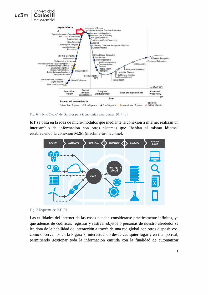
Al analizar la gráfica Hypre Cycle de la Figura 5, se observa que el “internet de las
cosas”, a pesar de presentar una proyección de cinco a diez años (relativamente alto)
para figurar como una corriente principal, se presenta como una de las tecnologías a
punto de alcanzar la máxima expectación, sin embargo, como se observa en la Figura 6,
la evolución fue considerablemente drástica, adelantándose bastante a la proyección y
situando a IoT en el pico de máxima expectación tan solo tres años más tarde.
Fig. 5 “Hype Cycle” de Gartner para tecnologías emergentes 2011 [8]
8
Fig. 6 “Hype Cycle” de Gartner para tecnologías emergentes 2014 [8]
IoT se basa en la idea de micro-módulos que mediante la conexión a internet realizan un
intercambio de información con otros sistemas que “hablan el mismo idioma”
estableciendo la conexión M2M (machine-to-machine).
Fig. 7 Esquema de IoT [9]
Las utilidades del internet de las cosas pueden considerarse prácticamente infinitas, ya
que además de codificar, registrar y rastrear objetos o personas de nuestro alrededor se
les dota de la habilidad de interacción a través de una red global con otros dispositivos,
como observamos en la Figura 7, interactuando desde cualquier lugar y en tiempo real;
permitiendo gestionar toda la información emitida con la finalidad de automatizar

9
actividades y procesos diarios en nuestra vida cotidiana y así facilitar el análisis de la
información útil y la toma de decisiones.
Por el año 2010 no todo eran buenas noticias, ya que las expectativas, consideraciones
prácticas (incremento de dispositivos) y evolución de IoT seguían un ritmo aplastante y
no congruente con el protocolo de IP establecido. A inicios del 2010 quedaban menos
del 10% de IPs sin asignar, por lo que se ideo el protocolo IPv6, definida y diseñada
para reemplazar al Internet Protocol Version 4 (IPv4). Gracias al protocolo IPv6
(Internet Protocol Version 6), se evitara que el crecimiento a internet quede restringido,
y hará posible aumentar la gestión y seguridad de una mayor cantidad de dispositivos.
Fig. 8 Incremento cronológico del IoT [10]
El incremento de dispositivos IoT, Figura 8, ha ido siempre de la mano con la
evolución del Big Data, el cual es la principal vía para el tratamiento de una inmensa
cantidad de información para aplicaciones móviles o servicios en la nube ofrecido por
empresas con soluciones IoT, y optimizándolas aún más utilizando tecnologías
inalámbricas como redes móviles, WiFi, Zigbee o Bluetooth para facilitar su despliegue.
Una solución para este tipo de proyectos es Arduino, puesto que ha marcado un punto
de inflexión convirtiéndose en una herramienta ideal para llevar a cabo multitud de
prototipos con dispositivo que nos permite de forma económica y sencilla conectar
cualquier dispositivo a Internet. Con un Arduino y un sencillo módulo ethernet o wifi
podemos conectar a Internet una gran cantidad de sensores y actuadores, y enviar la
información relevante mediante internet, un SMS o email hacia cualquier parte del
mundo.

10
2.3. Módulos inteligentes “Thinking things”
Esta iniciativa, en el ámbito de internet de las cosas, permite realizar conectividad a
objetos mediante tecnologías, como la conectividad 2G, abriendo oportunidades muy
interesantes en el ámbito donde la conectividad WiFi es muy reducida y permitiendo
también un uso más eficiente de la red.
RFID (Radio frequency identification) pertenece a las tecnologías de identificación
automática (Auto ID). Este sistema permite almacenar, procesar y recuperar
información de una base de datos, mediante el uso de ondas de radio para el intercambio
de información. El propósito de este sistema es conocer la identidad de un objeto y
transmitir información del mismo.
Las etiquetas RFID son dispositivos pequeños similares a una pegatina que pueden
acompañar a toda clase de productos. Los dispositivos constan de una antena, un chip y
en algunos casos de una batería como se puede ver en la Figura 9. El chip posee
memoria interna de capacidad variable y puede ser de varios tipos:
o Solo lectura.
o Lectura y escritura.
o Anticolisión.
Fig. 9 Partes de un dispositivo RFID [11]
Los posibles usos del sistema RFID son múltiples pero principalmente se emplean para
identificar productos, como sistema de prevención de robos, el seguimiento de objetos y
control de stock en un almacén escaneando grandes bloques en lugar de uno a uno.

11
El sistema RFID puede proporcionarnos información de la localización, el estado dentro
de un proceso en el que se encuentre e incluso podría indicarnos las condiciones en las
que se encuentra un producto.
Las ventajas que ofrece el sistema son varias pero su coste aun es elevado y el nivel de
seguridad es bajo. Entre otras desventajas se encuentran los fallos de lectura que pueden
llegar a un 20%.
2.4. Elección Hardware de Control: Arduino
Para la realización del proyecto se podrían haber empleado alguna solución hardware,
módulos domóticos o algún PLC (Programable Logic Controller) existente en el
mercado, pero como se ha explicado en el apartado de introducción, uno de los
principales objetivos es realizar desde cero un sistema de monitorización que permita
aplicar los conocimientos adquiridos sobre microprocesadores y además aprender un
nuevo lenguaje de programación capaz de controlar dispositivos y los distintos sistemas
que lo componen.
Arduino es la solución seleccionada para este proyecto, puesto que es un
microcontrolador con muchas ventajas que cumple con las expectativas dado que es una
plataforma electrónica de hardware libre basada en una placa controlada por un
microcontrolador Atmel AVR. Gracias a que el sistema cuenta con entornos de software
y hardware flexibles y fáciles de utilizar, Arduino ha sido diseñado para adaptarse a las
necesidades de todo tipo de público capaz de adaptarse a la idea de “Do-It-yourselft”
(DIY) independientemente de si el usuario es un aficionado o experto en robótica o
equipos electrónicos. También consta de un simple, pero completo, entorno de
desarrollo, con el que es posible interactuar con la plataforma de manera muy sencilla y
amigable. Se puede definir por tanto como una sencilla herramienta de contribución a la
creación de prototipos, entornos, u objetos interactivos destinados a proyectos
multidisciplinares y multitecnológicos.
Ventajas del modelo elegido:
Precio: herramientas simples, dispositivos modulares, de bajo coste.
Sistema abierto: Arduino es una compañía open source y open hardware,
bajo la Licencia Pública General Reducida de GNU (LGPL) o la Licencia
Pública General de GNU (GPL), permitiendo la manufactura de las placas
Arduino y distribución del software por cualquier individuo.
Sistema didáctico: De interfaz hardware y software amigable y con un
lenguaje de programación sencillo, es posible empezar con pequeños
proyectos de forma rápida y segura. Además, es compatible con multitud de
módulos “plug&play”.
Entradas y salidas disponibles: Se le pueden conectar placas de expansión
(shields) a través de la disposición de los puertos de entrada y salida
12
(analógicas y digitales) presentes en la placa seleccionada. Las shields
complementan la funcionalidad del modelo de placa empleada, agregando
circuitería, sensores y módulos de comunicación externos a la placa original.
Amplia gama de versiones y accesorios compatibles
Compatibilidad: Librerías de libre distribución para poder comunicarse con
hardware y software de terceros.
Gran Comunidad: Muy extendido y estandarizado. Gran cantidad de
información y ejemplos existentes (compartidos por una gran comunidad).
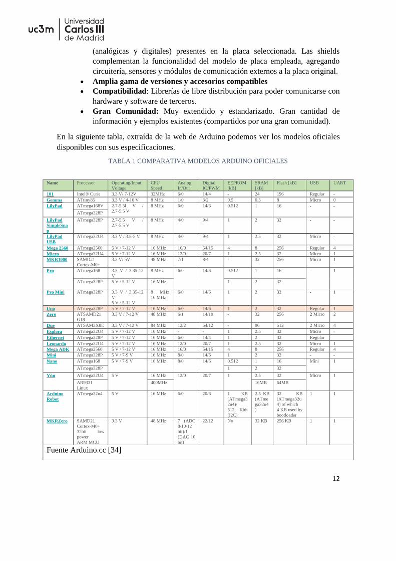
En la siguiente tabla, extraída de la web de Arduino podemos ver los modelos oficiales
disponibles con sus especificaciones.
TABLA 1 COMPARATIVA MODELOS ARDUINO OFICIALES
Name Processor Operating/Input
Voltage CPU
Speed Analog
In/Out Digital
IO/PWM EEPROM
[kB] SRAM
[kB]
Flash [kB] USB UART
101 Intel® Curie 3.3 V/ 7-12V 32MHz 6/0 14/4 - 24 196 Regular -
Gemma ATtiny85 3.3 V / 4-16 V 8 MHz 1/0 3/2 0.5 0.5 8 Micro 0
LilyPad ATmega168V 2.7-5.5l V /
2.7-5.5 V 8 MHz 6/0 14/6 0.512 1 16 - -
ATmega328P
LilyPad
SimpleSna
p
ATmega328P 2.7-5.5 V /
2.7-5.5 V 8 MHz 4/0 9/4 1 2 32 - -
LilyPad
USB ATmega32U4 3.3 V / 3.8-5 V 8 MHz 4/0 9/4 1 2.5 32 Micro -
Mega 2560 ATmega2560 5 V / 7-12 V 16 MHz 16/0 54/15 4 8 256 Regular 4
Micro ATmega32U4 5 V / 7-12 V 16 MHz 12/0 20/7 1 2.5 32 Micro 1 MKR1000 SAMD21
Cortex-M0+ 3.3 V/ 5V 48 MHz 7/1 8/4 - 32 256 Micro 1
Pro ATmega168 3.3 V / 3.35-12
V 8 MHz 6/0 14/6 0.512 1 16 - 1
ATmega328P 5 V / 5-12 V 16 MHz 1 2 32
Pro Mini ATmega328P 3.3 V / 3.35-12
V
5 V / 5-12 V
8 MHz
16 MHz 6/0 14/6 1 2 32 - 1
Uno ATmega328P 5 V / 7-12 V 16 MHz 6/0 14/6 1 2 32 Regular 1 Zero ATSAMD21
G18 3.3 V / 7-12 V 48 MHz 6/1 14/10 - 32 256 2 Micro 2
Due ATSAM3X8E 3.3 V / 7-12 V 84 MHz 12/2 54/12 - 96 512 2 Micro 4
Esplora ATmega32U4 5 V / 7-12 V 16 MHz - - 1 2.5 32 Micro -
Ethernet ATmega328P 5 V / 7-12 V 16 MHz 6/0 14/4 1 2 32 Regular
Leonardo ATmega32U4 5 V / 7-12 V 16 MHz 12/0 20/7 1 2.5 32 Micro 1 Mega ADK ATmega2560 5 V / 7-12 V 16 MHz 16/0 54/15 4 8 256 Regular 4
Mini ATmega328P 5 V / 7-9 V 16 MHz 8/0 14/6 1 2 32 - -
Nano ATmega168 5 V / 7-9 V 16 MHz 8/0 14/6 0.512 1 16 Mini 1
ATmega328P 1 2 32
Yùn ATmega32U4 5 V 16 MHz 12/0 20/7 1 2.5 32 Micro 1
AR9331
Linux
400MHz 16MB 64MB
Arduino
Robot ATmega32u4 5 V 16 MHz 6/0 20/6 1 KB
(ATmega3
2u4)/
512 Kbit
(I2C)
2.5 KB
(ATme
ga32u4
)
32 KB
(ATmega32u
4) of which
4 KB used by
bootloader
1 1
MKRZero SAMD21
Cortex-M0+
32bit low
power
ARM MCU
3.3 V 48 MHz 7 (ADC
8/10/12
bit)/1
(DAC 10
bit)
22/12 No 32 KB 256 KB 1 1
Fuente Arduino.cc [34]

13
A través de Arduino podemos recopilar multitud de información del entorno sin
excesiva complejidad. Gracias a sus pines de entrada, nos permite jugar con una gran
variedad de sensores (temperatura, luminosidad, presión, etc.) que nos brindan la
capacidad de controlar o actuar sobre ciertos factores del entorno que le rodean, como
por ejemplo: controlando luces, accionando motores, activando alarmas…y muchos
otros actuadores.
Los productos de Arduino son distribuidos como Hardware y Software Libre,
característica gracias a la cual los usuarios pueden acceder a placas prediseñadas o
incluso diseñar sus propias placas y módulos a la medida de sus necesidades.
Respecto al software, es totalmente libre, gratuito y está disponible para su descarga
desde la página web oficial de Arduino, y consiste de dos elementos principales: un
entorno de desarrollo (IDE) (basado en el entorno de processing y en la estructura del
lenguaje de programación Wiring), y en un bootloader de arranque que es ejecutado de
forma automática dentro del microcontrolador al encenderse. Las placas Arduino se
programan mediante un computador, usando comunicación serial.
Otra de las principales ventajas que presenta la plataforma Arduino es su autonomía
respecto a tener que mantenerse conectado a un PC como fuente de energía o
procesamiento software. Arduino es perfectamente capaz de trabajar en modo
“standalone”, siendo únicamente necesario precargar previamente el programa que
deseamos que mantenga en ejecución en el Arduino. A pesar de ser un dispositivo
autónomo el Arduino se mantiene operando en todo momento con la conexión al PC,
siendo capaz de comunicarse con diferentes tipos de software, como por ejemplo:
Macromedia Flash, Processing, Max/MSP, Pure Data, etc.

14
3. REQUISITOS DE SISTEMA
Una vez definido, en capítulos anteriores, que el objetivo del proyecto es el de
implementar un sistema autosuficiente capaz de llevar a cabo tareas de monitorización
del entorno, basado en la configuración de un microcontrolador Arduino. Y teniendo
presente el análisis, en el capítulo del estado del arte, no se dio con una solución
especifica actual que realice el servicio de tracking y análisis del estado de un envió.
Ahora se profundizara en las características de la aplicación a desarrollar y se fijaran los
objetivos concretos relativos a cada punto técnico del proyecto.
El sistema completo se puede analizar de dos formas:
Hardware: Compuesto principalmente por:
o Electrónica: Placa base de Arduino y shields complementarios, que
serán el conjunto principal de control.
o Elementos auxiliares como módulos de sensores.
o Comunicaciones: por puerto serie entre PC y Arduino, tarjetas de
memoria.
o Otros componentes electrónicos (sensores alternativos).
Software:
o Sera la interfaz necesaria para interactuar con el sistema completo de
forma sencilla.
o Scripts aplicados para el análisis de la información obtenida.
TABLA 2 ANÁLISIS DE ENVÍO DE PAQUETES
CARACTERÍSTICAS INHERENTES AL
ENVÍO DE UN PAQUETE
FUNCIÓN IMPLEMENTADA
Envíos directos de paquetes sin puntos de parada Encendido/apagado de circuitos.
Humedad variable debido al entorno del trayecto. Medición de Humedad relativa en el aire.
Temperatura variable debido al entorno del
trayecto.
Medición de la temperatura.
Exposición ambiente del paquete Medición de niveles lumínicos.
Trato específico de orientación (por ejemplo “este
lado arriba”)
Tratamiento giroscópico
Trato específico de fragilidad Estado de aceleración

15
4. HARDWARE EMPLEADO
Desde el momento en el que Arduino fue implementado como un proyecto educativo,
por el año 2005, ha experimentado una evolución e innovación constante. Debido a la
gran versatilidad del proyecto, y a la numerosa comunidad que la respalda, a día de hoy
existen multitud de placas Arduino, siendo la mayoría de ellas compatibles con distintas
versiones y adaptables prácticamente a cualquier tipo de requisito o necesidad presente
en un determinado proyecto.
Fig. 10 Placas de desarrollo Arduino [12]

16
Fig. 11 Sensores y módulos de Arduino [12]
Entre los principales módulos valorados para el desarrollo de este proyecto se
encuentran:
4.1. Arduino UNO
La placa Arduino UNO es una de las placas electrónicas más populares ya que suele
utilizarse para introducir al usuario en el aprendizaje de este tipo de dispositivo.
Arduino UNO es la evolución de la placa Duemilanove, Figura 12, que podría
considerarse la primera versión de la placa básica de Arduino, capaz de seleccionar
automáticamente la fuente de alimentación adecuada, de fuente externa o USB,
eliminando la necesidad de utilizar un conmutador para la selección de una u otra
opción, tal como ocurría en placas anteriores.

17
Fig.12 Placa Arduino Dumelianove [13]
Arduino UNO ha dejado a la placa Duemilanove en segundo plano ya que mediante una
conexión USB estándar es capaz de conectarse al ordenador y establecer el
funcionamiento de la placa para iniciar la programación y gestionar funcionalidades
extras que se obtienen de de placas compatibles, Shields. A diferencia de la antigua
Duemilanove, Arduino UNO integra un chip USB-serie para establecer la conexión por
consola. Además cuenta con un nuevo diseño de etiquetado para facilitar la
identificación de las distintas entradas y salidas de la placa.
Fig. 13 Placa Arduino UNO [14]
TABLA 3 CARACTERÍSTICAS PRINCIPALES ARDUINO UNO
Microcontrolador ATmega328P
Voltaje de operación 5V
Voltaje de entrada recomendado 7-12V
Pines digitales E/S 14 (6 disponen de salida PWM)
Pines de entrada analógica 6
Consumo por pin E/S 40mA
Consumo del pin 3.3V 50mA
Memoria flash 32kB (0.5kB empleados por el bootloader)
SRAM 2kB
EEPROM 1kB
Frecuencia de reloj 16MHz
Fuente electrocrea.com [14]
18
Arduino UNO cuenta con un puerto de comunicaciones UART (serie hardware), USB
(puerto virtual), comunicación mediante I2C (TWI) y SPI.
El resto de características y el pinout de esta placa podrán encontrarse en la carpeta de
ficheros anexos al proyecto.
4.2. Arduino MEGA
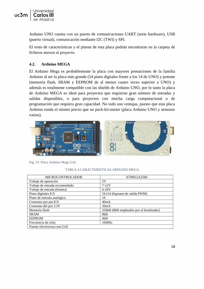
El Arduino Mega es probablemente la placa con mayores prestaciones de la familia
Arduino al ser la placa más grande (54 pines digitales frente a los 14 de UNO) y potente
(memoria flash, SRAM y EEPROM de al menos cuatro veces superior a UNO) y
además es totalmente compatible con las shields de Arduino UNO, por lo tanto la placa
de Arduino MEGA es ideal para proyectos que requieran gran número de entradas y
salidas disponibles, o para proyectos con mucha carga computacional o de
programación que requiera gran capacidad. No todo son ventajas, puesto que esta placa
Arduino ronda el mismo precio que un pack-kit-starter (placa Arduino UNO y sensores
varios).
Fig. 14 Placa Arduino Mega [14]
TABLA 4 CARÁCTERISTICAS ARDUINO MEGA
MICROCONTROLADOR ATMEGA2560
Voltaje de operación 5V
Voltaje de entrada recomendado 7-12V
Voltaje de entrada (limites) 6-20V
Pines digitales E/S 54 (14 disponen de salida PWM)
Pines de entrada analógica 16
Consumo por pin E/S 40mA
Consumo del pin 3.3V 50mA
Memoria flash 256kB (8kB empleados por el bootloader)
SRAM 8kB
EEPROM 4kB
Frecuencia de reloj 16MHz
Fuente electrocrea.com [14]

19
4.3. Comunicaciones
Las Placas de Arduino cuentan con distintos tipos, formas y puertos para intercambiar
información con dispositivos móviles, ordenadores y bases de datos físicas o en la nube;
utilizando diferentes tipos de interfaz de comunicación (y protocolos asociados) como:
4.3.1. La comunicación serie
En la actualidad gran parte de los protocolos utilizados establecen la comunicación
serie, como por ejemplo la generalmente establecida para comunicar el ordenador con el
dispositivo Arduino, pero además existen muchos dispositivos de comunicación
inalámbrica que utilizam la comunicación serie para hablar con Arduino como los
módulos Bluetooth y módulos Xbee.
Todas las placas de Arduino poseen al menos un puerto serie disponible en los pines
digitales 0 (RX) y 1 (TX) compartido con el USB. Por lo cual no es posible usar dichos
pines como entradas/salidas digitales.
En el caso del Arduino mega se dispone de tres puertos adicionales Serial_1, que ocupa
los pines 19 (RX) y 18 (TX), Serial_2 que ocupa los pines 17 (RX) y 16 (TX) y Serial_3
que ocupa los pines 15 (RX) y 14 (TX). Estos pines no están conectados al interfaz USB
del Arduino, a diferencia del caso anterior.
Comunicación serie:
Fig. 15 Protocolo de comunicación en serie [15]
Entra las funciones básicas que debemos conocer para manejar correctamente la
comunicación por puerto serie tenemos: begin(), read(), write(), print() y available()). Y
entre las funciones más importantes encontramos:
begin() -- El cual estable la velocidad de la UART en baudios para la
transmisión serie, también es posible configurar el número de bits de datos, la paridad y
los bits de stop, por defecto es 8 bits de datos, sin paridad y un bit de stop.
read() -- El cual lee el primer byte entrante del buffer serie.
write() -- Escribe datos en binario sobre el puerto serie. El dato es enviado como
un byte o serie de bytes.
print() -- Imprime datos al puerto serie como texto ASCII legible para humano,
también permite imprimir en otros formatos.
printInt() – Imprime el texto ASCII seguido de un carácter de retorno (ASCII 13,
or '\r') o salto de línea (ASCII 13, or '\r'), presenta el mismo formato que print().

20
available() -- Da la cantidad de bytes (caracteres) disponibles para leer en el
puerto serie, son datos que han llegado y se almacenan en el buffer serie que tiene un
tamaño de 64 bytes.
availableForWrite() -- Da la cantidad de bytes (caracteres) disponibles para
escribir en el búfer en serie sin bloquear la operación de escritura.
end() -- Deshabilita la comunicación serie permitiendo a los pines RX y TX ser
usado como pines digitales.
if(Serial) -- Especifica si el puerto serie está listo.
find() -- Lee datos del buffer serie hasta encontrar el string buscado.
findUntil() -- Lee datos del buffer serie hasta encontrar el string o un string de
longitud definida o termino de terminación, la respuesta es true o false.
parseInt() -- busca el siguiente entero válido en el stream de datos del puerto
serie.
parseFloat() -- busca el siguiente numero flotante válido en el stream de datos
del puerto serie.
readBytes() -- lee datos del buffer serie y lo guarda en una variable buffer.
setTimeout() -- configura el máximo de milisegundos de espera para la lectura
del puerto serie. Por defecto es un segundo.
readBytesUntil() -- lee caracteres del buffer serie y los guarda en un array de
caracteres, la función termina si el carácter terminados es encontrado o la longitud
determinada se ha leído o ha alcanzado el timeout.
readString() -- lee caracteres del buffer serie y los guarda en un string. La
función termina cuando se produce un timeout.
readStringUntil() -- lee caracteres del buffer serie y los guarda en un string. La
función termina cuando se produce un timeout.
serialEvent() -- llamado cuando hay datos disponibles.
flush() -- espera hasta la transmisión completa de los datos salientes.
peek() -- devuelve el siguiente carácter del buffer serie pero sin borrarlo de él.
Se debe tener en cuenta que las funciones de serial definidas valen para cualquier
dispositivo Arduino soportado por el IDE que se esté utilizando, pero luego cada
microcontrolador internamente usa unos registros y operaciones diferentes, por lo que
las funciones a bajo nivel vistas, sólo funcionarán con Arduino UNO.
Buffer Serial: Los puertos serie de los microcontroladores tienen un buffer que se va
llenando con la información, la cual se manteniendo disponible hasta la lectura con la
función read(), luego se va vaciando con una estructura de pila FIFO (First In First Out).
El tamaño del buffer serie en el Arduino UNO es de 64 bytes, por lo que al llenar el
buffer pierde el resto de elementos recibidos a continuación.
Dentro de la comunicación en serie tenemos la UART, por puerto I2C/TWI y la SPI.

21
4.3.1.1. Comunicación en serie UART
UART (siglas en inglés de Universal Asynchronous Receiver-Transmitter) es uno de los
protocolos serie más utilizados en la mayoría de los microcontroladores ya que es el
dispositivo que controla las interrupciones entre los puertos y dispositivos serie.
La UART se encargará de leer datos cuando llegan, generar y gestionar interrupciones,
enviar datos y gestionar los tiempos de bit. Para realizar la comunicación en serie
UART se toma bytes de datos y se transmiten los bits de manera individual y de forma
secuencial, los 8 bits de datos son transmitidos de la siguiente forma: un bit de inicio, a
nivel bajo, luego 8 bits de datos empezando por el menos significativo (LSB, del inglés
Least significant bit) y por ultimo un bit de parada a nivel alto, como se observa en la
Figura 15. En la UART del receptor se realiza el proceso contrario re ensamblando los
bits en bytes completos.
Fig. 16 Protocolo de comunicación UART [15]
UART se diferencia de SPI e I2C (tipos de comunicación en serie) en que es asíncrono
y los otros están sincronizados con señal de reloj. Para sustituir el sincronismo se
establece el tiempo de bit, que es el tiempo que se mantiene cada bit en la línea sin tener
en cuenta su valor, cero o uno. El tiempo de bit se establece al definir el ratio de baudios
que establece el número de bis que se puede enviar en un segundo, este valor se debe
establecer al inicio de la comunicación y debe de coincidir en ambos extremos de la
comunicación.
Una vez establecida la unidad de información, el tiempo de bit y el proceso de
intercambio de información, toca definir el estándar en la capa física, en el caso del
dispositivo UART a la salida de un microcontrolador casi siempre se optará por los
niveles TTL, en el cual un cero lógico se transforma en cero voltios y un uno lógico en
5 o 3.3 voltios, que la UART se encargara de poner en la línea de datos.
4.3.1.2. Comunicación en serie del bus SPI
SPI (siglas en inglés de Serial Peripheral Interface) es otro protocolo de comunicación
serie, ideal para la transferencia de información entre circuitos integrados en equipos

22
electrónicos digitales, que además acepten un flujo de bits serie regulados por una
comunicación síncrona, en el caso del SIP es de cuatro hilos, clasificándose en dos
grupos: de reloj o de datos, como observamos en la Figura 16.
Fig. 17 Protocolo de comunicación SPI [15]
Mediante un bus SPI se utiliza la comunicación master-slave, en la que el maestro se
encarga de enviar la señal de reloj a los esclavos presentes en la línea, tras cada pulso de
reloj envía un bit al esclavo y recibe un bit de éste.
La transmisión de información síncrona se lleva a cabo mediante las señales principales
que se observa en la Figura 17.
Fig. 18 Esquema comunicación Master Slave [15]

23
Donde:
SCK para el reloj del sistema, que establecerá la velocidad y sincronización
entre los dispositivos.
MOSI siglas en ingles de Master Out Slave In, línea de datos del master.
MISO siglas en ingles de Master In Slave Out, línea de datos del esclavo.
Y SS (siglas en ingles de Slave Selected) para controlar más de un esclavo.
Como es el master el que genera la señal de reloj necesita saber de antemano si un
esclavo va a generar una respuesta, la longitud (normalmente de dos bytes) y que
esclavo va a generar la respuesta. Ante la presencia de más de un esclavo se establece la
comunicación mediante la línea de control SS que indica a quien se envía o de quien se
requiere la respuesta.
Fig. 19 Línea de control SS [15]
Como se observar en la Figura 18, la señal de línea SS normalmente se mantiene en alto
nivel (HIGH) y se activa con la señal en bajo nivel (LOW), lo que activa al esclavo
seleccionado. En el caso de múltiples esclavos el bus SPI se conecta con una línea SS a
cada esclavo o en cascada, como observamos en la Figura 19. Y para finalizar la
transferencia de línea, la señal SS vuelve a alto nivel (HIGH) y el esclavo se desactiva.

24
Fig. 20 Múltiples líneas de control SS. [15]
En el caso de una línea por esclavo, cada uno cuenta con una línea SS para evitar ruido
no deseado que se podría generar si más de uno hable a la vez, es un sistema cómodo si
no es un numero alto de líneas.
Fig. 21 Configuración en cascada [15]
En el caso de un número elevado de esclavos se suele optar por la configuración en
cascada, conectando el MISO de uno (salida) con el MOSI (entrada) del siguiente. Con
esta configuración el maestro es el que envía los datos pero no recibe ninguna respuesta.
Normalmente en los sistemas de Arduino se cuenta de serie con el bus SPI, con una
librería estándar denominada SPI, que gestiona todas las complicaciones y el arbitraje
del protocolo.

25
TABLA 5 VENTAJAS E INCONVENIENTES DEL SPI
VENTAJAS DEL SPI INCONVENIENTES DEL SPI
Comunicación Full Duplex. Envía y recibe a la
vez lo que aumenta la velocidad.
Necesita más pines que el I2C o el Puerto serie
normal.
Más rápido que el I2C y que el puerto Serie
asíncrono normal.
Las comunicaciones tienen que estar
perfectamente establecidas de antemano. No
puedes enviar mensajes de diferentes longitudes
cuando te convenga.
El tamaño de los mensajes puede ser
arbitrariamente grande.
No hay señal de conformidad del esclavo, se
espera que obedezca y punto.
Se requiere un hardware sencillo (usualmente
barato).
Master único y casi sin posibilidad de master
múltiple.
Requiere un menor consumo y menor electrónica
de conexión que el I2C.
Funciona solo en distancias muy cortas.
Como el Clock lo proporciona el master, los
esclavos no necesitan osciladores (más barato).
Normalmente necesita un pin adicional por cada
esclavo y si el número de esta creces puede
acabar siendo un problema.
Fuente promotec.net
En las placas de Arduino tenemos definidos los pines a utilizar para realizar la conexión
en línea por SPI, aunque han surgido librerías que permiten mover de sitio los pines de
control. Una vez definidos los pines de control SPI solo se podrá utilizar dichos pines.
Según el modelo de Arduino seleccionado podremos usar los pines:
TABLA 6 PINES DE MODELOS DE PLACAS ARDUINO
MODELO
ARDUINO
MOSI MISO SCK SS SLAVE SS MASTER
UNO 11, ICSP-4 12, ICSP-1 13, ICSP-3 10 Z
MEGA 51, ICSP-4 50, ICSP-1 52, ICSP-3 53 Z
LEONARDO ICSP-4 ICSP-1 ICSP-3 Z Z
DUE ICSP-4 ICSP-1 ICSP-3 Z 4, 10, 52
Fuente prometec.net
Como se observa en la tabla 6, los pines ICSP siempre coinciden ya que así es posible
diseñar una conexión coherente con Shield externos y hacerlos compatibles para varios
modelos de Arduino.

26
Fig. 22 Pines placa Arduino UNO [15]
Fig. 23 Pines ICSP Placa Arduino UNO [15]
4.3.1.3. Comunicación en serie I2C, I²C o TWI
Con el tiempo la electrónica de los dispositivos se fue sobrepasando la capacidad de
integración de un microchip, ya que se requería que docenas de bloques se pongan de
acuerdo y establezcan una comunicación fluida y eficaz.
En los ochenta el fabricante de electrónica Philips propuso una norma de comunicación
digital abierta que especificaría la velocidad, los niveles de tensión, y los protocolos a
seguir.
El IIC o I²C (del inglés Inter-Integrated Circuit) o también conocido como TWI (del
inglés Two Wired Interface) pronto se convirtió en un estándar. Este tipo de
comunicación se caracteriza por:
Requiere únicamente el uso de solo 2 cables para su funcionamiento:
o Uno para la señal de reloj (CLK), puesto que es un protocolo
síncrono.
o El otro para la trasferencia de datos (SDA), compartida por el
maestro y esclavo, aunque es gestionada por la señal de reloj del
maestro, reduciendo así el número de líneas de bus comparado a SPI.

27
En I2C no se utiliza la selección de esclavos, en su lugar cada dispositivo
cuenta con una dirección exclusiva de 7 bits, por lo que se podrá conectar
hasta 112 dispositivos (2^7=128, donde 16 direcciones se reservan para usos
especiales).
Uno de los dispositivos conectados debe ser el maestro, y controlar la señal
de reloj.
En I2C no se requiere de una velocidad de reloj estricta, ya que el master es
el que genera la señal.
Un sistema puede ser multi-maestro, pero solo con uno activo a la vez,
proporcionando así un protocolo de arbitraje y evitando colisiones.
Fig. 24 Conexión en I2C [16]
Si existen dos o más señales atraviesan el mismo cable pueden causar conflicto, y
ocurrirían problemas si un dispositivo envía un 1 lógico al mismo tiempo que otro envía
un 0. Por tanto el bus es “cableado” con dos resistencias de pullup conectadas a SDA y
SCL para poner el bus a nivel alto, y los dispositivos envían niveles bajos (esta
información se consulta en lo anuales de cada dispositivo). Si quieren enviar un nivel
alto simplemente lo comunican al bus.
Dado que el maestro y el esclavo comparten el bus de datos (SDA) para realizar la
comunicación, el bus I2C emplea una trama (el formato de los datos enviados) amplia.
Utilizando los elementos:
7 bits de direccionamiento/identificación de esclavo
Un bit para especificar si se recibe o envía (lectura o escritura, R/W)
información.
Un bit de validación (ACK).
Uno o más bytes de datos enviados/recibidos.
Un bit de validación.

28
Fig. 25 Formato de datos enviados de I2C [17]
Dado que por cada ocho bits de datos se envían 18 bits en la comunicación obtendremos
menor velocidad del bus I2C. Siendo la velocidad estándar de transmisión de 100MHz,
con la posibilidad de acceder a un modo de alta velocidad de hasta 400MHz.
TABLA 7 VENTAJAS E INCONVENIENTES DEL I2C
VENTAJAS DEL I2C INCONVENIENTES DEL I2C
Requiere menos buses de comunicación Presenta una señal media-baja
Mecanismos para confirmación de recepción de
señal.
No es full dúplex.
Es posible la configuración multi master (uno
solo cada vez).
No hay verificación de mensaje correcto.
Fuente aprendiendoarduino.wordpress.com
Los sistemas de Arduino disponen de soporte I2C por hardware vinculado físicamente a
ciertos pines, como veremos en la tabla 8. También existe la opción de emplear
cualquier otro grupo de pines como bus I2C mediante la configuración del software,
pero en ese caso la velocidad será mucho menor.
TABLA 8 PINES VINCULADOS A I2C
MODELO SDA SCK
UNO A4 A5
NANO A4 A5
MINI PRO A4 A5
MEGA 20 21
Fuente arduino.cc
Para poder utilizar el bus I2C en Arduino, el IDE Standard proporciona la librería
“Wire.h”, la cual contiene las funciones necesarias para controlar el hardware integrado.

29
Algunas como:
beginTransmission() – Para comenzar la transmisión con un esclavo.
endTransmission() -- Para finaliza la transmisión y transmitir los bytes en
cola.
requestFrom(address,nBytes) -- solicita un numero de bytes al esclavo en la
dirección address.
available() -- Detecta si hay datos pendientes por ser leídos.
onReceive() -- Registra una función de callback al recibir un dato, es decir,
llama a una función cuando un esclavo recibe una transmisión de un
maestro.
onRequest() -- Registra una función de callback al solicitar un dato, es decir,
llama a una función cuando un maestro solicita datos de un maestro.
Ya se ha comentado que para establecer la comunicación mediante el bus SPI se utilizan
el direccionamiento de los esclavos, pero en la realidad no es tan fácil ya que no
siempre los fabricantes facilitan la dirección de los dispositivos o incluso lo
proporcionan de forma incorrecta.
Para esta situación Arduino cuenta con sketch llamado “Scanner I2C”, que analizaremos
en el capítulo 6 de diseño de proyecto. Dicho sketch realiza un barrido por todas las
direcciones posibles del bus, y obteniendo en el resultado las direcciones de los
dispositivos desconocidos.
4.4. Dispositivos de Comunicación
Las placas de Arduino, como se ha analizado con anterioridad, son sistemas altamente
versátiles, puesto que poseen variedad de soluciones a la hora de establecer la
comunicación con dispositivos externos, teniendo en cuenta las prestaciones de los
módulos involucrados e incluso el número de ellos, presentando configuraciones físicas
específicas de conexión por modulo, y en el caso de que haga falta se cuenta con la
capacidad de configurar el entorno de comunicación a medida de las necesidades,
mediante configuración software y librerías propias de Arduino.
Una de las principales formas de comunicación, como se ha visto en el apartado
anterior, es la utilización de buses de interconexión en puertos serie, síncronos o
asíncronos, como I2C/TWI o SPI, y las posibles conexiones físicas disponibles para
cada modelo de placas de Arduino mediante puertos serie (USB o pines). En este
apartado se describirán los dispositivos en los cuales se aplicarán dichas formas de
comunicación, teniendo en cuenta las ventajas y desventajas de cada configuración.

30
4.4.1. Ethernet Shield
La placa de Ethernet Arduino Shield nos da la capacidad de conectar el módulo de
Arduino, del estilo Leonardo o Arduino UNO, a una red Ethernet y realizar un pequeño
servidor o cliente web. Este módulo es la parte física que implementa la pila de
protocolos TCP/IP mediante la ayuda de librerías Arduino, permitiendo una
configuración web mediante implementación software.
Esta placa dispone de un slot para tarjetas de memoria micro-SD y de un controlador de
reset. Con el primero será posible almacenar ficheros o para utilizarlo como servidor
web integrado. Mientras que con el controlador de reset podremos restaurar la
información de fábrica automáticamente, para que el chip interno Wiznet W5100 esté
bien reiniciado y listo para utilizar al arranque.
La placa Arduino se comunica mediante un conector ICSP aplicando la comunicación
en línea de bus SPI, como ya vimos en el apartado anterior, con el chip ethernet Wiznet
W5100, pieza básica del módulo Ethernet, y con el slot de conexión micro-SD. Esto se
encuentra en los pines digitales 11, 12 y 13 en el modelo UNO y en los pines 50, 51 y
52 del modelo Mega. En ambas placas, el pin 10 es utilizado para seleccionar el W5100
y el pin 4 para la micro-SD. Estos pines no pueden ser utilizados para otros fines
mientras la Ethernet Shield esté conectada. En el MEGA, el pin SS (53) no es utilizado
pero debe dejarse como salida para que el bus SPI funcione correctamente.
Hay que tener en cuenta que la micro-SD y el W5100 comparten el bus SPI, por lo que
sólo uno de ellos puede ser utilizado a la vez. Si se desea utilizar ambos
simultáneamente, hay que tenerlo en cuenta al escribir el código.
Fig. 26 Placa ethernet shield [18]

31
4.5. Sensores
4.5.1. Sensor de Intensidad Lumínica LDR
Es un foto-resistor o componente resistivo que aporta información sobre la intensidad
lumínica que recibe, donde se observa que la resistencia es máxima en ausencia de luz
incidente y disminuye conforme aumenta la intensidad de luz.
Fig. 27 Sensor LDR [19]
Un sensor LDR es barato y útil para realizar medidas de carácter cuantitativo de la
intensidad de luz. Este sensor no puede ser usado como luxómetro por su poca precisión
además de que su valor de resistencia es dependiente de la temperatura y del espectro de
luz que percibe.
Fig. 28 Variación de la resistencia de un LDR con la temperatura y la frecuencia de luz [20]
Fig. 29 Variación de la resistencia de un LDR con la intensidad de luz [21]

32
TABLA 9 CARACTERÍSTICAS DEL SENSOR LDR GL5528
Diametro 5 mm
Tiempo de respuesta 25 ms
Resistencia con 10 lux (25°C) De 10 a 20 KΩ
Resistencia con 0 lux (25°C) 1.0 MΩ
Disipación de potencia (25°C) 100 mW
Voltaje máximo (25°C) 150 V
Rango de temperatura de funcionamiento De -30 a 70 °C
Fuente electan.com
Para reforzar la señal del sensor se hace uso de un módulo que contiene el chip LM358.
El cual se utiliza como seguidor de tensión, así a la salida del módulo se recoge la
misma tensión que la que se recoge del sensor LDR independientemente de la
intensidad llevando a cabo la función de amplificador de señal.
Fig. 30 Esquema LM358 [31]
TABLA 10 CARACTERÍSTICAS DEL MÓDULO LDR
Fuente de alimentación VCC
Min: 2.7V Típico: 5V Max: 5.5V
Corriente (a VCC = 5V) Min: 0.5mA Max: 6 mA
Resistencia (a 10Lux) Min: 5 K Ω Max: 20K Ω
Resistencia (a 0lux) 1M Ω
Tamaño 24 x 24 x 10 mm
Fuente electan.com

33
Fig. 31 Módulo sensor de luz [22]
4.5.2. Sensor de Temperatura y Humedad GHT11
Sensor digital de humedad y temperatura para Arduino. El DHT11 es un sensor de alta
fiabilidad muy económico que no requiere de pines analógicos y muy sencillo de usar
con Arduino o Raspberry Pi. Se puede encontrar en dos presentaciones, el sensor
DHT11 solo, o el sensor puedes estar insertado en una PCB. Ambas presentaciones no
tienen mucha diferencia en precio.
El sensor DHT11 insertado en una PCB cuenta con una resistencia de 5 kΩ de función
pull-up además de un LED indicador de funcionamiento. Una diferencia notable de
ambas versiones son los pines.
Los pines del sensor son 4 y los del sensor insertado en una PCB son 3.
Fig. 32 Módulo y sensor de temperatura y humedad [23]

34
Como podemos observar en la imagen anterior, los pines del sensor DHT11 son VCC
(alimentación). I/O (transmisión de datos), NC (no conecta, pin al aire) y GND
(conexión a tierra). Mientras que en módulo PCB los pines son GND (conexión a
tierra), DATA (transmisión de datos) y VCC (alimentación).
El único inconveniente es que solo actualiza datos cada 2 segundos.
TABLA 11 CARACTERÍSTICAS TÉCNICAS DEL DHT11
MODELO DHT11 TEMPERATURA HUMEDAD
Alimentación de 3,5 a 5 V Rango de 0 a 50°C Rango de 20 a 90% RH
Consumo 2,5 mA Precisión a 25°C ± 2ºC Precisión entre 0 y 50°C ± 5% RH
Señal de salida Digital Resolución 1ºC (8-bit) Resolución 1% RH
Fuente electronilab.com
El sensor DHT11 no usa una interfaz de comunicación estándar y tiene un protocolo
propio para comunicarse por solo un hilo. Dicho protocolo es simple y se implementa a
través del pin I/O.
La transmisión de datos del DHT11 se realiza por un único hilo de manera codificada
haciendo uso del ancho de un pulso en estado alto. La información se recibe en binario
traduciendo los pulsos largos como 1 y los cortos como 0.
Fig. 33 Codificación a binario del DHT11 [23]
Todos los pulsos bajos son de 50 μs, los pulsos altos de longitud 26-28 μs simbolizan un
0 lógico y los pulsos altos de longitud 70 μs simbolizan un 1 lógico.
La trama de datos enviada tiene una longitud de 40 bits (5bytes) donde los dos primeros
grupos de 8 bits dan información de la humedad y los dos siguientes grupos de 8 bits
dan información de la temperatura. El último grupo de 8 bits son los bits de paridad
sirven para verificar que no hay datos corruptos.

35
Fig. 34 Trama de datos DHT11 [23]
4.5.3. Transistor LM35
El Transistor LM35 es un sensor de temperatura analógico que tiene un voltaje de salida
proporcional a la temperatura. El LM35 mide la temperatura en °C como un rango que
va desde -55°C hasta 150°C. Es un sensor de fácil uso que no necesita un
microprocesador o microcontrolador.
La proporción entre voltaje y temperatura es de 10mV por cada grado centígrado,
además no necesita un offset, lo que significa que al medir 30mV se está midiendo una
temperatura de 3°C.
Fig. 35 Transistor LM35 [24]
Los pines del sensor son VCC (alimentación), Vout (voltaje salida) y GND (tierra).
TABLA 12 LM35 Y SUS CARACTERÍSTICAS PRINCIPALES
Resolución 10mV por cada grado
centígrado
Voltaje de alimentación desde 4Vdc hasta 20Vdc
Tipo de medición Salida analógica
Consumo de corriente 60 μA
Precisión ±¼°C
Fuente ecured.cu
El sensor LM35 fue la primera opción elegida para el proyecto, pero debido a que el
sensor DHT11 ofrece una mejora al medir de forma digital temperatura y humedad , el
sensor utilizado es el DHT11.

36
4.5.4. IMU
Un elemento IMU es un dispositivo con la capacidad de medir el movimiento, sus siglas
significan unidad de medición inercial en inglés (inertial measurement unit) y es capaz
de dar información de la velocidad, aceleración y orientación en la que se encuentra.
Estos dispositivos son usados por los sistemas de navegación de muchos vehículos
como los aviones, naves espaciales y barcos. Además son vitales en la dirección y
control de aparatos como los drones y los misiles.
4.5.4.1. MPU – 6050
El dispositivo MPU-6050 es un sensor del tipo IMU que puede medir movimiento hasta
en 6 grados de libertad. El sensor tiene un acelerómetro y un giroscopio de tres ejes que
son elementos MEMS (micro electronic mecanical sistem).
Los acelerómetros son elementos capaces de medir la aceleración del sistema u
objeto al que se encuentran conectados. Estos dispositivos se basan en varias
tecnologías como la piezoeléctrica, la piezorresistiva y la capacitancia variable.
Los acelerómetros empleados en el MPU-6050 son sistemas
microelectromecánicos de capacitancia variable. El funcionamiento se basa en
dos piezas, una fija y una móvil. La pieza móvil está conectada a un muelle tipo
diafragma que permite su movimiento al percibir aceleración modificando su
posición. Ambas piezas son distintas partes de un capacitador y al moverse
produce un cambio capacitivo que afecta la tensión pico de forma proporcional a
la aceleración recibida.
Fig. 36 Funcionamiento acelerómetro MEMS [25]
Los giroscopios elementos capaces de medir la velocidad angular del sistema u
objeto al que se encuentra conectado. Estos dispositivos son de tecnología de
sistemas microelectromecánicos y miden la velocidad angular usando el efecto
Coriolis.

37
El giroscopio del MPU-6050 es de tres ejes y puede medir la velocidad angular
de los ejes X, Y y Z o conocidos también como movimientos de cabeceo,
balanceo y guiñada.
Fig. 37 Mecanismo giroscopio MEMS [26]
El módulo MPU-6050 tiene conversores analógico digital internos de 16 Bit y su
protocolo de comunicación del módulo es el I2C.
Fig. 38Módulo MPU-6050 [27]
TABLA 13 CARACTERÍSTICAS DEL MÓDULO MPU
Fuente de alimentación De 3 a 5 V
Sensibilidad giroscopio ±250, ±500, ±1000, y ±2000dps
Sensibilidad acelerómetro ±2g, ±4g, ±8g y ±16g
Algoritmos embebidos para calibración
Sensor de temperatura digital
Entrada digital de video FSYNC
Interrupciones programables
Fuente naylampmecatronics.com

38
4.6. Otros elementos
4.6.1. Módulo RTC
El módulo RTC es un dispositivo con la función de llevar la cuenta de la hora y fecha
actual en un sistema informático de manera autónoma. Tiene un bajo consumo y su
propia fuente de alimentación. El módulo, que se puede ver en la figura 39, cuenta con
el DS1307 que es un circuito integrado que realiza la función de reloj en tiempo real
(RTC) tiene memoria propia para almacenar la hora y datos arbitrarios.
El CPU de Arduino es capaz de medir el tiempo pero a largo plazo no es capaz de
mantener la hora sin sufrir adelantos o atrasos. Debido a esto es necesario un circuito
integrado que tenga un oscilador a cristal de cuarzo capaz de medir el tiempo de manera
estable y al segundo exacto.
Fig. 39 Módulo RTC [32]
El protocolo de comunicación que usa el Módulo RTC es el I2C y las conexiones están
recogidas en la tabla 14.
TABLA 14 CONEXIONES ENTRE MÓDUKO RTC Y ARDUINO
Módulo RTC Arduino UNO
SCL A5
SDA A4
VCC 5V
GND GND
Fuente naylampmecatronics.com

39
El módulo RTC funciona con dos fuentes de alimentación, una de 5V y su fuente de
alimentación propia, las distintas fuentes de energías son gestionadas de manera
autónoma por el DS1307. En la figura 40 se puede ver el esquema del DS1307.
Fig. 40 Esquema de conexión del DS1307 [33]
TABLA 15 CARACTERÍSTICAS MÓDULO RTC
Memoria EEPROM 4C32 32k
Batería de litio recargable li2032
Sincronización durante un año en recarga máxima
Dimensiones 27mm x 28mm x 8,4mm
Fuente conectrolinformatica.com

40
5. ENTORNO DE PROGRAMACION Y SOFTWARE UTILIZADO
5.1. IDE Arduino
El software utilizado es un programa llamado IDE Arduino. Este programa es gratuito y
se puede obtener fácilmente descargándolo en la página oficial, su objetivo es facilitar el
uso de la electrónica y hacerla más accesible. Dicho programa se encarga de conectar el
hardware de Arduino y el ordenador para establecer una comunicación. Los
componentes principales del programa son:
Editor de texto, se escribe el código necesario para el funcionamiento del
programa. El programa creado a partir del código en el editor de texto es
conocido como sketch.
Área de mensajes, en donde se registra los procesos en ejecución y los posibles
problemas y fallos de código.
Consola de texto, sirve para la comunicación entre el ordenador y el hardware
Barra de herramientas, desde donde podemos acceder a las funciones principales
y a varios menús.
La barra de herramientas tiene botones de diferentes funciones como se ve en la Figura
38:
Verificar: comprueba si el código compila y envía mensaje de error en caso de
fallo.
Subir: en caso de no haber errores el programa se carga a la placa.
Nuevo: genera un nuevo sketch
Abrir: activa un menú desde el que podemos acceder a sketches de ejemplo y
cualquier sketch guardado.
Salvar: guarda los cambios del documento actual.
Monitor Serie: permite comunicar del pc con la placa para recibir y enviar datos.

41
Fig. 41 Interface Arduino IDE [28]
La herramienta IDE no es la única disponible, también existen otros editores de texto o
paquetes de programación como NetBeams o Eclipse que permiten visualizar y simular
proyectos.
El lenguaje de programación propio de Arduino está basado en Wiring y su entorno se
basa en Processing. Los proyectos que emplean esta tecnología son compatibles con
varios softwares y acepta estructuras programadas en C y C++.
Para tomar contacto por primera vez con el interfaz de Arduino se utilizó uno de los
ejemplos disponibles en las librerías de Arduino, el sketch “Blink”, como se observa en
la siguiente figura:
Fig. 42 Sketch blink

42
Con el sketch disponible en el editor de texto, se procede a compila el código, esperar el
mensaje de confirmación y después se vuelca el sketch en el microcontrolador. Como se
observa en la siguiente figura:
Fig. 43 Proceso de compilación
Dado que este tipo de sketches son básicos, el usuario es capaz conocer el entorno de
forma rápida y sencilla, pero llega un momento en que el código se va complicando y es
necesario integrar componentes o funcionalidades nuevas. Para ello Arduino nos pone a
disposición del usuario una gran cantidad de librerías disponibles y un interfaz de
instalación de nuevas librerías estándar y no estándar (redactadas por la comunidad)
para cubrir funcionalidades específicas para cada dispositivo.
Existen distintas formas de importar una librería, pero la que más se ha utilizado en este
proyecto es la que se explica en la Figura 40.

43
Fig. 44 Importar librería [29]
Al seleccionar la opción de gestionar librerías el usuario tiene la posibilidad de filtrar
las búsquedas (campos 1,2 y 3 de la Figura 41) e instalar o actualizar las librerías
necesarias (campo 4 de la Figura 41).
Fig. 45 Gestor de librerías [29]

44
6. DISEÑO MONTAJE Y EJECUCION
El sistema de seguimiento se ha desarrollado por sub-módulos funcionales,
implementados por separado para cumplir específicamente con cada requisito del
proyecto, y una vez implementados se acoplarían los sub-módulos en uno completo.
La gestión de interacción entre los sub-módulos se realizó mediante los diferentes tipos
de comunicación, descritos en el cuarto capítulo, de entre los cuales se aplicara la
comunicación serial, en el área de setup, para añadir mensajes en puntos de interés del
código y poder consultar el valor de variables a modo de control, ya que con el puerto
serie somos capaces de ver los mensajes generados a modo depurador (debugging en
inglés) utilizando el monitor del puerto serie.
Con el modulo completo y funcionando se registró toda la información en una tarjeta
SD, posteriormente esta información se analizó y procesó en el script de MatLAB para
aportar el resultado final al usuario.
6.1. Modulo sensor de Temperatura y Humedad
En el desarrollo de este módulo se diseñaron dos esquemas, el primero fue diseñado con
el sensor de temperatura LM35 por su bajo coste, dimensiones y versatilidad en la
medición de la temperatura, pero más tarde se optó por el sensor digital de temperatura
DHT11 ya que además de ser digital el registro de temperatura, también registramos el
nivel en porcentaje de humedad.
6.1.1. Esquema LM35
El diseño del módulo de temperatura, utilizando el transistor LM35, es el que se observa
en la Figura 42, el cual se ha diseñado siguiendo el datasheet de los dispositivos y
acoplándolos a la placa Arduino, incluyendo resistencias a modo de protección a
subidas de voltaje, y un componente LED el cual servirá de guía visual frente a
temperaturas altas.

45
Fig. 46 Esquema LM35
Para la implementación SW se realizó un sencillo script en Arduino, en el cual no hizo
falta llamar a ningún tipo de librería para conectar el dispositivo LM35, bastó con
definir como una entrada analógica en el PIN_A0, y el PIN_LED = 8 como salida.
6.1.2. Esquema DHT11
Como mejora del módulo de temperatura se decidió cambiar el diseño, sustituyendo el
transistor LM35 por el modulo sensor de humedad y temperatura DHT11, como se
observa en la Figura 43. Con esta mejora el sistema es más fiable, preciso y compacto,
ya que incorpora internamente componentes electrónicos.
Fig. 47 Esquema DHT11

46
La principal diferencia de esta mejora es apreciable en el SW, puesto que para utilizar el
componente DHT11 es necesario incluir librerías específicas, como por ejemplo la
librería DHT.h que se instaló mediante el gestor de librerías, como se muestra en la
siguiente figura:
Fig. 48 Librería para DTH11
Librería que incluyen funciones que facilitara la captura de datos y el proceso de
comunicación, se analizara en la sección de implementación del código.
6.2. Modulo sensor de Iluminación
Para el desarrollo de este módulo se diseñaron dos esquemas, el primero fue diseñado
con el componente foto-resistor LDR por su bajo coste, dimensiones y versatilidad en la
medición lumínica, pero más tarde se optó como mejora por el sensor de intensidad
lumínica GL5528/LDR, ya que además de registrar la iluminación de forma fiable y
precisa, incorpora componentes en el módulo.
6.2.1. Esquema LDR
El esquema del módulo sensor de luz presenta un foto-resistor LDR, implementado en
la Figura 46, el cual se ha diseñado siguiendo el datasheet de los dispositivos y
acoplándolos a la placa Arduino. Como es el caso del componente Buzzer (zumbador
que emite tonos, sonidos) que posee una determinada polaridad, o también el caso de y
una resistencia que además de cumplir la función protección a subidas de voltaje, en
este casi también está presente como un divisor de tensión, como se aprecia en la
siguiente imagen:
Fig. 49 Divisor de tensión LDR [30]

47
La imagen presenta las dos configuraciones posibles del LDR, la primera con el foto-
resistor en la parte inferior del divisor de tensión para medir el nivel de oscuridad,
mientras que en la segunda configuración, con el LDR en la parte superior del divisor de
tensión, se obtiene un sistema para medir el nivel de iluminación, justo el caso que se
está utilizando en este módulo.
Fig. 50 Esquema LDR
Para la implementación SW se realizó un sencillo script en Arduino, en el cual no hizo
falta llamar a ningún tipo de librería para conectar el foto-resistor LDR, bastó con
definir el pin analógico PIN_A0 como entrada y el pin digital PIN_13 como salida al
buzzer.
6.2.2. Esquema fotorresistencia 5528
Como mejora del módulo de exposición lumínica se decidió cambiar el diseño,
sustituyendo el foto-resistor LDR por el modulo foto-resistor 5528, como se observa en
la Figura 46. Dicho módulo incorpora un componente LDR, pero al estar integrado en
un módulo el sistema es más fiable, preciso y compacto, ya que incorpora internamente
otros componentes electrónicos.

48
Fig. 51 Esquema Fotorresistencia
A nivel de configuración SW no hay mucha diferencia con la configuración anterior, ya
que el PIN_A0 sigue siendo el pin analógico de entrada y el PIN_13 sigue siendo el pin
digital de salida al buzzer.
6.3. Modulo sensor de Giroscopio y Acelerómetro
Para el desarrollo de este módulo se realizó la conexión descrita en la siguiente imagen:
Fig. 52 Esquema MPU-6050
En la cual se utilizaron los pines analógicos PIN_A4 y PIN_A5 para la comunicación
I2C, ya que estos cumplen la función de SDA (Serial Data) y SCL (Serial Clock)
respectivamente.
Para la implementación de este módulo si fue necesaria la incorporación de algunas
librearías de Arduino, como son: MPU6050, I2Cdev.h, Wire.h, etc.

49
Fig. 53 Gestor de librerías MPU6050
El primer contacto con este módulo ha sido al abrir y ejecutar el ejemplo
“MPU6050_DMP6” incluido en la carpeta de la librería, como se observa en la
siguiente imagen:
Fig. 54 Ejemplo MPU6050
Dicho script está preparado para que una vez compilando y ejecutando este ejemplo
obtengamos la confirmación de que el sensor es operativo, y además medidas del
giroscopio, como observamos en la siguiente imagen:

50
Fig. 55 Compilando script
6.4. Módulo RTC DS1307
Para el desarrollo de este módulo se realizó la conexión descrita en la siguiente imagen:
Fig. 56 Conexión módulo RTC
En la cual se utilizaron los pines analógicos PIN_A4 y PIN_A5 para la comunicación
I2C, ya que estos cumplen la función de SDA (Serial Data) y SCL (Serial Clock)
respectivamente.

51
Para la implementación de este módulo si fue necesaria la incorporación de la librearía
RTClib especifica de Arduino para este dispositivo.
Fig. 57 Gestor de librerías RTC
El primer contacto con este módulo ha sido al abrir y ejecutar el ejemplo “ds1307”
incluido en la carpeta de la librería, como se observa en la siguiente imagen:
Fig. 58 Ejemplo RTClib
Dicho script está preparado para que una vez compilando y ejecutando este ejemplo
obtengamos la confirmación de que el sensor es operativo.

52
6.5. Montaje del módulo completo
Una vez diseñados, implementados, ejecutados y comprobados todos los sub-módulos y
su correcto funcionamiento de forma individual, sobre la placa base de Arduino UNO,
se procedió con los mismos pasos al diseño de un módulo global, teniendo en cuenta
que este no solo debe ser capaz de incorporar los sub-módulos diseñados, sino además
debe cumplir con la tarea de comunicarse de forma apropiada con cada uno de ellos
(utilizando los mecanismos de comunicación analizados en el cuarto capítulo) y sobre
todo cumplir con la tarea de registrar la información suministrada por todos los
componentes involucrados. Para dicho propósito se incorporó la placa Ethernet Shield
de Arduino, teniendo en cuanta los pines con propósito reservado, las librerías
necesarias y sus configuraciones de entrada o salida.
Además del Ethernet shield se añadieron algunos cambios en el módulo completo, se
incorporó y mejoró los mecanismos de apoyo visual y auditivo desarrollados en los sub-
módulos. A partir de estos periféricos adaptados en los sensores, de iluminación o de
temperatura, se implementó un nuevo un sistema de alarmas basado en un zumbador y
una terna de LEDs, los cuales se iluminan progresivamente según se vaya
incrementándose la temperatura, y en el caso de superar los cuarenta grados los LEDs se
encenderán de una determinada forma y se emitirá un tono.
Fig. 59 Esquema módulo completo

53
Fig. 60 Foto módulo completo
Con el diseño hardware completo del módulo global se procedió con la implementación
software del sistema utilizando la herramienta de Arduino.
6.5.1. Código del módulo completo
A continuación se detallará y analizará la estructura seguida en el sketch completo del
proyecto en Arduino.
6.5.1.1. Librerías Arduino:
Incluye las ya analizadas previamente en cada dispositivo, y las propias del Ethernet
shield: <SD.h> (para la escritura en la tarjeta SD) y <Wire.h> (para comunicación I2C),
ver figura:
Fig. 61 Librerías Arduino

54
6.5.1.2. Definición de Variables:
Para el módulo de humedad y temperatura definimos en la línea 29 el pin de entrada del
módulo DHT, en la 35 seleccionamos el modelo utilizado y en la 38 utilizamos la
función “dht( )”, definida en la librería <DHT.h>, para inicializar el módulo de
humedad y temperatura.
Fig. 62 Definición de variables DHT
Para gestionar el ethernet shield, en la línea 40, se define el pin 4 como chipSelect y en
la linea 57 se crea el fichero “myFile” para registrar los datos. En la linea 43 se definio
el pin para el buzzer. En la linea 50 se definió las variables (de 16 bits cada una) para el
el acelerador y giroscopio del módulo MPU6050, y en la línea 49 se define la direccion
hexadecimal necesaria para la comunicación I2C. En la linea 53 se define la variable
“rtc” para el modelo DS1307, definida en la librería <RTCLib.h>.
Fig. 63 Definición de variables MPU y RTC
6.5.1.3. Función SETUP:
Realizamos la inicialización de pins, variables o módulos definidos anteriormente. En la
línea 65 inicializamos el módulo DHT, entre las líneas 68 y 71 se definen los pines
como salida (para LEDs y buzzer).

55
Fig. 64 Función SETUP
Para la configuración de la comunicación I2C, en la línea 74 se inicia y define el
módulo Arduino como Master en la comunicación, en las líneas siguiente se configura
la intervención del MPU6050 en la comunicación I2C, definiendo el método de
escritura 0x6B descrito en el datasheet (incluido como anexo) como PWR_MGMT_1,
como se observa en la siguiente figura:
TABLA 16 REGISTRO PWR_MGMT_1
Addr
(Hex)
Addr
(Dec)
Register
Name
Serial
I/F
Bit7 Bit6 Bit5 Bit4 Bit3 Bit2 Bit1 Bit0
6B 107 PWR_M
GMT_1
R/W DEVICE
_RESET
SLEEP CYCL
E
- TEMP_
DIS
CLKSEL[2:0]
Fuente datasheet MPU6050, incluido en el Anexo
Fig. 65 SETUP: Configuración I2C
Una vez definida la transmisión I2C del MPU, se inicia con la comunicación serial en la
línea 81, estableciendo 9600 como el ratio de símbolos por segundo, o Baudios.
Fig. 66 Configuración puerto serie
Para la configuración del módulo RTC se implementó el siguiente fragmento de código
de la figura 68, en la cual la línea 90 ajusta la hora del dispositivo, pero será necesario
comentar esta línea al transferir el sketch por segunda vez para que el dispositivo
mantenga la hora y no intente configurarla nuevamente.

56
Fig. 67 Configuración RTC
Por último, dentro de la función de SETUP, se creó el fichero “DATA.txt” para registrar
toda la información generada por el sistema, como se observa en la figura 69.
Fig. 68 Creación y configuración fichero DATA
6.5.1.4. Función “LoggingTime”:
Es la primera de las funciones específica de un módulo, en este caso del RTC DS1307,
el cual tiene por propósito obtener la fecha y hora actual del ordenador (línea 90) y
escribirlas en el fichero DATA.txt (invocado con permisos de escritura en la línea 135).
En la línea 134 se asignó a la faviable “now” los valores de hora y fecha mediante la
función “rtc.now()” (de la librería <RTCLib.h>), los cuales se pasaron a valores
decimales y se escribieron en el fichero mediante la función “myFile.print()” (de la
librería <SD.h>). A modo de mensajes de control estos valores también fueron
mostrados en el monitor serie (desde línea 152 a la 161).

57
Fig. 69 Función LoggingTime
Un factor importante a la hora de escribir los valores en el fichero DATA es el incluir
una coma, ya que este carácter sirve como referencia para separar los datos al importar
el fichero a un documento Excel.
6.5.1.5. Función LogginTemperature:
Función implementada para obtener la temperatura ambiente mediante el módulo
DHT11. En la línea 172 se asignó a la variable “t” los valores de temperatura leídos,
mediante la función “dht.readTemperature()” (de la librería <DHT.h>). Desde la línea
176 a la 195 se manejan los LEDs y buzzer según los rangos de temperatura.

58
Fig. 70 Función LoggingTemperature
En la línea 198 se comprueba que se registraron valores en la variable “t”, y en caso de
error se genera un mensaje de control en el puerto serie.
Fig. 71 LoggingTemperature, comprobación
Esta función también incorpora mensajes de control por el puerto serie y mecanismos de
escritura en la tarjeta SD, y como se observa en la figura 73, se también se incluyó la
coma como carácter separador de cifras al escribir en el fichero.
Fig. 72 LoggingTemperature control y escritura en fichero
6.5.1.6. Función LoggingHumidity:
La humedad del ambiente también utilizo el sensor DHT11 por lo que se aplicaron las
mismas configuraciones en esta función, salvo la interacción de LEDs y buzzer.

59
Fig. 73 Función LoggingHumidity
6.5.1.7. Función LoggingBrightness:
Función implementada para obtener en nivel de iluminación ambiente mediante el
módulo 5528 basado en el fotorresistor LDR. En la línea 253 se asignó a la variable “p”
los valores lumínicos leídos en el pin analógico A0 mediante la función “analogRead()”.
Desde la línea 261 a la 273 seguimos el proceso de control mediante mensajes en el
puerto serie y el mecanismo de escritura en la tarjeta SD añadiendo la información de
luminosidad en el fichero de DATA.
Fig. 74 Función LoggingBrightness

60
6.5.1.8. Función LoggingGiro:
Función implementada para obtener información giroscópica y de aceleración mediante
el módulo MPU6050. Dicho modulo utiliza la comunicación I2C por lo que fue
necesario utilizar la función “Wire”. Como se observa en la figura 77, desde la línea 281
a la 284, se configuró la comunicación con el master del sistema (el módulo Arduino),
especificando la dirección hexadecimal del dispositivo slave, obtenida mediante el
sketch ScanningI2C (adjunto en el Anexo) que muestra en el monitor serie los
dispositivos conectados al sistema, ver figura 75 :
Fig. 75 Scanning dispositivos I2C
Para iniciar la comunicación se especifica la dirección del primer registro a enviar y el
total de espacio a ocupar en la comunicación, información disponible en el datasheet
incluida en el anexo, en la figura 76 se observan los registros involucrados en este tipo
de comunicación.
Fig. 76 Función LoggingGyro, registros I2C

61
TABLA 17 REGISTROS ACELERÓMETRO, TEMPERATURA Y GIROSCOPIO
Addr
(Hex)
Addr
(Dec.)
Register Name Serial
I/F
Bit7 Bit6 Bit5 Bit4 Bit3 Bit2 Bit1 Bit0
3B 59 ACELL_XOUT_H R ACELL_XOUT[15:8]
3C 60 ACELL_XOUT_L R ACELL_XOUT[7:0]
3D 61 ACELL_YOUT_H R ACELL_YOUT[15:8]
3E 62 ACELL_YOUT_L R ACELL_YOUT[7:0]
3F 63 ACELL_ZOUT_H R ACELL_ZOUT[15:8]
40 64 ACELL_ZOUT_L R ACELL_ZOUT[7:0]
41 65 TEMP_OUT_H R TEMP_OUT[15:8]
42 66 TEMP_OUT_L R TEMP_OUT[7:0]
43 67 GYRO_XOUT_H R GYRO_XOUT[15:8]
44 68 GYRO_XOUT_L R GYRO_XOUT[7:0]
45 69 GYRO_YOUT_H R GYRO_YOUT[15:8]
46 70 GYRO_YOUT_L R GYRO_YOUT[7:0]
47 71 GYRO_ZOUT_H R GYRO_ZOUT[15:8]
48 72 GYRO_ZOUT_L R GYRO_ZOUT[7:0]
Fuente datasheet MPU6050, incluida en el anexo
De la línea 308 a la 313 se muestran mensajes de control en el monitor serie.
Fig. 77 Función LoggingGyro
Por último los valores registrados del acelerómetro y giroscopio fueron añadidos al
fichero DATA, manteniendo la coma como carácter separador de los valores.

62
Fig. 78 Función LoggingGyro, escritura en fichero
6.5.1.9. Función LOOP:
Por último se define la función loop, la cual en cada iteración invoca a todas y cada una
de las funciones anteriormente analizadas.
Fig. 79 Función LOOP
Obteniendo como resultado final la información completa de las medidas realizadas por
todos los sub-módulos dentro de la memoria SD en el fichero DATA.txt el cual será
fácilmente exportado a un documento Excel, ya que al introducir el carácter de la coma,
entre cada medida registrada, el documento Excel es capaz de comprenderla como un
elemento separador.
A modo de control además se introdujo siempre mensajes de control en el puerto serie,
con estos mensajes se pudo confirmar en todo momento el correcto funcionamiento del
sistema. En la figura 80 se muestra un ejemplo del funcionamiento completo del
sistema.

63
Fig. 80 Puesto serial sistema completo

64
7. PRUEBAS, PROBLEMAS Y SOLUCIONES
7.1. Aplicación y análisis:
Para la puesta en marcha del módulo completo se realizaron distintas mediciones
aleatorias en las que el sistema de Arduino funcionó en óptimas condiciones. Estas
mediciones se realizaron a lo largo de la noche y parte del día para simular el
empaquetado y apertura del paquete enviado. En total se realizaron 6 distintas
mediciones acumulando aproximadamente 42 horas y 45 minutos de muestreo, con una
frecuencia de observación de cada dos segundos.
De estas mediciones se obtuvo una muestra conjunta de 77010 observaciones para la
variable temperatura, 77010 observaciones para la variable humedad y 76335
observaciones para la luz. Para los cuales, mediante la herramienta Excel, se ha
desarrollado la siguiente tabla de estadísticas descriptivas del sistema completo
Arduino:
TABLA 18 MEDIAS Y VALORES ESTADÍSTICOS
Temperatura Humedad Luz
Número de observaciones 77.010,00 77.010,00 76.335,00
Media 26,82 41,70 406,17
Desviación estándar 0,92 4,27 407,05
Mínimo 24,00 33,00 0,00
Máximo 29,00 51,00 1.023,00
Debido a la naturaleza climatológica de las variables se puede presuponer la existencia
de una relación entre las mismas. Por lo cual acompañamos la anterior tabla con una
tabla de correlaciones entre variables para medir la posible relación existente:
TABLA 19 TABLA DE CORRELACIONES
Temperatura Humedad Luz
Luz 12,50% -58,88% 100,00%
Humedad -65,72% 100,00% -----
Temperatura 100,00% ----- -----

65
Como el sistema completo de sensores basado en tecnología Arduino realizó estas
mediciones en un estado de funcionamiento óptimo, teniendo en cuenta las
especificaciones técnicas desarrolladas en capítulos anteriores, tales como:
Sensor DHT11: mide la temperatura entre 0 y 50 grados centígrados.
Sensor DHT11: mide los niveles de humedad entre 20%-90%.
Módulo sensor de luz 5528: se basa en la fotoresistencia, por lo que a mayores
niveles de exposición lumínica, mayor la probabilidad de generar ruido en la
medición.
En base a lo anterior expuesto y utilizando de base las muestras estadísticas obtenidas,
se procede a desarrollar una regla de decisión de aceptación del sistema completo
Arduino, para garantizar la calidad y funcionamiento óptimo del servicio.
Analizando la muestra obtenida se observó que las variables son de carácter continuo y
aunque no se conozca la distribución probabilística de la muestra, se tendrá en cuenta:
La ley de los grandes números: La cual señala que si se lleva a cabo repetidas
veces un mismo experimento, la frecuencia con la que se repetirá un
determinado suceso se acercará a una constante. Dicha constante será a su vez la
probabilidad de que ocurra este evento.
La teoría central del límite: La cual afirma que a medida que el tamaño de la
muestra se incrementa, la media muestral se acercará a la media de la población.
Por tanto se puede definir la distribución de la media muestral de una
determinada población con una varianza conocida. De manera que la
distribución seguirá una distribución normal si el tamaño de la muestra es lo
suficientemente grande.
Para realizar este estudio se definió como base que la muestra sigue una distribución
probabilística normal. Donde la media es valor más probable, por lo que para garantizar
la calidad y óptimo funcionamiento del servicio, se estimó un intervalo que minimice el
valor de este estadístico, validando así las condiciones medidas en cada envío.
También, en un primer análisis, se apreció que los valores presentan una fuerte
correlación entre las variables, aunque en algunos casos sea negativa. Por lo que se
realizó un análisis más completo para comprobar estas relaciones.
Para el diseño de los intervalos aceptación, que permitan garantizar la calidad y el
óptimo funcionamiento del sistema, se utilizó el método de inferencia Montecarlo
estimando los posibles valores del intervalo de aceptación.

66
7.1.1. Método de inferencia Montecarlo:
Para la realización de este modelo se utilizó la herramienta Microsoft Excel, donde se
realizó una simulación de 300 mil casos aleatorios, utilizando la función:
“=CONCATENATE(RANDBETWEEN(min;max);",";RANDBETWEEN(0;99))”,
donde se acotaron los valores entre el valor mínimo de cada variable y el valor máximo
observado, repitiendo este proceso para las 300 mil simulaciones. Una vez que el
programa haya calculó las 300 mil simulaciones, se estimó la media tomando los
nuevos datos simulados. (Primera imagen del ANEXO 2: Estadísticos).
Este proceso de simulación de datos se repitió 10 mil veces, con el objetivo de estresar
los datos reales y obtener resultados más robustos. Se siguieron los siguientes pasos:
Se estableció un rango donde reproducir la simulación.
Se determinó que el cálculo fue para encontrar la media
Se seleccionó la pestaña de “Datos”, se señaló la opción de “Análisis de Hipótesis”
(también conocido como “Análisis y si”) y se seleccionó la opción de “Tabla de
Datos”.
Siguiendo el proceso descrito, se repitió el cálculo de la media 10 mil veces.
Una vez finalizado el proceso de repetición de simulaciones, se hizo un cálculo medio
para obtener el valor más probable con un nivel de confianza del 95%. (Segunda imagen
del ANEXO 2: Estadísticos).
7.1.1.1. Parámetros método Montecarlo
Para la aplicación de este método se tomaron como base los siguientes factores:
Se manejan las variables componentes continuas.
Se realizaron simulaciones aleatorias, comprendidas entre el valor mínimo
menos la desviación estándar y el valor máximo más la desviación estándar. Con
esto se pretende disminuir el sesgo de los datos simulados en base a los datos
reales observados.
Las simulaciones están acotadas dentro de los parámetros reales observados, por
lo que las simulaciones cumplen con las mismas condiciones climatológicas de
la muestra real obtenido.
Para el cálculo de simulaciones se establece que los datos se distribuyen de
forma normal.

67
7.1.1.2. Resultados
Después de aplicar el método de inferencia Montecarlo, sobre las 300 mil simulaciones
generadas y las 10 mil medias obtenidas de las repeticiones de la simulación, se ha
obtenido los siguientes resultados para la media de cada variable:
TABLA 20 VARIABLES ESTADISTICAS DE SIMULACIÓN
Temperatura Humedad Luz
Media 26,55 42,05 510,7
También se realizó un análisis de las correlaciones entre las variables, para poder
comprobar la fuerza de las relaciones:
TABLA 21 TABLA DE CORRELACIÓN DE SIMULACIONES
Temperatura Humedad Luz
Luz 0,13% -0,12% 100,00%
Humedad -0,15% 100,00% -----
Temperatura 100,00% ----- -----
7.1.1.3. Conclusiones:
En base a los datos obtenidos de los distintos tipos de análisis a los que el sistema
completo Arduino ha sido sometido se puede concluir que:
La relación entre las variables es prácticamente nula y que a pesar de su
componente climático, son independientes.
Comparando las medias obtenidas de las observaciones reales con respecto a las
obtenidas por el método de inferencia Montecarlo, la diferencia es mínima. Por
lo que mientras la media se encuentre dentro del intervalo [media real; media
simulada] el cliente final puede considerar que el sistema funciona de manera
óptima con un 95% de nivel de confianza.
La variable luz es la más volátil debido al amplio abanico de posibles resultados
(de 0 a 1024) y además el dispositivo es sensible al calor, por lo que la varianza
entre las mediciones tiende a ser mucho mayor que el de las otras variables.
En base a lo anteriormente expuesto, se considera que un sistema de sensores basado en
tecnología Arduino funciona en condiciones ideales, cuando la media observada no
supera los rangos establecidos.

68
TABLA 22 RANGOS DE ACEPTACIÓN
Temperatura Humedad Luz
Rango de Aceptación media 26,55 – 26,82 41,7 – 42,5 460 – 510,7
Para considerar un rango de aceptación menos conservador, se puede reducir el nivel de
confianza. Incrementar el rango [minimo-maximo] de las observaciones, teniendo en
cuenta la varianza y dependiendo de las condiciones físicas a las que debe hacer frente
el paquete.
7.2. Problemas:
A lo largo del desarrollo del proyecto se hizo frente a diversos problemas a la hora de
implementar el modulo completo, ya que se trabajó sobre una arquitectura sub-modular
que debía cumplir específicamente con los requisitos de distintos componentes y a la
vez ser capaz de integrarlos a todos en un sistema global completo.
La naturaleza del proyecto requería conocimientos sobre un lenguaje y una arquitectura
específica, dichos conocimientos fueron adquiridos en una fase previa de análisis y
preparación para la implementación del dispositivo, pero como es de esperar surgieron
diversos problemas hardware y software, a los que se hizo frente mediante investigación
de la arquitectura y sobre todo recurriendo a la experiencia de la comunidad detrás de
esta tecnología, presente en la página oficial del dispositivo o en foros especializados.
Dado que el dispositivo Arduino está basado en un microcontrolador presenta una gran
versatilidad al momento de diseñar e implementar diversos proyectos, pero también
presenta algunos problemas y limitaciones, como los comentados a continuación:
Al ser un sistema de código abierto existen infinidad de posibles soluciones a un
problema, pero al mismo tiempo resulta complicado encontrar la herramienta
especifica necesaria para resolver algun problema, por ejemplo la utilización de
librerías oficiales y no oficiales.
Durante las pruebas de compilación y ejecución del código se obtuvieron
comportamientos inesperados, pero gracias a la consola de errores del interfaz de
Arduino, fue posible determinar la línea y error producido, como por ejemplo el uso
indebido de funciones, librerías no disponibles o variables no soportadas. Estos
problemas se solventaron con relativa facilidad gracias a la continua revisión del
código y sobre todo a la generación de mensajes de control y depuración utilizando
el monitor serie.
La comunicación con múltiples módulos fue uno de los mayores retos del proyecto,
en concreto la comunicación I2C. En la teoría se antojaba fácil de implementar pero

69
fue en la práctica donde no se contó con la suficiente información para su
implementación. Gracias a la función Scanning_I2C (que nos facilitó la dirección
hexadecimal de cada componente presente en el sistema) y a cada datasheet de los
componentes (adjuntos en el Anexo) fue que se pudo establecer satisfactoriamente
la comunicación.
La filosofía de Arduino se denomina plug_and_play ya que basta con conectar los
componentes para acceder a ellos y configurarlos, pero uno de los principales
problemas fue que con el movimiento estos componentes generaban ruino o se
desconectaban del módulo o la protoboard. este problema fue uno de los más
complicados de detectar, ya que los errores se atribuían a la implementación
software. Como solución se procedió a repasar las todas las conexiones en cada
prueba, aunque una solución más eficiente podría haber sido imprimir y soldar una
placa para el sistema completo.
La placa de Arduino UNO, al ser un microprocesador, presenta limitaciones con la
memoria y en algunas iteraciones la placa comentaba que se podrían producir
algunos problemas de estabilidad. Para lo cual se procedió a precargar sketch vacíos
antes de cada prueba.
El módulo RTC DS1307 presentó problemas a la hora de conectar el sistema a una
fuente externa y no depender del ordenador, mostraba información errónea en la
fecha y hora. Este problema se solvento consultando la información en la página de
Arduino y foros, donde se especificaba función que se utilizó en la línea 90 actualiza
siempre la información cada vez que se inicia el sistema, por lo que se procedió a
cargar dos veces el código, la primera para que esta función obtenga la información
necesaria y la segunda vez con esta línea comentada. Así el sistema arrancaba con la
hora y fecha correcta.

70
8. CONCLUSIONES Y TRABAJOS FUTUROS
El desarrollo de este proyecto comprendió de fases en las que los conocimientos
teóricos y prácticos adquiridos se pusieron a prueba, consolidado lo aprendido y
estableciendo una base para futuras prácticas.
Durante la investigación y las pruebas realizadas sobre el módulo de Arduino, se
comprobó las capacidades y limitaciones del sistema, siendo posible implementar
mejoras ya que se descubrieron posibles aplicaciones aun no exploradas.
Por otro lado, se cumplieron con las especificaciones buscadas durante la fase de diseño
por sub-modulo y también en el diseño del módulo completo. Consiguiendo el objetivo
de registrar las condiciones físicas a las que se expone un paquete durante el viaje de
envío.
Todo el proceso de gestión del proyecto siguió las etapas establecidas, cumpliendo los
objetivos marcados al inicio del documento, y además logrando cumplir con las
funcionalidades de mejoras en el sistema. Algunos de los principales hitos logrados son
los que se detallan a continuación:
Aprender un lenguaje de programación nuevo.
Utilizar los conocimientos previos sobre microcontroladores.
Adaptar un sistema sub-modular a un sistema completo.
Añadir la placa Ethernet shield en el sistema completo para utilizar la función de
registro de información de todos los sub-módulos.
Utilizar distintos tipos de comunicación de Arduino, como: SPI, I2C y
comunicación serial.
Análisis del esquema para poder reemplazar componentes por módulos más
funcionales.
Utilización de una fuente externar de alimentación, añadiendo independencia y
convirtiendo al sistema en un módulo autónomo y móvil.
Por todo esto se considera que se ha cumplido satisfactoriamente el objetivo global del
proyecto y de los objetivos secundarios, cumpliendo con mejoras definidas.
Como trabajos futuros para ampliar el sistema, se propone:
Dar el salto de la placa básica UNO de Arduino a alguna otra con mayor
capacidad, como Arduino MEGA o Arduino 101.
Añadir módulos con funcionalidad de comunicación inalámbrica.
Módulo BH1750 medidor le luz en luxes.

71
Modulo adaptador LCD1602 para pantalla LCD a I2C.
Módulo temperatura, humedad con conexión WiFi, Kit ESP8266 ESP-01/01S
DS18B20, ESP-01S DHT11.
Modulo temperatura, humedad DHT22

72
BIBLIOGRAFIA Y REFERENCIAS
[1].www.amazon.es/donde_esta_mi_pedido
[2].https://dutchmarq.nl/gartners-hype-cycle-in-emerging-technologies-2009-vs-
2012/gartner-hypecycle-emerging-technologies-2011/
[3].http://smartcio.es/internet-de-las-cosas/
[4].https://marketingdigitalmarcarrillo.com/2015/08/03/el-internet-de-las-cosas-
definiendo-conceptos-infografia/
[5].https://www.arduino.cc/reference/en/language/functions/communication/serial/
[6].https://www.17track.net/es
[7].https://www.aftership.com/es/couriers/spain-correos-es
[8].https://ciudadpostal.wordpress.com/2012/11/04/rastrear-en-amazon/
[9].https://es.slideshare.net/jmdelachica/wearable-conference-17-iot-wearables-en-
banca-fintech-y-payments
[10].http://www.cdssistemas.com.ar/articulos/business-process-management-y-iot-
la-senal-de-un-verdadero-cambio-de-paradigma
[11].https://marketingdigitalmarcarrillo.com/2015/08/03/el-internet-de-las-cosas-
definiendo-conceptos-infografia/
[12].https://endtimestruth.com/mark-of-the-beast/rfid/
[13].https://www.xataka.com/basics/que-arduino-como-funciona-que-puedes-hacer-
uno
[14].https://www.arduino.cc/en/Main/ArduinoBoardDuemilanove
[15].https://electrocrea.com/products/arduino-uno
[16].https://www.prometec.net/bus-spi/
[17].https://www.prometec.net/bus-i2c/
[18].https://aprendiendoarduino.wordpress.com/2017/07/09/i2c/
[19].https://aprendiendoarduino.wordpress.com/2016/07/04/ethernet-shield/
[20].http://www.uruktech.com/product/light-dependent-resistor-ldr-5mm/
[21].http://www.cortahierbas.es/arduptct/informacin_ldr.html
[22].https://pi.gate.ac.uk/pages/airpi-files/PD0001.pdf
[23].https://jesusvalverdesite.wordpress.com/2017/03/07/que-es-un-fotoresistor-ldr/
[24].https://programarfacil.com/blog/arduino-blog/sensor-dht11-temperatura-
humedad-arduino/
[25].http://www.geekbotelectronics.com/producto/lm35-sensor-de-temperatura/
[26].https://www.sensorsmag.com/embedded/sonic-nirvana-mems-
accelerometers-as-acoustic-pickups-musical-instruments
[27].http://www.artilhariadigital.com/2015/10/Giroscopio-classico-e-Giroscopio-
MEMS.html
[28].https://naylampmechatronics.com/sensores-posicion-inerciales-gps/33-modulo-
mpu6050-acelerometro-giroscopio-i2c.html
[29].https://es.slideshare.net/SantiagoRamirezCastao/diferentes-tipos-de-arduino
[30].https://programarfacil.com/blog/arduino-blog/instalar-una-libreria-de-arduino/

73
[31].http://www.induino.com/2013/07/analog-inputs-what-where-how-
working.html
[32].https://articulo.mercadolibre.com.ve/MLV-487999955-circuito-integrado-
amplificador-operacional-dual-lm358-_JM
[33].https://naylampmechatronics.com/blog/52_tutorial-rtc-ds1307-y-eeprom-
at24c32.html
[34].https://www.geekfactory.mx/tutoriales/tutoriales-arduino/ds1307-en-tinyrtc-
con-arduino/
[35].https://www.arduino.cc/
[36].https://es.wikipedia.org/wiki/Arduino
[37].https://es.wikipedia.org/wiki/RFID
[38].https://es.wikipedia.org/wiki/Universal_Asynchronous_Receiver-
Transmitter
[39].https://es.wikipedia.org/wiki/Ley_de_los_grandes_n%C3%BAmeros
[40].https://es.wikipedia.org/wiki/Teorema_del_l%C3%ADmite_central
[41].https://www.correos.es/ss/Satellite/site/producto-paquete_azul-
todos_paqueteria/detalle_de_producto-sidioma=es_ES
[42].https://www.amazon.es/gp/help/customer/display.html/ref=hp_201328650_
adp/?ie=UTF8&nodeId=200545460
[43].http://cgtcorreosfederal.es/sites/default/files/%23TemarioCGT2018%20%
C2%B7%20Tema%2014.pdf
[44].https://ec.europa.eu/consumers/odr/main/?event=main.consumer.rights

74
ANEXO 1: PRESUPUESTO Y ANÁLISIS SOCIO ECONÓMICO
Se adjunta el presupuesto del material utilizado para el montaje del prototipo.
TABLA 23 PRESUPUESTO
Componente Unidades Precio/ud. Subtotal
Arduino UNO R3 1 20,00 € 20,00 €
Arduino Ethernet Shield R3 1 17,21 € 17,21 €
Cables USB 2,0 de alimentación 1 1,50 € 1,50 €
Fotorresistores LDR 10 unidades 2,61 € 2,61 €
Modulo intensidad lumínica GL5528/LDR 1 6,00 € 6,00 €
DHT11 0 4,00€ 0,00€
Módulo DHT11 1 4,01 € 4,01 €
Protoboard 1 5,51 € 5,51 €
Tarjeta micro SD 1 8,00 € 8,00 €
Kit cables M-M 40 unidades 3,94 € 3,94 €
Kit cables M-H 40 unidades 5,00 € 5,00 €
Resistencias varias 10 unidades 2,00 € 2,00 €
LEDs 9 unidades 1,50 € 1,50 €
Total 77,28 €
Fuente conectrol: conectrolinformatica.com
No se añaden otros conceptos como horas de mano de obra o beneficio industrial por
tratarse de un trabajo académico, pero una estimación sería:
TABLA 24 OTROS CONCEPTOS
Coste personal (Tiempo dedicado) De Marzo a Septiembre después de jornada laboral.
Recursos propios Ordenador portátil. 750 € aprox.
Acceso a Internet. 60 € aprox.
Coste de trayectos por componentes, 30 € aprox.

75
ANEXO 1.1: ANÁLISIS SOCIO ECONÓMICO
Al inicio de esta memoria se analizó la evolución del internet de las cosas, dejando en
claro que ya es una realidad y sigue evolucionando cada día, estimándose un creciente
crecimiento en los próximos años.
Fig. 81 Evolución IoT
El uso de este módulo aportara un factor diferencial con respecto a los servicios
ofertados por otras soluciones, ya que las compañías contemplan el IoT como un
elemento clave en la transformación de sus negocios.
La información medida por el dispositivo complementa directamente al servicio de
monitorización de paquete, añadiendo valor a la calidad del servicio y a las empresas
que lo implementen.
Un ejemplo seria el incorporar el modulo implementado en un empaquetado completo
de correos, este envío se vería incrementado en 300 gramos al incluir este prototipo
actual, por lo que el cálculo del coste [41] se incrementaría en 0,16 €.
Este tipo de proyectos presenta actualmente una alta probabilidad de aceptación, debido
a que en la unión europea existe un marco favorable para potenciar el despliegue de IoT
adoptando una serie de medidas políticas con el fin de acelerar la adopción de IoT y
liberar su potencial en Europa.
Para la incorporación del dispositivo en el mercado se tomaría como punto de partida el
servicio de envió de paquetes de alto valor o de naturaleza frágil, ya que el coste de
incorporar el dispositivo es mucho menor que el de los tramites a realizar en caso de
desperfectos.
Con el tiempo el modulo sería notoriamente mejorado técnicamente y reducido en
tamaño, pudiendo así ofrecer el servicio a un mayor mercado o incluso a las empresas
que actualmente realizan servicio de monitorización de paquetes.

76
ANEXO 2: ESTADISTICOS
Fig. 82 Variables y distribucion Normal
Fig. 83 Estadísticos Asociados

77
Fig. 84 Distribución Normal Temperatura
Fig. 85 Distribución Normal Luz

78
Fig. 86 Distribución Normal Humedad

79
Fig. 87 Datos reales (izq.) VS 300 mil simulaciones (der.).
Tabla de datos reales y tabla de 300 mil simulaciones (respectivamente derecha e
izquierda).

80
Fig. 88 Re-simulaciones (izq.) y cálculo de estadísticos representativo (der.)
Tabla de re-simulaciones, repetición de las 10 veces de la simulación (covarianzas a la
derecha, medias a la izquierda)

81
ANEXO 3: ABSTRACT
The continue evolution of technologies has made possible the implementation of
countless technical solutions applicable to the environment that surround us even in
most common task of our day-to-day. The technologic development oriented to this
sector is call internet of things.
One example of the internet of things is the transport monitoring, we are capable of
knowing where an airplane is located during its flight and we can access to information
that wasn’t available before like any information related to package sending on the
course of the transport.
The most relevant issues related to package sending to customers are the time of
delivery, the date of the arrival of the package, if there is any trouble with the delivery,
be able to access to the information related to the localization of the package on the
course of the transport and at the time of receiving the package it’s important to know if
it’s in good conditions.
Now a day’s the many enterprises offer the service of tracking on real time for
customers. The most used ways of offering this information is through a web site, app
for mobile, a delivery office or sms.
The package conditions during the travel aren’t one of the available information offered
by any enterprise on this business.
The integrity of the package is important and according to the conditions of the package
the contents could be damaged if the article is fragile. The customers have the right of
receiving their purchases on perfect conditions and can also make reclamation in case
they receive a damaged package. In case there is any damaged article the information of
the environmental conditions can be of great help.
To face this matter and making use of knowledge acquired on the college carrier this
project develops one device capable of collect information about environmental
conditions of the package during the course of the transport.
To develop this device the project can make use of many technologies available, the
technology chosen is one platform with open source software and hardware, it’s
accessible (friendly programing) and affordable (low cost) to any people. This
technology is known as Arduino.
The reason of choosing this technology is due to Arduino is a microcontroller with
many advantages that meets expectations because is an electronic platform of free
hardware based on one electronic board controlled by one microcontroller Atmel AVR.
Thanks to the system has environments of software and hardware that are flexibles and
easy to use, Arduino has been develop to adapt to the needs of any kind of the people

82
capable of adapt the ideal of “Do-It-Yourself” (DIY) independently of the person
whether it is amateur or an expert in robotics or electronic. Arduino has a simple but
complete development environment with which is possible interact with the platform on
a simple and friendly manner. Therefore it can be defined like a simple tool of
contribution to the creation on prototypes, environments, or interactive objects destined
to multidisciplinary and multi-technological projects.
The Arduino technology has make a turning point becoming in an ideal tool to make
several prototypes with mechanism that help us to connect any device to internet
inexpensive and easily. With an Arduino and a basic ethernet piece or Wi-Fi, we can
connect to Internet a huge amount of sensors and actuators, and we can send relevant
data anywhere through internet, SMS or email.
The tracking device has been made with several electronic elements:
The Arduino board UNO: It is one of the most popular kind of electronic boards,
it’s normally used to introduce the user in the learning this type of device. The
Arduino board UNO is the evolution of Duemilanove board, which could be
considered the first version of Arduino´s basic board. The Duemilanove has
been moved to second place because the Arduino board through an USB
connection is able to connect the computer and to establish the operation of the
board to start the programing and to manage the different extra applications from
different compatible boards. Unlike the old Duemilanove, Arduino UNO has a
chip USB-series integrated to simplify the identification of different inputs and
outputs of the board.
The Arduino Ethernet shield gives the user the function of connecting the
Arduino module to a Ethernet grid and to perform one small server or web
client. This module is physical part that implements the protocols stack TCP/IP
through the help of Arduino libraries, enabling web configuration through
software implementation.
This board has one slot for memory cards micro-SD as well as a reset controller.
With the memory card is possible to store files or is possible to use as an
integrated web server. The reset controller enables the function of factory reset
automatically, so that the internal chip, Wiznet W5100, is ready to be used for
starting.
LDR is a photoresistor or resistor component that gives information about the
light intensity that it receives. The LDR has the maximum level of resistance
when the light intensity incident is minimum and the resistance level decreases
with the increase of incident light intensity.
One LDR sensor is inexpensive and useful to make quantitative measurements
of light intensity. This sensor is not indicated to be used as lux meter due to the

83
lack of precision as well as its resistance is dependent of the temperature and the
light spectrum incident.
The DHT11 is a moisture and temperature digital sensor for Arduino. It is a high
reliability sensor low cost and doesn’t have analog pins. This sensor is easily
used with Arduino or Raspberry Pi. It can be found in two modality, the DHT11
sensor alone and the sensor integrated in a Printed Circuit Board (PCB). Both
modalities have similar prices.
The data transmission of the DHT11 is made by only one string in a codified
manner making use of the pulse width on high state. The information is received
in binary translating long pulses as 1 and short pulses as 0.
All low states of the pulses are of 50 µs long, the high states of 26-28 µs long
are interpreted as 0 and the high states of 70 µs long are interpreted as 1.
The data frame send has a length of 40 bits (5bytes) where the first two groups
of 8 bits gives information of moisture and the next two groups of 8 bits gives
information of temperature. The last group of 8 bits are the parity bits and are
used verify that there are no corrupt data.
The MPU6050 device is a inertial measurement unit (IMU) sensor that can
measure movement of six degrees of freedom. The sensor has one accelerometer
and one gyroscope of three axis each and are micro electronic mechanical
system (MEMS) elements.
o The accelerometer is a mechanism capable of measure the acceleration of
the system or object in which it is connected. These devices are based on
many technologies like the piezoelectric, the piezoresistive and the
variable capacitance.
The accelerometer used in the MPU6050 is one micro electronic
mechanical system of variable capacitance. The operation of the
accelerometer is bases on two pieces, one is fixed and the other is
movable. The movable piece is attached to a spring that allows its
movement when an accelerating is perceived changing its position. Both
pieces are different parts of a capacitor and by changing the position of
the movable part the capacitance vary and produce variation on electrical
tension proportional to the acceleration received.
o The gyroscope is one element capable of measure the angular velocity of
the system or object in which it is connected. This device is of micro
electronic mechanical system technologic and it measures the angular
velocity using the Coriolis effect.
The gyroscope of the MPU6050 has three axis and it can measure the
angular velocity of the axis X,Y and Z also known as yaw, pitch and roll.

84
The Arduino CPU is able to measure time but in the long terms is not able to
maintain the time without suffering advances or delays, due to this behavior is
necessary to integrated an circuit with quartz crystal oscillator capable of
measuring time in a stable and accurate manner. That's why a RTC module was
selected, this module is a device with the function of carrying out the account of
the actual time and date in a computer system autonomously. This device has a
low consumption and also it has its own power supply to maintain the
configuration in case of loss of power. The module has the integrated circuit
DS1307, which performs the function of Real Time Clock (RTC) since it has its
own memory to store the time and arbitrary data configuration.
With the phases of device selection and system design completed, all devices are
integrated into a complete system, which is integrated by hardware components, such as
protoboard or cable connectors, and software components capable of managing the
different communication mechanisms used in the system, like Arduino IDE.
Arduino IDE is a open source program that can be obtained easily by downloading it on
the official website. Its objective is to provide a friendly interface that facilitate the use
of the electronic and make it more accessible. This program is responsible for
connecting the Arduino hardware and the computer interface in order to establish a
communication. The program is also responsible for the processing information, storing
and translating it, for this purpose it makes use of libraries available on the Arduino
interface, main website or specialized blogs where the community has developed
several solutions to the same problem. Through the use of the indicated libraries, a
program that fulfills all the required functions and data output will be created.
Once the Arduino complete system is underway, obtaining optimal results and
according to the technical specifications of the components involved. Different
measurements were made to obtaining a unified data base of 77010 observations for
temperature and humidity variables, and about 76335 observations for light variable.
This database, implemented in the Excel tool, is used as a reference for the elaboration
of a decision rule for acceptance that guarantees the quality and optimal operation of the
service.
In addition, due to the climatological nature of the variables, a first analysis of
correlation between variables was carried out, followed by an inference, to check the
existing relationship between the variables. But the results indicate that there is no
strong relationship between the variables.
Using as a base "the law of large numbers" and "the boundary central theorem" it is
understood that the sample tends to a normal probabilistic distribution, presenting the
average as the most probable and desired value to guarantee the quality and optimal
functioning of the service.
85
because the data follow the normal distribution, the Montecarlo inference method is the
most appropriate for the analysis, taking as reference the more than 70 thousand
observationsas a sample of each variable. Then a random simulation was performed,
obtaining 300 thousand values between the minimum and maximum values of each
variable and finally the arithmetic mean was calculated with these simulated data. This
last process was repeated 10 thousand times and from these results the average value of
the different means obtained was calculated, with the objective of stressing the real dana
and obtaining more robust results.
In order to perform the inference, the Microsoft Excel software was key, it was applied
in the generation of the simulated measures, and to applied functions such as
“concatenate” or “Hypothesis analysis” for the analysis of the 10 thousand cases.
From this analysis, it obtained a range between the observed real average and the
average obtained by inference that will serve as the decision rule of acceptance of the
system that at the same time guarantees the optimal functionality and quality of the
service.
To consider a less conservative acceptance range, the confidence level can be reduced.
Increase the range [minimum-maximum] of the observations, taking into account the
variance and depending on the physical conditions that the package must face.
Keywords: Internet of things, Arduino, sensors, open source, I2C, Serial
communication, tracking service.
86
ANEXO 4: CÓDIGO COMPLETO
/*********************************************************************
* DAVID ABARCA ALZAMORA
* 100081665
* GRADO EN INGENIERIA DE SISTEMAS AUDIOVISUALES
* UNIVERSIDAD CARLOS III DE MADRID
* Sistema de sensores con Arduino
* TFE-C2.214-16301 SISTEMA DE SENSORES PARA SEGUIMIENTO DEL
TRANSPORTE DE MERCANCÍAS
********************************************************************/
// ============================================================
// === MAIN LIBRARIES ===
// ============================================================
#include <RTClib.h>
#include <Adafruit_Sensor.h>
#include <SPI.h>
#include <SD.h>
#include <DHT.h>
#include <DHT_U.h>
#include <Wire.h>
/********************************************************************/
// ============================================================
// === MAIN VARIABLES DEFINITION ===
// ============================================================
//define DHT pin
# define DHTPIN 3 // we're connected to Digital PIN_3

87
//define DHT module is selected
//uncomment whatever type you're using
//#define DHTTYPE DHT22 // DHT 22 (AM2302)
//#define DHTTYPE DHT21 // DHT 21 (AM2301)
# define DHTTYPE DHT11 // DHT 11
// initialize DHT sensor for normal 16mhz Arduino
DHT dht(DHTPIN, DHTTYPE); // or dht(3,DHT11);
const int chipSelect = 4; // to match your SD shield or module; Arduino Ethernet shield
and modules: pin 4.
// Pin Buzzer
const int pinBuzzer = 7;
// Tones for buzzer component
// int tono[ ] = 261, 277, 294, 311, 330, 349, 370, 392, 415, 440,466, 494;
// mid C C# D D# E F F# G G# A
// MPU6050 variables.
#define MPU 0x69 // I2C address of the MPU, with AD0 HIGH.
int16_t AcX,AcY,AcZ,GyX,GyY,GyZ; // The MPU gives the values in 16-bit integers.
// RTC variables.
RTC_DS1307 rtc;
//const int RTCdir=0x50; // RTC 0x50 hexadecimal direction.
// Create a file to store the data.
File myFile;

88
/********************************************************************/
// ============================================================
// === MAIN SETUP FUNCTION ===
// ============================================================
void setup()
dht.begin(); // initializing the DHT sensor.
// Temperature output LEDS.
pinMode(7, OUTPUT);
pinMode(8, OUTPUT);
pinMode(9, OUTPUT);
//pinMode(pinBuzzer, OUTPUT);
// I2C configuration
Wire.begin(); // Master configuration.
Wire.beginTransmission(MPU);
Wire.write(0x6B); // PWR_MGMT_1 register
Wire.write(0); // set to zero (wakes up the MPU-6050)
Wire.endTransmission(true);
// initializing Serial monitor.
Serial.begin(9600);
// setup for the RTC
while (!Serial); // for Leonardo/Micro/Zero
if (!rtc.begin())
Serial.println("Couldn't find RTC");

89
while (1);
else
// following line sets the RTC to the date & time (from the PC) that this sketch was
compiled.
rtc.adjust(DateTime(F(__DATE__), F(__TIME__))); // it is necessary to comment
this line the second time it is transferred to keep the date and time.
// rtc.adjust(DateTime(2018,9,19,17,53,00));
// rtc.adjust(DateTime(2018,6,10,18,29,0)); //2018,Junio,10,18 h,29 min,0 seg
if (!rtc.isrunning())
Serial.println("RTC is NOT running!");
//rtc.adjust(DateTime(F(__DATE__), F(__TIME__)));
// setup for the SD card.
Serial.print("Initializing SD card...");
if (!SD.begin(chipSelect))
Serial.println("initialization failed!");
return;
Serial.println("initialization done.");
// open file.
myFile = SD.open("DATA.txt", FILE_WRITE);
// if the file opened ok, write to it:
if (myFile)
Serial.println("File opened ok");

90
// print the headings for the data information logged in memorie
myFile.println("Time h, Temperature ºC, Humedad %, Brightness Lx, AcX, AcY,
AcZ, Temp, GyX, GyY, GyZ");
myFile.close();
/*
void alarm (int num)
tone(pinBuzzer, tono[num]);
delay (1000);
//noTone(pinBuzzer);
*/
/*******************************************************************/
// ===========================================================
// === LOGGING TIME (data in DATE (yyyy/mm/dd) and TIME (hh:mm:ss) ===
// ===========================================================
void loggingTime()
DateTime now = rtc.now(); // now is a RTC function.
myFile = SD.open("DATA.txt", FILE_WRITE);
if (myFile)
myFile.print(now.year(), DEC);
myFile.print('/');
myFile.print(now.month(), DEC);
myFile.print('/');
myFile.print(now.day(), DEC);
myFile.print(',');

91
myFile.print(now.hour(), DEC);
myFile.print(':');
myFile.print(now.minute(), DEC);
myFile.print(':');
myFile.print(now.second(), DEC);
myFile.print(",");
// Serial monitor, debugging purposes.
Serial.print(now.year(), DEC);
Serial.print('/');
Serial.print(now.month(), DEC);
Serial.print('/');
Serial.println(now.day(), DEC);
Serial.print(now.hour(), DEC);
Serial.print(':');
Serial.print(now.minute(), DEC);
Serial.print(':');
Serial.println(now.second(), DEC);
myFile.close();
delay(500);
/*********************************************************************/
// ===========================================================
// === LOGGING TEMPERATURE (data in *C) ===
// ===========================================================
void loggingTemperature()

92
int t = dht.readTemperature();
// Read temperature as Fahrenheit.
//float f = dht.readTemperature(true);
if (t < 10 )
digitalWrite(9, LOW);
digitalWrite(8, LOW);
digitalWrite(7, HIGH);
else if (t > 10 && t < 33)
digitalWrite(9, LOW);
digitalWrite(8, HIGH);
digitalWrite(7, HIGH);
else if (t > 33 && t < 40)
digitalWrite(9, HIGH);
digitalWrite(8, HIGH);
digitalWrite(7, HIGH);
else
digitalWrite(9, HIGH);
digitalWrite(8, LOW);
digitalWrite(7, HIGH);
//alarm(2);
//tone(pinBuzzer, tono[5]);
// Check if any reads failed and exit early, to try again.
if (isnan(t) /*|| isnan(f)*/)
Serial.println("Failed to read from DHT sensor!");
return;

93
// Serial monitor, debugging purposes.
Serial.print("Temperature: ");
Serial.print(t);
Serial.println(" *C");
//Serial.print(f);
//Serial.println(" *F\t");
myFile = SD.open("DATA.txt", FILE_WRITE);
if (myFile)
Serial.println("open with success");
myFile.print(t);
myFile.print(", ");
myFile.close();
/*********************************************************************/
// ===========================================================
// === LOGGING HUMIDITY (data in %) ===
// ===========================================================
void loggingHumidity()
int h = dht.readHumidity(); // readHumidity is a DTH function.
// Check if any reads failed and exit early, to try again.
if (isnan(h) )
Serial.println("Failed to read from DHT sensor!");

94
return;
// Serial monitor, debugging purposes.
Serial.print("Humidity: ");
Serial.print(h);
Serial.println(" %");
myFile = SD.open("DATA.txt", FILE_WRITE);
if (myFile)
Serial.println("open with success");
myFile.print(h);
myFile.print(", ");
myFile.close();
/********************************************************************/
// ===========================================================
// === LOGGING BRIGHTNESS (data in Lx) ===
// ===========================================================
void loggingBrightness()
int p = analogRead(A0); // PIN_A0 as analogic INPUT.
// Check if any reads failed and exit early, to try again.
if (isnan(p) )
Serial.println("Failed to read from LDR sensor!");
return;

95
// Serial monitor, debugging purposes.
Serial.print("Brightness: ");
Serial.print(p);
Serial.println(" Lx");
myFile = SD.open("DATA.txt", FILE_WRITE);
if (myFile)
Serial.println("open with success");
myFile.print(p);
myFile.print(", ");
myFile.close();
/********************************************************************/
// ===========================================================
// === LOGGING ACCELEROMETER AND GYROSCOPE ===
// ===========================================================
void loggingGyro()
// Accelerometer values.
Wire.beginTransmission(MPU);
Wire.write(0x3B); // Register 0x3B requested - corresponds to AcX.
Wire.endTransmission(false);
Wire.requestFrom(MPU,6,true); // From register 0x3B, 6 registers are requested.
AcX=Wire.read()<<8|Wire.read(); // Each value occupies 2 registers.
AcY=Wire.read()<<8|Wire.read();
AcZ=Wire.read()<<8|Wire.read();

96
/*
* // Temperature values.
* Wire.beginTransmission(MPU);
* Wire.write(0x41); //Register 0x41 requested - corresponds to Temp
* Wire.endTransmission(false);
* Wire.requestFrom(MPU,2,true); //From register 0x41, 2 registers are requested
* Tmp=Wire.read()<<8|Wire.read(); //Each value occupies 2 registers
*/
// Gyro Values.
Wire.beginTransmission(MPU);
Wire.write(0x43); // Register 0x43 requested - corresponds to Gyro.
Wire.endTransmission(false);
Wire.requestFrom(MPU,6,true); // From register 0x43, 6 registers are requested.
GyX=Wire.read()<<8|Wire.read(); // Each value occupies 2 registers.
GyY=Wire.read()<<8|Wire.read();
GyZ=Wire.read()<<8|Wire.read();
// Serial monitor, debugging purposes.
Serial.print("Acelerometro bruto X: "); Serial.println(AcX);
Serial.print("Acelerometro bruto Y: "); Serial.println(AcY);
Serial.print("Acelerometro bruto Z: "); Serial.println(AcZ);
Serial.print("Giroscopo bruto Y: "); Serial.println(GyX);
Serial.print("Giroscopo bruto X: "); Serial.println(GyY);
Serial.print("Giroscopo bruto Z: "); Serial.println(GyZ);
myFile = SD.open("DATA.txt", FILE_WRITE);
if (myFile)

97
Serial.println("open with success");
myFile.print(AcX);
myFile.print(", ");
myFile.print(AcY);
myFile.print(", ");
myFile.print(AcZ);
myFile.print(", ");
//myFile.print(Tmp/340.00+36.53);
//myFile.print(", ");
myFile.print(GyX);
myFile.print(", ");
myFile.print(GyY);
myFile.print(", ");
myFile.print(GyZ);
myFile.println(", ");
myFile.close();
delay(1000);
/********************************************************************/
// ===========================================================
// === MAIN LOOP FUNCTION ===
// ===========================================================
void loop()
loggingTime();
loggingTemperature();
loggingHumidity();

98
loggingBrightness();
loggingGyro();
delay(2000);

99
ANEXO 5: DATASHEETS
MPU6050
https://www.invensense.com/wp-content/uploads/2015/02/MPU-6000-Register-
Map1.pdf
RTC DS1307
https://datasheets.maximintegrated.com/en/ds/DS1307.pdf
Arduino UNO
http://aiaaocrocketry.org/AIAAOCRocketryDocs/SPARC2014/Arduino%20Uno%20Overvie
w.pdf

AIAA OC Rocketry (Revision 3 April 27, 2014 - http://aiaaocrocketry.org)
ARDUINO UNO Revision 3 BOARD
The Arduino Uno is one of the most common and widely used Arduino processor boards. There are a wide variety of shields (plug in boards adding functionality). It is relatively inexpensive (about $25 - $35). The latest version as of this writing (3/2014) is Revision 3 (r3):
• Revision 2 added a pull-down resistor to the 8U2 HWB line, making it easier to put into DFU (Device Firmware Update) mode
• Revision 3 added o SDA and SCL pins are now brought out to the header
near the AREF pin (upper left on picture). SDA and SCL are for the I2C interface
o IOREF pin (middle lower on picture that allows shields to adapt to the voltage provided
o Another pin not connected reserved for future use The board can be powered from the USB connector (usually up to 500ma for all electronics including shield), or from the2.1mm barrel jack using a separate power supply when you cannot connect the board to the PC’s USB port.
Links: • Arduino web site: http://www.arduino.cc/ • Arduino Uno overview and image source: http://arduino.cc/en/Main/arduinoBoardUno#.UxNpBk2YZuG • DFU Mode (Device Firmware update) explanation: http://arduino.cc/en/Hacking/DFUProgramming8U2#.UxNqXE2YZuE • Arduino Uno schematic: http://arduino.cc/en/uploads/Main/Arduino_Uno_Rev3-schematic.pdf • Arduino Uno Eagle PCB Files: http://arduino.cc/en/uploads/Main/arduino_Uno_Rev3-02-TH.zip • Eagle PCB PCB design software (use Licesnse = “Run as Freeware”): https://www.cadsoftusa.com/download-eagle/ • Hardware Index – past and present boards: http://arduino.cc/en/Main/Boards#.UxNq9U2YZuE • Specifications comparison chart: http://arduino.cc/en/Products.Compare#.UxOJGk2YZuF • Board comparison chart: http://arduino.cc/en/Products.Compare#.UxN6oE2YZuE • Sources
o MP3Car: http://store.mp3car.com/SearchResults.asp?Search=arduino o Sparkfun: https://www.sparkfun.com/ o Adafruit: http://www.adafruit.com/category/17 o Amazon: http://www.amazon.com/s/ref=nb_sb_noss_1?url=search-alias%3Daps&field-keywords=Arduino o Pololu: http://www.pololu.com/search?query=Arduino

AIAA OC Rocketry (Revision 3 April 27, 2014 - http://aiaaocrocketry.org)
ARDUINO UNO Revision 3 Specifications
• Microcontroller: ATmega328 • Operating Voltage: 5V • Uno Board Recommended Input Voltage: 7 – 12 V • Uno Board Input Voltage Limits: 6 – 20 V • Digital I/O Pins: 14 total – 6 of which can be PWM • Analog Input Pins: 6 • Maximum DC Current per I/O pin at 5VDC: 40ma • Maximum DC Current per I/I pinat 3.3 VDC: 50ma • Flash Memory: 32KB (0.5KB used by bootloader) • SRAM Memory: 2KB • EEPROM: 1KB • Clock Speed: 16 MHz
Links: • Arduino specifications and image page: http://arduino.cc/en/Main/arduinoBoardUno#.UxOOLk2YZuH

AIAA OC Rocketry (Revision 3 April 27, 2014 - http://aiaaocrocketry.org) ARDUINO UNO Revision 3 Processor Peripherals (Atmel ATmega 328)
• Two 8-bit Timer/Counters with Separate Prescaler and
Compare Mode • One 16-bit Timer/Counter with Separate Prescaler, Compare
Mode, and Capture Mode • Real Time Counter with Separate Oscillator • Six PWM channes • Six channel 10 bit ADC including temperature measurement • Programmable Serial USART • Master/Slave SPI Serial Interface • Byte-oriented 2 wire Serial Interface (Philips I2C compatible) • Programmable Watchdog Timer with Separate On-chip
Oscillator • On-chip Analog Comparator
Links: • Source of above diagram: http://tekkpinoy.com/wp-content/uploads/2013/10/1.jpg • AT Mega 328 datasheet: http://www.atmel.com/Images/doc8161.pdf

AIAA OC Rocketry (Revision 3 April 27, 2014 - http://aiaaocrocketry.org) ARDUINO UNO Revision 3 and ATmega328 processor
The Arduino board makes it very easy to use the ATmega328 processor by providing easy access to most of the pins via the headers, In addition, it provides:
• 5 VDC regulated power from the 6 – 20 VDC input jack • 3.3 VDC regulated power available for other electronics • The crystal oscillator • A reset switch • USB access to the serial port • Headers for connection and for shields
Links: • Arduino specifications and image page: http://arduino.cc/en/Main/arduinoBoardUno#.UxOOLk2YZuH • ATmega328 processor image modified from image found at: http://www.protostack.com/microcontrollers/atmega328-pu-atmel-8-bit-
32k-avr-microcontroller

AIAA OC Rocketry (Revision 3 April 27, 2014 - http://aiaaocrocketry.org) ARDUINO UNO Revision 3 Processor Pinout (Atmel ATmega 328) – Commonly Used
Pin Definition • PORT B (PB0 – PB7) is an 8 bit bidirectional I/O port with internal
pull-ups. Processor pins 14 – 17 bring PB0 to PB5 out o PB0 – PB5 are also interrupts 0-5 respectively o PB1 can also be used as a PWM output o PB2 can also be SPI Bus Master Slave Select (*SS) or
PWM output o PB3 can also be or SPI Bus Master Out/Slave In (MOSI) or
PWM output o PB4 can also be SPI Bus Master In/Slave Out (MISO) o PB5 can also be SPI Bus Master Clock Input (SCK) o PB6 and PB7 are brought out on Processor pins 9 and 10
for the crystal clock oscillator • PORT C (PC0 – PC5) is a 7 bit bidirectional I/O port with internal
pull-up resistors. Processor pins 23 – 28 bring PC0 to PC5 out. o PC0 – PC5 are also interrupts 8-13 respectively o PC0 – PC5 can also be used as A/D inputs o PC4 and PC5 can also be used as SDA and SCL for I2C o PC6 is brought out on processor pin 1 as reset
• PORT D (D0 – D7) is an 8 bit bidirectional I/O port with internal pull-ups. Processor pins 2 – 6 and 11 – 13 bring all pins out
o PD0 can also be USART Input (RXD) o PD1 can also be USART Output (TXD) o PD3 can also be used as a PWM output o PD5 can also be used as a PWM output o PD6 can also be used as a PWM output
Links: • Source of above diagram: http://www.hobbytronics.co.uk/arduino-atmega328-pinout • AT Mega 328 datasheet: http://www.atmel.com/Images/doc8161.pdf

AIAA OC Rocketry (Revision 3 April 27, 2014 - http://aiaaocrocketry.org)
ARDUINO UNO Revision 3 Pinout (Uno PCB) – Commonly Used Features are printed on Silkscreen
The Arduino Uno pinout is printed in the silkscreen on the top of the part. While this pinout is a good start, it does not explain the complete story – but it does give a good beginning. At first you use mainly the pins in the female headers at the edge of the board (top and bottom in the photo), plus USB and maybe power
• Tx and Rx are serial UART pins used for RS-232 and USB communications • I2C is another serial communications method using a bidirectional data
line (SDA) and a clock line (SCL) • SPI is another serial communications method using one line for the
master to transmit (MOSI – Master Out Slave In), another for the master to receive (MISO), and a third as a clock (SCK)
• A/D in Analogue to Digital this input converts an analogue voltage in to a digital representation
• PWM (Pulse Width Modulator) is used to create a square wave with a specific duty cycle (high time vs low time)
• ICSP is the In Circuit Serial Programming – another way to program the processor
• Vcc is the voltage supplied to the processor (+5VDC regulated from the higher input voltage)
• 3.3VDC is a regulated voltage (from the higher input voltage) for peripherals needing that voltage – 50ma maximum
• IOREF provides a voltage reference so shields can select the proper power source
• AREF is a reference INPUT voltage used by the A/Ds • GND is the ground reference • RESET resets the processor (and some peripherals)
Links: • Source of above diagram: http://www.adafruit.com/blog/2012/05/25/handy-arduino-r3-pinout-diagram/ • Description of pin usage: http://www.gammon.com.au/forum/?id=11473 • Arduino Uno Pin Mapping: http://arduino.cc/en/Hacking/PinMapping168#.UxOJik2YZuE • Description of Arduino Serial: http://arduino.cc/en/reference/serial#.UxOMKk2YZuE • Description of the Arduino SPI functions and library: http://arduino.cc/en/Reference/SPI#.UxOPLk2YZuE • Description of Arduino A/D: http://arduino.cc/en/Tutorial/AnalogInputPins#.UxOM7k2YZuE • Description of Arduino PWM: http://arduino.cc/en/Tutorial/PWM#.UxOLz02YZuE • Tutorial on ISP: http://arduino.cc/en/Tutorial/ArduinoISP#.UxOUSk2YZuE • Tutorial on the AREF pin: http://tronixstuff.com/2013/12/12/arduino-tutorials-chapter-22-aref-pin/

AIAA OC Rocketry (Revision 3 April 27, 2014 - http://aiaaocrocketry.org)
ARDUINO UNO Revision 3 Processor Pinout (Atmel ATmega 328) – Other functions
Pin Definition • PORT B pins, in addition to digital I/O have other uses
o PB0 can also be the divided system clock output (CLKO) or Timer/Counter 1 Input Capture (ICP1)
o PB1 can also be Timer/Counter1 Output Compare Match A (OC1A) out
o PB2 can also be Timer/Counter1 Output Compare Match B (OC1B)
o PB3 can also be Timer/Counter2 Output Compare Match A out(OC2A)
• Port D pins, in addition to digital I/O have other uses o PD3 is also Timer/Counter2 Output Compare Match B
Output (OC2B) o PD4 is also Timer/Counter0 External Counter Input (T0) or
USART External Clock Input/Output (XCK) o PD5 is also Timer/Counter0 Ouoput Compare Match B
Output (OC0B) and Timer/Counter 1 External Counter Input
o PD6 can also be Analog Comparator Positive In (AIN0) o PD7 can also be Analog Comparator Negative In (AIN1)
Links: • Source of above diagram: http://nearbus.net/wiki/index.php?title=Atmega_328_Pinout • AT Mega 328 datasheet: http://www.atmel.com/Images/doc8161.pdf
NOTE: A single diagram showing all features of the Arduino Uno and the Atmel ATMega328 processor is shown in Appendix A

AIAA OC Rocketry (Revision 3 April 27, 2014 - http://aiaaocrocketry.org) APPENDIX A
Diagram from: http://arduino-info.wikispaces.com/file/view/ArduinoUNO-900.jpg/421496636/ArduinoUNO-900.jpg

AIAA OC Rocketry (Revision 3 April 27, 2014 - http://aiaaocrocketry.org) APPENDIX B
Diagram from document at: http://www.atmel.com/Images/doc8161.pdf
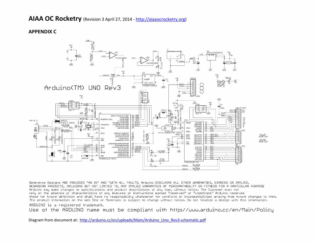
AIAA OC Rocketry (Revision 3 April 27, 2014 - http://aiaaocrocketry.org) APPENDIX C
Diagram from document at: http://arduino.cc/en/uploads/Main/Arduino_Uno_Rev3-schematic.pdf

AIAA OC Rocketry (Revision 3 April 27, 2014 - http://aiaaocrocketry.org) APPENDIX D
From arduino_Uno_Rev3-02-TH.zip file at http://arduino.cc/en/Main/ArduinoBoardUno#.Uxk9qk2YYpA
Eagle PCB software: Eagle PCB PCB design software (use Licesnse = “Run as Freeware”): https://www.cadsoftusa.com/download-eagle/

GENERAL DESCRIPTION The DS1307 serial real-time clock (RTC) is a low-power, full binary-coded decimal (BCD) clock/calendar plus 56 bytes of NV SRAM. Address and data are transferred serially through an I2C, bidirectional bus. The clock/calendar provides seconds, minutes, hours, day, date, month, and year information. The end of the month date is automatically adjusted for months with fewer than 31 days, including corrections for leap year. The clock operates in either the 24-hour or 12-hour format with AM/PM indicator. The DS1307 has a built-in power-sense circuit that detects power failures and automatically switches to the backup supply. Timekeeping operation continues while the part operates from the backup supply. TYPICAL OPERATING CIRCUIT
BENEFITS AND FEATURES Completely Manages All Timekeeping Functions
o Real-Time Clock Counts Seconds, Minutes, Hours, Date of the Month, Month, Day of the Week, and Year with Leap-Year Compensation Valid Up to 2100
o 56-Byte, Battery-Backed, General-Purpose RAM with Unlimited Writes
o Programmable Square-Wave Output Signal
Simple Serial Port Interfaces to Most Microcontrollers o I2C Serial Interface
Low Power Operation Extends Battery Backup Run Time o Consumes Less than 500nA in Battery-
Backup Mode with Oscillator Running o Automatic Power-Fail Detect and Switch
Circuitry
8-Pin DIP and 8-Pin SO Minimizes Required Space
Optional Industrial Temperature Range: -40°C to +85°C Supports Operation in a Wide Range of Applications
Underwriters Laboratories® (UL) Recognized PIN CONFIGURATIONS
VCC
SCL
SDA
X1
X2
VBAT
GND
SQW/OUT
VCC
SCL
SDA
X1
X2
VBAT
GND
SQW/OUT
PDIP (300 mils)SO (150 mils)
TOP VLEW
ORDERING INFORMATION PART TEMP RANGE VOLTAGE (V) PIN-PACKAGE TOP MARK*
DS1307+ 0°C to +70°C 5.0 8 PDIP (300 mils) DS1307 DS1307N+ -40°C to +85°C 5.0 8 PDIP (300 mils) DS1307N DS1307Z+ 0°C to +70°C 5.0 8 SO (150 mils) DS1307 DS1307ZN+ -40°C to +85°C 5.0 8 SO (150 mils) DS1307N DS1307Z+T&R 0°C to +70°C 5.0 8 SO (150 mils) Tape and Reel DS1307 DS1307ZN+T&R -40°C to +85°C 5.0 8 SO (150 mils) Tape and Reel DS1307N
+Denotes a lead-free/RoHS-compliant package. *A “+” anywhere on the top mark indicates a lead-free package. An “N” anywhere on the top mark indicates an industrial temperature range device. Underwriters Laboratories, Inc. is a registered certification mark of Underwriters Laboratories, Inc.
DS1307 CPU
V CC
V CC
V CC
SDA
SCL
GND
X2 X1
V CC
R PU R PU CRYSTAL
SQW/OUT
V BAT
R PU = t r /C b
DS1307 64 x 8, Serial, I2C Real-Time Clock
1 of 14 REV: 3/15

DS1307 64 x 8, Serial, I2C Real-Time Clock
ABSOLUTE MAXIMUM RATINGS Voltage Range on Any Pin Relative to Ground .................................................................................... -0.5V to +7.0V Operating Temperature Range (Noncondensing)
Commercial ................................................................................................................................ 0°C to +70°C Industrial .................................................................................................................................. -40°C to +85°C
Storage Temperature Range ............................................................................................................. -55°C to +125°C Soldering Temperature (DIP, leads) ........................................................................................ +260°C for 10 seconds Soldering Temperature (surface mount)…..……………………….Refer to the JPC/JEDEC J-STD-020 Specification.
Stresses beyond those listed under “Absolute Maximum Ratings” may cause permanent damage to the device. These are stress ratings only, and functional operation of the device at these or any other conditions beyond those indicated in the operational sections of the specifications is not implied. Exposure to the absolute maximum rating conditions for extended periods may affect device reliability.
RECOMMENDED DC OPERATING CONDITIONS (TA = 0°C to +70°C, TA = -40°C to +85°C.) (Notes 1, 2)
PARAMETER SYMBOL CONDITIONS MIN TYP MAX UNITS
Supply Voltage VCC 4.5 5.0 5.5 V
Logic 1 Input VIH 2.2 VCC + 0.3 V
Logic 0 Input VIL -0.3 +0.8 V
VBAT Battery Voltage VBAT 2.0 3 3.5 V
DC ELECTRICAL CHARACTERISTICS (VCC = 4.5V to 5.5V; TA = 0°C to +70°C, TA = -40°C to +85°C.) (Notes 1, 2)
PARAMETER SYMBOL CONDITIONS MIN TYP MAX UNITS
Input Leakage (SCL) ILI -1 1 µA
I/O Leakage (SDA, SQW/OUT) ILO -1 1 µA
Logic 0 Output (IOL = 5mA) VOL 0.4 V Active Supply Current (fSCL = 100kHz) ICCA 1.5 mA
Standby Current ICCS (Note 3) 200 µA
VBAT Leakage Current IBATLKG 5 50 nA
Power-Fail Voltage (VBAT = 3.0V) VPF 1.216 x VBAT
1.25 x VBAT
1.284 x VBAT V
DC ELECTRICAL CHARACTERISTICS (VCC = 0V, VBAT = 3.0V; TA = 0°C to +70°C, TA = -40°C to +85°C.) (Notes 1, 2)
PARAMETER SYMBOL CONDITIONS MIN TYP MAX UNITS
VBAT Current (OSC ON); SQW/OUT OFF IBAT1 300 500 nA
VBAT Current (OSC ON); SQW/OUT ON (32kHz) IBAT2 480 800 nA
VBAT Data-Retention Current (Oscillator Off) IBATDR 10 100 nA
WARNING: Negative undershoots below -0.3V while the part is in battery-backed mode may cause loss of data.
2 of 14

DS1307 64 x 8, Serial, I2C Real-Time Clock
AC ELECTRICAL CHARACTERISTICS (VCC = 4.5V to 5.5V; TA = 0°C to +70°C, TA = -40°C to +85°C.)
PARAMETER SYMBOL CONDITIONS MIN TYP MAX UNITS
SCL Clock Frequency fSCL 0 100 kHz Bus Free Time Between a STOP and START Condition tBUF 4.7 µs
Hold Time (Repeated) START Condition tHD:STA (Note 4) 4.0 µs
LOW Period of SCL Clock tLOW 4.7 µs
HIGH Period of SCL Clock tHIGH 4.0 µs Setup Time for a Repeated START Condition tSU:STA 4.7 µs
Data Hold Time tHD:DAT 0 µs
Data Setup Time tSU:DAT (Notes 5, 6) 250 ns
Rise Time of Both SDA and SCL Signals tR 1000 ns
Fall Time of Both SDA and SCL Signals tF 300 ns
Setup Time for STOP Condition tSU:STO 4.7 µs
CAPACITANCE (TA = +25°C)
PARAMETER SYMBOL CONDITIONS MIN TYP MAX UNITS
Pin Capacitance (SDA, SCL) CI/O 10 pF Capacitance Load for Each Bus Line CB (Note 7) 400 pF
Note 1: All voltages are referenced to ground. Note 2: Limits at -40°C are guaranteed by design and are not production tested. Note 3: ICCS specified with VCC = 5.0V and SDA, SCL = 5.0V. Note 4: After this period, the first clock pulse is generated. Note 5: A device must internally provide a hold time of at least 300ns for the SDA signal (referred to the VIH(MIN) of the SCL
signal) to bridge the undefined region of the falling edge of SCL. Note 6: The maximum tHD:DAT only has to be met if the device does not stretch the LOW period (tLOW) of the SCL signal. Note 7: CB—total capacitance of one bus line in pF.
3 of 14

DS1307 64 x 8, Serial, I2C Real-Time Clock
TIMING DIAGRAM
Figure 1. Block Diagram
START
SDA
STOP
SCL
t SU:STO
t HD:STA
t SU:STA
REPEATED START
t HD:DAT
t HIGH
t F t LOW t R
t HD:STA
t BUF
SU:DAT
4 of 14

DS1307 64 x 8, Serial, I2C Real-Time Clock
TYPICAL OPERATING CHARACTERISTICS (VCC = 5.0V, TA = +25°C, unless otherwise noted.)
ICCS vs. VCC
0
10
20
30
40
50
60
70
80
90
100
110
120
1.0 2.0 3.0 4.0 5.0VCC (V)
SUPP
LY C
URRE
NT (u
A
VBAT=3.0V
IBAT vs. Temperature
175.0
225.0
275.0
325.0
-40 -20 0 20 40 60 80TEMPERATURE (°C)
SUPP
LY C
URRE
NT (n
A
VCC=0V, VBAT=3.0
SQW=32kHz
SQW off
IBAT vs. VBAT
100
150
200
250
300
350
400
2.0 2.5 3.0 3.5VBACKUP (V)SU
PPLY
CUR
RENT
(nA
SQW=32kHz
SQW off
VCC = 0V
SQW/OUT vs. Supply Voltage
32768
32768.1
32768.2
32768.3
32768.4
32768.5
2.0 2.5 3.0 3.5 4.0 4.5 5.0 5.5Supply (V)
FREQ
UENC
Y (H
z)
5 of 14

DS1307 64 x 8, Serial, I2C Real-Time Clock
PIN DESCRIPTION PIN NAME FUNCTION
1 X1 Connections for Standard 32.768kHz Quartz Crystal. The internal oscillator circuitry is designed for operation with a crystal having a specified load capacitance (CL) of 12.5pF. X1 is the input to the oscillator and can optionally be connected to an external 32.768kHz oscillator. The output of the internal oscillator, X2, is floated if an external oscillator is connected to X1. Note: For more information on crystal selection and crystal layout considerations, refer to Application Note 58: Crystal Considerations with Dallas Real-Time Clocks.
2 X2
3 VBAT
Backup Supply Input for Any Standard 3V Lithium Cell or Other Energy Source. Battery voltage must be held between the minimum and maximum limits for proper operation. Diodes in series between the battery and the VBAT pin may prevent proper operation. If a backup supply is not required, VBAT must be grounded. The nominal power-fail trip point (VPF) voltage at which access to the RTC and user RAM is denied is set by the internal circuitry as 1.25 x VBAT nominal. A lithium battery with 48mAh or greater will back up the DS1307 for more than 10 years in the absence of power at +25°C. UL recognized to ensure against reverse charging current when used with a lithium battery. Go to: www.maxim-ic.com/qa/info/ul/.
4 GND Ground
5 SDA Serial Data Input/Output. SDA is the data input/output for the I2C serial interface. The SDA pin is open drain and requires an external pullup resistor. The pullup voltage can be up to 5.5V regardless of the voltage on VCC.
6 SCL Serial Clock Input. SCL is the clock input for the I2C interface and is used to synchronize data movement on the serial interface. The pullup voltage can be up to 5.5V regardless of the voltage on VCC.
7 SQW/OUT
Square Wave/Output Driver. When enabled, the SQWE bit set to 1, the SQW/OUT pin outputs one of four square-wave frequencies (1Hz, 4kHz, 8kHz, 32kHz). The SQW/OUT pin is open drain and requires an external pullup resistor. SQW/OUT operates with either VCC or VBAT applied. The pullup voltage can be up to 5.5V regardless of the voltage on VCC. If not used, this pin can be left floating.
8 VCC
Primary Power Supply. When voltage is applied within normal limits, the device is fully accessible and data can be written and read. When a backup supply is connected to the device and VCC is below VTP, read and writes are inhibited. However, the timekeeping function continues unaffected by the lower input voltage.
DETAILED DESCRIPTION The DS1307 is a low-power clock/calendar with 56 bytes of battery-backed SRAM. The clock/calendar provides seconds, minutes, hours, day, date, month, and year information. The date at the end of the month is automatically adjusted for months with fewer than 31 days, including corrections for leap year. The DS1307 operates as a slave device on the I2C bus. Access is obtained by implementing a START condition and providing a device identification code followed by a register address. Subsequent registers can be accessed sequentially until a STOP condition is executed. When VCC falls below 1.25 x VBAT, the device terminates an access in progress and resets the device address counter. Inputs to the device will not be recognized at this time to prevent erroneous data from being written to the device from an out-of-tolerance system. When VCC falls below VBAT, the device switches into a low-current battery-backup mode. Upon power-up, the device switches from battery to VCC when VCC is greater than VBAT +0.2V and recognizes inputs when VCC is greater than 1.25 x VBAT. The block diagram in Figure 1 shows the main elements of the serial RTC.
6 of 14

DS1307 64 x 8, Serial, I2C Real-Time Clock
OSCILLATOR CIRCUIT The DS1307 uses an external 32.768kHz crystal. The oscillator circuit does not require any external resistors or capacitors to operate. Table 1 specifies several crystal parameters for the external crystal. Figure 1 shows a functional schematic of the oscillator circuit. If using a crystal with the specified characteristics, the startup time is usually less than one second. CLOCK ACCURACY The accuracy of the clock is dependent upon the accuracy of the crystal and the accuracy of the match between the capacitive load of the oscillator circuit and the capacitive load for which the crystal was trimmed. Additional error will be added by crystal frequency drift caused by temperature shifts. External circuit noise coupled into the oscillator circuit may result in the clock running fast. Refer to Application Note 58: Crystal Considerations with Dallas Real-Time Clocks for detailed information. Table 1. Crystal Specifications*
PARAMETER SYMBOL MIN TYP MAX UNITS Nominal Frequency fO 32.768 kHz Series Resistance ESR 45 kΩ Load Capacitance CL 12.5 pF
*The crystal, traces, and crystal input pins should be isolated from RF generating signals. Refer to Application Note 58: Crystal Considerations for Dallas Real-Time Clocks for additional specifications. Figure 2. Recommended Layout for Crystal RTC AND RAM ADDRESS MAP Table 2 shows the address map for the DS1307 RTC and RAM registers. The RTC registers are located in address locations 00h to 07h. The RAM registers are located in address locations 08h to 3Fh. During a multibyte access, when the address pointer reaches 3Fh, the end of RAM space, it wraps around to location 00h, the beginning of the clock space.
NOTE: AVOID ROUTING SIGNAL LINES IN THE CROSSHATCHED AREA (UPPER LEFT QUADRANT) OF THE PACKAGE UNLESS THERE IS A GROUND PLANE BETWEEN THE SIGNAL LINE AND THE DEVICE PACKAGE.
LOCAL GROUND PLANE (LAYER 2)
CRYSTAL X1
X2
GND
7 of 14

DS1307 64 x 8, Serial, I2C Real-Time Clock
CLOCK AND CALENDAR The time and calendar information is obtained by reading the appropriate register bytes. Table 2 shows the RTC registers. The time and calendar are set or initialized by writing the appropriate register bytes. The contents of the time and calendar registers are in the BCD format. The day-of-week register increments at midnight. Values that correspond to the day of week are user-defined but must be sequential (i.e., if 1 equals Sunday, then 2 equals Monday, and so on.) Illogical time and date entries result in undefined operation. Bit 7 of Register 0 is the clock halt (CH) bit. When this bit is set to 1, the oscillator is disabled. When cleared to 0, the oscillator is enabled. On first application of power to the device the time and date registers are typically reset to 01/01/00 01 00:00:00 (MM/DD/YY DOW HH:MM:SS). The CH bit in the seconds register will be set to a 1. The clock can be halted whenever the timekeeping functions are not required, which minimizes current (IBATDR). The DS1307 can be run in either 12-hour or 24-hour mode. Bit 6 of the hours register is defined as the 12-hour or 24-hour mode-select bit. When high, the 12-hour mode is selected. In the 12-hour mode, bit 5 is the AM/PM bit with logic high being PM. In the 24-hour mode, bit 5 is the second 10-hour bit (20 to 23 hours). The hours value must be re-entered whenever the 12/24-hour mode bit is changed. When reading or writing the time and date registers, secondary (user) buffers are used to prevent errors when the internal registers update. When reading the time and date registers, the user buffers are synchronized to the internal registers on any I2C START. The time information is read from these secondary registers while the clock continues to run. This eliminates the need to re-read the registers in case the internal registers update during a read. The divider chain is reset whenever the seconds register is written. Write transfers occur on the I2C acknowledge from the DS1307. Once the divider chain is reset, to avoid rollover issues, the remaining time and date registers must be written within one second. Table 2. Timekeeper Registers ADDRESS BIT 7 BIT 6 BIT 5 BIT 4 BIT 3 BIT 2 BIT 1 BIT 0 FUNCTION RANGE
00h CH 10 Seconds Seconds Seconds 00–59 01h 0 10 Minutes Minutes Minutes 00–59
02h 0 12 10
Hour 10 Hour Hours Hours
1–12 +AM/PM 00–23 24 PM/
AM 03h 0 0 0 0 0 DAY Day 01–07 04h 0 0 10 Date Date Date 01–31
05h 0 0 0 10 Month Month Month 01–12
06h 10 Year Year Year 00–99 07h OUT 0 0 SQWE 0 0 RS1 RS0 Control —
08h–3Fh RAM 56 x 8 00h–FFh
0 = Always reads back as 0.
8 of 14

DS1307 64 x 8, Serial, I2C Real-Time Clock
CONTROL REGISTER The DS1307 control register is used to control the operation of the SQW/OUT pin.
BIT 7 BIT 6 BIT 5 BIT 4 BIT 3 BIT 2 BIT 1 BIT 0 OUT 0 0 SQWE 0 0 RS1 RS0
Bit 7: Output Control (OUT). This bit controls the output level of the SQW/OUT pin when the square-wave output is disabled. If SQWE = 0, the logic level on the SQW/OUT pin is 1 if OUT = 1 and is 0 if OUT = 0. On initial application of power to the device, this bit is typically set to a 0. Bit 4: Square-Wave Enable (SQWE). This bit, when set to logic 1, enables the oscillator output. The frequency of the square-wave output depends upon the value of the RS0 and RS1 bits. With the square-wave output set to 1Hz, the clock registers update on the falling edge of the square wave. On initial application of power to the device, this bit is typically set to a 0. Bits 1 and 0: Rate Select (RS[1:0]). These bits control the frequency of the square-wave output when the square-wave output has been enabled. The following table lists the square-wave frequencies that can be selected with the RS bits. On initial application of power to the device, these bits are typically set to a 1.
RS1 RS0 SQW/OUT OUTPUT SQWE OUT 0 0 1Hz 1 X 0 1 4.096kHz 1 X 1 0 8.192kHz 1 X 1 1 32.768kHz 1 X X X 0 0 0 X X 1 0 1
9 of 14

DS1307 64 x 8, Serial, I2C Real-Time Clock
I2C DATA BUS The DS1307 supports the I2C protocol. A device that sends data onto the bus is defined as a transmitter and a device receiving data as a receiver. The device that controls the message is called a master. The devices that are controlled by the master are referred to as slaves. The bus must be controlled by a master device that generates the serial clock (SCL), controls the bus access, and generates the START and STOP conditions. The DS1307 operates as a slave on the I2C bus. Figures 3, 4, and 5 detail how data is transferred on the I2C bus. Data transfer can be initiated only when the bus is not busy. During data transfer, the data line must remain stable whenever the clock line is HIGH. Changes in the data
line while the clock line is high will be interpreted as control signals. Accordingly, the following bus conditions have been defined:
Bus not busy: Both data and clock lines remain HIGH. START data transfer: A change in the state of the data line, from HIGH to LOW, while the clock is HIGH, defines a START condition. STOP data transfer: A change in the state of the data line, from LOW to HIGH, while the clock line is HIGH, defines the STOP condition. Data valid: The state of the data line represents valid data when, after a START condition, the data line is stable for the duration of the HIGH period of the clock signal. The data on the line must be changed during the LOW period of the clock signal. There is one clock pulse per bit of data.
Each data transfer is initiated with a START condition and terminated with a STOP condition. The number of data bytes transferred between START and STOP conditions is not limited, and is determined by the master device. The information is transferred byte-wise and each receiver acknowledges with a ninth bit. Within the I2C bus specifications a standard mode (100kHz clock rate) and a fast mode (400kHz clock rate) are defined. The DS1307 operates in the standard mode (100kHz) only. Acknowledge: Each receiving device, when addressed, is obliged to generate an acknowledge after the reception of each byte. The master device must generate an extra clock pulse which is associated with this acknowledge bit.
A device that acknowledges must pull down the SDA line during the acknowledge clock pulse in such a way that the SDA line is stable LOW during the HIGH period of the acknowledge related clock pulse. Of course, setup and hold times must be taken into account. A master must signal an end of data to the slave by not generating an acknowledge bit on the last byte that has been clocked out of the slave. In this case, the slave must leave the data line HIGH to enable the master to generate the STOP condition.
10 of 14

DS1307 64 x 8, Serial, I2C Real-Time Clock
Figure 3. Data Transfer on I2C Serial Bus Depending upon the state of the R/W bit, two types of data transfer are possible: 1. Data transfer from a master transmitter to a slave receiver. The first byte transmitted by the master is the
slave address. Next follows a number of data bytes. The slave returns an acknowledge bit after each received byte. Data is transferred with the most significant bit (MSB) first.
2. Data transfer from a slave transmitter to a master receiver. The first byte (the slave address) is transmitted by the master. The slave then returns an acknowledge bit. This is followed by the slave transmitting a number of data bytes. The master returns an acknowledge bit after all received bytes other than the last byte. At the end of the last received byte, a “not acknowledge” is returned.
The master device generates all the serial clock pulses and the START and STOP conditions. A transfer is ended with a STOP condition or with a repeated START condition. Since a repeated START condition is also the beginning of the next serial transfer, the bus will not be released. Data is transferred with the most significant bit (MSB) first.
ACKNOWLEDGEMENT SIGNAL FROM RECEIVER
ACKNOWLEDGEMENT SIGNAL FROM RECEIVER
R/ W DIRECTION
BIT
REPEATED IF MORE BYTES ARE TRANSFERED
START CONDITION
STOP CONDITION
OR REPEATED
START CONDITION
MSB
1 2 6 7 8 9 1 2 3-7 8 9 ACK ACK
SDA
SCL
11 of 14

DS1307 64 x 8, Serial, I2C Real-Time Clock
...AXXXXXXXXA1101000S 0 XXXXXXXX A XXXXXXXX A XXXXXXXX A P
<Slave Address> <Word Address (n)> <Data(n)> <Data(n+1)> <Data(n+X)>
S - StartA - Acknowledge (ACK)P - Stop
<RW
>
DATA TRANSFERRED(X+1 BYTES + ACKNOWLEDGE)
Master to slave
Slave to master
AXXXXXXXXA1101000S 1 XXXXXXXX A XXXXXXXX XXXXXXXX A P
<Slave Address> <Data(n)> <Data(n+1)> <Data(n+2)> <Data(n+X)>
S - StartA - Acknowledge (ACK)P - StopA - Not Acknowledge (NACK)
<RW
>
DATA TRANSFERRED(X+1 BYTES + ACKNOWLEDGE); NOTE: LAST DATA BYTE IS
FOLLOWED BY A NOT ACKNOWLEDGE (A) SIGNAL)
Master to slave
Slave to master
...A
The DS1307 can operate in the following two modes:
1. Slave Receiver Mode (Write Mode): Serial data and clock are received through SDA and SCL. After each byte is received an acknowledge bit is transmitted. START and STOP conditions are recognized as the beginning and end of a serial transfer. Hardware performs address recognition after reception of the slave address and direction bit (see Figure 4). The slave address byte is the first byte received after the master generates the START condition. The slave address byte contains the 7-bit DS1307 address, which is 1101000, followed by the direction bit (R/W), which for a write is 0. After receiving and decoding the slave address byte, the DS1307 outputs an acknowledge on SDA. After the DS1307 acknowledges the slave address + write bit, the master transmits a word address to the DS1307. This sets the register pointer on the DS1307, with the DS1307 acknowledging the transfer. The master can then transmit zero or more bytes of data with the DS1307 acknowledging each byte received. The register pointer automatically increments after each data byte are written. The master will generate a STOP condition to terminate the data write.
2. Slave Transmitter Mode (Read Mode): The first byte is received and handled as in the slave receiver mode. However, in this mode, the direction bit will indicate that the transfer direction is reversed. The DS1307 transmits serial data on SDA while the serial clock is input on SCL. START and STOP conditions are recognized as the beginning and end of a serial transfer (see Figure 5). The slave address byte is the first byte received after the START condition is generated by the master. The slave address byte contains the 7-bit DS1307 address, which is 1101000, followed by the direction bit (R/W), which is 1 for a read. After receiving and decoding the slave address the DS1307 outputs an acknowledge on SDA. The DS1307 then begins to transmit data starting with the register address pointed to by the register pointer. If the register pointer is not written to before the initiation of a read mode the first address that is read is the last one stored in the register pointer. The register pointer automatically increments after each byte are read. The DS1307 must receive a Not Acknowledge to end a read.
Figure 4. Data Write—Slave Receiver Mode Figure 5. Data Read—Slave Transmitter Mode
12 of 14

DS1307 64 x 8, Serial, I2C Real-Time Clock
AXXXXXXXX
1101000S
XXXXXXXX A XXXXXXXX XXXXXXXX A P
<Slave Address> <Word Address (n)> <Slave Address>
S - StartSr - Repeated StartA - Acknowledge (ACK)P - StopA - Not Acknowledge (NACK)
<RW
>
DATA TRANSFERRED(X+1 BYTES + ACKNOWLEDGE); NOTE: LAST DATA BYTE IS
FOLLOWED BY A NOT ACKNOWLEDGE (A) SIGNAL)
Master to slave
Slave to master
...
AXXXXXXXXA0 1101000Sr A1
<Data(n)> <Data(n+1)> <Data(n+2)> <Data(n+X)>
<RW
>
A
Figure 6. Data Read (Write Pointer, Then Read)—Slave Receive and Transmit PACKAGE INFORMATION For the latest package outline information and land patterns, go to www.maxim-ic.com/packages.
PACKAGE TYPE PACKAGE CODE DOCUMENT NO.
8 PDIP — 21-0043
8 SO — 21-0041
13 of 14

DS1307 64 x 8, Serial, I2C Real-Time Clock
REVISION HISTORY REVISION
DATE DESCRIPTION PAGES CHANGED
100208
Moved the Typical Operating Circuit and Pin Configurations to first page. 1
Removed the leaded part numbers from the Ordering Information table. 1 Added an open-drain transistor to SQW/OUT in the block diagram (Figure 1). 4 Added the pullup voltage range for SDA, SCL, and SQW/OUT to the Pin Description table and noted that SQW/OUT can be left open if not used. 6
Added default time and date values on first application of power to the Clock and Calendar section and deleted the note that initial power-on state is not defined.
8
Added default on initial application of power to bit info in the Control Register section. 9
Updated the Package Information section to reflect new package outline drawing numbers. 13
3/15 Updated Benefits and Features section 1
14 of 14 Maxim cannot assume responsibility for use of any circuitry other than circuitry entirely embodied in a Maxim product. No circuit patent licenses are implied. Maxim reserves the right to change the circuitry and specifications without notice at any time. Maxim Integrated Products, 120 San Gabr iel Dr ive, Sunnyvale, CA 94086 408-737-7600 © 2015 Maxim Integrated Products Maxim is a registered trademark of Maxim Integrated Products, Inc.

InvenSense Inc.
1197 Borregas Ave, Sunnyvale, CA 94089 U.S.A.
Tel: +1 (408) 988-7339 Fax: +1 (408) 988-8104
Website: www.invensense.com
Document Number: RM-MPU-6000A-00 Revision: 4.2
Release Date: 08/19/2013
1 of 46
MPU-6000 and MPU-6050
Register Map and Descriptions
Revision 4.2

MPU-6000/MPU-6050 Register Map and
Descriptions
Document Number: RM-MPU-6000A-00 Revision: 4.2 Release Date: 08/19/2013
2 of 46
CONTENTS
1 REVISION HISTORY ................................................................................................................................... 4
2 PURPOSE AND SCOPE ............................................................................................................................. 5
3 REGISTER MAP .......................................................................................................................................... 6
4 REGISTER DESCRIPTIONS ....................................................................................................................... 9
4.1 REGISTERS 13 TO 16 – SELF TEST REGISTERS ..................................................................................... 9
4.2 REGISTER 25 – SAMPLE RATE DIVIDER .............................................................................................. 11
4.3 REGISTER 26 – CONFIGURATION ........................................................................................................ 13
4.4 REGISTER 27 – GYROSCOPE CONFIGURATION .................................................................................... 14
4.5 REGISTER 28 – ACCELEROMETER CONFIGURATION ............................................................................. 15
4.6 REGISTER 35 – FIFO ENABLE ............................................................................................................ 16
4.7 REGISTER 36 – I2C MASTER CONTROL ............................................................................................... 17
4.8 REGISTERS 37 TO 39 – I2C SLAVE 0 CONTROL ................................................................................... 19
4.9 REGISTERS 40 TO 42 – I2C SLAVE 1 CONTROL ................................................................................... 22
4.10 REGISTERS 43 TO 45 – I2C SLAVE 2 CONTROL ................................................................................... 22
4.11 REGISTERS 46 TO 48 – I2C SLAVE 3 CONTROL ................................................................................... 22
4.12 REGISTERS 49 TO 53 – I2C SLAVE 4 CONTROL ................................................................................... 23
4.13 REGISTER 54 – I2C MASTER STATUS .................................................................................................. 25
4.14 REGISTER 55 – INT PIN / BYPASS ENABLE CONFIGURATION ................................................................ 26
4.15 REGISTER 56 – INTERRUPT ENABLE ................................................................................................... 27
4.16 REGISTER 58 – INTERRUPT STATUS ................................................................................................... 28
4.17 REGISTERS 59 TO 64 – ACCELEROMETER MEASUREMENTS ................................................................. 29
4.18 REGISTERS 65 AND 66 – TEMPERATURE MEASUREMENT ..................................................................... 30
4.19 REGISTERS 67 TO 72 – GYROSCOPE MEASUREMENTS ........................................................................ 31
4.20 REGISTERS 73 TO 96 – EXTERNAL SENSOR DATA ............................................................................... 32
4.21 REGISTER 99 – I2C SLAVE 0 DATA OUT .............................................................................................. 34
4.22 REGISTER 100 – I2C SLAVE 1 DATA OUT ............................................................................................ 34
4.23 REGISTER 101 – I2C SLAVE 2 DATA OUT ............................................................................................ 35
4.24 REGISTER 102 – I2C SLAVE 3 DATA OUT ............................................................................................ 35
4.25 REGISTER 103 – I2C MASTER DELAY CONTROL .................................................................................. 36
4.26 REGISTER 104 – SIGNAL PATH RESET ................................................................................................ 37
4.27 REGISTER 106 – USER CONTROL ....................................................................................................... 38
4.28 REGISTER 107 – POWER MANAGEMENT 1 .......................................................................................... 40
4.29 REGISTER 108 – POWER MANAGEMENT 2 .......................................................................................... 42

MPU-6000/MPU-6050 Register Map and
Descriptions
Document Number: RM-MPU-6000A-00 Revision: 4.2 Release Date: 08/19/2013
3 of 46
4.30 REGISTER 114 AND 115 – FIFO COUNT REGISTERS ........................................................................... 43
4.31 REGISTER 116 – FIFO READ WRITE .................................................................................................. 44
4.32 REGISTER 117 – WHO AM I ................................................................................................................ 45

MPU-6000/MPU-6050 Register Map and
Descriptions
Document Number: RM-MPU-6000A-00 Revision: 4.2 Release Date: 08/19/2013
4 of 46
1 Revision History
Revision Date Revision Description
11/29/2010 1.0 Initial Release
04/20/2011 1.1 Updated register map and descriptions to reflect enhanced register functionality.
05/19/2011 2.0
Updates for Rev C silicon:
Edits for readability (section 2.1)
Edits for changes in functionality (section 3, 4.4, 4.6, 4.7, 4.8, 4.21, 4.22, 4.23, 4.37)
10/07/2011 3.0 Updates for Rev D silicon:
Updated accelerometer sensitivity specifications (sections 4.6, 4.8, 4.10, 4.23)
10/24/2011 3.1 Edits for clarity
11/14/2011 3.2
Updated reset value for register 107 (section 3)
Updated register 27 with gyro self-test bits (section 4.4)
Provided gyro self-test instructions and register bits (section 4.4)
Provided accel self-test instructions (section 4.5)
3/9/2012 4.0
Updated register map to include Self-Test registers (section 3)
Added description of Self-Test registers (section 4.1)
Revised temperature register section (section 4.19)
Corrections in registers 107 and 108 (section 4.30)
2/11/2013 4.1 Added reset clarification for SPI interface (section 4.3)
8/19/2013 4.2 Updated sections 6, 7, 8, 10

MPU-6000/MPU-6050 Register Map and
Descriptions
Document Number: RM-MPU-6000A-00 Revision: 4.2 Release Date: 08/19/2013
5 of 46
2 Purpose and Scope
This document provides preliminary information regarding the register map and descriptions for the Motion Processing Units™ MPU-6000™ and MPU-6050™, collectively called the MPU-60X0™ or MPU™.
The MPU devices provide the world’s first integrated 6-axis motion processor solution that eliminates the package-level gyroscope and accelerometer cross-axis misalignment associated with discrete solutions. The devices combine a 3-axis gyroscope and a 3-axis accelerometer on the same silicon die together with an onboard Digital Motion Processor™ (DMP™) capable of processing complex 9-axis sensor fusion algorithms using the field-proven and proprietary MotionFusion™ engine.
The MPU-6000 and MPU-6050’s integrated 9-axis MotionFusion algorithms access external magnetometers or other sensors through an auxiliary master I
2C bus, allowing the devices to gather a full set of sensor data
without intervention from the system processor. The devices are offered in the same 4x4x0.9 mm QFN footprint and pinout as the current MPU-3000™ family of integrated 3-axis gyroscopes, providing a simple upgrade path and facilitating placement on already space constrained circuit boards.
For precision tracking of both fast and slow motions, the MPU-60X0 features a user-programmable gyroscope full-scale range of ±250, ±500, ±1000, and ±2000°/sec (dps). The parts also have a user-programmable accelerometer full-scale range of ±2g, ±4g, ±8g, and ±16g.
The MPU-6000 family is comprised of two parts, the MPU-6000 and MPU-6050. These parts are identical to each other with two exceptions. The MPU-6050 supports I
2C communications at up to 400kHz and has a
VLOGIC pin that defines its interface voltage levels; the MPU-6000 supports SPI at up to 20MHz in addition to I
2C, and has a single supply pin, VDD, which is both the device’s logic reference supply and the analog
supply for the part.
For more detailed information for the MPU-60X0 devices, please refer to the “MPU-6000 and MPU-6050 Product Specification”.

MPU-6000/MPU-6050 Register Map and
Descriptions
Document Number: RM-MPU-6000A-00 Revision: 4.2 Release Date: 08/19/2013
6 of 46
3 Register Map
The register map for the MPU-60X0 is listed below.
Addr (Hex)
Addr (Dec.)
Register Name Serial I/F
Bit7 Bit6 Bit5 Bit4 Bit3 Bit2 Bit1 Bit0
0D 13 SELF_TEST_X R/W XA_TEST[4-2] XG_TEST[4-0]
0E 14 SELF_TEST_Y R/W YA_TEST[4-2] YG_TEST[4-0]
0F 15 SELF_TEST_Z R/W ZA_TEST[4-2] ZG_TEST[4-0]
10 16 SELF_TEST_A R/W RESERVED XA_TEST[1-0] YA_TEST[1-0] ZA_TEST[1-0]
19 25 SMPLRT_DIV R/W SMPLRT_DIV[7:0]
1A 26 CONFIG R/W - - EXT_SYNC_SET[2:0] DLPF_CFG[2:0]
1B 27 GYRO_CONFIG R/W - - - FS_SEL [1:0] - - -
1C 28 ACCEL_CONFIG R/W XA_ST YA_ST ZA_ST AFS_SEL[1:0]
23 35 FIFO_EN R/W TEMP
_FIFO_EN XG
_FIFO_EN YG
_FIFO_EN ZG
_FIFO_EN ACCEL
_FIFO_EN SLV2
_FIFO_EN SLV1
_FIFO_EN SLV0
_FIFO_EN
24 36 I2C_MST_CTRL R/W MULT
_MST_EN WAIT
_FOR_ES SLV_3
_FIFO_EN I2C_MST _P_NSR
I2C_MST_CLK[3:0]
25 37 I2C_SLV0_ADDR R/W I2C_SLV0
_RW I2C_SLV0_ADDR[6:0]
26 38 I2C_SLV0_REG R/W I2C_SLV0_REG[7:0]
27 39 I2C_SLV0_CTRL R/W I2C_SLV0
_EN I2C_SLV0
_BYTE_SW I2C_SLV0 _REG_DIS
I2C_SLV0 _GRP
I2C_SLV0_LEN[3:0]
28 40 I2C_SLV1_ADDR R/W I2C_SLV1
_RW I2C_SLV1_ADDR[6:0]
29 41 I2C_SLV1_REG R/W I2C_SLV1_REG[7:0]
2A 42 I2C_SLV1_CTRL R/W I2C_SLV1
_EN I2C_SLV1
_BYTE_SW I2C_SLV1 _REG_DIS
I2C_SLV1 _GRP
I2C_SLV1_LEN[3:0]
2B 43 I2C_SLV2_ADDR R/W I2C_SLV2
_RW I2C_SLV2_ADDR[6:0]
2C 44 I2C_SLV2_REG R/W I2C_SLV2_REG[7:0]
2D 45 I2C_SLV2_CTRL R/W I2C_SLV2
_EN I2C_SLV2
_BYTE_SW I2C_SLV2 _REG_DIS
I2C_SLV2 _GRP
I2C_SLV2_LEN[3:0]
2E 46 I2C_SLV3_ADDR R/W I2C_SLV3
_RW I2C_SLV3_ADDR[6:0]
2F 47 I2C_SLV3_REG R/W I2C_SLV3_REG[7:0]
30 48 I2C_SLV3_CTRL R/W I2C_SLV3
_EN I2C_SLV3
_BYTE_SW I2C_SLV3 _REG_DIS
I2C_SLV3 _GRP
I2C_SLV3_LEN[3:0]
31 49 I2C_SLV4_ADDR R/W I2C_SLV4
_RW I2C_SLV4_ADDR[6:0]
32 50 I2C_SLV4_REG R/W I2C_SLV4_REG[7:0]
33 51 I2C_SLV4_DO R/W I2C_SLV4_DO[7:0]
34 52 I2C_SLV4_CTRL R/W I2C_SLV4
_EN I2C_SLV4 _INT_EN
I2C_SLV4 _REG_DIS
I2C_MST_DLY[4:0]
35 53 I2C_SLV4_DI R I2C_SLV4_DI[7:0]
36 54 I2C_MST_STATUS R PASS_
THROUGH I2C_SLV4
_DONE I2C_LOST
_ARB I2C_SLV4
_NACK I2C_SLV3
_NACK I2C_SLV2
_NACK I2C_SLV1
_NACK I2C_SLV0
_NACK
37 55 INT_PIN_CFG R/W INT_LEVEL INT_OPEN LATCH
_INT_EN INT_RD _CLEAR
FSYNC_ INT_LEVEL
FSYNC _INT_EN
I2C _BYPASS
_EN -
38 56 INT_ENABLE R/W - - -
FIFO _OFLOW
_EN
I2C_MST _INT_EN
- - DATA
_RDY_EN
3A 58 INT_STATUS R - - -
FIFO _OFLOW
_INT
I2C_MST _INT
- - DATA
_RDY_INT

MPU-6000/MPU-6050 Register Map and
Descriptions
Document Number: RM-MPU-6000A-00 Revision: 4.2 Release Date: 08/19/2013
7 of 46
Addr (Hex)
Addr (Dec.)
Register Name Serial I/F
Bit7 Bit6 Bit5 Bit4 Bit3 Bit2 Bit1 Bit0
3B 59 ACCEL_XOUT_H R ACCEL_XOUT[15:8]
3C 60 ACCEL_XOUT_L R ACCEL_XOUT[7:0]
3D 61 ACCEL_YOUT_H R ACCEL_YOUT[15:8]
3E 62 ACCEL_YOUT_L R ACCEL_YOUT[7:0]
3F 63 ACCEL_ZOUT_H R ACCEL_ZOUT[15:8]
40 64 ACCEL_ZOUT_L R ACCEL_ZOUT[7:0]
41 65 TEMP_OUT_H R TEMP_OUT[15:8]
42 66 TEMP_OUT_L R TEMP_OUT[7:0]
43 67 GYRO_XOUT_H R GYRO_XOUT[15:8]
44 68 GYRO_XOUT_L R GYRO_XOUT[7:0]
45 69 GYRO_YOUT_H R GYRO_YOUT[15:8]
46 70 GYRO_YOUT_L R GYRO_YOUT[7:0]
47 71 GYRO_ZOUT_H R GYRO_ZOUT[15:8]
48 72 GYRO_ZOUT_L R GYRO_ZOUT[7:0]
49 73 EXT_SENS_DATA_00 R EXT_SENS_DATA_00[7:0]
4A 74 EXT_SENS_DATA_01 R EXT_SENS_DATA_01[7:0]
4B 75 EXT_SENS_DATA_02 R EXT_SENS_DATA_02[7:0]
4C 76 EXT_SENS_DATA_03 R EXT_SENS_DATA_03[7:0]
4D 77 EXT_SENS_DATA_04 R EXT_SENS_DATA_04[7:0]
4E 78 EXT_SENS_DATA_05 R EXT_SENS_DATA_05[7:0]
4F 79 EXT_SENS_DATA_06 R EXT_SENS_DATA_06[7:0]
50 80 EXT_SENS_DATA_07 R EXT_SENS_DATA_07[7:0]
51 81 EXT_SENS_DATA_08 R EXT_SENS_DATA_08[7:0]
52 82 EXT_SENS_DATA_09 R EXT_SENS_DATA_09[7:0]
53 83 EXT_SENS_DATA_10 R EXT_SENS_DATA_10[7:0]
54 84 EXT_SENS_DATA_11 R EXT_SENS_DATA_11[7:0]
55 85 EXT_SENS_DATA_12 R EXT_SENS_DATA_12[7:0]
56 86 EXT_SENS_DATA_13 R EXT_SENS_DATA_13[7:0]
57 87 EXT_SENS_DATA_14 R EXT_SENS_DATA_14[7:0]
58 88 EXT_SENS_DATA_15 R EXT_SENS_DATA_15[7:0]
59 89 EXT_SENS_DATA_16 R EXT_SENS_DATA_16[7:0]
5A 90 EXT_SENS_DATA_17 R EXT_SENS_DATA_17[7:0]
5B 91 EXT_SENS_DATA_18 R EXT_SENS_DATA_18[7:0]
5C 92 EXT_SENS_DATA_19 R EXT_SENS_DATA_19[7:0]
5D 93 EXT_SENS_DATA_20 R EXT_SENS_DATA_20[7:0]
5E 94 EXT_SENS_DATA_21 R EXT_SENS_DATA_21[7:0]
5F 95 EXT_SENS_DATA_22 R EXT_SENS_DATA_22[7:0]
60 96 EXT_SENS_DATA_23 R EXT_SENS_DATA_23[7:0]
63 99 I2C_SLV0_DO R/W I2C_SLV0_DO[7:0]
64 100 I2C_SLV1_DO R/W I2C_SLV1_DO[7:0]
65 101 I2C_SLV2_DO R/W I2C_SLV2_DO[7:0]
66 102 I2C_SLV3_DO R/W I2C_SLV3_DO[7:0]

MPU-6000/MPU-6050 Register Map and
Descriptions
Document Number: RM-MPU-6000A-00 Revision: 4.2 Release Date: 08/19/2013
8 of 46
Addr (Hex)
Addr (Dec.)
Register Name Serial I/F
Bit7 Bit6 Bit5 Bit4 Bit3 Bit2 Bit1 Bit0
67 103 I2C_MST_DELAY_CTRL
R/W DELAY_ES _SHADOW
- - I2C_SLV4 _DLY_EN
I2C_SLV3 _DLY_EN
I2C_SLV2 _DLY_EN
I2C_SLV1 _DLY_EN
I2C_SLV0 _DLY_EN
68 104 SIGNAL_PATH_RESET
R/W - - - - - GYRO
_RESET ACCEL
_RESET TEMP
_RESET
6A 106 USER_CTRL R/W - FIFO_EN I2C_MST
_EN
I2C_IF
_DIS -
FIFO
_RESET
I2C_MST
_RESET
SIG_COND
_RESET
6B 107 PWR_MGMT_1 R/W DEVICE _RESET
SLEEP CYCLE - TEMP_DIS CLKSEL[2:0]
6C 108 PWR_MGMT_2 R/W LP_WAKE_CTRL[1:0] STBY_XA STBY_YA STBY_ZA STBY_XG STBY_YG STBY_ZG
72 114 FIFO_COUNTH R/W FIFO_COUNT[15:8]
73 115 FIFO_COUNTL R/W FIFO_COUNT[7:0]
74 116 FIFO_R_W R/W FIFO_DATA[7:0]
75 117 WHO_AM_I R - WHO_AM_I[6:1] -
Note: Register Names ending in _H and _L contain the high and low bytes, respectively, of an internal register value. In the detailed register tables that follow, register names are in capital letters, while register values are in capital letters and italicized. For example, the ACCEL_XOUT_H register (Register 59) contains the 8 most significant bits, ACCEL_XOUT[15:8], of the 16-bit X-Axis accelerometer measurement, ACCEL_XOUT. The reset value is 0x00 for all registers other than the registers below.
Register 107: 0x40.
Register 117: 0x68.

MPU-6000/MPU-6050 Register Map and
Descriptions
Document Number: RM-MPU-6000A-00 Revision: 4.2 Release Date: 08/19/2013
9 of 46
4 Register Descriptions
This section describes the function and contents of each register within the MPU-60X0.
Note: The device will come up in sleep mode upon power-up.
4.1 Registers 13 to 16 – Self Test Registers SELF_TEST_X, SELF_TEST_Y, SELF_TEST_Z, and SELF_TEST_A
Type: Read/Write
Register (Hex)
Register
(Decimal) Bit7 Bit6 Bit5 Bit4 Bit3 Bit2 Bit1 Bit0
0D 13 XA_TEST[4-2] XG_TEST[4-0]
0E 14 YA_TEST[4-2] YG_TEST[4-0]
0F 15 ZA_TEST[4-2] ZG_TEST[4-0]
10 16 RESERVED XA_TEST[1-0] YA_TEST[1-0] ZA_TEST[1-0]
Description:
These registers are used for gyroscope and accelerometer self-tests that permit the user to test the mechanical and electrical portions of the gyroscope and the accelerometer. The following sections describe the self-test process.
1. Gyroscope Hardware Self-Test: Relative Method
Gyroscope self-test permits users to test the mechanical and electrical portions of the gyroscope. Code for operating self-test is included within the MotionApps™ software provided by InvenSense. Please refer to the next section (Obtaining the Gyroscope Factory Trim (FT) Value) if not using MotionApps software.
When self-test is activated, the on-board electronics will actuate the appropriate sensor. This actuation will move the sensor’s proof masses over a distance equivalent to a pre-defined Coriolis force. This proof mass displacement results in a change in the sensor output, which is reflected in the output signal. The output signal is used to observe the self-test response.
The self-test response (STR) is defined as follows:
This self test-response is used to determine whether the part has passed or failed self-test by finding the change from factory trim of the self-test response as follows:
( ) ( )
This change from factory trim of the self-test response must be within the limits provided in the MPU-6000/MPU-6050 Product Specification document for the part to pass self-test. Otherwise, the part is deemed to have failed self-test.

MPU-6000/MPU-6050 Register Map and
Descriptions
Document Number: RM-MPU-6000A-00 Revision: 4.2 Release Date: 08/19/2013
10 of 46
Obtaining the Gyroscope Factory Trim (FT) Value If InvenSense MotionApps software is not used, the procedure detailed below should be followed to obtain the Factory trim value of the self test response (FT) mentioned above. For the specific registers mentioned below, please refer to registers 13-15.
The Factory trim value of the self test response (FT) is calculated as shown below. FT[Xg], FT[Yg], and FT[Zg] refer to the factory trim (FT) values for the gyroscope X, Y, and Z axes, respectively. XG_TEST is the decimal version of XG_TEST[4-0], YG_TEST is the decimal version of YG_TEST[4-0], and ZG_TEST is the decimal version of ZG_TEST[4-0].
When performing self test for the gyroscope, the full-scale range should be set to ±250dps.
( ) if XG_TEST ≠ 0 if XG_TEST = 0
( ) if YG_TEST ≠ 0 if YG_TEST = 0
( ) if ZG_TEST ≠ 0 if ZG_TEST = 0
2. Accelerometer Hardware Self-Test: Relative Method
Accelerometer self-test permits users to test the mechanical and electrical portions of the accelerometer. Code for operating self-test is included within the MotionApps software provided by InvenSense. Please refer to the next section (titled Obtaining the Accelerometer Factory Trim (FT) Value) if not using MotionApps software.
When self-test is activated, the on-board electronics will actuate the appropriate sensor. This actuation simulates an external force. The actuated sensor, in turn, will produce a corresponding output signal. The output signal is used to observe the self-test response.
The self-test response (STR) is defined as follows:
This self test-response is used to determine whether the part has passed or failed self-test by finding the change from factory trim of the self-test response as follows:
( ) ( )
This change from factory trim of the self-test response must be within the limits provided in the MPU-6000/MPU-6050 Product Specification document for the part to pass self-test. Otherwise, the part is deemed to have failed self-test.

MPU-6000/MPU-6050 Register Map and
Descriptions
Document Number: RM-MPU-6000A-00 Revision: 4.2 Release Date: 08/19/2013
11 of 46
Obtaining the Accelerometer Factory Trim (FT) Value If InvenSense MotionApps software is not used, the procedure detailed below should be followed to obtain the Factory trim value of the self test response (FT) mentioned above. For the specific registers mentioned below, please refer to registers 13-16. The Factory trim value of the self test response (FT) is calculated as shown below. FT[Xa], FT[Ya], and FT[Za] refer to the factory trim (FT) values for the accelerometer X, Y, and Z axes, respectively. In the equations below, the factory trim values for the accel should be in decimal format, and they are determined by concatenating the upper accelerometer self test bits (bits 4-2) with the lower accelerometer self test bits (bits 1-0).
When performing accelerometer self test, the full-scale range should be set to ±8g.
(
) if XA_TEST ≠ 0.
if XA_TEST = 0.
(
) if YA_TEST ≠ 0.
if YA_TEST = 0.
(
) if ZA_TEST ≠ 0.
if ZA_TEST = 0.
Parameters:
XA_TEST 5-bit unsigned value. FT[Xa] is determined by using this value as explained
above.
XG_TEST 5-bit unsigned value. FT[Xg] is determined by using this value as explained
above.
YA_TEST 5-bit unsigned value. FT[Ya] is determined by using this value as explained
above.
YG_TEST 5-bit unsigned value. FT[Yg] is determined by using this value as explained
above.
ZA_TEST 5-bit unsigned value. FT[Za] is determined by using this value as explained
above.
ZG_TEST 5-bit unsigned value. FT[Zg] is determined by using this value as explained
above.
4.2 Register 25 – Sample Rate Divider SMPRT_DIV
Type: Read/Write
Register (Hex)
Register
(Decimal) Bit7 Bit6 Bit5 Bit4 Bit3 Bit2 Bit1 Bit0
19 25 SMPLRT_DIV[7:0]
Description:

MPU-6000/MPU-6050 Register Map and
Descriptions
Document Number: RM-MPU-6000A-00 Revision: 4.2 Release Date: 08/19/2013
12 of 46
This register specifies the divider from the gyroscope output rate used to generate the Sample Rate for the MPU-60X0.
The sensor register output, FIFO output, and DMP sampling are all based on the Sample Rate.
The Sample Rate is generated by dividing the gyroscope output rate by SMPLRT_DIV:
Sample Rate = Gyroscope Output Rate / (1 + SMPLRT_DIV)
where Gyroscope Output Rate = 8kHz when the DLPF is disabled (DLPF_CFG = 0 or 7), and 1kHz when the DLPF is enabled (see Register 26).
Note: The accelerometer output rate is 1kHz. This means that for a Sample Rate greater than 1kHz, the same accelerometer sample may be output to the FIFO, DMP, and sensor registers more than once.
For a diagram of the gyroscope and accelerometer signal paths, see Section 8 of the MPU-6000/MPU-6050 Product Specification document.
Parameters:
SMPLRT_DIV 8-bit unsigned value. The Sample Rate is determined by dividing the
gyroscope output rate by this value.

MPU-6000/MPU-6050 Register Map and
Descriptions
Document Number: RM-MPU-6000A-00 Revision: 4.2 Release Date: 08/19/2013
13 of 46
4.3 Register 26 – Configuration CONFIG
Type: Read/Write
Register (Hex)
Register
(Decimal) Bit7 Bit6 Bit5 Bit4 Bit3 Bit2 Bit1 Bit0
1A 26 - - EXT_SYNC_SET[2:0] DLPF_CFG[2:0]
Description:
This register configures the external Frame Synchronization (FSYNC) pin sampling and the Digital Low Pass Filter (DLPF) setting for both the gyroscopes and accelerometers.
An external signal connected to the FSYNC pin can be sampled by configuring EXT_SYNC_SET.
Signal changes to the FSYNC pin are latched so that short strobes may be captured. The latched FSYNC signal will be sampled at the Sampling Rate, as defined in register 25. After sampling, the latch will reset to the current FSYNC signal state.
The sampled value will be reported in place of the least significant bit in a sensor data register determined by the value of EXT_SYNC_SET according to the following table.
EXT_SYNC_SET FSYNC Bit Location
0 Input disabled
1 TEMP_OUT_L[0]
2 GYRO_XOUT_L[0]
3 GYRO_YOUT_L[0]
4 GYRO_ZOUT_L[0]
5 ACCEL_XOUT_L[0]
6 ACCEL_YOUT_L[0]
7 ACCEL_ZOUT_L[0]
The DLPF is configured by DLPF_CFG. The accelerometer and gyroscope are filtered according to the value of DLPF_CFG as shown in the table below.
DLPF_CFG Accelerometer
(Fs = 1kHz)
Gyroscope
Bandwidth (Hz)
Delay (ms)
Bandwidth (Hz)
Delay (ms)
Fs (kHz)
0 260 0 256 0.98 8
1 184 2.0 188 1.9 1
2 94 3.0 98 2.8 1
3 44 4.9 42 4.8 1
4 21 8.5 20 8.3 1
5 10 13.8 10 13.4 1
6 5 19.0 5 18.6 1
7 RESERVED RESERVED 8
Bit 7 and bit 6 are reserved.
Parameters:
EXT_SYNC_SET 3-bit unsigned value. Configures the FSYNC pin sampling.
DLPF_CFG 3-bit unsigned value. Configures the DLPF setting.

MPU-6000/MPU-6050 Register Map and
Descriptions
Document Number: RM-MPU-6000A-00 Revision: 4.2 Release Date: 08/19/2013
14 of 46
4.4 Register 27 – Gyroscope Configuration GYRO_CONFIG
Type: Read/Write
Register (Hex)
Register
(Decimal) Bit7 Bit6 Bit5 Bit4 Bit3 Bit2 Bit1 Bit0
1B 27 XG_ST YG_ST ZG_ST FS_SEL[1:0] - - -
Description:
This register is used to trigger gyroscope self-test and configure the gyroscopes’ full scale range.
Gyroscope self-test permits users to test the mechanical and electrical portions of the gyroscope. The self-test for each gyroscope axis can be activated by controlling the XG_ST, YG_ST, and ZG_ST bits of this register. Self-test for each axis may be performed independently or all at the same time.
When self-test is activated, the on-board electronics will actuate the appropriate sensor. This actuation will move the sensor’s proof masses over a distance equivalent to a pre-defined Coriolis force. This proof mass displacement results in a change in the sensor output, which is reflected in the output signal. The output signal is used to observe the self-test response.
The self-test response is defined as follows:
Self-test response = Sensor output with self-test enabled – Sensor output without self-test enabled
The self-test limits for each gyroscope axis is provided in the electrical characteristics tables of the MPU-6000/MPU-6050 Product Specification document. When the value of the self-test response is within the min/max limits of the product specification, the part has passed self test. When the self-test response exceeds the min/max values specified in the document, the part is deemed to have failed self-test.
FS_SEL selects the full scale range of the gyroscope outputs according to the following table.
FS_SEL Full Scale Range
0 ± 250 °/s
1 ± 500 °/s
2 ± 1000 °/s
3 ± 2000 °/s
Bits 2 through 0 are reserved.
Parameters:
XG_ST Setting this bit causes the X axis gyroscope to perform self test.
YG_ST Setting this bit causes the Y axis gyroscope to perform self test.
ZG_ST Setting this bit causes the Z axis gyroscope to perform self test.
FS_SEL 2-bit unsigned value. Selects the full scale range of gyroscopes.

MPU-6000/MPU-6050 Register Map and
Descriptions
Document Number: RM-MPU-6000A-00 Revision: 4.2 Release Date: 08/19/2013
15 of 46
4.5 Register 28 – Accelerometer Configuration ACCEL_CONFIG
Type: Read/Write
Register (Hex)
Register
(Decimal) Bit7 Bit6 Bit5 Bit4 Bit3 Bit2 Bit1 Bit0
1C 28 XA_ST YA_ST ZA_ST AFS_SEL[1:0] -
Description:
This register is used to trigger accelerometer self test and configure the accelerometer full scale range. This register also configures the Digital High Pass Filter (DHPF).
Accelerometer self-test permits users to test the mechanical and electrical portions of the accelerometer. The self-test for each accelerometer axis can be activated by controlling the XA_ST, YA_ST, and ZA_ST bits of this register. Self-test for each axis may be performed independently or all at the same time.
When self-test is activated, the on-board electronics will actuate the appropriate sensor. This actuation simulates an external force. The actuated sensor, in turn, will produce a corresponding output signal. The output signal is used to observe the self-test response.
The self-test response is defined as follows:
Self-test response = Sensor output with self-test enabled – Sensor output without self-test enabled
The self-test limits for each accelerometer axis is provided in the electrical characteristics tables of the MPU-6000/MPU-6050 Product Specification document. When the value of the self-test response is within the min/max limits of the product specification, the part has passed self test. When the self-test response exceeds the min/max values specified in the document, the part is deemed to have failed self-test.
AFS_SEL selects the full scale range of the accelerometer outputs according to the following table.
AFS_SEL Full Scale Range
0 ± 2g
1 ± 4g
2 ± 8g
3 ± 16g
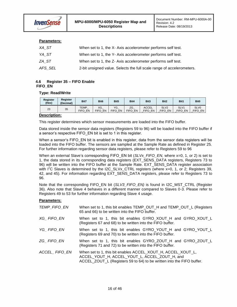
MPU-6000/MPU-6050 Register Map and
Descriptions
Document Number: RM-MPU-6000A-00 Revision: 4.2 Release Date: 08/19/2013
16 of 46
Parameters:
XA_ST When set to 1, the X- Axis accelerometer performs self test.
YA_ST When set to 1, the Y- Axis accelerometer performs self test.
ZA_ST When set to 1, the Z- Axis accelerometer performs self test.
AFS_SEL 2-bit unsigned value. Selects the full scale range of accelerometers.
4.6 Register 35 – FIFO Enable FIFO_EN
Type: Read/Write
Register (Hex)
Register
(Decimal) Bit7 Bit6 Bit5 Bit4 Bit3 Bit2 Bit1 Bit0
23 35 TEMP_
FIFO_EN XG_
FIFO_EN YG_
FIFO_EN ZG_
FIFO_EN ACCEL
_FIFO_EN SLV2
_FIFO_EN SLV1
_FIFO_EN SLV0
_FIFO_EN
Description:
This register determines which sensor measurements are loaded into the FIFO buffer.
Data stored inside the sensor data registers (Registers 59 to 96) will be loaded into the FIFO buffer if a sensor’s respective FIFO_EN bit is set to 1 in this register.
When a sensor’s FIFO_EN bit is enabled in this register, data from the sensor data registers will be loaded into the FIFO buffer. The sensors are sampled at the Sample Rate as defined in Register 25. For further information regarding sensor data registers, please refer to Registers 59 to 96
When an external Slave’s corresponding FIFO_EN bit (SLVx_FIFO_EN, where x=0, 1, or 2) is set to 1, the data stored in its corresponding data registers (EXT_SENS_DATA registers, Registers 73 to 96) will be written into the FIFO buffer at the Sample Rate. EXT_SENS_DATA register association with I
2C Slaves is determined by the I2C_SLVx_CTRL registers (where x=0, 1, or 2; Registers 39,
42, and 45). For information regarding EXT_SENS_DATA registers, please refer to Registers 73 to 96.
Note that the corresponding FIFO_EN bit (SLV3_FIFO_EN) is found in I2C_MST_CTRL (Register 36). Also note that Slave 4 behaves in a different manner compared to Slaves 0-3. Please refer to Registers 49 to 53 for further information regarding Slave 4 usage.
Parameters:
TEMP_FIFO_EN When set to 1, this bit enables TEMP_OUT_H and TEMP_OUT_L (Registers 65 and 66) to be written into the FIFO buffer.
XG_ FIFO_EN When set to 1, this bit enables GYRO_XOUT_H and GYRO_XOUT_L (Registers 67 and 68) to be written into the FIFO buffer.
YG_ FIFO_EN When set to 1, this bit enables GYRO_YOUT_H and GYRO_YOUT_L (Registers 69 and 70) to be written into the FIFO buffer.
ZG_ FIFO_EN When set to 1, this bit enables GYRO_ZOUT_H and GYRO_ZOUT_L (Registers 71 and 72) to be written into the FIFO buffer.
ACCEL_ FIFO_EN When set to 1, this bit enables ACCEL_XOUT_H, ACCEL_XOUT_L, ACCEL_YOUT_H, ACCEL_YOUT_L, ACCEL_ZOUT_H, and ACCEL_ZOUT_L (Registers 59 to 64) to be written into the FIFO buffer.

MPU-6000/MPU-6050 Register Map and
Descriptions
Document Number: RM-MPU-6000A-00 Revision: 4.2 Release Date: 08/19/2013
17 of 46
SLV2_ FIFO_EN When set to 1, this bit enables EXT_SENS_DATA registers (Registers 73 to 96) associated with Slave 2 to be written into the FIFO buffer.
SLV1_ FIFO_EN When set to 1, this bit enables EXT_SENS_DATA registers (Registers 73 to 96) associated with Slave 1 to be written into the FIFO buffer.
SLV0_ FIFO_EN When set to 1, this bit enables EXT_SENS_DATA registers (Registers 73 to 96) associated with Slave 0 to be written into the FIFO buffer.
Note: For further information regarding the association of EXT_SENS_DATA registers to particular slave devices, please refer to Registers 73 to 96.
4.7 Register 36 – I2C Master Control
I2C_MST_CTRL
Type: Read/Write
Register (Hex)
Register
(Decimal) Bit7 Bit6 Bit5 Bit4 Bit3 Bit2 Bit1 Bit0
24 36 MULT
_MST_EN WAIT
_FOR_ES SLV_3
_FIFO_EN I2C_MST _P_NSR
I2C_MST_CLK[3:0]
Description:
This register configures the auxiliary I2C bus for single-master or multi-master control. In addition, the
register is used to delay the Data Ready interrupt, and also enables the writing of Slave 3 data into the FIFO buffer. The register also configures the auxiliary I
2C Master’s transition from one slave read
to the next, as well as the MPU-60X0’s 8MHz internal clock.
Multi-master capability allows multiple I2C masters to operate on the same bus. In circuits where
multi-master capability is required, set MULT_MST_EN to 1. This will increase current drawn by approximately 30µA.
In circuits where multi-master capability is required, the state of the I2C bus must always be
monitored by each separate I2C Master. Before an I
2C Master can assume arbitration of the bus, it
must first confirm that no other I2C Master has arbitration of the bus. When MULT_MST_EN is set to
1, the MPU-60X0’s bus arbitration detection logic is turned on, enabling it to detect when the bus is available.
When the WAIT_FOR_ES bit is set to 1, the Data Ready interrupt will be delayed until External Sensor data from the Slave Devices are loaded into the EXT_SENS_DATA registers. This is used to ensure that both the internal sensor data (i.e. from gyro and accel) and external sensor data have been loaded to their respective data registers (i.e. the data is synced) when the Data Ready interrupt is triggered.
When the Slave 3 FIFO enable bit (SLV_3_FIFO_EN) is set to 1, Slave 3 sensor measurement data will be loaded into the FIFO buffer each time. EXT_SENS_DATA register association with I
2C Slaves
is determined by I2C_SLV3_CTRL (Register 48).
For further information regarding EXT_SENS_DATA registers, please refer to Registers 73 to 96.
The corresponding FIFO_EN bits for Slave 0, Slave 1, and Slave 2 can be found in Register 35.
The I2C_MST_P_NSR bit configures the I2C Master’s transition from one slave read to the next
slave read. If the bit equals 0, there will be a restart between reads. If the bit equals 1, there will be a stop followed by a start of the following read. When a write transaction follows a read transaction, the stop followed by a start of the successive write will be always used.

MPU-6000/MPU-6050 Register Map and
Descriptions
Document Number: RM-MPU-6000A-00 Revision: 4.2 Release Date: 08/19/2013
18 of 46
I2C_MST_CLK is a 4 bit unsigned value which configures a divider on the MPU-60X0 internal 8MHz clock. It sets the I
2C master clock speed according to the following table:
I2C_MST_CLK I2C Master Clock
Speed 8MHz Clock
Divider
0 348 kHz 23
1 333 kHz 24
2 320 kHz 25
3 308 kHz 26
4 296 kHz 27
5 286 kHz 28
6 276 kHz 29
7 267 kHz 30
8 258 kHz 31
9 500 kHz 16
10 471 kHz 17
11 444 kHz 18
12 421 kHz 19
13 400 kHz 20
14 381 kHz 21
15 364 kHz 22
Parameters:
MUL_MST_EN When set to 1, this bit enables multi-master capability.
WAIT_FOR_ES When set to 1, this bit delays the Data Ready interrupt until External Sensor data from the Slave devices have been loaded into the EXT_SENS_DATA registers.
SLV3_FIFO_EN When set to 1, this bit enables EXT_SENS_DATA registers associated with Slave 3 to be written into the FIFO. The corresponding bits for Slaves 0-2 can be found in Register 35.
I2C_MST_P_NSR Controls the I2C Master’s transition from one slave read to the next slave
read. When this bit equals 0, there is a restart between reads. When this bit equals 1, there is a stop and start marking the beginning of the next read.
When a write follows a read, a stop and start is always enforced.
I2C_MST_CLK 4 bit unsigned value. Configures the I2C master clock speed divider.
Note: For further information regarding the association of EXT_SENS_DATA registers to particular slave devices, please refer to Registers 73 to 96.

MPU-6000/MPU-6050 Register Map and
Descriptions
Document Number: RM-MPU-6000A-00 Revision: 4.2 Release Date: 08/19/2013
19 of 46
4.8 Registers 37 to 39 – I2C Slave 0 Control
I2C_SLV0_ADDR, I2C_SLV0_REG, and I2C_SLV0_CTRL
Type: Read/Write
Register (Hex)
Register
(Decimal) Bit7 Bit6 Bit5 Bit4 Bit3 Bit2 Bit1 Bit0
25 37 I2C_SLV0
_RW I2C_SLV0_ADDR[6:0]
26 38 I2C_SLV0_REG[7:0]
27 39 I2C_SLV0
_EN
I2C_SLV0 _BYTE _SW
I2C_SLV0_REG_DIS
I2C_SLV0_GRP
I2C_SLV0_LEN[3:0]
Description:
These registers configure the data transfer sequence for Slave 0. Slaves 1, 2, and 3 also behave in a similar manner to Slave 0. However, Slave 4’s characteristics differ greatly from those of Slaves 0-3. For further information regarding Slave 4, please refer to registers 49 to 53.
I2C slave data transactions between the MPU-60X0 and Slave 0 are set as either read or write
operations by the I2C_SLV0_RW bit. When this bit is 1, the transfer is a read operation. When the bit is 0, the transfer is a write operation.
I2C_SLV0_ADDR is used to specify the I2C slave address of Slave 0.
Data transfer starts at an internal register within Slave 0. This address of this register is specified by I2C_SLV0_REG.
The number of bytes transferred is specified by I2C_SLV0_LEN. When more than 1 byte is transferred (I2C_SLV0_LEN > 1), data is read from (written to) sequential addresses starting from I2C_SLV0_REG.
In read mode, the result of the read is placed in the lowest available EXT_SENS_DATA register. For further information regarding the allocation of read results, please refer to the EXT_SENS_DATA register description (Registers 73 – 96).
In write mode, the contents of I2C_SLV0_DO (Register 99) will be written to the slave device.
I2C_SLV0_EN enables Slave 0 for I2C data transaction. A data transaction is performed only if more
than zero bytes are to be transferred (I2C_SLV0_LEN > 0) between an enabled slave device (I2C_SLV0_EN = 1).
I2C_SLV0_BYTE_SW configures byte swapping of word pairs. When byte swapping is enabled, the high and low bytes of a word pair are swapped. Please refer to I2C_SLV0_GRP for the pairing convention of the word pairs. When this bit is cleared to 0, bytes transferred to and from Slave 0 will be written to EXT_SENS_DATA registers in the order they were transferred.
When I2C_SLV0_REG_DIS is set to 1, the transaction will read or write data only. When cleared to 0, the transaction will write a register address prior to reading or writing data. This bit should equal 0 when specifying the register address within the Slave device to/from which the ensuing data transaction will take place.

MPU-6000/MPU-6050 Register Map and
Descriptions
Document Number: RM-MPU-6000A-00 Revision: 4.2 Release Date: 08/19/2013
20 of 46
I2C_SLV0_GRP specifies the grouping order of word pairs received from registers. When cleared to 0, bytes from register addresses 0 and 1, 2 and 3, etc (even, then odd register addresses) are paired to form a word. When set to 1, bytes from register addresses are paired 1 and 2, 3 and 4, etc. (odd, then even register addresses) are paired to form a word.
I2C data transactions are performed at the Sample Rate, as defined in Register 25. The user is
responsible for ensuring that I2C data transactions to and from each enabled Slave can be
completed within a single period of the Sample Rate.
The I2C slave access rate can be reduced relative to the Sample Rate. This reduced access rate is
determined by I2C_MST_DLY (Register 52). Whether a slave’s access rate is reduced relative to the
Sample Rate is determined by I2C_MST_DELAY_CTRL (Register 103).
The processing order for the slaves is fixed. The sequence followed for processing the slaves is Slave 0, Slave 1, Slave 2, Slave 3 and Slave 4. If a particular Slave is disabled it will be skipped.
Each slave can either be accessed at the sample rate or at a reduced sample rate. In a case where some slaves are accessed at the Sample Rate and some slaves are accessed at the reduced rate, the sequence of accessing the slaves (Slave 0 to Slave 4) is still followed. However, the reduced rate slaves will be skipped if their access rate dictates that they should not be accessed during that particular cycle. For further information regarding the reduced access rate, please refer to Register 52. Whether a slave is accessed at the Sample Rate or at the reduced rate is determined by the Delay Enable bits in Register 103.
Parameters:
I2C_SLV0_RW When set to 1, this bit configures the data transfer as a read operation.
When cleared to 0, this bit configures the data transfer as a write operation.
I2C_SLV0_ADDR 7-bit I2C address of Slave 0.
I2C_SLV0_REG 8-bit address of the Slave 0 register to/from which data transfer starts.
I2C_SLV0_EN When set to 1, this bit enables Slave 0 for data transfer operations.
When cleared to 0, this bit disables Slave 0 from data transfer operations.
I2C_SLV0_BYTE_SW When set to 1, this bit enables byte swapping. When byte swapping is enabled, the high and low bytes of a word pair are swapped. Please refer to I2C_SLV0_GRP for the pairing convention of the word pairs.
When cleared to 0, bytes transferred to and from Slave 0 will be written to EXT_SENS_DATA registers in the order they were transferred.
I2C_SLV0_REG_DIS When set to 1, the transaction will read or write data only. When cleared to 0, the transaction will write a register address prior to reading or writing data.
I2C_SLV0_GRP 1-bit value specifying the grouping order of word pairs received from registers. When cleared to 0, bytes from register addresses 0 and 1, 2 and 3, etc (even, then odd register addresses) are paired to form a word. When set to 1, bytes from register addresses are paired 1 and 2, 3 and 4, etc. (odd, then even register addresses) are paired to form a word.
I2C_SLV0_LEN 4-bit unsigned value. Specifies the number of bytes transferred to and from Slave 0.
Clearing this bit to 0 is equivalent to disabling the register by writing 0 to I2C_SLV0_EN.

MPU-6000/MPU-6050 Register Map and
Descriptions
Document Number: RM-MPU-6000A-00 Revision: 4.2 Release Date: 08/19/2013
21 of 46
Byte Swapping Example
The following example demonstrates byte swapping for I2C_SLV0_BYTE_SW = 1, I2C_SLV0_GRP = 0, I2C_SLV0_REG = 0x01, and I2C_SLV0_LEN = 0x4:
1. The first byte, read from Slave 0 register 0x01, will be stored at EXT_SENS_DATA_00. Because I2C_SLV0_GRP = 0, bytes from even, then odd register addresses will be paired together as word pairs. Since the read operation started from an odd register address instead of an even address, only one byte is read.
2. The second and third bytes will be swapped, since I2C_SLV0_BYTE_SW = 1 and I2C_SLV0_REG[0] = 1. The data read from 0x02 will be stored at EXT_SENS_DATA_02, and the data read from 0x03 will be stored at EXT_SENS_DATA_01.
3. The last byte, read from address 0x04, will be stored at EXT_SENS_DATA_03. Because there is only one byte remaining in the read operation, byte swapping will not occur.
Slave Access Example
Slave 0 is accessed at the Sample Rate, while Slave 1 is accessed at half the Sample Rate. The other slaves are disabled. In the first cycle, both Slave 0 and Slave 1 will be accessed. However, in the second cycle, only Slave 0 will be accessed. In the third cycle, both Slave 0 and Slave 1 will be accessed. In the fourth cycle, only Slave 0 will be accessed. This pattern continues.

MPU-6000/MPU-6050 Register Map and
Descriptions
Document Number: RM-MPU-6000A-00 Revision: 4.2 Release Date: 08/19/2013
22 of 46
4.9 Registers 40 to 42 – I2C Slave 1 Control
I2C_SLV1_ADDR, I2C_SLV1_REG, and I2C_SLV1_CTRL
Type: Read/Write
Register (Hex)
Register
(Decimal) Bit7 Bit6 Bit5 Bit4 Bit3 Bit2 Bit1 Bit0
28 40 I2C_SLV1
_RW I2C_SLV1_ADDR[6:0]
29 41 I2C_SLV1_REG[7:0]
2A 42 I2C_SLV1
_EN
I2C_SLV1 _BYTE _SW
I2C_SLV1_REG_DIS
I2C_SLV1_GRP
I2C_SLV1_LEN[3:0]
Description:
These registers describe the data transfer sequence for Slave 1. Their functions correspond to those described for the Slave 0 registers (Registers 37 to 39).
4.10 Registers 43 to 45 – I2C Slave 2 Control
I2C_SLV2_ADDR, I2C_SLV2_REG, and I2C_SLV2_CTRL
Type: Read/Write
Register (Hex)
Register
(Decimal) Bit7 Bit6 Bit5 Bit4 Bit3 Bit2 Bit1 Bit0
2B 43 I2C_SLV2
_RW I2C_SLV2_ADDR[6:0]
2C 44 I2C_SLV2_REG[7:0]
2D 45 I2C_SLV2
_EN
I2C_SLV2 _BYTE _SW
I2C_SLV2_REG_DIS
I2C_SLV2_GRP
I2C_SLV2_LEN[3:0]
Description:
These registers describe the data transfer sequence for Slave 2. Their functions correspond to those described for the Slave 0 registers (Registers 37 to 39).
4.11 Registers 46 to 48 – I2C Slave 3 Control
I2C_SLV3_ADDR, I2C_SLV3_REG, and I2C_SLV3_CTRL
Type: Read/Write
Register (Hex)
Register
(Decimal) Bit7 Bit6 Bit5 Bit4 Bit3 Bit2 Bit1 Bit0
2E 46 I2C_SLV3
_RW I2C_SLV3_ADDR[6:0]
2F 47 I2C_SLV3_REG[7:0]
30 48 I2C_SLV3
_EN
I2C_SLV3 _BYTE _SW
I2C_SLV3_REG_DIS
I2C_SLV3_GRP
I2C_SLV3_LEN[3:0]
Description:
These registers describe the data transfer sequence for Slave 3. Their functions correspond to those described for the Slave 0 registers (Registers 37 to 39).
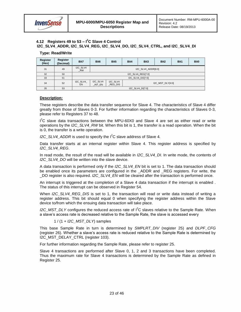
MPU-6000/MPU-6050 Register Map and
Descriptions
Document Number: RM-MPU-6000A-00 Revision: 4.2 Release Date: 08/19/2013
23 of 46
4.12 Registers 49 to 53 – I2C Slave 4 Control
I2C_SLV4_ADDR, I2C_SLV4_REG, I2C_SLV4_DO, I2C_SLV4_CTRL, and I2C_SLV4_DI
Type: Read/Write
Register (Hex)
Register
(Decimal) Bit7 Bit6 Bit5 Bit4 Bit3 Bit2 Bit1 Bit0
31 49 I2C_SLV4
_RW I2C_SLV4_ADDR[6:0]
32 50 I2C_SLV4_REG[7:0]
33 51 I2C_SLV4_DO[7:0]
34 52 I2C_SLV4_
EN
I2C_SLV4
_INT_EN
I2C_SLV4 _REG_DIS
I2C_MST_DLY[4:0]
35 53 I2C_SLV4_DI[7:0]
Description:
These registers describe the data transfer sequence for Slave 4. The characteristics of Slave 4 differ greatly from those of Slaves 0-3. For further information regarding the characteristics of Slaves 0-3, please refer to Registers 37 to 48.
I2C slave data transactions between the MPU-60X0 and Slave 4 are set as either read or write
operations by the I2C_SLV4_RW bit. When this bit is 1, the transfer is a read operation. When the bit is 0, the transfer is a write operation.
I2C_SLV4_ADDR is used to specify the I2C slave address of Slave 4.
Data transfer starts at an internal register within Slave 4. This register address is specified by I2C_SLV4_REG.
In read mode, the result of the read will be available in I2C_SLV4_DI. In write mode, the contents of I2C_SLV4_DO will be written into the slave device.
A data transaction is performed only if the I2C_SLV4_EN bit is set to 1. The data transaction should be enabled once its parameters are configured in the _ADDR and _REG registers. For write, the _DO register is also required. I2C_SLV4_EN will be cleared after the transaction is performed once.
An interrupt is triggered at the completion of a Slave 4 data transaction if the interrupt is enabled . The status of this interrupt can be observed in Register 54.
When I2C_SLV4_REG_DIS is set to 1, the transaction will read or write data instead of writing a register address. This bit should equal 0 when specifying the register address within the Slave device to/from which the ensuing data transaction will take place.
I2C_MST_DLY configures the reduced access rate of I2C slaves relative to the Sample Rate. When
a slave’s access rate is decreased relative to the Sample Rate, the slave is accessed every
1 / (1 + I2C_MST_DLY) samples
This base Sample Rate in turn is determined by SMPLRT_DIV (register 25) and DLPF_CFG (register 26). Whether a slave’s access rate is reduced relative to the Sample Rate is determined by I2C_MST_DELAY_CTRL (register 103).
For further information regarding the Sample Rate, please refer to register 25.
Slave 4 transactions are performed after Slave 0, 1, 2 and 3 transactions have been completed. Thus the maximum rate for Slave 4 transactions is determined by the Sample Rate as defined in Register 25.

MPU-6000/MPU-6050 Register Map and
Descriptions
Document Number: RM-MPU-6000A-00 Revision: 4.2 Release Date: 08/19/2013
24 of 46
Parameters:
I2C_SLV4_RW When set to 1, this bit configures the data transfer as a read operation. When cleared to 0, this bit configures the data transfer as a write operation.
I2C_SLV4_ADDR 7-bit I2C address for Slave 4.
I2C_SLV4_REG 8-bit address of the Slave 4 register to/from which data transfer starts.
I2C_SLV4_DO This register stores the data to be written into the Slave 4. If I2C_SLV4_RW is set 1 (set to read), this register has no effect.
I2C_SLV4_EN When set to 1, this bit enables Slave 4 for data transfer operations.
When cleared to 0, this bit disables Slave 4 from data transfer operations.
I2C_SLV4_INT_EN When set to 1, this bit enables the generation of an interrupt signal upon completion of a Slave 4 transaction.
When cleared to 0, this bit disables the generation of an interrupt signal upon completion of a Slave 4 transaction.
The interrupt status can be observed in Register 54.
I2C_SLV4_REG_DIS When set to 1, the transaction will read or write data. When cleared to 0, the transaction will read or write a register address.
I2C_MST_DLY Configures the decreased access rate of slave devices relative to the Sample Rate.
I2C_SLV4_DI This register stores the data read from Slave 4.
This field is populated after a read transaction.

MPU-6000/MPU-6050 Register Map and
Descriptions
Document Number: RM-MPU-6000A-00 Revision: 4.2 Release Date: 08/19/2013
25 of 46
4.13 Register 54 – I2C Master Status
I2C_MST_STATUS
Type: Read Only
Register (Hex)
Register
(Decimal) Bit7 Bit6 Bit5 Bit4 Bit3 Bit2 Bit1 Bit0
36 54 PASS_
THROUGH I2C_SLV4
_DONE I2C_LOST
_ARB I2C_SLV4
_NACK I2C_SLV3
_NACK I2C_SLV2
_NACK I2C_SLV1
_NACK I2C_SLV0
_NACK
Description:
This register shows the status of the interrupt generating signals in the I2C Master within the MPU-
60X0. This register also communicates the status of the FSYNC interrupt to the host processor.
Reading this register will clear all the status bits in the register.
Parameters:
PASS_THROUGH This bit reflects the status of the FSYNC interrupt from an external device into the MPU-60X0. This is used as a way to pass an external interrupt through the MPU-60X0 to the host application processor. When set to 1, this bit will cause an interrupt if FSYNC_INT_EN is asserted in INT_PIN_CFG (Register 55).
I2C_SLV4_DONE Automatically sets to 1 when a Slave 4 transaction has completed. This triggers an interrupt if the I2C_MST_INT_EN bit in the INT_ENABLE register (Register 56) is asserted and if the SLV_4_DONE_INT bit is asserted in the I2C_SLV4_CTRL register (Register 52).
I2C_LOST_ARB This bit automatically sets to 1 when the I2C Master has lost arbitration of the
auxiliary I2C bus (an error condition). This triggers an interrupt if the
I2C_MST_INT_EN bit in the INT_ENABLE register (Register 56) is asserted.
I2C_SLV4_NACK This bit automatically sets to 1 when the I2C Master receives a NACK in a
transaction with Slave 4. This triggers an interrupt if the I2C_MST_INT_EN bit in the INT_ENABLE register (Register 56) is asserted.
I2C_SLV3_NACK This bit automatically sets to 1 when the I2C Master receives a NACK in a
transaction with Slave 3. This triggers an interrupt if the I2C_MST_INT_EN bit in the INT_ENABLE register (Register 56) is asserted.
I2C_SLV2_NACK This bit automatically sets to 1 when the I2C Master receives a NACK in a
transaction with Slave 2. This triggers an interrupt if the I2C_MST_INT_EN bit in the INT_ENABLE register (Register 56) is asserted.
I2C_SLV1_NACK This bit automatically sets to 1 when the I2C Master receives a NACK in a
transaction with Slave 1. This triggers an interrupt if the I2C_MST_INT_EN bit in the INT_ENABLE register (Register 56) is asserted.
I2C_SLV0_NACK This bit automatically sets to 1 when the I2C Master receives a NACK in a
transaction with Slave 0. This triggers an interrupt if the I2C_MST_INT_EN bit in the INT_ENABLE register (Register 56) is asserted.

MPU-6000/MPU-6050 Register Map and
Descriptions
Document Number: RM-MPU-6000A-00 Revision: 4.2 Release Date: 08/19/2013
26 of 46
4.14 Register 55 – INT Pin / Bypass Enable Configuration INT_PIN_CFG
Type: Read/Write
Register (Hex)
Register
(Decimal) Bit7 Bit6 Bit5 Bit4 Bit3 Bit2 Bit1 Bit0
37 55 INT_LEVEL INT_OPEN LATCH
_INT_EN INT_RD _CLEAR
FSYNC_ INT_LEVEL
FSYNC_ INT_EN
I2C _BYPASS
_EN -
Description:
This register configures the behavior of the interrupt signals at the INT pins. This register is also used to enable the FSYNC Pin to be used as an interrupt to the host application processor, as well as to enable Bypass Mode on the I
2C Master. This bit also enables the clock output.
FSYNC_INT_EN enables the FSYNC pin to be used as an interrupt to the host application processor. A transition to the active level specified in FSYNC_INT_LEVEL will trigger an interrupt. The status of this interrupt is read from the PASS_THROUGH bit in the I
2C Master Status Register
(Register 54).
When I2C_BYPASS_EN is equal to 1 and I2C_MST_EN (Register 106 bit[5]) is equal to 0, the host application processor will be able to directly access the auxiliary I
2C bus of the MPU-60X0. When
this bit is equal to 0, the host application processor will not be able to directly access the auxiliary I2C
bus of the MPU-60X0 regardless of the state of I2C_MST_EN.
For further information regarding Bypass Mode, please refer to Section 7.11 and 7.13 of the MPU-6000/MPU-6050 Product Specification document.
Parameters:
INT_LEVEL When this bit is equal to 0, the logic level for the INT pin is active high.
When this bit is equal to 1, the logic level for the INT pin is active low.
INT_OPEN When this bit is equal to 0, the INT pin is configured as push-pull.
When this bit is equal to 1, the INT pin is configured as open drain.
LATCH_INT_EN When this bit is equal to 0, the INT pin emits a 50us long pulse.
When this bit is equal to 1, the INT pin is held high until the interrupt is cleared.
INT_RD_CLEAR When this bit is equal to 0, interrupt status bits are cleared only by reading INT_STATUS (Register 58)
When this bit is equal to 1, interrupt status bits are cleared on any read operation.
FSYNC_INT_LEVEL When this bit is equal to 0, the logic level for the FSYNC pin (when used as an interrupt to the host processor) is active high.
When this bit is equal to 1, the logic level for the FSYNC pin (when used as an interrupt to the host processor) is active low.
FSYNC_INT_EN When equal to 0, this bit disables the FSYNC pin from causing an interrupt to the host processor.
When equal to 1, this bit enables the FSYNC pin to be used as an interrupt to the host processor.

MPU-6000/MPU-6050 Register Map and
Descriptions
Document Number: RM-MPU-6000A-00 Revision: 4.2 Release Date: 08/19/2013
27 of 46
I2C_BYPASS_EN When this bit is equal to 1 and I2C_MST_EN (Register 106 bit[5]) is equal to 0, the host application processor will be able to directly access the auxiliary I2C bus of the MPU-60X0.
When this bit is equal to 0, the host application processor will not be able to directly access the auxiliary I
2C bus of the MPU-60X0 regardless of the state
of I2C_MST_EN (Register 106 bit[5]).
4.15 Register 56 – Interrupt Enable INT_ENABLE
Type: Read/Write
Register (Hex)
Register
(Decimal) Bit7 Bit6 Bit5 Bit4 Bit3 Bit2 Bit1 Bit0
38 56 -
FIFO _OFLOW
_EN
I2C_MST _INT_EN
- - DATA
_RDY_EN
Description:
This register enables interrupt generation by interrupt sources.
For information regarding the interrupt status for each interrupt generation source, please refer to Register 58. Further information regarding I
2C Master interrupt generation can be found in Register
54.
Bits 2 and 1 are reserved.
Parameters:
FIFO_OFLOW_EN When set to 1, this bit enables a FIFO buffer overflow to generate an interrupt.
I2C_MST_INT_EN When set to 1, this bit enables any of the I2C Master interrupt sources to
generate an interrupt.
DATA_RDY_EN When set to 1, this bit enables the Data Ready interrupt, which occurs each time a write operation to all of the sensor registers has been completed.

MPU-6000/MPU-6050 Register Map and
Descriptions
Document Number: RM-MPU-6000A-00 Revision: 4.2 Release Date: 08/19/2013
28 of 46
4.16 Register 58 – Interrupt Status INT_STATUS
Type: Read Only
Register (Hex)
Register
(Decimal) Bit7 Bit6 Bit5 Bit4 Bit3 Bit2 Bit1 Bit0
3A 58 - - - FIFO
_OFLOW _INT
I2C_MST _INT
- - DATA
_RDY_INT
Description:
This register shows the interrupt status of each interrupt generation source. Each bit will clear after the register is read.
For information regarding the corresponding interrupt enable bits, please refer to Register 56.
For a list of I2C Master interrupts, please refer to Register 54.
Bits 2 and 1 are reserved.
Parameters:
FIFO_OFLOW_INT This bit automatically sets to 1 when a FIFO buffer overflow interrupt has been generated.
The bit clears to 0 after the register has been read.
I2C_MST_INT This bit automatically sets to 1 when an I2C Master interrupt has been
generated. For a list of I2C Master interrupts, please refer to Register 54.
The bit clears to 0 after the register has been read.
DATA_RDY_INT This bit automatically sets to 1 when a Data Ready interrupt is generated.
The bit clears to 0 after the register has been read.

MPU-6000/MPU-6050 Register Map and
Descriptions
Document Number: RM-MPU-6000A-00 Revision: 4.2 Release Date: 08/19/2013
29 of 46
4.17 Registers 59 to 64 – Accelerometer Measurements ACCEL_XOUT_H, ACCEL_XOUT_L, ACCEL_YOUT_H, ACCEL_YOUT_L, ACCEL_ZOUT_H, and ACCEL_ZOUT_L
Type: Read Only
Register (Hex)
Register
(Decimal) Bit7 Bit6 Bit5 Bit4 Bit3 Bit2 Bit1 Bit0
3B 59 ACCEL_XOUT[15:8]
3C 60 ACCEL_XOUT[7:0]
3D 61 ACCEL_YOUT[15:8]
3E 62 ACCEL_YOUT[7:0]
3F 63 ACCEL_ZOUT[15:8]
40 64 ACCEL_ZOUT[7:0]
Description:
These registers store the most recent accelerometer measurements.
Accelerometer measurements are written to these registers at the Sample Rate as defined in Register 25.
The accelerometer measurement registers, along with the temperature measurement registers, gyroscope measurement registers, and external sensor data registers, are composed of two sets of registers: an internal register set and a user-facing read register set.
The data within the accelerometer sensors’ internal register set is always updated at the Sample Rate. Meanwhile, the user-facing read register set duplicates the internal register set’s data values whenever the serial interface is idle. This guarantees that a burst read of sensor registers will read measurements from the same sampling instant. Note that if burst reads are not used, the user is responsible for ensuring a set of single byte reads correspond to a single sampling instant by checking the Data Ready interrupt.
Each 16-bit accelerometer measurement has a full scale defined in ACCEL_FS (Register 28). For each full scale setting, the accelerometers’ sensitivity per LSB in ACCEL_xOUT is shown in the table below.
AFS_SEL Full Scale Range LSB Sensitivity
0 ±2g 16384 LSB/g
1 ±4g 8192 LSB/g
2 ±8g 4096 LSB/g
3 ±16g 2048 LSB/g
Parameters:
ACCEL_XOUT 16-bit 2’s complement value.
Stores the most recent X axis accelerometer measurement.
ACCEL_YOUT 16-bit 2’s complement value.
Stores the most recent Y axis accelerometer measurement.
ACCEL_ZOUT 16-bit 2’s complement value.
Stores the most recent Z axis accelerometer measurement.

MPU-6000/MPU-6050 Register Map and
Descriptions
Document Number: RM-MPU-6000A-00 Revision: 4.2 Release Date: 08/19/2013
30 of 46
4.18 Registers 65 and 66 – Temperature Measurement TEMP_OUT_H and TEMP_OUT_L
Type: Read Only
Register (Hex)
Register
(Decimal) Bit7 Bit6 Bit5 Bit4 Bit3 Bit2 Bit1 Bit0
41 65 TEMP_OUT[15:8]
42 66 TEMP_OUT[7:0]
Description:
These registers store the most recent temperature sensor measurement.
Temperature measurements are written to these registers at the Sample Rate as defined in Register 25.
These temperature measurement registers, along with the accelerometer measurement registers, gyroscope measurement registers, and external sensor data registers, are composed of two sets of registers: an internal register set and a user-facing read register set.
The data within the temperature sensor’s internal register set is always updated at the Sample Rate. Meanwhile, the user-facing read register set duplicates the internal register set’s data values whenever the serial interface is idle. This guarantees that a burst read of sensor registers will read measurements from the same sampling instant. Note that if burst reads are not used, the user is responsible for ensuring a set of single byte reads correspond to a single sampling instant by checking the Data Ready interrupt.
The scale factor and offset for the temperature sensor are found in the Electrical Specifications table (Section 6.4 of the MPU-6000/MPU-6050 Product Specification document).
The temperature in degrees C for a given register value may be computed as:
Temperature in degrees C = (TEMP_OUT Register Value as a signed quantity)/340 + 36.53
Please note that the math in the above equation is in decimal.
Parameters:
TEMP_OUT 16-bit signed value.
Stores the most recent temperature sensor measurement.

MPU-6000/MPU-6050 Register Map and
Descriptions
Document Number: RM-MPU-6000A-00 Revision: 4.2 Release Date: 08/19/2013
31 of 46
4.19 Registers 67 to 72 – Gyroscope Measurements GYRO_XOUT_H, GYRO_XOUT_L, GYRO_YOUT_H, GYRO_YOUT_L, GYRO_ZOUT_H, and GYRO_ZOUT_L
Type: Read Only
Register (Hex)
Register
(Decimal) Bit7 Bit6 Bit5 Bit4 Bit3 Bit2 Bit1 Bit0
43 67 GYRO_XOUT[15:8]
44 68 GYRO_XOUT[7:0]
45 69 GYRO_YOUT[15:8]
46 70 GYRO_YOUT[7:0]
47 71 GYRO_ZOUT[15:8]
48 72 GYRO_ZOUT[7:0]
Description:
These registers store the most recent gyroscope measurements.
Gyroscope measurements are written to these registers at the Sample Rate as defined in Register 25.
These gyroscope measurement registers, along with the accelerometer measurement registers, temperature measurement registers, and external sensor data registers, are composed of two sets of registers: an internal register set and a user-facing read register set.
The data within the gyroscope sensors’ internal register set is always updated at the Sample Rate. Meanwhile, the user-facing read register set duplicates the internal register set’s data values whenever the serial interface is idle. This guarantees that a burst read of sensor registers will read measurements from the same sampling instant. Note that if burst reads are not used, the user is responsible for ensuring a set of single byte reads correspond to a single sampling instant by checking the Data Ready interrupt.
Each 16-bit gyroscope measurement has a full scale defined in FS_SEL (Register 27). For each full scale setting, the gyroscopes’ sensitivity per LSB in GYRO_xOUT is shown in the table below:
FS_SEL Full Scale Range LSB Sensitivity
0 ± 250 °/s 131 LSB/°/s
1 ± 500 °/s 65.5 LSB/°/s
2 ± 1000 °/s 32.8 LSB/°/s
3 ± 2000 °/s 16.4 LSB/°/s
Parameters:
GYRO_XOUT 16-bit 2’s complement value.
Stores the most recent X axis gyroscope measurement.
GYRO_YOUT 16-bit 2’s complement value.
Stores the most recent Y axis gyroscope measurement.
GYRO_ZOUT 16-bit 2’s complement value.
Stores the most recent Z axis gyroscope measurement.

MPU-6000/MPU-6050 Register Map and
Descriptions
Document Number: RM-MPU-6000A-00 Revision: 4.2 Release Date: 08/19/2013
32 of 46
4.20 Registers 73 to 96 – External Sensor Data EXT_SENS_DATA_00 through EXT_SENS_DATA_23
Type: Read Only
Register (Hex)
Register
(Decimal) Bit7 Bit6 Bit5 Bit4 Bit3 Bit2 Bit1 Bit0
49 73 EXT_SENS_DATA_00[7:0]
4A 74 EXT_SENS_DATA_01[7:0]
4B 75 EXT_SENS_DATA_02[7:0]
4C 76 EXT_SENS_DATA_03[7:0]
4D 77 EXT_SENS_DATA_04[7:0]
4E 78 EXT_SENS_DATA_05[7:0]
4F 79 EXT_SENS_DATA_06[7:0]
50 80 EXT_SENS_DATA_07[7:0]
51 81 EXT_SENS_DATA_08[7:0]
52 82 EXT_SENS_DATA_09[7:0]
53 83 EXT_SENS_DATA_10[7:0]
54 84 EXT_SENS_DATA_11[7:0]
55 85 EXT_SENS_DATA_12[7:0]
56 86 EXT_SENS_DATA_13[7:0]
57 87 EXT_SENS_DATA_14[7:0]
58 88 EXT_SENS_DATA_15[7:0]
59 89 EXT_SENS_DATA_16[7:0]
5A 90 EXT_SENS_DATA_17[7:0]
5B 91 EXT_SENS_DATA_18[7:0]
5C 92 EXT_SENS_DATA_19[7:0]
5D 93 EXT_SENS_DATA_20[7:0]
5E 94 EXT_SENS_DATA_21[7:0]
5F 95 EXT_SENS_DATA_22[7:0]
60 96 EXT_SENS_DATA_23[7:0]
Description:
These registers store data read from external sensors by the Slave 0, 1, 2, and 3 on the auxiliary I2C
interface. Data read by Slave 4 is stored in I2C_SLV4_DI (Register 53).
External sensor data is written to these registers at the Sample Rate as defined in Register 25. This access rate can be reduced by using the Slave Delay Enable registers (Register 103).
External sensor data registers, along with the gyroscope measurement registers, accelerometer measurement registers, and temperature measurement registers, are composed of two sets of registers: an internal register set and a user-facing read register set.
The data within the external sensors’ internal register set is always updated at the Sample Rate (or the reduced access rate) whenever the serial interface is idle. This guarantees that a burst read of sensor registers will read measurements from the same sampling instant. Note that if burst reads are not used, the user is responsible for ensuring a set of single byte reads correspond to a single sampling instant by checking the Data Ready interrupt.
Data is placed in these external sensor data registers according to I2C_SLV0_CTRL, I2C_SLV1_CTRL, I2C_SLV2_CTRL, and I2C_SLV3_CTRL (Registers 39, 42, 45, and 48). When more than zero bytes are read (I2C_SLVx_LEN > 0) from an enabled slave (I2C_SLVx_EN = 1), the slave is read at the Sample Rate (as defined in Register 25) or delayed rate (if specified in Register 52 and 103). During each Sample cycle, slave reads are performed in order of Slave number. If all slaves are enabled with more than zero bytes to be read, the order will be Slave 0, followed by Slave 1, Slave 2, and Slave 3.

MPU-6000/MPU-6050 Register Map and
Descriptions
Document Number: RM-MPU-6000A-00 Revision: 4.2 Release Date: 08/19/2013
33 of 46
Each enabled slave will have EXT_SENS_DATA registers associated with it by number of bytes read (I2C_SLVx_LEN) in order of slave number, starting from EXT_SENS_DATA_00. Note that this means enabling or disabling a slave may change the higher numbered slaves’ associated registers. Furthermore, if fewer total bytes are being read from the external sensors as a result of such a change, then the data remaining in the registers which no longer have an associated slave device (i.e. high numbered registers) will remain in these previously allocated registers unless reset.
If the sum of the read lengths of all SLVx transactions exceed the number of available EXT_SENS_DATA registers , the excess bytes will be dropped. There are 24 EXT_SENS_DATA registers and hence the total read lengths between all the slaves cannot be greater than 24 or some bytes will be lost.
Note: Slave 4’s behavior is distinct from that of Slaves 0-3. For further information regarding the characteristics of Slave 4, please refer to Registers 49 to 53.
Example:
Suppose that Slave 0 is enabled with 4 bytes to be read (I2C_SLV0_EN = 1 and I2C_SLV0_LEN = 4) while Slave 1 is enabled with 2 bytes to be read, (I2C_SLV1_EN=1 and I2C_SLV1_LEN = 2). In such a situation, EXT_SENS_DATA _00 through _03 will be associated with Slave 0, while EXT_SENS_DATA _04 and 05 will be associated with Slave 1.
If Slave 2 is enabled as well, registers starting from EXT_SENS_DATA_06 will be allocated to Slave 2.
If Slave 2 is disabled while Slave 3 is enabled in this same situation, then registers starting from EXT_SENS_DATA_06 will be allocated to Slave 3 instead.
Register Allocation for Dynamic Disable vs. Normal Disable
If a slave is disabled at any time, the space initially allocated to the slave in the EXT_SENS_DATA register, will remain associated with that slave. This is to avoid dynamic adjustment of the register allocation.
The allocation of the EXT_SENS_DATA registers is recomputed only when (1) all slaves are disabled, or (2) the I2C_MST_RST bit is set (Register 106).
This above is also true if one of the slaves gets NACKed and stops functioning.

MPU-6000/MPU-6050 Register Map and
Descriptions
Document Number: RM-MPU-6000A-00 Revision: 4.2 Release Date: 08/19/2013
34 of 46
4.21 Register 99 – I2C Slave 0 Data Out
I2C_SLV0_DO
Type: Read/Write
Register (Hex)
Register
(Decimal) Bit7 Bit6 Bit5 Bit4 Bit3 Bit2 Bit1 Bit0
63 99 I2C_SLV0_DO[7:0]
Description:
This register holds the output data written into Slave 0 when Slave 0 is set to write mode.
For further information regarding Slave 0 control, please refer to Registers 37 to 39.
Parameters:
I2C_SLV0_DO 8 bit unsigned value that is written into Slave 0 when Slave 0 is set to write mode.
4.22 Register 100 – I2C Slave 1 Data Out
I2C_SLV1_DO
Type: Read/Write
Register (Hex)
Register
(Decimal) Bit7 Bit6 Bit5 Bit4 Bit3 Bit2 Bit1 Bit0
64 100 I2C_SLV1_DO[7:0]
Description:
This register holds the output data written into Slave 1 when Slave 1 is set to write mode.
For further information regarding Slave 1 control, please refer to Registers 40 to 42.
Parameters:
I2C_SLV1_DO 8 bit unsigned value that is written into Slave 1 when Slave 1 is set to write mode.

MPU-6000/MPU-6050 Register Map and
Descriptions
Document Number: RM-MPU-6000A-00 Revision: 4.2 Release Date: 08/19/2013
35 of 46
4.23 Register 101 – I2C Slave 2 Data Out
I2C_SLV2_DO
Type: Read/Write
Register (Hex)
Register
(Decimal) Bit7 Bit6 Bit5 Bit4 Bit3 Bit2 Bit1 Bit0
65 101 I2C_SLV2_DO[7:0]
Description:
This register holds the output data written into Slave 2 when Slave 2 is set to write mode.
For further information regarding Slave 2 control, please refer to Registers 43 to 45.
Parameters:
I2C_SLV2_DO 8 bit unsigned value that is written into Slave 2 when Slave 2 is set to write mode.
4.24 Register 102 – I2C Slave 3 Data Out
I2C_SLV3_DO
Type: Read/Write
Register (Hex)
Register
(Decimal) Bit7 Bit6 Bit5 Bit4 Bit3 Bit2 Bit1 Bit0
66 102 I2C_SLV3_DO[7:0]
Description:
This register holds the output data written into Slave 3 when Slave 3 is set to write mode.
For further information regarding Slave 3 control, please refer to Registers 46 to 48.
Parameters:
I2C_SLV3_DO 8 bit unsigned value that is written into Slave 3 when Slave 3 is set to write mode.

MPU-6000/MPU-6050 Register Map and
Descriptions
Document Number: RM-MPU-6000A-00 Revision: 4.2 Release Date: 08/19/2013
36 of 46
4.25 Register 103 – I2C Master Delay Control
I2C_MST_DELAY_CTRL
Type: Read/Write
Register (Hex)
Register
(Decimal) Bit7 Bit6 Bit5 Bit4 Bit3 Bit2 Bit1 Bit0
67 103 DELAY
_ES _SHADOW
- - I2C_SLV4 _DLY_EN
I2C_SLV3 _DLY_EN
I2C_SLV2 _DLY_EN
I2C_SLV1 _DLY_EN
I2C_SLV0 _DLY_EN
Description:
This register is used to specify the timing of external sensor data shadowing. The register is also used to decrease the access rate of slave devices relative to the Sample Rate.
When DELAY_ES_SHADOW is set to 1, shadowing of external sensor data is delayed until all data has been received.
When I2C_SLV4_DLY_EN, I2C_SLV3_DLY_EN, I2C_SLV2_DLY_EN, I2C_SLV1_DLY_EN, and I2C_SLV0_DLY_EN are enabled, the rate of access for the corresponding slave devices is reduced.
When a slave’s access rate is decreased relative to the Sample Rate, the slave is accessed every
1 / (1 + I2C_MST_DLY) samples.
This base Sample Rate in turn is determined by SMPLRT_DIV (register 25) and DLPF_CFG (register 26).
For further information regarding I2C_MST_DLY, please refer to register 52.
For further information regarding the Sample Rate, please refer to register 25.
Bits 6 and 5 are reserved.
Parameters:
DELAY_ES_SHADOW When set, delays shadowing of external sensor data until all data has been received.
I2C_SLV4_DLY_EN When enabled, slave 4 will only be accessed at a decreased rate.
I2C_SLV3_DLY_EN When enabled, slave 3 will only be accessed at a decreased rate.
I2C_SLV2_DLY_EN When enabled, slave 2 will only be accessed at a decreased rate.
I2C_SLV1_DLY_EN When enabled, slave 1 will only be accessed at a decreased rate.
I2C_SLV0_DLY_EN When enabled, slave 0 will only be accessed at a decreased rate.

MPU-6000/MPU-6050 Register Map and
Descriptions
Document Number: RM-MPU-6000A-00 Revision: 4.2 Release Date: 08/19/2013
37 of 46
4.26 Register 104 – Signal Path Reset SIGNAL_PATH_RESET
Type: Write Only
Register (Hex)
Register
(Decimal) Bit7 Bit6 Bit5 Bit4 Bit3 Bit2 Bit1 Bit0
68 104 - - - - - GYRO
_RESET ACCEL
_RESET TEMP
_RESET
Description:
This register is used to reset the analog and digital signal paths of the gyroscope, accelerometer, and temperature sensors.
The reset will revert the signal path analog to digital converters and filters to their power up configurations.
Note: This register does not clear the sensor registers. The reset initializes the serial interface as well.
Bits 7 to 3 are reserved.
Parameters:
GYRO_RESET When set to 1, this bit resets the gyroscope analog and digital signal paths.
ACCEL_RESET When set to 1, this bit resets the accelerometer analog and digital signal paths.
TEMP_RESET When set to 1, this bit resets the temperature sensor analog and digital signal paths.

MPU-6000/MPU-6050 Register Map and
Descriptions
Document Number: RM-MPU-6000A-00 Revision: 4.2 Release Date: 08/19/2013
38 of 46
4.27 Register 106 – User Control USER_CTRL
Type: Read/Write
Register (Hex)
Register
(Decimal) Bit7 Bit6 Bit5 Bit4 Bit3 Bit2 Bit1 Bit0
6A 106 - FIFO_EN I2C_MST
_EN
I2C_IF
_DIS -
FIFO
_RESET
I2C_MST
_RESET
SIG_COND
_RESET
Description:
This register allows the user to enable and disable the FIFO buffer, I2C Master Mode, and primary
I2C interface. The FIFO buffer, I
2C Master, sensor signal paths and sensor registers can also be
reset using this register.
When I2C_MST_EN is set to 1, I2C Master Mode is enabled. In this mode, the MPU-60X0 acts as
the I2C Master to the external sensor slave devices on the auxiliary I
2C bus. When this bit is cleared
to 0, the auxiliary I2C bus lines (AUX_DA and AUX_CL) are logically driven by the primary I
2C bus
(SDA and SCL). This is a precondition to enabling Bypass Mode. For further information regarding Bypass Mode, please refer to Register 55.
MPU-6000: The primary SPI interface will be enabled in place of the disabled primary I2C interface
when I2C_IF_DIS is set to 1.
MPU-6050: Always write 0 to I2C_IF_DIS.
When the reset bits (FIFO_RESET, I2C_MST_RESET, and SIG_COND_RESET) are set to 1, these reset bits will trigger a reset and then clear to 0.
Bits 7 and 3 are reserved.
Parameters:
FIFO_EN When set to 1, this bit enables FIFO operations.
When this bit is cleared to 0, the FIFO buffer is disabled. The FIFO buffer cannot be written to or read from while disabled.
The FIFO buffer’s state does not change unless the MPU-60X0 is power cycled.
I2C_MST_EN When set to 1, this bit enables I2C Master Mode.
When this bit is cleared to 0, the auxiliary I2C bus lines (AUX_DA and
AUX_CL) are logically driven by the primary I2C bus (SDA and SCL).
I2C_IF_DIS MPU-6000: When set to 1, this bit disables the primary I2C interface and
enables the SPI interface instead.
MPU-6050: Always write this bit as zero.
FIFO_RESET This bit resets the FIFO buffer when set to 1 while FIFO_EN equals 0. This bit automatically clears to 0 after the reset has been triggered.
I2C_MST_RESET This bit resets the I2C Master when set to 1 while I2C_MST_EN equals 0.
This bit automatically clears to 0 after the reset has been triggered.

MPU-6000/MPU-6050 Register Map and
Descriptions
Document Number: RM-MPU-6000A-00 Revision: 4.2 Release Date: 08/19/2013
39 of 46
SIG_COND_RESET When set to 1, this bit resets the signal paths for all sensors (gyroscopes, accelerometers, and temperature sensor). This operation will also clear the sensor registers. This bit automatically clears to 0 after the reset has been triggered.
When resetting only the signal path (and not the sensor registers), please use Register 104, SIGNAL_PATH_RESET.

MPU-6000/MPU-6050 Register Map and
Descriptions
Document Number: RM-MPU-6000A-00 Revision: 4.2 Release Date: 08/19/2013
40 of 46
4.28 Register 107 – Power Management 1 PWR_MGMT_1
Type: Read/Write
Register (Hex)
Register
(Decimal) Bit7 Bit6 Bit5 Bit4 Bit3 Bit2 Bit1 Bit0
6B 107 DEVICE _RESET
SLEEP CYCLE - TEMP_DIS CLKSEL[2:0]
Description:
This register allows the user to configure the power mode and clock source. It also provides a bit for resetting the entire device, and a bit for disabling the temperature sensor.
By setting SLEEP to 1, the MPU-60X0 can be put into low power sleep mode. When CYCLE is set to 1 while SLEEP is disabled, the MPU-60X0 will be put into Cycle Mode. In Cycle Mode, the device cycles between sleep mode and waking up to take a single sample of data from accelerometer at a rate determined by LP_WAKE_CTRL (register 108). To configure the wake frequency, use LP_WAKE_CTRL within the Power Management 2 register (Register 108).
An internal 8MHz oscillator, gyroscope based clock, or external sources can be selected as the MPU-60X0 clock source. When the internal 8 MHz oscillator or an external source is chosen as the clock source, the MPU-60X0 can operate in low power modes with the gyroscopes disabled.
Upon power up, the MPU-60X0 clock source defaults to the internal oscillator. However, it is highly recommended that the device be configured to use one of the gyroscopes (or an external clock source) as the clock reference for improved stability. The clock source can be selected according to the following table.
CLKSEL Clock Source
0 Internal 8MHz oscillator
1 PLL with X axis gyroscope reference
2 PLL with Y axis gyroscope reference
3 PLL with Z axis gyroscope reference
4 PLL with external 32.768kHz reference
5 PLL with external 19.2MHz reference
6 Reserved
7 Stops the clock and keeps the timing generator in reset
For further information regarding the MPU-60X0 clock source, please refer to the MPU-6000/MPU-6050 Product Specification document.
Bit 4 is reserved.

MPU-6000/MPU-6050 Register Map and
Descriptions
Document Number: RM-MPU-6000A-00 Revision: 4.2 Release Date: 08/19/2013
41 of 46
Parameters:
DEVICE_RESET When set to 1, this bit resets all internal registers to their default values.
The bit automatically clears to 0 once the reset is done.
The default values for each register can be found in Section 3.
SLEEP When set to 1, this bit puts the MPU-60X0 into sleep mode.
CYCLE When this bit is set to 1 and SLEEP is disabled, the MPU-60X0 will cycle between sleep mode and waking up to take a single sample of data from active sensors at a rate determined by LP_WAKE_CTRL (register 108).
TEMP_DIS When set to 1, this bit disables the temperature sensor.
CLKSEL 3-bit unsigned value. Specifies the clock source of the device.
Note:
When using SPI interface, user should use DEVICE_RESET (register 107) as well as SIGNAL_PATH_RESET (register 104) to ensure the reset is performed properly. The sequence used should be: 1. Set DEVICE_RESET = 1 (register PWR_MGMT_1) 2. Wait 100ms 3. Set GYRO_RESET = ACCEL_RESET = TEMP_RESET = 1 (register SIGNAL_PATH_RESET) 4. Wait 100ms

MPU-6000/MPU-6050 Register Map and
Descriptions
Document Number: RM-MPU-6000A-00 Revision: 4.2 Release Date: 08/19/2013
42 of 46
4.29 Register 108 – Power Management 2 PWR_MGMT_2
Type: Read/Write
Register (Hex)
Register
(Decimal) Bit7 Bit6 Bit5 Bit4 Bit3 Bit2 Bit1 Bit0
6C 108 LP_WAKE_CTRL[1:0] STBY_XA STBY_YA STBY_ZA STBY_XG STBY_YG STBY_ZG
Description:
This register allows the user to configure the frequency of wake-ups in Accelerometer Only Low Power Mode. This register also allows the user to put individual axes of the accelerometer and gyroscope into standby mode.
The MPU-60X0 can be put into Accelerometer Only Low Power Mode using the following steps:
(i) Set CYCLE bit to 1 (ii) Set SLEEP bit to 0 (iii) Set TEMP_DIS bit to 1 (iv) Set STBY_XG, STBY_YG, STBY_ZG bits to 1
All of the above bits can be found in Power Management 1 register (Register 107).
In this mode, the device will power off all devices except for the primary I2C interface, waking only
the accelerometer at fixed intervals to take a single measurement. The frequency of wake-ups can be configured with LP_WAKE_CTRL as shown below.
LP_WAKE_CTRL Wake-up Frequency
0 1.25 Hz
1 5 Hz
2 20 Hz
3 40 Hz
For further information regarding the MPU-6050’s power modes, please refer to Register 107.
The user can put individual accelerometer and gyroscopes axes into standby mode by using this register. If the device is using a gyroscope axis as the clock source and this axis is put into standby mode, the clock source will automatically be changed to the internal 8MHz oscillator.
Parameters:
LP_WAKE_CTRL 2-bit unsigned value.
Specifies the frequency of wake-ups during Accelerometer Only Low Power Mode.
STBY_XA When set to 1, this bit puts the X axis accelerometer into standby mode.
STBY_YA When set to 1, this bit puts the Y axis accelerometer into standby mode.
STBY_ZA When set to 1, this bit puts the Z axis accelerometer into standby mode.
STBY_XG When set to 1, this bit puts the X axis gyroscope into standby mode.
STBY_YG When set to 1, this bit puts the Y axis gyroscope into standby mode.
STBY_ZG When set to 1, this bit puts the Z axis gyroscope into standby mode.

MPU-6000/MPU-6050 Register Map and
Descriptions
Document Number: RM-MPU-6000A-00 Revision: 4.2 Release Date: 08/19/2013
43 of 46
4.30 Register 114 and 115 – FIFO Count Registers FIFO_COUNT_H and FIFO_COUNT_L
Type: Read Only
Register (Hex)
Register
(Decimal) Bit7 Bit6 Bit5 Bit4 Bit3 Bit2 Bit1 Bit0
72 114 FIFO_COUNT[15:8]
73 115 FIFO_COUNT[7:0]
Description:
These registers keep track of the number of samples currently in the FIFO buffer.
These registers shadow the FIFO Count value. Both registers are loaded with the current sample count when FIFO_COUNT_H (Register 72) is read.
Note: Reading only FIFO_COUNT_L will not update the registers to the current sample count. FIFO_COUNT_H must be accessed first to update the contents of both these registers.
FIFO_COUNT should always be read in high-low order in order to guarantee that the most current FIFO Count value is read.
Parameters:
FIFO_COUNT 16-bit unsigned value. Indicates the number of bytes stored in the FIFO buffer. This number is in turn the number of bytes that can be read from the FIFO buffer and it is directly proportional to the number of samples available given the set of sensor data bound to be stored in the FIFO (register 35 and 36).

MPU-6000/MPU-6050 Register Map and
Descriptions
Document Number: RM-MPU-6000A-00 Revision: 4.2 Release Date: 08/19/2013
44 of 46
4.31 Register 116 – FIFO Read Write FIFO_R_W
Type: Read/Write
Register (Hex)
Register
(Decimal) Bit7 Bit6 Bit5 Bit4 Bit3 Bit2 Bit1 Bit0
74 116 FIFO_DATA[7:0]
Description:
This register is used to read and write data from the FIFO buffer.
Data is written to the FIFO in order of register number (from lowest to highest). If all the FIFO enable flags (see below) are enabled and all External Sensor Data registers (Registers 73 to 96) are associated with a Slave device, the contents of registers 59 through 96 will be written in order at the Sample Rate.
The contents of the sensor data registers (Registers 59 to 96) are written into the FIFO buffer when their corresponding FIFO enable flags are set to 1 in FIFO_EN (Register 35). An additional flag for the sensor data registers associated with I
2C Slave 3 can be found in I2C_MST_CTRL (Register 36).
If the FIFO buffer has overflowed, the status bit FIFO_OFLOW_INT is automatically set to 1. This bit is located in INT_STATUS (Register 58). When the FIFO buffer has overflowed, the oldest data will be lost and new data will be written to the FIFO.
If the FIFO buffer is empty, reading this register will return the last byte that was previously read from the FIFO until new data is available. The user should check FIFO_COUNT to ensure that the FIFO buffer is not read when empty.
Parameters:
FIFO_DATA 8-bit data transferred to and from the FIFO buffer.

MPU-6000/MPU-6050 Register Map and
Descriptions
Document Number: RM-MPU-6000A-00 Revision: 4.2 Release Date: 08/19/2013
45 of 46
4.32 Register 117 – Who Am I WHO_AM_I
Type: Read Only
Register (Hex)
Register
(Decimal) Bit7 Bit6 Bit5 Bit4 Bit3 Bit2 Bit1 Bit0
75 117 - WHO_AM_I[6:1] -
Description:
This register is used to verify the identity of the device. The contents of WHO_AM_I are the upper 6 bits of the MPU-60X0’s 7-bit I
2C address. The least significant bit of the MPU-60X0’s I
2C address is
determined by the value of the AD0 pin. The value of the AD0 pin is not reflected in this register.
The default value of the register is 0x68.
Bits 0 and 7 are reserved. (Hard coded to 0)
Parameters:
WHO_AM_I Contains the 6-bit I2C address of the MPU-60X0.
The Power-On-Reset value of Bit6:Bit1 is 110 100.

MPU-6000/MPU-6050 Register Map and
Descriptions
Document Number: RM-MPU-6000A-00 Revision: 4.2 Release Date: 08/19/2013
46 of 46
This information furnished by InvenSense is believed to be accurate and reliable. However, no responsibility is assumed by InvenSense for its use, or for any infringements of patents or other rights of third parties that may result from its use. Specifications are subject to change without notice. InvenSense reserves the right to make changes to this product, including its circuits and software, in order to improve its design and/or performance, without prior notice. InvenSense makes no warranties, neither expressed nor implied, regarding the information and specifications contained in this document. InvenSense assumes no responsibility for any claims or damages arising from information contained in this document, or from the use of products and services detailed therein. This includes, but is not limited to, claims or damages based on the infringement of patents, copyrights, mask work and/or other intellectual property rights.
Certain intellectual property owned by InvenSense and described in this document is patent protected. No license is granted by implication or otherwise under any patent or patent rights of InvenSense. This publication supersedes and replaces all information previously supplied. Trademarks that are registered trademarks are the property of their respective companies. InvenSense sensors should not be used or sold in the development, storage, production or utilization of any conventional or mass-destructive weapons or for any other weapons or life threatening applications, as well as in any other life critical applications such as medical equipment, transportation, aerospace and nuclear instruments, undersea equipment, power plant equipment, disaster prevention and crime prevention equipment.
InvenSense® is a registered trademark of InvenSense, Inc. MPUTM
, MPU-6000TM
, MPU-6050TM
, MPU-60X0TM
, Digital Motion Processor
™, DMP
™, Motion Processing Unit™, MotionFusion™, and MotionApps™ are trademarks of InvenSense, Inc.
©2011 InvenSense, Inc. All rights reserved.