
Silver nanoparticles decorated on a three-dimensional graphene
6
Silver nanoparticles decorated on a three-dimensional graphene scaffold for electrochemical applications A. Bello a , M. Fabiane a , D. Dodoo-Arhin a , K.I. Ozoemena b,c , N. Manyala a,n a Department of Physics, Institute of Applied Materials, SARChI Chair in Carbon Technology and Materials, University of Pretoria, Pretoria 0002, South Africa b Council for Scientific and Industrial Research, Meiring Naude Road, Brummeria, PO Box 395, Pretoria 0001, South Africa c Department of Chemistry, University of Pretoria, Pretoria 0002, South Africa article info Article history: Received 24 January 2013 Received in revised form 13 August 2013 Accepted 5 September 2013 Available online 13 September 2013 Keywords: Graphene foam CVD Electron beam evaporation Silver nanoparticles Electrochemical capacitor abstract Silver metal nanoparticles were decorated by electron beam evaporation on graphene foam (GF) grown by chemical vapour deposition. X-ray diffraction, Raman spectroscopy, scanning and transmission electron microscopy, and atomic force microscopy were used to investigate the structure and morphology of the graphene foam/silver nanoparticles (GF/Ag). Both samples were tested as electrodes for supercapacitors. The GF/Ag exhibited a significantly higher capacitive performance, including a specific capacitance value of ( 110 Fg 1 ) and excellent cyclability in a three-electrode electrochemical cell. These results demonstrate that graphene foam could be an excellent platform for metal particles for investigating improved electrochemical performance. Crown Copyright & 2013 Published by Elsevier Ltd. All rights reserved. 1. Introduction The discovery of graphene has inspired much research activity to understand its unique physicochemical properties and possible applications. Graphene [1] is a single layer of graphite consisting of a two-dimensional honeycomb lattice of sp 2 -bonded carbon atoms with a unique electronic structure that exhibits linear dispersion at a high symmetry point in the reciprocal space, resulting in effective dynamics of electrons [2]. It has been touted as an electrode material due to its theoretically high surface area (2630 m 2 g 1 ), high electrical conductivity, chemical stability and excellent mechanical properties [3–9]. Graphene is thus being considered as a building block for electrochemically active materials [10] and as a suitable platform for the loading of metal nanoparti- cles [11]. These subtle properties make graphene exceptional for both micro- and macroscopic applications. Recently, graphene–metal composites have been considered as electrode materials for electrochemical applications [12]. Metal nanoparticles such as Ag, Pd, Pt and Au exhibit large surface area to volume ratios at the nanoscale and hence are excellent materials where large surface areas are required. A variety of successful approaches for preparing graphene–metal composites have been reported. For instance, electrodeposition [13,14], che- mical reduction [15–18], epitaxial deposition [19] and chemical vapour deposition [20] have been used. However, it is usually difficult to achieve uniform and homogeneous coating of the graphene surface through some of these deposition techniques [21]. Chen et al. [22] reported on three-dimensional (3D) flexible and conductive interconnected graphene networks grown by chemical vapour deposition (CVD) using a nickel foam template. Since then, the 3D form of graphene has attracted application in fuel cells [23], batteries [24] and electrochemical cells [25] due to its high porosity, high specific surface area and high electrical conductivity. To the best of our knowledge, only a few pioneering studies on 3D graphene–metal composites have been done [23,25–28]. In this study, we report on the enhanced electrochemical performance of CVD-grown graphene foam (GF) decorated with silver nanoparti- cles using a physical technique (electron beam evaporation). The electrochemical effect of the Ag nanoparticles on the GF is discussed. We chose silver nanoparticles (as model electro-active nanoparticles) due to the fact that they possess a very high surface area to volume ratio, and have been shown to exhibit electro- chemical properties that make them suitable for potential applica- tion in electrochemical devices such as sensors [29–31] and in fuel cells (i.e. hydrogen-evolution reaction [32] and oxygen-reduction reaction [33]). 2. Experimental Graphene foam (GF) was synthesised by CVD onto a catalytic nickel foam (Alantum Innovation in alloy foam, Munich, Germany), Contents lists available at ScienceDirect journal homepage: www.elsevier.com/locate/jpcs Journal of Physics and Chemistry of Solids 0022-3697/$ - see front matter Crown Copyright & 2013 Published by Elsevier Ltd. All rights reserved. http://dx.doi.org/10.1016/j.jpcs.2013.09.006 n Corresponding author. Tel.: þ27 12 420 3549; fax: þ27 420 2516. E-mail addresses: [email protected], [email protected] (N. Manyala). Journal of Physics and Chemistry of Solids 75 (2014) 109–114
-
Upload
independent -
Category
Documents
-
view
1 -
download
0
Transcript of Silver nanoparticles decorated on a three-dimensional graphene
Silver nanoparticles decorated on a three-dimensional graphenescaffold for electrochemical applications
A. Bello a, M. Fabiane a, D. Dodoo-Arhin a, K.I. Ozoemena b,c, N. Manyala a,n
a Department of Physics, Institute of Applied Materials, SARChI Chair in Carbon Technology and Materials, University of Pretoria, Pretoria 0002, South Africab Council for Scientific and Industrial Research, Meiring Naude Road, Brummeria, PO Box 395, Pretoria 0001, South Africac Department of Chemistry, University of Pretoria, Pretoria 0002, South Africa
a r t i c l e i n f o
Article history:Received 24 January 2013Received in revised form13 August 2013Accepted 5 September 2013Available online 13 September 2013
Keywords:Graphene foamCVDElectron beam evaporationSilver nanoparticlesElectrochemical capacitor
a b s t r a c t
Silver metal nanoparticles were decorated by electron beam evaporation on graphene foam (GF) grownby chemical vapour deposition. X-ray diffraction, Raman spectroscopy, scanning and transmissionelectron microscopy, and atomic force microscopy were used to investigate the structure andmorphology of the graphene foam/silver nanoparticles (GF/Ag). Both samples were tested as electrodesfor supercapacitors. The GF/Ag exhibited a significantly higher capacitive performance, including aspecific capacitance value of (�110 Fg�1) and excellent cyclability in a three-electrode electrochemicalcell. These results demonstrate that graphene foam could be an excellent platform for metal particles forinvestigating improved electrochemical performance.
Crown Copyright & 2013 Published by Elsevier Ltd. All rights reserved.
1. Introduction
The discovery of graphene has inspired much research activityto understand its unique physicochemical properties and possibleapplications. Graphene [1] is a single layer of graphite consisting ofa two-dimensional honeycomb lattice of sp2-bonded carbon atomswith a unique electronic structure that exhibits linear dispersion ata high symmetry point in the reciprocal space, resulting ineffective dynamics of electrons [2]. It has been touted as anelectrode material due to its theoretically high surface area(2630 m2 g�1), high electrical conductivity, chemical stabilityand excellent mechanical properties [3–9]. Graphene is thus beingconsidered as a building block for electrochemically active materials[10] and as a suitable platform for the loading of metal nanoparti-cles [11]. These subtle properties make graphene exceptional forboth micro- and macroscopic applications.
Recently, graphene–metal composites have been considered aselectrode materials for electrochemical applications [12]. Metalnanoparticles such as Ag, Pd, Pt and Au exhibit large surface areato volume ratios at the nanoscale and hence are excellentmaterials where large surface areas are required. A variety ofsuccessful approaches for preparing graphene–metal compositeshave been reported. For instance, electrodeposition [13,14], che-mical reduction [15–18], epitaxial deposition [19] and chemicalvapour deposition [20] have been used. However, it is usually
difficult to achieve uniform and homogeneous coating of thegraphene surface through some of these deposition techniques[21].
Chen et al. [22] reported on three-dimensional (3D) flexibleand conductive interconnected graphene networks grown bychemical vapour deposition (CVD) using a nickel foam template.Since then, the 3D form of graphene has attracted application infuel cells [23], batteries [24] and electrochemical cells [25] due toits high porosity, high specific surface area and high electricalconductivity.
To the best of our knowledge, only a few pioneering studies on3D graphene–metal composites have been done [23,25–28]. In thisstudy, we report on the enhanced electrochemical performance ofCVD-grown graphene foam (GF) decorated with silver nanoparti-cles using a physical technique (electron beam evaporation). Theelectrochemical effect of the Ag nanoparticles on the GF isdiscussed. We chose silver nanoparticles (as model electro-activenanoparticles) due to the fact that they possess a very high surfacearea to volume ratio, and have been shown to exhibit electro-chemical properties that make them suitable for potential applica-tion in electrochemical devices such as sensors [29–31] and in fuelcells (i.e. hydrogen-evolution reaction [32] and oxygen-reductionreaction [33]).
2. Experimental
Graphene foam (GF) was synthesised by CVD onto a catalyticnickel foam (Alantum Innovation in alloy foam, Munich, Germany),
Contents lists available at ScienceDirect
journal homepage: www.elsevier.com/locate/jpcs
Journal of Physics and Chemistry of Solids
0022-3697/$ - see front matter Crown Copyright & 2013 Published by Elsevier Ltd. All rights reserved.http://dx.doi.org/10.1016/j.jpcs.2013.09.006
n Corresponding author. Tel.: þ27 12 420 3549; fax: þ27 420 2516.E-mail addresses: [email protected],
[email protected] (N. Manyala).
Journal of Physics and Chemistry of Solids 75 (2014) 109–114
420 g�2 in areal density and 1.6 mm in thickness. The details ofthe synthesis procedure are given in our previous paper [34]. Toprovide mechanical support for the 3D structure of the GF duringetching of the nickel, polymethylmethacrylate (PMMA) was drop-coated onto the sample and baked at 180 1C for 30 min. Thissolidifies the PMMA onto the nickel–graphene surface. The sam-ples were placed in a 3 M HCl solution at 80 1C and left overnightto ensure that the nickel was completely etched away. The GF wasthen placed in acetone at 50 1C to remove the PMMA, after whichthe samples were rinsed in deionised water and then dried. Agparticles were deposited on the GF at a rate of 0.5 Å/min in a 10�7
mbar vacuum using a standard electron beam evaporator with ane-Vap CVS-10 (MDC) power supply capable of accelerating elec-trons at 10 keV energy and equipped with a crystal monitor forfilm-thickness monitoring.
Raman spectroscopy data were collected on a Jobin YvonHoriba TX 6400 micro-Raman spectrometer equipped with a triplemonochromator system to eliminate contributions from Rayleighlines and using LabSpec (Ver. 5.78.24) analytical software. All thesamples were analysed with a 514 nm argon excitation laser(1.5 mW laser power on the sample to avoid thermal effects),a 50� objective with recording times ranging from 120 s and aresolution of 2 cm�1. To confirm the presence of the Ag nanopar-ticles and the corresponding microstructure, X-ray powder diffrac-tion (XRD) patterns of the GF samples were collected on an XPERT-PRO diffractometer (PANalytical BV, Netherlands) with theta/thetageometry, operating a cobalt tube at 35 kV and 50 mA. Thegoniometer is equipped with an automatic divergence slit and aPW3064 spinner stage. The instrumental resolution function wascharacterised with the NIST SRM 660a (LaB6) standard. The XRDpatterns of all samples were recorded in the 40.0–801 2θ rangewith a step size of 0.0171 and a counting time of 15.240 s per step.Qualitative phase analysis of the samples was conducted using theX'pert Highscore search–match software.
Morphological characterisation of the samples was performedon an Agilent 5500 atomic force microscope in acoustic mode at afrequency of �150 kHz. Images were obtained with a high-resolution Zeiss Ultra Plus 55 field emission scanning electronmicroscope (FE-SEM) operated at 2.0 kV, and with a JEOL JEM-2100F transmission electron microscope (TEM) operated at200 kV.
Finally, electrochemical measurements such as cyclic voltam-metry (CV) and galvanostatic charge–discharge were performedusing an Autolab PGSTAT workstation 302 (ECO-CHEMIE) drivenby GPES software in a three-electrode setup. The GF/Ag served asthe working electrode, a glassy carbon plate as the counterelectrode, Ag/AgCl (3 M KCl) as the reference electrode and 2 MKOH was used as the electrolyte. Electrochemical impedance
spectroscopy (EIS) was performed in the frequency range of100 kHz to 10 mHz.
The electrical resistance of both samples was measured via thefour-point method. The current and voltage were provided by asource-measure unit (Keithley 2636B). The values of appliedcurrent, I, and their corresponding voltages, V, were recordedand the resistance, R, was calculated from Ohm's law, i.e. fromR¼V/I. The cross-sectional area of the samples was calculated andthe conductivity, s, was then estimated according to s¼ l/AR.
3. Results and discussion
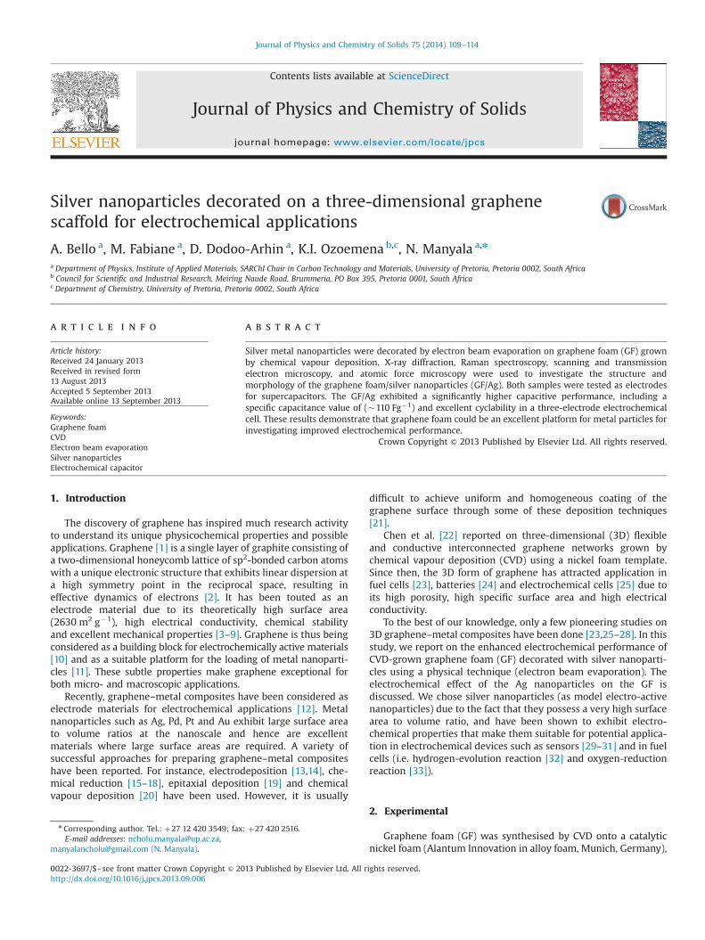
Fig. 1(a) shows the Raman spectrum of the GF which consistedof two major peaks at (1578 cm�1) and (2703 cm�1), correspond-ing to the typical G- and 2D-bands of graphene [35]. The absenceof the D-peak (disorder) around 1350 cm�1 on the spectrumshows that the GF is of good quality [36]. Fig. 1(b) shows theRaman spectrum of the GF/Ag sample. The appearance of a D-peakat 1350 cm�1 could be attributed to the strain effect on the atomicposition of the carbon atoms caused by the Ag particles. BothRaman spectra show weak bands at G* (2450 cm�1) whichoriginates from the double resonance process involving two iTOphonons around the K-point in the phonon dispersion of a two-dimensional graphite [37]. The 2D band also originate from thesame double resonance phenomenon and correspond to a fully-dispersive q¼2k while the 2450 cm�1 band correspond to non-dispersive q¼0, k for the electron and q for the phonon aremeasured from the K-point. From the corresponding phononfrequency and dispersion, the 2450 cm�1 band has been modelledwith an inter-valley process involving one iTO and one LA phononand assigned as an overtone of LO phonon mode [38,39].
The relatively low intensity of the D-peak implies that thecarbon atoms still maintain the honeycomb structure. The inten-sity of both the G- and 2D-peaks is greatly enhanced after thedeposition of the Ag particles. The enhancement factors of theG- and 2D-bands of graphene after Ag deposition are �4.5 and�5.5 respectively. The low values could be attributed to the weakvan der Waals interaction between Ag and graphene, which maychange the structure of the graphene. The results here are similarto those obtained by Lee et al. [40] who proposed that the Ramansignal in Ag-deposited graphene is due to the first-order processand therefore that the interaction between Ag nanoparticles andgraphene could lead to a change in the electronic structure.
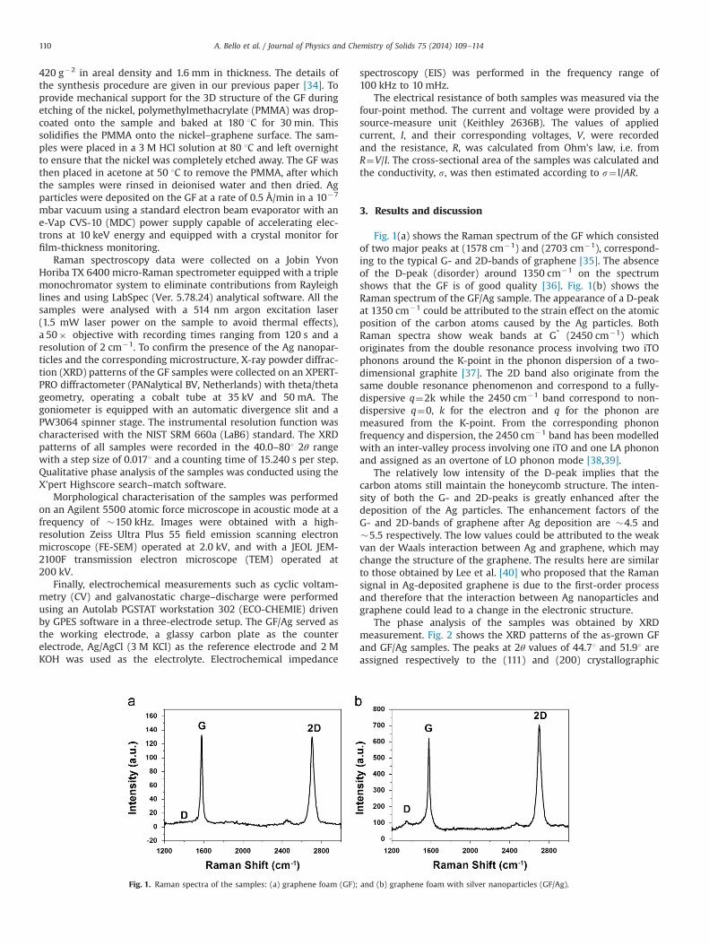
The phase analysis of the samples was obtained by XRDmeasurement. Fig. 2 shows the XRD patterns of the as-grown GFand GF/Ag samples. The peaks at 2θ values of 44.71 and 51.91 areassigned respectively to the (111) and (200) crystallographic
Fig. 1. Raman spectra of the samples: (a) graphene foam (GF); and (b) graphene foam with silver nanoparticles (GF/Ag).
A. Bello et al. / Journal of Physics and Chemistry of Solids 75 (2014) 109–114110
planes of the fluid catalytic cracking (FCC) silver nanoparticles.Due to the small quantity and size broadening at higher angles ofthe silver nanoparticles, peaks such as the (200) and (220) at peakpositions 51.91 and 76.71 are almost in the background.
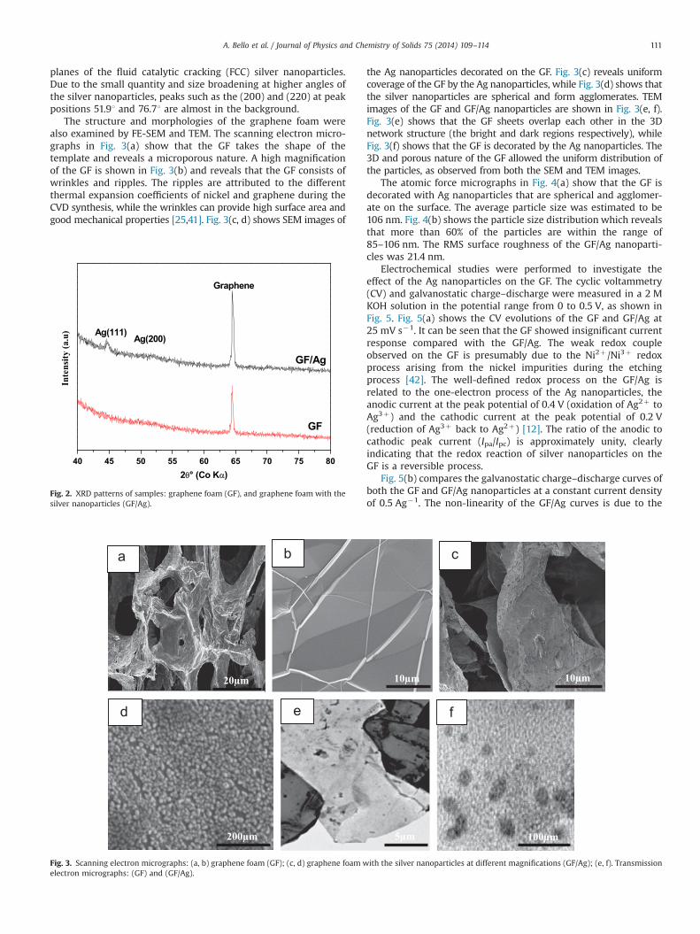
The structure and morphologies of the graphene foam werealso examined by FE-SEM and TEM. The scanning electron micro-graphs in Fig. 3(a) show that the GF takes the shape of thetemplate and reveals a microporous nature. A high magnificationof the GF is shown in Fig. 3(b) and reveals that the GF consists ofwrinkles and ripples. The ripples are attributed to the differentthermal expansion coefficients of nickel and graphene during theCVD synthesis, while the wrinkles can provide high surface area andgood mechanical properties [25,41]. Fig. 3(c, d) shows SEM images of
the Ag nanoparticles decorated on the GF. Fig. 3(c) reveals uniformcoverage of the GF by the Ag nanoparticles, while Fig. 3(d) shows thatthe silver nanoparticles are spherical and form agglomerates. TEMimages of the GF and GF/Ag nanoparticles are shown in Fig. 3(e, f).Fig. 3(e) shows that the GF sheets overlap each other in the 3Dnetwork structure (the bright and dark regions respectively), whileFig. 3(f) shows that the GF is decorated by the Ag nanoparticles. The3D and porous nature of the GF allowed the uniform distribution ofthe particles, as observed from both the SEM and TEM images.
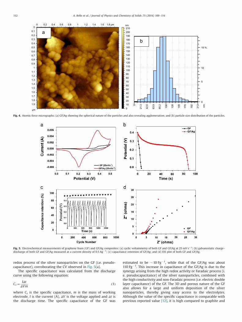
The atomic force micrographs in Fig. 4(a) show that the GF isdecorated with Ag nanoparticles that are spherical and agglomer-ate on the surface. The average particle size was estimated to be106 nm. Fig. 4(b) shows the particle size distribution which revealsthat more than 60% of the particles are within the range of85–106 nm. The RMS surface roughness of the GF/Ag nanoparti-cles was 21.4 nm.
Electrochemical studies were performed to investigate theeffect of the Ag nanoparticles on the GF. The cyclic voltammetry(CV) and galvanostatic charge–discharge were measured in a 2 MKOH solution in the potential range from 0 to 0.5 V, as shown inFig. 5. Fig. 5(a) shows the CV evolutions of the GF and GF/Ag at25 mV s�1. It can be seen that the GF showed insignificant currentresponse compared with the GF/Ag. The weak redox coupleobserved on the GF is presumably due to the Ni2þ/Ni3þ redoxprocess arising from the nickel impurities during the etchingprocess [42]. The well-defined redox process on the GF/Ag isrelated to the one-electron process of the Ag nanoparticles, theanodic current at the peak potential of 0.4 V (oxidation of Ag2þ toAg3þ) and the cathodic current at the peak potential of 0.2 V(reduction of Ag3þ back to Ag2þ) [12]. The ratio of the anodic tocathodic peak current (Ipa/Ipc) is approximately unity, clearlyindicating that the redox reaction of silver nanoparticles on theGF is a reversible process.
Fig. 5(b) compares the galvanostatic charge–discharge curves ofboth the GF and GF/Ag nanoparticles at a constant current densityof 0.5 Ag�1. The non-linearity of the GF/Ag curves is due to the
20µm 10µm
200µm
10µm
5µm 100µm
Fig. 3. Scanning electron micrographs: (a, b) graphene foam (GF); (c, d) graphene foam with the silver nanoparticles at different magnifications (GF/Ag); (e, f). Transmissionelectron micrographs: (GF) and (GF/Ag).
40 45 50 55 60 65 70 75 80
GF/Ag
Graphene
Ag(200)
Inte
nsity
(a.u
)
2θ° (Co K α)
Ag(111)
GF
Fig. 2. XRD patterns of samples: graphene foam (GF), and graphene foam with thesilver nanoparticles (GF/Ag).
A. Bello et al. / Journal of Physics and Chemistry of Solids 75 (2014) 109–114 111
redox process of the silver nanoparticles on the GF (i.e. pseudo-capacitance), corroborating the CV observed in Fig. 5(a).
The specific capacitance was calculated from the dischargecurve using the following equation:
Cs ¼IΔtΔVm
ð1Þ
where Cs is the specific capacitance, m is the mass of workingelectrode, I is the current (A), ΔV is the voltage applied and Δt isthe discharge time. The specific capacitance of the GF was
estimated to be �10 Fg�1, while that of the GF/Ag was about110 Fg�1. This increase in capacitance of the GF/Ag is due to thesynergy arising from the high redox activity or Faradaic process (i.e. pseudocapacitance) of the silver nanoparticles, combined withthe high conductivity and non-Faradaic process (i.e. electric doublelayer capacitance) of the GF. The 3D and porous nature of the GFalso allows for a large and uniform deposition of the silvernanoparticles, thereby giving easy access to the electrolytes.Although the value of the specific capacitance is comparable withprevious reported value [12], it is high compared to graphite and
0 0.2 0.4 0.6 0.8 1 1.2 1.4 1.6 1.8 µm
µm
0
0.1
0.2
0.3
0.4
0.5
0.6
0.7
0.8
0.9
1
1.1
1.2
1.3
1.4
1.5
1.6
1.7
1.8
1.9
nm
0102030405060708090100110120130140150160170180190200210
nm
0
21.3
42.6
63.9
85.2
106
128
149
170
192
213
0
5
10
15 %
Fig. 4. Atomic force micrographs: (a) GF/Ag showing the spherical nature of the particles and also revealing agglomeration; and (b) particle size distribution of the particles.
Fig. 5. Electrochemical measurements of graphene foam (GF) and GF/Ag composites: (a) cyclic voltammetry of both GF and GF/Ag at 25 mV s�1; (b) galvanostatic charge–discharge of both GF and GF/Ag measured at a current density of 0.5 Ag�1; (c) capacitance retention of GF/Ag; and (d) EIS plot of both GF and GF/Ag.
A. Bello et al. / Journal of Physics and Chemistry of Solids 75 (2014) 109–114112
carbon materials [45,46]. It demonstrates the feasibility of having agraphene sample with a low defect density as compared withreduced graphene oxide which is normally regarded as beingfunctionalized by the reducing agents, and also demonstrates theability of e-beam evaporation to load nanoparticles for improvedelectrochemical and catalytic applications. Fig. 5(c) shows thecontinuous charge–discharge curve of the GF/Ag sample and thecapacitance retention at a current density of 0.5 A/g. The electrodematerial is electrochemically stable after 1000 cycles and retains93% of its initial capacitance.
EIS is an excellent tool for investigating the electrochemicalcharacteristics of an electrode/electrolyte interface using a Nyquistplot, which is a representation of the real and imaginary parts ofthe impedance in the samples. The Nyquist plot of the electrode isshown in Fig. 5(d). It is worth stating that for ideal supercapaci-tors, the EIS (Nyquist) plot should be a line perpendicular to theimaginary axis. From the Nyquist plot, the slope at low frequenciescan also be used to evaluate the capacitive performance [43].However, a comparison of both samples shows that the Nyquistplot of GF/Ag is much closer to the ideal behaviour, thus indicatinga better capacitive behaviour. This could be attributed to the three-dimensionality of the graphene foam, which allows a uniformadsorption of silver nanoparticles, and to the high redox activity ofthe silver nanoparticles, coupled with the good conductivity ofthe GF.
The equivalent series resistance (ESR), including the resistanceof aqueous electrolyte, the intrinsic resistance of the compositematerial and the contact resistance at the electrode interface, canbe obtained from the X-intercept of the Nyquist plot [44]. Asshown in Fig. 5(d), the ESR of the GF/Ag sample (2.6 Ω) is muchlower than that of the GF sample (4.3 Ω). These results aresupported by electrical conductance measurements at room tem-perature for both GF and GF/Ag, for which the values of�7.6�10�2 S/m and �15�10�2 S/m were obtained respectively.It is clear from both results that GF/Ag exhibits half the ESR valueand twice the conductance value with respect to those of GF. Theseresults suggest that 3D GF can serve as an efficient support formetal nanoparticles for potential electrochemical applications,such as in the construction of electrochemical capacitors, electro-catalytic devices and electrochemical sensors.
4. Conclusions
In this work, GF was decorated with Ag nanoparticles using theelectron beam evaporation technique and the effect of Ag on theelectrochemical behaviour and specific capacitance of the GF/Agcomposites was investigated. The interaction of the silver metalwith the graphene foam was characterised using various micro-scopy and spectroscopy techniques. The morphologies reveal thatthe 3D structure of the GF provides support for adsorption andintegration of the metal nanoparticles. Also, the enhanced electro-chemical performance of the GF/Ag sample that was observed isdue to the synergistic effect between the graphene and the silvernanoparticles, which could be attributed to the good electricalconductivity and uniform loading of the silver nanoparticles ontothe surface of the GF. These results demonstrate that 3D GF couldserve as an excellent platform for depositing metal nanoparticlesfor fundamental and applied electrochemical studies.
Acknowledgements
This work is based on research supported by the South AfricanResearch Chairs Initiative (SARCHi) of the Department of Scienceand Technology (DST) and the National Research Foundation
(NRF). Any opinion, findings and conclusions or recommendationsexpressed in this work are those of authors and therefore the NRFand DST do not accept any liability with regard thereto. A. Bello.acknowledges the financial support from the University of Pretoriafor his study. We thank Dr Patricia Forbes for supplying thenickel foams.
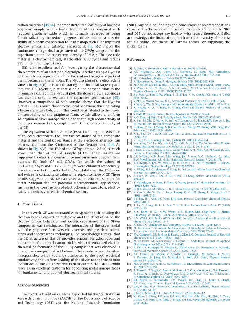
References
[1] A. Geim, K. Novoselov, Nature Materials 6 (2007) 183–191.[2] K.S. Novoselov, A.K. Geim, S.V. Morozov, D. Jiang, M.I. Katsnelson,
I.V. Grigorieva, S.V. Dubonos, A.A. Firsov, Nature 438 (2005) 197–200.[3] M.I. Katsnelson, Materials Today 10 (2007) 20–27.[4] K. Novoselov, A. Geim, S. Morozov, Science 306 (2004) 666–669.[5] M.D. Stoller, S. Park, Y. Zhu, J. An, R.S. Ruoff, Nano Letters 8 (2008) 3498–3502.[6] Y. Wang, Z. Shi, Y. Huang, Y. Ma, C. Wang, M. Chen, Y.S. Chen, Journal of
Physical Chemistry C 113 (2009) 13103–13107.[7] Z-S. Wu, W. Ren, D-W. Wang, F. Li, B. Liu, H-M. Cheng, ACS Nano 4 (2010)
5835–5842.[8] Y. Zhu, S. Murali, W. Cai, X. Li, Advanced Materials 22 (2010) 3906–3924.[9] Y. Sun, Q. Wu, G. Shi, Energy and Environmental Science 4 (2011) 1113–1132.[10] X. Huang, X. Qi, F. Boey, H. Zhang, Chemical Society Reviews 41 (2012)
666–686.[11] S. Park, R.S. Ruoff, Nature Nanotechnology 4 (2009) 217–224.[12] K.-S. Kim, I.-J. Kim, S.-J. Park, Synthetic Metals 160 (2010) 2355–2360.[13] X. Sun, M. Xie, G. Wang, H. Sun, A.S. Cavanagh, J.J. Travis, S.M. George, L. Jie,
Journal of the Electrochemical Society 159 (2012) A364–A369.[14] X. Dong, Y. Cao, J. Wang, M.B. Chan-Park, L. Wang, W. Huang, W.H. Peng, RSC
Advances 2 (2012) 4364–4369.[15] X. Li, B.K. Tay, J. Li, D. Tan, C.W. Tan, K. Liang, Nanoscale Research Letters 7
(2012) 205.[16] S. Liu, J. Tian, L. Wang, X. Sun, Carbon 49 (2011) 3158–3164.[17] Y.-K. Yang, C.-E. He, W.-J. He, L.-J. Yu, R.-G. Peng, X.-L. Xie, W. Xian-Bao, M. Yiu-
Wing, Journal of Nanoparticle Research 13 (2011) 5571–5581.[18] J. Tian, S. Liu, Y. Zhang, H. Li, L. Wang, Y. Luo, A.M. Asiri, A.O. Al-Youbi, X. Sun,
Inorganic Chemistry 51 (2012) 4742–4746.[19] G.F. Ndlovu, W.D. Roos, Z.M. Wang, J.K. Asante, M.G. Mashapa, C.J. Jafta,
B.W. Mwakikunga, K.T. Hillie, Nanoscale Research Letters 7 (2012) 173.[20] Y.H. Kahng, S. Lee, W. Park, G. Jo, M. Choe, J.-H. Lee, Y. Hyunung, L. Takhee,
L. Kwanghee, Nanotechnology 23 (2012) 075702.[21] H. Wang, H.S. Casalongue, Y. Liang, H. Dai, Journal of the American Chemical
Society 132 (2010) 7472–7477.[22] Z. Chen, W. Ren, L. Gao, B. Liu, S. Pei, H. Cheng, Nature Materials 10 (2011)
424–428.[23] T. Maiyalagan, X. Dong, P. Chen, X. Wang, Journal of Materials Chemistry 22
(2012) 5286–5290.[24] H. Ji, L. Zhang, M. Pettes, H. Li, S. Chen, Nano Letters 12 (2012) 2446–2451.[25] X. Cao, Y. Shi, W. Shi, G. Lu, X. Huang, Q. Yan, Q. Zhang, H. Zhang, Small 7
(2011) 3163–3168.[26] J.-S. Lee, H.-J. Ahn, J.-C. Yoon, J.-H. Jang, Physical Chemistry Chemical Physics
7943 (2011).[27] T. Lu, Y. Zhang, H. Li, L. Pan, Y. Li, Z. Sun, Electrochimica Acta 55 (2010)
4170–4173.[28] X.-C. Dong, H. Xu, X.-W. Wang, Y.-X. Huang, M.B. Chan-Park, H. Zhang,
L-H Wang, W. Huang, P. Chen, ACS Nano 6 (2012) 3206–3213.[29] C.M. Welch, C.E. Banks, AO. Simm, R.G. Compton, Analytical and Bioanalytical
Chemistry 382 (2005) 12–21.[30] X. Dai, G.G. Wildgoose, R.G. Compton, Analyst 131 (2006) 1241–1247.[31] M. Tominaga, T. Shimazoe, M. Nagashima, H. Kusuda, A. Kubo, Y. Kuwahara,
T. Isao, Journal of Electroanalytical Chemistry 590 (2006) 37–46.[32] F.W. Campbell, S.R. Belding, R. Baron, L. Xiao, R.G. Compton, Journal of Physical
Chemistry C 113 (2009) 14852–14857.[33] M. Chatenet, M. Aurousseau, R. Durand, F. Andolfatto, Journal of Applied
Electromagnetics 263 (2002) 1131–1140.[34] A. Bello, K. Makgopa, M. Fabiane, D. Dodoo-Ahrin, K.I. Ozoemena, N. Manyala,
Journal of Materials Science 48 (2013) 6707–6712.[35] A.C. Ferrari, J.C. Meyer, V. Scardaci, C. Casiraghi, M. Lazzeri, F. Mauri,
S. Piscanec, D. Jiang, K.S. Novoselov, S. Roth, A.K. Geim, Physical ReviewLetters 97 (2006) 1–4.
[36] M.S. Dresselhaus, A. Jorio, M. Hofmann, G. Dresselhaus, R. Saito, Nano Letters10 (2010) 751–758.
[37] T. Shimada, T. Sugai, C. Fantini, M. Souza, L.G. Cancado, A. Jorio, M.A. Pimenta,R. Saito, A. Grüneis, G. Dresselhaus, M.S. Dresselhaus, Y. Ohno, T. Mizutani,H. Shinohara, Carbon 43 (2005) 1049–1054.
[38] D.L. Mafra, G. Samsonidze, L.M. Malard, D.C. Elias, J.C. Brant, F. Plentz,E.S. Alves, M.A. Pimenta, Physical Review B 76 (2007) 233407.
[39] L.M. Malard, M.A. Pimenta, G. Dresselhaus, M.S. Dresselhaus, Physics Reports473 (2009) 51–87.
[40] J. Lee, K. Novoselov, H. Shin, ACS Nano 5 (2010) 608–612.[41] S.J. Chae, F. Güneş, K.K. Kim, E.S. Kim, G.H. Han, S.M. Kim, H.J. Shin, S. Yoon,
J. Choi, M.H. Park, C.W. Yang, D. Pribat, Y.H. Lee, Advanced Materials 21 (2009)2328–2333.
A. Bello et al. / Journal of Physics and Chemistry of Solids 75 (2014) 109–114 113

[42] L.-R. Zhang, J. Zhao, M. Li, H.-T. Ni, J. Zhang, X.-M. Feng, Y.-W. Ma, Q.-L. Fan,X.-Z. Wang, Z. Hu, W. Huang, New Journal of Chemistry 36 (2012) 1108.
[43] E. Frackowiak, F. Béguin, Carbon 39 (2001) 937–950.[44] J. Zhang, L.-B. Kong, J.-J. Cai, Y.-C. Luo, L. Kang, Journal of Solid State
Electrochemistry 14 (2010) 2065–2075.
[45] T. Cassagneau, J.H. Fendler, Journal of Physical Chemistry B (1999) 1789–1793.[46] L. Jiang, M. Vangari, T. Pryor, Z. Xiao, N.S. Korivi, Microelectronic Engineering
(2013) 52–57.
A. Bello et al. / Journal of Physics and Chemistry of Solids 75 (2014) 109–114114