SERVICE MANUAL - Wireless Sound Bar - Encompass Parts
72
SERVICE MANUAL SERVICE MANUAL CAUTION BEFORE SERVICING THE UNIT, READ THE “SAFETY PRECAUTIONS” IN THIS MANUAL. CONFIDENTIAL MODEL: SL4Y (SL4Y, SPH4B-W) P/NO : AFN79154806 MAY, 2019 MODEL: SL4Y (SL4Y, SPH4B-W) Copyright © 2019 LG Electronics Inc. All rights reserved. Only for training and service purposes. Wireless Sound Bar “Any reproduction, duplication, distribution (including by way of email, facsimile or other electronic means), publication, modification, copying or transmission of this Service Manual is STRICTLY PROHIBITED unless you have obtained the prior written consent of the LG Electronics entity from which you received this Service Manual. The material covered by this prohibition includes, without limitation, any text, graphics or logos in this Service Manual.”
-
Upload
khangminh22 -
Category
Documents
-
view
0 -
download
0
Transcript of SERVICE MANUAL - Wireless Sound Bar - Encompass Parts

SE
RV
ICE
MA
NU
AL
SERVICE MANUAL
CAUTIONBEFORE SERVICING THE UNIT, READ THE “SAFETY PRECAUTIONS”IN THIS MANUAL.
CONFIDENTIAL
MO
DE
L: S
L4Y
(SL
4Y, S
PH
4B-W
)
P/NO : AFN79154806 MAY, 2019
MODEL: SL4Y(SL4Y, SPH4B-W)
Copyright © 2019 LG Electronics Inc. All rights reserved. Only for training and service purposes.
Wireless Sound Bar
“Any reproduction, duplication, distribution (including by way of email, facsimile or otherelectronic means), publication, modification, copying or transmission of this Service Manual isSTRICTLY PROHIBITED unless you have obtained the prior written consent of the LG Electronicsentity from which you received this Service Manual. The material covered by this prohibition includes,without limitation, any text, graphics or logos in this Service Manual.”

1-1 Copyright © 2019 LG Electronics Inc. All rights reserved.Only for training and service purposes.
CONTENTS
SECTION 1 ........GENERAL
SECTION 2 ........CABINET & MAIN CHASSIS
SECTION 3 ........ELECTRICAL
SECTION 4 ........WIRELESS SUBWOOFER PART

1-2 Copyright © 2019 LG Electronics Inc. All rights reserved.Only for training and service purposes.
SECTION 1
GENERAL
CONTENTS
ESD PRECAUTIONS ......................................................................................................................................... 1-3
LOCATION OF CUSTOMER CONTROLS ........................................................................................................ 1-4
WIRELESS SUBWOOFER CONNECTION ....................................................................................................... 1-5
REAR SPEAKERS CONNECTION (SOLD SEPARATELY) ............................................................................ 1-6
HIDDEN KEY MODE ......................................................................................................................................... 1-7
FIRMWARE UPDATE GUIDE ........................................................................................................................... 1-8
SPECIFICATIONS ........................................................................................................................................... 1-11

1-3 Copyright © 2019 LG Electronics Inc. All rights reserved.Only for training and service purposes.
ESD PRECAUTIONS
Electrostatically Sensitive Devices (ESD)Some semiconductor (solid state) devices can be damaged easily by static electricity. Such componentscommonly are called Electrostatically Sensitive Devices (ESD). Examples of typical ESD devices are integratedcircuits and some field-effect transistors and semiconductor chip components. The following techniques shouldbe used to help reduce the incidence of component damage caused by static electricity.
1. Immediately before handling any semiconductor component or semiconductor-equipped assembly, drain offany electrostatic charge on your body by touching a known earth ground. Alternatively, obtain and wear acommercially available discharging wrist strap device, which should be removed for potential shock reasonsprior to applying power to the unit under test.
2. After removing an electrical assembly equipped with ESD devices, place the assembly on a conductive surface such as aluminum foil, to prevent electrostatic charge buildup or exposure of the assembly.
3. Use only a grounded-tip soldering iron to solder or unsolder ESD devices.4. Use only an anti-static solder removal device. Some solder removal devices not classified as "anti-static" can
generate electrical charges sufficient to damage ESD devices.5. Do not use freon-propelled chemicals. These can generate electrical charges sufficient to damage ESD
devices.6. Do not remove a replacement ESD device from its protective package until immediately before you are
ready to install it. (Most replacement ESD devices are packaged with leads electrically shorted together byconductive foam, aluminum foil or comparable conductive materials).
7. Immediately before removing the protective material from the leads of a replacement ESD device, touch theprotective material to the chassis or circuit assembly into which the device will by installed.
CAUTION : BE SURE NO POWER IS APPLIED TO THE CHASSIS OR CIRCUIT, AND OBSERVE ALL OTHER SAFETY PRECAUTIONS.
8. Minimize bodily motions when handing unpackaged replacement ESD devices. (Otherwise harmless motionsuch as the brushing together of your clothes fabric or the lifting of your foot from a carpeted floor can generate static electricity sufficient to damage an ESD device).
CAUTION. GRAPHIC SYMBOLS
THE LIGHTNING FLASH WITH APROWHEAD SYMBOL. WITHIN AN EQUILATERAL TRIANGLE, IS INTENDED TO ALERT THE SERVICE PERSONNEL TO THE PRESENCE OF UNINSULATED “DANGEROUS VOLTAGE” THAT MAY BE OF SUFFICIENT MAGNITUDE TO CONSTITUTE A RISK OF ELECTRIC SHOCK.
THE EXCLAMATION POINT WITHIN AN EQUILATERAL TRIANGLE IS INTENDED TO ALERT THESERVICE PERSONNEL TO THE PRESENCE OF IMPORTANT SAFETY INFORMATION IN SERVICELITERATURE.

1-4 Copyright © 2019 LG Electronics Inc. All rights reserved.Only for training and service purposes.
LOCATION OF CUSTOMER CONTROLS
Front panel
Rear panel
Display Window- Display window will be darkened automatically if there is no key input for 15 seconds. When you press any button, the display window will brighten.
Remote sensor
(Standby)- Switches the unit ON or OFF.
F (Function)- Select the function and input source by pressing F repeatedly.
Input source / Function Display
Optical LG Sound Sync (Wired) OPT
Bluetooth BT
LG Sound Sync (Wireless) LG TV
USB USB
+/− (Volume)- Adjusts volume level.
DC IN- Connect to the AC adapter.
OPTICAL IN- Connect the OPTICAL IN jack on the back of the unit to OPTICAL OUT jack on the TV.
USB Port- Connect USB memory device to the USB port on the back of the unit.
1
2
3
1
2
3

1-5 Copyright © 2019 LG Electronics Inc. All rights reserved.Only for training and service purposes.
WIRELESS SUBWOOFER CONNECTION
LED indicator of wireless subwoofer
LED Color Status
Yellow - green(Blink) The connection is trying.
Yellow - green The connection is completed.
RedThe wireless subwoofer is in standby mode or the connection is failed.
Off (No display)
The power cord of wirelesssubwoofer is disconnected.
Setting up the wireless subwoofer for the fi rst time
1. Connect the power cord to the subwoofer and plug the power cord into a power outlet.2. Turn on the main unit : The sound bar and wireless subwoofer will be automatically connected. - Yellow - green on the rear of wireless subwoofer turns on.
Manually pairing wireless subwoofer
When your connection is not completed, you can check red LED on the wireless subwoofer and the wireless subwoofer does not make sound. To solve the problem, follow the steps below.
1. Press PAIRING button on the rear of the wireless subwoofer.
- The yellow - green LED on the rear of the wireless subwoofer blinks quickly. (If the green LED does not blink, press and hold the PAIRING.)
2. Turn on the sound bar. - Pairing is completed. The yellow - green LED on the front of the wireless subwoofer turns on.
Note:• It takes a few seconds (and may take longer) for the main unit and the subwoofer to communicate with each other and make sounds.• The closer the main unit and the subwoofer, the better sound quality. It is recommended to install the main unit and the subwoofer as close as possible and avoid the cases below. - There is a obstacle between the main unit and the subwoofer. - There is a device using same frequency with this wireless connection such as a medical equipment, a microwave or a wireless LAN device. - Keep the sound bar and the subwoofer away from the device (ex. wireless router, microwave oven, etc.) over 1m to prevent wireless interference.

1-6 Copyright © 2019 LG Electronics Inc. All rights reserved.Only for training and service purposes.
Connecting the rear speakers
1. Connect the black stripe wire to the terminal marked - (minus) and the other end to the terminal marked + (plus).
2. Connect the wireless receiver and the rear speakers (right, left) with the speaker cables.
Color Position
Grey Rear rightBlue Rear left
Note :You need to purchase the wireless rear speakers kit (SPK8-S) to enjoy surround sound.
Caution :• Use the speaker supplied with this unit only. Using any other speaker may cause malfunction.• Be sure to match the speaker cable to the appropriate terminal on the components: + to + and – to –. If the cables are reversed, the sound will be distorted and will lack bass.
LED indicator of wireless receiver
LED Color Status
Yellow - green(Blink) The connection is trying.
Yellow - green The wireless receiver is receiving the signal from the sound bar.
Red The wreless receiver is in standby mode.
Off(No display)
The power cord of wirelessreceiver is disconnected
Setting up the wireless receiver for the fi rst time
1. Connect the power cord to the wireless receiver to the outlet.2. Turn on the main unit : The sound bar and wireless receiver will be automatically connected. - Yellow - green LED on the wireless receiver turns on.
Manually pairing wireless receiver
When your connection is not completed, you cansee the red LED on the wireless receiver and rearspeakers are not made sound. To solve the problem,follow the below steps.1. Press PAIRING button on the rear of the wireless receiver.
- The yellow - green LED on the wireless receiver blinks quickly.
2. Turn on the main unit - Paring is completed. The yellow - green LED on the wireless receiver turns on.
REAR SPEAKERS CONNECTION (SOLD SEPARATELY)

1-7 Copyright © 2019 LG Electronics Inc. All rights reserved.Only for training and service purposes.
HIDDEN MODE KEYS
EEPROM EDIT Main unit ‘ (Volume)’ + Remote control ‘NIGHT ON’
EEPROM CLEAR (Initialize) Main unit ‘ (Volume)’ + Remote control ‘'ASC ’
VERSION CHECK Main unit ‘ (Volume)’ + Remote control ‘ (Play/Pause)’
HIDDEN KEY MODE

1-8 Copyright © 2019 LG Electronics Inc. All rights reserved.Only for training and service purposes.
1. Preparation 1) SL4Y Series Units : Main Unit, Wireless Subwoofer Unit, Rear Speaker Unit(optional).2) SL4Y RCU.3) USB Memory.4) Android Device with “Music Flow Bluetooth” App for FOTA update, “Version Check APP” for Version Check.
※ Take care not to power off during update. ※ Do format USB memory before update (FAT32 f le system).
FIRMWARE UPDATE GUIDE
<Main Unit>Necessary
<Wireless Subwoofer Unit>If wireless subwoofer rx module
of primary unit is updated.
<USB Memory>for USB update
<Rear Speaker Unit>Optional as model suff x
If wireless rear rx module is updated
<RCU>Necessary

1-9 Copyright © 2019 LG Electronics Inc. All rights reserved.Only for training and service purposes.
2. USB Update Step 1. Prepare SL4 update binaries.
Update module Prefi x & Extension Filename Sample
DSP DSP_SL4Y*.ROM DSP_SL4_1812100_PRO1_rev1619.rom
Wireless Subwoofer Tx WOOFERTX_SL4Y*.BIN WOOFERTX_SL4_190007_181206_checksum_C7CA.bin
Wireless Subwoofer Rx WOOFERRX_SL4Y*.BIN WOOFERRX_SL4_191008_181206_checksum_90BE.bin
Wireless Rear Tx REARTX_SL4Y*.BIN REARTX_SL4_BAR_19.40.06_CHECKSUM_BEA0.bin
Wireless Rear Rx REARRX_SL4Y*.BIN REARRX_SL4_Ver185001_171128_checksum_DFDF.bin
PEQ PEQ_SL4Y*.BIN PEQ_SL4_1812070_PRO1_0EAD.bin
Option OPT*.BIN OPTION_SL4Y_EUS.bin * SLx : “SL4”, depends on model option.
Step 2. Copy all updated SL5/ SL6 binaries to USB memory.
Step 3. Power on SL5/ SL6 main unit.
Step 4. If there is an updated wireless subwoofer rx binary in update list, you need to pair between main unit and subwoofer unit before start update.
Step 5. If there is an updated wireless rear rx binary in update list, you need to pair between main unit and rear speaker unit before start update.
Step 6. Press Function key to change function to USB. Verify whether USB function is or not by VFD.
Step 7.Attach USB which has update binaries to the USB slot back of SL4Y main unit.
Step 8. Update will start automatically. VFD Model : Check VFD what module is in progress one by one.
USB
Update module VFD display
DSP
Option
PEQ
Wireless Subwoofer Rx
Wireless Subwoofer Tx
Wireless Rear Tx
Wireless Rear Rx
D-UP
OP-UP
EQ-UP
WR 00
WT 00
RT 00
RR 00
<SL4Y Series VFD Display in Update>※ The numbers in VFD display of wireless modules will increase in progress as progress percent from 00 to 100.
1-10 Copyright © 2019 LG Electronics Inc. All rights reserved.Only for training and service purposes.
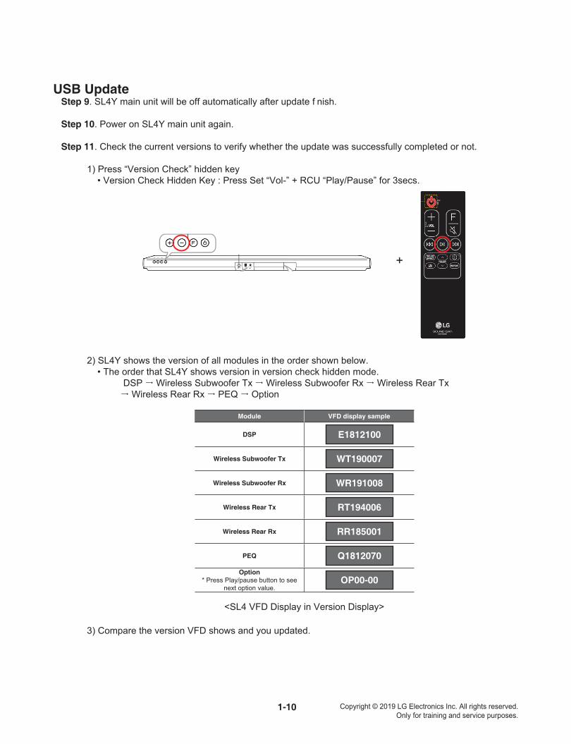
USB Update Step 9. SL4Y main unit will be off automatically after update f nish.
Step 10. Power on SL4Y main unit again.
Step 11. Check the current versions to verify whether the update was successfully completed or not.
1) Press “Version Check” hidden key • Version Check Hidden Key : Press Set “Vol-” + RCU “Play/Pause” for 3secs.
2) SL4Y shows the version of all modules in the order shown below. • The order that SL4Y shows version in version check hidden mode. DSP Wireless Subwoofer Tx Wireless Subwoofer Rx Wireless Rear Tx Wireless Rear Rx PEQ Option
3) Compare the version VFD shows and you updated.
+
Module VFD display sample
DSP
Wireless Subwoofer Tx
Wireless Subwoofer Rx
Wireless Rear Tx
Wireless Rear Rx
PEQ
Option* Press Play/pause button to see
next option value.
E1812100
WT190007
WR191008
RT194006
RR185001
Q1812070
OP00-00
<SL4 VFD Display in Version Display>
1-11 Copyright © 2019 LG Electronics Inc. All rights reserved.Only for training and service purposes.
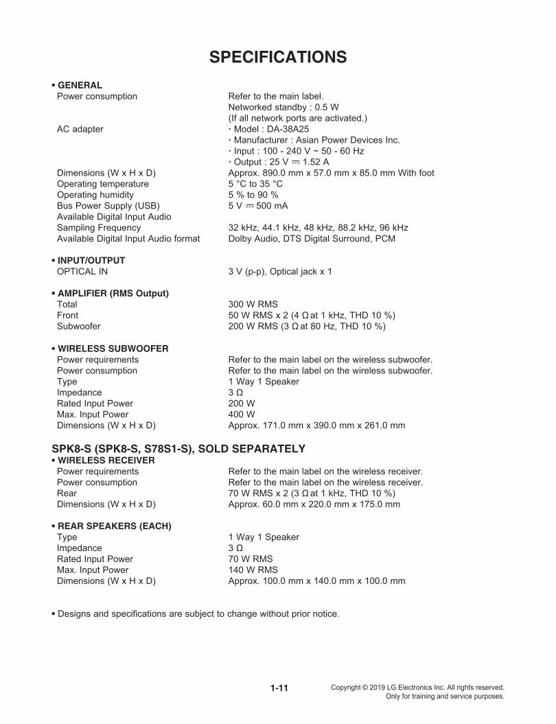
SPECIFICATIONS
• GENERALPower consumption Refer to the main label. Networked standby : 0.5 W (If all network ports are activated.)AC adapter Model : DA-38A25 Manufacturer : Asian Power Devices Inc. Input : 100 - 240 V ~ 50 - 60 Hz Output : 25 V 1.52 ADimensions (W x H x D) Approx. 890.0 mm x 57.0 mm x 85.0 mm With footOperating temperature 5 °C to 35 °COperating humidity 5 % to 90 %Bus Power Supply (USB) 5 V 500 mAAvailable Digital Input AudioSampling Frequency 32 kHz, 44.1 kHz, 48 kHz, 88.2 kHz, 96 kHzAvailable Digital Input Audio format Dolby Audio, DTS Digital Surround, PCM
• INPUT/OUTPUTOPTICAL IN 3 V (p-p), Optical jack x 1
• AMPLIFIER (RMS Output)Total 300 W RMSFront 50 W RMS x 2 (4 Ω at 1 kHz, THD 10 %)Subwoofer 200 W RMS (3 Ω at 80 Hz, THD 10 %)
• WIRELESS SUBWOOFERPower requirements Refer to the main label on the wireless subwoofer.Power consumption Refer to the main label on the wireless subwoofer.Type 1 Way 1 SpeakerImpedance 3 ΩRated Input Power 200 WMax. Input Power 400 WDimensions (W x H x D) Approx. 171.0 mm x 390.0 mm x 261.0 mm
SPK8-S (SPK8-S, S78S1-S), SOLD SEPARATELY• WIRELESS RECEIVER
Power requirements Refer to the main label on the wireless receiver.Power consumption Refer to the main label on the wireless receiver.Rear 70 W RMS x 2 (3 Ω at 1 kHz, THD 10 %)Dimensions (W x H x D) Approx. 60.0 mm x 220.0 mm x 175.0 mm
• REAR SPEAKERS (EACH)Type 1 Way 1 SpeakerImpedance 3 ΩRated Input Power 70 W RMSMax. Input Power 140 W RMSDimensions (W x H x D) Approx. 100.0 mm x 140.0 mm x 100.0 mm
• Designs and specifications are subject to change without prior notice.

1-12 Copyright © 2019 LG Electronics Inc. All rights reserved.Only for training and service purposes.

2-1 Copyright © 2019 LG Electronics Inc. All rights reserved.Only for training and service purposes.
SECTION 2
CABINET & MAIN CHASSIS
CONTENTS
DISASSEMBLY INSTRUCTIONS ..................................................................................................................... 2-21. HOW TO DISASSEMBLE THE MAIN SET .............................................................................................. 2-2
EXPLODED VIEWS ........................................................................................................................................... 2-71. MAIN UNIT SECTION ............................................................................................................................... 2-72. WIRELESS SUBWOOFER SECTION .................................................................................................... 2-113. PACKING ACCESSORY SECTION ....................................................................................................... 2-15

2-2 Copyright © 2019 LG Electronics Inc. All rights reserved.Only for training and service purposes.
DISASSEMBLY INSTRUCTIONS
Figure 1-2
Figure 1-1
1. HOW TO DISASSEMBLE THE MAIN SET
2) Remove the Case Bottom Assembly.
1) Remove the 19 screws.

2-3 Copyright © 2019 LG Electronics Inc. All rights reserved.Only for training and service purposes.
Figure 1-4
Figure 1-3
HOW TO DISASSEMBLE THE MAIN SET
4) Remove the SPK Chamber L/R Assembly.
3) Remove the 2 screws, Disconnect the Harmess/FFC cables (KEY, SPK) and Remove the Main PCB Assembly.

2-4 Copyright © 2019 LG Electronics Inc. All rights reserved.Only for training and service purposes.
Figure 1-6
Figure 1-5
HOW TO DISASSEMBLE THE MAIN SET
6) Remove the 4 screws and Disconnect FFC cables (BT, Wireless).
5) Remove the L/R Deco Assembly.
BT
Wireless

2-5 Copyright © 2019 LG Electronics Inc. All rights reserved.Only for training and service purposes.
Figure 1-8
Figure 1-7
HOW TO DISASSEMBLE THE MAIN SET
8) Remove the EMI Shield Tape of Bottom side.
7) Remove the EMI Shield Tape.

2-6 Copyright © 2019 LG Electronics Inc. All rights reserved.Only for training and service purposes.
Figure 1-9
HOW TO DISASSEMBLE THE MAIN SET9) Disassembly f nish.

Copyright © 2019 LG Electronics Inc. All rights reserved.Only for training and service purposes.
F
H CABLE1
CD
B/TA52
264
CABLE2
MAIN
F
JJ
DC
AB
B
G
A46
WIRELESSA54
CABLE3
I
G
I
A
A42
262266
A41
H
253
A55
CABLE5
CABLE6
CABLE4
WIRELESSA54
265
E
EXPLODED VIEWS1. MAIN UNIT SECTION
2-7 2-8
A80R
A80L

Copyright © 2019 LG Electronics Inc. All rights reserved.Only for training and service purposes.
2-122-11
954
955
D
E
WIRELESS
SMPS
AMPB
A
G
E
D
B
F
G
C
C
F
958
A900
951
A45W
A47WCN901
A49WA54W
959
A
300W
2. WIRELESS SUBWOOFER SECTIONNOTES) THE EXCLAMATION POINT WITHIN AN
EQUILATERAL TRIANGLE IS INTENDED TO ALERT THE SERVICE PERSONNEL TO THE PRESENCE OF IMPORTANT SAFETY INFORMATION IN SERVICELITERATURE.

2-15 Copyright © 2019 LG Electronics Inc. All rights reserved.Only for training and service purposes.
300 Power cord
833 AC adapter 900 Remote control
836 Screws (2)
835 Wall bracket
837 Holder, foot
806 Optical cable
�Optional Part
�
3. PACKING ACCESSORY SECTION

3-1 Copyright © 2019 LG Electronics Inc. All rights reserved.Only for training and service purposes.
SECTION 3 ELECTRICAL
CONTENTS
WIRING DIAGRAM ............................................................................................................................................ 3-2
BLOCK DIAGRAMS .......................................................................................................................................... 3-31. SYSTEM BLOCK DIAGRAM .................................................................................................................. 3-32. POWER BLOCK DIAGRAM ................................................................................................................... 3-4
ONE POINT REPAIR GUIDE ............................................................................................................................ 3-51. NO BOOTING WHEN YOU TURN THE UNIT ON, NO MESSAGE OR “HELLO” ON FRONT PANEL ........ 3-52. NO SOUND ............................................................................................................................................. 3-93. PROTECTION ERROR ......................................................................................................................... 3-12
ELECTRICAL TROUBLESHOOTING GUIDE ................................................................................................. 3-141. ADAPTER POWER CIRCUIT ............................................................................................................... 3-142. KEY PART ............................................................................................................................................ 3-233. USB FUNCTION ................................................................................................................................... 3-244. OPTICAL FUNCTION ........................................................................................................................... 3-25
WAVEFORMS OF MAJOR CHECK POINT .................................................................................................... 3-261. CRYSTAL .............................................................................................................................................. 3-262. FLASH MEMORY ................................................................................................................................. 3-263. TACT KEY ............................................................................................................................................. 3-274. USB ....................................................................................................................................................... 3-285. REMOTE CONTROL ............................................................................................................................ 3-296. OPTICAL ............................................................................................................................................... 3-307. FM ......................................................................................................................................................... 3-31
CIRCUIT VOLTAGE CHART ........................................................................................................................... 3-33
PRINTED CIRCUIT BOARD DIAGRAMS ....................................................................................................... 3-351. MAIN P. C. BOARD DIAGRAM ............................................................................................................ 3-352. KEY P. C. BOARD DIAGRAM .............................................................................................................. 3-37
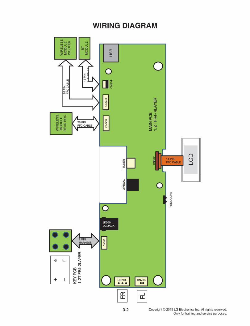
3-2 Copyright © 2019 LG Electronics Inc. All rights reserved.Only for training and service purposes.
US
B C
N50
6 C
N50
3
LCD
WIR
ELE
SS
M
OD
ULE
R
EAR
BO
X W
IRE
LES
S
MO
DU
LE
WO
OFE
R
BT
MO
DU
LE
OOPT
ICAL
TU
NER
26 PIN FFC CABLE
26 P
IN
FFC
CAB
LE
12 P
IN
FFC
CAB
LE
2 PIN HARNESS
REM
OC
ON
E
CN
502
JK300 DC JACK
CN704 CN703
CN
505
FR
FL
MAI
N P
CB
1.
2T F
R4-
4LAY
ER
KEY
PCB
1.
2T F
R4
2LAY
ER
CN
504
14 PIN FFC CABLE
WIRING DIAGRAM

3-3 Copyright © 2019 LG Electronics Inc. All rights reserved.Only for training and service purposes.
TAC
T-KE
Y
US
B D
P/D
N
RM
C
Flas
h fo
r DS
P(2
MBy
te)
SP
I
Flas
h fo
r EQ
(1M
Byte
)
FRO
NT
LCD
MB8
811
C1
BT_
CLK
/DA
T, B
T_R
X/TX
, BT_
RS
T
FL/T
WL
FR/T
WR
FL_P
/N, F
R_P
/N
AM
P_P
DN
(RS
T)
AM
P_F
AU
LT/C
LIP
0/P
RO
TEC
T
LPF
Wire
less
Woo
fer
Wire
less
Mod
ule
Rx
WL_
MU
TE/IN
T_W
F/M
SG
_RD
Y_W
FW
L_C
LK_W
F/D
AT_
WF
5 G
Hz
BC
K/L
RC
K/A
DA
TA2_
WF
SP
IFl
ash
(1 M
B)
Wire
less
Mod
ule
TX
OP
T_IN
/ O
PT_
DE
TO
ptic
al IN
AMP
27M
hz
US
B P
LAYB
ACK
PO
WE
R/F
UN
C/V
OL+
/-
MAI
N S
oC
IC50
1C
resc
endo
3+
IC40
2
TUN
ER
TUN
ER
_CE
/CLK
DA
T/R
ST
32.7
68 K
Hz
ADAP
TOR
25 VW
irele
ssR
ear B
ox
Wire
less
Mod
ule
Rx
WL_
MU
TE/IN
T_R
R/M
SG
_RD
Y_R
RW
L_C
LK_R
R/D
AT_
RR
/5
GH
z
BC
K/L
RC
K/A
DA
TA2_
RR
SP
IFl
ash
(1 M
B)
Wire
less
Mod
ule
TX
TUN
ER
_L/ T
UN
ER
_R
LCD
_STB
/RS
T/C
D/C
LK/D
AT
50W
50W
200W
60W
+
60W
New
Rea
r Wire
less
Rea
dy
BLOCK DIAGRAMS
1. SYSTEM BLOCK DIAGRAM

3-4 Copyright © 2019 LG Electronics Inc. All rights reserved.Only for training and service purposes.
DCDC[2A]
PVDD
12 VA
ADATOR(25 V) AMP
VD13ADC
1.3 VA
IC501Crescendo 3+
WIRELESSModule
WL_3V3
3.3 VA
BT Module
RCU, STB-LED
OPTICAL
DCDC DCDC
SwitchingTR
+12 V
1.35 V5.1 VA
VD33USB
VD33PLL
VD33
LDO
350 mA
NC
20 mA
10 mA
50 mA
IC302 IC300 IC303
AMP, Front LED*4ea
Switch
P_CTRL
P_CTRL
IC309
IC312
10 mA
100 mA
10 mA
20 mA
100 mA
100 mA
VCC33
Q301
USBLCD
500 mAUSB_5 VSwitchIC306
VD33
3.3 VA
3.3 VA
DCDC
IC301
SwitchWL_P_CTRL_WFIC310
VD33ADAC
VD33AADC
10 mA
NC
TUNER50 mATUNNER_3.3 V
LDOIC311
WIRELESSModule
RBOX_3V3 100mASwitchWL_P_CTRL_RRIC313
VCC_5 V 200 mA
2. POWER BLOCK DIAGRAM

3-5 Copyright © 2019 LG Electronics Inc. All rights reserved.Only for training and service purposes.
ONE POINT REPAIR GUIDE
1. NO BOOTING WHEN YOU TURN THE UNIT ON, NO MESSAGE OR “HELLO” ON FRONT PANEL
When you turn on your set, no message on the front panel, and stand-by LED doesn’t work.
1-1. IC302 System 12 VA (No 12 VA)1-1-1. SolutionReplace MAIN board.
1-1-2. How to troubleshoot (Countermeasure)1) Please check 25 VA of IC302 pin2 (VIN).2) If 25 VA is abnormal, please check adapter.3) If 25 VA is OK, but 12 VA is abnormal pin3 of IC302 (VOUT), replace MAIN board.
1-1-3. Service hint (Any picture / Remark)
< MAIN board top view >
2
R4
05
R4
07
R 4 0 8
R 4 0 9
R3
A3
R3
A4
R3
A5
R3
A6
C N 4 0 2
R5
A5
X4
01
C 5 A 1
C 5 A 2
F 3 0 0
F 3 0 1
C4
31
C 4 3 2
C4
33
C4
34
C4
35
C4
36
C4
37
C 4 3 8 C 4 3 9
C 4 4 0
C4
46
Q 3 0 0 Q 3 0 1
Z D 5 0 4
L 3 0 0
L 3 0 1
L 3 0 2
F M
R R 5 0 3
RR
50
5R
R5
06
RR
50
7R
R5
08
RR
50
9
RR
51
0R
R5
11
RR
51
2R
R5
13
RR
51
4R
R5
15
RR
51
6R
R5
17
FB
30
3
F B 3 0 4
FB
30
5
F BR 3 0 3
R C F 5 0 0
F B 3 1 4
F B 3 1 6 JK
50
2
FB
31
8R 3 0 8
R 3 1 0
R 3 1 2
R3
15
RC
50
20
3
04
05
06
RC
50
9
R 3 2 7
10
CN
50
0
11
12
CN502
13
14
15
18
19
R 5 2 8
R3
38
R3
39
22
23
C 3 0 0
R4
C3
C 3 0 7
C3
08
C3
09
C3
10
5 4 0
C3
11
R 5 4 1
C 3 1 2
C 3 1 3
C3
14
C3
15
C3
16
C3
17
C3
18
C3
19
R5
49
C4
A4
C 3 2 0
C4
A5
C3
21
C4
A6
C3
22
R 5 5 2
C 3 2 3
R3
65
R 5 5 9
R3
66
R3
68
C 3 3 0
C 3 3 1
5 6 1
C 3 3 3
R3
70
C 3 3 4
R 3 7 1
R3
75
R3
80
R3
81
C
T P _ G N D
C 5 4 7
C3
54
C 5 4 8
C 5 4 9
C3
55
C3
56
WR
50
5W
R5
06
WR
50
7W
R5
08
WR
50
9
D3
01
WR
51
0
C3
64
WR
51
1W
R5
12
WR
51
3
C3
67
C3
70
C 3 7 9
L4
06
L 4 0 7
IC3
00
C 3 8 1
I C 3 0 1
C 3 8 2
IC3
02
C 3 8 3
I C 3 0 9
C3
90
IC3
10
IC3
11
C 3 9 1
WC
50
2
C 3 9 2
C 3 9 3
I C 3 1 3
WC
50
3
C 3 9 4
WC
50
4
C 3 9 5
WC
50
5W
C5
06
WC
50
9
WC
51
3W
C5
14
WC
51
5
WC
51
9
WC
52
0
WC
52
2W
C5
23
R4
N4
FB
40
1
R4
N5
FB
40
2
F B 4 0 3
F B 4 0 4
R4
N8
R 5 F 2
R 5 F 1
C 5 F 2
C 5 F 1
F B 5 1 0
I C 4 0 2
C306 100nF
DGND
C312
10uF
/35V
R328
100K
R335
100K
R300
51K
(1%
)
DGND
PVDD
C307100nF/50V
C351
33pF
PWR_GD
C30010uF
/35V
12VA
R305
3.3K (1%)
C32310uF/35VNC
DGNDR301
47K
(1%
)
FB303UBW2012-121F
R306 22
C32010uF
/35V
C302
100n
F
C313
10uF
/35V
IC3021
PG2
IN3
SW4
GND5 BST
6 EN/SYNC
7 VCC
8 FB
L302
10UH
DGND
R307
390K
R340
56K
[25VA TO 12VA]
VOUT = 0.792x(47K/3.3K+1)= 12.072V
IC302IC302
L302L302

3-6 Copyright © 2019 LG Electronics Inc. All rights reserved.Only for training and service purposes.
ONE POINT REPAIR GUIDE
R31262K(1%)
R3278.2K
(1%)
DGND
C314100nF/50V
R355 33
C31010uF
/35V
C31610uF/16V
12VA
C30810uF/35V
R303
100K
DGND
5.1VA
C31910pF
DGND
C32110uF/16VC303 1uF(1)
C31810uF/16V
R31013K(1%)
DGNDDGND
DGND
IC3001VIN2SW3GND4 BST
5 EN
6 FB
D301
RCla
mp0
582B1C
2A3C
R346390K
R311150K
L300
10UH
FB304UBW2012-121F
VOUT = 0.798x((62K+8.2K)/13K+1)= 5.1V
[12VA TO 5.1VA]
NO BOOTING WHEN YOU TURN THE UNIT ON, NO MESSAGE OR “HELLO” ON FRONT PANEL
When you turn on your set, it will blank / no message on front panel / doesn’t work.
1-2. IC300 System 5.1 V (No 5.1 VA)1-2-1. SolutionCheck MAIN board.
1-2-2. How to troubleshoot (Countermeasure)1) Please check 5.1 VA of IC300 pin22) If 5.1 VA is abnormal, replace MAIN board.
1-2-3. Service hint (Any picture / Remark)
< MAIN board top view >
2
R4
05
R4
07
R 4 0 8
R 4 0 9
R3
A3
R3
A4
R3
A5
R3
A6
C N 4 0 2
R5
A5
X4
01
C 5 A 1
C 5 A 2
F 3 0 0
F 3 0 1
C4
31
C 4 3 2
C4
33
C4
34
C4
35
C4
36
C4
37
C 4 3 8 C 4 3 9
C 4 4 0
C4
46
Q 3 0 0 Q 3 0 1
Z D 5 0 4
L 3 0 0
L 3 0 1
L 3 0 2
F M
R R 5 0 3
RR
50
5R
R5
06
RR
50
7R
R5
08
RR
50
9
RR
51
0R
R5
11
RR
51
2R
R5
13
RR
51
4R
R5
15
RR
51
6R
R5
17
FB
30
3
F B 3 0 4
FB
30
5
F BR 3 0 3
R C F 5 0 0
F B 3 1 4
F B 3 1 6 JK
50
2
FB
31
8R 3 0 8
R 3 1 0
R 3 1 2
R3
15
RC
50
20
3
04
05
06
RC
50
9
R 3 2 7
10
CN
50
0
11
12
CN502
13
14
15
18
19
R 5 2 8
R3
38
R3
39
22
23
C 3 0 0
R4
C3
C 3 0 7
C3
08
C3
09
C3
10
5 4 0
C3
11
R 5 4 1
C 3 1 2
C 3 1 3
C3
14
C3
15
C3
16
C3
17
C3
18
C3
19
R5
49
C4
A4
C 3 2 0
C4
A5
C3
21
C4
A6
C3
22
R 5 5 2
C 3 2 3
R3
65
R 5 5 9
R3
66
R3
68
C 3 3 0
C 3 3 1
5 6 1
C 3 3 3
R3
70
C 3 3 4
R 3 7 1
R3
75
R3
80
R3
81
C
T P _ G N D
C 5 4 7
C3
54
C 5 4 8
C 5 4 9
C3
55
C3
56
WR
50
5W
R5
06
WR
50
7W
R5
08
WR
50
9
D3
01
WR
51
0
C3
64
WR
51
1W
R5
12
WR
51
3
C3
67
C3
70
C 3 7 9
L4
06
L 4 0 7
IC3
00
C 3 8 1
I C 3 0 1
C 3 8 2
IC3
02
C 3 8 3
I C 3 0 9
C3
90
IC3
10
IC3
11
C 3 9 1
WC
50
2
C 3 9 2
C 3 9 3
I C 3 1 3
WC
50
3
C 3 9 4
WC
50
4
C 3 9 5
WC
50
5W
C5
06
WC
50
9
WC
51
3W
C5
14
WC
51
5
WC
51
9
WC
52
0
WC
52
2W
C5
23
R4
N4
FB
40
1
R4
N5
FB
40
2
F B 4 0 3
F B 4 0 4
R4
N8
R 5 F 2
R 5 F 1
C 5 F 2
C 5 F 1
F B 5 1 0
I C 4 0 2
IC300IC300
L300L300

3-7 Copyright © 2019 LG Electronics Inc. All rights reserved.Only for training and service purposes.
ONE POINT REPAIR GUIDE
NO BOOTING WHEN YOU TURN THE UNIT ON, NO MESSAGE OR “HELLO” ON FRONT PANEL
When you turn on your set, it will blank / no message on front panel / doesn’t work.
1-3. IC301 System 3.3 V (No 3.3 VA)1-3-1. SolutionReplace MAIN board.
1-3-2. How to troubleshoot (Countermeasure)1) Please check 3.3 VA of IC301 pin3.2) If 3.3 VA is abnormal, replace MAIN board.
1-3-3. Service hint (Any picture / Remark)
< MAIN board top view >
R 4 0 8
R 4 0 9
R 5 A 0R 5 A 1
R 5 A 2
R 5 A 3R 5 A 4
R5
A6
R5
A7
OP
5
O P 6
OP
7
C4
37
C 4 4 0
L 3 0 1
Z D 5 1 1
L 3 0 8
R R 5 0 3
RR
50
5R
R5
06
RR
50
7R
R5
08
RR
50
9
RR
51
0R
R5
11
RR
51
2R
R5
13
RR
51
4R
R5
15
RR
51
6R
R5
17
FB
30
5
FB
30
6
FB
31
0
F B 3 1 4
9
F B 3 1 5
F B 3 1 6
FB
31
7
R 3 0 8
R 5 0 5R 5 0 6
R 5 0 7
R 3 1 4
R5
08
R5
09
R 3 1 9
RC
50
20
3
R 5 1 0
04
05
R5
12
06
R5
14
RC
50
9
R 5 1 5
R5
16
R 5 1 8
R 5 1 9
10
CN
50
0
11
12
CN50
13
14
R 5 2 0
15
R 5 2 1
18
19
R 5 2 5
R 5 2 6
R 5 2 9
22
23
R 5 3 0
R 5 3 1
R 5 3 2
R5
33
C 3 0 4
R5
34
C3
05
R 5 3 5
C3
09
C5
02
R 5 4 0
R 5 4 1
R 5 4 2
R 5 4 3
C 5 0 8
R 5 4 4
C 5 0 9
R 5 4 7R 5 4 8
X 5 0 0
C5
10
M C L K
R5
50
C 5 1 5
R5
51
C3
22
R 5 5 2
C 5 1 7
R 5 5 3
C 3 2 4
C 5 1 8
R 5 5 4
R5
55
C3
26
R5
56
C 3 2 7
R5
57
C3
29
R 5 5 9
R5
60
C 3 3 1
50
1
R 5 6 1
R5
62
C 3 3 3
R5
63
C 3 3 4
R5
64
R5
65
C3
35
R5
66
C3
37
R5
68
C3
39
R5
69
R 5 7 4
R 5 7 5R 5 7 6
O C P
R 5 7 8
R 5 7 9R 5 8 0
C 5 4 4
R 5 8 1
C 5 4 5
R 5 8 2
C 5 4 6
R 5 8 3
C3
54
R 5 8 4
R 5 8 5R 5 8 6
W R 5 0 3
WR
50
5W
R5
06
R 3 9 6
WR
50
7W
R5
08
WR
50
9
C 5 5 3
C 5 5 5
C5
56
C5
57
WR
51
0
C3
64
WR
51
1
C3
65
WR
51
2
R5
96
WR
51
3
C3
67
R5
97
WR
51
4
C3
68
R 5 9 8
WR
51
5
R 5 9 9
WR
51
6W
R5
17
D 5 0 2
C3
70
C 5 6 4
C3
71
C 5 7 0
C 3 8 1
I C 3 0 1
C 3 8 2C 3 8 3
I C 3 0 3
C 5 7 7
IC3
06
C 3 8 7
C 3 8 8
I C 5 0 1
IC3
10
C 3 9 1
WC
50
2
I C 3 1 2
C 3 9 2
I C 3 1 3
WC
50
3
WC
50
4
C 5 8 8
WC
50
5W
C5
06
C3
96C
39
8
WC
50
9
WC
51
0W
C5
11
WC
51
2W
C5
13
WC
51
4W
C5
15
WC
51
8
WC
51
9
WC
52
0
WC
52
2W
C5
23
R 5 F 2
R 5 F 1
C 5 F 2
C 5 F 1
F B 5 1 0
JK501
5.1VA 3.3VA
C32210uF/10V
C35410uF/10V
DGND
FB305UBW2012-121F
DGND
IC301
1EN2GND3LX4 IN
5 FB
C30910uF/10V
R316240K(1%)
R357100K
(1%)
R30924K(1%)
C367100nF/16V
C370100nF/16V
R356 4.7K
C36410uF/10V
R3080 OHM(1)
NCC32847pF
DGND
L301
470nH
VOUT = 0.6x(1+100k/((240k*24k)/(240k+24k)))= 3.35V
[5.1VA TO 3.3VA]
VOUT = 0.6x(1+(R357/(R309//R316)))
IC301IC301
L301L301

3-8 Copyright © 2019 LG Electronics Inc. All rights reserved.Only for training and service purposes.
NO BOOTING WHEN YOU TURN THE UNIT ON, NO MESSAGE OR “HELLO” ON FRONT PANEL
When you turn on your set, it will blank / no message on front panel, LCD doesn’t work.
1-4. LCD System power VCC_5V1-4-1. SolutionReplace MAIN/ LCD Module.
1-4-2. How to troubleshoot (Countermeasure)1) Please check CN502 VCC_5V of CN502 pin1.2) If VCC_5 V is abnormal, replace MAIN board.3) If VCC_5 V OK, replace LCD module.
1-4-3. Service hint (Any picture / Remark)
< MAIN board top view >
2
R4
05
R4
07
R 4 0 8
R 4 0 9
R3
A3
R3
A4
R3
A5
R3
A6
C N 4 0 2
R5
A5
X4
01
C 5 A 1
C 5 A 2
F 3 0 0
F 3 0 1
C4
31
C 4 3 2
C4
33
C4
34
C4
35
C4
36
C4
37
C 4 3 8 C 4 3 9
C 4 4 0
C4
46
Q 3 0 0 Q 3 0 1
Z D 5 0 4
L 3 0 0
L 3 0 1
L 3 0 2
F M
R R 5 0 3
RR
50
5R
R5
06
RR
50
7R
R5
08
RR
50
9
RR
51
0R
R5
11
RR
51
2R
R5
13
RR
51
4R
R5
15
RR
51
6R
R5
17
FB
30
3
F B 3 0 4
FB
30
5
F BR 3 0 3
R C F 5 0 0
F B 3 1 4
F B 3 1 6 JK
50
2
FB
31
8R 3 0 8
R 3 1 0
R 3 1 2
R3
15
RC
50
20
3
04
05
06
RC
50
9
R 3 2 7
10
CN
50
0
11
12
CN502
13
14
15
18
19
R 5 2 8
R3
38
R3
39
22
23
C 3 0 0
R4
C3
C 3 0 7
C3
08
C3
09
C3
10
5 4 0
C3
11
R 5 4 1
C 3 1 2
C 3 1 3
C3
14
C3
15
C3
16
C3
17
C3
18
C3
19
R5
49
C4
A4
C 3 2 0
C4
A5
C3
21
C4
A6
C3
22
R 5 5 2
C 3 2 3
R3
65
R 5 5 9
R3
66
R3
68
C 3 3 0
C 3 3 1
5 6 1
C 3 3 3
R3
70
C 3 3 4
R 3 7 1
R3
75
R3
80
R3
81
C
T P _ G N D
C 5 4 7
C3
54
C 5 4 8
C 5 4 9
C3
55
C3
56
WR
50
5W
R5
06
WR
50
7W
R5
08
WR
50
9
D3
01
WR
51
0
C3
64
WR
51
1W
R5
12
WR
51
3
C3
67
C3
70
C 3 7 9
L4
06
L 4 0 7
IC3
00
C 3 8 1
I C 3 0 1
C 3 8 2
IC3
02
C 3 8 3
I C 3 0 9
C3
90
IC3
10
IC3
11
C 3 9 1
WC
50
2
C 3 9 2
C 3 9 3
I C 3 1 3
WC
50
3
C 3 9 4
WC
50
4
C 3 9 5
WC
50
5W
C5
06
WC
50
9
WC
51
3W
C5
14
WC
51
5
WC
51
9
WC
52
0
WC
52
2W
C5
23
R4
N4
FB
40
1
R4
N5
FB
40
2
F B 4 0 3
F B 4 0 4
R4
N8
R 5 F 2
R 5 F 1
C 5 F 2
C 5 F 1
F B 5 1 0
I C 4 0 2
C5F62.2uF
3.3V
A
FB510PZ1608U221-1R4TF
LED-
LCD_STB
C5F1100nF
C5F210uF/10V(M)
VB0-
DGND
LCD_DAT
3.3VA
LCD_CD
R5F2 220 (M)
VCC_5V
R5F1 220 (M)
DGND
R5F5 0 NC
C5F310nF
R5F4 0 NC
R5F3 0 NC
R5F8 10M
LCD_STB
LCD_BL
R5F6 0 NC
DGND
VLCD
R5F7 0 NC
C5F5 0.33uF
LCD_DAT
VB1-
LCD_RST
LCD_CLK
LCD_CD
VB0+
VB1+
LED+
C5F42.2uF
LCD_CLK
LCD_RST
CN502
1 VLCD
2 VBO+
3 VB1+
4 VB1-
5 VB0-
6 VSS
7 VDD
8 SDA
9 SCK
10 CD
11 RSTB
12 CSB
13 LED-(K)
14 LED+(A)
Q502 1 COMMON
2 OUT3IN
Front_LCD
CN502CN502

3-9 Copyright © 2019 LG Electronics Inc. All rights reserved.Only for training and service purposes.
ONE POINT REPAIR GUIDE
2. NO SOUND
2-1. BLUETOOTH2-1-1. SolutionReplace MAIN board.
2-1-2. How to troubleshoot (Countermeasure)1) Please check status of Bluetooth cable connection. (at CN504 and BT module)2) Please check 3.3 VA (at pin1 of CN504). If 3.3 VA is OK, please check UART_RX, UART_TX, RESET, SCL, SDA, RTS, CST If no signal, please replace MAIN board.
2-1-3. Service hint (Any picture / Remark)
< MAIN board top view >
1
R 4 0 8
R 4 0 9
R 5 A 0R 5 A 1
R 5 A 2
R5
A6
R5
A7
OP
5
O P 6
OP
7
C4
37
C 4 4 0
Z D 5 1 1
Z D 5 1 2
FL
50
0
R R 5 0 3
RR
50
5R
R5
06
RR
50
7R
R5
08
RR
50
9
RR
51
0R
R5
11
RR
51
2R
R5
13
RR
51
4R
R5
15
RR
51
6R
R5
17
FB
30
6
FB
31
F B 3 1 4
FB
50
9
F B 3 1 6
R 5 0 7
R 3 1 4
R5
08
R5
09
R 3 1 9
RC
50
2R
C5
03
R 5 1 0
RC
50
4
RC
50
5
R5
12
RC
50
6
R5
14
RC
50
9
R 5 1 5
R5
16
R 5 1 9
RC
51
0
C
RC
51
1R
C5
12
CN50
RC
51
3
CN503
RC
51
4
CN504
R 5 2 0
RC
51
5
R C 5 1 6
CN506
R C 5 1 7
RC
51
8
RC
51
9
R 5 2 5
R 5 2 6
R 5 2 9
RC
52
2R
C5
23
R 5 3 1
R 5 3 2
R5
33
C 3 0 4
R5
34
R 5 4 0
R 5 4 1
C5
05
R 5 4 2
C 5 0 6
R 5 4 3
R 5 4 4
R 5 4 7R 5 4 8
C5
10
M C L K
C5
13
R5
50
R5
51
C 5 1 9
R5
55
R5
60
C 3 3 1
WF
B5
01
R5
62
C 3 3 3
R5
63
C 3 3 4
R5
64
R5
65
C3
35
R5
66
R5
68
R5
69
R 5 7 4
R 5 7 5R 5 7 6
O C P
R 5 7 8
R 5 7 9R 5 8 0
C 5 4 4
R 5 8 1
C 5 4 5
R 5 8 2
C 5 4 6
R 5 8 3
R 5 8 5R 5 8 6
W R 5 0 3
WR
50
5W
R5
06
WR
50
7W
R5
08
WR
50
9
C 5 5 2
C 5 5 5
C5
56
C5
57
WR
51
0
R5
94
WR
51
1
R5
95
WR
51
2
R5
96
WR
51
3
R5
97
WR
51
4
C3
68
R 5 9 8
WR
51
5
R 5 9 9
WR
51
6W
R5
17
D 5 0 2
D 5 0 3
C 5 6 9C 5 7 0
C 3 8 1C 3 8 2C 3 8 3
I C 3 0 3
IC3
06
C 3 8 7
C 3 8 8
IC3
10
C 3 9 1
WC
50
2
C 3 9 2
I C 3 1 3
WC
50
3
WC
50
4
WC
50
5W
C5
06
WC
50
9
WC
51
0W
C5
11
WC
51
2W
C5
13
WC
51
4W
C5
15
W C 5 1 6
W C 5 1 7
WC
51
8
WC
51
9R
FB
50
1
WC
52
0
WC
52
2W
C5
23
Rear SPKSubwoofer
JK501
C519 10uF
BT_TX
BT_RST
BT_RX
BT_VCC
C505 10pF
C506 100nF
BT_DAT
BT_CLK
C513 10pF
C514 10pF
C551 10pF
BT_GND
BT_RST
UART_TX
BT_CLK
BT_DAT
UART_RX
DGND
DGND
FB509
C510100nF
DGND C552100nF
R555 1K
ZD511
12
3
ZD512
12
3
3.3VA
CN504
EAG62611102
1 VDD
2 RESET
3 CTS
4 RTS
5 UART_RX
6 GND
7 UART_TX
8 GND
9 SCL
10 SDA
BLUETOOTH
CN504CN504
3-10 Copyright © 2019 LG Electronics Inc. All rights reserved.Only for training and service purposes.
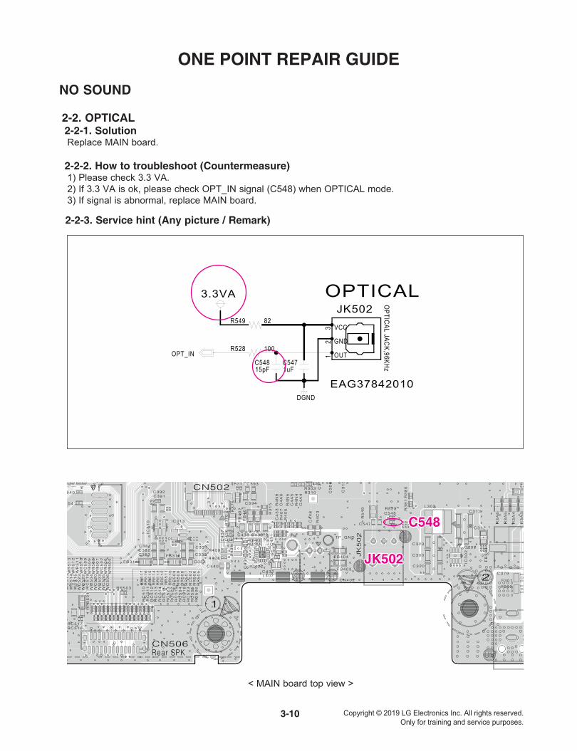
ONE POINT REPAIR GUIDE
NO SOUND
2-2. OPTICAL2-2-1. SolutionReplace MAIN board.
2-2-2. How to troubleshoot (Countermeasure)1) Please check 3.3 VA.2) If 3.3 VA is ok, please check OPT_IN signal (C548) when OPTICAL mode.3) If signal is abnormal, replace MAIN board.
2-2-3. Service hint (Any picture / Remark)
< MAIN board top view >
1
2
R4
05
R4
07
R 4 0 8
R 4 0 9
R3
A3
R3
A4
R3
A5
R3
A6
C N 4 0 2
X4
01
F 3 0 0
F 3 0 1
C4
31
C 4 3 2
C4
33
C4
34
C4
35
C4
36
C4
37
C 4 3 8 C 4 3 9
C 4 4 0
C4
46
L 3 0 2
F M
R R 5 0 3
RR
50
5R
R5
06
RR
50
7R
R5
08
RR
50
9
RR
51
0R
R5
11
RR
51
2R
R5
13
RR
51
4R
R5
15
RR
51
6R
R5
17
FB
30
3F B
R 3 0 3
F B 3 1 4
F B 3 1 6 JK
50
2
R 3 1 0
R3
15
RC
50
2R
C5
03
RC
50
4
RC
50
5R
C5
06
RC
50
9
RC
51
0R
C5
11
RC
51
2
CN502
RC
51
3R
C5
14
RC
51
5
R C 5 1 6
CN506
R C 5 1 7
RC
51
8
RC
51
9
R 5 2 8
RC
52
2R
C5
23
C 3 0 0
R4
C3
C 3 0 7
C3
08
C3
10
5 4 0
R 5 4 1
C 3 1 2
C 3 1 3
C3
1
R5
49
C4
A4
C 3 2 0
C4
A5
C4
A6
C 3 2 3C 3 3 1
C 3 3 3
R3
70
C 3 3 4
R 3 7 1
R3
75
R3
80
R3
81
T P _ G N D
C 5 4 7
C 5 4 8
WR
50
5W
R5
06
WR
50
7W
R5
08
WR
50
9
WR
51
0W
R5
11
WR
51
2W
R5
13
C 3 7 9
L4
06
L 4 0 7
C 3 8 1C 3 8 2
IC3
02
C 3 8 3
IC3
10
C 3 9 1
WC
50
2
C 3 9 2
C 3 9 3
I C 3 1 3
WC
50
3
C 3 9 4
WC
50
4
WC
50
5W
C5
06
WC
50
9
WC
51
3W
C5
14
WC
51
5
WC
51
9R
FB
50
1
WC
52
0
WC
52
2W
C5
23
R4
N4
FB
40
1
R4
N5
FB
40
2
F B 4 0 3
F B 4 0 4
R4
N8
I C 4 0 2
Rear SPK
OPTICAL JACK,96KHz
R528 100
3.3VA
OPT_IN
DGND
R549 82
C54815pF
C5471uF
JK502
EAG37842010
1 OUT
2 GND
3 VCC
OPTICAL
C548C548
JK502JK502

3-11 Copyright © 2019 LG Electronics Inc. All rights reserved.Only for training and service purposes.
USB_GND
USB5V
USB_N
C56910pF
NC
C57010pF
NC
USB_PUSB_P
USB_N
JK501
EAG62571101
1 5V
2 D-
3 D+
4 DGND
DGND
FL50012
3 4
C544100nF
DGND
USB_5V
D502D503
3 1
2
C54610uF
C545220uF
R5944.7
R5954.7
USB
ONE POINT REPAIR GUIDE
NO SOUND
2-3. USB2-3-1. SolutionReplace MAIN board.
2-3-2. How to troubleshoot (Countermeasure)1) Please check USB_5V at JK501 pin1.2) If soldering status and voltage has abnormal status, replace MAIN board.
2-3-3. Service hint (Any picture / Remark)
< MAIN board top view >
1
R 4 0 8
R 4 0 9
R 5 A 0R 5 A 1
R 5 A 2
R5
A6
R5
A7
OP
5
O P 6
OP
7
C4
37
C 4 4 0
Z D 5 1 1
Z D 5 1 2
FL
50
0
R R 5 0 3
RR
50
5R
R5
06
RR
50
7R
R5
08
RR
50
9
RR
51
0R
R5
11
RR
51
2R
R5
13
RR
51
4R
R5
15
RR
51
6R
R5
17
FB
30
6
FB
F B 3 1 4
FB
50
9
F B 3 1 6
R 5 0 7
R5
08
R5
09
R 3 1 9
RC
50
2R
C5
03
R 5 1 0
RC
50
4
RC
50
5
R5
12
RC
50
6
R5
14
RC
50
9
R 5 1 5
R5
16
R 5 1 9
RC
51
0R
C5
11
RC
51
2
CN50
RC
51
3
CN503
RC
51
4
CN504
RC
51
5
R C 5 1 6
CN506
R C 5 1 7
RC
51
8
RC
51
9
R 5 2 5
R 5 2 6
R 5 2 9
RC
52
2R
C5
23
R 5 3 1
R 5 3 2
R5
33
C 3 0 4
R5
34
R 5 4 0
R 5 4 1
C5
05
R 5 4 2
C 5 0 6
R 5 4 3
R 5 4 4
R 5 4 7R 5 4 8
C5
10
M C L K
C5
13
R5
50
R5
51
C 5 1 9
R5
55
R5
60
C 3 3 1
WF
B5
01
R5
62
C 3 3 3
R5
63
C 3 3 4
R5
64
R5
65
C3
35
R5
66
R5
68
R5
69
R 5 7 4
R 5 7 5R 5 7 6
O C P
R 5 7 8
R 5 7 9R 5 8 0
C 5 4 4
R 5 8 1
C 5 4 5
R 5 8 2
C 5 4 6
R 5 8 3
R 5 8 5R 5 8 6
W R 5 0 3
WR
50
5W
R5
06
WR
50
7W
R5
08
WR
50
9
C 5 5 2
C 5 5 5
C5
56
C5
57
WR
51
0
R5
94
WR
51
1
R5
95
WR
51
2
R5
96
WR
51
3
R5
97
WR
51
4
C3
68
R 5 9 8
WR
51
5
R 5 9 9
WR
51
6W
R5
17
D 5 0 2
D 5 0 3
C 5 6 9C 5 7 0
C 3 8 1C 3 8 2C 3 8 3
I C 3 0 3
IC3
0
C 3 8 7
C 3 8 8
IC3
10
C 3 9 1
WC
50
2
C 3 9 2
I C 3 1 3
WC
50
3
WC
50
4
WC
50
5W
C5
06
WC
50
9
WC
51
0W
C5
11
WC
51
2W
C5
13
WC
51
4W
C5
15
W C 5 1 6
W C 5 1 7
WC
51
8
WC
51
9R
FB
50
1
WC
52
0
WC
52
2W
C5
23
Rear SPKSubwoofer
JK501
JK501JK501

3-12 Copyright © 2019 LG Electronics Inc. All rights reserved.Only for training and service purposes.
ONE POINT REPAIR GUIDE
3. PROTECTION ERRORNo display or No Sound.
3-1. D(DC) PROTECTION3-1-1. SolutionReplace MAIN board.
3-1-2. How to troubleshoot (Countermeasure)1) Check DC Voltage of speaker out FL+/- (CN703 pin1, 2), FR +/- (CN704 pin1, 2, 3)2) Check resistor crack, cold solder of ESS IC out [FL+(R570), FL-(R571), FR+(R572), FR-(R573)].3) If ESS (IC501) out is ok and speaker out (FL+/-, FR+/-) has DC voltage replace MAIN board.
3-1-3. Service hint (Any picture / Remark)
< MAIN board top view >
MES
2
R3
A1
R3
A2
R3
A3
F R 2 +
R3
A4
R3
A5
F R 2 -
R3
A6
R5
A5
R 7 A 1
F L 2 +
F L 2 -
R7
C2
R7
C3
C 5 A 1
C 5 A 2
F 3 0 0
F 3 0 1
C 7 C 5
C 7 C 6
Q 3 0 0 Q 3 0 1
Z D 5 0 4
L 3 0 2
K E Y _ G
L709
L710
FB
30
3
JK
30
0
F B 3 1 3
F B 5 0 7
R C F 5 0 0
F B 5 0 8
C N 5 0 5
R 5 2 8
CN703
R3
38
CN704
R3
39
C 3 0 0
C 3 0 1C 3 0 7
C 5 0 3
C3
11
C 3 1 2
C 3 1 3
C3
15
C3
17
C 3 2 0
C 3 2 3
R3
65
R3
66
R3
80
R3
81
C3
47
C 3 4 8
R3
88
7
C 5 4 8
C 5 4 9
C3
55
C3
56
C 7 4 4
C 7 4 5
C 7 4 6
C7
47
D 3 0 0
C 7 5 8
C 7 5 9
R7
95
R7
96
R7
97
R7
98
C 3 7 8
C 3 7 9
D7
02
D7
03
C7
67
C7
68
IC3
02
I C 3 0 9
C7
71
C7
72
C7
73
C7
74
C 7 7 7
C3
90
C 7 7 8C 7 7 9
C7
80
C7
83
C7
84
C7
85
C7
86
K E Y _ T P
R
L
SL4 / SL4Y / SL4F MainEAX68408202 Ver1.1FR4-4L 1.2T 2018.12.06 261X67.5
CN703CN703
CN704CN704
3-13 Copyright © 2019 LG Electronics Inc. All rights reserved.Only for training and service purposes.
H:2
.55
mm
R7
A2
R7
A3
R 7 B 0
R7
B1
R 7 B 4
R7
B9
R7
C0
C7
A2
C7
A3
Z D
ZD
70
ZD
70
3
F R +
Q 7 0 8
Q 7 0 9
L7
09
L7
10
R3
0
R 3 0 1
R3
0
R 3 0 6
JK502
R3
07
F L +
F L -
R3
28
R7
15
R7
16
R3
3
C3
02
R3
40
C 3 0 6
R E M O _ T P
C7
07
C7
08
C 7 3 1
C7
36
C7
37
R7
74
C 7 3 8
C 3 5 1R 7 7 5
C 7 3 9
R 7 7 7
C7
41
R 7 8 2R 7 8 3R 7 8 4
R 7 8 5
C7
53
C7
54
C7
55
C7
56
IC7
03
ONE POINT REPAIR GUIDE
PROTECTION ERRORNo display or No Sound.
3-2. B(BURNT) PROTECTION3-2-1. SolutionReplace MAIN board.
3-2-2. How to troubleshoot (Countermeasure)1) Check voltage 12 V of IC703 at pin1 ~ 2, if 12V has problem refer to STEP 1-1.2) If 12 V is OK, replace MAIN board.
3-2-3. Service hint (Any picture / Remark)
IC703IC703
AMP_FAULT
C738 1uF
C736 100pF
R7A30
R782 100
C731 100nF
AMP_PROTECT
R775 47K
PGND
R783 NC
PGND
DC_PROTECTION
R702 27K
C739 1uF
PGND
R777 100
C730 1uF
R71547K
R703 10KZD702
Z02W3.9VNC
1
2
3C706 100pF
VCC33
IC703
26GND
1GVDD_AB
11GND
35OUT_B
3OC_ADJ
8DVDD
6INPUT_B
34GND
27OUT_D
33GND
7C_START
5INPUT_A
30PVDD_CD
9GND
28OUT_D
10GND
29PVDD_CD
4/RESET
31PVDD_CD
36PVDD_AB
2VDD
32OUT_C
12GND
25GND
13AVDD
14INPUT_C
23BST_D
24BST_C
15INPUT_D
22 GVDD_CD
16/FAULT
21 M3
17/OTW
18/CLIP
19 M120 M2
37PVDD_AB
38PVDD_AB
39OUT_A
40OUT_A
41GND
42GND
43BST_B
44BST_A
R7A2NC
ZD701KDZ13V-RTK/P
NC
C741 10uF
AMP_PDN
C737 1uF
R774 3.3
+12V
C708100pF
R7164.7K
C707100pF
R784 2.2K
ZD703Z02W3.9V
1
2
3
FL_OUT_N
FL_OUT_P
FR_OUT_P
FR_OUT_N
FR
ON
T L
FR
ON
T R
< MAIN board bottom view >

3-14 Copyright © 2019 LG Electronics Inc. All rights reserved.Only for training and service purposes.
ELECTRICAL TROUBLESHOOTING GUIDE
IC301 is not 3.3 VA
Check F301 Voltage 25 VA
Check FB305 Voltage 5.1 VA
Check Adapter
Replace Main PCB
YES
YES
YES
NO
NO
Check FB304 Voltage 12 VA
Check R308 Voltage 3.3 VA
Replace Main PCB
Replace Main PCB
YES
YES
NO
NO
OK
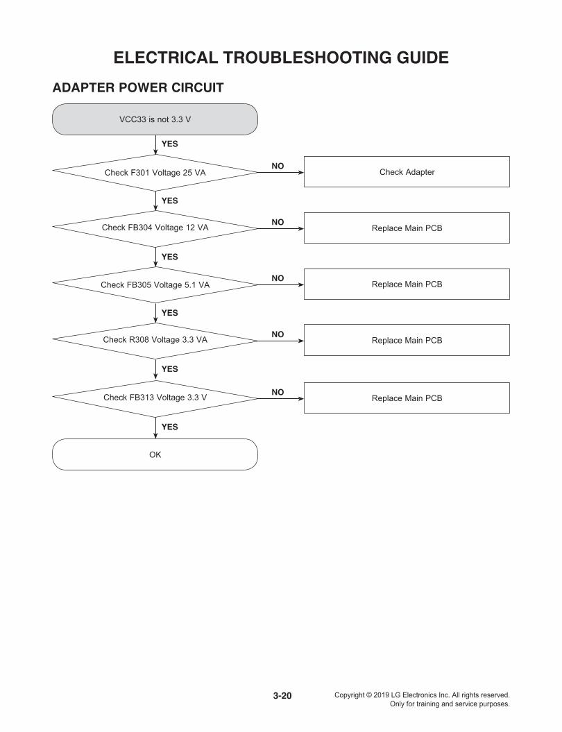
1. ADAPTER POWER CIRCUIT

3-15 Copyright © 2019 LG Electronics Inc. All rights reserved.Only for training and service purposes.
ELECTRICAL TROUBLESHOOTING GUIDE
ADAPTER POWER CIRCUIT
IC303 is not 1.3 VA
Check F301 Voltage 25 VA
Check FB305 Voltage 5.1 VA
Check Adapter
Replace Main PCB
YES
YES
YES
NO
NO
Check FB304 Voltage 12 VA
Check R314 Voltage 1.3 VA
Replace Main PCB
Replace Main PCB
YES
YES
NO
NO
OK

3-16 Copyright © 2019 LG Electronics Inc. All rights reserved.Only for training and service purposes.
ELECTRICAL TROUBLESHOOTING GUIDE
Q301 is not 12 V
Check F301 Voltage 25 VA Check Adapter
Replace Main PCB
NO
YES
NO
Check FB304 Voltage 12 VA
Check R774Voltage 12 V
Check Q301 2pinVoltage 12 V
Check IC302
YES
YES YES
NO
NO
OKOK
ADAPTER POWER CIRCUIT
YES

3-17 Copyright © 2019 LG Electronics Inc. All rights reserved.Only for training and service purposes.
ELECTRICAL TROUBLESHOOTING GUIDE
USB_5V is not 5 V
Check F301 Voltage 25 VA
Check FB305 Voltage 5.1 VA
Check Adapter
Replace Main PCB
YES
YES
YES
NO
NO
Check FB304 Voltage 12 VA
Check FB306 Voltage 5 V
Replace Main PCB
Replace Main PCB
YES
YES
NO
NO
OK
ADAPTER POWER CIRCUIT

3-18 Copyright © 2019 LG Electronics Inc. All rights reserved.Only for training and service purposes.
ELECTRICAL TROUBLESHOOTING GUIDE
Tuner is not 3.3 V
Check F301 Voltage 25 VA
Check FB305 Voltage 5.1 VA
Check Adapter
Replace Main PCB
YES
YES
YES
NO
NO
Check FB304 Voltage 12 VA
Check R311 Voltage 3.3 V
Replace Main PCB
Replace Main PCB
YES
YES
NO
NO
OK
ADAPTER POWER CIRCUIT

3-19 Copyright © 2019 LG Electronics Inc. All rights reserved.Only for training and service purposes.
ELECTRICAL TROUBLESHOOTING GUIDE
VD33ADAC_VD33AADC is not 3.3 V
Check F301 Voltage 25 VA
Check FB305 Voltage 5.1 V A
Check Adapter
Replace Main PCB
YES
YES
YES
NO
NO
Check FB304 Voltage 12 VA
Check FB311 Voltage 3.3 V
Replace Main PCB
Replace Main PCB
YES
YES
NO
NO
OK
ADAPTER POWER CIRCUIT
3-20 Copyright © 2019 LG Electronics Inc. All rights reserved.Only for training and service purposes.
ELECTRICAL TROUBLESHOOTING GUIDE
VCC33 is not 3.3 V
Check F301 Voltage 25 VA
Check FB305 Voltage 5.1 VA
Check Adapter
Replace Main PCB
YES
YES
YES
NO
NO
Check FB304 Voltage 12 VA
Check R308 Voltage 3.3 VA
Replace Main PCB
Replace Main PCB
YES
YES
NO
NO
Check FB313 Voltage 3.3 V Replace Main PCB
YES
NO
OK
ADAPTER POWER CIRCUIT

3-21 Copyright © 2019 LG Electronics Inc. All rights reserved.Only for training and service purposes.
ELECTRICAL TROUBLESHOOTING GUIDE
ADAPTER POWER CIRCUIT
WL_3V3 is not 3.3 V
Check F301 Voltage 25 VA
Check FB305 Voltage 5.1 VA
Check Adapter
Replace Main PCB
YES
YES
YES
NO
NO
Check FB304 Voltage 12 VA
Check R308 Voltage 3.3 VA
Replace Main PCB
Replace Main PCB
YES
YES
NO
NO
Check FB314 Voltage 3.3 V Replace Main PCB
YES
NO
OK

3-22 Copyright © 2019 LG Electronics Inc. All rights reserved.Only for training and service purposes.
ELECTRICAL TROUBLESHOOTING GUIDE
ADAPTER POWER CIRCUIT
RBOX_3V3 is not 3.3 V
Check F301 Voltage 25 VA
Check FB305 Voltage 5.1 VA
Check Adapter
Replace Main PCB
YES
YES
YES
NO
NO
Check FB304 Voltage 12 VA
Check R308 Voltage 3.3 VA
Replace Main PCB
Replace Main PCB
YES
YES
NO
NO
Check FB316 Voltage 3.3 V Replace Main PCB
YES
NO
OK

3-23 Copyright © 2019 LG Electronics Inc. All rights reserved.Only for training and service purposes.
ELECTRICAL TROUBLESHOOTING GUIDE
KEY PART
Replace the Cable1
Check R520 Pull-up Resistor
YES
Check CN505 1, 2 pinVoltage 3.3 V Check the connecting cables
Check RA01, RA04, RA05, RA06
Replace the Key PCB
YES
NO
Check SWA01, SWA02, SWA03, SWA04
OK
YES YES
NO
NO
OK
2. KEY PART

3-24 Copyright © 2019 LG Electronics Inc. All rights reserved.Only for training and service purposes.
ELECTRICAL TROUBLESHOOTING GUIDE
USB PART
Refer to Power Part Troubleshooting
Check JK501 1pin Voltage 5.1 V
YES
Check FB306 Voltage 5.1 V Check IC306
Check JK501 pin2(D-), pin3(D+)
Replace Main PCB
YES
NO
Check Reading OK
IC501 pin35, pin36
YES YES
NO
NO
OK
3. USB FUNCTION

3-25 Copyright © 2019 LG Electronics Inc. All rights reserved.Only for training and service purposes.
ELECTRICAL TROUBLESHOOTING GUIDE
OPTICAL FUNCTION
Refer to Power Part Troubleshooting
Check IC501 pin65Input waveform Check C511
Replace Main PCB
YES
NO
OK
4. OPTICAL FUNCTION
Replace Main PCB
Check R549 3.3VA Voltage
YES
Check JK502 Check R528
YES YES
NO
NO

3-26 Copyright © 2019 LG Electronics Inc. All rights reserved.Only for training and service purposes.
WAVEFORMS OF MAJOR CHECK POINT
1. CRYSTAL 2. FLASH MEMORY
FIG 1. X500 (27 MHz)
1
4
35
2
C550100nF
DGND
DGND
SF_CS
R559
0 OHM(1)NC
R552
0 OHM(1)
IC504
1CS#
2SO
3WP#
4VSS
5SI
6SCLK
7HOLD#
8VCC
R53610K
R539
10K
R53710K
R53810K
FB504PZ1608U221-1R4TF
3.3VA
For DSP(2MB)
1
R518510K
X50027MHz
1 IN/OUT 2FLOAT
3IN/OUT4 FLOAT
DGND
C51810pF
C51710pF
R556 0
R557 100
FIG 2. VCC, CS#, CLK, DO
2
3
4
5
VCC
CS#
CLK
DO
3-27 Copyright © 2019 LG Electronics Inc. All rights reserved.Only for training and service purposes.
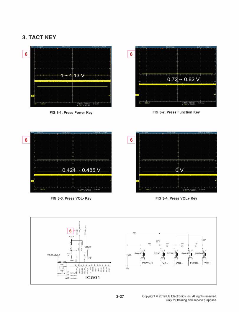
3. TACT KEY
FIG 3-2. Press Function Key
0.72 ~ 0.82 V
FIG 3-1. Press Power Key
1 ~ 1.13 V
6 6
FIG 3-3. Press VOL- Key FIG 3-4. Press VOL+ Key
0.424 ~ 0.485 V 0 V
6 6
6
VD33ADAC
C526 10uF
R5214.7K
R553
100
R567
0 NC
R58810K
C5641nF
R530
0
R519
47K
KEY
AMP_
CLIP
0
IC501
84RE
SET_
B
85SP
I_CS
2
86SP
I_CS
3
87SP
I_CL
K
88SP
I_DI
89SP
I_DO
90SP
I_W
P
91SP
I_HO
LD
92SP
DIF_
OUT
93SY
S_AD
C_A
94SY
S_AD
C_B
95SY
S_AD
C_C
96SY
S_AD
C_D
97PWM_VREF
98VD33ADAC
99VS33ADAC
DGND
VD33
3.3VA
DC_P
ROTE
CTIO
N
R520
4.7K
R554
100
DGND
RA01
680
RA03
1K
RA02
820
RA00
CA00100nF
SWA00
1 2
3 4
SWA01
1 2
3 4
SWA02
1 2
3 4
SWA03
1 2
3 4
SWA04
1 2
3 4
RA04
RA05750
RA06820
POWER FUNC.VOL+ VOL- WIFI

3-28 Copyright © 2019 LG Electronics Inc. All rights reserved.Only for training and service purposes.
4. USB
FIG 4-1. USB 5 V FIG 4-2. USB D+
7 8
FIG 4-3. USB D-
9
98
7
USB_GND
USB5V
USB_N
USB_P
JK5011 5V
2 D-
3 D+
4 DGNDC544100nF
DGND
USB_5V
D502D503
3 1
2
C54610uF
C545220uF
USB

3-29 Copyright © 2019 LG Electronics Inc. All rights reserved.Only for training and service purposes.
5. REMOTE CONTROL
FIG 5-1. Input Voltage
10
FIG 5-2. Low Timing
11
Item Measured Spec.
Input Level 3.3 V IR Receiver Spec: 2.7 ~ 5.5 V
“ Low” Timing 4.4 ms 3.6 ms ~ 5.04 ms
“ High” Timing 4.48 ms 4.08 ms ~ 5.04 msFIG 5-3. High Timing
12
1110
12
IR RECEIVER
REMOCON
DGND
C5A1100nF
R5A5100
C549100pF
3.3VA
C5A210uF
ZD504Z02W3.9V
12
3
RCF500
1G
ND
2VC
C3
OUT
4
GND
REMO_TP

3-30 Copyright © 2019 LG Electronics Inc. All rights reserved.Only for training and service purposes.
14
13
1.3VA
R525
33
C511 10nF
R542
100
R544
100
R545
100
R546
100
R547
100
R551 100
R550 100
C555NC
675RK2.2
575RK2.2
385RK2.2 NC
R578
100
R526
47K
OPT_IN
R548
100
AMP_
PRO
TECT
AMP_FAULT
AMP_PDN
LCD_
DAT
LCD_
STB
P_CT
RL
WL_
P_CT
RL_W
F
REM
OCO
N
UART
_RX
UART
_TX
IC50160
SR[16]
61SR[17]
62SR[22]
63SR[23]
64SR[24]
65SR
[25]
66SR
[26]
67AU
X[7]
68AU
X[6]
69AU
X[5]
70AU
X[4]
71VD
33
72SR
[10]
73SR
[11]
74O
P[16
]
75AU
X[3]
76AU
X[2]
77AU
X[1]
78AU
X[0]
79VD
3318
80VS
S33/
VSS
81VD
3318
82VD
33
83VD
D
VD33
R527 3.9KOPT_DET
R514 100
R566 100
WL_INT_RR
WL_MSG_RDY_RR
R515
100
LCD_
RST
LCD_
CD
LCD_
CLK
LCD_
BL
R516 100 TUNER_P_CTRL
R574
100
R529
100
6. OPTICAL
FIG 6-1. OPT IN
13
FIG 6-2. OPT DET
14

3-31 Copyright © 2019 LG Electronics Inc. All rights reserved.Only for training and service purposes.
15
TGND
R409 100
X40132.768KHZ
R4N8 100
TGND
IC402
1 NC2 FMI3 RFGND4 LPI5 RST
6
SEB
7
SCLK
8
SDIO
10
VD
11VA
12GND
13ROUT/[DOUT]
15DOUT
16
DFS
9
RCLK
14LOUT/[DFS]
17
GPO
3/[D
CLK]
18
GPO
2/[IN
T]
19
GPO
1
20
NC
C433 10nF
TGND
TUNER_3V3
C4A633pF
TUNER_DAT
TUNER_R
C43722pF
TUNER_CLK
FB401PZ1608U221-1R4TF
FB403TUNER
220ohm
DGND
R4C3 0
R407 10K
D401KDS226
1 C
2 AC
3A
TGND
TGND
TGND
C4A433pF
TGND
TUNER_RST
DGND
R408 100
C43810uFTGND
FB404TUNER
220ohm
C436100nF
TUNER_CER4N4 100 TGND
C434100nF
CN402
EAG64749901YAW025-02
1TGND2FM_ANT
DGND
C4322.7pF
L40756NH
C4A533pF
FB402PZ1608U221-1R4TF
FM_ANT
DGND
TGND
C446 1uF TUNER
C43522pF
R4N5 100
C440 1uF TUNER
L40656NH
TGND
C4311nF
TGND
R4051K
DGND
C43910uF
TUNER_L
FM
TP_GND
EAX68098001
Close to pin
FM TUNER
Close to pin
Close to pin
Reference PCB
7. FM
FIG 7. TUNER AUDIO
1.27 Vrms11111111111111111111111111111111111111111111111111111111111111111111111111111111111111111111111111111111111111111111111111111111111111111111111111111111111111111111111111111111111111111111.2222222222222222222222222222222222222222222222222222222222222222222222222222222222222222222222222222222222222222222222222222222222222222222222222222222222222222222222222222222222222222222222222227777777777777777777777777777777777777777777777777777777777777777 VVVVVVVVVVVVVVVVVVVVVVVVVVVVVVVVVVVVVVVVVVVVVVVVVVVVVVVVVVVVVVVVVVVVVVVVVVVVVVVVVVVVVVVVVVVVVVVVVVVVVVVVVVVVVVVVVVVVVVVVVVVVVVVVVVVVVVVVVVVVVVVVVVVVVVVVVVVVVVVVVVVVVVVVVVVVVVVVVVVVVVVVVVVVVVVVVVVVVVVVVVVVVVVVVVVVVVVVVVVVVVVVVVVVVVVVVVVVVVVVVVVVVVVVVVVVVVVVVVVVVVVVVVVVVVVVVVVVVVVVVVVVrrrrrrrrrrrrrrrrrrrrrrrrrrrrrrrrrmmmmmmmmmmmmmmmmmmmmmmmmmmmmmmmmmmmmmmmmmmmmmmmmmmmmmmmmmmmmmmmmmmmmmmmmmmmmmmmmmmmmmmmmmmmmmmmmmmmmmmmmmmmmmmmmmmmmmmmmmmmmmmmmmmmmmmmmmmssssssssssssssssssssssssssssssssssssssssssssssssssssssssssssssssssssssssssssssssssssssssssssssssssssssssssssssssssssssssssssssssssssssssssssssssssssssssssssssssssssssssssssssssssssssssssssssssssssssssssssssssssssssssssssssssssssssssssssssssssss
15

3-32 Copyright © 2019 LG Electronics Inc. All rights reserved.Only for training and service purposes.

Copyright © 2019 LG Electronics Inc. All rights reserved.Only for training and service purposes.
3-343-33
CIRCUIT VOLTAGE CHART
IC Sym Pin Spec Measured Voltage
IC300DC,DC
Vin: 1 SW: 2
Vin: 4.2 V ~ 17 V VOUT: 0.8 V ~ 10 V
Vin: 12.02 V VOUT: 5.20 V
IC301DC,DC
Vin: 4 SW: 3
Vin: 2.7 V ~ 5.5 V VOUT: 0.6 V ~ 5.225 V
Vin: 5.21 V VOUT: 3.44 V
IC302DC-DC
VIN: 2VOUT: 3
Vin: +4.0 V ~ +36 V Vout: 0.8 V ~ 33 V
Vcc: 25.42 V Vout: 12.02 V
IC303DC,DC
Vin: 4 SW: 3
Vin: 2.7 V ~ 5.5 V VOUT: 0.6 V ~ 5.225 V
Vin: 5.22 V VOUT: 1.41 V
IC306 Switch IC
Vin: 5 Vout: 1
Vin: 2.5 V ~ 5.5 V out: 0 V ~ 5.5 V
Vin: 3.38 V out: 3.36 V
IC309 Switch IC
Vin: 5 Vout: 1
Vin: 2.5 V ~ 5.5 V out: 0 V ~ 5.5 V
Vin: 3.38 V out: 3.36 V
IC310 Switch IC
Vin: 5 Vout: 1
Vin: 2.5 V ~ 5.5 V out: 0 V ~ 5.5 V
Vin: 3.34 V out: 3.33 V
IC311 LDO IC
Vin: 1Vout: 5 Vin: 2.3 V ~ 6 V Vin: 5.24 V
Out: 3.43 V
IC312 LDO IC
Vin: 1Vout: 5 Vin: 2.3 V ~ 6 V Vin: 5.22 V
Out: 3.4 V
IC313 Switch IC
Vin: 5 Vout: 1
Vin: 2.5 V ~ 5.5 V out: 0 V ~ 5.5 V
Vin: 3.34 V out: 3.33 V
IC500RESET
VCC: 3 VCC: 1.0 V ~ 7 V VCC: 3.35 V
IC501MAIN DSP
VDD : 20, 52, 83VDDAADC : 121
VD33 : 7,18,25,54,71,79,81,82VD33PLL : 41VD33USB : 37
VD33ADAC : 98, 116VD33AADC : 126
VDD : 1.3 V ± 5 % VDDAADC : 1.3 V ± 5 %
VD33 : 3.3 V ± 5 % VD33PLL : 3.3 V ± 5 % VD33USB : 3.3 V ± 5 %
VD33ADAC : 3.3 V ± 5 % VD33AADC : 3.3 V ± 5 %
VDD : 1.34 V VDDAADC : 1.35 V
VD33 : 3.33 V VD33PLL : 3.33 V VD33USB : 3.33 V
VD33ADAC : 3.31 V VD33AADC : 3.26 V
IC503SERIAL FLASH
MEMORYVCC: 8 VCC: 2.7 V ~ 3.6 V VCC: 3.30 V
IC504SERIAL FLASH
MEMORYVCC: 8 VCC: 2.7 V ~ 3.6 V VCC: 3.34 V
IC505SERIAL FLASH
MEMORYVCC: 8 VCC: 2.7 V ~ 3.6 V VCC: 3.37 V
IC703AMP
GVDD_AB: 1GVDD_CD: 22
PVDD_AB: 36,37,38PVDD_CD: 29,30,31
VDD: 2DVDD: 8AVDD: 13
GVDD_AB: -0.3 V ~ 13.2 V GVDD_CD: -0,3 V ~ 13.2 V
PVDD_AB: -0.3 V ~ 50 V PVDD_CD: -0.3 V ~ 50 V
VDD: -0.3 V ~ 13.2 V DVDD: -0.3 V ~ 4.2 V AVDD: -0.3 V ~ 8.5 V
GVDD_AB: 11.9 V GVDD_CD: 11.9 V PVDD_AB: 25.5 V PVDD_CD: 25.5 V
VDD: 11.9 V DVDD: 3.32 V AVDD: 7.76 V
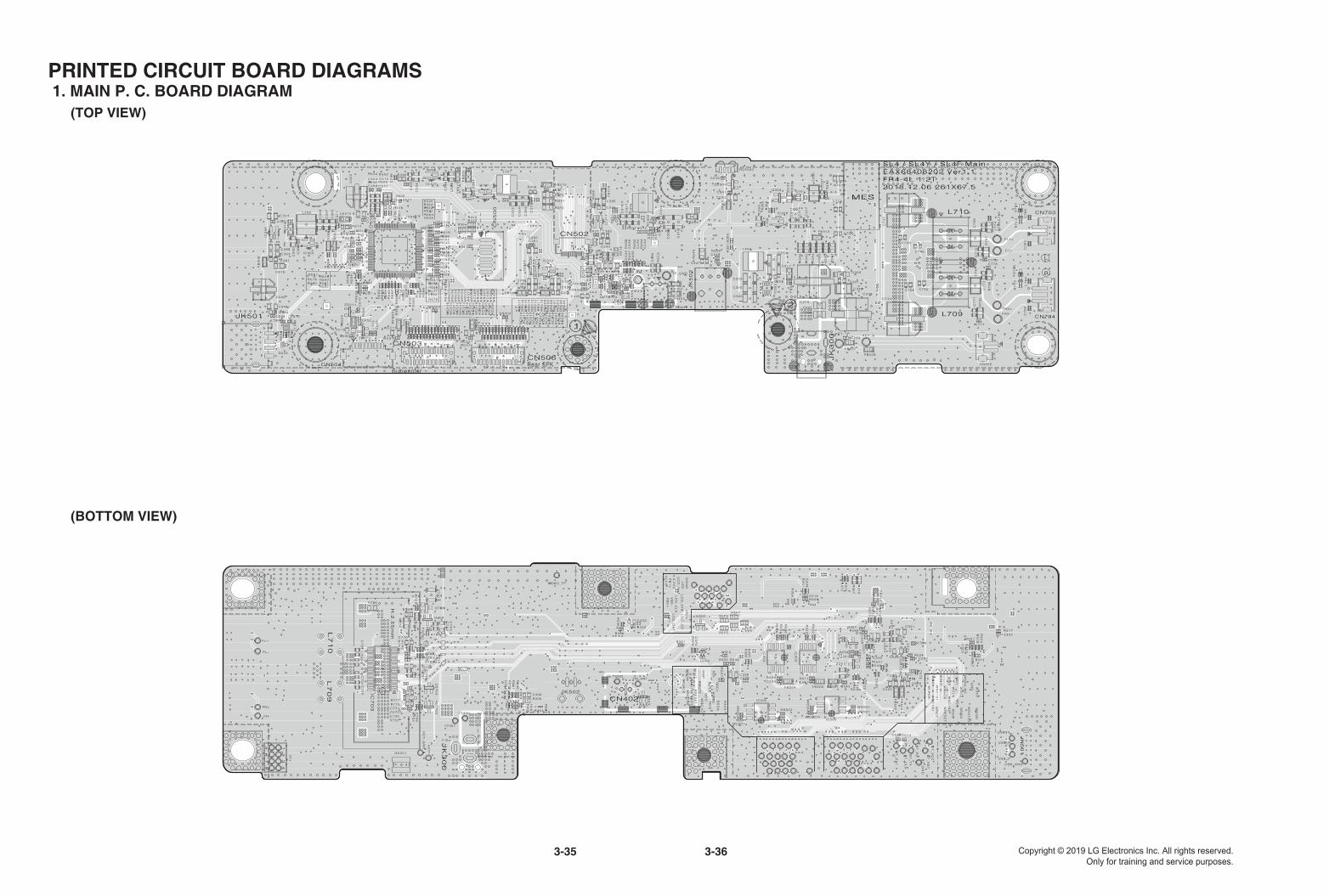
Copyright © 2019 LG Electronics Inc. All rights reserved.Only for training and service purposes.
MES
1
2
R4
05
R4
07
R 4 0 8
R 4 0 9
R3
A1
R3
A2
R3
A3
F R 2 +
R3
A4
R3
A5
F R 2 -
R3
A6
R 5 A 0R 5 A 1
C N 4 0 2
R 5 A 2
R 5 A 3R 5 A 4
R5
A5
R5
A6
R5
A7
R 7 A 1
F L 2 +
OP
5
F L 2 -O P 6
OP
7
R7
C2
R7
C3
X4
01
C 5 A 1
C 5 A 2
F 3 0 0
F 3 0 1
C4
31
C 4 3 2
C4
33
C4
34
C4
35
C4
36
C4
37
C 4 3 8 C 4 3 9
C 4 4 0
C4
46
C 7 C 5
C 7 C 6
Q 3 0 0 Q 3 0 1
Z D 5 0 4
L 3 0 0
L 3 0 1
Z D 5 1 1
L 3 0 2
Z D 5 1 2
L 3 0 8
F M
K E Y _ G
FL
50
0
L709
L710
R R 5 0 3
RR
50
5R
R5
06
RR
50
7R
R5
08
RR
50
9
RR
51
0R
R5
11
RR
51
2R
R5
13
RR
51
4R
R5
15
RR
51
6R
R5
17
FB
30
3
F B 3 0 4
FB
30
5
FB
30
6
JK
30
0
FB
31
0
F B 3 1 3R 3 0 3
F B 5 0 7
R C F 5 0 0
F B 3 1 4
F B 5 0 8
FB
50
9
F B 3 1 5
F B 3 1 6 JK
50
2
FB
31
7
FB
31
8R 3 0 8
R 3 1 0
R 5 0 5R 5 0 6
R 3 1 2
R 5 0 7
R 3 1 4
R5
08
R3
15
R5
09
R 3 1 9
RC
50
2R
C5
03
R 5 1 0
RC
50
4
RC
50
5
R5
12
RC
50
6
R5
14
RC
50
9
R 5 1 5
R5
16
R 5 1 8
R 5 1 9
R 3 2 7
RC
51
0
CN
50
0
RC
51
1R
C5
12
CN502
RC
51
3
CN503
RC
51
4
CN504
R 5 2 0
RC
51
5
C N 5 0 5
R 5 2 1
R C 5 1 6
CN506
R C 5 1 7
RC
51
8
RC
51
9
R 5 2 5
R 5 2 6
R 5 2 8
R 5 2 9
CN703
R3
38
CN704
R3
39
RC
52
2R
C5
23
C 3 0 0
R 5 3 0
C 3 0 1
R 5 3 1
R 5 3 2
R4
C3
R5
33
C 3 0 4
R5
34
C3
05
R 5 3 5
C 3 0 7
C3
08
C3
09
C5
02
C 5 0 3
C3
10
R 5 4 0
C3
11
R 5 4 1
C5
05
C 3 1 2
R 5 4 2
C 5 0 6
C 3 1 3
R 5 4 3
C3
14
C 5 0 8
R 5 4 4
C3
15
C 5 0 9
C3
16
C3
17
R 5 4 7
C3
18
R 5 4 8
C3
19
R5
49
X 5 0 0
C5
10
M C L K
C5
13
C4
A4
C 3 2 0
R5
50
C4
A5
C 5 1 5
C3
21
R5
51
C4
A6
C3
22
R 5 5 2
C 3 2 3
C 5 1 7
R 5 5 3
C 3 2 4
C 5 1 8
R 5 5 4
C 5 1 9
R5
55
C3
26
R5
56
C 3 2 7
R5
57
C3
29
R3
65
R 5 5 9
R3
66
R3
68
R5
60
C 3 3 0
C 3 3 1
WF
B5
01
R 5 6 1
R5
62
C 3 3 3
R5
63
R3
70
C 3 3 4
R5
64
R 3 7 1
R5
65
C3
35
R5
66
C3
37
R5
68
R3
75
C3
39
R5
69
R 5 7 4
R3
80
R3
81
R 5 7 5R 5 7 6
C3
47
O C P
C 3 4 8
R 5 7 8
T P _ G N D
R 5 7 9
R3
88
R 5 8 0
C 5 4 4
R 5 8 1
C 5 4 5
R 5 8 2
C 5 4 6
R 5 8 3C 5 4 7
C3
54
R 5 8 4
C 5 4 8
C 5 4 9
C3
55
R 5 8 5
C3
56
R 5 8 6
W R 5 0 3
WR
50
5W
R5
06
R 3 9 6
WR
50
7W
R5
08
C 7 4 4
WR
50
9
C 7 4 5
C 5 5 2
C 7 4 6
C 5 5 3
C7
47
D 3 0 0
D3
01
C 5 5 5
C5
56
C5
57
WR
51
0
R5
94
C3
64
WR
51
1
R5
95
C3
65
WR
51
2
R5
96
WR
51
3
C3
67
R5
97
WR
51
4
C3
68
R 5 9 8
WR
51
5
R 5 9 9
WR
51
6W
R5
17
D 5 0 2
D 5 0 3
C3
70
C 5 6 4
C 7 5 8
C3
71
C 7 5 9
R7
95
R7
96
R7
97
R7
98
C 5 6 9
C 3 7 8
C 3 7 9
D7
02
D7
03
C 5 7 0
L4
06
L 4 0 7
C7
67
IC3
00
C7
68
C 3 8 1
I C 3 0 1
C 3 8 2
IC3
02
C 3 8 3
I C 3 0 3
C 5 7 7
IC3
06
C 3 8 7
C 3 8 8
I C 3 0 9
C7
71
C7
72
C7
73
C7
74
I C 5 0 1
C 7 7 7
C3
90
IC3
10
C 7 7 8
IC3
11
C 3 9 1
C 7 7 9
WC
50
2
I C 3 1 2
C 3 9 2
C 3 9 3
I C 3 1 3
WC
50
3
C 3 9 4
WC
50
4
C 5 8 8
C 3 9 5
WC
50
5W
C5
06
C3
96C
39
8
C7
80
WC
50
9
C7
83
C7
84
C7
85
C7
86
WC
51
0W
C5
11
WC
51
2W
C5
13
WC
51
4W
C5
15
W C 5 1 6
W C 5 1 7
WC
51
8
K E Y _ T P
WC
51
9R
FB
50
1
WC
52
0
WC
52
2W
C5
23
R4
N4
FB
40
1
R4
N5
FB
40
2
F B 4 0 3
F B 4 0 4
R4
N8
R
L
SL4 / SL4Y / SL4F MainEAX68408202 Ver1.1FR4-4L 1.2T 2018.12.06 261X67.5
R 5 F 2
R 5 F 1
C 5 F 2
C 5 F 1
F B 5 1 0
I C 4 0 2
Rear SPKSubwoofer
JK501
1
8
23
4
76
5
H:2
.55
mm
KE
Y_
GN
D
RD
AT
A2R
MU
TE
DG
ND
WR
DY
U S B _ N
U S B _ P
CN402
LC
D_
ST
B
RR
DY
R7
A2
R7
A3
T G N D
R 7 B 0
R7
B1
R 7 B 4
BT
_R
ST
R7
B9
WL
RC
K
R7
C0
T P 3 0 0
T P 3 0 1
LE
D+
LE
D-
C7
A2
C7
A3
BT
_C
LK
WR
ES
ET
RC
S
WD
A2
_W
F
BT
_G
ND
RD
I
Z D 5 0 1
RD
O
BT
_R
X
Z D 7 0 1
ZD
70
2Z
D7
03
C 5 F 3
LC
D_
CD
F R +
RIN
IT
Q 7 0 8
Q 7 0 9
F R -
F M _ A N T
BT
_T
X
BT
_D
AT
WM
UT
E
L7
09
L7
10
R R 5 0 1
R R 5 0 2
RR
50
4
WN
C1
00
WN
C1
01
WN
C1
02
WN
C1
05
WN
C1
06
WN
C1
07
JK
30
0
F B 5 0 1
FB
50
2
FB
50
3
WW
P
RR
ES
ET
F B 5 0 4
R3
00
FB
31
1
F B 5 0 5
R 3 0 1
R 3 0 2
WS
CL
R 3 0 4
3.3
VA
R3
05
R 3 0 6
JK502
R3
07
WS
DA
R 3 0 9
R 3 1 1
R 3 1 3
R 3 1 6
R 3 1 7
RS
CL
R3
18
R C 5 0 1R 7 0 2
R7
03
RS
DA
R 5 1 1
F L +R 3 2 1
F L -
R3
22
R3
23
LC
D_
RS
T
LC
D_
DA
T
R3
28
R7
15
R5
22
R7
16
R5
23
R 5 2 4
WC
LK
R 5 2 7
R3
35
C3
02
C 3 0 3
R3
40
C 3 0 6
R5
36
R5
37
R5
38
R 5 3 9
R3
46
RC
LK
BT
_V
CC
C5
00
C 5 0 1
LC
D_
CL
K
R E M O _ T P
R 3 5 1
R5
45
R5
46
R 3 5 5
R3
56
R3
57
TP
1
C5
11
C7
06
W3
V3
C7
07
C 5 1 4
C7
08
C3
25
C3
28
WG
ND
R 5 5 8
R3
67
C5
20
C 5 2 1
C 5 2 2
C 5 2 3
VL
CD
C5
24
C5
25
C 3 3 2
C 5 2 6
R3
V3
C5
27
C5
28
C 5 2 9
R3
72
U S B 5 V
R3
73
R 5 6 7
WIN
IT
R3
74
RG
ND
C5
30
C5
31
C5
32
C5
33
R5
70
C5
34
C5
35
R5
71
C5
36
R5
72
C 5 3 7
R5
73
C 5 3 8
C5
39
C 7 3 0
C 7 3 1
R3
87
C 5 4 0C 5 4 1
C 5 4 2
C7
36
C 5 4 3
C7
37
R7
74
C 7 3 8
C 3 5 1R 7 7 5
C 7 3 9
RL
RC
K
R 7 7 7
W R 5 0 1
R3
91
W R 5 0 2
R3
92
WR
50
4
R 5 8 8
KE
Y
C7
41
WD
AT
A2
WB
CK
C 5 5 0
G S 3 0 1
C 5 5 1
R 7 8 2R 7 8 3R 7 8 4
R 7 8 5
C7
53
C 5 6 0
C7
54
C 5 6 1
C7
55
C7
56
RB
CK
C5
65
C 5 6 7
WC
S
C5
73 W
DI
WD
O
IC5
00
IC5
03
IC5
04
W C 5 0 1I C 5 0 5
I C 5 0 6
C 3 9 7
U S B _ G N D
IC7
03
VB
0+
RW
P
VB
0-
VB
1+
VB
1-
GN
D
C 5 F 6
C 5 F 4
C5
F5
R5
F8
R 5 F 7R 5 F 6
R 5 F 5R 5 F 4 R 5 F 3
Q 5 0 2
C 3 3 6C 3 3 8
D 4 0 1
JK
50
1
3-363-35
PRINTED CIRCUIT BOARD DIAGRAMS 1. MAIN P. C. BOARD DIAGRAM (TOP VIEW)
(BOTTOM VIEW)

Copyright © 2019 LG Electronics Inc. All rights reserved.Only for training and service purposes.
3-383-37
NC
VOL+
VOL-
POWER
FUCN
EAX68503501 VER1.3 SL4/SL5 KEY BOARDFR4-2L 1.2T 2018.12.07 PCB SIZE:40.6X30
TP
A0
0
TP
A0
1
S W A 0 0
SW
A0
1S
WA
02
SW
A0
3S
WA
04
RA
00
RA
01
RA
02
RA
03
RA
04
RA
05
RA
06
CA
00
C N A 0 0
2. KEY P. C. BOARD DIAGRAM (TOP VIEW) (BOTTOM VIEW)

Copyright © 2019 LG Electronics Inc. All rights reserved.Only for training and service purposes.
3-403-39

4-1 Copyright © 2019 LG Electronics Inc. All rights reserved.Only for training and service purposes.
SECTION 4
WIRELESS SUBWOOFER PART
CONTENTS
ONE POINT REPAIR GUIDE ............................................................................................................................ 4-21. NO POWER PROBLEM (PVDD) ............................................................................................................ 4-22. POWER ON ERROR .............................................................................................................................. 4-33. POWER ON ERROR .............................................................................................................................. 4-44. WIRELESS CONNECTION .................................................................................................................... 4-5
WAVEFORMS OF MAJOR CHECK POINT ...................................................................................................... 4-61. VOLTAGE ............................................................................................................................................... 4-62. AMP VOLTAGE ...................................................................................................................................... 4-73. PWM ....................................................................................................................................................... 4-84. LED ......................................................................................................................................................... 4-9
WIRING DIAGRAM .......................................................................................................................................... 4-11
BLOCK DIAGRAM .......................................................................................................................................... 4-13
PRINTED CIRCUIT BOARD DIAGRAMS ....................................................................................................... 4-151. WOOFER SMPS P. C. BOARD ............................................................................................................ 4-152. WOOFER AMP P. C. BOARD .............................................................................................................. 4-173. WOOFER KEY P. C. BOARD ............................................................................................................... 4-17

4-2 Copyright © 2019 LG Electronics Inc. All rights reserved.Only for training and service purposes.
ONE POINT REPAIR GUIDE
1. NO POWER PROBLEM (PVDD)No power problem occurs when you power on the unit
1-1. SolutionIf you check these points and find PVDD voltage is not checked, replace woofer SMPS board.
1-2. Service hint (Any picture / Remark)
< Woofer AMP board bottom view >
< Woofer AMP board top view >
PVDDPVDDpin3, 4, 5, 6 at WCN601pin3, 4, 5, 6 at WCN601
PVDDPVDDpin7 at WIC606pin7 at WIC606Nearby WC610Nearby WC610
PVDDPVDDpin7 at WIC607pin7 at WIC607Nearby WC686Nearby WC686
PVDD PVDD at WCA601at WCA601

4-3 Copyright © 2019 LG Electronics Inc. All rights reserved.Only for training and service purposes.
ONE POINT REPAIR GUIDE
2. POWER ON ERRORFundamental power check points
2-1. 12 V1) Check 12 V at WL604 nearby WL603 coil.2) If 12 V is not checked at the point, then find PVDD at pin7 of WIC606.3) 1), 2) is NG Replace WIC606.
If you can’t check PVDD voltage, then you replace woofer SMPS board.
2-2. 3.7 VA1) Check 3.7 VA at WL606 coil.2) If 3.7 VA is not checked at the point, then find PVDD at pin7 of WIC607.3) 1), 2) is NG Replace WIC607.
If you can’t check PVDD voltage, then you replace woofer SMPS board.
< Woofer AMP board top view >
< Woofer AMP board top view >
12 V 12 V at WL604at WL604
PVDDPVDDat pin7 of WIC606at pin7 of WIC606
3.7 VA 3.7 VA at WL606at WL606
PVDDPVDDat pin7 of WIC607at pin7 of WIC607

4-4 Copyright © 2019 LG Electronics Inc. All rights reserved.Only for training and service purposes.
ONE POINT REPAIR GUIDE
3. POWER ON ERRORMAIN SoC IC supply voltage check points
3-1. 3.3 VA1) Check 3.3 VA at WCA603 and WL627.2) Check 3.3V_PWM at pin5 of WIC605.3) Check 3.3 VA at pin7, 8 of WIC603.4) Check 3.3V_PWM at WL615 nearby WIC601.
If all voltages are OK, then check the PVDD voltage of woofer SMPS board.
< Woofer AMP board top view >
3.3V_PWM3.3V_PWMat WL615at WL615
3.3 VA 3.3 VA at WCA603, WL627at WCA603, WL627
3.3 VA 3.3 VA at pin7, 8 of WIC603at pin7, 8 of WIC603
3.3V_PWM3.3V_PWMat pin5 of WIC605at pin5 of WIC605

4-5 Copyright © 2019 LG Electronics Inc. All rights reserved.Only for training and service purposes.
ONE POINT REPAIR GUIDE
4. WIRELESS CONNECTIONWireless connection malfunction
4-1. 3.3 VA1) Check 3.3 VA at WL616.
4-2. Connection1) Wireless module connection closely.2) Implement Wireless Factory Reset. MAIN SET : Soundbar vol MIN and push Mute key (sustain 3 ~ 5 sec). Subwofer : Push Pairing key on the back case of the wireless subwoofer. The LED of of the wireless subwoofer blink red and green, pull out power cord. The main set and the wireless subwoofer are factory reset mode, then power on.
< Woofer KEY board top view >
< Woofer AMP board top view >
3.3 VA3.3 VAat WL616at WL616
Wireless moduleWireless moduleConnection checkConnection check
Pairing keyPairing key

4-6 Copyright © 2019 LG Electronics Inc. All rights reserved.Only for training and service purposes.
WAVEFORMS OF MAJOR CHECK POINT
1. VOLTAGE
FIG 1-1. WIC607 3.7 VA
1
FIG 1-2. PWM 3.3 V
2
FIG 1-3. Wireless 3.3 VA
3
3
2
1

4-7 Copyright © 2019 LG Electronics Inc. All rights reserved.Only for training and service purposes.
2. AMP VOLTAGE
FIG 2-1. Woofer PVDD
PVDD: 34.5 V
4
FIG 2-2. Woofer 12 V
5
4
4
5
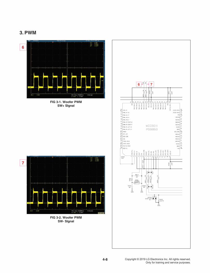
4-8 Copyright © 2019 LG Electronics Inc. All rights reserved.Only for training and service purposes.
3. PWM
FIG 3-1. Woofer PWMSW+ SIgnal
6
FIG 3-2. Woofer PWMSW- SIgnal
7
76

4-9 Copyright © 2019 LG Electronics Inc. All rights reserved.Only for training and service purposes.
4. LED
FIG 4-1. Pairing Off Status Red LED
8
FIG 4-2. Pairing On Status Yellow LED
9
98

4-10 Copyright © 2019 LG Electronics Inc. All rights reserved.Only for training and service purposes.

Copyright © 2019 LG Electronics Inc. All rights reserved.Only for training and service purposes.
DIP 2pin SWF
Harness Cable 12Pin
FFC SMD 24 Pin straight Dip 2Pin
(Power Cord)
SMPS PCB AMP PCB
Harness 12Pin Connector
Pairing Key 2Pin Harness
Cable 2Pin
Pairing Key PCB
LED CNT
Wirelessmodule
4-124-11
WIRING DIAGRAM

Copyright © 2019 LG Electronics Inc. All rights reserved.Only for training and service purposes.
WOOFERAMP
PVDD
WOOFERAMP
SW+LPF
DC-DC
DC-DC
LDOPVDD
PVDD
PWM 3.3
Wireless 3.3
3.7 V
LDO
PWM
PWM_SW+PWM_SW-
12 V
SW-LPF
Flash
4-144-13
BLOCK DIAGRAM

Copyright © 2019 LG Electronics Inc. All rights reserved.Only for training and service purposes.
4-164-15
PRINTED CIRCUIT BOARD DIAGRAMS 1. WOOFER SMPS P. C. BOARD (TOP VIEW) (BOTTOM VIEW)
NOTE) Warning Parts that are critical with respect to risk of fire or electrical shock.

Copyright © 2019 LG Electronics Inc. All rights reserved.Only for training and service purposes.
4-184-17
2. WOOFER AMP P. C. BOARD
3. WOOFER KEY P. C. BOARD
(TOP VIEW)
(TOP VIEW)
(BOTTOM VIEW)
(BOTTOM VIEW)