Service Manual - LG
162
Service Manual Model : LG-C300 Internal Use Only Service Manual LG-C300 Date: August, 2010 / Issue 1.0
-
Upload
khangminh22 -
Category
Documents
-
view
12 -
download
0
Transcript of Service Manual - LG

Service Manual
Model : LG
-C300
Internal Use Only
Service ManualLG-C300
Date: August, 2010 / Issue 1.0

- � -Copyright © 2010 LG Electronics. Inc. All right reserved.Only for training and service purposes
LGE Internal Use Only
Table Of Contents
1. INTRODUCTION ..................................................................5
1.1 Purpose ............................................................................................... 5
1.2 Regulatory Information ............................................................... 5
1.� Abbreviations ................................................................................... 7
2. PERFORMANCE ...................................................................9
2.1 H/W Features .................................................................................... 9
2.2 Technical Specification ...............................................................11
3. TECHNICAL BRIEF .............................................................16
�.1 Baseband Processor Introduction .........................................16
�.2 Power Management ....................................................................21
�.� FEM with integrated Power Amplifier Module
(RF7161, U�01) ...............................................................................��
�.4 Crystal(26 MHz, X102) .................................................................�6
�.5 RF Subsystem of PMB8810 (U102).........................................�7
�.6 MEMORY(PF�8F6066M0Y�DE, U102) ..................................42
�.7 BT module (U�02) .........................................................................44
�.8 SIM Card Interface ........................................................................46
�.9 LCD Interface ..................................................................................47
�.10 Battery Charger Interface .......................................................50
�.11 Keypad Interface ........................................................................51
�.12 Audio Front-End .........................................................................5�
�.1� Camera Interface(2M Fixed Focus Camera) .....................59
�.14 KEY BACLKLIGHT LED Interface ............................................61
�.15 Vibrator Interface .......................................................................62
4. TROUBLE SHOOTING .......................................................63
4.1 RF Component...............................................................................6�
4.2 RX Trouble .......................................................................................64
4.� TX Trouble ........................................................................................68
4.4 Power On Trouble .........................................................................72
4.5 Charging Trouble ..........................................................................75
4.6 Vibrator Trouble .............................................................................77
4.7 LCD Trouble .....................................................................................80
4.8 Camera Trouble .............................................................................84
4.9 Speaker Trouble ............................................................................88
4.10 Earphone Trouble ......................................................................90
4.11 Receiver Trouble .........................................................................92
4.12 Microphone Trouble .................................................................94
4.1� SIM Card Interface Trouble .....................................................96
4.14 KEY backlight Trouble ..............................................................98
4.15 Micro SD (uSD) Trouble ......................................................... 100
4.16 Bluetooth Trouble ................................................................... 102
4.17 FM Radio Trouble .................................................................... 104
5. DOWNLOAD ................................................................... 106
6. BLOCK DIAGRAM ........................................................... 119
7. CIRCUIT DIAGRAM ........................................................ 121
8. BGA PIN MAP ................................................................. 125
9. PCB LAYOUT ................................................................... 127
10.ENGINEERING MODE ................................................... 129
11. STAND ALONE TEST .................................................... 130
11.1 Introduction .............................................................................. 1�0
11.2 Setting Method ........................................................................ 1�0
11.� Tx Test ........................................................................................... 1��
11.4 Rx Test .......................................................................................... 1�5
12.AUTO CALIBRATION ..................................................... 137
12.1 Overview .................................................................................... 1�7
12.2 Configuration of HotKimchi ............................................... 1�7
12.� Description of Basic File ....................................................... 1�8
12.4 Procedure ................................................................................... 1�9
12.5 AGC ............................................................................................... 142
12.6 APC ............................................................................................... 142
12.7 ADC ............................................................................................... 142
12.8 Target Power ............................................................................. 142
13 EXPLODED VIEW & REPLACEMENT
PART LIST ...................................................................... 143
1�.1 EXPLODED VIEW ...................................................................... 14�
1�.2 Replacement Parts.................................................................. 145
1�.� Accessory ................................................................................... 16�

- 4 -LGE Internal Use Only Copyright © 2010 LG Electronics. Inc. All right reserved.Only for training and service purposes

- 5 -Copyright © 2010 LG Electronics. Inc. All right reserved.Only for training and service purposes
LGE Internal Use Only
1. INTRODUCTION
1. INTRODUCTION
4/133
1.1 PurposeThis manual provides the information necessary to repair, calibration, description and download the features of this model.
1.2 Regulatory InformationA. Security
Toll fraud, the unauthorized use of telecommunications system by an unauthorized part (for example, persons other than your company’s employees, agents, subcontractors, or person working on your company’s behalf) can result in substantial additional charges for your telecommunications services. System users are responsible for the security of own system. There are may be risks of toll fraud associated with your telecommunications system. System users are responsible for programming and configuring the equipment to prevent unauthorized use. The manufacturer does not warrant that this product is immune from the above case but will prevent unauthorized use of common-carrier telecommunication service of facilities accessed through or connected to it.
The manufacturer will not be responsible for any charges that result from such unauthorized use.
B. Incidence of Harm
If a telephone company determines that the equipment provided to customer is faulty and possibly causing harm or interruption in service to the telephone network, it should disconnect telephone service until repair can be done. A telephone company may temporarily disconnect service as long as repair is not done.
C. Changes in Service
A local telephone company may make changes in its communications facilities or procedure. If these changes could reasonably be expected to affect the use of the this phone or compatibility with the network, the telephone company is required to give advanced written notice to the user, allowing the user to take appropriate steps to maintain telephone service.
D. Maintenance Limitations
Maintenance limitations on this model must be performed only by the manufacturer or its authorized agent. The user may not make any changes and/or repairs expect as specifically noted in this manual. Therefore, note that unauthorized alternations or repair may affect the regulatory status of the system and may void any remaining warranty.
1. INTRODUCTION
1. INTRODUCTION

- 6 -LGE Internal Use Only Copyright © 2010 LG Electronics. Inc. All right reserved.Only for training and service purposes
1. INTRODUCTION
5/133
E. Notice of Radiated Emissions
This model complies with rules regarding radiation and radio frequency emission as defined by local regulatory agencies. In accordance with these agencies, you may be required to provide information such as the following to the end user.
F. Pictures
The pictures in this manual are for illustrative purposes only; your actual hardware may look slightly different.
G. Interference and Attenuation
Phone may interfere with sensitive laboratory equipment, medical equipment, etc.Interference from unsuppressed engines or electric motors may cause problems.
H. Electrostatic Sensitive Devices
ATTENTION
Boards, which contain Electrostatic Sensitive Device (ESD), are indicated
by the sign. Following information is ESD handling:
• Service personnel should ground themselves by using a wrist strap when exchange system
boards.
• When repairs are made to a system board, they should spread the floor with anti-static mat
which is also grounded.
• Use a suitable, grounded soldering iron.
• Keep sensitive parts in these protective packages until these are used.
• When returning system boards or parts like EEPROM to the factory, use the protective
package as described.
2. INTRODUCTION

- 7 -Copyright © 2010 LG Electronics. Inc. All right reserved.Only for training and service purposes
LGE Internal Use Only
1. INTRODUCTION
1.3 AbbreviationsFor the purposes of this manual, following abbreviations apply:
Offset Phase Locked LoopOPLL
Light Emitting DiodeLED
Low Drop OutputLDO
Liquid Crystal DisplayLCD
Intermediate FrequencyIF
International Portable User IdentityIPUI
Global System for Mobile CommunicationsGSM
General Purpose Interface BusGPIB
Gaussian Minimum Shift KeyingGMSK
Flexible Printed Circuit BoardFPCB
Electrostatic DischargeESD
Electrical Erasable Programmable Read-Only MemoryEEPROM
Digital Signal ProcessingDSP
dB relative to 1 milli wattdBm
Digital Communication SystemDCS
Digital to Analog ConverterDAC
Constant Current – Constant VoltageCC-CV
Bit Error RatioBER
BasebandBB
Automatic Power ControlAPC
1. INTRODUCTION

- 8 -LGE Internal Use Only Copyright © 2010 LG Electronics. Inc. All right reserved.Only for training and service purposes
1. INTRODUCTION
Wireless Application ProtocolWAP
Voltage Control Temperature Compensated Crystal OscillatorVCTCXO
Voltage Controlled OscillatorVCO
Universal Asynchronous Receiver/TransmitterUART
Time Division Multiple AccessTDMA
Time Division DuplexTDD
Travel AdapterTA
Side Tone Masking RatingSTMR
Pseudo SRAMPSRAM
Static Random Access MemorySRAM
Sending Loudness RatingSLR
Subscriber Identity ModuleSIM
Surface Acoustic WaveSAW
Real Time ClockRTC
Root Mean SquareRMS
Receiving Loudness RatingRLR
Radio FrequencyRF
Public Switched Telephone NetworkPSTN
Phase Locked LoopPLL
Programmable Gain AmplifierPGA
Printed Circuit BoardPCB
Power Amplifier ModulePAM
1. INTRODUCTION

- 9 -Copyright © 2010 LG Electronics. Inc. All right reserved.Only for training and service purposes
LGE Internal Use Only
2. PERFORMANCE
2. PERFORMANCE
8/133
2.1 H/W Features
2. SYSTEM SPECIFICATION
Item Feature Comment
Standard Battery Li-ion, 3.7V 900mAh
Talk time Up to 8 hrs : GSM850 & EGSM,TX Level : 10
Stand by time Up to 500 hrs : Paging Period 9
Charging time Under 3 hrs
RX Sensitivity GSM, EGSM: -109dBm, DCS: -109dBm c
TX output power GSM, EGSM: 33 dBm(Level 5), DCS , PCS: 30 dBm(Level 0)
SIM card type 3.0V / 1.8V
Display MAIN : 2.4” TFT 240 320 QVGA
Status Indicator
Hard icons. Key Pad (Qwerty)A ~ Z,0 ~ 9, #, *, Up/Down Left/Right OK KeySend Key, PWR Key ,Soft Key(Left/Right),Side key(Volume Up/Volume Down)
ANT Internal type (QUAD band)
EAR Phone Jack Yes (Stereo)
PC Synchronization Yes
Speech coding EFR/FR/HR/NB-AMR
Data and Fax Yes
GPRS compatibility Class 12
Vibrator Yes
Loud Speaker Yes
Voice Recoding Yes
Microphone Yes
2. SYSTEM SPECIFICATION

- 10 -LGE Internal Use Only Copyright © 2010 LG Electronics. Inc. All right reserved.Only for training and service purposes
2. PERFORMANCE
9/133
2. SYSTEM SPECIFICATION
Travel Adapter Yes
Speaker/Receiver 18x12 Speaker/ Receiver
MIDI SW decoded max. 32 poly
Item Feature Comment
Camera
Bluetooth / FM Radio BT 2.1 + EDR / 87.5 ~ 108MHz supported
Speaker DIS 16 mm, 3.4T spring / Receiver 1207*2.5T

- 11 -Copyright © 2010 LG Electronics. Inc. All right reserved.Only for training and service purposes
LGE Internal Use Only
2. PERFORMANCE
2.2 Technical Specification
Item Description Specification
1 Frequency Band
GSM850 EGSMTX: 824 ~ 849 MHz TX: 880 ~ 915MHzRX: 869 ~ 894 MHz RX: 925 ~ 960 MHz
DCSTX: 1710 ~ 1785 MHzRX: 1805 ~ 1880 MHz
PCSTX: 1850 ~ 1910 MHzRX: 1930 ~ 1990 MHz
2 Phase Error RMS < 5 degreesPeak < 20 degrees
3 Frequency Error < 0.1 ppm
4 Power Level
Level Power Toler. Level Power Toler.
6 31dBm 3dB 14 15dBm 3dB
7 29dBm 3dB 15 13dBm 3dB
8 27dBm 3dB 16 11dBm 5dB
9 25dBm 3dB 17 9dBm 5dB
10 23dBm 3dB 18 7dBm 5dB
11 21dBm 3dB 19 6dBm 5dB
12 19dBm 3dB
GSM850/EGSM
5 33dBm 2dB 13 17dBm 3dB
Level Power Toler. Level Power Toler.
1 28dBm 3dB 9 12dBm 4dB
2 26dBm 3dB 10 10dBm 4dB
3 24dBm 3dB 11 8dBm 4dB
4 22dBm 3dB 12 6dBm 4dB
5 20dBm 3dB 13 4dBm 4dB
6 18dBm 3dB 14 2dBm 5dB
7 16dBm 3dB 15 0dBm 5dB
DCS/PCS
0 30dBm 2dB 8 14dBm 3dB
2. SYSTEM SPECIFICATION

- 12 -LGE Internal Use Only Copyright © 2010 LG Electronics. Inc. All right reserved.Only for training and service purposes
2. PERFORMANCE
5 Output RF Spectrum(due to modulation)
Offset from Carrier (kHz). Max. dBc
100 +0.5
200 -30
250 -33
400 -60
600~ <1,200 -60
1,200~ <1,800 -60
1,800~ <3,000 -63
3,000~ <6,000 -65
6,000 -71
GSM850/ EGSM
Offset from Carrier (kHz). Max. dBc
100 +0.5
200 -30
250 -33
400 -60
600~ <1,200 -60
1,200~ <1,800 -60
1,800~ <3,000 -65
3,000~ <6,000 -65
6,000 -73
DCS/PCS
6Output RF Spectrum(due to switching transient)
GSM850/ EGSM
Offset from Carrier (kHz). Max. dBm
400 -19
600 -21
1,200 -21
1,800 -24
Item Description Specification
2. SYSTEM SPECIFICATION

- 1� -Copyright © 2010 LG Electronics. Inc. All right reserved.Only for training and service purposes
LGE Internal Use Only
2. PERFORMANCE
Item Description Specification
6Output RF Spectrum(due to switching transient)
Offset from Carrier (kHz). Max. dBm
400 -22
600 -24
1,200 -24
1,800 -27
7 Spurious Emissions Conduction, Emission Status
8 Bit Error Ratio
GSM850, EGSMBER (Class II) < 2.439% @-102 dBmDCS,PCSBER (Class II) < 2.439% @-102 dBm
9 RX Level Report Accuracy 3 dB
10 SLR 15 3 dB
11 Sending Response
300 -12
1,000 -6
2,000 -6
3,000 -6
Frequency (Hz) Max.(dB) Min.(dB)
100 -
200 -
4,000 -
3,400 -9
0
0
4
4
-12
0
0
4
12 RLR 4 3 dB
DCS/PCS
2. SYSTEM SPECIFICATION

- 14 -LGE Internal Use Only Copyright © 2010 LG Electronics. Inc. All right reserved.Only for training and service purposes
2. PERFORMANCE
Item Description Specification
13 Receiving Response
300 -7
500 -5
1,000 -5
3,000 -5
Frequency (Hz) Max.(dB) Min.(dB)
100 -
200 -
4,000
3,400 -10
2
*
0
2
-12
0
2
2
14 STMR 17 5 dB
* Mean that Adopt a straight line in between 300 Hzand 1,000 Hz to be Max. level in the range.
15 Stability Margin > 6 dB
-20
-10
0
7
dB to ARL (dB) Level Ratio (dB)
-35
-30
10
30.7
33.3
33.7
31.7
17.5
22.5
25.5
16 Distortion
17 Side Tone Distortion Three stage distortion < 10%
18 System frequency (13 MHz) tolerance 2.5 ppm
19 32.768KHz tolerance 30 ppm
20 Ringer VolumeAt least 55 dBspl under below conditions:1. Ringer set as ringer.2. Test distance set as 1 m
2. SYSTEM SPECIFICATION

- 15 -Copyright © 2010 LG Electronics. Inc. All right reserved.Only for training and service purposes
LGE Internal Use Only
2. PERFORMANCE
2. SYSTEM SPECIFICATION
Item Description Specification
21 Charge CurrentConstant Charge Current : <. 400 mA
Total Charging Time : < 3 hours ( Battery 900mA )
2 -> 1
0 -> OFF
Bar Number Power
4 -> 2
-104 3
-106 Min.
-98 3
-101 322 Antenna Display
2 -> 1
1 -> 0
Battery Bar Number Voltage
3
3 -> 2 3.61 0.05 V 23 Battery Indicator
24 Low Voltage Warning( Blinking Bar)
3.46 0.05V (Call), 1 time per 1 minute (Receiver)
3.46 0.05V (Standby), 1 time per 3 minutes(Speaker)
25 Forced shut down Voltage
3.35 0.05V
27 Battery Type
Lithium-Ion Battery, Inner packStandard Voltage = 3.7 VBattery full charge voltage = 4.2 VCapacity: 900mAh
28 Travel ChargerSwitching-mode chargerInput: 100 ~ 240V, 50/60 HzOutput: 4.8V, 700mA
3.73 0.05 V
26 Sustain RTC without battery Over 50 hours
3.46 0.05 V
3.35 0.05 V
7
7 -> 5
5 -> 4
-92 Max.
-93 3
1 -> 0 -106 3

- 16 -LGE Internal Use Only Copyright © 2010 LG Electronics. Inc. All right reserved.Only for training and service purposes
3. TECHNICAL BRIEF
3. TECHNICAL BRIEF
3.1 Digital Main Processor
Figure. 3.1.1 X-Gold tm 213 Hardware Block Diagram
3. TECHNICAL BRIEF
3. TECHNICAL BRIEF

- 17 -Copyright © 2010 LG Electronics. Inc. All right reserved.Only for training and service purposes
LGE Internal Use Only
3. TECHNICAL BRIEF
16/133
3. TECHNICAL BRIEF
3.1.1 General• Technology:– SoC, Monolithic, 65 nm CMOS• Package:– eWLB, 8x8x0.8 mm– 0.5 mm pitch– 217 balls / 6-layer PCB
3.1.2 RF Transceiver• Dual-band direct conversion receiver• Tri/Quad-band possible with external circuitry• Fully integrated digital controlled X0• Additional buffer for 2 external system clocks• Fully digital RF-Synthesizer incl. -Transmitter
3.1.3 Baseband• DSP:– 156 MHz TeakLite™
• MCU:– ARM1176® @ 208 MHz
• MCU RAM:– 3.00Mbit
• Memory I/F:– 512 Mbit
• Modem:– GPRS class 12, (RX/TX CS1-CS4)– EGPRS class 12, (RX MCS1-MCS9, TX MCS1-MCS4)• Cipher Units:– A51/2/3– GEA-1/2/3• Security:– OMTP TR0– Secure Boot– RSA(ROM)/SHA-1(HW accel.)– OCDS disabling– Certificate Management

- 18 -LGE Internal Use Only Copyright © 2010 LG Electronics. Inc. All right reserved.Only for training and service purposes
3. TECHNICAL BRIEF
3. TECHNICAL BRIEF
• Speech Codec:– FR / HR / EFR / NB-AMR• Audio Codec (running on ARM1176):– SP-MIDI– SB-ADPCM– MP3– WB-AMR– AAC/AAC+/eAAC+• Others:– DARP (SAIC)– TTY• Customization:– E-Fuses
3.1.4 External Memory• External Bus Unit– 25-bit address bus (512 Mbit)– 16-bit data bus– 1.8V & 2.8V support• Flash / RAM– NOR Type– Serial Flash SPI and SPI-4– Parallel Flash (Page & Burst Mode)- 16-bit Demultiplexed- 16-bit AD-multiplexed- 16-bit AAD-multiplexed– iNAND Type e.g. oneNAND• Memory card– SD/MMC card interface with 1 or 4 data lines
3.1.5 Connectivity• 3xUSIF (configurable either as SPI or UART), I2C, I2S; Interfaces @ 1.8V• Direct (U)SIM 1.8/3V• USB2.0 up to 480 Mbit/s (High Speed) w/ external USB Phy over ULPI interface• Stereo Headset (Amplifier integrated)• 3 external analog measurement PIN’s• Bluetooth

- 19 -Copyright © 2010 LG Electronics. Inc. All right reserved.Only for training and service purposes
LGE Internal Use Only
3. TECHNICAL BRIEF
18/133
3. TECHNICAL BRIEF
3.1.6 Mixed Signal• Improved audio performance• Loudspeaker Audio Class D Amplifier, 700 mW@8 mono for hands-free and ringing• Stereo Headset 2x30 mW@16 w/o coupling C• Mono Earpiece 100 mW@16 • Digital microphone supported• Differential microphone inputs
3.1.7 FM Radio• Integrated FM radio– FM Stereo RDS Receiver– Sensitivity 2 V EMF– Support for US & EU bands– Stereo recording
3.1.8 Power Management• Direct-to-Battery Connection– LDOs (incl. capless)– DC/DC step-down converter– DC/DC step-up for white LED supply• Battery Type– Li-Polymer• Charging control– Battery temperature– Watchdog protection– Start-up on flat battery• External Charger– Switch mode• USB battery charging– USB charging spec 1.0 compliant• Backlight– Up to 5 serial white LEDs (integrated LDO)

- 20 -LGE Internal Use Only Copyright © 2010 LG Electronics. Inc. All right reserved.Only for training and service purposes
3. TECHNICAL BRIEF
3. TECHNICAL BRIEF
3.1.10 Main LCD Display• Type– 240*320, QVGA, 262k color (parallel)• Interface– Parallel 8bit MIPI-DBI Type B– Serial MIPI-DBI Type C– Interf. voltage at 1.8V or 2.8V• gRacr - Display Controller (Hardware)– 30 fps Display update without DMA (up to 60 fps) (full or partial)– Video post processing Scaling, Rotation (90 steps), Mirroring– Overlay with alpha blending– Color conversion YUV -> RGB– 2D vector graphics (Lines, filled rectangles, Bit block transfer (e.g. sprites, scrolling,
antialiased bitmap fonts)
3.1.11 Camera• 2.0 Mpxls, FF• Frame Rate : 15@UXGA, 30@SVGA • 39 MHz Pixel Rate• 15 [email protected] Mpx full resolution
3.1.12 Video Capabilities• Video Decoding MPEG-4/H.263– QCIF@30 fps– QVGA@15fps• Video Encoding MPEG-4/H.263– QCIF@15 fps
3.1.13 Audio Capabilities• Polyphonic ring tones– 64 voices MIDI, SP-MIDI– FM synthesizer• AMR-WB• True ring tones (MP3)• MP3, eAAC+• G.722 SB-ADPCM encoding/decoding

- 21 -Copyright © 2010 LG Electronics. Inc. All right reserved.Only for training and service purposes
LGE Internal Use Only
3. TECHNICAL BRIEF
3.2 Power ManagementA mobile platform requires power supplies for different functions. These power supplies are generated in the integrated power management Unit (PMU). The PMU is designed to deliver the power for a typical standard phone.
Figure. 3-2-1 Block Figure of the PMU Modules X-Gold tm 213
3. TECHNICAL BRIEF

- 22 -LGE Internal Use Only Copyright © 2010 LG Electronics. Inc. All right reserved.Only for training and service purposes
3. TECHNICAL BRIEF3. TECHNICAL BRIEF
DC/DC Step Down Converter for 1.8V (SD1) The DC/DC converter generates a 1.8V supply rail. This voltage rail is used to supply main parts of the system, like the digital core of the chip (via LDO LCORE), some parts of the mixed signal macro, parts of the RF macro and the external memory if a 1.8V memory is used. The efficiency of the DC/DC converter is optimized for an average load current of 100mA. That is the load current estimated for the GSM talk mode.
Linear voltage Regulators (low dropout) LDOs The LDOs are used to generate the supply for the different supply domains not directly supplied out of the DC/DC converter.The VSIM output current is high enough to drive USB SIM cards.
LCOREThe LCORE LDO provides the VCORE supply used for most of the digital parts of the chip
LPMUThe LPMU provides VPMU sued for the PMU supply, e.g. for the startup state machine and analog parts like ADC, sense amplifier etc.
LUSBThe LUSB LDO generates the supply for the USB transceiver (output driver and input). If no USB interface is required, LUSB can be used as general purpose LDO.
LAUXThe LAUX generates VAUX. It is a general purpose LDO and can be used for different functions depending on the phone application, e.g. for the display or Camera.
LMMCThe LMMC generates VMMC. It is a general purpose LDO and can be used e,g. for memory cards
LSIMThe LSIM LDO generates the VSIM supply for the SIM card and interface. It is designed to supply Standard SIM cards.
Other LDOsThe RF module has implemented several LDO’s for different RF Power domain.The mixed signal module has some LDO’s for the audio driver and microphone supply.

- 2� -Copyright © 2010 LG Electronics. Inc. All right reserved.Only for training and service purposes
LGE Internal Use Only
3. TECHNICAL BRIEF
22/133
3. TECHNICAL BRIEF
Table. 3-2-1 Power supply Domains (without RF)
- 24 -LGE Internal Use Only Copyright © 2010 LG Electronics. Inc. All right reserved.Only for training and service purposes
3. TECHNICAL BRIEF
3. TECHNICAL BRIEF
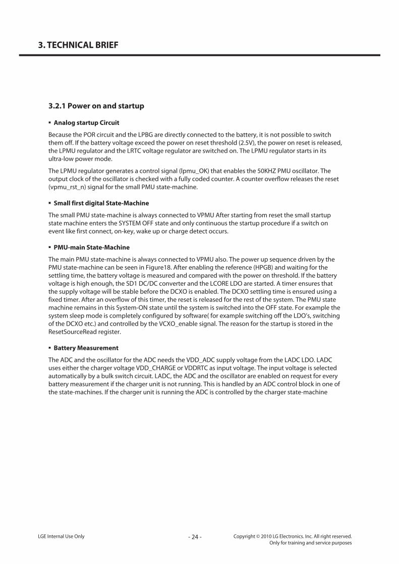
3.2.1 Power on and startup
Analog startup Circuit
Because the POR circuit and the LPBG are directly connected to the battery, it is not possible to switch them off. If the battery voltage exceed the power on reset threshold (2.5V), the power on reset is released, the LPMU regulator and the LRTC voltage regulator are switched on. The LPMU regulator starts in its ultra-low power mode.
The LPMU regulator generates a control signal (lpmu_OK) that enables the 50KHZ PMU oscillator. The output clock of the oscillator is checked with a fully coded counter. A counter overflow releases the reset (vpmu_rst_n) signal for the small PMU state-machine.
Small first digital State-Machine
The small PMU state-machine is always connected to VPMU After starting from reset the small startup state machine enters the SYSTEM OFF state and only continuous the startup procedure if a switch on event like first connect, on-key, wake up or charge detect occurs.
PMU-main State-Machine
The main PMU state-machine is always connected to VPMU also. The power up sequence driven by the PMU state-machine can be seen in Figure18. After enabling the reference (HPGB) and waiting for the settling time, the battery voltage is measured and compared with the power on threshold. If the battery voltage is high enough, the SD1 DC/DC converter and the LCORE LDO are started. A timer ensures that the supply voltage will be stable before the DCXO is enabled. The DCXO settling time is ensured using a fixed timer. After an overflow of this timer, the reset is released for the rest of the system. The PMU state machine remains in this System-ON state until the system is switched into the OFF state. For example the system sleep mode is completely configured by software( for example switching off the LDO’s, switching of the DCXO etc.) and controlled by the VCXO_enable signal. The reason for the startup is stored in the ResetSourceRead register.
Battery Measurement
The ADC and the oscillator for the ADC needs the VDD_ADC supply voltage from the LADC LDO. LADC uses either the charger voltage VDD_CHARGE or VDDRTC as input voltage. The input voltage is selected automatically by a bulk switch circuit. LADC, the ADC and the oscillator are enabled on request for every battery measurement if the charger unit is not running. This is handled by an ADC control block in one of the state-machines. If the charger unit is running the ADC is controlled by the charger state-machine

- 25 -Copyright © 2010 LG Electronics. Inc. All right reserved.Only for training and service purposes
LGE Internal Use Only
3. TECHNICAL BRIEF
24/133
3. TECHNICAL BRIEF
Figure.3.2.1 First Part of the State Machine, Running in Different Power Domains than the Second Part

- 26 -LGE Internal Use Only Copyright © 2010 LG Electronics. Inc. All right reserved.Only for training and service purposes
3. TECHNICAL BRIEF 3. TECHNICAL BRIEF
Figure 3.2.2 Second (Main) Part of the Startup State Machine in the VPMU Domain

- 27 -Copyright © 2010 LG Electronics. Inc. All right reserved.Only for training and service purposes
LGE Internal Use Only
3. TECHNICAL BRIEF
26/133
3. TECHNICAL BRIEF
3.2.2 Switching on due to first connectIf the battery voltage is connected the first time, that means the system enters the first time the SYSOFF state, this is stored in a first connect flag. If the first connect flag is set, the system will start immediately and not wait for any other system on event in the SYSOFF state.
3.2.3 Switching on due to on-Key eventThe on key is connected to the ONKEY pad. The ESD protection and the input structure of this pad are connected to VRTC. If the ONKEY pad is forced to VRTC by an external key or similar circuit, the system starts. The ONKEY is sampled with the PMU clock. It has to be sampled four times high before a valid on event is generated. The status of the ON key can be read in the PMU registers, so it can be used as a functional key during phone operation also.
3.2.4 Switching on due to RTC alarmThe real time clock can generate a wakeup signal called RTC alarm. This signal is sampled from the state-machine and after successfully detecting a high, the system is switched on.
3.2.5 Switching on due to chargingWhen a battery with a voltage below the SSONLEV level is inserted, the state machine will not start the system. As long as the battery voltage stays lover than SYSONLEV the system will stay off. The only possibility to start up the system is due to an external charger.
If an external charger is connected and detected and the battery is charged above the SYSONPRE voltage level the system will start up.The PMU main state machine waits in the Check battery state until the battery voltage condition is fulfilled. The charger state machine provides the necessary pre-charge indication signal. This pre-charge signal is denounced in a small counter to have a stable signal. This is important, especially in half/full-wave charging where the charger detection is switching between charger detected/not detected according the AC supply frequency. Reasons for details on pre-charging see the charger chapter. The charger is controlled by an independent state machine. The pre-charge signal is used to trigger the pre-charge signal is used to trigger the pre-charge functionality. The charger state machine fully control the pre-charge, the PMU-state machine now changes to state HPBG on state and the system starts. This state change is indicated to the charger state-machine to enable the charger watchdog for safety
3. TECHNICAL BRIEF
3.2.6 Power Supply Start-up sequenceIn order to avoid an excessive drop on the battery voltage caused by in-rush current during system power-on, possibly leading to system instability and “hick-ups” a staggered turn-on approach for the regulators is implemented. The regulators are turned on in a well defined sequence, thus spreading the in-rush current transients over time.
The IO’s of X-GOLD TM 213 are isolated in OFF mode (core supply is off). The isolation signal is controlled by the PMU state machine. This ensures that the PADs are in a well defined state during core supply settling. This allows to power up the LCORE core regulator and wait for the core to reach reset state before powering up the I/O supply regulators.

- 28 -LGE Internal Use Only Copyright © 2010 LG Electronics. Inc. All right reserved.Only for training and service purposes
3. TECHNICAL BRIEF
28/133
3. TECHNICAL BRIEF
Figure 3.2.3 Start Up Sequence (triggered by First Connect Event)

- 29 -Copyright © 2010 LG Electronics. Inc. All right reserved.Only for training and service purposes
LGE Internal Use Only
3. TECHNICAL BRIEF
3. TECHNICAL BRIEF
3.2.7 External Reset Handling
The chip reset can be controlled by an external RESET_N ball. If this ball is pulled low, the chip will be reset. All PMU registers are reset during the external reset including LSIM control bits. The PMU statemachines are also not reset from the external reset. An SW or watchdog reset will not reset the PMU registers. A SW and Watchdog reset is seen on the reset_n pad to allow the reset of external devices. Basically there are three reset sources, first the reset signal controlled by the PMU (reset_pmu_n_o), second the reset signal controlled by the SCU (resetout_o) and third the external reset (RESET_N). The SCU reset is triggered by SW (for example due to a SW reset or watchdog reset). The PMU reset is controlled by the PMU state machine. The output of the reset handling block is the reset_postscu_n_o signal. This signal controls for example the C subsystem and releases reset for the controller. During normal start up, the PMU releases the reset_pmu_n_o signal after entering the SYSTEM ON state. At this time the resetout_o signal is high, the RESET_N pad is not pulled low and therefore the reset_postscu_n_o signal follows the reset_pmu_n_o signal. That means the C reset will be released and the C starts operation. If the SW triggers an external reset via the SCU, signal resetout_o will be forced to low for a certain time and RESET_N will be forced to low by the open drain driver. At the same time the feedback to the SCU will be masked to not reset the baseband. The RESET_N pad is in the VDDRTC domain but the internal pull up is connected to the VDD_VDIG1 (1.8V) domain. That allows the pad to be used as reset for external devices running in the VDD1V8 domain. The RESET_N pad can also be used to monitor the chip internal reset condition during startup.
The open drain driver is a weak driver, that means it can be forced to high during debug from external pushing some current into the pad. In testmode signal reset_pmu_n_o is high, that means the chip reset is fully controlled from external .

- �0 -LGE Internal Use Only Copyright © 2010 LG Electronics. Inc. All right reserved.Only for training and service purposes
3. TECHNICAL BRIEF
30/133
3. TECHNICAL BRIEF
3.2.8 Sysclock Switching
The PMU controls the rf_sysclk_en signal of the DCXO in the RF macro. During startup the PMU enables the DCXO. After the system is running the DCXO is controlled by the SCU of the baseband by using the vcxo_enable signal. This is handled by a dedicated logic in the PMU, see Figure 21. As long as rf_sysclk_en_pmu, the output of the PMU state-machine is high, vcxo_enable controls the rf_sysclk_en signal to the RF. If rf_sysclk_en_pmu is low, the DXCO is switched off, independent from vcxo_enable.
Figure 3.2.4 PMU, CGU and External Reset

- �1 -Copyright © 2010 LG Electronics. Inc. All right reserved.Only for training and service purposes
LGE Internal Use Only
3. TECHNICAL BRIEF
31/133
3. TECHNICAL BRIEF
3.2.10 Software Reset
A software reset does not affect any PMU register. The PMU register are reset with the reset_pmufsm_n_o signal. That means all PMU register are reset in OFF state. For details about the SW reset see chapter External Reset Handling .
3.2.9 Undervoltage Shutdown
In active mode the PMU periodically measures the battery voltage using the ADC from the charger unit. If the battery is measured to be below the programmable shut-down level (called SYSOFF), the system changes to OFF mode. This is done via the SHUTDOWN state of the PMU state machine. (see chapter switch OFF)
Figure 3.4.2 How sysclock Enable is Routed in the PMU

- �2 -LGE Internal Use Only Copyright © 2010 LG Electronics. Inc. All right reserved.Only for training and service purposes
3. TECHNICAL BRIEF
32/133
3. TECHNICAL BRIEF
3.2.11 PMU Clock
During the first startup (for example plugging in a battery) a PMU internal oscillator is used for generation of the PMU clock (pmu_clock). The frequency is slightly above 32 kHz (typ. 50 kHz) to be out of the audio band also for worst case devices. After first startup the software shall enable the 32 kHz crystal oscillator. It is not possible to use the 32 kHz oscillator during first startup, because the settling time of the oscillator can be quite long. After the 32 kHz oscillator is running and settled the software shall switch the PMU clock to the 32 kHz clock and disable the internal PMU oscillator for power saving reasons. The 32 kHz oscillator shall never be disabled after the PMU clock has been switched. The ADC in the charger unit has it’s own oscillator generating a frequency of about 10 MHz. This oscillator is running during charging and during battery measurements triggered by the PMU. It is off otherwise.
3.2.12 System Sleep Mode
The sleep mode is controlled by using the VCXO_enable signal. This signal is used to switch the LDO’s and the DC/DC converter SD1 in a programmable way into its low power mode (PFM). In addition DC/DC converter SD1 can be configured to change the output voltage to a lower value for additional power saving. VCXO_enable is also used to deactivate the HPBG and setting LDO LPMU in the ultra-low-power mode. In addition the DCXO is switched off by the VCXO_enable signal. The VCXO_enable signal is also used to switch some LDO’s (software configured) to sleep and/or off mode or to change the output voltages of said LDO’s. The state of the main PMU state machine is not changed due to VCXO_enable.
3.2.13 DC/DC Pre-Load Register Handling
The DC/DC converter works in different modes. If the mode is switched from PFM to PWM the pulse-width of the DC/DC converter depends on the current battery voltage (and on the output voltage). The PMU state-machine knows the battery voltage because of the battery supervision function. Depending on this value it selects a startup pulse-width for the DC/DC converter out of a register table. (4-values)
3.2.14 Power Down Sequence
Setting bit OFF in the GeneralControl register switches the system into OFF mode. After the turn off event, the state-machine switches to the SHUTDOWN state. The reset_pmu_n_o signal changes to low, the I/O pads are isolated using the padisolation_n signal, the LCORE LDO and the SD1 DC/DC converter are switched off, the LPMU LDO is switched to ultra-low power mode, the DCXO is turned off and the bandgap buffer is disabled. Before switching OFF the software shall have enabled the 32 kHz oscillator and has switched the PMU clock to the 32 kHz clock to archive the target OFF current .

- �� -Copyright © 2010 LG Electronics. Inc. All right reserved.Only for training and service purposes
LGE Internal Use Only
3. TECHNICAL BRIEF
33/133
3.3.1 Internal Block Diagram
3.3 FEM with integrated Power Amplifier Module (RF7161, U301)
Figure. 3-3-1 RF7161 FUNCTIONAL BLOCK DIAGRAM
3.3.2 General Description
The RF7161 is a quad-band (GSM850/EGSM900/DCS1800/PCS1900) GSM/GPRS, Class 12compliant transmit module with four interchangeable receive ports. This transmit modulebuilds upon RFMD’s leading power amplifier with PowerStar® integrated power control technology, pHEMT switch technology, and integrated transmit filtering for best-in-class harmonic performance. The results are high performance, reduced solution size, and ease ofimplementation. The device is designed for use as the final portion of the transmitter section ina GSM850/EGSM900/DCS1800/PCS1900 handset and eliminates the need for a PA-toantennaswitch module matching network. The device provides 50 matched input and outputports requiring no external matching components.
The RF7161 features RFMD’s latest integrated power-flattening circuit which significantly reduces current and power variation into load mismatch. Additionally, a VBATT tracking feature is incorporated to maintain switching performance as supply voltage decreases. The RF7161 also integrates an ESD filter to provide excellent ESD protection at the antenna port. The RF7161 is designed to provide maximum efficiency at rated POUT.
3. TECHNICAL BRIEF

- �4 -LGE Internal Use Only Copyright © 2010 LG Electronics. Inc. All right reserved.Only for training and service purposes
3. TECHNICAL BRIEF
33/133
3.3.1 Internal Block Diagram
3.3 FEM with integrated Power Amplifier Module (RF7161, U301)
Figure. 3-3-1 RF7161 FUNCTIONAL BLOCK DIAGRAM
3.3.2 General Description
The RF7161 is a quad-band (GSM850/EGSM900/DCS1800/PCS1900) GSM/GPRS, Class 12compliant transmit module with four interchangeable receive ports. This transmit modulebuilds upon RFMD’s leading power amplifier with PowerStar® integrated power control technology, pHEMT switch technology, and integrated transmit filtering for best-in-class harmonic performance. The results are high performance, reduced solution size, and ease ofimplementation. The device is designed for use as the final portion of the transmitter section ina GSM850/EGSM900/DCS1800/PCS1900 handset and eliminates the need for a PA-toantennaswitch module matching network. The device provides 50 matched input and outputports requiring no external matching components.
The RF7161 features RFMD’s latest integrated power-flattening circuit which significantly reduces current and power variation into load mismatch. Additionally, a VBATT tracking feature is incorporated to maintain switching performance as supply voltage decreases. The RF7161 also integrates an ESD filter to provide excellent ESD protection at the antenna port. The RF7161 is designed to provide maximum efficiency at rated POUT.
3. TECHNICAL BRIEF

- �5 -Copyright © 2010 LG Electronics. Inc. All right reserved.Only for training and service purposes
LGE Internal Use Only
3. TECHNICAL BRIEF
34/133
Figure 3.3.2 Band SW Logic Table
Figure 3.3.3 FEM CIRCUIT DIAGRAM
3. TECHNICAL BRIEF
1. RX1, RX2, RX3, and RX4 are broadband receive ports and each supports the EGSM, GSM850, PCS, and DCS bands.
10
R327
DNIC359
103U
21
11
10
9
8
7
31
6
41
5
51
4
61
3
71
2
18
1
19
20
21
22
23GND_SLUG
VRAMP
TX_ENABLE
GPCTRL0
GPCTRL1
1D
NG
VBATT
2D
NG
2LRT
CP
G
BL_NIF
R
9D
NG
3D
NG
8D
NG
BH_
NIFR
TN
A
4D
NG
4X
R
GND5
GND6
GND7
RX1
RX2
3X
R33pC302
303C
p33
p33403
C
L301 3.3n 3.3nL302
22pC343
3.3nL303
1nL308
1pC305
L306 3.3n
C3141.5p
C31539p
10nC316 C317
4.7u
1nC318
1nC319
DNIC392
VBAT
C32233p
1nC323
33pC325
1nC326
4.7uC327
56pC306
VLOGICBS2BS1TX_EN
GSM_OUT
DCS_PCS_OUT
TX_RAMP

- �6 -LGE Internal Use Only Copyright © 2010 LG Electronics. Inc. All right reserved.Only for training and service purposes
3. TECHNICAL BRIEF
35/133
3.4 Crystal(26 MHz, X102)
Figure. 3.4.2 Digital PREDISTORTION with LUXO
The DCXO tuning characteristic should be a first order linear function of the programming word AFC. The variable capacitance array is a first order linear function of the digital word DIG, which leads to a nonlinear curve ppm vs. DIG (and also a nonlinear ppm vs. AFC for DIG=AFC). In order to linearize the ppm vs. AFC curve the implementation of a predistortion is necessary. To get the wanted linear ppm vs. AFC tuning curve some digital predistortion of the AFC word is required. This predistortion is performed by the linearization unit for crystal oscillator (LUXO). The LUXO calculates the corresponding DIG value according to the given AFC value.
Figure. 3.4.1 Crystal Oscillator External Connection
The X-GOLDTM213 RF-Subsystem contains a fully integrated 26 MHz digitally controlled crystal oscillator, designed for 8 pF crystals. The only external part of the oscillator is the crystal itself. Overall pulling range of the DCXO is approximately 55 ppm, controllable by a 13-bit tuning word.
This frequency serves as comparison frequency within the RF-PLL and as clock frequency for the digital circuitry.The 26 MHz reference clock can also be applied to external components like Bluetooth or GPS, via the two buffered output signals FSYS1 and FSYS2.
3. TECHNICAL BRIEF
3.4 Crystal(26 MHz, X102)

- �7 -Copyright © 2010 LG Electronics. Inc. All right reserved.Only for training and service purposes
LGE Internal Use Only
3. TECHNICAL BRIEF
36/133
3.5 RF Subsystem of PMB8810 (U101)
3.5.1 GENERAL DESCRIPTION
The PMB8810 RF subsystem is designed for dual-band GSM voice and data applications (GPRS class 12). The system can be configured to support one low band, GSM850 or EGSM900, and one high band, DCS1800 or PCS1900. A block diagram of the RF subsystem is given in Figure 3-5-1.
Figure. 3-5-1 Block DIAGRAM of RF Subsystem
3. TECHNICAL BRIEF
3.5 RF Subsystem of PMB8810 (U102)
3.5.1 GENERAL DESCRIPTIONThe PMB8810 RF subsystem is designed for dual-band GSM voice and data applications (GPRS class 12). The system can be configured to support one low band, GSM850 or EGSM900, and one high band, DCS1800 or PCS1900. A block diagram of the RF subsystem is given in Figure 3-4-1.
Figure. 3-5-1 Block DIAGRAM of RF Subsystem
3. TECHNICAL BRIEF3.5 RF Subsystem of PMB8810 (U101)

- �8 -LGE Internal Use Only Copyright © 2010 LG Electronics. Inc. All right reserved.Only for training and service purposes
3. TECHNICAL BRIEF
37/133
3.5.2 FUNCTIONAL DESCRIPTION
Figure. 3.5.2 RECEIVER CHAIN BLOCK DIAGRAM
3. TECHNICAL BRIEF
3.5.2.1 Receiver
The X-GOLD™213 dual-band receiver is based on a Direct Conversion Receiver (DCR) architecture. Input impedance of the LNAs is optimized to achieve a matching without (external) high quality inductors. By use of frequency dividers (by 2/4) the LO frequency is derived from the RF frequency synthesizer.The receive path is fully differential to suppress the on-chip interferences and reduce DC-offsets. The analog chain of the receiver contains two LNAs (low/high band), a quadrature mixer followed by an analog baseband filter and 14-bit continuous-time delta-sigma analog-to-digital converter. The filtered and digitized signal is fed into the digital signal processing chain, which provides decimation, DC offset removal and programmable gain control.

- �9 -Copyright © 2010 LG Electronics. Inc. All right reserved.Only for training and service purposes
LGE Internal Use Only
3. TECHNICAL BRIEF
38/133
Figure. 3.5.3 TRANSMITTER CHAIN BLOCK DIAGRAM
3. TECHNICAL BRIEF
3.5.2.2 Transmitter
The GMSK transmitter supports power class 4 for GSM850 or GSM900 as well as power class 1 for DCS1800 or PCS1900. The digital transmitter architecture is based on a fractional-N sigma-delta synthesizer for constant envelope GMSK modulation. This configuration allows a very low power design without any external components.Up- and down-ramping is performed via the ramping DAC connected to VRAMP.
RF synthesizer
The RF subsystem contains a fractional-N sigma-delta synthesizer for the frequency synthesis. Respective to the chosen band of operation the phase locked loop (PLL) operates at twice or forth of the target signal frequency. In receive operation mode the divided output signal of the digital controlled oscillator output (DCO) serves as local oscillator signal for the balanced mixer. For transmit operation the fractional-N sigma-delta synthesizer is used as modulation loop to process the phase/frequency signal. The 26 MHz reference signal of the phase detector incorporated in the PLL is provided by the reference oscillator.

- 40 -LGE Internal Use Only Copyright © 2010 LG Electronics. Inc. All right reserved.Only for training and service purposes
3. TECHNICAL BRIEF
Figure. 3.5.4 PA AND FEM CONTROL BLOCK DIAGRAM
3. TECHNICAL BRIEF
3.5.2.3 Front-end/PA Control Interface
Two outputs (FE1, FE2) for direct control of antenna switch modules enable to select RX- and TX-mode as well as low- and high-band operation.An extra band select signal PABS for the power amplifier is used, to support discrete PA and switching modules. Time accurate power dissipation of the PA is achieved by the control signal PAEN. A minor set of power amplifiers require a bias voltage to enhance power efficiency. Support of this power amplifiers is achieved by the implemented bias DAC.

- 41 -Copyright © 2010 LG Electronics. Inc. All right reserved.Only for training and service purposes
LGE Internal Use Only
3. TECHNICAL BRIEF
Figure. 3.5.5 POWER SUPPLY BLOCK DIAGRAM
3. TECHNICAL BRIEF
3.5.2.4 Power Supply
To increase power efficiency most parts of the RF subsystem are supplied by the DCDC converter situated in the PMU subsystem. Conversion of the 1.8 V output voltage of the DCDC to the 1.3 V/1,4 V circuit supply voltages is achieved by several Low-DropOut regulators (LDO).One embedded direct-to-battery LDO provides the 2.5 V supply voltage for the remaining circuits.

- 42 -LGE Internal Use Only Copyright © 2010 LG Electronics. Inc. All right reserved.Only for training and service purposes
3. TECHNICAL BRIEF
3.6 MEMORY(PF38F6066M0Y3DE, U102)
The Numonyx™ StrataFlash® Cellular Memory (M18) device provides high read and write performance at low voltage on a 16-bit data bus.The flash memory device has a multi-partition architecture with read-while-program and read-while-erase capability.The device supports synchronous burst reads up to 108 MHz using ADV# and CLK address-latching (legacy-latching) on some litho/density combinations and up to 133 MHz using CLK address-latching only on some litho/density combinations. It is listed below in the following table..
Figure. 3.6.1 MEMORY BLOCK DIAGRAM
3. TECHNICAL BRIEF
3.6 MEMORY(PF38F6066M0Y3DE, U102)

- 4� -Copyright © 2010 LG Electronics. Inc. All right reserved.Only for training and service purposes
LGE Internal Use Only
3. TECHNICAL BRIEF
42/133
3. TECHNICAL BRIEF
In continuous-burst mode, a data Read can traverse partition boundaries.Upon initial power-up or return from reset, the device defaults to asynchronous arrayread mode. Synchronous burst-mode reads are enabled by programming the Read Configuration Register. In synchronous burst mode, output data is synchronized with a user-supplied clock signal. A WAIT signal provides easy CPU-to-flash memory synchronization.Designed for low-voltage applications, the device supports read operations with VCC at 1.8 V, and erase and program operations with VPP at 1.8 V or 9.0 V. VCC and VPP can be tied together for a simple, ultra-low power design. In addition to voltage flexibility, a dedicated VPP connection provides complete data protection when VPP is less than VPPLK.A Status Register provides status and error conditions of erase and program operations.One-Time-Programmable (OTP) registers allow unique flash device identification that can be used to increase flash content security. Also, the individual block-lock feature provides zero-latency block locking and unlocking to protect against unwanted program or erase of the array.The flash memory device offers three power savings features:• Automatic Power Savings (APS) mode: The device automatically enters APS following a read-cycle completion.• Standby mode: Standby is initiated when the system deselects the device by deasserting CE#.• Deep Power-Down (DPD) mode: DPD provides the lowest power consumption and is enabled by programming in the Enhanced Configuration Register. DPD is initiatied by asserting the DPD pin.
Table 3_6_1 M18 Frequency combinations

- 44 -LGE Internal Use Only Copyright © 2010 LG Electronics. Inc. All right reserved.Only for training and service purposes
3. TECHNICAL BRIEF
3.7 BT module (U302)
3. TECHNICAL BRIEF
Figure 3_7_1. BT BLOCK DIAGRAM
This module has an integrated radio transceiver that has been optimized for use in 2.4GHz Bluetooth Wireless systems. It has been designed to provide low-power, robust communications for applications Operating in the globally available 2.4GHz unlicensed ISM band. It is fully compliant with the Bluetooth Radio Specification and enhanced data rate specification and meets or exceed the requirement to provide the highest communication link quality of service.
3.7 BT module (U302)

- 45 -Copyright © 2010 LG Electronics. Inc. All right reserved.Only for training and service purposes
LGE Internal Use Only
3. TECHNICAL BRIEF
3.7.1 Transmitter path
3. TECHNICAL BRIEF
This module features a fully integrated zero IF transmitter. The baseband transmitted data Is digitally modulated in the modem block and up-converted the 2.4GHz ISM band in the Transmitter path. The transmitter path consists of signal filtering, I/Q up-conversion, high -output power amplifier(PA), and RF filtering. It also incorporates modulation schemes P/4-DQPSK for 2 Mbps and 8-DPSK for 3 Mbps to support enhanced data rate.
• Digital modulator
The digital modulator performs the data modulation and filtering required for the GFSK, b/4DQPSK, and 8-DPSK signal. The fully digital modulator minimizes any frequency drift or anomalies in the modulation characteristics of the transmitted signal and is much more Stable than direct VCO modulation schemes.
• Power Amplifier
The integrated PA for the BCM2070 is configurable for Class 2 operation, transmitting up to +4 dBm as well as Class 1 operation and transmit power up to +12 dBm at the chip, gFSK, >2.5V supply. Due to the linear nature of the PA, combined with some integrated filtering, no External filters are requires for meeting Bluetooth and regulatory harmonic and spurious requirements. For integrated mobile handset applications, where Bluetooth is integrated next to the celluar radio, minimal external filtering can be applied to achieve near thermal noise levels for spurious and radiated noise emissions. Using a highly linearized, temperature compensated design the PA can transmit +12 dBm for Basic rate and +10 dBm for enhanced data rates(2 to 3 Mbps). A flexible supply voltage range Allows the PA to operate from 1.2V to 3.0V. The minimum supply voltage at VDDTF is 1.8V to achieve +10dBm of transmit power.
3.7.2 Receiver path
The receiver path uses a low IF scheme to down-convert the received signal for demodulation in the digital demodulator and bit synchronizer. The receiver path provides a high degree of Linearity, an extended dynamic range, and high order on-chip channel filtering to ensure reliable operation in the noisy 2.4GHz ISM bnad. The front-end topology, with built-in out -of-bnad attenuation, enables the device to be used in most applications with no off-chip Filtering. For integrated handset operation where the Bluetooth function is integrated close to the celluar transmitter, minimal external filtering is required to eliminate the desensitization of The receiver by the cellular transmit signal.

- 46 -LGE Internal Use Only Copyright © 2010 LG Electronics. Inc. All right reserved.Only for training and service purposes
3. TECHNICAL BRIEF
3.8 SIM Card Interface
Figure 3-8-1. SIM CARD Interface
Signal Description
SIM_RST This signal makes SIM card to HW default status.
SIM_CLK This signal is transferred to SIM card.
SIM_DATA This signal is interface datum.
The Main Base Band Processor(XMM2130) provides SIM Interface Module. The XMM2130 checks status Periodically During established call mode whether SIM card is inserted or not, but it doesn't check during deep sleep mode. In order to communicate with SIM card, 3 signals SIM_DATA, SIM_CLK, SIM_RST.And This model supports 1.8/3V SIM Card.
3. TECHNICAL BRIEF
J401
8 7
6 3
5 2
4 1VCCGND
RSTVPP
CLKI_O
GND1GND2
ZD403 ZD401
R4174.7K
2V85_VSIM
2V85_VSIM
0.1uC413
DNIC414
22pC415
ZD40222pC416
DNIR418
SIM_CLKSIM_RST
SIM_DATA
These are added for CMCC ESD test
ZD200ZD201 is DNI defaultly
SIM_CONNECTOR 1(Default)
3.8 SIM Card Interface

- 47 -Copyright © 2010 LG Electronics. Inc. All right reserved.Only for training and service purposes
LGE Internal Use Only
3. TECHNICAL BRIEF
3.9 LCD Interface
Figure 3-9-1. LCD Interface of LCD FPCB
3. TECHNICAL BRIEF
VBAT
444R
smho
K001
1uFC425
1V8_VDD
C426
2.2u
C42727pF
100ohms
R445
VA415
FL403
01
5
64
73
82
91INOUT_A1 INOUT_B1
INOUT_A2 INOUT_B2
INOUT_A3 INOUT_B3
INOUT_A4 INOUT_B4
1G
2G
VMMC
C4281uF
TP402
TP403
TP404TP405
VA416
100ohms
R446
CN403
27
26
25
24
23
22
21
20
19
18
17
16
15
14
13
12
11
10
9
8
7
6
5
4
3
2
1
0.001uFC429
FL404
01
5
64
73
82
91INOUT_A1 INOUT_B1
INOUT_A2 INOUT_B2
INOUT_A3 INOUT_B3
INOUT_A4 INOUT_B4
1G
2G
C4300.001uF
FL405
01
5
64
73
82
91INOUT_A1 INOUT_B1
INOUT_A2 INOUT_B2
INOUT_A3 INOUT_B3
INOUT_A4 INOUT_B4
1G
2G
LCD_RSNLCD_MAIN_CS
LCD_DATA00LCD_DATA01LCD_DATA02LCD_DATA03
LCD_DATA04LCD_DATA05LCD_DATA06LCD_DATA07
LCD_VSYNC
NLCD_WR
_LCD_RESET
LCD_ID
MLED5MLED4MLED3MLED2MLED1
MAKER ID : LOW
LCD CONNECTOR

- 48 -LGE Internal Use Only Copyright © 2010 LG Electronics. Inc. All right reserved.Only for training and service purposes
3. TECHNICAL BRIEF
47/133
The RT9396 is an integrated solution for backlighting and phone camera input supply. The part contains a charge pump white LED driver and dual low dropout linear regulators. This IC can be shutdown by pulling ENA low.
In the section of charge pump, The RT9396 can power up 5 white LEDs with regulated constant current for uniform intensity. Each channel (LED1-LED5) can support up to25mA. The part maintains highest efficiency by utilizing a x1/x1.5/x2 fractional charge pump and low dropout current regulators. An internal 5-bit DAC is used for brightness control. Users can easily configure up to 32-step of LED current by I2C interface.
In the section of linear regulator, The RT9396 comprises a dual channel, low noise, and low dropout regulator sourcing up to 300mA at each channel. The range of output voltage can be configured from 1.1V to 3.3V by I2C interface. The outputs of LDO offer 3% accuracy and low dropout voltage of 250mV @300mA. The LDO also provides current limiting and output short circuit thermal folded back protection.
Figure 3-9-2. RT9396 CIRCUIT DIAGRAM
3. TECHNICAL BRIEF
1u
C401
1u
C402
R427
100K0.1u
C418
2.2u
C419
1u
C433C420
1u
1V8_HPVDD
2.2u
C421 C422
2.2u
VBAT
324C u1
424C u1
U402
24
23
22
21
20
19
18
8
7
6
5
9
4
10
3
11
2
12
1
31 41 51 61 7 1L
CS
AD
S
NE
MW
P
FC
DN
GP
LDO1
N2C
LDO2
N1C
LDO3
P1C
LDO4
P2C
AGND
VIN
LDOIN
LED6
LED5
LED4
LED3
LED2
LED1
VOUT
1V8_VDD
K0 1
344R
CAM_A_2V8
CAM_D_1V5
CAM_IO_1V8
I2C_SCLI2C_SDA
LCD_BL_CTRL
MLED5MLED4MLED3MLED2MLED1

- 49 -Copyright © 2010 LG Electronics. Inc. All right reserved.Only for training and service purposes
LGE Internal Use Only
3. TECHNICAL BRIEF
3. TECHNICAL BRIEF
Figure 3-9-3. RT9396C FUNCTION BLOCK DIAGRAM

- 50 -LGE Internal Use Only Copyright © 2010 LG Electronics. Inc. All right reserved.Only for training and service purposes
3. TECHNICAL BRIEF
3.10 Battery Charger Interface
Figure 3-10-1 BATTERY CHARGER BLOCK
The RT9524 is a fully integrated single-cell Li-Ion battery charger IC ideal for portable applications. The RT 9524 optimizes the charging task by using a control algorithm including pre-charge mode, fast charge mode and constant voltage mode. The input voltage range of the VIN pin can be as high as 30V. When the input voltage exceeds the OVP threshold, it will turn off the charging MOSFET to avoid overheating of the chip.
In RT9524, the maximum charging current can be programmed with an external resister. For the USB application, user can set the current to 100mA/500mA through EN/SET pin. For the factory mode, the RT9524 can allow 4.2V/2.3V power pass through to support system operation. It also provides a 50mA LDO to support the power of peripheral circuit. The internal thermal feedback circuit regulates the die temperature to optimize the charge rate for all ambient temperatures. The RT9524 provides protection functions such as under voltage protection, over voltage protection for VIN supply and thermal protection for battery temperature.
The RT9524 is available in a WDFN-10L 2x3 package to achieve optimized solution for PCB space and thermal considerations.
3. TECHNICAL BRIEF
From External Source(Travel Adaptor or USB)
0.1uC257
1V8_VDD
C2211u
0.1u
C222
VBUS_USB
1u
C223
RT9524EUSY0410801
U203
65
74
83
92
101
11PGND
VIN BATT
ISET PGB
GND1 CHGSB
LDO GND2
IEOC EN_SET
VBAT
100KR217
820
R233
3.9K
R234
CHG_EN
LDO_OUT_EOC
(25V)(10V)
CHARGING IC
From External Source(Travel Adaptor or USB)

- 51 -Copyright © 2010 LG Electronics. Inc. All right reserved.Only for training and service purposes
LGE Internal Use Only
3. TECHNICAL BRIEF
3.11 Keypad Interface
Figure 3-11-1 MAIN KEY STRUCTURE
3. TECHNICAL BRIEF
Figure 3-11-1 MAIN KEY STRUCTURE
KB431KB432KB433
CN401
4
3
2
1
VA419
KB404
KB434KB430KB435KB436KB437
KB405KB406KB407KB445
KB411 KB410 KB409 KB438 KB408 KB403 KB402 KB401
KB419KB418KB417KB416KB415KB414KB413KB412
KB440 KB439 KB443 KB444 KB421 KB441 KB442 KB420
KB429KB428KB427KB426KB425KB424KB423KB422
R416 100ohms
VA417
R428 100ohmsR429 100ohms
VA418
KEY_COL0
KEY_COL2
KEY_COL3
KEY_COL4
KEY_ROW7
KEY_ROW7
KEY_COL5
KEY_COL5
KEY_ROW0
KEY_ROW1
KEY_ROW2
KEY_ROW5
KEY_ROW6
KEY_ROW6
KEY_ROW3
KEY_COL1
KEY_ROW4
@
Q W E R T Y U I
O P AS D F G H
J K L
BACK SHIFT
Z X C
V B N M ?(QUES) ENTER LOCK MESSAGE
SENDRIGHT SOFTLEFT SOFTSYM.(PRIOD),(COMMA)SPACE
OK LEFT RIGHT UP DOWN
2.2u
C146
VRTC
100KR117
100
R118
D101
END_KEY
KB101
PWRON
POWER ON

- 52 -LGE Internal Use Only Copyright © 2010 LG Electronics. Inc. All right reserved.Only for training and service purposes
3. TECHNICAL BRIEF
51/133
The Keypad Interface is a peripheral controller, which can be used for scanning external keypad matrices with up to 8 rows and 8 columns (that is 64 standard keys). By adding an additional row of keys connected to ground the number of keys can be extended by up to 8 keys. This results in a maximum number of 72 keys to by identified by the Keypad Interface Controller.The Keypad Scan Module reduces the number of interrupts and polling through the processor and therefore reduces the power consumption. The module is able to debounce and scan the external keypad matrix automatically without any software intervention. After debouncing it generates an interrupt. The interface controller contains information about the key (or key combination) that was pressed and how long it was pressed.
Figure 3-11-3 Block Diagram and System Integration of the KPD
3. TECHNICAL BRIEF

- 5� -Copyright © 2010 LG Electronics. Inc. All right reserved.Only for training and service purposes
LGE Internal Use Only
3. TECHNICAL BRIEF
3.12 Audio Front-End
Figure 3.12.1 Audio Section Overview
3.12.1 Functional Overview
The audio front-end of X-GOLD™213 offers the digital and analog circuit blocks for both receive and transmit audio operation, from a mobile phone perspective (called audio-in and audio-out subsequently). It features a high-quality, stereo digital-to-analog path with amplifier stages for connecting acoustic transducers to X-GOLD™213. In audio-in path the supply voltage generation for electret microphones, a low-noise amplifier and analog to digital conversion are integrated in X-GOLD™213. A more detailed functional description will be given in the following sections.
The audio front-end itself can be considered to be organized in three sub-blocks:• Interface to processor cores (TEAKLite® and - indirectly - ARM)• Digital filters• Analog part
The following figure shows an architecture overview of the Audio section.
1. TECHNICAL BRIEF

- 54 -LGE Internal Use Only Copyright © 2010 LG Electronics. Inc. All right reserved.Only for training and service purposes
3. TECHNICAL BRIEF
The audio front-end of X-GOLD™213 has the following major operation modes:
• Power-down: All analog parts are in power down and all clocks of the digital part are switched off.• Audio mode: Digital decimation/interpolation filters are connected to the interface buffers and the analog part is enabled.
These major modes can be modified by certain control register settings.
• Due to the new gain settings in the TX path, the maximum input voltage is limited to 0.8 Vpp.• In both voiceband paths, the value range for voice samples is confined to 97.5%, i.e. to [-31948, 31947] or [8334H, 7CCBH] in X-GOLD™213.• On the TX path, 83% "1"s on the VTPDM line correspond to a 16-bit value of 7CCBH and 17% "1"s correspond to a 16-bit value of 8334H at the digital filter output. Thus the usable range is 66%. This range can be scaled to 100% by Firmware.• The high-pass functions of the voiceband filters have to be implemented in firmware on TEAKLite®.
3. TECHNICAL BRIEF
Figure 3.12.2 Overview of Clocking and Interfaces of Audio Front End

- 55 -Copyright © 2010 LG Electronics. Inc. All right reserved.Only for training and service purposes
LGE Internal Use Only
3. TECHNICAL BRIEF
Interpolation Filter
The interpolation path of the X-GOLD™213 audio front-end increases the sampling rate of the audio samples to the rate of the digital-to-analog converter. Because the input sampling rates can vary between 8 kHz and 47.619 kHz the filter characteristic and oversampling ratio can be adjusted to the respective sampling rate. The requirements for the interpolation filters depend on the sampling rate, because a sufficient out-of-band discrimination in the audio frequency band (20 Hz,...,20 kHz) has to be ensured.
Decimation Filter
The digital decimation filter on X-GOLD™213 has two operating modes: 8 kHz output sampling rate and 16 kHz output sampling rate (or 16 kHz output sample rate and 16kHz bandwidth in case of doubled ASMD clock).
3.12.3 Analog Part
The analog part of the X-GOLD™213 audio front-end in audio-out direction consists of a stereo digital to analog converter (multi-bit oversampling converter) which transforms the output of the digital interpolation filter into analog signals. It is followed by the gain control/amplifier section. The DAC outputs can be switched to several output buffers. In audio-in section there is an input multiplexer which selects either one of two differential microphone inputs to be connected to the low-noise amplifier and analog pre-filter. The signals from the analog pre-filter are input to a second-order sigma-delta analog-to-digital converter. In addition there is a connection for FM-radio playing.
Audio-out Part
The analog audio-out part consists of two multi-bit digital-to-analogue converters (DAC) and an output stage. The signal sources are switched to the output drivers in the output stage. The output drivers consist of: a) one mono, differential class-D Loudspeaker driver, b) one mono, differential Earpiece driver and c) one stereo, single-ended (with uni- or bipolar signals), Headset driver.
3. TECHNICAL BRIEF
3.12.2 Digital Part
The digital part of the X-GOLD™213 audio front-end comprises an interface to the TEAKLite® bus, interfaces to the interrupt units of TEAKLite®, digital interpolation filters for oversampling digital-to-analog conversion, digital decimation filters for analog-to-digital conversion and an interface to the analog part of the audio front-end. For the digital microphone all the filtering is done in a dedicated hardware. The output sample stream is then fed in a duplicated ring buffer structure like the data from the analog microphone path (after A/D conversion and subsequent digital filtering).

- 56 -LGE Internal Use Only Copyright © 2010 LG Electronics. Inc. All right reserved.Only for training and service purposes
3. TECHNICAL BRIEF
Output Amplifier
The different output buffers in X-GOLD™213 are driven by the outputs of the selection block. The differential earpiece driver can be used to drive a 16 earpiece and works in differential. The two single ended headset drivers can be used to drive a 16 headset. They can work unipolar mode, where an AC coupling of the headset might be needed, or can work also in bipolor mode. The differential loudspeaker driver can be used to drive a 8 loudspeaker. As it is a class-D amplifier the needed suppression of the higher harmonics of the switching signalshas to be achieved by the external circuitry. The buffers are designed to be short circuit protected.
3. TECHNICAL BRIEF
Figure 3.12.3 Switching for R/L DACs onto Buffers
Digital-to-analog converters
The multi-bit oversampling DACs of the X-GOLD™213 audio front-end convert the 16-bit data words coming from the digital interpolation filters to analogue signals.

- 57 -Copyright © 2010 LG Electronics. Inc. All right reserved.Only for training and service purposes
LGE Internal Use Only
3. TECHNICAL BRIEF
Figure 3.12.4 Different Application Scenarios
3. TECHNICAL BRIEF
In order to achieve the single-speaker concept by parallel connection of Earpiece and Headset amplifier the Earpiece amplifier have to sustain the up to 5 V voltage of the class-D amplifier.
Audio-in Path
The audio-in path of X-GOLD™213 provides two differential microphone input sources, MIC1and MIC2.
• The inputs for microphone MIC1 are MICP1 and MICN1.• The inputs for microphone MIC2 are MICP2 and MICN2.
The audio-in path consists of an input selector, a low noise amplifier and following pre-filter with gain control, a second order -converter and a digital decimation filter. It supports both standard GSM (bandwidth 3.5 kHz) and wideband (bandwidth 7 kHz) speech bands.The differential input signal from the microphone first passes a low noise amplifier and following pre-filter and an anti-aliasing pre-filtering stage achieving and overall variable gain ranging from 0 dB to +39 dB . The signal is then modulated by a second order -converter which is clocked with the same clock rate as the digital to analog converters. The -converter delivers a 1-bit pulse density modulated data stream at a rate of 2 MHz to the digital decimation filter which reduces the rate to 8 kHz or 16 kHz, depending on the current mode.To improve SNR the sample frequency can be doubled in dedicated modes and the modulated data stream is 4MHz instead of 2 MHz.

- 58 -LGE Internal Use Only Copyright © 2010 LG Electronics. Inc. All right reserved.Only for training and service purposes
3. TECHNICAL BRIEF
3. TECHNICAL BRIEF
Microphone Supply
X-GOLD™213 has a single ended power-supply concept for electret microphones:For both modes a minimal load capacitance of t.b.d. nF is necessary to guarantee stable operation of the buffer.The maximal load capacitance must not exceed t.b.d. nF.2 microphone supplies VMIC and VUMIC are available. The supply VUMIC has a ultra-low-power mode, where the current consumption is minimum, whilst at the same time the noise performance is reduced. For this purpose the VUMIC is directly supplied out of the VMIC regulator, the Mic-Buffer can be switched off and only the quiescent current of the VMIC regulator is present. This mode can be used to supply a headset and allow accessory detection with highly reduced current consumption For normal operation the supply can be switched to normal operation mode with improved noise performance. In case of an digital microphone VMIC can be used for supplying this microphone.
Figure 3.12.5 Typical Microphone Supply Generation (alternative)

- 59 -Copyright © 2010 LG Electronics. Inc. All right reserved.Only for training and service purposes
LGE Internal Use Only
3. TECHNICAL BRIEF
3.13 Camera Interface(2M Fixed Focus Camera)
3.13.1 PMB8810 Camera Interface
The Camera Interface (CIF) represents a complete video and still picture input interface (see Figure 3.13.1).
The CIF contains image processing, scaling, and compression functions. The integrated image processing unit supports image sensors with integrated YCbCr processing.
Scaling is used for downsizing the sensor data for either displaying them on the LCD, or for generating data streams for MPEG-4 compression. In general, YCbCr 4:2:2 JPEG compressed images should use the full sensor resolution, but they can also be downscaled to a lower resolution for smaller JPEG files. Scaling also can be used for digital zoom effects, because the scalers are capable of up-scaling as well.CIF all data is transmitted via the memory interface to an AHB bus system using a bus master interface.Programming is done by register read/write transactions using an AHB slave interface.
3. TECHNICAL BRIEF
Figure 3.13.1 Block Diagram of Camera Interface

- 60 -LGE Internal Use Only Copyright © 2010 LG Electronics. Inc. All right reserved.Only for training and service purposes
3. TECHNICAL BRIEF
Functional Overview of CIF
The following list gives an overview over the CIF’s functionality:
• 78 MHz system clock • 78 MHz sensor clock• 78 MHz JPEG encoder clock• 32-bit AHB slave programming interface• ITU-R BT 601 compliant video interface supporting YCbCr• ITU-R BT 656 compliant video interface supporting YCbCr data• 8-bit camera interface• 12-bit resolution per color component internally• YCbCr 4:2:2 processing• Hardware JPEG encoder incl. JFIF1.02 stream generator and programmable quantization and
Huffman tables• Windowing and frame synchronization• Continuous resize support• Frame skip support for video (e.g. MPEG-4) encoding• Macro block line, frame end, capture error, data loss interrupts and sync. (h_start, v_start) interrupts• Programmable polarity for synchronization signals• Luminance/chrominance and chrominance blue/red swapping for YUV input signals• Maximum input resolution of 3 Mpixels (2048x1536 pixels)• Main scaler with pixel-accurate up- and down-scaling to any resolution between 3 MP (2048x1536)
and 32x16• pixel in processing mode• Buffer in system memory organized as ring-buffer• Buffer overflow protection for raw data and JPEG files• Asynchronous reset input, software reset for the entire IP and separate software resets for all sub-
modules• Interconnect test support• Semi planar storage format• Color processing (contrast, saturation, brightness, hue)• Power management by software controlled clock disabling of currently not needed sub-modules
3. TECHNICAL BRIEF

- 61 -Copyright © 2010 LG Electronics. Inc. All right reserved.Only for training and service purposes
LGE Internal Use Only
3. TECHNICAL BRIEF
3.14 KEY BACLKLIGHT LED Interface
Key Backlight LED is controlled by switch (Q401). If KEY_BL_EN is high, Current is flowing from VBAT to LED. Then Light emitted from The LED. KEY_BL_EN is operating PWM. It is reducing current consumption.
Figure 3-14-1 Key Backlight Block
3. TECHNICAL BRIEF
LD408 LD406 LD403 LD407 LD404 LD405 LD409 LD410 LD411 LD414 LD413 LD412
D401
051
104R
LD401
Q401
1
23
K001
844R
LD402
VBAT
smho051
034R
smh o051
134R
234R
sm ho05 1
334R
smh o051
smh o051
434R
smho051
534R
smho051
634R
smho051
734R
smho051
834R
smho051
934R
smho051
044R
144R
smho051
244R
smho051
1.2K
R447
0.1u
C431
KEY_BL_EN
Figure 3-14-1 Key Backlight Block

- 62 -LGE Internal Use Only Copyright © 2010 LG Electronics. Inc. All right reserved.Only for training and service purposes
3. TECHNICAL BRIEF
3.15 Vibrator Interface
Support PWM signal which generated by hardware itself via register control direct connect to the VIB and VSSVIB pin from XMM2130 without any external component required it is capable to driver the vibrator motor up to 150mA.
Figure 3-15-1 Vibrator Driver Block Diagram
3. TECHNICAL BRIEF
Figure 3-15-2 Vibrator Driver Block
L208 0.1uH
0.1uH
L209
VB201
2
1
33p
C253
1uFC254
VIB_P
SJMY0007110VIB_N
VIB_P
MOTOR

- 6� -Copyright © 2010 LG Electronics. Inc. All right reserved.Only for training and service purposes
LGE Internal Use Only
4. TROUBLE SHOOTING
4. TROUBLE SHOOTING
4.1 RF Component
4. TROUBLE SHOOTING
Figure 4.1
U102 Memory(512NOR/128pSDRAM)PF38F5060M0Y3DF
U101(PMB8810) Main Chip (A-GOLDRADIO)
U301 FEM(Tx Module)
X102 Crystal, 26MHz Clock
U102
U301
X102U101
4. TROUBLE SHOOTING
SW301

- 64 -LGE Internal Use Only Copyright © 2010 LG Electronics. Inc. All right reserved.Only for training and service purposes
4.2 RX Trouble
CHECKING FLOW
4. TROUBLE SHOOTING
START
Re-download SW or Do calibration again
HP8960 : Test mode62 CH, 7 level setting (TCH)
62CH, -60dBm setting (BCCH)Spectrum analyzer setting
Oscilloscope setting
(1) CheckCrystal Circuit
(2) CheckMobile SW &TX module
(3) Check PLL Control
4. TROUBLE SHOOTING

- 65 -Copyright © 2010 LG Electronics. Inc. All right reserved.Only for training and service purposes
LGE Internal Use Only
4. TROUBLE SHOOTING
(1) Checking Crystal Circuit
4. TROUBLE SHOOTING
TEST POINT
CIRCUIT WAVEFORM
CHECKING FLOW
1 pin
Figure 4.2.1
26 MHz O.K?No
Crystal is OK.See next page to check PLL Circuit
Yes
Replace X102
Figure 4.2.2 Figure 4.2.3
1 pin : 26MHz
X102
2V85_VSIM
G4
G2
G3
M8
A11
B11
K12
K11
B2
A3
B3
A2
J8
H7USIF2_RTS_N
USIF2_CTS_N
USIF1_TXD_MTSR
USIF1_RXD_MRST
USIF1_RTS_N
USIF1_CTS_N
DPLUS
DMINUS
XOX
XO
VSIM
SIM_IO
SIM_CLK
SIM_RST0.1uC126
26MHz
DSX321G-26MX102
21
34
SIM_CLK
BT_RXDBT_TXDUSB_DPUSB_DM
UART_TXUART_RX
NLB_AD25
NUB
SIM_RST
SIM_DATA
Close to the 26MHz XTAL EINT2
CC1CC6IO
Connect GND plane directly
TP1
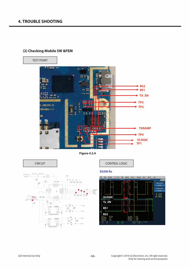
- 66 -LGE Internal Use Only Copyright © 2010 LG Electronics. Inc. All right reserved.Only for training and service purposes
4. TROUBLE SHOOTING
(2) Checking Mobile SW &FEM
4. TROUBLE SHOOTING
TEST POINT
CIRCUIT
Figure 4.2.4
CONTROL LOGIC
EGSM Rx
VLOGIC
Tx_EN
BS1
BS2
TP1
TP2TP3
TP4
BS2BS1
TX_EN
VLOGIC
TXRAMP
Test point
TP1
10
R327
DNIC359
103U
21
11
10
9
8
7
31
6
41
5
51
4
61
3
71
2
18
1
19
20
21
22
23GND_SLUG
VRAMP
TX_ENABLE
GPCTRL0
GPCTRL1
1D
NG
VBATT
2D
NG
2LRT
CP
G
BL_NIF
R
9D
NG
3D
NG
8D
NG
BH_
NIFR
TN
A
4D
NG
4X
R
GND5
GND6
GND7
RX1
RX2
3X
R33pC302
303C
p33
p33403
C
L301 3.3n 3.3nL302
22pC343
3.3nL303
1nL308
1pC305
869M894M,925M960MHz
FL301 SFSB0001803
105
63
72
94
81IN_881_5 OUT_881_5
IN_942_5 OUT_942_5
GND1 GND2
GND3 GND4
GND5 GND6
L306 3.3n
C3141.5p
C31539p
10nC316 C317
4.7u
1nC318
1nC319
DNIC392
VBAT
C32233p
1nC323
1.8n
L320
L3092.2n
33pC325
1nC326
1.8n
L319
1805M1880M,1930M1990M
FL302 SFSB0001903
105
63
72
94
81IN_1842_5 OUT_1842_5
IN_1960 OUT_1960
GND1 GND2
GND3 GND4
GND5 GND6
4.7uC327
L310DNI
56pC306
22p
C396
9.1nL305
27nL312
22p
C398
VLOGICBS2BS1TX_EN
RX12
RX12X
RX34
RX34X
GSM_OUT
DCS_PCS_OUT
TX_RAMP
.
.
.
.
.
.
TP1

- 67 -Copyright © 2010 LG Electronics. Inc. All right reserved.Only for training and service purposes
LGE Internal Use Only
4. TROUBLE SHOOTING
CHECKING FLOW
4. TROUBLE SHOOTING
Check TP1 of SW301
TP1 Signal is OK? Replace Mobile SW (SW301)
Yes
No
Yes
Mobile SW & TX Module is OK.
Check PMB8810Control Signal is
(VLogic, BS1, BS2)OK ?
No
Yes
Check TP4 of U301 ?
Replace FEM (U301)TP2(High Band), TP3(Low Band) Signal is OK ?
No
Yes
EGSM Rx

- 68 -LGE Internal Use Only Copyright © 2010 LG Electronics. Inc. All right reserved.Only for training and service purposes
4. TROUBLE SHOOTING
4.3 TX Trouble
CHECKING FLOW
4. TROUBLE SHOOTING
START
Redownload SW or Do calibration again
HP8960 : Test mode62 CH, 7 level setting (TCH)
62CH, -60dBm setting (BCCH)Spectrum analyzer setting
Oscilloscope setting
(1)CheckCrystal Circuit
(2) CheckMobile SW &FEM
(3) Check PLL Control

- 69 -Copyright © 2010 LG Electronics. Inc. All right reserved.Only for training and service purposes
LGE Internal Use Only
4. TROUBLE SHOOTING
(1) Checking Crystal Circuit
4. TROUBLE SHOOTING
TEST POINT
CIRCUIT WAVEFORM
CHECKING FLOW
Figure 4.3.1
26 MHz O.K?No
Crystal is OK.See next page to check PLL Circuit
Yes
Replace X102
Figure 4.3.2 Figure 4.3.3
1 pin : 26MHz
X101
1 pin
2V85_VSIM
G4
G2
G3
M8
A11
B11
K12
K11
B2
A3
B3
A2
J8
H7USIF2_RTS_N
USIF2_CTS_N
USIF1_TXD_MTSR
USIF1_RXD_MRST
USIF1_RTS_N
USIF1_CTS_N
DPLUS
DMINUS
XOX
XO
VSIM
SIM_IO
SIM_CLK
SIM_RST0.1uC126
26MHz
DSX321G-26MX102
21
34
SIM_CLK
BT_RXDBT_TXDUSB_DPUSB_DM
UART_TXUART_RX
NLB_AD25
NUB
SIM_RST
SIM_DATA
Close to the 26MHz XTAL EINT2
CC1CC6IO
Connect GND plane directly
TP1
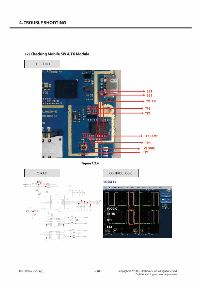
- 70 -LGE Internal Use Only Copyright © 2010 LG Electronics. Inc. All right reserved.Only for training and service purposes
4. TROUBLE SHOOTING
(2) Checking Mobile SW & TX Module
4. TROUBLE SHOOTING
TEST POINT
CIRCUIT
Figure 4.2.4
CONTROL LOGIC
EGSM Tx
VLOGIC
Tx_EN
BS1
BS2
TP1
TP2TP3
TP4
BS2BS1
TX_EN
VLOGIC
TXRAMP
SW301
TP2 TP3
10
R327
DNIC359
103U
21
11
10
9
8
7
31
6
41
5
51
4
61
3
71
2
18
1
19
20
21
22
23GND_SLUG
VRAMP
TX_ENABLE
GPCTRL0
GPCTRL1
1D
NG
VBATT
2D
NG
2LRT
CP
G
BL_NIF
R
9D
NG
3D
NG
8D
NG
BH_
NIFR
TN
A
4D
NG
4X
R
GND5
GND6
GND7
RX1
RX2
3X
R33pC302
303C
p33
p33403
C
L301 3.3n 3.3nL302
22pC343
3.3nL303
1nL308
1pC305
869M894M,925M960MHz
FL301 SFSB0001803
105
63
72
94
81IN_881_5 OUT_881_5
IN_942_5 OUT_942_5
GND1 GND2
GND3 GND4
GND5 GND6
L306 3.3n
C3141.5p
C31539p
10nC316 C317
4.7u
1nC318
1nC319
DNIC392
VBAT
C32233p
1nC323
1.8n
L320
L3092.2n
33pC325
1nC326
1.8n
L319
1805M1880M,1930M1990M
FL302 SFSB0001903
105
63
72
94
81IN_1842_5 OUT_1842_5
IN_1960 OUT_1960
GND1 GND2
GND3 GND4
GND5 GND6
4.7uC327
L310DNI
56pC306
22p
C396
9.1nL305
27nL312
22p
C398
VLOGICBS2BS1TX_EN
RX12
RX12X
RX34
RX34X
GSM_OUT
DCS_PCS_OUT
TX_RAMP
.
.
.
.
.
.
TP2TP�

- 71 -Copyright © 2010 LG Electronics. Inc. All right reserved.Only for training and service purposes
LGE Internal Use Only
4. TROUBLE SHOOTING
CHECKING FLOW
4. TROUBLE SHOOTING
Check TP2& TP3
Mobile SW & FEM is OK.
Yes
TP5 signal same as TP1? Replace SW301
No
Yes
Replace PMB8810 (U101)TP2(High Band), TP3(Low Band) Signal is OK ?
No
Yes
Check PMB8810Control Signal is (VLogic,TX EN, BS1, BS2)OK ?
No
Yes
Yes
Check TP4 of U301 ?
TP1 Signal is OK? Replace FEM (U301)No
EGSM Tx

- 72 -LGE Internal Use Only Copyright © 2010 LG Electronics. Inc. All right reserved.Only for training and service purposes
4. TROUBLE SHOOTING
4.4 Power On Trouble
4. TROUBLE SHOOTING
Figure 4.1
TEST POINT
VMMC
VCORE
VDDMS VDDXO
VDDTDC
VRTCVPMUVAUX
VUSB VDDRF2

- 7� -Copyright © 2010 LG Electronics. Inc. All right reserved.Only for training and service purposes
LGE Internal Use Only
4. TROUBLE SHOOTING
4. TROUBLE SHOOTING
Figure 4.2 power block of LG-C300
CIRCUIT
Figure 4.2 Power block of LG-C300
C1012.2u
1V8_VDD
1V8_VDD
VUSB
1V8_VDD
VBAT
75FB101
R1030
VCORE
1V8_VDD
VDDMS
1V8_VDD
VUSB
VDDTRX
1V8_VDD
1V8_VDD
VDDTDC
C1060.1u
1V8_VDD
1V8_VDD
VDDRF2 VDDTDC
VMMC
470R106
VCORE
Q101
1
23
VMMC
1V8_VDDVRF1
C1110.1u
VAUX
VAUX
0.1uC113
1uC114
VRF1VDDMS
100K
R107
3.3u
101L
VBAT
VDDXO
C1152.2u470n
C117
VBAT_RF2
470nC118
1V8_VDD VPMU
4.7nC119
VBAT
47nC120
C121470n
47nC122
VPMUVBAT
VBAT VDDRF2
0.1uC124
L4A14
K1A15
P2
N1R15
M2T15
N3M11
M1M10
L1N11
K2R11
K3T11
N12
6K
5T
6R
7M
4T
6M
6L
01
L
51
C
51F
01H
31
G
9M
7L
21F
8P
21E
41
G
61
R
21A
21B
11
E
31
H
21G
31A
01J
31
F
41
F
51
P
41P
8G
8K
9J
9H
8F
9T
01P
5R
7K
9G
8N
61P
41
L
7R
7T
6T
7P
1D
S_D
DV
BF_1D
S
1D
S_S
SV
WS_ 1
DS
SM
SS
V
PST
AB
V
UM
P _TA
BV
1OI
DD
V
2OI
DD
V
UB
E_D
DV
UM
PV
UM
P_S
SV
1E
RO
C_S
SV
2E
RO
C_S
SV
3E
RO
C _S
SV
ER
OC
V
ER
OC
DD
V
PC8
V1D
DV
RSL
SS
V
XRT
SS
V
XR
SS
V
18V1
DD
V
PM
AR
V
GID_
SS
V
SM
DD
V
OX
DD
V
CDT
DD
V
DM
MD
DV
GE
ND
DV
TA
BV
OC
DS
SV
XU
AV
OX
SS
V
CM
MV
BS
UV
2 FR
DD
V
1FR
V
OL_S
SV
FR
SS
V
CTR
V
NE
SN
ES
PE
SN
ES
GH
CD
DV
SC
BS
C
GH
CV
TN
HS
V
M0
M1 A_D0
M2 A_D1
VDD_FMR A_D2
FMRIN A_D3
FMRINX A_D4
CP1 A_D5
CP2 A_D6
A_D7
TX1 A_D8
FE2 A_D9
VBAT
C1251u
C1280.1u
VDDXO
C1290.1u
220nC130
VBAT_RF2 VRTC
R1093.9K
220nC131
5.6KR110
18pC132
C107
22u
C147
5p
C133 DNIR111
0
4.7n
C123
211R
0
IND
531C
C134 10u
BS2
FM_ANT
LCD_IDBAT_TEMP
GSM_OUT
TX_RAMP
LDO_OUT
AD09AD08AD07AD06AD05AD04AD03AD02AD01AD00
ABB
(10V)
PIN_H10Seperate and shield
Speaker Supply
(10V)
VDD_IO2
VBATSP
(1%)
PMU PADSRF SUPPLY DOMAIN
VDD1V8CP
VDD_IO1
PIN_H13PIN_B14
RF SUPPLIES (DIRTY GND)
PMU SUPPLIES
PIN K8PIN M9PIN L7PIN P8
RF SUPPLIES (CLEAN GND)
(10V)
VBAT_PMU
PIN P14PIN P16
PIN P10
PIN R5PIN G9
PIN_B12PIN_E11PIN_G14PIN_G13
ABB SUPPLIES
DBB SUPPLIES
PIN K7
PIN N8
VDD_EBU
RF
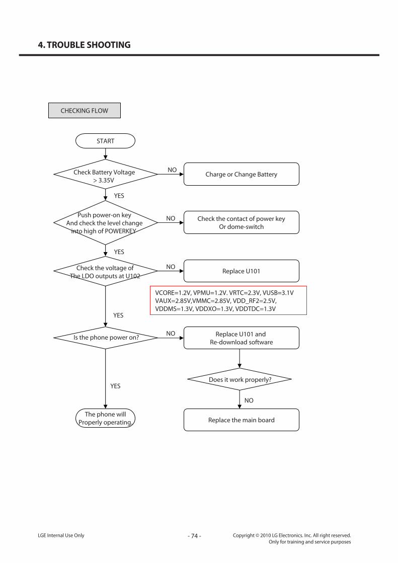
- 74 -LGE Internal Use Only Copyright © 2010 LG Electronics. Inc. All right reserved.Only for training and service purposes
4. TROUBLE SHOOTING
4. TROUBLE SHOOTING
CHECKING FLOW
START
Check Battery Voltage> 3.35V
Push power-on keyAnd check the level change
into high of POWERKEY
Check the voltage ofThe LDO outputs at U102
Is the phone power on?
The phone willProperly operating.
Charge or Change Battery
Check the contact of power keyOr dome-switch
Replace U101
VCORE=1.2V, VPMU=1.2V. VRTC=2.3V, VUSB=3.1VVAUX=2.85V,VMMC=2.85V, VDD_RF2=2.5V, VDDMS=1.3V, VDDXO=1.3V, VDDTDC=1.3V
Does it work properly?
Replace the main board
YES
YES
YES
YES
NO
NO
NO
NO
NO
Replace U101 and Re-download software

- 75 -Copyright © 2010 LG Electronics. Inc. All right reserved.Only for training and service purposes
LGE Internal Use Only
4. TROUBLE SHOOTING
4.5 Charging Trouble
TEST POINT
CIRCUIT
Figure 4.5
4. TROUBLE SHOOTING
CN201
U203
C223
TP1
0.1uC257
1V8_VDD
C2211u
0.1u
C222
VBUS_USB
1u
C223
RT9524EUSY0410801
U203
65
74
83
92
101
11PGND
VIN BATT
ISET PGB
GND1 CHGSB
LDO GND2
IEOC EN_SET
VBAT
100KR217
820
R233
3.9K
R234
CHG_EN
LDO_OUT_EOC
(25V)(10V)
CHARGING IC
TP1

- 76 -LGE Internal Use Only Copyright © 2010 LG Electronics. Inc. All right reserved.Only for training and service purposes
4. TROUBLE SHOOTING
CHECKING FLOW
4. TROUBLE SHOOTING
START
Is I/O Connector(CN201)well-soldered ?
Check the voltage atPin 1 U203 = 5.1V ?
(C223)
YES
YES
Battery is charged?
YES
Charging isproperly operating
NO
NO
NO
Resolder the CN201(Pin 1 : VBUS_USB)
The TA is out of orderChange the TA
Replace the main board
Battery is charged?
NO
Change the battery
Charging isproperly operating
YES

- 77 -Copyright © 2010 LG Electronics. Inc. All right reserved.Only for training and service purposes
LGE Internal Use Only
4. TROUBLE SHOOTING
4. TROUBLE SHOOTING
4.6 Vibrator Trouble
TEST POINT
Figure 4.6
Vibrator PAD
Rear Cover
C254_TP1
L209_TP2

- 78 -LGE Internal Use Only Copyright © 2010 LG Electronics. Inc. All right reserved.Only for training and service purposes
4. TROUBLE SHOOTING
4. TROUBLE SHOOTING
CIRCUIT
MainIC
(U101)
TP1
TP2
9R
5A
5B
8C
8B
8A
8D
4B
31L
51L
61L
4A
8R
8T
01F
9E
9C
9B
9D
01E
01D
3NI _
PK
4NI _
PK
5N I_
PK
0TU
O_P
K
1TU
O_P
K
2 TU
O_P
K
3TU
O_P
K
5TU
O_P
K
B IV
B IV_
SS
V
0 TU
OKL
C
K23 F
K 23C
SO
N_TE
SE
R
N I2 T
0KL
C_1S 2I
XR_1
S 2I
XT _1S2I
0A
W _1S2 I
LC
S _C2 I
AD
S _C2 I
FFO
NO
K23K L
C
TNI _
BB
D_TB
TNI _
C IU
M
XR_
MC
PX T_
MC
P
NE_
ANL_
MF
TC
ETE
D_K
OO
H
TE
D _D
SU
TNI _
YE
K
S TC _T
B
STR_T
B
P_BI
V
PWRON
TE
SE
RN
TNI_I
PS
AD
S_Y
EK
LC
S_Y
EK
5 TNI
E
6 TNI
E
VDDP_DIG1
0TNI
E
4TNI
E
1TN I
E
1TNI
E
0TNI
E
L208 0.1uH
0.1uH
L209
VB201
2
1
33p
C253
1uFC254
VIB_P
SJMY0007110VIB_N
VIB_P
MOTOR
Main IC (U101)
TP1
TP2

- 79 -Copyright © 2010 LG Electronics. Inc. All right reserved.Only for training and service purposes
LGE Internal Use Only
4. TROUBLE SHOOTING
4. TROUBLE SHOOTING
CHECKING FLOW
SETTING : Enter the engineering mode, and set vibrator on at vibration of BB test menu
START
YES
NO
Replace vibrator
YES
VibratorWorking well !
Check the contact pinof vibrator ?
Clean the Pad.
YES
Replace the U102 NOIs the voltage at
Pin (+) high?
YES
Replace the U102 NOIs the voltage at
Vibrator PAD(+) high?

- 80 -LGE Internal Use Only Copyright © 2010 LG Electronics. Inc. All right reserved.Only for training and service purposes
4. TROUBLE SHOOTING
4.7 LCD Trouble
TEST POINT
Figure 4.7
CN403
FL403
FL404
FL405
C415_TP2
R417_TP1
U402

- 81 -Copyright © 2010 LG Electronics. Inc. All right reserved.Only for training and service purposes
LGE Internal Use Only
4. TROUBLE SHOOTING
4. TROUBLE SHOOTING
CIRCUIT
Test point
TP2
TP1
VBAT
444R
smho
K001
1uFC425
1V8_VDD
C426
2.2u
C42727pF
100ohms
R445
VA415
FL403
01
5
64
73
82
91INOUT_A1 INOUT_B1
INOUT_A2 INOUT_B2
INOUT_A3 INOUT_B3
INOUT_A4 INOUT_B4
1G
2G
VMMC
C4281uF
TP402
TP403
TP404TP405
VA416
100ohms
R446
CN403
27
26
25
24
23
22
21
20
19
18
17
16
15
14
13
12
11
10
9
8
7
6
5
4
3
2
1
0.001uFC429
FL404
01
5
64
73
82
91INOUT_A1 INOUT_B1
INOUT_A2 INOUT_B2
INOUT_A3 INOUT_B3
INOUT_A4 INOUT_B4
1G
2G
C4300.001uF
FL405
01
5
64
73
82
91INOUT_A1 INOUT_B1
INOUT_A2 INOUT_B2
INOUT_A3 INOUT_B3
INOUT_A4 INOUT_B4
1G
2G
LCD_RSNLCD_MAIN_CS
LCD_DATA00LCD_DATA01LCD_DATA02LCD_DATA03
LCD_DATA04LCD_DATA05LCD_DATA06LCD_DATA07
LCD_VSYNC
NLCD_WR
_LCD_RESET
LCD_ID
MLED5MLED4MLED3MLED2MLED1
MAKER ID : LOW
LCD CONNECTOR
1u
C401
1u
C402
R427
100K0.1u
C418
2.2u
C419
1u
C433C420
1u
1V8_HPVDD
2.2u
C421 C422
2.2u
VBAT
324C u1
424C u1
U402
24
23
22
21
20
19
18
8
7
6
5
9
4
10
3
11
2
12
1
31 41 51 61 7 1L
CS
AD
S
NE
MW
P
FC
DN
GP
LDO1
N2C
LDO2
N1C
LDO3
P1C
LDO4
P2C
AGND
VIN
LDOIN
LED6
LED5
LED4
LED3
LED2
LED1
VOUT
1V8_VDD
K0 1
344R
CAM_A_2V8
CAM_D_1V5
CAM_IO_1V8
I2C_SCLI2C_SDA
LCD_BL_CTRL
MLED5MLED4MLED3MLED2MLED1
TP�
TP�

- 82 -LGE Internal Use Only Copyright © 2010 LG Electronics. Inc. All right reserved.Only for training and service purposes
4. TROUBLE SHOOTING
4. TROUBLE SHOOTING
Waveform
Graph 4.7.1. LCD Backlight Control Signal Waveform
Graph 4.7.2. LCD Data Waveform
LCD_BL_CTRL
LCD_RS
LCD_CS
LCD_WR

- 8� -Copyright © 2010 LG Electronics. Inc. All right reserved.Only for training and service purposes
LGE Internal Use Only
4. TROUBLE SHOOTING
4. TROUBLE SHOOTING
CHECKING FLOW
START
Is the connection ofCN403 with LCD connector ok ?
YES
NOReassemble LCD connector
NO
Check the Voltage Level of C422 is about Battery voltage ?(LCD_BL_CTRL signal
is high Level)
NO
YES
YES
Check the Waveform ofEMI filter ?
Resoldering or Replace U402
NO
Resoldering EMI filter.(FL403,FL404,FL405)
Does LCD workproperly ?
Replace LCD module
LCD working well !
YES

- 84 -LGE Internal Use Only Copyright © 2010 LG Electronics. Inc. All right reserved.Only for training and service purposes
4. TROUBLE SHOOTING
4. TROUBLE SHOOTING
4.8 Camera Trouble
TEST POINT
Figure 4.8
CN402
C420
U402
C401 C402
TP1
TP2TP3TP4

- 85 -Copyright © 2010 LG Electronics. Inc. All right reserved.Only for training and service purposes
LGE Internal Use Only
4. TROUBLE SHOOTING
CIRCUIT
TP1
TP2
TP3TP4
5pF
FL401
0 15
64
73
82
91INOUT_A1 INOUT_B1
INOUT_A2 INOUT_B2
INOUT_A3 INOUT_B3
INOUT_A4 INOUT_B4
1G
2G
GND
2.2KR407
2.2KR408
C403DNI
C404DNI
CAM_IO_1V8 CAM_D_1V5CAM_A_2V8100KR409
1V8_VDD
0.1uC405
R410 22
R411 51
C4060.1u
C4070.1u
C40856p56p
C40956p
C410
15pC411
15pC412
CN40261413171612518
7594103112121182419232022
52627282920313231
DN
GP
2D
NG
P3
DN
GP
4D
NG
P5
DN
GP
6D
NG
P7
DN
GP
8D
NG
P
D0 PCLKD1 VSYNCD2 HSYNCD3 STANDBYD4 SCKD5 SDAD6 RESETBD7 MCLK
1D
NG
D2
DN
GD
3D
NG
D1
DN
GA
2D
NG
AD
DV
DO I
DD
VD
DV
A
5pFFL402
015
64
73
82
91INOUT_A1 INOUT_B1
INOUT_A2 INOUT_B2
INOUT_A3 INOUT_B3
INOUT_A4 INOUT_B4
1G
2G
CAM_DATA0CAM_DATA1CAM_DATA2CAM_DATA3
CAM_DATA4CAM_DATA5CAM_DATA6CAM_DATA7
CAM_HSYNC
CAM_PCLK
CAM_RESET
CAM_VSYNC
CAM_MCLK
I2C_SCLI2C_SDA
CAM_STANDBY
CAMERA INTERFACE
1u
C401
1u
C402
R427
100K0.1u
C418
2.2u
C419
1u
C433C420
1u
1V8_HPVDD
2.2u
C421 C422
2.2u
VBAT
324C u1
424C u1
U402
24
23
22
21
20
19
18
8
7
6
5
9
4
10
3
11
2
12
1
31 41 51 61 7 1L
CS
AD
S
NE
MW
P
FC
DN
GP
LDO1
N2C
LDO2
N1C
LDO3
P1C
LDO4
P2C
AGND
VIN
LDOIN
LED6
LED5
LED4
LED3
LED2
LED1
VOUT
1V8_VDD
K0 1
344R
CAM_A_2V8
CAM_D_1V5
CAM_IO_1V8
I2C_SCLI2C_SDA
LCD_BL_CTRL
MLED5MLED4MLED3MLED2MLED1
TP1TP2
TP�TP4

- 86 -LGE Internal Use Only Copyright © 2010 LG Electronics. Inc. All right reserved.Only for training and service purposes
4. TROUBLE SHOOTING
4. TROUBLE SHOOTING
Waveform
Graph 4.8.1. I2C Data Waveform
Graph 4.8.3.CAM_VSYNC vs.CAM_HSYNC Waveform
Graph 4.8.2. MCLK Waveform
Graph 4.8.4.CAM_HSYNC vs.CAM_PCLK Waveform
I2C_DATA
CAM_RESET
CAM_MCLK
CAM_MCLK
26MHz
CAM_VSYNC
CAM_HSYNC 26MHz
CAM_HSYNC
CAM_PCLK

- 87 -Copyright © 2010 LG Electronics. Inc. All right reserved.Only for training and service purposes
LGE Internal Use Only
4. TROUBLE SHOOTING
CHECKING FLOW
4. TROUBLE SHOOTING
Is the connection ofCN402 with Camera ok ?
Check the each voltage Level of
C402( 2.8V), C420( 1.8V) is right ?(SWIF signal is high Level)
Does Camera workproperly ?
Check the Waveform of I2C_CLK, I2C_DATA,
CAM_MCLK(26MHz) ?
Check the Waveform ofData pins on CN402?
START
Camera working well !
NO Reassemble camera connectorwith camera.
NO
YES
YES
Resoldering or Replace U402
NO Replace U101 or Change the board
YES
YES
YES
NO Replace U101 or Change the board
NO Replace Camera Module.

- 88 -LGE Internal Use Only Copyright © 2010 LG Electronics. Inc. All right reserved.Only for training and service purposes
4. TROUBLE SHOOTING
4.9 Speaker Trouble
2. TROUBLE SHOOTING
TEST POINT
CIRCUIT
Figure 4.11.1
U202
C210_TP2 C209_TP1
L211_TP4
L210_TP3
C255
C256
TP1TP2
TP3
TP4
R263
DNI
0.1uC203
WM9093ECS-RU202
EUSY0403901
3B
A4
C3
C2
2B
D1
D3
4D
C1
A1D2
1B
D5
A2
A5
A3B5
4B
C5
4C
DN
G
OUT+
DD
VP
H
CPVDDCPVSS
CN
HPL
OUT-
SAI
B
IN2- HPR
IN1+
DD
VS
IN3-
IN2+
AD
S
IN1-
IN3+
CP
LC
S
10uC202
C2040.1u
C2052.2u
C206
2.2u
1uC256
C209
47p
C210
47p
C211
0.1u
C212
0.1u
C213 2.2u
C214 2.2uR20120 20
R208
C218 2.2u
0
R212
1V8_VDD
VBAT
1uC255
1800R238
DNI
FB207
1V8_HPVDD
R250
DNI
I2C_SCL
I2C_SDA
EAR_SPK_NEAR_SPK_P
HP_LOUTHP_ROUT
EAR_GND
EAR_GND
EAR_GND
SPK_NSPK_P
AUDIO AMP SUB SYSTEM & SIGNAL DISTRIBUTOR
TP2
C201100pF
SUSY0024805
CN202
2
1L210
0
C21647pF
C21747pF
VA201 VA202
L211
0
SPK_N
SPK_P
SPK
TP�
TP1
TP4

- 89 -Copyright © 2010 LG Electronics. Inc. All right reserved.Only for training and service purposes
LGE Internal Use Only
4. TROUBLE SHOOTING
CHECKING FLOW
2. TROUBLE SHOOTING
START < Cal l >
Check the state of contact of speaker
Speaker Working well!!
Check the Audio signalC255, C256
No
Yes
Change the U101
Replace/Change speakerNo
Check the Audio signalC210,C209
No Replace/Change the U202
Yes
Yes
START< Mp3>
Check the state of contact of speaker
Speaker Working well!!
Check the Audio signalC255,C256
Yes
Check the Audio signalL210. L211
Yes
Yes
No
No
No

- 90 -LGE Internal Use Only Copyright © 2010 LG Electronics. Inc. All right reserved.Only for training and service purposes
4. TROUBLE SHOOTING
4.10 Earphone Trouble
2. TROUBLE SHOOTING
TEST POINT
Figure 4.11.1
CIRCUIT
U202
C210
FB206_TP4
FB205_TP3
C209
C255_TP1
C256_TP2
TP3
TP4TP1TP2
4.10 Earphone Trouble
2. TROUBLE SHOOTING
TEST POINT
Figure 4.11.1
CIRCUIT
U202
C210
FB206_TP4
FB205_TP3
C209
C255_TP1
C256_TP2
TP3
TP4TP1TP2
R263
DNI
0.1uC203
WM9093ECS-RU202
EUSY0403901
3B
A4
C3
C2
2B
D1
D3
4D
C1
A1D2
1B
D5
A2
A5
A3B5
4B
C5
4C
DN
G
OUT+
DD
VP
H
CPVDDCPVSS
CN
HPL
OUT-
SAI
B
IN2- HPR
IN1+
DD
VS
IN3-
IN2+
AD
S
IN1-
IN3+
CP
LC
S
10uC202
C2040.1u
C2052.2u
C206
2.2u
1uC256
C209
47p
C210
47p
C211
0.1u
C212
0.1u
C213 2.2u
C214 2.2uR20120 20
R208
C218 2.2u
0
R212
1V8_VDD
VBAT
1uC255
1800R238
DNI
FB207
1V8_HPVDD
R250
DNI
I2C_SCL
I2C_SDA
EAR_SPK_NEAR_SPK_P
HP_LOUTHP_ROUT
EAR_GND
EAR_GND
EAR_GND
SPK_NSPK_P
AUDIO AMP SUB SYSTEM & SIGNAL DISTRIBUTOR
762R
0
IN
D
8 62R
C244 47p
0
252R
VAUX
R265
DNI
R264
DNI
270pF
C240
IN
D
522R
0081
402BF
24 2C
F p4 2
L2020.1uH
FB205
1800
VA205
L203
0.1uH1V8_VDD
VA211
VA206
0.1uH
L204
DNI
R239
1800
FB206
270pFC252
VA209
L207
0.1uH
VA210
DNI
R230
R266
DNI
C262DNI
C261
DNI
R251
0
J201
2
3
4
5
6
1 M5
M4
M3
M4F
M1
M6
Q201
S
G
D
062R
01
1V8_VDD
R262
1M
R261
100K
008 1
802BF
FM_ANT
HP_LOUT
HP_ROUT
JACK_DETECT
EAR_GND
EAR_GND
TP2
TP1
TP4
TP�

- 91 -Copyright © 2010 LG Electronics. Inc. All right reserved.Only for training and service purposes
LGE Internal Use Only
4. TROUBLE SHOOTING
CHECKING FLOW
2. TROUBLE SHOOTING
START
YES
Earphone will work properly
Can you hear Your voice fromthe earphone?
Set the audio part of the test Equipment
to echo mode
Change the earphone
and try again
NOCan you hearthe sound fromthe earphone?
Set the audio part of the test equipment to PRBS
or Continuous wave mode
YES
YES
Resolder J201 NO
YES
Can you hearthe sound fromthe earphone?
NO
Change the earphone
and try again
NOCan you hear
Your voice fromthe earphone?
NO
Resolder FB205,FB206
C210,C209 (Call, MP3)
Resolder C255,C256
or Change theU202 & U101
Check the Display on ear-jack
detect icon

- 92 -LGE Internal Use Only Copyright © 2010 LG Electronics. Inc. All right reserved.Only for training and service purposes
4. TROUBLE SHOOTING
4.11 Receiver Trouble
4. TROUBLE SHOOTING
TEST POINT
CIRCUIT
Figure 4.11Receiver
padC142_TP1 C143_TP2
C246_TP4C245_TP3
TP3
TP4
TP1
TP2
1nC102
C105220n
47pC108
47pC109C110
47pC11247p
VMIC
T1
A1
T16
A16
T10
P11
R10
P13
P12
T13
R13
T12
R12
N15
N16
T14
R14
M16
M15
K15
T2
P9
J6
R3
M3
K4
N4
T3
J3A_D21
A_D22
A_D23
A_D24
CS0_N
CS1_N
ADV_N
WAIT_N
ANAMON
BFCLK0
FSYS_EN
EPN
EPP
HSL
HSR
LSN
LSP
MICN1
MICP1
MICN2
MICP2
VMIC
VUMIC
ACD
AGND
VREF
NC1
NC2
NC3
NC4
1nC127
C136DNI 47p
C142C14347pDNI
C144VHSMIC
RCV_N
MIC_N
HS_MIC_NMIC_P
HS_MIC_P
AD22AD21
MEM_CLK
NWAITNADVNRAM_CSNROM_CS
EAR_SPK_NEAR_SPK_P
RCV_P
FSYS_EN
AD23
AD24
PLACE THESE CAPS NEAR BB IC
VDDP_DIG1
TP1SURY0013401
CN204
2
10.1uHL205
L206 0.1uH
VA207
ICVL0518100Y500FR
C24547pF
VA208
ICVL0518100Y500FR
47pFC246
RCV_N
RCV_P
MAIN RECEIVER
TP2
TP�TP4

- 9� -Copyright © 2010 LG Electronics. Inc. All right reserved.Only for training and service purposes
LGE Internal Use Only
4. TROUBLE SHOOTING
CHECKING FLOW
4. TROUBLE SHOOTING
START
Does waveform atC142 and C143
Fluctuate?
NOChange the U101
YES
Receiver will work properly.
Is receiver connectedProperly?
YES
NOResolder/Change the receiver
Does waveform atC245 and C246
Fluctuate?
No Replace/Change the receiver
Yes
SETTING : After initialize Agilent 8960, Test EGSM900, DCS mode ( or GSM850, PCS mode )
Set the property of audio as PRBS or continuous wave. Set the receiving volume of mobile as Max.

- 94 -LGE Internal Use Only Copyright © 2010 LG Electronics. Inc. All right reserved.Only for training and service purposes
4. TROUBLE SHOOTING
4.12 Microphone Trouble
TEST POINT
CIRCUIT
Figure 4.12
2. TROUBLE SHOOTING
C233_TP2C231_TP1 MIC201C236_TP3
TP3
TP1
TP2
VMIC
100n
L201
39p
C230 C231
10u
C232
39p
332C
u1.0
632C
u1.0
C237
39p
C238
39p0
R235D201
SUMY0010609
MIC201
4
3
2
1P
G1
G2
O
VA204VA203
MIC_N
MIC_P
MICROPHONE
TP1
TP2
TP�

- 95 -Copyright © 2010 LG Electronics. Inc. All right reserved.Only for training and service purposes
LGE Internal Use Only
4. TROUBLE SHOOTING
SETTING : After initialize Agilent 8960, Test EGSM900, DCS mode ( or GSM850, PCS mode )
CHECKING FLOW
START
NO
YES
Microphone will workproperly.
YES
Check the signalLevel at each side of MIC201.
Is it a few tensmV AC?
Check the soldering ofC233, C236
Make a phone call, then check C231 mic bias signal
comes from U101?
NO
Change the microphone
YES
NOResolder component
1. Check mic Bias signal line2. Change the U101
Check microphone sound hole
2. TROUBLE SHOOTING

- 96 -LGE Internal Use Only Copyright © 2010 LG Electronics. Inc. All right reserved.Only for training and service purposes
4. TROUBLE SHOOTING
4.13 SIM Card Interface Trouble
TEST POINT
CIRCUIT
Figure 4.13
4. TROUBLE SHOOTING
PIN 6
PIN 4
PIN 1
PIN 3
J401
Pin1Pin3 Pin4Pin6
J401
8 7
6 3
5 2
4 1VCCGND
RSTVPP
CLKI_O
GND1GND2
ZD403 ZD401
R4174.7K
2V85_VSIM
2V85_VSIM
0.1uC413
DNIC414
22pC415
ZD40222pC416
DNIR418
SIM_CLKSIM_RST
SIM_DATA
These are added for CMCC ESD test
ZD200ZD201 is DNI defaultly
SIM_CONNECTOR 1(Default)
PIN6
PIN1PIN�
PIN4

- 97 -Copyright © 2010 LG Electronics. Inc. All right reserved.Only for training and service purposes
LGE Internal Use Only
4. TROUBLE SHOOTING
CHECKING FLOW
4. TROUBLE SHOOTING
START
Does the SIM cardsupport 3V or 1.8V ?
NO Change the SIM Card. This phone supports 3V or 1.8V SIM card.
YES
Is Voltage at the pin1 of J201
2.85V or 1.8V?
NOChange the U101
NO
YES
Resolder J401YES
Voltage output of VSIM LDO
Is 2.85V?
Change the SIM Card and try again.
Does it workProperly?
YES
SIM card is properly working
redownload SW.Does it work
Properly?
NOChange the main board
NO
YES
SIM card is properly working.

- 98 -LGE Internal Use Only Copyright © 2010 LG Electronics. Inc. All right reserved.Only for training and service purposes
4. TROUBLE SHOOTING
4. TROUBLE SHOOTING
4.14 KEY backlight Trouble
TEST POINT
Q201
LD401 ~ LD414
Figure 4.14

- 99 -Copyright © 2010 LG Electronics. Inc. All right reserved.Only for training and service purposes
LGE Internal Use Only
4. TROUBLE SHOOTING
4. TROUBLE SHOOTING
CHECKING FLOW
START
Is Pin3 of Q401 low at KEY_BL_EN
= high ?
NO Check Q401
Are all LEDsWorking?
NO
YES
Check the solderingeach R and LED
Backlight will work properly.
NO
Replace or resoldercomponent
YES
CIRCUIT
TP1LD408 LD406 LD403 LD407 LD404 LD405 LD409 LD410 LD411 LD414 LD413 LD412
D401
051
104R
LD401
Q401
1
23
K001
844R
LD402
VBAT
smho051
034R
smh o051
134R
234R
sm ho05 1
334R
smh o051
smh o051
434R
smho051
534R
smho051
634R
smho051
734R
smho051
834R
smho051
934R
smho051
044R
144R
smho051
244R
smho051
1.2K
R447
0.1u
C431
KEY_BL_EN
TP1

- 100 -LGE Internal Use Only Copyright © 2010 LG Electronics. Inc. All right reserved.Only for training and service purposes
4. TROUBLE SHOOTING
4. TROUBLE SHOOTING
4.15 Micro SD (uSD) Trouble
TEST POINT
CIRCUIT
R211_TP1
Figure 4.15
TP1
3 02D
43
52
61
ENSY0020901S201
1
2
3
4
5
6
7
8
SWA SWB
GND
FB202
202R
smho
K7 4
smh o
K 74
30 2R
47ohms
R204
R205
100Kohms
0.001uFC215
1V8_VDD
VA212
DNI
90 2R
smho
K74
VA213
DNI
smho
K74
0 12R
1 12R
smh o
K74
2.2uF
C220
VMMC
20 2D
43
52
61
USD_DET
USD_CLK
USD_CMD
USD_D1
USD_D2
USD_D3
USD_D0
MICRO SD Connector
TP1

- 101 -Copyright © 2010 LG Electronics. Inc. All right reserved.Only for training and service purposes
LGE Internal Use Only
4. TROUBLE SHOOTING
4. TROUBLE SHOOTING
CHECKING FLOW
Micro SD Card willwork properly
Micro SD DetectOK?
START
NO
YES
Check out MC_CLK & Data
Timing OK?Re-download SWNO
YES
YES
Replace Micro SD Card
Check theR250=2.8V?
YES
NO
Change U101

- 102 -LGE Internal Use Only Copyright © 2010 LG Electronics. Inc. All right reserved.Only for training and service purposes
4. TROUBLE SHOOTING
4. TROUBLE SHOOTING
4.16 Bluetooth Trouble
TEST POINT
CIRCUIT
Figure 4.16.1
C374_TP4 BT_CLK
ANT
U302
C389_TP1
C385_TP2
C386_TP3
Test pointTest point
TP1
TP2TP3
TP4C389 100p
2450MHz
FL303
4231
IN OUTGND1 GND2
TP319
TP321
DNIC393
C371 10p
L3071.2n
613R
0
TP325TP324
TP327TP326
TP322
DNIC391
L318 2.2n
ANT304SNMF0059501
23
1FEED
GND2 GND1
C384 2.2u
673C
IN
D
IN
D573
C
BCM2070CB0KUFBXGU302
2C
2D
2F3D
6C
7A
7G
5E
4E
6B
B7
E3
E6
B3
E8B5
D7
D8G3
C8G2
F5A4
F4
G6C7
F6A8
F3E7
C4F7
B2
B4D1
G4
2A
1C
1B
1E1F
1G
1A
5A
8B8F
5G
6A
8G
3A
TA
BV
3O
DD
V
2O
DD
V
1O
DD
V
3C
DD
V
2C
DD
V
1C
DD
V
GE
RV
XP
DD
V
FR
DD
V
ANL
DD
V
FID
DV
FTD
DV
VH
GE
RV
RES
RFP RST_N
REG_EN
SCL TM0
SDA TM2
SPIM_CLK PCM_IN
SPIM_CS_N PCM_OUT
PCM_CLK
LPO_IN PCM_SYNC
XIN UART_TXD
XOUT UART_RXD
UART_RTS_N
GPIO_0 UART_CTS_N
GPIO_1
TCXO_OR_OUT_GPIO_5
TCXO_OR_IN_GPIO_6
GPIO_7
NI_X
EO
C
0TU
O_X
EO
C
1TU
O_X
EO
C
7S
SV
6S
SV
5S
SV
4S
SV
3S
SV
2S
SV
1S
SV
TP320
TP323
1V8_VDD1nC377
2.2uC386
1V8_VDDVAUX
C3852.2u
0R326
10pC382
10nC381
10nC380
10nC383
10pC378 C379
1u
600
TJ106-5001M1-
BH
FB304
C374 1n
C373 1n
15KR308
DNIC370 C372
DNI
R330
DNI
R329
0
CLK32K
DBB_BT_INT
BT_DBB_INT
BT_CLK
PCM_CLKPCM_RXPCM_TX
PCM_SYNC
BT_CTSBT_RTS
BT_RXDBT_TXD
FSYS_EN
BT_RESET
Bluetooth
TP�TP2
TP1
TP2

- 10� -Copyright © 2010 LG Electronics. Inc. All right reserved.Only for training and service purposes
LGE Internal Use Only
4. TROUBLE SHOOTING
4. TROUBLE SHOOTING
CHECKING FLOW
YES
BT willwork properly
Check condition of matching components
(C389)
A condition is good?NO
YES
Give the additory solder inC389
Check Bias VoltageVAUX at C386
1V8_VDD at C385
YES
NO ReplaceU101
Check the C374 BT_CLK
YES
NO ReplaceU101
Check BT Test point pinNO Replace
U302

- 104 -LGE Internal Use Only Copyright © 2010 LG Electronics. Inc. All right reserved.Only for training and service purposes
4. TROUBLE SHOOTING
4. TROUBLE SHOOTING
4.17 FM Radio Trouble
TEST POINT
CIRCUIT
Figure 4.17
Q301
ANT301L304_TP1
TP1
4.7nC119
B13
C14
E16
F16
C16
D16
A14
A15
R15
T15
M11
M10
N11
R11
T11
N12
41L
7R
7T
6T
7P
1D
S_D
DV
BF_1D
S
1D
S_S
SV
WS_ 1
DS
M0
M1
M2
VDD_FMR
FMRIN
FMRINX
CP1
CP2
TX1
FE2
RX12
RX12X
RX34
RX34X
VDET
C133 DNIR111
0
BS2
FM_ANT
LCD_IDBAT_TEMP
RX12RX12X
RX34RX34X
GSM_OUT Q301
2
13
C3101u
24KR303
22n
L304
R304270ohms
4.7KR305
470n
C312
470n
C313
5.1ohmsR306
27p
C341
270n
L313
C394
27p
ANT301
2
1L314
56n
FM_ANT
FM_LNA_EN
FM_ANT_1
FM_ANT_1
.
C244 47p
0
252R
24 2C
F p4 2
L2020.1uH
L203
0.1uH
VA211
R251
0
J201
2
3
4
5
6
1 M5
M4
M3
M4F
M1
M6
FM_ANT
EAR_GND
TP1

- 105 -Copyright © 2010 LG Electronics. Inc. All right reserved.Only for training and service purposes
LGE Internal Use Only
4. TROUBLE SHOOTING
4. TROUBLE SHOOTING
CHECKING FLOW
A condition is good?
STARTCheck of ear_jack
condition
NO
YES
FM_radio willwork properly
Check condition of matching components
(C389, C371, L318)
A condition is good?NO
YES
Give the additory solder in
C389, C371, L318
Replace J201
Check FM LNA EN(L304)
YES
NO ReplaceU101

- 106 -LGE Internal Use Only Copyright © 2010 LG Electronics. Inc. All right reserved.Only for training and service purposes
5. DOWNLOAD
5. DOWNLOAD
LG-C�00
LG-C�00

- 107 -Copyright © 2010 LG Electronics. Inc. All right reserved.Only for training and service purposes
LGE Internal Use Only
5. DOWNLOAD
LG-C�00
LG-C�00
LG-C�00

- 108 -LGE Internal Use Only Copyright © 2010 LG Electronics. Inc. All right reserved.Only for training and service purposes
5. DOWNLOAD
LG-C�00
LG-C�00
LG-C�00

- 109 -Copyright © 2010 LG Electronics. Inc. All right reserved.Only for training and service purposes
LGE Internal Use Only
5. DOWNLOAD
LG-C�00

- 110 -LGE Internal Use Only Copyright © 2010 LG Electronics. Inc. All right reserved.Only for training and service purposes
5. DOWNLOAD
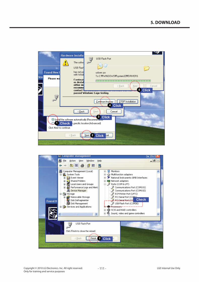
- 111 -Copyright © 2010 LG Electronics. Inc. All right reserved.Only for training and service purposes
LGE Internal Use Only
5. DOWNLOAD

- 112 -LGE Internal Use Only Copyright © 2010 LG Electronics. Inc. All right reserved.Only for training and service purposes
5. DOWNLOAD
‘LG-C�00’

- 11� -Copyright © 2010 LG Electronics. Inc. All right reserved.Only for training and service purposes
LGE Internal Use Only
5. DOWNLOAD

- 114 -LGE Internal Use Only Copyright © 2010 LG Electronics. Inc. All right reserved.Only for training and service purposes
5. DOWNLOAD

- 115 -Copyright © 2010 LG Electronics. Inc. All right reserved.Only for training and service purposes
LGE Internal Use Only
5. DOWNLOAD
LG-C�00
LG-C�00
LG-C�00 ‘LG-C�00’
LG-C�00 LG-C�00
LG-C�00 ‘LG-C�00’
LG-C�00

- 116 -LGE Internal Use Only Copyright © 2010 LG Electronics. Inc. All right reserved.Only for training and service purposes
5. DOWNLOAD
LG-C�00 LG-C�00
LG-C�00 LG-C�00
LG-C�00 LG-C�00

- 117 -Copyright © 2010 LG Electronics. Inc. All right reserved.Only for training and service purposes
LGE Internal Use Only
5. DOWNLOAD
LG-C�00 LG-C�00

- 118 -LGE Internal Use Only Copyright © 2010 LG Electronics. Inc. All right reserved.Only for training and service purposes
5. DOWNLOAD
LG-C�00 LG-C�00
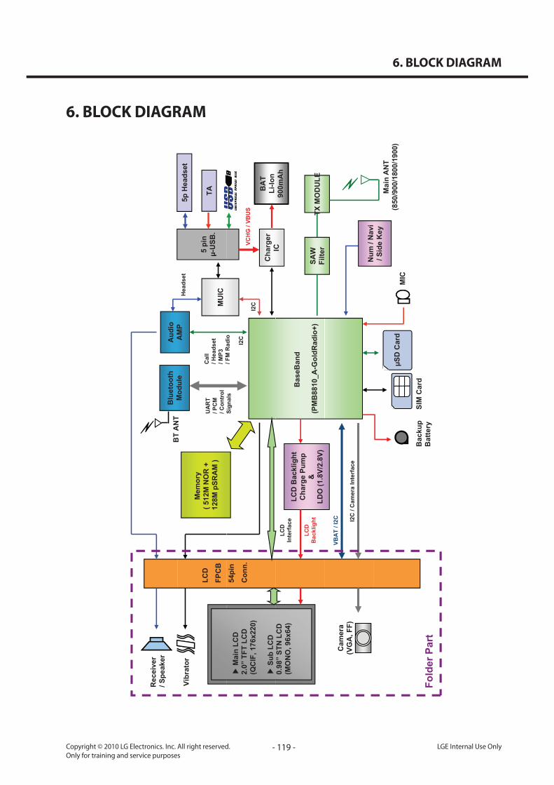
- 119 -Copyright © 2010 LG Electronics. Inc. All right reserved.Only for training and service purposes
LGE Internal Use Only
6. BLOCK DIAGRAM
6. BLOCK DIAGRAMLG
E In
tern
al U
se O
nly
LG-A
133
Blo
ck D
iagr
am
Rec
eive
r/ S
peak
erB
luet
ooth
Mod
leB
TA
NT
Aud
ioA
MP
5 pi
nµ-
USB
.TA
Mem
ory
( 512
M N
OR
+
128M
pSR
AM
)
Vibr
ator
Mod
ule
BT
AN
T
UAR
T/ P
CM
/ Con
trol
Sil
MU
IC
AM
P
Cal
l/ H
eads
et
/ MP3
/FM
Rad
io
5p H
eads
et
LCD
FPC
B
Hea
dset
Mai
n LC
D2.
0” T
FT L
CD
(QC
IF, 1
76x2
20)
Sub
LCD
BA
TLi
-Ion
Cha
rger
IC
Sign
als
VCH
G /
VBU
SI2
C
/FM
Rad
io
I2C
54pi
n
Con
n.
0.98
” ST
N L
CD
(MO
NO
, 96x
64)
900m
Ah
Bas
eBan
d
(PM
B88
10_A
-Gol
dRad
io+)
LCD
Inte
rfac
e
SAW
Filte
rTX
MO
DU
LE
IC
LCD
Bac
klig
htC
harg
e Pu
mp
&LD
O (1
.8V/
2.8V
)
LCD
Bac
klig
ht
Cam
era
(VG
A, F
F)I2
C /
Cam
era
Inte
rfac
e
Num
/ N
avi
VBAT
/ I2
C
MIC
SIM
Car
d
Mai
n A
NT
(850
/900
/180
0/19
00)
µSD
Car
d
/ Sid
e K
ey
Bac
kup
Cha
lleng
e10
10Th
e Pe
ople
Com
pany
Bat
tery
Fold
er P
art

- 120 -LGE Internal Use Only Copyright © 2010 LG Electronics. Inc. All right reserved.Only for training and service purposes

- 121 -
7. CIRCUIT DIAGRAM
LGE Internal Use OnlyCopyright © 2010 LG Electronics. Inc. All right reserved.Only for training and service purposes
R10210K
16 15 14 13 12 11 10 9 8 7 6 5 4 3 2 1
L
K
J
I
H
G
F
E
D
C
B
A
L
K
J
I
H
G
F
E
D
C
B
A
16 15 14 13 12 11 10 9 8 7 6 5 4 3 2 1
C1012.2u
1V8_VDD
1V8_VDD
VUSB
1nC102
1V8_VDD
1V8_VDD
VBAT
75FB101
R1030
VCORE
R104DNI
1V8_VDD
VDDMS
1V8_VDD
VUSB
VDDTRX
1V8_VDD
101TAB
1V8_VDD
1uC104
VDDTDC
C105220n
C1060.1u
1V8_VDD
ON_SW
1V8_VDD
VDDRF2
100KR105
VBUS_USB
47pC108
VDDTDC
VMMC
470R106
47pC109C110
47p
VCORE
841R
K001
Q101
1
23
VRTC
VMMC
1V8_VDDVRF1
C1110.1u
VAUX
VAUX
C11247p
0.1uC113
1uC114
VRF1VDDMS
OJ101
VMIC
100K
R107
VBAT
3.3u
101L
VBAT
VDDXO
C1152.2u
TP101
VDDTRX
100KR108
470nC117
UA101
12
11
10
9
8
7
6
5
4
3
2
1GND
RX
TX
NC1
ON_SW
VBAT
NC2
NC3
NC4
DSR
RTS
CTS
GND
RX
TX
VCHAR
ON_SW
VBAT
PWR
URXD
UTXD
3G 2.5G
2V85_VSIM
VBAT_RF2
470nC118
1V8_VDD VPMU
4.7nC119
VBAT
47nC120
C121470n
47nC122
R137
1K
VPMUVBAT
VBAT VDDRF2
0.1uC124
U101
9R
5A
5B
8C
8B
8A
8D
4B
31
L
51
L
61
L
4A
8R
8T
01
F
9E
9C
9B
9D
01
E
01
D
01
C
01
B
01
A
9A
6E
7G
6F
7E
7F
6G
8E
7C
6C
7B
7A
5C
6B
6A
2D
1G
1F
4D
3C
3E
4F
2E
3F
1B
1C
2C
3D
2F
1D
1E
9L
01
K
8L
F9G10
H11
T1J11
A1F11
T16G11
A16C4
J12
T10J13
P11K16
R10H15
H16
P13G16
P12J16
T13J15
R13H12
T12
R12K5
G5
N15H6
N16H2
T14H3
R14H1
M16
M15G4
G2
K15G3
M8
T2
P9A11
J6B11
R3K12
M3K11
K4B2
N4A3
T3B3
J3A2
R2J8
P4H7
H4J7
J2H8
J4
R1B14
C12
J1B15
R4B16
C13
P3B13
P1C14
P5E16
N2F16
L3C16
L2D16
L4A14
K1A15
P2
N1R15
M2T15
N3M11
M1M10
L1N11
K2R11
K3T11
N12
6K
5T
6R
7M
4T
6M
6L
01L
51C
51F
01H
31G
9M
7L
21F
8P
21E
41G
61R
21A
21B
11E
31H
21G
31A
01J
31F
41F
51P
41P
8G
8K
9J
9H
8F
9T
01P
5R
7K
9G
8N
61P
41L
7R
7T
6T
7P
1D
S_D
DV
BF_1D
S
1D
S_S
SV
WS_ 1
DS
SM
SS
V
PST
AB
V
UM
P _TA
BV
1OI
DD
V
2OI
DD
V
UB
E_D
DV
UM
PV
UM
P_S
SV
1E
RO
C_S
SV
2E
RO
C_S
SV
3E
RO
C _S
SV
ER
OC
V
ER
OC
DD
V
PC8
V1D
DV
RSL
SS
V
XRT
SS
V
XR
SS
V
18V1
DD
V
PM
AR
V
GID_
SS
V
SM
DD
V
OX
DD
V
CDT
DD
V
DM
MD
DV
GE
ND
DV
TA
BV
OC
DS
SV
XU
AV
OX
SS
V
CM
MV
BS
UV
2FR
DD
V
1FR
V
OL_S
SV
FR
SS
V
CTR
V
NE
SN
ES
PE
SN
ES
GH
CD
DV
SC
BS
C
GH
CV
TN
HS
V
M0
M1 A_D0
M2 A_D1
VDD_FMR A_D2
FMRIN A_D3
FMRINX A_D4
CP1 A_D5
CP2 A_D6
A_D7
TX1 A_D8
FE2 A_D9
RX12 A_D10
RX12X A_D11
RX34 A_D12
RX34X A_D13
VDET A_D14
PABS A_D15
PABIAS
FE1 WR_N
TX2 RD_N
PAEN
VDDTRX A_D16
A_D17
USIF2_TXD_MTSR A_D18
USIF2_RXD_MRST A_D19
USIF2_RTS_N A_D20
USIF2_CTS_N A_D21
USIF1_TXD_MTSR A_D22
USIF1_RXD_MRST A_D23
USIF1_RTS_N A_D24
USIF1_CTS_N CS0_N
DPLUS CS1_N
DMINUS ADV_N
XOX WAIT_N
XO ANAMON
BFCLK0
VSIM
SIM_IO FSYS_EN
SIM_CLK
SIM_RST EPN
EPP
MMCI_CMD HSL
MMCI_DAT_0 HSR
MMCI_CLK LSN
MMCI_DAT_1 LSP
MMCI_DAT_2
MMCI_DAT_3 MICN1
MICP1
SWIF_TXRX MICN2
TDO MICP2
TDI VMIC
TMS VUMIC
TCK
TRST_N ACD
TRIG_IN AGND
MON1 VREF
MON2
MON3 NC1
FSYS1 NC2
FSYS2 NC3
DIGUP_CLK NC4
DIGUP1
DIGUP2 VDDFS
NBF
DEL
PBF
DE L
VR
DD
E L
0D_FI
D
1D _FI
D
2D _FI
D
3D_FI
D
4D_FI
D
5D_FI
D
6D _FI
D
7D_FI
D
8D_FI
D
1S
C_FID
DC_FI
D
RW_FI
D
DR_FI
D
DH_FI
D
DV_FI
D
TE
SE
R _FID
0D_FI
C
1D_FI
C
2D _FI
C
3D_FI
C
4D_FI
C
5D_FI
C
6D _FI
C
7D_FI
C
KLC
P_FIC
CN
YS
H_FIC
CN
YS
V _FIC
2 TU
OK L
C
DP_FI
C
TE
SE
R_FIC
0NI_
PK
1NI_
PK
2NI_
PK
3NI_
PK
4NI_
PK
5NI_
PK
0TU
O_P
K
1TU
O_P
K
2TU
O_P
K
3TU
O_P
K
5TU
O_P
K
BIV
BIV_
SS
V
0TU
OKL
C
K23 F
K23C
SO
N_TE
SE
R
NI2T
0KL
C_1S2I
XR_1
S2I
XT_1S2I
0A
W_1S2I
LC
S_C2I
AD
S_C2I
FFO
NO
VBAT
1V8_VDD
C1251u
0.1uC126
2.2u
C146
1nC127
C1280.1u
VDDXO
C1290.1u
220nC130
VBAT_RF2
CN101
9
8
7
6
5
4
3
2
1
VRTC
R1093.9K
220nC131
5.6KR110
18pC132
VRTC
C107
22u
TP102
TP104
TP105
IND
631R
OJ102
C147
5p
C136DNI
1V8_VDD
0.1uR135
0.1u
C137
R113 100KR114 100K
1V8_VDD
0.1u
C138
1u
C139
1V8_VDD
1uC140
1V8_VDD
201D
43
52
61
100KR117
100
R118
C141 470n
C133 DNI
R120DNI
47pC142
R121 100K
TP106
R122
10
TP107
TP108
DNIR123R124
DNI
K7.4
521R
C14347pDNI
C144
10KPT101
10R126
10R127
VHSMIC
U102
C4
C11
E7
D12
D4
E5
D10
E10
D11
E4
G3
G4
F6
F7
G8
G9
F10
F11
F4
F5
G6
G7
F8
F9
G11
G12
K14
K1
H12
H3
C12
C3
A14
A1
D9
G5
F3
E12
D5
G10
E3
H4
D7
H11
E9
E8
E11
E6
F12
D8
D6
H7
C8
C7
D3
H8P_CRE
WAIT_
P_LB_P_UB_P_CE1_
CLK
WE_OE_
AVD_
F1_CE_
F_RST_F_WP_P_CE2
F_DPD
VCC1VCC2
VCCQ1VCCQ2
VSS1VSS2VSS3VSS4
F_VPP
NC1NC2NC3NC4NC5NC6NC7NC8
ADQ0ADQ1ADQ2ADQ3ADQ4ADQ5ADQ6ADQ7ADQ8ADQ9ADQ10ADQ11ADQ12ADQ13ADQ14ADQ15
A16A17A18A19A20A21A22A23A24A25
22p
C103
D101
R111
0
ON_SW
26MHz
DSX321G-26MX102
21
34
C148
DNI
END_KEY
KB101
32.768KHz
FC-135
X101
21
22p
C116F_MODE
R119 43K
4.7n
C123
211R
0
IND
531C
C134 10u
R130100K100K
R131
TP110
U103
65
7
8
4
2
1
3OUT1
IN
OUT2
EN_SET
OUT3
OUT4
GND OUT5
1V8_VDD
R132100K
R133100K100K
R134
C1451u
0AT
AD_
MA
C1
A TA
D_M
AC
2A T
AD_
MA
C3
ATA
D_M
AC
4AT
AD_
MA
C5
A TA
D_M
AC
6AT
AD_
MA
C7
ATA
D_M
AC
CN
YS
H_M
AC
KLC
P _M
AC
TE
SE
R_M
AC
CN
YS
V_M
AC
K23KL
C
KLC
M_M
AC
SR_
DC L
SC_
NIA
M _D
CLN
00AT
AD_
DCL
1 0AT
AD _
DCL
2 0AT
AD _
DCL
30AT
AD_
DCL
4 0AT
AD_
DCL
5 0AT
AD _
DCL
60AT
AD _
DCL
70AT
AD _
DCL
NE_
GH
CT
NI _TB _
BB
D
CN
YS
V_D
CL
RW _
DCL
N
TNI_
BB
D_TB
TNI_
CIU
M
RCV_N
VLOGIC
BS2
FM_ANT
BT_CLK
I2C_SCLI2C_SDA
PCM_CLK
XR_
MC
PXT_
MC
P
PCM_SYNC
SC_I
PS
_LCD_RESET
NE_
ANL_
MF
TC
ETE
D_K
OO
H
TE
D_D
SU
TNI_
YE
K
LCD_IDBAT_TEMP
MIC_N
HS_MIC_NMIC_P
HS_MIC_P
USD_CLK
USD_CMD
USD_D1USD_D2USD_D3
BS1
TX_EN
RX12RX12X
RX34RX34X
SIM_CLK
GSM_OUT
DCS_PCS_OUT
STC_T
B
STR_T
B
BT_RXDBT_TXD
TX_RAMP
P_BI
V
TDO
TDO
TCK
TCK
TMS
TMS
TDI
TDI
LDO_OUT
USB_DPUSB_DM
PWRON
PWRON
PWRON
AD22
AD22
AD21
AD21
AD20
AD20
AD19
AD19
AD18
AD18
AD17
AD17
AD16
AD16
MEM_CLK
MEM_CLK
NWAIT
NWAIT
AD15
AD15
AD14
AD14
AD13
AD13
AD12
AD12
AD11
AD11
AD10
AD10
AD09
AD09
AD08
AD08
AD07
AD07
AD06
AD06
AD05
AD05
AD04
AD04
AD03
AD03
AD02
AD02
AD01
AD01
AD00
AD00
NADV
NADV
NRAM_CS
NRAM_CS
NRD
NRD
NWR
NWR
NRESET
NRESET
TE
SE
RN
NROM_CS
NROM_CS
1V8_VDD
UART_TX
UART_TX
UART_TX
UART_RX
UART_RX
UART_RX
NLB_AD25
NLB_AD25
NLB_AD25NUB
NUB
EAR_SPK_NEAR_SPK_P
ON_SW
ON_SW
RCV_PNTRST
NTRST
CO
E_
USD_D0
TC
ETE
D_K
CAJ
FSYS_EN
BT_RESET
BT_RESET
SIM_RST
SIM_DATA
LCD_BL_CTRL
LCD_BL_CTRLNE_L
B_Y
EK
TNI_I
PS
SPI_MISOSPI_MOSI
SPI_CLK
WLAN_RESET
WLAN_REG_ON
IO_EXPANDER0
IO_EXPANDER0
AD
S_Y
EK
LC
S_Y
EK
YB
DN
ATS_
MA
C
AD23
AD23AD24
AD24
F_MODE
EDOM
_F
CTR_
DD
V
ABB
RF
RF
5TNI
E
INT PORT
0TNI
E
VDDP_SIMBT_DBB_INT
DIF_RESETEINT4
LIGHT BLUERF PADS
(SUPER CAP)
USIF1_CTS_N
Not Assembly BT Model
VDDP_DIG1
(10V)
PIN_H10
PIN COLOR DESCRIPTION
EINT4/EINT1
PT101 is DNI defaultly
Seperate and shield
Speaker Supply
(10V)
MEMORY
6TNI
E
_CHG_EOC
VDD_IO2
PLACE THESE CAPS NEAR BB IC
Close to the 26MHz XTAL
VBATSP
SLIDET2INSIGNAL NAME
DIGUP2
BACKUP BATTERY
ABB
VDDP_DIG1
MUIC_INTCC0CC1IO
ON BOARD ARM9 JTAG & ETM INTERFACE
(1%)
0TNI
E
ABB PADSVDDP_EBU
CC0CC1IO
PMU PADSRF SUPPLY DOMAIN
VDDP_DIG1
VDDP_MMC
DBB SUPPLIES
4TNI
E
VDD1V8CP
EINT2
VDD_IO1
1TNI
E
EINT7CC1CC6IO
EINT0PIN NAME
PIN_H13PIN_B14
RF SUPPLIES (DIRTY GND)
ORANGE
PMU SUPPLIES
PIN K8PIN M9PIN L7PIN P8
VDDP_DIG1
VDDP_ULPI
RF SUPPLIES (CLEAN GND)
(NOT MOUNTED)
1TNI
E
VDDP_DIG1
uSD_DET
(10V)
YELLOW
7TNI
E
VBAT_PMU
PIN P14PIN P16
POWER ON
CC1CC6IO
USIF1_RTS_N
PIN P10
PIN R5PIN G9
1GI
D_P
DD
V
VDDP_DIG2
VDDP_DIG1
EINT3
Connect GND plane directly
CN101 : SW DEBUG
6TNI
E
PIN_B12PIN_E11PIN_G14PIN_G13
UART PORT
CC0CC7IO
OI3C
C1C
C
ABB SUPPLIES
DBB SUPPLIES
PIN K7
PIN N8
(FOR SW DEBUGGING / NOT MOUNTED)
VDD_EBU
0TNI
E
RF
DBB SIGNAL PADSMAGENTA
PMU PADSLIGHT GREEN
(1G NOR AD MUX / 256 pSRAM : De MUX type)
ON BOARD UART/USB INTERFACE
need to replace to 1% (5%) (1%)

7. CIRCUIT DIAGRAM
- 122 -LGE Internal Use Only Copyright © 2010 LG Electronics. Inc. All right reserved.Only for training and service purposes
062C
n1
R263
DNI
FL201
INOUT
GND1GND2
302D
43
52
61
632R
K63
0.1uC203
762R
0
ENSY0020901S201
1
2
3
4
5
6
7
8
SWA SWB
GND
0.1uC257
IN
D
862R
C201100pF
C244 47p
04-5151-005-100-883
ENRY0010801
CN203
15
13
11
9
7
5
4
3
2
1
14
12
10
8
6
16 15 14 13 12 11 10 9 8 7 6 5 4 3 2 1
L
K
J
I
H
G
F
E
D
C
B
A
L
K
J
I
H
G
F
E
D
C
B
A
16 15 14 13 12 11 10 9 8 7 6 5 4 3 2 1
FB202
SUSY0024805
CN202
2
1
VBUS_USB
WM9093ECS-RU202
EUSY0403901
3B
A4
C3
C2
2B
D1
D3
4D
C1
A1D2
1B
D5
A2
A5
A3B5
4B
C5
4C
DN
G
OUT+
DD
VP
H
CPVDDCPVSS
CN
HPL
OUT-
SAI
B
IN2- HPR
IN1+D
DV
S
IN3-
IN2+
AD
S
IN1-
IN3+
CP
LC
S
10uC202
C2040.1u
C2052.2u
C206
2.2u
0
252R
L210
0
1uC256
C209
47p
C210
47p
C211
0.1u
C212
0.1u
C213 2.2u
C214 2.2uR20120
202R
smho
K74
smho
K74
302R
47ohms
R204
R205
100Kohms
0.001uFC215
1V8_VDD
C21647pF
C21747pF
VAUX
VA212
DNI
20R208
C218 2.2u
902R
smho
K74
VA213
DNI
smh o
K74
012R
1 12R
smh o
K74
2.2uF
C220
1V8_VDD
C2211u
0.1u
C222
0
R212
51KR213
0
412R
MUIC_DM
VBUS_USB
1u
C223
VA201
RT9524EUSY0410801
U203
65
74
83
92
101
11PGND
VIN BATT
ISET PGB
GND1 CHGSB
LDO GND2
IEOC EN_SET
R216100K
VA202
1V8_VDD
0.1uC224 C225
39p
VBAT
100KR217
1V8_VDD
10R219
VBAT
VBAT
VMIC
100n
L201
39p
C230 C231
10u
C232
39p
SURY0013401
CN204
2
1
332C
u1.0
R265
DNI
EUSY0407701LMV331U204
4 3
2
5 1IN+VCC
GND
IN-OUT
100uC235
632C
u1.0
C237
39p
C238
39p
R264
DNI
VHSMIC
smho
K5.1
422R
270pF
C240
IN
D
522R
0081
402BF
622R
smho
K022
722R
smho
M1
120pFC241
242C
Fp42
L2020.1uH
FB205
1800
VA205
0.022uFC243
47ohms
R228
L203
0.1uH
VBAT
1V8_VDD
VA211
VBUS_USB
VA206
0.1uH
L204
DNI
R239
VAUX
132R
IN
D
0.1uHL205
L206 0.1uH
VA207
ICVL0518100Y500FR
C24547pF
VA208
ICVL0518100Y500FR
47pFC246
10pFC247
R232
2.2Kohms
1800
FB206
560pFC248
C249
560pF
2.2uFC250
0.022uFC251
270pFC252
VA209
L207
0.1uH
VA210
VMMC
820
R233
3.9K
R234
DNI
R230
202D
43
52
61
R266
DNI
C262DNI
C261
DNI
100R237
0R235
HSBC-3PT25-17N
ENZY0020402
CN201
3
24
1
1uC255
R251
0
D201
1800R238
102CS
21
J201
2
3
4
5
6
1 M5
M4
M3
M4F
M1
M6
DNI
C258
DNI
FB207
SUMY0010609
MIC201
4
3
2
1P
G1
G2
O
Q201
S
G
D
1V8_HPVDD
1V8_VDD
L211
0
VA204VA203
R250
DNI
L208 0.1uH
0.1uH
L209
VB201
2
1
062R
01
1V8_VDD
33p
C253
R262
1M
R261
100K
008 1
802BF
C259270pF
1uFC254
0.1uC226
C2390.1u
R207 1
2.2KR215
FB203 1000
TP201
U201
4B
D2
B2
A1A2
B3
C2
A4
C1
A3D1
E4
D3D4
E3
E2C3
E1C4
1B
YLP
PU
SV
UART_TX VBUS
UART_RX DM
DP
USB_DM ID
USB_DP
AUDIO_L R2_2K
AUDIO_R
MIC
DSS
_INT
SDA CLDO
SCL
GND TE
SI
1 R206
R2182.2K
C227 2.2u
R220DNI
2.2uC228
1.5nC229
1V8_VDD
VBAT
R222 27
R223 27
CHG_EN
MUIC_INT
RCV_N
FM_ANT
I2C_SCL
I2C_SCL
I2C_SDA
I2C_SDA
HOOK_DETECT
USD_DET
BAT_TEMP
MIC_N
HS_MIC_N
MIC_P
HS_MIC_P
USD_CLK
USD_CMD
USD_D1
USD_D2
USD_D3
VIB_P
LDO_OUT
USB_DPUSB_DM
UART_TXUART_RX
EAR_SPK_NEAR_SPK_P
RCV_P
_EOC
USD_D0
HP_LOUT
HP_LOUT
HP_ROUT
HP_ROUT
MUIC_ID
MUIC_ID
MUIC_DM
MUIC_DM
MUIC_DP
MUIC_DP
JACK_DETECTEAR_GND
EAR_GND
EAR_GND
EAR_GND
EAR_GND
SPK_N
SPK_N
SPK_P
SPK_P
SJMY0007110
MUIC
need to replace to 1%
(5%)
(1%)
SPK
5PIN CONNECTOR
(25V)
MICRO SD Connector
3.5phi HEADSETAUDIO AMP SUB SYSTEM & SIGNAL DISTRIBUTOR
MAIN RECEIVER
(1%)
(10V)
BATTERY CONNECTOR
(1%)
( USB & EAR MIC & TA &UART )CHARGING IC
MUST BE PLACED NEAR IO CONNECTOR
MICROPHONE
VIB_N
(25V)
(10V)
VIB_P
MOTOR

- 123 -
7. CIRCUIT DIAGRAM
LGE Internal Use OnlyCopyright © 2010 LG Electronics. Inc. All right reserved.Only for training and service purposes
10
R327
DNIC359
103U
21
11
10
9
8
7
31
6
41
5
51
4
61
3
71
2
18
1
19
20
21
22
23GND_SLUG
VRAMP
TX_ENABLE
GPCTRL0
GPCTRL1
1D
NG
VBATT
2D
NG
2LRT
CP
G
BL_NIF
R
9D
NG
3D
NG
8D
NG
BH_
NIFR
TN
A
4D
NG
4X
R
GND5
GND6
GND7
RX1
RX2
3X
R
123L 2.7n
33pC302
C389 100p
2450MHz
FL303
4231
IN OUTGND1 GND2
303C
p33
p33403
C
L301 3.3n 3.3nL302
Q301
2
13
22pC343
3.3nL303
TP319
TP321
SW301
43
2
1ANT COMMON
G3 G4
DNIC393
1nL308
1pC305
ANT302
C371 10p
C320
1p
GND301 C308
6.8p
C3101u
24KR303
22n
L304
869M894M,925M960MHz
FL301 SFSB0001803
105
63
72
94
81IN_881_5 OUT_881_5
IN_942_5 OUT_942_5
GND1 GND2
GND3 GND4
GND5 GND6
R304270ohms
4.7KR305
470n
C312
470n
C313
L306 3.3n
C3141.5p
C31539p
5.1ohmsR306
10nC316 C317
4.7u
1nC318
1nC319
27p
C341
L3071.2n
DNIC392
VBAT
613R
0
C32233p
1nC323
1.8n
L320
270n
L313
16 15 14 13 12 11 10 9 8 7 6 5 4 3 2 1
L
K
J
I
H
G
F
E
D
C
B
A
L
K
J
I
H
G
F
E
D
C
B
A
16 15 14 13 12 11 10 9 8 7 6 5 4 3 2 1
L3092.2n
33pC325
1nC326
1.8n
L319
1805M1880M,1930M1990M
FL302 SFSB0001903
105
63
72
94
81IN_1842_5 OUT_1842_5
IN_1960 OUT_1960
GND1 GND2
GND3 GND4
GND5 GND6
4.7uC327
L310DNI
TP325TP324
TP327TP326
TP322
DNIC391
L318 2.2n
ANT304SNMF0059501
23
1FEED
GND2 GND1
C384 2.2u
673C
IN
D
C394
27p
56pC306
IN
D573
C
BCM2070CB0KUFBXGU302
2C
2D
2F3D
6C
7A
7G
5E
4E
6B
B7
E3
E6
B3
E8B5
D7
D8G3
C8G2
F5A4
F4
G6C7
F6A8
F3E7
C4F7
B2
B4D1
G4
2A
1C
1B
1E1F
1G
1A
5A
8B8F
5G
6A
8G
3A
TA
BV
3O
DD
V
2O
DD
V
1O
DD
V
3C
DD
V
2C
DD
V
1C
DD
V
GE
RV
XP
DD
V
FR
DD
V
ANL
DD
V
FID
DV
FTD
DV
VH
GE
RV
RES
RFP RST_N
REG_EN
SCL TM0
SDA TM2
SPIM_CLK PCM_IN
SPIM_CS_N PCM_OUT
PCM_CLK
LPO_IN PCM_SYNC
XIN UART_TXD
XOUT UART_RXD
UART_RTS_N
GPIO_0 UART_CTS_N
GPIO_1
TCXO_OR_OUT_GPIO_5
TCXO_OR_IN_GPIO_6
GPIO_7
NI_X
EO
C
0TU
O_X
EO
C
1TU
O_X
EO
C
7S
SV
6S
SV
5S
SV
4S
SV
3S
SV
2S
SV
1S
SV
TP320
ANT301
2
1
TP323
22p
C396
9.1nL305
1V8_VDD1nC377
2.2uC386
1V8_VDDVAUX
C3852.2u
0R326
10pC382
10nC381
10nC380
10nC383
10pC378 C379
1u
600
TJ106-5001M1-
BH
FB304
C374 1n
C373 1n
15KR308
DNIC370 C372
DNI
27nL312
R330
DNI
22p
C398
0513
R
L322
8.2n
L314
56n
R329
0
CLK32K
DBB_BT_INT
BT_DBB_INT
VLOGICBS2
FM_ANT
BT_CLK
PCM_CLKPCM_RXPCM_TX
PCM_SYNC
FM_LNA_EN
BS1TX_EN
RX12
RX12X
RX34
RX34X
GSM_OUT
DCS_PCS_OUT
BT_CTSBT_RTS
BT_RXDBT_TXD
TX_RAMP
FM_ANT_1
FM_ANT_1
FSYS_EN
BT_RESET
LOWLOWLOWLOW
LOWLOW
TX_EN
LOW
.
LOWHIGHHIGHLOW
HIGH
RF PART
.
.
LOWHIGHHIGH
BS2
.
LOWLOWHIGH
MODE
STANDBYEGSM_RX
GSM850_RX
.
.
.
PCS_RXDCS_RXLB_TXHB_TX
VLOGIC
LOWHIGHLOWLOWLOW
HIGHHIGH
BS1
LOWLOW
HIGH
Bluetooth

7. CIRCUIT DIAGRAM
- 124 -LGE Internal Use Only Copyright © 2010 LG Electronics. Inc. All right reserved.Only for training and service purposes
KB431
5pF
FL401
015
64
73
82
91INOUT_A1 INOUT_B1
INOUT_A2 INOUT_B2
INOUT_A3 INOUT_B3
INOUT_A4 INOUT_B4
1G
2G
KB432J401
8 7
6 3
5 2
4 1VCCGND
RSTVPP
CLKI_O
GND1GND2
LD408
KB433
LD406
GND
LD403 LD407 LD404 LD405 LD409 LD410 LD411 LD414 LD413 LD412
D401
051
104R
1u
C401
1u
C402
CN401
4
3
2
1
LD401
Q401
1
23
VA419
KB404
KB434KB430KB435
100ohmsR402
R4033.3K
1V8_VDD
100ohmsR404
R405 100ohms
KB436
R406 100ohms
KB437
KB405KB406KB407KB445
KB411 KB410 KB409 KB438
2.2KR407
KB408 KB403
2.2KR408
C403DNI
KB402 KB401
KB419KB418KB417KB416KB415KB414KB413KB412
KB440 KB439 KB443 KB444
C404DNI
KB421 KB441 KB442
1UFC432
KB420
KB429KB428KB427
CAM_IO_1V8 CAM_D_1V5CAM_A_2V8
KB426KB425
100KR409
1V8_VDD
0.1uC405
KB424KB423
R410 22
KB422ZD403
R411 51
C4060.1u
C4070.1u
C40856p56p
C40956p
C410
15pC411
15pC412
CN402
61413171612518
7594103112121182419232022
52627282920313231
DN
GP
2D
NG
P3
DN
GP
4D
NG
P5
DN
GP
6D
NG
P7
DN
GP
8D
NG
P
D0 PCLKD1 VSYNCD2 HSYNCD3 STANDBYD4 SCKD5 SDAD6 RESETBD7 MCLK
1D
NG
D2
DN
GD
3D
NG
D1
DN
GA
2D
NG
AD
DV
DOI
DD
VD
DV
A
K001
844R
100pFC434
100ohmsR412100ohmsR413
R414 100ohms
R415 100ohms
R416 100ohms
ZD401
R4174.7K
2V85_VSIM
2V85_VSIM
0.1uC413
DNIC414
22pC415
ZD40222pC416
R4193.3K
120K
R420
100ohmsR421R422 100ohms
R423 100ohmsR424 100ohms
100ohmsR425
1UFC417
U401
4 131211 10 198
157
166
175
184
193
202
211
2232425262728292D
NG
P
2D
NG
BTE
SE
R
IX O
X
LE
S_KL
C
DD
V
01P
TEST P40
SEL_28P P41
P57 P42
P56 P43
P55 P44
P17 P45
P15 P46
1D
NG
45P
35P
25P
15P
05P
74P
100ohmsR426
104A
V204
AV
404A
V
504A
V
604A
V
16 15 14 13 12 11 10 9 8 7 6 5 4 3 2 1
L
K
J
I
H
G
F
E
D
C
B
A
L
K
J
I
H
G
F
E
D
C
B
A
16 15 14 13 12 11 10 9 8 7 6 5 4 3 2 1
VA417
R427
100K
R428 100ohmsR429 100ohms
0.1u
C418
2.2u
C419
VA418
LD402
VBAT
5pFFL402
015
64
73
82
91INOUT_A1 INOUT_B1
INOUT_A2 INOUT_B2
INOUT_A3 INOUT_B3
INOUT_A4 INOUT_B4
1G
2G
smho051
034R
smho051
134R
234R
smho051
334R
smho051
smho051
434R
1u
C433
VA403
100pFC435
smho051
534R
100pFC436
944R
IND
smho051
634R
smho051
734R
smho051
834R
704A
V
smho051
934R
smho051
044R
144R
smho051
244R
smho051
804A
V
904A
V
014A
V
114A
V
214A
V
314A
V414
AV
C420
1u
1V8_HPVDD
2.2u
C421 C422
2.2u
VBAT
324C u1
424C u1
U402
24
23
22
21
20
19
18
8
7
6
5
9
4
10
3
11
2
12
1
31 41 51 61 71L
CS
AD
S
NE
MW
P
FC
DN
GP
LDO1
N2C
LDO2
N1C
LDO3
P1C
LDO4
P2C
AGND
VIN
LDOIN
LED6
LED5
LED4
LED3
LED2
LED1
VOUT
1V8_VDD
K01
344R
10R450
CAM_A_2V8
CAM_D_1V5
10R452
CAM_IO_1V8
VBAT
444R
smho
K001
10R451
1uFC425
1V8_VDD
C426
2.2u
C42727pF
100ohms
R445
VA415
FL403
01
5
64
73
82
91INOUT_A1 INOUT_B1
INOUT_A2 INOUT_B2
INOUT_A3 INOUT_B3
INOUT_A4 INOUT_B4
1G
2G
VMMC
C4281uF
TP402
TP403
TP404TP405
VA416
100ohms
R446
CN403
27
26
25
24
23
22
21
20
19
18
17
16
15
14
13
12
11
10
9
8
7
6
5
4
3
2
1
0.001uFC429
FL404
01
5
64
73
82
91INOUT_A1 INOUT_B1
INOUT_A2 INOUT_B2
INOUT_A3 INOUT_B3
INOUT_A4 INOUT_B4
1G
2G
C4300.001uF
FL405
01
5
64
73
82
91INOUT_A1 INOUT_B1
INOUT_A2 INOUT_B2
INOUT_A3 INOUT_B3
INOUT_A4 INOUT_B4
1G
2G
DNIR4181.2K
R447
0.1u
C431
CAM_DATA0CAM_DATA1CAM_DATA2CAM_DATA3
CAM_DATA4CAM_DATA5CAM_DATA6CAM_DATA7
CAM_HSYNC
CAM_PCLK
CAM_RESET
CAM_VSYNC
CAM_MCLK
LCD_RSNLCD_MAIN_CS
LCD_DATA00LCD_DATA01LCD_DATA02LCD_DATA03
LCD_DATA04LCD_DATA05LCD_DATA06LCD_DATA07
LCD_VSYNC
NLCD_WR
I2C_SCL
I2C_SCL
I2C_SDA
I2C_SDA
_LCD_RESET
KEY_INT
LCD_ID
SIM_CLK
KEY_COL0
KEY_COL0
KEY_COL2
KEY_COL2
KEY_COL3
KEY_COL3
KEY_COL4
KEY_COL4
KEY_ROW7
KEY_ROW7
KEY_ROW7
KEY_COL5
KEY_COL5
KEY_COL5
KEY_ROW0
KEY_ROW0
KEY_ROW1
KEY_ROW1
KEY_ROW2
KEY_ROW2
KEY_ROW5
KEY_ROW5
KEY_ROW6
KEY_ROW6
KEY_ROW6
KEY_ROW3
KEY_ROW3
KEY_COL1
KEY_COL1
KEY_ROW4
KEY_ROW4
SIM_RSTSIM_DATA
LCD_BL_CTRL
KEY_BL_EN
KEY_SDA
KEY_SCL
MLED5
MLED5
MLED4
MLED4
MLED3
MLED3
MLED2
MLED2
MLED1
MLED1
CAM_STANDBY
@
Q W E R T Y
CAMERA INTERFACE
U I
O
These are added for CMCC ESD test
ZD200ZD201 is DNI defaultly
P A
SIM_CONNECTOR 1(Default)
S D F G H
J K L
BACK SHIFT
Z X C
V B N M ?(QUES) ENTER LOCK MESSAGE
SENDRIGHT SOFTLEFT SOFTSYM.(PRIOD),(COMMA)SPACE
OK LEFT RIGHT UP DOWN
MAKER ID : LOW
LCD CONNECTOR

- 125 -Copyright © 2010 LG Electronics. Inc. All right reserved.Only for training and service purposes
LGE Internal Use Only
8. BGA PIN MAP
8. BGA PIN MAP
118/133
8 BGA PIN MAP (Top View)
BGA IC pin check (U101)
Ball Diagram (Top View), PMB8810(A-GOLDRADIO+)
: not in use
BGA IC pin check (U102)

- 126 -LGE Internal Use Only Copyright © 2010 LG Electronics. Inc. All right reserved.Only for training and service purposes
8. BGA PIN MAP
BGA IC pin check (U102)
Ball Diagram (Top View), PF38F6066M0Y3DE
: not in use
BGA IC pin check (U101)

- 127 -
9. PCB LAYOUT
LGE Internal Use OnlyCopyright © 2010 LG Electronics. Inc. All right reserved.Only for training and service purposes
104DL
KB
431K
B415
KB
439K
B438
544BK
204DL
134R
014BK
504BK
404BK
014DL
404DL
804DL
KB
435K
B442
KB
426K
B419
314DL
KB
101K
B444
KB
423K
B417
LD407
KB
422K
B416
R434
LD414
KB
443K
B408
KB
402
LD403
LD411
KB
406
KB
432K
B409
KB
440K
B414
KB
433K
B429
KB
413
MIC
201
R235
KB
434K
B428
KB
412D
201
KB
407
034R
KB
430K
B411
KB
427K
B420
LD412
LD409
KB
403
LD406
KB
436K
B441
R432
LD405
KB
425K
B418
KB
401K
B424
KB
437K
B421
LG-C300_MAIN_SPFY0229001-1.0_TOP
MIC201 (Main Mic)- No Mic Operation

9. PCB LAYOUT
- 128 -LGE Internal Use Only Copyright © 2010 LG Electronics. Inc. All right reserved.Only for training and service purposes
L
8
7A CB D E F
G
1
41
K
J
H
G
F
E
D
C
B
A
1
1
D
5
T R MP N JK EFGH D C B
4
5
BA1
A1
16
EDC
202NC
102 NC
R132
914AV
101 D
304 R744 R
102AV
612 C
012L
112L
712 C
202AV
983 C 303LF
U103
R131
714AV
614 R
R118
924 R
824 R
814AV
134 C
634 C
514 R
844 R
254 R
434 C
944 R
154 R
R421914 R
VA
402
183 C
601 R
234 C
223PT
283 C
C355
R107
201 U
R119
832 C
302AV
904 C
R216
CN
402R
201R
208C
117
901 C
C127
201 C
801 C
201PT
J401
804 C
202L
112AV
242 C
C244
L203
012AV
R230
C418
R443
R427
312 C
VA
209
702 R
402BF
502AV
J201
VA
206
C421
U201
201X
231 C
021 C
213L
611 C
L320
903L
C303
X101
301 C
203LF
101TAB
062 R
302 U
103 U
C318
193 C
L318
073 C C371273 C
C387
R332
TP308
R127
CN
401
104 Q
304AV
104 D
302 D
202 D
R126
C353
R135
S201
714 C 024 R
ANT304
U304
C358
C357
R130
TP110
R117
U401
VA
404
VA
405
R425
VA
406R
405
VA
414R
422
R406
R316R
330
C378
C379
C311
C399
L317
R134
202 R312AV
041 C
014AV624 R
054 R534 C
L307
913PT
C201
773 C
083 C
683 C
R329
023PTR326
373 C
483 C
C356
843 C
C301
C145
R109
101 Q
R121 TP
106
701PT
R113
731 C
TP108
R114
R133
R205
C215
402 R
902 R
112 R
012 R
022 C
202BF
212AV
302 R
114AV404 R
104AV
424 R
314AV
204 R
214AV
324 R
314 R
214 R
VA
407
904AV
R414
804AV
C347
522 C
232 C
834 R
NC2
40
802AV
702AV
642 C
602L
542 C
502L
123PT
423PT 523PT 723PT
623PT C383
U302
C349
103X
643 C
833 R
303 U
413 R
543 C
532 C
R110
632 C
R124
C141
R123
102L
732 C
402AV
C231
032 C
934 R
634 R
734 R
044 R
104 R
334 R
144 R
244 R
534 R
403BF
673 C
312 R
C224
C138
C404
R410
583 C
573 C
C412
473 C
323PT
393 C
803 R FL402
912 R
931 C 952 C
C233 304 DZ
414 C 614 C
104 DZ
014 C 604 C
921 C
821 C
C121
601 CR122
021 R
C114
R103
401 R
101TP
C126C
413
C415814 R
204 DZ714 R
401PT
704 C 504 C
212 C
C107
C134
L101
112 C 412 C
552 C
202 U502 C
R212
652 C
C203
C111
501 C
101 C
911 C
C113
C136
111 R
531 C
C124331 C
C110
C144
C112
211 R
501PT
R315
GN
D301
304 C
704 R
R252
R251
R409
804 R
R411
114 C
FL401C
204
R238
C206
202 C
C210
362 R
812 C
C209
052 R
C143031 C
511 C
241 C
914 C
932 R
C401
702BF
C433
R264
C420
C402
204 U
544 R C430
VA
415
C429
R446
VA
416
444 R
524 C
VB
201U
101
C427
C428
902L
C118
R105
C258
R237
R265
C422
C241
R228
632 R
U204
C423
C424 624 C
CN
403
L208
352 C
452 C
C229
TP101
R215
TP201
722 C
822 C
R108
C131
R102
R136
741 C
FB101
413 C
L303
C359
L306S
W301
C308
023 C
L207
FB205
C262
C240
C146
401 C
712 RR
306
403 RL304FB203
321 C
232 R 422 R
052 C
R225
FB206
342 C 942 C
C252
C261
842 CC247
152 C
R266
L204
722 R
R214
R231
622 R
R261
521 R
493 C
313L
R303
413L
Q301
213 C
C313
503 R
143 C
752 C
013 C
R218
C221
R223
R222
R220
R206
C226
C239
221 C
521 C
503L
013L
L319
C396
C398
C322
103LF
C302
C304
713 C
C323
613 C
723 C523 C
C326
841 C
841 R
731 R
201 D
L321L322
AN
T302
FL403
R267
R268
332 R
CN
203C
306C
392
Q201
R262
FB208
304PT
404PT
FL404
504PT
FL405
204PT
103TNA
432 R C260
222 C
C223
FL201
102 CS
103L
503 C
L308
L302C
343
R327
C319
C315
CN
101
LG-C300_MAIN_SPFY0229001-1.0_BOT
CN402 (Camera Module socket)- No Camera
BAT101 (Backup Battery)-RTC Rest
U402 (Charge Pump)- No LCD Backlight
CN403(LCD Connector)- No LCD Display
VB201 (vibrator pad)- No vibrator
U203 (Charging IC)- No Charging
U201 (MUIC)- No Booting- No USB/Serial Connection
X102 (X-tal 26M)- No Power On- No Service
U301 (PAM)- No Call
ANT302 (Main RF contact pad)
U302 (BT Module)- No BT Operation
U202 (Audio AMP)- No Sound
CN201(Battery Connector)- No Power On
CN401 (Side-key pad)- No side key Operation
U102 (Memory)- No Power On- No Download
U101 (BB IC)- No Power On- No Download- No Display
S201 (µ-SD Connector)- No µ-SD Operation
J401 (SIM Connector)- No SIM Operation
U401(Tr. for Key Backlight)- No Key Backlight

- 129 -Copyright © 2010 LG Electronics. Inc. All right reserved.Only for training and service purposes
LGE Internal Use Only
10.ENGINEERING MODE
10.ENGINEERING MODE10. ENGINEERING MODE
9. ENGINEERING MODE
Engineering mode is designed to allow a service man/engineer to view and test the basic functions provided by a handset. The key sequence for switching the engineering mode on is “1809#*300# “Select. Pressing END will switch back to non-engineering mode operation. Use Up and Down key to select a menu and press ‘select’ key to progress the test. Pressing ‘back key will switch back to the original test menu.
[1] DEVICE TEST
[1-1] Auto All Test
[1-2] Main LCD
[5] Factory Reset
[3] SW Sanity Test
[4] Version
[2] ELT Mode
[3-1] FPRI Test
[1] Usage Info
[2-1] Band Selection[2-2] Battery Info[2-3] Audio Tunning[2-4] UART Setting[2-5] BT Testing[2-6] Defect Report System
[1-3] Sub LCD[1-4] LCD Backlight[1-5] Key Backlight[1-6] Speaker[1-7] Vibrator[1-8] Camera[1-9] Sub Camera[1-10] Mic Loopback[1-11] Key Press Test[1-12] Speaker Vib Test
[2] Eng Mode
[3-2] DB Check[3-3] E Serial NO[3-4] UA.String[3-5] Unlock SIM
1. Factory Mode 2. Eng Mode
[3] Band Select[3-1] Auto[3-2] GSM 850[3-3] GSM900[3-4] DCS 1800[3-5] PCS 1900
[4] Network Info
[3-1] Cell Env. (Idle)[3-2] Cell Env. (Ded)[3-3] PS Log Save[3-4] TCPIP Debug[3-5] PCS 1900
[5] Other[5-1] Bluetooth Test Menu[5-2] PS Attach Mode[5-3] MMS Test[5-4] SIM Info
[6] Debug Setting[5-1] Variable Watch[5-2] Heap Freesize[5-3] Heap Leakage[5-4] Heap Assert[6-5] QM Heap Freesize[6-6] Developer Debug

- 1�0 -LGE Internal Use Only Copyright © 2010 LG Electronics. Inc. All right reserved.Only for training and service purposes
11. STAND ALONE TEST
11. STAND ALONE TEST11. STAND ALONE TEST
11.1 IntroductionThis manual explains how to examine the status of RX and TX of the model.
A. Tx TestTX test - this is to see if the transmitter of the phones is activating normally.
B. Rx TestRX test - this is to see if the receiver of the phones is activating normally.
11.2 Setting Method
10. STAND ALONE TEST
1. Set COM Port2. Check PC Bau Rate3. Confirm EEPROM & Delta file prefix name

- 1�1 -Copyright © 2010 LG Electronics. Inc. All right reserved.Only for training and service purposes
LGE Internal Use Only
11. STAND ALONE TEST
10. STAND ALONE TEST
Not Connected
Connected
4. Click “Update Info” for communicating Phone and Test-Program

- 1�2 -LGE Internal Use Only Copyright © 2010 LG Electronics. Inc. All right reserved.Only for training and service purposes
11. STAND ALONE TEST
Change “ptest mood”
5. For the purpose of the Standalone Test, Change the Phone to “ptest mode” and then Click the “Reset” bar.
6. Select “Non signaling” in the Quick Bar menu. Then Standalone Test setup is finished.

- 1�� -Copyright © 2010 LG Electronics. Inc. All right reserved.Only for training and service purposes
LGE Internal Use Only
11. STAND ALONE TEST
10. STAND ALONE TEST
1. “Non signaling mode” bar and then confirm “OK” text in the command line.
11.3 Tx Test

- 1�4 -LGE Internal Use Only Copyright © 2010 LG Electronics. Inc. All right reserved.Only for training and service purposes
11. STAND ALONE TEST
2. Put the number of TX Channel in the ARFCN3. Select “Tx” in the RF mode menu and “PCL” in the PA Level menu.4. Finally, Click “Write All” bar and try the efficiency test of Phone.

- 1�5 -Copyright © 2010 LG Electronics. Inc. All right reserved.Only for training and service purposes
LGE Internal Use Only
11. STAND ALONE TEST
10. STAND ALONE TEST
11.4 Rx Test
1. Put the number of RX Channel in the ARFCN.2. Select “Rx” in the RF mode menu.3. Finally, Click “Write All” bar and try the efficiency test of Phone.

- 1�6 -LGE Internal Use Only Copyright © 2010 LG Electronics. Inc. All right reserved.Only for training and service purposes
10. STAND ALONE TEST
Change “normal mode “
4. The Phone must be changed “normal mode” after finishing Test. 5. Change the Phone to “normal mode” and then Click the “Reset” bar.
11. STAND ALONE TEST

- 1�7 -Copyright © 2010 LG Electronics. Inc. All right reserved.Only for training and service purposes
LGE Internal Use Only
12.AUTO CALIBRATION
12.AUTO CALIBRATION
12.1 Overview
Auto-cal (Auto Calibration) is the PC side Calibration tool that perform Tx, Rx and BatteryCalibration with Agilent 8960(GSM call setting instrument) and Tektronix PS2521G(ProgrammablePower supply).Auto-cal generates calibration data by communicating with phone and measuring equipment thenwrite it into calibration data block of flash memory in GSM phone.
12. AUTO CALIBRATION
11. AUTO CALIBRATION
CM_GSM_MULTI
Common
Debug
dll,ocx
Hot_Kimchi
Model
UI
Multi_HK
LG_UI_Ad6500_004.dll
KF300d
Spec_GD350_001
dwdio.dll
LG_RfCal_InfiKE000Ag_177.dll
LG_RfTest_E5515C_122.dll
xmm2130_eep008.cfg
AutoSetup_GD350_001
Ezlooks
Procedure_GD350_001
PwrSupply_Cmd
script_001
Setup_Cal_Parameter_001
PwrSupply_Cmd
DLL_PwrControlD.dll
Dll_SerialATD.dll
LG_CL_039.dll
At_Serial_Cmd
ComLMPLib_1_11.dll
HK_40
ShieldBox_DllD.dll
GuiTk115d.dll
Dll_EzLooksMQ_016.dll
ComLMPLib_2_11.dll
Debug
Result
Auto
CalAuto
Cal
DLL_E5515CD.DLL
(Windows 98)MFCD DLL COPY
vsflex7l_ocx_regist
(Windows XP)MFCD DLL COPY
(Windows 2000)MFCD DLL COPY
12.2 Configuration of HotKimchi
12.1 Overview
LG-C�00
LG-C�00
LG-C�00
LG-C300

- 1�8 -LGE Internal Use Only Copyright © 2010 LG Electronics. Inc. All right reserved.Only for training and service purposes
12.AUTO CALIBRATION
12.3 Description of Basic File
12.1 Common-. LG_CL_039.dll : Common logic dll, Module In Charge of Reading PID & S/W Version, Booting.-. Dll_SerialATD.dll : Serial Communication Module From Phone by AT Command.-. DLL_PwrControlD.dll : Communication Module From Power supply.-. DLL_E5515CD.DLL : Communication Module From Agilent 8960(Test Set).-. At_Serial_Cmd.xml : Definition File of AT Command.-. PwrSupply_Cmd.xml : Definition File of Power supply command.
12.2 Debug-. Debug - Cal : Result File of Calibration.
Auto : Result File of Auto Test.CalAuto : Result File of Cal & Auto Test.
12.3 dll, ocx-. vsflex7l_ocx_regist : Registration File for System use
-. Windows XXX)MFCD DLL : Registration File for System use
12.4 HotKimchi-. HK_40.exe : Execute File, HK_XX XX is File Version.-. ComLMPLib_1_11.dll : Communication Module With PLC or Shield Box In Automation Rack.
Support to J&S Shield Box and Tescom TC-5981A.-. ComLMPLib_2_11.dll : Communication Module With PLC or Shield Box In Automation Rack.
Support to J&S Shield Box and Tescom TC-5981A.-. Dll_EzLooksMQ_005.dll : Communication Module with ezTray Installed In Local PC.-. GuiTk115d.dll : control library-. ShieldBox_DllD.dll : Communication with Shield Box. Support to Tescom TC-5952B.
12.5 Model-. LG_RfCal_InfiKE000Ag_177.dll : Main Module of Calibration-. LG_RfTest_E5515C_122.dll : Main Module of Auto Test-. Xmm2130_eep008.cfg : Cal Data Save binary Module.-. AutoSetup_LG-A133_100.xml : RF TEST Setup Module.-. Ezlooks.xml : Calibration ezLooks Item & Cal Spec Definition Module.-. Procedure_LG-A133_001.xml : RF TEST Procedure Definition Module.-. Script_001.xml : RF TEST Setup calibration Setup Module.-. Spec_LG-A133_001.xml : Definition Module of Auto Test Spec -. Setup_Cal_Parameter_001.xml : Calibration Definition Module.
11. AUTO CALIBRATION
LG-C300
LG-C300
LG-C300&
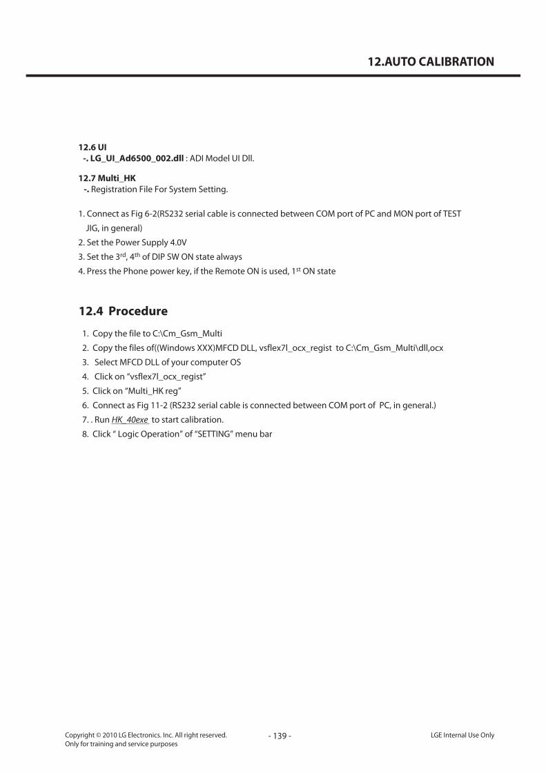
- 1�9 -Copyright © 2010 LG Electronics. Inc. All right reserved.Only for training and service purposes
LGE Internal Use Only
12.AUTO CALIBRATION
1. Connect as Fig 6-2(RS232 serial cable is connected between COM port of PC and MON port of TEST
JIG, in general)
2. Set the Power Supply 4.0V
3. Set the 3rd, 4th of DIP SW ON state always
4. Press the Phone power key, if the Remote ON is used, 1st ON state
1. Copy the file to C:\Cm_Gsm_Multi
2. Copy the files of((Windows XXX)MFCD DLL, vsflex7l_ocx_regist to C:\Cm_Gsm_Multi\dll,ocx
3. Select MFCD DLL of your computer OS
4. Click on “vsflex7l_ocx_regist”
5. Click on “Multi_HK reg”
6. Connect as Fig 11-2 (RS232 serial cable is connected between COM port of PC, in general.)
7. . Run HK_40exe to start calibration.
8. Click “ Logic Operation” of “SETTING” menu bar
11. AUTO CALIBRATION
12.4 Procedure
12.6 UI-. LG_UI_Ad6500_002.dll : ADI Model UI Dll.
12.7 Multi_HK-. Registration File For System Setting.

- 140 -LGE Internal Use Only Copyright © 2010 LG Electronics. Inc. All right reserved.Only for training and service purposes
12.AUTO CALIBRATION
9. Set PORT (using RS232 cable) that PC can communicate with the phone
11. AUTO CALIBRATION
10. Select “ LOGIC MODE” that you want
Logic mode: 1-> Calibration only2-> Auto test only
3-> Cal & Auto

- 141 -Copyright © 2010 LG Electronics. Inc. All right reserved.Only for training and service purposes
LGE Internal Use Only
12.AUTO CALIBRATION
11. AUTO CALIBRATION
11. Select the model name “LG-A133”
12. Click “start” button
Model name Start button
LG-C�00
LG-C�00
LG-C�00

- 142 -LGE Internal Use Only Copyright © 2010 LG Electronics. Inc. All right reserved.Only for training and service purposes
12.AUTO CALIBRATION
11. AUTO CALIBRATION
12.5 AGCThis procedure is for Rx calibration.In this procedure, We can get RSSI correction value. Set band EGSM and press Start button theresult window will show correction values per every power level and gain code and the samemeasure is performed per every frequency.
12.6 APCThis procedure is for Tx calibration.In this procedure you can get proper scale factor value and measured power level.
12.7 ADCThis procedure is for battery calibration.You can get main Battery Config Table and temperature Config Table will be reset.
12.8 Target Power
29dBm29dBm29dBmMax power
1909.8 MHz1880 MHz1850.2 MHzFrequency
810661512Channel
PCS 1900
29.5dBm29.5dBm29.5dBmMax power
1784.8 MHz1747.6 MHz1710.2 MHzFrequency
885699512Channel
DCS1800
32.3dBm32.3dBm32.3dBmMax power
914.8 MHz897.4 MHz880.2 MHzFrequency
12437975Channel
EGSM 900
32.3dBm32.3dBm32.3dBmMax power
848.8 MHz836.8 MHz824.2 MHzFrequency
251191128Channel
GSM 850
HighMiddleLowDescriptionBAND

- 143 -
13. EXPLODED VIEW & REPLACEMENT PART LIST
13.1 EXPLODED VIEW
LGE Internal Use OnlyCopyright © 2010 LG Electronics. Inc. All right reserved.Only for training and service purposes
Location No. Part Name
ACGA00 COVER, BATTERY, ASSY
SBPL00 BATTERY
GMEY00 SCREW
SNGF00 INTENNA, MAIN
SJMY00 MOTOR
SUSY00 SPEAKER
SNGF01 INTENNA, FM
ACGM00 COVER, REAR, ASSY
ACKA00 CAN, SHIELD, ASSY
SVCY00 CAMERA
MIC201 MICROPHONE
ADCA00 DOME, METAL ,ASSY
SPKY00 PCB, SIDE KEY
SURY00 RECEIVER
SVLM00 LCD
SAFY00 PCB, ASSY
AKAC00 KEYPAD, MAIN
AKAD00 KEYPAD, SUB
MBJZ00 BUTTON, VOLUME
MTAD00 TAPE, WINDOW, LCD
MWAC00 WINDOW, LCD
ACGK00 COVER, FRONT, ASSY
ACGK00
MWAC00 MTAD00
SVLM00 SURY00
SVCY00SNGF01
SUSY00
SJMY00
SNGF00
GMEY00
SBPL00
SPKY00
ACKA00
MIC201
ADCA00
MBJZ00
AKAD00
AKAC00
SAFY00 ACGM00 ACGA00

- 144 -LGE Internal Use Only Copyright © 2010 LG Electronics. Inc. All right reserved.Only for training and service purposes

- 145 -Copyright © 2010 LG Electronics. Inc. All right reserved.Only for training and service purposes
LGE Internal Use Only
13. EXPLODED VIEW & REPLACEMENT PART LIST
by SBOM standard on GCSC
Level LocationNo. Description Part Number Spec Color Remark
1 GSM,BAR/FILP TGSM0088401 WHITEORANGE
2 AAAY00 ADDITION AAAY0486204 WHITEORANGE
3 ACGA00 COVER ASSY,BATTERY ACGA0041303 PINK
4 MCJA00 COVER,BATTERY MCJA0127001 MOLD, PC LUPOY SC-1004A, , , , , WHITE
2 APAY00 PACKAGE APAY0151001 LG-C300 STD(EU1) WITHOUTCOLOR
3 APLY00 PALLET ASSY APLY0003901 EU1 TYPE_Body(SW)+Cap(EU)+AL_1200EA WITHOUTCOLOR
4 MBEC00 BOX,CARTON MBEC0003601 BOX, TW, , , , , WITHOUTCOLOR
4 MCCL00 CAP,BOX MCCL0002501 BOX, TW, , , , , WITHOUTCOLOR
4 MPCY00 PALLET MPCY0012403 COMPLEX, (empty), , , , , DARK BLUE
3 MBAD00 BAG,VINYL(PE) MBAD0005204 COMPLEX, (empty), , , , , WITHOUTCOLOR
3 MBEE00 BOX,MASTER MBEE0061001 BOX, TW, , 307, 170, 251, 1 COLOR WITHOUTCOLOR
3 MBEF00 BOX,UNIT MBEF0148902 BOX, TW, , , , , WITHOUTCOLOR
3 MLAC00 LABEL,BARCODE MLAC0004541 PRINTING, (empty), , , , , WithoutColor
3 MLAJ00 LABEL,MASTER BOX MLAJ0004402 LABEL,MASTER BOX(for CGR TDR 2VER. mbox_label) WithoutColor
3 MLAZ01 LABEL MLAZ0050901 PRINTING, (empty), , , , , WITHOUTCOLOR
2 APEY PHONE APEY0915204 WHITEORANGE
3 ACGY COVER ASSY,EMS ACGY0007804 WHITEORANGE
4 ACGK00 COVER ASSY,FRONT ACGK0162601 WHITE
5 AKAC00 KEYPAD ASSY,MAIN AKAC0014501 WITHOUTCOLOR
13.2 Replacement Parts Note: This Chapter is used for reference, Part order is ordered
<Mechanic component>

- 146 -LGE Internal Use Only Copyright © 2010 LG Electronics. Inc. All right reserved.Only for training and service purposes
13. EXPLODED VIEW & REPLACEMENT PART LIST
Level LocationNo. Description Part Number Spec Color Remark
5 AKAD00 KEYPAD ASSY,SUB AKAD0004301 WITHOUTCOLOR
5 MBJZ00 BUTTON MBJZ0034001 MOLD, PC LUPOY SC-1004A, , , , , WITHOUTCOLOR
5 MCJK00 COVER,FRONT MCJK0130101 MOLD, PC LUPOY SC-1004A, , , , , COLORUNFIXED
5 MDAY00 DECO MDAY0073101 MOLD, PC LUPOY SC-1004A, , , , , WITHOUTCOLOR
5 MDAY01 DECO MDAY0073001 COMPLEX, (empty), , , , , WITHOUTCOLOR
5 MPBG00 PAD,LCD MPBG0110201 COMPLEX, (empty), , , , , WITHOUTCOLOR
5 MPBZ00 PAD MPBZ0297701 COMPLEX, (empty), , , , , WITHOUTCOLOR
5 MPBZ01 PAD MPBZ0297601 COMPLEX, (empty), , , , , WITHOUTCOLOR
5 MTAB00 TAPE,PROTECTION MTAB0402101 COMPLEX, (empty), , , , , WITHOUTCOLOR
5 MTAD00 TAPE,WINDOW MTAD0128001 COMPLEX, (empty), , , , , WITHOUTCOLOR
5 MTAZ00 TAPE MTAZ0317501 COMPLEX, (empty), , , , , WITHOUTCOLOR
5 MWAC00 WINDOW,LCD MWAC0145101 MOLD, Tempered Glass, , , , , WITHOUTCOLOR
4 ACGM00 COVER ASSY,REAR ACGM0162301 ORANGE
5 MCCE00 CAP,RECEPTACLE MCCE0059601 MOLD, PC LUPOY SC-1004A, , , , , WITHOUTCOLOR
5 MCJN00 COVER,REAR MCJN0122801 MOLD, PC LUPOY SC-1004A, , , , , ORANGE
5 MDAY00 DECO MDAY0073201 MOLD, PC LUPOY SC-1004A, , , , , WITHOUTCOLOR
5 MFBC FILTER,SPEAKER MFBC0051901 COMPLEX, (empty), , , , , BLACK
5 MLAB LABEL,A/S MLAB0001102 C2000 USASV DIA 4.0 WHITE
5 MPBN00 PAD,SPEAKER MPBN0095501 COMPLEX, (empty), , , , , WITHOUTCOLOR
5 MPBT00 PAD,CAMERA MPBT0095601 COMPLEX, (empty), , , , , WITHOUTCOLOR
5 MPBZ00 PAD MPBZ0361301 COMPLEX, (empty), , , , , WITHOUTCOLOR
5 MSAZ00 SHEET MSAZ0074201 COMPLEX, (empty), , , , , WITHOUTCOLOR
5 MTAA00 TAPE,DECO MTAA0223901 COMPLEX, (empty), , , , , WITHOUTCOLOR

- 147 -Copyright © 2010 LG Electronics. Inc. All right reserved.Only for training and service purposes
LGE Internal Use Only
13. EXPLODED VIEW & REPLACEMENT PART LIST
Level LocationNo. Description Part Number Spec Color Remark
5 MWAE00 WINDOW,CAMERA MWAE0062101 CUTTING, PMMA MR 200, , , , , WITHOUTCOLOR
4 GMEY00 SCREW MACHINE,BIND GMEY0014301 2.7 mm,3.5 mm,MSWR3 ,Ni,+ ,NYLOK(0.6) Silver
6 ACKA00 CAN ASSY,SHIELD ACKA0037201 WITHOUTCOLOR
7 MAAA00 ABSORBER,ELECTROMAGNETIC WAVE MAAA0007501 COMPLEX, (empty), , , , , WITHOUT
COLOR
7 MCBA00 CAN,SHIELD MCBA0077401 PRESS, STS, , , , , WITHOUTCOLOR
6 ADCA00 DOME ASSY,METAL ADCA0114601 WITHOUTCOLOR
6 MIDZ00 INSULATOR MIDZ0255401 COMPLEX, (empty), , , , , WITHOUTCOLOR
6 MIDZ01 INSULATOR MIDZ0255501 COMPLEX, (empty), , , , , WITHOUTCOLOR
6 MIDZ02 INSULATOR MIDZ0280901 COMPLEX, (empty), , , , , WITHOUTCOLOR
6 MPBZ00 PAD MPBZ0355701 COMPLEX, (empty), , , , , WITHOUTCOLOR
6 MSAZ00 SHEET MSAZ0073801 COMPLEX, (empty), , , , , WITHOUTCOLOR
6 MTAC00 TAPE,SHIELD MTAC0094601 COMPLEX, (empty), , , , , TRANSPARENT
6 MTAZ00 TAPE MTAZ0317701 COMPLEX, (empty), , , , , WITHOUTCOLOR
6 MLAZ00 LABEL MLAZ0038301 PID Label 4 Array WITHOUTCOLOR
7 ANT301 CONTACT MCIZ0004401 PRESS, STS, 0.12, , , , WITHOUTCOLOR
7 SC201 CAN,SHIELD MCBA0059201 PRESS, STS, , , , , WITHOUTCOLOR
3 MLAA00 LABEL,APPROVAL MLAA0062303 COMPLEX, (empty), , , , , WITHOUTCOLOR

- 148 -LGE Internal Use Only Copyright © 2010 LG Electronics. Inc. All right reserved.Only for training and service purposes
13. EXPLODED VIEW & REPLACEMENT PART LIST
by SBOM standard on GCSC
Level LocationNo. Description Part Number Spec Color Remark
5 SJMY00 VIBRATOR,MOTOR SJMY0007905 3 V,0.08 A,5.8*5.1*9 ,cylinder motor ,; ,3V , , ,11000 , , ,,29
5 SNGF ANTENNA,GSM,FIXED SNGF0061901 3.0 ,-5.0 dBd, ,LG-C300 FM Internal_FPCB, Pb-Free ,;,SINGLE ,-5.0 ,50ohm ,3.0
5 SNGF00 ANTENNA,GSM,FIXED SNGF00618013.0 ,-2.0 dBd, ,LG-C300 Main InternalGSM850+900+1800+1900, Pb-Free ,; ,QUAD ,-2.0,50ohm ,3.0
5 SUSY00 SPEAKER SUSY0024805 PIN ,8 ohm,91 dB,16 mm,3.4T spring 0.9W ,; , , , , , ,,CONTACT
4 SAFY PCB ASSY,MAIN SAFY0376404
5 SAFB00 PCB ASSY,MAIN,INSERT SAFB0121301
6 BRAH00 RESIN,PC BRAH0001301 ; , , , ,[empty] Black
6 SPKY00 PCB,SIDEKEY SPKY0090601 POLYI ,0.18 mm,MULTI-2 , ,; , , , , , , , , ,
6 SURY00 RECEIVER SURY0010120 ASSY , dB, ohm,1207*2.5T ,10mm ,; , , , , , ,WIRE ,
6 SVCY00 CAMERA SVCY0026901 CMOS ,MEGA ,2M FF, Hynix 1/5", 7x7x4.1t, Socket
6 SVLM00 LCD MODULE SVLM0034001 Main ,2.4" ,320*240 ,54.3*46.8*1.7t ,262K ,TFT ,TM,NT35399 ,Landscape LCD ,
5 SAFF PCB ASSY,MAIN,SMT SAFF0278104
6 SAFC00 PCB ASSY,MAIN,SMTBOTTOM SAFC0148701
7 ANT304 ANTENNA,MOBILE,FIXED SNMF0059501 3.0 ,-2.0 dB,Amotech-3015 Size BT Chip Antenna, Pb-Free ,; ,SINGLE ,-2.0 ,50ohm ,3.0
7 BAT101 MODULE,ETC SMZY0023501 3.8 Backup Capacitor 0.03F ,; ,Module Assembly
7 C101 CAP,CERAMIC,CHIP ECCH0005603 2.2 uF,10V ,K ,X5R ,TC ,1608 ,R/TP
7 C102 CAP,CERAMIC,CHIP ECCH0000143 1 nF,50V,K,X7R,HD,1005,R/TP
7 C103 CAP,CERAMIC,CHIP ECCH0000115 22 pF,50V,J,NP0,TC,1005,R/TP
7 C104 CAP,CERAMIC,CHIP ECCH0004904 1 uF,6.3V ,K ,X5R ,TC ,1005 ,R/TP
7 C105 CAP,CHIP,MAKER ECZH0001216 220 nF,10V ,K ,X5R ,TC ,1005 ,R/TP
7 C106 CAP,CHIP,MAKER ECZH0003103 0.1 uF,10V ,K ,X7R ,HD ,1005 ,R/TP
7 C107 CAP,CHIP,MAKER ECZH0025502 22000000 pF,6.3V ,M ,X5R ,HD ,2012 ,R/TP ,; ,0.85t,[empty] ,[empty] ,[empty] ,[empty] ,[empty] ,[empty]
7 C108 CAP,CERAMIC,CHIP ECCH0000122 47 pF,50V,J,NP0,TC,1005,R/TP
7 C109 CAP,CERAMIC,CHIP ECCH0000122 47 pF,50V,J,NP0,TC,1005,R/TP
13.2 Replacement Parts Note: This Chapter is used for reference, Part order is ordered
<Main component>

- 149 -Copyright © 2010 LG Electronics. Inc. All right reserved.Only for training and service purposes
LGE Internal Use Only
13. EXPLODED VIEW & REPLACEMENT PART LIST
Level LocationNo. Description Part Number Spec Color Remark
7 C110 CAP,CERAMIC,CHIP ECCH0000122 47 pF,50V,J,NP0,TC,1005,R/TP
7 C111 CAP,CHIP,MAKER ECZH0003103 0.1 uF,10V ,K ,X7R ,HD ,1005 ,R/TP
7 C112 CAP,CERAMIC,CHIP ECCH0000122 47 pF,50V,J,NP0,TC,1005,R/TP
7 C113 CAP,CHIP,MAKER ECZH0003103 0.1 uF,10V ,K ,X7R ,HD ,1005 ,R/TP
7 C114 CAP,CERAMIC,CHIP ECCH0004904 1 uF,6.3V ,K ,X5R ,TC ,1005 ,R/TP
7 C115 CAP,CERAMIC,CHIP ECCH0005603 2.2 uF,10V ,K ,X5R ,TC ,1608 ,R/TP
7 C116 CAP,CERAMIC,CHIP ECCH0000115 22 pF,50V,J,NP0,TC,1005,R/TP
7 C117 CAP,CHIP,MAKER ECZH0001217 470 nF,6.3V ,K ,X5R ,TC ,1005 ,R/TP
7 C118 CAP,CHIP,MAKER ECZH0001210 470 nF,10V ,Z ,Y5V ,HD ,1005 ,R/TP
7 C119 CAP,CERAMIC,CHIP ECCH0000151 4.7 nF,25V,K,X7R,HD,1005,R/TP
7 C120 CAP,CERAMIC,CHIP ECCH0002002 47000 pF,10V ,K ,B ,HD ,1005 ,R/TP
7 C121 CAP,CHIP,MAKER ECZH0001217 470 nF,6.3V ,K ,X5R ,TC ,1005 ,R/TP
7 C122 CAP,CERAMIC,CHIP ECCH0002002 47000 pF,10V ,K ,B ,HD ,1005 ,R/TP
7 C123 CAP,CERAMIC,CHIP ECCH0000151 4.7 nF,25V,K,X7R,HD,1005,R/TP
7 C124 CAP,CHIP,MAKER ECZH0003103 0.1 uF,10V ,K ,X7R ,HD ,1005 ,R/TP
7 C125 CAP,CERAMIC,CHIP ECCH0004904 1 uF,6.3V ,K ,X5R ,TC ,1005 ,R/TP
7 C126 CAP,CHIP,MAKER ECZH0003103 0.1 uF,10V ,K ,X7R ,HD ,1005 ,R/TP
7 C127 CAP,CERAMIC,CHIP ECCH0000143 1 nF,50V,K,X7R,HD,1005,R/TP
7 C128 CAP,CHIP,MAKER ECZH0003103 0.1 uF,10V ,K ,X7R ,HD ,1005 ,R/TP
7 C129 CAP,CHIP,MAKER ECZH0003103 0.1 uF,10V ,K ,X7R ,HD ,1005 ,R/TP
7 C130 CAP,CHIP,MAKER ECZH0001216 220 nF,10V ,K ,X5R ,TC ,1005 ,R/TP
7 C131 CAP,CHIP,MAKER ECZH0001216 220 nF,10V ,K ,X5R ,TC ,1005 ,R/TP
7 C132 CAP,CERAMIC,CHIP ECCH0000113 18 pF,50V,J,NP0,TC,1005,R/TP
7 C134 CAP,CERAMIC,CHIP ECCH0007803 10 uF,10V ,M ,X5R ,HD ,1608 ,R/TP ,; , ,[empty] ,[empty],[empty] ,[empty] ,[empty] ,[empty] ,0.8 mm
7 C137 CAP,CHIP,MAKER ECZH0003103 0.1 uF,10V ,K ,X7R ,HD ,1005 ,R/TP
7 C138 CAP,CHIP,MAKER ECZH0003103 0.1 uF,10V ,K ,X7R ,HD ,1005 ,R/TP
7 C139 CAP,CERAMIC,CHIP ECCH0004904 1 uF,6.3V ,K ,X5R ,TC ,1005 ,R/TP
7 C140 CAP,CERAMIC,CHIP ECCH0004904 1 uF,6.3V ,K ,X5R ,TC ,1005 ,R/TP
7 C141 CAP,CHIP,MAKER ECZH0001217 470 nF,6.3V ,K ,X5R ,TC ,1005 ,R/TP
7 C142 CAP,CERAMIC,CHIP ECCH0000122 47 pF,50V,J,NP0,TC,1005,R/TP
7 C143 CAP,CERAMIC,CHIP ECCH0000122 47 pF,50V,J,NP0,TC,1005,R/TP

- 150 -LGE Internal Use Only Copyright © 2010 LG Electronics. Inc. All right reserved.Only for training and service purposes
13. EXPLODED VIEW & REPLACEMENT PART LIST
Level LocationNo. Description Part Number Spec Color Remark
7 C146 CAP,CERAMIC,CHIP ECCH0000198 2.2 uF,6.3V ,M ,X5R ,TC ,1005 ,R/TP
7 C147 CAP,CHIP,MAKER ECZH0000806 5 pF,50V ,C ,NP0 ,TC ,1005 ,R/TP
7 C201 CAP,CHIP,MAKER ECZH0000813 100 pF,50V ,J ,NP0 ,TC ,1005 ,R/TP
7 C202 CAP,CERAMIC,CHIP ECCH0007803 10 uF,10V ,M ,X5R ,HD ,1608 ,R/TP ,; , ,[empty] ,[empty],[empty] ,[empty] ,[empty] ,[empty] ,0.8 mm
7 C203 CAP,CERAMIC,CHIP ECCH0000182 0.1 uF,10V ,K ,X5R ,HD ,1005 ,R/TP
7 C204 CAP,CERAMIC,CHIP ECCH0000182 0.1 uF,10V ,K ,X5R ,HD ,1005 ,R/TP
7 C205 CAP,CERAMIC,CHIP ECCH0000198 2.2 uF,6.3V ,M ,X5R ,TC ,1005 ,R/TP
7 C206 CAP,CERAMIC,CHIP ECCH0000198 2.2 uF,6.3V ,M ,X5R ,TC ,1005 ,R/TP
7 C209 CAP,CERAMIC,CHIP ECCH0000122 47 pF,50V,J,NP0,TC,1005,R/TP
7 C210 CAP,CERAMIC,CHIP ECCH0000122 47 pF,50V,J,NP0,TC,1005,R/TP
7 C211 CAP,CERAMIC,CHIP ECCH0002001 0.1 uF,6.3V ,K ,B ,HD ,1005 ,R/TP , , ,[empty] ,[empty],[empty] ,[empty] ,[empty] ,[empty] ,.5 mm
7 C212 CAP,CERAMIC,CHIP ECCH0002001 0.1 uF,6.3V ,K ,B ,HD ,1005 ,R/TP , , ,[empty] ,[empty],[empty] ,[empty] ,[empty] ,[empty] ,.5 mm
7 C213 CAP,CERAMIC,CHIP ECCH0000198 2.2 uF,6.3V ,M ,X5R ,TC ,1005 ,R/TP
7 C214 CAP,CERAMIC,CHIP ECCH0000198 2.2 uF,6.3V ,M ,X5R ,TC ,1005 ,R/TP
7 C215 CAP,CERAMIC,CHIP ECCH0000143 1 nF,50V,K,X7R,HD,1005,R/TP
7 C216 CAP,CERAMIC,CHIP ECCH0000122 47 pF,50V,J,NP0,TC,1005,R/TP
7 C217 CAP,CERAMIC,CHIP ECCH0000122 47 pF,50V,J,NP0,TC,1005,R/TP
7 C218 CAP,CERAMIC,CHIP ECCH0000198 2.2 uF,6.3V ,M ,X5R ,TC ,1005 ,R/TP
7 C220 CAP,CERAMIC,CHIP ECCH0000198 2.2 uF,6.3V ,M ,X5R ,TC ,1005 ,R/TP
7 C221 CAP,CHIP,MAKER ECZH0001215 1 uF,10V ,K ,X5R ,TC ,1005 ,R/TP
7 C222 CAP,CHIP,MAKER ECZH0003103 0.1 uF,10V ,K ,X7R ,HD ,1005 ,R/TP
7 C223 CAP,CHIP,MAKER ECZH0003503 1 uF,25V ,K ,X5R ,HD ,1608 ,R/TP
7 C224 CAP,CHIP,MAKER ECZH0003103 0.1 uF,10V ,K ,X7R ,HD ,1005 ,R/TP
7 C225 CAP,CERAMIC,CHIP ECCH0000120 39 pF,50V,J,NP0,TC,1005,R/TP
7 C226 CAP,CHIP,MAKER ECZH0003504 100 nF,25V ,K ,X7R ,HD ,1608 ,R/TP
7 C227 NOT ASSEMBLE 99999999999 NOT ASSEMBLE ColorUnfixed
7 C228 CAP,CERAMIC,CHIP ECCH0000155 10 nF,16V,K,X7R,HD,1005,R/TP
7 C229 CAP,CERAMIC,CHIP ECCH0000145 1.5 nF,50V,K,X7R,HD,1005,R/TP
7 C230 CAP,CERAMIC,CHIP ECCH0000120 39 pF,50V,J,NP0,TC,1005,R/TP

- 151 -Copyright © 2010 LG Electronics. Inc. All right reserved.Only for training and service purposes
LGE Internal Use Only
13. EXPLODED VIEW & REPLACEMENT PART LIST
Level LocationNo. Description Part Number Spec Color Remark
7 C231 CAP,CERAMIC,CHIP ECCH0005604 10000000 pF,6.3V ,M ,X5R ,TC ,1608 ,R/TP , , ,[empty],[empty] ,[empty] ,[empty] ,[empty] ,[empty] ,0.8 mm
7 C232 CAP,CERAMIC,CHIP ECCH0000120 39 pF,50V,J,NP0,TC,1005,R/TP
7 C233 CAP,CHIP,MAKER ECZH0003103 0.1 uF,10V ,K ,X7R ,HD ,1005 ,R/TP
7 C235 CAP,TANTAL,CHIP ECTH0002703 100 uF,10V ,M ,STD ,3216 ,R/TP ,; ,0.0001 ,20% ,10V ,,-55TO+125C , ,3.2X1.6X1MM ,NONE ,SMD ,R/TP
7 C236 CAP,CHIP,MAKER ECZH0003103 0.1 uF,10V ,K ,X7R ,HD ,1005 ,R/TP
7 C237 CAP,CERAMIC,CHIP ECCH0000120 39 pF,50V,J,NP0,TC,1005,R/TP
7 C238 CAP,CERAMIC,CHIP ECCH0000120 39 pF,50V,J,NP0,TC,1005,R/TP
7 C239 CAP,CHIP,MAKER ECZH0003103 0.1 uF,10V ,K ,X7R ,HD ,1005 ,R/TP
7 C241 CAP,CERAMIC,CHIP ECCH0000129 120 pF,50V,J,NP0,TC,1005,R/TP
7 C242 CAP,CHIP,MAKER ECZH0000901 24 pF,50V ,J ,NP0 ,TC ,1005 ,R/TP
7 C243 CAP,CERAMIC,CHIP ECCH0000179 22 nF,16V ,K ,X5R ,HD ,1005 ,R/TP
7 C244 CAP,CERAMIC,CHIP ECCH0000122 47 pF,50V,J,NP0,TC,1005,R/TP
7 C245 CAP,CERAMIC,CHIP ECCH0000122 47 pF,50V,J,NP0,TC,1005,R/TP
7 C246 CAP,CERAMIC,CHIP ECCH0000122 47 pF,50V,J,NP0,TC,1005,R/TP
7 C247 CAP,CERAMIC,CHIP ECCH0000110 10 pF,50V,D,NP0,TC,1005,R/TP
7 C248 CAP,CHIP,MAKER ECZH0003118 560 pF,50V ,K ,X7R ,HD ,1005 ,R/TP
7 C249 CAP,CHIP,MAKER ECZH0003118 560 pF,50V ,K ,X7R ,HD ,1005 ,R/TP
7 C250 CAP,CERAMIC,CHIP ECCH0005603 2.2 uF,10V ,K ,X5R ,TC ,1608 ,R/TP
7 C251 CAP,CERAMIC,CHIP ECCH0000179 22 nF,16V ,K ,X5R ,HD ,1005 ,R/TP
7 C253 CAP,CHIP,MAKER ECZH0000830 33 pF,50V ,J ,NP0 ,TC ,1005 ,R/TP
7 C254 CAP,CERAMIC,CHIP ECCH0004904 1 uF,6.3V ,K ,X5R ,TC ,1005 ,R/TP
7 C255 CAP,CHIP,MAKER ECZH0001215 1 uF,10V ,K ,X5R ,TC ,1005 ,R/TP
7 C256 CAP,CHIP,MAKER ECZH0001215 1 uF,10V ,K ,X5R ,TC ,1005 ,R/TP
7 C257 CAP,CERAMIC,CHIP ECCH0000182 0.1 uF,10V ,K ,X5R ,HD ,1005 ,R/TP
7 C259 CAP,CHIP,MAKER ECZH0001116 270 pF,50V ,K ,X7R ,HD ,1005 ,R/TP
7 C260 CAP,CERAMIC,CHIP ECCH0000143 1 nF,50V,K,X7R,HD,1005,R/TP
7 C302 CAP,CHIP,MAKER ECZH0000830 33 pF,50V ,J ,NP0 ,TC ,1005 ,R/TP
7 C303 CAP,CHIP,MAKER ECZH0000830 33 pF,50V ,J ,NP0 ,TC ,1005 ,R/TP
7 C304 CAP,CHIP,MAKER ECZH0000830 33 pF,50V ,J ,NP0 ,TC ,1005 ,R/TP
7 C305 CAP,CHIP,MAKER ECZH0000802 1 pF,50V ,C ,NP0 ,TC ,1005 ,R/TP

- 152 -LGE Internal Use Only Copyright © 2010 LG Electronics. Inc. All right reserved.Only for training and service purposes
13. EXPLODED VIEW & REPLACEMENT PART LIST
Level LocationNo. Description Part Number Spec Color Remark
7 C306 CAP,CHIP,MAKER ECZH0000841 56 pF,50V ,J ,NP0 ,TC ,1005 ,R/TP
7 C308 CAP,CERAMIC,CHIP ECCH0001001 6.8 pF,50V ,D ,NP0 ,TC ,1005 ,R/TP ,; , ,0.5PF ,50V,NP0 ,[empty] ,1005 ,R/TP , mm
7 C310 CAP,CERAMIC,CHIP ECCH0004904 1 uF,6.3V ,K ,X5R ,TC ,1005 ,R/TP
7 C312 CAP,CHIP,MAKER ECZH0001217 470 nF,6.3V ,K ,X5R ,TC ,1005 ,R/TP
7 C313 CAP,CHIP,MAKER ECZH0001217 470 nF,6.3V ,K ,X5R ,TC ,1005 ,R/TP
7 C314 CAP,CHIP,MAKER ECZH0000822 1.5 pF,50V ,C ,NP0 ,TC ,1005 ,R/TP
7 C315 CAP,CERAMIC,CHIP ECCH0000120 39 pF,50V,J,NP0,TC,1005,R/TP
7 C316 CAP,CERAMIC,CHIP ECCH0000155 10 nF,16V,K,X7R,HD,1005,R/TP
7 C317 CAP,CERAMIC,CHIP ECCH0007802 4.7 uF,10V ,M ,X5R ,TC ,1608 ,R/TP
7 C318 CAP,CERAMIC,CHIP ECCH0000143 1 nF,50V,K,X7R,HD,1005,R/TP
7 C319 CAP,CERAMIC,CHIP ECCH0000143 1 nF,50V,K,X7R,HD,1005,R/TP
7 C320 CAP,CHIP,MAKER ECZH0000802 1 pF,50V ,C ,NP0 ,TC ,1005 ,R/TP
7 C322 CAP,CHIP,MAKER ECZH0000830 33 pF,50V ,J ,NP0 ,TC ,1005 ,R/TP
7 C323 CAP,CERAMIC,CHIP ECCH0000143 1 nF,50V,K,X7R,HD,1005,R/TP
7 C325 CAP,CHIP,MAKER ECZH0000830 33 pF,50V ,J ,NP0 ,TC ,1005 ,R/TP
7 C326 CAP,CERAMIC,CHIP ECCH0000143 1 nF,50V,K,X7R,HD,1005,R/TP
7 C327 CAP,CERAMIC,CHIP ECCH0007802 4.7 uF,10V ,M ,X5R ,TC ,1608 ,R/TP
7 C341 CAP,CERAMIC,CHIP ECCH0000117 27 pF,50V,J,NP0,TC,1005,R/TP
7 C343 CAP,CERAMIC,CHIP ECCH0000115 22 pF,50V,J,NP0,TC,1005,R/TP
7 C371 CAP,CERAMIC,CHIP ECCH0000110 10 pF,50V,D,NP0,TC,1005,R/TP
7 C373 CAP,CERAMIC,CHIP ECCH0000143 1 nF,50V,K,X7R,HD,1005,R/TP
7 C374 CAP,CERAMIC,CHIP ECCH0000143 1 nF,50V,K,X7R,HD,1005,R/TP
7 C377 CAP,CERAMIC,CHIP ECCH0000143 1 nF,50V,K,X7R,HD,1005,R/TP
7 C378 CAP,CERAMIC,CHIP ECCH0000110 10 pF,50V,D,NP0,TC,1005,R/TP
7 C379 CAP,CERAMIC,CHIP ECCH0004904 1 uF,6.3V ,K ,X5R ,TC ,1005 ,R/TP
7 C380 CAP,CERAMIC,CHIP ECCH0000155 10 nF,16V,K,X7R,HD,1005,R/TP
7 C381 CAP,CERAMIC,CHIP ECCH0000155 10 nF,16V,K,X7R,HD,1005,R/TP
7 C382 CAP,CERAMIC,CHIP ECCH0000110 10 pF,50V,D,NP0,TC,1005,R/TP
7 C383 CAP,CERAMIC,CHIP ECCH0000155 10 nF,16V,K,X7R,HD,1005,R/TP
7 C384 CAP,CERAMIC,CHIP ECCH0000198 2.2 uF,6.3V ,M ,X5R ,TC ,1005 ,R/TP
7 C385 CAP,CERAMIC,CHIP ECCH0000198 2.2 uF,6.3V ,M ,X5R ,TC ,1005 ,R/TP

- 15� -Copyright © 2010 LG Electronics. Inc. All right reserved.Only for training and service purposes
LGE Internal Use Only
13. EXPLODED VIEW & REPLACEMENT PART LIST
Level LocationNo. Description Part Number Spec Color Remark
7 C386 CAP,CERAMIC,CHIP ECCH0000198 2.2 uF,6.3V ,M ,X5R ,TC ,1005 ,R/TP
7 C389 CAP,CHIP,MAKER ECZH0000813 100 pF,50V ,J ,NP0 ,TC ,1005 ,R/TP
7 C394 CAP,CERAMIC,CHIP ECCH0000117 27 pF,50V,J,NP0,TC,1005,R/TP
7 C396 CAP,CERAMIC,CHIP ECCH0000115 22 pF,50V,J,NP0,TC,1005,R/TP
7 C398 CAP,CERAMIC,CHIP ECCH0000115 22 pF,50V,J,NP0,TC,1005,R/TP
7 C401 CAP,CERAMIC,CHIP ECCH0004904 1 uF,6.3V ,K ,X5R ,TC ,1005 ,R/TP
7 C402 CAP,CERAMIC,CHIP ECCH0004904 1 uF,6.3V ,K ,X5R ,TC ,1005 ,R/TP
7 C405 CAP,CHIP,MAKER ECZH0003103 0.1 uF,10V ,K ,X7R ,HD ,1005 ,R/TP
7 C406 CAP,CHIP,MAKER ECZH0003103 0.1 uF,10V ,K ,X7R ,HD ,1005 ,R/TP
7 C407 CAP,CHIP,MAKER ECZH0003103 0.1 uF,10V ,K ,X7R ,HD ,1005 ,R/TP
7 C408 CAP,CHIP,MAKER ECZH0000841 56 pF,50V ,J ,NP0 ,TC ,1005 ,R/TP
7 C409 CAP,CHIP,MAKER ECZH0000841 56 pF,50V ,J ,NP0 ,TC ,1005 ,R/TP
7 C410 CAP,CHIP,MAKER ECZH0000841 56 pF,50V ,J ,NP0 ,TC ,1005 ,R/TP
7 C411 CAP,CERAMIC,CHIP ECCH0000112 15 pF,50V,J,NP0,TC,1005,R/TP
7 C412 CAP,CERAMIC,CHIP ECCH0000112 15 pF,50V,J,NP0,TC,1005,R/TP
7 C413 CAP,CHIP,MAKER ECZH0003103 0.1 uF,10V ,K ,X7R ,HD ,1005 ,R/TP
7 C415 CAP,CERAMIC,CHIP ECCH0000115 22 pF,50V,J,NP0,TC,1005,R/TP
7 C416 CAP,CERAMIC,CHIP ECCH0000115 22 pF,50V,J,NP0,TC,1005,R/TP
7 C417 CAP,CHIP,MAKER ECZH0001215 1 uF,10V ,K ,X5R ,TC ,1005 ,R/TP
7 C418 CAP,CHIP,MAKER ECZH0003103 0.1 uF,10V ,K ,X7R ,HD ,1005 ,R/TP
7 C419 CAP,CERAMIC,CHIP ECCH0005603 2.2 uF,10V ,K ,X5R ,TC ,1608 ,R/TP
7 C420 CAP,CERAMIC,CHIP ECCH0004904 1 uF,6.3V ,K ,X5R ,TC ,1005 ,R/TP
7 C421 CAP,CERAMIC,CHIP ECCH0005603 2.2 uF,10V ,K ,X5R ,TC ,1608 ,R/TP
7 C422 CAP,CERAMIC,CHIP ECCH0005603 2.2 uF,10V ,K ,X5R ,TC ,1608 ,R/TP
7 C423 CAP,CHIP,MAKER ECZH0001215 1 uF,10V ,K ,X5R ,TC ,1005 ,R/TP
7 C424 CAP,CHIP,MAKER ECZH0001215 1 uF,10V ,K ,X5R ,TC ,1005 ,R/TP
7 C425 CAP,CHIP,MAKER ECZH0001215 1 uF,10V ,K ,X5R ,TC ,1005 ,R/TP
7 C426 CAP,CERAMIC,CHIP ECCH0005603 2.2 uF,10V ,K ,X5R ,TC ,1608 ,R/TP
7 C427 CAP,CERAMIC,CHIP ECCH0000117 27 pF,50V,J,NP0,TC,1005,R/TP
7 C428 CAP,CHIP,MAKER ECZH0001215 1 uF,10V ,K ,X5R ,TC ,1005 ,R/TP
7 C429 CAP,CERAMIC,CHIP ECCH0000143 1 nF,50V,K,X7R,HD,1005,R/TP

- 154 -LGE Internal Use Only Copyright © 2010 LG Electronics. Inc. All right reserved.Only for training and service purposes
13. EXPLODED VIEW & REPLACEMENT PART LIST
Level LocationNo. Description Part Number Spec Color Remark
7 C430 CAP,CERAMIC,CHIP ECCH0000143 1 nF,50V,K,X7R,HD,1005,R/TP
7 C431 CAP,CHIP,MAKER ECZH0003103 0.1 uF,10V ,K ,X7R ,HD ,1005 ,R/TP
7 C432 CAP,CHIP,MAKER ECZH0001215 1 uF,10V ,K ,X5R ,TC ,1005 ,R/TP
7 C433 CAP,CERAMIC,CHIP ECCH0004904 1 uF,6.3V ,K ,X5R ,TC ,1005 ,R/TP
7 C434 CAP,CHIP,MAKER ECZH0000813 100 pF,50V ,J ,NP0 ,TC ,1005 ,R/TP
7 C435 CAP,CHIP,MAKER ECZH0000813 100 pF,50V ,J ,NP0 ,TC ,1005 ,R/TP
7 C436 CAP,CHIP,MAKER ECZH0000813 100 pF,50V ,J ,NP0 ,TC ,1005 ,R/TP
7 CN201 CONNECTOR,ETC ENZY0020402 3 ,2.5 mm,BOTTOM , ,
7 CN203 CONNECTOR,I/O ENRY0010801 5 ,0.65 mm,STRAIGHT ,- ,M USB Normal ,; ,5 ,0.64MM,STRAIGHT ,RECEPTACLE ,DIP ,[empty] ,
7 CN402 CONN,SOCKET ENSY0023701 24 ,ETC , ,0.7 mm,7x7x3.95t, (1.3M Socket)
7 CN403 CONNECTOR,FFC/FPC ENQY0014201 27 PIN,0.3 mm,STRAIGHT , , ,; , ,0.30MM ,FFC/FPC,STRAIGHT ,BOTH ,SMD ,R ,LOCKING ,
7 D101 DIODE,TVS EDTY0010101 SOD-923 ,5 V,300 mW,R/TP ,15pF ,; , ,5.8V(MIN),12.5V(1A) ,40A ,300mW ,[empty] ,[empty] ,2P ,2
7 D102 DIODE,TVS EDTY0009801 SOT-963 ,5 V,25 W,R/TP , ,; , , , , , ,[empty] ,[empty] ,2P,1
7 D202 DIODE,TVS EDTY0009801 SOT-963 ,5 V,25 W,R/TP , ,; , , , , , ,[empty] ,[empty] ,2P,1
7 D203 DIODE,TVS EDTY0009801 SOT-963 ,5 V,25 W,R/TP , ,; , , , , , ,[empty] ,[empty] ,2P,1
7 D401 VARISTOR SEVY0004301 18 V, ,SMD ,10pF, 1005
7 FB101 FILTER,BEAD,CHIP SFBH0007103 75 ohm,1005 ,CHIP BEAD, 300mA
7 FB202 FILTER,BEAD,CHIP SFBH0000903 600 ohm,1005 ,
7 FB203 FILTER,BEAD,CHIP SFBH0000912 1000 ohm,1005 ,
7 FB204 FILTER,BEAD,CHIP SFBH0008105 1800 ohm,1005 ,Chip bead ,; ,1800ohm ,; ,[empty] ,R/TP
7 FB205 FILTER,BEAD,CHIP SFBH0008105 1800 ohm,1005 ,Chip bead ,; ,1800ohm ,; ,[empty] ,R/TP
7 FB206 FILTER,BEAD,CHIP SFBH0008105 1800 ohm,1005 ,Chip bead ,; ,1800ohm ,; ,[empty] ,R/TP
7 FB208 FILTER,BEAD,CHIP SFBH0008105 1800 ohm,1005 ,Chip bead ,; ,1800ohm ,; ,[empty] ,R/TP
7 FB304 FILTER,BEAD,CHIP SFBH0000903 600 ohm,1005 ,
7 FL201 FILTER,EMI/POWER SFEY0007101 SMD ,1CH,1608Feedthru ESD/EMI filter for power Pb-free
7 FL301 FILTER,SAW,DUAL SFSB0001803
881.5 MHz,25 MHz,2.5 dB,23 dB,942.5 MHz,35 MHz,2.9dB,18 dB,1.8*1.4*0.5 ,SMD,869M~894M,925M~960M,10p,B,150,LH,GSM850+EGSM Rx,DIP_OUT ,; ,881.5+942.5 ,1.8*1.4*0.5 ,SMD ,R/TP

- 155 -Copyright © 2010 LG Electronics. Inc. All right reserved.Only for training and service purposes
LGE Internal Use Only
13. EXPLODED VIEW & REPLACEMENT PART LIST
Level LocationNo. Description Part Number Spec Color Remark
7 FL302 FILTER,SAW,DUAL SFSB0001903
1842.5 MHz,75 MHz,3.1 dB,12 dB,1960 MHz,60 MHz,3.2dB,8 dB,1.8*1.4*0.5 ,SMD,1805M~1880M,1930M~1990M,10p,B,170,DCS+PCSRx,LH,DIP_OUT ,; ,1842.5+1960 ,1.8*1.4*0.5 ,SMD,R/TP
7 FL303 FILTER,DIELECTRIC SFDY0003001 2450 MHz,2.0*1.25*1.05 ,SMD ,2400M~2500M, IL 1.6,4pin, U-U, 50-50, BT BPF ,; ,BPF ,2450 ,100 ,SMD ,R/TP
7 FL401 FILTER,EMI/POWER SFEY0015501 SMD ,Pb-free_4ch_5p-100ohm-5p ,; ,Filter,LCR
7 FL402 FILTER,EMI/POWER SFEY0015501 SMD ,Pb-free_4ch_5p-100ohm-5p ,; ,Filter,LCR
7 FL403 FILTER,EMI/POWER SFEY0012501 SMD ,SMD ,18 V,4ch. EMI_ESD Filter (200 Ohm,25pF)
7 FL404 FILTER,EMI/POWER SFEY0012501 SMD ,SMD ,18 V,4ch. EMI_ESD Filter (200 Ohm,25pF)
7 FL405 FILTER,EMI/POWER SFEY0012501 SMD ,SMD ,18 V,4ch. EMI_ESD Filter (200 Ohm,25pF)
7 J201 CONN,JACK/PLUG,EARPHONE ENJE0008001 ,6 , ,; ,[empty] ,4P ,[empty] ,R/TP , ,BLACK
,12.55x6.3x4.0t
7 J401 CONN,SOCKET ENSY0022101 6 ,ETC , ,2.54 mm,H=1.5
7 L101 INDUCTOR,SMD,POWER ELCP00094103.3 uH,N ,2x2.5x1.0 ,R/TP ,chip power ,; ,3.3uH ,30% ,;,400mA ,; ,; ,; ,SHIELD ,2.5X2MM ,[empty] ,R/TP,Inductor,Wire Wound,Chip
7 L201 INDUCTOR,CHIP ELCH0003842 100 nH,J ,1005 ,R/TP ,MLCI
7 L202 INDUCTOR,CHIP ELCH0005009 100 nH,J ,1005 ,R/TP ,
7 L203 INDUCTOR,CHIP ELCH0005009 100 nH,J ,1005 ,R/TP ,
7 L204 INDUCTOR,CHIP ELCH0005009 100 nH,J ,1005 ,R/TP ,
7 L205 INDUCTOR,CHIP ELCH0003842 100 nH,J ,1005 ,R/TP ,MLCI
7 L206 INDUCTOR,CHIP ELCH0003842 100 nH,J ,1005 ,R/TP ,MLCI
7 L207 INDUCTOR,CHIP ELCH0005009 100 nH,J ,1005 ,R/TP ,
7 L208 INDUCTOR,CHIP ELCH0005009 100 nH,J ,1005 ,R/TP ,
7 L209 INDUCTOR,CHIP ELCH0005009 100 nH,J ,1005 ,R/TP ,
7 L210 PCB ASSY,MAIN,PADSHORT SAFP0000501
7 L211 PCB ASSY,MAIN,PADSHORT SAFP0000501
7 L301 INDUCTOR,CHIP ELCH0003826 3.3 nH,S ,1005 ,R/TP ,chip
7 L302 INDUCTOR,CHIP ELCH0003826 3.3 nH,S ,1005 ,R/TP ,chip
7 L303 INDUCTOR,CHIP ELCH0003826 3.3 nH,S ,1005 ,R/TP ,chip
7 L304 INDUCTOR,CHIP ELCH0005004 22 nH,J ,1005 ,R/TP ,
7 L305 INDUCTOR,CHIP ELCH0003818 9.1 nH,J ,1005 ,R/TP ,
7 L306 INDUCTOR,CHIP ELCH0003826 3.3 nH,S ,1005 ,R/TP ,chip

- 156 -LGE Internal Use Only Copyright © 2010 LG Electronics. Inc. All right reserved.Only for training and service purposes
13. EXPLODED VIEW & REPLACEMENT PART LIST
Level LocationNo. Description Part Number Spec Color Remark
7 L307 INDUCTOR,CHIP ELCH0001411 1.2 nH,S ,1005 ,R/TP ,PBFREE
7 L308 INDUCTOR,CHIP ELCH0001403 1 nH,S ,1005 ,R/TP ,PBFREE
7 L309 INDUCTOR,CHIP ELCH0005001 2.2 nH,S ,1005 ,R/TP ,
7 L312 INDUCTOR,CHIP ELCH0005005 27 nH,J ,1005 ,R/TP ,
7 L313 INDUCTOR,CHIP ELCH0010402 270 nH,M ,1005 ,R/TP ,CHIP
7 L314 INDUCTOR,CHIP ELCH0003825 56 nH,J ,1005 ,R/TP ,chip inductor,PBFREE
7 L318 INDUCTOR,CHIP ELCH0003832 2.2 nH,S ,1005 ,R/TP ,MLCI
7 L319 INDUCTOR,CHIP ELCH0003847 1.8 nH,S ,1005 ,R/TP ,chip coil
7 L320 INDUCTOR,CHIP ELCH0003847 1.8 nH,S ,1005 ,R/TP ,chip coil
7 L321 INDUCTOR,CHIP ELCH0003815 2.7 nH,S ,1005 ,R/TP ,
7 L322 INDUCTOR,CHIP ELCH0003838 8.2 nH,J ,1005 ,R/TP ,MLCI
7 PT101 THERMISTOR SETY0006301 NTC ,10000 ohm,SMD ,1005, 3350~3399k, J, R/T,PBFREE
7 Q101 TR,BJT,NPN EQBN0020501 ESM ,0.15 W,R/TP , ,; ,NPN ,5V ,60V ,50V ,150mA,0.1uA MAX ,10 MIN 700 MAX ,100mW ,ESM ,R/TP ,3P
7 Q201 TR,FET,P-CHANNEL EQFP0007601 ESM (EMT3) ,0.1 W,-30 V,-0.05 A,R/TP ,High Speed P-ch MOSFET, Pb-free
7 Q301 TR,BJT,NPN EQBN0019201 VSM ,0.1 W,R/TP ,1.2*1.2*0.5 Vcbo=20, Vceo=12,Vebo=2V, Ic=100mA
7 Q401 TR,BJT,NPN EQBN0020501 ESM ,0.15 W,R/TP , ,; ,NPN ,5V ,60V ,50V ,150mA,0.1uA MAX ,10 MIN 700 MAX ,100mW ,ESM ,R/TP ,3P
7 R102 RES,CHIP,MAKER ERHZ0000405 10 Kohm,1/16W ,J ,1005 ,R/TP
7 R103 PCB ASSY,MAIN,PADSHORT SAFP0000501
7 R105 RES,CHIP,MAKER ERHZ0000406 100 Kohm,1/16W ,J ,1005 ,R/TP
7 R106 RES,CHIP,MAKER ERHZ0000484 470 ohm,1/16W ,J ,1005 ,R/TP
7 R107 RES,CHIP,MAKER ERHZ0000204 100 Kohm,1/16W ,F ,1005 ,R/TP
7 R108 RES,CHIP,MAKER ERHZ0000406 100 Kohm,1/16W ,J ,1005 ,R/TP
7 R109 RES,CHIP,MAKER ERHZ0000475 3900 ohm,1/16W ,J ,1005 ,R/TP
7 R110 RES,CHIP,MAKER ERHZ0000499 5600 ohm,1/16W ,J ,1005 ,R/TP
7 R111 PCB ASSY,MAIN,PADSHORT SAFP0000501
7 R112 PCB ASSY,MAIN,PADSHORT SAFP0000501
7 R113 RES,CHIP,MAKER ERHZ0000406 100 Kohm,1/16W ,J ,1005 ,R/TP
7 R114 RES,CHIP,MAKER ERHZ0000406 100 Kohm,1/16W ,J ,1005 ,R/TP

- 157 -Copyright © 2010 LG Electronics. Inc. All right reserved.Only for training and service purposes
LGE Internal Use Only
13. EXPLODED VIEW & REPLACEMENT PART LIST
Level LocationNo. Description Part Number Spec Color Remark
7 R117 RES,CHIP,MAKER ERHZ0000406 100 Kohm,1/16W ,J ,1005 ,R/TP
7 R118 RES,CHIP ERHY0003301 100 ohm,1/16W ,J ,1005 ,R/TP
7 R119 RES,CHIP ERHY0000272 43K ohm,1/16W,J,1005,R/TP
7 R121 RES,CHIP,MAKER ERHZ0000406 100 Kohm,1/16W ,J ,1005 ,R/TP
7 R122 RES,CHIP,MAKER ERHZ0000402 10 ohm,1/16W ,J ,1005 ,R/TP
7 R125 RES,CHIP ERHY0000254 4.7K ohm,1/16W,J,1005,R/TP
7 R126 RES,CHIP,MAKER ERHZ0000206 10 ohm,1/16W ,F ,1005 ,R/TP
7 R127 RES,CHIP,MAKER ERHZ0000206 10 ohm,1/16W ,F ,1005 ,R/TP
7 R137 RES,CHIP ERHY0000241 1K ohm,1/16W,J,1005,R/TP
7 R148 RES,CHIP,MAKER ERHZ0000406 100 Kohm,1/16W ,J ,1005 ,R/TP
7 R201 RES,CHIP,MAKER ERHZ0000240 20 ohm,1/16W ,F ,1005 ,R/TP
7 R202 RES,CHIP,MAKER ERHZ0000486 47 Kohm,1/16W ,J ,1005 ,R/TP
7 R203 RES,CHIP,MAKER ERHZ0000486 47 Kohm,1/16W ,J ,1005 ,R/TP
7 R204 RES,CHIP,MAKER ERHZ0000483 47 ohm,1/16W ,J ,1005 ,R/TP
7 R205 RES,CHIP,MAKER ERHZ0000406 100 Kohm,1/16W ,J ,1005 ,R/TP
7 R206 RES,CHIP,MAKER ERHZ0000434 1 ohm,1/16W ,J ,1005 ,R/TP
7 R207 RES,CHIP,MAKER ERHZ0000434 1 ohm,1/16W ,J ,1005 ,R/TP
7 R208 RES,CHIP,MAKER ERHZ0000240 20 ohm,1/16W ,F ,1005 ,R/TP
7 R209 RES,CHIP,MAKER ERHZ0000486 47 Kohm,1/16W ,J ,1005 ,R/TP
7 R210 RES,CHIP,MAKER ERHZ0000486 47 Kohm,1/16W ,J ,1005 ,R/TP
7 R211 RES,CHIP,MAKER ERHZ0000486 47 Kohm,1/16W ,J ,1005 ,R/TP
7 R212 PCB ASSY,MAIN,PADSHORT SAFP0000501
7 R213 RES,CHIP,MAKER ERHZ0000295 51 Kohm,1/16W ,F ,1005 ,R/TP
7 R214 PCB ASSY,MAIN,PADSHORT SAFP0000501
7 R215 RES,CHIP,MAKER ERHZ0000443 2200 ohm,1/16W ,J ,1005 ,R/TP
7 R216 RES,CHIP,MAKER ERHZ0000204 100 Kohm,1/16W ,F ,1005 ,R/TP
7 R217 RES,CHIP,MAKER ERHZ0000406 100 Kohm,1/16W ,J ,1005 ,R/TP
7 R218 RES,CHIP,MAKER ERHZ0000443 2200 ohm,1/16W ,J ,1005 ,R/TP
7 R219 RES,CHIP,MAKER ERHZ0000206 10 ohm,1/16W ,F ,1005 ,R/TP
7 R222 RES,CHIP,MAKER ERHZ0000451 27 ohm,1/16W ,J ,1005 ,R/TP

- 158 -LGE Internal Use Only Copyright © 2010 LG Electronics. Inc. All right reserved.Only for training and service purposes
13. EXPLODED VIEW & REPLACEMENT PART LIST
Level LocationNo. Description Part Number Spec Color Remark
7 R223 RES,CHIP,MAKER ERHZ0000451 27 ohm,1/16W ,J ,1005 ,R/TP
7 R224 RES,CHIP,MAKER ERHZ0000529 1.5 Kohm,1/16W ,J ,1005 ,R/TP
7 R226 RES,CHIP,MAKER ERHZ0000445 220 Kohm,1/16W ,J ,1005 ,R/TP
7 R227 RES,CHIP,MAKER ERHZ0000407 1000 Kohm,1/16W ,J ,1005 ,R/TP
7 R228 RES,CHIP,MAKER ERHZ0000483 47 ohm,1/16W ,J ,1005 ,R/TP
7 R232 RES,CHIP,MAKER ERHZ0000443 2200 ohm,1/16W ,J ,1005 ,R/TP
7 R233 RES,CHIP ERHY0000185 820 ohm,1/16W ,F ,1005 ,R/TP
7 R234 RES,CHIP,MAKER ERHZ0000278 3900 ohm,1/16W ,F ,1005 ,R/TP
7 R236 RES,CHIP ERHY0000140 36K ohm,1/16W,F,1005,R/TP
7 R237 RES,CHIP ERHY0003301 100 ohm,1/16W ,J ,1005 ,R/TP
7 R238 FILTER,BEAD,CHIP SFBH0008105 1800 ohm,1005 ,Chip bead ,; ,1800ohm ,; ,[empty] ,R/TP
7 R251 PCB ASSY,MAIN,PADSHORT SAFP0000501
7 R252 PCB ASSY,MAIN,PADSHORT SAFP0000501
7 R260 RES,CHIP,MAKER ERHZ0000402 10 ohm,1/16W ,J ,1005 ,R/TP
7 R261 RES,CHIP,MAKER ERHZ0000406 100 Kohm,1/16W ,J ,1005 ,R/TP
7 R262 RES,CHIP,MAKER ERHZ0000407 1000 Kohm,1/16W ,J ,1005 ,R/TP
7 R267 PCB ASSY,MAIN,PADSHORT SAFP0000501
7 R303 RES,CHIP,MAKER ERHZ0000449 24 Kohm,1/16W ,J ,1005 ,R/TP
7 R304 RES,CHIP,MAKER ERHZ0000531 270 ohm,1/16W ,J ,1005 ,R/TP
7 R305 RES,CHIP,MAKER ERHZ0000485 4700 ohm,1/16W ,J ,1005 ,R/TP
7 R306 RES,CHIP,MAKER ERHZ0003801 5.1 ohm,1/16W ,J ,1005 ,R/TP
7 R308 RES,CHIP,MAKER ERHZ0000422 15 Kohm,1/16W ,J ,1005 ,R/TP
7 R315 PCB ASSY,MAIN,PADSHORT SAFP0000501
7 R316 PCB ASSY,MAIN,PADSHORT SAFP0000501
7 R327 RES,CHIP,MAKER ERHZ0000206 10 ohm,1/16W ,F ,1005 ,R/TP
7 R329 PCB ASSY,MAIN,PADSHORT SAFP0000501
7 R330 PCB ASSY,MAIN,PADOPEN SAFO0000501 0OHM_1005_DNI
7 R401 RES,CHIP,MAKER ERHZ0000355 270 ohm,1/16W ,F ,1005 ,R/TP

- 159 -Copyright © 2010 LG Electronics. Inc. All right reserved.Only for training and service purposes
LGE Internal Use Only
13. EXPLODED VIEW & REPLACEMENT PART LIST
Level LocationNo. Description Part Number Spec Color Remark
7 R402 RES,CHIP ERHY0003301 100 ohm,1/16W ,J ,1005 ,R/TP
7 R403 RES,CHIP,MAKER ERHZ0000465 3300 ohm,1/16W ,J ,1005 ,R/TP
7 R404 RES,CHIP ERHY0003301 100 ohm,1/16W ,J ,1005 ,R/TP
7 R405 RES,CHIP ERHY0003301 100 ohm,1/16W ,J ,1005 ,R/TP
7 R406 RES,CHIP ERHY0003301 100 ohm,1/16W ,J ,1005 ,R/TP
7 R407 RES,CHIP,MAKER ERHZ0000443 2200 ohm,1/16W ,J ,1005 ,R/TP
7 R408 RES,CHIP,MAKER ERHZ0000443 2200 ohm,1/16W ,J ,1005 ,R/TP
7 R409 RES,CHIP,MAKER ERHZ0000406 100 Kohm,1/16W ,J ,1005 ,R/TP
7 R410 RES,CHIP,MAKER ERHZ0000441 22 ohm,1/16W ,J ,1005 ,R/TP
7 R411 RES,CHIP ERHY0000105 51 ohm,1/16W,F,1005,R/TP
7 R412 RES,CHIP ERHY0003301 100 ohm,1/16W ,J ,1005 ,R/TP
7 R413 RES,CHIP ERHY0003301 100 ohm,1/16W ,J ,1005 ,R/TP
7 R414 RES,CHIP ERHY0003301 100 ohm,1/16W ,J ,1005 ,R/TP
7 R415 RES,CHIP ERHY0003301 100 ohm,1/16W ,J ,1005 ,R/TP
7 R416 RES,CHIP ERHY0003301 100 ohm,1/16W ,J ,1005 ,R/TP
7 R417 RES,CHIP,MAKER ERHZ0000485 4700 ohm,1/16W ,J ,1005 ,R/TP
7 R419 RES,CHIP,MAKER ERHZ0000465 3300 ohm,1/16W ,J ,1005 ,R/TP
7 R420 RES,CHIP,MAKER ERHZ0000213 120 Kohm,1/16W ,F ,1005 ,R/TP
7 R421 RES,CHIP ERHY0003301 100 ohm,1/16W ,J ,1005 ,R/TP
7 R422 RES,CHIP ERHY0003301 100 ohm,1/16W ,J ,1005 ,R/TP
7 R423 RES,CHIP ERHY0003301 100 ohm,1/16W ,J ,1005 ,R/TP
7 R424 RES,CHIP ERHY0003301 100 ohm,1/16W ,J ,1005 ,R/TP
7 R425 RES,CHIP ERHY0003301 100 ohm,1/16W ,J ,1005 ,R/TP
7 R426 RES,CHIP ERHY0003301 100 ohm,1/16W ,J ,1005 ,R/TP
7 R427 RES,CHIP,MAKER ERHZ0000406 100 Kohm,1/16W ,J ,1005 ,R/TP
7 R428 RES,CHIP ERHY0003301 100 ohm,1/16W ,J ,1005 ,R/TP
7 R429 RES,CHIP ERHY0003301 100 ohm,1/16W ,J ,1005 ,R/TP
7 R433 RES,CHIP,MAKER ERHZ0000355 270 ohm,1/16W ,F ,1005 ,R/TP
7 R435 RES,CHIP,MAKER ERHZ0000355 270 ohm,1/16W ,F ,1005 ,R/TP
7 R436 RES,CHIP,MAKER ERHZ0000355 270 ohm,1/16W ,F ,1005 ,R/TP
7 R437 RES,CHIP,MAKER ERHZ0000355 270 ohm,1/16W ,F ,1005 ,R/TP

- 160 -LGE Internal Use Only Copyright © 2010 LG Electronics. Inc. All right reserved.Only for training and service purposes
Level LocationNo. Description Part Number Spec Color Remark
7 R438 RES,CHIP,MAKER ERHZ0000355 270 ohm,1/16W ,F ,1005 ,R/TP
7 R439 RES,CHIP,MAKER ERHZ0000355 270 ohm,1/16W ,F ,1005 ,R/TP
7 R440 RES,CHIP,MAKER ERHZ0000355 270 ohm,1/16W ,F ,1005 ,R/TP
7 R441 RES,CHIP,MAKER ERHZ0000355 270 ohm,1/16W ,F ,1005 ,R/TP
7 R442 RES,CHIP,MAKER ERHZ0000355 270 ohm,1/16W ,F ,1005 ,R/TP
7 R443 RES,CHIP,MAKER ERHZ0000405 10 Kohm,1/16W ,J ,1005 ,R/TP
7 R444 RES,CHIP,MAKER ERHZ0000406 100 Kohm,1/16W ,J ,1005 ,R/TP
7 R445 RES,CHIP ERHY0003301 100 ohm,1/16W ,J ,1005 ,R/TP
7 R446 RES,CHIP ERHY0003301 100 ohm,1/16W ,J ,1005 ,R/TP
7 R447 RES,CHIP,MAKER ERHZ0000412 1200 ohm,1/16W ,J ,1005 ,R/TP
7 R448 RES,CHIP,MAKER ERHZ0000405 10 Kohm,1/16W ,J ,1005 ,R/TP
7 R450 RES,CHIP,MAKER ERHZ0000402 10 ohm,1/16W ,J ,1005 ,R/TP
7 R451 RES,CHIP,MAKER ERHZ0000402 10 ohm,1/16W ,J ,1005 ,R/TP
7 R452 RES,CHIP,MAKER ERHZ0000402 10 ohm,1/16W ,J ,1005 ,R/TP
7 S201 CONN,SOCKET ENSY0020901 8 PIN,STRAIGHT , , mm,
7 SW301 CONN,RF SWITCH ENWY0008701 STRAIGHT H=1.35 ,SMD , dB, ,; ,1.40MM ,STRAIGHT,SOCKET ,SMD ,P/TR ,AU , ,
7 U101 IC EUSY0421201BGA ,210 ,R/TP ,EDGE Rx,ARM11208MHz,FMR,2.0Mp,QVGA Display ,; ,IC,DigitalBaseband Processor
7 U102 IC EUSY0417801 FBGA ,56 ,ETC ,Fully 1.8V ADmux 1G(mono die) NOR +256M(128*2) psRAM ,; ,IC,MCP
7 U201 IC EUSY0372001 WCSP ,20 ,R/TP ,MUIC ,; ,IC,Analog Switch
7 U202 IC EUSY0403901 WLCSP ,20 ,R/TP ,Mono Audio Subsystem ,; ,IC,AudioSub System
7 U203 IC EUSY0410801 DFN ,10 ,R/TP ,DFN Cal Test Mode Single Charger IC forMicro USB ,; ,IC,Charger
7 U204 IC EUSY0407701 SC-70 ,5 ,R/TP ,Comparator ,; ,IC,TTL
7 U301 RF MODULE,HANDSET SMRH0006301 MHz, MHz, ,GPRS QUAD TX MODULE, SP6T,6.63*5.24*1.02, 22pin
7 U302 IC EUSY0382201 FPBGA ,50 ,R/TP ,4.5x4.0x0.6, BT2.1, 0.5pitch ,;,IC,Bluetooth
7 U401 IC EUSY0300008 QFN ,28 ,R/TP ,64key ,; ,IC,Bus Controller
7 U402 IC EUSY0344403 QFN ,24 ,R/TP ,4CH+2LDO ,; ,IC,Sub PMIC
7 VA201 VARISTOR SEVY0004301 18 V, ,SMD ,10pF, 1005
7 VA202 VARISTOR SEVY0004301 18 V, ,SMD ,10pF, 1005
13. EXPLODED VIEW & REPLACEMENT PART LIST

- 161 -Copyright © 2010 LG Electronics. Inc. All right reserved.Only for training and service purposes
LGE Internal Use Only
13. EXPLODED VIEW & REPLACEMENT PART LIST
Level LocationNo. Description Part Number Spec Color Remark
7 VA203 DIODE,TVS EDTY0010101 SOD-923 ,5 V,300 mW,R/TP ,15pF ,; , ,5.8V(MIN),12.5V(1A) ,40A ,300mW ,[empty] ,[empty] ,2P ,2
7 VA204 DIODE,TVS EDTY0010101 SOD-923 ,5 V,300 mW,R/TP ,15pF ,; , ,5.8V(MIN),12.5V(1A) ,40A ,300mW ,[empty] ,[empty] ,2P ,2
7 VA205 VARISTOR SEVY0005202 5.5 V,+-30 ,SMD ,1005, 100 pF, Pb free
7 VA206 VARISTOR SEVY0005202 5.5 V,+-30 ,SMD ,1005, 100 pF, Pb free
7 VA207 VARISTOR SEVY0004301 18 V, ,SMD ,10pF, 1005
7 VA208 VARISTOR SEVY0004301 18 V, ,SMD ,10pF, 1005
7 VA209 VARISTOR SEVY0005202 5.5 V,+-30 ,SMD ,1005, 100 pF, Pb free
7 VA210 VARISTOR SEVY0005202 5.5 V,+-30 ,SMD ,1005, 100 pF, Pb free
7 VA211 DIODE,TVS EDTY0010501 1.0 x 0.6 x 0.5mm ,15 V,120 W,R/TP , ,; , ,16.7V (min),28V (max) ,4A , ,[empty] ,R/TP ,2P ,1
7 VA401 VARISTOR SEVY0004301 18 V, ,SMD ,10pF, 1005
7 VA402 VARISTOR SEVY0004301 18 V, ,SMD ,10pF, 1005
7 VA403 DIODE,TVS EDTY0010101 SOD-923 ,5 V,300 mW,R/TP ,15pF ,; , ,5.8V(MIN),12.5V(1A) ,40A ,300mW ,[empty] ,[empty] ,2P ,2
7 VA404 VARISTOR SEVY0004301 18 V, ,SMD ,10pF, 1005
7 VA405 VARISTOR SEVY0004301 18 V, ,SMD ,10pF, 1005
7 VA406 VARISTOR SEVY0004301 18 V, ,SMD ,10pF, 1005
7 VA407 VARISTOR SEVY0004301 18 V, ,SMD ,10pF, 1005
7 VA408 VARISTOR SEVY0004301 18 V, ,SMD ,10pF, 1005
7 VA409 VARISTOR SEVY0004301 18 V, ,SMD ,10pF, 1005
7 VA410 VARISTOR SEVY0004301 18 V, ,SMD ,10pF, 1005
7 VA411 VARISTOR SEVY0004301 18 V, ,SMD ,10pF, 1005
7 VA412 VARISTOR SEVY0004301 18 V, ,SMD ,10pF, 1005
7 VA413 VARISTOR SEVY0004301 18 V, ,SMD ,10pF, 1005
7 VA414 VARISTOR SEVY0004301 18 V, ,SMD ,10pF, 1005
7 VA415 VARISTOR SEVY0004301 18 V, ,SMD ,10pF, 1005
7 VA416 VARISTOR SEVY0004301 18 V, ,SMD ,10pF, 1005
7 VA417 VARISTOR SEVY0004301 18 V, ,SMD ,10pF, 1005
7 VA418 VARISTOR SEVY0004301 18 V, ,SMD ,10pF, 1005
7 VA419 VARISTOR SEVY0004301 18 V, ,SMD ,10pF, 1005
7 X101 X-TAL EXXY0018701 32.768 KHz,20 PPM,12.5 pF,70 Kohm,SMD ,3.2*1.5*0.9,

- 162 -LGE Internal Use Only Copyright © 2010 LG Electronics. Inc. All right reserved.Only for training and service purposes
13. EXPLODED VIEW & REPLACEMENT PART LIST
Level LocationNo. Description Part Number Spec Color Remark
7 X10² X-TAL EXXY002700126 MHz,7 PPM,8 pF,40 ohm,SMD ,3.2*2.5*0.75 ,26MHzIFX ULC2 Ref. Clock, Pb-Free ,; ,26MHz ,[empty] ,3.6fF-Motion ,1.0pF-Shunt , ,SMD ,R/TP
7 ZD401 DIODE,TVS EDTY0008606 DFN-2 ,7.82 V,150 mW,R/TP ,PB-FREE
7 ZD402 DIODE,TVS EDTY0008606 DFN-2 ,7.82 V,150 mW,R/TP ,PB-FREE
7 ZD403 DIODE,TVS EDTY0008606 DFN-2 ,7.82 V,150 mW,R/TP ,PB-FREE
6 SAFD00 PCB ASSY,MAIN,SMT TOP SAFD0146901
7 D201 DIODE,TVS EDTY0008606 DFN-2 ,7.82 V,150 mW,R/TP ,PB-FREE
7 LD401 DIODE,LED,CHIP EDLH0011901 WHITE ,1608 ,R/TP ,PB-FREE(ZENER)
7 LD402 DIODE,LED,CHIP EDLH0011901 WHITE ,1608 ,R/TP ,PB-FREE(ZENER)
7 LD403 DIODE,LED,CHIP EDLH0011901 WHITE ,1608 ,R/TP ,PB-FREE(ZENER)
7 LD404 DIODE,LED,CHIP EDLH0011901 WHITE ,1608 ,R/TP ,PB-FREE(ZENER)
7 LD405 DIODE,LED,CHIP EDLH0011901 WHITE ,1608 ,R/TP ,PB-FREE(ZENER)
7 LD406 DIODE,LED,CHIP EDLH0011901 WHITE ,1608 ,R/TP ,PB-FREE(ZENER)
7 LD407 DIODE,LED,CHIP EDLH0011901 WHITE ,1608 ,R/TP ,PB-FREE(ZENER)
7 LD408 DIODE,LED,CHIP EDLH0011901 WHITE ,1608 ,R/TP ,PB-FREE(ZENER)
7 LD409 DIODE,LED,CHIP EDLH0011901 WHITE ,1608 ,R/TP ,PB-FREE(ZENER)
7 LD410 DIODE,LED,CHIP EDLH0011901 WHITE ,1608 ,R/TP ,PB-FREE(ZENER)
7 LD411 DIODE,LED,CHIP EDLH0011901 WHITE ,1608 ,R/TP ,PB-FREE(ZENER)
7 LD412 DIODE,LED,CHIP EDLH0011901 WHITE ,1608 ,R/TP ,PB-FREE(ZENER)
7 LD413 DIODE,LED,CHIP EDLH0011901 WHITE ,1608 ,R/TP ,PB-FREE(ZENER)
7 LD414 DIODE,LED,CHIP EDLH0011901 WHITE ,1608 ,R/TP ,PB-FREE(ZENER)
7 MIC201 MICROPHONE SUMY0010609 UNIT ,-42 dB,3.76*2.95*1.1 ,mems smd mic ,; , , ,OMNI,[empty] , ,[empty]
7 R235 PCB ASSY,MAIN,PADSHORT SAFP0000501
7 R430 RES,CHIP,MAKER ERHZ0000355 270 ohm,1/16W ,F ,1005 ,R/TP
7 R431 RES,CHIP,MAKER ERHZ0000355 270 ohm,1/16W ,F ,1005 ,R/TP
7 R432 RES,CHIP,MAKER ERHZ0000355 270 ohm,1/16W ,F ,1005 ,R/TP
7 R434 RES,CHIP,MAKER ERHZ0000355 270 ohm,1/16W ,F ,1005 ,R/TP
7 SPFY00 PCB,MAIN SPFY0229001 FR-4 ,1.0 mm,STAGGERED-6 ,GW200 ,; , , , , , , , , ,

- 16� -Copyright © 2010 LG Electronics. Inc. All right reserved.Only for training and service purposes
LGE Internal Use Only
13. EXPLODED VIEW & REPLACEMENT PART LIST
by SBOM standard on GCSC
Level LocationNo. Description Part Number Spec Color Remark
3 SBPL00 BATTERY PACK,LI-ION SBPL00982013.7 V,900 mAh,1 CELL,PRISMATIC,463450,INNERPACK,WW ,; ,3.7 ,900 ,180 ,PRISMATIC,4.6X34X50 ,5.1X34X50 ,BLACK ,INNERPACK ,
3 BATTERY PACK,LI-ION SBPL00989013.7 V,900 mAh,1 CELL,PRISMATIC ,463450,innerpack,WW ,; ,3.7 ,900 ,180 ,PRISMATIC ,4.6x34x50 ,4.6x34x53,BLACK ,innerpack ,
BLACK
3 SSAD00 ADAPTOR,AC-DC SSAD0034501100-240V ,5060 Hz,4.8 V,0.4 A,CE ,AC-DC ADAPTOR ,;,90Vac~264Vac ,4.8Vdc ,400mA ,5060 , ,WALL 2P ,USB,
3 ADAPTOR,AC-DC SSAD0034502100-240V ,5060 Hz,4.8 V,.4 A,CE ,AC-DC ADAPTOR ,;,90Vac~264Vac ,4.8Vdc ,400mA ,5060 , ,WALL 2P ,USB,
3 ADAPTOR,AC-DC SSAD0034503100-240V ,5060 Hz,4.8 V,.4 A,CE ,AC-DC ADAPTOR ,;,90Vac~264Vac ,4.8Vdc ,400mA ,5060 , ,WALL 2P ,USB,
3 ADAPTOR,AC-DC SSAD0034504100-240V ,5060 Hz,4.8 V,.4 A,CE ,AC-DC ADAPTOR ,;,90Vac~264Vac ,4.8Vdc ,400mA ,5060 , ,WALL 2P ,USB,
13.3 Accessory Note: This Chapter is used for reference, Part order is ordered