Service Manual - DVD Player - WASP.kz
46
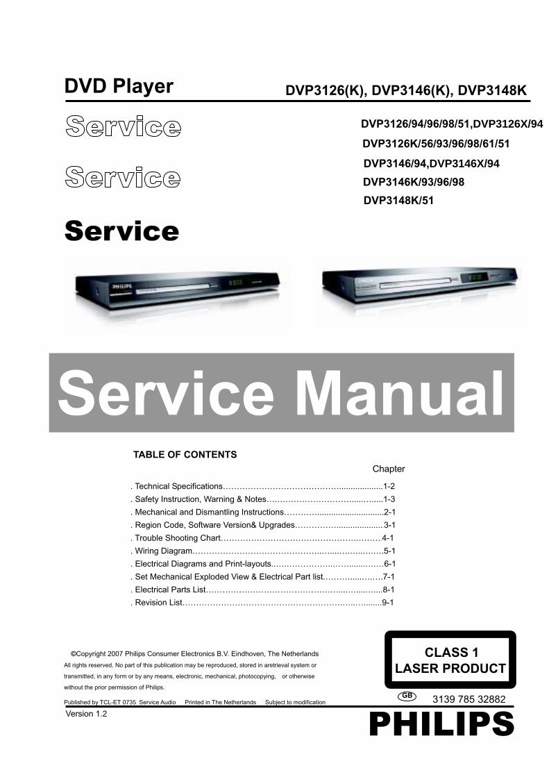
. Technical Specifications……………………………………...................1-2 . Safety Instruction, Warning & Notes….……………………….....….....1-3 . Mechanical and Dismantling Instructions………….............................2-1 . Region Code, Software Version& Upgrades…………….....................3-1 . Trouble Shooting Chart………………………………………….……….4-1 . Wiring Diagram………………………………………..…....….…..….….5-1 . Electrical Diagrams and Print-layouts..….……………..…….......….…6-1 . Set Mechanical Exploded View & Electrical Part list.……….....….….7-1 . Electrical Parts List…………………………………………....….....…...8-1 . Revision List………………………………………………….…..…........9-1 TABLE OF CONTENTS Chapter 3139 785 32882 Version 1.2 DVP3126(K), DVP3146(K), DVP3148K Service Manual PHILIPS GB ©Copyright 2007 Philips Consumer Electronics B.V. Eindhoven, The Netherlands All rights reserved. No part of this publication may be reproduced, stored in aretrieval system or transmitted, in any form or by any means, electronic, mechanical, photocopying, or otherwise without the prior permission of Philips. CLASS 1 LASER PRODUCT Published by TCL-ET 0735 Service Audio Printed in The Netherlands Subject to modification DVP3126/94/96/98/51,DVP3126X/94 DVP3126K/56/93/96/98/61/51 DVP3146/94,DVP3146X/94 DVP3146K/93/96/98 DVP3148K/51 Service DVD Player
-
Upload
khangminh22 -
Category
Documents
-
view
1 -
download
0
Transcript of Service Manual - DVD Player - WASP.kz
. Technical Specifications……………………………………...................1-2
. Safety Instruction, Warning & Notes….……………………….....….....1-3
. Mechanical and Dismantling Instructions………….............................2-1
. Region Code, Software Version& Upgrades…………….....................3-1
. Trouble Shooting Chart………………………………………….……….4-1
. Wiring Diagram………………………………………..…....….…..….….5-1
. Electrical Diagrams and Print-layouts..….……………..…….......….…6-1
. Set Mechanical Exploded View & Electrical Part list.……….....….….7-1
. Electrical Parts List…………………………………………....….....…...8-1
. Revision List………………………………………………….…..…........9-1
TABLE OF CONTENTS
Chapter
3139 785 32882Version 1.2
DVP3126(K), DVP3146(K), DVP3148K
Service Manual
PHILIPSGB
©Copyright 2007 Philips Consumer Electronics B.V. Eindhoven, The Netherlands
All rights reserved. No part of this publication may be reproduced, stored in aretrieval system or
transmitted, in any form or by any means, electronic, mechanical, photocopying, or otherwise
without the prior permission of Philips.
CLASS 1
LASER PRODUCT
Published by TCL-ET 0735 Service Audio Printed in The Netherlands Subject to modification
DVP3126/94/96/98/51,DVP3126X/94
DVP3126K/56/93/96/98/61/51
DVP3146/94,DVP3146X/94
DVP3146K/93/96/98
DVP3148K/51
Service
DVD Player

Technical Specifications
TV standard (PAL/50Hz) (NTSC/60Hz)
Number of lines 625 525
Playback Multi standard (PAL/NTSC)
Video performance
Video DAC 12 bit, 108MHz
YPbPr 0.7Vpp ---- 75 ohm
Video output 1Vpp ----- 75 ohm
Video format
Digital Compression MPEG 2 for DVD,SVCD
MPEG 1 for VCD
Div ® (For DVP3146/94,DVP3146K/98)
DVD 50Hz 60Hz
Horiz resolution 720 pixels 720 pixels
Vertical resolution 576lines 480 lines
VCD 50Hz 60Hz
Horiz. resolution 352 pixels 352 pixels
Vertical resolution 288lines 240 lines
Audio format
Digital MPEG/AC-3/ Compressed
PCM Digital
16, 20, 24bits
fs, 44.1, 48, 96kHz
MP3(ISO 9660) 96,112,128,256,320kbps
& variable bit rate fs,32,
44.1,48 kHz
Analogue Sound Stereo
Dolby surround compatible downmix from Dolby Digital multi-channel
sound
Audio performance
DA converter 24bits, 192KHz
DVD fs 96kHz 4Hz----44kHz
fs 48kHz 4Hz----22kHz
SVCD fs 48kHz 4Hz----22kHz
fs 44.1kHz 4Hz----20kHz
CD/ VCD fs 44.1kHz 4Hz----20kHz
Signal-Noise (1kHz) >90dB
Dynamic Range (1kHz) >80dB
Cross talk (1kHz) >70dB
Distortion/Noise (1kHz) >65dB
MPEG MP3 MPEG Audio L3
6 Channal analog ouput
Audio Front L/R Cinch( White/Red)
Audio Rear L/R Cinch( White/Red)
Audio Center Cinch( Blue)
Audio Subwoofer Cinch(Black)
Connections
YPbPr output Cinch 3x
Video output Cinch( yellow)
Audio output (L+R ) Cinch (white/red)
Digital output 1 coaxial
IEC60958 for CDDA/ LPCM
IEC61937 for MPEG1/2,
Dolby Digital
Cabinet
Dimensions (w X h X d) 360 x 37 x 209 mm /360 x 38 x 209 mm
Weight Approximately 1.35kg
Power consumption
Power supply Rating 110V -240V;
50/60HZ
Power consumption <10W
Power consumption in standby mode <1W
Specifications subject to change without prior notice.
1-2
Safety instruction
1. General safety
Safety regulations require that during a repair:
. Connect the unit to the mains via an isolation transformer.
. Replace safety components indicated by the symbol ,
only by components identical to the original ones. Any
other component substitution (other than original type)
may increase risk of fire or electrical shock hazard.
Safety regulations require that after a repair, you must
return the unit in its original condition. Pay, in particular,
attention to the following points:
. Route the wires/cables correctly, and fix them with the
mounted cable clamps.
. Check the insulation of the mains lead for external
damage.
. Check the electrical DC resistance between the mains
plug and the secondary side:
1) Unplug the mains cord, and connect a wire between
the two pins of the mains plug.
2) Set the mains switch the “on” position (keep the
mains cord unplug).
3) Measure the resistance value between the mains
plug and the front panel, controls, and chassis
bottom.
4) Repair or correct unit when the resistance
measurement is less than 1M .
5) Verify this, before you return the unit to the
customer/user (ref. UL-standard no. 1492).
6) Switch the unit “off”, and remove the wire between
the two pins of the mains plug.
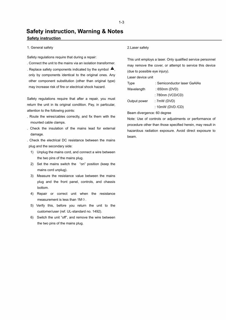
2.Laser safety
This unit employs a laser. Only qualified service personnel
may remove the cover, or attempt to service this device
(due to possible eye injury).
Laser device unit
Type : Semiconductor laser GaAlAs
Wavelength : 650nm (DVD)
: 780nm (VCD/CD)
Output power : 7mW (DVD)
: 10mW (DVD /CD)
Beam divergence: 60 degree
Note: Use of controls or adjustments or performance of
procedure other than those specified herein, may result in
hazardous radiation exposure. Avoid direct exposure to
beam.
Safety instruction, Warning & Notes
1-3
Warning
1.General
. All ICs and many other semiconductors are susceptible to
electrostatic discharges (ESD). Careless handing during
repair can reduce life drastically. Make sure that, during
repair, you are at the same potential as the mass of the
set by a wristband with resistance. Keep components and
tools at this same potential. Available ESD protection
equipment:
1) Complete kit ESD3 (small tablemat, wristband,
connection box, extension cable and earth cable)
4822 310 10671.
2) Wristband tester 4822 344 13999.
. Be careful during measurements in the live voltage
section. The primary side of the power supply , including
the heat sink, carries live mains voltage when you
connect the player to the mains (even when the player is
“off”!). It is possible to touch copper tracks and/or
components in this unshielded primary area, when you
service the player. Service personnel must take
precautions to prevent touching this area or components
in this area. A “lighting stroke” and a stripe-marked
printing on the printed wiring board, indicate the primary
side of the power supply.
. Never replace modules, or components, while the unit is
“on”.
2. Laser
. The use of optical instruments with this product, will
increase eye hazard.
. Only qualified service personnel may remove the cover
or attempt to service this device, due to possible eye
injury.
. Repair handing should take place as much as possible
with a disc loaded inside the player.
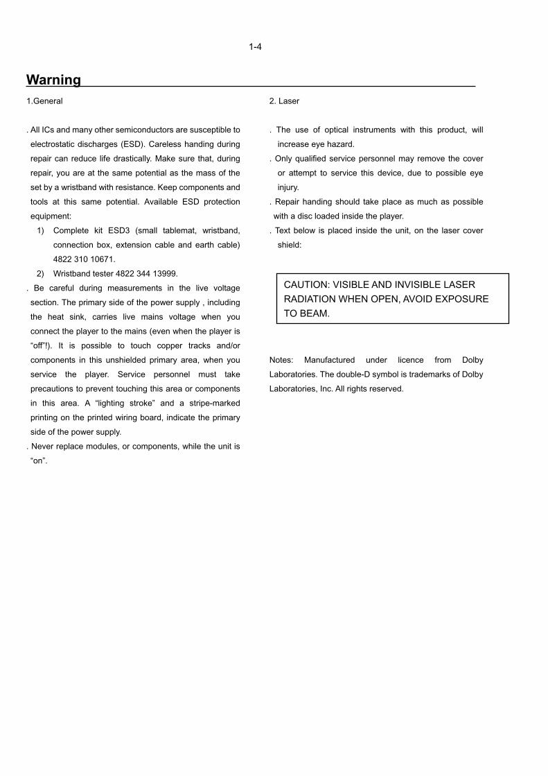
. Text below is placed inside the unit, on the laser cover
shield:
Notes: Manufactured under licence from Dolby
Laboratories. The double-D symbol is trademarks of Dolby
Laboratories, Inc. All rights reserved.
CAUTION: VISIBLE AND INVISIBLE LASER
RADIATION WHEN OPEN, AVOID EXPOSURE
TO BEAM.
1-4

Lead-Free requirement for service
INDENTIFICATION:
Regardless of special logo (not always indicated)
One must treat all sets from 1.1.2005 onwards, according next rules.
Important note: In fact also products a little older can also be treated in this way as long as you avoid mixing solder-alloys (leaded/ lead-free). So best to always use SAC305 and the higher temperatures belong to this.
Due to lead-free technology some rules have to be respected by the workshop during a repair:
Use only lead-free solder alloy Philips SAC305 with
order code 0622 149 00106. If lead-free solder-paste is
required, please contact the manufacturer of your
solder-equipment. In general use of solder-paste within
workshops should be avoided because paste is not easy
to store and to handle.
Use only adequate solder tools applicable for lead-free
solder alloy. The solder tool must be able
o To reach at least a solder-temperature of 400°C,
o To stabilize the adjusted temperature at the
solder-tip
o To exchange solder-tips for different applications.
Adjust your solder tool so that a temperature around
360°C – 380°C is reached and stabilized at the solder
joint. Heating-time of the solder-joint should not exceed
~ 4 sec. Avoid temperatures above 400°C otherwise
wear-out of tips will rise drastically and flux-fluid will be
destroyed. To avoid wear-out of tips switch off un-used
equipment, or reduce heat.
Mix of lead-free solder alloy / parts with leaded solder
alloy / parts is possible but PHILIPS recommends
strongly to avoid mixed
solder alloy types (leaded and lead-free). If one cannot
avoid, clean carefully the
solder-joint from old solder alloy and re-solder with new
solder alloy (SAC305).
Use only original spare-parts listed in the
Service-Manuals. Not listed standard-material
(commodities) has to be purchased at external
companies.
Special information for BGA-ICs:
- always use the 12nc-recognizable soldering
temperature profile of the specific BGA (for
de-soldering always use highest lead-free
temperature profile, in case of doubt)
- lead free BGA-ICs will be delivered in so-called
‘dry-packaging’ (sealed pack including a silica gel
pack) to protect the IC against moisture. After
opening, dependent of MSL-level seen on
indicator-label in the bag, the BGA-IC possibly
still has to be baked dry. This will be
communicated via AYS-website.
Do not re-use BGAs at all.
For sets produced before 1.1.2005, containing
leaded soldering-tin and components, all needed
spare-parts will be available till the end of the
service-period. For repair of such sets nothing
changes.
On our website:
www.atyourservice.ce.Philips.com
You find more information to:
BGA-de-/soldering (+ baking instructions)
Heating-profiles of BGAs and other ICs used in
Philips-sets
You will find this and more technical information
within the “magazine”, chapter “workshop news”.
For additional questions please contact your local
repair-helpdesk.
Notes
1-5

Mechanical and Dismantling Instructions Dismantling Instruction
The following guideline is a general instruction for how to dismantle the player, Detailed operation done according the set unit.Step1: Remove 5 screws around the Top Cover, then remove the Top Cover (Figure 1).
Step2: If it is necessary to dismantle Loader or Front Panel, It should be remove the Front door assembly first. (Figure 2) Note: Make sure to operate gently otherwise the guider would be damaged.
2-1
Figure 1
Please kindly note that dismantle
the front door assembly carefully
to avoid damage tray and the front
door assembly.
Figure 2
Mechanical and Dismantling Instructions Dismantling Instruction
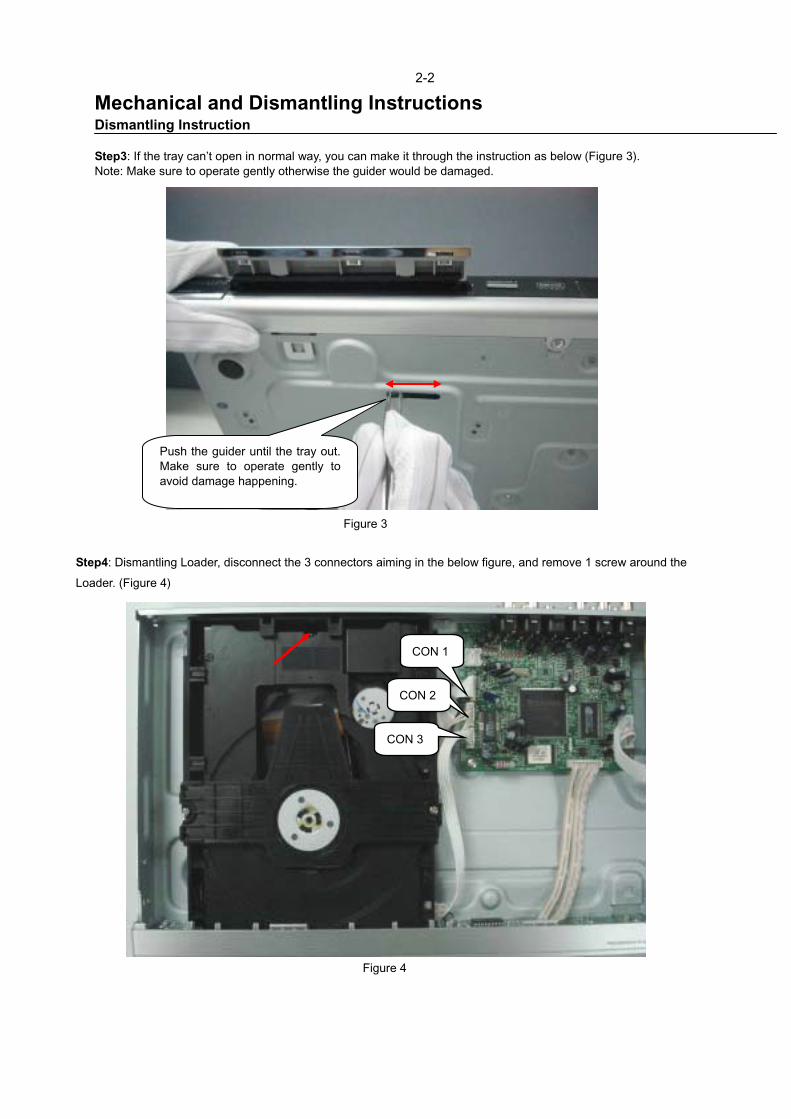
Step3: If the tray can’t open in normal way, you can make it through the instruction as below (Figure 3).Note: Make sure to operate gently otherwise the guider would be damaged.
Step4: Dismantling Loader, disconnect the 3 connectors aiming in the below figure, and remove 1 screw around the
Loader. (Figure 4)
Push the guider until the tray out. Make sure to operate gently to avoid damage happening.
Figure 3
2-2
Figure 4
CON 3
CON 1
CON 2

Mechanical and Dismantling Instructions Dismantling Instruction
Step5: Dismantling Front Panel, disconnect the 1 connector, then release the snaps on the both sides of Front Panel and bottom
cabinet , then gently pull the Panel out from the set. (Figure 5 & 6 & 7)
Figure 6
Snap 1
Figure 5
CON 4
2-3
Snap 2
Figure 7

Mechanical and Dismantling Instructions Dismantling Instruction
Step6: Dismantling Main Board, first disconnect the 1 connector, then remove 4 screws to remove the Main board. (Figure 8)
Step7: Remove the 2 screws on Power Board to dismantle the Power Board. (Figure 9)
2-4
Figure 9
Figure 8
CON 5
Figure 8

Software upgrade
Preparation to upgrade software
1) Start the CD Burning software and create a new CD
project (Data Disc) with the following setting:
Label: DVP3XXX (No need the label name)
Note: It is required capital letter for the File System
name, and it no need have the File name during
start the CD burning software for Zoran project.
2) Burn the data onto a blank CDR
A. Procedure for software upgrade:
1) Power on the set and insert the prepared Upgrade
CDR.
2) The set will starts reading disc & response with the
following display TV screen:
Loading
Firmware Upgrade Erase and program.
Start Cancel
Select Start to start upgrade.
3) Press <OK> button to confirm, then screen will display :
Firmware Upgrade Programming, Please Wait...
Do not Switch the Player Off !
4) The upgraded disc will automatically out when files
coping complete, then take out the disc.
5) About 1 minute later, the tray will automatically close
when upgrading complete.
B. Read out the software versions to confirm upgrading
1) Power on e set and Open the tray door.
2) Press <9><6><6>button to check the software
information.
The software version and other information are display
on the TV screen as follows:
BE Version: DVP3XXXXX_XX.XX
FE Version: DCX.XXXXXX.XX.XX
DSP Version: DSP.XX
Region Code: X
3-1
Caution: The set must not be power off during
upgrading, Otherwise the Main board will be
damaged entirely.
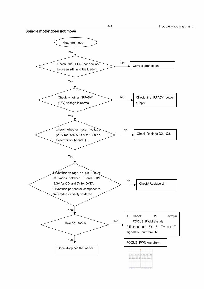
4-1
Spindle motor does not move
Yes
Yes
No
No
No
No
Yes
Check whether “RFA5V”
(+5V) voltage is normal.
Correct connection
Check the RFA5V power
supply
Check/Replace Q2 Q3.
Check/ Replace U1.
Have no focus
1. Check U1 182pin
FOCUS_PWM signals
2.If there are F+, F-, T+ and T-
signals output from U7.
Check/Replace the loader
Yes
Yes
No
Go
Check whether laser voltage
(2.3V for DVD & 1.9V for CD) on
Collector of Q2 and Q3
Check the FFC connection
between 24P and the loader.
1.Whether voltage on pin 129 of
U1 varies between 0 and 3.3V
(3.3V for CD and 0V for DVD),
2.Whether peripheral components
are eroded or badly soldered
Trouble shooting chart
Motor no move
FOCUS_PWN waveform
4-2
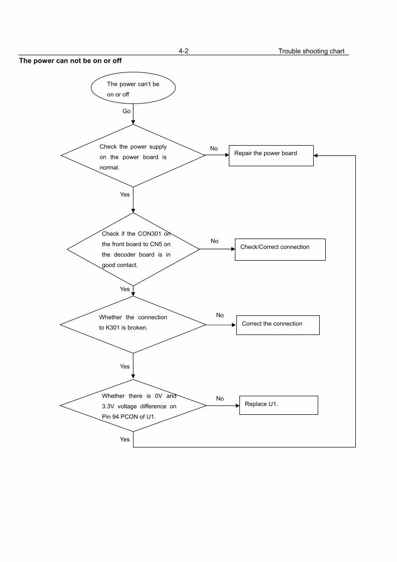
The power can not be on or off
Go
Yes
Yes
No
No
The power can’t be
on or off
Yes
Repair the power boardCheck the power supply
on the power board is
normal.
Check/Correct connection
Whether the connection
to K301 is broken. Correct the connection
Replace U1.
No
No
Yes
Yes
Check if the CON301 on
the front board to CN5 on
the decoder board is in
good contact.
Whether there is 0V and
3.3V voltage difference on
Pin 94 PCON of U1.
Trouble shooting chart

4-3
All output voltages on the power board is 0V or deviated.
No
No
No
Yes
No
U1(PIN 8 - Drain waveform)
Replace F1
Replace C1&C2 if D1, D2, D3, D4
are normal.
Check/ replace U1.
Check whether U1 are eroded.
All output voltages on
the power board is 0V or
deviated
Check whether there is
300V on C1 or C2.
Check whether 100KHz oscillating signal on Pin6 of U1
Check if +5V, , +12V and
-12V are short.
Check whether the components in the
short-circuit voltage are defected or eroded.
Yes
Yes
Yes
Yes
U1(PIN 3 - RC waveform)
Check whether
F1 is blown
Trouble shooting chart

4-4
Disc cannot be read.
No
Yes
No
Yes
No
Yes
Yes
No
No
Yes
Disc cannot be read.
Check the loaded circuit
1.Check voltage on pin 100 of U1
varies between 0 and 3.3V:
3.3V for CD
0V for DVD
2.Check whether peripheral
Check the FFC connection
between 24P and the loader.
Check U1 and peripheral components
Re-solder or replace the defective parts
Check the connection
between U1 Correct connection
Replace U1 or loader.
Yes
Check whether there is laser
voltage (2.3V for DVD and 1.9V for
CD) on Collector of Q2 &Q3
Check if there is RFO signal on
pin10 of CN2. (The normal RFO
signal is a clear reticulated wave)
Check U1, U7, and
peripheral components are
eroded or badly soldered.
Trouble shooting chart

4-5
Only DVD disc or only disc except DVD can be played
No
No
Yes
Only DVD disc, or only disc
except DVD can be Played.
Check the FFC connection
between 24pin and the
loader.
Check the loaded circuit
Check the solder status on U1 and
peripheral components
Check whether there is voltage
variance on pin 182 of U1. check if bad solder exist on U1
and peripheral components
Replace the bad spare parts
Check whether pins of U1 and peripheral components are badly soldered, defected
Check Q2 whether in good condition
Yes
Yes
Yes
Go
Correct connection
Change U1 or the loader.
No
No
Yes
Check laser voltage (2.3V)
output on Collector of Q2, if
pin181 of U1is at low level.
No
Trouble shooting chart

4-6
No display on LED, and buttons do not work
No
No
No
Yes
Yes
No display on LED, and
buttons do not work
Check whether there is correct contact between CON301 and CN5
Correct connection
Fix power supply board top a power supply for should electric circuit
Check the U1’s pin 131,132,133
arrive the CN5 connect condition
Correct connection
Replace U301 or LED
Yes
Yes
Yes
No
Check VCC(+5v) voltage on the power and front board
Check there are CS, DATA and CLK signals on CON301 on the front board.
1.Check whether bad solder exists on U301 and pins of LED, 2.Check whether the circuit connected to K302, K303, K304 and K301 is broken, 3.Check whether R300, R301 and R302 are open-circuit.
CN5 (PIN 2 CLK) CN5 (PIN4 DOUT)
Trouble shooting chart

4-7
Distorted audio and loud noise
No
Yes
No
Yes
Yes
No
Distorted audio and loud noise
Replace R176 and R175
Check Q27
Replace Q17~Q18 ,Q40~Q43
Check whether the mutingtransistor R176 andR175 are normal.
Yes
Check whether the mutingtransistor Q17~Q18,Q40~Q43Q42 are normal
Checking the U1 leads the feet has no to break to open
Correct connection
No
Yes
Check the power supply voltages +12V to the operation amplifying Q27 and -12V are normal.
Replace U1
Trouble shooting chart

4-8
Abnormal color of video picture
Yes
Abnormal color of
video picture
Check whether the 3.3V and 1.8V power supply voltages on the decoder board are normal.
Check Y1, R13, C38 and C39
Check other of power supply electric
circuit
Correct the connection
Check whether the video filter network circuit is normal.
Yes
Yes
No
No
No
Check whether the 27MHz
output signal normal.
change U1
Yes
No
Trouble shooting chart
Check if the video signals on Pin 147,149,151,152,154 of U1 are normal
4-9
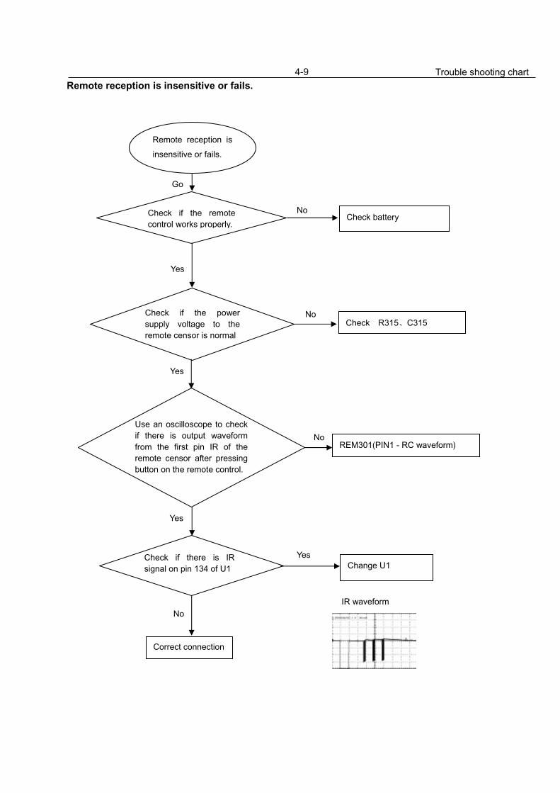
Remote reception is insensitive or fails.
No
Remote reception is
insensitive or fails.
Check if the remote control works properly.
Check battery
Check R315 C315
Use an oscilloscope to check if there is output waveform from the first pin IR of the remote censor after pressingbutton on the remote control.
REM301(PIN1 - RC waveform)
Check if there is IR signal on pin 134 of U1
Check if the power supply voltage to the remote censor is normal
Go
No
No
No
Yes
Yes
Yes
Correct connection
Yes Change U1
IR waveform
Trouble shooting chart

4-10
No video picture, no sound.
Change EC9, D1and Q1.
No video picture, no sound.
Check if the reset circuit consisting ofEC9, D1 and Q1 is normal (at a high level for tens of milliseconds, then constantly at 0V).
Check whether there is 27MHz signal output.
Check the loaded circuit
Crystal oscillator Y1 and
peripheral components
are defected or eroded.
No
No
No
Yes
Yes
Yes
27Mhz waveform
Check whether all the voltages from the power board to the decoder board are normal.
CVBS(R21 point) waveform
Check if there is 135MHz
signal output on R2.
Check whether short-circuit or bad solder on U2,U4
SDRAM(R2 PCLK) waveform
Check U1.
No
No
Reconnect the component in
Yes
Yes
Check if short-circuit and bad solder exist on Pin 151
Yes
No
Trouble shooting chart
Go

5
5
4
4
3
3
2
2
1
1
D D
C C
B B
A A
DATA
OK BOARD
-12V
4
GND_LD
VR_CD
GND
POWER_K
CD-LD
9
OPU_HFM(-RFA5V)
1
6
RF_F
IR Receiver
1
HOMESW
TACT+
1
INSW
DVD LOADER
+5V
GND
GND
GND
GND
24
RF
Remark:DVP3146 DVP3126 have no Karaoke.
2
MIC
9
1
SP-
POWERSUPPLY
TACT-
16M FLASH
1
GND
AGND
GND
VC
DVD_LD
POWER_K
LOAD-
16M SDRAM
RF_D
SWITCHBOARD
OUTSW
(TCL)TDM-1 + KHM313
RF_E
CLK
CD/DVD
DV33IR
EEPROM
VCC(-RFA5V)
VR_DVD
1
LED DRIVE ET6202
+12V
ZR36966D/ZR36962
LED Display
GNDGND
KARAOKE A/D CS5340
7
SL-
RF_ARF_B
MD(C-GND)
5
MOTOR
DRIVER
AM5888S
+5V
CS
LOAD+
4
RF_C
NC(C-GND)
1
+5V
1
KARAOKE AMPKey-matrix
1
TACT-
NC(C-GND)
-12V
SL+
7
2
1
AC IN
LED+5V
1
SP+
FACT+
CN1
CN9CN5
CN3
CN4
CN2
CON301
CON302
CN601
CON2
CN301
CON1
U1
U4 U5
U7
U2
U13
U301REM301
LED1
SL&SR CEN&LFECOAX L&RCN7
AUDIOAMP&LPFVIDEO
LPF&DRIVE
CN6 Y
Pb CVBS
PR
Remark:DVP3146(K) USE ZORAN36966,DVP3126(k) USE ZORAN36962.
DVP3126(K)/XX, DVP3146(K)/XX,DVP3148K/XX WIRING DIAGRAM
5-1 5-1

A
A
B
B
C
C
D
D
E
E
1 1
2 2
3 3
4 4
FROM MAIN BOARD
C300
C301
C302
C303
C306
C314
C315
C316
CE300
CE301
CON301
CON302
D301
D302
K302
K303
K304
LED1
R300
R301
R302
R303
R304
R305
R306
R307
R308
R315
REM301
U301
B2
B2
B2
B2
B1
A1
B1
C1
C2
B1
A1
C1
D2
D2
E3
E2
D2
E2
B2
B2
B2
B2
B2
B2
C1
C2
C2
B1
B1
D2
GRID6
CLK
5VL
GRID3
GRID6
IR
GND
GRID5
POWER_KCLK
CS
KS1
POWER_K
SEG4
GRID[1:7]
SEG2 SEG2SEG3
GRID1DATA
DATA
SEG4
GND
5VL
KE
Y2
SEG6
GRID2
GRID4
KS2
DV33
KE
Y1
SEG5
GRID7
IR
GRID7
SEG[1:9]
SEG5
GRID5
SEG6
CS
SEG3
SEG1
GRID3GRID4
GND
SEG1
5V
GRID2
GRID1
DV33
5V
K303 play/pause
C300
100P
R315
100 ohm
C301
100P
C302
100P
U301ET6202
123456789
1011121314
2827262524232221201918171615
OSCDI/OCLKSTBKEY1KEY2VDDSEG1/KS1SEG2/KS2SEG3/KS3SEG4/KS4SEG5/KS5SEG6/KS6SEG7/KS7
GNDGRID1GRID2
GNDGRID3GRID4
GNDVDD
SEG14/GRID5SEG13/GRID6SEG12/GRID7
SEG10/KS10SEG9/KS9SEG8/KS8
+CE300
47uF
C31547p
CON302CON2(2.0)
12
C31447p
+
CE30147uF
R307 10KR308 10K
R303
4K7
R304
4K7
R305
4K7
REM301
REM
123
IRGNDVCC
C31647p
C3060.1u
K304
open/close
R300 100
R306
51K
R301 100
LED1
JDD350501AG
123456789
10111213
GRID1GRID2GRID3GRID4GRID5GRID6GRID7SEG1SEG2SEG3SEG4SEG5SEG6
D3021N4148
R302 100
D3011N4148
C303
0.1u
CON301
CON9(2.0)
123456789
K302 stop
6-1 6-1
Front Board Electric Diagram for DVP3126(K)/XX, DVP3146(K)/XX, DVP3148K/XX

A
A
B
B
C
C
D
D
E
E
1 1
2 2
3 3
4 4
C200
C201
C203
C204
C205
C206
C207
C208
C209
CE200
CE201
CN601
D200
G1
L200
MIC200
Q200
R200
R201
R202
R203
R204
R205
R206
R207
R208
R209
R210
RP200
U200A
U200B
USB
A1
B1
B2
C2
C1
D2
A2
C2
D2
A1
B1
D3
A2
A3
A1
A1
B2
B1
B1
A2
B2
B2
C1
D2
D2
C3
C3
B1
C2
C1
D2
A3
+5V
-12VA
+5VMIC_OUT
USB_DNUSB_DP
USB_DPUSB_DN
VCC
-12V
MIC_OUT MIC
-12V -12VA
VCC
VCC
CE201
22uF
C204100p
R206
3.9K
C2081uF/0805
C207
1uF/0805
G1
C206 47p
R203
8.2K
CN601
USB1.1
12345678
R207 6.8K
MIC200
2
3
1
2
3
1
C200
0.1u
D200
1N4148
C203
1000p
L200
FB500R
R204
4.7K
R210
150
+
-
U200B
NJM4558
5
67
84
R201
2.2K
C201
0.1u
C205 47p
RP20010K
13
24
5
CE200
22uF
R209
680
USB
345126
VCCDATA-DATA+
GNDGNDGND
+
-
U200A
NJM4558
3
21
84
R205 68K
R208
1K
Q2009014
R202 1K
R200
1.2K
C2091uF/0805
OK+USB Board Electric Diagram for DVP3126K/XX, DVP3146K/XX, DVP3148K/XX
6-2 6-2

6-36-3
Front Board Print-Layout (Bottom Side) for DVP3126(K)/XX, DVP3146(K)/XX, DVP3148K/XX
Switch Board Print-Layout (Bottom Side) for DVP3126(K)/XX, DVP3146(K)/XX, DVP3148K/XX
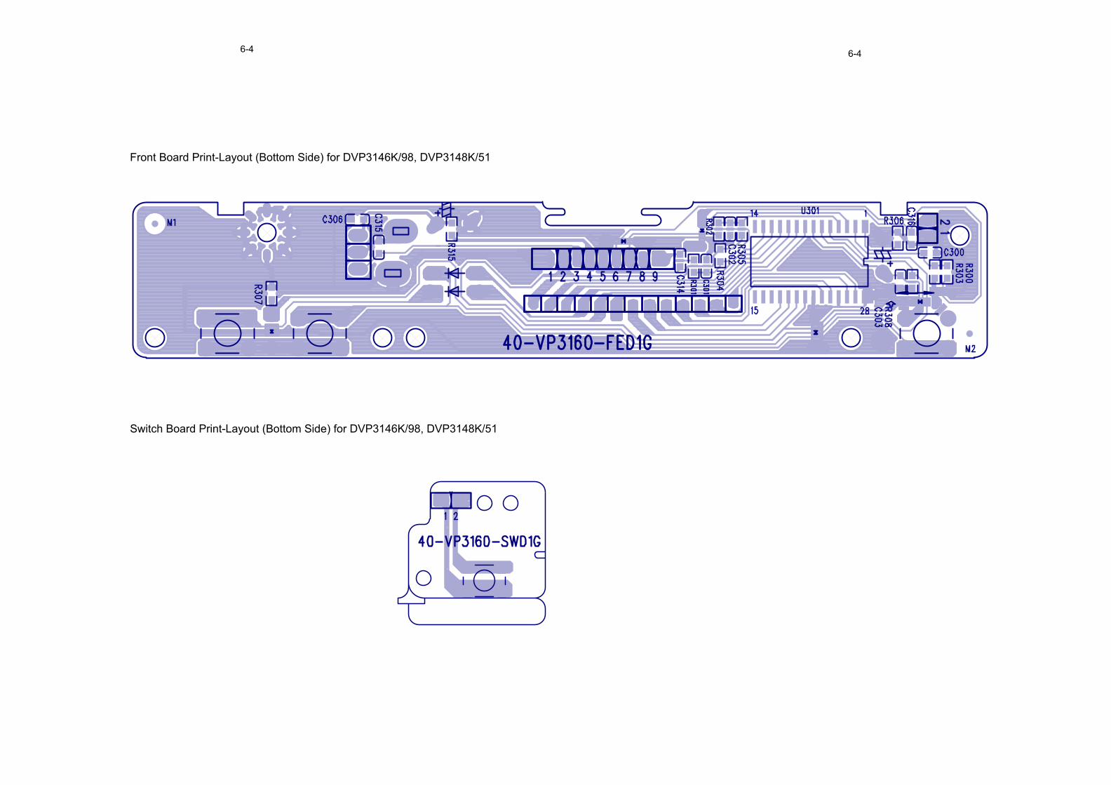
Front Board Print-Layout (Bottom Side) for DVP3146K/98, DVP3148K/51
Switch Board Print-Layout (Bottom Side) for DVP3146K/98, DVP3148K/51
6-4 6-4

A
A
B
B
C
C
D
D
E
E
1 1
2 2
3 3
4 4
* CAUTION :
PLEASE USE THE PARTS HAVING THE DESIGNATED PARTS NUMBER WITHOUT FAIL.
THE PARTS MARKED WITH ARE IMPORTANT PARTS ON THE SAFETY.
C1
C10
C11
C12
C14
C2
C3
C4
C5
C6
C7
C8
C9
CON1
CON2
D1
D10
D2
D3
D4
D5
D6
D7
D8
F1
L1
L2
L6
R1
R10
R11
R12
R13
R2
R3
R4(NU)
R5
R7
R8
R9
RV1
T1
TR1
U1
U2
U3
B1
B3
B3
B1
C2
B1
C1
C2
B2
C2
C2
C2
B2
A1
D2
A1
C2
B1
A1
B1
C1
C1
C2
B2
A1
B1
C2
B1
C2
C3
B2
A2
B3
B2
B2
C2
D2
D3
B3
C3
A1
B2
A1
A2
B3
B3
+C7
1000uF/16V
R1NU
+C447uF/25V
+ C1
22uF/400VD3
1N4007
C110.1uF/50V
R31/4W120K
C5152/1KV
+ C6
47uF/25V
R12
1/6W33
R5
1/6W5.6K 1%
U2PC123X92
12
43
F1T2AL/250ac
+ C222uF/400V
D6IN4148
R101/6W100
D5IN4148
C14NU
U3TL431
2
1
3
C10
0.1uF/50V
U1TNY276
81
5 6
4
7
3 2
SE
N/U
V
S S
Drain
S
NC
BP
/M
RV1
10K471
R11
1/6W22
D7FR102
D8IN4007
R71/6W5.1k 1%
L6
+
C9
10uF/50V
T1 EEL22
8
11
6
4
73
1
9
5
2
12
10
R91/6W10k
D21N4007
R21/4W120K
+C8
470uF/16V
D10 SR360
CON1AC INPUT
12
++
D11N4007
TR1NTC 10
R81/6W2.2k
+C310uF/50V
CON2
8X2.5 HEADER
12345678
+5V+5VGNDGND+12VGND-12V-24V
R13
1/6W100k
D41N4007
R4(NU)
1/6W10k
L26.8uH
C12102/400Vac
L1 680uH
Power Board Electric Diagram for DVP3126(K)/XX
6-5 6-5

6-6 6-6
Power Board Print-Layout (Bottom Side) for DVP3126(K)/XX
A
A
B
B
C
C
D
D
E
E
1 1
2 2
3 3
4 4
PLEASE USE THE PARTS HAVING THE DESIGNATED PARTS NUMBER WITHOUT FAIL.THE PARTS MARKED WITH ARE IMPORTANT PARTS ON THE SAFETY.* CAUTION :
C1C10C11C12C2C3C4C5C6C7C8C9CON1CON2CY1D1D10D2D3D4D5D6D7
B1A3C3C2B1C1C2A2C2C3C3A3A1D2B4A1C3A1A1A1C1C2C2D8
D9F1FB1L1L2R1R10R11R12R2R3R5R7R8R9RV1T1TR1U1U2U3
B2B2A1B1B1C3A2B3A3C2B2B2D3D3B3B3A1B2A1A2B3B3
R5
12k 1%
D10SR240
TR1NTC 10
D21N4007
R2300K/1/4W
+ C447uF/25V
D31N4007
D61N4148
U3TL431
2
1
3
D91N4007
D41N4007
+C8
470uF/16V
CON1AC INPUT
12
++
R82.2k
+C6
47uF/25V
R156k 1/4W
C12102/50V(NU)
U2PC123X92
12
43
RV110K471
R10220
+ C310uF/50V(NU)
R1222(NU)
D81N4007
R711.3k 1%
+C9
10uF/50V
R3300K/1/4W
D5FR102(NU)
L26.8uH
+C2
22uF/250V
C110.1uF
+C1
22uF/250V
F1T2AL/250ac
FB12.2uH
D71N4148
L1750uH
T1
8
11
1
73
5
9
2
4
12
10
6
R1122
R910k
D11N4007
+C7
1000uF/16V
CY1102/400Vac
C100.1uF
CON2
8X2.5 HEADER
12345678
+5V+5VGNDGND+12VGND-12V-22V
C5222/400V
U1FSDH321
45
1 2
8
3
7 6
CS
Start
up
GN
D
Vcc
Drain
FB
Drain
Drain
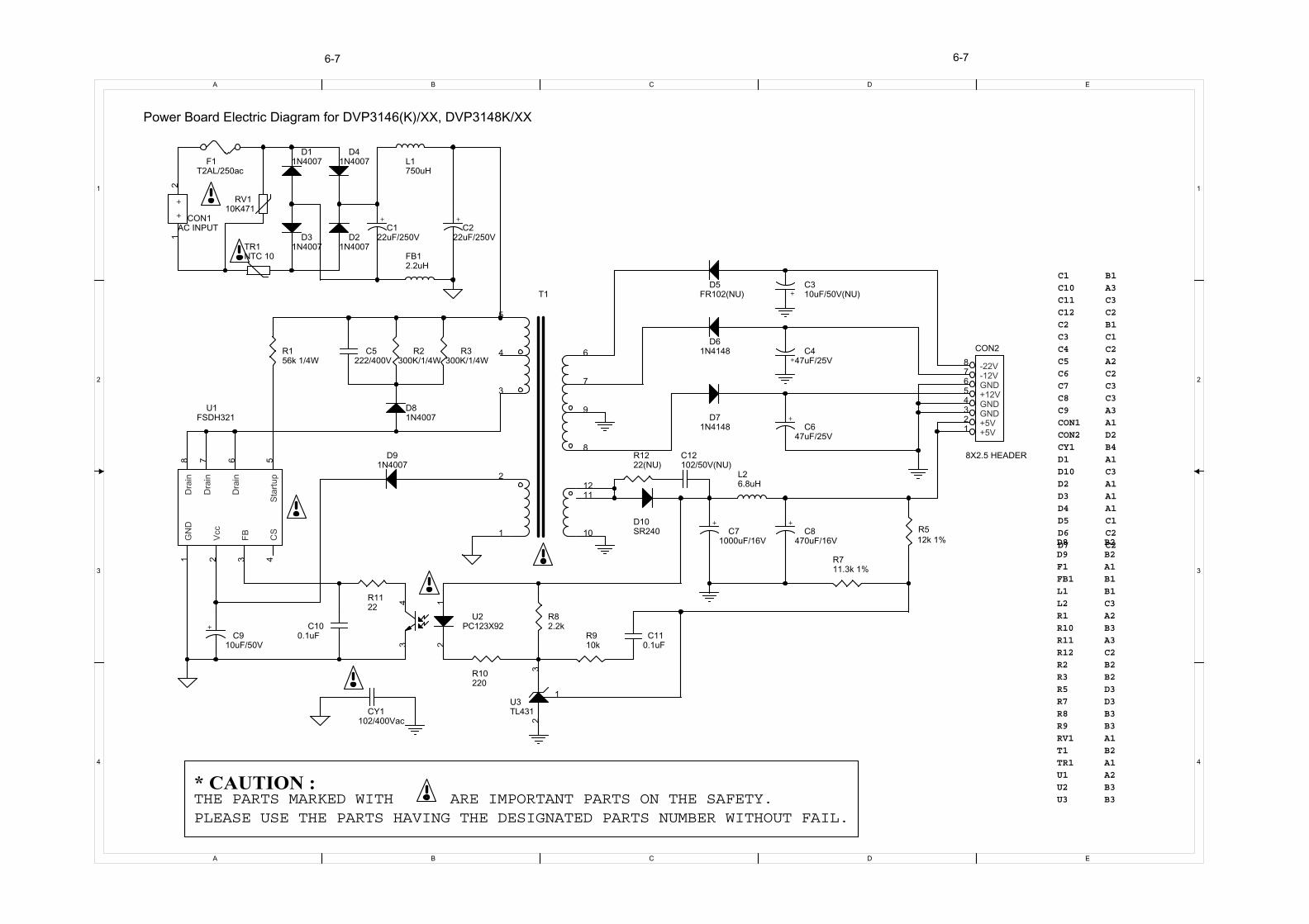
Power Board Electric Diagram for DVP3146(K)/XX, DVP3148K/XX
6-7 6-7

6-86-8
Power Board Print-Layout (Bottom Side) for DVP3146(K)/XX, DVP3148K/XX

A
A
B
B
C
C
D
D
E
E
1 1
2 2
3 3
4 4
Vaddis 9
SDRAM configuration:
1X16Mbit: CS0# = Low;
1X64Mbit: CS1# = Low; CS0#=BA1
SDRAM speed <=7ns
Tras <=44.4ns
Trp <=22.2ns
Close to Pin37 of U4
R39 R40Flash select
Intel NM 0R
AMD/SST 0R NM
Flash speed <= 70 nS.If plan to use 90nsFlash, it needs to beverified by s/w.
A19
NCNCRY/BY#
BYTE#
Close to Vaddis!
Close to Vaddis!
Important power supply!
JP3 JP2BOOTSEL
Play OPEN OPEN
Download
SW debug
OPEN CLOSE
CLOSE OPEN
UART
RESET
Place de-coupling capacitors close to power pins.
Close to Vaddis
Close to Vaddis
CrystalUse it to connect the shell of the crystal with ground.
OPU: 313A HD65R5: 22K 11KR6: 33K 18K
EEPROM
Imax 165mA
Imax 120mA
Imax 9mA
Imax 0.5mA
CN10CN109C2C3C4C5C6C7C8C9C10C11C12C15C19C20C21C22C23C24C25C26C27C28C29C30C31C32C33C34C35C36C37C38C39C43C44C45C48C49C50C51C189C190C191C192C193C194C201C202C205C206D1EC1EC4
EC9EC20FB1FB3FB4FB6FB7FB8FB9FB30JP2JP3Q1R1R2R3R4R5R6R7R8R9R10R13R14R15R19R20R21R22R24R30R33R34R35R36R37R38R39R40R41R42R56R223R224R225R226R227R228R229R235R238U1AU2U3U4U5X11Y1
DDAAAABAAAAAACAAAAACCCCCCCBBBBCCBDDDDBACCBCCCCCCBCDDDAD
4444444444444344444111111111111131123411111111113221241
DCADDCCCCBAADBBBBBBCBBCDDDCCCCDDDDDDDDAAAACDDDCCCCDDBBBADDD
23411122233324311111112111222222222233113333333333111441341
RA
MC
KE
RA
MC
AS
-
RA
MD
AT
5
RA
MD
AT
4
RA
MA
DD
8
RA
MD
AT
15
RA
MD
AT
9
RA
MA
DD
7
RA
MD
QM
RA
MA
DD
4
RA
MW
E-
RA
MA
DD
9
RA
MA
DD
0
RA
MD
AT
7
RA
MA
DD
10
RA
MA
DD
1R
AM
AD
D2
RA
MD
AT
11
RA
MD
AT
6
RA
MD
AT
0
RA
MC
S0-
RA
MD
QM
RA
MA
DD
5R
AM
AD
D6
RA
MD
AT
10
RA
MR
AS
-
RA
MB
A
RA
MD
AT
1R
AM
DA
T13
RA
MD
AT
2
RA
MD
AT
12
RA
MA
DD
11
PC
LK
RA
MA
DD
3
RA
MC
S1-
RA
MD
AT
8
RA
MD
AT
14
RA
MD
AT
3
RA
MB
A
RA
MD
QM
RA
MA
DD
6R
AM
AD
D5
PC
LK
RA
MD
AT
11
RA
MR
AS
-
RA
MD
AT
0
RA
MC
S0-
RA
MA
DD
3
RA
MD
AT
1
RA
MD
AT
12
RA
MD
AT
13
RA
MD
AT
10
RA
MD
AT
2
RA
MD
AT
4
RA
MC
AS
-
RA
MD
AT
14
RA
MA
DD
1
RA
MD
AT
3
RA
MD
AT
8
RA
MD
AT
15
RA
MD
AT
9
RA
MA
DD
7
RA
MA
DD
9
RA
MD
AT
7
RA
MW
E-
RA
MA
DD
10
RA
MD
AT
5
RA
MA
DD
4
RA
MA
DD
0
RA
MD
QM
RA
MA
DD
8
RA
MA
DD
2
RA
MD
AT
6
SDRAM3.3V
SDRAM3.3V
SDRAM3.3V
MEMADD15MEMADD14MEMADD13MEMADD12MEMADD11MEMADD10MEMADD9MEMADD8
MEMADD18MEMADD17MEMADD7MEMADD6MEMADD5MEMADD4MEMADD3MEMADD2MEMADD1
MEMADD16
MEMDAT15MEMDAT7MEMDAT14MEMDAT6MEMDAT13MEMDAT5MEMDAT12MEMDAT4
MEMDAT11MEMDAT3MEMDAT10MEMDAT2MEMDAT9MEMDAT1MEMDAT8MEMDAT0
MEMADD0
MEMWR#
MEMRD#
SPDL_SSLED_S
RF
MEMADD2
MEMADD1
DUPRD1DUPTD1
DUPTD0DUPRD0
STBY_KEY
AMCLK
ALRCLKABCLK
PCLK
VDDPWM
I2C
_D
AT
I2C
_C
LK
DUPRD1 MUTE_CTL
RESET#
OSCOUT
OSCIN
LED/PCON
DAC_RST#
VDDPLL
VDDAFE
APWM_R-
CLOSE
RA
MD
AT
1
RA
MD
AT
2
MEMADD6
TR
AC
K_P
WM
ME
MD
AT
8
ME
MD
AT
9
MIC
_O
N
LE
D/P
CO
N
RA
MD
AT
5R
AM
DA
T11
MEMADD18
MEMADD8
LD
_C
D
DRVSB
RA
MD
AT
0
RA
MD
AT
10
RA
MW
E-
MEMDAT14
RF
N
VD
DA
FE
S/PDIF_OUT
FPC_STB
OSCIN
RA
MD
AT
14
MEMADD15
MEMDAT15
MEMDAT12
RF
P
DUPTD1
VDDDAC
RA
MC
S0-
MEMADD14
MEMDAT5
HOMESW
CD_DVD
RA
MD
AT
7
RA
MC
S1-
RA
MA
DD
9
RAMADD1
MEMADD1
MEMADD13
OSCOUT
RA
MD
AT
13
RA
MD
QM
RAMADD2
MEMADD9
MD
_D
VD
RA
MC
KE
APWM_L+
OPEN
FPC_CLK
RA
MA
DD
11
RA
MA
DD
8
MEMADD3
MEMDAT4MEMDAT11
VDDDAC
APWM_L-
INSW
VDDPLL
MEMADD4MEMADD5
MEMDAT7
MEMDAT3
DUPRD0
DUPRD1
RA
MD
AT
15
RAMADD6
RAMADD7
MEMADD10
MEMDAT10
VC
MD
_C
D
ME
MC
S0#
ME
MR
D#
IRRCV
MEMADD7
MEMADD11
MEMDAT13
ME
MD
AT
1
MEMADD19
Y_R_V
RAMADD4
IN_OUT_SW
FPC_DOUT
C_B_U
IPC
LK
RA
MB
A
RA
MA
DD
0
MEMADD12
MEMDAT2
VD
DA
FE
SP
DL_S
EN
S-
SLE
D_P
WM
RAMADD3
RA
MD
AT
9
MEMWR#
LD
_D
VD
RE
SO
UT
VR
EF
VD
DP
WM
ME
MD
AT
0
V1
VDDDAC
MEMADD17
MEMDAT6
SP
DL_S
EN
S+
ME
MA
DD
0
VO
CA
L_D
ET
RAMADD5
RA
MD
AT
3R
AM
DA
T12
RA
MC
AS
-
RA
MA
DD
10
MEMADD19
MEMADD16
MIC
_V
OC
AL
RA
MC
KE
AIN
DUPTD0
RA
MD
AT
4
RA
MD
AT
6
RA
MD
AT
8
RA
MR
AS
-
MEMADD2
CVBS_C
CVBS_G_Y
APWM_R+
IRRCV
FOCUS_S
FO
CU
S_P
WM
SP
DL_P
WM
TRACK_S
ST
BY
_K
EY
VDD1AFE
VD
D1A
FE
RF
_A
RF
_B
RF
_C
RF
_D
RF
_E
RF
_F
DSPVCC33
DSPVCC33
RESET#
DSPVCC33
I2C_CLKI2C_DAT
WPCON
V1 V2
APWM_SR+APWM_CEN-APWM_CEN+
WP
CO
N
MEMCS0#
APWM_SL-APWM_SL+
APWM_SR-
AP
WM
_LF
E-
AP
WM
_LF
E+
DA
C_R
ST
#
V2
C_B_U
Y_R_VCVBS_C
ABCLKALRCLK
AMCLK
FOCUS_S
SLED_S
RF
STBY_KEY
VO
CA
L_D
ET
MIC
_O
N
MUTE_CTL
LED/PCON
DAC_RST#
CLOSE
RF
_E
APWM_L+
FPC_STB
RF
_A
LD
_D
VD
CD_DVD
APWM_R-
S/PDIF_OUT
RF
_D
DRVSB
MIC
_V
OC
AL
RF
_C
INSW
VC
IN_OUT_SW
FPC_DOUT
LD
_C
D
MD
_D
VD
HOMESW
MD
_C
D
IRRCV
RF
_F
SP
DL_S
EN
S-
OPEN
SP
DL_S
EN
S+
AIN
FPC_CLK
RF
_B
CVBS_G_Y
SPDL_S
TRACK_S
APWM_L-
APWM_SL-APWM_SL+
APWM_SR-APWM_SR+
APWM_CEN+APWM_CEN-
AP
WM
_LF
E-
AP
WM
_LF
E+
DA
C_R
ST
#
APWM_R+
DSPVCC33
DSPVCC33
DSPVCC33
SERVO33
DSPVCC33
DSPVCC18
DSPVCC33
DSPVCC18
DSPVCC33
DSPVCC33DSPVCC33
DSPVCC33
DSPVCC33
DSPVCC33
DSPVCC18
DSPVCC33
DSPVCC33
DSPVCC33
DSPVCC33
R3 51K
C310nF
U4
SST39VF800[39VF400/800/160]
123456789
101112131415161718192021222324
484746454443424140393837363534333231302928272625
A15A14A13A12A11A10A9A8NCA20WE#RP#VPPWP#A19A18A17A7A6A5A4A3A2A1
A16VCCQ
GNDDQ15
DQ7DQ14
DQ6DQ13
DQ5DQ12
DQ4VCC
DQ11DQ3
DQ10DQ2DQ9DQ1DQ8DQ0OE#GNDCE#
A0
+ EC20
NM[470uF/6.3V]
R238 4.7R
C710nF
R35
10K
+ EC4100uF/16V
R5 22K
R9
100R
C37
10pF[NM]
C31
1000pF
CN10
HYPER_TERMINAL I/F
1234
C1910nF
C2610nF
C44NM[0.1uF]
C194 33pF
R223 NM [0R]
C2010.1uF
R33 330R
C38 22pF
C25100nF
C202 1000pF
C2410nF
C410nF
R56 4.7R
R411K[NM]
FB4500Z
C810nF
CN109
DOWN_LOAD_I/F
1234
C193 33pF
C210nF
FB3500Z
EC910uF/16V
R19
75R
1%
R22810K[NM]
Y1
27.000MHzThird overtone
JP3BOOTSEL1[NM]
R39 0R
R372K
C1510nF
R24 0R
C28100nF
R1 4.7K
R10
392 Ohm 1%
C2910nF
R421K[NM]
C192 33pF FB6
500Z
C49
0.1
uF
R34 10K
R20
75R
1%
C2051000pF
C1110nF
C32
1000pF
R7
15.4
K 1
%
FB1
500Z
JP2BOOTSEL1[NM]
FB9 75Z
C191 33pF
+EC147uF/16V
R36 100R
C35 1000pF
R21
75R
1%
C1210nF
C4810nF
FB8 75Z
C206NM[20p]
C33
27nF
C2010nF
C4522pF[NM]
U5
NM[24LC02 ]
1234
8765
A0A1A2
GND
VCCWPSCLSDA
C190 33pF
C50
33pF
R14220K
R22
75R
1%
R2
75R
U2
16Mbit: K4S161622C-TC/L70
12345678910
11
12
13
14
15
16
17
18
19
20
21
22
23
24
25
50
49
48
47
46
45
44
43
42
41
40
39
38
37
36
35
34
33
32
31
30
29
28
27
26
VD
DD
Q0
DQ
1V
SS
QD
Q2
DQ
3V
DD
QD
Q4
DQ
5V
SS
QD
Q6
DQ
7V
DD
QLD
QM
WE
CA
SR
AS
CS
BA
A10/A
PA
0A
1A
2A
3V
DD
VS
SD
Q15
DQ
14
VS
SQ
DQ
13
DQ
12
VD
DQ
DQ
11
DQ
10
VS
SQ
DQ
9D
Q8
VD
DQ
NC
UD
QM
CLK
CK
EN
CA
9A
8A
7A
6A
5A
4V
SS
Q1BT3904
C910nF
C36 1000pF
C610nF
C30100nF
FB7 75Z
R22710K[NM]
R4 51K
R235 4.7R
C2210nF
C189 33pF
C510nF
R40 NM
C34
1000pF
U1A
ZR36962
208
207
206
205
204
203
202
201
200
199
198
197
196
195
194
193
192
191
190
189
188
187
186
185
184
183
182
178
176
179
177
174
175
173
180
181
161
172
163
170
171
167
168
165
166
162
159
160
169
164
158
157
123456789
101112131415161718192021222324252627282930313233343536373839404142
4948
5051
53
52
54
55
57
56
58
59
61
60
62
63
65
64
66
67
69
70
71
72
68
73
74
76
75
77
78
80
79
81
82
84
83
85
86
89
87
90
91
92
156155154153152151150149148147146145144143142141140139138137136135134133132131130129128127126125124123122121120119118117116115114113112111110109108107106105
44454647
88
93
94
95
96
97
98
99
100
101
102
103
104
43
VD
DP
GP
IO[9
]/M
EM
DA
T[9
]M
EM
DA
T[1
]G
PIO
[8]/M
EM
DA
T[8
]M
EM
DA
T[0
]M
EM
RD
#M
EM
CS
0#
ME
MA
DD
[0]
GP
IO[6
3]/M
EM
CS
2#
GP
IO[6
2]/F
CU
_IO
RD
#G
PIO
[61]/F
CU
_IO
WR
#G
PIO
[60]/F
CU
_S
CLK
GP
IO[5
9]/F
CU
_C
S2#
GP
IO[5
8]/F
CU
_C
S3#
GP
IO[5
7]/F
CU
_W
AIT
#G
PIO
[56]/F
CU
_R
ST
IGP
IO[5
5]/F
CU
_IR
QG
ND
CV
DD
CIG
PIO
[54]/P
WM
CO
[5]
GP
IO[5
3]/P
WM
CO
[4]
GP
IO[5
2]/P
WM
CO
[3]
GP
IO[5
1]/P
WM
CO
[2]
GN
DP
WM
GP
IO[5
0]/P
WM
CO
[1]
VD
DP
WM
GP
IO[4
9]/P
WM
CO
[0]
CD
_M
D
GN
DR
EF
DV
D_M
D
VD
DS
AF
E
VR
EF
RE
SO
UT
VC
CD
_LD
DV
D_LD B
GN
D1A
FE CGH KF JE
VD
DA
FE
VD
D1A
FEA
GN
DA
FE D
RF
NR
FP
MEMDAT[2]MEMDAT[10]/GPIO[0]MEMDAT[3]MEMDAT[11]/GPIO[1]MEMDAT[4]MEMDAT[12]/GPIO[2]MEMDAT[5]MEMDAT[13]/GPIO[3]MEMDAT[6]MEMDAT[14]/GPIO[4]GNDCMEMDAT[7]MEMDAT[15]VDDCVDDPMEMADD[16]MEMCS1#/GPIO[5]MEMADD[15]MEMADD[14]MEMADD[13]MEMADD[12]MEMADD[11]MEMADD[10]MEMADD[9]MEMADD[8]MEMWR#MEMADD[18]/GPIO[6]MEMADD[17]MEMADD[7]MEMADD[6]GNDCMEMADD[5]MEMADD[4]MEMADD[3]VDDPMEMADD[2]MEMADD[1]MEMADD[19]/IGPIO[7]USBVDDUSBDP/GPO[67]USBDN/GPO[68]USBGND
RAMADD[6]RAMADD[2]
RAMADD[1]RAMADD[7]
RA
MA
DD
[0]
VDDC
RA
MA
DD
[8]
RA
MA
DD
[10]
GN
DC
VD
DP
RA
MA
DD
[9]
RA
MA
DD
[11]/G
PO
[64]
RA
MB
AR
AM
CS
0#
RA
MC
S1#/G
PO
[65]
RA
MR
AS
#
VD
DP
RA
MC
AS
#
GN
DC
RA
MW
E#
GN
DP
CLK
PC
LK
VD
DP
CLK
RA
MD
AT
[8]
RA
MD
QM
RA
MD
AT
[7]
RA
MD
AT
[9]
VD
DP
RA
MD
AT
[6]
GN
DC
RA
MD
AT
[10]
RA
MD
AT
[11]
RA
MD
AT
[5]
RA
MD
AT
[4]
RA
MD
AT
[12]
VD
DP
RA
MD
AT
[3]
GN
DC
RA
MD
AT
[13]
RA
MD
AT
[14]
RA
MD
AT
[2]
RA
MD
AT
[1]
RA
MD
AT
[15]
RA
MD
AT
[0]
GNDDACBS2RSETDAC1
VDDDACDAC2DAC3
VDDDACDAC4
GNDDAC_DDAC5XINXO
VDDPLLGNDPLLRESET#
GNDCVDDC
GPIO[48]/DUPRD1GPIO[47]/DUPTD1GPIO[46]/DUPRD0
GPIO[45]/PWMCO[5]/DUPTD0VDDP
IGPIO[44]GPIO[43]/TDOGPIO[42]/TCK
GPIO[41]/TDI/NMIGPIO[40]GPIO[39]GPIO[38]
IGPIO[37]/TMS/NMIGPIO[36]GPIO[35]
GPIO[34]/RAMCKE/SPDIFINGPIO[33]/AIN/SPDIFIN
GPIO[32]/SPDIFOGPIO[31]/ABCLK
GPIO[30]/ALRCLKVDDP
GPIO[29]/AMCLKGNDC
GPIO[28]/AOUT[0]/APWM0-GPIO[27]/APWM0+
GPIO[26]/AOUT[1]/APWM1-GPIO[25]/APWM1+
GPIO[24]/AOUT[2]/APWM2-IGPIO[23]/APWM2+
GNDAPWMGPIO[22]/AOUT[3]/APWM3-
GPIO[21]/APWM3+GPIO[20]/APWM4-
GPIO[19]/PWMCO[5]/APWM4+VDDAPWM
RAMADD[3]RAMADD[5]VDDIPGNDC
VD
DC
VD
DP
RA
MD
QM
2/R
AM
CK
E/G
PO
[66]
GN
DC
RA
MC
KE
/SD
I_P
SC
/GP
IO[1
0]
GP
AIO
/IG
PIO
[11]
AP
WM
7+
/GP
IO[1
2]
AP
WM
7-/
GP
IO[1
3]
AP
WM
6+
/GP
IO[1
4]
AP
WM
6-/
GP
IO[1
5]
AP
WM
5+
/GP
IO[1
6]
AP
WM
5-/
GP
IO[1
7]
AIN
/SP
DIF
IN/IO
[18]
RAMADD[4]
C1010nF
D1
LL4148
C51
0.1uF
R15
75R
R22610K[NM]
R13 75R
C2110nF
C2710nF
R22910K[NM]
C39 22pF
C2310nF
R382K
R225 0R[NM]
FB30500Z
R30
15K
U3
NM[64Mbit:K4S641632H-UC70]
1 2 3 4 5 6 7 8 9 10
11
12
13
14
15
16
17
18
19
20
21
22
23
24
25
26
27
28
29
30
31
32
33
34
35
36
37
38
39
40
41
42
43
44
45
46
47
48
49
50
51
52
53
54
VD
DD
Q0
VD
DQ
DQ
1D
Q2
VS
SQ
DQ
3D
Q4
VD
DQ
DQ
5D
Q6
VS
SQ
DQ
7V
DD
DQ
ML
WE
#C
AS
#R
AS
#C
S#
BA
0B
A1
A10
A0
A1
A2
A3
VD
DV
SS
A4
A5
A6
A7
A8
A9
A11
NC
CK
EC
LK
DQ
MH
NC
VS
SD
Q8
VD
DQ
DQ
9D
Q10
VS
SQ
DQ
11
DQ
12
VD
DQ
DQ
13
DQ
14
VS
SQ
DQ
15
VS
S
R2244.7K[NM]
C43
0.22uF
R8
100R
R6 51K
6-9 6-9
Main Board Electric Diagram for DVP3126(K)/XX, DVP3146(K)/XX, DVP3148K/XX: INDEX

A
A
B
B
C
C
D
D
E
E
1 1
2 2
3 3
4 4
OPU 313A HD65 502WR49: 100R 0R 91RR50: 100R 0R 91R
EMC
Close to CN2
CN2 is used for Sanyo/Sony OPUs
2.1V
Close to motor driver.
HOMESWGND
SLED+
SP-
LOAD-
SP+
SLED-
GND
LOAD+
INSW
OUTSW
CD/DVD Control :
DVD=LOW
CD=HIGH
OPU: 313A HD65R76: 2.2R 1R
Imax=600mA Imax=250mA
Close to Q4
Close to Q5
CN2CN3CN4C42C52C53C54C55C56C57C58C62C63C64C65C66C67C68C123C124C125C126C127C195C196D19EC10EC11EC12EC13EC14EC38EC39L2Q2
Q3Q4Q5RR1RR2R43R44R45R46R47R48R49R50R52R61R62R66R70R71R72R73R74R75R76R84R85R86R87R88R90R91R92R219U7
ACDCCAAAAAABBBBCCCCDDDDDDDDAAAAADB
1333211111211223333331111214444432
AAAAAAAAAAABCAAACDDEDEEAADAAAABDDAA
14341111122334442233333211111233311
LOAD+
FACT-SL_MOT-SL_MOT+
TACT+
FACT+
FOCUS_S
DV
DL
D
CD
LD
TRACK_SSLED_S
SP_M-
SPDL_SENS+
SPDL_SENS-
VC2
SP_M-
TACT-
SP_MOT+
VC2
VR_CD
SPDL_S
SP_MOT-
DRVSB
SP_MOT+
LOAD-
TACT+
VC1
FACT-
OPU5V
FACT+
CDLD
OPU_HFM
VR_DVD
DVDLD
TACT-
LOAD+
IN_OUT_SWINSW
VR_CD
VR_DVD
SL_MOT+SL_MOT-
CD_DVD
LOAD+
FACT+
FACT-
SL_MOT+
SL_MOT-
LOAD-
VC2
SP_MOT+
TACT+
TACT-
SP_M-
SP_MOT-
LOAD-
HOMESW
TRACK_SSPDL_S
SPDL_SENS+
SPDL_SENS-
INSWIN_OUT_SWHOMESW
RF_ARF_B
RF_CRF_D
RF
RF_F
RF_E
LD_DVD
LD_CD
VC
FOCUS_S
DRVSB
SLED_S
CD_DVD
MD_DVD
MD_CD
TR_B2
REGO1
TR_B1
FOCUS_S
REGO2
SLED_S
DRVSB
REGO1 REGO2
TR_B1 TR_B2
OPEN
CLOSE
SPDL_S
TRACK_S
DSPVCC33
RFA5V
DSPVCC33
DSPVCC33
DSPVCC33
RFA5V
DSPVCC33
M5VM5V
DSPVCC18DSPVCC33
GND GND
M5V
DSPVCC18
DSPVCC33
SERVO33
CN2
SF-HD6B/0.5mm,24P TOP
242322212019181716151413121110987654321
25262728
F-F+T+T-CD
CD/DVDRF
ABF
GND-PDVC
VCCE
NCVR-CD
VR-DVDLD-CD
MDHFM
NCLD-DVDGND-LD
GNDGNDGNDGND
R49100R
R86
33K
R752K
R904.7K
D19
BAT54C
2
3
1
R48 33R
+ EC13
47uF/16V
C126
1000pF
R88 0R[NM]
+ EC12100uF/16V
C1961000pF
Q5
SS8550D
b
ec
CN3
NM(TRAY_CNN)
12345
C56[1000pF]
R46 220R
C125
220pF
C1951000pF
R924.7K
C66NM[1nF]
C124
1000pF
EC14220uF/16V
R66
1K
R61 0R
CN4
NM(SLED & SPINDLE)
123456
Q39012
R50100R
R62 0RR219 0R
R434.7R
C127
0.1uF
R47 [0R]
R72
1%
4.7k
R84
1K 1%
R454.7R
R914.7K
C570.1uF
+EC38
220uF/16V
C42 0.1uF
C63100pF
C68
0.1uF
R52
3.3K
Q29012
R70
1%20k
C541000pF
C52NM1uF
C64NM[1nF]
L2 10uH
C67
0.1uF
R761R
+ EC39
220uF/16V
C123
220pF
C580.1uF
R85
1K 1%
C53NM1uF
R73
1%
10k
R44 220R
RR2
2.2 OHM 2W
R742K
RR1 6.8 OHM 1W
+ EC10
47uF/16V
C65NM[1nF]
R71
1%
12k
C620.1uF
R87 NM [0R]
C551000pF
U7 AM5888S(HSOP-28)
1
9
10
12
3
2
15
7
14
13
21
19
20
24
27
6
4
5
28
8
11
17
18
16
23
22
25
26
29 30
VINFC
VOTR-
VOTR+
VOSL-
REGO2
TR_B1
VOTK+
REV
VOFC+
VOFC-
VCTL
VCC2
NC
NC
BIAS
FWD
VINSL
REGO1
MUTE
VCC1
VOSL+
VOLD+
VOLD-
VOTK-
VINLD
GND
TR_B2
VINTK
GND GND
Q4
SS8550D
+ EC11
47uF/16V
6-10 6-10
Main Board Electric Diagram for DVP3126(K)/XX, DVP3146(K)/XX, DVP3148K/XX: Front end

A
A
B
B
C
C
D
D
E
E
1 1
2 2
3 3
4 4
Mic vocal detected by ADP software
Mic signal mute/mix/echo process by ADP
ADP: Audio Digital Process
ADC circuit for Karaoke
Max. amplitude of Mic_Audio signal is 4Vrms
Full scale input: 0.65Vrms (when VA=3.3V)M0=1, M1=1: clock slave;Package: TSSOP16.
Value in [] is for external ADC.
External MicroPhone detection
MUTE_CTLLow:Mute.
Close to Q31
CN7CN9CN11C83C84C85C86C87C88C89C90C91C92C93C94C95C96C97C98C99C100C101C102C103C104C120C121C122C129C130C132C133C210C211C212C213C214C215C216C217C220C221C222C223C224C225C226C227C310C311C312C313C314C315C316C317D2D3D4D15D16EC25EC26EC27EC28EC30EC31EC32EC33EC34EC35EC36EC40EC41EC42EC43FB10Q13Q14Q15
Q17Q18Q19Q20Q21Q22Q31Q40Q41Q42Q43R51R57R58R100R101R102R103R104R105R106R107R108R109R110R111R112R113R114R115R116R117R120R123R124R125R126R127R128R129R130R133R134R135R136R137R138R139R140R141R142R143R144R149R150R151R152R153R154R155R157R158R160R161R162R163R164R165R166R167R168R169R170R171R172R173R174R175R176R194
R195R196R197R300R301R302R303R304R305R306R307R310R311R312R313R314R315R316R317R320R321R322R323R324R325R326R327R330R331R332R333R334R335R336R337R350R351R352R353R354R355R356R357R358R359R360R361R381R382R383R384R385R386R387R388R391R392R393R394R395R396R397R398U13U14AU14BU15AU15BU16AU16BU17AU17B
DDDBBCCCCDDBBCCCCDDBBCCCDDDBBCCCCDDBBCBBCBBCBBCCCCCCCCCCCCCCCCCACCDDCCCC
333333333334444444422222222332333333334442223332222223333334444111214332
DDAAAADDDDDAAAAAAAAAAAAAAAAAAAAABBAAAAAAABBCBBCBBCBBCCCCCCCCCCCCCDDDDDDDDDDDDDDD
12112233423111111111111111222222444443432111111111222111111111222121211121212223
EBDAAAAAAAABBBBCCCCCCDDDDDDDDDBBBCCCDBCDCCCCDCCDBCBCBCBCABAAADDDDAAAAAAACCCCBBAA
31412122222111112111111123333311333344442222433433442233334222212112223434231343
MUTE_BIAS1
MIC_IN
ABCLKALRCLK
AMCLK
VA
DAC_RST#
VOCAL_DET
MIC_IN
MUTE_CTL
LRIN
-12VA
AIN
VA LRIN
MIC_IN
-12VD5V
+12VA
LFE_OUT
MUTE
MUTE
CEN_OUT
S/PDIF_OUT
COAX_SPDIF
COAX_SPDIF
LFE_OUTCEN_OUT
RMAIN_OUT
SL_OUTSR_OUT
+12VA
-12VA
SR_OUT
MUTE
MUTE
AUDIO_MIX_L
MIC
+12VA
+12VA
-12VA
MUTE
AUDIO_MIX_R
MUTE
LMAIN_OUT
LMAIN_OUT
MUTE
MIC
RMAIN_OUT
MIC
-12VA
SL_OUT
MIC_ON
MIC_VOCAL
AIN
VOCAL_DET
DAC_RST#
MUTE_CTL
AMCLK
APWM_LFE-
APWM_CEN+
APWM_LFE+
APWM_CEN-
ABCLKALRCLK
S/PDIF_OUT
APWM_SR-
APWM_SL-
APWM_SR+
APWM_SL+
APWM_R-
APWM_L-
APWM_R+
APWM_L+
M5V
-12V
+12V
-12VA
DSPVCC33
DSPVCC33DSPVCC33
DSPVCC33
D5V
DSPVCC33
-12VA
+12VA
D5V
+12VA
-12VAC97 33pF
+
EC32NM
[10uF/16V]
R151120K 1%
R397120K 1%
R134
4.7K 1%
Q22
NM[BT3094]
Q43
BT3904
R398120K 1%
C227100pF
R124220R
R332 120K 1%
R3265.6K
R311
4.7K 1%
CN11
AUDIO OUT
123456
R1715.6k[NM]
R155 120K 1%
C91200pF
+ EC30
NM[10uF/16V]
Q31
BT3904
R157 120K 1%
+
-
U15B
NJM4558 OPA
5
67
84
Q20NM[BT3904]
R153 120K 1%
C211 33pF
Q139012H
R161120K 1%
C215180pF
R123100K
R1434.7K 1%
R149120K 1%
D15NM
[1N4148]
D2
LL4148
C1200.1uF
R115NM[10K]
+
EC43
22uF
R3056.8K
R101 NM[4.7R]
C130100pF
C2230.1uF
C88NM[2200pF]
R3356.8K
R1706.8k[1K]
R317
470R
Q159012H
C98 33pF
R1640R[39K]
R300
4.7K 1%
Q21NM[BT3094]
+
EC28
22uFR162120K 1%
R141
4.7K 1%
R110NM[100K]
U13
NM[CS5340]
123456789
10111213141516
M0MCLK
VLSDOUT
GNDVD
SCLKLRCK/RST
AINLVQAINRVAREF_GNDFILT+M1
R196
39R
Q17
BT3904
C310200pF
R310
4.7K 1%
R167 0R[18K]
R387120K 1%
R130NM[6.8K]
D3 LL4148
C9633pF
R312 120K 1%
R388120K 1%
R304120K 1%
R322 120K 1%
R106NM[NM]
R361
4.7K 1%
R166 NM[4.7K]
C86
NM[0.1uF]
+
EC40
22uF
+
EC34NM[10uF/16V]
R57 NM[0R]
R136
4.7K 1%
Q19[NM]9012H
C312200pF
R158 120K 1%
R303
4.7K 1%
Q40
BT3904
R114NM[2K]
C316200pF
C990.1uF
R165 NM[4.7K]
C2130.1uF
R386 120K 1%
D4LL4148
C31333pF
C31733pF
R111NM[100K]
R127 10K
R385 120K 1%
C1030.1uF
R173
470R
R3165.6K
R108
NM[4.7K]
R359
4.7K 1%
R144
4.7K 1%
R160120K 1%
R302 120K 1%
R353
4.7K 1%
C83
NM
[0.1uF]
R175 33R
R354
4.7K 1%
R51 NM[3.3K]
R331
4.7K 1%
R103NM[10K]
R112NM[15K]
R129 33R
R194
NM
R301
4.7K 1%
R12547K
R327
470R
R320
4.7K 1%
R1630R[39K]
R334120K 1%
C31133pF
C104
0.1uF
+
-
U17A
NJM4560 OPA
3
21
84
C9533pF
Q41
BT3904
R355
4.7K 1%
R313
4.7K 1%
R104 NM[33R]
C220180pF
R3065.6K
C121
0.1uF
R100NM
[4.7K]
C31533pF
+
-
U15A
NJM4558 OPA
3
21
84
R352
4.7K 1%
R350
4.7K 1%
R135
4.7K 1%
C85
NM
[0.1uF]
+
EC2647uF/25V
R116NM[2K]
+
-
U17B
NJM4560 OPA
5
67
84
R138
4.7K 1%
R351
4.7K 1%
Q18
BT3904
+
EC41
22uF
R356
4.7K 1%
CN9
4PIN*2.0
1234
+
EC33NM[22uF/16V]
C2220.1uF
R3156.8K
EC36
47uF/25V
C226 33pF
C225180pF
+
-
U16A
NJM4560 OPA
3
21
84
C122
22pF
R102NM[4.7K]
C89
NM
[1uF]
C129100pF
R3256.8K
+
EC27
22uF
FB10 500ZNM
R107 NM[1K]
R117NM[4.7K]
R324120K 1%
R337
470R
R139
4.7K 1%
R381 120K 1%
R120
100K
R19556R
C314200pF
C1000.1uF
R382 120K 1%
R58NM[3.3K]
R360
4.7K 1%
R1696.8k[1K]
R358
4.7K 1%
R105NM150
R330
4.7K 1%
+
-
U16B
NJM4560 OPA
5
67
84
R176 33R
C102 NM[100pF]
R383120K 1%
C2120.1uF
+ EC31
NM
[10uF/16V]
C87
NM[1uF]
R197
62R
+
EC42
22uF
C101 NM[100pF]
R174
470R
R384120K 1%
R333
4.7K 1%
C216 33pF
EC35470uF/16V
CN7
AUDIO OUT
123456
R1374.7K 1%
R392 120K 1%
C93180pF
R142
4.7K 1%
R321
4.7K 1%
Q42
BT3904
C1321000pF
R133
4.7K 1%
R391 120K 1%
C84
NM
[0.1uF]
R128 10K
R323
4.7K 1%
C1331000pF
R396 120K 1%
R314120K 1%
R395 120K 1%
D16NM[1N4148]
R113NM[1M]
C217
100pF
R126 100R
R3365.6K
R168 0R[18K]
R154 120K 1%
C94180pF
+
-
U14A
NJM4560 OPA
3
21
84
R393120K 1%
C214100pF
R1725.6k[NM]
C92200pF
R152 120K 1%
R394120K 1%
+EC2547uF/25V
R1404.7K 1%
R307
470R
C221 33pF
R357
4.7K 1%
R150120K 1%
R109
NM[4.7K]
C90
NM
[0.1uF]
C210180pF
+
-
U14B
NJM4560 OPA
5
67
84
Q14 9012H
C224100pF
6-11 6-11
Main Board Electric Diagram for DVP3126(K)/XX, DVP3146(K)/XX, DVP3148K/XX: Audio Input_Outp
A
A
B
B
C
C
D
D
E
E
1 1
2 2
3 3
4 4
+12V: +12V(+-10%)-12V: -12V(+-10%)+5V: +5V(+-2.5%)
TO POWER BOARD
LED/PCON:
L: STBY.
H:
Working.
Imax=17mA
Imax 800mA
4
Imax 60mA
STBY_KEY:
L: STBY or wake up.
H: Working.
GND
CLK
DAT
GNDLED_5V
CS
IR
Power_k
DV33
Imax 25mA
LED/PCON
CN1CN5CN6C16C105C106C107C108C109C110C111C112C113C114C115C116C137C138C139C141C142C143C144C146C147C148C149C151C153C154C180D7D8D9D10D11D12D13D14D20EC44FB26FB27FB34JP1LL1L3L4L5L6Q27Q28Q30R203R204R205R208R209R210R211R212R213R214R232R233R234R239R338R340
AADACCCCCDDDDDDDAAAAAAACBCAAABCDDDDDDDDBDBBBBACCCCBBBABBBBBBBBBBBBBDB
313222231223222322222223233332311222233312222312233321133333333312313
CVBS_G_Y
CVBS_C
Y_R_V
C_B_U
RFA5V
-12V
M5V
LED/PCON
V_OUTU_OUT
LED5V
STBY_KEY
D5V
+P12V
LED5V
Y_OUT
V_OUT
Y_OUT
U_OUT
FPC_DOUTFPC_STBFPC_CLK
LED/PCON
RCA_CVBS_OUT
RCA_CVBS_OUT
C_B_U
CVBS_C
Y_R_V
CVBS_G_Y
LED/PCON
FPC_CLKSTBY_KEY
IRRCV
FPC_STBFPC_DOUT
LED/PCON
DSPVCC33
RFA5V
-12V
M5V
+12V
DSPVCC33DSPVCC33
DSPVCC33
D5V
DSPVCC33
DSPVCC33
DSPVCC33
DSPVCC33
1
7
CN1
CON7 2.5mm
1234567
C180100pF
C112 10pF
R233 470R
L3 1uH
R20410K
C105150pF
R232
22K
D10
LL4148
R338 0R
D9
LL4148
C111 10pF
FB27 500Z 0805
FB34[NM]500Z 0805
Q28
BT3904
C114150pF
C107150pF
JP1 NM
C1440.1uF
C113150pF
R3400
R2082K
C1530.1uF
D12
LL4148
D11
LL4148
C142100pF
C141100pF
C1510.1uF
C139100pF
Q27
8550D
C138100pF
L5 1uH
C137100pF
L6 1uH
C14610nF
R21022K
R2134.7K
D20LL4148
C154100p
R234 33R
D14
LL4148
D13
LL4148
+
EC44
220uF/16V
FB26 500Z 0805
R21422k
CN5
CON9
123456789
10
R209
NM
C109 10pF
C108150pF
R2052K
C110 10pF
R239
[NM]
LL1 FB AXIAL
D7
LL4148
C116150pF
R2112K
R2032.2K
D8
LL4148
C115150pF
C1490.1uF
C16100pF
C14710nF
Q308550D
C106150pF
CN6
VIDEO OUT
123456
C14810nF
L4 1uH
C1430.1uF
R212
4.7K
6-12 6-12
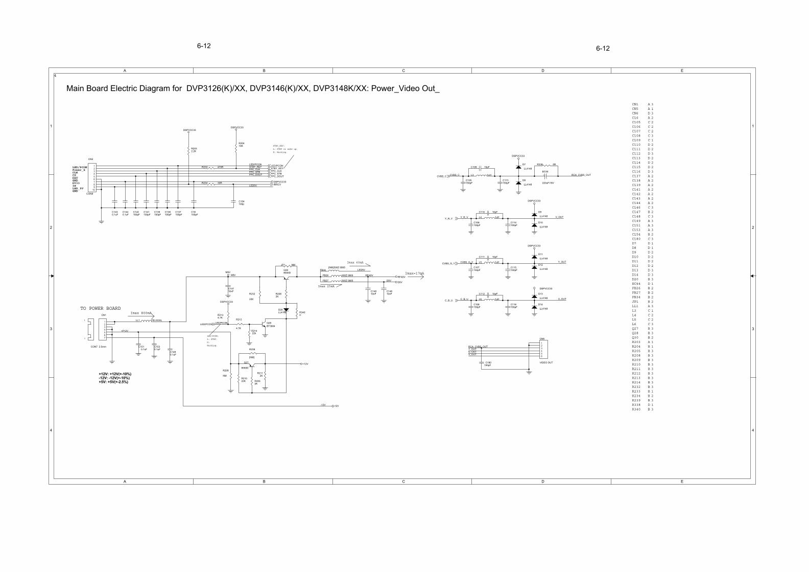
Main Board Electric Diagram for DVP3126(K)/XX, DVP3146(K)/XX, DVP3148K/XX: Power_Video Out_

6-136-13
Main Board Print-Layout (Top Side) for DVP3126(K)/XX, DVP3146(K)/XX, DVP3148K/XX
6-14 6-14
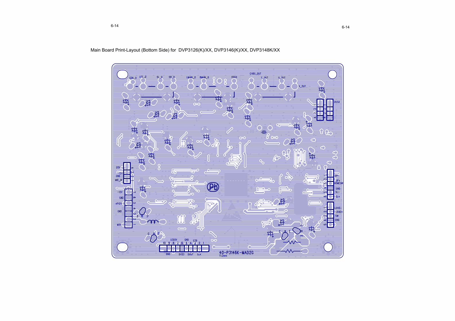
Main Board Print-Layout (Bottom Side) for DVP3126(K)/XX, DVP3146(K)/XX, DVP3148K/XX

A
A
B
B
C
C
D
D
E
E
1 1
2 2
3 3
4 4
Vaddis 9
SDRAM configuration:
1X16Mbit: CS0# = Low;
1X64Mbit: CS1# = Low; CS0#=BA1
SDRAM speed <=7ns
Tras <=44.4ns
Trp <=22.2ns
Close to Pin37 of U4
R39 R40Flash select
Intel NM 0R
AMD/SST 0R NM
Flash speed <= 70 nS.If plan to use 90nsFlash, it needs to beverified by s/w.
A19
NCNCRY/BY#
BYTE#
Close to Vaddis!
Close to Vaddis!
Important power supply!
JP3 JP2BOOTSEL
Play OPEN OPEN
Download
SW debug
OPEN CLOSE
CLOSE OPEN
UART
RESET
Place de-coupling capacitors close to power pins.
Close to Vaddis
Close to Vaddis
CrystalUse it to connect the shell of the crystal with ground.
OPU: 313A HD65R5: 22K 11KR6: 33K 18K
EEPROM
Imax 165mA
Imax 120mA
Imax 9mA
Imax 0.5mA
CN10CN109C2C3C4C5C6C7C8C9C10C11C12C15C19C20C21C22C23C24C25C26C27C28C29C30C31C32C33C34C35C36C37C38C39C43C44C45C48C49C50C51C189C190C191C192C193C194C201C202C205C206D1EC1EC4
EC9EC20FB1FB3FB4FB6FB7FB8FB9FB30JP2JP3Q1R1R2R3R4R5R6R7R8R9R10R13R14R15R19R20R21R22R24R30R33R34R35R36R37R38R39R40R41R42R56R223R224R225R226R227R228R229R235R238U1AU2U3U4U5X11Y1
DDAAAABAAAAAACAAAAACCCCCCCBBBBCCBDDDDBACCBCCCCCCBCDDDAD
4444444444444344444111111111111131123411111111113221241
DCADDCCCCBAADBBBBBBCBBCDDDCCCCDDDDDDDDAAAACDDDCCCCDDBBBADDD
23411122233324311111112111222222222233113333333333111441341
RA
MC
KE
RA
MC
AS
-
RA
MD
AT
5
RA
MD
AT
4
RA
MA
DD
8
RA
MD
AT
15
RA
MD
AT
9
RA
MA
DD
7
RA
MD
QM
RA
MA
DD
4
RA
MW
E-
RA
MA
DD
9
RA
MA
DD
0
RA
MD
AT
7
RA
MA
DD
10
RA
MA
DD
1R
AM
AD
D2
RA
MD
AT
11
RA
MD
AT
6
RA
MD
AT
0
RA
MC
S0-
RA
MD
QM
RA
MA
DD
5R
AM
AD
D6
RA
MD
AT
10
RA
MR
AS
-
RA
MB
A
RA
MD
AT
1R
AM
DA
T13
RA
MD
AT
2
RA
MD
AT
12
RA
MA
DD
11
PC
LK
RA
MA
DD
3
RA
MC
S1-
RA
MD
AT
8
RA
MD
AT
14
RA
MD
AT
3
RA
MB
A
RA
MD
QM
RA
MA
DD
6R
AM
AD
D5
PC
LK
RA
MD
AT
11
RA
MR
AS
-
RA
MD
AT
0
RA
MC
S0-
RA
MA
DD
3
RA
MD
AT
1
RA
MD
AT
12
RA
MD
AT
13
RA
MD
AT
10
RA
MD
AT
2
RA
MD
AT
4
RA
MC
AS
-
RA
MD
AT
14
RA
MA
DD
1
RA
MD
AT
3
RA
MD
AT
8
RA
MD
AT
15
RA
MD
AT
9
RA
MA
DD
7
RA
MA
DD
9
RA
MD
AT
7
RA
MW
E-
RA
MA
DD
10
RA
MD
AT
5
RA
MA
DD
4
RA
MA
DD
0
RA
MD
QM
RA
MA
DD
8
RA
MA
DD
2
RA
MD
AT
6
SDRAM3.3V
SDRAM3.3V
SDRAM3.3V
MEMADD15MEMADD14MEMADD13MEMADD12MEMADD11MEMADD10MEMADD9MEMADD8
MEMADD18MEMADD17MEMADD7MEMADD6MEMADD5MEMADD4MEMADD3MEMADD2MEMADD1
MEMADD16
MEMDAT15MEMDAT7MEMDAT14MEMDAT6MEMDAT13MEMDAT5MEMDAT12MEMDAT4
MEMDAT11MEMDAT3MEMDAT10MEMDAT2MEMDAT9MEMDAT1MEMDAT8MEMDAT0
MEMADD0
MEMWR#
MEMRD#
SPDL_SSLED_S
RF
MEMADD2
MEMADD1
DUPRD1DUPTD1
DUPTD0DUPRD0
STBY_KEY
AMCLK
ALRCLKABCLK
PCLK
VDDPWM
I2C
_D
AT
I2C
_C
LK
DUPRD1 MUTE_CTL
RESET#
OSCOUT
OSCIN
LED/PCON
DAC_RST#
VDDPLL
C_B_U
VDDAFE
APWM_R-
CLOSE
RA
MD
AT
1
RA
MD
AT
2
MEMADD6
TR
AC
K_P
WM
ME
MD
AT
8
ME
MD
AT
9
MIC
_O
N
LE
D/P
CO
N
RA
MD
AT
5R
AM
DA
T11
MEMADD18
MEMADD8
LD
_C
D
DRVSB
RA
MD
AT
0
RA
MD
AT
10
RA
MW
E-
MEMDAT14
RF
N
VD
DA
FE
S/PDIF_OUT
FPC_STB
OSCIN
RA
MD
AT
14
MEMADD15
MEMDAT15
MEMDAT12
RF
P
DUPTD1
VDDDAC
RA
MC
S0-
MEMADD14
MEMDAT5
HOMESW
CD_DVD
RA
MD
AT
7
RA
MC
S1-
RA
MA
DD
9
RAMADD1
MEMADD1
MEMADD13
OSCOUT
RA
MD
AT
13
RA
MD
QM
RAMADD2
MEMADD9
MD
_D
VD
RA
MC
KE
APWM_L+
OPEN
FPC_CLK
RA
MA
DD
11
RA
MA
DD
8
MEMADD3
MEMDAT4MEMDAT11
VDDDAC
APWM_L-
INSW
VDDPLL
MEMADD4MEMADD5
MEMDAT7
MEMDAT3
DUPRD0
DUPRD1
RA
MD
AT
15
RAMADD6
RAMADD7
MEMADD10
MEMDAT10
VC
MD
_C
D
ME
MC
S0#
ME
MR
D#
IRRCV
MEMADD7
MEMADD11
MEMDAT13
ME
MD
AT
1
MEMADD19
Y_R_V
RAMADD4
IN_OUT_SW
FPC_DOUT
IPC
LK
RA
MB
A
RA
MA
DD
0
MEMADD12
MEMDAT2
VD
DA
FE
SP
DL_S
EN
S-
SLE
D_P
WM
RAMADD3
RA
MD
AT
9
MEMWR#
LD
_D
VD
RE
SO
UT
VR
EF
VD
DP
WM
ME
MD
AT
0
V1
VDDDAC
MEMADD17
MEMDAT6
SP
DL_S
EN
S+
ME
MA
DD
0
VO
CA
L_D
ET
RAMADD5
RA
MD
AT
3R
AM
DA
T12
RA
MC
AS
-
RA
MA
DD
10
MEMADD19
MEMADD16
MIC
_V
OC
AL
RA
MC
KE
AIN
DUPTD0
RA
MD
AT
4
RA
MD
AT
6
RA
MD
AT
8
RA
MR
AS
-
MEMADD2
CVBS_C
CVBS_G_Y
APWM_R+
IRRCV
FOCUS_S
FO
CU
S_P
WM
SP
DL_P
WM
TRACK_S
ST
BY
_K
EY
VDD1AFE
VD
D1A
FE
RF
_A
RF
_B
RF
_C
RF
_D
RF
_E
RF
_F
DSPVCC33
DSPVCC33
RESET#
DSPVCC33
I2C_CLKI2C_DAT
WPCON
V1 V2
APWM_SR+APWM_CEN-APWM_CEN+
WP
CO
N
MEMCS0#
APWM_SL-APWM_SL+
APWM_SR-
AP
WM
_LF
E-
AP
WM
_LF
E+
DA
C_R
ST
#
V2
C_B_U
Y_R_VCVBS_C
ABCLKALRCLK
AMCLK
FOCUS_S
SLED_S
RF
STBY_KEY
VO
CA
L_D
ET
MIC
_O
N
MUTE_CTL
LED/PCON
DAC_RST#
CLOSE
RF
_E
APWM_L+
FPC_STB
RF
_A
LD
_D
VD
CD_DVD
APWM_R-
S/PDIF_OUT
RF
_D
DRVSB
MIC
_V
OC
AL
RF
_C
INSW
VC
IN_OUT_SW
FPC_DOUT
LD
_C
D
MD
_D
VD
HOMESW
MD
_C
D
IRRCV
RF
_F
SP
DL_S
EN
S-
OPEN
SP
DL_S
EN
S+
AIN
FPC_CLK
RF
_B
CVBS_G_Y
SPDL_S
TRACK_S
APWM_L-
APWM_SL-APWM_SL+
APWM_SR-APWM_SR+
APWM_CEN+APWM_CEN-
AP
WM
_LF
E-
AP
WM
_LF
E+
DA
C_R
ST
#
APWM_R+
DSPVCC33
DSPVCC33
DSPVCC33
SERVO33
DSPVCC33
DSPVCC18
DSPVCC33
DSPVCC18
DSPVCC33
DSPVCC33DSPVCC33
DSPVCC33
DSPVCC33
DSPVCC33
DSPVCC18
DSPVCC33
DSPVCC33
DSPVCC33
DSPVCC33
R15
75R
C192 33pF
R22610K[NM]
FB6
500Z
R13 75R
C49
0.1
uF
C2110nF
R34 10K
R3 51K
C2710nF
R20
75R
1%
C310nF
R22910K[NM]
C2051000pF
U4
SST39VF800[39VF400/800/160]
123456789
101112131415161718192021222324
484746454443424140393837363534333231302928272625
A15A14A13A12A11A10A9A8NCA20WE#RP#VPPWP#A19A18A17A7A6A5A4A3A2A1
A16VCCQ
GNDDQ15
DQ7DQ14
DQ6DQ13
DQ5DQ12
DQ4VCC
DQ11DQ3
DQ10DQ2DQ9DQ1DQ8DQ0OE#GNDCE#
A0
C39 22pF
C1110nF
+ EC20
NM[470uF/6.3V]
C2310nF
C32
1000pF
R238 4.7R
R382K
R7
15.4
K 1
%
C710nF
R225 0R[NM]
FB1
500Z
R35
10K
FB30500ZJP2BOOTSEL1[NM]
+ EC4100uF/16V
R30
15K
FB9 75Z
R5 22K
U3
NM[64Mbit:K4S641632H-UC70]
1 2 3 4 5 6 7 8 9 10
11
12
13
14
15
16
17
18
19
20
21
22
23
24
25
26
27
28
29
30
31
32
33
34
35
36
37
38
39
40
41
42
43
44
45
46
47
48
49
50
51
52
53
54
VD
DD
Q0
VD
DQ
DQ
1D
Q2
VS
SQ
DQ
3D
Q4
VD
DQ
DQ
5D
Q6
VS
SQ
DQ
7V
DD
DQ
ML
WE
#C
AS
#R
AS
#C
S#
BA
0B
A1
A10
A0
A1
A2
A3
VD
DV
SS
A4
A5
A6
A7
A8
A9
A11
NC
CK
EC
LK
DQ
MH
NC
VS
SD
Q8
VD
DQ
DQ
9D
Q10
VS
SQ
DQ
11
DQ
12
VD
DQ
DQ
13
DQ
14
VS
SQ
DQ
15
VS
S
C191 33pF
R9
100R
R2244.7K[NM]
+EC147uF/16V
C37
10pF[NM]
C43
0.22uF
R36 100R
C31
1000pF
R8
100R
C35 1000pF
CN10
HYPER_TERMINAL I/F
1234
R6 51K
R21
75R
1%
C1910nF
C1210nF
C2610nF
C4810nF
C44NM[0.1uF]
FB8 75Z
C194 33pF
C206NM[20p]
R223 NM [0R]
C33
27nF
C2010.1uF
C2010nF
R33 330R
C4522pF[NM]
C38 22pF
U5
NM[24LC02 ]
1234
8765
A0A1A2
GND
VCCWPSCLSDA
C25100nF
C202 1000pF
C190 33pF
C2410nF
C50
33pF
C410nF
R14220K
R56 4.7R
R22
75R
1%
R411K[NM]
R2
75R
FB4500Z
U2
16Mbit: K4S161622C-TC/L70
12345678910
11
12
13
14
15
16
17
18
19
20
21
22
23
24
25
50
49
48
47
46
45
44
43
42
41
40
39
38
37
36
35
34
33
32
31
30
29
28
27
26
VD
DD
Q0
DQ
1V
SS
QD
Q2
DQ
3V
DD
QD
Q4
DQ
5V
SS
QD
Q6
DQ
7V
DD
QLD
QM
WE
CA
SR
AS
CS
BA
A10/A
PA
0A
1A
2A
3V
DD
VS
SD
Q15
DQ
14
VS
SQ
DQ
13
DQ
12
VD
DQ
DQ
11
DQ
10
VS
SQ
DQ
9D
Q8
VD
DQ
NC
UD
QM
CLK
CK
EN
CA
9A
8A
7A
6A
5A
4V
SS
C810nF
Q1BT3904
CN109
DOWN_LOAD_I/F
1234
C910nF
C193 33pF
C36 1000pF
C210nF
C610nF
FB3500Z
C30100nF
EC910uF/16V
FB7 75Z
R19
75R
1%
R22710K[NM]
R22810K[NM]
R4 51K
Y1
27.000MHzThird overtone
R235 4.7R
JP3BOOTSEL1[NM]
C2210nF
R39 0R
C189 33pF
R372K
C510nF
C1510nF
R40 NM
R24 0R
C34
1000pF
C28100nF
U1A
ZR36962
208
207
206
205
204
203
202
201
200
199
198
197
196
195
194
193
192
191
190
189
188
187
186
185
184
183
182
178
176
179
177
174
175
173
180
181
161
172
163
170
171
167
168
165
166
162
159
160
169
164
158
157
123456789
101112131415161718192021222324252627282930313233343536373839404142
4948
5051
53
52
54
55
57
56
58
59
61
60
62
63
65
64
66
67
69
70
71
72
68
73
74
76
75
77
78
80
79
81
82
84
83
85
86
89
87
90
91
92
156155154153152151150149148147146145144143142141140139138137136135134133132131130129128127126125124123122121120119118117116115114113112111110109108107106105
44454647
88
93
94
95
96
97
98
99
100
101
102
103
104
43V
DD
PG
PIO
[9]/M
EM
DA
T[9
]M
EM
DA
T[1
]G
PIO
[8]/M
EM
DA
T[8
]M
EM
DA
T[0
]M
EM
RD
#M
EM
CS
0#
ME
MA
DD
[0]
GP
IO[6
3]/M
EM
CS
2#
GP
IO[6
2]/F
CU
_IO
RD
#G
PIO
[61]/F
CU
_IO
WR
#G
PIO
[60]/F
CU
_S
CLK
GP
IO[5
9]/F
CU
_C
S2#
GP
IO[5
8]/F
CU
_C
S3#
GP
IO[5
7]/F
CU
_W
AIT
#G
PIO
[56]/F
CU
_R
ST
IGP
IO[5
5]/F
CU
_IR
QG
ND
CV
DD
CIG
PIO
[54]/P
WM
CO
[5]
GP
IO[5
3]/P
WM
CO
[4]
GP
IO[5
2]/P
WM
CO
[3]
GP
IO[5
1]/P
WM
CO
[2]
GN
DP
WM
GP
IO[5
0]/P
WM
CO
[1]
VD
DP
WM
GP
IO[4
9]/P
WM
CO
[0]
CD
_M
D
GN
DR
EF
DV
D_M
D
VD
DS
AF
E
VR
EF
RE
SO
UT
VC
CD
_LD
DV
D_LD B
GN
D1A
FE CGH KF JE
VD
DA
FE
VD
D1A
FEA
GN
DA
FE D
RF
NR
FP
MEMDAT[2]MEMDAT[10]/GPIO[0]MEMDAT[3]MEMDAT[11]/GPIO[1]MEMDAT[4]MEMDAT[12]/GPIO[2]MEMDAT[5]MEMDAT[13]/GPIO[3]MEMDAT[6]MEMDAT[14]/GPIO[4]GNDCMEMDAT[7]MEMDAT[15]VDDCVDDPMEMADD[16]MEMCS1#/GPIO[5]MEMADD[15]MEMADD[14]MEMADD[13]MEMADD[12]MEMADD[11]MEMADD[10]MEMADD[9]MEMADD[8]MEMWR#MEMADD[18]/GPIO[6]MEMADD[17]MEMADD[7]MEMADD[6]GNDCMEMADD[5]MEMADD[4]MEMADD[3]VDDPMEMADD[2]MEMADD[1]MEMADD[19]/IGPIO[7]USBVDDUSBDP/GPO[67]USBDN/GPO[68]USBGND
RAMADD[6]RAMADD[2]
RAMADD[1]RAMADD[7]
RA
MA
DD
[0]
VDDC
RA
MA
DD
[8]
RA
MA
DD
[10]
GN
DC
VD
DP
RA
MA
DD
[9]
RA
MA
DD
[11]/G
PO
[64]
RA
MB
AR
AM
CS
0#
RA
MC
S1#/G
PO
[65]
RA
MR
AS
#
VD
DP
RA
MC
AS
#
GN
DC
RA
MW
E#
GN
DP
CLK
PC
LK
VD
DP
CLK
RA
MD
AT
[8]
RA
MD
QM
RA
MD
AT
[7]
RA
MD
AT
[9]
VD
DP
RA
MD
AT
[6]
GN
DC
RA
MD
AT
[10]
RA
MD
AT
[11]
RA
MD
AT
[5]
RA
MD
AT
[4]
RA
MD
AT
[12]
VD
DP
RA
MD
AT
[3]
GN
DC
RA
MD
AT
[13]
RA
MD
AT
[14]
RA
MD
AT
[2]
RA
MD
AT
[1]
RA
MD
AT
[15]
RA
MD
AT
[0]
GNDDACBS2RSETDAC1
VDDDACDAC2DAC3
VDDDACDAC4
GNDDAC_DDAC5XINXO
VDDPLLGNDPLLRESET#
GNDCVDDC
GPIO[48]/DUPRD1GPIO[47]/DUPTD1GPIO[46]/DUPRD0
GPIO[45]/PWMCO[5]/DUPTD0VDDP
IGPIO[44]GPIO[43]/TDOGPIO[42]/TCK
GPIO[41]/TDI/NMIGPIO[40]GPIO[39]GPIO[38]
IGPIO[37]/TMS/NMIGPIO[36]GPIO[35]
GPIO[34]/RAMCKE/SPDIFINGPIO[33]/AIN/SPDIFIN
GPIO[32]/SPDIFOGPIO[31]/ABCLK
GPIO[30]/ALRCLKVDDP
GPIO[29]/AMCLKGNDC
GPIO[28]/AOUT[0]/APWM0-GPIO[27]/APWM0+
GPIO[26]/AOUT[1]/APWM1-GPIO[25]/APWM1+
GPIO[24]/AOUT[2]/APWM2-IGPIO[23]/APWM2+
GNDAPWMGPIO[22]/AOUT[3]/APWM3-
GPIO[21]/APWM3+GPIO[20]/APWM4-
GPIO[19]/PWMCO[5]/APWM4+VDDAPWM
RAMADD[3]RAMADD[5]VDDIPGNDC
VD
DC
VD
DP
RA
MD
QM
2/R
AM
CK
E/G
PO
[66]
GN
DC
RA
MC
KE
/SD
I_P
SC
/GP
IO[1
0]
GP
AIO
/IG
PIO
[11]
AP
WM
7+
/GP
IO[1
2]
AP
WM
7-/
GP
IO[1
3]
AP
WM
6+
/GP
IO[1
4]
AP
WM
6-/
GP
IO[1
5]
AP
WM
5+
/GP
IO[1
6]
AP
WM
5-/
GP
IO[1
7]
AIN
/SP
DIF
IN/IO
[18]
RAMADD[4]
R1 4.7K
C1010nF
R10
392 Ohm 1%
D1
LL4148
C2910nFC51
0.1uF
R421K[NM]
6-15 6-15
Main Board Electric Diagram for DVP3146K/93: Vaddis_SDRAM_Fla

A
A
B
B
C
C
D
D
E
E
1 1
2 2
3 3
4 4
OPU 313A HD65 502WR49: 100R 0R 91RR50: 100R 0R 91R
EMC
Close to CN2
CN2 is used for Sanyo/Sony OPUs
2.1V
Close to motor driver.
HOMESWGND
SLED+
SP-
LOAD-
SP+
SLED-
GND
LOAD+
INSW
OUTSW
CD/DVD Control :
DVD=LOW
CD=HIGH
OPU: 313A HD65R76: 2.2R 1R
Imax=600mA Imax=250mA
Close to Q4
Close to Q5
CN2CN3CN4C42C52C53C54C55C56C57C58C62C63C64C65C66C67C68C123C124C125C126C127C195C196D19EC10EC11EC12EC13EC14EC38EC39L2Q2
Q3Q4Q5RR1RR2R43R44R45R46R47R48R49R50R52R61R62R66R70R71R72R73R74R75R76R84R85R86R87R88R90R91R92R219U7
ACDCCAAAAAABBBBCCCCDDDDDDDDAAAAADB
1333211111211223333331111214444432
AAAAAAAAAAABCAAACDDEDEEAADAAAABDDAA
14341111122334442233333211111233311
LOAD+
FACT-SL_MOT-SL_MOT+
TACT+
FACT+
FOCUS_S
DV
DL
D
CD
LD
TRACK_SSLED_S
SP_M-
SPDL_SENS+
SPDL_SENS-
VC2
SP_M-
TACT-
SP_MOT+
VC2
VR_CD
SPDL_S
SP_MOT-
DRVSB
SP_MOT+
LOAD-
TACT+
VC1
FACT-
OPU5V
FACT+
OPU_HFM
CDLDVR_DVD
DVDLD
TACT-
LOAD+
IN_OUT_SWINSW
VR_CD
VR_DVD
SL_MOT+SL_MOT-
CD_DVD
LOAD+
FACT+
FACT-
SL_MOT+
SL_MOT-
LOAD-
VC2
SP_MOT+
TACT+
TACT-
SP_M-
SP_MOT-
LOAD-
HOMESW
TRACK_SSPDL_S
SPDL_SENS+
SPDL_SENS-
INSWIN_OUT_SWHOMESW
RF_ARF_B
RF_CRF_D
RF
RF_F
RF_E
LD_DVD
LD_CD
VC
FOCUS_S
DRVSB
SLED_S
CD_DVD
MD_DVD
MD_CD
TR_B2
REGO1
TR_B1
FOCUS_S
REGO2
SLED_S
DRVSB
REGO1 REGO2
TR_B1 TR_B2
OPEN
CLOSE
SPDL_S
TRACK_S
DSPVCC33
RFA5V
DSPVCC33
DSPVCC33
DSPVCC33
RFA5V
DSPVCC33
M5VM5V
DSPVCC18DSPVCC33
GND GND
M5V
DSPVCC18
DSPVCC33
SERVO33
Q29012
R70
1%20k
C541000pF
C52NM1uF
C64NM[1nF]
L2 10uH
C67
0.1uF
R761R
CN2
SF-HD6B/0.5mm,24P TOP
242322212019181716151413121110987654321
25262728
F-F+T+T-CD
CD/DVDRF
ABF
GND-PDVC
VCCE
NCVR-CD
VR-DVDLD-CD
MDHFM
NCLD-DVDGND-LD
GNDGNDGNDGND
+ EC39
220uF/16V
R49100R
C123
220pF
R86
33K
C580.1uF
R752K
R85
1K 1%
C53NM1uF
R904.7K
R73
1%
10k
D19
BAT54C
2
3
1
R44 220R
R48 33R
RR2
2.2 OHM 2W
+ EC13
47uF/16V
R742K
C126
1000pF
RR1 6.8 OHM 1W
R88 0R[NM]
+ EC10
47uF/16V
+ EC12100uF/16V
C65NM[1nF]
C1961000pF
R71
1%
12k
Q5
SS8550D
b
ec
C620.1uF
CN3
NM(TRAY_CNN)
12345 R87 NM [0R]
C56[1000pF]
C551000pF
R46 220R
U7 AM5888S(HSOP-28)
1
9
10
12
3
2
15
7
14
13
21
19
20
24
27
6
4
5
28
8
11
17
18
16
23
22
25
26
29 30
VINFC
VOTR-
VOTR+
VOSL-
REGO2
TR_B1
VOTK+
REV
VOFC+
VOFC-
VCTL
VCC2
NC
NC
BIAS
FWD
VINSL
REGO1
MUTE
VCC1
VOSL+
VOLD+
VOLD-
VOTK-
VINLD
GND
TR_B2
VINTK
GND GND
C125
220pF
Q4
SS8550D
C1951000pF
+ EC11
47uF/16V
R924.7K
C66NM[1nF]
C124
1000pF
EC14220uF/16V
R66
1K
R61 0R
CN4
NM(SLED & SPINDLE)
123456
Q39012
R50100R
R62 0RR219 0R
R434.7R
C127
0.1uF
R47 [0R]
R72
1%
4.7k
R84
1K 1%
R454.7R
R914.7K
C570.1uF
+EC38
220uF/16V
C42 0.1uF
C63100pF
C68
0.1uF
R52
3.3K
6-166-16
Main Board Electric Diagram for DVP3146K/93: Front end

A
A
B
B
C
C
D
D
E
E
1 1
2 2
3 3
4 4
Mic vocal detected by ADP software
Mic signal mute/mix/echo process by ADP
ADP: Audio Digital Process
ADC circuit for Karaoke
Max. amplitude of Mic_Audio signal is 4Vrms
Full scale input: 0.65Vrms (when VA=3.3V)M0=1, M1=1: clock slave;Package: TSSOP16.
Value in [] is for external ADC.
External MicroPhone detection
MUTE_CTLLow:Mute.
Close to Q31
CN7CN9CN11C83C84C85C86C87C88C89C90C91C92C97C98C99C100C101C102C103C104C120C121C122C129C130C132C133C210C211C212C213C214C215C216C217C220C221C222C223C224C225C226C227D2D3D4D15D16EC25EC26EC27EC28EC30EC31EC32EC33EC34EC35EC36EC40EC41EC42EC43FB10Q13Q14Q15Q17Q18Q19Q20Q21Q22Q31Q40Q41Q42Q43R51R57R58R100R101R102R103R104R105R106R107
EBDAAAAAAAACCCCCCDDDDDDDDDBBBCCCDBCDBCCCDBCDABAAADDDDAAAAAAACCCCBBAADDAAAADDDDDAAAAAAAAAAA
314121222221111111112333331133334434222242243342222111122234342213431111223342311111111111
R108R109R110R111R112R113R114R115R116R117R120R123R124R125R126R127R128R129R130R133R135R136R139R141R142R149R152R153R160R163R164R165R166R167R168R169R170R171R172R173R174R175R176R194R195R196R197R300R301R302R303R304R305R306R307R310R311R312R313R314R315R316R317R320R321R322R323R324R325R326R327R330R331R332R333R334R335R336R337U13U14AU14BU15AU15BU16AU16BU17AU17B
AAAAAAAAAABBAAAAAAABCBBCBCCCCCCCCDDDDDDDDDDDDDDBBCCCCCCBBCCCCCCBBCCCCCCBBCCCCCCACCDDCCCC
1111222222444443432111111111111111111111122333333333333343344442222222223223233111114322
MUTE_BIAS1
ABCLKALRCLK
AMCLK
VA
DAC_RST#
VOCAL_DET
MIC_IN
MUTE_CTL
LRIN
-12VA
AIN
MIC_IN
VA LRIN
MIC_IN
-12VD5V
S/PDIF_OUT
COAX_SPDIF
COAX_SPDIF
LFE_OUTCEN_OUT
RMAIN_OUT
SL_OUTSR_OUT
MIC
+12VA
LMAIN_OUT
MUTE
MIC
-12VA
MUTE
RMAIN_OUT
+12VA
AUDIO_MIX_LMICMUTE
LMAIN_OUT
AUDIO_MIX_R
-12VA
MUTE
MUTE
+12VA
MUTE
LFE_OUT
SR_OUT
SL_OUT
MUTE
CEN_OUT
-12VA
+12VA
MIC_ON
MIC_VOCAL
AIN
VOCAL_DET
DAC_RST#
MUTE_CTL
AMCLK
ABCLKALRCLK
S/PDIF_OUT
APWM_L+
APWM_R+
APWM_R-
APWM_L-
APWM_SL+
APWM_SR-
APWM_LFE+
APWM_SL-
APWM_SR+
APWM_LFE-
APWM_CEN+
APWM_CEN-
M5V
-12V
+12V
-12VA
DSPVCC33
DSPVCC33DSPVCC33
DSPVCC33
D5V
DSPVCC33
-12VA
M5V
D5V
+12VA
-12VAC97 150pF
+
EC32NM
[10uF/16V]
R320
43K
Q22
NM[BT3094]
Q43
BT3904
R330
43K
C227100pF
R124220R
R332 47K
R326NM
CN11
AUDIO OUT
123456
C911500pF
R171NM
R32447k
R311
43K
Q31
BT3904
+ EC30
NM[10uF/16V]
+
-
U15B
NJM4558 OPA
5
67
84
Q20NM[BT3904]
Q139012H
C211 150pF
C2151500pF
R123100K
R14947k
C1200.1uF
D2
LL4148
D15NM
[1N4148]
R323
2.2K
R115NM[10K]
+
EC43
22uF
C130100pF
R101 NM[4.7R]
R3051K
C2230.1uF
C88NM[2200pF]
R1701K
R3351K
Q159012H
C98 150pF
R1640R[18K]
R317
470
Q21NM[BT3094]
+
EC28
22uF
R300
43K
R196
39R
U13
NM[CS5340]
123456789
10111213141516
M0MCLK
VLSDOUT
GNDVD
SCLKLRCK/RST
AINLVQAINRVAREF_GNDFILT+M1
R110NM[100K]
Q17
BT3904
R167 0R[18K]
R310
43KD3 LL4148
R130NM[6.8K]
R312 47K
R322 47K
R30447k
R106NM[NM]
R166 NM[6.8K]
C86
NM[0.1uF]
R57 NM[0R]
+
EC34NM[10uF/16V]
R136
43K
+
EC40
22uF
Q19[NM]9012H
R153 47K
R321
43K
R303
2.2K
R114NM[2K]
R165 NM[6.8K]
C990.1uF
Q40
BT3904
C2130.1uF
D4LL4148
R127 10K
R111NM[100K]
C1030.1uF
R333
2.2K
R173
470
R108
NM[4.7K]
R316NM
R16047k
R302 47K
C83
NM
[0.1uF]
R175 100R
R51 NM[3.3K]
R129 33R
R112NM[15K]
R103NM[10K]
R194
NM
R12547K
R1630R[18K]
R327
470
R301
43K
R141
2.2K
C104
0.1uF
R152 47K
+
-
U17A
NJM4560 OPA
3
21
84
Q41
BT3904
R104 NM[33R]
R313
2.2K
C121
0.1uF
R306NM
R100NM
[4.7K]
+
-
U15A
NJM4558 OPA
3
21
84
R135
2.2K
C85
NM
[0.1uF]
R116NM[2K]
+
EC2647uF/25V
+
-
U17B
NJM4560 OPA
5
67
84
Q18
BT3904
+
EC41
22uF
+
EC33NM[22uF/16V]
CN9
4PIN*2.0
1234
C2220.1uF
R3151K
EC36
47uF/25V
C226 150pF
C122
22pF
+
-
U16A
NJM4560 OPA
3
21
84
C129100pF
C89
NM
[1uF]
R102NM[4.7K]
+
EC27
22uF
R3251K
R107 NM[1K]
FB10 500ZNM
R117NM[4.7K]
R139
43K
R337
470
R33447k
R19556R
R120
100K
C1000.1uF
R58NM[3.3K]
R1691K
R105NM150
R176 100R
+
-
U16B
NJM4560 OPA
5
67
84
C102 NM[22pF]
C2201500pF
R197
62R
C87
NM[1uF]
+ EC31
NM
[10uF/16V]
R174
470
C101 NM[22pF]
+
EC42
22uF
C2120.1uF
CN7
AUDIO OUT
123456
EC35470uF/16V
C216 150pF
R142
43K
C1321000pF
R133
43K
Q42
BT3904
C1331000pF
R128 10K
C84
NM
[0.1uF]
R31447k
C217
100pF
R113NM[1M]
D16NM[1N4148]
R126 100R
R168 0R[18K]
+
-
U14A
NJM4560 OPA
3
21
84
R336NM
R331
43K
C214100pF
R172NM
C921500pF
+EC2547uF/25V
R307
470
C221 150pF
C90
NM
[0.1uF]
R109
NM[4.7K]
C2251500pF
C2101500pF
+
-
U14B
NJM4560 OPA
5
67
84
C224100pF
Q14 9012H
6-17 6-17
Main Board Electric Diagram for DVP3146K/93: Audio Input_Outp

A
A
B
B
C
C
D
D
E
E
1 1
2 2
3 3
4 4
+12V: +12V(+-10%)-12V: -12V(+-10%)+5V: +5V(+-2.5%)
TO POWER BOARD
LED/PCON:
L: STBY.
H:
Working.
Imax=17mA
Imax 800mA
4
Imax 60mA
STBY_KEY:
L: STBY or wake up.
H: Working.
GND
CLK
DAT
GNDLED_5V
CS
IR
Power_k
DV33
Imax 25mA
LED/PCON
CN1CN5CN6C16C105C106C107C108C109C110C111C112C113C114C115C116C137C138C139C141C142C143C144C146C147C148C149C151C153C154C180D7D8D9D10D11D12D13D14D20EC44FB26FB27FB34JP1LL1L3L4L5L6Q27Q28Q30R203R204R205R208R209R210R211R212R213R214R232R233R234R239R338R340
AADACCCCCDDDDDDDAAAAAAACBCAAABCDDDDDDDDBDBBBBACCCCBBBABBBBBBBBBBBBBDB
313222231223222322222223233332311222233312222312233321133333333312313
CVBS_G_Y
CVBS_C
Y_R_V
C_B_U
RFA5V
-12V
M5V
LED/PCON
V_OUTU_OUT
LED5V
STBY_KEY
D5V
+P12V
LED5V
Y_OUT
V_OUT
Y_OUT
U_OUT
FPC_DOUTFPC_STBFPC_CLK
LED/PCON
RCA_CVBS_OUT
RCA_CVBS_OUT
C_B_U
CVBS_C
Y_R_V
CVBS_G_Y
LED/PCON
FPC_CLKSTBY_KEY
IRRCV
FPC_STBFPC_DOUT
LED/PCON
DSPVCC33
RFA5V
-12V
M5V
+12V
DSPVCC33DSPVCC33
DSPVCC33
D5V
DSPVCC33
DSPVCC33
DSPVCC33
DSPVCC33
D13
LL4148
+
EC44
220uF/16V
FB26 500Z 0805
R21422k
CN5
CON9
123456789
10
R209
NM
C109 10pF
C108150pF
R2052K
1
7
CN1
CON7 2.5mm
1234567
C110 10pF
C180100pF
R239
[NM]
C112 10pF
LL1 FB AXIAL
R233 470RD7
LL4148
L3 1uH
C116150pF
R20410K
R2112K
C105150pF
R2032.2K
R232
22K
D8
LL4148
D10
LL4148
C115150pF
R338 0R
C1490.1uF
D9
LL4148
C16100pF
C111 10pF
C14710nF
FB27 500Z 0805
Q308550D
FB34[NM]500Z 0805
C106150pF
Q28
BT3904
CN6
VIDEO OUT
123456
C114150pF
C14810nF
C107150pF
L4 1uH
JP1 NM
C1430.1uF
C1440.1uF
R212
4.7K
C113150pF
R3400
R2082K
C1530.1uF
D12
LL4148
D11
LL4148
C142100pF
C141100pF
C1510.1uF
C139100pF
Q27
8550D
C138100pF
L5 1uH
C137100pF
L6 1uH
C14610nF
R21022K
R2134.7K
D20LL4148
C154100p
R234 33R
D14
LL4148
6-186-18
Main Board Electric Diagram for DVP3146K/93: Power_Video Out_

6-19 6-19
Main Board Print-Layout (Top Side) for DVP3146K/93

6-20 6-20
Main Board Print-Layout (Bottom Side) for DVP3146K/93
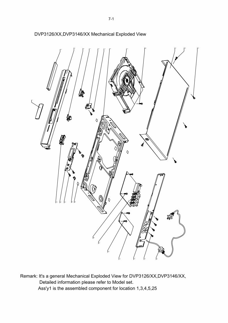
7-1
DVP3126/XX,DVP3146/XX Mechanical Exploded View
Remark: It's a general Mechanical Exploded View for DVP3126/XX,DVP3146/XX,Detailed information please refer to Model set.
Ass'y1 is the assembled component for location 1,3,4,5,25

NoAssy1
2
6
8
9
11
14
16
17
19
21
2224
12NC No.996510002904996510002893996510002683
996510002682996510002892
996510001163
996510001177
996510001805996510002887996510001166
/996510001682
996510001179
996510001537996510002223
996510002899996510001883996510002901996510002890
996510001820996510001190996510001878
996510002902996510002891996510002680
/
/996510001164
Part NameFront Panel Ass’y for DVP3126/94 ,DVP3126X/94Front Panel Ass’y for DVP3126/98/96/51Front Panel Ass’y for DVP3146/94,DVP3146X/94
Front Door Ass’y for DVP3146/94,DVP3146X/94Front Door Ass’y for DVP3126/94/98/96/5 1
Ass’y-Switch Board
Bottom Cabinet
Loader for DVP3126/94/98,DVP3126x/94Loader for DVP3126/96/51Loader for DVP3146/94,DVP346x/94
Top coverTop cover for DVP3126/94,DVP3126x/94,DVP3146/94,
DVP3146x/94
Power Cord for DVP3126/94/51,DVP3126x/94,
DVP3146/94,DVP3146X/94
Power Cord for DVP3126/98Power Cord for DVP3126/96
Back Panel for DVP3126/94,DVP3126x/94Back Panel for DVP3146/94 ,DVP3146x/94Back Panel for DVP3126/98Back Panel for DVP3126/96
Ass’y-Power Board for DVP3126/94,DVP3126x/94Ass’y-Power Board for DVP3126/98Ass’y-Power Board for DVP3146/94/96DVP3126/51,DVP3146x/94Ass’y-Main Board for DVP3126/94,DVP3126x/94Ass’y-Main Board for DVP3126/98/96/51Ass’y-Main Board for DVP3146/94,DVP3146x/94
Pad 4
ESD Pad 1Ass’y-Front Board DVP3126/94,DVP3126x/94
ENCASING & ACCESSORIES PARTS LISTQ'ty
1
1
1
1
1
1
1
1
1
1
1
1
1
No
710121315182023
12NC No.
/ / / / / / / /
Part Name
S/T Screw B2.6X8 BFMachine ScrewTriangle M/C Screw 3*6Triangle M/C Screw B3*6S/T Screw B 3 X 8 BFTriangle M/C Screw B3*6Triangle M/C Screw B3*6
S/T Screw B2.6X8 BF
Q'ty
2 1 2 3 4 2 2 3
SCREW LIST
Accessory
PAC2PAC1RC
RCPAC8PAC3PAC3PAC5
Cable
C0N302CON301CN2CN1
CN3CN1
CN4
CN4
996510001203996510001202996510001822
996510001806996510001106996510002903996510002681996510002668
996510001171996510001172996510001168996510001169
996510001192
996510001904
996510001170 /
RIGHT BUFFERLEFT BUFFERREMOTE CONTROL forDVP3126/94 ,DVP3126x/94,DVP3146/94,DVP3146x/94REMOTE CONTROL for DVP3126/98/51VIDEO CABLE 1500mmDISPLAY BOXDISPLAY BOX for DVP3146x/94POLY BAG for DVP3146/94,DVP3146x/94
2P HS DVP3126/94 ,DVP3126x/94HS 9PIN DVP3126/94,DVP3126x/9424PIN HS DVP3146/94 ,DVP3146x/94TJC3-7Y/SCN-7P L=80MM for DVP3126/94/98 , DVP3126x/94PH-5Y/PH-5Y L=130MM 1 for DVP3126/94,
DVP3126X/94,DVP3146/94,DVP3146x/94
CABLE HS 7P 2468#26 for DVP3126/96/51,
DVP3146/94,DVP3146x/94
6PIN HS for DVP3146/94,DVP3146x/94
6PIN HS for DVP3126/51
7-2
Note:Only the parts mentioned in this list are normal service spare parts
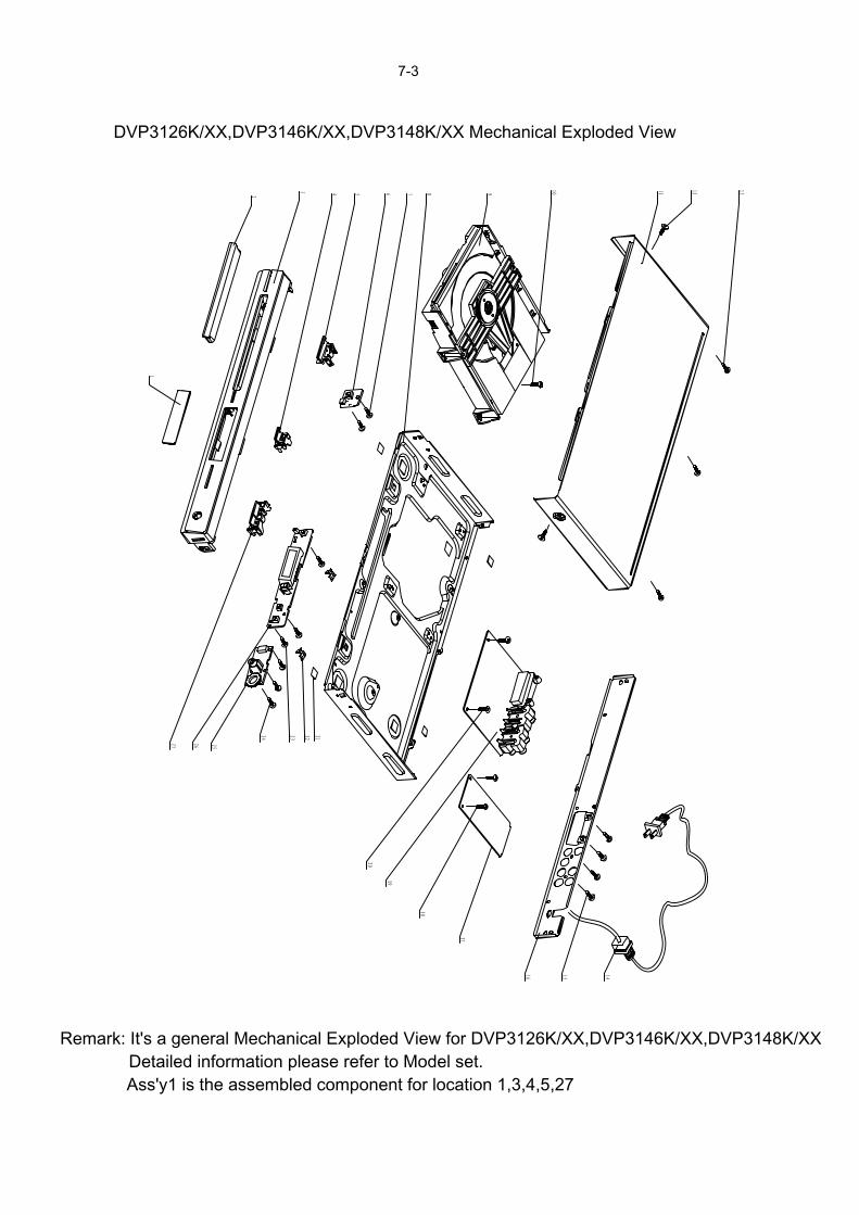
7-3
DVP3126K/XX,DVP3146K/XX,DVP3148K/XX Mechanical Exploded View
Remark: It's a general Mechanical Exploded View for DVP3126K/XX,DVP3146K/XX,DVP3148K/XXDetailed information please refer to Model set.
Ass'y1 is the assembled component for location 1,3,4,5,27

No 12NC No. Part Name Q'ty No 12NC No. Part Name Q'ty
Ass'y1 996510004028 Front Panel Ass'y for DVP3126K/61 1 26 996510001164 Ass'y-Front Board for DVP3126K/61/56/96/51/93 1
996510002889 Front Panel Ass'y for DVP3126K/56/96 DVP3146K/93
996510002678 Front Panel Ass'y for DVP3146K/93 996510001189 Ass'y-Front Board for DVP3146K/96/98/51
996510002671 Front Panel Ass'y for DVP3146K/96/98 DVP3148K/51
/ Front Panel Ass'y for DVP3148K/51 7 / S/T Screw B2.6X8 BF 2
996510002896 Front Panel Ass'y for DVP3126K/98/51/93 10 / Machine Screw 1
/ Front Panel Ass'y for DVP3146K/51 12 / Triangle M/C Screw 3*6 2
2 996510002888 Front Door Ass'y for DVP3126K/61/56/96/98/51/93 1 13 / Triangle M/C Screw B3*6 3
996510002677 Front Door Ass'y for DVP3146K/93 15 / S/T Screw B 3 X 8 BF 4
996510002670 Front Door Ass'y for DVP3146K/96/98/51 18 / Triangle M/C Screw B3*6 2
/ Front Door Ass'y for DVP3148K/51 20 / Triangle M/C Screw B3*6 2
6 996510001163 Ass'y-Switch Board for DVP3146K/93 1 23 / S/T Screw B2.6X8 BF 3
DVP3126K/96/56/61/98/51/93 24 / S/T Screw B2.6X8 BF 2
996510001188 Ass'y-Switch Board for DVP3146K/96/98/51, Accessory
DVP3148K/51 AVCAB 996510001106 VIDEO CABLE 1500mm 1
8 996510001177 Bottom Cabinet 1 RC 996510001778 REMOTE CONTROL for DVP3126K/96/56/98/51/61 1
9 996510001805 Loader for DVP3126K/98 1 RC 996510002675 REMOTE CONTROL for DVP3126K/93
996510002887 Loader for DVP3126K/56/96/51/61/93 RC 996500034181 REMOTE CONTROL for DVP3146K/96/51/98
996510001864 Loader for DVP3146K/93/51,DVP3148K/51 DVP3148K/51
996510001166 Loader for DVP3146K/96/98 RBuffer 996510001203 RIGHT BUFFER for DVP3126K/93/56/96/51/93/61 1
11 996510001682 Top cover for DVP3126K/61/56/96/98/51/93 1 DVP3146K/93/51
DVP3146K/93/96/51,DVP3148K-51 LBuffer 996510001202 LEFT BUFFER 1
/ Top cover for DVP3146K/98 DBOX 996510005744 COLOUR BOX for DVP3126K/61 1
14 996510005741 Power Cord for DVP3126K/61 1 DBOX 996510002895 COLOUR BOX for DVP3126K/93
996510001206 Power Cord for DVP3126K/93 DBOX 996510002676 COLOUR BOX for DVP3146K/93
996510001179 Power Cord for DVP3126K/56/51,DVP3148K/51 DBOX / COLOUR BOX for DVP3126K/51
DVP3146K/51 DBOX / COLOUR BOX for DVP3146K/51
996510002223 Power Cord for DVP3126/K/96,DVP3146K/96 DBOX / COLOUR BOX for DVP3146K/98
996510001537 Power Cord for DVP3146K/98,DVP3126K/98 IFU 996510005756 OPERATION MANUAL for DVP3126K/61 2
16 996510005742 Rear Cabinet for DVP3126K/61 1 FUSE 996510001780 FUSE 2A 250V 5X20MM 1
996510002897 Rear Cabinet for DVP3126K/93 Battery 996510003815 BAT 1.5V/R03/AAA 1-PACK 1
/ Rear Cabinet for DVP3126K/56/51 Cable
/ Rear Cabinet for DVP3126K/96 CON301 996510001172 HS 9PIN 1
/ Rear Cabinet for DVP3146K/93 CN601 996510001184 4P HS 1
/ Rear Cabinet for DVP3146K/96 CN2 996510001168 24PIN HS for DVP3126K/56/96/98/51/93/61,DVP3146K/96/51/98 1
/ Rear Cabinet for DVP3146K/98 CON2 996510001904 CABLE HS 7P 2468#26 60 for DVP3126K/56/61/93/ 1
/ Rear Cabinet for DVP3148K/51 96/98/51, DVP3146K/93/96/98/51, DVP3148K/51
DVP3146K/51 C0N302 996510001171 2P HS for DVP3126K/96/98, DVP3146K/93 1
/ Rear Cabinet for DVP3126K/98 C0N302 996510004064 2P HS for DVP3126K/51/61/93 1
17 996510001878 Ass'y-Power Board for DVP3126K/56/96/51/61/93 1 C0N302 996510001193 PH-2Y/SAW-2P L=170MM for DVP3146K/96 1
DVP3146K/93/96/51,DVP3148K/51 C0N302 / 2P HS for DVP3146K/51/98 1
996510002667 Ass'y-Power Board for DVP3146K/98, CN3 996510001192 PH-5Y/PH-5Y for DVP3126K/56/96/98, 1
DVP3126K/98 DVP3146K/96/98, DVP3148K/51
19 996510002886 Ass'y-Main Board for DVP3126K/61/56/96/98/51 1 CN3 / PH-5Y/PH-5Y for DVP3126K/51/61/93 DVP3146K/51 1
996510002894 Ass'y-Main Board for DVP3126K/93 996510004063 CABLE PH-5Y/PH-5Y L=130MM for DVP3126K/61/93
996510002673 Ass'y-Main Board for DVP3146K/93 CN4 996510001170 6PIN HS for DVP3146K/96 1
996510001877 Ass'y-Main Board for DVP3146K/96/98/51 CN4 / 6PIN HS for DVP3126K/51/61/93 DVP3146K/98 1
DVP3148K/51 CN4 996510001222 HS 6P PH-6Y/PH-6Y for DVP3146K/93/51 1
21 / Pad 4
22 / ESD Pad 1
25 996510001183 Ass'y-OK Board for DVP3126K/61/98/51, 1 Note:Only the parts mentioned in this list are normal service spare parts
DVP3146K/93/96/98/51,DVP3148K/51
996510002674 Ass'y-OK Board for DVP3126K/93
996510002674 Ass'y-OK Board for DVP3126K/56/96
ENCASING & ACCESSORIES PARTS LIST ENCASING & ACCESSORIES PARTS LIST
7-4

REVISION LIST
Version 1.0*Initial release
Version 1.1* Update Service manual to include 3126/51,3126k/51* Correction of Partcode to Philips 12nc
Version 1.2* Include DVP3126X/94 and DVP3146X/94 models
Remark: This Service manual only for Philips Service repairment, PleaseDon't transmitt or forward it to others.
8-1