20″ LCD TV/DVD - SERVICE MANUAL
78
SERVICE MANUAL TM EMERSON AND THE G-CLEF LOGO ARE REGISTERED TRADEMARKS OF EMERSON RADIO CORP., PARSIPPANY, NEW JERSEY, U.S.A. 20″ LCD TV/DVD LD200EM8
-
Upload
khangminh22 -
Category
Documents
-
view
1 -
download
0
Transcript of 20″ LCD TV/DVD - SERVICE MANUAL

SERVICE MANUAL
TM
EMERSON AND THE G-CLEF LOGO ARE REGISTERED TRADEMARKSOF EMERSON RADIO CORP., PARSIPPANY, NEW JERSEY, U.S.A.
20″ LCD TV/DVDLD200EM8

IMPORTANT SAFETY NOTICE
Proper service and repair is important to the safe, reliable operation of all Funai Equipment. The service procedures recommended by Funai and described in this service manual are effective methods of performing service operations. Some of these service special tools should be used when and as recommended.
It is important to note that this service manual contains various CAUTIONS and NOTICES which should be carefully read in order to minimize the risk of personal injury to service personnel. The possibility exists that improper service methods may damage the equipment. It also is important to understand that these CAUTIONS and NOTICES ARE NOT EXHAUSTIVE. Funai could not possibly know, evaluate and advice the service trade of all conceivable ways in which service might be done or of the possible hazardous consequences of each way. Consequently, Funai has not undertaken any such broad evaluation. Accordingly, a servicer who uses a service procedure or tool which is not recommended by Funai must first use all precautions thoroughly so that neither his safety nor the safe operation of the equipment will be jeopardized by the service method selected.
The LCD panel is manufactured to provide many years of useful life. Occasionally a few non active pixels may appear as a tiny spec of color. This is not to be considered a defect in the LCD screen.
Manufactured under license from Dolby Laboratories. “Dolby” and the double-D symbol are trademarks of Dolby Laboratories.
TABLE OF CONTENTS
Specifications . . . . . . . . . . . . . . . . . . . . . . . . . . . . . . . . . . . . . . . . . . . . . . . . . . . . . . . . . . . . . . . . . . . . . . . . . . . 1-1Laser Beam Safety Precautions . . . . . . . . . . . . . . . . . . . . . . . . . . . . . . . . . . . . . . . . . . . . . . . . . . . . . . . . . . . . . 2-1Important Safety Precautions . . . . . . . . . . . . . . . . . . . . . . . . . . . . . . . . . . . . . . . . . . . . . . . . . . . . . . . . . . . . . . . 3-1Standard Notes for Servicing . . . . . . . . . . . . . . . . . . . . . . . . . . . . . . . . . . . . . . . . . . . . . . . . . . . . . . . . . . . . . . . 4-1Cabinet Disassembly Instructions . . . . . . . . . . . . . . . . . . . . . . . . . . . . . . . . . . . . . . . . . . . . . . . . . . . . . . . . . . . . 5-1Electrical Adjustment Instructions . . . . . . . . . . . . . . . . . . . . . . . . . . . . . . . . . . . . . . . . . . . . . . . . . . . . . . . . . . . . 6-1 How to Initialize the LCD TV/DVD. . . . . . . . . . . . . . . . . . . . . . . . . . . . . . . . . . . . . . . . . . . . . . . . . . . . . . . . . . . . 7-1Firmware Renewal Mode . . . . . . . . . . . . . . . . . . . . . . . . . . . . . . . . . . . . . . . . . . . . . . . . . . . . . . . . . . . . . . . . . . 8-1 Block Diagrams . . . . . . . . . . . . . . . . . . . . . . . . . . . . . . . . . . . . . . . . . . . . . . . . . . . . . . . . . . . . . . . . . . . . . . . . . . 9-1Schematic Diagrams / CBA's and Test Points. . . . . . . . . . . . . . . . . . . . . . . . . . . . . . . . . . . . . . . . . . . . . . . . . . 10-1Waveforms . . . . . . . . . . . . . . . . . . . . . . . . . . . . . . . . . . . . . . . . . . . . . . . . . . . . . . . . . . . . . . . . . . . . . . . . . . . . 11-1Wiring Diagram . . . . . . . . . . . . . . . . . . . . . . . . . . . . . . . . . . . . . . . . . . . . . . . . . . . . . . . . . . . . . . . . . . . . . . . . . 12-1System Control Timing Charts . . . . . . . . . . . . . . . . . . . . . . . . . . . . . . . . . . . . . . . . . . . . . . . . . . . . . . . . . . . . . 13-1IC Pin Function Descriptions. . . . . . . . . . . . . . . . . . . . . . . . . . . . . . . . . . . . . . . . . . . . . . . . . . . . . . . . . . . . . . . 14-1Lead Identifications . . . . . . . . . . . . . . . . . . . . . . . . . . . . . . . . . . . . . . . . . . . . . . . . . . . . . . . . . . . . . . . . . . . . . . 15-1Exploded Views. . . . . . . . . . . . . . . . . . . . . . . . . . . . . . . . . . . . . . . . . . . . . . . . . . . . . . . . . . . . . . . . . . . . . . . . . 16-1Mechanical Parts List . . . . . . . . . . . . . . . . . . . . . . . . . . . . . . . . . . . . . . . . . . . . . . . . . . . . . . . . . . . . . . . . . . . . 17-1Electrical Parts List . . . . . . . . . . . . . . . . . . . . . . . . . . . . . . . . . . . . . . . . . . . . . . . . . . . . . . . . . . . . . . . . . . . . . . 18-1

1-1 A7440SP
SPECIFICATIONS
< LCD TV Section >
< TUNER >VHF/UHF Input : 75 ohm Unbal., F type
Intermediate Freq. : Picture 45.75 MHz, Sound 41.25 MHz
< LCD PANEL >
< VIDEO >
< AUDIO >
All items are measured across 8 Ω load at speaker output terminal..
Description Condition Unit Nominal Limit
1. Video S/N 80dB dB --- >43
2. Audio S/N 80dB dB --- >45
Description Condition Unit Nominal Limit
1. Number of Pixels HorizontalVertical
pixelspixels
1024768
------
2. Viewing Angle HorizontalVertical
°°
-60 to 60-60 to 40
------
Description Condition Unit Nominal Limit
1. Over Scan HorizontalVertical
%%
55
------
2. Color TemperatureAT 80% WHITE FIELD
xy
°K 110000.2760.282
---±0.005±0.005
3. Resolution HorizontalVertical
lineline
400350
------
4. Brightness AT 100% WHITE FIELD cd/m2 250 ---
Description Condition Unit Nominal Limit
1. Audio Output Power 10% THD: Lch/Rch W 1.0/1.0 0.8/0.8
2. Audio Distortion 500mW: Lch/Rch % 1.5/1.5 3.0/3.0
3. Audio Freq. Response -6dB: Lch-6dB: Rch
HzHz
70 to 8 k70 to 8 k
------
4. Audio S/N VIDEO1VIDEO2
dBdB
------
>45/45>45/45

1-2 A7440SP
< ATSC >
Description Condition Unit Nominal Limit
1. RECEIVED FREQ. RANGE (-28dBm)
+kHz --- >100
–
2. ATSC DYNAMIC RANGE (min./max.)
VHF LOW BAND. CH.4
dBm --- -76/0VHF HI BAND. CH.10
UHF BAND. CH.41
3. ATSC SUSCEPTIBILITY TO RANDOM NOISE
VHF LOW BAND. CH.4
dB --- <26VHF HI BAND. CH.10
UHF BAND. CH.41
4. NTSC CO-CHANNEL INTERFERENCE
VHF LOW BAND. CH.4
dB --- >-6VHF HI BAND. CH.10
UHF BAND. CH.41
5. MULTIPATH
A
dB --- <6
B
C
D
E
F
FF
G
6. Audio S/N (0dBfs)Lch
dB --- >50Rch
7. Audio DIST. (0dBfs)Lch
% --- <3Rch

1-3 A7440SP
<DVD Section>< DVD >
Note: Nominal specifications represent the design specifications. All units should be able to approximate these. Some will exceed and some may drop slightly below these specifications. Limit specifications represent the absolute worst condition that still might be considered acceptable. In no case should a unit fail to meet limit specifications.
Description Condition Unit Nominal Limit
1. Horizontal Resolution (TDV-540 TIT.2 CHP.16) --- Line 350 330
2. Video S/N at CN3400 (TDV-540 TIT.2 CHP.6) --- dB 60 55
3. S/N Chroma (TDV-540 TIT.2 CHP.17)
AM --- dB 58 53
PM --- dB 58 53
4. Audio Distortion (LPCM 48 kHz, W/LPF) (PTD 1-NOR TIT.1 CHP.1)
LR % 0.03 0.07
5. Audio freq. response (LPCM 48 kHz) (PTD 1-NOR TIT.1 CHP.5 -- 10)
L, 20 HzR, 20 HzL, 20 kHzR, 20 kHz
dB 0 +4/-5
6. Audio S/N (LPCM 48 kHz, W/LPF, A-WTD) (PTD 1-NOR TIT.1 CHP.1 -- 2)
LR dB 85 75

2-1 E7NLSP
LASER BEAM SAFETY PRECAUTIONS
This DVD player uses a pickup that emits a laser beam.
The laser beam is emitted from the location shown in the figure. When checking the laser diode, be sure to keep your eyes at least 30 cm away from the pickup lens when the diode is turned on. Do not look directly at the laser beam.
CAUTION: Use of controls and adjustments, or doing procedures other than those specified herein, may result in hazardous radiation exposure.
Location: Top of DVD mechanism.
Do not look directly at the laser beam coming from the pickup or allow it to strike against your skin.
Drive Mechanism Assembly
Laser Beam Radiation
Laser Pickup
Turntable
LASER RADIATIONWHEN OPEN. DO NOT
STARE INTO BEAM.
CAUTION

3-1 LTVN_ISP
IMPORTANT SAFETY PRECAUTIONS
Prior to shipment from the factory, our products are strictly inspected for recognized product safety and electrical codes of the countries in which they are to be sold. However, in order to maintain such compliance, it is equally important to implement the following precautions when a set is being serviced.
Safety Precautions for LCD TV Circuit1. Before returning an instrument to the
customer, always make a safety check of the entire instrument, including, but not limited to, the following items:
a. Be sure that no built-in protective devices are defective and have been defeated during servicing. (1) Protective shields are provided on this chassis to protect both the technician and the customer. Correctly replace all missing protective shields, including any removed for servicing convenience. (2) When reinstalling the chassis and/or other assembly in the cabinet, be sure to put back in place all protective devices, including but not limited to, nonmetallic control knobs, insulating fishpapers, adjustment and compartment covers/shields, and isolation resistor/capacitor networks. Do not operate this instrument or permit it to be operated without all protective devices correctly installed and functioning. Servicers who defeat safety features or fail to perform safety checks may be liable for any resulting damage.
b. Be sure that there are no cabinet openings through which an adult or child might be able to insert their fingers and contact a hazardous voltage. Such openings include, but are not limited to, (1) spacing between the Liquid Crystal Panel and the cabinet mask, (2) excessively wide cabinet ventilation slots, and (3) an improperly fitted and/or incorrectly secured cabinet back cover.
c. Antenna Cold Check - With the instrument AC plug removed from any AC source, connect an electrical jumper across the two AC plug prongs. Place the instrument AC switch in the on position. Connect one lead of an ohmmeter to the AC plug prongs tied together and touch the other ohmmeter lead in turn to each tuner antenna input exposed terminal screw and, if applicable, to the coaxial connector. If the measured resistance is less than 1.0 megohm or greater than 5.2 megohm, an abnormality exists that must be corrected before the instrument is returned to the customer. Repeat this test with the instrument AC switch in the off position.
d. Leakage Current Hot Check - With the instrument completely reassembled, plug the AC line cord directly into a 120 V AC outlet. (Do not use an isolation transformer during this test.) Use a leakage current tester or a metering system that complies with American National Standards Institute (ANSI) C101.1 Leakage Current for Appliances and Underwriters Laboratories (UL) 1410, (50.7). With the instrument AC switch first in the on position and then in the off position, measure from a known earth ground (metal water pipe, conduit, etc.) to all exposed metal parts of the instrument (antennas, handle brackets, metal cabinet, screw heads, metallic overlays, control shafts, etc.), especially any exposed metal parts that offer an electrical return path to the chassis. Any current measured must not exceed 0.5 milli-ampere. Reverse the instrument power cord plug in the outlet and repeat the test.
ANY MEASUREMENTS NOT WITHIN THE LIMITS SPECIFIED HEREIN INDICATE A POTENTIAL SHOCK HAZARD THAT MUST BE ELIMINATED BEFORE RETURNING THE INSTRUMENT TO THE CUSTOMER OR BEFORE CONNECTING THE ANTENNA OR ACCESSORIES.
2. Read and comply with all caution and safety-related notes on or inside the receiver cabinet, on the receiver chassis, or on the Liquid Crystal Panel.
ALSO TEST WITHPLUG REVERSEDUSING ACADAPTER PLUGAS REQUIRED
TEST ALL EXPOSEDMETAL SURFACES
READING SHOULD NOT BE ABOVE 0.5 mA
EARTHGROUND
_
DEVICELEAKAGECURRENT
TESTER
+BEINGTESTED

3-2 LTVN_ISP
3. Design Alteration Warning - Do not alter or add to the mechanical or electrical design of this TV receiver. Design alterations and additions, including, but not limited to circuit modifications and the addition of items such as auxiliary audio and/or video output connections, might alter the safety characteristics of this receiver and create a hazard to the user. Any design alterations or additions will void the manufacturer's warranty and may make you, the servicer, responsible for personal injury or property damage resulting therefrom.
4. Hot Chassis Warning -
a. Some TV receiver chassis are electrically connected directly to one conductor of the AC power cord and maybe safety-serviced without an isolation transformer only if the AC power plug is inserted so that the chassis is connected to the ground side of the AC power source. To confirm that the AC power plug is inserted correctly, with an AC voltmeter, measure between the chassis and a known earth ground. If a voltage reading in excess of 1.0V is obtained, remove and reinsert the AC power plug in the opposite polarity and again measure the voltage potential between the chassis and a known earth ground.
b. Some TV receiver chassis normally have 85V AC(RMS) between chassis and earth ground regardless of the AC plug polarity. This chassis can be safety-serviced only with an isolation transformer inserted in the power line between the receiver and the AC power source, for both personnel and test equipment protection.
c. Some TV receiver chassis have a secondary ground system in addition to the main chassis ground. This secondary ground system is not isolated from the AC power line. The two ground systems are electrically separated by insulation material that must not be defeated or altered.
5. Observe original lead dress. Take extra care to assure correct lead dress in the following areas: a. near sharp edges, b. near thermally hot parts-be sure that leads and components do not touch thermally hot parts, c. the AC supply, d. high voltage, and, e. antenna wiring. Always inspect in all areas for pinched, out of place, or frayed wiring. Check AC power cord for damage.
6. Components, parts, and/or wiring that appear to have overheated or are otherwise damaged should be replaced with components, parts, or wiring that meet original specifications. Additionally, determine the cause of overheating and/or damage and, if necessary, take corrective action to remove any potential safety hazard.
7. Product Safety Notice - Some electrical and mechanical parts have special safety-related characteristics which are often not evident from visual inspection, nor can the protection they give necessarily be obtained by replacing them with components rated for higher voltage, wattage, etc. Parts that have special safety characteristics are identified by a # on schematics and in parts lists. Use of a substitute replacement that does not have the same safety characteristics as the recommended replacement part might create shock, fire, and/or other hazards. The product's safety is under review continuously and new instructions are issued whenever appropriate. Prior to shipment from the factory, our products are strictly inspected to confirm they comply with the recognized product safety and electrical codes of the countries in which they are to be sold. However, in order to maintain such compliance, it is equally important to implement the following precautions when a set is being serviced.

3-3 LTVN_ISP
Precautions during ServicingA. Parts identified by the # symbol are critical for
safety.Replace only with part number specified.
B. In addition to safety, other parts and assemblies are specified for conformance with regulations applying to spurious radiation. These must also be replaced only with specified replacements.Examples: RF converters, RF cables, noise blocking capacitors, and noise blocking filters, etc.
C. Use specified internal wiring. Note especially:
1) Wires covered with PVC tubing
2) Double insulated wires
3) High voltage leads
D. Use specified insulating materials for hazardous live parts. Note especially:
1) Insulation Tape
2) PVC tubing
3) Spacers
4) Insulators for transistors.
E. When replacing AC primary side components (transformers, power cord, etc.), wrap ends of wires securely about the terminals before soldering.
F. Observe that the wires do not contact heat producing parts (heat sinks, oxide metal film resistors, fusible resistors, etc.)
G. Check that replaced wires do not contact sharp edged or pointed parts.
H. When a power cord has been replaced, check that 5~6 kg of force in any direction will not loosen it.
I. Also check areas surrounding repaired locations.
J. Use care that foreign objects (screws, solder droplets, etc.) do not remain inside the set.
K. When connecting or disconnecting the internal connectors, first, disconnect the AC plug from the AC supply outlet.
L. When installing parts or assembling the cabinet parts, be sure to use the proper screws and tighten certainly.

3-4 LTVN_ISP
Safety Check after ServicingExamine the area surrounding the repaired location for damage or deterioration. Observe that screws, parts and wires have been returned to original positions. Afterwards, perform the following tests and confirm the specified values in order to verify compliance with safety standards.
1. Clearance Distance
When replacing primary circuit components, confirm specified clearance distance (d) and (d') between soldered terminals, and between terminals and surrounding metallic parts. (See Fig. 1)
Table 1: Ratings for selected area
Note: This table is unofficial and for reference only. Be sure to confirm the precise values.
2. Leakage Current Test
Confirm the specified (or lower) leakage current between B (earth ground, power cord plug prongs) and externally exposed accessible parts (RF terminals, antenna terminals, video and audio input and output terminals, microphone jacks, earphone jacks, etc.) is lower than or equal to the specified value in the table below.
Measuring Method: (Power ON)
Insert load Z between B (earth ground, power cord plug prongs) and exposed accessible parts. Use an AC voltmeter to measure across both terminals of load Z. See Fig. 2 and following table.
Table 2: Leakage current ratings for selected areas
Note: This table is unofficial and for reference only. Be sure to confirm the precise values.
AC Line Voltage Region Clearance Distance (d), (d’)
110 to 130 V U.S.A. or Canada
≥ 3.2 mm (0.126 inches)
AC Line Voltage Region Load Z Leakage Current (i) Earth Ground (B) to:
110 to 130 V U.S.A. or Canada
0.15 µF CAP. & 1.5 kΩ RES. Connected in parallel i ≤ 0.5 mA rms Exposed accessible
parts
Chassis or Secondary Conductor
Primary Circuit
Fig. 1
d' d
AC Voltmeter (High Impedance)
Exposed Accessible Part
B Earth Ground Power Cord Plug Prongs
Z
Fig. 2

4-1 TVDVDN_SN
STANDARD NOTES FOR SERVICING
Circuit Board Indications1. The output pin of the 3 pin Regulator ICs is
indicated as shown.
2. For other ICs, pin 1 and every fifth pin are indicated as shown.
3. The 1st pin of every male connector is indicated as shown.
Instructions for Connectors1. When you connect or disconnect the FFC (Flexible
Foil Connector) cable, be sure to first disconnect the AC cord.
2. FFC (Flexible Foil Connector) cable should be inserted parallel into the connector, not at an angle.
Pb (Lead) Free SolderPb free mark will be found on PCBs which use Pb free solder. (Refer to figure.) For PCBs with Pb free mark, be sure to use Pb free solder. For PCBs without Pb free mark, use standard solder.
How to Remove / Install Flat Pack-IC
1. Removal
With Hot-Air Flat Pack-IC Desoldering Machine:
1. Prepare the hot-air flat pack-IC desoldering machine, then apply hot air to the Flat Pack-IC (about 5 to 6 seconds). (Fig. S-1-1)
2. Remove the flat pack-IC with tweezers while applying the hot air.
3. Bottom of the flat pack-IC is fixed with glue to the CBA; when removing entire flat pack-IC, first apply soldering iron to center of the flat pack-IC and heat up. Then remove (glue will be melted). (Fig. S-1-6)
4. Release the flat pack-IC from the CBA using tweezers. (Fig. S-1-6)
CAUTION:
1. The Flat Pack-IC shape may differ by models. Use an appropriate hot-air flat pack-IC desoldering machine, whose shape matches that of the Flat Pack-IC.
2. Do not supply hot air to the chip parts around the flat pack-IC for over 6 seconds because damage to the chip parts may occur. Put masking tape
Top View
Out In
Bottom ViewInput
5
10
Pin 1
Pin 1
FFC Cable
Connector
CBA
* Be careful to avoid a short circuit.
Pb free mark
Fig. S-1-1

4-2 TVDVDN_SN
around the flat pack-IC to protect other parts from damage. (Fig. S-1-2)
3. The flat pack-IC on the CBA is affixed with glue, so be careful not to break or damage the foil of each pin or the solder lands under the IC when removing it.
With Soldering Iron:
1. Using desoldering braid, remove the solder from all pins of the flat pack-IC. When you use solder flux which is applied to all pins of the flat pack-IC, you can remove it easily. (Fig. S-1-3)
2. Lift each lead of the flat pack-IC upward one by one, using a sharp pin or wire to which solder will not adhere (iron wire). When heating the pins, use a fine tip soldering iron or a hot air desoldering machine. (Fig. S-1-4)
3. Bottom of the flat pack-IC is fixed with glue to the CBA; when removing entire flat pack-IC, first apply soldering iron to center of the flat pack-IC and heat up. Then remove (glue will be melted). (Fig. S-1-6)
4. Release the flat pack-IC from the CBA using tweezers. (Fig. S-1-6)
Hot-airFlat Pack-ICDesolderingMachine
CBA
Flat Pack-IC
Tweezers
Masking Tape
Fig. S-1-2
Flat Pack-IC Desoldering Braid
Soldering Iron
Fig. S-1-3
Fine TipSoldering Iron
SharpPin
Fig. S-1-4

4-3 TVDVDN_SN
With Iron Wire:
1. Using desoldering braid, remove the solder from all pins of the flat pack-IC. When you use solder flux which is applied to all pins of the flat pack-IC, you can remove it easily. (Fig. S-1-3)
2. Affix the wire to a workbench or solid mounting point, as shown in Fig. S-1-5.
3. While heating the pins using a fine tip soldering iron or hot air blower, pull up the wire as the solder melts so as to lift the IC leads from the CBA contact pads as shown in Fig. S-1-5.
4. Bottom of the flat pack-IC is fixed with glue to the CBA; when removing entire flat pack-IC, first apply soldering iron to center of the flat pack-IC and heat up. Then remove (glue will be melted). (Fig. S-1-6)
5. Release the flat pack-IC from the CBA using tweezers. (Fig. S-1-6)
Note: When using a soldering iron, care must be taken to ensure that the flat pack-IC is not being held by glue. When the flat pack-IC is removed from the CBA, handle it gently because it may be damaged if force is applied.
2. Installation1. Using desoldering braid, remove the solder from
the foil of each pin of the flat pack-IC on the CBA so you can install a replacement flat pack-IC more easily.
2. The “” mark on the flat pack-IC indicates pin 1. (See Fig. S-1-7.) Be sure this mark matches the 1 on the PCB when positioning for installation. Then presolder the four corners of the flat pack-IC. (See Fig. S-1-8.)
3. Solder all pins of the flat pack-IC. Be sure that none of the pins have solder bridges.
To Solid Mounting Point
Soldering Iron
Iron Wire
or
Hot Air Blower
Fig. S-1-5
Fine TipSoldering IronCBA
Flat Pack-ICTweezers
Fig. S-1-6
Example :
Pin 1 of the Flat Pack-ICis indicated by a " " mark. Fig. S-1-7
Presolder
CBA
Flat Pack-IC
Fig. S-1-8

4-4 TVDVDN_SN
Instructions for Handling Semi-conductorsElectrostatic breakdown of the semi-conductors may occur due to a potential difference caused by electrostatic charge during unpacking or repair work.
1. Ground for Human Body
Be sure to wear a grounding band (1 MΩ) that is properly grounded to remove any static electricity that may be charged on the body.
2. Ground for Workbench
Be sure to place a conductive sheet or copper plate with proper grounding (1 MΩ) on the workbench or other surface, where the semi-conductors are to be placed. Because the static electricity charge on clothing will not escape through the body grounding band, be careful to avoid contacting semi-conductors with your clothing.
<Incorrect>
CBA
Grounding Band
Conductive Sheet orCopper Plate
1MΩ
1MΩ
<Correct>
CBA

5-1 A7440DC
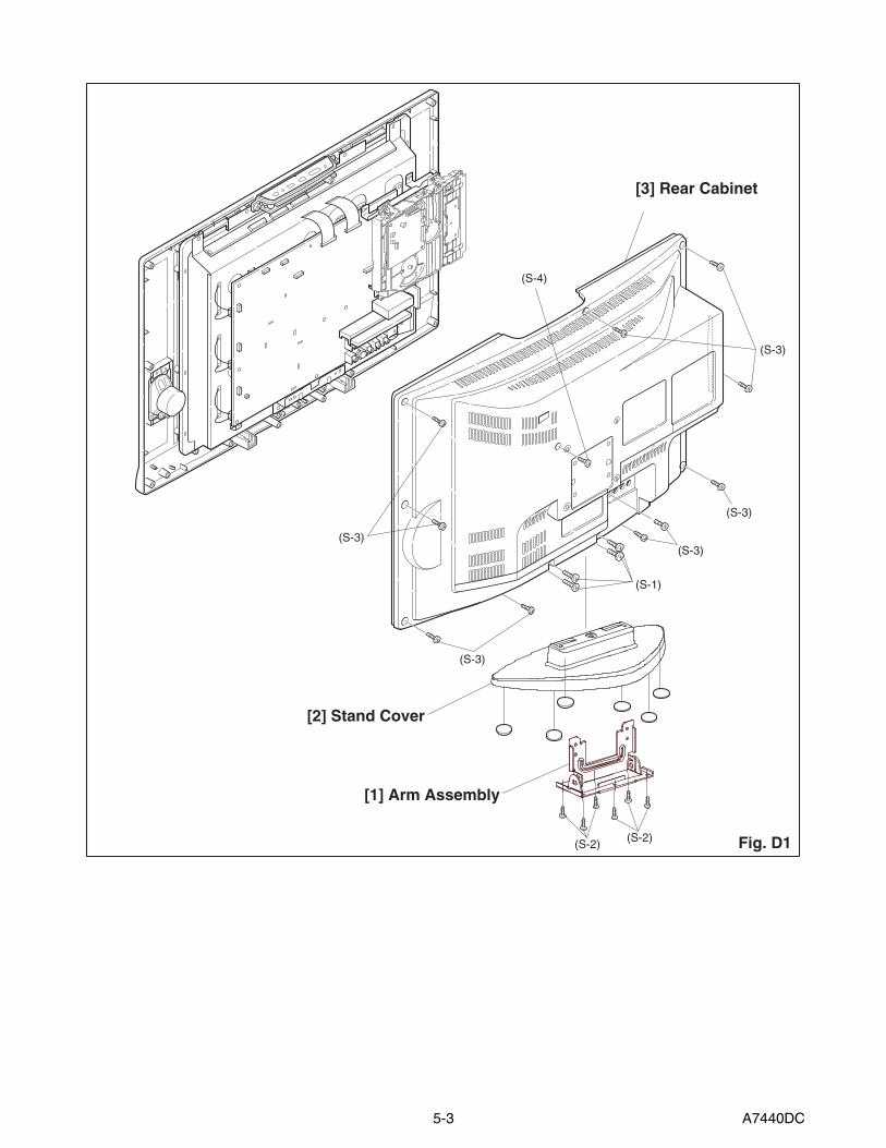
CABINET DISASSEMBLY INSTRUCTIONS
1. Disassembly FlowchartThis flowchart indicates the disassembly steps for the cabinet parts, and the CBA in order to gain access to item(s) to be serviced. When reassembling, follow the steps in reverse order. Bend, route and dress the cables as they were.
2. Disassembly Method
Step/Loc. No.
Part
Removal
Fig. No.
Remove/*Unhook/Unlock/Release/Unplug/Unclamp/
Desolder
Note
[1] Arm Assembly D1 4(S-1), 6(S-2) ---
[2] Stand Cover D1 --------------- ---
[3] Rear Cabinet D1 10(S-3), (S-4) ---
[4] DVD Main CBA Unit
D2D6
(S-5), *CN201, *CN301, *CN401, *CN601, *CN801
1
[2] Stand Cover
[14] IR Sensor CBA
[1] ArmAssembly[3] Rear Cabinet
[13] Function CBA
[8] Jack Holder [4] DVD Main CBA Unit
[6] DVD Holder(Top)
[7] DVD Holder(Bottom)
[5] DVD Mechanism
[9] DTV Module CBA Unit
[10] Main CBA
[11] Tilt Stand Holder
[18] Front Cabinet
[12] LCD Module
[17] Speaker (s)
[15] Junction-A CBA
[16] Junction-B CBA
[5] DVD Mechanism D2 3(S-6)
2345
[6] DVD Holder(Top) D2 2(S-7) ---
[7] DVD Holder (Bottom) D2 2(S-8) ---
[8] Jack Holder D3 (S-9) ---
[9]DTV Module CBA Unit
D3D6
7(S-10), *CL801, *CL802, *CL1104, *CL1107, *CN61, *CN62, *CN401, *CN402, *CN403, *CN1201, *CN1202, Module PCB Holder
---
[10] Main CBA D3 --------------- ---
[11] Tilt Stand Holder D4 2(S-11) ---
[12] LCD Module D4 11(S-12) ---
[13] Function CBA
D5D6 5(S-13) ---
[14] IR Sensor CBA
D5D6 (S-14), Washer ---
[15] Junction-A CBA D5 Desolder ---
[16] Junction-B CBA D5 Desolder ---
[17] Speaker (s) D5 4(S-15), Speaker Holder (s) ---
[18] Front Cabinet D5 --------------- ---
↓(1)
↓(2)
↓(3)
↓(4)
↓(5)
Step/Loc. No.
Part
Removal
Fig. No.
Remove/*Unhook/Unlock/Release/Unplug/Unclamp/
Desolder
Note

5-2 A7440DC
Note:
(1) Order of steps in procedure. When reassembling, follow the steps in reverse order. These numbers are also used as the Identification (location) No. of parts in figures.
(2) Parts to be removed or installed.
(3) Fig. No. showing procedure of part location
(4) Identification of parts to be removed, unhooked, unlocked, released, unplugged, unclamped, or desoldered. P = Spring, L = Locking Tab, S = Screw, CN = Connector* = Unhook, Unlock, Release, Unplug, or Desoldere.g. 2(S-2) = two Screws (S-2), 2(L-2) = two Locking Tabs (L-2)
(5) Refer to the following "Reference Notes in the Table."
Reference Notes1. CAUTION 1: Electrostatic breakdown of the laser
diode in the optical system block may occur as a potential difference caused by electrostatic charge accumulated on cloth, human body etc., during unpacking or repair work.To avoid damage of pickup follow next procedures.
1) Short the three short lands of FPC cable with solder before removing the FFC cable (CN201) from it. If you disconnect the FFC cable (CN201), the laser diode of pickup will be destroyed. (Fig. D2)
2) Disconnect the Connectors (CN301), (CN401), (CN601) and (CN801). Remove Screw (S-5) and remove the DVD Main CBA Unit. (Fig. D2)
2. Reassembly Notes of New DVD Mechanism:
a. To remove the Chassis Cover, remove two screws A as shown in Fig. D2.
b. To avoid damage of the pickup unit (laser diode), confirm that the three short lands (either of two places) are shorted out by soldering between them as shown in View A in Fig. D2.
c. Connect the FFC cables of the new DVD Mechanism to the three connectors (CN201, CN301, CN801) on the DVD Main CBA.
d. After confirming that the FFC cables are securely connected to the three connectors, remove the solder from the three short lands. If the solder is not removed, the laser diode will not light and it will not be possible to read discs.
e. Insert the pin A on the Chassis Cover into the hole A on the Main Chassis as shown in Fig. D2. Then tighten two screws A to install the Chassis Cover.
3. CAUTION 2: When reassembling, confirm the FFC cable (CN201) is connected completely. Then remove the solder from the three short lands of FPC cable. (Fig. D2)
4. How to eject a disc in emergencyPress and hold [EJECT] on the unit for more than 5 seconds.
5. How to eject manually
1) Remove the Rear Cabinet.
2) To remove the DVD Main CBA Unit, remove a screw (S-5) in Fig. D2. Do not disconnect connectors.
3) To remove the Chassis Cover, remove two screws A as shown in Fig. D2.
4) Remove a disc.
5-3 A7440DC
[3] Rear Cabinet
[2] Stand Cover
(S-4)
(S-3)
(S-3)
(S-1)
(S-2)
(S-3)
(S-3)
(S-3)
(S-2) Fig. D1
[1] Arm Assembly

5-4 A7440DC
Chassis Cover
Pin A
A
Hole A
Main Chassis
Remove two screws A, then short the three short lands by soldering as shown in View for A.
Screws A
View for A
Either of two places
FPC Cable
(S-7)
(S-8)
[4] DVD Main CBA Unit
[5] DVD Mechanism
[6] DVD Holder(Top)
[7] DVD Holder(Bottom)
A
Fig. D2
(S-5)
(S-6)
(S-6)

5-5 A7440DC
(S-10)
(S-10)(S-10)
(S-10)
(S-10)
(S-9)
[8] Jack Holder
[10] Main CBA
[9] DTV ModuleCBA Unit
Module PCB Holder
Fig. D3

5-6 A7440DC
(S-12)
(S-11)
(S-12)
(S-12)
(S-12)
(S-12)
[12] LCD Module [11] Tilt Stand Holder
Fig. D4

5-7 A7440DC
Washer
[14] IR Sensor CBA
[18] Front Cabinet
(S-14)
(S-13)
(S-13)
(S-13)[13] Function CBA
[17] SpeakerSpeakerHolder
(S-15)
[15] Junction-A CBA
Desolder
[17] Speaker
Desolder
SpeakerHolder
SpeakerHolder
(S-15)
[16] Junction-B CBA
Fig. D5

5-8 A7440DC
TV Cable Wiring Diagram
CN802
CN801
To Speaker
Fig. D6
CL1104
To Speaker
CN1201CN1202CN1301CN401
CN402
CN403
To LCDModule
Main CBA
CN1302
IR Sensor CBA
CN62 CN61
CN101CN102
DTV Module CBA Unit
CL1107Function CBA
To LCD Module
CL801
Junction-ACBA
CL802
Junction-BCBA
CN1651
CN1701
DVD Main CBA Unit
CN601
CN301CN201
CN801
CN401
To DVD Mechanism

6-1 A7440EA
ELECTRICAL ADJUSTMENT INSTRUCTIONS
General Note: “CBA” is abbreviation for “Circuit Board Assembly.”Note: Electrical adjustments are required after
replacing circuit components and certain mechanical parts. It is important to perform these adjustments only after all repairs and replacements have been completed. Also, do not attempt these adjustments unless the proper equipment is available.
Test Equipment Required1. DC Voltmeter
2. NTSC Pattern Generator (Color Bar W/White Window, Red Color, Dot Pattern, Gray Scale, Monoscope, Multi-Burst)
3. Remote control unit
4. Color Analyzer
How to make the Service remote control unit:Cut “A” portion of the attached remote control unit as shown in Fig. 1.
How to set up the service mode:
Service mode:1. Use the service remote control unit.
2. Turn the power on. (Use main power on the TV unit.)
3. Press the service button on the service remote control unit as shown in Fig. 1.
1. Initial SettingGeneral: Enter the Service mode. (See page 6-1.)
Set the each initial data as shown on table 1 below.
Table 1: Initial Data
Fig. 1
service button
A
ItemButton
(on the service remote control)
Data Value
RF-BRT
[SETUP] → [1]
127
RF-CNT 190
RF-CLR-R 75
RF-CLR-B 75
RF-TNT 128
RF-SHR 112
V-BRT
[SETUP] → [2]
127
V-CNT 190
V-CLR-R 70
V-CLR-B 70
V-TNT 128
V-SHR 112
S-BRT
[SETUP] → [3]
125
S-CNT 190
S-CLR-R 65
S-CLR-B 80
S-TNT 128
S-SHR 112
D1-BRT
[SETUP] → [4]
127
D1-CNT 170
D1-CLR-R 70
D1-CLR-B 70
D1-TNT 128
D1-SHR 112

6-2 A7440EA
The following adjustment normally are not attempted in the field. Only when replacing the LCD Panel then adjust as a preparation.
2. Flicker Adjustment1. Enter the Service mode.
2. Press [2] button on the service remote control unit. The following screen appears.
3. If Flicker Adjustment is not fit, the screen become the following.
4. Press [CH o / p] buttons on the remote control unit so that flash stops.
D2-BRT
[SETUP] → [5]
128
D2-CNT 180
D2-CLR-R 85
D2-CLR-B 85
D2-TNT 128
D2-SHR 112
D3-BRT
[SETUP] → [6]
120
D3-CNT 170
D3-CLR-R 80
D3-CLR-B 80
D3-TNT 128
D3-SHR 112
DT-BRT
[SETUP] → [7]
137
DT-CNT 190
DT-CLR-R 70
DT-CLR-B 75
DT-TNT 128
DT-SHR 112
VCOM [2] 128
COR(C/D1)[VOL n] → [1]
128
C-COR(C/D2) 128
COB(C/D1)[VOL n] → [3]
128
C-COB(C/D2) 128
DR(C/D1)[VOL n] → [4]
128
C-DR(C/D2) 128
DB(C/D1)[VOL n] → [6]
128
C-DB(C/D2) 128
ItemButton
(on the service remote control)
Data Value
FLASH (Go and Off)

6-3 A7440EA
3. White Balance AdjustmentPurpose: To mix red, green and blue beams correctly for pure white.
Symptom of Misadjustment: White becomes bluish or reddish.
Note: Use the service remote control unit
1. Operate the unit for more than 20 minutes.
2. Input the White Purity.
3. Set the color analyzer to the CHROMA mode and bring the optical receptor to the center on the LCD-Panel surface after zero point calibration as shown above.Note: The optical receptor must be set perpendicularly to the LCD Panel surface.
4. [RF/VIDEO1]Enter the Service mode. Press [VOL n] button on the remote control unit and select “C/D1” mode. [VIDEO2]Enter the Service mode. Press [VOL n] button on the remote control unit and select “C/D2” mode.
5. [RF/VIDEO1]----(APL 80%)Press [6] button to select “DB(C/D1)” for Blue adjustment. Press [4] button to select “DR(C/D1)” for Red adjustment. When “x” value and “y” value are not within specification, adjust “DB (C/D1)” or “DR (C/D1)”. Refer to “1. Initial Setting.”[RF/VIDEO1]----(APL 20%)Press [3] button to select “COB(C/D1)” for Blue
adjustment. Press [1] button to select “COR(C/D1)” for Red adjustment. When “x” value and “y” value are not within specification, adjust “COB (C/D1)” or “COR (C/D1)”. Refer to “1. Initial Setting.”
6. [VIDEO2]----(APL 80%)Press [6] button to select “C-DB(C/D2)” for Blue adjustment. Press [4] button to select “C-DR(C/D2)” for Red adjustment.When “x” value and “y” value are not within specification, adjust “C-DB(C/D2)” or “C-DR(C/D2)”. Refer to “1. Initial Setting.”[VIDEO2]----(APL 20%)Press [3] button to select “C-COB(C/D2)” for Blue adjustment. Press [1] button to select “C-COR(C/D2)” for Red adjustment.When “x” value and “y” value are not within specification, adjust “C-COB(C/D2)” or “C-COR(C/D2)”. Refer to “1. Initial Setting.”
7. Turn the power off and on again. (Main power button on the TV unit.)
4. Sub-Brightness AdjustmentPurpose: To get proper brightness.
Symptom of Misadjustment: If Sub-Brightness is incorrect, proper brightness cannot be obtained by adjusting the Brightness Control.
1. Enter the Service mode. Then input above signal.
2. [RF/VIDEO1]Press [SETUP] button on the service remote control unit and press [1] on the service remote control (selecting “BRT” mode). [VIDEO2]Press [SETUP] button on the service remote control unit and press [3] on the service remote control (selecting “C-BRT” mode).
Test Point Adj. Point Mode Input
ScreenVOL. n buttons
[RF/VIDEO1] C/D1[VIDEO2] C/D2
White Purity (APL 80%)
or(APL 20%)
M. EQ. Spec.
Pattern Generator, Color analyzer
(at White APL 80%)x= 0.276 ± 0.03 (0.246 to 0.306)y= 0.282 ± 0.03 (0.252 to 0.312)
(at White APL 20%)x= 0.276 ± 0.01 (0.266 to 0.286)y= 0.282 ± 0.01 (0.272 to 0.292)
Figure
Color Analyzer
It carries out in a darkroom.
L = 3 cm
Perpendicularity
INPUT: WHITE 80%, 20%
Adj. Point Input
[SETUP] button
Ant. input, Any channel, SMPTE pattern,[RF/VIDEO1]: CG-931 (KENWOOD),[VIDEO2]: CG-931 (KENWOOD),w/SETUP 7.5IRE
M. EQ. Spec.
Pattern Generator See below
Figure
White
Black
C positionB position
A position
6-4 A7440EA
3. Make sure that contrast and brightness controls are set to initial position.
4. Confirm “C” position was beginning to bright.
5. If “C” position was beginning to bright, no need to adjust.
6. If “C” position is not available or to be highly brightness, then adjust IIC-BUS dada.[RF/VIDEO1]: BRT[VIDEO2]: C-BRT
7. Turn the power off and on again. (Main power button on the TV unit.)

7-1 A7420INT
HOW TO INITIALIZE THE LCD TV/DVD
To put the program back at the factory-default, initialize the LCD TV/DVD as the following procedure.
< DVD Section >1. Press [1], [2], [3], [4], and [DISPLAY] buttons on the
remote control unit in that order. Fig. g appears on the screen.
2. Press [CLEAR] button on the remote control unit. Fig. h appears on the screen.
When “OK” appears on the screen, the factorydefault will be set.
3. To exit this mode, press [CH. o / p] button to go toTV mode, or press [POWER] button to turn thepower off.
< LCD TV Section >1. Turn the power on. (Use main power on the TV
unit.)
2. To enter the service mode, press the service button on the service remote control unit. (Refer to page 6-1.)
- To cancel the service mode, press [POWER] button on the remote control.
3. To initialize the LCD television, press [DISPLAY] button on the remote control unit.
4. Confirm "FF" indication on the upper right of the screen.
MODEL : ******* Version : *.** Region : *
EXIT: SELECTEEPROM CLEAR : CLEAR
Fig. g
"*******" differs depending on the models.
MODEL : ******* Version : *.** Region : *
EEPROM CLEAR : OK
EXIT: SELECTEEPROM CLEAR : CLEAR
"*******" differs depending on the models.
Fig. h

8-1 A7420FW
FIRMWARE RENEWAL MODE1. Turn the power on and press [EJECT] button on the
remote control unit to put the LCD TV/DVD intoDVD mode. Then remove the disc.
2. To put the LCD TV/DVD into F/W version up mode,press [9], [8], [7], [6], and [MODE] buttons on theremote control unit in that order.Fig. a appears on the screen.
3. Insert the disc for version up into the disc slot.4. The LCD TV/DVD enters the F/W version up mode
automatically. Fig. c appears on the screen. If youenter the F/W for different models, “Disc Error” willappear on the screen, then the disc will be ejectedautomatically.
The appearance shown in (*1) of Fig. c isdescribed as follows:
5. After programming is finished, the disc will beejected automatically. Fig. e appears on the screenand the checksum will be shown in (*2).
At this time, no button is available.6. Remove the disc.7. Unplug the AC cord from the AC outlet. Then plug it
again.8. Press [EJECT] button on the remote control unit to
put the LCD TV/DVD into DVD mode again.9. Press [1], [2], [3], [4], and [DISPLAY] buttons on the
remote control unit in that order. Fig. g appears on the screen.
10.Press [CLEAR] button on the remote control unit. Fig. h appears on the screen.
When “OK” appears on the screen, the factorydefault will be set. Then the firmware renewalmode is complete.
11.To exit this mode, press [CH. o / p] button to go toTV mode, or press [POWER] button to turn thepower off.
F/W Version Up Mode Model No : *******VERSION : *.**
Please insert a DISCfor F/W Version Up.
EXIT: SELECT
"*******" differs depending on the models.
Fig. a Version Up Mode Screen
VERSION : ************.***Reading...
F/W Version Up Mode Model No : *******VERSION : *.**
Fig. c Programming Mode Screen
"*******" differ depending on the models.
(*1)
AppearanceNo. State
Reading... Sending files into the memory
Erasing... Erasing previous version data
Programming...
1
2
3 Writing new version data
VERSION : ************.***CompletedSUM : 7ABC
F/W Version Up Mode Model No : *******VERSION : *.**
"*******" differ depending on the models.
Fig. e Completed Program Mode Screen
(*2)
MODEL : ******* Version : *.** Region : *
EXIT: SELECTEEPROM CLEAR : CLEAR
Fig. g
"*******" differs depending on the models.
MODEL : ******* Version : *.** Region : *
EEPROM CLEAR : OK
EXIT: SELECTEEPROM CLEAR : CLEAR
"*******" differs depending on the models.
Fig. h

9-1
BLOCK DIAGRAMS < LCD TV SECTION >System Control Block Diagram
A7441BLS
FU
NC
TIO
N C
BA
KE
Y-IN
-12
2CL1
107
KE
Y S
WIT
CH
KE
Y-IN
-21
1K
EY
SW
ITC
H
IC12
02(T
V M
ICR
O C
ON
TR
OLL
ER
)
3 94
CN
1301
28K
EY-
IN-1
RE
MO
TE
RE
SE
TR
ES
ET
AL+
3.3V
(D)
37 38X
1301
27M
Hz
XIN
XO
UT
19V
CO
M
18 51IF
-MU
TE
INP
UT-
2
MA
IN C
BA
4K
EY-
IN-2
27P
-ON
-H
VO
LUM
EA
UD
IO-M
UT
E
SD
AS
CL
INP
UT-
0IN
PU
T-1
S-S
W
IF-M
UT
EIN
PU
T-2
VG
H-H
23 4849 304750 31
TO P
OW
ER
SU
PP
LYB
LOC
K D
IAG
RA
M
TO IF
/VID
EO
BLO
CK
DIA
GR
AM
TO A
UD
IOB
LOC
K D
IAG
RA
M
TO D
TV
MO
DU
LEB
LOC
K D
IAG
RA
M
P-O
N-H
26V
GH
-H
VO
LUM
EA
UD
IO-M
UT
E
INP
UT-
0IN
PU
T-1
S-S
WS
CL
SD
A
IC61
(ME
MO
RY
)
SC
L65
SD
A
29B
US
-OP
EN
5A
FT-
IN
44F
SC
AF
T-IN
FS
C
Q91
7IR
SE
NS
OR
CB
A
CL1
104
CN
1302
RE
MO
TE
SE
NS
OR
RV
1142
RE
MO
TE
33
157
SD
AS
CL
BA
CK
LIG
HT-
AD
J20
TO L
CD
BA
CK
LIG
HT
BLO
CK
DIA
GR
AM
BA
CK
LIG
HT-
AD
J
VC
OM
TO L
CD
B
LOC
K D
IAG
RA
M
BA
CK
LIG
HT-
SW
BA
CK
LIG
HT-
SW
152
DT
V-O
N-H
DT
V-O
N-H
IC12
05(M
EM
OR
Y)
SC
L6
SD
A57
WP
17 16 15155
153
IC10
1(D
TV
SIG
NA
L P
RO
CE
SS
)
DT
V M
OD
UL
E C
BA
UN
IT
38155
154
153
204
DT
V-S
-SR
EQ
DT
V-S
-SC
LKD
TV
-S-S
IND
TV
-S-S
OU
TD
TV
-S-R
ES
ET
CN
61C
N10
112
1210
109
98
87
7D
TV
-S-S
RE
Q
DT
V-S
-SR
EQ
DT
V-S
-SIN
DT
V-S
-SO
UT
DT
V-S
-SC
LK
DT
V-S
-RE
SE
T
DT
V-S
-SC
LKD
TV
-S-S
IND
TV
-S-S
OU
TD
TV
-S-R
ES
ET
87D
VD
-SC
LK86
DV
D-C
S88
DV
D-S
DAT
A85
DV
D-R
EM
OT
E13
LED
-CO
NT
11D
ISC
-OU
T12
DIS
C-I
N
DV
D-S
CLK
DV
D-C
SD
VD
-SD
ATA
DV
D-R
EM
OT
ELE
D-C
ON
TD
ISC
-OU
TD
ISC
-IN
TO S
YS
TE
M C
ON
TR
OL
/SE
RV
O B
LOC
K D
IAG
RA
M<
DV
D S
EC
TIO
N>
84D
VD
-MA
IN-P
DV
D-M
AIN
-P
DV
D-M
UT
E
14D
VD
-MU
TE
INP
UT-
2

9-2 A7441BLIF
IF/Video Block Diagram
TO A
UD
IOB
LOC
K D
IAG
RA
M
TO LCD
BLO
CK
DIA
GR
AM
TO LCD
BLO
CK
DIA
GR
AM
INP
UT-
0(IN
V)
INP
UT-
1(IN
V)
SA
WF
ILT
ER
TU
61S
F11
IF7
SIF
MA
IN C
BA TO
AU
DIO
BLO
CK
DIA
GR
AM
JK70
6V
IDE
O-Y
IN JK70
7V
IDE
O-P
bIN JK
708
VID
EO
-Pr
IN
JK70
3V
IDE
O-I
N1
JK70
1S
-VID
EO
IN
TO SY
ST
EM
C
ON
TR
OL
BLO
CK
DIA
GR
AM
S-S
W
IF-M
UT
E
CY
IC78
1(I
NP
UT
SE
LEC
T)
5 34
12 1314
SW
CO
NT
RO
L
109
11
INP
UT-
0
INP
UT-
1
INP
UT-
2
TO S
YS
TE
M C
ON
TR
OL
BLO
CK
DIA
GR
AM
Q70
7
Q70
8
INP
UT-
2(IN
V)
Q70
9
(TU
NE
R U
NIT
)C
F31
IC31
(IF
SIG
NA
L P
RO
CE
SS
)
VIF
AM
PV
IDE
OD
ET
VC
O
4.5M
Hz
FIL
TE
R
RF
AG
C
AM
P
SIF
AM
P16
1318
174
78
1
TO S
YS
TE
M C
ON
TR
OL
BLO
CK
DIA
GR
AM
AF
T-IN
SIF
TR
AP
11
FS
C
IF A
GC
DE
T
AF
TE
QA
MP
2
DE
FE
AT
RF
-CV
BS
S-VI
DEO
-C/D
VD-C
S-VI
DEO
-Y/D
VD-Y
VID
EO
-YV
IDE
O-P
bV
IDE
O-P
rV
IDE
O-I
N1
VID
EO
SIG
NA
LA
UD
IO S
IGN
AL
DV
D M
AIN
CB
A U
NIT
CN
601
CN
1701
DV
D-C
10D
VD
-Y
DV
D-C
TO D
IGIT
AL
SIG
NA
LP
RO
CE
SS
BLO
CK
DIA
GR
AM
<D
VD
SE
CT
ION
>
DV
D-Y
83 1
WF
8
WF
9

9-3
Audio Block Diagram
A7441BLA
MA
IN C
BA
AU
DIO
-MU
TE
VO
LUM
ETO
SY
ST
EM
C
ON
TR
OL
BLO
CK
DIA
GR
AM
INP
UT-
0(IN
V)
INP
UT-
1(IN
V)
SC
LS
DA
IC85
2(I
NP
UT
SE
LEC
T)
SW
CT
L
INH
3
12 15 11 14 1 4
69
10
ST
ER
EO
FIL
TE
R75
uSD
E-E
MP
H
dBX
DE
-EM
PH
L+R
FIL
TE
R
WID
E B
AN
DF
ILT
ER
WID
E B
AN
DR
MS
DE
TW
IDE
BA
ND
EX
PAN
D
SP
EC
TR
AL
EX
PAN
D
SP
EC
TR
AL
RM
S D
ET
SP
EC
TR
AL
FIL
TE
R
OF
FS
ET
CA
NC
EL
L-C
H
R-C
H
MAT
RIX
AG
CO
FF
SE
TC
AN
CE
LL-
RF
ILT
ER
(L-R
)/S
AP
SW
SA
PF
ILT
ER
I2C
DE
CO
RD
ER
SA
PD
EM
OD
SA
P O
UT
FIL
TE
R
2930TO
IF
/VID
EO
BLO
CK
DIA
GR
AM
TU
NE
R
TU
NE
R(L-C
H)
(R-C
H)
21 2724
IC85
1(M
TS
/SA
P A
UD
IO S
IGN
AL
PR
OC
ES
S)
AU
DIO
(L)
-IN
1
JK70
4
DIG
ITA
LA
UD
IO-O
UT
(CO
AX
IAL)
JK17
01
SIF
JK70
5A
UD
IO(R
)-I
N1
JK70
9A
UD
IO(L
)-I
N2
JK71
0A
UD
IO(R
)-I
N2
OF
FS
ET
CA
NC
EL
14
IC80
1 (A
UD
IO A
MP
)
7
VO
LUM
E
11 A
MP
AM
P
MU
TE
/STA
ND
BY
CO
NT
RO
L
2
Q80
2
P-O
N+
5V(2
)
TO IF
/VID
EO
B
LOC
KD
IAG
RA
M
13
2
WF
7
AU
DIO
1
AU
DIO
2
AU
DIO
1A
UD
IO2
SIF
/BB
SW
INP
UT
VC
AS
IFD
EM
OD
INP
UT-
2(IN
V)
6
DT
V
DT
V5
1
DT
V-S
PD
IFD
TV
-AU
DIO
(L)
TO D
TV
M
OD
ULE
BLO
CK
D
IAG
RA
MD
TV
-AU
DIO
(R)
AU
DIO
SIG
NA
L
AU
DIO
MU
TE
JK80
1H
EA
DP
HO
NE
JAC
K SP
801
SP
EA
KE
RR
-CH
JUN
CT
ION
-B C
BA
CL8
02S
P80
2 S
PE
AK
ER
L-C
H
JUN
CT
ION
-A C
BA
CL8
01
22
SP
-GN
D1
1S
P-L
22
SP
-GN
D1
1S
P-R
8 3
(R-C
H)
(L-C
H)
12
Q17
01
BU
FF
ER
CN
1701
CN
601
DV
D M
AIN
CB
A U
NIT
DV
D-M
UT
E13
6D
VD
-AU
DIO
(L)
125
DV
D-A
UD
IO(R
)14
7D
VD
-SP
DIF
DV
D-M
UT
ED
VD
-AU
DIO
(L)
DV
D-A
UD
IO(R
)S
PD
IF16
9
DV
D-M
UT
E
TO D
IGIT
AL
SIG
NA
LP
RO
CE
SS
BLO
CK
DIA
GR
AM
<D
VD
SE
CT
ION
>
WF
12
WF
10W
F11
Q17
03
SW
ITC
HIN
GIN
PU
T-2

9-4
DTV Module Block Diagram
A7441BLDTV
IC10
1 (D
TV
SIG
NA
L P
RO
CE
SS
)
IC25
2(A
UD
IO D
/A C
ON
VE
RT
ER
)
IC20
2 (F
LAS
H M
EM
OR
Y)
AD
C/A
GC
I/F
DIG
ITA
L S
IGN
AL
PR
OC
ES
S
S
YS
TE
M D
EC
OD
ER
/V
IDE
O D
EC
OD
ER
/V
IDE
O F
OR
MAT
C
ON
VE
RT
ER
/2D
GR
AP
HIC
S
TU
61(T
UN
ER
UN
IT)
DIF
-OU
T1
CN
62C
N10
2
LPF
DIF
-OU
T2
DIF
-AG
C
SD
AS
CL
XIN
-27M
Hz
XO
UT-
27M
Hz
DT
V M
OD
UL
E C
BA
UN
IT
MA
IN C
BA
VID
EO
SIG
NA
L
1111
DIF
-OU
T1
1212
DIF
-OU
T2
99
DIF
-AG
C18
18D
TV
-Y19
19D
TV
-Pr
2020
DT
V-P
b15
15D
TV-A
UD
IO(L
)16
16D
TV-A
UD
IO(R
)
10 11 8
174
178
182
187
186
159
158
162
161
6 515 14
7 815
6
144
143
140
27M
Hz
OS
C
X27
114
41
15
XIN
-25M
Hz
XO
UT-
25M
Hz
25M
Hz
OS
C
X28
14 5
VID
EO
EN
CO
DE
R
AU
DIO
DE
CO
DE
R
AU
DIO
D/A
CO
NV
ER
TE
R
SD
RA
MI/F F
LAS
HM
EM
OR
YI/F
IC20
1 (D
DR
SD
RA
M)
22
DT
V-S
PD
IF14
14S
DA
1515
SC
L
4 5
55
TU
-SD
A4
4T
U-S
CL
CN
62
L-C
HR
-CH
SD
AS
CL
BU
S-C
ON
T
*1
*1 7
9~81
,85,
87,8
9~91
,92,
94,9
6~98
,
102
,104
,106
*2
*2 5
5,56
,58,
60,6
1,11
6,11
9,12
0,12
4,
125
,127
,129
,130
*3
*3 1
,2,7
~12
,20,
206,
209,
211,
213~
216,
*4
*4 2
3~25
,27,
29,3
2~36
,41~
44,4
7,48
,50,
5
2~54
,205
*5
*5 1
~9,
16~
25,4
8
*6
*6 2
9~36
,38~
45
*7*7
28~
32,3
5~42
*8
*8 2
,4,5
,7,8
,10,
11,1
3,54
,56,
57,5
9,60
,
62,
63,6
5
TO L
CD
BLO
CK
D
IAG
RA
M
TO A
UD
IOB
LOC
K
DIA
GR
AM
TO S
YS
TE
M
CO
NT
RO
LB
LOC
K
DIA
GR
AM
CN
61C
N10
1
BU
FF
ER
Q24
3
BU
FF
ER
Q24
5
BU
FF
ER
Q24
4
BU
FF
ER
Q25
1
SD
AS
CL
DA
TA
BU
S(0
-15)
AD
DR
ES
S B
US
(0-1
2)
DA
TA
BU
S(0
-15)
AD
DR
ES
S B
US
(1-2
0)
CN
102
DD
R S
DR
AM
FLA
SH
ME
MO
RY
SW
SW
DT
V-S
PD
IF
DT
V-A
UD
IO(L
)
DT
V-A
UD
IO(R
)
DT
V-P
bD
TV
-Pr
DT
V-Y
Q21
1Q
212
Q21
3
Q21
4
AU
DIO
SIG
NA
L

9-5
LCD Block Diagram
A7441BLLCD
TO IF/V
IDE
OB
LOC
KD
IAG
RA
M
MA
IN C
BA
RF
-CV
BS
S-V
IDE
O-C
/DV
D-C
IC12
02(L
CD
DR
IVE
/ S
IGN
AL
PR
OC
ES
S)
67 57 76
S-V
IDE
O-Y
/DV
D-Y
TO IF/V
IDE
OB
LOC
KD
IAG
RA
M
TO D
TV
MO
DU
LEB
LOC
KD
IAG
RA
M
VID
EO
-YV
IDE
O-P
bV
IDE
O-P
r665675
A/D
VID
EO
SIG
NA
LP
RO
CE
SS
LCD
RG
BS
IGN
AL
PR
OC
ES
S
R BG Y Pb
Pr
A/D
A/D
A/D
A/D
A/D
R BG
CV
BS
C Y
WF
3
WF
1
WF
2
WF
4
WF
5
WF
6
VID
EO
-IN
171
DT
V-Y
DT
V-P
b
73 54
DT
V-P
r
64
VID
EO
SIG
NA
L
CN
1201
OR
(0)
29O
R(1
)28
LCD
MO
DU
LE
OR
(2)
27O
R(3
)26
OR
(4)
25O
R(5
)24
OG
(0)
22O
G(1
)21
OG
(2)
20O
G(3
)19
OG
(4)
18O
G(5
)17
OB
(0)
15O
B(1
)14
OB
(2)
13O
B(3
)12
OB
(4)
11O
B(5
)10
ER
(0)
6E
R(1
)5
ER
(2)
4E
R(3
)3
ER
(4)
2E
R(5
)1
EG
(0)
31E
G(1
)30
EG
(2)
22E
G(3
)21
EG
(4)
20E
G(5
)19
EB
(0)
17E
B(1
)16
EB
(2)
15E
B(3
)14
EB
(4)
13E
B(5
)12
OF
FE
V24
ST
V26
CLK
V28
VC
OM
35
ST
H31
PO
L32
LP33
CLE
AR
34
CN
1201
148
147
144
143
142
141
140
139
138
137
133
132
131
130
129
128
127
126
112
117
116
115
114
113
105
111
110
98 97 96 95 93 92 91 90 89 106
107
108
149
150
151
B(E
VE
N)
G(E
VE
N)
R(E
VE
N)
B(O
DD
)
G(O
DD
)
R(O
DD
)
CN
1202
ST
HP
OL
LP15
6C
LEA
R
OF
FE
VS
TV
CLK
V
CLK
L8
125
CLK
L
VC
OM
TO SY
ST
EM
CO
NT
RO
LB
LOC
KD
IAG
RA
M

9-6
Power Supply Block Diagram
A7441BLP
Q10
05S
W+
25V
4A/1
25V
F60
14A
/125
VLI
NE
FIL
TE
R
L601
AC
601
AC
CO
RD
BR
IDG
ER
EC
TIF
IER
D60
5 -
D60
8
HO
TC
OL
DT
601
1110161315
2
4 3
1 2
IC60
1E
RR
OR
VO
LTA
GE
DE
T
Q60
1
Q60
3S
WIT
CH
ING
CO
NT
RO
L
SW
ITC
HIN
G
MA
IN C
BA
4 7 6
+12
V
P-O
N-H
BA
CK
LIG
HT-
SW
HO
T C
IRC
UIT
. BE
CA
RE
FU
L.
9 12
INV
+22
V
+35
V
TO S
YS
TE
MC
ON
TR
OL
BLO
CK
D
IAG
RA
M
TO L
CD
BA
CK
LIG
HT
BLO
CK
D
IAG
RA
M
Q91
3F
EE
DB
AC
K
IC90
4+
1.8V
RE
G.
IC90
5+
5V R
EG
.
Q40
2Q
403
VT
+33
V
P-O
N+
5V(1
)
P-O
N+
9V
TO S
YS
TE
MC
ON
TR
OL
BLO
CK
D
IAG
RA
M
D92
3S
HU
NT
RE
G.
SW
ITC
HIN
GQ
916
D92
4 SH
UN
TR
EG
. DT
V-O
N-H
AL+
3.3V
(D)
AL+
3.3V
(A)
AL+
1.2V
(D)
Q90
2S
W+
3.3V D92
0S
HU
NT
RE
G.
IC90
1+
1.2V
RE
G.
Q90
1S
W+
3.3V
D91
6 SH
UN
TR
EG
.Q
923
SW
+12
V
Q90
5S
W+
6.5V
14
Q90
8S
W+
3.3V
Q90
9S
W+
2.5V
Q91
8S
W+
9V
Q90
7S
W+
5V
Q90
3S
W+
5V
SW
ITC
HIN
GQ
906
SW
ITC
HIN
GS
WIT
CH
ING
CN
102
DT
V-O
N+
3.3V
44
CN
62
DT
V-O
N+
2.5V
55
DT
V-O
N+
1.8V
66
DT
V-O
N+
3.3V
DT
V-O
N+
1.8V
DT
V-O
N+
2.5V
CN
101
DT
V-O
N+
5V3
3C
N61
DT
V-O
N+
5V
DT
V M
OD
UL
E
CB
A U
NIT
SW
ITC
HIN
GQ
919
PAN
EL+
25V
2PA
NE
L+25
V3
PAN
EL+
3.3V
5PA
NE
L+3.
3V6
CN
1202
PAN
EL+
10.8
V8
TO
LCD
M
OD
ULE
Q91
0S
W+
3.3V
SW
ITC
HIN
GQ
1004
VG
H-H
TO S
YS
TE
MC
ON
TR
OL
BLO
CK
D
IAG
RA
MS
WIT
CH
ING
Q10
01
SW
ITC
HIN
GQ
1002
Q10
06S
W-6
V
PAN
EL-
6V10
D10
02S
HU
NT
RE
G.
Q10
03+
10.8
V R
EG
.
DV
D-M
AIN
-P
Q91
1S
W+
5V
SW
ITC
HIN
GQ
912
DV
D M
AIN
CB
A U
NIT
CN
1651
CN
401
DV
D-O
N+
3.3V
EV
+9V
DV
D-O
N+
5V
EV
+1.
2VA
L+3.
3V(D
)
EV
+3.
3V
11~
12E
V+
9V11
~12
11~
12E
V+
9V11
~12
10D
VD
-ON
+5V
10
9D
VD
-ON
+3.3
V9
1A
L+3.
3V(D
)1
6~8
EV
+3.
3V6~
8
4~5
EV
+1.
2V4~
5
Q90
4+
3.3V
RE
G.
Q91
4+
3.3V
RE
G.
IC90
2+
1.2V
RE
G.
D90
4S
HU
NT
RE
G.
JS90
3
CA
UT
ION
!F
ixed
vol
tage
(or
Aut
o vo
ltage
sel
ecta
ble)
pow
er s
uppl
y ci
rcui
t is
used
in th
is u
nit.
If M
ain
Fus
e (F
601)
is b
low
n , c
heck
to s
ee th
at a
ll co
mpo
nent
s in
the
pow
er s
uppl
yci
rcui
t are
not
def
ectiv
e be
fore
you
con
nect
the
AC
plu
g to
the
AC
pow
er s
uppl
y.O
ther
wis
e it
may
cau
se s
ome
com
pone
nts
in th
e po
wer
sup
ply
circ
uit t
o fa
il.
For
con
tinue
d pr
otec
tion
agai
nst r
isk
of fi
re,
repl
ace
only
with
sam
e ty
pe 4
A, 1
25V
fuse
.C
AU
TIO
N !
:
AT
TE
NT
ION
: U
tilis
er u
n fu
sibl
e de
rec
hang
e de
mêm
e ty
pe d
e 4
A, 1
25V
.4A
/125
V
NO
TE
:T
he v
olta
ge fo
r pa
rts
in h
ot c
ircui
t is
mea
sure
d us
ing
hot G
ND
as
a co
mm
on te
rmin
al.

9-7
LCD Backlight Block Diagram
A7441BLLB
CU
RR
EN
TC
ON
TR
OL
SW
ITC
H
Q42
1
Q42
4
T40
1C
N40
1
LC
D M
OD
UL
EIN
VE
RT
ER
CB
A
BA
CK
LIG
HT
BA
CK
LIG
HT
BA
CK
LIG
HT
OV
ER
VO
LTAG
EP
RO
TEC
TOR
Q42
2,42
3
1 2 1 2
CN
402
CN
403 1 2
9 8
3 5 26 1 4
10 7
CU
RR
EN
TC
ON
TR
OL
SW
ITC
H
Q44
1
Q44
4
T40
2
OV
ER
VO
LTAG
EP
RO
TEC
TOR
Q44
2,44
3
9 8
3 5 26 1 4
10 7
CU
RR
EN
TC
ON
TR
OL
SW
ITC
H
Q46
1
Q46
4
T40
3
OV
ER
VO
LTAG
EP
RO
TEC
TOR
Q46
2,46
3
9 8
3 5 26 1 4
10 7
OV
ER
VO
LTAG
EP
RO
TEC
TOR
Q40
4Q
406
+10
V R
EG
.
OV
ER
CU
RE
RE
NT
PR
OTE
CTO
R
Q42
5
Q40
5 SW
ITC
HIN
G
SW
ITC
HIN
G
SW
ITC
HIN
G
SW
ITC
HIN
G
INV
+22
V
TO PO
WE
RS
UP
PLY
BLO
CK
DIA
GR
AM
BA
CK
LIG
HT-
AD
J
Q40
1
SW
+22
V
TO S
YS
TE
MC
ON
TR
OL
BLO
CK
D
IAG
RA
M
SW
ITC
HIN
GQ
407
9-8 A7441BLSD
IC30
1(S
ER
VO
DR
IVE
)
CN
301
M
SLE
D
MO
TO
R
M
SP
IND
LE
MO
TO
R
IC10
1(M
ICR
O C
ON
TR
OLL
ER
)
+ -+ -
+ -+ -
+ -+ - + -
SLE
DM
OTO
RD
RIV
E
FO
CU
SA
CT
UAT
OR
DR
IVE
SP
IND
LEM
OTO
RD
RIV
E
TR
AC
KIN
GA
CT
UAT
OR
DR
IVE
126
LOA
D-D
ISC
SLD
67
SP
DL
66
TR
AC
KIN
GD
RIV
E
127
FO
CU
S D
RIV
EF
S(+
)F
S(-
)
TS
(+)
TS
(-)
LOA
D-D
ISC
1S
P(+
)2
SP
(-)
6LO
AD
-DIS
C3
GN
D4
SL(
-)5
SL(
+)
VR
EF
RE
SE
T70
RE
SE
T
IC46
2
13
EV
+3.
3V(D
)
IC20
2(O
P A
MP
)
15 16 14 13 12 11 17 182364 531 225 2427 26
121
SP
-RO
T
124
FD
-OF
ST
123
TD
-OF
ST
RE
SE
T
IC46
1
21
EV
+3.
3V(D
)
TO D
IGIT
AL
SIG
NA
L P
RO
CE
SS
BLO
CK
D
IAG
RA
M DR
IVE
CB
A
DV
D M
AIN
CB
A U
NIT
CN
1651
MA
IN C
BA
CN
401 3
DIS
C-O
UT
32
LED
-CO
NT
2
122
SL-
AD
S
DIS
C-I
N
12 6
753
3D
ISC
-IN
32
DIS
C-O
UT
2CN
801
CN
5001
DIS
C-O
UT
SE
NS
OR
CB
A
EV
+3.
3V
1LE
D-P
OW
ER
1
Q80
4
63D
ISC
-IN
61D
ISC
-OU
T
TO SY
ST
EM
CO
NT
RO
LB
LOC
KD
IAG
RA
M<
LC
D T
V S
EC
TIO
N >
53D
VD
-SC
LK54
DV
D-C
S
49D
VD
-RE
MO
TE
56D
VD
-SD
ATA
25DV
D-R
EMO
TE25
24D
VD
-SD
ATA
2422
DV
D-C
S22
21D
VD
-SC
LK21
23D
ISC
-IN
23
DV
D-S
CLK
DV
D-C
SD
VD
-SD
ATA
DV
D-R
EM
OT
ELE
D-C
ON
TD
ISC
-OU
TD
ISC
-IN
65
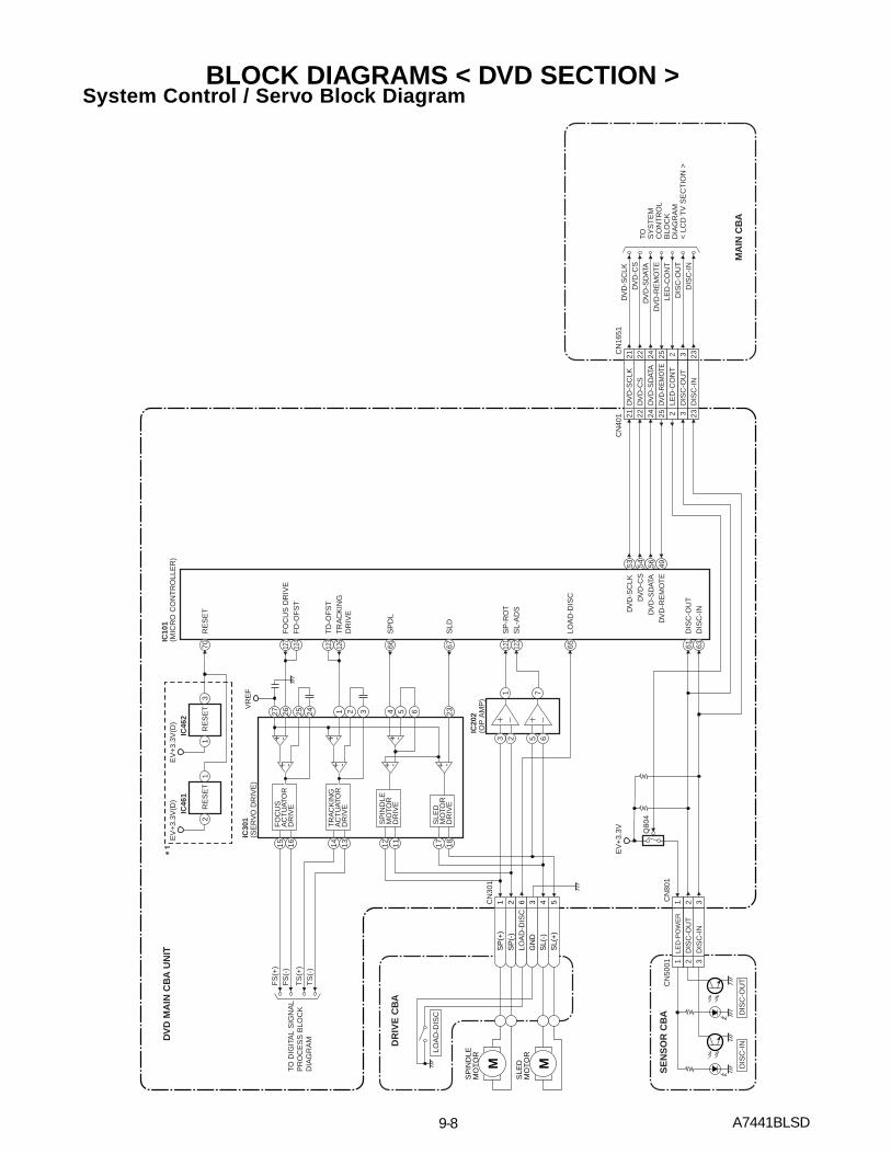
BLOCK DIAGRAMS < DVD SECTION >System Control / Servo Block Diagram

9-9 A7441BLD
Digital Signal Process Block Diagram
C16
D18
A17
B15
DV
D-L
D8
CD
-LD
10
PD
-MO
NI
7
FS
(+)
2F
S(-
)3
TS
(+)
1T
S(-
)4C
N20
1
CN
201
CN
201
IC20
1(S
W)
IC10
1(M
ICR
O C
ON
TR
OLL
ER
)
FS
FS
(+)
CD
/DV
D
FS
(-)
TS
(+)
TS
(-)
TS
DE
TE
CTO
R
CD
/DV
D19
Q25
1,Q
252
CDDV
D
AM
P
Q25
3,Q
254
AM
P
4
13
6
GN
D(C
D-P
D)
5G
ND
(LD
)9
RF
SIG
NA
LP
RO
CE
SS
CIR
CU
IT
DV
D/C
DF
OR
MAT
TE
R
AU
DIO
I/F VID
EO
I/FN
TS
C/P
AL
EN
CO
DE
R
DM
A
BC
U
INS
T.R
OM
32B
ITC
PU
DAT
AR
AM
INT
ER
RU
PT
CO
NT
RO
LLE
RW
ATC
H D
OG
TIM
ER
CP
UI/F
TIM
ER
DE
CO
DE
RI/F
CP
UI/F
RE
AD
ME
MO
RY
DAT
AR
AM
DS
PD
EC
OD
ER
I/O PR
OC
ES
SO
R
INS
T.R
OM
DAT
AR
AM
INS
T.R
OM
SE
RIA
L
D/A
GE
NE
RA
LI/O IN
TE
RR
UP
TC
ON
TR
OLL
ER
TIM
ER
WAT
CH
DO
GT
IME
R
RE
MO
TE
CO
NT
RO
L
32B
IT C
PU
ST
RE
AM
I/F
EX
TE
RN
AL
ME
MO
RY
I/FS
DR
AM
EC
C
UM
AC
100
115
116
113
114
106
104
105
103
62
DE
BU
G
BC
U
INS
TC
AC
HE
DAT
AC
AC
HE
D/A
131
139
Y C
DV
D-Y
DV
D-C
152
SP
DIF
151
DV
D-M
UT
E
146
DV
D-A
UD
IO(R
)
144
DV
D-A
UD
IO(L
)
SD
RA
M A
DD
RE
SS
(0-1
0)
IC10
3(F
LAS
H R
OM
)
FLA
SH
RO
M
29 36 38 45
~ ~
FD
Q (
0-15
)
~
1 9 16 25 48
~
FAD
R (
0-19
)
SD
RA
M D
ATA
(0-1
5)
PIC
K-U
PU
NIT
TO S
YS
TE
M
CO
NT
RO
L/S
ER
VO
BLO
CK
DIA
GR
AM
DV
D M
AIN
CB
A U
NIT
TO IF
/VID
EO
BLO
CK
D
IAG
RA
M
TO A
UD
IOB
LOC
K
DIA
GR
AM
IC50
1(S
DR
AM
)
SD
RA
M D
ATA
(0-1
5)
SD
RA
M A
DD
RE
SS
(0-1
0)19
4
209~
2 12 39 49
~ ~20 24 27 32
~ ~
159
178~
99 98 97
21~
3034
~42
212
1~4
7~14
17~
1821
5~21
6
AU
DIO
D/A
CO
NV
ER
TE
R
< L
CD
TV
S
EC
TIO
N >
< L
CD
TV
S
EC
TIO
N >
GN
D(D
VD-P
D)
6
VID
EO
SIG
NA
LA
UD
IO S
IGN
AL

10-1 LC4ND_SC
SCHEMATIC DIAGRAMS / CBA’S AND TEST POINTS
Standard Notes
WARNING
Many electrical and mechanical parts in this chassis have special characteristics. These characteristics often pass unnoticed and the protection afforded by them cannot necessarily be obtained by using replacement components rated for higher voltage, wattage, etc. Replacement parts that have these special safety characteristics are identified in this manual and its supplements; electrical components having such features are identified by the mark “#” in the schematic diagram and the parts list. Before replacing any of these components, read the parts list in this manual carefully. The use of substitute replacement parts that do not have the same safety characteristics as specified in the parts list may create shock, fire, or other hazards.
Notes:1. Do not use the part number shown on these
drawings for ordering. The correct part number is shown in the parts list, and may be slightly different or amended since these drawings were prepared.
2. All resistance values are indicated in ohms (K = 103, M = 106).
3. Resistor wattages are 1/4W or 1/6W unless otherwise specified.
4. All capacitance values are indicated in µF (P = 10-6 µF).
5. All voltages are DC voltages unless otherwise specified.

10-2 LC4ND_SC
LIST OF CAUTION, NOTES, AND SYMBOLS USED IN THE SCHEMATIC DIAGRAMS ON THE FOLLOWING PAGES:
1. CAUTION:CAUTION: FOR CONTINUED PROTECTION AGAINST RISK OF FIRE, REPLACE ONLY WITH SAME TYPE_A,_V FUSE.
ATTENTION: UTILISER UN FUSIBLE DE RECHANGE DE MÊME TYPE DE_A,_V.
2. CAUTION: Fixed Voltage (or Auto voltage selectable) power supply circuit is used in this unit. If Main Fuse (F601) is blown, first check to see that all components in the power supply circuit are not defective before you connect the AC plug to the AC power supply. Otherwise it may cause some components in the power supply circuit to fail.
3. Note:1. Do not use the part number shown on the drawings for ordering. The correct part number is shown in the
parts list, and may be slightly different or amended since the drawings were prepared.
2. To maintain original function and reliability of repaired units, use only original replacement parts which are listed with their part numbers in the parts list section of the service manual.
4. Voltage indications for PLAY and STOP modes on the schematics are as shown below:
5. How to read converged lines
6. Test Point Information
2 31 5.0< 0 >
TV mode DVD mode
< TV Section > Unit: Volts
5.0
The same voltage forboth TV & DVD modes
Unit: Volts
Indicates that the voltageis not consistent here.
2 31 5.0(2.5)
PLAY mode STOP mode5.0
The same voltage forboth PLAY & STOP modes
Unit: Volts
Indicates that the voltageis not consistent here.
< DVD Section >
3
2
1
A B C D
1-B1
1-D3
AREA D3
AREA B1
1-D3
Distinction AreaLine Number (1 to 3 digits)
Examples:1. "1-D3" means that line number "1" goes to the line number "1" of the area "D3". 2. "1-B1" means that line number "1" goes to the line number "1" of the area "B1".
: Indicates a test point with a jumper wire across a hole in the PCB.
: Used to indicate a test point with a component lead on foil side.
: Used to indicate a test point with no test pin.
: Used to indicate a test point with a test pin.

10-3 A7441SCM1
Main 1/6 Schematic Diagram < LCD TV Section >
2 24.43 24.44 05 3.36 3.37 08 10.89 010 -6.211 012 1.213 0.714 0.515 0.716 1.317 1.118 019 1.220 0.9
21 0.7
22 0.8
23 0
24 0
25 0
26 0
27 0
28 2.1
29 0
30 1.3
31 1.3
32 0
33 0
CN1201
1 1.22 1.03 0.84 0.75 1.06 1.47 08 1.29 010 1.211 0.712 0.513 0.714 1.315 1.116 017 1.218 0.919 0.720 0.721 1.322 1.323 024 1.225 1.026 0.927 0.828 1.029 1.430 031 032 1.733 0.334 3.435 1.7
CN1202
1 0
VOLTAGE CHART
Pin No. Voltage
Pin No. Voltage

10-4 A7441SCM2
Main 2/6 Schematic Diagram < LCD TV Section >
CN61
1 02 1.13 5.24 3.15 3.26 07 2.98 3.29 1.710 0.111 012 3.413 014 3.115 3.1
CN62
1 ---2 3.33 04 3.45 2.66 1.97 ---8 09 010 011 012 013 014 ---15 2.616 2.617 018 ~19 ~20 ~
VOLTAGE CHART
Pin No. Voltage
Pin No. Voltage

10-5 A7441SCM3
Main 3/6, Junction-A & Junction-B Schematic Diagram < LCD TV Section >

10-6 A7441SCM4
Main 4/6 Schematic Diagram < LCD TV Section >

10-7
For continued protection against risk of fire, replace only with same type 4 A, 125V fuse.
CAUTION ! :
ATTENTION : Utiliser un fusible de rechange de même type de 4A, 125V.4A/125V
CAUTION !Fixed voltage (or Auto voltage selectable) power supply circuit is used in this unit.If Main Fuse (F601) is blown , check to see that all components in the power supplycircuit are not defective before you connect the AC plug to the AC power supply.Otherwise it may cause some components in the power supply circuit to fail.
NOTE:The voltage for parts in hot circuit is measured usinghot GND as a common terminal.
A7441SCM5
Main 5/6 Schematic Diagram < LCD TV Section >

10-8 A7441SCM6
Main 6/6 Schematic Diagram < LCD TV Section >

10-9 A7441SCF
Function Schematic Diagram < LCD TV Section >

10-10 A7441SCIR
IR Sensor Schematic Diagram < LCD TV Section >

10-11 A7441SCDT1
DTV Module 1/2 Schematic Diagram < LCD TV Section >

10-12 A7441SCDT2
DTV Module 2/2 Schematic Diagram < LCD TV Section >

10-13 A7441SCD1
DVD Main 1/3 Schematic Diagram < DVD Section >
1 NOTE: Either IC461 or IC462 is used for DVD MAIN CBA UNIT.

10-14 A7441SCD2
DVD Main 2/3 Schematic Diagram < DVD Section >

10-15 A7441SCD3
DVD Main 3/3 Schematic Diagram < DVD Section >

10-16
PIN 1 OFCN1701
WF8
PIN 3 OFCN1701
WF9
PIN 5 OFCN1701
WF10
PIN 7 OFCN1701
WF11
PIN 9 OFCN1701
WF12
BA7140F01011-1
Main CBA Top View
For continued protection against risk of fire, replace only with same type 4 A, 125V fuse.
CAUTION ! :
ATTENTION : Utiliser un fusible de rechange de même type de 4A, 125V.4A/125V
CAUTION !Fixed voltage (or Auto voltage selectable) power supply circuit is used in this unit.If Main Fuse (F601) is blown , check to see that all components in the power supplycircuit are not defective before you connect the AC plug to the AC power supply.Otherwise it may cause some components in the power supply circuit to fail.
NOTE:The voltage for parts in hot circuit is measured usinghot GND as a common terminal.
Because a hot chassis ground is present in the powersupply circuit, an isolation transformer must be used.Also, in order to have the ability to increase the inputslowly,when troubleshooting this type power supplycircuit, a variable isolation transformer is required.
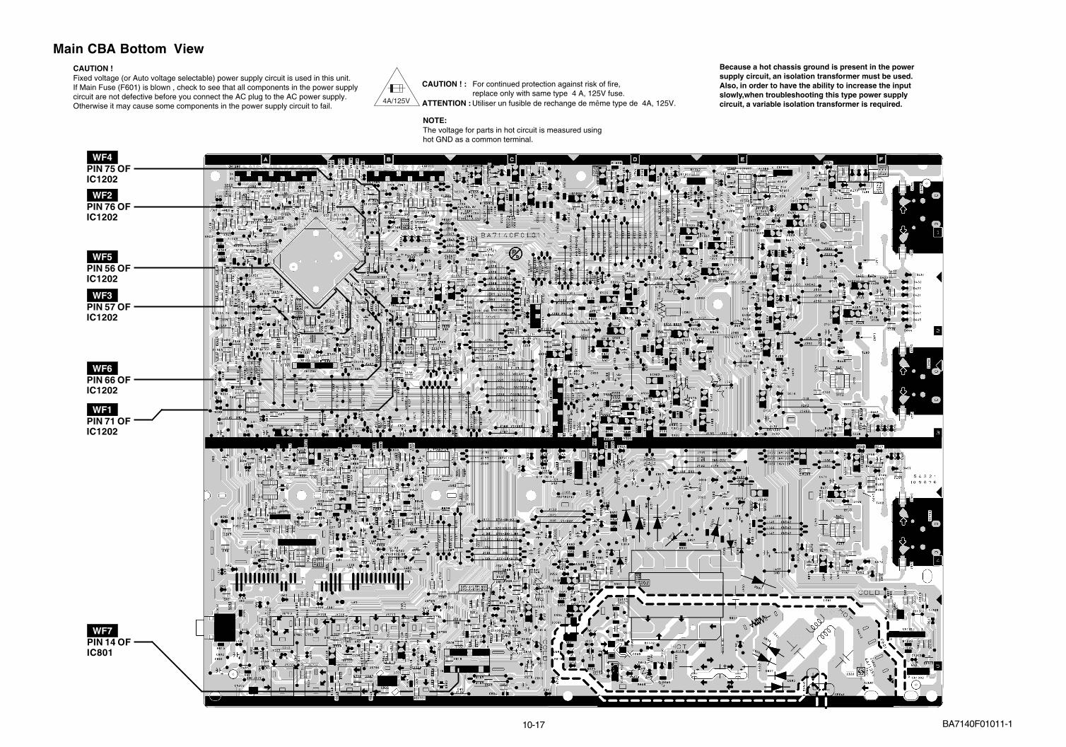
10-17
PIN 76 OFIC1202
WF2
PIN 75 OFIC1202
WF4
PIN 71 OFIC1202
WF1
PIN 66 OFIC1202
WF6
PIN 57 OFIC1202
WF3
PIN 56 OFIC1202
WF5
PIN 14 OFIC801
WF7
Main CBA Bottom View
BA7140F01011-1
For continued protection against risk of fire, replace only with same type 4 A, 125V fuse.
CAUTION ! :
ATTENTION : Utiliser un fusible de rechange de même type de 4A, 125V.4A/125V
CAUTION !Fixed voltage (or Auto voltage selectable) power supply circuit is used in this unit.If Main Fuse (F601) is blown , check to see that all components in the power supplycircuit are not defective before you connect the AC plug to the AC power supply.Otherwise it may cause some components in the power supply circuit to fail.
Because a hot chassis ground is present in the powersupply circuit, an isolation transformer must be used.Also, in order to have the ability to increase the inputslowly,when troubleshooting this type power supplycircuit, a variable isolation transformer is required.
NOTE:The voltage for parts in hot circuit is measured usinghot GND as a common terminal.

10-18
Function CBA Top View
Function CBA Bottom View
BA7420F01021-1
IR Sensor CBA
Top View
IR Sensor CBA
Bottom View
BA7420F01021-2
BA7420F01021-3
BA7420F01021-4
Junction-A CBA Top & Bottom View
Junction-B CBA Top & Bottom View

WAVEFORMS < LCD TV SECTION >
A7440WF11-1
Input: NTSC Color Bar Signal (with 1kHz Audio Signal)
WF1 ~ WF7 = Waveforms to be observed atWaveform check points.(Shown in Schematic Diagram.)
CVBS 0.2V 20µs
WF1 Pin 71 of IC1202
S-VIDEO-Y 0.2V
WF2 Pin 76 of IC1202
20µs
S-VIDEO-C 0.2V
WF3 Pin 57 of IC1202
20µs AUDIO 0.1V 0.5ms
WF7 Pin 14 of IC801
VIDEO-Pr 0.2V 20µs
Pin 66 of IC1202WF6
VIDEO-Pb 0.2V 20µs
Pin 56 of IC1202WF5
VIDEO-Y 0.2V 20µs20µs
Pin 75 of IC1202WF4

Input: NTSC Color Bar Signal (with 1kHz Audio Signal) DVD Video (Power on (Stop) MODE)
WF8 ~ WF12 = Waveforms to be observed atWaveform check points.(Shown in Schematic Diagram.)
WF8 Pin 1 of CN1701
WF9 Pin 3 of CN1701
WF10 Pin 5 of CN1701
Pin 9 of CN1701WF12
Pin 7 of CN1701WF11
20µs0.2VDVD-Y
DVD-C 0.2V 20µs
DVD-AUDIO(L) 0.5V 0.5ms
DVD-AUDIO(R) 0.5V 0.5ms
DVD-SPDIF 1V 0.1µs
A7440WF11-2
WAVEFORMS < DVD SECTION >

WIRING DIAGRAM < LCD TV SECTION >
A7441WI12-1
TU
61 T
UN
ER
UN
IT
VID
EO
-YIN AU
DIO
(R)
-IN
1
AU
DIO
(L)
-IN
2
S-V
IDE
OIN V
IDE
O-P
bIN V
IDE
O-P
rINV
IDE
O-I
N1
AU
DIO
(L)
-IN
1
AU
DIO
(R)
-IN
2
MA
IN C
BA
CL1
107
FU
NC
TIO
N
CB
A
AC
601
AC
CO
RD
CN
1301
1 32 4
1 32 4
KE
Y-IN
-2
AL+
3.3V
(D)
KE
Y-IN
-1
GN
D
CL1
104
IR S
EN
SO
R
CB
A
CN
1302
1 32 4
1 32 4
AL+
3.3V
(D)
RE
MO
TE
GN
D
NU
55
NU
CN
61C
N10
11 32 54 76 8 9 10 131211 14 15
1 32 54 76 8 9 10 131211 14 15
D-G
ND
DT
V-S
-SO
UT
DT
V-S
-SIN
DT
V-S
-SC
LKD
TV
-S-S
RE
QD
-GN
DT
U-S
DA
TU
-SC
LD
TV
-ON
+5V
DT
V-S
PD
IFD
-GN
D
DT
V-S
-RE
SE
TD
-GN
DS
DA
SC
L
CN
621 32 54 76 8 9 10 131211 14 15 1716 1918 20
CN
102
1 32 54 76 8 9 10 131211 14 15 1716 1918 20
DIF
-OU
T1
A-G
ND
DIF
-AG
CA
-GN
DS
MA
RT-
AN
T(N
U)
DT
V-O
N+
1.8V
DT
V-O
N+
2.5V
DT
V-O
N+
3.3V
D-G
ND
DT
V-O
N-H
2N
U
DIF
-OU
T2
A-G
ND
DTV
-VID
EO
(NU
)D
TV
-AU
DIO
(L)
DT
V-A
UD
IO(R
)A
-GN
DD
TV
-YD
TV
-Pr
DT
V-P
bD
TV
MO
DU
LE
CB
A U
NIT
DIG
ITA
LA
UD
IO-O
UT
(CO
AX
IAL)
1 21 2 1 2
SP
-RS
P-G
ND
1CL8
01
CL8
02
2S
P-L
SP
-GN
D
SP
802
SP
EA
KE
RL-
CH
SP
801
SP
EA
KE
RR
-CH
JUN
CT
ION
-A
CB
A
JUN
CT
ION
-B
CB
A
LED
-CO
NT
2D
ISC
-OU
T3
EV
+1.
2V5
EV
+3.
3V6
EV
+3.
3V7
EV
+3.
3V8
DV
D-O
N+
3.3V
9D
VD
-ON
+5V
10E
V+
9V11
EV
+9V
12G
ND
13G
ND
14G
ND
15G
ND
16G
ND
17G
ND
18G
ND
19P
WR
CO
N(N
U)
20D
VD
-SC
LK21
DV
D-C
S22
DIS
C-I
N23C
N16
51
EV
+1.
2V4
AL+
3.3V
(D)
1
DV
D-S
DAT
A24
DV
D-R
EM
OT
E25
TO
D
VD
MA
INC
BA
UN
ITC
N40
1
TO
WIR
ING
DIA
GR
AM
<
DV
DS
EC
TIO
N >
DV
D-C
3G
ND
2D
VD
-Y1C
N17
01
DV
D-A
UD
IO(R
)7
GN
D4
DV
D-A
UD
IO(L
)5
DV
D-M
UT
E6
GN
D8
DV
D-S
PD
IF9
TO
DV
D M
AIN
C
BA
UN
ITC
N60
1
BA
CK
LIG
HT
CN
401
21
BA
CK
LIG
HT
CN
403
21
BA
CK
LIG
HT
CN
402
21
CN
1201
1 32 54 76 8 9 10 131211 14 15 1716 1918 2120 22 23 24 272625 28
OB
[4]
OB
[5]
GN
DC
LKL
GN
DE
R [0
]E
R [1
]E
R [2
]E
R [3
]E
R [4
]E
R [5
]
OB
[3]
OB
[2]
OB
[1]
OB
[0]
GN
DO
G [5
]O
G [4
]O
G [3
]O
G [2
]O
G [1
]O
G [0
]G
ND
OR
[5]
OR
[4]
OR
[3]
OR
[2]
OR
[1]
313029 32
OR
[0]
GN
DS
TH
PO
L33
LP34
CLE
AR
35V
CO
M
CN
1202
1 32 54 76 8 9 10 131211 14 15 1716 1918 2120 22 23 24 25
GN
DPA
NE
L-6V
GN
DPA
NE
L+25
VPA
NE
L+25
VG
ND
PAN
EL+
3.3V
PAN
EL+
3.3V
GN
DPA
NE
L+10
.8V
GN
D
EB
[4]
EB
[3]
EB
[2]
EB
[1]
EB
[0]
GN
DE
G [5
]E
G [4
]E
G [3
]E
G [2
]G
ND
OF
FE
VG
ND
2726 2928 30 31 32 33
ST
VG
ND
CLK
VG
ND
EG
[1]
EG
[0]
GN
DG
ND
EB
[5]
LC
D M
OD
UL
E

A7441WID
WIRING DIAGRAM < DVD SECTION >
CN
201
CN
301
LOA
D-D
ISC
LED-CONT2DISC-OUT3
EV+1.2V5EV+3.3V6EV+3.3V7EV+3.3V8DVD-ON+3.3V9DVD-ON+5V10EV+9V11EV+9V12GND13GND14GND15GND16GND17GND18GND19PWRCON(NU)20DVD-SCLK21DVD-CS22DISC-IN23
CN
401
EV+1.2V4
FS
TS
DE
TEC
TOR
79
112
36
5
M
SP
IND
LEM
OT
OR
M
SLE
DM
OT
OR
4
DV
D M
AIN
CB
A U
NIT
DR
IVE
CB
AD
VD
ME
CH
AN
ISM
PIC
K U
P U
NIT
LOAD-DISC 6SL(+) 5SL(-) 4GND 3SP(-) 2SP(+) 1
FS(-) 3TS(-) 4
GND(CD-PD) 5GND(DVD-PD) 6
PD-MONI 7DVD-LD 8
TS(+) 1FS(+) 2
GND 11NU 12
VREF 13NU 14
B 15C 16
GND(LD) 9CD-LD 10
A 17D 18
CD/DVD 19DVD-ON+5V 20
DVD-C10GND9DVD-Y8
CN
601
DVD-AUDIO(R)14
GND11DVD-AUDIO(L)12DVD-MUTE13
GND15DVD-SPDIF16
DIS
C-I
N
CN
5001
DIS
C-O
UT
LED-POWER 11DISC-OUT 22
GND 44DISC-IN 33
SE
NS
OR
CB
A
CN
801
CN
5001
is s
olde
red
dire
ctly
to th
e P
CB
.
AL+3.3V(D)1
DVD-SDATA24DVD-REMOTE25
TO
WIR
ING
DIA
GR
AM
<
LC
D T
V S
EC
TIO
N >
TO
MA
IN C
BA
CN
1651
TO
MA
IN C
BA
CN
1701
12-2

13-1 A7420TI
SYSTEM CONTROL TIMING CHARTS
Disc IN(TL221)
Sled Drive(TP303)
Disc Drive(TP301)
Focus Drive(TP304)
Tracking Drive(TP302)
0V
3.3V
0V
1.65V
0V
0V
0V
1.65V
1.65V
1.65V
Disc In
Disc Rotation
PlayDisc Stop
Disc Out
Disc In ~ Play/Play ~ Disc Out

14-1 A7440PIN
IC PIN FUNCTION DESCRIPTIONS
IC1202 (LCD Drive / LCD Signal Process / TV Micro Controller)
Pin No. Signal Name Function
1 VDD+3.3V +3.3V VDD
2 VDD+3.3V +3.3V VDD
3 KEY-IN-1 Key Input 1
4 KEY-IN-2 Key Input 2
5 AFT-IN AFT Voltage Input
6 PROTECT-1 Power Supply Protection 1
7 PROTECT-2 Power Supply Protection 2
8 PROTECT-4 Power Supply Protection 4
9 NU Not Used
10 VSS GND
11 DISC-OUT Disc Out Detect Signal
12 DISC-IN Disc In Detect Signal
13 LED-CONT LED Control Signal
14 DVD-MUTE DVD Audio Mute Signal
15 DTV-S-SOUT DTV Serial Data Out
16 DTV-S-SIN DTV Serial Data In
17 DTV-S-SREQ DTV Serial Request
18 IF-MUTE IF Mute Signal Output
19 VCOM VCOM
20 BACKLIGHT-ADJ Inverter Control Signal Output
21 VDD+3.3V +3.3V VDD
22 DTV-ON-H2 DTV On Signal 2 at High
23 VOLUME Volume Control Signal Output
24 VDD+1.2V +1.2V VDD
25 VDD+1.2V +1.2V VDD
26 VGH-H VGH Signal at High
27 P-ON-H Power On Signal at High
28 REMOTE Remote Control Signal Input
29 BUS-OPEN Chip select
30 SCL Serial Clock
31 SDA Serial Data
32 NU Not Used
33 NU Not Used
34 NU Not Used
35 NU Not Used
36 NU Not Used
37 XIN Crystal Oscillation Input (27MHz)
38 XOUT Crystal Oscillation Output (27MHz)
39 VSS GND
40 VSS GND
41 VSS GND
42 VDD+3.3V +3.3V VDD
43 VDD+3.3V +3.3V VDD
44 FSC Clock Output
45 MPSEL MP Select
46 TEST GND
47 S-SW Detecting S-VIDEO Jack Connection
48 AUDIO-MUTE Audio Mute Signal Output
49 INPUT-0 Input Select 0 Signal Output
50 INPUT-1 Input Select 1 Signal Output
51 INPUT-2 Input Select 2 Signal Output
52 NU Not Used
53 NU Not Used
54 DTV-Pb DTV Pb Signal Input
55 NU Not Used
56 VIDEO-Pb Component Video Pb Signal Input
57 S-VIDEO-C/DVD-C Chrominance Signal Input
58 AVDDB +3.3V VDD
59 AVSSB GND
60 SVSS GND
61 NU Not Used
62 NU Not Used
63 NU Not Used
64 DTV-Pr DTV Pr Signal Input
65 NU Not Used
66 VIDEO-Pr Component Video Pr Signal Input
67 RF-CVBS Composite Video Signal Input
68 AVDDC +3.3V VDD
69 AVSSC GND
70 NU Not Used
71 VIDEO-IN1 Composite Video Signal Input
72 NU Not Used
73 DTV-Y DTV Y Signal Input
74 NU Not Used
Pin No. Signal Name Function
14-2 A7440PIN
75 VIDEO-Y Component Video Y Signal Input
76 S-VIDEO-Y/DVD-Y Luminance Signal Input
77 AVDDA +3.3V VDD
78 VSS GND
79 VDD+3.3V +3.3V VDD
80 VSS GND
81 VSS GND
82 VDD+3.3V +3.3V VDD
83 VDD+3.3V +3.3V VDD
84 DVD-MAIN-P Power On Signal at High for DVD
85 DVD-REMOTE DVD Remote Control Signal
86 DVD-CS DVD Interface Chip Select
87 DVD-SCLK DVD Interface Serial Clock
88 DVD-SDATA DVD Interface Serial Data
89 EB[5] Pixel Data Output (EB)
90 EB[4] Pixel Data Output (EB)
91 EB[3] Pixel Data Output (EB)
92 EB[2] Pixel Data Output (EB)
93 EB[1] Pixel Data Output (EB)
94 RESET Reset Output
95 EB[0] Pixel Data Output (EB)
96 EG[5] Pixel Data Output (EG)
97 EG[4] Pixel Data Output (EG)
98 EG[3] Pixel Data Output (EG)
99 VDD+1.2V +1.2V VDD
100 VDD+1.2V +1.2V VDD
101 VDD+1.2V +1.2V VDD
102 VDD+1.2V +1.2V VDD
103 VDD+3.3V +3.3V VDD
104 VDD+3.3V +3.3V VDD
105 EG[2] Pixel Data Output (EG)
106 OFFEV Enable Signal
107 STV Start Pulse Signal
108 CLKV Shift Clock Signal
109 VSS GND
110 EG[1] Pixel Data Output (EG)
111 EG[0] Pixel Data Output (EG)
112 ER[5] Pixel Data Output (ER)
113 ER[4] Pixel Data Output (ER)
114 ER[3] Pixel Data Output (ER)
115 ER[2] Pixel Data Output (ER)
Pin No. Signal Name Function
116 ER[1] Pixel Data Output (ER)
117 ER[0] Pixel Data Output (ER)
118 VSS GND
119 VSS GND
120 VSS GND
121 VSS GND
122 LPF Panel Clock PLL Filter
123 RSPI Reference Terminal
124 NU Not Used
125 CLKL Clock Signal Output
126 OB[5] Pixel Data Output (OB)
127 OB[4] Pixel Data Output (OB)
128 OB[3] Pixel Data Output (OB)
129 OB[2] Pixel Data Output (OB)
130 OB[1] Pixel Data Output (OB)
131 OB[0] Pixel Data Output (OB)
132 OG[5] Pixel Data Output (OG)
133 OG[4] Pixel Data Output (OG)
134 VDD+3.3V +3.3V VDD
135 VDD+3.3V +3.3V VDD
136 VDD+3.3V +3.3V VDD
137 OG[3] Pixel Data Output (OG)
138 OG[2] Pixel Data Output (OG)
139 OG[1] Pixel Data Output (OG)
140 OG[0] Pixel Data Output (OG)
141 OR[5] Pixel Data Output (OR)
142 OR[4] Pixel Data Output (OG)
143 OR[3] Pixel Data Output (OG)
144 OR[2] Pixel Data Output (OG)
145 VDD+1.2V +1.2V VDD
146 VDD+1.2V +1.2V VDD
147 OR[1] Pixel Data Output (OG)
148 OR[0] Pixel Data Output (OG)
149 STH Start Pulse Signal
150 POL Polarity Reverse Signal
151 LP Latch Pulse Signal
152 DTV-ON-H DTV On Signal at High
153 DTV-S-RESET DTV Reset
154 NU Not Used
155 DTV-S-SCLK DTV Serial Clock
156 Clear Panel Control Signal
157 BACKLIGHT-SW Inverter Control Signal Output
158 NU Not Used
Pin No. Signal Name Function

14-3 A7440PIN
159 VSS GND
160 VSS GND
Pin No. Signal Name Function

15-1 A7440LE
16 9
1 8
1 2 3 4
1: Vin2: Vo3: GND4: Vc
E C B E C B
5
4
8
1
1 2 3
1: GND2: Vout3: Vin
120
41
80
81
401
160
121
1: Vin2: Vo3: GND
1 2 3G D S
AN17812APQ070XF01SZH 2SC4881F HFE
2SK3563(Q) LD1117V
KTA1267-GR-AT/PKTA1281Y-AT/PKTC3199-GR-AT/P
2SA950-Y(TE2 F T)2SC2120-Y(TE2 F T)
Note:A: AnodeK: CathodeE: EmitterC: CollectorB: BaseR: ReferenceS: SourceG: GateD: Drain
KIA7805API/P
1: IN2: GND3: OUT
1 2 3
16 9
8
TC4053BF(EL N F)TC4052BF(ELNF)
1
32 17
16
AN5832SA-E1V
1
LTV-817C-F
1
2
4
3
1: A2: K3: E4: C
LD1117SC-R
R8A02030A92FP-RF0Z
BR24L64F-WE2AT24C128N-10SU-1.8 S TPC8214-H
B C E20 11
101
M61116FP TF0G
LEAD IDENTIFICATIONS

16-1 A7441CEX
EXPLODED VIEWS
Cabinet
B17
B34
A1
B15
B15
B15A8
B15
L6
B2
B13
B4
B9
B8
B11
B12
L18
L12
L12
L12
L12
L12
L12
L12
L8
L8
L8
L8
L8
L8
L6
L3
L6
A3A7
B19
A20
A9
L20
A10
A13
A4
B3
B14
B18
L3
L3
L5
L3
L3
L3
L3
L2
L11
A12
A12
See Electrical Parts List for parts with this mark.
L9L9
L9
B10
B10
B21
Function CBA
IR Sensor CBA
Main CBA
AC601
B14
A6
S8
CL1402
CL1401
LCD-1
B1
B1
L6
SP801
Junction-A CBA
B1
B1
L6
SP802
Junction-B CBA
L20
L13
L13
1B1
DVD Main CBA Unit
L3-10
CL1651
CL1701
DTV Module CBA Unit

16-2 A7441PEX
Packing
S1
FRONT
FRONT
S2
S4
Tape
Packing Tape
Packing Tape
S3
X1
Some Ref. Numbers are not in sequence.
X4
X3
X2
Packing Tape
Packing Tape
S8
S9

20070219 17-1 A7441CA
MECHANICAL PARTS LIST
PRODUCT SAFETY NOTE: Products marked with a # have special characteristics important to safety. Before replacing any of these components, read carefully the product safety notice in this service manual. Don't degrade the safety of the product through improper servicing.
NOTE: Parts that are not assigned part numbers (---------) are not available.
Ref. No. Description Part No.
A1 FRONT CABINET A7441UH 1EM121851
A3 CONTROL PLATE A7420UH 1EM322467
A4 REAR CABINET A7440UH 1EM121850
A6# RATING LABEL A7441UH ----------
A7 FUNCTION KNOB L3253UD L3253UD 1EM220961
A8 FRONT PLATE L3256UG 1EM322040A
A9 STAND COVER A7441UH 1EM221555
A10 CONNECTER CAP A7440UH 1EM424253
A12 STAND RUBBER FOOT L4300UA 1EM422534
A13 CAUTION LABEL L3150UA ----------
A20 POP LABEL A7420UH ----------
1B1 DVD MECHA SLOT E7 N7XT0KVM N7XT0KVM
B1 SPEAKER HOLDER A7120UH 1EM423986
B2 TILT STAND HOLDER A7140UH 1EM322402
B3 STAND HOLDER L2500UA 1EM321428
B4 JACK HOLDER A7140UH 1EM322538
B8 ARM ASSEMBLY A7140UH 1EM221550
B9 MODULE PCB HOLDER P7150UT 1EM322373A
B11 DVD HOLDER(TOP) A7440UH 1EM322445
B12 DVD HOLDER(BOTTOM) A7440UH 1EM322446
B13 RUBBER CUSHION L0170UA 1EM420551
B14 CLOTH(10X180XT0.5) L0336JG 0EM408827
B15 CLOTH 10X150XT1.0 1EM421092
B18 FELT L2550UA 1EM423716
B19 LASER CAUTION LABEL L3150UA ----------
B34 CLOTH(10X30XT 0.3) T5300UA 0EM407441
CL1401 WIRE ASSEMBLY 35PIN FFC 35PIN/85MM WX1A7140-006
CL1402 WIRE ASSEMBLY 33PIN FFC 33PIN/85MM WX1A7140-005
CL1651 WIRE ASSEMBLY 25PIN FFC 25PIN/285MM WX1A7440-001
CL1701 WIRE ASSEMBLY 9PIN FFC 9PIN/118MM WX1A7440-002
L2 SCREW P-TIGHT M3X8 BIND HEAD+ GBJP3080
L3 SCREW P-TIGHT 3X10 BIND HEAD+ GBHP3100
L3-10 SCREW P-TIGHT M3X8 BIND HEAD+ GBJP3080
L5 SCREW P-TIGHT M4X18 BIND HEAD+ GBHP4180
L6 SCREW P-TIGHT M3*10 WASHERHEAD+ GCJP3100
L8 SCREW P-TIGHT 3X14 WASHER HEAD+ GCJP3140
L11 SCREW S-TIGHT M3X8 BIND HEAD+ GBHS3080
L12 SCREW S-TIGHT M3X8 BIND HEAD+ GBJS3080
L13 SCREW S-TIGHT M3X10 BIND HEAD+ GBJS3100
L18 DOUBLE SEMS SCREW M4X12 + BLAK FPH34120
L20 SCREW B-TIGHT M4X8 BIND HEAD+ BLK GBHB4080
LCD-1 LCD MODULE LC5 20INCH UF200XA
SP801 SPEAKER S0407F10 DSD0807XQ002
SP802 SPEAKER S0407F10 DSD0807XQ002
PACKINGS1 CARTON A7441UH 1EM424167
S2 STYROFOAM TOP A7440UH 1EM021671
S3 STYROFOAM BOTTOM A7440UH 1EM021676
S4 SET BAG L0301UB 1EM320014A
S8 RFID LABEL P7100UM ----------
S9 LABEL EAS(H3761UD) MAKER NO.ZLLFNSLE1
----------
ACCESSORIESX1 BAG POLYETHYLENE 235X365XT0.03 0EM408420A
X2# OWNERS MANUAL A7441UH 1EMN22105
X3 REMOTE CONTROL NF602UD 192/ECNLC5D1/NF602UD
NF602UD
X4 DRY BATTERY R6UW/2S XB0M311MS001
Ref. No. Description Part No.

20070219 18-1 A7441EL
ELECTRICAL PARTS LIST
PRODUCT SAFETY NOTE: Products marked with a # have special characteristics important to safety. Before replacing any of these components, read carefully the product safety notice in this service manual. Don't degrade the safety of the product through improper servicing.
NOTES:
1. Parts that are not assigned part numbers (---------) are not available.
2. Tolerance of Capacitors and Resistors are noted with the following symbols.
DTV MODULE CBA UNIT
DVD MAIN CBA UNIT
MAIN CBA
C.....±0.25% D.....±0.5% F.....±1%
G.....±2% J......±5% K.....±10%
M.....±20% N.....±30% Z.....+80/-20%
Ref. No. Description Part No.
DTV MODULE CBA UNIT 1ESA14067
Ref. No. Description Part No.
DVD MAIN CBA UNIT N7ET8KUP
Ref. No. Description Part No.
MAIN CBAConsists of the following:
1ESA13897
CAPACITORSC22 ELECTROLYTIC CAP. 100µF/10V M CE1AMASDL101
C23 CHIP CERAMIC CAP.(1608) CH J 1000pF/50V CHD1JJ3CH102
C24 CHIP CERAMIC CAP.(1608) CH J 1000pF/50V CHD1JJ3CH102
C25 CHIP CERAMIC CAP.(1608) B K 0.01µF/50V CHD1JK30B103
C27 FILM CAP.(P) 0.018µF/50V J CA1J183MS029
C28 CHIP CERAMIC CAP.(1608) B K 0.047µF/50V CHD1JK30B473
C29 CHIP CERAMIC CAP. CH D 3pF/50V CHD1JD3CH3R0
C31 PCB JUMPER D0.6-P5.0 JW5.0T
C32 ELECTROLYTIC CAP. 100µF/10V M CE1AMASDL101
C34 CHIP CERAMIC CAP.(1608) CH J 47pF/50V CHD1JJ3CH470
C35 ELECTROLYTIC CAP. 1µF/50V M CE1JMASDL1R0
C36 CHIP CERAMIC CAP.(1608) CH J 47pF/50V CHD1JJ3CH470
C37 CHIP CERAMIC CAP. CH J 680pF/50V CHD1JJ3CH681
C39 ELECTROLYTIC CAP. 0.47µF/50V M CE1JMASDLR47
C42 CHIP CERAMIC CAP.(1608) B K 0.01µF/50V CHD1JK30B103
C46 PCB JUMPER D0.6-P5.0 JW5.0T
C47 CHIP CERAMIC CAP. CH D 5pF/50V CHD1JD3CH5R0
C48 CERAMIC CAP.(AX) CH K 2.7pF/50V CCA1JKTCH2R7
C60 CHIP CERAMIC CAP.(1608) CH J 33pF/50V CHD1JJ3CH330
C62 ELECTROLYTIC CAP. 100µF/10V M CE1AMASDL101
C63 ELECTROLYTIC CAP. 47µF/50V M CE1JMASDL470
C64 CHIP CERAMIC CAP.(1608) B K 1000pF/50V CHD1JK30B102
C67 CHIP CERAMIC CAP.(1608) F Z 0.1µF/25V CHD1EZ30F104
C68 CHIP CERAMIC CAP.(1608) CH J 33pF/50V CHD1JJ3CH330
C69 ELECTROLYTIC CAP. 1000µF/6.3V M CE0KMASDL102
C71 CHIP CERAMIC CAP.(1608) CH J 47pF/50V CHD1JJ3CH470
C72 CHIP CERAMIC CAP.(1608) CH J 47pF/50V CHD1JJ3CH470
C74 CHIP CERAMIC CAP. F Z 1µF/10V CHD1AZ30F105
C75 CHIP CERAMIC CAP. F Z 1µF/10V CHD1AZ30F105
C77 CHIP CERAMIC CAP.(1608) F Z 0.1µF/25V CHD1EZ30F104
C79 CHIP CERAMIC CAP.(1608) CH J 33pF/50V CHD1JJ3CH330
C83 CHIP RES.(1608) 1/10W 0 Ω RRXAZR5Z0000
C85 CHIP CERAMIC CAP. CH J 330pF/50V CHD1JJ3CH331
C86 CHIP CERAMIC CAP. CH J 330pF/50V CHD1JJ3CH331
C87 CHIP CERAMIC CAP.(1608) B K 1000pF/50V CHD1JK30B102
C89 CHIP CERAMIC CAP. CH J 220pF/50V CHD1JJ3CH221
C90 ELECTROLYTIC CAP. 10µF/50V M CE1JMASDL100
C91 CHIP CERAMIC CAP.(1608) B K 1000pF/50V CHD1JK30B102
C401 ELECTROLYTIC CAP. 47µF/50V M CE1JMASDL470
C402 CHIP CERAMIC CAP.(1608) B K 5600pF/50V CHD1JK30B562
C403 ELECTROLYTIC CAP. 10µF/50V M CE1JMASDL100
C405 ELECTROLYTIC CAP. 0.22µF/50V M CE1JMASDLR22
C421 CAP CHIP 5pF 3KV C XC CA3F5R05M016
C422 CHIP CERAMIC CAP.(1608) B K 0.01µF/50V CHD1JK30B103
C423 CAP CHIP 5pF 3KV C XC CA3F5R05M016
C425 CHIP CERAMIC CAP.(1608) B K 0.01µF/50V CHD1JK30B103
C426 ELECTROLYTIC CAP. 10µF/50V M CE1JMASDL100
C427 CHIP CERAMIC CAP.(1608) B K 0.01µF/50V CHD1JK30B103
C428 ELECTROLYTIC CAP. 10µF/50V M CE1JMASDL100
C429 CHIP CERAMIC CAP.(1608) B K 0.01µF/50V CHD1JK30B103
C430 CAP METALIZED FILM 0.068µF/250V/J CT2E683MS041
C431 ELECTROLYTIC CAP. 10µF/50V M CE1JMASDL100
C432 CHIP CERAMIC CAP.(1608) B K 0.01µF/50V CHD1JK30B103
C441 CAP CHIP 5pF 3KV C XC CA3F5R05M016
C442 CHIP CERAMIC CAP.(1608) B K 0.01µF/50V CHD1JK30B103
C443 CAP CHIP 5pF 3KV C XC CA3F5R05M016
C445 CHIP CERAMIC CAP.(1608) B K 0.01µF/50V CHD1JK30B103
C446 ELECTROLYTIC CAP. 10µF/50V M CE1JMASDL100
C447 CHIP CERAMIC CAP.(1608) B K 0.01µF/50V CHD1JK30B103
C448 ELECTROLYTIC CAP. 10µF/50V M CE1JMASDL100
C449 CHIP CERAMIC CAP.(1608) B K 0.01µF/50V CHD1JK30B103
C450 CAP METALIZED FILM 0.068µF/250V/J CT2E683MS041
C451 ELECTROLYTIC CAP. 10µF/50V M CE1JMASDL100
C461 CAP CHIP 5pF 3KV C XC CA3F5R05M016
C462 CHIP CERAMIC CAP.(1608) B K 0.01µF/50V CHD1JK30B103
C463 CAP CHIP 5pF 3KV C XC CA3F5R05M016
C465 CHIP CERAMIC CAP.(1608) B K 0.01µF/50V CHD1JK30B103
C466 ELECTROLYTIC CAP. 10µF/50V M CE1JMASDL100
C467 CHIP CERAMIC CAP.(1608) B K 0.01µF/50V CHD1JK30B103
C468 ELECTROLYTIC CAP. 10µF/50V M CE1JMASDL100
C469 CHIP CERAMIC CAP.(1608) B K 0.01µF/50V CHD1JK30B103
C470 CAP METALIZED FILM 0.068µF/250V/J CT2E683MS041
C471 ELECTROLYTIC CAP. 10µF/50V M CE1JMASDL100
C472 ELECTROLYTIC CAP. 10µF/50V M CE1JMASDL100
C601# METALIZED FILM CAP. 0.33µF/250V CT2E334MS037
C608 CERAMIC CAP. 1000pF/2KV CA3D102PAN04
C611# ELECTROLYTIC CAPACITOR 270µF/200V CA2D271DYG05
C612 FILM CAP.(P) 0.027µF/50V J CA1J273MS029
C613 FILM CAP.(P) 0.082µF/50V J CMA1JJS00823
C614 FILM CAP.(P) 0.001µF/50V J CA1J102MS029
C641# SAFETY CAP. 4700pF/250V KX CA2E472MR050
C659 CERAMIC CAP.(AX) B K 0.0015µF/50V CA1J152TU011
C704 ELECTROLYTIC CAP. 10µF/50V M H7 CE1JMAVSL100
C707 CHIP CERAMIC CAP.(1608) F Z 0.1µF/25V CHD1EZ30F104
C708 CHIP CERAMIC CAP.(1608) CH J 100pF/50V CHD1JJ3CH101
C713 CHIP CERAMIC CAP. B K 1500pF/50V CHD1JK30B152
Ref. No. Description Part No.

20070219 18-2 A7441EL
C714 CHIP CERAMIC CAP. F Z 1µF/10V CHD1AZ30F105
C715 CHIP CERAMIC CAP. B K 1500pF/50V CHD1JK30B152
C716 CHIP CERAMIC CAP. F Z 1µF/10V CHD1AZ30F105
C740 CHIP CERAMIC CAP.(1608) CH J 100pF/50V CHD1JJ3CH101
C751 CHIP CERAMIC CAP. F Z 1µF/10V CHD1AZ30F105
C752 CHIP CERAMIC CAP. F Z 1µF/10V CHD1AZ30F105
C753 CHIP CERAMIC CAP. B K 1500pF/50V CHD1JK30B152
C754 CHIP CERAMIC CAP. B K 1500pF/50V CHD1JK30B152
C781 ELECTROLYTIC CAP. 10µF/50V M CE1JMASDL100
C782 CHIP CERAMIC CAP.(1608) B K 0.1µF/50V CHD1JK30B104
C786 CHIP CERAMIC CAP.(1608) F Z 0.1µF/25V CHD1EZ30F104
C791 CERAMIC CAP.(AX) B K 100pF/50V CCA1JKT0B101
C801 ELECTROLYTIC CAP. 220µF/16V M CE1CMASDL221
C802 ELECTROLYTIC CAP. 220µF/16V M CE1CMASDL221
C805 ELECTROLYTIC CAP. 10µF/50V M CE1JMASDL100
C806 CHIP CERAMIC CAP. F Z 1µF/10V CHD1AZ30F105
C807 CHIP CERAMIC CAP. F Z 1µF/10V CHD1AZ30F105
C809 ELECTROLYTIC CAP. 10µF/50V M CE1JMASDL100
C810 ELECTROLYTIC CAP. 2.2µF/50V M CE1JMASDL2R2
C811 ELECTROLYTIC CAP. 47µF/16V M CE1CMASDL470
C812 CHIP CERAMIC CAP. F Z 1µF/10V CHD1AZ30F105
C813 CHIP CERAMIC CAP. F Z 1µF/10V CHD1AZ30F105
C818 ELECTROLYTIC CAP. 470µF/16V M CE1CMASDL471
C819 CHIP CERAMIC CAP. CH J 680pF/50V CHD1JJ3CH681
C820 CHIP CERAMIC CAP. CH J 680pF/50V CHD1JJ3CH681
C821 CHIP CERAMIC CAP.(1608) F Z 0.1µF/25V CHD1EZ30F104
C822 ELECTROLYTIC CAP. 10µF/50V M CE1JMASDL100
C823 CHIP CERAMIC CAP.(1608) F Z 0.1µF/25V CHD1EZ30F104
C824 CHIP CERAMIC CAP. CH J 180pF/50V CHD1JJ3CH181
C825 CHIP CERAMIC CAP.(1608) F Z 0.1µF/25V CHD1EZ30F104
C826 CHIP CERAMIC CAP.(1608) F Z 0.1µF/25V CHD1EZ30F104
C827 CERAMIC CAP.(AX) F Z 0.1µF/50V CCA1JZTFZ104
C853 ELECTROLYTIC CAP. 2.2µF/50V M CE1JMASDL2R2
C854 CHIP CERAMIC CAP.(1608) B K 0.1µF/50V CHD1JK30B104
C855 CHIP CERAMIC CAP.(1608) B K 0.1µF/50V CHD1JK30B104
C856 CHIP CERAMIC CAP.(1608) B K 0.33µF/10V CHD1AK30B334
C857 ELECTROLYTIC CAP. 2.2µF/50V M CE1JMASDL2R2
C858 ELECTROLYTIC CAP. 2.2µF/50V M CE1JMASDL2R2
C859 ELECTROLYTIC CAP. 4.7µF/50V M CE1JMASDL4R7
C860 ELECTROLYTIC CAP. 10µF/50V M CE1JMASDL100
C863 ELECTROLYTIC CAP. 2.2µF/50V M CE1JMASDL2R2
C864 CHIP CERAMIC CAP.(1608) B K 0.022µF/50V CHD1JK30B223
C865 CHIP CERAMIC CAP.(1608) B K 0.1µF/50V CHD1JK30B104
C866 CHIP CERAMIC CAP. F Z 2.2µF/10V CHD1AZ30F225
C867 CHIP CERAMIC CAP. F Z 2.2µF/10V CHD1AZ30F225
C868 CHIP CERAMIC CAP.(1608) B K 1µF/10V CHD1AK30B105
C869 CHIP CERAMIC CAP.(1608) B K 0.022µF/50V CHD1JK30B223
C901 ELECTROLYTIC CAP. 2200µF/25V M CE1EMZPDL222
C902 ELECTROLYTIC CAP. 470µF/25V M CE1EMASDL471
C903 ELECTROLYTIC CAP. 1000µF/10V M CE1AMASDL102
C904 ELECTROLYTIC CAP. 0.47µF/50V M H7 CE1JMAVSLR47
C905 ELECTROLYTIC CAP. 1000µF/6.3V M CE0KMASDL102
C906 ELECTROLYTIC CAP. 470µF/6.3V M CE0KMASDL471
C907 ELECTROLYTIC CAP. 100µF/50V M CE1JMASDL101
C908 ELECTROLYTIC CAP. 1000µF/6.3V M CE0KMASDL102
C909 ELECTROLYTIC CAP. 47µF/16V M CE1CMASDL470
C910 ELECTROLYTIC CAP. 47µF/16V M CE1CMASDL470
C911 ELECTROLYTIC CAP. 10µF/50V M CE1JMASDL100
C912 ELECTROLYTIC CAP. 1µF/50V M CE1JMASDL1R0
C913 FILM CAP.(P) 0.0027µF/50V J CMA1JJS00272
C915 CHIP CERAMIC CAP.(1608) B K 0.1µF/50V CHD1JK30B104
C916 ELECTROLYTIC CAP. 10µF/50V M CE1JMASDL100
C920 ELECTROLYTIC CAP. 220µF/16V M CE1CMASDL221
Ref. No. Description Part No.
C921 ELECTROLYTIC CAP. 1000µF/6.3V M CE0KMASDL102
C922 ELECTROLYTIC CAP. 470µF/6.3V M CE0KMASDL471
C923 ELECTROLYTIC CAP. 100µF/6.3V M CE0KMASDL101
C925 ELECTROLYTIC CAP. 47µF/25V M CE1EMASDL470
C926 CHIP CERAMIC CAP.(1608) CH J 47pF/50V CHD1JJ3CH470
C995 ELECTROLYTIC CAP. 100µF/16V M CE1CMASDL101
C1001 CHIP CERAMIC CAP.(1608) B K 0.01µF/50V CHD1JK30B103
C1003 ELECTROLYTIC CAP. 220µF/16V M CE1CMASDL221
C1004 CHIP CERAMIC CAP.(1608) B K 0.01µF/50V CHD1JK30B103
C1005 ELECTROLYTIC CAP. 22µF/50V M CE1JMASDL220
C1006 CHIP CERAMIC CAP.(1608) B K 0.01µF/50V CHD1JK30B103
C1007 CHIP CERAMIC CAP.(1608) B K 0.01µF/50V CHD1JK30B103
C1008 ELECTROLYTIC CAP. 10µF/50V M CE1JMASDL100
C1204 CHIP CERAMIC CAP.(1608) F Z 0.1µF/25V CHD1EZ30F104
C1205 CHIP CERAMIC CAP.(1608) F Z 0.1µF/25V CHD1EZ30F104
C1207 CHIP CERAMIC CAP.(1608) F Z 0.1µF/25V CHD1EZ30F104
C1209 CHIP CERAMIC CAP.(1608) CH J 100pF/50V CHD1JJ3CH101
C1210 CHIP CERAMIC CAP.(1608) B K 0.01µF/50V CHD1JK30B103
C1211 CHIP CERAMIC CAP.(1608) F Z 0.1µF/25V CHD1EZ30F104
C1213 CHIP CERAMIC CAP.(1608) F Z 0.1µF/25V CHD1EZ30F104
C1216 CHIP CERAMIC CAP.(1608) F Z 0.1µF/25V CHD1EZ30F104
C1217 ELECTROLYTIC CAP. 100µF/16V M CE1CMASDL101
C1218 CHIP CERAMIC CAP.(1608) F Z 0.1µF/25V CHD1EZ30F104
C1219 ELECTROLYTIC CAP. 100µF/16V M CE1CMASDL101
C1220 ELECTROLYTIC CAP. 100µF/10V M H7 CE1AMAVSL101
C1221 ELECTROLYTIC CAP. 100µF/10V M H7 CE1AMAVSL101
C1223 ELECTROLYTIC CAP. 100µF/10V M H7 CE1AMAVSL101
C1301 CHIP CERAMIC CAP.(1608) B K 0.01µF/50V CHD1JK30B103
C1302 CHIP CERAMIC CAP.(1608) B K 0.1µF/50V CHD1JK30B104
C1304 CHIP CERAMIC CAP. CH J 330pF/50V CHD1JJ3CH331
C1312 CHIP CERAMIC CAP.(1608) F Z 0.1µF/25V CHD1EZ30F104
C1313 CHIP CERAMIC CAP.(1608) F Z 0.1µF/25V CHD1EZ30F104
C1314 CHIP CERAMIC CAP.(1608) F Z 0.1µF/25V CHD1EZ30F104
C1316 CHIP CERAMIC CAP.(1608) F Z 0.1µF/25V CHD1EZ30F104
C1319 CHIP CERAMIC CAP.(1608) CH J 47pF/50V CHD1JJ3CH470
C1320 CHIP CERAMIC CAP.(1608) CH J 47pF/50V CHD1JJ3CH470
C1321 CHIP CERAMIC CAP.(1608) CH J 33pF/50V CHD1JJ3CH330
C1322 CHIP CERAMIC CAP.(1608) CH J 33pF/50V CHD1JJ3CH330
C1323 CHIP CERAMIC CAP.(1608) B K 0.01µF/50V CHD1JK30B103
C1324 ELECTROLYTIC CAP. 100µF/16V M CE1CMASDL101
C1331 CHIP CERAMIC CAP.(1608) F Z 0.1µF/25V CHD1EZ30F104
C1334 CHIP CERAMIC CAP.(1608) B K 0.1µF/50V CHD1JK30B104
C1335 CHIP CERAMIC CAP.(1608) B K 0.1µF/50V CHD1JK30B104
C1336 CHIP CERAMIC CAP.(1608) F Z 0.1µF/25V CHD1EZ30F104
C1337 CHIP CERAMIC CAP.(1608) B K 0.1µF/50V CHD1JK30B104
C1338 CHIP CERAMIC CAP.(1608) F Z 0.1µF/25V CHD1EZ30F104
C1339 CHIP CERAMIC CAP.(1608) F Z 0.1µF/25V CHD1EZ30F104
C1340 CHIP CERAMIC CAP.(1608) F Z 0.1µF/25V CHD1EZ30F104
C1341 ELECTROLYTIC CAP. 47µF/16V M CE1CMASDL470
C1342 CHIP CERAMIC CAP.(1608) B K 0.1µF/50V CHD1JK30B104
C1343 CHIP CERAMIC CAP.(1608) B K 0.1µF/50V CHD1JK30B104
C1344 CHIP CERAMIC CAP.(1608) F Z 0.1µF/25V CHD1EZ30F104
C1345 CHIP CERAMIC CAP.(1608) B K 0.1µF/50V CHD1JK30B104
C1346 CHIP CERAMIC CAP.(1608) F Z 0.1µF/25V CHD1EZ30F104
C1347 CHIP CERAMIC CAP.(1608) F Z 0.1µF/25V CHD1EZ30F104
C1348 CHIP CERAMIC CAP.(1608) F Z 0.1µF/25V CHD1EZ30F104
C1349 ELECTROLYTIC CAP. 47µF/16V M CE1CMASDL470
C1350 CHIP CERAMIC CAP.(1608) B K 0.1µF/50V CHD1JK30B104
C1351 CHIP CERAMIC CAP.(1608) F Z 0.1µF/25V CHD1EZ30F104
C1352 CHIP CERAMIC CAP.(1608) B K 0.1µF/50V CHD1JK30B104
C1353 CHIP CERAMIC CAP.(1608) F Z 0.1µF/25V CHD1EZ30F104
C1355 CHIP CERAMIC CAP.(1608) B K 0.1µF/50V CHD1JK30B104
C1356 CHIP CERAMIC CAP.(1608) F Z 0.1µF/25V CHD1EZ30F104
Ref. No. Description Part No.

20070219 18-3 A7441EL
C1359 CHIP CERAMIC CAP.(1608) F Z 0.1µF/25V CHD1EZ30F104
C1360 CHIP CERAMIC CAP.(1608) F Z 0.1µF/25V CHD1EZ30F104
C1361 ELECTROLYTIC CAP. 47µF/16V M CE1CMASDL470
C1362 CHIP CERAMIC CAP. F Z 1µF/10V CHD1AZ30F105
C1366 CHIP CERAMIC CAP.(1608) F Z 0.1µF/25V CHD1EZ30F104
C1367 CHIP CERAMIC CAP.(1608) F Z 0.1µF/25V CHD1EZ30F104
C1368 CHIP CERAMIC CAP.(1608) F Z 0.1µF/25V CHD1EZ30F104
C1369 CERAMIC CAP.(AX) B K 1000pF/50V CCA1JKT0B102
C1370 ELECTROLYTIC CAP. 100µF/10V M H7 CE1AMAVSL101
C1371 ELECTROLYTIC CAP. 100µF/10V M H7 CE1AMAVSL101
C1372 ELECTROLYTIC CAP. 100µF/10V M H7 CE1AMAVSL101
C1373 ELECTROLYTIC CAP. 100µF/10V M H7 CE1AMAVSL101
C1374 CHIP CERAMIC CAP.(1608) F Z 0.1µF/25V CHD1EZ30F104
C1375 CHIP CERAMIC CAP.(1608) F Z 0.1µF/25V CHD1EZ30F104
C1664 CHIP CERAMIC CAP.(1608) CH J 1000pF/50V CHD1JJ3CH102
C1665 CHIP CERAMIC CAP.(1608) CH J 1000pF/50V CHD1JJ3CH102
C1705 CHIP CERAMIC CAP. F Z 1µF/10V CHD1AZ30F105
C1803 PCB JUMPER D0.6-P5.0 JW5.0T
C1804 PCB JUMPER D0.6-P5.0 JW5.0T
C1810 ELECTROLYTIC CAP. 4.7µF/50V M CE1JMASDL4R7
C1822 ELECTROLYTIC CAP. 10µF/50V M CE1JMASDL100
C1823 ELECTROLYTIC CAP. 10µF/50V M CE1JMASDL100
C1824 CHIP CERAMIC CAP. B K 6800pF/50V CHD1JKB0B682
C1825 CHIP CERAMIC CAP. B K 6800pF/50V CHD1JKB0B682
C1914 ELECTROLYTIC CAP. 100µF/10V M H7 CE1AMAVSL101
CONNECTORSCN401 BACK LIGHT CONNECTOR 1717369-1 JB17D02AP001
CN402 BACK LIGHT CONNECTOR 1717369-1 JB17D02AP001
CN403 BACK LIGHT CONNECTOR 1717369-1 JB17D02AP001
CN1201 FMN CONNECTOR SIDE 35P 35FMN-STRK-A(LF)(SN)
JCFNG35JG022
CN1202 FMN CONNECTOR SIDE 33P 33FMN-STRK-A(LF)(SN)
JCFNG33JG022
CN1303 PH CONNECTOR TOP 4P B4B-PH-K-S (LF)(SN)
J3PHC04JG029
CN1651 FMN CONNECTOR TOP25P 25FMN-BTK-A(LF)(SN)
JCFNG25JG019
CN1701 CONNECTOR PRINT MES G/09/S/09FMN-BTRK-A(
JCFNG09JG020
DIODESD31 SWITCHING DIODE 1SS133(T-77) QDTZ001SS133
D62 SWITCHING DIODE 1SS133(T-77) QDTZ001SS133
D63 SWITCHING DIODE 1SS133(T-77) QDTZ001SS133
D68 SWITCHING DIODE 1SS133(T-77) QDTZ001SS133
D401 SWITCHING DIODE 1SS133(T-77) QDTZ001SS133
D402 SWITCHING DIODE 1SS133(T-77) QDTZ001SS133
D403 ZENER DIODE MTZJT-777.5B QDTB0MTZJ7R5
D404 SWITCHING DIODE 1SS133(T-77) QDTZ001SS133
D406 SWITCHING DIODE 1SS133(T-77) QDTZ001SS133
D407 SWITCHING DIODE 1SS133(T-77) QDTZ001SS133
D408 ZENER DIODE MTZJT-776.2B QDTB0MTZJ6R2
D409 ZENER DIODE MTZJT-7710B QDTB00MTZJ10
D410 ZENER DIODE MTZJT-775.6B QDTB0MTZJ5R6
D411 ZENER DIODE MTZJT-775.6B QDTB0MTZJ5R6
D421 SWITCHING DIODE 1SS133(T-77) QDTZ001SS133
D422 SWITCHING DIODE 1SS133(T-77) QDTZ001SS133
D423 SWITCHING DIODE 1SS133(T-77) QDTZ001SS133
D424 SWITCHING DIODE 1SS133(T-77) QDTZ001SS133
D425 SWITCHING DIODE 1SS133(T-77) QDTZ001SS133
D426 SWITCHING DIODE 1SS133(T-77) QDTZ001SS133
D427 SWITCHING DIODE 1SS133(T-77) QDTZ001SS133
D428 SWITCHING DIODE 1SS133(T-77) QDTZ001SS133
D429 SWITCHING DIODE 1SS133(T-77) QDTZ001SS133
D430 SWITCHING DIODE 1SS133(T-77) QDTZ001SS133
Ref. No. Description Part No.
D431 SWITCHING DIODE 1SS133(T-77) QDTZ001SS133
D432 SWITCHING DIODE 1SS133(T-77) QDTZ001SS133
D433 SWITCHING DIODE 1SS133(T-77) QDTZ001SS133
D434 SWITCHING DIODE 1SS133(T-77) QDTZ001SS133
D441 SWITCHING DIODE 1SS133(T-77) QDTZ001SS133
D442 SWITCHING DIODE 1SS133(T-77) QDTZ001SS133
D443 SWITCHING DIODE 1SS133(T-77) QDTZ001SS133
D444 SWITCHING DIODE 1SS133(T-77) QDTZ001SS133
D445 SWITCHING DIODE 1SS133(T-77) QDTZ001SS133
D446 SWITCHING DIODE 1SS133(T-77) QDTZ001SS133
D447 SWITCHING DIODE 1SS133(T-77) QDTZ001SS133
D448 SWITCHING DIODE 1SS133(T-77) QDTZ001SS133
D449 SWITCHING DIODE 1SS133(T-77) QDTZ001SS133
D450 SWITCHING DIODE 1SS133(T-77) QDTZ001SS133
D451 SWITCHING DIODE 1SS133(T-77) QDTZ001SS133
D452 SWITCHING DIODE 1SS133(T-77) QDTZ001SS133
D453 SWITCHING DIODE 1SS133(T-77) QDTZ001SS133
D454 SWITCHING DIODE 1SS133(T-77) QDTZ001SS133
D461 SWITCHING DIODE 1SS133(T-77) QDTZ001SS133
D462 SWITCHING DIODE 1SS133(T-77) QDTZ001SS133
D463 SWITCHING DIODE 1SS133(T-77) QDTZ001SS133
D464 SWITCHING DIODE 1SS133(T-77) QDTZ001SS133
D465 SWITCHING DIODE 1SS133(T-77) QDTZ001SS133
D466 SWITCHING DIODE 1SS133(T-77) QDTZ001SS133
D467 SWITCHING DIODE 1SS133(T-77) QDTZ001SS133
D468 SWITCHING DIODE 1SS133(T-77) QDTZ001SS133
D469 SWITCHING DIODE 1SS133(T-77) QDTZ001SS133
D470 SWITCHING DIODE 1SS133(T-77) QDTZ001SS133
D471 SWITCHING DIODE 1SS133(T-77) QDTZ001SS133
D472 SWITCHING DIODE 1SS133(T-77) QDTZ001SS133
D473 SWITCHING DIODE 1SS133(T-77) QDTZ001SS133
D474 SWITCHING DIODE 1SS133(T-77) QDTZ001SS133
D605# DIODE 1N5397-B NDLZ001N5397
D606# DIODE 1N5397-B NDLZ001N5397
D607# DIODE 1N5397-B NDLZ001N5397
D608# DIODE 1N5397-B NDLZ001N5397
D609 ZENER DIODE MTZJT-775.6B QDTB0MTZJ5R6
D611# ZENER DIODE MTZJT-7722B QDTB00MTZJ22
D612 PCB JUMPER D0.6-P5.0 JW5.0T
D613 SWITCHING DIODE 1SS133(T-77) QDTZ001SS133
D614 SWITCHING DIODE 1SS133(T-77) QDTZ001SS133
D624# ZENER DIODE MTZJT-7739B QDTB00MTZJ39
D801 SWITCHING DIODE 1SS133(T-77) QDTZ001SS133
D802 SWITCHING DIODE 1SS133(T-77) QDTZ001SS133
D803 ZENER DIODE MTZJT-776.2B QDTB0MTZJ6R2
D901 SCHOTTKY BARRIER DIODE ERC84-009 QDLZERC84009
D902 RECTIFIER DIODE FR202-B/P NDQZ000FR202
D903 SCHOTTKY BARRIER DIODE SB240-B/P NDQZ000SB240
D904 IC SHUNT REGULATOR KIA431-AT/P NSZBA0TJY036
D905 ZENER DIODE MTZJT-778.2A QDTA0MTZJ8R2
D906 SCHOTTKY BARRIEA DIODE 11EQS04 QD4Z011EQS04
D907 SCHOTTKY BARRIER DIODE SB240-B/P NDQZ000SB240
D909 DIODE FR154 NDLZ000FR154
D910 DIODE 1ZC43(Q) QDLZ001ZC43Q
D911 SCHOTTKY BARRIER DIODE SB240-B/P NDQZ000SB240
D912 RECTIFIER DIODE 1N4005 NDQZ001N4005
D913 DIODE FR104-B NDLZ000FR104
D914 SWITCHING DIODE 1SS133(T-77) QDTZ001SS133
D915 SWITCHING DIODE 1SS133(T-77) QDTZ001SS133
D916 IC SHUNT REGULATOR KIA431-AT/P NSZBA0TJY036
D917 SWITCHING DIODE 1SS133(T-77) QDTZ001SS133
D918 SWITCHING DIODE 1SS133(T-77) QDTZ001SS133
D919 SWITCHING DIODE 1SS133(T-77) QDTZ001SS133
Ref. No. Description Part No.

20070219 18-4 A7441EL
D920 IC SHUNT REGULATOR KIA431-AT/P NSZBA0TJY036
D921 ZENER DIODE MTZJT-775.6C QDTC0MTZJ5R6
D922 ZENER DIODE MTZJT-775.6C QDTC0MTZJ5R6
D923 IC SHUNT REGULATOR KIA431-AT/P NSZBA0TJY036
D924 IC SHUNT REGULATOR KIA431-AT/P NSZBA0TJY036
D925 SWITCHING DIODE 1SS133(T-77) QDTZ001SS133
D926 ZENER DIODE MTZJT-7739B QDTB00MTZJ39
D927 SWITCHING DIODE 1SS133(T-77) QDTZ001SS133
D928 ZENER DIODE MTZJT-7733B QDTB00MTZJ33
D931 DIODE FR154 NDLZ000FR154
D932 SCHOTTKY BARRIEA DIODE 11EQS04 QD4Z011EQS04
D933 ZENER DIODE MTZJT-775.6B QDTB0MTZJ5R6
D934 SWITCHING DIODE 1SS133(T-77) QDTZ001SS133
D935 ZENER DIODE MTZJT-773.9B QDTB0MTZJ3R9
D939 SWITCHING DIODE 1SS133(T-77) QDTZ001SS133
D940 ZENER DIODE MTZJT-7710B QDTB00MTZJ10
D941 SWITCHING DIODE 1SS133(T-77) QDTZ001SS133
D942 SWITCHING DIODE 1SS133(T-77) QDTZ001SS133
D943 SWITCHING DIODE 1SS133(T-77) QDTZ001SS133
D945 SWITCHING DIODE 1SS133(T-77) QDTZ001SS133
D946 SWITCHING DIODE 1SS133(T-77) QDTZ001SS133
D947 PCB JUMPER D0.6-P5.0 JW5.0T
D948 PCB JUMPER D0.6-P5.0 JW5.0T
D949 SWITCHING DIODE 1SS133(T-77) QDTZ001SS133
D951 SWITCHING DIODE 1SS133(T-77) QDTZ001SS133
D952 SWITCHING DIODE 1SS133(T-77) QDTZ001SS133
D955 SWITCHING DIODE 1SS133(T-77) QDTZ001SS133
D956 ZENER DIODE MTZJT-7712B QDTB00MTZJ12
D957 SWITCHING DIODE 1SS133(T-77) QDTZ001SS133
D960 SWITCHING DIODE 1SS133(T-77) QDTZ001SS133
D961 SWITCHING DIODE 1SS133(T-77) QDTZ001SS133
D962 SWITCHING DIODE 1SS133(T-77) QDTZ001SS133
D963 SWITCHING DIODE 1SS133(T-77) QDTZ001SS133
D1001 SWITCHING DIODE 1SS133(T-77) QDTZ001SS133
D1002 IC SHUNT REGULATOR KIA431-AT/P NSZBA0TJY036
D1003 SWITCHING DIODE 1SS133(T-77) QDTZ001SS133
D1004 ZENER DIODE MTZJT-7724B QDTB00MTZJ24
D1005 ZENER DIODE MTZJT-776.2B QDTB0MTZJ6R2
D1325 ZENER DIODE MTZJT-774.3B QDTB0MTZJ4R3
ICSIC31 IC VIF/SIF M61116FP TF0G QSZBA0SHT034
IC61 IC EEPROM AT24C128N-10SU-1.8 S NSZBA0TAZ083
IC601# PHOTOCOUPLER LTV-817C-F NPEC0LTV817F
IC781 IC SWITCH TC4053BF(EL N F) QSZBA0TTS163
IC801 IC AN17812A QSZBA0SMS017
IC851 IC MTS DECORDER AN5832SA-E1V QSZBA0TMS003
IC852 IC SWITCHING TC4052BF(ELNF) QSZBA0TTS162
IC901 VOLTAGE REGULATOR LD1117SC-R NSZBA0TSS229
IC902 IC LD1117V NSZBA0SSS046
IC904 VOLTAGE REGULATOR PQ070XF01SZH QSZBA0SSH054
IC905 IC VOLTAGE REGULATOR 5V KIA7805API/P NSZBA0SJY041
IC1202 IC DVP-V6 R8A02030A92FP-RF0Z QSZAA0RHT156
IC1205 IC BR24L64F-WE2 QSZBA0TRM071
COILSL21 PCB JUMPER D0.6-P5.0 JW5.0T
L22 INDUCTOR 150µH-J-26T LLAXJATTU151
L31 PCB JUMPER D0.6-P5.0 JW5.0T
L32 INDUCTOR 18µH-J-26T LLAXJATTU180
L61 PCB JUMPER D0.6-P5.0 JW5.0T
L63 PCB JUMPER D0.6-P5.0 JW5.0T
L66 INDUCTOR CHIP LK16081R0K-T 1.0µH LLACKB3TU1R0
L401 COIL CHOKE ELC10D101EL LLC101KMS003
Ref. No. Description Part No.
L402 COIL CHOKE ELC10D101EL LLC101KMS003
L403 COIL CHOKE ELC10D101EL LLC101KMS003
L601# LINE FILTER 5.0MH 6Y075 LLBG00ZKT004
L701 PCB JUMPER D0.6-P5.0 JW5.0T
L781 PCB JUMPER D0.6-P5.0 JW5.0T
L851 PCB JUMPER D0.6-P5.0 JW5.0T
L1200 CHIP RES. 1/10W J 100 Ω RRXAJR5Z0101
L1301 PCB JUMPER D0.6-P5.0 JW5.0T
L1338 INDUCTOR 1.0µH-J-26T LLAXJATTU010
L1346 INDUCTOR 1.0µH-J-26T LLAXJATTU010
L1351 INDUCTOR 1.0µH-J-26T LLAXJATTU010
L1356 INDUCTOR 1.0µH-J-26T LLAXJATTU010
TRANSISTORSQ401 NPN TRANSISTOR POWER 2SC4881F HFE
MAX320QQWZ2SC4881F
Q402 TRANSISTOR 2SA950-Y(TE2 F T) QQSY02SA950F
Q403 TRANSISTOR KTC3199-GR-AT/P NQS4KTC3199P
Q404 TRANSISTOR KTC3199-GR-AT/P NQS4KTC3199P
Q405 TRANSISTOR KTA1267-GR-AT/P NQS1KTA1267P
Q406 TRANSISTOR 2SC2120-Y(TE2 F T) QQSY2SC2120F
Q407 TRANSISTOR KTC3199-GR-AT/P NQS4KTC3199P
Q421# FET MOS SMD TPC8214-H QF2ZTPC8214H
Q422 TRANSISTOR KTC3199-GR-AT/P NQS4KTC3199P
Q423 TRANSISTOR KTC3199-GR-AT/P NQS4KTC3199P
Q424 TRANSISTOR KTC3199-GR-AT/P NQS4KTC3199P
Q425 TRANSISTOR KTC3199-GR-AT/P NQS4KTC3199P
Q441# FET MOS SMD TPC8214-H QF2ZTPC8214H
Q442 TRANSISTOR KTC3199-GR-AT/P NQS4KTC3199P
Q443 TRANSISTOR KTC3199-GR-AT/P NQS4KTC3199P
Q444 TRANSISTOR KTC3199-GR-AT/P NQS4KTC3199P
Q461# FET MOS SMD TPC8214-H QF2ZTPC8214H
Q462 TRANSISTOR KTC3199-GR-AT/P NQS4KTC3199P
Q463 TRANSISTOR KTC3199-GR-AT/P NQS4KTC3199P
Q464 TRANSISTOR KTC3199-GR-AT/P NQS4KTC3199P
Q601# FET MOS 2SK3563(Q) QFWZ2SK3563Q
Q603# TRANSISTOR 2SC2120-Y(TE2 F T) QQSY2SC2120F
Q707 TRANSISTOR KTC3199-GR-AT/P NQS4KTC3199P
Q708 TRANSISTOR KTC3199-GR-AT/P NQS4KTC3199P
Q709 TRANSISTOR KTC3199-GR-AT/P NQS4KTC3199P
Q802 TRANSISTOR KTC3199-GR-AT/P NQS4KTC3199P
Q901 TRANSISTOR 2SC2120-Y(TE2 F T) QQSY2SC2120F
Q902 TRANSISTOR 2SC2120-Y(TE2 F T) QQSY2SC2120F
Q903 TRANSISTOR 2SC2120-Y(TE2 F T) QQSY2SC2120F
Q904 TRANSISTOR 2SC2120-Y(TE2 F T) QQSY2SC2120F
Q905 TRANSISTOR 2SA950-Y(TE2 F T) QQSY02SA950F
Q906 TRANSISTOR KTC3199-GR-AT/P NQS4KTC3199P
Q907 TRANSISTOR 2SC2120-Y(TE2 F T) QQSY2SC2120F
Q908 TRANSISTOR 2SC2120-Y(TE2 F T) QQSY2SC2120F
Q909 TRANSISTOR 2SC2120-Y(TE2 F T) QQSY2SC2120F
Q910 TRANSISTOR KTA1267-GR-AT/P NQS1KTA1267P
Q911 TRANSISTOR KTA1281Y-AT/P NQVYKTA1281P
Q912 TRANSISTOR KTC3199-GR-AT/P NQS4KTC3199P
Q913 TRANSISTOR KTC3199-GR-AT/P NQS4KTC3199P
Q914 TRANSISTOR KTC3199-GR-AT/P NQS4KTC3199P
Q916 TRANSISTOR KTC3199-GR-AT/P NQS4KTC3199P
Q917 TRANSISTOR KTC3199-GR-AT/P NQS4KTC3199P
Q918 TRANSISTOR KTC3199-GR-AT/P NQS4KTC3199P
Q919 TRANSISTOR KTC3199-GR-AT/P NQS4KTC3199P
Q923 TRANSISTOR 2SA950-Y(TE2 F T) QQSY02SA950F
Q1001 TRANSISTOR KTC3199-GR-AT/P NQS4KTC3199P
Q1002 TRANSISTOR KTA1267-GR-AT/P NQS1KTA1267P
Q1003 TRANSISTOR 2SC2120-Y(TE2 F T) QQSY2SC2120F
Q1004 TRANSISTOR KTC3199-GR-AT/P NQS4KTC3199P
Ref. No. Description Part No.

20070219 18-5 A7441EL
Q1005 TRANSISTOR KTA1267-GR-AT/P NQS1KTA1267P
Q1006 TRANSISTOR KTC3199-GR-AT/P NQS4KTC3199P
Q1007 TRANSISTOR KTC3199-GR-AT/P NQS4KTC3199P
Q1701 TRANSISTOR KTC3199-GR-AT/P NQS4KTC3199P
Q1703 TRANSISTOR KTC3199-GR-AT/P NQS4KTC3199P
RESISTORSR17 CHIP RES.(1608) 1/10W 0 Ω RRXAZR5Z0000
R18 CHIP RES.(1608) 1/10W 0 Ω RRXAZR5Z0000
R21 CHIP RES. 1/10W J 270k Ω RRXAJR5Z0274
R23 CHIP RES. 1/10W J 2.2k Ω RRXAJR5Z0222
R24 CHIP RES. 1/10W J 820k Ω RRXAJR5Z0824
R25 CHIP RES. 1/10W J 8.2k Ω RRXAJR5Z0822
R26 CARBON RES. 1/4W J 100 Ω RCX4JATZ0101
R34 CHIP RES.(1608) 1/10W 0 Ω RRXAZR5Z0000
R38 CHIP RES. 1/10W J 100 Ω RRXAJR5Z0101
R42 CHIP RES. 1/10W J 220 Ω RRXAJR5Z0221
R46 CARBON RES. 1/4W J 1k Ω RCX4JATZ0102
R48 CHIP RES.(1608) 1/10W 0 Ω RRXAZR5Z0000
R49 CHIP RES. 1/10W J 1.8k Ω RRXAJR5Z0182
R61 CHIP RES. 1/10W J 220 Ω RRXAJR5Z0221
R62 CHIP RES. 1/10W J 220 Ω RRXAJR5Z0221
R63 CHIP RES.(1608) 1/10W 0 Ω RRXAZR5Z0000
R64 CHIP RES.(1608) 1/10W 0 Ω RRXAZR5Z0000
R65 CHIP RES.(1608) 1/10W 0 Ω RRXAZR5Z0000
R67 CHIP RES.(1608) 1/10W 0 Ω RRXAZR5Z0000
R68 CHIP RES.(1608) 1/10W 0 Ω RRXAZR5Z0000
R72 CHIP RES.(1608) 1/10W 0 Ω RRXAZR5Z0000
R73 CHIP RES. 1/10W J 22k Ω RRXAJR5Z0223
R74 CHIP RES. 1/10W J 22k Ω RRXAJR5Z0223
R75 CHIP RES. 1/10W J 10k Ω RRXAJR5Z0103
R401 CHIP RES. 1/10W J 1.5k Ω RRXAJR5Z0152
R402 CARBON RES. 1/4W J 27k Ω RCX4JATZ0273
R403 CARBON RES. 1/4W J 150 Ω RCX4JATZ0151
R404 CARBON RES. 1/4W J 5.6k Ω RCX4JATZ0562
R406 CHIP RES. 1/10W J 3.3k Ω RRXAJR5Z0332
R407 CHIP RES. 1/10W J 10k Ω RRXAJR5Z0103
R408 CARBON RES. 1/4W J 820 Ω RCX4JATZ0821
R409 CARBON RES. 1/4W J 10k Ω RCX4JATZ0103
R410 CARBON RES. 1/4W J 1.2k Ω RCX4JATZ0122
R411 CHIP RES. 1/10W J 1 Ω RRXAJR5Z01R0
R412 CHIP RES. 1/10W J 10k Ω RRXAJR5Z0103
R413 CHIP RES. 1/10W J 33k Ω RRXAJR5Z0333
R414 CARBON RES. 1/4W J 680 Ω RCX4JATZ0681
R415 CARBON RES. 1/4W J 150 Ω RCX4JATZ0151
R416 CARBON RES. 1/4W J 150 Ω RCX4JATZ0151
R417 CARBON RES. 1/4W J 150 Ω RCX4JATZ0151
R418 CARBON RES. 1/4W J 1.2k Ω RCX4JATZ0122
R419 CARBON RES. 1/4W J 150 Ω RCX4JATZ0151
R420 CHIP RES. 1/10W J 10k Ω RRXAJR5Z0103
R421 CHIP RES. 1/10W J 390 Ω RRXAJR5Z0391
R422 CHIP RES. 1/10W J 390 Ω RRXAJR5Z0391
R423 CHIP RES. 1/10W J 1k Ω RRXAJR5Z0102
R424 CHIP RES. 1/10W J 10k Ω RRXAJR5Z0103
R425 CHIP RES. 1/10W J 10k Ω RRXAJR5Z0103
R426 CHIP RES. 1/10W J 1k Ω RRXAJR5Z0102
R427 CHIP RES. 1/10W J 10k Ω RRXAJR5Z0103
R428 CHIP RES. 1/10W J 22 Ω RRXAJR5Z0220
R429 CHIP RES. 1/10W J 22 Ω RRXAJR5Z0220
R430 CHIP RES. 1/10W J 4.7k Ω RRXAJR5Z0472
R431 CHIP RES. 1/10W J 4.7k Ω RRXAJR5Z0472
R432 CHIP RES. 1/10W J 10k Ω RRXAJR5Z0103
R433 CHIP RES. 1/10W J 10k Ω RRXAJR5Z0103
Ref. No. Description Part No.
R434 CHIP RES. 1/10W J 15k Ω RRXAJR5Z0153
R435 CHIP RES. 1/10W J 2.2k Ω RRXAJR5Z0222
R436 CHIP RES. 1/10W J 10k Ω RRXAJR5Z0103
R437 CHIP RES. 1/10W J 10k Ω RRXAJR5Z0103
R438 CHIP RES. 1/10W J 3.3k Ω RRXAJR5Z0332
R441 CHIP RES. 1/10W J 390 Ω RRXAJR5Z0391
R442 CHIP RES. 1/10W J 390 Ω RRXAJR5Z0391
R443 CHIP RES. 1/10W J 1k Ω RRXAJR5Z0102
R444 CHIP RES. 1/10W J 10k Ω RRXAJR5Z0103
R445 CHIP RES. 1/10W J 1k Ω RRXAJR5Z0102
R446 CHIP RES. 1/10W J 10k Ω RRXAJR5Z0103
R447 CHIP RES. 1/10W J 22 Ω RRXAJR5Z0220
R448 CHIP RES. 1/10W J 22 Ω RRXAJR5Z0220
R449 CHIP RES. 1/10W J 4.7k Ω RRXAJR5Z0472
R450 CHIP RES. 1/10W J 4.7k Ω RRXAJR5Z0472
R451 CHIP RES. 1/10W J 10k Ω RRXAJR5Z0103
R452 CHIP RES. 1/10W J 10k Ω RRXAJR5Z0103
R453 CHIP RES. 1/10W J 10k Ω RRXAJR5Z0103
R456 CHIP RES. 1/10W J 10k Ω RRXAJR5Z0103
R457 CHIP RES. 1/10W J 10k Ω RRXAJR5Z0103
R461 CHIP RES. 1/10W J 390 Ω RRXAJR5Z0391
R462 CHIP RES. 1/10W J 390 Ω RRXAJR5Z0391
R463 CHIP RES. 1/10W J 1k Ω RRXAJR5Z0102
R464 CHIP RES. 1/10W J 10k Ω RRXAJR5Z0103
R465 CHIP RES. 1/10W J 1k Ω RRXAJR5Z0102
R466 CHIP RES. 1/10W J 10k Ω RRXAJR5Z0103
R467 CHIP RES. 1/10W J 22 Ω RRXAJR5Z0220
R468 CHIP RES. 1/10W J 22 Ω RRXAJR5Z0220
R469 CHIP RES. 1/10W J 4.7k Ω RRXAJR5Z0472
R470 CHIP RES. 1/10W J 4.7k Ω RRXAJR5Z0472
R471 CHIP RES. 1/10W J 10k Ω RRXAJR5Z0103
R472 CHIP RES. 1/10W J 10k Ω RRXAJR5Z0103
R473 CHIP RES. 1/10W J 10k Ω RRXAJR5Z0103
R474 CHIP RES. 1/10W J 100 Ω RRXAJR5Z0101
R476 CHIP RES. 1/10W J 10k Ω RRXAJR5Z0103
R477 CHIP RES. 1/10W J 10k Ω RRXAJR5Z0103
R601# CEMENT RES. 3W K 1.2 Ω RW031R2PG007
R603 CARBON RES. 1/4W J 390k Ω RCX4JATZ0394
R604 CARBON RES. 1/4W J 390k Ω RCX4JATZ0394
R605 CARBON RES. 1/4W J 390k Ω RCX4JATZ0394
R607 CARBON RES. 1/4W J 180 Ω RCX4JATZ0181
R608 CARBON RES. 1/4W J 220 Ω RCX4JATZ0221
R609 CARBON RES. 1/4W J 390k Ω RCX4JATZ0394
R610 CARBON RES. 1/4W J 150 Ω RCX4JATZ0151
R613# METAL OXIDE FILM RES. 2W J 0.47 Ω RN02R47ZU001
R621 CARBON RES. 1/4W J 1.2k Ω RCX4JATZ0122
R623 CARBON RES. 1/4W J 2.2k Ω RCX4JATZ0222
R701 CHIP RES. 1/10W J 100k Ω RRXAJR5Z0104
R702 CHIP RES. 1/10W J 100k Ω RRXAJR5Z0104
R703 CHIP RES. 1/10W J 100k Ω RRXAJR5Z0104
R704 CHIP RES. 1/10W J 100k Ω RRXAJR5Z0104
R707 CHIP RES. 1/10W J 100 Ω RRXAJR5Z0101
R708 CHIP RES. 1/10W J 10k Ω RRXAJR5Z0103
R709 CHIP RES. 1/10W J 10k Ω RRXAJR5Z0103
R715 CARBON RES. 1/4W J 100 Ω RCX4JATZ0101
R716 CARBON RES. 1/4W J 100 Ω RCX4JATZ0101
R717 CHIP RES. 1/10W J 75 Ω RRXAJR5Z0750
R718 CHIP RES. 1/10W J 22k Ω RRXAJR5Z0223
R719 CHIP RES. 1/10W J 22k Ω RRXAJR5Z0223
R722 CHIP RES. 1/10W J 75 Ω RRXAJR5Z0750
R725 CHIP RES. 1/10W J 75 Ω RRXAJR5Z0750
R734 CHIP RES. 1/10W J 100 Ω RRXAJR5Z0101
R736 CHIP RES. 1/10W J 75 Ω RRXAJR5Z0750
Ref. No. Description Part No.

20070219 18-6 A7441EL
R738 CHIP RES. 1/10W J 100 Ω RRXAJR5Z0101
R739 CHIP RES. 1/10W J 100 Ω RRXAJR5Z0101
R742 CHIP RES. 1/10W J 75 Ω RRXAJR5Z0750
R744 CHIP RES. 1/10W J 75 Ω RRXAJR5Z0750
R756 CHIP RES. 1/10W J 22k Ω RRXAJR5Z0223
R759 CHIP RES. 1/10W J 22k Ω RRXAJR5Z0223
R784 CHIP RES. 1/10W J 100k Ω RRXAJR5Z0104
R785 CHIP RES. 1/10W J 100k Ω RRXAJR5Z0104
R787 CHIP RES. 1/10W J 100k Ω RRXAJR5Z0104
R788 CHIP RES. 1/10W J 100k Ω RRXAJR5Z0104
R797 CHIP RES. 1/10W J 3.9k Ω RRXAJR5Z0392
R798 CHIP RES. 1/10W J 10k Ω RRXAJR5Z0103
R799 CHIP RES. 1/10W J 10k Ω RRXAJR5Z0103
R805# METAL RESISTER. 2W J 2.7 Ω RN022R7ZU001
R807# METAL OXIDE FILM RES. 2W J 2.2 Ω RN022R2ZU001
R808 CHIP RES. 1/10W J 2.2k Ω RRXAJR5Z0222
R809 CHIP RES. 1/10W J 4.7k Ω RRXAJR5Z0472
R810 CHIP RES. 1/10W J 10k Ω RRXAJR5Z0103
R811 CARBON RES. 1/4W J 10k Ω RCX4JATZ0103
R812 CHIP RES. 1/10W J 4.7k Ω RRXAJR5Z0472
R813 CHIP RES. 1/10W J 47k Ω RRXAJR5Z0473
R814 CHIP RES. 1/10W J 22k Ω RRXAJR5Z0223
R815 CARBON RES. 1/4W J 180 Ω RCX4JATZ0181
R816 CHIP RES. 1/10W J 22k Ω RRXAJR5Z0223
R817 CHIP RES. 1/10W J 47k Ω RRXAJR5Z0473
R818 CHIP RES. 1/10W J 8.2k Ω RRXAJR5Z0822
R819 CARBON RES. 1/4W J 180 Ω RCX4JATZ0181
R820 CHIP RES. 1/10W J 100k Ω RRXAJR5Z0104
R821 PCB JUMPER D0.6-P5.0 JW5.0T
R822 CHIP RES. 1/10W J 100k Ω RRXAJR5Z0104
R823 CHIP RES. 1/10W J 100k Ω RRXAJR5Z0104
R824 CHIP RES. 1/10W J 100k Ω RRXAJR5Z0104
R825 CHIP RES. 1/10W J 100k Ω RRXAJR5Z0104
R826 CHIP RES. 1/10W J 100k Ω RRXAJR5Z0104
R827 CHIP RES. 1/10W J 100k Ω RRXAJR5Z0104
R828 CHIP RES. 1/10W J 100k Ω RRXAJR5Z0104
R829 CHIP RES. 1/10W J 100k Ω RRXAJR5Z0104
R830 CHIP RES. 1/10W J 100k Ω RRXAJR5Z0104
R831 CHIP RES. 1/10W J 100k Ω RRXAJR5Z0104
R832 CHIP RES. 1/10W J 100k Ω RRXAJR5Z0104
R833 CHIP RES. 1/10W J 100k Ω RRXAJR5Z0104
R834 CHIP RES. 1/10W J 100k Ω RRXAJR5Z0104
R837 CHIP RES. 1/10W J 1k Ω RRXAJR5Z0102
R838 CARBON RES. 1/4W J 12k Ω RCX4JATZ0123
R839 CHIP RES. 1/10W J 12k Ω RRXAJR5Z0123
R840 CHIP RES. 1/10W J 1.5k Ω RRXAJR5Z0152
R842 CHIP RES. 1/10W J 100k Ω RRXAJR5Z0104
R843 CARBON RES. 1/4W J 100k Ω RCX4JATZ0104
R844 CHIP RES. 1/10W J 2.2k Ω RRXAJR5Z0222
R851 CHIP RES. 1/10W J 100 Ω RRXAJR5Z0101
R852 CHIP RES. 1/10W J 100 Ω RRXAJR5Z0101
R853 CHIP RES. 1/10W J 3.3k Ω RRXAJR5Z0332
R855 CHIP RES. 1/10W J 180k Ω RRXAJR5Z0184
R900 CHIP RES. 1/10W J 22k Ω RRXAJR5Z0223
R901 CARBON RES. 1/4W J 3.3 Ω RCX4JATZ03R3
R906 METAL OXIDE FILM RES. 2W J 6.8 Ω RN026R8ZU001
R907 CARBON RES. 1/4W J 680 Ω RCX4JATZ0681
R908 CHIP RES. 1/10W F 3.3k Ω RRXAFR5H3301
R909 CHIP RES. 1/10W F 10k Ω RRXAFR5H1002
R910 METAL OXIDE FILM RES. 2W J 10 Ω RN02100ZU001
R911 CARBON RES. 1/4W J 680 Ω RCX4JATZ0681
R912 CHIP RES. 1/10W F 3.3k Ω RRXAFR5H3301
R913 CHIP RES. 1/10W F 10k Ω RRXAFR5H1002
Ref. No. Description Part No.
R914 CARBON RES. 1/2W J 1.0 Ω RCX2JZQZ01R0
R915 CHIP RES. 1/10W F 1.2k Ω RRXAFR5H1201
R916 CHIP RES. 1/10W J 47k Ω RRXAJR5Z0473
R917 CARBON RES. 1/4W J 1.8 Ω RCX4JATZ01R8
R918 CARBON RES. 1/4W J 470 Ω RCX4JATZ0471
R919 CARBON RES. 1/4W J 470 Ω RCX4JATZ0471
R921 CARBON RES. 1/4W J 10k Ω RCX4JATZ0103
R922 CARBON RES. 1/4W J 47k Ω RCX4JATZ0473
R923 CARBON RES. 1/4W J 1k Ω RCX4JATZ0102
R924 CHIP RES. 1/10W J 10k Ω RRXAJR5Z0103
R925 CARBON RES. 1/4W J 10k Ω RCX4JATZ0103
R926 CARBON RES. 1/4W J 1.8 Ω RCX4JATZ01R8
R927 CARBON RES. 1/4W J 470 Ω RCX4JATZ0471
R928 CARBON RES. 1/4W J 470 Ω RCX4JATZ0471
R929 CARBON RES. 1/4W J 1.5 Ω RCX4JATZ01R5
R930 PCB JUMPER D0.6-P5.0 JW5.0T
R931 CARBON RES. 1/4W J 22 Ω RCX4JATZ0220
R932 CARBON RES. 1/4W J 560 Ω RCX4JATZ0561
R933 CHIP RES. 1/10W F 3.3k Ω RRXAFR5H3301
R934 CHIP RES. 1/10W F 10k Ω RRXAFR5H1002
R935 CARBON RES. 1/4W J 2.2 Ω RCX4JATZ02R2
R936 CARBON RES. 1/4W J 2.2 Ω RCX4JATZ02R2
R937 CARBON RES. 1/4W J 680 Ω RCX4JATZ0681
R938 CHIP RES. 1/10W F 220 Ω RRXAFR5H2200
R939 CHIP RES. 1/10W F 22k Ω RRXAFR5H2202
R940 CARBON RES. 1/4W J 10k Ω RCX4JATZ0103
R941 CARBON RES. 1/4W J 3.3k Ω RCX4JATZ0332
R942 CHIP RES. 1/10W J 10k Ω RRXAJR5Z0103
R943 CHIP RES. 1/10W J 10k Ω RRXAJR5Z0103
R945 CARBON RES. 1/4W J 10k Ω RCX4JATZ0103
R946 CARBON RES. 1/4W J 390 Ω RCX4JATZ0391
R947 CHIP RES. 1/10W J 10k Ω RRXAJR5Z0103
R948 CHIP RES. 1/10W J 10k Ω RRXAJR5Z0103
R949 CARBON RES. 1/4W J 10k Ω RCX4JATZ0103
R950 CARBON RES. 1/4W J 150k Ω RCX4JATZ0154
R952 CARBON RES. 1/4W J 470 Ω RCX4JATZ0471
R953 CARBON RES. 1/4W J 12k Ω RCX4JATZ0123
R954 CARBON RES. 1/4W J 390 Ω RCX4JATZ0391
R955 CARBON RES. 1/4W J 6.8k Ω RCX4JATZ0682
R956 CHIP RES. 1/10W F 470 Ω RRXAFR5H4700
R957 CHIP RES. 1/10W F 10k Ω RRXAFR5H1002
R958# CHIP RES. 1/10W F 6.8k Ω RRXAFR5H6801
R959# CHIP RES. 1/10W F 6.8k Ω RRXAFR5H6801
R960# CHIP RES. 1/10W F 5.6k Ω RRXAFR5H5601
R961# CHIP RES. 1/10W F 5.6k Ω RRXAFR5H5601
R962# CHIP RES. 1/10W F 300 Ω RRXAFR5H3000
R963# CHIP RES. 1/10W F 300 Ω RRXAFR5H3000
R964# CHIP RES. 1/10W F 300 Ω RRXAFR5H3000
R965# CHIP RES. 1/10W F 300 Ω RRXAFR5H3000
R966 CARBON RES. 1/4W J 22 Ω RCX4JATZ0220
R968 CHIP RES. 1/10W J 68k Ω RRXAJR5Z0683
R969 CHIP RES. 1/10W J 1k Ω RRXAJR5Z0102
R970 CARBON RES. 1/4W J 47 Ω RCX4JATZ0470
R971 CARBON RES. 1/4W J 1k Ω RCX4JATZ0102
R972 CARBON RES. 1/2W J 3.9 Ω RCX2JZQZ03R9
R973 CARBON RES. 1/2W J 3.9 Ω RCX2JZQZ03R9
R974 PCB JUMPER D0.6-P5.0 JW5.0T
R975 CHIP RES. 1/10W J 1k Ω RRXAJR5Z0102
R977 PCB JUMPER D0.6-P5.0 JW5.0T
R978 CHIP RES. 1/10W F 10k Ω RRXAFR5H1002
R979 CHIP RES. 1/10W F 3.3k Ω RRXAFR5H3301
R980 CARBON RES. 1/4W J 1.2 Ω RCX4JATZ01R2
R981 CARBON RES. 1/4W J 120 Ω RCX4JATZ0121
Ref. No. Description Part No.
20070219 18-7 A7441EL
R982 METAL OXIDE FILM RES. 1W J 0.39 Ω RN01R39ZU001
R985 CHIP RES. 1/10W F 3.3k Ω RRXAFR5H3301
R986 CHIP RES. 1/10W F 6.8k Ω RRXAFR5H6801
R988 CARBON RES. 1/4W J 10k Ω RCX4JATZ0103
R992 CHIP RES. 1/10W J 1k Ω RRXAJR5Z0102
R993 CHIP RES. 1/10W J 3.3k Ω RRXAJR5Z0332
R996 PCB JUMPER D0.6-P5.0 JW5.0T
R997 CARBON RES. 1/4W J 47k Ω RCX4JATZ0473
R998 CHIP RES. 1/10W J 220 Ω RRXAJR5Z0221
R1001 CHIP RES. 1/10W J 3.3k Ω RRXAJR5Z0332
R1002 CHIP RES. 1/10W J 10k Ω RRXAJR5Z0103
R1003 CHIP RES. 1/10W J 3.3k Ω RRXAJR5Z0332
R1004 CHIP RES. 1/10W J 27k Ω RRXAJR5Z0273
R1005 CARBON RES. 1/4W J 4.7k Ω RCX4JATZ0472
R1006 CHIP RES. 1/10W J 1.5k Ω RRXAJR5Z0152
R1007 CARBON RES. 1/4W J 100 Ω RCX4JATZ0101
R1008 CHIP RES. 1/10W F 10k Ω RRXAFR5H1002
R1009 CHIP RES.(1608) 1/10W 0 Ω RRXAZR5Z0000
R1010 CHIP RES. 1/10W F 3k Ω RRXAFR5H3001
R1011 CHIP RES.(1608) 1/10W 0 Ω RRXAZR5Z0000
R1013 CARBON RES. 1/4W J 47k Ω RCX4JATZ0473
R1014 CHIP RES. 1/10W J 3.3k Ω RRXAJR5Z0332
R1015 CHIP RES. 1/10W J 10k Ω RRXAJR5Z0103
R1016 CHIP RES. 1/10W J 3.3k Ω RRXAJR5Z0332
R1017 CARBON RES. 1/4W J 27k Ω RCX4JATZ0273
R1018 CARBON RES. 1/4W J 1.5k Ω RCX4JATZ0152
R1019 CHIP RES. 1/10W J 22k Ω RRXAJR5Z0223
R1020 CHIP RES. 1/10W J 10k Ω RRXAJR5Z0103
R1021 CARBON RES. 1/4W J 150 Ω RCX4JATZ0151
R1022 CHIP RES. 1/10W J 47k Ω RRXAJR5Z0473
R1023 CHIP RES. 1/10W J 56k Ω RRXAJR5Z0563
R1024 PCB JUMPER D0.6-P5.0 JW5.0T
R1051 CARBON RES. 1/4W J 10 Ω RCX4JATZ0100
R1052 RES CHIP.(1608) 1/10W J 0.30 Ω RRXAR30HH007
R1053 RES CHIP.(1608) 1/10W J 0.30 Ω RRXAR30HH007
R1201 CHIP RES.(1608) 1/10W 0 Ω RRXAZR5Z0000
R1203 CARBON RES. 1/4W J 33 Ω RCX4JATZ0330
R1204 CHIP RES. 1/10W J 33 Ω RRXAJR5Z0330
R1205 CARBON RES. 1/4W J 33 Ω RCX4JATZ0330
R1207 CARBON RES. 1/4W J 33 Ω RCX4JATZ0330
R1208 CARBON RES. 1/4W J 33 Ω RCX4JATZ0330
R1209 CHIP RES. 1/10W J 56 Ω RRXAJR5Z0560
R1210 CHIP RES. 1/10W J 56 Ω RRXAJR5Z0560
R1211 CHIP RES. 1/10W J 56 Ω RRXAJR5Z0560
R1212 CHIP RES. 1/10W J 56 Ω RRXAJR5Z0560
R1213 CHIP RES. 1/10W J 56 Ω RRXAJR5Z0560
R1214 CHIP RES. 1/10W J 56 Ω RRXAJR5Z0560
R1215 CHIP RES. 1/10W J 56 Ω RRXAJR5Z0560
R1216 CHIP RES. 1/10W J 56 Ω RRXAJR5Z0560
R1217 CHIP RES. 1/10W J 56 Ω RRXAJR5Z0560
R1218 CHIP RES. 1/10W J 56 Ω RRXAJR5Z0560
R1219 CHIP RES. 1/10W J 56 Ω RRXAJR5Z0560
R1220 CHIP RES. 1/10W J 56 Ω RRXAJR5Z0560
R1221 CHIP RES. 1/10W J 56 Ω RRXAJR5Z0560
R1222 CHIP RES. 1/10W J 56 Ω RRXAJR5Z0560
R1223 CHIP RES. 1/10W J 56 Ω RRXAJR5Z0560
R1224 CHIP RES. 1/10W J 56 Ω RRXAJR5Z0560
R1225 CHIP RES. 1/10W J 56 Ω RRXAJR5Z0560
R1226 CHIP RES. 1/10W J 56 Ω RRXAJR5Z0560
R1227 CHIP RES. 1/10W J 56 Ω RRXAJR5Z0560
R1228 CHIP RES. 1/10W F 10k Ω RRXAFR5H1002
R1229 CHIP RES. 1/10W J 1k Ω RRXAJR5Z0102
R1230 CHIP RES. 1/10W J 56 Ω RRXAJR5Z0560
Ref. No. Description Part No.
R1231 CHIP RES. 1/10W J 56 Ω RRXAJR5Z0560
R1233 CHIP RES. 1/10W J 56 Ω RRXAJR5Z0560
R1234 CHIP RES. 1/10W J 56 Ω RRXAJR5Z0560
R1235 CHIP RES. 1/10W J 56 Ω RRXAJR5Z0560
R1236 CHIP RES. 1/10W J 56 Ω RRXAJR5Z0560
R1237 CHIP RES. 1/10W J 56 Ω RRXAJR5Z0560
R1238 CHIP RES. 1/10W J 56 Ω RRXAJR5Z0560
R1239 CHIP RES. 1/10W J 56 Ω RRXAJR5Z0560
R1240 CHIP RES. 1/10W J 56 Ω RRXAJR5Z0560
R1241 CHIP RES. 1/10W J 1k Ω RRXAJR5Z0102
R1242 CHIP RES. 1/10W J 22k Ω RRXAJR5Z0223
R1243 CHIP RES. 1/10W J 33 Ω RRXAJR5Z0330
R1244 CHIP RES. 1/10W J 33 Ω RRXAJR5Z0330
R1245 CHIP RES. 1/10W J 33 Ω RRXAJR5Z0330
R1246 CHIP RES. 1/10W J 33 Ω RRXAJR5Z0330
R1247 CHIP RES. 1/10W J 33 Ω RRXAJR5Z0330
R1248 CHIP RES. 1/10W J 56 Ω RRXAJR5Z0560
R1249 CHIP RES. 1/10W J 56 Ω RRXAJR5Z0560
R1250 CHIP RES. 1/10W J 56 Ω RRXAJR5Z0560
R1251 CHIP RES. 1/10W J 56 Ω RRXAJR5Z0560
R1252 CHIP RES. 1/10W J 56 Ω RRXAJR5Z0560
R1253 CHIP RES. 1/10W J 56 Ω RRXAJR5Z0560
R1254 CHIP RES. 1/10W J 56 Ω RRXAJR5Z0560
R1255 CHIP RES. 1/10W J 56 Ω RRXAJR5Z0560
R1256 CHIP RES. 1/10W J 56 Ω RRXAJR5Z0560
R1257 CHIP RES. 1/10W J 56 Ω RRXAJR5Z0560
R1258 CHIP RES. 1/10W J 56 Ω RRXAJR5Z0560
R1259 CHIP RES. 1/10W J 56 Ω RRXAJR5Z0560
R1260 CHIP RES. 1/10W J 56 Ω RRXAJR5Z0560
R1307 CHIP RES. 1/10W J 1k Ω RRXAJR5Z0102
R1308 CHIP RES. 1/10W J 1k Ω RRXAJR5Z0102
R1311 CHIP RES. 1/10W J 33 Ω RRXAJR5Z0330
R1312 CHIP RES. 1/10W J 100 Ω RRXAJR5Z0101
R1313 CHIP RES. 1/10W J 10k Ω RRXAJR5Z0103
R1314 CHIP RES. 1/10W J 100 Ω RRXAJR5Z0101
R1315 CHIP RES. 1/10W J 10k Ω RRXAJR5Z0103
R1316 CHIP RES. 1/10W J 10k Ω RRXAJR5Z0103
R1319 CHIP RES. 1/10W J 33 Ω RRXAJR5Z0330
R1320 CHIP RES. 1/10W J 33 Ω RRXAJR5Z0330
R1321 CHIP RES. 1/10W J 33 Ω RRXAJR5Z0330
R1322 CHIP RES. 1/10W J 33 Ω RRXAJR5Z0330
R1323 CHIP RES. 1/10W J 33 Ω RRXAJR5Z0330
R1324 CHIP RES. 1/10W J 33 Ω RRXAJR5Z0330
R1325 CHIP RES. 1/10W J 33 Ω RRXAJR5Z0330
R1326 CHIP RES. 1/10W J 560 Ω RRXAJR5Z0561
R1327 CHIP RES. 1/10W J 47 Ω RRXAJR5Z0470
R1328 CHIP RES. 1/10W J 470 Ω RRXAJR5Z0471
R1329 CHIP RES. 1/10W J 33 Ω RRXAJR5Z0330
R1330 CHIP RES. 1/10W J 33 Ω RRXAJR5Z0330
R1336 CHIP RES. 1/10W J 56 Ω RRXAJR5Z0560
R1337 CHIP RES. 1/10W J 1M Ω RRXAJR5Z0105
R1338 CHIP RES. 1/10W J 33 Ω RRXAJR5Z0330
R1339 CARBON RES. 1/4W J 33 Ω RCX4JATZ0330
R1340 CHIP RES.(1608) 1/10W 0 Ω RRXAZR5Z0000
R1341 CHIP RES. 1/10W J 33 Ω RRXAJR5Z0330
R1342 CHIP RES. 1/10W J 4.7k Ω RRXAJR5Z0472
R1343 CHIP RES. 1/10W J 100 Ω RRXAJR5Z0101
R1344 CHIP RES. 1/10W J 10k Ω RRXAJR5Z0103
R1345 CHIP RES.(1608) 1/10W 0 Ω RRXAZR5Z0000
R1346 CHIP RES. 1/10W J 10k Ω RRXAJR5Z0103
R1347 CHIP RES.(1608) 1/10W 0 Ω RRXAZR5Z0000
R1348 CHIP RES. 1/10W J 100 Ω RRXAJR5Z0101
R1349 CHIP RES. 1/10W J 100 Ω RRXAJR5Z0101
Ref. No. Description Part No.
20070219 18-8 A7441EL
ANALOG KEY CBA
FUNCTION CBA
R1350 CHIP RES.(1608) 1/10W 0 Ω RRXAZR5Z0000
R1352 CHIP RES. 1/10W J 4.7k Ω RRXAJR5Z0472
R1353 CHIP RES. 1/10W J 15k Ω RRXAJR5Z0153
R1354 CHIP RES. 1/10W J 100 Ω RRXAJR5Z0101
R1359 CHIP RES. 1/10W J 10k Ω RRXAJR5Z0103
R1360 CHIP RES. 1/10W J 10k Ω RRXAJR5Z0103
R1361 CHIP RES. 1/10W J 2.2k Ω RRXAJR5Z0222
R1362 CHIP RES. 1/10W J 33 Ω RRXAJR5Z0330
R1363 CHIP RES. 1/10W J 1k Ω RRXAJR5Z0102
R1364 CHIP RES. 1/10W J 1k Ω RRXAJR5Z0102
R1701 CHIP RES. 1/10W J 100 Ω RRXAJR5Z0101
R1703 CHIP RES. 1/10W J 22k Ω RRXAJR5Z0223
R1704 CHIP RES. 1/10W J 100 Ω RRXAJR5Z0101
R1705 CHIP RES. 1/10W J 470 Ω RRXAJR5Z0471
R1706 CHIP RES. 1/10W J 1k Ω RRXAJR5Z0102
R1707 CHIP RES. 1/10W J 1k Ω RRXAJR5Z0102
R1709 CHIP RES. 1/10W J 75 Ω RRXAJR5Z0750
R1710 CHIP RES. 1/10W J 10k Ω RRXAJR5Z0103
R1802 CHIP RES. 1/10W J 1.8k Ω RRXAJR5Z0182
R1803 CHIP RES. 1/10W J 1.8k Ω RRXAJR5Z0182
R1805 CHIP RES. 1/10W J 1.8k Ω RRXAJR5Z0182
R1806 CHIP RES. 1/10W J 1.8k Ω RRXAJR5Z0182
R1901 CHIP RES. 1/10W J 120 Ω RRXAJR5Z0121
R1902 CARBON RES. 1/4W J 470 Ω RCX4JATZ0471
MISCELLANEOUSAC601# AC CORD PB8K9F9110A-057 WAC0172LW008
B10 POW HEAT SINK A7120UH 1EM423993
B17 CLOTH(10X30XT0.5) B5900UA 0EM404486
B21 MODULE HEAT SINK PMC P7150UT 1EM423968
BC61 BEADS INDUCTOR FBR07HA121SB-00 LLBF00STU030
BC62 BEADS INDUCTOR FBR07HA121SB-00 LLBF00STU030
BC65 BEADS INDUCTOR FBR07HA121SB-00 LLBF00STU030
BC602 BEADS INDUCTOR FBR07HA121SB-00 LLBF00STU030
BC901 BEADS INDUCTOR FBR07HA121SB-00 LLBF00STU030
BC902 BEADS INDUCTOR FBR07HA121SB-00 LLBF00STU030
BC903 BEADS INDUCTOR FBR07HA121SB-00 LLBF00STU030
BC904 PCB JUMPER D0.6-P5.0 JW5.0T
CF31 CERAMIC FILTER SFSRA4M50CF00-B0 FBB455PMR004
F601# FUSE STC4A125V U/CT PAGE20CW3402
FH601 FUSE HOLDER MSF-015 LF (B110) XH01Z00LY002
FH602 FUSE HOLDER MSF-015 LF (B110) XH01Z00LY002
GP642# GAP. FNR-G3.10D FAZ000LD6005
J153 BEAD INDUCTOR FBA04HA600NA-00 LLBF00LTU026
JK701 Y/C JACK YKF51-5646N JYEJ040JC001
JK703 RCA JACK AV-4B-54H YELLOW JXRJ010SNJ01
JK704 RCA JACK WHITE AV-4B-58H WHITE JXRJ010SNJ04
JK705 RCA JACK AV-4A-57H RED JYRJ010SNJ01
JK706 RCA JACK AV-4B-55H JXRJ010SNJ05
JK707 RCA JACK AV-4B-56H JXRJ010SNJ02
JK708 RCA JACK AV-4B-57H JXRJ010SNJ03
JK709 RCA JACK WHITE AV-4B-58H WHITE JXRJ010SNJ04
JK710 RCA JACK AV-4A-57H RED JYRJ010SNJ01
JK801 MINIATURE JACK(PB FREE) CKX-035-318AZ4 JYSL010SNJ01
JK1701 JACK RCA PCB S AV-4B-70HH JXRJ010SNJ06
JS67 PCB JUMPER D0.6-P5.5 JW5.5T
JS426 PCB JUMPER D0.6-P5.0 JW5.0T
JS446 PCB JUMPER D0.6-P17.5 JW17.5T
JS466 PCB JUMPER D0.6-P22.5 JW22.5T
JS702 PCB JUMPER D0.6-P5.0 JW5.0T
JS703 PCB JUMPER D0.6-P5.0 JW5.0T
JS704 CHIP RES.(1608) 1/10W 0 Ω RRXAZR5Z0000
JS705 PCB JUMPER D0.6-P5.0 JW5.0T
Ref. No. Description Part No.
JS903 PCB JUMPER D0.6-P10.0 JW10.0T
L9 SCREW B-TIGHT D3X8 BIND HEAD+ GBJB3080
SA601# SURGE ABSORBER 470V+-10PER NVQZ10D471KB
SF11 FILTER CERAMIC BAND PASS SAFHS45M7VAJZ00B05
FBB456LMR004
T401# TRANS INVERTER ETJV27ZK27AC LTZ2PC0MS006
T402# TRANS INVERTER ETJV27ZK27AC LTZ2PC0MS006
T403# TRANS INVERTER ETJV27ZK27AC LTZ2PC0MS006
T601# TRANS POWER 7709 LTT2PC0KT021
TP1801 PCB JUMPER D0.6-P5.0 JW5.0T
TP1802 PCB JUMPER D0.6-P5.0 JW5.0T
TP1803 PCB JUMPER D0.6-P5.0 JW5.0T
TU61 TUNER UNIT U4002AF UTUNATSSP001
X1301 XTAL OSCILLATOR 27.00MHz 15PPM FXC276LLN002
Ref. No. Description Part No.
ANALOG KEY CBAConsists of the following:
1ESA14018
FUNCTION CBAIR SENSOR CBAJUNCTION-A CBAJUNCTION-B CBA
----------------------------------------
Ref. No. Description Part No.
FUNCTION CBAConsists of the following:
----------
CAPACITORSC1103 CERAMIC CAP.(AX) B 0.01µF/50V CCK1JKT0B103
C1105 CERAMIC CAP.(AX) B 0.01µF/50V CCK1JKT0B103
RESISTORSR1101 CARBON RES. 1/4W J 10k Ω RCX4JATZ0103
R1102 CARBON RES. 1/4W J 47 Ω RCX4JATZ0470
R1103 CARBON RES. 1/4W J 1.5k Ω RCX4JATZ0152
R1104 CARBON RES. 1/4W J 1.5k Ω RCX4JATZ0152
R1105 CARBON RES. 1/4W J 2.2k Ω RCX4JATZ0222
R1106 CARBON RES. 1/4W J 2.7k Ω RCX4JATZ0272
R1107 CARBON RES. 1/4W J 4.7k Ω RCX4JATZ0472
R1108 CARBON RES. 1/4W J 6.8k Ω RCX4JATZ0682
R1109 CARBON RES. 1/4W J 10k Ω RCX4JATZ0103
R1110 CARBON RES. 1/4W J 47 Ω RCX4JATZ0470
R1111 CARBON RES. 1/4W J 1.5k Ω RCX4JATZ0152
R1112 CARBON RES. 1/4W J 1.5k Ω RCX4JATZ0152
R1113 CARBON RES. 1/4W J 2.2k Ω RCX4JATZ0222
R1114 CARBON RES. 1/4W J 2.7k Ω RCX4JATZ0272
R1115 CARBON RES. 1/4W J 4.7k Ω RCX4JATZ0472
SWITCHESSW1101 TACT SWITCH SKQSAB SST0101AL038
SW1102 TACT SWITCH SKQSAB SST0101AL038
SW1103 TACT SWITCH SKQSAB SST0101AL038
SW1104 TACT SWITCH SKQSAB SST0101AL038
SW1105 TACT SWITCH SKQSAB SST0101AL038
SW1107 TACT SWITCH SKQSAB SST0101AL038
SW1111 TACT SWITCH SKQSAB SST0101AL038
SW1114 TACT SWITCH SKQSAB SST0101AL038
SW1115 TACT SWITCH SKQSAB SST0101AL038
SW1116 TACT SWITCH SKQSAB SST0101AL038
MISCELLANEOUSCL1107 WIRE ASSEMBLY 4PIN SW 20V 4PIN/128MM WX1A7140-001
Ref. No. Description Part No.

20070219 18-9 A7441EL
IR SENSOR CBA
JUNCTION-A CBA
JUNCTION-B CBA
Ref. No. Description Part No.
IR SENSOR CBAConsists of the following:
----------
CAPACITORC1142 ELECTROLYTIC CAP. 2.2µF/50V M H7 CE1JMAVSL2R2
RESISTORR1143 CARBON RES. 1/4W J 120 Ω RCX4JATZ0121
MISCELLANEOUSCL1104 WIRE ASSEMBLY 5PIN SENSOR 20V 5PIN/
305MMWX1A7140-002
RV1142 REMOCON RECEIVE UNIT KSM-602SR2E-2 USESJRSKK045
Ref. No. Description Part No.
JUNCTION-A CBAConsists of the following:
----------
MISCELLANEOUSCL801 WIRE ASSEMBLY 2PIN SPEAKER 20V 2PIN/
230MMWX1A7140-007
Ref. No. Description Part No.
JUNCTION-B CBAConsists of the following:
----------
MISCELLANEOUSCL802 WIRE ASSEMBLY 2PIN SPEAKER 20V 2PIN/
230MMWX1A7140-007

© 2007 Funai Electric Co., Ltd.
All rights reserved. No part of this manual may be reproduced, copied, transmitted, disseminated, transcribed, downloaded or stored in any storage medium, in any form or for any purpose without the express prior written consent of Funai. Furthermore, any unauthorized commercial distribution of this manual or any revision hereto is strictly prohibited.
Information in this document is subject to change without notice. Funai reserves the right to change the content herein without the obligation to notify any person or organization of such changes.
with the design is a registered trademark of Funai Electric Co., Ltd and may not be used in any way without the express written consent of Funai. All other trademarks used herein remain the exclusive property of their respective owners. Nothing contained in this manual should be construed as granting, by implication or otherwise, any license or right to use any of the trademarks displayed herein. Misuse of any trademarks or any other content in this manual is strictly prohibited. Funai shall aggressively enforce its intellectual property rights to the fullest extent of the law.
LD200EM8A7441UH
2007-03-08