Sequential Logic and State Machines
53
550 9 SEQUENTIAL LOGIC AND STATE MACHINES 9.1 INTRODUCTION Logic is classified in two main types: combinational and sequential. We covered examples of combinational circuits in the previous chapter. This chapter mainly deals with sequential logic circuits. Let us recall that combinational logic cir- cuits are those whose outputs depend on the current inputs. Such outputs are considered good or stable after the gate propagation delays have settled down. Combinational circuits are logic circuits without memory capabilities. Sequen- tial logic circuits’ outputs depend not only on the current inputs but also on their past history. This means that somehow sequential circuits must have some sort of memory. Such information in the sequential circuit memory is referred to as a state. Having added the memory concept to the sequential circuit, the outputs of a sequential circuit may depend on the current inputs and the current state or just on the current state. The terms sequential logic or state machine are often interchangeably used. Now within sequential state machines there are two categories of them: synchronous and asynchronous state machines. The majority of digital designs are done with synchronous logic. Synchronous designs are very well behaved and controlled by typically a fixed frequency clock, the clock supplies pulses at well-defined intervals of time. Asynchronous designs are not clocked and designers try to stay away from them because of their complexity and debug difficulties. In synchronous designs states can only change upon an active edge of the clock. Asynchronous Electrical, Electronics, and Digital Hardware Essentials for Scientists and Engineers, First Edition. Ed Lipiansky. © 2013 The Institute of Electrical and Electronics Engineers, Inc. Published 2013 by John Wiley & Sons, Inc.
-
Upload
khangminh22 -
Category
Documents
-
view
1 -
download
0
Transcript of Sequential Logic and State Machines

550
9
SEQUENTIAL LOGIC AND STATE MACHINES
9.1 INTRODUCTION
Logic is classified in two main types: combinational and sequential. We covered examples of combinational circuits in the previous chapter. This chapter mainly deals with sequential logic circuits. Let us recall that combinational logic cir-cuits are those whose outputs depend on the current inputs. Such outputs are considered good or stable after the gate propagation delays have settled down. Combinational circuits are logic circuits without memory capabilities. Sequen-tial logic circuits’ outputs depend not only on the current inputs but also on their past history. This means that somehow sequential circuits must have some sort of memory. Such information in the sequential circuit memory is referred to as a state. Having added the memory concept to the sequential circuit, the outputs of a sequential circuit may depend on the current inputs and the current state or just on the current state. The terms sequential logic or state machine are often interchangeably used. Now within sequential state machines there are two categories of them: synchronous and asynchronous state machines. The majority of digital designs are done with synchronous logic. Synchronous designs are very well behaved and controlled by typically a fixed frequency clock, the clock supplies pulses at well-defined intervals of time. Asynchronous designs are not clocked and designers try to stay away from them because of their complexity and debug difficulties. In synchronous designs states can only change upon an active edge of the clock. Asynchronous
Electrical, Electronics, and Digital Hardware Essentials for Scientists and Engineers, First Edition. Ed Lipiansky.© 2013 The Institute of Electrical and Electronics Engineers, Inc. Published 2013 by John Wiley & Sons, Inc.

INTRODUCTION 551
designs are useful when input signals to the circuit may change at any time. Asynchronous circuits must obtain a stable state before an input can change again. Simultaneous changes of more than one input at a time are usually prohibited in asynchronous circuits. When two different micro-controllers communicate to each other, since each one has its own synchronous clock domain, the interfacing between the two is done as if the circuits were asyn-chronous with respect to each other. Examples of ways of allowing communi-cation between independently synchronous machines are serial interfaces, such as RS-232, I2C, and so on. Another example of asynchronous signals that need to be interfaced to a synchronous machine are the external devices inter-rupts that need to be routed to a micro-controller interrupt line. To accomplish that, asynchronous circuits, referred to as synchronizers and priority encoders are employed. Throughout this chapter the emphasis is given on synchronous state machines.
It is important to visualize that almost anything built in electronics is or contains one or more state machines. A garden-watering control system with a soil humidity sensor embedded in the soil is a good example of a state machine. The watering system can be programmed to water for 5 minutes every day provided that the humidity sensor detects more soil moisture is needed. However, if the humidity sensor detects enough soil moisture, the watering period for that day can be skipped. Other examples of embedded state machines that we see on a daily basis are traffic lights, washing machines, alarm clocks, computerized controls in automobiles, like anti-lock braking systems (ABS), cash registers in stores, global positioning systems (GPS), all kinds of telephones and many more gadgets. Table 9.1 below summarizes the two types of sequential state machines that exist and some of their fundamen-tal characteristics.
Table 9.1 Types of sequential logic circuits
Sequential Circuits (Have Memory)
Synchronous AsynchronousClocked Non clockedMoore Mealy Outputs changes occur on response to
a change on an input. Changing more than one input at any given time is avoided.
Outputs depend on present state only
Outputs depend on present state and current inputs
Simplest to understand Complicated to understandRobust design. Preferred design practice.
Very reliable behavior.Hard to debug. Designers avoid them
as much as practically possible. Whenever used they are usually interfaced with clocked state machines. Require synchronizing circuits.

552 SEQUENTIAL LOGIC AND STATE MACHINES
9.2 LATCHES AND FLIP-FLOPS (FF)
The fundamental memory element is the latch. A latch can memorize a binary state indefinitely as long as there is power to the circuit and no failures occur. The basic latch is built with two NOR gates or two NAND gates. More elabo-rate combinations of latches and features can be obtained and are referred to as flip-flops. Figure 9.1 depicts an SR-latch implementation that with two NOR gates.
From Figure 9.1 we observe that the output of each NOR is fed back into one of the inputs of the adjacent NOR gate. That scheme is called a cross-coupled NOR gate configuration. The S (Set) and the R (Reset) inputs are the controlling signals to the latch. The Q output or simply the noninverted output, and Q or the inverted output indicate the state the latch is in. Assuming one correctly uses the latch, it can only be in one of two possible states at any given time. The Set state is when the latched Q output holds a one (Q holds a zero). The Reset state is when the latched Q output holds a zero (Q holds a one). The Set state is also called the Preset state, while the Reset state is also called the Clear state. For consistency we will continue to talk just about Set and Reset states. The latch is said to be in a state (Set or Reset) after the transients and gate propagation delays effects are over. A very simple example of the use of a latch is to detect if a signal made a change from one state to the other. For example, we leave the house and would like to know if our telephone will ring at least once during our absence. Assume that the latch is initially in a Reset state and its Q output driving an LED, the LED is off and we leave the house. An off LED means the phone never rang. Assume that during our absence the phone rings, the LED will light up. When we come home we see the turned on LED. What happens if the phone ringed more than once, nothing would happen, the LED continues to be turned on. Note that a latch can only store one bit of information. We need more latches if we want to detect multiple rings. We will get there. The fact that the latch has two outputs it does not mean that it can store two bits; because after transients elapse the outputs are always complements of each other (provided that the latch was
Figure 9.1 SR-latch with NOR gates.
S (set input)
R (reset input)Q
Q_

LATCHES AND FLIP-FLOPS (FF) 553
used correctly). We will analyze several cases to understand the SR-latch operation.
Case 1 The latch is initially Reset and then the SR inputs set it.Let us remember that the output of a NOR gate is one only if both of its
inputs are zero, and the output is one when either one of its inputs is one.The following analysis can be followed with the aid of Figure 9.2. Observe
that the S and R inputs of the latch are negated or zero. We need to check if the state of its outputs Q = 0 and Q = 1 is consistent with inputs S = 0 and R = 0. Since Q = 1 and R = 0, the top NOR gate produces a 0 at the Q output. Since Q = 0 and S = 0 the bottom NOR gate sustains a 1. Interchangeably, if we analyze the same conditions starting with the bottom gate we have
Figure 9.2 Case 1: From a Reset latch to a Set latch: (a) latch circuit with sequence of inputs and outputs; (b) timing diagram.
S = 0
R = 0 Q = 0
Q = 1_
(a)
(b)
S
R
Q
Q_
time in gate propagation delays
1 2 3 4 5
00
0
t = 0 1 2 3 4
0 0 0
1
t = 0 1 2 3 4
1 0 0
t = 0 1 2 3 4
1 1 1
0
1 2 3 4
0 0 0
t = 0
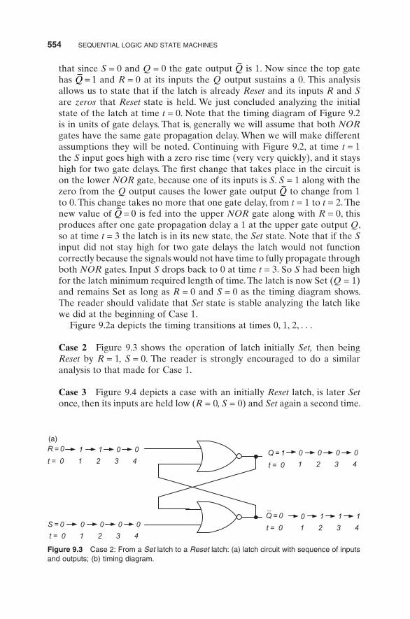
554 SEQUENTIAL LOGIC AND STATE MACHINES
that since S = 0 and Q = 0 the gate output Q is 1. Now since the top gate has Q = 1 and R = 0 at its inputs the Q output sustains a 0. This analysis allows us to state that if the latch is already Reset and its inputs R and S are zeros that Reset state is held. We just concluded analyzing the initial state of the latch at time t = 0. Note that the timing diagram of Figure 9.2 is in units of gate delays. That is, generally we will assume that both NOR gates have the same gate propagation delay. When we will make different assumptions they will be noted. Continuing with Figure 9.2, at time t = 1 the S input goes high with a zero rise time (very very quickly), and it stays high for two gate delays. The first change that takes place in the circuit is on the lower NOR gate, because one of its inputs is S. S = 1 along with the zero from the Q output causes the lower gate output Q to change from 1 to 0. This change takes no more that one gate delay, from t = 1 to t = 2. The new value of Q = 0 is fed into the upper NOR gate along with R = 0, this produces after one gate propagation delay a 1 at the upper gate output Q, so at time t = 3 the latch is in its new state, the Set state. Note that if the S input did not stay high for two gate delays the latch would not function correctly because the signals would not have time to fully propagate through both NOR gates. Input S drops back to 0 at time t = 3. So S had been high for the latch minimum required length of time. The latch is now Set (Q = 1) and remains Set as long as R = 0 and S = 0 as the timing diagram shows. The reader should validate that Set state is stable analyzing the latch like we did at the beginning of Case 1.
Figure 9.2a depicts the timing transitions at times 0, 1, 2, . . .
Case 2 Figure 9.3 shows the operation of latch initially Set, then being Reset by R = 1, S = 0. The reader is strongly encouraged to do a similar analysis to that made for Case 1.
Case 3 Figure 9.4 depicts a case with an initially Reset latch, is later Set once, then its inputs are held low (R = 0, S = 0) and Set again a second time.
Figure 9.3 Case 2: From a Set latch to a Reset latch: (a) latch circuit with sequence of inputs and outputs; (b) timing diagram.
S = 0
R = 0 Q = 1
Q = 0_
(a)
0
1
t = 0 1 2 3 4
1 0 0
0
t = 0 1 2 3 4
0 0 0
t = 0
1 2 3 4
1 1 1
0
1 2 3 4
0 0 0
t = 0

Figure 9.4 Case 3: From a Reset latch to a Set latch followed by one more Setting: (a) latch circuit with sequence of inputs and outputs; (b) timing diagram.
S = 0
R = 0Q= 0
Q= 1_
S
R
Q
Q_
1 2 3 4 5
0
0
0
t = 0 1 2 3 4
0 0 0
1
t = 0 1 2 3 4
1 0 0
t = 0
1 2 3 4
0 0 0
0
1 2 3 4
1 1 1
t = 0
6
5
0
1
5
51
5
0
(a)
(b)
time in gate propagation delays
Figure 9.3 (Continued )
(b)
S
R
Q
Q_
time in gate propagation delays
1 2 3 4 50

556 SEQUENTIAL LOGIC AND STATE MACHINES
The importance of this case is to show that an already Set latch when Set again, remains Set, no changes.
Case 4 Shows a misuse of the latch. When both inputs are one (S = 1, R = 1) the latch no longer has complementary outputs. But this is not as bad as what follows. Upon both inputs dropping back to 0 a race condition takes place. Figure 9.5b timing diagram expresses that with question marks along the horizontal axis starting at time t = 3. If both gates delays are identical it is not possible to determine the state of outputs Q and Q. Their state is undetermined. However, if one gate is faster than the other one, the faster gate will race and dominate the end state of the latch. Both of these cases are depicted by Figure 9.6, which assumes that the top gate (gate 1) is faster than gate 2, and Figure 9.7 which assumes that the bottom gate
Figure 9.5 Case 4: Nonallowed usage of the latch; both NOR gates have identical gate delays so that a final state is undetermined: (a) latch circuit; (b) timing diagram.
S = 0
R = 0Q= 0
Q= 1_
S
R
Q
Q_
1 2 3 4 5
0
1
0
t = 0 1 2 3 4
1 0 0
1
t = 0 1 2 3 4
1 0 0
t = 0
1 2 3 4
0 ? ?
0
1 2 3 4
0 ? ?
t = 0
6
5
0
0
5
5?
5
?
Undetermined
(a)
(b)
time in gate propagation delays
????????????????????????????????????
????????????????????????????????????

LATCHES AND FLIP-FLOPS (FF) 557
(gate 2) is faster than gate 1. In summary, Figures 9.5, 9.6 and 9.7 are all representations of Case 4, the nonallowed case.
Having worked on all of the above examples we are now ready to write the characteristic table of the SR-latch. Table 9.2 summarizes the latch behavior.
9.2.1 NAND-Implemented R S/ Latch
An SR-latch implemented with NAND gates turns out to be an SR-latch with low-true or active low inputs. S becomes active when driven low, else S is inactive. The same is true for R. R becomes active when driven low, and inac-tive when driven high. It is important and also interesting to notice that the noninverted Q output is the output of the NAND gate whose input is S. Unlike
Figure 9.6 Case 4: Nonallowed usage of the latch; top NOR gate is faster than bottom NOR gate: (a) latch circuit; (b) timing diagram.
S = 0
R = 0Q= 0
Q= 1_
S
R
Q
Q_
1 2 3 4 5
0
1
0
t = 0 1 2 3 4
1 0 0
1
t = 0 1 2 3 4
1 0 0
t = 0
1 2 3 4
0 0 0
0
1 2 3 4
0 1 1
t = 0
6
5
0
0
5
51
5
0
1
2
Gate 1 is faster than Gate 2
(a)
(b)
time in gate propagation delays

558 SEQUENTIAL LOGIC AND STATE MACHINES
Figure 9.7 Case 4: Nonallowed usage of the latch; bottom NOR gate is faster than top NOR gate: (a) latch circuit; (b) timing diagram.
S = 0
R = 0Q= 0
Q= 1_
S
R
Q
Q_
time in gate propagation delays1 2 3 4 5
0
1
0
t = 0 1 2 3 4
1 0 0
1
t = 0 1 2 3 4
1 0 0
t = 0
1 2 3 4
0 1 1
0
1 2 3 4
0 0 0
t = 0
6
5
0
0
5
50
5
1
1
2
Gate 2 is faster than Gate 1
(a)
(b)
Table 9.2 NOR-based SR-latch characteristic table
S R Q Q Description
0 0 Retains previously latched state of Q
Retains previously latched state of inverted Q
Holds the previously latched state
0 1 0 1 Reset1 0 1 0 Set1 1 0 0 Nonallowed condition. Outputs
are no longer complements of each other. A race condition occurs upon both inputs being negated.

LATCHES AND FLIP-FLOPS (FF) 559
the NOR-based SR-latch that has it Q output associated with the active high R input. Figure 9.8 shows the implementation of a NAND-based R S/ latch. Table 9.3 presents the characteristic table for a NAND-based latch.
Other than the differences observed on Table 9.3, the NAND-based latch is not different from the NOR-based latch. They both hold the previously latched state when both inputs are negated, they both can be in one of two possible states at any given time; the Q and Q loose their complementary nature upon both inputs being asserted at the same time. Finally, both latches exhibit a race condition when the inputs are negated immediately after being both asserted.
9.2.2 SR-Latch with Enable
We place an AND gate in front of every latch input and a clock pulse gates the flow of the S and R inputs to the latch. When the clock pulse is high the latch is a regular SR-latch, but when the clock pulse is low, the latch holds the previously latched state. Figure 9.9 depicts an SR-latch with enable.
Figure 9.8 NAND-based R S/ latch.
S (set input)
R (reset input)Q
Q
_
_
_
Table 9.3 Characteristic cable for the R S/ latch
S R Q Q Description
0 0 1 1 Nonallowed condition. Outputs are no longer complements of each other. A race condition occurs upon both inputs being negated.
0 1 1 0 Set1 0 0 1 Reset1 1 Retains previously
latched state of QRetains previously
latched state of inverted Q
Holds the previously latched state

560 SEQUENTIAL LOGIC AND STATE MACHINES
Figure 9.9 NOR-based SR-latch with clock pulse or enable.
Rinternal
Q
Q_
Sinternal
R
S
CP = Clock Pulse
Table 9.4 NOR-based SR-latch with clock pulse or enable, characteristic table
R S Clock Pulse Q Q
0 0 1 Previously latched Q Previously latched inverted Q0 1 1 1 01 0 1 0 11 1 1 Not-allowed Not-allowedX X 0 Previously latched Q Previously latched inverted Q
Table 9.4 shows the SR-latch with enable characteristic table. Note that we called the enable (E) is also called clock pulse (CP). The emphasis is on the fact that the enable is a level sensitive control line, unlike flip-flops, which we will cover in other sections of this chapter, are clock-edge sensitive devices.
The NAND-based version of the latest follows for reference. Figure 9.10 depicts the NAND-based latch. Table 9.5 contains the NAND-based latch characteristic table. Note that regardless of the clock pulse or enable control line, both latches implementations, either with NOR or NAND gates still have the nonallowed state that would lead to a race condition upon their inputs negating at the same time. One more time let us remember that the NOR-based latch has active high inputs (R, S) while the NAND-based latch has active low inputs (R S, ). However, when we add the two NAND gates to gate the R S, inputs into the NAND-based SR-latch, refer again to Figure 9.10, it is worth mentioning that the composite latch, which includes the gating NAND gates, acts as if it was an active high input device, whereas the internal NAND-based SR-latch is still an active low input device. Refer to the annotations for the internal R S, inputs (active low) and the external R,S inputs (active high) in Figure 9.10.
Whenever we want to refer to a latch with active high or active low inputs, with enable or without it, there are four new schematic symbols for them. Refer to Figure 9.11, which depicts the three types of latches that we have been discuss-ing. It is important to note that regardless of the internal implementation of

LATCHES AND FLIP-FLOPS (FF) 561
circuit presented by a schematic symbol, its inputs and its characteristic table govern its behavior.
9.2.3 Master/Slave SR-Flip-Flop
SR-latches are useful in control applications. Latches with and without clock pulse enable are still not very precise because their Q outputs will not settle to their stable state as long as the enable is active or as long as the inputs do not settle. What we would like to have are devices that respond to either a low-to-high or a high-to-low going edge of the clock pulse or enable. Such devices, which are clock-edge sensitive or master slave devices, change state at the active edge of their clock. The clock is no longer called enable, it is just the clock input. An enable has the connotation of level sensitivity, whereas clocks have the connotation of edge sensitivity.
Figure 9.10 NAND-based SR-latch with clock pulse or enable.
Rinternal
Q
Q
_
Sinternal
R
S
CP = Clock Pulse
Non-complemented output
_
_
External active high inputDeMorgan’s equivalents
DeMorgan’s equivalents
active low input
active low input
External active high input
Table 9.5 NOR-based SR-latch with clock pulse or enable characteristic table
R S Clock Pulse Q(t + 1) Q t( )+ 1
0 0 1 Previously latched Q(t) Previously latched Q t( )0 1 1 1 (Set) 01 0 1 0 (Reset) 11 1 1 1 (Not allowed) 1 (Not allowed)X X 0 Previously latched Q(t) Previously latched Q( )t

562 SEQUENTIAL LOGIC AND STATE MACHINES
One master/slave configuration can be implemented with two cascaded SR-latches. Figure 9.12 shows the interconnection of both latches. Negative and a positive edge triggered flip-flops with their respective schematic symbols are shown.
Note a few differences between the symbols for latches and for flip-flops. All positive edge-sensitive devices show their clock with a small triangular symbol adjacent to the clock input line inside the device symbol. Negative edge-sensitive devices show their clock with a small triangular symbol adjacent to the clock input line and within the device symbol. Additionally, a bubble (inverting circle) is drawn at the base of the triangular symbol, just outside the symbol perimeter. Since clocks are inputs to flip-flop, clocks are drawn on the left-hand side of the schematic symbol. Figure 9.12 c and d depict, respectively,
Figure 9.11 Latches schematics symbols: (a) SR-latch with active high inputs and no enable; (b) SR-latch with active low inputs and no enable; (c) SR-latch with active high inputs and an active high enable.
Q
Q_
S
R
Q
Q_
S
R
_
_
Q
Q_
S
R
CP
(a)
(b)
(c)

LATCHES AND FLIP-FLOPS (FF) 563
symbols of a negative edge triggered SR flip-flop and a positive edge triggered SR flip-flop.
Let us analyze how the SR flip-flop of Figure 9.12a operates. The first SR-latch is referred to as the master latch, while the right-hand side latch is the slave device. Note that both latches are simply active high inputs latches with
Figure 9.12 SR-latches forming an SR master/slave flip-flop: (a) negative edge triggered SR flip-flop; (b) positive edge triggered SR flip-flop; (c) negative edge triggered flip-flop symbol; (d) positive edge triggered flip-flop symbol.
(a)
(b)
(c) (d)

564 SEQUENTIAL LOGIC AND STATE MACHINES
active high enable input. The inverter in the clock line of the latches causes them to become enabled in a mutually exclusive fashion. When the left-hand side latch is enabled or open, the right-hand side one is disabled or latched, and vice versa. A latched SR-latch refers to the latch holding or preserving its output value due to its negated enable.* So let us present any of the three valid input combinations (i.e., R = S = 0, or R = 1, S = 0, or R = 0, S = 1) to the left-hand side latch. The rightmost latch will preserve or hold its outputs at
Figure 9.13 Positive and negative edge triggered SR flip-flop timing.
Qinternal
Qinternal
Q
Q_
time units (these are not gate delays)1 2 3 4 50 6
_
R
S
Clock
Masteropen
Slave closed
Masteropen
Slave closed
Masteropen
Slave closed
Masterclosed
Slave open
Masterclosed
Slave open
Masterclosed
Slave open
* A latch is said to be enabled when its outputs may change due to changes of its inputs. A latch is said to be disabled when its outputs are latched and will not change due to changes of its inputs.
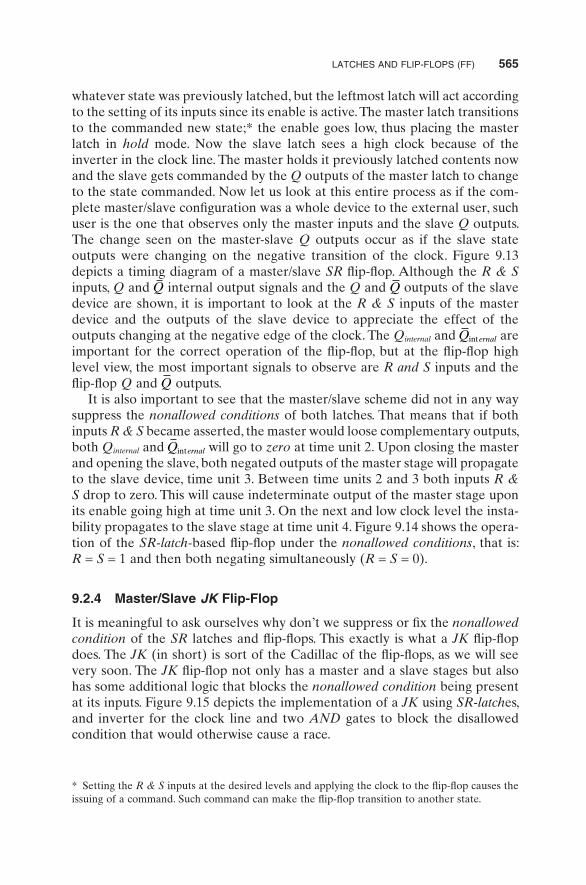
LATCHES AND FLIP-FLOPS (FF) 565
whatever state was previously latched, but the leftmost latch will act according to the setting of its inputs since its enable is active. The master latch transitions to the commanded new state;* the enable goes low, thus placing the master latch in hold mode. Now the slave latch sees a high clock because of the inverter in the clock line. The master holds it previously latched contents now and the slave gets commanded by the Q outputs of the master latch to change to the state commanded. Now let us look at this entire process as if the com-plete master/slave configuration was a whole device to the external user, such user is the one that observes only the master inputs and the slave Q outputs. The change seen on the master-slave Q outputs occur as if the slave state outputs were changing on the negative transition of the clock. Figure 9.13 depicts a timing diagram of a master/slave SR flip-flop. Although the R & S inputs, Q and Q internal output signals and the Q and Q outputs of the slave device are shown, it is important to look at the R & S inputs of the master device and the outputs of the slave device to appreciate the effect of the outputs changing at the negative edge of the clock. The Qinternal and Q ernalint are important for the correct operation of the flip-flop, but at the flip-flop high level view, the most important signals to observe are R and S inputs and the flip-flop Q and Q outputs.
It is also important to see that the master/slave scheme did not in any way suppress the nonallowed conditions of both latches. That means that if both inputs R & S became asserted, the master would loose complementary outputs, both Qinternal and Q ernalint will go to zero at time unit 2. Upon closing the master and opening the slave, both negated outputs of the master stage will propagate to the slave device, time unit 3. Between time units 2 and 3 both inputs R & S drop to zero. This will cause indeterminate output of the master stage upon its enable going high at time unit 3. On the next and low clock level the insta-bility propagates to the slave stage at time unit 4. Figure 9.14 shows the opera-tion of the SR-latch-based flip-flop under the nonallowed conditions, that is: R = S = 1 and then both negating simultaneously (R = S = 0).
9.2.4 Master/Slave JK Flip-Flop
It is meaningful to ask ourselves why don’t we suppress or fix the nonallowed condition of the SR latches and flip-flops. This exactly is what a JK flip-flop does. The JK (in short) is sort of the Cadillac of the flip-flops, as we will see very soon. The JK flip-flop not only has a master and a slave stages but also has some additional logic that blocks the nonallowed condition being present at its inputs. Figure 9.15 depicts the implementation of a JK using SR-latches, and inverter for the clock line and two AND gates to block the disallowed condition that would otherwise cause a race.
* Setting the R & S inputs at the desired levels and applying the clock to the flip-flop causes the issuing of a command. Such command can make the flip-flop transition to another state.

566 SEQUENTIAL LOGIC AND STATE MACHINES
Figure 9.14 SR flip-flop operating under nonallowed conditions.
1 2 3 4 50 6
Undeterminedstates
Qinternal
Qinternal
Q
Q_
_
time (ms)
R
S
Clock
note thatcomplementarynature ofQ output is lost
Masteropen
Slave closed
Masteropen
Slave closed
Masteropen
Slave closed
Masterclosed
Slave open
Masterclosed
Slave open
Masterclosed
Slave open
Let us inspect the JK and find out if it operates like the SR flip-flop at least under some input conditions. Assuming the JK is initially in the Set state and that its inputs J and K are zero, we know that the master latch should also be holding a Set state. Remember that a Set state means that Q = 1 and Q = 0. Notice the two AND gates, one fed by the Q output of the slave latch and the other AND fed by the Q output of the slave latch. Since we are assuming that both J & K are equal to 0 (this is our initial condition), the outputs of both AND gates produce zeros. These zeros feed the R and S inputs of the master stage latch. Thus, upon clocking this device as long as we want, while the JK inputs are negated, the flip-flop will preserve or hold the previously captured state. Such previous state in our example was the Set state. If we start the analysis all over again with just a minor change that the JK initial state is a

LATCHES AND FLIP-FLOPS (FF) 567
Reset we will arrive at the same conclusion. This means that our newly defined JK flip-flop holds the previous state for negated inputs J and K. This is so far no different than an SR flip-flop.
Assuming the JK flip-flop is again Set, if we bring the K input high and keep J low, note that the JK lower AND gate, is fed by a one from the Set state (or the Q output) and a 1 from the fact that K is high. Thus, the master stage SR latch sees the condition R = 1, S = 0, which after the clock allows to propagate the output of the master stage to the slave stage the JK flip-flop ends up in a Reset state. Similarly, if the JK is already Reset, clocking the condition R = 1, S = 0 will continue to Reset the JK, thus it stays Reset for as long as we keep clocking the flip-flop.
Now if we assume that out original JK flip-flop is either Set or Reset, input conditions are: R = 0, S = 1,the flip-flop will end up in a Set state for as long as we keep clocking the JK. So far the JK flip-flop behaves just like an SR flip-flop for the given conditions.
Now the JK becomes more interesting, assume an initially Set JK flip-flop and inputs J and K are both high, one more time following the logic of Figure 9.15a the one at the Q output of the slave stage along with K input that is one, produces a one at the output of the lower AND with inputs Q and K. Remem-ber that J is one and with its associated AND gate that receives a zero from the
Figure 9.15 Negative edge-triggered master/slave JK flip-flop: (a) flip-flop logic circuit; (b) schematics symbol.
Q
Q_
S
R
CP
Q
Q_
S
R
CP
J
K
Clock
Q
Q_
Qinternal
Qinternal_
J
K
Clock
(a)
(b)
Q
Q_
J
K

568 SEQUENTIAL LOGIC AND STATE MACHINES
Q output of the slave stage, thus it produces a zero at the S input of the master stage SR latch. In summary, the master latch sees R = 1 and S = 0. These condi-tions produce the master latch to Reset. This Reset state propagates to the slave stage so that after a complete clock, the JK flip-flop Q output goes from 1 to 0.
Now what happens if we clock the JK FF one more time, while both inputs J and K are still 1? Now since the Q output of the slave stage is 0, with K = 1 into the bottom AND gate produces a zero into the R input of the slave stage. However, since Q is 1 and J is 1, the top AND generates a 1 into the J input of the JK flip-flop. Upon such state of the inputs propagating through the master and slave stages, after one complete clock cycle, the Q output of the JK sets again. If we allow the clock to run indefinitely, the JK flip-flop Q output will toggle from 1 to 0 and from 0 to 1. Similarly, Q toggles from 0 to 1 and from 1 to 0. The above function of the JK just described does not preclude both inputs to the JK of being one.
Next we summarize the complete behavior of our negative edge triggered master/slave JK flip-flop. Table 9.6 summarizes the JK FF characteristic table.
Table 9.6 applies to negative clock edges. The same table applies to positive edge triggered JK flip-flop if under the Clock column we indicate an up-going arrow. The logic for a positive edge triggered JK and its schematics symbols are depicted in Figure 9.16.
The SR FF is very similar to the JK FF; the difference is that the SR does not support the simultaneous assertion of its R and S inputs. By inspection of the JK FF characteristic table, it is easy to see that only the last row of the JK would be equivalent to a nonallowed condition for the SR. We present the SR FF characteristic table in Table 9.7. Since generally we will be using positive edge triggered devices, the SR characteristic table is presented for rising clock edges.
9.2.5 Master/Slave T and D Type Flip-Flops
We will now study two more flip-flops and we will address them as particular cases of a JK. If we tie both inputs of a JK flip-flop together as shown in Figure 9.17a, the JK is renamed T for Toggle flip-flop and its schematic symbol can be found in Figure 9.17b. Table 9.8 lists the characteristic table of a T flip-flop.
Table 9.6 Negative edge triggered master/slave JK flip-flop characteristic table
Clock J K Q(t + 1)
↓ 0 0 Hold (no change)↓ 0 1 0 (Reset)↓ 1 0 1 (Set)↓ 1 1 Complement (toggle)0 X X Hold (no change)

LATCHES AND FLIP-FLOPS (FF) 569
The next and last flip-flop that we will cover is the D-type flip-flop or the Data flip-flop. The D-type flip-flop can be constructed by tying the JK inputs as depicted by Figure 9.17c; its schematic symbol is presented in Figure 9.17d.
The D-type flip-flop characteristic table is presented in Table 9.9.The D flip-flop is commonly used to store a bit of information. It is in
essence a 1-bit register. Remember that the SR latch studied earlier also stores one bit of information, but the latch is not a clocked device like the D flip-flop, the latch is referred to as an asynchronous device. Multi-bit registers are made with D flip-flops; a flip-flop per bit of storage is required. With the current
Figure 9.16 Positive edge-triggered master/slave JK: (a) Flip-flop logic circuit; (b) schematics symbol.
Q
Q_
S
R
CP
Q
Q_
S
R
CP
J
K
Clock
Q
Q_
Qinternal
Qinternal_
J
K
Clock
(a)
(b)
Q
Q_
J
K
Table 9.7 Positive edge triggered master/slave SR flip-flop characteristic table
Clock S R Q(t + 1) Comments
↑ 0 0 Q(t) Hold (no change)↑ 0 1 0 Reset↑ 1 0 1 Set↑ 1 1 Not-allowed Unpredictable0 X X Q(t) Hold (no change)

570 SEQUENTIAL LOGIC AND STATE MACHINES
Figure 9.17 (a) Positive edge triggered master slave T flip-flop circuit diagram; (b) schematic symbol; (c) positive edge triggered master slave D flip-flop circuit diagram; (d) schematic symbol.
D Q
Q_
J
K
T
Clock
Q
Q_
J
K
T Q
Q_
T
Clock
D Q
Q_
D
Clock
Clock
(a) (b)
(c) (d)
Table 9.8 T-flip-flop characteristic table
Clock T Q(t + 1) Comment
↑ 0 Q(t) Hold (no change)↑ 1 Q t( ) Complement (toggle)0 X Q(t) Hold (no change)
Table 9.9 D-flip-flop characteristic table
Clock D Q(t + 1) Comment
↑ 0 0 Reset↑ 1 1 Set0 X Q(t) Hold (no change)
state-of-the-art technology, the D-FF is the most widely used sequential device. Field programmable gate arrays (FPGAs), application specific integrated cir-cuits (ASICs), and programmable logic devices (PLDs) make use of the D-FF extensively. The D flip-flop is the most commonly used device. The other flip-flops (SR, T, and JK) were more heavily used when medium scale integration (MSI) circuits use was more prevalent. Those MSI ICs were the very popular 7400 series, manufactured by many different IC manufacturers for more than two decades.

TIMING CHARACTERISTICS OF SEQUENTIAL ELEMENTS 571
Those were the days when there were practically no FPGAs, ASICs, and PLDs. When these types of devices became available, they were not as widely used and their cost was high. That situation is practically reversed today.
9.3 TIMING CHARACTERISTICS OF SEQUENTIAL ELEMENTS
This section deals with the fundamental timing parameters that clocked sequential devices must meet in order to operate correctly. Given a flip-flop like an SR, JK, T, or a D-type, before an active edge of the clock, it is required that the inputs be stable before and after the active edge of the clock makes its active transition. A positive edge-triggered device active transition of its clock is a low-to-high clock transition. A negative edge-triggered device active transition of its clock is a high-to-low clock transition. The time required by the device inputs to be stable prior to the active transition of the clock is called the set-up time (tSU).
Additionally, the data inputs to the flip-flops are required to stay at the level that they were set up for a period of time immediately after the active edge of the clock. This time is referred to as the input data hold-time (tH). For example, if one wants to clock a high level into a D flip-flop, the high level must be stable before, during, and after the active edge of the clock by a total time given by tSU + tH. These two timing parameters insure that the delays and timing requirements of the master and slave stages within the flip-flops are met. When we studied SR-latches we learned that the minimum required delay for a single latch to produce a stable output is at least two-gate delays. To obtain some positive margin, the latch inputs should be stable some time longer than that minimum requirement. Luckily integrated circuit flip-flop manufacturers and ASIC manufacturers dictate the timing parameters required by their internal flip-flops. Another important timing parameter of a flip-flop is the clock-to-output propagation delay also called the clock-to-Q delay. Gen-erally speaking the clock-to-Q (tCQ) and the clock to Q- - (tCQ
) need not and they are usually not the same. Engineers calculating timing requirements usually pick the longest of both clock-to-output times. Figure 9.18 shows the set-up; hold time and clock-to-output parameters of a clocked device and how they are related to the active edge of the clock.
9.3.1 Timing of Flip-Flops with Additional Set and Reset Control Inputs
The four flip-flops that we studied (i.e., SR, JK, D, and T) may be available with two additional control inputs, Set and Reset. What is the purpose of these control inputs? Since flip-flops are used to design state machines, many times it is convenient to start or restart a flip-flop to a known state. Such state may be a Reset or a Set, depending on the application. Flip-flops available in inte-grated circuits are usually made with asynchronous reset and set control

572 SEQUENTIAL LOGIC AND STATE MACHINES
inputs. Other flip-flops are available with synchronous inputs. Asynchronous reset and set control inputs act on the state output of the flip-flop (the Q outputs) completely asynchronously with respect to the clock. We learned that flip-flops will only change state on or immediately after the active edge of the clock; and asynchronous control input will make the flip-flop change state virtually at any point between active clock edges. Synchronous set and reset inputs are like any other inputs of the flip-flop, like J or K inputs, they must meet the set-up and hold time requirements of the flip-flop and the flip-flop makes a transition to either the set or reset state on the next active clock edge. Figure 9.19 depicts a timing diagram of a flip-flop with asynchronous reset and one with synchronous reset. A flip-flop asynchronous reset or set input is required not to assert during an active clock transition, else possible timing malfunction may occur.
Note that in Figure 9.19a upon the assertion of the active high asynchronous reset, the Q output goes low virtually immediately or shortly after the Q output delay without waiting for the next active edge of the clock. This means
Figure 9.18 Flip-flop timing parameters.
Data inputs
tSU tH
Active clock edge
Window of required data stability
Clock
Data need not be stable Data need not be stable
Valid Present State Q(t) Valid Next State Q(t+1)Q and Q outputs_
tCOmin
COmaxt
Flip-flop R, S, D, T, J, or K
VT TV
VT
VT

TIMING CHARACTERISTICS OF SEQUENTIAL ELEMENTS 573
that the present state is abruptly interrupted and the reset is applied at the Q output. In Figure 9.19b upon the assertion of the active high synchronous reset, the Q output waits until the active edge of the clock arrives, and then the Q output gets reset then. Naturally there is also a clock-to-output delay before the Q output changes to the zero state. It is important to see that in the
Figure 9.19 Timing diagram showing (a) asynchronous reset and (b) synchronous reset.
Clock
Asynchronous Reset
Q output Q(t) Q(t+1)
Clock
Synchronous Reset
Q output Q(t) Q(t+1)
Asynchronous Reset aborts completion ofnext state prior to next active edge clock
Synchronous Reset allows completion of next state, then state after “next state” is Reset
Present state Next state
Present state Next state
(a)
(b)

574 SEQUENTIAL LOGIC AND STATE MACHINES
synchronous case the currently being executed state reaches completion and the reset state synchronously takes place on the subsequent active clock edge.
9.4 SIMPLE STATE MACHINES
Instead of defining what state machines are, we will present a simple example of a synchronous state machine; understand what it does, how it is described, and how it is designed. Later on we will make general statements as to what state machines are, but not without having gone over one simple but complete example.
Example 9.1 Define a 2-bit synchronous up binary counter with an asynchro-nous reset: (1) Write its state table and (2) state diagram. (3) Perform a logic implementation of the counter using positive edge-triggered JK flip-flops.
Solution to Example 9.1
A 2-bit synchronous up binary counter is a 2-bit state machine. Upon clocking the state machine the counter will go through states 00, 01, 10, 11, and it will repeat that sequence of four states indefinitely, as long as it continues to be clocked. Figure 9.20 shows the state machine state diagram, while Table 9.10 depicts the state table of the 2-bit counter. The purpose of the asynchronous reset is for external logic to reset the state machine upon power-up. If there was no reset the initial state of the state machine after power-up is unpredict-able; in other words with no reset initializing the flip-flop, one cannot predict which will be the starting state.
Note that the state machine Q1 state bit is the MSB and Q0 is the LSB. The state machine has an asynchronous input, its Reset which we can easily imple-ment using the asynchronous reset of the flip-flops to be used. Note that the state machine upon Reset being negated and receiving clocks it will walk through states 00, 01, 10, 11, 00, . . . indefinitely. If at any time Reset goes high the state machine will abruptly go to state 00. Notice that all state transitions are conditioned by the Reset input, the present state and upon the reception of a clock the machine will move to its next state. Unfortunately, the state diagram does not show in a clean way the fact that Reset is asynchronous. If the design requirements would have been to do the same design with a syn-chronous Reset, the state diagram would not change. Usually in state machine design Reset is one of the few or sometimes the only asynchronous control signal in the system. It is customary to synchronize asynchronous signals into the clock domain of the state machine that one is dealing with.
State machines in a general sense have two main parts, its sequential logic, that is the flip-flops that memorize the state Q(t). They also have their

SIMPLE STATE MACHINES 575
00
01
10
11
Reset = 1
Reset = 1
Reset
= 1
Res
et =
1
Reset =
0
Reset
= 0
Reset = 0
Reset = 0
State key: Q1 Q0
MSB LSB
Figure 9.20 2-bit synchronous up binary counter state diagram.
Table 9.10 State table for the 2-bit counter of Example 9.1
Clock
Present State Next State Async. Reset Input
Q1(t) Q0(t) Q1(t + 1) Q0(t + 1) (Active high) Reset
↑ 0 0 0 1 0↑ 0 1 1 0 0↑ 1 0 1 1 0↑ 1 1 0 0 00 X X 0 0 1
combinational logic, which is the logic used by the sequential portion of the machine to determine the inputs to the flip-flops that will generate the next state. Figure 9.21 depicts a high-level circuit diagram showing the state machine pieces. The block with the shape of a cloud represents combinational logic, or simply circuitry without memory. Note: having said that reset is needed to initialize the state of a machine, other methodologies are used to initialize state machines. One such method is designing scannable machines. All the state machine registers upon power on can be configured like a giant shift register and a known state is clocked in every flip-flop. Once all flip-flops are initialized

576 SEQUENTIAL LOGIC AND STATE MACHINES
the state machine is placed back in its normal operating mode and begins to run. For a good reference in scannable systems refer to [1].
By inspection of Figure 9.21 we can observe that the present state through the combinational logic produces the outputs for flip-flops 1 and 2 inputs. Reset as stated earlier is directly applied to the asynchronous reset input that we assume the JK flip-flops already have. So we need to come up with four logic equations, which are the equations of the flip-flop inputs as a function of the present state. The equations follow:
J Q Q1 1 0= f( ), (9.1)
K Q Q1 1 0= g( ), (9.2)
J Q Q0 1 0= h( ), (9.3)
K Q Q0 1 0= i( ), . (9.4)
With the present state information and the combinational logic the inputs to each flip-flop is presented so that upon the next active edge of the clock the state machine goes to its next state. So before doing the design we need a dif-ferent form of the JK flip-flop characteristic table that facilitates the design process. Such new table is the JK flip-flop excitation table. Actually, the excita-tion table presents the same information provided by the characteristic table but in the following form:
Figure 9.21 2-bit up synchronous counter logic diagram.
Clk
Q
Q_
J
K
Clk
Q
Q_
J
K
Reset
Reset
Q1
(MSB)
Q0
Clock
Asynchronous_Reset
FF-1
FF-0
J
J
K
K
1
1
0
0
Comb. logic
Q1
Q0
State bit
State bit
(LSB)

SIMPLE STATE MACHINES 577
“What do the FF inputs need to be to make a transition from a determined present state to a desired next state when the active clock edge is present?” Review Table 9.6 with the JK FF characteristic table. Using Table 9.6 we compose the excitation table for the JK FF. Table 9.11 depicts such excita-tion table.
It is important to emphasize that since the excitation table has a present state and a next state column without showing the clock explicitly, the same table applies to positive as well as to negative edge-triggered devices. Let us recall from the previous chapter that X refers to a don’t care condition, either a 1 or a 0.
State Machine Design Process Our 2-bit counter has four states and we are using two flip-flops to implement it. A circuit designed with n flip-flops can support a maximum number of 2n states; this is the case in our example: 2-bit machine and four states. At times some sequential circuit designs have less than 2n states. So we need to be careful about what we do if the state machine accidentally lands in one of those unused states. For the design process we will merge the state table of the desired state machine (Table 9.10) with the excita-tion table (Table 9.11) of the flip-flops to be used. We construct a new table that has present state, next state information, and the outputs of the combina-tional circuit of Figure 9.21; such outputs are the flip-flop inputs. The new table is the excitation table for the complete design and Table 9.12 shows it.
Table 9.11 JK FF excitation table
Present State Next State JK FF inputs
Q(t) Q(t + 1) J K
0 0 0 X0 1 1 X1 0 X 11 1 X 0
Table 9.12 Excitation table for the 2-bit counter design of Ex. 9.1 using JK FF
Inputs of Combinational Circuit
Next State
Outputs of Combinational Circuit
Present State Flip-Flop Inputs
Q1(t) Q0(t) Q1(t + 1) Q0(t + 1) J1 K1 J0 K0
0 0 0 1 0 X 1 X0 1 1 0 1 X X 11 0 1 1 X 0 1 X1 1 0 0 X 1 X 1

578 SEQUENTIAL LOGIC AND STATE MACHINES
Notice that the asynchronous Reset input was left out of the excitation table because it is directly hardwired to the asynchronous reset of the flops (Fig. 9.21).
The present and next state columns of Table 9.12 are identical to those of Table 9.10.
To fill in the columns for J1, K1, J0, and K0 of Table 9.12 we will proceed to work with FF-1 inputs first and FF-0 later. Let us ask ourselves what do inputs J1 and K1 need to be to go from a present state Q1(t) = 0 to next state Q1(t + 1) = 0. The answer to this is on Table 9.11 third line from the top, that is, J1 = 0 and K0 = X. So we proceed to fill in the first line under the J1 and K1 columns with 0 and X, respectively. For the next entry: what do inputs J1 and K1 need to be to go from a present state Q1(t) = 0 to next state Q1(t + 1) = 1. Again from Table 9.11 the answer is J1 = 1 and K1 = X. This is the next entry under columns for J1 and K1. We continue doing the same process until we are done with columns J1 and K1. We do the same for flip-flop 0 columns J0 and K0. Having completed Table 9.12 we look at it from a different perspective when we need to design the combinational logic that the state machine requires, refer one more time to Figure 9.21. Imagine that we remove from Table 9.12 the two columns that correspond to the next state bits Q1(t + 1) and Q0(t + 1). What is left of Table 9.12 should be seen as a combinational logic truth table. This table has four outputs: J1, K1, J0, and K0. These four outputs are Equations (9.1) through (9.4), which are functions of the present state bits Q1(t) and Q0(t). To solve the four logic equations we can do four K. maps, one per output. Figure 9.22 shows the K. maps.
The SOP simplifications from each output follow:
J Q1 0= (9.5)
K Q1 0= (9.6)
J0 1= (9.7)
K0 1= . (9.8)
Note that the SOP functions for J1 and K1 became independent of Q1. J0 and K0 end up being constants (Equations (9.7) and (9.8)). The actual circuit diagram for the complete state machine of Example 9.1 is redrawn with the actual logic found with Equations (9.5) through (9.8). Figure 9.23 shows the circuit.
9.4.1 SR Flip-Flop Excitation Table
To derive the excitation tables of the SR flip-flop we refer back to character-istic table provided by Table 9.7. This table is repeated below for the reader’s convenience.
Starting with the SR flip-flop, this device basically works like the JK flip-flop with the exception of the S = 1, R = 1 which is not allowed for the SR. Tables 9.13 and 9.14 show the SR FF characteristic and excitation tables, respectively.

SIMPLE STATE MACHINES 579
Figure 9.23 State machine for Example 9.1 logic implementation.
Clk
Q
Q_
J
K
Clk
Q
Q_
J
K
Reset
Reset
Q1
(MSB)
Q0
Clock
Asynchronous_Reset
FF-1
FF-0
J1
J
K1
K
0
0
Q0
Tied to Logic “1” (VDD) State bit
State bit
Figure 9.22 Karnaugh maps for outputs J1, K1, J0, and K0.
0
1
0 1
0 1
2 3
Q0
0
1
0 1
0 1
2 3
Q1
Q0
Q1
Q0
Q1
Q1
Q0
Q0
Q1
Q0
Q1
Q0
Q1
Q1
Q0
0
1
0 1
0 1
2 3
0
1
0 1
0 1
2 3
J1 K.Map K1 K.Map
J0 K.Map K0 K.Map
1
XX
X X
1
1
1
X
X
X
X
1
1

580 SEQUENTIAL LOGIC AND STATE MACHINES
Recall that to construct the excitation table of an SR FF we need to ask ourselves what do inputs S and R need to be prior to the active clock edge, to cause a transition from a given the present state to a desired next state? From Table 9.13, Row 1, states that S = 0 and R = 0 will do the job, because it holds the previous state. Also S = 0 and R = 1 (Table 9.13, Row 2) will do the same thing because this condition Resets the FF. Thus, S = 0 and R = X produces a transition from present state zero to next state zero; refer to Table 9.14, Row 1 for S = 0, R = X. It is easy to see that S = 1 and R = 0 (Table 9.13, Row 3) Sets the FF and that S = 0 and R = 1 (Table 9.13, Row 2) Resets the FF. Finally, having a present state of one to transition to a next state of one we either Set the FF (S = 1 and R = 0) or hold the previous state (S = 0 and R = 0); thus, S = X and R = 0; refer to Table 9.14, Row 4.
9.4.2 T Flip-Flop Excitation Table
In a similar fashion, to derive the T FF excitation table we start with the T FF characteristic table (Table 9.15).
Again we ask ourselves the question: “what does input T need to be prior to the active clock edge, to cause a transition from a given the present state to a desired next state?” We start constructing the T FF excitation Table 9.16. So using the T FF characteristic Table 9.15, we see that to obtain a zero present state to zero next state transition, the T input needs to be a zero (hold, no state
Table 9.13 SR FF characteristic table
Row Clock S R Q(t + 1)
1 ↑ 0 0 Hold last Q(t)2 ↑ 0 1 0 (Reset)3 ↑ 1 0 1(Set)4 ↑ 1 1 Not-allowed5 0 X X Hold last Q(t)
Table 9.14 SR FF excitation table
Row
Present State Next StateSR FF inputs
Q(t) Q(t + 1) S R
1 0 0 0 X2 0 1 1 03 1 0 0 14 1 1 X 0

SIMPLE STATE MACHINES 581
change). This gets written as a zero entry under Row 1 for T FF input column of Table 9.16. To fill in the T input for Rows 2 and 3 of Table 9.16, inspecting Table 9.15 we see that in both cases input T must be a one. Finally, for Table 9.15, Row 1, for the T FF not to change from present state 1 to next state 1, then T input needs to be a zero. This is shown on Table 9.16, Row 4 and under the T FF input column.
9.4.3 D Flip-Flop Excitation Table
Similar to the way we did with the SR and T excitation tables we create the D FF excitation table. Note that the D FF, which is the simplest one to under-stand, simply copies whatever the D input is, to the Q output upon the active edge of the clock.
Since we want an excitation table to cause the usual four-row present state to next state transitions, the D input needs to be whatever we want the next state to become. Tables 9.17 and 9.18 depict the characteristic and the excita-tion tables for a D FF.
Table 9.15 T-flip-flop characteristic table
Row Clock T Q(t + 1) Comment
1 ↑ 0 Q(t) Hold (no change)2 ↑ 1 Q t( ) Complement (toggle)3 0 X Q(t) Hold (no change)
Table 9.16 T FF excitation table
Row
Present State Next State T FF input
Q(t) Q(t + 1) T
1 0 0 02 0 1 13 1 0 14 1 1 0
Table 9.17 D Flip-flop characteristic table
Clock D Q(t + 1) Comment
↑ 0 0 Reset↑ 1 1 Set0 X Q(t) Hold (no change)

582 SEQUENTIAL LOGIC AND STATE MACHINES
Table 9.18 D FF excitation table
Row
Present State Next State D FF input
Q(t) Q(t + 1) D
1 0 0 02 0 1 13 1 0 04 1 1 1
Example 9.2 Let us now use the D flip-flop to implement a 2-bit up binary counter just like the one that we covered in Example 9.1. The counter will have an asynchronous reset input that upon being asserted it will force the counter to go to state Q1Q0 = 00. Implement the counter only with D flip-flops and the required next state combinational logic.
Clearly the state diagram for this counter is identical to the state diagram depicted in Figure 9.20. The logic implementation though is structurally similar to that of Figure 9.21, but the JK FF’s are replaced with D FF’s. Figure 9.24 depicts the circuit diagram of our counter to be implemented with D FF’s. The design of the state machine control logic is implemented generating the excita-tion table of the complete circuit using the D FF excitation tables and the state machine state diagram. Table 9.19 depicts Example 9.2 excitation table.
Proceeding to do the K. maps for D0 and D1 both as functions of present state bits: Q1(t) and Q0(t) we obtain the K. maps shown in Figure 9.25
Figure 9.24 2-bit binary up counter for Example 9.2.
Clk
Q
Q_
D
Clk
Q
Q_
D
Reset
Reset
Q1
(MSB)
Q0
Clock
Asynchronous_Reset
FF-1
FF-0
D
D
1
0
Comb. logic
Q1
Q0
State bit
State bit
(LSB)

SIMPLE STATE MACHINES 583
D f Q t Q t Q0 1 0 0= =[ ( ), ( )] (9.9)
D Q t Q t Q Q1 1 0 0 1= = ⊕g[ ( ), ( )] (9.10)
Equations (9.9) and (9.10) lead to the logic implementation presented in Figure 9.26.
Table 9.19 Excitation table for the 2-bit up counter design of Example 9.2 using D FF
Inputs of Combinational Circuit
Next State
Outputs of Combinational Logic
Present State Flip-flop inputs
Q1(t) Q0(t) Q1(t + 1) Q0(t + 1) D1 D0
0 0 0 1 0 10 1 1 0 1 01 0 1 1 1 11 1 0 0 0 0
Figure 9.25 K. maps for D FF inputs D0 and D1 as a function of the present state bits.
0
1
0 1
0 1
2 3
Q
Q0
1
Q1
Q0
0
1
0 1
0 1
2 3
Q
Q0
1
Q1
Q0
D K. Map 1D K. Map0
1
1
1
1
The previous examples dealt with a synchronous state machine that made state transitions in an unconditional fashion. Except for the asynchronous Reset input to the flip-flops, (and of course the clock) there were no other inputs to the state machine. Let us now consider slightly more complex state machines. Assume that we want to design a machine that makes state transitions upon being on a certain state and upon an input being one or zero. Such state transi-tions are referred to as conditional state transitions, because they depend on the state of an external state machine input in addition to the present state of the machine. Unconditional state transitions occur when the present to next state transition takes places irrespective of the level of the state machine external input. In a general sense, state machines can have a mix of conditional and unconditional state transitions or only one of the two kinds.

584 SEQUENTIAL LOGIC AND STATE MACHINES
Figure 9.26 Logic implementation of 2-bit up counter with D FFs.
Clk
Q
Q_
D
Clk
Q
Q_
D
Reset
Reset
Q1
(MSB)
Q0
Clock
Asynchronous_Reset
FF-1
FF-0
D
D
1
0
Q0
State bit
State bit
Q0
_
Q1
0Q_
Example 9.3 Given the state diagram of Figure 9.27, (a) find the state table of the circuit and (b) perform a logic implementation of the state machine using D FF. Assume that the external state machine input A is synchronous to the state machine clock. This concept has to do with state machine timing requirements, which will be discussed in another section within this chapter. So do not worry a whole lot of the previous sentence right away, we will get to it in greater detail.
Figure 9.27 state diagram exhibits two different types of state transitions: conditional as well as unconditional transitions. The state machine has two bits of state and a single external and clock-synchronized input A. State transitions from state 00 to 11 or 01 are conditional transitions. The state diagram should be read as follows for those transitions: If the present state is 00 and input A is high the next state is 01, else if present state is 00 and input A is low the next state is 11. All other transitions, that is, from state 01 to 00, 11 to 00 and 10 to 00, are unconditional state transitions. Let us make clear before the circuit is drawn that the state key is defined as Q1 Q0, where Q0 is the LSB of state. From the state diagram in Figure 9.27 we will construct the excitation table for the circuit to be designed. Note that the only conditional state transitions that exist are Rows 1 and 2 of Table 9.20; state transition from 00 to 11 occurs only upon input A being low. On Row 2 the state transition from 00 to 01 occurs on A being high. Rows 3 through 8 all show unconditional state transi-tions. For example, for the state transition 01 to 00 we can see in Rows 3 and 4 that take place regardless of whether A is low or high.

SIMPLE STATE MACHINES 585
Carefully inspecting excitation Table 9.20 we have to obtain combinational equations for the D FF inputs D1 and D0 as functions of the present state and the external state machine input A. So imagining that the next states columns are gone from Table 9.20 we use such table as a truth table to find out the simplified products of sum logic equations for the D FF inputs D0 and D1.
D1 1 0= f Q t Q t A[ ( ), ( ), ] (9.11)
D0 1 0= g Q t Q t A[ ( ), ( ), ]. (9.12)
We proceed creating the K. maps for each FF input, but note that for this example the K. maps are 3-variable maps which can be observed from Equa-tions (9.11) and (9.12).
From the K. maps of Figure 9.28 we obtain:
D Q Q A1 1 0= (9.13)
and
D Q Q0 1 0= . (9.14)
The logic implementation of our state machine using logic Equations (9.13) and (9.14) is depicted in Figure 9.29.
Figure 9.27 State diagram for Example 9.3.
00
11
10
01
A=1A=0
State key: Q1 Q0

586 SEQUENTIAL LOGIC AND STATE MACHINES
Table 9.20 Excitation table for the state machine design of Ex. 9.3 using D FF
Row
Combinational Circuit Inputs
Next State
Combinational Circuit Outputs
Present StateExternal
Input Flip-Flop
Inputs
Q1(t) Q0(t) A Q1(t + 1) Q0(t + 1) D1 D0
1 0 0 0 1 1 1 12 0 0 1 0 1 0 13 0 1 0 0 0 0 04 0 1 1 0 0 0 05 1 0 0 0 0 0 06 1 0 1 0 0 0 07 1 1 0 0 0 0 08 1 1 1 0 0 0 0
Figure 9.28 Karnaugh maps for Example 9.3.
00 01 11 10
0
1
Q
A
0 1 3 2
4 5 7 6
1
Q
Q
00 01 11 10
0
1
Q A
0 1 3 2
4 5 7 6
1 1
1
1
K. map for D1
K. map for D0
0A
Q0
AQ1
0
Q0
Q1

SIMPLE STATE MACHINES 587
Example 9.4 Design a 3-bit down binary counter. Design an output called MIN-COUNT that detects when state 0 (000) is reached. The output must be a function of the state bits. Use D FFs. (1) generate the state diagram of the counter, (2) generate the circuit excitation table, (3) find the logic for output MIN-COUNT and (4) find the complete logic for the counter state machine. We will move a little faster throughout this example, since most of the concepts have already been explored in previous examples. Refer to Figure 9.30 for the state machine state diagram.
The excitation table (Table 9.21) follows from the state diagram. The state diagram of our down counter has unconditional state transitions. This means that no external input to the counter exists to prevent or allow any of the state transitions. The output logic has to detect state 000; this output must remain asserted during the time the counter is at state 000. Once the counter is in any other state, the output has to be negated. Thus, the logic for the MIN-COUNT output is a three input AND gate that receives inverted state bits: Q2(t), Q1(t), and Q0(t). By DeMorgan’s rule such gate is a three-input NOR gate.
Now to design the state machine we use excitation Table 9.21 come up with the excitation functions or the input equations of each state flip-flop: D2, D1, and D0 as a function of the three state bits Q2(t), Q1(t), and Q0(t). Proceeding as we did before, we need to produce three 3-variable Karnaugh maps to obtain a simplified SOP expression for each FF input.
From Figure 9.31 we obtain a simplified SOP forms for D2, D1, and D0:
Figure 9.29 Logic implementation of state machine for Example 9.3.
Clk
Q
Q_
D
Clk
Q
Q_
D
Q0
(MSB)Q1
Clock
FF-0
FF-1
D
D
0
1
Q1
State bit
State bit
Q1
_
Q0
1Q_
Q0
_
__
A_
Q0
_
A

588 SEQUENTIAL LOGIC AND STATE MACHINES
Table 9.21 Excitation table for the down counter of Example 9.4
Present State Output Next StateD Flip-Flop
Inputs
Q2(t) Q1(t) Q0(t) MIN-COUNT Q2(t + 1) Q0(t + 1) Q0(t + 1) D2 D1 D0
0 0 0 1 1 1 1 1 1 10 0 1 0 0 0 0 0 0 00 1 0 0 0 0 1 0 0 10 1 1 0 0 1 0 0 1 01 0 0 0 0 1 1 0 1 11 0 1 0 1 0 0 1 0 01 1 0 0 1 0 1 1 0 11 1 1 0 1 1 0 1 1 0
Figure 9.30 State diagram of 3-bit down counter for Example 9.4.
111
110
101
100
000
001
010
011
/ MIN-COUNT=1 / MIN-COUNT=0
/ MIN-COUNT=0
/ MIN-COUNT=0
/ MIN-COUNT=0/ MIN-COUNT=0
/ MIN-COUNT=0
/ MIN-COUNT=0
State Key: Q Q Q2 1 0

SIMPLE STATE MACHINES 589
Figure 9.31 Karnaugh maps for FF next state equations for Example 9.4: (a) D2 map; (b) D1 map; (c) D0 map.
00 01 11 10
0
1
Q
Q
0 1 3 2
4 5 7 6
1 Q2
K. map for D2
Q 0QQ2
1
10
00 01 11 10
0
1
Q
Q
0 1 3 2
4 5 7 6
1
Q2
K. map for D1
Q 0QQ2
1
10
00 01 11 10
0
1
Q
Q
0 1 3 2
4 5 7 6
1
Q2
K. map for D0
Q 0QQ2
1
10
1
1
1 1
1
1
1
1 1
(a)
(b)
(c)

590 SEQUENTIAL LOGIC AND STATE MACHINES
D Q Q Q Q Q Q Q2 2 1 0 2 1 2 0= + + (9.15)
D Q Q Q Q Q Q1 1 0 1 0 1 0= + = ⊕ (9.16)
D Q0 0= . (9.17)
Figure 9.32 depicts the implemented state machine of Example 9.4 with next state Equations (9.15), (9.16), and (9.17).
Figure 9.32 Implementation of state machine for Example 9.4.
Clk
Q
Q_
D
Clk
Q
Q_
D
Q2
(MSB)
Q1
Clock
FF-2
FF-1
D
D
2
1
Q2
State bit
Q1
_
Q0
Q2
_
_
Clk
Q
Q_
DQ0
FF-0
Q0
_
Q1
_
Q_
2
Q0
Q2
Q1
Q1
Q0
MIN_COUNTQ1
Q0
Q2
Example 9.5 A shift register: An n-bit shift register is an n-bit register that makes provision of shifting its stored data by one bit position at every active clock edge. It is possible to design shift registers that shift bits to the right or that can shift bits to the left. More elaborate shift registers can be designed to

SIMPLE STATE MACHINES 591
shift left or right upon asserting a shift direction control input. In this example we will address a 4-bit shift register that shifts data from its LSB one bit posi-tion to the left to a more significant bit. The LSB will get loaded with a zero. For example, given the 4-bit binary number 1010, shifting it left by one bit position leads to 0100; another shift left will produce 1000; another shift left produces 0000. Figure 9.33 depicts the left shifting of the example just described.
Shift registers are used in arithmetic and control type operations. Multipli-cation and division algorithms use shift registers. Control applications can use
Figure 9.33 Left shifting a four-bit number, loading the LSB with a zero: (a) left-shift operation; (b) four-bit shift register with D FF.
QD QD
(MSB)
Clock
D
QD Q Q0Q1Q2
Q0
D
FF-1FF-2FF-3 FF-0_
Q1
_Q2
_
Q3
Q3
_
Q_
Q_
Q_
Q_
Direction of data transfer
1 10 0
10 0
1 00 0
0
0 00 0
Initial data
Data after third left-shift
Data after second left-shift
Data after first left-shift
“0”
“0”
“0”
“0”
“0”
(a)
(b)

592 SEQUENTIAL LOGIC AND STATE MACHINES
9.5 SYNCHRONOUS STATE MACHINES GENERAL CONSIDERATIONS
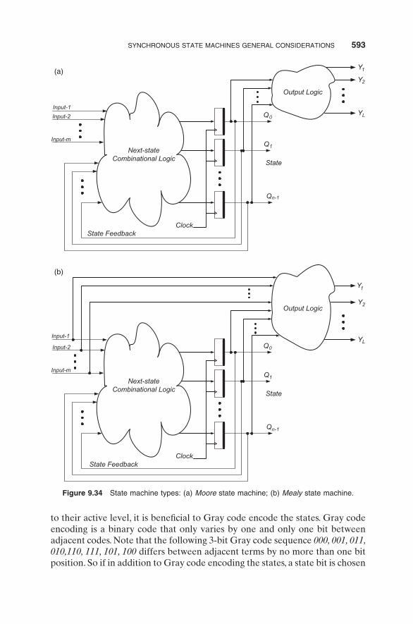
State machines consist of three fundamental pieces of logic. The flip-flops, which serve as the memory elements, store state information. The next state logic is the logic that receives state information and external state machine inputs if any. The third and last piece is the logic that generates the machine outputs. The next state logic produces the correct signals to the flip-flops, so that the transition to the desired next state occurs. Figure 9.34a,b depict the two most important state machine architectures, the Moore and the Mealy state machines. Referring to Figure 9.34a we see a Moore machine block diagram. This machine has next state logic and flip-flops, which does not differ much from a Mealy (Fig. 9.34b) state machine. The fundamental difference between the Moore and Mealy is the way in which both state machines produce the control outputs. Moore machines produce their outputs with combina-tional logic that is only function of the present state bits. Mealy state machines produce their control outputs with combinational logic that is a function not only of the present state bits but also the external inputs to the state machine.
This implies that the control outputs not only may change when the state is updated but also when the any of the state machine external inputs change. Note that it is customary in computer architecture literature to indicate clocked elements with memory (i.e., flip-flops) with a heavy trace where their Q outputs are. Sometimes when the heavy trace is shown the clock does not need to be explicitly drawn, as we did in Figure 9.34.
9.5.1 Synchronous State Machine Design Guidelines
The single most important step of designing a state machine is the complete, accurate and concise description of the problem that needs to be solved. This is in essence producing a specification. Now we need to translate such descrip-tion into a state diagram. Determine the external state machines inputs and the control outputs. We also need to determine the number of states needed, try to minimize them if possible. Choose the flip-flops type to be used. Do the state assignments. There are three basic ways of making state assignments. The simplest one is to do binary state assignments, usually takes the smallest number of flip-flops but with more next state combinational logic. If we know that some state machine outputs need to be glitch free during their transition
shift registers. Other uses of shift registers include serial-to-parallel and parallel-to-serial data conversion for data communication applications. Advanced central processing units (CPUs) use shift registers in conjunction with multiplexers to implement barrel shifters. Barrel shifters allow a CPU to perform shifts either left or right by any amount of desired bits, such that the amount of bits is within the width of the CPU registers, in a single clock cycle.
SYNCHRONOUS STATE MACHINES GENERAL CONSIDERATIONS 593
Figure 9.34 State machine types: (a) Moore state machine; (b) Mealy state machine.
State Feedback
Y
Input-1
Input-2
Input-m
Q0
1Q
Qn-1
Next-stateCombinational Logic
State
Clock
Output Logic
1
Y
Y
2
L
Input-1
Input-2
Input-m
Q0
1Q
Qn-1
Next-stateCombinational Logic
State
Clock
Output Logic
1
Y
Y
2
L
Y
State Feedback
(a)
(b)
to their active level, it is beneficial to Gray code encode the states. Gray code encoding is a binary code that only varies by one and only one bit between adjacent codes. Note that the following 3-bit Gray code sequence 000, 001, 011, 010,110, 111, 101, 100 differs between adjacent terms by no more than one bit position. So if in addition to Gray code encoding the states, a state bit is chosen

594 SEQUENTIAL LOGIC AND STATE MACHINES
to be a needed state machine output, then such output will be glitch-free. For example, if one of our state machine outputs is a WRITE signal, we definitely want this signal not to glitch, ever. State one-hot encoding is another technique that uses a flip-flop per state. Although this scheme uses more flip-flops that it would require if we binary encoded the states, it has the advantage that it is very simple to design and debug. Usually when designing state machines FPGAs using a few more flip-flops is not a problem when compared to the benefits that it provides. Care must be exercised upon resetting the state machine to a desired initial state. We create the excitation table of the state machine. That means to construct a table that shows the required excitation (flip-flop inputs) to obtain the desired next state for state/ input combination. This leads to the design of the next state logic. Finally, we decide how we want the outputs to be generated. Do we want a Moore machine, where the outputs are strictly functions of the state bits? Alternatively, do we need a Mealy machine, where the outputs depend not only on the state bits but also on the state machine inputs? Finally, we draw a complete schematics or logic diagram of the design. The above steps assume a fairly manual procedure to design state machine. These days CAD tools such as hardware description languages (HDL), Verilog and VHDL being the two most popular ones, allow a designer to design and simulate the behavior of the state machine before it is actually implemented with logic gates. HDLs are beyond the scope of this book. Refer-ences to HDLs are cited in the Further Reading section of this chapter.
In summary, we can list the basic steps required to design synchronous state machines.
(a) Produce a complete and succinct state machine specification.(b) Determine number of states needed, state machine inputs and outputs.(c) Produce a state diagram and state assignments.(d) Optionally minimize the number of states.(e) If any unused states are present in the state machine designed, ensure
that if for some undesired reason the state machine got into one or more of such states, that it finds a graceful way to continue operating, to recover or to stop.
(f) Choose the flip-flop type to be used.(g) Produce the circuit excitation table.(h) Design the next state logic using the excitation table.(i) Design the output logic.(j) All or some of the steps above will have to be repeated and refined
until you reach at a satisfactory solution that meets the requirements.
It is important to keep in mind that there are three major factors that are present in any practical design that is done with the purpose of becoming a large volume product. From an engineering point of view the natural factor is

SYNCHRONOUS STATE MACHINES GENERAL CONSIDERATIONS 595
quality. Quality is associated with the idea that the machine works, reliably and consistently. The other two factors are that the project has to meet a given schedule and meet its cost targets. In essence quality, cost, and schedule are practically inseparable factors that at one point or another throughout the design cycle, will force engineering to make tradeoffs to meet the overall goals.
9.5.2 Timing Considerations: Long and Short Path Analyses
Synchronous state machines need to operate at some intended clock fre-quency. But this is not all; most importantly, every clocked device has its own set-up and hold time requirements that need to be met at all times. Given a simple synchronous state machine such as the one in Figure 9.35, the timing path between to consecutive clock edges is:
t t t TCOmax PDmax SUmin CLKmin+ + ≤ (9.18)
Figure 9.35 Long path analysis of a simple state machine.
Q
Q_
DQ0
D-FF-0
Q0
_
Q
Q_
DQ1
D-FF-1
Q1
_
CombinationalLogic A
tPDA
tPDB
Clock
CombinationalLogic B
Path 0
Path 1
D1
D0

596 SEQUENTIAL LOGIC AND STATE MACHINES
where tCOmax is the flip-flop maximum clock-to-output delay, tPDmax is the com-binational logic maximum propagation delay, tSUmin is the minimum required set-up time that the manufacturers specifies for its flip-flop, and TCLKmin is the minimum required clock period to allow the required minimum set-up time to the flip-flop. Equation (9.18) has to be met individually for every one of the timing paths that exist in the circuit designed.
In particular and referring to the two-path state machine of Figure 9.35, Equation (9.18) can be written for each one of the long paths. One path, Path 0, shown with very heavy lines, begins at the Q0 output of DFF-0, continues to the input of combinational logic B, the output of logic B ends at the D1 input of DFF-1.The second long path, Path 1, is drawn with standard weight lines, begins at the Q1 output of DFF-1, continues through combinational logic A, and ends at the D0 input of DFF-0. Rewriting Equation (9.18) for path 0 which starts at the Q0 output of DFF-0 and ends at the D1 input of DFF-1, we obtain.
t t t TCO max PDBmax SU min CLKmin0 1+ + ≤ . (9.19)
For the other path, beginning at the Q1 output of DFF-1 and ending at the D0 input of DFF-0, we have:
t t t TCO max PDAmax SU min CLKmin1 + + ≤0 . (9.20)
In Equation (9.19) tCO0max is the maximum or longest clock-to-output delay of FF0, tPDBmax is the maximum propagation delay of combinational logic B and tSU1min is the minimum required set-up time needed by FF1, which is the des-tination flip-flop of this path. Similarly, in Equation (9.20) tCO1max is the maximum or longest clock-to-output delay of FF1, tPDAmax is the maximum propagation delay of combinational logic A and tSU0min is the minimum required set-up time needed by FF0, which is the destination flip-flop of this path. Note that in order to meet set-up time requirements both long paths must be strictly less than TCLKmin. The state machine uses the same clock (at least from a logical standpoint) ; whichever path is the longest is the one that determines the maximum frequency of operation. This example ignores wire delays, transmis-sion lines effects, clock skews, and signal integrity issues.
When a state machine path, such as the one given by Equations (9.19) or (9.20) is not met, we refer to this as being a long path (also referred to as the critical path of the state machine). Excessive long paths cause set-up time viola-tions. Set-up and/or hold time violations of a flip-flop cause the device to temporarily go into an undefined or metastable state. Looking at Equation (9.18) it is clear to see that given a TCLKmin is equivalent to specifying a maximum operating frequency. So once TCLKmin is fixed, the three left-hand side terms in Equation (9.18) need to be such that their sum is strictly less than TCLKmin. When tCOmax + tPDmax + tSUmin equals TCLKmin, the set-up time of the flip-flop is just marginally met. In practice we want to have a small but positive

SYNCHRONOUS STATE MACHINES GENERAL CONSIDERATIONS 597
Figure 9.36 Short path analysis of a simple state machine.
margin to account for other factors such as noise, ground bounce and other electrical effects not accounted for by Equation (9.18). Long path analysis or set-up time calculations are an edge-to-edge phenomenon. In practical designs usually the term that can be significantly reduced in order to meet set-up time is the combinational logic propagation delay (tDmax). The reason is that once a family or type of flip-flop is selected for the design, the state machine designer has little or no control over tCO and tSU since these are flip-flop timing param-eters. On the other hand, when every effort was made to meet Equation (9.18) either by reducing tPdmax or by changing flip-flops for faster ones (with smaller tCOmax and tSUmin), there is still a possibility of rearranging the circuit logic and topology. Shall this last attempt fail to meet Equation (9.18), there is no more option other than reducing the operating frequency of the state machine. Stretching out the clock cycle of the state machine is the last and least desir-able mean to implement, when the machine violates set-up time.
We have not mentioned anything about hold time requirements yet. Hold time analysis is also referred to as short path analysis. Let us consider the simple circuit of Figure 9.36.
The circuit of Figure 9.36 is a synchronous divide-by-two counter. Let us look into the hold time requirements by its flip-flop. Since the complemented Q output is tied back into the D input at the time an active clock edge occurs the data present at the D input has to be held constant or stable not just before the clock edge but also immediately after the clock edge. So we then write this requirement as:
t tCOmin Hmin≥ . (9.21)
At first Equation (9.21) seems a bit awkward to understand. One of the reasons is that neither the clock period nor the set-up time show up in Equa-tion (9.21). Since the data into the flip-flop is provided by its complemented Q output, fed directly with a zero delay wire, it is under the control of how fast is the clock-to-inverted-Q-output delay. This also determines how long the current data at the D input stays around (hold time requirement) imme-diately after the clock edge. So that is the reason why it is important that the

598 SEQUENTIAL LOGIC AND STATE MACHINES
Example 9.6 Given the simple state machine of Figure 9.36 assume the fol-lowing flip-flop parameters are: tCOmin = 1 ns tCOmax = 5 ns, tSUmin = 3 ns and tHmin = 1.5 ns.
(a) Determine doing long path analysis, the highest frequency at which the flip-flop can be clocked reliably. Assume that zero timing margin on set-up is acceptable.
(b) Doing short path analysis, determine if there are any hold time viola-tions. Assume that zero margin on hold time is acceptable.
Solution to Example 9.6
(a) For long path analysis for the circuit of Figure 9.36 we have that:
t t t TCOmax PDmax SUmin CLKmin+ + ≤ (9.23)
where tCOmax = 5 ns, tPDmax = 0 ns and we assume that the wire has zero delay and tSUmin = 3 ns. We rewrite Equation (9.23) using the numerical values and it becomes:
5 3+ + ≤0 tCLKmin. (9.24)
Thus tCLKmin = 8 ns, which corresponds to a frequency of 125 MHz.(b) Doing short path analysis and not to have a hold time violation the
following is required:
t tCOmin Hmin≥ (9.25)
where tCOmin = 1 ns and tHmin = 1.5 ns.
Clearly Equation (9.25) cannot be met with the values given so the circuit has a hold time violation. Note that regardless of the clock frequency you cannot
clock-to-output minimum delay be larger than the hold time required by the flip-flop. Shall the flip-flop be too fast, that is, tCOmin < tH, a hold time violation takes place. Analyzing hold time violations or the lack of them is referred to as short path analysis. Just like in the set-up case, for hold time requirements Equation (9.21) wants the inequality to be “greater than or equal”. When tCOmin equals tH the flip-flop just barely meets hold time requirements. It is practically desirable for Equation (9.21) to exceed the hold time required by the flip-flop. In other words:
t tCOmin H+ =positive-margin . (9.22)

SUMMARY 599
fix the hold time violation. In ASIC design what engineers do is place a buffer between the D input and the Q output with a propagation delay of at least 0.5 ns, for this particular example just to comply with the hold time required by the flip-flop. However, care must be exercised because helping the hardware meet hold time, degrades or takes away timing margin out of the set-up time. Now Equation (9.23) no longer has a 0 ns tPDmax term and it becomes 0.5 ns, and that reduces the maximum frequency of operation from 125 MHz down to 117.6 MHz (tCLK = 8.5 ns).
9.6 SUMMARY
This chapter covers sequential devices or devices with memory. Latches and flip-flops are the fundamental memory elements with which to build state machines. It is important to distinguish the latch from a flip-flop. Generally, a latch is basically an asynchronous device, it typically does not have a clock and is not sensitive to a clock edge. A flip-flop typically is referred to as a master/slave clock edge sensitive device. When in doubt, the reader should read the context carefully to determine which type of device the author is referring to. State machines are logic circuits that have combinational logic, that is, gates without feedback, plus sequential logic, or devices built using combinational logic with feedback. Remember that the basic latch was built with 2- NOR gates (alternatively with 2 NAND gates) with feedback in a cross-coupled configuration. Synchronous state machine are circuits whose flip-flops get clocked at the same time. State machines have state bits, and their next state upon applying the subsequent clock edge depends not only on the present state but also on the machine external inputs. We generally described two basic synchronous state machines, the Moore and the Mealy types. The basic difference between them is that the Mealy state machine produces outputs that are function of the state and external inputs. The Moore state machine produces outputs, which are only functions of the state. We designed state machine deriving excitation tables for the circuits, using any flip-flop type we really prefer to use. The D flip-flop is the predominant type used in programmable logic and ASICs. A general section on how to design state machines was provided. Such design emphasizes the state assignment an encoding types available: binary, Gray code and one-hot. Finally designers try to stay away from total asynchronous designs for reasons of design difficulty and not being easy to test. Generally designs are quasi-synchronous. Each state machine has its own clock domain; however, both of them need to inter-face to each other. Timing analysis can be broken down in two major pieces: long-path and short-path timing analyses. It is a requirement that every path in a circuit has to comply with both to have a timing error-free (or metastability-free) design.

600 SEQUENTIAL LOGIC AND STATE MACHINES
Table 9.22 State table for Problems 9.2 through 9.5
Clock Input A Present State Next State
↑ 1 00 10↑ 0 00 01↑ X 01 10↑ 0 10 11↑ 1 10 00↑ 1 11 10↑ 0 11 01
FURTHER READING
1. Parag K. Lala, Fault Tolerant and Fault Testable Hardware Design, Prentice Hall International, London, 1985.
2. Frederick J. Hill and Gerald R. Peterson, Digital Systems Hardware Organization and Design, 3rd ed., John Wiley and Sons, New York, 1981.
3. David J. Comer, Digital Logic and State Machine Design, 3rd ed., Oxford University Press, New York, 1995.
4. Donald E. Thomas and Philip R. Moorby, The Verilog Description Language, 4th ed., Kluwer Academic Publishers, Norwell, MA, 1998.
PROBLEMS
9.1 Draw the circuit of a master-slave JK flip-flop entirely with NAND gates.
9.2 Implement the state machine whose state table is shown in Table 9.22 with JK flip-flops and combinational gates. Draw the circuit schematics.
9.3 Implement the state machine whose state table is shown in Table 9.22 with two D-type flip-flops and logic gates. Draw the circuit schematics.
9.4 Implement the state machine whose state table is shown in Table 9.22 with a ROM of the smallest possible size; and using D-type flip-flops. Draw the circuit schematics.
9.5 Implement the state machine whose state table is shown in Table 9.22 with 1-of-8 muxes and D-type flip-flops. Draw the circuit schematics.
9.6 For the state machine of Figure 9.37 derive a complete state table. Note that the state machine has 2 bits of state and two external inputs: A and B. Draw the circuit schematics.
9.7 Design the state machine, whose state diagram is shown by Figure 9.37 using 2 JK flip-flops and some minimal number of logic gates. Draw the circuit schematics.

Figure 9.38 State diagram for Problem 9.12.
0000
0001
0010
0100 1100
1111
1110
1011
0101
0110
0111 1000
1001
1101
0011
1010
X_
X
X
X_
X_
X
X
X_
XX_
X X_
X
X_
X_
X
Figure 9.37 State diagram for Problems 9.6 through 9.10.
00
0111
10
A B
A B
A B
A B
_
_ _
_
A_
A
A B_
A B_ _
A B_
A B

602 SEQUENTIAL LOGIC AND STATE MACHINES
9.8 Design the state machine of Figure 9.37 using 2 T-type flip-flops and some minimal number of logic gates. Draw the circuit schematics.
9.9 Design the state machine of Figure 9.37 using 2 D-type flip-flops and some minimal number of logic gates. Draw the circuit schematics.
9.10 Design the state machine of Figure 9.37 using the smallest size ROM and two D-type flip-flops. Draw the circuit schematics.
9.11 Design a 3-bit decrementing binary counter. Write the state table of the to-be-designed counter. Draw the circuit schematics.
9.12 Design a state machine that whose state diagram is given by Figure 9.38. (a) Do an implementation using the smallest possible ROM and the smallest possible number of D-type flip-flops. (b) Write a table with the micro-code for the ROM. Assume that input X is already synchronized to the state machine clock. Draw the circuit schematics.