Semiconductor-based heterostructure formation using low energy ion beams: Ion beam deposition (IBD)...
33
Semiconductorbased heterostructure formation using low energy ion beams: Ion beam deposition (IBD) & combined ion and molecular beam deposition (CIMD) N. Herbots, O. C. Hellman, P. A. Cullen, and O. Vancauwenberghe Citation: AIP Conference Proceedings 167, 259 (1988); doi: 10.1063/1.37156 View online: http://dx.doi.org/10.1063/1.37156 View Table of Contents: http://scitation.aip.org/content/aip/proceeding/aipcp/167?ver=pdfcov Published by the AIP Publishing Articles you may be interested in Effect of ion sputtering on Ge epitaxy on GaAs(110) Appl. Phys. Lett. 68, 1660 (1996); 10.1063/1.115897 The effects of secondary particle bombardment on ion beam sputtered thin films of Y1Ba2Cu3O x deposited on MgO (100) AIP Conf. Proc. 200, 102 (1990); 10.1063/1.39062 Ion beam sputter deposition of YBa2Cu3O7: Beam induced target changes and their effect on deposited film composition AIP Conf. Proc. 200, 95 (1990); 10.1063/1.39034 Studies on ion scattering and sputtering processes in ion beam sputterdeposition of high Tc superconducting films: The optimization of deposition parameters AIP Conf. Proc. 200, 79 (1990); 10.1063/1.39032 Negative ion effects during magnetron and ion beam sputtering of YBa2Cu3Ox AIP Conf. Proc. 165, 106 (1988); 10.1063/1.37097 This article is copyrighted as indicated in the article. Reuse of AIP content is subject to the terms at: http://scitation.aip.org/termsconditions. Downloaded to IP: 129.219.247.33 On: Mon, 29 Sep 2014 17:22:12
Transcript of Semiconductor-based heterostructure formation using low energy ion beams: Ion beam deposition (IBD)...
Semiconductorbased heterostructure formation using low
energy ion beams: Ion beam deposition (IBD) & combined ion
and molecular beam deposition (CIMD)
N. Herbots, O. C. Hellman, P. A. Cullen, and O. Vancauwenberghe
Citation: AIP Conference Proceedings 167, 259 (1988); doi: 10.1063/1.37156
View online: http://dx.doi.org/10.1063/1.37156
View Table of Contents:
http://scitation.aip.org/content/aip/proceeding/aipcp/167?ver=pdfcov
Published by the AIP Publishing
Articles you may be interested in Effect of ion sputtering on Ge epitaxy on GaAs(110)
Appl. Phys. Lett. 68, 1660 (1996); 10.1063/1.115897
The effects of secondary particle bombardment on ion beam sputtered thin films of
Y1Ba2Cu3O x deposited on MgO (100)
AIP Conf. Proc. 200, 102 (1990); 10.1063/1.39062
Ion beam sputter deposition of YBa2Cu3O7: Beam induced target changes and
their effect on deposited film composition
AIP Conf. Proc. 200, 95 (1990); 10.1063/1.39034
Studies on ion scattering and sputtering processes in ion beam sputterdeposition
of high Tc superconducting films: The optimization of deposition parameters
AIP Conf. Proc. 200, 79 (1990); 10.1063/1.39032
Negative ion effects during magnetron and ion beam sputtering of YBa2Cu3Ox
AIP Conf. Proc. 165, 106 (1988); 10.1063/1.37097
This article is copyrighted as indicated in the article. Reuse of AIP content is subject to the terms at:
http://scitation.aip.org/termsconditions. Downloaded to IP: 129.219.247.33 On: Mon, 29 Sep 2014 17:22:12
259
SEMICONDUCTOR-BASED HETEROSTRUCTURE FORMATION USING LOW ENERGY ION BEAMS: ION BEAM DEPOSITION (IBD) & COMBINED ION
AND MOLECULAR BEAM DEPOSITION (CIMD)
N. Herbots ' , O.C. Hellmanb, P.A. Cullen b and O. Vancauwenberghe c Deparunent of Materials Science and Engineering
MASSACHUSETTS INSTITUTE OF TECHNOLOGY, 77 MASSACHUSETTS AVE, CAMBRH3GE MA 02139
TO THE MEMORY OF THOMAS S. NOGGLE
ABSTRACT
In our previous work, we investigated the use of ion beam deposition (IBD) to grow epitaxial films at tempe~'atures lowe~ than those used in thermal processing (less than 500~ Presently, we have applied IBD to the growth of dense (6.4 x 10²² atom/era 3) silicon dioxide thin films at 400~ Through these experiments we have found several clues to the microscopic processes leading to the formation of thin fdm phases by low energy ions. Using Monte-Carlo simulations, we have found that low energy atomic collision cascades in silicon have unique feaua'es such as a high probability of relocation events that refill vacancies as they are created. Our results show that the combination of a low defect density in low energy collision cascades with the high mobility of inten'stitials in covalent materials can be used to athermally generate atomic displacements that can lead to onJering. These displacements can lead to epitaxial ordering at subsu'ate temperatures below the minimum temperature necessa~ for molecular beam epitaxy (550~ It can also lead to the formation of high quality silicon dioxide at temperatures well below that of thermal oxidation in silicon (i.e. < 850~ A growth model which we derived from these observations provides a fundamental understanding of how atomic collisions can be used to induce epitsxy or compound formation at low temperatures.
Applications of low eaergy ion beams to the fabrication of arfficially structured materials at temperatures below which thermal decomposition and diffusivity become negligible have been explored using the insights gained from our model. This has led to the conception of a technique combining ion and molecular beam deposition (CIMD). We show that such a combination resolves the limitations of molecular beam epitaxy (MBE) and ion beam deposition (IBD) when either is used alone.
aSponsofed by the IBM grant to MIT and the National Science Foundation, under contract 84-18718-DMR. b IBM Doctoral Fellow c Belgian American Educational Foundation Doctoral Fellow dWork sponsored by the divisicm of Materials Science of the US Department of Energy, under contract DE-AC05-840R21400, with Martin Marietta Energy Systems, Inc.
(~ 1988 American Institute of Physics
259
SEMICONDUCTOR·BASED HETEROSTRUCTURE FORMATION USING LOWENERGY ION BEAMS: ION BEAM DEPOSITION (IBD) & COMBINED ION
AND MOLECULAR BEAM DEPOSITION (CIMD)
N. Herbots" , O.C. Hellmanb , P.A. Cullenb and O. VancauwenberghCCDepartment ofMalerials Scient:e andEngineering
MAssACHUSETTS INSTITUTE OF TECHNOLOGY, 77 MASSAOfUSETIS AVB,CAMBRIDGE MA 02139
To THE MEMORY OF THOMAS S. NOGGLE
ABSTRACT
In our previous work, we investigated the use ofion beam deposition (lBO) to growepitaxial films at temperatures lower than those used in thCfllla1 processing (less than SOO"C).Presently, we have applied IBO to the growth ofdense (6.4 X 1()22 atom/cm3) silicon dioxide thinfilms at 400°C. Through these experiments we have found several clues to the microscopicprocesses leading to the formation of thin film phases by low energy ions. Using Monte-Carlosimulations, we have found that low energy atomic collision cascades in silicon have uniquefeatures such as a high probability of relocation events that refill vacancies as they are created. Ourresults show that the combination of a low defect density in low energy collision cascades with thehigh mobility of interstitials in covalent materials can be used to atherma1ly generate atomicdisplacements that can lead to ordering. These displacements can lead to epitaxial OJdering atsubstrate temperatures below the minimum temperature necessllJy for molecular beam epitaxy(550°C). It can also lead to the formation of high quality silicon dioxide at temperatures well belowthat of thermal oxidation in silicon (Le. < 850°C). A growth model which we denved from theseobservations provides a fundamental understanding of how atomic collisions can be used to induceepitaxy or compound formation at low temperatures.
Applications of low energy ion beams to the fabrication of artificially structured materials attemperatures below which thenna! decomposition and diffusivity become negligible have beenexplored using the insights gained from our model. This has led to the conception of a techniquecombining ion and molecular beam deposition (CIMO). We show that such a combinationresolves the limitations of molecular beam epitaxy (MBE) and ion beam deposition (lBO) wheneither is used alone.
"Sponsored by Ihe IBM grant 10MIT and the National Science Foundation, under conttaet 84-I8718·DMR.b IBM Doctoral FeUow
CBelgian American Educational Foundation Doctoral Fellow
dWork sponsored by the division ofMaterials Science of the US Department ofEnergy, under contractDE-ACOS-840R2l400, with Martin Marietta Energy Systems, Inc.
@ 1988 American Institute of Physics This article is copyrighted as indicated in the article. Reuse of AIP content is subject to the terms at:
http://scitation.aip.org/termsconditions. Downloaded to IP: 129.219.247.33 On: Mon, 29 Sep 2014 17:22:12

260
I. INTRODUCTION
This paper reviews recent results on the growth of materials by direct low energy ion beam deposition, especially new results pertaining to the formation of oxides at low temperatures. It also discusses, for the first time, the growth of materials by the simultaneous use of a molecular beam and a low energy ion beam, where the latter contributes directly to the deposition of material in addition to enhancing growth processes. We call this novel technique Combined Ion and Molecular Beam Deposition (CIMD) [1].
1. ION BEAM DEPOSITION
This paper discusses the features of low energy ion beams when used to directly deposit thin films from an ion beam only, hence true ion beam deposition, based on the results obtained from independent research efforts at Hitachi [2-4], Philips Laboratories [5], and most recently Oak Ridge National Laboratory (ORNL) [6-10, 16]. Each of these investigations involved both metallic and semiconductor film growth, while ORNL has also undertaken the growth of insulating overlayers [11]. Our intent is to discuss, on the basis of these previous studies and the new results we recently obtained on ion beam oxides, our current understanding of the fundamental physical processes by which low energy ion beams can induce epitaxial growth and chemical reactions at temperatures significantly lower than the ones used in other existing growth techniques. We have derived from these experiments a phenomenological model that quantitatively links computer simulations of low energy atomic collisions with IBD experiments. We have found evidence, both theoretically and experimentally, that IBD provides the capability of manipulating atomic mobilities at solid surfaces and several monolayers below these surfaces. This manipulation occurs through atomic collision processes that require little thermal activation and produce the same effects as conventional thermal processing. It is on the basis of these observations that the unique properties and intrinsic limitations of IBD will be discussed for applications to the growth of semiconductor- based heterostructures of electronic quality.
2. COMBINED ION AND MOLECULAR BEAM DEPOSITION
Overcoming the limitations of IBD is a second point we address. Using our interpretive model and recent results, we have derived the concept of CIMD where an ion beam and a molecular beam simultaneously hit a substrate during deposition. In this process, the ion beam contributes a significant fraction of the deposited species or provides one of the elements of the material to be grown. For instance, epitaxial silicon can be grown by combining a flux of +Si ions with a Si molecular beam. To form an oxide or a nitride, the ion beam supplies +O or +N and the molecular beam provides the material to be oxidized or nitridized (for instance Si), while the substrate is a material from which a stable dielectric film may or may not be formed (Ge, GaAs, InP). The key role played by the species contributed by the ion beam is to modify or enhance the kinetic processes leading to thin film formation. We will show that CIMD can provide a new degree of freedom in the athermal control of atomic mobility by adjusting the rate of atomic displacements during simultaneous growth from molecular and ion beams. CIMD can also take place in the low temperature conditions enabled by IBD, while using the molecular beam to adjust a parameter we have found critical in controlling microstructural evolution during thin fdm formation with an ion beam: the ratio R F between the areal density of atomic displacements F D
(displacements/cm2.sec) produced by the incoming ions, and the total flux F T of ions F i and
molecules F m into the surface (species/cm2.sec). This new parameter R F (displacements/species),
whose value is predetermined by the deposition energy in IBD, can be adjusted independently in CIMD through the relative intensity of each beam. A compromise can thus be established between the enhancement of atomic mobility during growth and the number of residual displacements after
260
I. INlRODUcnON
This paper reviews recent results on the growth ofmaterials by direct low energy ion beamdeposition, especially new results pertaining to the formation of oxides at low temperatures. It alsodiscusses, for the fIrst time, the growth ofmaterials by the simultaneous use of a molecular beamand a low energy ion beam, where the latter contributes directly to the deposition ofmaterial inaddition to enhancing growth processes. We call this novel technique Combined Ion andMolecular BeamDeposition (CIMD) [1].
1. ION BEAMDEPOSmON
This paper discusses the features of low energy ion beams when used to directly depositthin fIlms from an ion beam only, hence true ion beam.deposition, based on the results obtainedfrom independent research efforts at Hitachi [2-4], Philips Laboratories [5], and most recently OakRidge National Laboratory (ORNL) [6-10, 16]. Each of these investigations involved bothmetallic and semiconductor fIlm growth, while ORNL has also undertaken the growth of insulatingoverlayers [11]. Our intent is to discuss, on the basis of these previous studies and the new resultswe recently obtained on ion beam oxides, our current understanding of the fundamental physicalprocesses by which low energy ion beams can induce epitaxial growth and chemical reactions attemperatures signifIcantly lower than the ones used in other existing growth techniques. We havederived from these experiments a phenomenological model that quantitatively links computersimulations of low energy atomic collisions with mD experiments. We have found evidence, boththeoretically and experimentally, that mD provides the capability ofmanipulating atomic mobilitiesat solid surfaces and several monolayers below these surfaces. This manipulation occurs throughatomic collision processes that require little thermal activation and produce the same effects asconventional thermal processing. It is on the basis of these observations that the unique propertiesand intrinsic limitations ofmD will be discussed for applications to the growth of semiconductor-based heterostructures ofelectronic quality.
2. COMBINED ION ANDMOLECULAR BEAM DEPOSmON
Overcoming the limitations ofmD is a second point we address. Using our interpretivemodel and recent results, we have derived the concept of CIMD where an ion beam and amolecular beam simultaneously hit a substrate during deposition. In this process, the ion beamcontributes a signifIcant fraction of the deposited species or provides one of the elements of thematerial to be grown. For instance, epitaxial silicon can be grown by combining a flux of +Si ionswith a Si molecular beam. To form an oxide or a nitride, the ion beam supplies +Q or +N and themolecular beam provides the material to be oxidized or nitridized (for instance Si), while thesubstrate is a material from which a stable dielectric fIlm mayor may not be formed (Ge, GaAs,1nP). The key role played by the species contributed by the ion beam is to modify or enhance thekinetic processes leading to thin mm formation. We will show that CIMD can provide a newdegree of freedom in the athermal control of atomic mobility by adjusting the rate of atomicdisplacements during simultaneous growth from molecular and ion beams. CIMD can also takeplace in the low temperature conditions enabled by mD, while using the molecular beam to adjust aparameter we have found critical in controlling microstructural evolution during thin fIlm formationwith an ion beam: the ratio Rp between the areal density of atomic displacements Fo(displacements/cm2·sec) produced by the incoming ions, and the total flux Fr of ions Fj and
molecules Fm into the surface (species/cm2·sec). This new parameter Rp (displacements/species),
whose value is predetermined by the deposition energy in mD, can be adjusted independently inCIMD through the relative intensity of each beam. A compromise can thus be established betweenthe enhancement of atomic mobility during growth and the number of residual displacements after
This article is copyrighted as indicated in the article. Reuse of AIP content is subject to the terms at:
http://scitation.aip.org/termsconditions. Downloaded to IP: 129.219.247.33 On: Mon, 29 Sep 2014 17:22:12

261
growth, making the latter compatible with the epitaxial quality required for electronic and optoelectronic applications.
In addition, the issue of cross-contamination from a volatile species, which is pervasive in the MBE process, can be resolved by an adequate design of the deposition apparatus and by introducing potential contaminants as an ion beam rather than as a vapor phase. For instance, we have been able to successively conduct ion beam oxidation and ion beam epitaxial deposition in the same UHV environment. The capability of confining ionized species through electrostatic or magnetic steering enables the introduction of high vapor pressure materials such as arsenic in a Si MBE system, for instance, and a rapid recovery to uncompromised conditions for the deposition of uncompensated p-type material. The low temperature of the substrate and system during the arsenic ion beam processing also limits arsenic deposition to where the beam impinges. Ion beam induced epitaxy also makes possible the growth of arsenic doped Si from a molecular beam at low temperature without the necessity of post-annealing for electrical activation. In section III, we will describe a model from which growth parameters for CIMD such as temperature, ion energy and dose-rate can be computed, in the same way we have previously suggested for IBD [6].
II. EVOLUTION OF THE IBD CONCEPT AND ITS IM]n..F_,MENTATION
1. THE NECESSITY OF A TRUE ION BEAM
While techniques such as sputter deposition can also be called ion deposition, deposition from ion beams whose energy is both well-defined and well-controlled provides more insight into the fundamental processes involved in such deposition, and results in better epitaxial properties for ion-grown semiconductor materials. From this point of view, only techniques using an energy specific ion beam should be considered IBD techniques.
Two types of implementations have been investigated to obtain a monomodal energy distribution of ions relative to the target surface. The fast consists of attaching a low energy (10 to 3000 eV) ion accelerator of the Calutron type to a deposition chamber. The other is more complex and involves the use of a medium energy (20 keV to 200 keV) ion implantation accelerator and a deceleration apparatus to slow the ions from their extraction voltage to the desired energy. Several considerations make the second option preferable.
2. LIMITATIONS OF LOW ENERGY ION SOURCES
Despite its simplicity, the first option is problematic because the theoretical brightness of an ion source is limited by the space charge, an effect which increases with higher current densities. The effect of the space charge becomes more important with decreasing ion extraction energy and with increasing time of flight from ion source to target. Thus, the combination of low energies, high current density and the use of a beamline which lengthens the ions' paths results in extreme defocusing and severe current losses before the ion beam reaches the target. In addition, the possibility of energy analysis and especially mass analysis at low energies is limited, thus making difficult the deposition of a high purity or monoisotopic films. Hence, Calulron sources have enabled worthwhile studies on the growth of IBD films, but their low deposition rates (1 - 10 nm per hour) have led investigators to conclude that such an IBD configuration is impractical. This type of system, however, did allow the first true UHV deposition of high purity epitaxial films of silicon and germanium on silicon at temperatures as low as 150~ [5].
3. HIGHER ENERGY ION SOURCES AND DECELERATION
The use of higher energy ion beams combined with a deceleration system has provided deposition rates higher by as much as an order of magnitude (> 100 nm per hour): as yet impractical for epitaxial deposition, but quite competitive for oxidation. The first attempts with this
261
growth, making the latter compatible with the epitaxial quality required for electronic andoptoelectronic applications.
In addition, the issue of cross-contamination from a volatile species, which is pervasive inthe MBE process, can be resolved by an adequate design of the deposition apparatus and byintroducing potential contaminants as an ion beam rather than as a vapor phase. For instance, wehave been able to successively conduct ion beam oxidation and ion beam epitaxial deposition in thesame UHV environment The capability of confining ionized species through electrostatic ormagnetic steering enables the introduction of high vapor pressure materials such as arsenic in a SiMBE system, for instance, and a rapid recovery to uncompromised conditions for the deposition ofuncompensated p-typematerial. The low temperature of the substrate and system during thearsenic ion beam processing also limits arsenic deposition to where the beam impinges. Ion beaminduced epitaxy also makes possible the growth of arsenic doped Si from a molecular beam at lowtemperature without the necessity of post-annealing for electrical activation. In section III, we willdescribe a model from which growth parameters for CIMD such as temperature, ion energy anddose-rate can be computed, in the same way we have previously suggested for ffiD [6].
n. EVOLUTION OFTIIE ffiD CONCEPT AND ITS IMPLEMENTAnON
1. THE NECESSITY OF ATRUE ION BEAM
While techniques such as sputter deposition can also be called ion deposition, depositionfrom ion beams whose energy is both well-defined and well-controlled provides more insight intothe fundamental processes involved in such deposition, and results in better epitaxial properties forion-grown semiconductor materials. From this point of view, only techniques using an energyspecific ion beam should be considered ffiD techniques.
Two types of implementations have been investigated to obtain a monomodal energydistribution of ions relative to the target surface. The first consists of attaching a low energy (10 to3000 eV) ion accelerator of the Calutron type to a deposition chamber. The other is more complexand involves the use of a medium energy (20 keV to 200 keV) ion implantation accelerator and adeceleration apparatus to slow the ions from their extraction voltage to the desired energy. Severalconsiderations make the second option preferable.
2. LIMITATIONS OF LOW ENERGY ION SOURCES
Despite its simplicity, the first option is problematic because the theoretical brightness of anion source is limited by the space charge, an effect which increases with higher current densities.The effect of the space charge becomes more important with decreasing ion extraction energy andwith increasing time of flight from ion source to target. Thus, the combination of low energies,high current density and the use of a bearnline which lengthens the ions' paths results in extremedefocusing and severe current losses before the ion beam reaches the target. In addition, thepossibility of energy analysis and especially mass analysis at low energies is limited, thus makingdifficult the deposition of a high purity or monoisotopic films. Hence, Calutron sources haveenabled worthwhile studies on the growth of ffiD films, but their low deposition rates (1 - 10 nmper hour) have led investigators to conclude that such an ffiD configuration is impractical. Thistype of system, however, did allow the first true UHV deposition of high purity epitaxial films ofsilicon and germanium on silicon at temperatures as low as 150°C [5].
3. HIGHER ENERGY ION SOURCES AND DECELERATION
The use of higher energy ion beams combined with a deceleration system has provideddeposition rates higher by as much as an order of magnitude (> 100 nm per hour): as yetimpractical for epitaxial deposition, but quite competitive for oxidation. The first attempts with this
This article is copyrighted as indicated in the article. Reuse of AIP content is subject to the terms at:
http://scitation.aip.org/termsconditions. Downloaded to IP: 129.219.247.33 On: Mon, 29 Sep 2014 17:22:12
262
configuration took place at Hitachi and used a deceleration system that was part of the substmte holder [2]. The extraction voltage of the implanter minus the desired ion deposition energy (200 eV in those experiments) was directly applied to the holder. Pressures reported for epitaxial
deposition were quite high (10 ~ Torr) and no surface preparation was used prior to the growth of epitaxial Si and Ge on silicon at 200~ It was proposed that the native oxide was sputtered during deposition [3-4]. Experimental evidence for these claims was based on in-sire RI-m.Er~ analysis only; these results could not be reproduced by other independent researchers, who used ion channeling and cross-sectional TEM to establish the microstructure of the deposited films [5-10]. Zalm, who performed IBD at the same energies (150-200 eV) as the Hitachi group but in UHV conditions, demonstrated that the lowering of epitaxial temperature was a direct function of the partial pressures of the residual gases CO, N2, CO2 and H20. The minimum temperature for epitaxy was found to be a function of the partial pressures of these gases, and was established to
be 150~ for a total base pressure of 10 -10 Torr.
It is likely that the impossibility of maintaining a clean surface in a contaminated system before initiating deposition was the cause of these observations rather than residual gas adsorption during growth. Nevertheless, we have found in our own attempt to reproduce the results of the Hitachi group that not only are native oxides and surface contamination a problem, but that residual gas incorporation and reactivity with the deposited material is quite significant, due to ion beam
induced chemical processes [7,11]. Even at a total pressure of l0 -9 Torr in a baked system, a massive incorporation of the main residual gas (hydrogen) can take place during silicon deposition, making it mandatory to maintain efficient hydrogen pumping during epitaxial growth [7].
III. ATOMISTIC MECHANISMS DURING ION BEAM DEPOSITION
1. ENERGY RANGE FOR IBD
We speak about an ion beam deposition process when overlayers are grown on a substrate directly from low energy/ons, and the number of species leaving the substrate does not exceed the number of ions deposited. A simple parameter which determines the ratio of outcoming species to incoming species is the transverse kinetic energy of the ion with respect to the surface. Thus, the IBD criteria are met when the incoming ion energy is less than a certain energy, EIBD, at which the sputtering loss equals the incoming ion flux. In other words, EIBD is the energy at which global loss from the surface is equal to one species per ion. The loss mechanisms include physical and chemical sputtering, as well as particle backscattering and enhanced resorption. EIBD is thus simply the energy below which material from an ion beam can accumulate on a substrate at a stationary rate. This energy EIBD lies below I keV for most materials at temperatures below 600~ When neutral species are simultaneously used for the deposition process, deposition can occur using ion energies significantly higher than EIBD, due to the low sputtering yield of neuUals (Sm -10 -3) with energies -* kT. The global sputtering yield is
S T = (S i F i + S m Fm)/F T or ~ S i F i/F T < S i
and can be controlled via adjustment of the intensity of either beam. Hence, CIMD introduces one degree of freedom in fulf'dling the deposition criteria, and broadens the range of ion energies allowable.
2. ATHERMAL ENHANCEMENT OF EPITAXIAL ORDERING: PHENOMENOLOGICAL MODEL
Subsurface Mobility
The next consequence of using low energy ions for growth is enhanced solid phase epitaxial ordering [1-14] or enhanced chemical reactivities at low temperature [11,15]. These
262
configuration took place atHitachi and used a deceleration system that was part of the substrateholder [2]. The extraction voltage of the implanter minus the desired ion deposition energy (200eY in those experiments) was directly applied to the holder. Pressures reported for epitaxialdeposition were quite high (l()-6 Torr) and no surface preparation was used prior to the growth ofepitaxial Si andGe on silicon at 200"C. Itwas proposed that the native oxide was sputtered duringdeposition [3-4]. Experimental evidence for these claims was based on in-situ RHEED analysisonly; these results could not be reproduced by other independent researchen, who used ionchanneling and cross-sectional TEM to establish the microstructure of the deposited films [5-10].Zalm, who performed ffiD at the same energies (150-200 eY) as theHitachi group but in UHVconditions, demonstrated that the lowering of epitaxial temperature was a direct function of thepartial pressures of the residual gases CO, N2' CCh and H20. The minimum temperature forepitaxy was found to be a function of the partial pressures of these gases, and was established tobe 150°C for a total base pressure of 10-10 Torr.
It is likely that the impossibility ofmaintaining a clean surface in a contaminated systembefore initiating deposition was the cause of these observations rather than residual gas adsorptionduring growth. Nevertheless, we have found in our own attempt to reproduce the results of theHitachi group that not only are native oxides and surface contamination a problem, but that residualgas incorporation and reactivity with the deposited material is quite significant, due to ion beaminduced chemical processes [7,11]. Even at a total pressure of 10-9Torr in a baked system, amassive incorporation of the main residual gas (hydrogen) can take place during silicon deposition,making it mandatory tomaintain efficient hydrogen pumping during epitaxial growth [7].
III. ATOMISTIC MECHANISMS DURING ION BEAMDEPOSmON
1. ENERGY RANGE FOR IBD
We speak about an ion beam deposition process when overlayers are grown on a substratedirectly from low energy ions, and the number of species leaving the substrate does not exceed thenumber of ions deposited. A simple parameter which determines the ratio of outeoming species toincoming species is the transverse kinetic energy of the ion with respect to the surface. Thus, theffiD criteria are met when the incoming ion energy is less than a certain energy, EIBDo at which thesputtering loss equals the incoming ion flux. In other words, EIBD is the energy at which globalloss from the surface is equal to one species per ion. The loss mechanisms include physical andchemical sputtering, as well as particle backscattering and enhanced desorption. EIBD is thussimply the energy below which material from an ion beam can accumulate on a substrate at astationary rate. This energy EIBD lies below 1keY for most materials at temperatures below600°C. When neutral species are simultaneously used for the deposition process, deposition canoccur using ion energies significantly higher than EIBD, due to the low sputtering yield of neutrals(sm -10-3) with energies .. kT. The global sputtering yield is
ST = (Si Fi+ smFm)/FTor - SiFi1FT < Si
and can be controlled via adjustment of the intensity of either beam. Hence, CIMO introduces onedegree of freedom in fulfIlling the deposition criteria, and broadens the range of ion energiesallowable.
2. AlHERMAL ENHANCEMENTOF EPITAXIAL ORDERING: PHENOMENOLOGICALMODEL
Subsurface Mobility
The next consequence of using low energy ions for growth is enhanced solid phaseepitaxial ordering [1-14] or enhanced chemical reactivities at low temperature [11,15]. These
This article is copyrighted as indicated in the article. Reuse of AIP content is subject to the terms at:
http://scitation.aip.org/termsconditions. Downloaded to IP: 129.219.247.33 On: Mon, 29 Sep 2014 17:22:12
263
effects can be described simply in terms of athermal enhancement of atomic mobility, i.e. a~omic displacements induced by low energy ion collisions in the fast few monolayers in the target [ 16]. Such collision events can only take place at ion energies large enough to displace at least one atom in an elastic process (>10 eV), i.e. at energies well above the thermal energies of pm'ficles in a molecular beam (<l eV). In a low energy (hence, low density) collision cascade, most atomic displacements will result in a net motion of an individual atom from one lattice site to another;, it is these displacements which enhance epitaxial ordering near the subsWate surface, while pceserving the coherency of the lattice, as shown in the calculations below.
The lower limit of the energy range for the enhancement of subsurface atomic mobility is thus the energy required to induce an atomic displacement by a collision process in the subslrate or in the growing f'flm, El> This threshold for an atomic displacement is of importance for lowering the temperature for epilz~dal growth, because ions with sufficient energy can induce atomic jumps that are substitutes for thermally activated atomic jumps.
Surface Mobility
Ion energies lower than ED can also be used to enhance epitaxial growth. In this case, however, the ions' energy enhances adatom mobility at the surface on/y, because only weakly bound surface atoms can be displaced by collision energies lower than El> The surface binding energy for atoms in a far-from-equillbrium processes is of the order of twice the sublimation energy, a few eV for most elements (4.9 eV for Si, 3.9 eV for Ge) [6]. Thus, if the ion energy drops below ED, a fundamental change occurs in the epitaxial growth mechanism; a subsurface process is replaced by a process limited to the surface only. Functionally, this implies that the occurrence of epitaxial deposition of ions with energies below ED will be more dependent on surface structure, temperature and composition than for those with energies above. In other words, while the physics of subsurface atomic mobility enhancement by atomic collisions can be described through a fairly simple model based on a single energy, ED, as shown below, the mechanisms by which the mobility of surface atoms can be enhanced are more complex. The crystallographic structure of the surface, the large number of defects such as steps, terraces and ledges which play an active role in epitaxial growth from the surface multiply the number of possible mechanisms and activation energies associated with them. Hence, the understanding of processes at these lower energies requires a much more detailed knowledge of growth atomistics at surfaces. In summary, while there is an energy threshold for subsurface atomic mobility, there are several lower thresholds for atomic displacements processes at the surface, making the interpretation of experiments involving lower energies more complex.
Practically, the temperature lowering of the global process will be more significant for E > ED but the epitaxial quality will be poorer (more displacements) than IBD used alone. From a fundamental point of view, a detailed study of the dependence of epitaxy on energy and temperature for ion energies lower than ED could provide both new insights into atomistic mechanisms taking place during epitaxy and information on their individual activation energies. The difficulty of working at such low energies could be overcome by using a low energy beam impinging the surface at a chosen angle, so that the ion normal velocity with respect to the surface can be selected by geometry. An interesting property of this configuration is that most ions can be made to reflect away from the surface after energy exchange, so that no ion incorporation occurs. In that case, the combination of IVIBE with the ion beam would allow manipulation of surface processes without having to produce an ion beam of a compatible material. Such a technique would be classified as Ion Assisted Deposition (IAD) rather than IBD or CIMD because the sole role of the ion beam is to modify the kinetics of the deposition rather than to participate in the deposition itself.
263
effects can be described simply in tenns ofathermlJl enhancement of atomic mobility, i.e. atomicdisplacements induced by low energy ion collisions in the ftrst few monolayers in the target [16].Such collision events can only take place at ion energies large enough to displace at least one atomin an elastic process (> I0 eV), i.e. at energies well above the thermal energies ofparticles in amolecular beam «1 eV). In a low energy (hence, low density) collision cascade, most atomicdisplacements will result in a net motion of an individual atom from one lattice site to another; it isthese displacements which enhance epitaxial ordering near the substrate surface, while preservingthe coherency of the lattice, as shown in the calculations below.
1be lower limit of the energy range for the enhancement of subsurface atomic mobility isthus the energy required to induce an atomic displacement by a collision process in the substrate orin the growing ftlm, Eo- This threshold for an atomic displacement is of importance for loweringthe temperature for epitaxial growth, because ions with sufftcient energy can induce atomic jumpsthat are substitutes for thermally activated atomic jumps.
Surface Mobility
Ion energies lower than ED can also be used to enhance epitaxial growth. In this case,however, the ions' energy enhances adatom mobility at the surface only, because only weaklybound surface atoms can be displaced by collision energies lower than Eo- 1be surface bindingenergy for atoms in a far-from-equilibrium processes is of the order of twice the sublimationenergy, a few eV for most elements (4.9 eV for Si, 3.9 eV forGe) [6]. Thus, if the ion energydrops below Eo. a fundamental change occurs in the epitaxial growth mechanism; a subsurfaceprocess is replaced by a process limited to the surface only. Functionally, this implies that theoccurrence of epitaxial deposition of ions with energies below ED will be more dependent onsurface structure, temperature and composition than for those with energies above. In otherwords, while the physics of subsurface atomic mobility enhancement by atomic collisions can bedescribed through a fairly simple model based on a single energy, Eo. as shown below, themechanisms by which the mobility of surface atoms can be enhanced are more complex. Thecrystallographic structure of the surface, the large number of defects such as steps, terraces andledges which play an active role in epitaxial growth from the surface multiply the number ofpossible mechanisms and activation energies associated with them. Hence, the understanding ofprocesses at these lower energies requires a much more detailed knowledge of growth atomistics atsurfaces. In summaIY, while there is an energy threshold for subsurface atomic mobility, there areseveral lower thresholds for atomic displacements processes at the surface, making theinterpretation of experiments involving lower energies more complex.
Practically, the temperature lowering of the global process will be more significant for E >ED but the epitaxial quality will be poorer (more displacements) thanmD used alone. From afundamental point of view. a detailed study of the dependence of epitaxy on energy andtemperature for ion energies lower than ED could provide both new insights into atomisticmechanisms taking place during epitaxy and information on their individual activation energies.The difficulty ofworking at such low energies could be overcome by using a low energy beamimpinging the surface at a chosen angle, so that the ion normal velocity with respect to the surfacecan be selected by geometry. An interesting property of this configuration is that most ions can bemade to reflect away from the surface after energy exchange, so that no ion incorporation occurs.In that case, the combination ofMBE with the ion beam would allow manipulation of surfaceprocesses without having to produce an ion beam ofa compatible material. Such a techniquewould be classifted as Ion Assisted Deposition (lAD) rather thanmDorelMO because the salerole of the ion beam is to modify the kinetics of the deposition rather than to participate in thedeposition itself.
This article is copyrighted as indicated in the article. Reuse of AIP content is subject to the terms at:
http://scitation.aip.org/termsconditions. Downloaded to IP: 129.219.247.33 On: Mon, 29 Sep 2014 17:22:12
264
Microstructural Dependence Of ED
An approximate average energy for atomic displacement ED is 13 eV for semiconductors and 25 eV for metals. This energy depends on the orientation of the crystal with respect to the direction of displacement. The probability P that a collision will cause atomic displacement is a function of the energy transferred from the ion to the target atom in an elastic collision. P => 0 below a minimum threshold of a few eV, and increases slowly towards 1.0 at energies that can be as high as 100 eV or more, depending on the target and its microstructure. For our calculations, we take an average value for ED, such that P= 0 for E <ED, P =1 for E >ED.
Differences between Metals and Semiconductors
An important dependence on microstructure is due to the variation of atomic density in different crystal structures. The open crystal structure of a diamond cubic or zinc blende structure of semiconductors allows interstitials to exist in the lattice without strain fields as large as those which would accompany an interstitial in a close-packed metal.
Another difference between close-packed metals and semiconductors is the collective nature of the interactions between the target atoms and the incoming ion. It is well-known that at some low energy threshold, the binary collision approximation (BCA) breaks down. But the threshold itself is not well established. One way to determine whether the BCA is still legitimate is to conduct a molecular dynamics (MD) calculation, in which all atoms potentially participate to the interaction with the moving species, and establish whether one atom at a time still dominates the interaction. An MD calculation in a metal using the isotropic Lennard-Jones potential shows that, on average, about 60 different atoms participate in the interaction when a particle of energy on the order of kT impacts on the substrate [ 17]. Atoms considered to be participating in the collision are those that gain an energy that can be considered significant. For an impact energy >Em three or more atoms in general dominate the interaction by gaining simultaneously energies which are significant with respect to ED [18]. One can say that in these conditions, the BCA breaks down since it considers that only one atom at a time participates in the interaction.
In semiconductors, the anisoa~opic interatomic potentials such as the Stillinger-Weber potential, have a shorter range [ 17]. At energies above Eo, the binary collision approximation is still a valid hypothesis. The BCA continues to be legitimate for semiconductors at lower energies than those for metals. That interstitials are more easily formed in semiconductors than in metals is directly reflected in the lower threshold energy found for the former. Interstitials are also more likely to diffuse within the crystal without disturbing other atoms in their latlice sites. In a collision in a close packed metal, the energy is dissipated by displacing several atoms around the site of the collision, thus resulting in a collective motion of atoms that qualifies as plastic deformation. This is what we consider the most fundamental difference between ion beam processes in metals and semiconductors. As a consequence we expect metals to also exhibit enhanced epitaxial rates at low temperature under ion bombardment, but with many more residual extended defects. In conclusion, the response of a material to ion beams can be qualified as elastic for materials such as silicon under low energy or low dose-rate bombardment that allow for point-defect formation followed by spontaneous elastic recombination (as described below). Metals will tend to offer a plastic response over a wider range of energies and dose-rates, because little free volume is available for point defect motion, leading to a larger number of atomic displacements during cascade formation. This can explain the difficulty of forming an amorphous metal with an ion beam and of achieving high quality ion beam epitaxy of metals.
264
Microstructural Dependeru::eofED
An approximate average energy for atomic displacement ED is 13 eV for semiconductorsand 25 eV for metals. This energy depends on the orientation of the crystal with respect to thedirection of displacement. The probability P that a collision will cause atomic displacement is afunction of the energy transferred from the ion to the target atom in an elastic collision. P => 0below a minimum threshold of a few eV, and increases slowly towards 1.0 at energies that can beas high as 100 eV or more, depending on the target and its microstructure. For our calculations,we take an average value for ED, such that P= 0 for E <ED, P =1 for E >Eo.
Differences between Metals and Semiconductors
An important dependence on microstructure is due to the variation of atomic density indifferent crystal structures. The open crystal structure of a diamond cubic or zinc blende structureof semiconductors allows interstitials to exist in the lattice without strain fields as large as thosewhich would accompany an interstitial in a close-packed metal.
Another difference between close-packed metals and semiconductors is the collective natureof the interactions between the target atoms and the incoming ion. It is well-known that at somelow energy threshold, the binary collision approximation (BCA) breaks down. But the thresholditself is not well established. One way to determine whether the BCA is still legitimate is toconduct a molecular dynamics (MD) calculation, in which all atoms potentially participate to theinteraction with the moving species, and establish whether one atom at a time still dominates theinteraction. An MD calculation in a metal using the isotropic Lennard-Jones potential shows that,on average, about 60 different atoms participate in the interaction when a particle of energy on theorderofkT impacts on the substrate [17]. Atoms considered to be participating in the collision arethose that gain an energy that can be considered significant. For an impact energy> Eo. three ormore atoms in general dominate the interaction by gaining simultaneously energies which aresignificant with respect to ED [18]. One can say that in these conditions, the BCA breaks downsince it considers that only one atom at a time participates in the interaction.
In semiconductors, the anisotropic interatomic potentials such as the Stillinger-Weberpotential, have a shorter range [17]. At energies above ED, the binary collision approximation isstill a valid hypothesis. The BCA continues to be le$.itimate for semiconductors at lower energiesthan those for metals. That interstitials are more easily formed in semiconductors than in metals isdirectly reflected in the lower threshold energy found for the former. Interstitials are also morelikely to diffuse within the crystal without disturbing other atoms in their lattice sites. In a collisionin a close packed metal, the energy is dissipated by displacing several atoms around the site of thecollision, thus resulting in a collective motion of atoms that qualifies as plastic deformation. Thisis what we consider the most fundamental difference between ion beam processes in metals andsemiconductors. As a consequence we expect metals to also exhibit enhanced epitaxial rates at lowtemperature under ion bombardment, but with many more residual extended defects. Inconclusion, the response of a material to ion beams can be qualified as elastic for materials such assilicon under low energy or low dose-rate bombardment that allow for point-defect formationfollowed by spontaneous elastic recombination (as described below). Metals will tend to offer aplastic response over a wider range of energies and dose-rates, because little free volume isavailable for point defect motion, leading to a larger number of atomic displacements duringcascade formation. This can explain the difficulty of forming an amorphous metal with an ionbeam and of achieving high quality ion beam epitaxy ofmetals.
This article is copyrighted as indicated in the article. Reuse of AIP content is subject to the terms at:
http://scitation.aip.org/termsconditions. Downloaded to IP: 129.219.247.33 On: Mon, 29 Sep 2014 17:22:12

265
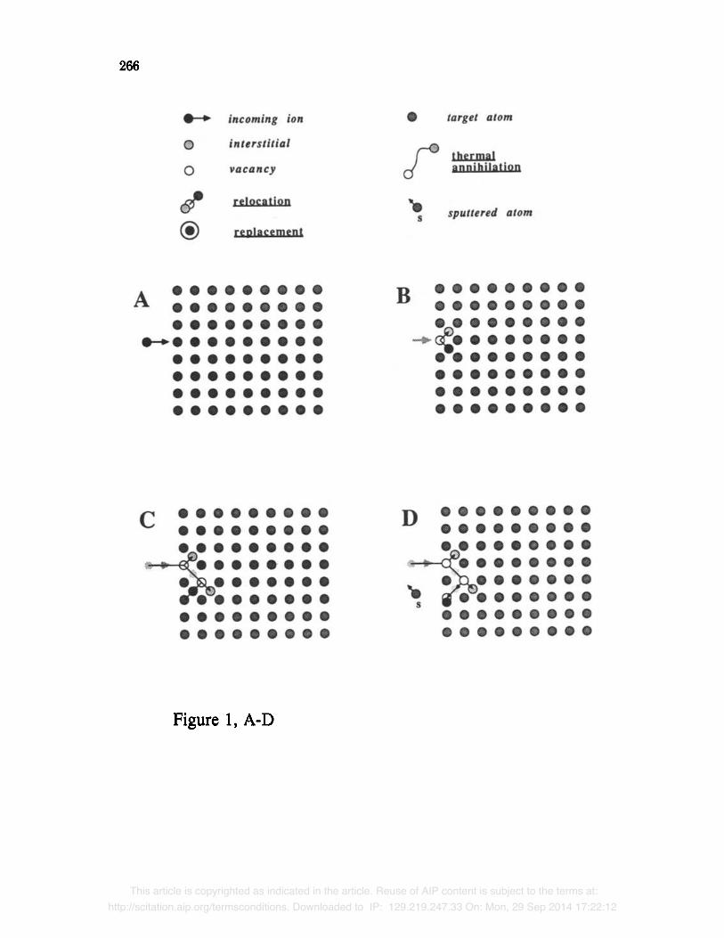
Classification of Collision Events : Replacements and Relocations
The concept of a minimum energy to cream an atomic displacement implies that an atomic collision resulting in one of the species (either target atom or incoming atom) having an energy less than Eo, cannot lead to the formation of a stable vacancy. In a collision with an ion of energy Ei, an energy AE is transferred from the incoming ion to the target atom; the two end up with energies E i' and Eat, respectively. If F-,i' and Eat are both larger than ED, then a defect pair is created, with a f'Lxed vacancy and an atom with kinetic energy Eat- ED', where ED' is the fraction of ED the atom loses in escaping the lattice site (The ion loses a corresponding energy ED - ED' escaping the lattice site, thus the total energy lost in vacancy creation is ED). Such defect pair formation occurs with a high probability during medium energy collisions processes such as ion implantation and sputtering with keV ions, as has been demonstrated many times experimentally and through computer simulations. They can leave permanent damage in the target if their density is large enough to lead to a local collapse of lattice ordering over several interatomic distances.
At typical energies used for IBD, however, the collisions often result in one of the particles having an energy less than ED (we call it a slow particle). If this slow particle is the atom originally residing on that site, one can say that no defect has been formed; the short-lived interstitial recombines with the vacancy within the timescale of the collision, and the incoming particle has merely transferred some fraction of its energy to the lattice. The reason for this spontaneous annihilation is that in this configuration, the elastic strain around the interstitial resulting from the lattice and the close proximity of a vacancy produces an attractive force between interstitial and vacancy leading to elastic recombination. The timescale at which elastic recombination takes place is about 10 -13 sec. On the other hand, if the slow particle after collision is the incoming ion, and the struck atom has received enough energy to leave the collision site, the lattice site will be refilled by the slow ion. Such an event is called a replacement (Fig. ld-e). The net result of this process is that a foreign species, introduced as an ion into the subsurface region of the substrate, now resides on a lattice site after producing only one interstitial, without the creation of a vacancy. If the subsurface is reasonably defect-free to start with, the closest recombination sink for the surviving interstitial is the surface (Fig. lh). If the incoming atom is a target atom put into motion by a prior collision, this is a relocation (Fig. 1f-g).
Elastic recombination only happens if elastic strain is coherent enough to result into a net force leading to the motion of the interstitial towards the vacancy, rather than, for example, lattice collapse and amorphization. This condition is fulfilled if there is a low density of atonuc displacements around that site within the timescale of the cascade and if the dose-rate is low enough to avoid cascade overlap. Replacement/relocation events can be calculated independent of whether the target is monocrystalline, polycrystalline or amorphous. Elastic recombinations can be detected in calculations by testing for a slow particle after defect pair formation without reference to a well-defined crystalline arrangement, or a random network.
The number of displacements Na produced by an ion of energy Ei can be larger than Ei/E D. This is because not all of ED is consumed by a relocation event. The energy necessary to activate a relocation is E D, but some of this energy may be used in activating a second displacement, thus recycling a certain portion of that energy. The energy Er dissipated in relocations is then found to be equal to the energy of the slow particles E5 (typically a few eV). NvED is consumed in the Na displacements that lead to Nv vacancies which remain after N r relocation and replacement events
occur (2+1=3 in Fig. lg). The total number of displacements Na is then related to the energy of the incoming ion by
265
Classification o/Collision Events: Replacements andRelocations
The concept of a minimum energy to create an atomic displacement implies that an atomiccollision resulting in one of the species (either target atom or incoming atom) having an energy lessthan Eo. cannot lead to the formation of a stable vacancy. In a collision with an ion of energy Ej,an energy dE is transferred from the incoming ion to the target atom; the two end up with energiesEj' and Eat> respectively. IfEj' and Eat are both larger than ED, then a defect pair is created, with afixed vacancy and an atom with kinetic energy Eat - ED', where ED' is the fraction ofED the atomloses in escaping the lattice site (The ion loses a corresponding energy ED - ED' escaping the latticesite, thus the total energy lost in vacancy creation is ED). Such defect pair formation occurs with ahigh probability during medium energy collisions processes such as ion implantation andsputtering with keY ions, as has been demonstrated many times experimentally and throughcomputer simulations. They can leave permanent damage in the target if their density is largeenough to lead to a local collapse of lattice ordering over several interatomic distances.
At typical energies used for ffiD, however, the collisions often result in one of the particleshaving an energy less than ED (we call it a slow particle). If this slow particle is the atom originallyresiding on that site, one can say that no defect has been formed; the short-lived interstitialrecombines with the vacancy within the timescale of the collision, and the incoming particle hasmerely transferred some fraction of its energy to the lattice. The reason for this spontaneousannihilation is that in this configuration, the elastic strain around the interstitial resulting from thelattice and the close proximity of a vacancy produces an attractive force between interstitial andvacancy leading to elastic recombination. The timescale at which elastic recombination takes placeis about 10-13 sec. On the other hand, if the slow particle after collision is the incoming ion, andthe struck atom has received enough energy to leave the collision site, the lattice sitewill be refilledby the slow ion. Such an event is called a replacement (Fig. Id-e). The net result of this processis that a foreign species, introduced as an ion into the subsurface region of the substrate, nowresides on a lattice site after producing only one interstitial, without the creation of a vacancy. If thesubsurface is reasonably defect-free to start with, the closest recombination sink for the survivinginterstitial is the surface (Fig. Ih). If the incoming atom is a target atom put into motion by a priorcollision, this is a relocation (Fig. If-g).
Elastic recombination only happens if elastic strain is coherent enough to result into a netforce leading to the motion of the interstitial towards the vacancy, rather than, for example, latticecollapse and amorphization. This condition is fulfllled if there is a low density of atonucdisplacements around that site within the timescale of the cascade and if the dose-rate is lowenough to avoid cascade overlap. Replacement/relocation events can be calculated independent ofwhether the target is monocrystalline, polycrystalline or amorphous. Elastic recombinations can bedetected in calculations by testing for a slow particle after defect pair formation without reference toa well-defmed crystalline arrangement, or a random network.
The number of displacements Nd produced by an ion of energy Ej can be larger than E/Eo.This is because not all of ED is consumed by a relocation event The energy necessary to activate arelocation is ED, but some of this energy may be used in activating a second displacement, thusrecycling a certain portion of that energy. The energy Er dissipated in relocations is then found tobe equal to the energy of the slow particles Es (typically a few eV). NvEo is consumed in the Nddisplacements that lead to Nvvacancies which remain after Nr relocation and replacement eventsoccur (2+1=3 in Fig. Ig). The total number of displacements Nd is then related to the energy ofthe incoming ion by
This article is copyrighted as indicated in the article. Reuse of AIP content is subject to the terms at:
http://scitation.aip.org/termsconditions. Downloaded to IP: 129.219.247.33 On: Mon, 29 Sep 2014 17:22:12
266
Figure 1, A-D
266
.... incoming ion • target atom
0 interstitial
dthermal
0 vacancy annihilation
d' relocatjon ..sputtered atom
@s
replacement
A·········••••••••••••••••••............ .••••••••••••••••••••••••••••••••••••
B ••••••••••••••••••.••••••••
• ••••••••• ••••••••• ••••••••• ••••••••
c·········•••••••••.••••••••.- .••••••••••••••••••••••••••
Figure 1, A-D
D·········•••••••••.• •••••••.. .
s ••••••••
• ••••••••• ••••••••
This article is copyrighted as indicated in the article. Reuse of AIP content is subject to the terms at:
http://scitation.aip.org/termsconditions. Downloaded to IP: 129.219.247.33 On: Mon, 29 Sep 2014 17:22:12
267
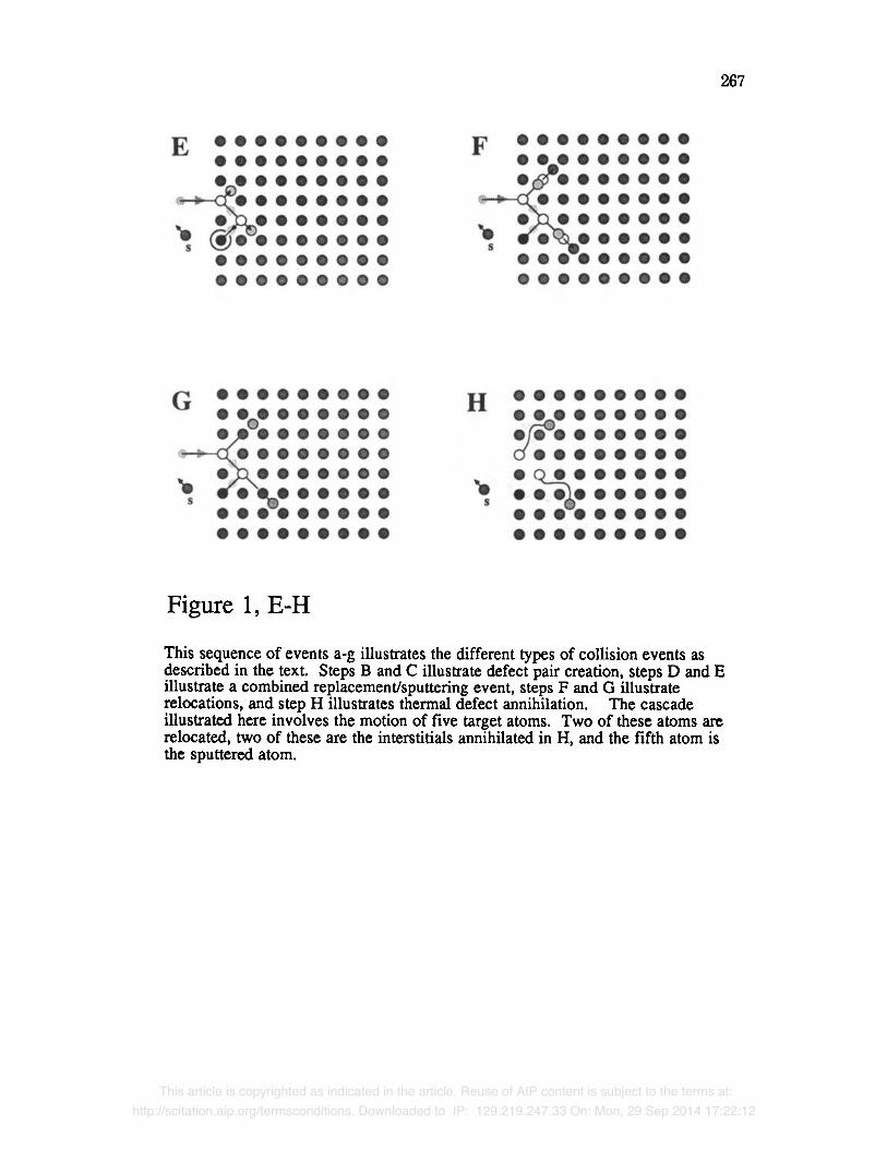
Figure 1, E-H
This sequence of events a-g illustrates the different types of collision events as described in the text. Steps B and C illustrate defect pair creation, steps D and E illustrate a combined replacement/sputtering event, steps F and G illustrate relocations, and step H illustrates thermal defect annihilation. The cascade illustrated here involves the motion of five target atoms. Two of these atoms are relocated, two of these are the interstitials annihilated in H, and the fifth atom is the sputtered atom.
F
...s
E·········••••••••••••••••••
....... ••••••••
• •••••••@••••••••••••••••••••••••••
••••••••••••••••••• •••••••
crto.....-a ••••••••
• •••••••• •••••••••••••••• ••••••••
267
G·········•••••••••.••••••••
... . .s •• •••••
••••••••••••••••••
Figure 1, E-H
H
...s
• ••••••••.• ••••••••• •••••••..! !o······•••••••••• ••••••••
This sequence of events a-g illustrates the different types of collision events asdescribed in the text Steps B and C illustrate defect pair creation, steps D and Eillustrate a combined replacement/sputtering event, steps F and G illustraterelocations, and step H illustrates thermal defect annihilation. The cascadeillustrated here involves the motion of five target atoms. Two of these atoms arerelocated, two of these are the interstitials annihilated in H, and the fifth atom isthe sputtered atom.
This article is copyrighted as indicated in the article. Reuse of AIP content is subject to the terms at:
http://scitation.aip.org/termsconditions. Downloaded to IP: 129.219.247.33 On: Mon, 29 Sep 2014 17:22:12

268
E iffiE DN v+N rEs < NdED
and
Nd = Nv + N r
and the ratio R o of athermal atomic jumps from one lattice site to another versus the number of athcrmal atomic jumps which create vacancies is Nr/Nv. When R o > 1, we find that epitaxial ordering rather than damage generation can take place.
Fig. la-g gives the configuration of a collision cascade for a 40 eV Ge ion in a Si substratc, that was found to have a high statistical incidence (> 50% of 10,000 trajectories), except for the ejection of a sputtered atom, through Monte-Carlo simulations using a modified version of the TRIM code [25]. This version discriminates among each type of event we have defined through appropriate tests on the ion and recoils energies, and hence permits statistical classification of ~ajcctories. The energy of the incoming ion (40 cV) allows for the creation of only two stable defect pairs (Nv = 2) but the number of relocations is 2 (Nr= 3), and thus the total number of atomic jumps induced by the collision Nd is 5. Hence, Re= 1.5. In Fig. lh, the resulting configuration is schematized. Two vacancies have been created in the subsurface region, and are immobile below 400~ The two interstitials are mobile even at room temperature, and are thermally diffusing. Because of the proximity of the vacancies (a few interatomic distances), the probability for capture is high (Fig. lh): epitaxy is actually taking place. It should also be noted that the role of relocations and ion replacement becomes significant only for low energies where Ei is within an order of magnitude of ED (15 to 150 eV). Beyond that limit, the contribution of relocations and replacements towards the total number of displacements becomes negligible: Re is between 0.1 and 0.2 for energies generally used for ion implantation and sputtering [19].
3. ATHERMAL ENHANCEMENT OF EPITAXIAL ORDERING: COMPUTATIONAL RESULTS
Having defined the model, vocabulary and techniques we used to analyze step by step the interaction of a low energy ion with a solid target, we can now quantify IBD and CIMD processes as a function of three primary variables: energy, substrate temperature and ion-to-target mass ratio. The conditions we chose for the simulation data shown as examples are typical for our experimental variables (Ge or oxygen ions, silicon substrate, 25~ < T < 600~ 20 eV g E < 200
eV, dose-rate ~1013 ions/cm2.sec). After calculating the statistical properties of individual low energy collision cascades, we can derive a global model of thin film growth as a function of the cascade parameters that we are now able to quantify.
Defects and Ion Depth Distributions during IBD at the Timescale of Collision Events
Fig. 2a represents the statistical depth distribution of the total number of displacements generated by a 65 eV Ge ion in a Si substrate. Fig. 2b depicts the depth distribution of the residual number of defects at the end of the collision process. Although a 65 eV Ge ion can produce, at most, only 4 defect pairs, a statistical average of 8 displacements per ion is found, due to the several relocation events. The ion mean projected range Rp is 0.85 nm, which is about 4
monolayers below the surface*. For ion energies above ED, this is as expected since their energy
* The calculated range is a function of the interatomic potential between the incoming ion and the target atom. The potential function used in the calculations is the universal potential proposed by Ziegler, Biersffi'k, and Limnark, which contains semi-empirical parameters for the five exponential terms giving the potential as a function of the interatomic distance. The validity of this potential at very low energies has been demonstrated recently both experimentally and theoretically by A. Tenner and A. Kleyn [20].
268
and
Nd= Nv + Nr
and the ratio Raof athennal atomic jumps from one lattice site to another versus the number ofathermal atomic jumps which create vacancies is NrlNv. When Ra 1, we find that epitaxialordering rather than damage generation can take place.
Fig. la-g gives the configuration of a collision cascade for a 40 eV Ge ion in a Si substrate,that was found to have a high statistical incidence (> 50% of 10,000 trajectories), except for theejection of a sputtered atom, through Monte-Carlo simulations using a modified version of theTRIM code [25]. This version discriminates among each type of event we have defined throughappropriate tests on the ion and recoils energies, and hence permits statistical classification oftrajectories. The energy of the incoming ion (40 eV) allows for the creation of only two stabledefect pairs (Nv =2) but the number of relocations is 2 (Nr= 3), and thus the total number ofatomic jumps induced by the collision Nd is 5. Hence, Ra= 1.5. In Fig. Ih, the resultingconfiguration is schematized Two vacancies have been created in the subsurface region, and areimmobile below 400°C. The two interstitials are mobile even at room temperature, and arethennally diffusing. Because of the proximity of the vacancies (a few interatomic distances), theprobability for capture is high (Fig. Ih): epitaxy is actually taking place. It should also be notedthat the role of relocations and ion replacement becomes significant only for low energies where E;.is within an order ofmagnitude ofED (15 to 150 eV). Beyond that limit, the contribution ofrelocations and replacements towards the total number of displacements becomes negligible: Ro isbetween 0.1 and 0.2 for energies generally used for ion implantation and sputtering [19].
3. ATIlERMAL ENHANCEMENT OF EPITAXIAL ORDERING: COMPUTATIONAL RESULTS
Having defmed the model, vocabulary and techniques we used to analyze step by step theinteraction of a low energy ion with a solid target, we can now quantify IBD and CIMD processesas a function of three primary variables: energy, substrate temperature and ion-to-target mass ratio.The conditions we chose for the simulation data shown as examples are typical for ourexperimental variables (Ge or oxygen ions, silicon substrate, 25°C < T < 600°C, 20 eV :S E :S 200eV, dose-rate -1013 ions/cm2·sec). After calculating the statistical properties of individual lowenergy collision cascades, we can derive a global model of thin film growth as a function of thecascade parameters that we are now able to quantify.
Defects and Ion Depth Distributions during IBD at the Timescale ofCollision Events
Fig. 2a represents the statistical depth distribution of the total number ofdisplacementsgenerated by a 65 eVGe ion in a.Si substrate. Fig. 2b depicts the depth distribution of the residualnumber of defects at the end of the collision process. Although a 65 eV Ge ion can produce, atmost, only 4 defect pairs, a statistical average of 8 displacements per ion is found, due to theseveral relocation events. The ion mean projected range Rp is 0.85 nm, which is about 4monolayers below the surface·. For ion energies above ED, this is as expected since their energy
• The calculated range is a function of the interatomic potential between the incoming ion and the target atom. Thepotential function used in the calculations is the universal potential proposed by Ziegler, Biersack, and Littmark,which contains semi-empirical parameters for the five exponential terms giving the potential as a function of theinteratomic distance. The validity of this potential at very low energies has been demonstrated recently bothexperimentally and theoretically by A. Tenner and A. Kleyn [20].
This article is copyrighted as indicated in the article. Reuse of AIP content is subject to the terms at:
http://scitation.aip.org/termsconditions. Downloaded to IP: 129.219.247.33 On: Mon, 29 Sep 2014 17:22:12
269
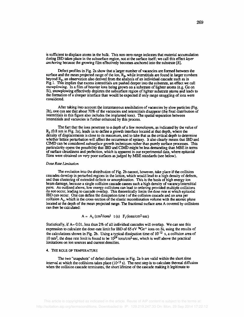
is sufficient to displace atoms in the bulk. This non-zero range indicates that material accumulation during IBD takes place in the subsurface region, not at the surface itself; we call this effect layer anchoring because the growing film effectively becomes anchored into the substrate [8].
Defect profiles in Fig. 2a show that a larger number of vacancies are formed between the surface and the mean projected range of the ion, Rp, while interstitials are found in larger numbers beyond Rp, an observation also derived from the ahalysis of an individual cascade such as in Fig. 1. This implies that excess interstitials are pushed deeper into the substrate, an effect we call snowplowing. In a film of heavier ions being grown on a substrate of lighter atoms (e.g. Ge on Si), snowplowing effectively depletes the subsurface region of lighter substrate atoms and leads to the formation of a sharper interface than would be expected if only range straggling of ions were considered.
After taking into account the instantaneous annihilation of vacancies by slow particles (Fig. 2b), one can see that about 70% of the vacancies and interstitials disappear (the final distribution of interstitials in this figure also includes the implanted ions). The spatial separation between interstitials and vacancies is further enhanced by this process.
The fact that the ions penetrate to a depth of a few monolayers, as indicated by the value of Rp (0.8 nm in Fig. 2a), leads us to define a growth interface located at that depth, where the density of displacements is close to its maximum, and to take that as the critical depth to determine whether lattice perturbation will affect the occuncnce of epitaxy. It also dearly means that IBD and CIMD can be considered subsurface growth techniques rather than purely surface processes. This particularity opens the possibility that IBD and CIMD might be less demanding than MBE in terms of surface cleanliness and perfection, which is apparent in our experimental data, where epitaxial films were obtained on very Ix)or surfaces as judged by MBE standards (see below).
Dose Rate Limitation
The evolution into the distribution of Fig. 2b cannot, however, take place if the collision cascades develop in perturbed regions in the lattice, which would lead to a high density of defects, and thus clustering of extended defects or amorphization. This is the basis of high energy ion beam damage, because a single collision cascade causes such a high density of vacancy/interstitial pairs. As outlined above, low energy collisions can lead to ordering provided multiple collisions do not occur, leading to cascade overlap. This theoretically limits the dose rate at which epitaxial IBD can occur. One can define the dissipation time t of the collision cascade and an area per collision Ac, which is the cross-section of the elastic recombination volume with the atomic plane
located at the depth of the mean projected range. The fractional surface area A covered by collisions can then be calculated:
A = A c (cm2/ions) t (s) Fi (ions/cm2"sec)
Statistically, if A= 0.01, less than 2% of all individual cascades will overlap. We can use this
expression to calculate the dose-rate limit for IBD of 65 eV 7~43e+ ions on Si, using the results of
the calculations shown in Fig. 2b. Using a typical dissipation time of 10 "12 s, a collision area of
10 nm 2, the dose rate limit is found to be 1024 ions/cm2.sec, which is well above the practical limitations on ion sources and current densities.
4. THE ROLE OF TEMPERATURE
The two "snapshots" of defect disadbutions in Fig. 2a-b are valid within the short time interval at which the collisions takes place (10 -13 s). The next step is to calculate thermal diffusion when the collision cascade terminates, the short lifetime of the cascade making it legitimate to
269
is sufficient to displace atoms in the bulk. This non-zero range indicates that material accumulationduringmo takes place in the subsurface region, not at the surface itself; we call this effect layeranchoring because the growing film effectively becomes anchored into the substrate [8].
Defect profiles in Fig. 2a show that a larger number of vacancies are fonned between thesurface and the mean projected range of the ion, Rp, while interstitials are found in larger numbersbeyond RI1, an observation also derived from the analysis of an individual cascade such as inFig.l. This implies that excess interstitials are pushed deeper into the substrate, an effect we callsnowplowing. In a film of heavier ions being grown on a substrate oflighter atoms (e.g. Ge onSi), snowplowing effectively depletes the subsurface region of lighter substrate atoms and leads tothe formation of a sharper interface than would be expected ifonly range straggling of ions wereconsidered.
After taking into account the instantaneous annihilation of vacancies by slow particles (Fig.2b), one can see that about 70% of the vacancies and interstitials disappear (the final distribution ofinterstitials in this figure also includes the implanted ions). The spatial separation betweeninterstitials and vacancies is further enhanced by this process.
The fact that the ions penetrate to a depth of a few monolayers, as indicated by the value ofRp (0.8 nm in Fig. 2a), leads us to defme a growth interface located at that depth, where thedensity of displacements is close to its maximum, and to take that as the critical depth to determinewhether lattice perturbation will affect the occurrence of epitaxy. It also clearly means thatmo andCIMO can be considered subsurface growth techniques rather than purely surface processes. Thisparticularity opens the possibility thatmo and CIMO might be less demanding than MBE in termsof surface cleanliness and perfection, which is apparent in our experimental data, where epitaxialfilms were obtained on very poor surfaces as judged by MBE standards (see below).
Dose Rate Limitation
The evolution into the distribution ofFig. 2b cannot, however, take place if the collisioncascades develop in perturbed regions in the lattice, which would lead to a high density of defects,and thus clustering of extended defects or amorphization. This is the basis of high energy ionbeam damage, because a single collision cascade causes such a high density of vacancy/interstitialpairs. As outlined above, low energy collisions can lead to ordering provided multiple collisionsdo not occur, leading to cascade overlap. This theoretically limits the dose rate at which epitaxialmo can occur. One can defme the dissipation time t of the collision cascade and an area percollision Ac, which is the cross-section of the elastic recombination volume with the atomic planelocated at the depth of the mean projected range. The fractional surface area A covered by collisionscan then be calculated:
A = Ac (cm2/ionsl t (s) Fj (ions/cm2·sec)
Statistically, ifA= 0.01, less than 2% of all individual cascades will overlap. We can use thisexpression to calculate the dose-rate limit formo of 65 eV JlGe+ ions on Si, using the results ofthe calculations shown in Fig. 2b. Using a typical dissipation time of 10-12 s, a collision area of10 nm2
, the dose rate limit is found to be IQ24 ions/cm2·sec, which is well above the practicallimitations on ion sources and current densities.
4. THE ROLE OF TEMPERATURE
The two "snapshots" of defect distributions in Fig. 2a-b are valid within the short timeinterval at which the collisions takes place (l0-13 s). The next step is to calculate thermal diffusionwhen the collision cascade terminates, the short lifetime of the cascade making it legitimate to
This article is copyrighted as indicated in the article. Reuse of AIP content is subject to the terms at:
http://scitation.aip.org/termsconditions. Downloaded to IP: 129.219.247.33 On: Mon, 29 Sep 2014 17:22:12

270
Z 0 klml
Z 0 Ill
|
Z
0
1.25
1.00
0.75
0.50
0.25
0.00 0
1.25
1.00
0.75
0.50 I
0.25
0.00 0
1 0 21
1020
1019
10 TM
1017
1016
IA
eV -> Si
I , I , i ~ . ,
4 8 12 16 20
DEPTH (A)
74Ge+, 65 eV -> Si I B
4 8 12 16
DEPTH (A) 20
I C 74Ge+, 65 eV -> Si I 9 9 1 4 9 1 4 9 1 4 9 1 4 9 300 K
1
[vacl 9
9 [ in t ] i i i i I I I I I l l l ~ l l I l l l I I I I I l l I
i g
I n I n I
10 ~ 20 30
Figure 2
These graphs show the progression of vacancy and inter- stitial concentrations through calculations of defect creation by low energy ion "implantation" (2a), athermal defect recombination (2b), and thermal defect recombination and diffusion (2c). The first two calculations are made by TRIM, using the parameters shown. The second calculation included a test for athermal recombination. The third calculation is performed using results from TRIM for defect creation, and a finite element method for defect diffusion, and a recombination volume radius of 5A.
270
Figure 2
These graphs showthe progression ofvacancy and inter-stitial concentrationsthrough calculationsof defect creationby low energy ion"implantation" (2a),athermal defectrecombination (2b),and thermal defectrecombination anddiffusion (2c). Thefirst two calculationsare made by TRIM,using the parametersshown. The secondcalculation includeda test for athermalrecombination. Thethird calculation isperformed usingresults from TRIMfor defect creation,and a finite elementmethod for defectdiffusion, and arecombinationvolume radius ofsA.
20
30
16
[int]
12
740e; 65 eV -> Si
20o
A
8
DEPTH (A)
10
4
4 8 12 16 20
DEPTH (A)
740e; 65 eV -> Si
••• 740e; 65 eV -> Si
• ••• 300K
••••[vae] •
••
vae
•
•••••••••••••••••••••••••••...
•
o
1.25 .---:::------------
1.00
0.50
0.25
0.75
1.00
1.25 r--------......,..--
0.25
0.50
0.75
zo
-
zo
-
'?l•
uzou
This article is copyrighted as indicated in the article. Reuse of AIP content is subject to the terms at:
http://scitation.aip.org/termsconditions. Downloaded to IP: 129.219.247.33 On: Mon, 29 Sep 2014 17:22:12
271
consider thermal effects separately form collision effects. Thermal mobilities are quite significant for interstitials in Si even at 300~ and nearly negligible for vacancies below 400~ Using recent values of these mobilities, we have calculated the steady-state defect dislribution near a subswate
surface during IBD for a typical dose rate of 1013 ions/cm2.sec. This distribution is shown in Fig. 2c. While vacancies are retained in the amount of 2 x 10²~ (0.4% of the lattice sites are vacant) at the peak of the diswibution, interstitials are annihilated when reaching the surface and are distributed over several 100 nm at an average concentration of less than 3• 3. In summary, the residual defects left by athermal displacements are mostly immobile vacancies which are confined to the top 1.5 nm of the growing film. Interstitials introduced by athermal displacements dissipate away by diffusion both to the surface and into the growing film. The high concentration of interstitials thus produced throughout the trim also results in the annihilation of vacancies which may exist there, thus making the vacancy concentration in the film negligible. Interstitials which diffuse into the film may coalesce as extended defects. We will show in the experimental section that such an extensive migration of interstifials and their coalescence deep in the substrate take place, and agree qualitatively with our calculations.
5. THIN FILM FORMATION BY IBD
From what we have learned from the previous calculations, we can now describe the process of thin film formation by IBD in three phases, as shown in Fig. 3a-c. The first is an initial implantation during which incoming ions progressively replace subswate atoms in the first few atomic layers. We call it the ion implantation regime (Fig. 3a). Upon saturation of the subsurface distribution peak at a concenwation close to the atomic density, another regime is initiated in which the whole subsurface region becomes progressively converted into the material deposited, by the combination of snowplowing and also sputtering in the case of an ion-to-target mass ratio =)l. We call this the transition regime (Fig. 3b). Layers of the new trim are anchored in the subsWate, and the subsurface region is converted into the material being deposited. Eventually, the whole subsurface region becomes converted into the species being deposited, and the third phase is a compositionally homogeneous growth of the deposited ion in its own thin film matrix. It is a stationary growth regime that we call the true IBD regime (Fig. 3c). Fig. 4 gives a pictorial representation of regime and highlights the specific characteristics derived from the calculations, and which we also observed in the films we deposited.
6. LOW TEMPERATURE ION BEAM OXIDATION
During ion beam induced chemical reactions, ion kinetic energy is used to overcome or to bypass rate-limiting activation barriers in a reaction process, as illustrated by the ion beam oxidation of silicon. In the thermal oxidation of silicon, molecular dissociation, physisorbtion, chemisorbtion, and solid-state diffusion are all reaction steps which requi~ thermal activation energy (Fig. 5a). However, an oxygen ion ofE > 15 eV impinging on a silicon target has sufficient energy to bypass all of these steps (Fig. 5b). Even solid-state diffusion can be unnecessary if the ion comes to rest in the target where it can bond to adjacent silicon atoms. At low temperatures (50 ~ where diffusivity of oxygen in silicon dioxide is limited, the ion energy can be used to control the penetration of oxygen into the silicon, thus determining a maximum oxide thickness. At 450 ~ which can be considered low for silicon processing since dopant diffusion and segregation is negligible, oxygen diffusivity is still significant. However, the generation of excess interstitials and their pile-up in the amorphous oxide will rapidly decrease the diffusivity of oxygen into the crystalline substrate. Hence, the oxidation process will be thickness limited beyond a certain point, determined by the number of interstitials generated (hence the oxygen dose and the ion energy), rather than by the range of the ion. Ion beam oxidation is thus an athermal technique for growing a dense oxide whose thickness is determined primarily by the oxygen ion energy.
271
consider thennal effects separately form collision effects. Thennal mobilities are quite significantfor interstitials in Si even at 300°C, and nearly negligible for vacancies below 400°C. Using recentvalues of these mobilities, we have calculated the steady-state defect distribution near a substrate
surface during IBD for a typical dose rate of 1013 ionslcm2·sec. This distribution is shown in Fig.2c. While vacancies are retained in the amount of 2 x 1()20/cm3 (0.4% of the lattice sites are vacant)at the peak of the distribution, interstitials are annihilated when reaching the surface and aredistributed over several 100 nm at an average concentration ofless than 3xlOI7 /cm3• Insummary, the residual defects left by athermal displacements are mostly immobile vacancies whichare confined to the top 1.5 nm of the growing film. Interstitials introduced by athennaldisplacements dissipate away by diffusion both to the surface and into the growing film. The highconcentration of interstitials thus produced throughout the film also results in the annihilation ofvacancies which may exist there, thus making the vacancy concentration in the film negligible.Interstitials which diffuse into the film may coalesce as extended defects. We will show in theexperimental section that such an extensive migration of interstitials and their coalescence deep inthe substrate take place, and agree qualitatively with our calculations.
5. 1HIN Fll..M FORMATION BY ffiD
From what we have learned from the previous calculations, we can now describe theprocess of thin film formation by IBD in three phases, as shown in Fig. 3a-c. The first is an initialimplantation during which incoming ions progressively replace substrate atoms in the first fewatomic layers. We call it the ion implantation regime (Fig. 3a). Upon saturation of the subsurfacedistribution peak at a concentration close to the atomic density, another regime is initiated in whichthe whole subsurface region becomes progressively converted into the material deposited, by thecombination of snowplowing and also sputtering in the case of an ion-to-target mass ratio Wecall this the transition regime (Fig. 3b). Layers of the new film are anchored in the substrate, andthe subsurface region is converted into the material being deposited. Eventually, the wholesubsurface region becomes converted into the species being deposited, and the third phase is acompositionally homogeneous growth of the deposited ion in its own thin film matrix. It is astationary growth regime that we call the true IBD regime (Fig.3c). Fig. 4 gives a pictorialrepresentation of regime and highlights the specific characteristics derived from the calculations,and which we also observed in the films we deposited.
6. LOWTEMPERAnJRE ION BEAM OXIDATION
During ion beam induced chemical reactions, ion kinetic energy is used to overcome or tobypass rate-limiting activation barriers in a reaction process, as illustrated by the ion beamoxidation of silicon. In the thennal oxidation of silicon, molecular dissociation, physisorbtion,chemisorbtion, and solid-state diffusion are all reaction steps which require thennal activationenergy (Fig. Sa). However, an oxygen ion ofE > 15 eV impinging on a silicon target hassufficient energy to bypass all of these steps (Fig. 5b). Even solid-state diffusion can beunnecessary if the ion comes to rest in the target where it can bond to adjacent silicon atoms. Atlow temperatures (50°C), where diffusivity of oxygen in silicon dioxide is limited, the ion energycan be used to control the penetration ofoxygen into the silicon, thus determining a maximumoxide thickness. At 450°C, which can be considered low for silicon processing since dopantdiffusion and segregation is negligible, oxygen diffusivity is still significant. However, thegeneration of excess interstitials and their pile-up in the amorphous oxide will rapidly decrease thediffusivity of oxygen into the crystalline substrate. Hence, the oxidation process will be thicknesslimited beyond a certain point, determined by the number of interstitials generated (hence theoxygen dose and the ion energy), rather than by the range of the ion. Ion beam oxidation is thusan athermal technique for growing a dense oxide whose thickness is determined primarily by theoxygen ion energy.
This article is copyrighted as indicated in the article. Reuse of AIP content is subject to the terms at:
http://scitation.aip.org/termsconditions. Downloaded to IP: 129.219.247.33 On: Mon, 29 Sep 2014 17:22:12
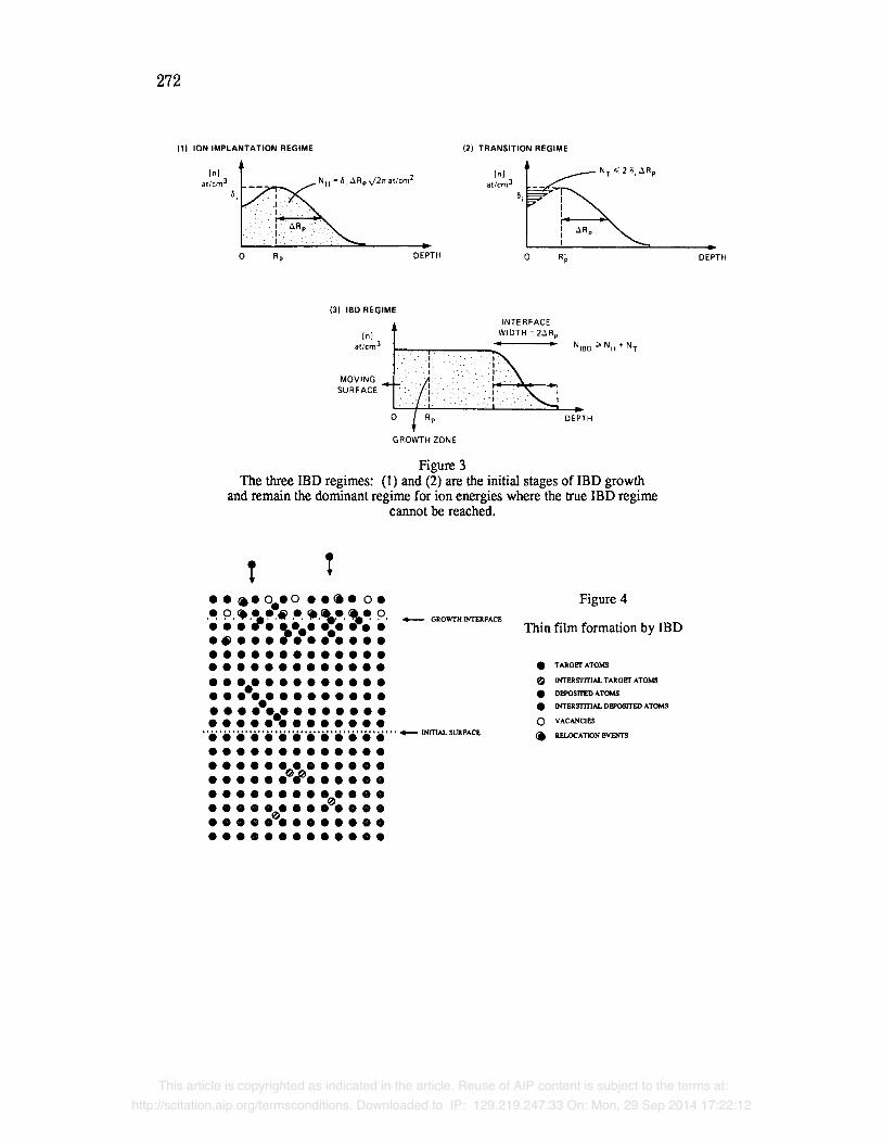
272
(11 ION IMPLANTATION REGIME
[hi ~ at/cm 3 _ _ _ Nil = 6 i ~Rp X/2~ at/cm 2
5i
I.
O Rp DEPTH
(2) TRANSITION REGIME
{n} l ~ NT ~<2~.&RP at/cm 3 __
I ~Rp
o R i, DE~TH
(3} IBD REGIME JNTERFACE
{n} T WIDTH = 2~-Rp
at/cm3 ~ ~ ~- : . ' I " - . . ~ - ~
9 9 . i . ' . ' . . P. 9 MOVING
' - - ' , ~1 : ' ' . : 9 SORFACE "" / ! p : ' T " : ~:
GROWTH ZONE
NIBD ~ NIl + NT
L
DEPTH
Figure 3 The three IBD regimes: (1) and (2) are the initial stages of IBD growth
and remain the dominant regime for ion energies where the true IBD regime cannot be reached.
! ! o O Q o o g o o o ~ o o o o o ~ o ~ ~
o o o o o ~ o o o % o o o O O O O O O O O O O O O O
O O O O O O O O O O O O O
O 0 O_O O g o O O O O 0 O
9 9 O~oO O O 9 9 9 9 9 9
9 9 9 9 o - g i g 9 9 9 9 9 O O O O O ~ O O O O O O O "6'~'~'~"~'~'~"6'~'~'~"~'~'"~.~P^c~
0 0 0 0 0 0 0 0 0 0 0 0 0 0 0 0 0 0 0 0 0 0 0 0 : 0 o o o o e o ~ o o o o 9
0 0 0 0 O 0 0 0 0 0 0 0 0 0 0 0 0 0 0 0 0 0 0 0 0 0 0 0 0 0 0 0 0
Figure 4
Thin film formation by IBD
TARGET ATOMS
INTERSTITIAL TARGET ATOM.~
DEPOSITED ATOMS
9 INTERSTITIAL DEPOSITED ATOMS
0 VACANCIES
R~LOC ATI~N ~v ENT$
272
111 ION IMPLANTATION REGIME 121 TRANSITION REGIME
[nl
at/em3
6,
o DEPTH
131 IBD REGIME
[n]
at/cm3
MOVING
SURFACE
GROWTH ZONE
In]
at/cm 3
o
INTERFACE
WIDTH = 2t>R p. ..
R'p
DEPTH
DEPTH
Figure 3
The three IBD regimes: (1) and (2) are the initial stages of IBD growthand remain the dominant regime for ion energies where the true IBD regime
cannot be reached.
T T•••• 0•• 0 •••• o.
•• 9. +- G'OWTHn<rERPACE
:: :.::-:.: :.: :::•••••••••••••••••••••••••••••••••••••••••••••••••••••••••••••••••••••••••••••••••.... .Ii' .' iii' Ii' iii' .. - INITtAL SURPACE
•••••••••••••..... ·OJ·······...... .•••••••• • 0••• 0
•••• 00••••••••
••••••••••••••••••••••••••
Figure 4
Thin film formation by IBD
• TARGET ATOMS
o INTE.RSTrrIAL TARGET ATOMS
• DEPOSITED ATOMS
• INTERSTrflAL DEPOSITED ATOMS
o VACANCIES
<a RELOCATION EVENTS
This article is copyrighted as indicated in the article. Reuse of AIP content is subject to the terms at:
http://scitation.aip.org/termsconditions. Downloaded to IP: 129.219.247.33 On: Mon, 29 Sep 2014 17:22:12
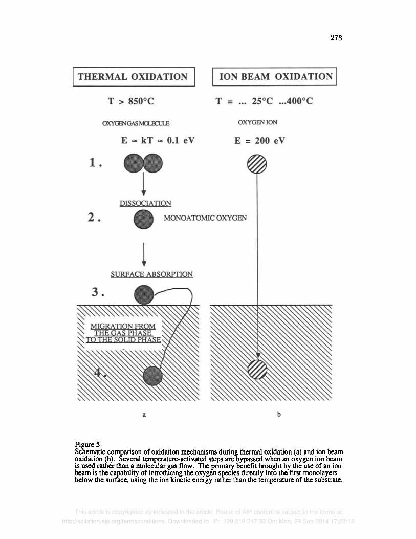
273
Figure 5 Schematic comparison of oxidation mechanisms duringthermal oxidation (a) and ion beam oxidation (b). Several temperature-activated steps arebypassed when an oxygen ion beam is used rather than a molecular gas flow. The pmna~ benefit brought by the use of an ion beam is the capability of introducing the oxygen species directly into the fLrSt monolayers below the surface, using the ion kinetic energy rather than the temperature of the substrate.
273
ITHERMAL OXIDATION I I ION BEAM OXIDATIO
T > 850°C
OXYGENGASM:LOCULE
E z kT z 0.1 eV
OXYGEN ION
E = 200 eV
1 .
2.
,.DISSOCIATION
• MONOATOMIC OXYGEN
!SURfACE ABSORPTION
a b
Figure 5Schematic comparison of oxidation mechanisms during thermal oxidation (a) and ion beamoxidation (b). Several temperature-activated stel's are bypassed when an oxygen ion beamis used rather than a molecular gas flow. The pnmary benefit brought by the use of an ionbeam is the capability of introducing the oxygen species directly into the fIrst monolayersbelow the surface, using the ion kinetic energy rather than the temperature of the substrate.
This article is copyrighted as indicated in the article. Reuse of AIP content is subject to the terms at:
http://scitation.aip.org/termsconditions. Downloaded to IP: 129.219.247.33 On: Mon, 29 Sep 2014 17:22:12
274
IV. EXPERIMENTS & DISCUSSION
1. IBD APPARATUS
The IBD apparatus built at ORNL has been the object of several publications [6- 12, 16, 22]. We will thus only describe the principle of the experimental set-up and focus on secondary effects of the design that have recently been found to be important for the ultimate purity and the desired microsl~,_cture of IBD films.
Ion Beam Production and Transport
The production of a low energy ion beam with a flux comparable in magnitude to that of a molecular beam is a complex problem primarily because of space charge effects. The space charge causes a low energy beam to diverge as it is Iransported towards the target. This effect becomes more significant at lower energies and at higher current densities, limiting the maximum flux achievable for a given source and beam geometry, independent of the ionization efficiency of the source. In order to ensure good vacuum conditions and ion beam purity, ion beam analysis and differential pumping are necessary to avoid incorporation of desorbed gas and spurious ions into the films. This lengthens the path of the low energy ions before they reach the target and makes the space charge effect unavoidable. This problem is solved in the ORNL apparatus by producing the ions at a fairly high energy (35 keV), at which space charge effects are negligible over distances of the order of 100 mm. The ion beam is mass analyzed and energy analyzed in a high resolution magnet ( m/Am = 1200) at 35 keV. The beam has a diameter of -2.2 cm after exlraction, analysis and collimation through a first set of slits. It is then transported at 35 keV through a differentially pumped beamline into the deposition chamber. The beamline consists of three differential pumping stages separating a 10 -7 Tort pressure in the ion source from the UHV chamber's base pressure of 10 -10 Torr. Each stage has its own pumping unit and a pair of copper collimating apertures of -2.9 cm diameter. The apertures are liquid nitrogen cooled and a fifth set of apertures defines the beam spot in the UHV chamber before it reaches the target. No copper was ever observed in the films, as measured by Auger Electron Spectroscopy (AES) and Secondary Ion Mass Spectrometry (SIMS), which means that the contamination was less than 104 a/o. The ions are decelerated only after ion beam mass analysis and transport to the target, in the immediate vicinity of the subslrate.
lon Beam Deceleration
Only when the beam is about to reach the target is it decelera~d (Fig. 6). This is done by biasing the sample holder, which is a fiat metal disk aligncd in the same plane as the sample. The assembly acts as a fiat electrode, biased at the extraction voltage (35 kV), minus the desired deposition voltage. Another disk, of the same diameter (10.16 cm) faces the substrate holder at a distance of an 2.54 cm, and has in its center a 2.54 cm aperture to transmit the beam to the target. This second electrode serves as secondary electron suppressor and is biased at -1 kV with respect to ground potential. A third electrode is present upstream of the suppressor at a distance of 2.54 cm and is held at ground potential. This configuration has the strong advantage of simplicity, and minimizes defocusing after deceleration. The design requires good alignment of each electrode with respect to the beam, because misalignment away from normal to the subslrate can lead to deflection rather than deceleration, and hence no deposition.
The ion source used is a modified filament source of the Freeman type. The maximum energy spre~l. Er to be expected from this source can be estimated from the arc voltage. The energy dis~bul~on in the decelerated ion beam can be considered monomodal, with an asymmetry in the distribution due the fact that ions with an initial energy lower than 35 keV - E l , where El is the energy selected for deposition, cannot reach the target.
274
N. EXPERIMENTS & DISCUSSION
1. IBDAPPARAnJS
The ffiD apparatus built atORNL has been the object of several publications [6-12, 16,22]. We will thus only describe the principle of the experimental set-up and focus onsecondary effects of the design that have recently been found to be important for the ultimate purityand the desired microstructure of ffiD films.
Ion BeamProduction andTransport
The production of a low energy ion beamwith a flux comparable in magnitude to that of amolecular beam is a complex problem primarily because of space charge effects. The space chargecauses a low energy beam to diverge as it is lransported towards the target. This effect becomesmore significant at lower energies and at higher current densities, limiting themaximum fluxachievable for a given source and beam geometty, independent of the ionization efficiency of thesource. In order to ensure good vacuum conditions and ion beam purity, ion beam analysis anddifferential pumping are necessary to avoid incorporation ofdesorbed gas and spurious ions intothe films. This lengthens the path of the low energy ions before they reach the target and makesthe space charge effect unavoidable. This problem is solved in the ORNL apparatus by producingthe ions at a fairly high energy (35 keV), at which space charge effects are negligible over distancesof the order of 100 mm. The ion beam is mass analyzed and energy analyzed in a high resolutionmagnet (m/6m = 12(0) at 35 keY. The beam has a diameter of -2.2 cm after extraction, analysisand collimation through a first set of slits. It is then lransported at 35 keY through a differentiallypumped beamline into the deposition chamber. The beamline consists of three differential pumpingstages separating a 10-7 Torr pressure in the ion source from the UHV chamber's base pressure of10-10Torr. Each stage has its own pumping unit and a pair of copper collimating apertures of -2.9cmdiameter. The apertures are liquid nitrogen cooled and a fifth set of apertures defines the beamspot in the UHV chamber before It reaches the target No copper was ever observed in the films,as measured by Auger Electron Spectroscopy (AES) and Secondary IonMass Spectrometry(SIMS), which means that the contamination was less than 104 aJo. The ions are decelerated onlyafter ion beam mass analysis and lransport to the target, in the immediate vicinity of the substrate.
IonBeamDeceleration
Only when the beam is about to reach the target is it decelerated (Fig. 6). This is done bybiasing the sample holder, which is a flat metal disk aligned in the same plane as the sample. Theassembly acts as a flat electrode, biased at the extraction voltage (35 ky), minus the desireddeposition voltage. Another disk, of the same diameter (10.16 cm) faces the substrate holder at adistance of an 2.54 cm, and has in its center a 2.54 cm aperture to transmit the beam to the target.This second electrode serves as secondary electron suppressor and is biased at -1 kV with respectto ground potential. A third electrode is present upstream of the suppressor at a distance of2.54 cmand is held at ground potential. This configuration has the strong advantage of simplicity, andminimizes defocusing after deceleration. The design requires good alignment of each electrodewith respect to the beam, because misalignment away from normal to the substrate can lead todeflection rather than deceleration, and hence no deposition.
The ion source used is a modified filament source of the Freeman type. The maximumenergy Er to be expected from this source can be estimated from the arc voltage. The energydistribution in the decelerated ion beam can be considered monomodal, with an asymmetty in thedistribution due the fact that ions with an initial energy lower than 35 keV - E" where E, is theenergy selected for deposition, cannot reach the target.
This article is copyrighted as indicated in the article. Reuse of AIP content is subject to the terms at:
http://scitation.aip.org/termsconditions. Downloaded to IP: 129.219.247.33 On: Mon, 29 Sep 2014 17:22:12

275
Bias = -1 IcV
Bias =Ground
}---Electron Suppressor Electrode
Ground Electrode
275
Focal Point of Ion BeamA&rMass Analysis
CWTCIlt DensityProme
rzJFigure 6.
Representation of ion trajectories asthe ions are decelerated anddefocused near the target
The sample holder is seen to actas a lens for those particles whichare slightly misaligned or whichdo not have sufficient energyto reach the target.
The right half of the beam is omittedfrom the drawing for clarity. TheCWTCllt density profile on the rightis a typical plot of current densityacross one radius of the beam.
Ion trajectories
r o
This article is copyrighted as indicated in the article. Reuse of AIP content is subject to the terms at:
http://scitation.aip.org/termsconditions. Downloaded to IP: 129.219.247.33 On: Mon, 29 Sep 2014 17:22:12

276
A direct observation of ion reflection is the collection of reflected ions on the electron suppressor disk held at -1 kV. Ions arc reflected at the end of the deceleration when their energy approaches zero with respect to the substrate holder. They am then reaccclerated to a potential of 36 kV when they turn around and impinge on the electron suppressor. The reflected beam is smmgly defocused and a annular deposit of approximately 5.1 cm in diameter is observed around the suppressor aperture. A highly undesirable consequence of this is the sputtering of suppressor material onto the film by reflected ions. Suppressor mamial incoqxration into IBD films was initially very significant. For instance, 7 a/o of stainless steel was found incorporated uniformly
into a 3 nm thick germanium film grown by 65 eV Ge + ions on a silicon substrate held at room temperature. No evidence of stainless steel was found beyond the film interface within the substratc by SIMS, indicating that high energy neutral incorporation is v~'y unlikely. The problem of fdm contamination can be drastically reduced by using a suppressor material identical to the material being deposited, which brings the contamination level down to less than 0.035 a/o (determined using Rutherford backscattcring analysis).
Further reduction can be achieved by using a substrate holder of the same material. It was observed that the stainless steel sample holder was gradually covered with material from the ion beam over several depositions, resulting in a gradual reduction of contamination. This effect decreases contamination to amounts below the detection limits of ion scattering and SIMS. It should be noted that material from the sample holder itself can migrate to the surface of the sample during heated deposition. This was especially apparent when the part of the holder in direct contact with the sample was made out of molybdenum, which being heavier is easily detected by ion scattering and was the only metallic part of the electrode not made of stainless steel. We found an initial contamination level on the order of 0.01 a/o for samples grown at 600~ which subsequently decreased as the molybdenum became coated with silicon through successive depositions.
In conclusion, it is essential in such a design that the suppressor as well as the sample holder be made of a material compatible with the deposit, or becomes progressively coated by it though a series of preliminary depositions, which is the case for the data shown here. As far as thin multilayercd deposits of monoisotopcs arc concerned, a purity of 1 to 0.1 a/o is the best that can be expected, since each deposition leaves a trace of contamination for the next. A pure monoisotopic film can be realized after successive depositions of the same isotope, as shown in Fig. 7. This SIMS profile of a single film of 3~ grown up to a thickness of 150 nm demonstrates an isotopic purity better than 10 -4 a/o, the sensitivity of SIMS to silicon. It is also interesting to note that the contamination level in C and O in the fdm are equal to that found in the electronic grade Si substrate, which is within the sensitivity of SIMS (~ 1016 atoms/cm3).
Because the width of the interface can be verified by cross-section TEM to be less than 1 nm, such a sharp, monoisotopic interface is ideal for use as an interface width calibration standard for SIMS. The interface width measured in SIMS can be deconvoluted into a true width and an instrumental broadening width. Because the true width is known and small compared to the instrumental broadening, the instrumental broadening can be measured with great accuracy.
2. GENERAL PROPERTIES OF IBD THIN FILMS
Atomic Density
An interesting characteristic common to all IBD films we have grown (which amounts to about one hundred at the time of this writing) is the fact that their densities are very close to bulk densities when grown at a base pressure of 10 -10 Tort, whether their microstructure is amorphous, polycrystalline or monocrystalline [7]. We have calculated the atomic density of these films by combining 2 MeV He ion scattering measurements, which provides the absolute areal
276
A direct observation of ion reflection is the collection of reflected ions on the electronsuppressor disk held at -1 kV. Ions are reflected at the end of the deceleration when their energyapproaches zero with respect to the substrate holder. They are then reaccelerated to a potential of 36kV when they turn around and impinge on the electron suppressor. The reflected beam is stronglydefocused and a annular deposit of approximately 5.1 cm in diameter is observed around thesuppressor aperture. A highly undesirable consequence of this is the sputtering of suppressormaterial onto the film by reflected ions. Suppressor material incorporation into IBD films wasinitially very significant. For instance, 7 alo of stainless steel was found incorporated uniformlyinto a 3 nm thick germanium ftlm grown by 65 eV Ge+ ions on a silicon substrate held at roomtemperature. No evidence of stainless steel was found beyond the film interface within thesubstrate by SIMS, indicating that high energy neutral incorporation is very unlikely. The problemof ftlm contamination can be drastically reduced by using a suppressor material identical to thematerial being deposited, which brings the contamination level down to less than 0.035 alo(determined using Rutherford backscattering analysis).
Further reduction can be achieved by using a substrate holder of the same material. Itwasobserved that the stainless steel sample holder was gradually covered with material from the ionbeam over several depositions, resulting in a gradual reduction of contamination. This effectdecreases contamination to amounts below the detection limits of ion scattering and SIMS. Itshould be noted that material from the sample holder itselfcan migrate to the surface of the sampleduring heated deposition. This was especially apparent when the part of the holder in direct contactwith the sample was made out of molybdenum, which being heavier is easily detected by ionscattering and was the only metallic part of the electrode not made of stainless steel. We found aninitial contamination level on the order ofom alo for samples grown at 600°C, whichsubsequently decreased as the molybdenum became coated with silicon through successivedepositions.
In conclusion, it is essential in such a design that the suppressor as well as the sampleholder be made of a material compatible with the deposit, or becomes progressively coated by itthough a series of preliminary depositions, which is the case for the data shown here. As far asthin multilayered deposits of monoisotopes are concerned, a purity of 1 to 0.1 alo is the best thatcan be expected, since each deposition leaves a trace of contamination for the next. A puremonoisotopic film can be realized after successive depositions of the same isotope, as shown inFig. 7. This SIMS profile of a single film of 30Si grown up to a thickness of 150 nm demonstratesan isotopic purity better than 1(T4 alo, the sensitivity of SIMS to silicon. It is also interesting tonote that the contamination level in C and 0 in the fIlm are equal to that found in the electronicgrade Si substrate, which is within the sensitivity of SIMS (-1016 atoms/cm3).
Because the width of the interface can be verified by cross-section TEM to be less than 1nm, such a sharp, monoisotopic interface is ideal for use as an interface width calibration standardfor SIMS. The interface width measured in SIMS can be deconvoluted into a true width and aninstrumental broadening width. Because the true width is known and small compared to theinstrumental broadening, the instrumental broadening can be measured with great accuracy.
2. GENERAL PROPERTIES OF ffiO nUN FILMS
Atomic Density
An interesting characteristic common to all IBD films we have grown (which amounts toabout one hundred at the time of this writing) is the fact that their densities are very close to bulkdensities when grown at a base pressure of 10-10 Torr, whether their microstructure isamorphous, polycrystalline or monocrystalline [7]. We have calculated the atomic density of thesefilms by combining 2MeVHe ion scattering measurements, which provides the absolute areal
This article is copyrighted as indicated in the article. Reuse of AIP content is subject to the terms at:
http://scitation.aip.org/termsconditions. Downloaded to IP: 129.219.247.33 On: Mon, 29 Sep 2014 17:22:12

277
Figure 7 SIMS sputter-profile of 3~ on Si(100) grown to a thickness of 150 nm; argon ions were used for sputtering. The width of the Si(100) interface was found to be less than 15 nm by RBS, and less than 2 nm by cross-section TEM. The inter- face width in this SIMS profile is 25 nm, which can be mostly attribu~i to instru- mental broadening as well as to ion beam mixing during the sputtering process.
SIMS PROFILE
lo't N ~
1, I I I " lo' i.o.15~m ~l
liP
0 2 4 6 8 10 12 14 16 18 20 sPtn'rz~ Te~m (Mg~.)
Figure 8a 3 nm thick IBD film grown using 74Ge; 900 eV on Si(100) at room temperature. In this cross-section TEM, the Ge film appears as a dark contrast region 3 nm thick on top of the structure.
Figure 8b RBS spectra showing the Ge deposit on top of the substrate, confirming the presence of ion damage 30 nm into the substrate,seen in (8a) as a medium contrast region between the Ge film and lower part of the substrate.
Figure 7SIMS sputter-profile of:IlSi on Si(lOO)
to a thickness of 150 nm; argonIons were used for sputtering. The widthof the Si(lOO) interface was found to beless than 15 nm by RBS, and less than2 nm by cross-section TEM. 'The inter-
width in this SIMS profile is 25 nm,which can be mostly attributed to instru-mental broadening as well as to ion beammixing during the sputtering process.
Figure 8a3 nm thickmD film grown using 74Ge'900 eV on Si(lOO) at roomIn this cross-section TEM, the Ge filmappears as a dark contrast region 3 nmthick on top of the structure.'
277
SIMSPROFn.E
I()I !':-----------.107
Ill'
lOS
10"1()3
10'
la'
2 4 6 • 10 12 14 16 11 20
SPlTITERTIME (MIN.)
Figure 8bRBS spectra showing the Ge depositon top of the substrate, confirmingthe presence of ion damage 30 nm intothe substrate,seen in (8a) as a mediumcontrast region between the Ge film andlower part of the substrate.
This article is copyrighted as indicated in the article. Reuse of AIP content is subject to the terms at:
http://scitation.aip.org/termsconditions. Downloaded to IP: 129.219.247.33 On: Mon, 29 Sep 2014 17:22:12

278
density in the film with an accuracy of a few percent, and cross-section TEM, which provides the absolute geomelrical thickness of the film with a resolution of 0.5 nm. Fig. 8 shows a ~ 3 e thin film grown from 200 eV Ge on silicon at room temperature. The cross-sectional TEM shows that an amorphous film of 3 tun thickness has been grown on a heavily damaged silicon subswate while the ion scattering measmement provides the number of Ge atoms present on the surface (1.35X10¹⁶ atom/cm 2) and confirms the presence of damage about 30 nm below the surface. The atomic density of the amorphous film is found to be 4.5• atom/cm 3 (4.8• atom/cm 3 for bulk Ge). Another amorphous Ge film, grown at a lower energy, 40 eV, is shown in Fig. 9. It shows the same quality in atomic density (Sx1016 atom/cm2 divided by 10 nm yielded a density of 5• atom/cm3), this time with a greater numerical accuracy. The high density consistently found in amorphous and polyerystalline films grown in an uncontaminated ambient [7], can be attributed to the satm'ation of the film with self-interstitials during IBD growth. This Ixoperty is attractive for thin film applications such as coatings.
Interface Width and Composition
The width of the interface in the cross-section TEM of Fig. 8 is 1 nm: this is in agreement with our model [6] which predicts a width of twice the range straggling of the ion, 2XARp, which amounts to 0.9 nm for 200 eV Ge in silicon. A similar interface definition is observed in Fig. 9 in a film grown with 40 eV germanium 0ess than Inm). In addition, no damage is observed in the substrate by cross-section TEM.
A high resolution Auger depth profile by 500 eV Argon sputming shows that the interface width in this structure scales to less than 9% of the equivalent thickness of the film (10 nm). At the interface location, residual oxygen from the native oxide, in the amount of 1.4x10¹⁴ atom/cm 2, is still present after deposition. The original amount of oxygen measured by ion scattering is 1016
atom/cm 2, corresponding to a thickness of 2.5 nm. The reduction of the native oxide to 1.4% of the original concentration during IBD is consistent with the "anchoring" process we protms~, by which thin film growth is initiated below the surface and depletes the initial surface of subslrate atoms. These results illustrate how thin film growth by IBD can reduce the spurious native oxide that usually affects adhesion and contact resistance when evaporation methods are used. It should be noted that despite native oxide reduction, the films do not exhibit epitaxial ordering with respect to the subsWate, because the range of the ion (0.8 nm) is well within the original disordered oxide film.
Fig. 10 shows another striking example of the quality of interface formation. In this case, an amorphous Si-Ge superlattice with a 10nm periodicity has been formed at 600~ with 65 eV ions, by switching the magnetic selection between Si and Ge [7,8,10]. The cross-section clearly shows the highly uniform 2.5 nm native oxide on the last deposited film (silicon), which can be compared to the initial native oxide of the silicon substrate present prior to multilayer deposition. The original oxide has been nearly completely consumed in the deposition process and the Ge/Si interface replacing this original SiO2/Si interface is 1 nm thick. One can compare it to the following Ge/Si interface formed by sequential depositions in uninterrupted UHV which is about twice as sharp (2ARp = 0.4 nm). A faint contrast at the location of the original surface, 1 nm into the first Ge film, can be seen and is further evidence of the anchoring effect and of the strong reduction of the native oxide film detected by the Auger measurement of Fig. 9.
Thin Film Uniformity, Homogeneous Nucleation and the Effect of Contaminants
The uniformity of the films was established on a microscopic scale by cross-section TEM, which showed that one such as that of Fig. 8 was perfectly continuous over several nun, despite its thickness of only 3 urn. This perfect uniformity is in agreement with our model where we propose that IBD initiates thin film formation by homogeneous nucleation, through the creation of
278
density in the fllm with an accuracy of a few percent, and cross-section TEM , which provides theabsolute geometrical thickness of the film with a resolution of 0.5 nm. Fig. 8 shows a 74Qe thinfllm grown from 200 eV Ge on silicon at room temperature. The cross-sectional TEM shows thatan amorphous fllm of 3 nm thickness has been grown on a heavily damaged silicon substrate whilethe ion scattering measurement provides the number ofGe atoms present on the surface(1.35X10¹⁶ atomlcm2) and confinns the presence of damage about 30 nm below the surface. Theatomic density of the amorphous film is found to be 4.5xl()22 atom/cm3 (4.8xl()22 atomlcm3 forbulk Ge). Another amorphous Ge film, grown at a lower energy, 40 eV, is shown in Fig. 9. Itshows the same quality in atomic density (5X10¹⁶ atomlcm2 divided by 10 nm yielded a density of5xl()22 atomlcm3), this time with a greater numerical accuracy. The high density consistentlyfound in amorphous and polycrystalline fIlms grown in an uncontaminated ambient [7], can beattributed to the saturation of the film with self-interstitials duringmn growth. This property isattractive for thin film applications such as coatings.
Interface Width andComposition
The width of the interface in the cross-section TEM ofFig. 8 is 1nm: this is in agreementwith our model [6] which predicts a width of twice the range straggling of the ion, , whichamounts to 0.9 nm for 200 eV Ge in silicon. A similar interface defmition is observed in Fig. 9in a fIlm grown with 40 eV germanium (less than 1nm). In addition, no damage is observed in thesubstrate by cross-section TEM.
A high resolution Auger depth profIle by 500 eVArgon sputtering shows that the interfacewidth in this structure scales to less than 9% of the equivalent thickness of the film (10 nm). At theinterface location, residual oxygen from the native oxide, in the amount of 1.4x10¹⁴ atomlcm2, isstill present after deposition. The original amount ofoxygen measured by ion scattering is 1016
atom/cm2, corresponding to a thickness of 2.5 run. The reduction of the native oxide to 1.4% ofthe original concentration duringmn is consistent with the "anchoring" process we proposed, bywhich thin fIlm growth is initiated below the surface and depletes the initial surface of substrateatoms. These results illustrate how thin fllm growth bymn can reduce the spurious native oxidethat usually affects adhesion and contact resistance when evaporation methods are used. It shouldbe noted that despite native oxide reduction, the fIlms do not exhibit epitaxial ordering with respectto the substrate, because the range of the ion (0.8 nm) is well within the original disordered oxidefilm.
Fig. 10 shows another striking example of the quality of interface formation. In this case,an amorphous Si-Ge superlattice with a 10 nm periodicity has been formed at 6OO"C with 65 eVions, by switching the magnetic selection between Si and Ge [7,8,10]. The cross-section clearlyshows the highly uniform 2.5 nm native oxide on the last deposited fIlm (silicon), which can becompared to the initial native oxide of the silicon substrate present prior to multilayer deposition.The original oxide has been nearly completely consumed in the deposition process and the GeiSiinterface replacing this original SiQiSi interface is 1nm thick. One can compare it to thefollowing GeiSi interface formed by sequential depositions in uninterrupted UHV which is abouttwice as sharp (URp = 0.4 nm). A faint contrast at the location of the original surface, 1nm intothe first Ge fIlm, can be seen and is further evidence of the anchoring effect and of the strongreduction of the native oxide film detected by the Auger measurement ofFig. 9.
Thin Film Uniformity, Homogeneous Nucleation and the Effect ofContaminants
The uniformity of the films was established on a microscopic scale by cross-section TEM,which showed that one such as that of Fig. 8 was perfectly continuous over several mm, despite itsthickness of only 3 nm. This perfect uniformity is in agreement with our model where we proposethatmn initiates thin fIlm formation by homogeneous nucleation, through the creation of
This article is copyrighted as indicated in the article. Reuse of AIP content is subject to the terms at:
http://scitation.aip.org/termsconditions. Downloaded to IP: 129.219.247.33 On: Mon, 29 Sep 2014 17:22:12

279
(b)
Figure 9
2.0
1.8 9 GERMANIUM 7
1.6 9 SILICON
1.4 A OXYGEN (enlarged 5 x)
1.2 SURFACE INTERFACE
1.0 + ~ ~4tI,--4P 0.8 0.6 L d ~0Dn~l~eM_...~\ / Si (100)
< 0.4
02
0"0 . . . . . . . . 0 5 10 15 20 25 30 35 40 45
SPUTIERING TIME IN SECONDS ( x 1000 )
10 nm thick film grown using 74Ge 40 eV ions on Si (100). The cross-section TEM (a) shows at low magnification the film uniformity. The Auger profile (b) through the film shows the reduction of the oxide at the interface and the abrupt transition in composition from Ge to Si.
Figure 10 Si/Ge mutilayer of 10 nm periodicity made by IBD of 74Ge (1), 3~ (2), 74Ge (3) and 3~ (4) at 65 eV
on Si (100) at Room Temperature.
279
(a)
I 0.5 IJm
• GERMANIUM
• SILICON
• OXYGEN (enlarged 5 x)
(b)
Figure 9
2.0 r--------------...,1.8
1.6
1.4
1.2 SURFACE
1.0
0.8
0.6
0.4
0.2
0.0 L......&.......................... .....=dC:E:;;;J............_L..........
o 5 10 15 20 25 30 35 40 45SPUTfERING TIME IN SECONDS ( x 1000 )
10 run thick film grown using 74 Ge 40 eV ions on Si (100).
The cross-section TEM (a) shows at low magnification the film unifonnity.
The Auger profile (b) through the film shows the reduction of the oxide at
the interface and the abrupt transition in composition from Ge to Si.
••.>Residualnative oxideon i (100)
ative oxide
on
3
OSi •• •••••• <.. 4<··3<··2<-- I
Figure 10 Si/Ge mutilayer of 10 run periodicit6made by IBD of74Ge(1), 30Si(2), 74Ge(3) and 3 Si (4) at 65 eV
on Si (100) at Room Temperature.
This article is copyrighted as indicated in the article. Reuse of AIP content is subject to the terms at:
http://scitation.aip.org/termsconditions. Downloaded to IP: 129.219.247.33 On: Mon, 29 Sep 2014 17:22:12

280
equivalent nucleation sites by each small collision cascade anchoring the film into the substrate. The same uniformity was found for the 10 nm film grown at 40 eV in Fig. 9 (no coalescence observed, thickness variation less than 0.35 nm). In fact, the few cases of non-uniformity we have encountered were always correlated with the presence of impurities where the material had coalesced. Such a case is illustrated in Fig. 11, where a Ge deposit was made on a contaminated silicon surface. The fdm exhibited strong islanding, in contrast with a film grown at the same energy on a clean surface. Local stainless steel contamination was established through Auger mapping, and showed an exact correspondence between the location of the islands identified in the SEM mode.
Damage Production
Damage production during IBD is put in evidence by comparing films grown with the same
ion energies and dose rates, but at different temperatures. Fig. 12 shows a 40 eV deposit of 74Ge made at 400~ compared to one at room temperature in Fig. 9. Buried damage loops, identified as interstitials [8], were found between 50 and 200 nm below the surface, hence two orders of magnitude deeper than the range of 40 eV Ge ions in silicon (0.7 nm). The total number of displaced atoms can be estimated as 5Xl014atom/cm2 from the cross-section TEM. This number is only I% of the total dose used to grow that film, and represents thus a small fraction of the total number of displacements and interstitials generated during IBD. This theoretical figure includes all interstitials escaping into the substrate, while the cross-section TEM can only reveal those that coalesced into extended defects, hence the value obtained by TEM should be lower. Post- annealing of this structure at the same temperature for the same duration as that of deposition did not modify the defect distribution or size, as measured by TEM, indicating that residual interstitials have achieved a stable configuration for that temperature and cannot be annealed easily. A higher temperature anneal in an epitaxial film (1100~ yielded the same results, for the same reasons: interstitials accumulate in the film, with the consequence that very high temperatures are needed in order to thermally generate enough vacancies to annihilate them, as discussed further below (Fig. 13).
3. EPITAXIAL GROWTH BY ION BEAM DEPOSITION
According to our model, epitaxial growth can take place using collisional processes to create defects which participate in that growth. Specifically, some fraction of vacancies are required for epitaxy because they act as sites at which atomic motion and ordering can take place. However, vacancy overpopulation can result in amorphization. IBD takes advantage of ion energy to create a high density of vacancies at the growth interface, while using a surplus of mobile interstitials to annihilate vacancies in the rest of the film, and to limit the concentration of vacancies at the growth interface. Because these defects are created athermally, their rate of creation depends on ion flux and ion energy, not on temperature. Thus, epitaxial growth by IBD exploits ordering mechanisms which are temperature independent, thus allowing for either an increase in epitaxial growth rate, or for a lowering of processing temperature.
Experiments, while still fragmentary because temperature, energy, surface contamination and IBD deposition rate at present constitute four independent parameters each to be explored systematically to quantify the whole process, brought observations that could be consistently interpreted within the frame of our model. In this section we will summarize our results rather than go into extensive experimental detail; for these details see [7-11 ].
Role of Temperature during Epitaxial Growth
Several depositions of 3~ in Si(100) were made at temperatures ranging between 350~ and 600~ and energies ranging between 20 and 40 eV, at a deposition rate of approximately 0.6
280
equivalent nucleation sites by each small collision cascade anchoring the fIlm into the substrate.The same uniformity was found for the 10 nm fIlm grown at 40 eV in Fig. 9 (no coalescenceobserved, thickness variation less than 0.35 nm). In fact, the few cases of non-unifonnity we haveencountered were always correlated with the presence of impurities where the material hadcoalesced. Such a case is illustrated in Fig. 11, where a Ge deposit was made on a contaminatedsilicon sUlface. The fIlm exhibited strong islanding, in contrast with a fIlm grown at the sameenergy on a clean sUlface. Local stainless steel contamination was established through Augermapping, and showed an exact correspondence between the location of the islands identifIed in theSEMmode.
DamageProdu.ction
Damage production during mD is put in evidence by comparing fIlms grown with the sameion energies and dose rates, but at different temperatures. Fig. 12 shows a 40 eV deposit of 74Qemade at 400°C compared to one at room temperature in Fig. 9. Buried damage loops, identifIed asinterstitials [8], were found between 50 and 200 nm below the surface, hence two orders ofmagnitude deeper than the range of40 eV Ge ions in silicon (0.7 nm). The total number ofdisplaced atoms can be estimated as 5X10¹⁴atomlcm2 from the cross-section TEM. This number isonly 1% of the total dose used to grow that fIlm, and represents thus a small fraction of the totalnumber ofdisplacements and interstitials generated during mD. This theoretical fIgure includes allinterstitials escaping into the substrate, while the cross-section TEM can only reveal those thatcoalesced into extended defects, hence the value obtained by TEM should be lower. Post-annealing of this structure at the same temperature for the same duration as that of deposition didnot modify the defect distribution or size, as measured by TEM, indicating that residual interstitialshave achieved a stable confIguration for that temperature and cannot be annealed easily. A highertemperature anneal in an epitaxial fIlm (1100°C) yielded the same results, for the same reasons:interstitials accumulate in the fIlm, with the consequence that very high temperatures are needed inorder to thermally generate enough vacancies to annihilate them, as discussed further below(Fig. 13).
3. EPITAXIALGROwrn BY ION BEAMDEPOSmON
According to our model, epitaxial growth can take place using collisional processes tocreate defects which participate in that growth. Specillcally, some fraction of vacancies arerequired for epitaxy because they act as sites at which atomic motion and ordering can take place.However, vacancy overpopulation can result in amorphization. mD takes advantage of ion energyto create a high density of vacancies at the growth interface, while using a surplus ofmobileinterstitials to annihilate vacancies in the rest of the fIlm, and to limit the concentration of vacanciesat the growth interface. Because these defects are created athermally, their rate of creation dependson ion flux and ion energy, not on temperature. Thus, epitaxial growth by mD exploits orderingmechanisms which are temperature independent, thus allowing for either an increase in epitaxialgrowth rate, or for a lowering of processing temperature.
Experiments, while still fragmentary because temperature, energy, surface contaminationand mD deposition rate at present constitute four independent parameters each to be exploredsystematically to quantify the whole process, brought observations that could be consistentlyinterpreted within the frame ofour model. In this section we will summarize our results rather thango into extensive experimental detail; for these details see [7-11].
Role o/Temperature during Epitaxial Growth
Several depositions in Si(l00) were made at temperatures ranging between 350°Cand 600°C and energies ranging between 20 and 40 eV, at a deposition rate of approximately 0.6
This article is copyrighted as indicated in the article. Reuse of AIP content is subject to the terms at:
http://scitation.aip.org/termsconditions. Downloaded to IP: 129.219.247.33 On: Mon, 29 Sep 2014 17:22:12

281
Figure 11 Ge film grown by IBD of 65 eV Ge at room temperature on a Si(100) surface contaminated with iron, which is dispersed on the surface as a precipitate. The uneven distribution of the contamination leads to the coalescense of Ge deposit in islands rather than to layer-by-layer growth as seen in Figures 7-10. In (a), a SEM micrograph shows the presence of islands. In Co), an iron composition map obtained by Scanning Auger Microscopy shows the location of iron and demonstrates the association of iron precipitates with the nucleation of Ge islands. In (c), a cross-section TEM of the same sample is shown (note that a 300 nm thick silicon cap is covering the Ge deposit and was grown in-situ after Ge IBD to preserve the structure before it was exposed to atmosphere.
281
a b
c
Figure 11Ge film grown by ffiD of 65 eV Ge at room temperature on a Si(IOO) surface contaminatedwith iron, which is dispersed on the surface as a precipitate. The uneven distribution of thecontamination leads to the coalescense ofGe deposit in islands rather than to layer-by-Iayergrowth as seen in Figures 7-10. In (a), a SEM micrograph shows the presence of islands. In(b), an iron composition map obtained by Scanning Auger Microscopy shows the location ofiron and demonstrates the association of iron precipitates with the nucleation ofGe islands. In(c), a cross-section TEM of the same sample is shown (note that a 300 nm thick silicon cap iscovering the Ge deposit and was grown in-situ after Ge ffiD to preserve the structure before itwas exposed to atmosphere.
This article is copyrighted as indicated in the article. Reuse of AIP content is subject to the terms at:
http://scitation.aip.org/termsconditions. Downloaded to IP: 129.219.247.33 On: Mon, 29 Sep 2014 17:22:12
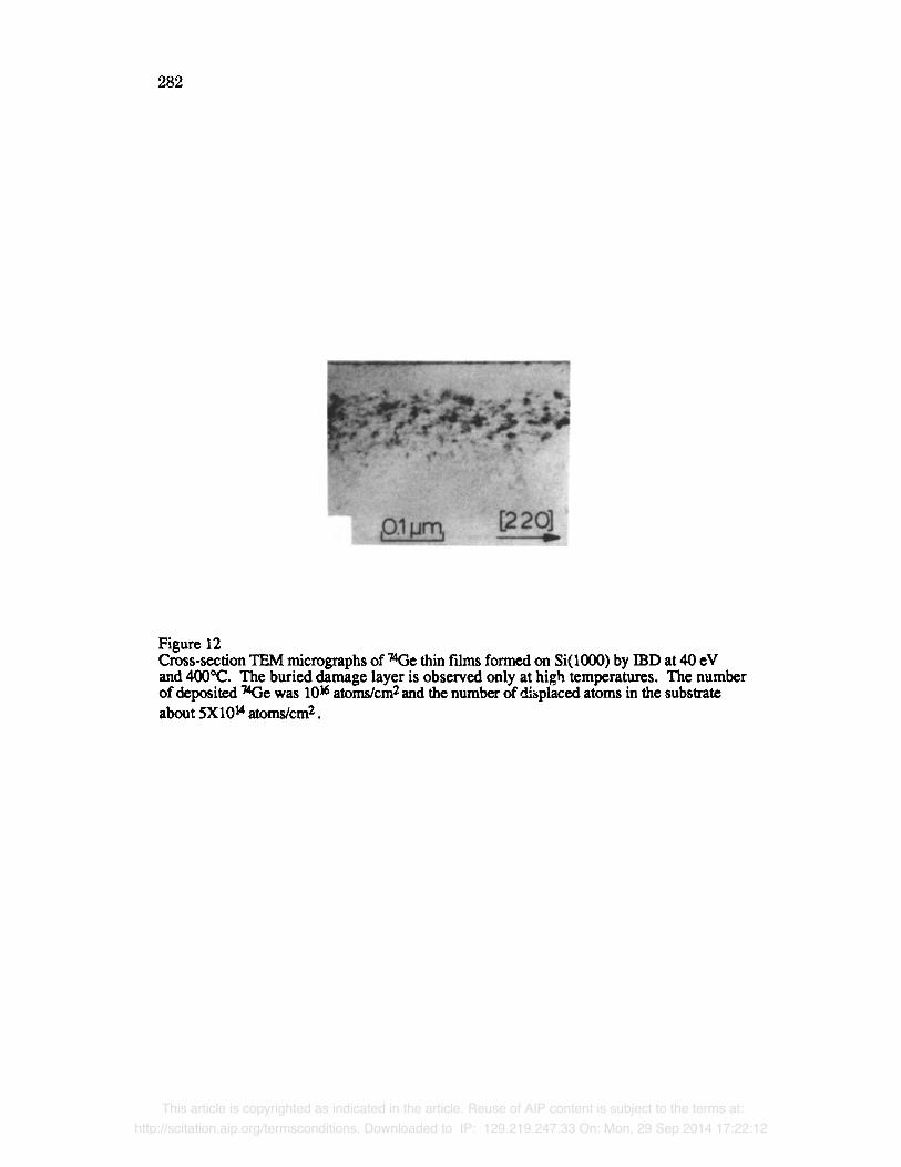
282
Figure 12 Cross-section TEM micrographs of V4Gc thin films formed on Si(1000) by IBD at 40 cV and 400~ The buried damage layer is observed only at high temperatures. The number of deposited ~4Ge was I0 ~ atoms/cm 2 and the number of ~splaced atoms in the subsu'atc
about 5X I0 ~ atoms/cm 2 .
282
,0.1 fJrT\ [220]
Figure 12Cross-section TEMmicrographs of'14Qe thin films fonned on Si(1(00) by IBD at 40 eVand 400°C. The buried damage layer is observed only at high temperatures. The numberof deposited '14Qe was 1016 atomslcm2and the number of displaced atoms in the substrate
about 5X10¹⁴ atomslcm2 .
This article is copyrighted as indicated in the article. Reuse of AIP content is subject to the terms at:
http://scitation.aip.org/termsconditions. Downloaded to IP: 129.219.247.33 On: Mon, 29 Sep 2014 17:22:12

283
0
Z
0.50
0.45
0.40
0.35
0.30
0.25
0.20
0.15
. . . . ! . . . . i . . . . ! . . . . i . . . . ! . . . . i . . . . t . . . . ! . . . . ! . . . .
o 3~ 40 eV -> Si(lO0), T = 600 ~ o AF1ER SPUTTERING WITH 3 keV h" + + ANNEAL FOR 20" AT 950 ~ 5" AT 1100 ~
CHANNEUNG ALONG <110> AXIS
IBD Si Si(~00)
0 . 1 0 ~
0.05
0.00 -100.-50. O. 50. 100. 150. 200. 250. 300. 350. 400.
DEPTH (nm)
Figure 13 RBS data taken on the IBD film shown in Figures 7 and 14b. The film was annealed after IBD and argon sputter-cleaning. After 10 minutes at 950~ and 5 minutes at 1100~ little damage reduction was observed in the film.
283
0.45 <> JOSi• 40 eV -> $(100), T = 600°
o AFTER SPUITERING WITH 3 keY N+
0.40 + ANNEAl.. FOR 20' AT 950°, 5' AT 1100°
0.35 CHANNEUNG ALONG <110> AXIS
0.20
0.25
'On0."">=S
0.15
ISO Si $(100)
0.10
0.05
o.oo.....-100. -50. 100. 150. 200. 250. 300. 350. 400.
DEPTH (nm)
Figure 13RBS data taken on the IBD film shown in Figures 7 and 14b. The film was annealed afterIBD and argon sputter-cleaning. After 10 minutes at 950°C and 5 minutes at I 100°C littledamage reduction was observed in the film.
This article is copyrighted as indicated in the article. Reuse of AIP content is subject to the terms at:
http://scitation.aip.org/termsconditions. Downloaded to IP: 129.219.247.33 On: Mon, 29 Sep 2014 17:22:12
284
rim/rain. Epitaxial growth was observed both for 20 eV and 40 eV ions for three temperatures (350~ 400~ and 600 ~ These data are shown in Fig. 14a-g, which also shows the maximal solid phase epitaxial regrowth rate of silicon amorphised by ion implantation of a single crystal, for comparison (from reference [23]). It can be seen that for IBD at 600~ thermal mobility should play a significant role during growth since thermally activated motion of the amorphons/single crystal interface takes place at a rate that is significantly larger that the rate at which silicon atoms are deposited on the substrate. One can argue that the IBD deposition rate (0.6 nm/min) is slow enough that epitaxial ordering occurs through thermal annealing rather than through ion-induced atomic collisions processes. At 400~ and below, however, the contribution of thermal epitaxy is insignificant, as the solid phase epitaxial growth rate becomes infinitesimal (<0.06 rim/rain). Epitaxial growth in that range of temperature can thus be attributed to the effect of the ion beam.
Ion Beam Epitaxy at 600 ~
These observations are directly confn'med by the comparison of cross-section TEM micrographs of f'rims grown at 600~ and 400~ respectively (Fig. 14b-e). At higher temperatures, extended defects are found in the films, close to the thin ftlm/substrate interface, which is the region submitted to the longest anneal duration during deposition. Dislocation loops or stacking faults are found in the first half of the film that is closest to the interface, while the other half, which is closer to the surface, does not exhibit as many defects (Fig.14b-c). It appears thus that extended defects are nucleated at the interface. Ion channeling measurements confirmed this depth distribution of defects, with minimum yields close to that of single crystals near the surface region (3.5-4%) and highest nearby the interface (10-20%) in 100 nm thick films (Fig. 14r These observations are also consistent with the fact that the surface acts as a recombination sink for defects while the interface acts as a trap. Thus, migration of ion beam generated defects occurs during growth and can be attributed to thermal diffusivity, and, most probably, if the interface were defect-free, no extended defects would be nucleated. X-ray Bragg profiling has provided evidence that the films are uniaxially strained. The substrates where buried damage loops are found, as in Fig. 12, are also uniaxially strained [9].
Ion Beam Epitaxy at 350-400~
On the other hand, films grown at 350~ and 400~ exhibit fewer visible defects in cross- section TEM micrographs, and a much more uniform epitaxial quality. The defects nature and distribution is also radically different. A few threading dislocations, instead of the many dislocation loops, are nucleated from the interface and reach the surface. Their number and location is a direct function of interface quality in terms of microstructure: the more numerous dislocations in Fig. 14d directly correlate with the large number of interface defects while the low density of such dislocations in Fig. 14r scales with the smaller number of interface defects observed. In addition, the defect densities of these interfaces are much higher than in Fig. 14b-c, but the total number of defects in the films is significantly lower. This indicates that if defects are nucleated at the interface during growth at 350-400 ~ they do not grow much further and do not extend into the films as in the case of the higher temperature depositions. Ion channeling data confirms part of these TEM observations: the minimum yields are typically 4 % near the surface and 6 % nearby the interface in a 100 nm thick f'dm. But the minimum yields do not drop below 4 %, revealing that at least 1% of the atoms are still displaced from lattice sites (Fig.14g). Such a large density of defects seems at first to be incompatible with the TEM observations. TEM has a better sensitivity to defects than RBS and the defect density in Fig. 14e-g is lower than those for the higher temperatures (Fig. 14b-c). X-Ray Bragg profiling demonstrated that these films were also strained.
While still pursuing more detailed X-ray investigations on these structures, which have until now mostly confirmed these first measurements, we speculate that the peculiar growth mode by which the films are formed may lead to specific defects configurations leading to present
284
nm/min. Epitaxial growth was observed both for 20 eV and 40 eV ions for three temperatures(350°C, 4OQ°C and 600 0c). These data are shown in Fig. 14a-g, which also shows the maximalsolid phase epitaxial regrowth rate of silicon amorphised by ion implantation of a single crystal, forcomparison (from reference (23]). It can be seen that for ffiD at 6OQ°C, thermal mobility shouldplaya significant role during growth since thermally activated motion of the amorphous/singlecrystal interface takes place at a rate that is significantly larger that the rate at which silicon atomsare deposited on the substrate. One can argue that the ffiD deposition rate (0.6 nm/min) is slowenough that epitaxial ordering occurs through thermal annealing rather than through ion-inducedatomic collisions processes. At 4OQ°C and below, however, the contribution of thermal epitaxy isinsignificant, as the solid phase epitaxial growth rate becomes infinitesimal (<0.06 nm/min).Epitaxial growth in that range of temperature can thus be attributed to the effect of the ion beam.
Ion Beam Epitaxy at 600 "C
These observations are directly confirmed by the comparison of cross-section TEMmicrographs of films grown at 6OQ°C and 400°C respectively (Fig. 14b-e). At highertemperatures, extended defects are found in the films, close to the thin film/substrate interface,which is the region submitted to the longest anneal duration during deposition. Dislocation loopsor stacking faults are found in the first half of the film that is closest to the interface, while the otherhalf, which is closer to the surface, does not exhibit as many defects (Fig.14b-c). It appears thusthat extended defects are nucleated at the interface. Ion channeling measurements confirmed thisdepth distribution of defects, with minimum yields close to that of single crystals near the surfaceregion (3.5-4%) and highest nearby the interface (10-20%) in 100 om thick films (Fig. 14e).These observations are also consistent with the fact that the surface acts as a recombination sink fordefects while the interface acts as a trap. Thus, migration of ion beam generated defects occursduring growth and can be attributed to thermal diffusivity, and, most probably, if the interfacewere defect-free, no extended defects would be nucleated. X-ray Bragg profiling has providedevidence that the films are uniaxially strained. The substrates where buried damage loops arefound, as in Fig. 12, are also uniaxially strained [9].
Ion Beam Epitaxy at 350-400"C
On the other hand, films grown at 350°C and 400°C exhibit/ewer visible defects in cross-section TEMmicrographs, and a much more unifonn epitaxial quality. The defects nature anddistribution is also radically different A few threading dislocations, instead of the manydislocation loops, are nucleated from the interface and reach the surface. Their number andlocation is a direct function of interface quality in terms ofmicrostructure: the more numerousdislocations in Fig. 14d directly correlate with the large number of interface defects while the lowdensity of such dislocations in Fig. 14e scales with the smaller number of interface defectsobserved. In addition, the defect densities of these interfaces are much higher than in Fig. 14b-c,but the total number of defects in the films is significantly lower. This indicates that ifdefects arenucleated at the interface during growth at 350-400 °C, they do not grow much further and do notextend into the films as in the case of the higher temperature depositions. Ion channeling dataconfirms part of these TEM observations: the minimum yields are typically 4 % near the surfaceand 6 % nearby the interface in a 100 nm thick film. But the minimum yields do not drop below4 %, revealing that at least 1% of the atoms are still displaced from lattice sites (Fig.14g). Such alarge density of defects seems at first to be incompatible with the TEM observations. TEM has abetter sensitivity to defects than RBS and the defect density in Fig. 14e-g is lower than those forthe higher temperatures (Fig. 14b-c). X-Ray Bragg profiling demonstrated that these films werealso strained.
While still pursuing more detailed X-ray investigations on these structures, which haveuntil now mostly confirmed these first measurements, we speculate that the peculiar growth modeby which the films are formed may lead to specific defects configurations leading to present
This article is copyrighted as indicated in the article. Reuse of AIP content is subject to the terms at:
http://scitation.aip.org/termsconditions. Downloaded to IP: 129.219.247.33 On: Mon, 29 Sep 2014 17:22:12
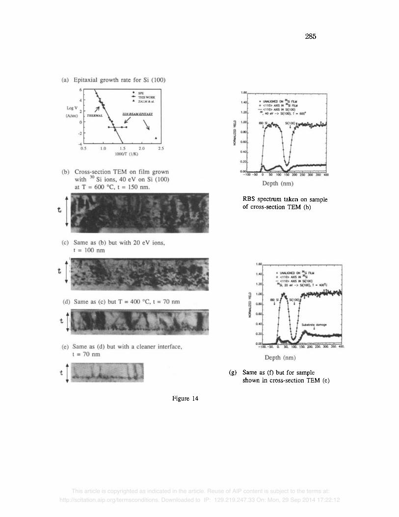
285
RBS spectrum taken on sample
of cross-section TEM (b)
(g) Same as (f) but for sample
shown in cross-section TEM (e)
Figure 14
285
(a) Epitaxial growth rate for Si (100)
Depth (nm)
• UtWJCHO) ON r&JiIo <110> AXIS II JIg n..w- <110'> AXIS II 51(100)
" .... '" -) , • fIJtf
I ....
1.10
\
1.0 1.5 2.0 2.5
looorr (11K)
-4'------''---->.----'---.-J0.5
-2
log v2
(Mec)
o
(b) Cro . ection TEM on film grown
with 30 Si ions, 40 eV on Si (100)
at T = 600 °e, t = 150 nm.
t
'-:1" '.' }-,.. . ..\"
r ... II .,. .- ...... . ......
RBS spectrum taken on sample
of cross-section TEM (b)
(c) Same a (b) but with 20 eV ions.
t = 100 nm
t
Depth (nm)
1.10
I .... • UPW.QO C»4.11lsi Jt.Mo <110'> Am IIj -s;
1.20- <,,0> AXIS .. 51(100)"sl. 20 .. -) 51('00), , • 40IIc
OJlO
io.to
0.10
O.
(g) Same as (f) but for sample
shown in cross-section TEM (e)
(d) Same a (c) but T = 400 °C. t = 70 nm
(e) Same as (d) but with a cleaner interface,
t = 70 nm
t
t
Figure 14
This article is copyrighted as indicated in the article. Reuse of AIP content is subject to the terms at:
http://scitation.aip.org/termsconditions. Downloaded to IP: 129.219.247.33 On: Mon, 29 Sep 2014 17:22:12
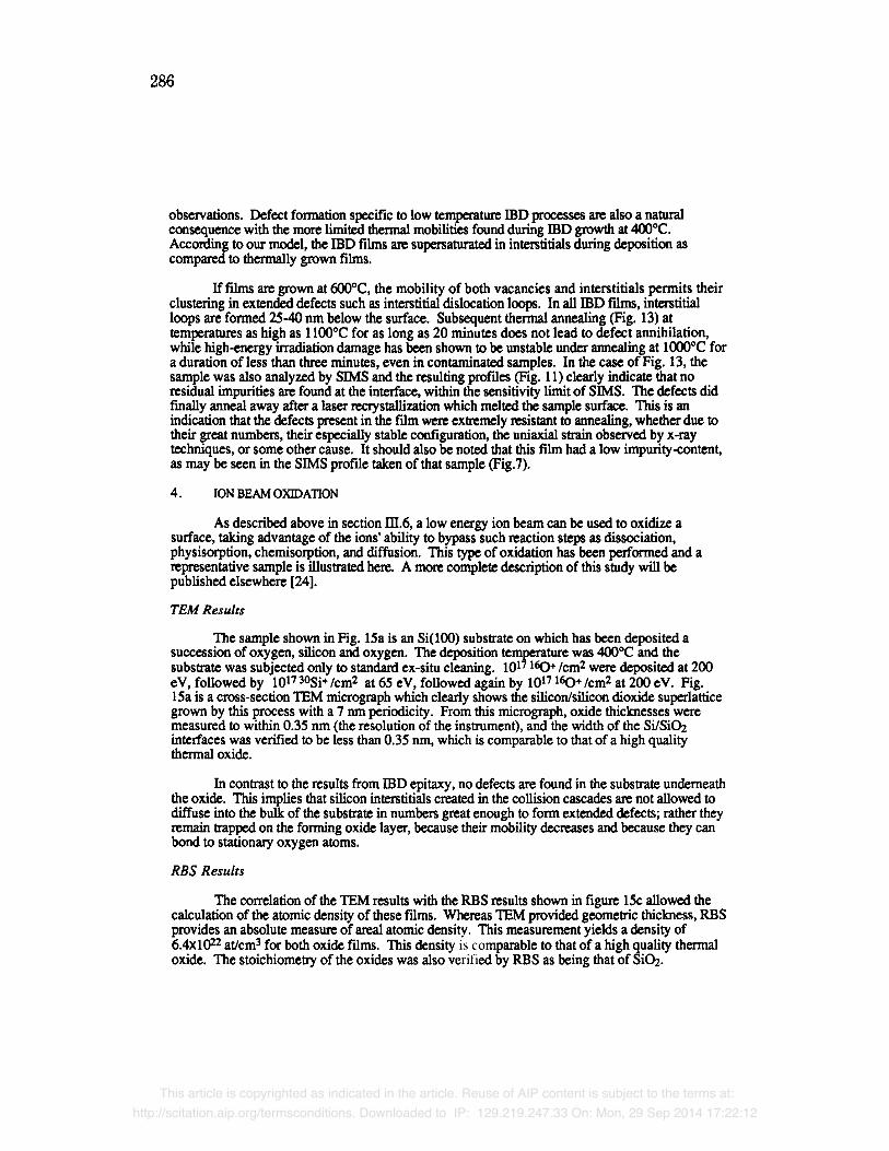
286
observations. Defect formation specific to low temperature IBD processes are also a natural consequence with the more limited thermal mobilities found during IBD growth at 400~ According to our model, the IBD films are supersatttrated in interstitials during deposition as compared to thermally grown films.
If fiims are grown at 600~ the mobility of both vacancies and interstitials permits their clustering in extended defects such as interstitial dislocation loops. In all IBD fdms, interstitial loops arc formed 25-40 nm below the surface. Subsequent thermal annealing (Fig. 13) at temperatures as high as 1100~ for as long as 20 minutes does not lead to defect annihilation, while high-energy irradiation damage has been shown to be unstable under annealing at 1000~ for a duration of less than three minutes, even in contaminated samples. In the case of Fig. 13, the sample was also analyzed by SIMS and the resulting profdes (Fig. 11) clearly indicate that no residual impurities are found at the interface, within the sensitivity limit of SIMS. The defects did finally anneal away after a laser rccrystallization which melted the sample surface. This is an indication that the defects present in the film were extremely resistant to annealing, whether due to their great numbers, their especially stable configuration, the uniaxial strain observed by x-ray techniques, or some other cause. It should also be noted that this film had a low impurity-content, as may be seen in the SIMS profde taken of that sample (Fig.7).
4. ION BEAM OXIDATION
As described above in section I1/.6, a low energy ion beam can be used to oxidize a surface, taking advantage of the ions' ability to bypass such reaction steps as dissociation, physisorption, chemisorption, and diffusion. This type of oxidation has been performed and a representative sample is illustrated here. A more complete description of this study will be published elsewhere [24].
TEM Results
The sample shown in Fig. 15a is an Si(100) subslrate on which has been deposited a succession of oxygen, silicon and oxygen. The deposition temperature was 400~ and the substrate was subjected only to standard ex-situ cleaning, l017 l('O+/era 2 were deposited at 200 eV, followed by 10173~ 2 at 65 eV, followed again by l017160+/cm2 at 200 eV. Fig. 15a is a cross-section TEM micrograph which clearly shows the silicon/silicon dioxide supcrlattice grown by this process with a 7 mn periodicity. From this micrograph, oxide thicknesses were measured to within 0.35 nm (the resolution of the instrument), and the width of the Si/SiO2 interfaces was verified to be less than 0.35 nm, which is comparable to that of a high quality thermal oxide.
In contrast to the results from IBD epitaxy, no defects are found in the substrate underneath the oxide. This implies that silicon interstitials created in the collision cascades are not allowed to diffuse into the bulk of the substrate in numbers great enough to form extended defects; rather they remain trapped on the forming oxide layer, because their mobility decreases and because they can bond to stationary oxygen atoms.
RBS Results
The correlation of the TEM results with the RBS results shown in figure 15c allowed the calculation of the atomic density of these films. Whereas TEM provided geome~ic thickness, RBS provides an absolute measure of areal atomic density. This measurement yields a density of 6.4XI022 at/cm 3 for both oxide films. This density is comparable to that of a high quality thermal oxide. The stoichiometry of the oxides was also verified by RBS as being that of SiO2.
286
observations. Defect fonnation specific to low temperaturemo processes are also a naturalconsequence with the more limited thennal mobilities found duringmo growth at 400°C.According to our model, themo films are supersaturated in interstitials during deposition ascompared to thennally grown films.
If films are grown at 600°C, the mobility of both vacancies and interstitials permits theirclustering in extended defects such as interstitial dislocation loops. In allmo films, interstitialloops are formed 25-40 nm below the surface. Subsequent thennal annealing (Fig. 13) attemperatures as high as I100°C for as long as 20 minutes does not lead to defect annihilation,while high-energy irradiation damage has been shown to be unstable under annealing at lOOO°C fora duration of less than three minutes, even in contaminated samples. In the case ofFig. 13, thesample was also analyzed by SIMS and the resulting profiles (Fig. II) clearly indicate that noresidual impurities are found at the interface, within the sensitivity limit of SIMS. The defects didfmally anneal away after a laser recrystallization which melted the sample surface. This is anindication that the defects present in the film were extremely resistant to annealing, whether due totheir great numbers, their especially stable configuration, the uniaxial strain observed by x-raytechniques, or some other cause. It should also be noted that this film had a low impurity-content,as may be seen in the SIMS profile taken of that sample (Fig.7).
4. ION BEAMOXIDATION
As described above in section ill.6, a low energy ion beam can be used to oxidize asurface, taking advantage of the ions' ability to bypass such reaction steps as dissociation,physisorption, chemisorption, and diffusion. This type ofoxidation has been performed and arepresentative sample is illustrated here. Amore complete description of this study will bepublished elsewhere [24].
TEM Results
The sample shown in Fig. 15a is an Si(l00) substrate on which has been deposited asuccession of oxygen, silicon and oxygen. The deposition was 400°C and thesubstrate was subjected only to standard ex-situ cleaning. 101 16()+ Icm2were deposited at 200eV, followed by 1017 30Si+ Icm2 at 65 eV, followed again by 1017 16()+ Icm2 at 200 eV. Fig.15a is a cross-section TEMmicrograph which clearly shows the silicon/silicon dioxide superlatticegrown by this process with a 7 nm periodicity. From this micrograph, oxide thicknesses weremeasured to within 0.35 nm (the resolution of the instrument), and the width of theinterfaces was verified to be less than 0.35 nm, which is comparable to that of a high qualitythermal oxide.
In contrast to the results frommo epitaxy, no defects are found in the substrate underneaththe oxide. This implies that silicon interstitials created in the collision cascades are not allowed todiffuse into the bulk of the substrate in numbers great enough to form extended defects; rather theyremain trapped on the forming oxide layer, because their mobility decreases and because they canbond to stationary oxygen atoms.
RBS Results
The correlation of the TEM results with the RBS results shown in figure 15c allowed thecalculation of the atomic density of these films. Whereas TEM provided geometric thickness, RBSprovides an absolute measure of areal atomic density. This measurement yields a density of6.4x1()22 atlcm3for both oxide films. This density is comparable to that of a high quality thennaloxide. The stoichiometry of the oxides was also verified by RBS as being that of SiCh.
This article is copyrighted as indicated in the article. Reuse of AIP content is subject to the terms at:
http://scitation.aip.org/termsconditions. Downloaded to IP: 129.219.247.33 On: Mon, 29 Sep 2014 17:22:12
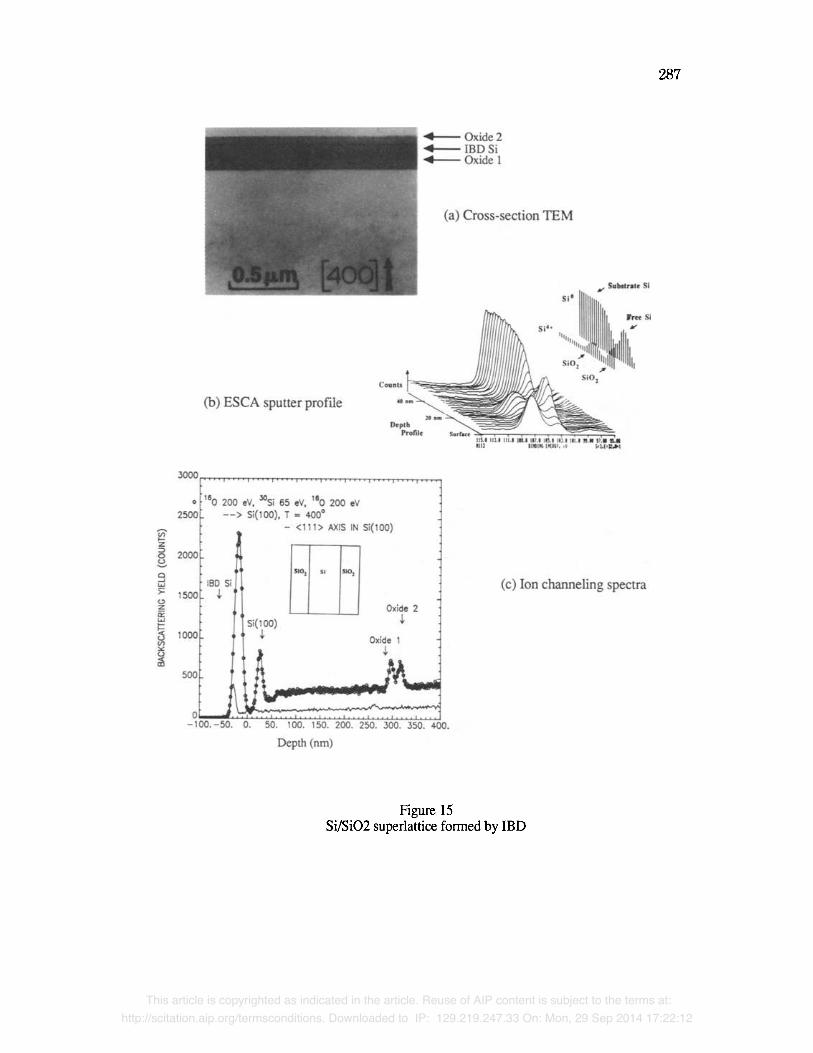
287
Figure 15 Si/SiO2 superlattice formed by IBD
287
(b) ESCA sputter profile
4---- Oxide 24----IBD Si4---- Oxide 1
(a) Cross-section TE
(c) Ion channeling spectra
Oxide 2
Oxide 1
Si(I00)
ISO Si
500
1000
• "0 200 eV. JOSi 65 eV. '80 200 eV
2500 --> Si(100). T = 400·
- <111> AXIS I Si( 00)
1500
-100. -50. O. 50. 100. 150. 200. 250. 300. 350. 400.
Depth (nm)
Figure 15Si/Si02 superlattice formed by ffiO
This article is copyrighted as indicated in the article. Reuse of AIP content is subject to the terms at:
http://scitation.aip.org/termsconditions. Downloaded to IP: 129.219.247.33 On: Mon, 29 Sep 2014 17:22:12
288
ESCA Results
Chemical bonding states in the IBD oxide were characterized using angular-resolved ESCA measurements on a PHI Model 5400 at the Physical Electronics Division of Perkin-Elmer. A sputter profile through the sample illustrating two photoemissions measured from the silicon as a function of depth is shown in Fig. 15b. The binding energy peak near 107 eV corresponds to silicon twice bonded to oxygen, while the peak near 103 eV corresponds to silicon bonded only to silicon. The modulation in chemical state through the film is demonstrated by the transition observed from one photoemission to the other. No other photoemission was detected, indicating that no partial oxidation states were present. The angular resolution was used to verify that the overlapping of peaks, for example the appearance of a free silicon signal at the surface, was due to photoemission from subsurface regions and not due to the presence cf free silicon at the surface.
Overcoming limitations of lBD for growing oxides
These observations illustrate the interest of oxides prepared by IBD. The structures of these oxides are of a quality comparable with that of thermal oxides, and the oxide can be grown at
surprisingly low temperatures and in an environment compatible with UHV materials processing. However, there are limitations on growing thick oxides by IBD. That is, once the oxide grows thicker than the mean projected range of the ion, film growth is limited by solid phase diffusion, and the time for film growth increases exponentially with film thickness, as observed by independent investigation. This limitation can be overcome by alternating, in our example, deposition of silicon and oxygen using an ion source with great material versatility.
A more elegant solution of this problem in terms of efficiency and technological potential is the simultaneous use of a silicon molecular beam and an oxygen ion beam: CIMD. Besides being able to grow high quality oxides on silicon, CIMD would allow the growth of heterodielectrics.
For instance, silicon dioxide could be formed on germanium or gallium arsenide using a silicon molecular source and an oxygen ion source, thereby circumventing the problems of germanium oxide instability and gallium and arsenic oxides' immiscibility. This capability of CIMD is an attractive solution to the formation of high quality dielectrics on compound semiconductors.
V. CONCLUSIONS
1. FUNDAMENTAL CONCEPTS OF IBD AND CIMD
A simple collisional model has been developed to describe thin film deposition by low energy ion beams. Through this model, we have been able to study the growth mechanism and interpret certain properties of IBD frims, such as compositionally sharp interfaces, high atomic density, low temperature epitaxy and the formation of silicon and germanium oxides. Our model has enabled an interpretational analysis of specific properties of IBD films, such as interstitial loop formation, unique damage distribution and a temperature dependence of epitaxial quality. The fundamental understanding elicited by this modeling has led to the conception of a novel processing technique which can overcome the limitations of IBD both in low temperature epitaxy and low temperature formation of dielectlic films: CIMD.
2. FUTURE WORK
The investigations of materials growth by IBD has brought forth important insights into some aspects of epitaxial ordering processes and defect formation by low-energy ion beams. The next step is to use this knowledge to overcome current limitations in materials processing due to the role of temperature in deleterious effects as the dimensions of heterostructures shrink. The control of atomic mobility by collisions processes rather than by temperature offers the possibility of growing silicon-based heterostructures in a temperature range within which dopant diffusion,
288
ESCA Results
Chemical bonding states in the ffiD oxide were characterized using angular-resolved ESCAmeasurements on a Pill Model 5400 at the Physical Electronics Division of Perkin-Elmer. Asputter profIle through the sample illustrating two photoemissions measured from the silicon as afunction of depth is shown in Fig. 15b. The binding energy peak near 107 eV corresponds tosilicon twice bonded to oxygen, while the peak near 103 eV corresponds to silicon bonded only tosilicon. The modulation in chemical state through the fIlm is demonstrated by the transitionobserved from one photoemission to the other. No other photoemission was detected, indicatingthat no partial oxidation states were present. The angular resolution was used to verify that theoverlapping of peaks, for example the appearance of a free silicon signal at the surface, was due tophotoemission from subsurface regions and not due to the presence cf free silicon at the surface.
Overcoming limitations ofIBD for growing oxides
These observations illustrate the interest of oxides prepared by ffiD. The structures ofthese oxides are of a quality comparable with that of thermal oxides, and the oxide can be grown atsurprisingly low temperatutes and in an environment compatible with UlN materials processing.However, there are limitations on growing thick oxides by ffiD. That is, once the oxide growsthicker than the mean projected range of the ion, fIlm growth is limited by solid phase diffusion,and the time for film growth increases exponentially with fIlm thickness, as observed byindependent investigation. This limitation can be overcome by alternating, in out example,deposition of silicon and oxygen using an ion source with great material versatility.
A more elegant solution of this problem in terms of efficiency and technological potential isthe simultaneous use of a silicon molecular beam and an oxygen ion beam: CIMD. Besides beingable to grow high quality oxides on silicon, CIMD would allow the growth of heterodielectrics.For instance, silicon dioxide could be formed on germanium or gallium arsenide using a siliconmolecular SOutce and an oxygen ion source, thereby circumventing the problems of germaniumoxide instability and gallium and arsenic oxides' immiscibility. This capability ofCIMD is anattractive solution to the formation of high quality dielectrics on compound semiconductors.
V. CONCLUSIONS
I. FUNDAMENTAL CONCEPTS OF lBD AND ClMO
A simple collisional model has been developed to describe thin fIlm deposition by lowenergy ion beams. Through this model, we have been able to study the growth mechanism andinterpret certain properties of ffiD fIlms, such as compositionally sharp interfaces, high atomicdensity, low temperature epitaxy and the formation of silicon and germanium oxides. Our modelhas enabled an interpretational analysis of specific properties of ffiD fIlms, such as interstitial loopformation. unique damage distribution and a temperature dependence of epitaxial quality. Thefundamental understanding elicited by this modeling has led to the conception of a novelprocessing technique which can overcome the limitations of ffiD both in low temperature epitaxyand low temperature formation of dielectric fIlms: CIMD.
2. FUTURE WORK
The investigations ofmaterials growth by ffiD has brought forth important insights intosome aspects of epitaxial ordering processes and defect formation by low-energy ion beams. Thenext step is to U5C this knowledge to overcome current limitations in materials processing due to therole of temperature in deleterious effects as the dimensions of heterostructutes shrink. The controlof atomic mobility by collisions processes rather than by temperature offers the possibility ofgrowing silicon-based heterostructures in a temperatute range within which dopant diffusion,
This article is copyrighted as indicated in the article. Reuse of AIP content is subject to the terms at:
http://scitation.aip.org/termsconditions. Downloaded to IP: 129.219.247.33 On: Mon, 29 Sep 2014 17:22:12

289
surface segregation, and thermal decomposition will be reduced to insignificant levels. The inherent limitations due to the IBD process itself, excess interstitial generation, can be overcome by combining simultaneous deposition by IBD and MBE into the CIMD technique which has the potential to bring displacement rates under control and thus hold defect generation to a tolerable level. This is the direction of our future theoretical and experimental work.
ACKNOWI .EI~EMENTS
The authors wish to acknowledge J.P. Biersack, L.C. Feldman, M. Grabow, G. Kalonji, D.F. Pedraza, M.T. Robinson, P.C. Zalm and D.M. Zehner for stimulating discussions, helpful comments and advice. We also wish to acknowledge J.S. Moore and D.K. Thomas for their assistance in maintaining, preparing and running the ion implantation accelerator, C.W. Boggs and J.T. Luck for the delicate work of thinning the cross-sections for the TEM measurements, and Lillian Gilbradsen of the Physical Electronics Division of Perkin-Elmer for her technical help and patience in careful and repeated angular-resolved ESCA measurements.
REFERENCES
[1] N. Herbots and O.C. Hellman, US Patent pending (1987).
[2] P. Tsukizor T. Nakai and N. Ohmae, J. Appl. Phys., 42 p. 4770 (1976).
[3] K. Yagi, S. Tamura, T. Tokuyama, Jap. J. Appl. Phys. 16, 245-251 (1977).
[4] T. Tokuyama, K. Yagi, K. Miyake, M. Tamura, N. Natsuaki, and S. Ta~hi, Nucl. Inst. and Meth. 182/183 pp.241- 250 (1981).
[5] P.C. Zalm and L.J. Beckers, Appl. Phys. Left., 41 p. 167 (1982).
[6] N. Herbots, B.R. Appleton, T.S. Noggle, R.A. Zuhr and SJ. Pennycook, Nucl. Instr. and Meth., B 13, pp. 250-258 (1986).
[7] N. Herbots, B.R. Appleton, S.J. Pennycook, T.S. Noggle and R.A. Zuhr, in Beam-Solid Interactions and Phase Transformations. Eds. H. Kurtz, G.L. Olson and J.M. Poate, Mat. Res. Soc. Syrup. Proc., Vol. 51, pp. 3669-74 (1986).
[8] N. Herbots, B.R. Appleton, T.S. Noggle, S.J. Pennycook, R.A. Zuhr and D.M. Zhener, Semiconductor-based HeterosU'uctures: Interfacial Slructure and Stability. Eds. M.L. Green, J.E.E. Baglin, G.Y. Chin, H.W. Deckman, W. Mayo andD. Narashinham, pp. 335-349 (1986).
[9] R.A. Zuhr, B.R. Appleton, N. Herbots, B.C. Larson, T.S. Noggle and S. J. Pennycook, J. Vac. Sci. Tech., A5 (4), pp. 2135-2139 (1987).
[10] B.R. Appleton, SJ. Pennycook, R.A. Zuhr, N. Herbots and T.S. Noggle, Nucl. Instr. and Meth., B 19/20, pp.975-982 (1987).
[11] N. Herbots, D.M. Zhener, B.R. Appleton, S.J. Pennycook, T.S. Noggle, and R.A. Zuht, to be submitted to Appl. Phys. Lett. (1988).
[12] J.E. Greene, A. Rockett and J.-E. Sundgren, in Photon. Beam. and Plasma Stimulated Chemical Processes at
Surfaces. Eds. V.M. Donnelly, I.P. Herman and M. Hirose, Mat. Res. Soc. Syrup. Proc., Vol. 75, pp. 39-35 (1987).
[13] J.E. Greene, Crit. Rev. in Sol. St. and Mater. Sci., Vol. 11, 1, pp. 47-227 (1983).
[14] J.M.E. Harper, Solid State Technology, 30(4), pp. 129-134 (1987). [See also JJ. Coumo, J.M.E. Harper, and H.T.G. Hentzell, J. Appl. Phys., 58 (1) (1985) for an extensive review and bibliography from these authors.]
289
surface segregation, and thennal decomposition will be reduced to insignificant levels. Theinherent limitations due to the IBD process itself, excess interstitial generation, can be overcome bycombining simultaneous deposition by IBD and MBE into the CIMD technique which has thepotential to bring displacement rates under control and thus hold defect generation to a tolerablelevel. This is the direction of our future theoretical and experimental work.
ACKNOWLEDGEMENTS
The authors wish to acknowledge J.P. Biersack, L.C. Feldman, M. Grabow, G. Kalonji,D.F. Pedraza, M.T. Robinson, P.C. Zalm and D.M. Zehner for stimulating discussions, helpfulcomments and advice. We also wish to acknowledge J.S. Moore and D.K. Thomas for theirassistance in maintaining, preparing and running the ion implantation accelerator, C.W. Boggs andJ.T. Luck for the delicate work of thinning the cross-sections for the TEM measurements, andLillian Gilbradsen of the Physical Electronics Division ofPerkin-Elmer for her technical help andpatience in careful and repeated angular-resolved ESCA measurements.
REFERENCES
[l] N. Herbots and O.c. Hellman, US Patent pending (1987).
[2] P. Tsukizoe, T. Nakai and N. Ohmae, J. Appl. Phys.. 42 p. 4770 (1976).
[3] K. Yagi, S. Tamura, T. Tokuyama, Jap. J. Appl. Phys. 16.245-251 (1977).
[4] T. Tokuyama, K. Yagi, K. Miyake, M. Tamura, N. Natsuaki, and S. Tachi, Nucl. Insl. and Melh. 1821183
pp.241- 250 (1981).
[5] P.C. Zalm and L.J. Beckers, Appl. Phys. Lett., 41 p. 167 (1982).
[6] N. Herbots, B.R. Appleton, T.S. Noggle, R.A. Zuhr and SJ. Pennycook, Nucl. Instr. and Melh., B 13,pp.250-258 (1986).
[7] N. Herbats, B.R. Appleton, SJ. Pennycook, T.S. Noggle and R.A. Zuhr, in Beam-Solid Interactions and Phase
Transformations Eds. H. Kurtz, G.L. Olson and 1.M. Poate, Mal. Res. Soc. Symp. Proc., Vol. 51, pp. 3669-74
(1986).
[8] N. Herbats, B.R. Appleton, T.S. Noggle, S.l. Pennycook, R.A. Zuhr and O.M. Zhener, Semjconductor-baSed
Heterostructures: Interfacial Structure and Stability, Eds. M.L. Green, 1.E.E. Baglio, G.Y. Chin, H.W. Deckman,
W. Mayo and O. Narashinharn, pp. 335-349 (1986).
[9] R.A. Zuhr, B.R. Appleton, N. Herbots, B.C. Larson, T.S. Noggle and S. 1. Pennycook, J. Vac. Sci. Tech., A5(4), pp. 2135-2139 (1987).
[10] B.R. Appleton, SJ. Pennycook, R.A. Zuhr, N. Herbats and T.S. Noggle, Nucl. Inslr. and Melh., B 19120,
pp.975-982 (1987).
[11] N. HerbolS, OM. Zhener, B.R. Appleton, S.J. Pennycook, T.S. Noggle, and R.A. ZUhr, to be submitted to
Appl. Phys. Lett. (1988).
[l2] l.E. Greene, A. Rockett and 1.-E. Sundgren, in Photon Beam and Plasma Stimulated Chemjca! Processes at
Eds. V.M. Donnelly, J.P. Herman and M. Hirose, Mal. Res. Soc. Symp. Proc., Vol. 75, pp. 39-35
(1987).
[13] 1.E. Greene, Cril. Rev. in Sol. SI. and Mater. Sci., Vol. 11, I, pp. 47-227 (1983).
[14] 1.M.E. Harper, Solid Slale Technology, 30(4), pp. 129-134 (1987). [See also JJ. Coumo, 1.M.E. Harper,and H.T.G. Hentzell, J. Appl. Phys., 58 (1) (1985) for an extensive review and bibliography from these authors.]
This article is copyrighted as indicated in the article. Reuse of AIP content is subject to the terms at:
http://scitation.aip.org/termsconditions. Downloaded to IP: 129.219.247.33 On: Mon, 29 Sep 2014 17:22:12
290
[15] S.S. Todorov, S.L. Schillinger, and E.R. Fossum in Photon. Beam. and Plasma S6mulated Chemical Processes at Surfaces. Eds. V.M. Donnelly, I.P. Herman and M. Hirose, Mat. Res. Soc. Symp. Proc., Vol. 75, pp.
349-354 (1987).
[16] B.R. Appleton, R.A. Zuhr, T.S. Noggle, N. Herbots, and SJ. Pannycook in photon. Beam. and Plasma Stimulated Chemical Processes at Surfaces. Eds. V.M. Donnelly, I.P. Herman and M. Hirose, Mat. Res. Soc.
Syrup. Proc., Vol. 75, pp. 39-35 (1987).
[17] M.H. Grabow and G.H. Gilmer in Ini6al Sta2es of Eoitaxial Growth. Eds. R. Hull, J.M. Gibson, and D.A.
Smith, Mat. Res. Soc. Syrup. Proc., Voi. 94, pp. 15-24 (1987).
[18] These observatices were made during discussions on MD simulations on metals, with D.H. Harrison, Jr., who is here gratefully acknowledged for having made the time and the data available for such discussions.
[19] Values established by running the modified TRIM code used in this work for higher energies and confirmed by i n , d e n t calculations by J.P. Biersack.
[20] A. Tenner, ~ , PhD thesis, FOM-Instituut, Amsterdam, The Netherlands (1986).
[21] U. GOsele in Semiconductor Silicon 1986. Eds. H.R. Huff, T. Abe and B. Kolbesen (Pannington: The Eleco'ocbemical Society), p. 541 (1986).
[22] R.A. Zuhr, G.D. Alton, B.R. Appleton, N. Herbots, T.S. Noggle and S.J. Pennycook in Materials Modification and Growth Usin~ Ion Beam.x, Eds. UJ. Gibson, A.E. White and P.P. Pronko, Mat. Res. Soc. Syrup.
Proc., Vol. 93, pp. 243-251 (1987).
[23] E.P. Donovan, F. Spaepen, D. Tumbull, J.M. Poate and D.C. Jacobson, J. Appl. Phys., $7 (1985).
[24] N. Herbots, P. Cullen, SJ. Pennycook, B.R. Appleton, T.S. Noggle and R.A. Zuhr, to be published Nucl. Instr. and Meth., B (1988).
[25] J.P. Biersack and W. Eckstein J. Appl. Phys, A34, p. 73 (1984).
290
U5] S.S. Todorov, S.L. Schillinger, and E.R. Fossum in PhQton. Beam. and Plasma Stimulated ChemjcalProcesses at Sudaces, Eds. V.M. Donnelly, I.P. Herman and M. Hirose, Mat. Res. Soc. Symp. Proc.. VQI. 75, pp.349-354 (1987).
[16] B.R. Appleton, R.A. Zuhr, T.S. Noggle, N. Herbats, and SJ. Pennycook in Photon Beam and PlasmaSlimulated Chemical Processes at Sudaces, Eds. VM. Donnelly, I.P. Herman and M. Hirose, Mat. Res. Soc.
Symp. Proc., VQI. 75, pp. 39-35 (1987).
[17] MR. Grabow and G.H. Gilmer in Initial Stages Qf Epitaxial Growlh, Eds. R. Hull, JM. Gibson, and D.A.Smith, Mat. Res. Soc. Symp. Proc.. VQI. 94, pp. 15-24 (1987).
[18] These Qbservalions were made during discussiQns on MD simulatiQns Qn metals, wilh D.H. Harrison, Jr., whQis here gratefully acknowledged for having made the time and !he data available for such discussiQns.
[19] Values established by running lhe modified TRIM code used in this WQrk fQr higher energies and confirmed byindependent calculatiQns by J.P. Biersack.
[20] A. Tenner, RajnbQw Scatterjna, PhD lhesis, FOM-Instituul, Amsterdam, The Netherlands (1986).
[21] U. GOsele in Semiconductor Si!icon 1986, Eds. H.R. Huff, T. Abe and B. KQlbesen (PenningtQn: TheElectrochemical Society), p. 541 (1986).
[22] R.A. Zuhr, GD. Alton, B.R. Appleton, N. Herbots, T.S. NQggie and SJ. Pennycook inMa1crialiModification and Growth J!sina Ion Beams, Eds. UJ. GibsQn, A.E. White and P.P. PronkQ, Mat. Res. Soc. Symp.Proc., VQI. 93, pp. 243-251 (1987).
[23] E.P. DQnovan, F. Spaepen, D. Turnbull, J.M. PQate and D.C. JacQbsQn, J. Appl. Phys., 57 (1985).
[24] N. HerbolS, P. Cullen, SJ. Pennycook, B.R. Appleton, T.S. NQggle and R.A. Zuhr, tQ be published Nucl.Instr. andMeth., B (1988).
[25] J.P. Biersack and W. Eckstein J. Appl. Phys, A34, p. 73 (1984).
This article is copyrighted as indicated in the article. Reuse of AIP content is subject to the terms at:
http://scitation.aip.org/termsconditions. Downloaded to IP: 129.219.247.33 On: Mon, 29 Sep 2014 17:22:12