Resistance of a Molecule - arXiv
32
arXiv:cond-mat/0208183v1 [cond-mat.mes-hall] 8 Aug 2002 To appear in “Nanoscience, Engineering and Technology Handbook” edited by William Goddard, Donald Brenner, Sergey Lyshevski and Gerald Iafrate, published by CRC Press. Resistance of a Molecule Magnus Paulsson * , Ferdows Zahid † and Supriyo Datta ‡ School Of Electrical & Computer Engineering, Purdue University, 1285 Electrical Engineering Building, West Lafayette, IN - 47907-1285, USA October 30, 2018 1 Introduction 2 2 Qualitative Discussion 5 2.1 Where is the Fermi energy? ..................... 5 2.2 Current flow as a “balancing act” .................. 8 3 Coulomb Blockade? 11 3.1 Charging Effects ........................... 11 3.2 Unrestricted Model .......................... 14 3.3 Broadening .............................. 15 4 Non Equilibrium Green’s Function (NEGF) Formalism 17 5 An Example: Quantum Point Contact (QPC) 20 6 Concluding Remarks 25 A MATLAB Codes 26 A.1 Discrete One Level Model ...................... 26 A.2 Discrete Two Level Model ...................... 26 A.3 Broadened One Level Model ..................... 27 A.4 Unrestricted Discrete One-Level Model ............... 27 A.5 Unrestricted Broadened One-Level Model ............. 28 * [email protected] † [email protected] ‡ [email protected]
-
Upload
khangminh22 -
Category
Documents
-
view
5 -
download
0
Transcript of Resistance of a Molecule - arXiv

arX
iv:c
ond-
mat
/020
8183
v1 [
cond
-mat
.mes
-hal
l] 8
Aug
200
2
To appear in “Nanoscience, Engineering and Technology Handbook” edited byWilliam Goddard, Donald Brenner, Sergey Lyshevski and Gerald Iafrate,
published by CRC Press.
Resistance of a Molecule
Magnus Paulsson∗, Ferdows Zahid†and Supriyo Datta‡
School Of Electrical & Computer Engineering,
Purdue University,
1285 Electrical Engineering Building,
West Lafayette, IN - 47907-1285, USA
October 30, 2018
1 Introduction 2
2 Qualitative Discussion 52.1 Where is the Fermi energy? . . . . . . . . . . . . . . . . . . . . . 52.2 Current flow as a “balancing act” . . . . . . . . . . . . . . . . . . 8
3 Coulomb Blockade? 113.1 Charging Effects . . . . . . . . . . . . . . . . . . . . . . . . . . . 113.2 Unrestricted Model . . . . . . . . . . . . . . . . . . . . . . . . . . 143.3 Broadening . . . . . . . . . . . . . . . . . . . . . . . . . . . . . . 15
4 Non Equilibrium Green’s Function (NEGF) Formalism 17
5 An Example: Quantum Point Contact (QPC) 20
6 Concluding Remarks 25
A MATLAB Codes 26A.1 Discrete One Level Model . . . . . . . . . . . . . . . . . . . . . . 26A.2 Discrete Two Level Model . . . . . . . . . . . . . . . . . . . . . . 26A.3 Broadened One Level Model . . . . . . . . . . . . . . . . . . . . . 27A.4 Unrestricted Discrete One-Level Model . . . . . . . . . . . . . . . 27A.5 Unrestricted Broadened One-Level Model . . . . . . . . . . . . . 28

2 Resistance of a Molecule
1 Introduction
In recent years, several experimental groups have reported measurements of thecurrent-voltage (I-V) characteristics of individual or small numbers of molecules.Even three-terminal measurements showing evidence of transistor action hasbeen reported using carbon nanotubes [1, 2] as well as self-assembled mono-layers of conjugated polymers [3]. These developments have attracted muchattention from the semiconductor industry and there is great interest from anapplied point of view to model and understand the capabilities of molecularconductors. At the same time, this is also a topic of great interest from thepoint of view of basic physics. A molecule represents a quantum dot, at least anorder of magnitude smaller than semiconductor quantum dots, which allows usto study many of the same mesoscopic and/or many-body effects at far highertemperatures.
Figure 1: Conceptual picture of a “molecular transistor” showing a shortmolecule (Phenyl dithiol, PDT) sandwiched between source and drain contacts.Most experiments so far lack good contacts and do not incorporate the gateelectrodes.
So what is the resistance of a molecule? More specifically, what do wesee when we connect a short molecule between two metallic contacts as shownin Fig. 1 and measure the current (I) as a function of the voltage (V)? Mostcommonly we get I-V characteristics of the type sketched in Fig. 2. This has beenobserved using many different approaches including breakjunctions [4, 5, 6, 7, 8],scanning probes [9, 10, 11, 12], nanopores [13] and a host of other methods(see for example [14]). A number of theoretical models have been developedfor calculating the I-V characteristics of molecular wires using semi-empirical[12, 15, 16, 17, 18] as well as first principles [19, 20, 21, 22, 23, 24, 25] theory.

1 INTRODUCTION 3
−2 0 2 −2 0 2
Symmetric
Asymmetric
Con
duct
ance
(dI
/dV
)
Cur
rent
(A
)
Conductance gap
Voltage (V) Voltage (V)
Figure 2: Schematic picture, showing general properties of measured current-voltage (I-V) and conductance (G-V) characteristics for molecular wires. Solidline, symmetrical I-V. Dashed line, asymmetrical I-V.
Our purpose in this chapter is to provide an intuitive explanation for theobserved I-V characteristics using simple models to illustrate the basic physics.However, it should be noted that molecular electronics is a fast developingfield and much of the excitement arises from the possibility of discovering novelphysics beyond the paradigms discussed here. To cite a simple example, veryfew experiments to date [3] incorporate the gate electrode shown in Fig. 1, andwe will largely ignore the gate in this chapter. However, the gate electrodecan play a significant role in shaping the I-V characteristics and deserves moreattention. This is easily appreciated by looking at the applied potential profileUapp generated by the electrodes in the absence of the molecule. This potentialprofile satisfies the Laplace equation without any net charge anywhere, and isobtained by solving:
∇ · (ǫ∇Uapp) = 0 (1)
subject to the appropriate boundary values on the electrodes (Fig. 3). It is ap-parent that the electrode geometry has a significant influence on the potentialprofile that it imposes on the molecular species and this in term could obviouslyaffect the I-V characteristics in a significant way. After all, it is well known thata three-terminal metal/oxide/semiconductor Field Effect Transistor (MOSFET)with a gate electrode has a very different I-V characteristic compared to a twoterminal “n-i-n” diode: The current in a MOSFET saturates under increasingbias, but the current in an “n-i-n” diode keeps increasing indefinitely. In con-trast to the MOSFET, whose I-V is largely dominated by classical electrostatics,the I-V characteristics of molecules is determined by a more interesting inter-play between nineteenth century physics (electrostatics) and twentieth centuryphysics (quantum transport) and it is important to do justice to both aspects.
Outline of chapter : We will start in section 2 with a qualitative discussion ofthe main factors affecting the I-V characteristics of molecular conductors, usinga simple toy model to illustrate their role. However, this toy model misses twoimportant factors: (1) Shift in the energy level due to charging effects as themolecule loses or gains electrons and (2) broadening of the energy levels due to

4 Resistance of a Molecule
SOURCE
DRA
N
+0.5
I
−0.5
RAIN
+0.5
+0.5
+0.5
D
0
+0.5
−0.5
0
+0.5
−0.5
−0.5
SOURCE
GATE
GATE
(a) Electrode configuration
(b) Potential profile along x−x’
x x’ x x’
Figure 3: Schematic picture, showing potential profile for two geometries, with-out gate (left) and with gate (right).
their finite lifetime arising from the coupling (Γ1 and Γ2) to the two contacts.Once we incorporate these effects (section 3) we obtain more realistic I-V plots,even though the toy model assumes that conduction takes place independentlythrough individual molecular levels. In general, however, multiple energy levelsare simultaneously involved in the conduction process. In section 4 we willdescribe the non-equilibrium Green’s function (NEGF) formalism which canbe viewed as a generalized version of the one-level model to include multiplelevels or conduction channels. This formalism provides a convenient frameworkfor describing quantum transport [26] and can be used in conjunction with abinitio or semi-empirical Hamiltonians as described in a set of related articles[27, 28]. Here (section 5) we will illustrate the NEGF formalism with a simplesemi-empirical model for a gold wire, ’n’ atoms long and one atom in cross-section. We could call this a Aun molecule through that is not how one normallythinks of a gold wire. However, this example is particularly instructive becauseit shows the lowest possible “resistance of a molecule” per channel, which isπh/e2 = 12.9 kΩ [29].

2 QUALITATIVE DISCUSSION 5
2 Qualitative Discussion
2.1 Where is the Fermi energy?
Energy Level Diagram: The first step in understanding the current (I) vs. voltage(V) curve for a molecular conductor is to draw an energy level diagram andlocate the Fermi energy. Consider first a molecule sandwiched between twometallic contacts, but with very weak electronic coupling. We could then lineup the energy levels as shown in Fig. 4 using the metallic work function (WF)and the electronic affinity (EA) and ionization potential (IP ) of the molecule.For example, a (111) gold surface has a work function of ∼ 5.3 eV while theelectron affinity and ionization potential, EA0 and IP0, for isolated phenyldithiol (Fig. 1) in the gas phase have been reported to be ∼ 2.4 eV and 8.3eV respectively [30]. These values are associated with electron emission andinjection to and from a vacuum and may need some modification to account forthe metallic contacts. For example the actual EA, IP will possibly be modifiedfrom EA0, IP0 due to the image potential Wim associated with the metalliccontacts [31]:
EA = EA0 +Wim (2)
IP = IP0 −Wim (3)
- IP
- EA
Vacuum Level
E
WF
f
E : Equilibrium Fermi Energy
IP : Ionization Potential
f
EA : Electron Affinity
Figure 4: Equilibrium energy level diagram for a metal-molecule-metal sandwichfor a weakly coupled molecule.
The probability of the molecule losing an electron to form a positive ion isequal to e(WF−IP )/kBT while the probability of the molecule gaining an electronto form a negative ion is equal to e(EA−WF )/kBT . We thus expect the moleculeto remain neutral as long as both (IP −WF ) and (WF −EA) are much largerthan kBT , a condition that is usually satisfied for most metal-molecule combi-nations. Since it costs too much energy to transfer one electron into or out ofthe molecule, it prefers to remain neutral in equilibrium.

6 Resistance of a Molecule
The picture changes qualitatively if the molecule is chemisorbed directly onthe metallic contact (Fig. 5). The molecular energy levels are now broadenedsignificantly by the strong hybridization with the delocalized metallic wavefunc-tions, making it possible to transfer fractional amounts of charge to or from themolecule. Indeed there is a charge transfer which causes a change in the elec-trostatic potential inside the molecule and the energy levels of the molecule areshifted by a contact potential (CP), as shown.
HOMO
WF
LUMO
CP
WF : Metal Work Function
CP : Contact Potential
HOMO:Highest Occupied Molecular Orbital LUMO:Lowest Unoccupied Molecular Orbital
Figure 5: Equilibrium energy level diagram for a metal-molecule-metal sandwichfor a molecule strongly coupled to the contacts.
It is now more appropriate to describe transport in terms of the HOMO-LUMO levels associated with incremental charge transfer [32] rather than theaffinity and ionization levels associated with integer charge transfer. Whetherthe molecule-metal coupling is strong enough for this to occur depends on therelative magnitudes of the single electron charging energy (U) and energy levelbroadening (Γ). As a rule of thumb, if U >> Γ, we can expect the structureto be in the Coulomb Blockade (CB) regime characterized by integer chargetransfer; otherwise it is in the self-consistent field (SCF) regime characterizedby fractional charge transfer. This is basically the same criterion that one usesfor the Mott transition in periodic structures, with Γ playing the role of thehopping matrix element. It is important to note that for a structure to be inthe CB regime both contacts must be weakly coupled, since the total broadeningΓ is the sum of the individual broadening due to the two contacts. Even if onlyone of the contacts is coupled strongly we can expect Γ ∼ U thus putting thestructure in the SCF regime. Fig. 14 in Sec. 3.2 illustrates the I-V characteristicsin the CB regime using a toy model. However, a moderate amount of broadeningdestroys this effect (see Fig. 17) and in this chapter we will generally assume
2 QUALITATIVE DISCUSSION 7
that the conduction is in the SCF regime.Location of the Fermi energy: The location of the Fermi energy relative to
the HOMO and LUMO levels is probably the most important factor in determin-ing the current (I) versus voltage (V) characteristics of molecular conductors.Usually it lies somewhere inside the HOMO-LUMO gap. To see this, we firstnote that Ef is located by the requirement that the number of states below theFermi energy must be equal to the number of electrons in the molecule. Butthis number need not be equal to the integer number we expect for a neutralmolecule. A molecule does not remain exactly neutral when connected to thecontacts. It can and does pick up a fractional charge depending on the workfunction of the metal. However, the charge transferred (δn) for most metal-molecule combinations is usually much less than one. If δn were equal to +1,the Fermi energy would lie on the LUMO while if δn were -1, it would lie on theHOMO. Clearly for values in between, it should lie somewhere in the HOMO-LUMO gap.
A number of authors have performed detailed calculations to locate the Fermienergy with respect to the molecular levels for a phenyl dithiol molecule sand-wiched between gold contacts, but there is considerable disagreement. Differenttheoretical groups have placed it close to the LUMO [16, 21] or to the HOMO[12, 19]. The density of states inside the HOMO-LUMO gap is quite small mak-ing the precise location of the Fermi energy very sensitive to small amounts ofelectron transfer, a fact that could have a significant effect on both theory andexperiment. As such it seems justifiable to treat Ef as a “fitting parameter”within reasonable limits when trying to explain experimental I-V curves.
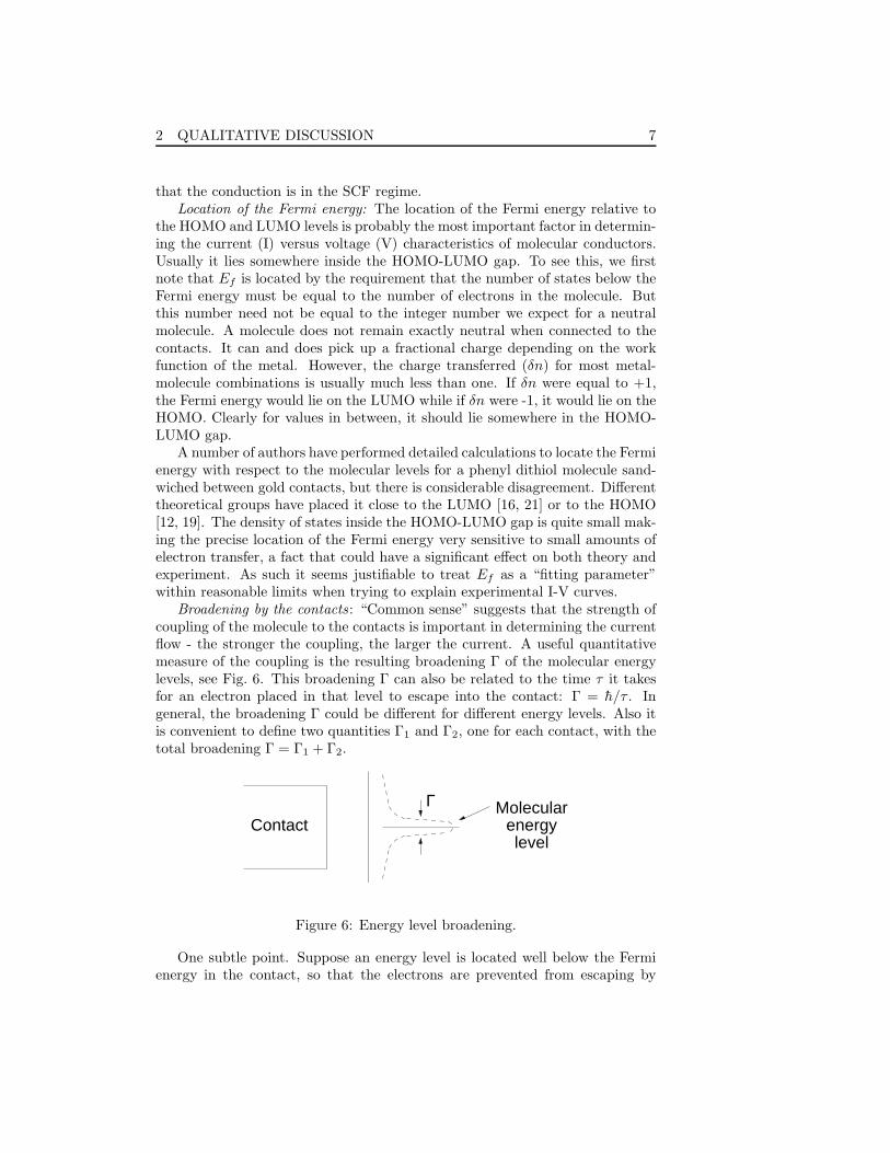
Broadening by the contacts : “Common sense” suggests that the strength ofcoupling of the molecule to the contacts is important in determining the currentflow - the stronger the coupling, the larger the current. A useful quantitativemeasure of the coupling is the resulting broadening Γ of the molecular energylevels, see Fig. 6. This broadening Γ can also be related to the time τ it takesfor an electron placed in that level to escape into the contact: Γ = h/τ . Ingeneral, the broadening Γ could be different for different energy levels. Also itis convenient to define two quantities Γ1 and Γ2, one for each contact, with thetotal broadening Γ = Γ1 + Γ2.
Contact
Γ Molecularenergylevel
Figure 6: Energy level broadening.
One subtle point. Suppose an energy level is located well below the Fermienergy in the contact, so that the electrons are prevented from escaping by

8 Resistance of a Molecule
the exclusion principle. Would Γ be zero? No, the broadening would still beΓ, independent of the degree of filling of the contact as discussed in Ref. [26].This observation is implicit in the NEGF formalism, though we do not invokeit explicitly.
2.2 Current flow as a “balancing act”
LUMOO
HOMO µ
µ
1
2 E f
LUMOO
HOMOO
µ
µ
1
2
E f
(i) Contact 1 positive (ii) Contact 1 negative
Figure 7: Schematic energy level diagram of metal-molecule-metal structurewhen contact 1 is (i) positively biased and when contact 1 is (ii) negativelybiased with respect to contact 2.
Once we have drawn an equilibrium energy level diagram, we can understandthe process of current flow which involves a non-equilibrium situation where thedifferent reservoirs (e.g., the source and the drain) have different electrochemicalpotentials µ, see Fig. 7. For example if a positive voltage V is applied externallyto the drain with respect to the source, then the drain has an electrochemicalpotential lower than that of the source by eV : µ2 = µ1 − eV . The source anddrain contacts thus have different Fermi functions and each seeks to bring theactive device into equilibrium with itself. The source keeps pumping electronsinto it hoping to establish equilibrium. But equilibrium is never achieved asthe drain keeps pulling electrons out in its bid to establish equilibrium withitself. The device is thus forced into a balancing act between two reservoirswith different agendas which sends it into a non-equilibrium state intermediatebetween what the source and drain would like to see. To describe this balancingprocess we need a kinetic equation that keeps track of the in and out-flow ofelectrons from each of the reservoirs.
Kinetic equation: This balancing act is easy to see if we consider a simple onelevel system, biased such that the energy ǫ lies in between the electrochemicalpotentials of the two contacts (Fig. 8). An electron in this level can escapeinto contacts 1 and 2 at a rate of Γ1/h and Γ2/h respectively. If the level werein equilibrium with contact 1 then the number of electrons occupying the levelwould be given by:
N1 = 2(for spin)f(ǫ, µ1) (4)

2 QUALITATIVE DISCUSSION 9
µ1
µ2
Rate(e /s)−
/h /h
Contact 1 Level
Γ1 Γ2
Contact 2
Figure 8: Illustration of the kinetic equation.
where
f(ǫ, µ) =1
1 + eǫ−µ
kBT
(5)
is the Fermi function. Similarly if the level were in equilibrium with contact 2the number would be:
N2 = 2(for spin)f(ǫ, µ2) (6)
Under non-equilibrium conditions the number of electrons N will be some-where in between N1 and N2. To determine this number we write a steady statekinetic equation that equates the net current at the left junction:
IL =eΓ1
h(N1 −N) (7)
to the net current at the right junction:
IR =eΓ2
h(N −N2) (8)
Steady state requires IL = IR, from which we obtain:
N = 2Γ1f(ǫ, µ1) + Γ2f(ǫ, µ2)
Γ1 + Γ2(9)
so that from Eq. 7 or 8 we obtain the current:
I =2e
h
Γ1Γ2
Γ1 + Γ2(f(ǫ, µ1)− f(ǫ, µ2)) (10)
Eq. 10 follows very simply from an elementary model, but it serves to il-lustrate a basic fact about the process of current flow. No current will flowif f(ǫ, µ1) = f(ǫ, µ2). A level that is way below both electrochemical poten-tials µ1 and µ2 will have f(ǫ, µ1) = f(ǫ, µ2) = 1 and will not contribute to thecurrent, just like a level that is way above both potentials µ1 and µ2 and hasf(ǫ, µ1) = f(ǫ, µ2) = 0. It is only when the level lies in between µ1 and µ2 (orwithin a few kBT of µ1 and µ2) that we have f(ǫ, µ1) 6= f(ǫ, µ2) and a current

10 Resistance of a Molecule
flows. Current flow is thus the result of the difference in opinion between thecontacts. One contact would like to see more electrons (than N) occupy thelevel and keeps pumping them in, while the other would like to see fewer thanN electrons and keeps pulling them out. The net effect is a continuous transferof electrons from one contact to another.
−2 −1 0 1 2
−40
−20
0
20
40
Voltage (V)
Cur
rent
(µA
)
Figure 9: The current-voltage (I-V) characteristics for our toy model with µ1 =Ef − eV/2, µ2 = Ef + eV/2, Ef = −5.0 eV, ǫ0 = −5.5 eV and Γ1 = Γ2 = 0.2eV. Matlab code in appendix A.1 (U = 0).
Fig. 9 shows a typical current (I) versus voltage (V ) calculated from Eq. 10,using the parameters indicated in the caption. At first the current is zerobecause both µ1, µ2 are above the energy level.
µ2
µ1
ε
Once µ2 drops below the energy level, the current increases to Imax which is themaximum current that can flow through one level and is obtained from Eq. 10by setting f(ǫ, µ1) = 1 and f(ǫ, µ2) = 0:
Imax =2e
hΓeff =
2e
h
Γ1Γ2
Γ1 + Γ2(11)
µ2
µ1
ε
Note that in Fig. 9 we have set µ1 = Ef − eV/2 and µ2 = Ef + eV/2. Wecould, of coarse, just as well have set µ1 = Ef − eV and µ2 = Ef . But the,

3 COULOMB BLOCKADE? 11
the average potential in the molecule would be −V/2 and we would need toshift ǫ appropriately. It is more convenient to choose our reference such thatthe average molecular potential is zero and there is no need to shift ǫ.
Note that the current is proportional to Γeff which is the parallel combina-tion of Γ1 and Γ2. This seems quite reasonable if we recognize that Γ1 and Γ2
represents the strength of the coupling to the two contacts and as such are liketwo conductances in series. For long conductors we would expect a third con-ductance in series representing the actual conductor. This is what we usuallyhave in mind when we speak of conductance. But short conductors have virtu-ally zero resistance and what we measure is essentially the contact or interfaceresistance1. This is an important conceptual issue, that caused much argumentand controversy in the 1980’s and was finally resolved when experimentalistsmeasured the conductance of very short conductors and found it approximatelyequal to 2e2/h which is a fundamental constant equal to 77.8 µA/V. The inverseof this conductance h/2e2 = 12.9 kΩ is now believed to represent the minimumcontact resistance that can be achieved for a one-channel conductor. Even acopper wire with a one atom cross section will have a resistance at least thislarge. Our simple one-level model (Fig, 9) does not predict this result becausewe have treated the level as discrete, but the more complete treatment in latersections will show it.
3 Coulomb Blockade?
As we mentioned in section 2, a basic question we need to answer is whether theprocess of conduction through the molecule belongs to the Coulomb Blockade(CB) or the Self-Consistent Field (SCF) regime. In this section, we will firstdiscuss a simple model for charging effects (section 3.1) and then look at thedistinction between the simple SCF regime and the CB regime (section 3.2).Finally, in section 3.3 we show how moderate amount of level broadening oftendestroy CB effects making a simple SCF treatment quite accurate.
3.1 Charging Effects
Given the level (ǫ), broadening (Γ1, Γ2) and the electrochemical potentials µ1
and µ2 of the two contacts, we can solve Eq. 10 for the current I. But we wantto include charging effects in the calculations. Therefore, we add a potentialUSCF due to the change in the number of electrons from the equilibrium value(f0 = f(ǫ0, Ef )):
USCF = U (N − 2f0) (12)
similar to a Hubbard model. We then let the level ǫ float up or down by thispotential:
ǫ = ǫ0 + USCF (13)
1Four-terminal measurments have been used to separate the contact from the device resis-tance (see for example Ref. [33]).

12 Resistance of a Molecule
Since the potential depends on the number of electrons, we need to calculatethe potential using the self consistent procedure shown in Fig. 10.
(Eq. 12)N USCF
1 2 1 2ε , µ , µ , Γ , Γ ,
0 USCF
N, I (Eq. 9, 10)
Figure 10: Illustration of the SCF procedure.
−2 −1 0 1 2
−40
20
0
−20
40
Voltage (V)
Cur
rent
(µA
)
−2 −1 0 1 20
50
100
150
200
250
Voltage (V)
Con
duct
ance
(µA
/V)
U=0
U=1
U=1
U=0
f ε
conductancegap
∆=4(|E − |− )0
Figure 11: The current-voltage (I-V) characteristics (left) and conductance-voltage (G-V) (right) for our toy model with Ef = −5.0 eV, ǫ0 = −5.5 eV andΓ1 = Γ2 = 0.2 eV. Solid lines, charging effects included (U = 1.0 eV). Dashedline, no charging (U = 0). Matlab code in appendix A.1
Once the converged solution is obtained, the current is calculated fromEq. 10. This very simple model captures much of the observed physics of molec-ular conduction. For example, the results obtained by setting Ef = −5.0 eV,ǫ0 = −5.5 eV, Γ1 = 0.2 eV, Γ2 = 0.2 eV are shown in Fig. 11 with (U = 1.0eV) and without (U = 0 eV) charging effects. The finite width of the conduc-tance peak (with U = 0) is due to the temperature used in the calculations(kBT = 0.025 eV). Note how the inclusion of charging tends to broaden thesharp peaks in conductance, even though we have not included any extra levelbroadening in this calculation. The size of the conductance gap is directly re-lated to the energy difference between the molecular energy level and the Fermienergy. The current starts to increase when the voltage reaches 1 V, which isexactly 2 |Ef − ǫ0| as would be expected even from a theory with no charging.Charging enters the picture only at higher voltages, when a chemical potentialtries to cross the level. The energy level shifts in energy (Eq. 13) if the charging

3 COULOMB BLOCKADE? 13
energy is non-zero. Thus, for a small charging energy, the chemical potentialeasily crosses the level giving a sharp increase of the current. If the chargingenergy is large, the current increases gradually since the energy level follows thechemical potential due to the charging.
E f−3.5
LUMO
HOMO
−1.5
−5.5
E f−5.0
E f−2.5
−6 −4 −2 0 2 4 6−100
−50
0
50
100
Voltage (V)
Cur
rent
(µA
)
Ef=−5.0
Ef=−3.5
Ef=−2.5
Figure 12: Right, the current-voltage (I-V) characteristics for the two level toymodel for three different values of the Fermi energy (Ef ). Left, the two energylevels (LUMO= −1.5 eV, HOMO= −5.5 eV) and the three different Fermienergies (−2.5, −3.5, −5.0) used in the calculations. (Other parameters usedU = 1.0 eV, Γ1 = Γ2 = 0.2 eV) Matlab code in appendix A.2
What determines the conductance gap? The above discussion shows that theconductance gap is equal to 4 (|Ef − ǫ0| −∆) where ∆ is equal to ∼ 4kBT (plusΓ1+Γ2 if broadening is included, see section 3.3), and ǫ0 is the HOMO or LUMOlevel whichever is closest to the Fermi energy, as pointed out in Ref. [34]. Thisis unappreciated by many who associate the conductance gap with the HOMO-LUMO gap. However, we believe that what conductance measurements showis the gap between the Fermi energy and the nearest molecular level2. Fig. 12shows the I-V characteristics calculated using a two-level model (obtained by astraightforward extension of the one-level model) with the Fermi energy locateddifferently within the HOMO-LUMO gap giving different conductance gaps cor-responding to the different values of |Ef − ǫ0|. Note that with the Fermi energylocated halfway in between, the conductance gap is twice the HOMO-LUMOgap and the I-V shows no evidence of charging effects because the depletion ofthe HOMO is neutralized by the charging of the LUMO. This perfect compen-sation is unlikely in practice, since the two levels will not couple identically tothe contacts as assumed in the model.
A very interesting effect that can be observed is the asymmetry of the I-V characteristics if Γ1 6= Γ2 as shown in Fig. 13. This may explain several
2With very asymmetric contacs, the conductance gap could be equal to the HOMO-LUMOgap as commonly assumed in interpreting STM spectra. However, we belive that the picturepresented here is more accurate unless the contact is so strongly coupled that there is asignificant density of Metal-Induced Gap States (MIGS)[28]

14 Resistance of a Molecule
−2 −1 0 1 2
−40
−20
0
20
40
Voltage (V)
Cu
rre
nt
(µA
)
Γ1=0.2 : Γ
2=0.4
Γ1=0.4 : Γ
2=0.2
−2 −1 0 1 2
−40
−20
0
20
40
Voltage (V)
Cu
rre
nt
(µA
)
Γ1=0.2 : Γ
2=0.4
Γ1=0.4 : Γ
2=0.2
(a) (b)
Figure 13: The current-voltage (I-V) characteristics for our toy model (Ef =−5.0 eV and U = 1.0 eV). (a) Conduction through HOMO (Ef > ǫ0 = −5.5eV). (b) Conduction through LUMO (Ef < ǫ0 = −4.5 eV). Solid lines, Γ1 = 0.2eV < Γ2 = 0.4 eV. Dashed lines, Γ1 = 0.4 eV > Γ2 = 0.2 eV. Matlab codein appendix A.1. Here positive voltage is defined as a voltage that lowers thechemical potential of contact 1.
experimental results which show asymmetric I-V [12, 6] as discussed by Ghoshet al. [35]. Assuming that the current is conducted through the HOMO level(Ef > ǫ0), the current is less when a positive voltage is applied to the stronglycoupled contact, see Fig. 13(a). This is due to the effects of charging as has beendiscussed in more detail in Ref. [35]. Ghosh et al. also shows that this resultwill reverse if the conduction is through the LUMO level. We can simulate thissituation by setting ǫ0 equal to −4.5 eV, 0.5 eV above the equilibrium Fermienergy Ef . The sense of asymmetry is now reversed as shown in Fig. 13(b).The current is larger when a positive voltage is applied to the strongly coupledcontact. Comparing with STM measurements seems to favor the first case, i.e.,conduction through the HOMO [35].
3.2 Unrestricted Model
In the previous examples (Figs. 11, 13) we have used values of Γ1,2 that aresmaller than the charging energy U . However, under these conditions one canexpect Coulomb Blockade (CB) effects which are not captured by a “restrictedsolution” which assumes that both spin orbitals see the same self-consistent field.However, an unrestricted solution, which allows the spin degeneracy to be lifted,will show these effects3. For example, if we replace Eq. 13 with (f0 = f(ǫ0, Ef )):
ǫ↑ = ǫ0 + U (N↓ − f0) (14)
ǫ↓ = ǫ0 + U (N↑ − f0) (15)
3The unrestricted one-particle picture discussed here provides at least a reasonable qual-itative picture of CB effects, though a complete description requires a more advanced manyparticle picture [36]. The one-particle picture leads to one of many possible states of the devicedepending on our initial guess, while a full many particle picture would include all states.

3 COULOMB BLOCKADE? 15
where the up-spin level feels a potential due to the down-spin electrons andvice-versa, then we obtain I-V curves as shown in Fig. 14.
If the SCF iteration is started with a spin degenerate solution, the samerestricted solution as before is obtained. However, if the iteration is startedwith a spin non-degenerate solution a different looking I-V is obtained. Theelectrons only interact with the the electron of the opposite spin. Therefore,the chemical potential of one contact can cross one energy level of the moleculesince the charging of that level only affects the opposite spin level. Thus, the I-Vcontains two separate steps separated by U instead of a single step broadenedby U .
−4 −2 0 2 4
−40
−20
0
20
40
Voltage (V)
Cur
rent
(µA
)
Unrestricted solutionRestricted solution
Figure 14: The current-voltage (I-V) characteristics for restricted (dashed line)and unrestricted solutions (solid line). Ef = −5.0 eV, ǫ0 = −5.5 eV, Γ1 = Γ2 =0.2 eV and U = 1.0 eV. Matlab code in appendix A.1 and A.4
For a molecule chemically bonded to a metallic surface, e.g., a PDT moleculebonded by a thiol group to a gold surface, the broadening Γ is expected to beof the same magnitude or larger than U . This washes out CB effects as shownin Fig. 17. Therefore, the CB is not expected in this case. However, if thecoupling to both contacts is weak we should keep the possibility of CB and theimportance of unrestricted solutions in mind.
3.3 Broadening
So far we have treated the level ǫ as discrete, ignoring the broadening Γ = Γ1+Γ2
that accompanies the coupling to the contacts. To take this into account weneed to replace the discrete level with a Lorentzian density of states D(E):
D(E) =1
2π
Γ
(E − ǫ)2 + (Γ/2)2(16)
As we will see later, Γ is in general energy-dependent so that D(E) can deviatesignificantly from a Lorentzian shape. We modify Eqs. 9, 10 for N and I to

16 Resistance of a Molecule
−4 −2 0 2 4
−40
−20
0
20
40
Voltage (V)
Cur
rent
(µA
)
Discrete LevelWith Broadening
Figure 15: The current-voltage (I-V) characteristics: Solid line, include broad-ening of the level by the contacts. Dashed line, no broadening, same as solidline in Fig. 11. Matlab code in appendix A.3 and A.1 (Ef = −5.0, ǫ0 = −5.5,U = 1 and Γ1 = Γ2 = 0.2 eV).
include an integration over energy:
N = 2
∞∫
−∞
dED(E)Γ1f(E, µ1) + Γ2f(E, µ2)
Γ1 + Γ2(17)
I =2e
h
∞∫
−∞
dED(E)Γ1Γ2
Γ1 + Γ2(f(E, µ1)− f(E, µ2)) (18)
−4 −2 0 2 4−15
−10
−5
0
5
10
15
Voltage (V)
Cur
rent
(µA
)
Unrestricted, discreteUnrestricted, broadenedRestricted, broadened
Figure 16: Current-voltage (I-V) characteristics showing the Coulomb blockade:discrete unrestricted model (solid line, Matlab code in appendix A.4) and thebroadened unrestricted model (dashed line, A.5). The dotted line shows thebroadened restricted model without Coulomb blockade (A.3). For all curves thefollowing parameters were used Ef = −5.0, ǫ0 = −5.5, U = 1 and Γ1 = Γ2 =0.05 eV.

4 NON EQUILIBRIUM GREEN’S FUNCTION (NEGF) FORMALISM 17
The charging effect is included as before by letting the center ǫ, of the molecu-lar density of states, float up or down according to Eqs. (12,13) for the restrictedmodel or Eqs. (14,15) for the unrestricted model.
−4 −2 0 2 4
−40
−20
0
20
40
Voltage (V)
Cur
rent
(µA
)
Unrestricted, discreteUnrestricted, broadendRestricted, broadened
Figure 17: Current-voltage (I-V) characteristics showing the suppression of theCoulomb blockade by broadening: discrete unrestricted model (solid line) andthe broadened unrestricted model (dashed line). The dotted line shows thebroadened restricted model. Γ1 = Γ2 = 0.2 eV.
For the restricted model, the only effect of broadening is to smear out theI-V characteristics as evident from Fig. 15. The same is true for the unre-stricted model as long as the broadening is much smaller than the charging en-ergy (Fig. 16). But moderate amounts of broadening can destroy the Coulombblockade effects completely and make the I-V characteristics look identical tothe restricted model (Fig. 17). With this in mind, we will use the restrictedmodel in the remainder of this chapter.
4 Non Equilibrium Green’s Function (NEGF)
Formalism
The one-level toy model described in the last section includes the three basicfactors that influence molecular conduction, namely, Ef − ǫ0, Γ1,2 and U . How-ever, real molecules typically have multiple levels that often broaden and overlapin energy. Note that the two-level model (Fig. 12) in the last section treated thetwo levels as independent and such models can be used only if the levels do notoverlap. In general we need a formalism that can do justice to multiple levelswith arbitrary broadening and overlap. The non-equilibrium Green’s function(NEGF) formalism described in this section does just that.
In the last section we obtained equations for the number of electrons, N andthe current, I for a one-level model with broadening. It is useful to rewrite theseequations in terms of the Green’s function G(E) which is defined as follows:
G(E) =
(
E − ǫ+ iΓ1 + Γ2
2
)−1
(19)

18 Resistance of a Molecule
The density of states D(E) is proportional to the spectral function A(E) definedas:
A(E) = −2Im G(E) (20)
D(E) =A(E)
2π(21)
while the number of electrons, N and the current, I can be written as:
N =2
2π
∞∫
−∞
dE(
|G(E)|2Γ1f(E, µ1) + |G(E)|
2Γ2f(E, µ2)
)
(22)
I =2e
h
∞∫
−∞
dE Γ1Γ2 |G(E)|2 (f(E, µ1)− f(E, µ2)) (23)
In the NEGF formalism the single energy level ǫ is replaced by a Hamiltonianmatrix [H ] while the broadening Γ1,2 is replaced by a complex energy-dependentself-energy matrix [Σ1,2(E)] so that the Green’s function becomes a matrix givenby:
G(E) = (ES −H − Σ1 − Σ2)−1
(24)
where S is the identity matrix of the same size as the other matrices and thebroadening matrices Γ1,2 are defined as the imaginary (more correctly as theanti-Hermitian) parts of Σ1,2:
Γ1,2 = i(
Σ1,2 − Σ†1,2
)
(25)
The spectral function is the anti-Hermitian part of the Green’s function:
A(E) = i(
G(E)−G†(E))
(26)
from which the density of states D(E) can be calculated by taking the trace:
D(E) =Tr (AS)
2π(27)
The density matrix [ρ] is given by, c.f., Eq. 22:
ρ =1
2π
∞∫
−∞
[
f(E, µ1)GΓ1G† + f(E, µ2)GΓ2G
†]
dE (28)
from which the total number of electrons, N can be calculated by taking a trace:
N = Tr (ρS) (29)
The current is given by, c.f., Eq. 23:
I =2e
h
∞∫
−∞
[
Tr(
Γ1GΓ2G†)
(f(E, µ1)− f(E, µ2))]
dE (30)
4 NON EQUILIBRIUM GREEN’S FUNCTION (NEGF) FORMALISM 19
Equations 24 through 30 constitute the basic equations of the NEGF formal-ism which have to be solved self consistently with a suitable scheme to calculatethe self-consistent potential matrix [USCF ], c.f., Eq. 13:
H = H0 + USCF (31)
where H0 is the bare Hamiltonian (like ǫ0 in the toy model) and USCF is anappropriate functional of the density matrix ρ:
USCF = F (ρ) (32)
This self-consistent procedure is essentially the same as in Fig. 10 for the onelevel toy model, except that scalar quantities have been replaced by matrices:
ǫ0 → [H0] (33)
Γ → [Γ] , [Σ] (34)
N → [ρ] (35)
USCF → [USCF ] (36)
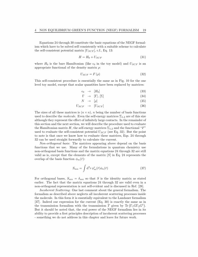
The sizes of all these matrices is (n× n), n being the number of basis functionsused to describe the molecule. Even the self-energy matrices Σ1,2 are of this sizealthough they represent the effect of infinitely large contacts. In the remainder ofthis section and the next section, we will describe the procedure used to evaluatethe Hamiltonian matrix H , the self-energy matrices Σ1,2 and the functional “F”used to evaluate the self-consistent potential USCF (see Eq. 32). But the pointto note is that once we know how to evaluate these matrices, Eqs. 24 through32 can be used straight forwardly to calculate the current.
Non-orthogonal basis : The matrices appearing above depend on the basisfunctions that we use. Many of the formulations in quantum chemistry usenon-orthogonal basis functions and the matrix equations 24 through 32 are stillvalid as is, except that the elements of the matrix [S] in Eq. 24 represents theoverlap of the basis function φm(r):
Smn =
∫
d3r φ∗m(r)φn(r) (37)
For orthogonal bases, Smn = δmn so that S is the identity matrix as statedearlier. The fact that the matrix equations 24 through 32 are valid even in anon-orthogonal representation is not self-evident and is discussed in Ref. [28].
Incoherent Scattering: One last comment about the general formalism. Theformalism as described above neglects all incoherent scattering processes insidethe molecule. In this form it is essentially equivalent to the Landauer formalism[37]. Indeed our expression for the current (Eq. 30) is exactly the same as inthe transmission formalism with the transmission T given by Tr
(
Γ1GΓ2G†)
.But it should be noted that, the real power of the NEGF formalism lies in itsability to provide a first principles description of incoherent scattering processes- something we do not address in this chapter and leave for future work.

20 Resistance of a Molecule
A practical consideration: Both Eq. 28 and 30 require an integral over allenergy. This is not a problem in Eq. 30 because the integrand is non-zero onlyover a limited range where f(E, µ1) differs significantly from f(E, µ2). But inEq. 28 the integrand is non-zero over a large energy range and often has sharpstructures making it numerically challenging to evaluate the integral. One wayto address this problem is to write:
ρ = ρeq +∆ρ (38)
where ρeq is the equilibrium density matrix given by:
ρ =1
2π
∞∫
−∞
f(E, µ)[
GΓ1G† +GΓ2G
†]
dE (39)
and ∆ρ is the change in the density matrix under bias:
ρ =1
2π
∞∫
−∞
GΓ1G† [f(E, µ1)− f(E, µ)] +GΓ2G
† [f(E, µ2)− f(E, µ)] dE (40)
The integrand in Eq. 40 for ∆ρ is non-zero only over a limited range (like Eq. 30for I) and is evaluated relatively easily. The evaluation of ρeq (Eq. 39) howeverstill has the same problem but this integral (unlike the original Eq. 28) can betackled by taking advantage of the method of contour integration as describedin Ref. [38, 39].
5 An Example: Quantum Point Contact (QPC)
ContactContact
0 0.2 0.4 0.6 0.8 10
20
40
60
80
Applied Bias (V)
Cur
rent
(µA
)
Figure 18: Left, wire consisting of six gold atoms forming a Quantum Point
Contact (QPC). Right, quantized conductance (I = e2
πhV ).
Consider for example a gold wire stretched between two gold surfaces asshown in Fig. 18. One of the seminal results of mesoscopic physics is that such

5 AN EXAMPLE: QUANTUM POINT CONTACT (QPC) 21
a wire has a quantized conductance equal to e2
πh ∼ 77.5 µA/V ∼ (12.9 kΩ)−1
.This was first established using semiconductor structures [29, 40, 41] at 4 K, butrecent experiments on gold contacts have demonstrated it at room temperature[42]. How can a wire have a resistance that is independent of its length? Theanswer is that this resistance is really associated with the interfaces betweenthe narrow wire and the wide contacts. If there is scattering inside the wireit would give rise to an additional resistance in series with this fundamentalinterface resistance. The fact that a short wire has a resistance of 12.9 kΩ isa non-obvious result that was not known before 1988. This is a problem forwhich we do not really need a quantum transport formalism; a semi-classicaltreatment would suffice. The results we obtain here are not new or surprising.What is new is that we treat the gold wire as an Au6 molecule and obtain wellknown results commonly obtained from a continuum treatment.
In order to apply the NEGF formalism from the last section to this problem,we need the Hamiltonian matrix [H ], the self energy matrices Σ1,2 and the self-consistent field USCF = F ([ρ]). Let us look at these one by one.
Hamiltonian: We will use a simple semi-empirical Hamiltonian which usesone s-orbital centered at each gold atom as the basis functions with the elementsof the Hamiltonian matrix given by:
Hij = ǫ0 if i = j (41)
= −t if i, j are nearest neighbors
where ǫ0 = −10.92 eV and t = 2.653 eV. The orbitals are assumed to beorthogonal, so that the overlap matrix S is the identity matrix.
s gs
1Σ 2
Σg
Device
Figure 19: Device, surface Green’s function (gs) and Self-energies (Σ).
Self Energy: Once we have a Hamiltonian for the entire molecule-contactsystem, the next step is to “partition” the device from the contacts and obtainthe self-energy matrices Σ1,2 describing the effects of the contacts on the device.The contact will be assumed to be essentially unperturbed relative to the surfaceof a bulk metal so that the full Green’s function (GT ) can be written as (the

22 Resistance of a Molecule
energy E is assumed to have an infinitesimal imaginary part i0+):
GT =
(
ES −H ESdc −Hdc
EScd −Hcd ESc −Hc
)−1
=
(
G Gdc
Gcd GC
)
(42)
where “c” denotes one of the contacts (the effect of the other contact can beobtained separately). We can use straight forward matrix algebra to show that:
G = (ES −H − Σ)−1
(43)
Σ = (ESdc −Hdc) (ESc −Hc)−1 (EScd −Hcd) (44)
The matrices Sdc, Sc, Hdc, Hc are all infinitely large since the contact is infinite.But the element of Sdc, Hdc are non-zero only for a small number of contactatoms whose wavefunctions significantly overlap the device. Thus, we can write:
Σ = τgsτ† (45)
where τ is the non-zero part of ESdc −Hdc having dimensions (d× s) where ’d’is the size of the device matrix , and ’s’ is the number of surface atoms of thecontact having a non-zero overlap with the device. gs is a matrix of size s × swhich is a subset of the full infinite-sized contact Green’s function (ESc −Hc)
−1.
This surface Green’s function can be computed exactly by making use of theperiodicity of the semi-infinite contact, using techniques that are standard insurface physics [31]. For a one-dimensional lead, with a Hamiltonian given byEq. 41, the result is easily derived [29]:
gs(E) = −eika
t(46)
where “ka” is related to the energy through the dispersion relation:
E = ǫ0 − 2t cos(ka) (47)
The results presented below were obtained using the more complicated surfaceGreen’s function for an FCC (111) gold surface as described in Ref. [28]. How-ever, using the surface Green’s function in Eq. 46 gives almost identical results.
Electrostatic potential : Finally we need to identify the electrostatic potentialacross the device (Fig. 20) by solving the Poisson equation:
−∇2Utot =e2n
ǫ0(48)
with the boundary conditions given by the potential difference Vapp betweenthe metallic contacts (here ǫ0 is the dielectric constant). To simplify the cal-culations we divide the solution into a applied and self consistent potential(Utot = Uapp + USCF ) where Uapp solves the Laplace equation with the knownpotential difference between the metallic contacts:
∇2Uapp = 0 Uapp = −eVn on electrode ’n’ (49)

5 AN EXAMPLE: QUANTUM POINT CONTACT (QPC) 23
SC
FU
Gold contact
V/2
Gold contact
V/2
Geo
met
ry
QPC
FCC surfaceAu (111)
Ext
erna
lpo
tent
ial (
U
)ap
p
Figure 20: The electrostatic potentials divided into the applied (Uapp) and selfconsistent field (USCF ) potentials. The boundary conditions can clearly be seenin the figure, USCF is zero at the boundary and Uapp = ±Vapp/2.
Thus, Utot solves Eq. 48 if USCF solves Eq. 48 with zero potential at the bound-ary.
∇2USCF = −e2n
ǫ0USCF = 0 on all electrodes (50)
In the treatment of the electrostatic we assume the two contacts to be semi-infinite classical metals separated by a distance (W ). This gives simple solutionsto both Uapp and USCF . The applied potential is given by (capacitor):
Uapp =V
Wx (51)
where x is the position relative to the midpoint between the contacts. Theself consistent potential is easily calculated with the method of images wherethe potential is given by a sum over the point charges and all their images.However, to avoid the infinities associated with point charges, we adopt thePariser-Parr-Pople (PPP) method [43, 17] in the Hartree approximation. ThePPP functional describing the electron-electron interactions is:
He−eij = δij
∑
k
(ρkk − ρeqkk) γik (52)

24 Resistance of a Molecule
where ρ is the charge density matrix, ρeq the equilibrium charge density (in thiscase ρeqii = 1 since we are modeling the s-electrons of gold) and the one centertwo-electron integral γij . The diagonal elements γii are obtained from experi-mental data and the off-diagonal elements (γij) are parameterized to describe apotential that decrease as the inverse of the distance (1/Rij):
γij =e2
4πǫ0Rij +2e2
γii+γjj
(53)
Calculations on the QPC : The results for the I-V and potential for a QPCare shown in Fig. 21. The geometry used was a linear chain of six gold atomsconnected to the FCC (111) surface of the contacts in the center of a surfacetriangle. The Fermi energy of the isolated contacts was calculated to be Ef =−8.67 eV, by requiring that there is one electron per unit cell.
As evident from the figure, the I-V characteristics is linear and the slope gives
a conductance of 77.3 µA/V close to the quantized value of e2
πh ∼ 77.5 µA/V aspreviously mentioned. What makes the QPC distinct from typical molecules isthe strong coupling to the contacts which broadens all levels into a continuousdensity of states and any evidence of a conductance gap (Fig. 2) is completelylost. Examining the potential drop over the QPC shows a linear drop overthe center of the QPC with slightly larger drop at the end atoms. This mayseem surprising since transport is assumed to be “ballistic” and one expects novoltage drop across the chain of gold atoms. This can be shown to arise becausethe chain is very narrow (one atom in cross-section) compared to the screeninglength [19].
0 0.2 0.4 0.6 0.8 10
20
40
60
80
Applied Bias (V)
Cur
rent
(µA
)
1 2 3 4 5 6−0.5
0
0.5
Atom number
∆Ons
ite p
oten
tial
1
µ2
µ
Figure 21: I-V (left) and potential drop for an applied voltage of 1 V (right)for a six atom QPC connected to two contacts. The potential plotted is thedifference in onsite potential from the equilibrium case.
We can easily imagine a experimental situation where the device (QPC ormolecule) is attached asymmetrically to the two contacts with one strong andone weak side. To model this situation we artificially decreased the interactionbetween the right contact and the QPC by a factor of 0.2. The results of thiscalculation are shown in Fig. 22. A weaker coupling gives a smaller conductance,as compared with the previous figure. More interesting is that the potential drop

6 CONCLUDING REMARKS 25
over the QPC is asymmetric. Also in line with our classical intuition, the largestpart of the voltage drop occurs at the weakly coupled contact with smallerdrops over the QPC and at the strongly coupled contact. The consequences ofasymmetric voltage drop over molecules has been discussed by Ghosh et al [35].
−2 −1 0 1 2
−20
0
20
Voltage (V)
Cu
rre
nt (µ
A)
1 2 3 4 5 6−0.5
0
0.5
Atom number∆O
nsite
pot
entia
l
1
µ2
µ
Figure 22: I-V and potential drop for an applied voltage of 1 V for the QPCasymmetrically connected the gold contacts. The coupling to the right contactused is −0.2t.
6 Concluding Remarks
In this chapter we have presented an intuitive description of the current-voltage(I-V) characteristics of molecules using simple toy models to illustrate the basicphysics (sections 1-3). These toy models were also used to motivate the rigor-ous Non-Equilibrium Green’s Function (NEGF) theory (section 4). A simpleexample was then used in section 5 to illustrate the application of the NEGFformalism. The same basic approach can be used in conjunction with a moreelaborate Huckel Hamiltonian or even an ab initio Hamiltonian. But for theseadvanced treatments we refer the reader to Refs. [28, 27].
Some of these models are publicly available through the Purdue SimulationHub (www.nanohub.purdue.edu) and can be run without any need for installa-tion. In addition to the models discussed here, there is a Huckel model whichis an improved version of the earlier model made available in 1999. Further im-provements may be needed to take into account the role of inelastic scatteringor polaronic effects, especially in longer molecules like DNA chains.
Acknowledgments
Sections 2 and 3 are based on material from a forthcoming book by one of theauthors (S.D.) entitled “Quantum Phenomena: From Atoms to Transistors”. Itis a pleasure to acknowledge helpful feedback from Mark Ratner, Phil Bagwelland Mark Lundstrom. The authors are grateful to Prashant Damle and AvikGhosh for helpful discussions regarding the ab initio models. This work wassupported by the NSF under Grant No. 0085516 - EEC.

26 Resistance of a Molecule
A MATLAB Codes
TheMatlab codes for the toy models can also be obtained at “www.nanohub.purdue.edu”.
A.1 Discrete One Level Model
% Toy model, one level
% Inputs (all in eV)
E0=-5.5;Ef=-5;gam1=0.2;gam2=0.2;U=1;
% Constants (all MKS, except energy which is in eV)
hbar=1.06e-34;q=1.6e-19;IE=(2*q*q)/hbar;kT=.025;
% Bias (calculate 101 voltage points in [-4 4] range)
nV=101;VV=linspace(-4,4,nV);dV=VV(2)-VV(1);
N0=2/(1+exp((E0-Ef)/kT));
for iV=1:nV % Voltage loop
UU=0;dU=1;
V=VV(iV);mu1=Ef-(V/2);mu2=Ef+(V/2);
while dU>1e-6 % SCF
E=E0+UU;
f1=1/(1+exp((E-mu1)/kT));f2=1/(1+exp((E-mu2)/kT));
NN=2*((gam1*f1)+(gam2*f2))/(gam1+gam2); % Charge
Uold=UU;UU=Uold+(.05*((U*(NN-N0))-Uold));
dU=abs(UU-Uold);[V UU dU];
end
curr=IE*gam1*gam2*(f2-f1)/(gam1+gam2);
II(iV)=curr;N(iV)=NN;[V NN];
end
G=diff(II)/dV;GG=[G(1) G]; % Conductance
h=plot(VV,II*10^6,’k’); % Plot I-V
A.2 Discrete Two Level Model
% Toy model, two levels
% Inputs (all in eV)
Ef=-5;E0=[-5.5 -1.5];gam1=[.2 .2];gam2=[.2 .2];U=1*[1 1;1 1];
% Constants (all MKS, except energy which is in eV)
hbar=1.06e-34;q=1.6e-19;IE=(2*q*q)/hbar;kT=.025;
n0=2./(1+exp((E0-Ef)./kT));
nV=101;VV=linspace(-6,6,nV);dV=VV(2)-VV(1);Usc=0;
for iV=1:nV
dU=1;
V=VV(iV);mu1=Ef+(V/2);mu2=Ef-(V/2);
while dU>1e-6
E=E0+Usc;
f1=1./(1+exp((E-mu1)./kT));f2=1./(1+exp((E-mu2)./kT));
n=2*(((gam1.*f1)+(gam2.*f2))./(gam1+gam2));

A MATLAB CODES 27
curr=IE*gam1.*gam2.*(f1-f2)./(gam1+gam2);
Uold=Usc;Usc=Uold+(.1*(((n-n0)*U’)-Uold));
dU=abs(Usc-Uold);[V Usc dU];
end
II(iV)=sum(curr);N(iV,:)=n;
end
G=diff(II)/dV;GG=[G(1) G];
h=plot(VV,II); % Plot I-V
A.3 Broadened One Level Model
% Toy model, restricted solution with broadening
% Inputs (all in eV)
E0=-5.5;Ef=-5;gam1=0.2;gam2=0.2;U=1.0;
% Constants (all MKS, except energy which is in eV)
hbar=1.06e-34;q=1.6e-19;IE=(2*q*q)/hbar;kT=.025;
% Bias (calculate 101 voltage points in [-4 4] range)
nV=101;VV=linspace(-4,4,nV);dV=VV(2)-VV(1);
N0=2/(1+exp((E0-Ef)/kT));
for iV=1:nV % Voltage loop
UU=0;dU=1;
V=VV(iV);mu1=Ef-(V/2);mu2=Ef+(V/2);
nE=400; % Nummerical integration over 200 points
id=diag(eye(nE))’;
EE=linspace(-10,0,nE);dE=EE(2)-EE(1);
f1=1./(1+exp((EE-id*mu1)/kT));
f2=1./(1+exp((EE-id*mu2)/kT));
while dU>1e-4 % SCF
E=E0+UU;
g=1./(EE-id*(E+i/2*(gam1+gam2)));
NN=2*sum(g.*conj(g).*(gam1*f1+gam2*f2))/(2*pi)*dE;
Uold=UU;UU=Uold+(.2*((U*(NN-N0))-Uold));
dU=abs(UU-Uold);[V UU dU];
end
curr=IE*gam1*gam2*sum((f2-f1).*g.*conj(g))/(2*pi)*dE;
II(iV)=real(curr);N(iV)=NN;[V NN curr E mu1 mu2];
end
G=diff(II)/dV;GG=[G(1) G]; % Conductance
h=plot(VV,II,’.’); % Plot I-V
A.4 Unrestricted Discrete One-Level Model
% Toy model unrestricted solution
% Inputs (all in eV)
E0=-5.5;Ef=-5;gam1=0.2;gam2=0.2;U=1;
%Constants (all MKS, except energy which is in eV)

28 Resistance of a Molecule
hbar=1.06e-34;q=1.6e-19;IE=(q*q)/hbar;kT=.025;
% Bias (calculate 101 voltage points in [-4 4] range)
nV=101;VV=linspace(-4,4,nV);dV=VV(2)-VV(1);
N0=1/(1+exp((E0-Ef)/kT));
for iV=1:nV % Voltage loop
U1=0;U2=1e-5;dU1=1;dU2=1;% Set U2=U1 for restricted solution
V=VV(iV);mu1=Ef-(V/2);mu2=Ef+(V/2);
while (dU1+dU2)>1e-6 % SCF
E1=E0+U1;E2=E0+U2;
f11=1/(1+exp((E1-mu1)/kT));f21=1/(1+exp((E1-mu2)/kT));
f12=1/(1+exp((E2-mu1)/kT));f22=1/(1+exp((E2-mu2)/kT));
NN1=((gam1*f12)+(gam2*f22))/(gam1+gam2);
NN2=((gam1*f11)+(gam2*f21))/(gam1+gam2);
Uold1=U1;Uold2=U2;
U1=Uold1+(.05*((2*U*(NN1-N0))-Uold1));
U2=Uold2+(.05*((2*U*(NN2-N0))-Uold2));
dU1=abs(U1-Uold1);dU2=abs(U2-Uold2);
end
curr1=IE*gam1*gam2*(f21-f11)/(gam1+gam2);
curr2=IE*gam1*gam2*(f22-f12)/(gam1+gam2);
I1(iV)=curr1;I2(iV)=curr2;
N1(iV)=NN1;N2(iV)=NN2;[V NN1 NN2];
end
G=diff(I1+I2)/dV;GG=[G(1) G]; % Conductance
h=plot(VV,I1+I2,’-’); % Plot I-V
A.5 Unrestricted Broadened One-Level Model
% Toy model, unrestricted solution with broadening
% Inputs (all in eV)
E0=-5.5;Ef=-5;gam1=0.2;gam2=0.2;U=1;
% Constants (all MKS, except energy which is in eV)
hbar=1.06e-34;q=1.6e-19;IE=(q*q)/hbar;kT=.025;
% Bias (calculate 101 voltage points in [-4 4] range)
nV=101;VV=linspace(-4,4,nV);dV=VV(2)-VV(1);
N0=1/(1+exp((E0-Ef)/kT));
nE=200; % Nummerical integration over 200 points
id=diag(eye(nE))’;
EE=linspace(-9,-1,nE);dE=EE(2)-EE(1);
for iV=1:nV % Voltage loop
U1=0;U2=1;dU1=1;dU2=1;
V=VV(iV);mu1=Ef-(V/2);mu2=Ef+(V/2);
f1=1./(1+exp((EE-id*mu1)/kT));
f2=1./(1+exp((EE-id*mu2)/kT));
while (dU1+dU2)>1e-3 % SCF
E1=E0+U1;E2=E0+U2;

A MATLAB CODES 29
g1=1./(EE-id*(E1+i/2*(gam1+gam2)));
g2=1./(EE-id*(E2+i/2*(gam1+gam2)));
NN1=sum(g1.*conj(g1).*(gam1*f1+gam2*f2))/(2*pi)*dE;
NN2=sum(g2.*conj(g2).*(gam1*f1+gam2*f2))/(2*pi)*dE;
Uold1=U1;Uold2=U2;
U1=Uold1+(.2*((2*U*(NN2-N0))-Uold1));
U2=Uold2+(.2*((2*U*(NN1-N0))-Uold2));
dU1=abs(U1-2*U*(NN2-N0));dU2=abs(U2-2*U*(NN1-N0));
end
curr=IE*gam1*gam2*sum((f2-f1).*(g1.*conj(g1)+ ...
g2.*conj(g2)))/(2*pi)*dE;
II(iV)=real(curr);N(iV)=NN1+NN2;
[V NN1 NN2 curr*1e6 E1 E2 mu1 mu2];
end
G=diff(II)/dV;GG=[G(1) G]; % Conductance
h=plot(VV,II,’--’); % Plot I-V

30 Resistance of a Molecule
References
[1] P. Avouris, P. G. Collins, and M. S. Arnold. Engineering carbon nanotubesand nanotube circuits using electrical breakdown. Science, 2001.
[2] A. Bachtold, P. Hadley, T. Nakanishi, and C. Dekker. Logic circuits withcarbon nanotube transistors. Science, 294:1317, 2001.
[3] H. Schon, H. Meng, and Z. Bao. Self-assembled monolayer organic field-effect transistors. Nature, 413:713, 2001.
[4] R. P. Andres, T. Bein, M. Dorogi, S. Feng, J. I. Henderson, C. P. Kubiak,W. Mahoney, R. G. Osifchin, and R. Reifenberger. ”coulomb staircase” atroom temperature in a self-assembled molecular nanostructure. Science,272:1323, 1996.
[5] M. A. Reed, C. Zhou, C. J. Muller, T. P. Burgin, and J. M. Tour. Conduc-tance of a molecular junction. Science, 278:252, 1997.
[6] C. Kergueris, J.-P. Bourgoin, D. Esteve, C. Urbina, M. Magoga, andC. Joachim. Electron transport through a metal-molecule-metal junction.Phys. Rev. B, 59(19):12505, 1999.
[7] C. Kergueris, J. P. Bourgoin, and S. Palacin. Experimental investigations ofthe electrical transport properties of dodecanethiol and α, ω bisthiolterthio-phene molecules embedded in metal-molecule-metal junctions. Nanotech-
nology, 10:8, 1999.
[8] J. Reichert, R. Ochs, H. B. Weber, M. Mayor, and H. v. Lohneysen. Drivingcurrent through single organic molecules. cond-mat/0106219, June 2001.
[9] S. Hong, R. Reifenberger, W. Tian, S. Datta, J. Henderson, and C. P.Kubiak. Molecular conductance spectroscopy of conjugated, phenyl-basedmolecules on au(111): the effect of end groups on molecular conduction.Superlattices and Microstructures, 28:289, 2000.
[10] J. J. W. M. Rosink, M. A. Blauw, L. J. Geerligs, E. van der Drift, andS. Radelaar. Tunneling spectroscopy study and modeling of electron trans-port in small conjugated azomethine molecules. Phys. Rev. B, 62(15):10459,2000.
[11] C. Joachim and J. K. Gimzewski. An electromechanical amplifier using asingle molecule. Chem. Phys. Lett., 265:353, 1997.
[12] W. Tian, S. Datta, S. Hong, R. Reifenberger, J. I. Henderson, and P. Ku-biak. Conductance spectra of molecular wires. J. Chem. Phys., 109(7):2874,1998.
[13] J. Chen, W. Wang, M. A. Reed, A. M. Rawlett, D. W. Price, andJ. M. Tour. Room-temperature negative differential resistance in nanoscalemolecular junctions. Appl. Phys. Lett., 77(8):1224, 2000.

REFERENCES 31
[14] D. Porath, A. Bezryadin, S. de Vries, and C. Dekker. Direct measurementof electrical transport through dna molecules. Nature, 403:635, 2000.
[15] M. Magoga and C. Joachim. Conductance of molecular wires connected orbonded in parallel. Phys. Rev. B, 59(24):16011, 1999.
[16] L. E. Hall, J. R. Reimers, N. S. Hush, and K. Silverbrook. Formal-ism, analytical model, and a priori green’s-function-based calculations ofthe current-voltage characteristics of molecular wires. J. Chem. Phys.,112:1510, 2000.
[17] M. Paulsson and S. Stafstrom. Self-consistent-field study of conductionthrough conjugated molecules. Phys. Rev. B, 64:035416, 2001.
[18] E. G. Emberly and G. Kirczenow. Multiterminal molecular wire systems: Aself-consistent theory and computer simulations of charging and transport.Phys. Rev. B, 62(15):10451, 2000.
[19] P. S. Damle, A. W. Ghosh, and S. Datta. Unified description of molecularconduction: From molecules to metallic wires. Phys. Rev. B, 64:201403(R),2001.
[20] J. Taylor, H. Gou, and J. Wang. Ab initio modeling of quantum transportproperties of molecular electronic devices. Phys. Rev. B, 63:245407, 2001.
[21] M. Di Ventra, S. T. Pantelides, and N. D. Lang. First-principles calculationof transport properties of a molecular device. Phys. Rev. Lett., 84:979, 2000.
[22] P. S. Damle, A. W. Ghosh, and S. Datta. First-principles analysis of molec-ular conduction using quantum chemistry software. Chem. Phys., 281:171,2002.
[23] Y. Q. Xue, S. Datta, and M. A. Ratner. Charge transfer and ”band lineup”in molecular electronic devices: A chemical and numerical interpretation.J. Chem. Phys., 115:4292, 2001.
[24] J. J. Palacios, A. J. Perez-Jimenez, E. Louis, and J. A. Verges. Fullerene-based molecular nanobridges: A first-principles study. Phys. Rev. B,64(11):115411, 2001.
[25] J. M. Seminario, A. G. Zacarias, and J. M. Tour. Molecular current-voltagecharacteristics. J. Phys. Chem. A, 1999.
[26] S. Datta. Nanoscale device modeling: the green’s function method. Super-lattices and Microstructures, 28:253, 2000.
[27] P. S. Damle, A. W. Ghosh, and S. Datta. Molecular nanoelectronics, chap-ter Theory of nanoscale device modeling. 2002. Editor, M. Reed, to bepublished in 2002, for a preprint e-mail ’[email protected]’.

32 Resistance of a Molecule
[28] F. Zahid, M. Paulsson, and S. Datta. Advanced Semiconductors and Or-
ganic Nano-Techniques, chapter Electrical Conduction through Molecules.Academic press, 2002. Editor H. Markoc, to be published in 2002, for apreprint e-mail ’[email protected]’.
[29] S. Datta. Electronic transport in mesoscopic systems. Cambridge UniversityPress, Cambridge, UK, 1997.
[30] S. G. Lias et al. Gas-Phase Ion and Neutral Thermochemistry in Journal
of Physical and Chemical Reference Data. American Chemical Society andAmerical Insitute of Physics, 1988.
[31] M. C. Desjoqueres and D. Spanjaard. Concepts in Surface Physics.Springer-Verlag, Berlin, Heidelberg, New York, second edition, 1996.
[32] R. G. Parr and W. Yang. Density Functional Theory of Atoms and
Molecules, page 99. Oxford University Press, 1989.
[33] R. de Picciotto, H.L. Stormer, L.N. Pfeiffer, K.W. Baldwin, and K.W.West. Four-terminal resistance of a ballistic quantum wire. Nature, 411:51,2001.
[34] S. Datta, W. Tian, S. Hong, R. Reifenberger, J. I. Henderson, and C. P.Kubiak. Current-voltage characteristics of self-assembled monolayers byscanning tunneling microscopy. Phys. Rev. Lett., 79:2530, 1997.
[35] A. W. Ghosh, F. Zahid, P. S. Damle, and S. Datta. Insights from I-Vasymmetry in molecular conductors. preprint cond-mat/0202519.
[36] Special Issue on Single Charge Tunneling, volume 85. Z. Phys. B., 1991.
[37] P. F. Bagwell and T. P. Orlando. Landauer’s conductance formula and itsgeneralization to finite voltages. Phys. Rev. B, 40(3):1456, 1989.
[38] M. Brandbyge, J. Taylor, K. Stokbro, J.-L. Mozos, and P. Ordejon. Densityfunctional method for nonequilibrium electron transport. Phys. Rev. B,65(16):165401, 2002.
[39] R. Zeller, J. Deutz, and P. Dederichs. Solid State Commun., 44:993, 1982.
[40] Y. Imry. Introduction to Mesoscopic Physics. Oxford University Press,1997.
[41] D. K. Ferry and S. M. Goodnick. Transport in nanostructures. CambridgeUniversity Press, 1997.
[42] K. Hansen, E. Laegsgaard, I. Stensgaard, and F. Besenbacher. Quantizedconductance in relays. Phys. Rev. B, 56:1022, 1997.
[43] J. N. Murrell and A. J. Harget. Semi-empirical SCF MO Theory of
Molecules. John Wiley & sons, London, 1972.