REPAIR MANUAL - Photo-parts
129
p ght Nkn p at n ll R ghts R s P nt n apan pt R RP R NU L
-
Upload
khangminh22 -
Category
Documents
-
view
0 -
download
0
Transcript of REPAIR MANUAL - Photo-parts

作成承認印 配布許可印
Copyright c 2004 by Nikon Corporation.
All Rights Reserved.
無断転載を禁ず!!
Printed in Japan September 2004
VAA27001-R.3641.A
REPAIR MANUAL

VAA27001-R.3641.A
- E8400 -
SPECIFICATIONS ・・・・・・・・・・・・・・・・・・・・・・・・・・・・・・・・・・・・・・・・・・・・・・・・・・・・・・・・・・・・・・・・・・・・・・・・・M1-M2
DISASSEMBLY
WARNING ・・・・・・・・・・・・・・・・・・・・・・・・・・・・・・・・・・・・・・・・・・・・・・・・・・・・・・・・・・・・・・・・・・・・・・・・・・・・・・・・・D1
REAR COVER ・・・・・・・・・・・・・・・・・・・・・・・・・・・・・・・・・・・・・・・・・・・・・・・・・・・・・・・・・・・・・・・・・・・・・・・・・・・・・・D2
DIAL UNIT・・・・・・・・・・・・・・・・・・・・・・・・・・・・・・・・・・・・・・・・・・・・・・・・・・・・・・・・・・・・・・・・・・・・・・・・・・・・・・・・・D6
REAR SW ・・・・・・・・・・・・・・・・・・・・・・・・・・・・・・・・・・・・・・・・・・・・・・・・・・・・・・・・・・・・・・・・・・・・・・・・・・・・・・・・・・D6
LCD ・・・・・・・・・・・・・・・・・・・・・・・・・・・・・・・・・・・・・・・・・・・・・・・・・・・・・・・・・・・・・・・・・・・・・・・・・・・・・・・・・・・・・・・D7
EVF UNIT・・・・・・・・・・・・・・・・・・・・・・・・・・・・・・・・・・・・・・・・・・・・・・・・・・・・・・・・・・・・・・・・・・・・・・・・・・・・・・・・D10
DISASSEBMLY OF EVF UNIT・・・・・・・・・・・・・・・・・・・・・・・・・・・・・・・・・・・・・・・・・・・・・・・・・・・・・・・・・・・・・・・D11
FRONT COVER ・・・・・・・・・・・・・・・・・・・・・・・・・・・・・・・・・・・・・・・・・・・・・・・・・・・・・・・・・・・・・・・・・・・・・・・・・・・D13
LIGHT-SHIELD RING ・・・・・・・・・・・・・・・・・・・・・・・・・・・・・・・・・・・・・・・・・・・・・・・・・・・・・・・・・・・・・・・・・・・・・・D14
MAIN CONDENSER ・・・・・・・・・・・・・・・・・・・・・・・・・・・・・・・・・・・・・・・・・・・・・・・・・・・・・・・・・・・・・・・・・・・・・・・D14
DISASSEMBLY OF FRONT COVER ・・・・・・・・・・・・・・・・・・・・・・・・・・・・・・・・・・・・・・・・・・・・・・・・・・・・・・・・・・D15
CF CARD COVER ・・・・・・・・・・・・・・・・・・・・・・・・・・・・・・・・・・・・・・・・・・・・・・・・・・・・・・・・・・・・・・・・・・・・・・・・・D16
PW1 PCB・・・・・・・・・・・・・・・・・・・・・・・・・・・・・・・・・・・・・・・・・・・・・・・・・・・・・・・・・・・・・・・・・・・・・・・・・・・・・・・・・D17
BATTERY CHAMBER・・・・・・・・・・・・・・・・・・・・・・・・・・・・・・・・・・・・・・・・・・・・・・・・・・・・・・・・・・・・・・・・・・・・・・D18
SPEAKER ・・・・・・・・・・・・・・・・・・・・・・・・・・・・・・・・・・・・・・・・・・・・・・・・・・・・・・・・・・・・・・・・・・・・・・・・・・・・・・・・D20
TB1 PCB ・・・・・・・・・・・・・・・・・・・・・・・・・・・・・・・・・・・・・・・・・・・・・・・・・・・・・・・・・・・・・・・・・・・・・・・・・・・・・・・・・D21
CP1 PCB ・・・・・・・・・・・・・・・・・・・・・・・・・・・・・・・・・・・・・・・・・・・・・・・・・・・・・・・・・・・・・・・・・・・・・・・・・・・・・・・・・D22
PAF SENSOR UNIT ・・・・・・・・・・・・・・・・・・・・・・・・・・・・・・・・・・・・・・・・・・・・・・・・・・・・・・・・・・・・・・・・・・・・・・・・D23
CCD MOUNT ・・・・・・・・・・・・・・・・・・・・・・・・・・・・・・・・・・・・・・・・・・・・・・・・・・・・・・・・・・・・・・・・・・・・・・・・・・・・・D24
3RD LENS GROUP ・・・・・・・・・・・・・・・・・・・・・・・・・・・・・・・・・・・・・・・・・・・・・・・・・・・・・・・・・・・・・・・・・・・・・・・・D26
DRIVE GEAR・・・・・・・・・・・・・・・・・・・・・・・・・・・・・・・・・・・・・・・・・・・・・・・・・・・・・・・・・・・・・・・・・・・・・・・・・・・・・D27
FIXED BARREL・・・・・・・・・・・・・・・・・・・・・・・・・・・・・・・・・・・・・・・・・・・・・・・・・・・・・・・・・・・・・・・・・・・・・・・・・・・D29
2ND LENS GROUP BARREL UNIT・・・・・・・・・・・・・・・・・・・・・・・・・・・・・・・・・・・・・・・・・・・・・・・・・・・・・・・・・・・D30
SHUTTER ・・・・・・・・・・・・・・・・・・・・・・・・・・・・・・・・・・・・・・・・・・・・・・・・・・・・・・・・・・・・・・・・・・・・・・・・・・・・・・・・D31
1ST LENS GROUP・・・・・・・・・・・・・・・・・・・・・・・・・・・・・・・・・・・・・・・・・・・・・・・・・・・・・・・・・・・・・・・・・・・・・・・・・D32
ASSEMBLY
1ST LENS GROUP・・・・・・・・・・・・・・・・・・・・・・・・・・・・・・・・・・・・・・・・・・・・・・・・・・・・・・・・・・・・・・・・・・・・・・・・・・・A1
SHUTTER ・・・・・・・・・・・・・・・・・・・・・・・・・・・・・・・・・・・・・・・・・・・・・・・・・・・・・・・・・・・・・・・・・・・・・・・・・・・・・・・・・・A3
2ND LENS GROUP BARREL UNIT・・・・・・・・・・・・・・・・・・・・・・・・・・・・・・・・・・・・・・・・・・・・・・・・・・・・・・・・・・・・・A4
FIXED BARREL・・・・・・・・・・・・・・・・・・・・・・・・・・・・・・・・・・・・・・・・・・・・・・・・・・・・・・・・・・・・・・・・・・・・・・・・・・・・・A5
DRIVE GEAR・・・・・・・・・・・・・・・・・・・・・・・・・・・・・・・・・・・・・・・・・・・・・・・・・・・・・・・・・・・・・・・・・・・・・・・・・・・・・・・A7
PAF SENSOR UNIT ・・・・・・・・・・・・・・・・・・・・・・・・・・・・・・・・・・・・・・・・・・・・・・・・・・・・・・・・・・・・・・・・・・・・・・・・・・A8
3RD LENS GROUP ・・・・・・・・・・・・・・・・・・・・・・・・・・・・・・・・・・・・・・・・・・・・・・・・・・・・・・・・・・・・・・・・・・・・・・・・・・A9
CCD MOUNT ・・・・・・・・・・・・・・・・・・・・・・・・・・・・・・・・・・・・・・・・・・・・・・・・・・・・・・・・・・・・・・・・・・・・・・・・・・・・・A10
RESOLUTION INSPECTION ・・・・・・・・・・・・・・・・・・・・・・・・・・・・・・・・・・・・・・・・・・・・・・・・・・・・・・・・・・・・・・・・A12
CP1 PCB ・・・・・・・・・・・・・・・・・・・・・・・・・・・・・・・・・・・・・・・・・・・・・・・・・・・・・・・・・・・・・・・・・・・・・・・・・・・・・・・・・A13
TB1 PCB ・・・・・・・・・・・・・・・・・・・・・・・・・・・・・・・・・・・・・・・・・・・・・・・・・・・・・・・・・・・・・・・・・・・・・・・・・・・・・・・・・A14
SPEAKER ・・・・・・・・・・・・・・・・・・・・・・・・・・・・・・・・・・・・・・・・・・・・・・・・・・・・・・・・・・・・・・・・・・・・・・・・・・・・・・・・A15
BATTERY CHAMBER・・・・・・・・・・・・・・・・・・・・・・・・・・・・・・・・・・・・・・・・・・・・・・・・・・・・・・・・・・・・・・・・・・・・・・A16
PW1 PCB・・・・・・・・・・・・・・・・・・・・・・・・・・・・・・・・・・・・・・・・・・・・・・・・・・・・・・・・・・・・・・・・・・・・・・・・・・・・・・・・・A18
CF CARD COVER ・・・・・・・・・・・・・・・・・・・・・・・・・・・・・・・・・・・・・・・・・・・・・・・・・・・・・・・・・・・・・・・・・・・・・・・・・A19
ASSEMBLY OF FRONT COVER ・・・・・・・・・・・・・・・・・・・・・・・・・・・・・・・・・・・・・・・・・・・・・・・・・・・・・・・・・・・・・A20
LIGHT-SHIELD RING ・・・・・・・・・・・・・・・・・・・・・・・・・・・・・・・・・・・・・・・・・・・・・・・・・・・・・・・・・・・・・・・・・・・・・・A21
CONTENTS

VAA27001-R.3641.A
- E8400 -
FRONT COVER ・・・・・・・・・・・・・・・・・・・・・・・・・・・・・・・・・・・・・・・・・・・・・・・・・・・・・・・・・・・・・・・・・・・・・・・・・・・A22
ASSEMBLY OF EVF UNIT ・・・・・・・・・・・・・・・・・・・・・・・・・・・・・・・・・・・・・・・・・・・・・・・・・・・・・・・・・・・・・・・・・・A23
EFV UNIT・・・・・・・・・・・・・・・・・・・・・・・・・・・・・・・・・・・・・・・・・・・・・・・・・・・・・・・・・・・・・・・・・・・・・・・・・・・・・・・・A25
LCD ・・・・・・・・・・・・・・・・・・・・・・・・・・・・・・・・・・・・・・・・・・・・・・・・・・・・・・・・・・・・・・・・・・・・・・・・・・・・・・・・・・・・・A26
DIAL UNIT・・・・・・・・・・・・・・・・・・・・・・・・・・・・・・・・・・・・・・・・・・・・・・・・・・・・・・・・・・・・・・・・・・・・・・・・・・・・・・・A29
REAR SW ・・・・・・・・・・・・・・・・・・・・・・・・・・・・・・・・・・・・・・・・・・・・・・・・・・・・・・・・・・・・・・・・・・・・・・・・・・・・・・・・A29
REAR COVER ・・・・・・・・・・・・・・・・・・・・・・・・・・・・・・・・・・・・・・・・・・・・・・・・・・・・・・・・・・・・・・・・・・・・・・・・・・・・A30
ADJUSTMENT ・・・・・・・・・・・・・・・・・・・・・・・・・・・・・・・・・・・・・・・・・・・・・・・・・・・・・・・・・・・・・・・・・・・・・・・A35-A49
DISCRIPTION OF CIRCUIT・・・・・・・・・・・・・・・・・・・・・・・・・・・・・・・・・・・・・・・・・・・・・・・・・・・・・・・・・・・・・・・・・E1-E9
ELECTRICITY
OVERALL WIRING・・・・・・・・・・・・・・・・・・・・・・・・・・・・・・・・・・・・・・・・・・・・・・・・・・・・・・・・・・・・・・・・・・・・・・・・E10
OVERALL BLOCK DIAGRAM ・・・・・・・・・・・・・・・・・・・・・・・・・・・・・・・・・・・・・・・・・・・・・・・・・・・・・・・・・・・・・・E11
ASIC BLOCK DIAGRAM ・・・・・・・・・・・・・・・・・・・・・・・・・・・・・・・・・・・・・・・・・・・・・・・・・・・・・・・・・・・・・・・・・・・E12
CP-1 (LENS) BLOCK DIAGRAM・・・・・・・・・・・・・・・・・・・・・・・・・・・・・・・・・・・・・・・・・・・・・・・・・・・・・・・・・・・・・E13
CP-1 (8bit MICRO PROCESSOR) BLOCK DIAGRAM・・・・・・・・・・・・・・・・・・・・・・・・・・・・・・・・・・・・・・・・・・・・E14
CA-1 BLOCK DIAGRAM ・・・・・・・・・・・・・・・・・・・・・・・・・・・・・・・・・・・・・・・・・・・・・・・・・・・・・・・・・・・・・・・・・・・E15
PW-1 BLOCK DIAGRAM・・・・・・・・・・・・・・・・・・・・・・・・・・・・・・・・・・・・・・・・・・・・・・・・・・・・・・・・・・・・・・・・・・・E16
PW-2 BLOCK DIAGRAM・・・・・・・・・・・・・・・・・・・・・・・・・・・・・・・・・・・・・・・・・・・・・・・・・・・・・・・・・・・・・・・・・・・E17
PW-3 BLOCK DIAGRAM・・・・・・・・・・・・・・・・・・・・・・・・・・・・・・・・・・・・・・・・・・・・・・・・・・・・・・・・・・・・・・・・・・・E18
VF-1 CIRCUIT DIAGRAM ・・・・・・・・・・・・・・・・・・・・・・・・・・・・・・・・・・・・・・・・・・・・・・・・・・・・・・・・・・・・・・・・・・E19
TB-1 BLOCK DIAGRAM ・・・・・・・・・・・・・・・・・・・・・・・・・・・・・・・・・・・・・・・・・・・・・・・・・・・・・・・・・・・・・・・・・・・E20
TB-2 BLOCK DIAGRAM ・・・・・・・・・・・・・・・・・・・・・・・・・・・・・・・・・・・・・・・・・・・・・・・・・・・・・・・・・・・・・・・・・・・E21
TB-3 BLOCK DIAGRAM ・・・・・・・・・・・・・・・・・・・・・・・・・・・・・・・・・・・・・・・・・・・・・・・・・・・・・・・・・・・・・・・・・・・E22
DMA CIRCUIT DIAGRAM・・・・・・・・・・・・・・・・・・・・・・・・・・・・・・・・・・・・・・・・・・・・・・・・・・・・・・・・・・・・・・・・・・E23
VFA CIRCUIT DIAGRAM・・・・・・・・・・・・・・・・・・・・・・・・・・・・・・・・・・・・・・・・・・・・・・・・・・・・・・・・・・・・・・・・・・・E24
SYA CIRCUIT DIAGRAM・・・・・・・・・・・・・・・・・・・・・・・・・・・・・・・・・・・・・・・・・・・・・・・・・・・・・・・・・・・・・・・・・・・E25
SYB CIRCUIT DIAGRAM ・・・・・・・・・・・・・・・・・・・・・・・・・・・・・・・・・・・・・・・・・・・・・・・・・・・・・・・・・・・・・・・・・・E26
CAA CIRCUIT DIAGRAM ・・・・・・・・・・・・・・・・・・・・・・・・・・・・・・・・・・・・・・・・・・・・・・・・・・・・・・・・・・・・・・・・・・E27
CAB CIRCUIT DIAGRAM ・・・・・・・・・・・・・・・・・・・・・・・・・・・・・・・・・・・・・・・・・・・・・・・・・・・・・・・・・・・・・・・・・・E28
FUSE configuration(PW-1)・・・・・・・・・・・・・・・・・・・・・・・・・・・・・・・・・・・・・・・・・・・・・・・・・・・・・・・・・・・・・・・・・E29
INSPECTION STANDARDS・・・・・・・・・・・・・・・・・・・・・・・・・・・・・・・・・・・・・・・・・・・・・・・・・・・・・・・・・・・・・・・・・R1-R7
TOOl LIST ・・・・・・・・・・・・・・・・・・・・・・・・・・・・・・・・・・・・・・・・・・・・・・・・・・・・・・・・・・・・・・・・・・・・・・・・・・・・・・・T1-T5

VAA27001-R.3641.A
- M1・ E8400 -
Type E8400 digital camera
Effective pixels 8.0 million
CCD
Image size (pixels)
2/3˝ CCD; total pixels: 8.31 million
• 3,264 × 2,448 (8M) • 3,264 × 2,176 (3 : 2) • 2,592 × 1,944 (5M)
• 2,048 × 1,536 (3M) • 1,600 × 1,200 (2M) • 1,280 × 960 (1M)
• 1,024 × 768 (PC) • 640 × 480 (TV)
Lens
Focal length
Construction
3.5× Zoom Nikkor ED
F=6.1-21.6 mm (35-mm [135] camera-format equivalent: 24 - 85 mm)
10 elements in 7 groups (includes 2 glass-molded ED lens elements)
Digital zoom Up to 4 × (35-mm [135] camera-format equivalent: 340 mm)
Auto focus (AF)
Focus range
Focus-area selection
AF-assist illuminator
The following functions are usable: Phase difference detection AF by using the AF
distance measurement sensor/Contrast detection TTL AF/Multi-area automatic focus.
50 cm (1'8" )8-∞ ; 3 cm (1.2 ")-∞ (W) / 20 cm (7.9")-∞ (T) in macro and
manual focus modes
Center; auto 5-area multi AF; manual 9-area multi AF
Class 1 LED product (IEC60825-1 Edition 1.2-2001); max. output: 1900 μW
Viewfinder
Magnifi cation
Frame coverage
Diopter adjustment
0.44., 235,000-dot, polysilicon TFT color LCD viewfi nder
Approximately 0.2 . 0.7 ×
Approximately 97% horizontal and 97% vertical
-3- +1 m-1
Monitor
Frame coverage
1.8., 134,000-dot, High Transmissive Advanced TFT LCD monitor with brightness
and hue adjustment
Approximately 97% horizontal and 97% vertical (shooting)
Exposure
Metering
Exposure control
Range
Four mode through-the-lens (TTL) metering:
・ 256-segment matrix ・ Spot ・ Center-weighted ・ Spot AF area
Programmed auto exposure with fl exible program, shutter-prior-ity auto, aperture-
priority auto, manual, exposure compensation (.2.0 . +2.0 EV in 1/3 EV steps),
autoexposure bracketing, AE-BSS
W: 0- + 18.5EV
T: +1.5- + 18.5EV
Storage
Media
File system
File format
SD (Secure Digital) memory cards, internal memory
Compliant with Design rule for Camera File systems (DCF), Exif 2.2, and Digital
Print-Order Format (DPOF)
Compressed: JPEG-baseline-compliant
Movies: QuickTime
Shutter
Speed
Mechanical and charge-coupled electronic shutter
2- 1/3,000 s (auto and exposure mode P), 8- 1/3,000 s (exposure modes S and
A), BULB / TIME (max. 10 min.) and 8- 1/3,000 s (exposure mode M), 1/30-
1/8,000s (Ultra HS). Maximum at some apertures is 1/1,500 s.
SPECIFICATIONS

VAA27001-R.3641.A
- M2・ E8400 -
Aperture
Range
Seven-blade iris diaphragm.
Ten settings in steps of 1/3 EV (to minimum of f/7)
Sensitivity Approximately equivalent to ISO 50, 100, 200, 400; Auto
Self-timer 10 s or 3 s; can be used with supplied ML-L3 remote control
Built-in Speedlight
Range (approx)
Sync method
W: 0.5 . 6.0 m/1' 8"- 19'8" T: 0.5 . 3.0 m/1' 8"- 9'10"
Standard i-TTL fl ash for digital SLR
Accessory shoe
Sync contact
Standard ISO hot-shoe contact with safety lock
X-contact only
Storage
Media
File system
File formats
Type I and II CompactFlash. (CF) and Microdrive cards
Compliant with Design Rule for Camera File System (DCF) *, Exif 2.2, and Digital
Print Order Format (DPOF)
Uncompressed: RAW (NEF), TIFF-RGB
Compressed: JPEG-baseline-compliant (1 : 2, 1 : 4, 1 : 8, 1 : 16)
Movies: QuickTime Sound fi les: WAV
Interface USB 2.0 high speed
Video output Can be selected from NTSC and PAL
Supported languages Chinese (Simplifi ed and Traditional), Dutch, English, French, German, Italian, Japa-
nese, Korean, Spanish, Swedish
I/O terminals DC in; digital I / O (audio-visual out and USB)
Power sources ・ One rechargeable Nikon EN-EL7 lithium-ion battery (supplied)
・ MB-CP10 battery pack (available separately) with six AA (LR6) alkaline, lithium,
NiCad, or NiMH batteries
・ EH-54 AC adapter (available separately)
Battery life Approximately 260 shots (EN-EL7; based on CIPA standard *)
Dimensions 113 × 82 × 75 mm/4.4. × 3.2. × 3.0. (W × H × D)
Approximate weight 400 g (14 oz) without battery or memory card
Operating environment
Temperature
Humidity
0 - 40°C (32 – 104°F)
Less than 85% (no condensation)
* Industry standard for measuring life of camera batteries. Measured at 25 °C (77 °F); zoom adjusted with each shot,
built-in Speedlight fi red with every other shot, image mode set to NORMAL / 8M
Unless otherwise stated, all fi gures are for a camera with a fully-charged EN-EL7 battery operated at an ambient tem-
perature of 25 °C (77 °F).

VAA27001-R.3641.A
- D1 ・ E8400 -
Disassembly
Note : ① Remove the battery and the CF card prior to dissassmbly. ② When disassembling, make sure to memorize the processing state of wires, screws
to be fixed and their types, etc. ③ Because electrical parts are easily damaged by static electricity, make sure that you
are well earthed/grounded.
・Lead-free solder is used for this product.・For soldering work, the special solder and soldering iron are required.・Do NOT mix up lead-free solder with traditional solder.・Use the special soldering iron respectively for lead-free solder and lead solder. They
cannot be used in common.

VAA27001-R.3641.A
- D2 ・ E8400 -
REAR COVER
1. Removal of screws
・ Remove the screw ① (M1.7 × 3).
・ Open the USB cover and remove the screw ② (M1.7 × 3.5).・ The USB cover and the USB holder can be removed.
Screw ②
USB cover
USB holder
Screw ①

VAA27001-R.3641.A
- D3 ・ E8400 -
・ Open the DC cover and remove the screw ③ (M1.7 × 4).・ Open the CF card cover and remove the screw ④ (M1.7 × 3).
DC cover
Screw ③
Screw ④
CF card cover

VAA27001-R.3641.A
- D4 ・ E8400 -
・ Remove the four screws ⑤ (M1.7 × 3.5).・ Remove the screw ⑥ (M1.7 × 3.5).
Screw ⑤Screw ⑥
Screw ⑤

VAA27001-R.3641.A
- D5 ・ E8400 -
2. Removal of rear cover
・ Remove the rear cover to the position as shown below.※ Remove the rear cover in parallel with the front cover (because the spacer at the rear cover side may interfere
with the one at the EVF side).・ Remove the connector ⑦ .・ Remove the FPC ⑧ .・ Remove the FPC ⑨ .・ Remove the rear cover.・ The DC cover can be removed.
FPC⑧
FPC⑨Connector ⑦
Rear cover
DC cover

VAA27001-R.3641.A
- D6 ・ E8400 -
DIAL UNIT
・ Remove the screw ① (M1.4 × 3.5).・ Remove the two screws ② (M1.7 × 2.5).・ Remove the dial unit.
Screw ①
Screw ②
Dial unit
REAR SW
・ Remove the seven screws ① (M1.7 × 3).・ Remove the two screws ② (M1.7 × 3.5).・ Remove the rear SW.
Screw ①
Screw ②
Rear SWScrew ①
Screw ①

VAA27001-R.3641.A
- D7 ・ E8400 -
LCD MONITOR UNIT
1. Removal of LCD monitor unit
Screw ②Screw ③
・ Remove the screw ① (M1.7 × 3).・ Remove the two screws ② (M1.7 × 4).・ Remove the two screws ③ (M1.7 × 3).・ Remove the LCD monitor unit.
LCD monitor unit
Screw ①

VAA27001-R.3641.A
- D8 ・ E8400 -
2. Disassembly of LCD monitor unit
Screw ④
(Fig.1)
Screw ④
Screw ④LCD back cover
FPC⑤FPC⑥
LCD side holder
LCD holder
LCD monitor
Screw ⑪
TB3 PCB
Screw ⑩
Screw ⑩
LCD front cover
VF1 PCB
Connector⑦
Connector⑧
Connector⑨
Joint unit
・ Put the LCD monitor unit as shown at the right (Fig. 1) and remove the four screws (4) (M1.7 × 3).
・ Remove the LCD back cover.・ Remove the FPC's ⑤ and (6).・ Remove the connectors ⑦ , ⑧ and ⑨ .・ Remove the three screws ⑩ (M1.7 × 2).・ Remove the LCD front cover.・ Remove the LCD side holder.・ Remove the joint unit.・ Remove the LCD holder.・ Unhook the LCD holder and remove the LCD monitor.・ Unsolder the VF1 PCB at 2 places.・ Remove the screw ⑪ (M1.7 × 2) and then remove the TB3 PCB.

VAA27001-R.3641.A
- D9 ・ E8400 -
3. Disassembly of joint unit
・ Remove the screw ⑫ (M1.7 × 2).・ Remove the screw ⑬ (M1.4 × 4) and then remove the joint cover.・ Remove the screw ⑭ (M1.7× 2) and then remove the LCD switch holder.・ Remove the rotary switch.
AAB
Screw ⑫
Screw ⑬
Joint cover
Screw ⑭
LCD switch holder
Rotary switch

VAA27001-R.3641.A
- D10 ・ E8400 -
EVF UNIT
・ Remove the two screws (M1.7 × 3).
Screw
・ Remove the connector ① .・ Remove the FPC ② .・ Remove the FPC ③ .
・ Remove the connector ④ .・ The EVF unit can be removed. Connector ④
EVF
EVF
Connector ①
FPC②
FPC③

VAA27001-R.3641.A
- D11 ・ E8400 -
DISASSEMBLY OF EVF UNIT
1. Flash holder unit
・ Remove the screw ① (M1.7 × 2.5).・ Remove the EVF.※ Remove the boss of the EVF from the hole on the flash holder unit. (Fig. 1)
Screw ①
EVF
Flash holder unit
(Fig.1)
Boss is fitted.
・ Take off the EVF dial back spacer.・ Remove the screw ② (M1.7 × 3) and then remove the EVF holder.・ Remove the two screws ③ (M1.7 × 4) and then remove the strap mounting, the strap cap and the strap holder.・ Remove the screw ④ (M1.7 × 3) and then remove the LCD ⑤ .・ Remove the hot shoe front spacer.・ Remove the hot shoe cover.
EVF dial back spacer
Screw ②
EVF holder
Screw ③
Strap mounting
Strap cap
Strap holder
Screw ④
LCD⑤
Hot shoe front spacer
Hot shoe cover

VAA27001-R.3641.A
- D12 ・ E8400 -
2. EVF
・ Take off the EVF light spacer.・ Take off the harness spacer.・ Remove the LCD ⑥ .
EVF light spacer
Harness spacer
LCD⑥

VAA27001-R.3641.A
- D13 ・ E8400 -
FRONT COVER
1. Removal of screws
・ Remove the two screws ① (M1.7 × 3.5).・ Remove the screw ② (M1.7 × 3.5).・ Remove the screw ③ (M1.7 × 4).・ Remove the screw ④ (M1.7 × 4).・ Remove the screw ⑤ (M1.7 × 3).
・ Remove the FPC ⑤ .・ Remove the FPC (6).・ Remove the connector ⑦ .・ Remove the connector ⑧ .・ Remove the front cover.
2. Removal of front cover
Connector ⑦
Front cover
Screw ①Screw ②
Screw ③
Screw ④
Screw ① Screw ⑤
FPC⑤
FPC⑥
Connector ⑧

VAA27001-R.3641.A
- D14 ・ E8400 -
DISCHARGE OF MAIN CONDENSER
LIGHT-SHIELD RING
・ Remove the light-shield ring.
Light-shield ring
2KΩ/5W
Main
condenser

VAA27001-R.3641.A
- D15 ・ E8400 -
DISASSEMBLY OF FRONT COVER
1. Removal of flash unit
・ Remove the two screws ① (M1.4 × 4).・ Remove the flash unit.
2. Removal of power switch unit
・ Remove the screw ② (M1.7 × 3).・ Remove the screw ③ (M1.7 × 3.5).・ Remove the two screws ④ (M1.7× 6.0).・ Remove the power switch unit by pulling up.
Screw ① Flash unit
Screw ②
SLD holder unit
Screw ③
Screw ④Power switch unit

VAA27001-R.3641.A
- D16 ・ E8400 -
CF CARD COVER
1. Removal of CF card cover
・ Remove the two screws ① (M1.7 × 3.5).・ Remove the CF card holder.
2. Disassembly of CF card cover
・ Remove the CF card cover.・ Remove the CF card shaft.・ Remove the two screws ② (M1.7 × 3).・ Remove the CF card spring.
Screw ①
CF card holder
Screw ②
CF card spring
CF card shaft
CF card coverCF card holder

VAA27001-R.3641.A
- D17 ・ E8400 -
PW1 PCB
1. Removal of PW1 PCB
・ Remove the connector.・ Remove the FPC.
・ Remove the two screws ① (M1.7 × 3).・ Remove the screw ② (M1.7 × 2.5).・ Remove the PW1 PCB from the connector of the main PCB.
Connector
FPC
Screw ①
Screw ②
PW1 PCB

VAA27001-R.3641.A
- D18 ・ E8400 -
BATTERY CHAMBER
1. Removal of battery chamber
・ Remove the three screws ① (M1.7 × 3).・ Remove the PW2 PCB.・ Remove the battery chamber.
2. Disassembly of battery holder cover
・ Remove the battery holder cover.
Screw ①
PW2 PCB
Battery chamber
Screw ①
Screw ②
Battery holder coverScrew ③
Slide cover
Spring knob cover
Battery cover
Knob spacer
Knob
・ Remove the two screws ② (M1.7 × 3).・ Remove the holder cover.・ Remove the two screws ③ (M1.7 × 2.5).・ Remove the slide cover.・ Remove the spring knob cover.・ Remove the battery cover.・ Remove the knob spacer.・ Remove the knob.
Battery holder cover

VAA27001-R.3641.A
- D19 ・ E8400 -
3. Disassembly of battery chamber
・ Remove the two screws ④ (M1.7 × 3.5).・ Remove the screw ⑤ (M1.4 × 3).・ Unhook and remove the LOW battery holder.・ Remove the flexible PWB.・ Remove the two screws (6) (M1.7 × 3.5).・ The shaft holder, the shaft holder springs (2 pcs.) and the spring holder can be removed.・ Remove the two screws ⑦ (M1.7 × 3.5).・ Unhook and remove the holder.・ The eject spring can be removed.
Screw ④
Screw ⑤
LOW battery holder
Flexible PWB
Screw ⑥
Shaft holder
Shaft holder spring
Spring holder
Screw ⑦Holder
Eject spring
Screw ⑦
Battery out holder

VAA27001-R.3641.A
- D20 ・ E8400 -
SPEAKER
・ Turn over the harness spacer and remove the connector ① .
・ Remove the two screws ② (M1.7 × 3).
・ Remove the lens holder and then remove the connector ③ .
・ Remove the screw ④ (M1.7 × 3).・ Remove the speaker.
Harness spacer
Connector ①
Screw ②
Lens holder
Connector ③
Screw ④
Speaker

VAA27001-R.3641.A
- D21 ・ E8400 -
TB1 PCB
・ Remove the connector.・ Remove the TB1 holder.・ Turn over the harness spacer and remove the TB1 PCB.
ConnectorTB1 holder
Harness spacerTB1 PCB
Boss

VAA27001-R.3641.A
- D22 ・ E8400 -
CP1 PCB
・ Remove the screw ① (M1.7 × 3).・ Remove the lens up holder.・ Remove the FPC ② .・ Remove the FPC ③ .・ Remove the two screws ④ (M1.7 × 6).・ Remove the CP1 PCB.・ Remove the LPF spacer.・ Remove the optical filter.・ Remove the spacer.・ Remove the CCD.・ Remove the mounting lens.・ Remove the insulator spacer.
Screw ①
Lens up holder
FPC②
FPC③
Screw ④
CP1 PCB
LPF spacer
Optical filter
Spacer
CCD
Mounting lens
Insulator spacer
Lens barrel unit

VAA27001-R.3641.A
- D23 ・ E8400 -
※ When disassembling the lens barrel unit, it is not necessary to disassemble the PAF sensor and the drive gear unit.
Note: When removing the PAF sensor, replacing it with a new one or turning its position adjusting screw, adjustment is
necessary. Perform the PAF sensor position adjustment among the adjustment items.
PAF SENSOR UNIT
・ Remove the screw ① (M1.4× 4.5).・ Remove the two screws ② (M1.4× 3).・ Remove the screw ③ (M1.4× 6.5).・ Remove the PAF sensor unit.
PAF sensor unit
Screw ②
Screw ③
Screw ①
Sensor position adjusting screw
Screw ②

VAA27001-R.3641.A
- D24 ・ E8400 -
CCD MOUNT
・ Turn over the retaining tape and remove the shutter FPC.
・ Remove the screw ① (M1.4× 5.5).・ Remove the screw ② (M1.4× 3).・ Remove the zoom motor unit.
Retaining tape
Shutter FPC
Screw ①
Screw ②
Zoom motor unit
Note:All of the tools for the FFD adjustment are not prepared. So, the lens barrel can be disassembled and assembled
but each unit (lens) of the 1st, 2nd and 3rd lens groups cannot be replaced with a new one.

VAA27001-R.3641.A
- D25 ・ E8400 -
・ Remove the PI. (Fig. 1)・ Remove the two screws ③ (M1.7× 5.5).
・ Remove the two screws ③ (M1.7× 5.5).・ Remove the CCD mount.
(Fig.1)
Screw ③
Screw ③
CCD mount
PI
VAA27001-R.3641.A
- D26 ・ E8400 -
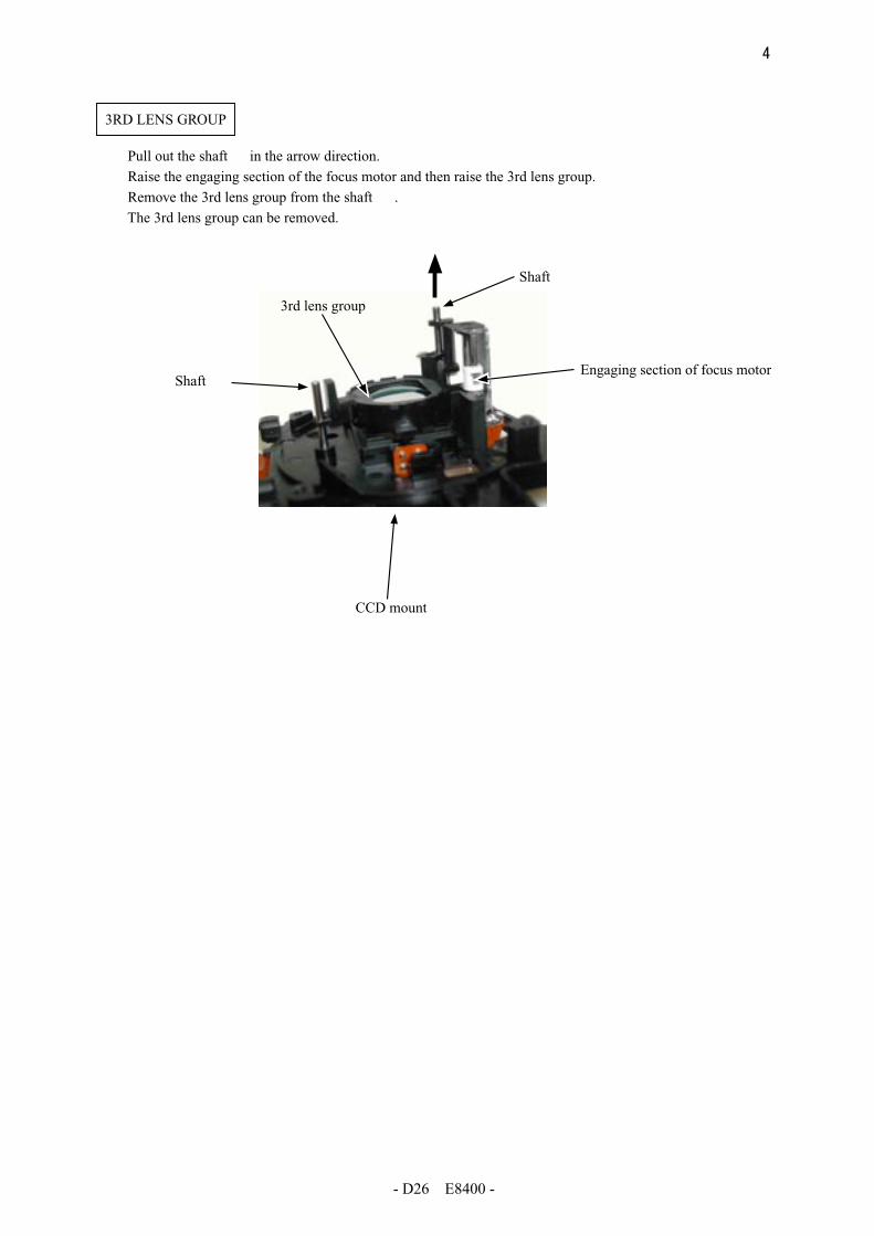
3RD LENS GROUP
・ Pull out the shaft ① in the arrow direction.・ Raise the engaging section of the focus motor and then raise the 3rd lens group.・ Remove the 3rd lens group from the shaft ② .・ The 3rd lens group can be removed.
3rd lens group
Shaft ②Engaging section of focus motor
Shaft ①
CCD mount

VAA27001-R.3641.A
- D27 ・ E8400 -
DRIVE GEAR
・ Remove the screw ① (M1.4× 4.5).・ Remove the two screws ② (M1.4× 3).・ Remove the screw ③ (M1.4× 6.5).・ Remove the PAF sensor unit.※When assembling, it is necessary to adjust the PAF sensor position. If you do not disassemble the drive gear unit,
carry out the work from P. D29.
・ Remove the shaft.・ Remove the knurled gear.・ Remove the two screws ④ (M1.4× 4).・ Remove the gear retainer.
Shaft
Knurled gear
Screw ④
Gear retainer
Screw ②Screw ③
PAF sensor unitScrew ②
Screw ①

VAA27001-R.3641.A
- D28 ・ E8400 -
・ Remove the gears ⑤ to ⑧ .・ Remove the two shafts ⑨ .
Shaft ⑨
Gear ⑤
Gear ⑥
Gear ⑦Gear ⑧
・ Remove the gear ⑩ .・ Remove the shaft ⑪ .
Gear ⑩
Shaft ⑪

VAA27001-R.3641.A
- D29 ・ E8400 -
FIXED BARREL
・ Remove the FPC retainer and pull out the FPC from the fixed barrel.
FPC retainer
FPC
・ Turn the fixed barrel in the arrow direction to remove it.・ The light-shield ring can be removed from the fixed barrel.
Cam barrel
Light-shield ring
Fixed barrel

VAA27001-R.3641.A
- D30 ・ E8400 -
2ND LENS GROUP BARREL UNIT
・ Turn the straight barrel unit to the stopper in the arrow direction.・ The 2nd lens group barrel unit can be removed upward.
2nd lens group barrel unit

VAA27001-R.3641.A
- D31 ・ E8400 -
SHUTTER
・ Remove the double-adhesive tape from the shutter FPC.
Shutter FPC
・ Push down the 2nd lens group frame and fix it with tape, etc.
・ Pull out the shutter FPC.
・ Remove the two screws (M1.4× 3).
Screw
Shutter
2nd lens group frame
Aperture frame
・ Remove the shutter between the 2nd lens group frame and the aperture frame.
2nd lens group frame
Shutter FPC
Tape

VAA27001-R.3641.A
- D32 ・ E8400 -
1ST LENS GROUP
・ Take off the name plate. (It is adhered with the double-adhesive tape.)
・ Remove the three screws (M1.4× 4).・ Remove the cover ring.
Screw
Cover ring
・ The light-shield ring can be removed.・ Turn the 1st lens group counterclockwise to
remove it.
Name plate
Light-shield ring #648
1st lens group#603

VAA27001-R.3641.A
- D33 ・ E8400 -
・ Remove the adjusting washer.
Adjusting washer
1st lens group

VAA27001-R.3641.A
- A1 ・ E8400 -
ASSEMBLY1ST LENS GROUP
・ Set the adjusting washer.
・ Set the 1st lens group. Turn the 1st lens group frame clockwise and move it down.・ Set the light-shield ring #648 onto #603.・ Draw out the 1st lens group frame and fi x the light-shield ring.※ Be careful not to catch the light-shield ring.
Adjusting washer
1st lens group
Light-shield ring #648
1st lens group frame#603

VAA27001-R.3641.A
- A2 ・ E8400 -
・ Set the cover ring.・ Tighten the three screws (M1.4× 4).
・ Adhere the name plate.
Screw
Cover ring
Name plate

VAA27001-R.3641.A
- A3 ・ E8400 -
SHUTTER
・ When the aperture frame is at the front position, adhere the tape to fix it.
・ Set the shutter between the aperture frame and the 2nd lens group frame.
・ Tighten the two screws (M1.4× 3).
・ Take off the tape fixing the 2nd lens group frame.・ Insert the shutter FPC, fit the hole position on the FPC to the boss and adhere the FPC with the double-adhesive tape.
Boss
Shutter
2nd lens group frame
Aperture frame
Tape
Screw
2nd lens group frame
Shutter FPC
Tape

VAA27001-R.3641.A
- A4 ・ E8400 -
2ND LENS GROUP BARREL UNIT
・ Fit the inner diameter convex sections of #605 (3 places) to the grooves A of #604 (3 places) and set them to each other.
・ Fit #622 (3 places) to the cam grooves of #603 (3 places).
・ As pushing the 2nd lens group frame, turn and fi t the 2nd lens group barrel unit.
2nd lens group frame
2nd lens group barrel unit
2nd lens group barrel unit
Cam barrel unit
#604
#622× 3
Groove A (3 places)
#605
#603
Convex section (3 places)

VAA27001-R.3641.A
- A5 ・ E8400 -
・Set the light-shield ring #649.・ Fit the position A on the 1st lens group barrel unit to the position B on the fixed barrel and set them to each other by
turning the 1st lens group barrel unit in the arrow direction.※ Fit the convex section of the 1st lens group barrel unit to the depression of the fixed barrel.
FIXED BARREL
Light-shield ring #649
Fit the convex section to the
depression.
Fit the positions to each
other.
1st lens group barrel unit
Fixed barrel
A
B

VAA27001-R.3641.A
- A6 ・ E8400 -
・ Make sure that the hook A is above the end face B of the lens barrel unit.・ The convex section must be fitted in the fixed barrel.
・ Insert the FPC and set the FPC retainer.
B
A
Convex section
B
A
FPC retainer
FPC

VAA27001-R.3641.A
- A7 ・ E8400 -
・ Set the shaft ⑪ .・ Set the gear ⑩ .
DRIVE GEAR
・ Set the two shafts ⑨ .・ Set the gear ⑧ , gear ⑦ , gear ⑥ and gear ⑤ in this order.
Shaft ⑨
Gear ⑤
Gear ⑥
Gear ⑦Gear ⑧
Gear ⑩
Shaft ⑪

VAA27001-R.3641.A
- A8 ・ E8400 -
・ Set the gear retainer.・ Tighten the two screws ④ (M1.4× 4).・ Set the knurled gear, insert the shaft and adhere them with 1512B. (Fig. 2)※ Be careful for the direction of the gear #673. (Fig. 1)
・ Set the PAF sensor unit.・ Tighten the screw ③ (M1.4× 6.5).・ Tighten the two screws ② (M1.4× 3).・ Tighten the screw ① (M1.4× 4.5).
PAF SENSOR UNIT
Shaft
Knurled gear
Screw ④
Gear retainer
(Fig.1)
This surface should be
at the bottom side.
Screw ②Screw ③
PAF sensor unitScrew ②
Screw ①
Adhesive: 1512B
(To the head of shaft)

VAA27001-R.3641.A
- A9 ・ E8400 -
・ Set the 3rd lens group into the focus motor and the shaft ② .・ Insert the shaft ① in the arrow direction.
3RD LENS GROUP
3rd lens group
Shaft ②Engaging section of focus motor
Shaft ①

VAA27001-R.3641.A
- A10 ・ E8400 -
CCD MOUNT
・ Set the CCD mount.・ Tighten the two screws ③ (M1.7× 5.5).
・ Tighten the two screws ③ (M1.7× 5.5).・ Apply the adhesive (1512B) to the top surface of the PI. (Applied quantity: size of sesame grain) (Fig. 2: Section A)
・ Set the PI. (Fig. 1)・ After setting the PI, apply the adhesive (1512B) to its side. (Fig. 2: Section B)
(Fig.1)
Screw ③
CCD mount
PI
Screw ③(Fig.2)
Adhesive: 1512B
Top surface of PI
Side of PI
Adhesive: 1512B
A
B

VAA27001-R.3641.A
- A11 ・ E8400 -
・ Set the zoom motor unit.・ Tighten the screw ② (M1.4× 3).・ Tighten the screw ① (M1.4× 5.5).
・ Set the shutter FPC and adhere the retaining tape as shown below.
Screw ①
Screw ②
Zoom motor unit
Retaining tape
Shutter FPC

VAA27001-R.3641.A
- A12 ・ E8400 -
Resolution inspection
When dissembling and repairing the lens-barrel, be sure to check the following after assembling it into the camera body.
・Resolution inspection
By shooting the high-definition resolution chart (J63079), confirm that the number of TV lines is within the stan-
dard.
TV lines (standard):
1450 TV lines or more in the center; 900 TV lines or more at the periphery
(ref. The resolution is represented by “TV lines”, which are total number of black-and-white strips distinguish-
able on the TV screen.)
(a) To take pictures, set the camera as follows: Shooting-mode (AUTO), Image quality mode (High), Flash mode
(Flash cancel)
(b) Check the zoom position at WIDE, MIDDLE and TELE.
The object distance: WIDE (approx. 0.36 m), MIDDLE (approx. 0.7 m), and TELE (approx.1.3 m). Set the
chart fully screened in the LCD of the camera and fix it on a tripod.
(c) Open the shot image by Photoshop, and confirm it by the magnified display, e.g. 100%, etc.
(d) Check if the resolution in the center and the 4 corners of the periphery is identifiable in black and white at the
position circled in red as below.
In case the resolution is defective, it is necessary to replace the lens-barrel group unit with the new one.
High-definition resolution chart (J63079)

VAA27001-R.3641.A
- A13 ・ E8400 -
・ Set the mounting lens.・ Set the insulator spacer.・ Set the IC.・ Set the spacer.・ Set the optical filter.※ Be careful for its setting direction. (Fig. 1)・ Set the LPF spacer.※ Be careful for its setting direction. (Fig. 2)・ Set the lens barrel unit into the CP1 PCB.・ Tighten the two screws ④ (M1.7 × 6).・ Set the FPC ③ .・ Set the FPC ② .・ Set the lens up holder.・ Tighten the screw ① (M1.7 × 3).
CP1 PCB
LPF spacer setting direction as
viewed from the PCB side.
(Fig.2)
Setting direction of optical filter
Lens
barrel sideCP1
PCB side
(Fig.1)
Screw ①
Lens up holder
FPC②
FPC③
Screw ④
CP1 PCB
LPF spacer
Optical filter
Spacer
IC
Mounting lens
Insulator spacer
Lens barrel unit

VAA27001-R.3641.A
- A14 ・ E8400 -
TB1 PCB
・ Set the TB1 PCB and then set the TB1 holder.・ Set the connector.・ Adhere the harness spacer as shown below.
ConnectorTB1 holder
Harness spacerTB1 PCB
Boss

VAA27001-R.3641.A
- A15 ・ E8400 -
SPEAKER
・ Set the speaker and tighten the screw ④ (M1.7 × 3). ・ Set the connector ③ and then set the lens holder.
・ Tighten the two screws ② (M1.7 × 3). ・ Set the connector ① and adhere the harness spacer.
Lens holder
Connector ③
Screw ④
Speaker
Harness spacer
Connector ①
Screw ②

VAA27001-R.3641.A
- A16 ・ E8400 -
1. Assembly of battery chamber
・ Set the eject spring into the battery out holder.・ Set the holder.・ Tighten the two screws ⑦ (M1.7 × 3.5).・ Set the spring holder, the shaft holder springs (2 pcs.) and the shaft holder.・ Tighten the two screws ⑥ (M1.7 × 3.5).・ Set the flexible PWB and then set the LOW battery holder.・ Tighten the screw ⑤ (M1.4 × 3).・ Tighten the two screws ④ (M1.7 × 3.5).
BATTERY CHAMBER
Screw ④
Screw ⑤
LOW battery holder
Flexible PWB
Screw ⑥
Shaft holder
Shaft holder spring
Spring holder
Screw ⑦Holder
Eject spring
Screw ⑦
Battery out holder

VAA27001-R.3641.A
- A17 ・ E8400 -
2. Assembly of battery holder cover
・ Set the knob spacer and the knob onto the battery cover.・ Set the spring knob cover.・ Set the slide cover.・ Tighten the two screws ③ (M1.7× 2.5).・ Set the holder cover.・ Tighten the two screws ② (M1.7 × 3).
3. Installation of battery chamber
・ Fit the PW2 PCB onto the battery chamber.・ Set the PW3 PCB and tighten the three screws ① (M1.7 × 3).
・ Set the battery holder cover.
Screw ②
Battery holder coverScrew ③
Slide cover
Spring knob cover
Battery cover
Knob spacer
Knob
Battery holder cover
Screw ①
PW2 PCB
Battery chamber
Screw ①

VAA27001-R.3641.A
- A18 ・ E8400 -
・ Set the PW1 PCB onto the connector of the main PCB.・ Tighten the screw ② (M1.7 × 2.5).・ Tighten the two screws ① (M1.7 × 3).
・ Set the FPC.・ Set the connector.
PW1 PCB
Screw ①
Screw ②
PW1 PCB
Connector
FPC
VAA27001-R.3641.A
- A19 ・ E8400 -
2. Setting of CF card cover
・ Set the CF card holder.・ Tighten the two screws ① (M1.7 × 3.5).
・ Set the CF card spring onto the CF card holder and tighten the two screws ② (M1.7 × 3).・ Insert the CF card shaft into the CF card cover. Then, set the CF card cover onto the CF card holder.
1. Assembly of CF card cover
CF CARD COVER
Screw ①
CF card holder
Screw ②
CF card spring
CF card shaft
CF card coverCF card holder

VAA27001-R.3641.A
- A20 ・ E8400 -
ASSEMBLY OF FRONT COVER
・ Set the flash unit.・ Tighten the two screws ① (M1.4 × 4).
2. Installation of flash unit
1. Installation of power switch unit
・ Set the power switch unit from above.・ Tighten the two screws ④ (M1.7 × 6.0).・ Tighten the screw ③ (M1.7 × 3.5).・ Tighten the screw ② (M1.7 × 3).
Screw ① Flash unit
Screw ②
SLD holder unit
Screw ③
Screw ④Power switch unit

VAA27001-R.3641.A
- A21 ・ E8400 -
LIGHT-SHIELD RING
・ Set the light-shield ring. (When setting, the gloss surface of the light-shield ring must face the front cover side.)
Light-shield ring

VAA27001-R.3641.A
- A22 ・ E8400 -
・ Set the front cover.・ Set the connector ⑧ .・ Set the connector ⑦ .・ Set the FPC ⑥ .・ Set the FPC ⑤ .
1. Setting of front cover
2. Attaching of screws
・ Tighten the screw ⑤ (M1.7 × 3).・ Tighten the screw ④ (M1.7 × 4).・ Tighten the screw ③ (M1.7 × 4).・ Tighten the screw ② (M1.7 × 3.5).・ Tighten the two screws ① (M1.7 × 3.5).
FRONT COVER
Connector ⑦
Front cover
FPC⑤
FPC⑥
Connector ⑧
Screw ①Screw ②
Screw ③
Screw ④
Screw ① Screw ⑤

VAA27001-R.3641.A
- A23 ・ E8400 -
・ Set the LCD ⑥ .・ Adhere the harness spacer.
1. EVF
ASSEMBLY OF EVF UNIT
・ Adhere the EVF light spacer in the order as shown below.
(1) (2) (3)
(4) (5) (6)
EVF light spacer
harness Spacer
LCD⑥

VAA27001-R.3641.A
- A24 ・ E8400 -
・ Set the hot shoe cover.・ Set the hot shoe front spacer.・ Set the LCD ⑤ and tighten the screw ④ (M1.7 × 3).・ Set the strap holder, and the strap cap and the strap mounting and tighten the two screws ③ (M1.7 × 4).・ Set the EVF holder and tighten the screw ② (M1.7 × 2.5).・ Adhere the EVF dial back spacer.・ Fit the boss of the EVF to the hole on the flash holder unit. Then, set the EVF. (Fig. 1)
2. Flash holder unit
・ Tighten the screw ① (M1.7 × 2.5).
EVF dial back spacer
Screw ②
EVF holder
Screw ③
Strap mounting
Strap cap
Strap holder
Screw ④
LCD⑤
Hot shoe front spacer
Hot shoe cover
Screw ①
EVF
Flash holder unit
Fit the boss to the hole.
(Fig.1)

VAA27001-R.3641.A
- A25 ・ E8400 -
・ Set the connector ④ and then set the EVF.
・ Set the FPC ③ .・ Set the FPC ② .・ Set the connector ① .
・ Tighten the two screws (M1.7 × 3).
EVF UNIT
Screw
Connector ④
EVF
EVF
Connector ①
FPC②
FPC③

VAA27001-R.3641.A
- A26 ・ E8400 -
1. Assembly of joint unit
・ Set the rotary switch.・ Set the LCD switch holder and tighten the screw ⑭ (M1.7 × 2).・ Set the joint cover and tighten the screw ⑬ (M1.4 × 4) and the screw ⑫ (M1.7 × 2).
LCD
AAB
Screw ⑫
Screw ⑬
Joint cover
Screw ⑭
LCD switch holder
Rotary switch

VAA27001-R.3641.A
- A27 ・ E8400 -
2. Assembly of LCD monitor unit
・ Set the TB3 PCB and tighten the screw ⑪ (M1.7 × 2).・ Set the VF1 PCB onto the LCD holder and perform soldering (at 2 places).・ Set the LCD monitor.・ Set the LCD front cover.・ Set the LCD side holder.・ Set the joint unit.・ Tighten the three screws ⑩ (M1.7 × 2).・ Set the connectors ⑦ , ⑧ and ⑨ .・ Set the FPC's ⑥ and ⑤ .・ Set the LCD back cover and tighten the four screws ④ (M1.7 × 3).
Screw ④
Screw ④LCD back cover
FPC⑤FPC⑥
LCD side holder
LCD holder
LCD monitor.
Screw ⑪
TB3 PCB
Screw ⑩
Screw ⑩
LCD front cover
VF1 PCB
Connector⑦
Connector⑧
Connector⑨
Joint unit
VAA27001-R.3641.A
- A28 ・ E8400 -
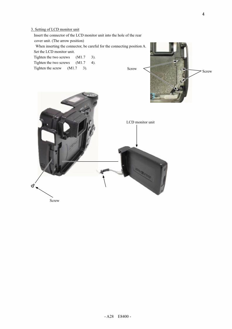
3. Setting of LCD monitor unit
・ Insert the connector of the LCD monitor unit into the hole of the rear cover unit. (The arrow position)※When inserting the connector, be careful for the connecting position A.・ Set the LCD monitor unit.・ Tighten the two screws ③ (M1.7 × 3).・ Tighten the two screws ② (M1.7 × 4).・ Tighten the screw ① (M1.7 × 3). Screw ②
Screw ③
LCD monitor unit
Screw ①
A

VAA27001-R.3641.A
- A29 ・ E8400 -
DIAL UNIT
・ Set the dial unit.・ Tighten the two screws ② (M1.7 × 2.5).・ Tighten the screw ① (M1.4 × 3.5).
Screw ①
Screw ②
Dial unit
・ Set the rear SW.・ Tighten the seven screws ① (M1.7 × 3).・ Tighten the two screws ② (M1.7 × 3.5).
REAR SW
Screw ①
Screw ②
Rear SWScrew ①
Screw ①

VAA27001-R.3641.A
- A30 ・ E8400 -
1. Setting of rear cover
・ Set the FPC ⑨ .・ Set the connector ⑦ .
・ Set the FPC ⑧ .
FPC⑨Connector ⑦
FPC⑧
REAR COVER

VAA27001-R.3641.A
- A31 ・ E8400 -
・ Set the DC cover.・ Set the rear cover.
Rear cover
DC cover

VAA27001-R.3641.A
- A32 ・ E8400 -
Screw ⑤Screw ⑥
・ Tighten the screw ⑥ (M1.7 × 3.5).・ Tighten the four screws ⑤ (M1.7 × 3.5).
2. Attaching of screws
Screw ⑤

VAA27001-R.3641.A
- A33 ・ E8400 -
・ Tighten the screw ④ (M1.7 × 3).・ Tighten the screw ③ (M1.7 × 4).
Screw ③
Screw ④
・ Set the USB holder and the USB cover. (Fig. 1)・ Open the USB cover and tighten the screw ② (M1.7 × 3.5).
Screw ②
USB cover
USB holder
Set the USB cover onto the USB holder.
(Fig.1)

VAA27001-R.3641.A
- A34 ・ E8400 -
・ Tighten the screw ① (M1.7 × 3).
Screw ①

VAA27001-R.3641.A
- A35 ・ E8400 -
ADJUSTMENT
1.Equipment
Personal computer (PC), AC adapter EH-54, USB cable (UC-E6) and CF card
2.Servicing tools
Pattern box, color meter, luminance meter, siemens star chart, PAF adjustment software (J18368), calibration software
(J65066) and oscilloscope
3.Adjustment items and order
1.PAF inspection/adjustment
1-1.PAF sensor position adjustment
1-2.PAF accuracy inspection・ adjustment
2. Lens adjustment
3.AWB adjustment
4.CCD white dot defect compensation
5.CCD black dot defect compensation
6.Built-in speed light adjustment
7.USB storage information registration
8.LCD Panel Adjustment
8-1.LCD H AFC Adjustment
8-2.LCD RGB Offset Adjustment
8-3.LCD Gain Adjustment
8-4.LCD Blue Brightness Adjustment
8-5.LCD Red Brightness Adjustment
8-6.LCD Vcom Adjustment
Note 1: When removing the front cover or the rear cover from the camera, perform the PAF accuracy inspection
(adjustment).
Note 2: Perform not only the PAF accuracy adjustment but also the lens adjustment. If you perform only one of
them, it is not sufficient for adjusting the camera function.
Note 3: Set "Mass Storage" for USB of the camera.
Note 4: When the lens, the CCD, the optical filter or the CP-1 PCB is replaced with a new one, the adjustments of "1-2"
to "5" as mentioned above must be performed again. Perform the adjustments of "3" to "5" in the order.
4.Setup
① System requirements
・WindowsR 98 or Me, 2000, XP
・IBM-compatible PC/AT with Pentium or higher processor
・CD-ROM drive
・3.5-inch 2HD diskette drive
・USB port
・40 MB or more RAM
・Hard disk drive with 15 MB or more memory space
・VGA or SVGA monitor with 256 or more color display

VAA27001-R.3641.A
- A36 ・ E8400 -
② Installation of the PAF inspection/adjustment software
・Insert the PAF inspection/adjustment software into the floppy disk drive.
・Copy the folder "PE8400" on the floppy disk drive into an optional folder of HD.
・(Example) C: /E8400
・Double-click the copied file "PE8400", and the folder to be unfrozen is displayed. Press the [OK] button, and
unfreezing starts.
・When unfreezing is finished, two files "E8400PAF.EXE" and "camapi32.dll" are made. The installation is finished.
・Press the [HISTORY] button at the lower left on the screen, and the version of the adjustment software is displayed.
・Select the button for the adjustment or inspection to be executed. After pressing the item button, follow the instructions
on each displayed menu.
Note: Japanese is not displayed correctly in the English OS.
③ Outline of the adjustment software
・Double-click and execute "E8400.EXE", and the inspection/adjustment software starts.
・To select a desirable language, press the button in "Language" at the lower right on the main menu.

VAA27001-R.3641.A
- A37 ・ E8400 -
④ Installation of the calibration software
・Insert the calibration software into the floppy disk drive.
・Open "Explorer".
・Copy the folder "DscCalDI.exe" on the floppy disk drive into an optional folder of HD.
③Making of the PAF position adjustment chart
A chart is attached to the repair manual in the PDF form. Print this chart to make the PAF position adjustment chart.
For the paper size, use "A4" or "letter size 11 × 8.5".
The chart size can affect the accuracy. Print the chart by setting as follows in the printing menu of "Adobe(r)Reader(r)"
and then use it.
・[Enlargement/reduction of page] must not be set.
・[Print according to paper] must not be set.
Note: The expression of the above two items may not be same in all of "Adobe(r)Reader(r)".
※ After printing, make sure that the interval between the upper and lower two lines in the chart is "95mm ± 5mm".
Then, use the chart.
95mm
5.Installing USB driver
If the USB driver is necessary, install Nikon View via CD-ROM packed with the camera.

VAA27001-R.3641.A
- A38 ・ E8400 -
6.Pattern box
Before using the pattern box, turn its power on to carry out "Aging" approx. 30 minutes: the color temperature
should be 3100 ± 20K by the adjustment with the color meter, and the luminance should be 900 ± 20cd/m2 by
theadjustment with the luminance meter. When using the pattern box and for a while after its power turns off, the
lamp and its surroundings are subject to high temperatures, so care should be taken when
・Procedure for correcting Pattern Box
Note: Be sure to perform the aging correction.
① Measure the measuring point (center of diffusion plate) with the Color Meter (J63081).
② Adjust the pattern box so that the color temperature should be 3100± 20K by using "VR for adjustment of the
color temperature".
③ Measure the center of the diffusion plate with the Luminance Meter BM-3000 (J63068).
④ Adjust the pattern box so that the luminance should be 900 ± 20cd/m2 by using "Knob for luminance
adjustment".
⑤ Repeat from ① to ④ So that the color temperature should be 3100 ± 20k and luminance should be 900 ±
20cd/m2.
Power switch
VR for adjustment of
the color temperature
Knob for luminance
adjustment Iris unit
Diffusion plate
Area to be measured
Adjustment is necessary. × Adjustment is not necessary.
7.Adjustments required when parts are replaced

VAA27001-R.3641.A
- A39 ・ E8400 -
8.Connecting the camera to the computer
① Insert the camera connector of USB cable in the notch of the camera’s USB port.
② Connect the cable to the USB port on PC.
1-1.PAF sensor position adjustment
① Camera condition
・Make adjustment while the rear cover is opened and the EVF/hot shoe unit is already removed from the camera.
(Fig. 1 on page A41)
・Set the camera so that the PAF sensor position (as shown below) is 1m away from the chart.
カメラ
1m
PAF位置調整 チャート
Adjustment items
電源はACアダプターから 供給して下さい。 USBポートへ
USBケーブル USB Cable
To USB portSupply the power through
the AC adapter.
Camera
PAF position adjustment chart

VAA27001-R.3641.A
- A40 ・ E8400 -
② Set the PAF position adjustment chart and the camera correctly.
・Insert the CF card into the camera.
・Turn on the power in the photography mode.
・Press the [DISP] button on the camera to display the guideline.
・Set the camera lens to the optical zoom TELE end.
・Fit the guideline (yellow) of the camera monitor to the horizontal line (black) of the chart correctly not to be deviated
or inclined. (Fig. 1)
Fig.1

VAA27001-R.3641.A
- A41 ・ E8400 -
Adjusting screw
Fig.1
Adhesive: 1521B
③ PAF position adjustment
・Start the PAF inspection/adjustment software and execute "PAF POSITION ADJUSTMENT" in the adjustment menu.
Adjust the position according to the instructions of the adjustment software.
・To adjust the position, adjust the sensor height with the adjusting screw. (Fig. 1)
・After the adjustment, fix the adjusting screw and the PAF sensor unit with the adhesive. (Fig. 2)
・After finishing the adjustment, take out the CF card.
Fig.2

VAA27001-R.3641.A
- A42 ・ E8400 -
1-2.PAF accuracy inspection・ adjustment
・Perform the inspection and adjustment while the camera is in the assembled condition.
・Insert the CF card into the camera.
・Set each chart to be at the center on the screen. (Fig. 1)
・Start the PAF inspection/adjustment software and select "PAF ACCURACY INSPECTION" or "PAF ACCURACY
ADJUSTMENT" in the menu. Make adjustment according to the instructions of the adjustment software.
・Make sure that the accuracy is within the standard. The adjustment is finished.
・After finishing the adjustment, take out the CF card.
Fig.1
Calibration software
・Connect the camera to PC and turn on the power of the camera.
・When the calibration software starts, the following is displayed on the PC monitor.

VAA27001-R.3641.A
- A43 ・ E8400 -
2.レンズ調整
[Preparations]
・Set the Siemens star chart.
・Turn the power switch of the camera to on.
・Make sure that the center of the siemens star chart is at the center on the camera screen.
[Conditions]
・The siemens star chart should be A3-size or larger (Copy and enlarge A4-size siemens chart included in the service
manual for the usage.)
・Illumination over the object should be 400 lux ± 10%
・Set the siemens star chart and the camera (front surface of lens) at 150 cm ± 3 cm distance between them.
[How-to]
・Double click on "DscCalDi.exe".
・Click "Focus" then "Yes".
・Lens adjustment values will appear on the screen.
Judgment standard: xd0 = 0 ± 50, xd12 = 0 ± 50, xd19 = 0 ± 50 xd31 = 0 ± 50
・Click "OK".
Result of adjustment
カメラ150cm±3cm
ジーメンススターチャート
"Yes"
Camera
Siemens star chart

VAA27001-R.3641.A
- A44 ・ E8400 -
3.AWB adjustment
[Preparations]
・Pattern Box(Color temperature: 3100± 20K, Luminance: 900± 20cd/m2)
[Conditions]
・Set the pattern box and camera (lens front) at "0cm" distance between them.
Note) Do not allow outside light to enter in.
[How to]
・Double-click on "DscCalDi.exe".
・Click "AWB", then "Yes".
・AWB adjustment values will appear on the screen.
Judgment standard: CHECK=128± 2, 128± 2, 130± 30
・Click "OK".
カメラ
バターンボックス
"Yes"
Result of adjustmentCamera
Pattern Box

VAA27001-R.3641.A
- A45 ・ E8400 -
4.CCD white dot defect compensation
[Conditions]
・With the lens shutter being closed, read the defect of CCD pixels. Then, make the correction data and rewrite the data
by the following procedure.
Correct the upper level of defective 1300 pixels from the brightest number of CCD pixels.
[How to]
・Double-click on "DscCalDi.exe".
・Select "CCD Defect" from Test menu of Calibration Software and click the "OK". Refer to FIG-1.
After adjustment, the adjustment value will appear on the screen. Refer to FIG-2.
<FIG-2>
5.CCD black dot defect compensation
[Conditions]
・Fix the camera so that only the white part of the pattern box should be displayed on the screen.
(Do not allow outside light to enter in as much as possible.)
・With the lens shutter being opend, read the defect (black dots) of CCD pixels. Then, make the correction data and
rewrite the data by the following procedure.
Correct the upper level of defective 30 pixels (black dots in bright place) of CCD pixels.
[How to]
・Double-click on "DscCalDi.exe".
・Select "CCD Black" from Test menu of Calibration Software and click "OK". Refer to FIG-1.
After adjustment, the adjustment value will appear on the screen. Refer to FIG-3.
CCD Defect
CCD Black
カメラ
バターンボックス
<FIG-3>
<FIG-1>
Camera
Pattern Box

VAA27001-R.3641.A
- A46 ・ E8400 -
6.Built-in speed light adjustment
[Adjustment]
・Double-click "DscCalDi.exe".
・Input "114" into "Cal Mode" and click "OK". Refer to <FIG-1>.
・The speed light flashes automatically and the adjustment is finished. Then, the adjustment result is displayed. If
"OK" is displayed, the speed light unit operates within the standard. If "NG" is displayed, perhaps the speed light unit
malfunctions. Refer to <FIG-2>.
・Click the [OK] button. The adjustment is finished.
7.USB storage information registration
USB storage data is important when the camera is connected to a computer via a USB connection.
If there are any errors in the USB storage data, or if it has not been saved, the USB specifications will not be satisfied, so
always check and save the USB storage data.
[How to]
1.Connect the camera to a computer.
2.Double-click on the "DscCalDi.exe".
3.Click on the "Get" button in the USB storage window and check the USB storage data.
VID:NIKON
PID: NIKON DSC E8400
Serial:
Rev.:1.00
4. Check the “Serial” in the above USB storage data. If the displayed value is different from the serial number printed
on the base of the camera, enter the number on the base of the camera, and click the "Set" button.
5. Check VID and Rev. entries in the USB storage data. If any of them are different from the values in 3. above, enter
the details of 3. and click the "Set" button.
〈FIG-1〉
Result of adjustment
〈FIG-2〉

VAA27001-R.3641.A
- A47 ・ E8400 -
8.LCD Panel Adjustment
【VF1 board (Side B) Point to be measured / adjustment】
8‐1.LCD H AFC Adjustment
[Preparations]
Turn the power switch ON.
[How to]
1. Double-click on "DscCalDi.exe".
2. Set "VCO" to "ON". (After the H AFC adjustment is completed,
set to "OFF".)
3. Select "0" on the LCD H AFC.
4. By checking the LCD monitor, adjust H AFC so that the
difference between the LCD screen and the LCD adjustment
frame can become the same distance and symmetrical (A = B).
8‐2.LCD RGB Offset Adjustment
[How to]
1.Adjust LCD “RGB Offset” so that the amplitude of the
CL426 waveform is 7.30 V ± 0.15 Vp-p.
LCD screen
LCD Adjustment frame
CL426(VG)CL415(HDD)
CL427(VB)
CL421(TCOM)
CL425(VR)
CL426 Waveform
7.30V± 0.15Vp-p

VAA27001-R.3641.A
- A48 ・ E8400 -
8‐3.LCD Gain Adjustment
[How to]
1.Adjust LCD “Gain” so that the amplitude of the CL426
waveform is 4.25 V ± 0.1 Vp-p.
[Note]
This adjustment should be made after completing 8-2. LCD
"RGB Offset" adjustment.
CL426 Waveform
4.25V± 0.1Vp-p
8‐4.LCD Red Brightness Adjustment
[How to]
1.Adjust LCD “B Bright” so that the amplitude of the
CL425 waveform is (VG -0.1) ± 0.1 Vp-p with
respect to the CL426 (VG) waveform.
[Note]
This adjustment should be made after completing 15-2. LCD
RGB Offset adjustment and 15-3. LCD Gain adjustment.
CL426 Waveform
VG
CL425 Waveform
(VG- 0.1)± 0.1Vp-p

VAA27001-R.3641.A
- A49 ・ E8400 -
8‐5.LCD Blue Brightness Adjustment
[How to]
1.Adjust LCD “R Bright” so that the amplitude of the CL427
waveform is (VG+0.15)± 0.1 Vp-p with respect to
the CL426 (VG) waveform.
[Note]
This adjustment should be made after completing 8-2. LCD RGB
Offset adjustment and 8-3. LCD Gain adjustment.
VG
CL426 Waveform
CL427 Waveform
(VG+ 0.15)± 0.1Vp-p
8‐6.LCD Vcom Adjustment
[How to]
1.Switch the oscilloscope to DC.
2.Adjust LCD "VCOMDC" so that the amplitude of the CL421 waveform is 5.6V ± 0.05Vp-p.
CL421 Waveform
5.6± 0.05Vp-p

VAA27001-R.3641.A
- E1 ・ E8400 -

VAA27001-R.3641.A
- E2 ・ E8400 -

VAA27001-R.3641.A
- E3 ・ E8400 -
VAA27001-R.3641.A
- E4 ・ E8400 -

VAA27001-R.3641.A
- E5 ・ E8400 -
VAA27001-R.3641.A
- E6 ・ E8400 -

VAA27001-R.3641.A
- E7 ・ E8400 -

VAA27001-R.3641.A
- E8 ・ E8400 -

VAA27001-R.3641.A
- E9 ・ E8400 -

VAA27001-R.3641.A
- E10 ・ E8400 -
総合結線図
OVERALL WIRING
ZOOM -
ZPLS_E2ZPLS_A+C
FOCUS_1BZPLS_E1
ZPLS_K
FPI_KFOCUS_2A
FPI_A+CFPI_E
FOCUS_2BFOCUS_1A
SH+
SP+SP-
INT MICGND
USB D(+)
VIDEO_OUTAUDIO_OUTZAV_JACK
ZP_A+C
USB D(-)USB_VDD
ZP_E
ZP_K
GND
GND
ST3ST4
ST2ST1
SH-
-CE1D03
GND
A08
A10
D06
D05
D07
A09
-0E VCC
A07
D04
-VS1
-CE2
-CD2
-CD1 D11
A02
A00
A01
A04
A03
WP
D01
D00
D02
A05
A06
D12
D14
D13
D15
+3.25V(D)
DC-
DC+
VM4.5V
-INPACK
RDY/BSY
-IOWR
-WAIT
-CSEL
RESET
-IORD
-REG
BVD1
BVD2
-VS2 D09
D10
D08
GND
VCC
-WE
EVF_CA
EVF_AN
VDD(3V)
GND
SB_RDY
VDD(5V)
GND
SB_TG2
SB_TG1
SB_CSP
SB_STR
SB_CS1
STRO
BE
SB_TX
SB_CSPD
VDD
COM
HCK1
TEST
HCK2R DWN
ENHST
RGT
BNC G PCG
VST
VSS
STB
VCK
SB_RX
CLK5 NC P_UP
SB_RST
P_SW
SB_CS2
BATTERY-
BATTERY+
BAT+
COM_BAT
BAT-
DC_DETDC-
DC_DETDC+
BATTERY+
BATTERY-
UNREGST
STGN
D
+3.25V(D)
SB5CTL
+12V(L)+12V(E)+3.45V(A)
GNDGNDMGNDMGNDMGNDVM4.5VVM4.5VVM4.5V
+3.25V(D)+3.25V(D)+1.58V(D)+1.58V(D)
+1.58V(D)+1.58V(D)
SB_5VSB_3VSB5CTLSB3CTL
UNREG(SY)VDD6DCINGNDGND
LCD_BLPAFONPAF5VPAONPON
BACKUP
LCD_CALCD_ANLCDONEVF_CAEVF_ANEVFONEVF_BLEVF_BL
EVFONEVF_ANEVF_CALCDONLCD_ANLCD_CA+12V(L)+12V(E)+3.45V(A)
GNDGNDMGNDMGNDMGND
VM4.5VVM4.5V
+3.25V(D)+3.25V(D)
SB_5VSB_3V
SB3CTLUNREG(SY)
DCINVDD6
GNDGND
LCD_BLPAFONPAF5VPAONPON
BACKUP
ZOOM +
SCAN OUT 3SCAN IN 5
GNDSHUTTER
SCAN IN 4SCAN OUT 2
COM_BATNC
COM_BAT
GNDSCAN IN 0C
SCAN OUT 4SCAN IN 3CSHUTTER
SCAN IN 1CSCAN OUT 2SCAN IN 4C
SCAN IN 2C
SCAN IN 6E
LED ANODELED CATHODE
LED ANODELED CATHODE
12V(L)+3.25V(D)
LCDSDLCDEN
LCDCK
CSYNCLCDY
GND
ASIC-UASIC-V
GND+3.25V(D)
CSYNCLCDY
GND
LCDSDLCDEN
LCDCK
ASIC-VASIC-U
12V(L)
GND
SO5
SI0F
SI1F
SO5
SI1FSO5
SCAN IN 6C
SCAN IN 5ESCAN IN 1D
SCAN IN 4ESCAN IN 1E
SCAN IN 2ESCAN IN 0E
SCAN IN 0DSCAN OUT 3
SCAN IN 3DSCAN IN 4D
SCAN IN 2D
SCAN IN 6D
SCAN IN 5D
SCAN IN 3ESCAN OUT 4
SCAN OUT 2
SCAN
IN1A
SCAN
IN2A
SCAN
IN4A
SCAN
IN3A
SCAN
OUT1
SCAN
IN2B
SCAN
IN3B
SCAN
IN4B
SCAN
OUT0
SCAN
IN5
LEDCA
S19
S20
S21
S22
S23
VDD
SCAN
IN1B
SCAN
IN0
CMD1
CND2
GND
NC
GNDRCVDD3
COM0
COM1
COM2
COM3
S0S1S2S3S4S5S6S7S8S9S10
S11
S12
S13
S14
S15
S16
S17
S18
PAF_CEN
PAF_CLK
PAF_EXT
PAF5V
PAF_DATA
PAF_TEMP
PAF_END
PAF_RST
GND
GND
VDD3RC
SI1FS05
LCD ANLCD CA
SI0F
LCD CALCD AN
UD
ADOU
TGD
OUT
VREF
LCD AN
LCD CALCD CA
LCD CA
LCD ANLCD AN
LRGCK1
GVDD
INIB GSP
INI
GCK2
P_VID
SSPB
SCKBVR SCK
VDD
SSP
VSS
VBVG
PCTLB
TCOM
PCTL
SPEAKER
SI0FSI1FSO5
CP1(DMA)(SYA)(SYB)(CAA)(CAB)(VFA)
PW3
PW1
PW2
TB1TB3
VF1
TB2
-4 GND
GND-2GND-3
-6 GND-5 GND
-1 GND
BATTERY
SW UNIT
LENS
MIC
VIDEO
USB&
FLASHCOMPACT
EVF STROBO
EXTBATTERY
UNITRELEASE
BACK SWUNIT
LCD
MODE DIAL PAFMODE LCD
CN182
CN181
CN110CN
141
CN522
CN501
CN802
CN801
CN102
CN521
JK551
CN502
CN104
CN951
CN304
CN303CN306
CN173CN107
CN175
CN172
CN301
CN302
CN307
CN351
CN305
CN171
CN174
DC JACK
1AV4J10UC160G
22
21
20
19
18
17
16
15
14
13
12
11
10
9
8
7
6
5
4
3
2
2
1
2
1
8
7
6
5
4
3
2
113121110987654321 3332313029282726252423222120191817161514
40
39
38
37
36
35
34
33
32
31
30
29
28
27
26
25
24
23
22
21
20
19
18
17
16
15
14
13
12
11
10
9
8
7
6
5
4
3
2
1
5049484746454443424140393837363534 21 20 19 18 17 16 15 14 13 12 11 10 9 8 7 6 5 4 3 2 118 17 16 15 14 13 12 11 10 9 8 7 6 5 4 3 2 1
321
21
40
39
38
37
36
35
34
33
32
31
30
29
28
27
26
25
24
23
22
21
20
19
18
17
16
15
14
13
12
11
10
9
8
7
6
5
4
3
2
1
1
6
5
4
3
2
1
2
1
10
9
8
7
6
5
4
3
2
1
2
1
11
10
9
8
7
6
5
4
3
2
1
11
10
9
8
7
6
5
4
3
2
1
2
1
2
1
17
16
15
14
13
12
11
10
9
8
7
6
5
4
3
2
1
3
2
1
16
15
14
13
12
16
15
14
13
12
6
5
4
3
2
1
10987654321 876543211514131211 987654321313029282726252423222120191817161514131211109 242322212019181716151413121110987654321
DMA
CAB
DMA
DMA
DMAVFAVFA DMA
DMA
+15.0V(A)-7.6V(A)
+15.0V(A)-7.6V(A)
SYA
SYA
SYA
SYA
DMA
SYA
SYA
SYB
SYA
SYA
MODEL: E8400OVERALL WIRING
W1-67200/SX789-JNK

VAA27001-R.3641.A
- E11 ・ E8400 -
総合ブロック図
OVERALL BLOCK DIAGRAM
SDRAM
SD(0:31)
SA(0:14)
32MbitFlash
IC121
IC351CN351PAF PAF DRIVER
D(0:15)A(1:21)
CKIN1
CKIN2FSC4
IC111CLOCK
GENERATOR28.63636MHzX1101
FD(0:15)
CA(0:10)
IC171LCD DRIVER
LCD MONITOR
CSYNC
PADUOUT
PADVO
UT
PADYO
UT
LCDY
ASIC-U
ASIC-V
LCDEN
LCDSD
LCDCK
EVFENEVFSD
EVFCK
IC152VIDEO AMP
IC801LCD
EVF DRIVER
EVF
4MHz 32.768KHz
MRST
ZTESTPLLEN
CLKSEL0
SCKSDI
SDOSREQ
IC3018bit CPU
ZOOM DRIVERSHUTTER DRIVERIRIS DRIVER
IC951
PICTL
ZMIN1,2
ZPULSE1,2
ZRESET
CAB LENS BLOCK
SIN1,2
Z3501
TO PW1BACKUP
AD(0:11)
ADCK
TGVD,TGHD
CCDCK
CCDSD
CCDEN
SUBG
T
TG_SCK
PAF_SCKPAF_SIPAF_SO
TG_SEN
TG_RST
TG_SDATA
CCD BLOCK
IC101ASIC
8M Pixel
IC903H DriverV. Driver
IC904 IC905
CCDCDS/AGC,A/D C
DP DM
FPC
PW1
PW3
CP1
SYB
CAA
LCD BACKLIGHT
DC/DC
ELECTRONIC
FLASH
STROBO
UNIT
CN501CN104
VDD
REGULATOR
IC302
SYA
CONVERTER
RELEASE UNIT
MODE DIAL
BACK SW UNIT
EN-EL7USB DRIVER
IC132
A[2:8]
D[0:14]
AOUT
AIN
VF1
VFAIC181AUDIO AMP
EXT BATTERY
CN102
IC952FOCUS DRIVER
IIN(1:4)
FCW,FOE
FCLK,FMODE
FRSTB
IC103IC104
256Mbit X2
CN107
MODEL: E8400BLOCK DIAGRAM: OVERALL
CN801
CN141
COMPACTFLASHTYPE-2
CN110TO USB
&VIDEO
MIC SPEAKER
VIDEO OUTAUDIO OUT
CN181CN182
CN301
CN302
CN303
CN304
CN951 LENS
3.5
DC-JACK
JK551

VAA27001-R.3641.A
- E12 ・ E8400 -
ASIC ブロック図
ASIC BLOCK DIAGRAM
DIGITALCLAMP
SIGNALPROCESSOR
AF,AE,AWB
SRAMSRAM
D/AY
VIDEO
CR-Y D/A
D/A
NTSC/PAL
ENCODERSRAM
BUS BUS
DIGITALI/F
A/D
D/ATG/SG
AUDIO
CLKGENPLL
SDRAMCONTROLLER
JPEGCONTROLLER
135MHz4FSC
48MHz48MHz
96MHz
ARM
UART
CF
PWM
SIOIC301MICROPROCESSOR
EXT PORT(LENS DRIVER)
PIO
BUS I/F
FLASH MEMORY
SIO
SDRAM
CCDBLOCK
IC101 ASIC
B-Y
RGB
CCDDRIVER
AUDIO
MIC
CF CARD
IC132
IC351PAF DRIVER
USB DRIVER
MODEL: E8400BLOCK DIAGRAM: ASIC
BUS I/F

VAA27001-R.3641.A
- E13 ・ E8400 -
CP-1(レンズ部)ブロック図
CP-1(LENS) BLOCK DIAGRAM
IC952
ZOOM DRIVER
FPI
FCLK
FRSTB
IRIS DRIVER
FCW
FOE
IIN4
IIN3
IIN2
IIN1
FOCUS DRIVER
IN1
IN9
IN10
IN2
IN3
IN4
ZOOM+
ZOOM-
FOCUS_1A
FOCUS_1B
FOCUS_2A
FOCUS_2B
ZRESET
UPD168110
OUT9
OUT10
OUT1A
OUT1B
OUT2A
OUT2B
CW
OE
CLK
RESETTB
F.M.
CN951
Z.M.
23
12
2
24
16
18
9
7
12
11
10
9
PI CTL
SWQ9509
ZP_A+CFPI_A+CZPLS_A+C
VM
3
4 28
30
29
20, 41
35
37
34
36
ZMIN1
ZMIN2 7
5
8
6
VCC
OUT7
OUT6
OUT8
OUT5
SH+
SH-
RFG1
IN7
IN8
IN6
IN5
SHUTTER DRIVER
LB8649FNIC951
VM4.5V
SW REG.PON
IC502Q9601, L9601C9604, D9601
UNREG(SY)
I.M.
24
25
26
27OUT4
OUT3
OUT2
OUT1 ST1
ST2
ST3
ST4
VDD3
SIN1
SIN2
MAIN BLOCKSYSTEM CONTROL BLOCK
S.M.
FMODE MODE1
Q9502ZPULSE1ZPULSE2
Q9501
9
7
10
8
22ZP_E
FPI_E 13
5, 12, 21
64
ZPLS_EIZPLS_E2
1
2
19
18
15
14
16
17
IC101_PIN205
IC101_PIN202
IC101_PIN197
IC101_PIN204
IC101_PIN203
IC301_PIN28
IC301_PIN98
IC301_PIN15IC301_PIN29
IC101_PIN206
IC301_PIN87
IC301_PIN88
IC101_PIN208
IC101_PIN207
IC101_PIN201
IC101_PIN200
IC101_PIN199
IC101_PIN198
MODEL :E8400BLOCK DIAGRAM: LENS

VAA27001-R.3641.A
- E14 ・ E8400 -
CP-1(8bit MICRO PROCESSOR)ブロック図
CP-1(8bit MICRO PROCESSOR) BLOCK DIAGRAM
Q3002
SHUTTER
TO PW1Z3501
116
4:31
MODE LCD
1 VDD3
BAT_PULLUP
Q3005,Q3006Q3007,Q3008
Q3010
COM_BATINTERFACE
RXDO
CN305 TXDO
2
3
4321
8 7 6 5
X3002
X3001
32kHz
4MHz
SCAN IN1
SCAN OUT0
IC301
8bit MICROPROCESSOR
SCAN IN2SCAN IN3SCAN IN4
SCAN OUT1
SCAN OUT2
SCAN OUT3
S
+/- EXT_DET
TELE
1st
AUTO
ISO
--
--
--
PLAY
PA ONP ON
LCD ON
SB RESET
SREQSISOSCK
ASIC TESTMAIN RESET
VLC2
VLC1VLC0
VLCDCCAPL
CAPHSEL 794/789
ZRESET
COMREQ
PAF ON
ZPULSE2ZM IN2ZM IN1
PICTL
USB CONNECT
PICTL
ZM IN1ZM IN2ZPULSE2
PAFON
COMREQ
ZRESET
MRSTZTEST
SDO
SB_RST
LCDON
PON
PAON
USBCNT
SDISCK
WB
DEL(AFM)
XIN
XOUTXCOUT
XCIN
SREQ
Q3001
SCAN IN0
WIDE
OK
AFF-L/AE-L
CMD IN1
ADVREF ON
CMD IN2
101
7
SHUTTER
BAT PULLUP
IR IN
RXDTXD
CMD
BKUP CTL
RESET
UNREG
AL3.2V
BAT
OFF
LI
UNREG(SY)
AL3.2V BACKUP3.2V
VDD BATTERY
BACKUP
IC302
DC INBAT OFF
VDD0RESET
AV JACK
LEFT RIGHT MENU
-- --
SCAN OUT4
AFM
P
SBS
QUALSETUP
LCD/EVF
PW_ON
ZCARD
SCAN IN5SCAN IN6
LCD_REV
Quick View
EL ON
MOVIE
AM
0
0
1
1
2
2
3
3
4
4
5
5
6SCAN INSCAN OUT
SCENE
FUNC
DISP
UP DOWN
LCD_OPEN
MODEL: E8400BLOCK DIAGRAM: SYSTEM CONTROL
TO DMA
TO DMA
TO DMA
TO CAB
TO CAB
TEST
CN307
BACKLIGHT
ELON
BATTERYUNREG(SY)
SELF LEDQ3011
VDD6
CARD
DC IN
EVFONLCD_BL
EVF_BLEVF_BL
LCD_BLEVF ON
PLLENCLKSEL0
TG_RSTTG_RST
CLKSEL0PLLEN
POP UP SW
POP OUT P_UP
P_SW
SB 3VSB 5V
SB3CTLSB5CTL
ZPULSE1ZPULSE1
BEEPBEEP
BACKUP3.2V
SWD3.2V
Q3003
SCAN OUT5
TO BATTERY(TO DMA)
(TO PW2)
46:49, 51:74
87
88
29
28
90
98
97
77
76
75
78
79
80
15
102
14
9
96
31
30
115
119
81
82
84
106
105
83
11
94
10
38
40
43
44
45
41
42
109
110
111
112
113
13
5
114
118
120
1
117
16
2
6
103
17
19
24
23
33
99
36
95
20
27
12
25
92
86

VAA27001-R.3641.A
- E15 ・ E8400 -
CA-1 ブロック図
CA-1 BLOCK DIAGRAM
LENS
CCDIMAG
ESENSO
R
EF
+15.2V(A)
-7.7V(A)
ICX456AQ
VDD
VL
VOUT
CCDIN
252627
1819
1716
14
5049
3526
41
1:10,31,32
SCK
SDATA SL
D0:11
VHLD,VST,V6,V5BV5A,V4,V3B,V3AV2,V1C,V1B,V1A
CSUB
O_LPF
IC903
Q9002
15
SWQ9001
25
IC904
CDS,AG
C,A/DC
AD9945
IC905
CXD3622GA
22
1626
H.DRIVER
V.DRIVER
SHP
SHD
CLPOB
PBLK
DATACLK
CCDCK
CCDSD
CCDEN
AD0:11
SUBG
T
TG-SCK
TG-SDATA
TG-SEN
TGHD
TGVD
ADCK
TG-RST
SCK
SSI
SEN
HR VR CKI
RST
46 38 47 37 45 36 28
XSHP
XSHD
OBCLP
PBLK
ADCLK
22:24,27,28
11,56,66,58,68
55,64,60,70
3,7,12:14,15:17
21,22,24,25
1:12
17,18,19,20
MODEL:E8400
BLOCKDIAGRAM
:CCD
TODMA
RG,LH1H1C,H2C
SUB,H1A,H2AH1B,H2B

VAA27001-R.3641.A
- E16 ・ E8400 -
PW-1 ブロック図
PW-1 BLOCK DIAGRAM
+3.25V(D)
+1.58V(D)+1.58V(D)
SB5CTL
UNREG(SY)SB3CTL
+3.25V(D)
VM4.5V
+3.25V(D)
SB_5VSB_3V
BACKUP
LCD_BL
DCIN
PAFONPAF5VPAONPON
GND
VDD6
GND
NE1
NE2
FB2
PWM1
PWM2
FB1
GND
VDD
EXT2
EXT1
UNREG STST GND
IN5-
FB5
IN1-
VREG
IN5+
IN3-
IN4- IN2-
FB2
FB1
FB4
FB3
CPST
RT
CTST
VREF
VCC CP
+15.0V(A)-7.6V(A)
GND
MGNDMGND
MGND
+3.45V(A)
LCDON
+12V(L)+12V(E)
LCD_ANLCD_CA
EVF_BL
EVF_ANEVF_CA
EVFON
GND
VM4.5VVM4.5V
IN6-
FB6
CNT3
CNT4
CNT1
CNT2
OUT6
OUT5
CNT6
CNT5
SEL3
PVCC
PGND
2
OUT2
OUT0
OUT1
OUT4
OUT3
CT
VBAT
CS1
CS2
ON/OFF
GND
PGND
1 CS5
CS4
CS6
SEL2
CS3
IN2C2-
GND SET
IN1 C1-
SHDNOUT
C2+C1+
SHDN BP
IN OUT
16081A 32V
2A 32V1608
2.0A 32V1608
3216
16082A 32V
NP04SB
NP04SB
1608
POSCA
P
2125
1608
1608
3216
3216
<FOR CCD>
3216
3216
OSC FREQ;512.3KHz
1608
2125
POSCA
P
2125
QFA7709R-H1-G
1608
1608
<FOR AF-LED>
1608
2125
<FOR LCD BACKLIGHT>
<FOR LCD 12.0V>
GRAYPINK
GRAY
PINKLIGHT BLUE
DC-
DC+DC_DET
BATT-BATT+
180mA
BACK UP BATT
+3.25V(D)
P ON
PA ON
VM4.5V
MGND
+15.0V(A)
-7.5V(A)
+3.45V(A)
+1.58V(D)
OM/ORZL51B2350GZ
3216
MGNDMGND
POSCA
PPO
SCA
P
SB5CTL
SB3CTL
SB_5V
SB_3V
PAFON
(VREF=1V)
69mA
50mA
PAF5V
VDD6
LCDON
EVF BL
LCD PANEL MAX CURRENT=5mAMAX RATING;13V
EVFON
LCD BL
+12.0V(E)
+12.0V(L)
VF=13.3VEQ R=745ohmANODE-CATHODE voltage is 13.4V when DUMMY LOAD=750ohm
LED CATHODE(LCD)
LED ANODE(LCD)
CH2
CH3
CH1
(SX7MVM)<DIGITAL 1.58V>
<DIGITAL 3.25V>
<LENS&3.45V(A)>
CH6
CH5
CH4
E
C
BE
C
B
E
C
B
BCE
C5017
L5013
L5011
L5012
R5213
R5219
R5218
R5217
Q5024
Q5023
R5216
R5215
R5214
R5212
R5211
D5012
D5011
D5015
Q5020
F5001
F5004
F5003
F5002
Q5021
Q5022C5
220
R5046
C5073
R5073
C5072
C5193
C9604
R5045
C5044
Q5001
R5196
C5192
R9605
C9603
R5076
R5074
R5044
L5003
T5001
R5100
R5057
R5056
R5055
R5054
R5053
D5003
D5008
D9601
Z3501
D5005
R9603
R9602
R5194
Q5019
R5043
CN501
L5004
Q5005
Q5006
R5071
C5071
Q5004Q5003
C5050
C5047
R5050
Q5002
C5049
L5002
R5049
L5001
C5041
C5048
D5002
C5043
D5001
IC502
Q9601
C9601
R5195
CN502
Q5018
R9604
R5192
L5008
R5193
L9601
C5001R5001
R5018
C5014
C5015
R5022
R5024
C5016
R5020
R5017
C5013
R5019
R5015 VR502
C5012
C5011
Q5008
Q5007
R5099
R5160
R5162
R5098
C5092
C5093
R5093
R5161
R5096
R5094
D5004
C5094
R5091
C5091
R5025
C5002
R5003
IC501
C5004C5005
C5006
C5010
C5003
C5009
C5008 R5157
R5158
R5156
R5155R5154
D5006
R5153
C5153
R5152
C5152
IC504 C5174
C5173
R5172
R5171
C5171
C5172
IC503
C5157
R5159
C5156
Q5009
L5005
L5006
Q5012
R5114
C5114
Q5011
R5113C5
112
C5113
R5112 Q5013
Q5014
R5137
L5007
R5138
Q5015
C5132
D5007
0.1;B
2.2M;1/1
6J
1K;1/16J
1K;1/16J
1M;1/16J
CPH3409
2SC4617(R)
10K;1/1
6J10K;1/1
6J
10K;1/1
6J10K;1/1
6J
SD833-04(SC)
SD833-04(SC)
DZUD
ZS4.3
B
2SC4617(R)
1A
2A
100K
;1/16J
3LN01S
MCH630510;16
B
270;1/16D
6800P;B
0;1/16
Z
33;8-V
33;8-V
33;8-V
11K;1/16D
4700P;B
CPH3423
63.4K
;1/16D
62P;CH
30K;1/1
6D
62P;CH
20.5K;1/16D
12K;1/1
6D
160K
;1/16D
10;M
SAGAMI 6RKH
0;1/16Z
100K
;1/16J
22K;1/16D 150K
;1/16D
10K;1/16J
150;1
/16J
EP10QY
03
EP10QY
03SD
833-0
4(SC)
ML621-TZ17
RB551V
-30
0;1/16
Z
0;1/16
Z
0;1/16
Z
UP03396
1K;1/16J
6.8;N
CPH3313
CPH3313
56K;1/1
6J
1;B
2SC4617(R)DTA114YM
1;B
10;16
B
82K;1/1
6J2S
A1774(R
)
10;10
B
47;K
100K
;1/16J
47;K
10;16
B
1;16B
RSD376
1;25B
RSD376
XC9503B095A
RTR030P02
10;16
B
180K
;1/16D
2
CPH3313
120K
;1/16D
0;1/16
Z
15;M
47K;1/1
6J
15;M
680;1
/16J
1500P;B
1500P;B
0;1/16
Z
0;1/16
Z4700P;B
0;1/16
Z
1M;1/16J
0.01;B
1M;1/16J
9.1K;1/16D
3.3K
0.47;B
1;B
EMF21
EMF21
100K
;1/16J
100K
;1/16J
2.2K;1/1
6J2.2
K;1/1
6J
33;8-V
6800P;B
0;1/16
Z
0;1/16Z
6.65K;1/16D
15K;1/1
6DEP10QY
03
10;B
40
56K;1/1
6J
1;B
0;1/16Z
4700P;B
0.01;B
2.7K;1/16J
2.7K;1/16J
FA7709R-H1-G
0.1;B
0.1;B
0.082;B
150P;CH
0.1;B
0.068;B 1.1K;1/16D
1K;1/16D
1.1K;1/16D
1.1K;1/16D1.1K;1/16D
UDZS
7.5B
27K;1/1
6D
1000P;B
1K;1/16J
4.7;H
MAX1912
2.2;B
0.47;B
0;1/16Z
13;1/16D
4.7;B
0.47;B
LK112M50
2.2;B
0;1/16Z
0.1;B
QS5U17
10;M
0.1;B
22;M
DTC114EM
11.8K;1/16D
2.2;B
QS5U17
130K
;1/16D1;16B
2200P;B
1K;1/16J
UP03396
UP03396
10K;1/16D
22;M
56;1/16D
QS5U17
2.2;B
UDZS
16B
1AV4L26B3450G
1AV4L26B3470G
1AV4L26B3470G
F47K1R0C3LFND
F47K2R0C3LFND
F47K2R0C3LFND
F47K2R0C3LFND
1AV4L51B6050G
1AV4J11VG401G
6
5
43
2
1
1
5
43
2
1
40
39
38
37
36
35
34
33
32
31
30
29
28
27
26
25
24
23
22
21
20
5
4
2
7
8
6
3
5 4 3 2 1
109876
2
1
1
2
3
404142434445464748
34
35
36
373839 6
5
43
2
1
6
5
43
2
1
19
18
17
16
15
14
13
12
11
10
9
8
7
6
5
4
3
2
1
4
5
6
7
8
9
10
11
12
13 14 15 16 17 18 19 20 21 22 23 24
25
26
27
28
29
30
31
32
33
54
32
1 109
87
6
5 4
321
5 4
321
5 4
321
5
43
2
1
5
43
2
1
5 4
321
TO PW2
TO PW3
TO STROBO
TO CP1(DMA)CN104
P1-67200/SX789-JNK
PW1!
!
SWITCHING CONTROL
REG.
SWITCHING CONTROLLED CHARGE PUMP
MODEL: E8400CIRCUIT DIAGRAM: PW1
!
!
!

VAA27001-R.3641.A
- E17 ・ E8400 -
PW-2 ブロック図
PW-2 BLOCK DIAGRAM
COM_BAT
BAT +
BAT -
BATT TERMINAL
COM_BAT
BATTERY -
TO PW1BATTERY +
TO CP1(SYA)
NC
CN521
CN5222
1AV4J10B2140N
1AV4J10UC020G
3
2
1
2
1
MODEL: E8400CIRUCIT DIAGRAM: PW2
P2-67200/SX789-JNK
PW2

VAA27001-R.3641.A
- E18 ・ E8400 -
PW-3 ブロック図
PW-3 BLOCK DIAGRAM
TO PW1PINK
GRAYLIGHT BLUE DC_DET
DC-
DC+JK551
MK3 R/A TYPE2
DC JACK
1AV4J11B6510N
PW3P3-67200/SX789-JNK
MODEL: E8400CIRCUIT DIAGRAM: PW3

VAA27001-R.3641.A
- E19 ・ E8400 -
VF-1 回路図
VF-1 CIRCUIT DIAGRAM
LCDEN
SI1FSO5
12V(L)
LCDCKLCDSD
P_VIDPCTLBPCTLTCOM
+3.25V(D)
LCD ANLCD AN
LCD CALCD AN
LCD ANLCD CAGNDCSYNCLCDY
ASIC-VASIC-UGND
VCC
TST2
TST1
VCOADJ
FOADJ
SCLK
B/B-Y
R/R-Y
G/Y
VDI
VDO
REF
VDD2
GND4
SLOA
D
SDATA
UDLRSYNCIN
OPOUT
OPIN
TCOM
P_VID
P_VID_CIN
HDO
CLR
PCTL
PCTLB
SCK
VCC2
SIG.C
VR
VR_CIN
VG
VG_CIN
VB
VB_CIN
GND2
SCKB
SSP
GND
SSPB
VDD1
GND3
EXB
EXG
EXR
INI
INIB
GSP
GCK2
GCK1
GDOUTADOUTVREFLRUDGCK2GCK1GSPINIBINIGVDDSSPBSSPVSSSCKBSCKVDDVB
VRVG
SI0FSO5
LCD CALCD CA
SO5SI1FSI0F
3216
1608 1608
1608
1608
2016
1608
1608
1608
OM/ORVD03Z
16V
2125
1608
1608
REG3.0V
1608
Hi-ON 16V
3225
2520ON/OFF
OUT
IN
TO CN173
TO CN173
+12.3V(L)
L12VLCDSCK
TCOM
L12V
PCTLB
PCTL
P_VID
P_VID
PCTLB
PCTL
TCOM
+12.3V(L)
+3.3V(L)
VREF
VR
VG
VB
SCKBSSP
SSPB
LCDSCK
SSP
VREF
LRUD
GCK2
GCK1
GSPINIBINI
SSPB
SCKB
VB
VG
VR
+3.3V(L)
GCK1
UDLR INI
INIB
GSP
GCK2
+12.3V(L) L12V
CN173
CN172
C1718
R1717
C1717
RB171
C1714
C1716
R1709
R1738
CN171
C1758
CN174
C1721
R1702
R1712
R1711
R1701
R1735
IC173
C1725
C1724C1723C1722
C1702
L1704
C1703
C1711
C1708
R1705
R1706
C1709
IC171C1707
R1707
C1706
C1712
R1703
R1739
C1701
D1701
C1759
CN175
R1704
C1746
C1754
C1748
C1778
L1702
16
2
0.1;B
100K;1/16D
10;F
220
1;B
0.68;F
100K;1/16J
2.2;1/16J
0.1;B
24
6
22;B
15K;1/16D
100K;1/16D
33K;1/16D
68K;1/16J
560;1/16J
1;B
0.01;B0.01;B0.01;B
560P;B
10;J
0.1;B
180P;CH
0.68;F
75;1/16D
75;1/16D
0.68;F
LRS572110.68;F
75;1/16D
0.01;B
0.01;B
33K;1/16D
270K;1/16D
1;B
UDZS16B 1;B
2
10K;1/16DTK11130CS
1;B 1;B0.1;B
3.3;B
10;K
TO TB3
LCD DRIVER
REGULATOR
1AV4J10UC160G
1AV4J10UC020G
1AV4J11SL241G
1AV4J11SL060G
QLRS57211---J
1AV4J10QL020G
QTK11130CS--J
4
3
2
1
2
1
4
3
2
1
4
3
2
1
16
15
14
13
12
11
10
9
8
7
6
5
52
51
50
49
48
47
46
45
44
43
42
41
40
39 38 37 36
4321
35 34 33 32 31 30 29 28 27
26
25
24
23
22
21
20
19
18
17
16
15
14
1312111098765
24
23
22
21
20
19
18
17
16
15
14
13
12
11
10
9
8
7
6
5
6
5
2
1
5
43
2
1
TO CP1(DMA)CN107
TO SW UNIT
TO LCD
TO LCD
Z1-67200/SX789-JNKVF1
MODEL: E8400CIRCUIT DIAGRAM: VF1

VAA27001-R.3641.A
- E20 ・ E8400 -
TB-1 ブロック図
TB-1 BLOCK DIAGRAM
TO CP1(SYA)CN306
LED CATHODE
LED ANODE
D6501LTLOH9203
6
5
43
2
1
T1-67200/SX789-JNK
TB1
MODEL: E8400CIRCUIT DIAGRAM: TB1

VAA27001-R.3641.A
- E21 ・ E8400 -
TB-2 ブロック図
TB-2 BLOCK DIAGRAM
TO CP1(SYA)CN305
GND
RC
VDD3GND
GNDOUT
VCC
2125
A6701
C6701
R6701IR RECEIVER
RS-771
33;6.3-T
47;1/16J
DSRS-771----K
4
32
1
TB2T2-67200/SX789-JNK
MODEL: E8400CIRCUIT DIAGRAM: TB2

VAA27001-R.3641.A
- E22 ・ E8400 -
TB-3 ブロック図
TB-3 BLOCK DIAGRAM
TO VF1CN172
SI1F
SO5
S69011AV4S10B6440G
1
3 2
T3-67200/SX789-JNK
TB3
MODEL:E8400CIRCUIT DIAGRAM: TB3

VAA27001-R.3641.A
- E23 ・ E8400 -
DMA 回路図
DMA CIRCUIT DIAGRAM
HOLD
ERCF
;1AV2
HL9JC2
1--(NEW
)
NEW
TOSY
A
TO SYA
+3.25V(D)
VM4.5VVM4.5VVM4.5V
-7.6V(A)
+3.25V(D)
UNREG(SY)
+1.58V(D)+1.58V(D)
+3.25V(D)
LCD_AN
EVF_ANEVF_CA
+15.0V(A)+3.45V(A)
+12V(L)LCD_CA
+12V(E)
EVF_BL
LCDON
EVFON
SB3CTL
VDD6DCIN
SB_5V
SB5CTLSB_3V
GNDGND
BACKUP
LCD_BL
PAON
PAFONPAF5V
MGNDMGND
MGND
GNDGND
PON
SB_RST
VDD(3V)
VDD(5V)
GND
SB_RDY
GND
SB_CSPDSB_TG1SB_CSPSB_TG2
SB_RX
SB_TXSB_STRSTROBE
SB_CS2
SB_CS1
CLK5
NCP_SW
P_UP
373372
377
379378
375376
385386
384
393394
391392
396395
388387
390389
382
380381
383
374
285318
153
IC101
551
241161
371370
234281
110
IC101
6231
195147
308
(PAF_X)
GNDGND
GNDGND
GND
GND
GNDGND
GND
GNDGND
GNDGND
GND
GND
GNDGND
GND
GNDGND
GNDGND
GNDGND
GNDGND
GND
OVDDW/VDDOVDDW/VDD
OVDDW/VDDOVDDW/VDD
OVDDW/VDD
OVDDW/VDDOVDDW/VDD
OVDDW/VDDOVDDW/VDD
OVDDW/VDD
PPIOB7/A6
PPIOB11/E8PPIOB10/B6
PPIOB14/H10PPIOB13/A7PPIOB12/H9
PPIOB9/E7PPIOB8/F8
IVDDW/B7
PPIOB3/F7PPIOB4/A5
PPIOB0/A3
PPIOB2/B4PPIOB1/A4
PPIOB6/B5PPIOB5/E6
VINCLK/B10
VDATA1/H12VDATA0/A11
VOUTCLK/F11VSYNC/A10
PPIOB18/H11
PPIOB16/F9PPIOB17/A8
PPIOB15/E9
PPIOB21/A9PPIOB22/F10PPIOB23/B9
PPIOB20/E10PPIOB19/B8
CVDD/E11
VDAT
A5/A12
VSTD
ATA1
/F14
VSTD
ATA0
/A14
ASTF
LG/H15
ASTR
EQ/B13
VSTD
ATA4
/A15
VSTD
ATA2
/B14
VSTD
ATA3
/E14
ASTE
N/F13
ASTD
ATA/A1
3VD
ATA7
/E13
VDAT
A6/B12VDATA4/F12
VDATA2/E12
GND
GNDGND
GNDGND
GNDGND
GNDGND
VDATA3/B11 DP/A16
OVDD
W/F1
5
VSTD
ATA6
/B16
VSTD
ATA7
/F16
VSTD
ATA5
/E15
DM/B15
VSTR
EQ/B17
VSTE
N/E1
6CV
DD/A17
+3.25V(D)
S05SI1FSI0F
CSYNC
LCD ANLCD CAGND
LCDY
LCDCK
ASIC-UASIC-V
GND
12V(L)
LCDSDLCDEN
BVD1D08
RDY/BSY
-INPACK
RESET
-CSEL
-WAIT
-VS2
-REG
-IORD-IOWR
-CD1-CD2
-VS1-CE2
VCC
D01
D11D12
D02
A00D00
WP
-WE
D14D13
D15
BVD2
D10GND
D09
D06D05
D07
D04
GNDD03
-CE1
A08A09
A02
A04A05
A03
A01
A07
A06VCC
A10-0E
SDI/M
25
PPIO6/P
22
PPO17/T19
PPO19/U21PPO18/V26
PPO15/U26PPO16/T22
PPIO7/R
26
PPIO5/P
25
PPO14/T25PPO8
/R21
PPO9
/R19
CVDD/U25
LCD4FSC/W25
PPO22/W26
PPO20/U22PPO21/V25
PPO23/U19
SPSD/V22
SCK/M2
6
PPIO1/N
25
PPIO3/P
26PP
IO4/P
21
PPIO2/N
26
PPIO0/N
22
SREQ
/N19
PPCS
/N21 PPO12/T21
PPO13/R22
PPO1
0/R25
PPO1
1/T26
CD8/AA22
ZMOE/AB20
ZWAIT/AF22ZIOWR/AB21ZIORD/AE21ZMWE/AA18
IVDDW/AF20ZCCE1/AB19
ZCCE2/AE19
ZSCE/AE20ZREG/AF21
CD12/AE24
CD10/AD26CD11/AD25
CD15/AE23
CD13/AF24CD14/AA20
SD0/AB18
SD2/AF19
CD9/AC25
CA2/AE22
CA0/AF23CA1/AA19
CD1/AA25
CD5/AB25
CD3/AB26
CRZB0/V19CRZB1/AA26
CDT0/V21ZSWP/Y26
CDT1/Y25
CD7/AC26CD6/Y21
SD1/W17
CA3/W18
CD0/W22
CD4/Y22
CD2/W21
RXD1
/H26
DSDO
0/L21
BRCK
/K21
TXD1
/H25
CVDD
/K19
ZDSC
S0/K26
ZDSC
S2/L2
2ZD
SCS1
/M19
DSDO
2/K25
DSCK
1/L26
DSCK
2/M22
DSCK
0/L25
DSDO
1/K22
SDO/M2
1
RTS/J22
RXD2
/J26
TXD2
/J25
CTS/L19
SD21/AA14SD20/AE14
SD23/AE13SD22/AF14
SD15/AE15
SD11/AE16SD10/AF17
SD13/AB15
CVDD/AE18
SD14/AF16
SD17/AF15
SD19/AB14
SD16/AA15
SD18/W14
SD5/AB17
SD7/AF18SD6/AA16
SD3/AA17
SD12/W15
SD8/AE17SD9/AB16
SD4/W16
SD27/AE12SD28/AA13
SD24/AB13SD25/AF13SD26/W13
HBLK
/G22
IVDD
W/F2
6XS
UB/H21
CPOB
/G26
SUBG
T/J21
CPDM
/H22
PBLK
/G25
XSG3
B/E2
6XS
G3/F2
5
TGHD
/E20
TGVD
/H18
CCD1
1/E19
ADCK
/A21
BLCK
/B21
CSYN
C/A2
2
CCD5
/B19
CCD4
/F17
CCD6
/E18
VCTR
LEN/A1
8CC
D0/B18
CCD2
/H16
CCD3
/A19
CCD1
/E17
CCD1
0/F18
CCD9
/B20
CCD7
/A20
CCD8
/H17
XV1/E
21XV
2/A23
XVH/B2
2
XV6/B
24XV
5/F20
XSG1
A/G2
1
XSG2
B/J19
XSG2
C/E2
5
XSG1
C/D2
5XS
G1B/D2
6
XSG2
A/F22
XV8/C
26XV
7/C25
XV3/A
24XV
4/B23
XVS/F19
A5A6
A3
A1A2
A4DQ0
VSSCE
OE
A0
DQ8
GNDP
/C2
PLLS
EL0/D
2PL
LSEL
1/F5
PLL27M
/J8
OVDDW/VDDOVDDW/VDD
OVDDW/VDDOVDDW/VDD
OVDDW/VDD
OVDDW/VDD
PLLTES
T/C1
OVDDW/VDD
PLLE
N/G6
RSTS
EL/H5
TEST
0/G1
TEST
2/K8
TEST
1/G2
SCNE
N/J5
CLKS
EL0/F
2CL
KSEL
1/F
CKIN2/E
2CK
IN1/D
1
MCLK
/G5
ZRST
/H6
FSC4
/E1
VDDP/B3
OVDDW/VDD
OVDDW/VDD
OVDDW/VDD
OVDDW/VDDOVDDW/VDD
OVDDW/VDD
OVDDW/VDDOVDDW/VDD
OVDDW/VDD
OVDDW/VDDOVDDW/VDD
OVDDW/VDDOVDDW/VDD
OVDDW/VDD
TCK/J6
TRST
/K5
TMS/H2
VDD
LD0
LD3
GND
D13GND
VDD
WRB
SCAN
1
INT0B
LD6DPDM GND
PVDD VDD
RPU
GND
LD4
GND
VDD
D12
GND
NCD8D10
CSB
GND
VDDD1 A6 A2A4ZRAS
/AF6
ZRCE
/AA8
SA14/AE6
ZCAS
/AB7
SA7/AB9SA6/AF9
SA9/AB8SA8/AE8
SA13/AF7
SA12/AE7
SA10/AF8SA11/AA9
A5/U8
A4/W
5
A6/W
2
D9/AC1
D12/A
A1D1
1/AB1
D10/V
8
D8/AC2
D15/A
A2ZW
E/Y1
ZRE/Y5
D13/A
A5D1
4/W6
D4/AB6
D3/AD2
D6/AD1
RDY/AA
7
DACK
/AF5
CKRE
/AE5
CKRA
M/W9
DREQ
/AE4
D0/AF4
D2/AE3
D1/AF3
D7/AB2
A1/Y2
A2/W
1
D5/Y6
A3/V6
SD31/AB12
DQM2/AB11DQM1/AE11
CVDD/AB10
DQM3/AF11ZRWE/AE10
DQM0/AA12
SD30/AF12SD29/W12
SA5/AA10
SA1/AF10SA2/AA11
SA3/W10
SA0/W11
SA4/AE9
A14/U
5
PADV
REF/P
2
PADA
GND3
/R5
PADA
VDD/R2
PADV
GUV/P5
PADA
GND3
/T2PA
DAOU
T/8R
PADU
OUT/P
6
PADV
OUT/P
1
PADY
OUT/N
5PA
DDVD
D/N1
PADF
S/P8
PADV
GA/R1
PADA
GND1
/N6
IVDD
W/R6
A15/T
1
A16/T
5
A11/T
6A1
2/U1
A8/V2
A7/V1
CVDD
/T8A9
/U6
A10/V
5
A13/U
2
TDI/L8
ZCS1
/J2
A21/J
1ZC
S0/K6
TDO/H1
A19/M
8
PADV
REFH
/L1PA
DCH0
/M2
PADD
G33/M
5PA
DCH1
/M6
PADV
GY/N2
PADA
DAVD
D/N8
PADV
REFM
/M1
CVDD
/L6
JSEL
/L2A1
7/K1
A18/K
2
A20/L
5
A13
A11A10
A12
A15A14
A8A9
WP/ACCRY/BY
RESET
A17A7
A18
A19A20WE
NC
DQ13
DQ15/A-1
BYTE
DQ14
DQ11
DQ12
DQ6
DQ5
A16
DQ7
VSS
VCCDQ4
DQ10
DQ9DQ1
DQ2
DQ3
NC A1 A3NCNC M1 D5 NCD7A7 D3D0 D9 NCD11
RDB
D14
VDD
GND
SCAN
0INT2B LD1VDD
VBUS
NC
GND
A5
M0NC
D4D2
GND
GND
GND
GND
AVDD
LD14LD12
RREF
PVSS
XOUTINTB_ALL
RSDM
EP1_RD
B
LD5
EP2_WRB
EP2_DR
QB
LD8LD10
EP1_DR
QB
D6
EP1_TCBEP1_DACKB
NC
EP2_DACKBFM21
M2
GNDINT1BACTIVE
D15
AVSS(R)AVSS
LD13
NCBUNRI
LD15
RSDP
LD7
LD2GND
EP2_TCB
LD9LD11
RESE
TBXIN_
CLK
DQ11
VCCQDQ12
DQ9DQ10VSSQ
DQ4DQ3VSSQ
DQ6
VCCQDQ5
VSS
VSSQDQ15DQ0
VCC
VCCQ
DQ2DQ1
DQ13DQ14
VSSQ VCCQ
DQ4
VSSQDQ3
DQ5DQ6
VCCQDQ11DQ12
DQ9
VSSQDQ10
VCCQ
VCCQ
VCCDQ0 DQ15
VSSQ
VSS
DQ1DQ2 DQ13
DQ14
VSSQ VCCQ
VDD1
CLK1OUT
CLK2ON
VSS1
VDD1
FS2XTAL
,SEL
FS3
VSS2
REFC
LK
VDD2
FS1
CLK2
OUT
TEST
2
AVSS
AVDD
XOUT
XIN
AVDD
TEST
1
TRAP
NC
STBY
OUTSAG
VCC
IN
GND
OM/ORSO08W1TOKZ
0dB
15K
30K
REG
+7dB
ALC
EVR0d
B
SPBIAS
0dB
SP-
VSSVCCA4A3
CKE
A7
A5A6
A9A11A12
A8BS1
/RAS/CSBS0
A1A2
A0
DQ8VSS
DQ7VCC
CLK/CAS
NC/WELDQM
UDQM
VCCA3
VSSA4
NC
A5
A8A9
A6A7
/RAS
A0
A2A1
BS0BS1
/CS
VCCDQ7
/CAS
LDQM/WE
A11A12
DQ8
UDQM
CKECLK
VSS
ZAV_JACKUSB D(+)
AUDIO_OUTVIDEO_OUT
GND
GND
USB_VDDUSB D(-)
0dB
+42.5
dB
LPF 0dB
PB
LABIAS
LOGIC
+8.5d
BRE
C
SP+
GNDINT MIC
TO CAB
TO SYB
TO SYA
TO VFA
OM/ORBG109W1NECZ_R
1AV4F34BM105GH=0.9
DMA;1AV4J10UQ401G
CELL;OR/OMZJ11VN200GZ
CELL;OR/OMSK40V074AZPW1;1AV4J11VG401G
OM/ORTR56Z
2125
2125
H=0.95
OM/ORZF34C9225GZ
(PACKAGE SIZE;14.0X14.0X1.0 MAX)400L VFBGA
OM/ORB
G48FJT2Z_R
OM/ORTR25Z
H=1.4
IN ON/OFF
OUT
OM/RXR71AZ
RIVER
OM/ORZF34C9225GZH=0.9
OM/ORSK02V052AZ
OM/ORXR71AZH=1
1608TYPE
CT3528B2Z
CT2125A2AZH=1.2
H=1.2
OM/ORZJ11B5670GZ
H=1.0
OM/RQ028Y1RHMZ
OM/ORS
O54W
1FJTZ
H=1.2
256MTSOP
OM/ORS
O54W
1FJTZ
H=1.2
256MTSOP
OM/RQO20Y1RHMZ
OM/ORLL87ZH=1
OM/ORSK02V052AZ
-6 GND
-2 GND-1 GND
-4 GNDGND-5
GND-3OMTR71Z
OMTR71Z
H=1.4
1608
IN ON/OFF
OUT
OM/ORTR25Z
1608
1608
1005
1005
1608
CT2125A2
A
CT2125A2
A
1608
BGA 1608
OM/ORLL61Z2012
1608
REG
Hi-ON
3.0V
OM/ORLL61Z2012
1608
BGA
1608
1608
1608
1005
1608
1608
1608
1608
1608
1608
1608
1608
10051005
1608
1608
1608
3.0VREG
1608
1608
Hi-ON
1608
TOVF
A
TOVF
A
TOVF
A
SB_RDY
SB_STR
+3.25V_USB
P_UP
PAFON
PAF5V
EVF_BL
EVF_CA
VDD6
VDD3
+3.45V(A)
+15.2V(A)
UNREG(SY)
DCIN
SB_5V
SB5CTL
SB_3V
LCDCA
-7.7V(A)
SB3CTL
+12V(L)
+12V(E)
LCDAN
+1.7V(D)
VM4.5V
LCD_BL
BACKUP
PON
PAON
LCDON
EVFON
EVF_AN
SB_CLK
SB_RST
SB_3V
SB_TG2
STROBE
SB_TG1
SB_RX
SB_5V
SB_CS1
SB_CS2
SB_TX
P_SW
TG_SCK
TG_SDATA
TG_SEN
TG_RST
SUBGT
SB_5V
VDD3
A_VD
D3
LDMY
SB_CSPD
SB_TX
PAF_SOPAF_SI
PAF_CS
AFLED_CA_CTLAFLED_AN_CTL
+1.7V(D)
SB_CSP
+1.7V(D)
EVFEN
SB_STRSB_CS2
EVFSDEVFCK
ZVMUTENTZPALCFRESET
SB_CSPD
SB_CS1STROBE
VDD3
A_VD
D1.8
SB_CSP
A_VD
D3A_
VDD1
.8
USBCNT
VDD3
LDMY
ZMIN2
ZMIN1
ZMWE
SREQ
PAF_SC
K
EVF_CA
EVF_AN
PAFON
VDD3
VDD3
BACKUP
VDD3
PAF5V
PAF_CSPAF_SO
PAF_SI
PAF_SCK
USBCNT
ZCARD
MRST
ZAVJACK
DCIN
BEEP
EVFON
SO5
SB_RST
SB3CTL
SB5CTL
LCD_BL
SI0F
SI1F
AFLED_AN_CTL
AFLED_CA_CTL
VDD6
ZMIN2
ZMIN1
ZPULSE1
ZPULSE2
ZRESETPICTL
AL3.2V
UNREG(SY)
TG_RST
EVF_BL
P_SW
P_UP
COMREQ
PLLEN
CLKSEL0
SREQ
SDI
SDO
SCK
ZTEST
PON
PAON
LCDON
SB_TG2SB_TG1
VDD3
VDD3
ZLINEMUTE
FPI
SIN2
VDD3
FPI
LCDCK
LCDSD
LCDEN
+12V(L)
ASIC-U
ASIC-V
LCDY
CSYNC
LCDCA
LCDANSI0FSI1F
SO5
ZWAIT
+3.25V_USB
COMR
EQSB
_CLK
CRZB0
TG_S
ENTG
_SDA
TATG
_SCK
CDT0
CA8
CA9
CA7
CA10
CA5
CA6
CA4
IIN1
FOE
FCW
SIN1
SB_R
X
USBR
EQ
ZCCE2
ZCCE1
ZMWEZMOE
CA2CA1
CA3
FD15FD14FD13FD12FD11FD10FD9FD8
FOE
FCLK
FMODE
FRSTB
FCW
VM4.5V
IIN4
IIN3
IIN1
IIN2
SIN2
SIN1
LCDY
CSYNC
ASIC-V
ASIC-U
EVFSD
EVFEN
+12V(E)
EVFCK
FD3
FD4
FD5
FD6
FD7
ZCCE1
CA10
ZCARD ZMOE
CDT0 CA9
CA8
CA7
CA6
CA5
CA4
CA3
CA2
CA1
CA0
FD0
FD1
FD2
FD11
FD12
FD13
FD14
FD15
ZCCE2
ZIORD
ZIOWR
CRZB0
AL3.2
V
ZWAIT
ZREG
FD8
FD9
VDD3 FD10
SD13SD12
SD14
SD16SD15
SD11SD10
SD24SD23
SD26
SD28SD27
SD25
SD21SD20
SD18SD19
SD17
SD22
AD7
AD10
AD11
AD8
AD9
AD3
AD4
AD1
AD0
AD2
AD6
AD5
ADCK
SUBG
T
TGHD
TGVD
CSYN
C
SD4
SD7SD6SD5
SDI
SCK
AUDS
D
AUDL
DLC
DEN
CCDE
NCC
DCK
LCDS
D
CCDS
D
SDO
LCDC
KAU
DCK
SD1
ZREG
ZIOWRZIORD
SD0
SD3
SD2
IIN4
IIN2IIN3
FD2FD3
FD0FD1
FCLK
FMOD
EFR
STB
FD6FD7
FD5
CA0
FD4
SD9SD8
TGHD
TGVD
AD0
AD1
AD2
AD3
AD4
AD5
AD6
AD7
AD8
AD9
AD10
AD11
ADCK
CCDCK
CCDSD
CCDEN
-7.7V(A)
A2
A7
A5A6
A3A4
A1
ZFRD
D8D0
ZCS0
ZRESET
ZPULSE1
ZPULSE2
PICTL
ZCS1
USBVIN
+3.25V_USB
D15
D8
D12D10
A3A7D1 A5
D6
D13
DP
ZFWR
DM
SA6
SA0
SA2SA1
DQM3ZRWE
SA5
SA3SA4
SA7
SD31
DQM1DQM2
DQM0
SD29SD30
SA11
SA9SA8
SA10
VDD3
JSEL
ZFRD
ZFWRTCK
TMS
TRST
TDITDO
SCNEN
+15.2V(A)
+3.45V(A)
VDD3
ZFWRMRST
A16
A19
A8A18
A20
A12
A14A15
A13
A9
A11A10
A21
D3
D2D10
D11
D1D9
VDD3
D13D6
D12D5
D15D7
A17
D14
D4
SCNE
N
TRST
TMS
CLKS
EL0
MRST
ZTES
T
PLLE
N
TCK
ASICAIN
A3 A1
ASIC-V
ASIC-U
ZCS1
SA14
SB_R
DY
A6USBREQ
D2D4
TDO
TDI
ASICAO
UT
JSEL
A16
A13
A12
A15
A14
ZCS0
A20
A21
A19
A17
A18
ZCAS
ZRAS
SA12
SA13
CKRA
M
D8 D7D9 D4D5 D1 D0D3 D2D6D11
D10
CKRE
A2
ZFRD
A8A10
A11
A9 A5A6 A4A7
ZFWR
D12
D14
D15
D13
ZRCS
+1.7V(D)
VDD3
SD7
SD5SD6
SD1SD2
SD0
SD4SD3
SD15
SD10
SD11
SD8
SD9
SD14
SD12
SD13
VDD3
SD26
SD28SD27
SD24
SD25
SD31
SD29SD30
SD16
SD21
SD20
SD23
SD22
SD17
SD19
SD18
MRST
VOUT
VDD3
LCDY
ZVMUTE
D14
D11
ZFRD
D5D3 D9D7A8A4 D0A2
BEEP
VDD3
ZRWEZCAS
DQM0
ZRAS
SA0
SA13SA14
SA10
SA3
SA1SA2
ZRCS
SA4SA5
SA11
CKRAM
DQM1
SA12CKRE
SA9SA8
SA6SA7
SA3SA2
SA7SA8
SA5SA4
SA6
SA9
SA12
DQM3
CKRE
SA11
CKRAM
SA14
ZRWEDQM2
ZCAS
ZRCSZRAS
SA13SA10SA0SA1
AUDIOOUT
DM
DP
NTZPAL
ASICAOUT
ZAVJACK
VOUT
USBVIN
AUDSD
AUDIOOUT
AUDLD
AUDCK
ZLINEMUTE
ASICAIN
VDD3
R1019
R1015
CN102
CN104
R1003
R1002
R1013
R1010
R1017
R1022R1006
R1020
R1012
R1007
R1014
R1016
Q1002
R1011
C1006
C1005
C1004
C1003
C1008
C1016
C1007
R1001
XF103
L1001
C1001
C1901
C1903
C1020
C1021
C1018
C1019
C1023
C1022
R1008
R1009
RB104
L1312
L1311L1310
VA135
VA132
IC101
CN107
R1905
C1904
C1905
RB114
C1341
R1004
RB101
RB103
CN141
C1330
C1332
Q1303
C1333
C1331
RB141
C1402
C1401
R1409
RB142
IC141
C1403
R1401
Q1401
R1018
RB106
IC121
R1201
R1064
C1348
R1372C1347
C1338
C1334
C1343
RB137
C1201
RB107
L1004
C1002
C1050
IC106C1024
C1015
R1053
C1017
R1071
R1072
R1074
R1073
R1021L1051
C1345
R1005
RB133
R1371
R1373
RB135
RB131
RB132R1374
IC132
R1066
R1052
C1057
C1056
R1054
R1093
C1054
C1052
C1051
R1047
XF101
C1010
L1002IC103
C1014
C1012
L1005
C1013
XF102
IC104
X1101
XF110 C1101
R1102
L1101
IC111
IC111R1111
C1103
C1104
C1114
R1104L1103
R1103L1102
IC111
L1501
R1527
VA133
R1387
R1386
L1003
R1507
R1508
R1526
C1519
R1522
IC152
C1504
R1512
C1515
R1501
C1512
C1513
Q1501
C1501
CN110VA134
C1336
X1301
C1337
RB134
RB136
R1339
C1339
C1342
C1335
D1301
R1361
IC181
Q1803
Q1802C1817
Q1802
R1809
C1819
C1810
C1808
R1808
Q1802
C1818
R1805
C1813
CN182
C1804R1810C1
802
R1804
CN181
C1009
C1011
C1619
IC111
C1102
C1105
R1301 L1303
VA131VA130
L1304
L1302
C1809
R1803
R1818
R1802
C1803
C1807
C1806
R1806C1805
C1801
R1807
C1812
C1815
C1811
C1814
C1816
IC182
40
0;1/16Z
0;1/16Z
0;1/16Z
220;1/16J
0;1/16Z
0;1/16Z
0;1/16Z
220;1/16J
220;1/16J
1K;1/16J
0;1/16Z
0;1/16Z
0;1/16Z
0;1/16Z
EMD3
47K;1/1
6J
1;B
1;B
1;B
1;B
0.1;F
0.1;F
0.1;F
0;1/16Z
CKD610JB0J225MT
FBMH1608HM102-T
4.7;B
10;B
10;B
1;B
0.1;F
1;B
1;B
0.1;F
0.1;F
47K;1/1
6J
47K;1/1
6J 10K
BK1608LL241-T
BK1608LL241-TBK1608LL241-T
AVR-M1005C080MT
AVRL101A3R3FT
KS6M3U2025CBP
16
10K;1/16J
1000P;B
1000P;B
10K
1;B
10K;1/16J
220
220
24
0.1;B
10;6.3-T
DTC144EM
10;6.3-T
0.1;B
100K
1;B
0.1;F
100K;1/16J
10K
TC7W32FK
0.1;F
10K;1/1
6J
EMD12
68;1/16J
100
NBM29DL32TF70PBT
10;1/16J
0.01;B
1.5K;1/1
6D0.1;F
0.1;F
0.1;F
0.1;F10
K
1;B
47K
10K;1/1
6J
10;K
0.1;B
4.7;B
TK11126CS-GG1;B
1;B
1K;1/16D
1;B
150;1
/16D
100;1
/16D
100;1
/16D
56;1/16D
10K;1/16J 47;K 0.1;B
10K;1/1
6J
10K
9.1K;1/16D
36;1/16D
10K
10K
10K36;1/16D
UPD70122-F1-DN21K;1/16J
3.6K;1/1
6D 0.1;B
0.1;B
2.2K;1/1
6D
750;1
/16D
0.1;F
1;B
0.1;B
10;1/16J
NFM18PC105R0J3D
0.1;F
FBMH1608HM102-T
W982516CH-750.1;F
0.1;F
FBMH
1608HM
102-T
0.1;F
NFM18PC105R0J3D
W982516CH-75
28.63636MHZ
CKD610JB0J225MT
0.01;B
100;1
/16D
FBMH1608HM102-T
BU2394KN
BU2394KN470;1/16D
1;B
0.01;B
10P;CH
47;1/16DBK1608LL241-T
47;1/16DBK1608LL680
BU2394KN
10;J
1M;1/16J
AVR-M1005C080MT
10K;1/16J
10K;1/16J
DLP11SN900SL2L
51;1/16D
130;1
/16D
75;1/16D
1;B
1.5K;1/1
6J
TK15460L
0.1;B1.5K;1/1
6J
1;B
22K;1/1
6J
22;4-T
47;6.3-T
EMT1
12P;CH
AVR-M1608C120MT
12P;CH
30.000MHZ
12P;CH
10K
10K
330;1
/16D
0.1;F
1;B 0.1;B
1SS4
00
10K;1/1
6J
BH6411KN
DTA144EM
DTC143TM0.47;B
DTC143TM
2.7K;1/1
6D
0.1;B
0.033;B
0.033;B
270K;1/16D
DTC1
43TM
0.1;B470K;1/16J
4.7;B
2
0.1;B33K;1/16D0.1
;B
2.2K;1/1
6J
2
1;B 1;B
18P;CH
BU2394KN5P;CH
5P;CH
220K;1/16J BK1608LM751
AVRL101A3R3FTAVRL101A3R3FT21
BK1608LM751
BK1608LM751
0.1;B
2.2K;1/16J
1K;1/16J3.9K;1/1
6J
4.7;B
0.1;B0.1;B
33K;1/16D330P;B
1;B
27K;1/16D
4.7;B
1;B
1;B
1;B 1;B
TK11130CS
TO STROBO
TO PW1CN501
SX7MVM
TO VF1
TO COMPACT FLASH
REGULATOR
TO USB&VIDEO
TO MIC
SDRAM SDRAM
CLOCK GENERATORTO SP
REGULATOR
1AV4J11VN200G
QXXAGM3U2025N
1AV4J10UC160G
1AV4J10B1120G
QTC7W32FK---P
QAG67200789CN
QTK11126CS-GG
QXXAG20122A1P
QW982516CH75N QW982516CH75N
1AV4V10B5620G
QTK15460L---K
1AV4V10B6480G
QBH6411KN---P
1AV4J10QL020G
QBU2394KN---P
1AV4J11B5670G
1AV4J10QL020G
QTK11130CS--J
TG_SCK
TG_SEN
SUBGT
TG_RST
TG_SDATA
MGND
LDMY
ZMIN2
ZMIN1
EVF_CA
EVF_AN
PAFON
VDD3
BACKUP
PAF_CS
PAF_SI
PAF_SCK
PAF5V
PAF_SO
VDD3
ZMIN2
VDD6
SB5CTL
SI0F
LCD_BL
SI1F
SO5
SB_RST
SB3CTL
BEEP
DCIN
EVFON
AFLED_AN_CTL
AFLED_CA_CTL
MRST
ZCARD
USBCNT
ZAVJACK
ZMIN1
PICTLZRESET
ZPULSE2
ZPULSE1
UNREG(SY)
AL3.2V
P_SW
EVF_BL
PLLEN
COMREQ
SREQ
CLKSEL0
P_UP
TG_RST
PAON
PON
LCDON
SDO
SCK
SDI
ZTEST
VDD3
FPI
FOE
FCLK
FMODE
FRSTB
FCW
VM4.5V
IIN4
IIN3
IIN1
IIN2
SIN2
SIN1
LCDY
EVFONEVFON
CSYNC
ASIC-V
EVFCK
EVFEN
+12V(E)
ASIC-U
EVFSD
VDD3
TGVD
AD1
AD3
AD5
AD7
AD9
AD11
CCDCK
CCDEN
-7.7V(A)
CCDSD
ADCK
AD10
AD8
AD6
AD4
AD2
AD0
TGHD
ZRESET
ZPULSE2
ZPULSE1
PICTL
+15.2V(A)
VDD3
+3.45V(A)
20
19
18
17
16
15
14
13
12
11
10
9
8
7
6
5
4
3
2
1
40
39
38
37
36
35
34
33
32
31
30
29
28
27
26
25
24
23
22
21
20
19
18
17
16
15
14
13
12
11
10
9
8
7
6
5
4
3
2
1
6
5
4 3
2
1
31
2
379
378
377
376
375
374
373
372
371
370
369
368
367
366
365
364
363
362
361
360
359
358
357
356
355
354
353
352
351
350
349
348
347
346
345
344
343
342
341
340
339
338
337
336
335
334
333
332
331
330
329
328
327
326
325
324
323
322
321
320
319
318
317
316
315
314
313
312
311
310
309
308
307
306
305
304
303
302
301
300 299 298 297 296 295 294 293 292 291 290 289 288 287 286 285 284 283 282 281 280 279 278 277 276 275 274 273 272 271 270 269 268 267 266 265 264 263 262 261 260 259 258 257 256 255 254 253 252 251 250 249 248 247 246 245 244 243 242 241 240 239 238 237 236 235 234 233 232 231 230 229 228 227 226 225 224 223 222 221 220 219 218 217 216 215 214 213 212 211 210 209 208 207 206 205 204 203 202 201
200
199
198
197
196
195
194
193
192
191
190
189
188
187
186
185
184
183
182
181
180
179
178
177
176
175
174
173
172
171
170
169
168
167
166
165
164
163
162
161
160
159
158
157
156
155
154
153
152
151
150
149
148
147
146
145
144
143
142
141
140
139
138
137
136
135
134
133
132
131
130
129
128
127
126
125
124
123
122
16
15
14
13
12
11
10
9
8
7
6
5
4
3
2
1
50
49
48
47
46
45
44
43
42
41
40
39
38
37
36
35
34
33
32
31
30
29
28
27
26
25
24
23
22
21
20
19
18
17
16
15
14
13
12
11
10
9
8
7
6
5
4
3
2
1
8765
4 3 2 1
654
3 2 1
6
5
4
3
2
1 48
47
46
45
44
43
400
399
398
397
396
395
394
393
392
391
390
389
388
387
386
385
384
383
382
381
380
22212019181716151413121110987654321
121
120
119
118
117
116
115
114
113
112
111
110
109
108
107
106
105
104
103
102
101
1009998979695949392919089888786858483828180797877767574737271706968676665646362616059585756555453525150494847464544434241403938373635343332313029282726252423
112 111 110 109 108 107 106 105 104 103 102 101 100 99 98 97 96 95 94 93 92 91 90 89 88 87 86 85
84
83
82
814
3
2
1
24
23
22
21
20
19
18
17
16
15
14
13
12
11
10
9
8
7 42
41
40
39
38
37
36
35
34
33
32
31
30
29
28
27
26
25 5
4 3
2
1
80
79
78
77
76
75
74
73
72
71
70
69
68
67
66
65
64
63
62
61
60
59
58
57
56555453525150494847464544434241403938373635343332313029
28
27
26
25
24
23
22
21
20
19
18
17
16
15
14
13
12
11
10
9
8
7
6
5
1 3
254
53
52
51
50
49
48
47
46
45
44
4312
11
10
9
8
7
6
5
4
3
2
1
1
2
3
54
53
52
51
50
49
48
47
46
45
44
4312
11
10
9
8
7
6
5
4
3
2
1
4
5
4
3
2
1
1
2
3
20 19 18 17 16
11
12
13
14
15
21
3
109876
8
7
6
54
3
2
1
6
5
43
2
1
2
1 3
4
28 27 26 25 24 23 22
21
20
19
184
3
2
1
1
23
2
1
142
41
40
39
38
37
36
35
34
33
32
31
30
29
2827
26
25
24
23
22
21
20
19
18
17
16
15
14
13 42
41
40
39
38
37
36
35
34
33
32
31
30
29
2827
26
25
24
23
22
21
20
19
18
17
16
15
14
13
8
7
6
5
4
3
2
1
17
16
15
141312111098
7
6
5 2
5
4 3
2
1
TO CAA
TO CAB
TO SYA
TO SYB
TOVF
1&VF
A
TO VF1
TO SYA
TO CAB
TO VF1
CN173
TO VF1&VFA
TO VF1&VFA
D1-67200/SX789-JNK
DMA
ASIC
32bit PROGRAM FLASH
USB DRIVER
VIDEO AMP
AUDIO AMP
MOEL: E8400CIRCUIT DIAGRAM: CP1(DMA)

VAA27001-R.3641.A
- E24 ・ E8400 -
VFA 回路図
VFA CIRCUIT DIAGRAM
NCG
COM
VCC1-3
SIG-C
VCC2
-12 FBR
FBB
GND2
VCC3
-P12
BOUTFBG
GOUT
VSS2
FBPS
IGGN
D3
COM-M
PSIG
COM-E
REF
ROU
T
PCG
TEST
VSTVCKSTBENDWNRGTHSTHCK2HCK1
BR
VDDVSS
TEST
1
VSEP TCSYSC IN
TEST2
OSD ROSD G
B/B-Y
RESETOSD B
R/R-Y
F0ADJVREG
DWN
GND1
G/Y
RGT
HDIN
VDIN
SDAT
SEN
CKI
CKO
VSS1
NOTU
SED
SCK
SLVC
O
SEL
STB
VDD2
KCK1_MKCK2_M
HST-E
HST-M
HCK1-EHCK2-E
HDODC0
VDO
PCG(WIDE)
DA/OUT
VSTVCK
ENDC1
RPD
VDD1
16V
1608
(0.5%)
EVF_CAEVF_AN
H=1.6
OM/ORQF64Y1SNYZ_M
ON/OFF
OUT
IN
OM/RLL60Z
H=2.3
1608
16V
1608
1608
1608
Hi-ON
1608
3.3VREG
16V
1608
1608
1608
1608
1608
16082016
OM/ORLL61Z2012
3225
2125
TO DMA
TO DMA
COM
G
R
DWN
RGT
E12V
E3V
R
COM
OPEN
G B
EVFON
E3V
VDD3
PCG
VST
VCK
STB
ENDWN
RGT
HST
HCK2
HCK1
EVF_CA
EVF_AN
B
ASIC-U
ASIC-V
E12V
LCDY
STB
E3V
HCK1HCK2HST
PCGVCKVSTEN
EVFON
+12V(E)
EVFENEVFSD
ASIC-U
ASIC-V
CSYNCLCDY
+12V(E) E12V
CSYN
C
EVF_CA
EVF_AN
EVFCK
VDD3
EVFC
K
EVFE
NEV
FSD
C8008
C8007
C8019 C8016
C8017
C8018
C8013
R8030
C8009
C8035
R8012
R8013
C8015
C8014
R8014
IC803
C8033
C8032
C8031
CN801
CN802
C8001
R8011
C8022
R8005
C8021
C8026
C8003
C8027
C8025
C8023C8024
R8021L8001
RB801
C8006
C8005
IC801 L8002
C8002
C8011
C8012
0.01;B1;F
1;F
0.22;B
0.01;B
0.01;B
47;10-T
10;1/16J
0.47;B 0.1;B
10;1/16J
10;1/16J
0.22;B
0.22;B
10;1/16J
TK11130CS
0.1;B
0.1;B1;B
0.1;B
0.022;B
15K;1/16D
1;B
0.33;B
1;F
180P
;CH
1;B
1;B1;B
560;1/16J
10;J
10K;1/1
6D
560
0.01;B1;F
CXA3628R10;K
10;B
3.3;B
6800P;B
TO EVF
REGULATOR
LCD EVF DRIVER
TO EVF
1AV4J11SL181G
1AV4J10EZ020G
EVFON
+12V(E)
EVFEN
EVFSD
ASIC-U
ASIC-V
CSYNC
LCDY
EVF_AN
EVF_CA
EVFCK
VDD3
18
17
1649
48 47 46 45 44 43 42 41 40 39 38 37 36 35 34 33
32
5
43
2
1
15
14
13
12
11
10
9
8
7
6
5
4
3
2
1
2
1
64
63
62
61
60
59
58
57
56
55
54
53
52
51
50
321
31
30
29
28
27
26
25
24
23
22
21
20
19
18
17
16151413121110987654
Z2-67200/SX789-JNK
VFA
MODEL: E8400CIRCUIT DIAGRAM: CP1(VFA)

VAA27001-R.3641.A
- E25 ・ E8400 -
SYA 回路図
SYA CIRCUIT DIAGRAM
SB RESET
NOTU
SED
ALWAYS 3.2V
TO PW2
(PAF
ON)
POP OUT
COM_BAT
VDD3RCGND
LED ANODELED CATHODE
G D
S
COM0
COM1
COM2
COM3
S0S1S2S3S4S5S6S7S8S9S11
S12
S13
S14
S15
S16
S17
S18
S19
S20
S21
S22
S23
NCVDD
LEDCA
S10
EL ON
FUNCSCAN IN 0C
GNDSHUTTER
SCAN IN 3CSCAN OUT 4SCAN IN 6ESCAN IN 4CSCAN OUT 2SCAN IN 1CSCAN IN 2C
SCAN IN 5SCAN OUT 3
SCAN OUT 2SCAN IN 4
SHUTTERGND
NOTU
SED
NOT USED
NOT USED
VDD0
VSS0 USB_RST
PICTLCOMREQ
ADVREF ON
MAIN RESET
BKUP CTL
SHUTTER
PON
PLLEN
ELON
PAON
EVF_BL
CLKSEL0
LCD_BL
LCDON
EVFO
N
ZMIN1
ZMIN2
TG_RST S23
ASICTEST
S7
S9
S8
S3
S4
S1
S0
SCOM0
S2
S6
S5
S13
S11
S12
S18
S17
S21
S20
S22
S19
S15
S14
S16
S10
SCENE
MOVIE
SETUP
QUAL
ISO
WB
PLAY
AUTO
P
S
A
M
GNDCMD2
SCAN IN 0SCAN IN 1B
SCAN IN 3BSCAN IN 4BSCAN OUT 1SCAN IN 5SCAN OUT 0SCAN IN 4A
SCAN IN 2ASCAN IN 1A
SCAN IN 3A
SCAN IN 2B
CMD1
POPUP
SW
NOT USED
NOTU
SED
NOT USED
NOT USED
NOT USED
NOT USED
NOT USED
SCAN
IN6
SELF
LED
PRGSCK
RXD/PRGSI
TXD/PRGSO
SCAN
IN4
SCAN
IN5
ZPULSE1
CMDIN2
IRIN
BATO
FF
SB 3V
SB 5V
SCAN OUT0
BAT PULLUP
BEEP
SCAN IN1
SCAN IN2
SCAN OUT5
SCAN OUT2
SCAN OUT1
SCAN OUT4
SCAN OUT3
SCAN IN0
SCAN IN3
USB CONNECT
VLC2
COM0
CAPL
CAPH
VLC1
VLC0
COM2
COM1
ZRESET
ZPULSE2
RESET
XCOU
T
ADVREF
DCIN
COM3
AVSS0
DAVREF
CMD IN1
BATTERY
CARD
VLCDC
SEL 794/789
RIGHT
DOWN
OK
UP
LEFT
MENU
SCAN IN 3ESCAN OUT 4SCAN IN 1E
SCAN IN 0E
SCAN IN 5ESCAN IN 1DSCAN IN 5DSCAN IN 4DSCAN IN 3DSCAN IN 2DSCAN IN 0DSCAN OUT 3SCAN IN 6DSCAN IN 6CSCAN OUT 2
SCAN IN 2E
SCAN IN 4E
SCK
SI SO SREQ
XIN
VSS1
XCIN
IC XOUT
VDD1
SCENE
M
FUNC
DISP
UP DOWN LEFT
-- -- -- --
--
RIGHT
2
1
3
SCAN IN
0
SCAN OUT0
4
LCD_OPEN5
MOVIE SETUP QUAL ISO WB
PLAYAUTOPSA
EL ON
MENUOK
1st
WIDE
AVJACK
4 5
TELE
EXT_DET
AF-L/AE-LDEL(AFM)Quick View
+/-
2
SBS
31
LCD_REV
LCD/EVF
PW_ON
6
TEST
AFM
3216AZ
2125
SBS
1st
+/-
Quick View
TELE
WIDE
AF-L/AE-L
DEL(AFM)
DISP
LCD/EVF
AFM
BACK UP 3.2V
PW_ON
DET2.9V
GND
BATTERYBACKUP
REG.
3.2V
UNREG
ALWAYS
ALWAYS
+LI
3.3VDET
2.4VDET
REST
CL301 CL302
TO SYB
SHUTTER
IRIN
VDD3
BAT_PULLUP
TXD0
AL3.2V
RXD0
VDD6
TO DMA
PF_CTL_AN
PF_CTL_CA
SB_RST
COMREQ
USBCNT
SB5CTL
SB3CTL
P_UP
BEEP
S19
S21
S20
S17
S16
S14
S12
S18
S15
S13
S11
S23
S22
S9 S8 S7 S6 S5 S4 S3 S2 S1 S0 COM3
COM2
COM1
COM0LED_CA
VDD3
LCD_BL
TG_RST
PAFON
AFLED_AN_CTL
AFLED_CA_CTL
BACKUP
AL3.2V
ZAVJACK
MRST
S10
PLLEN
ZTEST
CLKSEL0
EVF_BL
EVFON
LED_CA
SI0C
SI6E
SI3C
SI4C
SI2C PICTL
PON
LCDON
PAON
ZMIN2
ZMIN1
S0
S1
S2
S3
S4
S5
S6
S7
S8
S9
ZPULSE1
ZRESET
ZPULSE2
S11
S10
S21
S23
S22
S12
S14
S16
S18
S20
S19
S17
S15
S13
SI2C
CMD2
CMD1
SO1
SO0
SI3
SI6
SO3
SO2
SI5
SI4
SHUTTER
SI0
SI1
SI2
BAT_PULLUP
SI4
COM0
COM1
COM2
COM3
ZCARD
SHUTTER
SI3
SI1
SO5
SO0
SO1
SO2
SO3
SO4
SO5
SI2
SI0
SI3E
SI1E
SI4E
SI0E
SI2E
SI5E
SI1D
SI5D
SI2D
SI0D
SI4D
SI3D
SI6D
SI6C
SI1D
SI1E SI0D
SI0E
SI3D
SI3E SI2D
SI2E
SI5D
SI5E SI4D
SI4E
SI6D
SI6C
SI0C
SI4C
SI3C
SI6E
SO4
SO5
SO5
SI0F
TODM
A
SI1F
SI6
SI5
SI4
CMD1
CMD2
TXD0
RXD0
IRIN
SDO
SDI
SCK
SREQ
P_SW
UNREG(SY)
DCIN
BCE
CN305
CN306
Q3007
Q3006
R3024
D3009
R3020
Q3008Q3005
R3023
R3021
R3028
R3036
Q3010
R3034
R3013
R3012
R3015R3014
Q3014
Q3013
Q3012
R3017
R3016
Q3011
C3007
R3018
R3019
CN307
CN303
CN304
D3002
R3037
IC302D3001
C3003
Q3002
C3005
R3001
R3009
C3002
R3046
R3045
C3009
C3006
VA301
Q3009
Q3003
RB303
R3030
R3007
C3014
R3011
CN302
D3003
RB301
R3042
R3041
R3040
R3039
R3038
RB302
IC301Q3004
R3029
C3025
C3026
C3028
C3027
D3015
R3033
RB304
CN301
D3010
D3012
D3011D3005
D3004
D3006
R3043
RB305Q3001C3
022
C3017
R3031
R3032
C3010
R3003
R3026 C3
016
C3013
X3002 X3001
C3011
C3012
R3004
R3005
3
2
DTA144EM
DTC144EM
22K;1/16J
ZUDZS6.8B
100;1/16J
DTA114EMDTC114EM
100K;1/16J
1K;1/16J
100K;1/16J
0;1/16Z
3LP01S
0;1/16Z
18;1/16D
18;1/16D
22;1/16D22;1/16D
2SA2018
DTC123JM
EMH11
2.2K;1/16J
100K;1/16J
EMH10
15;6.3-T
100;1/16D
100;1/16D
31
10
6
1SS400
0;1/16Z
S8424BAAFTGRB520S-30
0.1;F
DTA144EM
0.1;F
1K;1/16J
680;1/16J
1;F
100K;1/16J
100K;1/16J
0.1;F
0.1;F AV
R-M1005C080MT
DTC123JM
DTA114EM
47K
10K;1/16J
0.1;F
68;1/16D
15
DMA6S121
33K
1K;1/16J
1K;1/16J
1K;1/16J
1K;1/16J
1K;1/16J
33K
UPD780316GC-515-9EB-A
DTC144EM
220K;1/16J
1;B 1;B 1;B1;B
1SS400
2.7M;1/16J
47K
10K;1/16J
17
NSDEMP11XV6T5
NSDEMP11XV6T5
NSDEMP11XV6T5DMA6S121
DMA6S121
1K;1/16J
DMA6S121
100K0.01;B
0.01;B
220;1/16J
0;1/16Z
DTC123EM
0.01;B
330K;1/16J10K;1/16J 0.1
;F
0.1;F
32.768KHz-T4M00G55
20P;CH
18P;CH
300K;1/16D
150K;1/16D
TO TB2
TO TB1
TOMO
DELCD
TO EXT BATTERY REGULATOR
TO RELEASE UNIT
TO MODE DIAL
8bit MICRO PROCESSOR
TO BACK SW UNIT
1AV4J11SL061G
1AV4J10QL030G
1AV4J10UC020G
1AV4J11VE310G
1AV4J11SJ101G
1AV4J11SJ151G QXXAG16GC515N
1AV4J11SL171G
3
2
1
2
1
3
2
1
6
5
43
2
1
654
3 2 1
31302928272625242322212019181716151413121110987654321
10
9
8
7
6
5
4
3
2
1
6
5
4
3
2
1
8 7 6
321
5
4
50
51
52
53
54
55
56
57
58
59
60
101
100
99
98
97
96
95
94
93
92
91
90 89 88 87 86 85 84 83 82 81 80 79 78 77 76 75 74 73 72 71 70 69 68 67 66 65 64 63 62 61
15
14
13
12
11
10
9
8
7
6
5
4
3
2
1
6
5
43
2
1
31
32
33
34
35
36
37
38
39
40
41
42
43
44
45
46
47
48
49
120
119
118
117
116
115
114
113
112
111
110
109
108
107
106
105
104
103
102
17
16
15
14
13
12
11
10
9
8
7
6
5
4
3
2
1
43
1
2 5
6
4
6
5
3
2
1
3
1
2
4
6
5 6
5
43
2
1
6
5
43
2
1
3
2
1 6
5
4
1 2 3 4 5 6 7 8 9 10 11 12 13 14 15 16 17 18 19 20 21 22 23 24 25 26 27 28 29 30
41
22
3 1
SWD 3.2V
TO DMA CN104TO DMA
TO DMA
TO DMA
TO DMA
SYAY1-67200/SX789-JNK
MODEL: E8400CIRCUIT DIAGRAM: CP1(SYA)

VAA27001-R.3641.A
- E26 ・ E8400 -
SYB 回路図
SYB CIRCUIT DIAGRAM
PAF5VPAF_EXTPAF_CENPAF_CLKPAF_RSTPAF_ENDGND
PAF_DATAPAF_TEMP
NOT USED
NOT USED
NOT USED
NOT USED
NOT USED
NOT USED
NOTU
SED
NOTU
SED
NOTU
SED
XT2
XT1
NOTU
SED
NOTU
SED
NOTU
SED
NOTU
SED
NOTU
SED
NOTU
SED
NOTU
SED
NOTU
SED
NOTU
SED
NOTU
SED
NOT USED NOTU
SED
AVSS
PAF_RST
PAF_EXT
PAF_DATA
PAF_TEMP
PAF_END
PAF_CEN
PAF_CLK
LED_CA
LED_AN
AVREF
VSS
XIN
IC(FLMD0)
VDD
REGC
RESET
SCKSISO
XOUT
NOTU
SED
NOTU
SED SREQ
NOT USED
NOT USED
NOT USED
NOT USED
NOT USED
NOT USED
NOT USED
NOT USED
NOT USED
NOT USED
NOTU
SED
VDD
PRG SCK
VSS
PRG SO
PRG SI
FLMD1
VCC
Y2
Y1
GND
A2
A1
A0 VCC
C0 B2
B3
A3
C3
C1
B1
GND
C2A1
A2B0
TO SYA
TO DMA
1608
3.25V
Hi-ON
REG
OUT
INON/OFF
1608
1608
PF_CTL_AN
PF_CTL_CA
PAF_SI
PAF_SCK
VDD3
PAF_CS
PAF_SO
PAF5V
C3505
C3501
RB351
CN351
R3508
R3505
R3507
R3509
R3506
IC351
RB352
IC353
IC352
C3507
C3503
R3503
IC354
C3510
C3511
D3501
C3504
X3501
C3502
0.1;B
1;B
100
9
0;1/16Z100;1/16J
100;1/16J
0;1/16Z
100;1/16J
UPD780136GB-016-8EU-A
10K
NC7WZ16P6X
0.1;B
0.1;B
XC6211B32AM
1;B1;B
1SS400
0.1;B
10M0G52
74VHCT08AMTC
100K;1/16D
1;B
TO PAF
REGULATOR
QNC7WZ16P6X-K
1AV4J11SJ090GQXXAG136B016N
Q74VHCT08AMTP
9
8
7
6
5
4
3
2
1
64
63
62
61
60
59
58
57
56
55
54
53
52
51
50
49
48 47 46 45 44 43 42 41 40 39 38 37 36 35 34 33
32
31
30
29
28
27
26
25
24
23
22
21
20
19
18
17
14
13
12
11
10
9
87
6
5
4
3
2
1
6
5
43
2
1
5
43
2
1
2
1413121110987654321
13
1615
Y2-67200/SX789-JNK
SYB
BUFFER IC
8bit MICRO PROCESSOR
2INPUT AND IC
MODEL: E8400CIRCUIT DIAGRAM: CP1(SYB)

VAA27001-R.3641.A
- E27 ・ E8400 -
CAA 回路図
CAA CIRCUIT DIAGRAM
REG
IN
3.0V
VOUT
OFFON/
SDATA
D5
D7D8
D6SHDSHP
AVSSAVDD
D9
D10
DATACLK
DVDD
PBLK
DVSS
DRVDD
DRVSS
D11
CLPOB
REFTCCDIN
D3D4
SCK
NCNC D0NCSL D1
REFB D2
RST
EXP
AVD2
NC
VH2
NC
AVD4
AVS7
AVD7
AVS4
AVD5
AVS2
NCVL2
VL1
VH1V2V1C
V3B
V1A
VDD1
VSS2 V4ID
VSS1SUB
V5A
Vst
NC
VM2
V5B
PBLK
VDD2
V3A
V1B
V6
VM1
GND
V3A
V1C
V1B
H1C
LH1
V2H2C
V5A
SUB
VST
VHLD V6
CSUB
V5B
H2A
H1A
V3B
H1B
V4H2B
VL
GND
V1A
GND
VOUT
RG VDD CKI
SSI AVS1
AVS8
AVD6
H2C
AVD3
AVS5
H2A
H2B
LH1
AVD8
TEST1
SNCSL
TEST2
NC
SSGSL
WEN/FLD
OBCLP
HR
CLPDM
TEST4
OSCI
VR OSCO
XSHD
XSHP
AVD1
CKO
SCK
SEN
RGNCADCLK
MCKO
TEST3
H1B
AVS6
H1C
AVS3
H1A
NC
AD7
AD6
AD5
AD4
AD11
AD10
AD9
AD8
AD3
AD2
AD1
AD0
SUBGT
TG_SCK
TG_SDATA
TG_SEN
TG_RST
TGHD
TGVD
AD0 AD0
AD1 AD1
AD2 AD2
AD3 AD3
AD4 AD4
AD5 AD5
AD6 AD6
AD7 AD7
AD8 AD8
AD9 AD9
AD10 AD10
+15.2V(A)
-7.7V(A)
VDD3
AD11 AD11
CCDCK
CCDSDCCDEN
ADCK
+3.45V(A)
E
C
B
E
C
B
C9006
IC909
R9004
C9053R9002
C9024
L9008
R9010
R9053
RB903
RB902
RB901
C9021
C9020
C9023
C9025
IC904C9018
C9022
XF901
R9055
R9054
R9001
R9044
R9048
C9046
C9017
R9011
R9012
C9014
C9016
C9015
C9013
IC905
C9019
C9040C9048
C9049
C9047
C9038
C9039
R9036
C9010
R9007
R9003
R9005
D9001
C9003
D9002R9006
C9004
R9032
C9007
C9002
C9011
IC903
R9046
C9012
R9008
Q9002
C9009
C9008
C9056
R9020
XF902
C9052
L9007
R9014R9015
R9016
R9013
R9017
R9022
R9024
R9043C9043
C9051 R9042C9042
C9050
R9041
R9040
C9044
R9030
R9029
C9045
C9035
C9041
C9005
Q9001
C9057
R9028
R9039
R9037
R9034
R9038
1;B
10K;1/16J
1;B4.7K;1/16J
22;10-T
FBMH1608HM102-T
0;1/16Z
0;1/16Z
22
22
22
1;B
0.1;B
0.1;B
0.1;B
AD99450.1;B
1;B
XC6211B302M
CKD610JB0J225MT
0;1/16Z
0;1/16Z
0;1/16Z
3.9;1/16J
1K;1/16J
1000P;B
22;10-T
0;1/16Z
0;1/16Z
1;F
0.01;B
0.01;B1;F
CXD3622GA
0.1;B
0.1;B
1000P;B
1000P;B
1000P;B
0.1;B
0.1;B
0;1/16Z
1;F
1.3K;1/16J
100K;1/16J
MA141K
0.1;B
MA2J7271M;1/16J
10;16-T
82K;1/16J
1;F
0.1;B
ICX456AQ
820;1/16J
1;B
2.2K;1/16J
2SC3931
0.1;F1;F
0.1;B
1000P;B
0;1/16Z
CKD610JB0J225MT
1000P;B
FBMH1608HM102-T
10K;1/16J
0;1/16Z
0;1/16Z
0;1/16Z
0;1/16Z
10;1/16J
0;1/16Z
4.7;1/16J0.1;B
1000P;B 4.7;1/16J0.1;B
1000P;B 4.7;1/16J
4.7;1/16J
0.1;B
10;1/16J
10;1/16J
1000P;B
0.1;B
0.1;B
0.1;F10K;1/16J
2SD1819A
10P;CH
0;1/16Z
4.7;1/16J
4.7;1/16J
4.7;1/16J
4.7;1/16J
AD5
AD6
AD4
AD3
AD1
AD2
AD7
SUBGT
TGHD
TG_SCK
TG_SDATA
TG_RST
TG_SEN
TGVD
AD0
AD9
AD10
AD8
AD11
-7.7V(A)
CCDEN
ADCK
VDD3
+15.2V(A)
+3.45V(A)
CCDCK
CCDSD
1
2
3
5
4 13
2
3231302928272625
24
23
22
21
20
19
18
17
16 15 14 13 12 11 10 9
8
7
6
5
4
3
2
1
80
79
78
77
76
75
74
73
7229
28
27
26
25
24
23
22
21
20 19 18 17 16 15 14 13 12 11 10 9 8 7 6 5 4 3 2 1
28 27 26 25 24 23 22 21 20 19 18
1110987654321
17 16 15
141312
1
2
3
71
70
69
68
67
66
65
64
63
62
61
6059585756555453525150494847464544434241
40
39
38
37
36
35
34
33
32
31
30
H. DRIVERV. DRIVER
TO DMA
CDS, AGC, A/D C
C1-67200/SX789-JNK
CAA
VHLD
CCDIMAGE SENSOR
MODEL: E8400CIRCUIT DIAGRAM: CP1(CAA)

VAA27001-R.3641.A
- E28 ・ E8400 -
ZP_A+CZP_K
ZP_E
SH+SH-ST4ST3ST1ST2
FPI_EFPI_A+CFPI_K
FOCUS_2A
INHD
OUT8 RFG2
IN8
VREF
VC2VC1
PGND
VB1NC
OUT1
VCC
OUT4
OUT2
OUT3
IN2
IN1
NC
IN3
ISHIAENC
RFG1
IN5
OUT11
OUT10
IN7
IN6
IN4
OUT9
SGND
FC2FC1
VB3
VB2VCCNC
IN10
IN12
NC
IN11
IN9
OUT12
PGNDNC
OUT7
OUT5
OUT6 FOCUS_1A
FOCUS_2BFOCUS_1BZPLS_E1ZPLS_A+CZPLS_E2ZPLS_K
ZOOM +ZOOM -
STOPOE
PGND2OUT2B
MOB
OUT1B
FIL1FB1
FB2PS
OUT2AVM2
OUT1A
MOBSELPGND1
VM1
LGNDCOSC
MODECLK CW
VDDFIL2
RESETTB
2125
2125
OM/RIC48SANZH=1
OM/ORSK22V069ZOM/ORTR56Z
OM/ORTR56Z
OM/ORTR71Z
OM/ORTR56Z
1608
1608
FOCUS DRIVER
AF2A
PICT
L
VDD3
VM4.5V
VDD3
IIN1
SIN2
IIN2
IIN3
IIN4
AF1B
AF1A
AF2A
AF2B
VM4.5V
LDMY
FCW
FRSTB
FMODE
FPI
SIN1
ZRESET
ZPULSE2
ZMIN1
ZMIN2
ZPULSE1
FCLK
FOE
AF1AAF1B
AF2B
AF2A
R9502
Q9509
C9511
R9511
C9512
R9501
C9513
C9502
C9506
C9505
C9519
C9504
R9507
R9503
IC951
R9505
R9510
R9509
C9507
R9515
C9508
C9521
R9508
Q9501
RB952
CN951
Q9503
R9504
R9518
R9517
Q9502
R9519
R9516
R9513
R9512
C9516
C9517
IC952
C9515
C9514
C9501
C9518
0.56;1/4F
EMB10N
0.047;B
330;1/16J
0.047;B
330;1/16J
0.047;B
0.033;B
0.1;F
0.1;F
10;B
0.1;F
470;1
/16D
3K;1/16D
QLB8649FN
10K;1/1
6D
3.3K;1/16D
33K;1/1
6D
0.1;F
68K;1/1
6D
0.1;F
0.047;B
EMH16
10K
100;1/16J
22
DTC114EM
1K;1/16J
56K;1/1
6J
3.9K;1/1
6J
EMH16
56K;1/1
6J
3.9K;1/1
6J
5.1K;1/16D
5.1K;1/16D
1000P;B
1000P;B
UPD168110
0.1;F
330P;B
0.1;F
0.1;F
TO LENS
LENS DRIVER
TEMB10------H
QLB8649FN---P
1AV4J11RV220G
QUPD168110MAP
MGND
MGND
MGND
MGND
MGND
SIN1
IIN4
IIN1
IIN2
SIN2
IIN3
MGNDMGND
MGND
MGND
LDMY
VDD3
FRSTB
FCW
FMODE
VM4.5V
FPI
ZPULSE1
ZMIN1
ZRESET
ZPULSE2
PICTL
ZMIN2
MGND
FCLK
FOE
MGNDMGND
MGND
MGND
6
5
43
2
1
22
21
20
19
18
17
16
15
14
13
12
11
10
48
47
46
45
44
43
42
41
40
39
38
37
36 35 34 33 32 31 30 29 28 27 26 25
24
23
22
21
20
19
18
17
16
15
14
13
121110987654321
654
3 2 1
9
8
7
6
5
4
3
2
1
654
3 2 1
24
23
22
21
20
19
18
17
16
15
14
1312
11
10
9
8
7
6
5
4
3
2
1
TO DMA
TO DMA
TO DMA
C2-67200/SX789-JNK
CAB
MODEL:E8400CIRCUIT DIAGRAM: CP1(CAB)
CAB 回路図
CAB CIRCUIT DIAGRAM

VAA27001-R.3641.A
- E29 ・ E8400 -
FUSE 配置図(PW1 基板) FUSE configuration (PW-1)
+
156
10
+
IC50
1
1 1213
24
2536
3748
F500
22A
F50042A
L500
5L5
004
L500
3
Q501
0
Q5009
L500
8
IC502
L5008
L500
3L5
004
L5005
L500
6
L500
7
C519
3
C960
4L9
601
Q501
4
Q5013
Q501
1
Q501
5
F5003
2A
F500
11A
CN501
CN501
12021 40
CN50
2 CN50
2T5
001
SX789_PW1
SIDE-B
DC+
DC-
Q5005
Q5006
1AG4B10E8900EB
DC_D
ET
GY
LBPK
L500
5L5
003
L500
4
L500
8
D960
1
L960
1
C9604
T5001
CN501
CN502
Q960
1
Q5018
IC50
2
C519
3
D5008
D5002
D5001
L5001
C504
8
C5043
Q500
5D5003
Q5009
L500
2
R5052
D5004
Q500
6
C5220 F5004
R5151
R5194
C5191
R5191
R5192
R9603
C9602R9602
R9601
R5072
R5071
C509
1C5
071
R5091
R5092
Q501
1
Q501
5
C5111 C5131
C5132C5
152
L5011
D501
1
Q502
4
Q5023
R5219 R521
8R5217
R521
5
R521
6
L501
2
C511
2
F500
1
L501
5
R515
9 Q501
0Q5013
C5114
Q5014
R511
1
R513
1
F5003
IC501
R501
7
C5013
R5018
R501
9R5
021
R502
3
R5020
C5014
R5022
C5015
R5024
C5016
R5002 R5004
C500
1
R500
1
C500
2
R500
3R5
015 C5
010
C5003C5
004
C500
5
C500
6
C500
7
C500
9
R5008
R5007
C501
2
L5009
C507
4
R5100
C5096
C5151
F500
2
R500
6
R513
9
R500
5
C5017
C5154
C5049
R5161
Q5016 R5132
L5007L5006
F5001F5002
F5003
F5004
Fuse Function Phenomenon when only the
fuse has blown out
Rating
F5001 Protects the system control IC
input unit.
Auto power is OFF when the
AC adapter operates.
1.0A 32V
F5002 Protects the lens power supply・
drive circuit.
The lens does not operate. 2.0A 32V
F5003 Protects the DC/DC converter. The power supply of camera is
not ON.
2.0A 32V
F5004 Protects the DC/DC converter. The power supply of camera is
not ON.
2.0A 32V

VAA27001-R.3641.A
- E8400 -
The contents of inspection standards and tools for E8400
[1] Inspection standards ................................................................................................................................. R1 to R7
[2] Tools ......................................................................................................................................................... T1 to T5

VAA27001-R.3641.A
- R1 ・ E8400 -
Item Criteria Applied tool(s)
External view
Gap/Difference in
height
Outside and inside
status
• General components
Gap: 0.3mm or less
Difference in height: 0.15mm or less
• When the battery cover is closed:
Gap: 0.6mm or less (Difference between right and left must
not be noticeable.)
• Difference in height: 0.3mm or less
(Perform measurement under free condition with battery.)
• There must be no noticeable damage and soil.
• When pushing the main body, noticeable noise must not be
heard.
(Observe and check it by naked eyes under fluorescent lamp
and natural sunshine.)
Visual observation
Operation/Operability
Operation
Operability of buttons
Lever/Knob
Operation touch
Each cover
• While operating, any irregularities or irregular noise shall not
be required.
(Check it by shaking the camera while operating.
Lightly hit the camera onto the Linoleum-laid desk while
operating.)
• No cave-ins of the buttons shall be required.
• Malfunctions shall not be required.
• Operator must feel "click" on each button.
• "Click" must occur when or after a switch is ON.
(Check it while operating normally.)
• When clicking, normal touch shall be required. Any outstand-
ing "caught-in-mechanism" touch or "rubbed-in-mechanism"
touch or play shall not be required.
(Check and observe the condition through normal operation.)
• When operating a lever or knob by hand, any irregular condi-
tions shall not be required.
(Operate the camera in the actual photography procedure and
check the operation touch.)
• When closed, there must not be an extreme play.
• Each cover can be opened/closed without any outstanding
"caught-in-mechanism" touch or "rubbed-in-mechanism"
touch or abnormal noise.
(Open and close each cover and check it.)
Primary battery/
Secondary battery
Inspection standards

VAA27001-R.3641.A
- R2 ・ E8400 -
Item Criteria Applied tool(s)
Monitor
Shooting image ・Inclined degree of image shall be 0.5 degree or less.
・PC monitor and print output
(Output will be evaluated while the display range boundary
of LCD unit is regarded as standard when the through-the-
monitor image is made.)
Photoshop
Printer
Lens capacity
Focal length Wide-end position (Compelling∞ )
6.1 mm + 7%
– 2%
Tele-end position (Compelling∞ )
21.6 mm + 2%
– 7%
Focal length
Measuring
instrument
Lens drive tool
Open aperture F No.
Peripheral light reduc-
tion
Ghost/Flare
Surface ghost
Distortion
Dust in a picture
Wide-end position (Compelling∞ )
F2.6 + 8%
– 2%
Tele-end position (Compelling∞ )
F4.9 + 10%
0%
• Against the center of the screen, the luminance of the screen’
s outermost circumference must be 35% or more.
• When an image is 70% of the screen, the luminance of the
image height must be 60% or more against the center of the
screen.
• When the light is reduced, the difference must be 25% or less
in luminance between right and left.
• Take a picture of the 5100K viewer and check the image.
• Check at Wide end and Tele end.
• Check at the near distance position and the ∞ position.
• Check in full aperture condition.
• There must not be an outstanding malfunction.
• There must not be an outstanding flare at the center.
• There must not be an outstanding deformation.
• There must not be an outstanding dust in a picture.
Focal length
Measuring
instrument
Lens drive tool
Visual observation
Lens barrel
Zoom • There must not be an abnormal action (for example, the unit
operates one-sidedly or its operation is not smooth or it is
caught).
(As changing the camera's posture, check it in all the
directions.)
Visual observation

VAA27001-R.3641.A
- R3 ・ E8400 -
Item Criteria Applied tool(s)
AF
Distance measurement
operation
Shortest photograph
distance
Normal
Macro
• Focus must be fit in a selected area.
(Select the AF area and check it.)
The focus of AF must be fit at the following distance.
• 500mm
(Check at each zoom position.)
• Within 30mm from the protection glass surface
(Set to the "Macro" mode.)
(Check at each zoom position in the range where the "Macro"
mode display (tulip) color is changed into yellow.)
Visual observation
Tape measure
Shooting with a speed
light
Light adjustment
accuracy
Guide No. FULL
(ISO100 • m)
Recycling time
Lock under uncharged
condition
• Tele-end: 0.5~2m
• Wide-end: 0.5~3.6m
In the above range, ± 0.5Ev or less
(ISO: AUTO , • Speed light: Compelling flash, • Exposure:
P mode)
• 10± 0.5EV
(Charge for 18 seconds with the new battery and perform
measurement within 1 second.)
• Within 8 seconds
(When the full-charged battery mark is displayed)
• While the shutter release button is lightly pressed, the speed
light icon blinks and “release” cannot be accepted.
(While the camera is under speed light pop-up condition
and uncharged condition in the flash mode, press the release
button.)
Standard reflection
plate
Flash meter
New battery
Visual observation
Wrong flash
Speed light pop-up
operation
• Wrong flash must not occur.
(Check by loading/unloading a battery, giving a light shock
and operating mode buttons except S2.)
• When stored or during storing action, the speed light shall not
have an outstanding "caught-in-mechanism" touch, "rubbed-
in-mechanism" touch, play, etc.
• Latch must be accurately effective.
• When luminance is low, pop-up operation must be done by
lightly pressing the shutter release button.
(Push the speed light in each direction and check it.)
New primary battery
Visual observation

VAA27001-R.3641.A
- R4 ・ E8400 -
Item Criteria Applied tool(s)
Quality of image
Resolution in AF
Reproduction of color
The resolution must be in compliance with the following values
in all the postures of the EIA J chart evaluation.
• Horizontal center: 1450 TV lines
Vertical center: 1450 TV lines
• Horizontal line(s) at each corner: 900 TV lines
Vertical line(s) at each corner: 900 TV lines
• 10m-Near distance (including “macro near distance”)
Center
Horizontal : 1250 TV pcs. or more
Vertical : 1250 TV pcs. or more
• Set the conditions as follows: FINE, auto. white balance,
center-weighted metering, A mode, sensitivity 50, gradation
adjustment standard and profile emphasis standard
• Wide-end position, aperture "open"
• Take a picture of the chart with a full angle of view.
Then, open the recorded image data file through PHOTO-
SHOP and check the resolution visually.
AUTO mode
Histogram RGBR G B
205± 20 205± 20 205± 20205± 20 205± 20 20± 15205± 20 10± 10 10± 10
P, A, S, M mode
Histogram RGBR G B
W 210± 20 210± 20 210± 20Ye 210± 20 210± 20 25± 15R 205± 20 15± 10 15± 10
• Set the conditions as follows: FINE, auto. white balance,
center-weighted metering, P mode, sensitivity 50, gradation
adjustment standard and profile emphasis standard
• Equip the 5100K viewer with the chart and shoot an object in
the full range of angle of view.
Open the recorded image data file through PHOTOSHOP
and pick up a measurement section with the corner color (its
central area 64 × 64 pixels) with the rectangle selector tool.
• Read the histogram's RGB.
EIAJ chart
PHOTOSHOP
Color bar chart

VAA27001-R.3641.A
- R5 ・ E8400 -
Item Criteria Applied tool(s)
Finder • EVF
View / Image
Defective pixels
View Field of view
Dust, fluff and damage
• Eyepiece unit
• EVF unit
• There must be no blur, distortion, ghost, halation or other out-
standing troubles in contrast, gradation, etc.
• This should comply with the LCD specification.
• In each of upward, downward, rightward and leftward direc-
tions:
Through-the-monitor image: 96 ~ 100%
Play-back image: 98 ~ 100%
(Trace the range which can be checked with the finder on the
picture which was taken at the 3m position.)
Size of dust Quantity100μm or more 050μm or more and less than 100μm
3 or less
Less than 50μmNot collected in one point nor outstanding
Size of dust Quantity50μm or more 030μm or more and 50μm or less
2 or less
Less than 30μmNot collected in one point nor outstanding
Visual observation
Visual observation
Scale
Visual observation
Visual observation

VAA27001-R.3641.A
- R6 ・ E8400 -
Item Criteria Applied tool(s)
LCD and others
Monitor LCD View
Visual field ratio
Defective pixels
Self-timer
Operation time:
10 seconds
3 seconds
• There must be no shading in the LCD display range + Periph-
ery 0.3mm.
• The inclination of the image and the monitor frame must be
0.75° or less.
• Through-the-monitor image: 96 to 100%
• Play-back image: 98 to 100%
• Reproduce each single color of R, G, B and white and check
visually.
・ A: Area of 4/16 from the
center of B
・ B: Valid display range
・ Defect of line: There must be no defect.
・ Defect of spot: The quantity of defect must be the number in
the table below or less.
Bright pixels Dim pixels Dark pixelsA
1 3 4B
Total 3 4
・ Bright pixels: Visible through 5% ND filter
・ Dim pixels: Visible through 10% ND filter
・ Dark pixels: Visible in dark condition
• 10 ± 0.5 seconds
• 3 ± 0.5 seconds
Visual observation
Visual observation
Visual observation
Visual observation
Stop watch
Electric characteristics
Consumption current
Stand-by
Start (Photography)
• 0.40mA or less (when the power switch is OFF)
• 0.50mA or less (at "Sleep")
• 1A or less (when the custom "0" start monitor is ON)
Constant voltage
power supply
Ammeter
MB-CP10
1 2 1
1
B
A 2
1

VAA27001-R.3641.A
- R7 ・ E8400 -
Item Criteria Applied tool(s)
B. C voltage Level 1
Level 2 Level 3 Level 4
When voltage is returned (increased)
Level 1 Level 2 Level 3
・7.4± 0.2 V(for battery), 6.7± 0.2 V(for secondary battery)・7.15± 0.2 V(for battery), 6.1± 0.2 V(for secondary battery)・6.3± 0.2 V(for battery), 5.4± 0.2 V(for secondary battery)・5.5± 0.2 V(for battery), 4.2± 0.2 V(for secondary battery)
・8.0± 0.2 V(for battery), 7.3± 0.2 V(for secondary battery)・7.75± 0.2 V(for battery), 6.7± 0.2 V(for secondary battery)・6.5± 0.2 V(for battery), 5.6± 0.2 V(for secondary battery)
・ Connect the constant-voltage power supply to MB-CP10. Decrease the power supply voltage 1 second before measurement and, under the following conditions, measure the voltage. (Note: Do not perform measurement when increasing the voltage.)・ When the voltage is decreased Level 1: The battery low power mark lights up on the monitor
LCD. Level 2: The battery half power mark lights up on the monitor
LCD. Level 3: The "consumed battery" warning appears on the
monitor LCD. Level 4: The monitor LCD is turned off. (When 30 seconds
have passed since Level 3, the monitor LCD is automatically turned off. Measure the voltage before it is automatically turned off.)
・ When the voltage is increased (returned), connect the constant-voltage power supply to MB-CP10 and check the voltage at Level 3 (when the "consumed battery" warning appears). Then, turn off the power, increase the voltage by 0.1V and set the power switch from "OFF" to "ON". Under the following conditions, measure the voltage. (When changing the voltage, turn off the power.)
Level 1: The battery mark does not appear on the monitor LCD.
Level 2: The battery low power mark lights up on the monitor LCD.
Level 3: The battery half power mark lights up on the monitor LCD.
・ At each level, the B. C voltage when the voltage is returned must be at least 0.1V higher than when the voltage is decreased.
MB-CP10 in the market can be used.※ Perform inspection with MB-CP10 (external battery).
The data for the secondary battery should be regarded as reference values.
Constant voltage power supplyVolt meter

VAA27001-R.3641.A
- T1・ E8400 -
[2] 工具一覧表 Tool List
※:新規工具
※:New tool
工具番号
Tool No.
J63080
J63080A
J63081
J63068
名 称
Name
パターンボックス LV-1450DC
Pattern Box LV-1450DC
交換用ハロゲンランプ (LV-1450DC用 )
Spare Harogen Lamp (For LV-1450DC)
カラーメータ (ミノルタカラーメータⅢ F)
Color Meter(Minolta Color meterⅢ F)
輝度計 BM-3000
Luminance Meter BM-3000
備 考
Remarks
共通 (E4300, E3500,
E3100, E2100, E5400,
E3700, E3200, E2200,
E8700, E4100, E8400)
Common(E4300, E3500,
E3100, E2100, E5400,
E3700, E3200, E2200,
E8700, E4100, E8400)
LV-1450DC
Exclusive
共通
Common
共通
Common
POWER
BM-3000

VAA27001-R.3641.A
- T2・ E8400 -
※:新規工具
※:New tool
工具番号
Tool No.
J65066
サービスマニュアル添付
Attached in
Service Manual
サービスマニュアル添付
Attached in
Service Manual
J18368
名 称
Name
キャリブレーションソフト
Calibration Software
E8400 PAF Position chart
ジーメンスチャート
Siemens chart
E8400 PAF点検・調整ソフト
E8400 PAF Inspection & Adjustment software
備 考
Remarks
共通 (E995,E775,E885
E5000, E2500, E4500
E5700, E4300, E3500
E3100, E2100, E5400
E3700, E3200, E2200
E8700, E4100, E8400)
Common(E995,E775,E885
E5000, E2500, E4500
E5700, E4300, E3500
E3100, E2100, E5400
E3700, E3200, E2200
E8700, E4100, E8400)
E8400
共通
Common
E8400
※

VAA27001-R.3641.A
- T3・ E8400 -
※:新規工具
※:New tool
工具番号
Tool No.
J61208
J61208-1
J61208-2
J61208-3
名 称
Name
E8400 AFチャート(3枚組 J61208-1,-2,-3)
AF CHART FOR E8400 (3 Charts J61208-1,-2,-3)
E8400 AFチャート(3m用)
AF CHART FOR E8400 (For 3m)
E8400 AFチャート(2m用)
AF CHART FOR E8400 (For 2m)
E8400 AFチャート(1m用)
AF CHART FOR E8400 (For 1m)
備 考
Remarks
E8400
E8400
E8400
E8400
※
※
※
※

VAA27001-R.3641.A
- T4・ E8400 -
E8400 PAF Position

VAA27001-R.3641.A
- T5・ E8400 -
ジーメンススターチャート