RED615 ANSI Modbus Point List Manual - ABB
124
— RELION® 615 SERIES Line Differential Protection and Control RED615 ANSI Modbus Point List Manual
-
Upload
khangminh22 -
Category
Documents
-
view
0 -
download
0
Transcript of RED615 ANSI Modbus Point List Manual - ABB

—RELION® 615 SERIES
Line Differential Protection andControlRED615 ANSIModbus Point List Manual


Document ID: 1MAC807817-MBIssued: 2019-06-07
Revision: BProduct version: 5.0 FP1
© Copyright 2019 ABB. All rights reserved

Copyright
This document and parts thereof must not be reproduced or copied without writtenpermission from ABB, and the contents thereof must not be imparted to a third party, norused for any unauthorized purpose.
The software or hardware described in this document is furnished under a license and maybe used, copied, or disclosed only in accordance with the terms of such license.
TrademarksABB and Relion are registered trademarks of the ABB Group. All other brand or productnames mentioned in this document may be trademarks or registered trademarks of theirrespective holders.
WarrantyPlease inquire about the terms of warranty from your nearest ABB representative.
www.abb.com/mediumvoltage
www.abb.com/substationautomation
Disclaimer
The data, examples and diagrams in this manual are included solely for the concept orproduct description and are not to be deemed as a statement of guaranteed properties. Allpersons responsible for applying the equipment addressed in this manual must satisfythemselves that each intended application is suitable and acceptable, including that anyapplicable safety or other operational requirements are complied with. In particular, anyrisks in applications where a system failure and/or product failure would create a risk forharm to property or persons (including but not limited to personal injuries or death) shallbe the sole responsibility of the person or entity applying the equipment, and those soresponsible are hereby requested to ensure that all measures are taken to exclude ormitigate such risks.
This product has been designed to be connected and communicate data and informationvia a network interface which should be connected to a secure network. It is the soleresponsibility of the person or entity responsible for network administration to ensure asecure connection to the network and to take the necessary measures (such as, but notlimited to, installation of firewalls, application of authentication measures, encryption ofdata, installation of anti virus programs, etc.) to protect the product and the network, itssystem and interface included, against any kind of security breaches, unauthorized access,interference, intrusion, leakage and/or theft of data or information. ABB is not liable forany such damages and/or losses.
This document has been carefully checked by ABB but deviations cannot be completelyruled out. In case any errors are detected, the reader is kindly requested to notify themanufacturer. Other than under explicit contractual commitments, in no event shall ABBbe responsible or liable for any loss or damage resulting from the use of this manual or theapplication of the equipment.

Conformity
This product complies with the directive of the Council of the European Communities onthe approximation of the laws of the Member States relating to electromagneticcompatibility (EMC Directive 2014/30/EU) and concerning electrical equipment for usewithin specified voltage limits (Low-voltage directive 2014/35/EU). This conformity isthe result of tests conducted by ABB in accordance with the product standards EN 50263and EN 60255-26 for the EMC directive, and with the product standards EN 60255-1 andEN 60255-27 for the low voltage directive. The product is designed in accordance with theinternational standards of the IEC 60255 series and ANSI C37.90. This product complieswith the UL 508 certification.
Table of contents
Section 1 Introduction............................................................................9This manual.............................................................................................. 9Intended audience.................................................................................... 9Product documentation...........................................................................10
Product documentation set................................................................10Document revision history................................................................. 10Related documentation......................................................................11
Symbols and conventions.......................................................................11Symbols.............................................................................................11Document conventions...................................................................... 11Functions, codes and symbols.......................................................... 12
Section 2 Modbus data mappings....................................................... 17Overview.................................................................................................17Supported functions................................................................................17
Supported functions in RED615........................................................ 17Indications...............................................................................................20
Premapped indications...................................................................... 21Common data 1............................................................................21CTRL.CBCILO1 Circuit breaker enable signals (1)...................... 21CTRL.CBCSWI1 Circuit breaker (1) mom. position......................21CTRL.CBCSWI1 Circuit breaker (1) mom+mcd position..............22CTRL.CBXCBR1 Circuit-breaker control (1) – 52-1..................... 22CTRL.DCSXSWI1 Disconnector position indication (1) – 52-TOC..............................................................................................22CTRL.DCSXSWI2 Disconnector position indication (2) –29DS-1......................................................................................... 23CTRL.DCSXSWI3 Disconnector position indication (3) –29DS-2......................................................................................... 23CTRL.DCXSWI1 Disconnector control (1) – 29DS-1....................23CTRL.DCXSWI2 Disconnector control (2) – 29DS-2....................24CTRL.ESSXSWI1 Grounding switch indication (1) – 29GS-1...... 24CTRL.ESSXSWI2 Grounding switch indication (2) – 29GS-2...... 24CTRL.ESXSWI1 Grounding switch control (1) – 29GS-1............. 25LD0.BSTGGIO1 Binary signal transfer (1) – BST-1..................... 25LD0.CCBRBRF1 Circuit breaker failure protection (1) – 50BF-1..26
Table of contents
RED615 ANSI 1Point List Manual

LD0.CCSPVC1 Current circuit failure detection (1) – CCM-1.......26LD0.CMMXU1 Three-phase current measurement (1) – IA,IB, IC.............................................................................................26LD0.DARREC1 Autoreclosing (1) – 79-1......................................27LD0.DARREC1 Autoreclosing state (1) – 79-1.............................28LD0.DEFHPDEF1 Directional ground-fault protection, highstage (1) – 67/50N-1.....................................................................28LD0.DEFLPDEF1 Directional ground-fault protection, lowstage (1) – 67/51N-1.....................................................................29LD0.DEFLPDEF2 Directional ground-fault protection, lowstage (2) – 67/51N-2.....................................................................29LD0.DPHHPDOC1 Three-phase directional overcurrentprotection, high stage (1) – 67/50P-1........................................... 29LD0.DPHLPDOC1 Three-phase directional overcurrentprotection, low stage (1) – 67/51P-1.............................................30LD0.DPHLPDOC2 Three-phase directional overcurrentprotection, low stage (2) – 67/51P-2.............................................30LD0.EFHPTOC1 Non-directional ground-fault protection,high stage (1) – 50G-1..................................................................31LD0.EFLPTOC1 Non-directional ground-fault protection, lowstage (1) – 51G-1..........................................................................31LD0.EFLPTOC2 Non-directional ground-fault protection, lowstage (2) – 51N-1..........................................................................31LD0.EFPADM1 Admittance-based ground-fault protection (1)– 21YN-1.......................................................................................32LD0.EFPADM2 Admittance-based ground-fault protection (2)– 21YN-2.......................................................................................32LD0.EFPADM3 Admittance-based ground-fault protection (3)– 21YN-3.......................................................................................32LD0.FRPFRQ1 Frequency protection (1) – 81-1.......................... 32LD0.FRPFRQ2 Frequency protection (2) – 81-2.......................... 33LD0.FRPFRQ3 Frequency protection (3) – 81-3.......................... 33LD0.FRPFRQ4 Frequency protection (4) – 81-4.......................... 34LD0.HAEFPTOC1 Harmonics-based ground-fault protection(1) – 51NHA-1...............................................................................34LD0.INRPHAR1 Three-phase inrush detector (1) – INR-1........... 35LD0.INTRPTEF1 Transient/intermittent ground-faultprotection (1) – 67NIEF-1............................................................. 35LD0.LEDGGIO1 Indication LED states Color1/Color2 – LED.......35LD0.LEDGGIO1 Indication LED states OFF/ColorX – LED..........37LD0.LEDPTRC1 Global conditioning (1)...................................... 38LD0.LEDPTRC1 Global conditioning - phase information (1)...... 38
Table of contents
2 RED615 ANSIPoint List Manual

LD0.LNPLDF1 Line differential protection with in-zone powertransformer (1) – 87L-1.................................................................38LD0.MVGAPC1 Move (8 pcs) (1) – MV-1.....................................39LD0.MVGAPC2 Move (8 pcs) (2) – MV-2.....................................40LD0.NSPTOC1 Negative-sequence overcurrent protection(1) – 46-1...................................................................................... 40LD0.NSPTOC2 Negative-sequence overcurrent protection(2) – 46-2...................................................................................... 41LD0.NSPTOV1 Negative-sequence overvoltage protection(1) – 47-1...................................................................................... 41LD0.PDNSPTOC1 Phase discontinuity protection (1) – 46PD-1..41LD0.PHHPTOC1 Three-phase non-directional overcurrentprotection, high stage (1) – 50P-1................................................ 42LD0.PHIPTOC1 Three-phase non-directional overcurrentprotection, instantaneous stage (1) – 50P-3.................................42LD0.PHLPTOC1 Three-phase non-directional overcurrentprotection, low stage (1) – 51P-1..................................................43LD0.PHPTOV1 Three-phase overvoltage protection (1) – 59-1... 43LD0.PHPTOV2 Three-phase overvoltage protection (2) – 59-2... 44LD0.PHPTOV3 Three-phase overvoltage protection (3) – 59-3... 44LD0.PHPTUV1 Three-phase undervoltage protection (1) – 27-1.45LD0.PHPTUV2 Three-phase undervoltage protection (2) – 27-2.45LD0.PHPTUV3 Three-phase undervoltage protection (3) – 27-3.46LD0.PSPTUV1 Positive-sequence undervoltage protection(1) – 47U-1....................................................................................46LD0.RESCMMXU1 Residual current measurement (1) – IG-1.....47LD0.RESVMMXU1 Residual voltage measurement (1) – VG-1... 47LD0.ROVPTOV1 Residual overvoltage protection (1) – 59G-1....47LD0.ROVPTOV2 Residual overvoltage protection (2) – 59N-1.... 48LD0.ROVPTOV3 Residual overvoltage protection (3) – 59N-2.... 48LD0.SECRSYN1 Synchronism and energizing check (1) – 25-1. 48LD0.SPCGAPC2 Generic control point (16 pcs) (2) – SPC-2...... 49LD0.SSCBR1 Circuit-breaker condition monitoring (1) –52CM-1.........................................................................................50LD0.T1PTTR1 Three-phase thermal protection for feeders,cables and distribution transformers (1) – 49F-1.......................... 50LD0.T2PTTR1 Three-phase thermal overload protection, twotime constants (1) – 49T-1............................................................51LD0.TCSSCBR1 Trip circuit supervision (1) – TCM-1..................51LD0.TCSSCBR2 Trip circuit supervision (2) – TCM-2..................51LD0.TRPPTRC1 Master trip (1) – 86/94-1....................................51
Table of contents
RED615 ANSI 3Point List Manual

LD0.TRPPTRC2 Master trip (2) – 86/94-2....................................52LD0.WPWDE1 Wattmetric-based ground-fault protection (1)– 32N-1.........................................................................................52LD0.WPWDE2 Wattmetric-based ground-fault protection (2)– 32N-2.........................................................................................52LD0.WPWDE3 Wattmetric-based ground-fault protection (3)– 32N-3.........................................................................................53LD0.XAGGIO130 Physical I/O states (AIM card XA130)............. 53LD0.XGGIO100 Physical I/O states (PSM card X100).................53LD0.XGGIO110 Physical I/O states (BIO card X110).................. 54LD0.XGGIO120 Physical I/O states (AIM card X120).................. 55LD0.XGGIO130 Physical I/O states (BIO card X130) ................. 56
Unmapped indications....................................................................... 57All premapped three-phase protection function stages, trip/phase-dependent objects added.................................................. 57Common data 2............................................................................57LD0.BSTGGIO1 Binary signal transfer (1) – BST-1..................... 58LD0.CBPSOF1 Switch onto fault (1) – SOTF-1............................59LD0.CMHAI1 Current total demand distortion (1) – PQI-1........... 59LD0.DARREC1 Autoreclosing (1) – 79-1......................................59LD0.DIAGLCCH1 Ethernet supervision (1).................................. 60LD0.IL1TCTR1 Three-phase CT supervision (1)..........................60LD0.LDPRLRC1 Load profile record (1) – LoadProf.................... 60LD0.MAPGAPC1 Multipurpose protection (1) – MAP-1............... 61LD0.MAPGAPC2 Multipurpose protection (2) – MAP-2............... 61LD0.MAPGAPC3 Multipurpose protection (3) – MAP-3............... 61LD0.MAPGAPC4 Multipurpose protection (4) – MAP-4............... 62LD0.MAPGAPC5 Multipurpose protection (5) – MAP-5............... 62LD0.MAPGAPC6 Multipurpose protection (6) – MAP-6............... 62LD0.MAPGAPC7 Multipurpose protection (7) – MAP-7............... 63LD0.MAPGAPC8 Multipurpose protection (8) – MAP-8............... 63LD0.MAPGAPC9 Multipurpose protection (9) – MAP-9............... 63LD0.MAPGAPC10 Multipurpose protection (10) – MAP-10......... 64LD0.MAPGAPC11 Multipurpose protection (11) – MAP-11......... 64LD0.MAPGAPC12 Multipurpose protection (12) – MAP-12......... 64LD0.MAPGAPC13 Multipurpose protection (13) – MAP-13......... 65LD0.MAPGAPC14 Multipurpose protection (14) – MAP-14......... 65LD0.MAPGAPC15 Multipurpose protection (15) – MAP-15......... 65LD0.MAPGAPC16 Multipurpose protection (16) – MAP-16......... 66LD0.MAPGAPC17 Multipurpose protection (17) – MAP-17......... 66
Table of contents
4 RED615 ANSIPoint List Manual

LD0.MAPGAPC18 Multipurpose protection (18) – MAP-18......... 66LD0.MDSOPT1 Runtime counter for machines and devices(1) – OPTM-1................................................................................67LD0.PCSITPC1 Protection communication supervision (1) –PCS-1...........................................................................................67LD0.PHQVVR1 Voltage variation (1) – PQSS-1...........................67LD0.RESTCTR1 IG CT supervision (1)........................................68LD0.RESTVTR1 VG VT supervision (1).......................................68LD0.SCEFRFLO1 Fault locator (1) – 21FL-1............................... 68LD0.SEQSPVC1 Fuse failure supervision (1) – 60-1................... 69LD0.SPCGAPC1 Generic control point (16 pcs) (1) – SPC-1...... 69LD0.UDFCNT1 Multipurpose generic up-down counter (1) –CTR-1........................................................................................... 70LD0.UDFCNT2 Multipurpose generic up-down counter (2) –CTR-2........................................................................................... 70LD0.UDFCNT3 Multipurpose generic up-down counter (3) –CTR-3........................................................................................... 71LD0.UDFCNT4 Multipurpose generic up-down counter (4) –CTR-4........................................................................................... 71LD0.UL1TVTR1 Three-phase VT supervision (1)........................ 71LD0.VMHAI1 Voltage total harmonic distortion (1) – PQVPH-1... 71LD0.VMMXU1 Three-phase voltage measurement (1) – VA,VB, VC..........................................................................................72LD0.VMMXU2 Three-phase voltage measurement (2) – VA,VB, VC (2).................................................................................... 72LD0.VSQVUB1 Voltage unbalance (1) – PQVUB-1..................... 72LD0.XARGGIO130 Alarm/warning............................................... 73
Registers.................................................................................................73Premapped registers......................................................................... 73
Active parameter setting group - read and write...........................73Control structure 1........................................................................ 74Control structure 2........................................................................ 74Control structure 3........................................................................ 74Control structure 4........................................................................ 75Control structure 5........................................................................ 75Control structure 6........................................................................ 75Control structure 7........................................................................ 76Control structure 8........................................................................ 76Device ID string............................................................................ 76Event record structure.................................................................. 76Fault record structure header....................................................... 81
Table of contents
RED615 ANSI 5Point List Manual

Fault record data.......................................................................... 81Protection relay's real-time clock (in local time mode) - readand write (synchronize)................................................................ 85Protection relay's real-time clock (in UTC time mode) - readand write (synchronize)................................................................ 85Indication bits mirrored in registers...............................................86SSR1 System status register (1) device health............................ 86SSR2 System status register (2) protection relay's mode andstate..............................................................................................87SSR3 System status register (3) data available 1 (client-dependent)................................................................................... 87SSR4 System status register (4) data available 2 (client-dependent, user-definable)...........................................................88SSR5 System status register (5) device alive register................. 88SSR6 System status register (6) control command status(client-dependent).........................................................................89System diagnostic values............................................................. 89Time and reason for latest protection relay reset......................... 90User-definable bits [Alt.2], visible on 0x,1x,3x and 4x.................. 90User-definable registers [Alt.1], visible on 3x and 4x....................91CTRL.CBCSWI1 Circuit breaker operation counter (1) ............... 91LD0.CMMXU1 Phase current demand values (1) – IA, IB, IC...... 91LD0.CMMXU1 Three-phase current measurement (1) – IA,IB, IC.............................................................................................93LD0.CSMSQI1 Sequence current measurement (1) – I1, I2, I0... 93LD0.DARREC1 Autoreclosing counters (1) – 79-1.......................93LD0.DARREC1 Autoreclosing values (1) – 79-1.......................... 94LD0.HAEFMHAI1 Current harmonics (1) .................................... 94LD0.LNPLDF Line differential protection with in-zone powertransformer (1) – 87L-1.................................................................94LD0.RESCMMXU1 Residual current demand value (1) – IG-1.... 95LD0.RESCMMXU1 Residual current measurement (1) – IG-1.....95LD0.RESVMMXU1 Residual voltage demand value (1) – VG-1.. 96LD0.RESVMMXU1 Residual voltage measurement (1) – VG-1... 96LD0.SECRSYN1 Synchronism and energizing check (1) – 25.....96LD0.SSCBR1 Circuit-breaker condition monitoring (1) –52CM-1.........................................................................................97LD0.T1PTTR1 Three-phase thermal protection for feeders,cables and distribution transformers (1) – 49F-1.......................... 97LD0.VMMXU1 Three-phase voltage measurement (1) – VA,VB, VC..........................................................................................98
Table of contents
6 RED615 ANSIPoint List Manual

LD0.VMMXU1 Voltage demand values (1) – VA, VB, VC............ 98Unmapped registers.......................................................................... 98
CTRL.LLN0 Local, Remote, Station, Off and Combinations........ 99LD0.CMHAI1 Current total demand distortion (1) – PQI-1........... 99LD0.FMMXU1 Frequency measurement (1) – f-1........................ 99LD0.LLN0/LPHD1/LDEV1 System values ................................. 100LD0.MDSOPT1 Runtime counter for machines and devices(1) – OPTM-1..............................................................................100LD0.MVI4GAPC1 Integer value move (1) – MVI4-1................... 100LD0.PEMMXU1 Three-phase power and energymeasurement (1) – P, E-1.......................................................... 101LD0.PHQVVR1 Voltage variation (1) – PQSS-1.........................101LD0.SCA4GAPC1 Analog value scaling (1) – SCA4-1...............102LD0.SCA4GAPC2 Analog value scaling (2) – SCA4-2...............102LD0.SCA4GAPC3 Analog value scaling (3) – SCA4-3...............102LD0.SCA4GAPC4 Analog value scaling (4) – SCA4-4...............103LD0.SCEFRFLO1 Fault locator (1) – 21FL-1............................. 103LD0.SPEMMTR1 Single-phase power and energymeasurement (1)........................................................................ 103LD0.SPEMMXU1 Single-phase power and energymeasurement demand values (1) – SP, SE-1............................ 105LD0.SPEMMXU1 Single-phase power and energymeasurement (1) – SP, SE-1......................................................106LD0.T2PTTR1 Three-phase thermal overload protection, twotime constants (1) – 49T-1..........................................................107LD0.VMHAI1 Voltage total harmonic distortion (1) – PQVPH-1. 107LD0.VMMXU2 Three-phase voltage measurement (2) – VA,VB, VC (2).................................................................................. 108LD0.VMMXU2 Voltage demand values (2) – VA, VB, VC (2).....108LD0.VSMSQI1 Sequence voltage measurement (1) – V1, V2,V0............................................................................................... 109LD0.XARGGIO130 RTD input values.........................................109
Controls................................................................................................ 110Reset, acknowledge and trigger points........................................... 110CTRL.CBCSWI1 Circuit breaker control (1).................................... 111CTRL.DCXSWI1 Disconnector control (1) – 29DS-1.......................111CTRL.DCXSWI2 Disconnector control (2) – 29DS-2.......................112CTRL.ESXSWI1 Grounding switch control (1) – 29GS-1................ 112LD0.BSTGGIO1 Binary signal transfer (1) – BST-1........................ 112LD0.LDEV1 Protection relay's warm reset (1)................................. 113LD0.SPCGAPC1 Generic control point (16 pcs) (1) – SPC-1......... 113
Table of contents
RED615 ANSI 7Point List Manual

LD0.SPCGAPC2 Generic control point (16 pcs) (2) – SPC-2......... 113LD0.SRGAPC1 Set-reset (8 pcs) (1) – SR-1...................................114LD0.SRGAPC2 Set-reset (8 pcs) (2) – SR-2...................................115Unmapped control points.................................................................115Unmapped controls......................................................................... 115
LD0.UDFCNT1 Multipurpose generic up-down counter (1) –CTR-1......................................................................................... 115LD0.UDFCNT2 Multipurpose generic up-down counter (2) –CTR-2......................................................................................... 116LD0.UDFCNT3 Multipurpose generic up-down counter (3) –CTR-3......................................................................................... 116LD0.UDFCNT4 Multipurpose generic up-down counter (4) –CTR-4......................................................................................... 116
Section 3 Glossary............................................................................ 117
Table of contents
8 RED615 ANSIPoint List Manual

Section 1 Introduction
1.1 This manual
The point list manual describes the outlook and properties of the data points specific to theprotection relay. The manual should be used in conjunction with the correspondingcommunication protocol manual.
1.2 Intended audience
This manual addresses the communication system engineer or system integratorresponsible for pre-engineering and engineering for communication setup in a substationfrom an protection relay perspective.
The system engineer or system integrator must have a basic knowledge of communicationin protection and control systems and thorough knowledge of the specific communicationprotocol.
1MAC807817-MB B Section 1Introduction
RED615 ANSI 9Point List Manual

1.3 Product documentation
1.3.1 Product documentation set
Pla
nnin
g &
pu
rcha
se
Eng
inee
ring
Inst
alla
tion
Com
mis
sion
ing
Ope
ratio
n
Mai
nten
ance
Dec
omm
issi
onin
g,
dein
stal
latio
n &
dis
posa
l
Quick start guideQuick installation guideBrochureProduct guideOperation manualInstallation manualConnection diagramEngineering manualTechnical manualApplication manualCommunication protocol manualIEC 61850 engineering guidePoint list manualCyber security deployment guideline
GUID-12DC16B2-2DC1-48DF-8734-0C8B7116124C V2 EN
Figure 1: The intended use of documents during the product life cycle
Product series- and product-specific manuals can be downloaded from theABB Web site http://www.abb.com/relion.
1.3.2 Document revision historyDocument revision/date Product version HistoryA/2018-02-26 5.0 FP1 First release
B/2019-06-07 5.0 FP1 Content updated
Download the latest documents from the ABB Web sitehttp://www.abb.com/substationautomation.
Section 1 1MAC807817-MB BIntroduction
10 RED615 ANSIPoint List Manual

1.3.3 Related documentationName of the document Document IDModbus Communication Protocol Manual 1MAC057386-MB
1.4 Symbols and conventions
1.4.1 Symbols
The caution icon indicates important information or warning related to theconcept discussed in the text. It might indicate the presence of a hazardwhich could result in corruption of software or damage to equipment orproperty.
The information icon alerts the reader of important facts and conditions.
The tip icon indicates advice on, for example, how to design your projector how to use a certain function.
Although warning hazards are related to personal injury, it is necessary to understand thatunder certain operational conditions, operation of damaged equipment may result indegraded process performance leading to personal injury or death. Therefore, complyfully with all warning and caution notices.
1.4.2 Document conventions
A particular convention may not be used in this manual.
• Abbreviations and acronyms are spelled out in the glossary. The glossary alsocontains definitions of important terms.
• Push button navigation in the LHMI menu structure is presented by using the pushbutton icons.To navigate between the options, use and .
• Menu paths are presented in bold.Select Main menu/Settings.
• LHMI messages are shown in Courier font.To save the changes in nonvolatile memory, select Yes and press .
1MAC807817-MB B Section 1Introduction
RED615 ANSI 11Point List Manual

• Parameter names are shown in italics.The function can be enabled and disabled with the Operation setting.
• Parameter values are indicated with quotation marks.The corresponding parameter values are "Enabled" and "Disabled".
• Input/output messages and monitored data names are shown in Courier font.When the function picks up, the PICKUP output is set to TRUE.
• Dimensions are provided both in inches and mm. If it is not specifically mentioned,the dimension is in mm.
• This document assumes that the parameter setting visibility is "Advanced".
1.4.3 Functions, codes and symbolsTable 1: Functions included in the relay
Function IEC 61850 IEC 60617 ANSI/C37.2-2008Protection
Three-phase non-directional overcurrentprotection, instantaneous stage
PHIPTOC1 3I>>> (1) 50P-3
Three-phase directional overcurrentprotection, low stage
DPHLPDOC1 3I> -> (1) 67/51P-1
DPHLPDOC2 3I> -> (2) 67/51P-2
Three-phase directional overcurrentprotection, high stage
DPHHPDOC1 3I>> -> (1) 67/50P-1
Non-directional ground-fault protection, highstage
EFHPTOC1 Io>> (1) 50G-1
Directional ground-fault protection, low stage DEFLPDEF1 Io> -> (1) 67/51N-1
DEFLPDEF2 Io> -> (2) 67/51N-2
Directional ground-fault protection, highstage
DEFHPDEF1 Io>> -> (1) 67/50N-1
Admittance-based ground-fault protection EFPADM1 Yo> -> (1) 21YN-1
EFPADM2 Yo> -> (2) 21YN-2
EFPADM3 Yo> -> (3) 21YN-3
Wattmetric-based ground-fault protection WPWDE1 Po> -> (1) 32N-1
WPWDE2 Po> -> (2) 32N-2
WPWDE3 Po> -> (3) 32N-3
Transient/intermittent ground-faultprotection
INTRPTEF1 Io> -> IEF (1) 67NIEF
Harmonics-based ground-fault protection HAEFPTOC1 Io>HA (1) 51NHA
Negative-sequence overcurrent protection NSPTOC1 I2> (1) 46-1
NSPTOC2 I2> (2) 46-2
Phase discontinuity protection PDNSPTOC1 I2/I1> (1) 46PD
Table continues on next page
Section 1 1MAC807817-MB BIntroduction
12 RED615 ANSIPoint List Manual

Function IEC 61850 IEC 60617 ANSI/C37.2-2008Residual overvoltage protection ROVPTOV1 Uo> (1) 59G
ROVPTOV2 Uo> (2) 59N-1
ROVPTOV3 Uo> (3) 59N-2
Three-phase undervoltage protection PHPTUV1 3U< (1) 27-1
PHPTUV2 3U< (2) 27-2
PHPTUV3 3U< (3) 27-3
Three-phase overvoltage protection PHPTOV1 3U> (1) 59-1
PHPTOV2 3U> (2) 59-2
PHPTOV3 3U> (3) 59-3
Positive-sequence undervoltage protection PSPTUV1 U1< (1) 47U-1
Negative-sequence overvoltage protection NSPTOV1 U2> (1) 47-1
Frequency protection FRPFRQ1 f>/f<,df/dt (1) 81-1
FRPFRQ2 f>/f<,df/dt (2) 81-2
FRPFRQ3 f>/f<,df/dt (3) 81-3
FRPFRQ4 f>/f<,df/dt (4) 81-4
Three-phase thermal protection for feeders,cables and distribution transformers
T1PTTR1 3Ith>F (1) 49F-1
Three-phase thermal overload protection,two time constants
T2PTTR1 3Ith>T/G/C (1) 49T-1
Binary signal transfer BSTGGIO1 BST (1) BST-1
Circuit breaker failure protection CCBRBRF1 3I>/Io>BF (1) 50BF-1
Three-phase inrush detector INRPHAR1 3I2f> (1) INR-1
Switch onto fault CBPSOF1 SOTF (1) SOTF-1
Master trip TRPPTRC1 Master Trip (1) 86/94-1
TRPPTRC2 Master Trip (2) 86/94-2
Table continues on next page
1MAC807817-MB B Section 1Introduction
RED615 ANSI 13Point List Manual

Function IEC 61850 IEC 60617 ANSI/C37.2-2008Multipurpose protection MAPGAPC1 MAP (1) MAP-1
MAPGAPC2 MAP (2) MAP-2
MAPGAPC3 MAP (3) MAP-3
MAPGAPC4 MAP (4) MAP-4
MAPGAPC5 MAP (5) MAP-5
MAPGAPC6 MAP (6) MAP-6
MAPGAPC7 MAP (7) MAP-7
MAPGAPC8 MAP (8) MAP-8
MAPGAPC9 MAP (9) MAP-9
MAPGAPC10 MAP (10) MAP-10
MAPGAPC11 MAP (11) MAP-11
MAPGAPC12 MAP (12) MAP-12
MAPGAPC13 MAP (13) MAP-13
MAPGAPC14 MAP (14) MAP-14
MAPGAPC15 MAP (15) MAP-15
MAPGAPC16 MAP (16) MAP-16
MAPGAPC17 MAP (17) MAP-17
MAPGAPC18 MAP (18) MAP-18
Fault locator SCEFRFLO1 FLOC (1) 21FL-1
Line differential protection with in-zonepower transformer
LNPLDF1 3Id/I> (1) 87L-1
High-impedance fault detection PHIZ1 HIF (1) HIZ-1
Power quality
Current total demand distortion CMHAI1 PQM3I (1) PQI-1
Voltage total harmonic distortion VMHAI1 PQM3U (1) PQVPH-1
Voltage variation PHQVVR1 PQMU (1) PQSS-1
Voltage unbalance VSQVUB1 PQUUB (1) PQVUB-1
Control
Circuit-breaker control CBXCBR1 I <-> O CB (1) 52-1
Disconnector control DCXSWI1 I <-> O DCC (1) 29DS-1
DCXSWI2 I <-> O DCC (2) 29DS-2
Grounding switch control ESXSWI1 I <-> O ESC (1) 29GS-1
Disconnector position indication DCSXSWI1 I <-> O DC (1) 52-TOC
DCSXSWI2 I <-> O DC (2) 29DS-1
DCSXSWI3 I <-> O DC (3) 29DS-2
Grounding switch indication ESSXSWI1 I <-> O ES (1) 29GS-1
ESSXSWI2 I <-> O ES (2) 29GS-2
Table continues on next page
Section 1 1MAC807817-MB BIntroduction
14 RED615 ANSIPoint List Manual

Function IEC 61850 IEC 60617 ANSI/C37.2-2008Autoreclosing DARREC1 O -> I (1) 79
Synchronism and energizing check SECRSYN1 SYNC (1) 25
Condition monitoring
Circuit-breaker condition monitoring SSCBR1 CBCM (1) 52CM-1
Trip circuit supervision TCSSCBR1 TCS (1) TCM-1
TCSSCBR2 TCS (2) TCM-2
Current circuit supervision CCSPVC1 MCS 3I (1) CCM
Fuse failure supervision SEQSPVC1 FUSEF (1) 60-1
Protection communication supervision PCSITPC1 PCS (1) PCS-1
Runtime counter for machines and devices MDSOPT1 OPTS (1) OPTM-1
Measurement
Load profile record LDPRLRC1 LOADPROF (1) LoadProf
Three-phase current measurement CMMXU1 3I (1) IA, IB, IC
Sequence current measurement CSMSQI1 I1, I2, I0 (1) I1, I2, I0
Residual current measurement RESCMMXU1 Io (1) IG
Three-phase voltage measurement VMMXU1 3U (1) VA, VB, VC
VMMXU2 3U (2) VA, VB, VC (2)
Residual voltage measurement RESVMMXU1 Uo (1) VG-1
Sequence voltage measurement VSMSQI1 U1, U2, U0 (1) V1, V2, V0
Single-phase power and energymeasurement
SPEMMXU1 SP, SE SP, SE-1
Three-phase power and energymeasurement
PEMMXU1 P, E (1) P, E-1
RTD/mA measurement XRGGIO130 X130 (RTD) (1) X130 (RTD) (1)
Frequency measurement FMMXU1 f (1) f
IEC 61850-9-2 LE sampled value sending SMVSENDER SMVSENDER SMVSENDER
IEC 61850-9-2 LE sampled value receiving(voltage sharing)
SMVRECEIVER SMVRECEIVER SMVRECEIVER
Other
Minimum pulse timer TPGAPC1 TP (1) 62TP-1
TPGAPC2 TP (2) 62TP-2
TPGAPC3 TP (3) 62TP-3
TPGAPC4 TP (4) 62TP-4
Minimum pulse timer (second resolution) TPSGAPC1 TPS (1) 62TPS-1
Minimum pulse timer (minute resolution) TPMGAPC1 TPM (1) 62TPM-1
Pulse timer PTGAPC1 PT (1) 62PT-1
PTGAPC2 PT (2) 62PT-2
Table continues on next page
1MAC807817-MB B Section 1Introduction
RED615 ANSI 15Point List Manual

Function IEC 61850 IEC 60617 ANSI/C37.2-2008Time delay off TOFGAPC1 TOF (1) 62TOF-1
TOFGAPC2 TOF (2) 62TOF-2
TOFGAPC3 TOF (3) 62TOF-3
TOFGAPC4 TOF (4) 62TOF-4
Time delay on TONGAPC1 TON (1) 62TON-1
TONGAPC2 TON (2) 62TON-2
TONGAPC3 TON (3) 62TON-3
TONGAPC4 TON (4) 62TON-4
Set-reset SRGAPC1 SR (1) SR-1
SRGAPC2 SR (2) SR-2
SRGAPC3 SR (3) SR-3
SRGAPC4 SR (4) SR-4
Move MVGAPC1 MV (1) MV-1
MVGAPC2 MV (2) MV-2
Generic control point SPCGAPC1 SPC (1) SPC-1
SPCGAPC2 SPC (2) SPC-2
Analog value scaling SCA4GAPC1 SCA4 (1) SCA4-1
SCA4GAPC2 SCA4 (2) SCA4-2
SCA4GAPC3 SCA4 (3) SCA4-3
SCA4GAPC4 SCA4 (4) SCA4-4
Integer value move MVI4GAPC1 MVI4 (1) MVI4-1
Generic up-down counters UDFCNT1 UDCNT (1) CTR-1
UDFCNT2 UDCNT (2) CTR-2
UDFCNT3 UDCNT (3) CTR-3
UDFCNT4 UDCNT (4) CTR-4
Section 1 1MAC807817-MB BIntroduction
16 RED615 ANSIPoint List Manual

Section 2 Modbus data mappings
2.1 Overview
This document describes the Modbus data points and structures available in the protectionrelay. The point lists describe a superset of all data available through the standardconfiguration/s including the optional functionalities.
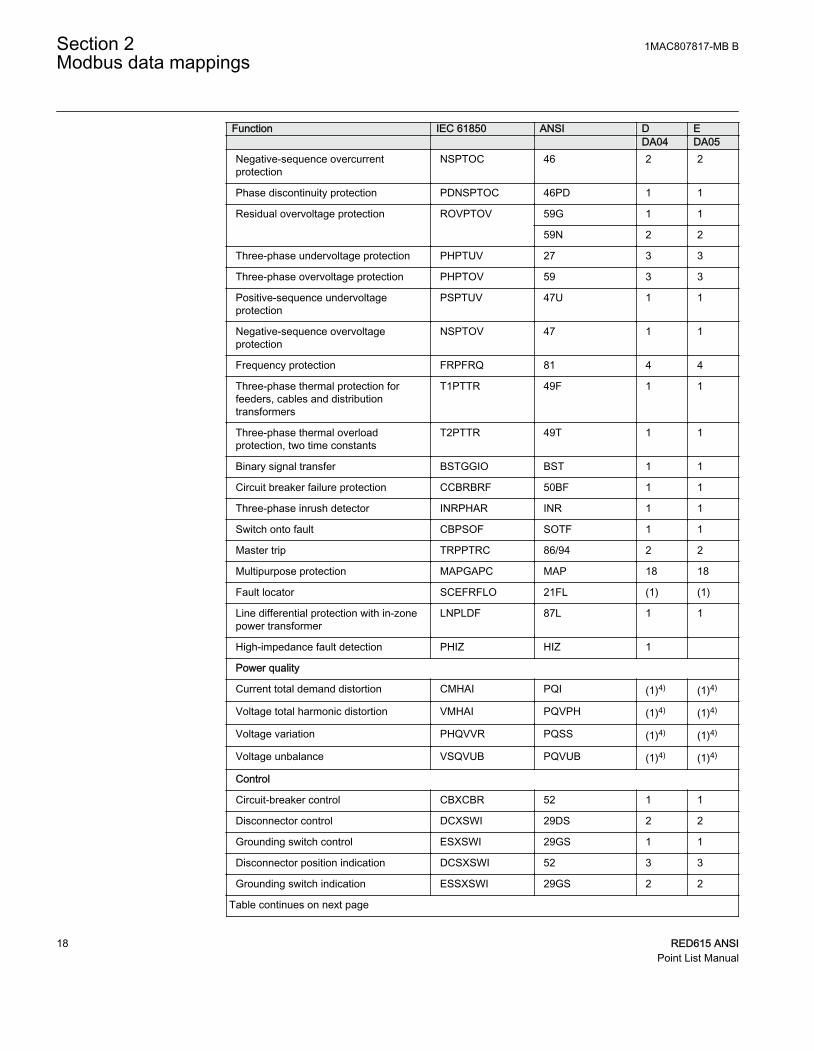
2.2 Supported functions
2.2.1 Supported functions in RED615Table 2: Supported functions
Function IEC 61850 ANSI D E DA04 DA05
Protection
Three-phase non-directional overcurrentprotection, instantaneous stage
PHIPTOC 50P-3 1 1
Three-phase directional overcurrentprotection, low stage
DPHLPDOC 67/51P 2 2
Three-phase directional overcurrentprotection, high stage
DPHHPDOC 67/50P 1 1
Non-directional ground-fault protection,high stage
EFHPTOC 50G 1 1
Directional ground-fault protection, lowstage
DEFLPDEF 67/51N 2 2
Directional ground-fault protection, highstage
DEFHPDEF 67/50N 1 1
Admittance-based ground-faultprotection1)
EFPADM 21YN (3)1) (3)1)2)
Wattmetric-based ground-faultprotection1)
WPWDE 32N (3)1) (3)1)2)
Transient/intermittent ground-faultprotection
INTRPTEF 67NIEF 13) 12)3)
Harmonics-based ground-faultprotection1)
HAEFPTOC 51NHA (1)1)3) (1)1)3)
Table continues on next page
1MAC807817-MB B Section 2Modbus data mappings
RED615 ANSI 17Point List Manual
Function IEC 61850 ANSI D E DA04 DA05
Negative-sequence overcurrentprotection
NSPTOC 46 2 2
Phase discontinuity protection PDNSPTOC 46PD 1 1
Residual overvoltage protection ROVPTOV 59G 1 1
59N 2 2
Three-phase undervoltage protection PHPTUV 27 3 3
Three-phase overvoltage protection PHPTOV 59 3 3
Positive-sequence undervoltageprotection
PSPTUV 47U 1 1
Negative-sequence overvoltageprotection
NSPTOV 47 1 1
Frequency protection FRPFRQ 81 4 4
Three-phase thermal protection forfeeders, cables and distributiontransformers
T1PTTR 49F 1 1
Three-phase thermal overloadprotection, two time constants
T2PTTR 49T 1 1
Binary signal transfer BSTGGIO BST 1 1
Circuit breaker failure protection CCBRBRF 50BF 1 1
Three-phase inrush detector INRPHAR INR 1 1
Switch onto fault CBPSOF SOTF 1 1
Master trip TRPPTRC 86/94 2 2
Multipurpose protection MAPGAPC MAP 18 18
Fault locator SCEFRFLO 21FL (1) (1)
Line differential protection with in-zonepower transformer
LNPLDF 87L 1 1
High-impedance fault detection PHIZ HIZ 1
Power quality
Current total demand distortion CMHAI PQI (1)4) (1)4)
Voltage total harmonic distortion VMHAI PQVPH (1)4) (1)4)
Voltage variation PHQVVR PQSS (1)4) (1)4)
Voltage unbalance VSQVUB PQVUB (1)4) (1)4)
Control
Circuit-breaker control CBXCBR 52 1 1
Disconnector control DCXSWI 29DS 2 2
Grounding switch control ESXSWI 29GS 1 1
Disconnector position indication DCSXSWI 52 3 3
Grounding switch indication ESSXSWI 29GS 2 2
Table continues on next page
Section 2 1MAC807817-MB BModbus data mappings
18 RED615 ANSIPoint List Manual

Function IEC 61850 ANSI D E DA04 DA05
Autoreclosing DARREC 79 (1) (1)
Synchronism and energizing check SECRSYN 25 1 (1)5)
Condition monitoring
Circuit-breaker condition monitoring SSCBR 52CM 1 1
Trip circuit supervision TCSSCBR TCM 2 2
Current circuit supervision CCSPVC CCM 1 1
Fuse failure supervision SEQSPVC 60 1 1
Protection communication supervision PCSITPC PCS 1 1
Runtime counter for machines anddevices
MDSOPT OPTM 1 1
Measurement
Load profile record LDPRLRC LoadProf 1 1
Three-phase current measurement CMMXU IA, IB, IC 1 1
Sequence current measurement CSMSQI I1, I2, I0 1 1
Residual current measurement RESCMMXU IG 1 1
Three-phase voltage measurement VMMXU VA, VB, VC 2 1(1)4)
Residual voltage measurement RESVMMXU VG 1
Sequence voltage measurement VSMSQI V1, V2, V0 1 1
Single-phase power and energymeasurement
SPEMMXU SP, SE 1 1
Three-phase power and energymeasurement
PEMMXU P, E 1 1
RTD/mA measurement XRGGIO130 X130 (RTD) (1)
Frequency measurement FMMXU f 1 1
IEC 61850-9-2 LE sampled valuesending6)
SMVSENDER SMVSENDER (1) (1)
IEC 61850-9-2 LE sampled valuereceiving (voltage sharing)6)
SMVRECEIVER SMVRECEIVER (1) (1)
Other
Minimum pulse timer (2 pcs) TPGAPC 62TP 4 4
Minimum pulse timer (2 pcs, secondresolution)
TPSGAPC 62TPS 1 1
Minimum pulse timer (2 pcs, minuteresolution)
TPMGAPC 62TPM 1 1
Pulse timer (8 pcs) PTGAPC 62PT 2 2
Time delay off (8 pcs) TOFGAPC 62TOF 4 4
Time delay on (8 pcs) TONGAPC 62TON 4 4
Table continues on next page
1MAC807817-MB B Section 2Modbus data mappings
RED615 ANSI 19Point List Manual

Function IEC 61850 ANSI D E DA04 DA05
Set-reset (8 pcs) SRGAPC SR 4 4
Move (8 pcs) MVGAPC MV 2 2
Generic control point (16 pcs) SPCGAPC SPC 2 2
Analog value scaling SCA4GAPC SCA4 4 4
Integer value move MVI4GAPC MVI4 1 1
Generic up-down counters UDFCNT CTR 4 4
1, 2, ... = Number of included instances. The instances of a protection function represent the number ofidentical protection function blocks available in the standard configuration.() = Optional
1) One of the following can be ordered as an option; Admittance based E/F, Wattmetric based E/F orHarmonics based E/F. The option is an addition to the existing E/F of the original configuration. The optionalground-fault protection has a predefined configuration in the relay. The optional ground-fault protection canbe set on or off.
2) "Calculated V0" is always used3) "Measured IG" is always used4) Power quality option includes Current total demand distortion, Voltage total harmonic distortion and Voltage
variation.5) Only available with IEC 61850-9-26) Only available with COM0031...0037
2.3 Indications
Table 3: Explanations of the indications table columns
Column name DescriptionBitA Default 0X and 1X bit address for the data.
RegA Default 3X and 4X register.bit (00-15) address for the data.
IEC 61850 name Original IED data object identification. Described in the IEC 61850 format as LogicalDevice.Logical Node and thereafter .Data Object.Data Attribute. Logical Node is thesame as the application function block name.
SA name The signal may have a defined label that is visible, for example, in the ApplicationConfiguration tool in PCM600.
Description Short description of the signal. See the technical manual for more information.
Value Meaning of the value states.
Section 2 1MAC807817-MB BModbus data mappings
20 RED615 ANSIPoint List Manual

2.3.1 Premapped indications
2.3.1.1 Common data 1
Table 4: Common data 1
BitA RegA IEC 61850 name SA name Description Values CTRL.LLN0
2720 170.00 .Loc.stVal - Remote/Local state 0/1=Rem/Loc
2721 170.01 .LocKeyHMI.stVal.Station - Station state 1=Station
DR.RDRE1
2722 170.02 .RcdMade.stVal - DR recording made 1=Made
2723 170.03 .mcd
2.3.1.2 CTRL.CBCILO1 Circuit breaker enable signals (1)
Table 5: CTRL.CBCILO1 Circuit breaker enable signals (1)
BitA RegA IEC 61850 name SA name Description Values CTRL.CBCILO1
2824 176.08 .EnaOpn.stVal ENA_OPEN Open enabled 1=Enabled
2825 176.09 .EnaCls.stVal ENA_CLOSE Close enabled 1=Enabled
2.3.1.3 CTRL.CBCSWI1 Circuit breaker (1) mom. position
Table 6: CTRL.CBCSWI1 Circuit breaker (1) mom. position
BitA RegA IEC 61850 name SA name Description Values CTRL.CBCSWI1 POSITION
2804 175.04 .Pos.stVal.Close - Close bit 1=Close
2805 175.05 .Pos.stVal.Open - Open bit 1=Open
2806 175.06 .Pos.stVal.Fault - Fault bit 1=Pos(00/11)
2834 177.02 .SynItlByps.stVal ITL_BYPASS Interlock bypass 1=Bypass
2835 177.03 .mcd
1MAC807817-MB B Section 2Modbus data mappings
RED615 ANSI 21Point List Manual

2.3.1.4 CTRL.CBCSWI1 Circuit breaker (1) mom+mcd position
Table 7: CTRL.CBCSWI1 Circuit breaker (1) mom+mcd position
BitA RegA IEC 61850 name SA name Description Values CTRL.CBCSWI1 POSITION
2816 176.00 .Pos.stVal.Close Close bit 1=Close
2817 176.01 .mcd
2818 176.02 .Pos.stVal.Open Open bit 1=Open
2819 176.03 .mcd
2820 176.04 < reserved >
2821 176.05 < reserved >
2822 176.06 .Pos.stSeld SELECTED CB selected for control 1=Selected
2823 176.07 .mcd
2.3.1.5 CTRL.CBXCBR1 Circuit-breaker control (1) – 52-1
Table 8: CTRL.CBXCBR1 Circuit-breaker control (1) – 52-1
BitA RegA IEC 61850 name SA name Description Values CTRL.CBXCBR1
2836 177.04 .BlkOpn.stVal BLK_OPEN Open blocked 1=Blocked
2837 177.05 .mcd
2838 177.06 .BlkCls.stVal BLK_CLOSE Close blocked 1=Blocked
2839 177.07 .mcd
2840 177.08 .ItlByPss.stVal ITL_BYPASS Interlock bypass 1=Bypass
2841 177.09 .mcd
2.3.1.6 CTRL.DCSXSWI1 Disconnector position indication (1) – 52-TOC
Table 9: CTRL.DCSXSWI1 Disconnector position indication (1) – 52-TOC
BitA RegA IEC 61850 name SA name Description Values CTRL.DCSXSWI1 POSITION
2792 174.08 .Pos.stVal.Close - Close bit 1=Close
2793 174.09 .Pos.stVal.Open - Open bit 1=Open
2794 174.10 .Pos.stVal.Fault - Fault bit 1=Pos(00/11)
Section 2 1MAC807817-MB BModbus data mappings
22 RED615 ANSIPoint List Manual

2.3.1.7 CTRL.DCSXSWI2 Disconnector position indication (2) – 29DS-1
Table 10: CTRL.DCSXSWI2 Disconnector position indication (2) – 29DS-1
BitA RegA IEC 61850 name SA name Description Values CTRL.DCSXSWI2 POSITION
2795 174.11 .Pos.stVal.Close - Close bit 1=Close
2796 174.12 .Pos.stVal.Open - Open bit 1=Open
2797 174.13 .Pos.stVal.Fault - Fault bit 1=Pos(00/11)
2.3.1.8 CTRL.DCSXSWI3 Disconnector position indication (3) – 29DS-2
Table 11: CTRL.DCSXSWI3 Disconnector position indication (3) – 29DS-2
BitA RegA IEC 61850 name SA name Description Values CTRL.DCSXSWI3 POSITION
2798 174.14 .Pos.stVal.Close - Close bit 1=Close
2799 174.15 .Pos.stVal.Open - Open bit 1=Open
2800 175.00 .Pos.stVal.Fault - Fault bit 1=Pos(00/11)
2.3.1.9 CTRL.DCXSWI1 Disconnector control (1) – 29DS-1
Table 12: CTRL.DCXSWI1 Disconnector control (1) – 29DS-1
BitA RegA IEC 61850 name SA name Description Values CTRL.DCXSWI1 POSITION
3472 217.00 .Pos.stVal.Close - Close bit 1=Close
3473 217.01 .Pos.stVal.Open - Open bit 1=Open
3474 217.02 .Pos.stVal.Fault - Fault bit 1=Pos(00/11)
3475 217.03 .Pos.stSeld - Control selected 1=Selected
CTRL.DCCILO1
3476 217.04 .EnaOpn.stVal ENA_OPEN Open enabled 1=Enabled
3477 217.05 .EnaCls.stVal ENA_CLOSE Close enabled 1=Enabled
CTRL.DCXSWI1
3478 217.06 .BlkOpn.stVal BLK_OPEN Open blocked 1=Blocked
3479 217.07 .mcd
3480 217.08 .BlkCls.stVal BLK_CLOSE Close blocked 1=Blocked
3481 217.09 .mcd
CTRL.DCCILO1
3482 217.10 .ItlByps.stVal ITL_BYPASS Interlock bypass 1=Bypass
3483 217.11 .mcd
1MAC807817-MB B Section 2Modbus data mappings
RED615 ANSI 23Point List Manual

2.3.1.10 CTRL.DCXSWI2 Disconnector control (2) – 29DS-2
Table 13: CTRL.DCXSWI2 Disconnector control (2) – 29DS-2
BitA RegA IEC 61850 name SA name Description Values CTRL.DCXSWI2 POSITION
3484 217.12 .Pos.stVal.Close - Close bit 1=Close
3485 217.13 .Pos.stVal.Open - Open bit 1=Open
3486 217.14 .Pos.stVal.Fault - Fault bit 1=Pos(00/11)
3487 217.15 .Pos.stSeld - Control selected 1=Selected
CTRL.DCCILO2
3488 218.00 .EnaOpn.stVal ENA_OPEN Open enabled 1=Enabled
3489 218.01 .EnaCls.stVal ENA_CLOSE Close enabled 1=Enabled
CTRL.DCXSWI2
3490 218.02 .BlkOpn.stVal BLK_OPEN Open blocked 1=Blocked
3491 218.03 .mcd
3492 218.04 .BlkCls.stVal BLK_CLOSE Close blocked 1=Blocked
3493 218.05 .mcd
CTRL.DCCILO2
3494 218.06 .ItlByps.stVal ITL_BYPASS Interlock bypass 1=Bypass
3495 218.07 .mcd
2.3.1.11 CTRL.ESSXSWI1 Grounding switch indication (1) – 29GS-1
Table 14: CTRL.ESSXSWI1 Grounding switch indication (1) – 29GS-1
BitA RegA IEC 61850 name SA name Description Values CTRL.ESSXSWI1 POSITION
2801 175.01 .Pos.stVal.Close - Close bit 1=Close
2802 175.02 .Pos.stVal.Open - Open bit 1=Open
2803 175.03 .Pos.stVal.Fault - Fault bit 1=Pos(00/11)
2.3.1.12 CTRL.ESSXSWI2 Grounding switch indication (2) – 29GS-2
Table 15: CTRL.ESSXSWI2 Grounding switch indication (2) – 29GS-2
BitA RegA IEC 61850 name SA name Description Values CTRL.ESSXSWI2 POSITION
2807 175.07 .Pos.stVal.Close - Close bit 1=Close
2808 175.08 .Pos.stVal.Open - Open bit 1=Open
2809 175.09 .Pos.stVal.Fault - Fault bit 1=Pos(00/11)
Section 2 1MAC807817-MB BModbus data mappings
24 RED615 ANSIPoint List Manual

2.3.1.13 CTRL.ESXSWI1 Grounding switch control (1) – 29GS-1
Table 16: CTRL.ESXSWI1 Grounding switch control (1) – 29GS-1
BitA RegA IEC 61850 name SA name Description Values CTRL.ESXSWI1 POSITION
3496 218.08 .Pos.stVal.Close - Close bit 1=Close
3497 218.09 .Pos.stVal.Open - Open bit 1=Open
3498 218.10 .Pos.stVal.Fault - Fault bit 1=Pos(00/11)
3499 218.11 .Pos.stSeld - Control selected 1=Selected
CTRL.ESCILO1
3500 218.12 .EnaOpn.stVal ENA_OPEN Open enabled 1=Enabled
3501 218.13 .EnaCls.stVal ENA_CLOSE Close enabled 1=Enabled
CTRL.ESXSWI1
3502 218.14 .BlkOpn.stVal BLK_OPEN Open blocked 1=Blocked
3503 218.15 .mcd
3504 219.00 .BlkCls.stVal BLK_CLOSE Close blocked 1=Blocked
3505 219.01 .mcd
CTRL.ESCILO1
3506 219.02 .ItlByps.stVal ITL_BYPASS Interlock bypass 1=Bypass
3507 219.03 .mcd
2.3.1.14 LD0.BSTGGIO1 Binary signal transfer (1) – BST-1
Table 17: LD0.BSTGGIO1 Binary signal transfer (1) – BST-1
BitA RegA IEC 61850 name SA name Description Values LD0.BSTGGIO1
2784 174.00 .Alm1.stVal SEND_SIG_A Send alarm 1=Alarm
2785 174.01 .mcd
2786 174.02 .Alm2.stVal RECV_SIG_A Receive alarm 1=Alarm
2787 174.03 .mcd
1MAC807817-MB B Section 2Modbus data mappings
RED615 ANSI 25Point List Manual

2.3.1.15 LD0.CCBRBRF1 Circuit breaker failure protection (1) – 50BF-1
Table 18: LD0.CCBRBRF1 Circuit breaker failure protection (1) – 50BF-1
BitA RegA IEC 61850 name SA name Description Values LD0.CCBRBRF1
2828 176.12 .Str.general CB_FAULT_AL Timer running 1=Running
2829 176.13 .mcd
2830 176.14 .OpEx.general TRBU Fail, external trip 1=Ext.trip
2831 176.15 .mcd
2832 177.00 .OpIn.general TRRET Internal re-trip 1=Re-trip
2833 177.01 .mcd
2.3.1.16 LD0.CCSPVC1 Current circuit failure detection (1) – CCM-1
Table 19: LD0.CCSPVC1 Current circuit failure detection (1) – CCM-1
BitA RegA IEC 61850 name SA name Description Values LD0.CCSPVC1
2864 179.00 .Alm.stVal ALARM Alarm 1=Alarm
2865 179.01 .mcd
2866 179.02 .Op.general FAIL Failure trip 1=Trip
2867 179.03 .mcd
2.3.1.17 LD0.CMMXU1 Three-phase current measurement (1) – IA, IB, IC
Table 20: LD0.CMMXU1 Three-phase current measurement (1) – IA, IB, IC
BitA RegA IEC 61850 name SA name Description Values LD0.CMMXU1
2752 172.00 .HiAlm.stVal HIGH_ALARM High alarm 1=Alarm
2753 172.01 .mcd
2754 172.02 .HiWrn.stVal HIGH_WARN High warning 1=Warning
2755 172.03 .mcd
2756 172.04 .LoWrn.stVal LOW_WARN Low warning 1=Warning
2757 172.05 .mcd
2758 172.06 .LoAlm.stVal LOW_ALARM Low alarm 1=Alarm
2759 172.07 .mcd
Section 2 1MAC807817-MB BModbus data mappings
26 RED615 ANSIPoint List Manual
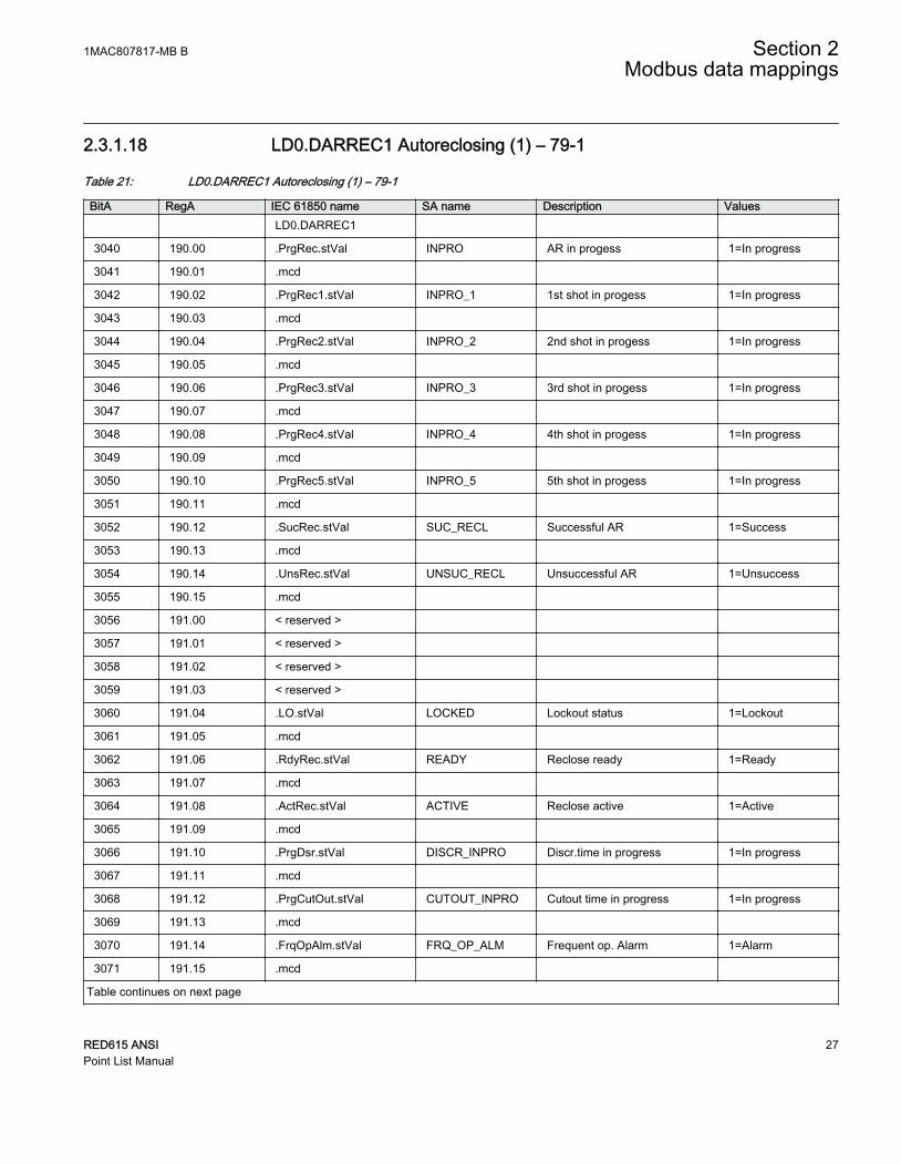
2.3.1.18 LD0.DARREC1 Autoreclosing (1) – 79-1
Table 21: LD0.DARREC1 Autoreclosing (1) – 79-1
BitA RegA IEC 61850 name SA name Description Values LD0.DARREC1
3040 190.00 .PrgRec.stVal INPRO AR in progess 1=In progress
3041 190.01 .mcd
3042 190.02 .PrgRec1.stVal INPRO_1 1st shot in progess 1=In progress
3043 190.03 .mcd
3044 190.04 .PrgRec2.stVal INPRO_2 2nd shot in progess 1=In progress
3045 190.05 .mcd
3046 190.06 .PrgRec3.stVal INPRO_3 3rd shot in progess 1=In progress
3047 190.07 .mcd
3048 190.08 .PrgRec4.stVal INPRO_4 4th shot in progess 1=In progress
3049 190.09 .mcd
3050 190.10 .PrgRec5.stVal INPRO_5 5th shot in progess 1=In progress
3051 190.11 .mcd
3052 190.12 .SucRec.stVal SUC_RECL Successful AR 1=Success
3053 190.13 .mcd
3054 190.14 .UnsRec.stVal UNSUC_RECL Unsuccessful AR 1=Unsuccess
3055 190.15 .mcd
3056 191.00 < reserved >
3057 191.01 < reserved >
3058 191.02 < reserved >
3059 191.03 < reserved >
3060 191.04 .LO.stVal LOCKED Lockout status 1=Lockout
3061 191.05 .mcd
3062 191.06 .RdyRec.stVal READY Reclose ready 1=Ready
3063 191.07 .mcd
3064 191.08 .ActRec.stVal ACTIVE Reclose active 1=Active
3065 191.09 .mcd
3066 191.10 .PrgDsr.stVal DISCR_INPRO Discr.time in progress 1=In progress
3067 191.11 .mcd
3068 191.12 .PrgCutOut.stVal CUTOUT_INPRO Cutout time in progress 1=In progress
3069 191.13 .mcd
3070 191.14 .FrqOpAlm.stVal FRQ_OP_ALM Frequent op. Alarm 1=Alarm
3071 191.15 .mcd
Table continues on next page
1MAC807817-MB B Section 2Modbus data mappings
RED615 ANSI 27Point List Manual

BitA RegA IEC 61850 name SA name Description Values3072 192.00 .RclTmStr.stVal Reclaim time started
3073 192.01 .mcd
3074 192.02 .ProCrd.stVal Protection coordination 1=In progress
3075 192.03 .mcd
3076 192.04 .CBManCls.stVal MAN_CB_CL CB manually closed 1=CB closed
3077 192.05 .mcd
3078 192.06 .OpCls.general CLOSE_CB Operate (close XCBR) 1=Close CB
3079 192.07 .mcd
3080 192.08 .OpOpn.general OPEN_CB Operate (open XCBR) 1=Open CB
3081 192.09 .mcd
3082 192.10 .UnsCBCls.stVal UNSUC_CB CB closing failed 1=Failed
3083 192.11 .mcd
3084 192.12 .WtMstr.stVal CMD_WAIT Master signal to follower 1=Signal
3085 192.13 .mcd
2.3.1.19 LD0.DARREC1 Autoreclosing state (1) – 79-1
Table 22: LD0.DARREC1 Autoreclosing state (1) – 79-1
BitA RegA IEC 61850 name SA name Description Values LD0.DARREC1
2724 170.04 .AutoRecOn.stVal AR_ON AutoRecloser state 0/1=Off/On
2.3.1.20 LD0.DEFHPDEF1 Directional ground-fault protection, high stage (1) –67/50N-1
Table 23: LD0.DEFHPDEF1 Directional ground-fault protection, high stage (1) – 67/50N-1
BitA RegA IEC 61850 name SA name Description Values LD0.DEFHPTOC1
2928 183.00 .Str.general PICKUP Stage pickup 1=Pickup
2929 183.01 .mcd
2930 183.02 .Op.general TRIP Stage trip 1=Trip
2931 183.03 .mcd
Section 2 1MAC807817-MB BModbus data mappings
28 RED615 ANSIPoint List Manual
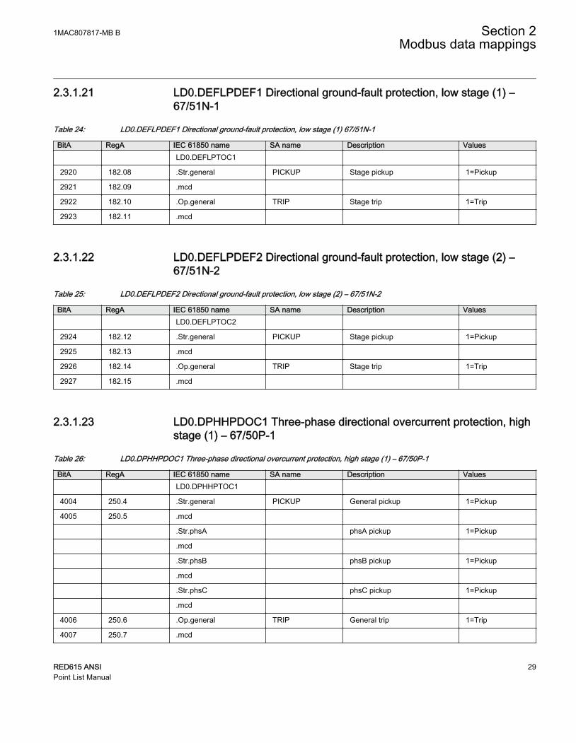
2.3.1.21 LD0.DEFLPDEF1 Directional ground-fault protection, low stage (1) –67/51N-1
Table 24: LD0.DEFLPDEF1 Directional ground-fault protection, low stage (1) 67/51N-1
BitA RegA IEC 61850 name SA name Description Values LD0.DEFLPTOC1
2920 182.08 .Str.general PICKUP Stage pickup 1=Pickup
2921 182.09 .mcd
2922 182.10 .Op.general TRIP Stage trip 1=Trip
2923 182.11 .mcd
2.3.1.22 LD0.DEFLPDEF2 Directional ground-fault protection, low stage (2) –67/51N-2
Table 25: LD0.DEFLPDEF2 Directional ground-fault protection, low stage (2) – 67/51N-2
BitA RegA IEC 61850 name SA name Description Values LD0.DEFLPTOC2
2924 182.12 .Str.general PICKUP Stage pickup 1=Pickup
2925 182.13 .mcd
2926 182.14 .Op.general TRIP Stage trip 1=Trip
2927 182.15 .mcd
2.3.1.23 LD0.DPHHPDOC1 Three-phase directional overcurrent protection, highstage (1) – 67/50P-1
Table 26: LD0.DPHHPDOC1 Three-phase directional overcurrent protection, high stage (1) – 67/50P-1
BitA RegA IEC 61850 name SA name Description Values LD0.DPHHPTOC1
4004 250.4 .Str.general PICKUP General pickup 1=Pickup
4005 250.5 .mcd
.Str.phsA phsA pickup 1=Pickup
.mcd
.Str.phsB phsB pickup 1=Pickup
.mcd
.Str.phsC phsC pickup 1=Pickup
.mcd
4006 250.6 .Op.general TRIP General trip 1=Trip
4007 250.7 .mcd
1MAC807817-MB B Section 2Modbus data mappings
RED615 ANSI 29Point List Manual

2.3.1.24 LD0.DPHLPDOC1 Three-phase directional overcurrent protection, lowstage (1) – 67/51P-1
Table 27: LD0.DPHLPDOC1 Three-phase directional overcurrent protection, low stage (1) – 67/51P-1
BitA RegA IEC 61850 name SA name Description Values LD0.DPHLPDOC1
4008 250.8 .Str.general PICKUP General pickup 1=Pickup
4009 250.9 .mcd
.Str.phsA phsA pickup 1=Pickup
.mcd
.Str.phsB phsB pickup 1=Pickup
.mcd
.Str.phsC phsC pickup 1=Pickup
.mcd
4010 250.1 .Op.general TRIP General trip 1=Trip
4011 250.11 .mcd
2.3.1.25 LD0.DPHLPDOC2 Three-phase directional overcurrent protection, lowstage (2) – 67/51P-2
Table 28: LD0.DPHLPDOC2 Three-phase directional overcurrent protection, low stage (2) – 67/51P-2
BitA RegA IEC 61850 name SA name Description Value LD0.DPHLPDOC2
4012 250.12 .Str.general PICKUP General pickup 1=Pickup
4013 250.13 .mcd
.Str.phsA phsA pickup 1=Pickup
.mcd
.Str.phsB phsB pickup 1=Pickup
.mcd
.Str.phsC phsC pickup 1=Pickup
.mcd
4014 250.14 .Op.general TRIP General trip 1=Trip
4015 250.15 .mcd
Section 2 1MAC807817-MB BModbus data mappings
30 RED615 ANSIPoint List Manual
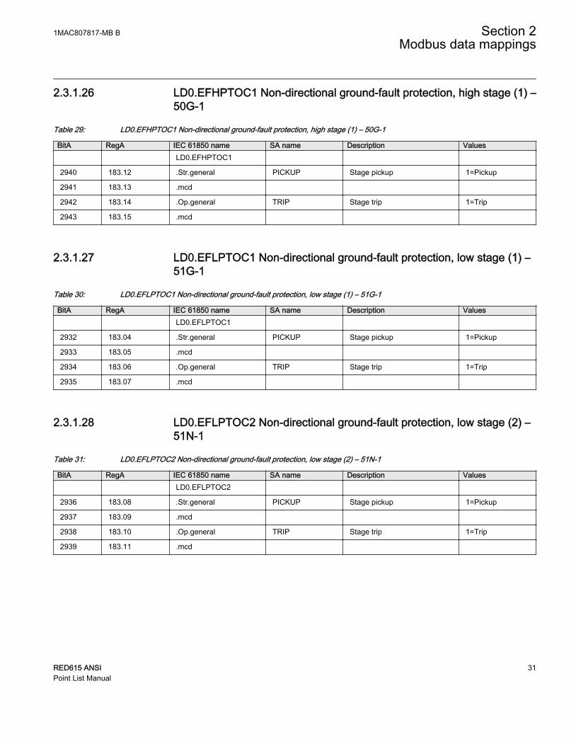
2.3.1.26 LD0.EFHPTOC1 Non-directional ground-fault protection, high stage (1) –50G-1
Table 29: LD0.EFHPTOC1 Non-directional ground-fault protection, high stage (1) – 50G-1
BitA RegA IEC 61850 name SA name Description Values LD0.EFHPTOC1
2940 183.12 .Str.general PICKUP Stage pickup 1=Pickup
2941 183.13 .mcd
2942 183.14 .Op.general TRIP Stage trip 1=Trip
2943 183.15 .mcd
2.3.1.27 LD0.EFLPTOC1 Non-directional ground-fault protection, low stage (1) –51G-1
Table 30: LD0.EFLPTOC1 Non-directional ground-fault protection, low stage (1) – 51G-1
BitA RegA IEC 61850 name SA name Description Values LD0.EFLPTOC1
2932 183.04 .Str.general PICKUP Stage pickup 1=Pickup
2933 183.05 .mcd
2934 183.06 .Op.general TRIP Stage trip 1=Trip
2935 183.07 .mcd
2.3.1.28 LD0.EFLPTOC2 Non-directional ground-fault protection, low stage (2) –51N-1
Table 31: LD0.EFLPTOC2 Non-directional ground-fault protection, low stage (2) – 51N-1
BitA RegA IEC 61850 name SA name Description Values LD0.EFLPTOC2
2936 183.08 .Str.general PICKUP Stage pickup 1=Pickup
2937 183.09 .mcd
2938 183.10 .Op.general TRIP Stage trip 1=Trip
2939 183.11 .mcd
1MAC807817-MB B Section 2Modbus data mappings
RED615 ANSI 31Point List Manual

2.3.1.29 LD0.EFPADM1 Admittance-based ground-fault protection (1) – 21YN-1
Table 32: LD0.EFPADM1 Admittance-based ground-fault protection (1) – 21YN-1
BitA RegA IEC 61850 name SA name Description Values LD0.EFPADM1
2992 187.00 .Str.general PICKUP Stage pickup 1=Pickup
2993 187.01 .mcd
2994 187.02 .Op.general TRIP Stage trip 1=Trip
2995 187.03 .mcd
2.3.1.30 LD0.EFPADM2 Admittance-based ground-fault protection (2) – 21YN-2
Table 33: LD0.EFPADM2 Admittance-based ground-fault protection (2) – 21YN-2
BitA RegA IEC 61850 name SA name Description Values LD0.EFPADM2
2996 187.04 .Str.general PICKUP Stage pickup 1=Pickup
2997 187.05 .mcd
2998 187.06 .Op.general TRIP Stage trip 1=Trip
2999 187.07 .mcd
2.3.1.31 LD0.EFPADM3 Admittance-based ground-fault protection (3) – 21YN-3
Table 34: LD0.EFPADM3 Admittance-based ground-fault protection (3) – 21YN-3
BitA RegA IEC 61850 name SA name Description Values LD0.EFPADM3
3000 187.08 .Str.general PICKUP Stage pickup 1=Pickup
3001 187.09 .mcd
3002 187.10 .Op.general TRIP Stage trip 1=Trip
3003 187.11 .mcd
2.3.1.32 LD0.FRPFRQ1 Frequency protection (1) – 81-1
Table 35: LD0.FRPFRQ1 Frequency protection (1) – 81-1
BitA RegA IEC 61850 name SA name Description Values LD0.FRPTRC1
4016 251 .Str.general PICKUP Stage 1 pickup 1=Pickup
4017 251.1 .mcd
Table continues on next page
Section 2 1MAC807817-MB BModbus data mappings
32 RED615 ANSIPoint List Manual

BitA RegA IEC 61850 name SA name Description Values LD0.FRPTOF1 Overfrequency
4018 251.2 .Op.general OPR_OFRQ Trip 1=Trip
4019 251.3 .mcd
LD0.FRPTUF1 Underfrequency
4020 251.4 .Op.general OPR_UFRQ Trip 1=Trip
4021 251.5 .mcd
LD0.FRPFRC1 Frequency gradient
4022 251.6 .Op.general OPR_FRG Trip 1=Trip
4023 251.7 .mcd
2.3.1.33 LD0.FRPFRQ2 Frequency protection (2) – 81-2
Table 36: LD0.FRPFRQ2 Frequency protection (2) – 81-2
BitA RegA IEC 61850 name SA name Description Values LD0.FRPTRC2
4024 251.8 .Str.general PICKUP Stage 2 pickup 1=Pickup
4025 251.9 .mcd
LD0.FRPTOF2 Overfrequency
4026 251.1 .Op.general OPR_OFRQ Trip 1=Trip
4027 251.11 .mcd
LD0.FRPTUF2 Underfrequency
4028 251.12 .Op.general OPR_UFRQ Trip 1=Trip
4029 251.13 .mcd
LD0.FRPFRC2 Frequency gradient
4030 251.14 .Op.general OPR_FRG Trip 1=Trip
4031 251.15 .mcd
2.3.1.34 LD0.FRPFRQ3 Frequency protection (3) – 81-3
Table 37: LD0.FRPFRQ3 Frequency protection (3) – 81-3
BitA RegA IEC 61850 name SA name Description Values LD0.FRPTRC3
4032 252 .Str.general PICKUP Stage 3 pickup 1=Pickup
4033 252.1 .mcd
LD0.FRPTOF3 Overfrequency
4034 252.2 .Op.general OPR_OFRQ Trip 1=Trip
Table continues on next page
1MAC807817-MB B Section 2Modbus data mappings
RED615 ANSI 33Point List Manual

BitA RegA IEC 61850 name SA name Description Values4035 252.3 .mcd
LD0.FRPTUF3 Underfrequency
4036 252.4 .Op.general OPR_UFRQ Trip 1=Trip
4037 252.5 .mcd
LD0.FRPFRC3 Frequency gradient
4038 252.6 .Op.general OPR_FRG Trip 1=Trip
4039 252.7 .mcd
2.3.1.35 LD0.FRPFRQ4 Frequency protection (4) – 81-4
Table 38: LD0.FRPFRQ4 Frequency protection (4) – 81-4
BitA RegA IEC 61850 name SA name Description Values LD0.FRPTRC4
4040 252.8 .Str.general PICKUP Stage 4 pickup 1=Pickup
4041 252.9 .mcd
LD0.FRPTOF4 Overfrequency
4042 252.1 .Op.general OPR_OFRQ Trip 1=Trip
4043 252.11 .mcd
LD0.FRPTUF4 Underfrequency
4044 252.12 .Op.general OPR_UFRQ Trip 1=Trip
4044 252.13 .mcd
LD0.FRPFRC4 Frequency gradient
4046 252.14 .Op.general OPR_FRG Trip 1=Trip
4047 252.15 .mcd
2.3.1.36 LD0.HAEFPTOC1 Harmonics-based ground-fault protection (1) –51NHA-1
Table 39: LD0.HAEFPTOC1 Harmonics-based ground-fault protection (1) – 51NHA-1
BitA RegA IEC 61850 name SA name Description Values LD0.HAEFPTOC1
3312 207.00 .Str.general PICKUP Stage pickup 1=Pickup
3313 207.01 .mcd
3314 207.02 .Op.general TRIP Stage trip 1=Trip
3315 207.03 .mcd
Section 2 1MAC807817-MB BModbus data mappings
34 RED615 ANSIPoint List Manual

2.3.1.37 LD0.INRPHAR1 Three-phase inrush detector (1) – INR-1
Table 40: LD0.INRPHAR1 Three-phase inrush detector (1) – INR-1
BitA RegA IEC 61850 name SA name Description Values LD0.INRPHAR1
2964 185.04 .Str.general BLK2H General pickup 1=Pickup
2965 185.05 .mcd
2966 185.06 .Str.phsA Phs A pickup 1=Pickup
2967 185.07 .mcd
2968 185.08 .Str.phsB Phs B pickup 1=Pickup
2969 185.09 .mcd
2970 185.10 .Str.phsC Phs C pickup 1=Pickup
2971 185.11 .mcd
2.3.1.38 LD0.INTRPTEF1 Transient/intermittent ground-fault protection (1) –67NIEF-1
Table 41: LD0.INTRPTEF1 Transient/intermittent ground-fault protection (1) – 67NIEF-1
BitA RegA IEC 61850 name SA name Description Values LD0.INTRPTEF1
2948 184.04 .Str.general PICKUP Stage pickup 1=Pickup
2949 184.05 .mcd
2950 184.06 .Op.general TRIP Stage trip 1=Trip
2951 184.07 .mcd
2.3.1.39 LD0.LEDGGIO1 Indication LED states Color1/Color2 – LED
These LED indication points interpret the case when a signal is wired to both the OK andALARM inputs, but inverted to the other. This means that the LED toggles between redand green colors. The default color for ALARM is red and green for OK. Colors can,however, be reconfigured with a setting parameter.
1MAC807817-MB B Section 2Modbus data mappings
RED615 ANSI 35Point List Manual

OKALARMRESET
LEDxSignal
NOTGUID-2AE4D47A-2BBD-4422-A81C-CF2EB7473379 V1 EN
Figure 2: Signal wired to both OK and ALARM inputs – inverted to the other
If the OK and ALARM inputs are wired to separate indication signals, theLED will have three legal states and cannot be expressed with one bit only.In this case, it is possible to combine this LED bit interpretation with thecorresponding value from the other LED state interpretation.
OKALARMRESET
LEDx
Signal 1Signal 2
GUID-051741E8-4D66-412C-BA0A-0B849B5E58F2 V1 EN
Figure 3: Separate signals wired to OK and ALARM inputs
Table 42: LD0.LEDGGIO1 Indication LED states Color1/Color2 – LED
BitA RegA IEC 61850 name SA name Description Values LD0.LEDGGIO1
3520 220.00 .LEDSt1.stVal - LED 1 state 0/1=Color1/2
3521 220.01 .LEDSt2.stVal - LED 2 state 0/1=Color1/2
3522 220.02 .LEDSt3.stVal - LED 3 state 0/1=Color1/2
3523 220.03 .LEDSt4.stVal - LED 4 state 0/1=Color1/2
3524 220.04 .LEDSt5.stVal - LED 5 state 0/1=Color1/2
3525 220.05 .LEDSt6.stVal - LED 6 state 0/1=Color1/2
3526 220.06 .LEDSt7.stVal - LED 7 state 0/1=Color1/2
3527 220.07 .LEDSt8.stVal - LED 8 state 0/1=Color1/2
3528 220.08 .LEDSt9.stVal - LED 9 state 0/1=Color1/2
3529 220.09 .LEDSt10.stVal - LED 10 state 0/1=Color1/2
3530 220.10 .LEDSt11.stVal - LED 11 state 0/1=Color1/2
3531 220.11 <reserved> 0
Section 2 1MAC807817-MB BModbus data mappings
36 RED615 ANSIPoint List Manual

2.3.1.40 LD0.LEDGGIO1 Indication LED states OFF/ColorX – LED
These LED indication points interpret the case when an indication signal is wired to eitherthe OK or ALARM input of the LED function block. The default color for ALARM is redand green for OK. Colors can, however, be reconfigured with a setting parameter.
OKALARMRESET
LEDx
OKALARMRESET
LEDx
Signal
Signal
GUID-775477F8-C2DE-4138-B2C0-6B7C2774D4D2 V1 EN
Figure 4: Signal wired to either OK or Alarm input
Table 43: LD0.LEDGGIO1 Indication LED states OFF/ColorX – LED
BitA RegA IEC 61850 name SA name Description Values LD0.LEDGGIO1
2768 173.00 .LEDSt1.stVal - LED 1 state 0/1=Off/Color
2769 173.01 .LEDSt2.stVal - LED 2 state 0/1=Off/Color
2770 173.02 .LEDSt3.stVal - LED 3 state 0/1=Off/Color
2771 173.03 .LEDSt4.stVal - LED 4 state 0/1=Off/Color
2772 173.04 .LEDSt5.stVal - LED 5 state 0/1=Off/Color
2773 173.05 .LEDSt6.stVal - LED 6 state 0/1=Off/Color
2774 173.06 .LEDSt7.stVal - LED 7 state 0/1=Off/Color
2775 173.07 .LEDSt8.stVal - LED 8 state 0/1=Off/Color
2776 173.08 .LEDSt9.stVal - LED 9 state 0/1=Off/Color
2777 173.09 .LEDSt10.stVal - LED 10 state 0/1=Off/Color
2778 173.10 .LEDSt11.stVal - LED 11 state 0/1=Off/Color
2779 173.11 <reserved> 0
1MAC807817-MB B Section 2Modbus data mappings
RED615 ANSI 37Point List Manual

2.3.1.41 LD0.LEDPTRC1 Global conditioning (1)
Table 44: LD0.LEDPTRC1 Global conditioning (1)
BitA RegA IEC 61850 name SA name Description Values LD0.LEDPTRC1
2736 171.00 .Str.general - Global pickup 1=Pickup
2737 171.01 .mcd
2738 171.02 .Op.general - Global trip 1=Trip
2739 171.03 .mcd
2.3.1.42 LD0.LEDPTRC1 Global conditioning - phase information (1)
Table 45: LD0.LEDPTRC1 Global conditioning - phase information (1)
BitA RegA IEC 61850 name SA name Description Values LD0.LEDPTRC1
2980 186.00 .Str.phsA Pickup phsA 1=Pickup
2981 186.01 .mcd
2982 186.02 .Str.phsB Pickup phsB 1=Pickup
2983 186.03 .mcd
2984 186.04 .Str.phsC Pickup phsC 1=Pickup
2985 186.05 .mcd
2986 186.06 .Op.phsA Trip phsA 1=Trip
2987 186.07 .mcd
2988 186.08 .Op.phsB Trip phsB 1=Trip
2989 186.09 .mcd
2990 186.10 .Op.phsC Trip phsC 1=Trip
2991 186.11 .mcd
2.3.1.43 LD0.LNPLDF1 Line differential protection with in-zone power transformer(1) – 87L-1
Table 46: LD0.LNPLDF1 Line differential protection with in-zone power transformer (1) – 87L-1
BitA RegA IEC 61850 name SA name Description Values LD0.LNPTRC1
.Op.phsA Phs A trip 1=Trip
.mcd
.Op.phsB Phs B trip 1=Trip
Table continues on next page
Section 2 1MAC807817-MB BModbus data mappings
38 RED615 ANSIPoint List Manual

BitA RegA IEC 61850 name SA name Description Values .mcd
.Op.phsC Phs C trip 1=Trip
.mcd
.Str.phsA Phs A pickup 1=Pickup
.mcd
.Str.phsB Phs B pickup 1=Pickup
.mcd
.Str.phsC Phs C pickup 1=Pickup
.mcd
4000 250 .Op.general TRIP Stage trip 1 = Trip
4001 250.1 .mcd
4002 250.2 .Str.general PICKUP Stage pickup 1 = Pickup
4003 250.3 .mcd
2.3.1.44 LD0.MVGAPC1 Move (8 pcs) (1) – MV-1
Table 47: LD0.MVGAPC1 Move (8 pcs) (1) – MV-1
BitA RegA IEC 61850 name SA name Description Values LD0.MVGAPC1
3536 221.00 .SPCSO1.stVal Input 1 0/1=Off/On
3537 221.01 .mcd
3538 221.02 .SPCSO2.stVal Input 2 0/1=Off/On
3539 221.03 .mcd
3540 221.04 .SPCSO3.stVal Input 3 0/1=Off/On
3541 221.05 .mcd
3542 221.06 .SPCSO4.stVal Input 4 0/1=Off/On
3543 221.07 .mcd
3544 221.08 .SPCSO5.stVal Input 5 0/1=Off/On
3545 221.09 .mcd
3546 221.10 .SPCSO6.stVal Input 6 0/1=Off/On
3547 221.11 .mcd
3548 221.12 .SPCSO7.stVal Input 7 0/1=Off/On
3549 221.13 .mcd
3550 221.14 .SPCSO8.stVal Input 8 0/1=Off/On
3551 221.15 .mcd
1MAC807817-MB B Section 2Modbus data mappings
RED615 ANSI 39Point List Manual
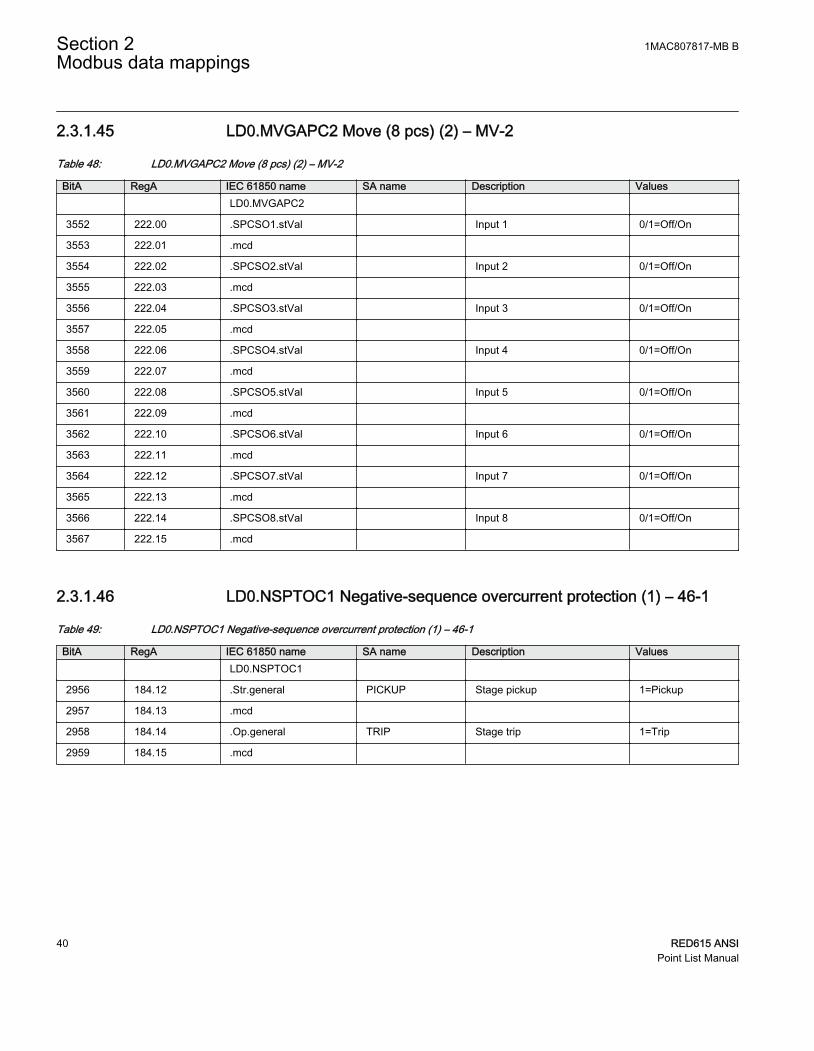
2.3.1.45 LD0.MVGAPC2 Move (8 pcs) (2) – MV-2
Table 48: LD0.MVGAPC2 Move (8 pcs) (2) – MV-2
BitA RegA IEC 61850 name SA name Description Values LD0.MVGAPC2
3552 222.00 .SPCSO1.stVal Input 1 0/1=Off/On
3553 222.01 .mcd
3554 222.02 .SPCSO2.stVal Input 2 0/1=Off/On
3555 222.03 .mcd
3556 222.04 .SPCSO3.stVal Input 3 0/1=Off/On
3557 222.05 .mcd
3558 222.06 .SPCSO4.stVal Input 4 0/1=Off/On
3559 222.07 .mcd
3560 222.08 .SPCSO5.stVal Input 5 0/1=Off/On
3561 222.09 .mcd
3562 222.10 .SPCSO6.stVal Input 6 0/1=Off/On
3563 222.11 .mcd
3564 222.12 .SPCSO7.stVal Input 7 0/1=Off/On
3565 222.13 .mcd
3566 222.14 .SPCSO8.stVal Input 8 0/1=Off/On
3567 222.15 .mcd
2.3.1.46 LD0.NSPTOC1 Negative-sequence overcurrent protection (1) – 46-1
Table 49: LD0.NSPTOC1 Negative-sequence overcurrent protection (1) – 46-1
BitA RegA IEC 61850 name SA name Description Values LD0.NSPTOC1
2956 184.12 .Str.general PICKUP Stage pickup 1=Pickup
2957 184.13 .mcd
2958 184.14 .Op.general TRIP Stage trip 1=Trip
2959 184.15 .mcd
Section 2 1MAC807817-MB BModbus data mappings
40 RED615 ANSIPoint List Manual

2.3.1.47 LD0.NSPTOC2 Negative-sequence overcurrent protection (2) – 46-2
Table 50: LD0.NSPTOC2 Negative-sequence overcurrent protection (2) – 46-2
BitA RegA IEC 61850 name SA name Description Values LD0.NSPTOC2
2960 185.00 .Str.general PICKUP Stage pickup 1=Pickup
2961 185.01 .mcd
2962 185.02 .Op.general TRIP Stage trip 1=Trip
2963 185.03 .mcd
2.3.1.48 LD0.NSPTOV1 Negative-sequence overvoltage protection (1) – 47-1
Table 51: LD0.NSPTOV1 Negative-sequence overvoltage protection (1) – 47-1
BitA RegA IEC 61850 name SA name Description Values LD0.NSPTOV1
4050 253.2 .Str.general PICKUP General pickup 1=Pickup
4051 253.3 .mcd
.Str.phsA phsA pickup 1=Pickup
.mcd
.Str.phsB phsB pickup 1=Pickup
.mcd
.Str.phsC phsC pickup 1=Pickup
.mcd
4052 253.4 .Op.general TRIP General trip 1=Trip
4053 253.5 .mcd
2.3.1.49 LD0.PDNSPTOC1 Phase discontinuity protection (1) – 46PD-1
Table 52: LD0.PDNSPTOC1 Phase discontinuity protection (1) – 46PD-1
BitA RegA IEC 61850 name SA name Description Values LD0.PDNSPTOC1
2952 184.08 .Str.general PICKUP Stage pickup 1=Pickup
2953 184.09 .mcd
2954 184.10 .Op.general TRIP Stage trip 1=Trip
2955 184.11 .mcd
1MAC807817-MB B Section 2Modbus data mappings
RED615 ANSI 41Point List Manual

2.3.1.50 LD0.PHHPTOC1 Three-phase non-directional overcurrent protection,high stage (1) – 50P-1
Table 53: LD0.PHHPTOC1 Three-phase non-directional overcurrent protection, high stage (1) – 50P-1
BitA RegA IEC 61850 name SA name Description Values LD0.PHHPTOC1
2890 180.10 .Str.general PICKUP General pickup 1=Pickup
2891 180.11 .mcd
2892 180.12 .Str.phsA Phs A pickup 1=Pickup
2893 180.13 .mcd
2894 180.14 .Str.phsB Phs B pickup 1=Pickup
2895 180.15 .mcd
2896 181.00 .Str.phsC Phs C pickup 1=Pickup
2897 181.01 .mcd
2898 181.02 .Op.general TRIP General trip 1=Trip
2899 181.03 .mcd
2.3.1.51 LD0.PHIPTOC1 Three-phase non-directional overcurrent protection,instantaneous stage (1) – 50P-3
Table 54: LD0.PHIPTOC1 Three-phase non-directional overcurrent protection, instantaneous stage (1) – 50P-3
BitA RegA IEC 61850 name SA name Description Values LD0.PHIPTOC1
2910 181.14 .Str.general PICKUP General pickup 1=Pickup
2911 181.15 .mcd
2912 182.00 .Str.phsA Phs A pickup 1=Pickup
2913 182.01 .mcd
2914 182.02 .Str.phsB Phs B pickup 1=Pickup
2915 182.03 .mcd
2916 182.04 .Str.phsC Phs C pickup 1=Pickup
2917 182.05 .mcd
2918 182.06 .Op.general TRIP General trip 1=Trip
2919 182.07 .mcd
Section 2 1MAC807817-MB BModbus data mappings
42 RED615 ANSIPoint List Manual

2.3.1.52 LD0.PHLPTOC1 Three-phase non-directional overcurrent protection, lowstage (1) – 51P-1
Table 55: LD0.PHLPTOC1 Three-phase non-directional overcurrent protection, low stage (1) – 51P-1
BitA RegA IEC 61850 name SA name Description Values LD0.PHLPTOC1
2880 180.00 .Str.general PICKUP General pickup 1=Pickup
2881 180.01 .mcd
2882 180.02 .Str.phsA Phs A pickup 1=Pickup
2883 180.03 .mcd
2884 180.04 .Str.phsB Phs B pickup 1=Pickup
2885 180.05 .mcd
2886 180.06 .Str.phsC Phs C pickup 1=Pickup
2887 180.07 .mcd
2888 180.08 .Op.general TRIP General trip 1=Trip
2889 180.09 .mcd
2.3.1.53 LD0.PHPTOV1 Three-phase overvoltage protection (1) – 59-1
Table 56: LD0.PHPTOV1 Three-phase overvoltage protection (1) – 59-1
BitA RegA IEC 61850 name SA name Description Values LD0.PHPTOV1
4054 253.6 .Str.general PICKUP General pickup 1=Pickup
4055 253.7 .mcd
.Str.phsA phsA pickup 1=Pickup
.mcd
.Str.phsB phsB pickup 1=Pickup
.mcd
.Str.phsC phsC pickup 1=Pickup
.mcd
4056 253.8 .Op.general TRIP General trip 1=Trip
4057 253.9 .mcd
1MAC807817-MB B Section 2Modbus data mappings
RED615 ANSI 43Point List Manual

2.3.1.54 LD0.PHPTOV2 Three-phase overvoltage protection (2) – 59-2
Table 57: LD0.PHPTOV2 Three-phase overvoltage protection (2) – 59-2
BitA RegA IEC 61850 name SA name Description Values LD0.PHPTOV2
4058 253.1 .Str.general PICKUP General pickup 1=Pickup
4059 253.11 .mcd
.Str.phsA phsA pickup 1=Pickup
.mcd
.Str.phsB phsB pickup 1=Pickup
.mcd
.Str.phsC phsC pickup 1=Pickup
.mcd
4060 253.12 .Op.general TRIP General trip 1=Trip
4061 253.13 .mcd
2.3.1.55 LD0.PHPTOV3 Three-phase overvoltage protection (3) – 59-3
Table 58: LD0.PHPTOV3 Phase overvoltage protection (3) – 59-3
BitA RegA IEC 61850 name SA name Description Values LD0.PHPTOV3
4062 253.14 .Str.general PICKUP General pickup 1=Pickup
4063 253.15 .mcd
.Str.phsA phsA pickup 1=Pickup
.mcd
.Str.phsB phsB pickup 1=Pickup
.mcd
.Str.phsC phsC pickup 1=Pickup
.mcd
4064 254 .Op.general TRIP General trip 1=Trip
4065 254.1 .mcd
Section 2 1MAC807817-MB BModbus data mappings
44 RED615 ANSIPoint List Manual

2.3.1.56 LD0.PHPTUV1 Three-phase undervoltage protection (1) – 27-1
Table 59: LD0.PHPTUV1 Three-phase undervoltage protection (1) – 27-1
BitA RegA IEC 61850 name SA name Description Values LD0.PHPTUV1
4066 254.2 .Str.general PICKUP General pickup 1=Pickup
4067 254.3 .mcd
.Str.phsA phsA pickup 1=Pickup
.mcd
.Str.phsB phsB pickup 1=Pickup
.mcd
.Str.phsC phsC pickup 1=Pickup
.mcd
4068 254.4 .Op.general TRIP General trip 1=Trip
4069 254.5 .mcd
2.3.1.57 LD0.PHPTUV2 Three-phase undervoltage protection (2) – 27-2
Table 60: LD0.PHPTUV2 Three-phase undervoltage protection (2) – 27-2
BitA RegA IEC 61850 name SA name Description Values LD0.PHPTUV2
4070 254.6 .Str.general PICKUP General pickup 1=Pickup
4071 254.7 .mcd
.Str.phsA phsA pickup 1=Pickup
.mcd
.Str.phsB phsB pickup 1=Pickup
.mcd
.Str.phsC phsC pickup 1=Pickup
.mcd
4072 254.8 .Op.general TRIP General trip 1=Trip
4073 254.9 .mcd
1MAC807817-MB B Section 2Modbus data mappings
RED615 ANSI 45Point List Manual

2.3.1.58 LD0.PHPTUV3 Three-phase undervoltage protection (3) – 27-3
Table 61: LD0.PHPTUV3 Three-phase undervoltage protection (3) – 27-3
BitA RegA IEC 61850 name SA name Description Values LD0.PHPTUV3
4074 254.1 .Str.general PICKUP General pickup 1=Pickup
4075 254.11 .mcd
.Str.phsA phsA pickup 1=Pickup
.mcd
.Str.phsB phsB pickup 1=Pickup
.mcd
.Str.phsC phsC pickup 1=Pickup
.mcd
4076 254.12 .Op.general TRIP General trip 1=Trip
4077 254.13 .mcd
2.3.1.59 LD0.PSPTUV1 Positive-sequence undervoltage protection (1) – 47U-1
Table 62: LD0.PSPTUV1 Positive-sequence undervoltage protection (1) – 47U-1
BitA RegA IEC 61850 name SA name Description Values LD0.PSPTUV1
4078 254.14 .Str.general PICKUP General pickup 1=Pickup
4079 254.15 .mcd
.Str.phsA phsA pickup 1=Pickup
.mcd
.Str.phsB phsB pickup 1=Pickup
.mcd
.Str.phsC phsC pickup 1=Pickup
.mcd
4080 255 .Op.general TRIP General trip 1=Trip
4081 255.1 .mcd
Section 2 1MAC807817-MB BModbus data mappings
46 RED615 ANSIPoint List Manual

2.3.1.60 LD0.RESCMMXU1 Residual current measurement (1) – IG-1
Table 63: LD0.RESCMMXU1 Residual current measurement (1) – IG-1
BitA RegA IEC 61850 name SA name Description Values LD0.RESCMMXU1
2760 172.08 .HiAlm.stVal HIGH_ALARM High alarm 1=Alarm
2761 172.09 .mcd
2762 172.10 .HiWrn.stVal HIGH_WARN High warning 1=Warning
2763 172.11 .mcd
2.3.1.61 LD0.RESVMMXU1 Residual voltage measurement (1) – VG-1
Table 64: LD0.RESVMMXU1 Residual voltage measurement (1) – VG-1
BitA RegA IEC 61850 name SA name Description Values LD0.RESVMMXU1
2764 172.12 .HiAlm.stVal HIGH_ALARM High alarm 1=Alarm
2765 172.13 .mcd
2766 172.14 .HiWrn.stVal HIGH_WARN High warning 1=Warning
2767 172.15 .mcd
2.3.1.62 LD0.ROVPTOV1 Residual overvoltage protection (1) – 59G-1
Table 65: LD0.ROVPTOV1 Residual overvoltage protection (1) – 59G-1
BitA RegA IEC 61850 name SA name Description Values LD0.ROVPTOV1
3008 188.00 .Str.general PICKUP General pickup 1=Pickup
3009 188.01 .mcd
3010 188.02 .Op.general TRIP General trip 1=Trip
3011 188.03 .mcd
1MAC807817-MB B Section 2Modbus data mappings
RED615 ANSI 47Point List Manual

2.3.1.63 LD0.ROVPTOV2 Residual overvoltage protection (2) – 59N-1
Table 66: LD0.ROVPTOV2 Residual overvoltage protection (2) – 59N-1
BitA RegA IEC 61850 name SA name Description Values LD0.ROVPTOV2
3012 188.04 .Str.general PICKUP General pickup 1=Pickup
3013 188.05 .mcd
3014 188.06 .Op.general TRIP General trip 1=Trip
3015 188.07 .mcd
2.3.1.64 LD0.ROVPTOV3 Residual overvoltage protection (3) – 59N-2
Table 67: LD0.ROVPTOV3 Residual overvoltage protection (3) – 59N-2
BitA RegA IEC 61850 name SA name Description Values LD0.ROVPTOV3
3016 188.08 .Str.general PICKUP General pickup 1=Pickup
3017 188.09 .mcd
3018 188.10 .Op.general TRIP General trip 1=Trip
3019 188.11 .mcd
2.3.1.65 LD0.SECRSYN1 Synchronism and energizing check (1) – 25-1
Table 68: LD0.SECRSYN1 Synchronism and energizing check (1) – 25-1
BitA RegA IEC 61850 name SA name Description Values LD0.SECRSYN1
3882 242.10 .SynPrg SYNC_INPRO Synch. in progress 1=In progress
3883 242.11 .mcd
3884 242.12 .FailCmd CMD_FAIL_AL Close request fail 1=Failed
3885 242.13 .mcd
3886 242.14 .FailSyn CL_FAIL_AL Close cmd fail 1=Failed
3887 242.15 .mcd
Section 2 1MAC807817-MB BModbus data mappings
48 RED615 ANSIPoint List Manual
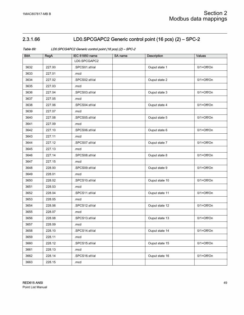
2.3.1.66 LD0.SPCGAPC2 Generic control point (16 pcs) (2) – SPC-2
Table 69: LD0.SPCGAPC2 Generic control point (16 pcs) (2) – SPC-2
BitA RegA IEC 61850 name SA name Description Values LD0.SPCGAPC2
3632 227.00 .SPCS01.stVal Ouput state 1 0/1=Off/On
3633 227.01 .mcd
3634 227.02 .SPCS02.stVal Ouput state 2 0/1=Off/On
3635 227.03 .mcd
3636 227.04 .SPCS03.stVal Ouput state 3 0/1=Off/On
3637 227.05 .mcd
3638 227.06 .SPCS04.stVal Ouput state 4 0/1=Off/On
3639 227.07 .mcd
3640 227.08 .SPCS05.stVal Ouput state 5 0/1=Off/On
3641 227.09 .mcd
3642 227.10 .SPCS06.stVal Ouput state 6 0/1=Off/On
3643 227.11 .mcd
3644 227.12 .SPCS07.stVal Ouput state 7 0/1=Off/On
3645 227.13 .mcd
3646 227.14 .SPCS08.stVal Ouput state 8 0/1=Off/On
3647 227.15 .mcd
3648 228.00 .SPCS09.stVal Ouput state 9 0/1=Off/On
3649 228.01 .mcd
3650 228.02 .SPCS10.stVal Ouput state 10 0/1=Off/On
3651 228.03 .mcd
3652 228.04 .SPCS11.stVal Ouput state 11 0/1=Off/On
3653 228.05 .mcd
3654 228.06 .SPCS12.stVal Ouput state 12 0/1=Off/On
3655 228.07 .mcd
3656 228.08 .SPCS13.stVal Ouput state 13 0/1=Off/On
3657 228.09 .mcd
3658 228.10 .SPCS14.stVal Ouput state 14 0/1=Off/On
3659 228.11 .mcd
3660 228.12 .SPCS15.stVal Ouput state 15 0/1=Off/On
3661 228.13 .mcd
3662 228.14 .SPCS16.stVal Ouput state 16 0/1=Off/On
3663 228.15 .mcd
1MAC807817-MB B Section 2Modbus data mappings
RED615 ANSI 49Point List Manual

2.3.1.67 LD0.SSCBR1 Circuit-breaker condition monitoring (1) – 52CM-1
Table 70: LD0.SSCBR1 Circuit-breaker condition monitoring (1) – 52CM-1
BitA RegA IEC 61850 name SA name Description Values LD0.SSCBR1
2848 178.00 .OpnAlm.stVal TRV_T_OP_ALM Opn travel time alarm 1=Alarm
2849 178.01 .ClsAlm.stVal TRV_T_CL_ALM Cls travel time alarm 1=Alarm
LD0.SSOPM1
2850 178.02 .SprChaAlm.stVal SPR_CHR_ALM Spring charge alarm 1=Alarm
LD0.SSCBR1
2851 178.03 .OpCntAlm.stVal OPR_ALM CB operations alarm 1=Alarm
2852 178.04 .OpCntLO.stVal OPR_LO CB operations lockout 1=Lockout
2853 178.05 .LonTmAlm.stVal MON_ALM CB inactive alarm 1=Alarm
LD0.SSIGM1
2854 178.06 .InsAlm.stVal PRES_ALM Low pressure alarm 1=Alarm
2855 178.07 .InsBlk.stVal PRES_LO Low pressure lockout 1=Lockout
LD0.SSCBR1
2856 178.08 .APwrAlm.stVal IPOW_ALM Lyt alarm 1=Alarm
2857 178.09 .APwrLO.stVal IPOW_LO Lyt lockout 1=Lockout
2858 178.10 .RmnNumOpAlm.stVal CB_LIFE_ALM CB lifetime alarm 1=Alarm
2.3.1.68 LD0.T1PTTR1 Three-phase thermal protection for feeders, cables anddistribution transformers (1) – 49F-1
Table 71: LD0.T1PTTR1 Three-phase thermal protection for feeders, cables and distribution transformers (1) – 49F-1
BitA RegA IEC 61850 name SA name Description Values LD0.T1PTTR1
2972 185.12 .Str.general PICKUP General pickup 1=Pickup
2973 185.13 .mcd
2974 185.14 .AlmThm.general ALARM Thermal alarm 1=Alarm
2975 185.15 .mcd
2976 186.00 .Op.general TRIP General trip 1=Trip
2977 186.01 .mcd
Section 2 1MAC807817-MB BModbus data mappings
50 RED615 ANSIPoint List Manual

2.3.1.69 LD0.T2PTTR1 Three-phase thermal overload protection, two timeconstants (1) – 49T-1
Table 72: LD0.T2PTTR1 Three-phase thermal overload protection, two time constants (1) – 49T-1
BitA RegA IEC 61850 name SA name Description Values LD0.T2PTTR1
4082 255.2 .Str.general PICKUP General pickup 1=Pickup
4083 255.3 .mcd
4084 255.4 .AlmThm.general ALARM Thermal alarm 1=Alarm
4085 255.5 .mcd
4086 255.6 .Op.general TRIP General trip 1=Trip
4087 255.7 .mcd
2.3.1.70 LD0.TCSSCBR1 Trip circuit supervision (1) – TCM-1
Table 73: LD0.TCSSCBR1 Trip circuit supervision (1) – TCM-1
BitA RegA IEC 61850 name SA name Description Values LD0.TCSSCBR1
2780 173.12 .CircAlm.stVal ALARM Supervision alarm 1=Alarm
2781 173.13 .mcd
2.3.1.71 LD0.TCSSCBR2 Trip circuit supervision (2) – TCM-2
Table 74: LD0.TCSSCBR2 Trip circuit supervision (2) – TCM-2
BitA RegA IEC 61850 name SA name Description Values LD0.TCSSCBR2
2782 173.14 .CircAlm.stVal ALARM Supervision alarm 1=Alarm
2783 173.15 .mcd
2.3.1.72 LD0.TRPPTRC1 Master trip (1) – 86/94-1
Table 75: LD0.TRPPTRC1 Master trip (1) – 86/94-1
BitA RegA IEC 61850 name SA name Description Values LD0.TRPPTRC1
2740 171.04 .Op.general - Op. input signal 1=Operate
2741 171.05 .mcd
2742 171.06 .Tr.general - Trip output signal 1=Trip
2743 171.07 .mcd
1MAC807817-MB B Section 2Modbus data mappings
RED615 ANSI 51Point List Manual
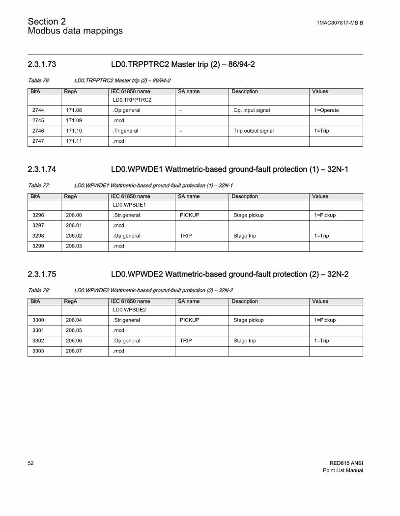
2.3.1.73 LD0.TRPPTRC2 Master trip (2) – 86/94-2
Table 76: LD0.TRPPTRC2 Master trip (2) – 86/94-2
BitA RegA IEC 61850 name SA name Description Values LD0.TRPPTRC2
2744 171.08 .Op.general - Op. input signal 1=Operate
2745 171.09 .mcd
2746 171.10 .Tr.general - Trip output signal 1=Trip
2747 171.11 .mcd
2.3.1.74 LD0.WPWDE1 Wattmetric-based ground-fault protection (1) – 32N-1
Table 77: LD0.WPWDE1 Wattmetric-based ground-fault protection (1) – 32N-1
BitA RegA IEC 61850 name SA name Description Values LD0.WPSDE1
3296 206.00 .Str.general PICKUP Stage pickup 1=Pickup
3297 206.01 .mcd
3298 206.02 .Op.general TRIP Stage trip 1=Trip
3299 206.03 .mcd
2.3.1.75 LD0.WPWDE2 Wattmetric-based ground-fault protection (2) – 32N-2
Table 78: LD0.WPWDE2 Wattmetric-based ground-fault protection (2) – 32N-2
BitA RegA IEC 61850 name SA name Description Values LD0.WPSDE2
3300 206.04 .Str.general PICKUP Stage pickup 1=Pickup
3301 206.05 .mcd
3302 206.06 .Op.general TRIP Stage trip 1=Trip
3303 206.07 .mcd
Section 2 1MAC807817-MB BModbus data mappings
52 RED615 ANSIPoint List Manual
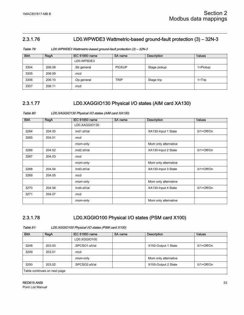
2.3.1.76 LD0.WPWDE3 Wattmetric-based ground-fault protection (3) – 32N-3
Table 79: LD0.WPWDE3 Wattmetric-based ground-fault protection (3) – 32N-3
BitA RegA IEC 61850 name SA name Description Values LD0.WPSDE3
3304 206.08 .Str.general PICKUP Stage pickup 1=Pickup
3305 206.09 .mcd
3306 206.10 .Op.general TRIP Stage trip 1=Trip
3307 206.11 .mcd
2.3.1.77 LD0.XAGGIO130 Physical I/O states (AIM card XA130)
Table 80: LD0.XAGGIO130 Physical I/O states (AIM card XA130)
BitA RegA IEC 61850 name SA name Description Values LD0.XAGGIO130
3264 204.00 .Ind1.stVal XA130-Input 1 State 0/1=Off/On
3265 204.01 .mcd
.mom-only Mom only alternative
3266 204.02 .Ind2.stVal XA130-Input 2 State 0/1=Off/On
3267 204.03 .mcd
.mom-only Mom only alternative
3268 204.04 .Ind3.stVal XA130-Input 3 State 0/1=Off/On
3269 204.05 .mcd
.mom-only Mom only alternative
3270 204.06 .Ind4.stVal XA130-Input 4 State 0/1=Off/On
3271 204.07 .mcd
.mom-only Mom only alternative
2.3.1.78 LD0.XGGIO100 Physical I/O states (PSM card X100)
Table 81: LD0.XGGIO100 Physical I/O states (PSM card X100)
BitA RegA IEC 61850 name SA name Description Values LD0.XGGIO100
3248 203.00 .SPCSO1.stVal X100-Output 1 State 0/1=Off/On
3249 203.01 .mcd
.mom-only Mom only alternative
3250 203.02 .SPCSO2.stVal X100-Output 2 State 0/1=Off/On
Table continues on next page
1MAC807817-MB B Section 2Modbus data mappings
RED615 ANSI 53Point List Manual

BitA RegA IEC 61850 name SA name Description Values3251 203.03 .mcd
.mom-only Mom only alternative
3252 203.04 .SPCSO3.stVal X100-Output 3 State 0/1=Off/On
3253 203.05 .mcd
.mom-only Mom only alternative
3254 203.06 .SPCSO4.stVal X100-Output 4 State 0/1=Off/On
3255 203.07 .mcd
.mom-only Mom only alternative
3256 203.08 .SPCSO5.stVal X100-Output 5 State 0/1=Off/On
3257 203.09 .mcd
.mom-only Mom only alternative
3258 203.10 .SPCSO6.stVal X100-Output 6 State 0/1=Off/On
3259 203.11 .mcd
.mom-only Mom only alternative
2.3.1.79 LD0.XGGIO110 Physical I/O states (BIO card X110)
Table 82: LD0.XGGIO110 Physical I/O states (BIO card X110)
BitA RegA IEC 61850 name SA name Description Values LD0.XGGIO110
3216 201.00 .Ind1.stVal X110-Input 1 State 0/1=Off/On
3217 201.01 .mcd
.mom-only Mom only alternative
3218 201.02 .Ind2.stVal X110-Input 2 State 0/1=Off/On
3219 201.03 .mcd
.mom-only Mom only alternative
3220 201.04 .Ind3.stVal X110-Input 3 State 0/1=Off/On
3221 201.05 .mcd
.mom-only Mom only alternative
3222 201.06 .Ind4.stVal X110-Input 4 State 0/1=Off/On
3223 201.07 .mcd
.mom-only Mom only alternative
3224 201.08 .Ind5.stVal X110-Input 5 State 0/1=Off/On
3225 201.09 .mcd
.mom-only Mom only alternative
3226 201.10 .Ind6.stVal X110-Input 6 State 0/1=Off/On
Table continues on next page
Section 2 1MAC807817-MB BModbus data mappings
54 RED615 ANSIPoint List Manual

BitA RegA IEC 61850 name SA name Description Values3227 201.11 .mcd
.mom-only Mom only alternative
3228 201.12 .Ind7.stVal X110-Input 7 State 0/1=Off/On
3229 201.13 .mcd
.mom-only Mom only alternative
3230 201.14 .Ind8.stVal X110-Input 8 State 0/1=Off/On
3231 201.15 .mcd
.mom-only Mom only alternative
3232 202.00 .SPCSO1.stVal X110-Output 1 State 0/1=Off/On
3233 202.01 .mcd
.mom-only Mom only alternative
3234 202.02 .SPCSO2.stVal X110-Output 2 State 0/1=Off/On
3235 202.03 .mcd
.mom-only Mom only alternative
3236 202.04 .SPCSO3.stVal X110-Output 3 State 0/1=Off/On
3237 202.05 .mcd
.mom-only Mom only alternative
3238 202.06 .SPCSO4.stVal X110-Output 4 State 0/1=Off/On
3239 202.07 .mcd
.mom-only Mom only alternative
2.3.1.80 LD0.XGGIO120 Physical I/O states (AIM card X120)
Table 83: LD0.XGGIO120 Physical I/O states (AIM card X120)
BitA RegA IEC 61850 name SA name Description Values LD0.XGGIO120
3200 200.00 .Ind1.stVal X120-Input 1 State 0/1=Off/On
3201 200.01 .mcd
.mom-only Mom only alternative
3202 200.02 .Ind2.stVal X120-Input 2 State 0/1=Off/On
3203 200.03 .mcd
.mom-only Mom only alternative
3204 200.04 .Ind3.stVal X120-Input 3 State 0/1=Off/On
3205 200.05 .mcd
.mom-only Mom only alternative
Table continues on next page
1MAC807817-MB B Section 2Modbus data mappings
RED615 ANSI 55Point List Manual

BitA RegA IEC 61850 name SA name Description Values3206 200.06 .Ind4.stVal X120-Input 4 State 0/1=Off/On
3207 200.07 .mcd
.mom-only Mom only alternative
2.3.1.81 LD0.XGGIO130 Physical I/O states (BIO card X130)
Table 84: LD0.XGGIO130 Physical I/O states (BIO card X130)
BitA RegA IEC 61850 name SA name Description Values LD0.XGGIO130
3280 205.00 .Ind1.stVal X130-Input 1 State 0/1=Off/On
3281 205.01 .mcd
.mom-only Mom only alternative
3282 205.02 .Ind2.stVal X130-Input 2 State 0/1=Off/On
3283 205.03 .mcd
.mom-only Mom only alternative
3284 205.04 .Ind3.stVal X130-Input 3 State 0/1=Off/On
3285 205.05 .mcd
.mom-only Mom only alternative
3286 205.06 .Ind4.stVal X130-Input 4 State 0/1=Off/On
3287 205.07 .mcd
.mom-only Mom only alternative
3288 205.08 .Ind5.stVal X130-Input 5 State 0/1=Off/On
3289 205.09 .mcd
.mom-only Mom only alternative
3290 205.10 .Ind6.stVal X130-Input 6 State 0/1=Off/On
3291 205.11 .mcd
.mom-only Mom only alternative
3264 204.00 .SPCSO1.stVal X130-Output 1 State 0/1=Off/On
3265 204.01 .mcd
.mom-only Mom only alternative
3266 204.02 .SPCSO2.stVal X130-Output 2 State 0/1=Off/On
3267 204.03 .mcd
.mom-only Mom only alternative
3268 204.04 .SPCSO3.stVal X130-Output 3 State 0/1=Off/On
3269 204.05 .mcd
.mom-only Mom only alternative
Section 2 1MAC807817-MB BModbus data mappings
56 RED615 ANSIPoint List Manual

2.3.2 Unmapped indications
Unmapped indications are indication data that have no initial Modbus mapping locations,but can be added to the user-definable Modbus area using the CommunicationManagement tool in PCM600. If Modbus events are enabled for these indication signals,the event identification is the user-definable area address.
2.3.2.1 All premapped three-phase protection function stages, trip/phase-dependent objects added
Table 85: All premapped three-phase protection function stages, trip/phase-dependent objects added
BitA RegA IEC 61850 name SA name Description Values LD0.xxxxxxxx (various)
.Op.phsA Phs A trip 1 = Trip
.mcd
.Op.phsB Phs B trip 1 = Trip
.mcd
.Op.phsC Phs C trip 1 = Trip
.mcd
2.3.2.2 Common data 2
Table 86: Common data 2
BitA RegA IEC 61850 name SA name Description Values LD0.LDEV1
.StLstOv.stVal Internal ind. overflow 1=Overflow
.mcd
.MeasLstOv.stVal Internal meas. overflow 1=Overflow
.mcd
.ChgFlg.stVal Configuration changed 1=Changed
.mcd
.FacSet.stVal Factory settings in use 1=In use
.mcd
LD0.GNRLLTMS1
.TmChSt1.stVal Time synch. status 0/1=Down/Up
.mcd
LD0.SCHLCCH1
.ChLiv.stVal CH1LIV Ethernet channel 1 live 1=Live
Table continues on next page
1MAC807817-MB B Section 2Modbus data mappings
RED615 ANSI 57Point List Manual

BitA RegA IEC 61850 name SA name Description Values .mcd
LD0.SCHLCCH2
.ChLiv.stVal CH2LIV Ethernet channel 2 live 1=Live
.mcd
LD0.SCHLCCH3
.ChLiv.stVal CH3LIV Ethernet channel 3 live 1=Live
.mcd
2.3.2.3 LD0.BSTGGIO1 Binary signal transfer (1) – BST-1
Table 87: LD0.BSTGGIO1 Binary signal transfer (1) – BST-1
BitA RegA IEC 61850 name SA name Description Values LD0.BSTGGIO1
.SPCSO1.stVal RECV_SIG_1 Output 1 State 0/1=Off/On
.mcd
.SPCSO2.stVal RECV_SIG_2 Output 2 State 0/1=Off/On
.mcd
.SPCSO3.stVal RECV_SIG_3 Output 3 State 0/1=Off/On
.mcd
.SPCSO4.stVal RECV_SIG_4 Output 4 State 0/1=Off/On
.mcd
.SPCSO5.stVal RECV_SIG_5 Output 5 State 0/1=Off/On
.mcd
.SPCSO6.stVal RECV_SIG_6 Output 6 State 0/1=Off/On
.mcd
.SPCSO7.stVal RECV_SIG_7 Output 7 State 0/1=Off/On
.mcd
.SPCSO8.stVal RECV_SIG_8 Output 8 State 0/1=Off/On
.mcd
.Ind1.stVal SEND_SIG_1 Input 1 State 0/1=Off/On
.mcd
.Ind2.stVal SEND_SIG_2 Input 2 State 0/1=Off/On
.mcd
.Ind3.stVal SEND_SIG_3 Input 3 State 0/1=Off/On
.mcd
.Ind4.stVal SEND_SIG_4 Input 4 State 0/1=Off/On
Table continues on next page
Section 2 1MAC807817-MB BModbus data mappings
58 RED615 ANSIPoint List Manual

BitA RegA IEC 61850 name SA name Description Values .mcd
.Ind5.stVal SEND_SIG_5 Input 5 State 0/1=Off/On
.mcd
.Ind6.stVal SEND_SIG_6 Input 6 State 0/1=Off/On
.mcd
.Ind7.stVal SEND_SIG_7 Input 7 State 0/1=Off/On
.mcd
.Ind8.stVal SEND_SIG_8 Input 8 State 0/1=Off/On
.mcd
2.3.2.4 LD0.CBPSOF1 Switch onto fault (1) – SOTF-1
Table 88: LD0.CBPSOF1 Switch onto fault (1) – SOTF-1
BitA RegA IEC 61850 name SA name Description Values LD0.CBPSOF1
.Op.general TRIP Stage trip 1=Trip
.mcd
2.3.2.5 LD0.CMHAI1 Current total demand distortion (1) – PQI-1
Table 89: LD0.CMHAI1 Current total demand distortion (1) – PQI-1
BitA RegA IEC 61850 name SA name Description Values LD0.CMHAI1
.Alm.stVal ALARM 1=Alarm
.mcd
2.3.2.6 LD0.DARREC1 Autoreclosing (1) – 79-1
Table 90: LD0.DARREC1 Autoreclosing (1) – 79-1
BitA RegA IEC 61850 name SA name Description Values LD0.DARREC1
.InInhRec.stVal INHIBIT_RECL Inhibit reclose 1=Inhibit
.mcd
.InBlkThm.stVal BLK_THERM Thermal block 1=Block
.mcd
1MAC807817-MB B Section 2Modbus data mappings
RED615 ANSI 59Point List Manual

2.3.2.7 LD0.DIAGLCCH1 Ethernet supervision (1)
Table 91: LD0.DIAGLCCH1 Ethernet supervision (1)
BitA RegA IEC 61850 name SA name Description Values LD0.DIAGLCCH1
.ChLiv.stVal CHLIV Ethernet channel live 1=Live
.mcd
.RedChLiv.stVal REDCHLIV Red. Ethernet channel live 1=Live
.mcd
2.3.2.8 LD0.IL1TCTR1 Three-phase CT supervision (1)
Table 92: LD0.IL1TCTR1 Three-phase CT supervision (1)
BitA RegA IEC 61850 name SA name Description Values LD0.IL1TCTR1
.Alm.stVal ALARM Alarm 1=Alarm
.mcd
.Wrn.stVal WARNING Warning 1=Warning
.mcd
2.3.2.9 LD0.LDPRLRC1 Load profile record (1) – LoadProf
Table 93: LD0.LDPRLRC1 Load profile record (1) – LoadProf
BitA RegA IEC 61850 name SA name Description Value LD0.LDPRLRC1
.MemWrn.stVal Recording memory warning 1=Warning
.mcd
.MemAlm.stVal Recording memory alarm 1=Alarm
.mcd
Section 2 1MAC807817-MB BModbus data mappings
60 RED615 ANSIPoint List Manual

2.3.2.10 LD0.MAPGAPC1 Multipurpose protection (1) – MAP-1
Table 94: LD0.MAPGAPC1 Multipurpose protection (1) – MAP-1
BitA RegA IEC 61850 name SA name Description Values LD0.MAPGAPC1
.Str.general PICKUP Stage pickup 1 = Pickup
.mcd
.Op.general TRIP Stage trip 1 = Trip
.mcd
2.3.2.11 LD0.MAPGAPC2 Multipurpose protection (2) – MAP-2
Table 95: LD0.MAPGAPC2 Multipurpose protection (2) – MAP-2
BitA RegA IEC 61850 name SA name Description Values LD0.MAPGAPC2
.Str.general PICKUP Stage pickup 1 = Pickup
.mcd
.Op.general TRIP Stage trip 1 = Trip
.mcd
2.3.2.12 LD0.MAPGAPC3 Multipurpose protection (3) – MAP-3
Table 96: LD0.MAPGAPC3 Multipurpose protection (3) – MAP-3
BitA RegA IEC 61850 name SA name Description Values LD0.MAPGAPC3
.Str.general PICKUP Stage pickup 1 = Pickup
.mcd
.Op.general TRIP Stage trip 1 = Trip
.mcd
1MAC807817-MB B Section 2Modbus data mappings
RED615 ANSI 61Point List Manual

2.3.2.13 LD0.MAPGAPC4 Multipurpose protection (4) – MAP-4
Table 97: LD0.MAPGAPC4 Multipurpose protection (4) – MAP-4
BitA RegA IEC 61850 name SA name Description Values LD0.MAPGAPC4
.Str.general PICKUP Stage pickup 1 = Pickup
.mcd
.Op.general TRIP Stage trip 1 = Trip
.mcd
2.3.2.14 LD0.MAPGAPC5 Multipurpose protection (5) – MAP-5
Table 98: LD0.MAPGAPC5 Multipurpose protection (5) – MAP-5
BitA RegA IEC 61850 name SA name Description Values LD0.MAPGAPC5
.Str.general PICKUP Stage pickup 1 = Pickup
.mcd
.Op.general TRIP Stage trip 1 = Trip
.mcd
2.3.2.15 LD0.MAPGAPC6 Multipurpose protection (6) – MAP-6
Table 99: LD0.MAPGAPC6 Multipurpose protection (6) – MAP-6
BitA RegA IEC 61850 name SA name Description Values LD0.MAPGAPC6
.Str.general PICKUP Stage pickup 1 = Pickup
.mcd
.Op.general TRIP Stage trip 1 = Trip
.mcd
Section 2 1MAC807817-MB BModbus data mappings
62 RED615 ANSIPoint List Manual

2.3.2.16 LD0.MAPGAPC7 Multipurpose protection (7) – MAP-7
Table 100: LD0.MAPGAPC7 Multipurpose protection (7) – MAP-7
BitA RegA IEC 61850 name SA name Description Values LD0.MAPGAPC7
.Str.general PICKUP Stage pickup 1 = Pickup
.mcd
.Op.general TRIP Stage trip 1 = Trip
.mcd
2.3.2.17 LD0.MAPGAPC8 Multipurpose protection (8) – MAP-8
Table 101: LD0.MAPGAPC8 Multipurpose protection (8) – MAP-8
BitA RegA IEC 61850 name SA name Description Values LD0.MAPGAPC8
.Str.general PICKUP Stage pickup 1 = Pickup
.mcd
.Op.general TRIP Stage trip 1 = Trip
.mcd
2.3.2.18 LD0.MAPGAPC9 Multipurpose protection (9) – MAP-9
Table 102: LD0.MAPGAPC9 Multipurpose protection (9) – MAP-9
BitA RegA IEC 61850 name SA name Description Values LD0.MAPGAPC9
.Str.general PICKUP Stage pickup 1 = Pickup
.mcd
.Op.general TRIP Stage trip 1 = Trip
.mcd
1MAC807817-MB B Section 2Modbus data mappings
RED615 ANSI 63Point List Manual

2.3.2.19 LD0.MAPGAPC10 Multipurpose protection (10) – MAP-10
Table 103: LD0.MAPGAPC10 Multipurpose protection (10) – MAP-10
BitA RegA IEC 61850 name SA name Description Values LD0.MAPGAPC10
.Str.general PICKUP Stage pickup 1 = Pickup
.mcd
.Op.general TRIP Stage trip 1 = Trip
.mcd
2.3.2.20 LD0.MAPGAPC11 Multipurpose protection (11) – MAP-11
Table 104: LD0.MAPGAPC11 Multipurpose protection (11) – MAP-11
BitA RegA IEC 61850 name SA name Description Values LD0.MAPGAPC11
.Str.general PICKUP Stage pickup 1 = Pickup
.mcd
.Op.general TRIP Stage trip 1 = Trip
.mcd
2.3.2.21 LD0.MAPGAPC12 Multipurpose protection (12) – MAP-12
Table 105: LD0.MAPGAPC12 Multipurpose protection (12) – MAP-12
BitA RegA IEC 61850 name SA name Description Values LD0.MAPGAPC12
.Str.general PICKUP Stage pickup 1 = Pickup
.mcd
.Op.general TRIP Stage trip 1 = Trip
.mcd
Section 2 1MAC807817-MB BModbus data mappings
64 RED615 ANSIPoint List Manual

2.3.2.22 LD0.MAPGAPC13 Multipurpose protection (13) – MAP-13
Table 106: LD0.MAPGAPC13 Multipurpose protection (13) – MAP-13
BitA RegA IEC 61850 name SA name Description Values LD0.MAPGAPC13
.Str.general PICKUP Stage pickup 1 = Pickup
.mcd
.Op.general TRIP Stage trip 1 = Trip
.mcd
2.3.2.23 LD0.MAPGAPC14 Multipurpose protection (14) – MAP-14
Table 107: LD0.MAPGAPC14 Multipurpose protection (14) – MAP-14
BitA RegA IEC 61850 name SA name Description Values LD0.MAPGAPC14
.Str.general PICKUP Stage pickup 1 = Pickup
.mcd
.Op.general TRIP Stage trip 1 = Trip
.mcd
2.3.2.24 LD0.MAPGAPC15 Multipurpose protection (15) – MAP-15
Table 108: LD0.MAPGAPC15 Multipurpose protection (15) – MAP-15
BitA RegA IEC 61850 name SA name Description Values LD0.MAPGAPC15
.Str.general PICKUP Stage pickup 1 = Pickup
.mcd
.Op.general TRIP Stage trip 1 = Trip
.mcd
1MAC807817-MB B Section 2Modbus data mappings
RED615 ANSI 65Point List Manual

2.3.2.25 LD0.MAPGAPC16 Multipurpose protection (16) – MAP-16
Table 109: LD0.MAPGAPC16 Multipurpose protection (16) – MAP-16
BitA RegA IEC 61850 name SA name Description Values LD0.MAPGAPC1
.Str.general PICKUP Stage pickup 1 = Pickup
.mcd
.Op.general TRIP Stage trip 1 = Trip
.mcd
2.3.2.26 LD0.MAPGAPC17 Multipurpose protection (17) – MAP-17
Table 110: LD0.MAPGAPC17 Multipurpose protection (17) – MAP-17
BitA RegA IEC 61850 name SA name Description Values LD0.MAPGAPC17
.Str.general PICKUP Stage pickup 1 = Pickup
.mcd
.Op.general TRIP Stage trip 1 = Trip
.mcd
2.3.2.27 LD0.MAPGAPC18 Multipurpose protection (18) – MAP-18
Table 111: LD0.MAPGAPC18 Multipurpose protection (18) – MAP-18
BitA RegA IEC 61850 name SA name Description Values LD0.MAPGAPC18
.Str.general PICKUP Stage pickup 1 = Pickup
.mcd
.Op.general TRIP Stage trip 1 = Trip
.mcd
Section 2 1MAC807817-MB BModbus data mappings
66 RED615 ANSIPoint List Manual

2.3.2.28 LD0.MDSOPT1 Runtime counter for machines and devices (1) – OPTM-1
Table 112: LD0.MDSOPT1 Runtime counter for machines and devices (1) – OPTM-1
BitA RegA IEC 61850 name SA name Description Values LD0.MDSOPT1
OpTmWrn.stVal PICKUP Accum.op.time Warn. 1 = Warning
.mcd
OpTmAlm.stVal TRIP Accum.op.time Alarm 1 = Alarm
.mcd
2.3.2.29 LD0.PCSITPC1 Protection communication supervision (1) – PCS-1
Table 113: LD0.PCSITPC1 Protection communication supervision (1) – PCS-1
BitA RegA IEC 61850 name SA name Description Value LD0.PCSITPC1
.HealthAlm.stVal ALARM Protection comm. alarm 1=Alarm
.mcd
2.3.2.30 LD0.PHQVVR1 Voltage variation (1) – PQSS-1
Table 114: LD0.PHQVVR1 Voltage variation (1) – PQSS-1
BitA RegA IEC 61850 name SA name Description Values LD0.PH1QVVR1
.VarStrGen.stVal - Variation event detected 1=Detected
.mcd
.VarEnd.stVal - Variation event ended 1=Ended
.mcd
.SwlOp.stVal - Swell event detected 1=Detected
.mcd
.DipOp.stVal - Dip event detected 1=Detected
.mcd
.IntrOp.stVal - Interruption event detected 1=Detected
.mcd
1MAC807817-MB B Section 2Modbus data mappings
RED615 ANSI 67Point List Manual

2.3.2.31 LD0.RESTCTR1 IG CT supervision (1)
Table 115: LD0.RESTCTR1 IG CT supervision (1)
BitA RegA IEC 61850 name SA name Description Values LD0.RESTCTR1
.Alm.stVal ALARM Alarm 1=Alarm
.mcd
.Wrn.stVal WARNING Warning 1=Warning
.mcd
2.3.2.32 LD0.RESTVTR1 VG VT supervision (1)
Table 116: LD0.RESTVTR1 VG VT supervision (1)
BitA RegA IEC 61850 name SA name Description Values LD0.RESTVTR1
.Alm.stVal ALARM Alarm 1=Alarm
.mcd
.Wrn.stVal WARNING Warning 1=Warning
.mcd
2.3.2.33 LD0.SCEFRFLO1 Fault locator (1) – 21FL-1
Table 117: LD0.SCEFRFLO1 Fault locator (1) – 21FL-1
BitA RegA IEC 61850 name SA name Description Values LD0.SCEFRFLO1
.Alm.stVal ALARM Fault loc alarm 1=Alarm
.mcd
.TrgSt.stVal Function triggered 1=Trig
.mcd
Section 2 1MAC807817-MB BModbus data mappings
68 RED615 ANSIPoint List Manual

2.3.2.34 LD0.SEQSPVC1 Fuse failure supervision (1) – 60-1
Table 118: LD0.SEQSPVC1 Fuse failure supervision (1) – 60-1
BitA RegA IEC 61850 name SA name Description Values LD0.SEQSPVC1
.Str.general FUSEF_U Pickup 1=Pickup
.mcd
.Str3Ph.general FUSEF_3PH 3-phase pickup 1=Pickup
.mcd
2.3.2.35 LD0.SPCGAPC1 Generic control point (16 pcs) (1) – SPC-1
Table 119: LD0.SPCGAPC1 Generic control point (16 pcs) (1) – SPC-1
BitA RegA IEC 61850 name SA name Description Values LD0.SPCGAPC1
.SPCSO1.stVal Ouput state 1 0/1=Off/On
.mcd
.SPCSO2.stVal Ouput state 2 0/1=Off/On
.mcd
.SPCSO3.stVal Ouput state 3 0/1=Off/On
.mcd
.SPCSO4.stVal Ouput state 4 0/1=Off/On
.mcd
.SPCSO5.stVal Ouput state 5 0/1=Off/On
.mcd
.SPCSO6.stVal Ouput state 6 0/1=Off/On
.mcd
.SPCSO7.stVal Ouput state 7 0/1=Off/On
.mcd
.SPCSO8.stVal Ouput state 8 0/1=Off/On
.mcd
.SPCSO9.stVal Ouput state 9 0/1=Off/On
.mcd
.SPCSO10.stVal Ouput state 10 0/1=Off/On
.mcd
.SPCSO11.stVal Ouput state 11 0/1=Off/On
.mcd
Table continues on next page
1MAC807817-MB B Section 2Modbus data mappings
RED615 ANSI 69Point List Manual

BitA RegA IEC 61850 name SA name Description Values .SPCSO12.stVal Ouput state 12 0/1=Off/On
.mcd
.SPCSO13.stVal Ouput state 13 0/1=Off/On
.mcd
.SPCSO14.stVal Ouput state 14 0/1=Off/On
.mcd
.SPCSO15.stVal Ouput state 15 0/1=Off/On
.mcd
.SPCSO16.stVal Ouput state 16 0/1=Off/On
.mcd
2.3.2.36 LD0.UDFCNT1 Multipurpose generic up-down counter (1) – CTR-1
Table 120: LD0.UDFCNT1 Multipurpose generic up-down counter (1) – CTR-1
BitA RegA IEC 61850 name SA name Description Values LD0. UDFCNT1
.DnCntSt.stVal DNCNT_STS Status of the down counting 1= down counting
.mcd
UpCntSt.stVal UPCNT_STS Status of the up counting 1= up counting
.mcd
2.3.2.37 LD0.UDFCNT2 Multipurpose generic up-down counter (2) – CTR-2
Table 121: LD0.UDFCNT2 Multipurpose generic up-down counter (2) – CTR-2
BitA RegA IEC 61850 name SA name Description Values LD0. UDFCNT2
.DnCntSt.stVal DNCNT_STS Status of the down counting 1= down counting
.mcd
UpCntSt.stVal UPCNT_STS Status of the up counting 1= up counting
.mcd
Section 2 1MAC807817-MB BModbus data mappings
70 RED615 ANSIPoint List Manual

2.3.2.38 LD0.UDFCNT3 Multipurpose generic up-down counter (3) – CTR-3
Table 122: LD0.UDFCNT3 Multipurpose generic up-down counter (3) – CTR-3
BitA RegA IEC 61850 name SA name Description Values LD0. UDFCNT3
.DnCntSt.stVal DNCNT_STS Status of the down counting 1= down counting
.mcd
UpCntSt.stVal UPCNT_STS Status of the up counting 1= up counting
.mcd
2.3.2.39 LD0.UDFCNT4 Multipurpose generic up-down counter (4) – CTR-4
Table 123: LD0.UDFCNT4 Multipurpose generic up-down counter (4) – CTR-4
BitA RegA IEC 61850 name SA name Description Values LD0. UDFCNT4
.DnCntSt.stVal DNCNT_STS Status of the down counting 1= down counting
.mcd
UpCntSt.stVal UPCNT_STS Status of the up counting 1= up counting
.mcd
2.3.2.40 LD0.UL1TVTR1 Three-phase VT supervision (1)
Table 124: LD0.UL1TVTR1 Three-phase VT supervision (1)
BitA RegA IEC 61850 name SA name Description Values LD0.UL1TVTR1
.Alm.stVal ALARM Alarm 1=Alarm
.mcd
.Wrn.stVal WARNING Warning 1=Warning
.mcd
2.3.2.41 LD0.VMHAI1 Voltage total harmonic distortion (1) – PQVPH-1
Table 125: LD0.VMHAI1 Voltage total harmonic distortion (1) – PQVPH-1
BitA RegA IEC 61850 name SA name Description Values LD0.VMHAI1
.Alm.stVal ALARM 1=Alarm
.mcd
1MAC807817-MB B Section 2Modbus data mappings
RED615 ANSI 71Point List Manual
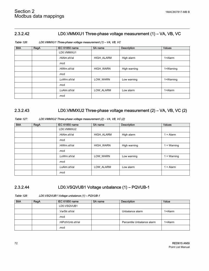
2.3.2.42 LD0.VMMXU1 Three-phase voltage measurement (1) – VA, VB, VC
Table 126: LD0.VMMXU1 Three-phase voltage measurement (1) – VA, VB, VC
BitA RegA IEC 61850 name SA name Description Values LD0.VMMXU1
.HiAlm.stVal HIGH_ALARM High alarm 1=Alarm
.mcd
.HiWrn.stVal HIGH_WARN High warning 1=Warning
.mcd
.LoWrn.stVal LOW_WARN Low warning 1=Warning
.mcd
.LoAlm.stVal LOW_ALARM Low alarm 1=Alarm
.mcd
2.3.2.43 LD0.VMMXU2 Three-phase voltage measurement (2) – VA, VB, VC (2)
Table 127: LD0.VMMXU2 Three-phase voltage measurement (2) – VA, VB, VC (2)
BitA RegA IEC 61850 name SA name Description Values LD0.VMMXU2
.HiAlm.stVal HIGH_ALARM High alarm 1 = Alarm
.mcd
.HiWrn.stVal HIGH_WARN High warning 1 = Warning
.mcd
.LoWrn.stVal LOW_WARN Low warning 1 = Warning
.mcd
.LoAlm.stVal LOW_ALARM Low alarm 1 = Alarm
.mcd
2.3.2.44 LD0.VSQVUB1 Voltage unbalance (1) – PQVUB-1
Table 128: LD0.VSQVUB1 Voltage unbalance (1) – PQVUB-1
BitA RegA IEC 61850 name SA name Description Value LD0.VSQVUB1
.VarStr.stVal Unbalance alarm 1=Alarm
.mcd
.HiPctVUnb.stVal Percentile Unbalance alarm 1=Alarm
.mcd
Section 2 1MAC807817-MB BModbus data mappings
72 RED615 ANSIPoint List Manual

2.3.2.45 LD0.XARGGIO130 Alarm/warning
Table 129: LD0.XARGGIO130 Alarm/warning
BitA RegA IEC 61850 name SA name Description Values LD0.XARGGIO130
.Alm.stVal XARGGIO130 alarm 1 = Alarm
.mcd
.Wrn.stVal XARGGIO130 warning 1 = Warning
.mcd
2.4 Registers
Table 130: Explanations of columns in register tables
Column name DescriptionRegA Default 3X and 4X register address for the data.
Type Type of the register. The alternatives are u16, u32 (unsigned 16 and 32 bits integer) ori16, i32 (signed 16 and 32 bit integer).
Scale Scale factor as default. Also, an adjustable offset value exists that is set to 0 by default.
IEC 61850 name Original IED data object identification. Described in the IEC 61850 format as LogicalDevice.Logical Node and thereafter .Data Object.Data Attribute. Logical Node is thesame as the application function block name.
SA name The signal may have a defined label that is visible, for example, in the ApplicationConfiguration tool in PCM600.
Description Short description of the signal. See the technical manual for more information. Also, if aregister is writable, it is stated here.
Values The value range of the original IEC 61850 value, that is, before scaling.
2.4.1 Premapped registers
2.4.1.1 Active parameter setting group - read and write
Table 131: Active parameter setting group - read and write
RegA Type Scale IEC 61850 name SA name Description Values2301 u16 1 Active setting group 1...6
1MAC807817-MB B Section 2Modbus data mappings
RED615 ANSI 73Point List Manual

2.4.1.2 Control structure 1
Table 132: Control structure 1
RegA Type Scale IEC 61850 name SA name Description Values8001 Execute register 1
8002 Password reg 1 acc to setting
8003 Password reg 2 acc to setting
8004 Control register < single bit >
8005 Confirm register < single bit >
2.4.1.3 Control structure 2
Table 133: Control structure 2
RegA Type Scale IEC 61850 name SA name Description Values8006 Execute register 1
8007 Password reg 1 acc to setting
8008 Password reg 2 acc to setting
8009 Control register < single bit >
8010 Confirm register < single bit >
2.4.1.4 Control structure 3
Table 134: Control structure 3
RegA Type Scale IEC 61850 name SA name Description Values8011 Execute register 1
8012 Password reg 1 acc to setting
8013 Password reg 2 acc to setting
8014 Control register < single bit >
8015 Confirm register < single bit >
Section 2 1MAC807817-MB BModbus data mappings
74 RED615 ANSIPoint List Manual

2.4.1.5 Control structure 4
Table 135: Control structure 4
RegA Type Scale IEC 61850 name SA name Description Values8016 Execute register 1
8017 Password reg 1 acc to setting
8018 Password reg 2 acc to setting
8019 Control register < single bit >
8020 Confirm register < single bit >
2.4.1.6 Control structure 5
Table 136: Control structure 5
RegA Type Scale IEC 61850 name SA name Description Values8021 Execute register 1
8022 Password reg 1 acc to setting
8023 Password reg 2 acc to setting
8024 Control register < single bit >
8025 Confirm register < single bit >
2.4.1.7 Control structure 6
Table 137: Control structure 6
RegA Type Scale IEC 61850 name SA name Description Values8026 Execute register 1
8027 Password reg 1 acc to setting
8028 Password reg 2 acc to setting
8029 Control register < single bit >
8030 Confirm register < single bit >
1MAC807817-MB B Section 2Modbus data mappings
RED615 ANSI 75Point List Manual

2.4.1.8 Control structure 7
Table 138: Control structure 7
RegA Type Scale IEC 61850 name SA name Description Values8031 Execute register 1
8032 Password reg 1 acc to setting
8033 Password reg 2 acc to setting
8034 Control register < single bit >
8035 Confirm register < single bit >
2.4.1.9 Control structure 8
Table 139: Control structure 8
RegA Type Scale IEC 61850 name SA name Description Values8036 Execute register 1
8037 Password reg 1 acc to setting
8038 Password reg 2 acc to setting
8039 Control register < single bit >
8040 Confirm register < single bit >
2.4.1.10 Device ID string
Table 140: Device ID string
RegA Type Scale IEC 61850 name SA name Description Values
9000 u16 ASCII coded string 1)
...
9120 u16
1) See the technical manual.
2.4.1.11 Event record structure
Table 141: Event record structure
RegA Type Scale IEC 61850 name SA name Description Values Selection write:
9250 u16 1 - Num of multiple records 1...10
9251 i16 1 - Read selection -499…3
Table continues on next page
Section 2 1MAC807817-MB BModbus data mappings
76 RED615 ANSIPoint List Manual

RegA Type Scale IEC 61850 name SA name Description Values Record 1 data to read:
9252 u16 1 - Record sequence num 1...9999
9253 u16 1 - Unread records left 0...499
Timestamp of record
9254 u16 1 - Year, Month Year/Month
9255 u16 1 - Day, Hour Day/Hour
9256 u16 1 - Minute, Second Min/Sec
9257 u16 1 - Millisecond Millisecond
9258 u16 1 Event identification 1)
9259 u16 1 Data object ID1 1)
9260 u16 1 Data object ID2 1)
9261 u16 1 Event data value 1 1)
9262 u16 1 Event data value 2 1)
Record 2 data to read: If selected
9263 u16 1 - Record sequence num 1..9999
9264 u16 1 - Unread records left 0..499
Timestamp of record
9265 u16 1 - Year, Month Year/Month
9266 u16 1 - Day, Hour Day/Hour
9267 u16 1 - Minute, Second Min/Sec
9268 u16 1 - Millisecond Millisecond
9269 u16 1 Event identification 1)
9270 u16 1 Data object ID1 1)
9271 u16 1 Data object ID2 1)
9272 u16 1 Event data value 1 1)
9273 u16 1 Event data value 2 1)
Record 3 data to read: If selected
9274 u16 1 - Record sequence num 1...9999
9275 u16 1 - Unread records left 0...499
Timestamp of record
9276 u16 1 - Year, Month Year/Month
9277 u16 1 - Day, Hour Day/Hour
9278 u16 1 - Minute, Second Min/Sec
Table continues on next page
1MAC807817-MB B Section 2Modbus data mappings
RED615 ANSI 77Point List Manual

RegA Type Scale IEC 61850 name SA name Description Values9279 u16 1 - Millisecond Millisecond
9280 u16 1 Event identification 1)
9281 u16 1 Data object ID1 1)
9282 u16 1 Data object ID2 1)
9283 u16 1 Event data value 1 1)
9284 u16 1 Event data value 2 1)
Record 4 data to read: If selected
9285 u16 1 - Record sequence num 1...9999
9286 u16 1 - Unread records left 0...499
Timestamp of record
9287 u16 1 - Year, Month Year/Month
9288 u16 1 - Day, Hour Day/Hour
9289 u16 1 - Minute, Second Min/Sec
9290 u16 1 - Millisecond Millisecond
9291 u16 1 Event identification 1)
9292 u16 1 Data object ID1 1)
9293 u16 1 Data object ID2 1)
9294 u16 1 Event data value 1 1)
9295 u16 1 Event data value 2 1)
Record 5 data to read: If selected
9296 u16 1 - Record sequence num 1...9999
9297 u16 1 - Unread records left 0...499
Timestamp of record
9298 u16 1 - Year, Month Year/Month
9299 u16 1 - Day, Hour Day/Hour
9300 u16 1 - Minute, Second Min/Sec
9301 u16 1 - Millisecond Millisecond
9302 u16 1 Event identification 1)
9303 u16 1 Data object ID1 1)
9304 u16 1 Data object ID2 1)
9305 u16 1 Event data value 1 1)
9306 u16 1 Event data value 2 1)
Table continues on next page
Section 2 1MAC807817-MB BModbus data mappings
78 RED615 ANSIPoint List Manual
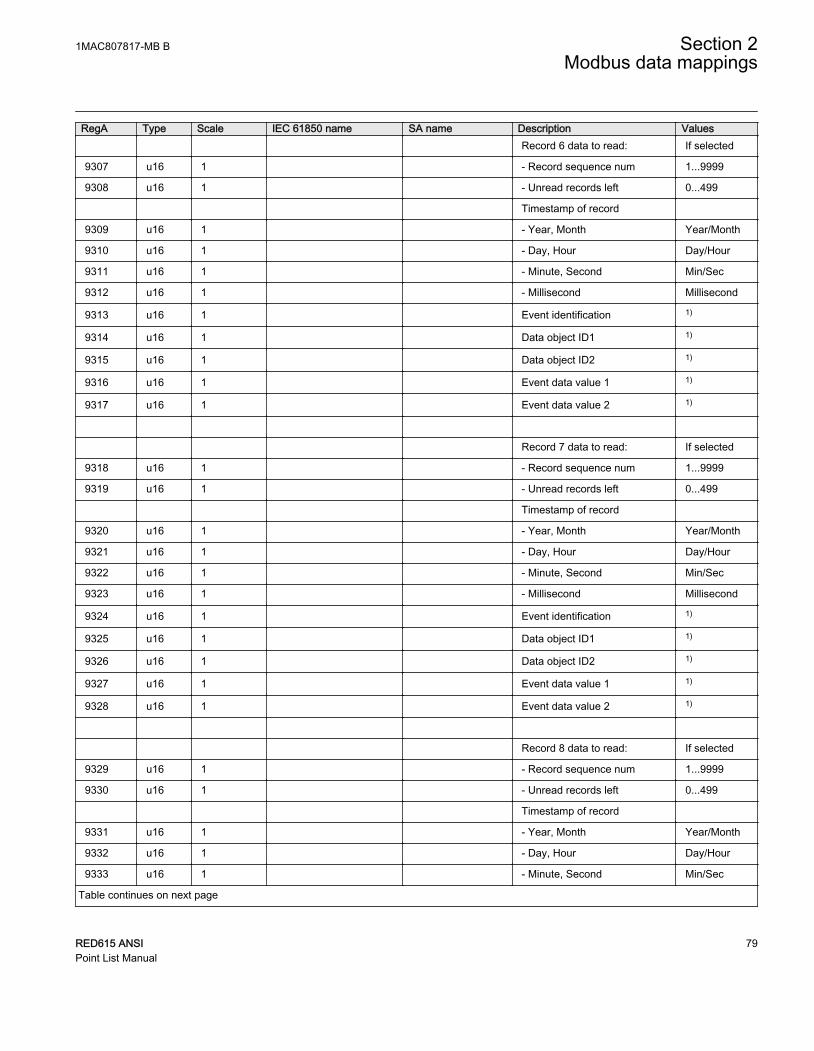
RegA Type Scale IEC 61850 name SA name Description Values Record 6 data to read: If selected
9307 u16 1 - Record sequence num 1...9999
9308 u16 1 - Unread records left 0...499
Timestamp of record
9309 u16 1 - Year, Month Year/Month
9310 u16 1 - Day, Hour Day/Hour
9311 u16 1 - Minute, Second Min/Sec
9312 u16 1 - Millisecond Millisecond
9313 u16 1 Event identification 1)
9314 u16 1 Data object ID1 1)
9315 u16 1 Data object ID2 1)
9316 u16 1 Event data value 1 1)
9317 u16 1 Event data value 2 1)
Record 7 data to read: If selected
9318 u16 1 - Record sequence num 1...9999
9319 u16 1 - Unread records left 0...499
Timestamp of record
9320 u16 1 - Year, Month Year/Month
9321 u16 1 - Day, Hour Day/Hour
9322 u16 1 - Minute, Second Min/Sec
9323 u16 1 - Millisecond Millisecond
9324 u16 1 Event identification 1)
9325 u16 1 Data object ID1 1)
9326 u16 1 Data object ID2 1)
9327 u16 1 Event data value 1 1)
9328 u16 1 Event data value 2 1)
Record 8 data to read: If selected
9329 u16 1 - Record sequence num 1...9999
9330 u16 1 - Unread records left 0...499
Timestamp of record
9331 u16 1 - Year, Month Year/Month
9332 u16 1 - Day, Hour Day/Hour
9333 u16 1 - Minute, Second Min/Sec
Table continues on next page
1MAC807817-MB B Section 2Modbus data mappings
RED615 ANSI 79Point List Manual

RegA Type Scale IEC 61850 name SA name Description Values9334 u16 1 - Millisecond Millisecond
9335 u16 1 Event identification 1)
9336 u16 1 Data object ID1 1)
9337 u16 1 Data object ID2 1)
9338 u16 1 Event data value 1 1)
9339 u16 1 Event data value 2 1)
Record 9 data to read: If selected
9340 u16 1 - Record sequence num 1...9999
9341 u16 1 - Unread records left 0...499
Timestamp of record
9342 u16 1 - Year, Month Year/Month
9343 u16 1 - Day, Hour Day/Hour
9344 u16 1 - Minute, Second Min/Sec
9345 u16 1 - Millisecond Millisecond
9346 u16 1 Event identification 1)
9347 u16 1 Data object ID1 1)
9348 u16 1 Data object ID2 1)
9349 u16 1 Event data value 1 1)
9350 u16 1 Event data value 2 1)
Record 10 data to read: If selected
9351 u16 1 - Record sequence num 1...9999
9352 u16 1 - Unread records left 0...499
Timestamp of record
9353 u16 1 - Year, Month Year/Month
9354 u16 1 - Day, Hour Day/Hour
9355 u16 1 - Minute, Second Min/Sec
9356 u16 1 - Millisecond Millisecond
9357 u16 1 Event identification 1)
9358 u16 1 Data object ID1 1)
9359 u16 1 Data object ID2 1)
9360 u16 1 Event data value 1 1)
9361 u16 1 Event data value 2 1)
1) See the technical manual.
Section 2 1MAC807817-MB BModbus data mappings
80 RED615 ANSIPoint List Manual

2.4.1.12 Fault record structure header
Table 142: Fault record structure header
RegA Type Scale IEC 61850 name SA name Description Values Selection write
9401 i16 1 Read selection -99…3
Record data header
9402 u16 1 Record sequence num 0...65535
9403 u16 1 Unread records left 0...99
Timestamp of record
9404 u16 1 Year, month Year/Month
9405 u16 1 Day, hour Day/Hour
9406 u16 1 Minute, second Min/Sec
9407 u16 1 Millisecond Millisecond
9408 u16 1 Timestamp quality
2.4.1.13 Fault record data
The table shows all potential data available in the fault record application. Which data isactually recorded depends on the functions available and enabled in the protection relay'sconfiguration.
Table 143: Fault record data
RegA Type Scale IEC 61850 name SA name Description Values LD0.FLTRFRC1 Fault record data
9409 u32 1 .OpCnt.stVal Fault record number (high) 0..999999
9410 (Low word)
9411 i16 1 .ProFnc.stVal Protection function -32768...32767
9412 u16 100 .Hz.mag Frequency 30…80.00[Hz]
9413 u16 100 .StrDur.mag Start duration 0...100.00 [%]
9414 u32 1000 .StrOpTm.mag Operate time [ms] (high) 0...999999.999
9415 (Low word)
9416 u32 100 .FltPtR.mag Fault resistance 0.00…1000000.00ohms
9417 (Low word)
Table continues on next page
1MAC807817-MB B Section 2Modbus data mappings
RED615 ANSI 81Point List Manual

RegA Type Scale IEC 61850 name SA name Description Values9418 u32 100 .FltDiskm.mag Fault distance 0.00…
9999.99 pu
9419 (Low word)
9420 u16 1 .ActSetGr.stVal Active setting group 1…6
9421 u16 1 .ShotPntr.stVal AR shot pointer value 0...7
Captured values during fault
9422 u16 1000 .Max50DifAA.mag Max. diff. current phs A 0.000...80.000[pu]
9423 u16 1000 .Max50DifAB.mag Max. diff. current phs B 0.000...80.000[pu]
9424 u16 1000 .Max50DifAC.mag Max. diff. current phs C 0.000...80.000[pu]
9425 u16 1000 .Max50RstAA.mag Max. bias current phs A 0.000…50.000 [pu]
9426 u16 1000 .Max50RstAB.mag Max. bias current phs B 0.000…50.000 [pu]
9427 u16 1000 .Max50RstAC.mag Max. bias current phs C 0.000…50.000 [pu]
9428 u16 1000 .DifAPhsA.mag Diff. current phs A 0.000...80.000[pu]
9429 u16 1000 .DifAPhsB.mag Diff. current phs B 0.000...80.000[pu]
9430 u16 1000 .DifAPhsC.mag Diff. current phs C 0.000...80.000[pu]
9431 u16 1000 .RstAPhsA.mag Bias current phs A 0.000…50.000 [pu]
9432 u16 1000 .RstAPhsB.mag Bias current phs B 0.000…50.000 [pu]
9433 u16 1000 .RstAPhsC.mag Bias current phs C 0.000…50.000 [pu]
9434 u16 1000 .DifARes.mag Diff. current Io 0.000...80.000[pu]
9435 u16 1000 .RstARes.mag Bias current Io 0.000…50.000 [pu]
9436 u16 1000 .Max50APhsA1.mag Max. current phs A(1) 0.000…50.000 [×In]
9437 u16 1000 .Max50APhsB1.mag Max. current phs B(1) 0.000…50.000 [×In]
9438 u16 1000 .Max50APhsC1.mag Max. current phs C(1) 0.000…50.000 [×In]
9439 u16 1000 .Max50ARes1.mag Max. current Io(1) 0.000…50.000 [×In]
9440 u16 1000 .APhsA1.mag Current phs A(1) 0.000…50.000 [×In]
Table continues on next page
Section 2 1MAC807817-MB BModbus data mappings
82 RED615 ANSIPoint List Manual

RegA Type Scale IEC 61850 name SA name Description Values9441 u16 1000 .APhsB1.mag Current phs B(1) 0.000…
50.000 [×In]
9442 u16 1000 .APhsC1.mag Current phs C(1) 0.000…50.000 [×In]
9443 u16 1000 .ARes1.mag Current Io(1) 0.000…50.000 [×In]
9444 u16 1000 .AResClc1.mag Current Io-Calc(1) 0.000…50.000 [×In]
9445 u16 1000 .APsSeq1.mag Current Ps-Seq(1) 0.000…50.000 [×In]
9446 u16 1000 .ANgSeq1.mag Current Ng-Seq(1) 0.000…50.000 [×In]
9447 u16 1000 .PhVPhsA1.mag Voltage phs A(1) 0.000...4.000[×Un]
9448 u16 1000 .PhVPhsB1.mag Voltage phs B(1) 0.000...4.000[×Un]
9449 u16 1000 .PhVPhsC1.mag Voltage phs C(1) 0.000...4.000[×Un]
9450 u16 1000 .PPVPhsAB1.mag Voltage phs AB(1) 0.000...4.000[×Un]
9451 u16 1000 .PPVPhsBC1.mag Voltage phs BC(1) 0.000...4.000[×Un]
9452 u16 1000 .PPVPhsCA1.mag Voltage phs CA(1) 0.000...4.000[×Un]
9453 u16 1000 .VRes1.mag Voltage Uo(1) 0.000...4.000[×Un]
9454 u16 1000 .VZro1.mag Voltage Zro-Seq(1) 0.000...4.000[×Un]
9455 u16 1000 .VPsSeq1.mag Voltage Ps-Seq(1) 0.000...4.000[×Un]
9456 u16 1000 .VNgSeq1.mag Voltage Ng-Seq(1) 0.000...4.000[×Un]
9457 u16 100 .MaxTmpRl.mag PTTR thermal level 0.00...99.99
9458 u16 100 .AMaxNgPs.mag PDNSPTOC1 ratio I2/I1 0.00...999.99[%]
9459 i16 100 .HzRteChg.mag Frequency gradient -10.00...10.00[Hz/s]
9460 i16 100 .CondNeut.mag Conductance Yo -1000.00...1000.00 [mS]
9461 i16 100 .SusNeut.mag Susceptance Yo -1000.00...1000.00 [mS]
9462 i32 100 .PPLoopRis.mag Fault loop resistance -1000.00...1000.00 [ohm]
9463 i32 (Low word)
Table continues on next page
1MAC807817-MB B Section 2Modbus data mappings
RED615 ANSI 83Point List Manual

RegA Type Scale IEC 61850 name SA name Description Values9464 i32 100 .PPLoopReact.mag Fault loop reactance -1000.00...10
00.00 [ohm]
9465 i32 (Low word)
9466 u16 1000 .CBClrTm.mag Breaker clear time 0.000...3.000[s]
9467 u16 1000 .APhsA2.mag Current phs A(2) 0.000…50.000 [×In]
9468 u16 1000 .APhsB2.mag Current phs B(2) 0.000…50.000 [×In]
9469 u16 1000 .APhsC2.mag Current phs C(2) 0.000…50.000 [×In]
9470 u16 1000 .ARes2.mag Current Io(2) 0.000…50.000 [×In]
9471 u16 1000 .AResClc2.mag Current Io-Calc(2) 0.000…50.000 [×In]
9472 u16 1000 .APsSeq2.mag Current Ps-Seq(2) 0.000…50.000 [×In]
9473 u16 1000 .ANgSeq2.mag Current Ng-Seq(2) 0.000…50.000 [×In]
9474 u16 1000 .PhVPhsA2.mag Voltage phs A(2) 0.000...4.000[×Un]
9475 u16 1000 .PhVPhsB2.mag Voltage phs B(2) 0.000...4.000[×Un]
9476 u16 1000 .PhVPhsC2.mag Voltage phs C(2) 0.000...4.000[×Un]
9477 u16 1000 .PPVPhsAB2.mag Voltage phs AB(2) 0.000...4.000[×Un]
9478 u16 1000 .PPVPhsBC2.mag Voltage phs BC(2) 0.000...4.000[×Un]
9479 u16 1000 .PPVPhsCA2.mag Voltage phs CA(2) 0.000...4.000[×Un]
9480 u16 1000 .VRes2.mag Voltage Uo(2) 0.000...4.000[×Un]
9481 u16 1000 .VZro2.mag Voltage Zro-Seq(2) 0.000...4.000[×Un]
9482 u16 1000 .VPsSeq2.mag Voltage Ps-Seq(2) 0.000...4.000[×Un]
9483 u16 1000 .VNgSeq2.mag Voltage Ng-Seq(2) 0.000...4.000[×Un]
9484 i16 100 .DifANAngVN1.mag. Angle Uo-Io(1) -180.00…180.00 [deg]
9485 i16 100 .DifAAAngVBC1.mag. Angle UBC-IA(1) -180.00…180.00 [deg]
9486 i16 100 .DifABAngVCA1.mag Angle UCA-IB(1) -180.00…180.00 [deg]
Table continues on next page
Section 2 1MAC807817-MB BModbus data mappings
84 RED615 ANSIPoint List Manual

RegA Type Scale IEC 61850 name SA name Description Values9487 i16 100 .DifACAngVAB1.mag Angle UAB-IC(1) -180.00…
180.00 [deg]
9488 i16 100 .DifANAngVN2.mag. Angle Uo-Io(2) -180.00…180.00 [deg]
9489 i16 100 .DifAAAngVBC2.mag. Angle UBC-IA(2) -180.00…180.00 [deg]
9490 i16 100 .DifABAngVCA2.mag Angle UCA-IB(2) -180.00…180.00 [deg]
9491 i16 100 .DifACAngVAB2.mag Angle UAB-IC(2) -180.00…180.00 [deg]
2.4.1.14 Protection relay's real-time clock (in local time mode) - read and write(synchronize)
Table 144: Protection relay's real-time clock (in local time mode) - read and write (synchronize)
RegA Type Scale IEC 61850 name SA name Description Values
9201 Control register 0...21)
9202 Year 2000...2999
9203 Month 1...12
9204 Day 1...31
9205 Hour 0...23
9206 Minute 0...59
9207 Second 0...59
9208 Millisecond 0…999
1) See the technical manual.
2.4.1.15 Protection relay's real-time clock (in UTC time mode) - read and write(synchronize)
Table 145: Protection relay's real-time clock (in UTC time mode) - read and write (synchronize)
RegA Type Scale IEC 61850 name SA name Description Values
9211 Control register 0...21)
9212 Year 2000...2999
9213 Month 1...12
9214 Day 1...31
9215 Hour 0...23
Table continues on next page
1MAC807817-MB B Section 2Modbus data mappings
RED615 ANSI 85Point List Manual

RegA Type Scale IEC 61850 name SA name Description Values9216 Minute 0...59
9217 Second 0...59
9218 Millisecond 0…999
1) See the technical manual.
2.4.1.16 Indication bits mirrored in registers
Table 146: Indication bits mirrored in registers
RegA Type Scale IEC 61850 name SA name Description Values170.00 Bit Indication bit 2720 (0x1700)
170.01 Bit Indication bit 2721 (0x1701)
: : :
170.14 Bit Indication bit 2734 (0x170E)
170.15 Bit Indication bit 2735 (0x170F)
171.00 Bit Indication bit 2736 (0x1710)
2.4.1.17 SSR1 System status register (1) device health
Table 147: SSR1 System status register (1) device health
RegA Type Scale IEC 61850 name SA name Description Values128.00 Bit Device global error 1=Error
128.01 Bit Device global warning 1=Warning
128.02 Bit < reserved > 0
128.03 Bit < reserved > 0
128.04 Bit < reserved > 0
128.05 Bit < reserved > 0
128.06 Bit < reserved > 0
128.07 Bit < reserved > 0
128.08 Bit < reserved > 0
128.09 Bit < reserved > 0
128.10 Bit < reserved > 0
128.11 Bit < reserved > 0
128.12 Bit < reserved > 0
128.13 Bit < reserved > 0
128.14 Bit < reserved > 0
128.15 Bit < reserved > 0
Section 2 1MAC807817-MB BModbus data mappings
86 RED615 ANSIPoint List Manual

2.4.1.18 SSR2 System status register (2) protection relay's mode and state
Table 148: SSR2 System status register (2) protection relay's mode and state
RegA Type Scale IEC 61850 name SA name Description Values129.00 Bit Device test mode 1=Test mode
129.01 Bit < reserved > 0
129.02 Bit Remote/Local state 0/1=Rem/Loc
Active setting group SG=1...6
129.03 Bit - bit 0
129.04 Bit - bit 1
129.05 Bit - bit 2
129.06 Bit Protection relay's timesynchfailure 1=Failure
129.07 Bit < reserved > 0
129.08 Bit Last reset cause a 1=Cold start
129.09 Bit Last reset cause b 1=Watchdog
129.10 Bit Last reset cause c 1=Warm start
129.11 Bit < reserved > 0
129.12 Bit < reserved > 0
129.13 Bit < reserved > 0
129.14 Bit < reserved > 0
129.15 Bit < reserved > 0
2.4.1.19 SSR3 System status register (3) data available 1 (client-dependent)
Table 149: SSR3 System status register (3) data available 1 (client-dependent)
RegA Type Scale IEC 61850 name SA name Description Values130.00 Bit Unread event records available 1=Available
130.01 Bit Unread fault records available 1=Available
130.02 Bit < reserved > 0
130.03 Bit < reserved > 0
130.04 Bit Any momentary bit updated 1=Updated
130.05 Bit Any mcd bit set 1=Set
130.06 Bit Device restart bit 1=IED restart
130.07 Bit < reserved > 0
130.08 Bit Event record selected 1=Selected
130.09 Bit Fault record selected 1=Selected
130.10 Bit < reserved > 0
Table continues on next page
1MAC807817-MB B Section 2Modbus data mappings
RED615 ANSI 87Point List Manual

RegA Type Scale IEC 61850 name SA name Description Values130.11 Bit < reserved > 0
130.12 Bit < reserved > 0
130.13 Bit < reserved > 0
130.14 Bit < reserved > 0
130.15 Bit < reserved > 0
2.4.1.20 SSR4 System status register (4) data available 2 (client-dependent, user-definable)
Table 150: SSR4 System status register (4) data available 2 (client-dependent, user-definable)
RegA Type Scale IEC 61850 name SA name Description Values131.00 Bit Data category 1 has changed 1=Changed
131.01 Bit Data category 2 has changed 1=Changed
131.02 Bit Data category 3 has changed 1=Changed
131.03 Bit Data category 4 has changed 1=Changed
131.04 Bit Data category 5 has changed 1=Changed
131.05 Bit Data category 6 has changed 1=Changed
131.06 Bit Data category 7 has changed 1=Changed
131.07 Bit Data category 8 has changed 1=Changed
131.08 Bit Data category 9 has changed 1=Changed
131.09 Bit Data category 10 has changed 1=Changed
131.10 Bit Data category 11 has changed 1=Changed
131.11 Bit Data category 12 has changed 1=Changed
131.12 Bit Data category 13 has changed 1=Changed
131.13 Bit Data category 14 has changed 1=Changed
131.14 Bit Data category 15 has changed 1=Changed
131.15 Bit Data category 16 has changed 1=Changed
2.4.1.21 SSR5 System status register (5) device alive register
Table 151: SSR5 System status register (5) device alive register
RegA Type Scale IEC 61850 name SA name Description Values132 u16 1 Device alive counter 0...65535
Section 2 1MAC807817-MB BModbus data mappings
88 RED615 ANSIPoint List Manual

2.4.1.22 SSR6 System status register (6) control command status (client-dependent)
Table 152: SSR6 System status register (6) control command status (client-dependent)
RegA Type Scale IEC 61850 name SA name Description Values
Last cmd result code 1)
133.00 Bit - bit 0
133.01 Bit - bit 1
133.02 Bit - bit 2
133.03 Bit - bit 3
133.04 Bit - bit 4
133.05 Bit - bit 5
133.06 Bit - bit 6
133.07 Bit - bit 7
Response Type 1)
133.08 Bit - bit 0
133.09 Bit - bit 1
Command state 1)
133.10 Bit - bit 0
133.11 Bit - bit 1
Cmd sequence number 0...15
133.12 Bit - bit 0
133.13 Bit - bit 1
133.14 Bit - bit 2
133.15 Bit - bit 3
1) See the technical manual.
2.4.1.23 System diagnostic values
Table 153: System diagnostic values
RegA Type Scale IEC 61850 name SA name Description Values LD0.LDEV1
2050 u16 1 .DevWrn.stVal Warning Last warning code 1)
2051 u16 1 .DevFail.stVal Internal fault Last internal fault code 1)
DR.RDRE1
2052 u16 1 .FltNum.stVal Num. of DR recordings 0...N
2053 u16 1 .MemUsed.stVal DR memory used 0...100 [%]
Table continues on next page
1MAC807817-MB B Section 2Modbus data mappings
RED615 ANSI 89Point List Manual

RegA Type Scale IEC 61850 name SA name Description Values LD0.LPHD1
2054 u16 1 .NumPwrUp.stVal Num. of cold starts 0...65535
2055 u16 1 .WrmStr.stVal Num. of warm starts 0...65535
2056 u16 1 .WacTrg.stVal Num. of watchdog resets 0...65535
LD0.LDEV1
2057 u16 1 .ChgAckCnt.stVal Num. of conf. changes 0...65535
LD0.LLN0
u16 1 .ParChgCnt.stVal Num. of setting changes 0…65535
1) See the technical manual.
2.4.1.24 Time and reason for latest protection relay reset
Table 154: Time and reason for latest protection relay reset
RegA Type Scale IEC 61850 name SA name Description Values9221 u16 1 Year 2000...2999
9222 u16 1 Month 1...12
9223 u16 1 Day 1...31
9224 u16 1 Hour 0...23
9225 u16 1 Minute 0...59
9226 u16 1 Second 0...59
9227 u16 1 Millisecond 0…999
9228 u16 1 Reset reason
9228.0 Bit - bit 0 1=Cold start
9228.1 Bit - bit 1 1=Watchdog
9228.2 Bit - bit 2 1=Warm start
2.4.1.25 User-definable bits [Alt.2], visible on 0x,1x,3x and 4x
Table 155: User-definable bits [Alt.2], visible on 0x,1x,3x and 4x
BitA Type Scale IEC 61850 name SA name Description Values(0) Bit < not mappable - not visible >
1 Bit Usr reg 1.Bit 01
2 Bit Usr reg 1.Bit 02
3 Bit Usr reg 1.Bit 03
: : :
: : :
Table continues on next page
Section 2 1MAC807817-MB BModbus data mappings
90 RED615 ANSIPoint List Manual

BitA Type Scale IEC 61850 name SA name Description Values15 Bit Usr reg 1.Bit 15
16 Bit Usr reg 2.Bit 00
17 Bit Usr reg 2.Bit 01
: : :
: : :
2046 Bit Usr reg 127.Bit 14
2047 Bit Usr reg 127.Bit 15
2.4.1.26 User-definable registers [Alt.1], visible on 3x and 4x
Table 156: User-definable registers [Alt.1], visible on 3x and 4x
RegA Type Scale IEC 61850 name SA name Description Values(0) Reg < not mappable - not visible >
1 Reg User register 1
2 Reg User register 2
3 : :
: : :
: : :
127 Reg User register 127
2.4.1.27 CTRL.CBCSWI1 Circuit breaker operation counter (1)
Table 157: CTRL.CBCSWI1 Circuit breaker operation counter (1)
RegA Type Scale IEC 61850 name SA name Description Values CTRL.CBCSWI1
2027 u16 1 .OpCntRs.stVal Operation counter Operation counter 0…65535
2.4.1.28 LD0.CMMXU1 Phase current demand values (1) – IA, IB, IC
Table 158: LD0.CMMXU1 Phase current demand values (1) – IA, IB, IC
RegA Type Scale IEC 61850 name SA name Description Values LD0.CAVMMXU1 Demand value
2001 u16 1000 .A.phsA.cVal.mag I_DMD_A Phs A amplitude 0.00…50.0[xIn]
2002 u16 1000 .A.phsB.cVal.mag I_DMD_B Phs B amplitude 0.00…50.0[xIn]
Table continues on next page
1MAC807817-MB B Section 2Modbus data mappings
RED615 ANSI 91Point List Manual

RegA Type Scale IEC 61850 name SA name Description Values2003 u16 1000 .A.phsB.cVal.mag I_DMD_C Phs C amplitude 0.00…50.0
[xIn]
2004 Year - month
2005 Day - hour
2006 Minute - second
2007 Milliseconds
2008 Time quality
LD0.CMAMMXU1 Max demand values
2009 u16 1000 .A.phsA.cVal.mag Max demand IL1 Phs A amplitude 0.00…50.0[xIn]
2010 Year - month
2011 Day - hour
2012 Minute - second
2013 Milliseconds
2014 Time quality
2015 u16 1000 .A.phsB.cVal.mag Max demand IL2 Phs B amplitude 0.00…50.0[xIn]
2016 Year - month
2017 Day - hour
2018 Minute - second
2019 Milliseconds
2020 Time quality
2021 u16 1000 .A.phsC.cVal.mag Max demand IL2 Phs C amplitude 0.00…50.0[xIn]
2022 Year - month
2023 Day - hour
2024 Minute - second
2025 Milliseconds
2026 Time quality
LD0.CMIMMXU1 Min demand values
u16 1000 .A.phsA.cVal.mag Max demand IL1 Phs A amplitude 0.00…50.0[xIn]
u16 1000 .A.phsB.cVal.mag Max demand IL2 Phs B amplitude 0.00…50.0[xIn]
u16 1000 .A.phsC.cVal.mag Max demand IL3 Phs C amplitude 0.00…50.0[xIn]
Section 2 1MAC807817-MB BModbus data mappings
92 RED615 ANSIPoint List Manual

2.4.1.29 LD0.CMMXU1 Three-phase current measurement (1) – IA, IB, IC
Table 159: LD0.CMMXU1 Three-phase current measurement (1) – IA, IB, IC
RegA Type Scale IEC 61850 name SA name Description Values LD0.CMMXU1 Phase current (1)
138 u16 1000 .A.phsA.instCVal.mag I_INST_A Phs A amplitude0.00...40.0[xIn]
139 u16 1000 .A.phsB.instCVal.mag I_INST_B Phs B amplitude0.00...40.0[xIn]
140 u16 1000 .A.phsC.instCVal.mag I_INST_C Phs C amplitude0.00...40.0[xIn]
2.4.1.30 LD0.CSMSQI1 Sequence current measurement (1) – I1, I2, I0
Table 160: LD0.CSMSQI1 Sequence current measurement (1) – I1, I2, I0
RegA Type Scale IEC 61850 name SA name Description Values LD0.CSMSQI1 Sequence of currents
143 u16 1000 .SeqA.c1.instCVal.mag I1_INST Positive amplitude0.00...40.0[xIn]
144 u16 1000 .SeqA.c2.instCVal.mag I2_INST Negative amplitude0.00...40.0[xIn]
145 u16 1000 .SeqA.c2.instCVal.mag I3_INST Zero amplitude0.00...40.0[xIn]
2.4.1.31 LD0.DARREC1 Autoreclosing counters (1) – 79-1
Table 161: LD0.DARREC1 Autoreclosing counters (1) – 79-1
RegA Typw Scale IEC 61850 name SA name Description Values LD0.DARREC1
2031 u16 1 .RecCnt1.stVal CNT_SHOT1 AR 1st shot counter 0…65535
2032 u16 1 .RecCnt2.stVal CNT_SHOT2 AR 2nd shot counter 0…65535
2033 u16 1 .RecCnt3.stVal CNT_SHOT3 AR 3rd shot counter 0…65535
2034 u16 1 .RecCnt4.stVal CNT_SHOT4 AR 4th shot counter 0…65535
2035 u16 1 .RecCnt5.stVal CNT_SHOT5 AR 5th shot counter 0…65535
2036 u16 1 .FrqOpCnt.stVal FRQ_OPR_CNT AP freq. op. counter 0…65535
1MAC807817-MB B Section 2Modbus data mappings
RED615 ANSI 93Point List Manual

2.4.1.32 LD0.DARREC1 Autoreclosing values (1) – 79-1
Table 162: LD0.DARREC1 Autoreclosing values (1) – 79-1
RegA Type Scale IEC 61850 name SA name Description Values LD0.DARREC1
135 i16 1 .AutoRecSt.stVal STATUS AR state -2...41)
136 u16 1 .ShotPntr.stVal SHOT_PTR AR shot pointer value 0...6
137 u16 1 .OpCntRs.stVal COUNTER AR operation counter 0...65535
1) See the technical manual.
2.4.1.33 LD0.HAEFMHAI1 Current harmonics (1)
Table 163: LD0.HAEFMHAI1 Current harmonics (1)
RegA Type Scale IEC 61850 name SA name Description Values LD0.HAEFMHAI1
151 u16 10 .HRmsA.res.cVal.mag I_HARM_RES Current harmonics 0..250.0 [A]
2.4.1.34 LD0.LNPLDF Line differential protection with in-zone power transformer(1) – 87L-1
Table 164: LD0.LNPLDF1 Line differential protection with in-zone power transformer (1) – 87L-1
RegA Type Scale IEC 61580 name SA name Description Values LD0.LNPDIF1 Differential current
2040 u16 1000 .DifAClc.phsA.mag Phs A magnitude 0...50.00 [×In]
2041 u16 1000 .DifAClc.phsB.mag Phs B magnitude 0...50.00 [×In]
2042 u16 1000 .DifAClc.phsC.mag Phs C magnitude 0...50.00 [×In]
LD0.LNPDIF1 Bias current
2043 u16 1000 .RstA.phsA.mag Phs A magnitude 0...50.00 [×In]
2044 u16 1000 .RstA.phsB.mag Phs B magnitude 0...50.00 [×In]
2045 u16 1000 .RstA.phsC.mag Phs C magnitude 0...50.00 [×In]
Section 2 1MAC807817-MB BModbus data mappings
94 RED615 ANSIPoint List Manual

2.4.1.35 LD0.RESCMMXU1 Residual current demand value (1) – IG-1
Table 165: LD0.RESCMMXU1 Residual current demand value (1) – IG-1
RegA Type Scale IEC 61850 name SA name Description Values LD0.RCAVMMXU1 Demand value
1989 u16 1000 .A.res.cVal.mag I_DMD_RES Residual amplitude 0.00…50.0[xIn]
1990 Year - month
1991 Day - hour
1992 Minute - second
1993 Milliseconds
1994 Time quality
LD0.RCMAMMXU1 Max. demand value
1995 u16 1000 .A.res.cVal.mag Max demand Io Residual amplitude 0.00…50.0[xIn]
1996 Year - month
1997 Day - hour
1998 Minute - second
1999 Milliseconds
2000 Time quality
LD0.RCMIMMXU1 Min. demand value
u16 1000 .A.res.cVal.mag Min demand Io Residual amplitude 0.00…50.0[xIn]
2.4.1.36 LD0.RESCMMXU1 Residual current measurement (1) – IG-1
Table 166: LD0.RESCMMXU1 Residual current measurement (1) – IG-1
RegA Type Scale IEC 61850 name SA name Description Values LD0.RESCMMXU1 Residual current (1)
141 u16 1000 .A.res.instCVal.mag I0_INST - amplitude0.00...40.0[xIn]
1MAC807817-MB B Section 2Modbus data mappings
RED615 ANSI 95Point List Manual

2.4.1.37 LD0.RESVMMXU1 Residual voltage demand value (1) – VG-1
Table 167: LD0.RESVMMXU1 Residual voltage demand value (1) – VG-1
RegA Type Scale IEC 61850 name SA name Description Values LD0.RVAVMMXU1 Demand value
1977 u16 1000 .PhV.res.cVal.mag U_DMD_RES Residual amplitude 0.00…4.0[xUn]
1978 Year - month
1979 Day - hour
1980 Minute - second
1981 Milliseconds
1982 Time quality
LD0.RVMAMMXU1 Max. demand value
1983 u16 1000 .PhV.res.cVal.mag Max demand Uo Residual amplitude 0.00…4.0[xUn]
1984 Year - month
1985 Day - hour
1986 Minute - second
1987 Milliseconds
1988 Time quality
LD0.RVMIMMXU1 Min. demand value
u16 1000 .PhV.res.cVal.mag Min demand Io Residual amplitude 0.00…4.0[xUn]
2.4.1.38 LD0.RESVMMXU1 Residual voltage measurement (1) – VG-1
Table 168: LD0.RESVMMXU1 Residual voltage measurement (1) – VG-1
RegA Type Scale IEC 61850 name SA name Description Values LD0.RESVMMXU1 Residual voltage (1)
142 u16 1000 .A.res.instCVal.mag U0_INST - amplitude0.00...4.00[xUn]
2.4.1.39 LD0.SECRSYN1 Synchronism and energizing check (1) – 25
Table 169: LD0.SECRSYN1 Synchronism and energizing check (1) – 25
RegA Type Scale IEC 61850 name SA name Description Values LD0.SECRSYN1
169 u16 1 .EnSt.stVal ENERG_STATE Energ. state of line and bus 0...41)
1) See the technical manual.
Section 2 1MAC807817-MB BModbus data mappings
96 RED615 ANSIPoint List Manual

2.4.1.40 LD0.SSCBR1 Circuit-breaker condition monitoring (1) – 52CM-1
Table 170: LD0.SSCBR1 Circuit-breaker condition monitoring (1) – 52CM-1
RegA Type Scale IEC 61850 name SA name Description Values LD0.SSCBR1
2060 u16 1 .InaTmdCnt.stVal INA_DAYS CB inactive days 0...65535
2061 u16 1 .OpTmOpn.mag T_TRV_OP Open travel time 0...60000 [ms]
2062 u16 1 .OpTmCls.mag T_TRV_CL Close travel time 0...60000 [ms]
LD0.SSOPM1
2063 u16 100 .TmsSprCha.mag T_SPR_CHR Spring charge time0.00…99.99[s]
LD0.SPH1SCBR1
2064 i16 1 .RmnNumOp.stVal CB_LIFE_A Remain.life phs A -/+ 9999
LD0.SPH2SCBR1
2065 i16 1 .RmnNumOp.stVal CB_LIFE_B Remain.life phs B -/+ 9999
LD0.SPH3SCBR1
2066 i16 1 .RmnNumOp.stVal CB_LIFE_C Remain.life phs C -/+ 9999
LD0.SPH1SCBR1
2067 u16 1 .AccmAPwr.mag IPOW_A Iyt phs A 0...1E6
LD0.SPH2SCBR1
2068 u16 1 .AccmAPwr.mag IPOW_B Iyt phs B 0...1E6
LD0.SPH3SCBR1
2069 u16 1 .AccmAPwr.mag IPOW_C Iyt phs C 0...1E6
2.4.1.41 LD0.T1PTTR1 Three-phase thermal protection for feeders, cables anddistribution transformers (1) – 49F-1
Table 171: LD0.T1PTTR1 Three-phase thermal protection for feeders, cables and distribution transformers (1) – 49F-1
RegA Type Scale IEC 61850 name SA name Description Values LD0.T1PTTR1
146 i16 1 .Tmp.mag TEMP Object temperature-100.0…9999.9 [C]
147 u16 1 .TmpRl.mag TEMP_RL Relative temperature0.00…99.99[C]
148 i16 1 .TmpUsed.mag TEMP_AMB Ambient temperature-99…999.99[C]
149 u16 1 .OpTm.stVal T_OPERATE Time to operate 0…60000 [s]
150 u16 1 .BlkThmRsTm.stVal T_ENA_CLOSE Time to deactivate block 0…60000 [s]
1MAC807817-MB B Section 2Modbus data mappings
RED615 ANSI 97Point List Manual

2.4.1.42 LD0.VMMXU1 Three-phase voltage measurement (1) – VA, VB, VC
Table 172: LD0.VMMXU1 Three-phase voltage measurement (1) – VA, VB, VC
RegA Type Scale IEC 61850 name SA name Description Values LD0.VMMXU1 Phase-ground voltage (1)
152 u16 1000 .phV.phsA.cVal.mag U_DB_A - Phs A amplitude0.00...4.00[xUn]
153 u16 1000 .phV.phsB.cVal.mag U_DB_B - Phs B amplitude0.00...4.00[xUn]
154 u16 1000 .phV.phsC.cVal.mag U_DB_C - Phs C amplitude0.00...4.00[xUn]
LD0.VMMXU1 Phase-phase voltage (1)
155 u16 1000 .PPV.phsAB.cVal.mag U_DB_AB - Phs AB amplitude0.00...4.00[xUn]
156 u16 1000 .PPV.phsBC.cVal.mag U_DB_BC - Phs BC amplitude0.00...4.00[xUn]
157 u16 1000 .PPV.phsCA.cVal.mag U_DB_CA - Phs CA amplitude0.00...4.00[xUn]
2.4.1.43 LD0.VMMXU1 Voltage demand values (1) – VA, VB, VC
Table 173: LD0.VMMXU1 Voltage demand values (1) – VA, VB, VC
RegA Type Scale IEC 61850 name SA name Description Values LD0.VAVMMXU1 Demand value
1954 u16 1000 .PhV.phsA.cVal.mag U_DMD_A Phs A amplitude 0.00…4.0[×Un]
1955 u16 1000 .PhV.phsB.cVal.mag U_DMD_B Phs B amplitude 0.00…4.0[×Un]
1956 u16 1000 .PhV.phsC.cVal.mag U_DMD_C Phs C amplitude 0.00…4.0[×Un]
1957 u16 1000 .PPV.phsAB.cVal.mag U_DMD_AB Phs AB amplitude 0.00…4.0[×Un]
1958 u16 1000 .PPV.phsBC.cVal.mag U_DMD_BC Phs BC amplitude 0.00…4.0[×Un]
1959 u16 1000 .PPV.phsCA.cVal.mag U_DMD_CA Phs CA amplitude 0.00…4.0[×Un]
2.4.2 Unmapped registers
Unmapped registers are register data that have no initial Modbus mapping locations, butcan be added to the user-definable Modbus area using the Communication Managementtool in PCM600. The initial register type settings of these objects have little meaning,
Section 2 1MAC807817-MB BModbus data mappings
98 RED615 ANSIPoint List Manual

since it is always possible to redefine the settings completely for the user-definableregister.
2.4.2.1 CTRL.LLN0 Local, Remote, Station, Off and Combinations
Table 174: CTRL.LLN0 Local, Remote, Station, Off and Combinations
RegA Type Scale IEC 61850 name SA name Description Values CTRL.LLN0
u16 1 .LocKeyHMI.stVal
0=Off; 1=Loc; 2=Rem; 3=Stat;4=L+R; 5=L+S; 6=L+S+R; 7=S+R 0…7
2.4.2.2 LD0.CMHAI1 Current total demand distortion (1) – PQI-1
Table 175: LD0.CMHAI1 Current total demand distortion (1) – PQI-1
RegA Type Scale IEC 61850 name SA name Description Values LD0.CMHAI1 3-second mean value
u16 100 .TddA.phsA.cVal.mag 3SMHTDD_A Phs A 0...500.00 [%]
u16 100 .TddA.phsB.cVal.mag 3SMHTDD_B Phs B 0...500.00 [%]
u16 100 .TddA.phsC.cVal.mag 3SMHTDD_C Phs C 0...500.00 [%]
Demand value
u16 100.DmdTddA.phsA.cVal.mag DMD_TDD_A Phs A 0...500.00 [%]
u16 100.DmdTddA.phsB.cVal.mag DMD_TDD_B Phs B 0...500.00 [%]
u16 100.DmdTddA.phsC.cVal.mag DMD_TDD_C Phs C 0...500.00 [%]
Max demand value
u16 100.MaxDmdTddA.phsA.cVal.mag - Phs A 0...500.00 [%]
u16 100.MaxDmdTddA.phsB.cVal.mag - Phs B 0...500.00 [%]
u16 100.MaxDmdTddA.phsB.cVal.mag - Phs C 0...500.00 [%]
2.4.2.3 LD0.FMMXU1 Frequency measurement (1) – f-1
Table 176: LD0.FMMXU1 Frequency measurement (1) – f-1
RegA Type Scale IEC 61850 name SA name Description Values LD0.FMMXU1
u16 100 .Hz.mag F_DB Frequency35.00...75.00[Hz]
1MAC807817-MB B Section 2Modbus data mappings
RED615 ANSI 99Point List Manual

2.4.2.4 LD0.LLN0/LPHD1/LDEV1 System values
Table 177: LD0.LLN0/LPHD1/LDEV1 System values
RegA Type Scale IEC 61850 name SA name Description Values LD0.LLN0
u16 1 .ParChgCnt.stVal Num. of setting changes 0…65535
2.4.2.5 LD0.MDSOPT1 Runtime counter for machines and devices (1) – OPTM-1
Table 178: LD0.MDSOPT1 Runtime counter for machines and devices (1) – OPTM-1
RegA Type Scale IEC 61850 name SA name Description Values LD0.MDSOPT1
u16 1 .OpTmh.stVal OPR_TIME Total operation hours 0…299999
2.4.2.6 LD0.MVI4GAPC1 Integer value move (1) – MVI4-1
Table 179: LD0.MVI4GAPC1 Integer value move (1) – MVI4-1
RegA Type Scale IEC 61850 name SA name Description Values LD0.MVI4GAPC1
i32 1 .ISCS01.stVal OUT1 - Integer value 1 (high)-/+2147483647
- Low word
i32 1 .ISCS02.stVal OUT2 - Integer value 2 (high)-/+2147483647
- Low word
i32 1 .ISCS03.stVal OUT3 - Integer value 3 (high)-/+2147483647
- Low word
i32 1 .ISCS04.stVal OUT4 - Integer value 4 (high)-/+2147483647
- Low word
Section 2 1MAC807817-MB BModbus data mappings
100 RED615 ANSIPoint List Manual

2.4.2.7 LD0.PEMMXU1 Three-phase power and energy measurement (1) – P, E-1
Table 180: LD0.PEMMXU1 Three-phase power and energy measurement (1) – P, E-1
RegA Type Scale IEC 61850 name SA name Description Values LD0.PEMMXU1
i32 1 .TotW.instMag P_INST Total active power P (high) -/+ 999,999
.TotW.instMag (Low word)
i32 1 .TotVAr.instMag Q_INST Total reactive power Q (high) -/+ 999,999
.TotVAr.instMag (Low word)
i32 1 .TotVA.instMag S_INST Total apparent power S (high) -/+ 999,999
.TotVA.instMag (Low word)
i16 1000 .TotPF.instMag PF_INST Average power factor -1...1
2.4.2.8 LD0.PHQVVR1 Voltage variation (1) – PQSS-1
Table 181: LD0.PHQVVR1 Voltage variation (1) – PQSS-1
RegA Type Scale IEC 61850 name SA name Description Values LD0.PH1QVVR1 Voltage swell
u32 1 .SwlInstCnt.stVal INSTSWELLCNT - Inst counter (high) 0…
- (Low word) 2147483647
u32 1 .SwlMomCnt.stVal MOMSWELLCNT - Mom counter (high) 0…
- (Low word) 2147483647
u32 1 .SwlTmpCnt.stVal TEMPSWELLCNT - Temp counter (high) 0…
- (Low word) 2147483647
u32 1 .SwlMaxCnt.stValMAXDURSWELLCNT - Max. duration.counter (high) 0…
- (Low word) 2147483647
Voltage dip
u32 1 .DipInstCnt.stVal INSTDIPCNT - Inst counter (high) 0…
- (Low word) 2147483647
u32 1 .DipMomCnt.stVal MOMDIPCNT - Mom counter (high) 0…
- (Low word) 2147483647
u32 1 .DipTmpCnt.stVal TEMPDIPCNT - Temp counter (high) 0…
- (Low word) 2147483647
u32 1 .DipMaxCnt.stVal MAXDURDIPCNT - Max. duration counter (high) 0…
- (Low word) 2147483647
Voltage interrupts
u32 1 .IntrMomCnt.stVal MOMINTCNT - Mom counter (high) 0…
Table continues on next page
1MAC807817-MB B Section 2Modbus data mappings
RED615 ANSI 101Point List Manual

RegA Type Scale IEC 61850 name SA name Description Values - (Low word) 2147483647
u32 1 .IntrTmpCnt.stVal TEMPINTCNT - Temp counter (high) 0…
- (Low word) 2147483647
u32 1 .IntrSstCnt.stVal SUSTINTCNT - Sustain counter (high) 0…
- (Low word) 2147483647
u32 1 .IntrMaxCnt.stVal MAXDURINTCNT - Max. duration counter (high) 0…
2.4.2.9 LD0.SCA4GAPC1 Analog value scaling (1) – SCA4-1
Table 182: LD0.SCA4GAPC1 Analog value scaling (1) – SCA4-1
RegA Type Scale IEC 61850 name SA name Description Values LD0.SCA4GAPC1
i16 1000 .AnValOut1.mag AO1_VALUE Analog value 1 after scaling 0...N
i16 1000 .AnValOut2.mag AO2_VALUE Analog value 2 after scaling 0...N
i16 1000 .AnValOut3.mag AO3_VALUE Analog value 3 after scaling 0...N
i16 1000 .AnValOut4.mag AO4_VALUE Analog value 4 after scaling 0...N
2.4.2.10 LD0.SCA4GAPC2 Analog value scaling (2) – SCA4-2
Table 183: LD0.SCA4GAPC2 Analog value scaling (2) – SCA4-2
RegA Type Scale IEC 61850 name SA name Description Values LD0.SCA4GAPC2
i16 1000 .AnValOut1.mag AO1_VALUE Analog value 1 after scaling 0…N
i16 1000 .AnValOut2.mag AO2_VALUE Analog value 2 after scaling 0…N
i16 1000 .AnValOut3.mag AO3_VALUE Analog value 3 after scaling 0…N
i16 1000 .AnValOut4.mag AO4_VALUE Analog value 4 after scaling 0…N
2.4.2.11 LD0.SCA4GAPC3 Analog value scaling (3) – SCA4-3
Table 184: LD0.SCA4GAPC3 Analog value scaling (3) – SCA4-3
RegA Type Scale IEC 61850 name SA name Description Values LD0.SCA4GAPC3
i16 1000 .AnValOut1.mag AO1_VALUE Analog value 1 after scaling 0…N
i16 1000 .AnValOut2.mag AO2_VALUE Analog value 2 after scaling 0…N
i16 1000 .AnValOut3.mag AO3_VALUE Analog value 3 after scaling 0…N
i16 1000 .AnValOut4.mag AO4_VALUE Analog value 4 after scaling 0…N
Section 2 1MAC807817-MB BModbus data mappings
102 RED615 ANSIPoint List Manual

2.4.2.12 LD0.SCA4GAPC4 Analog value scaling (4) – SCA4-4
Table 185: LD0.SCA4GAPC4 Analog value scaling (4) – SCA4-4
RegA Type Scale IEC 61850 name SA name Description Values LD0.SCA4GAPC4
i16 1000 .AnValOut1.mag AO1_VALUE Analog value 1 after scaling 0…N
i16 1000 .AnValOut2.mag AO2_VALUE Analog value 2 after scaling 0…N
i16 1000 .AnValOut3.mag AO3_VALUE Analog value 3 after scaling 0…N
i16 1000 .AnValOut4.mag AO4_VALUE Analog value 4 after scaling 0…N
2.4.2.13 LD0.SCEFRFLO1 Fault locator (1) – 21FL-1
Table 186: LD0.SCEFRFLO1 Fault locator (1) – 21FL-1
RegA Type Scale IEC 61850 name SA name Description Values LD0.SCEFRFLO1
u16 1 .FltDiskm.mag FLT_DISTANCE Fault distance in pu0…3000.0000[pu]
u16 1 .FltLoop.stVal FAULT_LOOP Fault impedance loop 0…7 (see doc)
u16 1 .FltPtR.mag RF Fault point resistance0.0...1000000.0 [ohm]
u16 1 .FltR.mag RFLOOP Fault loop resistance0.0...1000000.0 [ohm]
u16 1 .FltX.mag XFLOOP Fault loop reactance0.0...1000000.0 [ohm]
u16 1 .PhReact.mag XFPHASE Fault phase reactance0.0...1000000.0 [ohm]
u16 1 .RatFltALod.mag IFLT_PER_ILD Fault to load current ratio 0...60000.00
u16 1 .EqDisLod.mag S_CALC Est. load distance 0.00...1.00
u16 1 .PhGndCapac.mag XC0F_CALC Est. PhE capacitive reactance0.0...1000000.0 [ohm]
u16 1 .FltDisQ.stVal FLT_DIST_Q Fault distance quality 0…511
2.4.2.14 LD0.SPEMMTR1 Single-phase power and energy measurement (1)
Table 187: LD0.SPEMMTR1 Single-phase power and energy measurement (1)
RegA Type Scale IEC 61850 name SA name Description Values LD0.SPE1MMTR1
u32 1 .SupWh.actVal Accumulated Reverse activeenergy (high) , phase A
0...1E10
[kWh]
Table continues on next page
1MAC807817-MB B Section 2Modbus data mappings
RED615 ANSI 103Point List Manual

RegA Type Scale IEC 61850 name SA name Description Values .SupWh.actVal (low word)
u32 1 .SupVArh.actVal Accumulated Reverse reactiveenergy (high) , phase A
0...1E10
[kWh]
.SupVArh.actVal (low word)
u32 1 .DmdWh.actVal Accumulated Forward activeenergy (high) , phase A
0...1E10
[kWh]
.DmdWh.actVal (low word)
u32 1 .DmdVArh.actVal Accumulated Forward reactiveenergy (high) , phase A
0...1E10
[kWh]
.DmdVArh.actVal (low word)
u32 1 . EnValRs.Oper.ctlVal Reset of accumulated energyreading
0...1E10
[kWh]
. EnValRs.Oper.ctlVal (low word)
LD0.SPE2MMTR1
u32 1 .SupWh.actVal Accumulated Reverse activeenergy (high) , phase B
0...1E10
[kWh]
.SupWh.actVal (low word)
u32 1 .SupVArh.actVal Accumulated Reverse reactiveenergy (high) , phase B
0...1E10
[kWh]
.SupVArh.actVal (low word)
u32 1 .DmdWh.actVal Accumulated Forward activeenergy (high) , phase B
0...1E10
[kWh]
.DmdWh.actVal (low word)
u32 1 .DmdVArh.actVal Accumulated Forward reactiveenergy (high) , phase B
0...1E10
[kWh]
.DmdVArh.actVal (low word)
LD0.SPE3MMTR1
u32 1 .SupWh.actVal Accumulated Reverse activeenergy (high) , phase C
0...1E10
[kWh]
.SupWh.actVal (low word)
u32 1 .SupVArh.actVal Accumulated Reverse reactiveenergy (high) , phase C
0...1E10
[kWh]
.SupVArh.actVal (low word)
u32 1 .DmdWh.actVal Accumulated Forward activeenergy (high) , phase C
0...1E10
[kWh]
.DmdWh.actVal (low word)
Table continues on next page
Section 2 1MAC807817-MB BModbus data mappings
104 RED615 ANSIPoint List Manual

RegA Type Scale IEC 61850 name SA name Description Values u32 1 .DmdVArh.actVal Accumulated Forward reactive
energy (high) , phase C0...1E10
[kWh]
.DmdVArh.actVal (low word)
2.4.2.15 LD0.SPEMMXU1 Single-phase power and energy measurement demandvalues (1) – SP, SE-1
Table 188: LD0.SPEMMXU1 Single-phase power and energy measurement demand values (1) – SP, SE-1
RegA Type Scale IEC 61850 name SA name Description Values LD0.SPEAVMMXU1 Demand value
i32 1 .W.phsA.cVal.mag Active power P (high) , phase A -/+ 999,999
. (low word)
i32 1 .W.phsB.cVal.mag Active power P (high) , phase B -/+ 999,999
. (low word)
i32 1 .W.phsC.cVal.mag Active power P (high) , phase C -/+ 999,999
. (low word)
i32 1 .VAr.phsA.cVal.mag Reactive power Q (high) , phaseA
-/+ 999,999
. (low word)
i32 1 .VAr.phsB.cVal.mag Reactive power Q (high), phaseB
-/+ 999,999
. (low word)
i32 1 .VAr.phsC.cVal.mag Reactive power Q (high) , phaseC
-/+ 999,999
. (low word)
i32 1 .VA.phsA.cVal.mag Apparent power S (high) , phaseA
-/+ 999,999
. (low word)
i32 1 .VA.phsB.cVal.mag Apparent power S (high), phaseB
-/+ 999,999
. (low word)
i32 1 .VA.phsC.cVal.mag Apparent power S (high) , phaseC
-/+ 999,999
. (low word)
i16 1000 .PF.phsA.cVal.mag Power factor , phase A -1…1
i16 1000 .PF.phsB.cVal.mag Power factor, phase B -1…1
i16 1000 .PF.phsC.cVal.mag Power factor , phase C -1…1
LD0.SPEMAMMXU1 Max demand value
Table continues on next page
1MAC807817-MB B Section 2Modbus data mappings
RED615 ANSI 105Point List Manual

RegA Type Scale IEC 61850 name SA name Description Values i32 1 .W.phsA.cVal.mag Active power P, phase A -/+ 999,999
i32 1 .W.phsB.cVal.mag Active power P, phase B -/+ 999,999
i32 1 .W.phsC.cVal.mag Active power P, phase C -/+ 999,999
i32 1 .VAr.phsA.cVal.mag Reactive power Q, phase A -/+ 999,999
i32 1 .VAr.phsB.cVal.mag Reactive power Q, phase B -/+ 999,999
i32 1 .VAr.phsC.cVal.mag Reactive power Q, phase C -/+ 999,999
i32 1 .VA.phsA.cVal.mag Apparent power S, phase A -/+ 999,999
i32 1 .VA.phsB.cVal.mag Apparent power S, phase B -/+ 999,999
i32 1 .VA.phsC.cVal.mag Apparent power S, phase C -/+ 999,999
LD0.SPEMIMMXU1 Min demand value
i32 1 .W.phsA.cVal.mag Active power P, phase A -/+ 999,999
i32 1 .W.phsB.cVal.mag Active power P, phase B -/+ 999,999
i32 1 .W.phsC.cVal.mag Active power P, phase C -/+ 999,999
i32 1 .VAr.phsA.cVal.mag Reactive power Q, phase A -/+ 999,999
i32 1 .VAr.phsB.cVal.mag Reactive power Q, phase B -/+ 999,999
i32 1 .VAr.phsC.cVal.mag Reactive power Q, phase C -/+ 999,999
i32 1 .VA.phsA.cVal.mag Apparent power S, phase A -/+ 999,999
i32 1 .VA.phsB.cVal.mag Apparent power S, phase B -/+ 999,999
i32 1 .VA.phsC.cVal.mag Apparent power S, phase C -/+ 999,999
2.4.2.16 LD0.SPEMMXU1 Single-phase power and energy measurement (1) – SP,SE-1
Table 189: LD0.SPEMMXU1 Single-phase power and energy measurement (1) – SP, SE-1
RegA Type Scale IEC 61850 name SA name Description Values LD0.SPEMMXU1
i32 1 .W.phsA.instCVal.mag PL1-kW:1 Total active power, phase A -/+ 999,999
.W.phsA.instCVal.mag (low word)
i32 1 .W.phsB.instCVal.mag PL2-kW:1 Total active power, phase B -/+ 999,999
.W.phsB.instCVal.mag (low word)
i32 1 .W.phsC.instCVal.mag PL3-kW:1 Total active power, phase C -/+ 999,999
.W.phsC.instCVal.mag (low word)
i32 1 .VAr.phsA.instCVal.mag QL1-VAr:1 Total reactive power , phase A -/+ 999,999
.VAr.phsA.instCVal.mag (low word)
i32 1 .VAr.phsB.instCVal.mag QL2-VAr:1 Total reactive power , phase B -/+ 999,999
.VAr.phsB.instCVal.mag (low word)
Table continues on next page
Section 2 1MAC807817-MB BModbus data mappings
106 RED615 ANSIPoint List Manual

RegA Type Scale IEC 61850 name SA name Description Values i32 1 .VAr.phsC.instCVal.mag QL3-VAr:1 Total reactive power , phase C -/+ 999,999
.VAr.phsC.instCVal.mag (low word)
i32 1 .VA.phsA.instCVal.mag SL1-kVA:1 Total apparent power , phase A -/+ 999,999
.VA.phsA.instCVal.mag (low word)
i32 1 .VA.phsB.instCVal.mag SL2-kVA:1 Total apparent power , phase B -/+ 999,999
.VA.phsB.instCVal.mag (low word)
i32 1 .VA.phsC.instCVal.mag SL3-kVA:1 Total apparent power , phase C -/+ 999,999
.VA.phsC.instCVal.mag (low word)
i16 1000 .PF.phsA.instCVal.mag PFL1:1 Average power factor , phase A -1...1
i16 1000 .PF.phsB.instCVal.mag PFL2:1 Average power factor , phase B -1...1
i16 1000 .PF.phsC.instCVal.mag PFL3:1 Average power factor , phase C -1...1
.RcdRs.Oper.ctlVal (Demands)
2.4.2.17 LD0.T2PTTR1 Three-phase thermal overload protection, two timeconstants (1) – 49T-1
Table 190: LD0.T2PTTR1 Three-phase thermal overload protection, two time constants (1) – 49T-1
RegA Type Scale IEC 61850 name SA name Description Values LD0.T2PTTR1
i16 1 .Tmp.mag TEMP Object temperature-100.0…9999.9 [C]
u16 1 .TmpRl.mag TEMP_RL Relative temperature0.00…99.99[C]
u16 1 .OpTm.stVal T_OPERATE Est. Time to operate 0...60000 [s]
u16 1 .BlkThmRsTm.stVal THERMLEV_END Est. Time to deactivate block 0...60000 [s]
2.4.2.18 LD0.VMHAI1 Voltage total harmonic distortion (1) – PQVPH-1
Table 191: LD0.VMHAI1 Voltage total harmonic distortion (1) – PQVPH-1
RegA Type Scale IEC 61850 name SA name Description Values LD0.VMHAI1 3-second mean value
u16 100 .ThdPhV.phsA.cVal.mag 3SMHTHD_A Phs A 0...500.00 [%]
u16 100 .ThdPhV.phsB.cVal.mag 3SMHTDD_B Phs B 0...500.00 [%]
u16 100 .ThdPhV.phsC.cVal.mag 3SMHTDD_C Phs C 0...500.00 [%]
Demand value
u16 100.DmdThdPhV.phsA.cVal.mag DMD_TDD_A Phs A 0...500.00 [%]
Table continues on next page
1MAC807817-MB B Section 2Modbus data mappings
RED615 ANSI 107Point List Manual

RegA Type Scale IEC 61850 name SA name Description Values
u16 100.DmdThdPhV.phsB.cVal.mag DMD_TDD_B Phs B 0...500.00 [%]
u16 100.DmdThdPhV.phsC.cVal.mag DMD_TDD_C Phs C 0...500.00 [%]
Max demand value
u16 100.MaxDmdThdV.phsA.cVal.mag - Phs A 0...500.00 [%]
u16 100.MaxDmdThdV.phsB.cVal.mag - Phs B 0...500.00 [%]
u16 100.MaxDmdThdV.phsC.cVal.mag - Phs C 0...500.00 [%]
2.4.2.19 LD0.VMMXU2 Three-phase voltage measurement (2) – VA, VB, VC (2)
Table 192: LD0.VMMXU2 Three-phase voltage measurement (2) – VA, VB, VC (2)
RegA Type Scale IEC 61850 name SA name Description Values LD0.VMMXU2 Phase-ground voltage (2)
u16 1000 .phV.phsA.cVal.mag U_DB_A Phs A amplitude 0.00..4.00[xUn]
u16 1000 .phV.phsB.cVal.mag U_DB_B Phs B amplitude 0.00..4.00[xUn]
u16 1000 .phV.phsC.cVal.mag U_DB_C Phs C amplitude 0.00..4.00[xUn]
LD0.VMMXU2 Phase-phase voltage (2)
u16 1000 .PPV.phsAB.cVal.mag U_DB_AB Phs AB amplitude 0.00..4.00[xUn]
u16 1000 .PPV.phsBC.cVal.mag U_DB_BC Phs BC amplitude 0.00..4.00[xUn]
u16 1000 .PPV.phsCA.cVal.mag U_DB_CA Phs CA amplitude 0.00..4.00[xUn]
2.4.2.20 LD0.VMMXU2 Voltage demand values (2) – VA, VB, VC (2)
Table 193: LD0.VMMXU2 Voltage demand values (2) – VA, VB, VC (2)
RegA Type Scale IEC 61850 name SA name Description Values LD0.VAVMMXU2 Demand value
u16 1000 .PhV.phsA.cVal.mag U_DMD_A Phs A amplitude 0.00…4.0[×Un]
u16 1000 .PhV.phsB.cVal.mag U_DMD_B Phs B amplitude 0.00…4.0[×Un]
Table continues on next page
Section 2 1MAC807817-MB BModbus data mappings
108 RED615 ANSIPoint List Manual

RegA Type Scale IEC 61850 name SA name Description Values u16 1000 .PhV.phsC.cVal.mag U_DMD_C Phs C amplitude 0.00…4.0
[×Un]
u16 1000 .PPV.phsAB.cVal.mag U_DMD_AB Phs AB amplitude 0.00…4.0[×Un]
u16 1000 .PPV.phsBC.cVal.mag U_DMD_BC Phs BC amplitude 0.00…4.0[×Un]
u16 1000 .PPV.phsCA.cVal.mag U_DMD_CA Phs CA amplitude 0.00…4.0[×Un]
2.4.2.21 LD0.VSMSQI1 Sequence voltage measurement (1) – V1, V2, V0
Table 194: LD0.VSMSQI1 Sequence voltage measurement (1) – V1, V2, V0
RegA Type Scale IEC 61850 name SA name Description Values LD0.VSMSQI1 Sequence of voltages
u16 1000 .SeqA.c1.instCVal.mag U1_INST - Positive amplitude0.00...4.00[xUn]
u16 1000 .SeqA.c2.instCVal.mag U2_INST - Negative amplitude0.00...4.00[xUn]
u16 1000 .SeqA.c2.instCVal.mag U3_INST - Zero amplitude0.00...4.00[xUn]
2.4.2.22 LD0.XARGGIO130 RTD input values
Table 195: LD0.XARGGIO130 RTD input values
RegA Type Scale IEC 61850 name SA name Description Values LD0.XARGGIO130
i16 1 .AnIn1.mag AI_VAL1 RTD input 1 in ohms -/+ 10000.00
i16 1 .AnIn2.mag AI_VAL2 RTD input 2 in ohms -/+ 10000.00
i16 1 .AnIn3.mag AI_VAL3 RTD input 3 in ohms -/+ 10000.00
i16 1 .AnIn4.mag AI_VAL4 RTD input 4 in ohms -/+ 10000.00
1MAC807817-MB B Section 2Modbus data mappings
RED615 ANSI 109Point List Manual

2.5 Controls
Table 196: Explanations of the controls table columns
Column name Description0xA Coil (0X) address for control value.
CS Control structure and bit within the structure for control value.
IEC 61850 name Original IED data object identification. Described in the IEC 61850 format as LogicalDevice.Logical Node and thereafter .Data Object.Data Attribute. Logical Node is thesame as the application function block name.
SA name The signal may have a defined label that is visible, for example, in the ApplicationConfiguration tool in PCM600.
Description Short description of the signal. See the technical manual for more information.
Value Meaning of the written value.
2.5.1 Reset, acknowledge and trigger pointsTable 197: Reset, acknowledge and trigger points
0xA CS IEC 61850 name SA name Description Values LD0.LLN0
2060 2.00 .IndLEDRs.Oper.ctlVal Reset indications and LEDs 1=Reset
2061 2.01 .ProgLEDRs.Oper.ctlVal Reset Alarm LEDs 1=Reset
LD0.PEMMXU1
2062 2.02 .RcdRs.Oper.ctlVal Reset Power max demands 1=Reset
LD0.DARREC1
2063 2.03 .RecRs.Oper.ctlVal Reset reclosing 1=Reset
2064 2.04 .CntRs.Oper.ctlVal Reset reclosing counters 1=Reset
LD0.SSCBR1
2065 2.05 .RsAccmAPwr.Oper.ctlVal
Reset CB accum. energy 1=Reset
2066 2.06 .RsCBWear.Oper.ctlVal Reset CB wear data 1=Reset
DR.RDRE1
2067 2.07 .RcdTrg.Oper.ctlVal Trig DR recording 1=Trig
2068 2.08 .MemClr.Oper.ctlVal Clear DR memory 1=Clear
LD0.CMMXU1
2069 2.09 .RcdRs.Oper.ctlVal Reset Max current1 demands 1=Reset
LD0.PEMMTR1
2070 2.10 .SupDmdRs.Oper.ctlVal Reset energy values 1=Reset
LD0.SCCBR1
Table continues on next page
Section 2 1MAC807817-MB BModbus data mappings
110 RED615 ANSIPoint List Manual

0xA CS IEC 61850 name SA name Description Values2071 2.11 .RsTrvTm.Oper.ctlVal Reset CB travel time 1=Reset
2072 2.12 .RsSprChaTm.Oper.ctlVal
Reset CB spring charge time 1=Reset
LD0.RESCMMXU1
2073 2.13 .RcdRs.Oper.ctlVal Reset IG (1) max demands 1=Reset
LD0.RESVMMXU1
2074 2.14 .RcdRs.Oper.ctlVal Reset VG (1) max demands 1=Reset
2.5.2 CTRL.CBCSWI1 Circuit breaker control (1)Table 198: CTRL.CBCSWI1 Circuit breaker control (1)
0xA CS IEC 61850 name SA name Description Values CTRL.CBCSWI1
2048 1.00 .Pos.Oper.ctlVal Select open 1=Select
2049 1.01 .Pos.Oper.ctlVal Select close 1=Select
2050 1.02 .Pos.Oper.ctlVal Cancel selection 1=Cancel
2051 1.03 .Pos.Oper.ctlVal Execute selection 1=Execute
2052 1.04 .Pos.Oper.ctlVal Direct open 1=Open
2053 1.05 .Pos.Oper.ctlVal Direct close 1=Close
2.5.3 CTRL.DCXSWI1 Disconnector control (1) – 29DS-1Table 199: CTRL.DCXSWI1 Disconnector control (1) – 29DS-1
0xA CS IEC 61850 name SA name Description Values CTRL.DCCSWI1
2144 7.00 .Pos.Oper.ctlVal Select open 1=Select
2145 7.01 .Pos.Oper.ctlVal Select close 1=Select
2146 7.02 .Pos.Oper.ctlVal Cancel selection 1=Cancel
2147 7.03 .Pos.Oper.ctlVal Execute selection 1=Execute
2148 7.04 .Pos.Oper.ctlVal Direct open 1=Open
2149 7.05 .Pos.Oper.ctlVal Direct close 1=Close
1MAC807817-MB B Section 2Modbus data mappings
RED615 ANSI 111Point List Manual

2.5.4 CTRL.DCXSWI2 Disconnector control (2) – 29DS-2Table 200: CTRL.DCXSWI2 Disconnector control (2) – 29DS-2
0xA CS IEC 61850 name SA name Description Values CTRL.DCCSWI2
2150 7.06 .Pos.Oper.ctlVal Select open 1=Select
2151 7.07 .Pos.Oper.ctlVal Select close 1=Select
2152 7.08 .Pos.Oper.ctlVal Cancel selection 1=Cancel
2153 7.09 .Pos.Oper.ctlVal Execute selection 1=Execute
2154 7.10 .Pos.Oper.ctlVal Direct open 1=Open
2155 7.11 .Pos.Oper.ctlVal Direct close 1=Close
2.5.5 CTRL.ESXSWI1 Grounding switch control (1) – 29GS-1Table 201: CTRL.ESXSWI1 Grounding switch control (1) – 29GS-1
0xA CS IEC 61850 name SA name Description Values CTRL.ESXSWI1
2054 1.06 .Pos.Oper.ctlVal Select open 1=Select
2055 1.07 .Pos.Oper.ctlVal Select close 1=Select
2056 1.08 .Pos.Oper.ctlVal Cancel selection 1=Cancel
2057 1.09 .Pos.Oper.ctlVal Execute selection 1=Execute
2058 1.10 .Pos.Oper.ctlVal Direct open 1=Open
2059 1.11 .Pos.Oper.ctlVal Direct close 1=Close
2.5.6 LD0.BSTGGIO1 Binary signal transfer (1) – BST-1Table 202: LD0.BSTGGIO1 Binary signal transfer (1) – BST-1
0xA CS IEC 61850 name SA name LD0.BSTGGIO1
.SPCSO1.Oper.ctlVal Signal 1 0/1=Off/On
.SPCSO2.Oper.ctlVal Signal 2 0/1=Off/On
.SPCSO3.Oper.ctlVal Signal 3 0/1=Off/On
.SPCSO4.Oper.ctlVal Signal 4 0/1=Off/On
.SPCSO5.Oper.ctlVal Signal 5 0/1=Off/On
.SPCSO6.Oper.ctlVal Signal 6 0/1=Off/On
.SPCSO7.Oper.ctlVal Signal 7 0/1=Off/On
.SPCSO8.Oper.ctlVal Signal 8 0/1=Off/On
Section 2 1MAC807817-MB BModbus data mappings
112 RED615 ANSIPoint List Manual

2.5.7 LD0.LDEV1 Protection relay's warm reset (1)Table 203: LD0.LDEV1 Protection relay's warm reset (1)
0xA CS IEC 61850 name SA name Description Values LD0.LDEV1
2080 3.00 .WrmStrCmd.Oper.ctlVal Warm reboot of protection relay 1=Reboot
2.5.8 LD0.SPCGAPC1 Generic control point (16 pcs) (1) – SPC-1
The binary outputs can be configured either as pulse- or persistent-type outputs. Pulse-type outputs are triggered with the write value "1". Persistent-type outputs can be writtenwith both values "1" and "0". The setting mode "toggled" for local operation correspondsto "persistent" for remote operation.
Table 204: LD0.SPCGAPC1 Generic control point (16 pcs) (1) – SPC-1
0xA CS IEC 61850 name SA name Description Values LD0.SPCGAPC1
2112 5.00 .SPCS01.ctlVal Output 1 control 0/1=Off/On
2113 5.01 .SPCS02.ctlVal Output 2 control 0/1=Off/On
2114 5.02 .SPCS03.ctlVal Output 3 control 0/1=Off/On
2115 5.03 .SPCS04.ctlVal Output 4 control 0/1=Off/On
2116 5.04 .SPCS05.ctlVal Output 5 control 0/1=Off/On
2117 5.05 .SPCS06.ctlVal Output 6 control 0/1=Off/On
2118 5.06 .SPCS07.ctlVal Output 7 control 0/1=Off/On
2119 5.07 .SPCS08.ctlVal Output 8 control 0/1=Off/On
2120 5.08 .SPCS09.ctlVal Output 9 control 0/1=Off/On
2121 5.09 .SPCS10.ctlVal Output 10 control 0/1=Off/On
2122 5.10 .SPCS11.ctlVal Output 11 control 0/1=Off/On
2123 5.11 .SPCS12.ctlVal Output 12 control 0/1=Off/On
2124 5.12 .SPCS13.ctlVal Output 13 control 0/1=Off/On
2125 5.13 .SPCS14.ctlVal Output 14 control 0/1=Off/On
2126 5.14 .SPCS15.ctlVal Output 15 control 0/1=Off/On
2127 5.15 .SPCS16.ctlVal Output 16 control 0/1=Off/On
2.5.9 LD0.SPCGAPC2 Generic control point (16 pcs) (2) – SPC-2
The binary outputs can be configured either as pulse- or persistent-type outputs. Pulse-type outputs are triggered with the write value "1". Persistent-type outputs can be written
1MAC807817-MB B Section 2Modbus data mappings
RED615 ANSI 113Point List Manual

with both values "1" and "0". The setting mode "toggled" for local operation correspondsto "persistent" for remote operation.
Table 205: LD0.SPCGAPC2 Generic control point (16 pcs) (2) – SPC-2
0xA CS IEC 61850 name SA name Description Values LD0.SPCGAPC2
2128 6.00 .SPCS01.ctlVal Output 1 control 0/1=Off/On
2129 6.01 .SPCS02.ctlVal Output 2 control 0/1=Off/On
2130 6.02 .SPCS03.ctlVal Output 3 control 0/1=Off/On
2131 6.03 .SPCS04.ctlVal Output 4 control 0/1=Off/On
2132 6.04 .SPCS05.ctlVal Output 5 control 0/1=Off/On
2133 6.05 .SPCS06.ctlVal Output 6 control 0/1=Off/On
2134 6.06 .SPCS07.ctlVal Output 7 control 0/1=Off/On
2135 6.07 .SPCS08.ctlVal Output 8 control 0/1=Off/On
2136 6.08 .SPCS09.ctlVal Output 9 control 0/1=Off/On
2137 6.09 .SPCS10.ctlVal Output 10 control 0/1=Off/On
2138 6.10 .SPCS11.ctlVal Output 11 control 0/1=Off/On
2139 6.11 .SPCS12.ctlVal Output 12 control 0/1=Off/On
2140 6.12 .SPCS13.ctlVal Output 13 control 0/1=Off/On
2141 6.13 .SPCS14.ctlVal Output 14 control 0/1=Off/On
2142 6.14 .SPCS15.ctlVal Output 15 control 0/1=Off/On
2143 6.15 .SPCS16.ctlVal Output 16 control 0/1=Off/On
2.5.10 LD0.SRGAPC1 Set-reset (8 pcs) (1) – SR-1Table 206: LD0.SRGAPC1 Set-reset (8 pcs) (1) – SR-1
0xA CS IEC 61850 name SA name Description Values LD0.SRGAPC1
2096 4.00 .Rs1.Oper.ctlVal Reset flip-flop 1 1=Reset
2097 4.01 .Rs2.Oper.ctlVal Reset flip-flop 2 1=Reset
2098 4.02 .Rs3.Oper.ctlVal Reset flip-flop 3 1=Reset
2099 4.03 .Rs4.Oper.ctlVal Reset flip-flop 4 1=Reset
2100 4.04 .Rs5.Oper.ctlVal Reset flip-flop 5 1=Reset
2101 4.05 .Rs6.Oper.ctlVal Reset flip-flop 6 1=Reset
2102 4.06 .Rs7.Oper.ctlVal Reset flip-flop 7 1=Reset
2103 4.07 .Rs8.Oper.ctlVal Reset flip-flop 8 1=Reset
Section 2 1MAC807817-MB BModbus data mappings
114 RED615 ANSIPoint List Manual

2.5.11 LD0.SRGAPC2 Set-reset (8 pcs) (2) – SR-2Table 207: LD0.SRGAPC2 Set-reset (8 pcs) (2) – SR-2
0xA CS IEC 61850 name SA name Description Values LD0.SRGAPC2
2104 4.08 .Rs1.Oper.ctlVal Reset flip-flop 1 1=Reset
2105 4.09 .Rs2.Oper.ctlVal Reset flip-flop 2 1=Reset
2106 4.10 .Rs3.Oper.ctlVal Reset flip-flop 3 1=Reset
2107 4.11 .Rs4.Oper.ctlVal Reset flip-flop 4 1=Reset
2108 4.12 .Rs5.Oper.ctlVal Reset flip-flop 5 1=Reset
2109 4.13 .Rs6.Oper.ctlVal Reset flip-flop 6 1=Reset
2110 4.14 .Rs7.Oper.ctlVal Reset flip-flop 7 1=Reset
2111 4.15 .Rs8.Oper.ctlVal Reset flip-flop 8 1=Reset
2.5.12 Unmapped control pointsTable 208: Unmapped control points
IEC 61850 name Description Value
LD0.LLN0.MeasStatRs.Oper.ctlVal Reset all min. and max. demands 1=Reset
LD0.LLN0.PQRs.Oper.ctlVal Reset all power quality data 1=Reset
LD0.FLTRFRC1.RcdRs.Oper.ctlVal Reset fault record data 1=Reset
2.5.13 Unmapped controls
2.5.13.1 LD0.UDFCNT1 Multipurpose generic up-down counter (1) – CTR-1
Table 209: LD0.UDFCNT1 Multipurpose generic up-down counter (1) – CTR-1
IEC 61850 name SA name Description ValuesRsCnt.Oper.ctlVal Reset counter Resets counter value 0=Cancel; 1=Reset
LodCnt.Oper.ctlVal Load counter Loads the counter topreset value 0=Cancel; 1=Load
1MAC807817-MB B Section 2Modbus data mappings
RED615 ANSI 115Point List Manual
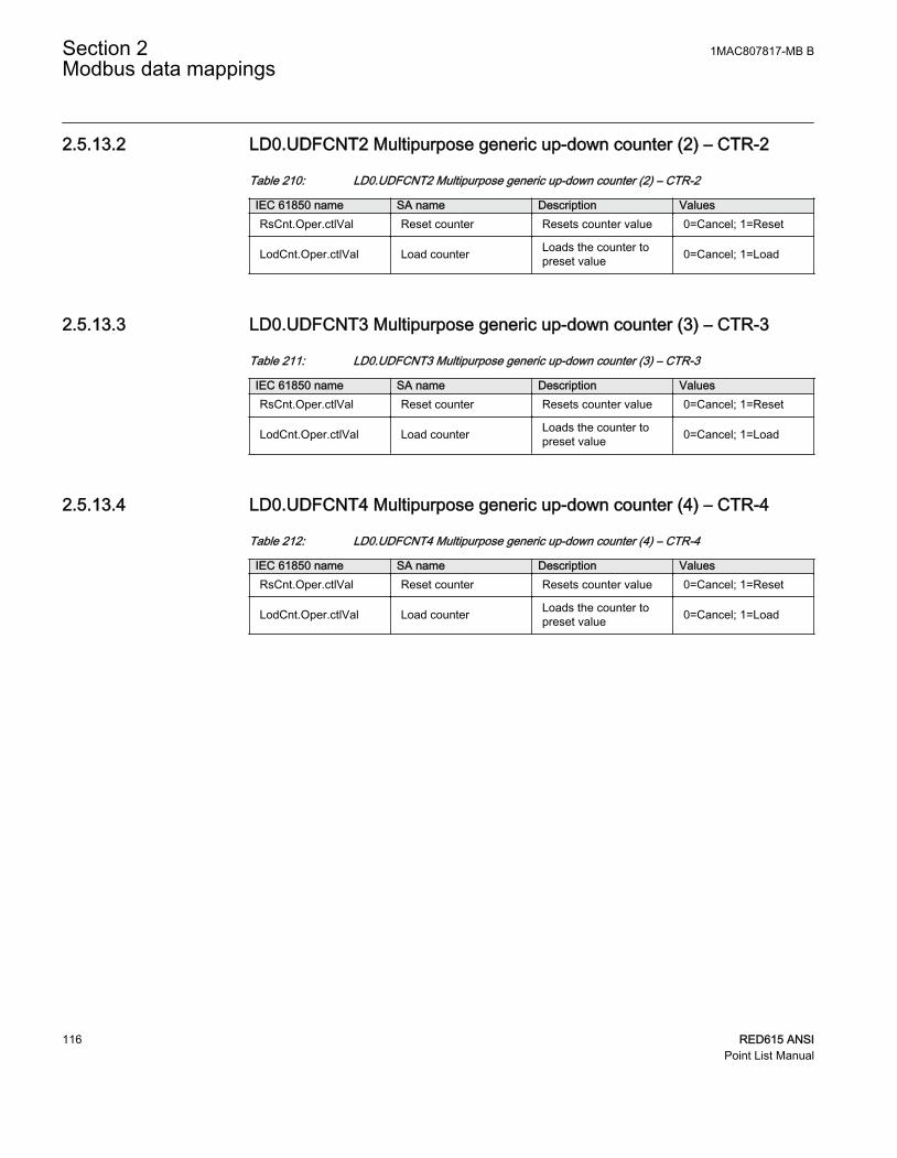
2.5.13.2 LD0.UDFCNT2 Multipurpose generic up-down counter (2) – CTR-2
Table 210: LD0.UDFCNT2 Multipurpose generic up-down counter (2) – CTR-2
IEC 61850 name SA name Description ValuesRsCnt.Oper.ctlVal Reset counter Resets counter value 0=Cancel; 1=Reset
LodCnt.Oper.ctlVal Load counter Loads the counter topreset value 0=Cancel; 1=Load
2.5.13.3 LD0.UDFCNT3 Multipurpose generic up-down counter (3) – CTR-3
Table 211: LD0.UDFCNT3 Multipurpose generic up-down counter (3) – CTR-3
IEC 61850 name SA name Description ValuesRsCnt.Oper.ctlVal Reset counter Resets counter value 0=Cancel; 1=Reset
LodCnt.Oper.ctlVal Load counter Loads the counter topreset value 0=Cancel; 1=Load
2.5.13.4 LD0.UDFCNT4 Multipurpose generic up-down counter (4) – CTR-4
Table 212: LD0.UDFCNT4 Multipurpose generic up-down counter (4) – CTR-4
IEC 61850 name SA name Description ValuesRsCnt.Oper.ctlVal Reset counter Resets counter value 0=Cancel; 1=Reset
LodCnt.Oper.ctlVal Load counter Loads the counter topreset value 0=Cancel; 1=Load
Section 2 1MAC807817-MB BModbus data mappings
116 RED615 ANSIPoint List Manual
Section 3 Glossary
ANSI American National Standards InstituteEMC Electromagnetic compatibilityIEC 61850 International standard for substation communication and
modelingIEC 61850-9-2 A communication protocol based on the IEC 61850 standard
seriesIED Intelligent electronic deviceLED Light-emitting diodeLHMI Local human-machine interfaceModbus A serial communication protocol developed by the Modicon
company in 1979. Originally used for communication in PLCsand RTU devices.
PCM600 Protection and Control IED ManagerUL Underwriters Laboratories
1MAC807817-MB B Section 3Glossary
RED615 ANSI 117Point List Manual
ABB Distribution SolutionsDistribution AutomationP.O. Box 699FI-65101 VAASA, FinlandPhone +358 10 22 11
ABB Inc.655 Century PointLake Mary, FL 32746, USAPhone +1-800-222 1946
www.abb.com/mediumvoltagewww.abb.com/relionwww.abb.com/substationautomation
—
© Copyright 2019 ABB. All rights reserved. 1MA
C80
7817
-MB
B


![u[sonic] Modbus - Lambrecht meteo](https://static.fdokumen.com/doc/165x107/6334bd04a6138719eb0b33dc/usonic-modbus-lambrecht-meteo.jpg)