
PUBLICATION RF Phase Reference Distribution System for ...
138
EuCARD-BOO-2013-002 European Coordination for Accelerator Research and Development PUBLICATION RF Phase Reference Distribution System for the TESLA Technology Based Projects; EuCARD Editorial Series on Accelerator Science and Technology (J-P.Koutchouk, R.S.Romaniuk, Editors), Vol.18 Czuba, K (Warsaw University of Technology Poland) 04 March 2013 The research leading to these results has received funding from the European Commission under the FP7 Research Infrastructures project EuCARD, grant agreement no. 227579. This work is part of EuCARD Work Package 2: DCO: Dissemination, Communication & Outreach. The electronic version of this EuCARD Publication is available via the EuCARD web site <http://cern.ch/eucard> or on the CERN Document Server at the following URL : <http://cds.cern.ch/record/1523225 EuCARD-BOO-2013-002
-
Upload
khangminh22 -
Category
Documents
-
view
1 -
download
0
Transcript of PUBLICATION RF Phase Reference Distribution System for ...

EuCARD-BOO-2013-002
European Coordination for Accelerator Research and Development
PUBLICATION
RF Phase Reference Distribution Systemfor the TESLA Technology Based Projects;EuCARD Editorial Series on AcceleratorScience and Technology (J-P.Koutchouk,
R.S.Romaniuk, Editors), Vol.18
Czuba, K (Warsaw University of Technology Poland)
04 March 2013
The research leading to these results has received funding from the European Commissionunder the FP7 Research Infrastructures project EuCARD, grant agreement no. 227579.
This work is part of EuCARD Work Package 2: DCO: Dissemination, Communication &Outreach.
The electronic version of this EuCARD Publication is available via the EuCARD web site<http://cern.ch/eucard> or on the CERN Document Server at the following URL :
<http://cds.cern.ch/record/1523225
EuCARD-BOO-2013-002

WARSAW UNIVERSITY OF TECHNOLOGYFaculty of Electronics and Information Technology
Institute of Electronic SystemsMicrowave Circuits and Instrumentation Division
Krzysztof Czuba
RF PHASE REFERENCE DISTRIBUTION SYSTEMFOR THE TESLA TECHNOLOGY BASED PROJECTS
Ph.D. Thesis
Thesis supervisor:Prof. Dr. Hab. Janusz Dobrowolski
Warsaw, 2007

Abstract
Since many decades physicists have been building particle accelerators and usually new projects became more advanced, more complicated and larger than predecessors. The importance and complexity of the phase reference distribution systems used in these accelerators have grown significantly during recent years. Amongst the most advanced of currently developed accelerators are projects based on the TESLA technology. These projects require synchronization of many RF devices with accuracy reaching femtosecond levels over kilometre distances. Design of a phase reference distribution system fulfilling such requirements is a challenging scientific task. There are many interdisciplinary problems which must be solved during the system design. Many, usually negligible issues, may became very important in such system. Furthermore, the design of a distribution system on a scale required for the TESLA technology based projects is a new challenge and there is almost no literature sufficiently covering this subject.
This thesis is devoted to the conceptual analysis, design and realization of a complete phase reference distribution system for the FLASH accelerator. The most important design issues are considered. Important distribution system architectures are described with their advantages and disadvantages. Methods of characterization of signal phase instabilities in distribution system components are presented. A general, system-level design method of the distribution system is proposed. The designed FLASH distribution system is divided into three subsystems: the Master Oscillator System, coaxial cable links and the fiber-optic link with active phase stabilization. The design, realization and tests of these subsystems are described. Performance of designed distribution system components is analysed and tested. Many practical information useful for the distribution system design are included in this work. The result of this thesis is a working distribution system prepared for installation in the FLASH facility.
This book contains a PhD thesis submitted at the Warsaw University of Technolgy in 2007. In comparison to the original some minor mistakes were corrected in this version.
2

Acknowledgments
I would like to thank my doctoral thesis supervisor Professor Janusz Dobrowolski for continuous support and encouragement that helped me with work on my thesis
I offer my thanks to all members of the ZUiAM group of ISE in Warsaw, where I was successfully taught all my knowledge about RF engineering. Special thanks for Dr. Wojciech Wiatr and Dr. Krzysztof Antoszkiewicz who were supervisors of my previous theses and to Dr. Zbigniew Nosal for many advices – sometimes very simple but invaluable.
I owe sincere thanks to Dr. Stefan Simrock for constant supporting my work in DESY and invaluable comments.
I would like to express special thanks to people involved in the Master Oscillator project. First of all to Henning Weddig from DESY for great support of a person with large engineering experience, good cooperation and many fruitful discussions, drawing the MO System block diagrams and friendly work environment. Thanks to excellent engineer and company leader, Erhard Salow from Inwave GmbH who provided most of the electronics for the Master Oscillator. I express gratitude to Bastian Lorbeer from DESY for many discussions and effort put in experiments. Last but not least thanks to people that were supporting the work on the MO assembly in the time of writing this thesis, Bartlomiej Szczepanski, Bibiane Wendland, Harry Busse and Andrzej Stefański.
I offer special thanks to Matthias Felber and Frank Eints from DESY and Michał Ładno from PERG group who helped me with the development of the FO link. They begun as inexperienced students but presented great will of work and defended their theses as very valuable engineers. We created together a good team with friendly work environment and we put enormous effort in the development of our project.
I would like to thank “the microwave group” people Dr. Frank Ludwig and Matthias Hoffmann for many inspiring discussions and friendly, stimulating work environment.
I would also like to thank all colleagues from ISE, TUL and DESY, too many to mention them all, who were also working in Hamburg, for friendly atmosphere, many events and many cheerful trips who helped me in surviving time spent far from home.
Finally I would like to thank my wife, Kasia for support, inspiration and patience during the long time of our separations when I was travelling forth and back between Warsaw and Hamburg. Kasia also made many graphics for this thesis.
I acknowledge the support of the Polish Ministry of Science and Higher Education, Grant No. 3T11B02929 and the European Community-Research Infrastructure Activity under the FP6 “Structuring the European Research Area” program (CARE, contract no. RII3-CT-2003-506395)
3
CONTENTS
1. Introduction...............................................................................................................................7
1.1. Motivation ........................................................................................................................7
1.2. TESLA, TTF, FLASH – meaning and chronology of names ...........................................81.3. Research goals, main contributions of this work...............................................................9
1.4. Thesis organization..........................................................................................................10
2. Distribution system architectures..........................................................................................11
2.1. Distribution system definition.........................................................................................11
2.2. Passive PRDS, optical fiber (LEP energy upgrade)........................................................122.3. Stabilized PRDS, coaxial line + passive optical fiber (CEBAF).....................................13
2.4. Active, coaxial cable (TRISTAN)...................................................................................142.5. Active PRDS, coaxial cable + optical fiber (NLC).........................................................15
3. Theoretical background.........................................................................................................18
3.1. Sinusoidal signal phase stability definition.....................................................................183.2. Classification of phase instabilities.................................................................................20
3.2.1.Short-term and long-term instability...................................................................................................213.2.2.Random and systematic instabilities...................................................................................................213.2.3.Absolute, two-port and relative (in)stability.......................................................................................213.2.4.Frequency drifts and aging..................................................................................................................22
3.3. Characterization of phase instabilities ............................................................................233.3.1.Measures in the frequency domain.....................................................................................................233.3.2.Measures in the time domain..............................................................................................................253.3.3.Phase jitter...........................................................................................................................................25
3.4. Influence of selected PRDS components on distributed signal phase instability...........263.4.1.Oscillator phase noise.........................................................................................................................263.4.2.Frequency multiplier noise.................................................................................................................293.4.3.Frequency divider noise......................................................................................................................293.4.4.Phase-locked loop noise model...........................................................................................................303.4.5.Phase noise added by amplifier and passive components...................................................................363.4.6.Long term phase drifts in the distribution media................................................................................383.4.7.Short term relative instability calculation...........................................................................................403.4.8.RF fiber-optic links.............................................................................................................................41
4. FLASH distribution system design requirements and conceptual analysis......................43
4.1. Design requirements........................................................................................................434.1.1.FLASH system overview and the need for device synchronization...................................................434.1.2.History of the FLASH PRDS synchronization requirements.............................................................474.1.3.General requirements and remarks.....................................................................................................474.1.4.Required frequency values..................................................................................................................484.1.5.Phase jitter requirements.....................................................................................................................484.1.6.Required phase noise levels................................................................................................................494.1.7.FLASH system layout and distribution distances...............................................................................52
4.2. Possible PRDS architectures...........................................................................................544.2.1.General design method.......................................................................................................................544.2.2.Considerations on available technology, important issues and design choices..................................54
4.3. FLASH PRDS architecture proposal...............................................................................60
5. FLASH phase reference distribution system details ...........................................................66
4

5.1. Master Oscillator System.................................................................................................665.1.1.General requirements..........................................................................................................................665.1.2.Reference oscillator............................................................................................................................675.1.3.Frequency generation scheme, conceptual analysis, block diagram...................................................675.1.4.Low Power Part details.......................................................................................................................745.1.5.Power supply, temperature stabilisation, crate cabling.......................................................................77
5.2. Coaxial cable system.......................................................................................................785.2.1.Choice of cable type and other issues of cable distribution link.........................................................785.2.2.Cable distribution system layout.........................................................................................................815.2.3.Power budget calculations..................................................................................................................845.2.4.Cable temperature regulation, phase drift calculations ......................................................................85
5.3. Fiber-optic long distance distribution link.......................................................................865.3.1.Introduction.........................................................................................................................................865.3.2.System conception..............................................................................................................................875.3.3.Optical phase shifter...........................................................................................................................895.3.4.Considerations for sources of errors...................................................................................................91
6. Experiments and measurement results.................................................................................95
6.1. Master Oscillator System performance measurements...................................................956.1.1.MO phase noise, short term stability..................................................................................................956.1.2.Phase drifts in the MO System............................................................................................................98
6.2. Fiber-optic link performance.........................................................................................1006.2.1.FO system test set-up........................................................................................................................1006.2.2.FO system with ODL........................................................................................................................1026.2.3.FO system with phase shifter made of fiber spool in the oven.........................................................1056.2.4.FO system with ODL and fiber spool in oven..................................................................................106
7. Summary and conclusions....................................................................................................107
7.1. Summary........................................................................................................................107
7.2. Conclusions and notes on achieved research goals.......................................................1087.3. Perspectives of further research.....................................................................................109
8. Appendix 1 – MO System design details and project management.................................111
9. Appendix 2 - Cable temperature stabilisation, cable installation.....................................117
10. Appendix 3 – Optical Delay Line.........................................................................................119
11. Appendix 4 – Temperature controlled oven.......................................................................120
12. Appendix 5 – FO system design details...............................................................................122
13. Appendix 6 – Phase Detectors..............................................................................................126
14. References..............................................................................................................................129
14.1. Publications with author's contribution.........................................................................12914.2. Bibliography..................................................................................................................130
5
Acronyms
ACC - Accelerating module of the TESLA system. It includes 8 superconducting cavitiesADC - Analog to Digital ConverterBW - BandwidthCW - Continuous WaveDAC - Digital to Analog ConverterDSB - Double Side-Band phase noiseEMI - Electromagnetic Interference, page 57FLASH - Freie-Elektronen-LASer1 in Hamburg, chapter 1.2, used interchangeably with
TTF and VUV-FELFO - Fiber-Optic link, in this thesis used for describing the system with active signals
phase stabilisation, chapter 5.3ILC - International Linear ColliderLLRF - Low Level Radio Frequency, page 44LPP - Low Power Part of the MOMO - Master Oscillator, chapter 4.1MO System - Master Oscillator System. The reference oscillator with all devices generating
frequencies required for the PRDS, page 48ODL - Optical Delay Line with a step motor, page 90OCXO - Oven Controlled Crystal Oscillator, page 62PLL - Phase-Locked Loop, chapter 3.4.4PN - Phase NoisePRDS - Phase Reference Distribution SystemPSD - Power Spectral Density, page 24RF - Radio FrequencyRFS - Radio Frequency station, here understood as one of target devices for the
PRDSSMA - RF cable connector typeSSB - Single Side-Band phase noise, page 24VCO - Voltage Controlled Oscillator, page 30VCXO - Voltage Controlled Crystal OscillatorTESLA - TeV Energy Superconducting Linear AcceleratorTTF - TESLA Test Facility, chapter 1.2, used interchangeably with FLASH and VUV-
FELVUV-FEL - Vacuum Ultraviolet Free Electron Laser, chapter 1.2, used interchangeably with
TTF and FLASH
1 Free-Electron Laser in German
6

1. Introduction
1. Introduction
1.1. Motivation
The importance of phase reference distribution and synchronization systems for the physical particle accelerators has grown significantly during recent years. Since many decades physicists have been building particle accelerators and usually new projects became more advanced, more complicated and larger than predecessors. Currently, one of the most advanced accelerator technologies is the TESLA [101] technology. TESLA stands for TeV-Energy Superconducting Linear Accelerator. This technology was developed in DESY2 in 1990's. The basic element of the TESLA technology is a pure niobium, nine-cell resonator3 [102, ch. 2.1]. Resonators operate in temperature of 2 K in order to obtain the superconductivity effect which makes possible obtaining values of the unloaded quality factor Q as high as 1010 at the resonance frequency of 1.3 GHz.
A high-gradient electromagnetic field is pumped by high power (10 MW peak pulse power) klystrons to the superconducting cavities. Obtained field gradients inside of a cavity exceed 30 MV/m. Such high-gradient fields are used to accelerate (increase energy) of electrons injected from a device called RF-GUN (or electron gun) [103, ch. 3.1.1] into the accelerating structure made of a chain of cavities. For proper acceleration, electron bunches must enter the cavity in precisely defined time, when the electric field direction assures increasing of the electron energy. Therefore the RF-GUN must be precisely synchronized with the accelerating structure. A control system is applied on the electromagnetic field amplitude and phase [102 ch. 3.3.7] in order to assure proper conditions for particle acceleration. Field parameters are stabilized with specified accuracy relatively to the reference signal and electron beam position. The phase stable 1.3 GHz reference signal is provided to the control system by the reference distribution system.
A group of accelerating cavities powered by one klystron with a control system and all necessary subsystems needed for proper particle acceleration is called an RF station. The particle energy is increased in one RF station by specified amount. The total number of RF stations installed in the accelerator depends on the accelerator type and the required energy of particles at the end of the accelerating structure. For example, the future project, called International Linear Collider (ILC) [42], formerly TESLA, may require installation of 1000 RF stations distributed along a straight tunnel with the length of 33 kilometres. All RF stations must be precisely synchronized.
The reference signals are provided to RF stations by the Phase Reference Distribution System (PRDS)4. Recent demands on the accuracy of synchronization and physical dimensions of TESLA technology based projects placed the PRDS design amongst the most difficult and challenging tasks to be performed during the accelerator development. As it will
2 Deutsches Elektronen-Synchrotron, Hamburg, Germany3 The 9 cell resonator is frequently called `cavity' in literature. For convenience reasons.4 The PRDS definition and the difference between the PRDS and synchronization system is explained in
chapter 2.1
7

1. Introduction
be presented in the next chapters of this thesis, the PRDS must deliver very stable signals (about 10 different frequencies), with various power levels to many RF stations spread along the accelerator. In general, the PRDS can be split into three main parts: a reference oscillator, a frequency multiplication network and a long distance distribution system. Multiple design issues of all subsystems and their influence on the overall synchronization precision must be considered. Example list of important design issues is given below:• short and long term stability of the signal generated by the reference oscillator,• signal stability after frequency multiplication or division,• phase noise issues,• choice of the reference oscillator frequency and multiplication/division factor values,• power amplifier influence on signal phase stability,• temperature stability of the signal generation and amplification system,• choice of the distribution media for long distance links (e.g. RF cable, optical fiber, ...),• temperature sensitivity of the distribution media, long term phase drift regulation,• available technology and system cost.
Optimal design of PRDS and its components with a prediction of system performance is a challenging scientific task. Such task was given to the author of this thesis at the beginning of his cooperation with DESY. Many questions appeared in the first stage of work, e.g.: • How to solve problems listed above (and many others)?• What are the interdependences between these problems?• What is the influence of each problem on the final performance of the PRDS?• How to specify parameters of PRDS components in order to achieve the performance
required for the entire system?• Does one really need “worlds best” (and most expensive) devices?• How to estimate system performance and be sure that time and money spent for
development will not be waisted?Even a simple question “How to start?” was very difficult to answer. The main problem
is that most of the issues and questions listed above belong to various fields of knowledge. Many of these issues (e.g. phase noise) are very well known and were described in many scientific publications. But, to the knowledge of the author of this thesis, there is no literature comprehensively covering interdependences between these problems in the way that can be useful for PRDS design purposes. Known publications on accelerator synchronization systems built before the time of writing this thesis do not provide general methods for PRDS design and performance analysis. This situation motivated the author of this thesis to take an attempt of gathering necessary knowledge about issues crucial to the PRDS performance in one “short” thesis. A method of PRDS design and analysis is proposed which can significantly reduce time and cost of system development.
1.2. TESLA, TTF, FLASH – meaning and chronology of names
There are several names of the TESLA technology based projects used in this thesis. The meaning and chronology of those names must be briefly explained in order to make it easier for the reader to localize the purpose of described considerations.
As mentioned above, the TESLA technology was developed in DESY in the 1990-ties.
8

1. Introduction
This technology was intended for the design of large (33 km) linear accelerator of the same name [101, ch.3]. First tests of the TESLA technology were performed while operating a 100 meter long TESLA Test Facility (TTF) [103], called later TTF1. The next step in the development of the TESLA technology was a 300 meter long upgrade of the TTF1 started in 2002, given a name TTF2. The TTF2 was brought to operation and after a lasing action (in ultraviolet wavelength range) was obtained, its name was changed to VUV-FEL (Vacuum Ultraviolet Free Electron Laser). This project was appearing in official publications also under the name of TTF-VUV-FEL. This name was used till the early 2006 when it was replaced with FLASH, which is more attractive and easier to pronounce in different languages. FLASH stands for Freie-Elektronen-LASer5 in Hamburg. The names of TTF2, VUV-FEL and FLASH will be used interchangeably in the remainder of this thesis.
Resulting from the experience gained during the TTF/FLASH construction, a conceptual development of the XFEL (X-ray Free Electron Laser) [6] was performed and this project was approved. It will be 3.3 km long and the construction is expected to start in 2007.
The basic application of the TESLA technology: construction of the 33 km long TESLA linear accelerator was postponed by German Government because of very high costs. But in the year 2004 the International Technology Recommendation Panel (ITRP) recommended that the TESLA technology should be used for the design of the International Linear Collider (ILC), which will be a project of similar size to TESLA accelerator. Currently there is no fixed decision on the construction details but one can find proposals for 40 km long accelerating structure. The ILC will be designed and constructed by an international collaboration of high energy particle laboratories and institutes from Europe, the Americas, and Asia. The construction should start after the year 2010. The name of TESLA is no longer used for the accelerator but it still functions for describing the TESLA technology.
The work on the PRDS being subject of this thesis was started in 2003 during the development of the TTF2/FLASH facility. The intention was to test the PRDS prototype in the TTF2 facility and prepare it for the TESLA accelerator. Therefore the first publications by the author of this thesis concern the PRDS for the TESLA accelerator. As the names and plans were changed, the PRDS described in this thesis was ascribed to the FLASH facility. But many considerations and experiments were performed allowing to gain experience for the construction of the XFEL and/or ILC PRDS.
1.3. Research goals, main contributions of this work
The first goal of this thesis is the analysis of most important issues affecting the final performance of the PRDS. The knowledge gathered for this analysis can be used for considerations on the choice of optimum architecture of designed system.
Next goal is the development of a simple, practical method for designing such complicated PRDS. The PRDS complexity is so great that development of a complete mathematical system model is very difficult and for sure impractical. Therefore considerations were limited to range allowing for achieving a PRDS that fulfils given requirements. It was assumed that system-level not a circuit-level considerations are applicable. Otherwise the goal of the work would be overwhelmed by too many details which would result in confusion rather than in optimally designed project.
5 Free-Electron Laser in German
9

1. Introduction
The third, and most important goal was the design and realization of a working PRDS for the FLASH facility with effective use of gathered knowledge. The system should be tested and prepared for installation in the FLASH facility.
The last but not least goal was to gather the experience - both knowledge and practice - useful for the design of PRDS for larger accelerators like the XFEL and ILC.
The goals listed above were achieved and this work can be a very important contribution for designers of PRDS for future accelerator systems.
1.4. Thesis organization
The following chapters provide extensive information about the design issues, design method, system analysis and practical realization of the FLASH PRDS. Possibilities of extending the PRDS on longer distribution distances are described frequently.
In chapter 2 a definition of the PRDS is given and different PRDS architectures are described. Brief descriptions of representative PRDS types found in literature are also given.
In chapter 3 the most important theoretical issues affecting the PRDS performance are described. The definition, classification and methods of characterisation of phase instabilities are addressed. The most important PRDS components and their influence on the signal phase stability is characterised.
In chapter 4 the design requirements for the FLASH PRDS are given. Considerations on the choice of a suitable PRDS architecture are performed. Finally, the architecture is proposed.
Chapter 5 contains detailed description of the design of the FLASH PRDS. The system was split into three subsystems: a Master Oscillator, a coaxial cable distribution system and a fiber-optic link with active stabilisation of the distributed signal phase.
In chapter 6 performed experiments and measurement results are described. These results confirm the validity of considerations performed in preceding chapters.
Finally in the chapter 7 summary of performed work is given and conclusions are collected. Six appendices provide a brief description of technical details of designed subsystems of the PRDS.
10

2. Distribution system architectures
2. Distribution system architectures
2.1. Distribution system definition
Generally, the main purpose of the PRDS is the synchronization of multiple radio frequency devices belonging to one distributed system. Strictly, it can be understood as a network of signal guides (e.g. cables) used to transport stable signal from a stable source (Master Oscillator) to multiple RF stations (RFS). Nevertheless, as it was indicated in the first chapter, for the purpose of this thesis, the phase distribution system is treated as a sum of the MO and the distribution links. The PRDS can also be named a synchronization system but the word 'synchronization' is of much wider meaning than the main scope of this thesis. Here the PRDS must also clearly be distinguished from the timing system, usually used for synchronization of digital devices and adapted to distribute signals defined by one of digital logic standards. Timing system often provides time stamp codes used by the digital hardware for identification of certain time moments. The PRDS is used to distribute analogue (sine-wave) RF signals and it is often used in parallel with the timing system within one facility and both systems are synchronized with a common MO. Example of a timing system built for the FLASH facility is described in the DESY report [103, pp. 467-476].
Known literature provides numerous descriptions of PRDS. The PRDS architecture and complexity depends naturally on the application, synchronization accuracy requirements and actual state of the technology. Amongst the most important applications of the PRDS one can enumerate the following: • particle accelerators - physical experiments and heavy ion sources for medical facilities,• telecommunication systems (e.g. base station local oscillator synchronization) ,• radio-astronomy facilities, with many antennas distributed over broad area• large radar systems• navigation and positioning systems
Unambiguous PRDS type classification is very difficult because of a large number of possible classification criteria. Nevertheless, the knowledge of possible PRDS architectures and their advantages is essential in the first stage of system design. It may help the designer in taking proper decisions and saving a lot of time and money that must be spent for the system development. Therefore, in the remainder of this chapter a proposal of the PRDS classification is given and representative examples of formerly designed systems are described. A brief description of advantages and disadvantages of these systems is given. Knowledge gathered in references describing these systems was very useful in the first stages of the design of the PRDS being a subject of this thesis.
One can classify the PRDS according to the following criteria:1. System topology:
• Star• Line with pick-up points
2. Distribution media type:• Coaxial cable or waveguide
11

2. Distribution system architectures
• Optical fiber• Air (radio synchronization)
3. Distributed signal type:• Continuous sine wave• Pulses used for local oscillator synchronization
4. Influence on the signal:• Passive• Stabilized: e.g. temperature stabilized cable link• Active: with feedback circuits actively controlling signal phase
Proposed classification is of course not full and it can easily be extended with another. criteria. Each of existing PRDS examples given in the next sub-chapters can be ascribed one feature from each given category. Such set of features characterizes the architecture of a given PRDS more precisely but it does not define system performance. Obtained synchronization accuracy depends on multiple technical details as it is described in chapters 3, 4 and 5 of this thesis.
2.2. Passive PRDS, optical fiber (LEP energy upgrade)
• LocationSystem was installed and tested in the upgraded LEP facility in CERN, Geneva in years
1993 – 1994. Finally, installed links were intended to operate with active phase compensation circuits as described in [72], but there is an interesting reference [45] describing measurement results from installed fiber-optic links before switching the feedback on.
Figure 2.1: LEP upgrade PRDS layout. Figure source: [45]
12

2. Distribution system architectures
• FeaturesStar type of architecture with 6 long fiber-optic links (see fig. 2.1). Passive system with no
phase regulation. Both, standard and temperature compensated optical fiber were installed in parallel for comparison. The longest transmission distance equals 9.5 km. Optical fiber was located 1 meter underground.• Distributed frequencies
352 MHz• Obtained signal stability
Measurement duration: 10 months (long term drifts). Link length: 9.5 km = 19 km round-trip. No data for the short term stability.90o pp, it corresponds to 710,2 ps6 for the temperature compensated optical fiber.2100o pp, it corresponds to 1.67 μs for normal optical fiber.• Remarks
Given phase drift values are peak to peak during 10 months. Of course variations in shorter periods of time are much smaller (no precise data) and such system performance could be sufficient for certain applications. It also provides a good practical justification for active phase stabilization in more demanding facilities.
2.3. Stabilized PRDS, coaxial line + passive optical fiber (CEBAF)
• LocationThis distribution system was installed in the early 90-ties in the Continuous Electron
Beam Accelerator Facility (CEBAF) which is located in the Jefferson Lab scientific institute in Newport News, USA. System is described in the reference [48].• Features
Relatively simple system with temperature stabilization of the distribution line. The RF MO provides three frequencies: 70 MHz, 499 MHz and 1497 MHz. Signals of first two frequencies are amplified and distributed to the RF control system and klystron galleries where the 499 MHz signal is frequency multiplied by 3 to 1427 MHz. Both 70 MHz and 1427 MHz signals are distributed along the accelerator via ½” and 1 5/8” coaxial cables. The 1 5/8” cable is used to distribute 1427 MHz because of lower cable attenuation for this frequency. There are two identical distribution lines installed for two linacs7 in the system. Each line is 228 meter long. Both distribution lines are fabricated in 10 meter segments with directional couplers installed for both lines at the end of each segment.
Both ½” and 1 5/8” cables are wrapped around with heater tape and thermally insulated. The temperature is regulated with accuracy of ±0.1oC. There is also pressure regulation at the value of 4 psig8 applied to the 1 5/8” cable with the use of dry nitrogen. This is to suppress changes in dielectric length due to air pressure variations. The distribution line is isolated from the microphonic noise by suspending the entire distribution line from O-rings every 1.5 meter.
The signal with frequency of 1497 MHz is also distributed via fiber-optic reference line [14]. This line is used for phase drift monitoring purposes for the cable reference lines. The
6 Details on conversions of jitter values form angle to time domain are given in chapter 3.3.37 Linear accelerator8 Pressure unit used in hydraulics
13

2. Distribution system architectures
fiber-optic line is approximately 1.5 km long. It makes use of an ultra-phase stable optical fiber. The entire fiber length exhibits a thermal shift of 0.12o phase/oC.• Distributed frequencies
As mentioned above: 70 MHz, 1427 MHz and 1497 MHz.• Obtained signal stability
No measurement data provided but there is a statement that coaxial cable temperature regulation of ±0.1oC was achieved. This would result in ±0.65o phase change on the entire 228 meter link.• Remarks
The main advantage is the simplicity of the system. Only coaxial cable and directional couplers directly affect distributed signal parameters. No active signal path components (except amplifiers) means low degradation of the signal phase noise. Such system is also very reliable.
Among the disadvantages there is significant RF loss in the cable (13 dB at 1427 MHz for 228 meter). Such system becomes impractical for kilometre distribution distances. The installation of such system is relatively complex and expensive: thermal insulation, temperature and pressure regulation, 1 5/8” coaxial cable is rigid as hydraulic pipe.
2.4. Active, coaxial cable (TRISTAN)
• LocationThis distribution system was installed at the TRISTAN colliding beam ring in National
Laboratory for High Energy Physics in Japan. System was described in the reference [37].• Features
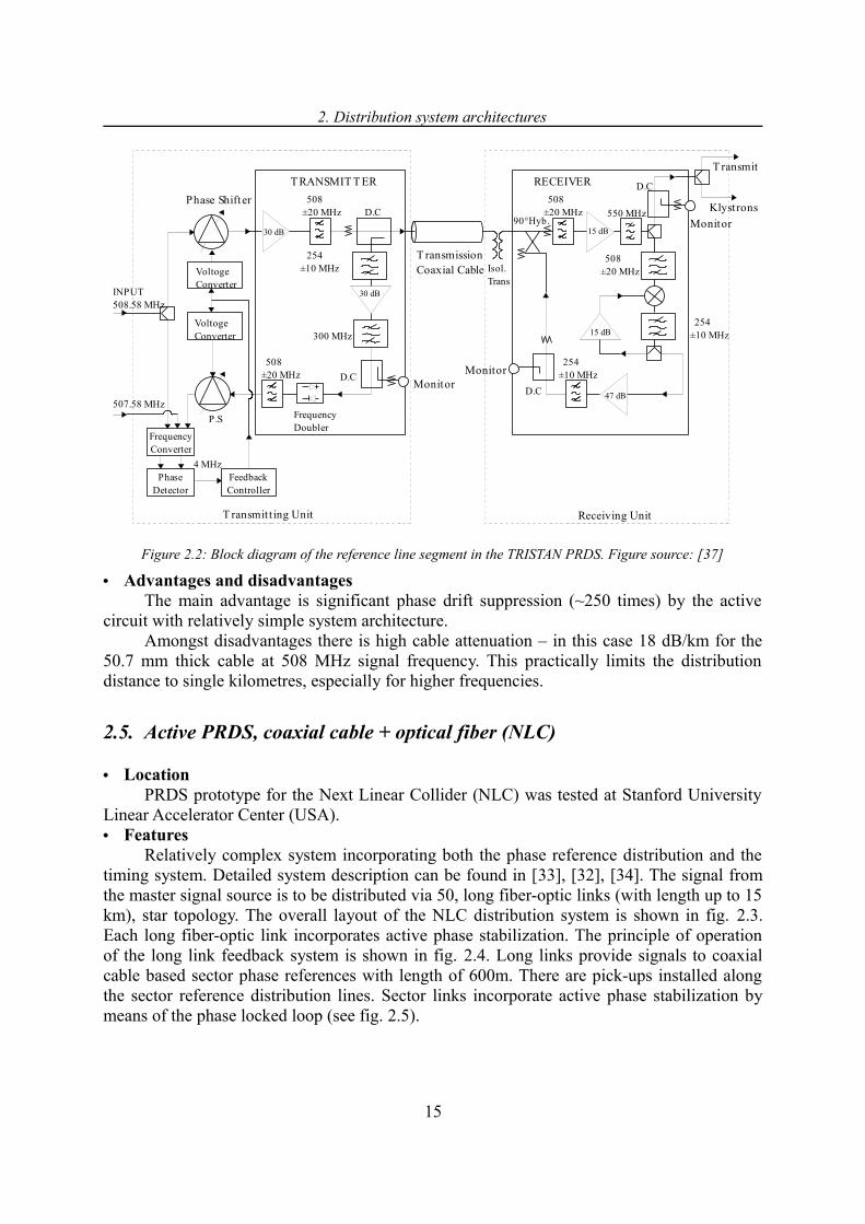
Signals are distributed using coaxial cable links. There are two distribution paths, each 1900 meter long. Each patch consists of four cable segments made of two kinds of cable. A 29 mm outer diameter cable used for short links (200 m) and 50.7 mm cable used for long links (760 m). Both paths start at the master oscillator and go around the collider ring. Path ends meet on the collider side opposite to the MO for phase comparison purposes.
Each segment of the reference line contains an active phase stabilization system. See fig. 2.2 for the block diagram. At the input of each segment there is a transmitting unit including voltage controlled phase shifter. Input signal of the transmitting unit is distributed via the cable to the receiving unit where part of it is converted to its second sub-harmonic and returned back to the transmitting unit through the same coaxial cable. The returned signal is doubled back to the original frequency and after passing a second phase shifter it is compared in phase with the input signal. Voltage obtained from the phase detector is used to lock the feedback loop regulating out phase drifts appearing in the reference line.• Distributed frequencies
508.58 MHz• Obtained signal stability
Provided are measurement results of a test system simulating 760 meter segment but with temperature changes 25 ±20oC applied to the cable which is much more than temperature changes expected in the accelerator conditions.
Measured was 0.8 degree (4.37 ps) of the output signal phase change. Measurement duration: 4 months. Open loop phase change was about 200 degree.
14
2. Distribution system architectures
Figure 2.2: Block diagram of the reference line segment in the TRISTAN PRDS. Figure source: [37]
• Advantages and disadvantagesThe main advantage is significant phase drift suppression (~250 times) by the active
circuit with relatively simple system architecture.Amongst disadvantages there is high cable attenuation – in this case 18 dB/km for the
50.7 mm thick cable at 508 MHz signal frequency. This practically limits the distribution distance to single kilometres, especially for higher frequencies.
2.5. Active PRDS, coaxial cable + optical fiber (NLC)
• LocationPRDS prototype for the Next Linear Collider (NLC) was tested at Stanford University
Linear Accelerator Center (USA).• Features
Relatively complex system incorporating both the phase reference distribution and the timing system. Detailed system description can be found in [33], [32], [34]. The signal from the master signal source is to be distributed via 50, long fiber-optic links (with length up to 15 km), star topology. The overall layout of the NLC distribution system is shown in fig. 2.3. Each long fiber-optic link incorporates active phase stabilization. The principle of operation of the long link feedback system is shown in fig. 2.4. Long links provide signals to coaxial cable based sector phase references with length of 600m. There are pick-ups installed along the sector reference distribution lines. Sector links incorporate active phase stabilization by means of the phase locked loop (see fig. 2.5).
15
T ransmissionCoaxial Cable
T RANSMIT T ER
508±20 MHz D.C
30 dB
30 dB
254±10 MHz
300 MHz
D.C
Frequency Doubler
508±20 MHz
Phase Shifter
VoltogeConverter
VoltogeConverter
P.S
FrequencyConverter
PhaseDetector
T ransmit t ing Unit
FeedbackController
507.58 MHz
INPUT508.58 MHz
Monitor
4 MHz
90°Hyb.
Monitor
D.C
Receiving Unit
RECEIVER
15 dB
508±20 MHz
Monitor
T ransmit
Klystrons
254±10 MHz
47 dB
15 dB 254±10 MHz
508±20 MHz
550 MHz
D.C
Isol. Trans

2. Distribution system architectures
Figure 2.3: Overall layout of the NLC distribution system. Figure source: [33]
• Distributed frequenciesThe target frequency equals 11.4 GHz but a value of 357 MHz (1/32 of 11.4 GHz) was
chosen for the distribution. The distributed frequency is locally multiplied at the target device.
Figure 2.4: Long link operating principle. Figure source: [33]
• Achieved signal stabilityResults are given only from tests of the long link. No data provided about the cable
reference line and overall system performance.Long term: +/- 2o (@11.4 GHz), corresponds to +/- 0.49 ps.Short term (phase noise integrated in 10 Hz bandwidth): 0.2o (@11.4 GHz), corresponds
to 50 fs.Tests were performed in laboratory conditions. No data from accelerator environment.
• RemarksThe laser of the long link operates in pulsed mode. Light pulses are amplitude
modulated by the RF signal from the master source. The CW signal is retrieved at link output by phase locked oscillator. All together makes the system complicated (test set-up described in [34]). This may lead to difficulties with the reliability of the system.
16
Tunnel
Linac
SectorLinac Sector
MasterSource
X50 Sectors
Long Links (15 km)
Low Level RF System
Klystrons
RF Structures
High Power RFDistribution System(DLDS)
Phase Detectors
PhaseDetectors
Measure phase vs.reference and beamvs. RF phase
Feedback
Sector phasereference ~ 600 M
LaserTransmitter
DirectionalCoupler
Circulator LengthAdjust
DirectionalCoupler
Outgoingphasedetector
Reflectedphasedetector
Feedback on ReflectedPhase
ReceiverPhaseDetector

2. Distribution system architectures
Figure 2.5: Coaxial cable sector phase reference distribution layout. Figure source: [33]
17
PhaseAverager
Phase Detectors
357 MHzVCO
PLL feedback
Phase referencefrom long fiber link
Reference phaseto device
coax
ΔL
Reflection(unterminated)
Forward andreverse couplers(Each Device)
Phase hereis fixed byPLL feedback
Forward signalis ΔL / C early
Reflected signalis ΔL / C late

3. Theoretical background
3. Theoretical background
Many methods for describing and characterization of signal stability can be found in very broad list of references. Nevertheless, a choice of suitable method for particular application is not an easy task and it requires a very deep understanding of properties and limitations of given measurement and description method. This chapter covers the definitions of the signal phase stability and methods of characterisation of phase instabilities. Provided descriptions are based on internationally accepted standards for the frequency and time metrology (cited in the further text). Range of provided definitions is limited to measures important from the point of view of the further text of this thesis.
Broad range of expressions can be found in the literature devoted to the performance of signal sources. A short description of selected expressions is provided in chapter 3.2. This description includes classification and explanation of terms that are used frequently in the remainder of this work.
Additionally, methods of characterization of the influence of the PRDS components on the signal phase stability are given. Tools and definitions described in this chapter will be a base for the stability analysis of the signal distributed in the PRDS.
3.1. Sinusoidal signal phase stability definition
The main feature of the PRDS being subject of this thesis, as it was described in chapter 2.1, is the distribution of phase-stable sine-wave signals. The instantaneous voltage v(t) of an ideal sine-wave signal can be expressed as
(3.1)whereV0 is the nominal peak voltage amplitudeν0 is the nominal frequency9, here also called instantaneous10
The phase of the sinusoidal signal is the angle “Φ” corresponding to a particular time “t”. From eq. (3.1), t = 2 0 t . The values of phase and the frequency are naturally related by
(3.2)
Basing on this equation the relationship between the frequency and phase stability (or instability) can be found. Important examples will be described in the remainder of this chapter. But, first the difference between the stability and instability should be distinguished.
Multiple references, like papers collected in the NIST technical note [92], provide deep analysis and definitions for characterization of the frequency stability. Most probably due to
9 “ν0” is used here to distinguish the instantaneous signal frequency from the Fourier frequency “f” that appears in spectral densities. The symbol “f “ (equivalent to ν0) will also be used in this thesis in cases where no mistake is possible.
10 Defined by [39] as ΔV/Δt, where ΔV is sinusoidal signal voltage change corresponding to infinitesimally small time Δt.
18
v t = V 0 sin 2 0 t
0 =1
2d t
dt
3. Theoretical background
practical reasons, definitions for characterization of phase instabilities, such as described in the IEEE standard [41], appear less frequently in the literature. It is more difficult to find a strict definition explaining the exact meaning of the frequency or phase stability. Relatively often authors write on frequency stability, when they mean instability, like noticed in references [71] and [85]. Such inconsistencies in notation usually do not lead to problems with interpretation of provided information.
References [39] and [67] give definitions for the frequency stability and instability:
Frequency stability is the degree to which an oscillating signal produces the same value of frequency for any interval, Δt, throughout specified period of time.
Frequency instability is the spontaneous and/or environmentally caused frequency change within a given time interval.
One usually refers to frequency stability when comparing one oscillator with another. Frequency or phase instabilities are results obtained from many practical measurement methods performed on one signal source. E.g. measurement of frequency changes within a specified period of time using a frequency counter.
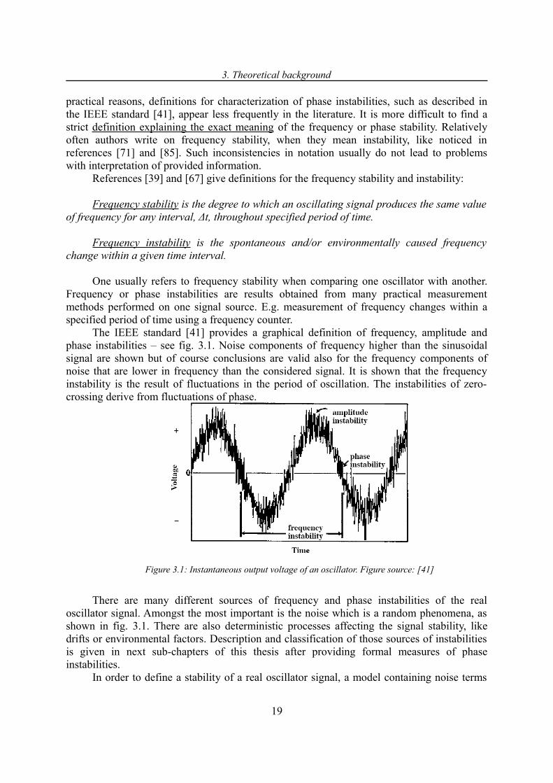
The IEEE standard [41] provides a graphical definition of frequency, amplitude and phase instabilities – see fig. 3.1. Noise components of frequency higher than the sinusoidal signal are shown but of course conclusions are valid also for the frequency components of noise that are lower in frequency than the considered signal. It is shown that the frequency instability is the result of fluctuations in the period of oscillation. The instabilities of zero-crossing derive from fluctuations of phase.
Figure 3.1: Instantaneous output voltage of an oscillator. Figure source: [41]
There are many different sources of frequency and phase instabilities of the real oscillator signal. Amongst the most important is the noise which is a random phenomena, as shown in fig. 3.1. There are also deterministic processes affecting the signal stability, like drifts or environmental factors. Description and classification of those sources of instabilities is given in next sub-chapters of this thesis after providing formal measures of phase instabilities.
In order to define a stability of a real oscillator signal, a model containing noise terms
19

3. Theoretical background
was introduced [39], [40], [41], [67], [85], [90], that is described by
(3.3)where:ε(t) is the deviation of amplitude from nominal valueφ(t) is deviation of phase from nominal value
Frequently, the parameters ε(t) and φ(t) are also called, respectively, amplitude noise and phase noise components. The amplitude noise component ε(t) can be neglected [85], [96] when characterizing precise signal sources. The instantaneous frequency (ν(t)) of a signal with phase noise component (eq. (3.3)), which is the time derivative of the signal phase divided by 2π, can be defined by
(3.4)
The fractional, normalized frequency y(t) was introduced as
(3.5)
This dimensionless and carrier frequency independent quantity characterizes the instantaneous frequency deviation from the nominal frequency. It is very useful for comparison of oscillators operating at different nominal frequencies. Equation (3.5) is also a definition of the frequency instability recommended by IEEE [41].
The phase instability can be expressed in units of time by
(3.6)
The frequency instability and the phase instability definitions can be related by
(3.7)
After stability and instability definitions given above, the classification of phase instabilities and practical measures used for characterization of for phase instabilities are presented in the following sub-chapters.
3.2. Classification of phase instabilities
Phase or frequency stability (or instability) can be described using different types of standard measures (see chapter 3.3). Usually, these complex measures precisely describe signal stability but there is a number of additional parameters that must be provided11 with given measure for full and unambiguous understanding of the result. Frequently, in practical applications, there is no need for full characterisation of signal instabilities. The characterisation is limited to particular range only, e.g. measurement is performed over limited period of time or within limited measurement bandwidth. Names of parameters obtained this way frequently appear in literature describing signal sources for different
11 Like measurement method, system bandwidth, measurement duration, environment. See e.g. [41]
20
t = 01
2
d t dt
y t = t − 0
0
=1
2 0
d t dt
y t =dx t
dt
x t =t 2 0
v t = [V 0 t] sin [2 0 t t ]

3. Theoretical background
applications. Those names neither define the phase instability (as in the chapter 3.1) nor define the measures of instability (as in the chapter 3.3). They are used for convenience as they limit the range of given instability measures. Short explanation and classification of those terms are given following sub-chapters. This classification can be useful for the reader, as those terms appear frequently in the further text of this thesis.
3.2.1. Short-term and long-term instability
The phase (in)stability measure can be split into two components – short-term and long-term stability. The short-term stability refers to all phase/frequency changes about the nominal of less than a few second duration [40]. This kind of stability derives from a “fast” phase noise components (measured at offset frequencies greater than 1 Hz). It is measured in units of spectral densities or timing jitter (chapter 3.3).
The long-term stability refers to the phase/frequency variations that occur over time periods longer than a few seconds. This kind of stability derives from slow processes like long term frequency drifts, aging and susceptibility to environmental parameters like temperature. The long-term stability is usually given as a parameter of a precise reference frequency generators like atomic standards or crystal oscillators. Besides standard measures it is very frequently expressed in parts per million (ppm) units per specified time period like hour, day, month or year.
3.2.2. Random and systematic instabilities
The fluctuating phase term φ(t) of the real signal (eq. (3.3)) can be caused by two kinds of fluctuations – random and deterministic. The random phenomena called phase noise is of the most frequent concern when characterizing oscillator signals. Because of the random nature of the phase noise, statistical methods for describing its parameters are used. Deep treatment of those methods exceeds the scope of this thesis but for interested reader there is a broad literature list covering aspects of random signals e.g. [20], [27], [63], [69], [93]. Practical measures for phase noise characterization are covered in chapter 3.3 of this thesis. The random phase noise in electronic circuits, especially in oscillators, comes from various physical processes in electronic component that include thermal noise, flicker and shot noise. Again, detailed analysis of basic noise phenomena in electronic circuits is beyond the scope of this thesis but it was very well covered in literature e.g. [27], [63], [68].
The second type of phase fluctuations – deterministic, are discrete signals appearing as distinct components in the spectral density plot. These signals are called spurious. They are related to known phenomena influencing the signal source such as power line frequency (50 Hz in Europe), vibration, mixing products or signals from electronic devices (e.g. switching power supplies) penetrating the circuit by electromagnetic interference.
3.2.3. Absolute, two-port and relative (in)stability
Two kinds of signal phase instability being of the interest of the PRDS designer can be distinguished – absolute and relative. The absolute stability refers to the total phase noise present at the output of the signal source or a system. It can be measured using a phase noise measurement system at any output along the signal distribution chain, e.g. at the output of a reference oscillator, power amplifier or long cable. Each time, the measured signal is treated
21
3. Theoretical background
as coming from one port source. Of course all devices of the signal chain, except the reference oscillator, are two-port devices and their contributions to signal phase instability can be analysed separately, regardless of the driving source [40], [77].
The relative stability refers to a measure between different points of the PRDS. Actually, it could be regarded as the accuracy of synchronization. This kind of stability can be of high importance for particle accelerator PRDS designer because often there is required a certain level of synchronization accuracy between various accelerator subsystems. Let us assume a distribution system containing a reference oscillator with phase slowly drifting in time and a number of ideal cables (having no influence on phase) distributing signal from the reference oscillator. The phase measured at the output of each cable against the reference oscillator, will be precisely following the reference oscillator phase. Therefore the phase difference between the ref. oscillator and each output will always be equal zero. Also phase difference measured between each output will be constant (perfectly stable). Naturally, in real systems, instabilities contributed by distribution devices will be measured between various outputs of the PRDS. In the simplest PRDS architecture – a line with pick-up points, the relative stability can be measured between each output and the system can be divided into a number of two-ports for the purpose of analysis of their contributions to instability. In more complex PRDS architectures with multiple signal distribution paths (e.g. star topology) the relative stability analysis requires more complicated approach depending on the architecture. A simple method of calculation of relative instabilities is described in chapter 3.4.7.
3.2.4. Frequency drifts and aging
Two different kinds of long-term stability can be distinguished – drifts and aging. Usually they could be treated as systematic instabilities because they are caused by environmental or internal factors that in many cases could be treated as deterministic. The references [95] and [41] provide definition for frequency aging as: change in the frequency of oscillation caused by changes in the components of the oscillator, either in the resonant unit or in the accompanying electronics. The remark is added that aging is the frequency change in time when factors external to the oscillator are kept constant.
Drift is the frequency change due to aging plus changes caused by the environment and other factors external to the oscillator, for example changes of the temperature, load and power supply.
Since the definition of drift includes aging and the requirements on the performance of the PRDS being subject of this thesis do not imply characterisation of aging, there was no practical need to analyse aging in the designed system. Therefore only drifts will be considered in the further chapters of this thesis for characterization of the long-term stability.
Frequency instabilities are usually characterised by a dimensionless quantity ff
=f 1−f
f, where f is the nominal frequency and f1 is the frequency value after the
change. Frequency changes caused by environmental factors are often measured in units of ppm. Usually additional parameters are provided with frequency instability values, e.g. 10-8
per day, or 10 ppm per 1 oC. More details on parameters used for characterisation of oscillator frequency instabilities can be found in [104].
22

3. Theoretical background
3.3. Characterization of phase instabilities
Multiple measures for characterization of phase instabilities are given in the literature. In the following sub-chapters there is provided a brief description of measures important from the point of view of this thesis. The reasons for choosing these measures were: the equipment available for the author of this thesis (only limited number of parameters could be measured) and the design specifications for the PRDS imposed by the FLASH facility design. As it will be shown in the chapter 4.1, the phase jitter12 of the distributed signal is one of the most important parameters of the distributed signals. Therefore available methods of measuring and describing phase jitter are analysed in this thesis.
3.3.1. Measures in the frequency domain
Frequency domain characterization of oscillator instabilities belongs to the most frequently used measures. The frequency “ f ” stands here for the Fourier frequency measured as an offset from the nominal signal frequency ν0 ( f = ν - ν0).
In the absence of noise, the spectrum of sinusoidal signal is a Dirac function. The presence of noise components (ε(t) and φ(t), eq. (3.3)) in the signal cause the broadening of the power spectrum around the carrier frequency ν0. For typical noise appearing in electronic circuits, the greater the offset frequency from carrier, the lower the power of the signal in the specified bandwidth. This can be plotted as in fig. 3.2.
Figure 3.2: Power spectral density of the signal plotted against frequency
The recommended measures for phase instabilities are one-sided13 spectral densities. The spectral density is a plot of a measure of signal parameter (e.g. rms power) in specified bandwidth versus the Fourier frequency. In practical cases the units of dBc/Hz are used. It stands for decibels related to carrier in 1 Hz bandwidth - see fig. 3.2. The one-sided densities are plotted by drawing one half of the spectrum envelope (in dB), usually the right side from the υ0, against the Fourier frequency f .
The recommended measure for the phase instability is the spectral density of phase fluctuations Sφ( f ) defined by eq. (3.8) and expressed in units of rad2/Hz. Although the Sφ( f ) it is defined as one-sided spectral density, it includes fluctuations from both side-bands of the
12 Described in chapter 3.3.313 Measured for positive Fourier frequencies (above the nominal signal frequency ν0). Usually one-sided
spectral density value equals ½ of the double sided (total) one because this density is symmetric around f = 0.
23
dBc
1Hz
ν
Pow
er
ν 0

3. Theoretical background
carrier [96]. It should be noticed that the phase spectral density is considered as phase noise power distribution and it is frequently called “Power Spectral Density” (PSD), although it involves no power measurement of the noisy signal. It is measured by passing a signal through a phase detector and measuring the power spectrum of the phase detector's output.
(3.8)
BW is the measurement system bandwidth in Hz. Besides Sφ( f ) there is another measure commonly used for characterizing the phase
instabilities which is called ℒ f (pronounce script-ell) and defined by [41], [51].
(3.9)
The ℒ f can be related to Sφ( f ) by
(3.10)
This relation is valid only when the value of integral of Sφ( f ) does not exceed 0.1 rad2. It is usually valid for frequencies f far enough from the carrier and it is frequently violated near the carrier.
To circumvent difficulties in the use of the ℒ f in situations where the small angle approximation is not valid, the ℒ f was redefined by the IEEE [41] as given by.
(3.11)
The ℒ f is plotted against frequency f in dBc/Hz units, which is calculated using
(3.12)
It is a commonly used method for describing the phase noise of the oscillator signal. The ℒ f is a standard output of modern phase noise measurement equipment. It is frequently called a single sideband phase noise (SSB) – name equivalent to the one-sided spectral density. Following this convention, the abbreviation of DSB derived from the double sideband phase noise is used frequently as equivalent to double-sided spectral density.
Another important instability measure is the spectral density of fractional frequency fluctuations Sy( f ) defined as [41]
(3.13)
where y2 f is the rms fractional frequency deviation as a function of Fourier frequency.
The frequency is the time derivative of the phase. Time domain differentiation
corresponds to multiplication by f 0
2
in the power spectral density domain. Therefore the
phase and frequency spectral densities are related by
24
S f = 2 f
1BW
ℒ f =power density in one phase noise modulation sideband , per Hz
total signal power
ℒ f =12
S f
ℒ f ≡12
S f
ℒ dBc f = 10 log ℒ f
S y f = y2 f
1BW
3. Theoretical background
(3.14)
3.3.2. Measures in the time domain
The frequency domain measures of instabilities described in the previous chapter are very useful until measured at Fourier frequencies higher than 1 Hz. At frequencies much lower than 1 Hz there are difficulties in precise measurements of the ℒ f spectrum. This region is particularly interesting for applications where a long term stability measurement is required. A good solution of this problem is a sequential measurement of signal frequency or phase over specified (long) period of time using e.g. a frequency counter. The values of frac-tional frequency y(t) (eq. (3.5)) can be calculated after each measurement of signal frequency ν(t). Statistical deviation of the fractional frequency y(t) is the measure of the instability.
Recommended [41] and most frequently used is the two-sample deviation σy(τ) also called the Allan deviation. It is the square root of the two sample variance σy
2(τ), called the Allan variance [4]. The Allan deviation can be calculated as
(3.15)where:
y i =x i1−x i
M - the number of frequency measurementsi - 1, 2, 3, ...,xi - the time residual measurement results (see eq. 3.6) made at time ti, ti+1 = ti+τ,
ti+2 = ti+2τ, ...τ - the fixed sampling interval.
A plot of σy(τ) versus τ for given signal source typically shows regions related to fundamental noise properties of the frequency source. There are methods allowing to calculate the Allan deviation from the power spectral density of phase noise. Broad treatment of the Allan variance and deviation can be found in the literature [3], [5], [8], [55], [90], [94]. Allan variance is not used in the further text of this thesis because the characterization of the absolute long term stability was not required for the designed PRDS. The characterization of relative long term drifts between different outputs of the PRDS was required. Therefore direct phase difference measurement by a precise phase detector was used for quantifying long term drifts – see chapter 6 for more details.
3.3.3. Phase jitter
Generally the jitter is defined as the time deviation of the significant instants of the disturbed signal from that of the ideal signal [10], [106]. Several kinds of jitter definitions can be found in references depending on the application and measurement method. Jitter is frequently described as the time domain measure of the instability of the oscillator signal period [74]. The recommended quantity for characterizing stability of frequency sources is the phase jitter jitter
2 [41] and it will be used for the purposes of this thesis. Phase jitter is described in terms of the phase difference of the jittered and ideal signals as a function of time. Separate chapter is devoted to the description of the phase jitter because this measure is
25
y = 12M −1
∑i=1
M −1
y i1− y i2
S y f =f 2
02 S f

3. Theoretical background
important for the designer of the FLASH PRDS. Specifications on the PRDS provide constrains on the values of the phase jitter.
Phase jitter is the integral of Sφ( f ) over the Fourier frequencies of application
(3.16)
It is necessary to specify the range of Fourier frequencies for the given jitter value. Calculation of phase jitter from the phase noise spectral density is “one-directional” operation – it is not possible to obtain the Sφ( f ) from the value of jitter
2 . The jitter2 can also be
calculated by replacing the Sφ( f ) with the ℒ f – but the relationship between the Sφ( f ) and the ℒ f (eq. (3.11)) must be taken into account.
The value of jitter2 can be interpreted as the phase noise power [1], and is expressed in
units of radian2. In practice the phase jitter is calculated in units of secondsrms (frequently called timing jitter Δtrms) by dividing the square root of jitter
2 by 2πν0
(3.17)
Since phase noise measurement results are obtained commonly from the measurement equipment in the form of a plot of ℒ f in units of dBc, it is useful to calculate the rms jitter directly from the phase noise spectrum. Such calculation can be performed by substituting to eq. (3.17) the value S lin f (in linear scale) given by [79]
(3.18)
Several practical examples of Δtrms calculation can be found in the article [9].Usually the jitter is calculated for Fourier frequency values above 10 Hz. Result of
calculation for frequencies lower than 10 Hz is called wander [41]. It is a frequently used quantity for characterizing the long term stability.
3.4. Influence of selected PRDS components on distributed signal phase instability
Basic parameters of important components of the PRDS are described in this chapter. The influence of particular components on the phase stability of the distributed signal is studied. The objective is to provide system-level description useful for analysis of the phase stability of distributed signals. Study and optimisation of internal parameters of the PRDS components are beyond the scope of this thesis. System performance analysis presented in the following chapters will be helpful in finding 'weak-points' of the system and specifying design requirements for the PRDS components (e.g. frequency multipliers).
3.4.1. Oscillator phase noise
Oscillators are amongst the most important components of the PRDS. A basic model for oscillator phase noise was proposed by David B. Leeson in 1966 [54]. Phase noise spectrum is derived from the basic feedback oscillator model. The feedback loop consists of (fig. 3.3) a
26
jitter2 =∫
f 1
f 2
S f df
Δ t rms = (1
2πν0
)√∫f 1
f 2
Sϕ( f )df
S lin f = 210ℒ dBc f
10

3. Theoretical background
noiseless amplifier, resonator circuit with quality factor Q and a component representing the noise generated in the feedback circuit. The e j term represents the noise signal at the oscillator input with random phase fluctuation Δθ(t).
G
Noise
SignalS
O (f)
B
f0
x
Amplifier
Resonator
ejΔθ
Figure 3.3: Basic feedback oscillator model. Circuit phase noise modelled as random term at the amplifier input.
The circuit noise (e.g. 1/f noise of the active device in amplifier) is further characterized by its spectral density Sδθ( f ). Leeson noticed that slow noise components – within the
feedback (resonator) half-bandwidth B = 0
2Q - are transferred by the feedback loop to the
frequency instabilities Δν of the oscillators output signal. The output frequency change is determined by the phase-frequency relationship of the feedback loop
(3.19)
Basing on this equation, in the frequency domain, the spectral densities of phase and frequency errors are tied by
(3.20)
Finally, the spectral density of the 'slow' fluctuations of the output signal phase can be calculated from
(3.21)
The fast noise components – with frequencies exceeding the resonator bandwidth – are not influenced by the feedback loop. In other words – the input signal phase fluctuations are directly transferred to the fluctuations of the output signal phase and the output spectral density Sφ( f ) is equal to the input spectral density Sδθ( f ). The loop bandwidth frequency
separating these two situations is called Leeson frequency f L =0
2Q.
The Leeson formula describing the spectral density of phase fluctuations is [54]
(3.22)
27
= 0
2Q t
S f = 0
2Q 2
S f
S f =1
f 2 0
2Q 2
S f
S f = [11f 2 0
2Q 2
]S f

3. Theoretical background
The phenomenon described by this equation is called the Leeson effect. It consists in multiplication of the oscillator internal circuits (amplifier) phase noise spectrum by f -2 for f < fL. This effect is shown in fig. 3.4 - typical oscillator case, in which the amplifier shows white and flicker phase noise.
Figure 3.4: The Leeson effect [84]
The Leeson formula (3.22) models only the simple oscillator case. Nonetheless, it has frequently been used and referred for last 40 years. There are many publications extending the Leeson model or showing the reasons of its inaccuracies [53], [65], [80], [81],[82]. Very good and detailed analysis of phase noise spectra in practical oscillators can be found in [84].
The real oscillators phase noise spectrum is usually more complex than that shown in fig. 3.4. A power-law model was introduced [39], [5] for describing the phase noise - eq. (3.23). 3.1 shows the phase noise terms of eq. (3.23). Graphical representation of power-law model is shown in fig. 3.5.
(3.23)
Table 3.1: Power spectral densities of noise types.
Noise type
white φ b0
flicker φ b−1 f −1
white f b−2 f −2
flicker f b−3 f −3
random walk f b−4 f −4
28
S f = ∑i=0
−4
bi f i
S f
ffL
amplifier flicker
amplifier white
white phase b0
white frequencyb
-2 f -2
b-3
f -3
flicker frequency
oscillator noise
amplifier noise
x f -2
Leeson effect
x f -2
oscillator
Sφ (
f )

3. Theoretical background
Figure 3.5: Power-law spectra
3.4.2. Frequency multiplier noise
The frequency multiplier is another important device of the PRDS. There are different kinds of frequency multipliers used in high frequency systems [62, ch. 7 and ch. 10]. In most cases the frequency multipliers make use of non-linear behaviour of a device (varactor diode, transistor, step recovery diode [28, ch. 2]) or are based on the phase-locked loop (PLL). The PLL phase noise modelling is described in chapter 3.4.4.
Regardless of the multiplier type, such circuit produces N full cycles of the output signal for each cycle of the input signal, where N is an integer number corresponding to the multiplication factor. Frequency multiplier is also a phase multiplier, that is, the total phase accumulation of the output signal is N times as great as the phase accumulation of the input signal [90]. Using the theory of frequency modulation it can be shown that the frequency (phase) deviation is also multiplied in the frequency multiplier [63, ch. 9.6]. Consequently, multiplication of signal frequency also multiplies its phase noise. This results in an N2
increase in the spectral density of the multiplier output signal. This corresponds to 20log(N) increase in the SSB phase noise ℒ f , expressed in decibels. Described effect corresponds only to ideal, noiseless frequency multipliers. In real cases the output phase noise is [78, ch. 4.9] (linear scale)
(3.24)
where A is additive term depending on the multiplier type. For good quality multipliers A varies between 0 dB and 3 dB and often it can be neglected. More details on frequency multiplier noise analysis can be found in [28, ch. 7]. Examples of noise spectrum of practical multipliers can be found in [24, ch. 3.9].
3.4.3. Frequency divider noise
Frequency divider, in contrast to the frequency multiplier, produces one full output signal cycle after N full cycles of the input signal, where N is an integer number corresponding to the division ratio. The symbol N is used for both division ratio of the frequency divider and multiplication factor of the frequency multiplier (previous chapter)
29
ℒ out f = N 2ℒ in f A
f
white phase b0
b-2f -2
b-4f -4
flicker phase
S φ ( f
)
b -1
f -1
white frequency
b-3f -3
flicker frequency
random walk frequency

3. Theoretical background
because the frequency dividers used in the feedback loops of frequency synthesizers are also characterized by N (see chapter 3.4.4). In that case the value of N defines the frequency multiplication factor by the synthesizer circuit.
Frequency divider is also a phase divider, that is, the total phase accumulation of the output signal is N times less than the phase accumulation of the input signal. Consequently, dividing the frequency of a signal also divides its phase noise by the same factor. This results in an 1/N2 decrease in the spectral density of the multiplier output signal. This corresponds to 20log(N) decrease in the SSB phase noise ℒ f , expressed in decibels. Described effect corresponds only to ideal, noiseless frequency multipliers. The output phase noise in practical cases can be characterized (in linear scale) by
(3.25)
where B is additive term depending on the multiplier construction. Known references do not provide range of typical values for B. The phase noise floor of the frequency divider output signal is given instead. It strongly depends on the divider construction and technology.
It must be noticed here that eq. (3.25) can be used only for calculations of change of the phase noise level of the divider input signal – it is a system level calculation. This equation does not characterize the intrinsic phase noise of the frequency divider.
When a frequency divider is used in the PLL frequency synthesizer, its phase noise is a significant contributor to the PLL output phase noise – see chapter 3.4.4. Therefore the frequency divider phase noise spectrum must be known for precise PLL phase noise prediction. Unfortunately, frequency divider manufacturers very rarely provide any phase noise data and when such data appears it is usually a phase noise spectrum for one input frequency and one N value14. The phase noise levels at the divider output depend on the operating frequency, input signal power and the division ratio N [23]. A digital frequency divider is typically built of a cascade of ÷2 dividers. Therefore the phase jitter of any stage is transferred to the following stage and each stage adds its own jitter [56]. Therefore the higher N (here is the number of cascaded dividers) the higher output signal jitter and phase noise.
Taking into account all issues mentioned above, it can be concluded, that for high performance synthesizer design, the phase noise of the frequency divider must be measured and/or modelled experimentally. This is beyond the scope of this thesis. Rough information about frequency divider phase noise for various types of frequency dividers can be found in literature sources [7], [24, ch. 3.9.6], [36, ch. 2-4-1], [73], [83, ch. 2.6.2]. Phase noise plots given in these references can be used for estimation of the value of B.
3.4.4. Phase-locked loop noise model
The basic Phase-Locked Loop (PLL) is shown in fig. 3.6. It consists of a Phase Detector (PD), a Loop Filter (LF) and a Voltage Controlled Oscillator (VCO). The phase of the output signal (vo) is compared in the PD with the phase of the input (reference) signal vref. The output voltage of the PD (vc) filtered in the LF is used to adjust the phase of the VCO signal. By this the feedback loop is closed and the VCO signal phase is locked to the reference signal phase.
The PLL can be used in the PRDS for synchronization of oscillators frequency multiplication and shaping phase noise spectrum of a signal at the PRDS output. There are
14 When data is given for frequency divider with programmable N value
30
ℒ out f =1
N 2ℒ in f B

3. Theoretical background
many references comprehensively covering the PLL behaviour and parameters, e.g. [17], [100]. In this chapter considerations are narrowed to the PLL phase noise analysis.
Figure 3.6: Basic block diagram of the PLL
Two sources of the phase noise appearing in the PLL output signal can be distinguished: the input signal phase noise and the phase noise generated by internal PLL components. Simple model for calculations of the phase-locked loop output noise is derived from the linear model of the PLL [100, ch. 2]. Basic PLL blocks are treated as noiseless and modelled with their transfer functions. Noise components characterizing each noise source are added to the signal in the feedback loop (shown in fig. 3.7),where:Kd - slope of the phase detector voltage to phase characteristic in V/RadianF(s) - loop filter transfer functions - complex frequency in the Laplace domainK0 - slope of the voltage controlled oscillator frequency to voltage characteristic in Hz/Vθi - phase of PLL input signalθe - phase difference (phase error) between input and output signals of the PLLθn - free running (not in a closed loop) VCO phase noiseθo - phase of PLL output signal
Figure 3.7: PLL linear model for noise transfer function calculation
The phase noise at the PLL output due to each contributor is characterized by closed loop transfer function from each noise source to the output. It must be remarked here, that the phase transfer functions for the PLL are obtained in the Laplace-domain with the help of transformation of all time dependent phases θ<> at specified locations (brackets <> stand for any index used in fig. 3.7 and 3.9) contributing to the loop output phase. Obtained transfer functions are later used for characterizing spectral densities Sφ<> of random phase fluctuations Δφ<>. This is a common approach to this task used in the literature (important positions cited in the remainder of this chapter) and it will also be used here.
* Output phase noise due to input phase noiseLets assume that the only source of noise is the input signal (θn = 0). Basing on the
control theory, the transfer function of the closed loop can be obtained from [100, ch. 2]
31
PD LF VCO-
vref vcvo
θi + +kd F(s) Ko/s-θo
θe vc
θn
θo
G(s)
3. Theoretical background
(3.26)
where G s =K d K o F s
s is the loop forward gain. The frequency response H(jω) can be
found by taking into account that(3.27)
H(jω) depends on the loop filter transfer function15 but in general it is a low-pass characteristic described by
(3.28)
Therefore for the input signal phase the PLL acts as a phase low-pass filter. In the frequency domain, the spectral densities of output and input signals phase fluctuations can be related by
(3.29)
* Output phase noise due to VCO noiseIn this case, the input noise θi is assumed to be zero. The transfer function of the
oscillator phase to the loop output is defined by
(3.30)
In the frequency domain, the transfer function He(jω) is a high-pass characteristic
(3.31)
As a result, the VCO phase is suppressed within the loop bandwidth. This is because the feedback tends to lock the VCO output signal phase θo to θi. The internal VCO phase fluctuations are transferred to the PLL output at frequencies higher than the loop bandwidth. The spectral density of phase fluctuations of the PLL output signal is related to the spectral density of the VCO phase fluctuations by
(3.32)
* Output phase noise due to input noise and VCO noiseThe phase noise components coming from different sources can be treated as
independent (uncorrelated). For distinguishing, the output noise spectral density component S i f 16 coming from the input noise, defined by eq. (3.29), is assigned a symbol Soi f .
The component Sn f coming from the VCO noise, defined by eq. (3.32), is assigned a symbol Son f . The total output phase fluctuations spectral density is a sum of these
15 Detailed analysis of PLL transfer functions with different types of loop filters can be found in following references[24, ch. 2.2 and 6], [83, ch. 1] and [100, ch. 3].16 The change of the angular frequency jω to the Fourier frequency f was made basing on eq. (3.27).
32
o
i
=G s
1G s= H s
So j = S i j∣H j ∣2
o
n
=1
1G s= H e s
H j =1
1j
K d K o F j
H e j =j
jKd K o F j
So j = S n j ∣H e j ∣2
s = j = j2 f

3. Theoretical background
components(3.33)
Taking into account eq. (3.29) and (3.32) the total output phase noise is given by
(3.34)
Summarizing performed considerations – basing on eq. (3.34): the noise of the PLL input signal dominates in the output signal at frequencies lower than the loop bandwidth. The phase noise component coming from the VCO dominates outside the loop bandwidth. A simple illustration of this phenomenon is shown in fig. 3.8. It is a simplified case where the input signal phase noise spectrum S i f is flat over frequency, the VCO noise spectrum Sn f is characterized only by one slope f -2 (no 1/f noise) and the loop transfer function is
a single-pole low-pass.Output noise components Soi f , Son f and the total output noise So f are
shown in fig. 3.8 for three different loop bandwidths: a) when the loop bandwidth is lower than the frequency fn at which the input noise is equal to the VCO noise, b) when the loop bandwidth is equal fn and c) when the loop bandwidth is greater than fn. Loop transfer functions given by equations (3.28) and (3.31) are also shown in the figure.
In the case (b) the output noise spectrum So f is equal to the input noise spectrum S i f for frequencies f < fn. For f > fn, So f is equal to the VCO noise spectrum Sn f . In the case (a) the noise component due to input signal noise can be neglected in the
output noise spectrum. Dominant is the VCO noise component. The shadowed area shows the additional (comparing to the case (b)) integrated noise power that appears in the output signal.
In the case (c), the VCO noise component Son f is suppressed and can be neglected in the output noise. The output noise is determined by the input noise contribution. Again, the shadowed area shows the additional integrated noise power. As it can be seen in fig. 3.8, the optimum loop bandwidth is in the case (b). However, it should not be forgotten that it is a simplified case. The phase noise spectra and loop transfer functions are more complicated in real PLL circuits. Also important is that one can distinguish more sources contributing to the output phase noise [17, ch. 14], [15], [83, ch. 2.6 and 2.7]: phase detector, loop filter components or power supply noise. Finding optimum loop bandwidth for more complicated cases is not so straightforward as described above but detailed considerations on this topic are beyond the scope of this thesis.
* Frequency synthesizer phase noisePLL frequency synthesizer is a phase-locked loop system with a frequency divider
(division ratio equals N) inserted in the feedback path. This allows for synchronizing a VCO operating at frequency equal N-times the PLL input frequency. Similarly to the basic PLL, the synthesizer phase noise can be derived from the linear model presented in fig. 3.9. The phase noise of the frequency divider is modelled as an additive term θN. All remaining symbols, are the same as explained by fig. 3.7.
The transfer functions for phase noise modelling are obtained in a similar way as described above (eq. (3.26) to (3.34)).
33
So f = S oi f S on f
So f = S i f ∣H f ∣2
Sn f ∣H e f ∣2

3. Theoretical background
Figure 3.8: PLL output phase noise due to input and VCO phase noise for three different loop bandwidths
Figure 3.9: PLL synthesizer linear model for transfer function calculations
The difference is that the division ratio N must be included in the transfer functions. The
34
Sφi( f )
Sφn( f )
|He( f )|2
|H( f )|2
1
f
Sφo( f )
Sφon( f ) Sφoi( f )
Sφi( f )
Sφn( f )
|He( f )|2
|H( f )|2
1
f
Sφo( f )
Sφon( f )Sφoi( f )
Sφi( f )
Sφn( f )
Sφ( f )
|He( f )|2
|H( f )|2
|H( f )|2
1
f
Sφo( f )
Sφon( f )
Sφoi( f )
S
S
S
(a)
(b)
(c)
fn
fn
fn
Sφ( f ) |H( f )|2
Sφ( f ) |H( f )|2
θi + +kd F(s) Ko/s-
θe vc
θn
θo
G(s)
:N+
θN

3. Theoretical background
closed loop transfer function of the synthesizer, Hsynt(s) is given by
(3.35)
Equation (3.35) can be rewritten by inserting the terms of G(s) and introducing
K =Kd K o
sN(3.36)
Equation (3.36) shows that the input signal phase θi is multiplied by N by the auxiliary transfer function Hr(s). In practical cases, the forward loop gain G(s) is very large within the loop bandwidth. Therefore the transfer function Hr(s) can be treated as it equals 1 and the phase θi can be treated as multiplied by N only.
The noise of the frequency divider θN is transferred to the PLL output by exactly the same transfer function Hsynt(s) as the input signal noise. Therefore the synthesizer output noise due to both noise sources can be characterized in the frequency domain by one of the following equations
(3.37)
(3.38)
It should be noticed that the noise spectral densities of reference signal and frequency divider are multiplied by N2 (or 20logN in the logarithmic scale), as in the case of frequency multiplier – chapter 3.4.2.
The transfer function of the VCO noise to the synthesizer output is obtained from
(3.39)
Similarly to the case described by equations (3.26) to (3.30), the VCO noise is high-pass filtered by the synthesizer transfer function He_synt(s). In the frequency domain this is described by
(3.40)
The total synthesizer output noise due to all contributors is obtained basing on the assumption that noises from all sources are uncorrelated. Similarly as in the case of eq. (3.33), the contributors of output noise spectral densities due to different sources are assigned corresponding indexes θo<>. The total output noise is the sum of all considered contributors
(3.41)
(3.42)
Summarizing performed considerations – basing on eq. (3.42): the PLL input signal noise and the frequency divider noise, at frequencies within the loop bandwidth, appear at the synthesizer output multiplied by N2|Hr( f )|2. The phase noise component coming from the
35
H synt s =o
i
=G s
11N
G s
H synt s =NK F s
1KF s = NH r s
So j = [S i j S N j ]∣H synt j ∣2
So j = [S i j S N j]N 2∣H r j∣2
H e _ synt s =o
n
=1
11N
G s
So j = S n j ∣H e _ synt j ∣2
So f = S oi f SoN f S on f
So f = [S i f S N f ]N 2∣H r f ∣2 Sn f ∣H e _ synt f ∣2

3. Theoretical background
VCO dominates outside the loop bandwidth.
A simple illustration of this phenomenon is shown in fig. 3.10, where the synthesizer output noise was analysed taking into account the input noise and the VCO noise. It was assumed that the loop transfer function is a single-pole low-pass, the input signal phase noise spectrum S i f has the 1/f noise component with a corner frequency lower than the loop bandwidth fn and the VCO noise spectrum Sn f is characterized only by one slope f -2 (no 1/f noise). The loop corner frequency fn was chosen at the intersection point of a plot of the input noise multiplied by N2 and the noise plot of the free running VCO. It was also assumed that the loop transfer function Hr( f ) is equal 1 within the loop bandwidth.
The simple example described above shows the method of analysing synthesizer phase noise. Similarly to the basic PLL described at the beginning of this chapter, there are more noise sources contributing to the output phase noise that can be distinguished in practical synthesizer circuits, e.g. phase detector noise, loop filter resistors, amplifier noise, power supply noise. More detailed considerations on the phase noise in PLL synthesizers can be found in [1], [17, ch. 14], [15], [49], [52], [83, ch. 2.6 and 2.7].
3.4.5. Phase noise added by amplifier and passive components
Although the amplifier (amplitude) noise theory is well known and has been studied in detail over many decades, the amplifier phase noise analysis appears rarely in references. Known literature sources derive phase noise degradation of amplified signal basing on the definition of the amplifier noise figure F0. It is assumed that the amplifier noise is a random process added to the useful signal and not correlated to it. The spectral density of phase fluctuations added to the signal by a noisy amplifier is expressed by [86, part 1], [84, ch. 1.4.1], [78, ch. 4.2]
(3.43)
where k is the Boltzmann's constant, 1.37·10-23 J/K, T is the temperature in Kelvin (usually the value of T0 = 290K is used) and Pin is the amplifier available input signal power.
Equation (3.43) carries the information of the phase fluctuations of both sides of the carrier. In practical cases, the phase noise measure of ℒ f is used. Taking into account the definition (3.11), the SSB noise added by the amplifier is expressed by
36
S f =F 0 kT
P in
Figure 3.10: Phase noise at the synthesizer output due to input signal phase noise and VCO phase noise
Sφi( f )
Sφn( f )
|He_synt( f )|2
|Hsynt( f )|2
1
f
Sφo( f )
Sφon( f )
Sφoi( f )
fn
Sφ( f ) |H( f )|2
20logN

3. Theoretical background
(3.44)
Interesting method for practical estimation of the total phase noise level at amplifier output was described by Puglia [77]. Puglia has assumed that the bandwidth equals 1 Hz. The total noise power No at the amplifier output is
(3.45)
where G is the amplifier gain and Nin is the input noise power. The subscript “o” was introduced to indicate parameters of the output signal, “in” was assigned to input signal parameters. Taking into account the 1 Hz bandwidth assumption and the definition (3.9), the amplifier output phase noise spectrum is described by
(3.46)
Substitution of terms of eq. (3.45) and relationship for the output signal power Po=GPin
to eq. (3.46), yields the following relationship for the phase noise spectrum of the output signal
(3.47)
There is inconsistency in the last part of (3.47) because the SSB noise ℒ in f is summed with the DSB So f given by (3.43) instead of SSB noise given by (3.44). The reason for the contradiction is that Puglia wrongly assumed that the F0kT term, which characterises a single sided power spectrum in the baseband, is directly transferred to the SSB phase noise around the signal carrier at the amplifier output. The noise transfer should be considered in terms of phase modulation as it is described in [86]. Nevertheless, there is no big error in the result of (3.47), which is only a 3dB in the logarithmic scale. Correcting it, the SSB phase noise level at the amplifier output can be modelled by
(3.48)
At T0 = 290K, the kT = 4.00·10-21 and in dB, kT = -174 dBm. Expressing (3.48) in decibels one obtains
(3.49)
For typical oscillator phase noise spectrum ℒ in f , the additive terms of white phase noise spectrum (for high offset frequencies) added by a low noise amplifier (low F0) are negligibly small.
The phase noise spectra of the amplifier output signal given by eq. (3.43) and (3.44) is flat over frequency. But there is a flicker noise component in the amplifier signal, which may be of significant importance in practical amplifiers [84, ch. 1.4.2], [78 ch. 4.3]. Therefore the generalized noise figure F modelling the effect of amplifier flicker noise was introduced in [77] and [1]
37
N o = F0 kTG GN in
ℒ o f =F 0 kTG GN in
GP in
=F 0 kT
P in
N in
Pin
= ℒ in f S o
ℒ f =12
F 0 kT
P in
ℒ o f =N o
Po
ℒ o f = ℒ in f 12
F 0 kT
P in
ℒ odB f =10log[ 10ℒ in dB f
10 10
-174dBm F 0dB − Pin dBm − 3dB10 ]

F = 1 f c
f F 0
3. Theoretical background
(3.50)
where fc is the corner frequency of the flicker noise.The F given by (3.50) can be substituted in eq. (3.43) to (3.48) instead of F0. Unfortu-
nately, the flicker corner frequency value is rarely provided by manufacturers in the amplifier datasheets. It varies significantly depending on the transistor technology. Several examples of typical fc values can be found in [78, ch. 4.3] and [98]. When fc value is not available, the es-timation of ℒ o f may be treated as accurate only at higher offset frequencies.
The simple amplifier phase noise model given by (3.48) can easily be used for any other active or passive device present in the signal chain, that influences its input signal power and can be characterized with a noise figure17, also for analog fiber-optic links, as are described in chapter 3.4.8.
The noise figure can also be found for passive, lossy components. Maas in [63, ch. 3.14], derives that at the temperature T0, the noise figure F0 of an attenuator is equal to its loss L. Therefore F0 should be substituted by L when calculating the phase noise from (3.48) or (3.49).
Another interesting effect described by Maas [63] is that the total noise figure FLa of a system consisting of an attenuator followed by a low noise amplifier (with noise figure F0) is equal
(3.51)
This relationship can be used for simplifying calculations of the phase noise of com-ponents cascade by including the losses of passive components into the amplifier noise figure.
3.4.6. Long term phase drifts in the distribution media
The PRDS signals are usually distributed by coaxial or fiber-optic cables. Such cables are sensitive to environmental factors, especially to ambient temperature changes. Since temperature changes are usually relatively slow, they cause the degradation of the long term stability of distributed signal. Characterisation of temperature induced phase drifts in the distribution media is described in the first part of this sub-chapter. In the second part, the signal phase change in the distribution media caused by the change of signal frequency is characterized.
* Phase drift due to temperature changeTemperature changes are affecting the physical length of the distribution medium,
which induce phase drifts of signal distributed in this medium. In coaxial cables the temperat-ure changes influence the electrical length of the cable by changing physical dimensions of cable or changing the electric permittivity of the dielectric material in the region between con-ductors. The optical length of an optical fiber is changing due to thermal expansion of the fiber or due to changes of the effective refractive index value neff. The thermal expansion factor of optical fiber is usually negligible (maximum 10%) comparing to the refractive index change [70]. The change of the effective refractive index is frequently characterised in literat-
17 This model is not valid for frequency conversion devices like mixers.
38
F La =L F 0

3. Theoretical background
ure by a parameter called thermo-optic coefficient (dn/dT)18. In this thesis the temperature coefficient of signal phase changes for both, coaxial cable and optical fiber was assigned the same symbol KT. It is interesting that typical values of KT for coaxial and fiber-optic cables are similar, of the order of 10-5 (10 ppm) [26], [33].
The value of signal phase change caused by temperature change can be estimated using basic relationships describing the light propagation. Because the light velocity in optical fiber is
(3.52)
where c0 = 3∙108 m/s is the light velocity in vacuum and the time t needed for the light to pass a section of optical fiber of length L equals
(3.53)
then the change of the effective refractive index Δneff after the change of temperature by ΔT can be calculated from
(3.54)
The propagation time change Δt after the temperature change ΔT can be calculated by substituting (3.54) to (3.53)
(3.55)
The result of (3.54) is the signal phase change (phase drift) in the time domain. It can be converted to angular value at given RF frequency f, by
(3.56)
Similar equations can be written for coaxial cables. The only difference is that the signal velocity in the cable
(3.57)
where εr is the relative dielectric constant of the dielectric material filling the cable. As mentioned above, the temperature change causes the changes ΔL of the cable length. The corresponding propagation time change can be obtained from similar equation as derived for the optical fiber
(3.58)
Phase drifts in long distribution link can be calculated from eq. (3.55) - (3.58) for given cable parameters and for expected range of temperature changes in the accelerator environment. Measurement results obtained during tests of the PRDS components confirmed the validity of these simple equations.
* Phase changes in distribution line due to signal frequency changesReference oscillator frequency drifts (unavoidable even in high quality devices) may be
a reason for significant phase changes between two PRDS outputs separated by long distance
18 n is the refractive index, T is the temperature
39
neff = neff K T T
t =Lc
=Lc0
neff
t =Lc0
neff KT T
= 360o f t [o]
t =Lc0
r K T T
c =c0
neff
c =c0
r

3. Theoretical background
distribution line. The range of phase drift in any type of distribution media can be calculated basing on the following considerations, published by the author in [4-A].
Assume link length L, signal frequency f and the signal velocity in the distribution media given by eq. (3.52) or (3.57). Number of RF signal wavelengths Nw in the link is
(3.59)
If the signal frequency change is equal ∆f = f1 – f, then the number of wavelengths changes by ΔNw = Nw1 - Nw
(3.60)
The phase change (measured in degrees) between both ends of the long link of length L is equal
(3.61)
It should be mentioned here that this type of phase error must be clearly distinguished from phase error between two signals with different frequencies, which changes as a linear function of time. This kind of phase error also does not correspond to the change of signal propagation time with frequency, usually referred to as dispersion [75, ch. 2.7 and 3.10]. Phase changes caused by signal frequency change can be important when comparing the phase of two signals that are delivered to the destination via two different media. An example can be a comparison of phase difference between signals distributed via coaxial cable and an optical fiber, when the signal velocity c is different in these media and/or the media length is different.
3.4.7. Short term relative instability calculation
Very important for the PRDS is the relative phase instability (described in chapter 3.2.3) measured between various outputs of the distribution system. A simple method of estimation of the short term instabilities, basing on the quantities introduced in the above sub-chapters is introduced in the following text.
Let us assume that the phase noise spectral density S in f of a signal at the input of a component of the distribution chain is transformed to the phase noise spectral density Sout f , of the device output signal – fig. 3.11. Jitter values Δtin and Δtout for both spectra
can be calculated using eq. (3.17). The relative jitter Δtrel is the difference between the input and output signal jitter.
(3.62)
Equivalent jitter calculation directly from the phase noise spectrum can be performed using the following formula
(3.63)
This method of relative jitter calculation is particularly useful in practical cases when the phase noise spectra of signals passing a device are known (measured) with no deeper
40
N w =L
= Lfc
N w = Lf 1
c− L
fc
=Lc f
= 360o N w [o]
t rel = ∣ tout − t in∣
t rel =1
2 0 ∫f 1
f 2
∣S out f − S in f ∣df
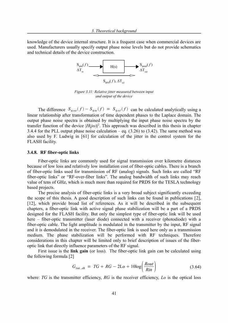
3. Theoretical background
knowledge of the device internal structure. It is a frequent case when commercial devices are used. Manufacturers usually specify output phase noise levels but do not provide schematics and technical details of the device construction.
Figure 3.11: Relative jitter measured between input and output of the device
The difference Sout f − S in f = Srel f can be calculated analytically using a linear relationship after transformation of time dependent phases to the Laplace domain. The output phase noise spectra is obtained by multiplying the input phase noise spectra by the transfer function of the device |H(jω)|2. This approach was described in this thesis in chapter 3.4.4 for the PLL output phase noise calculation – eq. (3.26) to (3.42). The same method was also used by F. Ludwig in [61] for calculation of the jitter in the control system for the FLASH facility.
3.4.8. RF fiber-optic links
Fiber-optic links are commonly used for signal transmission over kilometre distances because of low loss and relatively low installation cost of fiber-optic cables. There is a branch of fiber-optic links used for transmission of RF (analog) signals. Such links are called “RF fiber-optic links” or “RF-over-fiber links”. The analog bandwidth of such links may reach value of tens of GHz, which is much more than required for PRDS for the TESLA technology based projects.
The precise analysis of fiber-optic links is a very broad subject significantly exceeding the scope of this thesis. A good description of such links can be found in publications [2], [12], which provide broad list of references. As it will be described in the subsequent chapters, a fiber-optic link with active signal phase stabilization will be a part of a PRDS designed for the FLASH facility. But only the simplest type of fiber-optic link will be used here – fiber-optic transmitter (laser diode) connected with a receiver (photodiode) with a fiber-optic cable. The light amplitude is modulated in the transmitter by the input, RF signal and it is demodulated in the receiver. The fiber-optic link is used here only as a transmission medium. The phase stabilization will be performed with RF techniques. Therefore considerations in this chapter will be limited only to brief description of issues of the fiber-optic link that directly influence parameters of the RF signal.
First issue is the link gain (or loss). The fiber-optic link gain can be calculated using the following formula [2]
(3.64)
where: TG is the transmitter efficiency, RG is the receiver efficiency, Lo is the optical loss
41
Glink , dB = TG RG − 2Lo 10log RoutRin
H(s)Sφin( f )ΔT
in
Sφout( f )
ΔTout
Sφrel( f ), ΔTrel

3. Theoretical background
between transmitter and receiver and Rin and Rout are respectively the input and output impedances of the link.
In the PRDS being subject of this thesis considerations were limited to the choice of transmitter and receivers with sufficient efficiency and standard input and output impedances (50Ω). But there is an interesting phenomenon, that the fiber loss is doubled (in logarithmic scale) in RF fiber-optic links (the 2Lo term in eq. (3.64)). This occurs as a result of converting optical power to RF energy in the photodiode [2]. There the RF current is directly proportional to the optical power, but the RF power equals the square of the RF current. In logarithmic scale, this squared term turns into a factor of 2 in front of the optical loss. As it will be shown in chapter 5.3, the total optical loss in designed FO became very important because besides optical fiber there were other optical components used, which introduced significant loss values.
Another important issue of simple fiber-optic links that should be mentioned here is a very high value of the link noise figure, reaching tens of decibels (20 dB to 70 dB) [2], [12]. Because of such high noise figures, the phase noise performance (short term stability) of distributed signals is significantly limited. Fortunately the fiber-optic system described in chapter 5.3 can successfully suppress long term signal phase drifts. The short term stability of signal obtained at the end of that link can be improved with the use of a PLL by synchronizing with this signal a low-noise VCO.
42

4. FLASH distribution system design requirements and conceptual analysis
4. FLASH distribution system design requirements and conceptual analysis
Chapter 4.1 covers the description of design requirements for the FLASH PRDS with a short explanation of the origin of these requirements. Then, in chapter 4.2, system level considerations on PRDS architectures that could fulfil the synchronization requirements are performed, showing advantages and disadvantages of different solutions. As a result of these considerations the FLASH PRDS architecture is proposed (chapter 4.3). Results of considerations described in this chapter will be used in chapter 5 as a starting point for the detailed design of the FLASH PRDS.
4.1. Design requirements
Specification of the synchronization accuracy required for the TESLA technology based projects is a very difficult scientific problem. The main difficulties come from the following issues: system size (accelerator facility spreads over a large area), system complexity (multiple RF stations with complicated control systems incorporating analogue and digital subsystems), translations of instability measures between different physical domains (the phase jitter of RF reference signal affects the spatial energy spread of the electron bunches “travelling” inside of the accelerating structure, which in turn may affect required parameters of the laser light being the output of the FEL facility). There is a number of different requirements for the synchronization accuracy appearing in the literature, depending on the particular project based on the TESLA technology – see chapter 1.2 for the time chronology of these projects. As it was mentioned in chapter 1.2, this thesis is devoted to the analysis of performance of the FLASH PRDS but this PRDS was intended to be the development base for the PRDS for future projects like XFEL/ILC. Therefore possibilities of increasing the PRDS size are frequently considered in the remainder of this thesis. A short overview of the FLASH facility is given in the following text, before providing the design requirements for the FLASH PRDS.
4.1.1. FLASH system overview and the need for device synchronization
The principle of the FLASH operation is explained basing on the system layout shown in fig. 4.1. Electron bunches are injected into the accelerating structure from the laser driven RF gun [11], [46] system. The RF gun is a complicated RF device which requires a precise synchronization with the entire accelerator. The energy of electron bunches injected form the RF GUN is increased inside of the accelerating modules (in official publications these modules are called ACCn, where n is the module number). Chain of bunch compressors assure proper spatial energy spread of the bunches entering the undulator19 sections in which the free-electron lasing effect is obtained.
19 Undulator is a chain of alternately arranged magnets which causes periodical bending of the trajectory of electron bunches. Electrons are forced to move on a zigzag like path. During change of direction of electrons movement, a coherent light is emitted. This is called free electron lasing effect.
43

4. FLASH distribution system design requirements and conceptual analysis
Figure 4.1: Layout of the FLASH facility.
Each ACC module consists of eight superconducting cavities operating at the frequency of 1.3GHz. At each ACC there is a control system regulating the parameters of accelerating field (amplitude and phase). The basic block diagram of the RF control system is shown in fig. 4.2. The RF system can be split into two parts – high power part and the LLRF20 control system. The detailed description of operation principles of the LLRF control system (see [87] or [89]) exceeds the scope of this thesis. Important here is that the parameters of the accelerating field inside of the superconducting cavities are controlled by the RF system synchronized with the stable signal source called Master Oscillator (MO). In fig. 4.2 there is shown a number of devices (vector modulators, down and up-converters (LO signals), timing system, ADCs (requiring clock signals) and DACs) operating at different frequencies that require synchronization with the MO. In the FLASH facility there are seven accelerating modules – see fig. 4.1. It means that seven copies of the LLRF control system shown in fig. 4.2 must be synchronized with the MO. Besides LLRF control systems there is a number of other devices (not shown in fig. 4.1 and fig. 4.2) within of the accelerator facility that require precise synchronization like lasers, beam monitoring and diagnostic systems.
* Influence of the distributed signal jitter on the electron bunch parametersThe design requirements for the PRDS are derived mainly from the requirements on the
timing and spatial parameters of the electron beam. In the time of writing this thesis, the expected duration of electron bunches (which can be treated as very short current pulses) leaving the ACC7 should be within the range of 60fs. The duration and arrival time jitter of electron bunches depend on the parameters of the accelerating field controlled by the LLRF control system. The requirements on the stability of the accelerating field have been changing with the evolution of the TTF/FLASH system. One of the last considerations on this topic were published by Schlarb et al. [88]. It was calculated that the amplitude and phase of the accelerating field should be stabilized respectively to 5·10-5 and 0.01o within accelerating pulse21 duration (millisecond range). The last requirement of 0.01o for the signal frequency of 1.3 GHz corresponds to ca. 20 fs in the time domain. In internal DESY talks and documents, the last requirement on phase stabilization accuracy was sharpened to 10 fs for the reason of having a safety margin.
As the LLRF control system is synchronized with the PRDS, the field control accuracy depends on the jitter of the synchronization signals provided by the PRDS.
20 Abbreviation from Low Level Radio Frequency: feedback loop parts located between the downconverter and the vector modulator in fig. 4.2.
21 The TESLA technology requires pulsed operation of the accelerating structure.
44
experimentalarea
bypass1000 MeV 400 MeV
bunchcompressor
150 MeVbunch
compressor
4 MeV
undulators seeding collimator #7 #6 #5 #4 #3 #2 ACC #1 RF gun

4. FLASH distribution system design requirements and conceptual analysis
Figure 4.2: TTF RF control system scheme for one ACC module. Figure source [87]
The precise calculation of the contribution of the reference signal jitter to the beam jitter is a very difficult task because of the complexity of the system and feedback algorithms digitally implemented in the system controller. Parameters of the feedback controller are
45

4. FLASH distribution system design requirements and conceptual analysis
changed frequently by system operators, depending on the actual state of the accelerator and required electron beam parameters. Therefore there are only few publications on this topic known to the author of this thesis. Important considerations on the jitter in the FLASH LLRF system were published by Frank Ludwig et al. in [61]. The influence of LLRF control system components and the MO signal on the cavity (electron beam) jitter is modelled and the jitter budget is calculated for given system parameters and fixed phase noise spectra of the MO signal. Phase noise model is derived basing on a simplified schematic diagram of the LLRF system shown in fig. 4.3.
Transfer functions are derived for all important sources of phase noise in the LLRF system. Amongst the most important results there is a formula describing the residual phase noise S , RES f between the superconducting cavity output and the Master Oscillator
(4.1)
where g0 is the controller gain G(s) assumed to be constant, 12'
= g012 is the control loop bandwidth, 12 is the superconducting cavity cut-off frequency. Other parameters are the phase noise spectral densities of the MO, Down-Converter (DWC) and Modulator (MOD), as shown in fig. 4.3.
Figure 4.3: Simplified schematic diagram of a single cavity LLRF system at FLASH. Figure source [61]
Figure 4.4: Measured Phase noise of relevant LLRF subsystems. Figure source [61]
Equation (4.1) shows that the phase noise of the MO signal provided by the PRDS is high-pass filtered and the DWC and MOD phase noise are low pass filtered by the LLRF control system feedback loop. Therefore the MO jitter is significantly suppressed by the LLRF control system.
Jitter calculation in [61] is performed for typical LLRF control system parameters. Real phase noise spectrum measured in the so called “old” MO operating in the FLASH facility in 2006 was used. The phase noise spectra of the MO and other components used for jitter calculation are shown in fig. 4.4. The MO signal phase jitter equals 85 fs within a bandwidth
46
S , RES f = ∣ ss12
' ∣2
S , MO f ∣ 12'
s12' ∣
2
[S , DWC f 1g0
2 S , MOD f ]
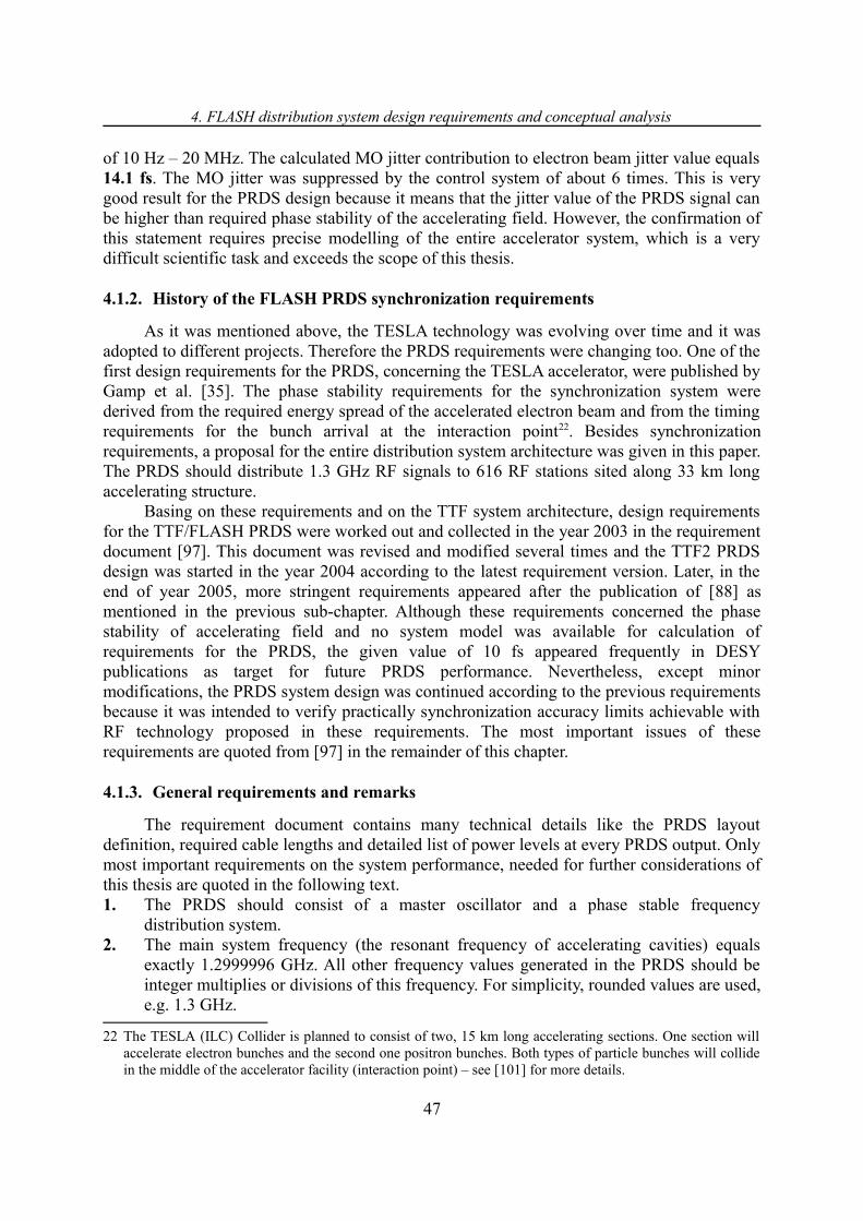
4. FLASH distribution system design requirements and conceptual analysis
of 10 Hz – 20 MHz. The calculated MO jitter contribution to electron beam jitter value equals 14.1 fs. The MO jitter was suppressed by the control system of about 6 times. This is very good result for the PRDS design because it means that the jitter value of the PRDS signal can be higher than required phase stability of the accelerating field. However, the confirmation of this statement requires precise modelling of the entire accelerator system, which is a very difficult scientific task and exceeds the scope of this thesis.
4.1.2. History of the FLASH PRDS synchronization requirements
As it was mentioned above, the TESLA technology was evolving over time and it was adopted to different projects. Therefore the PRDS requirements were changing too. One of the first design requirements for the PRDS, concerning the TESLA accelerator, were published by Gamp et al. [35]. The phase stability requirements for the synchronization system were derived from the required energy spread of the accelerated electron beam and from the timing requirements for the bunch arrival at the interaction point22. Besides synchronization requirements, a proposal for the entire distribution system architecture was given in this paper. The PRDS should distribute 1.3 GHz RF signals to 616 RF stations sited along 33 km long accelerating structure.
Basing on these requirements and on the TTF system architecture, design requirements for the TTF/FLASH PRDS were worked out and collected in the year 2003 in the requirement document [97]. This document was revised and modified several times and the TTF2 PRDS design was started in the year 2004 according to the latest requirement version. Later, in the end of year 2005, more stringent requirements appeared after the publication of [88] as mentioned in the previous sub-chapter. Although these requirements concerned the phase stability of accelerating field and no system model was available for calculation of requirements for the PRDS, the given value of 10 fs appeared frequently in DESY publications as target for future PRDS performance. Nevertheless, except minor modifications, the PRDS system design was continued according to the previous requirements because it was intended to verify practically synchronization accuracy limits achievable with RF technology proposed in these requirements. The most important issues of these requirements are quoted from [97] in the remainder of this chapter.
4.1.3. General requirements and remarks
The requirement document contains many technical details like the PRDS layout definition, required cable lengths and detailed list of power levels at every PRDS output. Only most important requirements on the system performance, needed for further considerations of this thesis are quoted in the following text.1. The PRDS should consist of a master oscillator and a phase stable frequency
distribution system.2. The main system frequency (the resonant frequency of accelerating cavities) equals
exactly 1.2999996 GHz. All other frequency values generated in the PRDS should be integer multiplies or divisions of this frequency. For simplicity, rounded values are used, e.g. 1.3 GHz.
22 The TESLA (ILC) Collider is planned to consist of two, 15 km long accelerating sections. One section will accelerate electron bunches and the second one positron bunches. Both types of particle bunches will collide in the middle of the accelerator facility (interaction point) – see [101] for more details.
47

4. FLASH distribution system design requirements and conceptual analysis
3. All frequencies should be phase locked to the reference oscillator. The reference frequency should be equal 9 MHz (1.3 GHz / 144). The reasons for choice of this frequency will be explained in chapter 4.3.
4. Most of the PRDS frequencies should be generated in a device located near the reference frequency generator (9 MHz). In the strict meaning, there is one reference signal generator called Master Oscillator. Yet, for convenience, the entire network of frequency generation circuits will also be called Master Oscillator or Master Oscillator System (MO System).
Table 4.1: Frequency values required for the FLASH PRDS
Output Frequency[MHz]
Multiple of the Reference
Exact Frequency Value [MHz]
Destination
50 Hz /180555.5 *Accelerator timing system. Used for comparison with zero crossings of
the mains power supply. TTL output.
1 /9 1.00309 Timing system, TTL output
9 *1 9.027775Auxiliary frequencies generation (sine) and timing system (TTL)
13.5 *3/2 13.5416625 Laser “new”
27 *3 27.08333 Laser “old”
81 *9 81.24998 Distribution frequency
108 *12 108.3333 Streak Camera
1300 *144 1299.9996 RF system reference frequency
1517 *168 1516.6662Beam position monitors reference
frequency, LINAC Racks
2856 ± 5 kHz tbd 2856.001105 LOLA – transverse deflecting cavity
for bunch monitors
4.1.4. Required frequency values
There is a number of signal frequencies that should be generated and distributed by the PRDS. Frequency values and destination components are collected in the 4.1.
The names and function of accelerator subsystems appearing in the last column of the table (Destination) will not be explained, as it is not important for further considerations in this thesis. These names are helpful in localizing those components in the FLASH facility and for estimation of the signal distribution distance. Layout of the FLASH system will be shown later, in fig. 4.7.
4.1.5. Phase jitter requirements
As it was mentioned above, the requirements on synchronization accuracy evolved with time and they were significantly sharpened in the end of 2005. The system development was progressing according to older requirements in the time when new specification appeared.
48

4. FLASH distribution system design requirements and conceptual analysis
Therefore both specifications are given in the table 4.2 and the results of considerations described in this thesis are frequently compared with both specifications.
Table 4.2: Required synchronization accuracy in terms of the phase jitter
Duration
Short term stability [fs] Long term stability [fs]
1 ms 100 ms 1 s 10 s Minute Hour Day
Integration Bandwidth#
1kHz - 1MHz
10 Hz - 1MHz
1Hz - 1MHz n/a n/a n/a n/a
Requirement before 2006
100 300 1000 1000 1000 2000 10000
Requirements from 2006 on
10 10 10 20 300 750 no data
# Phase noise integration bandwidth is specified only for short term stability because the equipment available in DESY in the time of writing this thesis, can measure phase noise only in the range of 1 Hz – 10 MHz. The long term stability is measured (where possible) directly by a phase detector.
Given set of requirements on the phase jitter must be fulfilled at every PRDS output (absolute instability – see chapter 3.2.3) and between each pair of outputs (relative instability). The second case requirements should in general be easier to fulfil because all output signals are synchronized with one reference oscillator, therefore signal phase at each output “follows” the MO phase. Naturally there is an additional phase jitter caused by the distribution system. This jitter will be observed as relative instability between outputs and the MO. Nevertheless, requirements for the relative instability should be different (most probably lighter) than requirements for the absolute instability. Therefore most probably the requirement document should be modified. It also should be expected that the electron beam jitter is affected more by the relative instabilities between accelerator subsystems synchronized with signals provided by the PRDS.
These statements can be confirmed only by detailed analysis of the entire accelerator system which is a very difficult scientific task being beyond the scope of this thesis. To the current knowledge of author of this thesis, there are no publications covering this subject.
4.1.6. Required phase noise levels
The requirement document contains specifications on the phase noise spectrum ℒ f for the signal frequencies that are of the highest importance for the accelerator system – 9 MHz and 1.3 GHz. The 1.3 GHz signal source should be phase locked to the 9 MHz reference. Other system frequencies listed in the table 4.1 should be created by division or multiplication of one of the 9 MHz or 1.3 GHz signals and the phase noise levels can be calculated basing on the given requirements. The details of phase noise specifications are given in table 4.3, table 4.4, fig. 4.5 and fig. 4.6.
49

4. FLASH distribution system design requirements and conceptual analysis
Table 4.3: Phase noise levels required for the 9 MHz reference
Frequency offset from carrier [Hz]
Phase noise ℒ f [dBc/Hz]
1 < -11510 < -140100 < -1501 k < -155
10 k < -162100 k < -1641 M < - 164
1 10 1E+2 1E+3 1E+4 1E+5 1E+6
-170
-160
-150
-140
-130
-120
-110
Offset from carrier frequency [Hz]
Pha
se n
oise
[dB
c/H
z]
Figure 4.5: Phase noise levels required for the 9 MHz reference
Table 4.4: Phase noise levels required for the 1.3 GHz oscillator
Frequency offset from carrier [Hz]
Phase noise ℒ f Locked condition
[dBc/Hz]
Phase noise ℒ f Free running
[dBc/Hz]1 NA NA
10 < -80 < -60100 < -105 < -801 k < -125 < -10510 k < -145 < - 135
100 k < -155 < -1551 M < - 150 (-155) < - 150 (-155)
The phase noise levels given above in the tables and figures were specified basing on the performance of commercially available, high quality signal sources operating at frequencies comparable to the required ones. The phase jitter values corresponding to these phase noise spectra were calculated with the use of formula (3.17) and published in [59]. Results of similar calculations23 of the phase jitter for both signal frequencies are collected in the table
23 In [59] the area under the phase noise curve was calculated by fitting rectangles: Area=(f2-f1)L1,where f1,2 are
50
4. FLASH distribution system design requirements and conceptual analysis
4.5 and 4.6.
1 10 100 1E+3 1E+4 1E+5 1E+6
-165
-155
-145
-135
-125
-115
-105
-95
-85
-75
-65
Offset from carrier frequency [Hz]
Pha
se n
oise
[dB
c/H
z]
Figure 4.6: Phase noise levels required for the 1.3 GHz oscillator locked to the reference
Table 4.5: Phase jitter values calculated for the 9 MHz signal
Offset frequency range [Hz]
jitter [µradrms] Δt [fs]
1 - 10 7.56 134
10 - 100 1.41 24.9
100 - 1k 1.54 27.2
1k - 10k 2.61 46.2
10k - 100k 4.30 76.1
100k - 1M 1.20 212
1 – 1M 29.4 520
10 - 1M 21.8 386
1k - 1M 18.9 334
The phase noise level given in the requirement document for 1.3 GHz signal at offset frequency of 1 MHz (last row in table 4.4) rises of 5 dB when comparing with the phase noise level at offset frequency of 100 kHz. Typically phase noise level in this offset frequency range remains constant or decreases. Therefore the phase noise value at 1 MHz offset frequency was
the integration frequencies and L1 is the phase noise level corresponding to f1. A bit more accurate approximation can be obtained by fitting rectangle and triangle and summing their areas: Area'=(f2-f1)[L2+0.5(L1-L2)]. The difference of results obtained by using these approximations is relatively small and decreases with decreasing difference f2 – f1. For more than 10 frequencies per decade the error of jitter calculation result is negligible. For one frequency per decade, as given in the tables above, the error equals about 30%. Therefore the second method was applied in this thesis when calculating jitter from phase noise values given as one value per frequency decade.
51

4. FLASH distribution system design requirements and conceptual analysis
corrected to -155 dBc/Hz – (value in brackets in table 4.4) and these values will be used in the remainder of this thesis. Such modification has only little influence on the value of phase jitter – see values in brackets in table 4.6. The jitter value changed only of 1.8 fs (from 212.0 fs to 210.2 fs) in offset frequency range 10 Hz – 1 MHz.
Table 4.6: Integrated jitter values for the 1.3 GHz signal
Offset frequency range [Hz]
jitter [µradrms] Δt [fs]
1 - 10 - -
10 - 100 1340 165
100 - 1k 240 29.4
1k - 10k 75.8 9.3
10k - 100k 25.0 3.0
100k - 1M 48.7 (33.7) 5.9 (4.1)
10 – 1M 1730.0 (1720.0) 212.0 (210.2)
1k - 1M 150.0 (135.0) 18.3 (16.5)
4.1.7. FLASH system layout and distribution distances
Schematic drawing of the FLASH facility is shown in fig. 4.7. Positions of most important system components requiring synchronization are shown. Approximate distances (in meters) of system components from the right upper corner of the facility are shown in the figure. The accelerating structure with RF Gun and ACC modules is located inside the 260 meter long tunnel which passes into the experimental hall.
Most of the LLRF control system components with high power klystrons are located in the areas called Hall 3 and its extension. There are also other devices requiring synchronization, whose functions are not important from the point of view of this thesis. Approximate paths of the phase reference signal distribution between the MO and accelerator devices are also shown in fig. 4.7.
Detailed information about the signal frequencies distributed to each of shown devices and power levels can be found in [97]. It is important to mention here is that the 1.3 GHz signal is distributed to each location, except devices called LOLA, LINAC9 and LINAC15. The required signal power level at most of the PRDS outputs is 10 dBm.
52

4. FLASH distribution system design requirements and conceptual analysis
10m
TT
F C
ON
TR
OL
RO
OM
LLR
F
contr
ol
rack
s
L O L A
165m
85m
19m
140m
260m
118m
105m
93m
56m
10m
0m44
m
wav
egu
ide
20m
New
LLR
F
contr
ol
rack
s
18m
Kly
stro
n 3
RF
GU
NA
CC
1A
CC
2A
CC
3A
CC
4AC
CE
LE
RA
TO
R T
UN
NE
L
HA
LL 3
exte
nsio
n
HA
LL 3
EO
S
EXPERIMENTAL HALL
Rac
kLI
NA
C 1
5LI
NA
C 9
Rac
k
LAS
ER
AC
C5
AC
C7
/ AC
C6
LOLA
95m
40m
56m
Kly
stro
n 2
Kly
stro
n 1
Kly
stro
n 5
Kly
stro
n 4
MA
ST
ER
OS
CIL
LA
TO
R
Figure 4.7: FLASH facility layout. Not to scale. Most important RF devices requiring synchronization with the Master Oscillator are shown.
53

4. FLASH distribution system design requirements and conceptual analysis
4.2. Possible PRDS architectures
The word architecture in this thesis means the overall system design, including such is-sues as layout and type of distribution lines, frequency generation scheme, signal power man-agement and stabilization of distributed signal phase. The architecture should be distinguished from topology, which was used to describe only the layout of distribution lines – chapter 2.1.
The choice of optimal PRDS architecture is one of the most difficult and important tasks that must be performed during the system design. It is important because the choice of the system architecture influences the entire design process and system performance. In the remainder of this chapter a general approach for defining PRDS architecture is proposed and the most important issues influencing the system architecture are described.
4.2.1. General design method
Figure 4.8: Most important issues influencing the choice of the final PRDS architecture
The main difficulty in defining the PRDS architecture is a large amount of interdependent issues that contribute to the overall system performance. Many important technical issues are described in the text below but let us first consider the high level factors that affect the system architecture. These issues and their interdependencies are shown in fig. 4.8. This illustration shows that the final and optimal decision on the PRDS architecture can be taken only after performing detailed study of presented factors. It is very difficult to provide a simple algorithm of finding the architecture. Nevertheless, a proposal of such algorithm is shown in fig. 4.9 and this algorithm is followed in the remainder of this thesis.
4.2.2. Considerations on available technology, important issues and design choices
Most important issues that must be taken into account in the first phase of a PRDS design are described in this sub-chapter. Presented considerations do not exactly reflect the general algorithm given in the previous chapter. It was intended here to provide a broad view on the complexity of the problem and show a way of choosing proper solutions. This sub-chapter should be treated as an overview (brainstorm form) of most important problems
54
Required performance,synchronization accuracy
System developmentinstallation and
maintenance cost
System ComplexityAvailable Technology
Reliability
Other design requirementsphysical layout, distance,number of frequencies...
FINAL SYSTEMARCHITECTURE

4. FLASH distribution system design requirements and conceptual analysis
related to the PRDS design. No choice concerning given issue of the PRDS is made here. Most of these problems are addressed in detail in further parts of this thesis. Considerations performed in this sub-chapter are the basis for the system architecture proposal described in chapter 4.3. Additional attention is given here to the possibilities of building a PRDS for larger accelerator facility like XFEL or ILC. Significant part of these considerations was published by the author in [8-A].
Figure 4.9: Proposed algorithm of PRDS architecture choice
* Distribution system topologyThere are two main types of distribution system topology, as described in chapter 2.1:
star (number of point-to-point links between MO and destination devices) and line with pick-up points (single distribution line). The choice of topology depends on the accelerator type. Star topology could be most useful for circle accelerator type with small number of target devices requiring synchronization. Several point-to-point links from the MO located in the centre of the circle to devices located at the accelerator circle may be the best choice.The line with pick-up points fits best to the needs of the linear accelerator facilities where the synchronizing signals should be distributed along the straight accelerator. The main advantage of line with pick-ups is that the smallest total length of distribution media (cable) can be used, which may entail installation simplicity and low cost. But in the case when a distribution of high frequency signals is needed, the parameters of pick-up points became critical for the quality of distributed signals. The use of high performance RF connectors and directional couplers may rise the system installation cost to levels higher than installation of equivalent number of point-to-point links with no directional couplers.
55
May implylow complexityand cost
NO
YES
YES
NO
Analyze requirements vs. available technology
Choose simplest architecture that may fulfill the design
requirements
System level considerations on technical issues e.g. choice of distributed
frequency, subsystem parameters
Estimate performance
Can requirements be met with proposed architecture
Choose other architecture
Acceptable cost
Detailed design of subsystems

4. FLASH distribution system design requirements and conceptual analysis
The reliability of the system is the next important factor. It is obvious that a simple point-to-point link is supposed to be much more reliable than a link of the same length with many pick-ups. One simple pick-up point contains a directional coupler or a power splitter and several (minimum three) connectors.
Another issue, especially concerning coaxial cable distribution lines, is the RF loss consisting of cable attenuation, losses in the connectors and a coupling ratio of the directional couplers. Naturally, the power level of the signal will decrease along the line. Usually equal power levels are required for the devices synchronized with the PRDS. Therefore a set of attenuators and/or amplifiers must be used along the distribution line to assure equal signal power levels. Such solution may significantly influence the stability of the signal and also further reduce the system reliability.
The number of issues enumerated above indicates the scale of difficulties met in the very first stage of system design and that detailed calculation of signal parameters and system cost must be performed before choosing the system topology, which at first glance seems to be a trivial problem. More details on this subject are given in chapter 5.2.1. As it will be shown, the attenuation of coaxial cables practically limits the distribution distances to hundreds of meters, which is sufficient for the FLASH facility. For longer systems (like XFEL) it may be reasonable to split distribution line into short segments (e.g. 300 meter long) and find a low attenuation method of providing stable signals to the beginning of each cable segment, e.g. by fiber-optic links.
* Distribution media typeThere are three possible choices: air (radio synchronization), coaxial cable (or
waveguide) and optical fiber. The simplest and therefore most reliable solution seems to be the use of coaxial cable. But, as mentioned above, the signal attenuation limits the range of practical use of coaxial cables. Also the cost of cable and its installation may be significant.
The importance of optical techniques has been growing rapidly during recent years. The signal transmission through the optical fiber offers broad bandwidth for transmitted signals, low media cost, high reliability and possibility of achieving large distribution distances be-cause of low optical losses in the fiber. But, as it was shown in chapter 3.4.8, the RF loss in simple optical link is much higher than the optical loss in the fiber. There is large conversion loss in optical receivers and transmitters and the noise figure values of optical links are high. These issues significantly degrade the quality of transmitted low noise RF signals and the use of the state-of-the-art optical systems may be much more expensive than installation of coaxial cable distribution system. It must also be taken into account that at each output of the optical link there must be an optical receiver converting optical signal to RF signal, which may be expensive and may influence signal performance and system reliability.
Again, as in the case of system architecture, the optimal choice of distribution media is a very difficult task and all above-mentioned factors must be carefully considered before tak-ing a proper decision. It will be shown in the further text of this thesis that for long distance PRDS (like the one for XFEL or ILC) it may be reasonable to use a combination of short coax cable sections supplied with long fiber-optic links.
Interesting alternative for cable signal distribution is the radio synchronization. The main advantages are lack of cable installation (low cost) and high immunity of air parameters to temperature changes – the long term phase stability is almost not affected. But the accelerator is equipped with high energy RF systems generating very high level of
56

4. FLASH distribution system design requirements and conceptual analysis
Electromagnetic Interference (EMI). This may drastically degrade the quality of distributed signal. Because of the EMI and additional signal stability degradation in RF transmitters and receivers the level of synchronization accuracy required for TESLA technology based systems is difficult to obtain by the air distribution.
* Passive distribution or active phase stabilization?The long term stability of distributed signal may be significantly affected by aging of
the distribution media and environmental factors, especially temperature changes. The longer the distribution distance and the higher the signal frequency, the bigger are the expected long term phase drifts (equations (3.55), (3.58) and (3.61)). As it is calculated in chapters 5.2 and 5.3 the long term stability requirement is violated for 1.3 GHz signal, in typical accelerator environment, for distribution distances longer than several tens of meters. Therefore for such distances the signal phase must be stabilized either by temperature stabilization of the distribution media or by active phase regulation by a feedback loop.
The main advantage of the temperature stabilization is that there are no additional components required in the signal path which in connection with stable temperature may assure very high reliability of the system. But the requirements for accuracy of temperature stabilization sharpens with the increasing link length. For distances longer than several hundred meters the required accuracy of temperature stabilization may be very difficult or even impossible to achieve and for sure impractical and very expensive. Therefore for long distribution distances the active signal phase regulation wins the competition with temperature regulation. The examples of systems with active phase stabilization incorporating both coax cable and optical techniques are shown in chapters 2.4 and 2.5. Detailed considerations on active system based on optical fiber are described in chapter 5.3. The main disadvantages of an active system are its complexity and high development costs (but the cost may be lower than installation of temperature stabilization). The development of such system is difficult and lengthy process. The reliability of active system is for sure much lower than that of passive, temperature stabilized link because usually such system incorporates large number of devices.
* Choice of MO type, frequency and specification of phase noiseProper selection of the MO type and its frequency value is one of the key decisions that
must be taken by the PRDS designer. The available technology must be analysed. For sure, at the current stage of technology, the atomic frequency standards offer best available signal stabilities. But such standards are expensive and their use is impractical for the TESLA technology PRDS because they offer “standard” frequency values e.g. 10 MHz. The frequency values required in the TESLA systems (multiples of 9.027775 MHz, see table 4.1) can not be obtained by simple division and/or multiplication (by integer number) of the standard frequency. More complicated frequency synthesis schemes may cause degradation of the signal stability to levels achievable from cheaper signal sources.
The standard frequency can also be obtained from widely available navigation systems. Global Positioning System (GPS) [44] is an example. There is a possibility of extracting 10 MHz atomic standard signal from the GPS signals [22], [58], [57]. Unfortunately, there is a high phase noise level present in such signal and the short term stability of the signal may be insufficient for the use in the TESLA systems. Nevertheless the GPS signal has excellent long term stability and it may be used for synchronization of other signal sources (e.g. crystal oscillators). But, additionally to the problems with high noise and EMI present in the radio
57

4. FLASH distribution system design requirements and conceptual analysis
transmission, one also has to consider high probability of degradation or total loss of GPS signal in the time of difficult atmospheric conditions like heavy rain, snowfalls and thunder storms – normal issues of receiving satellite signal when thick clouds cover the satellite transmitter.
Besides atomic frequency standards there are also very interesting optical sources of stable RF signals. Many publication appeared recently on the optical frequency standards, where special type of laser (sometimes called femtosecond laser) is suited to generate extremely stable RF signals in GHz range, e.g. [18], [30], [47]. Very interesting research in this field is conducted by DESY-MIT cooperation that works on the development of fiber laser for the accelerator synchronization purposes [99]. These optical techniques offer possibilities of obtaining much better signal stabilities than current RF signal generation techniques and it seems that optical standards will play significant and continuously growing role in future synchronization systems. Nevertheless, even though first successful experiments were conducted, in the moment of writing this thesis, these techniques are still in development stage and still a lot of research must be performed to take all advantages of these techniques. Currently, optical generators are expensive, complex and not very reliable devices. Therefore design of the PRDS using mature RF techniques is still justified and as it will be shown later, the temperature stabilized crystal oscillators offer sufficient performance for considered PRDS.
The selection of the value of the MO frequency is another difficult task. It requires careful analysis of available signal sources parameters. The signal stability degradation during frequency multiplication and/or division must be taken into account. As it was shown in chapter 3.4.2, the higher the multiplication factor (N), the higher the output signal phase noise. Therefore, in the cases when the signal frequency required by the synchronized device is higher than the MO frequency, it is advisable to select MO frequency value as close as pos-sible to the device frequency, so that the value of N is minimised. But, the analysis of avail-able devices (example shown in chapter 5.1), shows that the higher the frequency value, the worse the stability (especially long term) of the signal source. Therefore the MO frequency should be as low as possible. But this requirement is in contradiction with the previous one. Therefore the choice of the MO frequency must be a compromise between phase noise de-gradation in frequency multipliers and good long term stability of low frequency sources.
The choice of MO frequency directly influences the frequency generation scheme of the PRDS (described in the remainder of this chapter) and it also affects the distribution system architecture. For example, the RF signal loss (described above) increases with frequency in coax cables. So the lower the frequency generated at MO, the lower the RF loss and in turn the longer achievable distribution distances.
* Frequency generation schemeThis topic is strongly related to the choice of MO frequency and its phase noise level
specification that was addressed above. It can be especially important if it was decided that the final frequency value(s) (at the PRDS output) is different (higher) than the MO frequency and it will be generated in several stages by successive frequency multiplication. Several choices appear after such decision:
• generation of all frequencies at the MO and their distribution to the destinations,• distribution of the MO signal (one) frequency to destinations and local multiplication
to obtain the final frequency,
58

4. FLASH distribution system design requirements and conceptual analysis
• distribution of a signal with a frequency value different than the MO frequency and the final frequency.
The best explanation for this issue seems to be a practical example shown below.Let us assume that the MO frequency equals 9 MHz, and the final frequency value
equals 1300 MHz. Three possible frequency generation schemes are shown in fig. 4.10.
Figure 4.10: Three frequency generation schemes: a) the final freq. generated in the MO System, b) the final frequency generated locally at destinations from MO frequency distributed, c) Frequency value between the
MO and final frequency distributed, and the final frequency generated locally at destinations
In the case a) the final frequency is generated locally in the MO System and distributed to the destinations. The main advantage of this scheme is the simplicity – only one frequency multiplier (x144). Another advantage is that is possible to monitor the performance of the frequency multiplier, e.g. to measure long term drifts at the multiplier output against the MO signal. If the coax cable is used for distribution, the disadvantage of this frequency generation scheme is that the attenuation of the cable at 1.3 GHz is very large (may reach several tens of decibels per 1 km, see chapter 5.2) and it reduces the distribution distance. To assure proper power levels for entire long links, one has to use low attenuation (large diameter, high cost) coaxial cable or high power amplifier after the x144 multiplier or lower power amplifiers at each location (increase system complexity and decrease reliability). High cable attenuation causes fast power level decrease along the cable and it requires additional effort to obtain equal power levels at each destination. Therefore the simplicity of the frequency generation system does not give a warranty for the simplicity of the entire PRDS because of the number of power amplification devices. Power amplifiers can also degrade the signal stability by introducing additional noise and long term drifts.
Opposite situation is shown in the case b) in fig. 4.10, where the MO frequency of 9 MHz is distributed and multiplied locally at destination devices. Low cable loss at this frequency assures possibility of obtaining long distribution distances and slow power level decrease along the link and there may be no need for use of power amplifiers or their number and gain will be limited. But, the number of x144 frequency multipliers is equal to the number of PRDS outputs and this again entails higher system complexity and cost and lower reliability.
59
~M.O.
x9
9 MHz
1300 MHz outputs
x16 x16x16
81 MHz
~M.O.
x144
9 M Hz
1300 MHz outputs
~M.O.
x1449 MHz
1300 M Hz outputs
x144 x144
9 MHz1300 MHz
a) b)
c)

4. FLASH distribution system design requirements and conceptual analysis
The compromise between these both cases is shown in fig. 4.10 c), where the MO signal frequency is party multiplied at the MO (9 x 9 MHz = 81 MHz). The multiplication result can be called “distribution frequency”. It is distributed to destinations and there again multiplied (x16). One of the advantages of this solution is that the cable loss is still much lower at 81 MHz than at 1.3 GHz and power amplification can be avoided for relatively long distances. Also the parameters of frequency multipliers by 9 and by 16 can be much better than parameters of x144 frequency multiplier.
The general comparison of quality of all cases shown in fig. 4.10 can not be made here. The choice of optimal solution can be made only after detailed analysis of these cases taking into account parameters of available devices (freq. multipliers, cables, amplifiers), required signal stability, system layout, distribution distances and system cost. Therefore the analytical system modelling is rather impossible or at least very difficult and impractical. Development of optimal PRDS structure should rather be an iterative process with analysis of performance of proposed architecture, drawing conclusions and, if necessary, architecture improvements.
4.3. FLASH PRDS architecture proposal
As it was shown in fig. 4.9, the design process of the PRDS can be started from analysis of the design requirements taking into account available technology. Amongst most important requirements on the system performance are values of required phase jitter collected in table 4.2. The phase jitter values of the 1.3 GHz signal (main frequency in the FLASH system) should not exceed levels given in the table. The phase jitter values can be calculated from the phase noise power spectral density S f with the use of eq. (3.17) or from the SSB phase noise spectrum ℒ f after substituting eq. (3.18) to eq. (3.17).
The SSB phase noise ℒ f of the 1.3 GHz signal should be specified relying on the required phase jitter. Unfortunately, unambiguous calculation of the entire phase noise spectrum from a single value of phase jitter is impossible. Therefore the phase noise spectrum of the 1.3 GHz signal can be specified only in iterative manner by giving reasonable (possible to obtain by the available technology) phase noise levels in given Fourier frequency range, calculating jitter from eq. (3.17), comparing with the requirements and, if necessary modifying the phase noise level. Example of such calculations verifying the correctness of specification from the document [97] is given below.
Let us assume that the initial phase noise spectrum of the 1.3 GHz signal is the same as given in the requirement document [97], given in table 4.4 and fig.4.6. It is also plotted in fig. 4.11, line A. The jitter values calculated with the use of eq. (3.17) for various frequency ranges are collected in row A of table 4.7.
The phase jitter, calculated in range [10 Hz, 1 MHz], equals 210.2 fs. For frequency range [1kHz, 1 MHz] the phase jitter equals 16.5 fs. The required jitter value (table 4.2) for these frequency ranges equals respectively 300 fs and 100 fs. It follows that the phase noise spectrum was specified with significant margin, especially when comparing with the result of jitter calculation in the second frequency range (required phase jitter: 100 fs, phase jitter calculated from specified ℒ f : 16.5 fs).
Phase noise spectrum more exactly fulfilling the design requirements on the phase jitter is given in fig. 4.11 as the case B. Such values of ℒ f can be achieved with relatively low cost generators.
60

4. FLASH distribution system design requirements and conceptual analysis
Figure 4.11: Phase noise levels for jitter calculation
Table 4.7: Jitter values for five phase noise spectra of the 1.3 GHz signal
Offset frequency range [Hz]
10 - 100 100 - 1k 1k - 10k 10k - 100k 100k - 1M 10 - 1M 1k - 1M
Jitter valueΔT [fs]
A 165.0 29.4 9.3 3.1 4.1 210.2 16.5
B 165.0 39.0 42.9 37.0 16.4 299.9 96.3
C 92.5 16.7 9.3 3.1 4.1 125.7 16.5
D 52.0 9.7 9.3 3.1 4.1 78.2 16.5
E 3.0 1.7 1.8 1.0 2.3 9.7 5.0
It can be noticed that the biggest contribution to the jitter value comes from the noise spectrum in range [10 Hz, 100 Hz] (210.2 fs). As an example, the phase jitter was calculated for two cases C and D, where the level of ℒ f in this frequency range was consecutively decreased by 5 dB, starting from the level given in the requirement document. The calculated phase jitter values are equal respectively 125.7 fs and 78.2 fs.
The phase noise spectrum that could fulfil the second case requirements (table 4.2, after 2006) of 10 fs phase jitter is given in the case E in table 4.7 and fig. 4.11. But to the knowledge of the author of this thesis, obtaining such levels of ℒ f (-115dBc @ 10 Hz offset from carrier frequency for 1.3 GHz RF frequency) is very difficult or even impossible with the use of current techniques of RF signal generation.
* Reference oscillator parametersThe entire PRDS should be synchronized with a signal from reference generator called
MO. Basic considerations on the choice of the MO frequency were described in the previous chapter. Different types of the frequency generation scheme were shown in fig. 4.10.
The first approach is to use the MO operating directly at frequency of 1.3 GHz and divide its frequency in order to obtain other (lower) frequencies given in table 4.1. But,
61
▲ - A▼ - B - C ■ - D ►- E
10 100 1k 10k 100k 1M
-160
-150
-140
-130
-120
-110
-100
-90
-80
Offset from carrier frequency [Hz]
Pha
se n
oise
[dB
c/H
z]

4. FLASH distribution system design requirements and conceptual analysis
currently available oscillators operating in this frequency range offer much higher phase noise levels at low offset frequencies (<10 kHz) than required levels shown in fig. 4.11. It means that the requirements on the phase stability (especially the long term) stability not be fulfilled by a free running oscillator operating at frequency of 1.3 GHz.
Performance analysis of currently available oscillators yields a conclusion that the long term stability and phase noise levels for low offset frequencies tend to improve when the oscillator output frequency decreases. Therefore the MO should be chosen to operate at frequency lower than 1.3 GHz. The 1.3 GHz signal can be obtained from MO signal either by multiplication of the MO frequency with the use of a frequency multiplier – addressed in chapter 3.4.2 or synchronization (by means of phase-lock, chapter 3.4.4) of a 1.3 GHz Voltage Controlled Oscillator with the MO.
The specification of parameters of the reference oscillator should be performed taking into account the phase noise level of the 1.3 GHz signal (as calculated above) and the long term phase stability required for the PRDS. The MO phase noise spectrum can be calculated using eq. (3.24) for the frequency multiplier and eq. (3.42) for the PLL frequency synthesizer. In general, with signal frequency multiplication phase noise level increases as N2 (N is the multiplication factor). But in the case of the PLL, the output signal phase noise spectra can be shaped within the loop bandwidth according to the PLL transfer function given by eq. (3.36). This can be an advantage in comparison with frequency multiplier other than a PLL because the phase noise levels obtained by good quality VCOs at high offset frequencies (>1 MHz) can be lower than the phase noise obtained by other frequency multipliers (for the same offset frequency range). Therefore the short term stability can be improved by the PLL.
The final decision on the MO frequency value can be taken after considering all issues mentioned above and analysing parameters of available frequency sources. Since exact frequency values required for the PRDS (table 4.1) are different from standard ones available in the market, the MO will have to be a custom product. This will imply higher cost of the MO, which must also be considered.
It was concluded that the best long term stability and close in (in the range of Fourier frequency [1 Hz, 100 Hz]) phase noise levels of the 1.3 GHz signal can be obtained by frequency multiplication of a signal from Oven Controlled Crystal Oscillator (OCXO) operating at frequency close to 10 MHz. The nearest frequency value that can be multiplied by integer number (N = 144) to obtain 1.3 GHz is 9.027775 MHz. This frequency value is also needed in the accelerator system (table 4.1). Therefore a part of the OCXO signal can be directly distributed without a need for additional circuits generating this frequency value. Therefore the system cost and complexity can be reduced.
The rough estimation of phase noise levels required for such MO can be made by subtracting 20logN from the phase noise levels required for the 1.3 GHz signal. The result is given in table 4.8. This method of estimation is valid for ideal frequency multiplier. Unfortunately, obtaining phase noise levels calculated for frequencies above 1 kHz would be very difficult or even impossible with the use of available frequency multipliers.
62

4. FLASH distribution system design requirements and conceptual analysis
Table 4.8: Phase noise levels required for 1.3 GHz and 9 MHz signals when ideal frequency multiplier is used for obtaining 1.3 GHz signal
Offset frequency [Hz] 10 100 1k 10k 100k 1M
ℒ f required for 1.3 GHz [dBc/Hz]
-80 -105 -125 -145 -155 -155
ℒ f calculated for 9 MHz [dBc/Hz]
-123 -148 -168 -188 -198 -198
The results gathered in table 4.8 confirm the statement that the best choice for obtaining the 1.3 GHz signal will be a PLL frequency synthesizer. Its advantage, as described in chapter 3.4.4, is that the reference oscillator phase noise is increased by 20logN within the PLL bandwidth. The engineering experience shows that in applications similar to described here, the PLL bandwidths rarely exceed several hundred Hz. Therefore the phase noise level for the 9 MHz oscillator can be estimated by subtraction of 43 dB from the 1.3 GHz phase noise only within the loop bandwidth. The 9 MHz signal phase noise level outside the PLL bandwidth is less important, unless this signal is used for other purpose than generation of the 1.3 GHz signal and there is also a requirement of low phase noise level for this purpose. The phase noise level values for 9 MHz MO, given in the requirement document (collected in table 4.3) are specified with significant margin, e.g. -140 dBc @ 10 Hz (-123 dBc calculated here).
* Frequency generation scheme and distribution media typeThere are at least three possibilities of frequency generation, as shown in fig. 4.10.
Besides phase noise level, the choice is also strongly related to the type of media that will be used for signal distribution. Three most important media types are coaxial cable, waveguide and optical fiber. The use waveguide for distributing 1.3 GHz signals seems to be impractical because of big dimensions of the waveguide at this frequency. It would also require production of custom directional couplers and other components for connecting the waveguide with the LLRF system. This would imply very high installation costs.
The optical fiber is a very interesting choice. But the analogue optical transmission links exhibit high degradation of the short term stability of transmitted signal (see ch. 3.4.8). To achieve low phase noise levels at distribution destinations, phase-lock techniques should be used to synchronize a good quality 1.3 GHz VCO with the distributed optical signal. By this, improvement of the phase noise spectra of the distributed signal could be achieved. But it would imply high complexity and high cost of the entire system. The cost increase would also be caused by the fact that at each distribution destination a good quality optical receiver should be used. Such receivers may be expensive.
For that short distribution distances, as required for the FLASH facility, the use of coaxial cable may be a good solution. It would make possible to use the simplest frequency generation scheme with one 1.3 GHz signal source located at the references oscillator. But the cable attenuation can be a problem for the signal distribution. Typical RF loss for good quality coaxial cable equals 13 dB / 100 m for ½ inch cable and 6 dB / 100 m for 7/8 inch cable. Therefore, depending on the cable type, the attenuation of a 300 m long cable would be equal respectively 39 dB or 18 dB. In most cases the signal power level required at destination is 10 dBm. Precise calculation can not be performed in this stage of the PRDS design but taking into account additional losses in cable connectors and other devices like power splitters (e.g. 2
63
4. FLASH distribution system design requirements and conceptual analysis
dB) one can estimate that the power level at the output of the MO system should be higher than 30 dBm (= 10 dBm + 18 dB + 2 dB). Obtaining such power levels at 1.3 GHz is not difficult with the use of current technology but the manufacturers of power amplifiers usually do not provide data characterising signal stability degradation by the amplifier. For example long term signal phase drifts or signal phase temperature sensitivity, may be critical for the PRDS performance. These issues must be verified experimentally.
Besides 1.3 GHz there are many other signal frequencies that should be synchronized with the MO – table 4.1. Fortunately in the FLASH facility, most of these frequencies are to be provided to devices located near the MO – LLRF control racks shown in fig. 4.7. Therefore these frequencies can be generated locally at MO and it was decided that the MO System will be designed as one modular device, generating all frequencies. The proximity of the frequency multipliers and dividers to the reference oscillator will make easier maintaining and monitoring the system performance. The MO System should be assembled in temperature controlled chamber which should assure good long term phase stability of generated signals. More detailed analysis of the MO System and frequency generation scheme are given in chapter 5.1.
It was mentioned above, that the FLASH facility is intended to be an experimental base for development of technology needed for the design of larger accelerating facilities like XFEL and ILC. Therefore, besides main distribution scheme described above, possibilities of testing other distribution schemes have been foreseen. Besides links distributing 1.3 GHz signals, coax cable links distributing 81 MHz signal have been foreseen. The 81 MHz signal will be generated in the MO System (9 x 9 MHz). The 1.3 GHz signal will be obtained locally by multiplication (x 16) of the 81 MHz frequency. Since the 9 MHz signal should also be distributed to some locations where the 1.3 GHz signal is required, it makes the opportunity to generate 1.3 GHz with the use of x144 frequency multipliers. Also a fiber-optic links were foreseen for test purposes. Tests and performance comparison of all solutions are planned after the installation of complete PRDS. Conclusion of the comparison will be very useful for future PRDS designs.
* Long term phase drifts in the distribution mediaThe cables for the FLASH facility PRDS will be located partly in the accelerator tunnel
and partly in accelerator halls – see fig. 4.7. The concrete tunnel is located on the ground level with several open passages to accelerator halls. Therefore the temperature inside of the entire facility is susceptible to air temperature changes in the accelerator environment. Usually temperature inside of the tunnel, far from passages, is more stable than in halls. The temperature changes in Hamburg from day to night can exceed 10 oC and over a year it can be even more than 30 oC. It was measured that the temperature inside of the FLASH facility changes typically between 3 oC and 5 oC (peak-to-peak) over a day, with fastest changes between 6 and 8 a.m. (in the summer time) with rates of 1.5 oC per hour. Naturally it depends on the weather conditions and there are days with more stable temperature.
A simple estimation of signal phase drift for typical cable parameters can be made with the use of eq. (3.58). The cable length L = 300 m, signal velocity in the cable c = 0.88 c0, the phase/temperature coefficient KT = 10-5. In time domain, the phase change in cable equals Δt = 11.3 ps per 1 oC. For expected temperature change of 5 oC the Δt = 56.5 ps. This value significantly exceeds the long term phase stability limit of 10 ps per day given in table 4.2. Taking into account the fastest temperature changes (e.g. 1.5 oC per hour in morning time), the
64
4. FLASH distribution system design requirements and conceptual analysis
peak value of Δt equals 17 ps per hour. This violates the long term stability requirement of 2 ps per hour given in table 4.2. Similar results can be obtained for typical optical fiber.
The conclusion is that either a temperature compensated cable should be used or a temperature stabilisation must be applied. It was decided that all cables will be thermally insulated and cable temperature stabilisation system will be installed. More details on this subject are given in chapter 5.2.4. Additionally, a Fiber-Optic (FO) link with active phase stabilisation was developed. Excellent long term phase stability of distributed signal was achieved in this link – more details are given in chapter 5.3. The FO link will be used for signal phase monitoring in coaxial cable distribution links. Second FO link application is stable signal distribution on long distances (exceeding even 10 km).
* Summary of performed considerations on the PRDS architecture• the 9 MHz OCXO should be used as a reference oscillator,• the 1.3 GHz signal should be obtained by phase-locking of 1.3 GHz VCO to the 9 MHz
signal,• phase jitter values were calculated from required phase noise spectrum of the 1.3 GHz
signal. Calculation confirmed that requirements on the short term stability can be fulfilled by an oscillator with phase noise levels given in the requirement document,
• the validity of phase noise levels specified for the 9 MHz OCXO in the requirement document was confirmed,
• the 1.3 GHz signal and other signals required for the FLASH facility should be generated near the reference oscillator within the MO System,
• the 1.3 GHz signal should be distributed by temperature stabilised coaxial cables,• optical fiber link with active phase stabilisation should be used for monitoring of the
long term phase drifts in the coaxial cables,• experimental link with the 81 MHz signal should be installed. The 1.3 GHz signal will
be obtained locally at PRDS outputs and performance of both distribution schemes will be compared. This may be important for longer distribution distances as for the XFEL project.Detailed design analysis and description based on assumptions presented above are
described in following chapters of this thesis.
65

5. FLASH phase reference distribution system details
5. FLASH phase reference distribution system details
This chapter contains detailed description (on the system level) of the PRDS components. System details are specified basing on the design requirements and architecture assumptions described in the preceding chapter. A method of PRDS design is shown. The PRDS design is a very difficult task because the final system architecture must be derived taking into account many interdependent issues like system level stability requirements, available technology and system cost. A practical approach to this problem is shown. Theoretical and technical issues that significantly influence the PRDS performance are described. The chapter is split into three sub-chapters where the analysis and design of most important PRDS subsystems are performed. The first sub-chapter is devoted to the design of the Master Oscillator System, in the next one the signal distribution links are described and the last sub-chapter shows the design of the Fiber-Optic link with active phase stabilisation.
5.1. Master Oscillator System
Most important design issues of the MO System are described in this chapter. These are mainly system-level issues, like choice of frequency generation scheme. Conceptual analysis and justification of choices made for the system are described here. Description of technical details of the MO components like electrical schematics is avoided in this chapter. Important technical details will be described in appendix 1.
5.1.1. General requirements
The MO System should consist of the reference oscillator (MO) and the frequency generation network. The list of frequencies that should be generated by the MO System was given in the table 4.1. As it was described in preceding chapter, the most important frequency is 1.3 GHz. This frequency should be generated by phase locking of 1.3 GHz VCO to the 9 MHz OCXO. All remaining frequencies should be generated out of the 9 MHz signal by devices located near the MO, within the MO System. The exception is the 2.85 GHz signal which is required only in one location (called LOLA in fig. 4.7) of the accelerator, which is over 100 meter away from the MO System. Because of high cable attenuation at 2.85 GHz it is advisable to generate this frequency at LOLA device with the use of distributed signals (81 MHz or 1.3 GHz).
Additional requirements that influence the system design are listed below. The MO System should be designed in 19 inch rack standard [19] - this standard is used for electronics installation in the FLASH facility. The MO System should be split into suitable number of 19 inch crates. Each crate should be equipped with suitable system for monitoring of signal parameters: signal power level, PLL phase lock and, where applicable, signal phase drift between input and output of devices like power amplifiers.
The choice and/or design of MO subsystems is described in the reminder of this chapter.
66

5. FLASH phase reference distribution system details
5.1.2. Reference oscillator
It was decided (chapter 4.3) that the Oven Controlled Crystal Oscillator with operating frequency of 9.027775 MHz should be used as the reference oscillator for the PRDS. The required frequency value implies that the OCXO must be a custom made device. The best performance OCXO was offered by the Wenzel Associates Inc. company. The device belongs to the series called by the manufacturer Streamline Crystal Oscillators. The OCXO module consists of ten Stress Compensated (SC-cut) [38] crystals, which offer very good frequency stability. Typical and measured values of the OCXO phase noise spectrum are collected in table 5.1. The stability parameters are listed below:• Aging 1 x 10⁻⁹ per day, after 30 days operation• Temperature stability ±1 x 10⁻⁸, -30 oC to +70 oC• Short term frequency stability
- 1 x 10-11 for T = 1 s- 2 x 10-11 for T = 10 s
Table 5.1: Phase noise levels of the 9 MHz OCXO, catalogue and measured data
Offset frequency [Hz] 1 10 100 1k 10k 100k 1M
Typical ℒ f [dBc/Hz] -105 -135 -150 -155 -162 -164 -164
Measured ℒ f [dBc/Hz] -105 -136 -155 -164 -167 -168 -
5.1.3. Frequency generation scheme, conceptual analysis, block diagram
* Generation of the 1.3 GHz signalIt was derived in chapter 4.3 that the 1.3 GHz signal should be obtained by phase
locking of 1.3 GHz VCO to the 9 MHz OCXO which was specified in previous sub-chapter. Several schemes of locking the 1.3 GHz VCO signal were analysed. Two most important of them are shown in fig. 5.1.
The first scheme, shown in fig. 5.1a, is a simple x 144 PLL frequency synthesizer. A simple phase noise analysis of this PLL was performed basing on the relationship (3.42). The phase noise levels of the 9 MHz OCXO and 1.3 GHz VCO given in the requirement document (here in table 4.3 and 4.4) are used for PLL output phase noise calculation. The phase noise of frequency divider was neglected. In general, it is an important contributor to the PLL output noise. But it was found that neglecting frequency divider noise does not change the final conclusions of these considerations.
The results of calculations are shown in fig. 5.2a. The PLL bandwidth was chosen to be equal to the frequency of intersection24 of the phase noise line of the free running VCO and the reference (OCXO) phase noise increased by 43 dB ( = 20·log10 144, eq. (3.24), parameter B=0). The most important conclusion of this calculation result (fig. 5.2a) is that the phase noise level of the 1.3 GHz VCO phase locked to 9 MHz is higher than the level required for the FLASH facility for offset frequency range [100 Hz, 100 kHz]. If a VCO and a reference oscillator with the phase noise specified in the requirement document are used in this synthesis scheme, the required level of the 1.3 GHz signal phase noise can not be achieved.
24 Simple method for PLL bandwidth selection was described in chapter. 3.4.4; see fig. 3.8.
67
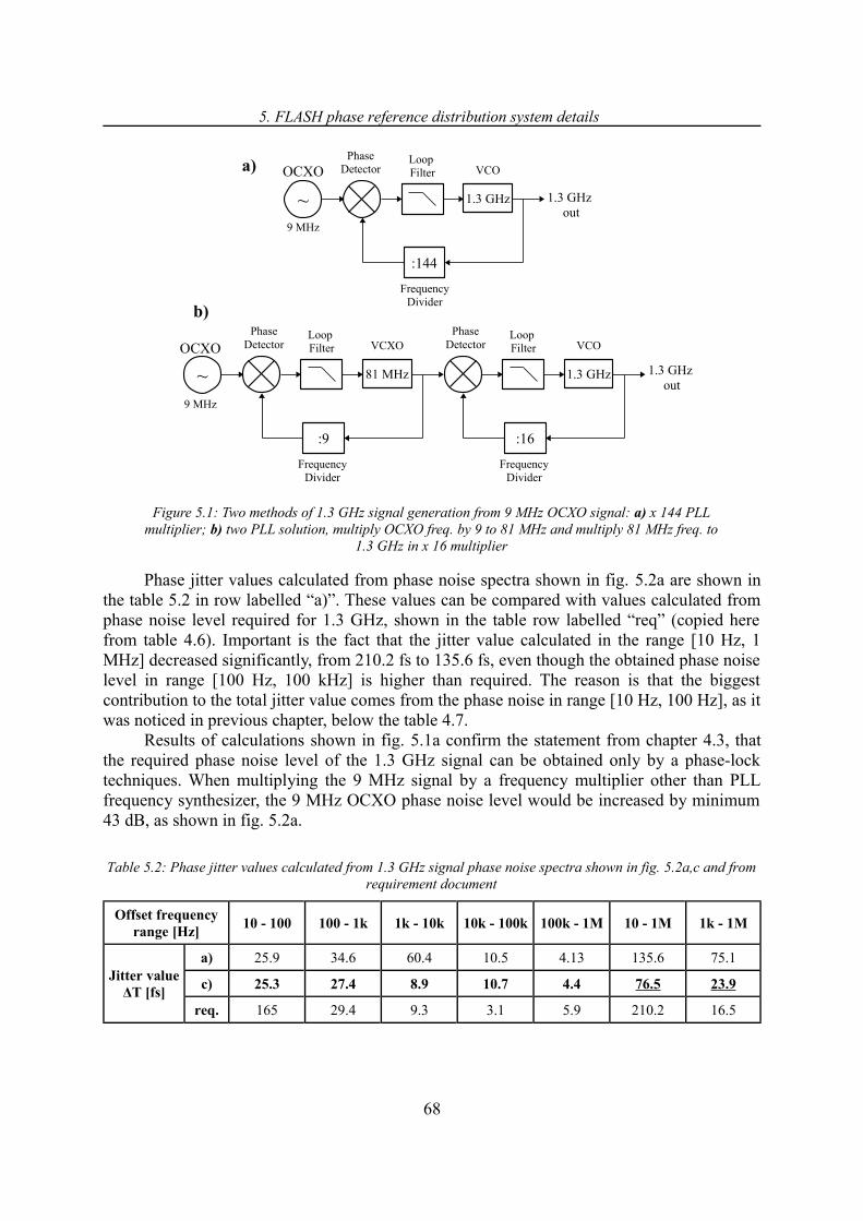
5. FLASH phase reference distribution system details
Figure 5.1: Two methods of 1.3 GHz signal generation from 9 MHz OCXO signal: a) x 144 PLL multiplier; b) two PLL solution, multiply OCXO freq. by 9 to 81 MHz and multiply 81 MHz freq. to
1.3 GHz in x 16 multiplier
Phase jitter values calculated from phase noise spectra shown in fig. 5.2a are shown in the table 5.2 in row labelled “a)”. These values can be compared with values calculated from phase noise level required for 1.3 GHz, shown in the table row labelled “req” (copied here from table 4.6). Important is the fact that the jitter value calculated in the range [10 Hz, 1 MHz] decreased significantly, from 210.2 fs to 135.6 fs, even though the obtained phase noise level in range [100 Hz, 100 kHz] is higher than required. The reason is that the biggest contribution to the total jitter value comes from the phase noise in range [10 Hz, 100 Hz], as it was noticed in previous chapter, below the table 4.7.
Results of calculations shown in fig. 5.1a confirm the statement from chapter 4.3, that the required phase noise level of the 1.3 GHz signal can be obtained only by a phase-lock techniques. When multiplying the 9 MHz signal by a frequency multiplier other than PLL frequency synthesizer, the 9 MHz OCXO phase noise level would be increased by minimum 43 dB, as shown in fig. 5.2a.
Table 5.2: Phase jitter values calculated from 1.3 GHz signal phase noise spectra shown in fig. 5.2a,c and from requirement document
Offset frequency range [Hz]
10 - 100 100 - 1k 1k - 10k 10k - 100k 100k - 1M 10 - 1M 1k - 1M
Jitter valueΔT [fs]
a) 25.9 34.6 60.4 10.5 4.13 135.6 75.1
c) 25.3 27.4 8.9 10.7 4.4 76.5 23.9
req. 165 29.4 9.3 3.1 5.9 210.2 16.5
68
a)
81 MHz
:9
~
Loop Filter
Phase Detector
Frequency Divider
VCXO
1.3 GHz
:16
Loop Filter
Phase Detector
Frequency Divider
VCO
b)
1.3 GHz out
OCXO
9 MHz
1.3 GHz
:144
~
Loop Filter
Phase Detector
Frequency Divider
VCO
1.3 GHz out
OCXO
9 MHz

5. FLASH phase reference distribution system details
Figure 5.2: Phase noise spectra: a) 1.3 GHz VCXO phase-locked directly to 9 MHz OCXO; b) 81 MHz VCXO phase-locked to 9 MHz OCXO; c) 1.3 GHz VCO phase-locked to 81 MHz VCXO from case b); d) Comparison of
1.3 GHz phase noise levels obtained in case a) and case c)
The second scheme shown in fig.5.1b consists of two frequency synthesizers connected in series. It is reasonable to choose the output frequency value of the first synthesizer from the list of frequency values required for the FLASH facility. After analysis of parameters of oscillators available on the market, it was found that the optimum phase noise level of 1.3 GHz signal can be obtained when the first synthesizer is used to generate 81 MHz signal (9 MHz x 9). Voltage Controlled Crystal Oscillators (VCXO) operating at 81 MHz are available with phase noise levels comparable to the phase noise 9 MHz OCXO at offset frequencies higher than few hundred Hz. Example of phase noise of the free running 81 MHz VCXO 25 is shown in fig. 5.2b. The long term stability (phase noise level at low offset frequencies) of the VCXO is significantly worse than the long term stability of the OCXO. But by phase-locking of the VCXO to the OCXO one can take advantages of both oscillators – low phase noise level at high offset frequencies and a good long term stability.
The 1.3 GHz VCO is phase locked to the 81 MHz VCXO signal by the second PLL frequency synthesizer (which multiplies 81 MHz x 16) shown in in fig.5.1b. The obtained phase noise spectrum of the 1.3 GHz signal is shown in fig.5.2c. Comparison of this phase
25 This phase noise spectrum was measured at DESY from a VCXO purchased for the MO project
69
1 00
1 01
1 02
1 03
1 04
1 05
1 06
- 1 7 0
- 1 6 0
- 1 5 0
- 1 4 0
- 1 3 0
- 1 2 0
- 1 1 0
- 1 0 0
- 9 0
- 8 0
f [Hz]
L(
f )
[dB
c/H
z]
b )
9 M H z O C X O9 M H z O C X O + 1 9 d B8 1 M H z V C X O f r e e8 1 M H z V C X O l o c k e d
1 0 0 1 0 1 1 0 2 1 0 3 1 0 4 1 0 5 1 0 6- 1 6 0
- 1 5 0
- 1 4 0
- 1 3 0
- 1 2 0
- 1 1 0
- 1 0 0
- 9 0
- 8 0
- 7 0
- 6 0
f [Hz]
L(
f )
[dB
c/H
z]
c )
8 1 M H z V C X O l o c k e d + 2 4 d B1 . 3 G H z V C O f r e e1 . 3 G H z V C O l o c k e d t o 8 1 M H z1 . 3 G H z r e q u i r e m e n t
1 0 0 1 0 1 1 0 2 1 0 3 1 0 4 1 0 5 1 0 6- 1 6 0
- 1 5 0
- 1 4 0
- 1 3 0
- 1 2 0
- 1 1 0
- 1 0 0
- 9 0
- 8 0
- 7 0
- 6 0
f [Hz]
L(
f )
[dB
c/H
z]
d )
1 . 3 G H z V C O l o c k e d t o 9 M H z1 . 3 G H z V C O l o c k e d t o 8 1 M H z1 . 3 G H z r e q u i r e m e n t
1 00
1 01
1 02
1 03
1 04
1 05
1 06
- 1 6 0
- 1 5 0
- 1 4 0
- 1 3 0
- 1 2 0
- 1 1 0
- 1 0 0
- 9 0
- 8 0
- 7 0
- 6 0
f [Hz]
L(
f )
[dB
c/H
z]
a )
9 M H z O C X O + 4 3 d B1 . 3 G H z V C O f r e e1 . 3 G H z V C O l o c k e d t o 9 M H z1 . 3 G H z r e q u i r e m e n t

5. FLASH phase reference distribution system details
noise with phase noise of a single PLL synthesizer (fig.5.2a) is shown in fig.5.2d. In offset frequency range [100 Hz, 10 kHz], the phase noise of the two PLL synthesizer is significantly lower than the phase noise of the the single PLL synthesizer.
Such decrease of phase noise level causes significant decrease of the phase jitter values – see table 5.2, row labelled “c)”. The phase jitter calculated in the frequency range [10 Hz, 1 MHz] is now as low as 76.5 fs. This is much less than required 300 fs. Phase jitter value in offset frequency range of [1 kHz, 1 MHz] equal to 23.9 fs is also smaller than 100 fs required in this range.
It must be reminded that obtained phase noise and phase jitter values were calculated with the use of phase noise levels specified in the requirement document for 9 MHz signal and 1.3 GHz free running VCO (table 4.3 and table 4.4). A good quality 1.3 GHz VCOs can be found with lower phase noise levels than specified in the requirement document. An oscillator based on a dielectric resonator is an example. Design and performance of example of such VCO operating at 1.28 GHz was described by Niehenke and Green in [66]. Phase noise levels were given in the paper for offset frequency range [1 kHz, 1 MHz] – given here in table 5.3. These values are of minimum 10 dB lower (better) than corresponding values specified in the requirement document for the free running 1.3 GHz VCO. Such a VCO used in the PRDS PLL could make it possible to obtain phase noise levels of the locked VCO comparable in the entire offset frequency range of [10 Hz, 1 MHz] with levels given in the requirement document.
Table 5.3: Phase noise levels of free running 1.28 GHz VCO described in paper [66]
Offset frequency [Hz] 1k 10k 100k 1M
ℒ f [dBc/Hz] -113 -143 -163 -169
In the moment of writing this thesis two types of 1.3 GHz VCO had been tested. First type is based on the Surface Acoustic Wave (SAW) resonator [78, ch. 2.15], [64]. the second tested type is a SAW replacement oscillator DCSO-130026. PLL modules with VCO based on the dielectric resonators are under development too. Phase noise spectra obtained by 1.3 GHz (DCSO) PLL module will be shown in chapter 6.1.1. Important technical details like PLL parameters of the SAW and DCSO modules can be found in [60, ch. 4.3.1].
The use of the two-PLL scheme for generation of 1.3 GHz signal has several practical advantages. As it was justified above, the phase noise contribution of the frequency divider in analysed PLLs was neglected. In practical frequency synthesizer circuits the intrinsic phase noise added to the signal by frequency divider27 can be a very important contributor to the output phase noise. The transfer function for the frequency divider phase noise in the PLL is the same as for the reference oscillator phase noise – see eq. (3.42). It means that the frequency divider noise within the loop bandwidth is also increased of 20·log10N [17, fig. 9.3].
Frequency divider :144 used in the single PLL is supposed to have much worse performance than dividers :9 and :16 used in the two PLL solution. Therefore lower intrinsic
26 Manufactured by the Synergy company27 A misunderstanding should be avoided here. As it was described in chapter 3.4.3, eq. (3.25), the frequency
divider decreases the phase noise of the signal by 20·log10N. This phenomenon should not be mistaken with intrinsic noise in the divider, e.g. phase noise floor at divider output, that does not depend on the signal phase noise but on the divider type (technology, division ratio...). The intrinsic noise is multiplied by the PLL.
70

5. FLASH phase reference distribution system details
phase noise levels of these dividers will be multiplied by lower numbers in both PLLs. This will result in further performance improvements of the two PLL solution comparing with the one PLL solution.
The 81 MHz is also required for the FLASH facility. Next advantage of using the two-PLL frequency synthesizer is that a part of the the 81 MHz signal can be used for distribution purposes without a need for using an additional frequency synthesizer. This can be also advantageous for the relative phase instabilities between the 81 MHz and 1.3 GHz signals.
Let us compare two schemes shown in fig. 5.3. Relative instabilities Δtrel between zero-crossings of the 1.3 GHz and 81 MHz signal phase are shown in these schemes. The value of Δtrel in the scheme shown in fig. 5.3a are expected to be greater than the instabilities Δtrel' in the scheme from fig. 5.3b.
* Generation of other signals required for the PRDSConsiderations should be performed for development of the scheme of generation of
other frequencies required for the PRDS (see table 4.1). Frequency values lower than 81 MHz (1 MHz, 9 MHz, 13.5 MHz, 27 MHz) can be obtained from the 9 MHz signal with the use of frequency multipliers, as shown in fig.5.3a or they may be obtained from 81 MHz signal with the use of frequency dividers as shown in fig.5.3b. Let us focus on the frequency of 27 MHz. Conclusions will be valid for remaining frequencies.
Figure 5.3: Two possible schemes of generation of MO frequencies
It should be reminded here that phase noise levels were not specified for these signals in the requirement document and no data is available on required phase jitter of these signals. Nevertheless it is shown below how to obtain possibly good performance of these signal sources.The 27 MHz signal can be obtained either by multiplication of 9 MHz x 3 or by division of 81 MHz by 3. It was assumed that 27 MHz should not be obtained by phase locking of 27 MHz VCXO to the 9 MHz signal but by the use of a frequency multiplier. The reason is that the precise value of 27.08333 MHz is not a standard value and a custom (expensive) VCXO should be used. Since there is no data on the required phase stability of the 27 MHz signal it can be assumed that this stability is not critical and there is no need for using state-of-the-art devices. A good quality x 3 frequency multipliers operating in this frequency range can be purchased.
Phase noise spectrum of 27 MHz signal calculated for both schemes is shown in fig. 5.4.
71
a)OCXO
9 MHz
PLL x 144~ 1.3 GHz out
PLL x 9
Mult. x 3
81 MHz out
27 MHz out
Mult. x ...
Other frequencies
b)OCXO
9 MHz
PLL x 9~ 1.3 GHz out
Div. : 3
81 MHz out
27 MHz out
Div. : ...
Other frequencies
PLL x 16
Δtrel
Δtrel1
Δtrel'
Δtrel1'

5. FLASH phase reference distribution system details
The phase noise levels of 9 MHz and 81 MHz signals are taken from fig. 5.2b. When a frequency multiplier is used, the phase noise level of the 9MHz OCXO signal is increased of 20·log103 = 9.54 dB. When a frequency divider is used, the phase noise level of the 81 MHz signal is decreased of 9.54 dB (eq. (3.25)). As it can be seen in fig. 5.4, for offset frequencies up to 100 Hz (loop bandwidth of the 81 MHz PLL), both phase noise spectra are comparable.
For higher offset frequencies the phase noise levels of the signal obtained by frequency division is significantly lower than that of the signal obtained by frequency multiplication. These levels are even lower than the OCXO phase noise levels! This is because the phase noise of the 81 MHz VCXO for high offset frequencies is comparable with the OCXO phase noise and the frequency divider reduces the phase noise level. Naturally, the phase noise level of the 27 MHz signal is also dependent on the frequency divider intrinsic noise, which can be higher than -172 dBc/Hz in available devices. This must be verified by measurements.
Besides 27 MHz, (below 81 MHz) there are also frequency values of 13.5 MHz, 9 MHz, and 1 MHz to be distributed by the PRDS. It was decided that these signals should also be obtained from 81 MHz signal.
The use of frequency dividers for obtaining 9 MHz, 13.5 MHz and 27 MHz signals from 81 MHz is also advantageous for the relative phase jitter Δtrel' between these signals and the 1.3 GHz signal. This was explained above, with the help of fig. 5.3, for 81 MHz signal and it is an important conclusion because the instabilities in the PRDS should be measured against the phase of the 1.3 GHz signal.
The 108 MHz signal can not be obtained by multiplication of 81 MHz by integer number. Therefore it was decided that a 108 MHz phase-locked VCXO will be used. The PLL synthesizer will be of the same construction as for the 81 MHz signal but, of course, the 9 MHz OCXO frequency must be multiplied by 12.
1 0 0 1 0 1 1 0 2 1 0 3 1 0 4 1 0 5 1 0 6
- 1 7 0
- 1 6 0
- 1 5 0
- 1 4 0
- 1 3 0
- 1 2 0
- 1 1 0
- 1 0 0
- 9 0
f [Hz]
L(
f ) [
dBc/
Hz]
9 M H z O C X O2 7 M H z ( 9 M H z O C X O x 3 )8 1 M H z V C X O l o c k e d2 7 M H z ( 8 1 M H z V C X O l o c k e d : 3 )
Figure 5.4: Phase noise levels of 27 MHz signal obtained by multiplication of 9 MHz OCXO and division of 81 MHz locked VCXO frequency
The 50 Hz TTL signal will be obtained from 108 MHz signal by a Direct Digital
72

5. FLASH phase reference distribution system details
Synthesiser (DDS) [36, ch. 4], [16].Last two frequencies specified in table 4.1 of 1517 MHz and 2856 MHz are required at
single locations in the FLASH facility. These locations are respectively over 40 and 100 meter away from the location of the MO system. Because of significant cable attenuation at these frequencies, it was decided that these signals will be obtained locally from the 81 MHz signal, at devices requiring these frequencies. Fractional-N frequency synthesizers [17, ch.5] were foreseen for generation of these frequencies.
* Master Oscillator System architectureBesides frequency generation scheme, there are several other issues that should be
considered in the development stage of the MO. As it was written at the beginning of this chapter, the MO system should be assembled in crates adapted to the 19 inch standard. Besides the reference oscillator and other devices used for obtaining necessary frequencies, there is a number of subsystems that should be incorporated in the MO, e.g. power supply circuits, signal power level monitors, signal phase monitors and power amplifiers. The latter, as it will be calculated in chapter 5.2.3, should deliver significant output power levels in order to assure required power level at PRDS outputs in the entire FLASH facility. Therefore the power amplifiers will be relatively large devices requiring big heat-sinks. There is also a large number of 81 MHz and 1.3 GHz signal outputs required for the MO system. Therefore a significant number of power splitters and directional couplers will have to be used.
Figure 5.5: Block diagram of the MO system
All factors described above make it impossible to fit the entire MO system into one 19 inch crate. The system must be split into several crates. The block diagram of the MO system is shown in fig. 5.5. It was decided that the OCXO and all frequency multipliers and dividers,
73
1.3 GHz PLL 1.3 GHz POWER AMPLIFIER
1.3 GHz
PA – Power Amplifier
44 dBm
30 dBm
LOW POWER PARTOCXO
9 MHz
~ 81 MHz PLLx 9
108 MHz PLLx 12
Div. : 3
Div. : 2
Div. : 9
Div. : 9
PLL x 16
PA
27 MHz
13.5 MHz
9 MHz
1 MHz
108 MHz
PA
1.3 GHz DISTRI-BUTION BOX
81 MHz POWER AMPLIFIER
81 MHz40 dBm
PA
81 MHz DISTRI-BUTION BOX

5. FLASH phase reference distribution system details
except 1.3 GHz PLL, will be placed in one crate called Low Power Part (LPP). Since the 1.3 GHz PLL is one of the most critical parts in the system, and new types of devices appear frequently in the market, it was decided to make additional crate with this PLL. If a new, better than actually used solution appears, it will be easy to replace the crate without rebuilding the entire MO system. The 1.3 GHz signal is amplified within the 1.3 GHz Power Amplifier module, which assures sufficient power level for signal distribution in the entire FLASH facility. The amplified signal is split within the 1.3 GHz Distribution Box, which contains a network of directional couplers and power splitters. The purpose of the 1.3 GHz Distribution Box is to provide sufficient number of outputs for all distribution links.
The 81 MHz signal is amplified and distributed similarly to the 1.3 GHz signal. More detailed description of MO system components is given in following sub-chapters. There are also briefly described technical issues that have very important influence on the signal stability.
5.1.4. Low Power Part details
The design of the MO LPP was a very long and difficult process. Besides proper choice of PLL and frequency divider parameters, there were many technical and engineering issues that had to be considered to make sure that the performance of signal sources is optimal. Most important of these issues are described in the remainder of this chapter. Issues less important from the point of view of the main considerations of this thesis are given in appendix 1.
* Construction of the 81 MHz and 108 MHz PLLOne of the first issues to be considered is the power level provided by the MO devices.
As it will be calculated in ch. 5.2.3, the power level of the 81MHz signal required at the output of the power amplifier should be equal at least +40 dBm. A custom, low phase drift and high linearity power amplifier was developed with power gain of 20 dB. The power level of +20 dBm must be provided to the input of this power amplifier from the 81 MHz PLL. The 81 MHz signal from the VCXO is also used for frequency dividers and 1.3 GHz PLL input (fig. 5.5). This signal should also be provided to power level monitoring circuit and to minimum one spare output for future use (both not shown in fig. 5.5). Therefore a gain block with output power of 26 dBm was used at the VCXO output. Attention was put for the gain block and the high power amplifier to avoid working near the 1 dB compression point. By this the amplifiers were operating in linear region and a rise of signal harmonics was avoided.
The block diagram of the 81 MHz PLL is shown in fig. 5.6. The power amplifier and power splitter were built into the feedback loop. Any phase drifts and other instabilities slower than the loop bandwidth appearing in these devices can be suppressed by the feedback loop. This is a solution assures that all following devices will be synchronized to the 81 MHz signals with the same phase.
Similar solution as shown in fig.5.6 was used for the 108 MHz PLL. There is also an amplifier and power splitter built into the feedback loop.
* Frequency dividersAs decided above, frequency values of 27 MHz, 13.5 MHz, 9 MHz, 1 MHz are obtained
by dividing the frequency of 81 MHz signal (fig. 5.5). Programmable, digital frequency
74

5. FLASH phase reference distribution system details
divider chips28 with output signals in ECL standard were used in the LPP.
Figure 5.6: The 81 MHz phase locked loop
These chips are characterised with a low phase noise level in the output signal. A level of -153 dBc/Hz at 10 kHz offset frequency29 is given in the device datasheet. Phase noise spectrum given by the manufacturer of the divider is shown in fig. 5.7.
Figure 5.7: HMC394 frequency divider phase noise spectrum. N = 4, fin = 1 GHz.
The block diagram of the frequency divider circuit used in the LPP is shown in fig. 5.8. The same design was applied for all frequency dividers in the MO system.
Figure 5.8: Frequency divider system
Output signal of the frequency divider chip is low-pass filtered and amplified. This type
28 HMC394, manufactured by the Hittite company.29 For input frequency equal 1 GHz and N equal 4.
75
81 MHz
:9
LoopFilter
Phase Detector
Frequency Divider
VCXO
4 x 20 dBm
Power Amplifier
Power Splitter
9 MHz reference
signal +26 dBm
:N
FilterFrequency
Divider
2 x 10 dBm
Buffer Amplifier
Power Splitter
Input signal
+13 dBm
To next divider

5. FLASH phase reference distribution system details
of frequency divider produces pulsed output signal with pulse duty-cycle inversely proportional to N. The higher N, the smaller the duty-cycle. The power of the output signal decreases quickly with N and it is advisable to use as low N values as possible. Therefore 1 MHz and 13.5 MHz signals are obtained with the use of two frequency dividers connected in series. E.g. the 13.5 MHz signal is obtained by dividing 27 MHz by N = 2. The duty-cycle of the divider output signal equals 50%. Higher value of duty-cycle makes it possible to use buffer amplifier with lower gain and therefore potentially with smaller influence on the signal phase stability.
Figure 5.9: Possible phase delays between output signals of various dividers
There is a feature of digital frequency dividers which may be very important for the PRDS performance. The output signal of such device is produced by counting periods (pulses) of the input signals and generating one output pulse after each N input pulses. After switching the power supply, the pulse counting begins with arbitrary delay depending on the circuit parameters and actual state of the input signal. Therefore the zero-crossings30 of output signals of different dividers can be delayed by integer number of input signal periods. This is explained in fig. 5.9.
The 81 MHz input signal and output signals of 27 MHz (: 3) and 9 MHz (: 9) frequency dividers are shown. For simplicity all signals are drawn as rectangular. The 81 MHz signal pulses are numbered in the figure. The 9 MHz divider started counting one 81 MHz signal period after the 27 MHz divider. The delay between rising edges of both signals is shown. Such delay is not a problem for the FLASH system, until it is constant. Timings in the FLASH system are adjusted during system start-up. Short break in the divider power supply (e.g. for maintenance issues) may result in a change of delay of divider output signals and it may yield a necessity of time consuming readjustments of the FLASH timings. To prevent such events, the reliability of the MO system should be high. Therefore it was decided that the MO system will be powered from battery based power supply, which can supply the MO for several hours when a problem with the network power occurs. This solution should minimize probability of switching the MO system off.
More system level technical details of the LPP design are described in appendix 1. Technical design issues of the MO subsystem like parameters of used VCOs and PLL filters can be found in the report thesis [60].
30 Zero-crossings in case of sinusoidal signals. Rising edges in case of rectangular signals
76
1 2 43 5 781 MHz signal
27 MHz signal
9 MHz signal
One period delay
1096 8 11
5. FLASH phase reference distribution system details
5.1.5. Power supply, temperature stabilisation, crate cabling
Most important issues not related directly to the signal generation chain but having important influence on the stability of generated signals are briefly addressed below.
* MO System power supplyThe power supply used for the MO System has a very important influence on the
stability of the generated signals. Amplitude noise from the power supply voltage can affect the phase noise of the signal in devices like oscillators and amplifiers. The 50 Hz power network frequency and its harmonic can appear in the phase noise spectrum as spectral lines. These lines significantly decrease the signal phase stability. Therefore a battery based power supply for the MO System was developed. The most important advantage of such solution is a very low noise and absence of 50 Hz lines in the supply voltage. As it was mentioned above, the battery can supply the MO System for few hours when the network power is switched off. Continuous MO operation is important for the FLASH facility because of necessity of phase adjustments in the accelerator system after start-up of the MO System.
* Temperature stabilisation of MO componentsTemperature is a critical factor for the long term phase stability of the MO System
signals. Measurements have shown that most of active system components (PLLs, amplifiers (chapter 6.1.2), frequency dividers) and also cables, change phase of the signal when the temperature is changing. Data on the temperature sensitivity is provided very rarely by manufacturers of electronic devices such as used in the MO system. Therefore theoretical analysis of this effect was difficult to perform and devices were characterized experimentally. The general conclusion is that for minimising long term phase drifts a temperature stable environment for the MO System electronics must be assured.
Therefore a significant effort was put in minimising speed and range of temperature changes. All active circuits in the signal generation chain were built into thick aluminium boxes. All boxes were fastened to a massive aluminium plate. Such mechanical set-up closed in tight 19 inch crate shows large thermal inertia. Therefore relatively fast signal phase changes caused by fast ambient temperature changes (were observed after opening door or window of the laboratory) were minimized. Low thermal resistance and significant thermal capacitance of the system plate also assures equal heat distribution within the crate. Furthermore the MO System was planned to be installed in the FLASH facility within a temperature controlled chamber. Temperature will be stabilized with accuracy of ±0.5 oC.
* Cables in the MO systemThere are many connections that had to be made between MO subsystems, between 19
inch crates as well as inside of each crate. During first test of the MO system components it was found that mechanical properties of cables and connectors have large influence on the phase of transmitted signals. Simple measurements performed with a phase detector have shown that when flexible coaxial cables with SMA connectors are used for interconnections, phase jumps occur randomly. The amplitude of these jumps for 1.3 GHz signal reached level of several pico-seconds (usually 2 -3 ps) in time domain. It was observed that such jumps occurred even during gentle knocking by hand on the laboratory table. Tests were also performed in a climate chamber. Phase jumps were observed in periods when chamber
77

5. FLASH phase reference distribution system details
compressor was switched on. It generated lots of mechanical vibrations. These experiments confirmed that the reason of phase jumps is a cable or connector sensitivity to mechanical vibrations. Fortunately, it was found also that this problem disappears when semi-rigid cables are used for interconnections. Therefore the cabling of the entire MO system was made with such cables.
5.2. Coaxial cable system
As it was decided in chapter 4.3, that signals generated within the MO System should be distributed over the FLASH facility with the use of RF coaxial cables. The system of cable links with all necessary devices like connectors and power splitters is the distribution part of the PRDS. Considerations on the design issues and performance analysis of the cable distribution system is described in this chapter.
5.2.1. Choice of cable type and other issues of cable distribution link
The coaxial cable is a coaxial transmission line surrounded by an insulating jacket that protects the line against environmental factors. Such transmission line consists of two concentric conductors separated by a dielectric material. The material may be continuous throughout the line (so called rigid coaxial lines [13]) or located at distinct points along the line in the shapes of “pegs” or “discs”. Electrical parameters of a coaxial line depend on the size of conductors and on the properties of the dielectric material.
Proper choice of cable type is a key decision for the signal distribution system. Most important issues that must be considered are: frequency of operation, power handling, attenuation, sensitivity of electrical length to temperature changes, characteristic impedance, mechanical properties (e.g. size and weight impinging on the cable handling and installation) and cable installation costs. Most important of these issues are addressed below.
* Cable characteristic impedanceThere are two most frequently used characteristic impedance values of coaxial cables:
50 Ω and 75 Ω. The 75 Ω standard is used mainly for broadcasting of television signals. It was decided that the 50 Ω impedance standard will be used for the PRDS because this standard is used for high frequency and microwave applications and there is broader choice of a good quality devices (e.g. power amplifiers, directional couplers, connectors) in this standard available in the market.
* Cable attenuationCable attenuation is a key parameter for the PRDS used for an accelerator facility
because of significant distribution distances. Attenuation is inversely proportional to the diameters of inner and outer conductors and it is proportional to signal frequency [13], [21, ch. 3.2.1]. Therefore the thinner the cable and the higher the signal frequency, the higher is the cable attenuation.
Attenuation is expressed in terms of loss per unit length, e.g. dB/100 m. Attenuation values (and other parameters) for cables selected of available in the market are collected in table 5.4.
The attenuation of ¼ inch cable at 1.3 GHz exceeds 22 dB / 100 m. Because of such
78

5. FLASH phase reference distribution system details
high attenuation using this cable for distribution distances reaching 300 meters is impractical. The attenuation at the same frequency for ½ inch and 7/8 inch cables is much lower. For the latter it is below 5 dB / 100 m, which would give approximately 15 dB / 300 meter. This is an acceptable value. But it must be remembered that the attenuation of the cable is an important but not only contributor to the total attenuation value of the distribution link. There are significant losses in connectors and other devices used in the cable link. Example calculations of the total attenuation and a power budget of a cable link will be presented in chapter 5.2.3.
Table 5.4: Parameters of selected coaxial cable types
DIAMETER 1/4” 1/2” 7/8”
CABLE FSJ1-50A# LCF12-50J* FSJ4-50B# HJ5-50# LCF78-50J*
Attenuation [dB/100m]1 MHz9 MHz81 MHz108 MHz1300 MHz3000 MHz
0.571.755.406.1322.5035.60
0.210.601.902.248.1513.20
0.320.802.503.5514.0022.40
0.110.350.901.264.907.96
0.110.300.901.194.707.38
Phase/Temp coefficient -30 to +40oC [ppm/oC]
-7 to +9 +11 to -0.3 -2 to +6 +5 to +11 +9 to -0.5
Signal velocity [% of c0] 84.0 88.0 81.0 91.6 88.0 # Cable manufactured by the Andrew Corporation; * Cable manufactured by the RFS
* Cable sensitivity to temperature changesThe next important cable parameter is the temperature sensitivity of the cable electrical
length. This phenomenon was explained in chapter 3.4.6. Signal phase drifts induced by the cable temperature changes are the main factor limiting the long term stability performance of the PRDS. Therefore a cable with the smallest value of the electrical length temperature sensitivity coefficient KT (see chapter 3.4.6) should be used in the PRDS.
Figure 5.10: Temperature coefficient of electrical length of the LCF12-50J 1/2 inch cable
79

5. FLASH phase reference distribution system details
Figure 5.11: Temperature coefficient of electrical length of the LCF78-50J 7/8 inch cable
Typical values of the KT of selected cable types are shown in table 5.4. The plots of the KT against temperature are available for two of these cables. These plots are shown in fig. 5.10 (½ inch cable) and fig. 5.11 (7/8 inch cable).
It is interesting that the temperature coefficient of the 7/8 inch cable is very low (+1 to -1 ppm/oC) in the temperature range of +10 to +40 oC (temperature in the FLASH facility is expected to vary within this range). The value of the temperature coefficient of this cable equals zero at T = +33 oC. The ½ inch cable exhibits a little broader range of temperature coefficient values. The KT equals zero at T = +38 oC. With the use of such cables one can obtain distribution links with very low values of phase drifts. One can also consider applying a stabilisation of the cable temperature at about +33 or +38 oC. This way it is possible to realize an almost drift free distribution link.
It was decided that the the LCF78-50J, 7/8 inch cable will be used for the distribution of 1.3 GHz signal. The type of cable was chosen because of a low value of temperature coefficient as described above. The diameter was chosen because of acceptable attenuation (about 4.7 dB/100 m).
As it was described in the previous chapter, experiments were planned for future applications like XFEL and ILC PRDS. For such long distribution links it may be reasonable to distribute 81 MHz signal and multiply the frequency up to 1.3 GHz locally at distribution destinations. Additional cable link was foreseen for this purpose. The LCF78-50J, 7/8 inch cable type was also used for distribution of the 81 MH signal even though the attenuation of the ½ inch cable would be sufficient at this frequency. A performance comparison was planned between both types of distribution (1.3 GHz and 81 MHz with frequency multiplication).
The LCF12-50J, ½ inch cable was chosen for distribution of all remaining signals.Calculations of expected values of phase drifts in cables installed in the FLASH facility
are given in chapter 5.2.4.After choosing the type of the cable there are many other issues that must be considered
carefully before the final design of the distribution line will be accomplished. These issues are briefly addressed below.
80

5. FLASH phase reference distribution system details
* ConnectorsThere are many connector types available for high frequency applications.
Considerations were narrowed down to popular types that have also been frequently used in DESY for the RF systems. From among them there are two connector types that fit to the PRDS purposes: “SMA” and “N”. The SMA connectors should not be used for the thick, rigid coaxial cables. PRDS cables will be installed in the FLASH facility on cable trails with many other cables. Changes in cabling will be performed frequently, especially in the accelerator development and installation stage. Moving cables may cause mechanical stress on the connectors which may lead to damages or uncontrolled signal phase changes.
Because of their mechanical robustness, the N type connectors seem to fit well for the PRDS purposes. It was also found experimentally that phase of the signal distributed in cables equipped with N connectors is less susceptible to mechanical vibrations than when SMA connectors are used. This is a desirable feature.
SMA connectors are used for interconnections within the crates of the MO system. As it was described above, semi-rigid coaxial cables with SMA connectors assure good quality of connections.
* Signal pick-up pointsConsiderations on the PRDS architecture choice are described in chapter 4.2.2. The
distribution line with pick-up points located along the FLASH facility was chosen. It is possible to use either power splitters or directional couplers for picking up the signal from the distribution cable.
It is advisable to use directional couplers in the distribution line because the main line loss is typically within the range of 0.2 – 1.0 dB. The loss of a two-way power splitter is equal a little bit more than 3 dB. Therefore the signal power level in the coaxial cable would be decreased of minimum 3 dB after each pick-up point. It can lead to too high power loss when many pick-up points are installed along the distribution line.
Second advantage of the directional coupler is a broad range of available coupling values. Directional couplers with decreasing coupling value can be used successively along the distribution line to compensate for the decrease of signal power level caused by coaxial cable loss. In this way equal power levels at each output can be assured.
5.2.2. Cable distribution system layout
The proposed scheme of the cable distribution system is shown in fig.5.12. There are four locations in the FLASH system that require precise synchronization with 1.3 GHz signal: so called “injector area” in Hall 3, including LLRF control racks shown in fig.5.12, New LLRF control racks, EOS, and Experimental Hall.
Many devices are located in the injector area, in LLRF control racks, in the vicinity of the MO. They will be synchronized with the use of short, thin cable links of length not exceeding several meters. These links are not shown in fig. 5.12.
Two main distribution lines are planned from the MO to New LLRF control racks and to the Experimental Hall. Signals to the EOS will be provided from the Experimental Hall line. Each line contains three cables with 9 MHz, 81 MHz and 1.3 GHz signals. There is one more cable with 108 MHz signal in the Experimental Hall line. Distribution of three frequencies to each important location is an excessive solution but, as described above, it was
81

5. FLASH phase reference distribution system details
intended to consider and test different signal distribution schemes that may be used for longer distances which will exist in the XFEL and ILC.
Besides the main distribution destinations there are many auxiliary locations where the stability of the signal is not critical or where the distributed signal will be used sporadically, for test purposes. An example is the cable 1 with 1.3 GHz signal. Many pick-up points were foreseen along this cable. Similarly the cable 4 which provides 1.3 GHz signal to klystrons.
There are also connections from cable 1 and cable 5 to the New LLRF racks. The intention of this arrangement is to create a possibility of comparing phase difference between signals distributed by two different cables of the same type, e.g. cable 1 and cable 2.
For transparency of fig. 5.12, distribution lines to New LLRF racks and to Experimental Hall are drawn separately, but they were installed side by side in the accelerator tunnel. Therefore connections made by cable 1 and 2 from MO to New LLRF racks should be of the same length and in the same environmental conditions. But cable 1 contains many pick-up points. By measuring signal phase difference between these cables, the influence of pick-up point on the signal stability in cable 1 can be studied experimentally.
It can be noticed that the topology of the system shown in fig. 5.12 corresponds neither to star type nor to line with pick-up points. It is a mixture of both types. It results from the layout of the FLASH facility, necessity of distribution of signals with various frequency values and from described excess of the system planned for test purposes.
There are also three fiber-optic cables shown in fig.5.12. They have create the optical distribution link described in chapter 5.3.
82
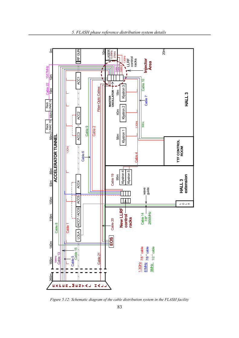
5. FLASH phase reference distribution system details
Figure 5.12: Schematic diagram of the cable distribution system in the FLASH facility
83
108M
Hz
10m
TT
F C
ON
TR
OL
RO
OM
LLR
F
contr
ol
rack
s
L O L A
165m
85m
19m
140m
260m
118m
105m
93m
56m
10m
0m44
m
wav
egu
ide
20m
New
LL
RF
co
ntr
ol
rack
s
18m
Kly
stro
n 3
RF
GU
NA
CC
1A
CC
2A
CC
3A
CC
4AC
CE
LE
RA
TO
R T
UN
NE
L
HA
LL 3
ex
ten
sio
nH
AL
L 3
EO
S
Rac
kLI
NA
C 1
5LI
NA
C 9
Rac
k
LAS
ER
AC
C5
AC
C7
/ AC
C6
LOLA
95m
40m
56m
Kly
stro
n 2
Kly
stro
n 1
Kly
stro
n 5
Kly
stro
n 4
MA
ST
ER
OS
CIL
LA
TO
R
1.3G
Hz
1.3G
Hz
2856
MH
z
9MH
z
13,5
MH
z
Cab
le 1
Cab
le 2
Cab
le 4
Cab
le 3
Cab
le 5 Cab
le 1
5
Cab
le 6
Cab
le 1
0
Cab
le 1
1C
able
12
Cab
le 1
47/
8"C
able
7
Cab
le 9
Cab
le 1
3C
able
8
Cab
le 2
215
17M
Hz
1.3G
Hz
Fib
er-O
ptic
Cab
les
Cab
le 1
9C
able
20
Cab
le 2
1
1.3G
Hz
9MH
z
81M
Hz
7/8
" ca
ble
7/8
" ca
ble
1/2
" ca
ble
27M
Hz
Inje
cto
rA
rea
E X P E R I M E N T A L H A L L

5. FLASH phase reference distribution system details
5.2.3. Power budget calculations
In order to find power level at output and required power level that should be provided by the MO System to the input of each link, power budget calculations must be performed for cable links. An example of such calculations for the most complicated (cable 1) link in the FLASH PRDS is shown below.
Figure 5.13: Detailed schematic of the "cable 1" link
Detailed schematic diagram of the “cable 1” link is shown in fig 5.13. Cable segments with approximate length separated by directional couplers are shown. Following data was used for calculation of 1.3 GHz signal attenuation: - cable attenuation equals 4.7 dB/100 m (7/8 inch, see table 5.4),- directional coupler main line loss equals 0.25 dB,- connector loss equals 0.25 dB31.
The approximate cable length in all sections equals 291 m. This yields cable attenuation of 13.7 dB. Power loss in 9 directional couplers equals 2.25 dB. Power loss of 20 connectors equals 5 dB. Together, the link loss equals about 21 dB. But there are four outputs required in
31 Worst case loss taken from connector datasheet. Typical value is lower.
84
-20 dB
-0.25 dB
-20 dB
-0.25 dB
-20 dB
-0.25 dB
-20 dB
-0.25 dB
-20 dB
-0.25 dB
-20 dB
-0.25 dB
-20 dB
-0.25 dB
-20 dB
-0.25 dB
-10 dB
-0.25 dB
Phas
e M
onito
rP
ositi
on 1
9 m
Phas
e M
onito
rP
ositi
on 2
7 m
AC
C1
AC
C2/
AC
C3
AC
C4-
AC
C7
New
LL
RF
Phas
e M
onito
rP
ositi
on 8
5 m
EO
S
Phas
e M
onito
rP
ositi
on 1
65 m
Power Splitter
Mas
ter
Osc
illa
tor
Sys
tem
Experimental Hall
„nea
r do
or”
15 m 10 m 8 m
23 m
20 m100 m25 m
40 m15 m35 m
Accelerator Tunnel

5. FLASH phase reference distribution system details
the Experimental Hall. A 4-way splitter causes signal power level decrease of about 7 dB. Therefore the attenuation from the beginning of the cable to the power splitter output equals about 28 dB.
In order to obtain minimum power equal to +10 dBm at each output of the power splitter, the power level delivered from the MO System must be minimum +38 dBm. A value of +40 dBm was specified for safety margin.
Taking into account this requirement, the necessity of delivering 1.3 GHz signal power to other cables (fig. 5.12) and losses in components of the 1.3 GHz distribution box (fig. 5.5), the value of +44 dBm was specified for the output power level of the 1.3 GHz Power Amplifier.
It should be noticed that the coupling value of all directional couplers shown in fig. 5.13 equals 20 dB. The only exception is the last directional coupler in the distribution line with the coupling value of 10 dB. This directional coupler is located about 270 meter away from the MO. The link attenuation from MO to this coupler equals about 20 dB. With a coupling ratio of 10 dB, coupled signal power level of above +10 dBm was assured.
Similar calculations were performed for all cable links in the PRDS. The power level of each frequency signal delivered by the MO System was specified basing on these calculations.
5.2.4. Cable temperature regulation, phase drift calculations
One of the most important calculations performed in the design stage of the cable link is estimation of signal phase drifts values in cables. Example of such calculation was described in chapter 4.3, (page 64) for a 300 meter long link and for typical value of the electrical length temperature coefficient.
More detailed calculations may be performed now, after the cable type is known. As results from fig. 5.10 and fig. 5.11, the temperature coefficients of chosen cables are lower than assumed in chapter 4.3. The temperature in the FLASH facility changes usually between 3 oC and 5 oC per day, depending on the weather conditions and the season of the year. Let us assume that the mean temperature value in the FLASH facility changes between +15 oC and +20 oC over a day. The mean value of the temperature coefficient of the 7/8 inch cable in this temperature range (fig. 5.11) equals about 1 ppm/oC. For the ½ inch cable it equals about 5 ppm/oC. Phase drift values calculated for both cable types with assumptions given above are collected in the fifth column of table 5.5. The long term stability requirement for the PRDS of 10 ps per day (table 4.2, before 2006) is fulfilled by the 7/8 inch cable. The same requirement is not fulfilled by the ½ inch cable – in this case the phase drift of the signal in the link to Experimental Hall may be equal to 27.46 ps per day.
There are hours (morning and late afternoon) where the temperature changes may reach rates up to 1.5 oC per hour. Expected peak values of phase drift per hour are collected in the sixth column of table 5.5. The requirement of 2 ps per hour (table 4.2, before 2006) is fulfilled by the 7/8 inch cable in all links and by the ½ inch cable only in link “10” (70 meter long). Maximum drift value of 0.75 ps per hour (required after 2006) is assured only by 110 meter long 7/8 inch cable.
85

5. FLASH phase reference distribution system details
Table 5.5: Peak values of phase drift calculated for most important cable links in the FLASH facility
1 2 3 4 5 6 7
Destination
Approx. cable length
[m]
Cable No.
Cable Diameter
[inch]
No cable temp. stabilisation,
phase drifts per day for ΔT = 5oC
[ps]
No cable temp. stabilisation,
phase drifts per hour ΔT = 1.5oC
[ps]
Cable temp. stabilised,
phase drifts for ΔT = ±0.5oC
[ps]
Experimental Hall
2901, 5, 13 7/8 5.49 1.65 0.22
15 1/2 27.46 8.24 1.10
EOS 1501, 5 7/8 2.84 0.85 0.11
8 1/2 14.20 4.26 0.57
New LLRF racks
1102, 6 7/8 2.08 0.63 0.08
9 1/2 10.42 3.13 0.42
Klystron 4-5, TTF control
room70
4, 7 7/8 1.33 0.40 0.05
10 1/2 6.63 1.99 0.47
It was decided in chapter 4.3 that the temperature of distribution cables should be stabilized. This decision was based on phase drift calculations with typical cable parameters. Results presented in table 5.5 show that requirements on the per day phase stability value could be fulfilled without temperature stabilisation when the 7/8 inch cable is used. Nevertheless, requirements are violated by links made with the ½ inch cable. It was also assumed that it may be reasonable to make distribution links with long term phase stability significantly better than required. Therefore a temperature stabilisation system was installed on the cable links. Temperature will be regulated with accuracy of ±0.5 oC. More details on the temperature stabilisation system are given in Appendix 2. It is important that with the temperature stabilisation, maximum values of phase drift per hour should be the same as maximum values of phase drifts per day.
Maximum values of phase drift expected in distribution links with temperature stabilisation are collected in the last column of the table 5.5. These values are significantly lower than required (table 4.2). E.g. phase drift in the longest link is over 45 times (10 ps / 0.22 ps) lower than required per day. This result may be important because phase drifts may appear in other components of the PRDS, especially in active devices. Such small drift values assured by the coaxial links leave a safety margin for other components.
5.3. Fiber-optic long distance distribution link
5.3.1. Introduction
Three different types of distribution links were distinguished in chapter 2.1: passive, stabilized and active. The coaxial cable distribution system with cable temperature stabilisation (described in previous chapter) is an example of stabilized link. Signal phase is stabilized indirectly by keeping the cable temperature constant.
86
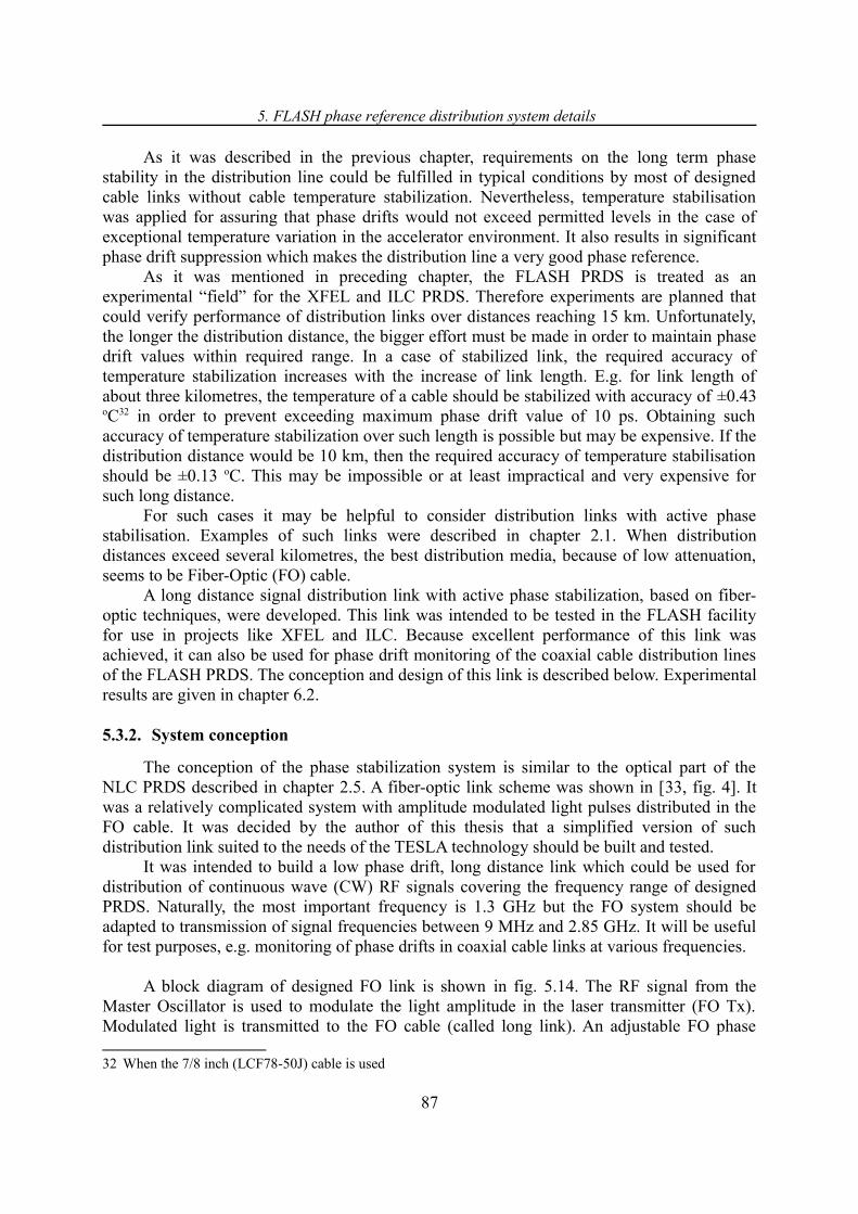
5. FLASH phase reference distribution system details
As it was described in the previous chapter, requirements on the long term phase stability in the distribution line could be fulfilled in typical conditions by most of designed cable links without cable temperature stabilization. Nevertheless, temperature stabilisation was applied for assuring that phase drifts would not exceed permitted levels in the case of exceptional temperature variation in the accelerator environment. It also results in significant phase drift suppression which makes the distribution line a very good phase reference.
As it was mentioned in preceding chapter, the FLASH PRDS is treated as an experimental “field” for the XFEL and ILC PRDS. Therefore experiments are planned that could verify performance of distribution links over distances reaching 15 km. Unfortunately, the longer the distribution distance, the bigger effort must be made in order to maintain phase drift values within required range. In a case of stabilized link, the required accuracy of temperature stabilization increases with the increase of link length. E.g. for link length of about three kilometres, the temperature of a cable should be stabilized with accuracy of ±0.43 oC32 in order to prevent exceeding maximum phase drift value of 10 ps. Obtaining such accuracy of temperature stabilization over such length is possible but may be expensive. If the distribution distance would be 10 km, then the required accuracy of temperature stabilisation should be ±0.13 oC. This may be impossible or at least impractical and very expensive for such long distance.
For such cases it may be helpful to consider distribution links with active phase stabilisation. Examples of such links were described in chapter 2.1. When distribution distances exceed several kilometres, the best distribution media, because of low attenuation, seems to be Fiber-Optic (FO) cable.
A long distance signal distribution link with active phase stabilization, based on fiber-optic techniques, were developed. This link was intended to be tested in the FLASH facility for use in projects like XFEL and ILC. Because excellent performance of this link was achieved, it can also be used for phase drift monitoring of the coaxial cable distribution lines of the FLASH PRDS. The conception and design of this link is described below. Experimental results are given in chapter 6.2.
5.3.2. System conception
The conception of the phase stabilization system is similar to the optical part of the NLC PRDS described in chapter 2.5. A fiber-optic link scheme was shown in [33, fig. 4]. It was a relatively complicated system with amplitude modulated light pulses distributed in the FO cable. It was decided by the author of this thesis that a simplified version of such distribution link suited to the needs of the TESLA technology should be built and tested.
It was intended to build a low phase drift, long distance link which could be used for distribution of continuous wave (CW) RF signals covering the frequency range of designed PRDS. Naturally, the most important frequency is 1.3 GHz but the FO system should be adapted to transmission of signal frequencies between 9 MHz and 2.85 GHz. It will be useful for test purposes, e.g. monitoring of phase drifts in coaxial cable links at various frequencies.
A block diagram of designed FO link is shown in fig. 5.14. The RF signal from the Master Oscillator is used to modulate the light amplitude in the laser transmitter (FO Tx). Modulated light is transmitted to the FO cable (called long link). An adjustable FO phase
32 When the 7/8 inch (LCF78-50J) cable is used
87

5. FLASH phase reference distribution system details
shifter is connected in series with the FO cable. The end of the long link is terminated with a mirror. The optical signal travelling through the entire link is reflected in the mirror and it returns the same way back to the optical circulator and further to the optical receiver A (called “FO Rx A”). Part of the optical signal is delivered to the optical receiver (FO Rx B) by a directional coupler located near the mirror. The optical signal is demodulated in the FO Rx B and obtained RF signal is provided to the output of the link.
Figure 5.14: Conceptual block diagram of the long-distance fiber-optic link
The difference between the phase of the input signal and the phase of the signal that travels twice throughout the entire link is measured by the phase detector. It can be assumed that the transmitted and reflected optical signals propagate with the same speed (system symmetry). It is true for most of standard optical components in the link, especially the fiber-optic cable. It can be stated that cable temperature changes affect the signal phase symmetrically (in both propagation directions) in the distribution fiber. Therefore the error voltage obtained at the output of the phase detector is carrying a precise information about the phase change in the long link. The phase change against the MO signal observed at the FO Rx A is twice as much as the phase change observed at FO Rx B.
The error voltage from the phase detector is used to adjust the phase length in the FO phase shifter. The phase error (error voltage) is decreased by means of a feedback loop. If the phase shifter used in the feedback loop also affects the signal phase symmetrically, the signal phase is stabilised at the mirror by holding the level of the detector's output voltage constant. In other words, the phase of reflected signal is kept stable. By this any “symmetrical” phase error that appears in the long link can be suppressed.
Naturally, long link signal phase changes slower than the feedback loop reaction are suppressed. As it will be described in further parts of this thesis, components used in the feedback loop (mainly the relatively slow optical phase shifter) limit the system reaction to long term phase drifts caused mainly by temperature changes. There are possibilities speeding up the feedback system reaction. But, as it was shown in chapter 3.4.8, the intrinsic phase noise level of optical links (realized in currently available technology) is relatively high and such link can not be used directly for transmission of low phase noise signals. A use of a phase-locked VCO is necessary at the output of the link in order to improve the far-of-carrier phase noise level. Such solution takes the advantages of both, long term phase stability of the FO link and good phase noise performance of the VCO.
88
Circulator Long Link Mirror
Phase Detector
DFB Laser FO Tx
FO Rx A
Phase shifter
Controller
DirectionalCoupler
FO Rx B
Error Voltage
Link output
Input Signal

5. FLASH phase reference distribution system details
It must be noticed that the signal phase is stabilised only at the mirror and the input of the FO Rx A. The phase stability at locations distant from the mirror is not warranted. Local phase changes (mainly due to local temperature variations) of significant values may occur in the FO cable laid along the accelerator in normal operating conditions. Therefore it is not recommended to make pick-up points far from the mirror. The proposed feedback scheme can be used for point-to-point applications only.
An FO system based on the principle shown in fig. 5.14 was successfully designed and tested. More technical details on the system design are given in appendix 5. Phase error analysis of the designed link is described in chapter 5.3.4. Most important experiments and measurement results showing the performance of designed link are described in chapter 6.2.
5.3.3. Optical phase shifter
One of the most critical parts of the FO link is the optical phase shifter (or equivalently: variable optical delay line). It should be chosen carefully to assure proper operation of the FO link. Therefore additional attention was devoted to the phase shifter in this chapter.
The optical phase shifter should assure sufficient phase shift range to cover phase changes in the long link fiber. It also should be electronically controlled for the purposes of use in the feedback loop. As mentioned above, the frequency response of the feedback loop is determined by the phase shifter. Therefore it is advisable to use relatively fast phase shifter.
The required phase shift (in terms of a time domain delay) value can be calculated with the use of eq. (3.55) for given optical fiber type, link length and range of temperature changes expected in the accelerator environment. A standard SMF-28 fiber with neff = 1.4682 was chosen for calculations. The value of the termo-optic coefficient given in the fiber datasheet KT = 10-5 (value of 7.5·10-6 was measured experimentally).
Calculation results are collected in table 5.6. Calculations were performed for maximum distribution distances expected in the TESLA technology based projects: 300 m for FLASH, 3 km for XFEL and 15 km for the ILC. For information, also a 1 km distance was added to calculations. Three temperature change ranges were used for calculations: 1 oC for reference, 1.5 oC and 5 oC as assumed, respectively, for peak hour and day temperature variations (see chapter 5.2.4, table 5.5).
Table 5.6: Phase shift ranges required for various distribution distances and temperature variations
Link Length [km]
Phase drift range for ΔT = 1 oC [ps]
Phase drift range for ΔT = 1.5 oC [ps]
Phase drift range for ΔT = 5 oC [ps]
0.3 (FLASH)
14.7 22.0 73.4
1 48.9 73.4 244.7
3 (XFEL)
146.8 220.2 734.1
15 (ILC)
734.1 1101.1 3670.5
There are several methods of realizing variable optical delay described in literature. An overview of most important methods is given in [31]. Number of available phase delay
89

5. FLASH phase reference distribution system details
realization methods for the purpose of designed FO link is practically limited to three:1. optical line stretching via piezoelectric effect,2. introducing a variable “air gap” into the fiber-optic link,3. change of optical length by changing temperature of a piece of fiber.
The optical line stretching is most frequently realized with a use of optical fiber wrapped on a cylinder made of a piezoelectric crystal [31, pp.2384], [43]. A diameter of this cylinder is changed by applying a voltage to the piezoelectric crystal. Mechanical stress applied to the optical fiber causes a change of the optical delay in the fiber. The main advantages of the fiber stretcher are a possibility of continuous change of delay value and a relatively high speed of such device. The frequency response of available fiber stretchers reaches range of several kilohertz. The main disadvantage is a narrow range of achievable delays – usually within single pico seconds. Therefore the usage of fiber stretchers is limited to FO links covering short distribution distances (several tenths of meters).
Second type of phase delay realization is achieved by introducing an air gap into the fiber-optic link. The principle of most frequently used solution is shown in fig. 5.15. The gap length between fiber-to-air converters is changed with use of a precise step motor.
Despite that all solutions described in this chapter are used for changing of optical delay, only the motorized solution is called by manufacturers the Optical Delay Line (ODL).
The maximum delay values achievable in commercial ODLs vary between 100 ps and 660 ps with resolution reaching single femtoseconds. Therefore ODLs can successfully be used is FO system designed for distribution distances reaching few kilometres.
Figure 5.15: Principle of realization of motorized optical delay line
The last of proposed methods of realization of variable optical delay is changing of temperature of a piece of fiber. The effect of phase change in fiber due to temperature described in chapter 3.4.6 is used. It is the same effect that causes phase drifts in the long link optical fiber.
Let us assume that the temperature change of fiber of length L is changed by ΔT. This causes a phase change in the fiber. To compensate for this phase change, the temperature of a fiber of the same length inserted in series with the main fiber should be changed by –ΔT. It is easily achievable in practice by inserting a spool with fiber into a temperature controlled chamber. Virtually every value of optical delay can be obtained with this method. It depends only on the length of a fiber and on the value of temperature change. Naturally, the limiting factors are the fiber attenuation (link gain), link noise and nonlinear effects in fiber like dispersion limiting the performance of distributed signals. Nevertheless, compensation of of phase drifts in distribution links reaching length of 20 km is achievable without significant
90
Step Motor
Fixed fiber-to-air converter
Variable fiber-to-air converter
Optical Fiber
Base
Air Gap

5. FLASH phase reference distribution system details
degradation of signal performance. The main drawback of this type of phase shifter is a relatively large inertia of a fiber spool leading to difficulties with designing high gain (low phase error) controllers for the feedback system (as shown in fig. 5.14).
Comparison of phase shift ranges achievable by optical phase shifter types described above with required phase shift values collected in table 5.6 yields a conclusion that the motorized ODL can successfully cover the FLASH distribution distances. For the XFEL it may be necessary to use a custom designed ODL (extended phase shift range) or a spool with fiber inside of a temperature controlled chamber. Use of the latter solution is necessary for distribution distances required for the ILC project.
The FO system prototype was designed and tested with both ODL and a fiber spool in the temperature controlled chamber. More details on phase shifter used in experiments are given in Appendix 3.
5.3.4. Considerations for sources of errors
Most important sources of phase errors in designed FO system and their influence on the output signal phase stability are analysed in this chapter. A part of these considerations was published by the author of this thesis in [2-A] and [3-A].
* Phase drifts in active components of the FO systemSignificant phase drift values may appear in components of the feedback system shown
in fig. 5.14. Especially the optical transmitter and receivers are sensitive to temperature variations. Output voltage changes with temperature may also appear in the phase detector even when perfectly stable signal phase difference is present at its input. Phase drifts appearing in these components may appear in the output signal of the FO system because these components are located asymmetrically in the feedback loop.
Let us assume first that phase drifts appear only in the FO transmitter. A simplified block diagram for phase error analysis is shown in fig. 5.16. Symbols Δφ with suitable indexes were assigned to corresponding phase errors.
Figure 5.16: Simplified FO link block diagram for analysis of the transmission of phase drifts in the FO Tx to the output of the link
The phase error ΔφTx appearing in the transmitter propagates to the output of the link. The same error is reflected in the mirror and it appears as ΔφA at the input of the phase detector. An error voltage proportional to this value of phase drift is obtained at the output of the phase detector. The feedback system reaction is the adjustment of the phase length in the
91
Long Link
∆ϕPS
FO Tx∆ϕ
LL
∆ϕTx
∆ϕA ∆ϕ
out = 0.5∆ϕ
TxPhase
Detector
PhaseShifter
Error Voltage

5. FLASH phase reference distribution system details
link by the phase shifter to make the error voltage equal to zero (make ΔφA = 0). But the phase of the optical signal travelling to the end of the link and back is adjusted twice by the phase shifter. Therefore after correcting for -ΔφA at the input of the phase detector, the phase change in one direction equals -0.5ΔφA. This value is appearing in the output signal of the FO link.
Similarly, the phase error appearing in the FO Rx A is corrected by the feedback loop and half of this error appears at the output of the link. Also when the output voltage of the phase detector is sensitive to temperature changes, the reaction the feedback loop is a correction of this “virtual” phase error. This error is also suppressed two times on the same principle as described above.
It is an important conclusion that the phase drifts appearing in the FO Tx, FO Rx A and in phase detector are suppressed with a factor of two by the feedback loop
Phase errors appearing in the FO Rx B can not be suppressed by the feedback because this receiver is located outside of the loop.
* Output signal phase drifts due to circulator crosstalkThe crosstalk33 between the input port and the return port of the optical circulator used
in the FO system may be a source of significant phase errors in the output signal. Because of this crosstalk, a part of the optical signal from the FO Tx gets through the circulator to the FO Rx A – path “A” shown in fig. 5.17. This signal is interfering with a signal that travels through the entire system mirrored back to the circulator. The result of this interference is a signal assigned “C”. In a long link, where the optical attenuation is significant, the power levels of signals A and B may be comparable. Let us examine the influence of this interference on the phase of the FO link output signal.
Figure 5.17: Illustration for the calculation of phase error due to circulator cross talk
The phases of signals A and B can have arbitrary values against the input signal phase. It depends on the optical lengths in the system. The phase of signal C, which is a vector sum of signals A and B (see fig. 5.18), can also be arbitrary and it is measured by the phase detector instead of signal B. The angle α of the signal C from the signal B the is the phase error caused by the crosstalk in the circulator.
33 In some datasheets of optical circulators the crosstalk is referred to as isolation
92
Circulator Long Link Mirror
Phase Detector
DFB Laser FO Tx
FO Rx A
Phase shifter
Controller
DirectionalCoupler
FO Rx B
Error Voltage
Link output
Input Signal
A B
C

5. FLASH phase reference distribution system details
Figure 5.18: Illustration to the interference of signals at the optical circulator
If the phase difference between signals A and B equals 0o or 180o, than the measured phase error α equals zero – this is “the best” case. The worst case is when the phase difference between signals A and B equals 90o or 270o – then a value of α reaches a maximum, which equals
(5.1)
This equation is valid for signal amplitudes (voltages). The optical and RF signals are usually characterized by power in units of dBm. Logarithmic measure is also used for describing crosstalk and attenuation. Therefore it is convenient to consider signal power levels.
The power value in linear scale changes with the power of 2 related to the voltage value. Therefore a following relationship is true in the linear scale
(5.2)
If the power is given in dBm, the right side of eq. (5.2) substituted to eq. (5.1) gives
(5.3)
The maximum angle values obtained with eq. (5.3) for given signal frequency value f can be converted to phase error in the time domain by
(5.4)
Typical values of circulator crosstalk in commercial devices vary between 25 dB and 55 dB. Besides crosstalk value, the power level difference between signals A and B depends also on the link attenuation34. For typical components used in the FO system, the attenuation from the input of the circulator, to the input of the FO Rx A varies between 10 dB and 20 dB. Therefore the value of ΔPdBm may vary in the range -35 dBm to -45 dBm when a circulator with crosstalk value of 55 dB is used.
Phase error values of the 1.3 GHz signal calculated with eq. (5.3) and (5.4) for various values of the power level difference between signals A and B are collected in table Błąd: Nie
34 The attenuation is a sum of all losses in optical components used in the link: circulator forward and back paths, phase shifter, long link fiber, mirror, fiber-optic connectors.
93
= arctan∣A∣
∣B∣
∣A∣∣B∣
= P A
P B
12
= arctan10∣P AdBm − PBdBm∣
10 12 = arctan10
∣ PdBm∣
20
t =
360of
A
B
Cα

5. FLASH phase reference distribution system details
znaleziono źródła odwołania.
Table 5.7: Maximum error values caused by circulator crosstalk
ΔPdBm [dBm] α [o] Δt [ps] Δt/2 [ps]
-5 29.35 62.71 31.36
-10 17.55 37.50 18.75
-15 10.08 21.54 10.77
-20 5.71 12.20 6.10
-25 3.22 688 3.44
-30 1.81 3.87 1.93
-35 1.02 2.18 1.09
-40 0.57 1.22 0.61
-45 0.32 0.69 0.34
-50 0.18 0.39 0.19
-55 0.10 0.22 0.11
It must be noticed that phase error coming from the circulator crosstalk measured by the phase detector is also suppressed by a factor of two by the feedback loop (the same principle as described above for the FO Tx). Therefore a value of Δt/2 given in the last column of table Błąd: Nie znaleziono źródła odwołania is observed at the output of the link.
Calculation results collected in the table show that within the expected range of ΔPdBm (-35 dBm to -45 dBm) error values are smaller or comparable to required 1 ps value. Therefore this error can not be neglected. Fortunately, as described above these are maximum possible values and usually this error should be much smaller.
94
6. Experiments and measurement results
6. Experiments and measurement results
The FLASH PRDS was split into three subsystems: MO System, coaxial cable distribution and FO link with active phase stabilization. Conceptual analysis and system level design of these subsystems were described in chapter 5. In this chapter experiments that were performed on designed subsystems are described. Most important measurement results are shown confirming the validity of performed considerations and showing that required phase stability of the distributed signal can be fulfilled by proposed PRDS.
6.1. Master Oscillator System performance measurements
6.1.1. MO phase noise, short term stability
The MO System was designed according to considerations described in chapter 5.1. Numerous tests and performance measurements were performed in order to verify the system performance. Measurement results important from the point of view of this thesis are described in this chapter. The phase noise spectra were measured and a short term stability (jitter values) were calculated out of measurement results.
Phase noise spectra were measured with the use of a Signal Source Analyser (SSA), E5052 manufactured by Agilent Technologies. Some of tested devices exhibited excellent phase noise levels - comparable with the sensitivity of the E5052 device. Therefore the phase noise sensitivity of the SSA is plotted in presented graphs, where necessary. The SSA offers also a function of phase jitter calculations. Jitter values given in this chapter, were calculated with this device.
Unfortunately, the input frequency range of the SSA begins at 10 MHz. Therefore the phase noise of the 9 MHz OCXO could not be measured.
More detailed description of phase noise measurement techniques and also results of additional measurement performed in the development stage of the MO System can be found in references [59], [60].
* 81 MHz PLLThe phase noise of 81 MHz VCXO phase locked to the 9 MHz OCXO is shown in fig.
6.1. This phase noise spectrum was measured at the output of the 81 MHz PLL incorporating a power amplifier – shown in fig. 5.6. The measured phase noise level is comparable with the sensitivity of the SSA in offset frequency range [1 Hz, 10 kHz]. Typical phase noise floor (sensitivity) of the SSA (at 100 MHz) is also plotted in fig. 6.1. It can be expected that for offset frequencies in range [1 Hz, 10 kHz] the phase noise of locked VCXO is significantly better than measured. To confirm this statement, phase noise level calculated for the 81 MHz signal in chapter 5.1.3 (fig. 5.2b) is also plotted in fig.6.1.There is a good agreement of calculation with measurement in offset frequency range [100 Hz, 1 MHz].
95

6. Experiments and measurement results
Figure 6.1: Measured phase noise of 81 MHz signal
Measured phase noise spectrum shows excellent performance of designed 81 MHz PLL. The calculated phase jitter value (offset frequency range [10 Hz, 1 MHz]) of 36.7 fs is also an excellent result at this frequency.
* 1.3 GHz PLLTwo 1.3 GHz VCO types were tested for the purpose of the PRDS (chpt. 5.1.3): a VCO
based on a SAW resonator and a DCSO type VCO. Unfortunately none of them could fulfil phase noise requirements for the PRDS signal. The phase noise of a free running and phase locked (to 81 MHz signal) DSCO is shown in fig. 6.2. Measured phase noise level is higher than required in offset frequency range [300 Hz, 800 kHz]. The phase jitter value calculated by the SSA (offset frequency range [10 Hz, 1 MHz]) equals about 90 fs. It is still better than required 300 fs (table 4.2). This result confirms the statement derived in chapter 4.3 (below table 4.7) that the 1.3 GHz signal phase noise was specified in the requirement document [97] with significant margin for the phase jitter values.
A phase-locked module with a Dielectric Resonator Oscillator (DRO) was under development in the time of writing this thesis. Available DRO prototype offered a possibility of obtaining phase jitter values in the range of 10 fs. Unfortunately in the time of writing this thesis only a free running DRO was available, without phase-lock circuitry so the performance of phase-locked DRO could not be measured.
* 27 MHz and 13.5 MHz frequency dividersMeasured phase noise spectra of the 13.5 MHz and 27 MHz are shown in fig. 6.3. These
signals are obtained by dividing the 81 MHz signal frequency as shown in fig. 5.8. Unfortunately, in offset frequency range [1 Hz, 1 kHz] the measured phase noise level is comparable with the phase noise floor of the SSA instrument. Therefore it is probable than
96
1 1 0 1 0 0 1 k 1 0 k 1 0 0 k 1 M 1 0 M
- 1 6 0
- 1 4 0
- 1 2 0
- 1 0 0
- 8 0
- 6 0
f [Hz]
L(
f )
[dB
c/H
z]
8 1 M H z V C X O f r e e8 1 M H z V C X O l o c k e dS S A p h a s e n o i s e f l o o rC a l c u l a t e d 8 1 M H z p h a s e n o i s e

6. Experiments and measurement results
real phase noise levels are smaller than measured.
1 0 1 0 0 1 k 1 0 k 1 0 0 k 1 M 1 0 M
- 1 6 0
- 1 4 0
- 1 2 0
- 1 0 0
- 8 0
- 6 0
- 4 0
- 2 0
f [Hz]
L(
f )
[dB
c/H
z]
1 . 3 G H z V C O f r e e1 . 3 G H z V C O l o c k e dR e q u i r e m e n t
Figure 6.2: Measured phase noise of 1.3 GHz signal
Figure 6.3: Measured phase noise of 13.5 MHz and 27 MHz signals
For offset frequencies greater than 1 kHz the measured phase noise level (-153 dBc @ 27 MHz) is higher than calculated in chapter 5.1.3 for this frequency generation scheme - see
97
1 1 0 1 0 0 1 k 1 0 k 1 0 0 k 1 M 1 0 M- 1 7 0
- 1 6 0
- 1 5 0
- 1 4 0
- 1 3 0
- 1 2 0
- 1 1 0
- 1 0 0
- 9 0
- 8 0
- 7 0
- 6 0
f [Hz]
L(
f )
[dB
c/H
z]
1 3 . 5 M H z2 7 M H zS S A n o i s e f l o o r

6. Experiments and measurement results
fig. 5.4. The reason of phase noise level degradation is the intrinsic phase noise of the frequency divider chip used in the system – shown in fig. 5.7. The measured values correspond to the values given in the datasheet of the frequency divider chip.
It can be noticed that (by a coincidence) measured phase noise levels of 27 MHz signal obtained with used frequency divider are comparable to theoretically calculated phase noise levels of 27 MHz signal obtained by multiplication (·3) of the 9 MHz signal (shown in fig. 5.4). Most probably real frequency multiplier would also cause some additional increase of the output signal phase noise level. Therefore the legitimacy of use the scheme with frequency division (fig. 5.3b) instead of the scheme with frequency multiplication (fig. 5.3a) is confirmed.
6.1.2. Phase drifts in the MO System
Many test were performed in the MO System development stage to verify the long therm stability of generated signals. There were too many experiments to present them all in this thesis. Therefore general conclusions are described and only one example of measurement of phase drifts in 1.3 GHz power amplifier is presented below.
It was found that the temperature sensitivity of signal phase in active devices is an important issue. In general, phase was changing in the range of about 1 ps to 3 ps per 1 oC of temperature change of the active device. Interesting measurement results, confirming this statement for designed PLLs, were published in [1-A]. Such sensitivity to temperature confirms the legitimacy of installing the MO System in a temperature stabilized environment. By this the long term phase drift values will be minimized to acceptable level.
* Phase drifts in 1.3 GHz power Amplifier against temperaturePhase drifts were measured with a self developed phase detector module described in
Appendix 6. The temperature of devices other than the currently tested circuit was stabilized during phase drift measurements. During some tests controlled temperature steps were applied on tested devices. For this purpose a self developed temperature controlled chamber described in Appendix 4 was used. Other tests were performed without controlling temperature of tested device – air temperature (in laboratory) was measured.
Figure 6.4: Set-up for 1.3 GHz Power Amplifier drift measurements
98
1.3 GHz
~
Phase Detector
ΔtpreAmp
pre-AmplifierPower Splitter
+20 dBm
Power Amplifier
+43 dBm
Phase Detector
ΔtPowerAmp
ΔtTotal
+37 dB +23 dBG = G =

6. Experiments and measurement results
It was claimed in chapter 4 that phase drifts in power amplifiers can be a significant contribution the overall PRDS performance. Unfortunately amplifier manufacturers very rarely provide data on phase drifts. To confirm the statement mentioned above, phase drifts in the 1.3 GHz Power Amplifier (PA) module designed for the MO System (fig. 5.5) were measured. The measured PA consists of two amplifying stages – pre-amplifier and a power amplifier.
The principle of phase drift measurement is shown in fig. 6.4. Two precise and temperature stable phase detectors were used to measure phase drifts in each amplifying stage. The measurement was performed in laboratory conditions over 11 hours. The phase drift values, the temperature of each amplifier and the air temperature was recorded to find a correlation between the temperature and phase drift values. More detailed description of the measurement set-up can be found in the report [91].
Figure 6.5: Results of 1.3 GHz phase drift measurements: upper plot – pre-Amplifier, middle plot – Power Amplifier, lower plot – total phase drift in PA module. Figure
published also in [91]
Obtained results are shown in fig. 6.5. The upper plot shows phase drifts in the pre-amplifier. The middle plot shows phase drifts in the power amplifier stage. The pre-amplifier exhibits greater temperature sensitivity of phase drifts. Interesting is that both amplifiers have
99
0 2 4 6 8 1 0 1 23 5
4 0
4 5
PA
tem
pera
ture
[*C
]
c o r r e l a t i o n = 9 7 . 7 7 %
0 2 4 6 8 1 0 1 2- 3
- 2
- 1
0
1
2
3
PA
pha
se d
iff.
[ps]
P o w e r A m p t e m p
P o w e r A m p d r i f t
0 2 4 6 8 1 0 1 23 5
3 7 . 5
4 0
preA
mp
tem
pera
ture
[*C
]
c o r r e l a t i o n = 9 2 . 8 1 %
0 2 4 6 8 1 0 1 2- 1
- 0 . 5
0
0 . 5
1
preA
mp
phas
e di
ff.
[ps]p r e A m p t e m p
p r e A m p d r i f t
0 2 4 6 8 1 0 1 22 6
2 7
2 8
Am
bien
t T
empe
ratu
re [
*C]
t i m e [ h r s ]
c o r r e l a t i o n = 9 2 . 7 9 %
0 2 4 6 8 1 0 1 2
- 1
0
1
2
Tot
al p
hase
diff
. [p
s]A m b i e n t T e m p
T o t a l d r i f t
6. Experiments and measurement results
opposite temperature coefficients. Phase difference over the pre-amplifier is decreasing with increasing value of temperature. In the power amplifier, the phase difference is increasing with increasing temperature. Therefore these phase drifts compensate partly. The total phase drift being a sum of both contributors (lower plot in fig. 6.5) is of smaller range than the pre-amplifier drift.
The correlation of measured phase drifts with temperature was calculated - values shown in fig. 6.5. Values significantly exceeding 90 % confirm that changes of temperature are the main reason of the long term stability degradation in active circuits used in the PRDS.
6.2. Fiber-optic link performance
The prototype of the FO link described in chapter 5.3 was built and tested. It was explained in chapter 5.3.3 that two phase shifter types can be used in the FO system depending on the distribution distance. The motorized Optical Delay Line (described in Appendix 3) can be used in the FLASH facility. For the XFEL and ILC a phase sifter made of a fiber spool located inside of a temperature controlled chamber (for simplicity called “oven” in further text of this thesis) should be used. But this kind of phase shifter is characterised with large inertia leading to problems with realization of precise phase control loop. Therefore an idea of testing both phase shifter types connected in series to take advantages of both solutions was developed.
Three experiments were performed. With the ODL, with the spool in the oven and with both phase shifters connected in series. The measurement set-up and results of these experiments are described blow.
6.2.1. FO system test set-up
The block diagram of the measurement set-up of the FO system is shown in fig. 6.6. A temperature controlled oven with a fiber (SMF-28 fiber type) spool fixed inside (length depending on test purpose) was used for simulation of the long link. Such solution made it possible to test the FO system behaviour after applying controlled temperature changes to the long link fiber. The FO link output signal phase drifts were measured directly (by additional phase detector) against the input signal phase.
The error voltage from the feedback loop phase detector was provided to a microcontroller based data acquisition system. During the first tests an evaluation board of the microcontroller was used. Later, for the final FO system version, a custom board with desired features was developed (see Appendix 5). The description of the developed board can be found in the thesis [50].
The micro-controller board was connected to a PC with a self-developed controller software. A standard PID (Proportional – Integral – Derivative) [105, ch. 1] controller type was applied. A Graphic User Interface (GUI) (described in Appendix 5) for the FO system controller was developed in the Matlab® environment. Error voltage was processed in the PC and results were sent back to the microcontroller and further to the phase shifter. Use of a PC with a GUI was a very convenient solution because it allowed for easy data processing, visualisation and storage – necessary in the development stage of the FO link. More detailed description of the development of the FO system PID controller and the GUI can be found in the thesis [29].
100

6. Experiments and measurement results
Figure 6.6: The measurement set-up of the FO system
In the development stage of the FO link, the microcontroller board was used as a data acquisition system (interface between PC and FO system). The same board is intended to work as a standalone (PC independent) system controller in the final FO system version. The PID controller software developed in the Matlab® language will later be converted to microcontroller software. With such approach, the same hardware was used for the system development and for the final system, which of course is advantageous.
The electronics used in the experimental set-up was assembled inside a small crate with a low-noise power supply circuits. A semi-rigid cables with SMA connectors were used for the RF signals because it was found that connections made with flexible cables are sensitive to mechanical vibrations. The assembled crate is shown in Appendix 5.
A fiber-optic transmitter incorporating a temperature stabilized semiconductor laser was developed (shown in Appendix 5). Commercial, fiber-optic receivers were used. All used fiber-optic components were equipped with FC/APC type connectors. It allowed for easy modifications of the system.
All passive fiber-optic components (except spools with fiber) were assembled on a plate covered with a soft foam – called further “optical breadboard” - see Appendix 5. By the use of such breadboard the system sensitivity to mechanical vibrations was suppressed.
The entire FO system test set-up was assembled inside of a big industrial climate chamber as shown in fig. 6.7. Set-up temperature was stabilized in order to minimize potential errors in system components, especially in phase detectors.
All measurements described below were performed with 1.3 GHz signal.
101
Circulator
Long Link Simulator
MirrorDFB Laser
FO Tx
FOa Rx A
Phase ShifterDirectionalCoupler
FO Rx B
Error Voltage
Link Output
Input Signal
Microcontroller
SerialPort
DAC
ADC
ADC
Serial Port
PC with Matlab GUI
Output PhaseError
Temp. change
Phase Detector
Phase Detector

6. Experiments and measurement results
Figure 6.7: FO system with ODL assembled in the climate chamber
6.2.2. FO system with ODL
Numerous tests were performed with 5 km fiber spool used as a long link. This was a spool with shortest fiber available in the experiment time. The temperature variations in the long link simulator oven were limited to 1.5 oC. Phase drifts caused by that range of of temperature changes could be compensated by the ODL.
Most important results of performed experiments are described in the reminder of this chapter. More detailed description of the experiment and more measurement results can be found in [2-A] and [29].
Figure 6.8: Phase drifts in the long link fiber (5 km) after the temperature step of 0.5oC. Measured with open feedback loop
102
Opticalbreadboardwith ODL
Long link simulator
Micro-controller
board
Crate withelectronics
1.3 GHz signalsource
0 0 . 5 1 1 . 5 2 2 . 5 3 3 . 5 4- 5 0
0
5 0
1 0 0
1 5 0
2 0 0
2 5 0
T i m e [ h ]
Pha
se C
hang
e [p
s]
R x A S ig n a l
R x B S ig n a l
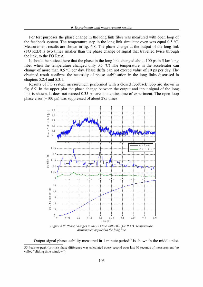
6. Experiments and measurement results
For test purposes the phase change in the long link fiber was measured with open loop of the feedback system. The temperature step in the long link simulator oven was equal 0.5 oC. Measurement results are shown in fig. 6.8. The phase change at the output of the long link (FO RxB) is two times smaller than the phase change of signal that travelled twice through the link, to the FO Rx A.
It should be noticed here that the phase in the long link changed about 100 ps in 5 km long fiber when the temperature changed only 0.5 oC! The temperature in the accelerator can change of more than 0.5 oC per day. Phase drifts can not exceed value of 10 ps per day. The obtained result confirms the necessity of phase stabilisation in the long links discussed in chapters 5.2.4 and 5.3.1.
Results of FO system measurement performed with a closed feedback loop are shown in fig. 6.9. In the upper plot the phase change between the output and input signal of the long link is shown. It does not exceed 0.35 ps over the entire time of experiment. The open loop phase error (~100 ps) was suppressed of about 285 times!
Figure 6.9: Phase changes in the FO link with ODL for 0.5 oC temperature disturbance applied to the long link
Output signal phase stability measured in 1 minute period35 is shown in the middle plot.
35 Peak-to-peak (or rms) phase difference was calculated every second over last 60 seconds of measurement (so called “sliding time window”)
103
0 . 0 5 0 . 1 0 . 1 5 0 . 2 0 . 2 5 0 . 3 0 . 3 5 0 . 4
0
0 . 1
0 . 2
0 . 3
0 . 4
0 . 5
Pha
se D
rift
at R
xB [
ps]
0 . 0 5 0 . 1 0 . 1 5 0 . 2 0 . 2 5 0 . 3 0 . 3 5 0 . 4 0
0 . 0 5
0 . 1
0 . 1 5
0 . 2
0 . 2 5
Sta
bilit
y [p
s]
0 0 . 0 5 0 . 1 0 . 1 5 0 . 2 0 . 2 5 0 . 3 0 . 3 5 0 . 4 0 . 4 50
1 0
2 0
3 0
4 0
5 0
T i m e [ h ]
OD
L M
ovem
ent
[ps]
p p - 1 m i n
r m s - 1 m i n
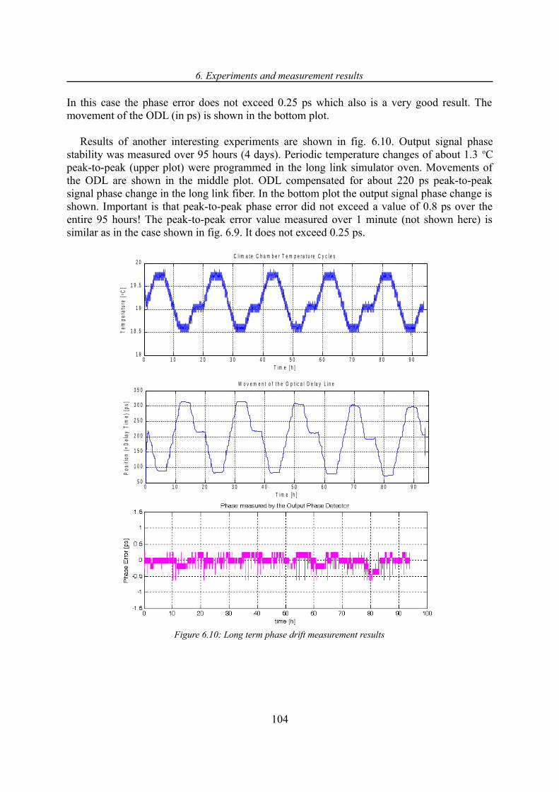
6. Experiments and measurement results
In this case the phase error does not exceed 0.25 ps which also is a very good result. The movement of the ODL (in ps) is shown in the bottom plot.
Results of another interesting experiments are shown in fig. 6.10. Output signal phase stability was measured over 95 hours (4 days). Periodic temperature changes of about 1.3 oC peak-to-peak (upper plot) were programmed in the long link simulator oven. Movements of the ODL are shown in the middle plot. ODL compensated for about 220 ps peak-to-peak signal phase change in the long link fiber. In the bottom plot the output signal phase change is shown. Important is that peak-to-peak phase error did not exceed a value of 0.8 ps over the entire 95 hours! The peak-to-peak error value measured over 1 minute (not shown here) is similar as in the case shown in fig. 6.9. It does not exceed 0.25 ps.
0 1 0 2 0 3 0 4 0 5 0 6 0 7 0 8 0 9 01 8
1 8 . 5
1 9
1 9 . 5
2 0C l i m a t e C h a m b e r T e m p e r a t u r e C y c l e s
T i m e [ h ]
Tem
pera
ture
[°C
]
0 1 0 2 0 3 0 4 0 5 0 6 0 7 0 8 0 9 05 0
1 0 0
1 5 0
2 0 0
2 5 0
3 0 0
3 5 0
T i m e [ h ]
Pos
ition
(=
Del
ay T
ime)
[ps
]
M o v e m e n t o f t h e O p t i c a l D e l a y L i n e
Figure 6.10: Long term phase drift measurement results
104

6. Experiments and measurement results
6.2.3. FO system with phase shifter made of fiber spool in the oven
The FO link was tested also with the phase shifter made of a fiber spool inside of the oven. The measurement set-up scheme was the same as shown in fig. 6.6. An example of measurement result is shown in fig. 6.11. The phase difference between the FO link output and its input is shown in the upper plot. The peak value of phase change reaches 2 ps. This is caused by too slow reaction of the phase shifter caused by relatively big inertia of the fiber spool. For the same reason the signal stability (middle plot) measured over one minute is also worse than in the case of the system with ODL. The peak value reaches 1 ps, which is 4 times more than in the ODL case. The biggest phase change of the output signal is observed during the fastest phase change in the long link simulator – during the temperature change in the long link simulator oven. The phase shifter was too slow to react properly.
Fortunately, in the accelerator conditions, the phase changes in the long link should be slower than in the long link simulator oven. Therefore results obtained in the accelerator environment should be better.
Figure 6.11: Phase changes in the FO link with the spool in oven for 0.5 oC temperature disturbance applied to the long link simulator
More tests were performed with this phase shifter type. System performance with long link lengths reaching 20 km was tested. High phase error suppression was also obtained. Measurement results are not shown in this thesis (actually, they look similarly to plotted in fig. 6.11). Description of representative experiments can be found in [4-A], [3-A], [6-A], [7-A], [25].
105
0
0 . 5
1
1 . 5
2
Pha
se D
rift
at R
xB [
ps]
0
0 , 2
0 , 4
0 , 6
0 , 8
Sta
bilit
y [p
s]
0 0 . 2 0 . 4 0 . 6 0 . 8 1
0
3 0
6 0
9 0
1 2 0
T i m e [ h ]
Pha
se S
hift
er R
eact
ion
[ps]
p p - 1 m i n
r m s - 1 m i n

6. Experiments and measurement results
6.2.4. FO system with ODL and fiber spool in oven
A conception of using two phase shifters connected in series in the FO link was also tested. Such solution may be useful for large distribution distances like in XFEL and ILC. The advantages of both phase shifter types could be taken – the large phase shift range of the fiber spool in the oven and a fast response of the ODL. With such solution much smaller phase errors of the output signal are expected.
Measurement set-up was, again, similar to the one shown in fig. 6.6, but the Matlab GUI software was modified. A PID controller for two phase shifters was developed. Detailed description of this experiment can be found in [29]. Example of measurement results is shown in fig. 6.12. A temperature step of -0.5 oC was applied to a 5 km of fiber in the long link. This induced about 100 ps of phase change in the fiber. After about 1.3 hour the temperature was changed back to the beginning value – a temperature step of + 0.5 oC was applied.
Figure 6.12: Phase changes in the FO link with two phase shifters connected in series for 0.5 oC temperature disturbance applied to the long link simulator
Two bottom plots in fig. 6.12 show the reaction of both phase shifters on the disturbance in the long link. The oven corrected for the entire 100 ps of the phase change. But in the time of fastest phase changes in the long link, the ODL compensated for phase error caused by too slow reaction of the oven phase shifter. One can see two ODL reactions around the time of 0.1 hour and 1.5 hour. In the time where the oven phase shifter speed was sufficient, the ODL reaction was equal to almost zero.
The most important, upper plot in fig. 6.12 is showing the measured phase difference between the long link output and the input signal. The peak value of this phase difference only slightly exceeded 0.2 ps over the entire measurement (2 hour long). This is an excellent result taking into account that the distribution distance was 5 km. The short term stability, measured over 1 minute varied about the value of 0.1 ps, which also is a very good result.
106
- 0 . 1
0
0 . 1
Pha
se D
rift
at R
xB [p
s]
0
0 . 1
0 . 2
Sta
bilit
y [p
s]
- 5
0
5
OD
L M
ovem
ent [
ps]
0 0 . 2 0 . 4 0 . 6 0 . 8 1 1 . 2 1 . 4 1 . 6 1 . 8 2- 1 2 0
- 9 0
- 6 0
- 3 0
0
T i m e [ h ]
Ove
n P
hase
Shi
fter
Rea
ctio
n [p
s]
p p - 1 m i n
r m s - 1 m i n
p s - 1 h o u r
r m s - 1 h o u r

7. Summary and conclusions
7. Summary and conclusions
7.1. Summary
This thesis was devoted to the design and performance analysis of the PRDS for the 300 meter long FLASH accelerator. The considerations begun in chapter 2 with definition of the PRDS meaning and description of possible PRDS architecture types. Also a brief descriptions of formerly realized representative types of PRDS architectures were given. Next, in chapter 3, the knowledge important for the PRDS designer was gathered and referenced to significant number of cited publications broadening the provided descriptions. Standard, internationally approved definitions of phase instabilities were given. Phase instabilities characterisation methods that can be useful for the PRDS design were addressed. The most important PRDS components and their influence on the signal phase stability were characterised.
Chapter 4 was devoted to the analysis of FLASH PRDS design requirements, development of PRDS design method and a proposal of the PRDS architecture. The theoretical background for specification of the synchronization accuracy for the accelerator was given. The synchronization requirements are derived from required parameters of the accelerated electron bunches. Only rare publications covering the difficult subject of accelerator system behaviour analysis for deriving precise phase jitter values required at PRDS outputs were found. This subject is far beyond the scope of this thesis but it is important to understand the origin of requirements and it was found that most probably requirements given for the FLASH PRDS were specified with too high margin of synchronization accuracy. Nevertheless, further considerations were performed with existing requirements.
In the further part of the chapter 4 important details of the FLASH PRDS requirements were given and a method for the system design was proposed. Considerations on the choice of a suitable PRDS architecture were performed. Finally, the PRDS architecture was proposed with important system-level choices and assumptions being a starting point for more detailed system design.
In chapter 5 the detailed description of the FLASH PRDS design was given. The system was split into three subsystems: the MO, the coaxial cable distribution system and the FO link with active phase stabilisation. Different signal generation schemes in the MO System were analysed. The legitimacy of choices taken in the chapter 4 was confirmed. Final design of the MO System was proposed and the performance of the system made of commercially available components was analysed (phase jitter values were calculated).
In the second part of chapter 5 the design and performance analysis of coaxial cable signal distribution system was described. It was shown that a complete design of a system of cable links is not a trivial task that requires a significant effort. Considerations on the choice of cable type were performed. Detailed cable system layout was proposed and its performance was analysed. Expected values of phase drifts in cables installed in the FLASH tunnel were calculated. It was shown that cable temperature stabilisation is important for assuring sufficiently low values of long term signal phase drifts. Also power calculations were
107

7. Summary and conclusions
performed for the distribution link. Many additional considerations showing issues important for designing cable distribution links for longer distances, like for the XFEL were described.
In the last part of chapter 5 the design of the long distance FO link with active phase stabilisation was described. The system conception was explained and detailed performance analysis was performed. Sources of phase errors were characterized.
In chapter 6 there were described experiments performed on realized PRDS subsystems. The phase noise (short term stability) and phase drifts of representative MO System components were measured. Very good agreement with theoretical considerations performed in preceding chapters was achieved. Also numerous tests of the FO system performance were presented. An excellent value of the long term signal phase stability of 0.1ps (peak-to-peak) over hours of measurement duration was achieved in 5 km long fiber link.
The short description of measurements given in chapter 6 was extended by six appendices showing important technical details and pictures of realised PRDS subsystems.
7.2. Conclusions and notes on achieved research goals
The author of this thesis was given a task of designing a PRDS for the FLASH accelerator. The designed system should fulfil the FLASH facility performance requirements but also it was intended to be an experimental base for development of PRDS for bigger projects like XFEL and ILC.
The first goal of this thesis was the analysis of most important issues affecting the final performance of the PRDS. This goal was achieved in the theoretical part of this work (chapters 3, 4 and 5). There are two main measures of the PRDS performance: the short and the long term stability of the output signal. The short term stability is related to the phase noise performance of PRDS components. The long term stability is affected by signal phase drifts in devices used for the PRDS design. Characterization and analysis of both types of stability was the main subject of the theoretical chapters. All design choices (like choice of subsystem architecture or selection of appropriate devices for subsystem realization) were preceded by considerations on the influence of this choice on the output signal phase stability. The validity of performed considerations was confirmed by many experiments described in chapter 6.
The second goal of this work was the development of a simple, practical method for designing such complicated PRDS. It was shown in chapter 4 that the complexity of designed PRDS is so great and there are so many interdependent issues affecting the final system performance that it is almost impossible and for sure impractical to make a complete mathematical system model allowing for precise system synthesis. Therefore considerations were limited to range allowing for designing a PRDS that fulfils given requirements. The second goal was achieved in two ways. First, in chapter 4, by giving a simple algorithm for the PRDS architecture choice. Second way is shown in chapters 4 and 5 by consequent system development. The design was started on the PRDS top-level by dividing it into three subsystems. Next, requirements for these subsystems were analysed and subsystem details were developed basing on this analysis. Proposed method may be simple and obvious for an experienced PRDS designer. But for sure, reading of chapters 4 and 5 may provide an enormous help for a researcher beginning with such challenging task as a new PRDS design.
The third, and most important goal of this thesis was the design and realization of a
108
7. Summary and conclusions
working PRDS for the FLASH facility with effective use of gathered knowledge. This goal was also achieved. A complete system of electronic devices was realized. Many of these devices are described in appendices. Photographs shown there should give sufficient impression on the scale of performed work. Further confirmation of achieving the third goal is given in chapter, 6 where results of performance measurements of designed PRDS subsystems were presented. These results confirm the validity of performed considerations and show that the required PRDS performance should be achieved. The PRDS was prepared for installation in the FLASH facility. The only issue that was not achieved was the performance measurement of the entire PRDS installed in the FLASH facility. It was impossible because the MO System and the FO link were not installed in the FLASH facility till the time of writing this thesis. The installation is a complicated process of replacing the existing “old” MO with the new MO System. It requires switching off the accelerator for a longer period of time which was possible after the time foreseen for completion of this thesis.
The last but not least goal was to gather the experience - both knowledge and experimental results - useful for the design of PRDS for larger accelerators like the XFEL and ILC, was also achieved. The theoretical knowledge on the instabilities and their sources that are described in chapter 3 is universal and can successfully be used in bigger PRDS. Considerations on extending distribution distance of the designed PRDS were appearing frequently in chapter 4. Calculations of the long term drift performance of coaxial cable links for long distribution distances were performed in chapter 5. The FO link described in chapters 5 and 6 is an excellent tool that can be used for highly phase stable signal distribution over long distances. The practical experience gathered during experiments (e.g. necessity of using semi-rigid cables for device interconnections) described in chapters 5, 6 and in appendices may be a very valuable contribution for future PRDS designers.
There is one more achievement of this thesis. It is a successful cooperation with people (see acknowledgements). The MO System was prepared by tight cooperation of few people from ISE, DESY and the Inwave GmbH company. Three BS.c theses (one Polish and two German (Diploma)) written by excellent and hard working students were driven by the development of the FO link project.
7.3. Perspectives of further research
First of all, the installation of designed PRDS should be accomplished in the FLASH facility few months after completion of this thesis. A significant number of performance measurements of the entire system will have to be performed.
In the nearest future, the design of the XFEL project will start. It will also require PRDS design. The considerations on the FLASH PRDS described in this thesis will be a good starting point for the XFEL PRDS, where requirements on distributed frequencies and synchronization accuracy are similar to FLASH PRDS requirements considered here. The PRDS size (distribution distances) for the XFEL will be greater. Therefore it seems that there will be more optical techniques than in the FLASH PRDS used for the XFEL PRDS. Nevertheless, the PRDS output signal is an RF signal and local signal distribution (over one or few RF stations, up to e.g. 100 meters) between optical fiber links and RF system devices will be necessary. Therefore results of this thesis may be very useful for this application.
The ILC is also planned to be developed in a little more distant future. Since that
109

7. Summary and conclusions
accelerator will also be based on the TESLA technology, the results of this thesis may also be important for the ILC PRDS development.
110
8. Appendix 1 – MO System design details and project management
8. Appendix 1 – MO System design details and project management
Most important design issues of the MO System were described in chapter 5.1. The MO System was designed according to this description. As it was shown in fig. 5.5, the MO System was split to six 19 inch crates. Each crate incorporates necessary frequency generation and distribution devices and a significant number of auxiliary devices (not shown in fig.5.5) like diagnostic and performance monitoring circuits. The number of necessary devices and very sharp design requirements made the MO System a very big and complicated project. A lot of research and experiments had to be performed before the final system version was assembled. The MO System development was performed by a team of people from DESY, the company Inwave GmbH and Warsaw University of Technology (WUT). The author of this thesis made a very significant contribution to the final design of the system by designing and testing many MO System devices.
This Appendix is devoted to the description of important technical details that influence the overall performance of the MO System. The final system assembly is also shown.
As it was described in the preceding chapters of this thesis, the temperature changes are one of the major factors causing the degradation of the long term phase stability of signals generated and distributed in the PRDS. Therefore special attention was put into minimising the influence of the temperature changes in the MO System components. All electronic circuits of the signal generation and distribution chain were assembled in thick metal (aluminium) boxes – examples are shown below, in photographs. These boxes were fixed to thick aluminium plate (chassis) inside of MO System crates. Low thermal resistance between boxes and chassis was assured by a thermal-conductive paste. In order to minimise the influence of air temperature changes on the chassis temperature, crates without ventilation slots were used. Such design of a crate assured relatively large thermal inertia and good heat distribution within the crate. The installation of the MO System inside of a temperature stabilized area is planned in the FLASH system. By this phase drifts in the MO System will be further suppressed.
The device assembly in metal boxes with connectors has also the advantage that each device could be easily replaced with another (improved) version (if needed) without reworking the entire crate. Such modular structure was very useful in the development stage of the MO System.
As mentioned above, besides the frequency generation devices, each crate of the MO System incorporates a number of auxiliary devices. Power level (or amplitude) monitors were applied to almost every device in the signal chain. There are also phase-lock detect circuits for each PLL and power supply voltage monitors. All signals from monitoring devices are collected by so called “amplitude supervision board”. Signals are provided from this board to a digital display installed at the front panels of each MO. There is also a connector with monitoring signals assembled on the back panel of each crate. A data acquisition system based on microcontroller boards similar to described in Appendix 5 is under development in the time of writing this thesis. This system will be connected on-line via ethernet to the accelerator control system. Phase drift measurement results will be stored and warning
111

8. Appendix 1 – MO System design details and project management
messages will be sent to FLASH operators in case of e.g. loosed phase-lock in one of PLLs. As it was mentioned in chapter 5.1, semi-rigid cables with SMA connectors were used
for interconnections between devices inside of each crate. It was found experimentally that such solution minimizes the sensitivity of the MO System to mechanical vibrations. When flexible cables were used phase jumps of amplitude reaching 2 ps occurred randomly in measured signals. But the use of semi-rigid cables made the crate design more difficult because minimum cable bending radius and avoidance of mechanical stress had to be assured. Because of this the design of the layout of devices in the MO System crates was a very difficult task. Example of such design is shown in the further text of this appendix.
There were two exact copies of the MO crates built and are assembled in the FLASH system for backup purposes. In case of fault in any crate, it can be quickly replaced with a backup one. Possible long break needed for repairing the damaged crate would be avoided by such solution. There are three copies of LPP crate because one of them is needed in accelerator module test facility (another project, not a part of the FLASH facility).
The list of crates an their amount is given below:- LPP – 3 pieces- 81 MHz Power Amplifier – 2 pieces- 1.3 GHz Power Amplifier – 2 pieces- 1.3 GHz PLL – 5 pieces- 81 MHz Distribution Box – 1 piece- 1.3 GHz Distribution Box – 1 piece
All together there are fourteen of 19 inch crates built for the MO System. This is quite a complicated system and a good planning was necessary during the work.
As described above, the mechanical assembly of the MO System crates was a complicated task and a good design preparation taking into account temperature stabilisation was necessary. Assembly drawings were made by the author of this thesis for each MO System crate. As an example, the assembly drawings of the LPP crates is shown below.
Because of the complexity, and large number of devices, the LPP chassis was fixed in the middle (height) of the crate and devices were assembled on both sides (called top and bottom side) of the chassis. The assembly drawing for the top side of the LPP chassis is shown in fig. 8.1. Number of devices in thick metal boxes is drawn with black lines. Devices assembled on the bottom side of the chassis are drawn with yellow lines. Also the semi-rigid cable connections are shown. Semi-rigid cable connections between the LPP devices and the front panel are drawn as lines with open ends directed towards the bottom of the drawing.
The assembly drawing for the bottom side of the LPP chassis is shown in fig. 8.2. This is a top side view for easier comparison with fig. 8.1. The devices assembled on the bottom side are drawn with black lines.
The photograph of the LPP crate assembled according to drawings shown above is shown in fig. 8.3. It is a picture from early stage of development, without semi-rigid cables. Some connections were made with flexible cables for test purposes.
The photograph of the LPP chassis assembled in the crate is shown in fig. 8.4. One can see the thick chassis and devices assembled on both sides.
112
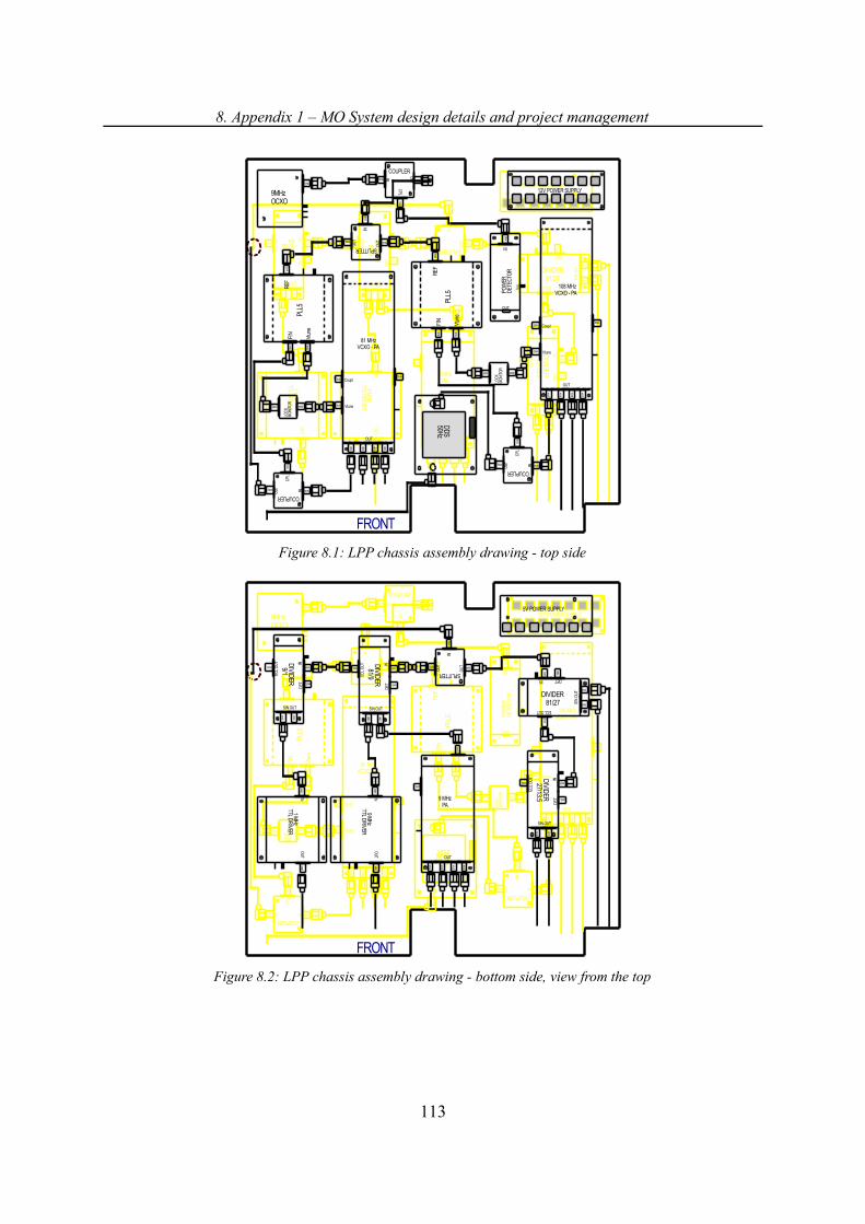
8. Appendix 1 – MO System design details and project management
Figure 8.1: LPP chassis assembly drawing - top side
Figure 8.2: LPP chassis assembly drawing - bottom side, view from the top
113
IN
OUTOUT
SPLITTER
SMA
SMASMA
OUT
9 MHz PA
SMA
SMA
SMA
SMA
SMA
SMA
INO
UT
9 MHz
TTL DRIVER
SMA
SMA
INO
UT
1 MHz
TTL DRIVER
SMA
SMA
5V POWER SUPPLY
DIVIDER 9/1
INDE
T
ECL
OUT
SIN OUT
SMA
SMA
SMA
SMA
SMA
DIVIDER 81/9
INDE
T
ECL
OUT
SIN OUT
SMA
SMA
SMA
SMA
SMA
DIVIDER 27/13.5
INDE
T
ECL
OUT
SIN OUT
SMA
SMA
SMA
SMA
SMA
DIVIDER 81/27
IN DET
ECL OUT
SIN
OUT
SMA
SMA
SMA
SMA
SMA
SMA
SMA
LOCK
MON
ITOR
SMA
SMA
LOCK
MO
NITO
RCP
L
INOUT
COUPLER
SMA
SMASMA
PLL5
SMA
SMA
SMA
REF
FIN
Vtun
ePLL5
SMA
SMA
SMA
REF
FIN
Vtun
e
IN
OUTOUT
SPLITTER
SMA
SMASMA
SMA Vtune
OUT
81 MHzVCXO - PA
SMASMA Coupl
SMA
SMA
SMA
SMA
50 HzDDS
DDS50Hz
SMA Vtune
OUT
108 MHzVCXO - PA
SMASMA Coupl
SMA
SMA
SMA
SMA
CPL
IN
OUT
COUPLER
SMA
SMA SMA
POW
ERDE
TECT
OR
OUT
IN
SMA
Vcc
CPL
INOUT
COUPLER
SMA
SMASMA
SMA
9MHzOCXO
12V POWER SUPPLY
FRONT
FRONT
SMA
SMA
LOCK
MON
ITOR
SMA
SMA
LOCK
MO
NITO
RCP
L
INOUT
COUPLER
SMA
SMASMA
PLL5
SMA
SMA
SMA
REF
FIN
Vtun
e
IN
OUTOUT
SPLITTER
SMA
SMASMA
SMA Vtune
OUT
108 MHzVCXO - PA
SMASMA Coupl
SMA
SMA
SMA
SMA
CPL
IN
OUT
COUPLER
SMA
SMA SMA12V POWER SUPPLY
50 HzDDS
DDS50Hz
SMA9MHzOCXO
POW
ERDE
TECT
OR
OUT
IN
SMA
Vcc
PLL5
SMA
SMA
SMA
REF
FIN
Vtun
e
SMA Vtune
OUT
81 MHzVCXO - PA
SMASMA Coupl
SMA
SMA
SMA
SMA
CPL
INOUT
COUPLER
SMA
SMASMA
IN
OUTOUT
SPLITTER
SMA
SMASMA
OUT
9 MHz PA
SMA
SMA
SMA
SMA
SMA
SMA
INO
UT
9 MHz
TTL DRIVER
SMA
SMA
INO
UT
1 MHz
TTL DRIVER
SMA
SMA
5V POWER SUPPLY
DIVIDER 9/1
INDE
T
ECL
OUT
SIN OUT
SMA
SMA
SMA
SMA
SMA
DIVIDER 81/9
INDE
T
ECL
OUT
SIN OUT
SMA
SMA
SMA
SMA
SMA
DIVIDER 27/13.5
INDE
T
ECL
OUT
SIN OUT
SMA
SMA
SMA
SMA
SMA
DIVIDER 81/27
IN DET
ECL OUT
SIN
OUT
SMA
SMA
SMA
SMA
SMA

8. Appendix 1 – MO System design details and project management
Figure 8.3: Photograph of the top side of the LPP crate. Early stage of development!
The photograph of the front panel of assembled LPP crate is shown in fig. 8.5. In the middle of the crate there is the mentioned above digital display for showing of the monitor signals. The source of displayed signal can be changed by the rotary switch located below the display.
Additionally, two photographs of completed crates of the signal distribution box and the 1.3 GHz PLL are shown in fig. 8.6 and fig. 8.7.
Finally, the photograph of finished MO crates in the 19 inch rack is shown in fig. 8.8. Unfortunately, because of lack of space in the rack, not all designed and assembled crates of the MO System are shown (e.g. distribution boxes are missing) but this photograph gives a good impression on the scale of the MO System project.
114
Figure 8.4: LPP chassis in assembled in the crate. Early stage of development.

8. Appendix 1 – MO System design details and project management
Figure 8.5: Front panel of the LPP crate
Figure 8.7: Completed 1.3 GHz PLL crate
115
Figure 8.6: Completed 1.3 GHz distribution box crate

8. Appendix 1 – MO System design details and project management
Figure 8.8: Photograph of the 19 inch rack with some of the MO System crates
116
LPP
1.3 GHz Power Amplifier
81 MHz Power Amplifier
1.3 GHz PLL
Power Supply
81 MHz Power Amplifier
LPP
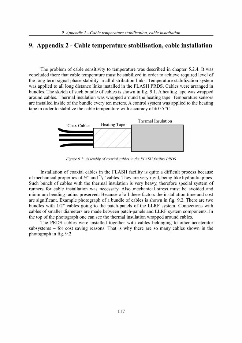
9. Appendix 2 - Cable temperature stabilisation, cable installation
9. Appendix 2 - Cable temperature stabilisation, cable installation
The problem of cable sensitivity to temperature was described in chapter 5.2.4. It was concluded there that cable temperature must be stabilized in order to achieve required level of the long term signal phase stability in all distribution links. Temperature stabilization system was applied to all long distance links installed in the FLASH PRDS. Cables were arranged in bundles. The sketch of such bundle of cables is shown in fig. 9.1. A heating tape was wrapped around cables. Thermal insulation was wrapped around the heating tape. Temperature sensors are installed inside of the bundle every ten meters. A control system was applied to the heating tape in order to stabilize the cable temperature with accuracy of ± 0.5 oC.
Figure 9.1: Assembly of coaxial cables in the FLASH facility PRDS
Installation of coaxial cables in the FLASH facility is quite a difficult process because of mechanical properties of ½“ and 7/8” cables. They are very rigid, being like hydraulic pipes. Such bunch of cables with the thermal insulation is very heavy, therefore special system of runners for cable installation was necessary. Also mechanical stress must be avoided and minimum bending radius preserved. Because of all these factors the installation time and cost are significant. Example photograph of a bundle of cables is shown in fig. 9.2. There are two bundles with 1/2” cables going to the patch-panels of the LLRF system. Connections with cables of smaller diameters are made between patch-panels and LLRF system components. In the top of the photograph one can see the thermal insulation wrapped around cables.
The PRDS cables were installed together with cables belonging to other accelerator subsystems – for cost saving reasons. That is why there are so many cables shown in the photograph in fig. 9.2.
117
Heating TapeThermal Insulation
Coax Cables

9. Appendix 2 - Cable temperature stabilisation, cable installation
Figure 9.2: Bundles of 1/2" cables installed in the FLASH facility
118

10. Appendix 3 – Optical Delay Line
10. Appendix 3 – Optical Delay Line
Optical delay line with a step motor was used as optical phase shifter in the FO link described in chapter 5.3. The ODL used in experiments is shown in fig. 10.1. The device type is ODL-300, manufactured by the OZ Optics company.
Most important features of used ODL:- 100 mm travel range- 330 ps of delay range- 4.7 fs resolution (one step of the motor)- 1.5 dB of maximum insertion loss- RS-232 interface for delay control- Attached singlemode fibers with FC/APC connectors
Figure 10.1: Optical Delay Line
119

11. Appendix 4 – Temperature controlled oven
11. Appendix 4 – Temperature controlled oven
As it was described in the preceding chapters, a temperature controlled chamber, called for simplicity “oven”, was developed for the purpose of the PRDS. The main application of the oven was the optical phase shifter. Spool with fiber inside of the oven was acting like the optical phase shifter as described in chapter 5.3.3. Also long fiber link in the accelerator tunnel conditions was simulated with the use of this oven. Another oven application was a temperature stabilization of temperature sensitive PRDS components (e.g. phase detectors). The oven was also very useful during experiments – precise temperature changes were applied on devices. By this the device sensitivity to temperature could be characterized.
Precise changes or stabilization of the inner oven temperature were required. In other words, the oven should be able to stabilize temperature, heat or cool. It should be as fast as possible with continuous temperature value control (ON/OFF36 temperature regulation was not applicable). The oven should also fit into the 19 inch rack system used in the FLASH facility for electronics. It was quite a difficult task to find relatively cheap commercial oven fulfilling all of these requirements. Therefore a custom oven was built by the author of this thesis.
It was decided that a Thermo-Electric Cooler (TEC) will be used for heating and cooling. A PID temperature controller was applied to the TEC. A commercial, temperature compensated PID controller was used. The photograph of the oven is shown in fig. 11.1. All mechanics of the second oven was also designed by the author of this thesis. The box was made by a professional mechanical workshop.
More details on the oven design and performance test results can be found in the report [3-A].
36 Typical temperature controllers switch on the heater (or cooler) for a period of time. Then the device is switched off. By this the temperature is kept within a specified range (e.g. ± 1oC) but it is swinging periodically. This is acceptable for many applications but may be a very big problem for characterization of sensitive PRDS components.
120
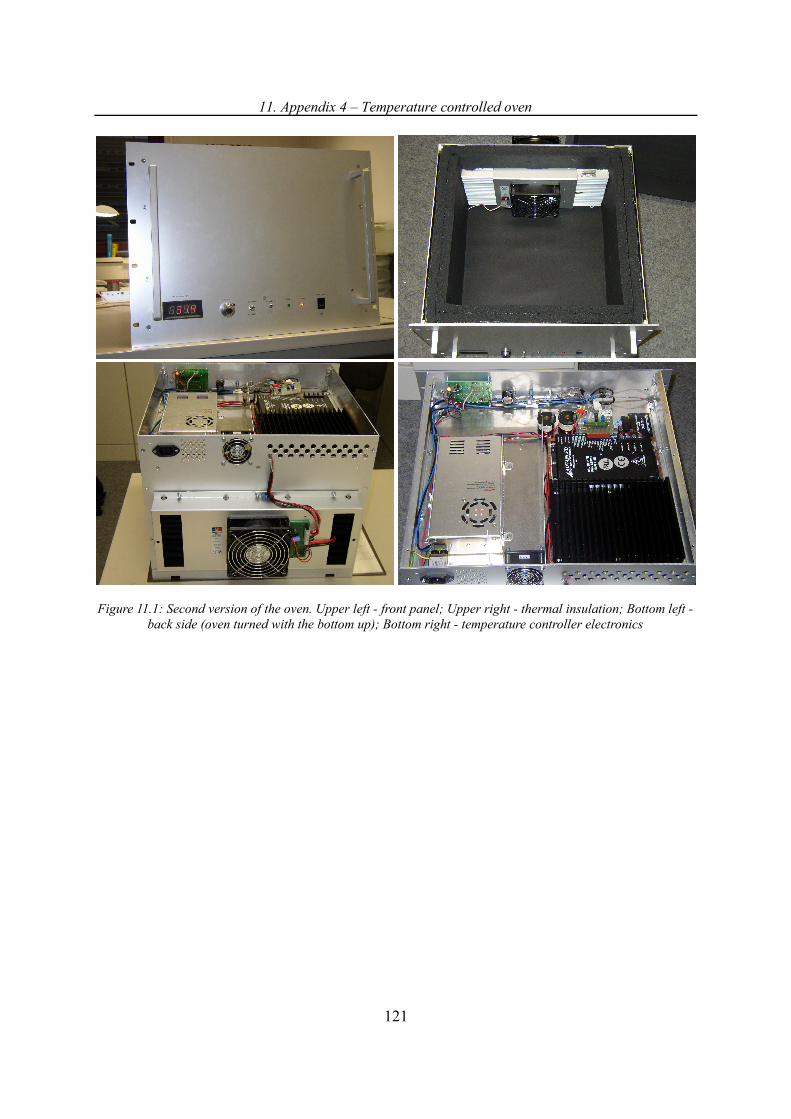
11. Appendix 4 – Temperature controlled oven
Figure 11.1: Second version of the oven. Upper left - front panel; Upper right - thermal insulation; Bottom left - back side (oven turned with the bottom up); Bottom right - temperature controller electronics
121

12. Appendix 5 – FO system design details
12. Appendix 5 – FO system design details
The system level design issues and the experimental set-up of the FO System were described in chapters 5.3 and 6.2. It could be noticed, especially in the latter chapter, how complicated was the system installation. Many subsystems had to be self developed and tested before the final system set-up was assembled. This was an enormous effort performed by the author of this thesis and two B.Sc. Students taking part in the project. A brief description of developed components of the FO link and other important technical issues are given in this appendix. Detailed description of all technical issues of the FO link is beyond the scope of this thesis and would lead to unacceptable increase of its volume.
It was mentioned chapter 6.2 that the SMF-28 fiber type was used in the FO link. This is a standard, low-cost fiber manufactured by the Corning company. One of the most important parameters of this fiber (for the FO link application) is the phase length sensitivity to temperature changes. A value of 10 ppm is given in the fiber datasheet. The value of 7.5 ppm was measured experimentally.
Spools with the SMF-28 fiber were used for the purpose of the optical phase shifter and the long link simulator. Fiber lengths available during performed experiments were 5 km, 10 km, 15 km and 20 km. Photograph of such spools (5 km and 10 km) is shown in fig. 12.1. Spools were covered with a wire net. This solution allowed a good air access to the fiber. Air was blown on the fiber by a fan inside of the oven.
Figure 12.1: Spools with fiber used for experiments
The fiber-optic transmitter (FO Tx) (see fig. 5.14) PCB was designed by the author of this thesis. A DFB laser module with integrated temperature sensor and Thermo-Electric Cooler was used. Laser diode controller and temperature controller circuits were applied to the laser module. The developed FO Tx PCB is shown in fig. 12.2. The RF input signal modulates the amplitude of the light produced by the laser in the FO Tx. Measured bandwidth of the FO Tx spreads between 50 MHz and 2.5 GHz (3 dB frequencies).
122

12. Appendix 5 – FO system design details
Figure 12.2: Laser transmitter PCB
There is a number of passive optical components used in the FO system – circulator, directional coupler, mirror (see fig. 6.6). Power splitters were also used for monitoring purposes. All of these devices were equipped with pieces of fibers (so called “pig-tailed” devices) with optical connectors. FC/APC connector type was selected for low optical loss and reflections. These components were assembled on a soft (made of foam) base called an “optical breadboard” The photograph of the optical breadboard is shown in fig. 12.3. By the use of the soft base the system sensitivity to mechanical vibrations was minimized.
Figure 12.3: The optical breadboard
The electronic components of the FO link (laser transmitter, optical receivers, phase detectors, power supplies) were assembled together in a small crate that could fit into one of
123
ODL
Mirror
Directional Coupler
Circulator

12. Appendix 5 – FO system design details
designed ovens (Appendix 4). By this, for test purposes, the crate temperature could be controlled or changed. Low noise power supplies were used. Additional filters were used in the supply voltage lines.
The photograph of the FO link crate is shown in fig. 12.4. Short semi-rigid cables were used in the crate for RF signal connections.
Figure 12.4: Crate with the FO link electronics
Important part of the FO link is the microcontroller board. Used PCB incorporates the MSC1211 microcontroller type with slow but precise, 8-channel ADC and four channel DAC. The PCB is also equipped with two serial ports (UART) for the RS-232 connections and the I2C bus. The I2C bus was used for communication with digital temperature sensors.
The components used in the FO link are relatively slow (the reaction of the optical phase shifter is very slow – time constant of the spool in the oven reaches tenths of minutes). The feedback system is supposed to suppress slow, long term drifts caused by air temperature changes. Therefore there is no need for using a fast data acquisition system. The ADC sample rate of 1 Sample-Per-Second (SPS) is sufficient for the purposes of designed FO link. Therefore choice of a microcontroller with slow ADC (1 kSPS) was justified.
As described in chapter 6.2, in the development stage of the link, the microcontroller board was used as data acquisition system for the FO link PID controller programmed in the computer. In the final system version the microcontroller board will work as a standalone (without a PC) FO link controller. A custom board with all features useful for the FO link was designed. The new board is equipped with a real time clock, flash memory for data storage and USB port for fast data exchange with PC. More details about this board can be found in the thesis [50]. Board photograph is shown in fig. 12.5.
The PID controller software was developed in the PC in the Matlab® environment. A Graphic User Interface (GUI) was developed for this controller. The screen-shot of the developed GUI is shown in fig. 12.6. The main purpose of the GUI was the measurement data analysis and visualisation and the providing tools for development of FO system controller parameters.
The measured and calculated data was plotted “on-line” in the GUI after taking each sample by the microcontroller board. Data could also be saved in files in the PC hard disc. Many parameters could be controlled and changed by the GUI user: PID controller parameters, ADC sampling time, measurement duration, used ADC and DAC channels. The GUI incorporates very useful functions for calculation of the signal stability over specified
124

12. Appendix 5 – FO system design details
period of time. The GUI was also used for controlling of the long link simulator oven. Different patterns of temperature change in the long link simulator were programmed. By this long duration measurements were performed automatically, without a need for operators supervision.
Figure 12.5: Microcontroller board developed for the FO link controller
Figure 12.6: Matlab GUI developed for the FO link control
125
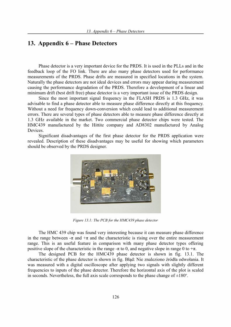
13. Appendix 6 – Phase Detectors
13. Appendix 6 – Phase Detectors
Phase detector is a very important device for the PRDS. It is used in the PLLs and in the feedback loop of the FO link. There are also many phase detectors used for performance measurements of the PRDS. Phase drifts are measured in specified locations in the system. Naturally the phase detectors are not ideal devices and errors may appear during measurement causing the performance degradation of the PRDS. Therefore a development of a linear and minimum drift (best drift free) phase detector is a very important issue of the PRDS design.
Since the most important signal frequency in the FLASH PRDS is 1.3 GHz, it was advisable to find a phase detector able to measure phase difference directly at this frequency. Without a need for frequency down-conversion which could lead to additional measurement errors. There are several types of phase detectors able to measure phase difference directly at 1.3 GHz available in the market. Two commercial phase detector chips were tested. The HMC439 manufactured by the Hittite company and AD8302 manufactured by Analog Devices.
Significant disadvantages of the first phase detector for the PRDS application were revealed. Description of these disadvantages may be useful for showing which parameters should be observed by the PRDS designer.
Figure 13.1: The PCB for the HMC439 phase detector
The HMC 439 chip was found very interesting because it can measure phase difference in the range between -π and +π and the characteristic is rising over the entire measurement range. This is an useful feature in comparison with many phase detector types offering positive slope of the characteristic in the range -π to 0, and negative slope in range 0 to +π.
The designed PCB for the HMC439 phase detector is shown in fig. 13.1. The characteristic of the phase detector is shown in fig. Błąd: Nie znaleziono źródła odwołania. It was measured with a digital oscilloscope after applying two signals with slightly different frequencies to inputs of the phase detector. Therefore the horizontal axis of the plot is scaled in seconds. Nevertheless, the full axis scale corresponds to the phase change of ±180o.
126
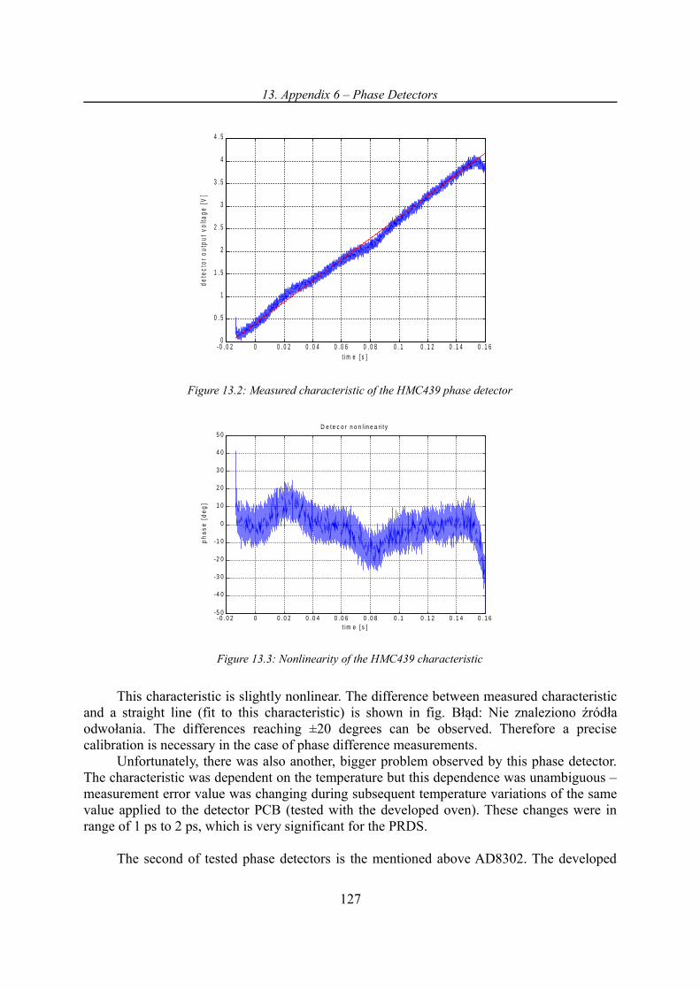
13. Appendix 6 – Phase Detectors
Figure 13.2: Measured characteristic of the HMC439 phase detector
Figure 13.3: Nonlinearity of the HMC439 characteristic
This characteristic is slightly nonlinear. The difference between measured characteristic and a straight line (fit to this characteristic) is shown in fig. Błąd: Nie znaleziono źródłaodwołania. The differences reaching ±20 degrees can be observed. Therefore a precise calibration is necessary in the case of phase difference measurements.
Unfortunately, there was also another, bigger problem observed by this phase detector. The characteristic was dependent on the temperature but this dependence was unambiguous – measurement error value was changing during subsequent temperature variations of the same value applied to the detector PCB (tested with the developed oven). These changes were in range of 1 ps to 2 ps, which is very significant for the PRDS.
The second of tested phase detectors is the mentioned above AD8302. The developed
127
- 0 . 0 2 0 0 . 0 2 0 . 0 4 0 . 0 6 0 . 0 8 0 . 1 0 . 1 2 0 . 1 4 0 . 1 60
0 . 5
1
1 . 5
2
2 . 5
3
3 . 5
4
4 . 5
t i m e [ s ]
dete
ctor
out
put
volta
ge [
V]
-0 . 0 2 0 0 . 0 2 0 . 0 4 0 . 0 6 0 . 0 8 0 . 1 0 . 1 2 0 . 1 4 0 . 1 6-5 0
-4 0
-3 0
-2 0
-1 0
0
1 0
2 0
3 0
4 0
5 0D e t e c o r n o n l in e a ri t y
t im e [ s ]
ph
as
e [
de
g]

13. Appendix 6 – Phase Detectors
PCB assembled in a thick metal box is shown in fig. Błąd: Nie znaleziono źródła odwołania. The characteristic of this detector is also slightly nonlinear but repeatable with temperature changes. Therefore standard phase detector calibration could easily be performed. The measured sensitivity of this phase detector to temperature changes is extremely low, being in the range of 0.05 to 0.1 degree per 1 oC (several phase detector boards were tested).
Figure 13.4: Developed AD8302 phase detector module
128

14. References
14. References
14.1. Publications with author's contribution
[1-A] Krzysztof Czuba, Henning Weddig, Bastian Lorbeer, Stefan Simrock, Erhard Salow, Norbert Fend, “Master oscillator design for the VUV-FEL project”, Konferencja Mikon 2006, Kraków, Polska, pp. 1123-1126
[2-A] Krzysztof Czuba, Matthias Felber, “Improved fiber-optic link for the phase reference distribution system for the TESLA technology based projects”, Proceedings of SPIE, Vol. 5948, part one, pp. 59480B-1 – 59480B-8
[3-A] K. Czuba, F. Eints, M. Felber, J. Dobrowolski, S. Simrock, “First generation of optical fiber phase reference distribution system for TESLA”, TESLA Report 2005-08, Hamburg, 28.02.2005
[4-A] K. Czuba, F. Eints, M. Felber, S. Simrock, “Fiber-optic link for the RF phase reference distribution system for the XFEL and TESLA projects”, WILGA 2004, Proceedings of SPIE Vol. 5775, p. 44-51, Feb. 2005
[5-A] Wojciech Giergusiewicz, Wojciech Jałmużna, Krzysztof Poźniak, Nikolay Ignashin, Mariusz Grecki, Dariusz Makowski, Tomasz Jeżyński, Karol Perkuszewski, Krzysztof Czuba, Stefan Simrock, Ryszard Romaniuk, “ Low latency control board for LLRF system – SIMCON 3.1”, Proceedings of SPIE, Vol. 5948, part two, pp. 59482C-1 – 59482C-8, 30.08 – 01.09.2005, Warsaw, Poland
[6-A] Ryszard S. Romaniuk, Krzysztof T. Poźniak, Tomasz Czarski, Krzysztof Czuba, Wojciech Giergusiewicz, Grzegorz Kasprowicz, Waldemar Koprek, „Optical network and FPGA/DSP based control system for free electron laser”, Biuletyn Polskiej Akademii Nauk, Seria Techniczna; vol. 53, No.2, 2005
[7-A] Krzysztof Czuba, Janusz Dobrowolski, Frank Eints, Matthias Felber, „Pierwsza generacja światłowodowego systemu dystrybucji sygnału odniesienia dla akceleratora TESLA”, Elektronika, nr 7/2005, str. 69 – 70
[8-A] Krzysztof Czuba, Henning C. Weddig „Design considerations for the RF phase reference distribution system for X-ray FEL and TESLA”, IEEE-SPIE WILGA 2003, Proc. SPIE vol.5484, pp 148-152
129

14. References
14.2. Bibliography
[1] “PN9000 automated phase noise measurement system, application note #1”, Aeroflex application note, 2003, available on-line at www.aeroflex.com
[2] “RF and microwave fiber-optic design guide”, Agere Systems Inc., Application Note AP01-006OPTO, April 2001
[3] David W. Allan, James A. Barnes, “A modified “Allan variance” with increased oscillator characterization ability”, Proceedings of 35th Annual Frequency Control Symposium, May 1981
[4] David W. Allan, “Time and frequency (time-domain) characterization, estimation and prediction of precision clocks and oscillators”, IEEE Transactions on Ultrasonics, Ferroelectrics and Frequency Control, 1987
[5] David W. Allan, Helmut Hellwig, Peter Kartaschoff, Jacques Vanier, John Vig, Gernot M. R. Winkler, Nicholas Yannoni, “Standard terminology for fundamental frequency and time metrology”, 42nd Annual Symposium on Frequency Control, 1988
[6] Massimo Altarelli, editor et. al., “The European X-Ray Free-Electron Laser, Technical Design Report”, DESY XFEL Project Group, Hamburg, Germany, July 2006
[7] Mark Bomford, “Selection of frequency dividers for microwave PLL applications”, Microwave Journal, November 1990, pp. 159 - 167
[8] International Radio Consultative Committee (C.C.I.R), “Characterization of frequency and phase noise”, Report 580, pp. 142-150, 1986
[9] David Chandler, “Phase jitter. Phase noise and voltage controlled oscillators”, Corning Frequency Control, application note available at www.corningfrequency.com
[10] Jackie Chin, Antonio Cantoni, “Phase Jitter ≡ Timing Jitter?”, IEEE communication letters, Vol. 2, No. 2, February 1998
[11] Eric R. Colby, “Design, Construction and Testing of a Radiofrequency Electron Photoinjectorfor the Next Generation Linear Collider” Technical Report PhD Thesis, University of California Los Angeles (UCLA), 1997
[12] Charles H. Cox, Edward I. Ackerman, Gary E. Betts, Joelle L. Prince, “Limits on the performance of RF-over-fiber links and their impact on device design”, IEEE Transactions on Microwave Theory and Techniques, vol. 54, No. 2, February 2006, pp. 906 - 920
[13] Kerry W. Cozad, “A technical review of transmission line designs and specifications
130

14. References
for transmitting television signals”, Andrew Corporation, Professional Paper PR50211, Orland Park, USA, 1998
[14] K. Crawford, S. Simrock, C. Hovater, A. Krycuk, “The CEBAF fiber optic phase reference system”, Particle Accelerator Proceedings, 1995
[15] Mark Curtin, Paul O`Brien, “Phase-locked loops for high-frequency receivers and transmitters”, Part 1 to 3, Analog Devices technical article, Analog-Dialogue 33, 1999, available on-line at www.analog.com
[16] “A technical tutorial on digital signal synthesis”, Analog Devices, rev. 12-2-99, 1999, tutorial available on-line at http://www.analog.com/UploadedFiles/Tutorials/450968421DDS_Tutorial_rev12-2-99.pdf
[17] Dean Baenrjee, “ PLL performance, simulation and design”, 4th edition, National Semiconductor, 2006. Book available on-line at http://www.national.com/appinfo/wireless/pll_designbook.html
[18] S. A. Diddams et.al., “A compact femtosecond-laser-based optical clockwork”, Proceedings of SPIE - Volume 4269, May 2001, pp. 77-83
[19] Deutches Institut für Normung (DIN) standard no. 41494 SC48D. Equivalent standard defined by IEC 60297 and EIA 310-D
[20] Janusz A. Dobrowolski, “Mikrofale”, Wydawnictwa Politechniki Warszawskiej, Warszawa, Poland, 1991. In Polish
[21] Janusz A. Dobrowolski, “Technika wielkich częstotliwości”, Oficyna Wydawnicza Politechniki Warszawskiej, Warszawa, Poland, 2001, In Polish
[22] L. R. Doolittle, C. Hovater, L. Merminga, J. Musson, M. Wissmann, “A low-cost, NIST-traceable, high performance dielectric resonator master oscillator”, Proceedings of the 1999 Particle Accelerator Conference, New York, 1999
[23] W. F. Egan, “Modelling phase noise in frequency dividers”, IEEE Transactions On Ultrasonics and Frequency Control, Vol. 37, No. 4, July 1990, pp. 307 - 315
[24] William F. Egan, “Frequency synthesis by phase locked loop”, second edition, John Willey & Sons, Inc., New York, USA, 1999
[25] Frank Eints, “Development of an algorithm for a RF fiber-optic phase controller”, DESY-THESIS (Advance publication), August 2004
[26] C. A. Ekdahl, Peter Formann, Lynn Veeser, “Fiber-optic ground-truth thermometer”, Los Alamos National Laboratory publication, LA-12580-MA, UC-706, July 1993
[27] J. Engberg, T. Larsen, “Noise theory of linear and nonlinear circuits”, John Willey &
131

14. References
Sons, Chichester, England, 1995
[28] Marek T. Faber, Jerzy Chramiec, Miroslaw T. Adamski, “Microwave and millimeter-wave diode frequency multipliers”, Artech House, Boston, UK, 1995
[29] Matthias Felber, “A feedback system based on optical fiber for compensating RF phase drifts”, Diploma Thesis, Fachhochschule Wedel, Germany, February 2006
[30] John J. McFerran, “Producing links in a modern phase coherent optical to microwave frequency chain”, PhD thesis, The University of Western Australia, Department of Physics, 2002
[31] István Frigyes, A. J. Seeds, “Optically generated true-time delay in phased-array antennas”, IEEE Transactions on Microwave Theory and Techniques, Vol. 43, No. 9, September 1995
[32] J. Frisch, D. G. Brown, E. L. Cisneros, “Performance of the prototype NLC phase and timing distribution system”, 9th Beam Instrumentation Workshop, Cambridge, MA., May 8-11, 2000, also SLAC-PUB-8458, Stanford, CA, USA, June 2000
[33] J. Frisch, D. G. Brown, E. L. Cisneros, “The RF phase distribution and timing system for the NLC”, 20th International Linac Conference (Linac 2000), Monterey, CA, USA, also SLAC-PUB-8578, Stanford, CA, USA, August 2000
[34] J. Frisch, D. Bernstein, D. G. Brown, E. L. Cisneros, “A high stability, low noise RF distribution system”, SLAC-PUB-9413, Stanford, CA, USA, August 2002
[35] A. Gamp, M. Liepe, T. Plawski, K. Rehlich, S. N. Simrock, “Design of the RF phase reference system and timing control for the TESLA Linear Collider”, XIX International Linear Accelerator Conference, Chicago, 1998
[36] Bar-Giora Goldberg, “Digital frequency synthesis demystified”, LLH Technology Publishing, Eagle Rock, USA, 1999
[37] H. Hayano, E. Ezura, “The RF reference line for TRISTAN”, Particle Accelerator Proceedings, 1987
[38] D. J. Healey, S. Y. Kwan, “SC-cut quartz crystal units in low-noise oscillator applications at VHF”, Proceedings of 35th Annual Frequency Control Symposium, USAERADCOM, Ft. Monmouth, MJ, 07703, May 1981, pp. 440 - 454
[39] D. A. Howe, D. W. Allan, J. A. Barnes, “Properties of signal sources and measurement methods”, Proceedings of the 35th Annual Symposjum on Frequency Control, pp A1 – A47, 1981
[40] Hewlett Packard, “Phase noise characterization of microwave oscillators. Frequency discriminator method”, Application Note 11729C-2
132

14. References
[41] “IEEE standard definitions of physical quantities for fundamental frequency and time metrology – random instabilities”, IEEE Std. 1139, Mar. 1999
[42] The International Committee for Future Accelerators (ICFA), “The Reference Design Report (RDR) for the International Linear Collider”, February 2007
[43] D. A. Jackson, R. Priest, A. Dandridge, A. B. Tveten, “Elimination of drift in a single-mode optical fiber interferometer using a piezoelectrically stretched coiled fiber”, Applied Optics, Vol. 19, No. 17, September 1980, pp. 2926 - 2929
[44] Jacek Januszewski, “Systemy satelitarne GPS Galileo i inne”, In Polish, PWN, October 2006
[45] L. de Jonge, J. P. H. Sladen, “RF reference distribution for the LEP energy upgrade”, Fourth European Particle Accelerator Conference (EPAC 94), London, UK, 1994
[46] Daniel Kotthaus, “Design of the control for the radio frequency electron gun of the VUV-FEL linac”, Msc thesis, Fachbereich Physik der Universität Hamburg, 2004
[47] Richard P. Kovachich, “The precision of modern phase coherent optical to microwave frequency chains”, PhD thesis, The University of Western Australia, Department of Physics, 2000
[48] A. Krycuk, J. Fugitt, K. Mahoney, S. Simrock, “The CEBAF frequency distribution system”, Particle Accelerator Proceedings, 1991
[49] Ken Kundert, “Predicting the phase noise of PLL-based frequency synthesizers”, Version 4B, November 2003, can be downloaded from www.designers-guide.org
[50] Michał Ładno, “Kontroler i karta akwizycji danych do światłowodowego systemu dystrybucji sygnału odniesienia dla akceleratora liniowego X-FEL”, BS.c Thesis, In Polish, Warsaw University of Technology, September 2006
[51] A. L. Lance, W. D. Seal, F. Labaar, “Phase noise and AM noise measurements in the frequency domain”, Infrared and Millimeter Waves Vol.11, Academic Press Inc. 1984
[52] Lance Lascari, “Accurate phase noise prediction in PLL synthesizers”, Applied Microwave&Wireless, part 1 – April 2000, part 2 – May 2000, available on-line at http://resume.rfdude.com/
[53] Thomas H. Lee, Ali Hajimiri, “Oscillator phase noise: A tutorial”, IEEE Journal of Solid State Circuits, Vol. 35, No. 3, March 2000, pp. 326 -336
[54] David B. Leeson, “A simple model of feedback oscillator noise spectrum”, Proceedings of the IEEE 54, 1966, pp. 329-330
[55] Paul Lesage, Théophane Ayi, “ Characterization of frequency stability: analysis of
133

14. References
the modified Allan variance and properties of its estimate”, IEEE Transactions on Instrumentation and Measurement, Vol. IM-33, No. 4, December 1984
[56] S. Levantino, L Romano, S. Pellerano, C. Samori, A. L. Laciata, “Phase noise in digital frequency dividers”, IEEE Journal Of Solid-State Circuits, Vol. 39, No. 5, May 2004, pp. 775 - 784
[57] C. Little, C. Green, “GPS disciplined rubidium oscillator”, European Frequency and Time Forum, 1996. EFTF 96., Tenth (IEE Conf. Publ. 418), Brighton, UK, pp. 105 - 110
[58] M. A. Lombardi, L. M. Nelson, A. N. Novick, V. S. Zhang, “Time and frequency measurements using the Global Positioning System”, Cal Lab Int. Jour. of Metrology, July-September 2001, pp. 26-33
[59] Bastian Lorbeer, “Phase noise measurements of the new Master Oscillator for TTF2”, Thesis, Fachbereich Elektrotechnik der Fachhochschule Lübeck, also available as DESY Thesis 2004-023, July 2004
[60] Bastian Lorbeer, “Stability of the Master Oscillator for FLASH at DESY”, TESLA Report 2006-11, October 2006
[61] F. Ludwig, M. Hoffmann, H. Schlarb, S. Simrock, “Phase stability of the next generation RF field control for VUV- and X-Ray free electron laser”, Proceedings of EPAC 2006, Edinburgh, Scotland, pp. 1453 - 1455
[62] Stephen A. Maas, “Nonlinear microwave and RF circuits”, second edition, Artech House, London, 2003
[63] Stephen A. Maas, “Noise in linear and nonlinear circuits”, Artech House, London, UK, 2005
[64] Gary K. Montress et. al., “Extremely Low-Phase-Noise SAW Resonators and Oscillators: Design and Performance”, IEEE Transactions on Ultrasonics, Ferroelectrics and Frequency Control, Vol. 35, No. 6, November 1988, pp. 657 - 667
[65] Jean-Christophe Nallatamby, Michel Prigent, “Phase noise in oscillators – Leeson formula revisited”, IEEE Transactions on Microwave Theory and Techniques, Vol. 51, No. 4, April 2003, pp. 1386 - 1394
[66] E. C. Niehenke, P. A. Green, “A low-noise L-band dielectric resonator stabilized microstrip oscillator”, IEEE MTT-S Digest, 1987, pp. 193 - 196
[67] D.A. Howe, D.W. Allan, J.A. Barnes, “Properties of oscillator signals and measurement methods”, NIST paper available on-line at http://tf.nist.gov/phase/Properties/main.htm
[68] Henry W. Ott, “Noise reduction techniques in electronic systems”, second edition,
134

14. References
John Willey & Sons, New York, USA, 1988
[69] Athanasios Papoulis, “Probability, random variables and stochastic processes”, third edition, McGraw-Hill, New York, USA, 1991
[70] Jinu Paul, Zhao Liping, Bryan Ngoi, Fang Zhong Ping, “Bragg grating temperature sensors: modeling the effect of adhesion of polymeric coatings “, Sensor Review Volume 24, Number 4, 2004, pp. 364-369 Copyright © Emerald Group Publishing Limited ISSN 0260-2288
[71] Donald B. Percival, “Characterization of frequency stability: frequency-domain estination of stability measures”, Proceedings of the IEEE, Vol. 79, No. 6, June 1991
[72] E. Peschardt, J. Sladen, “Phase compensated fiber-optic links for the LEP RF reference distribution”, Proc. IEEE Particle Accelerator Conference, Chicago, 20-23 March 1989, pp 1960-1962
[73] Donald E. Phillips, “Random noise in digital gates ans dividers”, 41st Annual Frequency Control Symposium, 1987, pp. 507 - 511
[74] Rick Poore, “Phase noise and jitter”, Agilent Eesof EDA, 17 May 2001, available on-line at http://eesof.tm.agilent.com/pdf/jitter_phasenoise.pdf
[75] David M. Pozar “Microwave engineering”, second edition, John Willey & Sons, Inc., 1998
[76] Ken Puglia, “Phase-locked loop noise models”, Microwave Engineering Europe, December/January 1995, pp. 31-40
[77] Kenneth V. Puglia, “Phase noise analysis of component cascades”, IEEE Microwave Magazine, December 2002, pp. 71 - 75
[78] Randall W. Rhea, “Oscillator design and computer simulation”, second edition, Noble Publishing Corporation, Atlanta, USA, 1995
[79] Neil Roberts, “Phase noise and jitter – a primer for digital designers”, EE Design, July 2003
[80] Ulrich L. Rohde, “All about phase noise in oscillators. Part 1 – How oscillator noise is described and analyzed”, QEX, Published by The American Radio Relay League, December 1993
[81] Ulrich L. Rohde, “All about phase noise in oscillators. Part 2 – How oscillator noise is predicted”, QEX, Published by The American Radio Relay League, January 1994
[82] Ulrich L. Rohde, “All about phase noise in oscillators. Part 3 – Example of oscillator circuits and their noise performance”, QEX, Published by The American Radio Relay League, February 1994
135

14. References
[83] Ulrih L. Rohde, “Microwave and wireless synthesizers: theory and design”, John Willey & Sons, Inc., New York, USA,
[84] Enrico Rubiola, “The Leeson effect. Phase noise in quasilinear oscillators”, Universite Henri Poincare, Nancy, France, 2005. Document available on-line at www.rubiola.org
[85] Jacques Rutman, F. L. Walls, “Characterization of frequency stability in precision frequency sources”, Proceedings of the IEEE, Vol. 79, No. 6, June 1991
[86] Dieter Scherer, “Today's Lesson – Learn About Low-Noise Design”, Microwaves, part I – April 1979, part II – May 1979
[87] Thomas Schilcher, “Vector sum control of pulsed accelerating fields in Lorenz force detuned superconducting cavities”, PhD Thesis, Fachbereich Physik der Universität Hamburg, 1998
[88] H. Schlarb, V. Ayvazyan, F. Ludwig, D. Noelle, B. Schmidt, S. Simrock, A. Winter, F. Kaertner, “Next generation synchronization system for the VUV-FEL at DESY”, Proceedings of the 27th International Free Electron Laser Conference, JACoW / eConf C0508213, pp. 118 – 121, Stanford, California, USA, 21-26 August 2005
[89] S.N. Simrock, I. Altmann, K. Rehlich, T. Schilcher, “Design of the Digital RF Control System for the TESLA Test Facility”, Proc. EPAC’96, Barcelona, Spain, p.349, 1996
[90] Samuel R. Stein, “Frequency and time – their measurement and characterization”, Precision Frequency Control, Volume 2, Chapter 12, 1985
[91] Karol Suchecki, “Results of phase drift measurements of power amplifiers”, Internal DESY, LLRF group report, document available on-line at https://ttfinfo.desy.de/LLRFelog-sec/index.jsp in folder 2006/week 32, 07.08.2006
[92] Edited by: D. B. Sullivan, D. W. Allan, D.A. Howe, F.L. Walls, “Characterization of clocks and oscillators”, National Institute of Standards and Technology, Technical Note 1337, 1990
[93] Jerzy Szabatin, “Podstawy teorii sygnałów”, wyd. 4, In Polish, Wydawnictwa Komunikacji i Łączności, Warszawa 2002
[94] Jacques Vanier, Michel Têtu, “Time domain measurement of frequency stability. A tutorial introduction”, Proceedings of the 10th Annual Precise Time and Interval (PTTI) Applications and Planning Meeting, 1978
[95] J. R. Vig, T. R. Meeker, “The aging of bulk acoustic wave resonators, filters and oscillators”, Proceedings of the 45th Annual Symposium on Frequency Control, pp. 77-101, 1991
136
14. References
[96] F. L. Walls, A. J. D. Clements, C. M. Felton, M. A. Lombardi, M. D. Wanek, “Extending the range and accuracy of phase noise measuremets”, Proceedings of the 42nd Annual Symposium on Frequency Control, 1988
[97] Henning Weddig, “Requirements for a low phase noise master oscillator and phase stable frequency distribution system fort he TESLA TEST FACILITY (TTF2)”, Revision 12/16.11.2004, Internal DESY paper. Document available on-line at https://ttfinfo.desy.de/LLRFelog-sec/index.jsp in the Master Oscillator section
[98] Wenzel Associates Inc., “Low Phase Noise Systems - Hints and Tips”, Document available on-line at http://www.wenzel.com/documents/hints.htm
[99] Axel Winter, Frank Ludwig, Jeff Chen, F. Ömer, “High precision laser master oscillator for optical timing distribution systems in future light sources”, Proceedings of EPAC 2006, Edinburgh, Scotland, pp. 2747 - 2751
[100] Dan H. Wolaver, “Phase-Locked Loop Circuit Design”, Prentice-Hall, New Jersey, 1991
[101] TESLA Technical Design Report, Part I Executive Summary, DESY, Hamburg, 2001
[102] TESLA Technical Design Report, Part II The Accelerator, DESY, Hamburg, 2001
[103] D. A. Edwards (editor), “TESLA Test Facility Linac Design Report”, version 1.0, DESY, Hamburg, March 1995
[104] Todd S. Tignor, “Specifying Crystal Oscillators”, Isotemp Research, Inc. paper nr 146-010, Document also available on-line at http://www.isotemp.com/146-010.html
[105] Antonio Visioli, “Practical PID control – (Advances in industrial control)”, Springer-Verlag London, 2006
[106] Ken Yang, Steve Lee, “Examine the effects of random noise on jitter”, Microwaves & RF, September 2004
137