Proton Radiation Testing of Digital Micromirror Devices for Space Applications
24
Proton Radiation Testing of Digital Micromirror Devices for Space Applications Kenneth Fourspring a Zoran Ninkov a , Bryan Fodness a , Massimo Robberto b , Sally Heap c and Alex G. Kim d a Rochester Institute of Technology, 54 Lomb Memorial Drive Rochester, NY 14623; b Space Telescope Science Institute, 3700 San Martin Drive, Baltimore, MD 21212; c Code 681 NASA Goddard Space Flight Center, Greenbelt, MD 20771; d E. O. Lawrence Berkeley National Laboratory, 1 Cyclotron Road, Berkeley, CA 94720 ABSTRACT Scientists are interested in using Digital Micromirror Devices (DMDs) as slit-masks in Multi-Object Spectrome- ters (MOS) on future space missions. A favored orbit is at the second Lagrangian point (L2). A requirement for mission planning is to determine how long such MEMS devices would remain operational given the L2 radiation environment, which is primarily composed of solar protons and cosmic rays. To this end, we have initiated DMD proton testing. Three DMDs were irradiated with high-energy protons (35-50 MeV) at the Lawrence Berkeley National Laboratory (LBNL) 88 00 Cyclotron. Assuming a typical spacecraft shielding of 100 mils of aluminum, our tests imply that DMDs remain fully operable in a 5-year mission at L2 with a margin of safety of 4.5. Keywords: Digital Micromirror Devices (DMDs), MEMS, Proton Irradiation. 1. INTRODUCTION 1.1 Digital Micromirror Devices Micro-Electrical Mechanical Systems (MEMS) are tiny mechanical devices produced with existing semiconductor fabrication techniques that integrate electrical interconnects and drive electronics into a single package. MEMs are the solution for miniaturizing bulky discrete devices and sensors. A miniaturized array of MEMS mirrors, Further author information: (Send correspondence to Kenneth Fourspring) Kenneth Fourspring.: E-mail: [email protected], Telephone: 585 475 7132 Zoran Ninkov E-mail: [email protected] Telephone: 585 475 7195 Bryan Fodness E-mail: [email protected] Telephone: 585 475 7132 Massimo Robberto E-mail: [email protected] Telephone: 410 338 4382 Sally Heap E-mail: [email protected] Telephone: 301 286 5359 Alex G. Kim E-mail: [email protected] Telephone: 510 486 4621 1
Transcript of Proton Radiation Testing of Digital Micromirror Devices for Space Applications

Proton Radiation Testing of Digital Micromirror Devices forSpace Applications
Kenneth Fourspringa Zoran Ninkova, Bryan Fodnessa, Massimo Robbertob, Sally Heapc and
Alex G. Kim d
aRochester Institute of Technology, 54 Lomb Memorial Drive Rochester, NY 14623;
bSpace Telescope Science Institute, 3700 San Martin Drive, Baltimore, MD 21212;
cCode 681 NASA Goddard Space Flight Center, Greenbelt, MD 20771;
dE. O. Lawrence Berkeley National Laboratory, 1 Cyclotron Road, Berkeley, CA 94720
ABSTRACT
Scientists are interested in using Digital Micromirror Devices (DMDs) as slit-masks in Multi-Object Spectrome-
ters (MOS) on future space missions. A favored orbit is at the second Lagrangian point (L2). A requirement for
mission planning is to determine how long such MEMS devices would remain operational given the L2 radiation
environment, which is primarily composed of solar protons and cosmic rays. To this end, we have initiated DMD
proton testing. Three DMDs were irradiated with high-energy protons (35−50MeV) at the Lawrence Berkeley
National Laboratory (LBNL) 88′′ Cyclotron. Assuming a typical spacecraft shielding of 100mils of aluminum,
our tests imply that DMDs remain fully operable in a 5-year mission at L2 with a margin of safety of 4.5.
Keywords: Digital Micromirror Devices (DMDs), MEMS, Proton Irradiation.
1. INTRODUCTION
1.1 Digital Micromirror Devices
Micro-Electrical Mechanical Systems (MEMS) are tiny mechanical devices produced with existing semiconductor
fabrication techniques that integrate electrical interconnects and drive electronics into a single package. MEMs
are the solution for miniaturizing bulky discrete devices and sensors. A miniaturized array of MEMS mirrors,
Further author information: (Send correspondence to Kenneth Fourspring)Kenneth Fourspring.: E-mail: [email protected], Telephone: 585 475 7132Zoran Ninkov E-mail: [email protected] Telephone: 585 475 7195Bryan Fodness E-mail: [email protected] Telephone: 585 475 7132Massimo Robberto E-mail: [email protected] Telephone: 410 338 4382Sally Heap E-mail: [email protected] Telephone: 301 286 5359Alex G. Kim E-mail: [email protected] Telephone: 510 486 4621
1
Figure 1. (Left) Illustration shows an extrapolated view of an individual DMD mirror. This mirror architecture is denotedas TI’s fast track design. Reflective surface of the mirror is fabricated from an aluminum alloy. (Right) Diagram showsa “Type-A” DMD package. The silicon substrate containing the array of DMD mirrors is mounted to a ceramic carrier.Borosilicate window is held above the DMD by a kovar metal frame. Device is wire-bonded to interconnects, whichterminate at the bottom of the ceramic carrier.
the DMD, has been under development at Texas Instruments (TI) for several decades.1 DMDs modulate light
spatially in digital projectors by flipping individual mirrors between two stable orientations. Many studies on
DMDs in digital projectors, all yielding favorable results, have been performed to evaluate the long-term reliability
and stability of DMDs.2 The TI DMDs tested in the present work are 0.7′′ 1024× 768 eXended Graphics Array
(XGA) DMDs, that have a 12◦ tip angle and a pitch of 13.68 µm. They represent one of TI’s current generation
devices. Previous studies describing the use of DMDs for MOS, namely Rochester Institute of Technology
Multi-Object Spectrograph (RITMOS)3 and InfraRed Multi-Object Spectrograph (IRMOS),4 utilized an earlier
generation DMD that had limited contrast, fewer total mirrors and significant scattered light. Current DMDs
have much greater contrast and optical performance due to the increased mirror tip angle, smaller mirror via
structure, and a reduced gap between adjacent mirrors (see Figure 1 Left). MOS is an acronym for Metal Oxide
Semiconductor, which are used in the DMD’ integrated drive circuitry, but in this paper the term MOS will be
used to abbreviate the phrase Multi-Object Spectroscopy.
The DMD is hermetically encapsulated, which is integral to the devices’ robustness and reliability. Moisture
and particle contamination are problems for un-packaged devices. Figure 1 shows the package structure. The
DMD silicon is mounted to a ceramic carrier, and gold wire-bonds are used to connect the silicon chip bond
pads. A kovar metal frame is mounted to the ceramic carrier. Another kovar metal frame is fused together with
an alkali-borosilicate glass (Corning type 7056 glass) window and electro-welded to the first metal frame. This
sealed package is then backfilled with dry nitrogen. The operational temperature of a DMD would likely be
somewhere between −40◦C to −100◦C depending on mission requirements. It is well understood that radiation
effects can be highly temperature dependent.5 However, to keep the test apparatus practical for these initial
tests, it was decided to irradiate the DMDs while they operated at room temperature. Future work will discuss
2

testing DMDs at the appropriate operational temperatures.
1.2 Radiation Tolerant Slit-Mask (Motivation)
The current ground-based approach to MOS generally uses one of two approaches to separate targets of interest:
fibers (e.g. Hydra6) or masks (e.g. GMOS7). For Hydra, large mechanical stems position fibers in the telescope
focal plane. The re-position times are on the order of an hour, and there are inherent limitations as to the min-
imum separation between two fibers. For Gemini Multi-Object Spectrograph (GMOS), the two-step procedure
involves capturing an image of the target field that is then used to machine the slit mask. Neither of these
approaches are practical for deployment in space.
The James Webb Space Telescope (JWST) includes a multi-object Near InfRared Spectrometer (NIRSpec)8 as
a primary instrument. The instrument uses a Micro-Shutter Array (MSA) to define the slits for the spectrometer.
The JWST MSA uses 100× 200 µm shutters and was custom built at the NASA Goddard Space Flight Center
(GSFC). These MSAs have limitations due to the high number of defective shutters and small format sizes
(365× 171). There is great interest to find alternative technologies to make programmable slits for future space
missions. The Commercial Off The Shelf (COTS) Digital Micromirror Device (DMD) is a logical candidate
to fulfill this role. DMDs are readily available with 100% operability and large format (up to 4000 × 2000
elements). The mirrors’ aluminum surface provides a broad spectral reflectivity. These COTS low cost mirrors are
integrated with Complementary Metal Oxide Semiconductor (CMOS) circuitry to allow spatial mirror patterns
to be uploaded easily.
Two DMD ground-based MOS instruments have been constructed and deployed (RITMOS3 & IRMOS4), and
one more is in development (BATMAN9). These systems proved to be useful MOS instruments and are precursors
for future space experiments.10 However, one of the outstanding uncertainties is the radiation tolerance of the
DMD. Gamma radiation testing has been completed on DMDs with a cumulative gamma dose of 10−15 krad−si.11
These results reported some failure modes at this dose. Unfortunately, the DMD and its drive electronics board
were both irradiated during this test. It is not possible to unambiguously distinguish whether the DMD or drive
electronics was the source of the degraded performance. MEMS components are becoming more commonly used
in spacecraft, but radiation testing of these devices is still in its beginnings.12 This paper reports on the first
proton testing of a DMD.
1.3 Radiation Modeling
The purpose of proton testing the DMD is to evaluate how it would function in the space environment, especially
at L2 (the second Lagrangian point). The L2 orbit is outside the boundary of the Van-Allen Radiation belts, so
3

0 2 4 6 8 10 12 14 16 18 2010
0
101
102
103
Equival ent Aluminum Thickne ss (mm)
Tota
lIo
nizin
gDose
(kra
d-S
i)
4π Dose at Centre of Aluminum Sphere
ESP Total Fluence
Shielding from Window
Shielding from Window & 100 mils Aluminum
Figure 2. Total dose of Solar protons in silicon after a 5-year mission at L2 (modeled by SPENVIS). 2.47mm of aluminumshielding corresponds to the shielding provided by the package. Additionally, 100mil of equivalent aluminum shielding isshown.
the primary radiation is composed of solar protons. Cosmic rays (composed of protons, electrons, gamma rays,
x-rays and heavy ions) also account for a portion of the radiation exposure at L2. The radiation budget is also
a function of the Sun’s eleven year cycle. The proton spectrum at L2 was modeled using the SPENVIS (Space
Environment Information System) software package.13 The Emission of Solar Proton Model14 (ESP) was used to
predict the long-term solar particle fluence for a five-year mission at L2 assuming a 95% confidence level. Figure 2
shows the shielded proton fluence for a five-year mission at L2 starting in 2020 using the “SHIELDDOSE2” model.
For a 3mm thick borosilicate window the shielding provided by the glass is 2.47mm of equivalent aluminum. The
ratio of borosilicate’s density(2.33 g
cm3
)to aluminum’s density
(2.70 g
cm3
)was used to calculate this equivalent
thickness. The bottom and sides of the DMD package offer additional shielding beyond that of the window.
As shown in Figure 2, the expected dose at the DMD silicon with just the window as shielding is predicted
to be 15 krad. A common value used for the level of space-craft shielding is 100mils = 2.54mm of equivalent
aluminum.15 Assuming this additional shielding, the expected dose at the DMD silicon would be 6.6 krad for a
five-year L2 mission. As will be discussed in Section 2.4, the DMDs were irradiated to a dose of 40 krad. The
range of proton energies (i.e. 35− 50MeV) used in the irradiation test were chosen to be near the peak proton
fluence (see Figure 3) at L2.
Proton testing often involves irradiating electronic parts of interest, and assessing both ionizing and non-
4

10−2
10−1
100
101
102
103
107
108
109
1010
1011
1012
Proton Energy (MeV)
Shield
edPro
tonDiff
ere
ntialFlu
ence
#cm
2M
eV
5mm Aluminum Shielding
Figure 3. Proton fluence as a function of energy at L2. Calculated using the ESP solar proton model using a total shieldingthickness of 5mm equivalent aluminum.
ionizing damage. The effect of proton radiation on an electronic component can also be cumulative or transient in
nature. Cumulative effects are proportional to the Total Ionizing Dose (TID). One kind of transient phenomenon
is known as single event effects (SEE). There are many different classifications of SEE’s, but one of particular
interest is single event upsets (SEU). A SEU is a type of soft error, which occurs when an energetic particle
passes close to a sensitive node of a memory element, resulting in a flipped bit.
The DMDs were proton tested with their packaging intact, as this is the most likely scenario for deployment
in space. Any material (e.g. the DMD window) in the proton beam results in interactions that degrade the
beam energy and fluence; however, testing the packaged DMD eliminates the possibility of moisture or particle
induced mirror failure. This means that the protons must be accelerated with sufficient energy to pass through
the DMD window and interact electrically with the DMD silicon to obtain meaningful results.
The proton flux incident on the DMD window was measured using an ionization chamber. The software
package SRIM16 was used to model the beam energy at the DMD silicon after passage through the window.
The results of this modeling are shown in Table 1: which lists the input beam energy, modeled energy at the
device and corresponding dose conversion factor CF. The dose conversion factor (CF) using the lower energy
LET (Linear Energy Transfer) was used to calculate the dose deposited in the device behind the window. A dose
measured incident on the window is then multiplied by the CF to obtain the dose at the DMD silicon behind the
5
window. After the protons pass through the window they have a lower energy, and therefore deposit a greater
dose due to the larger LET (dEdx ). For example, a 1 krad dose of 34.0MeV protons incident on the package,
corresponds to a 1.4 krad dose of 21.0MeV protons at the silicon.
Table 1. Beam Energy, LET and Dose Correction Factors from SRIM modelBeam Energy (MeV) LET dE
dx CFAt Window At Mirror ∆Energy In Window In Silicon
34.0 21.0 13.0 0.0134 0.0189 1.40944.2 34.5 9.7 0.0109 0.0132 1.21449.9 40.9 9.0 0.0100 0.0116 1.158
2. EXPERIMENT
The experiment was run using the following strategy. Three DMDs were irradiated (Serial numbers 140508,
140507, and 140106) using a different proton energy for each device, 34.0MeV, 44.2MeV and 49.9MeV. We will
refer in the rest of this paper to the beam energy on the DMD after the window’s absorption, i.e. 21.0MeV,
34.5MeV, and 40.9MeV respectively. The absorbed dose (i.e. the total "irradiation" time of the DMD in the
beam) was increased in steps of 2 krad or more. This is the equivalent dose after eight months on orbit at L2.
The functionality of the DMDs was examined during the intervals between each irradiation step by exercising
the DMD with a series of patterns. The irradiation sequences are described in Sections 2.4.1, 2.4.2, and 2.4.3.
The measures of the DMD post-irradiation operability are described in Sections 3.2 and 3.4.
2.1 Proton Irradiation Facility
To undertake proton testing of DMDs, 48 hours were allocated at the LBNL 88” cyclotron. The testing was
completed in cave 4A where the beam-line provided energies between 35.0MeV and 49.9MeV. Electronic atten-
uators allowed control of the beam to a desired flux rate. Only three beam energies were utilized because the
facility change time was between five and eight hours. A considerable amount of the time between irradiation
increments was required to complete the optical characterization of the DMD.
2.2 Irradiation Test Setup
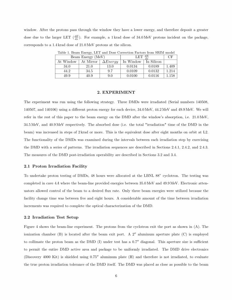
Figure 4 shows the beam-line experiment. The protons from the cyclotron exit the port as shown in (A). The
ionization chamber (B) is located after the beam exit port. A 2′′ aluminum aperture plate (C) is employed
to collimate the proton beam as the DMD (I) under test has a 0.7′′ diagonal. This aperture size is sufficient
to permit the entire DMD active area and package to be uniformly irradiated. The DMD drive electronics
(Discovery 4000 Kit) is shielded using 0.75′′ aluminum plate (H) and therefore is not irradiated, to evaluate
the true proton irradiation tolerance of the DMD itself. The DMD was placed as close as possible to the beam
6
Figure 4. Parts of the experimental apparatus are as follows: (A) is the proton beam-line exit port, (B) ionization chamber,(C) aluminum aperture plate, (D) high speed CCD camera, (E) a macro lens, (F) LED light source, (G) kinematic mount,(H) 0.75′′ aluminum shielding for the drive electronics, and (I) test DMD.
exit port, but with sufficient room to place the camera fixture. To limit systematic uncertainties and facilitate
comparison between subsequent irradiation runs, the DMD is not removed from the test bench or unpowered for
the duration of the test procedures. After each irradiation step, a CCD camera (D) and 50mm C-mount lens
(E) is placed in the beam-line looking at the DMD. This allows the DMD to be re-imaged onto the camera. A
kinematic magnetic mount (G) serves as the repeatable mounting fixture for this camera and light source (F).
The lens aperture is set to f/4 for the duration of the experimental data collection. An LED light source is used
to uniformly illuminate the active area of the DMD during the imaging process.
2.3 Optical Test Procedure
The goal of the optical test procedure was to determine which mirrors in the DMD array remained fully functional
at increasing dose levels. Operational mirrors were defined as mirrors that would flip to both stable states. Non-
functional mirrors were either stuck in one position, or failed to flip towards the CCD camera. Mirrors that stick
would be permanently attached to the substrate in either the “on” position or the “off” position. Mirrors that
fail to flip are mirrors in the central neutral position due to, e.g. a broken hinge or electrodes that fail to load
the proper voltages. The optical test procedure for the DMD had two sets of patterns. One set of “run” patterns
was sent to the DMD for use during the proton irradiation (Figure 5). A second set of “test” patterns (Figure 7)
was used to check the functionality of each individual mirror after irradiation.
The purpose of the first set of run patterns was to have the mirrors latched in one of the two stable positions
7

Figure 5. Five sequential DMD run patterns are shown here. Each zone is composed of 248 columns of DMD mirrors. Forrun one the top half of the DMD mirrors are on, and the bottom half are off. During run two, the mirrors are flipped inzone four. Next, for run three, the mirrors in zone three are flipped. This sequence continues for each irradiation step.This set of patterns is used to investigate the mirrors duty-cycle during proton irradiation. For the zones one to four, theduty-cycles tested were 100%, 75%, 66%, and 50%. Mirrors in zone one were in the same position for each irradiation.Mirrors in zone four alternated positions every other irradiation step.
Figure 6. (A) Run pattern was loaded into the DMD prior to the proton irradiation and an image was captured withthe camera. (B) Image was captured with the CCD camera after irradiation. Mirrors that flipped during the irradiationlook dark in the top half of the array and bright in the bottom half to the array in this example. (C) |A−B| shows thelocations of all of the flipped mirrors in the irradiation. (D) Same run pattern was reloaded into the DMD to ensure allmirrors went back to their programmed state.
for an irradiation, much like they would see on orbit. It was of interest to determine if any mirrors flipped during
the irradiation, so a simple procedure was devised. The run pattern was loaded into the DMD and an image
was taken with the CCD camera. After the DMD was irradiated, a second image was taken. By subtracting
these two images, the mirrors that flipped during the irradiation were detected. Next, the same run pattern was
reloaded and another image was taken. This procedure is illustrated in Figure 6. The second image was used
to verify that flipped mirrors would return to their programmed state after reloading the DMD memory. The
run pattern was broken up into four duty-cycle zones. Each zone was composed of 248 columns on the DMD.
Duty-cycle is defined as the percent of time a given mirror is in one state for the irradiations versus the opposite
state. To determine if the mirrors’ duty-cycle was a significant parameter, the run pattern was changed between
8

subsequent irradiation steps. In zone one, the mirrors were kept in the same state for all irradiation steps. The
zone four mirrors changed position at each subsequent irradiation step. For the zones one to four, the duty-cycles
tested were 100%, 75%, 66%, and 50%. The test pattern was latched and held for the duration of one irradiation.
Figure 7. Two DMD test patterns are shown here. One mirror per 10 × 10 sub-array is facing the CCD camera. Thissub-array is tiled across the DMD in its entirety. After a series of 100 of these test frames are loaded and imaged, theoptical test procedure is complete.
After the run pattern images were taken, a separate set of “test” patterns (Figure 7) was sent to the DMD.
The first DMD test pattern had all of the mirrors along the perimeter orientated towards the CCD camera. An
image was then taken with the CCD camera. This enabled the calibration of spatial correspondence between
mirrors and CCD pixels. The DMD test pattern was then broken up into 10× 10 blocks. A single DMD mirror,
from each 10 × 10 block, faced the camera. This 10 × 10 blocking was repeated across the entire DMD. The
CCD camera captured the series of 100 test patterns, so that each individual mirror in the DMD faced the CCD
camera in exactly one image. This procedure was repeated at each irradiation step. This same testing procedure
was performed at each of the three energies. The images were post-processed and truth maps were constructed
after the testing was completed.
2.4 Irradiation Sequence
2.4.1 Energy #1 (Beam - 34.0MeV Device - 21.0MeV) DMD serial number 140508
The initial set of tests was conducted with the beam energy tuned to 34MeV. Prior to irradiating devices, the
beam had to be optimized for uniformity across the beam aperture. The distance between the DMD and the
aperture plate was port was approximately 12 inches. Over this distance, the beam divergence was negligible.
The beam divergence was measured by placing a piece of film at the DMD test location and measuring the
diameter (2 inches) which was the same as the collimator plate. Gafcrhomic RTAQ217 film recorded the beam
9

uniformity at the DMD sample location. The film was scanned using an on-site densitometer. This process was
repeated until the beam was adjusted to be within the desired uniformity (approximately 1% uniformity across
the DMD).
Prior to traveling to LBNL, the top kovar metal frame with window was removed from four surplus DMDs.
This process is illustrated in Figure 8. The bottom portion of the package with DMD silicon was discarded. These
four sets of window frames were used to determine if the glass transmission changed after proton irradiation.
One of the DMD window frames was then irradiated with 34MeV protons to a dose of 20 krad with the beam
incident normal to the window. The window transmittance results are shown in Figure 9, and the results are
presented in Section 3.1.
Figure 8. (Left) Original DMD package. (Middle) Kovar metal frame and window are in the process of being removedfrom the DMD package. (Right) Kovar frame and window are separated from the DMD package.
After the first window frame had been irradiated, a powered and biased DMD was tested at 34MeV (21MeV
incident at the silicon). All of the DMDs were irradiated with the proton beam incident normal to the window.
Before irradiation, the baseline DMD functionality was validated using an optical test procedure as is described
in Section 2.3. The DMD run one pattern was loaded into the DMD. Next, the full surface of the DMD was
irradiated to 2 krad incident. The optical test procedure (Section 2.3) was then performed. For each run, the
loaded run pattern (Figure 5) was modified to test the influence of duty cycle. This was repeated until run ten,
where each run corresponded to an additional 2 krad incident dose. After run ten the irradiation dose step was
increased to 5 krad incident, and three additional runs were performed. The 34.0MeV run log is shown in Table
4.
2.4.2 Energy #2 (Beam - 44.2MeV Silicon - 34.5MeV) DMD serial number 140507
Next, the beam energy was tuned to 44.2MeV. The same beam uniformity measurements were taken with the
Gafchromic film. The second DMD window was irradiated to 20 krad. After the window was irradiated, the
second DMD was placed in the beam-line using the same control electronics to drive the DMD. A pre-irradiation
optical scan was completed. Then, a run pattern (Figure 5) was loaded into the DMD. The DMD was irradiated
to a 4 krad incident dose, and a post irradiation optical test was completed (Section 2.3). The proton energy
at the DMD silicon was 34.5MeV. The modified run image for run two was then loaded into the DMD. This
10

procedure was repeated until run six at which time the irradiation dose increment was changed to 5 krad incident.
The 44.2MeV run log is shown in Table 5. After the final irradiation increment and prior to the removal of this
DMD from the beam-line, an unknown but substantial additional proton dose irradiated this device due to a
beam-line control malfunction.
2.4.3 Energy #3 (Beam - 49.3MeV Silicon - 40.9MeV) DMD serial number 140106.
To test the final device, the beam was tuned to 49.3MeV. At the highest energies it was more difficult to tune
the cyclotron, and it therefore involved the longest down time. The third window was irradiated to a dose of
20 krad. The pre-irradiation test was done on the third DMD. The run pattern (Figure 5) was loaded into the
DMD. It was irradiated to a 4 krad incident dose. The optical test procedure was then repeated on this DMD
at each irradiation step. The step sizes were kept constant at 4 krad incident until run six, at which point the
step size was changed to 5 krad incident. The 49.3MeV run log is shown in Table 6.
3. RESULTS
3.1 Post-Irradiation Window Transmittance Loss
After irradiating the window frames to 20 krad, they became activated, and remained at Lawrence Berkley
National Labs (LBNL) for several weeks until they cooled to background level. After the windows were returned
to Rochester Institute of Technology (RIT), their transmittance and that of an unirradiated control window frame
were measured on Shimadzu Spectro-Photometer 2100− UV . Figure 9 shows the transmittance measurements,
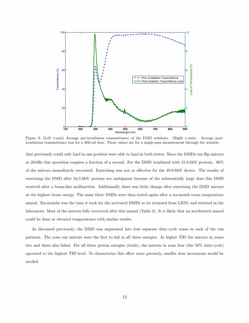
with a loss of 1 − 3% in the range 3.500Å − 9.000Å, and a peak up to 10% at 3.000Å. The windows were
then remeasured on a separate instrument, a J.A. Whoollam VASE (Variable Angle Spectroscopic Ellipsometer)
to validate these results. It is well known that borosilicate glass will yellow after being exposed to high-energy
protons,18 and our results illustrate this effect. These results are for a single-pass measurement, so the total
loss of transmittance would be the square of this value. An alternative window material such as magnesium
fluoride, which does not yellow as readily, could be used in the DMD package. However, the coefficient of
thermal expansion (CTE) of the borosilicate window is best matched to the entire DMD package.
3.2 Post-Irradiation DMD Functionality
The results of the optical tests at each irradiation step are shown in Figure 10. The percentages of operational
mirrors are shown as a function of proton dose. At all three tested energies, the DMDs withstood a TID of
approximately 30 krad. After the irradiation procedure at each energy was completed, the mirrors were exercised
using an alternating checkerboard pattern for several thousand cycles. By rapidly re-landing mirrors, mirrors
11
100 200 300 400 500 600 700 800 9000
20
40
60
80
100
Wavelength (nm)
Tra
nsm
itta
nce
(%
)
100 200 300 400 500 600 700 800 9000
2
4
6
8
10
Lo
ss o
f T
ran
sm
itta
nce
(%
)
Pre−Irriadiation Transmittance
Post Irridaiton Transmittance Loss
Figure 9. (Left y-axis) Average pre-irradiation transmittance of the DMD windows. (Right y-axis). Average post-irradiation transmittance loss for a 20krad dose. These values are for a single-pass measurement through the window.
that previously could only land in one position were able to land in both states. Since the DMDs can flip mirrors
at 20 kHz this operation requires a fraction of a second. For the DMD irradiated with 21.0MeV protons, 90%
of the mirrors immediately recovered. Exercising was not as effective for the 49.9MeV device. The results of
exercising the DMD after 34.5MeV protons are ambiguous because of the substantially large dose this DMD
received after a beam-line malfunction. Additionally there was little change after exercising the DMD mirrors
at the highest beam energy. The same three DMDs were then tested again after a six-month room temperature
anneal. Six-months was the time it took for the activated DMDs to be returned from LBNL and retested in the
laboratory. Most of the mirrors fully recovered after this anneal (Table 2). It is likely that an accelerated anneal
could be done at elevated temperatures with similar results.
As discussed previously, the DMD was segmented into four separate duty-cycle zones in each of the run
patterns. The zone one mirrors were the first to fail in all three energies. At higher TID the mirrors in zones
two and three also failed. For all three proton energies (trials), the mirrors in zone four (the 50% duty-cycle)
operated to the highest TID level. To characterize this effect more precisely, smaller dose increments would be
needed.
12

0 5 10 15 20 25 30 35 40 45 500
20
40
60
80
100
Work
ingMirro
rs 21. 0 MeV
0 5 10 15 20 25 30 35 40 45 500
20
40
60
80
100
Work
ingMirro
rs%
34. 5 MeV
0 5 10 15 20 25 30 35 40 45 500
20
40
60
80
100
Dose (k rad)
Work
ingMirro
rs%
40. 9 MeV
zone 1
zone 2
zone 3
zone 4
Figure 10. Percentage of working mirrors is plotted versus dose in krad. Note, the 34.5MeV device was irradiated to anadditional unknown dosage level after the last data point.
Table 2. The post-exposure DMD operability is shown here. Exercising was beneficial for the mirrors at the lowest energy21.0MeV. The * indicates no data.
21.0MeV After Irradiation After Exercising After 6 Month Room Temperature AnnealZone 1 5.0% 26.7% 99.98%Zone 2 2.9% 86.9% 100%Zone 3 0.0% 95.5% 100%Zone 4 1.2% 95.7% 100%
34.5MeV After Irradiation After Exercising After 6 Month Room Temperature AnnealZone 1 1.6% ∗ 79.72%Zone 2 5.8% ∗ 80.2%Zone 3 6.6% ∗ 90.4%Zone 4 5.2% ∗ 96.0%
40.9MeV After Irradiation After Exercising After 6 Month Room Temperature AnnealZone 1 3.2% 3.2% 99.99%Zone 2 3.1% 3.1% 100%Zone 3 3.7% 3.7% 100%Zone 4 2.7% 2.7% 100%
13
3.3 Duty Cycle Effect
The underlying cause for this duty-cycle effect is unknown, but may be mechanical in nature. Possibly, when
the mirror is latched in one state and the torsional hinge is irradiated, new defects are created in the hinge.
These defects reduce the stress in the latched hinge, and once bias is removed from this mirror, the mirror no
longer returns to its flat state. A related effect, seen when DMDs are used in projectors operated at elevated
temperatures, called “hinge memory" has been discussed.19 The two higher energies that used even larger dose
increment began exhibiting performance issues at slightly lower TID levels. This indicates that the DMD has
an apparent dose-rate effect, and that both the irradiation rate and TID are important in assessing the effect
of protons on DMD performance. The exercising and duty-cycle effects observed indicate the testing conditions
were harsh and unrealistic for several reasons. A minimum increment 2 krad was used during our testing. This
2 krad dose corresponds to the radiation dose the DMD would obtain after several months on orbit. On orbit,
it may be beneficial to optimize DMD operation to extend their life. Operationally, one can envision to exercise
the DMD in idle mode, switching them at high frequency (10 kHz or more, as designed) between their on/off
positions, each time an observation is not being carried out, like e.g. during telescope moves and in general when
the light detectors (CCD or IR) are also in idle mode.
3.3.1 Heating Effects
An alternate explanation for the hinge memory effect relates to hinge heating. This has been discussed previ-
ously.20 A worst case heating scenario due to proton kinetic energy transfer assumes all the proton kinetic energy
during an irradiation step is converted into thermal energy. The change in temperature can be calculated from
the specific heat of aluminum, target mass of the DMD, and energy absorbed from the incident 55MeV protons.
A δT much less than 1◦C is obtained. Comparatively when the DMD is used in a high output commercial
projector, a thermal load (δT > 10◦C) is placed on the DMD with minimal effects. Thus, a thermal explanation
for the mirrors becoming stuck does not seem viable.
3.3.2 Trapped Oxide charge (Dielectric Charging)
Another possible cause of sticking mirrors is trapped charge in DMD oxides. Metal Oxide Field Effect Field Effect
Transistor, MOSFET are very sensitive to trapped charge in insulating oxide layers.21 The types of trapped
charge affect NMOS and PMOS devices differently. As a charged particle passes through the oxide layer, the
radiation creates electron hole pairs. On average, one charge pair is produced for each 17 eV22 of energy absorbed
by the material. The only trapped charge that is important for the MEMS portion of the mirrors is unshielded
trapped charge. If there are regions of the DMD that have oxide without metal overlapping them, this can cause
14
the mirror actuation voltage to change. Without being able to directly test the CMOS memory, it is difficult
to determine if the trapped charge is present in the DMD’s CMOS transistors, or if the trapped charge occurs
in its MEMS spacer oxide layers in the super-structure. Trapped charge in either of these locations could cause
mirrors to no longer function. Various different types of MEMS devices have been shown to be sensitive to
trapped charge23 in these locations due to the nature of their electrostatic design.24
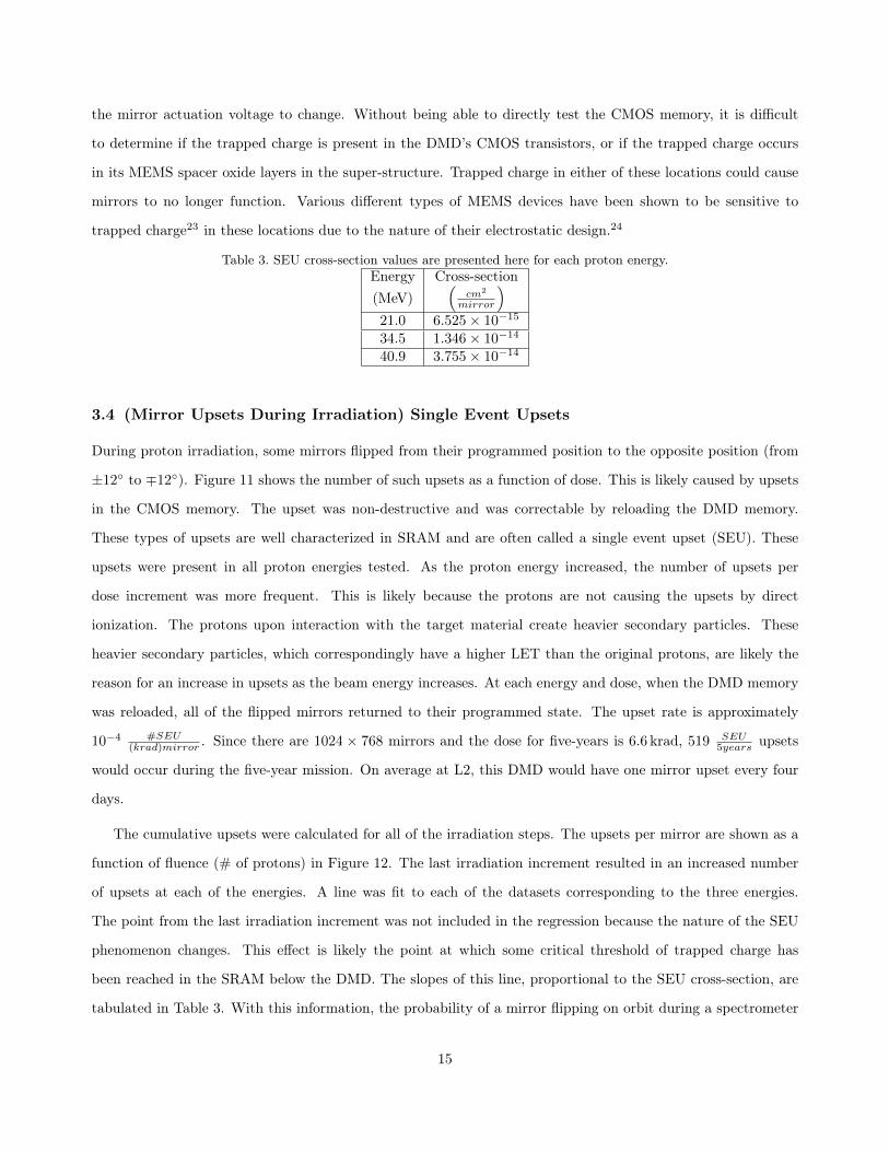
Table 3. SEU cross-section values are presented here for each proton energy.Energy Cross-section(MeV)
(cm2
mirror
)21.0 6.525× 10⁻¹⁵
34.5 1.346× 10⁻¹⁴
40.9 3.755× 10⁻¹⁴
3.4 (Mirror Upsets During Irradiation) Single Event Upsets
During proton irradiation, some mirrors flipped from their programmed position to the opposite position (from
±12◦ to ∓12◦). Figure 11 shows the number of such upsets as a function of dose. This is likely caused by upsets
in the CMOS memory. The upset was non-destructive and was correctable by reloading the DMD memory.
These types of upsets are well characterized in SRAM and are often called a single event upset (SEU). These
upsets were present in all proton energies tested. As the proton energy increased, the number of upsets per
dose increment was more frequent. This is likely because the protons are not causing the upsets by direct
ionization. The protons upon interaction with the target material create heavier secondary particles. These
heavier secondary particles, which correspondingly have a higher LET than the original protons, are likely the
reason for an increase in upsets as the beam energy increases. At each energy and dose, when the DMD memory
was reloaded, all of the flipped mirrors returned to their programmed state. The upset rate is approximately
10−4 #SEU(krad)mirror . Since there are 1024 × 768 mirrors and the dose for five-years is 6.6 krad, 519 SEU
5years upsets
would occur during the five-year mission. On average at L2, this DMD would have one mirror upset every four
days.
The cumulative upsets were calculated for all of the irradiation steps. The upsets per mirror are shown as a
function of fluence (# of protons) in Figure 12. The last irradiation increment resulted in an increased number
of upsets at each of the energies. A line was fit to each of the datasets corresponding to the three energies.
The point from the last irradiation increment was not included in the regression because the nature of the SEU
phenomenon changes. This effect is likely the point at which some critical threshold of trapped charge has
been reached in the SRAM below the DMD. The slopes of this line, proportional to the SEU cross-section, are
tabulated in Table 3. With this information, the probability of a mirror flipping on orbit during a spectrometer
15

0 5 10 1510
−7
10−6
10−5
10−4
10−3
run number
#SEU
(krad)m
irror
21.0 MeV
34.5 MeV
40.9 MeV
Figure 11. Number of upsets per mirror versus run number at each proton energy. For example, 10−4 #SEU(krad)mirror
×(1024 × 768mirrors) × 6.6 krad = 519 SEU5years
= 103.8SEUyear
= 0.28SEUDay
. This DMD would have one upset mirror everyfour days of operation during a five-year mission at L2.
0 0.5 1 1.5 2 2.5
x 1011
0
1
2
3
4
5
6
7
8x 10
−3
P +
cm 2
Upsets
Mirror
21.0 MeV
21.0 MeV Regression
34.5 MeV
34.5 MeV Regression
40.9 MeV
49.9 MeV Regression
Figure 12. Slope represents the SEU cross-section.
16

integration time can be calculated. The number of upsets and cross-sections are comparable to other SRAM
memory devices.25
4. CONCLUSION
A test procedure was developed to characterize proton irradiated DMDs at three different proton energies.
During irradiation two effects were observed that affected the performance of the device. The DMDs were
100% functional to a TID of 30 krad. For higher doses, it appears that the duty-cycle of the mirrors (i.e the
ratio of time the mirror is latched in one state versus the opposite latched position) during the irradiation
is important. Additionally, the proton flux rate also appears to be a significant factor in determining DMD
performance above 30 krad. The DMD failures are believed to be caused by trapped charges in oxide layers,
either in the CMOS memory transistors, or in the MEMs super-structure itself. Future work will test additional
electrical parameters to determine if the failure mechanisms are within the CMOS memory or in the MEMS
super-structure. Operationally, there were benefits from exercising the mirrors to avoid duty-cycle effects, and
thermal annealing seems to cure most of the damage not recovered by exercising the mirrors.
Some mirrors flipped from their programmed position to their opposite position during proton irradiation.
This is a type of SEU caused by CMOS memory upsets. The calculated SEU rates and corresponding upset
cross-sections agreed with those quoted for other SRAM devices fabricated with similar design rules.
While DMDs with the shielding from their package shielding can withstand a five-year mission with a 2×
margin of safety and a 4.5× margin of safety if 100mil of space-craft shielding is used. Overall, DMDs appear
to function well in a proton radiation environment and should be considered as a candidate for a slit mask on a
future space mission.
APPENDIX A. PROTON RUN LOGS
17

Table 4. 34MeV run log For DMD serial number 140508. The energy at the DMD silicon is 21.0MeV. *Started to seesticking mirrors in Zone 1. **Started to see additional sticking and non-functional mirrors in other zones. *** Effectscontinued across all four zones.
Average Incremental Integral Incremental Integral Silicon IrradiationFlux Fluence Fluence Dose Dose Dose Time
# p+cm2s
p+cm2
p+cm2 (krad) (krad) (krad) (s)
1 5.3× 10⁷ 9.07× 10⁹ 9.1× 1009 2.0 2.0 2.74 1722 5.4× 10⁷ 9.07× 10⁹ 1.8× 10¹⁰ 2.0 4.0 5.48 1693 5.3× 10⁷ 9.08× 10⁹ 2.7× 10¹⁰ 2.0 6.0 8.22 1734 5.5× 10⁷ 9.08× 10⁹ 3.6× 10¹⁰ 2.0 8.0 10.96 1665 5.6× 10⁷ 9.08× 10⁹ 4.5× 10¹⁰ 2.0 10.0 13.70 1636 5.8× 10⁷ 9.08× 10⁹ 5.4× 10¹⁰ 2.0 12.0 16.44 1577 5.5× 10⁷ 9.09× 10⁹ 6.4× 10¹⁰ 2.0 14.0 19.18 1648 5.4× 10⁷ 9.08× 10⁹ 7.3× 10¹⁰ 2.0 16.0 21.92 1689 5.1× 10⁷ 9.11× 10⁹ 8.2× 10¹⁰ 2.0 18.0 24.67 17910 4.8× 10⁷ 9.10× 10⁹ 9.1× 10¹⁰ 2.0 20.0 27.42 18911* 5.1× 107 2.25× 10¹⁰ 1.1× 10¹¹ 5.0 25.0 34.21 44512** 4.6× 10⁷ 2.25× 10¹⁰ 1.4× 10¹¹ 5.0 30.0 41.01 49313*** 4.7× 10⁷ 2.25× 10¹⁰ 1.6× 10¹¹ 5.0 34.9 47.81 476
Table 5. 44.2MeV run log For DMD serial number 140507. The energy at the DMD silicon is 34.5MeV. *Started to seeeffects in zone 1. After dose increment 8, this DMD received an extra unknown dose due to beam-line control malfunction.
Average Incremental Integral Incremental Integral Silicon IrradiationFlux Fluence Fluence Dose Dose Dose Time
# p+cm2s
p+cm2
p+cm2 (krad) (krad) (krad) (s)
1 8.5× 10⁷ 2.30× 10¹⁰ 2.3× 10¹⁰ 4.1 4.1 4.87 2712 7.5× 10⁷ 2.30× 10¹⁰ 4.6× 10¹⁰ 4.1 8.1 9.75 3053 8.4× 10⁷ 2.30× 10¹⁰ 6.9× 10¹⁰ 4.1 12.2 14.62 2734 8.6× 10⁷ 2.30× 10¹⁰ 9.2× 10¹⁰ 4.1 16.2 19.49 2695 8.4× 10⁷ 2.30× 10¹⁰ 1.2× 10¹¹ 4.1 20.3 24.36 2746 7.3× 10⁷ 2.87× 10¹⁰ 1.4× 10¹¹ 5.1 25.4 30.43 3917* 7.3× 107 2.87× 10¹⁰ 1.7× 10¹¹ 5.1 30.4 36.49 3928 7.1× 10⁷ 2.86× 10¹⁰ 2.0× 10¹¹ 5.1 35.5 42.56 404
Table 6. 49.3MeV run log For DMD serial number 140106. The energy at the DMD silicon is 40.9MeV. *Started to seeeffects in zone 1 **Global effects continue, and some mirrors recover by the end of optical characterization. ***Most ofarray is non-functional.
Average Incremental Integral Incremental Integral Silicon IrradiationFlux Fluence Fluence Dose Dose Dose Time
# p+cm2s
p+cm2
p+cm2 (krad) (krad) (krad) (s)
1 5.0× 10⁷ 2.40× 10¹⁰ 2.4× 10¹⁰ 4.0 4.0 4.45 4792 4.5× 10⁷ 2.40× 10¹⁰ 4.8× 10¹⁰ 4.0 8.0 8.90 5373 4.1× 10⁷ 2.43× 10¹⁰ 7.2× 10¹⁰ 4.0 12.0 13.40 5974 3.9× 10⁷ 2.40× 10¹⁰ 9.6× 10¹⁰ 4.0 16.1 17.85 6115 3.6× 10⁷ 2.40× 10¹⁰ 1.2× 10¹¹ 4.0 20.1 22.30 6726* 3.4× 107 3.00× 10¹⁰ 1.5× 10¹¹ 5.0 25.1 27.87 8907** 3.3× 10⁷ 3.00× 10¹⁰ 1.8× 10¹¹ 5.0 30.1 33.43 9028*** 3.0× 10⁷ 3.00× 10¹⁰ 2.1× 10¹¹ 5.0 35.1 38.99 995
18

REFERENCES
1. L. Hornbeck, “Current status of the digital micromirror device (dmd) for projection television applications,”
in Electron Devices Meeting, 1993. IEDM’93. Technical Digest., International, pp. 381–384, IEEE, 1993.
2. M. Douglass, “DMD reliability: a MEMS success story,” Proceedings of SPIE 4980, 2003.
3. R. D. Meyer, “RITMOS: a micromirror-based multi-object spectrometer,” Proceedings of SPIE 5492,
pp. 200–219, 2004.
4. J. W. MacKenty, “IRMOS: an infrared multi-object spectrometer using a MEMS micro-mirror array,”
Proceedings of SPIE 4841(2), pp. 953–961, 2003.
5. H.-J. Ziock, K. Holzscheiter, A. Morgan, A. Palounek, J. Ellison, A. Heinson, M. Mason, S. Wimpenny,
E. Barberis, N. Cartiglia, et al., “Temperature dependence of the radiation induced change of depletion volt-
age in silicon pin detectors,” Nuclear Instruments and Methods in Physics Research Section A: Accelerators,
Spectrometers, Detectors and Associated Equipment 342(1), pp. 96–104, 1994.
6. S. Barden and T. Armandroff, “Performance of the WIYN fiber-fed MOS system: Hydra,” in Proceedings
of SPIE, 2476, p. 56, 1995.
7. R. L. Davies, J. R. Allington-Smith, P. Bettess, E. Chadwick, R. Content, G. N. Dodsworth, R. Haynes,
D. Lee, I. J. Lewis, J. Webster, E. Ettedgui-Atad, S. M. Beard, M. A. Ellis, P. R. Hastings, P. R. Williams,
T. Bond, D. Crampton, T. J. Davidge, J. M. Fletcher, B. Leckie, C. L. Morbey, R. G. Murowinski, S. C.
Roberts, L. K. Saddlemyer, J. Sebesta, J. R. Stilburn, and K. Szeto, “Gmos: the gemini multiple object
spectrographs,” Optical Telescopes of Today and Tomorrow 2871(1), pp. 1099–1106, SPIE, 1997.
8. A. Kutyrev, R. Arendt, S. Moseley, R. Boucarut, T. Hadjimichael, M. Jhabvala, T. King, M. Li, J. Loughlin,
D. Rapchun, et al., “Programmable microshutter arrays for the jwst nirspec: optical performance,” Selected
Topics in Quantum Electronics, IEEE Journal of 10(3), pp. 652–661, 2004.
9. F. Zamkotsian, P. Spanò, L. Martin, M. Riva, P. Lanzoni, F. Zerbi, L. Valenziano, and L. Nicastro, “Dmd-
based mos demonstrator on galileo telescope,” in Proc. of SPIE Vol, 7735, pp. 77356E–1, 2010.
10. M. Robberto, A. Cimatti, A. Jacobsen, F. Zamkotsian, and F. Zerbi, “Applications of dmds for astrophysical
research,” arXiv preprint arXiv:0902.2775 , 2009.
11. F. Zamkotsian, E. Grassi, P. Lanzoni, R. Barette, C. Fabron, K. Tangen, L. Marchand, and L. Duvet, “DMD
chip space evaluation for ESA’s EUCLID mission,” Library 7596, pp. 75960E–75960E–12, 2010.
12. H. Shea, “Effects of radiation on mems,” in Proc. of SPIE Vol, 7928, pp. 79280E–1, 2011.
13. D. Heynderickx, B. Quaghebeur, E. Speelman, and E. Daly, “Esa’s space environment information system
(spenvis): A www interface to models of the space enviroment and its effects,” Proc. AIAA 371, 2000.
19

14. M. Xapsos, J. Barth, E. Stassinopoulos, E. Burke, and G. Gee, “Space environment effects: Model for
emission of solar protons (esp): Cumulative and worst case event fluences,” NASA STI/Recon Technical
Report N , p. 21507, 1999.
15. J. Barth, J. Isaacs, and C. Poivey, “The radiation environment for the next generation space telescope,”
NGST Project, internal document , 1999.
16. “James Ziegler - SRIM & TRIM.” http://www.srim.org/.
17. “Gafchromic rtqa2.” http://www.gafchromic.com/.
18. S. Pellicori, E. Russell, and L. Watts, “Radiation induced transmission loss in optical materials,” Applied
Optics 18(15), pp. 2618–2621, 1979.
19. M. Douglass, “Lifetime estimates and unique failure mechanisms of the digital micromirror device (dmd),” in
Reliability Physics Symposium Proceedings, 1998. 36th Annual. 1998 IEEE International, pp. 9–16, IEEE,
1998.
20. A. Sontheimer, “Digital micromirror device (dmd) hinge memory lifetime reliability modeling,” in Reliability
Physics Symposium Proceedings, 2002. 40th Annual, pp. 118–121, IEEE, 2002.
21. P. McWhorter and P. Winokur, “Simple technique for separating the effects of interface traps and trapped-
oxide charge in metal-oxide-semiconductor transistors,” Applied physics letters 48(2), pp. 133–135, 1986.
22. J. Benedetto and H. Boesch, “The relationship between 60co and 10-kev x-ray damage in mos devices,”
Nuclear Science, IEEE Transactions on 33(6), pp. 1317–1323, 1986.
23. L. Edmonds, G. Swift, and C. Lee, “Radiation response of a mems accelerometer: an electrostatic force,”
Nuclear Science, IEEE Transactions on 45(6), pp. 2779–2788, 1998.
24. T. Miyahira, H. Becker, S. McClure, L. Edmonds, A. Johnston, and Y. Hishinuma, “Total dose degradation
of mems optical mirrors,” Nuclear Science, IEEE Transactions on 50(6), pp. 1860–1866, 2003.
25. E. Petersen, “The seu figure of merit and proton upset rate calculations,” Nuclear Science, IEEE Transactions
on 45(6), pp. 2550–2562, 1998.
Biographies
20

Kenny Fourspring has been a Ph.D. student at Rochester Institute of Technology since 2009. Kenny is a
NASA Graduate Research Student Research (GSRP) Fellow. In 2008, he graduated with a BS in Microelectronic
Engineering at Rochester Institute of technology.
Zoran Ninkov is a Professor at the Rochester Institute of Technology. He received his BSc 1st Class Honors)
in Physics at the University of Western Australia in 1978, his MSc degree in Physical Chemistry from Monash
University in 1981, and his Ph.D. in Astronomy from the University of British Columbia. His research interests
are in the area of instrumentation development, detector testing and MEMS devices.
Bryan C. Fodness is a graduate student at Rochester Institute of Technology, Center for Imaging Science. He
has spent 10 years working in the space environments and radiation effects field. Bryan plans to receive his MS
in Imaging Science in 2014 and in 1999 graduated with a BS in Physics.
M. Robberto is AURA Scientist at the Space Telescope Science Institute (STScI) in Baltimore, working
within the Instrument Division as Instrument Scientist and Technical Lead for NIRCAM, the near-infrared
camera for the James Webb Space Telescope. Before joining STScI, he has beep part of the science staff of
21
the Turin Astronomical Observatory (Italy), Max Planck Institute fuer Astronomie (Heidelberg, German) and
the European Space Agency. His main expertise is the concept, development and operations of new infrared
instrumentation, both for ground and space astronomy.
Sara Heap has been an astronomer at NASA’s Goddard Space Flight Center since 1969.
Alex G. Kim is a staff scientist in the Physics Division of Lawrence Berkeley National Laboratory. His
research interests are in type Ia supernova cosmology and is currently participates in several experiments: the
Nearby Supernova Factory 2, Dark Energy Survey, Large Synoptic Survey - Dark Energy Science Collaboration,
and Euclid Consortium. He received his BS in physics from the University of Michigan in 1991, and his doctorate
in physics from the University of California, Berkeley in 1996.
List of Figures
1 Left) Illustration shows an extrapolated view of an individual DMD mirror. This mirror archi-
tecture is denoted as TI’s fast track design. Reflective surface of the mirror is fabricated from
an aluminum alloy. (Right) Diagram shows a “Type-A” DMD package. The silicon substrate
containing the array of DMD mirrors is mounted to a ceramic carrier. Borosilicate window is held
above the DMD by a kovar metal frame. Device is wire-bonded to interconnects, which terminate
at the bottom of the ceramic carrier. . . . . . . . . . . . . . . . . . . . . . . . . . . . . . . . . . 2
2 Total dose of Solar protons in silicon after a 5-year mission at L2 (modeled by SPENVIS). 2.47mm
of aluminum shielding corresponds to the shielding provided by the package. Additionally, 100mil
of equivalent aluminum shielding is shown. . . . . . . . . . . . . . . . . . . . . . . . . . . . . . . . 4
22
3 Proton fluence as a function of energy at L2. Calculated using the ESP solar proton model using
a total shielding thickness of 5mm equivalent aluminum. . . . . . . . . . . . . . . . . . . . . . . . 5
4 Parts of the experimental apparatus are as follows: (A) is the proton beam-line exit port, (B)
ionization chamber, (C) aluminum aperture plate, (D) high speed CCD camera, (E) a macro lens,
(F) LED light source, (G) kinematic mount, (H) 0.75′′ aluminum shielding for the drive electronics,
and (I) test DMD. . . . . . . . . . . . . . . . . . . . . . . . . . . . . . . . . . . . . . . . . . . . . 7
5 Five sequential DMD run patterns are shown here. Each zone is composed of 248 columns of
DMD mirrors. For run one the top half of the DMD mirrors are on, and the bottom half are off.
During run two, the mirrors are flipped in zone four. Next, for run three, the mirrors in zone
three are flipped. This sequence continues for each irradiation step. This set of patterns is used
to investigate the mirrors duty-cycle during proton irradiation. For the zones one to four, the
duty-cycles tested were 100%, 75%, 66%, and 50%. Mirrors in zone one were in the same position
for each irradiation. Mirrors in zone four alternated positions every other irradiation step. . . . 8
6 (A) Run pattern was loaded into the DMD prior to the proton irradiation and an image was
captured with the camera. (B) Image was captured with the CCD camera after irradiation.
Mirrors that flipped during the irradiation look dark in the top half of the array and bright in the
bottom half to the array in this example. (C) |A − B| shows the locations of all of the flipped
mirrors in the irradiation. (D) Same run pattern was reloaded into the DMD to ensure all mirrors
went back to their programmed state. . . . . . . . . . . . . . . . . . . . . . . . . . . . . . . . . . 8
7 Two DMD test patterns are shown here. One mirror per 10 × 10 sub-array is facing the CCD
camera. This sub-array is tiled across the DMD in its entirety. After a series of 100 of these test
frames are loaded and imaged, the optical test procedure is complete. . . . . . . . . . . . . . . . 9
8 (Left) Original DMD package. (Middle) Kovar metal frame and window are in the process of being
removed from the DMD package. (Right) Kovar frame and window are separated from the the
DMD package. . . . . . . . . . . . . . . . . . . . . . . . . . . . . . . . . . . . . . . . . . . . . . . 10
9 (Left y-axis) Average pre-irradiation transmittance of the DMD windows. (Right y-axis). Av-
erage post-irradiation transmittance loss for a 20krad dose. These values are for a single-pass
measurement through the window. . . . . . . . . . . . . . . . . . . . . . . . . . . . . . . . . . . . 12
10 Percentage of working mirrors is plotted versus dose in krad. Note, the 34.5MeV device was
irradiated to an additional unknown dosage level after the last data point. . . . . . . . . . . . . . 13
23

11 Number of upsets per mirror versus run number at each proton energy. For example, 10−4
#SEU(krad)mirror ×(1024 × 768mirrors) × 6.6 krad = 519 SEU
5years = 103.8SEUyear = 0.28SEU
Day . This DMD
would have one upset mirror every four days of operation during a five-year mission at L2. . . . . 16
12 Slope represents the SEU cross-section. . . . . . . . . . . . . . . . . . . . . . . . . . . . . . . . . . 16
24