
Microelectronic Devices and Technologies
71
Microelectronic Devices and Technologies Proceedings of the 2 nd International Conference on Microelectronic Devices and Technologies (MicDAT '2019) 22-24 May 2019 Amsterdam, The Netherlands Edited by Sergey Y. Yurish
-
Upload
khangminh22 -
Category
Documents
-
view
1 -
download
0
Transcript of Microelectronic Devices and Technologies

Microelectronic Devices and Technologies
Proceedings of the 2nd International Conference
on Microelectronic Devices and Technologies (MicDAT '2019)
22-24 May 2019
Amsterdam, The Netherlands
Edited by Sergey Y. Yurish

Sergey Y. Yurish, Editor Microelectronic Devices and Technologies MicDAT '2019 Conference Proceedings Copyright © 2019
by International Frequency Sensor Association (IFSA) Publishing, S. L.
E-mail (for orders and customer service enquires): [email protected]
Visit our Home Page on http://www.sensorsportal.com
All rights reserved. This work may not be translated or copied in whole or in part without the written permission of the publisher (IFSA Publishing, S. L., Barcelona, Spain).
Neither the authors nor International Frequency Sensor Association Publishing accept any responsibility or liability for loss or damage occasioned to any person or property through using the material, instructions, methods or ideas contained herein, or acting or refraining from acting as a result of such use.
The use in this publication of trade names, trademarks, service marks, and similar terms, even if they are not identifies as such, is not to be taken as an expression of opinion as to whether or not they are subject to proprietary rights.
ISBN: 978-84-09-11679-9 BN-201905154-XX BIC: TJFD

2nd International Conference on Microelectronic Devices and Technologies (MicDAT '2019) 22-24 May 2019, Amsterdam, The Netherlands
3
Contents
Contents ............................................................................................................................................................. 3 Foreword ........................................................................................................................................................... 4 The Total Ionizing Dose Effects on Silicon-Oxide-Nitride-Oxide-Silicon (SONOS) and Floating Gate (FG) Flash Technology ..................................................................................................... 5
J. S. Bi, M. Li, Y. N. Xu, K. Xi and M. Liu 5
Understanding Adsorption Effect of Boron Nitride Nanotube (BNNT) Based on First-principles Calculations ....................................................................................................................... 8
N. D. Lu, L. Li and M. Liu 8
A Proposal of Optical Rotor Based on a pn-Junction Rod. Theoretical Base and Its Potential ............. 11 Y. Omura,11
Solder Stress Developments at Random Vibration ...................................................................................... 16 Y. Kim, S. Lee, D. Hwang and S. Kim 16
Stacked FinFET-CMOS: A Promising FEOL Based Process Technology in Nanoscale 3-D Integration Circuits ................................................................................................................................. 19
Jin He, Yuan Ren, Xiaomeng He, Xiaomeng Wang, Jun Pan, Jingjing Liu and Mansun Chan19
Improved Detection Limit of Calcium Test Using an Over-Pressurized Box ............................................ 22 C. M. Hsu, W. T. Wu, G. W. Zhou and K. C. Wu22
Comparison of Self-heating Effect in SOI MOSFETs with Various Configuration of Buried Oxide ..... 24 K. O. Petrosyants, D. A. Popov 24
Nitrogen-doped Carbon-based Very Thin Film on Quartz or Sapphire Substrate as Back-side Illuminated Transmission Photocathode ...................................................................................................... 29
J. Huran,, N. I. Balalykin, M. A. Nozdrin, V. Sasinková, A. Kleinová, A. P. Kobzev and E. Kováčová29
A Simple Surface-potential-based Drain Current Model for Fully-depleted Poly-Si Thin Film Transistors in Strong Inversion Region with Low Drain Bias ................................................................... 33
Zhen Zhu and Junhao Chu 33
Analysis and Improvement of Linearity Performance of Low Noise Amplifier with Diode Loads ......... 36 S. Chen, D. Prêle, F. Voisin and A. Goldwurm 36
Design Assurance of COTS Based Electronic Systems ................................................................................ 43 Dr. J. S. Sagoo 43
Ultrasonic Bonding of Ag-4Pd Alloy Ribbon for High Power IC Packages .............................................. 51 C. H. Chen, Y. C. Lin and T. H. Chuang 51
Intramode Energy Exchange into a Thin Left-handed Film on a Kerr-Substrate .................................. 55 N. Litvinova, A. Buller and R. Litvinov 55
Artificial Neuron Based on Superconducting Elements .............................................................................. 58 F. Feldhoff, S. Braeunig, H. Toepfer 58
White Organic Light-emitting Diodes with mCPCN Double Emitting Layers for Lighting .................... 61 Shui-Hsiang Su, Yuchang Chen, Zhang-De Xue61
Temperature Investigation of Phonon-plasmon Modes in 4H-SiC Shottky Diodes for Power Electronic Devices ......................................................................................................................... 63
Artur Dobrowolski,, Jakub Jagiełło,, Wawrzyniec Kaszub, Tymoteusz Ciuk, Kinga Kosciewicz, Pawel P. Michalowski, Pawel Ciepielewski andrzej Wysmołek, Adrianna Chamryga, Pawel Kaminski 63
An All-digital Frequency Synthesizer for Fractional-ratio On-chip Clock Generation .......................... 65 Taeyeon Kim and Jongsun Kim65
Charge Transfer Within the F4TCNQ-MoS2 Van der Waals Interface .................................................... 68 Jiawei Wang, N. D. Lu, L. Li and M. Liu 68

2nd International Conference on Microelectronic Devices and Technologies (MicDAT '2019) 22-24 May 2019, Amsterdam, The Netherlands
4
Foreword On behalf of the MicDAT’ 2019 Organizing Committee, I introduce with pleasure these proceedings devoted to contributions from the 2nd International Conference on Microelectronic Devices and Technologies (MicDAT '2019) held in Amsterdam, The Netherlands, on 22-24 May 2019. The conference is organized by the International Frequency Sensor Association (IFSA) in technical cooperation with our sponsors Excelera, S.L. (Barcelona, Spain) and F2D, Ltd. (Ireland), and media partner - MDPI ‘Sensors’ journal (Switzerland). The conference program provides an opportunity for researchers interested in microelectronics to discuss their latest results and exchange ideas on the new trends and challenges. The main objective of the MicDAT’ 2019 conference is to encourage discussion on a broad range of microelectronics related topics and to stimulate new collaborations among the participants. The proceedings contains all papers of oral and poster presentations. We hope that these proceedings will give readers an excellent overview of important and diversity topics discussed at the conference. Based on the proceeding’s contributions, selected and extended papers will be submitted by the authors to the ‘Sensors & Transducers’ open access journal (ISSN: 2306-8515, e-ISSN 1726-5479). The limited number of articles, published in ‘Sensors & Transducers’ journal will be invited to be extended for ‘Advances in Microelectronics: Reviews’, Vol. 3, Book Series. We thank all authors for submitting their latest work, thus contributing to the excellent technical contents of the conference. Especially, we would like to thank the individuals and organizations that worked together diligently to make this conference a success, and to the members of the International Program Committee for the thorough and careful review of the papers. It is important to point out that the great majority of the efforts in organizing the technical program of the conference came from volunteers. Prof., Dr. Sergey Y. Yurish MicDAT’ 2019 Chairman

2nd International Conference on Microelectronic Devices and Technologies (MicDAT '2019) 22-24 May 2019, Amsterdam, The Netherlands
5
(001)
The Total Ionizing Dose Effects on Silicon-Oxide-Nitride-Oxide-Silicon
(SONOS) and Floating Gate (FG) Flash Technology
J. S. Bi 1, M. Li 1, Y. N. Xu 1, K. Xi 1 and M. Liu 1
1 Institute of Microelectronics, Chinese Academy of Sciences, Beijing, China Tel.: + 861082995940, fax: + 861082995940
E-mail: [email protected] Summary: The 60Co-γ ray TID radiation responses of 55 nm SONOS memory cells and 65 nm FG memory cells are investigated. The threshold voltage (Vth) and off-state leakage current (Ioff) of memory cells are measured before and after radiation, respectively. The physical mechanisms of charge loss process are analyzed to explain experiment results. Keywords: Total ionizing dose, γ ray, SONOS, Floating gate, Flash.
1. Introduction
Flash memory can be applied as memory storage in aerospace and nuclear industries, which demands high reliability under ionizing radiation. So it is important to investigate the total ionizing dose (TID) radiation response of them.
In this work, we explore the TID radiation responses of 65 nm FG memory cells and 55 nm SONOS memory cells up to 1 Mrad(Si), including the threshold voltage (Vth) shifts and off-state leakage current (Ioff). 2. Devices and Experimental Details
The SONOS memory cell consists of a 2T-stacked structure, a memory transistor (MT) in series with a select transistor (ST). All Id-Vg curves are performed on MT while leaving ST being ON state. The MT is a SONOS device with charge stored in discrete traps in the silicon nitride layer. For 65 nm FG memory cell, its nominal gate width and length are 80 nm and 130 nm, respectively with 10 nm thick tunnel oxide.
Basic electric characterization is performed with an Agilent B1500 parameter analyzer at room temperature. Fowler-Nordheim (FN) tunneling is used to program/erase the memory cells, as shown in
Table 1. Vth represents the gate voltage when drain current of the memory transistor is 1 μA (Id = 1 μA). MW is determined by the Vth difference between programmed and erased cells. Ioff is defined as the drain voltage at zero gate bias (Id@Vg = 0 V).
Both FG memory cells and SONOS memory cells are irradiated by γ rays generated from a 60Co source, at a dose rate of 50 rad(Si)/s. No bias is applied to the device during irradiation. Memory cells are irradiated in steps up to dose level of 1 Mrad(Si), while the Id-Vg
characteristics are recorded. Time intervals for electrical measurements between irradiation exposures are within the limits stated in MIL-STD-883D Test Method 1019.4 (start electrical characterization one hour after exposure, and begin the next exposure two hours later). 3. Results and Discussions
After 1 Mrad(Si) radiation, for both FG and SONOS memory, the Id-Vg curves of programmed cell exhibit a shift toward the negative direction while those of erased cell exhibit a shift toward the positive direction. This kind of curve shift is mainly caused by the charge loss process in the storage layer and the positive charge accumulated in the surrounding oxide, as shown in Fig. 1.
Table 1. Definition of operation conditions.

2nd International Conference on Microelectronic Devices and Technologies (MicDAT '2019) 22-24 May 2019, Amsterdam, The Netherlands
6
The Vth shifts and the MW variation with respect to TID radiation are shown in Fig. 2. According to Fig. 2(a), after 1 Mrad(Si) radiation, the Vth of SONOS memory cells in program state drifts down from 1.38 V to 0.73 V. While that, in erase state increases from -1.14 V to -0.78 V. According to Fig. 2(b), the Vth of FG memory cells in program state drifts down from 7.2 V to 5.55 V, while that in erase state increases
from 1.6 V to 2.82 V. The Vth shifts lead to a memory window shrinking. We normalize the memory window voltage to compare the radiation-hard capability of the two kinds of memories directly. As the result shows, after 1 Mrad(Si) radiation, the normalized MW for SONOS memory cells remains at 60 %, while that for the FG memory cells is only 48 %.
Fig. 1. Energy band diagram of the SONOS device with electrons stored in the nitride layer during irradiation.
(a) (b)
Fig. 2. Vth shifts of (a) 55 nm SONOS memory cell, and (b) 65 nm FG memory cell before and after radiation. The inset shows the normalized MW shifts.
Besides the impact of radiation on Vth, leakage
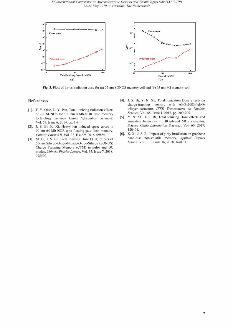
current at zero-bias gate voltage (Ioff) is widely used to evaluate the radiation effect. As shown in Fig. 3, after 1 Mrad(Si) radiation, the Ioff of SONOS memory cells in program state is 3 orders of magnitude higher than the corresponding one before radiation, and decreases from 21 μA to 12 μA for that in erase state. The Ioff of FG memory cells, by contrast, is only 1 order of magnitude higher than the corresponding one before radiation, and decreases from 1 nA to 0.18 nA. The Ioff variation can be attributed to the formation of parasitic transistor and the Vth shift induced by radiation.
4. Conclusions
The radiation induced Vth and Ioff degradation characteristics of 55 nm SONOS memory cell and
65 nm FG memory cell are investigated in this paper. The normalized memory window of SONOS memory cell is larger than that of FG memory cell after 1 Mrad(Si) radiation, showing that the SONOS memory cell exhibits a better data retention capability for the charge is stored in discrete traps in the Si3N4 layer. However, the leakage current of SONOS memory cell is larger than that of FG memory cell no matter in program or erase state, due to the formation of parasitic transistor. Acknowledgements
This research was supported by the NSF under Contracts 616340084.
2nd International Conference on Microelectronic Devices and Technologies (MicDAT '2019) 22-24 May 2019, Amsterdam, The Netherlands
7
(a) (b)
Fig. 3. Plots of Ioff vs. radiation dose for (a) 55 nm SONOS memory cell and (b) 65 nm FG memory cell.
References [1]. F. Y. Qiao, L. Y. Pan, Total ionizing radiation effects
of 2-T SONOS for 130 nm 4 Mb NOR flash memory technology, Science China Information Sciences, Vol. 57, Issue 6, 2014, pp. 1-9.
[2]. J. S. Bi, K. Xi, Heavy ion induced upset errors in 90-nm 64 Mb NOR-type floating-gate flash memory, Chinese Physics B, Vol. 27, Issue 9, 2018, 098501.
[3]. M. Li, J. S. Bi, Total Ionizing Dose (TID) effects of 55-nm Silicon-Oxide-Nitride-Oxide-Silicon (SONOS) Charge Trapping Memory (CTM) in pulse and DC modes, Chinese Physics Letters, Vol. 35, Issue 7, 2018, 078502.
[4]. J. S. Bi, Y. N. Xu, Total Ionization Dose effects on charge-trapping memory with Al2O3/HfO2/Al2O3
trilayer structure, IEEE Transactions on Nuclear Science, Vol. 65, Issue 1, 2018, pp. 200-205.
[5]. Y. N. XU, J. S. Bi, Total Ionizing Dose effects and annealing behaviors of HfO2-based MOS capacitor, Science China Information Sciences, Vol. 60, 2017, 120401.
[6]. K. Xi, J. S. Bi, Impact of γ-ray irradiation on graphene nano-disc non-volatile memory, Applied Physics Letters, Vol. 113, Issue 16, 2018, 164103.
2nd International Conference on Microelectronic Devices and Technologies (MicDAT '2019) 22-24 May 2019, Amsterdam, The Netherlands
8
(002)
Understanding Adsorption Effect of Boron Nitride Nanotube (BNNT)
Based on First-principles Calculations
N. D. Lu 1, L. Li 1 and M. Liu 1
1 Key Laboratory of Microelectronic Devices & Integrated Technology, Institute of Microelectronics, Chinese Academy of Sciences
Tel.: +86-10-82995582, fax: +86-10-82995583 E-mail: [email protected]
Summary: Based on the first-principles calculations, we have investigated the structure and electronic property of adsorbed small-molecule on boron nitride nanotubes (BNNTs). The potential application of BNNT as highly sensitive gas sensor for N-based small molecules has been discussed. For the BNNTs, the N-site displays the best the adsorption effect, as compared with B-site or center-site. Our results show that strong charge transfer in most cases corresponds to high adsorbed energy and small distance between BNNT and small molecules. Keywords: Gas sensor, First-principles calculations, Boron Nitride Nanotubes (BNNTs), Electronic property, Adsorption effect.
1. Introduction
Sensors with high sensitivity and selectivity act as the role for real-time detections of a variety of industrial processes and environment. Currently, plenty of low dimensional materials have been proposed as potential candidates of gas sensors [1-3]. The nanotubes are generally porous due to their high reactivity exterior surface, which makes them sensitive to small molecular [4]. As being important low-dimensional materials with wide band gaps, boron nitride nanotubes (BNNTs) have also received considerable interests. Despite the adsorption behavior of pure or doped BNNTs has been reported [5, 6], the structure and electronic properties of adsorbed small molecule on BNNTs is still ambiguous. Here, we investigate the structure and electronic property of BNNTs with absorbed small molecules, and then adsorption effect of small molecules.
2. Theory
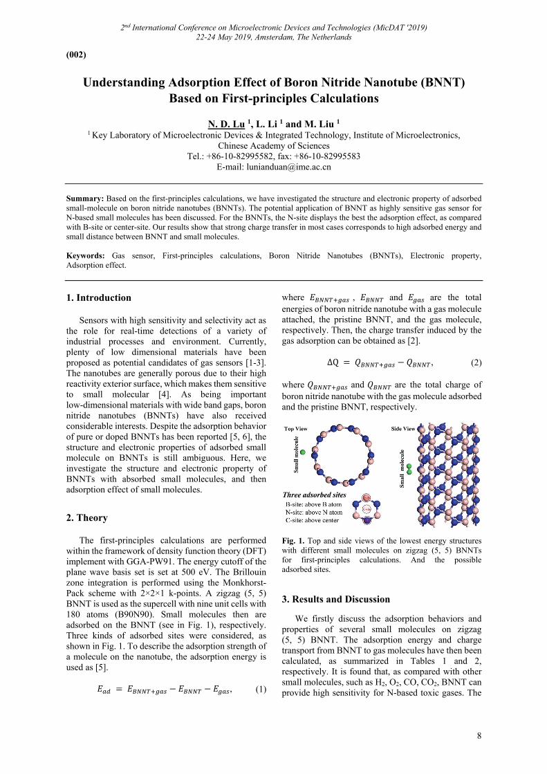
The first-principles calculations are performed within the framework of density function theory (DFT) implement with GGA-PW91. The energy cutoff of the plane wave basis set is set at 500 eV. The Brillouin zone integration is performed using the Monkhorst-Pack scheme with 2×2×1 k-points. A zigzag (5, 5) BNNT is used as the supercell with nine unit cells with 180 atoms (B90N90). Small molecules then are adsorbed on the BNNT (see in Fig. 1), respectively. Three kinds of adsorbed sites were considered, as shown in Fig. 1. To describe the adsorption strength of a molecule on the nanotube, the adsorption energy is used as [5].
𝐸 𝐸 𝐸 𝐸 , (1)
where 𝐸 , 𝐸 and 𝐸 are the total energies of boron nitride nanotube with a gas molecule attached, the pristine BNNT, and the gas molecule, respectively. Then, the charge transfer induced by the gas adsorption can be obtained as [2].
∆Q 𝑄 𝑄 , (2) where 𝑄 and 𝑄 are the total charge of boron nitride nanotube with the gas molecule adsorbed and the pristine BNNT, respectively.
Fig. 1. Top and side views of the lowest energy structures with different small molecules on zigzag (5, 5) BNNTs for first-principles calculations. And the possible adsorbed sites. 3. Results and Discussion
We firstly discuss the adsorption behaviors and properties of several small molecules on zigzag (5, 5) BNNT. The adsorption energy and charge transport from BNNT to gas molecules have then been calculated, as summarized in Tables 1 and 2, respectively. It is found that, as compared with other small molecules, such as H2, O2, CO, CO2, BNNT can provide high sensitivity for N-based toxic gases. The

2nd International Conference on Microelectronic Devices and Technologies (MicDAT '2019) 22-24 May 2019, Amsterdam, The Netherlands
9
corresponding densities of states (DOS) of adsorbed small molecule on zigzag (5, 5) BNNTs are shown in Fig. 2. Fig. 3 shows the site of LOMO and HOMO for pristine zigzag (5, 5) BNNT and different zigzag (5, 5) BNNT/gas. One can see that the LOMO and HOMO has been changed after BNNTs absorbed the different small molecules.
To understand the adsorption effect, we then investigate the adsorbed behavior of NO on BNNT for different adsorbed sites, that is, B-site, N-site and C-site (see in Fig. 1). Table II shows the adsorption energy 𝐸 (eV) and charge transfer from BNNT to small molecules ∆𝑄(eV) for three sites.
Table 1. Adsorption energy 𝐸 (eV), band gap and charge transfer from BNNT to small molecules ∆𝑄(eV).
Gas 𝑬𝒂𝒅(eV) ∆𝑸(eV) 𝑬𝒈(eV)
Pristine - - 4.680 H2 0.148 0.011 4.578 O2 0.023 -0.199 0.600 CO 0.157 -0.252 0.564 CO2 0.546 -0.163 0.080 NO 0.870 -0.261 1.150 NO2 1.377 -0.195 0.730
Fig. 2. DOS of different molecules on zigzag (5, 5) BNNTs.
In Table 2, one can see that the adsorption energy 𝐸 (eV) in B-site is larger than that in N-site and C-site. However, the B-site is not the optimal adsorbed sites, because ∆𝑄(eV) is positive. The positive ∆𝑄(eV) displays that the charge will transfer from small molecule to BNNT. Actually, the charge will more likely transfer from BNNT to small molecule. Thus, for NO gas, the optimal site should be the N-site.
Fig. 3. LOMO and HOMO of zigzag(5, 5) BNNT for pristine and with adsorbed small molecule. LOMO is the lowest unoccupied molecular orbital, and HOMO is highest occupied molecular orbital.
Table 2. Adsorption energy 𝐸 (eV), band gap and charge transfer from BNNT to small molecules ∆𝑄(eV)
for O or N atom of NO.
atom B-site N-site C-site
𝐸 (eV) N 2.187 1.157 0.573
O 2.289 0.870 0.591
∆𝑄 eV N 0.766 -0.058 -0.043
O 1.026 -0.261 -0.372
Then, the distance of between NO and BNNT
dependence of the energy gap, adsorption energy and charge transfer of zigzag (5, 5) BNNT/NO have been discussed in details in Fig. 4 and Fig. 5, respectively. It is obvious that the energy gap will increase and then decrease with the increase of the distance between the small molecule and BNNT. Otherwise, the adsorption effect of BNNTs will be optimal as the distance between the small molecule and BNNT is between 1.5 and 2.3 Å, according to the adsorption energy and charge transformation.

2nd International Conference on Microelectronic Devices and Technologies (MicDAT '2019) 22-24 May 2019, Amsterdam, The Netherlands
10
Fig. 4. The distance of between NO and BNNT dependence of the energy gap of zigzag (5, 5) BNNT/NO.
Fig. 5. The distance of between NO2 and BNNT dependence of adsorption energy and charge transfer
of zigzag (5, 5) BNNT/NO2, respectively.
3. Conclusions
Based on first-principles calculations, the potential application of BNNT as highly sensitive gas sensor for N-based small molecules has been demonstrated. Our calculations show that for N-based small molecule, N-site of BNNT is the optimal site for adsorbing small
molecule. Otherwise, the optimal distance for adsorbing small molecule is about 1.75 Å between BNNT and small molecule.
Acknowledgements
This work was supported by National key research and development program (No. 2017YFB0701703, 2016YFA0201802, 2018YFA0208503), by National Natural Science Foundation of China (No. 61890944, 61574166).
References [1]. J. Xiao, et al., Theoretical prediction of electronic
structure and carrier mobility in single-walled MoS2 Nanotubes, Sci. Rep., Vol. 4, 2014, 4327.
[2]. E. Montes, et al., Superior selectivity and sensitivity of blue phosphorus nanotubes in gas sensing applications, J. Mater. Chem. C, Vol. 5, 2017, pp. 5365-5371.
[3]. Y. Cai, et al., Energetics, charge transfer, and magnetism of small molecules physisorbed on phosphorene, J. Phys. Chem. C, Vol. 119, 2015, pp. 3102-3110.
[4]. S. J. Zhao, et al., Gas adsorption on MoS2 monolayer from first-principles calculations, Chem. Phys. Lett., Vol. 595, 2014, pp. 35-42.
[5]. M. Baei, et al., Adsorption properties of N2O on (6, 0),(7, 0), and (8, 0) zigzag single-walled boron nitride nanotubes: a computational study, Comp. Theor. Chem., Vol. 970, 2011, pp. 30-35.
[6]. A. Peyghan, et al., A first-principles study of the adsorption behavior of CO on Al-and Ga-doped single-walled BN nanotubes, Appl. Surf. Sci., Vol. 270, 2013, pp. 25-32.
2nd International Conference on Microelectronic Devices and Technologies (MicDAT '2019) 22-24 May 2019, Amsterdam, The Netherlands
11
(003)
A Proposal of Optical Rotor Based on a pn-Junction Rod.
Theoretical Base and Its Potential
Y. Omura 1, 2
1 Kansai University, Dept. Electric, Electronics, and Information Eng., Suita, 564-8680 Osaka, Japan 2 ACA & C., Isehara, 259-1135 Kanagawa, Japan
Tel.: +81663681121, fax: +81663888843 E-mail: [email protected]
Summary: This paper theoretically investigates how a Si pn-junction rod offers the potential to develop rotating motion. An analytical steady state solution of excess carrier concentration of the Si rod is derived from the continuity equation. The solution is given by a non-linear differential equation. Numerical calculation results strongly suggested that a 200-m-long Si rod should rotate with the acceleration of ~103 m/s2 under the illumination of 1 W/cm2. This is very good performance. It is demonstrated that the rotator suits various medical test chips without any battery. Keywords: pn junction, Rod, Light illumination, Rotation, Carrier generation, Recombination, Power generation.
1. Introduction
Micro Electro Mechanical System (MEMS) technology was proposed in the last century [1, 2], and its fundamental potentiality has been technically and commercially examined in various applications [3-5]. Given the old-fashioned technology available at its introduction, it was simply expected that MEMS device scale would range from hundreds of micrometers to few micrometers. However, this simple expectation has been proven flawed in real applications because achieving adequate reproducibility in device fabrication demanded very fine processing techniques, resulting high production costs. These technical barriers are missing in the “Nano-imprint technique” [6] and “3D printer technique” [7, 8]; they were proposed in the 1980s and 1990s, respectively, as advances from the original MEMS technology. Their advancement continues as well-known technologies.
Unfortunately, the demands imposed on MEMS devices in the health control and medical care fields are becoming more urgent in various communities all over the world. The MEMS devices created to meet requests [9-11], must have better low-power operation because most of them must work with very small batteries, not with ac power supplies. In extreme cases, cord-free operation is required. Such devices need a built-in battery that is charged by an external energy source. Although I proposed the advanced Schenkel circuit for RF-ID applications [12], the idea remains to be confirmed in practical applications.
In this paper, I theoretically examine the performance of an optical rotor based on a pn junction rod. It should work when irradiated by green light. The fundamental function and operation of the device are formulated mathematically based on semiconductor physics. In addition, its technological potential is also addressed.
2. Possible Device Structure and Rotation Principle 2.1. Possible Device Structure
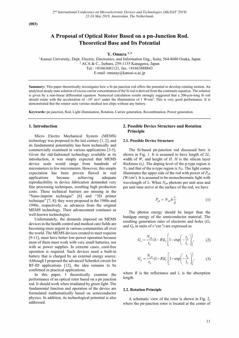
The Si-based pn-junction rod discussed here is shown in Fig. 1. It is assumed to have length of 2L, width of W, and height of H. H is the silicon layer thickness (ts). The doping level of the p-type region is NA and that of the n-type region is ND. The light comes illuminates the upper side of the rod with power of Pph
(W/cm2). It is assumed to be monochromatic light with wavelength of . When Nph photons per unit area and per unit time arrive at the surface of the rod, we have
ph ph
cP N h
(1)
The photon energy should be larger than the
bandgap energy of the semiconductor material. The resulting generation rates of electrons and holes (Gn and Gp in units of s-1cm-3) are expressed as
(1 ) 1 exp ,ph Sn C
S C
N tG R l
t l
(2)
(1 ) 1 exp ,ph Sp C
S C
N tG R l
t l
(3)
where R is the reflectance and lc is the absorption length.
2.2. Rotation Principle
A schematic view of the rotor is shown in Fig. 2, where the pn-junction rotor is located at the center of
2nd International Conference on Microelectronic Devices and Technologies (MicDAT '2019) 22-24 May 2019, Amsterdam, The Netherlands
12
the cavity space. It is assumed that the distance from the center of the rotor to the external electrode is D. When the light beam irradiates the surface of the pn-junction rod, electron-hole generation occurs in both the p-type and the n-type region. The p-type region is charged positively and the n-type region negatively. When the external electrodes, A and B, are alternatively biased, the rod will continue to rotate as long as the rod is irradiated. In order to ensure stable rotation of the rod, the frequency of the ac voltage must match the rotation period.
Fig. 1. pn junction rod.
Fig. 2. Rotation mechanism. A and B denote the electrodes.
3. Theoretical Base of Rod Rotation 3.1. Carrier Generation and Recombination Under the Light Illumination
The electron generation and recombination process in the p-type region generally follows the differential equation shown below.
20
2
( , )
( , ),
p
p p p pn p n n n
n
n x t
t
n x t n n nFG n F D
x x x
(4)
where np0 denotes the electron concentration at thermal equilibrium, Gn denotes the generation rate of electrons, n denotes the lifetime of electrons, F denotes the local electric field, n denotes the electron
mobility, and Dn denotes the diffusion constant of electrons.
The hole generation and recombination process in the n-type region generally follows the differential equation shown below.
20
2
( , )
( , ),
n
n n n np n p p p
p
p x t
t
p x t p p pFG p F D
x x x
(5)
where pn0 denotes the hole concentration at thermal equilibrium, Gp denotes the generation rate of holes, p
denotes the lifetime of holes, p denotes hole mobility, and Dp denotes the diffusion constant of holes. In the p-type region, Eq. (5) changes to
20
2
( , )
( , )
p
p p p pp p p p p
p
p x t
t
p x t p p pFG p F D
x x x
(6) The local electric field follows Poisson’s equations
as shown below.
0( ),p po p pS
F ep p n n
x
(7)
0 0( ),n nn nS
F ep p n n
x
(8)
where e denotes the elementary charge, and s denotes the semiconductor’s permittivity.
3.2. Steady State Solutions
At the steady state, we have
0
2
2
( , )
0,
p pn p n
n
p pn n
n x t n FG n
x
n nF D
x x
(9)
0
2
2
( , )
0,
n np n p
p
n np p
p x t p FG p
x
p pF D
x x
(10)
0
2
2
( , )
0
p pp p p
p
p pp p
p x t p FG p
x
p pF D
x x
(11)
2nd International Conference on Microelectronic Devices and Technologies (MicDAT '2019) 22-24 May 2019, Amsterdam, The Netherlands
13
Poisson’s equations (7) and (8) can be approximately rewritten as
( ),p AS
F ep N
x
(12)
( )n DS
F en N
x
(13)
These approximations are allowed based on charge
neutrality in the system. Equation (12) means that the hole concentration in the p-type region is ruled by the sum of the holes generated in the p-type region and those coming from the n-type region. Equation (13) also means the physical phenomenon for electrons is similar to that of holes in the p-type region.
First we calculate the steady state hole concentration in the p-type region using Eq. (12). When Equation (12) is integrated, we assume the local gradient of (pp - NA) is not so large. Hence, we have
( ) ,p A DpS
eF p N L
(14)
where LDp is the Debye length in the p-type region. Equation (11) is rewritten as
2
22
( , )0
p Dp p p pp p A
S
p A p p
p
p eL p pD p N
x xx
p x t N G
(15)
We replace the expression for pp(x) with the
following function P(x), which represents the excess hole concentration.
( ) ( )p A p pP x p x N G (16)
The above yields
2
20,p p P
P P PA P B C P
x xx
(17)
2
,Dp pP
p S
eLA
D
(18)
( 2 ),Dp pP A p p
p S
eLB N G
D
(19)
1
Pp p
CD
(20)
Equation (17) can be approximately solved for two
cases. Thus we have the following solution for P(x).
2 (0)2 exp 2
2(0) 2
( )(0)
1 exp 22
(0) 2
Pp
P P
P
p
P
P
C PC x
A CP
AP x
PC x
CP
A
(21)
3.3. Force of Rotation
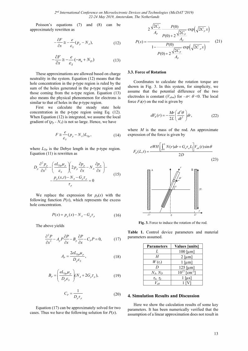
Coordinates to calculate the rotation torque are shown in Fig. 3. In this system, for simplicity, we assume that the potential difference of the two electrodes is constant (Vabm) for –< <0. The local force F(r) on the rod is given by
2
2( ) ,
2
Mr ddF r dr
L dt
(22)
where M is the mass of the rod. An approximate expression of the force is given by
0( ) ( ) sin
( , )2
L
n n abeWH N r dr G L V tF L t
D
(23)
Fig. 3. Force to induce the rotation of the rod. Table 1. Control device parameters and material parameters assumed.
Parameters Values [units]
L 100 [m] H 2 [m]
W (ts) 1 [m] D 125 [m]
NA, ND 1017 [cm-3] n, p 1 [s] Vab 1 [V]
4. Simulation Results and Discussion
Here we show the calculation results of some key parameters. It has been numerically verified that the assumption of a linear approximation does not result in

2nd International Conference on Microelectronic Devices and Technologies (MicDAT '2019) 22-24 May 2019, Amsterdam, The Netherlands
14
an appropriate solution. This section, therefore, adopts a non-linear differential equation for the numerical calculations. Calculation results of excess hole distribution in the p-type region of the rod are shown in Figs. 4-7, where device parameters are listed in Table 1. All simulations indicated that a rod length of tens of microns was most suitable. Fig. 4 plots the excess hole concentration versus distance from the rod center for three illumination power values (Pph, units of W/cm2). Fig. 5 plots the same curves but three rod thickness values (H, units of microns). Fig. 6 plots the same curves for three doping concentration values (NA, ND, units of cm-3), and Fig. 7 shows the same curves for three carrier lifetime values (n, p, units of s).
Fig. 4 reveals that excess hole concentration is not sensitive to the illumination, with is counter to the expectation. This suggests that very low power operation is available. Fig. 5 reveals that excess hole concentration is not sensitive to rod thickness, which suggests that carrier generation is not sensitive to local variations in rod thickness. Fig. 6 reveals that the excess hole concentration increases with the doping concentration, which suggests that care is needed in designing the doping concentration. Fig. 7 shows that the excess hole concentration profile is very sensitive to carrier lifetime as expected. Since poly-Si film is usually assumed, we must consider the crystallinity of the film. All these results reinforce the high potential for Si rod rotation under low-power light illumination.
Fig. 4. Excess hole concentration with parameter of illumination power.
Fig. 5. Excess hole concentration with parameter of rod thickness.
Fig. 6. Excess hole concentration with parameter of doping concentration.
We also calculated the force of rod rotation using
Eq. (24). When we assume the parameter values shown in Table 1, the rotation force is about 10-9 N. Since the mass of the Si rod is about 9.2×10⁻¹³ Kg, its acceleration is about 103 m/s2. Since this value is very large, it is expected that the Si rod will rotate rapidly even under weak illumination.
Fig. 7. Excess hole concentration with parameter of carrier lifetime.
5. Conclusion
This paper introduced a theoretical model and numerical simulations to investigate the potential of using a Si pn-junction rod as a mechanical rotor. An analytical, but approximated, steady state solution of excess carrier concentration of the Si rod was derived from the continuity equation. Simulation results strongly suggested that a 200-m-long Si rod should rotate with the acceleration of ~103 m/s2 under the illumination of 1 W/cm2. This is very good performance. Thus, this device is applicable as a mixer of chemical solutions in various medical test chips without any battery. Acknowledgement
A part of this study was financially supported by “Strategic Project to Support the Formation of Research Bases at Private Universities” in Japan:

2nd International Conference on Microelectronic Devices and Technologies (MicDAT '2019) 22-24 May 2019, Amsterdam, The Netherlands
15
Matching Fund Subsidy from MEXT (Ministry of Education, Culture, Sports, Sciences and Technology), 2015-2019, in Japan.
References [1]. H. C. Nathanson, W. E. Newell, R. A. Wickstrom,
J. R. Jr. Davis, The resonant gate transistor, IEEE Trans. Electron Devices, Vol. 14, Issue 1, 1967, pp. 117-133.
[2]. E. J. Garcia, J. J. Sniegowski, Surface micromachined microengine, Sensors and Actuators A, Vol. 48, 1995, pp. 203-214.
[3]. G. Piazza, V. Felmetsger, P. Muralt, R. H. Olsson III, R. Ruby, Piezoelectric aluminum nitride films for microelectromechanical systems, MRS Bulletin, Vol. 37, Issue 11, 2012, pp.1051-1061.
[4]. X. Yan, M. Qi, L. Lin, Self-lifting artificial insect wings via electrostatic flapping, in Proceedings of the 28th IEEE Int. International Conference on Micro Electro Mechanical Systems Conference (MEMS’15), Estoril, Jan. 2015, pp. 22-25.
[5]. D. Kang, K. Murali, N. Scianmarello, J. Park, J. H.-C. Chang, Y. Liu, K.-T. Chang, Y.-C. Tai, M. S. Humayun, MEMS oxygen transporter to treat retinal ischemia, in Proceedings of the 28th IEEE Int.
International Conference on Micro Electro Mechanical Systems Conference (MEMS’15), Estoril, January 2015, pp. 154-157.
[6]. S. Y. Chou, P. R. Krauss, P. J. Renstrom, Nanoimprint lithography, J. Vac. Sci. & Technol. B, Vol. 14, 1996, pp. 4129-4133.
[7]. H. Kodama, Invention of photo-solidilying modeling method, Macro Rev., Vol. 9, 1997, pp. 59-79.
[8]. A. J. Herbert, Solid object generation, J. Appl. Photographic Eng., Vol. 8, Issue 4, 1982, pp. 185-188.
[9]. N. Inomata, Y. Yamanishi, F. Arai, Manipulation and observation of carbon nanotubes in water under an optical microscope using a microfluidic chip, IEEE Trans. Nanotechnol., Vol. 8, Issue 4, 2009, pp.463-468.
[10]. C. M. Puleo, H. C. Yeh, T. H. Wang, Applications of MEMS technologies in tissue engineering, Tissue Eng., Vol. 13, Issue 12, 2007, pp. 2839-2854.
[11]. M. Noda, P. Lorchirachoonkul, T. Shimanouchi, K. Yamashita, H. Umakoshi, R. Kuboi, Sensitivity enhancement of leakage current microsensor for detection of target protein by using protein denaturant, IEEE Sensors Journal, Vol. 11, Issue 11, 2011, pp. 2749-2755.
[12]. Y. Omura, Y. Iida, Performance prospects of fully-depleted SOI MOSFET-based diodes applied to Schenkel circuit for RF-ID chips, Sci. Res., J. Cir. and Syst., Vol. 4, Issue 2, 2013, pp. 173-180.

2nd International Conference on Microelectronic Devices and Technologies (MicDAT '2019) 22-24 May 2019, Amsterdam, The Netherlands
16
(004)
Solder Stress Developments at Random Vibration
Y. Kim 1, S. Lee 1, D. Hwang2 and S. Kim 2
1 Inha University, Dept. of Mechatronics, 100 Inha-ro, Incheon, South Korea 2 Korea Aerospace Research Institute, Daejun, South Korea
Tel.: + 82328607334, fax: + 823287565261 E-mail: [email protected]
Summary: Large size commercially available plastic ball grid array chip packaging was tested and analyzed under random vibration to access its application feasibility on satellite electronics. Two extreme levels of the random vibrations, the power spectrum of which were 22.48 grms and 31.78 grms, were applied sequentially to investigate the sustainability of the PBGA chips mounted on the polyimide PCB with aluminum frame. It was found that the test results did not show any solder failure under the test conditions, indicating the robust structural integrity and providing the evidences justifying the PBGA packaging to the aerospace applications. Numerical analyses were also performed for the solder stress development mechanism. The results demonstrated that the first natural mode was not necessarily the dominant source for the maximum solder stress, and the PCB center location could be safer than nearby due to the higher frequency natural mode contributions to the stress developments. Keywords: PBGA reliability, Random vibration, COTS, Aerospace applications, Solder failure.
1. Introduction
The electronics packaging techniques employed for the satellite have been traditionally based on legacy, which usually lead to relatively heavy, bulky and expensive due to customized manufacturing. To overcome the pitfall, the applications of Commercially-Off-The-Shelves (COTS) such as PBGA chips have been suggested as a solution to the issues [1-3]. This study is to investigate the PBGA packaging application to the satellite by using big chips and PCB installation structure. A polyimide PCB was designed to a realistic size of actual electronics devices, and the large size PBGA chip was mounted to induce the solder joint stress. The entire specimen was tested under the two levels of PSD, and the solder joint failures were monitored. It is widely accepted that the maximum stress is generated by the first natural mode. To examine the predication, numerical calculations were also performed for the detail solder stress development mechanism under the random vibrations. 2. Sample and Tests
Fig. 1 shows the test sample with PBGA chips mounted on the printed circuit board. Two different sizes of the PBGA of 16 mm × 16 mm (type-1) and 10 mm × 10 mm (type-2) with daisy chains were employed with Sn/Pb (63/37) eutectic solder full array, the number of which were 361 and 100, and the ball size 0.45 mm and 0.4 mm, respectively. No underfills were applied. The power spectrum density of the random tests is shown in Fig. 2(a). Two steps of the mean square acceleration levels per unit bandwidth of 0.35 g2/Hz (acceptance level) and 0.7 g2/Hz (qualification level) were employed, and the signal’s
root mean square values were 22.48 grms and 31.78 grms, respectively, in the frequency range of 20~2000 Hz.
Fig. 2(b) represents the resistance measurements data at the qualification level. There was no failure found, which demonstrated the robust structural integrity of the PBGA chip packaging. To examine the PCB vibration behavior, an accelerometer was attached at near the chip P4, and the PSD was applied again. Fig. 3 shows the measurement data, showing the multiple peaks according to the natural modes. Fig. 4 is for the 1/4 finite element modeling of the sample structure. To cover the entire natural frequencies, the PCB boundaries were changed to four different boundary conditions (BC) of Xsymmetry-Ysymmetry (Xs-Ys), Xsymmetry-Yasymmetry (Xa-Ya), Xa-Ys and Xa-Ya. With the Xs-Ys BC, the first calculated mode is the first natural mode of the entire PCB. When the BC is Xs-Ya, the first calculated mode is the second natural mode of the entire PCb, etc. Fig. 5(a) represents the calculation results of the sample under the Xs-Ys boundary condition applied, and the maximum stress location was found at the corner of the center chip (P4) due to the effect of the first natural mode. At that maximum node, the rest of three boundary condition results were calculated and the RMS values were drawn in Fig. 5(b). The total maximum stress value was 102.5 MPa when all the values were added at 2000 Hz. For further investigation, the finite modeling was modified by replacing the P6 chip with the type-1, rendering all the chips were same size, and the same calculations were performed. Fig. 6 represents the maximum stress results when the boundary condition was Xs-Ys. Again, the maximum stress was found at the corner of the center chip, and the total stress was obtained in Fig. 6(b) as 102.5 MPa. Next, the maximum stress location when the BC was Xs-Ya, and found at the

2nd International Conference on Microelectronic Devices and Technologies (MicDAT '2019) 22-24 May 2019, Amsterdam, The Netherlands
17
corner of the P6 chip as shown in Fig. 7(a). As seen in Fig. 7(b), the major stress was developed with Xs-Ya BC, indicating the second natural mode was the major source of the stress. The total maximum stress at that node was 109.2 MPa as in Fig. 7(b), which is higher
than the stress at the center chip. The results indicated that, the effects of the natural modes higher than the first one were so significant that higher solder stress might occur at the chip located at nearby the PCB center.
Fig. 1. The sample configuration and the type-1 and type2 sodlers by X-ray.
(a) (b)
Fig. 2. (a) Power spectrum densities of the two levels; (b) The solder resistance measurements during the qualification level.
Fig. 3. The PCB vibration behavior measurements under the random vibration.
Fig. 4. 1/4 model for the test sample.
(a) (b)
Fig. 5. (a) Maximum solder stress location at Xs-Ys
of the sample using 1/4 model; (b) The stress developments by changing the boundary conditions.

2nd International Conference on Microelectronic Devices and Technologies (MicDAT '2019) 22-24 May 2019, Amsterdam, The Netherlands
18
(a) (b)
Fig. 6. (a) Maximum solder stress location at Xs-Ys
of the modified sample using 1/4 model; (b) The stress developments by changing the boundary conditions.
(a) (b)
Fig. 7. (a) Maximum solder stress location at Xs-Ya
of the modified sample using 1/4 model; (b) The stress developments by changing the boundary conditions.
4. Conclusions
The strong structural integrity of the PBGA chip packaging was verified to be applied to the satellite
electronics devices by testing the sizable chips under the harsh random vibration tests. The 1/4 finite element model was effectively used for the numerical calculations. The results represented that the maximum stress of the sample was found at the center chip solder. However, when the model was modified in the different chip size, the maximum stress was found at the chip located aside from the PCB center. The results demonstrated that, unlike usual assumption, the first natural mode is not necessarily the dominant mode for the maximum stress development, and depending on the chip size and location, the mode higher than the first one was significant in the random vibration, which induced the maximum solder stress at the chip located aside from the PCB center. Acknowledgements
This research was supported by Korea Aerospace Research Institute (NRF-2017M1A3A4A04037651) References [1]. H. Qi, M. Osterman, M. Pecht, Plastic ball grid array
solder joint reliability for avionics applications. IEEE Transaction of Components and Packaging Technology, Vol. 30, 2007, pp. 242-247.
[2]. F. Liu, Y. Lu, Z. Wang, Z. Zhang, Numerical simulation and fatigue life estimation of BGA packages under random vibration loading, Microelectronics Reliability, Vol. 55, 2015, pp. 2777-2785.
[3]. Y. K. Kim, D. S. Hwang, PBGA packaging reliability assessments under random vibrations for space applications, Microelectronics Reliability, Vol. 55, 2015, pp. 172-179.

2nd International Conference on Microelectronic Devices and Technologies (MicDAT '2019) 22-24 May 2019, Amsterdam, The Netherlands
19
(006)
Stacked FinFET-CMOS: A Promising FEOL Based Process Technology in Nanoscale 3-D Integration Circuits
Jin He, Yuan Ren, Xiaomeng He, Xiaomeng Wang, Jun Pan, Jingjing Liu and Mansun Chan
SoC Key Laboratory, Peking University Shenzhen Institute and PKU-HKUST Shenzhen-Hong Kong Institution, China
Tel.: 86-755-64321156, fax: 86-755-64321155 E-mail: [email protected]
Summary: This paper describes a methodology to combine the most scalable FinFET structure and CMOS integration processing to form stacked FinFET-CMOS technology used in 3-D integration circuits. The scalability of the proposed 3-D technology in the nanocale dimension is achieved through the promise of the double-gate structure offered by the FinFETs. The stack FinFET-CMOS process is realized in FEOL processing and can achieve extremely high packing density, which results in the 40 to 60 % reduction of capacitive loading. Various standard cells have been re-designed by the FinFET-CMOS technology resulting in significant reduction in cell size. The advantages in conventional circuit performance with the new 3-D standard cell library have also been demonstrated. Keywords: FinFET, 3-D integration circuits, Processing technology, Performance enhancement, Capacitive load.
1. Introduction
As traditional solid state CMOS integrated circuit technologies are scaling beyond 14 nm node, FinFET device structure already became the alternative to the conventional bulk MOSFET because of a number of advantages such as excellent short-channel-effects immunity, and unique mobility enhancement. In recent several years, FinFET has already applied in the 14 nm, 10 nm, and 7 nm node IC productions, and it may be extended beyond to 5 nm node. However, the past FinFET works only focused on the intrinsic transistor performance and circuit function demonstration and application, there has not been reported the impact of the interconnection on the circuit. Besides, the CAD methodology for the FinFET and related circuit design still followed the traditional bulk CMOS routine. The traditional interconnection technology will significantly influence the intrinsic transistor performance. So the CAD methodology may need any change to achieve the FinFET advantages over the bulk MOSFETs.
In this work, we proposed and demonstrated that a stacked FinFET-CMOS technology can potentially provide a solution to the above challenges. 3-D integrated circuits with multiple active layers stacked in the vertical direction have been suggested by ITRS roadmap [1] as a method to reduce the impact of loading interconnection by providing shorter connection paths between transistors through vertical wires. In this paper, we describe a methodology which combines the FinFET technology and 3-D integration using a local-clustering technique to utilize the advantages of both FinFET and 3-D integration with a relatively simple fabrication method based on past several works [2-5]. The design methodology and fabrication process is a quasi-2D and compatible with the existing CAD tools. In this approach, only the
standard cells in the design library are redesigned with closely coupled 3-D stacked transistors. By making the cell size smaller, the total lateral interconnect length can be reduced. 2. Fabrication Process and Device Performance
The structure of the stacked FinFET is illustrated in Fig. 1. It consists of a -shape gate straddles on a stacked fin that serves as the shared gate for both the NMOSFET and PMOSFET. The shared gate is used as an implant mask to achieve self-alignment for both N- and P-MOSFET source/drain regions. Between the two silicon active layers, there is an insulation layer to isolate the top and bottom devices.
Fig. 1. (a) 3-D schematic view, and (b) cross-section of the stacked FinFET structure.
The fabrication process of the 3-D stacked
FinFET-CMOS technology together with the Scan Electron Microscopy (SEM) cross-section of a fabricated inverter are shown in Fig. 2. The key processing steps are described below. Starting with a double layer of SOI wafer, a layer of LTO was

2nd International Conference on Microelectronic Devices and Technologies (MicDAT '2019) 22-24 May 2019, Amsterdam, The Netherlands
20
deposited to serve as a hard mask for the subsequent processing as shown in Fig. 2(a). The multi-layer films are etched together to form the stacked fins as shown in Fig. 2(b). The gate oxide is then grown and followed by the deposition of in-situ doped n+ gate polysilicon (Fig. 2(c)). The gate is defined by lithography resulting in the structure as shown in Fig. 2(d). Doping of the source/drain region of the top and bottom FinFETs is performed by ion implantation. The doping of the bottom is achieved by high energy implant through the top layer (Fig. 2(e)). In order to connect to the bottom layer, the unwanted regions of the top silicon layer are etched to expose the bottom layer at the desired locations. The contacts where the top transistors are connected to the bottom ones, are also opened in this step (Fig. 2(f)). It is followed by Phosphosilicate Glass (PSG) passivation and contact opening to various layers. The contact vias are filled to form the interconnect (Fig. 2(g)). The SEM images of the cross-section and top view of the stacked FinCMOS inverter are shown in Fig. 2(h). This technology provides a number of advantages to implement 3-D IC in highly scaled technology including: (1) high scalability inherent from the FinFET structure; (2) high density with more than 50 % area reduction compared to the conventional 2-D architecture; (3) reduced interconnect wiring distance among active devices; and (4) process compatibility with traditional 2-D CMOS technology, and (5) different device width between the top and bottom which can be implemented using different fin-heights that can be covered in the same floor plan.
Fig. 2. (a)-(g) The key processing steps to form the stacked FinFET-CMOS inverter (h) The SEM image of the top view and cross-section of the fabricated FinFET-CMOS inverter.
3. Circuit Performance
The layouts of some of the 3-D FinFET-CMOS standard cells are shown in Fig. 3. A large amount of area saving compared with conventional 2-D layout can be achieved by stacking the transistors. To further evaluate the performance of the 3-D stacked IC technology, we have extracted the device parameters from the fabricated device to obtain models for circuit simulation. Simulation results show that around 50 % area reduction and capacitive loading reduction from 40 % to 60 % can be achieved as shown in Fig. 4(a). The reduction comes from both more compact active devices placement and shorter interconnect distance between active devices within the cell. One detail performance estimation test and parameter extraction experiment from the measurement data shown in Fig. 4(b) indicated that the transistor compact active areas results in the 60 % reduction of the capacitance loading while the 3-D integration interconnection distance resulting in 40 % ratio of the capacitance loading reduction in the proposed stack FinFET technology.
Fig. 3. Layouts of some of the 3-D FinFET-CMOS standard cells compared with the conventional 2-D layout.
Fig. 4. Comparison of area and capacitance between 2-D planar gates and 3-D stacked FinFET-CMOS gates.
2nd International Conference on Microelectronic Devices and Technologies (MicDAT '2019) 22-24 May 2019, Amsterdam, The Netherlands
21
The standard cell approach is very useful in developing 3-D integrated circuit because it is compatible with the current planar IC design methodology and CAD Tools. Once the standard cells have been reconfigured using the 3-D process, 3-D IC can be designed using high-level hardware description languages and automatic placement and routing. This approach allows the benefit provided by 3-D IC to be quickly incorporated into the current technology. Additionally, when the circuit becomes more complex, long interconnect with parasitic capacitance larger than that of the gate capacitance become dominant in the RC delay in the path. The speed advantage of the proposed 3-D circuit will become more and more prominent.
4. Conclusions
We have developed a stacked FinFET-CMOS technology and form circuit building blocks into multi-layer clusters. Through circuit simulation, the stacked FinFET-CMOS structure shows better performance and lower delay when the number of transistors increases.
Acknowledgements
This work is funded by NFSC under Grants (61574005) and GD SNSFC Fund (2018A030313973). References [1]. International Technology Roadmap for Semiconduc-
tors http://www.itrs2.net [2]. K. Yamazaki, Y. Itoh, A. Wada, K. Morimoto,
Y. Tomita, 4-layer 3-D IC technologies for parallel signal processing, IEDM Tech. Dig., 1990, pp. 599-602.
[3]. R. J. Gutmann, J.-Q. Lu, S. Pozder, Y. Kwon, D. Menke, et al., A waferlevel 3-D IC technology platform, in Proceedings of the Adv. Metallization Conference, October 2003, pp. 19-26.
[4]. X. Wu, P. C. H. Chan, S. Zhang, C. Feng, M. Chan, Stacked 3-D Fin-CMOS technology, IEEE Electron Device Letters, Vol. 26, Issue 6, 2005, pp. 416-418.
[5]. S. Zhang, R. Han, X. Lin, et al., A stacked CMOS technology on SOI substrate, IEEE Electron Device Letters, Vol. 25, Issue 9, 2004, pp. 661-663.

2nd International Conference on Microelectronic Devices and Technologies (MicDAT '2019) 22-24 May 2019, Amsterdam, The Netherlands
22
(007)
Improved Detection Limit of Calcium Test Using an Over-Pressurized Box
C. M. Hsu, W. T. Wu, G. W. Zhou and K. C. Wu
Department of Electro-Optical Engineering, Southern Taiwan University of Science and Technology, Tainan, Taiwan
Tel.: +886 6 2533131 ext. 3620, fax: +886 6 2432912 E-mail: [email protected]
Summary: The necessity to develop techniques to measure water vapor transmission rate (WVTR) of a highly gas resistive film for flexible organic electronics is strongly demanded. This work demonstrates that the Ca-test implemented with an additional over-pressured N2 box is more reliable and could perform improved detection limit to a level less than 1×10⁻⁶ g/m2/day, much lower in contrast to ~ 1×10⁻⁴ g/m2/day of the traditional Ca-test. The lowered detection limit using the Ca test with the over-pressured N2 box packaging makes the measured WVTR more convincing. Results from the WVTR measurement of SiN/AF4 multiple stacked films suggest the number of film pairs is not the dominant factor influencing gas resistance quality. Keywords: Water vapor transmission rate, WVTR, Ca-test.
1. Introduction
As flexible electronics are making their ways to be one of the next generation technologies, development of the techniques to determine the water vapor transmission rate (WVTR) of a gas-barrier film is increasingly important. This is because flexible organic electronics such as organic light-emitting diodes (OLED) and organic solar cells (OSC) require highly isolated ambient to prevent the devices from being attacked by water or oxygen molecules and thus to assure a long device operation lifetime. It is then essential to confirm a gas-barrier substrate with low enough WVTR before they can be brought for flexible OLED and OSC applications.
Currently the only commercial WVTR measuring tool is MOCON that uses the coulorimetric phosphorous pentoxide sensor to detect the amount of water or oxygen molecules. Unfortunately, its nominal detection limit is 5×10⁻⁵ g/m2/day that is higher than the required level of < 1×10⁻⁵ g/m2/day for organic electronics applications. The use of other WVTR measuring techniques is then necessary. In comparison with the WVTR measuring techniques using quadrupole mass spectrometry [1] and tritium detector [2], calcium test (Ca-test) is a tool featuring relatively cost-effective, less safety issue and a WVTR detection limit of <1×10⁻⁶ g/m2/day [3]. The traditional Ca-test architecture involves a Ca sensor film and a pair of silver electrodes coated on a sample. The Ca is highly sensitive to moisture and needs to be frame packaged by a glass back-plate generally using UV-curable glue. However, the packaging yields accuracy and reliability issues due to that moisture can penetrate through the sealing glue.
In this work, we introduced a method that aims to lower the affecting factors to the Ca-test. The basic mechanism is to block the environmental moisture from reaching the packaged Ca-test device using over-
pressurized nitrogen. Results suggest the determination of WVTR for gas-barrier films with the Ca-test of this kind is more convincing.
2. Experimental Details
The fabrication of traditional Ca-test samples started with the deposition of a pair of 200-nm-thick silver electrodes using thermal evaporation on a substrate to be measured. Between the Ag electrodes a Ca film of 200 nm serving as the moisture sensor was deposited also using thermal evaporation. The physical dimensions of the substrate and the Ca sensor were 50 mm × 50 mm and 22.5 mm × 20 mm, respectively. Each Ag electrode was 2 mm overlapped with the Ca film. The Ca-test device was then frame sealed by UV curing a glass back-plate on top of the test substrate. The glass has a square trench of 30 mm × 30 mm allowing the Ca film not to be in contact with the back-plate. Approximate 3 mm long Ag electrode was exposed outside the back-plate for the connection to an I-V meter. The complete Ca-test packaging structure is schematically shown in Fig. 1a.
Fig. 1. (a) Traditional Ca-test packaging; (b) N2 box packaging, and (c) inside the N2 box.
To block the moisture from penetrating to the Ca
cell through the edge UV glue, the packaged Ca-test sample was sealed in a box filled with over-pressurized high purity nitrogen (Fig. 1b). The substrate was
2nd International Conference on Microelectronic Devices and Technologies (MicDAT '2019) 22-24 May 2019, Amsterdam, The Netherlands
23
placed to a window on the box (Fig. 1c) where the ambient moisture can move through the substrate and react with the Ca sensor to build the conductance-time (G-t) relationship for WVTR calculation. We named the packaging of this type the “N2 box” packaging. The Ca-tests were conducted on samples with both the traditional and the N2 box packaging.
3. Results and Discussions
Fig. 2 shows the normalized conductance of Ca sensor on glass substrate as a function of time for both the traditional and N2 box packaging. It clearly demonstrates that the N2 box packaged Ca sensors exhibit roughly linear and much shallower conductance gradient (G/t) than the traditionally packaged sample. Two Ca sensors were packaged with this type and their calculated WVTRs, according to the equation reported [3], are < 1×10⁻⁶ and 5.1×10⁻⁵ g/m2/day. In comparison, the traditionally packaged Ca sensor shows two G/t regions representing two WVTRs. In the first period the Ca sensor measures a smaller WVTR of 1.4×10⁻⁴ g/m2/day while in the second period it increases to 2.5×10⁻⁴ g/m2/day. This indicates that more water molecules penetrate into the Ca cell in the second period than in the first period. It is possible the WVTR in the first period reflects the reaction of Ca with the residual water molecules in the cell, whereas the WVTR in the second period includes the reaction with water molecules penetrating through the sealing UV-glue on the edge. From Fig. 2, one can tell that the Ca-test with an additional over-pressured N2 box exhibits improved detection limit and is more reliable due to the reduced leak of moisture from the edge sealing glue.
Fig. 2. Normalized G-t of Ca sensor on glass substrate with both traditional and N2 box packaging.
Based on these results, we were more confident on
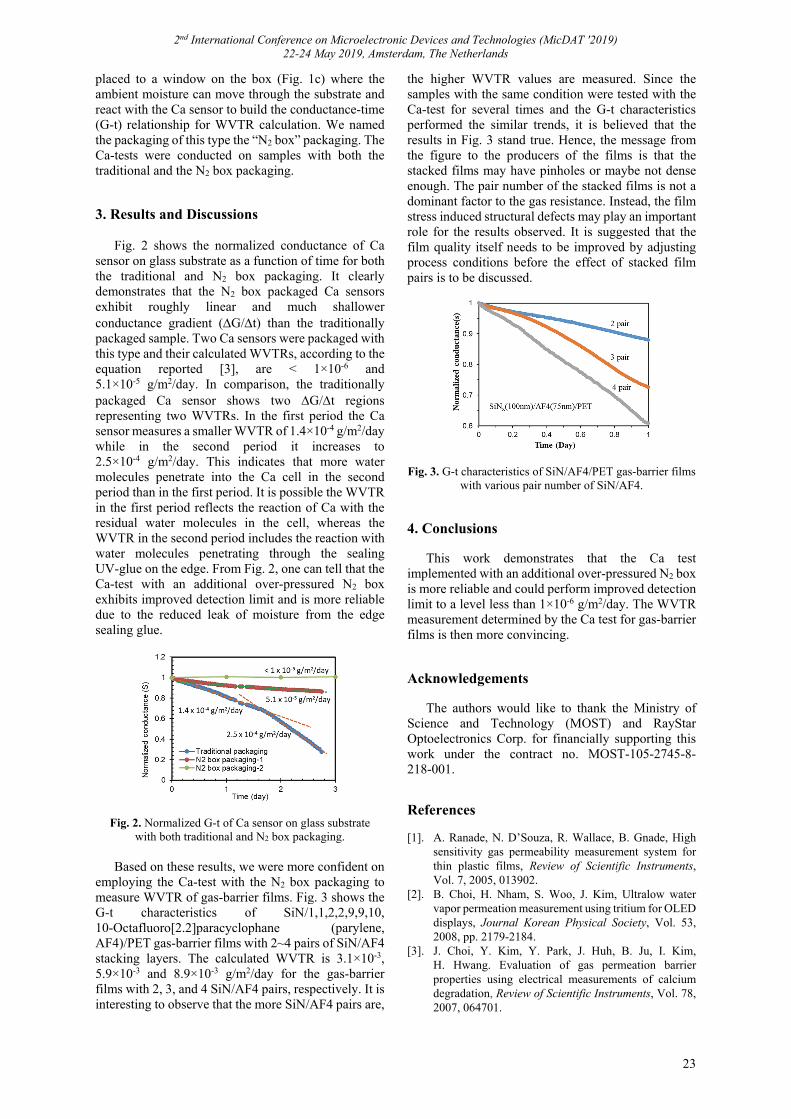
employing the Ca-test with the N2 box packaging to measure WVTR of gas-barrier films. Fig. 3 shows the G-t characteristics of SiN/1,1,2,2,9,9,10, 10-Octafluoro[2.2]paracyclophane (parylene, AF4)/PET gas-barrier films with 2~4 pairs of SiN/AF4 stacking layers. The calculated WVTR is 3.1×10⁻³, 5.9×10⁻³ and 8.9×10⁻³ g/m2/day for the gas-barrier films with 2, 3, and 4 SiN/AF4 pairs, respectively. It is interesting to observe that the more SiN/AF4 pairs are,
the higher WVTR values are measured. Since the samples with the same condition were tested with the Ca-test for several times and the G-t characteristics performed the similar trends, it is believed that the results in Fig. 3 stand true. Hence, the message from the figure to the producers of the films is that the stacked films may have pinholes or maybe not dense enough. The pair number of the stacked films is not a dominant factor to the gas resistance. Instead, the film stress induced structural defects may play an important role for the results observed. It is suggested that the film quality itself needs to be improved by adjusting process conditions before the effect of stacked film pairs is to be discussed.
Fig. 3. G-t characteristics of SiN/AF4/PET gas-barrier films
with various pair number of SiN/AF4. 4. Conclusions
This work demonstrates that the Ca test implemented with an additional over-pressured N2 box is more reliable and could perform improved detection limit to a level less than 1×10⁻⁶ g/m2/day. The WVTR measurement determined by the Ca test for gas-barrier films is then more convincing. Acknowledgements
The authors would like to thank the Ministry of Science and Technology (MOST) and RayStar Optoelectronics Corp. for financially supporting this work under the contract no. MOST-105-2745-8- 218-001.
References [1]. A. Ranade, N. D’Souza, R. Wallace, B. Gnade, High
sensitivity gas permeability measurement system for thin plastic films, Review of Scientific Instruments, Vol. 7, 2005, 013902.
[2]. B. Choi, H. Nham, S. Woo, J. Kim, Ultralow water vapor permeation measurement using tritium for OLED displays, Journal Korean Physical Society, Vol. 53, 2008, pp. 2179-2184.
[3]. J. Choi, Y. Kim, Y. Park, J. Huh, B. Ju, I. Kim, H. Hwang. Evaluation of gas permeation barrier properties using electrical measurements of calcium degradation, Review of Scientific Instruments, Vol. 78, 2007, 064701.

2nd International Conference on Microelectronic Devices and Technologies (MicDAT '2019) 22-24 May 2019, Amsterdam, The Netherlands
24
(010)
Comparison of Self-heating Effect in SOI MOSFETs with Various Configuration of Buried Oxide
K. O. Petrosyants, D. A. Popov 1
1 National Research University Higher School of Economics (Moscow Institute of Electronics and Mathematics), 34 Tallinskaya, 123458, Moscow, Russia
Tel.: +7-495-772-9590,15208 E-mail: [email protected]
Summary: In this work self-heating effect in SOI MOSFETs with various configuration of buried oxide was investigated using TCAD modeling. The basically electro-thermal transport model built-in to Sentaurus Synopsys tool was complemented by the set of new models for the temperature-dependent physical parameters: thermal conductivities λSi(T), λSiO2(T); oxide and trapped charge densities Nox(T), Nit(T) and others taking into account the special thermal effects that appear in modern deep submicron and nano-scale devices. Keywords: MOSFET, Buried oxide configuration, Temperature-induced device characteristics degradation, Device modeling, TCAD software.
1. Introduction
Currently, Silicon-on-Isolator (SOI) MOSFETs with a channel length of less than 100 nm are used in various types of CMOS VLSI circuits. These transistors can reduce the occupied chip area, power consumption and improve performance. Against this background, there are a number of features that have a significant impact on the MOSFET operation. These include the worst conditions of heat dissipation from the active region in SOI structures.
Heat transfer from the channel to the depth of the structure can be carried out only through SiO2 layers, which have a 100 times lower thermal conductivity λ(SiO2) = 1.4 W/mꞏK compared to silicon λ(Si) = 149 W/mꞏK. This negatively affects the reliability and performance of the IC [1].
In this way, several constructive-technological SOI MOSFET structures with various configuration of buried oxide (BOX) were proposed. According to experts, the most promising of them are (see Fig. 1): 1) Structures with L-shaped BOX (Quasi-SOI) [2]; 2) Structures with a “window” in BOX (SELBOX –
Selective Buried Oxide) [3]; 3) Structures with a partial BOX (Partial SOI) [4]; 4) Structures with ultra-thin BOX (thin-BOX SOI)
[5]; 5) Structures with a thin pocket and thin oxide (UTBB
SOI) [6]. Unfortunately, the effectiveness of the listed above
SOI MOSFET structures has not been studied sufficiently and requires in-depth consideration. In the available publications mainly shows the experimental current-voltage characteristics of the structures. There are very few published papers on this issue, and the results in them do not fully cover the problem. TCAD
modeling is an effective tool for this. Single papers are devoted to TCAD modeling of self-heating [1]. For some structures, there are no publications on TCAD modeling at all.
Prospects for the use of these SOI MOSFETs for industrial production are currently being evaluated by process engineers. Therefore, the use of instrument-technological modeling (TCAD) at this stage is relevant and in demand.
This paper is dedicated to the issues of TCAD modeling of SOI MOSFETs with various configuration of buried oxide. For this purpose, we used our TCAD model developed to account for thermal effects. 2. Self-heating Effect in SOI MOSFETs
Local temperature rise due to power dissipation in the channel region is one of the problems modern nanoscale and submicron MOSFET. [7]. Such heat in the MOSFET structure is removed from the channel region through the metal contacts of the source and drain, the gate region, the dielectric isolated and the substrate. All these regions, due to the exclusion of the substrate, are inefficient methods of heat removal, especially in the case of SOI MOSFETs, because under the channel region there is a layer of buried oxide (BOX), traditionally made of silicon oxide. The thermal conductivity of such a layer is two orders of magnitude less than that of bulk silicon, which leads to an even greater increase in temperature in the active region of the MOSFET. As a consequence, an increase in the structure temperature and a dense arrangement of devices on a chip leads to deterioration in their characteristics [8, 9].

2nd International Conference on Microelectronic Devices and Technologies (MicDAT '2019) 22-24 May 2019, Amsterdam, The Netherlands
25
3. TCAD Model for Self-heating Effect
A standard physical model set of Synopsys Sentaurus TCAD allows to simulation the characteristics of semiconductor devices in a wide temperatures range, including taking into account the effect of self-heating [10]. A thermodynamic model of carrier transfer is used to simulate the temperature inside the structure. The lattice temperature equation is added to the solution of the Poisson equation and the charge-carrier continuity equations. Taking into account the structure heating during the flow of large currents in it (the Joule-Lenz law) becomes possible using the thermodynamic model.
(a)
(b)
(c)
(d)
(e)
(f)
Fig. 1. SOI FET structures with different configuration of buried oxide: conventional SOI MOSFET (a); SELBOX (b), partial SOI (c), quasi SOI (d), thin BOX (e), ultra-thin BOX (f).
In real structures of SOI MOSFET, the electrical parameters degradation with increasing temperature is due to the influence of both the active structure of the device under the gate and the passive region, which includes shallow trench isolation (STI). For all the considered SOI MOSFET varieties, the passive regions do not differ from each other and make the same contribution to the degradation of the device parameters for all structures. Therefore, only the active region influence of the device will be considered.
By default, the following expression (1) is used to calculate the thermal conductivity of silicon in Synopsys TCAD, taking into account the external temperature (see Fig. 2). This dependence is valid in the temperature range from 200 to 600 K.
, (1)
where a = 0.03 cmꞏКꞏW-1, b = 1.56ꞏ10-3 cmꞏW-1 and c = 1.65ꞏ10-6 cmꞏК-1ꞏW-1.
The equation (1) takes into account the dependence of thermal conductivity only on temperature and does not take into account the thermal conductivity dependence on the thickness and doping level of the silicon layer. Additionally, the oxide-trap Nox(T) and interface-trap Not(T) charge densities are greatly increased with temperature increase (see Fig. 3) [11].
Fig. 2. Standard temperature dependence of silicon thermal conductivity [10].
Adequate modeling of temperature distribution is
impossible without taking these factors into account. In particular, the maximum temperature is directly related to device reliability.
Fig. 3. Oxide- and interface-trap charge densities vs. stress temperature for SiO2 capacitors stressed for 20 min
at an electric field of – 1.54 MV/cm [11]. 3.1. Thermal Conductivity Dependence on the Doping Profile
It is known [12] that the thermal conductivity dependence on the doping profile of the silicon layer has a significant effect on local heating. The thermal conductivity of heavily doped silicon layers is several times less due to increased phonon scattering on impurity ions [13].
The thermal conductivity dependence of phosphorus (see Fig. 4) and boron (see Fig. 5) atoms in the temperature range from 10 to 300 K was studied in [13].

2nd International Conference on Microelectronic Devices and Technologies (MicDAT '2019) 22-24 May 2019, Amsterdam, The Netherlands
26
The thermal conductivity dependences on the doping profile of the material for the electron (2) and hole (3) conductivity regions were obtained on the basis of the above experimental data.
, (2)
, (3)
where Nd is the electron concentration cm-3, Na is the hole concentration cm-3.
Fig. 4. Thermal conductivity data from study for the phosphorus doped silicon layers and the theory
developed [13].
Fig. 5. Thermal conductivity data from study for the boron doped silicon layers and the theory developed [13].
3.2. Thermal Conductivity Dependence on the Silicon Layer Thickness
Another factor that has a significant effect on local heating is the thermal conductivity dependence on the thickness of the silicon layer due to phonon scattering at the boundary of the active region. In [14], the authors summarized the data on the values of thermal
conductivity for silicon thickness from 10 nm to 1000 nm.
Experimental data for the value of thermal conductivity depending on the silicon layer thickness are presented in Fig. 6.
The thermal conductivity dependence on the silicon layer thickness was obtained on the basis of experimental data:
(4)
4. Simulation Results
The following functions were added to the code of the model for calculating the structure temperature with taking into account the influence of self-heating, to calculate the thermal conductivity of silicon: 1) the silicon thermal conductivity dependence on the doping profile; 2) the silicon thermal conductivity dependence on the silicon layer thickness.
Fig. 6. Temperature dependence of silicon thermal conductivity [14].
For all the device configurations in Fig. 1 the
common n-channel SOI MOSFET structure was used with the following parameters: L = 100 nm, tgate,ox = 2 nm, tox = 70 nm, tBOX = 80 nm, Nch = 8ꞏ1017 cm-3, Nd,s = 1ꞏ1020 cm-3, NLDD = 4ꞏ1019 cm-3; L1 = 30 nm, L2 = 100 nm (for the Quasi-SOI structure Fig. 1d).
The maximal internal temperature Tmax for all the devices was simulated using TCAD for the operating regime VDS = 2 V; VGS = 2 V. (see Fig. 7). The results were compared with the corresponding results for the conventional SOI and Si FET structures (see Fig. 8).
The high value of the maximum temperature for the traditional SOI MOSFET is due to the fact that heat removal from the channel region to the substrate can be carried out only through SiO2 layer, which has a 100 times lower coefficient of thermal conductivity compared to silicon. The existence or partial/full lack a “window” in a buried oxide significantly improves the heat dissipation.

2nd International Conference on Microelectronic Devices and Technologies (MicDAT '2019) 22-24 May 2019, Amsterdam, The Netherlands
27
(a) (b) (c)
(d) (e) (f)
Fig. 7. Temperature distribution in SOI FET structures with different configuration of buried oxide: conventional SOI
MOSFET (a); SELBOX (b), partial SOI (c), quasi SOI (d), thin BOX (e), ultra-thin BOX (f).
Fig. 8. The simulated Tmax for BOX SOI MOSFETs with different configuration of buried oxide.
5. Conclusions
The new temperature model for MOS transistors taking into account special effects that appear in modern submicron and nano-scale MOSFETs was developed. Temperature distributions for SOI MOSFETs with various configuration of buried oxide were simulated and it was shown that:
1) The heat dissipation to the substrate is considerably increased in the SOI FET structures with different configurations of the “BOX window” (see Fig. 7b, c, d), and the maximal internal temperature Tmax significantly reduced in comparison with Tmax of the conventional SOI MOSFET, approaching the typical values for the standard bulk-Si MOSFET;
2) The Tmax of “thick” BOX SOI FET with tBOX = 40 nm (twice smaller than tBOX = 80 nm for conventional SOI) is much higher (Tmax = 339 K) than that of bulk FET (Tmax = 316 K), but the Tmax can be
considerably reduced (Tmax = 309 K) by thinning the BOX up to tBOX = 6 nm (see Fig. 7);
3) The Tmax of Ultra-Thin BOX SOI FET (Tmax = 309 K) with tBOX = 6 nm lower than the Tmax of bulk FET (Tmax = 316 K) in deeply scaled nodes. Acknowledgements
The research was supported by Basic Research Program at the National Research University Higher School of Economics in 2019, grant No. ТZ-99 and by Russian Foundation for Basic Research, grant No. 18-07-00898 А. References [1]. J. Nayfach-Battilana, J. Renau, SOI, Interconnect,
Package, and Mainboard Thermal Characterization, in Proceedings of the 14th ACM/IEEE International Symposium on Low Power Electronics and Design (ISLPED’09), 2009, pp. 327-330.
[2]. W. Wu, X. An, T. Que, X. Zhang, D. Shen, G. Guo, R. Huang, Investigation of a radiation-hardened quasi-SOI device: performance degradation induced by single ion irradiation, Semiconductor Science and Technology, Vol. 31, Issue 10, 2016, 105009.
[3]. M. R. Narayanan, H. A. Nashash, Minimization of self-heating in SOI MOSFET devices with SELBOX structure, in Proceedings of the 11th International Conference on Advanced Semiconductor Devices & Microsystems (ASDAM’16), 2016, pp. 61-64.
[4]. J. Cheng, B. Zhang, Z. Li, The total dose radiation hardened MOSFET with good high-temperature performance, in Proceedings of the International

2nd International Conference on Microelectronic Devices and Technologies (MicDAT '2019) 22-24 May 2019, Amsterdam, The Netherlands
28
Conference on Communications, Circuits and Systems (ICCCAS’07), 2007, pp. 1252-1255.
[5]. V. P. Trivedi, J. G. Fossum, Nanoscale FD/SOI CMOS: Thick or thin BOX?, IEEE Electron Device Letters, Vol. 26, Issue 1, Jan. 2005, pp. 26-28.
[6]. T. Takahashi, T. Matsuki, T. Shinada, Y. Inoue, K. Uchida, Comparison of self-heating effect (SHE) in short-channel bulk and ultra-thin BOX SOI MOSFETs: Impacts of doped well, ambient temperature, and SOI/BOX thicknesses on SHE, in Proceedings of the Electron Devices Meeting (IEDM’13), 2013, pp. 7.4.1-7.4.4.
[7]. K. Bernstein, N. J. Rohrer, SOI Circuit Design Concepts, Kluwer Academic Publishers, 1998.
[8]. K. A. Jenkins, R. L. Franch, Impact of self-heating on digital SOI and strained-silicon CMOS circuits, in Proceedings of the Int. SOI Conference, 2003, pp. 161-163.
[9]. O. Semenov, A. Vassighi, M. Sachdev, Impact of self-heating effect on long-term reliability and performance degradation in CMOS circuits, IEEE Trans. on Dev. and Materials Reliab., Vol. 6, Issue 1, 2006, pp. 17-27.
[10]. TCAD Sentaurus User Manual J-2014.09, Synopsys, 2014.
[11]. D. M. Fleetwood, et al., Effects of device aging on microelectronics radiation response and reliability, Microelectronics Reliability, Vol. 47, 2007, pp. 1075-1085.
[12]. T. Takahashi, T. Matsuki, T. Shinada, Y. Inoue, K. Uchida, Comparison of self-heating effect (SHE) in short-channel bulk and ultra-thin BOX SOI MOSFETs: Impacts of doped well, ambient temperature, and SOI/BOX thicknesses on SHE, in Proceedings of the Electron Devices Meeting (IEDM’13), 2013, pp. 7.4.1-7.4.4.
[13]. M. Asheghi, K. Kurabayashi, R. Kasnavi, K. E. Goodson, Thermal conduction in doped single-crystal silicon films, J. Appl. Phys., Vol. 91, Issue 8, 2002, pp. 5079-5088.
[14]. W. Liu, K. Etessam-Yazdani, R. Hussin, M. Asheghi, Modeling and data for thermal conductivity of ultrathin single-crystal SOI layers at high temperature, IEEE Transactions on Electron Devices, Vol. 53, Issue 8, August 2006, pp. 1868-1876.

2nd International Conference on Microelectronic Devices and Technologies (MicDAT '2019) 22-24 May 2019, Amsterdam, The Netherlands
29
(011)
Nitrogen-doped Carbon-based Very Thin Film on Quartz or Sapphire
Substrate as Back-side Illuminated Transmission Photocathode
J. Huran 1,2, N. I. Balalykin 1, M. A. Nozdrin 1, V. Sasinková 3, A. Kleinová 4, A. P. Kobzev 1 and E. Kováčová2
1 Joint Institute for Nuclear Research, Joliot-Curie 6, 141980 Dubna, Moscow Region, Russian Federation 2 Institute of Electrical Engineering, Slovak Academy of Sciences, Dúbravská cesta 9,
84104 Bratislava, Slovakia 3 Institute of Chemistry, Slovak Academy of Sciences, Dúbravská cesta 9, 84538 Bratislava, Slovakia
4 Polymer Institute, Slovak Academy of Sciences, Dúbravská cesta 9, 84541 Bratislava, Slovakia Tel.: + 74962163843, fax: + 74962165767
E-mail: [email protected] Summary: The purpose of this study is to preparation of carbon-based very thin films and to measure photo-electron emission characteristics. Nitrogen-doped carbon-based very thin films were deposited on quartz or sapphire substrate by RF reactive magnetron sputtering using carbon target and gas mixture of Ar and reactive gases N2 or N2+H2. The concentration of elements in the films was determined by RBS and ERD analytical method simultaneously. Carbon-based films surface morphology was examined by scanning electron microscopy. Raman spectroscopy was used for chemical structural properties investigation of carbon films. The photo-electron emission properties were determined by the measurement of cathode bunch charge of prepared back-side pulsed laser illuminated transmission photocathode. Adding hydrogen to gas mixture and changing their flow when carbon films are growth leads to different results of photo-electron emission properties. Influence of chemical structural properties of N-doped carbon-based very thin films on quartz or sapphire substrates on the photo-induced electron emission of back-side illuminated transmission photocathode are discussed. Keywords: Carbon very thin film, Magnetron sputtering, Structural properties, Transmission photocathode.
1. Introduction
High quality electron field emitting materials with stable emission are needed for a wide range of applications. Various carbon based materials such as diamond, graphene, carbon nanotubes has received attention as novel electron field emission cold cathodes. To obtain high-power and high-brightness radiation in free-electron lasers, for future electron-positron colliders, as well as for other applications, the sources of intense electron beams with bunches having a small emittance and a large charge is required [1]. Photocathodes working in reflection mode were made of rich-diamond and rich-graphite nanodiamond layers, deposited on different conductive substrates by means of the pulsed spray [2]. The electron field emission behaviors of amorphous carbon, graphene sheets embedded carbon and graphite-like carbon structures were investigated and the mechanism of enhanced field emission was attributed to the nanosized graphene sheets which acted as electron emitters and transport channels [3]. The results of the quantum efficiency measurements, in the range 150-210 nm, of photocathodes based on poly-, nano-, and single crystalline diamond are reported [4]. Nitrogen doping into different carbon materials is discussed on the bases of the summarization of the reported experimental results by focusing on their preparation conditions, structures and application possibilities [5]. Diamond-like carbon films were deposited on the stainless steel mesh by PECVD
technique from gas mixtures CH4+D2+Ar, CH4+H2+Ar and reactive magnetron sputtering using a carbon target and gas mixtures Ar+D2, Ar+H2, for the transmission photocathode preparation [6].
In this paper, carbon-based very thin films doped with nitrogen were deposited by RF magnetron sputtering. The surface morphology and microstructure of carbon films are characterized carefully. The prepared back-side illuminated transmission photocathodes was used for investigation of photo-induced electron emission properties of carbon films. 2. Experiment
The carbon-based very thin films were grown on double side polished quartz or c-sapphire substrate by RF (radio frequency) reactive magnetron sputtering using gas mixtures Ar, N2 and H2. Stainless steel vacuum chamber was evacuated by turbomolecular pump to a base pressure ~5×10⁻³ Pa. The magnetron carbon target was high purity graphite disk 3 inch in diameter. Prior to deposition, quartz and c-sapphire substrates were cleaned by ultrasonically cleaning in methanol, acetone and deionised water to remove contaminants from the surface. Constant film deposition parameters were: flow of Ar- 25 sccm, N2- 8, sccm, working pressure 0.7 Pa, and magnetron input RF power 150 W at 13.56 MHz. Substrate holder temperatures was 900 oC. Tree series of samples was
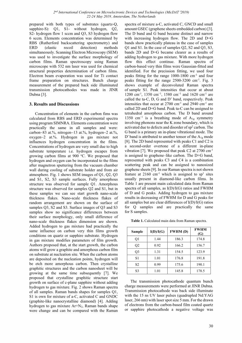
2nd International Conference on Microelectronic Devices and Technologies (MicDAT '2019) 22-24 May 2019, Amsterdam, The Netherlands
30
prepared with both types of substrates (quartz-Q, sapphire-S): Q1, S1- without hydrogen, Q2, S2- hydrogen flow 1 sccm and Q3, S3 hydrogen flow 6 sccm. Elements concentration was determined by RBS (Rutherford backscattering spectrometry) and ERD (elastic recoil detection) methods simultaneously. Scanning Electron Microscopy (SEM) was used to investigate the surface morphology of carbon films. Raman spectroscopy using Raman microscope with 532 nm laser was used for chemical structural properties determination of carbon films. Electron beam evaporation was used for Ti contact frame preparation on structures. Bunch charge measurement of the prepared back side illuminated transmission photocathodes was made in JINR Dubna [3]. 3. Results and Discussions
Concentration of elements in the carbon fims was calculated from RBS and ERD experimental spectra using program SIMNRA. Elements concentration were practically the same in all samples and were: carbon~83 at.%, nitrogen~13 at.%, hydrogen~2 at.%, oxygen~2 at.%. Hydrogen in gas mixture not influences hydrogen concentration in the films. Concentrations of hydrogen are very small due to high substrate temperature i.e. hydrogen escapes from growing carbon films at 900 oC. We proposed that hydrogen and oxygen can be incorporated to the films after magnetron sputtering from the vacuum chamber wall during cooling of substrate holder and from air atmosphere. Fig. 1 shows SEM images of Q1, Q2, Q3 and S1, S2, S3 sample surfaces. Fully amorphous structure was observed for sample Q1. Amorphous structure was observed for samples Q2 and S1, but in these samples we can see start growth nano-scale thickness flakes. Nano-scale thickness flakes of random arrangement are shown on the surface of samples Q3, S2 and S3. Surface images of Q3 and S3 samples show no significance differences between their surface morphology, only small difference of nano-scale thickness flakes dimension are shown. Added hydrogen to gas mixture had practically the same influence on carbon very thin films growth conditions on quartz or sapphire substrate. Hydrogen in gas mixture modifies parameters of film growth. Authors proposed that, at the start growth, the carbon atoms will grow a graphite and amorphous carbon film on substrate at nucleation site. When the carbon atoms are deposited on the nucleation points, hydrogen will be etch more amorphous carbon. Then crystalline graphitic structures and the carbon nanosheet will be growing at the same time subsequently [7]. We proposed that crystalline graphitic structure start growth on surface of c-plane sapphire without adding hydrogen to gas mixture. Fig. 2 shows Raman spectra of all samples. Raman bands shapes for samples Q1, S1 is own for mixture of a-C, activated C and GNDC (graphite-like nanocrystalline diamond) [4]. Adding hydrogen to gas mixture Ar+N2, Raman bands shape were change and can be compared with the Raman
spectra of mixture a-C, activated C, GNCD and small amount GSEC (graphene sheets embedded carbon) [3]. The D band and G band became distinct and narrow with increasing hydrogen flow. The 2D and D+G bands show practically plateau in the case of samples Q1 and S1. In the case of samples Q2, S2 and Q3, S3, bands 2D and D+G became clearer as a results of adding hydrogen to gas mixture. With more hydrogen flow this effect continue. Raman spectra of carbon-based very thin films were Gaussian-fitted and identified. For the precission fitting, we used four peaks fitting for the range 1000-1800 cm-1 and four peaks fitting for the range 2500-3200 cm-1. Fig. 3 shows example of deconvoluted Raman spectra of sample S1. Peak intensities that occur at about 1200 cm-1, 1350 cm−1, 1580 cm−1 and 1620 cm-1 are called the ta-C, D, G and D’ band, respectively. Peak intensities that occur at 2700 cm-1 and 2940 cm-1 are called 2D and D+G band. Peak ta-C can be assigned to tetrahedral amorphous carbon. The D band around 1350 cm−1 is a breathing mode of A1g symmetry involving phonons near the K zone boundary, which is activated due to defects and disorder of sp2 carbon. The G band is a primary an in-plane vibrational mode. The D′ band is attributed to another tensor of the A1g mode [8]. The 2D band represented with peaks C1 and C2 is a second-order overtone of a different in-plane vibration [7]. We proposed that peak C2 at 2700 cm-1 is assigned to graphene–like carbon. The D+G band, represented with peaks C3 and C4 is a combination scattering peak and can be assigned to nanosized graphene sheets [9]. In our Raman spectra is not shown feature at 2160 cm-1 which is assigned to sp1 sites usually present in diamond-like carbon films. In Table 1 are present main calculated data from Raman spectra of all samples, as I(D)/I(G) ratios and FWHM of D and G peaks. Adding hydrogen to gas mixture results in decreasing of FWHM for D and G peaks for all samples but are clear differences of I(D)/I(G) ratios for Q samples and are practically the same for S samples.
Table 1. Calculated main data from Raman spectra.
Sample I(D)/I(G) FWHM (D) FWHM
(G)
Q1 1.44 186.3 174.8
Q2 0.92 166.2 156.7
Q3 1.31 154.5 123.9
S1 1.01 176.8 191.8
S2 0.99 175.6 190.1
S3 1.01 145.8 178.5
The transmission photocathode quantum bunch
charge measurements were performed at JINR Dubna. Transmission photocathode was back side illuminate with the 15 ns UV laser pulses (quadrupled Nd:YAG laser, 266 nm) with laser spot size 5 mm. For the drawn of electrons from the carbon-based film coated quartz or sapphire photocathode a negative voltage was
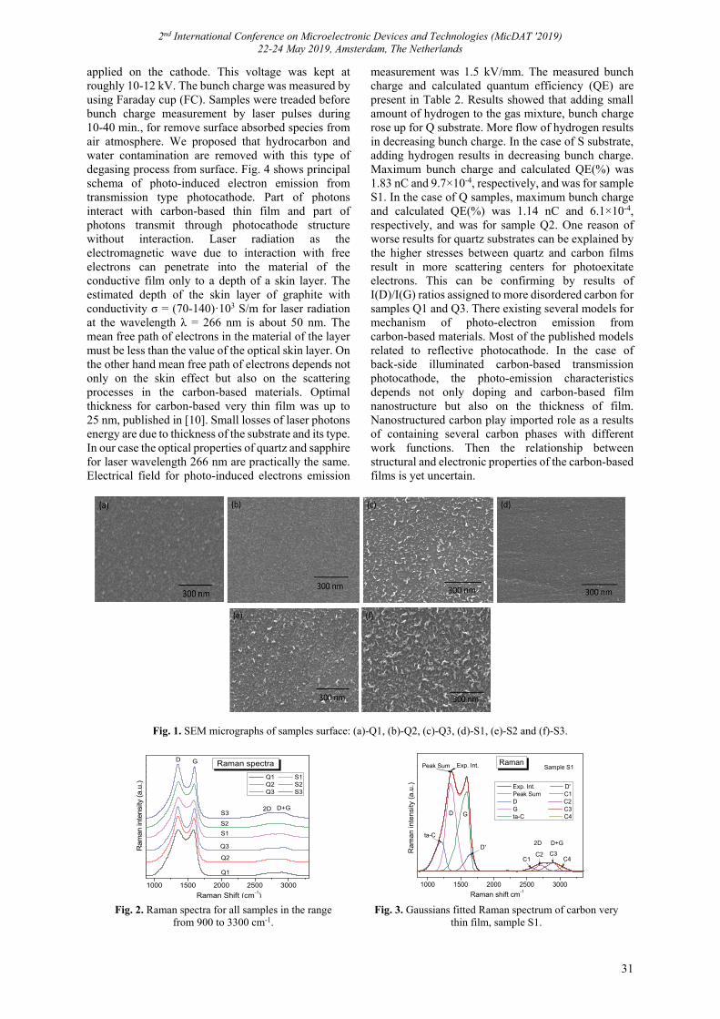
2nd International Conference on Microelectronic Devices and Technologies (MicDAT '2019) 22-24 May 2019, Amsterdam, The Netherlands
31
applied on the cathode. This voltage was kept at roughly 10-12 kV. The bunch charge was measured by using Faraday cup (FC). Samples were treaded before bunch charge measurement by laser pulses during 10-40 min., for remove surface absorbed species from air atmosphere. We proposed that hydrocarbon and water contamination are removed with this type of degasing process from surface. Fig. 4 shows principal schema of photo-induced electron emission from transmission type photocathode. Part of photons interact with carbon-based thin film and part of photons transmit through photocathode structure without interaction. Laser radiation as the electromagnetic wave due to interaction with free electrons can penetrate into the material of the conductive film only to a depth of a skin layer. The estimated depth of the skin layer of graphite with conductivity σ = (70-140)ꞏ103 S/m for laser radiation at the wavelength λ = 266 nm is about 50 nm. The mean free path of electrons in the material of the layer must be less than the value of the optical skin layer. On the other hand mean free path of electrons depends not only on the skin effect but also on the scattering processes in the carbon-based materials. Optimal thickness for carbon-based very thin film was up to 25 nm, published in [10]. Small losses of laser photons energy are due to thickness of the substrate and its type. In our case the optical properties of quartz and sapphire for laser wavelength 266 nm are practically the same. Electrical field for photo-induced electrons emission
measurement was 1.5 kV/mm. The measured bunch charge and calculated quantum efficiency (QE) are present in Table 2. Results showed that adding small amount of hydrogen to the gas mixture, bunch charge rose up for Q substrate. More flow of hydrogen results in decreasing bunch charge. In the case of S substrate, adding hydrogen results in decreasing bunch charge. Maximum bunch charge and calculated QE(%) was 1.83 nC and 9.7×10⁻⁴, respectively, and was for sample S1. In the case of Q samples, maximum bunch charge and calculated QE(%) was 1.14 nC and 6.1×10⁻⁴, respectively, and was for sample Q2. One reason of worse results for quartz substrates can be explained by the higher stresses between quartz and carbon films result in more scattering centers for photoexitate electrons. This can be confirming by results of I(D)/I(G) ratios assigned to more disordered carbon for samples Q1 and Q3. There existing several models for mechanism of photo-electron emission from carbon-based materials. Most of the published models related to reflective photocathode. In the case of back-side illuminated carbon-based transmission photocathode, the photo-emission characteristics depends not only doping and carbon-based film nanostructure but also on the thickness of film. Nanostructured carbon play imported role as a results of containing several carbon phases with different work functions. Then the relationship between structural and electronic properties of the carbon-based films is yet uncertain.
Fig. 1. SEM micrographs of samples surface: (a)-Q1, (b)-Q2, (c)-Q3, (d)-S1, (e)-S2 and (f)-S3.
Fig. 2. Raman spectra for all samples in the range
from 900 to 3300 cm-1. Fig. 3. Gaussians fitted Raman spectrum of carbon very
thin film, sample S1.
1000 1500 2000 2500 3000
Raman spectra
Ram
an in
tens
ity (
a.u.
)
Raman Shift (cm-1)
Q1 S1 Q2 S2 Q3 S3
Q1
S2
D G
2D D+G
Q2
Q3
S1
S3
1000 1500 2000 2500 3000
R
aman
inte
nsity
(a.
u.)
Raman shift cm-1
Raman
Exp. Int. D' Peak Sum C1 D C2 G C3 ta-C C4
Sample S1Exp. Int.Peak Sum
D G
ta-C2D D+G
C2D'
C3C4C1

2nd International Conference on Microelectronic Devices and Technologies (MicDAT '2019) 22-24 May 2019, Amsterdam, The Netherlands
32
Fig. 4. Principal schema of photo-induced electron emission
from transmission photocathode.
Table 2. The measured bunch charge and calculated QE.
Sample Q1 Q2 Q3 S1 S2 S3
Bunch charge [pC]
930 1140 840 1830 1650 1310
QE(%) ×10-4 4.9 6.1 4.5 9.7 8.7 6.8
4. Conclusions
For exploring the nanostructure effect on photo-induced electron emission properties of carbon-based very thin films, we prepared three types of carbon films on two substrates as quartz and sapphire. N-doped carbon-based very thin films were prepared by RF magnetron sputtering technology. Carbon films contain C, N and small amount of hydrogen and oxygen. SEM results showed no significance difference between sample surfaces prepared on both substrates for one series. Raman results showed interesting bands assigned to carbon based films as a-C, activated C, GNCD and very small amount of graphene-like carbon and graphene nanosheets embedded carbon. Maximum bunch charge and QE(%)×10-4 were 1.83 nC and 9.7, respectively, and was for transmission photocathode S1. Reported results in this study call for detailed studies of carbon thin films structural properties to optimize the design and technology of carbon-based photo-induced electron emitters as a back-side illuminated transmission photocathode. Acknowledgements
This research has been executed in the framework of the Topical Plan for JINR Research and International Cooperation (Project 02-0-1127-
2019/2021) and supported by the Slovak Research and Development Agency under contract APVV-0443-12.
References [1]. N. I. Balalykin, V. F. Minashkin, M. A. Nozdrin,
G. D. Shirkov, V. V. Zelenogorskii, E. I. Gacheva, A. K. Potemkin, J. Huran, Electron gun with a transmission photocathode for the Joint Institute for Nuclear Research photoinjector, Physics-Uspekhi, Vol. 60, 2017, pp. 1134-1141.
[2]. L. Velardi, A. Valentini, G. Cicala, UV photocathodes based on nanodiamond particles: Effect of carbon hybridization on the efficiency, Diamond & Related Materials, Vol. 76, 2017, pp. 1-8.
[3]. K. Sun, D. Diao, L. Yang, W. Zhang, X. Fan, Nanosized graphene sheets enhanced electron field emission behavior in pure carbon film, Thin Solid Films, Vol. 664, 2018, pp. 124-129.
[4]. M. A. Nitti, M. Colasuonno, E. Nappi, A. Valentini, E. Fanizza, F. Bénédic, G. Cicala, E. Milani, G. Prestopino, Performance analysis of poly-, nano-, and single-crystalline diamond-based photocathodes, Nuclear Instrument and Methods in Physics Research A, Vol. 595, 2008, pp. 131-135.
[5]. M. Inagaki, M. Toyoda, Y. Soneda, T. Morishita, Nitrogen-doped carbon materials, Carbon, Vol. 132, 2018, pp. 104-140.
[6]. J. Huran, N. I. Balalykin, A. A. Feshchenko, A. P. Kobzev, A. Kleinová, V. Sasinková, L. Hrubčín, Transmission photocathodes based on stainless steel mesh coated with deuterated diamond like carbon films, Nuclear Instrument and Methods in Physics Research A, Vol. 753, 2014, pp. 14-18.
[7]. P.-T. Tseng, P.-H. Tsai, A. Lu, J.-L. Hou, H.-Y. Tsai, Field emission characteristic study on bristling few-layer graphite/diamond composite film, Diamond & Related Materials, Vol. 73, 2017, pp. 121-131.
[8]. S. Takabayashi, H. Hayashi, M. Yang, R. Sugimoto, S. Ogawa, Y. Takakuwa. Chemical structure and electrical characteristics of diamondlike carbon films, Diamond & Related Materials, Vol. 81, 2018, pp. 16-26.
[9]. B. B. Wanga, X. L. Qu, Y. A. Chen, K. Zheng, K. Ostrikov, Effects of plasma and gas flow conditions on the structures and photoluminescence of carbon nanomaterials, Diamond & Related Materials, Vol. 84, 2018, pp 178–189.
[10]. N. I. Balalykin, J. Huran, M. A. Nozdrin, A. A. Feshchenko, A. P. Kobzev, V. Sasinková, P. Boháček, J. Arbet, Reactive magnetron sputtering of N-doped carbon thin films on quartz glass for transmission photocathode applications, Journal of Physics: Conf. Series, Vol. 992, 2018, 012031.
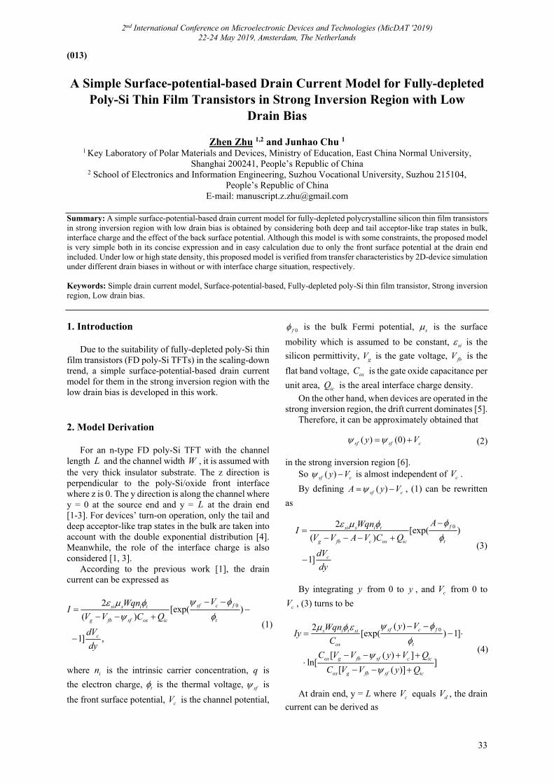
2nd International Conference on Microelectronic Devices and Technologies (MicDAT '2019) 22-24 May 2019, Amsterdam, The Netherlands
33
(013)
A Simple Surface-potential-based Drain Current Model for Fully-depleted
Poly-Si Thin Film Transistors in Strong Inversion Region with Low Drain Bias
Zhen Zhu 1,2 and Junhao Chu 1
1 Key Laboratory of Polar Materials and Devices, Ministry of Education, East China Normal University, Shanghai 200241, People’s Republic of China
2 School of Electronics and Information Engineering, Suzhou Vocational University, Suzhou 215104, People’s Republic of China
E-mail: [email protected] Summary: A simple surface-potential-based drain current model for fully-depleted polycrystalline silicon thin film transistors in strong inversion region with low drain bias is obtained by considering both deep and tail acceptor-like trap states in bulk, interface charge and the effect of the back surface potential. Although this model is with some constraints, the proposed model is very simple both in its concise expression and in easy calculation due to only the front surface potential at the drain end included. Under low or high state density, this proposed model is verified from transfer characteristics by 2D-device simulation under different drain biases in without or with interface charge situation, respectively. Keywords: Simple drain current model, Surface-potential-based, Fully-depleted poly-Si thin film transistor, Strong inversion region, Low drain bias. 1. Introduction
Due to the suitability of fully-depleted poly-Si thin film transistors (FD poly-Si TFTs) in the scaling-down trend, a simple surface-potential-based drain current model for them in the strong inversion region with the low drain bias is developed in this work. 2. Model Derivation
For an n-type FD poly-Si TFT with the channel length L and the channel width W , it is assumed with the very thick insulator substrate. The z direction is perpendicular to the poly-Si/oxide front interface where z is 0. The y direction is along the channel where y = 0 at the source end and y = L at the drain end [1-3]. For devices’ turn-on operation, only the tail and deep acceptor-like trap states in the bulk are taken into account with the double exponential distribution [4]. Meanwhile, the role of the interface charge is also considered [1, 3].
According to the previous work [1], the drain current can be expressed as
0[exp(( )
1] ,
2)fsfs i
g fb sf o
csi t
x
c
tic
WqnI
V V C Q
d
V
V
dy
(1)
where in is the intrinsic carrier concentration, q is
the electron charge, t is the thermal voltage, sf is
the front surface potential, cV is the channel potential,
0f is the bulk Fermi potential, s is the surface
mobility which is assumed to be constant, si is the
silicon permittivity, gV is the gate voltage, fbV is the
flat band voltage, oxC is the gate oxide capacitance per
unit area, icQ is the areal interface charge density.
On the other hand, when devices are operated in the strong inversion region, the drift current dominates [5].
Therefore, it can be approximately obtained that
( ) (0)sf sf cy V (2)
in the strong inversion region [6]. So ( )sf cy V is almost independent of cV .
By defining ( )sf cA y V , (1) can be rewritten
as
0[exp(
1
))
]
2
(s i
g fb c ox ic
fsi t
c
t
AWqnI
V V A V C Q
dV
dy
(3)
By integrating y from 0 to y , and cV from 0 to
cV , (3) turns to be
0 )( )2
[exp( 1]
[ ( ) ]ln[ ]
[ ( )]
sf cs i
ox
ox g fb sf
f
ft si
t
c ic
ox g fb s ic
y VWqnIy
C
C V V y V Q
C V V y Q
(4)
At drain end, y = L where cV equals dV , the drain
current can be derived as

2nd International Conference on Microelectronic Devices and Technologies (MicDAT '2019) 22-24 May 2019, Amsterdam, The Netherlands
34
0( )2[exp( 1]
[ ( )ln[ ]
)
)
[ ( ]
]
sfs i
ox
ox g fb sf ic
ox g f f
d
i
ft i
t
b s
s
d
c
LWqnI
LC
C V V L Q
C V L
V
V Q
V
(5)
from (4).
Meanwhile, the front surface potential, considering the effect of the back surface potential, can be calculated according to [1, 3]. 3. Result and Discussion
For n-type FD poly-Si TFTs with the very thick insulator substrate, including both tail and deep acceptor-like trap states in the bulk and the interface charge, this proposed simple surface-potential-based drain current model in strong inversion region with low drain bias (5) is compared with the simulation results of the 2D-device simulator MEDICI [7] from the transfer characteristics of both low and high state densities for without or with interface charge situation respectively. The used simulation data are from [1]. The devices’parameters used in the model are shown in Table 1.
Table 1. Values of parameters used in the model.
Symbol Parameter Value
NAa Active acceptor concentration
1016 cm-3
gd Deep state density at the conduction band edge
1×1018 cm-3eV-1
(for low state density) 2×1019 cm-3eV-1
(for high state density)
gt Tail state density at the conduction band edge
5×1018 cm-3eV-1
(for low state density) 1×1020 cm-3eV-1
(for high state density)
Td Characteristic temperature of the deep states
1060 K
Tt Characteristic temperature of the tail states
335 K
T Absolute temperature 300 Ktox Gate oxide thickness 0.1 μmVfb Flat band voltage -0.6 V
Qic Areal interface charge density
0 C/cm2
(without interface charge)
1.610-8 C/cm2 (with interface
charge)
tsi Thickness of the poly-Si layer
0.1 μm
μs Surface mobility 600 cm2/(V•S)W Width of the channel 10 μmL Length of the channel 10 μm
Figs. 1-4 show transfer characteristics of the above devices with the low or high state densities under different drain biases when icQ = 0 C/cm2 or
icQ = 1.610-8 C/cm2 respectively. In Fig. 1 and
Fig. 3, gd = 11018 cm-3eV-1 and gt = 51018 cm-3eV-1 for low state density. In Fig. 2 and Fig. 4, gd = 21019 cm-3eV-1 and gt = 11020 cm-3eV-1 for high state density. The gate voltage in model varies from 2 V to 20 V for Vd = 0.1 V, 4 V to 20 V for Vd = 1 V in Fig. 1 and Fig. 3, and from 4 V to 20 V for Vd = 0.1 V, 6 V to 20 V for Vd = 1 V in Fig. 2 and Fig. 4. The model (5) matches the simulation.
Fig. 1. Without interface charge, drain current in strong inversion region with low trap density under different drain
biases via model and 2D-device simulation.
Fig. 2. Without interface charge, drain current in strong inversion region with high trap density under different drain
biases via model and 2D-device simulation.
Fig. 3. With interface charge, drain current in strong inversion region with low trap density under different drain
biases via model and 2D-device simulation.

2nd International Conference on Microelectronic Devices and Technologies (MicDAT '2019) 22-24 May 2019, Amsterdam, The Netherlands
35
Fig. 4. With interface charge, drain current in strong inversion region with high trap density under different drain
biases via model and 2D-device simulation. 4. Conclusion
A simple surface-potential-based drain current model for FD poly-Si TFTs in strong inversion region with low drain bias is proposed considering the double exponential trap state distribution in bulk, the interface charge and the effect of the back surface potential. This proposed model matches the 2D-device simulation
results in transfer characteristics, with the merit of its concise expression and easiness in calculation due to only the front surface potential at the drain end included.
References [1]. Z. Zhu, J. Chu, submitted. [2]. Z. Zhu, J. Chu, A turn-on DC surface-potential-based
drain current model for fully-depleted poly-Si thin film transistors, TechConnect Briefs, Vol. 4, 2018, pp. 253-256.
[3]. Z. Zhu, J. Chu, A surface-potential-based drain current model suitable for poly-Si thin film transistors with thin body and thin gate oxide, Journal of Physics: Conference Series, Vol. 1141, 2018, 012066.
[4]. M. Hack, et al., Japanese Journal of Applied Physics, Vol. 29, 1990, pp. L2360-L2362.
[5]. Z. Zhu, J. Chu, Analysis of the current conduction in poly-Si thin film transistors, Semiconductor Science and Technology, Vol. 28, 2013, 015017.
[6]. N. Arora, MOSFET Modeling for VLSI Simulation: Theory and Practice, Springer-Verlag Wien, 1993.
[7]. Taurus Medici, Chapter 15, in User Guide, Version D-2010.03, Synopsys Inc., 2010. pp. 1-7.

2nd International Conference on Microelectronic Devices and Technologies (MicDAT '2019) 22-24 May 2019, Amsterdam, The Netherlands
36
(014)
Analysis and Improvement of Linearity Performance of Low Noise
Amplifier with Diode Loads
S. Chen 1, D. Prêle 1, F. Voisin 1 and A. Goldwurm 1 1 APC, Univ. Paris Diderot, CNRS/IN2P3, CEA/Irfu, Obs de Paris, Sorbonne Paris Cité, France
E-mail: [email protected] Summary: Scientific instruments often need an electronic readout system with small input noise, large output signals and small distortion. In order to adapt the newest requirements of an X-ray space mission, several differential low-noise amplifiers have been developed employing diodes as loads, based on a 350 nm SiGe BiCMOS technology. The amplifiers have shown a good performance of AC gain, noise and gain-drift. However, the linearity degrades due to cascaded topology. This summary proposes a new design with an AC current adjustment system based on the original amplifier topology, appended to the cascaded differential pairs using diodes as loads. The linearity performance is strongly improved according to the dedicated simulation results. Keywords: Non-linearity, Low-noise amplifier, Differential amplifier, BiCMOS technology, Hetero-junction bipolar transistor.
1. Introduction
Thanks to the advancing technology, scientific instruments have been quickly developed and turn to be more and more precise in decades. It leads to harsher requirements for electronic readout systems: the quality of detected signals could be degraded by input noise, gain-drift, non-linearity, etc.
Several Low-Noise Amplifiers (LNA) using a SiGe BiCMOS 350 nm technology have been developed, trying to reach the requirements such as an equivalent input voltage noise 1 𝑛𝑉/√𝐻𝑧, a large output signal with about 1 Vpp amplitude, a voltage gain at the order of a hundred V/V, with a gain drift ≤200 μV/V and a non-linearity < 1 % [1].
The LNAs use a common emitter topology with hetero-junction bipolar transistors (HBT) for the differential pair and diodes 1 as loads, as shown in Fig. 1. Amplifier A1 has one single differential stage with three diodes in series as loads; Amplifier A2 has three differential stages cascaded where each stage with two diodes in series as loads. Theoretically, according to Eq. (1), all the variables could be cancelled, and the gain just equals to the number of the diode loads nD in series, which produces a very stable gain. In addition, differential topology suppresses even order harmonics, improving the linearity. Moreover, the HBT provided by the technology has a good noise performance comparing to MOS.
|𝐺𝑎𝑖𝑛| 𝑔 𝑟 𝑛
𝑛 𝑛 , (1)
where gm is the HBT transconductance, rd is the small signal resistance of diodes, kB the Boltzmann constant, T is the temperature in Kelvin, q is the electron charge in absolute value, IC is the collector current, ID is the diode current and IC = ID [2].
Table 1 compares the measurement results of these two LNAs, both biased with IC = 2 mA and power supplied by VCC = 3.3 V. The gain performance of LNA A1 is very close to the theoretical analysis and simulations. In contrast, LNA A2 with three stages cascaded has the results less satisfying. Especially, when the output signal amplitude is larger than 227 mV, the gain’s non-linearity is already larger than 1 %.
Table 1. Measurements of the 2 LNAs with diodes loads.
LNA AC gain 1 % Non-linearity of gain
A1 2.97 V/V 𝑉 200 𝑚𝑉, 𝑉 594 𝑚𝑉
A2 7.57 V/V 𝑉 30 𝑚𝑉,
𝑉 227 𝑚𝑉
However, for having a larger gain, it is necessary
to cascade several such stages. The new topology presented in this article, is an AC base-current compensation system appended to the cascaded differential pairs using diodes as loads, aiming to solve the non-linearity problem found from the measurements of the amplifier A2. According to the simulation, the new topology could well improve the linearity performance.
1 The diode is realized by connecting the base and the collector of a HBT.

2nd International Conference on Microelectronic Devices and Technologies (MicDAT '2019) 22-24 May 2019, Amsterdam, The Netherlands
37
Fig. 1. Differential pair with 3 diode loads – LNA A1 (left); LNA A2 with 3 differential stages cascaded where each stage with two diodes in series as loads (right).
2. Linearity Analysis of Differential Pairs 2.1. Differential Pair with Resistive Loads
Resistance is a linear component, but bipolar transistor is non-linear. For a differential pair with resistive loads RC (Fig. 2), in the small signal analysis, its characteristics could be considered linear. But in the large signal analysis, the non-linear characteristics could not be neglected.
Considering a large differential signal applied to the differential inputs, ±∆V represent a change of the differential signal respectively at the two inputs during the same period, then Vin = 2∆V. On the other hand, Vout can be deducted as:
|𝑉 | 𝑉 𝑉
𝑉 𝐼 𝑅 𝑉 𝐼 𝑅
𝑅 𝐼 𝐼
(2)
∆V is introduced with Taylor expansion, as shown
in Eq. (3), where 𝑉 and IS the saturation
current [3].
Fig. 2. Differential pair with resistive loads.
𝐼 𝐼 𝐼 𝑒∆
𝐼 𝑒∆
𝐼 𝑒 𝑒∆
𝑒∆
𝐼 𝑒 1∆𝑉𝑉
12!
∆𝑉𝑉
13!
∆𝑉𝑉
⋯ 1∆𝑉𝑉
12!
∆𝑉𝑉
13!
∆𝑉𝑉
⋯
𝐼 𝑒2∆𝑉𝑉
13
∆𝑉𝑉
(3)
Substituting Eq. (3) into Eq. (2), the gain can be expressed by Eq. (4). It is noticeable that the standard differential topology improves the linearity performance of an amplifier by cancelling all the even-order harmonics. It is the remaining odd-order harmonics that introduce the main non-linearity [4].
|𝐺𝑎𝑖𝑛|
𝑉𝑉
𝑅 𝐼 𝐼
2∆𝑉
𝐼 𝑅 𝑒1
𝑉16
∆𝑉𝑉
(4)
2.2. Differential Pair with Diode Loads
Although diode and bipolar transistor are both non-linear components, bipolar transistor differential pair with diode loads has a better linear performance. With the same method, Vin = 2∆V = 2∆VBE, and Vout can be calculated by Eq. (5), with nD the number of diodes in series as loads.
|𝑉 | 𝑉 𝑉
𝑉 𝑛 𝑉 ∆𝑉 𝑉 𝑛 𝑉 ∆𝑉 2𝑛 ∆𝑉
(5)
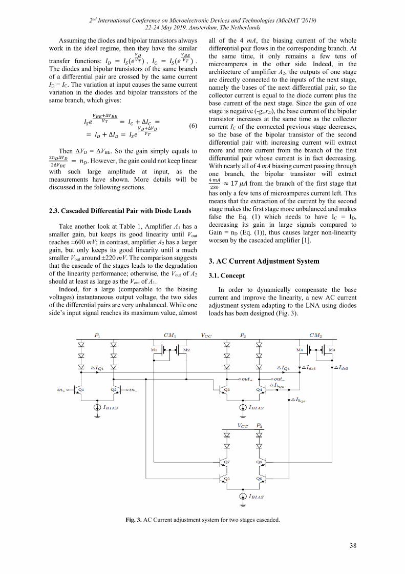
2nd International Conference on Microelectronic Devices and Technologies (MicDAT '2019) 22-24 May 2019, Amsterdam, The Netherlands
38
Assuming the diodes and bipolar transistors always work in the ideal regime, then they have the similar
transfer functions: 𝐼 𝐼 𝑒 , 𝐼 𝐼 𝑒 . The diodes and bipolar transistors of the same branch of a differential pair are crossed by the same current ID = IC. The variation at input causes the same current variation in the diodes and bipolar transistors of the same branch, which gives:
𝐼 𝑒
∆ 𝐼 ∆𝐼
𝐼 ∆𝐼 𝐼 𝑒∆
(6)
Then ∆VD = ∆VBE. So the gain simply equals to ∆
∆ 𝑛 . However, the gain could not keep linear
with such large amplitude at input, as the measurements have shown. More details will be discussed in the following sections. 2.3. Cascaded Differential Pair with Diode Loads
Take another look at Table 1, Amplifier A1 has a smaller gain, but keeps its good linearity until Vout reaches ±600 mV; in contrast, amplifier A2 has a larger gain, but only keeps its good linearity until a much smaller Vout around ±220 mV. The comparison suggests that the cascade of the stages leads to the degradation of the linearity performance; otherwise, the Vout of A2 should at least as large as the Vout of A1.
Indeed, for a large (comparable to the biasing voltages) instantaneous output voltage, the two sides of the differential pairs are very unbalanced. While one side’s input signal reaches its maximum value, almost
all of the 4 mA, the biasing current of the whole differential pair flows in the corresponding branch. At the same time, it only remains a few tens of microamperes in the other side. Indeed, in the architecture of amplifier A2, the outputs of one stage are directly connected to the inputs of the next stage, namely the bases of the next differential pair, so the collector current is equal to the diode current plus the base current of the next stage. Since the gain of one stage is negative (-gmrD), the base current of the bipolar transistor increases at the same time as the collector current IC of the connected previous stage decreases, so the base of the bipolar transistor of the second differential pair with increasing current will extract more and more current from the branch of the first differential pair whose current is in fact decreasing. With nearly all of 4 mA biasing current passing through one branch, the bipolar transistor will extract
17 𝜇𝐴 from the branch of the first stage that
has only a few tens of microamperes current left. This means that the extraction of the current by the second stage makes the first stage more unbalanced and makes false the Eq. (1) which needs to have IC = ID, decreasing its gain in large signals compared to Gain = nD (Eq. (1)), thus causes larger non-linearity worsen by the cascaded amplifier [1].
3. AC Current Adjustment System
3.1. Concept
In order to dynamically compensate the base current and improve the linearity, a new AC current adjustment system adapting to the LNA using diodes loads has been designed (Fig. 3).
Fig. 3. AC Current adjustment system for two stages cascaded.

2nd International Conference on Microelectronic Devices and Technologies (MicDAT '2019) 22-24 May 2019, Amsterdam, The Netherlands
39
In this system, a dummy differential pair P3 is added to the cascaded amplifier, with similar topology and same dimensions as the differential pair P1 and P2. Assuming the biasing conditions of the components of P3 are very close to those of P2, the base of Q5/Q6 will extract the same current as the base of Q3/Q4 does from P1. Until this step, twice the current is extracted as Q5/Q6 does from P1. Q7 and Q8 also have the same dimensions as Q5 and Q6. If they are also identically biased as Q5 and Q6, there will be the same amount of current passing through their bases as Q5 and Q6. Then the two current
mirrors CM1 and CM2, with , ,
permit to provide the currents back to P1, that always equal to the instantaneous current losses following the amplified signal. In consequence, there will be no extraction of current from the first stage, and the linearity performance of the whole topology could be maximized. 3.2. Tuning
For the transistors and diodes of the amplifiers, L = 400 μm and W = 0.4 μm are chosen as constants for emitter in order to reach a current gain β ≈ 230, close to its maximum value [5]. For the measurement of amplifier A1, VinCM = 1.1 V is used as the input voltage in common-mode between supply voltage 3.3 V and the ground 0 V, which permits a reasonable dynamic range and also lets the input voltage in common-mode very close to the output voltage in common-mode (VoutCM ≈ 1.1 V). IC = 2 mA is provided as biasing current for each branch of the differential pairs, in order to have an equivalent input noise lower than 1 𝑛𝑉/√𝐻𝑧 [2], at the same time having a large input resistance of the differential pair h11. In order to do a better comparison, we prefer to keep the same values mentioned above for the simulations. In consequence, the only parameters left are the channel’s length and width of the PMOS: M1, M2, M3 and M4. 3.2.1. Determination of the Channel’s Length for PMOS
The two current mirror CM1 and CM2 play a key role in the system. Since it is hoped that twice the extraction current can be given back to the first stage, it is important to well define the dimensions of PMOS. For the two PMOS of one current mirror have a large but different VDS, the channel-length modulation effect becomes quite noticeable, and their channel-length modulation coefficient λ could not be the same. In this situation, the currents could not be well regulated. In order to limit the channel-length modulation effect, it is better to use a longer length [4], so that the correction coefficient (1 + λVDS) in Eq. (7) is negligible, and the equation becomes the general expression of gm Eq. (8). Because the two PMOS of one current mirror have the
same △VGS, △IDS will be proportional to W/L. According to the simulation, L = 25 μm is enough to well limit the channel-length modulation effect and double the AC current by the current mirrors, namely iDS2 ≈ 2iDS1, iDS4 ≈ 2iDS3.
𝑔𝜕𝐼𝜕𝑉
𝜇 𝐶𝑊𝐿
𝑉 𝑉 1 𝜆𝑉 , (7)
𝑔𝑑𝐼𝑑𝑉
𝜇 𝐶𝑊𝐿
𝑉 𝑉 (8)
3.2.2. Determination of the Channel’s Width for PMOS
In order to well return twice the extraction AC current, it is also necessary that Q5 and Q6 in P3 have the similar biasing conditions to Q3 and Q4 in P2, so that they could have very close value of β. Then according to Eq. (9), they could extract the same ib [6]. Similarly, Q7 and Q8 should have the similar biasing conditions to Q5 and Q6, thus they could well copy the current and provide it to the current mirrors.
𝑑𝐼
𝑑𝑉𝑞𝐼
𝛽𝑘 𝑇 (9)
The VB of Q5/Q6 is fixed by the output of P1. The
VE of Q5/Q6 follows its VB by the difference around 0.72 V. The VC of Q7/Q8 is fixed by the voltage drop across the diode loads. However, the VB and VE of Q7/Q8 are free (the VC of Q5/Q6 equals to the VE of Q7/Q8), which need to vary the width of M1 and M3 to adapt. According to the simulation, with W1 = W3 = 25 μm, ibQ5 ≈ibQ7 ≈ ibQ3, ibQ6 ≈ ibQ8 ≈ ibQ4. 3.2.3. Simulation Results
The topology keeps good performances of AC gain and noise (Fig. 4), with a bandwidth larger than 200 MHz and an equivalent input voltage noise
700 𝑝𝑉/√𝐻𝑧. The comparison of simulation results in Fig. 5 illustrates that the linearity is strongly improved, up to Vin ≈ ±103 mV and Vout ≈ ±920 mV. Fig. 6 shows that the current extracted from Q1 is significantly reduced. Indeed, when IC reaches its minimum value in the corresponding branch of the differential pair, the instantaneous extraction current is dramatically reduced from original about 17 μA to now 10 nA. However, two small negative peaks of about 150 nA remain, but only when the IC is large as 3 mA. In any cases, this little fluctuation will not influence the differential pair’s normal operation at all.

2nd International Conference on Microelectronic Devices and Technologies (MicDAT '2019) 22-24 May 2019, Amsterdam, The Netherlands
40
Fig. 4. AC gain and noise simulation for 2 cascaded stages of differential pair with the AC current adjustment system.
Fig. 5. Simulation - Comparison of linearity performance between 2 cascaded stages of differential pair with and without the AC current adjustment system.
Fig. 6. AC Current adjustment performance simulation for 2 cascaded stages of differential pair
4. Discussions
4.1. Trade-off Between Noise, Input Impedance and Gain Drift Regarding Temperature Variation
The choice of the biasing current IC’s value is not only important for the performance of noise, but also
critical for the input resistance and the gain drift with regard to the variation of temperature. The simplification of the equivalent input noise Eq. (10) gives Eq. (11), which is useful to estimate the biasing current to optimize the noise [2]. With a source impedance RS ≈ 200 Ω for the differential inputs,
namely RS = 100 Ω for each input of the differential
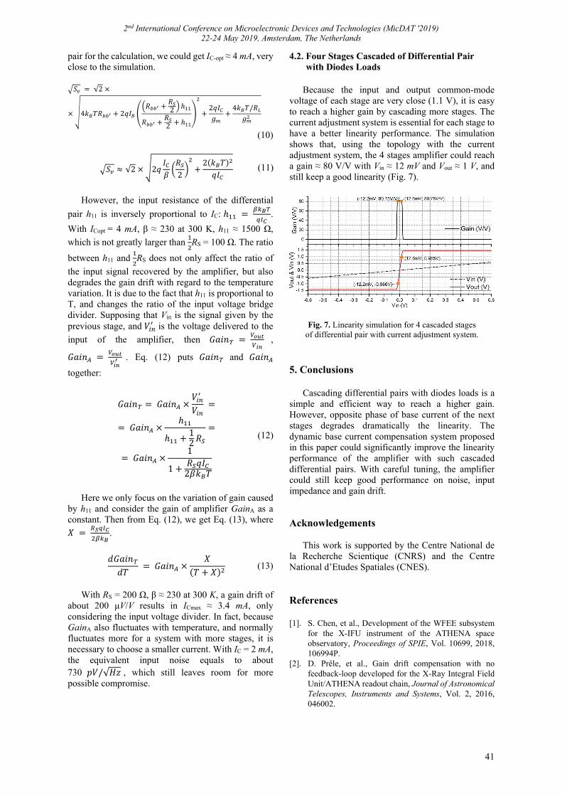
2nd International Conference on Microelectronic Devices and Technologies (MicDAT '2019) 22-24 May 2019, Amsterdam, The Netherlands
41
pair for the calculation, we could get IC-opt ≈ 4 mA, very close to the simulation.
𝑆 √2
4𝑘 𝑇𝑅 2𝑞𝐼𝑅
𝑅2 ℎ
𝑅𝑅2 ℎ
2𝑞𝐼𝑔
4𝑘 𝑇/𝑅𝑔
(10)
𝑆 √2 2𝑞𝐼𝛽
𝑅2
2 𝑘 𝑇𝑞𝐼
(11)
However, the input resistance of the differential
pair h11 is inversely proportional to IC: ℎ .
With ICopt = 4 mA, β ≈ 230 at 300 K, h11 ≈ 1500 Ω,
which is not greatly larger than RS = 100 Ω. The ratio
between h11 and RS does not only affect the ratio of
the input signal recovered by the amplifier, but also degrades the gain drift with regard to the temperature variation. It is due to the fact that h11 is proportional to T, and changes the ratio of the input voltage bridge divider. Supposing that Vin is the signal given by the previous stage, and 𝑉 is the voltage delivered to the
input of the amplifier, then 𝐺𝑎𝑖𝑛 ,
𝐺𝑎𝑖𝑛 . Eq. (12) puts 𝐺𝑎𝑖𝑛 and 𝐺𝑎𝑖𝑛
together:
𝐺𝑎𝑖𝑛 𝐺𝑎𝑖𝑛𝑉𝑉
𝐺𝑎𝑖𝑛ℎ
ℎ12 𝑅
𝐺𝑎𝑖𝑛1
1𝑅 𝑞𝐼
2𝛽𝑘 𝑇
(12)
Here we only focus on the variation of gain caused
by h11 and consider the gain of amplifier GainA as a constant. Then from Eq. (12), we get Eq. (13), where
𝑋 .
𝑑𝐺𝑎𝑖𝑛
𝑑𝑇 𝐺𝑎𝑖𝑛
𝑋𝑇 𝑋
(13)
With RS = 200 Ω, β ≈ 230 at 300 K, a gain drift of
about 200 μV/V results in ICmax ≈ 3.4 mA, only considering the input voltage divider. In fact, because GainA also fluctuates with temperature, and normally fluctuates more for a system with more stages, it is necessary to choose a smaller current. With IC = 2 mA, the equivalent input noise equals to about 730 𝑝𝑉/√𝐻𝑧 , which still leaves room for more possible compromise.
4.2. Four Stages Cascaded of Differential Pair with Diodes Loads
Because the input and output common-mode voltage of each stage are very close (1.1 V), it is easy to reach a higher gain by cascading more stages. The current adjustment system is essential for each stage to have a better linearity performance. The simulation shows that, using the topology with the current adjustment system, the 4 stages amplifier could reach a gain ≈ 80 V/V with Vin ≈ 12 mV and Vout ≈ 1 V, and still keep a good linearity (Fig. 7).
Fig. 7. Linearity simulation for 4 cascaded stages of differential pair with current adjustment system.
5. Conclusions
Cascading differential pairs with diodes loads is a simple and efficient way to reach a higher gain. However, opposite phase of base current of the next stages degrades dramatically the linearity. The dynamic base current compensation system proposed in this paper could significantly improve the linearity performance of the amplifier with such cascaded differential pairs. With careful tuning, the amplifier could still keep good performance on noise, input impedance and gain drift. Acknowledgements
This work is supported by the Centre National de la Recherche Scientique (CNRS) and the Centre National d’Etudes Spatiales (CNES). References [1]. S. Chen, et al., Development of the WFEE subsystem
for the X-IFU instrument of the ATHENA space observatory, Proceedings of SPIE, Vol. 10699, 2018, 106994P.
[2]. D. Prêle, et al., Gain drift compensation with no feedback-loop developed for the X-Ray Integral Field Unit/ATHENA readout chain, Journal of Astronomical Telescopes, Instruments and Systems, Vol. 2, 2016, 046002.

2nd International Conference on Microelectronic Devices and Technologies (MicDAT '2019) 22-24 May 2019, Amsterdam, The Netherlands
42
[3]. A. S. Sedra, K. C. Smith, Microelectronic Circuits, Vol. 1, Oxford University Press, New York, 1998.
[4]. B. Razavi, Design Of Analog CMOS Integrated Circuits, McGraw-Hill, 2000.
[5]. AMS 0.35 um HBT BiCMOS Process Parameters Rev. 5.0, AustriaMicrosystems AG, 2009.
[6]. S. M. Sze, K. K. Ng, Physics of Semiconductor Devices, John Wiley & Sons, 2006.

2nd International Conference on Microelectronic Devices and Technologies (MicDAT '2019) 22-24 May 2019, Amsterdam, The Netherlands
43
(015)
Design Assurance of COTS Based Electronic Systems
Dr. J. S. Sagoo 1
1 QinetiQ, St Andrews Road, Malvern, Worcestershire WR14 3PS, United Kingdom Tel.: + 44 1684 895188, fax: + 1684 894034
E-mail: [email protected] Summary: Assurance is a key activity for providing confidence that a system satisfies its requirements, which is most crucial for systems operating in safety related environments. Although techniques such as audits are important for providing assurance, they provide limited support for systems constructed from 3rd party COTS software and programmable electronic hardware. This is because for such systems developmental evidence may not be available. This paper presents an assurance approach which combines safety and formal techniques (such as HAZOP, fault trees and CPN). Specifically, this approach uses each technique to perform its analysis of the system and the results of each analysis are used as the basis of the other constituent techniques. The approach is applied to a case study, which involves a system that is required to automatically deploy parachutes when a skydiver exits an aircraft in flight. Using this case study, the attributes of the assurance approach is demonstrated. Keywords: Assurance, Petri nets, HAZOP, FTA, Sensor modelling, COTS.
1. Introduction
In the construction of computer based embedded control systems, assurance is a set of planned and systematic activities which are applied to provide confidence that a system development satisfies its given requirements [1]. For safety applications, assurance also provides an important means of showing that the development complies with agreed standards and that the system contains specified behaviours but excludes known unsafe or undesirable behaviours. In the automotive and aviation sectors, assurance activities are mandated by standards such as [2-4]. Specifically, in aviation, regulatory authorities require the production of system safety cases, for which assurance can provide the necessary evidence to form a robust system safety argument [5]. For the development of aviation software and programmable electronic hardware, assurance approaches such as technical reviews have become commonplace and are well-understood by system developers and independent assessors (acting for the regulatory authorities) [6, 7]. These approaches have become part of best practice [8, 9] and are applied at specific phases in the system development. Although technical reviews provide an important assurance technique, they can provide limited support for systems, for which, developmental evidence is unavailable, such as systems constructed from 3rd party Commercial-Off-The-Shelf (COTS) components.
This paper presents an approach that can be used to provide assurance in systems formed using 3rd party software and programmable electronic hardware COTS components. The aim of this paper is to present a pragmatic approach for assurance which is based on techniques that are familiar to the professional engineer, as this would most likely produce a more useable approach. Hence, this approach uses an integrated combination of safety techniques (such as
Hazard and Operability Study (HAZOP) and Fault Tree Analysis (FTA) [10]) with formal approaches (such as Coloured Petri nets (CPN) [11]) that can be used to provide systems assurance.
This paper considers the combination of techniques on the basis that the safety techniques possess an ‘intuitive’ quality that can allow an engineer to explore and understand the system’s safety behaviours. Formal techniques, on the other hand, can be used to conduct a detailed investigation of the system safety behaviours within a more rigorous framework. It is intended that this technique would be used during a system’s development to perform the safety assessment and guide the design activities rather than to be specifically used at the end of a development phase. This approach is illustrated by showing its application in a case study that involves an automatic actuation control system used in an airborne application.
1.1. Related Work
Safety techniques such as HAZOP and FTA are routinely used within a wide range of engineering sectors. HAZOP is intended to be used by a group of experts (who have a detailed understanding of the system to be assessed) to identify hazards from a system’s functional description. Since a system description can be available at any level of abstraction (ranging from top-level system functionality to detailed design), a HAZOP can be performed for different phases within a systems development. HAZOP is applied by using a set of guidewords with the system description to develop a set of scenarios. Each scenario is then assessed for its safety implications and this activity is used to derive hazards.
FTA is a prominent technique used in safety and reliability engineering to understand how a system can cause a hazard and then to determine how to reduce the risk of failure. FTA identifies all possible paths leading
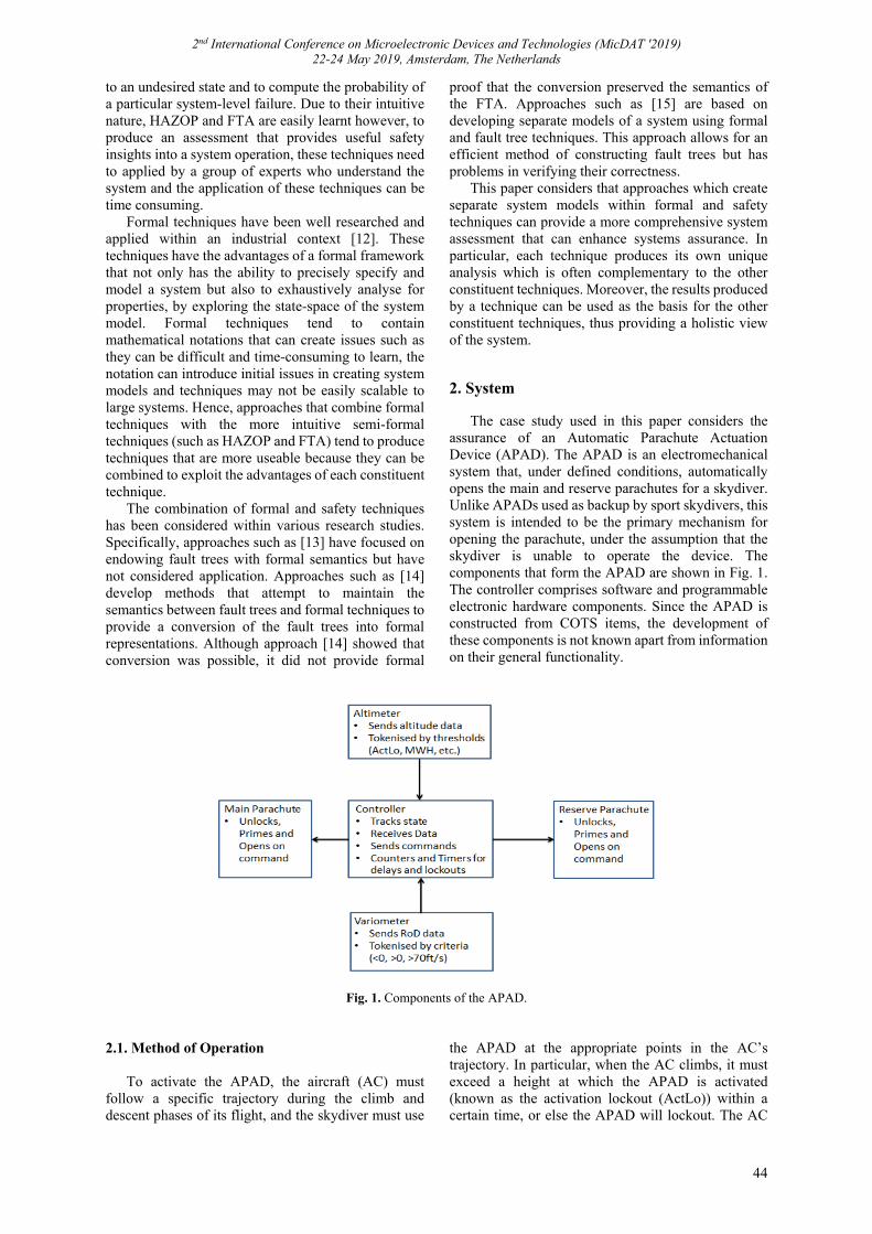
2nd International Conference on Microelectronic Devices and Technologies (MicDAT '2019) 22-24 May 2019, Amsterdam, The Netherlands
44
to an undesired state and to compute the probability of a particular system-level failure. Due to their intuitive nature, HAZOP and FTA are easily learnt however, to produce an assessment that provides useful safety insights into a system operation, these techniques need to applied by a group of experts who understand the system and the application of these techniques can be time consuming.
Formal techniques have been well researched and applied within an industrial context [12]. These techniques have the advantages of a formal framework that not only has the ability to precisely specify and model a system but also to exhaustively analyse for properties, by exploring the state-space of the system model. Formal techniques tend to contain mathematical notations that can create issues such as they can be difficult and time-consuming to learn, the notation can introduce initial issues in creating system models and techniques may not be easily scalable to large systems. Hence, approaches that combine formal techniques with the more intuitive semi-formal techniques (such as HAZOP and FTA) tend to produce techniques that are more useable because they can be combined to exploit the advantages of each constituent technique.
The combination of formal and safety techniques has been considered within various research studies. Specifically, approaches such as [13] have focused on endowing fault trees with formal semantics but have not considered application. Approaches such as [14] develop methods that attempt to maintain the semantics between fault trees and formal techniques to provide a conversion of the fault trees into formal representations. Although approach [14] showed that conversion was possible, it did not provide formal
proof that the conversion preserved the semantics of the FTA. Approaches such as [15] are based on developing separate models of a system using formal and fault tree techniques. This approach allows for an efficient method of constructing fault trees but has problems in verifying their correctness.
This paper considers that approaches which create separate system models within formal and safety techniques can provide a more comprehensive system assessment that can enhance systems assurance. In particular, each technique produces its own unique analysis which is often complementary to the other constituent techniques. Moreover, the results produced by a technique can be used as the basis for the other constituent techniques, thus providing a holistic view of the system. 2. System
The case study used in this paper considers the assurance of an Automatic Parachute Actuation Device (APAD). The APAD is an electromechanical system that, under defined conditions, automatically opens the main and reserve parachutes for a skydiver. Unlike APADs used as backup by sport skydivers, this system is intended to be the primary mechanism for opening the parachute, under the assumption that the skydiver is unable to operate the device. The components that form the APAD are shown in Fig. 1. The controller comprises software and programmable electronic hardware components. Since the APAD is constructed from COTS items, the development of these components is not known apart from information on their general functionality.
Fig. 1. Components of the APAD. 2.1. Method of Operation
To activate the APAD, the aircraft (AC) must follow a specific trajectory during the climb and descent phases of its flight, and the skydiver must use
the APAD at the appropriate points in the AC’s trajectory. In particular, when the AC climbs, it must exceed a height at which the APAD is activated (known as the activation lockout (ActLo)) within a certain time, or else the APAD will lockout. The AC
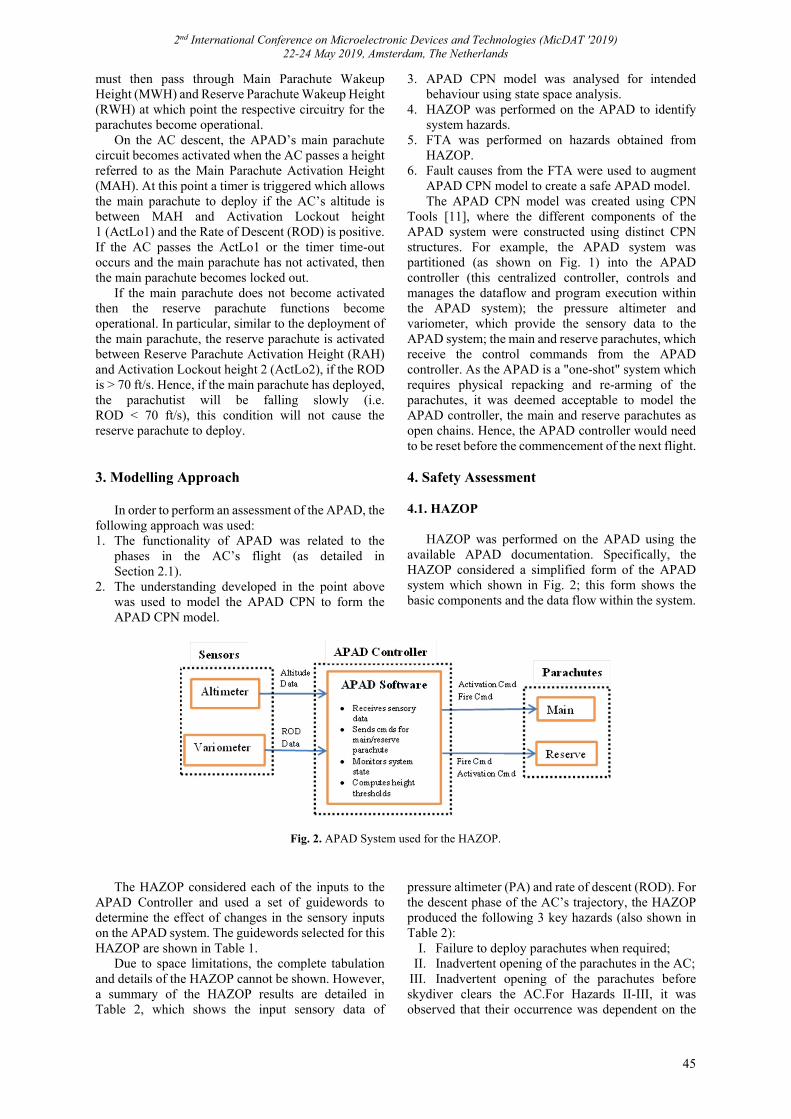
2nd International Conference on Microelectronic Devices and Technologies (MicDAT '2019) 22-24 May 2019, Amsterdam, The Netherlands
45
must then pass through Main Parachute Wakeup Height (MWH) and Reserve Parachute Wakeup Height (RWH) at which point the respective circuitry for the parachutes become operational.
On the AC descent, the APAD’s main parachute circuit becomes activated when the AC passes a height referred to as the Main Parachute Activation Height (MAH). At this point a timer is triggered which allows the main parachute to deploy if the AC’s altitude is between MAH and Activation Lockout height 1 (ActLo1) and the Rate of Descent (ROD) is positive. If the AC passes the ActLo1 or the timer time-out occurs and the main parachute has not activated, then the main parachute becomes locked out.
If the main parachute does not become activated then the reserve parachute functions become operational. In particular, similar to the deployment of the main parachute, the reserve parachute is activated between Reserve Parachute Activation Height (RAH) and Activation Lockout height 2 (ActLo2), if the ROD is > 70 ft/s. Hence, if the main parachute has deployed, the parachutist will be falling slowly (i.e. ROD < 70 ft/s), this condition will not cause the reserve parachute to deploy. 3. Modelling Approach
In order to perform an assessment of the APAD, the following approach was used: 1. The functionality of APAD was related to the
phases in the AC’s flight (as detailed in Section 2.1).
2. The understanding developed in the point above was used to model the APAD CPN to form the APAD CPN model.
3. APAD CPN model was analysed for intended behaviour using state space analysis.
4. HAZOP was performed on the APAD to identify system hazards.
5. FTA was performed on hazards obtained from HAZOP.
6. Fault causes from the FTA were used to augment APAD CPN model to create a safe APAD model. The APAD CPN model was created using CPN
Tools [11], where the different components of the APAD system were constructed using distinct CPN structures. For example, the APAD system was partitioned (as shown on Fig. 1) into the APAD controller (this centralized controller, controls and manages the dataflow and program execution within the APAD system); the pressure altimeter and variometer, which provide the sensory data to the APAD system; the main and reserve parachutes, which receive the control commands from the APAD controller. As the APAD is a "one-shot" system which requires physical repacking and re-arming of the parachutes, it was deemed acceptable to model the APAD controller, the main and reserve parachutes as open chains. Hence, the APAD controller would need to be reset before the commencement of the next flight. 4. Safety Assessment 4.1. HAZOP
HAZOP was performed on the APAD using the available APAD documentation. Specifically, the HAZOP considered a simplified form of the APAD system which shown in Fig. 2; this form shows the basic components and the data flow within the system.
Fig. 2. APAD System used for the HAZOP.
The HAZOP considered each of the inputs to the APAD Controller and used a set of guidewords to determine the effect of changes in the sensory inputs on the APAD system. The guidewords selected for this HAZOP are shown in Table 1.
Due to space limitations, the complete tabulation and details of the HAZOP cannot be shown. However, a summary of the HAZOP results are detailed in Table 2, which shows the input sensory data of
pressure altimeter (PA) and rate of descent (ROD). For the descent phase of the AC’s trajectory, the HAZOP produced the following 3 key hazards (also shown in Table 2):
I. Failure to deploy parachutes when required; II. Inadvertent opening of the parachutes in the AC;
III. Inadvertent opening of the parachutes before skydiver clears the AC.For Hazards II-III, it was observed that their occurrence was dependent on the

2nd International Conference on Microelectronic Devices and Technologies (MicDAT '2019) 22-24 May 2019, Amsterdam, The Netherlands
46
APAD having a breakaway mechanism which detects whether or not the APAD is on board the AC. Since it was not clear on what form of breakaway mechanism had been used with the APAD system, this paper focuses on Hazard I. Furthermore, Hazard I (which concerns the failure of the parachutes to open when skydiver performs a jump from AC) was also considered because it was better understood and more likely to be the critical hazard. Examples of the above hazards are shown in Table 2.
Table 1. Guidewords used for the APAD HAZOP.
Guideword Data Description
Too much The data value is too high (exceeds upper limit or bounds)
Too little The data value is too low (less than lower limit or bounds)
Incorrect The data value is within limits but has incorrect value
Table 2. Extract of HAZOP for the input provided by Pressure Altimeter to APAD System.
Hazard Sensor (Guideword)
Consequence/Implication
Parachutes do not open (Hazard I)
PA (Too little) Immediately after Skydiver jumps from AC
PA (Too little) Skydiver has jumped from AC
PA (Too much) Skydiver has jumped from AC
PA (Too much) Immediately after Skydiver jumps from AC
PA (Incorrect) Skydiver has jumped from AC
PA (Incorrect) Immediately after Skydiver jumps from AC
ROD (Too little) Skydiver has jumped from AC
ROD (Incorrect) Skydiver has jumped from AC
ROD (Incorrect) Immediately after Skydiver jumps from AC
ROD (Incorrect) Immediately after Skydiver jumps from AC
ROD (Incorrect) Skydiver has jumped from AC
ROD (Incorrect) Immediately after Skydiver jumps from AC
Premature opening of Parachutes (Hazards II-III)
PA (Too little) Skydiver has jumped from AC
PA (Too little) Skydiver is in AC
PA (Too little) Immediately after Skydiver jumps from AC
PA (Incorrect) Immediately after Skydiver jumps from AC
ROD (Too much) Skydiver is in AC
ROD (Too much) Immediately after Skydiver jumps from AC
ROD (Incorrect) Skydiver is in AC
ROD (Incorrect) Immediately after Skydiver jumps from AC
Parachutes open too late (Hazards II-III)
PA (Too little) Immediately after Skydiver jumps from AC
PA (Too much) Skydiver has jumped from AC
PA (Too much) Immediately after Skydiver jumps from AC
PA (Incorrect) Skydiver has jumped from AC
4.2. Fault Tree
The fault tree for the APAD system (referred to as APAD Fault Tree (FT)) was generated by considering each hazard obtained from the HAZOP and establishing the root cause of the hazards (using the APAD architecture and APAD documentation). Due to space limitations the complete APAD FT cannot be shown, however, the APAD FT for Hazard I is shown
in Fig. 3 and the following discusses the key results obtained from the APAD FT.
An inspection of the APAD FT confirmed that the APAD system has built in redundancy due to having two parachutes (i.e. the main and reserve parachutes).
In identifying the root causes for Hazard I, the APAD FT showed that the first main cause of this hazard, is when the skydiver exits from the AC (referred to as a jump), when the AC is at its

2nd International Conference on Microelectronic Devices and Technologies (MicDAT '2019) 22-24 May 2019, Amsterdam, The Netherlands
47
appropriate flight phase, and the APAD system is locked out. In this case both the main and reserve parachutes cannot be activated. This scenario could occur if the skydiver either jumps below ActLo or the APAD timer reaches maximum count before the AC reaches ActLo. The former is unlikely as the APAD system is likely to be used by trained skydivers but the latter is likely such as if the jump is delayed. This situation could be mitigated by installing a manual
lockout/disable system for use in the event of the jump being cancelled or delayed.
The second cause of Hazard I, identified from the APAD FT, is if the skydiver jumps below MWH. In this case the main parachutes will not be operational. Furthermore, in this scenario, if the skydiver jumps without the AC having reached the RWH, the reserve parachute will not be operational; increasing the risk from a failure of the Main.
Fig. 3. APAD FT for Hazard I. The third cause of Hazard I, identified from the
APAD FT, is faults occurring in the altimeter or variometer sensors causing incorrect sensory data values being sent to the APAD Controller. This situation introduces a single point of failure in the APAD system. To prevent erroneous readings from these sensors being used by the APAD software, several measures can be used such as:
A checkable readout (or error alert) can be implemented to ensure that the skydiver does not jump when the APAD controller either receives no or faulty data from the sensors.
Additional integrity checks can be implemented on the data provided by the sensors to the APAD Controller.
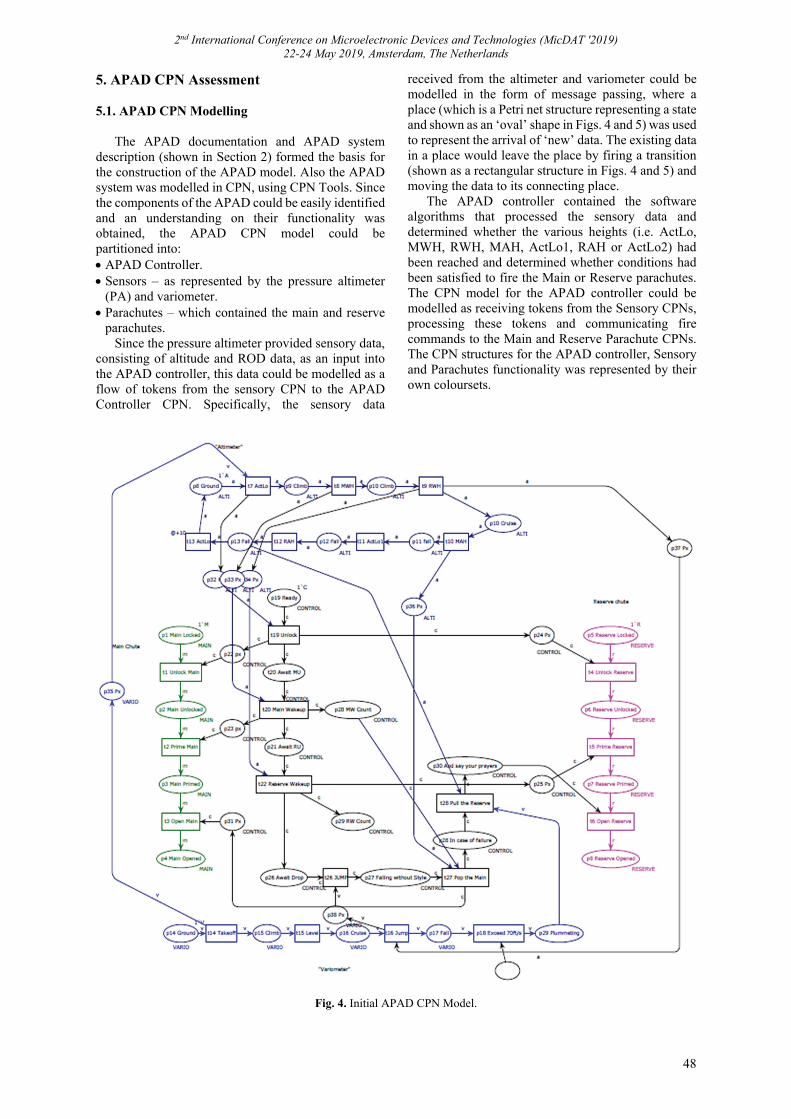
2nd International Conference on Microelectronic Devices and Technologies (MicDAT '2019) 22-24 May 2019, Amsterdam, The Netherlands
48
5. APAD CPN Assessment 5.1. APAD CPN Modelling
The APAD documentation and APAD system description (shown in Section 2) formed the basis for the construction of the APAD model. Also the APAD system was modelled in CPN, using CPN Tools. Since the components of the APAD could be easily identified and an understanding on their functionality was obtained, the APAD CPN model could be partitioned into: APAD Controller. Sensors – as represented by the pressure altimeter
(PA) and variometer. Parachutes – which contained the main and reserve
parachutes. Since the pressure altimeter provided sensory data,
consisting of altitude and ROD data, as an input into the APAD controller, this data could be modelled as a flow of tokens from the sensory CPN to the APAD Controller CPN. Specifically, the sensory data
received from the altimeter and variometer could be modelled in the form of message passing, where a place (which is a Petri net structure representing a state and shown as an ‘oval’ shape in Figs. 4 and 5) was used to represent the arrival of ‘new’ data. The existing data in a place would leave the place by firing a transition (shown as a rectangular structure in Figs. 4 and 5) and moving the data to its connecting place.
The APAD controller contained the software algorithms that processed the sensory data and determined whether the various heights (i.e. ActLo, MWH, RWH, MAH, ActLo1, RAH or ActLo2) had been reached and determined whether conditions had been satisfied to fire the Main or Reserve parachutes. The CPN model for the APAD controller could be modelled as receiving tokens from the Sensory CPNs, processing these tokens and communicating fire commands to the Main and Reserve Parachute CPNs. The CPN structures for the APAD controller, Sensory and Parachutes functionality was represented by their own coloursets.
Fig. 4. Initial APAD CPN Model.

2nd International Conference on Microelectronic Devices and Technologies (MicDAT '2019) 22-24 May 2019, Amsterdam, The Netherlands
49
Fig. 5. Improved APAD CPN Model.
5.2. Initial APAD CPN Model
The initial APAD CPN model was constructed and shown in Fig. 4. The initial APAD CPN contained the causal ordering of events detailed in the APAD documentation and this could be easily verified by performing a step-by-step simulation of the model, using CPN Tools. However, when CPN Tools was used to simulate the complete model, it produced some undesirable behaviors that could have safety implications. Specifically, these behvaiours includes situations such as the parachutes being ready to deploy whilst the MWH and RWH had not been reached. This scenario was undesirable because the APAD was not in synchrony with the external environment; the AC had not fully achieved its climb (which was the initial stage of AC’s flight) but the APAD had set the parachutes to deploy, as if required during AC descent.
In terms of CPN modelling a process of trial and improvement could have been used to remove the above undesirable behaviors by re-modelling and using mechanisms such as interlocks in the CPN model. However, in this paper, the results obtained from the APAD FT were used to inform the process of improving the CPN model.
5.3. Improved APAD CPN Model
The results from the APAD FT were used to modify the APAD CPN model to improve its safety functionality; the resulting CPN is shown in Fig. 5. The improvements made to the APAD CPN were as follows:
Firstly, the inclusion of a “status" place, which receives tokens from the APAD controller to display on the APAD; this allows the skydiver to have a display of the state of readiness of the APAD. This status report can prevent the skydiver inadvertently performing a jump with the APAD being in a state of having locked out of both the parachutes.
Secondly, additional CPN structures were added to Fig. 5 (such as ‘MW count’, ‘RW count’, ‘max’ and ‘not max’ places) to indicate lockout states. These modifications provide mitigation to the first and second causes shown by the APAD FT (detailed in Section 4.2).
Thirdly, timings were added to the APAD CPN model for the altimeter and variometer, as this would allow: 1. APAD controller to be in synchrony with AC
passing through the various phases of its trajectory (such as MWH, RWH, MAH and RAH). This

2nd International Conference on Microelectronic Devices and Technologies (MicDAT '2019) 22-24 May 2019, Amsterdam, The Netherlands
50
would prevent situations such as parachutes being ready to deploy when AC flight trajectory had not reached that stage;
2. Modelling of the process of sensor sampling and storage of measured data values.
5.2. AAD CPN State Space
A state space analysis of the improved APAD CPN model was performed using CPN Tools, which produced a large simulation graph comprising 280 nodes and 710 arcs. Although the simulation graph was difficult to analyse, sections of the graph were examined incrementally. The state space analysis showed that a dead marking (which represents the state of activation lockout having occurred, main parachute not deployed and reserve parachute not deployed) could occur. This marking represented an unsafe state at which a deadlock was reached if ActLo is not reached in time. This state was entirely predicted by the FTA. Since state space analysis did not show any other deadlock conditions, the improved APAD CPN model provided greater assurance in the APAD design.
6. Conclusions
This paper considered the issue of providing assurance for systems that are constructed from 3rd party software and programmable electronic hardware components. Providing assurance for such systems using standard methods (such as technical reviews) presents issues due to the lack of the availability of developmental evidence. Hence, this paper proposed an approach which used a combination of safety and formal techniques to provide systems assurance.
The motivation of combining safety techniques of HAZOP and FTA and formal techniques of CPN is that these techniques can produce useful assessments, which can be used for assurance, when limited information (or developmental evidence) exists for a system. Specifically, the application of the above techniques to a case study (presented in this paper, which involves a real-time safety related control system) has shown that: 1. The intuitive nature of HAZOP and FTA allows a
number of scenarios to be explored and can identify areas of known and unknown system behaviours.
2. Each technique can be used to perform its own unique analysis, without the need to introduce any complexities of ensuring whether the semantics of each technique has been preserved.
3. The results produced by each technique can be effectively used by the other constituent techniques.
Specifically, in this case study, the hazards derived from the HAZOP can be used as the base events for the FTA. The fault causes from the FTA can be used to assess the behavioural sequences that are produced by the CPN model. This can be used to modify the CPN model and constrain its behaviour. The application of the overall approach shows that
it allows a better understanding to be gained of the system behaviour. This understanding can inform on the risk posed by the system: high risk (if too many unknown behaviours), low risk (if most behaviours are known). This understanding can provide greater assurance in the overall system.
References [1]. D. Raheja, M. Allocco, Assurance Technologies
Principles and Practices, Wiley, 2006. [2]. Design Assurance Guidance for Airborne Electronic
Hardware, DO 254, EUROCAE/RTCA, 2000. [3]. Software Considerations in Airborne Systems and
Equipment Certification, DO 178C, EUROCAE/RTCA, 2012.
[4]. Road Vehicles – Functional Safety, BS ISO 26262, BS ISO, 2011.
[5]. D. Jackson, Software for Dependable Systems: Sufficient Evidence (D. Jackson, M. Thomas, L. Millett, Eds.), National Academies Press, 2007.
[6]. Conducting Airborne Electronic Hardware Reviews, FAA Job Aid, 28th February 2008.
[7]. Conducting Software Reviews Prior to Certification, FAA Job Aid, 16th January 2004.
[8]. L. Rierson, Developing Safety-Critical Software, CRC Press, 2013.
[9]. R. Fulton, R. Vandermolen, Airborne Electronic Hardware Design Assurance, CRC Press, 2015.
[10]. C. Ericson. Hazard Analysis Techniques for System Safety, Wiley, 2016.
[11]. CPN Tools, http://cpntools.org/ [12]. J. S. Fitzgerald, J. Bicarregui, P. G. Larsen,
J. Woodcock, Industrial Deployment of Formal Methods: Trends and Challenges, Industrial Deployment of System Engineering Methods (A. Romanovsky, M. Thomas, Eds.), Springer, 2013.
[13]. G. Schellhorn, A. Thums, W. Reif, Formal fault tree semantics, in Proceedings of the 6th World Conference on Integrated Design and Process Technology (IDPT’02), Pasadena, CA, 2002.
[14]. O. Ariss, D. Xu, W. Wong, Integrating safety analysis with functional modeling, IEEE Transactions on Systems, Man and Cybernetics, Vol. 41, Issue. 4, July 2010, pp. 610-624.
[15]. G. Schellhorn, A. Thums, W. Reif, Safety analysis of a radio-based crossing control systems using formal methods, in Proceedings of the 9th IFAC Symposium Control in Transportation Systems (CTS’2000), Braunschweig, Germany, June 2000, pp. 289-294.

2nd International Conference on Microelectronic Devices and Technologies (MicDAT '2019) 22-24 May 2019, Amsterdam, The Netherlands
51
(017)
Ultrasonic Bonding of Ag-4Pd Alloy Ribbon for High Power IC Packages
C. H. Chen 1, Y. C. Lin 2 and T. H. Chuang 1
1 Institute of Materials Science and Engineering, National Taiwan University, No. 1, Roosevelt Rd., Sec. 4, Taipei 106, Taiwan
2 Wire Technology Co., LTD, No. 27, Aly. 56, Ln. 320, Sec.1, Shatian Rd., Dadu Dist, Taichung 432, Taiwan Tel.: +886-2-2392-9635, fax: + 87654321
E-mail: [email protected] Summary: Ultrasonic Wire bonding is widely applied in the electronics industry, especially in the field of power integrated circuits (Power IC). In the present work, the microstructures of Ag-4Pd alloy 100 μm ultra-thin ribbon bonded on different DBC substrates metallized with Ni, Au and Pd were evaluated. The grain structure of the Ag-4Pd ribbon was controlled by different annealing parameters. It was observed by electron back-scattered diffraction that the grain size of the Ag-4Pd ribbon increased from 0.28 μm (as-rolled) to 8.46 μm (annealed at 800 °C for 2 h), and the twin boundary density increased by up to 77 % after annealing at the elevated temperature. The bonding interface showed no cracks, even after high temperature storage test at 150 °C for 1000 h. The pull strength of the Cu/Ni substrate was 1375.6 gf, but the yield rate was poor (20 %). On the other hand, DBC substrate metallized with Ni/Pd, Ni/Au, and Ni/Pd/Au films showed great bonding yield rates (over 90 %) with satisfactory pull strengths of 701.7 gf, 779.6 gf and 796.2 gf. The results indicated that Ag-alloy ribbon is a better choice than Al and Cu ribbons for Power IC packaging. Keywords: Wire bonding, Ultrasonic bonding, Ag-alloy ribbon, DBC substrate, EBSD, Power IC. 1. Introduction
Ultrasonic wire bonding is the most cost-effective way to provide interconnections in semiconductor devices. Recently, power integrated circuits (Power IC) have drawn increasing attention, especially in silicon-based Insulated Gate Bipolar Transistor (IGBT) modules. Automotive IGBT module packaging should meet the qualification standard of Automotive Electronics Council stress tests (AEC-Q101) [1], which requires dedicated quality control and high reliability. The key points in Power IC packaging are heat dissipation and tolerance of high current density. Traditionally, Al heavy wires and ribbons have been used for the interconnections between Power IC chips and Direct Bonded Copper (DBC) substrates [2-3]; however, the relatively high resistivity and poor thermal stability of aluminum limits its usage, especially under high current density. Subsequently, copper ribbon was considered as a substitutional material for Al [4]. However, wedge bonding of Cu requires high ultrasonic power, which is prone to cause damage to chips [5]. In addition, the hardness of copper ribbon usually causes bonding tool failure and tail up in a second wedge bond [6], which is not favorable in industrial production. Although feasible solutions for copper ribbon such as Cu/Al clad ribbon or Al-coated copper ribbon have been proposed, they usually fail in severe thermal cycle tests due to the growth of intermetallic compounds [7]. As an alternative, copper clip bonding was proposed to meet the requirements of high current density and better bonding quality [8-9]. However, clip bonding requires dedicated process control of solder spraying and alignment of joints, which is not favorable to industry
due to cost concerns. The failures of copper and aluminum have presented the need for another substitutional material for bonding wire. One proposed material is Ag-alloy ribbon. It has low electrical conductivity and great mechanical properties, so Ag-alloy ribbon may be a good candidate for Power IC packaging solutions. In the present study, the microstructure of Ag-4Pd 100 μm ultra-thin ribbon bonded on different DBC substrates metallized with Ni, Au and Pd was evaluated. The grain structure of the Ag-4Pd ribbon was controlled by different annealing parameters and characterized by means of electron backscattered diffraction. 2. Results
The inverse pole figure orientation map of an annealed Ag-4Pd ribbon texture is shown in Fig. 1. Misorientation above 3° was considered to indicate grain boundaries and colored black. The twin boundaries were marked with white. It was observed that the grain size of the Ag-4Pd ribbon increased from 0.28 μm (as-rolled) to 8.46 μm (annealed at 800 °C for 2 h), as shown in Fig. 2, and the twin boundary density increased by up to 77 % after annealing at the elevated temperature, as shown in Fig. 3.
The Ag-4Pd ribbon was bonded with electroplated surface metallization layers of thickness 70-80 μm on DBC substrates. Overview images of the ribbons bonded on the substrates are shown in Fig. 4.
The bonded interface was investigated by scanning electron microscope, and the bond strength was examined by wire-pull test. Cross sections of the bonded area are shown in Figs. 5-7, respectively. The

2nd International Conference on Microelectronic Devices and Technologies (MicDAT '2019) 22-24 May 2019, Amsterdam, The Netherlands
52
results indicated that the Ag-4Pd ribbon had a continuous bonding interface without cracks on each substrate with different metallized DBC substrates, revealing that no damage was caused to the substrates during the bonding process. Furthermore, after the samples were subjected to high temperature storage test (HTST) at 150 °C for 1000 h, the bonding interface remained unchanged, as shown in Fig. 8.
Fig. 1. EBSD image of Ag-4Pd alloy ribbon annealed at 650 °C for 2 h.
Fig. 2. Grain sizes of Ag-4Pd alloy ribbons annealed at different temperatures (2 h).
Fig. 3. Twin boundary densities of Ag-4Pd alloy ribbon annealed at different temperatures (2 h).
Fig. 4. Images of ultrasonic bonded Ag-4Pd alloy ribbon on (a) Cu/Ni DBC substrate, (b) Cu/Ni/Au DBC substrate,
with leftover parts from the wire-pull test.
Fig. 5. Cross-sectional image of Ag-4Pd alloy ribbon as-bonded on Cu/Ni/Au DBC substrate.
Fig. 6. Interfacial image of Ag-4Pd alloy ribbon as-bonded on Cu/Ni/Au DBC substrate.
Due to the elevated temperature, the high
temperature storage test can result in degradation and failure of the packaging modules, and in some cases, detachment of the wire joints. However, the wire bonds of Ag-alloy ribbon on DBC substrates remained the same after the HTST, and no cracks or detachments were found. Furthermore, no intermetallic compounds were found at the interface because the surface metallization layers (Au/Pd) were solid solutions to Ag-alloy ribbons. This result provides clear evidence that Ag-alloy ribbons can be expected to have outstanding properties with DBC substrates due to the ribbon material itself.
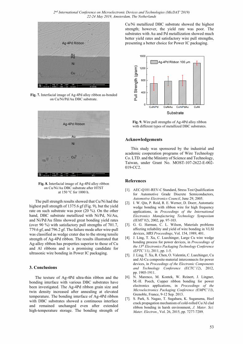
2nd International Conference on Microelectronic Devices and Technologies (MicDAT '2019) 22-24 May 2019, Amsterdam, The Netherlands
53
Fig. 7. Interfacial image of Ag-4Pd alloy ribbon as-bonded on Cu/Ni/Pd/Au DBC substrate.
Fig. 8. Interfacial image of Ag-4Pd alloy ribbon on Cu/Ni/Au DBC substrate after HTST
at 150 °C for 1000 h.
The pull strength results showed that Cu/Ni had the highest pull strength of 1375.6 gf (Fig. 9), but the yield rate on such substrate was poor (20 %). On the other hand, DBC substrate metallized with Ni/Pd, Ni/Au, and Ni/Pd/Au films showed great bonding yield rates (over 90 %) with satisfactory pull strengths of 701.7, 779.6 gf, and 796.2 gf. The failure mode after wire-pull was classified as wedge crater due to the strong tensile strength of Ag-4Pd ribbon. The results illustrated that Ag-alloy ribbon has properties superior to those of Cu and Al ribbons and is a promising candidate for ultrasonic wire bonding in Power IC packaging. 3. Conclusions
The texture of Ag-4Pd ultra-thin ribbon and the bonding interface with various DBC substrates have been investigated. The Ag-4Pd ribbon grain size and twin density increased after annealing at elevated temperature. The bonding interface of Ag-4Pd ribbon with DBC substrates showed a continuous interface and remained unchanged even after extended high-temperature storage. The bonding strength of
Cu/Ni metallized DBC substrate showed the highest strength; however, the yield rate was poor. The substrates with Au and Pd metallization showed much better yield rates and satisfactory wire pull strengths, presenting a better choice for Power IC packaging.
Fig. 9. Wire pull strengths of Ag-4Pd alloy ribbon with different types of metallized DBC substrates.
Acknowledgements
This study was sponsored by the industrial and academic cooperation programs of Wire Technology Co. LTD. and the Ministry of Science and Technology, Taiwan, under Grant No. MOST-107-2622-E-002-019-CC2. References [1]. AEC-Q101-REV-C Standard, Stress Test Qualification
for Automotive Grade Discrete Semiconductors, Automotive Electronics Council, June 29, 2005.
[2]. I. W. Qin, P. Reid, R. E. Werner, D. Doerr, Automatic wedge bonding with ribbon wire for high frequency applications, in Proceedings of the International Electronics Manufacturing Technology Symposium (IEMT’02), 2002, pp. 97-103.
[3]. G. G. Harman, C. L. Wilson, Materials problems affecting reliability and yield of wire bonding in VLSI devices, MRS Proceedings, Vol. 154, 1989, 401.
[4]. J. Ling, T. Xu, C. Luechinger, Large Cu wire wedge bonding process for power devices, in Proceedings of the 13th Electronics Packaging Technology Conference (EPTC’11), 2011, pp. 1-5.
[5]. J. Ling, T. Xu, R. Chen, O. Valentin, C. Luechinger, Cu and Al-Cu composite-material interconnects for power devices, in Proceedings of the Electronic Components and Technology Conference (ECTC’12), 2012, pp. 1905-1911.
[6]. N. Marenco, M. Kontek, W. Reinert, J. Lingner, M.-H. Poech, Copper ribbon bonding for power electronics applications, in Proceedings of the Microelectronics Packaging Conference (EMPC’13), Grenoble, France, 9-12 Sep. 2013.
[7]. S. Park, S. Nagao, T. Sugahara, K. Suganuma, Heel crack propagation mechanism of cold-rolled Cu/Al clad ribbon bonding in harsh environment, J. Mater. Sci: Mater. Electron., Vol. 26, 2015, pp. 7277-7289.

2nd International Conference on Microelectronic Devices and Technologies (MicDAT '2019) 22-24 May 2019, Amsterdam, The Netherlands
54
[8]. Y. Zhu, H. Chen, K. Xue, M. Li, J. Wu, Thermal and reliability analysis of clip bonding package using high thermal conductivity adhesive, in Proceedings of the IEEE 15th Electronics Packaging Technology Conference (EPTC’13), Singapore, 11-13 Dec. 2013, pp. 259-263.
[9]. K. K. Lwin, C. E. Tubillo, T. Panumard, J. Dimaano, N. Suthiwongsunthorn, S. Sirinorakul, Copper clip package for high performance MOSFETs and its optimization, in Proceedings of the 18th Electronics Packaging Technology Conference (EPTC’16), Singapore, 30 November – 3 December 2016, pp. 259-263.

2nd International Conference on Microelectronic Devices and Technologies (MicDAT '2019) 22-24 May 2019, Amsterdam, The Netherlands
55
(020)
Intramode Energy Exchange into a Thin Left-handed Film
on a Kerr-Substrate
N. Litvinova 1, A. Buller 1, and R. Litvinov 2
1 Tomsk State University of Control Systems and Radioelectronics, 634, Tomsk, Russia 2 Tomsk Polytechnic University, 634, Tomsk, Russia
E-mail: [email protected] Summary: The frequency-degenerate self-action of the four optical guided TE2-modes of a thin left-handed film on the substrate with Kerr-effect has been considered. The nonlinear coupled mode equations have been obtained. The exact analytical solution for mode intensities has shown the existence of the energy exchange between the modes. The transformation of the behavior of the energy exchange, when the initial conditions vary, has been analyzed. Keywords: Thin left-handed film optical waveguide, Kerr effect, Self-action of guided modes, Energy exchange.
1. Introduction
The control of the dispersion properties of the guided modes of the thin right- and left-handed films on an optically nonlinear substrate by varying the light intensity is discussed, for example, in Ref. [1, 2]. The control of the energy exchange between thin left-handed film modes on a Kerr-substrate is analyzed below. 2. Coupled Modes and Conservation Lows
The four optical guided modes of a thin left-handed film waveguide of the same type with propagation constants belonging to one continuous dispersion curve can propagate in the forward and backward directions and at the same frequency (see Fig. 1). The directions of the phase and group velocities of modes
with wave vector + (-) are coinciding (opposite). This case can be actualized for the TE2-mod at a frequency between the cutoff frequency and the frequency of the zero group velocity [3].
Fig. 1. Thin left-handed film waveguide and wave vectors of the forward- and backward-propagating optical modes.
If the substrate has the Kerr effect, these modes
interact with each other. The following relation can describe the electric intensity of the total light field:
1 20
,exp exp ,2
mr r m r
m r
IE C z x i z i t cc (1)
where I0 is the light intensity introduced into the waveguide; the index m means “f” or “b”; the index r means “+” or “-”; f,r = -f,r = r; m
rC z are the
functions describing the evolution of the forward- (f) and backward-propagating (b) modes; r and r(x) are the wave numbers of the modes and the functions describing the transverse distribution of the electric intensity, respectively, which can be calculated based on the relations given in [2, 3]; “сс” means complex conjugation. The functions m
rC z are considered
normalized in such a way that the squares sum of their absolute values is equal to unit at z = 0.
The coupled modes equations for initial functions
mrC z are obtained from Maxwell’s equations in the
framework of the method of slowly varying amplitudes satisfy the following elementary conservation laws:
2 2
2 2
2 2 2 2
,
,
,
f b
f b
f b b f
C z C z I
C z C z I
C z C z C z C z I
(2)
where constants I+, I-, and I can be calculated through the values of functions at z = 0. The new unknown functions are introduced as follows:
exp 2 ,
exp 2 ,
exp 2 ,
exp 2
f f
b b
f f
b b
c C i I I
c C i I I
c C i I I
c C i I I
(3)
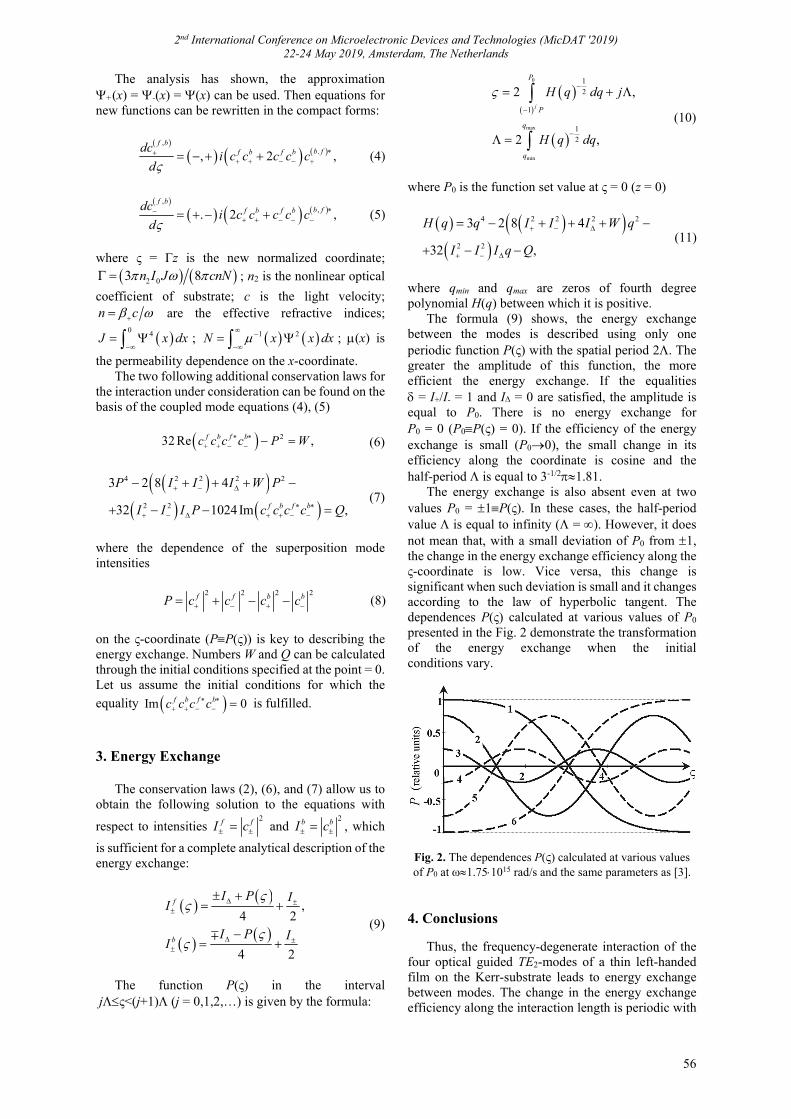
2nd International Conference on Microelectronic Devices and Technologies (MicDAT '2019) 22-24 May 2019, Amsterdam, The Netherlands
56
The analysis has shown, the approximation +(x) = -(x) = (x) can be used. Then equations for new functions can be rewritten in the compact forms:
,
., 2 ,f b
b ff b f bdci c c c c c
d
(4)
,
,. 2 ,f b
b ff b f bdci c c c c c
d
(5)
where ς = Γz is the new normalized coordinate;
2 03 8n I J cnN ; n2 is the nonlinear optical
coefficient of substrate; c is the light velocity; n c are the effective refractive indices;
0 4J x dx
; 1 2N x x dx
; (x) is
the permeability dependence on the x-coordinate. The two following additional conservation laws for
the interaction under consideration can be found on the basis of the coupled mode equations (4), (5)
232 Re ,f b f bc c c c P W
(6)
4 2 2 2 2
2 2
3 2 8 4
32 1024Im ,f b f b
P I I I W P
I I I P c c c c Q
(7)
where the dependence of the superposition mode intensities
2 2 2 2f f b bP c c c c
(8)
on the ς-coordinate (PP(ς)) is key to describing the energy exchange. Numbers W and Q can be calculated through the initial conditions specified at the point = 0. Let us assume the initial conditions for which the
equality Im 0f b f bc c c c is fulfilled.
3. Energy Exchange
The conservation laws (2), (6), and (7) allow us to obtain the following solution to the equations with
respect to intensities 2f fI c and
2b bI c , which
is sufficient for a complete analytical description of the energy exchange:
, 4 2
4 2
f
b
I P II
I P II
(9)
The function P(ς) in the interval
jς<(j+1) (j = 0,1,2,…) is given by the formula:
0 1
2
1
2 ,j
P
P
H q dq j
max
min
1
22 ,q
q
H q dq
(10)
where P0 is the function set value at ς = 0 (z = 0)
4 2 2 2 2
2 2
3 2 8 4
32 ,
H q q I I I W q
I I I q Q
(11)
where qmin and qmax are zeros of fourth degree polynomial H(q) between which it is positive.
The formula (9) shows, the energy exchange between the modes is described using only one periodic function P(ς) with the spatial period 2. The greater the amplitude of this function, the more efficient the energy exchange. If the equalities = I+/I- = 1 and I = 0 are satisfied, the amplitude is equal to P0. There is no energy exchange for P0 = 0 (P0P(ς) = 0). If the efficiency of the energy exchange is small (P00), the small change in its efficiency along the coordinate is cosine and the half-period is equal to 3-1/21.81.
The energy exchange is also absent even at two values P0 = 1P(ς). In these cases, the half-period value is equal to infinity ( = ). However, it does not mean that, with a small deviation of P0 from 1, the change in the energy exchange efficiency along the ς-coordinate is low. Vice versa, this change is significant when such deviation is small and it changes according to the law of hyperbolic tangent. The dependences P(ς) calculated at various values of P0 presented in the Fig. 2 demonstrate the transformation of the energy exchange when the initial conditions vary.
Fig. 2. The dependences P(ς) calculated at various values of P0 at 1.751015 rad/s and the same parameters as [3].
4. Conclusions
Thus, the frequency-degenerate interaction of the four optical guided TE2-modes of a thin left-handed film on the Kerr-substrate leads to energy exchange between modes. The change in the energy exchange efficiency along the interaction length is periodic with

2nd International Conference on Microelectronic Devices and Technologies (MicDAT '2019) 22-24 May 2019, Amsterdam, The Netherlands
57
amplitude, spatial shape and frequency, which strongly depend on the special superposition of the initial mode intensities.
References [1]. S. Chelkowski, J. Chrostowski, Scaling rules for slab
waveguides with nonlinear substrate, Applied Optics, Vol. 26, Issue 17, 2016, pp. 3681-3686.
[2]. S. A. Taya, H. M. Kullab, I. M. Qadoura, Dispersion properties of slab waveguides with double negative material guiding layer and nonlinear substrate, J. Opt. Soc. Am. B, Vol. 30, Issue 7, 2013, pp. 2008-2013.
[3]. D. A. Konkin, R. V. Litvinov, E. S. Parfenova, R. A. A. Rakhim, O. V. Stukach, Intramode wave packet in a thin left-handed film with the spectrum near the frequency of the zero group velocity, Quantum Electronics, Vol. 46, Issue 11, 2016, pp. 1040-1046.

2nd International Conference on Microelectronic Devices and Technologies (MicDAT '2019) 22-24 May 2019, Amsterdam, The Netherlands
58
(027)
Artificial Neuron Based on Superconducting Elements
F. Feldhoff 1, S. Braeunig 1, H. Toepfer 1
1 Technische Universität Ilmenau, Advanced Electromagnetics Group, Helmholtzplatz 2, 98693 Ilmenau
Tel.: +49 3677 69 1187, fax: +49 3677 69 1152 E-mail: [email protected]
Summary: The increasing need for processing devices leads towards a non-tolerable amount in energy consumption. Consequently, there is a need for non-von Neumann architecture based computing device. Therefore, neuromorphic hardware is seen as a promising way to achieve this goal. The increasing demand in tasks like signal processing, classification purposes in a highly parallel manner and for a huge amount of data vindicates the usage of cryo-electronics like RSFQ devices. In this abstract we propose an approach using the combination of a Josephson comparator as soma and a Josephson transmission line (JTL) as axon to build an artificial neuron as base element of an artificial neural network. Keywords: Neuromorphic computing, Single flux quantum, Artificial intelligence, Quantum information processing, Post Moore computing.
1. Introduction
The progress of shrinking transistor sizes is lowering recently so it is most likely that Moore’s Law will come to an end in the next few years. Meanwhile the amount of data produced by society or scientific institutions keeps growing. Examples are cancer research or nuclear high energy physics. Therefore, the computational power is growing and high-performance computers are built up in computation centers with a power demand of a grown-up city [1].
To overcome this issue, new attempts to perform computation in a more energy-efficient manner are developed. One of those is to mimic the way the human brain processes information also known as neuromorphic computing. This term was coined by Carver Mead in the late 80’s of the past century [2].
Since fast superconducting circuits using critically damped Josephson junctions create a similarly shaped voltage pulse as the biological example, there is an interest in developing neuromorphic circuits based on Josephson junctions. Examples are given in [3] and [4], both using pulses to build a superconducting neuron. In [3] magnetic junctions are used to create a synaptic valve. Another way is taken by [4], which includes opto-electronic devices into the circuit. The technology used in both cases is nonstandard and hence expensive.
We propose an approach using Josephson Junction based superconducting elements that will be created in a standard Nb/Al2O3/Nb technology as computing device. The RSFQ basics and the topology are pointed out in Section 2. In Section 3 temporary results are presented before in Section 4 a summary of the current state is given.
2. Building an Artificial Neuron 2.1. Basics
Josephson Junctions are the basic elements to create information processing device in superconducting circuits. In superconducting state, a supercurrent tunnels through the barrier.
The current through the junction is determined by Eq. (1)
𝑖 𝐼 𝑠𝑖𝑛 𝜑 , (1)
and the voltage across by Eq. (2)
𝑣 , (2)
where φ is the difference of the phases of the quantum mechanical order parameter across the junction. The Resistively and Capacitively Shunted Junction (RCSJ)-model is used to model the dynamic behavior of the Josephson junction (see Fig. 1). The resulting current is given in Eq. (3).
Fig. 1. Equivalent circuit of a Josephson junction with J, R, C: J is the Josephson junction, R is the normal
conducting phase, C is the junction capacitance.

2nd International Conference on Microelectronic Devices and Technologies (MicDAT '2019) 22-24 May 2019, Amsterdam, The Netherlands
59
𝑖 𝐼 𝑠𝑖𝑛 𝜑𝛷 𝐶2𝜋
𝑑 𝜑𝑑𝑡
𝛷2𝜋𝑅
𝑑𝜑𝑑𝑡
(3)
The Josephson junction is naturally an oscillator
and behaves like a hysteresis-free threshold element. If the current across the junction surpasses a specific critical current value, the junction leaves the superconducting state and a voltage can be measured over the junction. 2.2. Topology
The basic idea is to use a Josephson comparator as integrating threshold element for a spiking neuron. If the input current exceeds a defined threshold current, the comparator starts emitting single-flux pulses driven by the clock to subsequent stages. With an operating temperature greater than 0 K thermal noise is unavoid-able. In this case the noise is desirable and modeled as white Gaussian noise in simulation at the operating temperature of 4.2 K. The Josephson comparator exhibits a non-linear behavior relating to its switching probability under these circumstances. In this way the input current is encoded into the pulse rate of the comparator output. The maximum rate is determined by the clock pulse rate and descends with the lowering of the input current to zero. This nonlinear behavior allows the usage as element for the soma in an artificial neuron as the input space is transformed into a higher dimension. In the biologic archetype the resulting spikes propagate from the soma through the axon towards the dendrites of a following neuron. Electronic axons are built with Josephson transmission lines conducting the voltage pulses to the integrating part of the following Josephson comparator emulating the neuron’s dendrites (see Fig. 2). The design of a synaptic valve is omitted in this work and still under investigation.
Fig. 2. Schematic drawing neuron of the presented
architecture incorporated in the biological archetype.
3. Results
Simulations for the topology presented in this abstract are done with the WRSpice simulator in transient form [5]. The comparator design is taken from an existing work in [6]. Since the architecture is
not mature enough yet, simulation results are not included in this abstract and just an indication of expected results is given in Fig. 3. The time constant needs to be low enough to not slow down the circuit too much and high enough to integrate the voltage spikes over time. The nonlinear switching behavior is in this case transformed into a nonlinear trace of the output current. This current is a representation of the activity of the neuron and can be used as the input of a following comparator after integration. The resulting current achieves a range from 0 to 200 µA which needs to be considered in the design of the following comparator modules.
Fig. 3. Principle of the transient trace of the Josephson comparator. Input current (red) and the corresponding
output current (green).
4. Conclusions
To summarize, we suggest an approach to use a Josephson comparator as soma and a Josephson Transmission Line as axon for an artificial neuron. The simulation shows a significant nonlinear behavior relating to the comparators switching behavior. This makes the device a good candidate for a neuromorphic circuit which uses Single Flux Quantum pulses to process information. In conclusion we assume, that a soma based on a Josephson comparator is a promising way for being used in an artificial neural network like a spiking neural network or as basis for a cellular neural network. The aim is to achieve a VLSI Design of a superconducting neuron architecture in a standard niobium process. The realization of a synaptic weight to get the ability to train such a network is currently under investigation and more optimization w.r.t the energy consumption and operating speed needs to be done.
References [1]. R. Cavin, Rebooting the IT Revolution: A Call to
Action, Semiconductor Industry Association, Sep. 2015.
[2]. C. Mead, Neuromorphic electronic systems, Proceedings of IEEE, Vol. 78, Issue 10, 1990, pp. 1629-1636.
[3]. M. L. Schneider, et al., Energy-efficient single-flux-quantum based neuromorphic computing, in

2nd International Conference on Microelectronic Devices and Technologies (MicDAT '2019) 22-24 May 2019, Amsterdam, The Netherlands
60
Proceedings of the IEEE Int. Conference Rebooting Comput. (ICRC’17), 2017, pp. 1-4.
[4]. J. M. Shainline, S. M. Buckley, R. P. Mirin, S. W. Nam, Superconducting optoelectronic circuits for neuromorphic computing, Phys. Rev. Appl., Vol. 7, Issue 3, Mar. 2017, 034013.
[5]. S. R. Whiteley, Josephson junctions in SPICE3, IEEE Trans. Magn., Vol. 27, Issue 2, 1991, pp. 2902-2905.
[6] B. Ebert, T. Ortlepp, Optimization of Josephson junction comparators in terms of speed and accuracy, IEEE Trans. Appl. Supercond., Vol. 21, Issue 3, 2011, pp. 687-692.

2nd International Conference on Microelectronic Devices and Technologies (MicDAT '2019) 22-24 May 2019, Amsterdam, The Netherlands
61
(030)
White Organic Light-emitting Diodes with mCPCN Double Emitting
Layers for Lighting
Shui-Hsiang Su*, Yuchang Chen, Zhang-De Xue Department of Electronic Engineering, I-Shou University
No.1, Sec. 1, Syuecheng Rd., Dashu District, Kaohsiung City 84001,Taiwan, R.O.C. Tel.: +886-7-6577257, fax: +886-7-6577257
E-mail: [email protected]
Summary: In this work, we report on a white organic light emitting diodes (WOLEDs) with 9-(3-(9H-carbazol-9-yl)phenyl)-9H-carbazole-3-carbonitrile(mCPCN) as the host, and Iridium (III)bis[(4,6-difluorophenyl)-pyridinato-N,C2'] (FIrpic), [3,2-c]pyridinato-N,C2') acetylacetonate (PO-01) as blue and yellow dopants, respectively. The thermal stability of WOLED was enhanced by using mCPCN to be the emitting layer’ materials.
WOLEDs have been fabricated by using a double emitting layer (EML) structure and demonstrate a current efficiency of 21.6 cd/A. The peaks at 472 nm and 560 nm observed from WOLEDs electroluminescent (EL) spectrum result from Flrpic and PO-01 emission, respectively. The Commission Internationale de l’Eclairage (CIE) coordinates of WOLEDs are modulated by varying doping concentration of FIrpic and PO-01 in EML. The current efficiency of WOLEDs has been further increased by 30% while doping mCPCN into electron transporting layer (ETL) material. Its stepwise electron-transporting configuration, subsequently, increase charge carrier transporting capability and enhances electron-hole recombination for light emission from the active layer. The luminance of 13700 cd/m2 have been achieved and The CIE coordinates locate at from (0.42, 0.46) to (0.36, 0.44).
Keywords: WOLED, mCPCN, CIE.
1. Introduction
Organic light emitting diodes (OLEDs) has been the focus of public attention due to its self-luminous, wide color gamut, a wide viewing angle, high color saturation, low-power, flexible, low drive voltage, compact size, fast response. White OLEDs (WOLEDs) are one of the most promising technologies which will likely replace the existing liquid crystal display (LCD). In particular, WOLEDs have drawn particular attention because of their use in full-color displays combined with red-green-blue (RGB) color filters, liquid crystal display (LCD) backlights, and next-generation light sources.
To obtain high luminance of a typical layered OLED, the light-emitting layer is generally doped with various fluorescent or phosphorescent dyes. In this paper, iridium(III)bis[(4,6-di -fluorophenyl)-pyridinato- ,C2'] (FIrpic) and ridium(III) bis(4-phenylthieno [3,2-c] pyridinato-N,C2')acetylacetonate (PO-01) are used as blue and yellow dopants. The doping concentration of FIrpic and PO-01 is optimized and the performance of WOLEDs are characterized.
2. Experiment
In this study, the structures and energy level of WOLED is ITO/MoO3/TAPC/mCPCN/mCPCN:FIrpic(15nm)/mCPCN:PO – 01(x wt%)(15nm)/TPBi/LiF/Al. As shown in Fig.1. X was assumed as 2, 5, 8 and 10 wt% for device A1, A2, A3 and A4, respectively. Devices were fabricated on indium-tin-oxide (ITO)
glass substrates with a sheet resistance of 10 Ω/square. ITO substrates were cleaned and UV-ozone-treated before deposited. All layers were deposited by thermal evaporation system at a base pressure of under 10-6
Torr. The WOLEDs were formed such that the intersections between the ITO anode and the cathode stripes each had an area of 0.24 cm2.
The current density-voltage (J-V), power efficiency-current density-external quantum efficiency (ηp-J-ηext) and luminance-current density-luminous efficiency (L-J-ηL) performance were measured by the PR650 spectrometer and Keithley 2400 programmable voltage-current source. The EL spectra and the Commission Internationale d’Eclairage (CIE) coordinates of these devices are also obtained by using the PR650 spectroscan.
Fig. 1. The structure and energy level of the device.
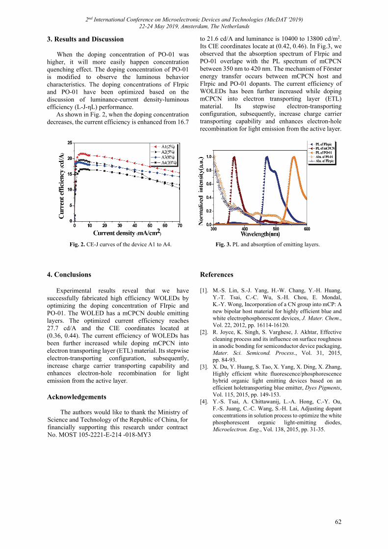
2nd International Conference on Microelectronic Devices and Technologies (MicDAT '2019) 22-24 May 2019, Amsterdam, The Netherlands
62
3. Results and Discussion
When the doping concentration of PO-01 was higher, it will more easily happen concentration quenching effect. The doping concentration of PO-01 is modified to observe the luminous behavior characteristics. The doping concentrations of FIrpic and PO-01 have been optimized based on the discussion of luminance-current density-luminous efficiency (L-J-ηL) performance.
As shown in Fig. 2, when the doping concentration decreases, the current efficiency is enhanced from 16.7
to 21.6 cd/A and luminance is 10400 to 13800 cd/m2. Its CIE coordinates locate at (0.42, 0.46). In Fig.3, we observed that the absorption spectrum of Flrpic and PO-01 overlape with the PL spectrum of mCPCN between 350 nm to 420 nm. The mechanism of Förster energy transfer occurs between mCPCN host and Flrpic and PO-01 dopants. The current efficiency of WOLEDs has been further increased while doping mCPCN into electron transporting layer (ETL) material. Its stepwise electron-transporting configuration, subsequently, increase charge carrier transporting capability and enhances electron-hole recombination for light emission from the active layer.
Fig. 2. CE-J curves of the device A1 to A4.
Fig. 3. PL and absorption of emitting layers.
4. Conclusions
Experimental results reveal that we have successfully fabricated high efficiency WOLEDs by optimizing the doping concentration of FIrpic and PO-01. The WOLED has a mCPCN double emitting layers. The optimized current efficiency reaches 27.7 cd/A and the CIE coordinates located at (0.36, 0.44). The current efficiency of WOLEDs has been further increased while doping mCPCN into electron transporting layer (ETL) material. Its stepwise electron-transporting configuration, subsequently, increase charge carrier transporting capability and enhances electron-hole recombination for light emission from the active layer.
Acknowledgements
The authors would like to thank the Ministry of Science and Technology of the Republic of China, for financially supporting this research under contract No. MOST 105-2221-E-214 -018-MY3
References [1]. M.-S. Lin, S.-J. Yang, H.-W. Chang, Y.-H. Huang,
Y.-T. Tsai, C.-C. Wu, S.-H. Chou, E. Mondal, K.-Y. Wong, Incorporation of a CN group into mCP: A new bipolar host material for highly efficient blue and white electrophosphorescent devices, J. Mater. Chem., Vol. 22, 2012, pp. 16114-16120.
[2]. R. Joyce, K. Singh, S. Varghese, J. Akhtar, Effective cleaning process and its influence on surface roughness in anodic bonding for semiconductor device packaging, Mater. Sci. Semicond. Process., Vol. 31, 2015, pp. 84-93.
[3]. X. Du, Y. Huang, S. Tao, X. Yang, X. Ding, X. Zhang, Highly efficient white fluorescence/phosphorescence hybrid organic light emitting devices based on an efficient holetransporting blue emitter, Dyes Pigments, Vol. 115, 2015, pp. 149-153.
[4]. Y.-S. Tsai, A. Chittawanij, L.-A. Hong, C.-Y. Ou, F.-S. Juang, C.-C. Wang, S.-H. Lai, Adjusting dopant concentrations in solution process to optimize the white phosphorescent organic light-emitting diodes, Microelectron. Eng., Vol. 138, 2015, pp. 31-35.

2nd International Conference on Microelectronic Devices and Technologies (MicDAT '2019) 22-24 May 2019, Amsterdam, The Netherlands
63
(031)
Temperature Investigation of Phonon-plasmon Modes in 4H-SiC Shottky Diodes for Power Electronic Devices
Artur Dobrowolski 1,2, Jakub Jagiełło 1,2, Wawrzyniec Kaszub 1, Tymoteusz Ciuk 1,
Kinga Kosciewicz 1, Pawel P. Michalowski 1, Pawel Ciepielewski 1, Andrzej Wysmołek 2, Adrianna Chamryga 1, Pawel Kaminski 1
1 Institute of Electronic Materials Technology, Wolczynska 133, Warsaw, 01-919, Poland 2 Faculty of Physics, University of Warsaw, Pasteura 5, Warsaw, 02-093, Poland
Abstract: Power devices based on Silicon Carbide semiconductors play an important role as a components for all electronic systems. Nowadays it’s recognized that at least 50 percent of the electricity is controlled by such elements via all over the world. It’s also expected that within more than ten years, percentage of the power devices converting electricity will raise up from today’s 30 to 80 %. This requires next generation of energy-efficient devices for power electronics. Keywords: SiC, power devices, raman spectroscopy, sims,
1. Introduction
In this work, we would like to present a thorough analysis of bulk charge carrier concentration in unintentionally-doped and low-doped n-type (N2) homoepitaxial SiC layers – promising candidate for Shottky diodes. The epi-layers were grown at temperatures exceeding 1600˚ and rates of 5-10 μm/h on up to 4-in 4H-SiC(0001) wafers in a R&D Aixtron VP508 reactor (ref. [1]). 2. Measurements
We would like to present conclusions mostly based results obtained by Raman spectroscopy performed using a Renishaw inVia spectrometer powered by a 532 nm Nd:YAG laser. Our results were also supported by the SIMS (Secondary Ion Mass Spectrometry) results to estimate bulk nitrogen concentration and SEM(Scanning Electron Microscopy) images (ref. [2] and [3]) to compare thickness of the epi-layers from both methods. 2.1 Raman Spectroscopy
In our measurements we were focused on energy line shifts of the longitudinal optical plasma-coupled (LOPC) A1 mode which is plasmon-phonon coupled LO mode as a function of temperature. The 11 um thick epi layers were investigated by Raman spectroscopy in a range from 4.6 K to 300 K in vacuum. Electron transition was observed in low temperatures. As a result, two independent effects were observed as a function of temperature. First was identified as a thermal expansion of crystal – which implies change of the force constant and consequently phonon energy shift was observed in recorded spectra. The second one was identified as a activation of free carriers influenced by plasmon-phonon coupling.
Fig. 1. Temperature dependence Raman spectra in range of phonon (LO) and coupled phonon-plasmon (LOPC). Line- shifts of modes depending on the temperature change is seen.
Based on the equation (1), we have determined the free carrier concentration depending on the temperature, which increases more than two times in given range of temperatures.
𝑛 1.23 10 ∗ 𝜔 964.1 , (1) where ωLOPC is LOPC mode position, 964.1 cm-1 is the theoretical position of LO phonon mode [4].
2.2. SIMS and Raman Depth Profiles
Tracing the position of LOPC mode in room temperature we have measured depth profiles changing the position of focal plane inside the sample. It provide information of free electrons

2nd International Conference on Microelectronic Devices and Technologies (MicDAT '2019) 22-24 May 2019, Amsterdam, The Netherlands
64
concentration’s gradient in layers interface (Fig. 2 b)). Knowing that epitaxial and substrate free carriers concentrations are different, we have estimated thickness of epitaxial layer. Obtained results were compared with SIMS depth profiles of measured distribution of nitrogen atoms concentration and SEM cross sections showed in background on the Fig. 2a.
Table 1. Temperature profile of free charge concentration obtained from equation (1).
3. Conclusions
Raman spectroscopy is non-destructive, quick and useful tool to determine the free-carrier concentration in temperature profile and thickness of epi layer by analyzing line-shift and shape of the Raman peaks.
References [1]. S. K. Kościewicz, W. Strupiński, D. Teklińska,
K. Mazur, A. Olszyna, Epitaxial growth on 4H-SiC on-axis, 0.5°, 1.25°, 2°, 4°, 8° off-axis substrates – defects analysis and reduction, Materials Science Forum, Vol. 679-680, 2011, pp. 95-98.
[2]. K. Kościewicz, W. Strupiński, W. Wierzchowski, K. Wieteska, A. Olszyna, Polytypism Study in SiC Epilayers Using Electron Backscatter Diffraction, Mater. Sci. Forum, Vol. 645-648, 2010, pp. 251-254.
[3]. K. Kościewicz, R. Bożek, W. Strupiński, A. Olszyna, Microscopic investigation of SiC epitaxial layers on on-axis 4H-SiC substrates using Kelvin Probe Force Microscopy, Acta Physica Polonica, A, Vol. 116, 2009, pp. 69-70.
[4]. S. Nakashima, H, Harima, Raman investigation of SiC polytypes, Physica Status Solidi, (a), Vol. 162, 1, 1997, pp. 39-64.
Fig. 2. a) SIMS sample’s profile of N atoms concentration. b) Raman depth profile of LOPC mode position (free electron concentration and layer thickness)
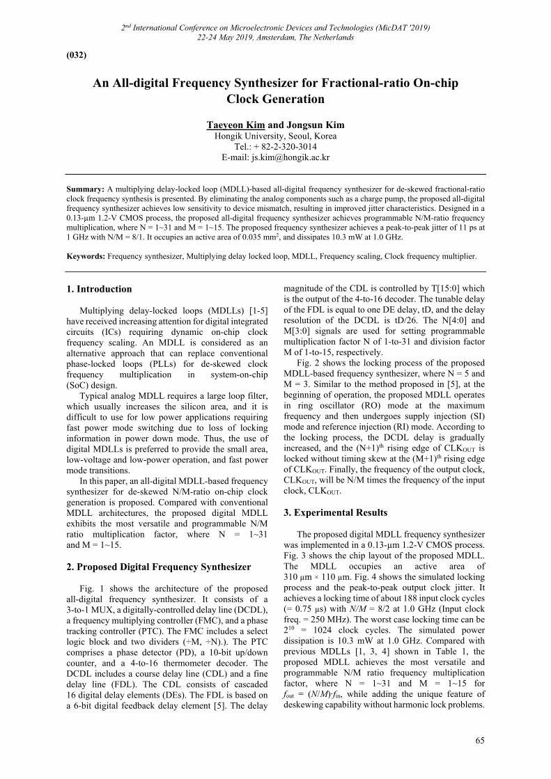
2nd International Conference on Microelectronic Devices and Technologies (MicDAT '2019) 22-24 May 2019, Amsterdam, The Netherlands
65
(032)
An All-digital Frequency Synthesizer for Fractional-ratio On-chip
Clock Generation
Taeyeon Kim and Jongsun Kim Hongik University, Seoul, Korea
Tel.: + 82-2-320-3014 E-mail: [email protected]
Summary: A multiplying delay-locked loop (MDLL)-based all-digital frequency synthesizer for de-skewed fractional-ratio clock frequency synthesis is presented. By eliminating the analog components such as a charge pump, the proposed all-digital frequency synthesizer achieves low sensitivity to device mismatch, resulting in improved jitter characteristics. Designed in a 0.13-µm 1.2-V CMOS process, the proposed all-digital frequency synthesizer achieves programmable N/M-ratio frequency multiplication, where N = 1~31 and M = 1~15. The proposed frequency synthesizer achieves a peak-to-peak jitter of 11 ps at 1 GHz with N/M = 8/1. It occupies an active area of 0.035 mm2, and dissipates 10.3 mW at 1.0 GHz. Keywords: Frequency synthesizer, Multiplying delay locked loop, MDLL, Frequency scaling, Clock frequency multiplier.
1. Introduction
Multiplying delay-locked loops (MDLLs) [1-5] have received increasing attention for digital integrated circuits (ICs) requiring dynamic on-chip clock frequency scaling. An MDLL is considered as an alternative approach that can replace conventional phase-locked loops (PLLs) for de-skewed clock frequency multiplication in system-on-chip (SoC) design.
Typical analog MDLL requires a large loop filter, which usually increases the silicon area, and it is difficult to use for low power applications requiring fast power mode switching due to loss of locking information in power down mode. Thus, the use of digital MDLLs is preferred to provide the small area, low-voltage and low-power operation, and fast power mode transitions.
In this paper, an all-digital MDLL-based frequency synthesizer for de-skewed N/M-ratio on-chip clock generation is proposed. Compared with conventional MDLL architectures, the proposed digital MDLL exhibits the most versatile and programmable N/M ratio multiplication factor, where N = 1~31 and M = 1~15. 2. Proposed Digital Frequency Synthesizer
Fig. 1 shows the architecture of the proposed all-digital frequency synthesizer. It consists of a 3-to-1 MUX, a digitally-controlled delay line (DCDL), a frequency multiplying controller (FMC), and a phase tracking controller (PTC). The FMC includes a select logic block and two dividers (÷M, ÷N).). The PTC comprises a phase detector (PD), a 10-bit up/down counter, and a 4-to-16 thermometer decoder. The DCDL includes a course delay line (CDL) and a fine delay line (FDL). The CDL consists of cascaded 16 digital delay elements (DEs). The FDL is based on a 6-bit digital feedback delay element [5]. The delay
magnitude of the CDL is controlled by T[15:0] which is the output of the 4-to-16 decoder. The tunable delay of the FDL is equal to one DE delay, tD, and the delay resolution of the DCDL is tD/26. The N[4:0] and M[3:0] signals are used for setting programmable multiplication factor N of 1-to-31 and division factor M of 1-to-15, respectively.
Fig. 2 shows the locking process of the proposed MDLL-based frequency synthesizer, where N = 5 and M = 3. Similar to the method proposed in [5], at the beginning of operation, the proposed MDLL operates in ring oscillator (RO) mode at the maximum frequency and then undergoes supply injection (SI) mode and reference injection (RI) mode. According to the locking process, the DCDL delay is gradually increased, and the (N+1)th rising edge of CLKOUT is locked without timing skew at the (M+1)th rising edge of CLKOUT. Finally, the frequency of the output clock, CLKOUT, will be N/M times the frequency of the input clock, CLKOUT.
3. Experimental Results
The proposed digital MDLL frequency synthesizer was implemented in a 0.13-µm 1.2-V CMOS process. Fig. 3 shows the chip layout of the proposed MDLL. The MDLL occupies an active area of 310 µm × 110 µm. Fig. 4 shows the simulated locking process and the peak-to-peak output clock jitter. It achieves a locking time of about 188 input clock cycles (= 0.75 µs) with N/M = 8/2 at 1.0 GHz (Input clock freq. = 250 MHz). The worst case locking time can be 210 = 1024 clock cycles. The simulated power dissipation is 10.3 mW at 1.0 GHz. Compared with previous MDLLs [1, 3, 4] shown in Table 1, the proposed MDLL achieves the most versatile and programmable N/M ratio frequency multiplication factor, where N = 1~31 and M = 1~15 for fout = (N/M)∙fin, while adding the unique feature of deskewing capability without harmonic lock problems.
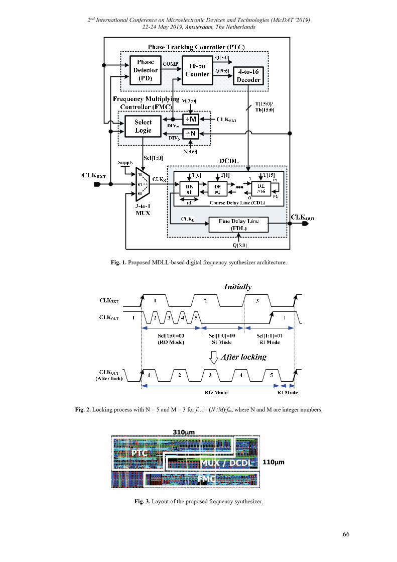
2nd International Conference on Microelectronic Devices and Technologies (MicDAT '2019) 22-24 May 2019, Amsterdam, The Netherlands
66
Fig. 1. Proposed MDLL-based digital frequency synthesizer architecture.
Fig. 2. Locking process with N = 5 and M = 3 for fout = (N /M)∙fin, where N and M are integer numbers.
Fig. 3. Layout of the proposed frequency synthesizer.
FMC
PTCMUX / DCDL 110μm
310μm
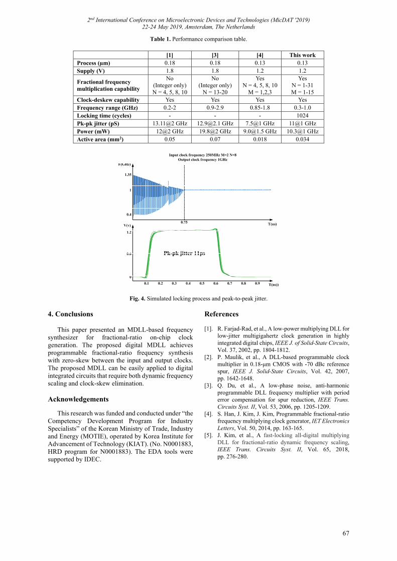
2nd International Conference on Microelectronic Devices and Technologies (MicDAT '2019) 22-24 May 2019, Amsterdam, The Netherlands
67
Table 1. Performance comparison table.
[1] [3] [4] This work Process (µm) 0.18 0.18 0.13 0.13 Supply (V) 1.8 1.8 1.2 1.2
Fractional frequency multiplication capability
No (Integer only)N = 4, 5, 8, 10
No (Integer only)
N = 13-20
Yes N = 4, 5, 8, 10
M = 1,2,3
Yes N = 1-31 M = 1-15
Clock-deskew capability Yes Yes Yes Yes Frequency range (GHz) 0.2-2 0.9-2.9 0.85-1.8 0.3-1.0 Locking time (cycles) - - - 1024 Pk-pk jitter (pS) 13.11@2 GHz [email protected] GHz 7.5@1 GHz 11@1 GHz Power (mW) 12@2 GHz 19.8@2 GHz [email protected] GHz 10.3@1 GHz Active area (mm2) 0.05 0.07 0.018 0.034
Fig. 4. Simulated locking process and peak-to-peak jitter.
4. Conclusions
This paper presented an MDLL-based frequency synthesizer for fractional-ratio on-chip clock generation. The proposed digital MDLL achieves programmable fractional-ratio frequency synthesis with zero-skew between the input and output clocks. The proposed MDLL can be easily applied to digital integrated circuits that require both dynamic frequency scaling and clock-skew elimination.
Acknowledgements
This research was funded and conducted under “the Competency Development Program for Industry Specialists” of the Korean Ministry of Trade, Industry and Energy (MOTIE), operated by Korea Institute for Advancement of Technology (KIAT). (No. N0001883, HRD program for N0001883). The EDA tools were supported by IDEC.
References [1]. R. Farjad-Rad, et al., A low-power multiplying DLL for
low-jitter multigigahertz clock generation in highly integrated digital chips, IEEE J. of Solid-State Circuits, Vol. 37, 2002, pp. 1804-1812.
[2]. P. Maulik, et al., A DLL-based programmable clock multiplier in 0.18-μm CMOS with -70 dBc reference spur, IEEE J. Solid-State Circuits, Vol. 42, 2007, pp. 1642-1648.
[3]. Q. Du, et al., A low-phase noise, anti-harmonic programmable DLL frequency multiplier with period error compensation for spur reduction, IEEE Trans. Circuits Syst. II, Vol. 53, 2006, pp. 1205-1209.
[4]. S. Han, J. Kim, J. Kim, Programmable fractional-ratio frequency multiplying clock generator, IET Electronics Letters, Vol. 50, 2014, pp. 163-165.
[5]. J. Kim, et al., A fast-locking all-digital multiplying DLL for fractional-ratio dynamic frequency scaling, IEEE Trans. Circuits Syst. II, Vol. 65, 2018, pp. 276-280.

2nd International Conference on Microelectronic Devices and Technologies (MicDAT '2019) 22-24 May 2019, Amsterdam, The Netherlands
68
(033)
Charge Transfer Within the F4TCNQ-MoS2 Van der Waals Interface
Jiawei Wang 1, N. D. Lu 1, L. Li 1 and M. Liu 1
1 Key Laboratory of Microelectronic Devices & Integrated Technology, Institute of Microelectronics, Chinese Academy of Sciences
Tel.: +86-10-82995582, fax: +86-10-82995583 E-mail: [email protected]
Summary: Charge transfer van der Waals interfaces (vdWIs) were formed between 2,3,5,6-Tetrafluoro-7,7,8, 8-tetracyanoquinodimethane (F4TCNQ) and MoS2, via which we realized the modulation of the onset voltages and optimization of subthreshold swing values in MoS2 based field effect transistors. Charge transfer process and its functionality mechanisms were further verified and investigated with first principle calculation, scanning Kelvin probe microscope (SKPM) characterization, and temperature-dependent electrical characterization.
Keywords: Van der Waals interface, Charge transfer effect, MoS2 field effect transistors, Organic molecule.
1. Introduction
In this work, we propose an strategy of organic charge transfer molecules treatment for MoS2 surface, with the formed organic-inorganic van der Waals interfaces (vdWIs), on one hand to address the incidental doping of sulphur vacancies, on the other hand to explore the novel microscopic interaction mechanisms within the organic-inorganic vdWIs, in additional with the possible functional applications. 2,3,5,6-Tetrafluoro-7,7,8,8-tetracyanoquinodimethane (F4TCNQ) with strong electron-withdrawing property is employed, whose lowest unoccupied molecular orbital (LUMO) locates at around ELUMO = -5.3 eV. Charge transfer vdWIs is formed by vacuum depositing F4TCNQ onto the surface of MoS2, at which electron transfer takes place from MoS2 layer to F4TCNQ nano-particals. With the depletion of residual electrons from sulphur vacancies, the onset voltages (Vons) of MoS2 based FETs are modulated from minus dozens volts to around zero, together with more ideal SS values. The existence of effective charge transfer and its functionality mechanisms are further verified and investigated with first principle calculation, scanning Kelvin probe microscope (SKPM) characterization, and temperature-dependent electrical characterization. 2. Results and Discussion
Optic image of one selected F4TCNQ decorated MoS2 FET is shown in Fig. 1b, together with the atomic force microscopic (AFM) image, the organic nanoparticles could be apparently identified on the surface of MoS2 flake. Fig. 1c is the schematic diagram for the anticipated charge transfer process at the vdWIs between MoS2 and F4TCNQ. Due to the ultra-low F4TCNQ’s LUMO at about ELUMO = -5.3 eV, electrons residual in MoS2’s donors or extended band states
would tend to be extracted by the oxidizing organic particles. Electric characterizations are performed on MoS2 FETs with different active layer thickness from monolayer to 5 nm. Fig. 1d shows the transfer curves of linear region at drain-source voltage Vds = 2 V, for FETs with/without F4TCNQ’s coating. FETs of bare MoS2 layer show onset voltages around Vons = -30 V, while after coating of F4TCNQ, positive shift of the transfer curves takes place, and the positions of Vons are more concentrated distributed within the range from -10 V to 0. This should be attributed to the charge transfer occurring at the vdWIs, in which process, the mobile electrons (could transport via multiple trapping and release process between the donor states and the extended band) distributed in the MoS2 layer are captured by the F4TCNQ’s particles, and become highly localized. Unlike reported methods for modulating, the formation of the vdWIs has not induce any degradation of FETs mobility, in addition, the subthreshold swings (SS) are universally improved, as shown in Fig. 1e, one selected device shows improvement in SS value from 1.9 to 0.8 V/dec.
To verify and investigate the charge transfer at the organic-inorganic vdWIs, atomic force microscope (AFM) and scanning Kelvin probe microscope (SKPM) are employed to characterize the surface of the F4TCNQ decorated MoS2. Fig. 2a shows the surface topology morphology of 5 µm × 5 µm area, uniformly distributed island-like F4TCNQ particles of hundreds nanometers could be identified. Surface potential distribution is illustrated in Fig. 2b, low potential centers could evidently be observed at the site where the F4TCNQ islands locate. Further annealing is performed to make the F4TCNQ islands larger and more accumulated, an islands cluster as high as 60 nm is selected for AFM/SKPM measurements. The topology morphology and surface potential distribution are shown in Fig. 2c and 2d. It is noted that the potential at the F4TCNQ islands region are not that uniformly low, at the edge of the island with lower height, the potential seems higher than the center. This

2nd International Conference on Microelectronic Devices and Technologies (MicDAT '2019) 22-24 May 2019, Amsterdam, The Netherlands
69
could be clearly identified via profiles extraction with cross lines shown in Fig. 2e, and the topology morphology shows wave packet-like profile. The transferred electrons in F4TCNQ particles actually
distribute in a finite range with respect to the vdWIs, which is known as the space charge region in p-n junction, as shown in schematic diagram of Fig. 2f.
Fig. 1. (a) Schematic diagram for device structure of MoS2 based FET with coated F4TCNQ nanoparticles. (b) Optic and AFM images of F4TCNQ modified MoS2 FET, the scale bars in optic and AFM images are respectively 10 um and 990 nm. (c) Energy alignment diagram at the van der Waals interface between MoS2 (blue) and F4TCNQ (red), the donor states distribute near below the MoS2’s conduction band edge. (d) Transfer curves of MoS2 based FETs with (red) and without (blue) F4TCNQ’s coating. (e) Transfer curve of one selected sample with (red) and without (blue) F4TCNQ’s coating, respectively displayed in logarithmic (symbols) and linear (lines) coordinate.
Fig. 2. Surface topological morphology (a) and potential distribution (b) in F4TCNQ decorated MoS2 FET. Surface topological morphology (c) and potential distribution (d) of annealed F4TCNQ particles, the scale bars for (a) and (b) are 1 um, the scale bars for (c) and (d) are 500 nm. (e) Cross section profiles of the positions denoted in (c) and (d), reveal the morphology (deep blue) and the potential (red) details. (f) Diagram of space charge region distributed in F4TCNQ particle.
To explore the potential applications of the organic-inorganic vdWIs, by taking advantages of the charge transfer effect, we carried out ammonia gas sensing tests with the F4TCNQ modified MoS2 FET together with bared MoS2 FET as comparison. The
sensitivity could exceed 1000 %, 2 to 3 orders larger than that of bared MoS2 based FET sensor in this work, and higher than those of any reported MoS2 based devices, as shown in Fig. 3.
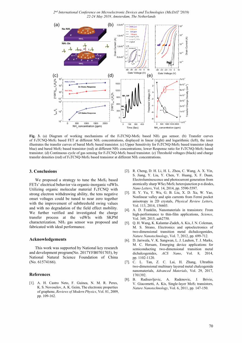
2nd International Conference on Microelectronic Devices and Technologies (MicDAT '2019) 22-24 May 2019, Amsterdam, The Netherlands
70
Fig. 3. (a) Diagram of working mechanisms of the F4TCNQ-MoS2 based NH3 gas sensor. (b) Transfer curves of F4TCNQ-MoS2 based FET at different NH3 concentrations, displayed in linear (right) and logarithmic (left), the inset illustrates the transfer curves of bared MoS2 based transistor. (c) Upper Sensitivity for F4TCNQ-MoS2 based transistor (deep blue) and bared MoS2 based transistor (red) at different NH3 concentrations; lower Response ratio for F4TCNQ-MoS2 based transistor. (d) Continuous cycle of gas sensing for F4TCNQ-MoS2 based transistor. (e) Threshold voltages (black) and charge transfer densities (red) of F4TCNQ-MoS2 based transistor at different NH3 concentrations. 3. Conclusions
We proposed a strategy to tune the MoS2 based FETs’ electrical behavior via organic-inorganic vdWIs. Utilizing organic molecular material F4TCNQ with strong electron withdrawing ability, the tens negative onset voltages could be tuned to near zero together with the improvement of subthreshold swing values and with no degradation of the field effect mobility. We further verified and investigated the charge transfer process at the vdWIs with SKPM characterization. NH3 gas sensor was proposed and fabricated with ideal performance.
Acknowledgements
This work was supported by National key research and development program(No. 2017YFB0701703), by National Natural Science Foundation of China (No. 61574166).
References [1]. A. H. Castro Neto, F. Guinea, N. M. R. Peres,
K. S. Novoselov, A. K. Geim, The electronic properties of graphene, Reviews of Modern Physics, Vol. 81, 2009, pp. 109-162.
[2]. R. Cheng, D. H. Li, H. L. Zhou, C. Wang, A. X. Yin, S. Jiang, Y. Liu, Y. Chen, Y. Huang, X. F. Duan, Electroluminescence and photocurrent generation from atomically sharp WSe2/MoS2 heterojunction p-n diodes, Nano Letters, Vol. 14, 2014, pp. 5590-5597.
[3]. H. Y. Yu, Y. Wu, G. B. Liu, X. D. Xu, W. Yao, Nonlinear valley and spin currents from Fermi pocket anisotropy in 2D crystals, Physical Review Letters, Vol. 113, 2014, 156603.
[4]. A. D. Franklin, Nanomaterials in transistors: From high-performance to thin-film applications, Science, Vol. 349, 2015, aab2750.
[5]. Q. H. Wang, K. Kalantar-Zadeh, A. Kis, J. N. Coleman, M. S. Strano, Electronics and optoelectronics of two-dimensional transition metal dichalcogenides, Nature Nanotechnology, Vol. 7, 2012, pp. 699-712.
[6]. D. Jariwala, V. K. Sangwan, L. J. Lauhon, T. J. Marks, M. C. Hersam, Emerging device applications for semiconducting two-dimensional transition metal dichalcogenides, ACS Nano, Vol. 8, 2014, pp. 1102-1120.
[7]. C. L. Tan, Z. C. Lai, H. Zhang, Ultrathin two-dimensional multinary layered metal chalcogenide nanomaterials, Advanced Materials, Vol. 29, 2017, 1701392.
[8]. B. Radisavljevic, A. Radenovic, J. Brivio, V. Giacometti, A. Kis, Single-layer MoS2 transistors, Nature Nanotechnology, Vol. 6, 2011, pp. 147-150.