Properties of HfO2/ultrathin SiO2/Si structures and their comparison with Si MOS structures...
6
Applied Surface Science 301 (2014) 34–39 Contents lists available at ScienceDirect Applied Surface Science journal h om epa ge: www.elsevier.com/locate/apsusc Properties of HfO 2 /ultrathin SiO 2 /Si structures and their comparison with Si MOS structures passivated in KCN solution Emil Pinˇ cík a,∗ , Hikaru Kobayashi b , Taketoshi Matsumoto b , Masao Takahashi b , Milan Mikula c , Róbert Brunner a a Institute of Physics SAS, Dúbravska cesta 9, 845 11 Bratislava, Slovak Republic b ISIR of Osaka University, and CREST, Japan Science and Technology Organization, 8-1 Mihogaoka, Ibaraki, Osaka 567-0047, Japan c Faculty of Chemical and Food Technology of SUT, Radlinského 9, 812 37 Bratislava, Slovak Republic a r t i c l e i n f o Article history: Received 29 October 2013 Received in revised form 17 January 2014 Accepted 18 January 2014 Available online 27 January 2014 Keywords: Monoclinic HfO2 phase Passivation KCN Interface defect states FTIR DLTS a b s t r a c t Electrical, optical and partly structural properties are investigated on very thin ALD HfO 2 /ultrathin NAOS SiO 2 /n-type Si structures. An ALD layer was deposited at 250 ◦ C and it contains amorphous and crystalline–probably monoclinic HfO 2 phases. HfO 2 films with both types of structural phases were not stable if thermal treatment above 200 ◦ C was applied. On as- prepared samples, deep interface traps with activation energy of W = 0.23 eV have been determined. After annealing of the structure at 200 ◦ C, the traps were partly transformed and a mid-gap level W = 0.49 eV was detected. FTIR and AFM measure- ments confirmed presence of HfO 2 monoclinic phase in the HfO 2 films. On the other side, the density of interface defect states of the structure decreased from approx. 10 12 eV −1 cm −2 to 10 11 eV −1 cm −2 after low temperature annealing of the reference structure. The results are compared with very similar (almost identical) development of interface defect states on the very thin thermal SiO 2 /Si structure before and after passivation in a 0.1 M KCN methanol solution.PACS: 78.55.Qr; 78.66.Jg; 81.16.Pr; 85.40Ls © 2014 The Authors. Published by Elsevier B.V. All rights reserved. 1. Introduction Many contributions have been devoted to investigation of HfO 2 /SiO 2 /Si structures because high-k materials offer unique pos- sibilities in the field of Si-based device miniaturization. Barret et al. [1] analyzed thermal stability of such structures. Tan et al. [2] published comparative study of interfacial characteristics of sputter-deposited hafnium dioxide (HfO 2 ) on native SiO 2 /Si. The same author, Tan et al., published a paper [3] about prepara- tion of high-quality ultrathin HfO 2 films and about comparison of HfO 2 /SiO 2 /Si structures. We are using term “ultrathin layer” for film of thickness less than 2.5 nm. Term “very thin” is used for thick- ness of films between 2.5 and 10 nm. Term “thin” layer is used for thickness above 10 nm. Taube analyzed fabrication and characterization HfO 2 films [4]. More authors devote their attention to structures HfO 2 /SiO 2 /SiC, e.g., in [5–9]. Alles et al. [10] published formation of monoclinic HfO 2 films by two step process where the initial growth of about 1 nm at 170 ◦ C was continued up to 10–30 nm at 300 ◦ C. This pro- This is an open-access article distributed under the terms of the Creative Com- mons Attribution-NonCommercial-No Derivative Works License, which permits non-commercial use, distribution, and reproduction in any medium, provided the original author and source are credited. ∗ Corresponding author. Tel.: +421 259410548; fax: +421 254776085. E-mail address: [email protected] (E. Pinˇ cík). cess formed uniform, monoclinic HfO 2 films with RMS roughness of 1.7 nm for 10–12 nm thick films. An 11 nm thick HfO 2 film deposited onto bilayer substrate (graphene) reduced the electron mobility by less than 10% at the Dirac point and by 30–40% far away from it. Monoclinic HfO 2 films were investigated by Raman spectroscopy in more laboratories. Alles et al. [10], Lixin Liu et al. [11] presented one of dominant peak in Raman spectra related to monoclinic HfO 2 at 496 cm −1 . This peak is assigned to the A g strongest vibration mode of monoclinic HfO 2 [12]. Formation of a SiO 2 interlayer and its properties have important role in successful formation of HfO 2 /SiO 2 /Si structures suitable for device fabrication. Japanese scientists–ISIR of Osaka University–developed during years 1998–2013 technology of formation of high-density ultrathin SiO 2 layers by wet chemical oxidation in an HNO 3 solution of high concentrations, see e.g., [13–20]. The used abbreviation of this pro- cess is NAOS–nitric acid oxidation of semiconductors. Kim et al. [21] published formation of ultrathin SiO 2 layer with low leakage cur- rent density with ∼100% nitric acid vapor. The vapor generated by boiling of HNO 3 solution was introduced into quartz glass tube and oxidation was performed at 100–200 ◦ C. In the paper is presented also corresponding phase diagram of the nitric acid and water sys- tem for concentration of HNO 3 from 0 to 100%. Si oxidation in HNO 3 vapor proceeds by following reactions: 2HNO 3 → NO 2 + NO + H 2 O + 2O Si + 2O → SiO 2 0169-4332/$ – see front matter © 2014 The Authors. Published by Elsevier B.V. All rights reserved. http://dx.doi.org/10.1016/j.apsusc.2014.01.113
Transcript of Properties of HfO2/ultrathin SiO2/Si structures and their comparison with Si MOS structures...
Pw
EMa
b
c
a
ARRAA
KMPKIFD
1
Hse[sstHont
MeH1
mno
0h
Applied Surface Science 301 (2014) 34–39
Contents lists available at ScienceDirect
Applied Surface Science
journa l h om epa ge: www.elsev ier .com/ locate /apsusc
roperties of HfO2/ultrathin SiO2/Si structures and their comparisonith Si MOS structures passivated in KCN solution�
mil Pincíka,∗, Hikaru Kobayashib, Taketoshi Matsumotob, Masao Takahashib,ilan Mikulac, Róbert Brunnera
Institute of Physics SAS, Dúbravska cesta 9, 845 11 Bratislava, Slovak RepublicISIR of Osaka University, and CREST, Japan Science and Technology Organization, 8-1 Mihogaoka, Ibaraki, Osaka 567-0047, JapanFaculty of Chemical and Food Technology of SUT, Radlinského 9, 812 37 Bratislava, Slovak Republic
r t i c l e i n f o
rticle history:eceived 29 October 2013eceived in revised form 17 January 2014ccepted 18 January 2014vailable online 27 January 2014
a b s t r a c t
Electrical, optical and partly structural properties are investigated on very thin ALD HfO2/ultrathinNAOS SiO2/n-type Si structures. An ALD layer was deposited at 250 ◦C and it contains amorphous andcrystalline–probably monoclinic HfO2 phases. HfO2 films with both types of structural phases were notstable if thermal treatment above 200 ◦C was applied. On as- prepared samples, deep interface traps withactivation energy of �W = 0.23 eV have been determined. After annealing of the structure at 200 ◦C, thetraps were partly transformed and a mid-gap level �W = 0.49 eV was detected. FTIR and AFM measure-
eywords:onoclinic HfO2 phase
assivationCN
nterface defect states
ments confirmed presence of HfO2 monoclinic phase in the HfO2 films. On the other side, the densityof interface defect states of the structure decreased from approx. 1012 eV−1 cm−2 to 1011 eV−1 cm−2 afterlow temperature annealing of the reference structure. The results are compared with very similar (almostidentical) development of interface defect states on the very thin thermal SiO2/Si structure before and
M KC
TIRLTSafter passivation in a 0.1
. Introduction
Many contributions have been devoted to investigation offO2/SiO2/Si structures because high-k materials offer unique pos-
ibilities in the field of Si-based device miniaturization. Barrett al. [1] analyzed thermal stability of such structures. Tan et al.2] published comparative study of interfacial characteristics ofputter-deposited hafnium dioxide (HfO2) on native SiO2/Si. Theame author, Tan et al., published a paper [3] about prepara-ion of high-quality ultrathin HfO2 films and about comparison offO2/SiO2/Si structures. We are using term “ultrathin layer” for filmf thickness less than 2.5 nm. Term “very thin” is used for thick-ess of films between 2.5 and 10 nm. Term “thin” layer is used forhickness above 10 nm.
Taube analyzed fabrication and characterization HfO2 films [4].ore authors devote their attention to structures HfO2/SiO2/SiC,
.g., in [5–9]. Alles et al. [10] published formation of monoclinicfO2 films by two step process where the initial growth of about
nm at 170 ◦C was continued up to 10–30 nm at 300 ◦C. This pro-
� This is an open-access article distributed under the terms of the Creative Com-ons Attribution-NonCommercial-No Derivative Works License, which permits
on-commercial use, distribution, and reproduction in any medium, provided theriginal author and source are credited.∗ Corresponding author. Tel.: +421 259410548; fax: +421 254776085.
E-mail address: [email protected] (E. Pincík).
169-4332/$ – see front matter © 2014 The Authors. Published by Elsevier B.V. All rights
ttp://dx.doi.org/10.1016/j.apsusc.2014.01.113
N methanol solution.PACS: 78.55.Qr; 78.66.Jg; 81.16.Pr; 85.40Ls© 2014 The Authors. Published by Elsevier B.V. All rights reserved.
cess formed uniform, monoclinic HfO2 films with RMS roughnessof 1.7 nm for 10–12 nm thick films. An 11 nm thick HfO2 filmdeposited onto bilayer substrate (graphene) reduced the electronmobility by less than 10% at the Dirac point and by 30–40% faraway from it. Monoclinic HfO2 films were investigated by Ramanspectroscopy in more laboratories. Alles et al. [10], Lixin Liu et al.[11] presented one of dominant peak in Raman spectra relatedto monoclinic HfO2 at 496 cm−1. This peak is assigned to the Ag
strongest vibration mode of monoclinic HfO2 [12]. Formation of aSiO2 interlayer and its properties have important role in successfulformation of HfO2/SiO2/Si structures suitable for device fabrication.Japanese scientists–ISIR of Osaka University–developed duringyears 1998–2013 technology of formation of high-density ultrathinSiO2 layers by wet chemical oxidation in an HNO3 solution of highconcentrations, see e.g., [13–20]. The used abbreviation of this pro-cess is NAOS–nitric acid oxidation of semiconductors. Kim et al. [21]published formation of ultrathin SiO2 layer with low leakage cur-rent density with ∼100% nitric acid vapor. The vapor generated byboiling of HNO3 solution was introduced into quartz glass tube andoxidation was performed at 100–200 ◦C. In the paper is presentedalso corresponding phase diagram of the nitric acid and water sys-tem for concentration of HNO3 from 0 to 100%. Si oxidation in HNO3
vapor proceeds by following reactions:2HNO3 → NO2 + NO + H2O + 2O
Si + 2O → SiO2
reserved.
E. Pincík et al. / Applied Surface S
Table 1List of prepared samples.
Name Mode of NAOS Temperature of Sisample at ALD
Thermalannealing
Sample No. 1 100% HNO3 vapor 250 ◦C As preparedSample No. 2 100% HNO3 vapor 250 ◦C 200 ◦C 10 minSample No. 3 100% HNO3 vapor 250 ◦C 300 ◦C 10 minSample No. 4 100% HNO3 vapor 250 ◦C 400 ◦C 10 min
Sample No. 1: as prepared HfO2/SiO2/Si; Sample No. 2: HfO2/SiO2/Si annealed in N2
at 200 ◦C, 10 min.Also samples annealed at 300 ◦C (Sample No. 3) and 400 ◦C (Sample No. 4) in N2
for 10 min were prepared and results will be partly presented and discussed in thep
rcwSt5s
tBtifp
didt
2
2
lhHci
cKwwfs
2s
weS8s∼
aper.
Diffusion of oxidizing species–mainly oxygen atoms–is theate-determining step. When the SiO2 layer is formed with highoncentration HNO3, its atomic density is higher than that formedith less concentrated HNO3. Authors are stating that ultrathin
iO2/Si structures have low interface state density, especially afterhe post-metalization annealing at 250 ◦C in inert atmosphere with
vol% of hydrogen and also the low concentration of suboxidepecies.
The research works of Slovakian laboratories from above men-ioned field of NAOS samples have been published in e.g., [23–25].ury et al. [26] published results obtained on HfO2/SiO2/Si struc-ures with similar composition and technology as it is presentedn this work. The present authors used acoustic version of DLTSor measurements and determination of corresponding electricalarameters.
The dominant aim of this work is to present application of high-ensity ultrathin NAOS SiO2 prepared in 100% HNO3 vapor as an
nterlayer between the Si substrate and the high-k HfO2 overlayereposited by the ALD and to discuss advantages and/or disadvan-ages of such structure.
. Experiment–preparation of samples
.1. Preparation of HfO2/SiO2/Si structures
A very thin HfO2 layer of 5 nm thickness was prepared by atomicayer deposition (ALD) from TDMAH: tetrakis(dimethylamino)afnium - Hf[N(CH3)2]4 in oxidant water steam at 250 ◦C. The ALDfO2 layer used in presented experiments contains amorphous andrystalline–probably monoclinic phases. This fact will be confirmedn the next parts.
A SiO2 interlayer of thickness approx. 0.6 nm between HfO2 and-Si was formed in 100% HNO3 vapor by technology described inim et al. [21]. The metal-oxide-semiconductor (MOS) structureas fabricated from P-doped n-type Si(1 0 0) wafers. The Si wafersere cleaned using Radio Corporation of America (RCA) method
ollowed by etching with dilute hydrofluoric acid. List of preparedamples is presented in Table 1.
.2. Preparation and KCN passivation of thermal very thin SiO2/Sitructures
Results obtained on the set of samples described in the Table
ill be compared with corresponding results presented in Pincikt al. [25]. Structure of samples is very thin thermal SiO2/n-i(100). We will compare results with as prepared samples (at00 ◦C) and with passivated in boiling 0.1 M solution of potas-ium cyanide (KCN) in methanol for 2 min. SiO2 thickness is7.4 nm.
cience 301 (2014) 34–39 35
3. Experimental methods
For investigation of electrical properties of prepared structuresin the form of metal-oxide-semiconductor (MOS), the followingmethods were used: charge version of deep level transient spec-troscopy (Q-DLTS), measurements of capacitance vs. voltage in timedomain (C–V), Fourier transform infrared spectroscopy (FTIR), IRreflectance, and atomic force microscopy (AFM).
3.1. Charge version of deep level transient spectroscopy (Q-DLTS)
The modified charge-based correlation DLTS method was usedto study prepared MOS structures. The equipment with corre-sponding software has been developed in Institute of Physics SAS,Bratislava, Slovakia [22] and commercial type does not exist. There-fore, it is needed briefly to describe it. This method is based on thecorrelation approach, i.e., the transient response of the MOS struc-ture under periodically applied voltage steps to the gate electrode ismeasured, and subsequently a weighted combination of the chargesignals obtained at various sampling events is achieved. The samp-ling events, as well as the weighting coefficients used in our work,are chosen with the aim to improve the selectivity in the measuredspectra. The resulting correlated charge DLTS signal is describedby a weighted summation of the contributions from three chan-nels. The parasitic output charge due to the presence of a leakagecurrent is eliminated by the used filtering scheme.
The following formula is valid for the measured Q-DLTS signalcoming from a deep trap:
�Q ≈[
Cox
Cox + Cs
]q × w × NT × exp(−ent), (1)
where w stands for the excited part of the depletion region, en isthe emission rate of the traps, NT for the trap density, Cox and Cs
for the capacitance of the oxide and that of the space charge layer,respectively. The emission rate from the trap is written as:
en = v × �n × Nc × exp(
−�E
kT
), (2)
where � is the mean thermal velocity of electrons, �n is the capturecross section and Nc is the effective density of states in the conduc-tion band. The DLTS response of the above mentioned structure wasmeasured at sampling events chosen to fit the following scheme:t1, 2t1 and 4t1. Sometimes, two sampling times, t1 and t2, are used,only at which t2 = 2 × t1. The resulting correlated charge DLTS signalSc is given by following equation:
Sc = Q (t1) − 1.5Q (2t1) + 0.5Q (4t1). (3)
3.2. Capacitance–voltage measurements (C–V)
Capacitance of the MOS diodes as a function of the gate bias wasmeasured by the improved feedback charge measurements in thetime domain. The feedback charge C–V method was described forthe first time by Mego [27] and commercial Keithley stand-aloneinstrument is available. Originally, the latter has been intendedfor measurements of the steady-state (dc) time-domain capaci-tance of semiconductor devices. Bias step �u0 is applied to theunknown capacitance C of the investigated structure and conse-quently the change (time dependent) of output voltage �u of the
integrator is registered. The capacitance C is given by the rela-tion C = CF(�u/�u0), where CF = 3.3 nF and �u0 = 60 mV are usedin our experiments. The sampling time was set to 10 m s. CQ–Vmeasurements and Q-DLTS were carried out using the home-madespectrometer developed at the Institute of Physics of SAS Bratislava,Slovakia [22].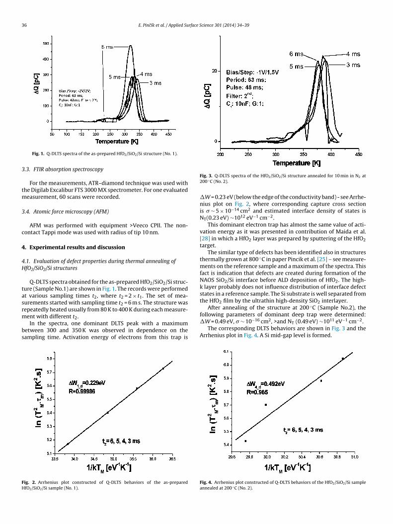
36 E. Pincík et al. / Applied Surface Science 301 (2014) 34–39
3
tm
3
c
4
4H
tasrm
bs
FH
following parameters of dominant deep trap were determined:
Fig. 1. Q-DLTS spectra of the as-prepared HfO2/SiO2/Si structure (No. 1).
.3. FTIR absorption spectroscopy
For the measurements, ATR–diamond technique was used withhe Digilab Excalibur FTS 3000 MX spectrometer. For one evaluated
easurement, 60 scans were recorded.
.4. Atomic force microscopy (AFM)
AFM was performed with equipment >Veeco CPII. The non-ontact Tappi mode was used with radius of tip 10 nm.
. Experimental results and discussion
.1. Evaluation of defect properties during thermal annealing offO2/SiO2/Si structures
Q-DLTS spectra obtained for the as-prepared HfO2/SiO2/Si struc-ure (Sample No.1) are shown in Fig. 1. The records were performedt various sampling times t2, where t2 = 2 × t1. The set of mea-urements started with sampling time t2 = 6 m s. The structure wasepeatedly heated usually from 80 K to 400 K during each measure-
ent with different t2.In the spectra, one dominant DLTS peak with a maximumetween 300 and 350 K was observed in dependence on theampling time. Activation energy of electrons from this trap is
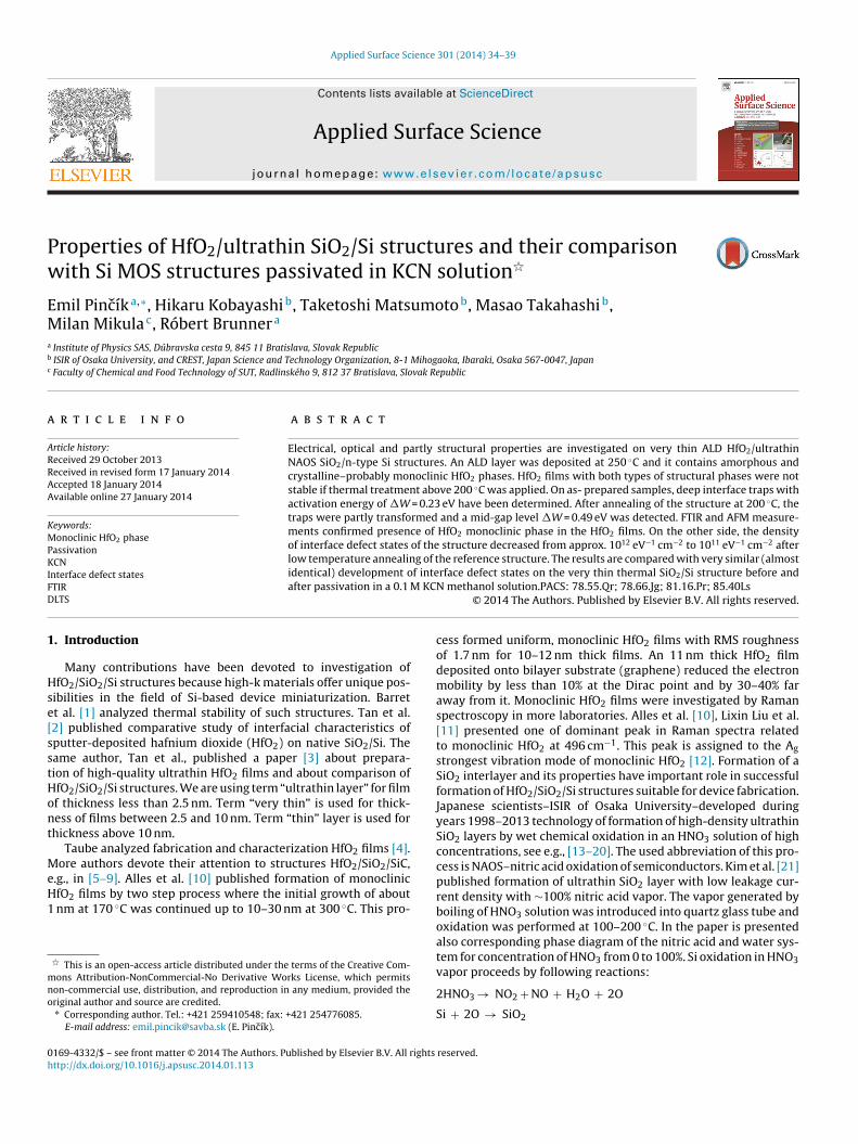
ig. 2. Arrhenius plot constructed of Q-DLTS behaviors of the as-preparedfO2/SiO2/Si sample (No. 1).
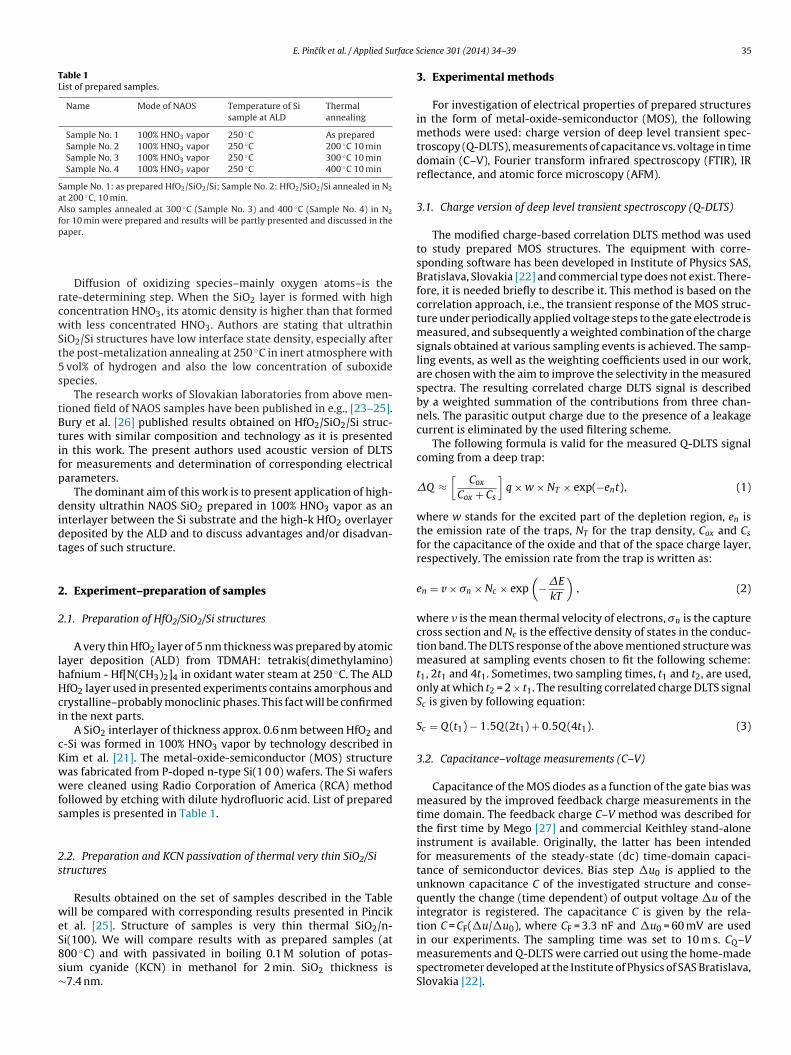
Fig. 3. Q-DLTS spectra of the HfO2/SiO2/Si structure annealed for 10 min in N2 at200 ◦C (No. 2).
�W = 0.23 eV (below the edge of the conductivity band) - see Arrhe-nius plot on Fig. 2, where corresponding capture cross sectionis � ∼ 5 × 10⁻¹⁴ cm2 and estimated interface density of states isNT(0.23 eV) ∼1012 eV−1 cm−2.
This dominant electron trap has almost the same value of acti-vation energy as it was presented in contribution of Maida et al.[28] in which a HfO2 layer was prepared by sputtering of the HfO2target.
The similar type of defects has been identified also in structuresthermally grown at 800 ◦C in paper Pincik et al. [25] – see measure-ments on the reference sample and a maximum of the spectra. Thisfact is indication that defects are created during formation of theNAOS SiO2/Si interface before ALD deposition of HfO2. The high-k layer probably does not influence distribution of interface defectstates in a reference sample. The Si substrate is well separated fromthe HfO2 film by the ultrathin high-density SiO2 interlayer.
After annealing of the structure at 200 ◦C (Sample No.2), the
�W = 0.49 eV, � ∼ 10−16 cm2, >and NT (0.49 eV) ∼1011 eV−1 cm−2.The corresponding DLTS behaviors are shown in Fig. 3 and the
Arrhenius plot in Fig. 4. A Si mid-gap level is formed.
Fig. 4. Arrhenius plot constructed of Q-DLTS behaviors of the HfO2/SiO2/Si sampleannealed at 200 ◦C (No. 2).

E. Pincík et al. / Applied Surface Science 301 (2014) 34–39 37
Fsw
4
aswK(wc
Hcias
pva
piccHHp
Fig. 7. C–V curve of the HfO2/SiO2/Si structure annealed at 200 ◦C (No. 2).
ig. 5. Q-DLTS spectra of the thermal SiO2/Si structure passivated in 0.1 M KCNolution. Inset shows Arrhenius plot prepared of behaviors of A peak. Peak B is relatedith formation of inversion layer.
.2. Comparison with defect passivation by KCN solution
This type of defects is very similar to those formed after passiv-tion of thermal SiO2/Si structure in boiling a 0.1 M KCN methanololution – see again contribution Pincik et al. [25] in which defectsith the same activation energy �W = 0.49 were formed. Ions in theCN methanol solution passivated a part of original defect states
Ec −0.23 eV) observed on the reference sample. The rest of themere transformed to defect states Ec −0.49 eV – see Fig. 5 with inset
ontaining corresponding Arrhenius plot.In this case, the role of the boiling KCN methanol solution has
fO2 film heated to 200 ◦C in forming gas. Hf atoms or Hf atomicomplexes diffuse through the ultrathin SiO2 interlayer to the Sinterface region. We cannot exclude also the fact that formation ofn inversion layer could start at about 400 K and this signal wasuperimposed in the measured Q-DLTS spectra (Fig. 3).
Contribution of the rest of deep traps observed for the as-repared sample with the activation energy of �W = 0.23 eV isisible in the temperature region 300 K–350 K as the signal with
considerably reduced amplitude (Fig. 3).The estimated density of interface defect states of the sam-
le annealed at 200 ◦C decreased to NT (0.49 eV) ∼1011 eV−1 cm−2,n comparison with as-prepared one, but the accumulationapacitance of the annealed sample also decreased–i.e., the opti-
al thickness of the investigated bi-layer and correspondingfO2/SiO2/Si interface increased most probably due to diffusion off atoms and/or Hf atomic complexes – see C–V curves on the asrepared Structure No. 1 (Fig. 6) and on Sample No. 2 after annealingFig. 6. C–V curve of the as-prepared HfO2/SiO2/Si structure (No. 1).
Fig. 8. AFM of the surface of the as-prepared HfO2/SiO2/Si structure (No. 1).
at 200 ◦C (Fig. 7). In both cases on the C–V curves there is a visi-ble starting process of formation of an inversion layer at negativevoltages.
An AFM image taken for the as-prepared Sample No. 1 – seeFig. 8 - illustrates a surface of the as-prepared HfO2 layer withRMS roughness between 0.20–0.25 nm. A crystalline–probablymonoclinic–HfO2 phase is visible inside of HfO2 amorphous matrix.
Annealing of the structure at 200 ◦C, 300 ◦C and 400 ◦C decreasesRMS roughness–for sample annealed at 400 ◦C, RMS roughnessdecreased to interval 0.16–0.19 nm – see Fig. 9.
4.3. Investigation of crystalline–probably monoclinic–phase inHfO2 films
For confirmation of the presence of monoclinic HfO2 phase
inside of the ALD layer, we have used FTIR spectroscopy – see Fig. 10and Fig. 11. In both figures, FTIR spectra of set of samples (a) No.1(as-prepared), (b) No.2 (annealed at 200 ◦C), (c) No.3 (annealed at300 ◦C) and (d) No.4 (annealed at 400 ◦C) are shown. The IR recordsFig. 9. AFM of the surface of the HfO2/SiO2/Si structure annealed in N2 for 10 minat 400 ◦C (No. 4).
38 E. Pincík et al. / Applied Surface Science 301 (2014) 34–39
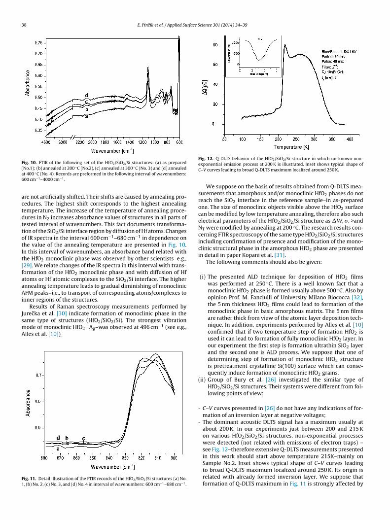
Fig. 10. FTIR of the following set of the HfO2/SiO2/Si structures: (a) as prepared( ◦ ◦
a6
actdttotIt[faaAi
JsmA
F1
No.1); (b) annealed at 200 C (No.2), (c) annealed at 300 C (No. 3) and (d) annealedt 400 ◦C (No. 4). Records are preformed in the following interval of wavenumbers:00 cm−1–4000 cm−1.
re not artificially shifted. Their shifts are caused by annealing pro-edures. The highest shift corresponds to the highest annealingemperature. The increase of the temperature of annealing proce-ures in N2 increases absorbance values of structures in all parts ofested interval of wavenumbers. This fact documents transforma-ion of the SiO2/Si interface region by diffusion of Hf atoms. Changesf IR spectra in the interval 600 cm−1–680 cm−1 in dependence onhe value of the annealing temperature are presented in Fig. 10.n this interval of wavenumbers, an absorbance band related withhe HfO2 monoclinic phase was observed by other scientists–e.g.,29]. We relate changes of the IR spectra in this interval with trans-ormation of the HfO2 monoclinic phase and with diffusion of Hftoms or Hf atomic complexes to the SiO2/Si interface. The highernnealing temperature leads to gradual diminishing of monoclinicFM peaks–i.e., to transport of corresponding atoms/complexes to
nner regions of the structures.Results of Raman spectroscopy measurements performed by
urecka et al. [30] indicate formation of monoclinic phase in the
ame type of structures (HfO2/SiO2/Si). The strongest vibrationode of monoclinic HfO2 Ag–was observed at 496 cm−1 (see e.g.,lles et al. [10]).ig. 11. Detail illustration of the FTIR records of the HfO2/SiO2/Si structures (a) No., (b) No. 2, (c) No. 3, and (d) No. 4 in interval of wavenumbers: 600 cm−1–680 cm−1.
Fig. 12. Q-DLTS behavior of the HfO2/SiO2/Si structure in which un-known non-exponential emission process at 200 K is illustrated. Inset shows typical shape ofC–V curves leading to broad Q-DLTS maximum localized around 250 K.
We suppose on the basis of results obtained from Q-DLTS mea-surements that amorphous and/or monoclinic HfO2 phases do notreach the SiO2 interface in the reference sample–in as-preparedone. The size of monoclinic objects visible above the HfO2 surfacecan be modified by low temperature annealing, therefore also suchelectrical parameters of the HfO2/SiO2/Si structure as �W, �, >andNT were modified by annealing at 200 ◦C. The research results con-cerning FTIR spectroscopy of the same type HfO2/SiO2/Si structuresincluding confirmation of presence and modification of the mono-clinic structural phase in the amorphous HfO2 phase are presentedin detail in paper Kopani et al. [31].
The following comments should also be given:
(i) The presented ALD technique for deposition of HfO2 filmswas performed at 250 ◦C. There is a well known fact that amonoclinic HfO2 phase is formed usually above 500 ◦C. Also byopinion Prof. M. Fanciulli of University Milano Biococca [32],the 5 nm thickness HfO2 films could lead to formation of themonoclinic phase in basic amorphous matrix. The 5 nm filmsare rather thick from view of the atomic layer deposition tech-nique. In addition, experiments performed by Alles et al. [10]confirmed that if two temperature step of formation HfO2 isused it can lead to formation of fully monoclinic HfO2 layer. Inour experiment the first step is formation ultrathin SiO2 layerand the second one is ALD process. We suppose that one ofdetermining step of formation of monoclinic HfO2 structureis pretreatment crystalline Si(100) surface which can conse-quently induce formation of monoclinic HfO2 grains.
(ii) Group of Bury et al. [26] investigated the similar type ofHfO2/SiO2/Si structures. Their systems were different from fol-lowing points of view:
- C–V curves presented in [26] do not have any indications of for-mation of an inversion layer at negative voltages;
- The dominant acoustic DLTS signal has a maximum usually atabout 200 K. In our experiments just between 200 and 215 Kon various HfO2/SiO2/Si structures, non-exponential processeswere detected (not related with emissions of electron traps) –see Fig. 12–therefore extensive Q-DLTS measurements presentedin this work should start above temperature 215K–mainly on
Sample No.2. Inset shows typical shape of C–V curves leadingto broad Q-DLTS maximum localized around 250 K. Its origin isrelated with already formed inversion layer. We suppose thatformation of Q-DLTS maximum in Fig. 11 is strongly affected by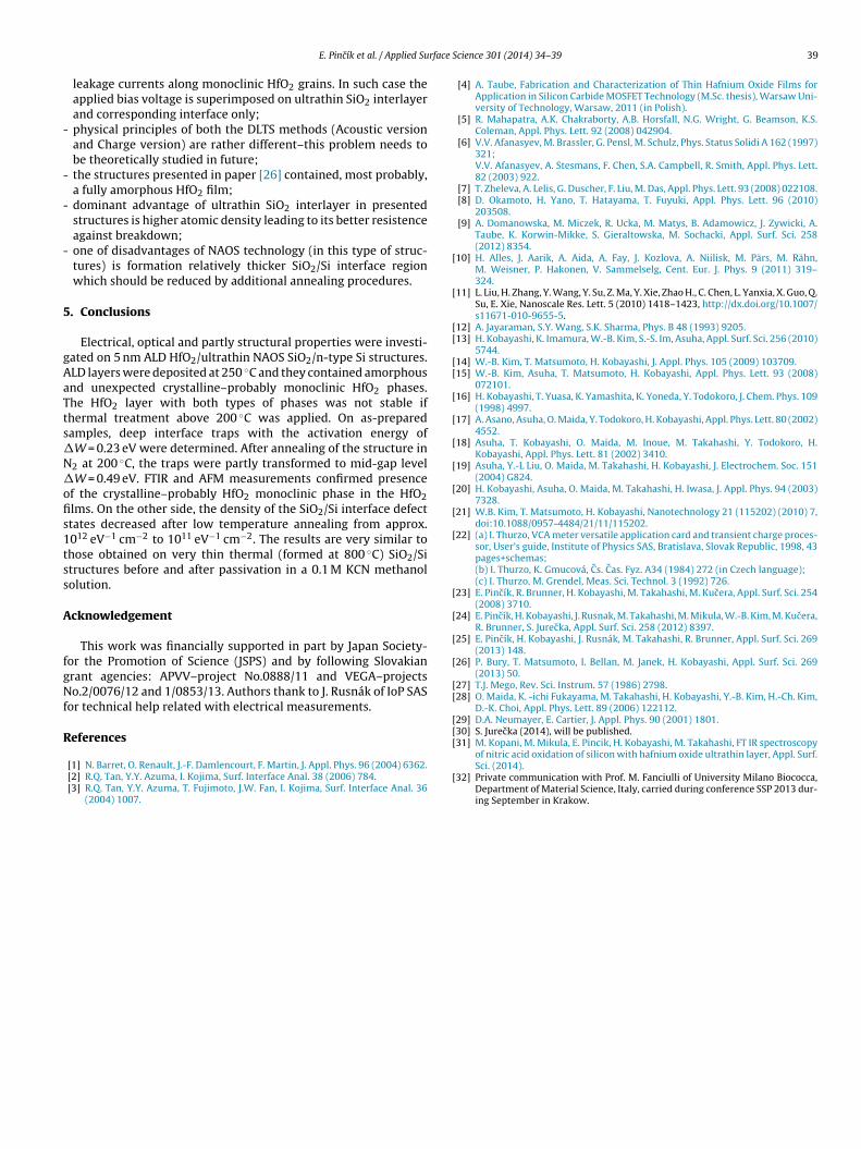
rface S
-
-
-
-
5
gAaTts�N�ofis1tss
A
fgNf
R
[
[
[[
[[
[
[
[
[
[
[
[
[
[
[
[
[[
[[[
E. Pincík et al. / Applied Su
leakage currents along monoclinic HfO2 grains. In such case theapplied bias voltage is superimposed on ultrathin SiO2 interlayerand corresponding interface only;
physical principles of both the DLTS methods (Acoustic versionand Charge version) are rather different–this problem needs tobe theoretically studied in future;
the structures presented in paper [26] contained, most probably,a fully amorphous HfO2 film;
dominant advantage of ultrathin SiO2 interlayer in presentedstructures is higher atomic density leading to its better resistenceagainst breakdown;
one of disadvantages of NAOS technology (in this type of struc-tures) is formation relatively thicker SiO2/Si interface regionwhich should be reduced by additional annealing procedures.
. Conclusions
Electrical, optical and partly structural properties were investi-ated on 5 nm ALD HfO2/ultrathin NAOS SiO2/n-type Si structures.LD layers were deposited at 250 ◦C and they contained amorphousnd unexpected crystalline–probably monoclinic HfO2 phases.he HfO2 layer with both types of phases was not stable ifhermal treatment above 200 ◦C was applied. On as-preparedamples, deep interface traps with the activation energy ofW = 0.23 eV were determined. After annealing of the structure in2 at 200 ◦C, the traps were partly transformed to mid-gap levelW = 0.49 eV. FTIR and AFM measurements confirmed presence
f the crystalline–probably HfO2 monoclinic phase in the HfO2lms. On the other side, the density of the SiO2/Si interface defecttates decreased after low temperature annealing from approx.012 eV−1 cm−2 to 1011 eV−1 cm−2. The results are very similar tohose obtained on very thin thermal (formed at 800 ◦C) SiO2/Sitructures before and after passivation in a 0.1 M KCN methanololution.
cknowledgement
This work was financially supported in part by Japan Society-or the Promotion of Science (JSPS) and by following Slovakianrant agencies: APVV–project No.0888/11 and VEGA–projectso.2/0076/12 and 1/0853/13. Authors thank to J. Rusnák of IoP SAS
or technical help related with electrical measurements.
eferences
[1] N. Barret, O. Renault, J.-F. Damlencourt, F. Martin, J. Appl. Phys. 96 (2004) 6362.[2] R.Q. Tan, Y.Y. Azuma, I. Kojima, Surf. Interface Anal. 38 (2006) 784.[3] R.Q. Tan, Y.Y. Azuma, T. Fujimoto, J.W. Fan, I. Kojima, Surf. Interface Anal. 36
(2004) 1007.
[
cience 301 (2014) 34–39 39
[4] A. Taube, Fabrication and Characterization of Thin Hafnium Oxide Films forApplication in Silicon Carbide MOSFET Technology (M.Sc. thesis), Warsaw Uni-versity of Technology, Warsaw, 2011 (in Polish).
[5] R. Mahapatra, A.K. Chakraborty, A.B. Horsfall, N.G. Wright, G. Beamson, K.S.Coleman, Appl. Phys. Lett. 92 (2008) 042904.
[6] V.V. Afanasyev, M. Brassler, G. Pensl, M. Schulz, Phys. Status Solidi A 162 (1997)321;V.V. Afanasyev, A. Stesmans, F. Chen, S.A. Campbell, R. Smith, Appl. Phys. Lett.82 (2003) 922.
[7] T. Zheleva, A. Lelis, G. Duscher, F. Liu, M. Das, Appl. Phys. Lett. 93 (2008) 022108.[8] D. Okamoto, H. Yano, T. Hatayama, T. Fuyuki, Appl. Phys. Lett. 96 (2010)
203508.[9] A. Domanowska, M. Miczek, R. Ucka, M. Matys, B. Adamowicz, J. Zywicki, A.
Taube, K. Korwin-Mikke, S. Gieraltowska, M. Sochacki, Appl. Surf. Sci. 258(2012) 8354.
10] H. Alles, J. Aarik, A. Aida, A. Fay, J. Kozlova, A. Niilisk, M. Pärs, M. Rähn,M. Weisner, P. Hakonen, V. Sammelselg, Cent. Eur. J. Phys. 9 (2011) 319–324.
11] L. Liu, H. Zhang, Y. Wang, Y. Su, Z. Ma, Y. Xie, Zhao H., C. Chen, L. Yanxia, X. Guo, Q.Su, E. Xie, Nanoscale Res. Lett. 5 (2010) 1418–1423, http://dx.doi.org/10.1007/s11671-010-9655-5.
12] A. Jayaraman, S.Y. Wang, S.K. Sharma, Phys. B 48 (1993) 9205.13] H. Kobayashi, K. Imamura, W.-B. Kim, S.-S. Im, Asuha, Appl. Surf. Sci. 256 (2010)
5744.14] W.-B. Kim, T. Matsumoto, H. Kobayashi, J. Appl. Phys. 105 (2009) 103709.15] W.-B. Kim, Asuha, T. Matsumoto, H. Kobayashi, Appl. Phys. Lett. 93 (2008)
072101.16] H. Kobayashi, T. Yuasa, K. Yamashita, K. Yoneda, Y. Todokoro, J. Chem. Phys. 109
(1998) 4997.17] A. Asano, Asuha, O. Maida, Y. Todokoro, H. Kobayashi, Appl. Phys. Lett. 80 (2002)
4552.18] Asuha, T. Kobayashi, O. Maida, M. Inoue, M. Takahashi, Y. Todokoro, H.
Kobayashi, Appl. Phys. Lett. 81 (2002) 3410.19] Asuha, Y.-L Liu, O. Maida, M. Takahashi, H. Kobayashi, J. Electrochem. Soc. 151
(2004) G824.20] H. Kobayashi, Asuha, O. Maida, M. Takahashi, H. Iwasa, J. Appl. Phys. 94 (2003)
7328.21] W.B. Kim, T. Matsumoto, H. Kobayashi, Nanotechnology 21 (115202) (2010) 7,
doi:10.1088/0957-4484/21/11/115202.22] (a) I. Thurzo, VCA meter versatile application card and transient charge proces-
sor, User’s guide, Institute of Physics SAS, Bratislava, Slovak Republic, 1998, 43pages+schemas;(b) I. Thurzo, K. Gmucová, Cs. Cas. Fyz. A34 (1984) 272 (in Czech language);(c) I. Thurzo, M. Grendel, Meas. Sci. Technol. 3 (1992) 726.
23] E. Pincík, R. Brunner, H. Kobayashi, M. Takahashi, M. Kucera, Appl. Surf. Sci. 254(2008) 3710.
24] E. Pincík, H. Kobayashi, J. Rusnak, M. Takahashi, M. Mikula, W.-B. Kim, M. Kucera,R. Brunner, S. Jurecka, Appl. Surf. Sci. 258 (2012) 8397.
25] E. Pincík, H. Kobayashi, J. Rusnák, M. Takahashi, R. Brunner, Appl. Surf. Sci. 269(2013) 148.
26] P. Bury, T. Matsumoto, I. Bellan, M. Janek, H. Kobayashi, Appl. Surf. Sci. 269(2013) 50.
27] T.J. Mego, Rev. Sci. Instrum. 57 (1986) 2798.28] O. Maida, K. -ichi Fukayama, M. Takahashi, H. Kobayashi, Y.-B. Kim, H.-Ch. Kim,
D.-K. Choi, Appl. Phys. Lett. 89 (2006) 122112.29] D.A. Neumayer, E. Cartier, J. Appl. Phys. 90 (2001) 1801.30] S. Jurecka (2014), will be published.31] M. Kopani, M. Mikula, E. Pincik, H. Kobayashi, M. Takahashi, FT IR spectroscopy
of nitric acid oxidation of silicon with hafnium oxide ultrathin layer, Appl. Surf.Sci. (2014).
32] Private communication with Prof. M. Fanciulli of University Milano Biococca,Department of Material Science, Italy, carried during conference SSP 2013 dur-ing September in Krakow.


![Structure and strain relaxation mechanisms of ultrathin epitaxial Pr[sub 2]O[sub 3] films on Si(111)](https://static.fdokumen.com/doc/165x107/633f80a8f43ed5a83d02c492/structure-and-strain-relaxation-mechanisms-of-ultrathin-epitaxial-prsub-2osub.jpg)