Prevention of radiation-induced damages by aqueous extract of Ganoderma lucidum occurring in...
12
AN-758 APPLICATION NOTE One Technology Way • P.O. Box 9106 • Norwood, MA 02062-9106 • Tel: 781/329-4700 • Fax: 781/461-3113 • www.analog.com INTRODUCTION This application note describes how to create a pulse output based on reactive energy readings from the ADE7753.The ADE7753 is an energy metering IC complete with rms, active, apparent, and reactive measurement capabilities. The quantities measured in the ADE7753 are read out through an SPI serial to parallel interface. For this example, the reactive energy pulse output application was implemented on a PIC16F877 microcontroller from Microchip. ® OVERVIEW Definition of Reactive Energy Reactive power is defined by the IEEE Standard Diction- ary 100-1996 as: Reactive Power V I n n n n =∑ × × ( ) = ∞ 1 sin ϕ where V n and I n are the voltage and current rms values of the nth harmonics of the line frequency and n is the phase difference between the voltage and the current nth harmonics. Reactive energy is the accumulation of reac- tive power over time. It should be positive for an inductive load, where the current is leading the voltage. Calculating Reactive Energy There are two main ways of calculating reactive power—indirectly, using the power triangle or directly, using a low-pass filter. Figure 1 shows the relationship between the active, reactive, and apparent energies that is assumed in the power triangle approach: REACTIVE POWER APPARENT POWER ACTIVE POWER Figure 1. Power Triangle Creating a Reactive Energy Pulse Output Based on the ADE7753 by Meghan Baker Reactive Energy Apparent Energy Active Energy = 2 2 – This relationship holds up well at the fundamental frequency but significant error is introduced when harmonics are present. In one type of direct reactive energy calculation, a con- stant 90° phase shift over frequency with an attenuation of 20 dB/decade is introduced. The cutoff frequency of the low-pass filter is set much lower than the funda- mental frequency such that there is a 90° phase shift at any frequency higher than the fundamental. These frequencies are attenuated by 20 dB/decade. This solu- tion is susceptible to variations in line frequency, which can be overcome by compensating the gain based on the line period. This is the method used by the ADE7753 to calculate reactive energy. The ADE7753 also has a period register that may be used by the microcontroller for gain compensation based on the line period. Pulse Output in the ADE7753 The ADE7753 provides a pulse output proportional to active energy. This pulse output is ideal for use in calibrating the active energy functionality against a reference meter. For this calibration, a steady load is applied to the energy meter being calibrated and to the reference meter. The pulse output from the meter under calibration is compared to that from the reference meter. Gain and offset compensations are performed by adjusting active energy gain and offset registers, CFDEN, WGAIN, and APOS, until the pulse output from the meter under test matches the reference meter both at the base current, Ib, and a lower test current, Imin. Figure 2 shows the ADE7753 signal chain used to calculate and calibrate the active energy register, AENERGY and the CF pulse output. REV. 0
-
Upload
independent -
Category
Documents
-
view
3 -
download
0
Transcript of Prevention of radiation-induced damages by aqueous extract of Ganoderma lucidum occurring in...
AN-758APPLICATION NOTE
One Technology Way • P.O. Box 9106 • Norwood, MA 02062-9106 • Tel: 781/329-4700 • Fax: 781/461-3113 • www.analog.com
INTRODUCTIONThis application note describes how to create a pulse output based on reactive energy readings from the ADE7753. The ADE7753 is an energy metering IC complete with rms, active, apparent, and reactive measurement capabilities. The quantities measured in the ADE7753 are read out through an SPI serial to parallel interface. For this example, the reactive energy pulse output application was implemented on a PIC16F877 microcontroller from Microchip.®
OVERVIEWDefinition of Reactive EnergyReactive power is defined by the IEEE Standard Diction-ary 100-1996 as:
Reactive Power V Inn
n n= ∑ × × ( )=
∞
1sin ϕ
where Vn and In are the voltage and current rms values of the nth harmonics of the line frequency and n is the phase difference between the voltage and the current nth harmonics. Reactive energy is the accumulation of reac-tive power over time. It should be positive for an inductive load, where the current is leading the voltage.
Calculating Reactive EnergyThere are two main ways of calculating reactive power—indirectly, using the power triangle or directly, using a low-pass filter.
Figure 1 shows the relationship between the active, reactive, and apparent energies that is assumed in the power triangle approach:
REACTIVEPOWER
APPARENTPOWER
ACTIVEPOWER
Figure 1. Power Triangle
Creating a Reactive Energy Pulse Output Based on the ADE7753by Meghan Baker
Reactive Energy Apparent Energy Active Energy= 2 2–
This relationship holds up well at the fundamental frequency but significant error is introduced when harmonics are present.
In one type of direct reactive energy calculation, a con-stant 90° phase shift over frequency with an attenuation of 20 dB/decade is introduced. The cutoff frequency of the low-pass filter is set much lower than the funda-mental frequency such that there is a 90° phase shift at any frequency higher than the fundamental. These frequencies are attenuated by 20 dB/decade. This solu-tion is susceptible to variations in line frequency, which can be overcome by compensating the gain based on the line period. This is the method used by the ADE7753 to calculate reactive energy. The ADE7753 also has a period register that may be used by the microcontroller for gain compensation based on the line period.
Pulse Output in the ADE7753The ADE7753 provides a pulse output proportional to active energy. This pulse output is ideal for use in calibrating the active energy functionality against a reference meter. For this calibration, a steady load is applied to the energy meter being calibrated and to the reference meter. The pulse output from the meter under calibration is compared to that from the reference meter. Gain and offset compensations are performed by adjusting active energy gain and offset registers, CFDEN, WGAIN, and APOS, until the pulse output from the meter under test matches the reference meter both at the base current, Ib, and a lower test current, Imin. Figure 2 shows the ADE7753 signal chain used to calculate and calibrate the active energy register, AENERGY and the CF pulse output.
REV. 0

–2–
AN-758
–3–
AN-758
Every time an LSB is accumulated in the active energy register, AENERGY, a pulse is generated at the digital to frequency converter. Once (CFNUM+1)/(CFDEN+1) pulses have been generated by the digital to frequency converter, a CF pulse is issued on Pin 11. Figure 3 dem-onstrates how the digital to frequency converter outputs pulses based on the accumulated active energy.
��������������
��������������
�
�������
��
�
�
�����
����������
�����
�������
���
Figure 3. CF Pulse Output Diagram
The ADE7753 does not provide gain or offset correction registers for reactive energy. A reactive energy pulse output simplifies calibration of this portion of the meter and must be produced external to the ADE7753.
DESIGN GOALSThe ADE7753 provides reactive energy readings but does not have a pulse output dedicated to reactive energy. The goal for this design is to produce a reactive energy pulse output derived from the measured reactive energy in the ADE7753.
The reactive energy pulse output should have the same scaling as the active energy pulse output so that at a power factor of 0, the reactive pulse output has the same frequency as the active energy pulse output at a power factor of 1. As the active energy pulse output is typically calibrated to 3200 imp/kWh, the reactive energy pulse output in this example is also calibrated to 3200 imp/kVARh.
The reactive energy pulse output should be accurate to ±2.5% from 0.05Ib ≤ I < 0.1Ib and ±2% from 0.1Ib ≤ I < Imax, as required by the IEC62053-23 specification for Class 2 reactive energy meters. A ±2% frequency variation should induce less than an additional 2.5% error.
DESIGN ARCHITECTURE The ADE7753 provides reactive energy readings every half line cycle. The frequency of the reactive energy read-ings is based on the number of half line cycles included in the accumulation. This number is set by the LINECYC register in the ADE7753. To place the ADE7753 in line cycle accumulation mode:
1. Set the number of half line cycles for the accumulation in the LINECYC register, address 0x1C
2. Enable line cycle accumulation mode by setting the CYCMODE bit in the MODE register, address 0x09.
3. Set the CYCEN bit in the IRQ enable register, IRQEN (address 0x0A), so that the IRQ line will go low when line cycle accumulation readings are available.
4. Reset the status register by reading the RSTSTATUS register, address 0x0C.
����������
�����������
���������
������������������
��������������
����������
���� ����
������
�
������ �����������
� �������� ������
�������������������������������������������� ����� ����������������������������
����������������������������������������������������
�� �
�� �
����������������������
�
�����������
��
�� �
������������� �
����
Figure 2. Active Energy AENERGY Register Signal Chain
REV. 0 REV. 0
–2–
AN-758
–3–
AN-758
5. Wait for the IRQ interrupt to go low and read the RSTSTATUS register (address 0x0C). The first line cycle accumulation energy readings after writing to the LINECYC register must be discarded because the accumulation time for this reading may not cor-respond to the new value in the LINECYC register.
6. Reset the status register by reading the RSTSTATUS register, address 0x0C.
7. Wait for the IRQ interrupt to go low and read the RSTSTATUS register, address 0x0C.
8. Read the LVARENERGY register, address 0x08.
9. Repeat steps 7 through 8 as desired.
Note that the line cycle accumulation readings available after the first line cycle accumulation interrupt may not be correct . It takes one line cycle accumulation period to lock on to a new value in the LINECYC register.
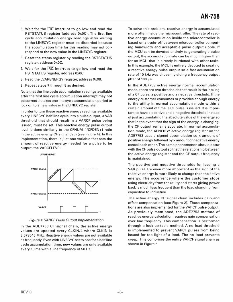
In order to turn these reactive energy readings available every LINECYC half line cycle into a pulse output, a VAR threshold that should result in a VARCF pulse being issued, must be set. This reactive energy pulse output level is done similarly to the CFNUM+1/CFDEN+1 ratio in the active energy CF signal path (see Figure 4). In this implementation, there is just one variable that sets the amount of reactive energy needed for a pulse to be output, the VARCFLEVEL.
�
����������
�����
�
�����
��������
����������
�����������
�����
�������
�
Figure 4. VARCF Pulse Output Implementation
In the ADE7753 CF signal chain, the active energy values are updated every CLKIN/4 where CLKIN is 3.579545 MHz. Reactive energy values are not available as frequently. Even with LINECYC set to one for a half line cycle accumulation time, new values are only available every 10 ms with a line frequency of 50 Hz.
To solve this problem, reactive energy is accumulated more often inside the microcontroller. The rate of reac-tive energy accumulation inside the microcontroller is based on a trade-off between microcontroller comput-ing bandwidth and acceptable pulse output ripple. If the MCU can be devoted entirely to generating a pulse output, the accumulation rate can be much higher than for an MCU that is already burdened with other tasks. In this example, the MCU is entirely devoted to creating a reactive energy pulse output so a fast accumulation rate of 10 kHz was chosen, yielding a frequency output jitter of 100 s.
In the ADE7753 active energy normal accumulation mode, there are two thresholds that result in the issuing of a CF pulse, a positive and a negative threshold. If the energy customer consumes or provides enough energy to the utility in normal accumulation mode within a certain amount of time, a CF pulse is issued. It is impor-tant to have a positive and a negative threshold instead of just accumulating the absolute value of the energy so that in the event that the sign of the energy is changing, the CF output remains accurate. In normal accumula-tion mode, the AENERGY active energy register on the ADE7753 uses a signed accumulation so x amount of positive energy followed by x amount of negative energy cancel each other. The same phenomenon should occur with the CF pulse output so that the relationship between the active energy register and the CF output frequency is maintained.
The positive and negative thresholds for issuing a VAR pulse are even more important as the sign of the reactive energy is more likely to change than the active energy. The occurrence where the customer stops using electricity from the utility and starts giving power back is much less frequent than the load changing from capacitive to inductive.
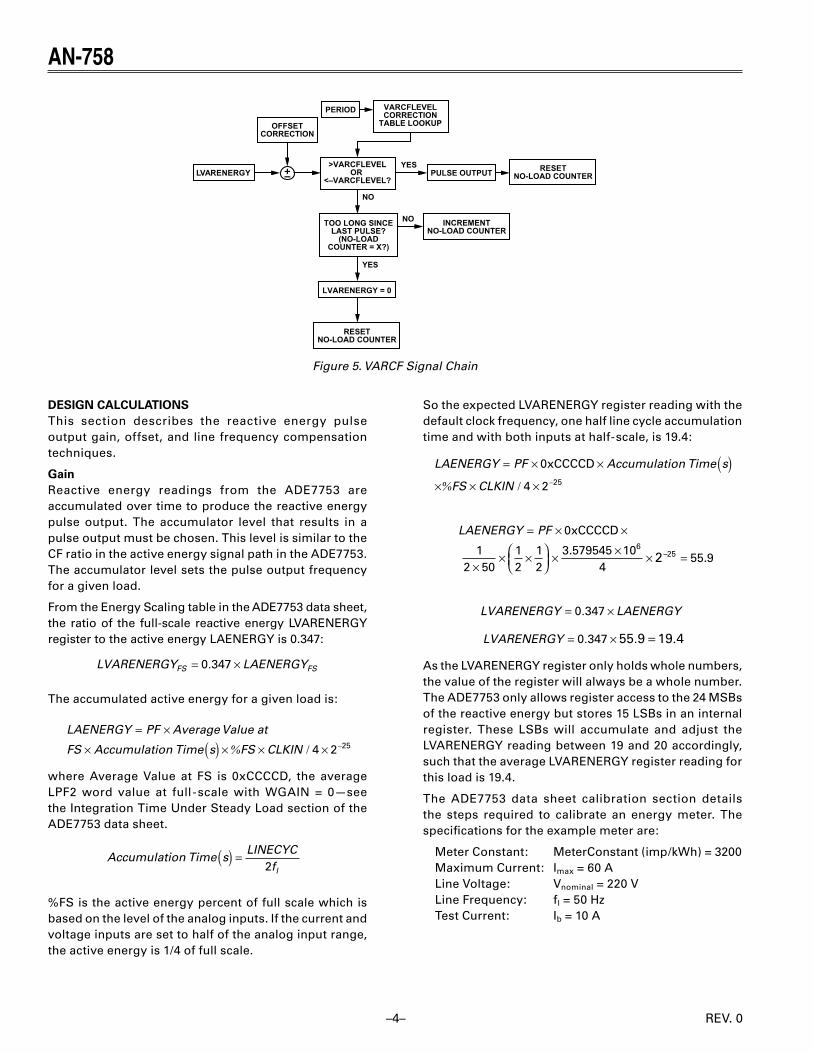
The active energy CF signal chain includes gain and offset compensation (see Figure 2). These compensa-tions are also implemented for the VARCF pulse output. As previously mentioned, the ADE7753 method of reactive energy calculation requires gain compensation over line frequency. This compensation is performed through a look up table method. A no-load threshold is implemented to prevent VARCF pulses from being issued for too light of a load. The no-load prevents creep. This comprises the entire VARCF signal chain as shown in Figure 5.
REV. 0 REV. 0
–4–
AN-758
–5–
AN-758
��������������������
����� ������
�������������
������������������ ������
����������������
���������� � �
���
��
����� ���� ��������� ������
��������������� � ���
����������
������
���������������� �������
������������ �������
������������ �������
���
Figure 5. VARCF Signal Chain
DESIGN CALCULATIONSThis section describes the reactive energy pulse output gain, offset, and line frequency compensation techniques.
GainReactive energy readings from the ADE7753 are accumulated over time to produce the reactive energy pulse output. The accumulator level that results in a pulse output must be chosen. This level is similar to the CF ratio in the active energy signal path in the ADE7753. The accumulator level sets the pulse output frequency for a given load.
From the Energy Scaling table in the ADE7753 data sheet, the ratio of the full-scale reactive energy LVARENERGY register to the active energy LAENERGY is 0.347:
LVARENERGY LAENERGYFS FS= ×0 347.
The accumulated active energy for a given load is:
LAENERGY PF Average Value at
FS Accumulation Time s FS CLKIN
= ×
× ( ) × × ×% / –4 2 25
where Average Value at FS is 0xCCCCD, the average LPF2 word value at full-scale with WGAIN = 0—see the Integration Time Under Steady Load section of the ADE7753 data sheet.
Accumulation Time sLINECYC
fl( ) =
2
%FS is the active energy percent of full scale which is based on the level of the analog inputs. If the current and voltage inputs are set to half of the analog input range, the active energy is 1/4 of full scale.
So the expected LVARENERGY register reading with the default clock frequency, one half line cycle accumulation time and with both inputs at half-scale, is 19.4:
LAENERGY PF Accumulation Time s
FS CLKIN
= × × ( )× × ×
0
4 2 25
xCCCCD
% / –
LAENERGY PF
..–
= × ×
×× ×
× × × =
0
12 50
12
12
3 579545 104
55 96
252
xCCCCD
LVARENERGY LAENERGY= ×0 347.
LVARENERGY = × =0 347 55 9 19 4. . .
As the LVARENERGY register only holds whole numbers, the value of the register will always be a whole number. The ADE7753 only allows register access to the 24 MSBs of the reactive energy but stores 15 LSBs in an internal register. These LSBs will accumulate and adjust the LVARENERGY reading between 19 and 20 accordingly, such that the average LVARENERGY register reading for this load is 19.4.
The ADE7753 data sheet calibration section details the steps required to calibrate an energy meter. The specifications for the example meter are:
Meter Constant: MeterConstant (imp/kWh) = 3200 Maximum Current: Imax = 60 A Line Voltage: Vnominal = 220 V Line Frequency: fl = 50 Hz Test Current: Ib = 10 A
REV. 0 REV. 0

–4–
AN-758
–5–
AN-758
In this example Imax and Vnominal scale to half of their respective analog input ranges. So for this meter, the maximum CF output with the current equal to Imax and the line voltage equal to Vnominal is:
CFMeter Constant Load
=( ) × ( )
× ( )imp kWh kW
s h
/
/cos
3600ϕ
CFmax = × × × ( ) =3200 60 220 10003600
0 11 73A V
s hHz
//
cos .
Since we would like to be able to compare our VAR pulse output to the CF pulse output, the expected reactive energy pulse output at a power factor of 0 is fixed to be the same as our expected active energy pulse output at a power factor of 1.
With the microcontroller accumulation rate set to 100 s, the accumulator level that results in a pulse being issued, the VARCFLEVEL, is set to 0x3FA9 (16297 decimal):
VARCFLEVELLVARENERGY
VARCF MCU Accumulation Time s=
×[ : ]24 0
( ) (1)
VARCFLEVEL =× ×
= =19 4
12 100 1016297 0 3 9
6
.–
d x FA
OffsetThe LVARENERGY register offset is determined by setting the power factor to 1. At a power factor of 1, no reactive energy should be measured. The VARCFOFFSET can then be calculated from the frequency output.
Rearranging Equation (1) yields
LVARENERGY VARCFLEVEL VARCF
MCU Accumulation Time s
= × ×( )
In this implementation, three bytes are used to set the offset: one is for sign of the offset, the second is for any whole offset, and the third is for fractional offset. The fractional offset is stored as an unsigned integer in the microcontroller with the decimal point fixed before the MSB such that:
VARCFOFFSET LVARENERGY= ×[ : ]24 0 28
The offset compensation is shown in Figure 6.
�� ����������
���������� ������������������������
��������
����� ������ ���������� ������
Figure 6. Reactive Energy Offset Compensation
Without looking at the actual sign of the LVARENERGY register, as opposed to the calculated value, it is impos-sible to tell whether the offset is positive or negative since the pulse output implementation should produce the same frequency for negative and positive VAR loads. So if the VARCF resulting from offset in the LVARENERGY register is 100 mHz, then a guess is made at the sign of the offset and OFFSETSIGN is set to positive. The whole offset, OFFSETWHOLE should be set to zero and the fractional offset, OFFSETFRAC should be set to 0x2A (42 decimal):
LVARENERGY VARCFLEVEL VARCF
MCU Accumulation Time s
= × ×( )
LVARENERGY = × × × =0 3 9 0 1 100 10 0 162976x FA . .–
where
VARCFLEVEL = 0 3 9x FA
VARCF = 100 mHz, the pulse output frequency due to the offset, at a power factor of 1
CAccumulationTime(s) = 100 s, the time between microcontroller accumulations.
OFFSETSIGN SIGN LVARENERGY= ( )
OFFSETSIGN 0=
OFFSETWHOLE INT LVARENERGY= ( )
OFFSETWHOLE 0=
OFFSETFRAC LVARENERGY= × 28
OFFSETFRAC = × = =0 16297 2 42 0 28. x A
REV. 0 REV. 0

–6–
AN-758
–7–
AN-758
The OFFSETSIGN flag is used to indicate whether the offset is positive or negative. The fractional offset is accumulated every microcontroller accumulation cycle and every time it overflows, a bit is added or subtracted from the running reactive energy total based on the offset sign flag. A sign bit is needed to know whether to look for a rollover from 0x00 to 0xFF or from 0xFF to 0x00. These transitions are reflected in the carry bit in the status register. Storing the whole part of the offset in a separate register makes it easy to correct for any whole offset every microcontroller accumulation cycle.
No-Load ThresholdThe reactive energy no-load threshold in the IEC62053-23 standard for a Class 2 meter is 0.5%Ib. This corresponds to 0.0209% of the full-scale reactive energy reading of the ADE7753. The ADE7753 has a more stringent active energy no-load threshold of 0.001% of the full-scale multiplier output. In this example, Imax and Vnominal are both set to half scale so the ADE7753 active energy no-load threshold is 0.4692 mHz:
CF No Load Threshold
FSno-load 1 max1CF= × × 1
%
VARCF . .
. ..no-load1
= × ××
=0 00001 11 731
0 5 0 50 4692Hz mHz
In this example, the reactive energy no-load threshold is implemented by counting the number of half line cycle periods that have passed since the last pulse. A no-load threshold of 0.4692 mHz, or 2131.29 seconds without a pulse, corresponds to 0x034089 (213,129 decimal) half line cycles at 50 Hz. So if 213,129 half line cycles have passed since the last pulse, then the accumulated LVARENERGY is cleared and the half line cycle count resumes from zero.
In this implementation, the reactive energy no-load threshold is set according to the IEC62053-23 speci-fication, using the same concept as the active energy no-load threshold. This reduces the resolution required in the offset register and makes it so that only two bytes are required for counting half line cycles for the no-load threshold instead of the three that would be required for the stricter no-load threshold.
CF No Load Threshold
FSno-load 2 max2CF= × × 1
%
VARCF . .
. ..no-load2
= × ××
=0 000209 11 731
0 5 0 59 795Hz mHz
Line Frequency Gain CompensationThis algorithm for producing a reactive pulse output requires an additional gain correction of the LVARENERGY readings over line frequency. To account for a variable line cycle frequency, two 1/f compensations need to be performed on the LVARENERGY readings, one to properly scale the readings based on their accumulation times and another to account for the 1/f attenuation of the reactive energy readings in the ADE7753.
The calculations for the pulse output assume that the gain of the LVARENERGY register is constant. However, the gain of the LVARENERGY register varies with line frequency. For example, at a line frequency of 52.5 Hz, less energy will be accumulated within a half line cycle than at 50 Hz since the accumulation time is shorter. Without gain compensation the pulse output for 52.5 Hz would be slower than for 50 Hz with the same load applied because the 52.5 Hz LVARENERGY readings would be lower. So a 1/f correction factor is required to properly weight the LVARENERGY readings across different accumulation times.
A low-pass filter is implemented on the current channel for calculating the reactive energy. This filter introduces an additional 1/f attenuation in the reactive energy readings.
Typically the line frequency can vary ±5% so the gain of the reactive energy register needs to be compensated to accurately represent the reactive energy during these fluctuations.
The ADE7753 PERIOD register can be used to determine the line frequency:
Line Period(s) PERIODCLKIN
= × 8
The amount of reactive energy that must be accumu-lated to output a pulse, the VARCFLEVEL, is adjusted according to this PERIOD reading. In this implementa-tion a lookup table is used for the corrections so that these calculations do not have to be done in the microcontroller.
REV. 0 REV. 0

–6–
AN-758
–7–
AN-758
Table I. VARCFLEVEL Line Frequency Correction Table
PERIOD (Decimal)Corrected VARCFLevel
Table Index
8512 0x3974 0
8544 0x39E2 1
8576 0x3A52 2
8608 0x3AC1 3
8640 0x3B31 4
8672 0x3BA2 5
8704 0x3C13 6
8736 0x3C84 7
8768 0x3CF6 8
8800 0x3D68 9
8832 0x3DDA 10
8864 0x3E4D 11
8896 0x3EC1 12
8928 0x3F34 13
8960 0x3FA9 14
8992 0x401D 15
9024 0x4092 16
9056 0x4108 17
9088 0x417D 18
9120 0x41F4 19
9152 0x426A 20
9184 0x42E2 21
9216 0x4359 22
9248 0x43D1 23
9280 0x4449 24
9312 0x44C2 25
9344 0x453B 26
9376 0x45B5 27
9408 0x462F 28
Since the line frequency can vary ±5%, the correction table must accommodate the nominal PERIOD register reading ±5%. The nominal PERIOD register reading at 50 Hz is about 8960 decimal. Therefore PERIOD readings from 8512 to 9408 must be corrected.
It would be easy to use the PERIOD register readings to directly index into a correction table, but at 896 entries, this table would be too big. To index a smaller correc-tion table using the PERIOD register readings there needs to be a formula to calculate the index into the correction table array from the PERIOD register value. If possible, a multiplication should be avoided as with this microcontroller it will take about 200 instruction cycles to perform a 16 by 16 multiplication. The incentive for using a lookup table is to reduce the time it takes to get the proper result. So there needs to be a fast way to index this table.
In a microcontroller it is easy to divide by 2n by right shifting the operand. Since 896 entries are evenly divis-ible by 25, or 32, this is an efficient way of indexing the correction table. The table has 896/32 + 1 = 29 entries, resulting in a worst case 0.4% error. With more resolution and therefore more entries in the table, the percent error would be reduced. The index into the correction table is the (PERIOD – PERIODnominal)/32 + 14. The entries for the table are calculated by multiplying the nominal VARCFLEVEL by (PERIOD/PERIODnominal)2 so that when the line frequency is higher than nominal, the VARCFLEVEL is lowered to accommodate the lower LVARENERGY register readings.
For example, if the PERIOD is 9408 and the nominal PERIOD is 8960, the array index should be 28:
INDEX PERIOD PERIODnominal= −( ) +/ 32 14
INDEX = ( ) + =9408 8960 32 14 28– /
The lookup table entry for a PERIOD of 9408 with a nominal PERIOD of 8960 and a nominal VARCFLEVEL of 0x3FA9 is calculated to be:
Lookup Table Value VARCFLEVELPERIOD
PERIODnominalnominal
= ×
2
Lookup Table Value = ×
= =0 3 994088960
17967 44 0 4622
x FA x F.
Firmware ArchitectureThe flowchart for the firmware implementation used to create the VARCF pulse output is shown in Figure 7.
REV. 0 REV. 0

–8–
AN-758
–9–
AN-758
������� ��������� ������������� ����������� ���������� ��� �������
��� ��� ���������� ���� ������� �����
���� ��� ������ ��������
���� ��� ������� �������� �� ����� ��� ���
���� ���������� �������� ������� ��� ��� ����
������ ����� �����
���� ���
���� ���
���������� ���������� ��� �������
���� ��� ����������
��� �� � ����� �� ��������� ����� �����
������ �������� ��������� ����� �� ����
����� ��� ������������ ���������
����� ������� �� ���������� ���� ��� ���� ������������ ��� ��� �� �� ��� ���� ��� ���� ����� ������������ ��� ������
���������� ��������� ��������
���
��
���
����� ���� ��� ����
���� ��������
��� ���� ���� ����� ��� ���� �� ������
���� ���
���� �����
Figure 7. Microcontroller Flow Chart
REV. 0 REV. 0

–8–
AN-758
–9–
AN-758
RESULTSLinearity
�������
�������
������
��
������
���� ��� � �� ���������� ���
��
��
��
������� �����
Figure 8. VARCF Linearity
The VARCF linearity error shown in Figure 8 is within the IEC 62053-23 Reactive Energy Class 2 specification for current variation. The specification requires:
Less than ± 2.5% error from 0.05Ib ≤ I < 0.1Ib
Less than ±2% error from 0.1Ib ≤ I < Imax.
This meter was calibrated with an Ib of 10 A and an Imax of 60 A. Thus there must be less than ±2.5% error from 0.5 A to 1 A. There must be less than ±2% error from 1 A to 60 A.
Performance with Line Frequency Variation
�������
�������
��
������
������
�� �� �� �� �� �� ������ ��������� ����
��
��
��
������� �����
Figure 9. VARCF Performance with Line Frequency variation
Figure 9 shows the performance of the VARCF pulse output over line frequency. The gain of the VAR read-ings must be compensated over line frequency because the digital to frequency converter accumulates at a constant frequency and assumes a fixed period for its input. An additional gain compensation is performed for the ADE7753 to account for the gain attenuation of the LPF used to calculate reactive energy. A look-up table is used to perform the gain compensation, so the error characteristic has a sawtooth pattern. This results from the frequencies that are on the edge of two compensa-tion bins and hence are not compensated ideally.
This VARCF implementation is within the IEC 62053-23 Reactive Energy Class 2 specifications for variation over the line frequency influence quantity. The specification requires less than ± 2.5% error induced from ± 2% frequency variation.
The graph shown above is for ±5% frequency variation and is well within this specification.
REV. 0 REV. 0

–10– –11–

–10– –11–

AN
0524
1–0–
4/05
(0)
–12–© 2005 Analog Devices, Inc. All rights reserved. Trademarks and registered trademarks are the property of their respective owners.