Deposition and modelling of lead zirconate titanate thin films ...
Upload
khangminh22Category
view
0download
0
PREPARATION OF LEAD-FREE BZT-BCT THIN FILMS BY CHEMICAL
SOLUTION DEPOSITION AND THEIR CHARACTERIZATION
A THESIS SUBMITTED TO
THE GRADUATE SCHOOL OF NATURAL AND APPLIED SCIENCES
OF
MIDDLE EAST TECHNICAL UNIVERSITY
BY
BARIŞ ÇELTİKÇİ
IN PARTIAL FULFILLMENT OF THE REQUIREMENTS
FOR
THE DEGREE OF MASTER OF SCIENCE
IN
METALLURGICAL AND MATERIALS ENGINEERING
SEPTEMBER 2012

Approval of the thesis:
PREPARATION OF BZT-BCT THIN FILMS BY CHEMICAL SOLUTION
DEPOSITION AND THEIR CHARACTERIZATION
submitted by BARIŞ ÇELTİKÇİ in partial fulfillment of the requirements for the
degree of Master of Science in Metallurgical and Materials Engineering
Department, Middle East Technical University by,
Prof. Dr. Canan Özgen
Dean, Graduate School of Natural and Applied Sciences
Prof. Dr. Cemil Hakan Gür
Head of Department, Metallurgical and Materials Engineering
Prof. Dr. Ahmet Macit Özenbaş,
Supervisor, Metallurgical and Materials Engineering Dept.,METU
Examining Committee Members:
Prof. Dr. Raşit Turan
Department of Physics, METU
Prof. Dr. Cevdet Kaynak
Metallurgical and Materials Engineering Dept., METU
Prof. Dr. A. Macit Özenbaş,
Metallurgical and Materials Engineering Dept., METU
Assoc. Prof. Dr. Burcu Akata Kurç,
Micro and Nanotechnology Dept., METU
Asst. Prof. Dr. Y. Eren Kalay,
Metallurgical and Materials Engineering Dept., METU
Date: 10.09.2012

iii
I hereby declare that all information in this document has been obtained and
presented in accordance with academic rules and ethical conduct. I also declare
that, as required by these rules and conduct, I have fully cited and referenced
all material and results that are not original to this work.
Name, Last Name: Barış ÇELTİKÇİ
Signature:

iv
ABSTRACT
PREPARATION OF BZT-BCT LEAD-FREE THIN FILMS BY CHEMICAL
SOLUTION DEPOSITION AND THEIR CHARACTERIZATION
Çeltikçi, Barış
M.S., Department of Metallurgical and Materials Engineering
Supervisor: Prof. Dr. Ahmet Macit Özenbaş
September 2012, 98 pages
In the presented thesis, lead-free Ba(Ti0.8Zr0.2)O3-(Ba0.7Ca0.3)TiO3 (BZT-BCT) thin
films were deposited on Pt/TiO2/SiO2/Si substrates using chemical solution
deposition method and then the effect of process parameters were investigated to
obtain optimum parameters of these lead-free thin films. The phase was selected near
to the morphotropic phase boundary (MPH) to increase the number of polarization
directions where rhombohedral and tetragonal phases exist together.
In this study, the effect of sintering temperatures on microstructure, dielectric and
ferroelectric properties were studied systematically. Among the various high-quality
BZT-BCT thin films with uniform thickness, the optimum dielectric and ferroelectric
responses were observed for films annealed at 800 oC for 1 h sintering time. The
thickness was kept constant for all measurements as 500 nm (triple layered films).
Therefore, the average grain sizes were found around 60 nm for samples sintered at
700,750 and 800 oC.
BZT-BCT thin films sintered at 800 oC showed effective remnant polarization and
coercive field values of 2.9 µC/cm2 and 49.4 kV/cm, together with a high dielectric

v
constant and low loss tangent of 365.6 and 3.52 %, respectively, at a frequency of
600 kHz due to pure perovskite phase showing full crystallization and minimum
surface porosity obtained at this temperature.
Keywords: Chemical Solution Deposition, Lead-Free Thin Films, BZT-BCT,
Ferroelectric Properties, Dielectric Properties.

vi
ÖZ
KURŞUN İÇERMEYEN BZT-BCT İNCE FİLMLERİN KİMYASAL
ÇÖZELTİDEN BİRİKTİRME YÖNTEMİYLE HAZIRLANIŞI VE
KARAKTERİZASYONU
Çeltikçi, Barış
Yüksek Lisans, Metalurji ve Malzeme Mühendisliği Bölümü
Tez Yöneticisi: Prof. Dr. Ahmet Macit Özenbaş
Eylül 2012, 98 sayfa
Yapılan tez çalışması kurşunsuz baryum titanat esaslı Ba(Ti0.8Zr0.2)O3-
(Ba0.7Ca0.3)TiO3 (BZT-BCT) ince filmlerin Pt/TiO2/SiO2/Si altlıkları üzerine
kimyasal çözelti biriktirme yöntemiyle büyütülmeleri ve denenen süreç
parametrelerinin en uygun film üretimi üzerine etkisinin araştırılmasıdır. İdeal film
üretiminin gerçekleştirilmesi amacıyla kompozisyon rombohedral-tetragonal fazların
bir arada gözlemlendiği morfotropik faz sınırına yakın seçilmiştir.
Bu çalışmada, üretilen filmlerin ferroelektrik ve dielektrik özelliklerinin birbirleri ile
olan ilişkisi ve sinterleme sıcaklıklarının ince filmlerin mikroyapı ve morfolojisi
üzerine olan etkisi sistematik bir şekilde çalışılmıştır. Uygulanan değişik sinterleme
sıcaklıkları içerisinde, en uygun ferroelektrik ve dielektrik özellikler 800 °C’de 1 saat
süreyle sinterlenen, homojen yüzeylere sahip filmlerde gözlemlenmiştir. Bütün
çalışma boyunca, film kalınlığı 500 nm (üç katmanlı film) olarak sabitlenmiştir.
Buna bağlı olarak ortalama tane boyutu yaklaşık 60 nm olarak 700, 750 ve 800
°C’de sinterlenen filmlerden elde edilmiştir
En iyi özellikler 800 °C’de sinterlenen filmlerde elde edilmiş olup, kalıcı
polarizasyon 2.9 µC/cm2 ve koersiv alan 49.4 kV/cm olarak hesaplanmıştır. Bu

vii
filmlerde dielektrik sabiti ve dielektrik kaybının 600 kHz frekansta elde edilen
değerleri de sırasıyla 365.6 ve % 3.52 olarak bulunmuştur. Bunun nedeninin 800
°C’de sinterlenen filmlerde tam kristalizasyon neticesinde oluşan saf perovskit fazı
ve düşük yüzey porozitesinden kaynaklandığı düşünülmektedir.
Anahtar Sözcükler: Kimyasal Çözelti Biriktirme, Kurşunsuz İnce Filmler, BZT-BCT,
Ferroelectrik Özellikler, Dielektrik Özellikler.

viii
To my family

ix
ACKNOWLEDGEMENTS
First of all, I would like to express my sincere gratitude to my supervisor Prof. Dr.
Macit Özenbaş for his support, guidance, impatience, supervision and
encouragement during the study.
I would like to thank to Dr. İbrahin Çam for his help during the dielectric
measurements and for his comments. I am also very grateful to all the staff of the
Department of Metallurgical and Materials Engineering and Central Laboratory staff
for all measurements.
I must thank to Surface Science Research Laboratory staff Burak Coşar, Murat
Güneş, Halil İbrahim Yavuz, Kerem Çağatay İçli and Berk Akbay for their endless
support and friendship.
Finally, I would like to express my deepest gratitude to my family for sharing my
hard times with me and their love, support and patience during my life.

x
TABLE OF CONTENTS
ABSTRACT ................................................................................................................ iv
ÖZ ............................................................................................................................... vi
ACKNOWLEDGEMENTS ........................................................................................ ix
TABLE OF CONTENTS ............................................................................................. x
LIST OF TABLES ..................................................................................................... xii
LIST OF FIGURES .................................................................................................. xiii
CHAPTERS
1 INTRODUCTION ................................................................................................. 1
2 LITERATURE SURVEY ...................................................................................... 4
2.1 Dielectric Properties of Materials ................................................................. 4
2.1.1 Dielectric Properties .......................................................................... 4
2.1.2 Polarization ....................................................................................... 7
2.2 Ferroelectric Properties of Materials ............................................................. 9
2.2.1 Ferroelectric Phenomena ................................................................... 9
2.2.2 Ferroelectric Thin Film Applications .............................................. 12
2.3 Piezoelectric Properties of Materials .......................................................... 14
2.3.1 Piezoelectric Charge Constant (d) ................................................... 15
2.3.2 Piezoelectric Charge Constant (g) ................................................... 17
2.3.3 Electromechanical Coupling Factor (k) .......................................... 18
2.4 State of Art ................................................................................................. 18
2.4.1 Potassium Sodium Niobates and Derivatives ................................. 19
2.4.2 Bismuth Sodium Titanates and Derivatives ................................... 20
2.4.3 Barium Titanate Based Compositions and BZT-BCT System ...... 20
2.4.4 Lead-Free Thin Film Progress ....................................................... 26
2.5 Chemical Solution Deposition Technique .................................................. 30
2.5.1 Preparation of the Solution and Process Chemistry ........................ 32
2.5.2 Spin Coating Process ...................................................................... 34

xi
2.5.3 Drying, Firing and Sintering of Perovskite Thin Films .................. 36
2.6 Viscosity of the Solutions ........................................................................... 38
3 EXPERIMENTAL PROCEDURE ...................................................................... 41
3.1 Solution Preparation .................................................................................... 41
3.1.1 Starting Materials ............................................................................ 41
3.1.2 Solution Preparation ........................................................................ 41
3.2 Film Preparation .......................................................................................... 44
3.2.1 Preparation of Substrate .................................................................. 44
3.2.2 Spin Coating .................................................................................... 44
3.2.3 Heat Treatment of BCT-BZT Thin Films ....................................... 46
3.3 Characterization of of BCT-BZT Thin Films ............................................. 46
3.3.1 Structural and Morphological Analysis ........................................... 46
3.3.2 Dielectric and Ferroelectric Measurements ..................................... 47
3.3.3 Thermal Analysis ............................................................................. 47
3.3.4 Viscosity Measurements .................................................................. 47
4 RESULTS AND DISCUSSION .......................................................................... 49
4.1 Thermal Analysis ........................................................................................ 51
4.2 Viscosity Measurements of BZT-BCT Solutions ....................................... 53
4.3 Crystalline Film Formation ......................................................................... 54
4.4 Morphology of BZT-BCT Thin Films ........................................................ 62
4.5 Dielectric Properties of BZT-BCT Thin Films ........................................... 71
4.6 Ferroelectric Properties of BZT-BCT Thin Films ...................................... 82
5 SUMMARY, CONCLUSION AND FURTHER SUGGESTIONS .................... 88
REFERENCES ........................................................................................................... 92

xii
LIST OF TABLES
TABLES
Table 2.1 Ferroelectric, dielectric and piezoelectric properties of lead-free thin films
in the literature ........................................................................................... 29
Table 3.1 Specifications of multilayered substrate .................................................... 45
Table 4.1 Experimental details for the determination of the optimum lead-free thin
films ........................................................................................................... 50
Table 4.2 Measured dielectric loss, capacitance values and calculated dielectric
constants as a function of frequency .......................................................... 73
Table 4.3 Capacitance, dielectric loss and dielectric constants of sintered samples at
different temperatures as a function of frequency...................................... 75
Table 4.4 Remnant Polarization and Coercive Field values for different sintering
temperatures ............................................................................................... 82

xiii
LIST OF FIGURES
FIGURES
Figure 2.1 A parallel plate capacitor when vacuum is present between the plates .... 5
Figure 2.2 Circuit diagrams (a) charging and loss current (b) vector drawing of loss
tangent for a typical dielectric [15] .......................................................... 6
Figure 2.3 An electric dipole which consists of two electric charges ........................ 7
Figure 2.4 (a) Cubic and (b) tetragonal phases for perovskite oxides ..................... 10
Figure 2.5 Ferroelectric (P-E) hysteresis loop. Circles with arrows represent the
polarization state of the material at the indicated fields [14] ................. 11
Figure 2.6 (a) Random polarization situation of domains in the material, (b)
orientation of domains with applied voltage, (c) remnant polarization
after the removal of applied voltage [19] ............................................... 12
Figure 2.7 A transistor of a FeRAM [21] ................................................................. 13
Figure 2.8 Switching voltage versus film thickness demonstrating the necessity of
thin films [22] ........................................................................................ 14
Figure 2.9 Change of the dimensions of the material with applied voltage [23] ..... 15
Figure 2.10 Comparison of some lead-free families and lead based-commercial
products with BZT-BCT composition [3] ............................................. 22
Figure 2.11 Phase diagram for BZT-BCT system which was determined by
dielectric constant versus temperature curves in the Liu’s work [3] ..... 22
Figure 2.12 (a1) A part of phase diagram of BZT-BCT phase that includes tricritical
point MPB. (a2) and (a3) Free energy diagram, which is isotropic, for
polarization rotation between tetragonal and rhombohedral phases at C-
R-T point. (a4) and (a5) Free energy diagram, which is anisotropic, for
polarization rotation between <001>T and <111>R states on MPB. (b1)
A typical phase diagram of polymorphic type MPB between tetragonal
and orthorhombic phases. (b2) and (b3) Free energy diagram, which is

xiv
anistropic, for polarization rotation between two ferroelectric crystal
structures on intersection point. (b4) and (b5) Schematic anisotropic free
energy diagram on polymorphic type MPB [3] .................................... 25
Figure 2.13 Categories of sol-gel processing technique. The route at the left in
the figure, called chemical solution deposition, was used in current
study [83] ............................................................................................... 32
Figure 2.14 Flow chart of typical chemical solution deposition technique for thin film
production [85] ....................................................................................... 33
Figure 2.15 Commonly used coating processes for the electronic oxides using
chemical solution deposition method [85] ............................................. 35
Figure 2.16 Stages during spin coating process [86] ................................................ 36
Figure 2.17 Laminar flow, (a) with a constant gradient, and (b) with a non-constant
gradient [91] ............................................................................................ 39
Figure 2.18 (a) Newtonian (b) shear thinning and (c) shear thickening situations for a
fluid [92] ................................................................................................. 40
Figure 3.1 Flow chart of two different steps for the production of BZT-BCT thin
films ........................................................................................................ 43
Figure 4.1 Differential Thermal Analysis (DTA) curves of Ba(Ti0.8Zr0.2)O3-
(Ba0.7Ca0.3)TiO3 powders.......................................................................... 52
Figure 4.2 Thermogravimetry (TG) curves of Ba(Ti0.8Zr0.2)O3-(Ba0.7Ca0.3)TiO3
powders ..................................................................................................... 52
Figure 4.3 Illustration of TG and DTA curves together ............................................. 53
Figure 4.4 Viscosity versus shear rate of BZT-BCT solution .................................... 54
Figure 4.5 X-ray diffractogram of (111)-Pt/Ti/SiO2/Si-(100) substrate .................... 55
Figure 4.6 X-ray diffractogram of Ba(Ti0.8Zr0.2)O3-(Ba0.7Ca0.3)TiO3 thin film of 500
nm thickness sintered at 500 °C for 1 h .................................................... 56
Figure 4.7 X-ray diffractogram of Ba(Ti0.8Zr0.2)O3-(Ba0.7Ca0.3)TiO3 thin film of 500
nm thickness sintered at 600 °C for 1 h .................................................... 57
Figure 4.8 X-ray diffractogram of Ba(Ti0.8Zr0.2)O3-(Ba0.7Ca0.3)TiO3 thin film of 500
nm thickness sintered at 700 °C for 1 h .................................................... 58
Figure 4.9 X-ray diffractogram of Ba(Ti0.8Zr0.2)O3-(Ba0.7Ca0.3)TiO3 thin film of 500
nm thickness sintered at 750 °C for 1 h ................................................... 59

xv
Figure 4.10 X-ray diffractogram of Ba(Ti0.8Zr0.2)O3-(Ba0.7Ca0.3)TiO3 thin film of 500
nm thickness sintered at 800 °C for 1 h .................................................. 59
Figure 4.11 X-ray diffractogram of Ba(Ti0.8Zr0.2)O3-(Ba0.7Ca0.3)TiO3 thin film of 500
nm thickness sintered at 850 °C for 1 h .................................................. 60
Figure 4.12 X-ray diffractogram of Ba(Ti0.8Zr0.2)O3-(Ba0.7Ca0.3)TiO3 thin film of 500
nm thickness sintered at 900 °C for 1 h .................................................. 60
Figure 4.13 X-Ray diffraction patterns of Ba(Ti0.8Zr0.2)O3-(Ba0.7Ca0.3)TiO3 thin films
sintered at different temperatures ............................................................ 61
Figure 4.14 SEM image of BZT-BCT thin film surfaces sintered at 800 °C for 1 h at
5000X magnification ............................................................................... 62
Figure 4.15 SEM image of BZT-BCT thin film surfaces sintered at 800 °C for 1 h at
1000X magnification ............................................................................... 63
Figure 4.16 SEM cross-sectional image of 500 nm thick BZT-BCT three layered film
sintered at 800 °C for 1 h ........................................................................ 63
Figure 4.17 SEM cross-sectional image of single layered 220 nm thick BZT-BCT
film sintered at 800 °C for 1 h ................................................................. 64
Figure 4.18 SEM cross-sectional image of double layered 350 nm thick BZT-BCT
film sintered at 800 °C for 1 h ................................................................. 65
Figure 4.19 SEM cross-sectional image of four layered 625 nm thick BZT-BCT film
sintered at 800 °C for 1 h ........................................................................ 65
Figure 4.20 SEM image of BZT-BCT thin film surfaces sintered at 700 °C for 1 h . 66
Figure 4.21 SEM image of BZT-BCT thin film surfaces sintered at 750 °C for 1 h . 66
Figure 4.22 SEM image of BZT-BCT thin film surfaces sintered at 800 °C for 1 h . 67
Figure 4.23 Oriented PZT phase which has dense and single grains along the
thickness [99] ........................................................................................ 68
Figure 4.24 Homogeneous nucleation results with pores and small grains in whole
film illustrated here in BaTiO3-based films [98] ................................... 69
Figure 4.25 SEM image of BZT-BCT thin film surfaces sintered at 850 °C for 1 h . 70
Figure 4.26 SEM image of BZT-BCT thin film surfaces sintered at 900 °C for 1 h . 70
Figure 4.27 SEM image of BZT-BCT thin film surfaces sintered at 900 °C for 1 h . 71
Figure 4.28 Capacitance-Frequency curves of BZT-BCT thin films sintered at 750 °C
for 1 h ...................................................................................................... 73

xvi
Figure 4.29 Dielectric Constant-Frequency curves of BZT-BCT thin films sintered at
750 °C for 1 h .......................................................................................... 74
Figure 4.30 Dielectric Loss-Frequency curves of BZT-BCT thin films sintered at
750 °C for 1 h .......................................................................................... 74
Figure 4.31 Capacitance-Frequency curves of BZT-BCT thin films sintered at
different temperatures for 1 h .................................................................. 76
Figure 4.32 Dielectric Constant-Dielectric Loss-Frequency curves of BZT-BCT thin
films sintered at 700 °C for 1 h ............................................................... 77
Figure 4.33 Dielectric Constant-Dielectric Loss-Frequency curves of BZT-BCT thin
films sintered at 750 °C for 1 h ............................................................... 78
Figure 4.34 Dielectric Constant-Dielectric Loss-Frequency curves of BZT-BCT thin
films sintered at 800 °C for 1 h ............................................................... 78
Figure 4.35 Dielectric Constant-Dielectric Loss-Frequency curves of BZT-BCT thin
films sintered at 850 °C for 1 h ............................................................... 79
Figure 4.36 Dielectric Constant-Dielectric Loss-Frequency curves of BZT-BCT thin
films sintered at 900 °C for 1 h ............................................................... 80
Figure 4.37 Dielectric Constant-Frequency curves of BZT-BCT thin films sintered at
different temperatures for 1 h .................................................................. 81
Figure 4.38 Dielectric Loss-Frequency curves of BZT-BCT thin films sintered at
different temperatures for 1 h .................................................................. 81
Figure 4.39 Hysteresis curves of BZT-BCT thin films for different applied voltages
sintered at 700 °C for 1 h ........................................................................ 83
Figure 4.40 Hysteresis curves of BZT-BCT thin films for different applied voltages
sintered at 750 °C for 1 h ........................................................................ 84
Figure 4.41 Hysteresis curves of BZT-BCT thin films for different applied voltages
sintered at 900 °C for 1 h ........................................................................ 84
Figure 4.42 Hysteresis curves of BZT-BCT thin films for different applied voltages
sintered at 800 °C for 1 h ........................................................................ 85
Figure 4.43 Hysteresis curves of BZT-BCT thin films for different applied voltages
sintered at 850 °C for 1 h ....................................................................... 86
Figure 4.44 Hysteresis curves of BZT-BCT thin films sintered at different
temperatures for 1 h using applied voltage of 15 V ............................... 87

1
CHAPTER 1
INTRODUCTION
For the second half of the last century, the lead based compositions attracted great
interest for ferroelectric, piezoelectric and dielectric applications, from microphones
to high quality scanning electron microscopes, actuators, sonar sensors, cell phones,
micro electromechanical systems (MEMs) and etc… [1], in the electronic industry.
Among the applications as thin films and ceramics, piezoelectric thin films have
attracted a great deal of attention because of many advantages. These are low
operating voltages, high economical market as MEMs, and greater design flexibility
with lithographic processes to fabricate [2].
In particular, the PZT phase (lead zirconate titanate) as a thin film shows superior
properties in consequence of the existing of morphotropic phase boundary (MPB) on
its phase diagram which allows the coexistence of two ferroelectric phases together.
This coexistence of the phases cause higher polarization with zero energy barrier on
polarization rotation from tetragonal to rhombohedral or rhombohedral to tetragonal
directions [3].
There are many production techniques for PZT thin films as pulsed laser deposition
(PLD), molecular beam epitaxy (MBE), chemical vapor deposition (CVD),
magnetron sputtering (PVD) and chemical solution deposition (CSD). Among them,
two methods have given prominence which are chemical solution deposition and
pulsed laser depositon techniques to observe columnar and dense structures for
perovskite oxides. However, physical vapor deposition techniques (such as pulsed
laser deposition) fail to display chemical homogeneity during the formation of
complex phases in the whole structure. Therefore, chemical solution deposition

2
remains as a suitable, low cost and highly flexible technique for the fabrication of
perovskite oxides in the form of thin films. Consequently, the chemical solution
deposition technique was selected for the entire study to determine ferroelectric and
dielectric properties of the lead-free compositions [4].
Although there are large number of advantages of PZT materials, the lead based
compositions are problematic for health because of their toxicity due to lead content
and it is prohibited to use in European Union and Japan in civil applications [5-6].
Thereupon, alternative phases have been studied during the last decade instead of
PZT material. There have been offered three main lead free families which are
barium titanates, alkaline niobates and bismuth sodium titanates and their
combinations for this purpose.
After the discovery of the ferroelectric property in potassium niobate, KNbO3 (KN)
by Matthias in the 1950s [7], some modifications on KN structure were performed.
Therefore, KN-based compositions such as potassium sodium niobate (KNN) were
the most attractive ones by the work of Saito et al. [5], that show remarkable
piezoelectric properties.
Bismuth sodium titanate (BNT) perovskite ferroelectrics have also been considered
as lead free systems for applications since the work by Smolenski in 1961 [6].
However the main problem in those pure types of systems is large coercive field and
dielectric losses due to porosity which lead to the insufficient poling thus yielding
moderate piezoelectric properties [2].
Third group of lead-free materials is barium titanate based compositions. This phase
has been generally used as an addition to have dense microstructures of KNN and
BNT systems. However, currently, the enormous piezoelectric coefficients have been
published with some modifications of the barium titanate phases through the addition
of calcium, zirconium and tin [8-11]. This is because of the lead-based compositions
and barium titanate based compositions have tricritical point on their phase diagrams.
If the film is produced exactly at this point, this situation causes zero energy barrier

3
for the change of polarization rotation from tetragonal to rhombohedral, or vice
versa. However, there is polymorphic point in the phase diagrams of KNN and BNT
based materials and this situation results with serious energy barrier for polarization
rotation and decreases polarization and piezoelectricity [12].
Although the bulk forms of barium titanate based Ba(Ti0.8Zr0.2)O3-(Ba0.7Ca0.3)TiO3
compositions were studied effectively, the film production of this phase was not
examined, yet. Therefore, the aim of the study is the growth of this new phase as a
thin film. The ferroelectric, dielectric and piezoelectric coefficients were determined
with a systematical study. The precursor was prepared carefully to form
homogeneous and crack free films. The thermal properties were determined using
thermal analysis of the powder form of the phase and correlated with phase analysis,
ferroelectric properties and dielectric properties. Thus, optimum conditions for the
production of these films were determined with correlations to the electrical
properties and phase analysis in the study.
This thesis is consisting of five chapters. In the beginning, a wide literature search
was mentioned. The lead-free families in the literature for the film form of
piezoelectric materials were explained in detail with comparisons of ferroelectric,
dielectric and piezoelectric properties. Theoretical approaches for ferroelectric,
dielectric and piezoelectric properties were done. The importance of perovskite
structure was touched, briefly. In the third chapter, all experimental details were
given for the production of the films that consist of spin coating, heat treatment and
characterization of the films. The results were discussed in chapter 4 with all
optimizations, approaches, phase analysis, thermal analysis, ferroelectric and
dielectric responses. Conclusions and further suggestions were given in chapter 5.

4
CHAPTER 2
LITERATURE SURVEY
2.1 Dielectric Properties of Materials
2.1.1 Dielectric Properties
A dielectric material is an electrical insulator that has a polarization effect with
applied voltage on the material. There is a dipole structure in these materials which
means electric charges do not flow inside the material but they are separated from
each other on opposite directions causing dielectric polarization [13].
A capacitor is a device used for charge storage on its’ parallel plates, one plate
becomes positively charged, the other plate negatively charged, with an applied
voltage. Each capacitor has a capacitance C. The capacitance (Farad) C is defined by
the quantity of charge stored on either plate, Q (Coulomb),
Eq. [2.1]
with voltage V (Volt) applied across the capacitor. An empty capacitor, which is a
condition of vacuum between the plates, can also be used in applications. In this
situation,
Eq. [2.2]

5
Figure 2.1 A parallel plate capacitor when vacuum is present between the plates.
where єo is permittivity of vacuum, 8.85x10⁻¹²
F/m, A is area of plates and d is the
distance between the plates. If a dielectric material exists between the plates, the
equation becomes,
Eq. [2.3]
where є is the permittivity of this dielectric medium, d is the thickness for the
dielectric medium and A is the contact area for the measurement [14]. The relative
permittivity єr, mostly called as dielectric constant (K), is the ratio between the
charge stored on an electrode slab of material brought to a given voltage and the
charge stored on a set of identical electrodes separated by vacuum.
Eq. [2.4]

6
Therefore, the dielectric constant can be written in terms of measured capacitance,
Eq. [2.5]
where єr is dielectric constant of thin film (form of material which we are searching),
єo is the permittivity of vacuum, 8.85x10⁻¹²
F/m, A is the contact area (mercury probe
area which we are using), d is the thickness of the film.
With alternating voltages, the charge stored on a dielectric has both real (in phase)
and imaginary (out of phase) components, caused by either resistive leakage or
dielectric absorption. The loss is expressed by the ratio of the out-of-phase
component to the in-phase component. This is D, the dissipation factor or the
dielectric loss, also frequently called as the loss tangent, tan δ in the literature. Figure
2.2 illustrates the situation with circuit diagrams.
Figure 2.2 Circuit diagrams (a) charging and loss current (b) vector drawing of loss
tangent for a typical dielectric [15].

7
In vector notation, the total current is the sum of the charging current and the loss
current. The angle y (known as δ) is between the vector for amplitude of the total
current and that for amplitude of the charging current is the loss angle, and the
tangent of this angle is the loss tangent.
tan δ = (loss current)/(charging current) =
Eq. [2.6]
where є’’
is the imaginary component and є’ is the real component of the permittivity
[16].
2.1.2 Polarization
In the theoretical explanation of capacitance, the best way is the description of
polarization mechanisms for the dielectric materials. There are electric dipoles which
are possible opposite (positive and negative) charges separated by a certain distance
that is illustrated in Figure 2.3
Figure 2.3 An electric dipole which consists of two electric charges.

8
An electric dipole moment p is associated with each dipole as follows:
p = q x d Eq. [2.7]
where q is the magnitude of each dipole charge and d is the distance between them.
The polarization is alignment of dipole moments with an external electric field in the
applied field direction. There are three types of polarization in materials as
electronic, ionic and orientation polarization and dielectric materials exhibit at least
one of these polarization types depending on material [13].
Upon the application of an external field, the electrons are displaced slightly with
respect to the nuclei; induced dipole moments result and cause the so-called
electronic polarization of the materials. When atoms of different types from
molecules, they will normally not share their electrons symmetrically, as the electron
clouds will be displaced toward the stronger binding atoms. Thus atoms acquire
charges of opposite polarity, and an external field acting on these net charges will
tend to change the equilibrium positions of atoms themselves. By these
displacements of charged atoms or group of atoms with respect to each other, a
second type of induced dipole moment is created; it represents the atomic
polarization of the dielectric material. The asymmetric charge distribution between
the unlike partners of a molecule gives rise, in addition to, to permanent dipole
moments which exist also in the absence of an external field. Such moments
experience a torque in an applied electric field that tends to orient them in the field
direction. Consequently, an orientation (dipole) polarization will arise [17].
The total polarization P of a substance is equal to the sum of the electronic, ionic and
orientation polarizations (Pe,Pi, and Po, respectively), or
P = Pe + Pi + Po Eq. [2.8]

9
2.2 Ferroelectric Properties of Materials
2.2.1 Ferroelectric Phenomena
Ferroelectricity is described generally with the presence of spontaneous polarization
in a crystal which has some polarization directions depending on the crystal type.
This spontaneous polarization can be increased or decreased with applied voltage in
polarization directions for ferroelectric materials. The spontaneous polarization is the
non-equilibrium position of centre atom in the crystal [13].
Figure 2.4 shows the perovskite structure for both (a) cubic and (b) tetragonal phases.
Perovskite crystals has a general formula ABO3, where A atoms (Ba+2
and Ca+2
for
our system) represent cations which are in the corners of the unit cell, and B atom
(Zr+4
or Ti+4
for us) represents a cation which is in the center of crystal and O-2
is
oxygen anions which surround the B type of atoms in an octahedra.
Above the Curie temperature, which is a phase transition temperature that the
spontaneous polarization disappears, the crystal has cubic structure and centro-
symmetric position of centre atom resulted with no dipole moment. Figure 2.4
illustrates both of the centrosymmetric and non-centrosymmetric situations. Below
the Curie temperature cubic perovskite phase changes to tetragonal phase and B type
atoms move in the O6 octahedra because of the internal stresses which are the reason
for non-centrosymmetric position and spontaneous polarization, thus material
becomes ferroelectric.

10
Figure 2.4 (a) Cubic and (b) tetragonal phases for perovskite oxides [14].
The definition of ferroelectricity is not well described with just the presence of
spontaneous polarization; rather change of its orientation or decreasing/increasing of
its polarization with an external field is essential. In this point the hysteresis loop has
to be mentioned in detail which is seen in Figure 2.5. If an electric field is applied to
the material, Ti atom moves in the direction of applied electric field and polarization
reaches to maximum (from A point to D point). D point is the saturation point, Ps. If
the field strength starts to decrease, some domains will back-switch, but at zero field
the polarization is nonzero (point E). The value of polarization at zero field (point E)
is called the remnant polarization, Pr. To reach a zero polarization state the field must
be reversed (point F). The field necessary to bring the polarization to zero is called
the coercive field, EC. It should be mentioned that the coercive field EC that is
determined from the intercept of the hysteresis loop with the field axis is not an
absolute threshold field. Further increase of the field in the negative direction will
cause a new alignment of dipoles and saturation (point G). A completed cycle is
resulted with hysteresis loop [15].

11
Figure 2.5 Ferroelectric (P-E) hysteresis loop. Circles with arrows represent the
polarization state of the material at the indicated fields [15].
The domains are the regions that each grain has common orientation of spontaneous
dipole moments below the Curie temperature. When there is no electric field, there is
just spontaneous polarization since the dipole moments in the domains are aligned
randomly, which is seen in Figure 2.6. When an electric field is applied to the
material, the domains are oriented in the same direction by the movement of
domains. If the applied electric field is removed some of the dipole moments remain
in their aligned position. The remaining polarization is called the remnant
polarization, Pr [18].

12
Figure 2.6 (a) Random polarization situation of domains in the material, (b)
orientation of domains with applied voltage, (c) remnant polarization after the
removal of applied voltage [19].
2.2.2 Ferroelectric Thin Film Applications
The ferroelectric effect was discovered by Valasek in 1921, in Rochelle salt. The
molecular formula of this material was KNaC4H4O6·4H2O. The effect was then not
considered in applications for some time, and after a few decades later the effect
came into great use. Today, the ferroelectric materials are used widely, mostly in
memory applications. During the last four decades, these memory applications have
been used frequently as Random Access Memories (RAM) and Read Only Memories
(ROM). Some examples of these applications are Dynamic RAM (DRAM), Static
RAM (SRAM), Electrically Programmable ROM (EPROM), Electrically Erasable
ROM (EEPROM), etc. [20]. However these memories have lower write and read
speed on working. In the late 1980s, the capacity and speed of these memories were
increased dramatically with the help of ferroelectric random access memories
(FeRAM) which depend on silicon based memory cells. Figure 2.7 shows structure
of a 1 transistor of FeRAM.

13
Ferroelectric RAM (FeRAM, F-RAM or FRAM) has similar in construction
to DRAM, however, uses a ferroelectric layer instead of a dielectric layer to achieve
Figure 2.7 A transistor of a FeRAM [21].
non-volatility. FeRAM is one of attractive research area of non-volatile random-
access memory technologies that offer the same functionality as flash memory.
FeRAM advantages over flash memory such as lower power usage, faster writing
performance
and a much greater write-erase cycles (exceeding 1016
for 3.3 V
devices) [23].
The important factor here for the usage of a ferroelectric layer is the thickness
dependence for the minimum voltage necessities [22]. To be able to use a
ferroelectric film on a transistor, the polarization voltage must be lower than 5 volts
and effective switching can be achieved with lower than 1 micron thickness of
ferroelectric material using 5 volts. Figure 2.8 illustrates the applied voltage
dependence of thickness of the ferroelectric films. Of course the ferroelectric

14
material used is also important for this figure. Here, lead zirconate titanate is used for
most of the applications.
Figure 2.8 Switching voltage versus film thickness demonstrating the necessity of
thin films [22].
2.3 Piezoelectric Properties of Materials
Piezoelectricity is a reversible effect that the mechanical stresses applied to the
material will cause the generation of the electrical charge, which is named with direct
piezoelectric effect, or reverse piezoelectric effect which is the change of dimensions
of the material with applied electric field.
Lead zirconate titanate (PZT) is well known piezoelectric material that will be
mentioned in detail in the next sections. In this type of material, applied voltage can
result in 0.1% change in the dimensions. This percentage is enough to produce
ultrasonic sensors. Also, the pressure applied to the PZT material can result to energy

15
generation which is one of the main energy harvesting research area in the world.
Figure 2.9 shows the direct piezoelectric effect on the material with the applied
voltage.
Figure 2.9 Change of the dimensions of the material with applied voltage [23].
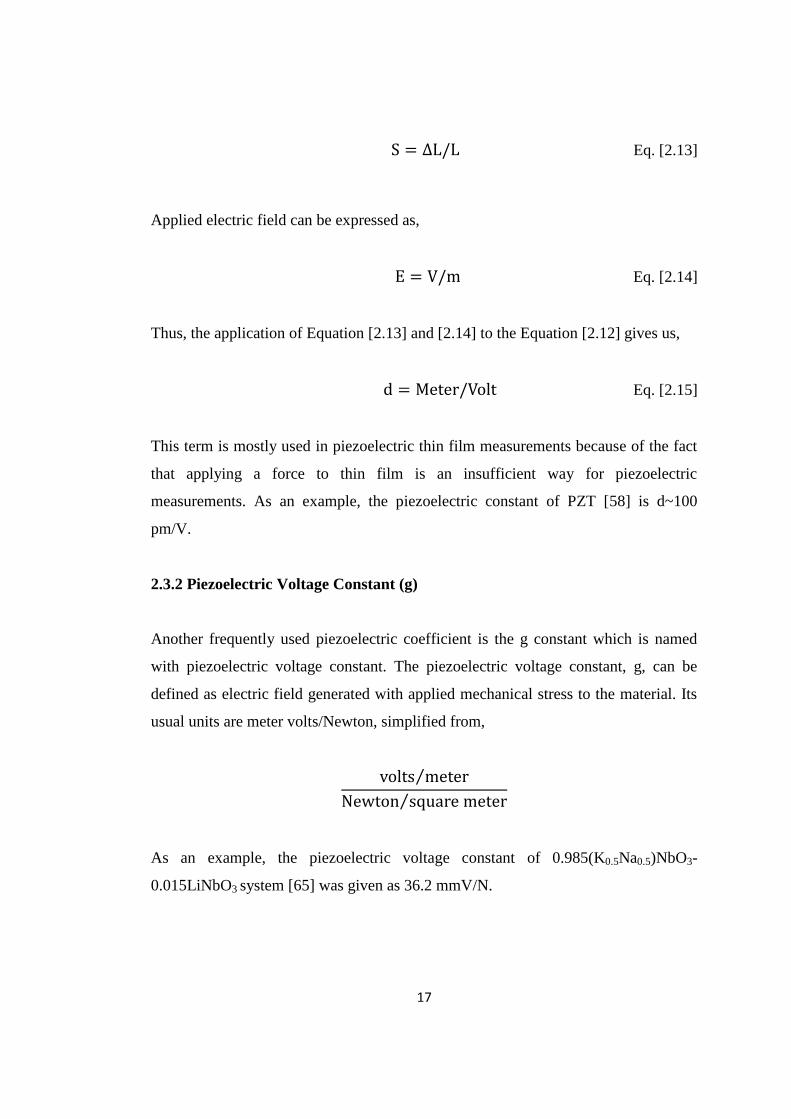
2.3.1 Piezoelectric Charge Constant (d)
The piezoelectric charge constant, d, is the polarization produced per applied
mechanical stress applied to a piezoelectric material or mechanical strain which is
generated per applied electric field. The direct piezoelectric effect is,
Eq. [2.9]
Eq. [2.10]
where D is the dielectric displacement, T is the stress, and d is the piezoelectric
charge constant (by using direct effect) [24-25].
Dielectric displacement D can be also described as the total surface charge density
which is induced in the material by the applied field and can be expressed as,

16
T is the applied stress on the material and can be expressed as,
Thus, by applying these two definitions to the Equation [2.10] gives us,
the well known unit of piezoelectric charge constant, pC/N. This is mainly used as
direct piezoelectric coefficient in most of the bulk applications of piezoelectric
materials. As an example, the piezoelectric coefficient for BCT-BZT bulk material
was reported as 620 pC/N [3].
The reverse effect of piezoelectricity can be created by applying an electric field
which causes a dipole moment on the system. This dipole moment is a result of the
movement of atoms which causes contraction or expansion on the bulk of the
piezoelectric material due to applied electric field [26]. Then, the change in the
dimensions of the material can be given as,
Eq. [2.11]
Eq. [2.12]
where S is the strain on the material, d is the piezoelectric coefficient and E is the
applied electric field strength, d is the piezoelectric charge constant (by using reverse
effect) [24-25].
Strain is the deformation by applied electric field on piezoelectric material that can
be expressed as,
17
Eq. [2.13]
Applied electric field can be expressed as,
Eq. [2.14]
Thus, the application of Equation [2.13] and [2.14] to the Equation [2.12] gives us,
Eq. [2.15]
This term is mostly used in piezoelectric thin film measurements because of the fact
that applying a force to thin film is an insufficient way for piezoelectric
measurements. As an example, the piezoelectric constant of PZT [58] is d~100
pm/V.
2.3.2 Piezoelectric Voltage Constant (g)
Another frequently used piezoelectric coefficient is the g constant which is named
with piezoelectric voltage constant. The piezoelectric voltage constant, g, can be
defined as electric field generated with applied mechanical stress to the material. Its
usual units are meter volts/Newton, simplified from,
As an example, the piezoelectric voltage constant of 0.985(K0.5Na0.5)NbO3-
0.015LiNbO3 system [65] was given as 36.2 mmV/N.

18
2.3.3 Electromechanical Coupling Factor (k)
The electromechanical coupling factor, sometimes named with piezoelectric coupling
factor, k, is a dimensionless indicator that measures the ability of the piezoelectric
material to convert electrical energy to the mechanical energy or mechanical energy
to electrical energy [27]. Its explicit definition can be represented as shown below,
Eq. [2.16]
or,
Eq. [2.17]
This dimensionless factor is always lower than 1, which means the energy
conversation is never fully completed without loss. So, for most of the strong
piezoelectric materials, the k factor can be about 0.7. The electromechanical coupling
factor of BCT-BZT ceramic phase, the main phase mentioned in this thesis, was
reported as 0.65 [10].
2.4 State of Art
Currently, the lead free research is a new surge with piezoelectric properties instead
of lead based compositions for ceramics and thin film applications [30]. Over the last
decade, the lead free thin film researches have been studied increasingly because of
the highly input applications such as MEMs. However, there are lots of limitations
on microstructure on the production of thin films. The aim of this thesis is the
production of the most attractive lead free phase with a thin film production method,
concisely.
The lead-free compositions were categorized as three main families, potassium
niobates (KN), bismuth sodium titanates (BNT) and barium titanates (BT). In the

19
presented section the state of art techniques for lead free piezoelectric families are
briefly described.
2.4.1 Potassium Sodium Niobates and Derivatives
Potassium sodium niobates (KNN) have been investigated as strongest candidate for
the lead free piezoelectric phases because of the high Curie temperature, moderate
ferroelectric responses, and large electromechanical coupling factor. However, the
piezoelectric performance for pure KNN structures was just 100 pC N-1
[29].
Therefore, there was a need for some modifications on compositions, the most
attractive one was Li modified compositions. A significant improvement was
achieved by Saito et. al. [5], who is the pioneer for compositional modifications
using Li, Ta, and Sb elements, with a piezoelectric coefficient of 416 pC N-1
in the
composition of (K,Na,Li)(Nb,Ta,Sb)O3. Hollenstain et. al. [30], investigated the
electrical responses of (K,Na,Li)(Nb,Ta)O3 composition and observed a piezoelectric
coefficient of 290 pC N-1
with an effective electromechanical coupling factor of
kp=0.46 at x=0.03 and y= 0.20. Lin et. al. [31], also had a study of (K,Na)1-xLix(Nb1-
yTay)O3 ceramics and observed that piezoelectric coefficient is 208 pC N-1
and
electromechanical coupling factor is kp=0.48 at x=0.04 y=0.225. Mn addition to the
composition was another work for the modifications on the composition,
(K,Na,Li)(Nb,Mn,Ta)O3 [32].
Thus, all the modifications were for the decrease of the Curie temperature to be
closer to the polymorphic point in their phase diagram which causes a significant
decrease in the energy barrier for easy polarization rotation that results with higher
piezoelectricity. Although there are investigations on potassium sodium titanate
phase and their derivatives, the electrical properties, especially electrical responses,
of these materials are not enough to be a good candidate instead of commercial lead
based phases.

20
2.4.2 Bismuth Sodium Titanates and Derivatives
Bismuth sodium titanates (BNT) and their solid solutions have been considered as
another main lead-free family for piezoelectric materials. First study was done by
Smolenski in 1961, that BNT phase shows moderate piezoelectric performance and
remnant polarization as 73 pC N-1
and 38 µC/cm2, respectively, with a Curie
temperature of 320 °C [6]. Advantages of this phase is easy production due to the use
of non-volatile elements and lower process temperatures during the sintering stage
compared to the KNN based compositions. However, one of the main disadvantages
of BNT composition is its lower electromechanical coupling factor due to higher
conductivity which can be understood from their high dielectric losses.
So, these factors lead the researchers for essential modifications on the BNT
composition with some additive phases such as BNT-BaTiO3 [33-37], BNT-SrTiO3
[38], BNT-PbTiO3 [39], BNT-BiFeO3 [40-42], BNT-BiKTiO3 [43], BNT-BiScO3
[44], BNT-NaNbO3 [45], BNT-BiKTiO3-BaTiO3 [46-47], BNT-KNbO3-
(Bi2O3.Sc2O3) [48], BNT-Ba(CuW)O3 [49], (NaBi)1-1.5xLaxTiO3 [50], and (Bi1-y(Na1-
x-yLix))0.5BayTiO3 [51]. The well known additive phase is BaTiO3 for decreasing the
conductivity and porosity for better dielectric constants. Abazari et. al. [52]
published a composition of (BiNa)TiO3-(BiK)TiO3-BaTiO3 ternary system as a thin
film produced by pulsed laser deposition technique with piezoelectric, ferroelectric
and dielectric constants as e31,f = -2.25 C/cm2, Pr
+ = 30µC/cm
2 and K ~ 575,
respectively. Although the investigations on BNT-based phases continue, there are
some thermodynamic restrictions of ternary systems which will be mentioned in the
next section, BNT-based compositions still are not good candidates for lead-free
alternatives.
2.4.3 Barium Titanate Based Compositions and BZT-BCT System
Another family of the lead-free alternatives is BaTiO3 and compositional derivatives.
Prior to about 1940, only a few types of salts were known as the ferroelectrics.
Subsequently, the piezoelectric effect was discovered on BaTiO3 phase. There were

21
three steps in the discovery of piezoelectricity. First one was the determination of a
high dielectric constant in the BaTiO3 composition by Thurnauer [53]. The second
step was the assumption that this high dielectric constant was caused by the
ferroelectricity of these materials. The third significant step was the discovery of the
poling process. The poling process is the application of high voltage to the material
to control electric moments of spontaneously polarized regions in desired direction.
Thus, the first commercial piezoelectric device was discovered in the BaTiO3-based
compositions and used at World War II in the radars. In time, the lead zirconate
titanate with various additives has become the dominant piezoelectric material as a
result of very strong and stable piezoelectric properties.
During the last five decade, BaTiO3 and derivatives have been mentioned as good
dielectric materials instead of piezoelectric materials that is because of relatively
high Curie temperature (~130 °C) [54]. This Curie temperature is far away from the
room temperature which is the working temperature for most of the applications.
Moving away from this tricritical (C-R-T) phase transformation temperature creates
higher energy barrier for changing of polarization rotation between rhombohedral
and tetragonal phases, that results with decreasing of the polarization [3]. This
tricritical phase transition temperature can be decreased by doping of either A or/and
B site substitutions, e.g., the addition of calcium into barium site or zirconium into
titanium site in the BaTiO3 structure [55-56]. While the Ca+2
addition decreases the
Curie temperature to around room temperature, the doping of Zr+4
increases the
electrical properties being chemically more stable than Ti+4
ions.
Recently, high piezoelectric responses have been reported due to compositional
modifications on BaTiO3 composition as (1-x)Ba(Zr0.2Ti0.8)O3-x(Ba0.7Ca0.3)TiO3
where x is 0.5. This composition will be referred as BZT-BCT from thereafter. The
piezoelectric coefficient of this system was 620 pC/N, which is almost higher than
the Pb-based system and much higher than other families (such as KNN-based
d33~416 pC/N [5], and BNT-based d33~200 pC/N [48]). This comparison was
illustrated in Figure 2.10. As it is seen, the piezoelectric performance of BZT-BCT
system is twice than KNN-LT-LS phase and undoped PZT phase and also almost

22
higher than that of commercial PZT-based piezoelectric systems.
Figure 2.10 Comparison of some lead-free families and lead based-commercial
products with BZT-BCT composition [3].
Figure 2.11 Phase diagram for BZT-BCT system which was determined by
dielectric constant versus temperature curves in the Liu’s work [3].
MPB

23
To explain these enormous piezoelectric values on BZT-BCT phase (Figure 2.11), a
composition-based phase transition phenomenon has to be discussed in detail for
perovskite oxides. This transition line in the phase diagram of perovskite oxides is
known as “morphotropic phase boundary (MPB)”. Basically, perovskite oxide’s
phase diagram has a line (MPB) that contains both of polarization directions as
rhombohedral <111> and tetragonal<001>. This coexistence causes the instability of
polarization state, so that the polarization direction can easily be rotated by any
electric field [58-59].
Although most of the lead-free systems (KNN, BNT) have morphotropic phase
boundary in their phase diagrams, it was unclear why these lead-free systems have
lower piezoelectric coefficients (d33~100-300 pC/N) than Pb-based systems (300-600
pC/N) and BZT-BCT system (d33~620 pC/N) with existing theories. There is an
explanation for this situation. The Pb-based and BZT-BCT systems have tricritical
point (TCR) which is an intersection for the cubic, tetragonal (T) and rhombohedral
(R) phases in their phase diagrams. In the explanations of Rossetti et al. [60] and
Haun et al. [61], the free energy (F) for polarization rotation between R and T phases
is a function of composition (x), temperature (T), magnitude of polarization (P), and
its direction (n) that can be written as Landau polynomial (Equation 2.18).
F(x,T,n,P) = A(x,T)P2 + B(x,n)P
4 + C(x,n)P
6 Eq. [2.18]
where A(x,T), B(x,n), and C(x,n) are the coefficients of second, fourth, and sixth
order terms, respectively. When the composition is produced exactly on tricritical
point in the phase diagram, this situation requires B(xMPB,n) = B(xTCP,n) = 0 and
C(xTCP,n) = C(xTCP) [62]. So, the equation becomes,
F(xTCP,T,n,P) = A(xTCP,T)P2 + C(xTCP)P
6 Eq. [2.19]
Therefore, the free energy for polarization rotation (F) becomes independent of
polarization direction (n) when the composition is produced exactly on this tricritical
point that can be seen in Equation 2.19. The disappearance of the anisotropy results

24
with zero energy barrier for polarization rotation from tetragonal state to
rhombohedral state [60]. This is the main reason for enormous piezoelectric
properties of the tricritical point type morphotropic phase boundary. In fact, the
phase should not be produced on the tricritical point because of the fact that cubic
phase does not show any piezoelectric effect. Any temperature instability, even 1 °C
above the Curie temperature, is enough for the shift away from this C-R-T point,
which can easily make the material non-piezoelectric by entering into the cubic
region. So, the phase has to be produced on MPB near to the C-R-T point. In this
situation the free energy of polarization rotation will not be zero as the above case,
however it gives us very weak polarization anisotropy. This is resulted with very low
energy barrier between <001>T and <111>R polarization states and the polarization
rotation is still easy.
While BaTiO3-based and PZT-based compositions have tricritical point type (C-R-T)
MPB as shown in Figure 2.12(a1), present lead-free piezoelectric families (KNN-
based and BNT-based) do not have a tricritical point type morphotropic phase
boundary in their phase diagrams as shown in Figure 2.12(b1).

25
Figure 2.12 (a1) A part of phase diagram of BZT-BCT phase that includes tricritical
point MPB. (a2) and (a3) Free energy diagram, which is isotropic, for polarization
rotation between tetragonal and rhombohedral phases at C-R-T point. (a4) and (a5)
Free energy diagram, which is anisotropic, for polarization rotation between <001>T
and <111>R states on MPB. (b1) A typical phase diagram of polymorphic type MPB
between tetragonal and orthorhombic phases. (b2) and (b3) Free energy diagram,
which is anistropic, for polarization rotation between two ferroelectric crystal
structures on intersection point. (b4) and (b5) Schematic anisotropic free energy
diagram on polymorphic type MPB [3].

26
Polymorphic phase transition also exhibits an enhancement on piezoelectric
properties because of the instability through coexistence of two ferroelectric crystal
structures. However, there is much more anisotropy along the polymorphic MPB
which results in larger energy barrier during the polarization rotation. Thus, lower
polarization is obtained in the case of polymorphic MPB in comparison to tricritical
type MPB.
Thus, the approach given above explains why higher piezoelectric coefficients can be
obtained in the BZT-BCT (d33~620 pC/N) and PZT-based compositions (d33~300-
600 pC/N) with respect to other lead-free familes (d33~100-300 pC/N).
2.4.4 Lead-Free Thin Film Progress
Over the last decade, the researches on lead-free piezoelectric thin films have been
constantly increasing. The families which are mentioned above were mainly used for
thin film processing. However, thin film processing needs different approaches and
experimental behaviors than ceramic (bulk) processing. The main problem of thin
film production is volatilization of species (such as K+, Na
+, Bi
3+, Ti
4+) during heat
treatment or the precursor preparing stage. This problem was seen mostly in the
chemical solution deposition or metal-organic deposition methods.
KNN-based compositions were fabricated using different techniques, such as
magnetron sputtering [63], chemical solution deposition (CSD) [64-79] and pulsed
laser deposition (PLD) [70]. As it is seen, the most attractive method of production
of KNN-based compositions is chemical solution deposition method. While pure
KNN composition (K0.5Na0.5)NbO3 [67] shows a moderate piezoelectric strain
coefficient d33~74.0 pm/V, the Li addition to this phase (Li,K, Na)NbO3 [65] causes
serious stoichiometric deviation and lattice defects in the Li-KNN films and results
with higher piezoelectric strain coefficient d33~83.1 pm/V which is much more close
the PZT film d33~100 pm/V [71]. Ta and Mn modified KNN thin films (KNL-x
NMT, x = 0 to 0.2) were also studied systematically to improve ferroelectric and
dielectric performance of KNN-based lead-free thin films [66]. In this phase 5 mole

27
% Mn addition plays an important role to decrease leakage current density. This
study showed that 10 mol. % Ta doping results with d33~61 pm/V piezoelectric strain
coefficient which is lower than that of Goh’s works [65,67]. However, the point of
the study is to obtain improved ferroelectric and dielectric properties in the
mentioned work as Pr~16.1 µC/cm2 and єr~2649, respectively. The second method
for the production of KNN-based compositions is pulsed laser deposition [70]. In this
study, Mn-doped (K0.44Na0.52Li0.04)(Nb0.84Ta0.1Sb0.06)O3 (KNN-LT-LS) thin films on
SrTiO3 substrates were examined. Piezoelectric strain coefficient of KNN-LT-LS
phase was determined as ~45 pm/V for 500 nm Mn doped films.
The well studied second phase as an alternate to lead-free piezoelectric thin film is
(Bi,Na)TiO3-based compositions which were fabricated using chemical solution
deposition [72-76] and pulsed laser deposition method [77,75]. Pure Bi0.5Na0.5TiO3
films were deposited on Pt/Ti/SiO2/Si substrates using CSD together with rapid
thermal annealing [74]. In this study, moderate dielectric and ferroelectric properties
were obtained as єr~277 and Pr~8.3 µC/cm2, respectively. The doping of Ba
2+ ions to
the phase, (Na0.5Bi0.5)xBa1-xTiO3 (NBT-BT) 96/4, causes good insulating
characteristics because of decreasing the porosity which was mentioned in the other
study [75]. Dielectric permittivity and dielectric loss of the NBT-BT 96/4 phase was
found as єr~740 and tan δ~5%. Zhang et. al. [73] studied the same composition
(NBT-BT 96/4) with a different substrate and found additionally the piezoelectric
constant of this phase as d33~94 pm/V. Also, dielectric permittivity, dielectric loss
and remnant polarization values were given as єr~504, tan δ~5% and 12 µC/cm2,
respectively in that study. Another BNT derivative is (1-x)BNT-xBKT composition
[76]. At x=0.15, dielectric constant was found as єr~360 with a dielectric loss of tan
δ~5.9%. The importance of this study is the improvement in ferroelectric properties
(as remnant polarization) of Pr~13.9 µC/cm2. BaTiO3 addition to BNT-BKT
(0.88)(Bi0.5Na0.5)TiO3-(0.08)(Bi0.5K0.5)TiO3-(0.04)BaTiO3 was studied also by
Abazari et. al. [52] on SrRuO3 coated SrTiO3 substrates. Dielectric permittivity and
dielectric loss was given as єr~750 and tan δ~15% while piezoelectric voltage
coefficient and remnant polarization was found to be -2.2 C/m2 and 30 µC/cm
2 which

28
is the highest obtained remnant polarization value in BNT based compositions. All
properties of lead-free thin film families can be seen in Table 2.1.
Many recent studies have been reported for the preparation of (Ba,Ca)(Zr,Ti)O3
derivatives for mostly bulk applications. Furthermore, there are a few studies about
the production of thin films with this composition using mainly pulsed laser
deposition and chemical solution deposition methods [78-81]. In these studies,
dielectric properties of the (Ba,Ca)(Zr,Ti)O3 thin films were studied in detail. While
(Ba,Ca)(Zr,Ti)O3 thin films show high dielectric constant around єr~1000 produced
by pulsed laser deposition method [78,81], films of same composition show a
moderate dielectric constant around єr~250 prepared using chemical solution
deposition method [80]. This situation is explained by the presence of porosity in
chemical solution deposited BaTiO3-based thin films where the porosity is the source
of moisture which causes a decrease in dielectric permittivity. In contrast, the pulsed
laser deposition method results with dense and oriented films. Recently, only one
study was exhibited all ferroelectric, dielectric and piezoelectric properties of this
phase as Pr+=14.1 µC/cm
2, є
r~1010 and d33=80 pm/V, respectively [78], using pulsed
laser deposition method. Among the variety of process types, the chemical solution
deposition method offers better control of the chemical composition and easy control
of the process with a disadvantage of grain sizes and orientation control compared
with physical vapor deposition methods. However, the control of the chemical
composition is quite important to produce a material on morphotropic phase
boundary for lower energy barrier to obtain optimum polarization. Moreover, the
preparation of Ba(Ti0.8Zr0.2)O3-(Ba0.7Ca0.3)TiO3 composition using chemical solution
deposition method and its ferroelectric and dielectric correlation have not been
reported yet.
In this thesis, we determine the ferroelectric and dielectric properties of
Ba(Ti0.8Zr0.2)O3-(Ba0.7Ca0.3)TiO3 composition prepared using chemical solution
deposition method for different process parameters. Thus, optimum electrical
properties were observed for BZT-BCT lead-free thin films using a systematic study.

Table 2.1 Ferroelectric, dielectric and piezoelectric properties of lead-free thin films in the literature.
Ref. Composition
Piezoelectric
displacement
coefficient
Dielectric
constant Current density Dielectric loss Coercive field
Remnant
polarization
d33 (pm/V) K (єr) J (A/cm2) D (tan δ) (%) Ec (kV/cm) Pr (µC/cm2)
[63] (K0.5Na0.5)NbO3 [KNN]
450
1.7
12
[64] (K0.5Na0.5)NbO3 [KNN]
10-7
90 (at -190
°C) 20 (at -190 °C)
[65] 0.985(K0.5Na0.5)NbO3-0.015LiNbO3 [KNN] 83.1 250
5
[66] (K0.48Na0.48Li0.04)(Nb0.895Ta0.1Mn0.005)O3 [KNN] 61 2650
22.2 16.1
[67] (K0.5Na0.5)NbO3 [KNN] 74 337 10-8 3.2 50 4
[68] (0.06)LiNbO3-0.94(K0.52Na0.58)NbO3 [KNN] 192 625 10-5
36.5 9.7
[69] (K0.4425Na0.52Li0.0375)(Nb0.8825Ta0.0375Sb0.08)O3 [KNN]
341
5 31.8 9.5
[71] Mn-doped
(K0.44Na0.52Li0.04)(Nb0.84Ta0.1Sb0.06)O3
[KNN] 45
30 15
[72] Pr3+ doped Na0.5Bi0.5TiO3 [BNT]
772
4.6 94 18.3
[73] 0.94(Na0.5Bi0.5)TiO3-0.06BaTiO3 [BNT] 94 504
5 103 12
[74] Na0.5Bi0.5TiO3 [BNT]
277 10-5 2 200 8.3
[75] (Na0.5Bi0.5)0.94Ba0.06TiO3 [BNT]
740 10-4 5
9
[76] Bi0.5 Na0.5TiO3- Bi0.5K0.5TiO3 [BNT] 360 5.9 13.8
[77] 0.92(Na0.5Bi0.5)TiO3-0.08BaTiO3 [BNT] 820 10-9 13 120 11
[52] 0.88(Bi0.5 Na0.5)TiO3-0.08(Bi0.5K0.5)TiO3-
0.04BaTiO3
[BNT] 600 20 95 30
[78] 0.5[Ba(Ti0.8Zr0.2)O3]-0.5[(Ba0.7Ca0.3)TiO3] [BZT-BCT] 80 1010 17.7 2.5
[79] (Ba0.95Ca0.05)(Zr0.2Ti0.8)O3 [BZT-BCT] 900 5
[80] (Ba0.95Ca0.05)(Zr0.05Ti0.95)O3 [BZT-BCT] 250 10-6
[81] (Ba0.90Ca0.10)(Zr0.25Ti0.75)O3 [BZT-BCT] 725 3
29

30
2.5 Chemical Solution Deposition Technique
The sol-gel technique has been considered for more than 100 years. A sol is
suspension of colloidal particles in a solution while the gel is a colloidal solid that
has an internal network structure with mixed solid and fluid components. Sol-gel
processing offers advantages over standard ceramic or glass processing for some
electronic applications. The process is a series of wet chemical reactions occurring at
relatively low temperatures. The chemical reactants are available in solution form
which allows for distillation of the materials. Thus, high purity “raw materials” for
electronic ceramics can be prepared in sol-gel process.
Multicomponent oxides can be formed via sol-gel processing. The individual
constituents are combined as liquids resulting in atomic level mixing. The final
material can be more homogeneous with respect to chemical species than could be
expected from processing in which solid-state or melt-phase diffusion is necessary to
get compound formation.
It should be noted that purity and homogeneity could also result from other types of
solution preparation of electronic ceramics. These advantages result from the liquid
nature of the reactants regardless of whether a powder or a monolithic gel is formed.
These advantages, therefore, are not limited to sol-gel processing. The three
dimensional network (rather than particulate) structure does allow for some
additional advantages [82].
Before the gelation is complete, the material is still fluid. Films or coatings of desired
compositions can be easily formed on a substrate. Another advantage is that after
drying, the gel is porous. The pores in dried gels are often extremely small
(approximately 10 nm). This allows lower firing temperatures to be used for sol-gel
derived pieces than for standardly processed pieces. The low firing temperature of
sol-gel derived material can also be important in compositions which undergo
undesired phase transitions or have volatile components. It is possible in certain
cases to process at sufficiently low temperatures, e.g. below the phase transition, thus

31
avoiding any deleterious effects. Categories of sol-gel processing technique were
shown in Figure 2.13.
The properties of an electronic ceramic device result from composition of materials
used as well as the micro and macrostructure of the piece. Because of the options
available in each of the steps during sol-gel processing there can be somewhat
independent control over porosity, crystal structure, and grain size. Sol-gel
processing thus allows for a variety of compositions and structures to be formed. The
resultant piece can, therefore, possess a unique combination of properties [82].
In review, due to the liquid nature of the constituents and the diversity of the
processing variables possible, sol-gel processing can offer many advantages for use
in electronic ceramics. They are: (1) purity, (2) homogeneity, (3) ease of forming a
variety of structures, (4) low temperature processing, and (5) unique combination of
properties.
The first usage of this technique for perovskite thin film production to produce
electronic oxides dates from the mid-1980s. Publications by Fukushima et. al. [84]
on the production of PZT (lead zirconate titanate) by sol-gel processing was the first
study to obtain desired properties as thin films in comparison with bulk of PZT
phase. With the help of this starter study, a wide range of metal oxides for electronic
industry [PbTiO3, BaTiO3, SrTiO3, (Ba,Sr)TiO3, Pb(Zr,Ti)O3, Ba(Zr,Ti)O3,
Pb(Sc,Ta)O3, Pb(Mg1/3Nb2/3)O3, SrBi2Ta2O9, SrBi2Nb2O9, (Bi1-xLax)4Ti3O12,
(La,Sr)CoO3, (La,Sr)MnO3, YBa2Cu3O7-δ, BaZrxY1-xO3 and etc.] were tried to be
produced using this technique.

32
Figure 2.13 Categories of sol-gel processing technique. The route at the left in the
figure, called chemical solution deposition, was used in current study [83].
2.5.1 Preparation of the Solution and Process Chemistry
Figure 2.14 illustrates the route of chemical solution deposition technique for thin
film production. At first the precursor has to be prepared by mixing of appropriate
amounts of metal-carboxylates and metal alkoxides and solvents. This stage is the
most critical step for thin film production. Compositional stoichiometry is obtained
in this stage and also the homogeneity of the solution is an important factor to obtain
optimum film quality.

33
Figure 2.14 Flow chart of typical chemical solution deposition technique for thin
film production [85].
Losses during the preparation of solution have to be considered carefully because of
the volatile raw materials such as Pb-acetate, Na-acetate or Ti-isopropoxide. To
obtain crack free films some chemical stabilizers, such as ethylene glycol, can be
added to the solution.
Metal carbocylates are common salts of carboxylic acids, R-COOH, where R is alkyl
group such as methyl, CH3 (acetic acid) ethyl, C2H5, etc. Carboxylates can normally
be dissolving in their own (parent) carboxylic acids [85]. This is important that Ba-
acetate and Ca-acetate were dissolved in acetic acid in current study. Alcohols (R-
OH) can be considered as weak acids, and metal salts of alcohols were called

34
alkoxides, M-(OR)x, where M is the metal part. The key reactions which are leading
to the formation of precursor species are hydrolysis and condensation.
Hydrolysis:
M(OR)x + H2O M(OH)x + xROH Eq. [2.20]
Condensation (alcohol elimination):
2M(OR)x(OH) M2O(OR)2x-3(OH) + ROH Eq. [2.21]
Condensation (water elimination):
2M(OR)x(OH) M2O(OR)2x-2(OH) + H2O Eq. [2.22]
These reactions cause the formation of a metal-oxygen-metal bridge, which can be
considered as the backbone of any oxide ceramic structure. Continued condensation
process increases the density of metal-oxygen-metal crosslinks until gelation or
precipitation occurs.
2.5.2 Spin Coating Process
Once the precursor has been prepared, there are three techniques for coating of the
films which are spin coating, spray coating and dip coating, as illustrated in Figure
2.15. In most of the researches, the spin coating process has been used generally. The
electroded (Pt is used for this purpose) Si substrates are the best ones for
piezoelectric applications. This substrate is held on the spin coater with the help of
vacuum or double sided sticker from back side of the wafer. The spin rate (in rpm)
and time are controlled to achieve desired thickness. The controlling of thickness is

35
quite important for a systematical study. The collaboration of precursor molarity,
spin rate and spin time affect directly the thickness of the film. For example, while
0.1 molar solution with 3000 rpm spin rate and 30 s spin time gives around ~10 nm
thickness, 0.85 molar solution with 1500 rpm and 30 s spin time results with ~150
nm film thickness.
Figure 2.15 Commonly used coating processes for the electronic oxides using
chemical solution deposition method [85].
A variety of defects can be seen when spin coating process is used. Any dirt
(particles mostly) from precursor or atmosphere will stick to the surface during spin
coating step. So, before the spin coating process, 0.2 µm nozzled filters has to be
used to obtain clean precursors. The control of the particles in the atmosphere can be
provided by the use of clean rooms.
According to Bornside et. al. [86], there are four stages during the spin coating
process which are illustrated in Figure 2.15. First one is the depositon of precursor
onto the substrate using a pipe. Usually the excess amount of solution is dropped to
the wafer for wetting to the surface as well. The second stage is spin-up which has
the aggressive fluid expulsion from the substrate by rotational speed. The next stage
is the smoothing of the precursor with a constant speed rotation. The final step is the
evaporation of solvents and gel formation. This is an important stage because of the
thickness and smoothing of the films are determined on this gel formation stage.

36
Figure 2.16 Stages during spin coating process [86].
The prediction of Mayerhofer about factors affecting the film thickness includes the
spin rate (f), the initial viscosity (ƞi), and the evaporation rate (e):
h α f2/3
i1/3
e1/3
Eq. [2.23]
2.5.3 Drying, Firing and Sintering of Perovskite Thin Films
After the spin coating step, the crystallization of the films were required to obtain
perovskite oxides. To obtain desired perovskite phase, all solvents and organics (in
the form of gel) have to be removed from the system. There are some stages during
the heat treatment process of the film. The first one is the removal of solvents or
water (if it exists) at relatively low temperatures (~150-200 °C). This step is named

37
as drying of the films. In this point it is necessary to say that all heat treatment
process has to be determined with a well studied TG/DTA measurement. The timing
during the steps was critical because of the fact that all reactions have to be
completed before the next step.
There are two main approaches that are commonly used to complete crystallization
of the films: the two step and the one step processes. Mainly the two step process is
described as first the pyrolysis which is the removal of all organics at relatively low
temperatures (~500 °C in our work) and then reaching to a high crystallization
temperature (~800 °C in our work). This two step process is much more preferred
option in the literature that allows crack-free films because of the fact that rapid
thermal treatment processes tends to create cracked films. When the heat treatment
occurs, the film has a shrinkage value along the thickness by 50 to 70%. So, it is an
essential to fabricate multilayered films in each pyrolysis step (3 pyrolsis steps were
used in our work to obtain desired thickness before the crystallization).
In the one step process, the material is heated directly to the crystallization
temperature, which consists of both organic removal and perovskite formation. This
one step process is named as rapid thermal annealing. This process is preferred
mostly for the formation of highly crystalline and oriented films with a much lower
film thicknesses because of the crystallization kinetics, and there are a few reports
about this process for BaTiO3 based phases [87-89]. The rapid thermal annealing also
tends to enhance film densification by delaying the onset of crystallization to higher
temperatures.
In the processing of BaTiO3 based compositions, the formation of the carbonate
phases complicates the annealing scheme. The reactions for phase transitions during
the heat treatment include:
The tiranium isopropoxide tends to create titanium oxide at temperatures 300-
350 °C. This situation results with a mixture of titanium oxide secondary

38
phases and weak crystalline alkaline (Ba,Ca for our study) carboxylate
netwoks.
The exact barium carboxylates occur at relatively high temperatures (450-500
°C). This is pyrolysis step and has to be waited enough to complete.
During the heat tratment, the secondary phases occur at the bulk of the film.
These are mostly complex carbonates, Ba2Ti2O5CO3 which is an intermediate
phase [90]. Mostly, this phase causes the increase in annealing temperatures
to higher temperatures.
2.6 Viscosity of the Solutions
Viscosity is the resistance of a fluid to flowing which is deformed by either shear
stress or tensile stress. For a viscous flow, the viscosity ƞ is coming from applied
shear stress τ and the change in the velocity du with the distance dy imposed by two
parallel plates, or
Eq. [2.24]
Viscosity unit is described as poises (P) and pascal-seconds (Pa-s); and 1 P equals to
1 dyne-s/sm2 , 1 Pa-s equals to 1 N-s/m
2. The correlation between poises (P) and
pascal-seconds can be given as 10 P = 1 Pa-s.
The straight, parallel and uniform flow is expected from the solutions, so the shear
stress, τ, between layers is directly proportional to the velocity gradient, du/dy, thus
the relative motion of the layer is,
Eq. [2.25]

39
where µ is named as the coefficient of viscosity, the viscosity, or the dynamic
viscosity. This equation was derived from Newton. A flow with a constant and non-
constant gradient is seen in Figure 2.17.
Figure 2.17 Laminar flow, (a) with a constant gradient, and (b) with a non-constant
gradient [91].
There are several viscosity types and mostly seen ones are Newtonian, shear
thickening and shear thinning. Types of viscosities are illustrated in Figure 2.18 [98].
The Newtonian fluids exhibit a linear behavior with the increase of shear rate. When
the viscosity decreases with increasing shear rate, it is called the fluid shear-thinning.
In opposite case where the viscosity increases as fluid is subjected to a higher shear
rate, fluid is called as shear-thickening [92].

40
Figure 2.18 (a) Newtonian (b) shear thinning and (c) shear thickening situations for
a fluid [92].
A power-law fluid is a type of generalized Newtonian fluid for which the shear
stress, τ, is given by,
Eq. [2.26]
where K is the flow consistency, ∂u/∂y is the shear rate, and n is the flow behavior
index. n is equal to 1 corresponding to Newtonian solution.
Eq. [2.27]
The effective viscosity as a function of shear rate can be found using Eq. 2.26 as
given in Eq. 2.27.

41
CHAPTER 3
EXPERIMENTAL PROCEDURE
In the current study, the lead-free BZT-BCT thin films were produced towards a
nominal composition of Ba(Ti0.8Zr0.2)O3-(Ba0.7Ca0.3)TiO3 to obtain coexistence of
rhombohedral and tetragonal phases at room temperature through morphotropic
phase boundary (MPB). Solution preparation, coating and annealing stages were
performed, respectively, to obtain optimum electrical properties.
3.1 Solution Preparation
3.1.1 Starting Materials
To achieve true composition of the BZT-BCT film, the precursor solution was
prepared using predetermined amounts of barium acetate Ba(CH3COO)2 (Aldrich
Co., purity 99+%), calcium acetate hydrate Ca(CH3COO2).H2O (Merck Co., purity
97+%), zirconium (IV) isopropoxide Zr(OC3H7)4 (Aldrich Co., 70wt.% solution in 1-
propanol) and titanium n-propoxide Ti(OC4H9)4 (Aldrich Co., 97+%) as starting
materials. 2-methoxyethanol C3H8O2 (Aldrich Co., purity 99%) and glacial acetic
acid C2H4O2 (Merck Co., purity 99.8+%) were used as solvents for metal alkoxides
(zirconium (IV) isopropoxide, titanium n-propoxide) and metal carboxylates (barium
acetate, calcium acetate hydrate), respectively.
3.1.2 Solution Preparation
To produce homogeneous films in desired composition, preparation of the precursor
is extremely important. Starting materials are divided in two groups as metal
alkoxides (zirconium (IV) isopropoxide, titanium n-propoxide) and metal

42
carboxylates (barium acetate, calcium acetate hydrate). Therefore the solvents for
these materials are different. 2-methoxyethanol and acetic acid were used as solvents
for metal alkoxides and metal carboxylates, respectively. In the first solution, to
prepare metal carboxylate complex, barium acetate, calcium acetate hydrate and
acetic acid were mixed in predetermined ratios at high temperature. The mixing of
materials with solvent at high temperature is crucially important to prevent from
precipitation. The temperature used for this stage was 125 ˚C for 1 h using an oil bath
for homogeneous heating. A reflux system was needed for high temperature heating
to avoid evaporation which results in the change of the molarity of solution.
Simultaneously, the second solution was prepared using zirconium (IV)
isopropoxide, titanium n-propoxide and 2-methoxyethanol through mixing with each
other at room temperature for 1 h. Subsequently, two solutions were combined
together and mixed at 75 ˚C for 2 h. To obtain a stable stock solution, the next step
was aging of the solution. Then, the solution was stirred at room temperature for 24 h
to obtain final stock solution. The final solution can be kept as stock at least 1 week
and has to be kept in an ultrasonic bath for 20 min for homogenization before each
usage.
The flow chart of the production of BZT-BCT film is shown in Figure 3.1. To
fabricate BZT-BCT film in desired composition and thickness, amounts of the
starting materials used and solvents have to be calculated carefully. The molarity and
volume of the solution was 0.845 M and 0.04 lt., respectively. So, the total mole
number of the starting materials in the solution was 0.0338 moles. At first, 3.6043 gr
barium acetate and 0.4410 gr calcium acetate hydrate were mixed with 10 ml acetic
acid at high temperature. The solution was mixed in the reflux system for 1 h using a
magnetic stirrer. At the same time, the second solution was prepared using 4.8075 gr
titanium n-propoxide, that includes 10% excessive amount to compensate
evaporation during sintering, and 0.6476 gr zirconium (IV) isopropoxide. The
amount of zirconium (IV) isopropoxide was calculated 30% excess because of the
fact that zirconium (IV) isopropoxide is 70 wt% in 1-propanol solution. 2-
methoxyethanol used was 30 ml to obtain 40 ml (+10 ml acetic acid) precursor. This
second solution was stirred at room temperature to avoid evaporation of titanium n-

43
propoxide for 1 h. The transparent solution has to be obtained to assure the
Figure 3.1 Flow chart of two different steps for the production of BZT-BCT thin
films.
dissolution of all materials used. Then, both of the solutions were mixed together and
stirred at 75 ˚C for 2 h. The role of this stage is to combine the two solutions to

44
obtain metal-oxygen-metal complex. At the end of this stage, a few milliliters acetic
acid could be added to ensure molarity of the solution. The final solution was stirred
24 h at room temperature for aging stage.
3.2 Film Preparation
3.2.1 Preparation of Substrates
The selection of the substrate is a definitive factor to determine desired
microstructure during a systematic study. Therefore, there are some parameters to
obtain consistency between substrate and film; as thermal expansion coefficient and
lattice misfit. The calculated lattice misfit between substrate and BZT-BCT film is
1.54%. The conductivity of the substrate as bottom electrode is another selection
criteria for piezoelectric applications. Thus, lead-free BZT-BCT thin films were
grown on (111)-Pt/Ti/SiO2/Si-(100) (INOSTEK Korea) substrates by CSD technique
in this thesis. Specifications of the substrate are shown in Table 3.1. The effective
usage of the substrate is only possible by divided wafers. Consequently, the
substrates were cut in square shape in dimensions of 1.5 cm to 1.5 cm. The
dimensions were selected such that wafers cover completely mercury probe
measurement area. The cutting procedure was done using a diamond glass cutter or
green light laser (GÜNAM - Center for Solar Energy Research and Applications at
METU). Usage of the laser beam has been preferred mostly to obtain minimum
dirtiness on wafer surfaces. Contaminations on the surface of wafers have to be
cleaned by ultrasonic alcohol procedure. Wafers were rinsed in acetone to remove
organics and contaminations using the ultrasonic bath for 15 min. Then, they were
rinsed in ethanol to clean the wafer surface from acetone with a second ultrasonic
bath procedure. Finally the surfaces were dried using high pressure nitrogen gas.
3.2.2 Spin Coating
Before each spin coating step, it is recommended to keep the precursor in the
ultrasonic bath for 20 min for homogenization. The prepared precursors were applied

45
to the substrates using Chemat Technology spin coating system by sticking on
double sided tapes. The precursor was dropped in excess amount onto the substrates
using Eppendorf pipettes. The thickness of the films depends on the viscosity of the
solution and speed of the coater. Different speeds were tried using spin coater and
optimum speed was determined as 1500 rpm for 30 s. To obtain desired thickness,
multiple (three layers) spin coating-pyrolysis steps were performed.
Table 3.1. Specifications of multilayered substrate.
Pt Layer (Top Electrode)
Production Method DC Magnetron Sputtering
Thickness (nm) 150
Orientation 111
Ti Layer (Exchange Layer)
Production Method DC Magnetron Sputtering
Thickness (nm) 10
SiO2 Layer
Production Method Thermal Oxidation
Thickness (nm) 3000
Substrate (Silicon Wafer)
Production Method CZ (Prime)
Thickness (µm) 525
Orientation 100
To obtain electrical properties, there is a minimum thickness where dielectric
breakdown is not observed. Dielectric breakdown is the existence of a high-voltage
(above 15 V for our measurements) that can find a conduction path on the film. On
the other hand, increasing film thickness causes cracks due to the increse of stresses
on the film surfaces and affects the microstructure by changing the orientation.
Therefore, optimum films thickness was determined as 500 nm using three spin
coating-pyrolysis steps.

46
3.2.3 Heat Treatment of BZT-BCT Thin Films
The first step on heat treatment of BZT-BCT thin films is drying process at 200 °C
for 15 min. In spin coating step, most of the acetic acid and water were removed
from the surface at high rpm values. Remaining chemicals, except 2-methoxyethanol,
were removed in this stage. The formation of inorganic film takes place with the
removal of all organics. Therefore, the second stage is pre-annealing of the films at
500 °C for 15 min. This process was repeated until desired thickness was reached.
The final step is sintering of inorganic amorphous films to form crystalline
perovskite structure. Various sintering temperatures were studied to observe pure
perovskite phase for 1 h sintering time. Additionally, annealing temperature is an
important factor in the formation of microstructure. In this process, the heating rate
of the furnace was 10 °C/min. After the process, the furnace was shut down and
waited until to reach the room temperature before the specimens were taken out.
In order to understand the effect of sintering temperature, five different temperatures
were selected as 700 °C, 750 °C, 800 °C, 850 °C and 900 °C. Sintering time was not
changed because it does not affect the microstructure for barium titanate based
phases. The selected thickness was 500 nm for three layered films that kept constant
during the current study.
3.3 Characterization of BZT-BCT Thin Films
3.3.1 Structural and Morphological Analysis
Cross-sectional and morphological analyses of the films were done using FEI Nova
Nano SEM 430 Field Emission Scanning Electron Microscope to find out
information about the morphology and thickness of the films. Additionally, grain size
of the films was studied to explain the change of the electrical properties with
different sintering temperatures. To correlate the microstructural results, phase

47
analysis were done by X-ray diffraction using Rigaku (Japan) D/MAX 2200/PC
Diffractometer between 20°-60° (2θ) with Cu (Kα) radiation. To investigate cracks
on the film surfaces, Nikon Type 104 Stereo Microscope was used.
3.3.2 Dielectric and Ferroelectric Measurements
Capacitance-frequency measurements of BZT-BCT films were conducted using
Agilent 4294A Impedance Analyzer for dielectric constant and tangent loss
measurements. These measurements were carried out in the frequency range of 1
kHz-1000 kHz with the oscillation voltage of 0.05 V at room temperature to
determine dielectric constant (єr) and tangent loss (tanδ) values. To obtain healthy
electrical contacts, Mercury Probe Model 802B-200 was used for both dielectric and
ferroelectric measurements. Contact area is a critical factor to define electrical field.
Therefore, the contact area for this mercury probe was 0.00454 cm2. Ferroelectric
measurements were done using Radiant Ferroelectric Tester LC (Radiant
Technologies, Inc.) for Polarization (µC/cm2)-Electric field (kV/cm) curves at the
voltages as 5 V, 10 V and 15 V.
3.3.3 Thermal Analysis
Differential Thermal Analysis (DTA) and Thermogravimetry analysis were done in
the Central Laboratory at Middle East Technical University by Simultaneous
Thermogravimetric Analyzer and Differential Thermal Analyzer to determine critical
reaction temperatures and weight losses of the BZT-BCT thin films during the heat
treatment stage. For this purpose, powder form of the material was prepared using
the precursor that was kept at the furnace for 5 h at 100 °C. This thermal analysis
gave information about drying, pyrolysis (organic removing) and annealing
temperatures and reactions.

48
3.3.4 Viscosity Measurements
Viscosity of the solutions was found by TA Instruments ARES Rheometer unit in
Central Laboratory at METU. Viscosity (Pa.s) of the solutions with increasing shear
rate (s-1
) curves was obtained for BZT-BCT solutions in order to find the uniformity
of the solutions.

49
CHAPTER 4
RESULTS AND DISCUSSION
The aim of the study was to produce lead-free alternative ferroelectric, piezoelectric
and dielectric Ba(Ti0.8Zr0.2)O3-(Ba0.7Ca0.3)TiO3 composition using chemical solution
deposition method. This composition was selected because of the fact that it is near
the morphotropic phase boundary. With the help of this method, homogenous
Newtonian stock solution was used to produce compositionally homogeneous, crack
free and smooth thin films. To be able to find optimum film production parameters,
the different sintering temperatures ( 700 °C, 750 °C, 800 °C, 850 °C, and 900 °C)
were studied at constant sintering time (1 h) while the film thickness was kept
constant. At first, the optimum film thickness was determined basically through
predetermined process parameters. There was a simple conclusion about the
thickness such that 2 coating layers (around 300 nm) were not enough to obtain
ferroelectric and dielectric measurements because of the dielectric breakdown.
Dielectric breakdown refers to the formation of electrically conducting regions in an
insulating material exposed to a strong electric field [93]. This situation yields a
conductive material where dielectric, ferroelectric and piezoelectric properties
disappear. 4 coating layers (around 650 nm) result into cracked films because of the
high stress on the films. So, 3 coating layers (around 500 nm) are the only choice at
this solution molarity (0.845 M) to produce Ba(Ti0.8Zr0.2)O3-(Ba0.7Ca0.3)TiO3
composition as a measurable thin film. All the film thicknesses were determined by
SEM study. By comparing thermal analysis, x-ray diffraction, ferroelectric and
dielectric results for different sintering temperatures, the optimum sintering
temperature was determined as 800 °C. The experimental details of the thin films
that were produced during the study are seen in Table 4.1.

50
Table 4.1 Experimental details for the determination of the optimum lead-free thin
films.
Composition
Sintering
Temperature
1 h
Number of
layers coated
Ba(Ti0.8Zr0.2)O3-(Ba0.7Ca0.3)TiO3 800 °C 2
Ba(Ti0.8Zr0.2)O3-(Ba0.7Ca0.3)TiO3 800 °C 3
Ba(Ti0.8Zr0.2)O3-(Ba0.7Ca0.3)TiO3 800 °C 4
Ba(Ti0.8Zr0.2)O3-(Ba0.7Ca0.3)TiO3 700 °C 3
Ba(Ti0.8Zr0.2)O3-(Ba0.7Ca0.3)TiO3 750 °C 3
Ba(Ti0.8Zr0.2)O3-(Ba0.7Ca0.3)TiO3 800 °C 3
Ba(Ti0.8Zr0.2)O3-(Ba0.7Ca0.3)TiO3 850 °C 3
Ba(Ti0.8Zr0.2)O3-(Ba0.7Ca0.3)TiO3 900 °C 3

51
4.1 Thermal Analysis
To find out exact process temperatures, Thermogravimetric and Differential Thermal
Analysis were done on powders. The powders were prepared using homogeneous
precursors that were kept at 100 °C for 5 h. Then, the analyses were examined
between 25 °C to 900 °C with a heating rate of 10 °C/min. Drying, pyrolysis and
sintering temperatures were determined through this thermal analysis to produce
crack-free smooth films.
Exothermic and endothermic reactions in the differential thermal analysis (DTA)
graph were determined to find out important stages while the BZT-BCT powders
were heated up to 1000 °C. Additionally, the weight loss points during the heating
were obtained with respect to thermogravimetry (TG) curves. TG and DTA curves of
Ba(Ti0.8Zr0.2)O3-(Ba0.7Ca0.3)TiO3 composition are shown in Figure 4.1 and Figure
4.2, respectively. Also, both of the curves were plotted together in Figure 4.3.
Thermogravimetry (TG) curve shows us the main three weight loss regions. The first
one is resulted with 11% loss and stable around 200 °C. In the spin coating process,
the evaporation of solvents is not fully completed even the gel form is observed. In
this region most of the solvents (acetic acid and 2-methoxyethanol) were evaporated
in the gel and evaporation is completed. Second weight loss region, resulted into 25
% weight loss between 200 to 500 °C, which is due to the decomposition of acetates
and organic compounds. The final weight loss region has 8% loss and occurs
between 500 to 800 °C. In this region the inorganic phase was formed. Exothermic
peak at 784 °C is the crystallization of perovskite phase.
Thus, the determined values for drying and pyrolysis temperatures were selected as
200 °C and 500 °C, respectively. The crystallization of perovskite phase begins with
784 °C that is seen as an exothermic peak in the DTA curve. So, the sintering
temperature is probably higher than 784 °C. However, this result is not enough to
determine exact sintering temperature. Therefore, a detailed crystallization study
with ferroelectric and dielectric correlations will be mentioned in the next sections.

52
Figure 4.1 Differential Thermal Analysis (DTA) curves of Ba(Ti0.8Zr0.2)O3-
(Ba0.7Ca0.3)TiO3 powders.
Figure 4.2 Thermogravimetry (TG) curves of Ba(Ti0.8Zr0.2)O3-(Ba0.7Ca0.3)TiO3
powders.

53
Figure 4.3 Illustration of TG and DTA curves together.
4.2 Viscosity Measurements of BZT-BCT Solutions
To understand the homogeneity of the solution, the viscosity measurements were
performed. It is necessary to have a uniform solution to obtain crack-free and smooth
films.
The viscosity measurement of Ba(Ti0.8Zr0.2)O3-(Ba0.7Ca0.3)TiO3 solution is given in
Figure 4.4. There is a stable behavior of the solution with increasing shear rate (s-1
)
which is a sign of uniform solution. The average viscosity is measured as 0.002154
Pa.s.
The character of the solution was estimated by calculating the power law index. It
was found to be around 1 by applying Equation [2.27]. The value is close to 1 which
means that the solution is Newtonian. Newtonian solutions are uniform and
homogeneous solutions.

54
Figure 4.4 Viscosity versus shear rate of BZT-BCT solution.
4.3 Crystalline Film Formation
The phase analysis were done to determine perovskite phase using XRD studies for
thin films grown on (111)-Pt/Ti/SiO2/Si-(100) substrates. Optimum sintering
temperatures were analyzed by comparing XRD spectra and the presence of
pyrochlore phases was identified. Pyrolysis temperature of 500 °C and sintering
temperatures of 600 °C, 700 °C, 750 °C, 800 °C, 850 °C, and 900 °C were compared.
Sintering time was 1 h for all samples. The thickness of the films is kept constant as
500 nm for all of the XRD measurements.
The perovskite structure of BaTiO3 has peaks approximately at 2θ = 22° (100), 33°
(110), 38° (111), 46° (200), 52° (210) and 57° (211) between 20 to 60 degrees.
However (111) peak could not be observed in the XRD spectra because of the
overlapping of Pt (111) peak which is coming from the substrate.

55
Figure 4.5 X-ray diffractogram of (111)-Pt/Ti/SiO2/Si-(100) substrate.
Figure 4.5 shows the XRD pattern of (111)-Pt/Ti/SiO2/Si-(100) substrate without any
coating on the surface. This spectrum is important to determine the peaks which are
coming from the substrate. Si peak is observed at 2θ=33.12° and determined also at
the JCPDS file number of 17-0901. The main platinum peak is also appeared at
2θ=40.25° with the help of JCPDS file number of 88-2343. There is an interesting
consequence here. Pt (111) peak for CuKβ diffraction was observed at 2θ=36.16°. In
addition to XRD peaks of Pt (111) from CuKα radiation, additional peaks of Pt (111)
due to CuKβ radiation were observed. Normally the usage of monochromatic filter
eliminates all other types of Cu radiations which are coming from the source except
for CuKα radiation. However, this situation was observed in some studies [94-96] for
Pt substrates.

56
Figure 4.6 X-ray diffractogram of Ba(Ti0.8Zr0.2)O3-(Ba0.7Ca0.3)TiO3 thin film of 500
nm thickness sintered at 500 °C for 1 h.
Figure 4.6 is the x-ray diffractogram of Ba(Ti0.8Zr0.2)O3-(Ba0.7Ca0.3)TiO3 phase in the
pyrolysis stage of heat treatment. There is not any crystallization at this temperature.
The amorphous Ba(Ti0.8Zr0.2)O3-(Ba0.7Ca0.3)TiO3 phase exists as a coating on the
substrate. So, this result gives us that 500 °C is an appropriate temperature for
pyrolysis step of heat treatment because of the fact that there is no crystallization at
this temperature.
Figure 4.7 illustrates the x-ray diffraction results of sintered Ba(Ti0.8Zr0.2)O3-
(Ba0.7Ca0.3)TiO3 phase at 600 °C. The first perovskite peak is observed at this
temperature with the existence of the first pyrochlore phase peak at 2θ=26.9°. This
pyrochlore phase is the intermediate secondary oxycarbonate Ba2Ti2O5.CO3 phase
prior to the formation of BaTiO3. The formation of this pyrochlore phase was studied
in detail by Duran et. al. [90]. The first study of metastable Ba2Ti2O5.CO3 phase was
done by Gopalakrishnamurthy et.al. [97] that is the key for the formation of BaTiO3
during the heat treatment of perovskite phase in air atmosphere. The formation of
BaTiO3 from the organic precursor involves three main steps during the heat

57
treatment: (i) drying of the solution, (ii) removal of organics and formation of
intermediate phases such as BaCO3, TiO2, BaCO3.TiO2, and Ba2Ti2O5.CO3, (iii)
decomposition of last intermediate phase that leads to the formation of BaTiO3 as the
final perovskite phase. According to Duran et. al. [90], the highest peak intensity of
Ba2Ti2O5.CO3 was obtained at 2θ=26.9° (100 a.u.) and only this peak is appeared at
600 °C sintering temperature that is the same with our results illustrated in Figure
4.7.
Figure 4.7 X-ray diffractogram of Ba(Ti0.8Zr0.2)O3-(Ba0.7Ca0.3)TiO3 thin film of 500
nm thickness sintered at 600 °C for 1 h.
In Duran’s work [90], the pyrochlore phase disappears simultaneously and the
perovskite BaTiO3 phase was formed fully at 700°C. In our results, the pyrochlore
phase (Ba2Ti2O5.CO3) did not disappear, but perovskite phase of Ba(Ti0.8Zr0.2)O3-
(Ba0.7Ca0.3)TiO3 begins to form which can be followed in Figure 4.8. In Duran’s
work, the formation of pyrochlore and perovskite phases were investigated between
500 °C to 700 °C. However, x-ray diffraction results for BaTiO3 based
Ba(Ti0.8Zr0.2)O3-(Ba0.7Ca0.3)TiO3 composition in our study were investigated between
500 °C to 900 °C.

58
Figure 4.8 X-ray diffractogram of Ba(Ti0.8Zr0.2)O3-(Ba0.7Ca0.3)TiO3 thin film of 500
nm thickness sintered at 700 °C for 1 h.
The pure perovskite phase was only observed without secondary phases sintered at
750 ˚C, 800 ˚C, and 850 ˚C which are seen in Figures 4.9-4.11. The peak intensities
of perovskite phase for these temperatures are almost the same. So, the selection of
optimum sintering temperature cannot be done by just using these X-ray results. The
perovskite peaks were emerged at approximately 2θ=22° (100), 31° (110), 45° (200),
51° (210) and 56° (211). Also there is (111) peak around 39°. However this peak
could not be observed in X-ray results because of the overlapping with main Pt (111)
peak.
The chemical solution deposition method for BaTiO3 based compositions fail to
display oriented growth and larger grain size for better polarization because of the
homogeneous nucleation of the films during sintering stage in comparison to PZT
films which have heterogeneous nucleation resulted with columnar growth of the
films in desired orientation [4]. In our study this situation was totally observed. The
perovskite phase has polycrystalline nature because of the homogeneous nucleation
of the films.

59
Figure 4.9 X-ray diffractogram of Ba(Ti0.8Zr0.2)O3-(Ba0.7Ca0.3)TiO3 thin film of 500
nm thickness sintered at 750 °C for 1 h.
Figure 4.10 X-ray diffractogram of Ba(Ti0.8Zr0.2)O3-(Ba0.7Ca0.3)TiO3 thin film of 500
nm thickness sintered at 800 °C for 1 h.

60
Figure 4.11 X-ray diffractogram of Ba(Ti0.8Zr0.2)O3-(Ba0.7Ca0.3)TiO3 thin film of 500
nm thickness sintered at 850 °C for 1 h.
Figure 4.12 X-ray diffractogram of Ba(Ti0.8Zr0.2)O3-(Ba0.7Ca0.3)TiO3 thin film of 500
nm thickness sintered at 900 °C for 1 h.

61
Figure 4.12 illustrates the x-ray diffractogram of Ba(Ti0.8Zr0.2)O3-(Ba0.7Ca0.3)TiO3
thin film sintered at 900 °C. Both of perovskite and pyrochlore phases were
coexisting in the system similar to sintered samples at 600 °C and 700 °C. However,
in 900 °C, the other peaks of pyrochlore Ba2Ti2O5.CO3 and the peaks of TiO2, TiO2-x
and BaCO3 and possible other Ca and Zr derivative secondary metastable phases
appeared. This situation draws a conclusion that heating the film to a temperature
above the exact sintering temperature without waiting enough time at this exact
temperature (the sintering temperature is lower than 900 °C in our study) causes
coexistence of pyrochlore and perovskite phase in the structure. This is because of
the incomplete transformation of the secondary intermediate phases to main
perovskite phase at those higher temperatures. Figure 4.13 illustrates the comparison
of all x-ray results for different sintering temperatures of Ba(Ti0.8Zr0.2)O3-
(Ba0.7Ca0.3)TiO3 thin films. As a conclusion of this part of the study, 750 ˚C, 800 ˚C,
and 850 ˚C sintering temperatures have to be compared with all ferroelectric and
dielectric results to find out optimum process parameters for the first time for
Ba(Ti0.8Zr0.2)O3-(Ba0.7Ca0.3)TiO3 phase using chemical solution deposition method in
the literature.
Figure 4.13 X-Ray diffraction patterns of Ba(Ti0.8Zr0.2)O3-(Ba0.7Ca0.3)TiO3 thin films
sintered at different temperatures.

62
4.4 Morphology of BZT-BCT Thin Films
The thickness and morphology studies were investigated by using Field Emission
Scanning Electron Microscope (FESEM). At first the crack involvement of the films
were examined using lower magnifications in FESEM. The stresses depend on
microstructure or thermal process can cause the crack initiation on the surface of the
films. Figure 4.14 shows the surfaces of the films and it is clear that there are no
cracks on surfaces at 5000X magnification. Also, Figure 4.15 shows that films are
crack-free and have smooth surface at 1000X magnification.
Figure 4.14 SEM image of BZT-BCT thin film surfaces sintered at 800 °C for 1 h at
5000X magnification.

63
Figure 4.15 SEM image of BZT-BCT thin film surfaces sintered at 800 °C for 1 h at
1000X magnification.
Figure 4.16 SEM cross-sectional image of 500 nm thick BZT-BCT three layered
film sintered at 800 °C for 1 h.

64
The thickness measurements were done to examine electrical properties because of
the thickness dependence of these properties by using scanning electron microscope.
Figure 4.16 shows the cross-section analysis of the BZT-BCT thin film sintered at
800 °C for 1 h. In this image the thickness of the film was found as 500 nm for triple
layering.
Also, another result from the cross-section analysis is that the films were sticking
well to the substrate. Additionally, the effect of multiple coating layers to obtain the
desired thickness was investigated using single to multilayered films can be observed
in Figures 4.17 to 4.19. Thickness values were estimated approximately between
220 to 625 nm. The thickness was measured as 220 nm in single layered films
produced by spin coating at a rate of 1500 rpm for 30 s. For the entire study the
molarity and the spin coating conditions were held constant. 350 nm thickness films
were obtained for two layered BZT-BCT thin films. Three and four layered films had
a thickness of 500 and 625 nm, respectively.
Figure 4.17 SEM cross-sectional image of single layered 220 nm thick BZT-BCT
film sintered at 800 °C for 1 h.

65
Figure 4.18 SEM cross-sectional image of double layered 350 nm thick BZT-BCT
film sintered at 800 °C for 1 h.
Figure 4.19 SEM cross-sectional image of four layered 625 nm thick BZT-BCT film
sintered at 800 °C for 1 h.

66
Figure 4.20 SEM image of BZT-BCT thin film surfaces sintered at 700 °C for 1 h.
Figure 4.21 SEM image of BZT-BCT thin film surfaces sintered at 750 °C for 1 h.

67
Figure 4.22 SEM image of BZT-BCT thin film surfaces sintered at 800 °C for 1 h.
Figures 4.20 to 4.25 show the surface morphologies of the BZT-BCT thin films
sintered between 700 °C to 900 °C for 1 h. Sintered samples at 700 °C, 750 °C and
800 °C do not yield differences about the grain sizes. Measured grain sizes are
approximately 60 nm for these samples. As a result of this situation, it can be said
that sintering temperatures between 700 °C to 800 °C do not affect much the
morphology and grain structure of these films.
The kinetics of phase transformation (solid to solid in our system) is quite important
for chemical solution deposition based thin film growth. Most of the chemical
solution deposition derived PZT thin films have columnar structure that is because
the peroskite phase is nucleated at the substrate interface and growth occurs toward
the surface of the film through the consumption of pyrochlore phase leading to
single grain thick films [4]. Since intermediate pyrochlore phases in bulk of the PZT
films can not overcome the critical sizes, which can be explained by lower driving
force of crystallization (typical crystallization temperature of PZT is about 600 °C),
they do not act as nucleation points within the bulk of the PZT film and
crystallization results in a favoring of heterogeneous nucleation. The illustration of

68
this situation in a real morphological analysis is seen in Figure 4.23 from Küguler’s
work [106]. In contrast to the PZT thin films, in BaTiO3 based compositions,
perovskite phase nucleation has occurred within the bulk of the film. High
crystallization temperatures of BaTiO3 based compositions (typical crystallization
temperature of BZT-BCT thin film is about 800 °C) lead to the overcoming of the
intermediate pyrochlore phases above the critical sizes within the bulk of the film.
Since crystallization starts at numerous nucleation sites throughout the film,
homogeneous nucleation within the amorphous matrix and heterogeneous nucleation
at the interface between substrate and film have occurred together [4]. The
morphology of homogeneously nucleated BaTiO3 film can be seen at Hoffmann’s
work [98] in Figure 4.24.
Figure 4.23 Oriented PZT phase which has dense and single grains along the
thickness [99].

69
Figure 4.24 Homogeneous nucleation results with pores and small grains in whole
film illustrated here in BaTiO3-based films [98].
In our thin films, this theory is clearly seen because of the fact that small grains and
pores exist on the surfaces. There will not be a dominant diffraction peak in XRD
measurements as a result of homogeneous nucleation (causes randomly orientation)
within the bulk of the film. X-ray diffraction results mentioned in the previous
section reflect the polycrystalline nature of the films. There is not any dominant peak
which is mostly coming from the oriented growth if it exists. In Figures 4.25, 4.26
and 4.27 for 850 °C and 900 °C sintered samples, the microstructure changed to a
more porous and sharp cornered grain structure. Although there is not any
intermediate phase peak in 850 °C sintered samples on XRD spectra, this
temperature can be accepted as a transition temperature to the formation of some
intermediate phases appearing at 900 °C. Therefore, the exact sintering temperature
is below these temperatures ranges of 850-900 °C.

70
Figure 4.25 SEM image of BZT-BCT thin film surfaces sintered at 850 °C for 1 h.
Figure 4.26 SEM image of BZT-BCT thin film surfaces sintered at 900 °C for 1 h.

71
Figure 4.27 SEM image of BZT-BCT thin film surfaces sintered at 900 °C for 1 h.
4.5 Dielectric Properties of BZT-BCT Thin Films
Dielectric properties of BZT-BCT thin films were measured by Agilent 4294A
impedance analyzer and a professional mercury probe contact through Capacitance-
Frequency measurements. Dielectric constant (єr) and tangent loss (tanδ) values were
obtained in the frequency range 1 kHz-1000 kHz with an oscillation voltage of 0.05
V in order to compare the dielectric properties of the films.
It is mentioned before that dielectric material becomes polarized in an applied
electric field. The direction of the polarization will also switch in order to align with
the new applied field (frequency). This cannot occur instantaneously: some time is
needed for the movement of charges or rotation of dipoles. If the field is switched,
there is a characteristic time that the orientational polarization (or average dipole
orientation) takes to adjust, called the relaxation time. Therefore, if the electric field
switches direction at a frequency higher than this characteristic frequency, the dipole
orientation cannot respond to the alternating field, the polarization direction is unable

72
to remain aligned with the field, and this polarization mechanism ceases to contribute
to the polarization of the dielectric material [100].
Therefore, a stable capacitance range has to be selected for an optimum dielectric
material. For good dielectrics, the dielectric constant does not vary much from dc to
microwave frequencies for most of the applications [25].
Effect of sintering temperature on dielectric constant and dielectric loss values was
investigated in this part of the thesis and morphology and crystallization of thin films
on dielectric properties was correlated mainly. Thickness (500 nm) was kept constant
in all dielectric evaluations.
The dielectric constant can be written in terms of measured capacitance,
Eq. [2.5]
where єr is dielectric constant of thin film, єo is the permittivity of vacuum,
8.85x10⁻¹²
F/m, A is the contact area (mercury probe area, 0.00454 cm2), d is the
thickness of the film.
Figure 4.28 illustrates the capacitance-frequency curves of BZT-BCT thin film
sintered at 750 °C where sintering period is 1 h. Also, Figure 4.29 and 4.30 show the
dielectric constant and dielectric loss curves, respectively, of BZT-BCT thin film
sintered at 750 °C for 1 h. Table 4.2 is the measured capacitance, dielectric loss and
calculated dielectric values for sintered samples at 750 °C for 1 h. Measured
capacitance value for 600 kHz (a randomly selected frequency) is about 2.03 nF. The
calculations using Equation 2.5 yields the dielectric constant as 252.5. Figure 4.31
shows all capacitance-frequency measurements for sintered samples at different
temperatures. So, after this point, the capacitance measurements for all samples will
not be given separately. Table 4.3 gives us all capacitance, dielectric constants and

73
dielectric loss values for sintered samples at different temperatures (700 °C, 750 °C,
800 °C, 850 °C, and 900 °C).
Figure 4.28 Capacitance-Frequency curves of BZT-BCT thin films sintered at 750
°C for 1 h.
Table 4.2 Measured dielectric loss, capacitance values and calculated dielectric
constants as a function of frequency.
Frequency (kHz)
200 kHz 400 kHz 600 kHz 800 kHz 1000 kHz
Capacitance
(nF) 1.98 1.98 2.03 2.12 2.36
Dielectric Loss
(%) 5.20 5.93 6.39 7.12 8.07
Dielectric
Constant 246.6 246.9 252.5 263.7 281.2

74
Figure 4.29 Dielectric Constant-Frequency curves of BZT-BCT thin films sintered at
750 °C for 1 h.
Figure 4.30 Dielectric Loss-Frequency curves of BZT-BCT thin films sintered at
750 °C for 1 h.

75
Table 4.3 Capacitance, dielectric loss and dielectric constants of sintered samples at
different temperatures as a function of frequency.
Frequency (kHz)
Sintering
Temperature 200 kHz 400 kHz 600 kHz 800 kHz 1000 kHz
700 °C
Capacitance
(nF) 0.25 0.24 0.24 0.25 0.25
Dielectric
Loss (%) 0.14 0.79 0.87 0.95 0.97
Dielectric
Constant (K) 30.4 30.2 30.3 30.4 30.6
750 °C
Capacitance
(nF) 1.98 1.98 2.03 2.12 2.36
Dielectric
Loss (%) 5.20 5.93 6.39 7.12 8.07
Dielectric
Constant (K) 246.6 246.9 252.5 263.7 281.2
800 °C
Capacitance
(nF) 2.85 2.87 2.94 3.05 3.22
Dielectric
Loss (%) 3.41 3.22 3.52 4.05 4.70
Dielectric
Constant (K) 354.5 357.2 365.6 379.6 400.8
850 °C
Capacitance
(nF) 1.68 1.69 1.73 1.80 1.91
Dielectric
Loss (%) 3.82 4.01 4.30 5.03 5.91
Dielectric
Constant (K) 208.8 210.0 215.4 224.5 237.9
900 °C
Capacitance
(nF) 1.84 1.85 1.90 1.99 2.11
Dielectric
Loss (%) 4.53 4.44 4.71 5.19 5.98
Dielectric
Constant (K) 229.5 230.6 236.5 247.2 263.2

76
Figure 4.31 Capacitance-Frequency curves of BZT-BCT thin films sintered at
different temperatures for 1 h.
Figure 4.32 to 4.36 illustrate the dielectric constant and dielectric loss values as a
function of frequency for sintered samples at 700 °C, 750 °C, 800 °C, 850 °C and
900 °C, respectively.
Figure 4.32 shows much lower dielectric constant and dielectric loss values when
they are compared with other samples. This is because of weak crystallization of
BZT-BCT thin films and existence of pyrochlore phase which were given in XRD
measurements (Fig.4.8). Especially, weak crystallization is an important factor that
leads to the lower charge capacity of the material. Therefore, this low capacitance
value results with low dielectric constant value. Additionally, the low dielectric loss
value can be explained using this situation. If there is a weak capacitive effect (lower
values of charges) on the surface, the possibility of leakage current (is the main
reason of dielectric loss) will decrease. Thus, dielectric loss also will decrease as a
result.

77
Figure 4.32 Dielectric Constant-Dielectric Loss-Frequency curves of BZT-BCT thin
films sintered at 700 °C for 1 h.
It is explained in section 4.3 of this thesis that crystallization data of 750 ˚C, 800 ˚C,
and 850 ˚C sintering temperatures have to be compared with all ferroelectric and
dielectric results to find out optimum process parameters. The dielectric constants
and dielectric loss curves of BZT-BCT thin films sintered at 750 °C and 800 °C are
seen in Figure 4.33 and 4.34, respectively. As it is seen in the Table 4.3 and Figure
4.34, the highest dielectric constant (365.6 at 600 kHz) in this study was observed for
BZT-BCT thin films sintered at 800 °C for 1 h. Also, the lowest dielectric loss values
were obtained using this process temperature. When the morphologies were
compared for samples sintered at 750 °C and 800 °C, the sintered samples at 750 °C
have higher amount of surface porosity than sintered samples at 800 °C which can be
a reason for lower dielectric constant for 750 °C process temperature. Secondly, as it
is seen in thermal analysis results (in Figure 4.1), the maximum peak value of the
crystallization temperature (784 °C) is higher than 750 °C which leads to better
crystallization of the films at higher temperatures (such as 800 °C). This can explain
higher dielectric constant obtained for sintered samples at 800 °C in comparison with
750 °C process temperature.

78
Figure 4.33 Dielectric Constant-Dielectric Loss-Frequency curves of BZT-BCT thin
films sintered at 750 °C for 1 h.
Figure 4.34 Dielectric Constant-Dielectric Loss-Frequency curves of BZT-BCT thin
films sintered at 800 °C for 1 h.

79
Figure 4.35 Dielectric Constant-Dielectric Loss-Frequency curves of BZT-BCT thin
films sintered at 850 °C for 1 h.
Figure 4.35 shows the dielectric constant and dielectric loss curves of BZT-BCT thin
films sintered at 850 °C for 1 h. In this process temperature, the dielectric constant
values were decreased dramatically. Morphological results showed that (Figure 4.23)
samples sintered at 850 °C have high surface porosity. Also, it is known that surface
porosity is the source of moisture and this moisture causes the ionic conductivity on
the surface. So, this dramatic decrease on the dielectric properties can be explained
with the presence of surface porosity on thin films at this sintering temperature.

80
Figure 4.36 Dielectric Constant-Dielectric Loss-Frequency curves of BZT-BCT thin
films sintered at 900 °C for 1 h.
Figure 4.36 illustrates the dielectric constant and dielectric loss as a function of
frequency for BZT-BCT thin films sintered at 900 °C for 1 h. The presence of
pyrochlore phase is a serious problem which was observed both in morphological
and crystallographic analysis. As it is seen, the presence of pyrochlore phase is not as
effective as the presence of moisture in comparison of dielectric properties, which
was observed for films sintered at 850 °C. Therefore, the dielectric constant of the
thin films sintered at 900 °C is slightly higher than the dielectric constant of films
sintered at 850 °C. All comparisons of dielectric constants and dielectric losses for
BZT-BCT thin films sintered at different temperatures can be examined in Figure
4.37 and 4.38, respectively.

81
Figure 4.37 Dielectric Constant-Frequency curves of BZT-BCT thin films sintered at
different temperatures for 1 h.
Figure 4.38 Dielectric Loss-Frequency curves of BZT-BCT thin films sintered at
different temperatures for 1 h.

82
4.6 Ferroelectric Properties of Materials
The ferroelectric properties of BZT-BCT thin films were investigated using
measurement of polarization produced by applied electric field to find out optimum
sintering temperature for the films. Remnant polarization (Pr) and coercive field (Ec)
values were measured. Five different sintering temperatures (700, 750, 800, 850 and
900 °C) were applied to the films. Sintering time and thickness kept constant as 1 h
and 500 nm, respectively. Table 4.4 shows the results of different sintering
temperatures on remnant polarization and coercive field at various applied voltages
for BZT-BCT thin films.
Ferroelectric responses were examined in the voltage range of 5 V to 15 V. Actually
higher voltages can be applied to the BZT-BCT thin films. However, 15 V is a limit
for maximum polarization of the films which have slope as zero. This situation is
called as saturation point of the hysteresis of the ferroelectric films.
Table 4.4 Remnant Polarization and Coercive Field values for different sintering
temperatures.
Sintering
Temperature
(°C)
Remnant polarization (Pr)
(µC/cm2)
Coercive Field (Ec)
(kV/cm)
5 V 10 V 15 V 5 V 10 V 15 V
700 0.63 1.00 1.18 16.8 28.0 28.6
750 0.55 1.05 1.16 11.0 25.0 11.6
800 1.04 1.82 2.91 19.0 33.0 47.5
850 0.64 1.29 2.07 16.8 31.0 40.0
900 0.45 0.94 0.95 17.0 25.0 23.0

83
Figure 4.39 to 4.43 show the hysteresis curves of BZT-BCT thin films for various
voltage values and different sintering temperatures. Sintered samples at 700, 750 and
900 °C have an interesting situation about comparison of different voltages. Remnant
polarization values for different applied voltages (especially 10 V and 15 V in
comparison) do not have so much difference which can also be followed in Table
4.4. For example, while remnant polarization value for sintered samples at 700 °C is
1.00 µC/cm2 for 10 V, it is 1.18 µC/cm
2 for 15 V. This is probably because of the
existence of pyrochlore phase at 700 °C and 900 °C which causes a limitation of the
polarization with applied higher voltages. Samples sintered at 750 °C exhibit no
pyrochlore phase in the films, however it was mentioned before (in comparison of
dielectric properties) that 750 °C is below the crystallization temperature which was
given in thermal analysis. So, as a result, the phase is also not well crystallized at this
process temperature which leads to lower electrical properties.
Figure 4.39 Hysteresis curves of BZT-BCT thin films for different applied voltages
sintered at 700 °C for 1 h.

84
Figure 4.40 Hysteresis curves of BZT-BCT thin films for different applied voltages
sintered at 750 °C for 1 h.
Figure 4.41 Hysteresis curves of BZT-BCT thin films for different applied voltages
sintered at 900 °C for 1 h.

85
However, BZT-BCT thin films sintered at 800 and 850 °C have a significant
difference in comparison with other process temperatures. At first, the situation of
having almost similar remnant polarization values which is mentioned above is not
seen for samples sintered at 800 and 850 °C. As it is seen in Figure 4.44
(Ferroelectric responses of Ba(Ti0.8Zr0.2)O3-(Ba0.7Ca0.3)TiO3 thin films as a function
of sintering temperature at applied voltages of 15 V), the maximum polarization
values were observed for BZT-BCT thin films sintered at 800 °C for 1 h as 2.9
µC/cm2. As explained before for the explanation of dielectric properties, the sample
sintered at 800 °C had the lowest amount of surface porosity which yielded the
highest remnant polarization value in comparison with sintered samples at 850 °C.
Figure 4.42 Hysteresis curves of BZT-BCT thin films for different applied voltages
sintered at 800 °C for 1 h.

86
Figure 4.43 Hysteresis curves of BZT-BCT thin films for different applied voltages
sintered at 850 °C for 1 h.
The coercive fields of the sintered samples at different temperatures do not tend to
give the same behavior of the remnant polarization with respect to sintering
temperatures until 800 °C. While the remnant polarizations of samples sintered for
700 to 750 °C do not vary much (as 1.16 and 1.18 µC/cm2, respectively), coercive
fields of the same samples were 28.6 and 11.6 kV/cm, respectively, at 15 V applied
voltage. The largest coercive field was observed as 47.5 kV/cm at 15 V applied
voltage for sintered samples at 800 °C for 1 h. For samples sintered at 850 °C, the
coercive field was also high such as 40.0 kV/cm. This can be explained by well
polarization which is seen in Figure 4.43. The coercive field for samples sintered at
900 °C is around 23.0 kV/cm since polarization observed is weak that can be
followed in Figure 4.41.

87
Figure 4.44 Hysteresis curves of BZT-BCT thin films sintered at different
temperatures for 1 h using applied voltage of 15 V.

88
CHAPTER 5
SUMMARY, CONCLUSIONS AND FURTHER SUGGESTIONS
In this thesis, lead free Ba(Ti0.8Zr0.2)O3-(Ba0.7Ca0.3)TiO3 thin films were prepared
using chemical solution deposition method and coated on (111)-Pt/Ti/SiO2/Si-(100)
substrates. Different process parameters were examined with respect to
morphological, structural and thermal properties to find out optimum ferroelectric
and dielectric properties of BZT-BCT thin films.
At first, it is clearly observed that stable stock solutions were obtained and ability for
a successful coating of these solutions was studied. The molarity and volume of the
solution was kept as 0.845 M and 40 ml, respectively, in all of the study. 2-
methoxyethanol and acetic acid were used as solvents and a few milliliters ethylene
glycol was used to obtain crack-free films. Viscosity measurements showed that
viscosity did not change with the increase of the shear rate which means that the
solution was uniform and homogeneous coatings can be done with these solutions.
Additionally, our films which are grown on Pt/Ti/SiO2/Si-(100) substrates were
crack-free and smooth. The spin coating process used in the study, 1500 rpm spin
rate and 30 s spinning speed, results with 500 nm thick film through 3 coating-
pyrolysis cycles and also different thicknesses were studied for single and multiple
layering. While single layered and two layered films had 220 and 350 nm thickness,
respectively, four layered films were 625 nm in thickness. It is observed about the
thickness that one and two coating-pyrolsis cycles were not enough to obtain
optimum ferroelectric and dielectric measurements because of the existence of
dielectric breakdown. Four layered coatings (around 650 nm in thickness) resulted
with cracked films because of the stresses produced on the films. Therefore, three

89
coating layers (around 500 nm in thickness) were the optimum choice at this solution
molarity (0.845 M) to produce Ba(Ti0.8Zr0.2)O3-(Ba0.7Ca0.3)TiO3 composition as a
measurable thin film.
Structural analyses were done for BZT-BCT 500 nm thin films to understand the
effect of process parameters on the crystallization behavior of these films. Structural
analysis showed that pure perovskite phase was observed without the presence of
secondary phases sintered at 750 ˚C, 800 ˚C, and 850 ˚C. The peak intensities of
perovskite phase for these temperatures were almost the same. Thus, the selection of
optimum sintering temperature cannot be done by just using these XRD results. 600
˚C, 700 ˚C and 900 ˚C sintering temperatures yielded strong pyrochlore phase peaks.
This pyrochlore phase was identified as secondary metastable Ba2Ti2O5.CO3 phase.
Scanning electron microscopy was used for morphology and cross-section analysis
of the BZT-BCT thin films to study surface morphology and film thicknesses. The
first morphological studies were done in lower magnifications to determine the
existence of cracks on the surfaces. It was clearly observed that surfaces are crack-
free. Sintered samples at 700 °C, 750 °C and 800 °C did not yield differences in
grain sizes. Measured grain sizes were approximately 60 nm for these samples. As a
result of this situation, it can be said that sintering temperatures between 700 °C to
800 °C do not affect much the morphology and grain structure of these films. Films
sintered at 850 ˚C showed a high amount of porosity on the surface.
Both morphological and structural analyses showed that BaTiO3 based
Ba(Ti0.8Zr0.2)O3-(Ba0.7Ca0.3)TiO3 composition had homogeneous nucleation
throughout the film. This type of growth mechanism yields polycrystalline films as
observed in structural analyses and dense-small grained morphology as observed in
morphological analysis. The control of the growth mechanism is quite important for
thin films to obtain desired electrical properties. As a further suggestion for this part
of the study, the change of dissipation of homogeneously nucleated grains within the
bulk of the film for the BaTiO3 based thin films is essential. One of the solutions for
this problem is decreasing the molarity of the precursor to obtain thinner layers for

90
each coating-pyrolsis step. For highly dilute solution, the single-coated layer is very
thin. This thickness contributes to heterogeneous nucleation at the interface between
the new coating layer and the former coated layer, resulting in layer-by-layer
homoepitaxial growth within individual grain. This method was tried and structural
and SEM analysis showed that highly oriented films were observed. However, this
study was not mentioned in the current study.
Dielectric constant (єr) and dielectric loss (tanδ) values were obtained in the
frequency range 1 kHz-1000 kHz with an oscillation voltage of 0.05 V in order to
compare the dielectric properties of the films with respect to capacitance-frequency
measurements. This frequency range is selected since dielectric properties were
almost stable. Optimum dielectric constant (єr) and dielectric loss (%) values were
obtained as 365.6 and 3.52 % at 600 kHz frequency for the BZT-BCT thin films
sintered at 800 °C.
The ferroelectric properties of BZT-BCT thin films were investigated using
measurement of polarization-applied electric field curves (hysteresis loops) to find
out optimum sintering temperature for the films. Remnant polarization (Pr) and
coercive field (Ec) values were determined as 2.91 µC/cm2 and 47.5 kV/cm,
respectively, for the films sintered at 800 °C using 15 V applied voltage.
Both ferroelectric and dielectric results were evaluated in the light of morphological
and structural information. Thus, process parameter as 800 °C is selected as the
optimum sintering temperature for the production of BaTiO3 based BZT-BCT thin
films.
To achieve better dielectric and ferroelectric properties, the presence of a dust free
environment is essential. Any unknown particle in the coating step can cause an
electric shortage between the electrodes during the measurements. Also, a
professional wafer cleaning has to be provided to remove all particles resulting from
substrate preparation for better films. Also, alcohol based Ba2+
, Ca
2+ metal alkoxides
can be used instead of metal acetates used in this study to decrease the sintering

91
temperatures which can result with better morphologies which is mentioned in the
literature.

92
REFERENCES
1. A.S. Bhalla and K. M. Nair, The American Ceramic Society, Vol. 25,
1992.
2. K. Tu, J. W. Mayer and L. C. Feldman, Electronic Thin Film Science for
Electrical Engineers and Materials Scienctists, Mazwell Macmillan
International, 1992.
3. W. Liu and X. Ren, Physical Review Letters, Vol. 103, 257602, 2009.
4. R. W. Schwartz, T. Schneller, R. Waser, Comptes Rendus Chimie, 433-
461, 2004.
5. Y. Saito, H. Takao, T. Tani, T. Nonoyama, K. Takatori, T. Homma, T.
Nagaya and M. Nakamura, Nature, Vol. 432, 7013, 2004.
6. G. A. Smolenskii, V. A. Isupov, A. I. Agranovskaya, and N. N. Krainik,
Sov. Phys. Solid State, Vol. 2, 11, 1961.
7. B. T. Matthias and J. P. Remeika, Phys. Rev., 82, 5, 727-729, 1951.
8. H. Bao, C. Zhou, D. Xue, J. Gao and X. Ren, Journal of Physics D:
Applied Physics, Vol. 43, 465401, 2010.
9. D. Xue, Y. Zhou, H. Bao, C. Zhou, J. Gao, and X. Ren, Journal of Applied
Physics, Vol. 109, 054110, 2011.
10. J. Gao, D, Xue, Y. Wang, D. Wang, L. Zhang, H. Wu, S. Guo, H. Bao, C.
Zhou, W. Liu, S. Hou, G. Xiao, and X. Ren, Applied Physics Letters, Vol.
99, 092901, 2011.
11. W. Li, Z. Xu, R. Chu, P. Fu, and G. Zang, J. Am. Ceram. Soc., Vol. 93,
2942-2944, 2010.
12. D. E. Cox et al., Appl. Phys. Lett., Vol. 79, 400, 2001.
13. W. D. Callister, J., Materials Science and Engineering An Introduction.
New York: Wiley, 2007, 7th edition.
14. Princeton University, Solid State Chemistry Group, November 2011,
http://www.princeton.edu/~cavalab/tutorials/public/structures/perovskites.
html

93
15. D. Damjanovic, Rep. Prog. Phys., Vol. 61, 1267- 1324, U.K. 2012.
16. B. Kaplan, Preparation of PNZT Thin Films by Chemical Solution
Deposition and Their Characterization. M.S. Thesis (Supervisor: Prof. Dr.
Macit Özenbaş), Middle East Technical University, Ankara-Turkey, 2005.
17. Dielectric Behaviour and Structure, Edited by C. P. Smyth, New York,
McGraw-Hill, 1955.
18. Dielectric Materials and Applications, Edited by Arthur R. Von Hippel,
pp. 19, 1954.
19. PC in control, http://www.pc-control.co.uk/piezoelectric_effect.htm,
January 2008.
20. P. K. Larsen, R. Cuppens and G. A. C. M. Spierings, Vol. 128, 265-292,
1992.
21. Ferroelectric RAM,
http://en.wikipedia.org/wiki/File:1T_FeRAM_cell_structure.svg, October
17, 2007.
22. J. F. Scott and C. Araujo, Vol. 246, 1400-1405, 1989.
23. Piezoelectric Materials, http://www.piezomaterials.com/, July 22, 2007.
24. Enver Koray Akdoğan, Dielectric and Piezoelectric Properties of Doped
PZT Ceramics, M.S. Thesis (Supervisior:Prof. Dr. Muharrem Timuçin),
Middle East Technical University, Ankara-Turkey, 1994.
25. Bernard Jaffe, Piezoelectric Ceramics, London, New York, Academic
Press, 1971.
26. Cambridge University, Teaching and Learning Packages, U.K. 2012,
http://www.doitpoms.ac.uk/tlplib/piezoelectrics/polarisation.php
27. American Piezo Ceramics International, LTD, Piezoelectric Ceramics:
Principles and Applications, Mackeywille, Pennsylvania, 17750 USA.
28. A. Safari and M. Abazari, Ferroelectrics, and Frequency Control, Vol. 57,
10, 2010.
29. K. Wang, J. F. Li, and N. Liu, Applied Physics Letters, Vol. 93, 092904,
2008.

94
30. E. Hollenstain, M. Davis, D. Damjanovic, and N. Setter, Applied Physics
Letters, Vol. 87, 182905, 2005.
31. D. Lin, K. W. Kwok, and H. L. W. Chan, Journal of Applied Physics, Vol.
102, 0.34102, 2007.
32. C. W. Ahn, H. J. Seog, A. Ullah, S. Y. Lee, J. W. Kim, S. S. Kim, M.
Park, K. No, and W. Kim, Vol. 111, 024110, 2012.
33. T. Takenaka, K. Maruyama, K. Sakata, Jpn. J. Appl. Phys., 30 (9B), p.
2236, 1991.
34. B.J. Chu, D.R. Chen, G.R. Li, Q.R. Yin, J. Eur. Ceram. Soc., 22, p. 2115,
2002.
35. L.F. Gao, Y.Q. Huang, Y. Hu, H.Y. Du, Ceram. Int., 33, p. 1041, 2007.
36. Y.F. Qu, D. Shan, J.J. Song, Mater. Sci. Eng. B, 121, p. 148, 2005.
37. J. Suchanicz, J. Kusz, H. Bohm, H. Duda, J.P. Mercurio, K. Konieczny, J.
Eur. Ceram. Soc., 23, p. 1559, 2003.
38. J.R. Gomah-Pettry, A.N. Salak, P. Marchet, V.M. Ferreira, J.P. Mercurio,
Phys. Stat. Sol. B, 241, p. 1949, 2004,
39. K. Sakata, T. Takenaka, Y. Naitou, Ferroelectrics, 131 (1992), p. 219
40. V. Dorcet, P. Marchet, G. Trolliad, J. Eur. Ceram. Soc., 27 (2007), p. 437
41. P. Marchet, E. Boucher, V. Dorcet, J.P. Mercurio, J. Eur. Ceram. Soc., 26
(2006), p. 3037
42. H. Nagata, N. Koizumi, T. Takenaka, Key Eng. Mater., 169–170 (1999), p.
37
43. A. Sasaki, T. Chiba, Y. Mamiya, E. Otsuki, Jpn. J. Appl. Phys., 38 (9B)
(1999), p. 5564
44. Y.M. Li, W. Chen, J. Zhou, Q. Xu, H.J. Sun, R.X. Xu, Mater. Sci. Eng. B,
112 (2004), p. 5
45. X.X. Wang, X.G. Tang, H.L.W. Chan, Appl. Phys. Lett., 85 (2004), p. 91
46. H. Nagata, T. Takenaka, Jpn. J. Appl. Phys., 37 (9B) (1998), p. 5311

95
47. X.X. Wang, H.L.W. Chan, C.L. Choy, J. Am. Ceram. Soc., 86 (10), p.
1809, 2003.
48. A. Herabut, A. Safari, J. Am. Ceram. Soc., 80 (11), p. 2954, 1997.
49. F. Gao, C.S. Zhang, X.C. Liu, L.H. Cheng, C.S. Tian, J. Eur. Ceram. Soc.,
27 , p. 3453, 2007.
50. X.Y. Wang, C.L. Wang, M.L. Zhao, J.F. Wang, K. Yang, J.C. Li, Mater.
Lett., 61, p. 3847, 2007.
51. D.M. Lin, D.Q. Xiao, J.G. Zhu, P. Yu, J. Eur. Ceram. Soc., 26, p. 3247,
2006.
52. M. Abazari, A. Safari, S. S. N. Bharadwaja, and S. Trolier-McKinstry,
Applied Physics Letters, Vol. 96, 082903, 2010.
53. Thurnauer H. ,The Rochester Engineer, Vol. 21, 74-75, 1947.
54. X.S. Wang, L.L. Zhan, H. Liu, J. W. Zhai, X. Yao, Mater. Chem. Phys.,
Vol. 112, 675, 2008.
55. O. P. Thakur, C. Prakash, and A. R. James, Journal of Alloys and
Compounds, Vol. 470, 548-551, 2009.
56. X. S. Wang, H. Yamada, and C. N. Xu, Applied Physics Letters, Vol. 86,
022905, 2005
57. Takenaka T. and Nagata H, J. Eur. Ceram. Soc., Vol 25, 2693, 2005.
58. H. X. Fu and R. E. Cohen, Nature (London), Vol. 403, 281, 2000.
59. M. Ahart et al., Nature (London), Vol. 451, 545 2008.
60. G. A. Rossetti, A. G. Khachaturyan, G. Akçay, and Y. Ni, Journal of
Applied Physics, Vol. 103, 114113, 2008.
61. M. J. Haun, E. Furman, S. J. Jang, and L. E. Cross, Ferroelectrics, Vol. 99,
13, 1989.
62. E. K. H. Salje, Phase Transitions in Ferroelastic and Co-Elastic Crystals,
Cambridge University Press, Cambridge, 1990.
63. J. Wu and J. Wang, Journal of Applied Physics, Vol. 106, 066101, 2009.

96
64. Y. Nakashima, W. Sakamoto and T. Yogo, Journal of European Ceramic
Society, Vol. 31, 2497-2503, 2011.
65. P. C. Goh, K. Yao, and Z. Chen, Applied Physics Letters, Vol. 99, 092902,
2011.
66. C. W. Ahn, H. J. Seog, A. Ullah, S. Y. Lee and J. W. Kim, Journal of
Applied Physics, Vol. 111, 024110, 2012.
67. P. C. Goh, K. Yao and Z. Chen, Applied Physics Letters, Vol. 97, 102901,
2010.
68. F. Lai, J. F. Li, Z. X. Zhu and Y. Xu, Journal of Applied Physics, Vol. 106,
064101, 2009.
69. L. Wang, R. Zuo, L. Liu, H. Su, M. Shi, X. Chu, X. Wang and L. Li,
Materials Chemistry and Physics, Vol. 130, 165-169, 2011.
70. M. Abazari, T. Choi, S. W. Cheong and A. Safari, Journal of Physics D:
Applied Physics, Vol. 43, 025405, 2010.
71. L. Lian and N. R. Sottos, Journal of Applied Physics, Vol. 87, 3941, 2000.
72. H. Zhou, X. Liu, N. Qin, and D. Bao, Journal of Applied Physics, Vol.
110, 034102, 2011.
73. D. Z. Zhang, X. J. Zheng, X. Feng, T. Zhang, J. Sun, S. H. Dai, L. J. Gong,
Y. Q. G. He, Z. Zhu, J. Huang and Z. Xu, Journal of Alloys and
Compounds, Vol. 504, 129-133, 2010.
74. T. Yu, K. W. Kwok and H. L. W. Chan, Thin Solid Films, Vol. 515, 3563-
3566, 2007.
75. Y. Guo, D. Akai, K. Sawada and M. Ishida, Solid State Sciences, Vol. 10,
928-933, 2008.
76. T. Yu, K. W. Kwok and H. L. W. Chan, Materials Letters, Vol. 61, 2117-
2120, 2007.
77. C. Dragoi, M. Cernea and L. Trupina, Applied Surface Science, Vol. 257,
9600-9605, 2011.
78. A. Piorra, A. Petraru, H. Kohlstedt, M. Wuttig, and E. Quandt, Journal of
Applied Physics, Vol. 109, 104101, 2011.
79. K. Mimura, T. Naka, T. Shimura, W. Sakamoto and T. Yogo, Thin Solid
Films, Vol. 516, 8408-8413, 2008.

97
80. L. N. Gao, J. W. Zhai, and X. Yao, J Sol-Gel Sci. Tech., Vol. 45, 51-55,
2008.
81. L. L. Jiand, X. G. Tang, Q. Li, H.L.W. Chan, Vacuum, Vol. 83, 1018-
1021, 2009.
82. Sol-Gel Technology for Thin Films, Fibers, Preforms, Electronics and
Specialty Shapes, Edited by Lisa C. Klein, pp. 297, 1988.
83. Nemo, http://optoweb.fis.uniroma2.it/opto/solgel/index.html, January
2008.
84. J. Fukushima, K. Kodaira,and T. Matsushita, Journal of Material Science,
Vol. 19, 595, 1984.
85. Robert W. Schwartz, T. Schneller, and R. Waser, C. R. Chimic, Vol. 7,
433-461, 2004.
86. D. E. Bornside, C. W. Macosco and L. E. Scriven, Journal of Imaging
Technology, Vol. 13, 122-129, 1987.
87. I.M. Reaney, K. Brooks, R. Klissurka, C. Pawlaczyk, N. Setter J. Am.
Ceram. Soc., Vol. 77, 1209, 1994.
88. E.M. Griswold, L. Weaver, M. Sayer, J.D. Calder J. Mater. Res., Vol. 10,
3149, 1995.
89. A.P. Wilkinson, J.S. Speck, A.K. Cheetham, S. Nataraan, J.M. Thomas
Chem. Mater., Vol. 6 , 750, 1994.
90. P. Duran, D. Gutierrez, J.Tartaj, M. A. Banares and C. Moure, Journal of
European Ceramic Society, Vol. 22, 797-807, 2002.
91. Viscosity, http://en.wikipedia.org/wiki/Viscosity, August 11, 2012.
92. Karakuşçu, Characterization of Maghemite Thin Films Prepared by Sol-
Gel Processing. M.S. Thesis (Supervisor: Prof. Dr. Macit Özenbaş),
Middle East Technical University, Ankara-Turkey, 2006.
93. Yale University, Fractal Geometry Couse Page, August 2012
http://classes.yale.edu/fractals/panorama/physics/dla/DBM/DBM.html
94. Y. Jiang, X. Tang, Q. Liu, T. Cheng, Y. Zhou, Trans. Nonferrous Met.
Soc. China 17, 862-865, 2007.
95. S. W. Ko, D. A. Mourcey, T. Clark, S. Trolier-McKinstry, J Sol-Gel Sci
Technol, 54, 269-275, 2010

98
96. L. Fang, M. Shen, D. Yao, Appl. Phys. A, 80, 1763-1767, 2005.
97. Gopalakrishnamurthy, H. S., Rao, M. S. and Kutty, T. R. N., Thermal
decomposition of titanyl oxalates—I. Barium titanyloxalate. J. Inorg. Nucl.
Chem., 1975, 37, 891–898.
98. Hoffmann et al., Journal of European Ceramic Society, 19, 1339-1343,
1999
99. C. Kügeler et al., Inst. of Solid State Res. & Jara-Fundamentals for Future
Inf. Technol., Jülich, Germany, 2006
100. Cambridge University, Teaching and Learning Packages, U.K.,
http://www.doitpoms.ac.uk/tlplib/dielectrics/variation.php, July 18, 2012.
Copyright © 2022 FDOKUMEN


![Characterization and aging response of the d[sub 31] piezoelectric coefficient of lead zirconate titanate thin films](https://static.fdokumen.com/doc/165x107/6324ff704643260de90d8576/characterization-and-aging-response-of-the-dsub-31-piezoelectric-coefficient-of.jpg)