PREFACE F re e s c a le S e m ic o n d u c to r, I n c . .. - NXP
261
MOTOROLA MC68330 USER’S MANUAL PREFACE The complete documentation package for the MC68330 consists of the MC68330 Integrated CPU32 Processor User’s Manual (MC68330UM/AD) and the MC68330 Integrated CPU32 Processor Technical Summary (MC68330UM/D). The MC68330 Integrated CPU32 Processor User’s Manual describes the programming, capabilities, registers, and operation of the MC68330. The MC68330 Integrated CPU32 Processor Technical Summary provides a description of the MC68330 capabilities and detailed electrical specifications. This user’s manual is organized as follows: Section 1 Device Overview Section 2 Signal Descriptions Section 3 Bus Operation Section 4 System Integration Module Section 5 CPU32 Section 6 IEEE 1149.1 Test Access Port Section 7 Applications Section 8 Electrical Characteristics Section 9 Ordering Information and Mechanical Data Freescale Semiconductor, I Freescale Semiconductor, Inc. For More Information On This Product, Go to: www.freescale.com nc...
-
Upload
khangminh22 -
Category
Documents
-
view
3 -
download
0
Transcript of PREFACE F re e s c a le S e m ic o n d u c to r, I n c . .. - NXP

MOTOROLA MC68330 USER’S MANUAL
PREFACEThe complete documentation package for the MC68330 consists of the MC68330Integrated CPU32 Processor User’s Manual (MC68330UM/AD) and the MC68330Integrated CPU32 Processor Technical Summary (MC68330UM/D).
The MC68330 Integrated CPU32 Processor User’s Manual describes the programming,capabilities, registers, and operation of the MC68330. The MC68330 Integrated CPU32Processor Technical Summary provides a description of the MC68330 capabilities anddetailed electrical specifications.
This user’s manual is organized as follows:
Section 1 Device OverviewSection 2 Signal DescriptionsSection 3 Bus OperationSection 4 System Integration ModuleSection 5 CPU32Section 6 IEEE 1149.1 Test Access PortSection 7 ApplicationsSection 8 Electrical CharacteristicsSection 9 Ordering Information and Mechanical Data
Fre
esc
ale
Se
mic
on
du
cto
r, I
Freescale Semiconductor, Inc.
For More Information On This Product, Go to: www.freescale.com
nc
...

MOTOROLA MC68330 USER’S MANUAL iii
TABLE OF CONTENTSParagraph Page
Number Title Number
Section 1Device Overview
1.1 Central Processor Unit .................................................................................... 1-21.2 System Integration Module............................................................................. 1-21.2.1 System Configuration and Protection Submodule..................................... 1-21.2.2 Clock Synthesizer............................................................................................. 1-31.2.3 Chip Selects ...................................................................................................... 1-31.2.4 External Bus Interface...................................................................................... 1-3
Section 2Signal Descriptions
2.1 Signal Index....................................................................................................... 2-12.2 Address Bus....................................................................................................... 2-12.2.1 Address Bus (A23—A0)................................................................................... 2-12.2.2 Address Bus (A31—A24) ................................................................................ 2-12.3 Data Bus (D15—D0) ........................................................................................ 2-42.4 Function Codes (FC3—FC0)......................................................................... 2-42.5 Chip Selects (CS3—CS0)............................................................................... 2-42.6 Interrupt Request Level (IRQ7, IRQ6, IRQ5, IRQ3) ................................ 2-52.7 Bus Control Signals ......................................................................................... 2-52.7.1 Data and Size Acknowledge (DSACK1, DSACK0).................................. 2-52.7.2 Autovector (AVEC)............................................................................................ 2-52.7.3 Address Strobe (AS)........................................................................................ 2-52.7.4 Data Strobe (DS)............................................................................................... 2-52.7.5 Transfer Size (SIZ1, SIZ0) .............................................................................. 2-62.7.6 Read/Write (R/W)............................................................................................... 2-62.8 Bus Arbitration Signals.................................................................................... 2-62.8.1 Bus Request (BR).............................................................................................. 2-62.8.2 Bus Grant (BG)................................................................................................... 2-62.8.3 Bus Grant Acknowledge (BGACK)................................................................. 2-62.8.4 Read-Modify-Write Cycle (RMC)..................................................................... 2-62.8.5 Byte Write Enable (UWE, LWE)...................................................................... 2-72.9 Exception Control Signals .............................................................................. 2-72.9.1 Reset (RESET)................................................................................................... 2-72.9.2 Halt (HALT)........................................................................................................ 2-72.9.3 Bus Error (BERR)............................................................................................... 2-72.10 Clock Signals .................................................................................................... 2-7
Fre
esc
ale
Se
mic
on
du
cto
r, I
Freescale Semiconductor, Inc.
For More Information On This Product, Go to: www.freescale.com
nc
...

iv MC68330 USER’S MANUAL MOTOROLA
TABLE OF CONTENTS (Continued)Paragraph Page
Number Title Number
2.10.1 System Clock (CLKOUT)................................................................................. 2-72.10.2 Crystal Oscillator (EXTAL, XTAL)................................................................... 2-82.10.3 External Filter Capacitor (XFC) ...................................................................... 2-82.10.4 Clock Mode Select (MODCK)......................................................................... 2-82.11 Instrumentation and Emulation Signals ....................................................... 2-82.11.1 Instruction Fetch (IFETCH).............................................................................. 2-82.11.2 Instruction Pipe (IPIPE)................................................................................... 2-82.11.3 Breakpoint (BKPT)............................................................................................ 2-82.11.4 Freeze (FREEZE).............................................................................................. 2-82.12 Test Signals....................................................................................................... 2-92.12.1 Test Clock (TCK)............................................................................................... 2-92.12.2 Test Mode Select (TMS).................................................................................. 2-92.12.3 Test Data In (TDI).............................................................................................. 2-92.12.4 Test Data Out (TDO)......................................................................................... 2-92.13 Synthesizer Power (VCCSYN) ...................................................................... 2-92.14 System Power and Gound (VCC and GND)................................................ 2-92.15 Signal Summary............................................................................................... 2-9
Section 3Bus Operation
3.1 Bus Transfer Signals........................................................................................ 3-13.1.1 Bus Control Signals ......................................................................................... 3-23.1.2 Function Codes................................................................................................. 3-33.1.3 Address Bus (A31—A0)................................................................................... 3-33.1.4 Address Strobe (AS)........................................................................................ 3-33.1.5 Data Bus (D15—D0) ........................................................................................ 3-43.1.6 Data Strobe (DS)............................................................................................... 3-43.1.7 Byte Write Enable (UWE, LWE)....................................................................... 3-43.1.8 Bus Cycle Termination Signals...................................................................... 3-43.1.8.1 Data Transfer and Size Acknowledge Signals (DSACK1 and DSACK0) 3-43.1.8.2 Bus Error (BERR)............................................................................................... 3-53.1.8.3 Autovector (AVEC)............................................................................................ 3-53.2 Data Transfer Mechanism............................................................................... 3-53.2.1 Dynamic Bus Sizing......................................................................................... 3-53.2.2 Misaligned Operands....................................................................................... 3-73.2.3 Operand Transfer Cases................................................................................. 3-83.2.3.1 Byte Operand to 8-Bit Port, Even (A0=0)...................................................... 3-83.2.3.2 Byte Operand to 16-Bit Port, Even (A0=0).................................................... 3-83.2.3.3 Byte Operand to 16-Bit Port, Odd (A0=1) ..................................................... 3-93.2.3.4 Word Operand to 8-Bit Port, Aligned............................................................. 3-93.2.3.5 Word Operand to 16-Bit Port, Aligned........................................................ 3-103.2.3.6 Long-Word Operand to 8-Bit Port, Aligned ............................................... 3-103.2.3.7 Long-Word Operand to 16-Bit Port, Aligned............................................. 3-123.2.4 Bus Operation................................................................................................. 3-14
Fre
esc
ale
Se
mic
on
du
cto
r, I
Freescale Semiconductor, Inc.
For More Information On This Product, Go to: www.freescale.com
nc
...

MOTOROLA MC68330 USER’S MANUAL v
TABLE OF CONTENTS (Continued)Paragraph Page
Number Title Number
3.2.5 Synchronous Operation with DSACKx...................................................... 3-143.2.6 Fast-Termination Cycles............................................................................... 3-153.3 Data Transfer Cycles..................................................................................... 3-163.3.1 Read Cycle...................................................................................................... 3-173.3.2 Write Cycle...................................................................................................... 3-183.3.3 Read-Modify-Write Cycle.............................................................................. 3-193.4 CPU Space Cycles........................................................................................ 3-223.4.1 Breakpoint Acknowledge Cycle.................................................................. 3-223.4.2 LPSTOP Broadcast Cycle............................................................................ 3-263.4.3 Module Base Address Register Access..................................................... 3-273.4.4 Interrupt Acknowledge Bus Cycles............................................................. 3-273.4.4.1 Interrupt Acknowledge Cycle — Terminated Normally........................... 3-273.4.4.2 Autovector Interrupt Acknowledge Cycle .................................................. 3-303.4.4.3 Spurious Interrupt Cycle............................................................................... 3-323.5 Bus Exception Control Cycles..................................................................... 3-333.5.1 Bus Errors........................................................................................................ 3-353.5.2 Retry Operation .............................................................................................. 3-373.5.3 Halt Operation ................................................................................................ 3-383.5.4 Double Bus Fault ........................................................................................... 3-403.6 Bus Arbitration................................................................................................ 3-403.6.1 Bus Request.................................................................................................... 3-433.6.2 Bus Grant......................................................................................................... 3-433.6.3 Bus Grant Acknowledge............................................................................... 3-433.6.4 Bus Arbitration Control.................................................................................. 3-433.6.5 Show Cycles................................................................................................... 3-453.7 Reset Operation ............................................................................................. 3-47
Section 4System Integration Module
4.1 Module Overview.............................................................................................. 4-14.2 Module Operation............................................................................................. 4-24.2.1 Module Base Address Register...................................................................... 4-24.2.2 System Configuration and Protection Function .......................................... 4-34.2.2.1 System Configuration ...................................................................................... 4-54.2.2.2 Internal Bus Monitor ......................................................................................... 4-54.2.2.3 Double Bus Fault Monitor................................................................................ 4-54.2.2.4 Spurious Interrupt Monitor .............................................................................. 4-54.2.2.5 Software Watchdog.......................................................................................... 4-64.2.2.6 Periodic Interrupt Timer ................................................................................... 4-64.2.2.6.1 Periodic Timer Period Calculation................................................................. 4-74.2.2.6.2 Using the Periodic Timer as a Real-Time Clock ......................................... 4-84.2.2.7 Simultaneous Interrupts by Sources in the SIM40..................................... 4-84.2.3 Clock Synthesizer............................................................................................. 4-84.2.3.1 Phase Comparator and Filter ...................................................................... 4-114.2.3.2 Frequency Divider ......................................................................................... 4-11
Fre
esc
ale
Se
mic
on
du
cto
r, I
Freescale Semiconductor, Inc.
For More Information On This Product, Go to: www.freescale.com
nc
...

vi MC68330 USER’S MANUAL MOTOROLA
TABLE OF CONTENTS (Continued)Paragraph Page
Number Title Number
4.2.3.3 Clock Control.................................................................................................. 4-124.2.4 Chip-Select Function .................................................................................... 4-124.2.4.1 Programmable Features............................................................................... 4-134.2.4.2 Global Chip-Select Operation..................................................................... 4-134.2.5 External Bus Interface................................................................................... 4-144.2.5.1 Port A................................................................................................................ 4-144.2.5.2 Port B................................................................................................................ 4-144.2.6 Low-Power Stop ............................................................................................ 4-154.2.7 Freeze.............................................................................................................. 4-154.3 Programmer's Model..................................................................................... 4-164.3.1 Module Base Address Register................................................................... 4-174.3.2 System Configuration and Protection Registers...................................... 4-184.3.2.1 Module Configuration Register (MCR)....................................................... 4-184.3.2.2 Autovector Register (AVR)............................................................................ 4-204.3.2.3 Reset Status Register (RSR)........................................................................ 4-204.3.2.4 Software Interrupt Vector Register (SWIV)................................................ 4-214.3.2.5 System Protection Control Register (SYPCR).......................................... 4-214.3.2.6 Periodic Interrupt Control Register (PICR) ................................................ 4-234.3.2.7 Periodic Interrupt Timer Register (PITR).................................................... 4-244.3.2.8 Software Service Register (SWSR) ........................................................... 4-244.3.3 Clock Synthesizer Control Register (SYNCR) ......................................... 4-254.3.4. Chip-Select Registers................................................................................... 4-264.3.4.1 Base Address Registers ............................................................................... 4-264.3.4.2 Address Mask Registers............................................................................... 4-274.3.4.3 Chip-Select Registers Programming Example ........................................ 4-294.3.5 External Bus Interface Control..................................................................... 4-294.3.5.1 Port A Pin Assignment Register 1 (PPARA1)............................................ 4-294.3.5.2 Port A Pin Assignment Register 2 (PPARA2)............................................ 4-304.3.5.3 Port A Data Direction Register (DDRA)...................................................... 4-304.3.5.4 Port A Data Register (PORTA)..................................................................... 4-304.3.5.5 Port B Pin Assignment Register (PPARB) ................................................. 4-314.3.5.6 Port B Data Direction Register (DDRB)...................................................... 4-314.3.5.7 Port B Data Register (PORTB, PORTB1) ................................................... 4-31
Section 5CPU32
5.1 Overview............................................................................................................. 5-15.1.1 Features.............................................................................................................. 5-25.1.2 Virtual Memory .................................................................................................. 5-25.1.3 Loop Mode Instruction Execution .................................................................. 5-35.1.4 Vector Base Register........................................................................................ 5-45.1.5 Exception Handling.......................................................................................... 5-45.1.6 Addressing Modes............................................................................................ 5-55.1.7 Instruction Set.................................................................................................... 5-55.1.7.1 Table Lookup and Interpolate Instructions................................................... 5-55.1.7.2 Low-Power Stop Instruction............................................................................ 5-7
Fre
esc
ale
Se
mic
on
du
cto
r, I
Freescale Semiconductor, Inc.
For More Information On This Product, Go to: www.freescale.com
nc
...

MOTOROLA MC68330 USER’S MANUAL vii
TABLE OF CONTENTS (Continued)Paragraph Page
Number Title Number
5.1.8 Processing States............................................................................................. 5-75.1.9 Privilege States................................................................................................. 5-75.2 Architecture Summary ..................................................................................... 5-85.2.1 Programming Model......................................................................................... 5-85.2.2 Registers.......................................................................................................... 5-105.2.3 Data Types...................................................................................................... 5-115.2.3.1 Organization in Registers............................................................................. 5-115.2.3.1.1 Data Registers................................................................................................ 5-115.2.3.1.2 Address Register............................................................................................ 5-125.2.3.1.3 Control Registers ........................................................................................... 5-135.2.3.2 Organization in Memory ............................................................................... 5-135.3 Data Organization and Addressing Capabilities ..................................... 5-135.3.1 Program and Data References.................................................................... 5-155.3.2 Notation Conventions ................................................................................... 5-155.3.3 Implicit Reference .......................................................................................... 5-165.3.4 Effective Address ........................................................................................... 5-165.3.4.1 Register Direct Mode..................................................................................... 5-175.3.4.1.1 Data Register Direct ...................................................................................... 5-175.3.4.1.2 Address Register Direct................................................................................ 5-175.3.4.2 Memory Addressing Modes......................................................................... 5-175.3.4.2.1 Address Register Indirect ............................................................................. 5-175.3.4.2.2 Address Register Indirect with Postincrement.......................................... 5-175.3.4.2.3 Address Register Indirect with Predecrement .......................................... 5-185.3.4.2.4 Address Register Indirect with Displacement........................................... 5-185.3.4.2.5 Address Register Indirect with Index (8-Bit Displacement).................... 5-195.3.4.2.6 Address Register Indirect with Index (Base Displacement)................... 5-205.3.4.3 Special Addressing Modes.......................................................................... 5-205.3.4.3.1 Program Counter Indirect with Displacement........................................... 5-205.3.4.3.2 Program Counter Indirect with Index (8-Bit Displacement).................... 5-215.3.4.3.3 Program Counter Indirect with Index (Base Displacement)................... 5-215.3.4.3.4 Absolute Short Address................................................................................ 5-225.3.4.3.5 Absolute Long Address ................................................................................ 5-225.3.4.3.6 Immediate Data.............................................................................................. 5-235.3.4.4 Effective Address Encoding Summary ...................................................... 5-235.3.5 Programming View of Addressing Modes................................................. 5-255.3.5.1 Addressing Capabilities ............................................................................... 5-255.3.5.2 General Addressing Mode Summary ........................................................ 5-285.3.6 M68000 Family Addressing Capability...................................................... 5-285.3.7 Other Data Structures ................................................................................... 5-295.3.7.1 System Stack.................................................................................................. 5-295.3.7.2 User Stacks..................................................................................................... 5-305.3.7.3 Queues ............................................................................................................ 5-315.4 Instruction Set................................................................................................. 5-325.4.1 M68000 Family Compatibility...................................................................... 5-325.4.1.1 New Instructions............................................................................................. 5-335.4.1.1.1 Low-Power Stop (LPSTOP)......................................................................... 5-33
Fre
esc
ale
Se
mic
on
du
cto
r, I
Freescale Semiconductor, Inc.
For More Information On This Product, Go to: www.freescale.com
nc
...

viii MC68330 USER’S MANUAL MOTOROLA
TABLE OF CONTENTS (Continued)Paragraph Page
Number Title Number
5.4.1.1.2 Table Lookup and Interpolate (TBL) .......................................................... 5-335.4.1.2 Unimplemented Instructions........................................................................ 5-335.4.2 Instruction Format and Notation.................................................................. 5-335.4.3 Instruction Summary ..................................................................................... 5-365.4.3.1 Condition Code Register.............................................................................. 5-405.4.3.2 Data Movement Instructions ........................................................................ 5-425.4.3.3 Integer Arithmetic Operations...................................................................... 5-435.4.3.4 Logical Instructions........................................................................................ 5-455.4.3.5 Shift and Rotate Instructions........................................................................ 5-455.4.3.6 Bit Manipulation Instructions........................................................................ 5-465.4.3.7 Binary-Coded Decimal (BCD) Instructions ............................................... 5-475.4.3.8 Program Control Instructions....................................................................... 5-475.4.3.9 System Control Instructions......................................................................... 5-485.4.3.10 Condition Tests .............................................................................................. 5-505.4.4 Using the Table Lookup and Interpolate Instruction ............................... 5-505.4.4.1 Table Example 1: Standard Usage............................................................ 5-515.4.4.2 Table Example 2: Compressed Table ....................................................... 5-525.4.4.3 Table Example 3: 8-Bit Independent Variable ......................................... 5-535.4.4.4 Table Example 4: Maintaining Precision................................................... 5-555.4.4.5 Table Example 5: Surface Interpolations.................................................. 5-565.4.5 Nested Subroutine Calls.............................................................................. 5-575.4.6 Pipeline Synchronization with the NOP Instruction................................. 5-575.5 Processing States.......................................................................................... 5-575.5.1 State Transitions............................................................................................ 5-575.5.2 Privilege Levels.............................................................................................. 5-585.5.2.1 Supervisor Privilege Level........................................................................... 5-585.5.2.2 User Privilege Level...................................................................................... 5-595.5.2.3 Changing Privilege Level............................................................................. 5-595.6 Exception Processing ................................................................................... 5-595.6.1 Exception Vectors.......................................................................................... 5-605.6.1.1 Types of Exceptions ...................................................................................... 5-615.6.1.2 Exception Processing Sequence ............................................................... 5-615.6.1.3 Exception Stack Frame................................................................................. 5-625.6.1.4 Multiple Exceptions ....................................................................................... 5-625.6.2 Processing of Specific Exceptions ............................................................. 5-635.6.2.1 Reset ................................................................................................................ 5-635.6.2.2 Bus Error.......................................................................................................... 5-655.6.2.3 Address Error.................................................................................................. 5-655.6.2.4 Instruction Traps............................................................................................. 5-665.6.2.5 Software Breakpoints.................................................................................... 5-665.6.2.6 Hardware Breakpoints.................................................................................. 5-675.6.2.7 Format Error.................................................................................................... 5-675.6.2.8 Illegal or Unimplemented Instructions ....................................................... 5-675.6.2.9 Privilege Violations........................................................................................ 5-685.6.2.10 Tracing............................................................................................................. 5-695.6.2.11 Interrupts.......................................................................................................... 5-70
Fre
esc
ale
Se
mic
on
du
cto
r, I
Freescale Semiconductor, Inc.
For More Information On This Product, Go to: www.freescale.com
nc
...

MOTOROLA MC68330 USER’S MANUAL ix
TABLE OF CONTENTS (Continued)Paragraph Page
Number Title Number
5.6.2.12 Return from Exception................................................................................... 5-725.6.3 Fault Recovery................................................................................................ 5-725.6.3.1 Types of Faults ............................................................................................... 5-755.6.3.1.1 Type I: Released Write Faults...................................................................... 5-755.6.3.1.2 Type II: Prefetch, Operand, RMW, and MOVEP Faults............................ 5-755.6.3.1.3 Type III: Faults during MOVEM Operand Transfer ................................... 5-765.6.3.1.4 Type IV: Faults during Exception Processing........................................... 5-775.6.3.2 Correcting a Fault .......................................................................................... 5-775.6.3.2.1 Type I — Completing Released Writes via Software .............................. 5-775.6.3.2.2 Type I — Completing Released Writes via RTE....................................... 5-785.6.3.2.3 Type II — Correcting Faults via RTE........................................................... 5-785.6.3.2.4 Type III — Correcting Faults via Software................................................. 5-785.6.3.2.5 Type III — Correcting Faults by Conversion and Restart........................ 5-795.6.3.2.6 Type III — Correcting Faults via RTE.......................................................... 5-795.6.3.2.7 Type IV — Correcting Faults via Software ................................................ 5-805.6.4 CPU32 Stack Frames ................................................................................... 5-805.6.4.1 Four-Word Stack Frame ............................................................................... 5-805.6.4.2 Six-Word Stack Frame.................................................................................. 5-815.6.4.3 BERR Stack Frame........................................................................................ 5-815.7 Development Support................................................................................... 5-845.7.1 CPU32 Integrated Development Support................................................. 5-845.7.1.1 Background Debug Mode (BDM) Overview ............................................. 5-845.7.1.2 Deterministic Opcode Tracking Overview................................................. 5-855.7.1.3 On-Chip Hardware Breakpoint Overview.................................................. 5-855.7.2 Background Debug Mode (BDM) ............................................................... 5-855.7.2.1 Enabling BDM ................................................................................................ 5-865.7.2.2 BDM Sources ................................................................................................. 5-875.7.2.2.1 External BKPT Signal ................................................................................... 5-875.7.2.2.2 BGND Instruction ........................................................................................... 5-875.7.2.2.3 Double Bus Fault ........................................................................................... 5-875.7.2.3 Entering BDM ................................................................................................. 5-875.7.2.4 Command Execution..................................................................................... 5-885.7.2.5 Background Mode Registers ....................................................................... 5-885.7.2.5.1 Fault Address Register (FAR) ...................................................................... 5-885.7.2.5.2 Return Program Counter (RPC) .................................................................. 5-885.7.2.5.3 Current Instruction Program Counter (PCC)............................................. 5-885.7.2.6 Returning from BDM...................................................................................... 5-895.7.2.7 Serial Interface............................................................................................... 5-895.7.2.7.1 CPU32 Serial Logic ...................................................................................... 5-905.7.2.7.2 Development System Serial Logic............................................................. 5-925.7.2.8 Command Set ................................................................................................ 5-945.7.2.8.1 Command Format.......................................................................................... 5-945.7.2.8.2 Command Sequence Diagrams................................................................. 5-955.7.2.8.3 Command Set Summary.............................................................................. 5-965.7.2.8.4 Read A/D Register (RAREG/RDREG)......................................................... 5-975.7.2.8.5 Write A/D Register (WAREG/WDREG) ....................................................... 5-98
Fre
esc
ale
Se
mic
on
du
cto
r, I
Freescale Semiconductor, Inc.
For More Information On This Product, Go to: www.freescale.com
nc
...

x MC68330 USER’S MANUAL MOTOROLA
TABLE OF CONTENTS (Continued)Paragraph Page
Number Title Number
5.7.2.8.6 Read System Register (RSREG)................................................................. 5-985.7.2.8.7 Write System Register (WSREG)................................................................ 5-995.7.2.8.8 Read Memory Location (READ)................................................................ 5-1005.7.2.8.9 Write Memory Location (WRITE)............................................................... 5-1005.7.2.8.10 Dump Memory Block (DUMP) ................................................................... 5-1025.7.2.8.11 Fill Memory Block (FILL)............................................................................. 5-1035.7.2.8.12 Resume Execution (GO)............................................................................. 5-1045.7.2.8.13 Call User Code (CALL)............................................................................... 5-1055.7.2.8.14 Reset Peripherals (RST)............................................................................. 5-1075.7.2.8.15 No Operation (NOP).................................................................................... 5-1075.7.2.8.16 Future Commands....................................................................................... 5-1085.7.3 Deterministic Opcode Tracking................................................................. 5-1085.7.3.1 Instruction Fetch (IFETCH)......................................................................... 5-1085.7.3.2 Instruction PIPE (IPIPE) ............................................................................. 5-1085.7.3.3 Opcode Tracking during Loop Mode ....................................................... 5-1105.8 Instruction Execution Timing...................................................................... 5-1105.8.1 Resource Scheduling ................................................................................. 5-1105.8.1.1 Microsequencer ........................................................................................... 5-1105.8.1.2 Instruction Pipeline...................................................................................... 5-1105.8.1.3 Bus Controller Resources .......................................................................... 5-1115.8.1.3.1 Prefetch Controller....................................................................................... 5-1125.8.1.3.2 Write-Pending Buffer................................................................................... 5-1125.8.1.3.3 Microbus Controller..................................................................................... 5-1125.8.1.4 Instruction Execution Overlap.................................................................... 5-1125.8.1.5 Effects of Wait States................................................................................... 5-1135.8.1.6 Instruction Execution Time Calculation ................................................... 5-1145.8.1.7 Effects of Negative Tails ............................................................................. 5-1155.8.2 Instruction Stream Timing Example ......................................................... 5-1165.8.2.1 Timing Example 1: Execution Overlap..................................................... 5-1165.8.2.2 Timing Example 2: Branch Instructions ................................................... 5-1165.8.2.3 Timing Example 3: Negative Tails............................................................ 5-1175.8.3 Instruction Timing Tables ........................................................................... 5-1185.8.3.1 Fetch Effective Address .............................................................................. 5-1205.8.3.2 Calculate Effective Address....................................................................... 5-1225.8.3.3 MOVE Instruction ......................................................................................... 5-1235.8.3.4 Special-Purpose MOVE Instruction.......................................................... 5-1245.8.3.5 Arithmetic/Logical Instructions................................................................... 5-1255.8.3.6 Immediate Arithmetic/Logical Instructions............................................... 5-1265.8.3.7 Binary-Coded Decimal and Extended Instructions ............................... 5-1275.8.3.8 Single Operand Instructions...................................................................... 5-1275.8.3.9 Shift/Rotate Instructions.............................................................................. 5-1285.8.3.10 Bit Manipulation Instructions...................................................................... 5-1295.8.3.11 Conditional Branch Instructions................................................................ 5-1295.8.3.12 Control Instructions...................................................................................... 5-130
Fre
esc
ale
Se
mic
on
du
cto
r, I
Freescale Semiconductor, Inc.
For More Information On This Product, Go to: www.freescale.com
nc
...

MOTOROLA MC68330 USER’S MANUAL xi
TABLE OF CONTENTS (Concluded)Paragraph Page
Number Title Number
5.8.3.13 Exception-Related Instructions and Operations..................................... 5-1315.8.3.14 Save and Restore Operations................................................................... 5-132
Section 6IEEE 1149.1 Test Access Port
6.1 Overview............................................................................................................. 6-16.2 Boundary Scan Register ................................................................................. 6-26.3 Instruction Register........................................................................................... 6-86.3.1 Extest (000)........................................................................................................ 6-86.3.2 Sample/Preload (001) ..................................................................................... 6-96.3.3 Bypass (X1X, 101)............................................................................................ 6-96.3.4 HI-Z (100) ........................................................................................................... 6-96.4 MC68330 Restrictions................................................................................... 6-106.5 Non-IEEE 1149.1 Operation........................................................................ 6-10
Section 7Applications
7.1 Minimum System Configuration..................................................................... 7-17.1.1 Processor Clock Circuitry................................................................................ 7-17.1.2 Reset Circuitry ................................................................................................... 7-37.1.3 SRAM Interface ................................................................................................. 7-37.1.4 ROM Interface.................................................................................................... 7-37.1.5 Serial Interface.................................................................................................. 7-47.2 MC68330 Initialization Sequence................................................................. 7-57.2.1 Startup ................................................................................................................ 7-57.2.2 SIM Module Configuration.............................................................................. 7-57.3 Memory Interface Information......................................................................... 7-67.3.1 Using a 8-Bit Boot ROM................................................................................... 7-77.3.2 Access Time Calculations............................................................................... 7-77.3.3 Calculating Frequency-Adjusted Output ...................................................... 7-9
Section 8Electrical Characteristics
8.1 Maximum Ratings ............................................................................................. 8-18.2 Thermal Characteristics................................................................................... 8-19.1 Standard MC68330 Ordering Information ................................................... 9-19.2 Pin Assignment — 132-Lead Quad Flat Pack (Top View) ........................ 9-29.2 Pin Assignment — 132-Lead Quad Flat Pack (Bottom View)................... 9-39.3 VCC and GND Functional Groups................................................................. 9-49.4 Alphabetized Signal List ................................................................................. 9-59.5 Package Dimensions FC Suffix ..................................................................... 9-6
Index
Fre
esc
ale
Se
mic
on
du
cto
r, I
Freescale Semiconductor, Inc.
For More Information On This Product, Go to: www.freescale.com
nc
...

xii MC68330 USER’S MANUAL MOTOROLA
LIST OF FIGURESFigure Page
Number Title Number
1-1 Block Diagram....................................................................................................... 1-12-1 Functional Signal Groups ................................................................................... 2-23-1 Input Sample Window.......................................................................................... 3-13-2 MC68330 Interface to Various Port Sizes........................................................ 3-73-3 Long-Word Operand Read Timing from 8-Bit Port....................................... 3-113-4 Long-Word Operand Write Timing to 8-Bit Port............................................ 3-123-5 Long-Word Operand and Word Read and Write Timing — 16-Bit Port 3-133-6 Fast Termination Timing................................................................................... 3-163-7 Word Read Cycle Flowchart ............................................................................ 3-173-8 Write Cycle Flowchart ....................................................................................... 3-183-9 Read-Modify-Write Cycle Timing .................................................................... 3-203-10 CPU Space Address Encoding....................................................................... 3-223-11 Breakpoint Operation Flowchart ..................................................................... 3-243-12 Breakpoint Acknowledge Cycle Timing (Opcode Returned)..................... 3-253-13 Breakpoint Acknowledge Cycle Timing (Exception Signaled) ................. 3-263-14 Interrupt Acknowledge Cycle Flowchart........................................................ 3-293-15 Interrupt Acknowledge Cycle Timing ............................................................. 3-303-16 Autovector Operation Timing........................................................................... 3-323-17 Bus Error without DSACK................................................................................. 3-363-18 Bus Error with DSACK....................................................................................... 3-363-19 Retry Sequence ................................................................................................. 3-373-20 Late Retry Sequence ........................................................................................ 3-383-21 HALT Timing....................................................................................................... 3-393-22 Bus Arbitration Flowchart for Single Request............................................... 3-413-23 Bus Arbitration Timing Diagram — Idle Bus Case....................................... 3-423-24 Bus Arbitration Timing Diagram — Active Bus Case .................................. 3-423-25 Bus Arbitration State Diagram......................................................................... 3-453-26 Show Cycle Timing Diagram........................................................................... 3-473-27 Timing for External Devices Driving RESET ................................................. 3-483-28 Initial Reset Operation Timing ......................................................................... 3-494-1 SIM40 Module Register Block............................................................................ 4-24-2 System Configuration and Protection Function .............................................. 4-44-3 Software Watchdog Block Diagram .................................................................. 4-64-4 Clock Block Diagram for Crystal Operaton ...................................................... 4-94-5 MC68330 Crystal Oscillator............................................................................. 4-104-6 Clock Block Diagram for External Oscillator Operation.............................. 4-104-7 SIM40 Programing Model................................................................................ 4-165-1 CPU32 Block Diagram......................................................................................... 5-35-2 Loop Mode Instruction Sequence ..................................................................... 5-35-3 User Programming Model................................................................................... 5-95-4 Supervisor Programming Model Supplement ................................................ 5-95-5 Status Register................................................................................................... 5-105-6 Data Organization in Data Registers.............................................................. 5-125-7 Address Organization in Address Registers................................................. 5-125-8 Memory Operand Addressing ......................................................................... 5-145-9 Single Effective-Address-Instruction Operation Word ................................ 5-15
Fre
esc
ale
Se
mic
on
du
cto
r, I
Freescale Semiconductor, Inc.
For More Information On This Product, Go to: www.freescale.com
nc
...

MOTOROLA MC68330 USER’S MANUAL xiii
LIST OF FIGURES (Continued)Figure Page
Number Title Number
5-10 EA Specification Formats................................................................................. 5-245-11 Using SIZE in the Index Selection.................................................................. 5-265-12 Using Absolute Address with Indexes ........................................................... 5-265-13 Addressing Array Items..................................................................................... 5-275-14 M68000 Family Address Extension Words................................................... 5-295-15 Instruction Word General Format.................................................................... 5-345-16 Table Example 1................................................................................................ 5-515-17 Table Example 2................................................................................................ 5-525-18 Table Example 3................................................................................................ 5-545-19 Exception Stack Frame..................................................................................... 5-625-20 Reset Operation Flowchart............................................................................... 5-645-21 Format $0 — Four-Word Stack Frame........................................................... 5-815-22 Format $2 — Six-Word Stack Frame ............................................................. 5-815-23 Internal Transfer Count Register..................................................................... 5-825-24 Format $C — BERR Stack for Prefetches and Operands........................... 5-835-25 Format $C — BERR Stack on MOVEM Operand......................................... 5-835-26 Format $C — Four-and Six-Word BERR Stack .......................................... 5-835-27 In-Circuit Emulator Configuration .................................................................. 5-855-28 Bus State Analyzer Configuration ................................................................. 5-855-29 BDM Block Diagram ......................................................................................... 5-865-30 BDM Command Execution Flowchart ........................................................... 5-895-31 Debug Serial I/O Block Diagram .................................................................... 5-915-32 Serial Interface Timing Diagram..................................................................... 5-925-33 BKPT Timing for Single Bus Cycle ................................................................ 5-935-34 BKPT Timing for Forcing BDM ........................................................................ 5-935-35 BKPT/DSCLK Logic Diagram ......................................................................... 5-935-36 Command-Sequence-Diagram Example ..................................................... 5-965-37 Functional Model of Instruction Pipeline ..................................................... 5-1095-38 Instruction Pipeline Timing Diagram............................................................ 5-1095-39 Block Diagram of Independent Resources ................................................. 5-1115-40 Simultaneous Instruction Execution............................................................. 5-1135-41 Attributed Instruction Times............................................................................ 5-1135-42 Example 1 — Instruction Stream .................................................................. 5-1165-43 Example 2 — Branch Taken.......................................................................... 5-1175-44 Example 2 — Branch Not Taken................................................................... 5-1175-45 Example 3 — Branch Negative Tail ............................................................. 5-1186-1 Test Access Port Block Diagram........................................................................ 6-26-2 Output Latch Cell (O.Latch)................................................................................. 6-56-3 Input Pin Cell ......................................................................................................... 6-56-4 Active-High Output Control Cell (IO.Ctl1)......................................................... 6-66-5 Active-Low Output Control Cell (IO.Ctl0).......................................................... 6-66-6 Bidirectional Data Cell (IO.Cell) ......................................................................... 6-76-7 General Arrangement for Bidirectional Pins.................................................... 6-76-8 Bypass Register .................................................................................................... 6-97-1 Minimum System Configuration Block Diagram............................................. 7-17-2 Sample Crystal Circuit......................................................................................... 7-2
Fre
esc
ale
Se
mic
on
du
cto
r, I
Freescale Semiconductor, Inc.
For More Information On This Product, Go to: www.freescale.com
nc
...

xiv MC68330 USER’S MANUAL MOTOROLA
LIST OF FIGURES (Concluded)Figure Page
Number Title Number
7-3 XFC and VCCSYN Capacitor Connections..................................................... 7-27-4 SRAM Interface ..................................................................................................... 7-37-5 EPROM Interface................................................................................................... 7-47-6 Serial Interface...................................................................................................... 7-47-7 External Circuitry for 8-Bit Boot ROM ................................................................ 7-77-8 8-Bit Boot ROM Timing......................................................................................... 7-77-9 Access Time Computation Diagram.................................................................. 7-87-10 Signal Relationships to CLKOUT ...................................................................... 7-97-11 Signal Width Specifications............................................................................. 7-107-12 Skew between Two Outputs............................................................................ 7-11
Fre
esc
ale
Se
mic
on
du
cto
r, I
Freescale Semiconductor, Inc.
For More Information On This Product, Go to: www.freescale.com
nc
...

MOTOROLA MC68330 USER’S MANUAL xv
LIST OF TABLESTable Page
Number Title Number
2-1 Signal Index........................................................................................................... 2-32-2 Function Codes..................................................................................................... 2-42-3 DSACKx Codes and Results .............................................................................. 2-52-4 Size Signal Encoding.......................................................................................... 2-62-5 Signal Summary................................................................................................ 2-103-1 Size Signal Encoding.......................................................................................... 3-23-2 Address Space Encoding ................................................................................... 3-33-3 DSACKx Encoding ............................................................................................... 3-53-4 DSACKx, BERR, and HALT Assertion Results ............................................. 3-343-5 Reset Source Summary ................................................................................... 3-484-1 Clock Operating Modes....................................................................................... 4-84-2 System Frequencies from 32.768-kHz Reference....................................... 4-124-3 Clock Control Signals....................................................................................... 4-124-4 Port A pin Assignment Register Function...................................................... 4-144-5 Port B pin Assignment Register....................................................................... 4-154-6 Show Cycle Control Bits................................................................................... 4-194-7 Deriving Software Watchdog Timeout........................................................... 4-224-8 BMT Encoding.................................................................................................... 4-234-9 PIIRQL Encoding................................................................................................ 4-234-10 DD Encoding ...................................................................................................... 4-294-11 PS Encoding....................................................................................................... 4-295-1 Instruction Set Summary..................................................................................... 5-65-2 Implicit Reference Instructions......................................................................... 5-165-3 Effective Addressing Mode Categories ......................................................... 5-255-4 Instruction Set Summary.................................................................................. 5-365-5 Condition Code Computations........................................................................ 5-415-6 Data Movement Operations............................................................................. 5-425-7 Integer Arithmetic Operations.......................................................................... 5-445-8 Logic Operations................................................................................................ 5-455-9 Shift and Rotate Operations............................................................................. 5-465-10 Bit Manipulation Operations ............................................................................ 5-475-11 Binary-Coded Decimal Operations ................................................................ 5-475-12 Program Control Operations............................................................................ 5-485-13 System Control Operations.............................................................................. 5-495-14 Condition Tests .................................................................................................. 5-505-15 Standard Usage Entries................................................................................... 5-515-16 Compressed Table Entries .............................................................................. 5-535-17 8-Bit Independent Variable Entries ................................................................ 5-545-18 Exception Vector Assignments........................................................................ 5-605-19 Exception Priority Groups................................................................................. 5-635-20 Tracing Control................................................................................................... 5-695-21 BDM Source Summary..................................................................................... 5-875-22 Polling the BDM Entry Source......................................................................... 5-885-23 CPU Generated Message Encoding.............................................................. 5-905-24 Size Field Encoding.......................................................................................... 5-945-25 BDM Command Summary............................................................................... 5-97
Fre
esc
ale
Se
mic
on
du
cto
r, I
Freescale Semiconductor, Inc.
For More Information On This Product, Go to: www.freescale.com
nc
...

xvi MC68330 USER’S MANUAL MOTOROLA
LIST OF TABLES (Concluded)Table Page
Number Title Number
5-26 Register Field for RSREG and WSREG......................................................... 5-996-1 Boundary Scan Control Bits ............................................................................... 6-36-2 Boundary Scan Bit Definitions ........................................................................... 6-46-3 Instructions............................................................................................................. 6-87-1 Memory Access Times at 16.768 MHz.............................................................. 7-9
Fre
esc
ale
Se
mic
on
du
cto
r, I
Freescale Semiconductor, Inc.
For More Information On This Product, Go to: www.freescale.com
nc
...

MOTOROLA MC68330 USER’S MANUAL 1-1
SECTION 1DEVICE OVERVIEW
The MC68330 is a 32-bit integrated processor unit, combining high-performance datamanipulation capabilities with a variety of circuits typically used to integrate a processorinto the overall computer system. The MC68330 is a member of the M68300 Family ofmodular devices featuring fully static, high-speed complementary metal-oxidesemiconductor (HCMOS) technology. Based on the powerful MC68020, the CPU32central processing module of the MC68330 provides enhanced system performance anduses the extensive software base of the M68000 Family. Figure 1-1 shows the majorcomponents of the MC68330.
CPU32CORE PROCESSOR
SIM40INTERMODULE BUS
CHIP SELECTS AND WAIT STAT
CLOCK SYNTHESIZE
EXTERNAL BUINTERFACE
SYSTEM CONFIGURATIAND PROTECTION
IEEE TEST
BUS ARBITRATION
Figure 1-1. Block Diagram
The MC68330 system integration module (SIM40) provides four chip selects thatenhance system integration for easy external memory or peripheral access. The CPU32and SIM40 modules are connected on-chip via an intermodule bus (IMB).
The major features of the MC68330 are as follows:
• Integrated System Functions in a Single Chip
• 32-Bit M68000 Family Central Processor
— Upward User-Object-Code Compatible with the MC68000 and MC68010
— New Instructions for Embedded Control Applications
— Higher Performance Execution
• Four Programmable Chip-Select Signals
Fre
esc
ale
Se
mic
on
du
cto
r, I
Freescale Semiconductor, Inc.
For More Information On This Product, Go to: www.freescale.com
nc
...

1-2 MC68330 USER’S MANUAL MOTOROLA
• System Failure Protection:
— Software Watchdog Timer
— Periodic Interrupt Timer
— Spurious Interrupt, Double Bus Fault, and Bus Timeout Monitors
— Automatic Programmable Bus Termination
• Up to 16 Discrete I/O Pins
• Low-Power Operation:
— HCMOS Technology Reduces Power in Normal Operation
— LPSTOP Mode Provides Static State for Lower Standby Drain
• Frequency: 0–25 MHz at 5-V Supply, Software Programmable
• Package: 132-Pin Plastic Quad Flat Pack (PQFP)
1.1 CENTRAL PROCESSOR UNITThe central processing unit of the MC68330 is the CPU32, an upward-compatibleM68000 Family member that excels in processing calculation-intensive algorithms andsupporting high-level languages. All MC68010 and most MC68020 enhancements, suchas virtual memory support, loop mode operation, instruction pipeline, and 32-bitmathematical operations, are supported. Powerful addressing modes providecompatibility with existing software programs and increase the efficiency of high-levellanguage compilers. New instructions, such as table lookup and interpolate and lowpower stop, support the specific requirements for embedded control applications. Mostinstructions can execute in half the number of clocks required by an MC68000, yieldingan overall 1.6 times performance of the same-speed MC68000.
1.2 SYSTEM INTEGRATION MODULEThe SIM40 includes an external interface and various functions that reduce the need forexternal glue logic. The SIM40 contains system configuration and protection, the clocksynthesizer, four chip selects, and the external bus interface (EBI).
1.2.1 System Configuration and ProtectionThe system configuration and protection function controls system configuration andprovides maximum system safeguards. System protection is provided on the MC68330by various monitors and timers, including the bus monitor, double bus fault monitor,spurious interrupt monitor, software watchdog timer, and the periodic interrupt timer.These system functions are integrated on the MC68330 to reduce board size and thecost incurred with external components.
1.2.2 Clock SynthesizerThe system clock can be generated by an on-chip phase-locked loop (PLL) circuit to runthe device from a 32.768-kHz watch crystal. An external clock can also be used. Thesystem speed can be changed dynamically with the PLL, providing either highperformance or low power consumption under software control. With its fully staticHCMOS design, it is possible to completely stop the system clock in software while stillpreserving the contents of the registers.
Fre
esc
ale
Se
mic
on
du
cto
r, I
Freescale Semiconductor, Inc.
For More Information On This Product, Go to: www.freescale.com
nc
...

MOTOROLA MC68330 USER’S MANUAL 1-3
1.2.3 Chip SelectsFour independent chip selects can enable external memory and peripheral circuits,providing all handshaking and timing signals with up to 265-ns access times. Block sizeis programmable in 256-byte increments up to the 4-Gbyte address capability. Accessescan be preselected for either 8- or 16-bit transfers and up to three wait states.
1.2.4 External Bus InterfaceBased on the MC68020 bus, the external bus provides 32 address lines and a 16-bitdata bus. The data bus allows dynamic sizing between 8- and 16-bit data accesses.External bus arbitration is accomplished by a four-line handshaking interface. Strobesignals provide easy byte-write capability. Transfers can be made in as little as two clockcycles.
Fre
esc
ale
Se
mic
on
du
cto
r, I
Freescale Semiconductor, Inc.
For More Information On This Product, Go to: www.freescale.com
nc
...

MOTOROLA MC68330 USER’S MANUAL 2-1
SECTION 2SIGNAL DESCRIPTIONS
This section contains brief descriptions of the MC68330 input and output signals in theirfunctional groups as shown in Figure 2-1.
2.1 SIGNAL INDEXThe input and output signals for the MC68330 are listed in Table 2-1. The name,mnemonic, and brief functional description are presented. For more detail on each signal,refer to the paragraph named for the signal. Guaranteed timing specifications for thesignals listed in Table 2-1 can be found in MC68330/D, MC68330 Technical Summary.
2.2 ADDRESS BUSThe address bus consists of the following two groups. Refer to 3.1.3 Address Bus forinformation on the address bus and its relationship to bus operation.
2.2.1 Address Bus (A23–A0)These three-state outputs (along with A31–A24) provide the address for the current buscycle, except in the CPU address space. Refer to 3.4 CPU Space Cycles for moreinformation on the CPU address space. A23 is the most significant address signal in thisgroup.
2.2.2 Address Bus (A31–A24)These pins can be programmed as the most significant eight address bits, port A parallelI/O, or interrupt acknowledge strobes. These pins can be used for more than one of theirmultiplexed functions as long as the external demultiplexing circuit properly resolvescollisions between the different functions.
A31–A24. These pins can function as the most significant eight address bits. A31 is themost significant address signal in this group.
Port A7–Port A0. These eight pins can serve as a dedicated parallel I/O port. See 4.2.5.1Port A for more information on programming these pins.
IACK7–IACK1. The MC68330 asserts one of these pins to indicate the level of anexternal interrupt during an interrupt acknowledge (IACK) cycle. Peripherals can use theIACK strobes instead of monitoring the address bus and function codes to determine thatan IACK cycle is in progress and to obtain the current interrupt level. See 3.4.4 InterruptAcknowledge Bus Cycles for more information. Only seven of these eight pins are usedas IACK strobe outputs since there is no IACK0 strobe.
Fre
esc
ale
Se
mic
on
du
cto
r, I
Freescale Semiconductor, Inc.
For More Information On This Product, Go to: www.freescale.com
nc
...
2-2 MC68330 USER’S MANUAL MOTOROLA
PORT A
A31/PORT A7/IAA30/PORT A6/IAA29/PORT A5/IAA28/PORT A4/IAA27/PORT A3/IAA26/PORT A2/IAA25/PORT A1/IA
A24/PORT
EXTERNALBUS
INTERFACE
TEST
A23–A
FC2–FC0
D15–D
RESETBERRHALT
ASDS
R/WSIZ1SIZ0
DSACKDSACK0
CLOCKBUSARBITRATION
BRBG
BGACKRMC
PORT B
IRQ7/PORT BIRQ6/PORT BIRQ5/PORT BIRQ4/PORT BIRQ3/PORT B3IRQ2/PORT B2IRQ1/PORT B1
MODCK/PORT
EXTALXTALCLKOUT
CPU32CORE
PROCESSOR
BK
PT
FREE
ZE
IPIP
EIF
ETC
H
SYSTEMINTEGRATION
MODULEINTERMODULE BUS
UWELWE
CS2
AVEC/CSCS1
CS3
TCKTMSTDITDO
CHIPSELECT
XFC
Figure 2-1. Functional Signal Groups
Fre
esc
ale
Se
mic
on
du
cto
r, I
Freescale Semiconductor, Inc.
For More Information On This Product, Go to: www.freescale.com
nc
...

MOTOROLA MC68330 USER’S MANUAL 2-3
Table 2-1. Signal Index
Signal Name Mnemonic FunctionAddress Bus A23–A0 Lower 24 bits of address busAddress Bus/ Port A7–A0/ IACK7–IACK1
A31–A24 Upper eight bits of address bus, parallel I/O port, or interruptacknowledge lines
Data Bus D15–D0 16-bit data bus used to transfer byte or word dataFunction Codes FC2–FC0 Identifies the processor state and the address space of the
current bus cycleChip Select /AVEC CS3–CS0 Enables peripherals at programmed addresses or provides
automatic vector request (CS0) during an interruptacknowledge cycle
Bus Request BR Indicates that an external device requires bus mastershipBus Grant BG Indicates that current bus cycle is complete and the
MC68330 has relinquished the busBus Grant Acknowledge BGACK Indicates that an external device has assumed bus
mastershipData and Size Acknowledge DSACK1,
DSACK0Provides asynchronous data transfers and dynamic bussizing
Byte Write Enable UWE, LWE Provides an enable signal for byte writes to external devices,when using a 16-bit port
Read-Modify-Write Cycle RMC Identifies the bus cycle as part of an indivisible read-modify-write operation
Address Strobe AS Indicates that a valid address is on the address busData Strobe DS During a read cycle, DS indicates that an external device
should place valid data on the data bus. During a write cycle,DS indicates that valid data is on the data bus.
Size SIZ1, SIZ0 Indicates the number of bytes remaining to be transferred forthis cycle
Read/Write R/W Indicates the direction of data transfer on the busInterrupt Request Level/Port B7 – B1
IRQ7 – IRQ1 Provides an interrupt priority level to the CPU32 or providesparallel I/O
Reset RESET System resetHalt HALT Suspend external bus activityBus Error BERR Indicates an erroneous bus operation is being attemptedSystem Clock Out CLKOUT Internal system clock outputCrystal Oscillator EXTAL, XTAL Connections for an external crystal to the internal oscillator
circuitExternal Filter Capacitor XFC Connection pin for an external capacitor to filter the circuit of
the phase-locked loopClock Mode Select/Port B0 MODCK Selects the source of the internal system clock or furnishes a
parallel I/O bitInstruction Fetch IFETCH Indicates when the CPU32 is performing an instruction word
prefetch and when the instruction pipeline has been flushedInstruction Pipe IPIPE Tracks movement of words through the instruction pipelineBreakpoint BKPT Signals a hardware breakpoint to the CPU32Freeze FREEZE Indicates that the CPU32 has entered background debug
modeTest Clock TCK Provides a clock for IEEE 1149.1 test logicTest Mode Select TMS Controls test mode operationsTest Data In TDI Shifts in test instructions and test dataTest Data Out TDO Shifts out test instructions and test dataSynchronizer Power VCCSYN Quiet power supply to VCO; also used to control synthesizer
mode after reset.System Power Supply and Return VCC, GND Power supply and return to the MC68330
Fre
esc
ale
Se
mic
on
du
cto
r, I
Freescale Semiconductor, Inc.
For More Information On This Product, Go to: www.freescale.com
nc
...

2-4 MC68330 USER’S MANUAL MOTOROLA
2.3 DATA BUS (D15–D0)These three-state bidirectional signals provide the general-purpose data path between theMC68330 and all other devices. Although the data path is a maximum of 16 bits wide, itcan be dynamically sized to support 8- or 16-bit transfers. D15 is the most significant bit ofthe data bus. Refer to 3.1.5 Data Bus for information on the data bus and its relationshipto bus operation.
2.4 FUNCTION CODES (FC2–FC0)These three-state outputs identify the processor state and the address space of thecurrent bus cycle, as listed in Table 2-2. Refer to 3.1.2 Function Codes and 3.4 CPUSpace Cycles for more information.
NOTE
Since FC3 is not implemented, the programmer must setFC3 and FCM3 to zero in the chip-select base addressand address mask registers.
Table 2-2. Function Codes
Function Code Bits Address Spaces3 2 1 00 0 0 0 Reserved (Motorola)0 0 0 1 User Data Space0 0 1 0 User Program Space0 0 1 1 Reserved (User )0 1 0 0 Reserved (Motorola)0 1 0 1 Supervisor Data Space0 1 1 0 Supervisor Program Space0 1 1 1 Supervisor CPU Space
2.5 CHIP SELECTS (CS3–CS0)
These pins are chip-select output signals. The CS0 pin can also be programmed as anautovector input.
CS3–CS0. The chip-select output signals enable peripherals at programmed addresses.CS0 is the chip select for a ROM containing the user's reset vector and initializationprogram; therefore, it functions as the boot chip select immediately after reset. Refer to4.2.4 Chip-Select Submodule for more information on chip selects.
AVEC. This signal requests an automatic vector during an interrupt acknowledge cycle.Refer to 3.4.4.2 Autovector Interrupt Acknowledge Cycle and 4.3.2.2 AutovectorRegister for more information on the autovector function.
Fre
esc
ale
Se
mic
on
du
cto
r, I
Freescale Semiconductor, Inc.
For More Information On This Product, Go to: www.freescale.com
nc
...

MOTOROLA MC68330 USER’S MANUAL 2-5
2.6 INTERRUPT REQUEST LEVEL (IRQ7 – IRQ1)These pins can be programmed to be either prioritized interrupt request lines or port Bparallel I/O.
IRQ7 – IRQ1. IRQ7, the highest priority, is nonmaskable. IRQ6–IRQ1 are internallymaskable interrupts. Refer to Section 5 CPU32 for more information on interrupt requestlines.
Port B7 – B0. These pins can be used as port B parallel I/O. Refer to 4.2.5.2 Port Bregisters for more information on parallel I/O signals.
2.7 BUS CONTROL SIGNALSThese signals control the bus transfer operations of the MC68330.
2.7.1 Data and Size Acknowledge (DSACK1, DSACK0)These two active-low input signals allow asynchronous data transfers and dynamic databus sizing between the MC68330 and external devices as listed in Table 2-3. Refer to3.1.7 Bus Cycle Termination Signals for more information on these signals and theirrelationship to dynamic bus sizing.
Table 2-3. DSACKx Codes and Results
DSACK1 DSACK0 Result
1(Negated)
1(Negated)
Insert Wait States in Current Bus Cycle
1(Negated)
0(Asserted)
Complete Cycle – Data Bus Port Size Is 8 Bits
0(Asserted)
1(Negated)
Complete Cycle –Data Bus Port Size Is 16 Bits
0(Asserted)
0(Asserted)
Reserved –Defaults to 16 Bit Port Size
2.7.2 Autovector (AVEC)
See 2.5 Chip Selects (CS3–CS0) .
2.7.3 Address Strobe (AS)This output signal is driven by the bus master to indicate a valid address on the addressbus. The function code, size, and read/write signals are also valid when AS is asserted.Refer to 3.1.4 Address Strobe for information about the relationship of AS to busoperation.
2.7.4 Data Strobe (DS)During a read cycle, this output signal is driven by the bus master to indicate that anexternal device should place valid data on the data bus. During a write cycle, the datastrobe indicates that valid data is on the data bus. Refer to 3.1.6 Data Strobe forinformation about the relationship of DS to bus operation.
Fre
esc
ale
Se
mic
on
du
cto
r, I
Freescale Semiconductor, Inc.
For More Information On This Product, Go to: www.freescale.com
nc
...

2-6 MC68330 USER’S MANUAL MOTOROLA
2.7.5 Transfer Size (SIZ1, SIZ0)These output signals are driven by the bus master to indicate the number of operandbytes remaining to be transferred in the current bus cycle (see Table 2-4). Refer to 3.2.1Dynamic Bus Sizing for more information.
Table 2-4. Size SignalEncoding
SIZ1 SIZ0 Transfer Size0 1 Byte1 0 Word1 1 3 Byte0 0 Long Word
2.7.6 Read/Write (R/W)This active-high output signal is driven by the bus master to indicate the direction of datatransfer on the bus. A logic one indicates a read from a slave device; a logic zero indicatesa write to a slave device. Refer to 3.1.1 Bus Control Signals for more information.
2.8 BUS ARBITRATION SIGNALSThe following signals are the four bus arbitration control signals used to determine the busmaster.
2.8.1 Bus Request (BR)This active-low input signal indicates that an external device needs to become the busmaster. This input is typically wire-ORed. Refer to 3.6 Bus Arbitration for moreinformation.
2.8.2 Bus Grant (BG)Assertion of this active-low output signal indicates that the bus master has relinquishedthe bus. Refer to 3.6.2 Bus Grant for more information.
2.8.3 Bus Grant Acknowledge (BGACK)Assertion of this active-low input indicates that an external device has become the busmaster. Refer to 3.6.3 Bus Grant Acknowledge for more information.
2.8.4 Read-Modify-Write Cycle (RMC)This output signal identifies the bus cycle as part of an indivisible read-modify-writeoperation; it remains asserted during all bus cycles of the read-modify-write operation toindicate that bus ownership cannot be transferred. Refer to 3.3.3 Read-Modify-WriteCycle for additional information.
Fre
esc
ale
Se
mic
on
du
cto
r, I
Freescale Semiconductor, Inc.
For More Information On This Product, Go to: www.freescale.com
nc
...

MOTOROLA MC68330 USER’S MANUAL 2-7
2.8.5 Byte Write Enable (UWE, LWE)On a write cycle to a 16-bit port, these active-low output signals indicate when the upperor lower eight bits of the data bus contain valid data. See 3.1.7 Byte Write Enable for adescription of byte write enable operation.
2.9 EXCEPTION CONTROL SIGNALSThese signals are used by the integrated processor unit to recover from an exception.
2.9.1 Reset (RESET)This active-low, open-drain, bidirectional signal is used to initiate a system reset. Anexternal reset signal (as well as a reset from the SIM) resets the MC68330 as well as allexternal devices. A reset signal from the CPU32 (asserted as part of the RESETinstruction) resets external devices only — the internal state of the CPU32 is not affected;other on-chip modules are reset, but the configuration is not altered. When asserted by theMC68330, this signal is guaranteed to be asserted for a minimum of 512 clock cycles.Refer to 3.7 Reset Operation for a description of bus reset operation and Section 5CPU32 for information about the reset exception.
2.9.2 Halt (HALT)This active-low, open-drain, bidirectional signal is asserted to suspend external busactivity, to request a retry when used with BERR, or to perform a single-step operation. Asan output, HALT indicates a double bus fault by the CPU32. Refer to 3.5 Bus ExceptionControl Cycles for a description of the effects of HALT on bus operation.
2.9.3 Bus Error (BERR)This active-low input signal indicates that an invalid bus operation is being attempted or,when used with HALT, that the processor should retry the current cycle. Refer to 3.5 BusException Control Cycles for a description of the effects of BERR on bus operation.
2.10 CLOCK SIGNALSThese signals are used by the MC68330 for controlling or generating the system clocks.Refer to 4.2.3 Clock Synthesizer for more information on the various clock signals.
2.10.1 System Clock (CLKOUT)This output signal is the system clock and is used as the bus timing reference by externaldevices. CLKOUT can be slowed in low-power stop mode. See 4.3.3 Clock SynthesizerControl Register (SYNCR) for more information.
2.10.2 Crystal Oscillator (EXTAL, XTAL)These two pins are the connections for an external crystal to the internal oscillator circuit.If an external oscillator is used, it should be connected to EXTAL, with XTAL left open.See 4.2.3 Clock Synthesizer for more information.
2.10.3 External Filter Capacitor (XFC)
Fre
esc
ale
Se
mic
on
du
cto
r, I
Freescale Semiconductor, Inc.
For More Information On This Product, Go to: www.freescale.com
nc
...

2-8 MC68330 USER’S MANUAL MOTOROLA
This pin is used to add an external capacitor to the filter circuit of the phase-locked loop.The capacitor should be connected between XFC and VCCSYN.
2.10.4 Clock Mode Select (MODCK)This pin selects the source of the internal system clock during reset. After reset, it can beprogrammed to be port B parallel I/O.
MODCK. The state of this active-high input signal during reset selects the source of theinternal system clock. If MODCK is high during reset, the internal voltage-controlledoscillator (VCO) furnishes the system clock. If MODCK is low during reset, an externalfrequency appearing at the EXTAL pin furnishes the system clock.
Port B0. This pin can be used as port B parallel I/O. Refer to 4.2.5.2 PORT B for moreinformation on parallel I/O signals.
2.11 INSTRUMENTATION AND EMULATION SIGNALSThese signals are used for test or software debugging.
2.11.1 Instruction Fetch (IFETCH)This active-low output signal indicates when the CPU32 is performing an instruction wordprefetch and when the instruction pipeline has been flushed. Refer to Section 5 CPU32for information about IFETCH.
2.11.2 Instruction Pipe (IPIPE)This active-low output signal is used to track movement of words through the instructionpipeline. Refer to Section 5 CPU32 for information about IPIPE.
2.11.3 Breakpoint (BKPT)This active-low input signal is used to signal a hardware breakpoint to the CPU32. Refer toSection 5 CPU32 for information about BKPT.
2.11.4 Freeze (FREEZE)Assertion of this active-high output signal indicates the CPU32 has acknowledged abreakpoint and has initiated background mode operation. See Section 5 CPU32 for moreinformation about FREEZE and background mode.
2.12 TEST SIGNALSThe following signals are used with the onboard test logic defined by the IEEE 1149.1standard. See Section 6 IEEE 1149.1 Test Access Port for more information on the useof these signals.
2.12.1 Test Clock (TCK)This input provides a clock for onboard test logic defined by the IEEE 1149.1 standard.
Fre
esc
ale
Se
mic
on
du
cto
r, I
Freescale Semiconductor, Inc.
For More Information On This Product, Go to: www.freescale.com
nc
...

MOTOROLA MC68330 USER’S MANUAL 2-9
2.12.2 Test Mode Select (TMS)This input controls test mode operations for onboard test logic defined by the IEEE 1149.1standard.
2.12.3 Test Data In (TDI)This input is used for serial test instructions and test data for onboard test logic defined bythe IEEE 1149.1 standard.
2.12.4 Test Data Out (TDO)This output is used for serial test instructions and test data for onboard test logic definedby the IEEE 1149.1 standard.
2.13 SYNTHESIZER POWER (VCCSYN)This pin supplies a quiet power source to the VCO to provide greater frequency stabilityand is also used to select clock modes (see Section 4 System Integration Module).
2.14 SYSTEM POWER AND GROUND (VCC AND GND)These pins provide system power and return to the MC68330. Multiple pins are providedfor adequate current capability. All power supply pins must have adequate bypasscapacitance for high-frequency noise suppression.
2.15 SIGNAL SUMMARYTable 2-5 presents a summary of all the signals discussed in the preceding paragraphs.
Fre
esc
ale
Se
mic
on
du
cto
r, I
Freescale Semiconductor, Inc.
For More Information On This Product, Go to: www.freescale.com
nc
...

2-10 MC68330 USER’S MANUAL MOTOROLA
Table 2-5. Signal Summary
Signal Name Mnemonic Input/Output
ActiveState
Three-State
Address Bus A23–A0 Out – YesAddress Bus/ Port A7–A0/IACK7-IACK1
A31–A24 Out/I/O/Out
–/–/Low Yes
Data Bus D15–D0 I/O – YesFunction Codes FC3–FC0 Out – YesChip Select/ AVEC CS3–CS0 Out/
InLow/Low
No
Bus Request BR In Low –Bus Grant BG Out Low NoBus Grant Acknowledge BGACK In Low –Data and Size Acknowledge DSACK1, DSACK0 In Low –Read-Modify-Write Cycle RMC Out Low YesAddress Strobe AS Out Low YesData Strobe DS Out Low YesByte Write Enable UWE, LWE Out Low YesSize SIZ1, SIZ0 Out – YesRead/Write R/W Out High/Low YesInterrupt Request Level/Port B7 – B1 IRQ7 – IRQ1 In/I/O Low/– –Reset RESET I/O Low NoHalt HALT I/O Low NoBus Error BERR In Low –System Clock Out CLKOUT Out – NoCrystal Oscillator EXTAL In – –Crystal Oscillator XTAL Out – –External Filter Capacitor XFC In – –Clock Mode Select/Port B0 MODCK In/I/O –/– –Instruction Fetch IFETCH Out Low YesInstruction Pipe IPIPE Out Low NoBreakpoint BKPT In Low –Freeze FREEZE Out High NoTest Clock TCK In – –Test Mode Select TMS In High –Test Data In TDI In High –Test Data Out TDO Out High –Synchronizer Power VCCSYN – – –System Power Supply and Return VCC, GND – – –
Fre
esc
ale
Se
mic
on
du
cto
r, I
Freescale Semiconductor, Inc.
For More Information On This Product, Go to: www.freescale.com
nc
...

MOTOROLA MC68330 USER’S MANUAL 3-1
SECTION 3BUS OPERATION
This section provides a functional description of the bus, the signals that control it, and thebus cycles provided for data transfer operations. It also describes the error and haltconditions, bus arbitration, and reset operation. Operation of the external bus is the samewhether the MC68330 or an external device is the bus master; the names anddescriptions of bus cycles are from the viewpoint of the bus master. For exact timingspecifications, refer to MC68330/D, MC68330 Technical Summary.
The MC68330 architecture supports byte, word, and long-word operands allowing accessto 8- and 16-bit data ports through the use of asynchronous cycles controlled by the sizeoutputs (SIZ1, SIZ0) and data size acknowledge inputs (DSACK1, DSACK0). TheMC68330 requires word and long-word operands to be located in memory on wordboundaries. The only type of transfer that can be performed to an odd address is a single-byte transfer, referred to as an odd-byte transfer. For an 8-bit port, multiple bus cyclesmay be required for an operand transfer due to either misalignment or a word or long-wordoperand.
3.1 BUS TRANSFER SIGNALSThe bus transfers information between the MC68330 and external memory or a peripheraldevice. External devices can accept or provide 8 bits or 16 bits in parallel and must followthe handshake protocol described in this section. The maximum number of bits acceptedor provided during a bus transfer is defined as the port width. The MC68330 contains anaddress bus that specifies the address for the transfer and a data bus that transfers thedata. Control signals indicate the beginning and type of the cycle as well as the addressspace and size of the transfer. The selected device then controls the length of the cyclewith the signal(s) used to terminate the cycle. Strobe signals, one for the address bus andanother for the data bus, indicate the validity of the address and provide timing informationfor the data. Both asynchronous and synchronous operation is possible for any port width.In asynchronous operation, the bus and control input signals are internally synchronized tothe MC68330 clock, introducing a delay. This delay is the time required for the MC68330to sample an input signal, synchronize the input to the internal clocks, and determinewhether it is high or low. In synchronous mode, the bus and control input signals must betimed to setup and hold times. Since no synchronization is needed, bus cycles can becompleted in three clock cycles in this mode. Additionally, using the fast-termination optionof the chip-select signals, two-clock operation is possible.
Furthermore, for all inputs, the MC68330 latches the level of the input during a samplewindow around the falling edge of the clock signal. This window is illustrated in Figure 3-1,where tsu and th are the input setup and hold times, respectively. To ensure that an inputsignal is recognized on a specific falling edge of the clock, that input must be stable duringthe sample window. If an input makes a transition during the window time period, the level
Fre
esc
ale
Se
mic
on
du
cto
r, I
Freescale Semiconductor, Inc.
For More Information On This Product, Go to: www.freescale.com
nc
...

3-2 MC68330 USER’S MANUAL MOTOROLA
recognized by the MC68330 is not predictable; however, the MC68330 always resolvesthe latched level to either a logic high or low before using it. In addition to meeting inputsetup and hold times for deterministic operation, all input signals must obey the protocolsdescribed in this section.
SAMPLE WINDO
tsu
th
CLKOUT
EXT
Figure 3-1. Input Sample Window
3.1.1 Bus Control SignalsThe MC68330 initiates a bus cycle by driving the address, size, function code andread/write outputs. At the beginning of a bus cycle, SIZ1 and SIZ0 are driven with thefunction code signals. SIZ1 and SIZ0 indicate the number of bytes remaining to betransferred during an operand cycle (consisting of one or more bus cycles). Table 3-1 liststhe encoding of SIZ1 and SIZ0. These signals are valid while address strobe (AS) isasserted. The read/write (R/W) signal determines the direction of the transfer during a buscycle. Driven at the beginning of a bus cycle, R/W is valid while AS is asserted. R/W onlytransitions when a write cycle is preceded by a read cycle or vice versa. The signal mayremain low for consecutive write cycles. The read-modify-write cycle (RMC) signal isasserted at the beginning of the first bus cycle of a read-modify-write operation andremains asserted until completion of the final bus cycle of the operation.
Table 3-1. Size Signal Encoding
SIZ1 SIZ0 Transfer Size
0 1 Byte
1 0 Word
1 1 3 Byte
0 0 Long-word
3.1.2 Function CodesThe function code signals (FC2–FC0) are outputs that indicate one of eight addressspaces to which the address applies. Seven of these spaces are designated as either useror supervisor, and program or data spaces. One other address space is designated asCPU space to allow the CPU32 to acquire specific control information not normally
Fre
esc
ale
Se
mic
on
du
cto
r, I
Freescale Semiconductor, Inc.
For More Information On This Product, Go to: www.freescale.com
nc
...

MOTOROLA MC68330 USER’S MANUAL 3-3
associated with read or write bus cycles. The function code signals are valid while AS isasserted.
Function codes (see Table 3-2) can be considered as extensions of the 32-bit address thatcan provide up to eight different 4-Gbyte address spaces. Function codes areautomatically generated by the CPU32 to select address spaces for data and program atboth user and supervisor privilege levels, and a CPU address space for processorfunctions. User programs access only their own program and data areas to increaseprotection of system integrity and can be restricted from accessing other information. TheS-bit in the CPU32 status register is set for supervisor accesses and cleared for useraccesses to provide differentiation. Refer to 3.4 CPU Space Cycles for more information.
Table 3-2. Address Space Encoding
Function Code Bits Address Spaces
2 1 0
0 0 0 Reserved (Motorola)
0 0 1 User Data Space
0 1 0 User Program Space
0 1 1 Reserved (User )
1 0 0 Reserved (Motorola)
1 0 1 Supervisor Data Space
1 1 0 Supervisor Program Space
1 1 1 Supervisor CPU Space
3.1.3 Address Bus (A31-A0)The address bus signals are outputs that define the address of the byte (or the mostsignificant byte) to be transferred during a bus cycle. The MC68330 places the address onthe bus at the beginning of a bus cycle. The address is valid while AS is asserted.
3.1.4 Address Strobe (AS)
AS is an output timing signal that indicates the validity of an address on the address busand of many control signals. AS is asserted approximately one-half clock cycle after thebeginning of a bus cycle.
3.1.5 Data Bus (D15-D0)The data bus is a bidirectional, nonmultiplexed, parallel bus that contains the data beingtransferred to or from the MC68330. A read or write operation may transfer 8 or 16 bits ofdata (one or two bytes) in one bus cycle. During a read cycle, the data is latched by theMC68330 on the last falling edge of the clock for that bus cycle. For a write cycle, all 16bits of the data bus are driven, regardless of the port width or operand size. The MC68330places the data on the data bus approximately one-half clock cycle after AS is asserted ina write cycle.
3.1.6 Data Strobe (DS)
Fre
esc
ale
Se
mic
on
du
cto
r, I
Freescale Semiconductor, Inc.
For More Information On This Product, Go to: www.freescale.com
nc
...

3-4 MC68330 USER’S MANUAL MOTOROLA
The data strobe is an output timing signal that applies to the data bus. For a read cycle,the MC68330 asserts DS and AS simultaneously to signal the external device to placedata on the bus. For a write cycle, DS signals to the external device that the data to bewritten is valid on the bus. The MC68330 asserts DS approximately one clock cycle afterthe assertion of AS during a write cycle.
3.1.7 Byte Write Enable (UWE, LWE)
The upper write enable (UWE) indicates that the upper eight bits of the data bus containsvalid data during a write cycle. The lower write enable (LWE) indicates that the lower eightbits of the data bus contains valid data during a write cycle. The equations of the bytewrite enables are as follows:
UWE = R/W + AS + A0LWE = R/W + AS + (A0 × SIZ0)
These signals have the same timing as AS, and are only valid when writing to a 16-bitport.
3.1.8 Bus Cycle Termination SignalsThe following signals can terminate a bus cycle.
3.1.8.1 DATA TRANSFER AND SIZE ACKNOWLEDGE SIGNALS (DSACK1 ANDDSACK0). During bus cycles, external devices assert DSACK1 and/or DSACK0 as partof the bus protocol. During a read cycle, this signals the MC68330 to terminate the buscycle and to latch the data. During a write cycle, this indicates that the external device hassuccessfully stored the data and that the cycle may terminate. These signals also indicateto the MC68330 the size of the port for the bus cycle just completed (see Table 3-3). Referto 3.3.1 Read Cycle for timing relationships of DSACK1 and DSACK0.
Additionally, the system integration module (SIM40) can be programmed to internallygenerate DSACK1 and DSACK0 for external accesses, eliminating logic required togenerate these signals. The SIM40 can alternatively be programmed to generate a fasttermination, providing a two-cycle external access. Refer to 3.2.6 Fast-TerminationCycles for additional information on these cycles.
3.1.8.2 BUS ERROR (BERR). This signal is also a bus cycle termination indicator and canbe used in the absence of DSACKx to indicate a bus error condition. BERR can also beasserted in conjunction with DSACKx to indicate a bus error condition, provided it meetsthe appropriate timing described in this section and in MC68330/D, MC68330 TechnicalSummary. Additionally, BERR and HALT can be asserted together to indicate a retrytermination. Refer to 3.5 Bus Exception Control Cycles for additional information on theuse of these signals.
The internal bus monitor can be used to generate the BERR signal for internal andinternal-to-external transfers in all the following descriptions. If the bus cycles of anexternal bus master are to be monitored, external BERR generation must be providedsince the internal BERR monitor has no information about transfers initiated by an externalbus master.
Fre
esc
ale
Se
mic
on
du
cto
r, I
Freescale Semiconductor, Inc.
For More Information On This Product, Go to: www.freescale.com
nc
...

MOTOROLA MC68330 USER’S MANUAL 3-5
3.1.8.3 AUTOVECTOR (AVEC). This signal can be used to terminate interruptacknowledge cycles, indicating that the MC68330 should internally generate a vector(autovector) number to locate an interrupt handler routine. AVEC can be generated eitherexternally or internally by the SIM40 (refer to Section 4 System Integration Module foradditional information). AVEC is ignored during all other bus cycles.
3.2 DATA TRANSFER MECHANISMThe MC68330 supports byte, word, and long-word operands, allowing access to 8- and16-bit data ports through the use of asynchronous cycles controlled by DSACK1 andDSACK0. The MC68330 also supports byte, word, and long-word operands, allowingaccess to 8- and 16-bit data ports through the use of synchronous cycles controlled by thefast-termination capability of the SIM40.
3.2.1 Dynamic Bus SizingThe MC68330 dynamically interprets the port size of the addressed device during eachbus cycle, allowing operand transfers to or from 8- and 16-bit ports. During an operandtransfer cycle, the slave device signals its port size (byte or word) and indicatescompletion of the bus cycle to the MC68330 through the use of the DSACKx inputs. Referto Table 3-3 for DSACKx encodings.
Table 3-3. DSACKx Encodings
DSACK1 DSACK0 Result1
(Negated)1
(Negated)Insert Wait States in Current Bus Cycle
1(Negated)
0(Asserted)
Complete Cycle — Data Bus Port Size is 8 Bits
0(Asserted)
1(Negated)
Complete Cycle — Data Bus Port Size is 16 Bits
0(Asserted)
0(Asserted)
Reserved — Defaults to 16-Bit Port Size
For example, if the MC68330 is executing an instruction that reads a long-word operandfrom a 16-bit port, the MC68330 latches the 16 bits of valid data and runs another buscycle to obtain the other 16 bits. The operation from an 8-bit port is similar, but requiresfour read cycles. The addressed device uses DSACKx to indicate the port width. Forinstance, a 16-bit device always returns DSACKx for a 16-bit port (regardless of whetherthe bus cycle is a byte or word operation).
Dynamic bus sizing requires that the portion of the data bus used for a transfer to or froma particular port size be fixed. A 16-bit port must reside on data bus bits 15–0, and an 8-bitport must reside on data bus bits 15–8. This requirement minimizes the number of buscycles needed to transfer data to 8- and 16-bit ports and ensures that the MC68330correctly transfers valid data.
The UWE/LWE signals are only valid for a 16-bit port width. Since an 8-bit port mustreside on data bus bits 15-8, the UWE/LWE signals are not required. AS or CS should beused for an 8-bit port.
Fre
esc
ale
Se
mic
on
du
cto
r, I
Freescale Semiconductor, Inc.
For More Information On This Product, Go to: www.freescale.com
nc
...

3-6 MC68330 USER’S MANUAL MOTOROLA
The MC68330 always attempts to transfer the maximum amount of data on all bus cycles;for a word operation, it always assumes that the port is 16 bits wide when beginning thebus cycle. The bytes of operands are designated as shown in Figure 3-2. The mostsignificant byte of a long-word operand is OP0, and OP3 is the least significant byte. Thetwo bytes of a word-length operand are OP0 (most significant) and OP1. The single byteof a byte-length operand is OP0. These designations are used in the figures anddescriptions that follow.
Figure 3-2 shows the required organization of data ports on the MC68330 bus for both 8-and 16-bit devices. The four bytes shown in Figure 3-2 are connected through the internaldata bus and data multiplexer to the external data bus. The data multiplexer establishesthe necessary connections for different combinations of address and data sizes. Themultiplexer takes the two bytes of the 16-bit bus and routes them to their requiredpositions. The positioning of bytes is determined by the size (SIZ1 and SIZ0) and address(A0) outputs. The SIZ1 and SIZ0 outputs indicate the number of bytes to be transferredduring the current bus cycle, as listed in Table 3-1. The number of bytes transferred duringa write or read bus cycle is equal to or less than the size indicated by the SIZ1 and SIZ0outputs, depending on port width. For example, during the first bus cycle of a long-wordtransfer to a word port, the size outputs indicate that four bytes are to be transferredalthough only two bytes are moved on that bus cycle.
The address line A0 also affects the operation of the data multiplexer. During an operandtransfer, A31–A1 indicate the word base address of that portion of the operand to beaccessed, and A0 indicates the byte offset from the base (i.e., either odd or even byte).Figure 3-2 lists the bytes required on the data bus for read cycles. The entries shown asOPn are portions of the requested operand that are read or written during that bus cycleand are defined by SIZ1, SIZ0, and A0 for the bus cycle. The transfer cases markedmisaligned are not generated by the MC68330.
Fre
esc
ale
Se
mic
on
du
cto
r, I
Freescale Semiconductor, Inc.
For More Information On This Product, Go to: www.freescale.com
nc
...

MOTOROLA MC68330 USER’S MANUAL 3-7
OP1OP0OP0
OP2OP1OP0
OP3OP2OP1OP0
3123
157 0
D0D8D15 D7OP0OP0(OP0OP0OP0OP0
(OP0
(OP0(OP0OP0(OP1(OP0OP1OP0
OP0 (OP1OP0 (OP0OP0 OP1(OP0 OP0OP0 (OP1OP0 (OP0OP0 OP1(OP0 OP0
A0SIZ0SIZ1Case
(a)(b)(c)(d)(e)
(g)(f)
(h)(i)(j)(k)(l)(m)(n)(o)
0 1 X 1 00 1 0 0 X0 1 1 0 X1 0 0 1 01 0 1 1 01 0 0 0 X1 0 1 0 X1 1 0 1 01 1 1 1 01 1 0 0 X1 1 1 0 X0 0 0 1 00 0 1 1 00 0 0 0 X0 0 1 0 X
Transfer Ca
Byte to ByByte to Word (EvByte to Word (OWord to Byte (AlignWord to Byte (MisaligWord to Word (AligWord to Word (Misalig3 Byte to Byte (Align3 Byte to Byte (Misalig3 Byte to Word (Align3 Byte to Word (MisaligLong Word to Byte (AligLong Word to Byte (MisaligLong Word to Word (AliLong Word to Word (Misali
OPERAND
Data BuDSACKDSACK
NOTES:1.Operands in parentheses are ignored by the MC68330 during read cycles.2. Misaligned and 3 byte transfer cases, identified by an asterisk, are not supported by the MC68330.3. A 3-byte to byte transfer does occur as the second byte transfer of a long-word to byte port transfer.
Figure 3-2. MC68330 Interface to Various Port Sizes
3.2.2 Misaligned OperandsIn this architecture, the basic operand size is 16 bits. Operand misalignment refers towhether an operand is aligned on a word boundary or overlaps the word boundary,determined by address line A0. When A0 is low, the address is even and is a word andbyte boundary. When A0 is high, the address is odd and is a byte boundary only. A byteoperand is properly aligned at any address; a word or long-word operand is misaligned atan odd address.
At most, each bus cycle can transfer a word of data aligned on a word boundary. If theMC68330 transfers a long-word operand over a 16-bit port, the most significant operandword is transferred on the first bus cycle, and the least significant operand word istransferred on a following bus cycle.
The CPU32 restricts all operands (both data and instructions) to be aligned. That is, wordand long-word operands must be located on a word or long-word boundary, respectively.The only type of transfer that can be performed to an odd address is a single-byte transfer,referred to as an odd-byte transfer. If a misaligned access is attempted, the CPU32generates an address error exception, and enters exception processing. Refer to Section5 CPU32 for more information on exception processing.
Fre
esc
ale
Se
mic
on
du
cto
r, I
Freescale Semiconductor, Inc.
For More Information On This Product, Go to: www.freescale.com
nc
...

3-8 MC68330 USER’S MANUAL MOTOROLA
3.2.3 Operand Transfer CasesThe following cases are examples of the allowable alignments of operands to ports.
3.2.3.1 BYTE OPERAND TO 8-BIT PORT, ODD OR EVEN (A0 = X). The MC68330drives the address bus with the desired address and the size pins to indicate a single-byteoperand.
DSACKDSACKA0SIZ0SIZ0 1 X 1 0
D0D8D15 D7(OP0OP0
OP07 0
BYTE OPERAN
DATA BUCYCLE
For a read operation, the slave responds by placing data on bits 15-8 of the data bus,asserting DSACK0 and negating DSACK1 to indicate an 8-bit port. The MC68330 thenreads the operand byte from bits 15–8 and ignores bits 7–0.
For a write operation, the MC68330 drives the single-byte operand on both bytes of thedata bus because it does not know the port size until the DSACKx signals are read. Theslave device reads the byte operand from bits 15-8 and places the operand in thespecified location. The slave then asserts DSACK0 to terminate the bus cycle.
3.2.3.2 BYTE OPERAND TO 16-BIT PORT, EVEN (A0 = 0). The MC68330 drives theaddress bus with the desired address and the size pins to indicate a single-byte operand.
DSACKDSACKA0SIZ0SIZ0 1 0 0 X
D0D8D15 D7(OP0OP0
OP07 0
BYTE OPERAN
DATA BUCYCLE
For a read operation, the slave responds by placing data on bits 15-8 of the data bus andasserting DSACK1 to indicate a 16-bit port. The MC68330 then reads the operand bytefrom bits 15-8 and ignores bits 7-0.
For a write operation, the MC68330 asserts UWE and drives the single-byte operand onboth bytes of the data bus because it does not know the port size until the DSACKxsignals are read. The slave device reads the operand from bits 15-8 of the data bus anduses the address to place the operand in the specified location. The slave then assertsDSACK1 to terminate the bus cycle.
3.2.3.3 BYTE OPERAND TO 16-BIT PORT, ODD (A0 = 1). The MC68330 drives theaddress bus with the desired address and the size pins to indicate a single-byte operand.
Fre
esc
ale
Se
mic
on
du
cto
r, I
Freescale Semiconductor, Inc.
For More Information On This Product, Go to: www.freescale.com
nc
...

MOTOROLA MC68330 USER’S MANUAL 3-9
DSACKDSACKA0SIZ0SIZ0 1 1 0 X
D0D8D15 D7(OP0 OP0
OP07 0
BYTE OPERAN
DATA BUCYCLE
For a read operation, the slave responds by placing data on bits 7–0 of the data bus andasserting DSACK1 to indicate a 16-bit port. The MC68330 then reads the operand bytefrom bits 7–0 and ignores bits 15–8.
For a write operation, the MC68330 asserts LWE and drives the single-byte operand onboth bytes of the data bus because it does not know the port size until the DSACKxsignals are read. The slave device reads the operand from bits 7–0 of the data bus anduses the address to place the operand in the specified location. The slave then assertsDSACK1 to terminate the bus cycle.
3.2.3.4 WORD OPERAND TO 8-BIT PORT, ALIGNED. The MC68330 drives the addressbus with the desired address and the size pins to indicate a word operand.
D0D8D15 D7OP0OP1
OP0 OP115 7 0
DSACKDSACKA0SIZ0SIZ1 0 0 1 00 1 1 1 0
WORD OPERAN
DATA BUCYCLE CYCLE
(OP1(OP1
8
For a read operation, the slave responds by placing the most significant byte of theoperand on bits 15–8 of the data bus and asserting DSACK0 to indicate an 8-bit port. TheMC68330 reads the most significant byte of the operand from bits 15-8 and ignores bits 7-0. The MC68330 then decrements the transfer size counter, increments the address, andreads the least significant byte of the operand from bits 15-8 of the data bus.
For a write operation, the MC68330 drives the word operand on bits 15–0 of the data bus.The slave device then reads the most significant byte of the operand from bits 15–8 of thedata bus and asserts DSACK0 to indicate that it received the data, but is an 8-bit port.The MC68330 then decrements the transfer size counter, increments the address, andwrites the least significant byte of the operand to bits 15–8 of the data bus.
3.2.3.5 WORD OPERAND TO 16-BIT PORT, ALIGNED. The MC68330 drives theaddress bus with the desired address and the size pins to indicate a word operand.
DSACKDSACKA0SIZ0SIZ1 0 0 0 X
OP0 OP115 0
D0D8D15 D7OP0 OP1
WORD OPERAN
DATA BUCYCLE
Fre
esc
ale
Se
mic
on
du
cto
r, I
Freescale Semiconductor, Inc.
For More Information On This Product, Go to: www.freescale.com
nc
...

3-10 MC68330 USER’S MANUAL MOTOROLA
For a read operation, the slave responds by placing the data on bits 15-0 of the data busand asserting DSACK1 to indicate a 16-bit port. When DSACK1 is asserted, the MC68330reads the data on the data bus and terminates the cycle.
For a write operation, the MC68330 asserts UWE and LWE, and drives the word operandon bits 15-0 of the data bus. The slave device then reads the entire operand from bits 15-0of the data bus and asserts DSACK1 to terminate the bus cycle.
3.2.3.6 LONG-WORD OPERAND TO 8-BIT PORT, ALIGNED. The MC68330 drives theaddress bus with the desired address and the size pins to indicate a long-word operand.
DSACKDSACKA0SIZ0SIZD0D8D15 D7
LONG-WORD OPERAN
DATA BU
1 1 1 1 01 0 0 1 00 1 1 1 0
0 0 0 1 0
OP1OP0 OP2 OP331 23 15 7 0
OP0OP1OP2OP3
(OP1(OP1(OP3(OP3
CYCLE CYCLE CYCLE
CYCLE
For a read operation, shown in Figure 3-3, the slave responds by placing the mostsignificant byte of the operand on bits 15-8 of the data bus and asserting DSACK0 toindicate an 8-bit port. The MC68330 reads the most significant byte of the operand (byte0) from bits 15-8 and ignores bits 7-0. The MC68330 then decrements the transfer sizecounter, increments the address, initiates a new cycle, and reads byte 1 of the operandfrom bits 15-8 of the data bus. The MC68330 repeats the process of decrementing thetransfer size counter, incrementing the address, initiating a new cycle, and reading a byteto transfer the remaining two bytes.
For a write operation, shown in Figure 3-4, the MC68330 drives the two most significantbytes of the operand on bits 15-0 of the data bus. The slave device then reads only themost significant byte of the operand (byte 0) from bits 15-8 of the data bus and assertsDSACK0 to indicate reception and an 8-bit port. The MC68330 then decrements thetransfer size counter, increments the address, and writes byte 1 of the operand to bits 15-8 of the data bus. The MC68330 continues to decrement the transfer size counter,increment the address, and write a byte to transfer the remaining two bytes to the slavedevice.
Fre
esc
ale
Se
mic
on
du
cto
r, I
Freescale Semiconductor, Inc.
For More Information On This Product, Go to: www.freescale.com
nc
...

MOTOROLA MC68330 USER’S MANUAL 3-11
CLKOUT
A31–A
FC2–FC0
SIZ0
SIZ1
D15–D
D7–D0
R/W
AS, CS
DS
DSACK0
DSACK1
S0 S2 S4 S0 S2 S4 S0 S2 S4 S0 S2 S4
OP0
4 BYTES 3 BYTES 2 BYTES 1 BYTE
BYTE READ
BYTE READ
BYTE READ
BYTE READ
OP1 OP2 OP3
LONG-WORD OPERAND READ FROM 8-B
Figure 3-3. Long-Word Operand Read Timing from 8-Bit Port
Fre
esc
ale
Se
mic
on
du
cto
r, I
Freescale Semiconductor, Inc.
For More Information On This Product, Go to: www.freescale.com
nc
...

3-12 MC68330 USER’S MANUAL MOTOROLA
CLKOUT
A31–A
FC2–FC
SIZ0
SIZ1
D15–D
D7–D0
R/W
AS,CS
DS
DSACK
DSACK
S0 S2 S4 S0 S2 S4 S0 S2 S4 S0 S2 S4
4 BYTES 3 BYTES 2 BYTES 1 BYTE
OP0 OP1 OP2 OP3
(OP3 (OP3(OP1(OP1
WRITE WRITE
LONG-WORD OPERAND WRITE TO 8-B
WRITEWRITE
Figure 3-4. Long-Word Write Operand Timing to 8-Bit Port
3.2.3.7 Long-Word Operand to 16-Bit Port, Aligned. Figure 3-5 shows both long-wordand word read and write timing to a 16-bit port.
LONG-WORD OPERAN
DATA BUCYCLE CYCLE
DSACKDSACKA0SIZ0SIZ0 0 0 0 X1 0 0 0 X
OP1OP0 OP2 OP331 23 15 7 0
D0D8D15 D7OP0 OP1OP2 OP3
Fre
esc
ale
Se
mic
on
du
cto
r, I
Freescale Semiconductor, Inc.
For More Information On This Product, Go to: www.freescale.com
nc
...

MOTOROLA MC68330 USER’S MANUAL 3-13
CLKOUT
A31–A
FC2–FC0
SIZ0
SIZ1
D15–D
D7–D0
R/W
AS,CS
DS
DSACK0
DSACK1
2 BYTES 2 BYTES4 BYTES
S0 S2 S4 S0 S2 S4 S0 S2 S4 S0 S2 S4 S0 S2 S4 S0 S2 S4
2 BYTES 2 BYTES
OP0
OP1
OP2
OP3
OP0
OP1
OP0 OP2 OP0
OP1OP3OP1
WORD READ FROM 16-BIT BU
LONG WORD WRITE TO16-BIT BUS
WORD WRITE TO 16-BIT BUS
LONG WORD READFROM 16-BIT BUS
4 BYTES
UWE,LWE
Figure 3-5. Long-Word and Word Read and Write Timing – 16-Bit Port
The MC68330 drives the address bus with the desired address and drives the size pins toindicate a long-word operand. For a read operation, the slave responds by placing the twomost significant bytes of the operand on bits 15-0 of the data bus and asserting DSACK1to indicate a 16-bit port. The MC68330 reads the two most significant bytes of the operand(bytes 0 and 1) from bits 15-0. The MC68330 then decrements the transfer size counter,increments the address, initiates a new cycle, and reads bytes 2 and 3 of the operandfrom bits 15-0 of the data bus.
For a write operation, the MC68330 asserts UWE and LWE, and drives the two mostsignificant bytes of the operand on bits 15-0 of the data bus. The slave device then readsthe two most significant bytes of the operand (bytes 0 and 1) from bits 15-0 of the data busand asserts DSACK1 to indicate reception and a 16-bit port. The MC68330 thendecrements the transfer size counter by 2, increments the address by 2, asserts UWE andLWE, and writes bytes 2 and 3 of the operand to bits 15-0 of the data bus.
Fre
esc
ale
Se
mic
on
du
cto
r, I
Freescale Semiconductor, Inc.
For More Information On This Product, Go to: www.freescale.com
nc
...

3-14 MC68330 USER’S MANUAL MOTOROLA
3.2.4 Bus OperationThe MC68330 bus is asynchronous, allowing external devices connected to the bus tooperate at clock frequencies different from the clock for the MC68330. Bus operation usesthe handshake lines (AS, DS, DSACK1, DSACK0, BERR, and HALT) to control datatransfers. AS signals a valid address on the address bus, and DS is used as a conditionfor valid data on a write cycle. Decoding the size outputs and lower address line A0provides strobes that select the active portion of the data bus. The slave device (memoryor peripheral) responds by placing the requested data on the correct portion of the databus for a read cycle or by latching the data on a write cycle; the slave asserts theDSACK1/DSACK0 combination that corresponds to the port size to terminate the cycle.Alternatively, the SIM40 can be programmed to assert the DSACK1/DSACK0combination internally and respond for the slave. If no slave responds or the access isinvalid, external control logic may assert BERR, or BERR with HALT to abort or retry thebus cycle, respectively. DSACKx can be asserted before the data from a slave device isvalid on a read cycle. The length of time that DSACKx may precede data must not exceeda specified value in any asynchronous system to ensure that valid data is latched into theMC68330. (See MC68330/D, MC68330 Technical Summary for timing parameters.) Notethat no maximum time is specified from the assertion of AS to the assertion of DSACKx.Although the MC68330 can transfer data in a minimum of three clock cycles when thecycle is terminated with DSACKx, the MC68330 inserts wait cycles in clock-periodincrements until DSACKx is recognized. BERR and/or HALT can be asserted afterDSACKx is asserted. BERR and/or HALT must be asserted within the time specified afterDSACKx is asserted in any asynchronous system. If this maximum delay time is violated,the MC68330 may exhibit erratic behavior.
3.2.5 Synchronous Operation with DSACKxAlthough cycles terminated with DSACKx are classified as asynchronous, cyclesterminated with DSACKx can also operate synchronously in that signals are interpretedrelative to clock edges. The devices that use these cycles must synchronize the responseto the MC68330 clock (CLKOUT) to be synchronous. Since the devices terminate buscycles with DSACKx, the dynamic bus sizing capabilities of the MC68330 are available.The minimum cycle time for these cycles is also three clocks. To support systems that usethe system clock to generate DSACKx and other asynchronous inputs, the asynchronousinput setup time and the asynchronous input hold time are given. If the setup and holdtimes are met for the assertion or negation of a signal, such as DSACKx, the MC68330 isguaranteed to recognize that signal level on that specific falling edge of the system clock.If the assertion of DSACKx is recognized on a particular falling edge of the clock, validdata is latched into the MC68330 (for a read cycle) on the next falling clock edge if thedata meets the data setup time. In this case, the parameter for asynchronous operationcan be ignored. The timing parameters are described in MC68330/D, MC68330 TechnicalSummary.
If a system asserts DSACKx for the required window around the falling edge of S2 andobeys the proper bus protocol by maintaining DSACKx (and/or BERR/HALT) until andthroughout the clock edge that negates AS (with the appropriate asynchronous input holdtime), no wait states are inserted. The bus cycle runs at its maximum speed for bus cycles
Fre
esc
ale
Se
mic
on
du
cto
r, I
Freescale Semiconductor, Inc.
For More Information On This Product, Go to: www.freescale.com
nc
...

MOTOROLA MC68330 USER’S MANUAL 3-15
terminated with DSACKx (three clocks per cycle). When BERR (or BERR and HALT) isasserted after DSACKx, BERR (and HALT) must meet the appropriate setup time prior tothe falling clock edge one clock cycle after DSACKx is recognized. This setup time iscritical, and the MC68330 may exhibit erratic behavior if it is violated. When operatingsynchronously, the data-in setup and hold times for synchronous cycles may be usedinstead of the timing requirements for data relative to DS.
3.2.6 Fast-Termination CyclesWith an external device that has a fast access time, the chip-select circuit fast-terminationenable (FTE) can provide a two-clock external bus transfer. Since the chip-select circuitsare driven from the system clock, the bus cycle termination is inherently synchronized withthe system clock. When fast-termination is selected, the DD bits of the correspondingaddress mask register are overridden. Refer to Section 4 System Integration Module formore information on chip selects. Fast-termination can only be used with zero wait states.To use the fast-termination option, an external device should be fast enough to have dataready, within the specified setup time, by the falling edge of S4. Figure 3-6 shows theDSACKx timing for a read with two wait states, followed by a fast-termination read andwrite. When using the fast-termination option, DS is asserted only in a read cycle, not in awrite cycle.
Refer to Section 4 System Integration Module for more information on chip selects.
CLKOUT
R/W
S0 S2 SW SW S4 S0 S4 S0 S4 S0
AS,CS
DS
DSACKx
D15–D
S1 S3 S5 S1 S5 S1 S5
FAST-TERMINATION
READ
TWO WAIT STATES IN R
* DSACKx only internally asserted for fast-termination cycles.
FAST-TERMINATION
WRITE
UWE,LWE
* *
Figure 3-6. Fast Termination Timing
3.3 DATA TRANSFER CYCLES
Fre
esc
ale
Se
mic
on
du
cto
r, I
Freescale Semiconductor, Inc.
For More Information On This Product, Go to: www.freescale.com
nc
...

3-16 MC68330 USER’S MANUAL MOTOROLA
The transfer of data between the MC68330 and other devices involves the followingsignals:
• Address Bus A31–A0
• Data Bus D15–D0
• Control Signals
The address and data buses are both parallel, nonmultiplexed buses. The bus mastermoves data on the bus by issuing control signals, and the bus uses a handshake protocolto ensure correct movement of the data. In all bus cycles, the bus master is responsiblefor deskewing all signals it issues at both the start and end of the cycle. In addition, thebus master is responsible for deskewing the acknowledge and data signals from the slavedevices. The following paragraphs define read, write, and read-modify-write cycleoperations. Each bus cycle is defined as a succession of states that apply to the busoperation. These states are different from the MC68330 states described for the CPU32.The clock cycles used in the descriptions and timing diagrams of data transfer cycles areindependent of the clock frequency. Bus operations are described in terms of external busstates.
3.3.1 Read CycleDuring a read cycle, the MC68330 receives data from a memory or peripheral device. Ifthe instruction specifies a long-word or word operation, the MC68330 attempts to read twobytes at once. For a byte operation, the MC68330 reads one byte. The section of the databus from which each byte is read depends on the operand size, address signal A0, andthe port size. Refer to 3.2.1 Dynamic Bus Sizing and 3.2.2 Misaligned Operands formore information. Figure 3-7 is a flowchart of a word read cycle.
BUS MASTER SLAVE
ADDRESS DEVICE
1. SET R/W TO READ2. DRIVE ADDRESS ON A31–A03. DRIVE FUNCTION CODE ON FC2–FC04. DRIVE SIZE PINS FOR OPERAND SIZE
ACQUIRE DATA
1. LATCH DA
5. ASSERT AS AND
START NEXT CYCLE
2. NEGATE AS AND
1. DECODE ADDRESS2. PLACE DATA ON D15–D0
PRESENT DATA
3. DRIVE DSACKx SIGN
TERMINATE CYCLE
1. REMOVE DATA FROM D12. NEGATE DSAC
Figure 3-7. Word Read Cycle Flowchart
Fre
esc
ale
Se
mic
on
du
cto
r, I
Freescale Semiconductor, Inc.
For More Information On This Product, Go to: www.freescale.com
nc
...

MOTOROLA MC68330 USER’S MANUAL 3-17
State 0 – The read cycle starts in state 0 (S0). During S0, the MC68330 places a validaddress on A31-A0 and valid function codes on FC2-FC0. The function codesselect the address space for the cycle. The MC68330 drives R/W high for a readcycle. SIZ1 and SIZ0 become valid, indicating the number of bytes requested fortransfer.
State 1 – One-half clock later, in state 1 (S1), the MC68330 asserts AS indicating avalid address on the address bus. The MC68330 also asserts DS during S1. Theselected device uses R/W, SIZ1 or SIZ0, A0, and DS to place its information on thedata bus. One or both of the bytes (D15-D8, and D7-D0) are selected by SIZ1,SIZ0, and A0. Concurrently, the selected device asserts DSACKx.
State 2 – As long as at least one of the DSACKx signals is recognized on the fallingedge of S2 (meeting the asynchronous input setup time requirement), data islatched on the falling edge of S4, and the cycle terminates.
State 3 – If DSACKx is not recognized by the start of state 3 (S3), the MC68330inserts wait states instead of proceeding to states 4 and 5. To ensure that waitstates are inserted, both DSACK1 and DSACK0 must remain negated throughoutthe asynchronous input setup and hold times around the end of S2. If wait statesare added, the MC68330 continues to sample DSACKx on the falling edges of theclock until one is recognized.
State 4 – At the falling edge of state 4 (S4), the MC68330 latches the incoming dataand samples DSACKx to get the port size.
State 5 – The MC68330 negates AS and DS during state 5 (S5). It holds the addressvalid during S5 to provide address hold time for memory systems. R/W, SIZ1 andSIZ0, and FC2-FC0 also remain valid throughout S5. The external device keeps itsdata and DSACKx signals asserted until it detects the negation of AS or DS(whichever it detects first). The device must remove its data and negate DSACKxwithin approximately one clock period after sensing the negation of AS or DS.DSACKx signals that remain asserted beyond this limit may be prematurelydetected for the next bus cycle.
3.3.2 Write CycleDuring a write cycle, the MC68330 transfers data to memory or a peripheral device. Figure3-8 is a flowchart of a write cycle operation for a word transfer.
Fre
esc
ale
Se
mic
on
du
cto
r, I
Freescale Semiconductor, Inc.
For More Information On This Product, Go to: www.freescale.com
nc
...

3-18 MC68330 USER’S MANUAL MOTOROLA
1. NEGATE DS, AS, AND UWE2. REMOVE DATA FROM D15–
BUS MASTER SLAVE
ADDRESS DEVICE
1. SET R/W TO WRITE2. DRIVE ADDRESS ON A31–A03. DRIVE FUNCTION CODE ON FC2–FC04. DRIVE SIZE PINS FOR OPERAND SIZE5. ASSERT AS AND UWE/LWE6. PLACE DATA ON D15–D07. ASSERT DS
TERMINATE OUTPUT TRANSFE
START NEXT CYCLE
1. DECODE ADDRESS2. LATCH DATA FROM D15–D0
ACCEPT DATA
3. ASSERT DSACKx SIGN
TERMINATE CYCLE
1. NEGATE DSAC
Figure 3-8. Write Cycle Flowchart
State 0 – The write cycle starts in S0. During S0, the MC68330 places a valid addresson A31-A0 and valid function codes on FC2-FC0. The function codes select theaddress space for the cycle. The MC68330 drives R/W low for a write cycle. SIZ1and SIZ0 become valid, indicating the number of bytes to be transferred.
State 1 – One-half clock later, in S1, the MC68330 asserts AS, indicating a validaddress on the address bus. During this state UWE and/or LWE is assertedsimultaneously with AS.
State 2 – During S2, the MC68330 places the data to be written onto D15-D0, andsamples DSACKx at the end of S2.
State 3 – The MC68330 asserts DS during S3, indicating that data is stable on thedata bus. As long as at least one of the DSACKx signals is recognized by the endof S2 (meeting the asynchronous input setup time requirement), the cycleterminates one clock later. If DSACKx is not recognized by the start of S3, theMC68330 inserts wait states instead of proceeding to S4 and S5. To ensure thatwait states are inserted, both DSACK1 and DSACK0 must remain negatedthroughout the asynchronous input setup and hold times around the end of S2. Ifwait states are added, the MC68330 continues to sample DSACKx on the fallingedges of the clock until one is recognized. The selected device uses R/W, SIZ1,SIZ0, and A0 to latch data from the appropriate byte(s) of D15-D8, and D7-D0.SIZ1, SIZ0, and A0 select the bytes of the data bus. If it has not already done so,the device asserts DSACKx to signal that it has successfully stored the data.
State 4 – The MC68330 issues no new control signals during S4.
State 5 – The MC68330 negates AS and DS during S5. It holds the address and datavalid during S5 to provide address hold time for memory systems. R/W, SIZ1, SIZ0,and FC2-FC0 also remain valid throughout S5. The external device must keep
Fre
esc
ale
Se
mic
on
du
cto
r, I
Freescale Semiconductor, Inc.
For More Information On This Product, Go to: www.freescale.com
nc
...

MOTOROLA MC68330 USER’S MANUAL 3-19
DSACKx asserted until it detects the negation of AS or DS (whichever it detectsfirst). The device must negate DSACKx within approximately one clock period aftersensing the negation of AS or DS. DSACKx signals that remain asserted beyondthis limit may be prematurely detected for the next bus cycle.
3.3.3 Read-Modify-Write CycleThe read-modify-write cycle performs a read, conditionally modifies the data in thearithmetic logic unit, and may write the data out to memory. In the MC68330, thisoperation is indivisible, providing semaphore capabilities for multiprocessor systems.During the entire read-modify-write sequence, the MC68330 asserts RMC to indicate thatan indivisible operation is occurring. The MC68330 does not issue a bus grant (BG) signalin response to a bus request (BR) signal during this operation. Figure 3-9 is an example ofa functional timing diagram of a read-modify-write instruction specified in terms of clockperiods.
CLK
A31–A
FC2–FC
S0 S2 S4 S2 S4 S0S0
R/W
SIZ1–SIZ
AS,CS
DS
DSACKx
D15–D
READ WRITE
INDIVISIBLE CYCLE
RMC
OUT
UWE,LWE
Figure 3-9. Read-Modify-Write Cycle Timing
Fre
esc
ale
Se
mic
on
du
cto
r, I
Freescale Semiconductor, Inc.
For More Information On This Product, Go to: www.freescale.com
nc
...

3-20 MC68330 USER’S MANUAL MOTOROLA
State 0 – The MC68330 asserts RMC in S0 to identify a read-modify-write cycle. TheMC68330 places a valid address on A31-A0 and valid function codes on FC2-FC0.The function codes select the address space for the operation. SIZ1 and SIZ0become valid in S0 to indicate the operand size. The MC68330 drives R/W high forthe read cycle.
State 1 – One-half clock later, in S1, the MC68330 asserts AS indicating a validaddress on the address bus. The MC68330 also asserts DS during S1.
State 2 – The selected device uses R/W, SIZ1, SIZ0, A0, and DS to place informationon the data bus. Either or both of the bytes (D15-D8 and D7-D0) are selected bySIZ1, SIZ0, and A0. Concurrently, the selected device may assert DSACKx.
State 3 – As long as at least one of the DSACKx signals is recognized by the end ofS2 (meeting the asynchronous input setup time requirement), data is latched on thenext falling edge of the clock, and the cycle terminates. If DSACKx is notrecognized by the start of S3, the MC68330 inserts wait states instead ofproceeding to S4 and S5. To ensure that wait states are inserted, both DSACK1and DSACK0 must remain negated throughout the asynchronous input setup andhold times around the end of S2. If wait states are added, the MC68330 continuesto sample DSACKx on the falling edges of the clock until one is recognized.
State 4 – At the end of S4, the MC68330 latches the incoming data.
State 5 – The MC68330 negates AS and DS during S5. If more than one read cycle isrequired to read in the operand(s), S0–S5 are repeated for each read cycle. Whenfinished reading, the MC68330 holds the address, R/W, and FC2-FC0 valid inpreparation for the write portion of the cycle. The external device keeps its data andDSACKx signals asserted until it detects the negation of AS or DS (whichever itdetects first). The device must remove the data and negate DSACKx withinapproximately one clock period after sensing the negation of AS or DS. DSACKxsignals that remain asserted beyond this limit may be prematurely detected for thenext portion of the operation.
Idle States – The MC68330 does not assert any new control signals during the idlestates, but it may internally begin the modify portion of the cycle at this time. S0–S5are omitted if no write cycle is required. If a write cycle is required, R/W remains inthe read mode until S0 to prevent bus conflicts with the preceding read portion ofthe cycle; the data bus is not driven until S2.
State 0 – The MC68330 drives R/W low for a write cycle. Depending on the writeoperation to be performed, the address lines may change during S0.
State 1 – In S1, the MC68330 asserts AS, indicating a valid address on the addressbus. During this state, UWE and/or LWE is asserted simultaneously with AS.
State 2 – During S2, the MC68330 places the data to be written onto D15-D0.
State 3 – The MC68330 asserts DS during S3, indicating stable data on the data bus.As long as at least one of the DSACKx signals is recognized by the end of S2(meeting the asynchronous input setup time requirement), the cycle terminates oneclock later. If DSACKx is not recognized by the start of S3, the MC68330 inserts
Fre
esc
ale
Se
mic
on
du
cto
r, I
Freescale Semiconductor, Inc.
For More Information On This Product, Go to: www.freescale.com
nc
...

MOTOROLA MC68330 USER’S MANUAL 3-21
wait states instead of proceeding to S4 and S5. To ensure that wait states areinserted, both DSACK1 and DSACK0 must remain negated throughout theasynchronous input setup and hold times around the end of S2. If wait states areadded, the MC68330 continues to sample DSACKx on the falling edges of theclock until one is recognized. The selected device uses R/W, DS, SIZ1, SIZ0, andA0 to latch data from the appropriate section(s) of D15-D8 and D7-D0. SIZ1, SIZ0,and A0 select the data bus sections. If it has not already done so, the deviceasserts DSACKx when it has successfully stored the data.
State 4 – The MC68330 issues no new control signals during S4.
State 5 – The MC68330 negates AS and DS during S5. It holds the address and datavalid during S5 to provide address hold time for memory systems. R/W and FC2-FC0 also remain valid throughout S5. If more than one write cycle is required,states S0–S5 are repeated for each write cycle. The external device keepsDSACKx asserted until it detects the negation of AS or DS (whichever it detectsfirst). The device must remove its data and negate DSACKx within approximatelyone clock period after sensing the negation of AS or DS.
3.4 CPU SPACE CYCLESFC2-FC0 select user and supervisor program and data areas. The area selected byfunction code FC2-FC0=$7 is classified as the CPU space. The breakpoint acknowledge,LPSTOP broadcast, module base address register access, and interrupt acknowledgecycles described in the following paragraphs use CPU space. The CPU space type, whichis encoded on A19-A16 during a CPU space operation, indicates the function that theMC68330 is performing. On the MC68330, four of the encodings are implemented asshown in Figure 3-10. All unused values are reserved by Motorola for additional CPUspace types.
0 0 0 0 0 0 0 0 0 0 0 0 0 0 0 0 0 0 0 T 0BKPT#19 16
CPU SPACE CYCLE
FUNCTIONCODE
BREAKPOINTACKNOWLEDGE
0
0 0 0 0 0 0 1 1 1 1 1 1 1 1 1 1 1 1 1 1 1 1 1 019 16 0
ADDRESS BUS
1 1 1 1 1 1 1 1 1 1 1 1 1 1 1 1 1LEVEL19 16 0
CPU SPACETYPE FIELD
0 0 0 0 0 0 1 1 1 1 1 1 1 1 1 1 0 0 0 0 0 0 0 019 16 0
1 1 10
LOW-POWERSTOP BROADCAST
INTERRUPTACKNOWLEDG
MODULE BASE ADDRESREGISTER ACCESS
200000000
31
31
1 1 1 11 1 1 11 1 1 1
0 0 0 00 0 0 0
0 0 0 00 0 0 0
31
31
1 1 102
1 1 102
1 1 102
Figure 3-10. CPU Space Address Encoding
Fre
esc
ale
Se
mic
on
du
cto
r, I
Freescale Semiconductor, Inc.
For More Information On This Product, Go to: www.freescale.com
nc
...

3-22 MC68330 USER’S MANUAL MOTOROLA
3.4.1 Breakpoint Acknowledge CycleThe breakpoint acknowledge cycle allows external hardware to insert an instructiondirectly into the instruction pipeline as the program executes. The breakpoint acknowledgecycle is generated by the execution of a breakpoint instruction (BKPT) or the assertion ofthe breakpoint pin. The T-bit state (shown in Figure 3-10) differentiates a softwarebreakpoint cycle (T=0) from a hardware breakpoint cycle (T=1).
When a BKPT is executed (software breakpoint), the MC68330 performs a word read fromCPU space, type 0, at an address corresponding to the breakpoint number (bits [2-0] ofthe BKPT opcode) on A4-A2, and the T-bit (A1) is cleared. If this bus cycle is terminatedwith BERR (i.e., no instruction word is available), the MC68330 then performs illegalinstruction exception processing. If the bus cycle is terminated by DSACKx, the MC68330uses the data on D15-D0 (for 16-bit ports) or two reads from D15-D8 (for 8-bit ports) toreplace the BKPT instruction in the internal instruction pipeline and then begins executionof that instruction.
When the CPU32 acknowledges breakpoint pin assertion (hardware breakpoint) withbackground mode disabled, the CPU32 performs a word read from CPU space, type 0, atan address corresponding to all ones on A4-A2 (BKPT#7) and the T-bit (A1) set. If this buscycle is terminated by BERR, the MC68330 performs hardware breakpoint exceptionprocessing. If this bus cycle is terminated by DSACKx, the MC68330 ignores data on thedata bus and continues execution of the next instruction.
NOTE
The BKPT pin is sampled on the same clock phase asdata and is latched with data as it enters the CPU32pipeline. If BKPT is asserted for only one bus cycle anda pipeline flush occurs before BKPT is detected by theCPU32, BKPT is ignored. To ensure detection of BKPTby the CPU32, BKPT can be asserted until a breakpointacknowledge cycle is recognized.
The breakpoint operation flowchart is shown in Figure 3-11. Figures 3-12 and 3-13 showthe timing diagrams for the breakpoint acknowledge cycle with instruction opcodessupplied on the cycle and with an exception signaled, respectively.
Fre
esc
ale
Se
mic
on
du
cto
r, I
Freescale Semiconductor, Inc.
For More Information On This Product, Go to: www.freescale.com
nc
...

MOTOROLA MC68330 USER’S MANUAL 3-23
ACKNOWLEDGE BREAKPO
IF BREAKPOINT INSTRUCTION EXECUTED: 1. SET R/W TO READ 2. SET FUNCTION CODE TO CPU SPACE 3. PLACE CPU SPACE TYPE 0 ON A19– 4. PLACE BREAKPOINT NUMBER ON A2 5. CLEAR T-BIT (A1) 6. SET SIZE TO WORD 7. ASSERT AS AND DS
IF BKPT PIN ASSERTED: 1. SET R/W TO READ 2. SET FUNCTION CODE TO CPU SPACE 3. PLACE CPU SPACE TYPE 0 ON A19– 4. PLACE ALL ONE'S ON A4–A2 5. SET T-BIT (A-1) TO ONE 6. SET SIZE TO WORD 7. ASSERT AS AND DS
IF BEAKPOINT INSTRUCTION EXECUTED AND DSACKx IS ASSERTED: 1. LATCH DATA 2. NEGATE AS AND DS 3. GO TO (A)
IF BKPT PIN ASSERTED AND DSACKx IS ASSER 1. NEGATE AS AND DS 2. GO TO (A) IF BERR ASSERTED: 1. NEGATE AS AND DS 2. GO TO (B)
(A) (B)
IF BREAKPOINT INSTRUCTION EXECUTED: 1. PLACE REPLACEMENT OPCODE ON DATA BU 2. ASSERT DSACKx -OR- 1. ASSERT BERR TO INITIATE EXCEPTION PROCE
IF BKPT PIN ASSERTED: 1. ASSERT DSACKx -OR- 1. ASSERT BERR TO INITIATE EXCEPTION PROCE
IF BREAKPOINT INSTRUCTION EXECUTED: 1. PLACE LATCHED DATA IN INSTRUCTION PIPE 2. CONTINUE PROCESSING
IF BKPT PIN ASSERTED: 1. CONTINUE PROCESSING
IF BREAKPOINT INSTRUCTION EXECUTED: 1. INITIATE ILLEGAL INSTRUCTION PROCESS
IF BKPT PIN ASSERTED: 1. INITIATE HARDWARE BREAKPOINT PROCE
1. NEGATE DSACKx or B
BREAKPOINT OPERATION FL
PROCESSOR
EXTERNAL DEVIC
Figure 3-11. Breakpoint Operation Flowchart
Fre
esc
ale
Se
mic
on
du
cto
r, I
Freescale Semiconductor, Inc.
For More Information On This Product, Go to: www.freescale.com
nc
...
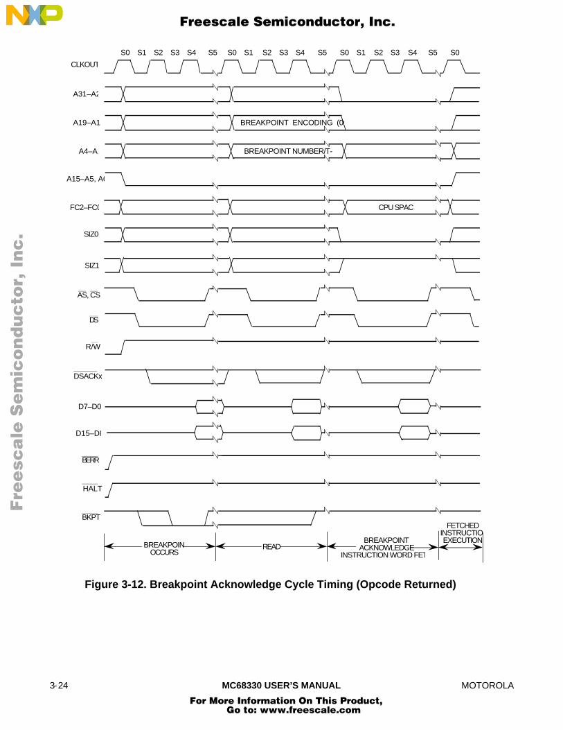
3-24 MC68330 USER’S MANUAL MOTOROLA
FC2–FC0
SIZ0
D15–D8
R/W
DSACKx
BERR
HALT
AS, CS
DS
BKPT
D7–D0
SIZ1
CPU SPACE
FETCHED INSTRUCTIONEXECUTIONBREAKPOINT
ACKNOWLEDGEINSTRUCTION WORD FET
A15–A5, A0
A19–A1
CLKOUT
A31–A2
A4–A1
S0 S1 S2 S3 S4 S5 S0 S1 S2 S3 S4 S5 S0 S1 S2 S3 S4 S5 S0
BREAKPOINT ENCODING (00
BREAKPOINT NUMBER/T-
BREAKPOINTOCCURS
READ
Figure 3-12. Breakpoint Acknowledge Cycle Timing (Opcode Returned)
Fre
esc
ale
Se
mic
on
du
cto
r, I
Freescale Semiconductor, Inc.
For More Information On This Product, Go to: www.freescale.com
nc
...

MOTOROLA MC68330 USER’S MANUAL 3-25
EXCEPTIONSTACKING
FC2–FC
SIZ0
D15–D
R/W
DSACKx
BERR
HALT
AS,CS
DS
BKPT
D7–D0
SIZ1
CPU SPACE
A19–A
A15–A5,
CLKOUT
A31–A2
A4–A
S0 S1 S2 S3 S4 S5
BREAKPOINT ENCODING
BREAKPOINT NUMBER/T
S0 S1 S2 S3 S4 S5 S0 S1 S2 S3 S4 S5 S0
BREAKPOINTOCCURS
READBREAKPOINT
ACKNOWLEDGEBUS ERROR ASSERTE
Figure 3-13. Breakpoint Acknowledge Cycle Timing (Exception Signaled)
3.4.2 LPSTOP Broadcast CycleThe LPSTOP broadcast cycle is generated by the CPU32 executing the LPSTOPinstruction. The external bus interface must get a copy of the interrupt mask level from the
Fre
esc
ale
Se
mic
on
du
cto
r, I
Freescale Semiconductor, Inc.
For More Information On This Product, Go to: www.freescale.com
nc
...

3-26 MC68330 USER’S MANUAL MOTOROLA
CPU32, so the CPU32 performs a CPU space type 3 write with the mask level encoded onthe data bus, as shown in the following figure. The CPU space type 3 cycle waits for thebus to be available, and is shown externally to indicate to external devices that theMC68330 is going into low-power stop mode. If an external device requires additional timeto prepare for entry into low-power stop mode, entry can be delayed by assertingf HALT.The SIM40 provides internal DSACKx response to this cycle. For more information on howthe SIM40 responds to low-power stop mode, see Section 4 System IntegrationModule.
0 0 0 0 0 0 0 0 0 0 0 0 0 0 0 0
15 14 13 12 11 10 9 8 7 6 5 4 3 2 1 0
RESET:I2 I1 I0
I2-I0 — Interrupt Mask LevelThe interrupt mask level is encoded on bits 2 – 0 of the data bus during anLPSTOP broadcast.
3.4.3 Module Base Address Register AccessAll internal module registers, including the SIM40, occupy a single 4K-byte block that isrelocatable along 4K-byte boundaries. The location is fixed by writing the desired baseaddress of the SIM40 block to the module base address register using the MOVESinstruction. The module base address register is only accessible in CPU space at address$0003FF00. The SFC or DFC register must indicate CPU space (FC2:0=$7), using theMOVEC instruction, before accessing MBAR. Refer to Section 4 System IntegrationModule for additional information on the module base address register.
3.4.4 Interrupt Acknowledge Bus CyclesThe CPU32 makes an interrupt pending in three cases. The first case occurs when aperipheral device signals the CPU32 (with the IRQ7-IRQ1 signals) that the devicerequires service and the internally synchronized value on these signals indicates a higherpriority than the interrupt mask in the status register. The second case occurs when atransition has occurred in the case of a level 7 interrupt. A recognized level 7 interruptmust be removed for one clock cycle before a second level 7 can be recognized. The thirdcase occurs if, upon returning from servicing a level 7 interrupt, the request level stays at 7and the processor mask level changes from 7 to a lower level, a second level 7 isrecognized. The CPU32 takes an interrupt exception for a pending interrupt within oneinstruction boundary (after processing any other pending exception with a higher priority).The following paragraphs describe the various kinds of interrupt acknowledge bus cyclesthat can be executed as part of interrupt exception processing.
3.4.4.1 INTERRUPT ACKNOWLEDGE CYCLE – TERMINATED NORMALLY. When theCPU32 processes an interrupt exception, it performs an interrupt acknowledge cycle toobtain the number of the vector that contains the starting location of the interrupt serviceroutine. Some interrupting devices have programmable vector registers that contain theinterrupt vectors for the routines they use. The following paragraphs describe the interruptacknowledge cycle for these devices. Other interrupting conditions or devices cannotsupply a vector number and use the autovector cycle described in 3.4.4.2 AutovectorInterrupt Acknowledge Cycle.
Fre
esc
ale
Se
mic
on
du
cto
r, I
Freescale Semiconductor, Inc.
For More Information On This Product, Go to: www.freescale.com
nc
...

MOTOROLA MC68330 USER’S MANUAL 3-27
The interrupt acknowledge cycle is a read cycle. It differs from the read cycle described in3.3.1 Read Cycle in that it accesses the CPU address space. Specifically, the differencesare as follows:
1. FC2-FC0 are set to $7 (FC2/FC1/FC0=111) for CPU address space.
2. A3, A2, and A1 are set to the interrupt request level, and the IACKx strobecorresponding to the current interrupt level is asserted. (Either the function codesand address signals or the IACKx strobes can be monitored to determine that aninterrupt acknowledge cycle is in progress and the current interrupt level.)
3. The CPU32 space type field (A19-A16) is set to $F (interrupt acknowledge).
4. Other address signals (A31-A20, A15-A4, and A0) are set to one.
5. The SIZ0, SIZ1, and R/W signals are driven to indicate a single-byte read cycle.The responding device places the vector number on the least significant byte of itsdata port (for an 8-bit port, the vector number must be on D15-D8; for a 16-bit port,the vector must be on D7-D0) during the interrupt acknowledge cycle. Beyond this,the cycle is terminated normally with DSACKx.
Figure 3-14 is a flowchart of the interrupt acknowledge cycle; Figure 3-15 shows the timingfor an interrupt acknowledge cycle terminated with DSACKx.
START NEXT CYCLE
RELEASE
1. NEGATE DSAC
MC68330INTERRUPTING DEVICE
REQUEST INTERRUPT GRANT INTERRUPT
PROVIDE VECTOR NUMBER
ACQUIRE VECTOR NUMBER
1. LATCH VECTOR NUM
1. PLACE VECTOR NUMBER ON LEAST SIGNIFICANT BYTE OF DATA BUS2. ASSERT DSACKx (OR AVEC IF NO V NUMBER)
2. NEGATE DS AND
1. SYNCHRONIZE IRQ1–IRQ72. COMPARE IRQ1–IRQ7 TO MASK LEVE WAIT FOR INSTRUCTION TO COMPLE3. PLACE INTERRUPT LEVEL ON A3–A1 TYPE FIELD (A19–A16) = $F4. SET R/W TO READ5. SET FC2–FC0 TO 1116. DRIVE SIZE PINS TO INDICATE A ONE TRANSFER 7. ASSERT AS AND DS
Figure 3-14. Interrupt Acknowledge Cycle Flowchart
Fre
esc
ale
Se
mic
on
du
cto
r, I
Freescale Semiconductor, Inc.
For More Information On This Product, Go to: www.freescale.com
nc
...

3-28 MC68330 USER’S MANUAL MOTOROLA
CLKOUT
A31–A
FC2–FC
S0 S2 S4 S2 S4 S0
SIZ0
DSACKx
D7–D0
R/W
AS,CS
DS
A3–A
A0
SIZ1
D15–D
S0 S1 S2
IRQ7–IRQ
VECTOR FROM 16-BIT POR
1 BYTE
INTERRUPT LEVEL
READ CYCLE
WRITE STACK
INTERNALARBITRATIO
IACK CYCLE
IACK7–IACK
VECTOR FROM 8-BIT POR
CPU SPACE
0 - 2 CLOCK
*
*Internal Arbitration may take between 0 to 2 clock cycles.
Figure 3-15. Interrupt Acknowledge Cycle Timing
3.4.4.2 AUTOVECTOR INTERRUPT ACKNOWLEDGE CYCLE. When the interruptingdevice cannot supply a vector number, it requests an automatically generated vector(autovector). Instead of placing a vector number on the data bus and asserting DSACKx,the device asserts AVEC to terminate the cycle. The DSACKx signals may not beasserted during an interrupt acknowledge cycle terminated by AVEC. The vector numbersupplied in an autovector operation is derived from the interrupt level of the currentinterrupt. When the AVEC signal is asserted instead of DSACKx during an interrupt
Fre
esc
ale
Se
mic
on
du
cto
r, I
Freescale Semiconductor, Inc.
For More Information On This Product, Go to: www.freescale.com
nc
...

MOTOROLA MC68330 USER’S MANUAL 3-29
acknowledge cycle, the MC68330 ignores the state of the data bus and internallygenerates the vector number (the sum of the interrupt level plus 24 ($18)).
AVEC is multiplexed with CS0. The AVEC bit in the module configuration register (MCR)controls whether the AVEC/CS0 pin is used as an autovector input or as CS0 (refer toSection 4 System Integration Module for additional information). AVEC is only sampledduring an interrupt acknowledge cycle. During all other cycles, AVEC is ignored.Additionally, AVEC can be internally generated for external devices by programming theautovector register. Seven distinct autovectors can be used, corresponding to the sevenlevels of interrupt available with signals IRQ7-IRQ1. Figure 3-16 shows the timing for anautovector operation.
Fre
esc
ale
Se
mic
on
du
cto
r, I
Freescale Semiconductor, Inc.
For More Information On This Product, Go to: www.freescale.com
nc
...
3-30 MC68330 USER’S MANUAL MOTOROLA
READ CYCLE
INTERNALARBITRATION
IACK CYCLE
WRITE STACK
S0 S2 S4 S2 S4 S0S0 S1 S2
1 BYTE
INTERRUPT LEVEL
CLKOUT
A31–A
FC2–FC
SIZ0
DSACKx
D15–D
R/W
AS
DS
A3–A
A0
SIZ1
AVEC
IRQ7-IRQ
IACK7–IACK
CPU SPACE
0 - 2 CLOCK
*
*Internal Arbitration may take between 0 to 2 clock cycles.
Figure 3-16. Autovector Operation Timing
3.4.4.3 SPURIOUS INTERRUPT CYCLE. Requested interrupts, whether internal orexternal, are arbitrated internally. When no internal module (including the SIM40, whichresponds for external requests) responds during an interrupt acknowledge cycle byarbitrating for the interrupt acknowledge cycle internally, the spurious interrupt monitorgenerates an internal bus error signal to terminate the vector acquisition. The MC68330automatically generates the spurious interrupt vector number, 24, instead of the interruptvector number in this case. When an external device does not respond to an interruptacknowledge cycle with AVEC or DSACKx, a bus monitor must assert BERR, which
Fre
esc
ale
Se
mic
on
du
cto
r, I
Freescale Semiconductor, Inc.
For More Information On This Product, Go to: www.freescale.com
nc
...

MOTOROLA MC68330 USER’S MANUAL 3-31
results in the CPU32 taking the spurious interrupt vector. If HALT is also asserted, theMC68330 retries the interrupt acknowledge cycle instead of using the spurious interruptvector.
3.5 BUS EXCEPTION CONTROL CYCLES
The bus architecture requires assertion of DSACKx from an external device to signal thata bus cycle is complete. Neither DSACKx nor AVEC is asserted in the following cases:
• DSACKx /AVEC is programmed to respond internally.
• The external device does not respond.
• Various other application-dependent errors occur.
The MC68330 provides BERR when no device responds by asserting DSACKx/AVECwithin an appropriate period of time after the MC68330 asserts AS. This mechanismallows the cycle to terminate and the MC68330 to enter exception processing for the errorcondition. HALT is also used for bus exception control. This signal can be asserted by anexternal device for debugging purposes to cause single bus cycle operation, or, incombination with BERR, a retry of a bus cycle in error. To properly control termination of abus cycle for a retry or a bus error condition, DSACKx, BERR, and HALT can be assertedand negated with the rising edge of the MC68330 clock. This assures that when twosignals are asserted simultaneously, the required setup and hold time for both is met forthe same falling edge of the MC68330 clock. This or an equivalent precaution should bedesigned into the external circuitry to provide these signals. Alternatively, the internal busmonitor could be used. The acceptable bus cycle terminations for asynchronous cyclesare summarized in relation to DSACKx assertion as follows (case numbers refer to Table3-4):
• Normal Termination: DSACKx is asserted; BERR and HALT remain negated(case 1).
• Halt Termination: HALT is asserted at the same time, or before DSACKx, andBERR remains negated (case 2).
• Bus Error Termination: BERR is asserted in lieu of, at the same time, or beforeDSACKx (case 3) or after DSACKx (case 4), and HALT remains negated; BERR isnegated at the same time or after DSACKx
• Retry Termination: HALT and BERR are asserted in lieu of, at the same time, orbefore DSACKx (case 5) or after DSACKx (case 6); BERR is negated at the sametime or after DSACKx, and HALT may be negated at the same time or after BERR.
Table 3-4 shows various combinations of control signal sequences and the resulting buscycle terminations. To ensure predictable operation, BERR and HALT should be negatedaccording to the specifications in the MC68330/D, MC68330 Technical Summary.DSACKx, BERR, and HALT may be negated after AS. If DSACKx or BERR remainasserted into S2 of the next bus cycle, that cycle may be terminated prematurely.
EXAMPLE A: A system uses a bus monitor timer to terminate accesses to an unpopulatedaddress space. The timer asserts BERR after timeout (case 3).
Fre
esc
ale
Se
mic
on
du
cto
r, I
Freescale Semiconductor, Inc.
For More Information On This Product, Go to: www.freescale.com
nc
...
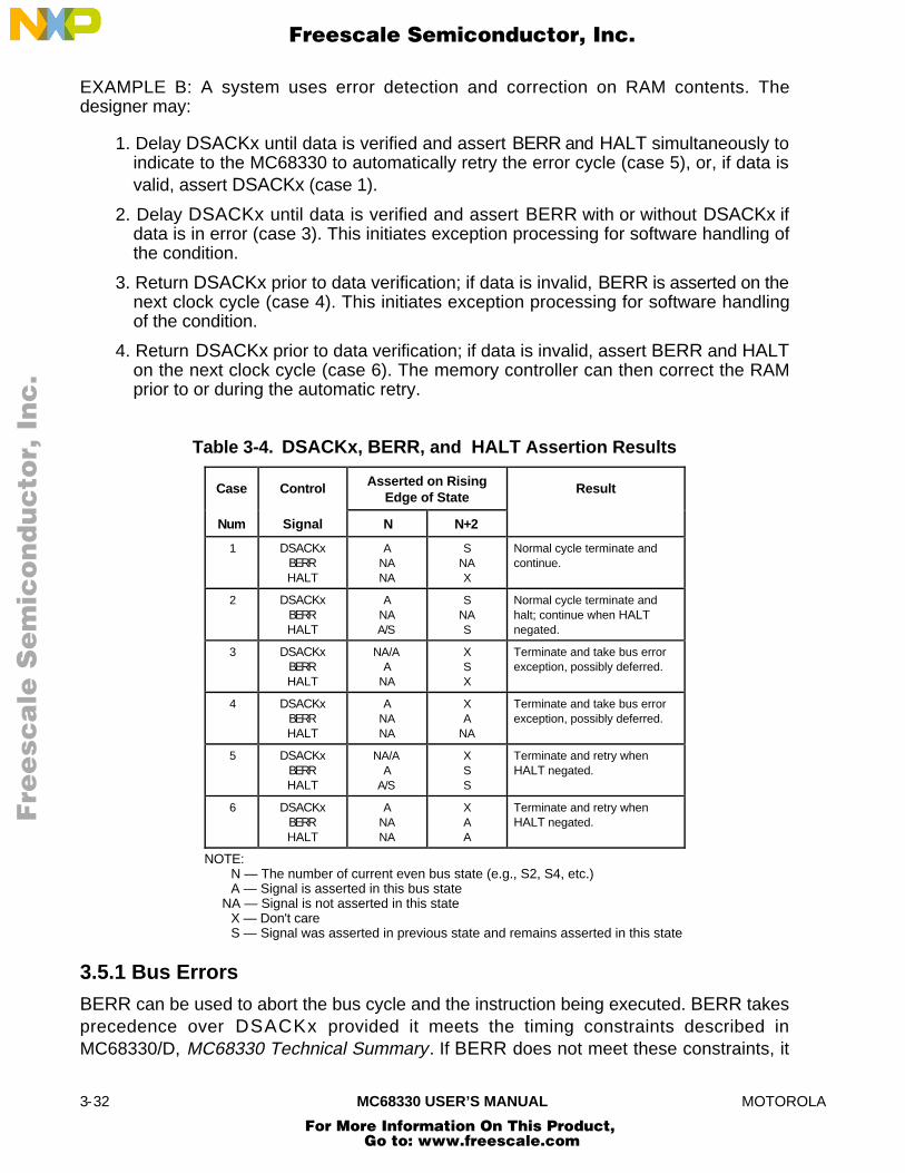
3-32 MC68330 USER’S MANUAL MOTOROLA
EXAMPLE B: A system uses error detection and correction on RAM contents. Thedesigner may:
1. Delay DSACKx until data is verified and assert BERR and HALT simultaneously toindicate to the MC68330 to automatically retry the error cycle (case 5), or, if data isvalid, assert DSACKx (case 1).
2. Delay DSACKx until data is verified and assert BERR with or without DSACKx ifdata is in error (case 3). This initiates exception processing for software handling ofthe condition.
3. Return DSACKx prior to data verification; if data is invalid, BERR is asserted on thenext clock cycle (case 4). This initiates exception processing for software handlingof the condition.
4. Return DSACKx prior to data verification; if data is invalid, assert BERR and HALTon the next clock cycle (case 6). The memory controller can then correct the RAMprior to or during the automatic retry.
Table 3-4. DSACKx, BERR, and HALT Assertion Results
Case Control Asserted on RisingEdge of State
Result
Num Signal N N+2
1 DSACKxBERRHALT
ANANA
SNAX
Normal cycle terminate andcontinue.
2 DSACKxBERRHALT
ANAA/S
SNAS
Normal cycle terminate andhalt; continue when HALTnegated.
3 DSACKxBERRHALT
NA/AA
NA
XSX
Terminate and take bus errorexception, possibly deferred.
4 DSACKxBERRHALT
ANANA
XA
NA
Terminate and take bus errorexception, possibly deferred.
5 DSACKxBERRHALT
NA/AA
A/S
XSS
Terminate and retry whenHALT negated.
6 DSACKxBERRHALT
ANANA
XAA
Terminate and retry whenHALT negated.
NOTE:N — The number of current even bus state (e.g., S2, S4, etc.)A — Signal is asserted in this bus state
NA — Signal is not asserted in this stateX — Don't careS — Signal was asserted in previous state and remains asserted in this state
3.5.1 Bus Errors
BERR can be used to abort the bus cycle and the instruction being executed. BERR takesprecedence over DSACKx provided it meets the timing constraints described inMC68330/D, MC68330 Technical Summary. If BERR does not meet these constraints, it
Fre
esc
ale
Se
mic
on
du
cto
r, I
Freescale Semiconductor, Inc.
For More Information On This Product, Go to: www.freescale.com
nc
...

MOTOROLA MC68330 USER’S MANUAL 3-33
may cause unpredictable operation of the MC68330. If BERR remains asserted into thenext bus cycle, it may cause incorrect operation of that cycle. When BERR is issued toterminate a bus cycle, the MC68330 may enter exception processing immediatelyfollowing the bus cycle, or it may defer processing the exception.
The instruction prefetch mechanism requests instruction words from the bus controllerbefore it is ready to execute them. If a bus error occurs on an instruction fetch, theMC68330 does not take the exception until it attempts to use that instruction word. Shouldan intervening instruction cause a branch or should a task switch occur, the bus errorexception does not occur. The bus error condition is recognized during a bus cycle in anyof the following cases:
• DSACKx and HALT are negated, and BERR is asserted.
• HALT and BERR are negated, and DSACKx is asserted. BERR is then assertedwithin one clock cycle (HALT remains negated).
• BERR and HALT are asserted together, indicating a retry.
When the MC68330 recognizes a bus error condition, it terminates the current bus cycle inthe normal way. Figure 3-17 shows the timing of a bus error for the case in whichDSACKx is not asserted. Figure 3-18 shows the timing for a bus error that is assertedafter DSACKx. Exceptions are taken in both cases. (Refer to Section 5 CPU32 for detailsof bus error exception processing.)
CLKOUT
S0 S2
DSACKx
R/W
AS,CS
DS
BERR
S0 S2SW S4SW S4
INTERNALPROCESSING
STACK WRITE
READ CYCLE WITH BUSERROR
FC2–FC0SIZ1-SIZ
D15–D
A31–A
Figure 3-17. Bus Error without DSACKx
Fre
esc
ale
Se
mic
on
du
cto
r, I
Freescale Semiconductor, Inc.
For More Information On This Product, Go to: www.freescale.com
nc
...

3-34 MC68330 USER’S MANUAL MOTOROLA
S0 S2 S4 S0 S2 S4
INTERNALPROCESSING
STACK WRITE
WRITE CYCLE
CLKOUT
DSACKx
R/W
DS
BERR
D15–D
A31–A
AS,CS
FC2–FC0SIZ1-SIZ
Figure 3-18. Late Bus Error with DSACKxIn the second case, in which BERR is asserted after DSACKx is asserted, BERR must beasserted within the time specified for purely asynchronous operation, or it must beasserted and remain stable during the sample window around the next falling edge of theclock after DSACKx is recognized. If BERR is not stable at this time, the MC68330 mayexhibit erratic behavior. BERR has priority over DSACKx. In this case, data may bepresent on the bus but may not be valid. This sequence can be used by systems that havememory error detection and correction logic and by external cache memories.
3.5.2 Retry Operation
When both BERR and HALT are asserted by an external device during a bus cycle, theMC68330 enters the retry sequence shown in Figure 3-19. A delayed retry, which issimilar to the delayed bus error signal described previously, can also occur (see Figure 3-20). The MC68330 terminates the bus cycle, places the control signals in their inactivestate, and does not begin another bus cycle until the BERR and HALT signals are negatedby external logic. After a synchronization delay, the MC68330 retries the previous cycleusing the same access information (address, function code, size, etc.). BERR should benegated before S2 of the retried cycle to ensure correct operation of the retried cycle.
Fre
esc
ale
Se
mic
on
du
cto
r, I
Freescale Semiconductor, Inc.
For More Information On This Product, Go to: www.freescale.com
nc
...

MOTOROLA MC68330 USER’S MANUAL 3-35
S0 S2 S0 S2SW S4SW S4
READ RERUNHALTREAD CYCLE WITHRETRY
DATA IGNORED
CLKOUT
DSACKx
R/W
AS,CS
DS
BERR
A31–A
FC2–FC0SIZ1-SIZ
D15–D
HALT
Figure 3-19. Retry Sequence
The MC68330 retries any read or write cycle of a read-modify-write operation separately;RMC remains asserted during the entire retry sequence. Asserting BR along with BERRand HALT provides a relinquish and retry operation. The MC68330 does not relinquish thebus during a read-modify-write operation. Any device that requires the MC68330 to giveup the bus and retry a bus cycle during a read-modify-write cycle must assert BERR andBR only (HALT must not be included). The bus error handler software should examine theread-modify-write bit in the special status word (refer to Section 5 CPU32) and take theappropriate action to resolve this type of fault when it occurs.
Fre
esc
ale
Se
mic
on
du
cto
r, I
Freescale Semiconductor, Inc.
For More Information On This Product, Go to: www.freescale.com
nc
...

3-36 MC68330 USER’S MANUAL MOTOROLA
S0 S2
S4 S0 S2 S4
HALT WRITE RERUN
WRITE CYCLE
CLKOUT
DSACKx
R/W
DS
BERR
A31–A
D15–D1
HALT
AS,CS
FC2–FC0SIZ1-SIZ
Figure 3-20. Late Retry Sequence
3.5.3 Halt Operation
When HALT is asserted and BERR is not asserted, the MC68330 halts external busactivity at the next bus cycle boundary (see Figure 3-21). HALT by itself does notterminate a bus cycle. Negating and reasserting HALT in accordance with the correcttiming requirements provides a single step (bus cycle to bus cycle) operation. HALTaffects external bus cycles only, thus a program that does not require use of the externalbus may continue executing. The single-cycle mode allows the user to proceed through(and debug) external MC68330 operations, one bus cycle at a time. Since the occurrenceof a bus error while HALT is asserted causes a retry operation, the user must anticipateretry cycles while debugging in the single-cycle mode. The single-step operation and thesoftware trace capability allow the system debugger to trace single bus cycles, singleinstructions, or changes in program flow.
When the MC68330 completes a bus cycle with HALT asserted, D15-D0 is placed in thehigh-impedance state, and bus control signals are driven inactive (not high-impedancestate); the address, function code, size, and read/write signals remain in the same state.The halt operation has no effect on bus arbitration (refer to 3.6 Bus Arbitration). Whenbus arbitration occurs while the MC68330 is halted, the address and control signals arealso placed in the high-impedance state. Once bus mastership is returned to theMC68330, if HALT is still asserted, the address, function code, size, and read/write
Fre
esc
ale
Se
mic
on
du
cto
r, I
Freescale Semiconductor, Inc.
For More Information On This Product, Go to: www.freescale.com
nc
...

MOTOROLA MC68330 USER’S MANUAL 3-37
signals are again driven to their previous states. The MC68330 does not service interruptrequests while it is halted.
CLKOUT
S0 S2 S4
R/W
DS
HALT
S0 S2 S4
BR
BG
BGACK
S0
READ HALT(ARBITRATION PERMITTEDWHILE THE PROCESSOR IS
HALTED)
READ
DSACKx
A31–A
D15–D1
AS,CS
FC2–FC0SIZ1-SIZ
Figure 3-21. HALT Timing
3.5.4 Double Bus FaultA double bus fault results when a bus error or an address error occurs during theexception processing sequence for any of the following:
• A previous bus error
• A previous address error
• A reset
For example, the MC68330 attempts to stack several words containing information aboutthe state of the machine while processing a bus error exception. If a bus error exceptionoccurs during the stacking operation, the second error is considered a double bus fault.
Fre
esc
ale
Se
mic
on
du
cto
r, I
Freescale Semiconductor, Inc.
For More Information On This Product, Go to: www.freescale.com
nc
...

3-38 MC68330 USER’S MANUAL MOTOROLA
When a double bus fault occurs, the MC68330 halts and drives the HALT line low. Only areset operation can restart a halted MC68330. However, bus arbitration can still occur(refer to 3.6 Bus Arbitration). A second bus error or address error that occurs afterexception processing has completed (during the execution of the exception handlerroutine, or later) does not cause a double bus fault. A bus cycle that is retried does notconstitute a bus error or contribute to a double bus fault. The MC68330 continues to retrythe same bus cycle as long as the external hardware requests it.
Reset can also be generated internally by the halt monitor (see Section 5 CPU32).
3.6 BUS ARBITRATIONThe bus design of the MC68330 provides for a single bus master at any one time, eitherthe MC68330 or an external device. One or more of the external devices on the bus canhave the capability of becoming bus master for the external bus, but not the MC68330internal bus. Bus arbitration is the protocol by which an external device becomes busmaster; the bus controller in the MC68330 manages the bus arbitration signals so that theMC68330 has the lowest priority. External devices that need to obtain the bus must assertthe bus arbitration signals in the sequences described in the following paragraphs.Systems that include several devices that can become bus master require externalcircuitry to assign priorities to the devices, so that when two or more external devicesattempt to become bus master at the same time, the one having the highest prioritybecomes bus master first. The sequence of the protocol is as follows:
1. An external device asserts BR.
2. The MC68330 asserts BG to indicate that the bus is available.
3. The external device asserts BGACK to indicate that it has assumed bus mastership.
BR may be issued any time during a bus cycle or between cycles. BG is asserted inresponse to BR. To guarantee operand coherency, BG is only asserted at the end of anoperand transfer. Additionally, BG is not asserted until the end of a read-modify-writeoperation (when RMC is negated) in response to a BR signal. When the requesting devicereceives BG and more than one external device can be bus master, the requesting deviceshould begin whatever arbitration is required. When it assumes bus mastership, theexternal device asserts BGACK and maintains BGACK during the entire bus cycle (orcycles) for which it is bus master. The following conditions must be met for an externaldevice to assume mastership of the bus through the normal bus arbitration procedure: 1) Itmust have received BG through the arbitration process, and 2) BGACK must be inactive,indicating that no other bus master has claimed ownership of the bus.
Figure 3-22 is a flowchart showing the detail involved in bus arbitration for a single device.This technique allows processing of bus requests during data transfer cycles. Refer toFigures 3-23 and 3-24 for the bus arbitration timing diagram.
BR is negated at the time that BGACK is asserted. This type of operation applies to asystem consisting of the MC68330 and one device capable of bus mastership. In a systemhaving a number of devices capable of bus mastership, BR from each device can be wire-ORed to the MC68330. In such a system, more than one bus request could be assertedsimultaneously. BG is negated a few clock cycles after the transition of BGACK. However,
Fre
esc
ale
Se
mic
on
du
cto
r, I
Freescale Semiconductor, Inc.
For More Information On This Product, Go to: www.freescale.com
nc
...

MOTOROLA MC68330 USER’S MANUAL 3-39
if bus requests are still pending after the negation of BG, the MC68330 asserts another BGwithin a few clock cycles after it was negated. This additional assertion of BG allowsexternal arbitration circuitry to select the next bus master before the current bus masterhas finished using the bus. The following paragraphs provide additional information aboutthe three steps in the arbitration process. Bus arbitration requests are recognized duringnormal processing, HALT assertion, and when the CPU32 has halted due to a double busfault.
GRANT BUS ARBITRATI
1. ASSERT B
TERMINATE ARBITRATI
1. NEGATE BG (AND WAITBGACK TO BE NEGAT
RE-ARBITRATE OR RESUME PROCESSOR OPERATION
PROCESSOR REQUESTING DEVIC
REQUEST THE BUS
1. ASSERT B
ACKNOWLEDGE BUS MASTERSHIP
1. EXTERNAL ARBITRATION DETERMINES NEXT BUS MASTER2. NEXT BUS MASTER WAITS FOR BGAC TO BE NEGATED3. NEXT BUS MASTER ASSERTS BGACK TO BECOME NEW MASTER4. BUS MASTER NEGATES BR
OPERATE AS BUS MASTER
RELEASE BUS MASTERSHIP
1. NEGATE BGA
1. PERFORM DATA TRANSFERS (REA WRITE CYCLES) ACCORDING TO TH SAME RULES THE PROCESSOR USE
Figure 3-22. Bus Arbitration Flowchart for Single Request
Fre
esc
ale
Se
mic
on
du
cto
r, I
Freescale Semiconductor, Inc.
For More Information On This Product, Go to: www.freescale.com
nc
...

3-40 MC68330 USER’S MANUAL MOTOROLA
CLKOUT
AS, CS
D15–D
A31–A
A0 A5 A5 A2 A3 A0
BR
BG
BGACK
UWE, LW
Figure 3-23. Bus Arbitration Timing Diagram — Idle Bus Case
CLKOUT
A31-A0
R/W
AS
DS
D15-D0
DSACK1, DSACK0
BR
BG
BGACK
S0 S1 S2 S3 S4 S5
Figure 3-24. Bus Arbitration Timing Diagram— Active Bus Case
Fre
esc
ale
Se
mic
on
du
cto
r, I
Freescale Semiconductor, Inc.
For More Information On This Product, Go to: www.freescale.com
nc
...

MOTOROLA MC68330 USER’S MANUAL 3-41
3.6.1 Bus Request
External devices capable of becoming bus masters request the bus by asserting BR. Thissignal can be wire-ORed to indicate to the MC68330 that some external device requirescontrol of the bus. The MC68330 is effectively at a lower bus priority level than theexternal device and relinquishes the bus after it has completed the current bus cycle (ifone has started). If no BGACK is received while the BR is active, the MC68330 remainsbus master once BR is negated. This prevents unnecessary interference with ordinaryprocessing if the arbitration circuitry inadvertently responds to noise or if an externaldevice determines that it no longer requires use of the bus before it has been grantedmastership.
3.6.2 Bus GrantThe MC68330 supports operand coherency, thus, if an operand transfer requires multiplebus cycles, the MC68330 does not release the bus until the entire transfer is complete.The assertion of BG is, therefore, subject to the following constraints:
• The minimum time for BG assertion after BR is asserted depends on internalsynchronization (see MC68330/D, MC68330 Technical Summary).
• During an external operand transfer, the MC68330 does not assert BG until after the lastcycle of the transfer (determined by SIZx and DSACKx).
• During an external operand transfer, the MC68330 does not assert BG as long as RMCis asserted.
• If the show cycle bits SHEN1-0 = 01, the MC68330 does not assert BG to an externalmaster.
Externally, the BG signal can be routed through a daisy-chained network or a priority-encoded network. The MC68330 is not affected by the method of arbitration as long as theprotocol is obeyed.
3.6.3 Bus Grant AcknowledgeAn external device cannot request and be granted the external bus while another device isthe active bus master. A device that asserts BGACK remains the bus master until itnegates BGACK. BGACK should not be negated until all required bus cycles arecompleted. Bus mastership is terminated at the negation of BGACK.
Once an external device receives the bus and asserts BGACK, it should negate BR. If BRremains asserted after BGACK is asserted, the MC68330 assumes that another device isrequesting the bus and prepares to issue another BG.
3.6.4 Bus Arbitration ControlThe bus arbitration control unit in the MC68330 is implemented with a finite state machine.As discussed previously, all asynchronous inputs to the MC68330 are internallysynchronized in a maximum of two cycles of the clock. As shown in Figure 3-25 inputsignals labeled R and A are internally synchronized versions of BR and BGACKrespectively. The BG output is labeled G, and the internal high-impedance control signal islabeled T. If T is true, the address, data, and control buses are placed in the high-
Fre
esc
ale
Se
mic
on
du
cto
r, I
Freescale Semiconductor, Inc.
For More Information On This Product, Go to: www.freescale.com
nc
...

3-42 MC68330 USER’S MANUAL MOTOROLA
impedance state after the next rising edge following the negation of AS and RMC. Allsignals are shown in positive logic (active high) regardless of their true active voltagelevel. The state machine shown in Figure 3-25 does not have a state 1 or state 4.State changes occur on the next rising edge of the clock after the internal signal is valid.The BG signal transitions on the falling edge of the clock after a state is reached duringwhich G changes. The bus control signals (controlled by T) are driven by the MC68330immediately following a state change, when bus mastership is returned to the MC68330.State 0, in which G and T are both negated, is the state of the bus arbiter while theMC68330 is bus master. R and A keep the arbiter in state 0 as long as they are bothnegated.
The MC68330 does not allow arbitration of the external bus during the RMC sequence. Forthe duration of this sequence, the MC68330 ignores the BR input. If mastership of the busis required during an RMC operation, BERR must be used to abort the RMC sequence.
Fre
esc
ale
Se
mic
on
du
cto
r, I
Freescale Semiconductor, Inc.
For More Information On This Product, Go to: www.freescale.com
nc
...

MOTOROLA MC68330 USER’S MANUAL 3-43
R
STATE 5
GTV
STATE 3
VG T
STATE 2
VGT
STATE 0
VG T
STATE 6
GTV
RAB
R A
AB
RA B+
RA
R
R A+
RA
RA
A+
R - BUS REQUESTA - BUS GRANT ACKNOWLEDGEB - BUS CYCLE IN PROGRESS
G - BUS GRANTT - THREE-STATE SIGNAL TO BUS CONTROLV - BUS AVAILABLE TO BUS CONTROL
RARA
RA
Figure 3-25. Bus Arbitration State Diagram
3.6.5 Show CyclesThe MC68330 can perform data transfers with its internal modules without using theexternal bus, but, when debugging, it is desirable to have address and data informationappear on the external bus. These external bus cycles, called show cycles, aredistinguished by the fact that AS is not asserted externally. DS is used to signal addressstrobe timing in show cycles.
After reset, show cycles are disabled and must be enabled by writing to the SHEN bits inthe module configuration register (see 4.3.2.1 Module Configuration Register (MCR)).
Fre
esc
ale
Se
mic
on
du
cto
r, I
Freescale Semiconductor, Inc.
For More Information On This Product, Go to: www.freescale.com
nc
...

3-44 MC68330 USER’S MANUAL MOTOROLA
When show cycles are disabled, the address bus, function codes, size, and read/writesignals continue to reflect internal bus activity. However, AS and DS are not assertedexternally and the external data bus remains in a high impedance state. When showcycles are enabled, DS indicates address strobe timing and the external data bus containsdata. The following paragraphs are a state-by-state description of show cycles, and Figure3-26 illustrates a show cycle timing diagram. Refer to MC68330/D, MC68330 TechnicalSummary for specific timing information.
State 0 – During state 0, the address and function codes become valid, R/W is drivento indicate a show read or write cycle, and the size pins indicate the number ofbytes to transfer. During a read, the addressed peripheral is driving the data bus,and the user must take care to avoid bus conflicts.
State 41 – One-half clock cycle later DS (rather than AS) is asserted to indicate thataddress information is valid.
State 42– No action occurs in state 42. The bus controller remains in state 42 (waitstates will be inserted) until the internal read cycle is complete.
State 43– When DS is negated, show data is valid on the next falling edge of thesystem clock. The external data bus drivers are enabled so that data becomes validon the external bus as soon as it is available on the internal bus.
State 0 – The address, function codes, read/write, and size pins change to begin thenext cycle. Data from the preceding cycle is valid through state 0.
A31–A0, FC2-FC0, SIZ1-SIZ0
CLKOUT
S0 S42 S1S41 S43 S2S0
R/W
AS, CS
DS
D15–D
SHOW CYCL START OF EXTERNAL CYC
BKPT
UWE, LWE
Figure 3-26. Show Cycle Timing Diagram
Fre
esc
ale
Se
mic
on
du
cto
r, I
Freescale Semiconductor, Inc.
For More Information On This Product, Go to: www.freescale.com
nc
...

MOTOROLA MC68330 USER’S MANUAL 3-45
3.7 RESET OPERATIONThe MC68330 has reset control logic to determine the cause of reset, synchronize it ifnecessary, and assert the appropriate reset lines. The reset control logic canindependently drive three different lines:
1. EXTRST (external reset) drives the external RESET pin.
2. CLKRST (clock reset) resets the clock module.
3. INTRST (internal reset) goes to all other internal circuits.
Table 3-5 summarizes the result of each reset source. Synchronous reset sources are notasserted until the end of the current bus cycle, whether or not RMC is asserted. Theinternal bus monitor is automatically enabled for synchronous resets; therefore if thecurrent bus cycle does not terminate normally, the bus monitor terminates it. Only single-byte or word transfers are guaranteed valid for synchronous resets. Asynchronous resetsources indicate a catastrophic failure, and the reset controller logic immediately resetsthe system. Resetting the MC68330 causes any bus cycle in progress to terminate as ifDSACKx, or BERR had been asserted. In addition, the MC68330 appropriately initializesregisters for a reset exception.
Table 3-5 Reset Source Summary
Type Source Timing Reset Lines Asserted by Controller
External External Synchronous INTRST CLKRST EXTRST
Power-up EBI Asynchronous INTRST CLKRST EXTRST
Software Watchdog Sys Prot Asynchronous INTRST CLKRST EXTRST
Double Bus Fault Sys Prot Asynchronous INTRST CLKRST EXTRST
Loss of Clock Clock Synchronous INTRST CLKRST EXTRST
Reset Instruction CPU32 Asynchronous – – EXTRST
If an external device drives RESET low, RESET should be asserted for at least 590 clockperiods to ensure that the MC68330 resets. The reset control logic holds reset assertedinternally until the external RESET is released. When the reset control logic detects thatexternal RESET is no longer being driven, it drives both internal and external reset low foran additional 512 cycles to guarantee this length of reset to the entire system. Figure 3-27shows the RESET timing.
RESET
1 CLOCK
DRIVEN BY MC68PULLED EXTERNALL
512 CLOCK> 590 CLOCK
Fre
esc
ale
Se
mic
on
du
cto
r, I
Freescale Semiconductor, Inc.
For More Information On This Product, Go to: www.freescale.com
nc
...

3-46 MC68330 USER’S MANUAL MOTOROLA
Figure 3-27. Timing for External Devices Driving RESET
If reset is asserted from any other source, the reset control logic asserts RESET for aminimum of 512 cycles, and until the source of reset is negated.
After any internal reset occurs, a 14-cycle rise time is allowed before testing for thepresence of an external reset. If no external reset is detected, the CPU32 begins its vectorfetch.
Figure 3-28 is a timing diagram of the power-up reset operation, showing the relationshipsbetween RESET, VCC, and bus signals. During the reset period, the entire bus three-states (except for non-three-statable signals, which are driven to their inactive state). OnceRESET negates, all control signals are driven to their inactive state, the data bus is in readmode, and the address bus is driven. After this, the first bus cycle for RESET exceptionprocessing begins.
CLKOUT
VCOLOCK
BUSCYCLES
RESET
VCC
1 2 3 4BUS STATEUNKNOWN
ADDRESS AND CONTROL SIGNAL
THREE-STATED
512 CLOCKS
NOTES:1. Internal start-up time.2. SSP read here.3. PC read here.4. First instruction fetched here.
14 CLOCKS≤
Figure 3-27. Initial Reset Operation Timing
When a reset instruction is executed, the MC68330 drives the RESET signal for 512 clockcycles. In this case, the MC68330 resets the external devices of the system, and theinternal registers of the MC68330 are unaffected.
Fre
esc
ale
Se
mic
on
du
cto
r, I
Freescale Semiconductor, Inc.
For More Information On This Product, Go to: www.freescale.com
nc
...

MOTOROLA MC68330 USER'S MANUAL 4-1
SECTION 4SYSTEM INTEGRATION MODULE
The MC68330 system integration module (SIM40) consists of several functions thatcontrol the system startup, initialization, configuration, and the external bus with aminimum of external devices. It also provides the IEEE 1149.1 boundary scancapabilities. The SIM40 functions include the following:
• System Configuration and Protection• Clock Synthesizer• Chip Selects and Wait States• External Bus Interface• Bus Arbitration• Dynamic Bus Sizing• IEEE 1149.1 Test Access Port
4.1 MODULE OVERVIEWThe system configuration and protection function controls system configuration andprovides various monitors and timers, including the internal bus monitor, double bus faultmonitor, spurious interrupt monitor, software watchdog timer, and the periodic interrupttimer.
The clock synthesizer generates the clock signals used by the SIM40 and the CPU32, aswell as the CLKOUT used by external devices.
The programmable chip-select function provides four chip-select signals that can enableexternal memory and peripheral circuits, providing all handshaking and timing signals.Each chip-select signal has an associated base address register and an address maskregister that contain the programmable characteristics of that chip select. Up to three waitstates can be programmed by bits in the address mask register.
The external bus interface (EBI) handles the transfer of information between the internalCPU32 and memory, peripherals, or other processing elements in the external addressspace. See Section 3 Bus Operation for further information.
The MC68330 dynamically interprets the port size of an addressed device during eachbus cycle, allowing operand transfers to or from 8- and 16-bit ports. The device signalsits port size and indicates completion of the bus cycle through the use of the DSACKxinputs. Dynamic bus sizing allows a programmer to write code that is not bus-widthspecific. For a discussion on dynamic bus sizing see Section 3 Bus Operation.
The MC68330 includes dedicated user-accessible test logic that is fully compliant withthe IEEE 1149.1 Standard Test Access Port and Boundary Scan Architecture. Problems
Fre
esc
ale
Se
mic
on
du
cto
r, I
Freescale Semiconductor, Inc.
For More Information On This Product, Go to: www.freescale.com
nc
...

4-2 MC68330 USER'S MANUAL MOTOROLA
associated with testing high-density circuit boards have led to the development of thisstandard under the sponsorship of the IEEE Test Technology Committee and Joint TestAction Group (JTAG). The MC68330 implementation supports circuit-board teststrategies based on this standard. Refer to Section 6 IEEE 1149.1 Test AccessPort for additional information.
4.2 MODULE OPERATIONThe following paragraphs describe the operation of the module base address register,system configuration and protection, clock synthesizer, and chip-select functions, and theexternal bus interface.
4.2.1 Module Base Address Register OperationThe module base address register (MBAR) controls the location of all module registers(see 4.3.1 Module Base Address Register). The address stored in this register isthe base address (starting location) for the internal module registers. The internalmodule registers are contained in a single 4K-byte block (see Figure 4-1) that isrelocatable along 4K-byte boundaries.
MC68330RELOCATABL
MODULEBLOCK
RAM(TYPICAL
$0000000
$XXXXXFFF
SIM40
MBAR($0003FF0FC=111)
$XXXXX000
$FFF
$07F
$000
$FFFFFFFF
NOTE: $XXXXX IS THE VALUE CONTAINED IN MBAR BITS B
Figure 4-1. SIM40 Module Register BlockThe location of the internal registers is fixed by writing the desired base address of the4K-byte block to the MBAR using the MOVES instruction to address $0003FF00 in CPUspace. The SFC and DFC registers contain the address space values (FC2–FC0) for theread or write operand of the MOVES instruction (see Section 5 CPU32 o rM68000PM/AD, Programmer’s Reference Manual). Therefore, the SFC or DFC registermust indicate CPU space (FC2–FC0=$7), using the MOVEC instruction, beforeaccessing MBAR. The offset from the base address is shown above each register
Fre
esc
ale
Se
mic
on
du
cto
r, I
Freescale Semiconductor, Inc.
For More Information On This Product, Go to: www.freescale.com
nc
...

MOTOROLA MC68330 USER'S MANUAL 4-3
diagram. The SIM40 address range, fixed within the relocatable 4K-byte memory block,is $000–$07F.
4.2.2 System Configuration and Protection FunctionThe SIM40 allows the user to control certain features of system configuration by writingbits in the module configuration register (MCR). This register also contains read-onlystatus bits that show the state of the SIM40.
All M68000 Family members are designed to provide maximum system safeguards. Asan extension of the family, the MC68330 promotes the same basic concepts ofsafeguarded design present in all M68000 members. In addition, many functions thatnormally must be provided by external circuits are incorporated in this device. Thefollowing features are provided in the system configuration and protection function:
SIM40 ConfigurationThe SIM40 allows the user to configure the system to the particular requirements.The functions include control of FREEZE and show cycle operation, the function ofthe CS3–CS0 signals, the access privilege of the supervisor/user registers, thelevel of interrupt arbitration, and automatic autovectoring for external interrupts.
Reset StatusThe reset status register provides the user with information on the cause of themost recent reset. The possible causes include: external, power-up, softwarewatchdog, double bus fault, loss of clock, and reset instruction.
Internal Bus MonitorThe SIM40 provides an internal bus monitor to monitor the data and sizeacknowledge (DSACK) response time for all internal bus accesses. An optionallows the monitoring of external bus accesses. For external bus accesses, fourselectable response times are provided to allow for variations in response speedof memory and peripherals used in the system. A bus error signal is asserted in-ternally if the DSACK response limit is exceeded. BERR is not asserted externally.This monitor can be disabled for external bus cyles only.
Double Bus Fault MonitorThe double bus fault monitor causes a reset to occur if the internal HALT isasserted by the CPU32, indicating a double bus fault. A double bus fault resultswhen a bus or address error occurs during the exception processing sequence fora previous bus or address error, a reset, or while the CPU is loading informationfrom a bus error stack frame during an RTE instruction. This function can bedisabled. See Section 3 Bus Operation for more information.
Spurious Interrupt MonitorIf no interrupt arbitration occurs during an interrupt acknowledge cycle (IACK), thebus error signal is asserted internally.
Software WatchdogThe software watchdog asserts reset or a level 7 interrupt (as selected by thesystem protection and control register) if the software fails to service the softwarewatchdog for a designated period of time (i.e., because it is trapped in a loop orlost). There are eight selectable timeout periods. This function can be disabled.
Fre
esc
ale
Se
mic
on
du
cto
r, I
Freescale Semiconductor, Inc.
For More Information On This Product, Go to: www.freescale.com
nc
...

4-4 MC68330 USER'S MANUAL MOTOROLA
Periodic Interrupt TimerThe SIM40 provides a timer to generate periodic interrupts. The periodic interrupttime period can vary from 122 µs to 15.94 s (with a 32.768-kHz crystal used togenerate the system clock). This function can be disabled.
Figure 4-2 shows a block diagram of the system configuration and protection function.
SOFTWARE RESETREQUEST orIRQ7
HALTRESET
BERR
SOFTWAREWATCHDOG
PERIODICINTERRUPT TIMER
IRQ7-IRQ
CLOCK
RESETSTATUS
2PRESCALER
9
MODULECONFIGURATIO
REQUEST
BUSMONITOR
SPURIOUS INTERRUPT MONITOR
DOUBLE BUSFAULT MONITO
Figure 4-2. System Configuration and Protection Function4.2.2.1 SYSTEM CONFIGURATION. Aspects of the system configuration arecontrolled by the MCR and the autovector register (AVR). The AVEC bit in the MCRcontrols whether the AVEC/CS0 pin is used as an autovector input or as CS0.
For debug purposes, internal bus accesses can be shown on the external bus. Thisfunction is called show cycles. The SHEN1, SHEN0 bits in the MCR control show cycles.
Arbitration for servicing interrupts is controlled by the value programmed into theinterrupt arbitration (IARB) field of the MCR. The SIM40 arbitrates for both its owninterrupts and externally generated interrupts. The SIM40 IARB must contain a valueother than $0 (interrupts with IARB=0 are discarded as extraneous).
The AVR contains bits that correspond to external interrupt levels that require anautovector response. The SIM40 supports up to seven discrete external interruptrequests. If the bit corresponding to an interrupt level is set in the AVR, the SIM40 returnsan autovector in response to the IACK cycle servicing that external interrupt request.
Fre
esc
ale
Se
mic
on
du
cto
r, I
Freescale Semiconductor, Inc.
For More Information On This Product, Go to: www.freescale.com
nc
...

MOTOROLA MC68330 USER'S MANUAL 4-5
Otherwise, external circuitry must either return an interrupt vector or assert the externalAVEC signal.
4.2.2.2 INTERNAL BUS MONITOR. The internal bus monitor continually checks forthe bus cycle termination response time by checking the DSACKx, BERR, and HALTstatus or the AVEC status during an IACK cycle. The monitor initiates a bus error if theresponse time is excessive. The bus monitor feature cannot be disabled for internalaccesses to an internal module. The internal bus monitor cannot check the DSACKxresponse on the external bus unless the MC68330 is the bus master. The BME bit in thesystem protection control register (SYPCR) enables the internal bus monitor for internal-to-external bus cycles. If the system contains external bus masters whose bus cyclesmust be monitored, an external bus monitor must be implemented. In this case, theinternal-to-external bus monitor option must be disabled.
The bus cycle termination response time is measured in clock cycles, and the maximum-allowable response time is programmable. The bus monitor response time periodranges from 8 to 64 system clocks (see Table 4-8). These options are provided to allowfor different response times of peripherals that might be used in the system.
4.2.2.3 DOUBLE BUS FAULT MONITOR. A double bus fault is caused by a buserror or address error during the exception processing sequence. The double bus faultmonitor responds to an assertion of HALT on the internal bus. Refer to Section 3 BusOperation for more information. The DBF bit in the reset status register indicates thatthe last reset was caused by the double bus fault monitor. The double bus fault monitorreset can be enabled by the DBFE bit in the SYPCR.
4.2.2.4 SPURIOUS INTERRUPT MONITOR. The spurious interrupt monitor issuesBERR if no interrupt arbitration occurs during an IACK cycle. Normally, during an IACKcycle, the SIM40 recognizes that the CPU32 is responding to interrupt request(s) andarbitrates for the privilege of returning a vector or asserting AVEC. (The SIM40 reportsand arbitrates for externally generated interrupts.) This feature cannot be disabled.
4.2.2.5 SOFTWARE WATCHDOG. The SIM40 provides a software watchdog optionto prevent system lock-up in case the software becomes trapped in loops with nocontrolled exit. Once enabled by the SWE bit in the SYPCR, the software watchdogrequires a special service sequence to be executed on a periodic basis. If this periodicservicing action does not occur, the software watchdog times out and issues a reset or alevel 7 interrupt (as programmed by the SWRI bit in the SYPCR). The address of theinterrupt service routine for the software watchdog interrupt is stored in the softwareinterrupt vector register (SWIV). Figure 4-3 shows a block diagram of the softwarewatchdog as well as the clock control circuits for the periodic interrupt timer.
The watchdog clock rate is determined by the SWP bit in the periodic interrupt timerregister (PITR) and the SWT bits in the SYPCR. See Table 4-7 for a list of watchdogtimeout periods.
The software watchdog service sequence consists of the following two steps: write $55 tothe software service register (SWSR) and write $AA to the SWSR. Both writes must occurin the order listed prior to the watchdog timeout, but any number of instructions oraccesses to the SWSR can be executed between the two writes.
Fre
esc
ale
Se
mic
on
du
cto
r, I
Freescale Semiconductor, Inc.
For More Information On This Product, Go to: www.freescale.com
nc
...

4-6 MC68330 USER'S MANUAL MOTOROLA
CLOCKDISABLE PRESCALER (2
CLOCKMUX
EXTAL
15 STAGE DIVIDER CHAIN (2LPSTOP
SWPPTP
FREEZE
SWCLK
PITCLK
PRECLK9
15
.
.
2 2 2 29 11 13 15
RESET
4 MODULUS COUNTE PITINTERRUPT
PITR
Figure 4-3. Software Watchdog Block Diagram
4.2.2.6 PERIODIC INTERRUPT TIMER. The periodic interrupt timer consists of an8-bit modulus counter that is loaded with the value contained in the PITR (see Figure4-3). The modulus counter is clocked by a signal derived from the buffered crystaloscillator (EXTAL) input pin unless an external frequency source is used. When anexternal frequency source is used (MODCK low during reset), the default state of theprescaler control bits (SWP and PTP) in the PITR is changed to enable both prescalers.
Either clock source (EXTAL or EXTAL÷512) is divided by four before driving the moduluscounter (PITCLK). When the modulus counter value reaches zero, an interrupt isgenerated. The level of the generated interrupt is programmed into the PIRQL bits in theperiodic interrupt control register (PICR). During the IACK cycle, the SIM40 places theperiodic interrupt vector, programmed into the PIV bits in the PICR, onto the internal bus.The value of bits 7–0 in the PITR is then loaded again into the modulus counter, and thecounting process starts over. If a new value is written to the PITR, this value is loaded intothe modulus counter when the current count is completed.
4.2.2.6.1 Periodic Timer Period Calculation. The period of the periodic timer canbe calculated using the following equation:
PITR count valueperiodic interrupt timer period = EXTAL frequency/prescaler value
22
Solving the equation using a crystal frequency of 32.768-kHz with the prescaler disabledgives:
PITR count valueperiodic interrupt timer period = 32768/1
22
periodic interrupt timer period = PITR count value8192
This gives a range from 122 µs, with a PITR value of $01 (00000001 binary), to 31.128ms, with a PITR value of $FF (11111111 binary).
Fre
esc
ale
Se
mic
on
du
cto
r, I
Freescale Semiconductor, Inc.
For More Information On This Product, Go to: www.freescale.com
nc
...

MOTOROLA MC68330 USER'S MANUAL 4-7
Solving the equation with the prescaler enabled (PTP=1) gives the following values:
PITR count valueperiodic interrupt timer period = 32768/512
22
periodic interrupt timer period = PITR count value16
This gives a range from 62.5 ms, with a PITR value of $01, to 15.94 s, with a PITR valueof $FF.
For fast calculation of periodic timer period using a 32.768-kHz crystal, the followingequations can be used:
With prescaler disabled:
programmable interrupt timer period = PITR (122 µs)
With prescaler enabled:
programmable interrupt timer period = PITR (62.5 ms)
4.2.2.6.2 Using the Periodic Timer as a Real-Time Clock. The periodicinterrupt timer can be used as a real-time clock interrupt by setting it up to generate aninterrupt with a one-second period. Rearranging the periodic timer period equation tosolve for the desired count value:
PITR count value = (PIT period) (EXTAL frequency)(Prescaler value) (22)
PITR count value = (1) (32768)(512) (22)
PITR count value = 16 (decimal)
Therefore, when using a 32.768-kHz crystal, the PITR should be loaded with a value of$10 with the prescaler enabled to generate interrupts at a one-second rate.
4.2.2.7 SIMULTANEOUS INTERRUPTS BY SOURCES IN THE SIM40. If thepossible level 7 interrupt sources in the SIM40 are simultaneously asserted, the SIM40will prioritize and service the interrupts in the following order: 1) software watchdog, 2)periodic interrupt timer, and 3) external interrupts.
4.2.3 Clock SynthesizerThe clock synthesizer can operate with either an external crystal or an external oscillatorfor reference, using the internal phase-locked loop (PLL) and voltage-controlledoscillator (VCO), or an external clock can drive the clock signal directly, at the operatingfrequency. There are four modes of clock operation, listed in Table 4-1.
Table 4-1. Clock Operating Modes
Fre
esc
ale
Se
mic
on
du
cto
r, I
Freescale Semiconductor, Inc.
For More Information On This Product, Go to: www.freescale.com
nc
...

4-8 MC68330 USER'S MANUAL MOTOROLA
Mode Description MODCKResetValue
VCCSYNOperating
ValueCrystal Mode External crystal used with the on-chip PLL and VCO to
generate a system clock and CLKOUT of programmablerates.
5 V 5 V
External ClockMode
The desired operating frequency is driven into EXTALresulting in a system clock and CLKOUT of the samefrequency, not tightly coupled (XFC=0V).
0 V 0 V*
External ClockMode with PLL
The desired operating frequency is driven into EXTAL,resulting in a system clock and CLKOUT of the samefrequency, with a tight skew between input and outputsignals.
0 V 5 V
Limp Mode Upon input signal loss for either clock mode using the PLL,operation continues at approximately one-half maximumspeed (affected by the value of the X-bit in SYNCR).
X 5 V
* For external clock mode, XFC should be tied to GND.
In crystal mode (see Figure 4-4), the clock synthesizer can operate from the on-chip PLLand VCO, using a parallel resonant crystal connected between the EXTAL and XTALpins as a reference frequency source. The oscillator circuit is shown in Figure 4-5. A32.768-kHz watch crystal provides an inexpensive reference, but the reference crystalfrequency can be any frequency in the range specified in MC68330/D, MC68330Technical Summary. When using a 32.768-kHz crystal, the system clock frequency isprogrammable (using the W, X, and Y bits in the SYNCR) over the range specified inMC68330/D, MC68330 Technical Summary.
CLKOUT
PHASECOMPARATOR
LOW-PASSFILTER VCO
CRYSTALOSCILLATOR
SYSTEMCLOCK
CLOCK CONTROL
XFC PIN VCCSYN
XFC
VCCSYN
0.1 µF
.01 µF
0.1 µF
NOTE 1: Must be low-leakage capacitor.
FEEDBACK DIVIDER
EXTAL XTAL
20 pF 20 pF
20 MΩ
330
Ω
1
Figure 4-4. Clock Block Diagram for Crystal Operation
Fre
esc
ale
Se
mic
on
du
cto
r, I
Freescale Semiconductor, Inc.
For More Information On This Product, Go to: www.freescale.com
nc
...

MOTOROLA MC68330 USER'S MANUAL 4-9
A separate power pin (VCCSYN) is used to allow the clock circuits to run with the rest ofthe device powered down and to provide increased noise immunity for the clock circuits.The source for VCCSYN should be a quiet power supply with adequate external bypasscapacitors placed as close as possible to the VCCSYN pin to ensure a stable operatingfrequency. Figure 4-4 shows typical values for the bypass and PLL external capacitors.The crystal manufacturer's documentation should be consulted for specificrecommendations for external components.
XTALEXTAL
60 kΩ
60 kΩ
Figure 4-5. MC68330 Crystal Oscillator
To use an external clock source (see Figure 4-6), the operating clock frequency can bedriven directly into the EXTAL pin (the XTAL pin must be left floating for this case). Thisresults in a system clock and CLKOUT that are the same as the input signal frequency,but not tightly coupled to it. To enable this mode, MODCK must be held low during reset,and VCCSYN and XFC held at 0V while the chip is in operation.
Fre
esc
ale
Se
mic
on
du
cto
r, I
Freescale Semiconductor, Inc.
For More Information On This Product, Go to: www.freescale.com
nc
...

4-10 MC68330 USER'S MANUAL MOTOROLA
CLKOUT
PHASECOMPARATOR
LOW-PASSFILTER VCO
CRYSTALOSCILLATOR
SYSTEMCLOCK
CLOCK CONTROL
XFC PIN VCCSYN
XFC
VCCSYN
.01 µF
0.1 µF
NOTE 1: MUST BE LOW-LEAKAGE CAPACITOR. 2: EXTERNAL MODE USES THIS PATH ONLY.
FEEDBACK DIVIDER
EXTAL XTAL
1
EXTERNALCLOCK
2
Figure 4-6. Clock Block Diagram for External Oscillator Operation
Alternatively, an external clock signal can be directly driven into EXTAL (with XTAL leftfloating) using the on-chip PLL. This results in an internal clock and CLKOUT signal ofthe same frequency as the input signal, with a tight skew between the external clock andthe internal clock and CLKOUT signals. To enable this mode, MODCK must be held lowduring reset, and VCCSYN connected to a quiet 5 V source.
If an input signal loss for either of the clock modes utilizing the PLL occurs, chipoperation can continue in limp mode with the VCO running at approximately one-half themaximum speed (affected by the value of the X-bit in the SYNCR register), using aninternal voltage reference. The limp mode bit (SLIMP) in the SYNCR indicates that a lossof input signal reference has been detected. The reset enable (RSTEN) bit controlswhether an input signal loss causes a system reset or causes the device to operate inlimp mode. The synthesizer lock bit (SLOCK) in the SYNCR indicates when the VCO haslocked onto the desired frequency, or if an external clock is being used.
4.2.3.1 PHASE COMPARATOR AND FILTER. The phase comparator takes theoutput of the frequency divider and compares it to an external input signal reference. Theresult of this compare is low-pass filtered and used to control the VCO. The comparatoralso detects when the external crystal or oscillator stops running to initiate the limp modefor the system clock.
The PLL requires an external low-leakage filter capacitor, typically in the range from 0.01to 0.1 µF, connected between the XFC and VCCSYN pins. The XFC capacitor shouldprovide 50 MΩ insulation, and should not be electrolytic. Smaller values of the external
Fre
esc
ale
Se
mic
on
du
cto
r, I
Freescale Semiconductor, Inc.
For More Information On This Product, Go to: www.freescale.com
nc
...

MOTOROLA MC68330 USER'S MANUAL 4-11
filter capacitor provide a faster response time for the PLL, and larger values providegreater frequency stability.
4.2.3.2 FREQUENCY DIVIDER. The frequency divider circuits divide the VCOfrequency down to the reference frequency for the phase comparator. The frequencydivider consists of the following: 1) a 2-bit prescaler controlled by the W bit in the SYNCRand 2) a 6-bit modulo downcounter controlled by the Y bits in the SYNCR.
Several factors are important to the design of the system clock. The resulting systemclock frequency must be within the limits specified for the device. The frequency of thesystem clock is given by the following equation:
FSYSTEM = FCRYSTAL (4(Y+1)22W+X)
The maximum VCO frequency limit must also be observed. The VCO frequency is givenby the following equation:
FVCO = FSYSTEM(2–X)
Since clearing the X-bit causes the VCO to run at twice the system frequency, the VCOupper frequency limit must be considered when programming the SYNCR. Both thesystem clock and VCO frequency limits are given in the MC68330/D, MC68330Technical Summary. Table 4-2 lists some the frequencies available from variouscombinations of SYNCR bits with a reference frequency of 32.768-kHz.
Table 4-2. System Frequencies from 32.768-kHz Reference
Y W=0; X=0 W=0; X=1 W=1; X=0 W=1; X=1000000 131 262 524 1049
000101 786 1573 3146 6291
001010 1442 2884 5767 11534
001111 2097 4194 8389 16777
010100 2753 5505 11010 22020
011001 3408 6816 13631 –
011111 4194 8389 16777 –
100011 4719 9437 18874 –
101000 5374 10748 20972 –
101101 6029 12059 23593 –
110010 6685 13369 – –
110111 7340 14680 – –
111100 7995 15991 – –
111111 8389 16777 – –
NOTE: System frequencies are in kHz.
4.2.3.3 CLOCK CONTROL. The clock control circuits determine the source used forboth internal and external clocks during special circumstances, such as low-power stop(LPSTOP) execution.
Table 4-3 summarizes the clock activity during LPSTOP, in crystal mode operation. Anyclock in the off state is held low. Two bits in the SYNCR (STEXT and STSIM) controlclock activity during LPSTOP. Refer to 4.2.6 Low-Power Stop for additionalinformation.
Fre
esc
ale
Se
mic
on
du
cto
r, I
Freescale Semiconductor, Inc.
For More Information On This Product, Go to: www.freescale.com
nc
...

4-12 MC68330 USER'S MANUAL MOTOROLA
Table 4-3. Clock Control Signals
Control Bits Clock OutputsSTSIM STEXT SIMCLK CLKOUT
0 0 EXTAL Off
0 1 EXTAL EXTAL
1 0 VCO Off
1 1 VCO VCO
NOTE: SIMCLK runs the periodic interrupt RESET and IRQx pin synchronizersin LPSTOP mode.
4.2.4 Chip-Select FunctionTypical microprocessor systems require external hardware to provide select signals toexternal memory and peripherals. This device integrates these functions on-chip toprovide the cost, speed, and reliability benefits of a higher level of integration. The chip-select function contains register pairs for each external chip-select signal. The pairconsists of a base address register and an address mask register that define thecharacteristics of a single chip select. The register pair provides flexibility for a widevariety of chip-select functions.
4.2.4.1 PROGRAMMABLE FEATURES. The chip-select function supports thefollowing programmable features:
Four Programmable Chip-Select CircuitsAll four chip-select circuits are independently programmable from the same list ofselectable features. Each chip-select circuit has an individual base addressregister and address mask register that contain the programmed characteristics ofthat chip select. The base address register selects the starting address for theaddress block in 256-byte increments. The address mask register specifies thesize of the address block range. The valid (V) bit of the base address registerindicates that the register information for that chip select is valid. A global chipselect allows address decode for a boot ROM before system initialization occurs.
Variable Block SizesThe block size, starting from the specified base address, can vary in size from 256bytes up to 4 Gbytes in 2n increments. This size is specified in the address maskregister.
Both 8- and 16-Bit Ports SupportedThe 8-bit ports are accessible on both odd and even addresses when connectedto data bus bits 15–8; the 16-bit ports can be accessed as odd bytes, even bytes,or even words. The port size is specified by the PS bits in the address maskregister.
Write Protect CapabilityThe WP bit in each base address register can restrict write access to its range ofaddresses.
Fast-Termination OptionProgramming the FTE bit in the base address register for the fast-terminationoption causes the chip-select function to terminate the cycle by asserting theinternal DSACKx early, providing a two-cycle external access.
Fre
esc
ale
Se
mic
on
du
cto
r, I
Freescale Semiconductor, Inc.
For More Information On This Product, Go to: www.freescale.com
nc
...

MOTOROLA MC68330 USER'S MANUAL 4-13
Internal DSACKx Generation for External Accesses with Programmable Wait StatesDSACKx can be generated internally with up to three wait states for a particulardevice using the DD bits in the address mask register.
Full 32-Bit Address Decode with Address Space CheckingThe FC bits in the base address register and FCM bits in the address maskregister are used to select address spaces for which the chip selects will beasserted.
4.2.4.2 GLOBAL CHIP-SELECT OPERATION. Global chip-select operation allowsaddress decode for a boot ROM before system initialization occurs. CS0 is the globalchip-select output, and its operation differs from the other external chip-select outputsfollowing reset. When the CPU32 begins fetching after reset, CS0 is asserted for everyaddress until the V-bit in the module address base register (MBAR) is set.
Global chip select provides a 16-bit port with three wait states, which allows a boot ROMto be located in any address space and still provide the stack pointer and programcounter values at $00000000 and $00000004, respectively. Global chip select does notprovide write protection and responds to all function codes. CS0 operates in this manneruntil the V-bit is set in the CS0 base address register. CS0 can be programmed tocontinue decode for a range of addresses after the V-bit is set, provided the desiredaddress range is first loaded into base address register 0. After the V-bit is set for CS0,global chip select can only be restarted with a system reset.
A system can use an 8-bit boot ROM if an external 8-bit DSACK is generated whichresponds in two wait states or less. See Section 7 Applications for a discussion.
4.2.5 External Bus InterfaceThis section describes port A and port B functions. Refer to Section 3 Bus Operationfor more information about the external bus interface.
4.2.5.1 PORT A. Port A pins can be independently programmed to be eitheraddresses A31–A24, discrete I/O pins, or IACKx pins. The port A pin assignmentregisters (PPARA1 and PPARA2) control the function of the port A pins as shown inTable 4-4. Upon reset, port A is configured as input pins. If the system uses these signalsas addresses, pulldowns should be put on these signals to avoid indeterminate valuesuntil the port A registers can be programmed.
Table 4-4. Port A Pin Assignment Register Function
Pin Function
Signal PPARA1 BIT = 0 PPARA1 BIT = 1 PPARA1 BIT = 0PPARA2 BIT = 0 PPARA2 BIT = X PPARA2 BIT = 1
A31 A31 PORT A7 IACK7A30 A30 PORT A6 IACK6A29 A29 PORT A5 IACK5A28 A28 PORT A4 IACK4A27 A27 PORT A3 IACK3A26 A26 PORT A2 IACK2
Fre
esc
ale
Se
mic
on
du
cto
r, I
Freescale Semiconductor, Inc.
For More Information On This Product, Go to: www.freescale.com
nc
...

4-14 MC68330 USER'S MANUAL MOTOROLA
A25 A25 PORT A1 IACK1A24 A24 PORT A0 –
4.2.5.2 PORT B. Port B pins can be independently programmed to be IRQx andMODCK pins, or discrete I/O pins. The port B pin assignment register (PPARB) controlsthe function of the port B pins as shown in Table 4-5. Upon reset, port B is configured toprovide for interrupt request inputs and MODCK.
Fre
esc
ale
Se
mic
on
du
cto
r, I
Freescale Semiconductor, Inc.
For More Information On This Product, Go to: www.freescale.com
nc
...

MOTOROLA MC68330 USER'S MANUAL 4-15
Table 4-5. Port B Pin AssignmentRegister
Pin Function
Signal PPARB BIT = 0 PPARB BIT = 1IRQ7 PORT B7 IRQ7IRQ6 PORT B6 IRQ6IRQ5 PORT B5 IRQ5IRQ4 PORT B4 IRQ4IRQ3 PORT B3 IRQ3IRQ2 PORT B2 IRQ2IRQ1 PORT B1 IRQ1
MODCK PORT B0 MODCK
NOTE: MODCK has no function after reset.
4.2.6 Low-Power StopExecuting the LPSTOP instruction provides reduced power consumption when theMC68330 is idle, with only the SIM40 remaining active. Operation of the SIM40 clockand CLKOUT during LPSTOP is controlled by the STSIM and STEXT bits in the SYNCR(see Table 4-3). LPSTOP disables the clock to the software watchdog in the low state.The software watchdog remains stopped until the LPSTOP mode is ended and begins torun again on the next rising clock edge.
NOTE
When the CPU32 executes the STOP instruction (asopposed to LPSTOP), the software watchdog continuesto run. If the software watchdog is enabled, it issues areset or interrupt when timeout occurs.
The periodic interrupt timer does not respond to an LPSTOP instruction; thus, it can beused to exit LPSTOP as long as the interrupt request level is higher than the CPU32interrupt mask level. To stop the periodic interrupt timer while in LPSTOP, the PITR mustbe loaded with a zero value before LPSTOP is executed. The bus monitor, double busfault monitor, and spurious interrupt monitor are all inactive during LPSTOP.
If an external device requires additional time to prepare for entry into LPSTOP mode,entry can be delayed by asserting HALT (see 3.4.2 LPSTOP Broadcast Cycle).
4.2.7 FreezeFREEZE is asserted by the CPU32 if a breakpoint is encountered with background modeenabled. Refer to Section 5 CPU32 for more information on the background mode.When FREEZE is asserted, the double bus fault monitor and spurious interrupt monitorcontinue to operate normally. However, the software watchdog and the periodic interrupttimer may be affected. Setting the FRZ1 bit in the MCR disables the software watchdogwhen FREEZE is asserted, and setting the FRZ0 bit in the MCR disables the periodicinterrupt timer when FREEZE is asserted.
Fre
esc
ale
Se
mic
on
du
cto
r, I
Freescale Semiconductor, Inc.
For More Information On This Product, Go to: www.freescale.com
nc
...

4-16 MC68330 USER'S MANUAL MOTOROLA
4.3 PROGRAMMER'S MODELFigure 4-7 is a programmer's model (register map) of all registers in the SIM40. For moreinformation about a particular register, refer to the description of the module or functionindicated in the right column. The ADDR (address) column indicates the offset of theregister from the address stored in the base address register. The FC (function code)column indicates whether a register is restricted to supervisor access (S) orprogrammable to exist in either supervisor or user space (S/U).
ADDR FC 15 8 7 0000 S MODULE CONFIGURATION REGISTER (MCR) SYSTEM
PROTECTION
004 S CLOCK SYNTHESIZER CONTROL REGISTER (SYNCR) CLOCK006 S AUTOVECTOR REGISTER (AVR) RESET STATUS REGISTER (RSR) SYSTEM
PROTECTION
010 S/U RESERVED PORT A DATA (PORTA) EBI012 S/U RESERVED PORT A DATA DIRECTION (DDRA) EBI014 S RESERVED PORT A PIN ASSIGNMENT 1 (PPRA1) EBI016 S RESERVED PORT A PIN ASSIGNMENT 2 (PPRA2) EBI018 S/U RESERVED PORT B DATA (PORTB) EBI01A S/U RESERVED PORT B DATA (PORTB1) EBI01C S/U RESERVED PORT B DATA DIRECTION (DDRB) EBI01E S RESERVED PORT B PIN ASSIGNMENT (PPARB) EBI020 S SW INTERRUPT VECTOR (SWIV) SYSTEM PROTECTION CONTROL
(SYPCR)SYSTEMPROTECTION
022 S PERIODIC INTERRUPT CONTROL REGISTER (PICR) SYSTEMPROTECTION
024 S PERIODIC INTERRUPT TIMING REGISTER (PITR) SYSTEMPROTECTION
026 S RESERVED SOFTWARE SERVICE (SWSR) SYSTEMPROTECTION
040 S ADDRESS MASK 1 CS0 CHIP SELECT042 S ADDRESS MASK 2 CS0 CHIP SELECT044 S BASE ADDRESS 1 CS0 CHIP SELECT046 S BASE ADDRESS 2 CS0 CHIP SELECT048 S ADDRESS MASK 1 CS1 CHIP SELECT04A S ADDRESS MASK 2 CS1 CHIP SELECT04C S BASE ADDRESS 1 CS1 CHIP SELECT04E S BASE ADDRESS 2 CS1 CHIP SELECT050 S ADDRESS MASK 1 CS2 CHIP SELECT052 S ADDRESS MASK 2 CS2 CHIP SELECT054 S BASE ADDRESS 1 CS2 CHIP SELECT056 S BASE ADDRESS 2 CS2 CHIP SELECT058 S ADDRESS MASK 1 CS3 CHIP SELECT05A S ADDRESS MASK 2 CS3 CHIP SELECT05C S BASE ADDRESS 1 CS3 CHIP SELECT05E S BASE ADDRESS 2 CS3 CHIP SELECT
Figure 4-7. SIM40 Programming Model
In the registers discussed in the following pages, the number in the upper right-handcorner indicates the offset of the register from the address stored in the module baseaddress register. The numbers on the top line of the register represent the bit position inthe register. The second line contains the mnemonic for the bit. The numbers below the
Fre
esc
ale
Se
mic
on
du
cto
r, I
Freescale Semiconductor, Inc.
For More Information On This Product, Go to: www.freescale.com
nc
...

MOTOROLA MC68330 USER'S MANUAL 4-17
register represent the bit values after reset. The access privilege is indicated in the lowerright-hand corner.
4.3.1 Module Base Address RegisterModule Base Address Register 1 $0003FF00
31 30 29 28 27 26 25 24 23 22 21 20 19 18 17 16
0 0 0 0 0 0 0 0 0 0 0 0 0 0 0 0RESET
BA31 BA30 BA29 BA28 BA27 BA26 BA25 BA24 BA23 BA22 BA21 BA20 BA19 BA18 BA17 BA16
CPU Space Only
Module Base Address Register 2 $0003FF0215 14 13 12 11 10 9 8 7 6 5 4 3 2 1 0
0 0 0 0 0 0 0 0 0 0 0 0 0 0 0 0RESET
AS6 AS5 AS4 AS3 AS2 AS1 AS0 VBA15 BA14 BA13 BA12 0 0 0 AS7
CPU Space Only
BA31–BA12 — Base Address Bits 31–12The base address field is the upper 20 bits of the module base address register,providing for block starting locations in increments of 4K-bytes.
AS7–AS0 — Address Space Bits 8–1The address space field allows particular address spaces to be masked, placingthe 4K module block into a particular address space(s). If an address space ismasked, an access to the register block location in that address space becomesan external access. The module block is not accessed. The address space bitsare:
AS7 — mask CPU space address space (FC2–FC0=111)AS6 — mask supervisor program address space (FC2–FC0=110)AS5 — mask supervisor data address space (FC2–FC0=101)AS4 — mask [Motorola reserved] address space (FC2–FC0=100)AS3 — mask [user reserved] address space (FC2–FC0=011)AS2 — mask user program address space (FC2–FC0=010)AS1 — mask user data address space (FC2–FC0=001)AS0 — mask [Motorola reserved] address space (FC2–FC0=000)
For each address space bit:1=Mask this address space from the internal module selection. The bus cycle
goes external.0=Decode for the internal module block.
V — Valid BitThis bit indicates when the contents of the module base address register are valid.The base address value is not used; therefore, all internal module registers arenot accessible until the V-bit is set.
1=Contents valid0=Contents not valid
NOTE
An access to this register does not affect externalspace, since the cycle is not run externally.
Fre
esc
ale
Se
mic
on
du
cto
r, I
Freescale Semiconductor, Inc.
For More Information On This Product, Go to: www.freescale.com
nc
...

4-18 MC68330 USER'S MANUAL MOTOROLA
The following is example code for accessing the module base address register (MBAR).
MBAR can be read using the following code: (Register D0 will contain the value ofMBAR.)
MOVE #7,D0 load D0 with the CPU space function codeMOVEC D0,SFC load SFC to indicate CPU spaceLEA $3FF00,A0 load A0 with the address of MBARMOVES.L (A0),D0 load D0 with the contents of MBAR
MBAR can be written to using the following code: (Address $0003FF00 in CPUspace (MBAR) will be loaded with the value $FFFF F001. This will set the baseaddress of the internal registers to $FFFFF.)
MOVE #7,D0 load D0 with the CPU space function codeMOVEC D0,DFC load SFC to indicate CPU spaceLEA $3FF00,A0 load A0 with the address of MBARMOVE.L #$FFFFF001,D0 load D0 with the value to be written into MBARMOVES.L D0,(A0) write the value contained in D0 into MBAR
4.3.2 System Configuration and Protection RegistersThe following paragraphs provide descriptions of the system configuration andprotection registers.
4.3.2.1 MODULE CONFIGURATION REGISTER (MCR). The MCR, which controlsthe SIM40 configuration, can be read or written at any time.
MCR $000
01 1 0 0 0 0 1 0 0 0 1 1 1 10RESET
15 14 13 12 11 10 9 8 7 6 5 4 3 2 1 0
0 FRZ1 FRZ2 FIRQ 0 0 SHEN SHEN0 SUPV 0 0 0 IARB3 IARB0IARB1IARB2
15 14 13 12 11 10 9 8 7 6 5 4 3 2 1 0
0 FRZ1 FRZ2 AVEC 0 0 SHEN1SHEN0 SUPV 0 0 0 IARB3 IARB0IARB1IARB2
Supervisor Only
Fre
esc
ale
Se
mic
on
du
cto
r, I
Freescale Semiconductor, Inc.
For More Information On This Product, Go to: www.freescale.com
nc
...

MOTOROLA MC68330 USER'S MANUAL 4-19
FRZ1 — Freeze Software Watchdog Enable1=When FREEZE is asserted, the software watchdog counters are disabled,
preventing interrupts from occurring during software debug.0=When FREEZE is asserted, the software watchdog counters continue to run. See
4.2.7 Freeze for more information.
FRZ0 — Freeze Periodic Interrupt Timer Enable1=When FREEZE is asserted, the periodic interrupt timer counters are disabled.0=When FREEZE is asserted, the periodic interrupt timer counters continue to
operate as programmed.
AVEC — Autovector1=Chip select 0 will be disabled, and this pin will fuction as an autovector input to
the device.0=The device will be configured with chip select 0 enabled.
SHEN1, SHEN0 — Show Cycle EnableThese two control bits determine what the EBI does with the external bus duringinternal transfer operations (See Table 4-6). A show cycle allows internal transfersto be externally monitored. The address, data, and control signals (except for AS)are driven externally. DS is used to signal address strobe timing for show cycles.Data is valid on the next falling clock edge after DS is negated. However, data isnot driven externally and AS and DS are not asserted externally for internalaccesses unless show cycles are enabled.
If external bus arbitration is disabled, the EBI will not recognize an external busrequest until arbitration is enabled again. When SHEN1 is set, an external busrequest causes an internal master to stop its current cycle and relinquish theinternal bus. The internal master resumes running cycles on the bus after BR andBGACK are negated. To prevent bus conflicts, external peripherals must notattempt to initiate cycles during show cycles with arbitration disabled.
Table 4-6. Show Cycle Control Bits
SHEN1 SHEN0 ACTION
0 0 Show cycles disabled, external arbitration enabled
0 1 Show cycles enabled, external arbitration disabled
1 X Show cycles enabled, external arbitration enabled
SUPV — Supervisor/User Data SpaceThe SUPV bit defines the SIM40 global registers as either supervisor data space oruser (unrestricted) data space.
1=The SIM40 registers defined as supervisor/user are restricted to supervisor dataaccess (FC2–FC0=$5). An attempted user-space write is ignored and returnsBERR.
0=The SIM40 registers defined as supervisor/user data are unrestricted (FC2 is adon't care).
Fre
esc
ale
Se
mic
on
du
cto
r, I
Freescale Semiconductor, Inc.
For More Information On This Product, Go to: www.freescale.com
nc
...

4-20 MC68330 USER'S MANUAL MOTOROLA
IARB3 – IARB0 — Interrupt Arbitration Bits 3–0The reset value of IARB is $F, allowing the SIM40 to arbitrate during an IACKcycle immediately after reset. The system software should initialize the IARB fieldto a value from $F (highest priority) to $1 (lowest priority). A value of $0 preventsarbitration and causes all SIM40 interrupts, including external interrupts, to bediscarded as extraneous.
4.3.2.2 AUTOVECTOR REGISTER (AVR). The AVR contains bits that correspond toexternal interrupt levels that require an autovector response. Setting a bit allows theSIM40 to assert an internal AVEC during the IACK cycle in response to the specifiedinterrupt request level. This register can be read and written at any time.
AVR $0067 6 5 4 3 2 1
0 0 0 0 0 0 0 0RESET
AV7 AV6 AV5 AV4 AV3 AV2 AV1 00
Supervisor Only
NOTE:
The IARB field in the MCR must contain a value otherthan $0 for the SIM40 to autovector for externalinterrupts.
4.3.2.3 RESET STATUS REGISTER (RSR). The RSR contains a bit for each resetsource to the SIM40. A set bit indicates the last type of reset that occurred, and only onebit can be set in the register. The RSR is updated by the reset control logic when theSIM40 comes out of reset. This register can be read at any time; a write has no effect. Formore information, see Section 3 Bus Operation.
RSR $0077 6 5 4 3 2 1 0
EXT POW SW DBF 0 LOC SYS 0
Supervisor Only
EXT — External Reset1=The last reset was caused by an external signal driving RESET.
POW — Power-Up Reset1=The last reset was caused by the power-up reset circuit.
SW — Software Watchdog Reset1=The last reset was caused by the software watchdog circuit.
DBF — Double Bus Fault Monitor Reset1=The last reset was caused by the double bus fault monitor.
LOC — Loss of Clock Reset1=The last reset was caused by a loss of frequency reference to the clock function.
This reset can only occur if the RSTEN bit in the clock function is set and the VCOis enabled.
SYS — System Reset
Fre
esc
ale
Se
mic
on
du
cto
r, I
Freescale Semiconductor, Inc.
For More Information On This Product, Go to: www.freescale.com
nc
...

MOTOROLA MC68330 USER'S MANUAL 4-21
1=The last reset was caused by the CPU32 executing a reset instruction. Thesystem reset does not load a reset vector or affect any internal CPU32 registers orSIM40 configuration registers, but does reset external devices.
4.3.2.4 SOFTWARE INTERRUPT VECTOR REGISTER (SWIV). The SWIVcontains the 8-bit vector that is returned by the SIM40 during an IACK cycle in responseto an interrupt generated by the software watchdog. This register can be read or writtenat any time. This register is set to the uninitialized vector, $0F, at reset.
SWIV $0207 6 5 4 3 2 1 0
0 0 0 0 1 1 1 1RESET
SWIV7 SWIV6 SWIV5SWIV4 SWIV3 SWIV2 SWIV1 SWIV0
Supervisor Only
4.3.2.5 SYSTEM PROTECTION CONTROL REGISTER (SYPCR). The SYPCRcontrols the system monitors, the prescaler for the software watchdog, and the busmonitor timing. This register can be read at any time, but can be written only once afterreset.
SYPCR $0217 6 5 4 3 2 1 0
0 0 0 0 0 0 0 0RESET
SWE SWRI SWT1 SWT0 DBFE BME BMT1 BMT0
Supervisor Only
SWE — Software Watchdog Enable1=Software watchdog enabled0=Software watchdog disabled
See 4.2.2.5 Software Watchdog for more information.
SWRI — Software Watchdog Reset/Interrupt Select1=Software watchdog causes a system reset.0=Software watchdog causes a level 7 interrupt to the CPU32.
SWT1, SWT0 — Software Watchdog TimingThese bits, along with the SWP bit in the PITR, control the divide ratio used toestablish the timeout period for the software watchdog. The software watchdogtimeout period is given by the following formula:
1EXTAL frequency/divide count
or
divide countEXTAL frequency
The software watchdog timeout period, listed in Table 4-7, gives the formula to derive thesoftware watchdog timeout for any clock frequency. The timeout periods are listed for a32.768-kHz crystal used with the VCO, and for a 16.777-MHz external oscillator.
Fre
esc
ale
Se
mic
on
du
cto
r, I
Freescale Semiconductor, Inc.
For More Information On This Product, Go to: www.freescale.com
nc
...

4-22 MC68330 USER'S MANUAL MOTOROLA
Table 4-7. Deriving Software Watchdog Timeout
SWP SWT1 SWT0 Software Timeout Period 32 .768-kHzCrystal Period
16.777-MHz ExternalClock Period
0 0 0 29/EXTAL Input Frequency 15.6 ms 30 µs0 0 1 211/EXTAL Input Frequency 62.5 ms 122 µs0 1 0 213/EXTAL Input Frequency 250 ms 488 µs0 1 1 215/EXTAL Input Frequency 1 s 1.45 µs1 0 0 218/EXTAL Input Frequency 8 s 15.6 µs1 0 1 220/EXTAL Input Frequency 32 s 62.5 µs1 1 0 222/EXTAL Input Frequency 128 s 250 µs1 1 1 224/EXTAL Input Frequency 512 s 1 µs
NOTE
When the SWP and SWT bits are modified to select asoftware timeout other than the default, the softwareservice sequence ($55 followed by $AA written to thesoftware service register) must be performed before thenew timeout period takes effect.
Refer to 4.2.2.5 Software Watchdog for more information.
DBFE — Double Bus Fault Monitor Enable1=Enable double bus fault monitor function0=Disable double bus fault monitor function
For more information, see 4.2.2.3 Double Bus Fault Monitor and Section 5CPU32 .
BME — Bus Monitor External Enable1=Enable bus monitor function for an internal-to-external bus cycle.0=Disable bus monitor function for an internal-to-external bus cycle.
For more information see 4.2.2.2 Internal Bus Monitor.
BMT — Bus Monitor Timing.These bits select the timeout period for the bus monitor (see Table 4-8).
Table 4-8. BMT Encoding
BMT1 BMT0 Bus Monitor Timeout Period
0 0 64 system clocks (CLKOUT)
0 1 32 system clocks
1 0 16 system clocks
1 1 8 system clocks
4.3.2.6 PERIODIC INTERRUPT CONTROL REGISTER (PICR). The PICRcontains the interrupt level and the vector number for the periodic interrupt request. Thisregister can be read or written at any time. Bits 15–11 are unimplemented and alwaysreturn zero; a write to these bits has no effect.
PICR $022
Fre
esc
ale
Se
mic
on
du
cto
r, I
Freescale Semiconductor, Inc.
For More Information On This Product, Go to: www.freescale.com
nc
...

MOTOROLA MC68330 USER'S MANUAL 4-23
7 6 5 4 3 2 1 015 14 13 12 11 10 9 8
0 0 0 0 1 1 1 10 0 0 0 0 0 0 0
PIV7 PIV6 PIV5 PIV4 PIV3 PIV2 PIV1 PIV00 0 0 0 0 PIRQL2PIRQL1PIRQL0
Supervisor Only
PIRQL2–PIRQL0 — Periodic Interrupt Request LevelThese bits contain the periodic interrupt request level. Table 4-9 lists whichinterrupt request level is asserted during an IACK cycle when a periodic interruptis generated. The periodic timer continues to run when the interrupt is disabled.
Table 4-9. PIRQL Encoding
PIRQL2 PIRQL1 PIRQL0 Interrupt Request Level
0 0 0 Periodic Interrupt Disabled
0 0 1 Interrupt Request Level 1
0 1 0 Interrupt Request Level 2
0 1 1 Interrupt Request Level 3
1 0 0 Interrupt Request Level 4
1 0 1 Interrupt Request Level 5
1 1 0 Interrupt Request Level 6
1 1 1 Interrupt Request Level 7
NOTE:
Use caution with a level 7 interrupt encoding due to theSIM40's interrupt servicing order. See 4 .2 .2 .7Simultaneous Interrupts by Sources in theSIM40 for the servicing order.
PIV7–PIV0 — Periodic Interrupt Vector Bits 7–0These bits contain the value of the vector generated during an IACK cycle inresponse to an interrupt from the periodic timer. When the SIM40 responds to theIACK cycle, the periodic interrupt vector from the PICR is placed on the bus. Thisvector number is multiplied by four to form the vector offset, which is added to thevector base register to obtain the address of the vector.
4.3.2.7 PERIODIC INTERRUPT TIMER REGISTER (PITR). The PITR containscontrol for prescaling the software watchdog and periodic timer as well as the countvalue for the periodic timer. This register can be read or written at any time. Bits 15–10are not implemented and always return zero when read. A write does not affect thesebits.
PITR $0247 6 5 4 3 2 1 015 14 13 12 11 10 9 8
0 0 0 0 0 0 0 00 0 0 0 0 0 MODCKRESET
MODCK
PITR7 PITR6 PITR5 PITR4 PITR3 PITR2 PITR1 PITR00 0 0 0 0 0 PTPSWP
Supervisor Only
SWP — Software Watchdog Prescale
Fre
esc
ale
Se
mic
on
du
cto
r, I
Freescale Semiconductor, Inc.
For More Information On This Product, Go to: www.freescale.com
nc
...
4-24 MC68330 USER'S MANUAL MOTOROLA
This bit controls the software watchdog clock source as shown in 4.3.2.5 SystemProtection Control Register (SYPCR).
1=Software watchdog clock prescaled by a value of 5120=Software watchdog clock not prescaled
The SWP reset value is the inverse of the MODCK bit state on the rising edge of reset.
PTP — Periodic Timer Prescaler ControlThis bit contains the prescaler control for the periodic timer.
1=Periodic timer clock prescaled by a value of 5120=Periodic timer clock not prescaled
The PTP reset value is the inverse of the MODCK bit state on the rising edge of reset.
PITR7–PITR0 — Periodic Interrupt Timer Register Bits 7–0The remaining bits of the PITR contain the count value for the periodic timer. Azero value turns off the periodic timer.
4.3.2.8 SOFTWARE SERVICE REGISTER (SWSR). The SWSR is the location towhich the software watchdog servicing sequence is written. The software watchdog canbe enabled or disabled by the SWE bit in the SYPCR. SWSR can be written at any timebut returns all zeros when read.
SWSR $0277 6 5 4 3 2 1 0
0 0 0 0 0 0 0 0
SWSR0SWSR7SWSR6SWSR5 SWSR3SWSR2SWSR1SWSR4RESET
Supervisor Only
4.3.3 Clock Synthesizer Control Register (SYNCR)The SYNCR can be read or written only in supervisor mode. The reset state of SYNCRproduces an operating frequency of 8.38-MHz, when the PLL is referenced to a 32.768-kHz reference signal. The system frequency is controlled by the frequency control bits inthe upper byte of the SYNCR as follows:
FSYSTEM = FCRYSTAL (4(Y+1)22W+X)
SYNCR $00415 14 13 12 11 10 9 8 7 6 5 4 3 2 1 0
0 0 1 1 1 1 1 1 0 0 0 U U 0 0 0RESET
STEXTSTSIMRSTENSLOCKSLIMP00RSVDY0Y1Y2Y3Y4Y5XW
U = Unaffected by reset Supervisor Only
W — Frequency Control BitThis bit controls the prescaler tap in the synthesizer feedback loop. Setting the bitincreases the VCO speed by a factor of four, requiring a time delay for the VCO torelock (see equation for determining system frequency).
X — Frequency Control BitThis bit controls a divide-by-two prescaler, which is not in the synthesizerfeedback loop. Setting the bit doubles the system clock speed without changingthe VCO speed, as specified in the equation for determining system frequency;therefore, no delay is incurred to relock the VCO.
Fre
esc
ale
Se
mic
on
du
cto
r, I
Freescale Semiconductor, Inc.
For More Information On This Product, Go to: www.freescale.com
nc
...

MOTOROLA MC68330 USER'S MANUAL 4-25
Y5–Y0 — Frequency Control BitsThe Y-bits, with a value from 0–63, control the modulus downcounter in thesynthesizer feedback loop, causing it to divide by the value of Y+1 (see theequation for determining system frequency). Changing these bits requires a timedelay for the VCO to relock.
RSVD — ReservedThis bit is reserved for factory testing.
SLIMP — Limp Mode1=A loss of input signal reference has been detected, and the VCO is running at
approximately one-half the maximum speed (affected by the X-bit in the SYNCRregister), determined from an internal voltage reference.
0=External input signal frequency is at VCO reference.
SLOCK — Synthesizer Lock1=VCO has locked onto the desired frequency (or system clock is driven externally).0=VCO is enabled, but has not yet locked.
RSTEN — Reset Enable1=Loss of input signal causes a system reset.0=Loss of input signal causes the VCO to operate at a nominal speed without
external reference (limp mode), and the device continues to operate at that speed.
STSIM — Stop Mode System Integration Clock1=When LPSTOP is executed, the SIM40 clock is driven from the VCO.0=When LPSTOP is executed, the SIM40 clock is driven from an external crystal or
oscillator, and the VCO is turned off to conserve power.
STEXT — Stop Mode External Clock1=When the LPSTOP instruction is executed, the external clock pin (CLKOUT) is
driven from the SIM40 clock as determined by the STSIM bit.0=When the LPSTOP instruction is executed, the external clock is held low to
conserve power.
4.3.4 Chip-Select RegistersThe following paragraphs provide descriptions of the registers in the chip-select function,and an example of how to program the registers.
4.3.4.1 BASE ADDRESS REGISTERS. There are four 32-bit base addressregisters in the chip-select function, one for each chip-select signal.
Base Address 1 $044, $04C, $054, $05C31 30 29 28 27 26 25 24 23 22 21 20 19 18 17 16
RESETBA31 BA30 BA29 BA28 BA27 BA26 BA25 BA24 BA23 BA22 BA21 BA20 BA19 BA18 BA17 BA16
U UU U U U U U U U U U U U U U
Supervisor Only
Base Address 2 $046, $04E, $056, $05E
0 0RESET
U U U U U U U U U U U U U U
15 14 13 12 11 10 9 8 7 6 5 4 3 2 1 0
BA15 BA14 BA13 BA12 BA11 BA10 BA9 BA8 FC3 FC2 FC1 FC0 WP FTE NCS V
Fre
esc
ale
Se
mic
on
du
cto
r, I
Freescale Semiconductor, Inc.
For More Information On This Product, Go to: www.freescale.com
nc
...
4-26 MC68330 USER'S MANUAL MOTOROLA
U = Unaffected by reset Supervisor Only
BA31–BA8 — Base Address Bits 31–8The base address field, the upper 24 bits of each base address register, selectsthe starting address for the chip select. The corresponding bits in AM31 – AM8 inthe address mask register define the size of the block specified by the chip select.The base address field (and the function code field) is compared to the addresson the address bus to determine if a chip select should be generated.
FC3–FC0 — Function Code Bits 3–0The value programmed in this field causes a chip select to be asserted for acertain address space type. There are eight address spaces specified as eitheruser or supervisor, program or data, and CPU. These bits should be used to allowaccess to one type of address space in the user program. If access to more thanone type of address space is desired, the function code mask bits should be usedin addition to the function code bits. To prevent access to CPU space, set the NCSbit.
NOTE:
Since FC3 is not implemented in the MC68330, theprogrammer must set FC3 to zero in this register.
WP — Write ProtectThis bit can restrict write accesses to the address range in a base addressregister. An attempt to write to the range of addresses specified in a base addressregister that has this bit set returns BERR.
1=Only read accesses allowed0=Either read or write allowed
FTE — Fast-Termination EnableThis bit causes the cycle to terminate early with an internal DSACKx, giving a fasttwo-clock external access. When clear, all external cycles are at least three clocks.If fast termination is enabled, the DD bits of the corresponding address maskregister are overridden (see Section 3 Bus Operation).
1=Fast-termination cycle enabled (termination determined by PS bits)0=Fast-termination cycle disabled (termination determined by DD and PS bits)
NCS — No CPU SpaceThis bit specifies whether or not a chip select will assert on a CPU space accesscycle. If both supervisor data and program accesses are desired, while ignoringCPU space accesses, then this bit should be set. The NCS bit is cleared at reset.
1=Suppress the chip select when accessing CPU space0=Asserts the chip select on CPU space accesses
V — Valid BitThis bit indicates that the contents of its base address register and address maskregister pair are valid. The programmed chip selects do not assert until the V-bit isset.
1=Contents valid0=Contents not valid
Fre
esc
ale
Se
mic
on
du
cto
r, I
Freescale Semiconductor, Inc.
For More Information On This Product, Go to: www.freescale.com
nc
...

MOTOROLA MC68330 USER'S MANUAL 4-27
4.3.4.2 ADDRESS MASK REGISTERS. There are four 32-bit address maskregisters in the chip-select function, one for each chip-select signal.
Address Mask 1 $040, $048, $050, $058
RESETAM31 AM30 AM29 AM28 AM27 AM26 AM25 AM24 AM23 AM22 AM21 AM20 AM19 A1M8 AM17 AM16
U UU U U U U U U U U U U U U U
31 30 29 28 27 26 25 24 23 22 21 20 19 18 17 16
Supervisor Only
Address Mask 2 $042, $04A, $052, $05A15 14 13 12 11 10 9 8 7 6 5 4 3 2 1 0
RESETAM15 AM14 AM13 AM12 AM11 AM10 AM9 AM8 FCM3 FCM2 FCM1 FCM0 DD1 DD0 PS1 PS0
U UU U U U U U U U U U U U U U
U = Unaffected by reset Supervisor Only
AM31–AM8 — Address Mask Bits 31–8The address mask field, the upper 24 bits of each address mask register, definesthe chip select block size. The block size is equal to 2n, where
n = (number of 1's in the address mask register bits 31–8) + 8.
Any set bit masks the corresponding base address register bit (base addressregister bit becomes a don’t care). By masking the address bits independently,external devices of different size address ranges can be used. Address mask bitscan be set or cleared in any order in the field, allowing a resource to reside inmore than one area of the address map. This field can be read or written at anytime.
FCM3–FCM0 — Function Code Mask Bits 3–0This field can be used to mask certain function code bits, allowing more than oneaddress space type to be assigned to a chip select. Any set bit masks thecorresponding function code bit.
NOTE:
Since FC3 is not implemented in the MC68330, theprogrammer must set FCM3 to zero in this register.
DD1, DD0 — DSACK Delay Bits 1 and 0This field determines the number of wait states added before DSACKx is returnedfor that entry. Table 4-10 lists the encoding for the DD bits.
NOTE:
The port size field must be programmed for a DSACKxresponse, or the DD bits have no significance.
Fre
esc
ale
Se
mic
on
du
cto
r, I
Freescale Semiconductor, Inc.
For More Information On This Product, Go to: www.freescale.com
nc
...

4-28 MC68330 USER'S MANUAL MOTOROLA
Table 4-10. DD Encoding
DD1 DD0 Response0 0 Zero Wait State
0 1 One Wait State
1 0 Two Wait States
1 1 Three Wait States
PS1, PS0 — Port Size Bits 1 and 0This field determines whether a given chip select responds with DSACKx and, ifso, what port size is returned. Table 4-11 lists the encoding for the PS bits.
Table 4-11. PS Encoding
P S 1 P S 0 Mode0 0 Reserved
0 1 16-Bit Port
1 0 8-Bit Port
1 1 External DSACKx Response
To use the external DSACKx pin, PS1–0 = 11 should be selected. The DD bitsthen have no significance.
4.3.4.3 CHIP SELECT REGISTERS PROGRAMMING EXAMPLE. The followingis an example of programming a chip select at starting address $40000, for a block sizeof 256K-bytes, accessing supervisor and user data spaces with a 16-bit port requiringtwo wait states. There will be no write protection, no fast termination, and no CPU spaceaccesses.
base address 1 = $0004base address 2 = $0013
address mask 1 = $0003address mask 2 = $FF49
4.3.5 External Bus Interface ControlThe following paragraphs describe the registers that control the I/O pins used with theexternal bus interface. Refer to the Section 3 Bus Operation for more informationabout the external bus interface. For a list of pin numbers used with port A and port B,see the pinout diagram in Section 9 Ordering Information and MechanicalData. Section 2 Signal Descriptions shows a block diagram of the port controlcircuits.
4.3.5.1 PORT A PIN ASSIGNMENT REGISTER 1 (PPARA1). PPARA1 selectsbetween an address and discrete I/O function for the port A pins. Any set bit defines thecorresponding pin to be an I/O pin, controlled by the port A data and data directionregisters. Any cleared bit defines the corresponding pin to be an address bit as definedin the following register diagram. Bits set in this register override the configuration settingof PPARA2. The all-ones reset value of PPARA1 configures it as an input port. Thisregister can be read or written at any time.
Fre
esc
ale
Se
mic
on
du
cto
r, I
Freescale Semiconductor, Inc.
For More Information On This Product, Go to: www.freescale.com
nc
...

MOTOROLA MC68330 USER'S MANUAL 4-29
PPARA1 $0157 6 5 4 3 2 1 0
PRTA7 PRTA6 PRTA5 PRTA4 PRTA3 PRTA2 PRTA1 PRTA0(A31 (A30 (A29 (A28 (A27 (A26 (A25 (A24
1 1 1 1 1 1 1 1RESET
Supervisor Only
4.3.5.2 PORT A PIN ASSIGNMENT REGISTER 2 (PPARA2). PPARA2 selectsbetween an address and IACKx function for the port A pins. Any set bit defines thecorresponding pin to be an IACKx output pin. Any cleared bit defines the correspondingpin to be an address bit as defined in the register diagram. Any set bits in PPARA1override the configuration set in PPARA2. Bit 0 has no function in this register becausethere is no level-zero interrupt. This register can be read or written at any time.
PPARA2 $0177 6 5 4 3 2 1 0
IACK7 IACK6 IACK5 IACK4 IACK3 IACK2 IACK10
(A31) (A30) (A29) (A28) (A27) (A26) (A25)
0 0 0 0 0 0 0 0RESET
Supervisor Only
The IACKx signals are asserted if a bit in PPARA2 is set and the CPU32 services anexternal interrupt at the corresponding level. IACKx signals have the same timing asaddress strobes.
NOTE:
Upon reset, port A is configured as an input port.
4.3.5.3 PORT A DATA DIRECTION REGISTER (DDRA). DDRA controls thedirection of the pin drivers when the pins are configured as I/O. Any set bit configures thecorresponding pin as an output. Any cleared bit configures the corresponding pin as aninput. This register affects only pins configured as discrete I/O. This register can be reador written at any time.
DDRA $0137 6 5 4 3 2 1 0
0 0 0 0 0 0 0 0
DD7 DD6 DD5 DD4 DD3 DD2 DD1 DD0RESET
Supervisor/User
4.3.5.4 PORT A DATA REGISTER (PORTA). PORTA affects only pins configuredas discrete I/O. A write to the port A data register is stored in the internal data latch, and, ifany port A pin is configured as an output, the value stored for that bit is driven on the pin.A read of the port A data register returns the value at the pin only if the pin is configuredas discrete input. Otherwise, the value read is the value stored in the internal data latch.This register can be read or written at any time.
PORTA $0117 6 5 4 3 2 1 0
U U U U U U U U
P7 P6 P5 P4 P3 P2 P1 P0RESET
Fre
esc
ale
Se
mic
on
du
cto
r, I
Freescale Semiconductor, Inc.
For More Information On This Product, Go to: www.freescale.com
nc
...

4-30 MC68330 USER'S MANUAL MOTOROLA
Supervisor/User
4.3.5.5 PORT B PIN ASSIGNMENT REGISTER (PPARB). PPARB is used toselect between the interrupts and MODCK, and a discrete I/O port. Any set bit defines thecorresponding pin to be an IRQ input. Any cleared bit defines the corresponding pin tobe a discrete I/O pin. The MODCK signal has no function after reset. The PPARB isconfigured to all-ones at reset to provide for interrupt request inputs and MODCK. Thisregister can be read or written at any time.
PPARB $01F7 6 5 4 3 2 1 0
PPARB7PPARB6PPARB PPARB4PPARB3PPARB2PPARB PPARB0(IRQ7 (IRQ6 (IRQ5 (IRQ4 (IRQ3 (MODCK
1 1 1 1 1 1 1 1
(IRQ2 (IRQ1RESET
Supervisor Only
4.3.5.6 PORT B DATA DIRECTION REGISTER (DDRB). DDRB controls thedirection of the pin drivers when the pins are configured as I/O. Any set bit configures thecorresponding pin as an output. Any cleared bit configures the corresponding pin as aninput. This register affects only pins configured as discrete I/O. This register can be reador written at any time.
DDRB $01D7 6 5 4 3 2 1 0
0 0 0 0 0 0 0 0
DD7 DD6 DD5 DD4 DD3 DD2 DD1 DD0RESET
Supervisor/User
4.3.5.7 PORT B DATA REGISTER (PORTB, PORTB1). This is a single registerthat can be accessed at two different addresses. The port B data register affects onlythose pins configured as discrete I/O. A write is stored in the internal data latch, and, ifany port B pin is configured as an output, the value stored for that bit is driven on the pin.A read of this register returns the value stored in the register only if the pin is configuredas a discrete output. Otherwise, the value read is the value of the pin. This register canbe read or written at any time.
PORTB, PORTB1 $019, 01B7 6 5 4 3 2 1 0
U U U U U U U U
P7 P6 P5 P4 P3 P2 P1 P0RESET
Supervisor/User
Fre
esc
ale
Se
mic
on
du
cto
r, I
Freescale Semiconductor, Inc.
For More Information On This Product, Go to: www.freescale.com
nc
...

MOTOROLA MC68330 USER'S MANUAL 5-1
SECTION 5CPU32
The CPU32, the first-generation instruction processing module of the M68300 Family, isbased on the industry-standard MC68000 core processor. It has many features of theMC68010 and MC68020 as well as unique features suited for high-performance processorapplications. The CPU32 provides a significant performance increase over the MC68000CPU, yet maintains source-code and binary-code compatibility with the M68000 Family.
5.1 OVERVIEWThe CPU32 is designed to interface to the intermodule bus (IMB), allowing interaction withother IMB submodules. In this manner, integrated processors can be developed thatcontain useful peripherals on-chip. This integration provides high-speed accesses amongthe IMB submodules, increasing system performance.
Another advantage of the CPU32 is low power consumption. The CPU32 is implementedin high-speed complementary metal-oxide semiconductor (HCMOS) technology, providinglow power use during normal operation. During periods of inactivity, the low-power stop(LPSTOP) instruction can be executed, shutting down the CPU32 and other IMB modules,greatly reducing power consumption.
Ease of programming is an important consideration when using an integrated processor.The CPU32 instruction format reflects a predominate register-memory interactionphilosophy. All data resources are available to all operations that require them. Theprogramming model includes eight multifunction data registers and seven general-purposeaddressing registers. The data registers readily support 8-bit (byte), 16-bit (word), and 32-bit (long-word) operand lengths for all operations. Address manipulation is supported byword and long-word operations. Although the program counter (PC) and stack pointers(SP) are special-purpose registers, they are also available for most data addressingactivities. Ease of program checking and diagnosis is enhanced by trace and trapcapabilities at the instruction level.
As processor applications become more complex and programs become larger, high-levellanguage (HLL) will become the system designer's choice in programming languages. HLLaids in the rapid development of complex algorithms with less error, and is readilyportable. The CPU32 instruction set will efficiently support HLL.
Fre
esc
ale
Se
mic
on
du
cto
r, I
Freescale Semiconductor, Inc.
For More Information On This Product, Go to: www.freescale.com
nc
...

5-2 MC68330 USER'S MANUAL MOTOROLA
5.1.1 FeaturesFeatures of the CPU32 are as follows:
• Fully Upward-Object-Code Compatible with M68000 Family
• Virtual Memory Implementation
• Loop Mode of Instruction Execution
• Fast Multiply, Divide, and Shift Instructions
• Fast Bus Interface with Dynamic Bus Port Sizing
• Improved Exception Handling for Embedded Control Applications
• Additional Addressing Modes— Scaled Index— Address Register Indirect with Base Displacement and Index— Expanded PC Relative Modes— 32-Bit Branch Displacements
• Instruction Set Additions
— High-Precision Multiply and Divide— Trap On Condition Codes— Upper and Lower Bounds Checking
• Enhanced Breakpoint Instruction
• Trace on Change of Flow
• Table Lookup and Interpolate Instruction
• LPSTOP Instruction
• Hardware Breakpoint Signal, Background Mode
• Fully Static Implementation
A block diagram of the CPU32 is shown in Figure 5-1. The major blocks depicted operatein a highly independent fashion that maximizes concurrences of operation while managingthe essential synchronization of instruction execution and bus operation. The buscontroller loads instructions from the data bus into the decode unit. The sequencer andcontrol unit provide overall chip control, managing the internal buses, registers, andfunctions of the execution unit.
5.1.2 Virtual MemoryA system that supports virtual memory has a limited amount of high-speed physicalmemory that can be accessed directly by the processor and maintains an image of a muchlarger "virtual'' memory on a secondary storage device. When the processor attempts toaccess a location in the virtual memory map that is not resident in physical memory, apage fault occurs. The access to that location is temporarily suspended while thenecessary data is fetched from secondary storage and placed in physical memory. TheCPU32 uses instruction restart, which requires that only a small portion of the internalmachine state be saved. After correcting the page fault, the machine state is restored, andthe instruction is refetched and restarted. This process is completely transparent to theapplication program.
Fre
esc
ale
Se
mic
on
du
cto
r, I
Freescale Semiconductor, Inc.
For More Information On This Product, Go to: www.freescale.com
nc
...

MOTOROLA MC68330 USER'S MANUAL 5-3
BUS CONTROL
INSTRUCTIONPREFETCH
ANDDECODE
EXECUTIONUNIT
SEQUENCER
CONTROL UNIT
BUSCONTROL
ADDRESS BUS
DATA BUS 16
32
Figure 5-1. CPU32 Block Diagram
5.1.3 Loop Mode Instruction ExecutionThe CPU32 has several features that provide efficient execution of program loops. One ofthese features is the DBcc looping primitive instruction. To increase the performance ofthe CPU32, a loop mode has been added to the processor. The loop mode is used by anysingle-word instruction that does not change the program flow. Loop mode is implementedin conjunction with the DBcc instruction. Figure 5-2 shows the required form of aninstruction loop for the processor to enter loop mode.
ONE-WORD INSTRUCTIO
DBcc
DBcc DISPLACEMEN$FFFC = 4
Figure 5-2. Loop Mode Instruction Sequence
The loop mode is entered when the DBcc instruction is executed and the loopdisplacement is –4. Once in loop mode, the processor performs only the data cyclesassociated with the instruction and suppresses all instruction fetches. The terminationcondition and count are checked after each execution of the data operations of the loopedinstruction. The CPU32 automatically exits the loop mode on interrupts or otherexceptions.
5.1.4 Vector Base RegisterThe vector base register (VBR) contains the base address of the 1024-byte exceptionvector table, which consists of 256 exception vectors. Exception vectors contain the
Fre
esc
ale
Se
mic
on
du
cto
r, I
Freescale Semiconductor, Inc.
For More Information On This Product, Go to: www.freescale.com
nc
...

5-4 MC68330 USER'S MANUAL MOTOROLA
memory addresses of routines that begin execution at the completion of exceptionprocessing. These routines perform a series of operations appropriate for thecorresponding exceptions. Because the exception vectors contain memory addresses,each consists of one long word, except for the reset vector. The reset vector consists oftwo long words: the address used to initialize the SSP and the address used to initializethe PC.
The address of an interrupt exception vector is derived from an 8-bit vector number andthe VBR. The vector numbers for some exceptions are obtained from an external device;other numbers are supplied automatically by the processor. The processor multiplies thevector number by four to calculate the vector offset, which is added to the VBR. The sumis the memory address of the vector. All exception vectors are located in supervisor dataspace, except the reset vector, which is located in supervisor program space. Only theinitial reset vector is fixed in the processor's memory map; once initialization is complete,there are no fixed assignments. Since the VBR provides the base address of the vectortable, the vector table can be located anywhere in memory; it can even be dynamicallyrelocated for each task that is executed by an operating system. Refer to 5.6 ExceptionProcessing for additional details.
31 0
VECTOR BASE REGISTER (VBR)
5.1.5 Exception HandlingThe processing of an exception occurs in four steps, with variations for different exceptioncauses. During the first step, a temporary internal copy of the status register (SR) is made,and the SR is set for exception processing. During the second step, the exception vectoris determined. During the third step, the current processor context is saved. During thefourth step, a new context is obtained, and the processor then proceeds with instructionprocessing.
Exception processing saves the most volatile portion of the current context by pushing iton the supervisor stack. This context is organized in a format called the exception stackframe. This information always includes the SR and PC context of the processor when theexception occurred. To support generic handlers, the processor places the vector offset inthe exception stack frame. The processor also marks the frame with a frame format. Theformat field allows the return-from-exception (RTE) instruction to identify what informationis on the stack so that it may be properly restored.
5.1.6 Addressing ModesAddressing in the CPU32 is register oriented. Most instructions allow the results of thespecified operation to be placed either in a register or directly in memory; this flexibilityeliminates the need for extra instructions to store register contents in memory.
The seven basic addressing modes are as follows:
• Register Direct• Register Indirect• Register Indirect with Index• Program Counter Indirect with Displacement
Fre
esc
ale
Se
mic
on
du
cto
r, I
Freescale Semiconductor, Inc.
For More Information On This Product, Go to: www.freescale.com
nc
...

MOTOROLA MC68330 USER'S MANUAL 5-5
• Program Counter Indirect with Index• Absolute• Immediate
Included in the register indirect addressing modes are the capabilities to postincrement,predecrement, and offset. The PC relative mode also has index and offset capabilities. Inaddition to these addressing modes, many instructions implicitly specify the use of the SR,SP and/or PC. Addressing is explained fully in 5.3 Data Organization and AddressingCapabilities.
5.1.7 Instruction SetThe instruction set of the CPU32 is very similar to that of the MC68020 (see Table 5-1).Two new instructions have been added to facilitate embedded control applications:LPSTOP and table lookup and interpolate (TBL). The following M68020 instructions arenot implemented on the CPU32:
BFxxx — Bit Field Instructions (BFCHG, BFCLR, BFEXTS, BFEXTU, BFFFO, BFINS,BFSET, BFTST)
CALLM, RTM — Call Module, Return ModuleCAS, CAS2 — Compare and Set (Read-Modify-Write Instructions)cpxxx — Coprocessor Instructions (cpBcc, cpDBcc, cpGEN, cpRESTORE, cpSAVE,
cpScc, cpTRAPcc)PACK, UNPK — Pack, Unpack BCD Instructions
The CPU32 traps on unimplemented instructions or illegal effective addressing modes,allowing user-supplied code to emulate unimplemented capabilities or to define special-purpose functions. However, Motorola reserves the right to use all currentlyunimplemented instruction operation codes for future M68000 core enhancements.
5.1.7.1 TABLE LOOKUP AND INTERPOLATE INSTRUCTIONS. To maximizethroughput for real-time applications, reference data is often "particulated'' and stored inmemory for quick access. The storage of each data point would require an inordinateamount of memory. The table instruction requires only a sample of data points stored inthe array, thus reducing memory requirements. Intermediate values are recovered withthis instruction via linear interpolation. The results may be rounded by a round-to-nearestalgorithm.
Table 5-1. Instruction Set Summary
Mnemonic Description Mnemonic Description
ABCD Add Decimal with Extend MOVEA Move AddressADD Add MOVE CCR Move Condition Code RegisterADDA Add Address MOVE SR Move to/from Status RegisterADDI Add Immediate MOVE USP Move User Stack PointerADDQ Add Quick MOVEC Move Control RegisterAND Logical AND MOVEM Move Multiple RegistersANDI Logical AND Immediate MOVEP Move Peripheral DataASL Arithmetic Shift Left MOVEQ Move QuickASR Arithmetic Shift Right MOVES Move Alternate Address SpaceBcc Branch Conditionally (16 Tests) MULS Signed MultiplyBCHG Bit Test and Change MULU Unsigned Multiply
Fre
esc
ale
Se
mic
on
du
cto
r, I
Freescale Semiconductor, Inc.
For More Information On This Product, Go to: www.freescale.com
nc
...

5-6 MC68330 USER'S MANUAL MOTOROLA
BCLR Bit Test and Clear NBCD Negate Decimal with ExtendBGND Enter Background Mode NEG NegateBKPT Breakpoint NEGX Negate with ExtendBRA Branch Always NOP No OperationBSET Bit Test and Set NOT Ones ComplementBSR Branch to Subroutine OR Logical Inclusive ORBTST Bit Test ORI Logical Inclusive OR ImmediateCHK Check Register against Bounds PEA Push Effective AddressCHK2 Check Register against Upper and RESET Reset External Devices
Lower Bounds ROL, ROR Rotate Left and RightCLR Clear Operand ROXL, ROXR Rotate with Extend Left and RightCMP Compare RTD Return and DeallocateCMPA Compare Address RTE Return from ExceptionCMPI Compare Immediate RTR Return and RestoreCMPM Compare Memory RTS Return from SubroutineCMP2 Compare Register against Upper SBCD Subtract Decimal with Extend
and Lower Bounds Scc Set ConditionallyDBcc Test Condition, Decrement and STOP Stop
Branch (16 Tests) SUB SubtractDIVS, DIVSL Signed Divide SUBA Subtract AddressDIVU, DIVUL Unsigned Divide SUBI Subtract ImmediateEOR Logical Exclusive OR SUBQ Subtract QuickEORI Logical Exclusive OR Immediate SUBX Subtract with ExtendEXG Exchange Registers SWAP Swap Data Register HalvesEXT, EXTB Sign Extend TAS Test and Set OperandILLEGAL Take Illegal Instruction Trap TBLS, TBLSN Table Lookup and Interpolate,JMP Jump SignedJSR Jump to Subroutine TBLU, TBLUN Table Lookup and Interpolate,LEA Load Effective Address UnsignedLINK Link and Allocate TRAPcc Trap Conditionally (16 Tests)LPSTOP Low-Power Stop TRAPV Trap on OverflowLSL, LSR Logical Shift Left and Right TST TestMOVE Move UNLK Unlink
Fre
esc
ale
Se
mic
on
du
cto
r, I
Freescale Semiconductor, Inc.
For More Information On This Product, Go to: www.freescale.com
nc
...

MOTOROLA MC68330 USER'S MANUAL 5-7
5.1.7.2 LOW-POWER STOP INSTRUCTION. In applications where power consumption isa consideration, the CPU32 forces the device into a low-power standby mode whenimmediate processing is not required. The low-power stop mode is entered by executingthe LPSTOP instruction. The processor will remain in this mode until a user-specified (orhigher) interrupt level or reset occurs.
5.1.8 Processing StatesThe processor is always in one of four processing states: normal, exception, halted, orbackground. The normal processing state is that associated with instruction execution; thebus is used to fetch instructions and operands and to store results. The exceptionprocessing state is associated with interrupts, trap instructions, tracing, and otherexception conditions. The exception may be internally generated explicitly by aninstruction or by an unusual condition arising during the execution of an instruction.Externally, exception processing can be forced by an interrupt, a bus error, or a reset. Thehalted processing state is an indication of catastrophic hardware failure. For example, ifduring the exception processing of a bus error another bus error occurs, the processorassumes that the system is unusable and halts. The background processing state isinitiated by breakpoints, execution of special instructions, or a double bus fault.Background processing allows interactive debugging of the system via a simple serialinterface. Refer to 5.5 Processing States for details.
5.1.9 Privilege StatesThe processor operates at one of two levels of privilege — supervisor or user. Thesupervisor level has higher privileges than the user level. Not all instructions are permittedto execute in the lower privileged user level, but all instructions are available at thesupervisor level. This scheme allows the supervisor to protect system resources fromuncontrolled access. The processor uses the privilege level indicated by the S-bit in thestatus register to select either the user or supervisor privilege level and either the userstack pointer (USP) or supervisor stack pointer (SSP) for stack operations.
Fre
esc
ale
Se
mic
on
du
cto
r, I
Freescale Semiconductor, Inc.
For More Information On This Product, Go to: www.freescale.com
nc
...

5-8 MC68330 USER'S MANUAL MOTOROLA
5.2 ARCHITECTURE SUMMARYThe CPU32 is upward source- and object-code compatible with the MC68000 andMC68010. It is downward source- and object-code compatible with the MC68020. Withinthe M68000 Family, architectural differences are limited to the supervisory operating state.User state programs can be executed unchanged on upward-compatible devices.
The major CPU32 features are as follows:
• 32-Bit Internal Data Path and Arithmetic Hardware
• 32-Bit Address Bus Supported by 32-Bit Calculations
• Rich Instruction Set
• Eight 32-Bit General-Purpose Data Registers
• Seven 32-Bit General-Purpose Address Registers
• Separate User and Supervisor Stack Pointers
• Separate User and Supervisor State Address Spaces
• Separate Program and Data Address Spaces
• Many Data Types
• Flexible Addressing Modes
• Full Interrupt Processing
• Expansion Capability
5.2.1 Programming ModelThe CPU32 programming model consists of two groups of registers that correspond to theuser and supervisor privilege levels. User programs can only use the registers of the usermodel. The supervisor programming model, which supplements the user programmingmodel, is used by CPU32 system programmers who wish to protect sensitive operatingsystem functions. The supervisor model is identical to that of MC68010 and laterprocessors.
The CPU32 has eight 32-bit data registers, seven 32-bit address registers, a 32-bit PC,separate 32-bit SSP and USP, a 16-bit SR, two alternate function code registers, and a32-bit VBR (see Figures 5-3 and 5-4).
Fre
esc
ale
Se
mic
on
du
cto
r, I
Freescale Semiconductor, Inc.
For More Information On This Product, Go to: www.freescale.com
nc
...

MOTOROLA MC68330 USER'S MANUAL 5-9
31 16 15 8 7 0
D0
D1
D2
D3 DATA REGISTERS
D4
D5
D6
D7
31 16 15
A0
A1
A2
A3 ADDRESS REGISTERS
A4
A5
A6
31 16 15 0
A7 (USP) USER STACK POINTER
31 0
PC PROGRAM COUNTER
15 8 7 0
0 CCR CONDITION CODEREGISTER
Figure 5-3. User Programming Model
31 16 15 0
A7' (SSP) SUPERVISOR STACK
POINTER
15 8 7 0
(CCR) SR STATUS REGISTER
31 0
PC PROGRAM COUNTER
31 3 2 0
SFC ALTERNATE FUNCTION
DFC CODE REGISTERS
Figure 5-4. Supervisor Programming Model Supplement
Fre
esc
ale
Se
mic
on
du
cto
r, I
Freescale Semiconductor, Inc.
For More Information On This Product, Go to: www.freescale.com
nc
...

5-10 MC68330 USER'S MANUAL MOTOROLA
5.2.2 RegistersRegisters D7 to D0 are used as data registers for bit, byte (8-bit), word (16-bit), long-word(32-bit), and quad-word (64-bit) operations. Registers A6 to A0 and the USP and SSP areaddress registers that may be used as software SPs or base address registers. RegisterA7 (shown as A7 and A7' in Figures 5-3 and 5-4) is a register designation that applies tothe USP in the user privilege level and to the SSP in the supervisor privilege level. Inaddition, address registers may be used for word and long-word operations. All of the 16general-purpose registers (D7 to D0, A7 to A0) may be used as index registers.
The PC contains the address of the next instruction to be executed by the CPU32. Duringinstruction execution and exception processing, the processor automatically incrementsthe contents of the PC or places a new value in the PC, as appropriate.
The SR (see Figure 5-5) contains condition codes, an interrupt priority mask (three bits),and three control bits. Condition codes reflect the results of a previous operation. Thecodes are contained in the low byte (CCR) of the SR. The interrupt priority maskdetermines the level of priority an interrupt must have in order to be acknowledged. Thecontrol bits determine trace mode and privilege level. At user privilege level, only the CCRis available. At supervisor privilege level, software can access the full SR.
The VBR contains the base address of the exception vector table in memory. Thedisplacement of an exception vector is added to the value in this register to access thevector table.
Alternate function code registers (SFC and DFC) contain 3-bit function codes. The CPU32generates a function code each time it accesses an address. Specific codes are assignedto each type of access. The codes can be used to select eight dedicated 4G-byte addressspaces. The MOVE instructions can use registers SFC and DFC to specify the functioncode of a memory address.
15 14 13 12 11 10 9 8 7 6 5 4 3 2 1 0T1 T0 S 0 0 I2 I1 I0 0 0 0 X N Z V C
EXTEND
NEGATIVE
ZERO
OVERFLOW
CARRY
INTERRUPTPRIORITY MAS
SUPERVISOR/USESTATE
TRACEENABLE
SYSTEM BYTUSER BYTE
(CONDITION CODE REGIST
Figure 5-5. Status Register
Fre
esc
ale
Se
mic
on
du
cto
r, I
Freescale Semiconductor, Inc.
For More Information On This Product, Go to: www.freescale.com
nc
...

MOTOROLA MC68330 USER'S MANUAL 5-11
5.2.3 Data TypesSix basic data types are supported:
• Bits
• Binary-Coded Decimal (BCD) Digits
• Byte Integers (8 bits)
• Word Integers (16 bits)
• Long-Word Integers (32 bits)
• Quad-Word Integers (64 bits)
5.2.3.1 ORGANIZATION IN REGISTERS. The eight data registers can store dataoperands of 1, 8, 16, 32, and 64 bits and addresses of 16 or 32 bits. The seven addressregisters and the two SPs are used for address operands of 16 or 32 bits. The PC is 32bits wide.
5.2.3.1.1 Data Registers. Each data register is 32 bits wide. Byte operands occupy thelow-order 8 bits, word operands, the low-order 16 bits, and long-word operands, the entire32 bits. When a data register is used as either a source or destination operand, only theappropriate low-order byte or word (in byte or word operations, respectively) is used orchanged — the remaining high-order portion is neither used nor changed. The leastsignificant bit (LSB) of a long-word integer is addressed as bit zero, and the mostsignificant bit (MSB) is addressed as bit 31. Figure 5-6 shows the organization of varioustypes of data in the data registers.
Quad-word data consists of two long words: for example, the product of 32-bit multiply orthe quotient of 32-bit divide operations (signed and unsigned). Quad words may beorganized in any two data registers without restrictions on order or pairing. There are noexplicit instructions for the management of this data type; however, the MOVEMinstruction can be used to move a quad word into or out of the registers.
BCD data represents decimal numbers in binary form. CPU32 BCD instructions use aformat in which a byte contains two digits — the four LSB contain the low digit, and thefour MSB contain the high digit. The ABCD, SBCD, and NBCD instructions operate on twoBCD digits packed into a single byte.
Fre
esc
ale
Se
mic
on
du
cto
r, I
Freescale Semiconductor, Inc.
For More Information On This Product, Go to: www.freescale.com
nc
...

5-12 MC68330 USER'S MANUAL MOTOROLA
31 30 1 0
MSB LSB
BYTE
31 24 23 16 15 8 7 0
HIGH-ORDER BYTE MIDDLE HIGH BYTE MIDDLE LOW BYTE LOW-ORDER BYTE
WORD
31 16 15 0
HIGH-ORDER WORD LOW-ORDER WORD
LONG WORD
31 0
LONG WORD
QUAD WORD
63 62 32
MSB HIGH-ORDER LONG WORD
31 1 0
LOW-ORDER LONG WORD LSB
Figure 5-6. Data Organization in Data Registers
5.2.3.1.2 Address Registers. Each address register and SP holds a 32-bit address.Address registers cannot be used for byte-sized operands. When an address register isused as a source operand, either the low-order word or the entire long-word operand isused, depending upon the operation size. When an address register is used as adestination operand, the entire register is affected, regardless of operation size. If thesource operand is a word, it is first sign extended to 32 bits, and then used in theoperation. Address registers can be used to support address computation. The instructionset includes instructions that add to, subtract from, compare, and move the contents ofaddress registers. Figure 5-7 shows the organization of addresses in address registers.
31 16 15 0
SIGN EXTENDED 16-BIT ADDRESS OPERAND
31 0
FULL 32-BIT ADDRESS OPERAND
Figure 5-7. Address Organization in Address Registers
5.2.3.1.3 Control Registers. The control registers contain control information forsupervisor functions. The registers vary in size. With the exception of the user portion ofthe SR (CCR), they are accessed only by instructions at the supervisor privilege level.
Fre
esc
ale
Se
mic
on
du
cto
r, I
Freescale Semiconductor, Inc.
For More Information On This Product, Go to: www.freescale.com
nc
...

MOTOROLA MC68330 USER'S MANUAL 5-13
The SR shown in Figure 5-5 is 16 bits wide. Only 11 bits of the SR are defined, and allundefined values are reserved by Motorola for future definition. The undefined bits areread as zeros and should be written as zeros for future compatibility. The lower byte of theSR is the CCR. Operations to the CCR can be performed at the supervisor or userprivilege level. All operations to the SR and CCR are word-size operations. For all CCRoperations, the upper byte is read as all zeros and is ignored when written, regardless ofprivilege level.
The alternate function code registers (SFC and DFC) are 32-bit registers with only bits 2—0 implemented. These bits contain address space values (FC2 to FC0) for the read orwrite operand of the MOVES instruction. The MOVEC instruction is used to transfer valuesto and from the alternate function code registers. These are long-word transfers — theupper 29 bits are read as zeros and are ignored when written.
5.2.3.2 ORGANIZATION IN MEMORY. Memory is organized on a byte-addressable basis.An address corresponds to a high-order byte. For example, the address (N) of a long-worddata item is the address of the most significant byte of the high-order word. The address ofthe most significant byte of the low-order word is (N + 2), and the address of the leastsignificant byte of the long word is (N + 3). The CPU32 requires data words and longwords, as well as instruction words, to be aligned on word boundaries. Data misalignmentis not supported. Figure 5-8 shows how operands and instructions are organized inmemory. Note that (N + X) is below (N) — that is, address value increases as one movesdown the page.
5.3 DATA ORGANIZATION AND ADDRESSING CAPABILITIESThe addressing mode of an instruction can specify the value of an operand (an immediateoperand), a register that contains the operand (register direct addressing mode), or howthe effective address of an operand in memory is derived. An assembler syntax has beendefined for each addressing mode.
Figure 5-9 shows the general format of the single effective-address-instruction operationword. The effective address field specifies the addressing mode for an operand that canuse one of the numerous defined modes. The designation is composed of two 3-bit fields,the mode field and the register field. The value in the mode field selects a mode or a set ofmodes. The register field specifies a register for the mode or a submode for modes that donot use registers.
Many instructions imply the addressing mode for only one of the operands. The formats ofthese instructions include appropriate fields for operands that use only a single addressingmode.
Fre
esc
ale
Se
mic
on
du
cto
r, I
Freescale Semiconductor, Inc.
For More Information On This Product, Go to: www.freescale.com
nc
...

5-14 MC68330 USER'S MANUAL MOTOROLA
BIT DATA1 BYTE = 8 BITS
BYTE DATA(8 BITS)
7 6 5 4 3 2 1 0
MSB = Most Significant Bit
LSB = Least Significant Bit
ADDRESS(32 BITS)
LONG-WORD DATA / INSTRUCTION (32 BITS)
WORD DATA / INSTRUCTION(16 BITS)15 0
WORD 0
WORD 1WORD 2
HIGH ORDER
LOW ORDERLONG WORD 0
MSB
LSB
LONG WORD 1
0
LSB
MSB
15
ADDRESS 1
ADDRESS 2
HIGH ORDER
LOW ORDER
LONG WORD 2
MSB BYTE 0 LSB BYTE 1
BYTE 2 BYTE 3
15 8 7 0
15 0
ADDRESS 0
WORD 0
MSD = Most Significant DigitLSD = Least Significant Digit
DECIMAL DATA2 BCD DIGITS = 1 BYTE
15 12 11 8 7 4 3 0MSD BCD 0
BCD 4
BCD 1
BCD 5
BCD 2
BCD6
BCD 3
BCD 7
LSD
MSB LSB
Figure 5-8. Memory Operand Addressing
Fre
esc
ale
Se
mic
on
du
cto
r, I
Freescale Semiconductor, Inc.
For More Information On This Product, Go to: www.freescale.com
nc
...

MOTOROLA MC68330 USER'S MANUAL 5-15
15 14 13 12 11 10 9 8 7 6 5 4 3 2 1 0
EFFECTIVE ADDRESS
X X X X X X X X X X
MODE REGISTER
Figure 5-9. Single Effective-Address-Instruction Operation Word
Additional information may be needed to specify an operand address. This information iscontained in an additional word or words called the effective address extension, and isconsidered part of an instruction. Address extension formats are discussed in 5.3.4.4Effective Address Encoding Summary.
When an addressing mode uses a register, the register is specified by the register field ofthe operation word. Other fields within the instruction specify whether the selected registeris an address or data register and how the register is to be used.
5.3.1 Program and Data ReferencesAn M68000 Family processor makes two classes of memory references, each of whichhas a complete, separate logical address space.
References to opcodes and extension words are program space references.
Operand reads and writes are primarily data space references. Operand reads are fromdata space in all but two cases — immediate operands embedded in the instructionstream and operands addressed relative to the current PC are program space references.All operand writes are to data space.
5.3.2 Notation ConventionsEA — Effective addressAn — Address register n
Example: A3 is address register 3Dn — Data register n
Example: D5 is data register 5Rn — Any register, data or address
Xn.SIZE*SCALE — Index register n (data or address),Index size (W for word, L for long word),Scale factor (1, 2, 4, or 8 for byte, word, long-word or quad-word scaling)
PC — Program counterSR — Status registerSP — Stack pointer
CCR — Condition code registerUSP — User stack pointerSSP — Supervisor stack pointer
dn — Displacement value, n bits widebd — Base displacementL — Long-word size
W — Word sizeB — Byte size
Fre
esc
ale
Se
mic
on
du
cto
r, I
Freescale Semiconductor, Inc.
For More Information On This Product, Go to: www.freescale.com
nc
...

5-16 MC68330 USER'S MANUAL MOTOROLA
(An) — Identifies an indirect address in a register
5.3.3 Implicit ReferenceSome instructions make implicit reference to the PC, the system SP, the USP, the SSP, orthe SR. Table 5-2 shows the instructions and the registers involved:
Table 5-2. Implicit ReferenceInstructions
Instruction Implicit RegistersANDI to CCR SRANDI to SR SRBRA PCBSR PC, SPCHK (exception) PC, SPCHK2 (exception) SSP, SRDBcc PCDIVS (exception) SSP, SRDIVU (exception) SSP, SREORI to CCR SREORI to SR SRJMP PCJSR PC, SPLINK SPLPSTOP SRMOVE CCR SRMOVE SR SRMOVE USP USPORI to CCR SRORI to SR SRPEA SPRTD PC, SPRTE PC, SP, SRRTR PC, SP, SRRTS PC, SPSTOP SRTRAP (exception) SSP, SRTRAPV (exception) SSP, SRUNLK SP
5.3.4 Effective AddressMost instructions specify the location of an operand by a field in the operation word calledan effective address field or an effective address ( ⟨EA⟩ ). An EA is composed of two 3-bitsubfields: mode specification field and register specification field. Each of the addressmodes is selected by a particular value in the mode specification subfield of the EA. TheEA field may require further information to fully specify the operand. This information,called the EA extension, is in a following word or words and is considered part of theinstruction (see 5.3.1 Program and Data References).
Fre
esc
ale
Se
mic
on
du
cto
r, I
Freescale Semiconductor, Inc.
For More Information On This Product, Go to: www.freescale.com
nc
...

MOTOROLA MC68330 USER'S MANUAL 5-17
5.3.4.1 REGISTER DIRECT MODE. These EA modes specify that the operand is in one ofthe 16 multifunction registers.
5.3.4.1.1 Data Register Direct. In the data register direct mode, the operand is in the dataregister specified by the EA register field.
OPERAND
GENERATION: ASSEMBLER SYNTAX:MODE: REGISTER:DATA REGISTER:NUMBER OF EXTENSION WOR
EA = DDn000nDn0
31 0
OPERAND
5.3.4.1.2 Address Register Direct. In the address register direct mode, the operand is inthe address register specified by the EA register field.
31 0
OPERAND
EA = AAn001nAn0
GENERATION: ASSEMBLER SYNTAX:MODE: REGISTER:DATA REGISTER:NUMBER OF EXTENSION WOR
5.3.4.2 MEMORY ADDRESSING MODES. These EA modes specify the address of thememory operand.
5.3.4.2.1 Address Register Indirect. In the address register indirect mode, the operand isin memory, and the address of the operand is in the address register specified by theregister field.
GENERATION:ASSEMBLER SYNTAX:MODE: REGISTER:ADDRESS REGISTER:
MEMORY ADDRESS:NUMBER OF EXTENSION WORDS: 0
EA = (An) (An)010nAn
OPERAND
0
MEMORY ADDRES031
31
5.3.4.2.2 Address Register Indirect with Postincrement. In the address register indirectwith postincrement mode, the operand is in memory, and the address of the operand is inthe address register specified by the register field. After the operand address is used, it isincremented by one, two, or four, depending on the size of the operand: byte, word, orlong word. If the address register is the SP and the operand size is byte, the address isincremented by two rather than one to keep the SP aligned to a word boundary.
Fre
esc
ale
Se
mic
on
du
cto
r, I
Freescale Semiconductor, Inc.
For More Information On This Product, Go to: www.freescale.com
nc
...

5-18 MC68330 USER'S MANUAL MOTOROLA
+
MEMORY ADDRES031
OPERAND031
MEMORY ADDRESS:NUMBER OF EXTENSION WORDS: 0
OPERAND LENGTH ( 1, 2, O
EA = (An)An = An + SI(An) +011nAn
GENERATION:
ASSEMBLER SYNTAX:MODE:REGISTER: ADDRESS REGISTER:
5.3.4.2.3 Address Register Indirect with Predecrement. In the address register indirectwith predecrement mode, the operand is in memory, and the address of the operand is inthe address register specified by the register field. Before the operand address is used, itis decremented by one, two, or four, depending on the operand size: byte, word, or longword. If the address register is the SP and the operand size is byte, the address isdecremented by two rather than one to keep the SP aligned to a word boundary.
MEMORY ADDRES031
OPERAND031
MEMORY ADDRESS:NUMBER OF EXTENSION WORDS: 0
OPERAND LENGTH (1, 2, O
An = An SIZE EA = (An) (An) 100nAn
GENERATION:
ASSEMBLER SYNTAX:MODE:REGISTER: ADDRESS REGISTER:
5.3.4.2.4 Address Register Indirect with Displacement. In the address register indirectwith displacement mode, the operand is in memory. The address of the operand is thesum of the address in the address register plus the sign-extended 16-bit displacementinteger in the extension word. Displacements are always sign extended to 32 bits beforebeing used in EA calculations.
+
GENERATION:ASSEMBLER SYNTAX:MODE: REGISTER:ADDRESS REGISTER:
DISPLACEMEN
MEMORY ADDRESS:NUMBER OF EXTENSION WORDS:
EA = (An) + d(d An)
nAn MEMORY ADDRES
OPERAND
0
0
31
31
SIGN EXTENDE31 0
INTEGER
1616,
101
5.3.4.2.5 Address Register Indirect with Index (8-Bit Displacement). This moderequires one extension word that contains the index register indicator and an 8-bitdisplacement. The index register indicator includes size and scale information. In thismode, the operand is in memory. The address of the operand is the sum of the contents ofthe address register, the sign-extended displacement value in the low-order eight bits of
Fre
esc
ale
Se
mic
on
du
cto
r, I
Freescale Semiconductor, Inc.
For More Information On This Product, Go to: www.freescale.com
nc
...

MOTOROLA MC68330 USER'S MANUAL 5-19
the extension word, and the sign-extended contents of the index register (possibly scaled).The user must specify displacement, address register, and index register.
+
+X
MEMORY ADDRES
INTEGERSIGN EXTENDED
SIGN-EXTENDED VAL
SCALE VALU
OPERAND
0
7 031
31 0
31 0
GENERATION:ASSEMBLER SYNTAX:MODE: REGISTER:ADDRESS REGISTER:
DISPLACEMEN
INDEX REGISTER
SCALE
MEMORY ADDRESS:NUMBER OF EXTENSION WORDS: 1
31
EA = (An) + (Xn*SCALE) (d An. SIZE*SCALE)
nAn
88
,110
This address mode can have either of two different formats of extension. The brief format(8-bit displacement) requires one word of extension and provides fast indexed addressing.The full format (16- and 32-bit displacement) provides optional displacement size. Bothforms use an index operand.
For brief format addressing, the address of the operand is the sum of the address in theaddress register, the sign-extended displacement integer in the low-order eight bits of theextension word, and the index operand. The reference is classed as a data reference,except for the JMP and JSR instructions. The index operand is specified "Ri.sz*scl''.
"Ri" specifies a general data or address register used as an index register. The indexoperand is derived from the index register. The index register is a data register if bit [15] =0 in the first extension word and an address register if bit [15] = 1. The index registernumber is given by extension word bits [14-12].
Index size is referred to as "sz". It may be either "W" or "L". Index size is given by bit [11]of the extension word. If bit [11] = 0, the index value is the sign-extended low-order wordinteger of the index register (W). If bit [11] = 1, the index value is the long integer in theindex register (L).
The term "scl'' refers to index scale selection and may be 1, 2, 4, or 8. The index value isscaled according to bits [10-9]. Codes 00, 01, 10, or 11 select index scaling of 1, 2, 4, or 8,respectively.
5.3.4.2.6 Address Register Indirect with Index (Base Displacement). The full formatindexed addressing mode requires an index register indicator and an optional 16- or 32-bitsign-extended base displacement. The index register indicator includes size and scaleinformation. In this mode, the operand is in memory. The address of the operand is thesum of the contents of the address register, the scaled contents of the sign-extendedindex register, and the base displacement.
Fre
esc
ale
Se
mic
on
du
cto
r, I
Freescale Semiconductor, Inc.
For More Information On This Product, Go to: www.freescale.com
nc
...

5-20 MC68330 USER'S MANUAL MOTOROLA
+
+X
MEMORY ADDRESS
SIGN-EXTENDED VAL
SCALE VALU
OPERAND
31 0
31 0
31 0
EA = (An) + (Xn*SCALE) + db(bd, An, Xn. SIZE*SCALE) 110nAn
031SIGN-EXTENDED VAL
SCALE VALUE
GENERATION:ASSEMBLER SYNTAMODE:REGISTER:ADDRESS REGISTER
BASE DISPLACEMEN
INDEX REGISTER
SCALE
MEMORY ADDRESS:NUMBER OF EXTENSION WORDS: 1, 2
5.3.4.3 SPECIAL ADDRESSING MODES. These special addressing modes do not usethe register field to specify a register number but rather to specify a submode.
5.3.4.3.1 Program Counter Indirect with Displacement. In this mode, the operand is inmemory. The address of the operand is the sum of the address in the PC and the sign-extended 16-bit displacement integer in the extension word. The value in the PC is theaddress of the extension word. The reference is a program space reference and is onlyallowed for read accesses.
EA = (PC) + d(d , PC)111010
ADDRESS OF EXTENSION WO
GENERATION:ASSEMBLER SYNTAX:MODE: REGISTER:PROGRAM COUNTER:
DISPLACEMEN
MEMORY ADDRESS:NUMBER OF EXTENSION WORDS:
INTEGERSIGN EXTENDED031
OPERAND31 0
031
+15
1616
5.3.4.3.2 Program Counter Indirect with Index (8-Bit Displacement). This mode issimilar to the address register indirect with index (8-bit displacement) mode described in5.3.4.2.5 Address Register Indirect with Index (8-Bit Displacement), but the PC isused as the base register.
Fre
esc
ale
Se
mic
on
du
cto
r, I
Freescale Semiconductor, Inc.
For More Information On This Product, Go to: www.freescale.com
nc
...

MOTOROLA MC68330 USER'S MANUAL 5-21
+
+X
SIGN-EXTENDED VAL
SCALE VALU
OPERAND
31 0
31 0
31 0
EA = (PC) + (Xn) + d(d PC, Xn. SIZE*SCALE111011
GENERATION:ASSEMBLER SYNTAX:MODE: REGISTER:PROGRAM COUNTER:
DISPLACEMEN
SCALE
MEMORY ADDRESS:NUMBER OF EXTENSION WORDS:
INDEX REGISTER
INTEGERSIGN EXTENDED031 7
SCALE VALU
88,
ADDRESS OF EXTENSION WO
The operand is in memory. The address of the operand is the sum of the address in thePC, the sign-extended displacement integer in the lower eight bits of the extension word,and the sized, scaled, and sign-extended index operand. The value in the PC is theaddress of the extension word. This reference is a program space reference and is onlyallowed for reads. The user must include the displacement, the PC, and the index registerwhen specifying this addressing mode.
5.3.4.3.3 Program Counter Indirect with Index (Base Displacement). This mode issimilar to the address register indirect with index (base displacement) mode described in3.4.2.6 Address Register Indirect With Index (Base Displacement), but the PC is usedas the base register. It requires an index register indicator and an optional 16- or 32-bitsign-extended base displacement.
The operand is in memory. The address of the operand is the sum of the contents of thePC, the scaled contents of the sign-extended index register, and the base displacement.The value of the PC is the address of the first extension word. The reference is a programspace reference and is only allowed for read accesses.
In this mode, the PC, the index register, and the displacement are all optional. However,the user must supply the assembler notation "ZPC'' (zero value is taken for the PC) toindicate that the PC is not used. This scheme allows the user to access the programspace without using the PC in calculating the EA. The user can access the program spacewith a data register indirect access by placing ZPC in the instruction and specifying a dataregister (Dn) as the index register.
Fre
esc
ale
Se
mic
on
du
cto
r, I
Freescale Semiconductor, Inc.
For More Information On This Product, Go to: www.freescale.com
nc
...

5-22 MC68330 USER'S MANUAL MOTOROLA
+
+X
ADDRESS OF EXTENSION WORD
SIGN-EXTENDED VAL
SCALE VALU
OPERAND
31 0
31 0
31 0
EA = (PC) + (Xn) + bd(bd, PC, Xn. SIZE*SCALE111011
031SIGN-EXTENDED VAL
SCALE VALUE
GENERATION:ASSEMBLER SYNTAMODE:REGISTER:PROGRAM COUNTE
BASE DISPLACEMEN
INDEX REGISTER
SCALE
MEMORY ADDRESS:NUMBER OF EXTENSION WORDS:
5.3.4.3.4 Absolute Short Address. In this addressing mode, the operand is in memory,and the address of the operand is in the extension word. The 16-bit address is signextended to 32 bits before it is used.
GENERATION:ASSEMBLER SYNTAMODE:REGISTER:EXTENSION WORD:
MEMORY ADDRESS:NUMBER OF EXTENSION WORDS: OPERAND
MEMORY ADDRESSIGN EXTENDE
31
31 15 0
0
EA GIVEN(xxx).W111000
5.3.4.3.5 Absolute Long Address. In this mode, the operand is in memory, and theaddress of the operand occupies the two extension words following the instruction word inmemory. The first extension word contains the high-order part of the address; the low-order part of the address is the second extension word.
15 0
15 0
EA GIVEN(xxx).L111001
GENERATION:ASSEMBLER SYNTAX:MODE:REGISTER: FI RST EXTENSION WORD:
SECOND EXTENSION WOR
ADDRESS HIGH
ADDRESS LOW
CONCATENATIO
OPERANDMEMORY ADDRESS: NUMBER OF EXTENSION WORDS:
31
31
0
0
5.3.4.3.6 Immediate Data. In this addressing mode, the operand is in one or twoextension words:
Byte Operation
The operand is in the low-order byte of the extension word.
Fre
esc
ale
Se
mic
on
du
cto
r, I
Freescale Semiconductor, Inc.
For More Information On This Product, Go to: www.freescale.com
nc
...

MOTOROLA MC68330 USER'S MANUAL 5-23
Word Operation
The operand is in the extension word.
Long-Word Operation
The high-order 16 bits of the operand are in the first extension word; thelow-order16 bits are in the second extension word.
GENERATION:ASSEMBLER SYNTAX:MODE:REGISTER:NUMBER OF EXTENSION WORDS:
OPERAND GIVEN#XXX1111001 OR 2
5.3.4.4 EFFECTIVE ADDRESS ENCODING SUMMARY. Most addressing modes useone of the three formats shown in Figure 5-10. The single EA instruction is in the format ofthe instruction word. The mode field of this word selects the addressing mode. Theregister field contains the general register number or a value that selects the addressingmode when the mode field contains "111''.
Some indexed or indirect modes use the instruction word followed by the brief formatextension word. Other indexed or indirect modes consist of the instruction word and thefull format of extension words. The longest instruction for the CPU32 contains sixextension words. It is a MOVE instruction with full format extension words for both sourceand destination EA and a 32-bit base displacement for both addresses.
Fre
esc
ale
Se
mic
on
du
cto
r, I
Freescale Semiconductor, Inc.
For More Information On This Product, Go to: www.freescale.com
nc
...

5-24 MC68330 USER'S MANUAL MOTOROLA
SINGLE EA INSTRUCTION FORMAT
15 14 13 12 11 10 9 8 7 6 5 4 3 2 1 0
EFFECTIVE ADDRESS
X X X X X X X X X X
MODE REGISTER
BRIEF FORMAT EXTENSION WORD
15 14 12 11 10 9 8 7 0
D/A REGISTER W/L SCALE 0 DISPLACEMENT
FULL FORMAT EXTENSION WORD(S)
15 14 12 11 10 9 8 7 6 5 4 3 2 0
D/A REGISTER W/L SCALE 1 BS IS BD SIZE 0 I/IS
BASE DISPLACEMENT (0, 1, OR 2 WORDS)
Field
Instruction RegisterExtensions RegisterD/A
W/L
Scale
Definition
General Register NumberIndex Register NumberIndex Register Type 0 = Dn 1 = AnWord/Long-Word Index Size 0 = Sign-Extended Word 1 = Long WordScale Factor 00 = 1 01 = 2 10 = 4 11 = 8
Field
BS
IS
BD SIZE
I/IS *
Definition
Base Register Suppress 0 = Base Register Added 1 = Base Register SuppressedIndex Suppressed 0 = Evaluate and Add Index Operand 1 = Suppress Index OperandBase Displacement Size 00 = Reserved 01 = Null Displacement 10 = Word Displacement 11 = Long-Word DisplacementIndex/Indirect Selection Indirect and Indexing Operand Determined in Conjunction with Bit 6, Index Suppress
*Memory indirect addressing will cause illegal instruction trap; must be = 000 if IS = 1
Figure 5-10. EA Specification Formats
EA modes can be classified as follows:
Data A data addressing EA mode refers to data operands.
Memory A memory addressing EA mode refers to memory operands.
Alterable An alterable addressing EA mode refers to writable operands.
Control A control addressing EA mode refers to unsized memory operands
Categories are sometimes combined, forming new, more restrictive categories. Twoexamples are alterable memory or alterable data. The former refers to addressing modesthat are both alterable and memory addresses; the latter refers to addressing modes thatare both alterable and data addresses. Table 5-3 lists the categories to which each of theEA modes belong.
Fre
esc
ale
Se
mic
on
du
cto
r, I
Freescale Semiconductor, Inc.
For More Information On This Product, Go to: www.freescale.com
nc
...

MOTOROLA MC68330 USER'S MANUAL 5-25
Table 5-3. Effective Addressing Mode Categories
Addressing Modes Code Register Data Memory Control Alterable Syntax
Data Register Direct 000 reg. no. X — — X Dn
Address Register Direct 001 reg. no. — — — X An
Address Register Indirect 010 reg. no. X X X X (An)
Address Register Indirect withPostincrement
011 reg. no. X X — X (An) +
Address Register Indirect withPredecrement
100 reg. no. X X — X – (An)
Address Register Indirect withDisplacement
101 reg.no. X X X X (d16, An)
Address Register Indirect with Index (8-Bit Displacemment)
110 reg. no. X X X X (d8, An, Xn)
Address Register Indirect with Index (Base Displacement)
110 reg. no. X X X X (bd, An, Xn)
Absolute Short 111 000 X X X X (xxx).W
Absolute Long 111 001 X X X X (xxx).L
Program Counter Indirect withDisplacement
111 010 X — X X (d16 , PC)
Program Counter Indirect with Index (8-Bit Displacement)
111 011 X — X X (d8, PC, Xn)
Program Counter Indirect with Index (Base Displacement)
111 011 X — X X (bd, PC, Xn)
Immediate 111 100 X X — — #(data)
5.3.5 Programming View of Addressing ModesExtensions to indexed addressing modes, indirection, and full 32-bit displacementsprovide additional programming capabilities for the CPU32. The following paragraphsdescribe addressing techniques and summarize addressing modes from a programmingpoint of view.
5.3.5.1 ADDRESSING CAPABILITIES. In the CPU32, setting the base register suppress(BS) bit in the full format extension word (see Figure 5-10) suppresses use of the baseaddress register in calculating the EA, allowing any index register to be used in place ofthe base register. Because any data register can be an index register, this provides a dataregister indirect form (Dn). This mode could also be called register indirect (Rn) becauseeither a data register or an address register can be used to address memory — anextension of M68000 Family addressing capability.
The ability to specify the size and scale of an index register (Xn.SIZE ∗ SCALE) in thesemodes provides additional addressing flexibility. When using the SIZE parameter, eitherthe entire contents of the index register can be used, or the least significant word can besign extended to provide a 32-bit index value (see Figure 5-11).
Fre
esc
ale
Se
mic
on
du
cto
r, I
Freescale Semiconductor, Inc.
For More Information On This Product, Go to: www.freescale.com
nc
...

5-26 MC68330 USER'S MANUAL MOTOROLA
31 16 15 0
USED IN ADDRESS CALCULAT
DLW D1
Figure 5-11. Using SIZE in the Index Selection
For the CPU32, the register indirect modes can be extended further. Becausedisplacements can be 32 bits wide, they can represent absolute addresses or the resultsof expressions that contain absolute addresses. This scheme allows the general registerindirect form to be (bd, Rn) or (bd, An, Rn) when the base register is not suppressed.Thus, an absolute address can be directly indexed by one or two registers (see Figure 5-12).
An
Rn
bd
SYNTAX: (bd,An,R
Figure 5-12. Using Absolute Address with Indexes
Setting the index register suppress bit (IS) in the full format extension word suppressesthe index operand. The indirect suppressed index register mode uses the contents ofregister An as an index to the pointer located at the address specified by thedisplacement. The actual data item is at the address in the selected pointer.
An optional scaling function supports direct array subscripting. An index register can beleft shifted by zero, one, two, or three bits before use in an EA calculation to scale for anarray of elements of corresponding size. This method is much more efficient than using anarithmetic value in one of the general-purpose registers to multiply the index register byone, two, four, or eight .
Scaling does not add to the EA calculation time. However, when combined with theappropriate derived modes, scaling produces additional capabilities. Arrayed structurescan be addressed absolutely and then subscripted; for example, (bd, Rn ∗ SCALE).Optionally, an address register that contains a dynamic displacement can be included inthe address calculation (bd, An, Rn ∗ SCALE). Another variation that can be derived is(An, Rn ∗ SCALE). In the first case, the array address is the sum of the contents of a
Fre
esc
ale
Se
mic
on
du
cto
r, I
Freescale Semiconductor, Inc.
For More Information On This Product, Go to: www.freescale.com
nc
...

MOTOROLA MC68330 USER'S MANUAL 5-27
register and a displacement (see Figure 5-13). In the second example, An contains theaddress of an array and Rn contains a subscript.
NOTE: Regardless of array structure, software increments
SYNTAX: MOVE.W (A5,A6.L*SCALE),(A7) WHERE: A5 = ADDRESS OF ARRAY STRUCTURE A6 = INDEX NUMBER OF ARRAY ITEM A7 = STACK POINTER
A6 = 0
SIMPLE ARRAY(SCALE = 1)
15 0
A6 = 1
RECORD OF 1 WORD(SCALE = 2)
15 0
A6 = 1
RECORD OF 2 WORDS(SCALE = 4)
A6 = 1
RECORD OF 4 WORDS(SCALE = 8)
2
2
2
15 0
7
34
2
index to point to next record.
Figure 5-13. Addressing Array Items
5.3.5.2 GENERAL ADDRESSING MODE SUMMARY. The addressing modes describedin the previous paragraphs are derived from specific combinations of options in theindexing mode or a selection of two alternate addressing modes. For example, theaddressing mode called register indirect (Rn) assembles as address register indirect if the
Fre
esc
ale
Se
mic
on
du
cto
r, I
Freescale Semiconductor, Inc.
For More Information On This Product, Go to: www.freescale.com
nc
...

5-28 MC68330 USER'S MANUAL MOTOROLA
register is an address register. If Rn is a data register, the assembler uses addressregister indirect with index mode, with a data register as the indirect register, andsuppresses the address register by setting the base suppress bit in the EA specification.
Assigning an address register as Rn provides higher performance than using a dataregister as Rn. Another case is (bd, An), which selects an addressing mode based on thesize of the displacement. If the displacement is 16 bits or less, the address register indirectwith displacement mode (d16, An) is used. When a 32-bit displacement is required, theaddress register indirect with index (bd, An, Xn) is used with the index registersuppressed.
It is useful to examine the derived addressing modes available to a programmer (withoutregard to the CPU32 EA mode actually encoded) because the programmer need not beconcerned about these decisions. The assembler can choose the more efficientaddressing mode to encode.
5.3.6 M68000 Family Addressing CapabilityPrograms can be easily transported from one member of the M68000 Family to another.The user object code of earlier members of the family is upwardly compatible with latermembers and can be executed without change. The address extension word(s) areencoded with information that allows the CPU32 to distinguish new additions to the basicM68000 Family architecture.
Earlier microprocessors have no knowledge of extension word formats implemented inlater processors, and, while they do detect illegal instructions, they do not decode invalidencodings of the extension words as exceptions.
Address extension words for the early MC68000, MC68008, MC68010, and MC68020microprocessors are shown in Figure 5-14.
The encoding for SCALE used by the CPU32 and the MC68020 is a compatible extensionof the M68000 architecture. A value of zero for SCALE is the same encoding for bothextension words; thus, software that uses this encoding is both upward and downwardcompatible across all processors in the product line. However, the other values of SCALEare not found in both extension formats; therefore, while software can be easily migratedin an upward-compatible direction, only nonscaled addressing is supported in a downwardfashion. If the MC68000 were to execute an instruction that encoded a scaling factor, thescaling factor would be ignored and would not access the desired memory address.
Fre
esc
ale
Se
mic
on
du
cto
r, I
Freescale Semiconductor, Inc.
For More Information On This Product, Go to: www.freescale.com
nc
...

MOTOROLA MC68330 USER'S MANUAL 5-29
MC68000/MC68008/MC68010
ADDRESS EXTENSION WORD
15 14 12 11 10 9 8 7 0
D/A REGISTER W/L 0 0 0 DISPLACEMENT INTEGER
D/A: 0 = Data Register Select1 = Address Register Select
W/L 0 = Word-Sized Operation
1 = Long-Word-Sized Operation
CPU32/MC68020
EXTENSION WORD
15 14 12 11 10 9 8 7 0
D/A REGISTER W/L SCALE 0 DISPLACEMENT INTEGER
D/A: 0 = Data Register Select1 = Address Register Select
W/L 0 = Word-Sized Operation
1 = Long-Word-Sized Operation
SCALE: 00 = Scale Factor 1 (Compatible with MC68000)01 = Scale Factor 2 (Extension to MC68000)
10 = Scale Factor 4 (Extension to MC68000)
11 = Scale Factor 8 (Extension to MC68000)
Figure 5-14. M68000 Family Address Extension Words
5.3.7 Other Data StructuresIn addition to supporting the array data structure with the index addressing mode, M68000processors also support stack and queue data structures with the address register indirectpostincrement and predecrement addressing modes. A stack is a last-in-first-out (LIFO)list; a queue is a first-in-first-out (FIFO) list. When data is added to a stack or queue, it ispushed onto the structure; when it is removed, it is " popped'' or pulled from the structure.The system stack is used implicitly by many instructions; user stacks and queues may becreated and maintained through use of addressing modes.
5.3.7.1 SYSTEM STACK. Address register 7 (A7) is the system SP. The SP is either theSSP or the USP, depending on the state of the S-bit in the SR. If the S-bit indicates thesupervisor state, the SSP is the SP, and the USP cannot be referenced as an addressregister. If the S-bit indicates the user state, the USP is the active SP, and the SSP cannotbe referenced. Each system stack fills from high memory to low memory. The addressmode –(SP) creates a new item on the active system stack, and the address mode (SP)+deletes an item from the active system stack.
The PC is saved on the active system stack on subroutine calls and is restored from theactive system stack on returns. On the other hand, both the PC and the SR are saved onthe supervisor stack during the processing of traps and interrupts. Thus, the correctexecution of the supervisor state code is not dependent on the behavior of user code, anduser programs may use the USP arbitrarily.
Fre
esc
ale
Se
mic
on
du
cto
r, I
Freescale Semiconductor, Inc.
For More Information On This Product, Go to: www.freescale.com
nc
...

5-30 MC68330 USER'S MANUAL MOTOROLA
To keep data on the system stack aligned properly, data entry on the stack is restricted sothat data is always put in the stack on a word boundary. Thus, byte data is pushed on orpulled from the system stack in the high-order half of the word; the low-order half isunchanged.
5.3.7.2 USER STACKS. The user can implement stacks with the address register indirectwith postincrement and predecrement addressing modes. With address register An (n = 0to 6), the user can implement a stack that is filled either from high to low memory or fromlow to high memory. Important considerations are as follows:
• Use the predecrement mode to decrement the register before its contents are used as thepointer to the stack.
• Use the postincrement mode to increment the register after its contents are used as thepointer to the stack.
• Maintain the SP correctly when byte, word, and long-word items are mixed in thesestacks.
To implement stack growth from high to low memory, use –(An) to push data on the stack,(An)+ to pull data from the stack.
For this type of stack, after either a push or a pull operation, register An points to the topitem on the stack. This scheme is illustrated as follows
An
LOW MEMORY(FREE)
TOP OF STACK
BOTTOM OF STACKHIGH MEMORY
To implement stack growth from low to high memory, use (An) + to push data on the stack,–(An) to pull data from the stack.
In this case, after either a push or pull operation, register An points to the next availablespace on the stack. This scheme is illustrated as follows:
BOTTOM OF STACKLOW MEMORY
TOP OF STACK(FREE)
HIGH MEMORYAn
5.3.7.3 QUEUES. Queues can be implemented using the address register indirect withpostincrement or predecrement addressing modes. Queues are pushed from one end andpulled from the other, and use two registers. A queue filled either from high to low memory
Fre
esc
ale
Se
mic
on
du
cto
r, I
Freescale Semiconductor, Inc.
For More Information On This Product, Go to: www.freescale.com
nc
...

MOTOROLA MC68330 USER'S MANUAL 5-31
or from low to high memory can be implemented with a pair (two of A0 to A6) of addressregisters. (An) is the "put'' pointer and (Am) is the " get'' pointer.
To implement growth of the queue from low to high memory, use (An)+ to put data into thequeue, (Am)+ to get data from the queue.
After a "put'' operation, the "put'' register points to the next available queue space, and theunchanged "get'' register points to the next item to be removed from the queue. After a"get'' operation, the "get'' register points to the next item to be removed from the queue,and the unchanged "put'' register points to the next available queue space, which isillustrated as follows:
GET (Am) +
PUT (An) +HIGH MEMORY
LOW MEMORY
(FREE)
LAST GET (FREE)NEXT GET
LAST PUT
To implement a queue as a circular buffer, the relevant address register should bechecked and (if necessary) adjusted before performing a "put'' or "get'' operation. Theaddress register is adjusted by subtracting the buffer length (in bytes) from the registercontents.
To implement growth of the queue from high to low memory, use –(An) to put data into thequeue, –(Am) to get data from the queue.
After a "put" operation, the "put" register points to the last item placed in the queue, andthe unchanged "get'' address register points to the last item removed from the queue. Aftera "get'' operation, the "get'' register points to the last item removed from the queue, andthe unchanged "put'' register points to the last item placed in the queue, which is illustratedas follows:
GET – (Am)
PUT – (An)
HIGH MEMORY
LOW MEMORY
LAST PUT(FREE)
NEXT GETLAST GET (FREE)
To implement the queue as a circular buffer, the "get'' or "put'' operation should beperformed first, and then the relevant address register should be checked and (ifnecessary) adjusted. The address register is adjusted by adding the buffer length (inbytes) to the register contents.
Fre
esc
ale
Se
mic
on
du
cto
r, I
Freescale Semiconductor, Inc.
For More Information On This Product, Go to: www.freescale.com
nc
...

5-32 MC68330 USER'S MANUAL MOTOROLA
5.4 INSTRUCTION SETThis section describes the set of instructions provided in the CPU32 and demonstratestheir use. Descriptions of the instruction format and the operands used by instructions areincluded. After a summary of the instructions by category, a detailed description of eachinstruction is listed in alphabetical order. Complete programming information is provided,as well as a description of condition code computation and an instruction format summary.
The CPU32 instructions include machine functions for all the following operations:
• Data Movement
• Arithmetic Operations
• Logical Operations
• Shifts and Rotates
• Bit Manipulation
• Conditionals and Branches
• System Control
The large instruction set encompasses a complete range of capabilities and, combinedwith the enhanced addressing modes, provides a flexible base for program development.
5.4.1 M68000 Family CompatibilityIt is the philosophy of the M68000 Family that all user-mode programs can executeunchanged on a more advanced processor and that supervisor-mode programs andexception handlers should require only minimal alteration.
The CPU32 can be thought of as an intermediate member of the M68000 Family. Objectcode from an MC68000 or MC68010 may be executed on the CPU32, and many of theinstruction and addressing mode extensions of the MC68020 are also supported.
5.4.1.1 NEW INSTRUCTIONS. Two instructions have been added to the M68000instruction set for use in embedded control applications. These are the low-power stop(LPSTOP) and the table lookup and interpolation (TBL) commands.
5.4.1.1.1 Low-Power Stop (LPSTOP). In applications where power consumption is aconsideration, the CPU32 can force the device into a low-power standby mode whenimmediate processing is not required. The low-power mode is entered by executing theLPSTOP instruction. The processor remains in this mode until a user-specified or higherlevel interrupt, or a reset, occurs.
5.4.1.1.2 Table Lookup and Interpolation (TBL). To maximize throughput for real-timeapplications, reference data is often precalculated and stored in memory for quick access.The storage of sufficient data points can require an inordinate amount of memory. TheTBL instruction uses linear interpolation to recover intermediate values from a sample ofdata points, and thus conserves memory.
When the TBL instruction is executed, the CPU32 looks up two table entries bounding thedesired result and performs a linear interpolation between them. Byte, word, and long-word operand sizes are supported. The result can be rounded according to a round-to-nearest algorithm or returned unrounded along with the fractional portion of the calculatedresult (byte and word results only). This extra precision can be used to reduce cumulative
Fre
esc
ale
Se
mic
on
du
cto
r, I
Freescale Semiconductor, Inc.
For More Information On This Product, Go to: www.freescale.com
nc
...

MOTOROLA MC68330 USER'S MANUAL 5-33
error in complex calculations. See 5.4.4 Using the Table Lookup and InterpolationInstructions for examples.
5.4.1.2 UNIMPLEMENTED INSTRUCTIONS. The ability to trap on unimplementedinstructions allows user-supplied code to emulate unimplemented capabilities or to definespecial-purpose functions. However, Motorola reserves the right to use all currentlyunimplemented instruction operation codes for future M68000 enhancements. See 5.6.2.8Illegal or Unimplemented Instructions for more details.
5.4.2 Instruction Format and NotationAll instructions consist of at least one word. Some instructions can have as many as sevenwords, as shown in Figure 5-15. The first word of the instruction, called the operationword, specifies instruction length and the operation to be performed. The remaining words,called extension words, further specify the instruction and operands. These words may beimmediate operands, extensions to the effective address mode specified in the operationword, branch displacements, bit number, special register specifications, trap operands, orargument counts.
Fre
esc
ale
Se
mic
on
du
cto
r, I
Freescale Semiconductor, Inc.
For More Information On This Product, Go to: www.freescale.com
nc
...

5-34 MC68330 USER'S MANUAL MOTOROLA
15 0
OPERATION WORD
(ONE WORD, SPECIFIES OPERATION AND MODES)
SPECIAL OPERAND SPECIFIERS
(IF ANY, ONE OR TWO WORDS)
IMMEDIATE OPERAND OR SOURCE ADDRESS EXTENSION
(IF ANY, ONE TO THREE WORDS)
DESTINATION EFFECTIVE ADDRESS EXTENSION
(IF ANY, ONE TO THREE WORDS)
Figure 5-15. Instruction Word General Format
Besides the operation code, which specifies the function to be performed, an instructiondefines the location of every operand for the function. Instructions specify an operandlocation in one of three ways:
• Register Specification A register field of the instruction contains the number of theregister.
• Effective Address An effective address field of the instruction contains addressmode information.
• Implicit Reference The definition of an instruction implies the use of specificregisters.
The register field within an instruction specifies the register to be used. Other fields withinthe instruction specify whether the register is an address or data register and how it is tobe used. 5.3 Data Organization and Addressing Capabilities contains detailed registerinformation.
Except where noted, the following notation is used in this section:
Data Immediate data from an instructionDestination Destination contentsSource Source contentsVector Location of exception vectorAn Any address register (A7 to A0)Ax, Ay Address registers used in computationDn Any data register (D7 to D0)Rc Control register (VBR, SFC, DFC)Rn Any address or data registerDh, Dl Data registers, high- and low-order 32 bits of productDr, Dq Data registers, division remainder, division quotientDx, Dy Data registers, used in computationDym, Dyn Data registers, table interpolation valuesXn Index register[An] Address extensioncc Condition coded# Displacement
Example: d16 is a 16-bit displacement⟨ea⟩ Effective address
Fre
esc
ale
Se
mic
on
du
cto
r, I
Freescale Semiconductor, Inc.
For More Information On This Product, Go to: www.freescale.com
nc
...

MOTOROLA MC68330 USER'S MANUAL 5-35
#⟨data⟩ Immediate data; a literal integerlabel Assembly program labellist List of registers
Example: D3–D0[...] Bits of an operand
Examples: [7] is bit 7; [31:24] are bits 31 to 24(...) Contents of a referenced location
Example: (Rn) refers to the contents of RnCCR Condition code register (lower byte of SR)
X — extend bitN — negative bitZ — zero bitV — overflow bitC — carry bit
PC Program counterSP Active stack pointerSR Status registerSSP Supervisor stack pointerUSP User stack pointerFC Function codeDFC Destination function code registerSFC Source function code register+ Arithmetic addition or postincrement– Arithmetic subtraction or predecrement/ Arithmetic division or conjunction symbol× Arithmetic multiplication= Equal to≠ Not equal to> Greater than≥ Greater than or equal to< Less than≤ Less than or equal toΛ Logical ANDV Logical OR⊕ Logical exclusive OR~ Invert; operand is logically complementedBCD Binary coded decimal, indicated by subscript
Example: Source10 is a BCD source operand.LSW Least significant wordMSW Most significant wordR/W Read/write indicator
In description of an operation, a destination operand is placed to the right of sourceoperands, and is indicated by an arrow (⇒).
5.4.3 Instruction SummaryThe instructions form a set of tools to perform the following operations:
Fre
esc
ale
Se
mic
on
du
cto
r, I
Freescale Semiconductor, Inc.
For More Information On This Product, Go to: www.freescale.com
nc
...

5-36 MC68330 USER'S MANUAL MOTOROLA
Data movement Bit manipulationInteger arithmetic Binary-coded decimal arithmeticLogic Program controlShift and rotate System control
The complete range of instruction capabilities combined with the addressing modesdescribed previously provide flexibility for program development. All CPU32 instructionsare summarized in Table 5-4.
Table 5-4. Instruction Set Summary
Opcode Operation Syntax
ABCD Source10 + Destination10 + X ⇒ Destination ABCD Dy,DxABCD –(Ay),–(Ax)
ADD Source + Destination ⇒ Destination ADD ⟨ ea ⟩,DnADD Dn, ⟨ea ⟩
ADDA Source + Destination ⇒ Destination ADDA ⟨ ea ⟩ ,An
ADDI Immediate Data + Destination ⇒ Destination ADDI # ⟨data ⟩,⟨ea ⟩
ADDQ Immediate Data + Destination ⇒ Destination ADDQ # ⟨data ⟩,⟨ea ⟩
ADDX Source + Destination + X ⇒ Destination ADDX Dy,DxADDX –(Ay),–(Ax)
AND Source Λ Destination ⇒ Destination AND ⟨ ea ⟩,DnAND Dn, ⟨ea ⟩
ANDI Immediate Data Λ Destination ⇒ Destination ANDI # ⟨data ⟩,⟨ea ⟩
ANDIto CCR
Source Λ CCR ⇒ CCR ANDI # ⟨data ⟩ ,CCR
ANDIto SR
If supervisor state the Source Λ SR ⇒ SRelse TRAP
ANDI # ⟨data ⟩ ,SR
Fre
esc
ale
Se
mic
on
du
cto
r, I
Freescale Semiconductor, Inc.
For More Information On This Product, Go to: www.freescale.com
nc
...

MOTOROLA MC68330 USER'S MANUAL 5-37
Table 5-4. Instruction Set Summary (Continued)
Opcode Operation Syntax
ASL,ASR Destination Shifted by ⟨ count⟩ ⇒ Destination ASd Dx,DyASd # ⟨data ⟩ ,DyASd ⟨ ea ⟩
Bcc If (condition true) then PC + d ⇒ PC Bcc ⟨label ⟩
BCHG ~(⟨ number⟩ of Destination) ⇒ Z;~(⟨ number⟩ of Destination) ⇒ ⟨ bit number ⟩ of Destination
BCHG Dn, ⟨ea ⟩BCHG # ⟨data ⟩,⟨ea ⟩
BCLR ~(⟨ number⟩ of Destination) ⇒ Z;0 ⇒ ⟨ bit number ⟩ of Destination
BCLR Dn,⟨ ea ⟩BCLR #⟨ data⟩,⟨ea ⟩
BGND If (background mode enabled) then enter background modeelse Format/Vector offset ⇒ –(SSP)PC ⇒ –(SSP)SR ⇒ –(SSP)(Vector) ⇒ PC
BGND
BKPT Run breakpoint acknowledge cycle;TRAP as illegal instruction
BKPT # ⟨data ⟩
BRA PC + d ⇒ PC BRA ⟨label ⟩
BSET ~(⟨ number⟩ of Destination) ⇒ Z;1 ⇒ ⟨ bit number ⟩ of Destination
BSET Dn, ⟨ea ⟩BSET # ⟨data ⟩,⟨ea ⟩
BSR SP – 4 ⇒ SP; PC ⇒ (SP); PC + d ⇒ PC BSR ⟨label ⟩
BTST – (⟨ number⟩ of Destination) ⇒ Z; BTST Dn,⟨ ea ⟩BTST #⟨ data⟩,⟨ ea⟩
CHK If Dn < 0 or Dn > Source then TRAP CHK ⟨ ea ⟩,Dn
CHK2 If Rn < lower bound or If Rn > upper boundthen TRAP
CHK2 ⟨ea ⟩ ,Rn
CLR 0 ⇒ Destination CLR ⟨ ea ⟩
CMP Destination — Source ⇒ cc CMP ⟨ ea ⟩,Dn
CMPA Destination — Source CMPA ⟨ ea ⟩ ,An
CMPI Destination — Immediate Data CMPI # ⟨data ⟩,⟨ea ⟩
CMPM Destination — Source ⇒ cc CMPM (Ay)+,(Ax)+
CMP2 Compare Rn < lower-bound or Rn > upper-bound and Set Condition Codes
CMP2 ⟨ ea ⟩ ,Rn
DBcc If condition false then (Dn – 1 ⇒ Dn;If Dn ≠ –1 then PC + d ⇒ PC)
DBcc Dn, ⟨label ⟩
DIVSDIVSL
Destination/Source ⇒ Destination DIVS.W ⟨ea ⟩ ,Dn 32/16 ⇒ 16r:16qDIVS.L ⟨ea ⟩ ,Dq 32/32 ⇒ 32qDIVS.L ⟨ea ⟩ ,Dr:Dq 64/32 ⇒ 32r:32qDIVSL.L ⟨ ea ⟩,Dr:Dq 32/32 ⇒ 32r:32q
DIVUDIVUL
Destination/Source ⇒ Destination DIVU.W ⟨ ea ⟩,Dn 32/16 ⇒ 16r:16qDIVU.L ⟨ ea ⟩,Dq 32/32 ⇒ 32qDIVU.L ⟨ ea ⟩,Dr:Dq 64/32 ⇒ 32r:32qDIVUL.L ⟨ ea ⟩ ,Dr:Dq 32/32 ⇒ 32r:32q
EOR Source ⊕ Destination ⇒ Destination EOR Dn,⟨ ea ⟩
EORI Immediate Data ⊕ Destination ⇒ Destination EORI #⟨ data⟩,⟨ ea ⟩
Fre
esc
ale
Se
mic
on
du
cto
r, I
Freescale Semiconductor, Inc.
For More Information On This Product, Go to: www.freescale.com
nc
...

5-38 MC68330 USER'S MANUAL MOTOROLA
Table 5-4. Instruction Set Summary (Continued)
Opcode Operation Syntax
EORIto CCR
Source ⊕ CCR ⇒ CCR EORI #⟨ data⟩ ,CCR
EORIto SR
If supervisor state the Source ⊕ SR ⇒ SRelse TRAP
EORI #⟨ data⟩ ,SR
EXG Rx ⇔ Ry EXG Dx,DyEXG Ax,AyEXG Dx,AyEXG Ay,Dx
EXTEXTB
Destination Sign-Extended ⇒ Destination EXT.W Dn extend byte to wordEXT.L Dn extend word to long wordEXTB.L Dn extend byte to long word
LLEGAL SSP – 2 ⇒ SSP; Vector Offset ⇒ (SSP);SSP – 4 ⇒ SSP; PC ⇒ (SSP);SSp – 2 ⇒ SSP; SR ⇒ (SSP);Illegal Instruction Vector Address ⇒ PC
ILLEGAL
JMP Destination Address ⇒ PC JMP ⟨ ea ⟩
JSR SP–4 ⇒ SP; PC ⇒ (SP)Destination Address ⇒ PC
JSR ⟨ ea ⟩
LEA ⟨ea ⟩ ⇒ An LEA ⟨ ea ⟩ ,An
LINK SP – 4 ⇒ SP; An ⇒ (SP)SP ⇒ An, SP + d ⇒ SP
LINK An,#⟨ displacement⟩
LPSTOP If supervisor state Immediate Data ⇒ SR Interrupt Mask ⇒ External Bus Interface (EBI)STOPelse TRAP
LPSTOP #⟨ data⟩
LSL,LSR Destination Shifted by ⟨ count⟩ ⇒ Destination LSd1 Dx,DyLSd1 # ⟨data ⟩ ,DyLSd1 ⟨ ea ⟩
MOVE Source ⇒ Destination MOVE ⟨ea ⟩,⟨ ea⟩
MOVEA Source ⇒ Destination MOVEA ⟨ ea ⟩,An
MOVEfrom CCR
CCR ⇒ Destination MOVE CCR,⟨ ea ⟩
MOVEto CCR
Source ⇒ CCR MOVE ⟨ea ⟩ ,CCR
MOVEfrom SR
If supervisor state then SR ⇒ Destinationelse TRAP
MOVE SR,⟨ ea ⟩
MOVEto SR
If supervisor state then Source ⇒ SRelse TRAP
MOVE ⟨ea ⟩ ,SR
MOVEUSP
If supervisor state then USP ⇒ An or An ⇒ USPelse TRAP
MOVE USP,AnMOVE An,USP
MOVEC If supervisor state then Rc ⇒ Rn or Rn ⇒ Rcelse TRAP
MOVEC Rc,RnMOVEC Rn,Rc
MOVEM Registers ⇒ DestinationSource ⇒ Registers
MOVEM register list,⟨ ea ⟩MOVEM ⟨ ea ⟩ ,register list
Fre
esc
ale
Se
mic
on
du
cto
r, I
Freescale Semiconductor, Inc.
For More Information On This Product, Go to: www.freescale.com
nc
...

MOTOROLA MC68330 USER'S MANUAL 5-39
Table 5-4. Instruction Set Summary (Continued)
Opcode Operation Syntax
MOVEP Source ⇒ Destination MOVEP Dx,(d,Ay)MOVEP (d,Ay),Dx
MOVEQ Immediate Data ⇒ Destination MOVEQ #⟨ data ⟩,Dn
MOVES If supervisor state then Rn ⇒ Destination [DFC] or Source [SFC] ⇒ Rnelse TRAP
MOVES Rn, ⟨ea ⟩MOVES ⟨ ea ⟩,Rn
MULS Source × Destination ⇒ Destination MULS.W ⟨ ea ⟩,Dn 16×16 ⇒ 32MULS.L ⟨ ea ⟩,Dl 32×32 ⇒ 32MULS.L ⟨ ea ⟩,Dh:Dl 32×32 ⇒ 64
MULU Source × Destination ⇒ Destination MULU.W ⟨ea ⟩ ,Dn 16×16 ⇒ 32MULU.L ⟨ea ⟩ ,Dl 32×32 ⇒ 32MULU.L ⟨ea ⟩ ,Dh:Dl 32×32 ⇒ 64
NBCD 0 – (Destination10) – X ⇒ Destination NBCD ⟨ea⟩
NEG 0 – (Destination) ⇒ Destination NEG ⟨ea ⟩
NEGX 0 – (Destination) – X ⇒ Destination NEGX ⟨ea⟩
NOP None NOP
NOT ~Destination ⇒ Destination NOT ⟨ ea ⟩
OR Source V Destination ⇒ Destination OR ⟨ ea ⟩,DnOR Dn, ⟨ea ⟩
ORI Immediate Data V Destination ⇒ Destination ORI # ⟨data⟩ ,⟨ ea⟩
ORIto CCR
Source V CCR ⇒ CCR ORI # ⟨data⟩ ,CCR
ORIto SR
If supervisor state then Source V SR ⇒ SRelse TRAP
ORI # ⟨data⟩ ,SR
PEA Sp – 4 ⇒ SP; ⟨ea ⟩ ⇒ (SP) PEA ⟨ ea ⟩
RESET If supervisor state then Assert RESETelse TRAP
RESET
ROL,ROR Destination Rotated by ⟨ count ⟩⇒ Destination ROd1 Rx,DyROd1 # ⟨data ⟩ ,DyROd1 ⟨ ea ⟩
ROXL,ROXR Destination Rotated with X by ⟨ count⟩ ⇒ Destination ROXd1 Rx,DyROXd1 # ⟨data ⟩ ,DyROXd1 ⟨ ea ⟩
RTD (SP) ⇒ PC; SP + 4 + d ⇒ SP RTD #⟨ displacement⟩
RTE If supervisor state the (SP) ⇒ SR; SP + 2 ⇒ SP; (SP) ⇒ PC; SP + 4 ⇒ SP; restore state and deallocate stack according to (SP)else TRAP
RTE
RTR (SP) ⇒ CCR; SP + 2 ⇒ SP;(SP) ⇒ PC; SP + 4 ⇒ SP
RTR
RTS (SP) ⇒ PC; SP + 4 ⇒ SP RTS
Fre
esc
ale
Se
mic
on
du
cto
r, I
Freescale Semiconductor, Inc.
For More Information On This Product, Go to: www.freescale.com
nc
...

5-40 MC68330 USER'S MANUAL MOTOROLA
Table 5-4. Instruction Set Summary (Concluded)
Opcode Operation Syntax
SBCD Destination10 – Source10 – X ⇒ Destination SBCD Dx,DySBCD –(Ax),–(Ay)
Scc If Condition True then 1s ⇒ Destinationelse 0s ⇒ Destination
Scc ⟨ea ⟩
STOP If supervisor state then Immediate Data ⇒ SR; STOPelse TRAP
STOP #⟨ data ⟩
SUB Destination – Source ⇒ Destination SUB ⟨ea ⟩ ,DnSUB Dn,⟨ ea ⟩
SUBA Destination – Source ⇒ Destination SUBA ⟨ ea ⟩,An
SUBI Destination – Immediate Data ⇒ Destination SUBI #⟨ data ⟩,⟨ea ⟩
SUBQ Destination – Immediate Data ⇒ Destination SUBQ #⟨ data ⟩,⟨ea ⟩
SUBX Destination – Source – X ⇒ Destination SUBX Dx,DySUBX –(Ax),–(Ay)
SWAP Register [31:16] ⇔ Register [15:0] SWAP Dn
TAS Destination Tested ⇒ Condition Codes;1 ⇒ bit 7 of Destination
TAS ⟨ea ⟩
TBLS ENTRY(n)+(ENTRY(n+1)–ENTRY(n))*Dx[7:0]/256 ⇒ Dx TBLS.⟨ size⟩ ⟨ ea⟩ , DxTBLS.⟨ size⟩ Dym:Dyn, Dx
TBLSN ENTRY(n)*256+(ENTRY(n+1)–ENTRY(n))*Dx[7:0] ⇒ Dx TBLSN.⟨ size⟩ ⟨ea ⟩ ,DxTBLSN.⟨ size⟩ Dym:Dyn, Dx
TBLU ENTRY(n)+(ENTRY(n+1)–ENTRY(n))*Dx[7:0]/256 ⇒ Dx TBLU. ⟨size ⟩ ⟨ea ⟩ ,DxTBLU. ⟨size ⟩ Dym:Dyn, Dx
TBLUN ENTRY(n)•256+(ENTRY(n+1)–ENTRY(n))•Dx[7:0] ⇒ Dx TBLUN.⟨ size⟩ ⟨ ea ⟩,DxTBLUN.⟨ size⟩ Dym:Dyn,Dx
TRAP SSP – 2 ⇒ SSP; Format/Offset ⇒ (SSP);SSP – 4 ⇒ SSP; PC ⇒ (SSP); SSP – 2 ⇒ SSP;SR ⇒ (SSP); Vector Address ⇒ PC
TRAP #⟨ vector⟩
TRAPcc If cc then TRAP TRAPccTRAPcc.W # ⟨data ⟩TRAPcc.L # ⟨data ⟩
TRAPV If V then TRAP TRAPV
TST Destination Tested ⇒ Condition Codes TST ⟨ ea ⟩
UNLK An ⇒ SP; (SP) ⇒ An; SP + 4 ⇒ SP UNLK An
NOTE 1: d is direction, L or R.
5.4.3.1 CONDITION CODE REGISTER. The CCR portion of the SR contains five bits thatindicate the result of a processor operation. Table 5-5 lists the effect of each instruction onthese bits. The carry bit and the multiprecision extend bit are separate in the M68000Family to simplify programming techniques that use them. Refer to Table 5-9 as anexample.
Fre
esc
ale
Se
mic
on
du
cto
r, I
Freescale Semiconductor, Inc.
For More Information On This Product, Go to: www.freescale.com
nc
...

MOTOROLA MC68330 USER'S MANUAL 5-41
Table 5-5. Condition Code Computations
Operations X N Z V C Special Definition
ABCD ∗ U ? U ? C = Decimal CarryZ = Z Λ Rm Λ ... Λ R0
ADD, ADDI, ADDQ ∗ ∗ ∗ ? ? V = Sm Λ Dm Λ Rm V Sm Λ Dm Λ RmC = Sm Λ Dm V Rm Λ Dm V Sm Λ Rm
ADDX ∗ ∗ ? ? ? V = Sm Λ Dm Λ Rm V Sm Λ Dm Λ RmC = Sm Λ Dm V Rm Λ Dm V Sm Λ RmZ = Z Λ Rm Λ ... Λ R0
AND, ANDI, EOR, EORI,MOVEQ, MOVE, OR, ORI,CLR, EXT, NOT, TAS, TST
— ∗ ∗ 0 0
CHK — ∗ U U U
CHK2, CMP2 — U ? U ? Z = (R = LB) V (R = UB)C = (LB < UB) Λ (IR < LB) V (R > UB) V (UB < LB) Λ (R > UB) Λ (R < LB)
SUB, SUBI, SUBQ ∗ ∗ ∗ ? ? V = Sm Λ Dm Λ Rm V Sm Λ Dm Λ RmC = Sm Λ Dm V Rm Λ Dm V Sm Λ Rm
SUBX ∗ ∗ ? ? ? V = Sm Λ Dm Λ Rm V Sm Λ Dm Λ RmC = Sm Λ Dm V Rm Λ Dm V Sm Λ RmZ = Z Λ Rm Λ ... Λ R0
CMP, CMPI, CMPM — ∗ ∗ ? ? V = Sm Λ Dm Λ Rm V Sm Λ Dm Λ RmC = Sm Λ Dm V Rm Λ Dm V Sm Λ Rm
DIVS, DIVU — ∗ ∗ ? 0 V = Division Overflow
MULS, MULU — ∗ ∗ ? 0 V = Multiplication Overflow
SBCD, NBCD ∗ U ? U ? C = Decimal BorrowZ = Z Λ Rm Λ ... Λ R0
NEG ∗ ∗ ∗ ? ? V = Dm Λ RmC = Dm V Rm
NEGX ∗ ∗ ? ? ? V = Dm Λ RmC = Dm V RmZ = Z Λ Rm Λ ... Λ R0
ASL ∗ ∗ ∗ ? ? V = Dm Λ (Dm – 1 V ... V Dm – r) V Dm Λ (Dm–1 V ... +Dm – r)C = Dm – r + 1
ASL (r = 0) — ∗ ∗ 0 0
LSL, ROXL ∗ ∗ ∗ 0 ? C = Dm – r + 1
LSR (r = 0) — ∗ ∗ 0 0
ROXL (r = 0) — ∗ ∗ 0 ? C = X
ROL — ∗ ∗ 0 ? C = Dm – r + 1
ROL (r = 0) — ∗ ∗ 0 0
ASR, LSR, ROXR ∗ ∗ ∗ 0 ? C = Dr – 1
ASR, LSR (r = 0) — ∗ ∗ 0 0
ROXR (r = 0) — ∗ ∗ 0 ? C = X
Table 5-5. Condition Code Computations (Continued)
Operations X N Z V C Special Definition
ROR — ∗ ∗ 0 ? C = Dr – 1
Fre
esc
ale
Se
mic
on
du
cto
r, I
Freescale Semiconductor, Inc.
For More Information On This Product, Go to: www.freescale.com
nc
...

5-42 MC68330 USER'S MANUAL MOTOROLA
ROR (r = 0) — ∗ ∗ 0 0
NOTE: The following notations apply to this table only.— = Not affected Sm = Source operand MSB
U = Undefined Dm = Destination operand MSB
? = See special definition Rm = Result operand MSB
∗ = General case R = Register tested
X = C n = Bit Number
N = Rm r = Shift count
Z = Rm Λ ... Λ R0 LB = Lower bound
Λ = Βοοlean AND UB = Upper bound
V = Boolean OR Rm = NOT Rm
5.4.3.2 DATA MOVEMENT INSTRUCTIONS. The MOVE instruction is the basic means oftransferring and storing address and data. MOVE instructions transfer byte, word, andlong-word operands from memory to memory, memory to register, register to memory, andregister to register. Address movement instructions (MOVE or MOVEA) transfer word andlong-word operands and ensure that only valid address manipulations are executed.
In addition to the general MOVE instructions, there are several special data movementinstructions — move multiple registers (MOVEM), move peripheral data (MOVEP), movequick (MOVEQ), exchange registers (EXG), load effective address (LEA), push effectiveaddress (PEA), link stack (LINK), and unlink stack (UNLK). Table 5-6 is a summary of thedata movement operations.
Table 5-6. Data Movement Operations
Instruction OperandSyntax
Operand Size Operation
EXG Rn, Rn 32 Rn ⇒ Rn
LEA ⟨ea ⟩, An 32 ⟨ea ⟩ ⇒ An
LINK An, # ⟨d⟩ 16, 32 SP – 4 ⇒ SP, An ⇒ (SP); SP ⇒ An, SP + d ⇒ SP
MOVE ⟨ea ⟩, ⟨ea ⟩ 8, 16, 32 Source ⇒ Destination
MOVEA ⟨ea ⟩, An 16, 32 ⇒ 32 Source ⇒ Destination
MOVEM list, ⟨ ea ⟩⟨ea ⟩, list
16, 3216, 32 ⇒ 32
Listed registers ⇒ DestinationSource ⇒ Listed registers
MOVEP Dn, (d16 , An)
(d16 , An), Dn
16, 32 Dn [31 : 24] ⇒ (An + d); Dn [23 : 16] ⇒ (An + d + 2); Dn [15 : 8] ⇒ (An + d + 4); Dn [7 : 0] ⇒ (An + d + 6)(An + d) ⇒ Dn [31 : 24]; (An + d + 2) ⇒ Dn [23 : 16]; (An + d + 4) ⇒ Dn [15 : 8]; (An + d + 6) ⇒ Dn [7 : 0]
MOVEQ #⟨ data ⟩, Dn 8 ⇒ 32 Immediate Data ⇒ Destination
PEA ⟨ea ⟩ 32 SP – 4 ⇒ SP; ⟨ ea ⟩ ⇒ SP
UNLK An 32 An ⇒ SP; (SP) ⇒ An, SP + 4 ⇒ SP
5.4.3.3 INTEGER ARITHMETIC OPERATIONS. The arithmetic operations include thefour basic operations of add (ADD), subtract (SUB), multiply (MUL), and divide (DIV) aswell as arithmetic compare (CMP, CMPM, CMP2), clear (CLR), and negate (NEG). Theinstruction set includes ADD, CMP, and SUB instructions for both address and dataoperations with all operand sizes valid for data operations. Address operands consist of 16or 32 bits. The clear and negate instructions apply to all sizes of data operands.
Fre
esc
ale
Se
mic
on
du
cto
r, I
Freescale Semiconductor, Inc.
For More Information On This Product, Go to: www.freescale.com
nc
...

MOTOROLA MC68330 USER'S MANUAL 5-43
Signed and unsigned MUL and DIV instructions include:
• Word multiply to produce a long-word product
• Long-word multiply to produce a long-word or quad-word product
• Division of a long-word dividend by a word divisor (word quotient and word remainder)
• Division of a long-word or quad-word dividend by a long-word divisor (long-word quotientand long-word remainder)
A set of extended instructions provides multiprecision and mixed-size arithmetic. Theseinstructions are add extended (ADDX), subtract extended (SUBX), sign extend (EXT), andnegate binary with extend (NEGX). Refer to Table 5-7 for a summary of the integerarithmetic operations.
Fre
esc
ale
Se
mic
on
du
cto
r, I
Freescale Semiconductor, Inc.
For More Information On This Product, Go to: www.freescale.com
nc
...

5-44 MC68330 USER'S MANUAL MOTOROLA
Table 5-7. Integer Arithmetic Operations
Instruction OperandSyntax
Operand Size Operation
ADD Dn, ⟨ea ⟩⟨ea ⟩, Dn
8, 16, 328, 16, 32
Source + Destination ⇒ Destination
ADDA ⟨ea ⟩, An 16, 32 Source + Destination ⇒ Destination
ADDI #⟨ data ⟩, ⟨ea ⟩ 8, 16, 32 Immediate Data + Destination ⇒ Destination
ADDQ #⟨ data ⟩, ⟨ea ⟩ 8, 16, 32 Immediate Data + Destination ⇒ Destination
ADDX Dn, Dn– (An), – (An)
8, 16, 328, 16, 32
Source + Destination + X ⇒ Destination
CLR ⟨ea ⟩ 8, 16, 32 0 ⇒ Destination
CMP ⟨ea ⟩, Dn 8, 16, 32 (Destination – Source), CCR shows results
CMPA ⟨ea ⟩, An 16, 32 (Destination – Source), CCR shows results
CMPI #⟨ data ⟩, ⟨ea ⟩ 8, 16, 32 (Destination – Immediate Data), CCR shows results
CMPM (An) +, (An) + 8, 16, 32 (Destination – Source), CCR shows results
CMP2 ⟨ea ⟩, Rn 8, 16, 32 Lower bound ≤ Rn ≤ Upper Bound, CCR shows results
DIVS/DIVU
DIVSL/DIVUL
⟨ea ⟩, Dn⟨ea ⟩, Dr : Dq
⟨ea ⟩, Dq⟨ea ⟩, Dr : Dq
32/16 ⇒ 16 : 1664/32 ⇒ 32 : 32
32/32 ⇒ 3232/32 ⇒ 32 : 32
Destination / Source ⇒ Destination (signed or unsigned)
EXT DnDn
8 ⇒ 1616 ⇒ 32
Sign Extended Destination ⇒ Destination
EXTB Dn 8 ⇒ 32 Sign Extended Destination ⇒ Destination
MULS/MULU ⟨ea ⟩, Dn⟨ea ⟩, Dl
⟨ea ⟩, Dh : Dl
16 × 16 ⇒ 3232 × 32 ⇒ 3232 × 32 ⇒ 64
Source ∗ Destination ⇒ Destination (signed or unsigned)
NEG ⟨ea ⟩ 8, 16, 32 0 – Destination ⇒ Destination
NEGX ⟨ea ⟩ 8, 16, 32 0 – Destination – X ⇒ Destination
SUB ⟨ea ⟩, DnDn, ⟨ea ⟩
8, 16, 32 Destination – Source ⇒ Destination
SUBA ⟨ea ⟩, An 16, 32 Destination – Source ⇒ Destination
SUBI #⟨ data ⟩, ⟨ea ⟩ 8, 16, 32 Destination – Immediate Data ⇒ Destination
SUBQ #⟨ data ⟩, ⟨ea ⟩ 8, 16, 32 Destination – Immediate Data ⇒ Destination
SUBX Dn, Dn– (An), – (An)
8, 16, 328, 16, 32
Destination – Source – X ⇒ Destination
TBLS/TBLU ⟨ea ⟩, DnDym : Dyn, Dn
8, 16, 32 Dyn – Dym ⇒ Temp(Temp ∗ Dn [7 : 0]) ⇒ Temp(Dym ∗ 256) + Temp ⇒ Dn
TBLSN/TBLUN ⟨ea ⟩, DnDym : Dyn, Dn
8, 16, 32 Dyn – Dym ⇒ Temp(Temp ∗ Dn [7 : 0]) / 256 ⇒ TempDym + Temp ⇒ Dn
Fre
esc
ale
Se
mic
on
du
cto
r, I
Freescale Semiconductor, Inc.
For More Information On This Product, Go to: www.freescale.com
nc
...
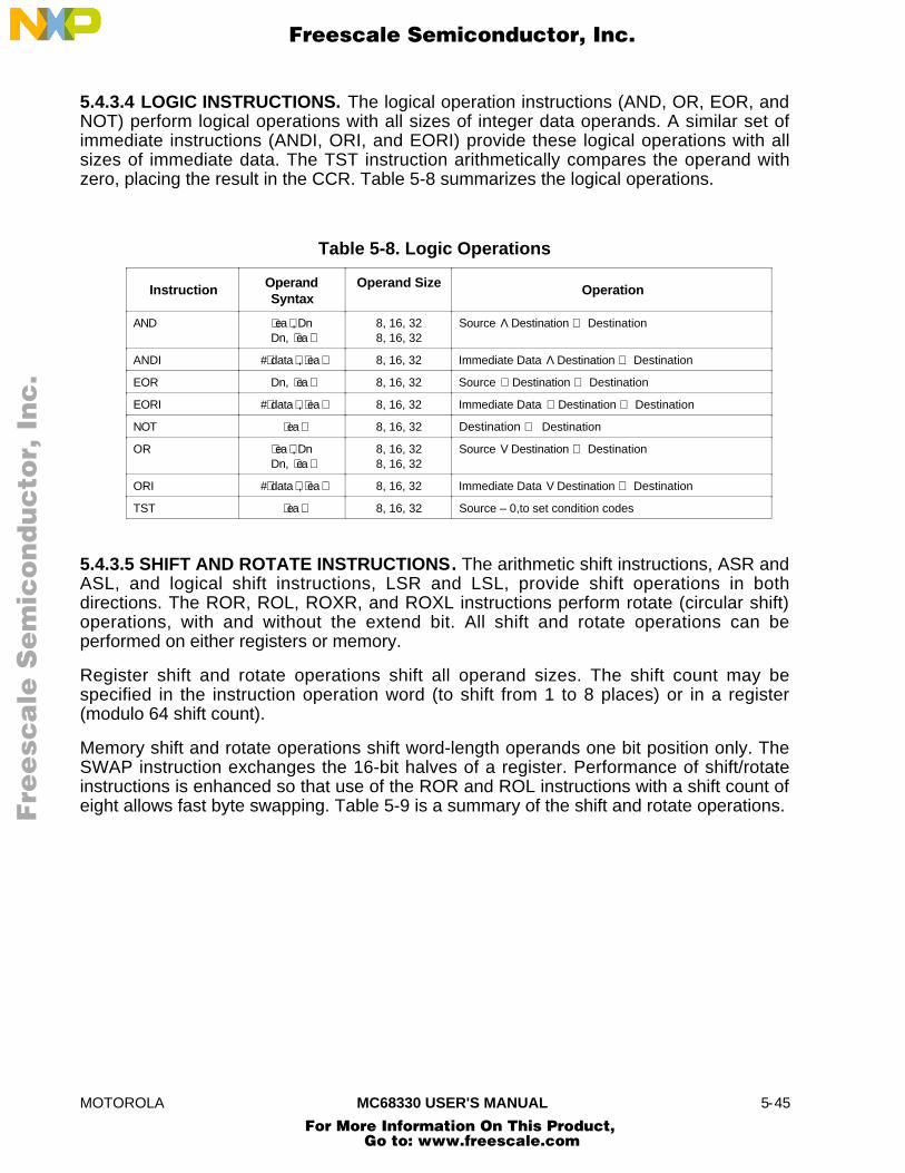
MOTOROLA MC68330 USER'S MANUAL 5-45
5.4.3.4 LOGIC INSTRUCTIONS. The logical operation instructions (AND, OR, EOR, andNOT) perform logical operations with all sizes of integer data operands. A similar set ofimmediate instructions (ANDI, ORI, and EORI) provide these logical operations with allsizes of immediate data. The TST instruction arithmetically compares the operand withzero, placing the result in the CCR. Table 5-8 summarizes the logical operations.
Table 5-8. Logic Operations
Instruction OperandSyntax
Operand Size Operation
AND ⟨ea ⟩, DnDn, ⟨ea ⟩
8, 16, 328, 16, 32
Source Λ Destination ⇒ Destination
ANDI #⟨ data ⟩, ⟨ea ⟩ 8, 16, 32 Immediate Data Λ Destination ⇒ Destination
EOR Dn, ⟨ea ⟩ 8, 16, 32 Source ⊕ Destination ⇒ Destination
EORI #⟨ data ⟩, ⟨ea ⟩ 8, 16, 32 Immediate Data ⊕ Destination ⇒ Destination
NOT ⟨ea ⟩ 8, 16, 32 Destination ⇒ Destination
OR ⟨ea ⟩, DnDn, ⟨ea ⟩
8, 16, 328, 16, 32
Source V Destination ⇒ Destination
ORI #⟨ data ⟩, ⟨ea ⟩ 8, 16, 32 Immediate Data V Destination ⇒ Destination
TST ⟨ea ⟩ 8, 16, 32 Source – 0,to set condition codes
5.4.3.5 SHIFT AND ROTATE INSTRUCTIONS. The arithmetic shift instructions, ASR andASL, and logical shift instructions, LSR and LSL, provide shift operations in bothdirections. The ROR, ROL, ROXR, and ROXL instructions perform rotate (circular shift)operations, with and without the extend bit. All shift and rotate operations can beperformed on either registers or memory.
Register shift and rotate operations shift all operand sizes. The shift count may bespecified in the instruction operation word (to shift from 1 to 8 places) or in a register(modulo 64 shift count).
Memory shift and rotate operations shift word-length operands one bit position only. TheSWAP instruction exchanges the 16-bit halves of a register. Performance of shift/rotateinstructions is enhanced so that use of the ROR and ROL instructions with a shift count ofeight allows fast byte swapping. Table 5-9 is a summary of the shift and rotate operations.
Fre
esc
ale
Se
mic
on
du
cto
r, I
Freescale Semiconductor, Inc.
For More Information On This Product, Go to: www.freescale.com
nc
...

5-46 MC68330 USER'S MANUAL MOTOROLA
Table 5-9. Shift and Rotate Operations
Instruction OperandSyntax
Operand Size Operation
ASL Dn, Dn#⟨ data ⟩, Dn
⟨ea ⟩
8, 16, 328, 16, 32
16
X/C 0
ASR Dn, Dn#⟨ data ⟩, Dn
⟨ea ⟩
8, 16, 328, 16, 32
16
X/C
LSL Dn, Dn#⟨ data ⟩, Dn
⟨ea ⟩
8, 16, 328, 16, 32
16
X/C 0
LSR Dn, Dn#⟨ data ⟩, Dn
⟨ea ⟩
8, 16, 328, 16, 32
16
X/C0
ROL Dn, Dn#⟨ data ⟩, Dn
⟨ea ⟩
8, 16, 328, 16, 32
16C
ROR Dn, Dn#⟨ data ⟩, Dn
⟨ea ⟩
8, 16, 328, 16, 32
16C
ROXL Dn, Dn#⟨ data ⟩, Dn
⟨ea ⟩
8, 16, 328, 16, 32
16C X
ROXR Dn, Dn#⟨ data ⟩, Dn
⟨ea ⟩
8, 16, 328, 16, 32
16CX
SWAP Dn 16
MSW LSW
5.4.3.6 BIT MANIPULATION INSTRUCTIONS. Bit manipulation operations areaccomplished using the following instructions: bit test (BTST), bit test and set (BSET), bittest and clear (BCLR), and bit test and change (BCHG). All bit manipulation operationscan be performed on either registers or memory. The bit number is specified as immediatedata or in a data register. Register operands are 32 bits long, and memory operands are 8bits long. Table 5-10 is a summary of bit manipulation instructions.
Table 5-10. Bit Manipulation Operations
Instruction OperandSyntax
Operand Size Operation
BCHG Dn, ⟨ea ⟩#⟨ data ⟩, ⟨ea ⟩
8, 328, 32
~(⟨ bit number ⟩ of destination) ⇒ Z ⇒ bit of destination
BCLR Dn, ⟨ea ⟩#⟨ data ⟩, ⟨ea ⟩
8, 328, 32
~(⟨ bit number ⟩ of destination) ⇒ Z; 0 ⇒ bit of destination
BSET Dn, ⟨ea ⟩#⟨ data ⟩, ⟨ea ⟩
8, 328, 32
~(⟨ bit number ⟩ of destination) ⇒ Z; 1 ⇒ bit of destination
Fre
esc
ale
Se
mic
on
du
cto
r, I
Freescale Semiconductor, Inc.
For More Information On This Product, Go to: www.freescale.com
nc
...

MOTOROLA MC68330 USER'S MANUAL 5-47
BTST Dn, ⟨ea ⟩#⟨ data ⟩, ⟨ea ⟩
8, 328, 32
~(⟨bit number ⟩ of destination) ⇒ Z
5.4.3.7 BINARY-CODED DECIMAL (BCD) INSTRUCTIONS. Five instructions supportoperations on BCD numbers. The arithmetic operations on packed BCD numbers are adddecimal with extend (ABCD), subtract decimal with extend (SBCD), and negate decimalwith extend (NBCD). Table 5-11 is a summary of the BCD operations.
Table 5-11. Binary-Coded Decimal Operations
Instruction OperandSyntax
Operand Size Operation
ABCD Dn, Dn– (An), – (An)
88
Source10 + Destination10+ X ⇒ Destination
NBCD ⟨ea ⟩ 88
0 – Destination10 – X ⇒ Destination
SBCD Dn, Dn– (An), – (An)
88
Destination10 – Source10 – X ⇒ Destination
5.4.3.8 PROGRAM CONTROL INSTRUCTIONS. A set of subroutine call and returninstructions and conditional and unconditional branch instructions perform program controloperations. Table 5-12 summarizes these instructions.
Table 5-12. Program Control Operations
Instruction OperandSyntax
Operand Size Operation
Conditional
Bcc ⟨ label ⟩ 8, 16, 32 If condition true, then PC + d ⇒ PC
DBcc Dn, ⟨ label ⟩ 16 If condition false, then Dn – 1 ⇒ PC; if Dn ≠ (– 1), then PC + d ⇒ PC
Scc ⟨ea ⟩ 8 If condition true, then destination bits are set to 1; else destination bits are cleared to 0
Unconditional
BRA ⟨ label ⟩ 8, 16, 32 PC + d ⇒ PC
BSR ⟨ label ⟩ 8, 16, 32 SP – 4 ⇒ SP; PC ⇒ (SP); PC + d ⇒ PC
JMP ⟨ea ⟩ none Destination ⇒ PC
JSR ⟨ea ⟩ none SP – 4 ⇒ SP; PC ⇒ (SP); destination ⇒ PC
NOP none none PC + 2 ⇒ PC
Returns
RTD #⟨ d⟩ 16 (SP) ⇒ PC; SP + 4 + d ⇒ SP
RTR none none (SP) ⇒ CCR; SP + 2 ⇒ SP; (SP) ⇒ PC; SP + 4 ⇒ SP
RTS none none (SP) ⇒ PC; SP + 4 ⇒ SP
Fre
esc
ale
Se
mic
on
du
cto
r, I
Freescale Semiconductor, Inc.
For More Information On This Product, Go to: www.freescale.com
nc
...

5-48 MC68330 USER'S MANUAL MOTOROLA
To specify conditions for change in program control, condition codes must be substitutedfor the letters "cc" in conditional program control opcodes. Condition test mnemonics aregiven below. Refer to 5.4.3.10 Condition Tests for detailed information on conditioncodes.
CC — Carry clear LS — Low or sameCS — Carry set LT — Less thanEQ — Equal MI — MinusF — False* NE — Not equalGE — Greater or equal PL — PlusGT — Greater than T — TrueHI — High VC — Overflow clearLE — Less or equal VS — Overflow set*Not applicable to the Bcc instruction
5.4.3.9 SYSTEM CONTROL INSTRUCTIONS. Privileged instructions, trappinginstructions, and instructions that use or modify the CCR provide system controloperations. All of these instructions cause the processor to flush the instruction pipeline.Table 5-13 summarizes the instructions. The preceding list of condition tests also appliesto the TRAPcc instruction. Refer to 5.4.3.10 Condition Tests for detailed information oncondition codes.
Fre
esc
ale
Se
mic
on
du
cto
r, I
Freescale Semiconductor, Inc.
For More Information On This Product, Go to: www.freescale.com
nc
...

MOTOROLA MC68330 USER'S MANUAL 5-49
Table 5-13. System Control Operations
Instruction OperandSyntax
Operand Size Operation
Privileged
ANDI #⟨ data ⟩, SR 16 Immediate Data Λ SR ⇒ SR
EORI #⟨ data ⟩, SR 16 Immediate Data ⊕ SR ⇒ SR
MOVE ⟨ea ⟩, SRSR, ⟨ea ⟩
1616
Source ⇒ SRSR ⇒ Destination
MOVEA USP, AnAn, USP
3232
USP ⇒ AnAn ⇒ USP
MOVEC Rc, RnRn, Rc
3232
Rc ⇒ RnRn ⇒ Rc
MOVES Rn, ⟨ea ⟩⟨ea ⟩, Rn
8, 16, 32 Rn ⇒ Destination using DFCSource using SFC ⇒ Rn
ORI #⟨ data ⟩, SR 16 Immediate Data V SR ⇒ SR
RESET none none Assert RESET line
RTE none none (SP) ⇒ SR; SP + 2 ⇒ SP; (SP) ⇒ PC; SP + 4 ⇒ SP;restore stack according to format
STOP #⟨ data ⟩ 16 Immediate Data ⇒ SR; STOP
LPSTOP #⟨ data ⟩ none Immediate Data ⇒ SR; interrupt mask ⇒ EBI; STOP
Trap Generating
BKPT #⟨ data ⟩ none If breakpoint cycle acknowledged, then execute returned operation word, else trap as illegal instruction.
BGND none none If background mode enabled, then enter background mode, else format/vector offset ⇒ – (SSP);PC ⇒ – (SSP); SR ⇒ – (SSP); (vector) ⇒ PC
CHK ⟨ea ⟩, Dn 16, 32 If Dn < 0 or Dn < (ea), then CHK exception
CHK2 ⟨ea ⟩, Rn 8, 16, 32 If Rn < lower bound or Rn > upper bound, then CHK exception
ILLEGAL none none SSP – 2 ⇒ SSP; vector offset ⇒ (SSP);SSP – 4 ⇒ SSP; PC ⇒ (SSP);SSP – 2 ⇒ SSP; SR ⇒ (SSP);llegal instruction vector address ⇒ PC
TRAP #⟨ data ⟩ none SSP – 2 ⇒ SSP; format/vector offset ⇒ (SSP);SSP – 4 ⇒ SSP; PC ⇒ (SSP); SR ⇒ (SSP);vector address ⇒ PC
TRAPcc none#⟨ data ⟩
none16, 32
If cc true, then TRAP exception
TRAPV none none If V set, then overflow TRAP exception
Condition Code Register
ANDI #⟨ data ⟩, CCR 8 Immediate Data Λ CCR ⇒ CCR
EORI #⟨ data ⟩, CCR 8 Immediate Data ⊕ CCR ⇒ CCR
MOVE ⟨ea ⟩, CCRCCR, ⟨ea ⟩
1616
Source ⇒ CCRCCR ⇒ Destination
ORI #⟨ data ⟩, CCR 8 Immediate Data V CCR ⇒ CCR
5.4.3.10 CONDITION TESTS. Conditional program control instructions and the TRAPccinstruction execute on the basis of condition tests. A condition test is the evaluation of alogical expression related to the state of the CCR bits. If the result is 1, the condition is
Fre
esc
ale
Se
mic
on
du
cto
r, I
Freescale Semiconductor, Inc.
For More Information On This Product, Go to: www.freescale.com
nc
...

5-50 MC68330 USER'S MANUAL MOTOROLA
true. If the result is 0, the condition is false. For example, the T condition is always true,and the EQ condition is true only if the Z-bit condition code is true. Table 5-14 lists eachcondition test.
Table 5-14. Condition Tests
Mnemonic Condition Encoding Test
T True 0000 1
F* False 0001 0
HI High 0010 C • Z
LS Low or Same 0011 C +Z
CC Carry Clear 0100 C
CS Carry Set 0101 C
NE Not Equal 0110 Z
EQ Equal 0111 Z
VC Overflow Clear 1000 V
VS Overflow Set 1001 V
PL Plus 1010 N
MI Minus 1011 N
GE Greater or Equal 1100 N • V + N • V
LT Less Than 1101 N • V + N • V
GT Greater Than 1110 N • V • Z + N • V • Z
LE Less or Equal 1111 Z + N • V + N • V
* Not available for the Bcc instruction.• = Boolean AND+ = Boolean ORN = Boolean NOT N
5.4.4 Using the Table Lookup and Interpolation Instructions.There are four table lookup and interpolate instructions. TBLS returns a signed, roundedbyte, word, or long-word result. TBLSN returns a signed, unrounded byte, word, or long-word result. TBLU returns an unsigned, rounded byte, word, or long-word result. TBLUNreturns an unsigned, unrounded byte, word, or long-word result. All four instructionssupport two types of interpolation data: an n-element table stored in memory, and a two-element range stored in a pair of data registers. The latter form provides a means ofperforming surface (3D) interpolation between two previously calculated linearinterpolations.
The following examples show how to compress tables and use fewer interpolation levelsbetween table entries. Example 1 (see Figure 5-16) demonstrates table lookup andinterpolation for a 257-entry table, allowing up to 256 interpolation levels between entries.Example 2 (see Figure 5-17) reduces table length for the same data to four entries.Example 3 (see Figure 5-18) demonstrates use of an 8-bit independent variable with aninstruction.
Two additional examples show how TBLSN can reduce cumulative error when multipletable lookup and interpolation operations are used in a calculation. Example 4
Fre
esc
ale
Se
mic
on
du
cto
r, I
Freescale Semiconductor, Inc.
For More Information On This Product, Go to: www.freescale.com
nc
...

MOTOROLA MC68330 USER'S MANUAL 5-51
demonstrates addition of the results of three table interpolations. Example 5 illustrates useof TBLSN in surface interpolation.
5.4.4.1 TABLE EXAMPLE 1: STANDARD USAGE. The table consists of 257 wordentries. As shown in Figure 5-16, the function is linear within the range 32768 ≤ X ≤49152. Table entries within this range are as given in Table 5-15 .
Table 5-15. Standard Usage Entries
Entry Number XValue
YValue
128* 32768 1311
162 41472 1659
163 41728 1669
164 41984 1679
165 42240 1690
192* 49152 1966
*These values are the end points of the range. All entries between these points fall on the line.
X16384 3276 4915 6553
INDEPENDENT VARIAB
DE
PE
ND
EN
T V
AR
IAB
LE
Y
Figure 5-16. Table Example 1
The table instruction is executed with the following bit pattern in Dx:
31 16 15 0
NOT USED 1 0 1 0 0 0 1 1 1 0 0 0 0 00 0
Table Entry Offset ⇒ Dx [8:15] = $A3 = 163
Fre
esc
ale
Se
mic
on
du
cto
r, I
Freescale Semiconductor, Inc.
For More Information On This Product, Go to: www.freescale.com
nc
...

5-52 MC68330 USER'S MANUAL MOTOROLA
Interpolation Fraction ⇒ Dx [0:7] = $80 = 128
Using this information, the table instruction calculates dependent variable Y:
Y = 1669 + (128 (1679 – 1669)) / 256 = 1674
5.4.4.2 TABLE EXAMPLE 2: COMPRESSED TABLE. In Example 2 (see Figure 5-17),the data from Example 1 has been compressed by limiting the maximum value of theindependent variable. Instead of the range 0 ≤ X = 65535, X is limited to 0 ≤ X ≤ 1023. Thetable has been compressed to only five entries, but up to 256 levels of interpolation areallowed between entries.
X256 512 786 1024
INDEPENDENT VARIAB
DE
PE
ND
EN
T V
AR
IAB
LE
Y
Figure 5-17. Table Example 2
NOTE
Extreme table compression with many levels ofinterpolation is possible only with highly linear functions.The table entries within the range of interest are listed inTable 5-16 .
Table 5-16 . Compressed Table Entries
Entry Number XValue
YValue
2 512 1311
3 786 1966
Fre
esc
ale
Se
mic
on
du
cto
r, I
Freescale Semiconductor, Inc.
For More Information On This Product, Go to: www.freescale.com
nc
...

MOTOROLA MC68330 USER'S MANUAL 5-53
Since the table is reduced from 257 to 5 entries, independent variable X must be scaledappropriately. In this case the scaling factor is 64, and the scaling is done by a singleinstruction:
LSR.W #6,Dx
Thus, Dx now contains the following bit pattern:
31 16 15 0
NOT USED 0 0 0 0 0 0 1 0 1 0 0 0 1 11 0
Table Entry Offset ⇒ Dx [8:15] = $02 = 2Interpolation Fraction ⇒ Dx [0:7] = $8E = 142
Using this information, the table instruction calculates dependent variable Y:
Y = 1331 + (142 (1966 – 1311)) / 256 = 1674
The function chosen for Examples 1 and 2 is linear between data points. If anotherfunction been been used, interpolated values might not have been identical.
5.4.4.3 TABLE EXAMPLE 3: 8-BIT INDEPENDENT VARIABLE. This example showshow to use a table instruction within an interpolation subroutine. Independent variable X iscalculated as an 8-bit value, allowing 16 levels of interpolation on a 17-entry table. X ispassed to the subroutine, which returns an 8-bit result. The subroutine uses the data listedin Table 5-17, based on the function shown in Figure 5-18.
Y
X1024 2048 3072 4096
INDEPENDENT VARIABL
IND
EP
EN
DE
NT
VA
RIA
BLE
Figure 5-18. Table Example 3
Fre
esc
ale
Se
mic
on
du
cto
r, I
Freescale Semiconductor, Inc.
For More Information On This Product, Go to: www.freescale.com
nc
...

5-54 MC68330 USER'S MANUAL MOTOROLA
Table 5-17. 8-Bit IndependentVariable Entries
X(Subroutine)
X(Instruction)
Y
0 0 0
1 256 16
2 512 32
3 768 48
4 1024 64
5 1280 80
6 1536 96
7 1792 112
8 2048 128
9 2304 112
10 2560 96
11 2816 80
12 3072 64
13 3328 48
14 3584 32
15 3840 16
16 4096 0
The first column is the value passed to the subroutine, the second column is the valueexpected by the table instruction, and the third column is the result returned by thesubroutine.
The following value has been calculated for independent variable X:
31 16 15 0
NOT USED 0 0 0 0 0 0 0 0 1 0 1 1 1 10 1
Since X is an 8-bit value, the upper four bits are used as a table offset and the lower fourbits are used as an interpolation fraction. The following results are obtained from thesubroutine:
Table Entry Offset ⇒ Dx [4:7] = $B = 11Interpolation Fraction ⇒ Dx [0:3] = $D = 13
Thus, Y is calculated as follows:
Y = 80 + (13 (64 – 80)) / 16 = 67
If the 8-bit value for X were used directly by the table instruction, interpolation would beincorrectly performed between entries 0 and 1. Data must be shifted to the left four placesbefore use:
LSL.W #4, Dx
The new range for X is 0 ≤ X ≤ 4096; however, since a left shift fills the least significantdigits of the word with zeros, the interpolation fraction can only have one of 16 values.
Fre
esc
ale
Se
mic
on
du
cto
r, I
Freescale Semiconductor, Inc.
For More Information On This Product, Go to: www.freescale.com
nc
...

MOTOROLA MC68330 USER'S MANUAL 5-55
After the shift operation, Dx contains the following value:
31 16 15 0
NOT USED 0 0 0 0 1 0 1 1 1 1 0 1 0 0 00
Execution of the table instruction using the new value in Dx yields:
Table Entry Offset ⇒ Dx [8:15] = $0B = 11Interpolation Fraction ⇒ Dx [0:7] = $D0 = 208
Thus, Y is calculated as follows:
Y = 80 + (208 (64 – 80)) / 256 = 67
5.4.4.4 TABLE EXAMPLE 4: MAINTAINING PRECISION. In this example, three tablelookup and interpolation (TLI) operations are performed and the results are summed. Thecalculation is done once with the result of each TLI rounded before addition and once withonly the final result rounded. Assume that the result of the three interpolations are asfollows (a ".'' indicates the binary radix point).
TLI # 1 0010 0000 . 0111 0000TLI # 2 0011 1111 . 0111 0000TLI # 3 0000 0001 . 0111 0000
First, the results of each TLI are rounded with the TBLS round-to-nearest-even algorithm.The following values would be returned by TBLS:
TLI # 1 0010 0000 .TLI # 2 0011 1111 .TLI # 3 0000 0001 .
Summing, the following result is obtained:
0010 0000 .0011 1111 .0000 0001 .0110 0000 .
Now, using the same TLI results, the sum is first calculated and then rounded according tothe same algorithm:
0010 0000 . 0111 00000011 1111 . 0111 00000000 0001 . 0111 00000110 0001 . 0101 0000
Rounding yields:
0110 0001 .
The second result is preferred. The following code sequence illustrates how addition of aseries of table interpolations can be performed without loss of precision in the intermediateresults:
Fre
esc
ale
Se
mic
on
du
cto
r, I
Freescale Semiconductor, Inc.
For More Information On This Product, Go to: www.freescale.com
nc
...

5-56 MC68330 USER'S MANUAL MOTOROLA
L0:TBLSN.B ⟨ea⟩, DxTBLSN.B ⟨ea⟩, DxTBLSN.B ⟨ea⟩, DlADD.L Dx, Dm Long addition avoids problems with carryADD.L Dm, DlASR.L #8, Dl Move radix pointBCC.B L1 Fraction MSB in carryADDQ.B #1, Dl
L1: . . .
5.4.4.5 TABLE EXAMPLE 5: SURFACE INTERPOLATIONS. The various forms of tablecan be used to perform surface (3D) TLIs. However, since the calculation must be splitinto a series of 2D TLIs, the possibility of losing precision in the intermediate results ispossible. The following code sequence, incorporating both TBLS and TBLSN, eliminatesthis possibility.
L0:MOVE.W Dx, Dl Copy entry number and fraction numberTBLSN.B ⟨ea⟩ , DxTBLSN.B ⟨ea⟩, DlTBLS.W Dx:Dl, Dm Surface interpolation, with roundASR.L #8, Dm Read just the resultBCC.B L1 No round necessaryADDQ.B #1, Dl Half round up
L1: . . .
Before execution of this code sequence, Dx must contain fraction and entry numbers forthe two TLI, and Dm must contain the fraction for surface interpolation. The ⟨ea ⟩ fields inthe TBLSN instructions point to consecutive columns in a 3D table. The TBLS sizeparameter must be word if the TBLSN size parameter is byte, and must be long word ifTBLSN is word. Increased size is necessary because a larger number of significant digitsis needed to accommodate the scaled fractional results of the 2D TLI.
5.4.5 Nested Subroutine CallsThe LINK instruction pushes an address onto the stack, saves the stack address at whichthe address is stored, and reserves an area of the stack for use. Using this instruction in aseries of subroutine calls will generate a linked list of stack frames.
The UNLK instruction removes a stack frame from the end of the list by loading anaddress into the SP and pulling the value at that address from the stack. When theinstruction operand is the address of the link address at the bottom of a stack frame, theeffect is to remove the stack frame from both the stack and the linked list.
5.4.6 Pipeline Synchronization with the NOP InstructionAlthough the no operation (NOP) instruction performs no visible operation, it does forcesynchronization of the instruction pipeline, since all previous instructions must completeexecution before the NOP begins.
Fre
esc
ale
Se
mic
on
du
cto
r, I
Freescale Semiconductor, Inc.
For More Information On This Product, Go to: www.freescale.com
nc
...

MOTOROLA MC68330 USER'S MANUAL 5-57
5.5 PROCESSING STATESThis section describes the processing states of the CPU32. It includes a functionaldescription of the bits in the supervisor portion of the SR and an overview of actions takenby the processor in response to exception conditions.
5.5.1 State TransitionsThe processor is in normal, background, or exception state unless halted.
When the processor fetches instructions and operands or executes instructions, it is in thenormal processing state. The stopped condition, which the processor enters when a STOPor LPSTOP instruction is executed, is a variation of the normal state in which no furtherbus cycles are generated.
Background state is an alternate operational mode used for system debugging. Refer to5.7 Development Support for more information.
Exception processing refers specifically to the transition from normal processing of aprogram to normal processing of system routines, interrupt routines, and other exceptionhandlers. Exception processing includes the stack operations, the exception vector fetch,and the filling of the instruction pipeline caused by an exception. Exception processingends when execution of an exception handler routine begins. Refer to 5.6 ExceptionProcessing for comprehensive information.
A catastrophic system failure occurs if the processor detects a bus error or generates anaddress error while in the exception processing state. This type of failure halts theprocessor. For example, if a bus error occurs during exception processing caused by abus error, the CPU32 assumes that the system is not operational and halts.
The halted condition should not be confused with the stopped condition. After theprocessor executes a STOP or LPSTOP instruction, execution of instructions can resumewhen a trace, interrupt, or reset exception occurs.
5.5.2 Privilege LevelsTo protect system resources, the processor can operate with either of two levels of access— user or supervisor. Supervisor level is more privileged than user level. All instructionsare available at the supervisor level, but execution of some instructions is not permitted atthe user level. There are separate SPs for each level. The S-bit in the SR indicatesprivilege level and determines which SP is used for stack operations. The processoridentifies each bus access (supervisor or user mode) via function codes to enforcesupervisor and user access levels.
In a typical system, most programs execute at the user level. User programs can accessonly their own code and data areas and are restricted from accessing other information.The operating system executes at the supervisor privilege level, has access to allresources, performs the overhead tasks for the user level programs, and coordinates theiractivities.
5.5.2.1 SUPERVISOR PRIVILEGE LEVEL. If the S-bit in the SR is set, supervisorprivilege level applies, and all instructions are executable. The bus cycles generated forinstructions executed in supervisor level are normally classified as supervisor references,and the values of the function codes on FC2–FC0 refer to supervisor address spaces.
Fre
esc
ale
Se
mic
on
du
cto
r, I
Freescale Semiconductor, Inc.
For More Information On This Product, Go to: www.freescale.com
nc
...

5-58 MC68330 USER'S MANUAL MOTOROLA
All exception processing is performed at the supervisor level. All bus cycles generatedduring exception processing are supervisor references, and all stack accesses use theSSP.
Instructions that have important system effects can only be executed at supervisor level.For instance, user programs are not permitted to execute STOP, LPSTOP, or RESETinstructions. To prevent a user program from gaining privileged access, except in acontrolled manner, instructions that can alter the S-bit in the SR are privileged. The TRAP#n instruction provides controlled user access to operating system services.
5.5.2.2 USER PRIVILEGE LEVEL. If the S-bit in the SR is cleared, the processorexecutes instructions at the user privilege level. The bus cycles for an instruction executedat the user privilege level are classified as user references, and the values of the functioncodes on FC2–FC0 specify user address spaces. While the processor is at the user level,implicit references to the system SP and explicit references to address register seven (A7)refer to the USP.
5.5.2.3 CHANGING PRIVILEGE LEVEL. To change from user privilege level to supervisorprivilege level, a condition that causes exception processing must occur. When exceptionprocessing begins, the current values in the SR, including the S-bit, are saved on thesupervisor stack, and then the S-bit is set, enabling supervisory access. Executioncontinues at supervisor level until exception processing is complete.
To return to user access level, a system routine must execute one of the followinginstructions: MOVE to SR, ANDI to SR, EORI to SR, ORI to SR, or RTE. Theseinstructions execute only at supervisor privilege level and can modify the S-bit of the SR.After these instructions execute, the instruction pipeline is flushed, then refilled from theappropriate address space.
The RTE instruction causes a return to a program that was executing when an exceptionoccurred. When RTE is executed, the exception stack frame saved on the supervisorstack can be restored in either of two ways.
If the frame was generated by an interrupt, breakpoint, trap, or instruction exception, theSR and PC are restored to the values saved on the supervisor stack, and executionresumes at the restored PC address, with access level determined by the S-bit of therestored SR.
If the frame was generated by a bus error or an address error exception, the entireprocessor state is restored from the stack.
5.6 EXCEPTION PROCESSINGAn exception is a special condition that pre-empts normal processing. Exceptionprocessing is the transition from normal mode program execution to execution of a routinethat deals with an exception. The following paragraphs discuss system resources relatedto exception handling, exception processing sequence, and specific features of individualexception processing routines.
Fre
esc
ale
Se
mic
on
du
cto
r, I
Freescale Semiconductor, Inc.
For More Information On This Product, Go to: www.freescale.com
nc
...

MOTOROLA MC68330 USER'S MANUAL 5-59
5.6.1 Exception VectorsAn exception vector is the address of a routine that handles an exception. The VBRcontains the base address of a 1024-byte exception vector table, which consists of 256exception vectors. Sixty-four vectors are defined by the processor, and 192 vectors arereserved for user definition as interrupt vectors. Except for the reset vector, each vector inthe table is one long word in length. The reset vector is two long words in length. Refer toTable 5-18 for information on vector assignment.
Table 5-18. Exception Vector Assignments
Vector Vector Offset Assignment
Number Dec Hex Space
0 0 000 SP Reset: Initial Stack Pointer1 4 004 SP Reset: Initial Program Counter2 8 008 SD Bus Error3 12 00C SD Address Error
4 16 010 SD Illegal Instruction5 20 014 SD Zero Division6 24 018 SD CHK, CHK2 Instructions7 28 01C SD TRAPcc, TRAPV Instructions
8 32 020 SD Privilege Violation9 36 024 SD Trace
10 40 028 SD Line 1010 Emulator11 44 02C SD Line 1111 Emulator
12 48 030 SD Hardware Breakpoint13 52 034 SD (Reserved for Coprocessor Protocol Violation)14 56 038 SD Format Error15 60 03C SD Uninitialized Interrupt
16–23 6492
04005C
SD (Unassigned, Reserved)—
24 96 060 SD Spurious Interrupt25 100 064 SD Level 1 Interrupt Autovector26 104 068 SD Level 2 Interrupt Autovector27 108 06C SD Level 3 Interrupt Autovector
28 112 070 SD Level 4 Interrupt Autovector29 116 074 SD Level 5 Interrupt Autovector30 120 078 SD Level 6 Interrupt Autovector31 124 07C SD Level 7 Interrupt Autovector
32–47 128188
0800BC
SD Trap Instruction Vectors (0–15)—
48–58 192232
0C00E8
SD (Reserved for Coprocessor)—
59–63 236252
0EC0FC
SD (Unassigned, Reserved)—
64–255 2561020
1003FC
SD User-Defined Vectors (192)
CAUTION
Because there is no protection on the 64 processor-defined vectors, external devices can access vectorsreserved for internal purposes. This practice is stronglydiscouraged.
Fre
esc
ale
Se
mic
on
du
cto
r, I
Freescale Semiconductor, Inc.
For More Information On This Product, Go to: www.freescale.com
nc
...

5-60 MC68330 USER'S MANUAL MOTOROLA
All exception vectors, except the reset vector, are located in supervisor data space. Thereset vector is located in supervisor program space. Only the initial reset vector is fixed inthe processor memory map. When initialization is complete, there are no fixedassignments. Since the VBR stores the vector table base address, the table can belocated anywhere in memory. It can also be dynamically relocated for each task executedby an operating system.
Each vector is assigned an 8-bit number. Vector numbers for some exceptions areobtained from an external device; others are supplied by the processor. The processormultiplies the vector number by four to calculate vector offset, then adds the offset to thecontents of the VBR. The sum is the memory address of the vector.
5.6.1.1 TYPES OF EXCEPTIONS. An exception can be caused by internal or externalevents.
An internal exception can be generated by an instruction or by an error. The TRAP,TRAPcc, TRAPV, BKPT, CHK, CHK2, RTE, and DIV instructions can cause exceptionsduring normal execution. Illegal instructions, instruction fetches from odd addresses, wordor long-word operand accesses from odd addresses, and privilege violations also causeinternal exceptions.
Sources of external exception include interrupts, breakpoints, bus errors, and resetrequests. Interrupts are peripheral device requests for processor action. Breakpoints areused to support development equipment. Bus error and reset are used for access controland processor restart.
5.6.1.2 EXCEPTION PROCESSING SEQUENCE. For all exceptions other than a resetexception, exception processing occurs in the following sequence. Refer to 5.6.2.1 Resetfor details of reset processing.
As exception processing begins, the processor makes an internal copy of the SR. After thecopy is made, the processor state bits in the SR are changed — the S-bit is set,establishing supervisor access level,and bits T1 and T0 are cleared, disabling tracing. Forreset and interrupt exceptions, the interrupt priority mask is also updated.
Next, the exception number is obtained. For interrupts, the number is fetched from CPUspace $F (the bus cycle is an interrupt acknowledge). For all other exceptions, internallogic provides a vector number.
Next, current processor status is saved. An exception stack frame is created and placedon the supervisor stack. All stack frames contain copies of the SR and the PC for use byRTE. The type of exception and the context in which the exception occurs determine whatother information is stored in the stack frame.
Finally, the processor prepares to resume normal execution of instructions. The exceptionvector offset is determined by multiplying the vector number by four, and the offset isadded to the contents of the VBR to determine displacement into the exception vectortable. The exception vector is loaded into the PC. If no other exception is pending, theprocessor will resume normal execution at the new address in the PC.
5.6.1.3 EXCEPTION STACK FRAME. During exception processing, the most volatileportion of the current context is saved on the top of the supervisor stack. This context isorganized in a format called the exception stack frame.
Fre
esc
ale
Se
mic
on
du
cto
r, I
Freescale Semiconductor, Inc.
For More Information On This Product, Go to: www.freescale.com
nc
...

MOTOROLA MC68330 USER'S MANUAL 5-61
The exception stack frame always includes the contents of SR and PC at the time theexception occurred. To support generic handlers, the processor also places the vectoroffset in the exception stack frame and marks the frame with a format code. The formatfield allows an RTE instruction to identify stack information so that it can be properlyrestored.
The general form of the exception stack frame is illustrated in Figure 5-19. Although someformats are peculiar to a particular M68000 Family processor, format 0000 is always legaland always indicates that only the first four words of a frame are present. See 5.6.4CPU32 Stack Frames for a complete discussion of exception stack frames.
STATUS REGISTER
PROGRAM COUNTER LOW
FORMAT VECTOR OFFSET
OTHER PROCESSOR STATE INFORMATION,DEPENDING ON EXCEPTION
(0, 2, OR 8 WORDS)
PROGRAM COUNTER HIGH
HIG
HE
R A
DD
RE
SS
ES
SP (AFTER STACKING
STA
CK
ING
OR
DE
R
0 15
Figure 5-19. Exception Stack Frame
5.6.1.4 MULTIPLE EXCEPTIONS. Each exception has been assigned a priority based onits relative importance to system operation. Priority assignments are shown in Table 5-19.Group 0 exceptions have the highest priorities. Group 4 exceptions have the lowestpriorities. Exception processing for exceptions that occur simultaneously is done bypriority, from highest to lowest.
It is important to be aware of the difference between exception processing mode andexecution of an exception handler. Each exception has an assigned vector that points toan associated handler routine. Exception processing includes steps described in 5.6.1.2Exception Processing Sequence, but does not include execution of handler routines,which is done in normal mode.
When the CPU32 completes exception processing, it is ready to begin either exceptionprocessing for a pending exception or execution of a handler routine. Priority assignmentgoverns the order in which exception processing occurs, not the order in which exceptionhandlers are executed.
Fre
esc
ale
Se
mic
on
du
cto
r, I
Freescale Semiconductor, Inc.
For More Information On This Product, Go to: www.freescale.com
nc
...

5-62 MC68330 USER'S MANUAL MOTOROLA
Table 5-19. Exception Priority Groups
Group/Priority
Exception andRelative Priority
Characteristics
0 Reset Aborts all processing (instruction orexception); does not save old context.
1.11.2
Address ErrorBus Error
Suspends processing (instruction orexception); saves internal context.
2 BKPT#n, CHK, CHK2,Division by Zero, RTE,
TRAP#n, TRAPcc, TRAPV
Exception processing is a part ofinstruction execution.
3 Illegal Instruction, Line A,Unimplemented Line F,
Privilege Violation
Exception processing begins beforeinstruction execution.
4.14.24.3
TraceHardware Breakpoint
Interrupt
Exception processing begins when currentinstruction or previous exceptionprocessing is complete.
As a general rule, when simultaneous exceptions occur, the handler routines for lowerpriority exceptions are executed before the handler routines for higher priority exceptions.For example, consider the arrival of an interrupt during execution of a TRAP instruction,while tracing is enabled. Trap exception processing (2) is done first, followed immediatelyby exception processing for the trace (4.1), and then by exception processing for theinterrupt (4.3). Each exception places a new context on the stack. When the processorresumes normal instruction execution, it is vectored to the interrupt handler, which returnsto the trace handler that returns to the trap handler.
There are special cases to which the general rule does not apply. The reset exception willalways be the first exception handled since reset clears all other exceptions. It is alsopossible for high-priority exception processing to begin before low-priority exceptionprocessing is complete. For example, if a bus error occurs during trace exceptionprocessing, the bus error will be processed and handled before trace exceptionprocessing is completed.
5.6.2 Processing of Specific ExceptionsThe following paragraphs provide details concerning sources of specific exceptions, howeach arises, and how each is processed.
5.6.2.1 RESET. Assertion of RESET by external hardware or assertion of the internalRESET signal by an internal module causes a reset exception. The reset exception hasthe highest priority of any exception. Reset is used for system initialization and forrecovery from catastrophic failure. The reset exception aborts any processing in progresswhen it is recognized, and that processing cannot be recovered. Reset performs thefollowing operations:
1. Clears T0 and T1 in the SR to disable tracing2. Sets the S-bit in the SR to establish supervisor privilege3. Sets the interrupt priority mask to the highest priority level (%111)4. Initializes the VBR to zero ($00000000)5. Generates a vector number to reference the reset exception vector6. Loads the first long word of the vector into the interrupt SP7. Loads the second long word of the vector into the PC
Fre
esc
ale
Se
mic
on
du
cto
r, I
Freescale Semiconductor, Inc.
For More Information On This Product, Go to: www.freescale.com
nc
...

MOTOROLA MC68330 USER'S MANUAL 5-63
8. Fetches and initiates decode of the first instruction to be executed
Figure 5-20 is a flowchart of the reset exception
ENTRY
FETCH VECTOR # 0
1 S 0 T0,T$7 I2:I0$0 VBR
FETCH VECTOR # 1
BUS ERROR OTHERWISSP (VECTOR
BUS ERROR
PREFETCH FIRST WO
BUS ERRORADDRESSERROROTHERWISE BEGI
INSTRUCTIONEXECUTION
EXIT
(DOUBLE BUS FAULT
ASSERT HALT
EXIT
OTHERWISPC (VECTOR
Figure 5-20. Reset Operation Flowchart
After initial instruction prefetches, normal program execution begins at the address in thePC. The reset exception does not save the value of either the PC or the SR.
If a bus error or address error occurs during reset exception processing sequence, adouble bus fault occurs. The processor halts, and the HALT signal is asserted to indicatethe halted condition.
Fre
esc
ale
Se
mic
on
du
cto
r, I
Freescale Semiconductor, Inc.
For More Information On This Product, Go to: www.freescale.com
nc
...

5-64 MC68330 USER'S MANUAL MOTOROLA
Execution of the RESET instruction does not cause a reset exception nor does it affectany internal CPU register, but it does cause the CPU32 to assert the RESET signal,resetting all internal and external peripherals.
5.6.2.2 BUS ERROR. A bus error exception occurs when an assertion of the BERR signalis acknowledged. The BERR signal can be asserted by one of three sources:
1. External logic by assertion of the BERR input pin2. Direct assertion of the internal BERR signal by an internal module3. Direct assertion of the internal BERR signal by the on-chip hardware watchdog
after detecting a no-response condition
Bus error exception processing begins when the processor attempts to use informationfrom an aborted bus cycle.
When the aborted bus cycle is an instruction prefetch, the processor will not initiateexception processing unless the prefetched information is used. For example, if a branchinstruction flushes an aborted prefetch, that word is not accessed, and no exceptionoccurs.
When the aborted bus cycle is a data access, the processor initiates exception processingimmediately, except in the case of released operand writes. Released write bus errors aredelayed until the next instruction boundary or until another operand access is attempted.
Exception processing for bus error exceptions follows the regular sequence, but contextpreservation is more involved than for other exceptions because a bus exception can beinitiated while an instruction is executing. Several bus error stack format organizations areutilized to provide additional information regarding the nature of the fault.
First, any register altered by a faulted-instruction EA calculation is restored to its initialvalue. Then a special status word (SSW) is placed on the stack. The SSW containsspecific information about the aborted access — size, type of access (read or write), buscycle type, and function code. Finally, fault address, bus error exception vector number,PC value, and a copy of the SR are saved.
If a bus error occurs during exception processing for a bus error, an address error, a reset,or while the processor is loading stack information during RTE execution, the processorhalts. This simplifies isolation of catastrophic system failure by preventing processorinteraction with stacks and memory. Only assertion of RESET can restart a haltedprocessor.
5.6.2.3 ADDRESS ERROR. Address error exceptions occur when the processor attemptsto access an instruction, word operand, or long-word operand at an odd address. Theeffect is much the same as an internally generated bus error. The exception processingsequence is the same as that for bus error, except that the vector number refers to theaddress error exception vector.
Address error exception processing begins when the processor attempts to useinformation from the aborted bus cycle.
If the aborted cycle is a data space access, exception processing begins when theprocessor attempts to use the data, except in the case of a released operand write.
Fre
esc
ale
Se
mic
on
du
cto
r, I
Freescale Semiconductor, Inc.
For More Information On This Product, Go to: www.freescale.com
nc
...

MOTOROLA MC68330 USER'S MANUAL 5-65
Released write exceptions are delayed until the next instruction boundary or attemptedoperand access.
An address exception on a branch to an odd address is delayed until the PC is changed.No exception occurs if the branch is not taken. In this case, the fault address and returnPC value placed in the exception stack frame are the odd address, and the currentinstruction PC points to the instruction that caused the exception.
If an address error occurs during exception processing for a bus error, another addresserror, or a reset, the processor halts.
5.6.2.4 INSTRUCTION TRAPS. Traps are exceptions caused by instructions. They arisefrom either processor recognition of abnormal conditions during instruction execution orfrom use of specific trapping instructions. Traps are generally used to handle abnormalconditions that arise in control routines.
The TRAP instruction, which always forces an exception, is useful for implementingsystem calls for user programs. The TRAPcc, TRAPV, CHK, and CHK2 instructions forceexceptions when a program detects a run-time error. The DIVS and DIVU instructionsforce an exception if a division operation is attempted with a divisor of zero.
Exception processing for traps follows the regular sequence. If tracing is enabled when aninstruction that causes a trap begins execution, a trace exception will be generated by theinstruction, but the trap handler routine will not be traced (the trap exception will beprocessed first, then the trace exception).
The vector number for the TRAP instruction is internally generated — part of the numbercomes from the instruction itself. The trap vector number, PC value, and a copy of the SRare saved on the supervisor stack. The saved PC value is the address of the instructionthat follows the instruction which generated the trap. For all instruction traps other thanTRAP, a pointer to the instruction causing the trap is also saved in the fifth and sixth wordsof the exception stack frame.
5.6.2.5 SOFTWARE BREAKPOINTS. To support hardware emulation, the CPU32 mustprovide a means of inserting breakpoints into target code and of announcing when abreakpoint is reached.
The MC68000 and MC68008 can detect an illegal instruction inserted at a breakpointwhen the processor fetches from the illegal instruction exception vector location. Since theVBR on the CPU32 allows relocation of exception vectors, the exception vector address isnot a reliable indication of a breakpoint. CPU32 breakpoint support is provided byextending the function of a set of illegal instructions ($4848–$484F).
When a breakpoint instruction is executed, the CPU32 performs a read from CPU space$0, at a location corresponding to the breakpoint number. If this bus cycle is terminated byBERR, the processor performs illegal instruction exception processing. If the bus cycle isterminated by DSACKx, the processor uses the data returned to replace the breakpoint inthe instruction pipeline and begins execution of that instruction. See Section 3 BusOperation for a description of CPU space operations.
5.6.2.6 HARDWARE BREAKPOINTS. The CPU32 recognizes hardware breakpointrequests. Hardware breakpoint requests do not force immediate exception processing, but
Fre
esc
ale
Se
mic
on
du
cto
r, I
Freescale Semiconductor, Inc.
For More Information On This Product, Go to: www.freescale.com
nc
...

5-66 MC68330 USER'S MANUAL MOTOROLA
are left pending. An instruction breakpoint is not made pending until the instructioncorresponding to the request is executed.
A pending breakpoint can be acknowledged between instructions or at the end ofexception processing. To acknowledge a breakpoint, the CPU performs a read from CPUspace $0 at location $1E (see Section 3 Bus Operation).
If the bus cycle terminates normally, instruction execution continues with the nextinstruction, as if no breakpoint request occurred. If the bus cycle is terminated by BERR,the CPU begins exception processing. Data returned during this bus cycle is ignored.
Exception processing follows the regular sequence. Vector number 12 (offset $30) isinternally generated. The PC of the currently executing instruction, the PC of the nextinstruction to execute, and a copy of the SR are saved on the supervisor stack.
5.6.2.7 FORMAT ERROR. The processor checks certain data values for controloperations. The validity of the stack format code and, in the case of a bus cycle faultformat, the version number of the processor that generated the frame are checked duringexecution of the RTE instruction. This check ensures that the program does not makeerroneous assumptions about information in the stack frame.
If the format of the control data is improper, the processor generates a format errorexception. This exception saves a four-word format exception frame and then vectorsthrough vector table entry number 14. The stacked PC is the address of the RTEinstruction that discovered the format error.
5.6.2.8 ILLEGAL OR UNIMPLEMENTED INSTRUCTIONS. An instruction is illegal if itcontains a word bit pattern that does not correspond to the bit pattern of the first word of alegal CPU32 instruction, if it is a MOVEC instruction that contains an undefined registerspecification field in the first extension word, or if it contains an indexed addressing modeextension word with bits 5–4 = 00 or bits 3–0 ≠ 0000.
If an illegal instruction is fetched during instruction execution, an illegal instructionexception occurs. This facility allows the operating system to detect program errors or toemulate instructions in software.
Word patterns with bits 15–12 = 1010 (referred to as A-line opcodes) are unimplementedinstructions. A separate exception vector (vector 10, offset $28) is given to unimplementedinstructions to permit efficient emulation.
Word patterns with bits 15–12 = 1111 (referred to as F-line opcodes) are used for M68000Family instruction set extensions. They can generate an unimplemented instructionexception caused by the first extension word of the instruction or by the addressing modeextension word. A separate F-line emulation vector (vector 11, offset $2C) is used for theexception vector.
All unimplemented instructions are reserved for use by Motorola for enhancements andextensions to the basic M68000 architecture. Opcode pattern $4AFC is defined to beillegal on all M68000 Family members. Those customers requiring the use of anunimplemented opcode for synthesis of "custom instructions," operating system calls, etc.,should use this opcode.
Fre
esc
ale
Se
mic
on
du
cto
r, I
Freescale Semiconductor, Inc.
For More Information On This Product, Go to: www.freescale.com
nc
...

MOTOROLA MC68330 USER'S MANUAL 5-67
Exception processing for illegal and unimplemented instructions is similar to that for traps.The instruction is fetched and decoding is attempted. When the processor determines thatexecution of an illegal instruction is being attempted, exception processing begins. Noregisters are altered.
Exception processing follows the regular sequence. The vector number is generated torefer to the illegal instruction vector or, in the case of an unimplemented instruction, to thecorresponding emulation vector. The illegal instruction vector number, current PC, and acopy of the SR are saved on the supervisor stack, with the saved value of the PC beingthe address of the illegal or unimplemented instruction.
5.6.2.9 PRIVILEGE VIOLATIONS. To provide system security, certain instructions can beexecuted only at the supervisor access level. An attempt to execute one of theseinstructions at the user level will cause an exception. The privileged exceptions are asfollows:
• AND Immediate to SR
• EOR Immediate to SR
• LPSTOP
• MOVE from SR
• MOVE to SR
• MOVE USP
• MOVEC
• MOVES
• OR Immediate to SR
• RESET
• RTE
• STOP
Exception processing for privilege violations is nearly identical to that for illegalinstructions. The instruction is fetched and decoded. If the processor determines that aprivilege violation has occurred, exception processing begins before instruction execution.
Exception processing follows the regular sequence. The vector number (8) is generated toreference the privilege violation vector. Privilege violation vector offset, current PC, andSR are saved on the supervisor stack. The saved PC value is the address of the first wordof the instruction causing the privilege violation.
5.6.2.10 TRACING. To aid in program development, M68000 processors include a facilityto allow tracing of instruction execution. CPU32 tracing also has the ability to trap onchanges in program flow. In trace mode, a trace exception is generated after eachinstruction executes, allowing a debugging program to monitor the execution of a programunder test. The T1 and T0 bits in the supervisor portion of the SR are used to controltracing.
When T[1:0] = 00, tracing is disabled, and instruction execution proceeds normally (seeTable 5-20).
Fre
esc
ale
Se
mic
on
du
cto
r, I
Freescale Semiconductor, Inc.
For More Information On This Product, Go to: www.freescale.com
nc
...

5-68 MC68330 USER'S MANUAL MOTOROLA
Table 5-20. Tracing Control
T1 T0 Tracing Function0 0 No tracing0 1 Trace on change of flow1 0 Trace on instruction execution1 1 (Undefined; reserved)
When T[1:0] = 01 at the beginning of instruction execution, a trace exception will begenerated if the PC changes sequence during execution. All branches, jumps, subroutinecalls, returns, and SR manipulations can be traced in this way. No exception occurs if abranch is not taken.
When T[1:0] = 10 at the beginning of instruction execution, a trace exception will begenerated when execution is complete. If the instruction is not executed, either becausean interrupt is taken or because the instruction is illegal, unimplemented, or privileged, anexception is not generated.
At the present time, T[1:0] = 11 is an undefined condition. It is reserved by Motorola forfuture use.
Exception processing for trace starts at the end of normal processing for the tracedinstruction and before the start of the next instruction. Exception processing follows theregular sequence (tracing is disabled so that the trace exception itself is not traced). Avector number is generated to reference the trace exception vector. The address of theinstruction that caused the trace exception, the trace exception vector offset, the currentPC, and a copy of the SR are saved on the supervisor stack. The saved value of the PC isthe address of the next instruction to be executed.
A trace exception can be viewed as an extension to the function of any instruction. If atrace exception is generated by an instruction, the execution of that instruction is notcomplete until the trace exception processing associated with it is also complete:
If an instruction is aborted by a bus error or address error exception, trace exceptionprocessing is deferred until the suspended instruction is restarted and completednormally. An RTE from a bus error or address error will not be traced because of thepossibility of continuing the instruction from the fault.
If an instruction is executed and an interrupt is pending on completion, the traceexception is processed before the interrupt exception.
If an instruction forces an exception, the forced exception is processed before thetrace exception.
If an instruction is executed and a breakpoint is pending upon completion of theinstruction, the trace exception is processed before the breakpoint.
If an attempt is made to execute an illegal, unimplemented, or privileged instructionwhile tracing is enabled, no trace exception will occur because the instruction is notexecuted. This is particularly important to an emulation routine that performs aninstruction function, adjusts the stacked PC to beyond the unimplemented instruction,and then returns. The SR on the stack must be checked to determine if tracing is on
Fre
esc
ale
Se
mic
on
du
cto
r, I
Freescale Semiconductor, Inc.
For More Information On This Product, Go to: www.freescale.com
nc
...

MOTOROLA MC68330 USER'S MANUAL 5-69
before the return is executed. If tracing is on, trace exception processing must beemulated so that the trace exception handler can account for the emulated instruction.
Tracing also affects normal operation of the STOP and LPSTOP instructions. If eitherbegins execution with T1 set, a trace exception will be taken after the instruction loads theSR. Upon return from the trace handler routine, execution will continue with the instructionfollowing STOP (LPSTOP), and the processor will not enter the stopped condition.
5.6.2.11 INTERRUPTS. There are seven levels of interrupt priority and 192 assignableinterrupt vectors within each exception vector table. Careful use of multiple vector tablesand hardware chaining will permit a virtually unlimited number of peripherals to interruptthe processor.
Interrupt recognition and subsequent processing are based on internal interrupt requestsignals (IRQ7–IRQ1) and the current priority set in SR priority mask I[2:0]. Interruptrequest level zero (IRQ7–IRQ1 negated) indicates that no service is requested. When aninterrupt of level one through six is requested via IRQ6–IRQ1, the processor comparesthe request level with the interrupt mask to determine whether the interrupt should beprocessed. Interrupt requests are inhibited for all priority levels less than or equal to thecurrent priority. Level seven interrupts are nonmaskable.
IRQ7–IRQ1 are synchronized and debounced by input circuitry on consecutive risingedges of the processor clock. To be valid, an interrupt request must be held constant for atleast two consecutive clock periods.
Interrupt requests do not force immediate exception processing, but are left pending. Apending interrupt is detected between instructions or at the end of exception processing —all interrupt requests must be held asserted until they are acknowledged by the CPU. If thepriority of the interrupt is greater than the current priority level, exception processingbegins.
Exception processing occurs as follows. First, the processor makes an internal copy of theSR. After the copy is made, the processor state bits in the SR are changed — the S-bit isset, establishing supervisor access level, and bits T1 and T0 are cleared, disabling tracing.Priority level is then set to the level of the interrupt, and the processor fetches a vectornumber from the interrupting device (CPU space $F). The fetch bus cycle is classified asan interrupt acknowledge, and the encoded level number of the interrupt is placed on theaddress bus.
If an interrupting device requests automatic vectoring, the processor generates a vectornumber (25 to 31) determined by the interrupt level number.
If the response to the interrupt acknowledge bus cycle is a bus error, the interrupt is takento be spurious, and the spurious interrupt vector number (24) is generated.
The exception vector number, PC, and SR are saved on the supervisor stack. The savedvalue of the PC is the address of the instruction that would have executed if the interrupthad not occurred.
Priority level seven interrupt is a special case. Level seven interrupts are nonmaskableinterrupts (NMI). Level seven requests are transition sensitive to eliminate redundantservicing and resultant stack overflow. Transition sensitive means that the level seveninput must change state before the CPU will detect an interrupt.
Fre
esc
ale
Se
mic
on
du
cto
r, I
Freescale Semiconductor, Inc.
For More Information On This Product, Go to: www.freescale.com
nc
...

5-70 MC68330 USER'S MANUAL MOTOROLA
An NMI is generated each time the interrupt request level changes to level seven(regardless of priority mask value), and each time the priority mask changes from seven toa lower number while the request level remains at seven.
Many M68000 peripherals provide for programmable interrupt vector numbers to be usedin the system interrupt request/acknowledge mechanism. If the vector number is notinitialized after reset and if the peripheral must acknowledge an interrupt request, theperipheral should return the uninitialized interrupt vector number (15).
See Section 4 System Integration Module for detailed information on interruptacknowledge cycles.
5.6.2.12 RETURN FROM EXCEPTION. When exception stacking operations for allpending exceptions are complete, the processor begins execution of the handler for thelast exception processed. After the exception handler has executed, the processor mustrestore the system context in existence prior to the exception. The RTE instruction isdesigned to accomplish this task.
When RTE is executed, the processor examines the stack frame on top of the supervisorstack to determine if it is valid and determines what type of context restoration must beperformed. See 5.6.4 CPU32 Stack Frames for a description of stack frames.
For a normal four-word frame, the processor updates the SR and PC with data pulled fromthe stack, increments the SSP by eight, and resumes normal instruction execution. For asix-word frame, the SR and PC are updated from the stack, the active SSP is incrementedby 12, and normal instruction execution resumes.
For a bus fault frame, the format value on the stack is first checked for validity. In addition,the version number on the stack must match the version number of the processor that isattempting to read the stack frame. The version number is located in the most significantbyte (bits [15:8]) of the internal register word at location SP + $14 in the stack frame. Thevalidity check ensures that stack frame data will be properly interpreted in multiprocessorsystems.
If a frame is invalid, a format error exception is taken. If it is inaccessible, a bus errorexception is taken. Otherwise, the processor reads the entire frame into the proper internalregisters, de-allocates the stack (12 words), and resumes normal processing. Bus errorframes for faults during exception processing require the RTE instruction to rewrite thefaulted stack frame. If an error occurs during any of the bus cycles required by rewrite, theprocessor halts.
If a format error occurs during RTE execution, the processor creates a normal four-wordfault stack frame below the frame that it was attempting to use. If a bus error occurs, abus-error stack frame will be created. The faulty stack frame remains intact, so that it maybe examined and repaired by an exception handler or used by a different type ofprocessor (e.g., an MC68010, MC68020, or a future M68000 processor) in amultiprocessor system.
5.6.3 Fault RecoveryThere are four phases of recovery from a fault: recognizing the fault, saving the processorstate, repairing the fault (if possible), and restoring the processor state. Saving andrestoring the processor state are described in the following paragraphs.
Fre
esc
ale
Se
mic
on
du
cto
r, I
Freescale Semiconductor, Inc.
For More Information On This Product, Go to: www.freescale.com
nc
...

MOTOROLA MC68330 USER'S MANUAL 5-71
The stack contents are identified by the SSW. In addition to identifying the fault typerepresented by the stack frame, the SSW contains the internal processor statecorresponding to the fault.
15 14 13 12 11 10 9 8 7 6 5 4 3 2 1 0
TP MV 0 TR B1 B0 RR RM IN RW LG SIZ FUNC
TP BERR frame typeMV MOVEM in progressTR Trace pendingB1 Breakpoint channel 1 pendingB0 Breakpoint channel 0 pendingRR Rerun write cycle after RTERM Faulted cycle was read-modify-write
IN Instruction/otherRW Read/write of faulted bus cycleLG Original operand size was long wordSIZ Remaining size of faulted bus cycle
FUNC Function code of faulted bus cycle
The TP field defines the class of the faulted bus operation. Two BERR exception frametypes are defined. One is for faults on prefetch and operand accesses, and the other is forfaults during exception frame stacking:
0=Operand or prefetch bus fault1=Exception processing bus fault
MV is set when the operand transfer portion of the MOVEM instruction is in progress atthe time of a bus fault. If a prefetch bus fault occurs while prefetching the MOVEM opcodeand extension word, both the MV and IN bits will be set.
0=MOVEM was not in progress when fault occurred1=MOVEM in progress when fault occurred
TR indicates that a trace exception was pending when a bus error exception wasprocessed. The instruction that generated the trace will not be restarted upon return fromthe exception handler. This includes MOVEM and released write bus errors indicated bythe assertion of either MV or RR in the SSW.
0=Trace not pending1=Trace pending
B1 indicates that a breakpoint exception was pending on channel 1 (external breakpointsource) when a bus error exception was processed. Pending breakpoint status is stacked,regardless of the type of bus error exception.
0=Breakpoint not pending1=Breakpoint pending
B0 indicates that a breakpoint exception was pending on channel 0 (internal breakpointsource) when the bus error exception was processed. Pending breakpoint status isstacked, regardless of the type of bus error exception.
Fre
esc
ale
Se
mic
on
du
cto
r, I
Freescale Semiconductor, Inc.
For More Information On This Product, Go to: www.freescale.com
nc
...

5-72 MC68330 USER'S MANUAL MOTOROLA
0=Breakpoint not pending1=Breakpoint pending
RR will be set if the faulted bus cycle was a released write. A released write is one that isoverlapped. If the write is completed (rerun) in the exception handler, the RR bit should becleared before executing RTE. The bus cycle will be rerun if the RR bit is set upon returnfrom the exception handler.
0=Faulted cycle was read, RMW, or unreleased write1=Faulted cycle was a released write
Faulted RMW bus cycles set the RM bit. RM is ignored during unstacking.
0=Faulted cycle was non-RMW cycle1=Faulted cycle was either the read or write of an RMW cycle
Instruction prefetch faults are distinguished from operand (both read and write) faults bythe IN bit. If IN is cleared, the error was on an operand cycle; if IN is set, the error was onan instruction prefetch. IN is ignored during unstacking.
0=Operand1=Prefetch
Read and write bus cycles are distinguished by the RW bit. Read bus cycles will set thisbit, and write bus cycles will clear it. RW is reloaded into the bus controller if the RR bit isset during unstacking.
0=Faulted cycle was an operand write1=Faulted cycle was a prefetch or operand read
The LG bit indicates an original operand size of long word. LG is cleared if the originaloperand was a byte or word — SIZ will indicate original (and remaining) size. LG is set ifthe original was a long word — SIZ will indicate the remaining size at the time of fault. LGis ignored during unstacking.
0=Original operand size was byte or word1=Original operand size was long word
The SSW SIZ field shows operand size remaining when a fault was detected. This fielddoes not indicate the initial size of the operand, nor does it necessarily indicate the properstatus of a dynamically sized bus cycle. Dynamic sizing occurs on the external bus and istransparent to the CPU. Byte size is shown only when the original operand was a byte.The field is reloaded into the bus controller if the RR bit is set during unstacking. The SIZfield is encoded as follows:
00 — Long word01 — Byte10 — Word11 — Unused, reserved
The function code for the faulted cycle is stacked in the FUNC field of the SSW, which is acopy of [FC2:FC0] for the faulted bus cycle. This field is reloaded into the bus controller ifthe RR bit is set during unstacking. All unused bits are stacked as zeros and are ignoredduring unstacking. Further discussion of the SSW is included in 5.6.3.1 Types of Faults.
Fre
esc
ale
Se
mic
on
du
cto
r, I
Freescale Semiconductor, Inc.
For More Information On This Product, Go to: www.freescale.com
nc
...

MOTOROLA MC68330 USER'S MANUAL 5-73
5.6.3.1 TYPES OF FAULTS. An efficient implementation of instruction restart dictates thatfaults on some bus cycles be treated differently than faults on other bus cycles. TheCPU32 defines four fault types: released write faults, faults during exception processing,faults during MOVEM operand transfer, and faults on any other bus cycle.
5.6.3.1.1 Type I — Released Write Faults. CPU32 instruction pipelining can cause a finalinstruction write to overlap the execution of a following instruction. A write that isoverlapped is called a released write. Since the machine context for the instruction thatqueued the write is lost as soon as the following instruction starts, it is impossible to restartthe faulted instruction.
Released write faults are taken at the next instruction boundary. The stacked PC is that ofthe next unexecuted instruction. If a subsequent instruction attempts an operand accesswhile a released write fault is pending, the instruction is aborted and the write fault isacknowledged. This action prevents stale data from being used by the instruction.
The SSW for a released write fault contains the following bit pattern:
15 14 13 12 11 10 9 8 7 6 5 4 3 2 0
0 0 0 TR B1 B0 1 0 0 0 LG SIZ FUNC
TR, B1, and B0 are set if the corresponding exception is pending when the BERRexception is taken. Status regarding the faulted bus cycle is reflected in the SSW LG, SIZ,and FUNC fields.
The remainder of the stack contains the PC of the next unexecuted instruction, the currentSR, the address of the faulted memory location, and the contents of the data buffer whichwas to be written to memory. This data is written on the stack in the format depicted inFigure 5-21.
5.6.3.1.2 Type II — Prefetch, Operand, RMW, and MOVEP Faults. The majority ofBERR exceptions are included in this category — all instruction prefetches, all operandreads, all RMW cycles, and all operand accesses resulting from execution of MOVEP(except the last write of a MOVEP Rn, ⟨ea⟩ or the last write of MOVEM, which are type Ifaults). The TAS, MOVEP, and MOVEM instructions account for all operand writes notconsidered released.
All type II faults cause an immediate exception that aborts the current instruction. Anyregisters that were altered as the result of an EA calculation (i.e., postincrement orpredecrement) are restored prior to processing the bus cycle fault.
The SSW for faults in this category contains the following bit pattern:
15 14 13 12 11 10 9 8 7 6 5 4 3 2 0
0 0 0 0 B1 B0 0 RM IN RW LG SIZ FUNC
The trace pending bit is always cleared, since the instruction will be restarted upon returnfrom the handler. Saving a pending exception on the stack causes a trace exception to betaken prior to restarting the instruction. If the exception handler does not alter the stackedSR trace bits, the trace is requeued when the instruction is started.
Fre
esc
ale
Se
mic
on
du
cto
r, I
Freescale Semiconductor, Inc.
For More Information On This Product, Go to: www.freescale.com
nc
...

5-74 MC68330 USER'S MANUAL MOTOROLA
The breakpoint pending bits are stacked in the SSW, even though the instruction isrestarted upon return from the handler. This avoids problems with bus state analyzerequipment that has been programmed to breakpoint only the first access to a specificlocation or to count accesses to that location. If this response is not desired, the exceptionhandler can clear the bits before return. The RM, IN, RW, LG, FUNC, and SIZ fields allreflect the type of bus cycle that caused the fault. If the bus cycle was an RMW, the RM bitwill be set and the RW bit will show whether the fault was on a read or write.
5.6.3.1.3 Type III — Faults During MOVEM Operand Transfer. Bus faults that occur asa result of MOVEM operand transfer are classified as type III faults. MOVEM instructionprefetch faults are type II faults.
Type III faults cause an immediate exception that aborts the current instruction. None ofthe registers altered during execution of the faulted instruction are restored prior toexecution of the fault handler. This includes any register predecremented as a result of theeffective address calculation or any register overwritten during instruction execution. Sincepostincremented registers are not updated until the end of an instruction, the registerretains its pre-instruction value unless overwritten by operand movement.
The SSW for faults in this category contains the following bit pattern:
15 14 13 12 11 10 9 8 7 6 5 4 3 2 0
0 1 0 TR B1 B0 RR 0 IN RW LG SIZ FUNC
MV is set, indicating that MOVEM should be continued from the point where the faultoccurred upon return from the exception handler. TR, B1, and B0 are set if acorresponding exception is pending when the BERR exception is taken. IN is set if a busfault occurs while prefetching an opcode or an extension word during instruction restart.RW, LG, SIZ, and FUNC all reflect the type of bus cycle that caused the fault. All writefaults have the RR bit set to indicate that the write should be rerun upon return from theexception handler.
The remainder of the stack frame contains sufficient information to continue MOVEM withoperand transfer following a faulted transfer. The address of the next operand to betransferred, incremented or decremented by operand size, is stored in the faulted addresslocation ($08). The stacked transfer counter is set to 16 minus the number of transfersattempted (including the faulted cycle). Refer to Figure 5-21 for the stacking format.
5.6.3.1.4 Type IV — Faults During Exception Processing. The fourth type of faultoccurs during exception processing. If this exception is a second address or bus error, themachine halts in the "double bus fault" condition. However, if the exception is one thatcauses a four- or six-word stack frame to be written, a bus cycle fault frame is writtenbelow the faulted exception stack frame.
The SSW for a fault within an exception contains the following bit pattern:
15 14 13 12 11 10 9 8 7 6 5 4 3 2 0
1 0 0 TR B1 B0 0 0 0 1 LG SIZ FUNC
TR, B1, and B0 are set if a corresponding exception is pending when the BERR exceptionis taken.
Fre
esc
ale
Se
mic
on
du
cto
r, I
Freescale Semiconductor, Inc.
For More Information On This Product, Go to: www.freescale.com
nc
...

MOTOROLA MC68330 USER'S MANUAL 5-75
The contents of the faulted exception stack frame are included in the bus fault stackframe. The pre-exception SR and the format/vector word of the faulted frame are stacked.The type of exception can be determined from the format/vector word. If the faultedexception stack frame contains six words, the PC of the instruction that caused the initialexception is also stacked. This data is placed on the stack in the format shown in Figure 5-22. The return address from the initial exception is stacked for RTE .
5.6.3.2 CORRECTING A FAULT. Fault correction methods are discussed in the followingparagraphs.
There are two ways to complete a faulted released write bus cycle. The first is to use asoftware handler. The second is to rerun the bus cycle via RTE.
Type II fault handlers must terminate with RTE, but specific requirements must also bemet before an instruction is restarted.
There are three varieties of type III operand fault recovery. The first is completion of aninstruction in software. The second is conversion to type II with restart via RTE. The thirdis continuation from the fault via RTE.
5.6.3.2.1 Type I — Completing Released Writes via Software. To complete a bus cyclein software, a handler must first read the SSW function code field to determine theappropriate address space, then access the fault address pointer on the stack, and thentransfer data from the stacked image of the output buffer to the fault address.
Because the CPU32 has a 16-bit internal data bus, long operands require two busaccesses. A fault during the second access of a long operand causes the LG bit in theSSW to be set. The SIZ field indicates remaining operand size. If operand coherency isimportant, the complete operand must be rewritten. After a long operand is rewritten, theRR bit must be cleared. Failure to clear the RR bit can cause RTE to rerun the bus cycle.Following rewrite, it is not necessary to adjust the PC (or other stack contents) beforeexecuting RTE.
5.6.3.2.2 Type I — Completing Released Writes via RTE. An exception handler can usethe RTE instruction to complete a faulted bus cycle. When RTE executes, the faultaddress, data output buffer, PC, and SR are restored from the stack. Any pendingbreakpoint or trace exceptions, as indicated by TR, B1, and B0 in the stacked SSW, arerequeued during SSW restoration. The RR bit in the SSW is checked during theunstacking operation; if it is set, the RW, FUNC, and SIZ fields are restored and thereleased write cycle is rerun.
To maintain long-word operand coherence, stack contents must be adjusted prior to RTEexecution. The fault address must be decremented by two if LG is set and SIZ indicates aremaining byte or word. SIZ must be set to long. All other fields should be left unchanged.The bus controller uses the modified fault address and SIZ field to rerun the completereleased write cycle.
Manipulating the stacked SSW can cause unpredictable results because RTE checks onlythe RR bit to determine if a bus cycle must be rerun. Inadvertent alteration of the controlbits could cause the bus cycle to be a read instead of a write or could cause access to adifferent address space than the original bus cycle. If the rerun bus cycle is a read,returned data will be ignored.
Fre
esc
ale
Se
mic
on
du
cto
r, I
Freescale Semiconductor, Inc.
For More Information On This Product, Go to: www.freescale.com
nc
...

5-76 MC68330 USER'S MANUAL MOTOROLA
5.6.3.2.3 Type II — Correcting Faults via RTE. Instructions aborted because of a type IIfault are restarted upon return from the exception handler. A fault handler must establishsafe restart conditions. If a fault is caused by a nonresident page in a demand-pagedvirtual memory configuration, the fault address must be read from the stack, and theappropriate page retrieved. An RTE instruction terminates the exception handler. Afterunstacking the machine state, the instruction is refetched and restarted.
5.6.3.2.4 Type III — Correcting Faults via Software. Sufficient information is containedin the stack frame to complete MOVEM in software. After the cause of the fault iscorrected, the faulted bus cycle must be rerun. Perform the following procedures tocomplete an instruction through software:
A. Setup for Rerun
Read the MOVEM opcode and extension from locations pointed to by stackframe PCand PC + 2. The EA need not be recalculated since the next operand address issaved in the stack frame. However, the opcode EA field must be examined todetermine how to update the address register and PC when the instruction iscomplete.
Adjust the mask to account for operands already transferred. Subtract the stackedoperand transfer count from 16 to obtain the number of operands transferred. Scanthe mask using this count value. Each time a set bit is found, clear it and decrementthe counter. When the count is zero, the mask is ready for use.
Adjust the operand address. If the predecrement addressing mode is in effect,subtract the operand size from the stacked value; otherwise, add the operand size tothe stacked value.
B. Rerun Instruction
Scan the mask for set bits. Read/write the selected register from/to the operandaddress as each bit is found.
As each operand is transferred, clear the mask bit and increment (decrement) theoperand address. When all bits in the mask are cleared, all operands have beentransferred.
If the addressing mode is predecrement or postincrement, update the register tocomplete the execution of the instruction.
If TR is set in the stacked SSW, create a six-word stack frame.and execute the tracehandler. If either B1 or B0 is set in the SSW, create another six-word stack frame andexecute the hardware breakpoint handler.
De-allocate the stack and return control to the faulted program.
5.6.3.2.5 Type III — Correcting Faults by Conversion and Restart. In some situations itmay be necessary to rerun all the operand transfers for a faulted instruction rather thancontinue from a faulted operand. Clearing the MV bit in the stacked SSW converts a typeIII fault into a type II fault. Consequently, MOVEM, like all other type II exceptions, will berestarted upon return from the exception handler. When a fault occurs after an operandhas transferred, that transfer is not "undone". However, these memory locations are
Fre
esc
ale
Se
mic
on
du
cto
r, I
Freescale Semiconductor, Inc.
For More Information On This Product, Go to: www.freescale.com
nc
...

MOTOROLA MC68330 USER'S MANUAL 5-77
accessed a second time when the instruction is restarted. If a register used in an EAcalculation is overwritten before a fault occurs, an incorrect EA is calculated uponinstruction restart.
5.6.3.2.6 Type III — Correcting Faults via RTE. The preferred method of MOVEM busfault recovery is to correct the cause of the fault and then execute an RTE instructionwithout altering the stack contents.
The RTE recognizes that MOVEM was in progress when a fault occurred, restores theappropriate machine state, refetches the instruction, repeats the faulted transfer, andcontinues the instruction.
MOVEM is the only instruction continued upon return from an exception handler. Althoughthe instruction is refetched, the EA is not recalculated, and the mask is rescanned thesame number of times as before the fault; modifying the code prior to RTE can causeunexpected results.
5.6.3.2.7 Type IV — Correcting Faults via Software. BERR exceptions can occur duringexception processing while the processor is fetching an exception vector or while it isstacking. The same stack frame and SSW are used in both cases, but each has a distinctfault address. The stacked faulted exception format/vector word identifies the type offaulted exception and the contents of the remainder of the frame. A fault addresscorresponding to the vector specified in the stacked format/vector word indicates that theprocessor could not obtain the address of the exception handler.
A BERR exception handler should execute RTE after correcting a fault. RTE restores theinternal machine state, fetches the address of the original exception handler, recreates theoriginal exception stack frame, and resumes execution at the exception handler address.
If the fault is intractable, the exception handler should rewrite the faulted exception stackframe at SP + $14 + $06 and then jump directly to the original exception handler. Thestack frame can be generated from the information in the BERR frame: the pre-exceptionSR (SP + $0C), the format/vector word (SP + $0E), and, if the frame being written is a six-word frame, the PC of the instruction causing the exception (SP + $10). The return PCvalue is available at SP + $02.
A stacked fault address equal to the current SP may indicate that, although the firstexception received a BERR while stacking, the BERR exception stacking was successfullycompleted. This occurrence is extremely improbable, but the CPU32 supports recoveryfrom it. Once the exception handler determines that the fault has been corrected, recoverycan proceed as described previously. If the fault cannot be corrected, move the supervisorstack to another area of memory, copy all valid stack frames to the new stack, create afaulted exception frame on top of the stack, and resume execution at the exceptionhandler address.
5.6.4 CPU32 Stack FramesThe CPU32 generates three different stack frames: four-word frames, six-word frames,and twelve-word BERR frames.
5.6.4.1 FOUR-WORD STACK FRAME. This stack frame is created by interrupt, formaterror, TRAP #n, illegal instruction, A-line and F-line emulator trap, and privilege violation
Fre
esc
ale
Se
mic
on
du
cto
r, I
Freescale Semiconductor, Inc.
For More Information On This Product, Go to: www.freescale.com
nc
...

5-78 MC68330 USER'S MANUAL MOTOROLA
exceptions. Depending on the exception type, the PC value is either the address of thenext instruction to be executed or the address of the instruction that caused the exception(see Figure 5-21).
Fre
esc
ale
Se
mic
on
du
cto
r, I
Freescale Semiconductor, Inc.
For More Information On This Product, Go to: www.freescale.com
nc
...

MOTOROLA MC68330 USER'S MANUAL 5-79
15 0
SP ⇒ STATUS REGISTER
+$02 PROGRAM COUNTER HIGHPROGRAM COUNTER LOW
+$06 0 0 0 0 VECTOR OFFSET
Figure 5-21. Format $0 — Four-Word Stack Frame
5.6.4.2 SIX-WORD STACK FRAME. This stack frame (see Figure 5-22) is created byinstruction-related traps, which include CHK, CHK2, TRAPcc, TRAPV, and divide-by-zero,and by trace exceptions. The faulted instruction PC value is the address of the instructionthat caused the exception. The next PC value (the address to which RTE returns) is theaddress of the next instruction to be executed.
15 0SP ⇒ STATUS REGISTER
+$02 NEXT INSTRUCTION PROGRAM COUNTER HIGHNEXT INSTRUCTION PROGRAM COUNTER LOW
+$06 0 0 1 0 VECTOR OFFSET+$08 FAULTED INSTRUCTION PROGRAM COUNTER HIGH
FAULTED INSTRUCTION PROGRAM COUNTER LOW
Figure 5-22. Format $2 — Six-Word Stack Frame
Hardware breakpoints also utilize this format. The faulted instruction PC value is theaddress of the instruction executing when the breakpoint was sensed. Usually this is theaddress of the instruction that caused the breakpoint, but, because released writes canoverlap following instructions, the faulted instruction PC may point to an instructionfollowing the instruction that caused the breakpoint. The address to which RTE returns isthe address of the next instruction to be executed.
5.6.4.3 BERR STACK FRAME. This stack frame is created when a bus cycle fault isdetected. The CPU32 BERR stack frame differs significantly from the equivalent stackframes of other M68000 Family members. The only internal machine state required in theCPU32 stack frame is the bus controller state at the time of the error and a single register.
Bus operation in progress at the time of a fault is conveyed by the SSW.
15 14 13 12 11 10 9 8 7 6 5 4 3 2 1 0
TP MV 0 TR B1 B0 RR RM IN RW LG SIZ FUNC
The BERR stack frame is 12 words in length. There are three variations of the frame, eachdistinguished by different values in the SSW TP and MV fields.
An internal transfer count register appears at location SP + $14 in all BERR stack frames.The register contains an 8-bit microcode revision number, and, for type III faults, an 8-bittransfer count. Register format is shown in Figure 5-23.
15 8 7 0
Fre
esc
ale
Se
mic
on
du
cto
r, I
Freescale Semiconductor, Inc.
For More Information On This Product, Go to: www.freescale.com
nc
...

5-80 MC68330 USER'S MANUAL MOTOROLA
MICROCODE REVISION NUMBER TRANSFER COUNT
Figure 5-23. Internal Transfer Count Register
The microcode revision number is checked before a BERR stack frame is restored viaRTE. In a multiprocessor system, this check ensures that a processor using stackedinformation is at the same revision level as the processor that created it.
The transfer count is ignored unless the MV bit in the stacked SSW is set. If the MV bit isset, the least significant byte of the internal register is reloaded into the MOVEM transfercounter during RTE execution.
For faults occurring during normal instruction execution (both prefetches and non-MOVEMoperand accesses) SSW [TP:MV] = 00. Stack frame format is shown in Figure 5-24.
Faults that occur during the operand portion of the MOVEM instruction are identified bySSW [TP:MV] = 01. Stack frame format is shown in Figure 5-25.
When a bus error occurs during exception processing, SSW [TP:MV] = 10. The frameshown in Figure 5-26 is written below the faulting frame. Stacking begins at the addresspointed to by SP – 6 (SP value is the value before initial stacking on the faulted frame).
The frame can have either four or six words, depending on the type of error. Four-wordstack frames do not include the faulted instruction PC (the internal transfer count registeris located at SP + $10 and the SSW is located at SP + $12).
The fault address of a dynamically sized bus cycle is the address of the upper byte,regardless of the byte that caused the error.
15 0SP ⇒ STATUS REGISTER+$02 RETURN PROGRAM COUNTER HIGH
RETURN PROGRAM COUNTER LOW+$06 1 1 0 0 VECTOR OFFSET+$08 FAULTED ADDRESS HIGH
FAULTED ADDRESS LOW+$0C DBUF HIGH
DBUF LOW+$10 CURRENT INSTRUCTION PROGRAM COUNTER HIGH
CURRENT INSTRUCTION PROGRAM COUNTER LOW+$14 INTERNAL TRANSFER COUNT REGISTER+$16 0 0 SPECIAL STATUS WORD
Figure 5-24. Format $C — BERR Stack for Prefetches and Operands
15 0SP ⇒ STATUS REGISTER+$02 RETURN PROGRAM COUNTER HIGH
RETURN PROGRAM COUNTER LOW+$06 1 1 0 0 VECTOR OFFSET+$08 FAULTED ADDRESS HIGH
Fre
esc
ale
Se
mic
on
du
cto
r, I
Freescale Semiconductor, Inc.
For More Information On This Product, Go to: www.freescale.com
nc
...

MOTOROLA MC68330 USER'S MANUAL 5-81
FAULTED ADDRESS LOW+$0C DBUF HIGH
DBUF LOW+$10 CURRENT INSTRUCTION PROGRAM COUNTER HIGH
CURRENT INSTRUCTION PROGRAM COUNTER LOW+$14 INTERNAL TRANSFER COUNT REGISTER+$16 0 1 SPECIAL STATUS WORD
Figure 5-25. Format $C — BERR Stack on MOVEM Operand
15 0SP ⇒ STATUS REGISTER+$02 NEXT INSTRUCTION PROGRAM COUNTER HIGH
NEXT INSTRUCTION PROGRAM COUNTER LOW+$06 1 1 0 0 VECTOR OFFSET+$08 FAULTED ADDRESS HIGH
FAULTED ADDRESS LOW+$0C PRE-EXCEPTION STATUS REGISTER
FAULTED EXCEPTION FORMAT/VECTOR WORD+$10 FAULTED INSTRUCTION PROGRAM COUNTER HIGH (SIX WORD FRAME ONLY)
FAULTED INSTRUCTION PROGRAM COUNTER LOW (SIX WORD FRAME ONLY)+$14 INTERNAL TRANSFER COUNT REGISTER+$16 1 0 SPECIAL STATUS WORD
Figure 5-26. Format $C — Four- and Six-Word BERR Stack
5.7 DEVELOPMENT SUPPORTAll M68000 Family members have the following special features that facilitate applicationsdevelopment:
Trace on Instruction Execution — All M68000 processors include an instruction-by-instruction tracing facility to aid in program development. The MC68020, MC68030,and CPU32 can also trace those instructions that change program flow. In tracemode, an exception is generated after each instruction is executed, allowing adebugger program to monitor execution of a program under test. See 5.6.2.10Tracing for more information.
Breakpoint Instruction — An emulator can insert software breakpoints into target codeto indicate when a breakpoint occurs. On the MC68010, MC68020, MC68030, andCPU32, this function is provided via illegal instructions ($4848–$484F) that serve asbreakpoint instructions. See 5.6.2.5 Software Breakpoints for more information.
Unimplemented Instruction Emulation — When an attempt is made to execute anillegal instruction, an illegal instruction exception occurs. Unimplemented instructions(F-line, A-line) utilize separate exception vectors to permit efficient emulation ofunimplemented instructions in software. See 5.6.2.8 Illegal or UnimplementedInstructions for more information.
Fre
esc
ale
Se
mic
on
du
cto
r, I
Freescale Semiconductor, Inc.
For More Information On This Product, Go to: www.freescale.com
nc
...

5-82 MC68330 USER'S MANUAL MOTOROLA
5.7.1 CPU32 Integrated Development SupportIn addition to standard MC68000 Family capabilities, the CPU32 has features to supportadvanced integrated system development. These features include background debugmode, deterministic opcode tracking, hardware breakpoints, and internal visibility in asingle-chip environment.
5.7.1.1 BACKGROUND DEBUG MODE (BDM) OVERVIEW. Microprocessor systemsgenerally provide a debugger, implemented in software, for system analysis at the lowestlevel. The BDM on the CPU32 is unique because the debugger is implemented in CPUmicrocode.
BDM incorporates a full set of debug options — registers can be viewed and/or altered,memory can be read or written, and test features can be invoked.
A resident debugger simplifies implementation of an in-circuit emulator. In a commonsetup (see Figure 5-27), emulator hardware replaces the target system processor. Acomplex, expensive pod-and-cable interface provides a communication path betweentarget system and emulator.
IN-CIRCUIT EMULATOR
TARGET PROCESSOR
TARGET SYSTEM
Figure 5-27. In-Circuit Emulator Configuration
By contrast, an integrated debugger supports use of a bus state analyzer (BSA) for in-circuit emulation. The processor remains in the target system (see Figure 5-28) and theinterface is simplified. The BSA monitors target processor operation and the on-chipdebugger controls the operating environment. Emulation is much closer to targethardware; thus many interfacing problems (i.e., limitations on high-frequency operation,AC and DC parametric mismatches, and restrictions on cable length) are minimized.
TARGET SYSTEM
TARGET PROCESSOR
BUS STATEANALYZER
Figure 5-28. Bus State Analyzer Configuration
5.7.1.2 DETERMINISTIC OPCODE TRACKING OVERVIEW. CPU32 function codeoutputs are augmented by two supplementary signals that monitor the instruction pipeline.The instruction fetch (IFETCH) output signal identifies bus cycles in which data is loadedinto the pipeline and signals pipeline flushes. The instruction pipe (IPIPE) output signal
Fre
esc
ale
Se
mic
on
du
cto
r, I
Freescale Semiconductor, Inc.
For More Information On This Product, Go to: www.freescale.com
nc
...

MOTOROLA MC68330 USER'S MANUAL 5-83
indicates when each mid-instruction pipeline advance occurs and when instructionexecution begins. These signals allow a BSA to synchronize with instruction streamactivity. Refer to 5.7.3 Deterministic Opcode Tracking for complete information.
5.7.1.3 ON-CHIP HARDWARE BREAKPOINT OVERVIEW. An external breakpoint inputand an on-chip hardware breakpoint capability permit breakpoint trap on any memoryaccess. Off-chip address comparators will not detect breakpoints on internal accessesunless show cycles are enabled. Breakpoints on prefetched instructions, which are flushedfrom the pipeline before execution, are not acknowledged, but operand breakpoints arealways acknowledged. Acknowledged breakpoints can initiate either exception processingor BDM. See 5.6.2.6 Hardware Breakpoints for more information.
5.7.2 Background Debug ModeBDM is an alternate CPU32 operating mode. During BDM, normal instruction execution issuspended, and special microcode performs debugging functions under external control.Figure 5-29 is a BDM block diagram.
BDM can be initiated in several ways — by externally generated breakpoints, by internalperipheral breakpoints, by the background instruction (BGND), or by catastrophicexception conditions. While in BDM, the CPU32 ceases to fetch instructions via theparallel bus and communicates with the development system via a dedicated, high-speed,SPI-type serial command interface.
SEQUENCERMICROCODE
SERIALINTERFACE
BUSCONTROL
IRC
BERR
BKPT
EXECUTIONUNIT
IPIPE/DSO
IFETCH/DSI
DATA BUS
BERR
BKPT/DSCLK
ADDRESS BUS
IRB
BERR
BKPT
IRA
BERR
BKPT
FREEZE
Figure 5-29. BDM Block Diagram
Fre
esc
ale
Se
mic
on
du
cto
r, I
Freescale Semiconductor, Inc.
For More Information On This Product, Go to: www.freescale.com
nc
...

5-84 MC68330 USER'S MANUAL MOTOROLA
5.7.2.1 ENABLING BDM. Accidentally entering BDM in a nondevelopment environmentcould lock up the CPU32 since the serial command interface would probably not beavailable. For this reason, BDM is enabled during reset via the breakpoint (BKPT) signal.
BDM operation is enabled when BKPT is asserted (low) at the rising edge of RESET. BDMremains enabled until the next system reset. A high BKPT signal on the trailing edge ofRESET disables BDM. BKPT is relatched on each rising transition of RESET. BKPT issynchronized internally and must be held low for at least two clock cycles prior to negationof RESET.
BDM enable logic must be designed with special care. If hold time on BKPT (after thetrailing edge of RESET) extends into the first bus cycle following reset, this bus cycle couldbe tagged with a breakpoint. Refer to Section 3 Bus Operation for timing information.
5.7.2.2 BDM SOURCES. When BDM is enabled, any of several sources can cause thetransition from normal mode to BDM. These sources include external breakpointhardware, the BGND instruction, a double bus fault, and internal peripheral breakpoints. IfBDM is not enabled when an exception condition occurs, the exception is processednormally. Table 5-21 summarizes the processing of each source for both enabled anddisabled cases. As depicted in the table, the BKPT instruction never causes a transitioninto BDM.
Table 5-21. BDM Source Summary
Source BDM Enabled BDM Disabled
BKPT Background Breakpoint Exception
Double Bus Fault Background Halted
BGND Instruction Background Illegal Instruction
BKPT Instruction Opcode Substitution/Illegal Instruction
Opcode Substitution/Illegal Instruction
5.7.2.2.1 External BKPT Signal. Once enabled, BDM is initiated whenever assertion ofBKPT is acknowledged. If BDM is disabled, a breakpoint exception (vector $0C) isacknowledged. The BKPT input has the same timing relationship to the data strobe trailingedge as does read cycle data. There is no breakpoint acknowledge bus cycle when BDMis entered.
5.7.2.2.2 BGND Instruction. An illegal instruction, $4AFA, is reserved for use bydevelopment tools. The CPU32 defines $4AFA (BGND) to be a BDM entry point whenBDM is enabled. If BDM is disabled, an illegal instruction trap is acknowledged. Illegalinstruction traps are discussed in 5.6.2.8 Illegal or Unimplemented Instructions.
5.7.2.2.3 Double Bus Fault. The CPU32 normally treats a double bus fault (two bus faultsin succession) as a catastrophic system error and halts. When this condition occurs duringinitial system debug (a fault in the reset logic), further debugging is impossible until theproblem is corrected. In BDM, the fault can be temporarily bypassed so that its origin canbe isolated and eliminated.
Fre
esc
ale
Se
mic
on
du
cto
r, I
Freescale Semiconductor, Inc.
For More Information On This Product, Go to: www.freescale.com
nc
...

MOTOROLA MC68330 USER'S MANUAL 5-85
5.7.2.3 ENTERING BDM. When the processor detects a breakpoint or a double bus fault,or decodes a BGND instruction, it suspends instruction execution and asserts theFREEZE output. FREEZE assertion is the first indication that the processor has enteredBDM. Once FREEZE has been asserted, the CPU enables the serial communicationhardware and awaits a command.
The CPU writes a unique value indicating the source of BDM transition into temporaryregister A (ATEMP) as part of the process of entering BDM. A user can poll ATEMP anddetermine the source (see Table 5-22) by issuing a read system register command(RSREG). ATEMP is used in most debugger commands for temporary storage — it isimperative that the RSREG command be the first command issued after transition intoBDM.
Table 5-22. Polling the BDM Entry Source
Source ATEMP [31:16] ATEMP [15:0]
Double Bus Fault SSW* $FFFF
BGND Instruction $0000 $0001
Hardware Breakpoint $0000 $0000
*SSW is described in detail in 5.6.3 Fault Recovery.
A double bus fault during initial SP/PC fetch sequence is distinguished by a value of$FFFFFFFF in the current instruction PC. At no other time will the processor write an oddvalue into this register.
5.7.2.4 COMMAND EXECUTION. Figure 5-30 summarizes BDM command execution.Commands consist of one 16-bit operation word and can include one or more 16-bitextension words. Each incoming word is read as it is assembled by the serial interface.The microcode routine corresponding to a command is executed as soon as the commandis complete. Result operands are loaded into the output shift register to be shifted out asthe next command is read. This process is repeated for each command until the CPUreturns to normal operating mode.
5.7.2.5 BACKGROUND MODE REGISTERS. BDM processing uses three special-purpose registers to track program context during development. A description of eachregister follows.
5.7.2.5.1 Fault Address Register (FAR). The FAR contains the address of the faultingbus cycle immediately following a bus or address error. This address remains availableuntil overwritten by a subsequent bus cycle. Following a double bus fault, the FARcontains the address of the last bus cycle. The address of the first fault (if one occurred) isnot visible to the user.
5.7.2.5.2 Return Program Counter (RPC). The RPC points to the location where fetchingwill commence after transition from background mode to normal mode. This registershould be accessed to change the flow of a program under development. Changing theRPC to an odd value will cause an address error when normal mode prefetching begins.
5.7.2.5.3 Current Instruction Program Counter (PCC). The PCC holds a pointer to thefirst word of the last instruction executed prior to transition into background mode. Due toinstruction pipelining, the instruction pointed to may not be the instruction which causedthe transition. An example is a breakpoint on a released write. The bus cycle may overlap
Fre
esc
ale
Se
mic
on
du
cto
r, I
Freescale Semiconductor, Inc.
For More Information On This Product, Go to: www.freescale.com
nc
...

5-86 MC68330 USER'S MANUAL MOTOROLA
as many as two subsequent instructions before stalling the instruction sequencer. Abreakpoint asserted during this cycle will not be acknowledged until the end of theinstruction executing at completion of the bus cycle. PCC will contain $00000001 if BDM isentered via a double bus fault immediately out of reset.
YES
NO
CONTINUE
ENTER BDM
• ASSERT FREEZE SIGNAL• WAIT FOR COMMAND SEND INITIAL COMMAND
• LOAD COMMAND REGISTER• ENABLE SHIFT CLOCK• SHIFT OUT 17 BITS• DISABLE SHIFT CLOCK
EXECUTE COMMAND
• LOAD: NOT READY/ RESPON• PERFORM COMMAND• STORE RESULTS
READ RESULTS/NEW COMMAND
• LOAD COMMAND REGISTER• ENABLE SHIFT CLOCK• SHIFT IN/OUT 17 BITS• DISABLE SHIFT CLOCK• READ RESULT REGISTER
IF RESULTS = "NOT READY"
CPU ACTIVITY DEVELOPMENT SYSTEM ACTIV
Figure 5-30. BDM Command Execution Flowchart
5.7.2.6 RETURNING FROM BDM. BDM is terminated when a resume execution (GO) orcall user code (CALL) command is received. Both GO and CALL flush the instructionpipeline and prefetch instructions from the location pointed to by the RPC.
The return PC and the memory space referred to by the SR SUPV bit reflect any changesmade during BDM. FREEZE is negated prior to initiating the first prefetch. Upon negationof FREEZE, the serial subsystem is disabled, and the signals revert to IPIPE/IFETCHfunctionality.
5.7.2.7 SERIAL INTERFACE. Communication with the CPU32 during BDM occurs via adedicated serial interface, which shares pins with other development features. The BKPT
Fre
esc
ale
Se
mic
on
du
cto
r, I
Freescale Semiconductor, Inc.
For More Information On This Product, Go to: www.freescale.com
nc
...

MOTOROLA MC68330 USER'S MANUAL 5-87
signal becomes the serial clock (DSCLK); serial input data (DSI) is received on IFETCH,and serial output data (DSO) is transmitted on IPIPE.
The serial interface uses a full-duplex synchronous protocol similar to the serial peripheralinterface (SPI) protocol. The development system serves as the master of the serial linksince it is responsible for the generation of DSCLK. If DSCLK is derived from the CPU32system clock, development system serial logic is unhindered by the operating frequency ofthe target processor. Operable frequency range of the serial clock is from DC to one-halfthe processor system clock frequency.
The serial interface operates in full-duplex mode i.e., data is transmitted and receivedsimultaneously by both master and slave devices. In general, data transitions occur on thefalling edge of DSCLK and are stable by the following rising edge of DSCLK. Data istransmitted MSB first and is latched on the rising edge of DSCLK.
The serial data word is 17 bits wide — 16 data bits and a status/control (S/C) bit.
16 15 0
S/C DATA FIELD
Bit 16 indicates the status of CPU-generated messages as shown in Table 5-23.
Table 5-23. CPU Generated Message Encoding
Encoding Data Message Type
0 xxxx Valid Data Transfer0 FFFF Command Complete; Status OK1 0000 Not Ready with Response; Come Again1 0001 BERR Terminated Bus Cycle; Data Invalid1 FFFF Illegal Command
Command and data transfers initiated by the development system should clear bit 16. Thecurrent implementation ignores this bit; however, Motorola reserves the right to use this bitfor future enhancements.
5.7.2.7.1 CPU Serial Logic. CPU serial logic, shown in the left-hand portion of Figure5-31, consists of transmit and receive shift registers and of control logic that includessynchronization, serial clock generation circuitry, and a received bit counter.
Both DSCLK and DSI are synchronized to on-chip clocks, thereby minimizing the chanceof propagating metastable states into the serial state machine. Data is sampled during thehigh phase of CLKOUT. At the falling edge of CLKOUT, the sampled value is madeavailable to internal logic. If there is no synchronization between CPU32 and developmentsystem hardware, the minimum hold time on DSI with respect to DSCLK is one full periodof CLKOUT.
Fre
esc
ale
Se
mic
on
du
cto
r, I
Freescale Semiconductor, Inc.
For More Information On This Product, Go to: www.freescale.com
nc
...

5-88 MC68330 USER'S MANUAL MOTOROLA
CONTROL LOGIC
SERIAL INPARALLEL OUT
PARALLEL INSERIAL OUT
EXECUTIONUNIT
STATUS
SYNCHRONIZMICROSEQUENCER
PARALLEL INSERIAL OUT
SERIAL INPARALLEL OUT
RESULT LATC
CONTROL LOGIC
STATUS DATA
DSI
DSO
DSCLKSERIALCLOCK
16
16
RCV DATA LATCH
CPU
INSTRUCTIONREGISTER BUS
16
COMMAND LATCH
DATA16
DEVELOPMENT SYSTEM
0
Figure 5-31. Debug Serial I/O Block Diagram
The serial state machine begins a sequence of events based on the rising edge of thesynchronized DSCLK (see Figure 5-32). Synchronized serial data is transferred to theinput shift register, and the received bit counter is decremented. One-half clock periodlater, the output shift register is updated, bringing the next output bit to the DSO signal.DSO changes relative to the rising edge of DSCLK and does not necessarily remain stableuntil the falling edge of DSCLK.
One clock period after the synchronized DSCLK has been seen internally, the updatedcounter value is checked. If the counter has reached zero, the receive data latch isupdated from the input shift register. At this same time, the output shift register is reloadedwith the “not ready/come again” response. Once the receive data latch has been loaded,the CPU is released to act on the new data. Response data overwrites the “not ready”response when the CPU has completed the current operation.
Data written into the output shift register appears immediately on the DSO signal. Ingeneral, this action changes the state of the signal from a high (“not ready” responsestatus bit) to a low (valid data status bit) logic level. However, this level change onlyoccurs if the command completes successfully. Error conditions overwrite the “not ready”response with the appropriate response that also has the status bit set.
Fre
esc
ale
Se
mic
on
du
cto
r, I
Freescale Semiconductor, Inc.
For More Information On This Product, Go to: www.freescale.com
nc
...
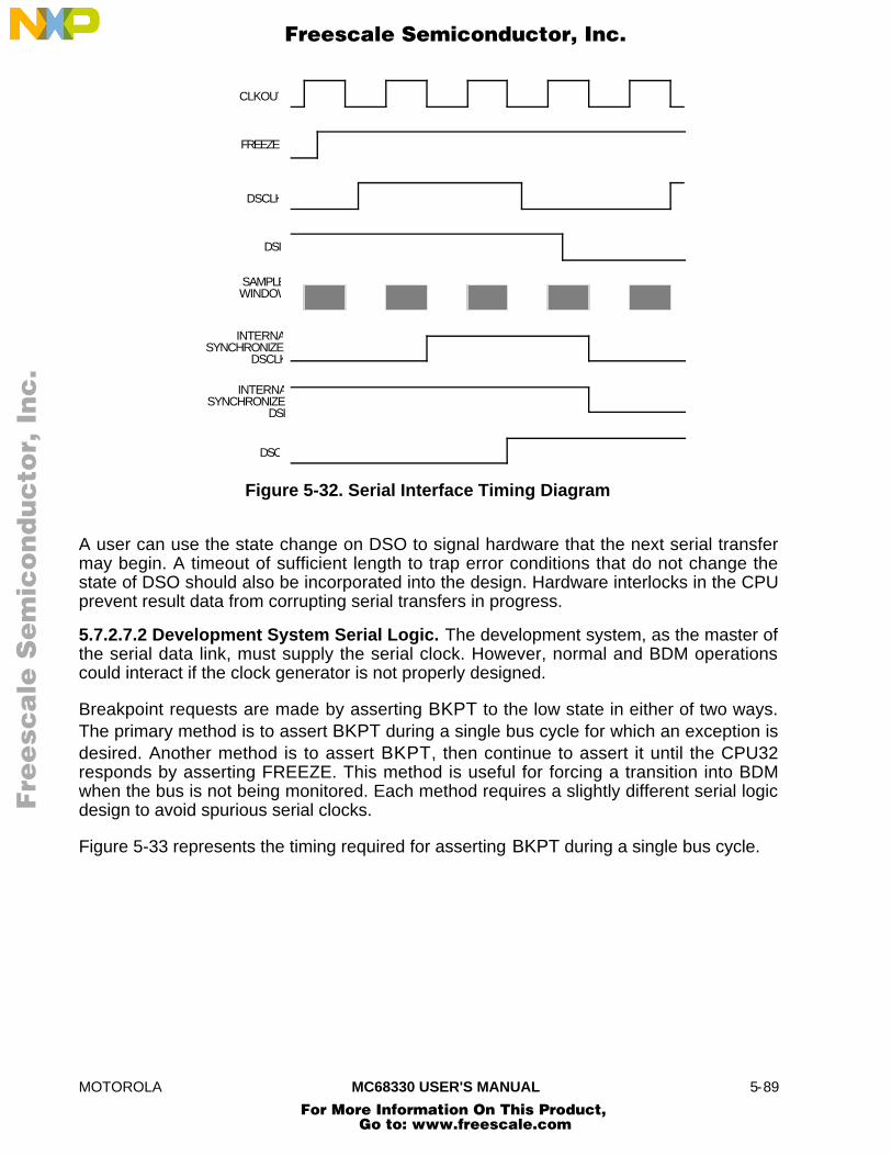
MOTOROLA MC68330 USER'S MANUAL 5-89
CLKOUT
FREEZE
DSCLK
DSI
SAMPLEWINDOW
INTERNASYNCHRONIZED
DSCLK
INTERNASYNCHRONIZED
DSI
DSO
Figure 5-32. Serial Interface Timing Diagram
A user can use the state change on DSO to signal hardware that the next serial transfermay begin. A timeout of sufficient length to trap error conditions that do not change thestate of DSO should also be incorporated into the design. Hardware interlocks in the CPUprevent result data from corrupting serial transfers in progress.
5.7.2.7.2 Development System Serial Logic. The development system, as the master ofthe serial data link, must supply the serial clock. However, normal and BDM operationscould interact if the clock generator is not properly designed.
Breakpoint requests are made by asserting BKPT to the low state in either of two ways.The primary method is to assert BKPT during a single bus cycle for which an exception isdesired. Another method is to assert BKPT, then continue to assert it until the CPU32responds by asserting FREEZE. This method is useful for forcing a transition into BDMwhen the bus is not being monitored. Each method requires a slightly different serial logicdesign to avoid spurious serial clocks.
Figure 5-33 represents the timing required for asserting BKPT during a single bus cycle.
Fre
esc
ale
Se
mic
on
du
cto
r, I
Freescale Semiconductor, Inc.
For More Information On This Product, Go to: www.freescale.com
nc
...

5-90 MC68330 USER'S MANUAL MOTOROLA
SHIFT_CL
FORCE_BGND
BKPT_TAG
FREEZE
BKPT
Figure 5-33. BKPT Timing for Single Bus Cycle
Figure 5-34 depicts the timing of the BKPT/FREEZE method. In both cases, the serialclock is left high after the final shift of each transfer. This technique eliminates thepossibility of accidentally tagging the prefetch initiated at the conclusion of a BDM session.As mentioned previously, all timing within the CPU is derived from the rising edge of theclock; the falling edge is effectively ignored.
BKPT_TAG
FREEZE
SHIFT_CLK
FORCE_BGND
BKPT
Figure 5-34. BKPT Timing for Forcing BDM
Figure 5-35 represents a sample circuit providing for both BKPT assertion methods. Asthe name implies, FORCE_BGND is used to force a transition into BDM by the assertionof BKPT. FORCE_BGND can be a short pulse or can remain asserted until FREEZE isasserted. Once asserted, the set-reset latch holds BKPT low until the first SHIFT_CLK isapplied.
BKPT/DSCLK
S1
S2
R
Q
Q
RESET
FORCE_BGND
BKPT_TAG
SHIFT_CLK
Figure 5-35. BKPT/DSCLK Logic Diagram
Fre
esc
ale
Se
mic
on
du
cto
r, I
Freescale Semiconductor, Inc.
For More Information On This Product, Go to: www.freescale.com
nc
...

MOTOROLA MC68330 USER'S MANUAL 5-91
BKPT_TAG should be timed to the bus cycles since it is not latched. If extended past theassertion of FREEZE, the negation of BKPT_TAG appears to the CPU32 as the firstDSCLK.
DSCLK, the gated serial clock, is normally high, but it pulses low for each bit to betransferred. At the end of the seventeenth clock period, it remains high until the start of thenext transmission. Clock frequency is implementation dependent and may range from DCto the maximum specified frequency. Although performance considerations might dictate ahardware implementation, software solutions can be used, provided serial bus timing ismaintained.
5.7.2.8 COMMAND SET. The following paragraphs describe the command set available inBDM.
5.7.2.8.1 Command Format. The following standard bit format is utilized by all BDMcommands.
15 10 9 8 7 6 5 4 3 2 0
OPERATION 0 R/W OP SIZE 0 0 A/D REGISTER
EXTENSION WORD(S)
Operation Field:The operation field specifies the commands. This 6-bit field provides for a maximum of 64unique commands.
R/W Field:The R/W field specifies the direction of operand transfer. When the bit is set, the transferis from CPU to development system. When the bit is clear, data is written to the CPU or tomemory from the development system.
Operand Size:For sized operations, this field specifies the operand data size. All addresses areexpressed as 32-bit absolute values. The size field is encoded as listed in Table 5-24.
Table 5-24 Size Field Encoding
Encoding Operand Size
00 Byte
01 Word
10 Long
11 Reserved
Address/Data (A/D) Field:The A/D field is used by commands that operate on address and data registers. Itdetermines whether the register field specifies a data or address register. One indicatesan address register; zero indicates a data register. For other commands, this field may beinterpreted differently.
Fre
esc
ale
Se
mic
on
du
cto
r, I
Freescale Semiconductor, Inc.
For More Information On This Product, Go to: www.freescale.com
nc
...

5-92 MC68330 USER'S MANUAL MOTOROLA
Register Field:In most commands, this field specifies the register number for operations performed on anaddress or data register.
Extension Word(s) (as required):At this time, no command requires an extension word to specify fully the operation to beperformed, but some commands require extension words for addresses or immediatedata. Addresses require two extension words because only absolute long addressing ispermitted. Immediate data can be either one or two words in length — byte and word dataeach require a single extension word, long-word data requires two words. Both operandsand addresses are transferred most significant word first.
5.7.2.8.2 Command Sequence Diagram. A command sequence diagram (see Figure 5-36)illustrates the serial bus traffic for each command. Each bubble in the diagramrepresents a single 17-bit transfer across the bus. The top half in each diagramcorresponds to the data transmitted by the development system to the CPU; the bottomhalf corresponds to the data returned by the CPU in response to the development systemcommands. Command and result transactions are overlapped to minimize latency.
The cycle in which the command is issued contains the development system commandmnemonic (in this example, read memory location). During the same cycle, the CPUresponds with either the lowest order results of the previous command or with a commandcomplete status (if no results were required).
During the second cycle, the development system supplies the high-order 16 bits of thememory address. The CPU returns a "not ready" response unless the received commandwas decoded as unimplemented, in which case the response data is the illegal commandencoding. If an illegal command response occurs, the development system shouldretransmit the command.
NOTE
The “not ready” response can be ignored unless amemory bus cycle is in progress. Otherwise, the CPUcan accept a new serial transfer with eight system clockperiods.
In the third cycle, the development system supplies the low-order 16 bits of a memoryaddress. The CPU always returns the “not ready” response in this cycle. At the completionof the third cycle, the CPU initiates a memory read operation. Any serial transfers thatbegin while the memory access is in progress return the “not ready” response.
Results are returned in the two serial transfer cycles following the completion of memoryaccess. The data transmitted to the CPU during the final transfer is the opcode for thefollowing command. Should a memory access generate either a bus or address error, anerror status is returned in place of the result data.
Fre
esc
ale
Se
mic
on
du
cto
r, I
Freescale Semiconductor, Inc.
For More Information On This Product, Go to: www.freescale.com
nc
...

MOTOROLA MC68330 USER'S MANUAL 5-93
COMMANDS TRANSMITTED TO THE CPU
COMMAND CODE TRANSMITTED DURING THIS CYCLE
HIGH-ORDER 16 BITS OF MEMORY ADDRESS
LOW-ORDER 16 BITS OF MEMORY ADDRESS
SEQUENCE TAKEN IFOPERATION HAS NOT COMPLETED
DATA UNUSED FROMTHIS TRANSFER
SEQUENCE TAKEN IFILLEGAL COMMANDIS RECEIVED BY CPU
RESULTS FROM PREVIOUS COMMAND
RESPONSES FROM THE CPU
NONSERIAL-RELATED ACTIVITY
MS ADDR"NOT READY
XXX"ILLEGAL
LS ADDR"NOT READY
NEXT CMD"NOT READY
READ (LONG???
NEXT CMD"NOT READY
XXX"NOT READY
XXXRESUL
TXXX
BERR/AERR
XXXMS RESULT
NEXT CMDLS RESULT
READMEMORYLOCATION
NEXTCOMMAND
CODE
SEQUENCE TAKEN IF BUS ERROR OR ADDRESS ERROR OCCURS ON MEMORY ACCESS
HIGH AND LOW-ORDER 16 BITS OF RESULT
Figure 5-36. Command-Sequence-Diagram Example
5.7.2.8.3 Command Set Summary. The BDM command set is summarized in Table 5-25.Subsequent paragraphs contain detailed descriptions of each command.
Fre
esc
ale
Se
mic
on
du
cto
r, I
Freescale Semiconductor, Inc.
For More Information On This Product, Go to: www.freescale.com
nc
...

5-94 MC68330 USER'S MANUAL MOTOROLA
Table 5-25. BDM Command Summary
Command Mnemonic Description
Read A/D Register RAREG/RDREG Read the selected address or data register and return the resultsvia the serial interface.
Write A/D Register WAREG/WDREG The data operand is written to the specified address or dataregister.
Read System Register RSREG The specified system control register is read. All registers that canbe read in supervisor mode can be read in BDM.
Write System Register WSREG The operand data is written into the specified system controlregister.
Read Memory Location READ Read the sized data at the memory location specified by the long-word address. The source function code (SFC) register determinesthe address space accessed.
Write Memory Location WRITE Write the operand data to the memory location specified by thelong-word address. The destination function code (DFC) registerdetermines the address space accessed.
Dump Memory Block DUMP Used in conjunction with the READ command to dump large blocksof memory. An initial READ is executed to set up the startingaddress of the block and to retrieve the first result. Subsequentoperands are retrieved with the DUMP command.
Fill Memory Block FILL Used in conjunction with the WRITE command to fill large blocks ofmemory. An initial WRITE is executed to set up the startingaddress of the block and to supply the first operand. Subsequentoperands are written with the FILL command.
Resume Execution GO The pipeline is flushed and refilled before resuming instructionexecution at the return PC.
Call User Code CALL Current PC is stacked at the location of the current SP. Instructionexecution begins at user patch code.
Reset Peripherals RST Asserts RESET for 512 clock cycles. The CPU is not reset by thiscommand. Synonymous with the CPU RESET instruction.
No Operation NOP NOP performs no operation and may be used as a null command.
5.7.2.8.4 Read A/D Register (RAREG/RDREG). Read the selected address or dataregister and return the results via the serial interface.
Command Format:
15 14 13 12 11 10 9 8 7 6 5 4 3 2 1 0
0 0 1 0 0 0 0 1 1 0 0 0 A/D REGISTER
Command Sequence:
RDREG/RAREG???
XXXMS RESULT
XXX"ILLEGAL
NEXT CMDLS RESULT
NEXT CMD"NOT READY
Operand Data:
None
Fre
esc
ale
Se
mic
on
du
cto
r, I
Freescale Semiconductor, Inc.
For More Information On This Product, Go to: www.freescale.com
nc
...

MOTOROLA MC68330 USER'S MANUAL 5-95
Result Data:The contents of the selected register are returned as a long-word value. The data isreturned most significant word first.
5.7.2.8.5 Write A/D Register (WAREG/WDREG). The operand (long-word) data is writtento the specified address or data register. All 32 bits of the register are altered by the write.
Command Format:
15 14 13 12 11 10 9 8 7 6 5 4 3 2 0
0 0 1 0 0 0 0 0 1 0 0 0 A/D REGISTER
Command Sequence:
WDREG/WAREG???
MS DATA"NOT READ
XXX"ILLEGAL
LS DATA"NOT READY
NEXT CMD"NOT READY
"CMD COMPLETNEXT CMD
Operand Data:
Long-word data is written into the specified address or data register. The data issupplied most significant word first.
Result Data:Command complete status ($0FFFF) is returned when register write is complete.
5.7.2.8.6 Read System Register (RSREG). The specified system control register is read.All registers that can be read in supervisor mode can be read in BDM. Several internaltemporary registers are also accessible.
Command Format:
15 14 13 12 11 10 9 8 7 6 5 4 3 0
0 0 1 0 0 1 0 0 1 0 0 0 REGISTER
Command Sequence:
RSREG???
XXXMS RESULT
XXX"ILLEGAL
NEXT CMDLS RESULT
NEXT CMD"NOT READY
Operand Data:
None
Fre
esc
ale
Se
mic
on
du
cto
r, I
Freescale Semiconductor, Inc.
For More Information On This Product, Go to: www.freescale.com
nc
...
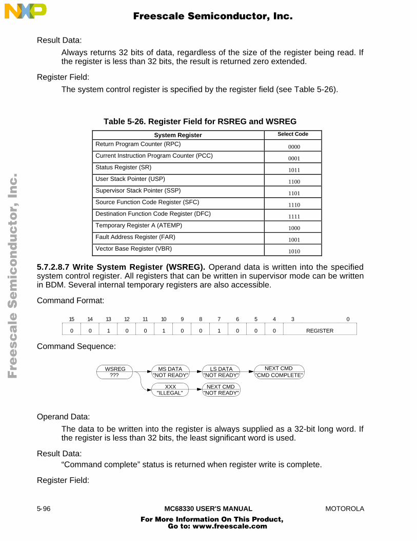
5-96 MC68330 USER'S MANUAL MOTOROLA
Result Data:
Always returns 32 bits of data, regardless of the size of the register being read. Ifthe register is less than 32 bits, the result is returned zero extended.
Register Field:
The system control register is specified by the register field (see Table 5-26).
Table 5-26. Register Field for RSREG and WSREG
System Register Select Code
Return Program Counter (RPC) 0000
Current Instruction Program Counter (PCC) 0001
Status Register (SR) 1011
User Stack Pointer (USP) 1100
Supervisor Stack Pointer (SSP) 1101
Source Function Code Register (SFC) 1110
Destination Function Code Register (DFC) 1111
Temporary Register A (ATEMP) 1000
Fault Address Register (FAR) 1001
Vector Base Register (VBR) 1010
5.7.2.8.7 Write System Register (WSREG). Operand data is written into the specifiedsystem control register. All registers that can be written in supervisor mode can be writtenin BDM. Several internal temporary registers are also accessible.
Command Format:
15 14 13 12 11 10 9 8 7 6 5 4 3 0
0 0 1 0 0 1 0 0 1 0 0 0 REGISTER
Command Sequence:
MS DATA"NOT READY"
XXX"ILLEGAL"
"NOT READY"
NEXT CMD"NOT READY"
"CMD COMPLETE"NEXT CMDWSREG
???LS DATA
Operand Data:
The data to be written into the register is always supplied as a 32-bit long word. Ifthe register is less than 32 bits, the least significant word is used.
Result Data:“Command complete” status is returned when register write is complete.
Register Field:
Fre
esc
ale
Se
mic
on
du
cto
r, I
Freescale Semiconductor, Inc.
For More Information On This Product, Go to: www.freescale.com
nc
...

MOTOROLA MC68330 USER'S MANUAL 5-97
The system control register is specified by the register field (see Table 5-26). TheFAR is a read-only register — any write to it is ignored.
5.7.2.8.8 Read Memory Location (READ). Read the sized data at the memory locationspecified by the long-word address. Only absolute addressing is supported. The SFCregister determines the address space accessed. Valid data sizes include byte, word, orlong word.
Command Format:
15 14 13 12 11 10 9 8 7 6 5 4 3 2 1 0
0 0 0 1 1 0 0 1 OP SIZE 0 0 0 0 0 0
Command Sequence:
LS ADDR"NOT READY"
READ (B/W)???
NEXT CMD"NOT READY"
XXX"NOT READY"
NEXT CMDRESULT
XXX"BERR/AERR"
READ MEMORY
LOCATION
NEXT CMD"NOT READY"
MS ADDR"NOT READY"
XXX"ILLEGAL"
LS ADDR"NOT READY"
READ (LONG)???
NEXT CMD"NOT READY"
XXX"NOT READY"
XXX"BERR/AERR"
READ MEMORY
LOCATIONNEXT CMD
"NOT READY"
MS ADDR"NOT READY"
XXX"ILLEGAL"
NEXT CMDLS RESULT
XXXMS RESULT
Operand Data:
The single operand is the long-word address of the requested memory location.
Result Data:
The requested data is returned as either a word or long word. Byte data is returnedin the least significant byte of a word result, with the upper byte cleared. Wordresults return 16 bits of significant data; long-word results return 32 bits.
A successful read operation returns data bit 16 cleared. If a bus or address error isencountered, the returned data is $10001.
5.7.2.8.9 Write Memory Location (WRITE). Write the operand data to the memorylocation specified by the long-word address. The DFC register determines the addressspace accessed. Only absolute addressing is supported. Valid data sizes include byte,word, and long word.
Command Format:
Fre
esc
ale
Se
mic
on
du
cto
r, I
Freescale Semiconductor, Inc.
For More Information On This Product, Go to: www.freescale.com
nc
...
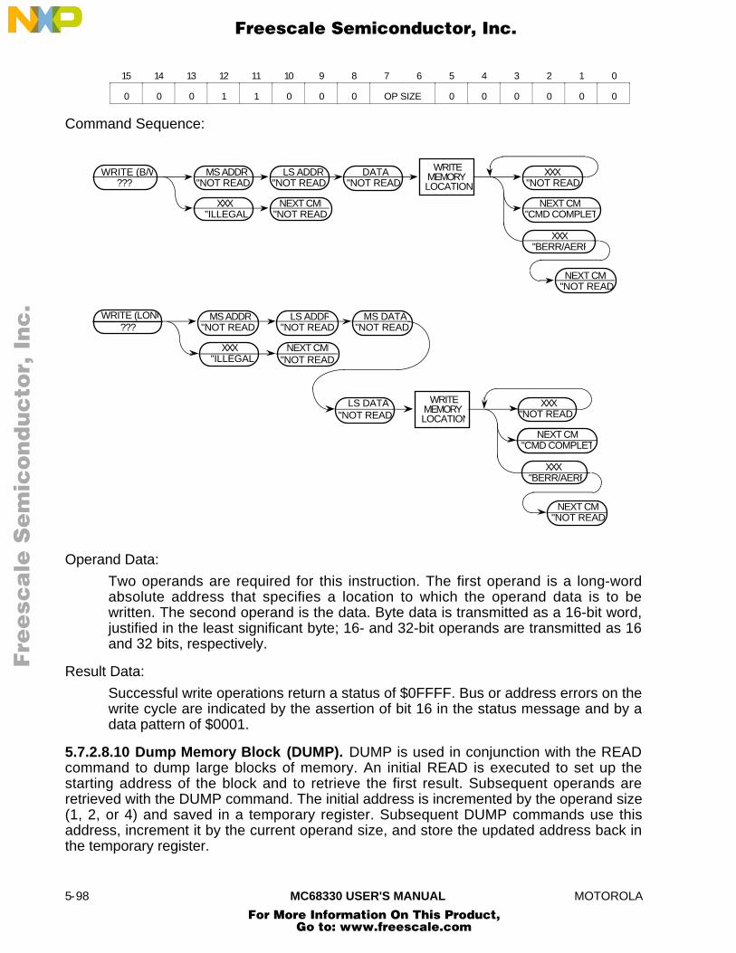
5-98 MC68330 USER'S MANUAL MOTOROLA
15 14 13 12 11 10 9 8 7 6 5 4 3 2 1 0
0 0 0 1 1 0 0 0 OP SIZE 0 0 0 0 0 0
Command Sequence:
MS ADDR"NOT READY
XXX"ILLEGAL
LS ADDR"NOT READY
NEXT CMD"NOT READY
WRITE (B/W???
NEXT CMD"NOT READY
XXX"NOT READY
XXX
XXX"BERR/AERR
NEXT CMD"CMD COMPLET
DATA"NOT READY
WRITEMEMORYLOCATION
MS ADDR"NOT READY
XXX"ILLEGAL
LS ADDR"NOT READY
NEXT CMD"NOT READY
WRITE (LONG???
MS DATA"NOT READY
LS DATA"NOT READY
WRITEMEMORYLOCATION
NEXT CMD"NOT READY
XXX"NOT READY
XXX
XXX"BERR/AERR
NEXT CMD"CMD COMPLET
Operand Data:
Two operands are required for this instruction. The first operand is a long-wordabsolute address that specifies a location to which the operand data is to bewritten. The second operand is the data. Byte data is transmitted as a 16-bit word,justified in the least significant byte; 16- and 32-bit operands are transmitted as 16and 32 bits, respectively.
Result Data:
Successful write operations return a status of $0FFFF. Bus or address errors on thewrite cycle are indicated by the assertion of bit 16 in the status message and by adata pattern of $0001.
5.7.2.8.10 Dump Memory Block (DUMP). DUMP is used in conjunction with the READcommand to dump large blocks of memory. An initial READ is executed to set up thestarting address of the block and to retrieve the first result. Subsequent operands areretrieved with the DUMP command. The initial address is incremented by the operand size(1, 2, or 4) and saved in a temporary register. Subsequent DUMP commands use thisaddress, increment it by the current operand size, and store the updated address back inthe temporary register.
Fre
esc
ale
Se
mic
on
du
cto
r, I
Freescale Semiconductor, Inc.
For More Information On This Product, Go to: www.freescale.com
nc
...

MOTOROLA MC68330 USER'S MANUAL 5-99
NOTE
The DUMP command does not check for a valid addressin the temporary register — DUMP is a valid commandonly when preceded by another DUMP or by a READcommand. Otherwise, the results are undefined. TheNOP command can be used for intercommand paddingwithout corrupting the address pointer.
The size field is examined each time a DUMP command is given, allowing the operandsize to be altered dynamically.
Command Format:
15 14 13 12 11 10 9 8 7 6 5 4 3 2 1 0
0 0 0 1 1 1 0 1 OP SIZE 0 0 0 0 0 0
Fre
esc
ale
Se
mic
on
du
cto
r, I
Freescale Semiconductor, Inc.
For More Information On This Product, Go to: www.freescale.com
nc
...
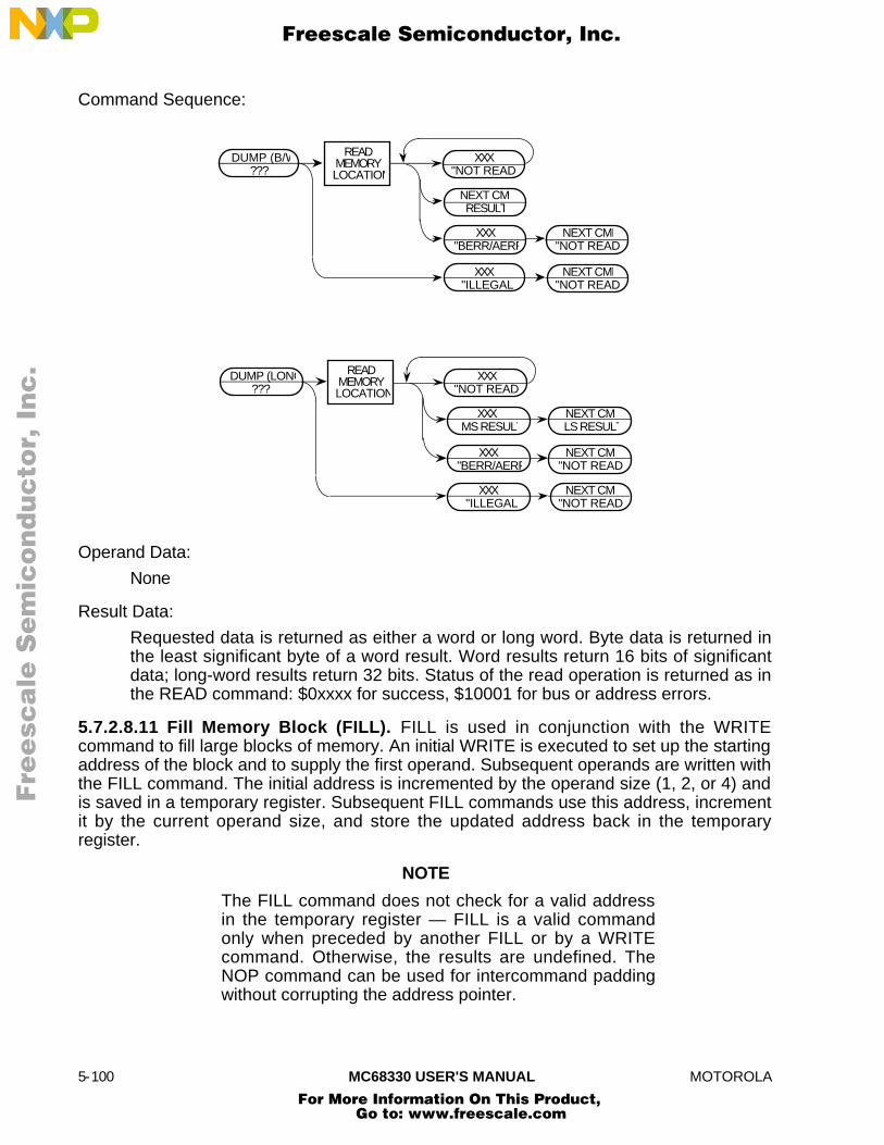
5-100 MC68330 USER'S MANUAL MOTOROLA
Command Sequence:
DUMP (B/W???
XXX"NOT READY
NEXT CMDRESULT
XXX"BERR/AERR
XXX"ILLEGAL
NEXT CMD"NOT READY
NEXT CMD"NOT READY
READMEMORYLOCATION
DUMP (LONG???
XXX"NOT READY
MS RESULT
XXX"BERR/AERR
XXX"ILLEGAL
NEXT CMD"NOT READY
NEXT CMD"NOT READY
NEXT CMDLS RESULT
READMEMORYLOCATION
XXX
Operand Data:
None
Result Data:
Requested data is returned as either a word or long word. Byte data is returned inthe least significant byte of a word result. Word results return 16 bits of significantdata; long-word results return 32 bits. Status of the read operation is returned as inthe READ command: $0xxxx for success, $10001 for bus or address errors.
5.7.2.8.11 Fill Memory Block (FILL). FILL is used in conjunction with the WRITEcommand to fill large blocks of memory. An initial WRITE is executed to set up the startingaddress of the block and to supply the first operand. Subsequent operands are written withthe FILL command. The initial address is incremented by the operand size (1, 2, or 4) andis saved in a temporary register. Subsequent FILL commands use this address, incrementit by the current operand size, and store the updated address back in the temporaryregister.
NOTE
The FILL command does not check for a valid addressin the temporary register — FILL is a valid commandonly when preceded by another FILL or by a WRITEcommand. Otherwise, the results are undefined. TheNOP command can be used for intercommand paddingwithout corrupting the address pointer.
Fre
esc
ale
Se
mic
on
du
cto
r, I
Freescale Semiconductor, Inc.
For More Information On This Product, Go to: www.freescale.com
nc
...

MOTOROLA MC68330 USER'S MANUAL 5-101
The size field is examined each time a FILL command is given, allowing the operand sizeto be altered dynamically.
Command Format:
15 14 13 12 11 10 9 8 7 6 5 4 3 2 1 0
0 0 0 1 1 1 0 0 OP SIZE 0 0 0 0 0 0
Command Sequence:
NEXT CMD"NOT READY
"NOT READY
XXXResult
XXX"BERR/AERR
"CMD COMPLET
DATA"NOT READY
XXX
NEXT CMDXXX"ILLEGAL
NEXT CMD"NOT READY
FILL (B/W???
WRITEMEMORYLOCATION
NEXT CMD"NOT READY
XXX"NOT READY
XXXResult
XXX"BERR/AERR
"CMD COMPLET
MS DATA"NOT READY"
NEXT CMDXXX"ILLEGAL
NEXT CMD"NOT READY
FILL (LONG???
LS DATA"NOT READY
WRITEMEMORYLOCATION
Operand Data:
A single operand is data to be written to the memory location. Byte data istransmitted as a 16-bit word, justified in the least significant byte; 16- and 32-bitoperands are transmitted as 16 and 32 bits, respectively.
Result Data:
Status is returned as in the WRITE command: $0FFFF for a successful operationand $10001 for a bus or address error during write.
5.7.2.8.12 Resume Execution (GO). The pipeline is flushed and refilled before normalinstruction execution is resumed. Prefetching begins at the return PC and current privilegelevel. If either the PC or SR is altered during BDM, the updated value of these registers isused when prefetching commences.
Fre
esc
ale
Se
mic
on
du
cto
r, I
Freescale Semiconductor, Inc.
For More Information On This Product, Go to: www.freescale.com
nc
...

5-102 MC68330 USER'S MANUAL MOTOROLA
NOTE
The processor exits BDM when a bus error or addresserror occurs on the first instruction prefetch from the newPC — the error is trapped as a normal mode exception.The stacked value of the current PC may not be valid inthis case, depending on the state of the machine prior toentering BDM. For address error, the PC does not reflectthe true return PC. Instead, the stacked fault address isthe (odd) return PC.
Command Format:
15 14 13 12 11 10 9 8 7 6 5 4 3 2 1 0
0 0 0 0 1 1 0 0 0 0 0 0 0 0 0 0
Command Sequence:
GO???
NORMAL MODE
XXX"ILLEGAL
NEXT CMD"NOT READY
Operand Data:
None
Result Data:
None
5.7.2.8.13 Call User Code (CALL). This instruction provides a convenient way to patchuser code. The return PC is stacked at the location pointed to by the current SP. Thestacked PC serves as a return address to be restored by the RTS command thatterminates the patch routine. After stacking is complete, the 32-bit operand data is loadedinto the PC. The pipeline is flushed and refilled from the location pointed to by the new PC.BDM is exited, and normal mode instruction execution begins.
NOTE
If a bus error or address error occurs during returnaddress stacking, the CPU returns an error status viathe serial interface and remains in BDM.
If a bus error or address error occurs on the firstinstruction prefetch from the new PC, the processor exitsBDM and the error is trapped as a normal modeexception. The stacked value of the current PC may notbe valid in this case, depending on the state of themachine prior to entering BDM. For address error, thePC does not reflect the true return PC. Instead, thestacked fault address is the (odd) return PC.
Fre
esc
ale
Se
mic
on
du
cto
r, I
Freescale Semiconductor, Inc.
For More Information On This Product, Go to: www.freescale.com
nc
...

MOTOROLA MC68330 USER'S MANUAL 5-103
Command Format:
15 14 13 12 11 10 9 8 7 6 5 4 3 2 1 0
0 0 0 0 1 0 0 0 0 0 0 0 0 0 0 0
Command Sequence:
LS ADDR"NOT READY
STACKRETURN PC
NORMAL MODE
MS ADDR"NOT READY
XXX"ILLEGAL
NEXT CMD"NOT READY
CALL???
FREEZE NEGATED
PREFETCH STARTED
XXXBERR/AERR
NEXT CMD"NOT READY
Operand Data:
The 32-bit operand data is the starting location of the patch routine, which is theinitial PC upon exiting BDM.
Result Data:
None
As an example, consider the following code segment. It is supposed to output a characterto an asynchronous communications interface adaptor. Note that the routine fails to checkthe transmit data register empty (TDRE) flag.
CHKSTAT: MOVE.B ACIAS,D0 Move ACIA status to D0BEQ.B CHKSTAT Loop till condition trueMOVE.B DATA,ACIAD Output data•••
MISSING: ANDI.B #2,D0 Check for TDRERTS Return to in-line code
BDM and the CALL command can be used to patch the code as follows:
1. Breakpoint user program at CHKSTAT2. Enter BDM3. Execute CALL command to MISSING4. Exit BDM5. Execute MISSING code6. Return to user program
5.7.2.8.14 Reset Peripherals (RST). RST asserts RESET for 512 clock cycles. The CPUis not reset by this command. This command is synonymous with the CPU RESETinstruction.
Command Format:
Fre
esc
ale
Se
mic
on
du
cto
r, I
Freescale Semiconductor, Inc.
For More Information On This Product, Go to: www.freescale.com
nc
...

5-104 MC68330 USER'S MANUAL MOTOROLA
15 14 13 12 11 10 9 8 7 6 5 4 3 2 1 0
0 0 0 0 0 1 0 0 0 0 0 0 0 0 0 0
Command Sequence:
RESET???
ASSERTRESET
XXX"NOT READY
XXX"ILLEGAL
NEXT CMD"NOT READY
NEXT CMD"CMD COMPLET
Operand Data:
None
Result Data:
The “command complete” response ($0FFFF) is loaded into the serial shifter afternegation of RESET.
5.7.2.8.15 No Operation (NOP). NOP performs no operation and may be used as a nullcommand where required.
Command Format:
15 14 13 12 11 10 9 8 7 6 5 4 3 2 1 0
0 0 0 0 0 0 0 0 0 0 0 0 0 0 0 0
Command Sequence:
XXX"ILLEGAL "NOT READY
NOP???
NEXT CMD"CMD COMPLET
NEXT CMD
Operand Data:
None
Result Data:
The “command complete” response ($0FFFF) is returned during the next shiftoperation.
5.7.2.8.16 Future Commands. Unassigned command opcodes are reserved by Motorolafor future expansion. All unused formats within any revision level will perform a NOP andreturn the ILLEGAL command response.
Fre
esc
ale
Se
mic
on
du
cto
r, I
Freescale Semiconductor, Inc.
For More Information On This Product, Go to: www.freescale.com
nc
...

MOTOROLA MC68330 USER'S MANUAL 5-105
5.7.3 Deterministic Opcode TrackingThe CPU32 utilizes deterministic opcode tracking to trace program execution. Twosignals, IPIPE and IFETCH, provide all information required to analyze instruction pipelineoperation.
5.7.3.1 INSTRUCTION FETCH (IFETCH). IFETCH indicates which bus cycles areaccessing data to fill the instruction pipeline. IFETCH is pulse-width modulated to multiplextwo indications on a single pin. Asserted for a single clock cycle, IFETCH indicates that thedata from the current bus cycle is to be routed to the instruction pipeline. IFETCH held lowfor two clock cycles indicates that the instruction pipeline has been flushed. The data fromthe bus cycle is used to begin filling the empty pipeline. Both user and supervisor modefetches are signaled by IFETCH.
Proper tracking of bus cycles via the IFETCH signal on a fast bus requires a simple statemachine. On a two-clock bus, IFETCH may signal a pipeline flush with associated prefetchfollowed immediately by a second prefetch. That is, IFETCH remains asserted for threeclocks, two clocks indicating the flush/fetch and a third clock signaling the second fetch.These two operations are easily discerned if the tracking logic samples IFETCH on the tworising edges of CLKOUT, which follow the address strobe (data strobe during show cycles)falling edge. Three-clock and slower bus cycles allow time for negation of the signalbetween consecutive indications and do not experience this operation.
5.7.3.2 INSTRUCTION PIPE (IPIPE). The internal instruction pipeline can be modeled asa three-stage FIFO (see Figure 5-37). Stage A is an input buffer — data can be used outof stages B and C. IPIPE signals advances of instructions in the pipeline.
Instruction register A (IRA) holds incoming words as they are prefetched. No decodingtakes place in the buffer. Instruction register B (IRB) provides initial decoding of theopcode and decoding of extension words; it is a source of immediate data. Instructionregister C (IRC) supplies residual opcode decoding during instruction execution.
I
R
C
DATA BUS
EXTENSIONWORDS
OPCODESRESIDUAL
I
R
B
I
R
A
Figure 5-37. Functional Model of Instruction Pipeline
Assertion of IPIPE for a single clock cycle indicates the use of data from IRB. Regardlessof the presence of valid data in IRA, the contents of IRB are invalidated when IPIPE isasserted. If IRA contains valid data, the data is copied into IRB (IRA ⇒ IRB), and the IRBstage is revalidated.
Fre
esc
ale
Se
mic
on
du
cto
r, I
Freescale Semiconductor, Inc.
For More Information On This Product, Go to: www.freescale.com
nc
...

5-106 MC68330 USER'S MANUAL MOTOROLA
Assertion of IPIPE for two clock cycles indicates the start of a new instruction andsubsequent replacement of data in IRC. This action causes a full advance of the pipeline(IRB ⇒ IRC and IRA ⇒ IRB). IRA is refilled during the next instruction fetch bus cycle.
Data loaded into IRA propagates automatically through subsequent empty pipeline stages.Signals that show the progress of instructions through IRB and IRC are necessary toaccurately monitor pipeline operation. These signals are provided by IRA and IRB validitybits. When a pipeline advance occurs, the validity bit of the stage being loaded is set, andthe validity bit of the stage supplying the data is negated.
Because instruction execution is not timed to bus activity, IPIPE is synchronized with thesystem clock and not the bus. Figure 5-38 illustrates the timing in relation to the systemclock.
IPIPE
EXTENSIONWORD USED
INSTRUCTIONSTART
EXTENSIONWORD USED
INSTRUCTIONSTART
IRA IRB IRA IRBIRA IRBIRB IRC
IRA IRB
CLKOUT
IRB IRC
Figure 5-38. Instruction Pipeline Timing Diagram
IPIPE should be sampled on the falling edge of the clock. The assertion of IPIPE for asingle cycle after one or more cycles of negation indicates use of the data in IRB (advanceof IRA into IRB). Assertion for two clock cycles indicates that a new instruction has started(both IRB ⇒ IRC and IRA ⇒ IRB transfers have occurred). Loading IRC always indicatesthat an instruction is beginning execution — the opcode is loaded into IRC by the transfer.
In some cases, instructions using immediate addressing begin executing and initiate asecond pipeline advance at the same time. IPIPE will not be negated between the twoindications, which implies the need for a state machine to track the state of IPIPE. Thestate machine can be resynchronized during periods of inactivity on the signal.
5.7.3.3 OPCODE TRACKING DURING LOOP MODE. IPIPE and IFETCH continue towork normally during loop mode. IFETCH indicates all instruction fetches up through thepoint that data begins recirculating within the instruction pipeline. IPIPE continues tosignal the start of instructions and the use of extension words even though data is beingrecirculated internally. IFETCH returns to normal operation with the first fetch after exitingloop mode.
5.8 INSTRUCTION EXECUTION TIMINGThis section describes the instruction execution timing of the CPU32. External clock cyclesare used to provide accurate execution and operation timing guidelines, but not exacttiming for every possible circumstance. This approach is used because exact execution
Fre
esc
ale
Se
mic
on
du
cto
r, I
Freescale Semiconductor, Inc.
For More Information On This Product, Go to: www.freescale.com
nc
...

MOTOROLA MC68330 USER'S MANUAL 5-107
time for an instruction or operation depends on concurrence of independently scheduledresources, on memory speeds, and on other variables.
An assembly language programmer or compiler writer can use the information in thissection to predict the performance of the CPU32. Additionally, timing for exceptionprocessing is included so that designers of multitasking or real-time systems can predicttask-switch overhead, maximum interrupt latency, and similar timing parameters.Instruction timing is given in clock cycles to eliminate clock frequency dependency.
5.8.1 Resource SchedulingThe CPU32 contains several independently scheduled resources. The organization ofthese resources within the CPU32 is shown in Figure 5-39. Some variation in instructionexecution timing results from concurrent resource utilization. Because resource schedulingis not directly related to instruction boundaries, it is impossible to make an accurateprediction of the time required to complete an instruction without knowing the entirecontext within which the instruction is executing.
5.8.1.1 MICROSEQUENCER. The microsequencer either executes microinstructions orawaits completion of accesses necessary to continue microcode execution. Themicrosequencer supervises the bus controller, instruction execution, and internalprocessor operations such as calculation of EA and setting of condition codes. It alsoinitiates instruction word prefetches after a change of flow and controls validation ofinstruction words in the instruction pipeline.
5.8.1.2 INSTRUCTION PIPELINE. The CPU32 contains a two-word instruction pipelinewhere instruction opcodes are decoded. Each stage of the pipeline is initially filled undermicrosequencer control and subsequently refilled by the prefetch controller as it empties.
Stage A of the instruction pipeline is a buffer. Prefetches completed on the bus beforestage B empties are temporarily stored in this buffer. Instruction words (instructionoperation words and all extension words) are decoded at stage B. Residual decoding andexecution occur in stage C.
Each pipeline stage has an associated status bit that shows whether the word in thatstage was loaded with data from a bus cycle that terminated abnormally.
5.8.1.3 BUS CONTROLLER RESOURCES. The bus controller consists of the instructionprefetch controller, the write pending buffer, and the microbus controller. These threeresources transact all reads, writes, and instruction prefetches required for instructionexecution.
The bus controller and microsequencer operate concurrently. The bus controller canperform a read or write or schedule a prefetch while the microsequencer controls EAcalculation or sets condition codes.
The microsequencer can also request a bus cycle that the bus controller cannot performimmediately. When this happens, the bus cycle is queued, and the bus controller runs thecycle when the current cycle is complete.
Fre
esc
ale
Se
mic
on
du
cto
r, I
Freescale Semiconductor, Inc.
For More Information On This Product, Go to: www.freescale.com
nc
...

5-108 MC68330 USER'S MANUAL MOTOROLA
MICROSEQUENCER AND CONTROL
CONTROL STOR
CONTROL LOGI
INSTRUCTION PIPELIN
STAGE STAGEC B
EXECUTION UNIT
PROGRAMCOUNTERSECTION
DATA SECTION
WRITE PENDINGBUFFER
PREFETCH CONTROLLER
MICROBUSCONTROLLER
ADDRESSBUS
DATABUS
BUS CONTROSIGNALS
STAGEA
BUS CONTROLLER
Figure 5-39. Block Diagram of Independent Resources
5.8.1.3.1 Prefetch Controller. The instruction prefetch controller receives an initialrequest from the microsequencer to initiate prefetching at a given address. Subsequentprefetches are initiated by the prefetch controller whenever a pipeline stage is invalidated,either through instruction completion or through use of extension words. Prefetch occursas soon as the bus is free of operand accesses previously requested by themicrosequencer. Additional state information permits the controller to inhibit prefetchrequests when a change in instruction flow (e.g., a jump or branch instruction) isanticipated.
In a typical program, 10 to 25 percent of the instructions cause a change of flow. Eachtime a change occurs, the instruction pipeline must be flushed and refilled from the newinstruction stream. If instruction prefetches, rather than operand accesses, were givenpriority, many instruction words would be flushed unused, and necessary operand cycleswould be delayed. To maximize available bus bandwidth, the CPU32 will schedule aprefetch only when the next instruction is not a change-of-flow instruction and when thereis room in the pipeline for the prefetch.
5.8.1.3.2 Write Pending Buffer. The CPU32 incorporates a single-operand write pendingbuffer. The buffer permits the microsequencer to continue execution after a request for awrite cycle is queued in the bus controller. The time needed for a write at the end of aninstruction can overlap the head cycle time for the following instruction, thus reducingoverall execution time. Interlocks prevent the microsequencer from overwriting the buffer.
Fre
esc
ale
Se
mic
on
du
cto
r, I
Freescale Semiconductor, Inc.
For More Information On This Product, Go to: www.freescale.com
nc
...

MOTOROLA MC68330 USER'S MANUAL 5-109
5.8.1.3.3 Microbus Controller. The microbus controller performs bus cycles issued by themicrosequencer. Operand accesses always have priority over instruction prefetches. Wordand byte operands are accessed in a single CPU-initiated bus cycle, although the externalbus interface may be required to initiate a second cycle when a word operand is sent to abyte-sized external port. Long operands are accessed in two bus cycles, most significantword first.
The instruction pipeline is capable of recognizing instructions that cause a change of flow.It informs the bus controller when a change of flow is imminent, and the bus controllerrefrains from starting prefetches that would be discarded due to the change of flow.
5.8.1.4 INSTRUCTION EXECUTION OVERLAP. Overlap is the time, measured in clockcycles, that an instruction executes concurrently with the previous instruction. As shown inFigure 5-40, portions of instructions A and B execute simultaneously, reducing totalexecution time. Because portions of instructions B and C also overlap, overall executiontime for all three instructions is also reduced.
Each instruction contributes to the total overlap time. The portion of execution time at theend of instruction A that can overlap the beginning of instruction B is called the tail ofinstruction A. The portion of execution time at the beginning of instruction B that canoverlap the end of instruction A is called the head of instruction B. The total overlap timebetween instructions A and B is the smaller tail of A and the head of B.
INSTRUCTION
INSTRUCTION B
INSTRUCTION
OVERLAP OVERLAP
Figure 5-40. Simultaneous Instruction Execution
The execution time attributed to instructions A, B, and C after considering the overlap isillustrated in Figure 5-41. The overlap time is attributed to the execution time of thecompleting instruction. The following equation shows the method for calculating theoverlap time:
Overlap = min (TailN, HeadN+1)
Fre
esc
ale
Se
mic
on
du
cto
r, I
Freescale Semiconductor, Inc.
For More Information On This Product, Go to: www.freescale.com
nc
...

5-110 MC68330 USER'S MANUAL MOTOROLA
INSTRUCTION
INSTRUCTION
INSTRUCTION
OVERLAPPERIOD
(ABSORBED BYINSTRUCTION
OVERLAPPERIOD
(ABSORBED BYINSTRUCTION B
Figure 5-41. Attributed Instruction Times
5.8.1.5 EFFECTS OF WAIT STATES. The CPU32 access time for on-chip peripherals istwo clocks. While two-clock external accesses are possible when the bus is operated in asynchronous mode, a typical external memory speed is three or more clocks.
All instruction times listed in this section are for word access only (unless an explicitexception is given), and are based on the assumption that both instruction fetches andoperand cycles are to a two-clock memory. Any time a long access is made, time for theadditional bus cycle(s) must be added to the overall execution time. Wait states due toslow external memory must be added to the access time for each bus cycle.
A typical application has a mixture of bus speeds — program execution from an off-chipROM, accesses to on-chip peripherals, storage of variables in slow off-chip RAM, andaccesses to external peripherals with speeds ranging from moderate to very slow. Toarrive at an accurate instruction time calculation, each bus access must be individuallyconsidered. Many instructions have a head cycle count, which can overlap the cycles ofan operand fetch to slower memory started by a previous instruction. In these cases, anincrease in access time has no effect on the total execution time of the pair of instructions.
To trace instruction execution time by monitoring the external bus, note that the order ofoperand accesses for a particular instruction sequence is always the same provided busspeed is unchanged and the interleaving of instruction prefetches with operands withineach sequence is identical.
5.8.1.6 INSTRUCTION EXECUTION TIME CALCULATION. The overall execution timefor an instruction depends on the amount of overlap with previous and followinginstructions. To calculate an instruction time estimate, the entire code sequence must beanalyzed. To derive the actual instruction execution times for an instruction sequence, theinstruction times listed in the tables must be adjusted to account for overlap.
The formula for this calculation is as follows:
C1 − min (T1, H2) + C2 − min (T2, H3) + C3 − min (T3, H4) + .. .. .where:
CN is the number of cycles listed for instruction N
TN is the tail time for instruction N
Fre
esc
ale
Se
mic
on
du
cto
r, I
Freescale Semiconductor, Inc.
For More Information On This Product, Go to: www.freescale.com
nc
...
MOTOROLA MC68330 USER'S MANUAL 5-111
HN is the head time for instruction N
min (TN, HM) is the minimum of parameters TN and HM
The number of cycles for the instruction (CN above) can include one or two EAcalculations in addition to the raw number in the cycles column. In these cases, calculateoverall instruction time as if it were for multiple instructions, using the following equation:
⟨CEA ⟩ − min (TEA, HOP) + COPwhere:
⟨CEA ⟩ is the instruction’s EA time
COP is the instruction’s operation time
TEA is the EA’s tail time
HOP is the instruction operation’s head time
min (TN, HM) is the minimum of parameters TN and HM
The overall head for the instruction is the head for the EA, and the overall tail for theinstruction is the tail for the operation. Therefore, the actual equation for execution timebecomes:
COP1 − min (TOP1, HEA2) + ⟨CEA ⟩2 − min (TEA2, HOP2) +COP2 − min (TOP2, HEA3) + . . .
Every instruction must prefetch to replace itself in the instruction pipe. Usually, theseprefetches occur during or after an instruction. A prefetch is permitted to begin in the firstclock of any indexed EAing mode operation.
Additionally, a prefetch for an instruction is permitted to begin two clocks before the end ofan instruction, provided the bus is not being used. If the bus is being used, then theprefetch occurs at the next available time when the bus would otherwise be idle.
5.8.1.7 EFFECTS OF NEGATIVE TAILS. When the CPU32 changes instruction flow, theinstruction decode pipeline must begin refilling before instruction execution can resume.Refilling forces a two-clock idle period at the end of the change-of-flow instruction. Thisidle period can be used to prefetch an additional word on the new instruction path.Because of the stipulation that each instruction must prefetch to replace itself, the conceptof negative tails has been introduced to account for these free clocks on the bus.
On a two-clock bus, it is not necessary to adjust instruction timing to account for thepotential extra prefetch. The cycle times of the microsequencer and bus are matched, andno additional benefit or penalty is obtained. In the instruction execution time equations, azero should be used instead of a negative number.
Negative tails are used to adjust for slower fetches on slower buses. Normally, increasingthe length of prefetch bus cycles directly affects the cycle count and tail values found inthe tables.
Fre
esc
ale
Se
mic
on
du
cto
r, I
Freescale Semiconductor, Inc.
For More Information On This Product, Go to: www.freescale.com
nc
...

5-112 MC68330 USER'S MANUAL MOTOROLA
In the following equations, negative tail values are used to negate the effects of a slowerbus. The equations are generalized, however, so that they may be used on any speed buswith any tail value.
NEW_TAIL = OLD_TAIL + (NEW_CLOCK – 2)IF ((NEW_CLOCK – 4) >0) THEN
NEW_CYCLE = OLD_CYCLE + (NEW_CLOCK -2) + (NEW_CLOCK – 4)ELSE
NEW_CYCLE = OLD_CYCLE + (NEW _CLOCK – 2)
where:
NEW_TAIL/NEW_CYCLE is the adjusted tail/cycle at the slower speedOLD_TAIL/OLD_CYCLE is the value listed in the instruction timing tablesNEW_CLOCK is the number of clocks per cycle at the slower speed
Note that many instructions listed as having negative tails are change of flow instructions,and that the bus speed used in the calculation is that of the new instruction stream.
5.8.2 Instruction Stream Timing ExamplesThe following programming examples provide a detailed examination of timing effects. Inall examples, the memory access is from external synchronous memory, the bus is idle,and the instruction pipeline is full at the start.
5.8.2.1 TIMING EXAMPLE 1 — EXECUTION OVERLAP. Figure 5-42 illustrates executionoverlap caused by the bus controller's completion of bus cycles while the sequencer iscalculating the next EA. One clock is saved between instructions since that is theminimum time of the individual head and tail numbers.
Instructions
MOVE.W A1, (A0) +ADDQ.W #1, (A0)CLR.W $30 (A1)
CLOCK
1 2 3 4 5 6 7 8 9 0 1 2 3 4 5 6 7 8
BUSCONTROLLER
INSTRUCTIONCONTROLLER
EXECUTIONTIME
WRITEFOR 1
1 PRE-FETCH
READFOR 2
WRITEFOR 2
2 PRE-FETCH
ADDQTO <EA
ADDQ.W #1,(A
EA FETCHADDQMOVE A1,(AO
MOVE.W A1,(A
EA CALCCLR
CLR<EA>
3 PRE-FETCH
3 PRE-FETCH
WRITEFOR 3
CLR.W $30(A
Figure 5-42. Example 1 — Instruction Stream
Fre
esc
ale
Se
mic
on
du
cto
r, I
Freescale Semiconductor, Inc.
For More Information On This Product, Go to: www.freescale.com
nc
...

MOTOROLA MC68330 USER'S MANUAL 5-113
5.8.2.2 TIMING EXAMPLE 2 — BRANCH INSTRUCTIONS. Example 2 shows whathappens when a branch instruction is executed for both the taken and not-taken cases.(see Figures 5-43 and 5-44). The instruction stream is for a simple limit check with thevariable already in a data register.
Instructions
MOVEQ #7, D1CMP.L D1, D0BLE.B NEXTMOVE.L D1, (A0)
CLOCK
1 2 3 4 5 6 7 8 9 0 1 2 3 4
BUSCONTROLLER
INSTRUCTIONCONTROLLER
EXECUTIONTIME
1 PRE-FETCH
CMPD1,D0
2 PRE-FETCH
WRITEFOR 3
CMPMOVEQ
MOVEQ#7,D1
BLE.B NOT TAKE
OFFSET CALC
NEXTINST.
PRE-FETCH
PRE-FETCH
PRE-FETCH
TAKEN TAKEN TAKEN
Figure 5-43. Example 2 — Branch Taken
CLOCK
1 2 3 4 5 6 7 8 9 0 1 2 3 4
BUSCONTROLLER
INSTRUCTIONCONTROLLER
EXECUTIONTIME
1 PRE-FETCH
CMPD1,D0
MOVEQ
MOVEQ#7,D1
BLE.B NOT TAKE
OFFSET CALC
WRITE FOR 4
3 PRE-FETCH
4 PRE-FETCH
NOT TAKEN
WRITE FOR 4
MOVE TO(A0)
MOVE.L D1,(A
CMP
2 PRE-FETCH
Figure 5-44. Example 2 — Branch Not Taken
5.8.2.3 TIMING EXAMPLE 3 — NEGATIVE TAILS. This example (see Figure 5-45)shows how to use negative tail figures for branches and other change-of-flow instructions.In this example, bus speed is assumed to be four clocks per access. Instruction three is atthe branch destination.
Instructions
MOVEQ #7, D1BRA.W FARAWAYMOVE.L D1, D0
Fre
esc
ale
Se
mic
on
du
cto
r, I
Freescale Semiconductor, Inc.
For More Information On This Product, Go to: www.freescale.com
nc
...

5-114 MC68330 USER'S MANUAL MOTOROLA
Although the CPU32 has a two-word instruction pipeline, internal delay causes minimumbranch instruction time to be three bus cycles. The negative tail is a reminder that an extratwo clocks are available for prefetching a third word on a fast bus; on a slower bus, thereis no extra time for the third word.
CLOCK
1 2 3 4 5 6 7 8 9 0 1 2 3 4
BUSCONTROLLER
INSTRUCTIONCONTROLLER
EXECUTIONTIME
MOVEQ OFFSET CALC
5 6 7 8 9
BRANCH OFFSE
BRA.W FARAWAY
TAKENTAKEN
FETCH MOVE.L FETCH NEXTINSTRUCTION PREFETCH
MOVETO D0
MOVE.L D1,DMOVEQ #7,D1
Figure 5-45. Example 3 — Branch Negative Tail
Example 3 illustrates three different aspects of instruction time calculation:
The branch instruction does not attempt to prefetch beyond the minimum number ofwords needed for itself.
The negative tail allows execution to begin sooner than would a three-word pipeline.
There is a one-clock delay due to late arrival of the displacement at the CPU.
Only changes of flow require negative tail calculation, but the concept can be generalizedto any instruction — only two words are required to be in the pipeline, but up to threewords may be present. When there is an opportunity for an extra prefetch, it is made. Aprefetch to replace an instruction can begin ahead of the instruction, resulting in a fasterprocessor.
5.8.3 INSTRUCTION TIMING TABLESThe following assumptions apply to the times shown in the tables in this section:
— A 16-bit data bus is used for all memory accesses.— Memory access times are based on two clock bus cycles with no wait states.— The instruction pipeline is full at the beginning of the instruction and is refilled by the
end of the instruction.
Three values are listed for each instruction and addressing mode:
Head: The number of cycles available at the beginning of an instruction to complete aprevious instruction write or to perform a prefetch.
Tail: The number of cycles an instruction uses to complete a write.
Cycles: Four numbers per entry, three contained in parentheses. The outer number isthe minimum number of cycles required for the instruction to complete.
Fre
esc
ale
Se
mic
on
du
cto
r, I
Freescale Semiconductor, Inc.
For More Information On This Product, Go to: www.freescale.com
nc
...

MOTOROLA MC68330 USER'S MANUAL 5-115
Numbers within the parentheses represent the number of bus accessesperformed by the instruction. The first number is the number of operand readaccesses performed by the instruction. The second number is the number ofinstruction fetches performed by the instruction, including all prefetches thatkeep the instruction and the instruction pipeline filled. The third number is thenumber of write accesses performed by the instruction.
As an example, consider an ADD.L (12, A3, D7.W ∗ 4), D2 instruction.
Paragraph 5.8.3.5 Arithmetic/Logic Instructions shows that the instruction has a head =0, a tail = 0, and cycles = 2 (0/1/0). However, in indexed, address register indirectaddressing mode, additional time is required to fetch the EA. Paragraph 5.8.3.1 FetchEffective Address gives addressing mode data. For (d8, An, Xn.Sz ∗ Scale), head = 4,tail = 2, cycles = 8 (2/1/0). Because this example is for a long access and the FEA tablelists data for word accesses, add two clocks to the tail and to the number of cycles ("X"table notation) to obtain head = 4, tail = 4, cycles = 10 (2/1/0).
Assuming that no trailing write exists from the previous instruction, EA calculation requiressix clocks. Replacement fetch for the EA occurs during these six clocks, leaving a head offour. If there is no time in the head to perform a prefetch, due to a previous trailing write,then additional time to do the prefetches must be allotted in the middle of the instruction orafter the tail.
TOTAL NUMBER OF CLOCNUMBER OF READ CYCL
NUMBER OF INSTRUCTION ACCESS CYNUMBER OF WRITE CYCL
8 (2 /1 /0)
The total number of bus-activity clocks is as follows:
(2 Reads × 2 Clocks/Read) + (1 Instruction Access × 2 Clocks/Access) +(0 Writes × 2 Clocks/Write) = 6 Clocks of Bus Activity
The number of internal clocks (not overlapped by bus activity) is as follows:
10 Clocks Total − 6 Clocks Bus Activity = 4 Internal Clocks
Memory read requires two bus cycles at two clocks each. This read time, implied in the tailfigure for the EA, cannot be overlapped with the instruction because the instruction has ahead of zero. An additional two clocks are required for the ADD instruction itself. The totalis 6 + 4 + 2 = 12 clocks. If bus cycles take more time (i.e., the memory is off-chip), add anappropriate number of clocks to each memory access.
The instruction sequence MOVE.L D0, (A0) followed by LSL.L #7, D2 provides anexample of overlapped execution. The MOVE instruction has a head of zero and a tail offour, because it is a long write. The LSL instruction has a head of four. The trailing write
Fre
esc
ale
Se
mic
on
du
cto
r, I
Freescale Semiconductor, Inc.
For More Information On This Product, Go to: www.freescale.com
nc
...

5-116 MC68330 USER'S MANUAL MOTOROLA
from the MOVE overlaps the LSL head completely. Thus, the two-instruction sequencehas a head of zero and a tail of zero, and a total execution of eight rather than 12 clocks.
General observations regarding calculation of execution time are as follows:
• Any time the number of bus cycles is listed as "X", substitute a value of one for byte andword cycles and a value of two for long cycles. For long bus cycles, usually add a value oftwo to the tail.
• The time calculated for an instruction on a three-clock (or longer) bus is usually longerthan the actual execution time. All times shown are for two-clock bus cycles.
• If the previous instruction has a negative tail, then a prefetch for the current instruction canbegin during the execution of that previous instruction.
• Certain instructions requiring an immediate extension word (immediate word EA, absoluteword EA, address register indirect with displacement EA, conditional branches with wordoffsets, bit operations, LPSTOP, TBL, MOVEM, MOVEC, MOVES, MOVEP, MUL.L,DIV.L, CHK2, CMP2, and DBcc) are not permitted to begin until the extension word hasbeen in the instruction pipeline for at least one cycle. This does not apply to long offsets ordisplacements.
5.8.3.1 FETCH EFFECTIVE ADDRESS. The fetch EA table indicates the number of clockperiods needed for the processor to calculate and fetch the specified EA. The total numberof clock cycles is outside the parentheses. The numbers inside parentheses (r/p/w) areincluded in the total clock cycle number. All timing data assumes two-clock reads andwrites.
Fre
esc
ale
Se
mic
on
du
cto
r, I
Freescale Semiconductor, Inc.
For More Information On This Product, Go to: www.freescale.com
nc
...
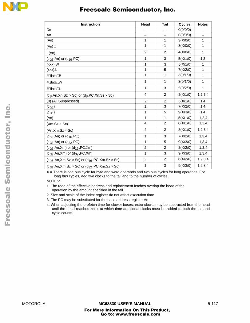
MOTOROLA MC68330 USER'S MANUAL 5-117
Instruction Head Tail Cycles NotesDn – – 0(0/0/0) –An – – 0(0/0/0) –(An) 1 1 3(X/0/0) 1
(An)+ 1 1 3(X/0/0) 1
−(An) 2 2 4(X/0/0) 1
(d16,An) or (d16,PC) 1 3 5(X/1/0) 1,3
(xxx).W 1 3 5(X/1/0) 1(xxx).L 1 5 7(X/2/0) 1
#⟨ data⟩ .B 1 1 3(0/1/0) 1
#⟨ data⟩ .W 1 1 3(0/1/0) 1
#⟨ data⟩ .L 1 3 5(0/2/0) 1
(d8,An,Xn.Sz × Sc) or (d8,PC,Xn.Sz × Sc) 4 2 8(X/1/0) 1,2,3,4
(0) (All Suppressed) 2 2 6(X/1/0) 1,4(d16) 1 3 7(X/2/0) 1,4
(d32) 1 5 9(X/3/0) 1,4
(An) 1 1 5(X/1/0) 1,2,4
(Xm.Sz × Sc) 4 2 8(X/1/0) 1,2,4
(An,Xm.Sz × Sc) 4 2 8(X/1/0) 1,2,3,4
(d16,An) or (d16,PC) 1 3 7(X/2/0) 1,3,4
(d32,An) or (d32,PC) 1 5 9(X/3/0) 1,3,4
(d16,An,Xm) or (d16,PC,Xm) 2 2 8(X/2/0) 1,3,4
(d32,An,Xm) or (d32,PC,Xm) 1 3 9(X/3/0) 1,3,4
(d16,An,Xm.Sz × Sc) or (d16,PC,Xm.Sz × Sc) 2 2 8(X/2/0) 1,2,3,4
(d32,An,Xm.Sz × Sc) or (d32,PC,Xm.Sz × Sc) 1 3 9(X/3/0) 1,2,3,4
X = There is one bus cycle for byte and word operands and two bus cycles for long operands. Forlong bus cycles, add two clocks to the tail and to the number of cycles.
NOTES:1. The read of the effective address and replacement fetches overlap the head of the
operation by the amount specified in the tail.2. Size and scale of the index register do not affect execution time.3. The PC may be substituted for the base address register An.4. When adjusting the prefetch time for slower buses, extra clocks may be subtracted from the head
until the head reaches zero, at which time additional clocks must be added to both the tail andcycle counts.
Fre
esc
ale
Se
mic
on
du
cto
r, I
Freescale Semiconductor, Inc.
For More Information On This Product, Go to: www.freescale.com
nc
...

5-118 MC68330 USER'S MANUAL MOTOROLA
5.8.3.2 CALCULATE EFFECTIVE ADDRESS. The calculate EA table indicates thenumber of clock periods needed for the processor to calculate a specified EA. The timingis equivalent to fetch EA except there is no read cycle. The tail and cycle time are reducedby the amount of time the read would occupy. The total number of clock cycles is outsidethe parentheses. The numbers inside parentheses (r/p/w) are included in the total clockcycle number. All timing data assumes two-clock reads and writes.
Instruction Head Tail Cycles NotesDn – – 0(0/0/0) –
An – – 0(0/0/0) –
(An) 1 0 2(0/0/0) –
(An)+ 1 0 2(0/0/0) –
−(An) 2 0 2(0/0/0) –
(d16,An) or (d16,PC) 1 1 3(0/1/0) 1,3
(xxx).W 1 1 3(0/1/0) 1
(xxx).L 1 3 5(0/2/0) 1
(d8,An,Xn.Sz × Sc) or (d8,PC,Xn.Sz × Sc) 4 0 6(0/1/0) 2,3,4
(0) (All Suppressed) 2 0 4(0/1/0) 4
(d16) 1 1 5(0/2/0) 1,4
(d32) 1 3 7(0/3/0) 1,4
(An) 1 0 4(0/1/0) 4
(Xm.Sz × Sc) 4 0 6(0/1/0) 2,4
(An,Xm.Sz × Sc) 4 0 6(0/1/0) 2,4
(d16,An) or (d16,PC) 1 1 5(0/2/0) 1,3,4
(d32,An) or (d32,PC) 1 3 7(0/3/0) 1,3,4
(d16,An,Xm) or (d16,PC,Xm) 2 0 6(0/2/0) 3,4
(d32,An,Xm) or (d32,PC,Xm) 1 1 7(0/3/0) 1,3,4
(d16,An,Xm.Sz × Sc) or (d16,PC,Xm.Sz × Sc) 2 0 6(0/2/0) 2,3,4
(d32,An,Xm.Sz × Sc) or (d32,PC,Xm.Sz × Sc) 1 1 7(0/3/0) 1,2,3,4
X = There is one bus cycle for byte and word operands and two bus cycles for long operands. For long bus cycles, add two clocks to the tail and to the number of cycles.
NOTES:1. Replacement fetches overlap the head of the operation by the amount specified in the tail.2. Size and scale of the index register do not affect execution time.3. The PC may be substituted for the base address register An.4. When adjusting the prefetch time for slower buses, extra clocks may be subtracted from the head
until the head reaches zero, at which time additional clocks must be added to both the tail andcycle counts.
Fre
esc
ale
Se
mic
on
du
cto
r, I
Freescale Semiconductor, Inc.
For More Information On This Product, Go to: www.freescale.com
nc
...

MOTOROLA MC68330 USER'S MANUAL 5-119
5.8.3.3 MOVE INSTRUCTION. The MOVE instruction table indicates the number of clockperiods needed for the processor to calculate the destination EA and to perform a MOVEor MOVEA instruction. For entries with CEA or FEA, refer to the appropriate table tocalculate that portion of the instruction time.
Destination EAs are divided by their formats (see 5.3.4.4 Effective Address EncodingSummary). The total number of clock cycles is outside the parentheses. The numbersinside parentheses (r/p/w) are included in the total clock cycle number. All timing dataassumes two-clock reads and writes.
When using this table, begin at the top and move downward. Use the first entry thatmatches both source and destination addressing modes.
Instruction Head Tail CyclesMOVE Rn, Rn 0 0 2(0/1/0)MOVE ⟨FEA⟩ , Rn 0 0 2(0/1/0)MOVE Rn, (Am) 0 2 4(0/1/x)MOVE Rn, (Am)+ 1 1 5(0/1/x)MOVE Rn, −(Am) 2 2 6(0/1/x)MOVE Rn, ⟨CEA ⟩ 1 3 5(0/1/x)MOVE ⟨FEA⟩ , (An) 2 2 6(0/1/x)MOVE ⟨FEA⟩ , (An)+ 2 2 6(0/1/x)MOVE ⟨FEA⟩ , −(An) 2 2 6(0/1/x)MOVE #, ⟨ CEA⟩ 2 2 6(0/1/x) ∗MOVE ⟨CEA⟩ , ⟨ FEA ⟩ 2 2 6(0/1/x)X = There is one bus cycle for byte and word operands and two bus cycles for long
operands. For long bus cycles, add two clocks to the tail and to the number of cycles.∗ = An # fetch effective address time must be added for this instruction:
⟨FEA⟩ +⟨ CEA⟩ + ⟨OPER ⟩NOTE: For instructions not explicitly listed, use the MOVE ⟨CEA⟩ , ⟨FEA⟩ entry. The source
EA is calculated by the calculate EA table, and the destination EA is calculated by thefetch EA table, even though the bus cycle is for the source EA.
Fre
esc
ale
Se
mic
on
du
cto
r, I
Freescale Semiconductor, Inc.
For More Information On This Product, Go to: www.freescale.com
nc
...

5-120 MC68330 USER'S MANUAL MOTOROLA
5.8.3.4 SPECIAL-PURPOSE MOVE INSTRUCTION. The special-purpose MOVEinstruction table indicates the number of clock periods needed for the processor to fetch,calculate, and perform the special-purpose MOVE operation on control registers or aspecified EA. Footnotes indicate when to account for the appropriate EA times. The totalnumber of clock cycles is outside the parentheses. The numbers inside parentheses(r/p/w) are included in the total clock cycle number. All timing data assumes two-clockreads and writes.
Instruction Head Tail CyclesEXG Rn, Rm 2 0 4(0/1/0)MOVEC Cr, Rn 10 0 14(0/2/0)MOVEC Rn, Cr 12 0 14-16(0/1/0)MOVE CCR, Dn 2 0 4(0/1/0)MOVE CCR, ⟨ CEA ⟩ 0 2 4(0/1/1)MOVE Dn, CCR 2 0 4(0/1/0)MOVE ⟨FEA⟩ , CCR 0 0 4(0/1/0)MOVE SR, Dn 2 0 4(0/1/0)MOVE SR, ⟨CEA ⟩ 0 2 4(0/1/1)MOVE Dn, SR 4 −2 10(0/3/0)MOVE ⟨FEA⟩ , SR 0 −2 10(0/3/0)MOVEM.W ⟨CEA⟩ , RL 1 0 8 + n × 4 (n + 1, 2, 0) 1
MOVEM.W RL, ⟨CEA ⟩ 1 0 8 + n × 4 (0, 2, n) 1
MOVEM.L ⟨CEA⟩ , RL 1 0 12 + n × 4(2n + 2, 2, 0)MOVEM.L RL, ⟨CEA ⟩ 1 2 10 + n × 4 (0, 2, 2n)MOVEP.W Dn, (d16, An) 2 0 10(0/2/2)MOVEP.W (d16, An), Dn 1 2 11(2/2/0)MOVEP.L Dn, (d16, An) 2 0 14(0/2/4)MOVEP.L (d16, An), Dn 1 2 19(4/2/0)MOVES (Save) ⟨CEA⟩ , Rn 1 1 3(0/1/0)MOVES (Op) ⟨CEA⟩ , Rn 7 1 11(X/1/0)MOVES (Save) Rn, ⟨CEA ⟩ 1 1 3(0/1/0)MOVES (Op) Rn, ⟨CEA ⟩ 9 2 12(0/1/X)MOVE USP, An 0 0 2(0/1/0)MOVE An, USP 0 0 2(0/1/0)SWAP Dn 4 0 6(0/1/0)X = There is one bus cycle for byte and word operands and two bus cycles for long
operands. For long bus cycles, add two clocks to the tail and to the number ofcycles.
1 = Each bus cycle may take up to four clocks without increasing total execution time.Cr = Control registers USP, VBR, SFC, and DFCn = Number of registers to transferRL = Register List< = Maximum time — certain data or mode combinations may execute faster.NOTE: The MOVES instruction has an additional save step which other instructions do not
have. To calculate the total instruction time, calculate the save, the effective address, and the operation execution times, and combine in the order listed, using the equations given in 5.8.1.6 Instruction Execution Time Calculation.
Fre
esc
ale
Se
mic
on
du
cto
r, I
Freescale Semiconductor, Inc.
For More Information On This Product, Go to: www.freescale.com
nc
...

MOTOROLA MC68330 USER'S MANUAL 5-121
5.8.3.5 ARITHMETIC/LOGIC INSTRUCTIONS. The arithmetic/logic instruction tableindicates the number of clock periods needed to perform the specified arithmetic/logicalinstruction using the specified addressing mode. Footnotes indicate when to account forthe appropriate EA times. The total number of clock cycles is outside the parentheses.The numbers inside parentheses (r/p/w) are included in the total clock cycle number. Alltiming data assumes two-clock reads and writes.
Instruction Head Tail Cycles
ADD(A) Rn, Rm 0 0 2(0/1/0)
ADD(A) ⟨FEA⟩ , Rn 0 0 2(0/1/0)
ADD Dn, ⟨FEA ⟩ 0 3 5(0/1/x)
AND Dn, Dm 0 0 2(0/1/0)
AND ⟨FEA⟩ , Dn 0 0 2(0/1/0)
AND Dn, ⟨FEA ⟩ 0 3 5(0/1/x)
EOR Dn, Dm 0 0 2(0/1/0)
EOR Dn, ⟨FEA ⟩ 0 3 5(0/1/x)
OR Dn, Dm 0 0 2(0/1/0)
OR ⟨FEA⟩ , Dn 0 0 2(0/1/0)
OR Dn, ⟨FEA ⟩ 0 3 5(0/1/x)
SUB(A) Rn, Rm 0 0 2(0/1/0)
SUB(A) ⟨FEA⟩ , Rn 0 0 2(0/1/0)
SUB Dn, ⟨FEA ⟩ 0 3 5(0/1/x)
CMP(A) Rn, Rm 0 0 2(0/1/0)
CMP(A) ⟨FEA⟩ , Rn 0 0 2(0/1/0)
CMP2 (Save)* ⟨FEA⟩ , Rn 1 1 3(0/1/0)
CMP2 (Op) ⟨FEA⟩ , Rn 2 0 16 - 18(X/1/0)
MUL(su).W ⟨FEA⟩ , Dn 0 0 26(0/1/0)
MUL(su).L (Save)* ⟨FEA⟩ , Dn 1 1 3(0/1/0)
MUL(su).L (Op) ⟨FEA⟩ , Dl 2 0 46 - 52(0/1/0)
MUL(su).L (Op) ⟨FEA⟩ , Dn:Dl 2 0 46(0/1/0)
DIVU.W ⟨FEA⟩ , Dn 0 0 32(0/1/0)
DIVS.W ⟨FEA⟩ , Dn 0 0 42(0/1/0)
DIVU.L (Save)* ⟨FEA⟩ , Dn 1 1 3(0/1/0)
DIVU.L (Op) ⟨FEA⟩ , Dn 2 0 <46(0/1/0)
DIVS.L (Save)* ⟨FEA⟩ , Dn 1 1 3(0/1/0)
DIVS.L (Op) ⟨FEA⟩ , Dn 2 0 <62(0/1/0)
TBL(su) Dn:Dm, Dp 26 0 28-30(0/2/0)
TBL(su) (Save)* ⟨CEA⟩ , Dn 1 1 3(0/1/0)
TBL(su) (Op) ⟨CEA⟩ , Dn 6 0 33-35(2X/1/0)
TBLSN Dn:Dm, Dp 30 0 30-34(0/2/0)
TBLSN (Save)* ⟨CEA⟩ , Dn 1 1 3(0/1/0)
TBLSN (Op) ⟨CEA⟩ , Dn 6 0 35-39(2X/1/0)
Fre
esc
ale
Se
mic
on
du
cto
r, I
Freescale Semiconductor, Inc.
For More Information On This Product, Go to: www.freescale.com
nc
...

5-122 MC68330 USER'S MANUAL MOTOROLA
Instruction Head Tail Cycles
TBLUN Dn:Dm, Dp 30 0 34-40(0/2/0)
TBLUN (Save)* ⟨CEA⟩ , Dn 1 1 3(0/1/0)
TBLUN (Op) ⟨CEA⟩ , Dn 6 0 39-45(2X/1/0)
X = There is one bus cycle for byte and word operands and two bus cycles for longoperands. For long bus cycles, add two clocks to the tail and to the number ofcycles.
< = Maximum time; certain data or mode combinations may execute faster.su = The execution time is identical for signed or unsigned operands.* These instructions have an additional save operation that other instructions do not have.
To calculate total instruction time, calculate save, ⟨ ea⟩ , and operation execution times,then combine in the order shown, using equations in 5.8.1.6 Instruction Execution TimeCalculations. A save operation is not run for long word divide and multiply instructionswhen ⟨ FEA⟩ = Dn,
5.8.3.6 IMMEDIATE ARITHMETIC/LOGIC INSTRUCTIONS. The immediatearithmetic/logic instruction table indicates the number of clock periods needed for theprocessor to fetch the source immediate data value and to perform the specifiedarithmetic/logic instruction using the specified addressing mode. Footnotes indicate whento account for the appropriate fetch effective or fetch immediate EA times. The totalnumber of clock cycles is outside the parentheses. The numbers inside parentheses(r/p/w) are included in the total clock cycle number. All timing data assumes two-clockreads and writes.
Instruction Head Tail CyclesMOVEQ #, Dn 0 0 2(0/1/0)ADDQ #, Rn 0 0 2(0/1/0)ADDQ #, ⟨ FEA⟩ 0 3 5(0/1/x)SUBQ #, Rn 0 0 2(0/1/0)SUBQ #, ⟨ FEA⟩ 0 3 5(0/1/x)ADDI #, Rn 0 0 2(0/1/0)∗ADDI #, ⟨ FEA⟩ 0 3 5(0/1/x) ∗ANDI #, Rn 0 0 2(0/1/0)∗ANDI #, ⟨ FEA⟩ 0 3 5(0/1/x) ∗EORI #, Rn 0 0 2(0/1/0)∗EORI #, ⟨ FEA⟩ 0 3 5(0/1/x) ∗ORI #, Rn 0 0 2(0/1/0)∗ORI #, ⟨ FEA⟩ 0 3 5(0/1/x) ∗SUBI #, Rn 0 0 2(0/1/0)∗SUBI #, ⟨ FEA⟩ 0 3 5(0/1/x) ∗CMPI #, Rn 0 0 2(0/1/0)∗CMPI #, ⟨ FEA⟩ 0 3 5(0/1/x) ∗X = There is one bus cycle for byte and word operands and two bus cycles for long
operands. For long bus cycles, add two clocks to the tail and to the number of cycles.∗ = An # fetch EA time must be added for this instruction: ⟨ FEA ⟩ +⟨FEA ⟩ + ⟨OPER⟩.
Fre
esc
ale
Se
mic
on
du
cto
r, I
Freescale Semiconductor, Inc.
For More Information On This Product, Go to: www.freescale.com
nc
...

MOTOROLA MC68330 USER'S MANUAL 5-123
5.8.3.7 BINARY-CODED DECIMAL AND EXTENDED INSTRUCTIONS. The binary-coded decimal and extended instruction table indicates the number of clock periodsneeded for the processor to perform the specified operation using the specified addressingmode. No additional tables are needed to calculate total effective execution time for theseinstructions. The total number of clock cycles is outside the parentheses. The numbersinside parentheses (r/p/w) are included in the total clock cycle number. All timing dataassumes two-clock reads and writes.
Instruction Head Tail CyclesABCD Dn, Dm 2 0 4(0/1/0)ABCD −(An), −(Am) 2 2 12(2/1/1)SBCD Dn, Dm 2 0 4(0/1/0)SBCD −(An), −(Am) 2 2 12(2/1/1)ADDX Dn, Dm 0 0 2(0/1/0)ADDX −(An), −(Am) 2 2 10(2/1/1)SUBX Dn, Dm 0 0 2(0/1/0)SUBX −(An), −(Am) 2 2 10(2/1/1)CMPM (An)+, (Am)+ 1 0 8(2/1/0)
5.8.3.8 SINGLE OPERAND INSTRUCTIONS. The single operand instruction tableindicates the number of clock periods needed for the processor to perform the specifiedoperation using the specified addressing mode. The total number of clock cycles is outsidethe parentheses. The numbers inside parentheses (r/p/w) are included in the total clockcycle number. All timing data assumes two-clock reads and writes.
Instruction Head Tail CyclesCLR Dn 0 0 2(0/1/0)CLR ⟨CEA⟩ 0 2 4(0/1/x)NEG Dn 0 0 2(0/1/0)NEG ⟨FEA⟩ 0 3 5(0/1/x)NEGX Dn 0 0 2(0/1/0)NEGX ⟨FEA⟩ 0 3 5(0/1/x)NOT Dn 0 0 2(0/1/0)NOT ⟨FEA⟩ 0 3 5(0/1/x)EXT Dn 0 0 2(0/1/0)NBCD Dn 2 0 4(0/1/0)NBCD ⟨FEA⟩ 0 2 6(0/1/1)Scc Dn 2 0 4(0/1/0)Scc ⟨CEA⟩ 2 2 6(0/1/1)TAS Dn 4 0 6(0/1/0)TAS ⟨CEA⟩ 1 0 10(0/1/1)TST ⟨FEA⟩ 0 0 2(0/1/0)X = There is one bus cycle for byte and word operands and two bus cycles for long
operands. For long bus cycles, add two clocks to the tail and to the number ofcycles.
Fre
esc
ale
Se
mic
on
du
cto
r, I
Freescale Semiconductor, Inc.
For More Information On This Product, Go to: www.freescale.com
nc
...

5-124 MC68330 USER'S MANUAL MOTOROLA
5.8.3.9 SHIFT/ROTATE INSTRUCTIONS. The shift/rotate instruction table indicates thenumber of clock periods needed for the processor to perform the specified operation onthe given addressing mode. Footnotes indicate when to account for the appropriate EAtimes. The number of bits shifted does not affect the execution time, unless noted. Thetotal number of clock cycles is outside the parentheses. The numbers inside parentheses(r/p/w) are included in the total clock cycle number. All timing data assumes two-clockreads and writes.
Instruction Head Tail Cycles NoteLSd Dn, Dm −2 0 (0/1/0) 1LSd #, Dm 4 0 6(0/1/0) —LSd ⟨FEA⟩ 0 2 6(0/1/1) —ASd Dn, Dm −2 0 (0/1/0) 1ASd #, Dm 4 0 6(0/1/0) —ASd ⟨FEA⟩ 0 2 6(0/1/1) —ROd Dn, Dm −2 0 (0/1/0) 1ROd #, Dm 4 0 6(0/1/0) —ROd ⟨FEA⟩ 0 2 6(0/1/1) —ROXd Dn, Dm −2 0 (0/1/0) 2ROXd #, Dm −2 0 (0/1/0) 3ROXd ⟨FEA⟩ 0 2 6(0/1/1) —NOTES:
1. Head and cycle times can be calculated as follows:Max (3 + (n/4) + mod(n,4) + mod (((n/4) + mod (n,4) + 1,2), 6)
or derived from the following table.2. Head and cycle times are calculated as follows: (count ≤ 63): max (3 + n + mod (n + 1,2), 6).3. Head and cycle times are calculated as follows: (count ≤ 8): max (2 + n + mod (n,2), 6).d = Direction (left or right)
Clocks Shift Counts6 0 1 2 3 4 5 6 8 9 128 7 10 11 13 14 16 17 20
10 15 18 19 21 22 24 25 2812 23 26 27 29 30 32 33 3614 31 34 35 37 38 40 41 4416 39 42 43 45 46 48 49 5218 47 50 51 53 54 56 57 6020 55 58 59 61 6222 63
Fre
esc
ale
Se
mic
on
du
cto
r, I
Freescale Semiconductor, Inc.
For More Information On This Product, Go to: www.freescale.com
nc
...

MOTOROLA MC68330 USER'S MANUAL 5-125
5.8.3.10 BIT MANIPULATION INSTRUCTIONS. The bit manipulation instruction tableindicates the number of clock periods needed for the processor to perform the specifiedoperation on the given addressing mode. The total number of clock cycles is outside theparentheses. The numbers inside parentheses (r/p/w) are included in the total clock cyclenumber. All timing data assumes two-clock reads and writes.
Instruction Head Tail CyclesBCHG #, Dn 2 0 6(0/2/0)∗BCHG Dn, Dm 4 0 6(0/1/0)BCHG #, ⟨ FEA⟩ 1 2 8(0/2/1)∗BCHG Dn, ⟨FEA ⟩ 2 2 8(0/1/1)BCLR #, Dn 2 0 6(0/2/0)∗BCLR Dn, Dm 4 0 6(0/1/0)BCLR #, ⟨ FEA⟩ 1 2 8(0/2/1)∗BCLR Dn, ⟨FEA ⟩ 2 2 8(0/1/1)BSET #, Dn 2 0 6(0/2/0)∗BSET Dn, Dm 4 0 6(0/1/0)BSET #, ⟨ FEA⟩ 1 2 8(0/2/1)∗BSET Dn, ⟨FEA ⟩ 2 2 8(0/1/1)BTST #, Dn 2 0 4(0/2/0)∗BTST Dn, Dm 2 0 4(0/1/0)BTST #, ⟨ FEA⟩ 1 0 4(0/2/0)∗BTST Dn, ⟨FEA ⟩ 2 0 8(0/1/0)∗ = An # fetch EA time must be added for this instruction:
⟨FEA⟩ + ⟨ FEA⟩ + ⟨ OPER⟩
5.8.3.11 CONDITIONAL BRANCH INSTRUCTIONS. The conditional branch instructiontable indicates the number of clock periods needed for the processor to perform thespecified branch on the given branch size, with complete execution times given. Noadditional tables are needed to calculate total effective execution time for theseinstructions. The total number of clock cycles is outside the parentheses. The numbersinside parentheses (r/p/w) are included in the total clock cycle number. All timing dataassumes two-clock reads and writes.
Instruction Head Tail CyclesBcc (taken) 2 −2 8(0/2/0)Bcc.B (not taken) 2 0 4(0/1/0)Bcc.W (not taken) 0 0 4(0/2/0)Bcc.L (not taken) 0 0 6(0/3/1)DBcc (T, not taken) 1 1 4(0/2/0)DBcc (F, −1, not taken) 2 0 6(0/2/0)DBcc (F, not −1, taken) 6 −2 10(0/2/0)DBcc (T, not taken) 4 0 6(0/1/0)∗DBcc (F, −1, not taken) 6 0 8(0/1/0)∗DBcc (F, not −1, taken) 6 0 10(0/0/0)∗∗ = In loop mode
Fre
esc
ale
Se
mic
on
du
cto
r, I
Freescale Semiconductor, Inc.
For More Information On This Product, Go to: www.freescale.com
nc
...
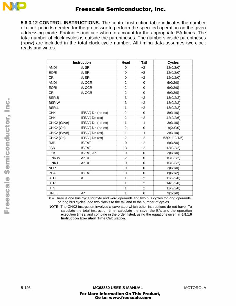
5-126 MC68330 USER'S MANUAL MOTOROLA
5.8.3.12 CONTROL INSTRUCTIONS. The control instruction table indicates the numberof clock periods needed for the processor to perform the specified operation on the givenaddressing mode. Footnotes indicate when to account for the appropriate EA times. Thetotal number of clock cycles is outside the parentheses. The numbers inside parentheses(r/p/w) are included in the total clock cycle number. All timing data assumes two-clockreads and writes.
Instruction Head Tail CyclesANDI #, SR 0 −2 12(0/2/0)EORI #, SR 0 −2 12(0/2/0)ORI #, SR 0 −2 12(0/2/0)ANDI #, CCR 2 0 6(0/2/0)EORI #, CCR 2 0 6(0/2/0)ORI #, CCR 2 0 6(0/2/0)BSR.B 3 −2 13(0/2/2)BSR.W 3 −2 13(0/2/2)BSR.L 1 −2 13(0/2/2)CHK ⟨FEA⟩ , Dn (no ex) 2 0 8(0/1/0)CHK ⟨FEA⟩ , Dn (ex) 2 −2 42(2/2/6)CHK2 (Save) ⟨FEA⟩ , Dn (no ex) 1 1 3(0/1/0)CHK2 (Op) ⟨FEA⟩ , Dn (no ex) 2 0 18(X/0/0)CHK2 (Save) ⟨FEA⟩ , Dn (ex) 1 1 3(0/1/0)CHK2 (Op) ⟨FEA⟩ , Dn (ex) 2 −2 52(X + 2/1/6)JMP ⟨CEA⟩ 0 −2 6(0/2/0)JSR ⟨CEA⟩ 3 −2 13(0/2/2)LEA ⟨CEA⟩ , An 0 0 2(0/1/0)LINK.W An, # 2 0 10(0/2/2)LINK.L An, # 0 0 10(0/3/2)NOP 0 0 2(0/1/0)PEA ⟨CEA⟩ 0 0 8(0/1/2)RTD # 1 −2 12(2/2/0)RTR 1 −2 14(3/2/0)RTS 1 −2 12(2/2/0)UNLK An 1 0 9(2/1/0)X = There is one bus cycle for byte and word operands and two bus cycles for long operands.
For long bus cycles, add two clocks to the tail and to the number of cycles.NOTE: The CHK2 instruction involves a save step which other instructions do not have. To
calculate the total instruction time, calculate the save, the EA, and the operationexecution times, and combine in the order listed, using the equations given in 5.8.1.6Instruction Execution Time Calculation.
Fre
esc
ale
Se
mic
on
du
cto
r, I
Freescale Semiconductor, Inc.
For More Information On This Product, Go to: www.freescale.com
nc
...

MOTOROLA MC68330 USER'S MANUAL 5-127
5.8.3.13 EXCEPTION-RELATED INSTRUCTIONS AND OPERATIONS. The exception-related instructions and operations table indicates the number of clock periods needed forthe processor to perform the specified exception-related actions. No additional tables areneeded to calculate total effective execution time for these instructions. The total numberof clock cycles is outside the parentheses. The numbers inside parentheses (r/p/w) areincluded in the total clock cycle number. All timing data assumes two-clock reads andwrites.
Instruction Head Tail CyclesBKPT (Acknowledged) 0 0 14(1/0/0)BKPT (Bus Error) 0 −2 35(3/2/4)Breakpoint (Acknowledged) 0 0 10(1/0/0)Breakpoint (Bus Error) 0 −2 42(3/2/6)Interrupt 0 −2 30(3/2/4)∗RESET 0 0 518(0/1/0)STOP 2 0 12(0/1/0)LPSTOP 3 −2 25(0/3/1)Divide-by-Zero 0 −2 36(2/2/6)Trace 0 −2 36(2/2/6)TRAP # 4 −2 29(2/2/4)ILLEGAL 0 −2 25(2/2/4)A-line 0 −2 25(2/2/4)F-line (First word illegal) 0 −2 25(2/2/4)F-line (Second word illegal) ea = Rn 1 −2 31(2/3/4)F-line (Second word illegal) ea ≠ Rn (Save) 1 1 3(0/1/0)F-line (Second word illegal) ea ≠ Rn (Op) 4 −2 29(2/2/4)Privileged 0 −2 25(2/2/4)TRAPcc (trap) 2 −2 38(2/2/6)TRAPcc (no trap) 2 0 4(0/1/0)TRAPcc.W (trap) 2 −2 38(2/2/6)TRAPcc.W (no trap) 0 0 4(0/2/0)TRAPcc.L (trap) 0 −2 38(2/2/6)TRAPcc.L (no trap) 0 0 6(0/3/0)TRAPV (trap) 2 −2 38(2/2/6)TRAPV (no trap) 2 0 4(0/1/0)∗ = Minimum interrupt acknowledge cycle time is assumed to be three clocks.NOTE: The F-line (Second word illegal) operation involves a save step which other
operations do not have. To calculate the total operation time, calculate the save,the calculate EA, and the operation execution times, and combine inthe order listed, using the equations given in 5.8.1.6 Instruction Execution TimeCalculation.
Fre
esc
ale
Se
mic
on
du
cto
r, I
Freescale Semiconductor, Inc.
For More Information On This Product, Go to: www.freescale.com
nc
...

5-128 MC68330 USER'S MANUAL MOTOROLA
5.8.3.14 SAVE AND RESTORE OPERATIONS. The save and restore operations tableindicates the number of clock periods needed for the processor to perform the specifiedstate save or return from exception. Complete execution times and stack length are given.No additional tables are needed to calculate total effective execution time for theseinstructions. The total number of clock cycles is outside the parentheses. The numbersinside parentheses (r/p/w) are included in the total clock cycle number. All timing dataassumes two-clock reads and writes.
Instruction Head Tail CyclesBERR on instruction 0 −2 <58(2/2/12)BERR on exception 0 −2 48(2/2/12)RTE (four-word frame) 1 −2 24(4/2/0)RTE (six-word frame) 1 −2 26(4/2/0)RTE (BERR on instruction) 1 −2 50(12/12/Y)RTE (BERR on four-word frame) 1 −2 66(10/2/4)RTE (BERR on six-word frame) 1 −2 70(12/2/6)< = Maximum time is indicated — certain data or mode combinations execute faster.Y = If a bus error occurred during a write cycle, the cycle is rerun by the RTE.
Fre
esc
ale
Se
mic
on
du
cto
r, I
Freescale Semiconductor, Inc.
For More Information On This Product, Go to: www.freescale.com
nc
...

MOTOROLA MC68330 USER’S MANUAL 6-1
SECTION 6IEEE 1149.1 TEST ACCESS PORT
The MC68330 includes dedicated user-accessible test logic that is fully compatible withthe IEEE 1149.1 Standard Test Access Port and Boundary Scan Architecture. Problemsassociated with testing high-density circuit boards have led to development of thisproposed standard under the sponsorship of the Test Technology Committee of IEEEand the Joint Test Action Group (JTAG). The MC68330 implementation supports circuit-board test strategies based on this standard.
The test logic includes a test access port (TAP) consisting of four dedicated signal pins, a16-state controller, and two test data registers. A boundary scan register links all devicesignal pins into a single shift register. The test logic, implemented using static logicdesign, is independent of the device system logic. The MC68330 implementationprovides the following capabilities:
a. Perform boundary scan operations to test circuit-board electrical continuity
b. Sample the MC68330 system pins during operation and transparently shiftout the result in the boundary scan register
c. Bypass the MC68330 for a given circuit-board test by effectively reducing theboundary scan register to a single cell
d. Disable the output drive to pins during circuit-board testing
NOTE
Certain precautions must be observed to ensure that the IEEE 1149.1test logic does not interfere with nontest operation. See 6.5 Non-IEEE1149.1 Operation for details.
6.1 OVERVIEWThis section, which includes aspects of the IEEE 1149.1 implementation that are specificto the MC68330, is intended to be used with the supporting IEEE 1149.1 document. Thediscussion includes those items required by the proposed standard to be defined and, incertain cases, provides additional information specific to the MC68330 implementation.For internal details and applications of the standard, refer to the IEEE 1149.1 document.
Fre
esc
ale
Se
mic
on
du
cto
r, I
Freescale Semiconductor, Inc.
For More Information On This Product, Go to: www.freescale.com
nc
...

6-2 MC68330 USER’S MANUAL MOTOROLA
An overview of the MC68330 implementation of IEEE 1149.1 is shown in Figure 6-1. TheMC68330 implementation includes a 3-bit instruction register and two test registers: a1-bit bypass register and a 108-bit boundary scan register. This implementation includesa dedicated TAP consisting of the following signals:
TCK — a test clock input to synchronize the test logic
TMS — a test mode select input (with an internal pullup resistor) that is sampled onthe rising edge of TCK to sequence the test controller's state machine
TDI — a test data input (with an internal pullup resistor) that is sampled on therising edge of TCK.
TDO — a three-state test data output that is actively driven in the shift-IR and shift-DR controller states. TDO changes on the falling edge of TCK.
3-BIT INSTRUCTION REGISTE
DECODER
TAPCTLR
TMS
TCK
BOUNDARY SCAN REGIS
BYPASS
TDIMUX
MUX TDO
TEST DATA REGISTE
(108 BITS
2 0
10 0
Figure 6-1. Test Access Port Block Diagram
6.2 BOUNDARY SCAN REGISTERThe MC68330 IEEE 1149.1 implementation has a 108-bit boundary scan register. Thisregister contains cells for all device signal and clock pins and associated control signals.The XTAL and XFC pins are associated with analog signals and are not included in theboundary scan register.
All MC68330 bidirectional pins, except the open-drain I/O pins (HALT and RESET), havea single register bit in the boundary scan register for pin data. All bidirectional pinsexcept HALT and RESET have an associated control bit in the boundary scan register.
Fre
esc
ale
Se
mic
on
du
cto
r, I
Freescale Semiconductor, Inc.
For More Information On This Product, Go to: www.freescale.com
nc
...

MOTOROLA MC68330 USER’S MANUAL 6-3
To ensure proper operation, the open-drain pins require external pullups. Twenty-onebits in the boundary scan register define the output enable signal for associated groupsof bidirectional and three-state pins. The 21 control bits and their bit positions are listedin Table 6-1.
Table 6-1. Boundary Scan Control Bits
Name Bit Number Name Bit Number Name Bit Numbercs0.ctl 4 a27.ctl 68 irq7.ctl 95
ifetch.ctl 34 a26.ctl 70 irq6.ctl 97modck.ctl 39 a25.ctl 72 irq5.ctl 99
a31.ctl 60 a24.ctl 74 irq4.ctl 101a30.ctl 62 ab.ctl 78 irq3.ctl 103a29.ctl 64 berr.ctl 79 irq2.ctl 105a28.ctl 66 db.ctl 80 irq1.ctl 107
Boundary scan bit definitions are shown in Table 6-2. The first column in Table 6-2defines the bit's ordinal position in the boundary scan register. The shift register cellnearest TDO (i.e., first to be shifted out) is defined as bit zero; the last bit to be shifted outis 107.
The second column references one of the five MC68330 cell types depicted in Figures 6-2 – 6-6, which describe the cell structure for that bit.
The third column lists the pin name for all pin-related cells or defines the name ofbidirectional control register bits. The active level of the control bits (i.e., output driver on)is defined by the last digit of the cell type listed for each control bit. For example, theactive-high level for ab.ctl (bit 78) is logic one since the cell type is IO.Ctl1. The activelevel for cs0.ctl (bit 4) is logic zero, since the cell type is IO.Ctl0. IO.Ctl0 (see Figure 6-5)differs from IO.Ctl1 (see Figure 6-4) by an inverter in the output enable path.
The fourth column lists the pin type: TS-Output indicates a three-state output pin, I/Oindicates a bidirectional pin, and OD-I/O denotes an open-drain bidirectional pin. Anopen-drain output pin has two states: off (high impedance) and logic zero.
The last column indicates the associated boundary scan register control bit forbidirectional and three-state pins.
Bidirectional pins include a single scan cell for data (IO.Cell) as depicted in Figure 6-6.These cells are controlled by one of the two cells shown in Figures 6-4 and 6-5. One ormore bidirectional data cells can be serially connected to a control cell as shown inFigure 6-7. Note that, when sampling the bidirectional data cells, the cell data can beinterpreted only after examining the IO control cell to determine pin direction.
Fre
esc
ale
Se
mic
on
du
cto
r, I
Freescale Semiconductor, Inc.
For More Information On This Product, Go to: www.freescale.com
nc
...

6-4 MC68330 USER’S MANUAL MOTOROLA
Table 6-2. Boundary Scan Bit Definitions
BitNum
CellType
Pin/CellName
PinType
OutputCTL Cell
Bi tNum
CellType
Pin/CellName
PinType
OutputCTL Cell
0 O.Latch CS3 TS-Output ab.ctl 54 IO.cell D11 I/O db.ctl1 O.Latch CS2 TS-Output ab.ctl 55 IO.cell D10 I/O db.ctl2 O.Latch CS1 TS-Output ab.ctl 56 IO.cell D9 I/O db.ctl3 IO.cell CS0 I/O cs0.ctl 57 IO.cell D8 I/O db.ctl4 IO.ctl0 cs0.ctl — — 58 IO.cell A0 I/O* ab.ctl5 IO.cell FC2 I/O* ab.ctl 59 IO.cell A31 I/O a31.ctl6 IO.cell FC1 I/O* ab.ctl 60 IO.ctl0 a31.ctl — —7 IO.cell FC0 I/O* ab.ctl 61 IO.cell A30 I/O a30.ctl8 IO.cell A1 I/O* ab.ctl 62 IO.ctl0 a30.ctl — —9 IO.cell A2 I/O* ab.ctl 63 IO.cell A29 I/O a29.ctl
10 IO.cell A3 I/O* ab.ctl 64 IO.ctl0 a29.ctl — —11 IO.cell A4 I/O* ab.ctl 65 IO.cell A28 I/O a28.ctl12 IO.cell A5 I/O* ab.ctl 66 IO.ctl0 a28.ctl — —13 IO.cell A6 I/O* ab.ctl 67 IO.cell A27 I/O a27.ctl14 IO.cell A7 I/O* ab.ctl 68 IO.ctl0 a27.ctl — —15 IO.cell A8 I/O* ab.ctl 69 IO.cell A26 I/O a26.ctl16 IO.cell A9 I/O* ab.ctl 70 IO.ctl0 a26.ctl — —17 IO.cell A10 I/O* ab.ctl 71 IO.cell A25 I/O a25.ctl18 IO.cell A11 I/O* ab.ctl 72 IO.ctl0 a25.ctl — —19 IO.cell A12 I/O* ab.ctl 73 IO.cell A24 I/O a24.ctl20 IO.cell A13 I/O* ab.ctl 74 IO.ctl0 a24.ctl — —21 IO.cell A14 I/O* ab.ctl 75 O.Latch LWE TS-Output ab.ctl22 IO.cell A15 I/O* ab.ctl 76 O.Latch UWE TS-Output ab.ctl23 IO.cell A16 I/O* ab.ctl 77 IO.cell RMC I/O* ab.ctl24 IO.cell A17 I/O* ab.ctl 78 IO.ctl1 ab.ctl — —25 IO.cell A18 I/O* ab.ctl 79 IO.ctl0 berr.ctl — —26 IO.cell A19 I/O* ab.ctl 80 IO.ctl1 db.ctl — —27 IO.cell A20 I/O* ab.ctl 81 IO.cell D7 I/O db.ctl28 IO.cell A21 I/O* ab.ctl 82 IO.cell D6 I/O db.ctl29 IO.cell A22 I/O* ab.ctl 83 IO.cell D5 I/O db.ctl30 IO.cell A23 I/O* ab.ctl 84 IO.cell D4 I/O db.ctl31 O.Latch FREEZE Output — 85 IO.cell D3 I/O db.ctl32 I.Pin BKPT Input — 86 IO.cell D2 I/O db.ctl33 IO.cell IFETCH I/O* ifetch.ctl 87 IO.cell D1 I/O db.ctl34 IO.ctl0 ifetch.ctl — — 88 IO.cell D0 I/O db.ctl35 O.Latch IPIPE Output — 89 IO.cell DSACK0 I/O** berr.ctl36 I.Pin EXTAL Input — 90 IO.cell DSACK1 I/O** berr.ctl37 O.Latch CLKOUT Output — 91 I.Pin BR Input —38 IO.cell MODCK I/O modck.ctl 92 O.Latch BG Output —39 IO.ctl0 modck.ctl — — 93 I.Pin BGACK Input —40 O.Latch RESET OD-I/O — 94 IO.cell IRQ7 I/O irq7.ctl41 I.Pin RESET OD-I/O — 95 IO.ctl0 irq7.ctl — —42 O.Latch HALT OD-I/O — 96 IO.cell IRQ6 I/O irq6.ctl43 I.Pin HALT OD-I/O — 97 IO.ctl0 irq6.ctl — —44 IO.cell BERR I/O** berr.ctl 98 IO.cell IRQ5 I/O irq5.ctl45 IO.cell DS I/O* ab.ctl 99 IO.ctl0 irq5.ctl — —46 IO.cell AS I/O* ab.ctl 100 IO.cell IRQ4 I/O irq4.ctl47 IO.cell R/W I/O* ab.ctl 101 IO.ctl0 irq4.ctl — —48 IO.cell SIZ0 I/O* ab.ctl 102 IO.cell IRQ3 I/O irq3.ctl49 IO.cell SIZ1 I/O* ab.ctl 103 IO.ctl0 irq3.ctl — —50 IO.cell D15 I/O db.ctl 104 IO.cell IRQ2 I/O irq2.ctl51 IO.cell D14 I/O db.ctl 105 IO.ctl0 irq2.ctl — —52 IO.cell D13 I/O db.ctl 106 IO.cell IRQ1 I/O irq1.ctl53 IO.cell D12 I/O db.ctl 107 IO.ctl0 irq1.ctl — —
NOTE: The indicated pins are implemented differently than defined in the signal definition description:* Input during Motorola factory test ** Output during Motorola factory test
Fre
esc
ale
Se
mic
on
du
cto
r, I
Freescale Semiconductor, Inc.
For More Information On This Product, Go to: www.freescale.com
nc
...

MOTOROLA MC68330 USER’S MANUAL 6-5
1MUX
1
G1
1MUX
1
G1
FROMLASTCELL
1 D
C1
CLOCK DR
1 D
C1
UPDATE D
SHIFT DRTO NEXT CELL
TO OUTPUTBUFFER
1 – EXTEST0 – OTHERWIS
DATA FROSYSTEM
LOGIC
Figure 6-2. Output Latch Cell (O.Latch)
FROM LAST CELL
1MUX
1
G1
DATA TO SYSTEMLOGIC
INPUT PIN
SHIFT DRCLOCK DR
TO NEXT CELL
1D
C1
1MUX
1
G1
1D
C1
UPDATE D
1 – EXTEST 0 – OTHERWISE
Figure 6-3. Input Pin Cell (I.Pin)
Fre
esc
ale
Se
mic
on
du
cto
r, I
Freescale Semiconductor, Inc.
For More Information On This Product, Go to: www.freescale.com
nc
...

6-6 MC68330 USER’S MANUAL MOTOROLA
1MUX
1
G1
1MUX
1
G1
OUTPUCONTRO
FROMSYSTEM
LOGIC
FROMLASTCELL
1D
C1
CLOCK DR
1D
C1
UPDATE D
TO NEXT CELL
TO OUTPUT ENABLE
R
RESET
(1=DRIVE
1 – EXTEST0 – OTHERWISE
SHIFT DR
Figure 6-4. Active-High Output Control Cell (IO.Ctl1)
1MUX
1
G1
1MUX
1
G1
OUTPCONTRO
FROMSYSTEM
LOGIC
FROMLASTCELL
1D
C1
CLOCK DR
1D
C1
UPDATE D
TO NEXT CELL
TO OUTPUT ENABLE
R
RESET
(1=DRIVE
1 – EXTEST0 – OTHERWISE
SHIFT DR
Figure 6-5. Active-Low Output Control Cell (IO.Ctl0)
Fre
esc
ale
Se
mic
on
du
cto
r, I
Freescale Semiconductor, Inc.
For More Information On This Product, Go to: www.freescale.com
nc
...
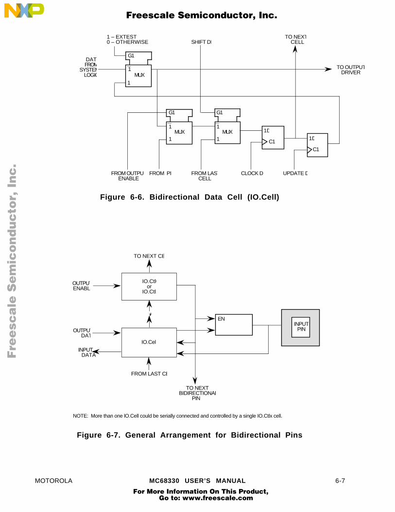
MOTOROLA MC68330 USER’S MANUAL 6-7
1MUX
1
G1
1MUX
1
G1
DATAFROM
SYSTEMLOGIC
FROM LASTCELL
1D
C1
CLOCK DR
1D
C1
UPDATE D
TO NEXT CELL
TO OUTPUT DRIVER
1 – EXTEST 0 – OTHERWISE SHIFT DR
1MUX
1
G1
FROM OUTPUENABLE
FROM PIN
Figure 6-6. Bidirectional Data Cell (IO.Cell)
IO.Ctl0or
IO.Ctl1
IO.Cel
EN
FROM LAST CE
OUTPUTDAT
INPUT DATA
OUTPUTENABL
INPUTPIN
TO NEXT CE
TO NEXTBIDIRECTIONAL
PIN
*
NOTE: More than one lO.Cell could be serially connected and controlled by a single IO.Ctlx cell.
Figure 6-7. General Arrangement for Bidirectional Pins
Fre
esc
ale
Se
mic
on
du
cto
r, I
Freescale Semiconductor, Inc.
For More Information On This Product, Go to: www.freescale.com
nc
...

6-8 MC68330 USER’S MANUAL MOTOROLA
6.3 INSTRUCTION REGISTERThe MC68330 IEEE 1149.1 implementation includes the three mandatory publicinstructions (EXTEST, SAMPLE/PRELOAD, and BYPASS), but does not support any ofthe optional public instructions defined by IEEE 1149.1. One additional public instruction(HI-Z) provides the capability for disabling all device output drivers. The MC68330includes a 3-bit instruction register without parity, consisting of a shift register with threeparallel outputs. Data is transferred from the shift register to the parallel outputs duringthe update-IR controller state. The three bits are used to decode the four uniqueinstructions listed in Table 6-3.
The parallel output of the instruction register is reset to all ones in the test-logic-resetcontroller state. Note that this preset state is equivalent to the BYPASS instruction.
Table 6-3. Instructions
CodeB 2 B 1 B 0
Instruction
0 0 0 EXTEST0 0 1 SAMPLE/PRELOADX 1 X BYPASS1 0 0 HI-Z1 0 1 BYPASS
During the capture-IR controller state, the parallel inputs to the instruction shift registerare loaded with the standard 2-bit binary value (01) into the two least significant bits andthe loss-of-crystal (LOC) status signal into bit 2. The parallel outputs, however, remainunchanged by this action since an update-IR signal is required to modify them.
The LOC status bit of the instruction register indicates whether an internal clock isdetected when operating with a crystal clock source. The LOC bit is clear when a clock isdetected and set when it is not. The LOC bit is always clear when an external clock isused. The LOC bit can be used to detect faulty connectivity when a crystal is used toclock the device.
6.3.1 EXTEST (000)The external test (EXTEST) instruction selects the 108-bit boundary scan register.EXTEST asserts internal reset for the MC68330 system logic to force a predictablebenign internal state while performing external boundary scan operations.
By using the TAP, the register is capable of a) scanning user-defined values into theoutput buffers, b) capturing values presented to input pins, c) controlling the direction ofbidirectional pins, and d) controlling the output drive of three-state output pins.
6.3.2 SAMPLE/PRELOAD (001)The SAMPLE/PRELOAD instruction selects the 108-bit boundary scan register, andprovides two separate functions. First, it provides a means to obtain a snapshot of systemdata and control signals. The snapshot occurs on the rising edge of TCK in the capture-
Fre
esc
ale
Se
mic
on
du
cto
r, I
Freescale Semiconductor, Inc.
For More Information On This Product, Go to: www.freescale.com
nc
...

MOTOROLA MC68330 USER’S MANUAL 6-9
DR controller state. The data can be observed by shifting it transparently through theboundary scan register.
NOTE
Since there is no internal synchronization between the IEEE 1149.1clock (TCK) and the system clock (CLKOUT), the user must providesome form of external synchronization to achieve meaningful results.
The second function of SAMPLE/PRELOAD is to initialize the boundary scan registeroutput cells prior to selection of EXTEST. This initialization ensures that known data willappear on the outputs when entering the EXTEST instruction.
6.3.3 BYPASS (X1X, 101)The BYPASS instruction selects the single-bit bypass register as shown in Figure 6-8.This creates a shift-register path from TDI to the bypass register and, finally, to TDO,circumventing the 108-bit boundary scan register. This instruction is used to enhancetest efficiency when a component other than the MC68330 becomes the device undertest.
1MUX
1
G1
1 D
C1
CLOCK DR
FROM TD
0
SHIFT DR
TO TDO
Figure 6-8. Bypass Register
When the bypass register is selected by the current instruction, the shift-register stage isset to a logic zero on the rising edge of TCK in the capture-DR controller state. Therefore,the first bit to be shifted out after selecting the bypass register will always be a logic zero.
6.3.4 HI-Z (100)The HI-Z instruction is not included in the IEEE 1149.1 standard. It is provided as amanufacturer’s optional public instruction to prevent having to backdrive the output pinsduring circuit-board testing. When HI-Z is invoked, all output drivers, including the two-state drivers, are turned off (i.e., high impedance). The instruction selects the bypassregister.
6.4 MC68330 RESTRICTIONSThe control afforded by the output enable signals using the boundary scan register andthe EXTEST instruction requires a compatible circuit-board test environment to avoiddevice-destructive configurations. The user must avoid situations in which the MC68330output drivers are enabled into actively driven networks. Overdriving the TDO driverwhen it is active is not recommended.
Fre
esc
ale
Se
mic
on
du
cto
r, I
Freescale Semiconductor, Inc.
For More Information On This Product, Go to: www.freescale.com
nc
...

6-10 MC68330 USER’S MANUAL MOTOROLA
The MC68330 includes on-chip circuitry to detect the initial application of power to thedevice. Power-on reset (POR), the output of this circuitry, is used to reset both the systemand IEEE 1149.1 logic. The purpose for applying POR to the IEEE 1149.1 circuitry is toavoid the possibility of bus contention during power-on. The time required to completedevice power-on is power-supply dependent. However, the IEEE 1149.1 TAP controllerremains in the test-logic-reset state while POR is asserted. The TAP controller does notrespond to user commands until POR is negated.
The MC68330 features a low-power stop mode, which is invoked using a CPUinstruction called LPSTOP. The interaction of the IEEE 1149.1 interface with low-powerstop mode is as follows:
1. Leaving the TAP controller test-logic-reset state negates the ability to achieveminimal power consumption, but does not otherwise affect device functionality.
2. The TCK input is not blocked in low-power stop mode. To consume minimalpower, the TCK input should be externally connected to VCC or ground.
3. The TMS and TDI pins include on-chip pullup resistors. In low-power stopmode, these two pins should remain either unconnected or connected to VCCto achieve minimal power consumption.
6.5 NON-IEEE 1149.1 OPERATIONIn non-IEEE 1149.1 operation, there are two constraints. First, the TCK input does notinclude an internal pullup resistor and should be pulled up externally to preclude mid-level inputs. The second constraint is to ensure that the IEEE 1149.1 test logic is kepttransparent to the system logic by forcing the TAP controller into the test-logic-reset state,using either of two methods. During power-up, POR forces the TAP controller into thisstate. Alternatively, sampling TMS as a logic one for five consecutive TCK rising edgesalso forces the TAP controller into this state. If TMS either remains unconnected or isconnected to VCC, then the TAP controller cannot leave the test-logic-reset state,regardless of the state of TCK.
Fre
esc
ale
Se
mic
on
du
cto
r, I
Freescale Semiconductor, Inc.
For More Information On This Product, Go to: www.freescale.com
nc
...

MOTOROLA MC68330 USER’S MANUAL 7-1
SECTION 7APPLICATIONS
This section provides guidelines for using the MC68330. Included in this section are adiscussion of the requirements for a minimum system configuration, sample initializationsequences for system startup, and interfacing to memory.
7.1 MINIMUM SYSTEM CONFIGURATIONOne of the powerful features of the MC68330 is the small number of externalcomponents needed to create an entire system. The information contained in thefollowing paragraphs details a simple high-performance MC68330 system (see Figure 7-1). This system configuration features the following hardware:
• Processor Clock Circuitry
• Reset Circuitry
• SRAM Interface
• ROM Interface
• Serial Interface
CLOCKCIRCUITS
MC68330
SRAM
ROM SERIAL INTERFACE
Figure 7-1. Minimum System Configuration Block Diagram
7.1.1 Processor Clock CircuitryThe MC68330 has an on-chip clock synthesizer that can operate from an on-chip phase-locked loop (PLL) and a voltage-controlled oscillator (VCO). The clock synthesizer usesan external crystal connected between the EXTAL and XTAL pins as a referencefrequency source. Figure 7-2 shows a typical circuit using an inexpensive 32.768-kHzwatch crystal. The 20-M resistor connected between the EXTAL and XTAL pins provides
Fre
esc
ale
Se
mic
on
du
cto
r, I
Freescale Semiconductor, Inc.
For More Information On This Product, Go to: www.freescale.com
nc
...

7-2 MC68330 USER’S MANUAL MOTOROLA
biasing for a faster oscillator startup time. The crystal manufacturer's documentationshould be consulted for specific recommendations on external component values.
MC68330
XTAL
EXTA
20 M
20 pF
20 pF
330 Ω
32.768 kH
Figure 7-2. Sample Crystal Circuit
A separate power pin (VCCSYN) is used to allow the clock circuits to operate with therest of the device powered down and to provide increased noise immunity for the clockcircuits. The source for VCCSYN should be a quiet power supply, and external bypasscapacitors (see Figure 7-3) should be placed as close as possible to the VCCSYN pin toensure a stable operating frequency.
MC6833
XFC
VCCSYN
1
NOTE 1: Must be a low leakage capacitor.
VCCSYN
0.1 µF 0.01 µFXFC
Figure 7-3. XFC and VCCSYN Capacitor Connections
Additionally, the PLL requires that an external low-leakage filter capacitor, typically in therange of 0.01 to 0.1 µF, be connected between the XFC and VCCSYN pins. The XFCcapacitor should provide 50 MΩ insulation, and should not be electrolytic. Smallervalues of the external filter capacitor provide a faster response time for the PLL, andlarger values provide greater frequency stability. Figure 7-3 depicts examples of both anexternal filter capacitor and bypass capacitors for VCCSYN.
7.1.2 Reset CircuitryBecause it is optional, reset circuitry is not shown in Figure 7-1. The MC68330 holdsitself in reset after power-up and asserts RESET to the rest of the system. If an external
Fre
esc
ale
Se
mic
on
du
cto
r, I
Freescale Semiconductor, Inc.
For More Information On This Product, Go to: www.freescale.com
nc
...

MOTOROLA MC68330 USER’S MANUAL 7-3
reset push button switch is desired, an external reset circuit is easily constructed byusing open-collector cross-coupled NAND gates to debounce the output from the switch.
7.1.3 SRAM InterfaceThe SRAM interface is very simple when the programmable chip selects are used.External circuitry to decode address information and circuitry to return data and sizeacknowledge (DSACK) is not required.
A15-A0
CSx
D15-D0
MC68330 MCM6206-3 MCM6206-3
W
E
W
E
D7-D0
.... ..
..
....
....
....
....
LWE
UWE
G
D15-D8
G
R/W
74F04
74F00
Figure 7-4. SRAM Interface
The SRAM interface shown in Figure 7-4 is a two-clock interface at 16.78-MHz operatingfrequency. The MCM6206-30 memories provide an access time of 12.5 ns when the Einput is low. If buffers are required to reduce signal loading or if slower and lessexpensive memories are desired, a three-clock cycle can be used. In the circuit shown inFigure 7-4, additional memories can be used provided that the MC68330 specificationfor load capacitance on the chip-select (CS) signal is not exceeded. (Address buffersmay be needed, however.)
7.1.4 ROM InterfaceUsing the programmable chip selects creates a very straightforward ROM interface. Asshown in Figure 7-5, no external circuitry is needed. Care must be used, however, not tooverload the address bus. Address buffers may be required to ensure that the totalsystem input capacitance on the address signals does not exceed the CL specification.
Fre
esc
ale
Se
mic
on
du
cto
r, I
Freescale Semiconductor, Inc.
For More Information On This Product, Go to: www.freescale.com
nc
...

7-4 MC68330 USER’S MANUAL MOTOROLA
MC68330
A16–A
D15–D
CS0
16-BITROM
C E
O E
Figure 7-5. EPROM Interface
7.1.5 Serial InterfaceThe necessary circuitry to create an RS-232 interface with the MC68330 includes anexternal crystal, a dual asynchronous receiver/transmitter (DUART), a dual D-type flip-flop, and an RS-232 receiver/driver (see Figure 7-6). The resistor and capacitor valuesshown are typical; the crystal manufacturer's documentation should be consulted forspecific recommendations on external component values. The circuit shown does notinclude modem support (ready to send (RTS) and clear to send (CTS) are not shown);however, these signals can be connected to the receiver/driver and to the connector in asimilar manner as the connections for TxD and RxD.
X1/CLK
X2
RxD
TxD
MC6868
4.7 pF
10 pF
3.6864 MH
Rx1
Tx1
RS
232
CO
NN
EC
TOR
C1+
MC14540
R
T
10 µ FC1-
MC68330
DTACKDSACK0
R/W R/W
CS1 CS
RESET RESET
D15 – D
IRQ IRQ
D8 – D0
10 M
V C2+
GND C1-10 µ F
10 µ F
10 µ FSS
GNDCC
CCV
DSACK1+5 V
A4 – A1 RS4 – RS
HALT
74F74
100 Ω
Figure 7-6. Serial Interface
7.2 MC68330 INITIALIZATION SEQUENCEThe following paragraphs discuss a suggested method for initializing the MC68330 afterpower-up.
Fre
esc
ale
Se
mic
on
du
cto
r, I
Freescale Semiconductor, Inc.
For More Information On This Product, Go to: www.freescale.com
nc
...

MOTOROLA MC68330 USER’S MANUAL 7-5
7.2.1 Startup
RESET is asserted by the MC68330 during the time in which VCC is ramping up, theVCO is locking onto the frequency, and the MC68330 is going through the resetoperation. After RESET is negated, four bus cycles are run, with CS0 being asserted tofetch the 32-bit program counter (PC) and the 32-bit stack pointer (SP) from the bootROM. Until programmed differently, CS0 is a 16-bit-wide, three-wait-state chip select.
After the PC and the SP are fetched, the following programming steps should befollowed:
• Initialize and set the valid bit in the module base address register (CPU spaceaddress $0003FF00) with the desired base address for the SIM registers.
• Initialize and set the valid bits in the necessary chip-select base address andaddress mask registers. Following this step, other system resources requiring theCSx signals can be accessed. Care must be exercised when changing theaddress for CS0. The address of the instruction following the MOVE instruction tothe CS0 base address register must match the value of the PC at that time.
7.2.2 SIM Module ConfigurationThe order of the following SIM register initializations is not important; however, time canbe saved by initializing the clock synthesizer control register first to quickly increase tothe desired processor operating frequency. The module base address register must beinitialized prior to any of following steps.
Clock Synthesizer Control Register (SYNCR)
• Set frequency control bits (W, X, Y) to specify frequency.• Select action taken during loss of crystal (RSTEN bit): activate a system reset or
operate in limp mode.• Select system clock and CLKOUT during LPSTOP (STSIM and STEXT bits).
Module Configuration Register (MCR)
• If using the software watchdog and/or the periodic interrupt timer, select actiontaken when FREEZE is asserted (FRZ bits).
• Select whether CS0 will be disabled and this bit function as an autovector input(AVEC), or CS0 will be enabled.
• Select the show cycle action (SHEN bits).• Select the access privilege for the supervisor/user registers (SUPV bit).• Select the interrupt arbitration level for the SIM (IARB bits).
Autovector Register (AVR)
• Select the desired external interrupt levels for internal autovectoring.
System Protection Control Register (SYPCR) (Note that this register can only be writtenonce after reset.)
• Enable the software watchdog, if desired (SWE bit).
Fre
esc
ale
Se
mic
on
du
cto
r, I
Freescale Semiconductor, Inc.
For More Information On This Product, Go to: www.freescale.com
nc
...

7-6 MC68330 USER’S MANUAL MOTOROLA
• If the watchdog is enabled, select whether a system reset or a level 7 interrupt isdesired at timeout (SWRI bit).
• If the watchdog is enabled, select the timeout period (SWT bits).• Enable the double bus fault monitor, if desired (DBF bit).• Enable the external bus monitor, if desired (BME bit).• Select timeout period for bus monitor (BMT bits).
Software Watchdog Interrupt Vector Register (SWIV)
• If using the software watchdog, program the vector number for a softwarewatchdog interrupt.
Periodic Interrupt Timer Register (PITR)
• If using the software watchdog, select whether or not to prescale (SWP bit).• If using the periodic interrupt timer, select whether or not to prescale (PTP bit).• Program the count value for the periodic timer, or program a zero value to turn off
the periodic timer (PITR bits).
Periodic Interrupt Control Register (PICR)
• If using the periodic timer, program the desired interrupt level for the periodicinterrupt timer (PIRQL bits).
• If using the periodic timer, program the vector number for a periodic timer interrupt.
Port A and B Registers
• Program the desired function of the port A signals (PPARA1 and PPARA2registers).
• Program the desired function of the port B signals (PPARB register).
7.3 MEMORY INTERFACE INFORMATIONThe following paragraphs contain information on using an 8-bit boot ROM, performingaccess time calculations, calculating frequency-adjusted outputs, and interfacing an 8-bitdevice to 16-bit memory using single-address mode.
7.3.1 Using an 8-Bit Boot ROM
Upon power-up, the MC68330 uses CS0 to begin operation. CS0 is a three-wait-state,16-bit chip select until programmed otherwise. If an 8-bit ROM is desired, externalcircuitry can be added to return an 8-bit DSACK in two wait states (see Figure 7-7).
CLKOUT
CS0
CP
MR
Q0Q1Q2Q3
DSACK0
74F393
Fre
esc
ale
Se
mic
on
du
cto
r, I
Freescale Semiconductor, Inc.
For More Information On This Product, Go to: www.freescale.com
nc
...

MOTOROLA MC68330 USER’S MANUAL 7-7
Figure 7-7. External Circuitry for 8-Bit Boot ROM
The `393 is a falling edge triggered counter; thus, CS0 is stable during the time in whichit is being clocked. CS0 acts as the asynchronous reset — i.e., when it is asserted, the`393 is allowed to count. The falling edge of S2 provides the first counting edge. Q1 doesnot transition on this falling edge, but transitions to a logic one on the subsequent edge.DSACK0 is Q1 inverted; thus, on the next falling edge, DSACK0 is seen as asserted,indicating an 8-bit port. When CS0 is negated, Q1 is again held in reset and DSACK0 isnegated. The timing diagram in Figure 7-8 illustrates this operation.
S0 S1 S2 SW SW SW SW S3 S4 S5 S0 S1 S2
CLKOUT
CS0
Q1
DSACK0
Q0
Figure 7-8. 8-Bit Boot ROM Timing
7.3.2 Access Time CalculationsThe two time paths that are critical in an MC68330 application using the CS signals areshown in Figure 7-9. The first path is the time from adddress valid to when data must beavailable to the processor; the second path is the time from CS asserted to when datamust be available to the processor.
CS
D15–D0
A31–A0
S0 S4S1 S5 S0
t 27
t9
t CSDV
t6
t ADV
Fre
esc
ale
Se
mic
on
du
cto
r, I
Freescale Semiconductor, Inc.
For More Information On This Product, Go to: www.freescale.com
nc
...

7-8 MC68330 USER’S MANUAL MOTOROLA
Figure 7-9. Access Time Computation Diagram
As shown in the diagram, an equation for the address access time, tADV, can bedeveloped as follows:
tADV = T(N – 1) – t6 – t272
where:
T = system clock periodN = number of clocks per accesst6 = CLKOUT high to address valid = 30 ns maximum at 16.78 MHz
t27 = data-in valid to CLKOUT low setup = 5 ns minimum at 16.78 MHz
An equation for the chip select access time, tCSDV, can be developed as follows:
tCSDV = T(N – 1) – t9 – t27
where:
T = system clock periodN = number of clocks per accesst9 = CLKOUT low to CS asserted = 30 ns maximum at 16.78 MHz
t27 = data-in valid to CLKOUT low setup = 5 ns minimum at 16.78 MHzUsing these equations, the memory access times at 16.78 MHz are shown in Table 7-1.
Table 7-1. Memory Access Times at 16.78 MHz
N = 2 N = 3 N = 4 N = 5 N = 6tADV 55 ns 115 ns 175 ns 235 ns 295 ns
tCSDV 25 ns 85 ns 145 ns 205 ns 265 ns
The values can be used to determine how many clock cycles an access will take, giventhe access time of the memory devices and any delays through buffers or external logicthat may be needed.
7.3.3 Calculating Frequency-Adjusted OutputThe general relationship between the CLKOUT and most input and output signals isshown in Figure 7-10. Most outputs transition off of a falling edge of CLKOUT, but thesame principle applies to those outputs that transition off of a rising edge.
CLKOUT
OUTPUTS
ASYNCHRONOUINPUTS
td
tsu ht
Fre
esc
ale
Se
mic
on
du
cto
r, I
Freescale Semiconductor, Inc.
For More Information On This Product, Go to: www.freescale.com
nc
...

MOTOROLA MC68330 USER’S MANUAL 7-9
Figure 7-10. Signal Relationships to CLKOUT
For outputs that are referenced to a clock edge, the propagation delay (td) does notchange as the frequency changes. For instance, specification 6 in the electricalcharacteristics, shown in MC68330/D, MC68330 Technical Summary, shows thataddress, function code, and size information is valid 3 to 30 ns after the rising edge ofS0. This specification does not change even if the device frequency is less than 16.78MHz. Additionally, the relationship between the asynchronous inputs and the clock edge,as shown in Figure 7-10, does not change as frequency changes.
A second type of specification indicates the minimum amount of time a signal will beasserted. This type of specification is illustrated in Figure 7-11.
OUTPUT
CLKOUT
tw
NT/2
td
Figure 7-11. Signal Width Specifications
The method for calculating a frequency-adjusted tw is as follows:
tw' = tw + N (Tf' – Tf) + (Tf' – td)2 2 2
where:
tw' = the frequency-adjusted signal widthtw = the signal width at 16.78 MHzN = the number of full one-half clock periods in tw
Tf' = one-half the new clock period2Tf = one-half the clock period at full speed2td = the propagation time from the clock edge
The following calculation uses a 16.78-MHz part, specification 14, AS width asserted, at12.5 MHz as an example:
tw = 100 nsN = 3
Tf' = 80 = 40 ns2 2Tf = 60 = 30 ns
Fre
esc
ale
Se
mic
on
du
cto
r, I
Freescale Semiconductor, Inc.
For More Information On This Product, Go to: www.freescale.com
nc
...

7-10 MC68330 USER’S MANUAL MOTOROLA
2 2td = 30 ns maximum
therefore:
tw' = 100 + 3(40 – 30) + (40 – 30) = 140 ns
The third type of specification used is a skew between two outputs, as shown in Figure 7-12.
OUTPUT2
OUTPUT1
CLKOUT
T/2
td1
d2
ts
t
Figure 7-12. Skew between Two Outputs
The method for calculating a frequency-adjusted ts is as follows:
ts' = ts + N (Tf' – Tf) + (Tf' – td1)2 2 2
where:
ts' = the frequency-adjusted skewts = the skew at full speedN = the number of full one-half clock periods in ts, if any
Tf' = one-half the new clock period2Tf = one-half the clock period at full speed2
td1 = the propagation time for the first output from the clock edge
The following calculation uses a 16.78-MHz part, specification 21, R/W high to A Sasserted, at 8 MHz as an example:
ts = 15 ns minimumN = 0Tf' = 125 = 62.5 ns2 2Tf = 60 = 30 ns2 2
td1 = 30 ns maximum
therefore:
Fre
esc
ale
Se
mic
on
du
cto
r, I
Freescale Semiconductor, Inc.
For More Information On This Product, Go to: www.freescale.com
nc
...

MOTOROLA MC68330 USER’S MANUAL 7-11
ts' = 15 + 0(62.5 – 30) + (62.5 – 30) = 47.5 ns minimum
In this manner, new specifications for lower frequencies can be derived for an MC68330.
Fre
esc
ale
Se
mic
on
du
cto
r, I
Freescale Semiconductor, Inc.
For More Information On This Product, Go to: www.freescale.com
nc
...

MOTOROLA MC68330 USER’S MANUAL 8-1
The following ratings define a range ofconditions in which the device will operatewithout being damaged. However, sectionsof the device may not operate normally whilebeing exposed to the electrical extremes.This device contains circuitry to protectagainst damage due to high static voltagesor electrical fields; however, it is advisedthat normal precautions be taken to avoidapplication of any voltages higher thanmaximum-rated voltages to this high-impedance circuit. Reliability of operation isenhanced if unused inputs are tied to anappropriate logic voltage level (e.g., eitherGND or VCC).
SECTION 8ELECTRICAL CHARACTERISTICS
This section contains information on the maximum ratings and thermal characteristics ofthe MC68330. Detailed information on power considerations, DC electricalcharacteristics, and AC timing specifications is provided in MC68330/D, MC68330Technical Summary.
8.1 MAXIMUM RATINGS
Rating Symbol Value Unit
Supply Voltage VCC -0.3 to + 7.0 V
Input Voltage Vin -0.3 to + 7.0 V
Operating Temperature Range TA 0 to 70 °C
Storage Temperature Range Tstg -55 to 150 °C
8.2 THERMAL CHARACTERISTICS
Characteristic Symbol Value Unit
Thermal Resistance - Junction to Ambient
Plastic 132-Pin PQFP θJA 42
°C/W
Fre
esc
ale
Se
mic
on
du
cto
r, I
Freescale Semiconductor, Inc.
For More Information On This Product, Go to: www.freescale.com
nc
...

MOTOROLA MC68330 USER’S MANUAL 9-1
SECTION 9ORDERING INFORMATION ANDMECHANICAL DATA
This section contains the pin assignments and package dimensions of the MC68330. Inaddition, detailed information is provided to be used as a guide when ordering.
9.1 STANDARD MC68330 ORDERING INFORMATION
Package Type Frequency(MHz)
Temperature Order Number
Plastic Quad Flat PackFC Suffix 16.78 0°C to + 70°C MC68330FC16
Fre
esc
ale
Se
mic
on
du
cto
r, I
Freescale Semiconductor, Inc.
For More Information On This Product, Go to: www.freescale.com
nc
...

9-2 MC68330 USER’S MANUAL MOTOROLA
9.2 PIN ASSIGNMENT 132-LEAD QUAD FLAT PACK (FC SUFFIX)
VCC
117
5051 83
17 1
D3
D2
D1D0
TCK
TMS
TDI
TDO
GND
FC2
FC1
GN
D
GN
D
GN
D
GN
DA2
0
A19
A17
A16
A15
A11
A10 A5 A4 A2 A1
GN
DA7 A3
GN
D
D9 A0 A3
1
D11
D10
D8 D5
D4A2
8
A27
A25
A24
D7
D6A2
6
UW
E
LWE
RM
C
A9 A8
GN
D
GND
D12
D13
D14
D15
SIZ1
MODCK
GND
CLKOUT
XFC
EXTAL
XTAL
SIZ0
GND
FREEZE
A23
A22
A21
R/W
MC68330FC16
(TOP VIEW)
GND
A18
A14
A13
A12
GN
D A6
GN
D
GN
D
GN
D
GN
D
A29
A30
GN
D
V CCSYN
VCC
VCC
VCC
AS
DSBERRHALT
RESET
IPIPE
IFETCH
BKPT
VC
C
VCC
GND
GND
VCC
FC0
VCC
DSACK0
DSACK1
BR
BG
BGACK
IRQ7IRQ6
IRQ5
IRQ4IRQ3
IRQ2
IRQ1
CS3CS2CS1
CS0
VC
C
VC
C
VC
C
V CC
V CC
V CC
V CC
VC
C
VC
C
V CC
GN
D
V CC
18
84
116
Fre
esc
ale
Se
mic
on
du
cto
r, I
Freescale Semiconductor, Inc.
For More Information On This Product, Go to: www.freescale.com
nc
...

MOTOROLA MC68330 USER’S MANUAL 9-3
VCC
117
505183
171
D12
D13
D14
D15
EXTAL
XTALGND
A22A21
GN
D
GN
D
GN
D
GN
D A1 A2 A4 A5 A6 A9 A10
A16
A17
A19
A20
GN
D
A14
A18
GN
D
D6 LW
E
GN
D
D4
D5
D7 D10
D11
A26
GN
D
A29
A30
D8
D9A28
A11
A12
GND
D3
D2
D1
D0
IRQ5
IRQ4IRQ3
IRQ1
TMS
TDO
CS1
CS0FC2
FC1
MC68330FC16
(BOTTOM VIEW)
GND
A3 A7 A8
GN
D
A15
GN
D
GN
D
A31
A27
A25
A24
UW
E
VCC
BR
BG
BGACKIRQ7
IRQ6
GNDCS3
CS2
V CC
GNDGND
VVCC
SIZ1
SIZ0
AS
DS
BERR
HALTRESET
MODCK
XFC
BKPT
FREEZE
A23
V CC
V CC
V CC
V CC
V CC
V CC
V CC
V CC
V CC
GN
D
V CC
116
84
18
GN
D
R/W
GND
CLKOUTVCC
VCC
VCCSYN
IPIPE
IFETCH
CC
RM
C
A0 GN
DV C
C
A13
FC0
TDI
TCK
IRQ2
VCC
DSACK0
DSACK1
Fre
esc
ale
Se
mic
on
du
cto
r, I
Freescale Semiconductor, Inc.
For More Information On This Product, Go to: www.freescale.com
nc
...

9-4 MC68330 USER’S MANUAL MOTOROLA
9.3 VCC AND GND FUNCTIONAL GROUPSThe VCC and GND pins are separated into groups to help electrically isolate the differentfunctions of the MC68330. These groups are shown in the following table.
Pin Group VC C GNDAddress Bus, Function Codes 1, 49, 50, 63, 72,
842, 51, 52, 53, 54,
62, 70, 80, 81, 82,83
Data Bus 14, 15, 16, 17,117, 118, 119, 120
18, 19, 115, 116
RMC, R/W, SIZx, DS, AS, BG,HALT, RESET, CLKOUT,MODCK, IPIPE, IFETCH,FREEZE, CSx,
IRQx, UWE,
LWE, TDO, Internal Logic
9, 35, 37, 93 8, 33, 41, 92
Oscillator 39 —Internal Only 108 71, 128
Fre
esc
ale
Se
mic
on
du
cto
r, I
Freescale Semiconductor, Inc.
For More Information On This Product, Go to: www.freescale.com
nc
...

MOTOROLA MC68330 USER’S MANUAL 9-5
9.4 ALPHABETIZED SIGNAL LISTThe following list contains alphabetized signal names with associated PQFP pins.
SignalName
PQFPPin
SignalName
PQFPPin
SignalName
PQFPPin
SignalName
PQFPPin
A0 7 BERR 29 FREEZE 45 MODCK 32A1 79 BG 106 GND 2 R/W 26A2 78 BGACK 105 GND 8 RESET 31A3 77 BKPT 4 4 GND 18 RMC 125A4 76 BR 107 GND 19 SIZ0 25A5 75 CLKOUT 34 GND 33 SIZ1 24A6 74 CS0 88 GND 41 TCK 97A7 73 CS1 89 GND 51 TDI 95A8 69 CS2 90 GND 52 TDO 94A9 68 CS3 91 GND 53 TMS 96A10 67 D0 111 GND 54 UWE 126A11 66 D1 112 GND 62 VCC 1A12 65 D2 113 GND 70 VCC 9A13 64 D3 114 GND 71 VCC 14A14 61 D4 121 GND 80 VCC 15A15 60 D5 122 GND 81 VCC 16A16 59 D6 123 GND 82 VCC 17A17 58 D7 124 GND 83 VCC 35A18 57 D8 10 GND 92 VCC 37A19 56 D9 11 GND 115 VCC 49A20 55 D10 12 GND 116 VCC 50A21 48 D11 13 GND 128 VCC 63A22 47 D12 20 HALT 30 VCC 72A23 46 D13 21 IFETCH 43 VCC 84A24 129 D14 22 IPIPE 42 VCC 93A25 130 D15 23 IRQ1 98 VCC 108A26 131 DS 28 IRQ2 99 VCC 117A27 132 DSACK0 110 IRQ3 100 VCC 118A28 3 DSACK1 109 IRQ4 101 VCC 119A29 4 EXTAL 38 IRQ5 102 VCC 120A30 5 FC0 85 IRQ6 103 VCCSYN 39A31 6 FC1 86 IRQ7 104 XFC 36AS 27 FC2 87 LWE 127 XTAL 40
Fre
esc
ale
Se
mic
on
du
cto
r, I
Freescale Semiconductor, Inc.
For More Information On This Product, Go to: www.freescale.com
nc
...
9-6 MC68330 USER’S MANUAL MOTOROLA
9.5 PACKAGE DIMENSIONS
FC Suffix
Fre
esc
ale
Se
mic
on
du
cto
r, I
Freescale Semiconductor, Inc.
For More Information On This Product, Go to: www.freescale.com
nc
...

MOTOROLA MC68330 USER’S MANUAL 9-7
Z PIN ONE INDENT
X
0.25 (0.010) T X Y ZS
SEATING PLANE D 132 PL
DIMABCDGHJKMNRSV
MILLIMETERS INCHESMIN MAX MIN MAX
24.06 24.20 0.947 0.95324.06 24.20 0.947 0.9534.07 4.57 0.160 0.1800.21 0.30 0.008 0.012
0.64 BSC 0.025 BSC0.51 1.01 0.020 0.0400.16 0.20 0.006 0.0080.51 0.76 0.020 0.0300° 8 0 8° ° °
27.88 1.0971.08527.31 27.55 1.075
NOTES: 1. DIMENSIONING AND TOLERANCING PER ANSI Y14.5M, 1982. 2. CONTROLLING DIMENSION: INCHES 3. DIM A, B, N, AND R DO NOT INCLUDE MOLD PROTRUSION. ALLOWABLE MOLD PROTRUSION FOR DIMENSIONS A AND B IS 0.25 (0.010), FOR DIMENSIONS N AND R IS 0.18 (0.007). 4. DATUM PLANE -W- IS LOCATED AT THE UNDERSIDE OF LEADS WHERE LEADS EXIT PACKAGE BODY. 5. DATUMS X-Y AND Z TO BE DETERMINED WHERE CENTER LEADS EXIT PACKAGE BODY AT DATUM -W-. 6. DIM S AND V TO BE DETERMINED AT SEATING PLANE, DATUM -T-. 7. DIM A, B, N AND R TO BE DETERMINED AT DATUM PLANE -W-.
Y
G
P P
S S S
0.05. (0.002)
0.20 (0.008) T X Y ZS S S S
0.20 (0.008) T X Y ZS S S S
0.25 (0.010) T X Y ZS S S S
0.05. (0.002)
H
C
0.20 (0.008) T X Y ZS S S S
.10 (0.004)
T
K M
JW
27.88 1.097
1.08527.31 27.55 1.075
28.0128.01
1.1031.103
SECTION P-P
V
N
S
A
LBR
Fre
esc
ale
Se
mic
on
du
cto
r, I
Freescale Semiconductor, Inc.
For More Information On This Product, Go to: www.freescale.com
nc
...