Powered Acoustimass®-30 Speaker System AM-30P
48
© 2008 Bose Corporation Service Manual Part Number 194382 REV 1 ® ® Powered Acoustimass ® -30 Speaker System AM-30P
-
Upload
khangminh22 -
Category
Documents
-
view
3 -
download
0
Transcript of Powered Acoustimass®-30 Speaker System AM-30P

© 2008 Bose Corporation Service ManualPart Number 194382 REV 1
®
®
Powered Acoustimass ®-30Speaker System
AM-30P

2
Contents
Safety Information ............................................................................................................. ............... 3Electrostatic Discharge Sensitive (ESDS) Device Handling ........................................................ 4Specifications ................................................................................................................. .................. 5Theory of Operation ............................................................................................................ ........ 6-18Figure 1. Center Channel Frequency Response ............................................................................ 10Figure 2. Surround Channel Frequency Response........................................................................ 11Figure 3. Bass and Left/Right Channel Frequency Response ....................................................... 11Figure 4. Dynamic Equalizer Frequency Response ....................................................................... 11Figure 5. Voltage at Collector of Q381 (Bass Amplifier) ................................................................. 16Figure 6. Treble Control Frequency Response .............................................................................. 16Figure 7. Simplified Block Diagram of Shared 2 Channel Class-G Amplifier ................................. 19Figure 8. PCB Block Diagram ........................................................................................................ 20Figure 9. Surround Decoder Block Diagram .................................................................................. 21
Disassembly/Assembly Procedures ....................................................................................... 22-28Figure 10. Screw Location ............................................................................................................. 22Figure 11. Cover Latch Rotated In ................................................................................................. 22Figure 12. Cover Latch Rotated Out .............................................................................................. 22Figure 13. Base-Plate Tabs ............................................................................................................ 22Figure 14. Module Enclosure Disassembly .................................................................................... 24Figure 15. Cover Assembly ............................................................................................................ 24Figure 16. Module Assembly Exploded View ................................................................................. 25Figure 17. Heatsink/Amplifier PCB Subassembly .......................................................................... 25Figure 18. Woofer Harness Hookup ............................................................................................... 27Figure 19. AM-30P Satellite Cube Array ........................................................................................ 28
Test Set-Up Parameters ......................................................................................................... ........ 29Test Procedures ................................................................................................................ ........ 30-33Part List Notes ................................................................................................................ ................ 34PCB Identification ............................................................................................................. ............. 34Main Part List ................................................................................................................. ................. 35Figure 20. Bass Module Exploded View ........................................................................................ 36Figure 21. Module Assembly Exploded View ................................................................................. 36
Electrical Part List ........................................................................................................... .......... 37-42Satellite Part List ............................................................................................................ ................ 43Figure 22. Satellite Exploded View ................................................................................................ 43
Packing Part List .............................................................................................................. .............. 44Figure 23. Packing ......................................................................................................................... 45
Integrated Circuits ............................................................................................................ ........ 46-48

3
1. Parts that have special safety characteristics are identified by the symbol on schematics or by special notes on the parts list. Use only replacement parts that
have critical characteristics recommended by the manufacturer.
2. Make leakage current or resistance measurements to determine that exposed parts are acceptably insulated from the supply circuit before returning the unit
to the customer. Use the following checks to perform these measurements:
A. Leakage Current Hot Check -With the unit completely reassembled, plugthe AC line cord directly into a 120V AC outlet. (Do not use an isolationtransformer during this test.) Use a leakage current tester or a meteringsystem that complies with American National Standards Institute (ANSI)C101.1 “Leakage Current for Appliances” and Underwriters Laboratories(UL) 1492 (71). With the unit AC switch first in the ON position, then in theOFF position, measure from a known earth ground (metal water pipe,conduit, etc.) to all exposed metal parts of the unit (antennas, handle bracket,metal cabinet, screwheads, metallic overlays, control shafts, etc.), especiallyany exposed metal parts that offer an electrical return path to the chassis.Any current measured must not exceed 0.5 milliamp. Reverse the unit powercord plug in the outlet and repeat test. ANY MEASUREMENTS NOT WITHINTHE LIMITS SPECIFIED HEREIN INDICATE A POTENTIAL SHOCK HAZ-
ARD THAT MUST BE ELIMINATED BEFORE RETURNING THE UNIT TO THE CUSTOMER.
B. Insulation Resistance Test Cold Check -(1) Unplug the power supply andconnect a jumper wire between the two prongs of the plug. (2) Turn on the
power switch of the unit. (3) Measure the resistance with an ohmmeter be- tween the jumpered AC plug and each exposed metallic cabinet part on the unit. When the exposed metallic part has a return path to the chassis, the reading should be between 1 and 5.2 Megohms. When there is no return path
to the chassis, the reading must be “infinite”. If it is not within the limits specified, there is the possibility of a shock hazard, and the unit must be repaired and re- checked before it is returned to the customer.
SAFETY INFORMATION
CAUTION: THE ACOUSTIMASS ® POWERED SPEAKER SYSTEM CONTAINS NO USER-SERVICEABLE PARTS. TO PREVENT WARRANTY INFRACTIONS, REFER SERVICINGTO WARRANTY SERVICE STATIONS OR FACTORY SERVICE.

4
PROPRIETARY INFORMATION
THIS DOCUMENT CONTAINS PROPRIETARY INFORMATION OFBOSE® CORPORATION WHICH IS BEING FURNISHED ONLY FORTHE PURPOSE OF SERVICING THE IDENTIFIED BOSE PRODUCTBY AN AUTHORIZED BOSE SERVICE CENTER OR OWNER OF THEBOSE PRODUCT, AND SHALL NOT BE REPRODUCED OR USEDFOR ANY OTHER PURPOSE.
ELECTROSTATIC DISCHARGE SENSITIVE (ESDS)DEVICE HANDLING
This unit contains ESDS devices. We recommend the following precautions when repairing,replacing or transporting ESDS devices:
• Perform work at an electrically grounded work station.
• Wear wrist straps that connect to the station or heel straps that connect to conductive floormats.
• Avoid touching the leads or contacts of ESDS devices or PC boards even if properlygrounded. Handle boards by the edges only.
• Transport or store ESDS devices in ESD protective bags, bins, or totes. Do not insert unpro-tected devices into materials such as plastic, polystyrene foam, clear plastic bags, bubble wrapor plastic trays.

5
SPECIFICATIONSDimensions: Module:
Satellite:
23.3"W x 7.5"D x 14.0"H(59 x 19 x 35.5cm)2.2"W x 3.2"D x 4.4"H(5.6 x 8.1 x 11.2cm)
Weight: Module:Satellite:Packed System:
33 lb. (15kg.)1 lb. (0.5kg.)27 lb. (12.3kg.)
Module:Satellites:
22
5-1/4" Woofers, 8Ω (parallel)2-1/4" Twiddlers™ (each satellite)
Finish: Module:
Satellites:
Black or White, scratch-resistant,satin-finishBlack or White, painted polymerfinish
Amplifier Power: Bass Channel: 80W maximum into 4Ω resistive load,≤0.2% THD, from 40Hz-200Hz
Left/ Center/Right Channels: 40W maximum into 4Ω resistive load,≤0.2% THD, from 200Hz-15kHz
Surround Channel: 20W Maximum into 4Ω resistive load,≤0.2% THD, from 200Hz-15kHz
All Channels driven: 50W (Bass), 50W (surround),25W (Left/Center/Right),≤0.2% THD
Input Impedance: System:Module:Satellites:
8.3kΩ4Ω (8Ω woofers wired in parallel)8Ω (4Ω Twiddlers wired in series)
Output Noise: A-weighted for Satellite channels <300µVrms
Output Hum: Unweighted for bass channel <2mVrms
Channel Separation: (Center and Surround)(Volume set at Maximum)
@210Hz >20dB >20dB
Port Tuning Frequency: Small Chamber:Large Chamber:
110Hz37Hz
Input Sensitivity: @1kHz produces maximum ratedpower in L/R channel outputs(at full volume)
.310Vrms input
Turn-On Delay: (Auto)
(time to speaker unmute) 1.1 ± .2 seconds
Turn-Off Delay: (time to speaker mute) .5 ± .1 seconds
Main Voltage: 120Vrms 60Hz220/240Vrms, 50Hz120/240Vrms
US version (configurable on PCB)Euro version (configurable on PCB)International version (with voltageselect switch)
Power Consumption: @ nominal mains voltage 350W (max. power)
Standby PowerConsumption: @ nominal mains voltage 15W

6
THEORY OF OPERATION1. Overview
The AM-30P is a five channel, 175 Watt, surround-sound powered Acoustimass® loudspeaker,designed to be used with either the CD-20 or CD-5V Music Center. The AM-30P and CD-20together form the complete Bose® Lifestyle® 30 home theater audio system. Major features ofthe AM-30P include:
• Patented Acoustimass speaker technology• Five independent high efficiency Class-G power amplifier channels• Patented (VideoStage®) surround-sound decoder• Microcontroller based remote control operation• Patented low frequency dynamic equalization• Miniature Jewel Cube ® satellite speakers• Manually adjustable bass and treble tone controls
The bass module portion of the AM-30P is identical to the AM-25P and similar to the AM-5 IIAcoustimass loudspeaker, except that the woofers are 8Ω instead of 4Ω, wired in parallel anddriven as a single channel. The acoustic response has been modified for powered speakerapplication. The Jewel Cube satellite speakers have been specially designed to work exclu-sively in equalized powered speaker applications .
The following theory of operation relates to the electronic module. The electronic moduleconsists of two printed circuit boards (referred to as the “Main” and “Amplifier” PCB) and amagnetically shielded power transformer. Each PCB will be discussed separately. First, ageneral operation and block diagram overview will be given (See Figure 8 block diagram),followed by a detailed description of each diagram block that will reference the schematicdiagram.
2. GENERAL OPERATION AND BLOCK DIAGRAM OVERVIEW
Connection to the CD-20 occurs through a 30 ft. shielded audio cable that carries the followingsignals:
• Left and right stereo audio (shielded)• Turn-on signal (10VDC)• Serial data signal
Figures 1, 2, and 3 show the total system frequency response, from DIN input to speakeroutput, for the left, right, center, surround, and bass channels.
2.1 General Audio Chain (Refer to Figure 8 PCB Block Diagram)
Audio is buffered and amplified by the DIFF-AMP stage and then passed through a preliminaryequalizer stage COMMON-EQ. Next, the audio is passed through a volume control dependentdynamic equalizer stage (consisting of the blocks labeled 37HZ BPF and DYNAMIC EQ VOL)and then presented to the digitally controlled master volume control stage. This is followed byan analog treble control stage (manually adjustable potentiometer). Next, the surround sounddecoder splits the left and right channel audio into five components: left, right, center, sur-round, and bass. Within the decoder block, center and surround channels pass through sepa-rate digital volume controls. The bass channel output is fed to an adjustable level control. Eachof these channels pass through separate equalizer stages, and then exit the Main PCB to thepower Amplifier PCB where they are amplified and sent to each speaker.
7
THEORY OF OPERATION
2.2 Surround Decoder
Surround channel information is audio that is recorded 180° out of phase (+90° left and -90°right) on to the left and right channels (in equal amplitude). On movie soundtracks this typicallyrepresents special effect sounds that are meant to be heard behind the listener. Center chan-nel information (movie dialogue for instance) is audio that is recorded in equal amplitude on toleft and right channels that is in phase (0° phase shift between left and right channels), ormonophonic.
The surround decoder indirectly determines the phase relationship between left and rightchannels by detecting the average amplitude of the L (left), R (right), and L-R (left minus right)audio signals. The relationship between these three quantities is enough to determine whetherin-phase or out-of-phase signal components exist.
A block diagram of the decoder is shown in Figure 9. Mathematically, the operation of thedecoder is essentially defined by the two equations shown in the center and surround multiplierblocks. The bar over the letters “L”, “R”, and “L-R” symbolize the average (rectified) level ofthese audio signals. How the decoder works is best understood by analyzing the block dia-gram under certain “pure” signal input conditions, namely: left only; right only; left equals right(mono) ; and surround (L=-R).
Referring to the center channel equation, it can be seen that for either a left only or right onlysignal input, the numerator and denominator quantity will be identical and therefore the ratiowill be equal to one, and when subtracted from one will equal zero. Hence, for this condition,the center channel signal (L+R) will be multiplied by zero and no audio will be passed on to thecenter channel output. If a mono signal is applied to the left and right inputs, the numerator willbe equal to zero, and when subtracted from one will equal one. Hence, the L+R signal ismultiplied by one and allowed to pass.
Referring to the surround channel equation, it can similarly be seen that for a left only or rightonly signal input, the equation reduces to zero and thus no output occurs. For a mono (L=R)input signal, by definition there is no L-R signal, and therefore no output. For the case of L=-R,the numerator is zero and the denominator is non-zero (2L) so that the equation simplifies to1-0 = 1. Hence, the L-R signal is multiplied by one and allowed to pass.
The left and right channel outputs are actually the sum of four separate signals. For either aleft only or right only input signal, no surround or center channel information exists (as dis-cussed above) and therefore L+R sums with L-R, resulting in 2L at the left output, and 2R atthe right output. For a mono signal input (L=R), the center channel L+R output signal subtractswith the left channel L+R input signal, and no left output occurs. Similar action occurs for theright channel output. For an L=-R input signal, the surround channel L-R output signal adds tothe right channel R-L signal and subtracts from the left channel L-R signal, resulting again inno left or right channel output.
To summarize the performance of the decoder:
• Left only input results in left only output• Right only input results in right only output• Mono (L=R) input results in center only output• L=-R (right inverted with left) results in surround only output

8
THEORY OF OPERATION
2.3 Microcontroller (Refer to Figure 8 PCB Block Diagram)
Upon request (via the remote control or console) the CD-20 sends out serial data commandsto the AM-30P microcontroller to select mode of operation (2, 3, 5 channel), adjust volumelevel (master, center, or surround), and control on/off mute. These customer settings are storedin the EEPROM.
The microcontroller also acts as a compressor to automatically regulate the master volumecontrol IC during amplifier clipping (from CLIP DETECT).
The microcontroller also handles mute and unmute commands to the amplifier during power-up and down of the system and monitors the status of several protection circuits in order toshutdown the power supply in the event of a system malfunction such as DC offset at thespeaker outputs or abnormal power supply voltage as received by DC FAULT DETECT.
2.4 Power Supply
AC power is applied to the Main PCB and is controlled by TURN-ON/OFF and then exits to theprimary winding of the power transformer. Secondary AC voltage of the transformer is rectifiedand filtered to DC on the Amplifier PCB and distributed to the power amplifier stages and theMain PCB.
3. DETAILED THEORY OF OPERATION ( Refer to schematic sheets 1 and 3)
3.1 Power Supply
The 10 Volt DC turn-on signal from the CD-20 is received at pin 1 of DIN connector J5. It isdirect coupled to the base of Q601. When the AM-30P receives the “turn-on pulse” from theCD-20, Q604 and Q601 conduct and provide a current path through opto-coupler U604. U604is a opto-coupler triac driver that requires a minimum of 5mA to trigger. The opto-couplerconducts through pin 4 and 6 to trigger the AC Mains triac Q605. The triac acts as a switch toenergize the primary winding of the power transformer.
The universal transformer (dual voltage) has dual primary windings that are wired in series for240V operation, and in parallel for 120V operation. U.S. and European transformers havesingle primary windings. Resistor R626 and capacitor C613 form a snubber network to sup-press the high voltage transients that can occur across the triac.
Secondary voltages are fully developed within 80 milliseconds of turn-on. Three main powersupplies are energized: ±17VDC for the low voltage power amplifier rails; ±34VDC for the highvoltage (Class-G) power amplifier rails; and ±12VDC regulated for the low power signal pro-cessing circuitry. +5.6VDC for the microcontroller is derived from the +12VDC supply throughresistor R620 and zener diode D600. When the 12V supply crosses the 10V threshold atpower-up (at about 40 milliseconds), diode D606 in the turn-on circuit conducts, and takes overthe task of supplying current to opto-coupler U604. At this point, the current draw requirementfrom the CD-20 drops a factor of 100 to less than 100uA, and Q601 acts as an emitter follower.

9
3.2 Audio Chain (Refer to the shcematic sheets 1 through 3 enclosed)
The following discussion references the left channel electronics. Right channel operation isidentical and therefore not specified.
The differential input amplifier stage (op-amp U13, pins 1, 2 and 3) buffers and preamplifies theCD-20 output signal. Gain is limited to 10.6dB to prevent potential overload (from the maxi-mum 2Vrms input signal). Capacitors C102, C103, C104 and C162 are for suppression ofRadio Frequency Interference (RFI). D100 and D101 are protection diodes for input overloador electrostatic discharge (ESD).
The output of the differential amplifier is applied to the “common eq” stage (schematic sheet 2)comprised of op-amp U6 (pins 8, 12, 13 and 14). This is an equalizer stage that has frequencyresponse corrections that are common to all the satellite speakers, but does not affect the lowfrequency band below 200Hz, which must remain “flat” so as not to affect the bass channellater in the chain.
The output of the common eq stage is applied to the dynamic equalizer stage. This stage hastwo paths; one is through the 37Hz bandpass filter (U6, pins 1, 2 and 3), the other is throughthe digitally controlled dynamic bass volume IC (U8). The output of the volume control isbuffered by op-amp U17, and the two paths are summed together through resistors R120 andR121. At full volume, the audio signal flows predominantly through U8 and U17, and thus thefrequency response is flat. At lower volume level, more audio flows through the bandpass filter,causing a gradual increasing peak in the frequency response centered at 37Hz. The volumelevel of U8 is dependent upon the level of the master volume control (U9) and is explained inthe next paragraph. The frequency response contour of the dynamic equalizer stage is shownin Figure 4.
The output of the dynamic equalizer stage is applied to the master volume control IC (U9). LikeU8 and U12, it internally consists of a 12 element resistor ladder network, with digitally con-trolled analog CMOS switches that adjust signal attenuation in 1dB increments from 0 to -80dB. When the strobe line (pin 10) is low, volume up/down commands are received from themicrocontroller. When U9 is set between 0 and -20dB, U8 is kept at 0dB (full volume). As U9 isdecremented below -20dB, U8 volume begins to decrement from 0dB in step with U9 (butoffset by 20dB).
The output of the master volume stage is applied to buffer amplifier U7, which has a gain of14dB. This is followed by a ±10dB treble control stage (potentiometer R50). The frequencyresponse graphs of this stage are shown in Figure 6.
THEORY OF OPERATION

10
Figure 1. Center Channel Frequency Response
Figure 2. Surround Channel Frequency Response
1E1 1E2 1E3 1E4 1E5FREQUENCY- - HERTZ
0
5
10
15
20
25
30
35
40
45
50
RESPONSE::DB
CENTER CHANNEL FREQUENCY RESPONSE
1E1 1E2 1E3 1E4 1E5FREQUENCY- - HERTZ
0
5
10
15
20
25
30
35
40
45
50
RESPONSE::DB
SURROUND CHANNEL FREQUENCY RESPONSE

11
Figure 4. Dynamic Equalizer Frequency Response
Figure 3. Bass and Left/Right Channel Frequency Response
1E1 1E2 1E3 1E4 1E5FREQUENCY- - HERTZ
0
5
10
15
20
25
30
35
40
45
50
RESPONSE::DB
BASSCHANNEL
LEFT/RIGHT CHANNEL
FREQUENCY- - HERTZ
- 40
- 35
- 30
- 25
- 20
- 15
- 10
- 5
0
RESPONSE::DB
1E51E41E31E21E1
DYNAMIC EQUALIZER FREQUENCY RESPONSE

12
THEORY OF OPERATION
3.3 Surround Detector (Refer to schematic sheet 1)
Output from differential amplifier U13 is applied to a pair of 85Hz 1st order high pass filters,one inverting, the other non-inverting. The inverting stage facilitates full wave detection in thenext stage. This output is sent to full wave negative peak detector stage U700. U700 is a quadcomparator with open collector output that can only sink current, and thus (with capacitorC706) acts as a negative peak detector with fast attack and medium (30ms) decay through 3kΩ discharge path R722. This voltage is further averaged by C707 at a slower time-constant of332ms through resistor R715. A similar negative peak detector circuit is used for the L-Rsignal and is comprised of 1/2 of U701 (pins 11, 12 and 13; 8, 9 and 14).
The voltage outputs of the three level detector stages (C705, C707 and C709 for L-R, L, and Rchannels respectively) are converted to current sources through quad op-amp U702 and quadtransistor's Q700, Q701 and Q703. Referring to the most basic L-R current source circuit(U702 pins 8, 9 and 10), the voltage at the inverting input of the op-amp is forced to be equalto the non-inverting voltage by feedback through transistor Q700. This voltage appears acrossresistor R710, and forces a current (V/2000) to flow through the emitter (and hence collector)of Q700. Operation of the two other voltage to current converter stages is similar to the aboveexcept that for the (L)-(R) current source the emitter resistors (R733 and R735) are not refer-ence to ground, but instead are referenced across the left and right outputs. Therefore thecurrent developed through either one of the transistors (Q707 or Q703) is proportional to thedifference between the left and right voltages at the non-inverting inputs. If left is more positivethan right, then the current flows through Q703, pins 10 and 8. If right is more positive than left,then the current flows through Q701, pins 12, and 14. In either case the current is directed outthrough R736 in one direction only. Operation of the (L)+(R) current source is similar exceptthat emitter resistor R734 is reference to ground, and therefore its current is proportional to thesum of left and right DC voltages. Finally, these three current sources are sent off to thedecoder’s current controlled gain cells, (see section 3.4 Decoder Gain Cells).
13
THEORY OF OPERATION
3.4 Decoder Gain Cell (Refer to Schematic sheet 2)
The output of the treble control stage is applied to the input of the surround sound decoder.The decoder is made up of several stages that include U10, U11, U12, and U14. At the input ofthe decoder, left and right audio channels are converted to L+R and L-R signals throughsumming amplifier U10, pins 1, 2 and 3 and differential amplifier U10, pins 12, 13 and 14,respectively.
The L+R (center) and L-R (surround) channels are applied to a dual current controlled amplifierU11 ( CA3280 operational transconductance amplifier). This IC is the heart of the decoder, asits momentary gain determines how the signal is steered (added or subtracted) into the variousoutput channels. The gain of this amplifier is directly proportional to the current flowing into pin3 (labeled I1 on the schematic), and inversely proportional to the current flowing into pin 1(labeled I4 on the schematic). Unlike a typical op-amp, the output of a transconductanceamplifier is a current, not a voltage. However, in effect, it is converted to a voltage when it flowsthrough the fixed parallel load resistor (R507 or R407) for the bottom amplifier.
It is important to understand how this gain block operates for specific audio input conditions.Consider the case of a mono input signal. The |L|-|R| current source (I1) will equal zero andtherefore the gain of center amplifier U11 will be zero (no output at U11, pin 13). Thus, the pathfor the audio signal at U10, pin 1 will be only through inverting amplifier U10 (pins 5, 6 and 7)and the L+R signal will pass forward. Likewise, the gain at surround amplifier U11, pin 12 willbe zero, but the L-R signal (at U10, pin 14) that is allowed to independently pass forwardthrough the inverting input of differential amplifier U10 is equal to zero, and therefore no outputoccurs.
Consider the case of an L=-R input signal (pure surround). The |L|-|R| current source will againbe zero because the value of this current is the difference between the average amplitude (notphase) level of each of the two channels. So once again the gain of amplifier U11, pin 13 iszero. But, in this case, the L+R audio signal at U10, pin 1 will be zero, and therefore the netresult is that no signal occurs at U10, pin 7. The same gain block is used in the surroundchannel, and likewise, for an L=-R signal, U11, pin 12 will be zero, but since there is L-R audioat U10, pin 14, it is inverted to the output of U10, pin 8.
Consider now the case of a left only or right only input signal. The ||L|-|R|| and |L|+|R| currentsources (I1 and I4) are equal. The gain of the circuit has been designed such that when I1 andI4 currents are equal, the output signal at pin 13 is 1/2 times the output signal at U10, pin 1. Inother words, the gain of amplifier U11 is -6.0dB. This signal is then amplified by 6dB at U10pins 5, 6 and 7 and exactly cancels with the inverting signal from U10, pin 1. Therefore, theoverall result is that there is no output at U10, pin 7 and no L+R audio is allowed to pass. Thesame action occurs for the gain cell made up of U11, pins 9, 10 and 12 and U10 pins 8, 9 and10 in the surround channel.
3.5 Decoder Matrix (Refer to Schematic sheet 2)
The L+R output at U10, pin 1 and the output of the Center and Surround gain cells (U10, pin 8)are differentially summed into the bass channel path at U300, pins 12, 13 and 14. In-phasebass is positively summed, and out of phase bass is inversely summed.

14
THEORY OF OPERATION
The center and surround channels each pass through an independent digital volume control(internally consisting of a CMOS switched passive resistor ladder network). In five channelmode the range of the center and surround volume controls are deliberately limited, from 0 to-4dB for the center channel, and from 0 to -12dB for the surround channel. In three channelmode, the surround volume control is set off. In two channel mode (conventional stereo) boththe center and surround volume controls are set off.
After passing through the volume control stage, the center channel is slightly equalized in themid-band region by filter stage U14, pins 1, 2 and 3. The surround channel is buffered andinverted by op-amp amplifier U14, pins 5, 6 and 7. Lastly, the center channel is negativelysummed into the left and right channel matrix amplifiers (U14, pins 12, 13 and 14 and U14 pins8, 9 and 10 respectively). The surround channel is negatively summed into the left channelmatrix amplifier, and positively summed into the right channel matrix amplifier.
3.6 Satellite Equalizaton
After being separated into left, right, center, and surround signals, all satellite channels un-dergo active filter equalization to band limit the response from 200Hz to 15kHz and correct forsatellite speaker frequency response irregularities. Left and right channel equalization (Figure1) is identical. Center and surround channel equalization (Figure1 and 2) has been separatelydeveloped based on psycho-acoustical evaluation.
3.7 Bass Channel Equalization
The bass channel signals from the decoder are applied to differential amplifier U300 pins 12,13 and 14. This stage is also used for gain adjustment and has a range from +6dB (boost) to -14dB (cut). The signal is passed through three stages of equalization to band limit thesignal from 37Hz to 200Hz, and provide frequency response correction to the bassmodule (Figure 3).
3.8 Bass Power Amplifier
The bass power amplifier is a discrete high efficiency Class-G design. Maximum power is 80Winto 4Ω at less than 0.1% THD. In Class-G operation the amplifier is powered by two differentpower supplies depending on the amplitude of the signal input. When the audio amplitude islow, the amplifier runs off of the lower supply rails, but during musical peaks it switches to thehigher supply rails. Efficiency is typically increased from 20% to 40%, and power dissipation isreduced by a factor of 2.5. Detailed operation is as follows:
Referring to sheet 3 of the schematic, audio input is applied to the Amplifier PCB at pin 8 ofconnector J2 and is AC coupled through C388. The amplifier is controlled by negative feed-back to op-amp U375, which is configured as an inverting amplifier with a voltage gain of 12(21.6dB). With no signal applied to the input, all output power devices are biased off. For anegative input signal, pin 6 goes high and conducts driver transistor Q384. Collector current ispulled through R390 and R389 until the voltage drop across R389 reaches about 1 Volt, atwhich time the high gain darlington transistor Q382 begins to conduct emitter current throughpower diode D376, which connects to the +17VDC supply. Collector current from Q382 flowsthrough the speaker load and the voltage at this node is regulated by feedback to the op-ampvia resistor R398.

15
When the audio output voltage approaches the 17VDC power supply rail, output transistorQ382 begins to saturate and conducts much more base current than the normal maximum of5mA. At approximately 8mA the voltage drop across 75Ω resistor R390 exceeds 0.6V andsmall signal transistor Q383 begins to conduct. This in turn conducts Class-G Darlingtontransistor Q381, which turns on the 34VDC power supply and reverse biases power diodeD376, effectively turning off the 17VDC supply. During this period, the wave form at the collec-tor of Q381 resembles the audio output signal plus the saturation drop of Q382 (See Figure 5)and Q381 is operated in the active region (not as a switch), thus sharing the power dissipation.
Crossover distortion and switching transients are not an issue due to the relatively low band-width of the amplifier (less than 250Hz) and the ability of the Acoustimass® bass module to roll-off high frequency distortion products. Crossover distortion is less than 0.5% at 200Hz, 1 Watt.
Muting of the amplifier (via remote mute or at system turn-on or turn-off) occurs when thevoltage at the mute input line (J2 pin 3) drops below 4.4 volts. Under this condition, Q377conducts through Q378, and in turn this conducts both positive and negative half cycle mutetransistors Q379 and Q380. These transistors saturate and cutoff output transistors Q382 andQ387.
3.9 Satellite Power Amplifiers
Each of the four satellite amplifiers are operated in Class-G configuration, and consist of a50W, Class AB monolithic integrated circuit (in a multiwatt-15 package, TDA7294). The ampli-fier is short circuit and thermally protected. External to this IC is a pair of TO-220 Darlingtontransistors (the same as used in the discrete bass amplifier) to perform the Class-G powersupply switching. The following detailed operation is described for the left and surround chan-nel only.
The surround signal is applied to capacitor C175 and couples to the non-inverting input of theTDA7294 amplifier chip. It is configured as a non-inverting amplifier with a voltage gain of 4(12dB). The output stage consists of a pair of MOSFET transistors, and the positive FET mustdevelop gate drive well above the supply voltage, and hence there is a bootstrap cap betweenpin 6 and 14.
With low amplitude signal, the amplifier runs off of the ±17VDC rails through power diodesD177 and D180. The power supply voltage at pin 13 is subtracted by 5.6V zener diode D176and divided down by the ratio of 1 + R182/R181. This bias voltage sets the threshold at whichtransistor Q175 turns on. When the audio at the input to the amplifier exceeds the voltage atthe emitter of Q175 by two diode drops, D175 and Q175 conduct. In turn this conducts smallsignal transistor Q179, which in turn conducts output transistor Q176. A negative feedbackloop is established that prevents Q176 from turning completely on, and the voltage at thecollector of Q176 resembles the audio output wave form plus several volts of saturation head-room. Q176, operating in the active region (instead of as an on/off switch), results in sharedpower dissipation between the transistor and the power amplifier IC. The phase lag created bythe input network R175 and C177 allows the power circuitry to switch on slightly ahead of thepower amplifier at high frequencies (above 8kHz) to minimize turn-on glitch.
THEORY OF OPERATION

16
Figure 5. Voltage at Collector of Q381 (Bass Amplifier)
Figure 6. Treble Control Frequency Response

17
The Class-G switching circuitry previously described for the surround channel amplifier is alsocontrolled by the left channel amplifier. Similarly, when the left audio input exceeds a certainlevel, diode D475 conducts and again transistor Q175 is triggered on. Therefore, the powersupply voltage that powers both amplifiers will switch high in response to a request from eitheramplifier. This is illustrated in Class-G block diagram Figure 7. With a 2:1 ratio in the powersupply rails, it can be shown that for typical music, each amplifier has to switch to the highstate only 4% of the time. Thus, even two amplifiers in parallel on the same power supply raildoes not result in a significant reduction in efficiency, yet a significant cost savings is achieved.
The amplifiers are muted by setting the voltage at pin 10 (mute pin) to less than 1.5VDC.Unmute occurs at 3.5VDC or above. In the AM-30P application, mute voltage is typically zerovolts and unmute is 5 volts. The mute and standby lines are tied together through dual diodeD102. In standby mode the maximum quiescent current to the chip is 3mA maximum, and inthe unmute condition is 60mA maximum.
3.10 Compressor Operation (Refer to the schematic sheet 1)
All four satellite amplifier channels are protected by a compressor that momentarily reducesthe master volume level of the system if any one of the amplifier channel outputs clip. Detailedoperation is as follows:
Each of the satellite power amplifier ICs has a voltage comparator (1/4 of U3) connectedacross its inputs. The outputs of the comparator are wired together to form a logic OR function.Normally, under unclipped audio conditions, the power amplifier IC, through feedback, main-tains the voltage across its input terminals to less than 1mV. Each comparator has its non-inverting input biased at +120mV (from voltage divider R11/R12) and therefore the output ishigh. When a particular amplifier clips at the output on the negative peaks by more than 480mV, U3 comparator will trip low. This condition is detected by the microcontroller at pin 7, andin response the microcontroller issues a volume down (-1dB) command to master volumecontrol IC U9. The microcontroller continues to sample pin 7 approximately once every milli-second, and will issue successive volume down commands until pin 7 goes high (indicatingthat clipping is no longer occurring). Release time of the compressor, or the rate at which themicrocontroller ramps the volume back up after no clipping, is set to approximately 8ms perdB.
3.11 Protection Circuits (Refer to schematic sheet 1)
Several protection circuits tie into the microcontroller, and the status of these lines are continu-ously monitored. The microcontroller has the ability to power off the system (including itself) inthe event of an emergency through the power-off line, pin 13. Normally this pin is high, butwhen switched low, it conducts through R641 and R643 which latches transistors Q606 andQ607 on, and current flow through opto-coupler U604 is interrupted, which in turn opens triacQ605 and the primary winding of the transformer. Once the power-off command is given themicrocontroller locks up and the unit can not be triggered back on until a 10VDC turn-on pulseis reissued from the CD-20. This only happens if the CD-20 is powered off and then back on,which can be done through the remote control. The protection circuits that tie into themicrocontroller are described as follows:
THEORY OF OPERATION

18
The thermal detect line feeds into pin 9 of the microcontroller. This is the output of a compara-tor that incorporates a thermistor to monitor the temperature of the Amplifier PCB near theheat sink. At room temperature (25°C) the thermistor resistance is 22kΩ. It forms a voltagedivider with resistor array R608 (pins 3-4), and a mirrored voltage divider exists R608 (pins 1-2) with R607 on the inverting input of the comparator (U600 pins 1, 6 and 7). At 80°C (which isthe maximum U.L. temperature of the outside cover material), the thermistor drops in value to1.0kΩ and triggers the comparator low. In response to this, the microcontroller issues a mutecommand to all the amplifiers. With all amplifiers muted, power dissipation of the system isless than 12 watts (including the transformer) and the temperature should cool enough within acouple minutes to trip the comparator high, at which time the microcontroller unmutes theamplifiers and normal operation resumes.
The offset line feeds into pin 8 of the microcontroller. This is the output of a comparator thatmonitors the DC offset voltage of all five of the power amplifiers. Each amplifier output isconnected to the inverting input of comparator U600, pin 8 through a 1MΩ resistor. This nodehas a normal bias of 2.0VDC. U600 is configured as a window comparator that will triggerbelow 1V or above 3V. If any one of the amplifiers experiences a DC offset voltage exceeding6 volts DC, the comparator will trip low. In response to this, the microcontroller will power-offthe system. At power-up there is a one second delay in acknowledging the status of the offsetline, due to the time required to charge up capacitor C605 to its bias voltage.
The power fail line feeds into pin 6 of the microcontroller. This is the output of a comparatorthat monitors the DC power supply rails. Several power supplies tie into this comparator. The±12VDC lines connect to the inverting input of U600, pin 4 through R634 and R635. Thevoltage sum at this point is normally 5.6V. The ±17VDC supplies are summed through resistorsR16 and R17. Under normal conditions this voltage is zero on the Amplifier PCB. This voltagesum is brought over to the Main PCB through connector J2, pin 13 (protect). There it issummed through resistor R602 to create a bias of 6VDC at the middle of D601. The balancingof this circuit is such that if any one or more of the power supply voltages fail or becomeheavily loaded and suffer an abnormal voltage drop, the comparator will trip low. In responseto this, the microcontroller will power off the system.
THEORY OF OPERATION

19
Figure 7. Simplified Block Diagram of Shared 2 Channel Class-G Amplifier

20
Figure 8. PCB Block Diagram

21
L in
+R
+L
-R
+L
L-R
L+RL out
R out
C out
S out
B out
++
+
+
-
-
R in
- -
DETECTOR
1-
DC CONTROL
DC CONTROL
1-
L-R
L+R
L-R
L-R
L-R
L
R
+
-
+
-
+
-
DUALVOL.CTL.
Figure 9. S
urround Decoder B
lock Diagram

22
Remove thesetwo screws
AM-5PIII
Remove thesetwo screws
AM-9P/25P
Figure 10. Screw Location
DISASSEMBLY/ASSEMBLY PROCEDURESBass Module
Note: Numbers in parentheses correspondto the callouts in the Figures referred to in thefollowing procedures.
1. Cover Removal
1.1 Remove the two screws indicated inFigure 10. These two screws were addedto secure the top cover on units built on orafter September 2, 1996.
1.2 Stand the Base Module up so the openport of the enclosure is facing down. Posi-tion the module so you are facing the backof the cover. See Figure 12.
1.3 Remove the two control knobs from theside of the cover.
1.4 Engage one of the cogs of the coverlatch with a scribe or small flat-head screw-driver. See Figure 11 and 15.
1.5 Rotate the cover latch counterclock-wise until the pointed section of the latch isoutside the cover and enclosure. SeeFigures 11, 13 and 15.
Figure 13. Base-Plate TabsFigure 11. Cover Latch Rotated In
Rotate pointed section out to open
1.6 Put your right-hand thumb into thecover's bass control knob hole. Grasp thefront of the enclosure with your right-handfingers.
Figure 12. Cover Latch Rotated Out
1.7 Press the Module's right base-plate tabdown with a scribe or small flat-headscrewdriver. See Figure 13 and 15 for thetab's location.
1.8 While the tab is pressed down, movethe cover forward (away from you) withyour thumb. This will disengage the rightside of the cover from the right base-platetab.
1.9 Release the left side of the cover bythe same method. Press down the leftbase-plate tab with a scribe or small flat-head screwdriver. Move the cover forwardwith your thumb inside the bass controlknob hole.
1.10 Once the cover is released from bothtabs it can be removed from the enclosure.

23
DISASSEMBLY/ASSEMBLY PROCEDURES
Note: Numbers in parentheses correspondto the callouts in the Figures referred to inthe following procedures.
2. Cover Replacement
2.1 Place the cover (1) over the moduleassembly (18). Align the cover so that theMain PCB input and output connectors areinserted into the holes of the cover. Refer toFigure 14.
2.2 Rotate the tab of the cover latch outfrom the enclosure. Refer to Figure 13 and15.
2.3 Slide the cover over the base-plate (4)(refer to Figure 16.) until the back of thecover snaps over the base-plate tabs.Refer to Figures 12 and 13.
2.4 Use a flat-head screwdriver or scribe torotate (to the left) the cover latch tab (3)back into the enclosure.
2.5 Attach the two tone control knobs (2)by pushing them in towards the module.They are keyed and will only fit one way.Refer to Figure 14.
3. Main PCB Assembly Removal
Note: Refer to Figures 14 and 16 for thisprocedure.
3.1 Perform procedure 1.
3.2 Remove the two screws (7) securingthe main PCB (5) to the adapter bracket(6).
3.3 Disconnect the transformer's 5-pinconnector from J7, the 8-pin cable from theamplifier, and the flat ribbon cable (8) fromconnector J8 on the main PCB.
3.4 Release the main PCB (5) from thefour snaps of the adapter bracket (6).
4. Main PCB Assembly Replacement
4.1 Place the main PCB (5) onto theadapter bracket (6) component side down.The J5, J9, and J11 input and outputconnectors should be facing the label sideof the module.
4.2 Press the main PCB into the adapterbracket's (6) four snaps.
4.3 Secure the main PCB to the adapterbracket by tightening two screws (7).
4.4 Connect the transformer's 5-pin cableto J7, connect the 8-pin cable from theamplifier's PCB to J10, and the flat ribboncable (8) to J8 on the main PCB.
4.5 Perform procedure 2.
5. Amplifier PCB Removal
5.1 Perform procedure 3.
5.2 Remove four silver screws (7) andeight black screws (17) securing theadapter bracket (6) to the base plate (4).Lift the bracket away from the enclosure.
5.3 Disconnect the transformer's 5-pincable from the amplifier PCB's J1 connec-tor. Disconnect the woofer harness connec-tor (9) from the amplifier PCB's J3 connec-tor. Disconnect the flat ribbon cable (8)from the amplifier PCB's J2 connector.

24
Figure 14. Module Enclosure Disassembly
Back of Module Cover
Base Plate TabsBase Plate Tabs
Cover Latch
Open
Close
Figure 15. Cover Assembly
(2)
(8)
(8)
(2)(2)
9
+ -
-+
2
1
18
17
21
19
20
Module Label Side
Input and OutputConnectors
Input and OutputConnectors

25
Not Applicable for -13, -23, -63
Module Assemblies
Adhesive Side Towards the Transformer
Voltage Select Switch for 115/230V Units
1
5
16
(2X)
Main PCB
7
6
3
15
14
4
8
Heatsink/Amplifier PCBSubassembly
5-Pin J7 Connector
J10 Connector, 8-Pin Cable
Cover Latch
Flat Ribbon Cable
Back of Cover
Input and OutputJ5,J9,J11Connectors
Base Plate
J2 Connector
J8 Connector
(2X)
5
10
11
Apply ThermalGrease
13
12
Amplifier PCB
J1 Connector
Heatsink Shown Face Down
C3
C7 C4
Push DownTo ReleaseMetal Plate
Figure 17. Heatsink/Amplifier PCB Subassembly
Figure 16. Module Assembly Exploded View

26
DISASSEMBLY/ASSEMBLY PROCEDURES
Note: Numbers in parentheses correspondto the callouts in the Figures referred to in thefollowing procedures. Refer to Figures 14, 16,and 17.
5.4 Lift out the heatsink amplifier PCBsubassembly from the base plate (4).
5.5 Place the subassembly on the work-bench with the heatsink (10) face down.
5.6 Place the tip of a flat-head screwdriverinto the metal plate's (11) small rectangularslot. Quickly pry the heatsink wall back justenough to release the metal plate from theheatsink. Refer to Figure 17.
Note: Do not put a permanent bend in theheatsink wall. A large bend in the heatsinkwall will not allow reassembly of theheatsink amplifier PCB subassembly.
5.7 Lift out the spring plate (12) that restson the power devices.
5.8 Remove the amplifier PCB from theheatsink.
6. Amplifier PCB Replacement
6.1 Place the amplifier PCB (5) into theheatsink (10). The PCB should be compo-nent side up with the transistors and ICsresting on the inner sides of the heatsink.
Note: Thermal grease should be applied tothe heatsink before seating the PCB.
6.2 Position the spring plate (12) into theholes of the PCB. The spring plate can onlybe inserted one way.
6.3 Position the metal plate (11) so that therectangular slot is on the same side as theamplifier PCB's J1 connector. The sidemarked" Outside" Should be facing out.Insert this side of the metal plate into theslot of the heatsink.
6.4 Press down on the metal plate quicklywith both palms of your hand. The plateshould snap into the slot of the heatsink.
6.5 Place the heatsink amplifier PCBsubassembly, metal plate side down, intothe module's base plate (4). The largecapacitors fit into the recess of the baseplate. Make sure that the rubber grommetsengage onto the plastic posts.
6.6 Connect the transformer's 5-pin cableto the amplifier PCB's J1 connector. Con-nect the woofer harness cable (9) back intothe PCB's J3 connector and the flat ribboncable (8) to the amplifier PCB's J2 connec-tor.
6.7 Place the adapter bracket over theheatsink amplifier PCB subassembly andtransformer.
Note: Before securing the adaptor bracketand main PCB over the heatsink amplifiersubassembly, route the flat ribbon cableunderneath the adaptor bracket andaround the heatsink.
6.8 Secure the adapter bracket (6) to thebase plate (4).
6.9 Redress any wire harness to theadaptor bracket as needed.
6.10 Perform procedure 2.
7. Transformer Removal
7.1 Perform procedure 5 through 5.2.
7.2 Disconnect the transformer's 5-pincable from the amplifier PCB's J1 connec-tor.
7.3 Lift the transformer from the module'sbase plate (4).

27
DISASSEMBLY/ASSEMBLY PROCEDURES
Figure 18. Woofer Harness Hookup
10. Woofer Replacement
10.1 Strip the ends of the module's wiringharness (9). Connect the yellow wire to thereplacement woofer's (20) + positive termi-nal and the green wire to the - negativeterminal. Refer to Figure 18.
10.2 Line up the woofer's gasket (21) overthe woofer's baffle panel hole.
10.3 Place the woofer over the gasket.Make sure it is seated evenly over thegasket and baffle hole.
10.4 Secure the woofer to the baffle.
10.5 Secure the module assembly to theenclosure.
10.6 Perform procedure 2.
Note: Numbers in parentheses correspondto the callouts in the Figures referred to in thefollowing procedures. Refer to Figures 14 and16.
8. Transformer Replacement
8.1 Place the transformer (14) into therecess of the base plate (4). Make sure thetransformer is positioned so that the pri-mary wires (red, white, brown, orange,black) that connect to the J7 connector arefacing the PCB.
8.2 Connect the transformer's 5-pin cableto the amplifier PCB's J1 connector. Con-nect the woofer harness cable (9) back intothe amplifier PCB's J3 connector.
8.3 Secure the adapter bracket to the baseplate and redress any wire harness asneeded.
8.4 Perform procedure 2.
9. Woofer Removal
9.1 Perform procedure 1.
9.2 Disconnect the woofer harness cable(9) from the amplifier PCB's J3 connector.
9.3 Remove eight black screws (17) thatsecure the module assembly (18) to theenclosure. Lift the module assembly awayfrom the enclosure.
9.4 Remove four screws (19) from thewoofer (20) under repair.
9.5 Lift the woofer up far enough to exposethe wires connected to the woofer's termi-nals.
9.6 Cut the wires as close to the terminalsas possible.
9.7 Remove the woofer from the enclo-sure.
+ -
+
Woofer -Green
Woofer +Yellow
-

28
DISASSEMBLY/ASSEMBLY PROCEDURES
Cube Array (Satellite) Procedures
Note: Numbers in parentheses correspondto the callouts in Figure 19.
1. Grille Assembly Removal
1.1 Swivel the cube array so that the grilleassemblies (1 and 2) are not aligned. Pullthe grille away from the enclosure by pryingoff one side of the grille with a small scribe.
Note: Do not lose the small grommets (6)that cover the screws located behind thegrille.
2. Grille Assembly Replacement
Note: Be sure the grommets (6) are inplace before replacing the grille assembly.
2.1 Align the grille assemblies (1 and 2)with the cube array. The curved edges ofthe grille must be oriented vertically. Snapthe grille into place.
Note: The grille assembly with the name-plate (3) should be on the bottom satellitecube.
3. Twiddler™ Removal
3.1 Perform procedure 1.
3.2 Remove the four grommets (6) cover-ing the screws that hold the twiddler (4) inplace.
3.3 Remove the four screws (5) holdingthe twiddler (4) in place. Lift the twiddler outof the enclosure and cut the wires as closeto the terminals as possible.
3
1
2
4
5
7
6
7
Figure 19. AM-30P Satellite Cube Array
4. Twiddler Replacement
4.1 Strip the wires and connect them tothe replacement twiddler's terminals asfollows:
4.1.1 If replacing the top twiddler, connect the black wire to the positive (+) terminal and the yellow wire to the negative (-) terminal.
4.1.2 If replacing the bottom twiddler, connect the yellow wire to the positive (+) terminal and the white wire to the negative (-) terminal.
4.2 Place the twiddler into the enclosureand secure it in place.
4.3 perform procedure 2.

29
Test Modes
TEST SET-UP PARAMETERS
Before performing the tests described in these procedures, use the following test setupparameters.
SPEAKER OUTPUT LOADING
All tests are to be performed with speaker outputs unloaded except for those specified in theAmplifier Test. Outputs should be loaded as listed below.
POTENTIOMETER SETTINGS
Potentiometers R50 (treble control) and R306 (bass control) should be set to the centerposition.
TURN-ON
Apply AC mains voltage. Wait 100ms and apply +10VDC between J5 Pin 1 and 7, or (ifconnected) power CD-20 on. Pin 7 is the ground reference point which has to be connected.
MANUAL TEST MODE
The microcontroller can be manually configured to operate in several different "Test Modes" tofacilitate input/output troubleshooting and repair without the need for a CD-20 music center (toprovide serial data commands to the microcontroller). This is necessary because, by default, allvolume control ICs (U8, U9, U12) are at minimum volume and all power amplifier stages aremuted in the absence of serial data input. The test modes are induced by grounding Pins 25, 26and 27 (*labeled TEST 3, TEST 2 and TEST 1 on the top side of the PC board) of U601 asfollows:
NOTE: To access this section of the PC board the top cover must be removed.
Note : Ground out the test mode pins before powering up the AM-30P unit.
30
Output MeasurementCenter Channel 0dB (reference)Left Channel ≤ -20dBrRight Channel ≤ -20dBrSurround Channel ≤ -16dBr
TEST PROCEDURES
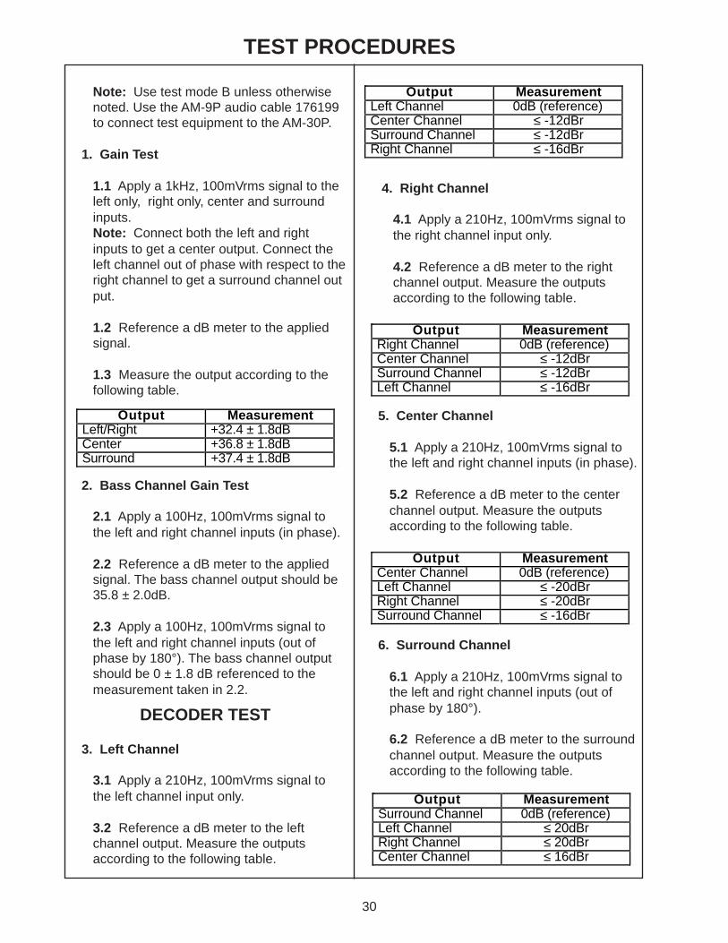
Note: Use test mode B unless otherwisenoted. Use the AM-9P audio cable 176199to connect test equipment to the AM-30P.
1. Gain Test
1.1 Apply a 1kHz, 100mVrms signal to theleft only, right only, center and surroundinputs.Note: Connect both the left and rightinputs to get a center output. Connect theleft channel out of phase with respect to theright channel to get a surround channel output.
1.2 Reference a dB meter to the appliedsignal.
1.3 Measure the output according to thefollowing table.
Output MeasurementLeft/Right +32.4 ± 1.8dBCenter +36.8 ± 1.8dBSurround +37.4 ± 1.8dB
2. Bass Channel Gain Test
2.1 Apply a 100Hz, 100mVrms signal tothe left and right channel inputs (in phase).
2.2 Reference a dB meter to the appliedsignal. The bass channel output should be35.8 ± 2.0dB.
2.3 Apply a 100Hz, 100mVrms signal tothe left and right channel inputs (out ofphase by 180°). The bass channel outputshould be 0 ± 1.8 dB referenced to themeasurement taken in 2.2.
Output MeasurementSurround Channel 0dB (reference)Left Channel ≤ 20dBrRight Channel ≤ 20dBrCenter Channel ≤ 16dBr
6. Surround Channel
6.1 Apply a 210Hz, 100mVrms signal tothe left and right channel inputs (out ofphase by 180°).
6.2 Reference a dB meter to the surroundchannel output. Measure the outputsaccording to the following table.
5. Center Channel
5.1 Apply a 210Hz, 100mVrms signal tothe left and right channel inputs (in phase).
5.2 Reference a dB meter to the centerchannel output. Measure the outputsaccording to the following table.
Output MeasurementRight Channel 0dB (reference)Center Channel ≤ -12dBrSurround Channel ≤ -12dBrLeft Channel ≤ -16dBr
4. Right Channel
4.1 Apply a 210Hz, 100mVrms signal tothe right channel input only.
4.2 Reference a dB meter to the rightchannel output. Measure the outputsaccording to the following table.
Output MeasurementLeft Channel 0dB (reference)Center Channel ≤ -12dBrSurround Channel ≤ -12dBrRight Channel ≤ -16dBr
DECODER TEST
3. Left Channel
3.1 Apply a 210Hz, 100mVrms signal tothe left channel input only.
3.2 Reference a dB meter to the leftchannel output. Measure the outputsaccording to the following table.

31
TEST PROCEDURES
9. Center Channel Frequency Response
9.1 Apply a 2.5kHz, 50mVrms signal to theleft and right inputs (in phase).
9.2 Reference a dB meter to the centerchannel output.
9.3 Measure the center channel outputaccording to the following table.
FREQUENCY RESPONSE
7. Bass Channel
7.1 Apply a 100Hz, 30mVrms signal to theleft and right inputs (in phase).
7.2 Reference a dB meter to the basschannel output. Measure the bass channeloutput according to the following table.
Frequency Output Tolerence20Hz -17.0dB ± 3.0dB35Hz +6.9dB ± 2.0dB100Hz 0dB
(reference)-
140Hz -0.1dB ± 1.5dB190Hz +3.8dB ± 1.5dB400Hz -24.6dB ± 3.5dB
10. Surround Channel FrequencyResponse
10.1 Apply a 2.5kHz, 50mVrms signal tothe left and right inputs (out of phase).
10.2 Reference a dB meter to the surroundchannel output.
10.3 Measure the surround channel outputaccording to the following table.
8. Left, Right Channel Frequency Re-sponse
8.1 Apply a 2.5kHz, 100mVrms signal tothe left or right channel only.
8.2 Reference a dB meter to the output ofthe same channel as the applied signal in8.1.
8.3 Measure the left or right channel outputaccording to the following table.
Note: Perform this test for both channels.
Frequency Output Tolerence150Hz -8.6dB ± 3.0dB240Hz +8.6dB ± 1.8dB440Hz +2.2dB ± 1.5dB750Hz +3.2dB ±1.5dB2.5kHz 0dB
(reference)-
12kHz +4.8dB ± 1.5dB20kHz -11.3dB ± 3.0dB
Frequency Output Tolerence150Hz -13.1dB ± 3.0dB240Hz +7.0dB ± 1.5dB550Hz +0.7dB ± 1.5dB800Hz +2.7dB ±1.5dB2.5kHz 0dB
(reference)-
12kHz +6.5dB ± 1.5dB20kHz -7.3dB ± 3.0dB
Frequency Output Tolerence150Hz -8.6dB ± 3.0dB240Hz +10.1dB ±1.5dB440Hz +1.1dB ±1.5dB750Hz +3.1dB ±1.5dB2.5kHz 0dB
(reference)-
12kHz +4.8dB ±1.5dB20kHz -11.3dB ± 2.5dB

32
Channel Input Freq. Dist.Bass 14mVrms (L+R) 100Hz <0.4%Left 64mVrms (L) 9kHz <0.2%Right 64mVrms (R) 9kHz <0.2%Center 38mVrms (L+R) 9kHz <0.2%Surround 30mVrms (L+R
180°out of phase)9kHz <0.2%
TEST PROCEDURES
14. Large Signal DistortionNote: Resistor loads connected only to thechannel under test.
Channel OutputLeft < 350uVrmsCenter < 600uVrmsSurround < 450uVrmsRight < 350uVrmsBass < 2mVrms
11. Dynamic Equalization (volume controldependent).
11.1 Apply a 37Hz, 1.0Vrms signal to theleft and right input (in phase). Reference adB meter to the applied signal. Set the unitto test mode D. The bass channel outputshould be -24.2 ± 1.5dBr relative to theinput.
11.2 Apply a 9.0kHz, 100mVrms signal tothe left and right channel inputs (in phase).Reference a dB meter to the applied signal.Set the unit to test mode D. The centerchannel output should be -44.7 ± 1.5dBrrelative to the input.
12. Volume IC Mute Test
12.1 Master Volume MuteSet the unit to test mode D. Apply a 100Hz,1.6Vrms signal to the left and right channelinputs (in phase). The bass channel outputshould be ≤ 50mVrms.
12.2 Center Channel MuteSet the unit to test mode F. Apply a 1.0kHz,.5Vrms signal to the left and right channelinputs (in phase). The center channeloutput should be ≤ 30mVrms.
12.3 Surround Channel MuteSet the unit to test mode F. Apply a 1.0kHz,.5Vrms signal to the left and right channelinputs (out of phase). The surround chan-nel output should be ≤ 30mVrms.
Channel Output (DC)Left < 15mV
Center < 40mVSurround < 40mV
Right < 15mVBass < 15mV
17. NoiseNote: All measurements are A-weightedexcept for the bass channel. The basschannel should be loaded. All inputsshorted.
15. Compressor TestNote: Load resistors not connected.Momentarily connect test mode B. Set theline voltage to 85Vac.
15.1 Apply a 1.0Vrms, 1kHz signal to theleft and right inputs (in phase). The distor-tion measured at the center channel outputshould be < 10% THD.
15.2 Apply a 520mVrms, 100Hz signal tothe left and right inputs. The distortionmeasured at the bass channel outputshould be < 5%.
16. DC OffsetNote: No signal connected to the inputs.
AMPLIFIER TEST
13. Small Signal Distortion (.5 W output)Note: All resistor loads connected, 30kHzLPF. See test set-up parameters.
Channel Input Freq. DistortionBass 260mVrms 100Hz <0.2 %Left 295mVrms 1kHz <0.2 %Right 295mVrms 1kHz <0.2 %Center 182mVrms 1kHz <0.2 %Surround 156mVrms 1kHz <0.2 %

33
TEST PROCEDURES
18. Bass Module Sweep Test
18.1 Apply a 100Hz, 40mVrms signal to themodule's audio input terminal. Set the basscontrol knob (potentiometer R306, MainPCB) to maximum. Sweep the oscillatorfrom 40Hz to 300Hz, listening for anyunusual buzz, rub, or extraneous sounds.
Note: There should not be any loudbuzzes or rattles from within the module.Redress any wire or component thatbuzzes or rattles.
19. Air Leak Test
19.1 Connect an oscillator to the module'saudio input terminal. Adjust the oscillator to40Hz, 27mVrms. Listen for air leaks aroundthe cabinet, paying particular attention tothe area where the base plate seals to thecabinet. If there is a "whooshing" noise,there is probably an air leak. Repair airleaks as required.
20. Tone Control Test
20.1 Apply a 100Hz, 40mVrms signal tothe audio input. Rotate the bass controlfully clockwise and counterclockwise fromits center position. The frequency responseshould increase and decrease smoothlywithout making any scratchy noise. Cleanor replace any control that is noisy.
20.2 Apply a 8kHz, 40mVrms signal.Rotate the treble control in the samemanner as the bass control. Look for asmooth response. Clean or replace anycontrol that is noisy.
34
PART LIST NOTES
1. This part is not normally available from Customer Service. Approval from the Field ServiceManager is required before ordering.
2. The individual parts located on the PCBs are listed in the Electrical Parts Lists.
3. This part is critical for safety purposes. Failure to use a substitute replacement withthe same safety characteristics as the recommended replacement part might create shock, fireand or other hazards.
4. This part is not interchangeable with the earlier versions of the AM-9P or AM-25P modules.
PCB IDENTIFICATION
To identify which AM-P product you are working on, look on the bottom side of the main PCBfor a six digit number with a dash variant. Below is a list of the numbers and the correspondingAM-P module assembly. Do not mix the PCB's from one AM-P product with another.
Product Service Main PCB VariationManual Number
AM-8P 194381 191990-1 U.S. 120Volt191990-2 EURO 230Volt191990-6 DUAL 120/230Volt
AM-25P 177870-S1 190341-1 U.S. 120Volt190341-2 EURO 230Volt190341-6 DUAL 120/230Volt
AM-30P 194382 193133-1 U.S. 120Volt193133-2 EURO 230Volt193133-6 DUAL 120/230Volt
On the bottom of the PCB is a module assembly number. The following is a list of thenumbers and the product they correspond to.
AM-8P 189879-131C U.S. 120Volt189879-231C EURO 230Volt189879-631C DUAL 120/230Volt
AM-25P 191170-131C U.S. 120Volt191170-231C EURO 230Volt191170-631C DUAL 120/230Volt
AM-30P 193134-131C U.S. 120Volt193134-231C EURO 230Volt193134-631C DUAL 120/230Volt

35
MAIN PART LIST(see Figures 20 and 21)
ItemNumber
Desciption PartNumber
Q t y Note
1 COVER, AM9P, REG, WHITECOVER, AM9P, REG, BLACK
172278-11172278-12
1
2 KNOB, TONE CONTROL, WHITEKNOB, TONE CONTROL, BLACK
172289-1172289-2
2
3 LATCH, COVER 172294 14 BASE PLATE 172288 15 PCB ASSY, AM-30P, 120V
PCB ASSY, AM-30P, 230VPCB ASSY, AM-30P, 120/230V
193133-1193133-2193133-6
1 changed 5/02
6 BRACKET, ADAPTOR 172287 17 SCREW, HI-LO, 6x3/8, PAN HEAD 147516-06 68 CABLE, FFC, 16 POS. 191124-16 19 HARNESS, WOOFER 172275 110 HEATSINK 172283 111 PLATE, HEATSINK, METAL 172291 112 PLATE, SPRING 172281 113 GROMMET, BASE PLATE 172295 214 TRANSFORMER, 115/230V 182577 1 3
15 CUSHION, TRANSFORMER 176169 216 GASKET, CONNECTOR, COVER 186845 117 SCREW, TAPP, 8-11x1.25, PAN, XRC/S 172672-20 818 MODULE ASSY, AM-30P, 120V
MODULE ASSY, AM-30P, 230VMODULE ASSY, AM-30P, DUAL
193134-131C193134-231C193134-631C
1
19 SCREW, TAPP, 8-11x.75, PAN, XRC/SQ 172672-12 820 WOOFER ASSY, 5.1/4" 172276 221 GASKET, 6.5" WOOFER 104794-08 222 GASKET, TAPE 175548 223 CAP,PORT, BLACK
CAP,PORT, WHITE173310-1173310-2
1
24 PORT, BOTTOM, BLACKPORT, BOTTOM, WHITE
173312-1173312-2
1
25 PORT SCREEN 145325 126 BUMPER, RECESSED, FOOT, .88" 142839 427 SCREW, HILO, 6-20X.625, PANHD, XRC 172779-10 228 ANCHOR, SCREW, #6, PLASTIC 186207 229 GASKET, TAPE, FOAM, PCB 174676 130 TAPE, FOAM 2" 134936-020 131 FOAM TAPE, 8" 134936-080 1- PORT, FLARE, 1.56"ID 189822-001 1

36
23
25
24
Figure 21. Module Assembly Exploded View
(2X)
5
10
11
13
12
(2)
(8)
(8)
(2)(2)
9
+-
-+
2
1
18
17
21
19
20
Not Applicable for -13, -23, -63
Module Assemblies
Voltage Select Switch for 115/230V Units
1
5
16
(2X)
7
6
3
15
14
4
8
10
MAIN PCB
Amplifier SubassemblyExploded View
Figure 20. Bass Module Exploded View

37
ELECTRICAL PART LIST
ReferenceDesignator
Description Part Number
Note
R3, 4, 129, 190, 192, 229, 290, 292,384, 610, 619, 622, 631-633, 642, 709,715, 731
10.0kΩ, CHIP, 0805, 5% 133626-1035
R7, 13, 15 20kΩ, CHIP, 0805, 5% 133626-2035R9, 196, 296, 376, 394, 609, 618, 629 1MΩ, CHIP, 0805, 5% 133626-1055R10, 12, 108, 111, 114, 118, 125, 126,155, 181, 183, 186, 188, 189, 191, 195,208, 211, 214, 218, 225, 226, 255, 281,283, 286, 288, 289, 291, 295, 307, 388,389, 396, 397, 455, 461, 551, 555, 560,561, 607, 617, 627, 734, 736, 737
1.00KΩ, CHIP, 0805, 1% 133625-1001
R11, 119, 122, 180, 185, 194, 219,222, 280, 285, 294, 322, 378, 380, 387,494, 594, 606, 614, 630
100kΩ, CHIP, 0805, 5% 133626-1045
R16, 17, 401, 501 8.25kΩ, CHIP, 0805, 1% 133625-8251R18, 20, 110, 210 4.42kΩ, CHIP, 0805, 1% 133625-4421R19, 21, 620, 623, 733, 735 499Ω, CHIP, 0805, 1% 133625-4990R51, 137, 237, 315, 324, 413, 457,513, 557
10Ω, CHIP, 0805, 5% 133626-1005
R104, 105, 197, 204, 205, 297, 301,303, 497, 597
6.81kΩ, CHIP, 0805, 1% 133625-6811
R106, 123, 134, 135, 206, 223, 231,235, 611, 616, 710
2.00kΩ, CHIP, 0805, 1% 133625-2001
R107, 109, 207, 209, 309, 408, 409,508, 509, 564, 602, 605, 612, 636
4.02kΩ, CHIP, 0805, 1% 133625-4021
R112, 113, 212, 213 44.2kΩ, CHIP, 0805, 1% 133625-4422R115, 116, 215, 216 1.82kΩ, 0805, 1/10W, 1% 133625-1821R117, 217 14.0kΩ, CHIP, 0805, 1% 133625-1402R120, 150, 184, 193, 220, 250, 284,293, 460
1.50kΩ, CHIP, 0805, 1% 133625-1501
R121, 124, 151, 175, 177, 221, 224,251, 275, 277, 381, 385, 475, 477, 575,577, 708, 721, 722
3.01kΩ, CHIP, 0805, 1% 133625-3011
R127, 128, 227, 228, 407, 507, 553,604
20.0kΩ, CHIP, 0805, 1% 133625-2002
R138, 238, 311, 320, 321, 377, 625 301Ω, CHIP, 0805, 1% 133625-3010R152, 252, 319 127kΩ, 0805, 1/10W, 1% 133625-1272R153, 164, 253, 264 19.1kΩ, 0805, 1/10W, 1% 133625-1912R154, 254 53.6kΩ, 0805, 1/10W, 1% 133625-5362R156, 256, 456, 463, 563, 634 10.0kΩ, CHIP, 0805, 1% 133625-1002R157, 160, 257, 260 1.40kΩ, CHIP, 0805, 1% 133625-1401R159, 259, 383 200kΩ, 0805, 1/10W, 1% 133625-2003R161, 261 1.10kΩ, 0805, 1/10W, 1% 133625-1101R162, 262, 462 25.5kΩ, 0805, 1/10W, 1% 133625-2552R163, 263 12.7kΩ, 0805, 1/10W, 1% 133625-1272
Resistors

38
ELECTRICAL PART LIST
Resistors (continued)
ReferenceDesignator
Description PartNumber
Note
R165, 265, 453, 511, 514, 515 23.7kΩ, 0805, 1/10W, 1% 133625-2372R166, 266 1.47kΩ, 0805, 1/10W, 1% 133625-1471R176, 276, 375, 476, 576 16.5kΩ, CHIP, 0805, 1% 133625-1652R178, 179, 278, 279, 312, 313, 399,478, 479, 578, 579, 641, 643
49.9kΩ, CHIP, 0805, 1% 133625-4992
R182, 187 4.22kΩ, 1206, 1/8W, 1% 124894-4221R282, 287 3.65kΩ, 1206, 1/8W, 1% 124894-3651R302, 304 1.27kΩ, CHIP, 0805, 1% 133625-1271R305 61.9kΩ, CHIP, 0805, 1% 133625-6192R310 332kΩ, CHIP, 0805, 1% 133625-3323R316 162kΩ, CHIP, 0805, 1% 133625-1623R317, 516, 601, 635 27.4kΩ, CHIP, 0805, 1% 133625-2742R318 150kΩ, 0805, 1/10W, 1% 133625-1503R379 10MΩ, CHIP, 0805, 5% 133626-1065R382 200Ω, CHIP, 0805, 5% 133626-2015R390, 395 75Ω,CHIP, 0805, 5% 133626-7505R391 JUMPER, CHIP, 0805 133627R392, 648 220Ω,0805, 1/10W, 5% 133626-2215R393 5.1Ω, 1206, 1/8W, 5% 124895-5R15R398, 600 33.2kΩ, CHIP, 0805, 1% 133625-3322R404, 504 15.8kΩ, CHIP, 0805, 1% 133625-1582R405, 505 24.3kΩ, CHIP, 0805, 1% 133625-2432R410, 411 73.2kΩ, CHIP, 0805, 1% 133625-7322R450, 566 2.21kΩ, CHIP, 0805, 1% 133625-2211R451 2.74kΩ, 0805, 1/10W, 1% 133625-2741R452 68.1kΩ, 0805, 1/10W, 1% 133625-6812R454, 554 38.3kΩ, 0805, 1/10W, 1% 133625-3832R459, 552 100kΩ, 0805, 1/10W, 1% 133625-1003R464, 562 21.0kΩ, 0805, 1/10W, 1% 133625-2102R466 2.32kΩ, 0805, 1/10W, 1% 133625-2321R510 78.7kΩ, 0805, 1/10W, 1% 133625-7872R550 1.33kΩ, 0805, 1/10W, 1% 133625-1331R559 93.1kΩ, 0805, 1/10W, 1% 133625-9312R603 200kΩ, CHIP, 0805, 5% 133626-2045R615 9.1kΩ, CHIP, 0805, 5% 133626-9125R626 39Ω, 1206, 1/8W, 5% 124895-3905R628, 640 JUMPER, CHIP, 1206 124896R646, 647, 649 1.00kΩ, 0805, 1/10W, 5% 133625-1025

39
ELECTRICAL PART LIST
ReferenceDesignator
Description PartNumber
Note
C1, 2, 123, 223, 407, 507 .033uF, 0805, X7R, 50V,10%
133623-333
C3, 4 4700uF, EL, BP, 85, 50V,20%
187394
C5, 6, 11, 12, 18-20, 28-43, 46-51, 54,55, 58, 59, 185, 285, 375, 379-381,485, 585, 601, 610, 710-717
.10uF, 0805, Y5V, 25V,80%
133624
C7 4700uF, EL, 85, 25V, 20% 170216C8, 14 2200uF, EL, 85, 20% 185929-222EC9, 10, 13, 15-17, 109, 117, 184, 209,217, 284, 401, 403, 476, 484, 501, 503,576, 584, 600, 700-709
10uF, EL, 20% 137126-100
C22-25, 161, 177, 178, 180, 182, 261,277, 278, 280, 282, 309, 383, 386, 461,477, 478, 561, 577, 578
1000pF, 0805, X7R, 50V,10%
133623-102
C62, 63, 65, 179, 183, 279, 283, 384,609, 611, 614, 616, 618
.01uF, 0805, X7R, 50V,10%
133623-103
C102, 103, 202, 203, 382, 387 3300pF, 0805, X7R, 50V,10%
133623-332
C104, 162, 186, 204, 262, 286, 615,621-625
100pF, 0805, COG, 50V,5%
133622-101
C105, 106, 153, 205, 206, 253 .047uF, BOX, 85, 63V, 5% 137127-473C107, 207 .027uF, BOX, 85, 100V, 5% 137127-273C108, 208 330pF, CER, 10%, 50V 140564-331C113, 213 .39uF, BOX, 85, 50V, 5% 137127-394C114, 214 .0047uF, BOX, 85, 100V,
5%137127-472
C115, 215 .022uF, BOX, 85, 100V, 5% 137127-223C116, 216, 459 .0022uF, BOX, 85, 100V,
5%137127-222
C120, 220 .0056uF, BOX, 85, 100V,5%
137127-562
C121, 221, 559 .0018uF, BOX, 85, 100V,5%
137127-182
C150, 151, 250, 251, 450, 451 .068uF, BOX, 85, 50V, 5% 137127-683C152, 252, 452 .039uF, BOX, 85, 100V, 5% 137127-393C155, 160, 255, 260, 406, 455, 460,555, 560, 602, 603
27pF, 0805, COG, 50V,5%
133622-270
C156, 157, 256, 257, 310, 311 .15uF, BOX, 85, 50V, 5% 137127-154C158, 159, 258, 259, 718, 719 .018uF, BOX, 85, 100V, 5% 137127-183C175, 275, 388, 475, 575, 604 1.0uF, EL, 20% 137126-1R0C181, 281, 481, 581 10uF, EL, 85, 25V, 20% 149947-100
Capacitors

40
ELECTRICAL PART LIST
ReferenceDesignator
Description PartNumber
Note
C300, 385, 405, 505 .1uF, BOX, 85, 50V, 5% 137127-104C301, 550-553 .082uF, BOX, 85, 50V, 5% 137127-823C302 680pF, MONO, COG, 50V,
5%140564-681
C303 .056uF, BOX, 85, 63V, 5% 137127-563C304 .0027uF, BOX, 85, 100V,
5%137127-272
C305, 306 .22uF, BOX, 85, 50V, 5% 137127-224C307, 453 .033uF, BOX,85,100V, 5% 137127-333C308 .001uF, BOX, 85, 100V, 5% 137127-102C376 100uF, EL, 105, 16V, 20% 139734-101C377, 378 1uF, 1206, Y5V, 16V, 80% 173383-105C389, 626-628 270pF, 0805, X7R, 50V,
10%133623-271
C456, 457 .12uF, BOX, 85, 50V, 5% 137127-124C506 .0033uF, BOX, 85, 100V,
5%137127-332
C508 .012uF, BOX, 85, 100V, 5% 137127-123C556, 557 .18uF, BOX, 85, 50V, 5% 137127-183C605 4.7uF, EL, 20% 137126-4R7C613 .0047uF, DISC, 60, AC 149016C617 22uF, EL, 20% 137126-220
Capacitors (continued)

41
ELECTRICAL PART LIST
ReferenceDesignator
Description PartNumber
Note
U1 VOLT REG, 37V, POS 137927U2 VOLT REG, 37V, NEG 137928U3, 600, 700 VOLTAGE COMPARATOR, LM339 187618-001U6, 7, 10, 14, 15, 16, 300, 703 QUAD OP AMP, TLO74D, SOIC 186112U8, 9, 12 VOLUME CNTRL, DIP-16, TC9213P 147622U11 OP AMP, POS, 36V, CA3280, DUAL 132591U13, 17, 375 OP AMP, DUAL, SO-8, NJM2082M 146820U175, 275, 475, 575 POWER AMP, AUDIO, TDA7294 170156U601 MICRO, uC, SO-28, ST6225M6, 190333U602 EEPROM, 1KB, SERIAL, 59C11 147536U604 OPTO-TRIAC, PDIP-6, MOC3023T 190334-001 3
U701 DUAL COMPARITOR, SO-8, LM393 148584U702 OP AMP, QUAD, SO14, TL074BCDT 188953
Integrated Circuits
ReferenceDesignator
Description PartNumber
Note
Q177, 179, 277, 279, 379, 385,386
PNP, SMALL 119168
Q175, 180, 275, 280, 377, 380,383, 384, 601
NPN, TAPE 117921
Q176, 276, 381, 382 DARL, P, TIP146T 172285Q178, 278, 387, 388 DARL, N, TIP141T 172284Q375 JFET, SOT,MMBF4392 134738Q376, 607, 700-703 BPLR, P, 55V, 150mA, SOT23 258007 Alt. 134743Q378 PNP, 2SB560F 140349Q605 TRIAC, TO220 178807 3
Q604, 606 NPN, SOT, MMBT3904 146819
Transistors
DiodesReferenceDesignator
Description PartNumber
Note
B1, 2 BRIDGE RECTIFIER 187611-001 3
D1, 3-6, 102, 202, 278, 375,578, 601
DUAL, SOT-23, BAV99 147239
D2 ZENER, 12V, 225mW, 5%, 1N5242 135247-5242D100, 101, 178, 201, 478 DUAL, SOT-23, BAV99 147239D176, 179, 276, 279, 602 ZENER, 5.6v, 225mW, 5%, IN5232 135247-5232D177, 180, 277, 280, 376, 377 1N5402 170219D378 ZENER, SOT23, 5%,
5.1V135247-5231
D600 ZENER, 5.6V, 225mW, 5%, 1N5232 135247-5232D603, 606, 701, 703, 704, 706 1N4531 136603D605 ZENER, 3.3V 135247-5226
DAVE PALMER
2/02

42
ELECTRICAL PART LISTMiscellaneous
ReferenceDesignator
Description PartNumber
Note
J1 HEADER 134290-05J2, 8 CONN, HEADER, RTANG, JST 16
FEST191169-16
J3 CONN, HEADER, RTANG, JST S2P-VH
190552-02
J4 CONN, HEADER, RTANG, 2.5mm 145402-08J5 CONN, DIN, RTANG, 8 POS 176198J6 CONN, HOUSING, AC, 2 POS,
FEMALE146563
J7 CONN, HEADER, 5 POS. 178742-5J9, 11 CONN, PHONO JACK 180567or260382-001J10 CABLE, FLAT, 8P, 24AWG 190701-001Y601, 602 (120V) JUMPER, 22AWG, INSUL, 7mm 135091-070F1 FUSE CLIP, 5mm 178548L600 INDUCTOR, LM4532, 1uH 178370-1R0F601 FUSE, 5X20mm, SLO-BLO, 3M 263401-3000 3
R5, 6 20 OHM, FUSING, 1/4W 130102-200 3
R14 THERMISTOR, 20K, ERTD 3FH L 203 177557R50, 306 POT, DUAL, 10K, DETENT. 185173R100, 200, 645 1.0KΩ, ARRAY, SMT, 4 POS, 5% 186433-1024R130, 230, 400, 500, 704, 711,727
3.9KΩ, ARRAY, SMT, 4 POS, 5% 186433-3924
R136 1.0 MΩ, ARRAY, SMT, 4 POS, 5% 186433-1054R167, 567 300Ω, ARRAY, SMT, 4 POS, 5% 186433-3014R608, 638, 700 100KΩ, ARRAY, SMT, 4 POS, 5% 186433-1044R664 100 OHM, FUSING, 1/4W 121243-
12110153
X600 CRY, CER, ONATOR, 8mHz 175627
43
Figure 22. Satellite Exploded View
SATELLITE PART LIST
3
1
2
4
5
7
6
7
ItemNumber
Description Part Number
Q t yPer
Assy
Note
1 Grille Assembly, Upper Black 192935-01 11 Grille Assembly, Upper White 192935-03 12 Grille Assembly, Lower Black 192935-02 12 Grille Assembly, Lower White 192935-04 13 Nameplate, Black 178725-01 13 Nameplate, White 178725-02 14 Twiddler™, 2.25" 273244-002 or 291636-001 25 Screw, Tapp, 4-16x.375, Pan, Xrec 181621-06 86 Grommet, Anti-Buzz 183891 87 Foam, Acoustic, Diecut, W/Screen 178714 2 1- Harness Assy, Twiddler 178719 1 2- H-Ring, Seal 178710-01 1 2- Snap Ring, Cube 313536-001 1 2

44
PACKING PART LIST
Item Number
Description Part Number
Q t y Note
1 Sat Assy, BlackSat Assy, White
194420-01C194420-02C
5
2 Line Cord, 120V, USLine Cord, 230V, UKLine Cord, 230V, EULIne Cord, 240V, AU
146999134725148203134726
1 3
3 Carton, LS30, US 188005-002 14 Sheet, Quick Start 193149 15 Remote Control 187700 16 Antenna, FM, Dipole, US, 75Ω
Antenna, FM, Dipole, Pal Con, Euro148589143185
1
7 Antenna, AM, Loop 178935 18 Power Pack, US, 120VAC
Power Pack, AUST., 240VACPower Pack, UK, 230VACPower Pack, EU, 230VAC
178371178373178374178375
1 3
9 Battery, "AA" Size 147538 310 Magazine, 6 Disk 187575 111 Bag, Poly, 4x6x2 mil 143393 112 Packing, D/C, Filler, D/W, LS20 188006 113 Packing, Filler, Accy, CD20 188010 114 Carton, Accy, CD20 Disp 188009-001 115 Carton, D/C, CD20 DISP, LS25 188020-001 116 Packing, Insert, Card, CD20 188022 117 Packing, Top Pad, EPS, Display PK 186424-001 118 Packing, Tray, EPS, LS20 DISP PK 186425-001 119 Envelope, Shipping 180005 120 D/C Carton 172282 121 Cable Pack, R, L, C, White
Cable Pack, R, L, C, Black294522-2010294522-3010
1
22 Cable, Speaker, LS/RS, WhiteCable, Speaker, LS/RS, Black
294523-2010294523-3010
1
23 Cable, Audio Input 188694 or19149324 Cable, RCA 6FT 185931-01 125 Screw, Shipping 186273 326 Bag, Poly 103351 127 Warranty Service Center List 187981 128 Bag, Poly 137847 129 Brochure, All Products 188898 130 Foot, 2.03 x .06 183621 431 Packing, Corner Post 148044 232 Packing, Insert, EPS 172279 133 Warranty Card, US
Warranty Card, Multi, Language181357181460
1
34 CD, Test, Lifestyle® Home Thtr. 193160 135 CD, Lifestyle Music System 183768 136 Manual, Owner's, LS30 193147 1
DAVE PALMER
DAVE PALMER
1
DAVE PALMER
DAVE PALMER
Changes made to Item number 23, Audio Cable. 6/7/01
DAVE PALMER

45
INSERT TAB INTOSLOT BETWEEN TOP OF DOORAND TOP COVER
19
1625
17
18
15
CD20
CD20 Pack
7
8
10
5911
13
13
CD20 PACK
DUAL VOLTAGE UNITSARE PACKED WITH A120V AND 220V POWER PACK
14 AM25PBASS BOX
SATELLITE ASSEMBLYPACK
3
28
2726 3029 34 35 3633
4
6
31
2
32
12
Breaks IntoTwo Pieces
1
24
23
21
22
20
Satellite AssemblyPack
Figure 23. Packing

46
Pin Function1 Anode2 Cathode3 NC4 Main Terminal5 Substrate Do Not
Connect6 Main Terminal
Opto-Triac DriverP/N 172297 (MOC3063T)
Main PCB AssemblyU604
Pin Connection1 Output 22 Output 13 V+4 Input 1-5 Input 1+6 Input 2-7 Input 2+8 Input 3-9 Input 3+10 Input 4-11 Input 4+12 GND13 Output 414 Output 3
Voltage ComparatorP/N 137929 (LM339N)Main PCB AssemblyU600, U700, U701
Amplifier PCB AssemblyU3
INTEGRATED CIRCUITS

47
INTEGRATED CIRCUITS
Volume ControlP/N 147622 (TC9213P)
Main PCB AssemblyU8, U9, U12
Operational Amplifier, QuadP/N 186112 (TL074)Main PCB Assembly
U6, U7, U10, U14-U16,U300, U703
Operational Amplifier, DualP/N 132591 (CA3280)Main PCB Assembly
U11

48
Pin Function15 -Vs (Power)14 Out13 +Vs (Power)12 N.C.11 N.C.10 Mute9 Stand-by8 -Vs (Signal)7 +Vs (Signal)6 Bootstrap5 N.C.4 SUR3 Non-Inverting Input2 Inverting Input1 Stand-by GND
EEPROM, 1KBP/N 147536 (59C11)Main PCB Assembly
U602
Audio Power AmplifierP/N 170156 (TDA7294)Amplifier PCB AssemblyU175, U275, U475, U575
INTEGRATED CIRCUITS