Power Management Selection Guide
68
Technology for Innovators TM Power Management Selection Guide 2Q 2006 TI Power Solutions: Power Behind Your Designs
-
Upload
khangminh22 -
Category
Documents
-
view
3 -
download
0
Transcript of Power Management Selection Guide

Technology for InnovatorsTM
Power Management Selection Guide2Q 2006
TI Power Solutions: Power Behind Your Designs

Power Management Selection Guide Texas Instruments 2Q 2006
2 Power Management Selection Guide
Table of Contents
Typical Power Applications 3System Power and Plug-In Solutions . . . . . . . . . . . . . . . . . . . . . . . . . . . . . . . . . . . . . . . . . .3Portable Power Solutions . . . . . . . . . . . . . . . . . . . . . . . . . . . . . . . . . . . . . . . . . . . . . . . . . . .3AC/DC Solutions . . . . . . . . . . . . . . . . . . . . . . . . . . . . . . . . . . . . . . . . . . . . . . . . . . . . . . . . . .4Isolated DC/DC Solutions . . . . . . . . . . . . . . . . . . . . . . . . . . . . . . . . . . . . . . . . . . . . . . . . . . .4FPGA and CPLD Power Solutions . . . . . . . . . . . . . . . . . . . . . . . . . . . . . . . . . . . . . . . . . . . . .5DSP Power Solutions . . . . . . . . . . . . . . . . . . . . . . . . . . . . . . . . . . . . . . . . . . . . . . . . . . . . . .6Active-Bus Termination Solutions . . . . . . . . . . . . . . . . . . . . . . . . . . . . . . . . . . . . . . . . . . . . .7
Fusion Digital Power™ Control Solutions 8
AC/DC and DC/DC Power Supply Products 10Power Factor Correction (PFC) . . . . . . . . . . . . . . . . . . . . . . . . . . . . . . . . . . . . . . . . . . . . . . .10PWM Power Supply Controllers . . . . . . . . . . . . . . . . . . . . . . . . . . . . . . . . . . . . . . . . . . . . .12MOSFET Drivers . . . . . . . . . . . . . . . . . . . . . . . . . . . . . . . . . . . . . . . . . . . . . . . . . . . . . . . . .18Loadshare Controllers . . . . . . . . . . . . . . . . . . . . . . . . . . . . . . . . . . . . . . . . . . . . . . . . . . . . .20
Plug-In Power Modules (POLA™ and Others) 21
Linear Regulators 24
Non-Isolated Switching DC/DC Regulators 28DC/DC Controllers (External Switch) . . . . . . . . . . . . . . . . . . . . . . . . . . . . . . . . . . . . . . . . .28DC/DC Converters (Integrated Switch) . . . . . . . . . . . . . . . . . . . . . . . . . . . . . . . . . . . . . . . .30Inductorless DC/DC Regulators (Charge Pumps) . . . . . . . . . . . . . . . . . . . . . . . . . . . . . . . .35
Application-Specific Multi-Output Solutions 37
Lighting Solutions 38White LED Drivers . . . . . . . . . . . . . . . . . . . . . . . . . . . . . . . . . . . . . . . . . . . . . . . . . . . . . . . .38LED Drivers . . . . . . . . . . . . . . . . . . . . . . . . . . . . . . . . . . . . . . . . . . . . . . . . . . . . . . . . . . . . .39CCFL Backlight Controllers . . . . . . . . . . . . . . . . . . . . . . . . . . . . . . . . . . . . . . . . . . . . . . . . .40Photoflash Capacitor Chargers . . . . . . . . . . . . . . . . . . . . . . . . . . . . . . . . . . . . . . . . . . . . . .41
Battery Management Products 42Battery Charge Management . . . . . . . . . . . . . . . . . . . . . . . . . . . . . . . . . . . . . . . . . . . . . . .42Battery Fuel Gauges . . . . . . . . . . . . . . . . . . . . . . . . . . . . . . . . . . . . . . . . . . . . . . . . . . . . . .44Lithium-Ion Protection . . . . . . . . . . . . . . . . . . . . . . . . . . . . . . . . . . . . . . . . . . . . . . . . . . . . .46Authentication for Batteries and Peripherals . . . . . . . . . . . . . . . . . . . . . . . . . . . . . . . . . . .47
Hot Swap and Power Distribution 47Power-over-Ethernet . . . . . . . . . . . . . . . . . . . . . . . . . . . . . . . . . . . . . . . . . . . . . . . . . . . . . .47Hot Swap Power Management . . . . . . . . . . . . . . . . . . . . . . . . . . . . . . . . . . . . . . . . . . . . . .49PCMCIA and USB Devices . . . . . . . . . . . . . . . . . . . . . . . . . . . . . . . . . . . . . . . . . . . . . . . . .51Power Multiplexers and Current-Limiting Switches . . . . . . . . . . . . . . . . . . . . . . . . . . . . .54
Supervisory Circuits (Voltage Supervisors) 56
Voltage References 58
Power Management Special Functions 60Real-Time Clocks . . . . . . . . . . . . . . . . . . . . . . . . . . . . . . . . . . . . . . . . . . . . . . . . . . . . . . . . .60Non-Volatile SRAM (NVSRAM) . . . . . . . . . . . . . . . . . . . . . . . . . . . . . . . . . . . . . . . . . . . . .62
Resources 63Power Management Design Tools . . . . . . . . . . . . . . . . . . . . . . . . . . . . . . . . . . . . . . . . . . .63Packaging . . . . . . . . . . . . . . . . . . . . . . . . . . . . . . . . . . . . . . . . . . . . . . . . . . . . . . . . . . . . . .64Device Index . . . . . . . . . . . . . . . . . . . . . . . . . . . . . . . . . . . . . . . . . . . . . . . . . . . . . . . . . . . .65TI Worldwide Technical Support . . . . . . . . . . . . . . . . . . . . . . . . . . . . . . . . . . . . . . . . . . . . .67Note: Military versions of some Power Management
products are available. Please visit: power.ti.com/militaryproducts
TI Power Solutions:
Power Behind
Your Designs
TI provides power management integra-tion, technology and value to help youdrive innovation and grow marketopportunities. This is coupled withcollaboration, tools, service and deliveryto help you get there faster. For moreinformation or technical assistance,please see TI Worldwide TechnicalSupport on page 67 of this selectionguide or visit TI’s Power Managementweb site at:
power.ti.com
Texas Instruments (TI) offers complete powersolutions with a full line of high-performanceproducts. These products, which range fromstandard linear ICs to plug-in and integratedpower solutions, are tailored to meet yourdesign challenges. And, TI makes designingeasier by providing leading-edge supporttools such as training, a broad selection ofevaluation modules (EVMs), applicationnotes, comprehensive technical documen-tation and more. TI also offers samples andsmall orders (shipped within 24 hours via TIauthorized distributors) that will help youaccelerate your time-to-market.
Included in this selection guide you will finddesign factors, featured products, graphicrepresentations of portfolios and parametrictables. A list of application notes and evalu-ation modules is included in each section ofthe guide.

Texas Instruments 2Q 2006 Power Management Selection Guide
Typical Power Applications 3
ACLine
Low Dropout
Regulator(Page 24)
Power Factor
Correction
or AC/DC(Page 10)
PWM
Controllers(Pages 8, 12)
MOSFET
Drivers(Pages 8, 18)
Power
SwitchesUSB
ExpressCard™
PCMCIA
(Page 51)
DC/DC
Converter(Page 30)
DC/DC
Controller(Page 28)
Hard Drive
Hot Swap
and
Power-over-Ethernet(Page 47)
Non-Isolated
Plug-In
Module
POLA™
(Page 21)
Supply
Voltage
Supervisor(Page 56) DSP/µC
System
Voltage
USB
Peripheral
Backplane
48-V or 24-VDC Input
Memory
Fusion
Digital Power™ Solutions
–+48-V
Isolated
Plug-In
Module(Page 21)
DSP
System
Voltages
Application-Specific
Multi-Output
Solutions
(Page 37)
Photoflash
Capacitor Chargers
(Page 41)
White LED Drivers
(Page 38)
Step-Down
DC/DC Converters
(Page 30)
Linear Regulators
(Page 24)
Application-Specific
Multi-Output
Solutions
(Page 37)
Photo Flash
LED Light
LCD Color
Display
Memory
Supervisory Circuits
(Voltage Supervisors)
(Page 56)
Battery
Fuel Gauges
(Page 44)
Lithium-Ion
Protection and
Authentication
for Batteries
(Pages 46, 47)
Battery Charge
Management
(Page 42)
DSP
µC
I2C Reset
Inductorless
DC/DC Regulators
(Charge Pumps)
(Page 35)
Step-Up DC/DC
Converters
(Page 30)Audio Supply
Noise-Sensitive
RF Circuitry
DC
Inputs
USB
Rechargeable
Battery
Battery Management
System Power and Plug-In Solutions
Portable Power Solutionswww.ti.com/portablepower

Power Management Selection Guide Texas Instruments 2Q 2006
Typical Power Applications4
Power Factor
Correction(Page 10)
PFC
PFC + PWM
UCC38050/51UCC3817A/18AUCC3819AUC3854/A/BUC3855A/B
UCC38500-3UCC28510-7UCC28521/28
MOSFET
Drivers(Page 18)
±2 A
±4 A
±9 A
TPS2811-15TPS2816-19TPS2828-29
UCC37323/4/5UCC27423/4/5UCD7201UCD7100
UCC37321/2
Bus Voltage3.3 to 48 V
Shunt
Regulators
TL431/ATLV431/ATL1431UC39431/2
AC Line:85 to 265-V AC
Rectified AC385 to 400-VBoosted DC
Output
Post
Regulation(Page 12, 24)
PWM
LDOs
UCC2540UCC3583
TPS7xxxUC382/385
Secondary
Side Control(Page 12, 18)
PWM
Drivers
UC3849UCC3839
TPS2811-15TPS2829-29UCC27423/4/5UCC37321/2UCC37323/4/5UCD7100UCD7201
Loadshare(Page 20)
Loadshare
UCC39002UC3907UC3902
PWM +
Loadshare
UC3849
Isolation
PWM
Controllers(Page 12)
PWM
(Forward,
Flyback)
PWM
(Half-Bridge,
Full-Bridge,
Push-Pull)
UCC28220/1UCC2891/2/3/4/7UCC35701/2UCC35705/6UCC3800-5UCC3809UCC3813-xUCC38C40-45
UCC3895UCC38083-6UCC3806UCC3808/AUC3825/AUC28025UCD8220/8620
Primary Side
Startup
UCC3960/61
Feedback(Page 58)
AC/DC Solutions Isolated DC/DC Solutions

Texas Instruments 2Q 2006 Power Management Selection Guide
Typical Power Applications 5
FPGA and CPLD Power Solutionswww.ti.com/xilinxfpga or www.ti.com/alterafpga
TPS750035V_INPUT
100 µF
100 µF
100 µF
10 µF
1.5 nF
1.5 nF
VCCAUX
VCCINT1.2 V @ 2 A
+
+
VCCO3.3 V @ 2 A
VCCAUX2.5 V @ 300 mA
IS1SW1FB1IS2
SW2FB2
OUT3FB3
AGNDDGND
IN1IN2IN3EN1SS1EN2SS2EN3
SS3DGND
3-ABUCK1
3-ABUCK2
300-mALDO
DGND
0.033 Ω
61.9 kΩ
36.5 kΩ
15.4 kΩ
61.9 kΩ
0.033 Ω
Q2
D2
D1
15 µH
5 µHQ1
10 nF
Highly Integrated TPS75003 Triple Supply Powering Spartan™-3
Access the sites for one-stop power management support for Xilinx® and Altera® FPGAs and CPLDs, including free downloads of power referencedesigns with complete schematics, bills-of-material and helpful implementation notes.
C2 0.047 µF
C12 0.047 µF
C6 10 µF
C16 10 µF
+
+
C7 220 µF
C17 220 µF
C8 0.047 µF
C18 0.047 µF
C5 6800 pF
C15 6800 pF
1.5 V at 6 A
3.3 V at 6 A
DIGITAL_VCCINT
DIGITAL_VCCIO
PLL_ENABLE
C3 68 pF
C13 68 pF
C1 0.012 µF
C11 0.012 µF
R9 10.0 kΩ
R114.7 kΩ
R53.74 kΩ
R21.18 kΩ
R61.18 kΩ
R410.0 kΩ
R810.0 kΩ
R39.76 kΩ
R79.76 kΩ
C9 470 µF4 V
C19 470 µF4 V
C10 470 µF4 V
C20 470 µF4 V
L1 4.7 µH
L2 4.7 µH
C4 0.1 µF
C14 0.1 µF
U1TPS54610PWP
U2TPS54610PWP
5V_INPUT
2827262524232221201918171615
2827262524232221201918171615
1234567891011121314
1234567891011121314
+
+
+
+
RTSYNCHSS/ENAVBIASVINVINVINVINVINPGNDPGNDPGNDPGNDPGND
ANAGNDVSENSE
COMPPWRGD
BOOTPHPHPHPHPHPHPHPHPH
RTSYNCHSS/ENAVBIASVINVINVINVINVINPGNDPGNDPGNDPGNDPGND
ANAGNDVSENSE
COMPPWRGD
BOOTPHPHPHPHPHPHPHPHPH
PWRPAD
PWRPAD
Two Highly Efficient TPS54610 6-A SWIFT™ DC/DC
Converters Powering Stratix® II
U1PTH05010WAS
U4TPS3828–50DBV
R117.4 kΩ
C1470 µF
C21.0 µF
C5470 µF
123
5
4
+
1.2 V at 15 ADIGITAL_VCCINT
5V_INPUT12345
109876
U2PTH05010WAS
R22.21 kΩ
C3470 µF
C6470 µF
+
2.5 V at 15 ADIGITAL_VCCAUX_VCCO
12345
109876
U3PTH05010WAS
R3698 Ω
C4470 µF
C7470 µF
+
+
+
+
3.3 V at 15 ADIGITAL_VCCO
12345
109876
GNDVINInhibitVoAdjVoSns
MgnUpMgnDwn
TrackGNDVout
RST
MRGND
VDD
WDI
GNDVINInhibitVoAdjVoSns
MgnUpMgnDwn
TrackGNDVout
GNDVINInhibitVoAdjVoSns
MgnUpMgnDwn
TrackGNDVout
PTH05010 Modules Providing
Fast Time-to-Market Power
Solution for Virtex®-4

Power Management Selection Guide Texas Instruments 2Q 2006
Typical Power Applications6
DSP Power Solutionswww.ti.com/dsppower
123456789
1011121314
2827262524232221201918171615
2
3
R4
R3
R110 kΩ
C20.1 µF
C147 µF
R62.0 kΩ
R2
1.5 kΩ
R5
10 kΩ
C422 µF
C522 µF
C30.1 µF
+ +
+
+
Q1BSS138
U1TPS767D3xxPWP
VDD_CORE
VDD_3.3V
RESET
VDD_3.3V3.875 to 5.5 VEN
VIN
1
PWRPAD
NCNC1GND
1IN1INNCNC2GND
2IN2INNCNC
1EN
2EN
1RESET
2RESET
NCNC
1FB/NC1OUT1OUT
NCNCNC
2OUT2OUT
NCNC
Dual 1-A Linear Regulator with Integrated Supply Voltage Supervisors
Powering TMS320F281x DSP
Access the site for one-stop DSP power management support, including free downloads of DSP power reference designs with complete schematics, bill-of-materials and helpful implementation notes.
U2TPS62300YZD
U3TPS3103K33DBV
U1TPS62300YZD
Q22SC2412K
Q12SC2412K
L22.2 µH
L12.2 µH
C410 µF
C110 µF
RESET
VIO
VCORE
C310 µF
C210 µF
A2B2C2D2
654
A2B2C2D2
R7909 kΩ
R2
R9100 kΩ
R1010 kΩ
R8
R1
VINSequencing Circuit
EN
R4100 kΩ
R5475 kΩ
R347.5 kΩ
A1B1C1D1
123
A1B1C1D1
VINENADJFB
GNDSW
M/SVOUT
VDDPFOPFI
RESET
MRGND
VINENADJFB
GNDSW
M/SVOUT
R6200 kΩ
Two Highly Power- and Space-Efficient TPS62300 500-mA DC/DC Converters
Powering TMS320VC5503/07/09A DSP

Texas Instruments 2Q 2006 Power Management Selection Guide
Typical Power Applications 7
Active-Bus Termination Solutions Device Input Bus Voltage (V) IOUT (A) Isolated Outputs VO Range (V) VO Adjustable Price*Plug-In Power Modules PTH03010/50/60Y 3.3 6, 10, 15 No 0.55 to 1.8 Yes 13.95, 9.95, 11.50PTH05010/50/60Y 5 6, 10, 15 No 0.55 to 1.8 Yes 13.95, 9.95, 11.50PTH12010/50/60Y 12 6, 8, 12 No 0.55 to 1.8 Yes 13.95, 9.95, 11.50
VOUT Switching PackageIOUT VIN Adj. Out Efficiency Frequency (max) Pin Count
Device (mA) (V) (V) (%) (kHz) HTSSOP EVM Price*Converters (with Integrated FETs) TPS54372 3000 3.0 to 6.0 0.2 to 4.5 90 700 20 Yes 2.35TPS54672 6000 3.0 to 6.0 0.2 to 4.5 90 700 28 Yes 3.35TPS54872 8000 4.0 to 6.0 0.2 to 4.5 85 700 28 Yes 3.95TPS54972 9000 3.0 to 4.0 0.2 to 4.5 90 700 28 Yes 4.20
IOUT3 VOUT3 Switching LightIOUT1 IOUT2 (Buf. VOUT1 VOUT2 (Buf. Frequency Load Selectable
(VDDQ) (VTT) VREF) VIN (VDDQ) (VTT) VREF) Selectable Eff. Control OutputDevice (A) (A) (mA) (V) Adj. (V) Fixed (V) Fixed (V) (kHz) Mode Scheme Discharge Package(s) Price*Controllers (with External FETs)TPS51020 >10 >3 3 4.5 to 2.5,1.8, VDDQ/2 VDDQ/2 270, 360, 450 Yes Voltage Yes 30 TSSOP 3.15
Switcher Switcher 28 Adj. ModeTPS51116 >10 +3/–3 10 3 to 2.5,1.8, VDDQ/2 VDDQ/2 400 Yes D-CAP/ Yes 20 HTSSOP1 1.20
Switcher LDO 28 Adj. Current Mode 24 QFN1
Controller LDOsTPS51100 — +3/–3 10 1.2 to — VDDQ/2 VDDQ/2 — — — Yes 10 MSOP1 0.80
LDO 3.62
1PowerPAD™. 2Requires separate 5-V supply. *Suggested resale price in U.S. dollars in quantities of 1,000.
Active-Bus Termination Solutions (DDR/QDR/GTL/SSTL/HSTL)TI offers a wide selection of active-bus termination solutions from LDOs and switching controllers to plug-in power. Typical application diagramsand product parameters are provided to aid product selection.
C5
C4
M1
TPS51116
VBST
DRVH
LL
DRVL
PGND
CS
VSIN
PGOOD
S5
S3
VLDOIN
VTT
VTTGND
VTTSNS
GND
MODE
VTTREF
COMP
VDDQSNS
VDDQSET
C2
C0
C1
L0
M0
C6
C3
R1
R0
R2
VIN
VDDQ
5V_IN
PGOODS3
S5
VTT
C12 x 10 µFCeramic
C20.1 µFCeramic
VIN
S5
GND
S3
VDDQSNS
VLDOIN
PGND
VTT
TPS51100
VTTREFVTTSNS
S3
VTTREF
5V_IN
S5
VDDQ
VTT
VIN
Standby
GND
VTT
VREF
CO1
Low-ESR(Required)
CIN(Required)
VT
T Te
rmin
atio
n Is
lan
d
1 kΩ1 %
1 kΩ1 %
VDDQ
SSTL-2Data/
AddressBus
CO2
Ceramic(Optional)
Q1BSS138(Optional)
COn
hf-Ceramic
PTHxx060Y(Top View)
1
2
8910
543
6
7
VIN PH
BOOT
PGND
VSENSE
VTTQ
AGND
VBIAS
InputTPS54372
COMP
Compensation
Network
REFIN
VDDQ
TPS54372: SWIFT™
PTHxx060Y: Plug-In Power TPS51116: Controller + LDO
TPS51100: LDO

Power Management Selection Guide Texas Instruments 2Q 2006
8 Fusion Digital PowerTM Control Solutions
TI’s family of Fusion Digital Power™ productsfocuses on three areas: Digital Power Drivers(UCD7K), Digital Power PWM Controllers(UCD8K) and Full Digital Controllers (UCD9K).These products are power management specificand provide both isolated and non-isolatedsolutions from AC line to point-of-load, covering uninterruptible power supplies(UPS), server, telecom, datacom and VRMapplications. The Fusion Digital Power ICsprovide cost-effective solutions with greaterlevels of performance, reliability and flexibilitythan today’s pure analog designs. For themost up-to-date information on digital powertechnology and product availability, go towww.ti.com/digitalpower
Key Benefits of Fusion
Digital Power
• Greater flexibility and better time-to-market• Enhanced performance of power supplies• Enables system communications such as
remote diagnostics• Lowers system cost by lowering total
component count
Other Benefits of Fusion Digital
Power Solutions from TI
• Programmable• Easy to use• High precision• Higher integration• Common development platform• Supports current and future topologies
Support
Digital control requires software support. TheUCD95K and UCD91K Fusion Digital Powercontrollers are supported with Code ComposerStudio™ IDE software. This is an integrateddevelopment environment that provides keydevelopment tools to reduce developmenttime and effort. As part of TI’s commitment tostandards in the power electronics industry,PMBus™ tools are also part of our digitalpower customer support. Additionally, ourreference designs are supported by graphicaluser interface (GUI) and source code examplesto jump-start designs and evaluation ofFusion Digital Power products from TI.
Digital Power Controller
UCD7K
PWM Stage VOUT
VIN
Driver(s)PowerStage
µC orDSP
Engine
E/AI-Limit
3.3-VRegulator
COMM
LogicPWM
UCD7K
Fusion Digital Power Control Drivers
UCD7K Family
The UCD7K drivers interface the digital con-troller to the power stage while providingprotection for the power supply as well asbias for the digital controller.
Key Features Benefits• High current gate drivers • Interfaces to the power stage• Programmable analog over-current limit with flag • Fail-proof and flexible overload protection• Onboard 3.3-V, 10-mA linear regulator • Provides power to the digital controller

Texas Instruments 2Q 2006 Power Management Selection Guide
Fusion Digital PowerTM Control Solutions 9
DigitalSupervisor
VOUT
UCD8K
VIN
Driver(s) PowerStage
House-keepingFunction
E/AFunction
I-Limit
COMM
Clock LogicPWM
3.3-VRegulator
UCD8K
UCD9K
UCD7K
E/AFunction
VOUT
VIN
Driver(s)LogicDPWM
I-Limit
PowerStage
µC or DSP
Engine
COMM
3.3-VRegulator
UCD9K
Fusion Digital Power PWM Controllers
UCD8K Family
Fusion Digital Power Controllers
UCD9K Family
The UCD8K controllers integrate PWM circuitryand a Fusion Digital Power control driver toclose the feedback loop in the analog domainunder digital supervision.
The UCD9K devices provide full digital powermanagement capabilities to close multiplefeedback loops in the digital domain and theintegrated resources for supervision, commu-nication, configuration and monitoring.
Key Features Benefits• Voltage mode or peak current mode control • Provides flexibility of control methods• Programmable over-current limit with flag • Fail-proof and flexible overload protection• Accepts clock input from the digital controller • Digitally controls switching frequency and maximum duty cycle• Onboard 3.3-V, 10-mA linear regulator • Provides power to digital controller
Key Features Benefits• Digital PWM, up to 150-ps resolution • No limit cycle at MHz switching frequencies• ADC: Up to 12 bits resolution • Accurate regulation and monitoring• ADC: As fast as 50-ns conversion time • Wide voltage loop bandwidth and fast transient response• Flash memory: Up to 64 KW for program and data • Allows for high complexity• Multifunction I/O ports, up to 48 • Provides high flexibility• PMBus™ compliant • Hardware peripheral for standardized communication

Power Management Selection Guide Texas Instruments 2Q 2006
10 AC/DC and DC/DC Power Supply Products
Power Factor Correction (PFC)
Power Level (W)
Ap
plicati
on
s
UCC3819
Tracking Boost PFC
UCC3817A/18A
BiCMOS 3854, LEM
UC385416-pin Avg. Current Mode
UC3854A/B
Improved 16-pin Avg. Current Mode
UC3855A/B
ZVT, Higher Frequency
UCC38500-03
PFC+PWM, LEM/TEM
UCC28521/8
PFC+PWM, TEM/TEM, Prog.MaxDC
Adapters
Lighting Ballasts
Value Desktop
Performance Desktop
Workstation and Servers
Monitors, Receivers, Peripherals
HVAC, White Goods
Switches, Hubs, Routers
Telecom Rectifiers
Battery Chargers (Offline)
Avg. I -Mode
ZVT
Avg. Current Mode
Transition Mode
ZVT
75 100 300 600 1 k+
UC3852
Transition Mode
UCC38050/51
Transition Mode, Ind. Std. Pinout
UC3853
EDP
Telecom/Datacom
Consumer
Legend
Legend
Featu
res
8-pin Avg. Current Mode
UCC28510-17
PFC+PWM, LEM/TEM, Prog.MaxDC
Power Factor Correction (PFC) Family of Products
Performance• Voltage feed-forward for linearized per-
formance and faster transient responseover wide line voltage range.
• Multiplier linearity and zero power detectfunctions improve light load operation.
• Onboard high output current drive capabilitywithout external MOSFET drivers.
Flexibility• Ability to work with a wide line
voltage range.• Different levels of under-voltage lockout
thresholds for self bias and auxiliary biasapplications.
• Ability to synchronize controllers to elimi-nate noise issues.
Design Factors
Control MethodAverage Current Mode (ACM) —Optimum control method to achieve PFC andlow harmonic distortion.
Transition Mode — Simpler inexpensivecontrol with high peak currents and filteringrequirements.
ZVT Mode — A type of soft switching tech-nique, which reduces EMI and allows forhigher frequency operations.
Protection• Soft-start (programmable) provides con-
trolled start-up.• Over-current protection (OCP) provides
protection during overload conditions.• Over-voltage protection (OVP) prevents
output capacitor, switches and load fromovercharge condition.
Power Level• IEC requirements are applicable to all
power supplies above 150 W.• Higher power converters may require
ZCT/ZVT techniques to achieve high efficiencies.
• Some of the simpler control techniques notusable at high power levels.
Features
From 50 W to 5 kW, TI PFC controllers deliverEN61000-3-2 compliance.• Industry standard architecture.• Deliver PF > 0.993.• New BiCMOS generation reduces
complexity.• Optimized PFC/PWM “combo” controllers.• Superior applications support.

Texas Instruments 2Q 2006 Power Management Selection Guide
AC/DC and DC/DC Power Supply Products
Power Factor Correction (PFC)
11
Resources For a complete list of Resources, visit power.ti.com
Part Number Description Price*Evaluation Modules (EVMs)UCC28051EVM 100-W Offline AC/DC Voltage Converter with PFC 49UCC28514EVM 100-W AC/DC Power Converter with PFC Regulating a 12-V DC Output 49UCC28517EVM 100-W AC/DC Power Converter with PFC Regulating 2 DC Outputs 49UCC28521EVM 350-W Two-phase Interleaved Power Factor Corrected Pre-regulator 99UCC28528EVM 350-W Two-phase Interleaved Power Factor Corrected Pre-regulator 99UCC38050EVM 110-W Universal Line Input PFC Boost Converter 49UCC38500 UCC38500 Evaluation Module: 100-W, Universal Line to 12-V Regulated Output 49UCC3817 UCC3817 Evaluation Module: 385-V, 250-W PFC Boost Converter 49
*Suggested resale price in U.S. dollars.
Literature Number Part Number DescriptionApplication NotesSLUA144 UC3854 UC3854 Controlled Power Factor Correction Circuit DesignSLVC018.ZIP UCC38050 MathCAD Application Design Tool for Use with the UCC38050 SLUU138 UCC38050 100-W Critical Conduction Power Factor Corrected PreregulatorSLUA308 UCC3817 UCC3817 Current Sense Transformer EvaluationSLUA296 UCCX8510-17 A New Synchronization Circuit for Power ConvertersSLUA294 UCC3817A/18A/19A Differences between UCC3817A/18A/19A and UCC3817/18/19SLUA269 UCC3819 UCC3819 250-W PFC Boost Follower Preregulator Design SLUA245 UCC3817 Synchronizing a PFC Controller from a Downstream Controller Gate DriveSLUA196 UC3854A/B, UC3855A/B UC3854A/B and UC3855A/B Provide Power Limiting with Sinusoidal Input Current for PFC Front EndsSLUA177 UC3854A/B UC3854A and UC3854B Advanced Power Factor Correction Control ICsSEM1500 UCC28510 Designing High Power Factor Off-Line Power SuppliesSEM700 UC3854 Optimizing the Design of High Power Factor Switching PreregulatorSLYT097 UCC28517 100-W PFC Power Converter with 12-V, 8-W Bias Supply (Part 1)SLYT092 UCC28517 100-W PFC Power Converter with 12-V, 8-W Bias Supply (Part 2)
Selection GuideTypical Max Start-Up UVLO PWM Prog. PWM
Control Power Soft Frequency Current Thresholds Max Duty Freq.Device Description Method1 Level Switching2 (kHz) (mA) (V) Cycle Option OVP Price*UC3852 Transition Mode PFC Controller CRM <150 W — Variable 1 16.3/11.5 — — — 1.70UC3853/A 8-Pin PFC Controller ACM 75 W to 300 W — 125 0.25 11.5/9.5 — — 0.99UC3854 PFC Controller ACM 200 W to 2 kW+ — 200 1.5 16/10 — — — 1.15UC3854A/B Improved PFC Controller ACM 200 W to 2 kW+ — 200 0.3 16/10 (’3854A) — — — 1.35
10.5/10 (’3854B)UC3855A/B High Performance Soft ACM 400 W to 2 kW+ ZVT 500 0.15 16/10 (’3855A) — — 5.70
Switching PFC Controller 10.5/10 (’3855B)UCC38050/1 Transition Mode CRM 50 W to 400 W — Variable 0.75 15.8/9.7 (’38050) — — 0.70
PFC Controller 12.5/9.7 (’38051)UCC3817A/8A BiCMOS PFC Controller ACM 75 W to 2 kW+ — 400 0.1 16/10 (’3817A) — — 1.15
10.5/10 (’3818A)UCC3819A Tracking Boost PFC Controller ACM 75 W to 2 kW+ — 400 0.1 10.2/9.7 — — 1.15UCC38500/1/2/3 PFC+PWM ACM 75 W to 1 kW+ — 400 0.1 16/10 (’38500/2) — 1x 2.35
Combo Controller 10.5/10 (’38501/3)UCC28510/1/2/3 Advanced PFC+PWM ACM 75 W to 1 kW+ — 600 0.1 16.6/9.3 (’28510/2) 3 1x 1.80
Combo Controller 10.2/9.7 (’28511/3)UCC28514/5/6/7 Advanced PFC+PWM ACM 75 W to 1 kW+ — 600 0.1 16.6/9.3 (’28514/6) 3 2x 1.80
Combo Controller 10.2/9.7 (’28515/7)UCC28521/8 Advanced PWM/PFC ACM 75 W to 1 kW+ — 600 0.1 10.2/9.7 3 2x 1.80
Combo Controller with — — —TEM/TEM Modulation
1CRM = critical conduction mode, ACM = average current mode. 3Up to 90%.2ZVT = zero voltage transition. *Suggested resale price in U.S. dollars in quantities of 1,000.

Power Management Selection Guide Texas Instruments 2Q 2006
AC/DC and DC/DC Power Supply Products
PWM Power Supply Controllers
12
Soft Switching• Zero Voltage Transition (ZVT) soft switch-
ing techniques minimize power loss atturn-on.
• Phase shifted, ZVT controllers maximizeefficiency in full-bridge converters.
Protection• Flexible over-current limiting circuitry pro-
vides programmable fault protection modes.• Programmable soft-start executes
predictable start-up on initialization andafter faults.
• High speed, cycle-by-cycle current limiting.• Maximum duty cycle clamp to prevent
transformer saturation.• Programmable deadtime control to prevent
cross conduction of power switches.
• Lower start-up current for offline applications (for BiCMOS products withUCC prefix).
• Low operating current (for BiCMOS productswith UCC prefix) for light-load efficiency.
• Programmable minimum duty cycle clampfor light-load efficiency (UCC3581).
Features• 10-W to 350-W offline and DC/DC
power supplies.• Single-ended topology power supplies,
buck, boost, flyback and forward.
Double-Ended Topologies
Current Mode — Control technique featur-ing fast transient response with inherentcycle-by-cycle current limiting.
Voltage Mode — Versatile, low-noise control method for wide duty cycle ranges.
Single-Ended Topologies
Control MethodVoltage Mode — Simple, low-noise control method for wide input and outputrange requirements.
Current Mode — Fast transient responsewith built-in current limiting.
Level of Integration• Integrated soft-start (programmable)
provides predictable start-up.• Internal leading edge blanking to suppress
switching spike from MOSFET turn-on.
Performance• Many voltage mode controllers have input
voltage feedforward for instantaneousresponse to input line changes.
• Most controllers have onboard high current drive capability without externalMOSFET drivers.
Features/Level of Integration
UCC35701/2High-LevelProtection
Green-Mode PWMs andOff-Line Bias Regulators(Flyback, forward, quasi-resonant flyback)
General-PurposeSingle-Ended PWM(Forward, flyback, buck,boost, SEPIC, Cuk)
Wide Input RangeVoltage Mode(Forward, flyback, boost)
Dual Outputs(Push-pull, half-bridge,two independentflybacks and forwards)
Soft-Switching (Active-clamp forward,active-clamp flyback)
UCC3884Freq. Foldback,
VxS ClampUCC3800-5UCC3813
4/5-VREF, SS, LEB
UCC38C42-45BiCMOS
UCC3842A-45A
UC3842-5UC3842A-5A
UCC2540Secondary Side
Sync. BuckUCC35705/64-MHz PWM with
Prog. Max DC
UCC3806BiCMOSUC3846
UC3846
UCC38083-6+Slope Comp.
UCC3808/A8-Pin P-P
UCC2897Adv. I-ModeAct-Clamp,
HVStart
UCC2891-4I-Mode
Act-Clamp,HVStart
UCC3580V-Mode
Act-Clamp
Current Mode
Voltage Mode
UCC3810Two Independent
Channels, ≤50% DC
UCC3807Prog. Max DC
UCC3809Prog. Max DC,
SS, No E/A
UCC286008-Pin QR GreenMode Controller
UCC3888/89Off-Line BiasRegulators
UCC3581Micropower
PWM
UCC28089Push-PullOscillator
Low- to Medium-Power PWM Controllers (25 W – 350 W)

Texas Instruments 2Q 2006 Power Management Selection Guide
AC/DC and DC/DC Power Supply Products
PWM Power Supply Controllers
13
Features/Level of Integration
UC3849Avg. I-Mode
w/LS
Single-Ended Controllers(Forward)
Secondary Side Control,Post Regulation(Forward, buck, synchronous buck)
Dual Controllers(Buck, boost, forward,interleaved flyback)
Dual-ComplementaryOutputs(Push-pull, half-bridge,full-bridge, current-fed/voltage-fed push-pull)
Soft-Switching, ZVT, ZVS(Phase-shifted full-bridge, resonant,active-clamp forward)
UCC3884FrequencyFoldback
VxS Clamp
UC3848Avg. I-Mode
UC3823A/B
UC3823UC3841UC3851
UCC2540Sec. Side
Sync Buck
UC3824UCC3580
Sync. Rect.Control
UCC3960/61Primary Side
Start-Up
UCC3583SSPRUCC3839
Avg. I-Mode
UCC28220/1InterleavedFwd/Flyback
Prog. Max DC > 50%
UCC3810Two Independent
Channels, ≤50% DC
UCC3806BiCMOSUC3846
UC28025
UC3825
UC3825A/BUC3846UC3856
UCC38083-6+Slope Comp.
UCC3808/A8-Pin P-P
UC3524AUC3525AUC3526A
UC3875-8φ-Shift w/Drivers
UCC3895Adv. φ-Shift
UC3879φ-Shift w/o Drivers
UCC2897Adv. I-ModeAct-Clamp,
HVStartUCC2891-4
I-ModeAct-Clamp,
HVStart
UCC3580V-Mode
Act-Clamp
UC3861-8Resonant Mode
Current Mode
Voltage Mode
Resonant Mode
Medium- to High-Power PWM Controllers (>300 W)
Resources For a complete list of Resources, visit power.ti.com
Part Number Description Price*Evaluation Modules (EVMs)UCC2540EVM-054 Secondary Side Post Regulator Evaluation Module with the UCC38083 49UCC28221EVM A 200-W Power Converter Using Two-Channel Interleaved Forward Converter Topology 49UCC2891EVM 48-V to 3.3-V Forward Converter with Active Clamp Reset Using the UCC2891 49UCC35705EVM 48-V to 3.3-V RCD Forward with the UCC35705 49UCC3895EVM-001 UCC3895EVM Configuring for Direct Control Driven Synchronous Rectifier Applications 99UCC3809EVM 10-W Flyback Converter Utilizing the UCC3809 49UCC3889EVM A Dual-Output, Non-Isolated Off-Line Power Supply Highlighting the UCC3889 and TPS77401 49
*Suggested resale price in U.S. dollars.
Literature Number DescriptionApplication NotesSLUA149 UCC3800/1/2/3/4/5 BiCMOS Current Mode Control ICs SLUA303 Designing for High Efficiency with the Active Clamp UCC2891 PWM ControllerSLUA276 25-W Forward Converter Design ReviewSLUA213 Comparing the UC3842, UCC3802, and UCC3809 Primary Side PWM ControllersSLUA246 A Comparison Between the BiCMOS UCC3895 Phase Shift Controller and the UC3875SLUA257 The UCC38C42 Family of High-Speed, BiCMOS Current-Mode PWM Controllers SLUA286 Low Voltage Feedback in PWM ApplicationsSLUA287 Control Driven Synchronous Rectifiers in Phase Shifted Full Bridge ConvertersSLUA322 Active Clamp Transformer Reset: High Side or Low Side?Reference DesignsSLUU135A UCC38083 50-W Push-Pull ConverterSLUA276 UCC38C42 25-W Forward ConverterSLUA274 UCC38C44 12-V Isolated Bias SupplySLUA275 UCC3895 OUTC/OUTD Asymmetric Duty Cycle OperationSLUU192A 48-V to 3.3-V Forward Converter with Active Clamp Reset Using the UCC2897 PWM ControllerSLUA303 Designing with the UCC2891 Active Clamp ControllerSLUU178 Using the UCC2891 Active Clamp and Reset PWM

Power Management Selection Guide Texas Instruments 2Q 2006
AC/DC and DC/DC Power Supply Products
PWM Power Supply Controllers
14
Selection Guide (Device parameters continued on next page)
Control TopologiesMethod
TypicalPower Maximum Supply 110-V UVLO:Level Practical Start-Up Operating Voltage Start-Up On/Off
Device (W) Frequency Current Current (V) Circuit (V)Green Mode Controllers and Offline Bias RegulatorsUCC3581 10 to 200 100 kHz 85 µA 300 µA 6.8 to 15 — 7.3/6.8UCC28600 50 to 150 130 kHz 25 µA 50 mA 30 — 13/8UCC3888/89 <10 250 kHz 150 µA 1.2 mA 9 — 8.4/6.3General-Purpose Single-Ended ControllersTL3842 30 to 350 500 kHz 0.5 mA 11 mA 10 to 30 — 16/10TL3843 30 to 350 500 kHz 0.5 mA 11 mA 7.6 to 30 — 8.4/7.6TL3844 30 to 350 500 kHz 0.5 mA 11 mA 10 to 30 — 16/10TL3845 30 to 350 500 kHz 0.5 mA 11 mA 7.6 to 30 — 8.4/7.6UC28023 50 to 750 1 MHz 1.1 mA 22 mA 9 to 30 — 9.2/8.4UC3823 50 to 750 1 MHz 1.1 mA 22 mA 9 to 30 — 9.2/8.4UC3823A/B 50 to 750 1 MHz 100 µA 28 mA 9 to 22 — 9.2/8.416/10UC3842 30 to 350 500 kHz 0.5 mA 11 mA 10 to 30 — 16.0/10.0UC3842A 30 to 350 500 kHz 0.3 mA 11 mA 10 to 30 — 16.0/10.0UC3843 30 to 350 500 kHz 0.5 mA 11 mA 7.6 to 30 — 8.4/7.6UC3843A 30 to 350 500 kHz 0.3 mA 11 mA 7.9 to 30 — 8.5/7.9UC3844 30 to 350 500 kHz 0.5 mA 11 mA 10 to 30 — 16.0/10.0UC3844A 30 to 350 500 kHz 0.3 mA 11 mA 10 to 30 — 16.0/10.0UC3845 30 to 350 500 kHz 0.5 mA 11 mA 7.6 to 30 — 8.4/7.6UC3845A 30 to 350 500 kHz 0.3 mA 11 mA 7.9 to 30 — 8.5/7.9UC3849 50 to 250 1 MHz — 21 mA 8.4 to 20 — 8.4/8UCC35705 25 to 250 4 MHz 50 µA 2.5 mA 8.2 to 15 — 8.8/8.2UCC35706 25 to 250 4 MHz 50 µA 2.5 mA 8.0 to 15 — 12/8UCC3800 10 to 200 1 MHz 100 µA 500 µA 7.2 to 15 — 7.2/6.9UCC3801 10 to 200 1 MHz 100 µA 500 µA 9.4 to 15 — 9.4/7.4UCC3802 10 to 200 1 MHz 100 µA 500 µA 12.5 to 15 — 12.5/8.3UCC3803 10 to 200 1 MHz 100 µA 500 µA 4.1 to 15 — 4.1/3.6UCC3804 10 to 200 1 MHz 100 µA 500 µA 12.5 to 15 — 12.5/8.3UCC3805 10 to 200 1 MHz 100 µA 500 µA 4.1 to 15 — 4.1/3.6UCC3807-1 10 to 200 1 MHz 100 µA 1.3 mA 6.9 to 15 — 7.2/6.9UCC3807-2 10 to 200 1 MHz 100 µA 1.3 mA 8.3 to 15 — 12.5/8.3UCC3807-3 10 to 200 1 MHz 100 µA 1.3 mA 4.1 to 15 — 4.3/4.1UCC3809-1 10 to 200 1 MHz 50 µA 500 µA 8 to 19 — 10.0/8.0UCC3809-2 10 to 200 1 MHz 50 µA 500 µA 8 to 19 — 15.0/8.0UCC3813-0 10 to 200 1 MHz 100 µA 500 µA 7.2 to 15 — 7.2/6.9UCC3813-1 10 to 200 1 MHz 100 µA 500 µA 9.4 to 15 — 9.4/7.4UCC3813-2 10 to 200 1 MHz 100 µA 500 µA 12.5 to 15 — 12.5/8.3UCC3813-3 10 to 200 1 MHz 100 µA 500 µA 4.1 to 15 — 4.1/3.6UCC3813-4 10 to 200 1 MHz 100 µA 500 µA 12.5 to 15 — 12.5/8.3UCC3813-5 10 to 200 1 MHz 100 µA 500 µA 4.1 to 15 — 4.1/3.6UCC3884 50 to 250 1 MHz 200 µA 5 mA 8.9 to 15 — 8.9/8.3UCC38C40 10 to 250 1 MHz 50 µA 2.3 mA 6.6 to 20 — 7.0/6.6UCC38C41 10 to 250 1 MHz 50 µA 2.3 mA 6.6 to 20 — 7.0/6.6UCC38C42 10 to 250 1 MHz 50 µA 2.3 mA 9 to 20 — 14.5/9UCC38C43 10 to 250 1 MHz 50 µA 2.3 mA 7.6 to 20 — 8.4/7.6
*Suggested resale price in U.S. dollars in quantities of 1,000. Preview devices are listed in bold blue.
Volta
ge M
ode
Curre
nt M
ode
Avg.
Cur
rent
Mod
eBu
ckBo
ost
Flyb
ack
(SEP
IC, C
uk)
Fwd
(Incl
udin
g 2-
Switc
h Fw
d)Fo
rwar
d (D
> 5
0%)
Inte
rleav
ed F
wd/
Flyb
ack/
Boos
tAc
t-Cla
mp
Fwd/
Flyb
ack
Push
-Pul
lI-F
ed/V
-Fed
Pus
h-Pu
llHa
lf-Br
idge
Full-
Brid
geΦ
-Shi
fted
FB

Texas Instruments 2Q 2006 Power Management Selection Guide
AC/DC and DC/DC Power Supply Products
PWM Power Supply Controllers
15
(Device parameters continued from previous page)
AvailablePackages
MaxVREF Duty Shut- Voltage Output Drive Leading
VREF Tol. Cycle Soft down Feed- (Sink/Source) Slope Sync EdgeDevice (V) (%) (%) Start E/A Pin forward (A) Comp Pin Blanking Price*Green Mode Controllers and Offline Bias RegulatorsUCC3581 4 1.5 Prog. — — 1/1 — — 14 14 1.00UCC28600 — — — — — — 1/–0.75 — — — 8 0.49UCC3888/89 2.5 3 5.5 — — 0.2/0.15 — — — 8 8 0.59General-Purpose Single-Ended ControllersTL3842 5 2 100 — — — 1/1 — — — 8/14 8 0.40TL3843 5 2 100 — — — 1/1 — — — 8/14 8 0.40TL3844 5 2 50 — — — 1/1 — — — 8/14 8 0.40TL3845 5 2 50 — — — 1/1 — — — 8/14 8 0.40UC28023 5.1 1 Prog. — — 1.5/1.5 — — 16 16 1.35UC3823 5.1 1 Prog. — 1.5/1.5 — — 16 20 16 1.60UC3823A/B 5.1 1 Prog. — 2/2 — — 16 20 16 4.90UC3842 5 1.5 100 — — — 1/1 — — — 8/14 8 0.80UC3842A 5 1.5 100 — — — 1/1 — — — 8/14 8 0.80UC3843 5 1.5 100 — — — 1/1 — — — 8/14 8 0.80UC3843A 5 1.5 100 — — — 1/1 — — — 8/14 8 0.80UC3844 5 1.5 50 — — — 1/1 — — — 8/14 8 0.80UC3844A 5 1.5 50 — — — 1/1 — — — 8/14 8 0.80UC3845 5 1.5 50 — — — 1/1 — — — 8/14 8 0.80UC3845A 5 1.5 50 — — — 1/1 — — — 8/14 8 0.80UC3849 5 2 Prog — — 0.3/0.3 — — 24 28 24 3.05UCC35705 — — 93 — — — 0.1/0.1 N/A — — 8 8 8 0.75UCC35706 — — 93 — — — 0.1/0.1 N/A — — 8 8 8 0.75UCC3800 5 1.5 100 — — 1/1 — — 100 ns 8 8 8 1.35UCC3801 5 1.5 50 — — 1/1 — — 100 ns 8 8 8 1.35UCC3802 5 1.5 100 — — 1/1 — — 100 ns 8 8 8 1.35UCC3803 4 1.5 100 — — 1/1 — — 100 ns 8 8 8 1.35UCC3804 5 1.5 50 — — 1/1 — — 100 ns 8 8 8 1.35UCC3805 4 1.5 50 — — 1/1 — — 100 ns 8 8 8 1.35UCC3807-1 2 (Int) — Prog. — — 1/1 — — 100 ns 8 8 1.50UCC3807-2 2 (Int) — Prog. — — 1/1 — — 100 ns 8 8 1.50UCC3807-3 2 (Int) — Prog. — — 1/1 — — 100 ns 8 8 1.50UCC3809-1 5 5 90 — — 0.8/0.4 — — — 8 8 8 8 0.85UCC3809-2 5 5 90 — — 0.8/0.4 — — — 8 8 8 8 0.85UCC3813-0 5 2 100 — — 1/1 — — 100 ns 8 8 8 0.80UCC3813-1 5 2 50 — — 1/1 — — 100 ns 8 8 8 0.80UCC3813-2 5 2 100 — — 1/1 — — 100 ns 8 8 8 0.80UCC3813-3 4 2 100 — — 1/1 — — 100 ns 8 8 8 0.80UCC3813-4 5 2 50 — — 1/1 — — 100 ns 8 8 8 0.80UCC3813-5 4 2 50 — — 1/1 — — 100 ns 8 8 8 0.80UCC3884 5 2.5 100 — 1/0.5 — — — 16 16 1.60UCC38C40 5 2 100 — — — 1/1 — — — 8 8 8 0.95UCC38C41 5 2 50 — — — 1/1 — — — 8 8 8 0.95UCC38C42 5 2 100 — — — 1/1 — — — 8 8 8 0.95UCC38C43 5 2 100 — — — 1/1 — — — 8 8 8 0.95
*Suggested resale price in U.S. dollars in quantities of 1,000. Preview devices are listed in bold blue.
MSO
PSS
OPTS
SOP
HTSS
OP-P
ower
PAD™
SOIC
SOIC
-W (3
00 m
il)SO
IC-W
Pow
erPL
CCDI
L (P
DIP)

Power Management Selection Guide Texas Instruments 2Q 2006
AC/DC and DC/DC Power Supply Products
PWM Power Supply Controllers
16
Selection Guide (Continued) (Device parameters continued on next page)
Control TopologiesMethod
TypicalPower Maximum Supply 110-V UVLO:Level Practical Start-Up Operating Voltage Start-Up On/Off
Device (W) Frequency Current Current (V) Circuit (V)General-Purpose Single-Ended Controllers (Continued)UCC38C44 10 to 250 1 MHz 50 µA 2.3 mA 9 to 20 — 14.5/9UCC38C45 10 to 250 1 MHz 50 µA 2.3 mA 7.6 to 20 — 8.4/7.6Wide-Input Range Voltage Mode ControllersUCC3570 25 to 250 500 kHz 85 µA 1 mA 9.0 to 15 — 13.0/9UCC35701 25 to 250 700 kHz 130 µA 750 µA 9.0 to 15 — 13.0/9UCC35702 25 to 250 700 kHz 130 µA 750 µA 8.8 to 15 — 9.6/8.8UCC35705 25 to 250 4 MHz 50 µA 2.5 mA 8.2 to 15 — 8.8/8.2UCC35706 25 to 250 4 MHz 50 µA 2.5 mA 8.0 to 15 — 12/8Dual Output ControllersTL494 50 to 500 300 kHz — 7.5 mA 7 to 40 — —TL594 50 to 500 300 kHz — 12.4 mA 7 to 40 — 6.1/6TL598 50 to 500 300 kHz — 15 mA 7 to 40 — 6.1/6SG3524 50 to 500 450 kHz — — 8 to 40 — —UC28025 50 to 750 1 MHz 1.1 mA 22 mA 9 to 30 — 9.2/8.4UC3524 50 to 500 250 kHz — — 8 to 40 — —UC3524A 50 to 500 250 kHz 4 mA 5 mA 8 to 40 — 7.5/7UC3525A/B 50 to 500 250 kHz — 14 mA 8 to 40 — 7.0/7.0UC3526A 50 to 500 250 kHz — 14 mA 8 to 35 — —UC3825 50 to 750 1 MHz 1.1 mA 22 mA 9 to 30 — 9.2/8.4UC3825A/B 50 to 750 1 MHz 100 µA 28 mA 9 to 22 — 16/109.2/8.4UC3827-1/-2 50 to 500 450 kHz 1000 µA 32 mA 8.4 to 20 — 9/8.4UC3846 50 to 750 500 kHz 1.5 mA 17 mA 8 to 40 — 7.7/7UC3856 50 to 750 1 MHz 1.5 mA 17 mA 8 to 40 — 7.7/7UCC28089 25 to 250 500 kHz 130 µA 1.4 mA 8 to 15 — 10.5/8.0UCC28220 50 to 800 1 MHz/ch. 200 µA 3 mA 8 to 14.5 — 10/8UCC28221 50 to 800 1 MHz/ch. 500 µA 3 mA 8 to 14.5 13/8UCC3806 50 to 750 350 kHz 100 µA 1.4 mA 7 to 15 — 7.5/6.7UCC3808-1/-2/A-1/A-2 50 to 500 1 MHz 130 µA 1 mA 4.3 to 15 — 12.5/8.34.3/4.1UCC38083/4/5/6 50 to 500 1 MHz 130 µA 20 mA 8.3 to 15 — 12.5/8.3UCC3810 50 to 500 1 MHz 150 µA 2 mA 8.3 to 11 — 11.3/8.3Soft-Switching, ZVT and ZVS ControllersUC3875-8 200 W to 2 kW 1+ MHz 150 µA 45 mA 10.7 to 20 — 10.7/9.315/9UC3879 200 W to 2 kW 500 kHz 150 µA 27 mA 11 to 20 — 15.2/910.7/9UCC2891/2/3/4 75 to 600 1 MHz 300 µA 2 mA 8.5 to 14.5 1 13/8.0UCC2897 75 to 600 1 MHz 300 µA 2 mA 8.5 to 14.5 13/8.0UCC3580-1/-2/-3/-4 50 to 500 500 kHz 100 µA 1.5 mA 7 to 15 — 15/8.5,9.8/5UCC3895 200 W to 2 kW 1 MHz 150 µA 5 mA 11 to 17 — 11/ 9Secondary-Side, Post RegulationUC3824 50 to 250 1 MHz 1.1 mA 22 mA 9 to 30 — 9.2/8.4UCC2540 50 to 500 1000 kHz — 12 mA 2.8 to 36 — —UCC3580-1/-2/-3/-4 50 to 500 500 kHz 100 µA 1.5 mA 7 to 15 — 15/8.5,9.8/5UCC3583 50 to 500 500 kHz 100 µA 3 mA 8.5 to 15 — 9/8.4UCC3960 25 to 250 400 kHz 150 µA 2.3 mA 8.0 to 19 — 9.5/10.5UCC3961 25 to 250 400 kHz 150 µA 2.3 mA 8.0 to 19 — 9.5/10.5
1UCC2891 and UCC2893.*Suggested resale price in U.S. dollars in quantities of 1,000.
Volta
ge M
ode
Curre
nt M
ode
Avg.
Cur
rent
Mod
eBu
ckBo
ost
Flyb
ack
(SEP
IC, C
uk)
Fwd
(Incl
udin
g 2-
Switc
h Fw
d)Fo
rwar
d (D
> 5
0%)
Inte
rleav
ed F
wd/
Flyb
ack/
Boos
tAc
t-Cla
mp
Fwd/
Flyb
ack
Push
-Pul
lI-F
ed/V
-Fed
Pus
h-Pu
llHa
lf-Br
idge
Full-
Brid
geΦ
-Shi
fted
FB

Texas Instruments 2Q 2006 Power Management Selection Guide
AC/DC and DC/DC Power Supply Products
PWM Power Supply Controllers
17
(Device parameters continued from previous page)
AvailablePackages
MaxVREF Duty Shut- Voltage Output Drive Leading
VREF Tol. Cycle Soft down Feed- (Sink/Source) Slope Sync EdgeDevice (V) (%) (%) Start E/A Pin forward (A) Comp Pin Blanking Price*General-Purpose Single-Ended Controllers (Continued)UCC38C44 5 2 50 — — — 1/1 — — — 8 8 8 0.95UCC38C45 5 2 50 — — — 1/1 — — — 8 8 8 0.95Wide-Input Range Voltage Mode ControllersUCC3570 5 2 Prog. — 1.2/1.2 N/A — N/A 14 14 3.45UCC35701 5 1.5 VS Clamp — 1.2/1.2 N/A N/A 14 14 14 2.95UCC35702 5 1.5 VS Clamp — 1.2/1.2 N/A N/A 14 14 14 2.95UCC35705 — — 93 — — — 0.1/0.1 N/A — N/A 8 8 8 0.75UCC35706 — — 93 — — — 0.1/0.1 N/A — N/A 8 8 8 0.75Dual Output ControllersTL494 5 5 45 — — — 0.2/0.2 N/A — 16 16 16 0.23TL594 5 1 45 — — — 0.2/0.2 N/A — 16 16 16 0.38TL598 5 1 45 — — — 0.2/0.2 N/A — 16 16 0.81SG3524 5 4 45 — — 0.1/0.1 N/A — 16 16 0.50UC28025 5.1 1 Prog. — — 1.5/1.5 — — 16 16 1.35UC3524 5 4 45 — — 0.1/0.1 N/A — 16 16 0.85UC3524A 5 2 Prog. — 0.2/0.2 — — 16 16 1.70UC3525A/B 5 2 Prog. — 0.2/0.2 — — 16 20 16 1.05UC3526A 5.1 1.3 Prog. — 0.2/0.2 — — 16 20 16 1.05UC3825 5.1 1 Prog. — — 1.5/1.5 — — 16 20 16 1.60UC3825A/B 5.1 1.5 Prog. — — 2/2 — — 16 20 16 2.65UC3827-1/-2 5 4 — — — 1/0.8 — — 24 28 24 3.50UC3846 5 2 Prog. — — 0.5/0.5 — — 16 20 16 1.60UC3856 5 2 Prog. — — 0.5/0.5 — — 16 20 16 1.70UCC28089 — — 50 — — — 0.5/1.0 — — 8 0.65UCC28220 3.3 4.5 Prog. — — — 0.01/0.01 Prog. — — 16 16 1.60UCC28221 3.3 4.5 Prog. — — — 0.01/0.01 Prog. — — 20 16 1.65UCC3806 5.1 3 Prog. — 0.5/0.5 — — 16 16 16 16 20 16 4.10UCC3808-1/-2/A-1/A-2 — — Prog. — — 1.0/0.5 — — 8 8 8 1.30UCC38083/4/5/6 5 2 50 — — — 1.0/0.5 Prog. — — 8 8 8 1.10UCC3810 5 2 50 — — 1/1 — — 16 16 1.85Soft-Switching, ZVT and ZVS ControllersUC3875-8 5 2 Prog. — — Four @ 2/2 — — 20 28 20 4.85UC3879 5 2.5 Prog. — — Four @ 0.1/0.1 — — 20 28 20 3.70UCC2891/2/3/4 5 1 Prog. — — 2/2, 2/2 Prog. — 16 16 1.50UCC2897 5 1 Prog. — — 2/2, 2/2 Prog. — 20 16 1.50UCC3580-1/-2/-3/-4 5 1 Prog. 0.5/1, 0.3/0.3 — — — 16 16 2.40UCC3895 5 3 Prog. — Four @ 0.1/0.1 — — 20 20 20 4.35Secondary-Side, Post RegulationUC3824 5.1 1 Prog. — — 1.5/1.5 — — 16 16 4.55UCC2540 3.3 0.6 100 — — 3/3 — — 20 1.85UCC3580-1/-2/-3/-4 5 1 Prog. 0.5/1, 0.3/0.3 — — — 16 16 1.90UCC3583 5 1.5 9.5 — — 0.5/1.5 — — 14 20 14 1.75UCC3960 — — 72 — — — 0.75/1.5 — — — 8 8 0.95UCC3961 — — 72 — — — 0.75/1.5 — — — 14 14 1.05
*Suggested resale price in U.S. dollars in quantities of 1,000.
MSO
PSS
OPTS
SOP
HTSS
OP-P
ower
PAD™
SOIC
SOIC
-W (3
00 m
il)SO
IC-W
Pow
erPL
CCDI
L (P
DIP)

Power Management Selection Guide Texas Instruments 2Q 2006
AC/DC and DC/DC Power Supply Products
MOSFET Drivers
18
MOSFET Drivers Family of Products
0 5 10 15 20 25 30 35 40
9.0
6.0
1.0
2.0
3.0
4.0
Supply Voltage Range (Vcc)
Peak
Out
put C
urre
nt (
A)
UC3708 (D)
TPS2811/12 /13 (D) (R)TPS2816/17/18/19 (R)
UC3706UC3709 (D) UC3707 (D) UC3705
UC3714UC3715 (D)
TPS2814/15 (D)TPS2828/29
TPS2838/39/48/49 (D)
UCC27221/2/3 (R)
UCC37323/4/5 (D)UCC27423/4/5 (D)
TPS2830/1/2/3 (D)TPS2834/5/6/7 (D)
UC3710
UCC37321/2
(D) Dual(R) Internal Regulator
Synchronous Buck Drivers
General-Purpose Drivers
1
OUTA
ENBA
2INA
3GND
7
ENBB8
Inverting
Noninverting
OUTB4
5
Inverting
NoninvertingINB
6 VDD
VDD
Dual 4-A MOSFET Drivers with Enable
UCC27423, UCC27424, UCC27425
Get samples and datasheets at: www.ti.com/sc/device/PARTnumber(Replace PARTnumber with UCC27423, UCC27424 or UCC27425)
Key Features• Independent enable functions for each driver• Industry-standard pinout• High-current drive capability of ±4 A• Unique bipolar and CMOS TrueDrive™ output stage provides high current at MOSFET
Miller thresholds
Design Factors
Supply Voltage Range — With internalvoltage regulators, MOSFET drivers can operate over a wide input voltage range,making them flexible for many applications.
Number of Outputs — Single and dual drivers are available to complement DC/DCswitching and motor control applications.
Output Configuration — Inverting, non-inverting, AND and NAND configurations are available.
TrueDrive™ Output Stage —- Used in TIhigh-current gate drivers and controllers, theTrueDrive output architecture is constructedof bipolar and CMOS transistors in parallel.TrueDrive technology delivers high currentwhere it is needed most—at the MOSFETMiller plateau region thresholds—and pro-vides switching efficiency gains.
Predictive Gate Drive™ Technology —This patented TI technology is a digital controltechnique to control delay times in high-efficiency, low-output-voltage synchronousbuck converters. See our application notes(SLUA281 and SLUA285) on Predictive GateDrive for a complete description.
UCC27423/24/25 block diagram.

Texas Instruments 2Q 2006 Power Management Selection Guide
AC/DC and DC/DC Power Supply Products
MOSFET Drivers
19
Selection GuidePeak IOUT Rise/Fall VCC Prop Dead
No. of Output Output Source/Sink Time Range Delay Input Time Protection InternalDevice Outputs Configuration Type1 (A) (ns) (V) (ns) Threshold Enable Control Features2 Regulator Price*General-Purpose Low-Side DriversTPS2811 2 Inverting TrueDrive™ 2.0/2.0 25/25 4 to 40 40 CMOS — — — 0.90TPS2812 2 Non-inverting TrueDrive 2.0/2.0 25/25 4 to 40 40 CMOS — — — 0.90TPS2813 2 See Note 3 TrueDrive 2.0/2.0 25/25 4 to 14 40 CMOS — — — 0.90TPS2814 2 Dual 2-input AND; TrueDrive 2.0/2.0 25/25 4 to 14 40 CMOS — — — — 0.90
one invertingTPS2815 2 2-input NAND TrueDrive 2.0/2.0 25/25 4 to 14 40 CMOS N/A — — 0.90TPS2816 1 Inverting TrueDrive 2.0/2.0 25/25 4 to 40 40 CMOS — N/A — 0.65TPS2817 1 Non-inverting TrueDrive 2.0/2.0 25/25 4 to 40 40 CMOS — N/A — 0.65TPS2818 1 Inverting TrueDrive 2.0/2.0 25/25 4 to 40 40 CMOS — N/A — 0.65TPS2819 1 Non-inverting TrueDrive 2.0/2.0 25/25 4 to 40 40 CMOS — N/A — 0.65TPS2828 1 Inverting TrueDrive 2.0/2.0 25/25 4 to 14 40 CMOS — N/A — — 0.60TPS2829 1 Non-inverting TrueDrive 2.0/2.0 25/25 4 to 14 40 CMOS — N/A — — 0.60UC3714 2 Non-inverting Bipolar 0.5/1.0 30/25 7 to 20 50 TTL/PWM Adj. — — 0.95UC3715 2 See Note 3 Bipolar 1.0/2.0 30/25 7 to 20 50 TTL/PWM Adj. — — 0.90UCC27323 2 Inverting TrueDrive 4.0/4.0 25/25 4 to 15 35 TTL/CMOS — — — — 0.80UCC27324 2 Non-inverting TrueDrive 4.0/4.0 25/25 4 to 15 35 TTL/CMOS — — — — 0.80UCC27325 2 See Note 3 TrueDrive 4.0/4.0 25/25 4 to 15 35 TTL/CMOS — — — — 0.80UCC27423 2 Inverting TrueDrive 4.0/4.0 25/25 4 to 15 35 TTL/CMOS — — — 0.85UCC27424 2 Non-inverting TrueDrive 4.0/4.0 25/25 4 to 15 35 TTL/CMOS — — — 0.85UCC27425 2 See Note 3 TrueDrive 4.0/4.0 25/25 4 to 15 35 TTL/CMOS — — — 0.85UCC28089 2 N/A Bipolar 0.5/1.0 28/13 8 to 15 45 N/A — Adj. OCP — 0.65UCC37321 1 Inverting TrueDrive 9/9 20/20 4 to 15 30 TTL/CMOS — — — 0.99UCC37322 1 Non-inverting TrueDrive 9/9 20/20 4 to 15 30 TTL/CMOS — — — 0.99UCC37323 2 Inverting TrueDrive 4.0/4.0 25/25 4 to 15 35 TTL/CMOS — — — — 0.75UCC37324 2 Non-inverting TrueDrive 4.0/4.0 25/25 4 to 15 35 TTL/CMOS — — — — 0.75UCC37325 2 See Note 3 TrueDrive 4.0/4.0 25/25 4 to 15 35 TTL/CMOS — — — — 0.75Synchronous Buck DriversTPS2830 2 Non-inverting TrueDrive 2.4/2.4 50/50 4.5 to 15 75 CMOS Adaptive OVPC — 1.05TPS2831 2 Inverting TrueDrive 2.4/2.4 50/50 4.5 to 15 75 CMOS Adaptive OVPC — 1.05TPS2832 2 Non-inverting TrueDrive 2.4/2.4 50/50 4.5 to 15 75 CMOS — Adaptive — — 1.00TPS2833 2 Inverting TrueDrive 2.4/2.4 50/50 4.5 to 15 75 CMOS — Adaptive — — 1.00TPS2834 2 Non-inverting TrueDrive 2.4/2.4 30/30 4.5 to 15 70 TTL Adaptive OVPC — 1.05TPS2835 2 Inverting TrueDrive 2.4/2.4 30/30 4.5 to 15 70 TTL Adaptive OVPC — 1.05TPS2836 2 Non-inverting TrueDrive 2.4/2.4 30/30 4.5 to 15 70 TTL — Adaptive — — 1.25TPS2837 2 Inverting TrueDrive 2.4/2.4 30/30 4.5 to 15 70 TTL — Adaptive — — 1.25TPS2838 2 Non-inverting TrueDrive 4/4 120 10 to 15 40 TTL Adaptive — 1.30TPS2839 2 Inverting TrueDrive 4/4 120 10 to 15 40 TTL Adaptive — 1.30TPS2848 2 Non-inverting TrueDrive 4/4 120 10 to 15 20 TTL Adaptive — 1.25TPS2849 2 Inverting TrueDrive 4/4 120 10 to 15 20 TTL Adaptive — 1.25UCC27221 2 Inverting TrueDrive 3.3/3.3 20/20 3.7 to 20 82/103 TTL — PGD4 — 1.35UCC27222 2 Non-Inverting TrueDrive 3.3/3.3 20/20 3.7 to 20 82/103 TTL — PGD4 — 1.35UCC27223 2 Non-Inverting TrueDrive 3.3/3.3 25/35 4.15 to 20 82/103 TTL PGD4 — 1.35UCD7100PWP 1 Uncommitted/ TrueDrive 4/4 10/10 4.5 to 16 20 CMOS/TTL — Adaptive Adjustable — 0.99
Non-InvertingUCD7201PWP 2 Uncommitted/ TrueDrive 4/4 10/10 4.5 to 16 20 CMOS/TTL — Adaptive Adjustable — 1.20
Non-Inverting1Output type: TrueDrive is the hybrid bipolar/CMOS output architecture for 3One inverting, one non-inverting.improved current drive capability at low voltages (at Miller threshold). 4Predictive Gate Drive™.
2OCP = over-current protection, OVPC = over-voltage protection crowbar. *Suggested resale price in U.S. dollars in quantities of 1,000.

Power Management Selection Guide Texas Instruments 2Q 2006
AC/DC and DC/DC Power Supply Products
Loadshare Controllers
20
Advanced 8-Pin Loadshare Controller
UCC39002
Get samples, datasheets, EVMs and app reports at: www.ti.com/sc/device/UCC39002
Key Features• High accuracy, better than 1% current share error at full load• High-side or low-side (GND reference) current-sense capability• Ultra-low offset current-sense amplifier using post package trimming
ADJ
EAO
LS
5
6
7CSO 8
GND4
VDD3
CS+2CS–
1Power Supplywith
Remote Sense
V+S+
S–
V–
Load
Syst
em–
Syst
em+
LS B
us
RADJ
UCC39002
Design Factors
Current Sensing — The power supply out-put current can be sensed in either the highor low side of the output being loadshared.Two controllers (UC3907, UCC39002) can beused in either arrangement; however, theUC3902 is for dedicated low-side (groundreferenced) current sensing.
Single or Differential Current Sensing —Optimal results can be obtained using a differential current-sense technique in bothhigh- and low-side applications. The single-ended configuration reduces pin count fordedicated, ground-referenced applications.
Single or Differential Share Bus —Depending on the amount of noise in anyspecific application, designers can choose touse either a single-ended or differential typecommon loadshare bus command among themodules being shared. True differential modeoffers the most noise immunity, but the single-ended variety can also yield excellent resultswhen designed with a high amplitude load-share signal.
Master/Slave Status — One loadsharecontroller (the UC3907) features a master/slave output signal for interfacing with other power supplies and end-system diagnostic circuits.
Hot-Swap/Hot-Plug — The new UCC39002features the ability to hot-swap or hot-plugmodular power supplies without disturbingthe loadshare bus “share” command.
Current Loop Compensation — Each ofthese loadshare controllers offers designersthe ability to compensate the current shareloop as required by the system or individualpower supplies.
Intel SSI Compliance — The UCC39002meets the Intel SSI spec requirements of 1) single connection between parallel modulesand 2) scalable loadshare voltage indepen-dent of the CS resistor.
Selection GuideReference Supply
VIN VIN Accuracy Share Pin CurrentDevice (min) (max) (%) Bus Count (mA) Price*UC3902 2.7 20 — Differential 8 6 1.85UC3907 4.5 35 1.25 Single Ended 16 6 2.10UCC39002 4 15 — Single Ended 8 2.5 0.95
*Suggested resale price in U.S. dollars in quantities of 1,000. New devices are listed in bold red.
Resources For a complete list of Resources, visit power.ti.com
Part Number Description Price*Evaluation Module (EVM)UCC39002EVM Advanced Loadshare Controller User’s Guide, HPA027A 49
*Suggested resale price in U.S. dollars.
Literature Number DescriptionApplication NotesSLUA270A 48-VIN, 12-VOUT Loadshare System Using the UCC39002 with
3 DC/DC ModulesSLUA128 The UC3902 Loadshare Controller and its Performance in
Distributed PowerSLUA147 UC3907 Loadshare IC Simplifies Parallel Power Supply Design

Texas Instruments 2Q 2006 Power Management Selection Guide
Plug-In Power Modules (POLA™ and Others) 21
PTQA
PTH04000PTH04070
PTH04000PTH04070
PTN04050
DCP02 #DCR01/02DCV01 #
PTH03030
PTMAPTB48540
PTMAPTB48540
PT4120PTB48500 #
PTB48560 PTB48501 #PTB48502 #
PTB48520
PTB78520
PTH05020PTV05020
PTH03020PTV03020
PTH05T210PTH05030
PTH04040
PTH04040
PTH08T240PTH12060PTH12010 PT6980 #
PTH05060PTH05010
PTH03060PTH03010
IOUT
# Multiple output voltages Special function; boost ♣ Special function; negative output
PTB78560
PTH08T230PTH12000PTH12050 PTV12010
PTH05050PTV05010PT6910 ♣
PT6940 #
PTH03050PTV03010PT6910 ♣
PT4140
PTN78020PTN78060
PTN78060
PTH04000PTH04070PT6670
PTN78060
PTN78060PTH08000PTH08080PT5070
PTH04000PTH04070
PTN78000
PTN78000
DCP01/02 #DCR01DCV01 #
PTN78020PT6640 ♣
PTH05000PT6670
PTH03000PT6670 PT6910 ♣PT6940 #
48 V
VIN
24 V
1 A 2 A 3 A 5 A 8 A 15 A 20 A 30 A 60 A
12 V
5 V
3.3 V
DCP01/02 #DCR01/02DCV01 #
PT4240 PT4240
PT4210PT4310 #
Non-IsolatedIsolated
PTH08T220PTH12020PTV12020
PTV08T250PTV08040PTH12040
PTH08T210PTH12030
PTB78520
16-A, 4.5-V to 14-V Input, POL Module with TurboTrans™ Technology
PTH08T220W
Get samples and datasheets at: www.ti.com/sc/device/PTH08T220W
The PTH08T220W is a high-performance, 16-A-rated, T2 point-of-load (POL) power module.Operating from an input voltage range of 4.5 V to 14 V, the PTH08T220W requires a single resistor to set the output voltage to any value over the range of 0.7 V to 5.5 V. The PTH08T220Wincorporates TurboTrans technology, SmartSync and Auto-Track™ sequencing.
+
RSET1%0.05 W(Required)
RUVLO1%0.05 W(Optional)
CI330 µF(Required)
CO220 µF(Required)
RTT1%0.05 W(Optional)
PTH08T220W
2
5
9
8
VINAuto-Track SmartSync
GNDGND
TurboTrans
43
GNDGND
+Sense6
LOAD
–Sense
+
11InhibitINH/UVLO
Auto-Track™
SmartSync
10 1
7
Sense
+Sense
VOUT
VOUTAdj
TurboTrans™
VOUT
VIN
Design Factors
Plug-in power solutions are board-mounted,completely integrated, DC/DC convertersrequiring only one or two external components.
Input Voltage (VIN) — Plug-in power solutions are designed to work from industry-standard DC bus voltages.
Output Current (IOUT) — The IOUT of theconverter should match the maximum currentneed of your application.
Output Voltage (VOUT) — Choose anadjustable or fixed VOUT that meets yourrequirements.
Isolation — Converters with electrical inputto output isolation are usually more complexand more expensive.
Features — TurboTrans,™ SmartSync, adjust-able VOUT, remote sense, over-temperature,over-current and output inhibit are some ofthe many features.
Airflow Requirements — The max currentof converters often depends on airflow. SOAcurves determine the airflow needs of con-verters at specific currents.
Plug-In Power Modules (POLA™ and Others) Family of Products
Protection — Fault protection can includeshort circuit, over-temperature, over-currentand over-voltage protection.
Package — Vertical mounting uses thesmallest footprint. Surface mount and hori-zontal through-hole are available in mostproduct series.

Power Management Selection Guide Texas Instruments 2Q 2006
Plug-In Power Modules (POLA™ and Others)22
Selection GuideInput Bus POUT VO Range VO Auto-Track™
Device1 Voltage Description or IOUT (V) Adjustable Sequencing POLA™ DDR-QDR Price*Non-Isolated Single Positive OutputPTH03000W 3.3 V 3.3-V Input 6-A POL 6 A 0.8 to 2.5 6.90PTH03010W 3.3 V 3.3-V Input 15-A POL with Auto-Track™ Sequencing 15 A 0.8 to 2.5 11.60PTH03020W 3.3 V 3.3-V Input 22-A POL with Auto-Track Sequencing 22 A 0.8 to 2.5 18.15PTH03030W 3.3 V 3.3-V Input 30-A POL with Auto-Track Sequencing 30 A 0.8 to 2.5 25.00PTH03050W 3.3 V 3.3-V Input 6-A POL with Auto-Track Sequencing 6 A 0.8 to 2.5 6.90PTH03060W 3.3 V 3.3-V Input 10-A POL with Auto-Track Sequencing 10 A 0.7 to 2.5 9.80PTH04000W 3.3 V/5 V 3-V to 5.5-V Input 3-A POL with Auto-Track Sequencing 3 A 0.9 to 3.6 4.50PTH04070W 3.3 V/5 V 3-V to 5.5-V Input 3-A POL 3 A 0.9 to 3.6 4.28PTH04040W 3.3 V/5 V 3-V to 5.5-V Input 60-A POL with Auto-Track Sequencing 60 A 0.8 to 3.6 35.00PTH05000W 5 V 5-V Input 6-A POL 6 A 0.8 to 3.6 6.90PTH05010W 5 V 5-V Input 15-A POL with Auto-Track Sequencing 15 A 0.8 to 3.6 11.60PTH05020W 5 V 5-V Input 22-A POL with Auto-Track Sequencing 22 A 0.8 to 3.6 18.15PTH05030W 5 V 5-V Input 30-A POL with Auto-Track Sequencing 30 A 0.8 to 3.6 25.00PTH05050W 5 V 5-V Input 6-A POL with Auto-Track Sequencing 6 A 0.8 to 3.6 6.90PTH05060W 5 V 5-V Input 10-A POL with Auto-Track Sequencing 10 A 0.8 to 3.6 9.80PTH05T210W 5 V 5-V Input, 30-A T2 2nd Gen PTH POL with TurboTrans™ 30 A 0.7 to 3.6 18.00PTH08000W 12 V 8-V to 14-V Input, 3-A POL 3 A 0.9 to 5.5 4.50PTH08080W 5 V/12 V 5-V to 18-V Input, 2.25-A POL 2.25 A 0.9 to 5.5 4.28PTH08T210W 12 V 5.5- to 14-V Input, 30-A T2 2nd Gen PTH POL with TurboTrans 30 A 0.7 to 3.6 18.00PTH08T220W 5 V/12 V 4.5- to 14-V Input, 16-A T2 2nd Gen PTH POL with TurboTrans 16 A 0.7 to 5.5 12.60PTH08T230W 5 V/12 V 4.5- to 14-V Input, 6-A T2 2nd Gen PTH POL with TurboTrans 6 A 0.7 to 5.5 7.90PTH08T240W 5 V/12 V 4.5- to 14-V Input, 10-A T2 2nd Gen PTH POL with TurboTrans 10 A 0.7 to 5.5 10.80PTH12000L/W 12 V 12-V Input 6-A POL 6 A 0.8 to 1.8/1.2 to 5.5 6.90PTH12010L/W 12 V 12-V Input 12-A POL with Auto-Track Sequencing 12 A 0.8 to 1.8/1.2 to 5.5 11.60PTH12020L/W 12 V 12-V Input 18-A POL with Auto-Track Sequencing 18 A 0.8 to 1.8/1.2 to 5.5 18.15PTH12030L/W 12 V 12-V Input 26-A POL with Auto-Track Sequencing 26 A 0.8 to 1.8/1.2 to 5.5 25.00PTH12040W 12 V 12-V Input 50-A POL with Auto-Track Sequencing 50 A 0.8 to 5.5 35.00PTH12050L/W 12 V 12-V Input 6-A POL with Auto-Track Sequencing 6 A 0.8 to 1.8/1.2 to 5.5 6.90PTH12060L/W 12 V 12-V Input 10-A POL with Auto-Track Sequencing 10 A 0.8 to 1.8/1.2 to 5.5 9.80PTH03010Y 3.3 V 3.3-V Input 15-A DDR Terminating Module 15 A Follows VREF 11.60PTH03050Y 3.3 V 3.3-V Input 6-A DDR Terminating Module 6 A Follows VREF 6.90
1See power.ti.com for a complete product offering. New devices are listed in bold red.*Suggested resale price in U.S. dollars in quantities of 1,000.
PTH QDR/DDR Series Power Modules
PTHxx060Y
Get samples and datasheets at: www.ti.com/sc/device/PARTnumber(Replace PARTnumber with PTH03060Y, PTH05060Y or PTH12060Y)
VIN
Standby
GND
VTT
VREF
CO1
Low-ESR(Required)
CIN(Required)
VT
T Term
inatio
n Is
lan
d
1 kΩ1 %
1 kΩ1 %
VDDQ
SSTL-2Data/
AddressBus
CO2
Ceramic(Optional)
Q1BSS138(Optional)
COn
hf-Ceramic
PTHxx060Y(Top View)
1
2
8910
543
6
7
Standard application.
Key Features • Non-isolated DC/DC modules for double
data rate (DDR) and quad data rate (QDR) 1 and 2 memory bus terminations
• Generates termination voltage (VTT) thatwill source or sink current to track anexternal reference voltage (VREF)
• VTT tracks VDDQ voltage with tolerance of±40 mV under transient conditions
• Supports VTT range from 0.55 to 1.8 V• 3.3-, 5- and 12-V input models• Output currents up to 15 A• POLA™ compatible

Texas Instruments 2Q 2006 Power Management Selection Guide
Plug-In Power Modules (POLA™ and Others) 23
Selection Guide (Continued)Input Bus POUT VO Range VO Auto-Track™
Device1 Voltage Description or IOUT (V) Adjustable Sequencing POLA™ DDR-QDR Price*Non-Isolated Single Positive Output (Continued)PTH03060Y 3.3 V 3.3-V Input 10-A DDR Terminating Module 10 A Follows VREF 9.80PTH05010Y 5 V 5-V Input 15-A DDR Terminating Module 15 A Follows VREF 11.60PTH05050Y 5 V 5-V Input 6-A DDR Terminating Module 6 A Follows VREF 6.90PTH05060Y 5 V 5-V Input 10-A DDR Terminating Module 10 A Follows VREF 9.80PTH12010Y 12 V 12-V Input 12-A DDR Terminating Module 12 A Follows VREF 11.60PTH12050Y 12 V 12-V Input 6-A DDR Terminating Module 6 A Follows VREF 6.90PTH12060Y 12 V 12-V Input 8-A DDR Terminating Module 8 A Follows VREF 9.80PTN04050C 3.3 V/5 V 3-V/5-V Input, 12-W Output Step-Up (Boost) ISR 12 W 5 to 15 8.00PTN78000W/H VO + 2 to 36 V Wide-Input, Wide-Output 1.5-A Positive Step-Down ISR 1.5 A 2.5 to 12/12 to 22 8.00PTN78060W/H VO + 2 to 36 V Wide-Input, Wide-Output 3-A Positive Step-Down ISR 3 A 2.5 to 12/12 to 22 11.00PTN78020W/H VO + 2 to 36 V Wide-Input, Wide-Output 6-A Positive Step-Down ISR 6 A 2.5 to 12/12 to 22 15.00PTV03010W 3.3 V 5-V Input 8-A Vertical SIP with Auto-Track™ Sequencing 8 A 0.8 to 2.5 6.90PTV03020W 3.3 V 5-V Input 18-A Vertical SIP with Auto-Track Sequencing 8 A 0.8 to 2.5 11.60PTV05010W 5 V 5-V Input 8-A Vertical SIP with Auto-Track Sequencing 8 A 0.8 to 3.6 6.90PTV05020W 5 V 5-V Input 18-A Vertical SIP with Auto-Track Sequencing 8 A 0.8 to 3.6 11.60PTV08040W 12 V 8-V to 14-V Input, 50-A Vertical SIP with Auto-Track Sequencing 50 A 0.8 to 3.6 35.00PTV08T250W 12 V 8-V to 14-V Input, 50-A T2 2nd Gen PTH POL with TurboTrans™ 50 A 0.8 to 3.6 36.00PTV12010L/W 12 V 12-V Input 8-A Vertical SIP with Auto-Track Sequencing 18 A 0.8 to 1.8/1.2 to 5.5 6.90PTV12020L/W 12 V 12-V Input 18-A Vertical SIP with Auto-Track Sequencing 18 A 0.8 to 1.8/1.2 to 5.5 11.60Non-Isolated Single Negative OutputPT6910 3.3 V/5 V 3.3-V/5-V Input 12-W Adjustable Plus to Minus Voltage Converter 12 W –1.2 to –6.5 26.25PTN04050A 3.3 V/5 V 3-V to 5-V Input, 6-W Positive to Negative (Buck-Boost) ISR 6 W –3.3 to –15 8.00PTN78000A 7 to 29 V Wide-Input, Wide-Output 1.5-A Positive to Negative (Buck-Boost) ISR 1.5 A –3 to –15 8.00PTN78060A 9 to 29 V Wide-Input, Wide-Output 15-W Positive to Negative (Buck-Boost) ISR 15 W –3 to –15 11.00PTN78020A 9 to 29 V Wide-Input, Wide-Output 25-W Positive to Negative (Buck-Boost) ISR 25 W –3 to –15 15.00Non-Isolated Multiple OutputPT5060 5 V 5- to ±12/15-VOUT 9-W Dual Output Adjustable ISR 9 W ±8 to ±20 10.80PT6940 3.3 V/5 V 6-A 3.3-V/5-V Input Adjustable Dual Output ISR Dual 6 A 1.2 to 3.3 32.40PT6980 12 V 10-A 12-V Input Adjustable Dual Output ISR 10 A 1.3 to 3.6 27.40Isolated Single OutputDCP01_B 5, 24 1-W Unregulated Isolated DC/DC Converter with Synchronization 1 W 5, 12, 15 5.35DCP02 5, 12, 24 2-W Unregulated Isolated DC/DC Converter with Synchronization 2 W 3.3, 5, 7, 9, 12, 15 6.95DCR01 5, 12, 24 1-W Regulated Isolated DC/DC Converter with Synchronization 1 W 3.3, 5 5.95PT4210 48 V 3- to 7-W 48-V Input Isolated DC/DC Converter 3 to 7 W 3.3 to 12 18.75PTB48520W 48 V 25-A 48-V Input Isolated POL Converter with Auto-Track I/O 75 W 1.8 to 3.6 62.00PTB48540A/B/C 48 V 10-W 48-V Input Isolated PoE Module 10 W 3.3, 5, 12 26.00PTB48560A/B/C 48 V 30-W 48-V Input Isolated POL Converter with Auto-Track I/O 30 W 3.3, 5, 12 25.00PTB78520W 18 V to 60 V 20-A 18-V to 60-V Input Isolated POL Converter with Track I/O 65 W 1.8 to 3.6 62.00PTB78560A/B/C 18 V to 60 V 30-W 18-V to 60-V Input Isolated POL Converter with Track I/O 30 W 3.3, 5, 12 25.00PTMA 48 V 10-W 48-V Input Isolated DC/DC Converter — Industry Std Footprint 10 W 3.3, 5, 12 20.00PTQA 48 V 100-W 48-V Input Isolated DC/DC Converter — Industry Std Footprint 100 W 2.5, 3.3 44.00Isolated Multiple OutputDCP01_DB 5, 15, 24 1-W Unregulated Dual Isolated DC/DC Converter with Synchronization 1 W ±5, ±12, ±15 5.90DCP02_D 5, 12, 24 2-W Unregulated Dual Isolated DC/DC Converter with Synchronization 2 W ±5, ±12, ±15 6.95PTB48500A 48 V 30-W 48-V Input Isolated Dual DC/DC Converter 30 W 3.3/1.2 43.00PTB48501A/B 48 V 35-W 48-V Input Isolated Dual DC/DC Converter 35 W 3.3/1.2 or 1.5 45.00PTB48502A/B 48 V 40-W 48-V Input Isolated Dual DC/DC Converter 40 W 3.3/1.2 or 1.5 49.00
1See power.ti.com for a complete product offering. New devices are listed in bold red.*Suggested resale price in U.S. dollars in quantities of 1,000.

Power Management Selection Guide Texas Instruments 2Q 2006
24 Linear Regulators
Linear and Low Dropout (LDO) Regulators
Linear and Low Dropout (LDO) Regulators Family of Products (selected models shown)
Input Voltage (V)
7500
5000
3000
2000
1500
1000
500
400
250
200
150
100
50
10 TPS797xx
TPS759xx
LP2985
LP2981
TPS791/2xx
TPS723xx
TPS732xx
TPS794xx
TPS703xx
TPS737xx
TPS786xx
TPS752/4xx
UC382-x, TPS758xx
TPS744xx
UC385-x
TPS715xx
TPS722xx
TPS736xx
TPS717xx
TPS721xx, TPS731xx
2416121097.55.53.32.72.51.8
Cu
rre
nt
Ou
tpu
t (m
A) TPS767D3xx
TPS796xx
TPS701xx
TPS712xx
Negative Supply
Dual Positive Supply
Single Positive Supply
TPS799/793xx
TLV1117TPS795xx
TPS725/6xx
2.2
NEW
TPS742/3xx NEW
NEW
NEW
NEW
TI offers an extremely broad LDO portfoliocovering applications from microamperekeep-alive circuits to 7.5-A telecom loads.Key products are highlighted in the diagramon this page and the table on page 25. For amore comprehensive selection, please reviewpages 26–27 or visit power.ti.com for ourcomplete portfolio.
Design Factors
Input Voltage — The minimum VIN must belarger than VOUT + VDO, independent from theminimum value given in the selection table.
Efficiency — By neglecting the quiescentcurrent (Iq) of the LDO, efficiency can be calculated as VOUT/VIN.
Power Dissipation — PD = (VIN – VOUT) xIOUT; PD is limited by package, TA and TJMAX.Refer to application note SLVA118, “DigitalDesigner’s Guide to Linear Voltage Regulators
and Thermal Management,” for support. Forhigher power dissipation or requirements forhigher efficiency, TI recommends step-down(buck) DC/DC converters/controllers (refer topages 28–34 for products).
Capacitor Requirements — The outputcapacitor and especially its ESR are criticalfor stability. Therefore, some LDOs requiretantalum output capacitors, which have highESR. If an LDO is stable with no outputcapacitor or with low-ESR ceramic outputcapacitors, it is usually stable with all typesof capacitors.
RF, Audio and Other Noise-SensitiveApplications — Select an LDO with highpower supply ripple rejection (PSRR) for noiseimmunity from the input supply, and low out-put noise (< 50 µVrms). Some LDOs have abypass (BP) pin for adding capacitance tolower the output noise.
PG/SVS — Devices such as microproces-sors, DSPs and FPGAs require a minimumvoltage for proper operation. The supply volt-age supervisor (SVS) function monitors thesystem voltages and outputs a signal whenthe voltages drop below a certain value, sothe system can reset and prevent malfunc-tion. An SVS asserts the reset signal after aspecified delay, while a power-good (PG)function does not have a delay.
Reverse Leakage Protection — In specialapplications where the voltage on the outputof the LDO is higher than at the input, thereverse leakage protection feature preventscurrent from flowing from the LDO output tothe input, which can be damaging to theinput supply, especially if it is a battery.
Application-Specific Multi-OutputSolutions — See page 37.

Texas Instruments 2Q 2006 Power Management Selection Guide
Linear Regulators
Linear and Low Dropout (LDO) Regulators
25
Product ApplicationsTarget Applications
IOUT
Device (mA) Highlights Price*TPS797xx 10 1.2-µA Iq, Power Good for brown-out protection, ceramic cap, SC70 0.34REF30xx 25 0.2% accuracy, 50-µA max IQ, SOT-23 0.59REF29xx 25 2% accuracy, 50-µA max IQ, SOT-23 0.49TPS715xx 50 3.4-µA Iq, 24-VIN max, ceramic cap, SC70 0.34TPS715Axx 80 Higher power version of TPS715xx, in thermally enhanced QFN 0.44TPS769xx 100 17-µA Iq, low-cost option for <100-mA apps, SOT23 0.29LP2981 100 16-VIN max, fast transient response, SOT23 0.36TPS731xx 150 Cap-free, 1% acc, 1.7- to 5.5-V VIN, custom VOUT available, SOT23 0.45LP2985 150 Low-cost option for 150-mA apps, SOT23 0.36TPS730xx 200 Low-cost alternative to TPS793xx, SOT23/WCSP 0.20TPS793xx 200 LP2985 cross, RF, ceramic cap, SOT23/WCSP 0.23TPS799xx 200 LP3985 cross with 40-µA Iq in TSOT23/WCSP/SON 0.30TPS794xx 250 RF, ceramic cap, thermally enhanced PowerPAD™ MSOP8 0.65TPS732xx 250 Cap-free, 1% acc, 1.7- to 5.5-V VIN, custom VOUT available, SOT23/QFN 0.65TPS766xx 250 35-µA Iq, Power Good, low-cost option for 250-mA apps, SOIC8 0.40TPS712xx 250/250 Dual RF LDO in QFN package, ceramic cap 0.80TPS736xx 400 Cap-free, 1% acc, 1.7- to 5.5-V VIN, custom VOUT avail., SOT23/QFN/SOT223 0.95TPS776xx 500 Low-cost option for 500-mA apps, SOIC and PowerPAD TSSOP (PWP) package 0.70TPS795xx 500 RF performance, ceramic cap, SOT223 1.05TPS726126 1000 1.26-V core and integrated reset for C5501/02 and C6711/12/13 1.10TPS725xx 1000 Low input voltage (down to 1.8 V), any cap LDO, SOT223/TO263/SOIC 1.10TPS796xx 1000 RF performance, ceramic cap, SOT223/TO263/QFN 1.10TPS768xx 1000 Low-cost option for 1-A apps, SOIC and PowerPAD TSSOP (PWP) 0.90TPS786xx 1500 RF performance, ceramic cap, SOT223/TO263 1.35UC382-x 3000 Separate Vbias allows regulation from as low as 1.7 VIN, TO220/TO263 2.70TPS51100 3000 Source/sink LDO; see page 7 for details 0.80UC385-x 5000 Separate Vbias allows regulation from as low as 1.7 VIN, TO220/TO263 3.15
*Suggested resale price in U.S. dollars in quantities of 1,000.
Hand
set
WLA
N
RF (H
igh P
SRR
+ Low
Nois
e)
Porta
bles
/PDA
/DSC
Reve
rse Le
akag
e Pro
tectio
n
MSP
430 P
roce
ssor
OMAP
™ P
roce
ssor
DSP
and F
PGA
DDR
Term
inat
ion
High
Vol
tage
Low
Pro
file (
≤1.2
mm)
Low
Cos
t
TPS736xx
GNDEN NR
IN OUTVIN VOUT
Optional
OptionalOptional
Typical application circuit for TPS736xx 400-mA cap-free LDO.

Power Management Selection Guide Texas Instruments 2Q 2006
Linear Regulators
Linear and Low Dropout (LDO) Regulators
26
Low Dropout (LDO) Regulators Selection GuideOutput Options Packages
VDOIO @ IO Iq Adj.
Device1 (mA) (mV) (µA) Fixed Voltage (V) (V) Features2 CO3 Comments Price*
Positive Voltage, Single Output DevicesTPS797xx 10 105 1.2 1.8, 3.0, 3.3 — 1.8 5.5 4 PG 0.47 µF C MSP430; Lowest Iq 0.34TPS715xx 50 415 3.2 2.5, 3.0, 3.3, 5.0 1.2 to 15 2.5 24 4 — 0.47 µF C Ultra-Low Iq 0.34TPS770xx 50 35 17 1.2, 1.5, 1.8, 2.5, 2.7, 2.8, 3.0, 3.3, 5.0 1.2 to 5.5 2.7 10 3 /EN 4.7 µF T Low Iq 0.34TPS790xx 50 57 18 1.5, 1.8, 2.5, 2.8, 3.0 — 2.7 10 3 /EN 4.7 µF T Low Iq and High VIN 0.36TPS715Axx 80 670 3.2 3.3 1.2 to 15 2.5 24 4 — 0.47 µF C Thermally Enhanced Pkg 0.44TPS789xx 100 115 18 1.5, 1.8, 2.5, 2.8, 3.0 — 2.7 13.5 3 /EN 4.7 µF T Low Iq and High VIN 0.30TPS792xx 100 38 185 2.5, 2.8, 3 1.2 to 5.5 2.7 5.5 2 EN, BP 1 µF C RF Low Noise; High PSRR 0.40TPS791xx 100 38 185 1.8, 3.3, 4.7 1.2 to 5.5 2.7 5.5 2 /EN, BP 1 µF C RF Low Noise; High PSRR 0.40TPS769xx 100 70 18 1.2, 1.5, 1.8, 2.5, 2.7, 2.8, 3.0, 3.3, 5.0 1.2 to 5.5 2.7 10 3 /EN 4.7 µF T Low Cost 0.29LP2981 100 200 600 1.8, 2.5, 2.8, 3.0, 3.3, 5 1.3 to 9 2.2 16 1 EN 3.3 µF C Fast Transient Response 0.36TPS76201 100 100 22 — 0.7 to 5.5 2.7 10 3 /EN 4.7 µF T Lowest VOUT LDO 0.37TPS717xx 150 170 50 1.8, 2.6, 2.8, 2.85, 3.0, 3.3, EEPROM4 0.9 to 6.2 2.5 6.5 1.5 EN, BP 1 µF C Ultra-High PSRR 0.45TPS731xx 150 30 400 1.5, 1.8, 2.5, 3.0, 3.3, 5.0, EEPROM4 1.20 to 5.5 1.7 5.5 1 EN, BP No Cap Reverse Leakage Protection 0.45LP2985 150 280 850 1.25, 1.5, 1.8, 2.5, 2.7–3.3, 5.0 — 2.2 16 1 EN 3.3 µF C Fast Transient Response 0.36TPS763xx 150 180 85 1.6, 1.8, 2.5, 2.7, 2.8, 3.0, 3.3, 3.8, 5.0 1.5 to 6.5 2.7 10 3 EN 4.7 µF T Low Cost 0.25TPS721xx 150 150 90 1.5, 1.6, 1.8 1.2 to 2.5 1.8 5.5 3 EN 0.1 µF C Low Noise and Low VIN 0.41TPS771xx 150 75 90 1.5, 1.8, 2.7, 2.8, 3.3, 5.0 1.5 to 5.5 2.7 10 2 /EN, SVS 10 µF T Low Noise 0.60TPS730xx 200 120 180 1.8, 2.5, 2.8, 2.85, 3.0, 3.3 1.2 to 5.5 2.7 5.5 2 EN, BP 2.2 µF C Low Cost vs. TPS793xx 0.23TPS793xx 200 77 180 1.8, 2.5, 2.8, 2.85, 3.0, 3.3, 4.75 1.2 to 5.5 2.7 5.5 2 EN, BP 2.2 µF C RF Low Noise, High PSRR 0.28TPS799xx 200 100 40 1.2, 1.5, 1.8, 1.9, 2.5, 2.6, 2.7, 2.8, 1.2 to 5.5 2.7 6.5 2 EN, BP 2.2 µF C Low Power vs. TPS793xx 0.35
2.85, 3.0, 3.2, 3.3, EEPROM4
TPS794xx 250 145 172 1.8, 2.5, 2.8, 3.0, 3.3 1.2 to 5.5 2.7 5.5 3 EN, BP 2.2 µF C RF Low Noise, High PSRR 0.65TPS732xx 250 40 400 1.5, 1.8, 2.5, 3.0, 3.3, 5.0, EEPROM4 1.20 to 5.5 1.7 5.5 1 EN, BP No Cap Reverse Leakage Protection 0.65TPS766xx 250 140 35 1.5, 1.8, 2.5, 2.7, 2.8, 3.0, 3.3, 5.0 1.25 to 5.5 2.7 10 3 /EN, PG 4.7 µF T Low Cost 0.40TPS773xx 250 125 90 1.5, 1.6, 1.8, 2.7, 2.8, 3.3, 5.0 1.5 to 5.5 2.7 10 2 /EN, SVS 10 µF T Low Noise 0.70TPS779xx 250 250 90 1.8, 2.5, 3.0 1.5 to 5.5 2.7 10 2 EN, SVS 10 µF T Low Noise 0.70TPS736xx 400 75 300 1.25, 1.5, 1.8, 2.5, 3.0, 3.3, EEPROM4 1.20 to 5.5 1.7 5.5 1 EN, BP No Cap Reverse Leakage Protection 0.95TPS795xx 500 105 265 1.6, 1.8, 2.5, 3.0, 3.3 1.2 to 5.5 2.7 5.5 2 EN, BP 1 µF C RF Low Noise, High PSRR 1.05TPS775xx 500 169 87 1.5, 1.6, 1.8, 2.5, 3.3 1.5 to 5.5 2.7 10 2 /EN, SVS 10 µF T Fast Transient Response 0.95TPS776xx 500 169 87 1.5, 1.8, 2.5, 2.8, 3.3 1.20 to 5.5 2.7 10 2 /EN, PG 10 µF T Fast Transient Response 0.70TPS777xx 750 260 85 1.5, 1.8, 2.5, 3.3 1.5 to 5.5 2.7 10 2 /EN,SVS 10 µF T Fast Transient Response 1.05TLV1117 800 1200 5 mA 1.2, 1.5, 1.8, 2.5, 3.3, 5.0 1.4 to 13 2.7 15 3 — 10 µF T Low Cost 0.41TPS737xx 1000 200 300 EEPROM4 1.2 to 5.5 2.0 5.5 2 EN 1 µF C Low Cost 0.60TPS725xx 1000 170 75 1.5, 1.6, 1.8, 2.5 1.2 to 5.5 1.8 6 2 EN, SVS No Cap Low Noise; SVS Delay 50 ms 1.10TPS726xx 1000 170 75 1.26, 1.5, 1.6, 1.8, 2.5 — 1.8 6 2 EN, SVS No Cap Low Noise; SVS Delay 200 ms 1.10TPS796xx 1000 200 310 1.8, 2.5, 2.8, 3.0, 3.3 1.2 to 5.5 2.7 5.5 2 EN, BP 1 µF C RF Low Noise, High PSRR 1.10TPS767xx 1000 230 85 1.5, 1.8, 2.5, 2.7, 2.8, 3.0, 3.3, 5.0 1.5 to 5.5 2.7 10 2 /EN, SVS 10 µF T Fast Transient Response 1.10TPS768xx 1000 230 80 1.5, 1.8, 2.5, 2.7, 2.8, 3.0, 3.3, 5.0 1.2 to 5.5 2.7 10 2 /EN, PG 10 µF T Fast Transient Response 0.90TPS742xx 1500 60 2 mA EEPROM4 0.8 to 3.3 0.9 5.25 1 EN, SS, PG No Cap Low VOUT, High Accuracy 2.25TPS743xx 1500 125 2 mA EEPROM4 0.8 to 3.3 0.9 5.25 1 EN, TR, PG No Cap Low VOUT, High Accuracy 2.25TPS786xx 1500 390 310 1.8, 2.5, 2.8, 3.0, 3.3 1.2 to 5.5 2.7 5.5 2 EN, BP 1 µF C RF Low Noise, High PSRR 1.35TPS751xx 1500 160 75 1.5, 1.8, 2.5, 3.3 1.5 to 5.0 2.7 5 2 /EN, PG 47 µF T Fast Transient Response 1.60TPS753xx 1500 160 75 1.5, 1.8, 2.5, 3.3 1.5 to 5.0 2.7 5 2 /EN, SVS 47 µF T Fast Transient Response 1.70TPS752xx 2000 210 75 1.5, 1.8, 2.5, 3.3 1.5 to 5.0 2.7 5 2 /EN, SVS 47 µF T Fast Transient Response 1.80TPS754xx 2000 210 75 1.5, 1.8, 2.5, 3.3 1.5 to 5.0 2.7 5 2 /EN, PG 47 µF T Fast Transient Response 1.75TPS744xx 3000 125 2 mA EEPROM4 0.8 to 3.3 0.9 5.25 1 EN, SS, PG No Cap Low VOUT, High Accuracy 2.95UC382-x 3000 350 6 mA 1.5, 2.1, 2.5 1.20 to 6.0 1.7 7.5 1 — 100 µF T Fast LDO with Reverse Leak. 2.70UCC383-x 3000 400 400 3.3, 5.0 1.2 to 8.5 1.8 9 2.5 /EN 22 µF T Reverse Leakage Protection 2.70TPS51100 3000 1250 3 1⁄2 VDDQSNS — 4.75 5.25 1.6 EN 20 µF C DDR/DDR2 VH Power 0.80TPS758xx 3000 150 110 1.5, 1.8, 2.5, 3.3 1.2 to 5.0 2.8 5.5 3 EN 47 µF T Fast Transient Response 2.70UC385-x 5000 350 8 mA 1.5, 2.1, 2.5 1.20 to 6.0 1.7 7.5 1 — 100 µF T Fast LDO with Reverse Leak. 3.15TPS756xx 5000 250 110 1.5, 1.8, 2.5, 3.3 1.2 to 5.0 2.8 5.5 3 EN 47 µF T Fast Transient Response 3.00TPS759xx 7500 400 110 1.5, 1.8, 2.5, 3.3 1.2 to 5.0 2.8 5.5 3 /EN, PG 47 µF T Fast Transient Response 3.20Negative Voltage, Single Output DevicesTPS723xx 200 280 130 –2.5 –1.2 to –9 –10 –2.7 2 EN, BP 2.2 µF C Low Noise, High PSRR 1.05UCC384-x 500 150 200 –12.0, –5.0 –1.25 to –15 –15 –3.5 3 /EN 4.7 µF T Duty Cycled Short 1.86
1xx represents the voltage option. For example, 33 represents the 3.3-V option. 3C = ceramic, T = tantalum, No Cap = capacitor-free LDO. New devices are listed in bold red.The adjustable output voltage option is represented by 01. 4EEPROM programmable at the factory, allowing production of custom
2BP = bypass pin for noise reduction capacitor, EN = active high enable, fixed voltages. Minimum quantities apply. Please contact TI./EN = active low enable, PG = Power Good, SS = soft-start pin, *Suggested resale price in U.S. dollars in quantities of 1,000.SVS = supply voltage supervisor, TR = tracking.
Min
V IN
Max
VIN
Accu
racy
(%)
WCS
P
SC70
SOT2
3
MSO
P
QFN
SO8
SOT2
23
PWP
TO22
0
PW TO26
3

Texas Instruments 2Q 2006 Power Management Selection Guide
Linear Regulators
Linear and Low Dropout (LDO) Regulators
27
Standard Linear Voltage Regulators Selection GuideVOUT/VREF Tol. Min IOUT for VIN VIN – VOUT
VOUT (nom) Over Temp. IOUT (max) Regulation Iq (max) VDO (typ) VDO (max) (max) (max)Device (V) (%) (mA) (mA) (mA) (V) (V) (V) (V) Price*LM237, LM337 Adj. (–1.2 to –37) 4 1500 1.2, 1.5 — — 3 — –40 0.29LM317, LM317M Adj. (1.2 to 37) 4 1500, 500 3.5 — — 3 — 40 0.27MC79Lxx/A –5, –12, –15 5, 10 100 — 6 to 6.5 1.7 2 to 2.5 –20, –27, –30 — 0.13TL317 Adj. (1.2 to 35) 4 100 1.5 — — 2.5 — 35 0.13TL780-xx 5, 12, 15 2 1500 — 8 2 2 to 2.5 25, 30, 30 — 0.32TL783 Adj. (1.25 to 125) 6 700 15 — — 20 — 125 1.15UA723 Adj. (2 to 37) 5 (25°C) 150 — 4 — 3 — 38 0.29UA78Lxx/A 2.6, 5, 6.2, 8, 9, 10, 12, 15 5, 10 100 — 6 to 6.5 1.7 2 to 2.5 20 to 30 — 0.11UA78Mxx 3.3, 5, 6, 8, 9, 12 5 500 — 6 2 2 to 2.5 25 to 30 — 0.25UA78xx 5, 8, 10, 12, 15, 24 5 1500 — 8 2 2 to 3 25 to 38 — 0.23UA79xx –5, –8, –12, –15 5 1500 — 2 1.1 2 to 2.5 –25 to 30 — 0.25UA79Mxx –5, –8 5 500 — 2 1.1 2 to 2.5 –25 — 0.25
*Suggested resale price in U.S. dollars in quantities of 1,000.
Dual Output LDOs Selection GuideOutput Options Features
VDO1 VDO2 VO VINIO1 IO2 @ IO1 @ IO2 Iq Fixed Voltage Accuracy (min) (max) Low (min) (max)
Device (mA) (mA) (mV) (mV) (µA) (V) Adj. (%) Package (V) (V) Enable PG SVS Seq Noise (V) (V) CO1 Comments Price*
TPS712xx 250 250 145 145 400 See Note 2 2 QFN 1.2 5.5 EN 2.7 5.5 2.2 µF C 0.80TPS713xx 250 250 145 145 400 3.3/1.8 2 QFN 1.2 5.5 EN 2.7 5.5 2.2 µF C Integrated SVS 0.90TPS707xx 250 150 83 125 187 See Note 3 2 PWP 1.2 5 EN—
2.7 5.5 10 µF T See TPS708xx4 1.20TPS701xx 500 250 170 220 187 See Note 3 2 PWP 1.2 5 EN—
2.7 5.5 10 µF T See TPS702xx4 1.50TPS767D3xx 1000 1000 350 350 85 3.3/2.5, 3.3/1.8 2 PWP 1.5 5.5 EN—
2.7 10 10 µF T Dual Output Fast LDO 2.00with Integrated SVS
TPS703xx 1000 2000 160 190 185 See Note 3 2 PWP 1.2 5.5 EN— 2.7 5.5 22 µF T See TPS704xx4 2.35
TPPM0110 1500 300 1000 2500 1000 3.3/1.8 2 — 1.8 3.3 — 4.7 5.3 100 µF T See TPPM0111 for 1.603.3-V/1.5-V Output
1C = ceramic, T = tantalum. 33.3/2.5, 3.3/1.8, 3.3/1.5, 3.3/1.2. *Suggested resale price in U.S. dollars in quantities of 1,000.21.8/2.85, 1.8/Adj., 2.8/2.8, 2.8/Adj., 2.85/2.85. 4For independent enables instead of integrated sequencing.
Resources For a complete list of Resources, visit power.ti.com
Literature Number DescriptionFree Development BoardsDEM-SOT23LDO Compatible with most positive-output LDOs in the SOT23 (DBV) packageDEM-SOT223LDO Compatible with most positive-output LDOs in the SOT223 (DCQ) packageApplication NotesSLVA118 Digital Designer’s Guide to Linear Regs and Thermal ManagementSLVA072 Technical Review of LDO Operation and PerformanceSLVA115 ESR, Stability and the LDO RegulatorSLVA119 Extending the Input Voltage Range of an LDO RegulatorSLUA256 Adjusting High Current LDOs down to 0.5-V Output VoltageSLMA002 PowerPAD Thermally Enhanced Package Application ReportSLVA076 Supply Voltage Drop on Fast Current DemandSLVA207 Understanding LDO Dropout
Automotive Qualified LDOs
LDO Controllers Selection GuideIq Idrive (max) VIN (max) VOUT (min) Tolerance Short Circuit
Device (mA) (mA) (V) (V) (%) Shutdown Limit Type Comments Price*UC3832/3 3.3 100 40 2 2 Yes Duty Cycle Precise 2.50UC3834 5.5 200 40 1.5 4 Yes Foldback High Efficiency 5.33UC3835/6 3.75 250 40 5.0/2.5 2 Yes Foldback High Efficiency 3.05UCC3837 1.2 500 12 1.5 1 No Duty Cycle 8-Pin 1.95LFC789D25 2 10 18 2.5 2 No — Dual 0.36
*Suggested resale price in U.S. dollars in quantities of 1,000.
Device IO (typ) (mA)TPS769xx-Q1 100TPS791xx-Q1 100TPS792xx-Q1 100TPS793xx-Q1 200TPS766xx-Q1 250TPS775xx-Q1 500TPS776xx-Q1 500TPS725xx-Q1 1000
Device IO (typ) (mA)TPS767xx-Q1 1000TPS768xx-Q1 1000TPS751xx-Q1 1500TPS753xx-Q1 1500TPS752xx-Q1 2000TPPM0110-Q1 1500/300TPPM0111-Q1 1500/300
Above parts are screened in accordance to AEC-Q100 and are suited for automotiveapplications. Additional devices can be released for automotive by contacting TI.Please see electrical specifics on previous page.

Power Management Selection Guide Texas Instruments 2Q 2006
28 Non-Isolated Switching DC/DC Regulators
DC/DC Controllers (External Switch)
Resources For a complete list of Resources, visit power.ti.com
Part Number Description Price*Evaluation Modules (EVMs)TPS40009EVM-001 TPS40009-Based 5-A Converter in Less Than One Square Inch 49TPS40021EVM-001 Highly Efficient Sync. Buck Converter with PWM Controller. 49
Input Range 2.5 to 5.0 V, at 3.3 VIN Steps Down to 1.5 V at 20 ATPS40055EVM-001 TPS40055-Based Design Converts Bus from 12 to 1.8 V at 15 A 49TPS40055EVM-002 Wide Range Input TPS40055 Converter Delivers 5 V at 2 A 49TPS40071EVM-001 Step-Down Converter Delivers 10 A from 5- to 12-V Bus Voltages 49TPS40074EVM-001 A 12-V Input, 1.5-V Output, 15-A Synchronous Buck Converter 49TPS40090EVM-001 Multiphase Buck Converter Steps Down from 12 to 1.5 V at 49
100 A with UCC27222 DriverTPS40090EVM-002 Multiphase 12 V to 1.5 V at 100 A 49TPS40100EVM-001 A 12-V Input, 3.3-V Output, 10-A Synchronous Buck Converter 49TPS40130EVM-001 Multi-Phase 12-VIN, 1.5-VOUT, 40-A Two-Phase Synchronous 49
Buck ConverterTPS40190EVM-001 A 12-V Input, 1.5-V Output, 10-A Synchronous Buck Converter 49TPS40200EVM-001 A 12-V Input, 3.3-V Output, 2.5-A Nonsynchronous Buck Converter 49TPS51020EVM-001 Highly Efficient Dual DDR Selectable EVM 49TPS5124EVM-001 Accepts VIN (6.5- to 15-V) 12-V Step-Down to Dual 2.0-V Outputs 49
at 6 A*Suggested resale price in U.S. dollars.
Literature Number DescriptionApplication NotesSLUA285 Predictive Gate Drive™—Frequently Asked QuestionsSLUA281 Predictive Gate Drive Boosts Converter Efficiency
Design Factors
Input Voltage — More than one voltagemay be available on the circuit board. Onevoltage can operate the controller IC, whileanother voltage can be used in the powerconversion section. Choose the most suitablevoltage that can handle the current neededby the system.
Output Voltage — The output voltage canbe adjusted down to the controller referencevoltage by using a voltage divider.
Output Current — Output current is oftenset by external power MOSFETs. Parallelingmultiple power MOSFETs can control highercurrents, as long as the MOSFET drivers canadequately drive the external FETs.
Efficiency — Higher efficiency will helpwith thermal issues, since wasted power isconverted into heat. Higher currents quicklygenerate more heat, so airflow and boardspace must be considered.
Accuracy — Today’s advanced processorsneed better accuracy to support lower corevoltages. There is a cost tradeoff when amore accurate controller is needed.
Protection Features — Applications thatuse many expensive processors and peripheralICs on a single board can benefit from thelong-term reliability ensured by implementingthe controller’s protection features.
TPS40K™ Series —Designer software available at:power.ti.com/40kswifttool
7
6
5
8
2
3
4
1RC
SS/SD
COMP
FB GND
GDRV
ISNS
VIN
VIN
VOUT
RSENSE
TPS40200
Wide Input Range (4.5-V to 52-V) Flexible Non-Synchronous
Buck Controller
TPS40200
Get samples, datasheets and EVMs at: www.ti.com/sc/device/TPS40200
The TPS40200 is a flexible non-synchronous controller with a built-in 200-mA driver for P-channelFETs. The circuit operates up to 52 V with a power-saving feature that turns off driver currentonce the external FET has beenfully turned on. The circuitoperates with voltage modefeedback and has feed-forwardinput voltage compensationthat responds instantly to inputvoltage change. The controller’s0.700-V reference is trimmedto 1%, providing the means tocontrol low voltages with goodaccuracy. The TPS40200 comesin an 8-pin SOIC and supportsmany of the features of morecomplex controllers.
Software
Tool Available
Typical application.

Texas Instruments 2Q 2006 Power Management Selection Guide
Non-Isolated Switching DC/DC Regulators
DC/DC Controllers (External Switch)
29
Selection GuideVO VO VREF Driver Output Protection2 Application3
VIN (max) (min) Tol Current Current Multiple Frequency Non- Source/ Prebias RemoteDevice (V) (V) (V) (%) (A) (A)1 Outputs (kHz) SCP OVP UVLO PG Sync Sink Operation Sync PGD DDR Sense Price*General-Purpose DC/DC ControllersTPS40007 2.25 to 5.5 4 0.7 1.5 1 15 No 300 0.99TPS40009 2.25 to 5.5 4 0.7 1.5 1 15 No 600 0.99TPS40021 2.25 to 5.5 4 0.7 1 2 25 No See Note 4 1.15TPS40040 2.25 to 5.5 4.95 0.60 1 1 15 No 300 0.65TPS40041 2.25 to 5.5 4.95 0.60 1 1 15 No 600 0.65TPS40052 10 to 40 35 0.7 1 1 20 No See Note 4 1.35TPS40055 8 to 40 35 0.7 1 1 20 No See Note 4 1.35TPS40057 8 to 40 35 0.7 1 1 20 No See Note 4 1.35TPS40061 10 to 55 40 0.7 1 1 10 No See Note 4 1.40TPS40071 4.5 to 28 23 0.7 1 1 20 No See Note 4 1.35TPS40074 4.5 to 28 23 0.7 1 1 20 No See Note 4 1.35TPS40100 4.5 to 18 6 0.7 0.6 1.3 20 No Program 1.45(Sequencing) 100 to 600TPS40190 4.5 to 15 12.75 0.59 1 1.2 20 No 300 0.99TPS40200 4.5 to 52 46 0.7 2 0.2 3 No Program 0.55
from35 to 500 kHz
TPS51020 4.5 to 28 24 0.85 1 2 20 2 450 2.40TPS5124 4.5 to 15 12 0.85 1 2 20 2 500 2.15UCC2541 2.7 to 35 30 0.7 — 3 40 No 1 MHz 1.45Multiphase DC/DC ControllersTPS40090 4.5 to 15 3.3 0.7 1 — 30 per No See Note 4 1.90(Up to 4 phase) phaseTPS40091 (w/Tristate) 4.5 to 15 3.3 0.7 1 — 30 per No See Note 4 1.90(Up to 4 phase) phaseTPS40120 (VID DAC) 4.5 to 5.5 1.6 0.8375 0.3 — — — — 0.49TPS40130 (2 phase) 3.0 to 40 4 0.7 1 1.2 30 per No See Note 4 1.15
phaseDC/DC Controllers with Light Load Efficiency CommentsTPS51020 4.5 to 28 5.5 0.85 1 2 20 2 + 1 270, 360, 450 Dual, DDR selectable w/skip mode 2.40TPS5110 4.5 to 28 3.5 0.9 1 1.5 1.2/1.5 1 + 1 Up to 500 Single buck w/NMOS LDO controller 2.35TPS51116 3 to 28 3.0 1.5 1 0.8 10 1 + 1 Up to 400 Sync switcher w/3-A tracking LDO 1.20TPS51117 4.5 to 28 5.5 0.75 1 3 10 1 Up to 550 Single buck 0.80TPS51120 4.5 to 28 5.5 2 1 3 20 2 + 1 + 1 270, 330, Dual buck with 5-V/3.3-V LDOs 2.50
430, 580TPS51124 3 to 28 5.5 0.76 1 3 10 2 300, 360, 420 Dual buck 2.25TPS5130 4.5 to 28 5.5 0.9 1.5 1.5 1.2/1.5 3 + 1 Up to 500 Triple buck w/NMOS LDO controller 3.65DC/DC Controllers (Without Drivers) CommentsTL1451A 3.6 to 50 50 2.5 4 0.02 — 2 500 Dual PWM buck/boost 0.95TL5001 3.6 to 40 50 1 5 0.02 — No 400 PWM buck boost, typ. ref. voltage tolerance ±5% 0.45TL5001A 3.6 to 40 50 1 3 0.02 — No 400 PWM buck boost, typ. ref. voltage tolerance ±3% 0.55Other Topology DC/DC Controllers CommentsTPS43000 1.8 to 9 8 0.8 2 1.25 7 No 2 MHz High-frequency, buck, boost, or sepic controller 2.10TPS64200 1.8 to 6.5 6.5 1.2 — — 3 No — Simple, hysteretic high-efficiency controller in SOT-23 0.55UC3572 4.75 to 30 0 –48 2 0.5 5 No 300 Simple inverting PWM controller 1.05
1Current levels of this magnitude can be supported. New devices are listed in bold red.2SCP = short-circuit protection, OVP = over-voltage protection, UVLO = under-voltage lockout.3The controller of choice for most applications will be the source/sink version, which has two-quadrant operation and will source or sink output current. PG = Power Good; PGD = Predictive Gate Drive™ technology included; DDR = supports DDR memory.
4Programmable up to 1 MHz.*Suggested resale price in U.S. dollars in quantities of 1,000.

Power Management Selection Guide Texas Instruments 2Q 2006
Non-Isolated Switching DC/DC Regulators
DC/DC Converters (Integrated Switch)
30
4.0 4.5
Input Voltage (V)
36201712109.06.05.53.0 3.32.72.52.251.80.9
TPS6200x
TPS62350 (CSP, I2C)
TPS6205x
TPS6204x
TPS62420 (Dual)
TPS62420 (Dual)
TPS6202x
TPS62400 (Dual)
TPS6230x, TPS6232x (CSP)
TPS6210x
TPS62400 (Dual)
TPS6222x
TPS6220x
14 A
9 A
8 A
6 A
2 A
3 A
1.5 A
1.2 A
1 A
800
600
500
400
300
TPS62110
TPS5430
TPS548xx
TPS540xx
TPS549xx
TPS546xx
TPS5431x
TPS54350
TPS5420
TPS5435xTPS62510
TPS54110
Ou
tpu
t C
urr
en
t (m
A)
PREVIEW
PREVIEW
PREVIEW
PREVIEW
PREVIEW
NEW
NEW
NEW
NEW
Buck
PREVIEW
Design Factors
Efficiency and Solution Size — Use ofinductive switching converters with integratedswitches is recommended when highest con-version efficiency and smallest solution sizeare desired.
TI’s family of low-power DC/DC converters(TPS6xxxx) and SWIFT™ (TPS54xxx) point-of-load step-down DC/DC converters achieve97% peak efficiencies. Synchronous rectifica-tion not only replaces the cost of an externalSchottky rectifier diode but also increases theconverter efficiency by up to 10%. Higherefficiency will directly translate into additionaloperating time in battery-powered applica-tions and smaller power dissipation in high-current applications, easing thermal design.
Integrating the high- and low-side switchingFETs reduces board space, as only resistorsand capacitors along with one inductor arerequired externally for operation. Dependingon the output current, DC/DC converters
DC/DC Step-Down Converters (Integrated Switch) Family of Products
come in packages such as CSP (800 mA),SOT-23 (400 mA), QFN-10 (1.2 A) and TSSOP-28 (13 A), further reducing solution size.
Output Current — Output current is typicallylimited by the size of the integrated FETs andis rated for the minimum input voltage (end-of-discharge voltage in battery systems) forthe TPS6xxxx series. The TPS54xxx outputcurrent denotes the continuously availableoutput current; higher peak-currents areachievable to ensure proper supply at start-upof high-performance DSP, FPGA and ASIC systems. For Boost converters, the datasheetspecifies the current limit of the built-inswitches. A rough estimate of the output current can be obtained using the formula:
IOUT = 0.65 x ISwitch(min) x (VIN/VOUT)
For output currents below 300 mA and efficien-cies under 90%, inductorless charge-pumpDC/DC regulators can be a cost and space-efficient alternative (see pages 35–36).
Input Voltage — DC/DC converters canoperate from a wide range of input sources:power modules, wall supplies or batteries. TheTPS6xxxx series with its small packaging andquiescent current is optimized for low-power,battery-operated applications. For battery-powered systems the input voltage changesover a wide range while the battery is beingdischarged. For this reason converter selec-tion depends on the given battery technologyand number of cells.
The TPS54xxx SWIFT™ series can operatefrom preregulated 24-, 12-, 5- or 3.3-V busvoltages.
Output Voltage — Lower voltages arerequired for today’s advanced DSPs, FPGAsand ASICs. To allow maximum flexibility, bothfixed and adjustable output voltages down to0.7 V are available. The TPS61xxx allowsinput voltage step-up to as high as 28 V.
Design Software
Available at
power.ti.com

Texas Instruments 2Q 2006 Power Management Selection Guide
Non-Isolated Switching DC/DC Regulators
DC/DC Converters (Integrated Switch)
31
5.5-V to 36-V Input, 3-A Step-Down DC/DC Converter
TPS5430
Get samples and datasheet at: www.ti.com/sc/device/TPS5430
VIN VOUT
TPS5430BOOT
PH
GND
VIN
VSENSE
ENA
GNDGND
The TPS5430 3-A DC/DC converter is ideal fora wide range of applications using a popular12- or 24-V rail. Using the SWIFT™ softwaretool greatly reduces development time.
Key Features• Integrated 110-mΩ N-channel MOSFET• Fixed 500-kHz switching frequency• Adjustable output voltage down to 1.23 V• Internal compensation• Internal slow start• Internal bootstrap diode• Voltage feed-forward• Built-in over-current protection and thermal
shutdown
4.5
Input Voltage (V)
12109.06.05.53.32.72.51.80.8 0.9
TPS61058
TPS61080
TPS61059
TPS6112x (+LDO)
TPS6113x
TPS63000
TPS6100x, TPS6101x
TPS63700
TPS61140/50 (Dual)
TPS6107x
TPS6100x, TPS6101x
TPS6104x
TPS6106x (CSP)
4.5 A
1.5 A
2.2 A
1.3 A
1.2 A
1 A
600
400
TPS61030
TPS6109x
TPS65522A (Integrated Photo Flash Charger and IGBT Driver)
TPS6102x
TPS6110x (+LDO)
Sw
itch
Cu
rren
t Lim
it (
mA
)
Inverter
Buck/BoostPREVIEW
NEW
NEW
NEW
PREVIEW
PREVIEW
Boost
• Only 18-µA shutdown quiescent current• –40°C to ~125°C operating junction
temperature range• Packaging: Small thermally enhanced 8-pin
SOIC PowerPAD™
Applications• Consumer: Set-top box, DVD, LCD displays• Industrial and car audio power supplies• Battery chargers, high-power LED supply• 12/24-V distributed power systems
DC/DC Step-Up Converters (Integrated Switch) Family of Products

Power Management Selection Guide Texas Instruments 2Q 2006
Non-Isolated Switching DC/DC Regulators
DC/DC Converters (Integrated Switch)
32
Resources For a complete list of Resources, visit power.ti.com
Literature Number DescriptionApplication NotesSLVA107 Designing for Small-Size, High-Frequency Applications with SWIFT™ RegulatorsSLVA126 SWIFT Regulators w/Ceramic Output Caps Worst Case Analysis and MeasurementSLVA109 Designing with the TPS54310 Synchronous Buck RegulatorSLVA111 Designing with the TPS54311 Through TPS54316 Synchronous Buck RegulatorsSLVA104A Designing with the TPS54610 Synchronous Buck RegulatorSLVA105A Designing with the TPS54611 Through TPS54616 Synchronous Buck RegulatorsSLVA113A Optimizing the Layout of the TPS5461x for Thermal PerformanceSLUA273 Using the TPS54372 Tracking/Termination Synchronous PWM SwitcherSLVA112 Using the TPS54672 Tracking/Termination Synchronous PWM SwitcherSLVA121 Using the TPS54872 Tracking/Termination Synchronous PWM SwitcherSLVA120 Using the TPS54972 Tracking/Termination Synchronous PWM SwitcherSLVA007 Sequencing with TPS54x80 and TPS54x73 SWIFT DC/DC ConvertersSLVA117 Dual Output Power Supply Sequencing for High Performance ProcessorsSLPB008B TI Power Solutions for Xilinx® FPGAsSLVA123 DVS For OMAP1510 Using TPS62200SLVA006 Maximum Output Current of TPS62050SLUA272 High Voltage Power Supply Using the TPS61040SLEA004 Extending Battery Life with the TPS61040 White Light LED DriverSLVA125 TPS61042 White Light LED Driver Boost ConverterSLVA131 TPS61042 Dual Li-Ion and Higher Input VoltagesSLVA122 White Light LED Driver With Gradual DimmingSLUA271 QFN/SON PCB Attachment Application NoteSLVA134 Adjusting the Output Voltage of Fixed-Voltage SWIFT DevicesSLUP100 Snubber Circuits Theory, Design and ApplicationSLVA201 Thermal Performance of SWIFT DC/DC Converters in 28-Pin HTSSOP PackageSLVA202 Low Voltage SWIFT DC/DC Converters Pin CompatibilitySLVA159A Using 3.3-V Signals for Spartan™-3 Configuration and JTAG PortsSLVA203 Using TPS54x80 Tracking SWIFT DC/DC Converters for Simultaneous Tracking of Input SupplySLVA212 Limitations of Slew Rate on the REFIN Pin of the TPS54x72 Family
Selection GuideIOUT VIN VOUT Max Frequency Power Current Thermal Sync Adj. Soft
Device (mA) (V) (V) (kHz) Good Enable Limit Shutdown Pin Start EVM Package Comments Price*SWIFT™ Synchronous Step-Down (Buck) Regulators — Up to 14 ATPS54110 1500 3.0 to 6.0 Adj. to 0.9 700 20 HTSSOP Adjustable Output Only 2.00TPS40222 1600 4.5 to 5.5 Adj. to 0.8 1250 6 SON Non-synchronous Buck 0.70TPS5420 2000 5.5 to 36 Adj. to 1.23 500 8 SOIC Non-synchronous Buck 1.70TPS5430 3000 5.5 to 36 Adj. to 1.23 500 8 HSOIC Non-synchronous Buck 1.85TPS54350/2/3/4/5/6/7 3000 4.5 to 20 Adj. and fixed 700 16 HTSSOP Sync. or Non-sync. Buck 2.05TPS54310/1/2/3/4/5/6 3000 3.0 to 6.0 Adj. and fixed 700 20 HTSSOP Adj., 0.9, 1.2, 1.5, 1.8, 2.5, 3.3 V 2.35TPS54317 3000 3.0 to 6.0 Adj. to 0.9 1600 24 QFN Output Voltage (0.9 to 0.9 x VIN) 2.50TPS54372 3000 3.0 to 6.0 Adj. to 0.2 700 20 HTSSOP Active Bus Termination/DDR 2.35TPS54380 3000 3.0 to 6.0 Adj. to 0.9 700 20 HTSSOP Sequencing (TRACKIN pin) 2.35TPS54550 5000 4.5 to 20 Adj. and fixed 700 16 HTSSOP Sync. or Non-sync. Buck 2.95TPS54610/1/2/3/4/5/6 6000 3.0 to 6.0 Adj. and fixed 700 28 HTSSOP Adj., 0.9, 1.2, 1.5, 1.8, 2.5, 3.3 V 3.35TPS54672 6000 3.0 to 6.0 Adj. to 0.2 700 28 HTSSOP Active Bus Termination/DDR 3.35TPS54680 6000 3.0 to 6.0 Adj. to 0.9 700 28 HTSSOP Sequencing (TRACKIN pin) 3.35TPS54810 8000 4.0 to 6.0 Adj. to 0.9 700 28 HTSSOP Adjustable Output Only 3.95TPS54872 8000 4.0 to 6.0 Adj. to 0.2 700 28 HTSSOP Active Bus Termination/DDR 3.95TPS54880 8000 4.0 to 6.0 Adj. to 0.9 700 28 HTSSOP Sequencing (TRACKIN pin) 3.95TPS54910 9000 3.0 to 4.0 Adj. to 0.9 700 28 HTSSOP Adjustable Output Only 4.20TPS54972 9000 3.0 to 4.0 Adj. to 0.2 700 28 HTSSOP Active Bus Termination/DDR 4.20TPS54980 9000 3.0 to 4.0 Adj. to 0.9 700 28 HTSSOP Sequencing (TRACKIN pin) 4.20TPS54010 14000 2.25 to 4.0 Adj. to 0.9 700 28 HTSSOP Dual Input Bus (2.5, 3.3 V) 5.30
*Suggested resale price in U.S. dollars in quantities of 1,000. New devices are listed in bold red. Preview devices are listed in bold blue.

Texas Instruments 2Q 2006 Power Management Selection Guide
Non-Isolated Switching DC/DC Regulators
DC/DC Converters (Integrated Switch)
33
Selection Guide (Continued)
SwitchCurrent Switching
Limit VOUT VOUT Peak FrequencyIOUT (typ) VIN Adj. Fixed Efficiency (typ)
Device (mA) (mA) (V) (V) (V) (%) (kHz) EVM Price*Low-Power Step-Down (Buck) Regulators — Small, Efficient, Low Iq
TPS62200 300 670 2.5 to 6.0 0.7 to 6.0 — 97 1000 10 0.015 0.1 6 1.20TPS62201/2/3/4 300 670 2.5 to 6.0 — 1.5, 1.6, 1.8, 3.3 97 1000 10 0.015 0.1 6 1.35TPS62205/6/7/8 300 670 2.5 to 6.0 — 1.2, 1.6, 1.875, 2.5. 2.6 97 1000 10 0.015 0.1 6 1.35TPS62220 400 880 2.5 to 6.0 0.7 to 6.0 — 95 1250 4.7 0.015 0.1 6 1.40TPS62221/2/3/4 400 880 2.5 to 6.0 — 1.5, 1.6, 1.8, 2.3 95 1250 4.7 0.015 0.1 6 1.50TPS62228/9 400 880 2.5 to 6.0 — 1.7, 1.875 95 1250 4.7 0.015 0.1 6 1.50TPS62400 400/600 800/1000 2.6 to 6.0 0.6 to 6.0 1.1/1.6 95 2250 2 x 3.3 0.030 0.1 10 2.70TPS62100/1/2/3 500 — 2.5 to 9.0 0.8 to 8.0 — 92 2000 10 0.625 1 8 1.90TPS62300 500 740 2.5 to 6.0 0.6 to 5.4 — 90 3000 1 0.086 0.1 8 10 1.85TPS62301/2/3/5 500 740 2.5 to 6.0 — 1.5, 1.6, 1.8, 1.875 93 3000 1 0.086 0.1 8 10 1.95TPS62320 500 740 2.5 to 6.0 0.6 to 5.4 — 90 3000 1 0.086 0.1 8 10 1.95TPS62321 500 740 2.5 to 6.0 — 1.5 93 3000 1 0.086 0.1 8 10 1.95TPS62000 600 1600 2.0 to 5.5 0.8 to 5.0 — 95 750 10 0.05 0.1 8 10 1.30TPS62001/2/3/4 600 1600 2.0 to 5.5 — 0.9, 1, 1.2, 1.5 95 750 10 0.05 0.1 10 1.40TPS62005/6/7/8 600 1600 2.0 to 5.5 — 1.5, 1.8, 1.9, 2.5, 3.3 95 750 10 0.05 0.1 10 1.40TPS62020/1 600 1100 2.5 to 6.0 0.7 to 6.0 — 95 1250 6.2 0.018 0.1 10 10 1.60TPS62026 600 1100 2.5 to 6.0 — 3.3 95 1250 6.2 0.018 0.1 10 10 1.60TPS62420 600/800 1000/1400 2.6 to 6.0 0.6 to 6.0 1.1/1.6 95 2250 2 x 3.3 0.030 0.1 10 2.95MC34063A 750 1500 3 to 40 1.25 to 33 — — 100 — 2.7 — 8 8 0.39TPS62050 800 1400 2.7 to 10.0 0.7 to 6.0 — 95 850 10 0.012 1.5 10 1.85TPS62051 800 1400 2.7 to 10.0 0.7 to 6.0 — 95 850 10 0.012 1.5 10 1.85TPS62052/4/6 800 1400 2.7 to 10.0 — 1.5, 1.8, 3.3 95 850 10 0.012 1.5 10 1.85TPS62350 800 1300 2.7 to 6.0 0.75 to 1.5375 — 95 3000 1.0 0.030 0.1 12 10 2.15TL2575/HV 1000 3200 4.75 to 40/60 1.25 to 38/58 3.3, 5, 12, 15 88 52 330 5 50 0.96/2.45TPS62040 1200 2000 2.5 to 6.0 0.7 to 6.0 — 95 1250 6.2 0.018 0.1 10 10 1.90TPS62042/3/4/6 1200 2000 2.5 to 6.0 — 1.5, 1.6, 1.8, 3.3 95 1250 6.2 0.018 0.1 10 10 1.90TPS62110 1500 2400 3.1 to 17 1.2 to 16 — 95 1000 6.8 0.018 1.5 16 2.50TPS62111/2 1500 2400 3.1 to 17 — 3.3, 5 95 1000 6.8 0.018 1.5 16 2.50TPS62510 1500 2000 1.6 to 3.8 0.6 to 3.8 — 97 1500 2.2 0.018 0.1 10 2.50
*Suggested resale price in U.S. dollars in quantities of 1,000. New devices are listed in bold red.Preview devices are listed in bold blue.
Reco
mmen
ded I
nduc
tor S
ize (µ
H)
Quie
scen
t Cur
rent
(typ
) (mA
)
Shut
dow
n Cur
rent
(typ
) (µA
)
Low
Bat
tery
Pow
er G
ood
Unde
rvol
tage
Lock
out
Ther
mal a
nd/o
r Sho
rt-Ci
rcui
tPr
otec
tion
Chip
scal
e (W
CSP)
SOT-2
3M
SOP
QFN
SOIC
Package

Power Management Selection Guide Texas Instruments 2Q 2006
Non-Isolated Switching DC/DC Regulators
DC/DC Converters (Integrated Switch)
34
Selection Guide (Continued)
SwitchCurrent Integrated
Limit VOUT VOUT LDOIOUT (typ) VIN Adj. Fixed IOUT (mA)/
Device (mA)1 (mA) (V) (V) (V) VOUT (V)Step-Up Regulators — Up to 4.5-A Switch LimitTPS6734 120 — 2.7 to 12 — 12 86 170 18 1.2 3 — 8 1.25TPS61041 50 250 1.8 to 6.0 VIN to 28 — 87 1000 10 0.028 0.1 — 6 0.75TPS61040 90 400 1.8 to 6.0 VIN to 28 — 87 1000 10 0.028 0.1 — 6 0.95TPS61045 100 450 1.8 to 6.0 VIN to 28 — 85 1000 4.7 0.035 1 — 8 1.35TPS61011/2/3 100 480/560/930 0.8 to 3.3 — 1.5/1.8/2.5 95 500 10 0.036 1 — 10 1.10TL497A — 500 4.5 to 12 (VIN + 2) to 30 — 85 — — 11 6000 — 14 14 0.86TPS61001/2/3 100 500/650/900 0.8 to 3.3 — 1.5/1.8/2.5 85 500 33 0.05 0.2 — 10 0.95TPS61080/1 — 500/1200 2.5 to 6.0 VIN to 27 — 85 1200 4.7 — — — 10 1.90TPS61070/71 150 600 0.9 to 5.5 1.8 to 5.5 — 90 12002 4.7 0.019 0.1 — 6 0.95TPS65130 700 800 2.7 to 5.5 15/–15 — 89 1380 4.7 0.5 0.2 — 24 2.95TPS61004/5/6 200 950/1000/1100 0.8 to 3.3 — 2.8/3/3.3 85 500 33 0.05 0.2 — 10 0.95TPS61014/5/6 200 1010/1060/1130 0.8 to 3.3 — 2.8/3/3.3 95 500 10 0.036 1 — 10 1.10TPS61000 200 1100 0.8 to 3.3 1.5 to 3.3 — 85 500 33 0.05 0.2 — 10 0.95TPS61007 200 1100 0.8 to 3.3 1.5 to 3.3 — 85 500 33 0.05 0.2 — 10 0.95TPS61010 200 1130 0.8 to 3.3 1.5 to 3.3 — 95 500 10 0.036 1 — 10 1.10MC34063A 750 1500 3 to 40 3 to 39.5 — — 100 — 2.7 — — 8 8 0.39TPS61020 500 1500 0.9 to 5.5 1.8 to 5.5 — 96 720 6.8 0.025 0.1 — 10 1.40TPS61024/5/7 500 1500 0.9 to 5.5 1.8 to 5.5 3/3.3/5 96 720 6.8 0.025 0.1 — 10 1.40TPS65131 700 2000 2.7 to 5.5 15/–15 — 88 1380 4.7 0.5 0.2 — 24 2.95TPS61090 700 2200 1.8 to 5.5 1.8 to 5.5 — 96 600 6.8 0.02 0.1 — 16 1.70TPS61091/2 700 2200 1.8 to 5.5 — 3.3/5 96 600 6.8 0.02 0.1 — 16 1.70TPS61030 1000 4500 1.8 to 5.5 1.8 to 5.5 — 96 600 6.8 0.02 0.1 — 16 16 2.10TPS61031/2 1000 4500 1.8 to 5.5 — 3.3/5 96 600 6.8 0.02 0.1 — 16 16 2.10Step-Up (Boost) Regulators with Integrated LDOTL499A 100 — 1.1 to 10 2.9 to 30 — 85 — — — 15 100/Adj. 0.90TPS61080/1 — 500/1200 2.5 to 6.0 VIN to 27 — 85 600 10 — — — 10 1.90TPS61120 500 1300 1.8 to 5.5 2.5 to 5.5 — 95 500 10 0.04 0.2 200/Adj. 16 16 1.95TPS61121/2 500 1300 1.8 to 5.5 — 3.3/3.6 95 500 10 0.04 0.2 200/1.5, 3.3 16 16 1.95TPS61100 200 1500 0.8 to 3.3 1.5 to 5.5 — 95 500 10 0.065 0.5 120/Adj. 24 20 1.85TPS61103/6/7 200 1500 0.8 to 3.3 — 3.3/3.3/3.3 95 500 10 0.065 0.5 120/Adj., 1.5, 1.8 24 20 1.85Buck-Boost RegulatorsTL497A — 500 4.5 to 12 1.2 to (VIN–1) — 85 — — 11 6000 — 14 14 0.86TPS61130 300 1300 1.8 to 5.5 2.5 to 5.5 — 90 500 10 0.04 0.2 200/Adj. 16 16 2.05TPS61131/2 300 1300 1.8 to 5.5 — 3.3/3.3 90 500 10 0.04 0.2 200/1.5, 3.3 16 16 2.05MC34063A 750 1500 3 to 40 3 to 39.5 — — 100 — 2.7 — — 8 8 0.39TPS63000 1200 1700 1.8 to 5.5 1.2 to 5.5 3.3/5.0 90 1800 2.2 0.030 0.1 — 10 3.35Inverting RegulatorsTPS6735 200 — 4 to 6.2 — –5.0 78 160 10 1.9 1 — 8 1.25TPS6755 200 — 2.7 to 9 Yes — 78 160 10 1.9 1 — 8 1.25TL497A — 500 4.5 to 12 –1.2 to –25 — 85 — — 11 6000 — 14 14 0.86TPS65130 700 800/2000 2.7 to 5.5 15/–15 — 89 1380 4.7 0.5 0.2 — 24 2.95TPS65131 700 800/2000 2.7 to 5.5 15/–15 — 81 1380 4.7 0.5 0.2 — 24 2.95TPS63700 360 1000 2.7 to 5.5 –2 to –15 — 84 1400 4.7 — 0.014 — 10 2.35MC34063A 750 1500 3 to 38 –1.25 to –36.3 — — 100 — 2.7 — — 8 8 0.39TL2575/HV 350 3200 4.75 to 25/45 –1.25 to –35/55 –5/–12/–15 88 52 330 5 50 — 0.96/2.45
1For boost converters, max. IOUT can be estimated with 0.65 x switch limit x (VIN/VOUT). New devices are listed in bold red.2PWM/PFM (TPS61070); PWM only (TPS61071). Preview devices are listed in bold blue.*Suggested resale price in U.S. dollars in quantities of 1,000.
Price*Peak
Effic
ienc
y (%
)
Switc
hing F
requ
ency
(typ
) (kH
z)
Reco
mmen
ded I
nduc
tor S
ize (µ
H)
Quie
scen
t Cur
rent
(typ
) (mA
)
Shut
dow
n Cur
rent
(typ
) (µA
)
Low
Bat
tery
Pow
er G
ood
Unde
rvol
tage
Lock
out
Ther
mal a
nd/o
r Sho
rt-Ci
rcui
tPr
otec
tion
SOT-2
3
MSO
P
QFN
TSSO
P
SOIC
EVM
Package

Texas Instruments 2Q 2006 Power Management Selection Guide
Non-Isolated Switching DC/DC Regulators
Inductorless DC/DC Regulators (Charge Pumps)
35
Inductorless DC/DC Regulators (Charge Pumps) Family of Products
Input Voltage (V)
6.56.05.43.63.32.5 2.71.80.9
300
250
200
150
125
100
60
50
30
20
TPS6040x (Inverter)
TPS603x
TPS6050x (Step Down)
TPS6024x
REG711-x
REG710-x
REG710-x
TPS6020x, TPS6021x
TPS6023x
TPS60101, TPS6013x
TPS6010x, TPS6012x
TPS60110, TPS6013x
Ou
tpu
t C
urr
en
t (m
A)
TPS6010x, TPS6012x, TPS6020x, TPS6021x
TPS6014x
Buck
Inverter
Boost
Design Factors
Efficiency and Solution Size — Use ofcharge pumps is recommended when a trade-off between efficiency and solution sizeneeds to be made. Higher efficiency willdirectly translate into additional operatingtime in battery-powered applications. Chargepumps achieve peak efficiencies of 90% andtypically require only a few capacitors foroperation. No inductors, diodes or FETs areneeded. Charge pumps come in small pack-ages such as SOT-23 and MSOP-8, which further reduce solution size.
Output Current — Charge pump convertersallow for small, power-efficient and cost-effective DC/DC solutions with output cur-rents less than 300 mA and output voltageless than 6 V. If larger output currents, higheroutput voltages or greater efficiency arerequired, use of an inductive switching con-verter is more cost- and space-efficient(pages 28–34).
Output Ripple and Noise – TI charge pumpsreduce output voltage ripple to a minimum byoperating a pair of integrated charge pumploops with a phase shift of 180 degrees. Thishelps to avoid the cost of additional filteringat the output. Charge pumps also tend togenerate less noise than an equivalent inductive switching converter of equal outputcurrent rating. This may be important in RF-sensitive or low-noise applications.
Resources For a complete list of Resources, visit power.ti.com
Literature Number DescriptionApplication NotesSLVA082 Powering the TMS320VC5402 DSP Using the TPS60100, TPS76918, and the TPS3305-18SLVA070A TPS6010x/TPS6011x Charge PumpSLVA098 Additional Negative Output with TPS601xxSLVA099 Improved Start-up Performance for Charge Pumps TPS6030xSLVA128 Optimizing Output Voltage Ripple for the REG710SLVA133 TPS6031x Evaluation Using the TPS6030xEVM

Power Management Selection Guide Texas Instruments 2Q 2006
Non-Isolated Switching DC/DC Regulators
Inductorless DC/DC Regulators (Charge Pumps)
36
Selection GuideFeatures Packaging
Switching Quiescent ShutdownVOUT VOUT Frequency Current Current
IOUT VIN Adj. Fixed Efficiency (max) (typ) (typ)Device (mA) (V) (V) (V) (%) (kHz) (µA) (µA) Price*Step-Down (Buck) RegulatorsTPS60500 250 1.8 to 6.5 0.8 to 3.3 — 90 1200 40 0.05 10 0.80TPS60501 250 1.8 to 6.5 — 3.3 90 1200 40 0.05 10 0.80TPS60502 250 1.8 to 6.5 — 1.8 90 1200 40 0.05 10 0.80TPS60503 250 1.8 to 6.5 — 1.5 90 1200 40 0.05 10 0.80Boost RegulatorsTPS60100 200 1.8 to 3.6 — 3.3 90 300 50 0.05 20 1.25TPS60101 100 1.8 to 3.6 — 3.3 90 300 50 0.05 20 1.05TPS60110 300 2.7 to 5.4 — 5.0 90 300 60 0.05 20 1.30TPS60111 150 2.7 to 5.4 — 5.0 90 300 60 0.05 20 1.15TPS60120/1 200 1.8 to 3.6 — 3.3 85 450 55 0.05 1 1 20 1.25TPS60122/3 100 1.8 to 3.6 — 3.3 85 450 55 0.05 1 1 20 1.05TPS60124/5 200 1.8 to 3.6 — 3.0 85 450 55 0.05 1 1 20 1.25TPS60130/1 300 2.7 to 5.4 — 5.0 90 450 60 0.05 1 1 20 1.30TPS60132/3 150 2.7 to 5.4 — 5.0 90 450 60 0.05 1 1 20 1.15TPS60140/1 100 1.8 to 3.6 — 5.0 70 450 65 0.05 1 1 20 1.05TPS60200/1 100 1.8 to 3.6 — 3.3 90 400 40 0.05 1 1 10 1.05TPS60202/3 50 1.8 to 3.6 — 3.3 90 400 40 0.05 1 1 10 0.95TPS60204/5 100 1.8 to 3.6 — 3.3 90 400 35 0.05 1 1 10 1.05TPS60210/1 100 1.8 to 3.6 — 3.3 90 400 35 2 Snooze 1 1 10 1.05TPS60212/3 50 1.8 to 3.6 — 3.3 90 400 35 2 Snooze 1 1 10 0.95TPS60230/1 125 2.7 to 6.5 — 5.52 85 1250 160 0.1 16 1.55TPS60240 12 1.8 to 5.5 — 3.3 90 160 250 0.1 8 1.15TPS60241 12 2.7 to 5.5 — 5.0 90 160 250 0.1 8 1.15TPS60242 12 1.8 to 5.5 — 3.0 90 160 250 0.1 8 1.15TPS60243 12 1.8 to 5.5 — 2.7 90 160 250 0.1 8 1.15TPS60300/2 20 0.9 to 1.8 — 3.3 90 900 35 1 3 10 0.95TPS60301/3 20 0.9 to 1.8 — 3.0 90 900 35 1 3 10 0.95TPS60310/2 20 0.9 to 1.8 — 3.3 90 900 35 2 Snooze 3 10 1.05TPS60311/3 20 0.9 to 1.8 — 3.0 90 900 35 2 Snooze 3 10 1.05ICL7660/A/S 20 1.5 to 12 — < 2 VIN 99 10, 35 80 — 0.38Buck-Boost RegulatorsREG710-2.5 30 1.8 to 5.5 — 2.5 90 1000 65 0.01 6 0.65REG710-2.7 30 1.8 to 5.5 — 2.7 90 1000 65 0.01 6 0.65REG710-3 30 1.8 to 5.5 — 3.0 90 1000 65 0.01 6 0.65REG710-3.3 30 1.8 to 5.5 — 3.3 90 1000 65 0.01 6 0.65REG71050 60 2.7 to 5.5 — 5.02 90 1000 65 0.01 6 0.65REG710-5 60 2.7 to 5.5 — 5.02 90 1000 65 0.01 6 0.65REG71055 60 3.0 to 5.5 — 5.52 90 1000 65 0.01 6 0.65REG711-2.5 50 1.8 to 5.5 — 2.5 90 1000 60 0.01 8 0.90REG711-2.7 50 1.8 to 5.5 — 2.7 90 1000 60 0.01 8 0.90REG711-3 50 1.8 to 5.5 — 3.0 90 1000 60 0.01 8 0.90REG711-3.3 50 1.8 to 5.5 — 3.3 90 1000 60 0.01 8 0.90REG711-5 50 2.7 to 5.5 — 5.0 90 1000 60 0.01 8 0.90Inverting RegulatorsLT1054 100 3.5 to 15 — –5.0 — 25 2500 100 1.44TPS60400 60 1.6 to 5.5 –(1.6 to 5.5) — 99 50 to 250 125 — 5 0.33TPS60401 60 1.6 to 5.5 –(1.6 to 5.5) — 99 28 65 — 5 0.33TPS60402 60 1.6 to 5.5 –(1.6 to 5.5) — 99 70 120 — 5 0.33TPS60403 60 1.6 to 5.5 –(1.6 to 5.5) — 99 300 425 — 5 0.33
1Features apply respectively to device numbers shown. For example, only the TPS60120 Preview devices are listed in bold blue.has the Low Battery feature and only the TPS60121 has the Power Good feature.
2White LED driver.3Feature applies only to second device shown. For example, only the TPS60302 has the Power Good feature.*Suggested resale price in U.S. dollars in quantities of 1,000.
Shut
dow
n
Low
Bat
tery
Pow
er G
ood
Unde
rvol
tage
Lo
ckou
t
Curre
nt Li
mit
Ther
mal L
imit
SOT-2
3
QFN
MSO
P
TSSO
P
EVM

Texas Instruments 2Q 2006 Power Management Selection Guide
Application-Specific Multi-Output Solutions 37
Integrated 6-Channel Power Solution for Handheld Equipment
TPS65020/1
Get samples and datasheets at: www.ti.com/sc/device/TPS65021
The TPS65021 is a small,integrated 6-channel powermanagement device featuringthree DC/DC and three LDOoutputs to power several sub-systems such as processorcore, memory and RF in hand-held applications. An I2Cinterface allows full program-mability of the device.
2.2 µH
2.2 µH
2.2 µH
I2C
Interface
V1
V2
V3
V4
V5
V6
1-CellLi-Ion
Smallest Solution Size6 x 6 mm2 QFN-40 Package
Design Factors
Integration Level — Application-specificpower management devices offer differentlevels of integration and address specificpower needs of the end equipment. They mayfeature building blocks such as chargers, linear regulators, DC/DC controllers or DC/DCconverters. Some devices also integrate specific communication interfaces such as I2Cto control voltages and other functions.
Package — Due to the integration level,power dissipation capability needs to be takeninto consideration. Most packages for highlyintegrated devices have a thermal pad at thebottom for optimal thermal performance.
Efficiency and External ComponentCount — Integrated power conversion devicestypically feature a combination of differentpower converters ranging from LDOs to chargepumps and inductive DC/DC regulators.
Multiple LDO devices may offer the mostchannels and least external components pergiven package size but are least efficient.Devices with several inductive DC/DC
converters require a larger package andexternal inductors, but they typically providethe best conversion efficiency and longestbattery life for portable applications.
Selection Guide
VIN
Device (V) Description Package Price*Integrated Power Management for Smartphone, PDA, Media PlayersTPS65800 3.0 to 4.7 Li-Ion Yes 10 3 — — 7 — I2C — — Complete 1-cell Li-Ion battery, lighting and power management for QFN-56 6.50
handheld applicationsTPS65010/1/2/3/4 2.5 to 6.0 Li-Ion — 4 2 — — 2 — I2C 0.07 0.015 Power management for Texas Instruments OMAP™ processors QFN-48 3.95TPS65020/1 2.5 to 6.0 — — 6 3 — — 3 — I2C 0.07 — Power management for Intel XScale,® OMAP™ and other processors with dynamic QFN-40 3.75
voltage scalingIntegrated Power Management for DSP, FPGA, ASICTPS75003 2.2 to 6.5 — — 3 — 2 — 1 — — 0.075 0.05 Power management for Xilinx® Spartan™-3 and other FPGA, DSP and ASIC QFN-20 1.90TPS62400/20 2.5 to 6.0 — — 2 2 — — — — Serial 0.03 2 Dual, synchronous DC/DC converter in 3x3 QFN with EasyScale™ interface QFN-10 2.70TPS71202 2.7 to 5.5 — — 2 — — — 2 — — — — Dual 250-mA, high PSRR, low noise LDO in 3x3 QFN QFN-10 0.80Integrated Power Management for Digital Still CameraTPS65520 1.5 to 5 — — 13 7 1 — 5 — — — — Complete 13-channel (7 DC/DC + 5 LDO) power management for DSC BGA-121 3.95Integrated Power Management for TFT/TFD LCD and OLED DisplaysTPS61045 1.8 to 6.0 — — 1 1 — — — — — 0.035 1 Digitally adjustable, small form factor LCD and passive-matrix OLED bias supply QFN-8 1.35TPS61080/1 2.5 to 6.0 — — 1 1 — — — — — 1 1 Adjustable, 27-V output, 0.7/1.6-A switch, OLED bias supply QFN-10 1.90TPS63700 2.7 to 5.5 — — 1 1 — — — — — 1 0.2 Adjustable, –15-V output, 1-A switch, inverting DC/DC converter for bias applications QFN-10 2.35TPS65110/1 2.4 to 5.5 — — 3 — — 3 — — — 0.05 1 High-accuracy, small form factor, inductorless LTPS LCD bias supply with low ripple QFN-24 1.70TPS65120/1/3/4 2.5 to 5.5 — — 4 1 — 2 1 — — — 0.1 High-accuracy, small form factor, LTPS and a-Si LCD bias supply, sequencing QFN-16 1.75TPS65130/1 2.7 to 5.5 — — 2 2 — — — — — 0.5 0.2 Positive/negative small form factor OLED, TFT and CCD bias supply, dual rail QFN-24 2.95TPS65100/5 2.7 to 5.8 — — 4 1 — 1 — 1 — 3.5 1 High-accuracy, large form factor TFT LCD bias supply w/vcom buffer, sequencing QFN/TSSOP-24 2.30TPS65140/5 2.7 to 5.8 — — 4 1 — 1 — 1 — 3.5 1 High-accuracy, large form factor TFT LCD bias supply w/Power Good, sequencing QFN/TSSOP-24 2.00TPS65150 1.8 to 6 — — 3 1 — 2 — — — — — High-accuracy, large form factor TFT LCD bias supply w/flicker compensation, QFN/TSSOP-24 2.40
sequencingTPS65160/60A/65 8 to 14 — — 4 2 — 2 — — — — — LCD TV/monitor TFT display bias supply w/protection, softstart, sequencing TSSOP-28 2.60
*Suggested resale price in U.S. dollars in quantities of 1,000. New devices are listed in bold red. Preview devices are listed in bold blue.
Char
ger
A/D
Conv
erte
r
No. o
f Reg
ulat
or O
utpu
tsDC
/DC
Conv
erte
rDC
/DC
Cont
rolle
rCh
arge
Pum
pLD
OLD
O Co
ntro
ller
Comm
unic
atio
n Int
erfa
ce
Quie
scen
t Cur
rent
(mA)
Shut
dow
n Cur
rent
(µA)

Power Management Selection Guide Texas Instruments 2Q 2006
38 Lighting Solutions
White LED Drivers
Design Factors
Series or Parallel LED Configuration —Drives the driver topology. Inductive boostconverters provide the necessary high voltageto a series LED string. This requires only onecurrent regulation loop and two connectionpoints for the LED string.
Charge pumps typically drive parallel LEDs;but unless each LED is current-regulated,each leg requires a current-set resistor. Oftenthe choice is driven by the already existingLED configuration in a pre-assembled colorLCD display module.
Current Regulation — Avoids brightnessvariations in LED strings or legs that consistof LEDs with different forward voltages (Vf).
Over-Voltage Protection (OVP) — Protectsthe inductive driver from destruction in casefaulty LEDs open the LED string.
Dimming — LED drivers typically featureanalog and/or digital mechanisms to adjustthe LED brightness.
Load-Disconnect During Shutdown —Eliminates leakage from the battery throughthe LED string to ground when the driver isdisabled, thus saving battery energy.
Selection Guide
VIN
Device (V) Type Package Price*TPS61041 1.8 to 6.0 Inductive 4 Series 250 No No No 1 µF No Yes 85 0.028 0.1 SOT-23 0.75TPS61040 1.8 to 6.0 Inductive 6 Series 400 No No No 1 µF No Yes 86 0.028 0.1 SOT-23 0.95TPS61043 1.8 to 6.0 Inductive 4 Series 400 Yes 17 No 100 nF Yes Yes 85 0.038 0.1 QFN-8 0.99TPS61042 1.8 to 6.0 Inductive 6 Series 500 Yes 28 No 100 nF Yes Yes 85 0.038 0.1 QFN-8 1.20TPS61140 2.5 to 6.0 Inductive See Note 4 2 Series 700 — — Yes — — — 85 — — QFN-10 1.85TPS61150 2.5 to 6.0 Inductive See Note 5 2 Series 700 — — Yes — — — 85 — — QFN-10 1.65TPS61058 2.7 to 5.5 Inductive 1 Series 1100 No No Yes 3 x 22 µF Yes — 5.5 — 0.1 QFN-10 0.85TPS61059 2.7 to 5.5 Inductive 1 Series 1500 No No Yes 3 x 22 µF Yes — 5.5 — 0.1 QFN-10 0.55TPS61060 2.7 to 6.0 Inductive 3 Series 400 Yes 14 Yes 220 pF Yes Yes 83 — 1 QFN-8/WCSP-8 1.35TPS61061 2.7 to 6.0 Inductive 4 Series 400 Yes 18 Yes 220 pF Yes Yes 82 — 1 QFN-8/WCSP-8 1.35TPS61062 2.7 to 6.0 Inductive 5 Series 400 Yes 22 Yes 220 pF Yes Yes 81 — 1 QFN-8/WCSP-8 1.35TPS61020 0.9 to 5.5 Inductive 1 Series 1500 Yes Optional Yes 2.2 µF Yes Flash 90 0.025 0.1 QFN-10 1.40REG71050 3.2 to 5.5 Charge pump 3 Parallel — No — — 2.2 µF — Yes 70 0.065 0.01 SOT-23 0.65TPS60231 2.7 to 6.5 Charge pump 3 Parallel — Yes — — 1 µF — Yes 85 0.200 0.1 QFN-16 0.95TPS60230 2.7 to 6.5 Charge pump 5 Parallel — Yes — — 1 µF — Yes 85 0.200 0.1 QFN-16 1.30TPS61080/1 2.5 to 6.0 Inductive 7 Series 1.3 A/0.7 A No 27 No 4.7 µF Yes No 94 1 1 QFN-10 1.90
1More LEDs can be driven in parallel string configuration. New devices are listed in bold red.2May be via ENABLE pin, CONTROL pin or analog feedback network. Preview devices are listed in bold blue.3Depends on LED current, input voltage, number of LEDs, ILED pin.41 OLED + 4 LED.52 outputs with a maximum of 6 LEDs on each.*Suggested resale price in U.S. dollars in quantities of 1,000.
Numb
er of
LEDs
1
LED
Conf
igur
atio
n
Switc
h Cur
rent
Limi
t (ty
p) (m
A)
Curre
nt R
egul
atio
n
Over
-Vol
tage
Pro
tect
ion
(min
) (V)
Sync
hron
ous
Outp
ut C
apac
itor
Load
-Disc
onne
ct
Durin
g Shu
tdow
n
Dimm
ing2
Peak
Effic
ienc
y3(%
)
Quie
scen
t Cur
rent
(ty
p) (m
A)
Shut
dow
n Cur
rent
(ty
p) (µ
A)
TPS60231
TPS61043
TPS61060
TPS61041
TPS61140Dual
+ 1 OLED
TPS61061
TPS61045
TPS60230
TPS61062
TPS61040
TPS61042
TPS61150Dual
Single High-PowerLED Driver forCamera Flash Multiple LED Driver
for Backlight Illumination
Single LED, Boost DC/DC
Multiple LED, Boost DC/DC
Dual Channel & Multiple LED,Boost DC/DC
Multiple LED, Charge Pump
2x4 or 2x5 or 2x6
1 3 4 5 6 8 10 12
TPS65552A
TPS61059
1.5-A Switch
1.2-A Switch
1.1-A Switch
0.5-A Switch
TPS61081
TPS61058
TPS61080
XenonFlash Charger
and IGBT Driver
Number of LEDs
NEW
PREVIEW
NEW
PREVIEW
NEW
PREVIEW
PREVIEW
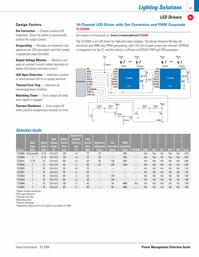
Texas Instruments 2Q 2006 Power Management Selection Guide
Lighting Solutions
LED Drivers
39
Design Factors
Dot Correction — Creates uniform LEDbrightness. Gives the ability to dynamicallycontrol the output current.
Grayscaling — Provides an enhanced colorspectrum per LED equivalent with the numberof grayscale steps available.
Output Voltage Monitor — Monitors volt-ages at constant current output terminals todetect LED failure and short circuit.
LED Open Detection — Indicates a brokenor disconnected LED at an output terminal.
Thermal Error Flag — Indicates anovertemperature condition.
Watchdog Timer — Turns output off whenscan signal is stopped.
Thermal Shutdown — Turns output offwhen junction temperature exceeds its limit.
SIN
VCC V(LED) V(LED)V(LED) V(LED)
SIN SIN
100 kΩOUT0 OUT0
SOUT SOUT
100 nF 100 nF
IREF IREF
OUT15 OUT15
XERR XERR XERR
SCLK SCLK SCLK
XLAT XLAT XLAT
GSCLK GSCLK GSCLK
DCPRG DCPRG DCPRG
BLANK BLANK BLANK
SOUT VPRG
7
VPRG
W_EEPROM
VPRG_D
VPRG_OE
VPRG
V(22V)V(22V)
50 kΩ 50 kΩ
50 kΩ
50 kΩ 50 kΩ
50 kΩ
VCC VCC
TLC5940 TLC5940
IC 0 IC n
Controller
16-Channel LED Driver with Dot Correction and PWM Grayscale
TLC5940
Get samples and datasheets at: www.ti.com/sc/device/TLC5940
The TLC5940 is an LED driver for high-end video displays. The device features 64-step dot correction and 4096-step PWM grayscaling, with 120 mA of peak current per channel. EEPROMis integrated into the IC, and the device is offered in HTSSOP, PDIP and QFN packages.
Selection GuideChannel-to-
Input Output Channel DataData Output Voltage Current Accuracy Transfer Brightness Dot PWMInput Count Range Drive (typ) Rate Adjustment Correction Grayscale
Device (Bits) (Bits) (V) (mA) (%) (MHz) (Steps) (Steps) (Steps) EEPROM OVM1 LOD2 TEF3 WDT4 TSD5 Price*TLC5904 8-bit parallel 8, 16 4.5 to 5.5 120 ±4 15 32 — 256 — Yes Yes No Yes Yes 3.70TLC5905 1 8, 16 4.5 to 5.5 120 ±4 15 32 — 256 — Yes Yes No Yes Yes 2.85TLC5911 7, 10 16 4.5 to 5.5 80 ±4 20 64 128 1024 — No Yes No Yes Yes 4.50TLC5930 1 12 3.0 to 3.6 40 ±1 20 64 256 1024 — Yes Yes Yes No No 2.50TLC5920 1 16 4.5 to 5.5 30 ±6 10 — — — — No No No No No 1.10TLC5921 1 16 4.5 to 5.5 80 ±1 20 — — — — No Yes No No Yes 1.25TLC5922 1 16 3.0 to 5.5 80 ±1 30 — 128 — — No No Yes No No 1.85TLC5923 1 16 3.0 to 5.5 80 ±1 30 — 128 — — No Yes Yes No No 1.90TLC5940 1 16 3.0 to 5.5 120 ±1 30 — 64 4096 Yes No Yes Yes No No 1.90TLC5941 1 16 3.0 to 5.5 80 ±1 30 — 64 4096 — No Yes Yes No No 1.65
1Output voltage monitoring.2LED open detection.3Thermal error flag.4Watchdog timer.5Thermal shutdown.*Suggested resale price in U.S. dollars in quantities of 1,000.

Selection GuideInput Power Dimming and Industrial
Voltage Control Transformer Protection TempDevice (V) Topology Type Control Version Packages Price*Input Voltage = 5 to 11 V (2-Cell Li-Ion Application)UCC3975 3 to 13.5 Flyback Piezo Yes UCC2975 8-pin TSSOP 1.70UCC3976 3 to 13.5 Half-bridge Piezo Yes UCC2976 8-pin TSSOP 1.00UCC3977 3 to 13.5 Push-pull Piezo Yes UCC2977 8-pin TSSOP 1.00TPS68000 8 to 30 Full Bridge Magnetic Yes TPS68000 30-pin TSSOP 2.50Input Voltage = 5 or 12 V (Regulated Supply)UCC3973 4.5 to 25 Royer Magnetic Yes UCC2973 8-pin TSSOP or SOIC 3.00UCC3976 3 to 13.5 Half-bridge Piezo Yes UCC2976 8-pin TSSOP 1.00TPS68000 8 to 30 Full Bridge Magnetic Yes TPS68000 30-pin TSSOP 2.50Input Voltage = 7 to 21 V (3- or 4-Cell Li-Ion Application)UCC3973 4.5 to 25 Royer Magnetic Yes UCC2973 8-pin TSSOP or SOIC 3.00TPS68000 8 to 30 Full Bridge Magnetic Yes TPS68000 30-pin TSSOP 2.50
*Suggested resale price in U.S. dollars in quantities of 1,000.The selection guide is a general reference tool. External components dictate most of the circuit parameters in the circuit; therefore, designs outside of the input voltage/device boundaries in the selection guide can be achieved.
Power Management Selection Guide Texas Instruments 2Q 2006
Lighting Solutions
CCFL Backlight Controllers
40
Resources For a complete list of Resources, visit power.ti.com
Part Number Description Price*Evaluation Modules (EVMs)UCC3973EVM UCC3973 Evaluation Module 50UCC3976-77EVM UCC3976 and UCC3977 Evaluation Module 50TPS68000EVM-161 TPS68000 Single-Lamp Evaluation Module 49TPS68000EVM-166 TPS68000 Multi-Lamp Evaluation Module 49
*Suggested resale price in U.S. dollars.
Tra
nsfo
rme
r O
utp
ut
Po
we
r (W
)
>6
5
4
3
2
13 to 6 V
1-Cell Li-Ion5 to 11 V
2-Cell Li-Ion5 or 12 V
Regulated Supply7 to 21 V
3- to 4-Cell Li-Ion
Input Voltage (Batteries, AC Adapter or Regulated Supply)
Piezo Transformer Control
Magnetic Transformer Control
UCC3975
UCC3977
UCC3975
UCC3976
UCC3977
UCC3976
UCC3972
UCC3973
UCC3974
UCC3972
UCC3973
CCFL Backlight Controllers Family of ProductsDesign Factors
Input Voltage — Backlight power suppliesrun from the battery or a regulated supply. Itis important to know the input voltage avail-able for the backlight supply to select thebest IC and power conversion topology togenerate the output power required to lightthe lamp.
Lamp Characteristics (Output Power) —Common CCFL lamps require 250- to 1000-VAC(2 to 10 mA) for operation. The relationshipbetween the input voltage and output voltagedictates the best IC and power topology.
Power Topology — The parts control thetransformer in different ways. Sometimes theinput/output relationship dictates a certaintopology. Different topologies also have different power conversion efficiencies.
Transformer Type — Piezo for smaller sizeand higher efficiency in some applications.
Control Options — Single or dual lamp control and dimming control.
Features
• Complete power-supply control for CCFL.• Magnetic or piezo transformer control.• Open lamp and transformer protection.
• Burst-dimming control for efficient, widedimming range.
• Four different power topologies:•• Half-bridge •• Flyback•• Royer •• Push-pull

Texas Instruments 2Q 2006 Power Management Selection Guide
Lighting Solutions
Photoflash Capacitor Chargers
41
Design Factors
Transformer — The output voltage of theconverter is set by the turns ratio of the fly-back transformer. The switching frequency isdetermined by the primary inductance of theflyback transformer. These two factors, alongwith the necessary voltage rating of the sec-ondary, are key requirements for selectingthe transformer.
Flash Capacitor — The flash capacitor mustbe rated for photoflash applications. The flashcapacitor usually has low inductance in orderto handle the surge currents during a flash.Capacitors not rated for photoflash applicationswill have a short lifespan in this application.
IGBT — Look for a photoflash rating whenselecting an IGBT used to trigger the flashtube. There are several IGBTs that can with-stand the voltage and surge currents associ-ated with the flash; however, they usuallycome in a very large package since these ratings are for continuous duty. The photoflash-rated IGBT has the same ratings but comes ina small package since the loads are all surgeand not continuous.
Flash Tube — Selection of a flash tube isbased on several system level considerationssuch as desired light spectrum, physical size,mounting method, trigger method, requiredlight power, flash frequency, flash voltage,
T1CTX16-17118
T2422-2304
FL1
D1ES1G
1
1
1
2
TRG3
3
C
E
G
4 4
5
120 µF10 µF
J5
+3.3 VFLASH+5.0 V
CHARGEGND
13579
12345
109876
2.2 µF
0.022 µF
1 MΩ
150 Ω11
D2Green
Charge Complete
Q1SSM25G45EM
TPS65552DGQ
PowerPAD™
+
Integrated Photoflash Charger and IGBT Driver
TPS65552A
Get datasheets at: www.ti.com/sc/device/TPS65552A
The TPS65552A offers a complete solution for charging a photoflash capacitor from a batteryinput, and subsequently discharging the capacitor to the xenon tube. The device includes anintegrated power switch, IGBT driver, and control logic blocks for charge applications.
Selection GuideInput Programmable Power Protection
Voltage VCC Peak Current Switch IGBT Max Over-Voltage ThermalDevice (V) (V) (A) (V) Driver On Time Shutdown Monitor Packaging Price*TPS65552A 1.8 to 12 5 0.95 to 1.8 50 Yes Yes Yes Yes 10-pin MSOP, 16-pin QFN 1.00TPS65560 1.6 to 12 2 to 4 0.9 to 1.8 50 Yes Yes Yes Yes 16-pin QFN 0.85
*Suggested resale price in U.S. dollars in quantities of 1,000. New devices are listed in bold red.
encapsulation material and tube coatings.Customers should determine which lamp toselect for their specific applications.
Trigger Transformer — Selection of thetrigger transformer should be performed once a lamp has been selected. Each lamp
has a specific trigger energy needed to initiatea flash.
Efficiency — The efficiency of the converteris greatly impacted by the recovery time ofthe high-voltage diode. The faster the diode,the better the efficiency.
TPS65552A application circuit.

Power Management Selection Guide Texas Instruments 2Q 2006
42 Battery Management Products
Battery Charge Management
Battery Charge Management Family of Products
2-A Synchronous Switchmode Charger
bq2410x
Get samples, datasheets and EVMs at: www.ti.com/sc/device/bq24100
The bq2410x are 2-A synchronous switchmode charge management devices for 1, 2 and 3 seriesLi-Ion or Li-polymer battery packs.
No. of CellsTopology
Sync/Non-Syncbq2470x
Non-Sync
Switchmode
ControlInterface
SMBusbq2472x1
bq2473x1
> 2 Cells
HardwareControl
Topology
Input StageAC + USB
Linear
Yes
1 Cell
No
FETs
External
Integrated
bq24105
bq24115
Stand-Alone
Host Control
AC/USB
Power Path
Power Path
Yesbq2403x
bq2402xNo
Non-Sync
2 Cells
bq2057C,bq2057
bq2057W/T,bq2400x
FETsExternal
Integrated
Synchronous
Switchmode
bq2420x, bq2401x,bq2406x1
1Product in development.2Can be used in this configuration. Please contact your
Regional Marketing Manager for details.
TerminationControl
bq24100Stand-Alone
TerminationControl
bq2403x2
Topology
Sync/Non-Sync
bq24113
bq24103
Switchmode
FETsExternal
Linear
Integrated bq2470x
Stand-Alone
Host ControlTermination
Control
Li-Ion Charger Selection
Design Factors
Battery Chemistry — Each battery chemistry has unique requirements for itscharge algorithm, which is critical for maxi-mizing its capacity, cycle life and safety.
Control Topology — A simple linear topology works well in applications with low-power (e.g., one- or two-cell Li-Ion) batterypacks that are charged at less than 1 A.
A switchmode topology is ideally suited forlarge (e.g., 3 or 4 series Li-Ion or multipleNiCd/NiMH) battery packs that require chargerates >1 A. The switchmode conversion minimizes heat generation during charging.
A charger using a current-limited topologyrequires a regulated or limited supply andsimply gates the charging current.
TS
ISET1
ISET2
BAT
SNS
STAT1
STAT2
PG
TMR
VOUT
VSSAGND
VIN
VIN
10 µF10 µF
CE
bq2410xVCC
AdapterPresent
Done
Charge
+Pack+
Pack–
Temp
RT1
RT2
VCC
0.1 µF
10 µH
0.1 Ω
7.5 kΩ
7.5 kΩ

Texas Instruments 2Q 2006 Power Management Selection Guide
Battery Management Products
Battery Charge Management
43
Selection GuideCharge PackagingCurrent Primary Charge
Number Control Integrated Internal VIN TerminationDevice of Cells Topology1 Power FET FET Max Method2 Price* CommentsMulti-Chemistry (Li-Ion and NiCd/NiMH)bq2000 Multiple Switching No — — PVD, min current Yes Yes 8 8 8 1.70 Charges NiCd, NiMH, and Li-Ionbq2000T Multiple Switching No — — ∆T/∆t, min current Yes Yes 8 8 8 1.70 Charges NiCd, NiMH, and Li-Ionbq24702/3 Multiple Switching No — 30 V Host controlled No No 283 24 3.10 Dynamic Power ManagementLi-Ion Chemistrybq24200 1 Current-limited Yes 500 mA 16.5 V Min current Yes Yes 8 0.85 Uses current-limited wall supplies, lowers power
dissipation
bq2057/C 1 Linear No — 18 V Min current No Yes 8 8 8 0.95 Low dropout, 4.1/4.2 V regulation, AutoComp™bq2057T/W 2 Linear No — 18 V Min current No Yes 8 8 1.20 Low dropout, 8.2/8.4 V regulation, AutoCompbq24001 1 Linear Yes 1.2 A 13.5 V Min current Yes Yes 20 20 1.20 4.1-V or 4.2-V regulation, bq24007/8 has timer
enable/disable pin
bq24004 2 Linear Yes 1.2 A 13.5 V Min current Yes Yes 20 20 1.60 8.2-V or 8.4-V regulation
bq24010 1 Linear Yes 1.0 A 18 V Min current Yes No 10 1.05 Allows use of unregulated wall supplies with high max VIN
bq24020 1 Linear Yes 1.0 A 7 V Min current Yes Yes 10 1.60 Autonomous USB and AC-adapter supply management
bq24030 1 Linear Yes 1.5 A 18 V Min current Yes Yes 20 2.30 Dynamic Power-Path Management powers the system and charges battery
bq24060 1 Linear Yes 1 A 18 V Min current Yes Yes 10 1.20 Thermal regulation, 6.5-V over-voltage protection
bq24100/8 1 Switching Yes 2.0 A 20 V Min current Yes Yes 20 2.10 Synchronous PWM, different status outputsbq24103/113 1 or 2 Switching Yes 2.0 A 20 V Min current/ Yes Yes 20 2.20 Synchronous PWM
Host controlledbq24105/115 1 to 3 Switching Yes 2.0 A 20 V Min current/ Yes Yes 20 3.50 Synchronous PWM, prog. output voltage
Host controlledbq25010/2 1 Linear Yes 500 mA 7 V Min current Yes No 20 1.90 USB, integrated DC/DC converter, output
adjustable or fixed 1.8 Vbq24720/1 3 or 4 Switching No — 30 V SMBus No Yes 32 4.90 Smart battery charger w/system power selectorbq24730 3 or 4 Switching No — 30 V Host controlled No Yes 40 4.90 Advanced synchronous battery charger with
system power selectorbq2954 Multiple Switching No — — Min current Yes Yes 16 16 2.50 PWM control, low/high-side current senseTPS65010 1 Linear Yes 1.0 A 6 V Min current Yes Yes 48 3.95 Integrated battery and power management5
TPS65800 1 Linear Yes 1.5 A 18 V Min current Yes Yes 56 6.50 Integrated battery and power management5
NiCd/NiMH Chemistrybq2002/C/E/F Multiple Current-limited No — — –∆V, PVD Yes Yes 8 8 1.05 Low-cost nickel charge ICsbq2002D/T Multiple Current-limited No — — ∆T/∆t Yes Yes 8 8 1.05 Different charge timers and status displaybq24400/1 Multiple Switching No — — PVD, ∆T/∆t Yes Yes 8 8 1.55 Simple switching controllerbq2004/E/H Multiple Switching No — — –∆V, PVD, ∆T/∆t Yes Yes 16 16 2.20 Selectable timers and pulse-trickle rates bq2005 Multiple Switching No — — –∆V, ∆T/∆t Yes Yes 20 2.20 Sequential fast charge of two battery packsLead-Acid ChemistryUC3906 Multiple Linear No — 40 V Max V, min I No No 16 16 2.75 Temp-compensated internal referenceUC3909 Multiple Switching No — 40 V Max V, min I No Yes 20 20 3.05 Differential current sense inputbq2031 Multiple Switching No — — Max V, –∆2 V, min I Yes Yes 16 16 2.80 Three user-selectable charge algorithms to
accommodate cyclic and standby applications1Current-limited = gating control of external, current-regulated/limited source. 2PVD = peak voltage detection; ∆T/∆t = rate of temperature rise; New devices are listed in bold red.host controlled = system processor must terminate charging; –∆V = negative voltage change; max V = maximum voltage; min I = minimum current;∆2V = second difference of cell voltage. 3Only bq24703 is available in QFN package. 4STAT = status; TS = temperature sensing; PG = power good; CE = change enable; TTE = timer and termination enable. 5See page 37. *Suggested resale price in U.S. dollars in quantities of 1,000.
Safe
ty Tim
er
Temp
Mon
itor
QFN/
MLP
MSO
P
TSSO
P
SOIC
DIP
EVM
Parameter bq24200 bq24201 bq24202 bq24203 bq24204 bq24205Regulation Voltage (V) 4.2 4.1 4.2 4.1 4.2 4.1Optional Functions4 STAT and TS STAT and TS STAT STAT — —
Parameter bq24001/7 bq24002 bq24003/8Charge Status Configuration Single LED 2 LEDs Single Bicolor LED
Parameter bq24004 bq24005 bq24006Charge Status Configuration Single LED 2 LEDs Single Bicolor LED
Parameter bq24010 bq24012 bq24013 bq24014Optional Functions4 PG and TS PG and CE CE and TTE CE and TS
Parameter bq24020 bq24022 bq24023 bq24024 bq24025 bq24026Optional Functions4 CE and TS PG and CE CE and TTE TTE and TS CE and TS TE and TSFast Charge Timer 5 5 5 5 5 7Taper Timer Yes Yes Yes Yes Yes No
Parameter bq24030 bq24032 bq24035 bq24038Output for AC Input Condition Regulated to 6 V Regulated to 4.4 V Cutoff at 6 V Regulated to 4.4 VCharge Regulation Voltage (V) 4.2 4.2 4.2 4.36
Parameter bq24060 bq24061 bq24065 bq24066Optional Functions4 TS CE TS CECharge Regulation Voltage (V) 4.2 4.2 4.36 4.36

Power Management Selection Guide Texas Instruments 2Q 2006
Battery Management Products
Battery Fuel Gauges
44
99% Accurate Gas Gauge Maximizes Run-Time
bq20z70, bq20z80, bq20z90
Get samples, datasheets, EVMs and app reports at: www.ti.com/sc/device/bq20z80
The dynamic Impedance Track™ gas gauge algorithm in the bq20z80 extends battery usability,allowing use of the full chemical capacity available in a battery pack. Additional featuresinclude instant state-of-charge and real-time impedance learning. Impedance Track also enablesreduction in development and production time. Remaining capacity is reported over the entirelife of the battery pack with better than 99% accuracy. The bq20z80 is ideally suited for batterypacks used in medical and industrial equipment, back-up batteries and laptop computers.
Design Factors
Battery Chemistry — Each battery chemistryhas different operating characteristics, suchas discharge profiles and self-discharge rate.TI gas gauge ICs are developed by chemistryto account for these differences to accuratelydisplay remaining energy in the battery.
Charge/Discharge Relationship — Thecharge and discharge rates dictate the senseresistor value.
Features
TI gas gauges and battery monitors accuratelytrack battery activity to compute the remain-ing battery capacity and system run-time.They feature:• Simple communication protocols.• High-resolution analog-to-digital converters
for accurate charge/discharge measurement.• Integrated CPU on gas gauges to compute
remaining battery capacity and run-time.
bq20z80
I2C Interface
Cell Inputs
Safety Control
32-k Clock
Supply Voltage
Chemical Fuse
Charge/Discharge
Power FETs
2 to 4 Series
Li-Ion Cells
Sense
Resistor
(10 mΩ)
Temp
Sensor
32 kh
Time Base
Ext/Int
Dedicated
Hardware
Communication
OV, UV and Safety
Temp
Sensor
1-Kbyte
Config.
Flash
EPROM
Integrating
ADC
Coulomb
Counting
ADC
Instantaneous
Voltage
bq29400bq29312
LDO
OC and SC
Level
Translator
Second-Level
Over-Voltage
Protection
Pack–
SMBus
Pack +
+
–
+
–
Battery Fuel Gauges Family of Products
bq27000
bq27200
C = D
bq2014H bq2014H
bq2013H
bq2016bq2013H
bq2016
bq2013H
bq2052
bq2050H
bq2084
bq20z70
bq20z80
bq20z90
bq2019
bq2023
bq26200
bq26220
bq2060A
<1
1
2
5
10
>15
D >> C
NiCd NiMH
C = D D >> C C = D
Li-lon
N/A
Primary
Lithium
D >> C
Lead
Acid
Chemistry
Independent
Pa
ck
Ca
pa
cit
y*
(A
h)
C = D N/A
C = D: Charge rate similar to discharge rate.D>>C: Discharge rate much greater than charge rate.N/A: Not Applicable.*Pack capacity ratings provide an approximate range for each gas gauge.

Texas Instruments 2Q 2006 Power Management Selection Guide
Battery Management Products
Battery Fuel Gauges
45
Resources For a complete list of Resources, visit power.ti.com
Selection GuideApprox. Battery Capacity Min Max Number of Communication Safety
Device (mAh) Series Cell LEDs Protocol Other Features Enhancement Packages Price*NiCd, NiMH Chemistrybq2013H 2000 to 15000 TBD 5 Single wire (HDQ) Programmable offset error compensation No 16-pin SOIC 3.70bq2014H 500 to 6000 TBD 5 Single wire (HDQ) Register compatible with bq2050H No 16-pin SOIC 3.70bq2016 1000 to 4500 TBD 5 Single wire (HDQ) Automatic offset calibration No 28-pin SSOP 3.00Lithium-Ion, Lithium-Polymer Chemistrybq2050H 500 to 6000 TBD 5 Single wire (HDQ) Register compatible with bq2014H Yes 16-pin SOIC 3.70bq2084 800 to 10000 TBD 3, 4 or 5 2 wire (SMBus) SBS 1.1 works with bq29312 based on bq2083; includes Yes 38-pin TSSOP 4.00
bq2050 dataset via single wire interfacebq20z70 800 to 10000 2 to 4 No LED HDQ and SMBus Self learning, dynamic fuel gauge algorithm with bq29330 Yes 20-pin TSSOP 2.90bq20z80 800 to 10000 2 to 4 3, 4 or 5 2 wire (SMBus) SBS 1.1 with Impedance Track™ technology Yes 38-pin TSSOP 4.60bq20z90 800 to 10000 2 to 4 3, 4 or 5 2 wire (SMBus) Self learning, dynamic fuel gauge algorithm with bq29330 Yes 30-pin TSSOP 3.30bq27x00 300 to 6000 1 (more w/external — HDQ or I2C Single- and dual-cell fuel gauge with runtime to empty No 10-pin DRK 2.50
components) and charge time to full based on measured currentPrimary Lithium Chemistrybq2052 1000 to 12000 1 2, 4 or 5 Single wire (HDQ) Automatic discharge compensation No 16-pin SOIC 4.00Lead Acid Chemistrybq2013H 2000 to 15000 10 5 Single wire (HDQ) Programmable offset error compensation No 16-pin SOIC 3.70Multi-Chemistrybq2060A 800 to 10000 0.1 4 or 5 SMBus or HDQ16 SBS 1.1 extended cold temp cell modeling and high Yes 28-pin SSOP 3.90
temp safety enhancement, improved bq2060Battery Monitors bq2019 >20000 1 — Single wire (HDQ) 64-bit ID ROM and 1 program output non-volatile memory — 8-pin TSSOP 1.95bq2023 >20000 0.25 — Single wire (SDQ) 64-bit ID ROM and 1 program output automatic offset — 8-pin TSSOP 2.00
error calibrationbq26200 >20000 0.25 — Single wire (HDQ) High-performance battery, coulomb counter — 8-pin TSSOP 2.00bq26220 >20000 0.25 — Single wire (HDQ) 64-bit ID ROM and 1 program output on-chip voltage — 8-pin TSSOP 2.05
measurement*Suggested resale price in U.S. dollars in quantities of 1,000. New devices are listed in bold red.
Part Number Description Price*Evaluation Modules (EVMs)bq2013HEVM-001 bq2013H Evaluation Kit for NiCd, 16.8 V 99bq2014HEVM-001 bq2014H Evaluation Kit for NiMH, 10.8 V 99bq2050HEVM-002 bq2050H Evaluation Kit for Li-lon, 10.8 V 99bq2060AEVM-001 bq2060A Evaluation Kit for Li-lon 99bq2060AEVM-002 bq2060A Evaluation Kit for NiMH 99bq2084EVM-001 bq2084 Evaluation Kit also features the bq29312 and bq29400 99bq20z70EVM-001 bq20z70 Evaluation kit also features the bq29330 and bq29412 99bq20z80EVM-001 bq20z80 Evaluation kit also features the bq29312 and bq29400 99bq20z90EVM-001 bq20z90 Evaluation kit also features the bq29330 and bq29412 99bq26220EVM-001 bq26220 Evaluation Kit for Multi-Chemistry, 2.6 to 4.5 V 99bq27000EVM bq27000 Evaluation Module 99bq27200EVM bq27200 Evaluation Module 99
*Suggested resale price in U.S. dollars.
Literature Number DescriptionApplication NotesSLUA324 Getting Started with the bq20z80 and EVMSLUA325 Feature Set Comparison Between bq2084 and bq20z80SLVA100 Advanced Gas Gauge Host Firmware Guide for the TI Battery Monitor ICsSLVA101 HDQ Communication Basics for TI’s Battery Monitor ICsSLVA102 Gas Gauging Basics Using TI’s Battery Monitor ICsSLVA114 Advanced Gas Gauge Host Firmware Flow Chart for the TI Battery Monitor ICsSLVA148 bq2083, bq2084, and bq2085 Calibration ProcedureSLVA149 Configuring the bq2060 and bq2060A EEPROMsSLVA150 Avoiding Clock Jitter with the bq2085 Advanced Gas GaugeSLVA151 Using Advance Features of the bq2060A Gas-Gauge ICSLUA338 Configuring the bq27000/200 for Gas Gauge ApplicationsSLUA359 Using SHA-1 in bq20zxx Family of Gas GaugesSLUA364 Theory and Implementation of Impedance Track Battery Fuel-Gauging
Algorithm

Power Management Selection Guide Texas Instruments 2Q 2006
Battery Management Products
Lithium-Ion Protection
46
Selection GuideNumber Charge/Discharge Threshold Shutdownof Series Current Voltage Current Available
Device Cells (A) (VOV) (µA) Other Features Packages Price*bq29312A 2, 3 or 4 External FET bq20841, bq20z801 1 Integrated LDO, works directly with bq2084 and bq20z80 gas gauge 24-pin TSSOP 1.30bq29330 2, 3 or 4 External FET bq20z901 1 Integrated LDO, works directly with bq20z90 gas gauge 20-pin TSSOP 1.45bq29412 2, 3 or 4 — 4.35 1 Second level overvoltage safety fuse blower for battery packs 8-pin TSSOP 0.42UCC3911-x 2 3 4.2/4.25/4.3/4.35 3.5 User controllable delay for tripping short circuit current protection 16-pin SOIC 2.15
1Controlled by bq208x, bq20z8x or bq20z9x gas gauge.See individual datasheets for full details.
*Suggested resale price in U.S. dollars in quantities of 1,000.
Lithium-Ion Protection Family of ProductsDesign Factors
Number of Series Cells — A battery isconstructed from a string of series and parallelcells. Each series cell, or group of paralleledcells, requires protection from overcharge,overdischarge and short-circuit conditions.
Threshold Voltage — Li-Ion and Li-polymercells are produced by many manufacturers.Some manufacturers’ technologies create cellsof different maximum stress voltages, other-wise known as the “over-voltage threshold.”This data is available from the cell supplier.
Threshold Tolerance — The over-voltagethreshold has a tolerance that needs to beaccounted for in the design for safety reasons.
Shutdown Current — In battery pack appli-cations, constant current draw needs to bevery low to preserve battery life.
Charge/Discharge Current — The passelement associated with each protection IC israted for maximum current whether it be aninternal or external FET.
Features
• BiCMOS process results in low currentconsumption.
• Different over-voltage thresholds allow onedesign to work with several cell suppliers.
• Sleep current consumption of less than 3.5 µA enables extended battery life.
43
Note: Current rating limit above 3 A is a function of the external MOSFETs used.
Char
ge/D
isch
arge
Cur
rent
(A)
bq29312Abq29330bq2941x
bq29312Abq29330bq2941xUCC3911
2Number of Series Cells
4
3
2
1
bq29312Abq29330bq2941x
• 50 mV precision internally trimmed thresh-olds maximize safety.
• Short-circuit protection eliminates theneed for an external fuse.
Resources For a complete list of Resources, visit power.ti.com
Part Number Description Price*Evaluation Modules (EVMs)bq2084EVM-001 bq2084 Evaluation Kit also features the bq29312 and bq29400 99bq20z70EVM-001 bq20z70 Evaluation Kit also features the bq29330 and bq29412 99bq20z80EVM-001 bq20z80 Evaluation Kit also features the bq29312 and bq29400 99bq20z90EVM-001 bq20z90 Evaluation Kit also features the bq29330 and bq29412 99
*Suggested resale price in U.S. dollars.

Texas Instruments 2Q 2006 Power Management Selection Guide
Battery Management Products
Authentication for Batteries and Peripherals
47
Selection GuideDevice Interface Pins Security Temp (°C) Price*bq2022 SDQ 3 ID number –40 to 85 1.25bq26150 HDQ 5 CRC algorithm –20 to 70 1.25bq26100 SDQ 5 SHA-1 encryption –20 to 70 1.30
*Suggested resale price in U.S. dollars in quantities of 1,000.
Design Factors
Original equipment manufacturers specifyproducts to achieve required performanceand safety goals. Authentication ensuresthat connected devices fulfill the establishedrequirements and are safe for the consumer.
Features
TI authentication devices use three levels of security.
• Identification Number — The host con-troller can request an identification numberthat is answered with a fixed response.
• CRC Algorithm — The host processorsends a random challenge and reads theresponse that is an encoding of the chal-lenge and a shared secret key through aCRC with a shared secret polynomial.
• SHA-1 Encryption — The host processorsends a random challenge and reads theresponse that is an encoding of the chal-lenge and a shared secret key through theSHA-1 cryptographic primitive.
Pack+
+–
Pack–
HDQInterface
Authenticationbq26150
Gas Gaugebq27000
Protector
Pullup Pullup
Single-Cell Battery Pack with Gas Gauge and Authentication
Design Factors
IEEE 802.3af Power-over-Ethernet —With approval of the IEEE 802.3af Power-over-Ethernet (PoE) standard, all data terminalequipment (DTE) now has the option to receivepower over existing CAT-5 and CAT-3 cablingthat is used for data transmission. The IEEE802.3af standard defines the requirementsassociated with providing and receiving PoEcables. The Power Sourcing Equipment (PSE)
provides the power on the cable and thePowered Device (PD) receives the power. Aspart of the IEEE 802.3af standard, the inter-face between the PSE and the PD is definedas it relates to the detection and classifica-tion protocol.
Power Sourcing Equipment (PSE) — TheTPS2384 Quad PSE Manager independentlymanages power for up to four Ethernet ports,reporting system status over a standard I2C
serial interface. The TPS2384 is the most inte-grated PSE solution on the market today withintegrated power FETs and sense resistors.
Powered Devices (PDs) — Acting as aninterface between the PSE and PD, theTPS23750 performs all detection, classifica-tion, inrush current limiting and switch FETcontrol that is necessary for compliance withthe IEEE 802.3af standard.
Hot Swap and Power Distribution
Power-over-Ethernet

Power Management Selection Guide Texas Instruments 2Q 2006
Hot Swap and Power Distribution
Power-over-Ethernet
48
C TM
R
VBIAS
TMRFREQ GATE
COM
AUX
RSP
COMP
VDD
58 V
0.1
µF
R DET
R CLA
SS
VDD
VSS
CLASSDET
Low VoltageIsolatedOutput
C BIA
S
VBIAS
From EthernetTransformers
From SparePairs or
Transformers
TPS23750
R FRE
Q FeedbackControl
Spare Pair
Spare Pair
Signal Pair
Signal Pair+48 V
Return
+48 V
RJ45
Switch/Hub
4 4
1 1
3 3
7 7
5 5
2 2
6 6
8 8
RJ45
Rx
Tx
Up to 100 mof CAT 5
PowerStage
TPS23750Power
Device andDC/DC
ControllerNRet
P Tx
Rx
TPS2384OptionalMSP430Micro-
controllerRCLASS
RDET
VREG
Power-over-Ethernet (PoE) Application Diagram
The new TPS2384 and TPS2375 are IEEE 802.3afcompliant power management ICs designed formanaging the connection between PowerSourcing Equipment (PSE) and Powered Devices(PDs) over Ethernet cables. www.ti.com/poe
IEEE 802.3af Integrated Primary-Side PD Controller
TPS23750
Selection GuideAbs Operating Full Inrush Current Auto RetryMax Temp Current Limit or Latch Off DC/DC
Device Description Detection Classification VIN (V) (°C) Limiting (mA) in Fault UVLO Interface Package Price*Power-over-Ethernet (PoE) Powered Device (PD) Interface SwitchesTPS2375 Powered Device Controller 4 Yes, Class 0-4 100 –40 to 85 Programmable 450 Latch Off 802.3af (30.6/39.4 V) PG SOIC-8, TSSOP-8 1.25TPS2375-1 Powered Device Controller 4 Yes, Class 0-4 100 –40 to 85 Programmable 450 Auto Retry 802.3af (30.6/39.4 V) PG TSSOP-8 1.25TPS2376 Powered Device Controller 4 Yes, Class 0-4 100 –40 to 85 Programmable 450 Latch Off Adjustable PG SOIC-8, TSSOP-8 1.25TPS2377 Powered Device Controller 4 Yes, Class 0-4 100 –40 to 85 Programmable 450 Latch Off Legacy (30.5/35.0 V) PG SOIC-8, TSSOP-8 1.25TPS2377-1 Powered Device Controller 4 Yes, Class 0-4 100 –40 to 85 Programmable 450 Auto Retry Legacy (30.5/35.0 V) PG SOIC-8 1.25TPS23750 Integrated PD with PWM Controller 4 Yes, Class 0-4 100 –40 to 85 Fixed 450 Auto Retry 802.3af (30.6/39.4 V) N/A TSSOP-20 1.75TPS23770 Integrated PD with PWM Controller 4 Yes, Class 0-4 100 –40 to 85 Fixed 450 Auto Retry Legacy (30.5/35.0 V) N/A TSSOP-20 1.75PTB48540 5 V, 10-W PoE Power Module 4 Yes, Class 0-4 100 –40 to 85 Fixed 450 Latch Off 802.3af (30.6/39.4 V) N/A 13-DIP Module 26.00
Get samples, datasheets, EVMs and app reportsat: www.ti.com/sc/device/TPS23750
The TPS23750 is a highly integrated devicethat combines the functionality of theTPS2375 with a primary-side DC/DC PWMcontroller. Designers can create a completefront-end solution for PoE-powered deviceswith minimal external components.
Abs Max OperatingVIN Temp IEEE
Device Applications Channels (V) (°C) Compliant Interface Disconnect Measurements Power FET Package Price*PoE Power Sourcing Equipment (PSE) ControllersTPS2383B Routers, switches, hubs, mid-spans 8 80 –40 to 85 Yes I2C Both AC and DC Current, voltage and capacitance External 64-pin LQFP 7.35TPS2384 Routers, switches, SOHO hubs, 4 80 –40 to 125 Yes I2C Both AC and DC Current, voltage, capacitance Internal 64-pin LQFP 3.90
mid-spans and temperature*Suggested resale price in U.S. dollars in quantities of 1,000. New devices are listed in bold red.For additional resources on PoE, including reference designs and evaluation modules, please see power.ti.com/poe

Texas Instruments 2Q 2006 Power Management Selection Guide
Hot Swap and Power Distribution
Hot Swap Power Management
49
UCC3915
UCC3912TPS202x
15
10
5
20
0
40
60
100
80
1 2 3 4(A)IOUT
V IN
(V)
V IN
UCC39161 UCC3916
UCC3918
(V)
Hot Swap Power Switch ICs (Integrated Power FET) Hot Swap Power Controller ICs (External Power FET)
–20
–40
–60
–100
–80
Full FeaturedHot SwapTPS2392TPS2393
RedundantOR-ing
Hot SwapTPS2350
Simple Hot SwapTPS2390TPS2391TPS2398TPS2399
PositiveHV
Hot SwapTPS2490TPS2491
TPS2300/01TPS2310/11TPS2320/21TPS2330/31
Features
Hot Swap Power Management Family of Products www.ti.com/atcapower
What is ATCA?
Advanced Telecommunications ComputingArchitecture (ATCA) is a new open standardfor carrier grade communications equipment.The requirements for ATCA are defined inPICMG 3.0 specifications and includemechanical, shelf management, power distri-bution, data transport, thermal, regulatoryguidelines and data/power connectors.
The ATCA PICMG 3.0 open standard has specific requirements for delivering dual –48-V power feeds to individual boardswhich may consume up to 200 W each.
ATCA Power Requirements
ATCA contains many requirements which aretypical of a modern, hot swapped power system. It also contains some requirementswhich are particular to ATCA. Among themost challenging are the transient ride-through specifications which mandate thatboards continue operation through a 5-msshort on both inputs. Boards must also continue operation through a 10-µs, 100-Vtransient at the input.
12-V/3.3-VAMC
Hot Swap
TPS2490/1TPS2330/1
POLA™Non-Isolated
Modules
PTH12060PTH12050PTH12000
TPS40K™DC/DC
Controllers
TPS40007/9TPS5124
Redundant–48-V
Supplies
AdvancedMezzanineCard
3.3 V
12-V Intermediate Bus
1.8 V
1.5 V
2.5 V
SVS
TPS3809TPS3123TPS370x
SWIFT™DC/DC
Converters
TPS54615TPS54315
–36-V to –72-VIsolated
DC/DC Modules
PT4660PT4560PT4480
VRTN_A
VRTN_B
–48V_A
–48V_B
Hot Swapand
Inrush Limiting
TPS2393TPS2350
EMIFilter
LDOs
TPS757xxTPS758xxTPS759xx
ATCA Power Solutions
• Dual, redundant –48 V from one or twopower plants
• UVLO between –32 V and –36 V• Inrush current limiting• Maximum 200 W per board• Fuses on both –48-V feeds and both
returns• Isolation between A and B feeds/returns• 5-ms holdup with input short to ground• 60-W maximum for mezzanine cards• 100-V transient capability

Power Management Selection Guide Texas Instruments 2Q 2006
Hot Swap and Power Distribution
Hot Swap Power Management
50
Resources For a complete list of Resources, visit power.ti.com
Part Number Description Price*Evaluation Modules (EVMs) and ToolsTPS2375EVM Power-over-Ethernet Powered Device Controller Evaluation Module 49TPS2384EVM Power-over-Ethernet Power Sourcing Equipment Controller Evaluation Module 149
*Suggested resale price in U.S. dollars. New devices are listed in bold red.
Literature Number Part Number DescriptionApplication NotesSLUA331 UC2572 ATCA High Voltage Energy Storage Technique to Reduce Size and Cost of Transient Holdup CircuitrySLVR248 TPS2490/TPS2231 ATCA AMC Hot Swap Reference DesignSLUU206 TPS2375/TPS2376/TPS2377 Estimating Available Application Power for Power-over-Ethernet ApplicationsSLUA318 TPS2393 –48-V ATCA Module Hot Swap Using the TPS2393SLVA158 TPS2490/TPS2491 Hot Swap Design Using the TPS2490/91 and MOSFET Transient Thermal ResponseSLUA313 TPS2392/TPS2393 Protecting the TPS2392/TPS2393 Insertion Detection Inputs in Fused ApplicationsSLVA163 TPS2400 Overvoltage Protector for High Voltage LoadsSLVS368 — Comparing Performance of Current Ramp and Voltage Ramp Hot Swap Controller ICsSLUA187 UCC3912/15 Programmable Hot Swap Power ManagerSLUA198 UCC3912 Electronic Circuit Breaker ICsSLUA131 UCC3912 Integrated Electronic Circuit Breaker IC for Hot SwapSLUA211 UCC3918 Hot Swap Power Manager Evaluation Board and SchematicSLUA283 TPS239x A Universal Telecommunications Hot Swap Device FamilySLUA302 TPS2398/99, TPS2390/91 A Comparison of Telecom Hot Swap Managers TPS2398/99 vs TPS2390/91SLUA291 TPS239x –48-V Hot Swap Performance Competitive ComparisonSLUA306 TPS2398/99 Using the TPS2398/99 Hot Swap Controller with Power Trends PT4485SLUA297 TPS2350 Boosting Supply Select Hysteresis on the TPS2350
Hot Swap Controllers (External FET) Selection Guide
VIN Range Enable/ PowerDevice Target Applications Channels (V) Shutdown Ramp Limiting Package Price*TPS2300/01 CompactPCI, General 2 3 to 13/3 to 5.5 1L/1H Voltage No 20-pin TSSOP 1.60TPS2310/11 CompactPCI, General 2 3 to 13/3 to 5.5 1L/1H Voltage No 20-pin TSSOP 1.60TPS2320/21 CompactPCI, General 2 3 to 13/3 to 5.5 1L/1H Voltage No 16-pin SOIC/TSSOP 1.35TPS2330/31 CompactPCI, General 1 3 to 13 1L/1H Voltage No 14-pin SOIC/TSSOP 1.25TPS2342 CompactPCI, PCI-X, PC-X2.0 12 3.3, Vaux, VIO, 5, +12, –12 1L Voltage No 80-pin HTQFP 7.00TPS2343 CompactPCI, PCI-X, PC-X2.0 12 3.3, Vaux, VIO, 5, +12, –12 1L Voltage No 80-pin SSOP 7.50TPS2350 Replace –48-V OR-ing Diodes 2 –12 to –80 1H Current No 14-pin SOIC/TSSOP 1.90TPS2363 PCI Express 6 3.3 Vaux, 3.3, +12 1L Voltage No 48-pin QFP 2.50TPS2390 Simple –48-V Telecom 1 –36 to –80 1H Current No 8-pin MSOP 1.00TPS2391 Simple –48-V Telecom 1 –36 to –80 1H Current No 8-pin MSOP 1.00TPS2392 Full Featured –48-V Telecom 1 –20 to –80 1H Current No 14-pin TSSOP 1.80TPS2393 Full Featured –48-V Telecom 1 –20 to –80 1H Current No 14-pin TSSOP, 1.80
44-pin TSSOPTPS2393A Full Featured –48-V Telecom 1 –20 to –80 1H Current No 14-pin TSSOP 1.80TPS2398 Simple –48-V Telecom with PG 1 –36 to –80 1H Current No 8-pin MSOP 1.25TPS2399 Simple –48-V Telecom with PG 1 –36 to –80 1H Current No 8-pin MSOP 1.25TPS2400 Overvoltage/Undervoltage Protection IC 1 2 to 100 1H — No SOT-23-5 0.80TPS2490 Servers, Basestations, +48 V 1 9 to 80 1H Current Yes 10-pin MSOP 1.70TPS2491 Servers, Basestations, +48 V 1 9 to 80 1H Current Yes 10-pin MSOP 1.70
*Suggested resale price in U.S. dollars in quantities of 1,000.
UV OV Faul
tPG La
tch
Auto
Ret
ry
Hot Swap Switches (Integrated FET) Selection GuideCurrent rDS(on)
VIN Limit per FET Enable/ PackageDevice Target Applications Channels (V) (A) (typ) (mΩ) Shutdown Ramp Options Price*UCC3915 Enclosure Management, General 1 7 to 15 0 to 3 150 1L Current SOIC-16, TSSOP-24 2.55UCC3912 RAID, SCSI, General 1 3 to 8 0 to 3 150 1L Current SOIC-16, TSSOP-24 2.30UCC3918 RAID, SCSI, General 1 3 to 6 0 to 4 75 1L Current SOIC-16, TSSOP-24 2.35UCC3916 SCSI, General 1 4 to 6 1.65 220 1L Current SOIC-8 1.70
*Suggested resale price in U.S. dollars in quantities of 1,000.

PCMCIA/CardBus Power Switch Matrix ICsCurrent Limit (min) (A)
0.3 0.7 1.0 2.53.3 V, 5 V, 12 V, VPPDual — — TPS2224A, TPS2226A, TPS2204A, TPS2206A, TPS2205, —Single TPS2212 — TPS2204A, TPS2210A, TPS2211A, TPS2220A, TPS2220B TPS2231No 12 VDual — — TPS2223A TPS2236Single — TPS2044B/54B1 — —No VPPDual — TPS2044B/54B1 — —
1UL products.
Texas Instruments 2Q 2006 Power Management Selection Guide
Hot Swap and Power Distribution
PCMCIA and USB Devices
51
PCMCIA Devices Family of ProductsDesign Factors
PCMCIA/CardBus Power SwitchesStandard PC cards require that VCC be switchedbetween ground, 3.3 V and 5 V, while VPP isswitched between ground, 3.3 V, 5 V and 12 V.CardBay sockets have the standard require-ments for VCC, but require ground, 3.3 V and5 V to VPP, and ground, 1.8 V or 3.3 V to VCORE.Other PC card applications may simply notneed 12 V or VPP while still having the stan-dard requirements for VCC. Therefore, considerthe voltage requirements of the applicationwhen selecting a PCMCIA power switch.
USB High-Power Peripheral SwitchWith Dual Current Limit + LDOTPS2140/41/50/51 — The TPS2140/41/50/51 target high-power USB peripheralssuch as ADSL modems. The devices contain apower switch and an LDO. The dual-current-limiting switch allows the use of high-valuecapacitance to stabilize the voltage from theUSB bus.
Dual Power Switch + LDO for USB Bus-Powered Peripherals and HubsTPS2148/49 — TPS2148 is a completepower management solution for USB bus-powered peripherals such as zip drives, whileTPS2149 is for USB bus-powered hubs, suchas keyboards with integrated hubs.TPS2148/9 each combine a 3.3-V LDO anddual power switch in a single MSOP. TheTPS2148 switch configuration allows powerand board capacitance segmentation to meetUSB system current requirements. TheTPS2149 switches manage two independentor four ganged USB ports.
4-Port USB Hub Power ControllersTPS207x — The TPS207x family providesthe complete power solution for 4-port self-powered, bus-powered or hybrid USB hubs byincorporating current-limited switches forfour ports, a 3.3-V 100-mA LDO, a 5-V LDOcontroller for self power (TPS2070, TPS2071)and a DP0 line control to signal an attach tothe host.
USB Devices Family of Products
USB Power Distribution SwitchesCurrent Limit (min) (A)
0.22 0.3 0.66 0.7 1.1 1.5 1.65 2.2Quad — TPS2048A/58A1 — TPS2044B/54B1 — — — —Triple — TPS2047B/57A1 — TPS2043B/53B1 TPS2063/671 — — —Dual — TPS2046B/56A — TPS2042B/52B1 TPS2062/66 TPS2060/641 — —Single TPS2020/30 TPS2045A/55A1 TPS2021/31 TPS2041B/51B1 TPS2022/32 — TPS2023/33 TPS2024/34
TPS2061/651
1UL products.
4-Port USB Hub Power Controllers5-V LDO Bus Power
Device Controller Mode Indicator Pins PackageTPS2070 Yes Active Low 32 HTSSOPTPS2071 Yes Active High 32 HTSSOPTPS2074 No Active Low 24 SSOPTPS2075 No Active High 24 SSOP
VIN/SW1
LDO_EN
EN1
SW2
EN2
GND
LDO_OUT
LDO_ADJ
OC1
OUT1
OUT2
OC2
TPS2145/55TSSOP-14
LDO VIN/SW1
EN1
SW2
EN2
GND
LDO_OUT
OC1
OUT1
OUT2
OC2
TPS2147/57MSOP-10
LDO VIN/SW1
LDO_EN
EN1
EN2
GND
LDO_OUT
OUT1
OUT2
TPS2148/58MSOP-8
LDO VIN
EN1
EN2
GND
LDO_OUT
OUT1
OC
OUT2
TPS2149/59MSOP-8
LDO
Dual Power Switch + LDO for USB Bus-Powered Peripherals and Hubs
USB High-Power Peripheral Bus Switch + LDODevice Switch Voltage DescriptionTPS2140 3.3 V 3.3-V, 500-mA switch with active-low enable, 250-mA LDOTPS2141 5.0 V 5.0-V, 500-mA switch with active-low enable, 250-mA LDOTPS2150 3.3 V 3.3-V, 500-mA switch with active-high enable, 250-mA LDOTPS2151 5.0 V 5.0-V, 500-mA switch with active-high enable, 250-mA LDO
DualThreshold
ILIMIT
LDO_IN
LDO_EN
LDO_OUTADJLDO_PG
SW_OUT
SW_PG
TPS2140/41/50/51TSSOP-14
LDO
SW_IN
SW_EN
GND

Power Management Selection Guide Texas Instruments 2Q 2006
Hot Swap and Power Distribution
PCMCIA and USB Devices
52
Design Factors (Continued)
Ease of Use — USB allows simplifiedinstallation and improved performance forperipheral devices by eliminating the need torepeatedly load new drivers and establishindividual settings. USB combines a multitudeof existing interfaces into a single easy-to-useconnector, greatly reducing system complexityand offering manufacturers the ability todevelop highly integrated products.
Power Distribution SwitchesTPS204xB/5xB — The TPS204xB/5xB families of 80-mΩ current-limiting powerswitches meet all the USB power managementrequirements for controlling downstreamports, and include additional features toimprove the design reliability. For example,when an over-current condition exists, thedevice intelligently shuts down only the portthat sees the fault.
TPS202x/3x/6x — The TPS202x/3x/6x families of low on-resistance current-limitingpower switches allow ganging of multipleports to a single switch, as described inApplication Note SLVA049. Though gangingcan be cost effective, all ports are affectedby a fault.
For detailed information regarding USB solutions, visit:
www.ti.com/sc/usbsolutions
Selection GuideNumber 3.3-V rDS(on) 5.0-V rDS(on) IOS
Device Interface of Ports (typ) (mΩ) (typ) (mΩ) (min) (A) Predecessor Price*PCMCIA/CardBus Switch Matrix ICs TPS2210A 3-line Serial 1 85 95 1 — 0.85TPS2204A 3-line Serial 2 85 95 1 TPS2214/14A 1.95TPS2220B 3-line Serial 1 85 95 1 TPS2220A 0.85TPS2223A 3-line Serial 2 85 95 1 — 1.80TPS2224A 3-line Serial 2 85 95 1 TPS2214/14A 1.95TPS2226A 3-line Serial 2 85 95 1 TPS2206, TPS2216/16A 2.10TPS2206A 3-line Serial 2 85 95 1 TPS2206, TPS2216/16A 2.10TPS2205 8-line Parallel 2 70 100 1 TPS2201 2.90TPS2211A 4-line Parallel 1 70 57 1 TPS2211 0.75TPS2212 4-line Parallel 1 160 160 0.3 — 1.45TPS2231 4-line Parallel 1 68 — 2.5 — 1.00TPS2044B or 54B Parallel 1 or 2 80 80 0.7 TPS2044/44A, TPS2054/54A 1.00TPS2221 Interface Parallel 1 72 97 1 — 1.85TPS2228 Interface Serial 2 72 97 1 — 3.10
*Suggested resale price in U.S. dollars in quantities of 1,000. New devices are listed in bold red.

Texas Instruments 2Q 2006 Power Management Selection Guide
Hot Swap and Power Distribution
PCMCIA and USB Devices
53
Selection Guide (Continued)Number IOS rDS(on) VIN Range Supply Current OC Logic OT Logic
Device of FETs (min) (A) (mΩ) (V) (µA) Output Output Enable Predecessor Price*USB Power Distribution Switches TPS2020/30 1 0.22 33 2.7 to 5.5 73 Yes Yes L/H — 1.05TPS2021/31 1 0.66 33 2.7 to 5.5 73 Yes Yes L/H TPS2014 1.05TPS2022/32 1 1.1 33 2.7 to 5.5 73 Yes Yes L/H TPS2015 1.05TPS2023/33 1 1.65 33 2.7 to 5.5 73 Yes Yes L/H — 1.05TPS2024/34 1 2.2 33 2.7 to 5.5 73 Yes Yes L/H — 1.05TPS2041B/51B 1 0.7 70 2.7 to 5.5 40 Each Yes L/H TPS2041/51/41A/51A 0.50TPS2042B/52B 2 0.7 70 2.7 to 5.5 53 Each Yes L/H TPS2042/52/42A/52A 0.70TPS2043B/53B 3 0.7 70 2.7 to 5.5 65 Each Yes L/H TPS2043/53/43A/53A 0.90TPS2044B/54B 4 0.7 70 2.7 to 5.5 75 Each Yes L/H TPS2044/54/44A/54A 1.00TPS2045A/55A 1 0.3 80 2.7 to 5.5 80 Each Yes L/H TPS2045/55 0.60TPS2046B/56A 2 0.3 80 2.7 to 5.5 80 Each Yes L/H TPS2046/46A/56 0.65TPS2047B/57A 3 0.3 80 2.7 to 5.5 160 Each Yes L/H TPS2047/47A/57 0.90TPS2048A/58A 4 0.3 80 2.7 to 5.5 160 Each Yes L/H TPS2048/58 1.20TPS2060/4 2 1.5 70 2.7 to 5.5 50 Each Yes L/H — 1.20TPS2061/5 1 1.1 70 2.7 to 5.5 43 Each Yes L/H — 0.60TPS2062/6 2 1.1 70 2.7 to 5.5 50 Each Yes L/H — 0.75TPS2063/7 3 1.1 70 2.7 to 5.5 65 Each Yes L/H — 0.90
Bus Powered Self PoweredNumber Bus Power VIN rDS(on) Current rDS(on) Current LDO
of Switch Indicator (min) (max) per FET Limit per FET Limit ControllerDevice Application FETs Enable (BPMODE) (V) ( V) (typ) (mΩ) (min) (A) (typ) (mΩ) (min) (A) (A) LDO Price*USB Power Controllers TPS2070 USB 4-port hub 8 L 1L 4.5 5.5 560 0.12 107 0.6 5 V, 3 A 3.3 V, 100 mA 2.55TPS2071 USB 4-port hub 8 L 1H 4.5 5.5 560 0.12 107 0.6 5 V, 3 A 3.3 V, 100 mA 2.55TPS2074 USB 4-port hub 8 L 1L 4.5 5.5 500 0.12 100 0.6 — 3.3 V, 100 mA 2.55TPS2075 USB 4-port hub 8 L 1H 4.5 5.5 500 0.12 100 0.6 — 3.3 V, 100 mA 2.55TPS2140 USB peripheral 1 L — 2.7 5.5 70 0.1 and 1.2 — — — Adj. 0.9 to 3.3 V, 250 mA 1.10TPS2141 USB peripheral 1 L — 4 5.5 70 0.1 and 1.2 — — — Adj. 0.9 to 3.3 V, 250 mA 1.10TPS2150 USB peripheral 1 H — 2.7 5.5 70 0.1 and 1.2 — — — Adj. 0.9 to 3.3 V, 250 mA 1.10TPS2151 USB peripheral 1 H — 4 5.5 70 0.1 and 1.2 — — — Adj. 0.9 to 3.3 V, 250 mA 1.10TPS2145 DSP, PDA 2 L — 2.9 5.5 340 0.2 — — — 3.3 V, 200 mA 1.15TPS2147 DSP, PDA 2 L — 2.9 5.5 340 0.2 — — — 3.3 V, 200 mA 1.10TPS2148 USB peripheral 2 L — 2.9 5.5 340 0.2 — — — 3.3 V, 200 mA 0.99TPS2149 USB 2-port hub 2 L — 2.9 5.5 340 0.2 — — — 3.3 V, 200 mA 0.95TPS2155 DSP, PDA 2 H — 2.9 5.5 340 0.2 — — — 3.3 V, 200 mA 1.15TPS2157 DSP, PDA 2 H — 2.9 5.5 340 0.2 — — — 3.3 V, 200 mA 1.10TPS2158 USB peripheral 2 H — 2.9 5.5 340 0.2 — — — 3.3 V, 200 mA 0.99TPS2159 USB 2-port hub 2 H — 2.9 5.5 340 0.2 — — — 3.3 V, 200 mA 0.95
*Suggested resale price in U.S. dollars in quantities of 1,000.

Power Management Selection Guide Texas Instruments 2Q 2006
Hot Swap and Power Distribution
Power Multiplexers and Current-Limiting Switches
54
Design Factors
Power MUX ICsPower MUX ICs are designed to transitionfrom a main power supply to an auxiliarysource when the main supply shuts down(e.g., switching from battery operation to awall adapter).
Current-Limiting Power SwitchesPower switches are used to intelligently turnpower on and off, while providing fault pro-tection. They are useful anywhere controlledallocation of power is needed to circuit blocks,modules, add-in cards or cabled connections.They are ideal for power sequencing or segmentation.
To minimize voltage drop, select devices with the lowest rDS(on) or Drain-to-Source on-resistance.
Universal Serial Bus (USB) Power Switchesand LDO+ Power Switch Combination ICs arecovered on pages 51–53.
ExpressCard™ Power SwitchesThe TPS2231 and TPS2236 ExpressCardpower interface switches provide the totalpower management solution required by theExpressCard specification. The TPS2231 andTPS2236 ExpressCard power interfaceswitches distribute 3.3 V, AUX, and 1.5 V tothe ExpressCard socket. Each voltage rail isprotected with integrated current-limiting circuitry. The TPS2231 supports systems withsingle-slot ExpressCard/34 or ExpressCard/54sockets. The TPS2236 supports systems withdual-slot ExpressCard sockets.
Current-Limiting Power Switch ICsCurrent Limit (min) (A)
0.22 0.3 0.345 0.66 0.7 1.1 1.65 2.2Fault ReportingQuad — TPS2048A/58A2 TPS2048/582 — TPS2044/542 — — —
TPS2095/6/7 TPS2044A/54A2
TPS2044B/54B2
TPS2085/6/7Triple — TPS2047B/57A TPS2047/572 — TPS2043/532 TPS2063/7 — —
TPS2043A/53A2
TPS2043B/53B2
Dual — TPS2046B/56A TPS2046/562 — TPS2042/522 TPS2062/6 — —TPS2090/1/2 TPS2042A/52A2
TPS2042B/52B2
TPS2080/1/2Single TPS2020/301 TPS2045A/55A2 TPS2045/552 TPS2021/311 TPS2041/512 TPS2022/32 TPS2023/33 TPS2024/34
TPS2041A/51A2 TPS2061/5TPS2041B/51B2
No Fault ReportingSingle TPS2010A — — TPS2011A — TPS2012A TPS2013A —
1Nemko recognized. 2UL and Nemko recognized.
Power MUX ICsIOUT
Configuration Device (mA) Transition CommentsTPS2100/1 IN1: 500, IN2: 10 Manual SOT-23, 0 to 70°CTPS2102/3 IN1: 500, IN2: 100 Manual SOT-23, 0 to 70°CTPS2104/5 IN1: 500, IN2: 100 Manual SOT-23, –40 to 85°C
IN1 TPS2110A Adj. 310 to 750 Auto/Manual TSSOPIN2 TPS2111A Adj. 630 to 1250 Auto/Manual TSSOP
TPS2112A Adj. 310 to 750 Auto TSSOP, Status pinTPS2113A Adj. 630 to 1250 Auto TSSOP, Status pinTPS2114A Adj. 310 to 750 Auto/Manual TSSOP, Status pinTPS2115A Adj. 630 to 1250 Auto/Manual TSSOP, Status pin
See also TPPM0301/2/3 (for NIC cards) in this selection guide on page 55.
ExpressCard Power Switch ICs3-V rDS(on) Current Limit
Device Ports (typ) (mΩ) Interface (min) (A)TPS2231 1 45 Parallel 2.5TPS2236 2 45 Parallel 2.5
Power Multiplexers Family of Products
Get samples, datasheets, EVMs and app reports at: www.ti.com/sc/device/TPS2231
Key Features• Meets PC card standard for ExpressCard™ technology• TTL-logic compatible inputs• Short-circuit and thermal protection• 50-µA (typ) quiescent current on 3.3-V auxiliary input (single)
3.3 VIN
1.5 VIN
SHDNSTBY
SYSRST
CPPECPUSB
GND
3.3 VOUT
1.5 VOUT
RCLKEN
PERST
OC
ExpressCard™
Hos
t Con
nect
orEx
pres
sCar
d Co
nnec
tor
Host Chipset/
Logic Circuits
Host
SourcePower
REFCLK+
REFCLK–
TPS2231
3.3 VAUX_IN 3.3 VAUX_OUT
Integrated ExpressCard™ Power Interface Switch
TPS2231
Typical ExpressCard™ power-distribution application.
Current-Limiting Switches Family of Products

Texas Instruments 2Q 2006 Power Management Selection Guide
Hot Swap and Power Distribution
Power Multiplexers and Current-Limiting Switches
55
Selection GuideNumber IN1 IN2 IN1 Output IN2 Output IN1 Supply IN2 Supply Transition Time
of rDS(on) rDS(on) Current Current Current Current Input Voltage IN1 to IN2 IN2 to IN1Device Inputs (mΩ) (mΩ) (mA) (mA) (µA) (µA) Range (V) (µs) (µs) Transition Price*Power MUX ICsTPPM0301/2 3 — — 400 400 2500 250 3 to 5.5 — — Autoswitch 1.60TPPM0303 3 — — 250 250 2500 250 3 to 5.5 — — Autoswitch 1.07TPS2100/1 2 250 1300 500 10 10 0.75 2.7 to 4.0 4 900 L/H enable 0.59TPS2102/3 2 250 1300 500 100 14 0.75 2.7 to 4.0 3 700 L/H enable 0.69TPS2104/5 2 250 1300 500 100 18 0.75 2.7 to 5.5 3 700 L/H enable 0.85TPS2110A/2A/4A 2 120 120 312 to 750 312 to 750 85 85 2.8 to 5.5 40 40 Autoswitch 0.70TPS2111A/3A/5A 2 84 84 625 to 1250 625 to 1250 85 85 2.8 to 5.5 40 40 Autoswitch 0.70
Number IOS rDS(on) VIN Range Supply Current OC Logic OT LogicDevice of FETs (min) (A) (mΩ) (V) (µA) Output Output Enable Predecessor Price*Current-Limiting Power Switch ICs TPS2010A 1 0.22 30 2.7 to 5.5 73 No No L TPS2010 0.75TPS2011A 1 0.66 30 2.7 to 5.5 73 No No L TPS2011 0.75TPS2012A 1 1.1 30 2.7 to 5.5 73 No No L TPS2012 0.75TPS2013A 1 1.65 30 2.7 to 5.5 73 No No L TPS2013 0.75TPS2020/30 1 0.22 33 2.7 to 5.5 73 Yes Yes L/H — 1.05TPS2021/31 1 0.66 33 2.7 to 5.5 73 Yes Yes L/H TPS2014 1.05TPS2022/32 1 1.1 33 2.7 to 5.5 73 Yes Yes L/H TPS2015 1.05TPS2023/33 1 1.65 33 2.7 to 5.5 73 Yes Yes L/H — 1.05TPS2024/34 1 2.2 33 2.7 to 5.5 73 Yes Yes L/H — 1.05TPS2041B/51B 1 0.7 70 2.7 to 5.5 43 Each Yes L/H TPS2041/51/41A/51A 0.50TPS2042B/52B 2 0.7 ea 70 2.7 to 5.5 50 Each Yes L/H TPS2042/52/42A/52A 0.70TPS2043B/53B 3 0.7 ea 70 2.7 to 5.5 65 Each Yes L/H TPS2043/53/43A/53A 0.90TPS2044B/54B 4 0.7 ea 70 2.7 to 5.5 75 Each Yes L/H TPS2044/54/44A/54A 1.00TPS2045A/55A 1 0.3 80 2.7 to 5.5 80 Each Yes L/H TPS2045/55 0.60TPS2046B/56A 2 0.3 ea 80 2.7 to 5.5 80 Each Yes L/H TPS2046/46A/56 0.65TPS2047B/57A 3 0.3 ea 80 2.7 to 5.5 160 Each Yes L/H TPS2047/47A/57 0.90TPS2048A/58A 4 0.3 ea 80 2.7 to 5.5 160 Each Yes L/H TPS2048/58 1.20TPS2060/4 2 1.5 ea 70 2.7 to 5.5 50 Each Yes L/H — 1.20TPS2061/5 1 1.1 70 2.7 to 5.5 43 Each Yes L/H — 0.60TPS2062/6 2 1.1 ea 70 2.7 to 5.5 50 Each Yes L/H — 0.75TPS2063/7 3 1.1 ea 70 2.7 to 5.5 65 Each Yes L/H — 0.90TPS2080/1/21 2 0.7 ea 80 2.7 to 5.5 85 Yes Yes 2H, 1L/1H, 2L — 0.65TPS2085/6/71 4 0.7 ea 80 2.7 to 5.5 85 Yes Yes 4H, 2L/2H, 4L — 1.05TPS2090/1/21 2 0.3 ea 80 2.7 to 5.5 85 Yes Yes 2H, 1L/1H, 2L — 0.65TPS2095/6/71 4 0.3 ea 80 2.7 to 5.5 85 Yes Yes 4H, 2L/2H, 4L — 1.05
1Can be configured as power MUX ICs.*Suggested resale price in U.S. dollars in quantities of 1,000.

Power Management Selection Guide Texas Instruments 2Q 2006
56 Supervisory Circuits (Voltage Supervisors)
Supervisory Circuits (Voltage Supervisors) Family of Products
Design Factors
System Voltages — The version of super-visor you require is dependent on the voltagerail(s) within the system. For example, super-visors designed to support a processor need tobe selected according to the voltage drivingthe processor.
Number of Channels — Typically the number of supervisor functions required in asystem is dependent on the processor andperipheral(s) voltages. For example, split-voltage processors may require supervision ofboth rails, while the memory in the systemmay also require supervision and be operatingon a third (different) voltage rail.
Manual Reset (MR) — This feature allowsthe user to manually reset the circuit or controlthe supervisory circuit by another device ofthe application.
Watchdog Input (WDI) — In situationswhere the system processor may not be func-tioning properly, its onboard watchdog featuremay fail to reset. Supervisors with integratedwatchdog functionality increase system relia-bility by being able to trigger a reset.
Active High Output — Allows the use ofprocessors with active high reset input withoutadditional components.
Power Fail Input/Output (PFI/PFO) —Allows for more flexibility by using this com-parator, e.g., for long-term battery observationand pre-warning.
Delay Time — Allows the voltage and othercomponents in the circuit to stabilize firstbefore the normal operation starts again.
Chip-Enable Gating — Chip-enable gatingprevents erroneous data from corruptingCMOS RAM during an undervoltage condition.
Watchdog
TPS3123
TPS3820
TPS3823
Backup-Battery Switch
TPS3809*
TLC77xxTL77xxA/B
UCCx946
TPS3813 bq2205TPS3606
TPS3619
TPS3617
Chip-Enable Gate
TPS3600TPS3610TPS3613
TPS3124
TPS3824
Reset Active High Watchdog Power Fail
TPS3125
TPS3825
TPS3837*
TPS3126TPS3103
TPS3828
TPS3128
DUAL
TPS3705
Power Fail
TPS3305-xx
Manual Reset
TPS3806
TL7770-xx
TPS3805*
TPS3707
TPS3106 TPS3306-xx
Watchdog,Power Fail
TRIPLE
TPS3510
TPS3514
TPS3513
TPS3511
UCx543
TPS3803*
UCx544TPS3307-xx
Manual Reset,Active High Reset
QUAD
UCx903
SINGLE
Watchdog
Reset Active High
*For low-cost solutions, start here
Manual Reset
TPS3801TPS3808
TPS3836
TPS3838
TL7757/9TL7700
Reset Active High,Power Fail
Reset Active High
TPS3110

Texas Instruments 2Q 2006 Power Management Selection Guide
Supervisory Circuits (Voltage Supervisors) 57
Selection Guide
VDD IDD TimeNumber of Supervised Range (typ) Delay
Device Supervisors Voltages Packages (V) (µA) (ms) Price* CommentsGeneral Purpose Supply SupervisorsTPS3808 1 Adj./0.9/1.2/1.5/1.8/2.5/ SOT-23 1.8 to 6.5 2.4 Prog — 0.5 OD 0.70
3.0/3.3/5.0/EEPROMTPS3103 1 1.2/1.5/2.0/3.3 SOT-23 0.4 to 3.3 1.2 130 — 0.75 OD 0.90TPS3123 1 1.2/1.5/1.8 SOT-23 0.75 to 3.3 14 180 1.4 3.6 PP 0.85TPS3124 1 1.2/1.5/1.8 SOT-23 0.75 to 3.3 14 180 1.4 3.6 PP 0.85TPS3125 1 1.2/1.5/1.8/3.0 SOT-23 0.75 to 3.3 14 180 — 3.6 PP 0.80TPS3126 1 1.2/1.5/1.8 SOT-23 0.75 to 3.3 14 180 — 3.5 OD 0.80TPS3128 1 1.2/1.5/1.8 SOT-23 0.75 to 3.3 14 180 1.4 3.5 OD 0.85TPS3800 1 2.7 SC-70 1.6 to 6.0 9 100 — 2 PP 0.49TPS3801 1 Adj./1.8/2.5/3.0/3.3/5.0 SC-70 1.6 to 6.0 9 200 — 2 PP 0.49TPS3802 1 3.0/3.3 SC-70 1.6 to 6.0 9 400 — 2 PP 0.49TPS3803 1 Adj./1.5 SC-70 1.3 to 6.0 3 5 µs — 1.5 OD 0.29TPS3809 1 2.5/3.0/3.3/5.0 SOT-23 2.0 to 6.0 9 200 — 2.2 PP 0.29TPS3813 1 2.5/3.0/3.3/5.0 SOT-23 2.0 to 6.0 9 25 Window 2.2 OD 0.90 Window WatchdogTPS3820/8-xx 1 3.3/5.0 SOT-23 1.1 to 5.5 15 25/200 0.2/1.6 2.4 PP/OD 0.65TPS3823 1 2.5/3.0/3.3/5.0 SOT-23 1.1 to 5.5 15 200 1.6 2.4 PP 0.65TPS3824-xx 1 2.5/3.0/3.3/5.0 SOT-23 1.1 to 5.5 15 200 1.6 2.2 PP 0.65TPS3825-xx 1 3.3/5.0 SOT-23 1.1 to 5.5 15 200 — 2.2 PP 0.55TPS3836/8 1 1.8/2.5/3.0/3.3 SOT-23 1.6 to 6.0 0.22 10/200 — 2.5 PP/OD 0.85TPS3837 1 1.8/2.5/3.0/3.3 SOT-23 1.6 to 6.0 0.22 10/200 — 2.4 PP 0.85TL7700 1 Adjustable DIP-8, SOP-8 1.8 to 40 0.6 mA Prog — 1 OC 2.25TL7757 1 5 SO-8, SOT-89, TO-92 1.0 to 7.0 1.4 mA 5 µs — 2.6 OC 0.32TL7759 1 5 SO-8 1.0 to 7.0 1.4 mA 5 µs — 2.6 OC 0.88TL77xxA 1 2.7/5/9/12/15 SO-8, DIP-8, SOP-8 3.5 to 18 1.8 mA Prog — 2 OC 0.25TL77xxB 1 2.7/3.3/5 SO-8, DIP-8 3.6 to 18 1.8 mA Prog — 2 OC 0.27TLC77xx 1 Adj./2.5/3.3/3.0/5.0 SO-8, DIP-8, TSSOP-8 2.0 to 6.0 9 Prog — 5.5 PP 0.65UCCx946 1 Adjustable SO-8, DIL-8, TSSOP-8 2.0 to 5.5 10 Prog Prog 2 PP 1.40TPS3807 2 3/3.5 SC-70 1.8 to 6.5 3.5 20 — 1 OD 0.95TPS3106 2 Adj./0.9/1.6/3.3 SOT-23 0.4 to 3.3 1.2 130 — 0.75 OD 0.90TPS3110 2 Adj./0.9/1.2/1.5/3.3 SOT-23 0.4 to 3.3 1.2 130 1.1 0.75 PP 0.99TPS3305-xx 2 1.8/2.5/3.3/5.0 SO-8, MSOP-8 2.7 to 6.0 15 200 1.6 2.7 PP 1.00TPS3306-xx 2 1.5/1.8/2.0/2.5/3.3/5.0 SO-8, MSOP-8 2.7 to 6.0 15 100 0.8 2.7 OD 1.05TPS3705-xx 2 3.0/3.3/5.0 SO-8, MSOP-8 2.0 to 6.0 30 200 1.6 2.1 PP 0.80TPS3707-xx 2 2.5/3.0/3.3/5.0 SO-8, MSOP-8 2.0 to 6.0 20 200 — 2.2 PP 0.75TPS3805 2 Adj./3.3 SC-70 1.3 to 6.0 3 5 µs — 1.5 PP 0.34TPS3806 2 Adj./2.0/3.3 SOT-23 1.3 to 6.0 3 5 µs — 2 OD 0.60TL7770-xx 2 5.0/12.0 & Adj. SO-16, DIP-16 3.5 to 18 5 mA Prog — 2 OC 1.55TPS3307-xx 3 Adj./1.8/2.5/3.3/5.0 SO-8, MSOP-8 2.0 to 6.0 15 200 — 2.7 PP 1.05UCx903 4 Adjustable DIP-18, PLCC-20 — 7 mA Prog — 5 OC 2.45Battery Backup Switchover Supply SupervisorsTPS3600 1 2.0/2.5/3.3/5.0 TSSOP-14 — 20 100 0.8 2.3 PP 2.30TPS3606-33 1 3.3 MSOP-10 — 20 100 0.8 2 PP 1.80TPS3610 1 1.8/5.0 TSSOP-14 — 20 100 0.8 2 PP 2.10TPS3613-01 1 Adjustable MSOP-10 — 20 100 — 1.7 PP 1.60TPS3617-50 1 5 MSOP-8 — 20 100 0.8 2 PP 1.35TPS3619 1 3.3/5.0 MSOP-8 — 15 100 — 2 PP 1.10bq2205LY 1 3.3 TSSOP-16 — 0.2 mA 55 — 1.7 OD Two 1.75 3.3-V SRAM Controller
with Battery BackupSpecial Function Supply Supervisorsbq2205LY 1 3.3 TSSOP-16 — 0.2 mA 55 — 1.7 OD Two 1.75 3.3-V SRAM Controller
with Battery BackupTPS3510 3 3.3/5.0/12.0 SO-8, DIP-8 — 1 mA 300 — 9.1 OD 0.55 PC Power SuppliesTPS3511 3 3.3/5.0/12.0 SO-8, DIP-8 — 1 mA 150 — 5.7 OD 0.55 PC Power SuppliesTPS3513 3 3.3/5.0/12.0 SO-14, DIP-14 — 1 mA 300 — 9.1 OD 0.85 PC Power SuppliesTPS3514 3 3.3/5.0/12.0 SO-14, DIP-14 — 1 mA 300 — 5.2 OD 0.85 PC Power Supplies
1PP = push-pull, OD = open drain, OC = open collector. *Suggested resale price in U.S. dollars in quantities of 1,000. New devices are listed in bold red.Note: Custom voltages can be provided. Minimum order quantities may apply. Contact TI for details and availability.
Wat
chdo
g Tim
erW
DI (s
ec)
Rese
t Thr
esho
ldAc
cura
cy (%
)M
anua
l Res
et In
put/M
R
Activ
e-Lo
w R
eset
Out
put
Activ
e-Hi
gh R
eset
Out
put
Rese
tOut
put T
opol
ogy1
Pow
er-F
ail P
FI/PF
O
Over
-Vol
tage
Det
ectio
n
Over
-Cur
rent
Det
ectio
n
Back
up-B
atte
ry S
witc
hove
r
Chip
-Ena
bled
Gat
ing

Power Management Selection Guide Texas Instruments 2Q 2006
58 Voltage References
Voltage References Family of Products
Design Factors
Topology — Shunt (two-terminal) vs. series(three-terminal). Shunt references are verysimilar to Zener diodes in operation as bothrequire an external resistor for biasing. Theexternal resistor determines the maximumcurrent that can be supplied to the load aswell as provide the minimum biasing currentto maintain regulation. Shunt referencesshould be considered when the load is nearlyconstant and power supply variations areminimal. Series references do not require anyexternal components and they should be con-sidered when the load is variable and lowervoltage overhead is of the importance. Theyare also more immune to the power supplychanges than shunt references.
Initial Accuracy — This parameter is ofprimary concern in systems where calibrationis impossible or inconvenient. Usually, it isaccomplished by the calibration of the overallsystem. Initial accuracy is specified with fixedinput voltage and no load current (for seriestype) or fixed bias current (for shunt type).
Output Noise — Output noise is usuallyspecified over two frequency ranges: 0.1 Hzto 10 Hz (peak-to-peak noise) and 10 Hz to 1 kHz (RMS noise). Noise can be importantbecause it can reduce dynamic range of theacquisition system. High-resolution dataacquisition systems may experience “dither”in the LSBs solely due to reference noise.Noise can be reduced by external filtering(REF102 has noise reduction pin).
Adjustable Output — Both fixed andadjustable outputs are available. Theadjustable output can be set via a resistordivider connected to a reference pin.
Packaging — Through-holes (PDIP and TO-92) and surface mount (SOIC, TSSOP, SOT-89 and SOT23) packages are available.
REF32xx
REF31xx
REF30xx
REF29xx
REF02A/B
REF102A/B
TL430
TL431/A/B
TL432/A/B
TL1431
TLV431/A/B
TLVH431/A/B
TLVH432/A/B
UC39431
UC39432/B
LT1004-xx
REF1004-xx
LM385/B-xx
LM336/B
LT1009
LM4040
LM4041
REF1112
Series (Fixed)Shunt (Adjustable)Shunt (Fixed)
Voltage References
Temperature Drift — Temperature drift isthe change in output voltage due to the tem-perature change, expressed in ppm/°C. BuriedZener type references (e.g., REF02, REF102)typically have a lower temperature drift thanbandgap type voltage references. Temperaturedrift can be specified in several ways (slope,butterfly and box), but the most common wayis the box method calculated as:
Long-Term Stability — The output of avoltage reference changes very gradually astime goes by. The greatest change occurs inthe first 500 hours. This parameter can beimportant in high-performance applications orin applications where periodic calibration isnot acceptable. TI specifies long-term stabilitydata based on the observation over 1000hours at room temperature.
TCppm
CV VT T Vnom°
=− ×
− ×( )( )
max min
max min
106

VS Iq per Channel tRESP VIO Vref Vref 25°C Vref Temp Co.Number of (min) (max) (max) Low-to-High Output (25°C) (max) Rail-to- Fixed Tolerance (typ)
Device Channels (V) (V) (mA) (µs) Type (mV) Rail (V) (%) (ppm/°C) Package Price*Comparator with Voltage ReferenceTLV3011 1 1.8 5.5 0.005 6 Open-Drain 12 In, Out 1.242 1 40 SOT23, SC70 0.75TLV3012 1 1.8 5.5 0.005 6 Push-Pull 12 In, Out 1.242 1 40 SOT23, SC70 0.75
*Suggested resale price in U.S. dollars in quantities of 1,000. Preview devices are listed in bold blue.
Texas Instruments 2Q 2006 Power Management Selection Guide
Voltage References 59
Current Current Match Temp Drift Voltage Current MirrorNo. of IOUT Tolerance (max) Tolerance (max) (typ) Compliance, 1% Tolerance (max)
Device Outputs (µA) (%) (%) (ppm/°C) (V) (%) Price*Current ReferencesREF200 2 100 1 1 25 2.5 to 40 0.5 2.60
Selection GuideInitial Temp. Coefficient IOUT Iq VIN
VOUT Tolerance (typ) (max) (max) (max) (min) (max)Device (V) @ 25°C (%) (ppm/°C) (ppm/°C) (mA) (mA) (V) (V) Package Price*Series Voltage ReferencesREF32xx 1.25, 2.048, 2.5, 3.0, 3.3, 4.096 0.2 4 7 ±10 0.12 1.8 3.5 SOT23 1.70REF31xx 1.25, 2.048, 2.5, 3.0, 3.3, 4.096 0.2 5 15 ±10 0.115 1.8 5.5 SOT23 1.10REF30xx 1.25, 2.048, 2.5, 3.0, 3.3, 4.096 0.2 20 50 25 0.05 1.8 5.5 SOT23 0.59REF29xx 1.25, 2.048, 2.5, 3.0, 3.3, 4.096 2 35 100 25 0.05 1.8 5.5 SOT23 0.49REF02A/B 5 0.2, 0.3 4 10, 15 21 1.4 8 40 SOIC, PDIP 1.75REF102A/B 10 0.05, 0.1 — 5, 10 10 1.4 11.4 36 SOIC, PDIP 1.75REF102C 10 0.025 — 2.5 10 1.4 11.4 36 SOIC, PDIP 4.85
Initial Adj. VOUT Min IZ Iq IOUT/IZ VIN Temp. CoefficientVOUT Tolerance (min) (max) for Reg. (max) (max) (min) (max) (typ) (max)
Device (V) @ 25°C (%) (V) (V) (µA) (mA) (mA) (V) (V) (ppm/°C) (ppm/°C) Package Price*Shunt Voltage ReferencesLM236-2.5, 2.5 2, 4 — — 400 — 10 — — 10, 13 33 SOIC, TSSOP, TO92 0.40LM336/B-2.5LM285-xx, 1.235, 2.5 1, 1.5, 2, 3 — — 10, 20 — 20 — — 20 — SOIC, TSSOP, TO92 0.18LM385/B-xxLM4040 2.048, 2.5, 3, 4.096, 0.1, 0.2, 0.5, 1 — — 75 — 20 — — 15 100, 150 SOT23, SC70, TO92 0.27
5, 10LM4041 Adj., 1.225 0.1, 0.2, 0.5, 1 1.225 10 75 — 12 — — 15 100, 150 SOT23, SC70, TO92 0.27LT1004-xx 1.235, 2.5 0.3, 0.8 — — 10, 20 — 20 — — 20 — SOIC, TSSOP, TO92 0.40LT1009 2.5 0.2 — — 400 — 10 — — — 25 SOIC, TSSOP, TO92 0.41REF1004-xx 1.235, 2.5 0.3, 0.4 — — 10, 20 — 20 — — 20 — SOIC, PDIP 1.23REF1112 1.25 0.2 — — 1 0.005 5 — — 10 30 SOT23 0.79TL1431 Adj. 0.4 2.5 36 1000 — 100 — — 23 114 SOIC, TSSOP, TO92 0.32TL430 Adj. 5 2.75 30 2000 — 100 — — 120 — TO92 0.58TL431/A/B, Adj. 0.5, 1, 2 2.495 36 600, 1000 — 100 — — 34 83 SOIC, PDIP, TSSOP, 0.14TL432/A/B SOT89, SOT23TLV431/A/B Adj. 0.5, 1, 1.5 1.24 6 80 — 15 — — 39 129 SOIC, SOT23, SC70, TO92 0.23TLVH431/A/B, Adj. 0.5, 1, 1.5 1.24 18 100 — 80 — — 39 129 SOT23, SC70, 0.27TLVH432/A/B SOT89, TO92UC39431 Adj., 2.82, 3.12, 5.1, 0.4 2.3 36 800 0.5 100 2.2 36 — — SOIC, PDIP 2.33
7.8, 10.42, 12.24UC39432/B Adj., 1.3 0.4, 0.8 2.2 36 800 0.5 100 2.2 36 — — SOIC, PDIP 2.09
Iq per VIO Vref
VS Channel (25°C) GBW Vref Vref Adj. 25°C Iref
Number of (min) (max) (max) (max) (typ) Single Fixed (min) (max) Tolerance (max)Device Channels (V) (V) (mA) (mV) (MHz) Supply (V) (V) (V) (%) (mA) Package Price*Op Amp with Voltage ReferenceTL103W/A 2 3 36 0.6 4, 3 0.9 Yes 2.5 — — 0.7, 0.4 100 SOIC8 0.32TSM104W/A 4 3 36 0.6 5, 3 0.9 Yes — 2.5 36 0.7, 0.4 100 SOIC, TSSOP 0.32

Power Management Selection Guide Texas Instruments 2Q 2006
60 Power Management Special Functions
Real-Time Clocks
Real-Time Clocks Family of Products
CPU Supervisor — Some parts include afull CPU supervisor that provides:• CPU reset (power-on and push-button).• Power-fail interrupt.• Watchdog timer.• Non-volatile control for additional NVSRAM.
The integration of the supervisor on the RTCcan reduce the component count in a design.• Onboard NVSRAM.• VCC tolerance.• Package type.
Design Factors
Data Bus Type — There are two data bustypes available: (1) address/data multiplexedand (2) parallel. With (1), the memory addresslines and data lines share the same pins.With (2), the address lines and data lines areseparate and the interface is the same as astatic RAM. The address/data multiplexeddevices have fewer pins but may requiremore logic to interface.
3- or 5-V Operation — The RTCs can runfrom a 5-V or 3-V rail.
— bq3285LDbq3285LF—
— —
bq3285bq3285E
— bq4285 — bq4802LY — — —
bq4845bq4845Ybq4802Y
— —
bq3287bq3287A
— —
bq3287Ebq3287EA
— —
bq4287bq4287E
— —
bq4830Ybq4850Y
— — — —
bq4822Ybq4832Ybq4842Ybq4852Y
— bq4802LY — — —
bq4847bq4847Ybq4802Y
Integrated Circuits
Address/Data Multiplexed
Address/Data Multiplexed
Parallel
Parallel
On-Chip & ExternalRAM Control
On-Chip & ExternalRAM Control
On-Chip NVSRAM
On-Chip NVSRAM
External RAM Control
3 V
114 Bytes 114 Bytes
3 V
3 V
5 V 5 V
5 V
5 V
On-Chip & ExternalRAM Control
On-Chip NVSRAM
242 Bytes
Modules(Includes Battery and Crystal)
No CPU Supervisor
CPU Supervisor
Features
• Real-time clock counts seconds throughcenturies in BCD format.
• Complete surface-mount solution withSNAPHAT® package.
• Less than 500 nA of current consumptionin battery backup mode.
• Clock accuracy (modules) better than 1 minute per month.
• Up to 512K x 8 of onboard NVSRAM.• 3- or 5-V operation.• Fully integrated CPU supervisor.

Texas Instruments 2Q 2006 Power Management Selection Guide
Power Management Special Functions
Real-Time Clocks
61
Integrated RTC and CPU Supervisor in Space-Saving SNAPHAT® Package
bq4802Y
Get samples and datasheets at: www.ti.com/sc/device/bq4802Y
bq4802Y RTC and CPU supervisor.
Key Features• Real-time clock counts seconds through
centuries in BCD format• SNAPHAT package allows small, compact
surface-mount solution• Automatic battery backup in the absence
of main power • Nonvolatile control for external SRAM• Full CPU supervisor:
•• Microprocessor reset with push-button override
•• Watchdog timer•• Power-fail interrupt warning•• Programmable periodic interrupt
SNAPHAT® moduleintegrates the backupbattery and RTC crystal
Special SOIC package allowsSNAPHAT attachment aftersurface-mount
Applications• Portable instrumentation• Fax/copy machines• Point-of-sale terminals
• Network hubs/routers• Set-top boxes• Test and medical equipment
Selection GuideVCC VCC External
Level Tolerance CPU Onboard NVSRAMDevice (V) (%) Supervisor NVSRAM Control Packages Price*Parallel Interfacebq4802Y 5 10 Yes No Yes 28-pin SOIC, TSSOP or DHS for SNAPHAT® 2.50bq4802LY 3 10 Yes No Yes 28-pin SOIC, TSSOP or DHS for SNAPHAT 2.50bq48SH-28X6NSH — — — — — SNAPHAT for Use with bq4802 DSH 3.60bq4845 5 5 Yes No Yes 28-pin SOIC 2.50bq4845Y 5 10 Yes No Yes 28-pin SOIC 2.50bq4830Y 5 10 No 32K x 8 No 28-pin DIP Module 10.50bq4822Y 5 10 No 8K x 8 No 28-pin DIP Module 9.50bq4832Y 5 10 No 32K x 8 No 32-pin DIP Module 12.50bq4842Y 5 10 No 128K x 8 No 32-pin DIP Module 14.50bq4852Y 5 10 No 512K x 8 No 36-pin DIP Module 29.00bq4847 5 5 Yes No Yes 28-pin DIP Module 4.95bq4847Y 5 10 Yes No Yes 28-pin DIP Module 4.95bq4850Y 5 10 No 512K x 8 No 32-pin DIP Module 25.00Address/Data Multiplexedbq3285 5 10 No 114 bytes No 24-pin SOIC 2.10bq3285E 5 10 No 242 bytes No 24-pin SOIC or SSOP 2.10bq3285LD 3 10 No 242 bytes No 24-pin SSOP 2.10bq3285LF 3 10 No 240 bytes No 24-pin SSOP 2.10bq3287 5 10 No 114 bytes No 24-pin DIP Module 3.80bq3287A1 5 10 No 114 bytes No 24-pin DIP Module 3.80bq3287E 5 10 No 242 bytes No 24-pin DIP Module 3.80bq3287EA1 5 10 No 242 bytes No 24-pin DIP Module 3.80bq4285 5 10 No 114 bytes Yes 24-pin SOIC 2.35bq4285E 5 10 No 114 bytes Yes 24-pin SOIC 2.35bq4287 5 10 No 114 bytes Yes 24-pin DIP Module 4.30
1The “A” versions have a RAM clear input pin. New devices are listed in bold red.*Suggested resale price in U.S. dollars in quantities of 1,000.

Power Management Selection Guide Texas Instruments 2Q 2006
Power Management Special Functions
Non-Volatile SRAM (NVSRAM)
62
Design Factors
Memory DensityThe densities range from 64 Kbit to 16 Mbitorganized x 8.
VCC ToleranceTo protect data during power-up/-downsequences, the NVSRAM automatically deselects the SRAM when its supply voltageis 5 or 10% below the nominal 5 V. The toler-ance should match the characteristics of the5-V supply.
Features
• 10-year data retention in the absence of power.
• Standard SRAM pinout and interface.• Unlimited write cycles.• Access times of 70 ns.• Automatic write protection during
power cycles.• Internal battery isolated until initial
power-up.• 28- to 36-pin DIP.
Non-Volatile SRAM (NVSRAM) Family of ProductsDevice Description Price*5% VCC Tolerancebq4010 8K x 8 (64 Kbit) 6.50bq4011 32K x 8 (256 Kbit) 7.50bq4013 128K x 8 (1 Mbit) 9.50bq4014 256K x 8 (2 Mbit) 20.00bq4015 512K x 8 (4 Mbit) 22.00bq4016 1024K x 8 (8 Mbit) 26.00bq4017 2048K x 8 (16 Mbit) 50.0010% VCC Tolerancebq4010Y 8K x 8 (64 Kbit) 6.50bq4011Y 32K x 8 (256 Kbit) 7.50bq4013Y 128K x 8 (1 Mbit) 9.50bq4014Y 256K x 8 (2 Mbit) 20.00bq4015Y 512K x 8 (4 Mbit) 22.00bq4016Y 1024K x 8 (8 Mbit) 26.00bq4017Y 2048K x 8 (16 Mbit) 50.00
*Suggested resale price in U.S. dollars in quantities of 1,000.

Texas Instruments 2Q 2006 Power Management Selection Guide
Resources
Power Management Design Tools
63
From data sheets and application notes tosoftware tools and evaluation modules, TI hasa variety of tools available to maximize yourdesign and speed your time to market. Belowis a partial list of resources.
Evaluation Modules (EVMs)
EVMs provide development and evaluationenvironments to help speed time to market.To find a list of available EVMs, go topower.ti.com, select “Design Resources,”then “Development Tools.” EVMs can be purchased through the TI eStore, where you cansearch for EVMs by product number, type orapplication. In most cases, EVMs are shippedwithin 24 hours.
Design Software
Go to power.ti.com to download these software tools:• SWIFT™ Designer Software Tool: Design software for TPS54000 DC/DC converters• TPS40K™: DC/DC Controller Products Designer Software: Design software for TPS40000
DC/DC controllers• TPS62K: Low-Power DC/DC Designer Software: Design software for TPS60000 DC/DC
converters
Reference Design Resources
Our reference design home page featuressolutions including schematics anddetailed bills of material. For a completelist of available reference designs, go to:www.ti.com/powerreferencedesigns
Power Quick Search Tool
Looking to find an appropriate device quickly? Go to power.ti.com and enter the desired inputand output voltage(s) in the Power Quick Search box.
• Power Management Reference DesignCookbook
• T2 Power Modules with TurboTrans™Technology Brochure
• Lighting and Display Power Selection Guide• MSP430 MCU Power Management Reference
Guide• Fusion Digital Power™ Control Solutions Guide• Power Management Reference Guide for
Altera® FPGAs and CPLDs• Power Management Reference Guide for
Xilinx® FPGAs• DSP Power Management Reference Guide
Power Management Literature
You can download the following literature from www.ti.com/analoglit
TI eStore
Get started quickly with 20 popular reference designs from which to choose.Schematics, bill of materials and in-depth
technical information are available.

Power Management Selection Guide Texas Instruments 2Q 2006
Resources
Packaging
64
Package Type
Package Designator
Wafer ScalePackage
(WSP)
YEG, YEK, YEJ, YEA, YZA, YED, YNA
Small OutlineTransistorPackage(SOT23)
DBY, DCN, Thin SOT, DDC
TransistorOutline (TO236)
DBZ
Mini SmallOutline
Package(MSOP)
DGK, DGS
Small OutlineNo Leads
(SON)
DRD, DRB, DRC
Shrink SmallOutline
Package(SSOP)
DBQ, DB, DL
Quad FlatpackNo Leads
(QFN)
RGS, RGY, RGT, RGV,RGY, RHC, RGA, RGP,RGW, RGY, RGE, RGU,RHD, RGL, RGD, RHB,RGF, RHA, RTA, RGN,RGZ, RGQ, RGC, RHE,
RHF
Thin QuadFlatpack(TQFP)
PBS, PJT, PFB, PAG
Small OutlineTransistor(SOT223)
DCY, DCQ
Heat Sink Thin QuadFlatpack(HTQFP)
PHP, PAP
Small OutlineIntegrated
Circuit(SOIC)
D, DTH, DTC, DW, DWU
High-Performance Analog PackagesPackage
TypePackage
Designator
Thin ShrinkSmall
OutlinePackage(TSSOP)
PW
PlasticDual-In-Line
Package(PDIP)
P, N, NT,NTD
SurfaceMountHeader(DDPak)
KTT, KTW
TransistorOutline(TO220)
KC
Heat SinkSmall
OutlinePackage(HSOP)
DWP, DWD
PowerSmall
OutlinePackage(PSOP3)
DKP (slugdown),
DKD (slugup)
Ball GridArray(BGA)

Texas Instruments 2Q 2006 Power Management Selection Guide
Resources
Packaging and Device Index
65
The PowerPAD™ should be connected to the appropriate internal signalplane as specified in the product datasheet. Depending on the electricalproperties of the thermally conductive epoxy used to connect theIntegrated Circuit (IC) to the lead frame, the PowerPAD may have a lowimpedance connection to the internal signal plane as specified in theproduct datasheet. Even though the PowerPAD should not be used asyour primary signal connection for the IC (use the designated signal pinsas specified in the product data sheet), the copper area under the padcan be connected to the specified signal plane per the product datasheet without affecting the device. Since the PowerPAD is intended toremove heat from the part, the size of the signal plane to which thethermal pad is attached within the board should be as large as neededto dissipate the heat. The via array recommendations in the documentsbelow may vary based on layout constraints and recommendations pre-sented in the product datasheet. The documents below should be usedas a general guideline for board design while referring to the productdatasheet for application specific via and land pattern requirements.
How to Connect the PowerPAD™
PowerPAD™ package as used by the SWIFT™ product family.
You can find additional information in the following resources.Technical literature can be accessed online with www-s.ti.com/sc/techlit/litnumber by replacing litnumber withone of the literature numbers shown below in parentheses.• Remember to check the CAD format for your package under
“Symbols/Footprints,” available in all TI Product Folders• Download the “PowerPAD Made Easy” application brief (SLMA004)
in conjunction with the “PowerPAD Thermally Enhanced Package”technical brief (SLMA002)
• Specific information on QFN/SON packages is available in applica-tion reports (SLUA271 and SCBA017)
• Visit TI’s Analog & Mixed-Signal KnowledgeBase atsupport.ti.com/sc/knowledgebase
• Ask our experts your specific design questions via email by select-ing Analog & Mixed-Signal email support in the Contact TechSupport frame at support.ti.com
Internal CopperNot Tied to Vias
PowerPAD™-to-PWBSolder Connection
Bottom LayerCopper Tied to Vias
Internal CopperTied to Vias
IC Body
Thermal Vias
Top Layer Copper
Pattern A
IC Body
Outline PowerPAD™
Solder Area
Device Page Device Page Device Page Device Page Device Page Device Pagebq2000 . . . . . . . . . . . . . . . . .43bq2000T . . . . . . . . . . . . . . . .43bq2002/C/E/F . . . . . . . .43, 66bq2002D/T . . . . . . . . . . .43, 66bq2004/E/H . . . . . . . . . .43, 66bq2005 . . . . . . . . . . . . . .43, 66bq2013H . . . . . . . . . .44-45, 66bq2014H . . . . . . . . . .44-45, 66bq2016 . . . . . . . . . . .44-45, 66bq2019 . . . . . . . . . . .44-45, 66bq2022 . . . . . . . . . . . . . .47, 66bq2023 . . . . . . . . . . .44-45, 66bq2031 . . . . . . . . . . . . . .43, 66bq2050H . . . . . . . . . .44-45, 66bq2052 . . . . . . . . . . . . . .45, 66bq2057/C . . . . . . . . . . . .43, 66bq2057T/W . . . . . . . . . .43, 66bq2060A . . . . . . . . . . . .45, 66bq2084 . . . . . . . . . . .44-46, 66bq20z70 . . . . . . . . . . . . .44-46
bq20z80 . . . . . . . . . .44-46, 66bq20z90 . . . . . . . . . . . . .44-46bq2205LY . . . . . . . . . . . .57, 66bq24001/7 . . . . . . . . . . .43, 66bq24003/8 . . . . . . . . . . . . . .43bq24004 . . . . . . . . . . . . .43, 66bq24005 . . . . . . . . . . . . . . . .43bq24006 . . . . . . . . . . . . . . . .43bq24010 . . . . . . . . . . . . .43, 66bq24012 . . . . . . . . . . . . . . . .43bq24013 . . . . . . . . . . . . . . . .43bq24014 . . . . . . . . . . . . . . . .43bq24020 . . . . . . . . . . . . .43, 66bq24022 . . . . . . . . . . . . . . . .43bq24023 . . . . . . . . . . . . . . . .43bq24024 . . . . . . . . . . . . . . . .43bq24025 . . . . . . . . . . . . . . . .43bq24026 . . . . . . . . . . . . . . . .43bq24030 . . . . . . . . . . . . .43, 66bq24032 . . . . . . . . . . . . . . . .43
bq24035 . . . . . . . . . . . . . . . .43bq24038 . . . . . . . . . . . . . . . .43bq24060 . . . . . . . . . . . . . . . .43bq24061 . . . . . . . . . . . . . . . .43bq24065 . . . . . . . . . . . . . . . .43bq24066 . . . . . . . . . . . . . . . .43bq24100/8 . . . . . . . . . . .43, 66bq24103/113 . . . . . . . . .43, 66bq24105/115 . . . . . . . . .43, 66bq24200 . . . . . . . . . . . . .43, 66bq24201 . . . . . . . . . . . . . . . .43bq24202 . . . . . . . . . . . . . . . .43bq24203 . . . . . . . . . . . . . . . .43bq24204 . . . . . . . . . . . . . . . .43bq24205 . . . . . . . . . . . . . . . .43bq24400/1 . . . . . . . . . . .43, 66bq24702/3 . . . . . . . . . . .43, 66bq24720/1 . . . . . . . . . . . . . .43bq24730 . . . . . . . . . . . . . . . .43bq25010/2 . . . . . . . . . . .43, 66
bq26100 . . . . . . . . . . . . .47, 66bq26150 . . . . . . . . . . . . .47, 66bq26200 . . . . . . . . . .44-45, 66bq26220 . . . . . . . . . . . . .45, 66bq27x00 . . . . . . . . . . . . .45, 66bq29312A . . . . . . . . . . . . . .46bq29330 . . . . . . . . . . . . .45-46bq29412 . . . . . . . . . . . . .45-46bq2954 . . . . . . . . . . . . . .43, 66bq3285 . . . . . . . . . . . . . .60-61bq3285E . . . . . . . . . . . . .60-61bq3285LD . . . . . . . . . . . .60-61bq3285LF . . . . . . . . . . . .60-61bq3287 . . . . . . . . . . . . . .60-61bq3287A . . . . . . . . . . . . .60-61bq3287E . . . . . . . . . . . . .60-61bq3287EA . . . . . . . . . . . .60-61bq4010 . . . . . . . . . . . . . . . . .62bq4010Y . . . . . . . . . . . . . . .62bq4011 . . . . . . . . . . . . . . . . .62
bq4011Y . . . . . . . . . . . . . . .62bq4013 . . . . . . . . . . . . . . . . .62bq4013Y . . . . . . . . . . . . . . .62bq4014 . . . . . . . . . . . . . . . . .62bq4014Y . . . . . . . . . . . . . . .62bq4015 . . . . . . . . . . . . . . . . .62bq4015Y . . . . . . . . . . . . . . .62bq4016 . . . . . . . . . . . . . . . . .62bq4016Y . . . . . . . . . . . . . . .62bq4017 . . . . . . . . . . . . . . . . .62bq4017Y . . . . . . . . . . . . . . .62bq4285 . . . . . . . . . . . . . .60-61bq4285E . . . . . . . . . . . . . . . .61bq4287 . . . . . . . . . . .60-61, 66bq4802LY . . . . . . . . . . . .60-61bq4802Y . . . . . . . . . . . . .60-61bq4822Y . . . . . . . . . .60-61, 66bq4830Y . . . . . . . . . .60-61, 66bq4832Y . . . . . . . . . .60-61, 66bq4842Y . . . . . . . . . .60-61, 66
bq4845 . . . . . . . . . . . . . .60-61bq4845Y . . . . . . . . . . . . .60-61bq4847 . . . . . . . . . . . . . .60-61bq4847Y . . . . . . . . . . . . .60-61bq4850Y . . . . . . . . . .60-61, 66bq4852Y . . . . . . . . . .60-61, 66bq48SH-28X6NSH . . . . . . . .61DCP01_B . . . . . . . . . . . .23, 66DCP01_DB . . . . . . . . . . .23, 66DCP02 . . . . . . . . . . .21, 23, 66DCP02_D . . . . . . . . . . . .23, 66DCR01 . . . . . . . . . . .21, 23, 66ICL7660/A/S . . . . . . . . .36, 66LFC789D25 . . . . . . . . . .27, 66LM236-2.5 . . . . . . . . . . .59, 66LM237 . . . . . . . . . . . . . .27, 66LM285-xx . . . . . . . . . . . .59, 66LM317 . . . . . . . . . . . . . . . . .27LM317M . . . . . . . . . . . . . . .27LM336/B . . . . . . . . . . . . . . .58
Device Index

Power Management Selection Guide Texas Instruments 2Q 2006
Resources
Device Index (Continued)
66
Device Page Device Page Device Page Device Page Device Page Device PageLM336/B-2.5 . . . . . . . . .59, 66LM337 . . . . . . . . . . . . . .27, 66LM385/B-xx . . . . . . .58-59, 66LM4040 . . . . . . . . . .58-59, 66LM4041 . . . . . . . . . .58-59, 66LP2981 . . . . . . . . . . .24-26, 66LP2985 . . . . . . . . . . .25-26, 66LT1004-xx . . . . . . . . .58-59, 66LT1009 . . . . . . . . . . .58-59, 66LT1054 . . . . . . . . . . . . . .36, 66MC34063A . . . . . . . .33-34, 66MC79Lxx/A . . . . . . . . . .27, 66PT4210 . . . . . . . . . . .21, 23, 66PT5060 . . . . . . . . . . . . . .23, 66PT6910 . . . . . . . . . . .21, 23, 66PT6940 . . . . . . . . . . .21, 23, 66PT6980 . . . . . . . . . . .21, 23, 66PTB48500A . . . . . . . . . .23, 66PTB48501A/B . . . . . . . .23, 66PTB48502A/B . . . . . . . .23, 66PTB48520W . . . . . . . . . .23, 66PTB48540 . . . . . . . .21, 48, 66PTB48540A/B/C . . . . . .23, 66PTB48560A/B/C . . . . . .23, 66PTB78520W . . . . . . . . . .23, 66PTB78560A/B/C . . . . . .23, 66PTH03000W . . . . . . . . .22, 66PTH03010W . . . . . . . . . . . .22PTH03010Y . . . . . . . . . . . . .22PTH03020W . . . . . . . . .22, 66PTH03030W . . . . . . . . .22, 66PTH03050W . . . . . . . . . . . .22PTH03050Y . . . . . . . . . . . . .22PTH03060W . . . . . . . . . . . .22PTH03060Y . . . . . . . . . . .22-23PTH04000W . . . . . . . . .22, 66PTH04040W . . . . . . . . .22, 66PTH04070W . . . . . . . . .22, 66PTH05000W . . . . . . . . .22, 66PTH05010W . . . . . . . . . . . .22PTH05010Y . . . . . . . . . . . . .23PTH05020W . . . . . . . . .22, 66PTH05030W . . . . . . . . .22, 66PTH05050W . . . . . . . . . . . .22PTH05050Y . . . . . . . . . . . . .23PTH05060W . . . . . . . . .22, 66PTH05060Y . . . . . . . .22-23, 66PTH05T210W . . . . . . . . . . .22PTH08000W . . . . . . . . .22, 66PTH08080W . . . . . . . . .22, 66PTH08T210W . . . . . . . . . . .22PTH08T220W . . . . . . . . .21-22PTH08T230W . . . . . . . . . . .22PTH08T240W . . . . . . . . . . .22PTH12000L/W . . . . . . . .22, 66PTH12010L/W . . . . . . . .22, 66PTH12010Y . . . . . . . . . .23, 66PTH12020L/W . . . . . . . .22, 66PTH12030L/W . . . . . . . .22, 66PTH12040W . . . . . . . . .22, 66PTH12050L/W . . . . . . . .22, 66PTH12050Y . . . . . . . . . .23, 66PTH12060L/W . . . . . . . .22, 66PTH12060Y . . . . . . . .22-23, 66PTMA . . . . . . . . . . . . . . .21, 23PTN04050A . . . . . . . . . . . . .23PTN04050C . . . . . . . . . . . . .23PTN78000A . . . . . . . . . .23, 66PTN78000W/H . . . . . . .23, 66PTN78020A . . . . . . . . . . . . .23PTN78020W/H . . . . . . . . . .23PTN78060A . . . . . . . . . . . . .23PTN78060W/H . . . . . . . . . .23PTQA . . . . . . . . . . . . . . . . . .23PTV03010W . . . . . . . . . .23, 66PTV03020W . . . . . . . . . .23, 66PTV05010W . . . . . . . . . .23, 66PTV05020W . . . . . . . . . .23, 66PTV08040W . . . . . . . . . . . . .23PTV08T250W . . . . . . . . . . . .23PTV12010L/W . . . . . . . .23, 66PTV12020L/W . . . . . . . .23, 66
REF02A/B . . . . . . . . .58-59, 66REF1004-xx . . . . . . . .58-59, 66REF102A/B . . . . . . . .58-59, 66REF102C . . . . . . . . . . . .59, 66REF1112 . . . . . . . . . .58-59, 66REF200 . . . . . . . . . . . . . .59, 66REF29xx . . . . . . .25, 58-59, 66REF30xx . . . . . . .25, 58-59, 66REF31xx . . . . . . . . . .58-59, 66REF32xx . . . . . . . . . .58-59, 66REG710-2.5 . . . . . . . . . . . . .36REG710-2.7 . . . . . . . . . . . . .36REG710-3 . . . . . . . . . . . . . . .36REG710-3.3 . . . . . . . . . . . . .36REG710-5 . . . . . . . . . . . . . . .36REG71050 . . . . . . . .36, 38, 66REG71055 . . . . . . . . . . .36, 66REG711-2.5 . . . . . . . . . . . . .36REG711-2.7 . . . . . . . . . . . . .36REG711-3 . . . . . . . . . . . . . . .36REG711-3.3 . . . . . . . . . . . . .36REG711-5 . . . . . . . . . . . . . . .36SG3524 . . . . . . . . . . .16-17, 66TL103W/A . . . . . . . . . . . . . .59TL1431 . . . . . . . . .4, 58-59, 66TL1451A . . . . . . . . . . . .29, 66TL2575/HV . . . . . . . . . . .33-34TL317 . . . . . . . . . . . . . . .27, 66TL3842 . . . . . . . . . . .14-15, 66TL3843 . . . . . . . . . . .14-15, 66TL3844 . . . . . . . . . . .14-15, 66TL3845 . . . . . . . . . . .14-15, 66TL430 . . . . . . . . . . . .58-59, 66TL431/A/B . . . . . . . .58-59, 66TL432/A/B . . . . . . . .58-59, 66TL494 . . . . . . . . . . . .16-17, 66TL497A . . . . . . . . . . . . .34, 66TL497A . . . . . . . . . . . . .34, 66TL499A . . . . . . . . . . . . .34, 66TL5001 . . . . . . . . . . . . . . . . .29TL5001A . . . . . . . . . . . . . . .29TL594 . . . . . . . . . . . .16-17, 66TL598 . . . . . . . . . . . .16-17, 66TL7700 . . . . . . . . . . .56-57, 66TL7757 . . . . . . . . . . . . . .57, 66TL7759 . . . . . . . . . . . . . .57, 66TL7770-xx . . . . . . . . .56-57, 66TL77xxA . . . . . . . . . . . . . . . .57TL77xxB . . . . . . . . . . . . . . . .57TL780-xx . . . . . . . . . . . .27, 66TL783 . . . . . . . . . . . . . . .27, 66TLC5904 . . . . . . . . . . . . .39, 66TLC5905 . . . . . . . . . . . . .39, 66TLC5911 . . . . . . . . . . . . .39, 66TLC5920 . . . . . . . . . . . . .39, 66TLC5921 . . . . . . . . . . . . .39, 66TLC5922 . . . . . . . . . . . . .39, 66TLC5923 . . . . . . . . . . . . .39, 66TLC5930 . . . . . . . . . . . . .39, 66TLC5940 . . . . . . . . . . . . .39, 66TLC5941 . . . . . . . . . . . . . . . .39TLC77xx . . . . . . . . . .56-57, 66TLV1117 . . . . . . . . . . . . .26, 66TLV3011 . . . . . . . . . . . . . . . .59TLV3012 . . . . . . . . . . . . . . . .59TLV431/A/B . . . . . . .58-59, 66TLVH431/A/B . . . . . .58-59, 66TLVH432/A/B . . . . . .58-59, 66TPPM0110 . . . . . . . . . . .27, 66TPPM0301/2 . . . . . . . . .55, 66TPPM0303 . . . . . . . . . . .55, 66TPS2010A . . . . . . . . .54-55, 66TPS2011A . . . . . . . . .54-55, 66TPS2012A . . . . . . . . .54-55, 66TPS2013A . . . . . . . . .54-55, 66TPS2020/30 . . . .51, 53-55, 66TPS2021/31 . . . .51, 53-55, 66TPS2021/31 . . . .51, 53-55, 66TPS2022/32 . . . .51, 53-55, 66TPS2023/33 . . . .51, 53-55, 66TPS2024/34 . . . . . . .53-55, 66TPS2041/51 . . . . . . . . . . . . .54
TPS2041A/51A . . . . . . . . . .54TPS2041B/51B . .51, 53-55, 66TPS2042/52 . . . . . . . . . . . . .54TPS2042A/52A . . . . . . . . . .54TPS2042B/52B . .51, 53-55, 66TPS2043/53 . . . . . . . . . . . . .54TPS2043A/53A . . . . . . . . . .54TPS2043B/53B . .51, 53-55, 66TPS2043B/53B . .51, 53-55, 66TPS2044/54 . . . . . . . . . . . . .54TPS2044A/54A . . . . . . . . . .54TPS2044B/54B . .51, 53-55, 66TPS2045/55 . . . . . . . . . .53-55TPS2045A/55A . .51, 53-55, 66TPS2046B/56A . .51, 53-55, 66TPS2046B/56A . .51, 53-55, 66TPS2047/57 . . . . . . . . . . . . .54TPS2047B/57A . .51, 53-55, 66TPS2048/58 . . . . . . . . . .53-55TPS2048A/58A . .51, 53-55, 66TPS2060/4 . . . . . . . .53, 55, 66TPS2061/5 . . . . . . . .53-55, 66TPS2061/65 . . . . . . . . . . . . .51TPS2062/6 . . . . . . . .53-55, 66TPS2063/7 . . . . . . . .53-55, 66TPS2070 . . . . . . . . .51, 53, 66TPS2071 . . . . . . . . .51, 53, 66TPS2074 . . . . . . . . .51, 53, 66TPS2075 . . . . . . . . .51, 53, 66TPS2080/1/2 . . . . . .54-55, 66TPS2085/6/7 . . . . . .54-55, 66TPS2090/1/2 . . . . . .54-55, 66TPS2095/6/7 . . . . . .54-55, 66TPS2100/1 . . . . . . . .54-55, 66TPS2102/3 . . . . . . . .54-55, 66TPS2104/5 . . . . . . . .54-55, 66TPS2110A/2A/4A . . . . .55, 66TPS2111A/3A/5A . . . . .55, 66TPS2112A . . . . . . . . . . . . . .54TPS2113A . . . . . . . . . . . . . .54TPS2114A . . . . . . . . . . . . . .54TPS2115A . . . . . . . . . . . . . .54TPS2140 . . . . . . . . .51, 53, 66TPS2141 . . . . . . . . .51, 53, 66TPS2145 . . . . . . . . . . . .53, 66TPS2147 . . . . . . . . . . . .53, 66TPS2148 . . . . . . . . .51, 53, 66TPS2149 . . . . . . . . .51, 53, 66TPS2150 . . . . . . . . .51, 53, 66TPS2151 . . . . . . . . .51, 53, 66TPS2155 . . . . . . . . . . . .53, 66TPS2157 . . . . . . . . . . . .53, 66TPS2158 . . . . . . . . . . . .53, 66TPS2159 . . . . . . . . . . . .53, 66TPS2204A . . . . . . . . .51-52, 66TPS2205 . . . . . . . . . .51-52, 66TPS2206A . . . . . . . . .51-52, 66TPS2210A . . . . . . . . .51-52, 66TPS2211A . . . . . . . . .51-52, 66TPS2212 . . . . . . . . . .51-52, 66TPS2220A . . . . . . . . . . . .51-52TPS2220B . . . . . . . . .51-52, 66TPS2221 . . . . . . . . . . . .52, 66TPS2223A . . . . . . . . .51-52, 66TPS2224A . . . . . . . . .51-52, 66TPS2226A . . . . . . . . .51-52, 66TPS2228 . . . . . . . . . . . .52, 66TPS2231 . . . . . . .51-52, 54, 66TPS2236 . . . . . . . . . . . .51, 54TPS2300/01 . . . . . . . . . .50, 66TPS2310/11 . . . . . . . . . .50, 66TPS2320/21 . . . . . . . . . .50, 66TPS2330/31 . . . . . . . . . .50, 66TPS2342 . . . . . . . . . . . .50, 66TPS2343 . . . . . . . . . . . .50, 66TPS2350 . . . . . . . . . . . .50, 66TPS2363 . . . . . . . . . . . . . . .50TPS2375 . . . . . . . . . . . .48, 66TPS23750 . . . . . . . . .47-48, 66TPS2375-1 . . . . . . . . . . .48, 66TPS2376 . . . . . . . . . . . .48, 66TPS2377 . . . . . . . . . . . .48, 66
TPS23770 . . . . . . . . . . .48, 66TPS2377-1 . . . . . . . . . . .48, 66TPS2383B . . . . . . . . . . . . . .48TPS2384 . . . . . . . . . .47-48, 66TPS2390 . . . . . . . . . . . .50, 66TPS2391 . . . . . . . . . . . .50, 66TPS2392 . . . . . . . . . . . .50, 66TPS2393 . . . . . . . . . . . .50, 66TPS2393A . . . . . . . . . . . . . .50TPS2398 . . . . . . . . . . . .50, 66TPS2399 . . . . . . . . . . . .50, 66TPS2400 . . . . . . . . . . . .50, 66TPS2490 . . . . . . . . . . . .50, 66TPS2491 . . . . . . . . . . . .50, 66TPS2811 . . . . . . . . . . . .19, 66TPS2812 . . . . . . . . . . . .19, 66TPS2813 . . . . . . . . . . . .19, 66TPS2814 . . . . . . . . . . . .19, 66TPS2815 . . . . . . . . . . . .19, 66TPS2816 . . . . . . . . . . . .19, 66TPS2817 . . . . . . . . . . . .19, 66TPS2818 . . . . . . . . . . . .19, 66TPS2819 . . . . . . . . . . . .19, 66TPS2828 . . . . . . . . . . . .19, 66TPS2829 . . . . . . . . . . . .19, 66TPS2830 . . . . . . . . . . . .19, 66TPS2831 . . . . . . . . . . . .19, 66TPS2832 . . . . . . . . . . . .19, 66TPS2833 . . . . . . . . . . . .19, 66TPS2834 . . . . . . . . . . . .19, 66TPS2835 . . . . . . . . . . . .19, 66TPS2836 . . . . . . . . . . . .19, 66TPS2837 . . . . . . . . . . . .19, 66TPS2838 . . . . . . . . . . . .19, 66TPS2839 . . . . . . . . . . . .19, 66TPS2848 . . . . . . . . . . . .19, 66TPS2849 . . . . . . . . . . . .19, 66TPS3103 . . . . . . . . . .56-57, 66TPS3106 . . . . . . . . . .56-57, 66TPS3110 . . . . . . . . . .56-57, 66TPS3123 . . . . . . . . . .56-57, 66TPS3124 . . . . . . . . . .56-57, 66TPS3125 . . . . . . . . . .56-57, 66TPS3126 . . . . . . . . . .56-57, 66TPS3128 . . . . . . . . . .56-57, 66TPS3305-xx . . . . . . .56-57, 66TPS3306-xx . . . . . . .56-57, 66TPS3307-xx . . . . . . .56-57, 66TPS3510 . . . . . . . . . .56-57, 66TPS3511 . . . . . . . . . .56-57, 66TPS3513 . . . . . . . . . .56-57, 66TPS3514 . . . . . . . . . .56-57, 66TPS3600 . . . . . . . . . .56-57, 66TPS3606-33 . . . . . . . . . .57, 66TPS3610 . . . . . . . . . .56-57, 66TPS3613-01 . . . . . . . . . .57, 66TPS3617-50 . . . . . . . . . .57, 66TPS3619 . . . . . . . . . .56-57, 66TPS3705-xx . . . . . . . . . .57, 66TPS3707-xx . . . . . . . . . .57, 66TPS3800 . . . . . . . . . . . .57, 66TPS3801 . . . . . . . . . .56-57, 66TPS3802 . . . . . . . . . . . .57, 66TPS3803 . . . . . . . . . .56-57, 66TPS3805 . . . . . . . . . .56-57, 66TPS3806 . . . . . . . . . .56-57, 66TPS3807 . . . . . . . . . . . . . . .57TPS3808 . . . . . . . . . .56-57, 66TPS3809 . . . . . . . . . .56-57, 66TPS3813 . . . . . . . . . .56-57, 66TPS3820/8-xx . . . . . . . .57, 66TPS3823 . . . . . . . . . .56-57, 66TPS3824-xx . . . . . . . . . .57, 66TPS3825-xx . . . . . . . . . .57, 66TPS3836/8 . . . . . . . . . . .57, 66TPS3837 . . . . . . . . . .56-57, 66TPS40007 . . . . . . . . . . .29, 66TPS40009 . . . . . . . . . . .29, 66TPS40021 . . . . . . . . . . .29, 66TPS40040 . . . . . . . . . . . . . .29TPS40041 . . . . . . . . . . . . . .29TPS40052 . . . . . . . . . . .29, 66
TPS40055 . . . . . . . . .28-29, 66TPS40057 . . . . . . . . . . .29, 66TPS40061 . . . . . . . . . . .29, 66TPS40071 . . . . . . . . . . .29, 66TPS40074 . . . . . . . . . . .29, 66TPS40090 . . . . . . . . . . .29, 66TPS40091 . . . . . . . . . . .29, 66TPS40100 . . . . . . . . . . .29, 66TPS40120 . . . . . . . . . . .29, 66TPS40130 . . . . . . . . . . .29, 66TPS40190 . . . . . . . . . . . . . .29TPS40200 . . . . . . . . . . . .28-29TPS40222 . . . . . . . . . . . . . .32TPS43000 . . . . . . . . . . .29, 66TPS51020 . . . . . . . . .7, 29, 66TPS5110 . . . . . . . . . . . .29, 66TPS51100 . . . . . . .7, 25-26, 66TPS51116 . . . . . . . . .7, 29, 66TPS51117 . . . . . . . . . . . . . .29TPS51120 . . . . . . . . . . . . . .29TPS51124 . . . . . . . . . . . . . .29TPS5124 . . . . . . . . .29, 49, 66TPS5130 . . . . . . . . . . . .29, 66TPS54010 . . . . . . . . . . .32, 66TPS54110 . . . . . . . .30, 32, 66TPS5420 . . . . . . . . . . . . . . .32TPS5430 . . . . . . . . . . . . .31-32TPS54310/1/2/3/4/5/6 . .32, 66TPS54317 . . . . . . . . . . . . . .32TPS54350/2/3/4/5/6/7 . .32, 66TPS54372 . . . . . . . . .7, 32, 66TPS54380 . . . . . . . . . . .32, 66TPS54550 . . . . . . . . . . . . . .32TPS54610/1/2/3/4/5/6 . .32, 66TPS54672 . . . . . . . . .7, 32, 66TPS54680 . . . . . . . . . . .32, 66TPS54810 . . . . . . . . . . .32, 66TPS54872 . . . . . . . . .7, 32, 66TPS54880 . . . . . . . . . . .32, 66TPS54910 . . . . . . . . . . .32, 66TPS54972 . . . . . . . . .7, 32, 66TPS54980 . . . . . . . . . . .32, 66TPS60100 . . . . . . . . .35-36, 66TPS60101 . . . . . . . . .35-36, 66TPS60110 . . . . . . . . .35-36, 66TPS60111 . . . . . . . . . . .36, 66TPS60120/1 . . . . . . . . . .36, 66TPS60122/3 . . . . . . . . . .36, 66TPS60124/5 . . . . . . . . . .36, 66TPS60130/1 . . . . . . . . . .36, 66TPS60132/3 . . . . . . . . . .36, 66TPS60140/1 . . . . . . . . . .36, 66TPS60200/1 . . . . . . . . . .36, 66TPS60202/3 . . . . . . . . . .36, 66TPS60204/5 . . . . . . . . . .36, 66TPS60210/1 . . . . . . . . . .36, 66TPS60212/3 . . . . . . . . . .36, 66TPS60230/1 . . . . . . . . . .36, 66TPS60240 . . . . . . . . . . .36, 66TPS60241 . . . . . . . . . . .36, 66TPS60242 . . . . . . . . . . .36, 66TPS60243 . . . . . . . . . . .36, 66TPS60300/2 . . . . . . . . . .36, 66TPS60301/3 . . . . . . . . . .36, 66TPS60310/2 . . . . . . . . . .36, 66TPS60311/3 . . . . . . . . . .36, 66TPS60400 . . . . . . . . . . .36, 66TPS60401 . . . . . . . . . . .36, 66TPS60402 . . . . . . . . . . .36, 66TPS60403 . . . . . . . . . . .36, 66TPS60500 . . . . . . . . . . .36, 66TPS60501 . . . . . . . . . . .36, 66TPS60502 . . . . . . . . . . .36, 66TPS60503 . . . . . . . . . . .36, 66TPS61000 . . . . . . . . . . .34, 66TPS61001/2/3 . . . . . . . .34, 66TPS61004/5/6 . . . . . . . .34, 66TPS61007 . . . . . . . . . . .34, 66TPS61010 . . . . . . . . . . .34, 66TPS61011/2/3 . . . . . . . .34, 66TPS61014/5/6 . . . . . . . .34, 66TPS61020 . . . . . . . .34, 38, 66
TPS61024/5/7 . . . . . . . .34, 66TPS61030 . . . . . . . .31, 34, 66TPS61031/2 . . . . . . . . . .34, 66TPS61040 . . . . .32, 34, 38, 66TPS61041 . . . . . . . .34, 38, 66TPS61042 . . . . . . . .32, 38, 66TPS61043 . . . . . . . . . . .38, 66TPS61045 . . . . . .34, 37-38, 66TPS61058 . . . . . . . . . . .31, 38TPS61059 . . . . . . . . . . .31, 38TPS61060 . . . . . . . . . . .38, 66TPS61061 . . . . . . . . . . .38, 66TPS61062 . . . . . . . . . . .38, 66TPS61070/71 . . . . . . . . . . . .34TPS61080/1 . . . . . . .34, 37-38TPS61090 . . . . . . . . . . .34, 66TPS61091/2 . . . . . . . . . .34, 66TPS61100 . . . . . . . . . . .34, 66TPS61103/6/7 . . . . . . . .34, 66TPS61120 . . . . . . . . . . .34, 66TPS61121/2 . . . . . . . . . .34, 66TPS61130 . . . . . . . . . . .34, 66TPS61131/2 . . . . . . . . . .34, 66TPS61140 . . . . . . . . . . . . . .38TPS61150 . . . . . . . . . . . . . .38TPS62000 . . . . . . . . . . .33, 66TPS62001/2/3/4 . . . . . .33, 66TPS62005/6/7/8 . . . . . .33, 66TPS62020/1 . . . . . . . . . .33, 66TPS62026 . . . . . . . . . . .33, 66TPS62040 . . . . . . . . . . .33, 66TPS62042/3/4/6 . . . . . .33, 66TPS62050 . . . . . . . . .32-33, 66TPS62051 . . . . . . . . . . .33, 66TPS62052/4/6 . . . . . . . .33, 66TPS62100/1/2/3 . . . . . .33, 66TPS62110 . . . . . . . . . . .33, 66TPS62111/2 . . . . . . . . . .33, 66TPS62200 . . . . . . . . .32-33, 66TPS62201/2/3/4 . . . . . .33, 66TPS62205/6/7/8 . . . . . .33, 66TPS62220 . . . . . . . . . . .33, 66TPS62221/2/3/4 . . . . . .33, 66TPS62228/9 . . . . . . . . . .33, 67TPS62300 . . . . . . . . .6, 33, 67TPS62301/2/3/5 . . . . . .33, 67TPS62320 . . . . . . . . . . .33, 67TPS62321 . . . . . . . . . . .33, 67TPS62350 . . . . . . . . . . .30, 33TPS62400 . . . . . . . . . . .30, 33TPS62420 . . . . . . . . . . .30, 33TPS62510 . . . . . . . . . . . . . .33TPS63000 . . . . . . . . . . .31, 34TPS63700 . . . . . . . .31, 34, 37TPS64200 . . . . . . . . . . .29, 67TPS65010 . . . . . . . . . . . . . .43TPS65010/1/2/3/4 . . . .37, 67TPS65020/1 . . . . . . . . . . . . .37TPS65100/5 . . . . . . . . . .37, 67TPS65110/1 . . . . . . . . . .37, 67TPS65120/1/3/4 . . . . . .37, 67TPS65130 . . . . . . . . . . .34, 67TPS65130/1 . . . . . . . . . . . . .37TPS65140/5 . . . . . . . . . .37, 67TPS65150 . . . . . . . . . . .37, 67TPS65160/60A/65 . . . . . . . .37TPS65520 . . . . . . . . . . .37, 67TPS65552A . . . . . . .38, 41, 67TPS65560 . . . . . . . . . . . . . .41TPS65800 . . . . . . . . . . .37, 43TPS6734 . . . . . . . . . . . .34, 67TPS6735 . . . . . . . . . . . .34, 67TPS6755 . . . . . . . . . . . .34, 67TPS68000 . . . . . . . . . . . . . .40TPS701xx . . . . . . . . . . . .27, 67TPS703xx . . . . . . . . .24, 27, 67TPS707xx . . . . . . . . . . . .27, 67TPS71202 . . . . . . . . . . . . . .37TPS712xx . . . . . . . . .25, 27, 67TPS713xx . . . . . . . . . . . .27, 67TPS715Axx . . . . . . . .25-26, 67TPS715xx . . . . . . . . .25-26, 67

Texas Instruments 2Q 2006 Power Management Selection Guide
Resources
Device Index (Continued)
67
Device Page Device Page Device Page Device Page Device Page Device Page
TI Worldwide Technical SupportInternetTI Semiconductor Product Information CenterHome Pagesupport.ti.comTI Semiconductor KnowledgeBase Home Pagesupport.ti.com/sc/knowledgebase
Product Information CentersAmericasPhone +1(972) 644-5580Fax +1(972)927-6377Internet support.ti.com/sc/pic/americas.htm
Europe, Middle East, and AfricaPhone
Belgium (English) +32 (0) 27 45 54 32Finland (English) +358 (0) 9 25173948France +33 (0) 1 30 70 11 64Germany +49 (0) 8161 80 33 11Israel (English) 180 949 0107Italy 800 79 11 37Netherlands (English) +31 (0) 546 87 95 45Russia +7 (0) 95 363 4824Spain +34 902 35 40 28Sweden (English) +46 (0) 8587 555 22United Kingdom +44 (0) 1604 66 33 99
Fax +49 (0) 8161 80 2045Internet support.ti.com/sc/pic/euro.htm
JapanFax
International +81-3-3344-5317Domestic 0120-81-0036
InternetInternational support.ti.com/sc/pic/japan.htmDomestic www.tij.co.jp/pic
AsiaPhone
International +886-2-23786800Domestic Toll Free Number
Australia 1-800-999-084China 800-820-8682Hong Kong 800-96-5941India +91-80-51381665 (Toll)Indonesia 001-803-8861-1006Korea 080-551-2804Malaysia 1-800-80-3973New Zealand 0800-446-934Philippines 1-800-765-7404Singapore 800-886-1028Taiwan 0800-006800Thailand 001-800-886-0010
Fax +886-2-2378-6808Email [email protected] or [email protected] support.ti.com/sc/pic/asia.htm
Safe Harbor StatementThis publication may contain forward-looking statements thatinvolve a number of risks and uncertainties. These “forward-looking statements” are intended to qualify for the safe harbor fromliability established by the Private Securities Litigation Reform Actof 1995. These forward-looking statements generally can beidentified by phrases such as TI or its management “believes,”“expects,” “anticipates,” “foresees,” “forecasts,” “estimates” orother words or phrases of similar import. Similarly, such state-ments herein that describe the company’s products, businessstrategy, outlook, objectives, plans, intentions or goals also areforward-looking statements. All such forward-looking state-ments are subject to certain risks and uncertainties that couldcause actual results to differ materially from those in forward-looking statements. Please refer to TI’s most recent Form 10-K formore information on the risks and uncertainties that could materi-ally affect future results of operations. We disclaim any intentionor obligation to update any forward-looking statements as a resultof developments occurring after the date of this publication.
Important Notice: The products and services of TexasInstruments Incorporated and its subsidiaries described hereinare sold subject to TI’s standard terms and conditions of sale.Customers are advised to obtain the most current and completeinformation about TI products and services before placing orders.TI assumes no liability for applications assistance, customer’sapplications or product designs, software performance, orinfringement of patents. The publication of information regardingany other company’s products or services does not constitute TI’sapproval, warranty or endorsement thereof.
Technology for Innovators, the black/red banner, AutoComp, Auto-Track, Code Composer Studio, Fusion Digital Power,Impedance Track, OMAP, POLA, PowerPAD, Predictive Gate Drive,SWIFT, TPS40K and TrueDrive are trademarks of Texas Instruments.ExpressCard is a trademark of the Personal Computer MemoryCard International Association (PCMCIA). Intel XScale is aregistered trademark of Intel Corporation. PMBus is a trademarkof System Management Interface Forum, Inc. SNAPHAT is aregistered trademark of STMicroelectronics Group. Stratix is atrademark and Altera is a registered trademark of AlteraCorporation. Spartan is a trademark and Virtex and Xilinx areregistered trademarks of Xilinx, Inc. Other trademarks are theproperty of their respective owners.
© 2006 Texas Instruments Incorporated
Printed in U.S.A. by (Printer, City, State), on recycled paper
D120905
TPS717xx . . . . . . . . . . . . . . .26TPS721xx . . . . . . . . . . . .26, 67TPS723xx . . . . . . . . . . . .26, 67TPS725xx . . . . . . . . .25-26, 67TPS725xx-Q1 . . . . . . . . . . . .27TPS726126 . . . . . . . . . . . . .25TPS726xx . . . . . . . . . . . .26, 67TPS730xx . . . . . . . . .25-26, 67TPS730xx . . . . . . . . .25-26, 67TPS731xx . . . . . . . . .25-26, 67TPS732xx . . . . . . . . .25-26, 67TPS736xx . . . . . . . . .25-26, 67TPS737xx . . . . . . . . . . . . . . .26TPS742xx . . . . . . . . . . . . . . .26TPS743xx . . . . . . . . . . . . . . .26TPS744xx . . . . . . . . . . . . . . .26TPS75003 . . . . . . . . .5, 37, 67TPS751xx . . . . . . . . . . . .26, 67TPS752xx . . . . . . . . . . . .26, 67TPS753xx . . . . . . . . . . . . . . .26TPS754xx . . . . . . . . . . . .26, 67TPS756xx . . . . . . . . . . . .26, 67TPS758xx . . . . . .24, 26, 49, 67TPS759xx . . . . . . . . . . . .26, 67TPS76201 . . . . . . . . . . .26, 67TPS763xx . . . . . . . . . . . .26, 67TPS766xx . . . . . . . . .25-26, 67TPS766xx-Q1 . . . . . . . . . . . .27TPS767D3xx . . . . . . . . .27, 67TPS767xx . . . . . . . . . . . .26, 67TPS768xx . . . . . . . . .25-26, 67TPS769xx . . . . . . . . .25-26, 67TPS769xx-Q1 . . . . . . . . . . . .27
TPS770xx . . . . . . . . . . . .26, 67TPS771xx . . . . . . . . . . . .26, 67TPS773xx . . . . . . . . . . . .26, 67TPS775xx . . . . . . . . . . . .26, 67TPS775xx-Q1 . . . . . . . . . . . .27TPS776xx . . . . . . . . .25-26, 67TPS776xx-Q1 . . . . . . . . . . . .27TPS777xx . . . . . . . . . . . .26, 67TPS779xx . . . . . . . . . . . .26, 67TPS786xx . . . . . . . . .25-26, 67TPS789xx . . . . . . . . . . . . . . .26TPS790xx . . . . . . . . . . . . . . .26TPS791xx . . . . . . . . . . . .26, 67TPS791xx-Q1 . . . . . . . . . . . .27TPS792xx . . . . . . . . . . . .26, 67TPS792xx-Q1 . . . . . . . . . . . .27TPS793xx . . . . . . . . .25-26, 67TPS793xx-Q1 . . . . . . . . . . . .27TPS794xx . . . . . . . . .24-26, 67TPS795xx . . . . . . . . .24-26, 67TPS796xx . . . . . . . . .24-26, 67TPS797xx . . . . . . . . .24-26, 67TPS799xx . . . . . . . . .25-26, 67TSM104W/A . . . . . . . . . . . .59UA723 . . . . . . . . . . . . . .27, 67UA78Lxx/A . . . . . . . . . .27, 67UA78Mxx . . . . . . . . . . . .27, 67UA78xx . . . . . . . . . . . . .27, 67UA79Mxx . . . . . . . . . . . .27, 67UA79xx . . . . . . . . . . . . .27, 67UC28023 . . . . . . . . . .14-15, 67UC28025 . . . . . . . .4, 16-17, 67UC3524 . . . . . . . . . . .16-17, 67
UC3524A . . . . . .13, 16-17, 67UC3525A/B . . . . . . .16-17, 67UC3526A . . . . . . . . .16-17, 67UC3572 . . . . . . . . . . . . .29, 67UC3714 . . . . . . . . . . .18-19, 67UC3715 . . . . . . . . . . .18-19, 67UC3823 . . . . . . . . . . .13-15, 67UC3823A/B . . . . . . .13-15, 67UC3824 . . . . . . . .13, 16-17, 67UC3825 . . . . . . . . . . .16-17, 67UC3825A/B . . . . . . .16-17, 67UC3827-1/-2 . . . . . . .16-17, 67UC382-x . . . . . . . . . .25-26, 67UC3832/3 . . . . . . . . . . .27, 67UC3834 . . . . . . . . . . . . .27, 67UC3835/6 . . . . . . . . . . .27, 67UC3842 . . . . . . . . . . . . . .13-15UC3842A . . . . . . . . . . . .14-15UC3843 . . . . . . . . . . . . . .14-15UC3843A . . . . . . . . . . . .14-15UC3844 . . . . . . . . . . . . . .14-15UC3844A . . . . . . . . . . . .14-15UC3845 . . . . . . . . . . . . . .14-15UC3845A . . . . . . . . . . . .14-15UC3846 . . . . .12-13, 16-17, 67UC3849 . . . . . . . . .4, 13-15, 67UC3852 . . . . . . . . . . . . .11, 67UC3853/A . . . . . . . . . . . . . .11UC3854 . . . . . . . . . . . . . .10-11UC3854A/B . . . . . . . . . .10-11UC3855A/B . . . . . . . .4, 11, 67UC3856 . . . . . . . .13, 16-17, 67UC385-x . . . . . . . . . .25-26, 67
UC3875-8 . . . . . . . . .16-17, 67UC3879 . . . . . . . .13, 16-17, 67UC3902 . . . . . . . . . . .4, 20, 67UC3906 . . . . . . . . . . . . .43, 67UC3907 . . . . . . . . . . . . .20, 67UC3909 . . . . . . . . . . . . .43, 67UC39431 . . . . . . . . . .58-59, 67UC39432/B . . . . . . . .58-59, 67UCC2540 . .4, 12-13, 16-17, 67UCC2541 . . . . . . . . . . . . . . .29UCC27221 . . . . . . . . . . .19, 67UCC27222 . . . . . . . .19, 28, 67UCC27223 . . . . . . . . . . .19, 67UCC27323 . . . . . . . . . . .19, 67UCC27324 . . . . . . . . . . .19, 67UCC27325 . . . . . . . . . . .19, 67UCC27423 . . . . . . . .18-19, 67UCC27424 . . . . . . . .18-19, 67UCC27425 . . . . . . . .18-19, 67UCC28089 . . . . .16-17, 19, 67UCC28220 . . . . . . . .16-17, 67UCC28221 . . . . . . . .16-17, 67UCC28510/1/2/3 . . . . . .11, 67UCC28514/5/6/7 . . . . . .11, 67UCC28521/8 . . . . . . . . .11, 67UCC28600 . . . . . . . .12, 14-15UCC2891/2/3/4 . . . .16-17, 67UCC2897 . . . .12-13, 16-17, 67UCC3570 . . . . . . . . .16-17, 67UCC35701 . . . . . . . .16-17, 67UCC35702 . . . . . . . .16-17, 67UCC35705 . . . . . . . .13-17, 67UCC35706 . . . . . . . .14-17, 67
UCC3580-1/-2/-3/-4 . .16-17, 67UCC3581 . . . . . .12, 14-15, 67UCC3583 . . . .4, 13, 16-17, 67UCC37321 . . . . . . . . . . .19, 67UCC37322 . . . . . . . . . . .19, 67UCC37323 . . . . . . . . . . .19, 67UCC37324 . . . . . . . . . . .19, 67UCC37325 . . . . . . . . . . .19, 67UCC3800 . . . . . . . . .14-15, 67UCC3801 . . . . . . . . .14-15, 67UCC3802 . . . . . . . . .13-15, 67UCC3803 . . . . . . . . .14-15, 67UCC3804 . . . . . . . . .14-15, 67UCC3805 . . . . . . . . .14-15, 67UCC38050/1 . . . . . . . . .11, 67UCC3806 . .4, 12-13, 16-17, 67UCC3807-1 . . . . . . . . . . .14-15UCC3807-2 . . . . . . . . . . .14-15UCC3807-3 . . . . . . . . . . .14-15UCC3808-1/2/A-1/2 . .16-17, 67UCC38083/4/5/6 . . .16-17, 67UCC3809-1 . . . . . . . . . . .14-15UCC3809-2 . . . . . . . . . . .14-15UCC3810 . . . . . .13, 16-17, 67UCC3813-0 . . . . . . . . . . .14-15UCC3813-1 . . . . . . . . . . .14-15UCC3813-2 . . . . . . . . . . .14-15UCC3813-3 . . . . . . . . . . .14-15UCC3813-4 . . . . . . . . . . .14-15UCC3813-5 . . . . . . . . . . .14-15UCC3817A/8A . . . . . . . .11, 67UCC3819A . . . . . . . . .4, 11, 67UCC3837 . . . . . . . . . . . .27, 67
UCC383-x . . . . . . . . . . . .26, 67UCC384-x . . . . . . . . . . . .26, 67UCC38500/1/2/3 . . . . . .11, 67UCC3884 . . . . . . . . .13-15, 67UCC3888/89 . . . .12, 14-15, 67UCC3895 . . . .4, 13, 16-17, 67UCC38C40 . . . . . . . .14-15, 67UCC38C41 . . . . . . . .14-15, 67UCC38C42 . . . . . . . .13-15, 67UCC38C43 . . . . . . . .14-15, 67UCC38C44 . . . . .13, 16-17, 67UCC38C45 . . . . . . . .16-17, 67UCC39002 . . . . . . . . . . .20, 67UCC3911-x . . . . . . . . . . .46, 67UCC3912 . . . . . . . . . . . .50, 67UCC3915 . . . . . . . . . . . .50, 67UCC3916 . . . . . . . . . . . .50, 67UCC3918 . . . . . . . . . . . .50, 67UCC3960 . . . . . . . . .16-17, 67UCC3961 . . . . . . . . .16-17, 67UCC3973 . . . . . . . . . . . .40, 67UCC3975 . . . . . . . . . . . .40, 67UCC3976 . . . . . . . . . . . .40, 67UCC3977 . . . . . . . . . . . .40, 67UCCx946 . . . . . . . . . .56-57, 67UCD7100PWP . . . . . . . .19, 67UCD7201PWP . . . . . . . .19, 67UCx903 . . . . . . . . . . .56-57, 67

PRSRT STDU.S. POSTAGE
PAIDDALLAS, TEXAS
PERMIT NO. 2758
Texas Instruments Incorporated
14950 F.A.A. Blvd.
Fort Worth, Texas 76155
Address service requested
SLVT145F
Technology for InnovatorsTM
www.ti.com/selectionInformation at Your Fingertips
TI has a full line of selection guides to help in your design process:
• Amplifier and Data Converter
• Clocks and Timing
• DSP
• Interface
• Logic
• Low-Power RF
• MSP430