PMP9801 Reference Design 5-V Output, 4000-V Isolated ...
15
1 TIDUC05 – September 2016 Submit Documentation Feedback Copyright © 2016, Texas Instruments Incorporated PMP9801 Reference Design 5-V Output, 4000-V Isolated Voltage Power Supply for RS485 Applications TI Designs PMP9801 Reference Design 5-V Output, 4000-V Isolated Voltage Power Supply for RS485 Applications Description The PMP9801 is an isolated Flyback DC-DC converter reference design based on the TPS61046. The input voltage ranges from 5 V to 20 V. The output voltage is set to 5 V. The output current can be up to 250 mA at 10-V input condition. The isolation voltage of the transformer is 4000-V DC. Both primary-side and secondary-side regulation solutions are introduced in the reference design. Resources PMP9801 Design Folder TPS61046 Product Folder ASK Our E2E Experts Features • 5-V to 20-V Input Voltage Range • 5-V Output Voltage With Up to 250-mA Output Current • Primary-Side Regulation to Reduce Cost • Secondary-Side Regulation for Excellent Load Regulation • Circuit Tested With Evaluation Board Applications • Appliances • Grid Infrastructure An IMPORTANT NOTICE at the end of this TI reference design addresses authorized use, intellectual property matters and other important disclaimers and information.
-
Upload
khangminh22 -
Category
Documents
-
view
0 -
download
0
Transcript of PMP9801 Reference Design 5-V Output, 4000-V Isolated ...

1TIDUC05–September 2016Submit Documentation Feedback
Copyright © 2016, Texas Instruments Incorporated
PMP9801 Reference Design 5-V Output, 4000-V Isolated Voltage PowerSupply for RS485 Applications
TI DesignsPMP9801 Reference Design 5-V Output, 4000-V IsolatedVoltage Power Supply for RS485 Applications
DescriptionThe PMP9801 is an isolated Flyback DC-DC converterreference design based on the TPS61046. The inputvoltage ranges from 5 V to 20 V. The output voltage isset to 5 V. The output current can be up to 250 mA at10-V input condition. The isolation voltage of thetransformer is 4000-V DC. Both primary-side andsecondary-side regulation solutions are introduced inthe reference design.
Resources
PMP9801 Design FolderTPS61046 Product Folder
ASK Our E2E Experts
Features• 5-V to 20-V Input Voltage Range• 5-V Output Voltage With Up to 250-mA Output
Current• Primary-Side Regulation to Reduce Cost• Secondary-Side Regulation for Excellent Load
Regulation• Circuit Tested With Evaluation Board
Applications• Appliances• Grid Infrastructure
An IMPORTANT NOTICE at the end of this TI reference design addresses authorized use, intellectual property matters and otherimportant disclaimers and information.

System Overview www.ti.com
2 TIDUC05–September 2016Submit Documentation Feedback
Copyright © 2016, Texas Instruments Incorporated
PMP9801 Reference Design 5-V Output, 4000-V Isolated Voltage PowerSupply for RS485 Applications
1 System Overview
1.1 System DescriptionThis reference design demonstrates an isolated flyback DC-DC converter based on the boost converter ICTPS61046. Two control methods are used to regulate the output voltage, one is the primary-sideregulation using an auxiliary wind, and the other is the secondary-side regulation using an optocouplerand a shunt voltage reference IC TL431. The primary-side regulation solution is low cost and easy toachieve; while the secondary-side regulation solution has much better output voltage regulation. Section 2and Section 3 focus on the primary-side regulation solution. Section 4 focuses on the secondary-sideregulation solution. Section 5 contains the bill of materials of both solutions.
1.2 Key System Specifications
Table 1 provides the electrical specification of the reference design. Operation conditions outside therange of the table are also possible if the electrical specification is within the value specified in theTPS61046 data sheet (SLVSCQ7).
(1) Users must ensure the peak current flowing through the primary-side of the transformer is not higher than the current limit of theTPS61046.
Table 1. Electrical Specification Summary
PARAMETER MINIMUM TYPICAL MAXIMUM UNITVBUS, Input voltage 5 10 20 V
VOUT, Output voltage 4.5 5 5.5 VIOUT, Output current — — 250 (1) mA
Isolation voltage 4000 — — V

OUT D1_F IN
OUT D1_F IN TST
W
(V V ) V
ƒ
1I
(V V V ) L
+ ×
D =+ + ×
SW IN OUT D1_FV V n (V V )= + × +
IN
D1_R OUT
VV V
n= +
Copyright © 2016, Texas Instruments Incorporated
www.ti.com System Design Theory
3TIDUC05–September 2016Submit Documentation Feedback
Copyright © 2016, Texas Instruments Incorporated
PMP9801 Reference Design 5-V Output, 4000-V Isolated Voltage PowerSupply for RS485 Applications
2 System Design Theory
2.1 Operating Principle and Circuit ImplementingFigure 1 shows the schematic of the reference design. The design is a flyback topology DC-DC converterbased on the TPS61046. The operating principle of the flyback converter is similar to the boost converter.When the low-side MOSFET is on, the SW-node voltage is approximately zero, and the current flowingthrough the primary-side of the transformer increases linearly. When the low-side MOSFET is off, theenergy stored in the primary-side winding releases to the secondary-side and also to the auxiliary winding.The output voltage of the auxiliary winding is in proportion to the secondary-side winding, so it can beused to regulate the VOUT to avoid adding a sensing circuit at the secondary side.[1]
Figure 1. Reference Design Schematic
2.2 Transformer DesignAssuming the turn ratio of the primary winding to the secondary winding is n, and the transformer is ideal,Equation 1 defines the voltage stress of the Schottky diode D1, and Equation 2 defines the voltage stressof SW node.
(1)
(2)
where• VD1_F = forward voltage of the Schottky diode, approximately 0.5 V
The maximum voltage of the TPS61046 SW pin should be lower than 32 V. So, n is set to 1. For an idealtransformer, the voltage of the SW pin is approximately 25.4 V when VIN = 20 V. In real application, thevoltage spike at the SW pin is higher because of the leakage inductance of the transformer. The turningsof the auxiliary winding are set to the same as the secondary-side winding. In CCM, the current ripple ofthe primary-side inductor can be calculated through Equation 3.
(3)
where• ƒsw = the switching frequency of the TPS61046 in CCM, 1 MHz

OUT D1_F D3 _F
REF
7 6
V V VR R 1
V
+ -æ ö
ç ÷= × -ç ÷è ø
System Design Theory www.ti.com
4 TIDUC05–September 2016Submit Documentation Feedback
Copyright © 2016, Texas Instruments Incorporated
PMP9801 Reference Design 5-V Output, 4000-V Isolated Voltage PowerSupply for RS485 Applications
• LT = the primary-side inductance of the transformer
The current ripple can be set to 40% of the current limiting value of the TPS61046. So the inductance LT isapproximately 10 µH when VIN = 10 V. Higher inductance helps to improve the output current capability,but the transformer is be larger.
TI recommends that the inductance of the primarily-side winding is in the range recommended by the datasheet, 1 µH to 22 µH, as listed in Table 2.
Table 2. TPS61046 Recommended Operating Condition
MIN TYP MAX UNITVIN Input voltage range 1.8 — 5.5 VVOUT Output voltage range 4.5 — 28 VL Effective inductance range 1.0 × 0.7 10 22 × 1.3 µHCIN 0.22 1.0 — µFCOUT 0.22 1.0 10 µFTJ –40 — 125 °C
The saturation current of the transformer should be higher than the current limiting value of the TP61046,which is typical 0.9 A.
2.3 VOUT Regulation CircuitFigure 1 shows the primary-side regulation solution. To sense the secondary-side voltage easily, anauxiliary winding with the same turnings as the secondary winding is used. TI recommends using therectifier D3 as a fast switching diode, such as 1N4148. Equation 4 defines the relationship of the feedbackresistors.
(4)
where• VD3_F = the forward voltage of the D3, approximately 0.7 V if using 1N4148• VREF = the reference voltage for the TPS61046 FB pin, 0.8 V
2.4 TPS61046 Input PinThe VIN pin of the TPS61046 must be lower than 5.5 V, even when the input voltage VBUS is 20 V. A 5.1-VZener diode D4 and a 5.1-kΩ current limiting resistor R3 are used to limit the voltage below 5.5 V, shownin Figure 1. A larger current limiting resistor can also be used if the minimum input voltage is higher.Ensure that the VIN pin voltage of the TPS61046 is higher than 1.8 V during start-up and normal operation.After finishing start-up the internal circuit of the TPS61046 is powered by the VOUT pin. So D2 and C5 mustbe placed.
2.5 Dummy LoadBecause the transformer is not ideal, the leakage inductance of the transformer causes the VSEN to beout of proportion to VOUT. The VOUT is be too high at light load condition and too low at heavy loadcondition. Instead of the fixed dummy load in the Low Cost 1-W Isolated Power Supply Solution WithTPS61085 application report [1], a self-adaptive dummy load circuit is proposed to improve loadregulation.
The circuit composes of a NPN Q1, a diode D5, and two resistors, as shown in Figure 1. The purpose ofthe circuit is to adjust its dummy load according to the output current. The NPN Q1 only conducts whenthe Schottky diode D1 is on. At this period, the energy of the transformer is transferred to the second side.Before the flyback enters CCM, the IOUT is proportional to the length of this period. The dummy loadincreases with the IOUT, which improves the load regulation and efficiency of the boost converter.

www.ti.com System Design Theory
5TIDUC05–September 2016Submit Documentation Feedback
Copyright © 2016, Texas Instruments Incorporated
PMP9801 Reference Design 5-V Output, 4000-V Isolated Voltage PowerSupply for RS485 Applications
Besides the self-adaptive dummy load circuit, R2 is also the dummy load, which is used to reduce theVOUT at no-load condition. The following two steps optimize resistors R4 and R2.1. Set the VIN to typical value and IOUT to full load (VIN = 10 V and IOUT = 250 mA in this reference design),
then decrease the resistance of R4 until VOUT is acceptable.2. Set the VIN to typical value and IOUT to zero, then decrease the resistance of R2 until VOUT is
acceptable.
Table 3 lists the test results.
Table 3. Dummy Load Optimization at VIN = 10 V
STEPS TO OPTIMIZEDUMMY LOAD
DUMMY LOAD (Ω) VOUT (V)R4 R2 IOUT = 0 mA IOUT = 250 mA
Step 1 499 ∞ 6.4 4.87Step 2 499 2.49 K 5.2 4.86
R1 between VBUS and VAUX is also the dummy load, but it does not help much to improve load regulation.R1 is used to prevent VAUX from rising too high and triggering OVP at the VBUS = 20 V condition.

IOUT (mA)
Effi
cien
cy (
%)
0 50 100 150 200 25030
40
50
60
70
80
D004
VBUS = 5VVBUS = 10VVBUS = 20V
IOUT (mA)
VO
UT
(V
)
0 25 50 75 100 125 150 175 200 225 2504.7
4.8
4.9
5
5.1
5.2
5.3
D003
VBUS = 5VVBUS = 10VVBUS = 20V
Test Results www.ti.com
6 TIDUC05–September 2016Submit Documentation Feedback
Copyright © 2016, Texas Instruments Incorporated
PMP9801 Reference Design 5-V Output, 4000-V Isolated Voltage PowerSupply for RS485 Applications
3 Test ResultsFigure 2 shows the load regulation of the reference design at different VBUS conditions.
Figure 2. Load Regulation of Primary-Side Regulation Solution (VOUT = 5 V)
Figure 3 shows the efficiency at different VBUS and IOUT conditions.
Figure 3. Efficiency of Primary-Side Regulation Solution

V (AC)
50 mV / divOUT
EN1 V / div
V
2 V / divOUT
www.ti.com Test Results
7TIDUC05–September 2016Submit Documentation Feedback
Copyright © 2016, Texas Instruments Incorporated
PMP9801 Reference Design 5-V Output, 4000-V Isolated Voltage PowerSupply for RS485 Applications
Figure 4 shows the start up waveform.
Figure 4. Start Up By EN Pin (VBUS = 10 V, IOUT = 10 mA)
Figure 5 shows the output voltage ripple at a VBUS = 10 V and IOUT = 250 mA condition.
Figure 5. VOUT Ripple at VIN = 10 V and IOUT = 250 mA

(a) 0 mA to 250 mA
(b) 250 mA to 0 mA
V (5 V Offset)
200 mV / divOUT
I
100 mA / divOUT
V (5 V Offset)
200 mV / divOUT
I
100 mA / divOUT
Test Results www.ti.com
8 TIDUC05–September 2016Submit Documentation Feedback
Copyright © 2016, Texas Instruments Incorporated
PMP9801 Reference Design 5-V Output, 4000-V Isolated Voltage PowerSupply for RS485 Applications
Figure 6 shows the 0- to 250-mA load transient waveform (a) and the 250- to 0-mA load transientwaveform (b) at VBUS = 10 V.
Figure 6. VOUT Ripple at Load Transient
Copyright © 2016, Texas Instruments Incorporated
www.ti.com Secondary-Side Regulation Solution
9TIDUC05–September 2016Submit Documentation Feedback
Copyright © 2016, Texas Instruments Incorporated
PMP9801 Reference Design 5-V Output, 4000-V Isolated Voltage PowerSupply for RS485 Applications
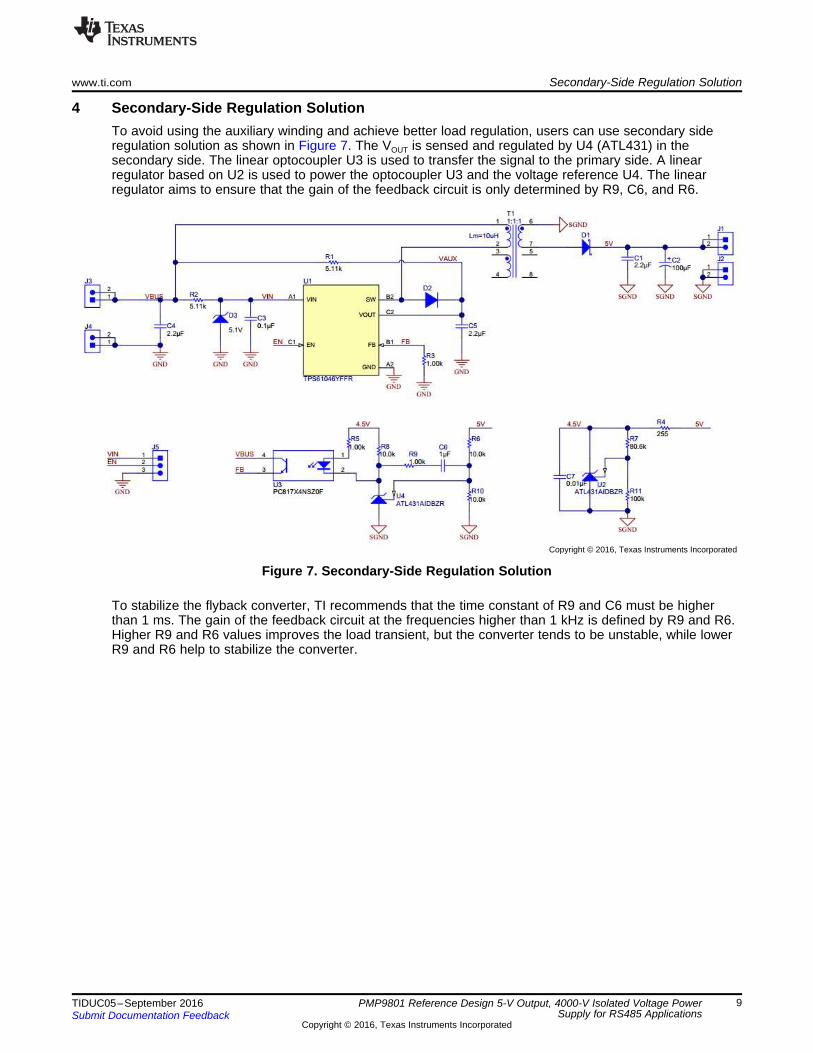
4 Secondary-Side Regulation SolutionTo avoid using the auxiliary winding and achieve better load regulation, users can use secondary sideregulation solution as shown in Figure 7. The VOUT is sensed and regulated by U4 (ATL431) in thesecondary side. The linear optocoupler U3 is used to transfer the signal to the primary side. A linearregulator based on U2 is used to power the optocoupler U3 and the voltage reference U4. The linearregulator aims to ensure that the gain of the feedback circuit is only determined by R9, C6, and R6.
Figure 7. Secondary-Side Regulation Solution
To stabilize the flyback converter, TI recommends that the time constant of R9 and C6 must be higherthan 1 ms. The gain of the feedback circuit at the frequencies higher than 1 kHz is defined by R9 and R6.Higher R9 and R6 values improves the load transient, but the converter tends to be unstable, while lowerR9 and R6 help to stabilize the converter.

IOUT (mA)
Effi
cien
cy (
%)
0 50 100 150 200 25030
40
50
60
70
80
D010
VBUS = 5VVBUS = 10VVBUS = 20V
IOUT (mA)
VO
UT
(V
)
0 50 100 150 200 2504.98
4.985
4.99
4.995
5
D009
VBUS = 5VVBUS = 10VVBUS = 20V
Secondary-Side Regulation Solution www.ti.com
10 TIDUC05–September 2016Submit Documentation Feedback
Copyright © 2016, Texas Instruments Incorporated
PMP9801 Reference Design 5-V Output, 4000-V Isolated Voltage PowerSupply for RS485 Applications
Figure 8 shows the load regulation. With the secondary-side regulation solution, VOUT is almost unchangedfrom no load to full load.
Figure 8. Load Regulation of Secondary-Side Regulation Solution
Figure 9 shows the efficiency of Figure 7.
Figure 9. Efficiency of Secondary-Side Regulation Solution

V (AC)
50 mV / divOUT
EN1 V / div
V
2 V / divOUT
www.ti.com Secondary-Side Regulation Solution
11TIDUC05–September 2016Submit Documentation Feedback
Copyright © 2016, Texas Instruments Incorporated
PMP9801 Reference Design 5-V Output, 4000-V Isolated Voltage PowerSupply for RS485 Applications
Figure 10 shows the start-up waveform of the secondary-side regulation solution at IOUT= 10 mA andVBUS= 10 V.
Figure 10. Start-Up Waveform of Secondary-Side Regulation Solution
Figure 11 shows the output voltage ripple of the secondary-side regulation solution at IOUT = 10 mA andVBUS = 10 V.
Figure 11. VOUT Ripple of Secondary-Side Regulation Solution

(a) 0 mA to 250 mA
(b) 250 mA to 0 mA
V (5 V Offset)
200 mV / divOUT
I
100 mA / divOUT
V (5 V Offset)
200 mV / divOUT
I
100 mA / divOUT
Secondary-Side Regulation Solution www.ti.com
12 TIDUC05–September 2016Submit Documentation Feedback
Copyright © 2016, Texas Instruments Incorporated
PMP9801 Reference Design 5-V Output, 4000-V Isolated Voltage PowerSupply for RS485 Applications
Figure 12 shows the 0-mA to 250-mA load transient waveform (a) and the 250-mA to 0-mA load transientwaveform (b) at VBUS = 10 V.
Figure 12. Load Transient of Secondary-Side Regulation Solution

www.ti.com Design Files
13TIDUC05–September 2016Submit Documentation Feedback
Copyright © 2016, Texas Instruments Incorporated
PMP9801 Reference Design 5-V Output, 4000-V Isolated Voltage PowerSupply for RS485 Applications
5 Design Files
5.1 SchematicsTo download the schematics, see the design files at http://www.ti.com/tool/PMP9801
5.2 Bill of MaterialsTo download the bill of materials (BOM), see the design files at http://www.ti.com/tool/PMP9801.
5.3 PCB Layout RecommendationsTo download the PCB Layout Recommendations, see the design files at http://www.ti.com/tool/PMP9801
5.4 Altium ProjectTo download the Altium Project, see the design files at http://www.ti.com/tool/PMP9801
5.5 Gerber FilesTo download the Gerber files, see the design files at http://www.ti.com/tool/PMP9801
6 Reference1. Texas Instruments, Low Cost 1W Isolated Power Supply Solution with TPS61085, Application Report
(SLVA496).

About the Author www.ti.com
14 TIDUC05–September 2016Submit Documentation Feedback
Copyright © 2016, Texas Instruments Incorporated
PMP9801 Reference Design 5-V Output, 4000-V Isolated Voltage PowerSupply for RS485 Applications
7 About the AuthorJASPER LI is a Power Application Engineer for the Texas Instruments Boost Converter Solution Group. Inthis role, he supports worldwide customers, writes application notes, and develops reference designs.Since 2013 his focus has been on ultra-low-power applications. Jasper received his master's degree inPower Electronics in 2013 at Zhejiang University in China.

IMPORTANT NOTICE AND DISCLAIMERTI PROVIDES TECHNICAL AND RELIABILITY DATA (INCLUDING DATASHEETS), DESIGN RESOURCES (INCLUDING REFERENCEDESIGNS), APPLICATION OR OTHER DESIGN ADVICE, WEB TOOLS, SAFETY INFORMATION, AND OTHER RESOURCES “AS IS”AND WITH ALL FAULTS, AND DISCLAIMS ALL WARRANTIES, EXPRESS AND IMPLIED, INCLUDING WITHOUT LIMITATION ANYIMPLIED WARRANTIES OF MERCHANTABILITY, FITNESS FOR A PARTICULAR PURPOSE OR NON-INFRINGEMENT OF THIRDPARTY INTELLECTUAL PROPERTY RIGHTS.These resources are intended for skilled developers designing with TI products. You are solely responsible for (1) selecting the appropriateTI products for your application, (2) designing, validating and testing your application, and (3) ensuring your application meets applicablestandards, and any other safety, security, or other requirements. These resources are subject to change without notice. TI grants youpermission to use these resources only for development of an application that uses the TI products described in the resource. Otherreproduction and display of these resources is prohibited. No license is granted to any other TI intellectual property right or to any third partyintellectual property right. TI disclaims responsibility for, and you will fully indemnify TI and its representatives against, any claims, damages,costs, losses, and liabilities arising out of your use of these resources.TI’s products are provided subject to TI’s Terms of Sale (https:www.ti.com/legal/termsofsale.html) or other applicable terms available eitheron ti.com or provided in conjunction with such TI products. TI’s provision of these resources does not expand or otherwise alter TI’sapplicable warranties or warranty disclaimers for TI products.IMPORTANT NOTICE
Mailing Address: Texas Instruments, Post Office Box 655303, Dallas, Texas 75265Copyright © 2021, Texas Instruments Incorporated